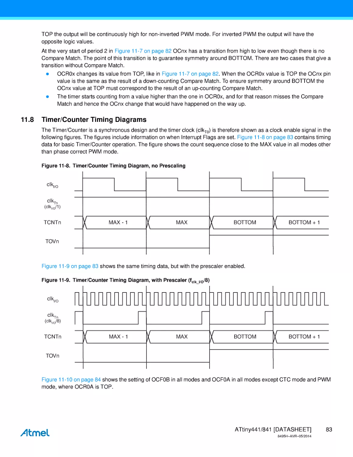
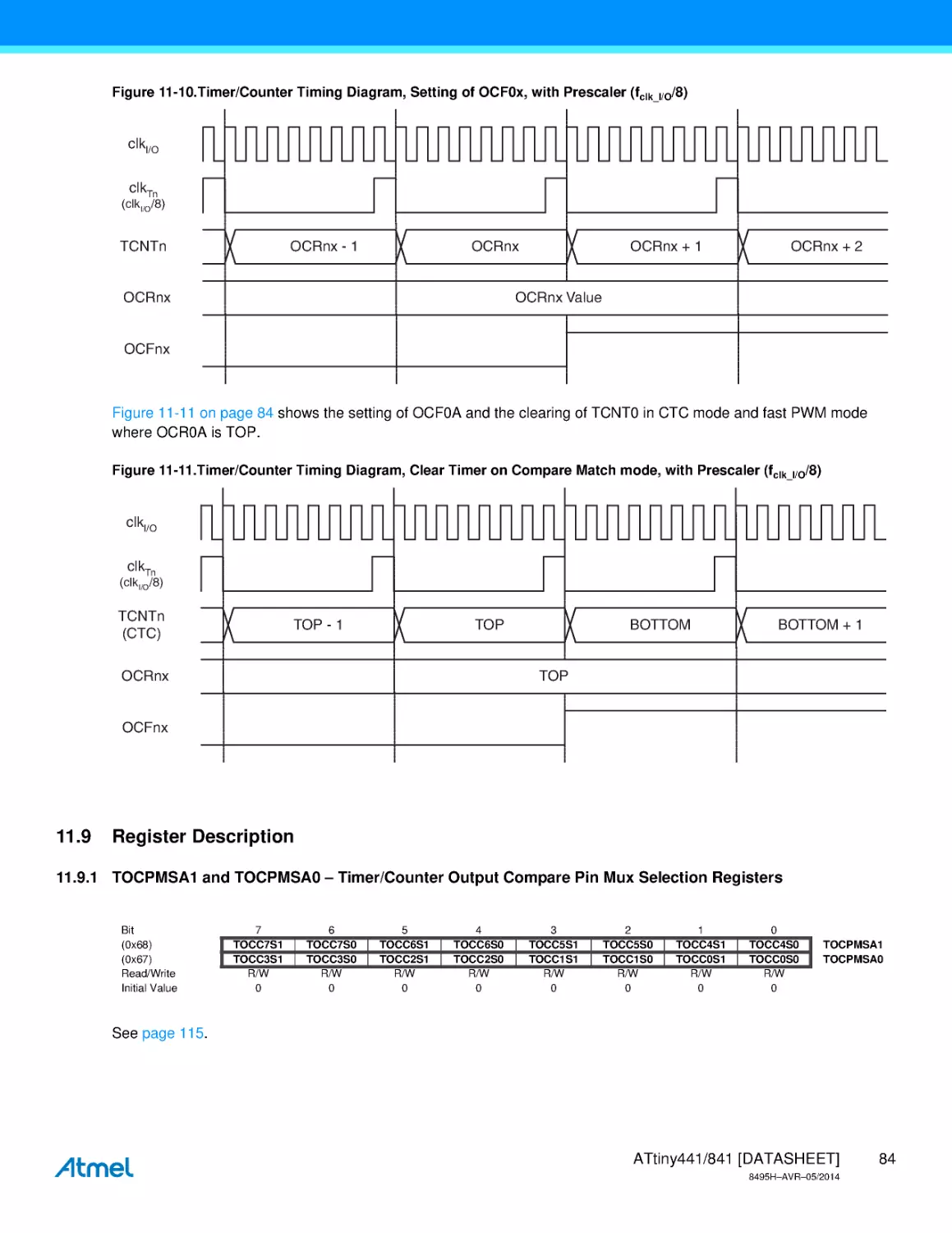
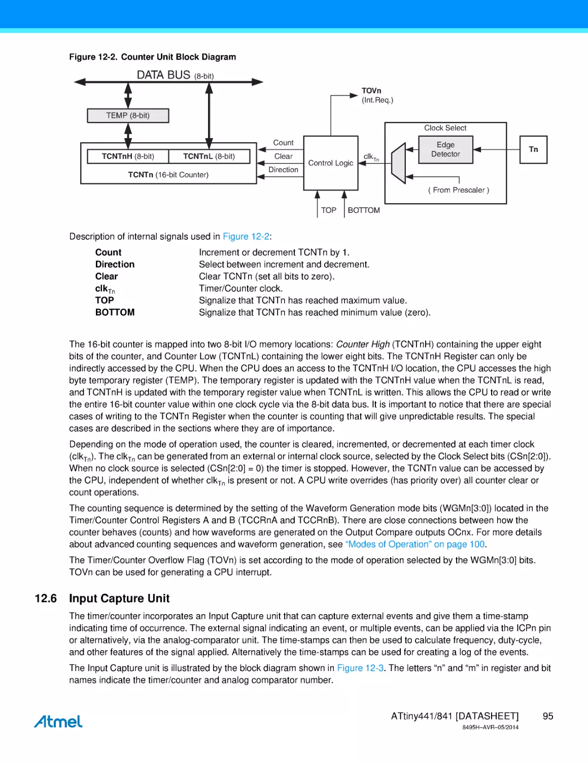
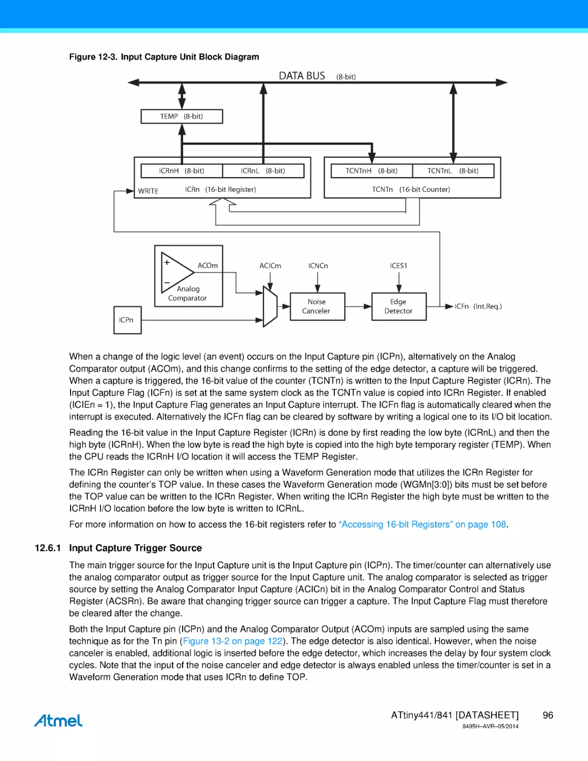
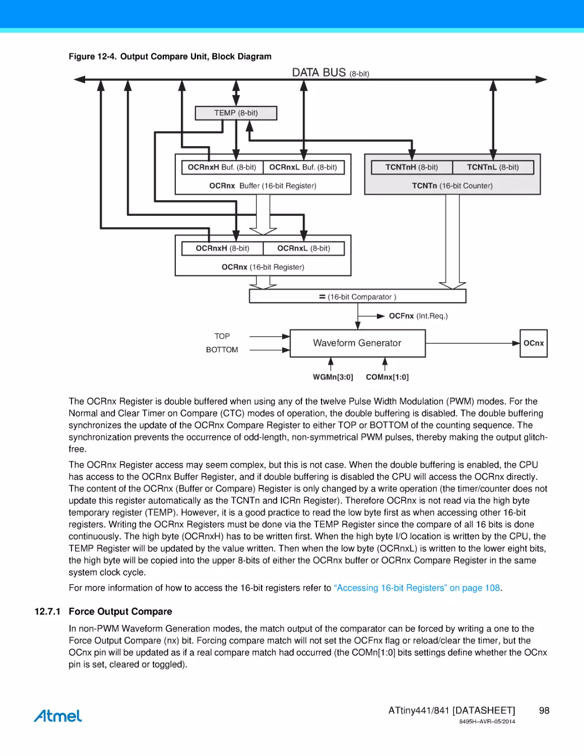
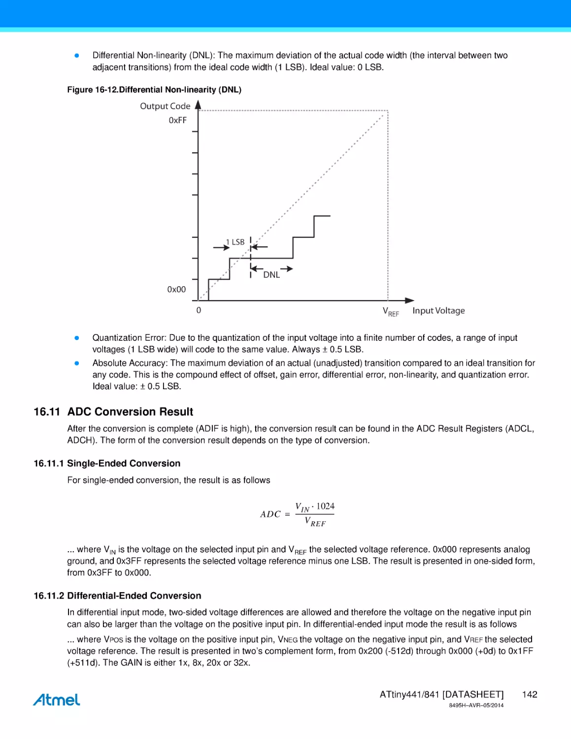
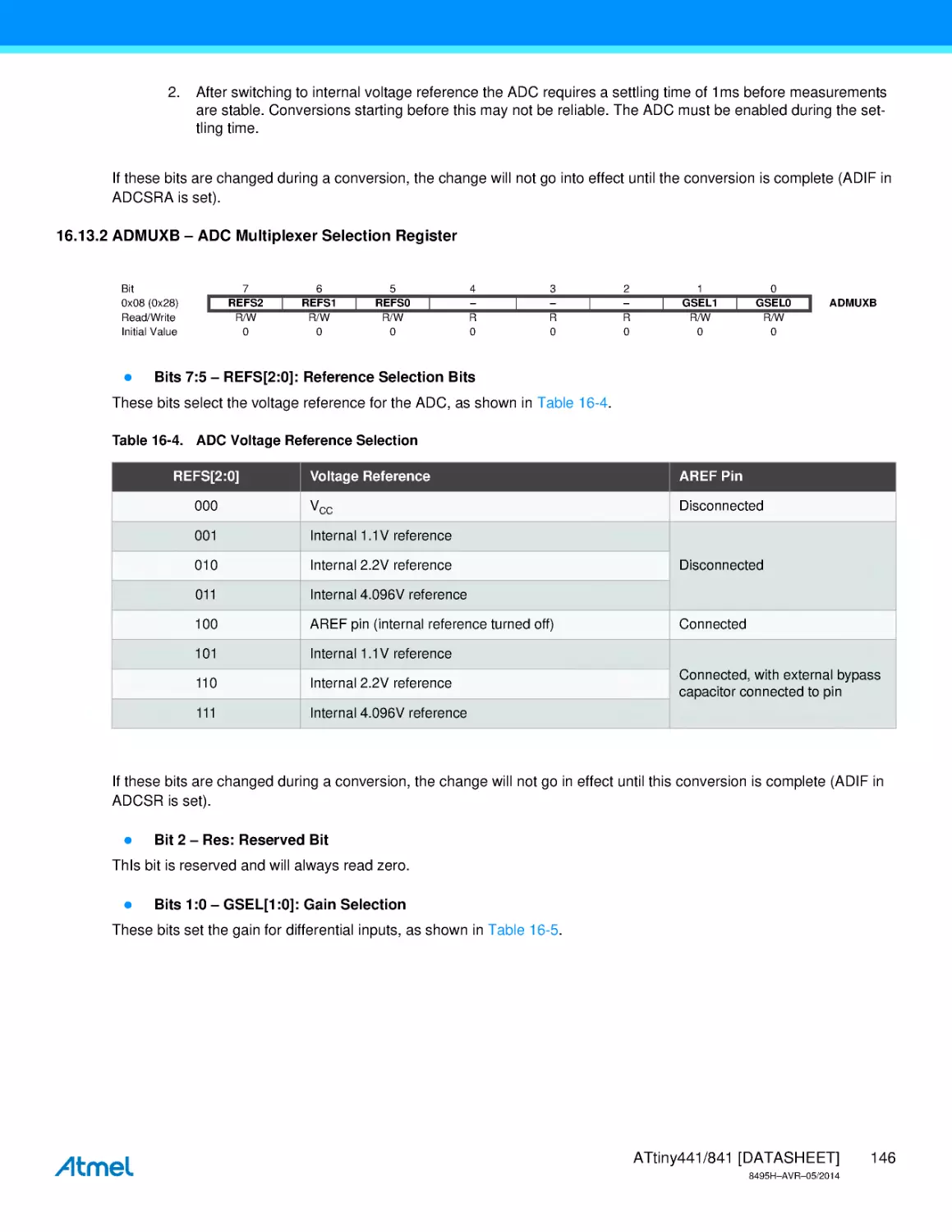
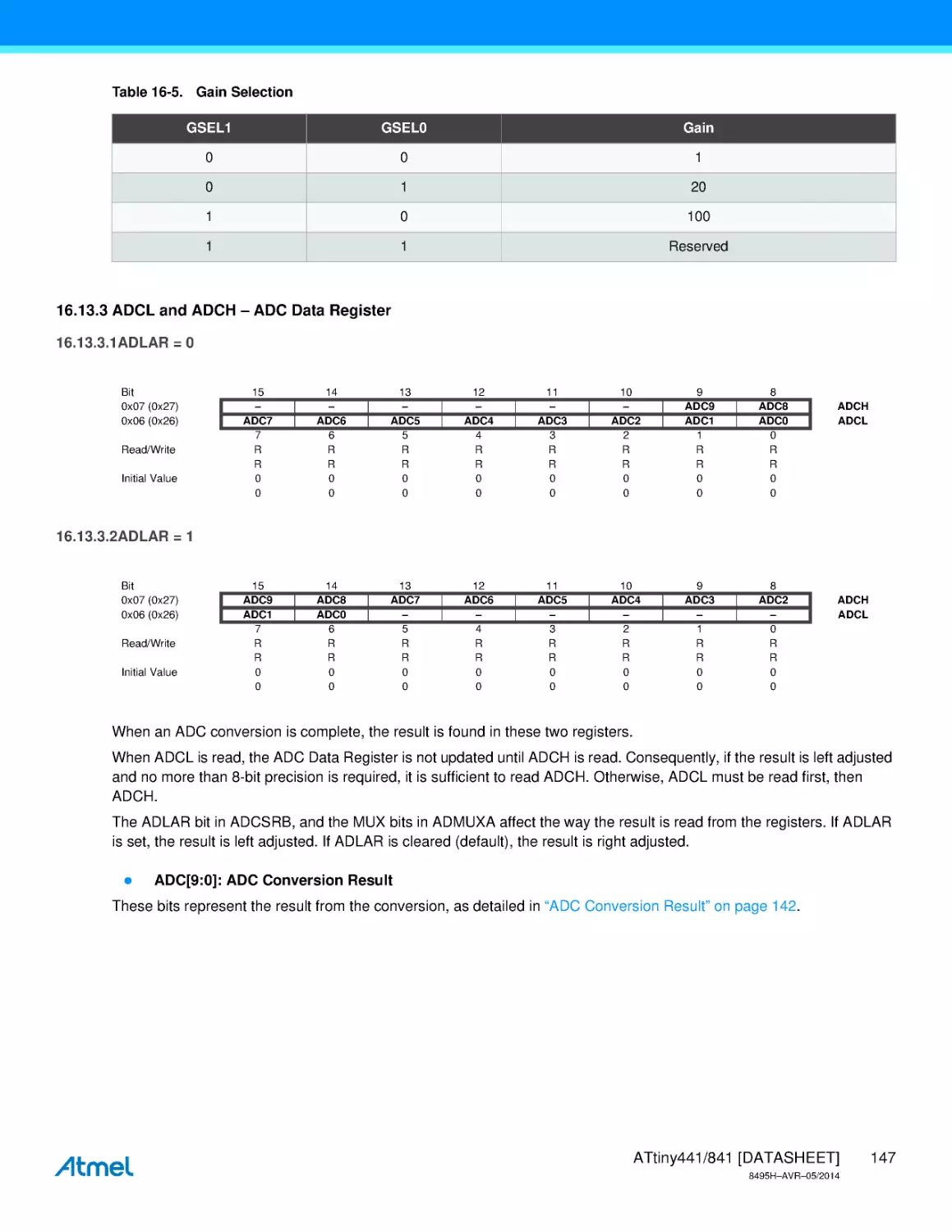
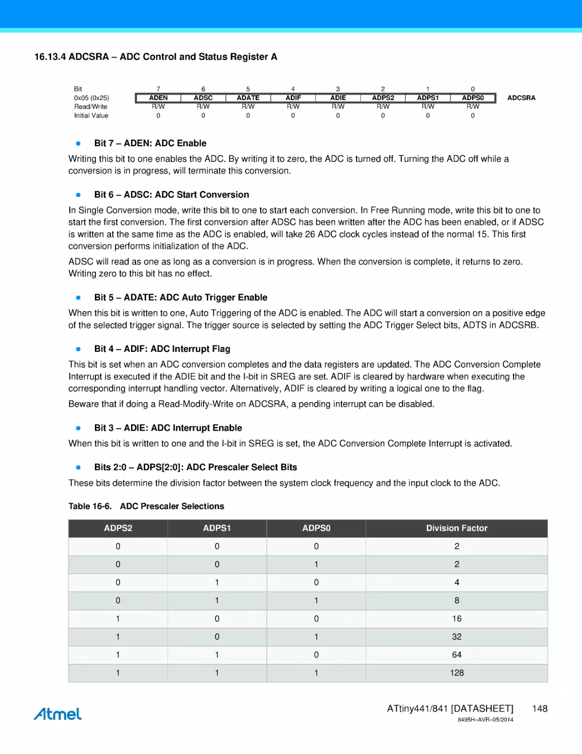
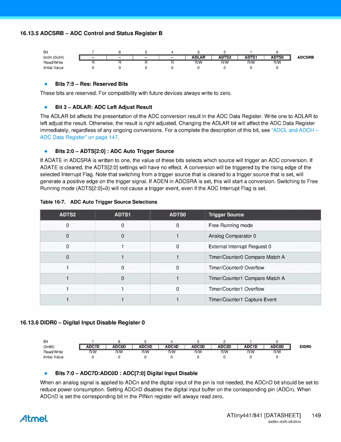
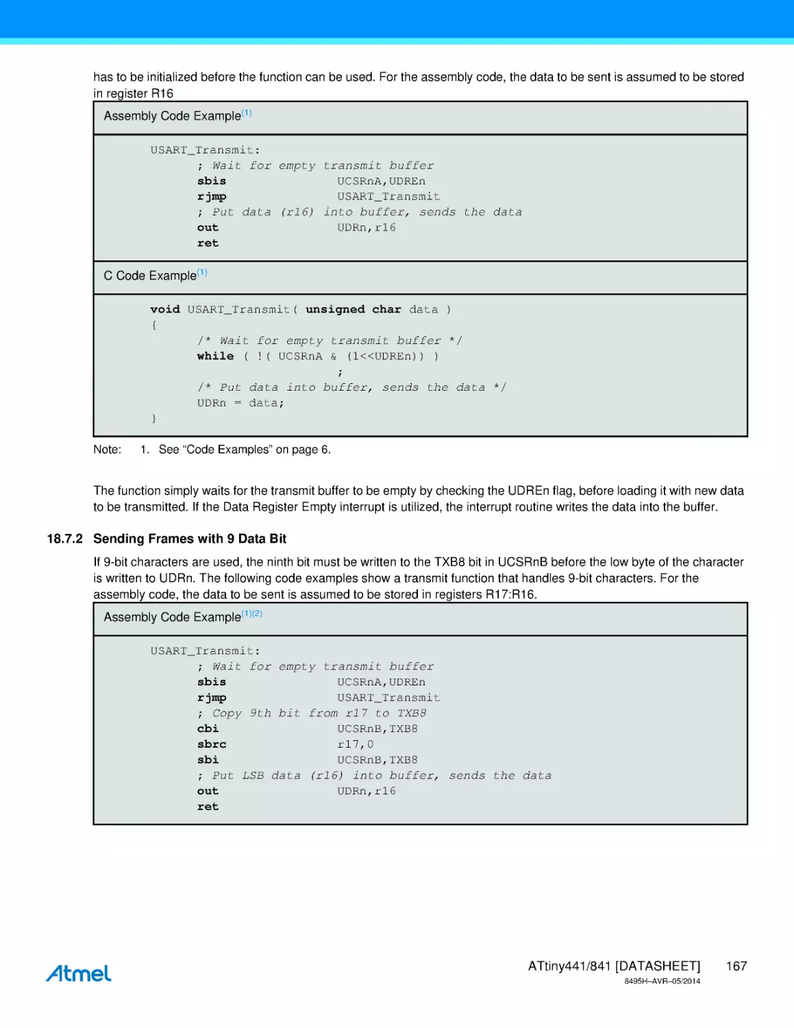
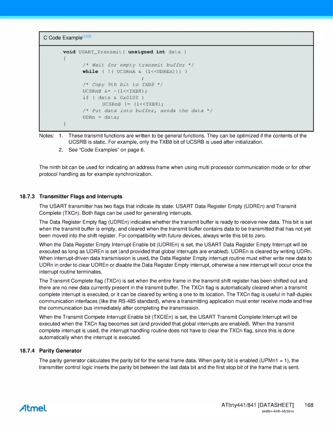
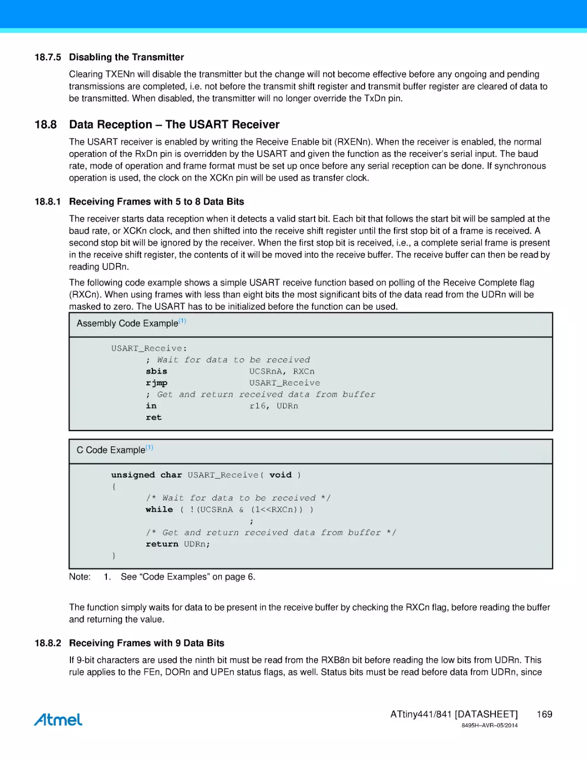
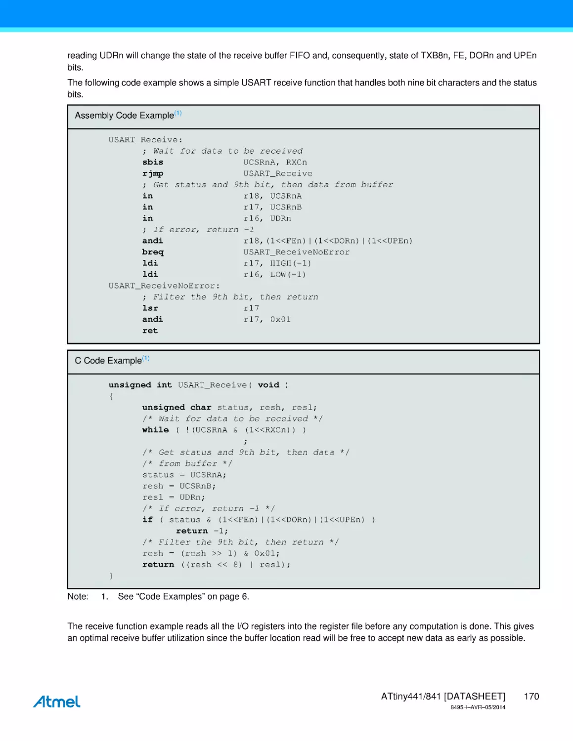
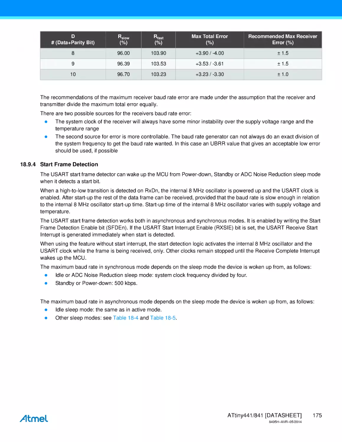
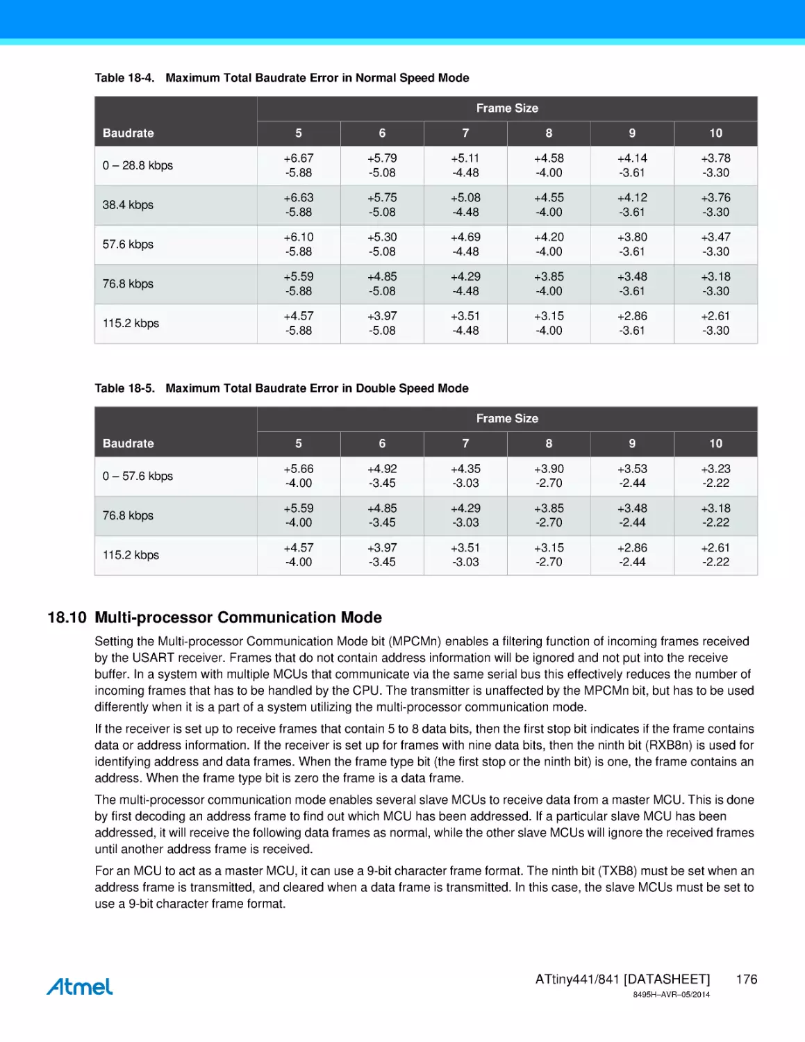
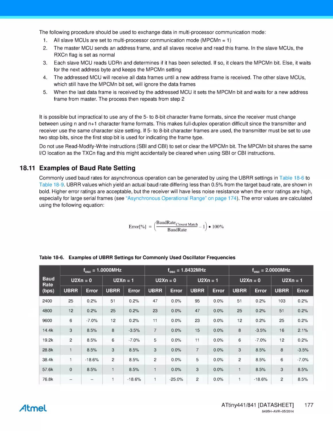
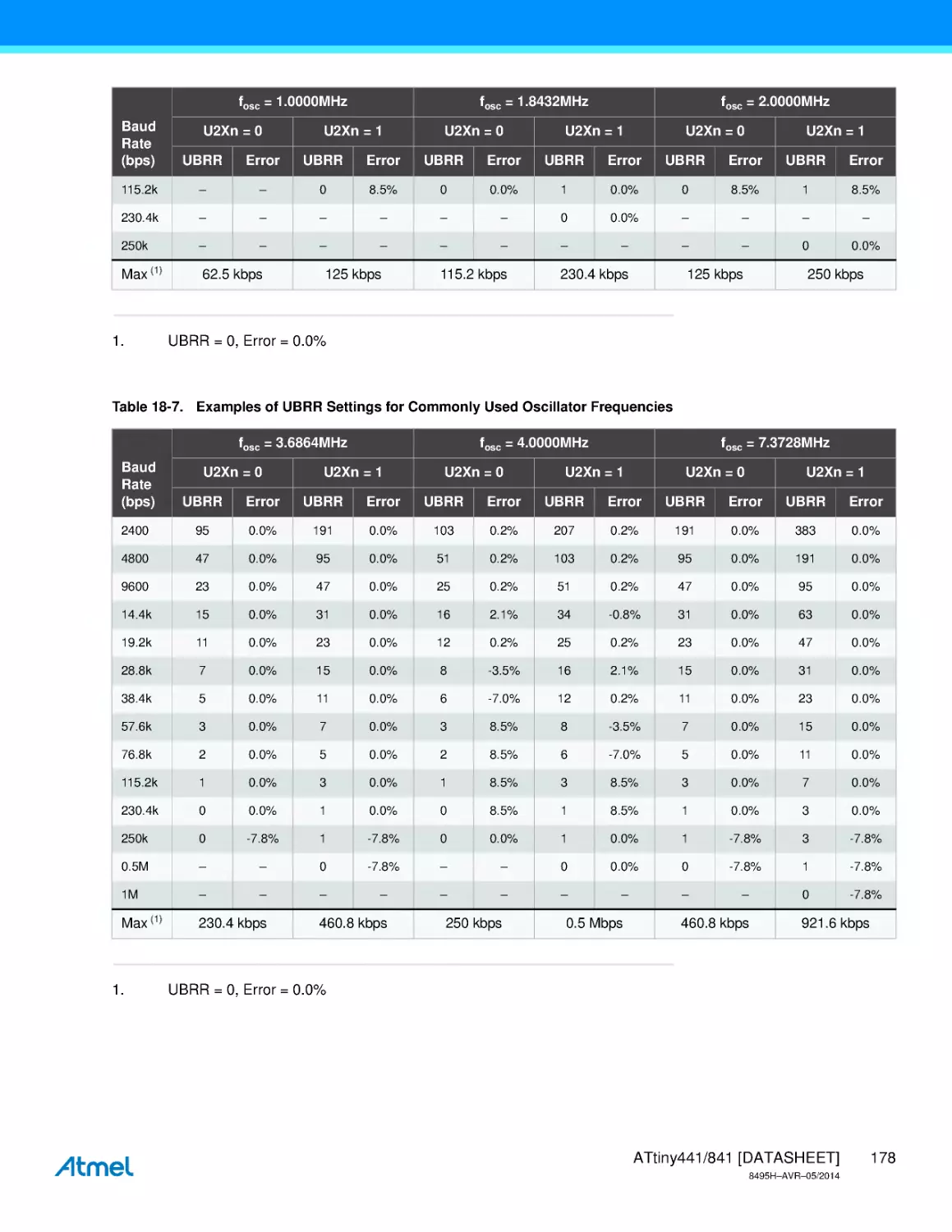
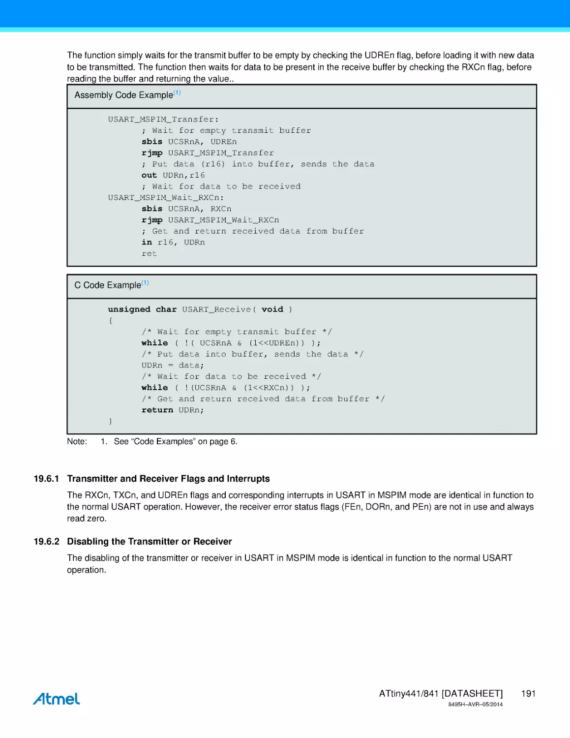
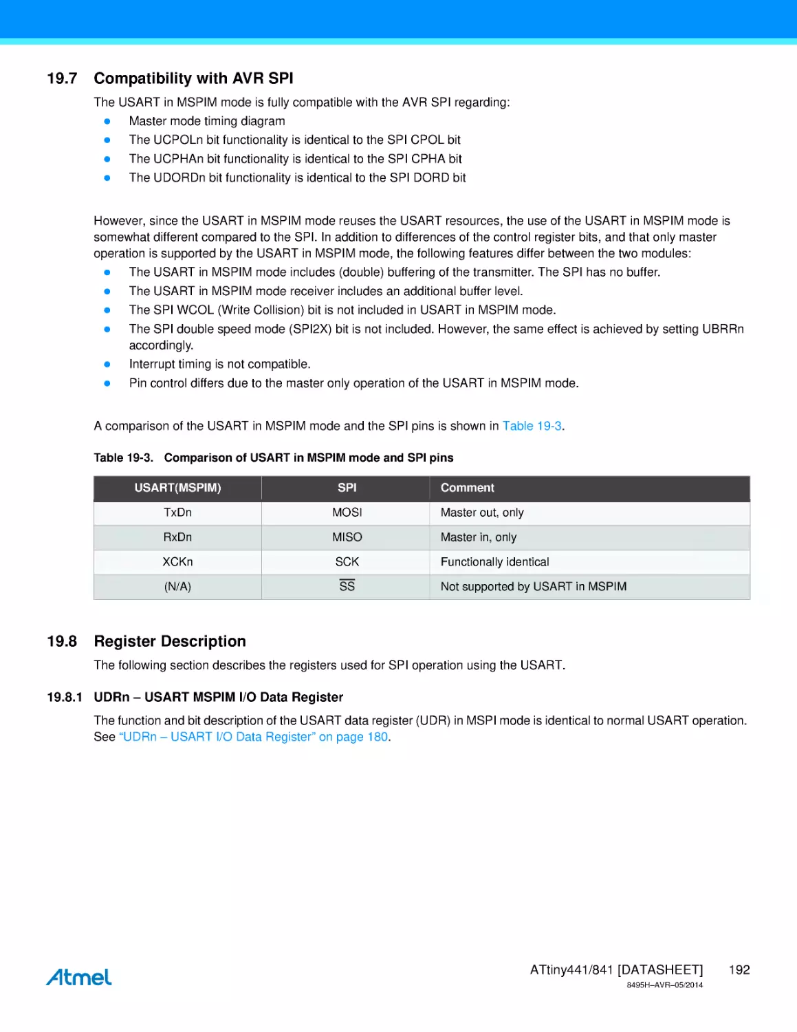
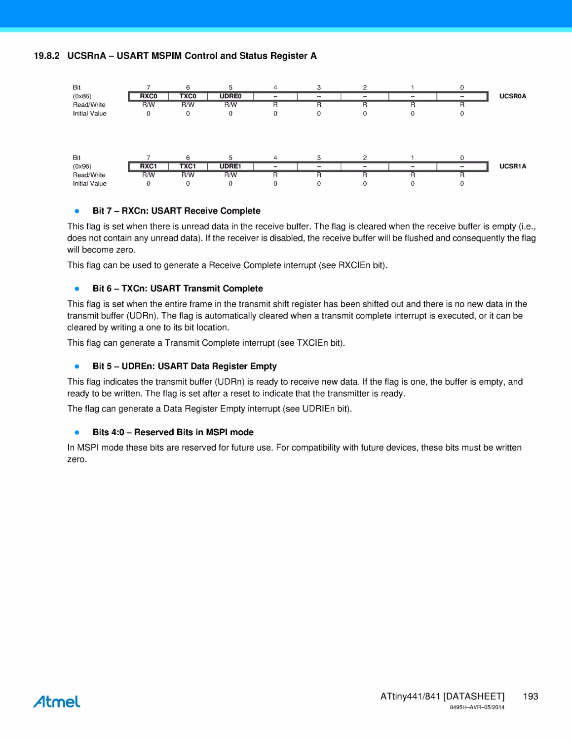
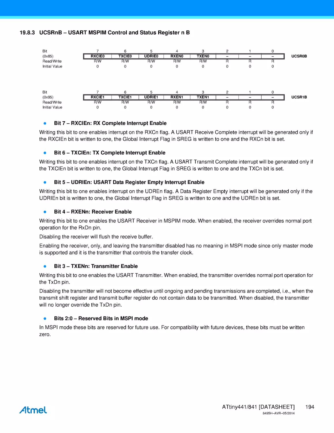
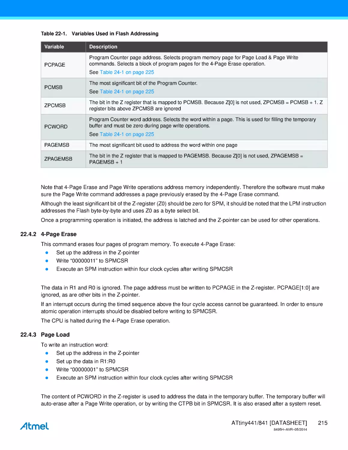
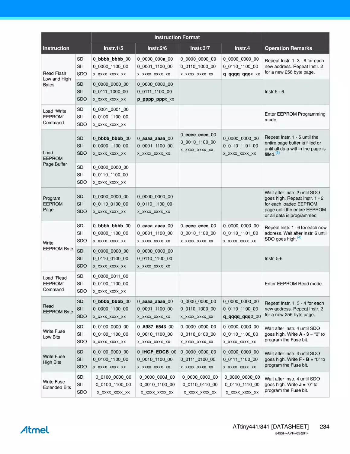
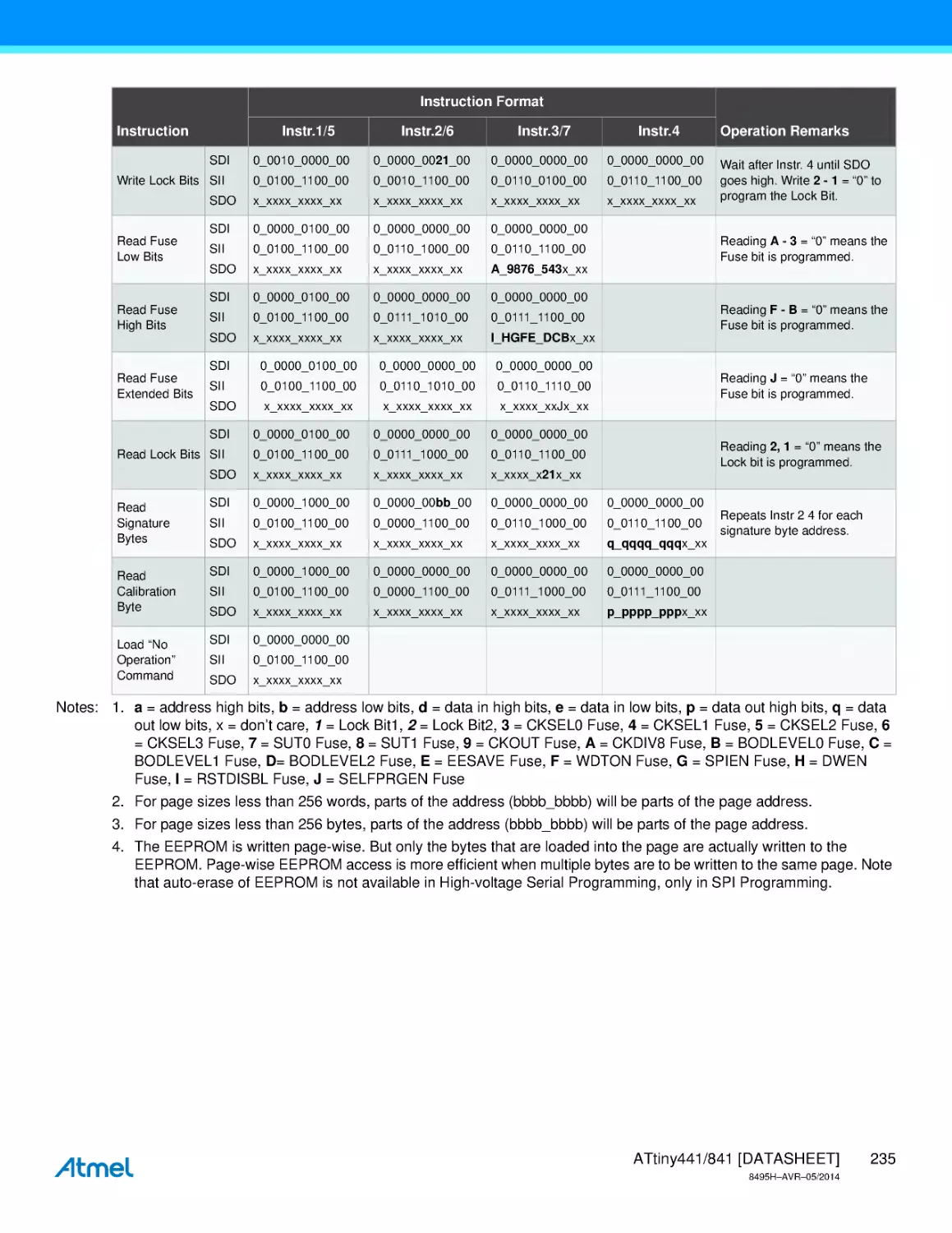
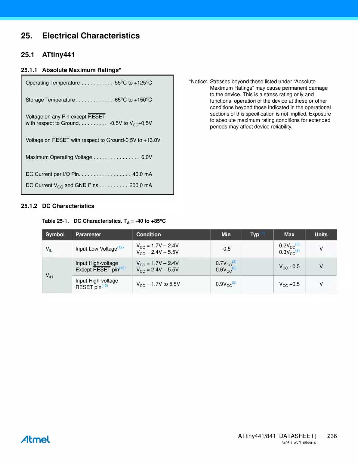
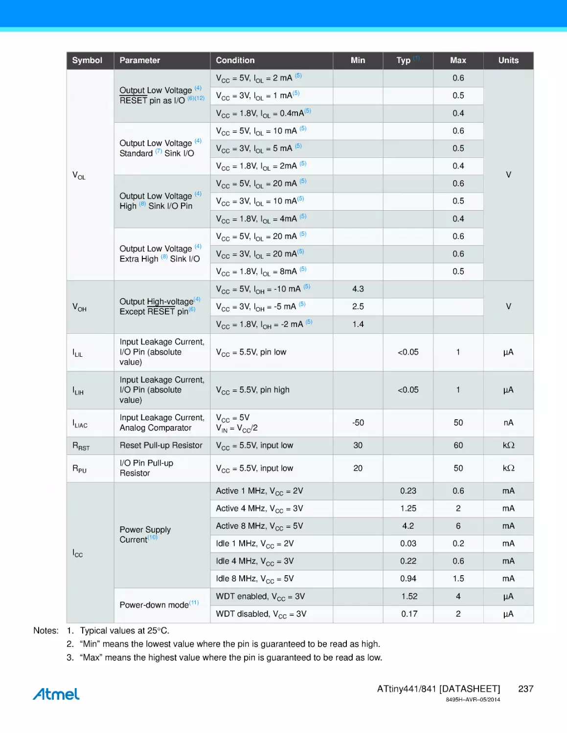
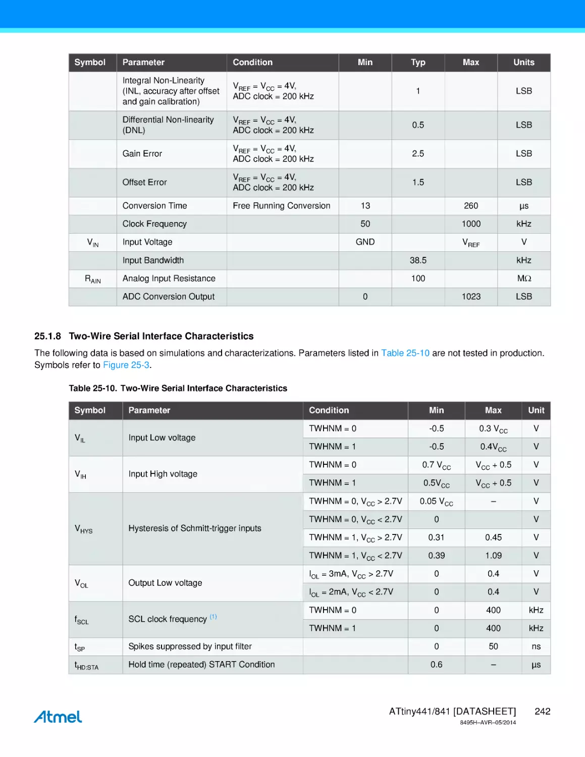
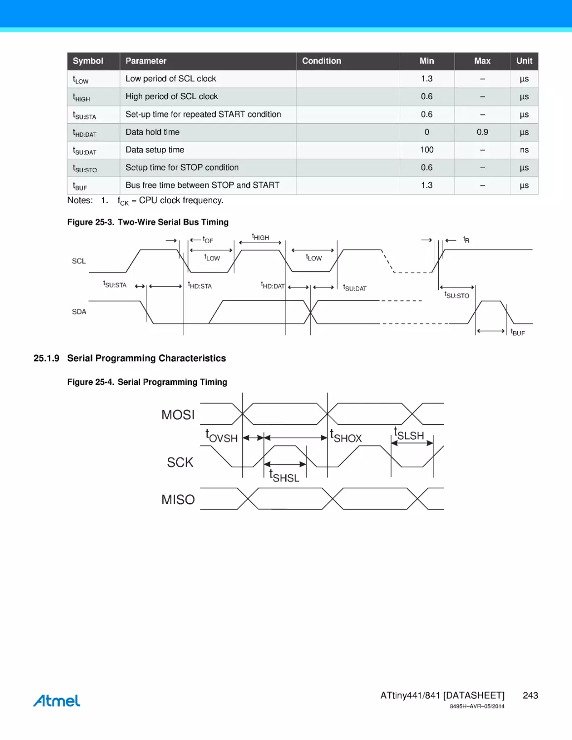
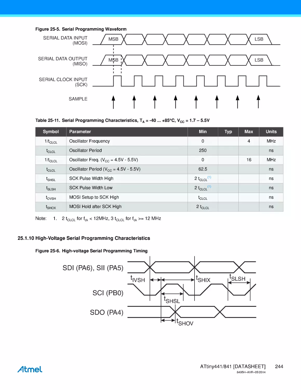
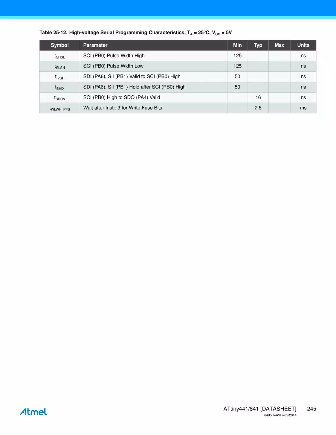
/


Текст
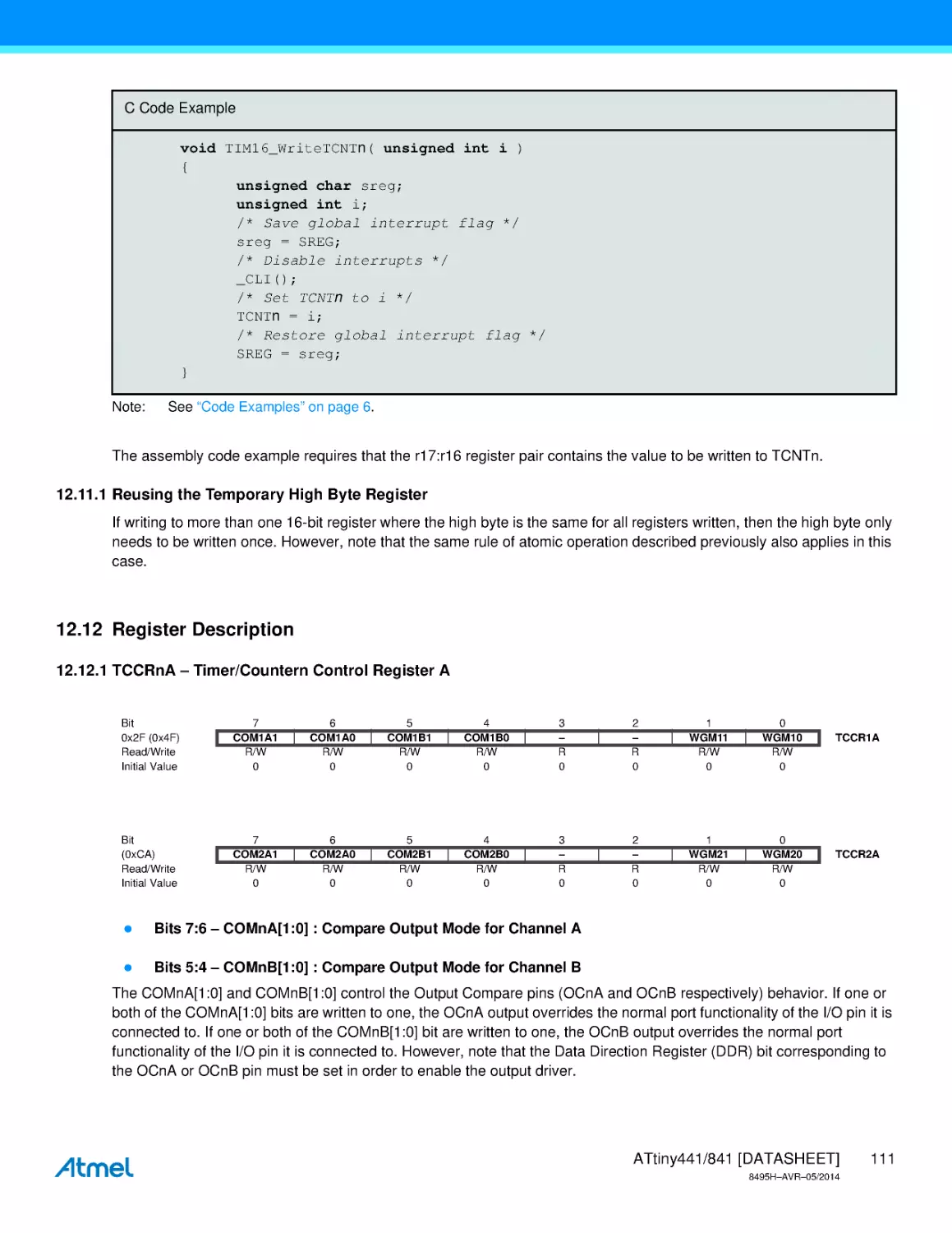
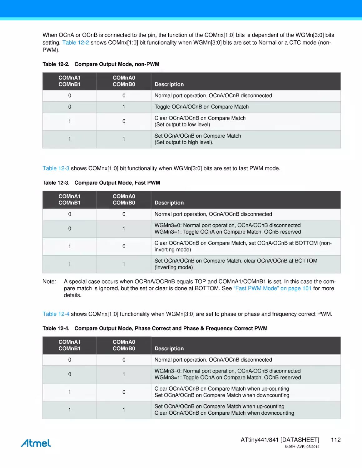
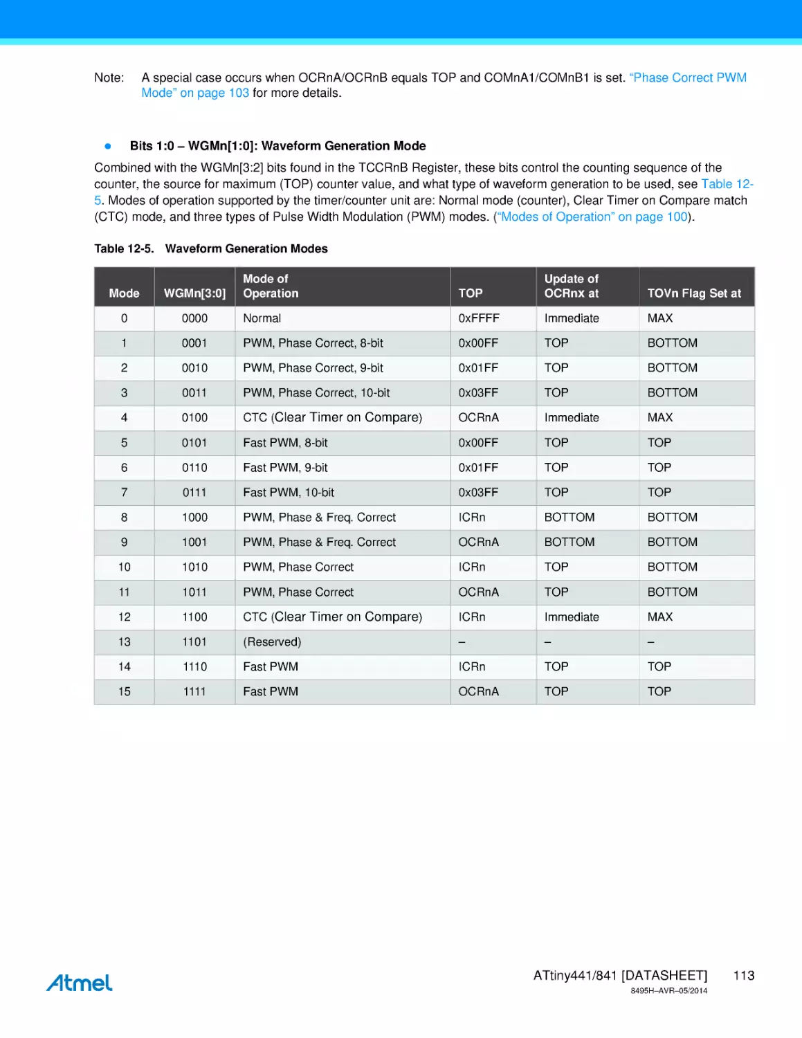
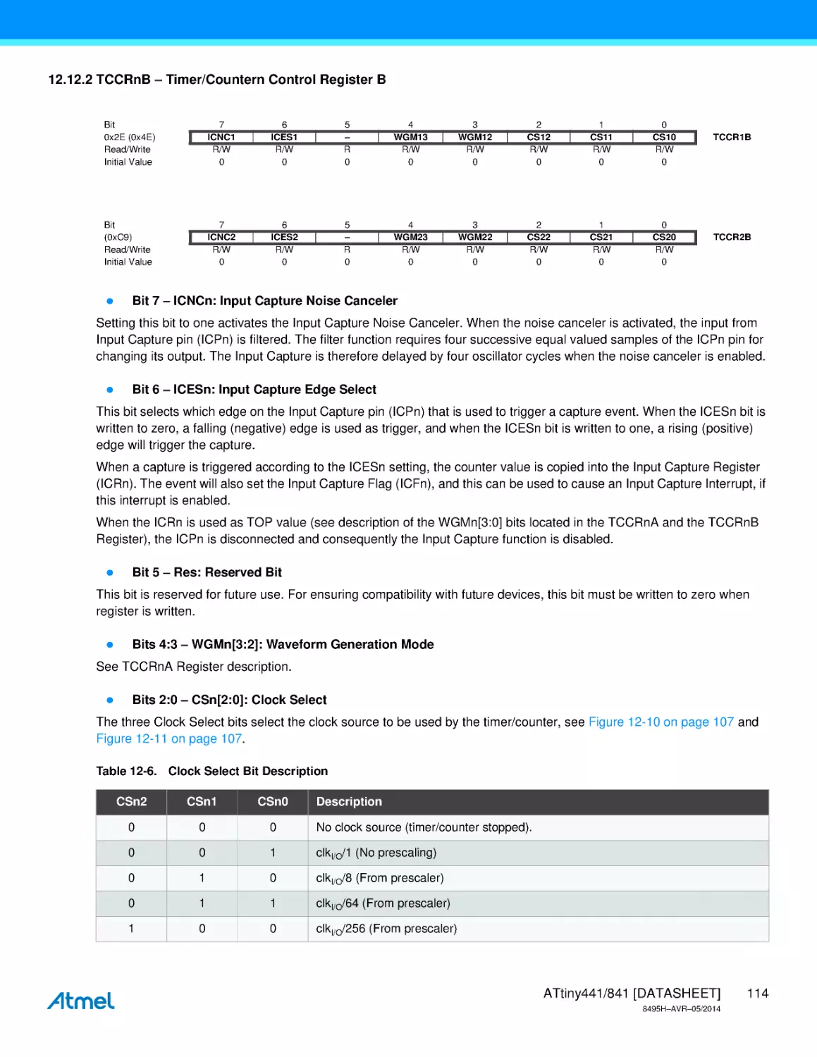
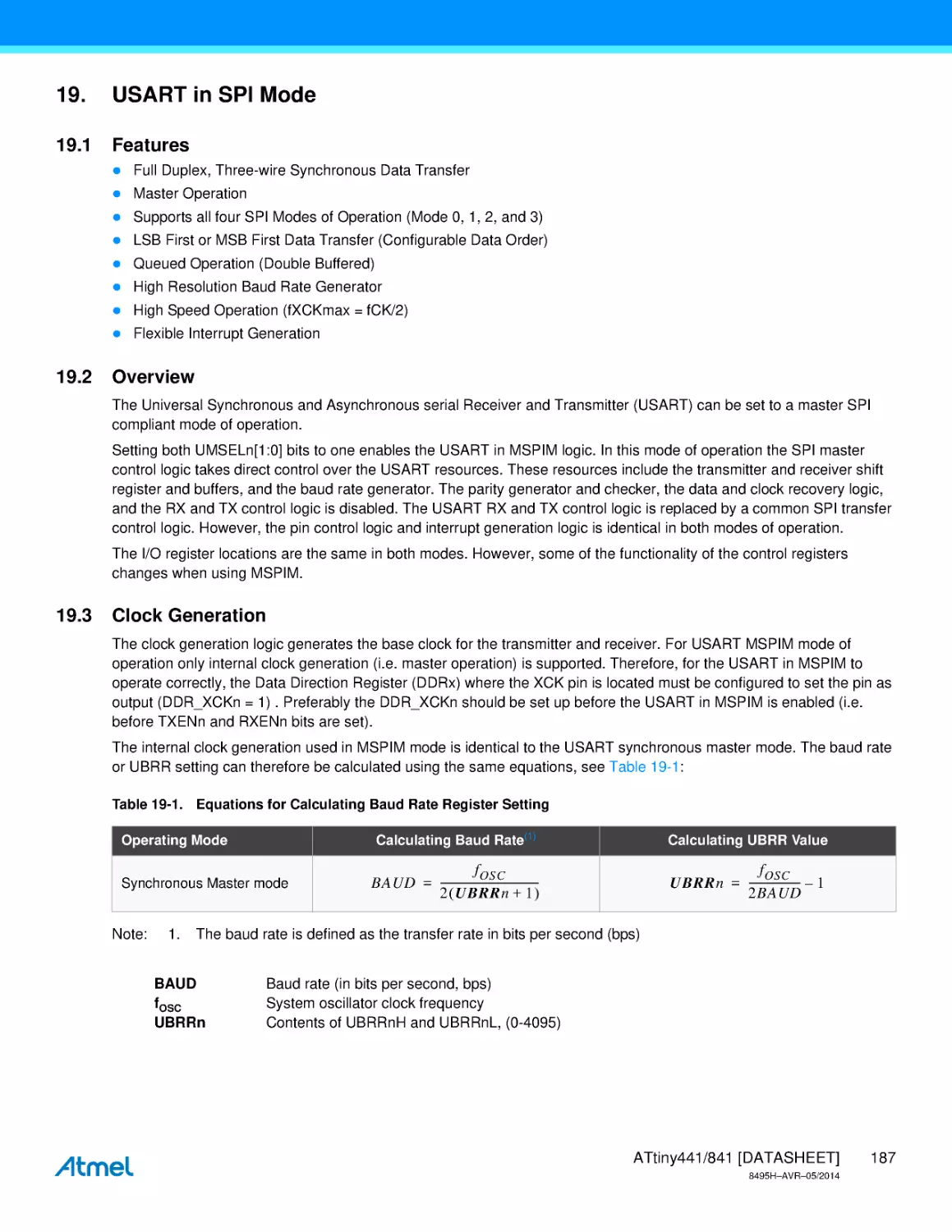
ATtiny441/ATtiny841
8-bit AVR Microcontroller with 4/8K Bytes In-System
Programmable Flash
DATASHEET
Features
High Performance, Low Power Atmel® AVR® 8-bit Microcontroller
Advanced RISC Architecture
120 Powerful Instructions – Most Single Clock Cycle Execution
32 x 8 General Purpose Working Registers
Fully Static Operation
Up to 16 MIPS Throughput at 16 MHz
Non-volatile Program and Data Memories
4/8K Bytes of In-System Programmable Flash Program Memory
Endurance: 10,000 Write/Erase Cycles
256/512 Bytes of In-System Programmable EEPROM
Endurance: 100,000 Write/Erase Cycles
256/512 Bytes Internal SRAM
Data Retention: 20 Years at 85oC / 100 Years at 25oC
Programming Lock for Self-Programming Flash & EEPROM Data Security
Peripheral Features
One 8-bit and Two 16-bit Timer/Counters with Two PWM Channels, Each
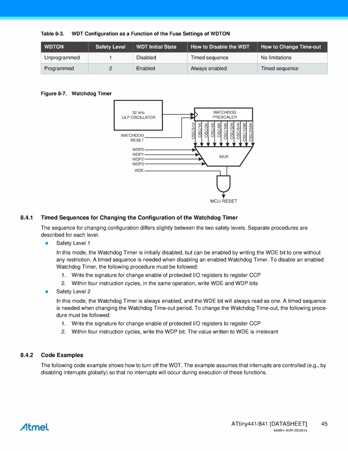
Programmable Ultra Low Power Watchdog Timer
10-bit Analog to Digital Converter
12 External and 5 Internal, Single-ended Input Channels
46 Differential ADC Channel Pairs with Programmable Gain (1x / 20x / 100x)
Two On-chip Analog Comparators
Two Full Duplex USARTs with Start Frame Detection
Master/Slave SPI Serial Interface
Slave I2C Serial Interface
Special Microcontroller Features
Low Power Idle, ADC Noise Reduction, Standby and Power-down Modes
Enhanced Power-on Reset Circuit
Programmable Brown-out Detection Circuit with Supply Voltage Sampling
External and Internal Interrupt Sources
Pin Change Interrupt on 12 Pins
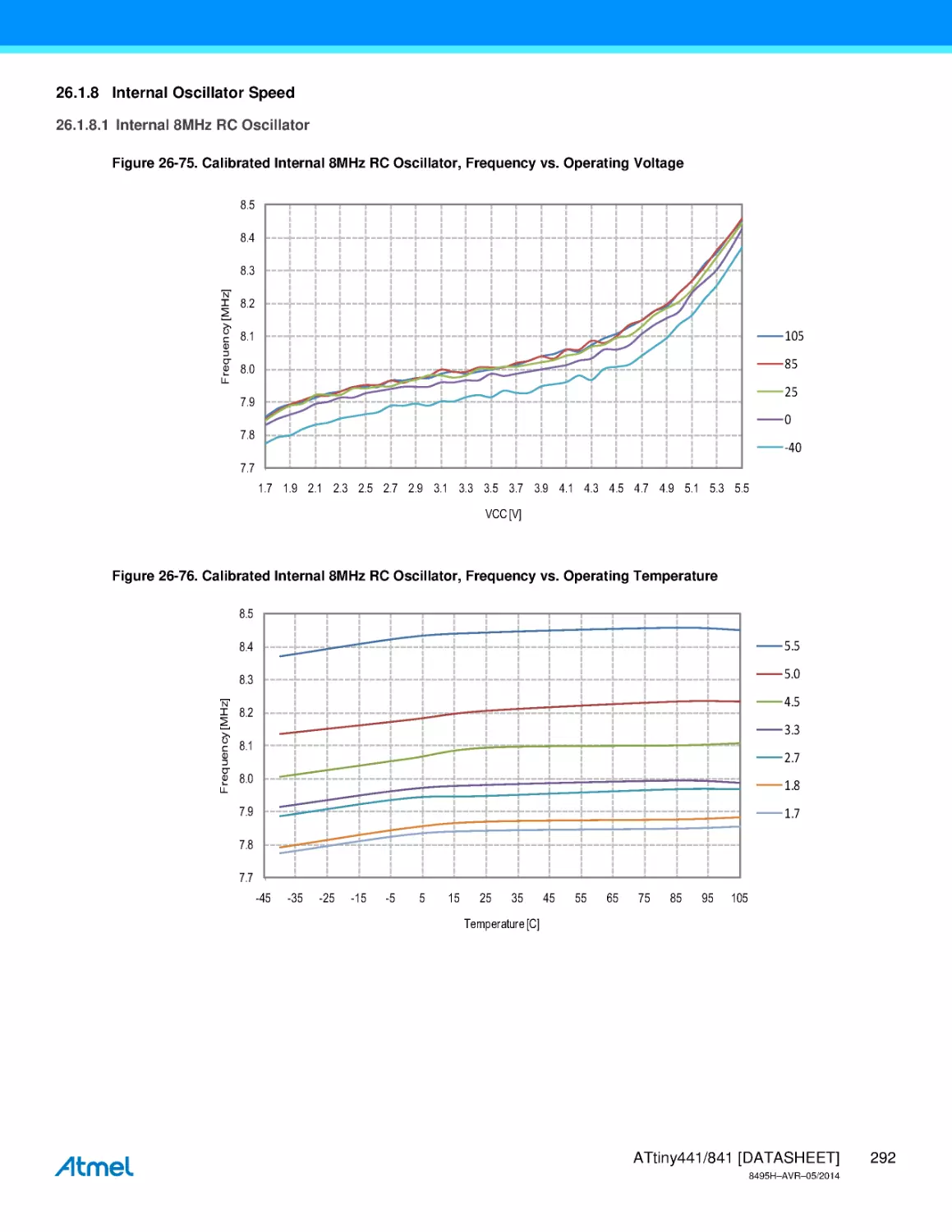
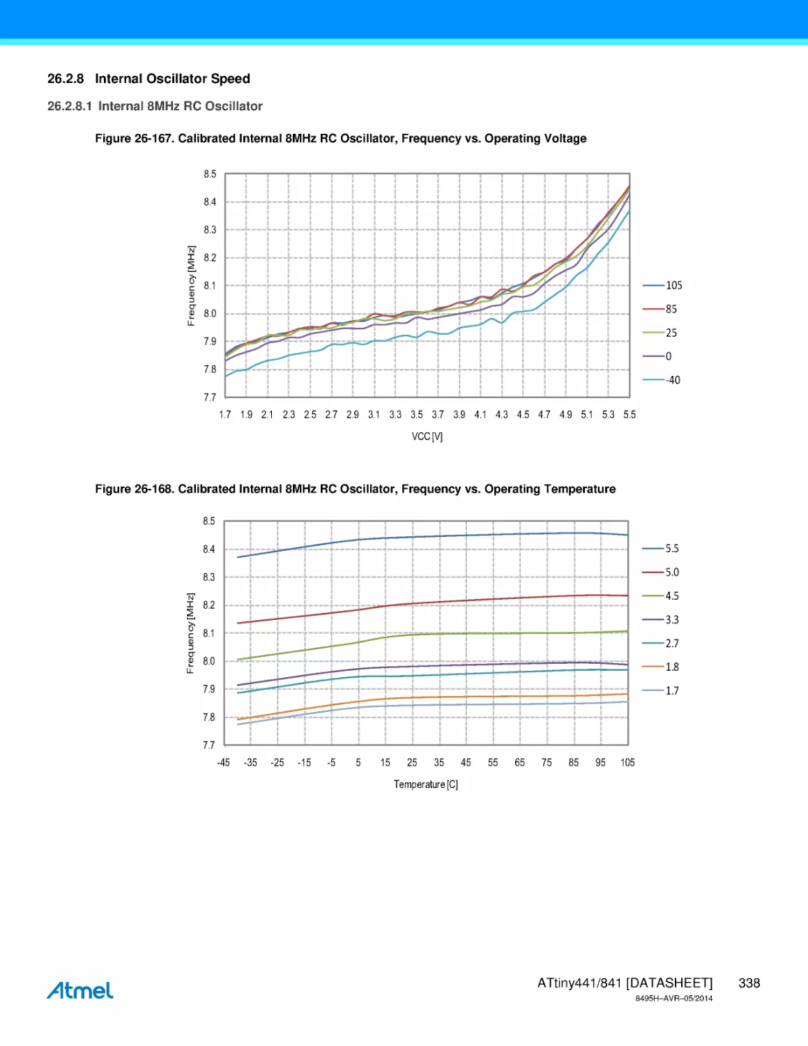
Calibrated 8MHz Oscillator with Temperature Calibration Option
Calibrated 32kHz Ultra Low Power Oscillator
High-Current Drive Capability on 2 I/O Pins
I/O and Packages
14-pin SOIC, 20-pad MLF/QFN and 20-pad VQFN
12 Programmable I/O Lines
Speed Grade
0 – 2 MHz @ 1.7 – 1.8V
0 – 4 MHz @ 1.8 – 5.5V
0 – 10 MHz @ 2.7 – 5.5V
0 – 16 MHz @ 4.5 – 5.5V
Low Power Consumption
Active Mode: 0.2 mA at 1.8V and 1MHz
Idle Mode: 30 µA at 1.8V and 1MHz
Power-Down Mode (WDT Enabled): 1.3µA at 1.8V
Power-Down Mode (WDT Disabled): 150nA at 1.8V
8495H–AVR–05/2014
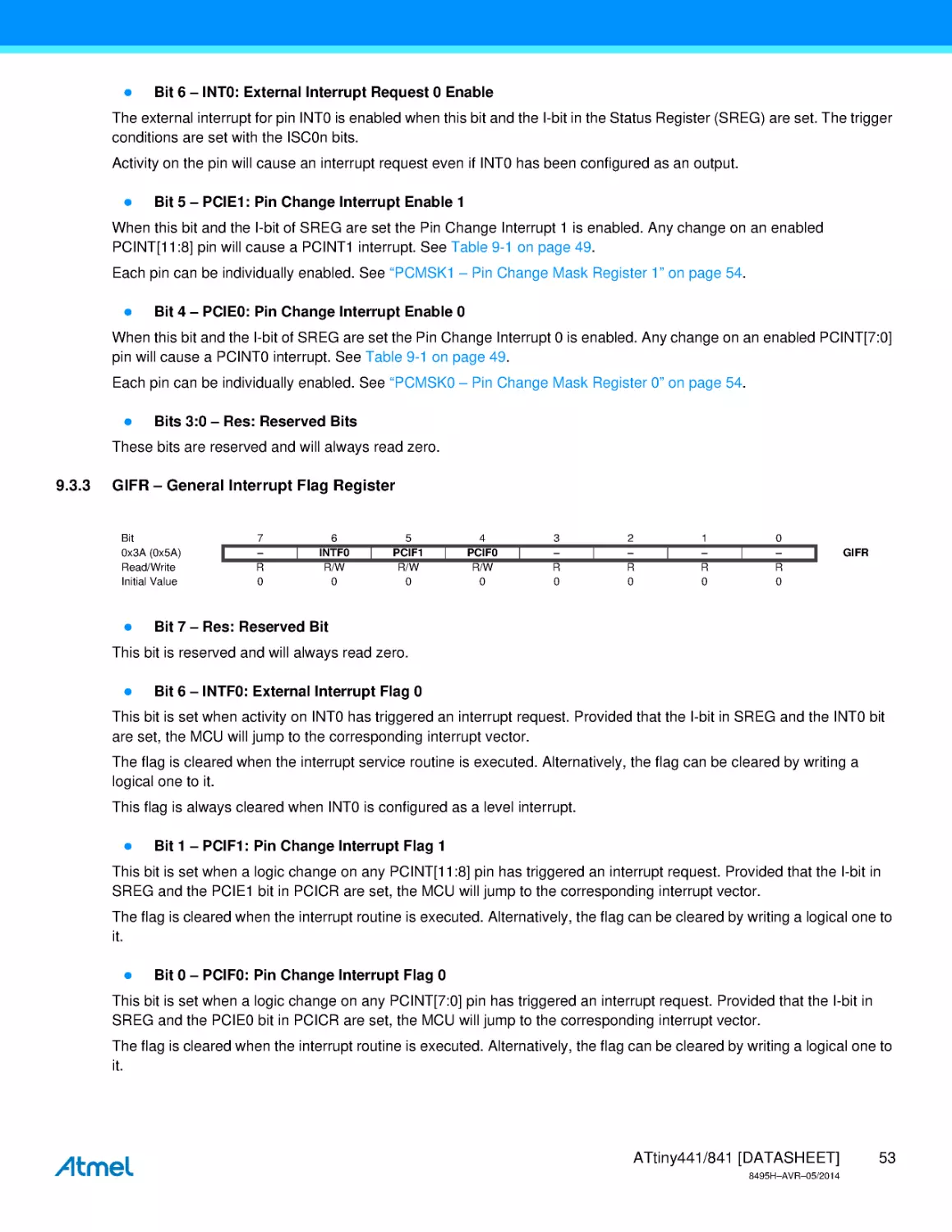
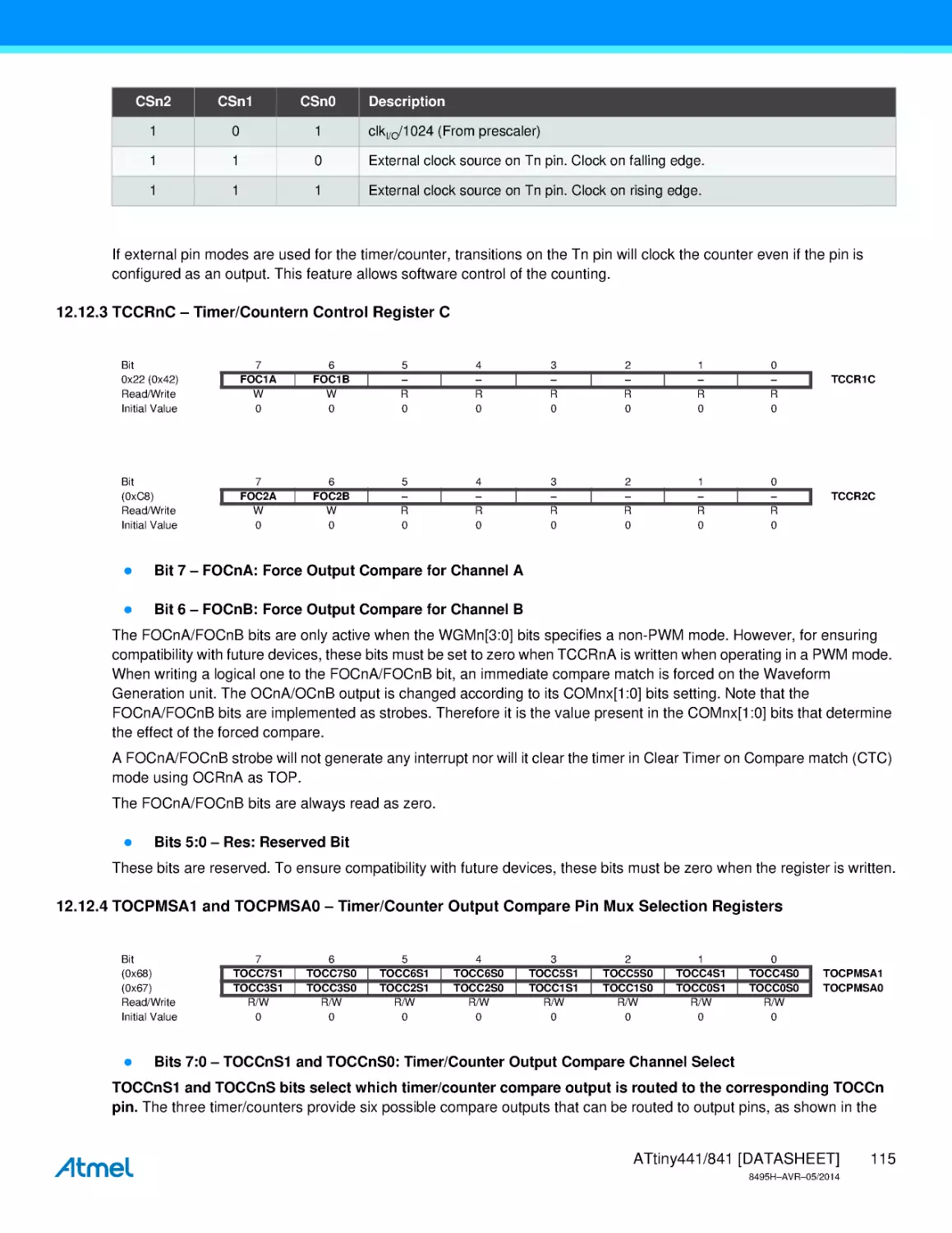
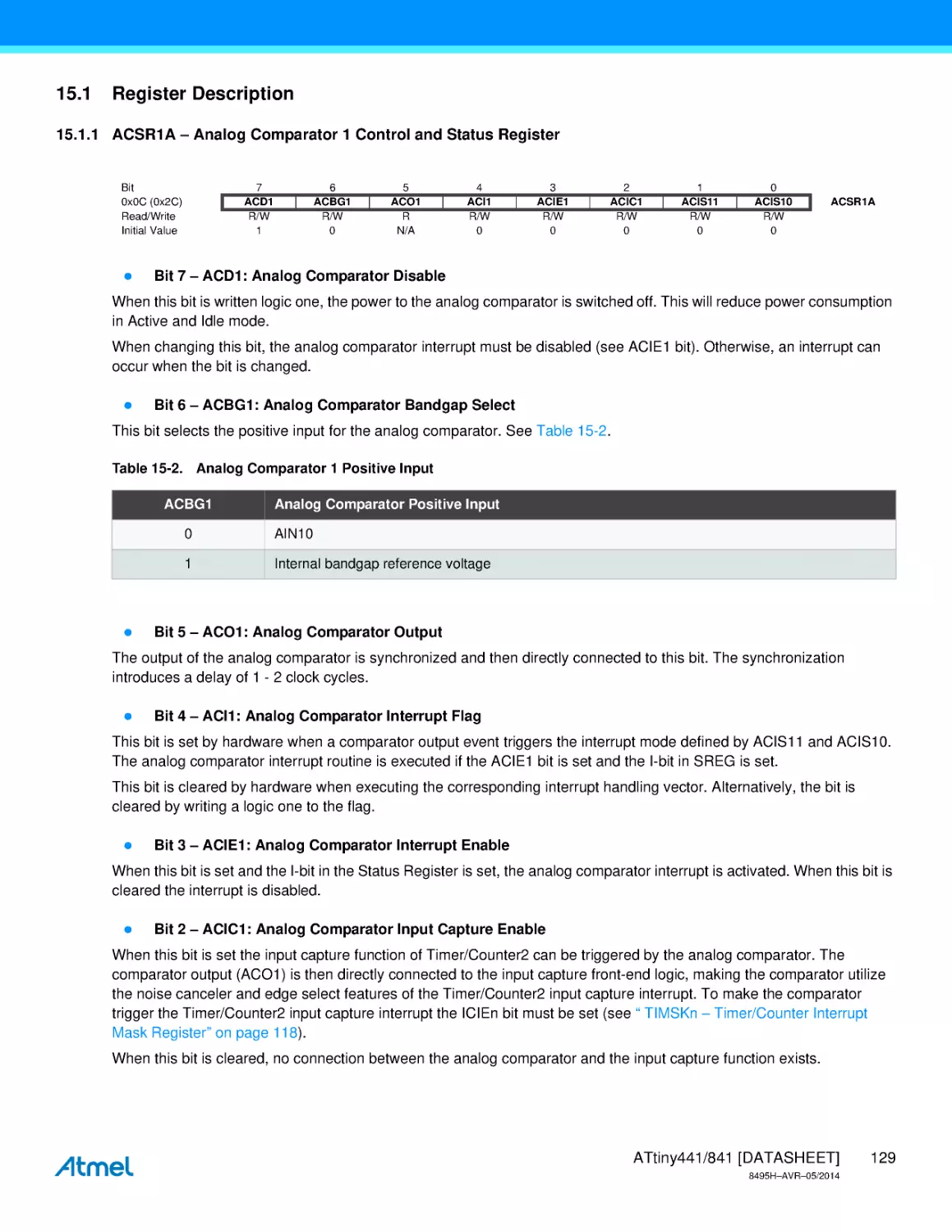
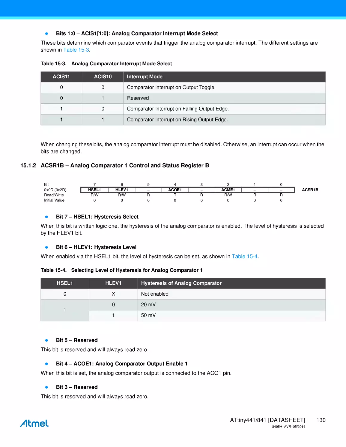
1.
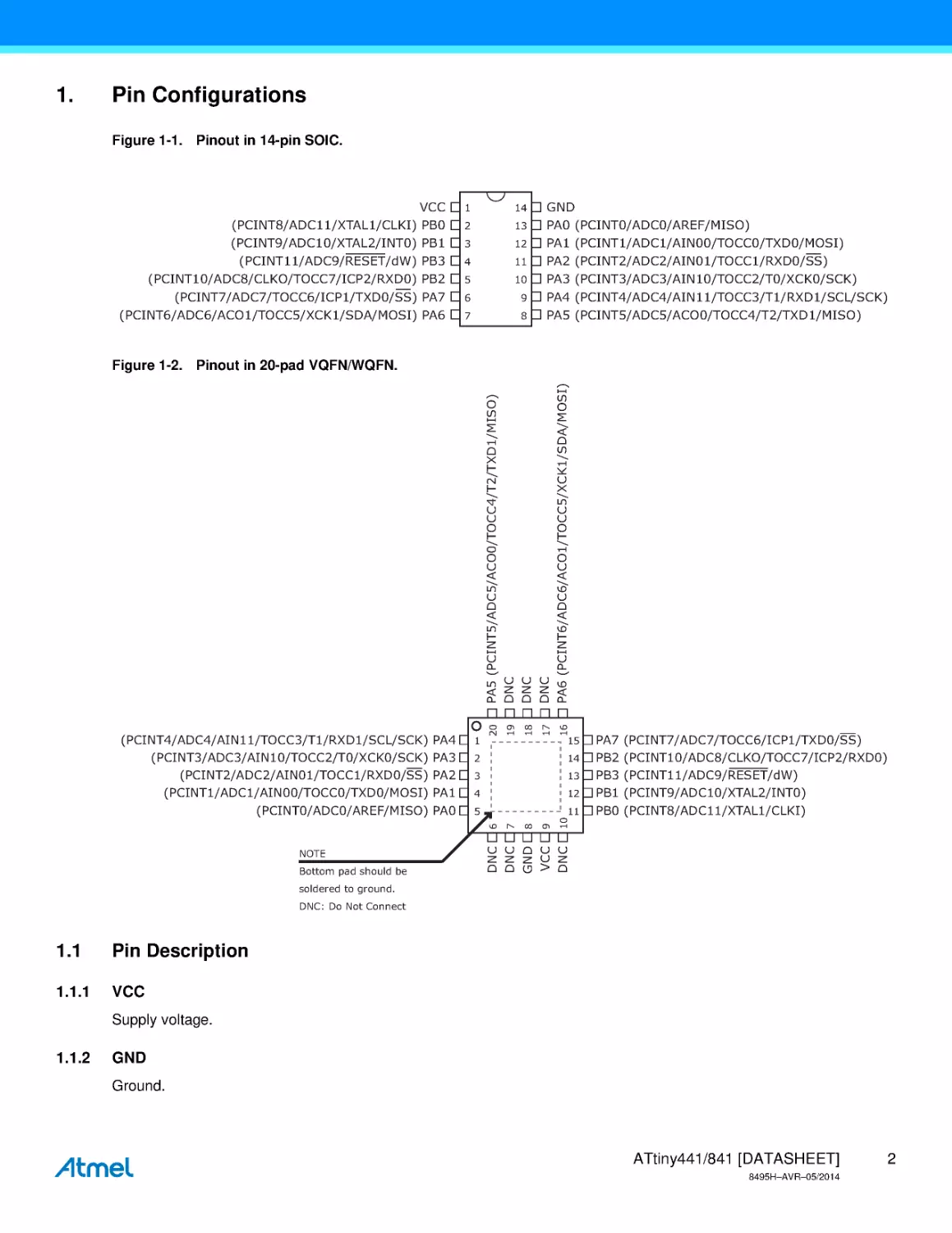
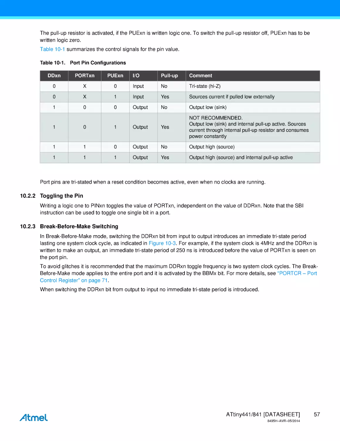
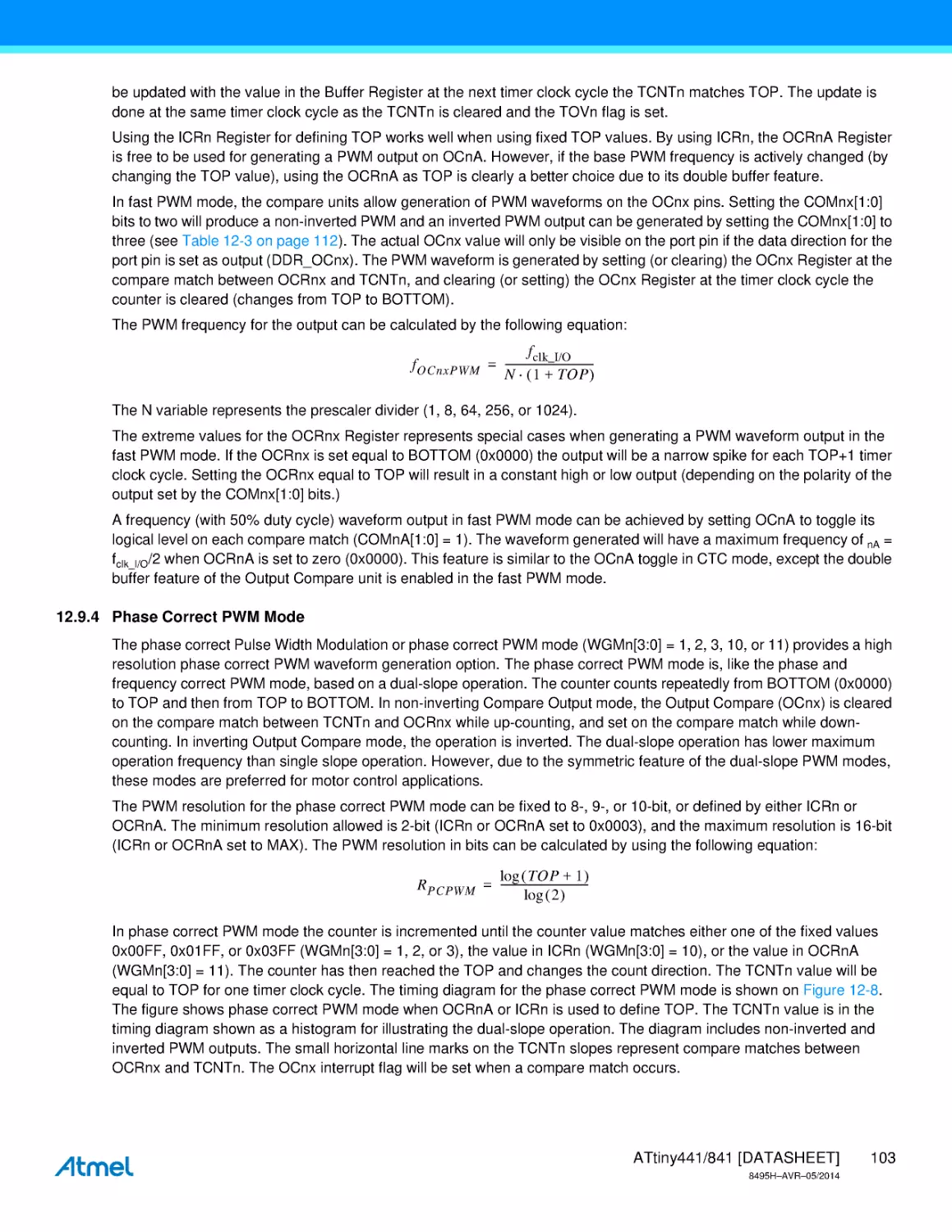
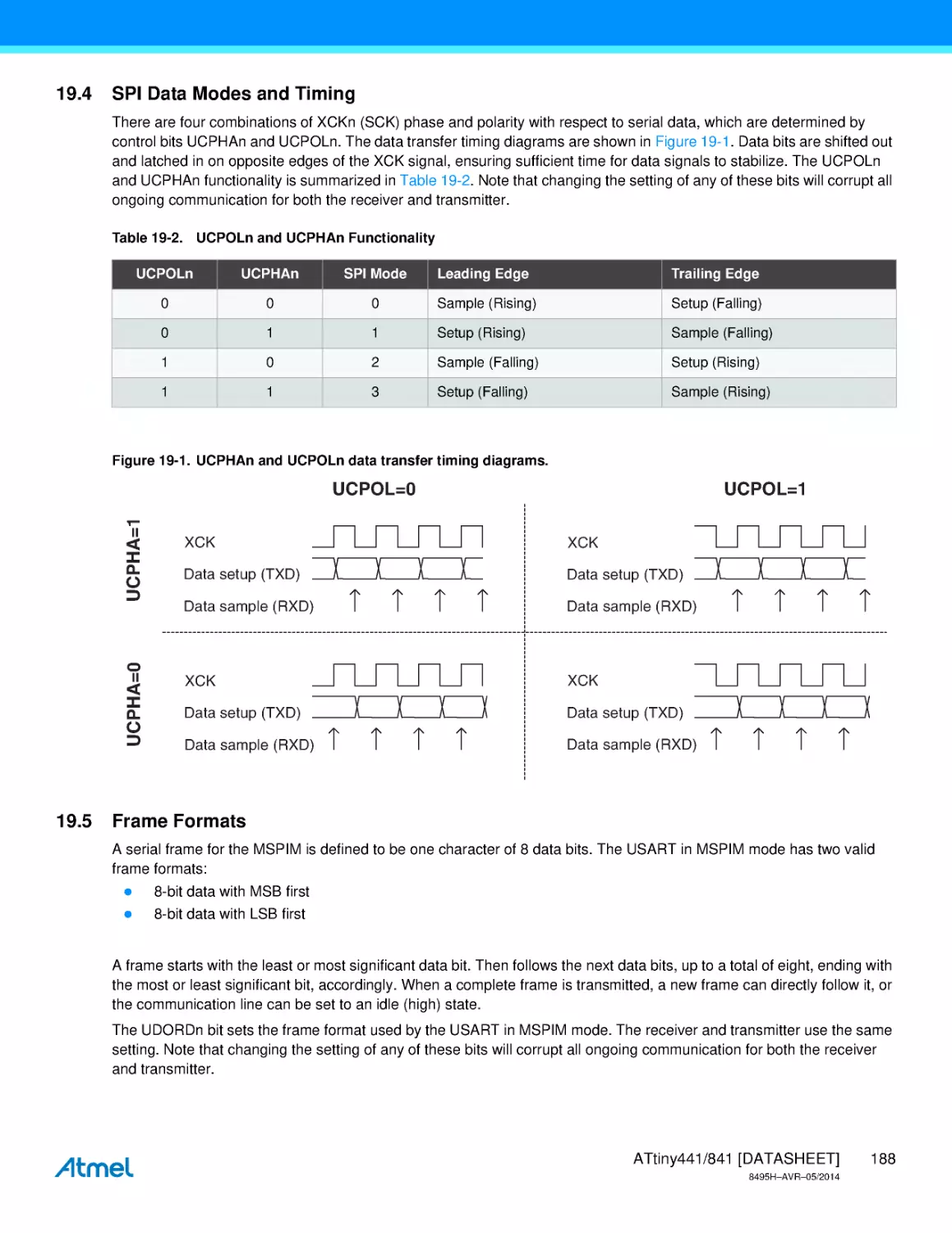
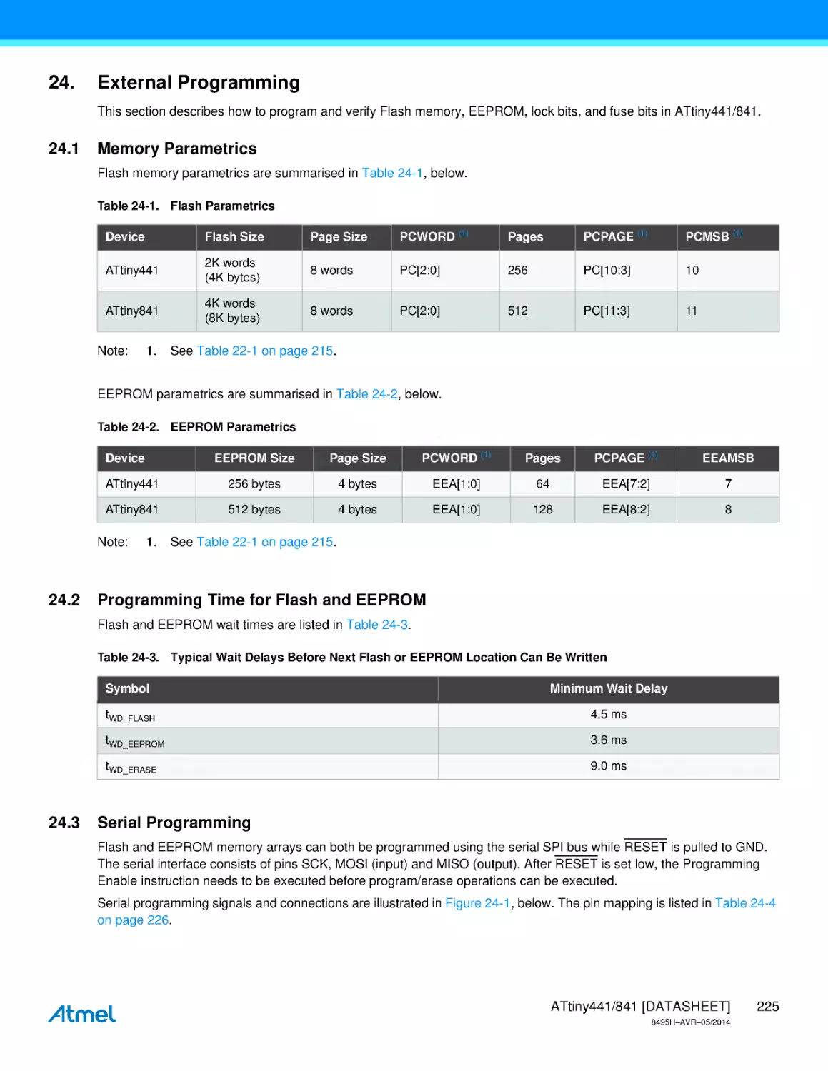
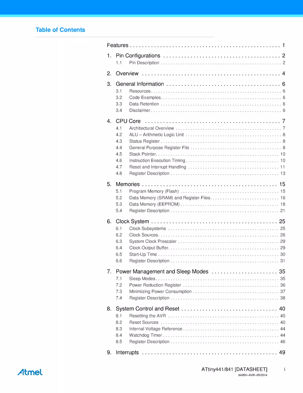
Pin Configurations
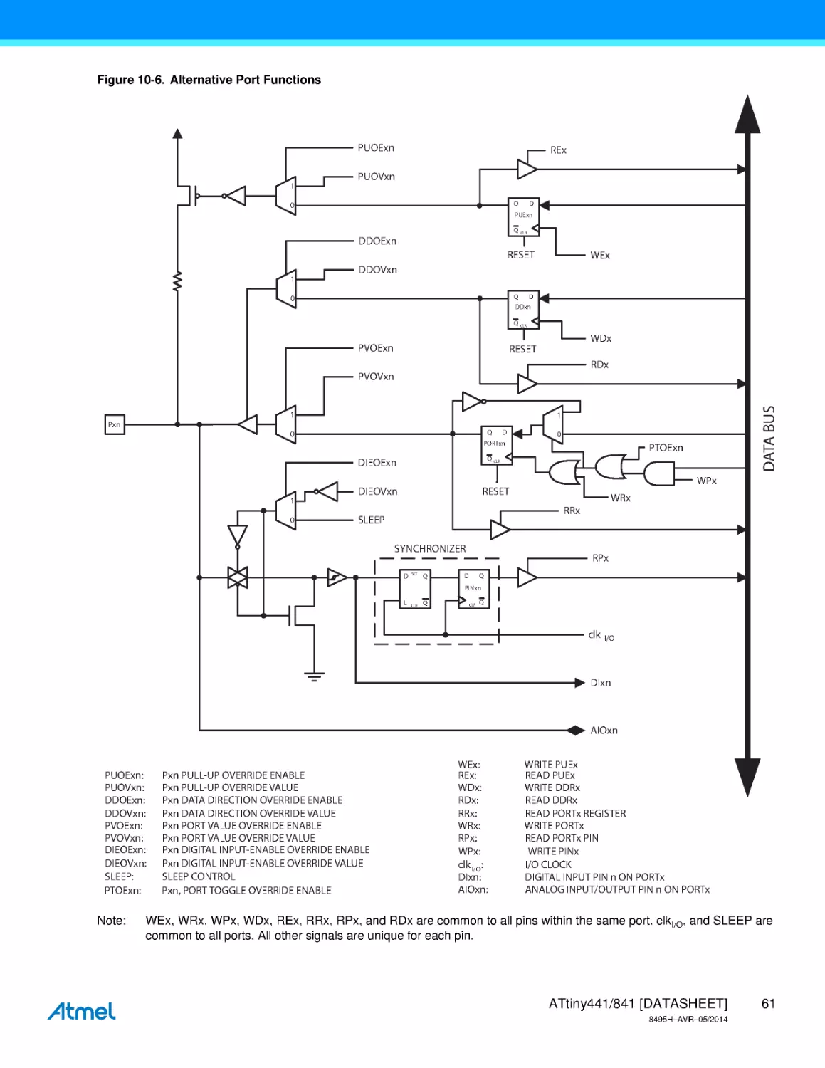
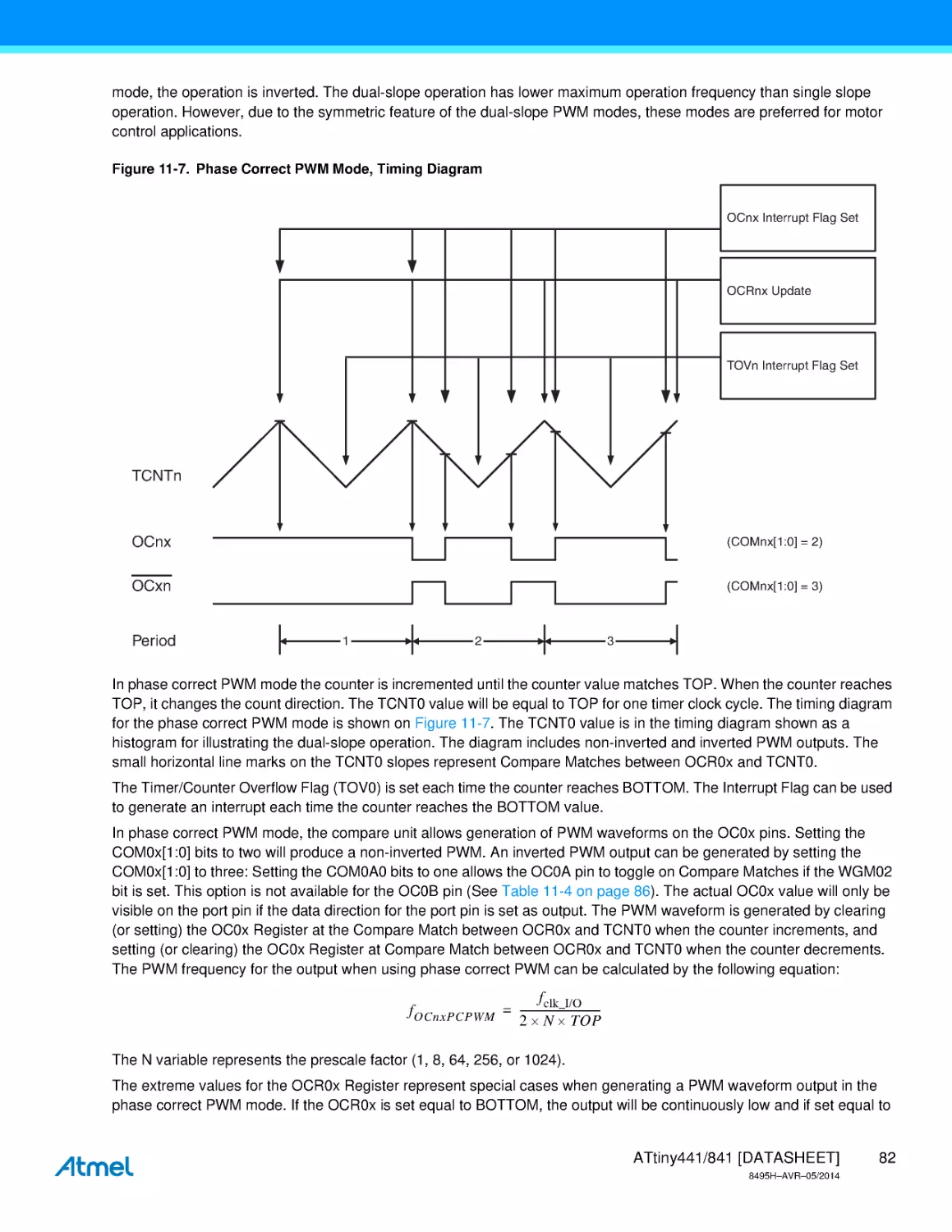
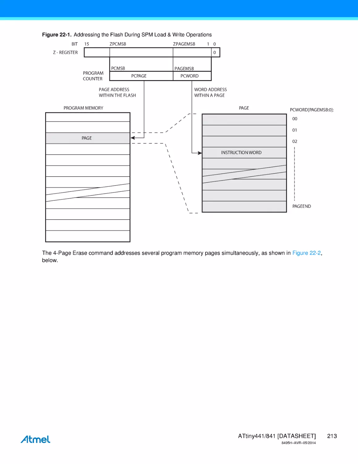
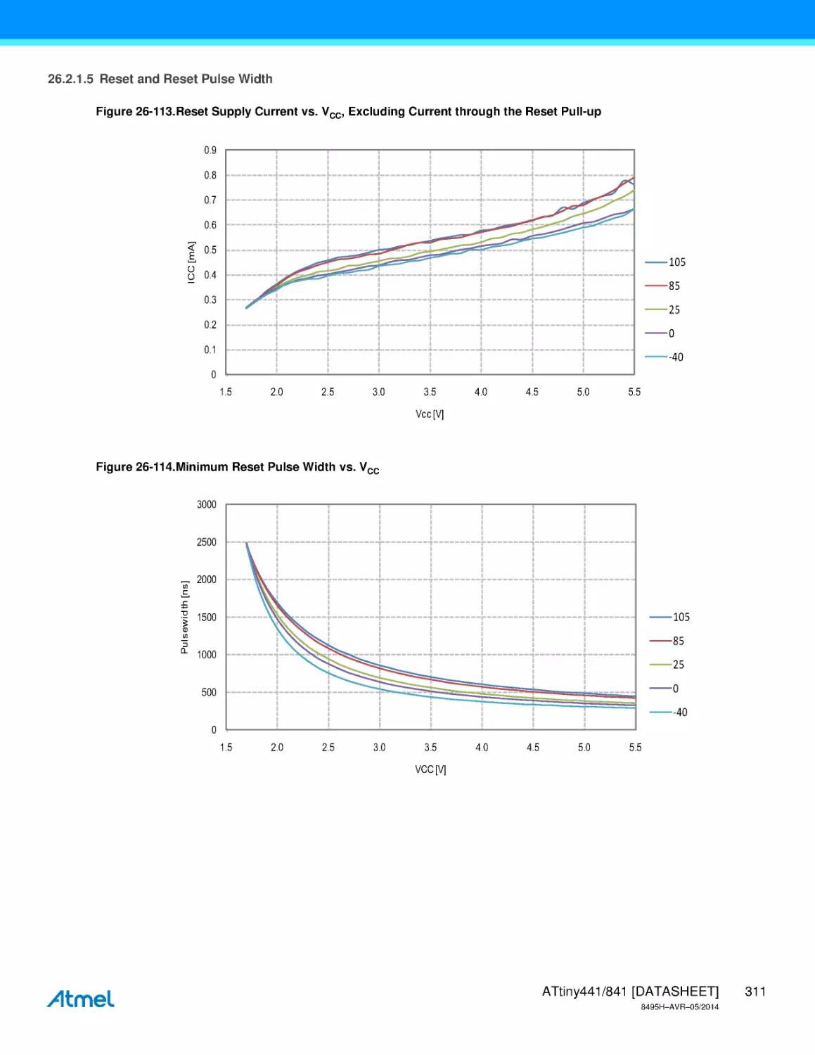
Figure 1-1. Pinout in 14-pin SOIC.
(PCINT8/ADC11/XTAL1/CLKI)
(PCINT9/ADC10/XTAL2/INT0)
(PCINT11/ADC9/RESET/dW)
(PCINT10/ADC8/CLKO/TOCC7/ICP2/RXD0)
(PCINT7/ADC7/TOCC6/ICP1/TXD0/SS)
(PCINT6/ADC6/ACO1/TOCC5/XCK1/SDA/MOSI)
VCC
PB0
PB1
PB3
PB2
PA7
PA6
1
14
2
13
3
12
4
11
5
10
6
9
7
8
GND
PA0 (PCINT0/ADC0/AREF/MISO)
PA1 (PCINT1/ADC1/AIN00/TOCC0/TXD0/MOSI)
PA2 (PCINT2/ADC2/AIN01/TOCC1/RXD0/SS)
PA3 (PCINT3/ADC3/AIN10/TOCC2/T0/XCK0/SCK)
PA4 (PCINT4/ADC4/AIN11/TOCC3/T1/RXD1/SCL/SCK)
PA5 (PCINT5/ADC5/ACO0/TOCC4/T2/TXD1/MISO)
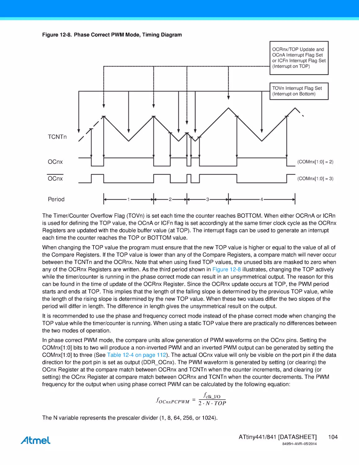
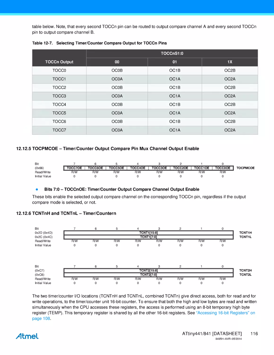
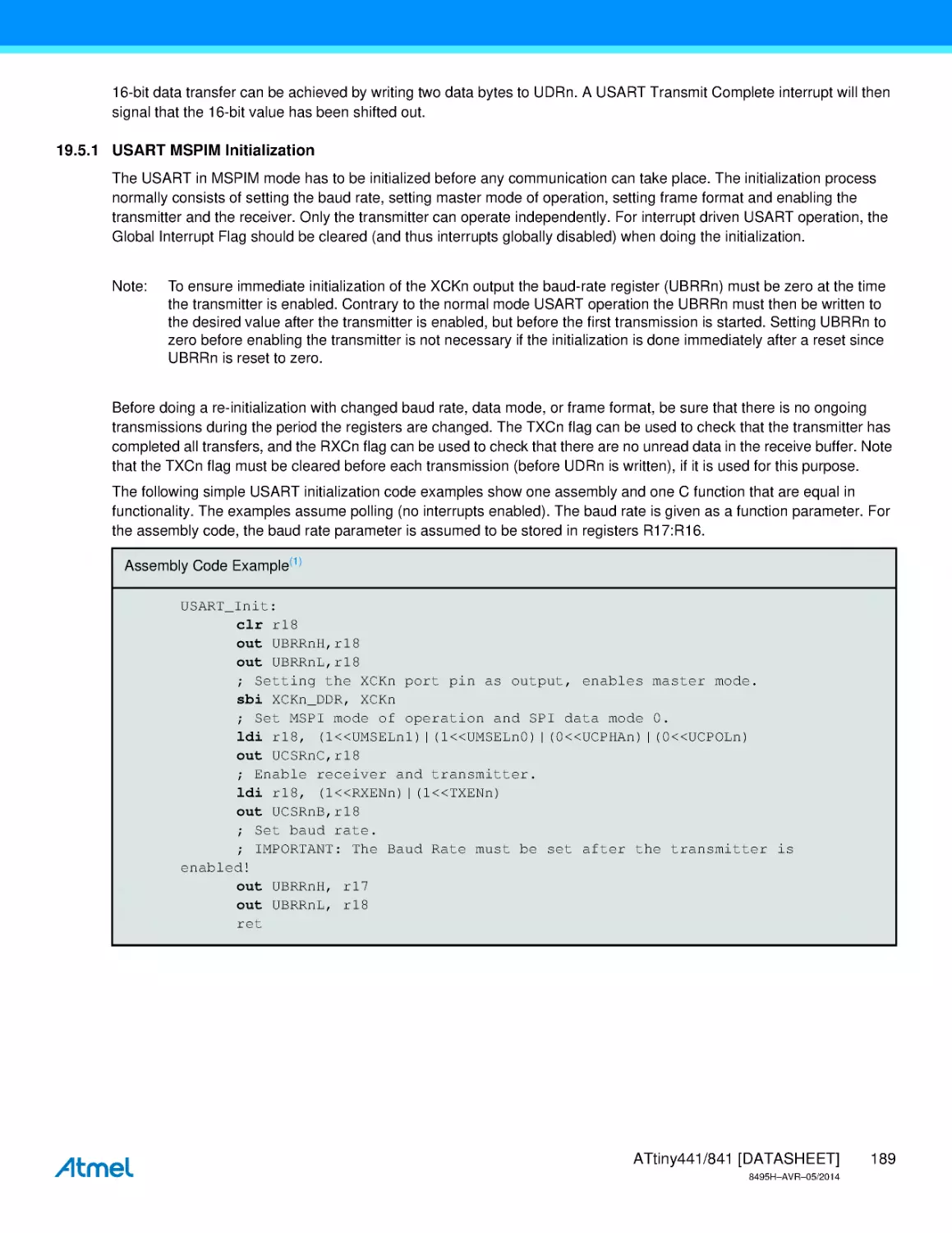
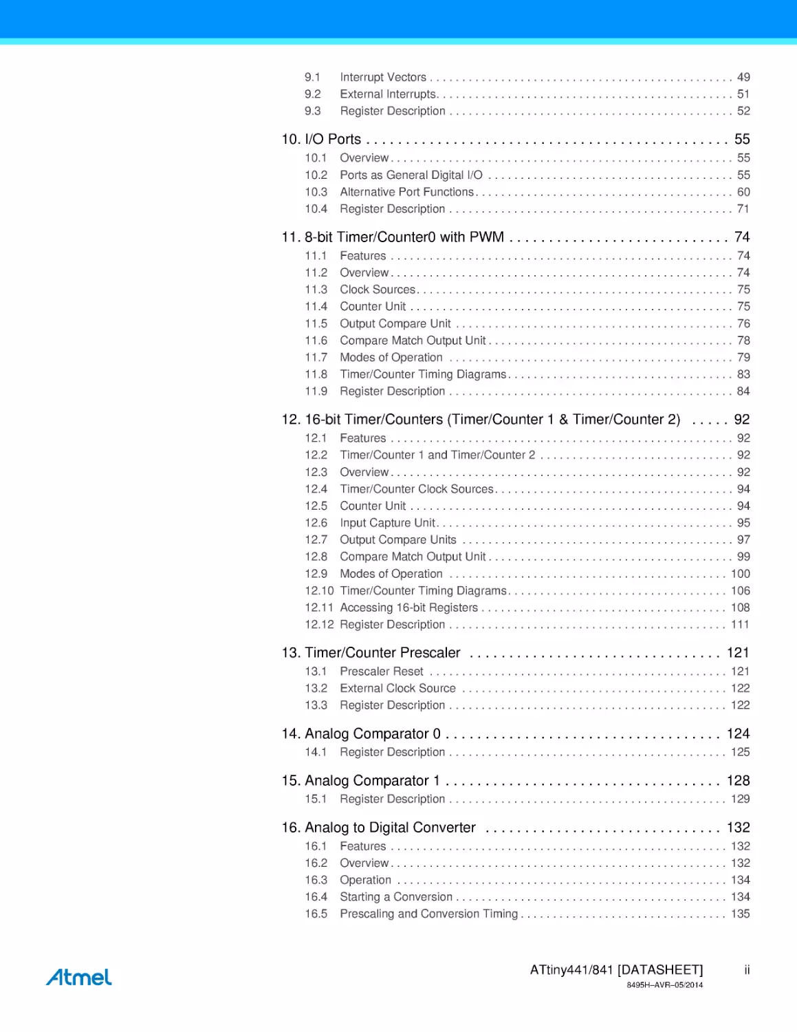
Bottom pad should be
16
17
18
13
4
12
5
11
10
3
9
14
8
15
2
PA7
PB2
PB3
PB1
PB0
(PCINT7/ADC7/TOCC6/ICP1/TXD0/SS)
(PCINT10/ADC8/CLKO/TOCC7/ICP2/RXD0)
(PCINT11/ADC9/RESET/dW)
(PCINT9/ADC10/XTAL2/INT0)
(PCINT8/ADC11/XTAL1/CLKI)
DNC
DNC
GND
VCC
DNC
NOTE
19
1
7
PA4
PA3
PA2
PA1
PA0
6
(PCINT4/ADC4/AIN11/TOCC3/T1/RXD1/SCL/SCK)
(PCINT3/ADC3/AIN10/TOCC2/T0/XCK0/SCK)
(PCINT2/ADC2/AIN01/TOCC1/RXD0/SS)
(PCINT1/ADC1/AIN00/TOCC0/TXD0/MOSI)
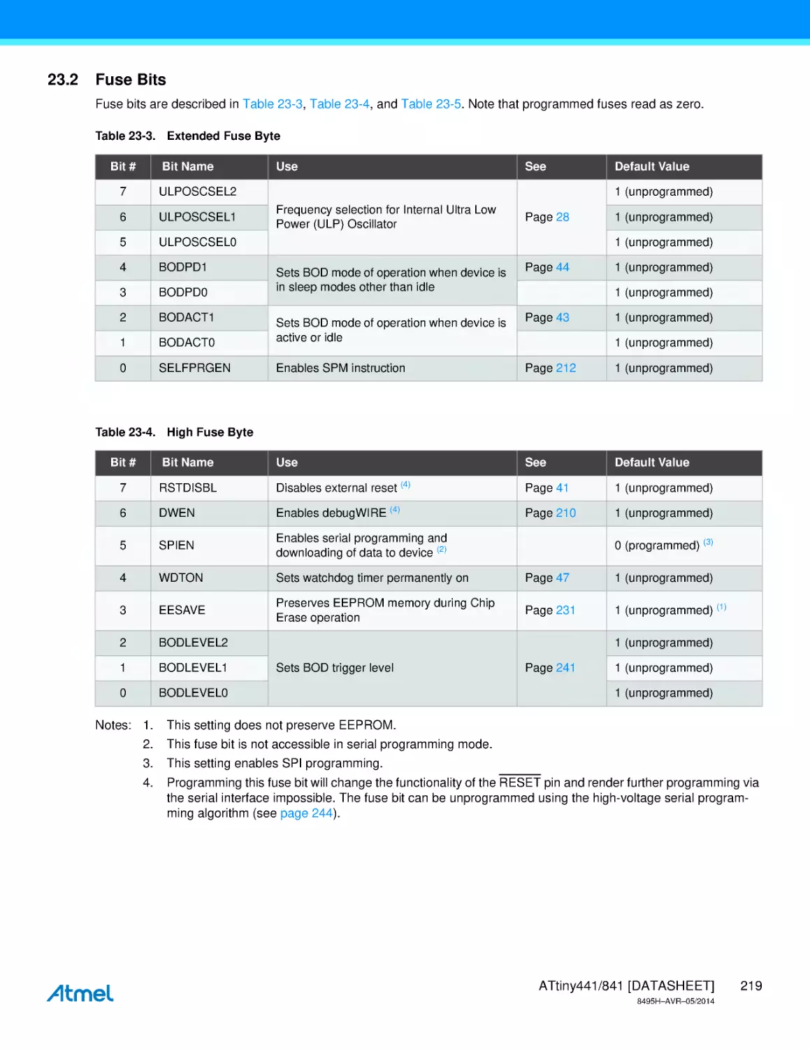
(PCINT0/ADC0/AREF/MISO)
20
PA5 (PCINT5/ADC5/ACO0/TOCC4/T2/TXD1/MISO)
DNC
DNC
DNC
PA6 (PCINT6/ADC6/ACO1/TOCC5/XCK1/SDA/MOSI)
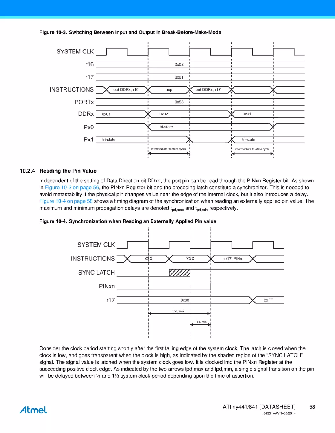
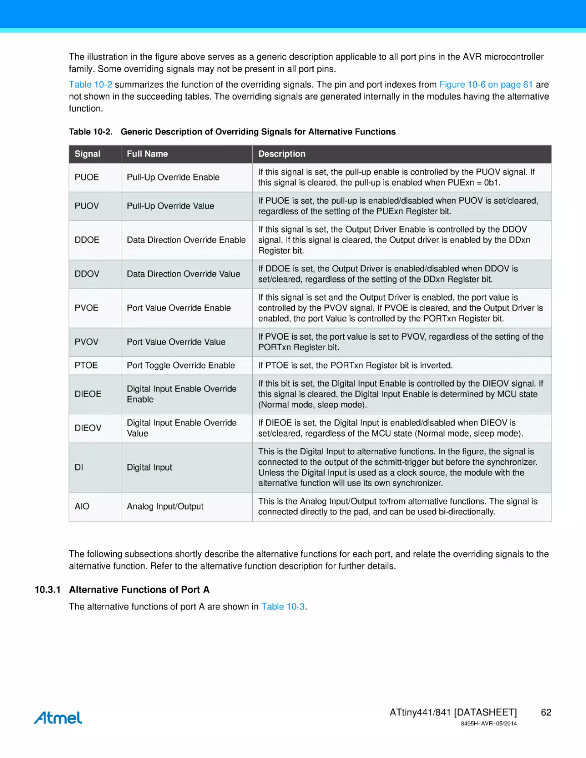
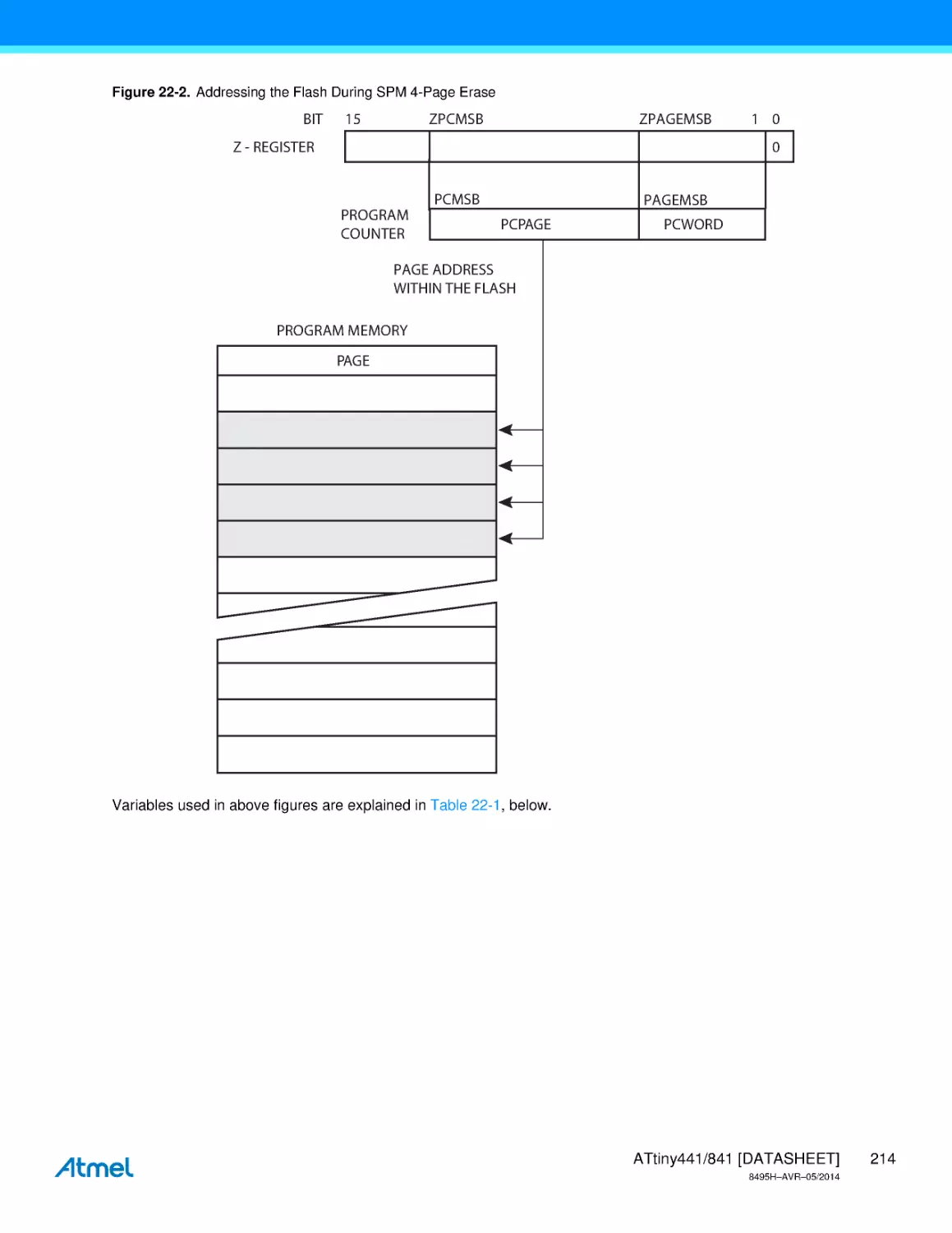
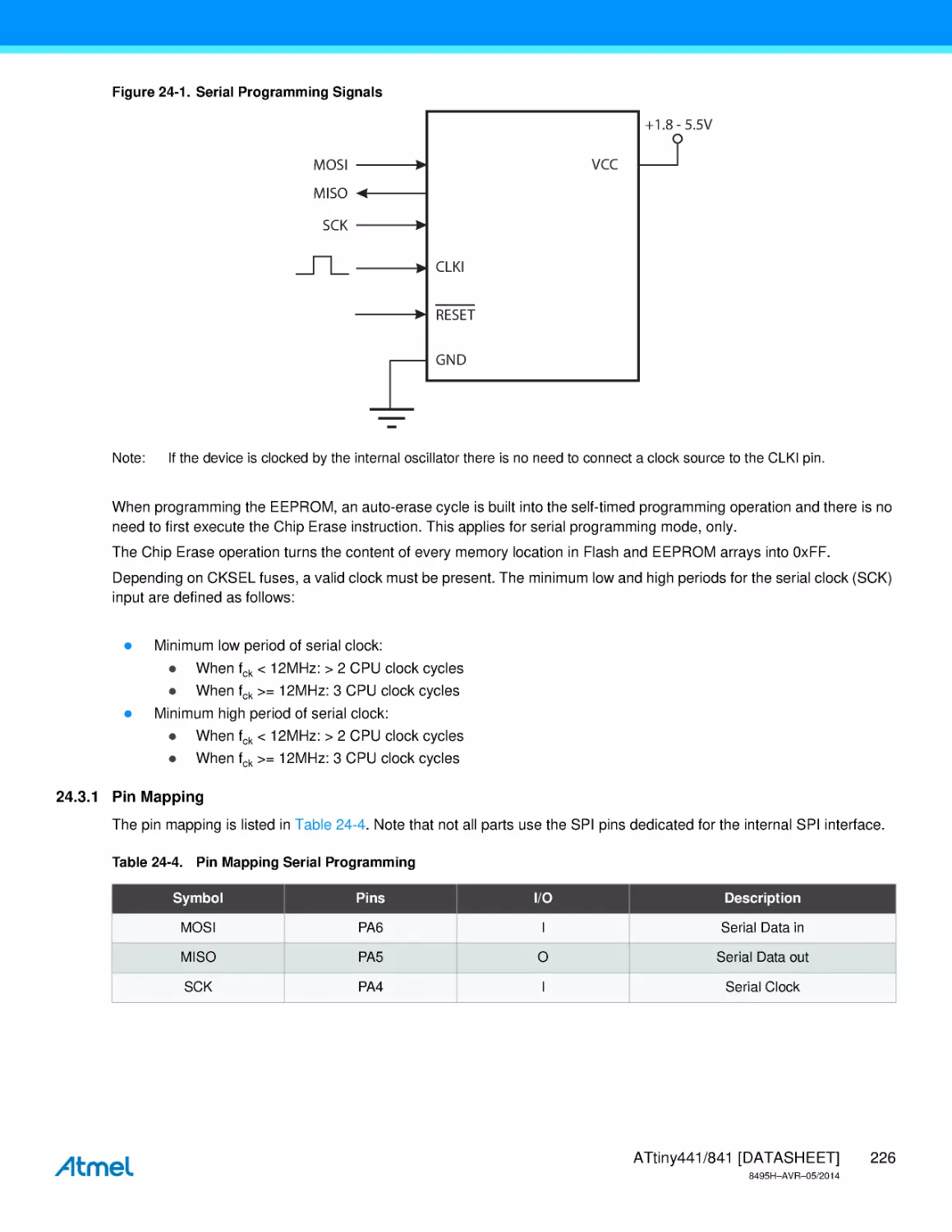
Figure 1-2. Pinout in 20-pad VQFN/WQFN.
soldered to ground.
DNC: Do Not Connect
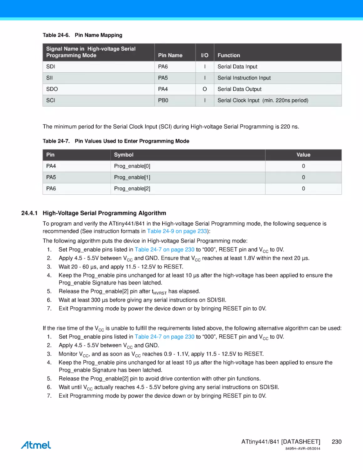
1.1
Pin Description
1.1.1
VCC
Supply voltage.
1.1.2
GND
Ground.
ATtiny441/841 [DATASHEET]
8495H–AVR–05/2014
2
1.1.3
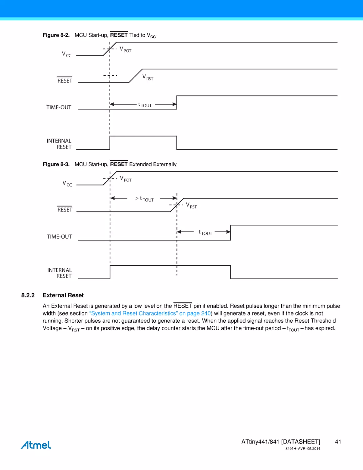
RESET
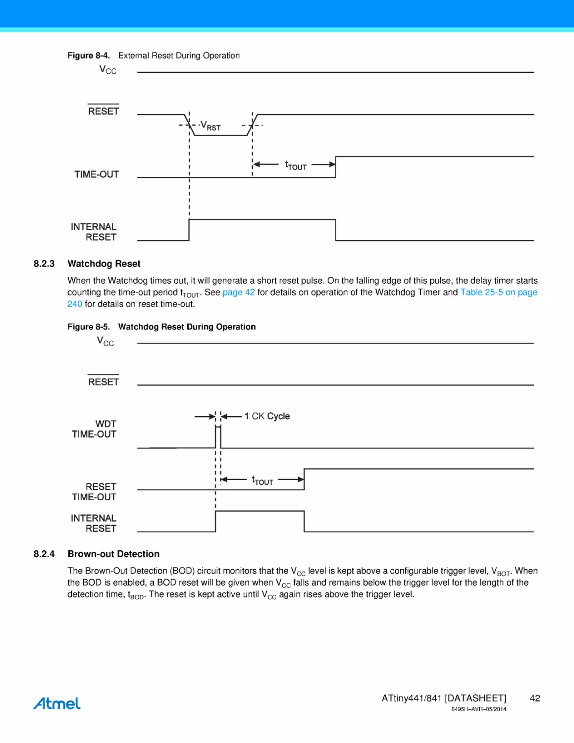
Reset input. A low level on this pin for longer than the minimum pulse length will generate a reset, even if the clock is not
running and provided the reset pin has not been disabled. The minimum pulse length is given in Table 25-5 on page 240.
Shorter pulses are not guaranteed to generate a reset.
The reset pin can also be used as a (weak) I/O pin.
1.1.4
Port A (PA7:PA0)
This is an 8-bit, bi-directional I/O port with internal pull-up resistors (selected for each bit). Output buffers have standard
sink and source capability, except ports PA7 and PA5, which have high sink capability. See Table 25-1 on page 236 for
port drive strength.
As inputs, port pins that are externally pulled low will source current provided that pull-up resistors are activated. Port
pins are tri-stated when a reset condition becomes active, even if the clock is not running.
This port has alternative pin functions for pin change interrupts, the analog comparator, and ADC. See “Alternative Port
Functions” on page 60.
1.1.5
Port B (PB3:PB0)
This is a 4-bit, bi-directional I/O port with internal pull-up resistors (selected for each bit). Output buffers have standard
sink and source capability. See Table 25-1 on page 236 for port drive strength.
As inputs, port pins that are externally pulled low will source current provided that pull-up resistors are activated. Port
pins are tri-stated when a reset condition becomes active, even if the clock is not running.
This port has alternative pin functions for pin change interrupts, and ADC. See “Alternative Port Functions” on page 60.
ATtiny441/841 [DATASHEET]
8495H–AVR–05/2014
3
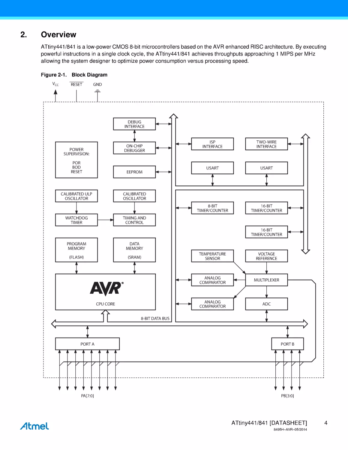
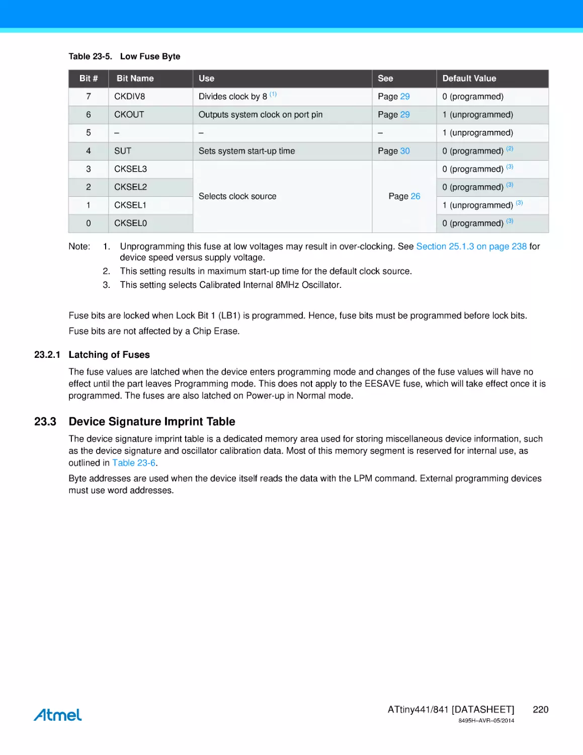
2.
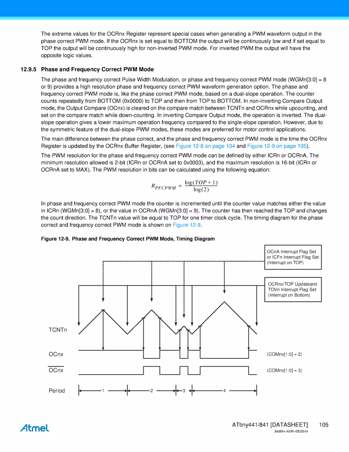
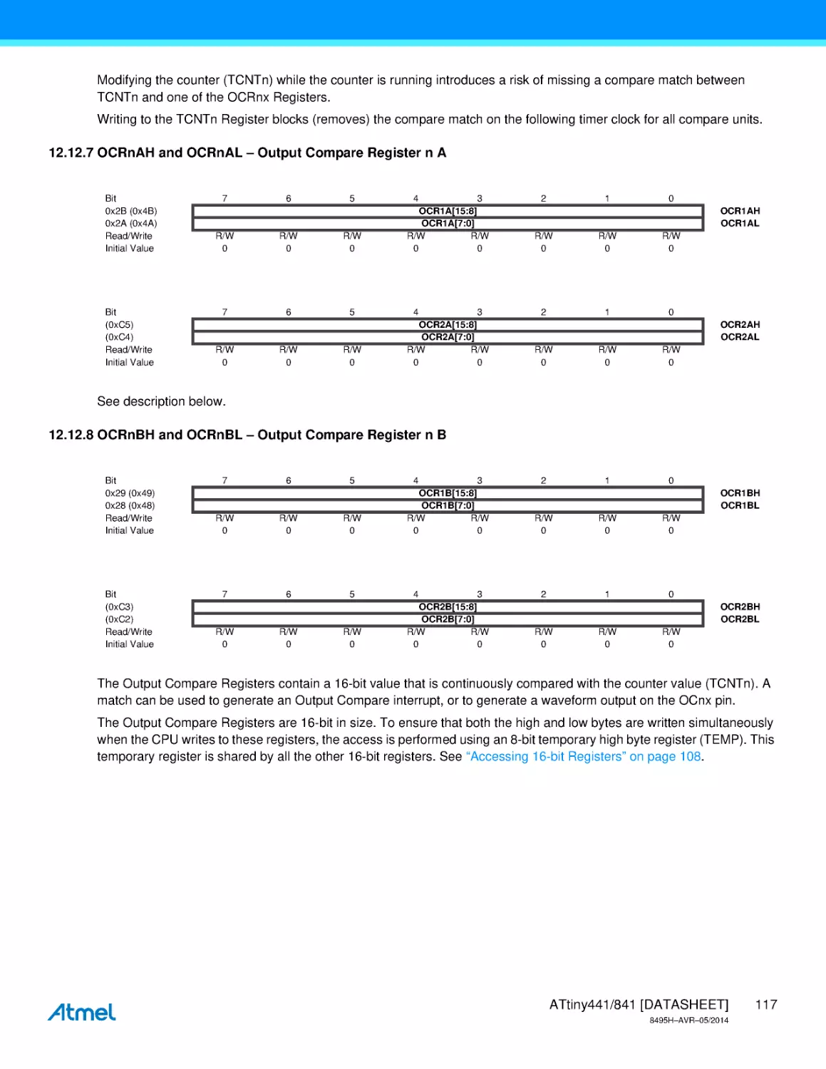
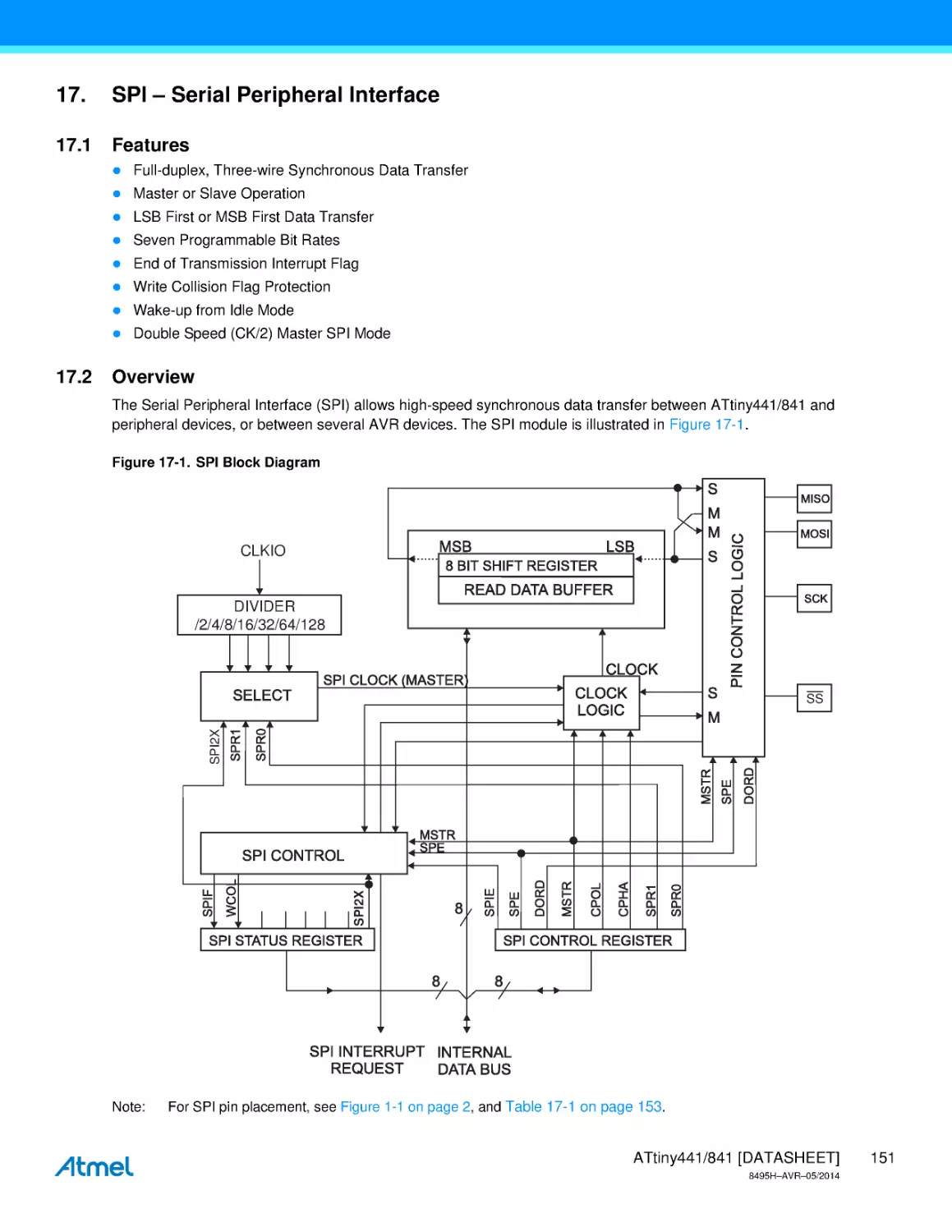
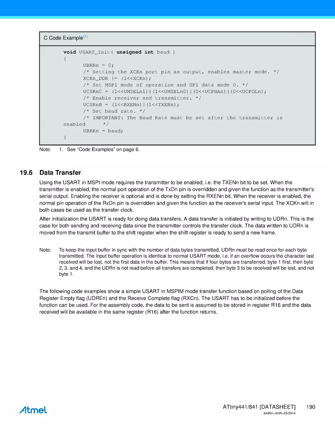
Overview
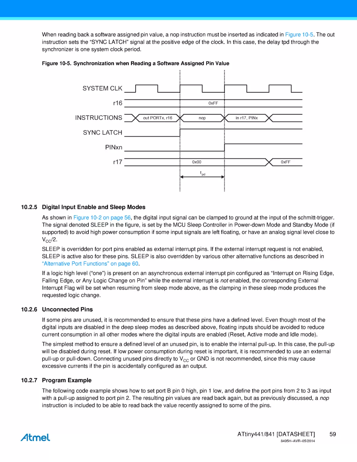
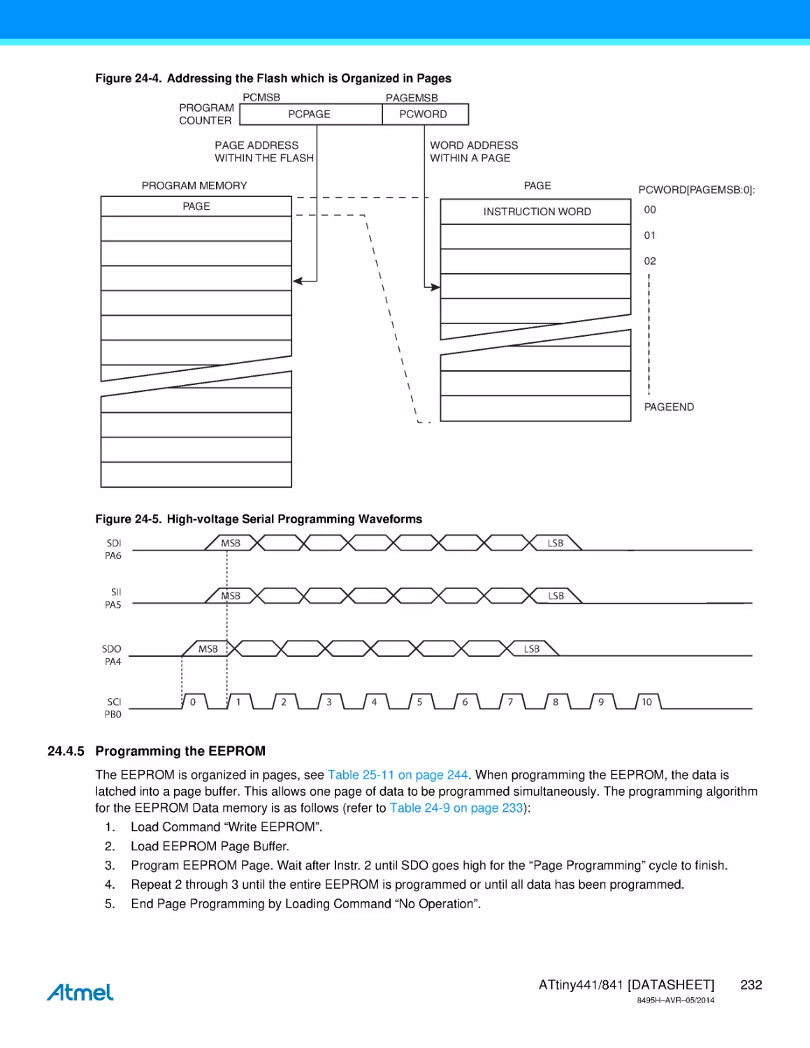
ATtiny441/841 is a low-power CMOS 8-bit microcontrollers based on the AVR enhanced RISC architecture. By executing
powerful instructions in a single clock cycle, the ATtiny441/841 achieves throughputs approaching 1 MIPS per MHz
allowing the system designer to optimize power consumption versus processing speed.
Figure 2-1. Block Diagram
VCC
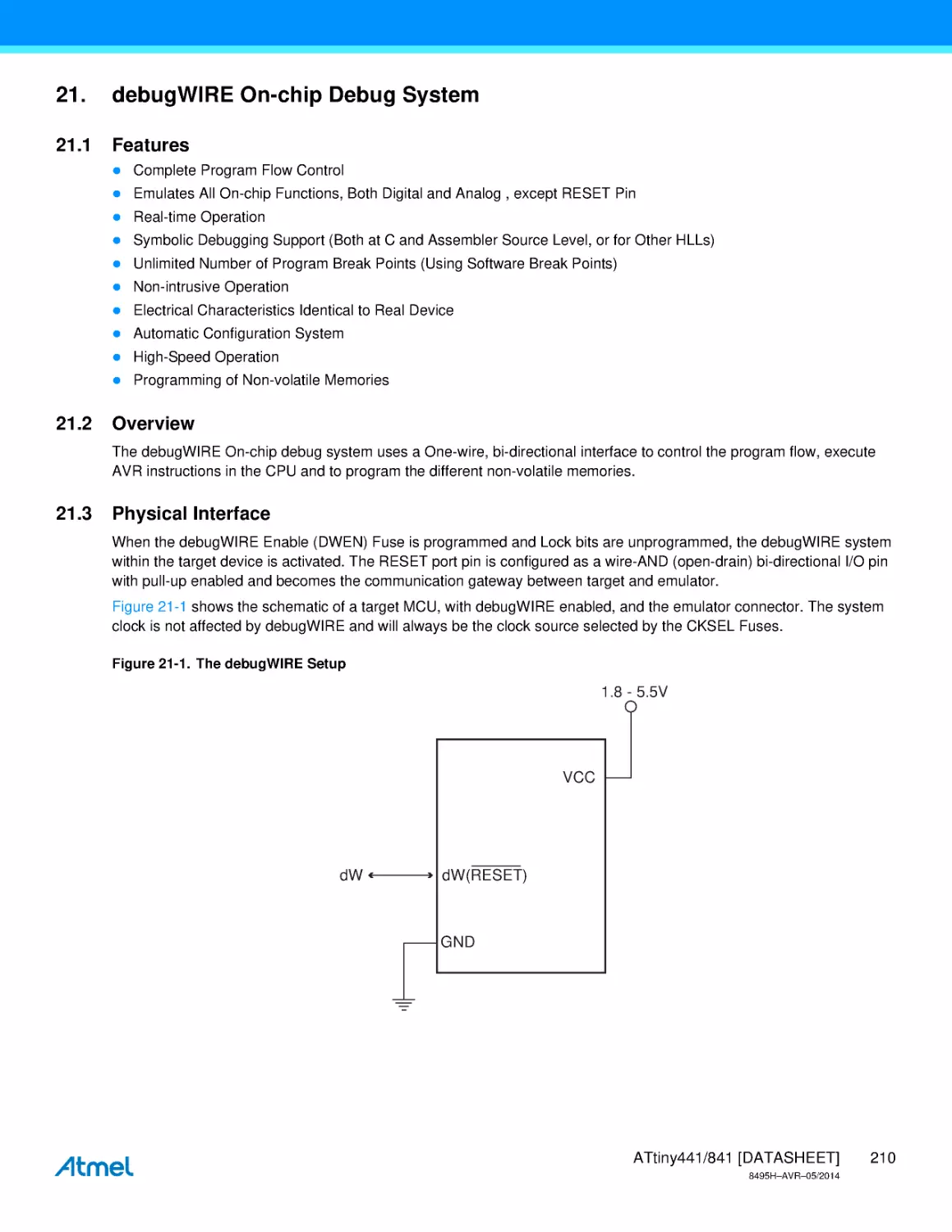
RESET
GND
DEBUG
INTERFACE
ON-CHIP
DEBUGGER
POWER
SUPERVISION:
POR
BOD
RESET
EEPROM
CALIBRATED ULP
OSCILLATOR
CALIBRATED
OSCILLATOR
WATCHDOG
TIMER
ISP
INTERFACE
TWO-WIRE
INTERFACE
USART
USART
8-BIT
TIMER/COUNTER
16-BIT
TIMER/COUNTER
TIMING AND
CONTROL
16-BIT
TIMER/COUNTER
PROGRAM
MEMORY
DATA
MEMORY
(FLASH)
(SRAM)
CPU CORE
TEMPERATURE
SENSOR
VOLTAGE
REFERENCE
ANALOG
COMPARATOR
MULTIPLEXER
ANALOG
COMPARATOR
ADC
8-BIT DATA BUS
PORT A
PORT B
PA[7:0]
PB[3:0]
ATtiny441/841 [DATASHEET]
8495H–AVR–05/2014
4
The AVR core combines a rich instruction set with 32 general purpose working registers. All 32 registers are directly
connected to the Arithmetic Logic Unit (ALU), allowing two independent registers to be accessed in a single instruction,
executed in one clock cycle. The resulting architecture is compact and code efficient while achieving throughputs up to
ten times faster than conventional CISC microcontrollers.
ATtiny441/841 provides the following features:
4K/8K bytes of in-system programmable Flash
256/512 bytes of SRAM data memory
256/512 bytes of EEPROM data memory
12 general purpose I/O lines
32 general purpose working registers
One 8-bit timer/counter with two PWM channels
Two 16-bit timer/counters with two PWM channels
Internal and external interrupts
One 10-bit ADC with 5 internal and 12 external channels
One ultra-low power, programmable watchdog timer with internal oscillator
Two programmable USARTs with start frame detection
Slave Two-Wire Interface (TWI)
Master/slave Serial Peripheral Interface (SPI)
Calibrated 8MHz oscillator
Calibrated 32kHz, ultra low power oscillator
Four software selectable power saving modes.
The device includes the following modes for saving power:
Idle mode: stops the CPU while allowing the timer/counter, ADC, analog comparator, SPI, TWI, and interrupt
system to continue functioning
ADC Noise Reduction mode: minimizes switching noise during ADC conversions by stopping the CPU and all I/O
modules except the ADC
Power-down mode: registers keep their contents and all chip functions are disabled until the next interrupt or
hardware reset
Standby mode: the oscillator is running while the rest of the device is sleeping, allowing very fast start-up
combined with low power consumption
The device is manufactured using Atmel’s high density non-volatile memory technology. The Flash program memory can
be re-programmed in-system through a serial interface, by a conventional non-volatile memory programmer or by an onchip boot code, running on the AVR core.
The ATtiny441/841 AVR is supported by a full suite of program and system development tools including: C compilers,
macro assemblers, program debugger/simulators and evaluation kits.
ATtiny441/841 [DATASHEET]
8495H–AVR–05/2014
5
3.
General Information
3.1
Resources
A comprehensive set of drivers, application notes, data sheets and descriptions on development tools are available for
download at http://www.atmel.com/avr.
3.2
Code Examples
This documentation contains simple code examples that briefly show how to use various parts of the device. These code
examples assume that the part specific header file is included before compilation. Be aware that not all C compiler
vendors include bit definitions in the header files and interrupt handling in C is compiler dependent. Please confirm with
the C compiler documentation for more details.
3.3
Data Retention
Reliability Qualification results show that the projected data retention failure rate is much less than 1 PPM over 20 years
at 85°C or 100 years at 25°C.
3.4
Disclaimer
Typical values contained in this datasheet are based on simulations and characterization of other AVR microcontrollers
manufactured on the same process technology.
ATtiny441/841 [DATASHEET]
8495H–AVR–05/2014
6
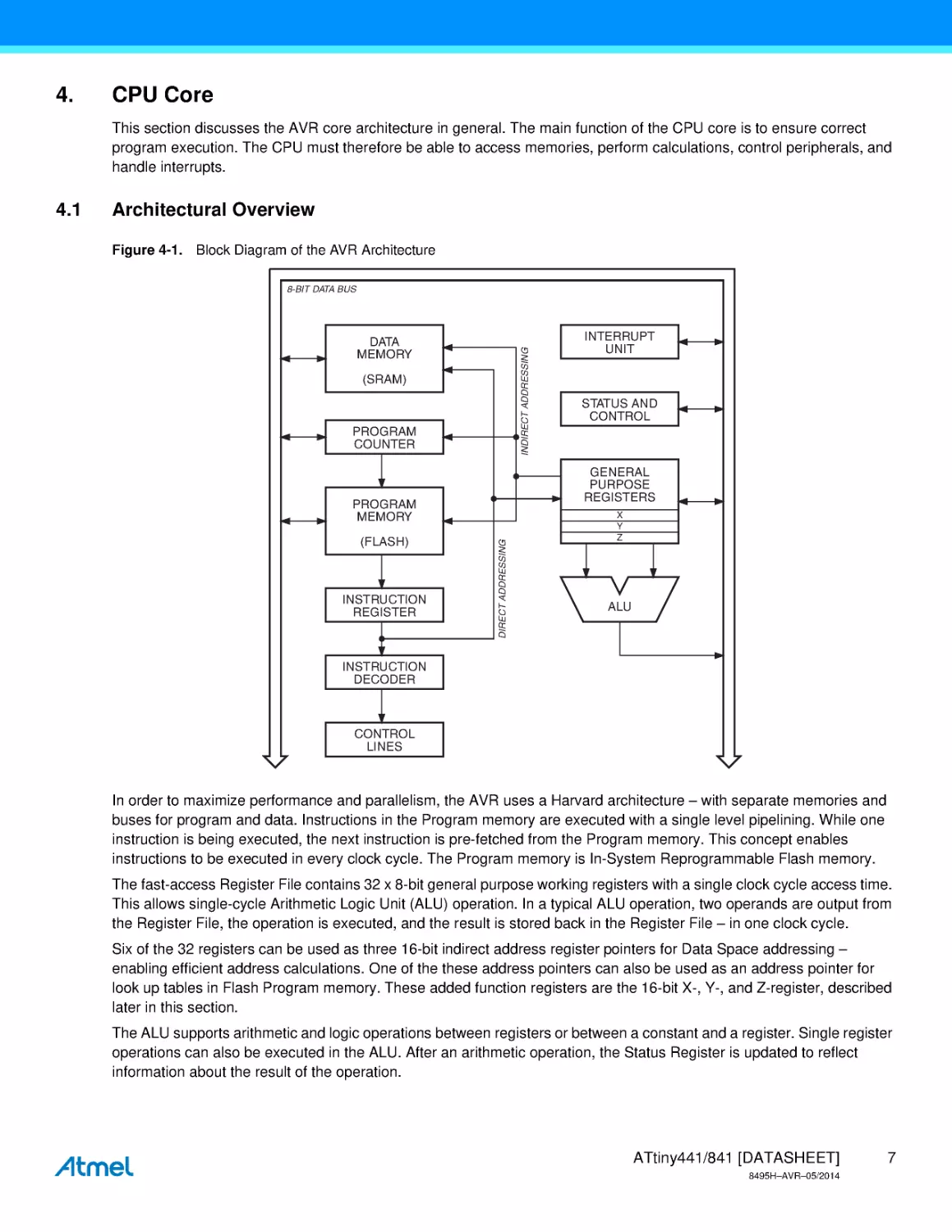
4.
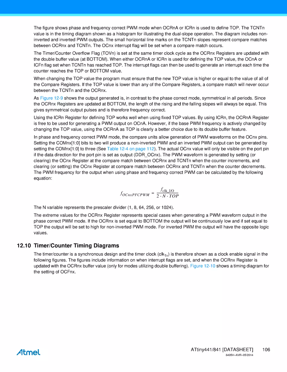
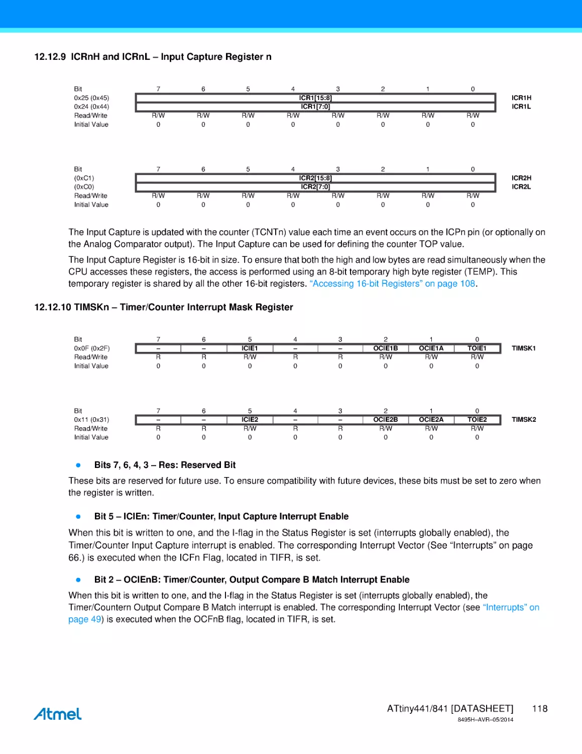
CPU Core
This section discusses the AVR core architecture in general. The main function of the CPU core is to ensure correct
program execution. The CPU must therefore be able to access memories, perform calculations, control peripherals, and
handle interrupts.
Architectural Overview
Figure 4-1. Block Diagram of the AVR Architecture
8-BIT DATA BUS
INDIRECT ADDRESSING
DATA
MEMORY
(SRAM)
PROGRAM
COUNTER
PROGRAM
MEMORY
(FLASH)
INSTRUCTION
REGISTER
INTERRUPT
UNIT
STATUS AND
CONTROL
GENERAL
PURPOSE
REGISTERS
DIRECT ADDRESSING
4.1
X
Y
Z
ALU
INSTRUCTION
DECODER
CONTROL
LINES
In order to maximize performance and parallelism, the AVR uses a Harvard architecture – with separate memories and
buses for program and data. Instructions in the Program memory are executed with a single level pipelining. While one
instruction is being executed, the next instruction is pre-fetched from the Program memory. This concept enables
instructions to be executed in every clock cycle. The Program memory is In-System Reprogrammable Flash memory.
The fast-access Register File contains 32 x 8-bit general purpose working registers with a single clock cycle access time.
This allows single-cycle Arithmetic Logic Unit (ALU) operation. In a typical ALU operation, two operands are output from
the Register File, the operation is executed, and the result is stored back in the Register File – in one clock cycle.
Six of the 32 registers can be used as three 16-bit indirect address register pointers for Data Space addressing –
enabling efficient address calculations. One of the these address pointers can also be used as an address pointer for
look up tables in Flash Program memory. These added function registers are the 16-bit X-, Y-, and Z-register, described
later in this section.
The ALU supports arithmetic and logic operations between registers or between a constant and a register. Single register
operations can also be executed in the ALU. After an arithmetic operation, the Status Register is updated to reflect
information about the result of the operation.
ATtiny441/841 [DATASHEET]
8495H–AVR–05/2014
7
Program flow is provided by conditional and unconditional jump and call instructions, capable of directly addressing the
whole address space. Most AVR instructions have a single 16-bit word format but 32-bit wide instructions also exist. The
actual instruction set varies, as some devices only implement a part of the instruction set.
During interrupts and subroutine calls, the return address Program Counter (PC) is stored on the Stack. The Stack is
effectively allocated in the general data SRAM, and consequently the Stack size is only limited by the total SRAM size
and the usage of the SRAM. All user programs must initialize the SP in the Reset routine (before subroutines or
interrupts are executed). The Stack Pointer (SP) is read/write accessible in the I/O space. The data SRAM can easily be
accessed through the five different addressing modes supported in the AVR architecture.
The memory spaces in the AVR architecture are all linear and regular memory maps.
A flexible interrupt module has its control registers in the I/O space with an additional Global Interrupt Enable bit in the
Status Register. All interrupts have a separate Interrupt Vector in the Interrupt Vector table. The interrupts have priority in
accordance with their Interrupt Vector position. The lower the Interrupt Vector address, the higher the priority.
The I/O memory space contains 64 addresses for CPU peripheral functions as Control Registers, SPI, and other I/O
functions. The I/O memory can be accessed directly, or as the Data Space locations following those of the Register File,
0x20 - 0x5F. In addition, the ATtiny441/841 has Extended I/O Space from 0x60 - 0xFF in SRAM where only the
ST/STS/STD and LD/LDS/LDD instructions can be used.
4.2
ALU – Arithmetic Logic Unit
The high-performance AVR ALU operates in direct connection with all the 32 general purpose working registers. Within a
single clock cycle, arithmetic operations between general purpose registers or between a register and an immediate are
executed. The ALU operations are divided into three main categories – arithmetic, logical, and bit-functions. See external
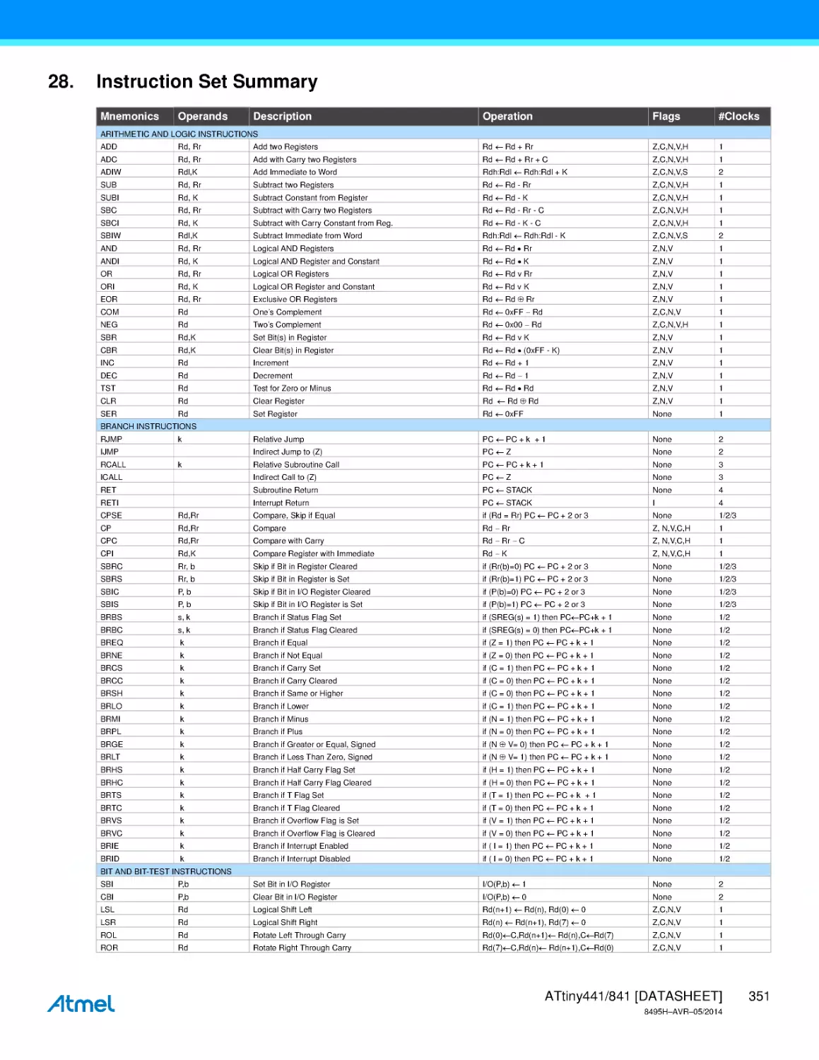
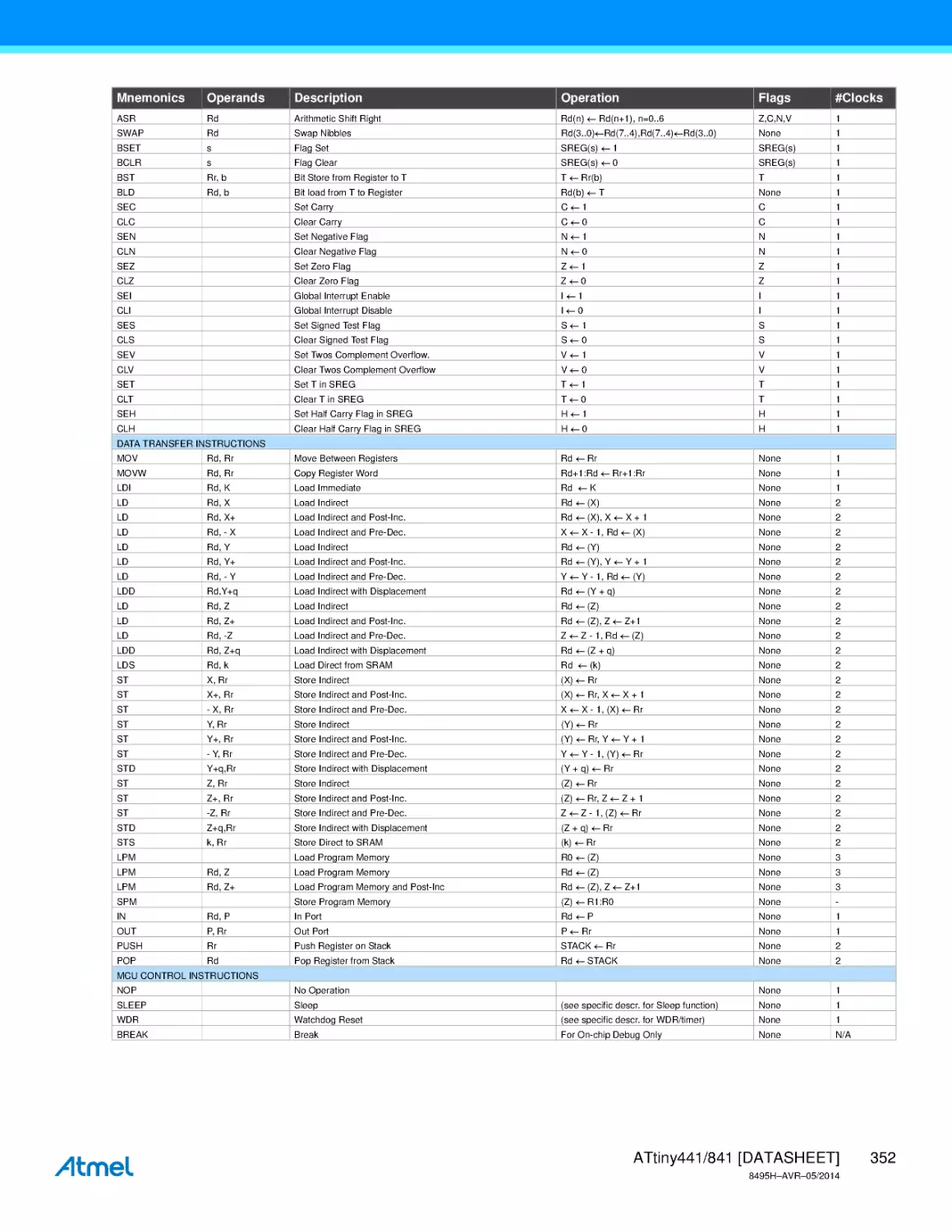
document “AVR Instruction Set” and “Instruction Set Summary” on page 351 section for more information.
4.3
Status Register
The Status Register contains information about the result of the most recently executed arithmetic instruction. This
information can be used for altering program flow in order to perform conditional operations. Note that the Status
Register is updated after all ALU operations. This will in many cases remove the need for using the dedicated compare
instructions, resulting in faster and more compact code. See external document “AVR Instruction Set” and “Instruction
Set Summary” on page 351 section for more information.
The Status Register is neither automatically stored when entering an interrupt routine, nor restored when returning from
an interrupt. This must be handled by software.
4.4
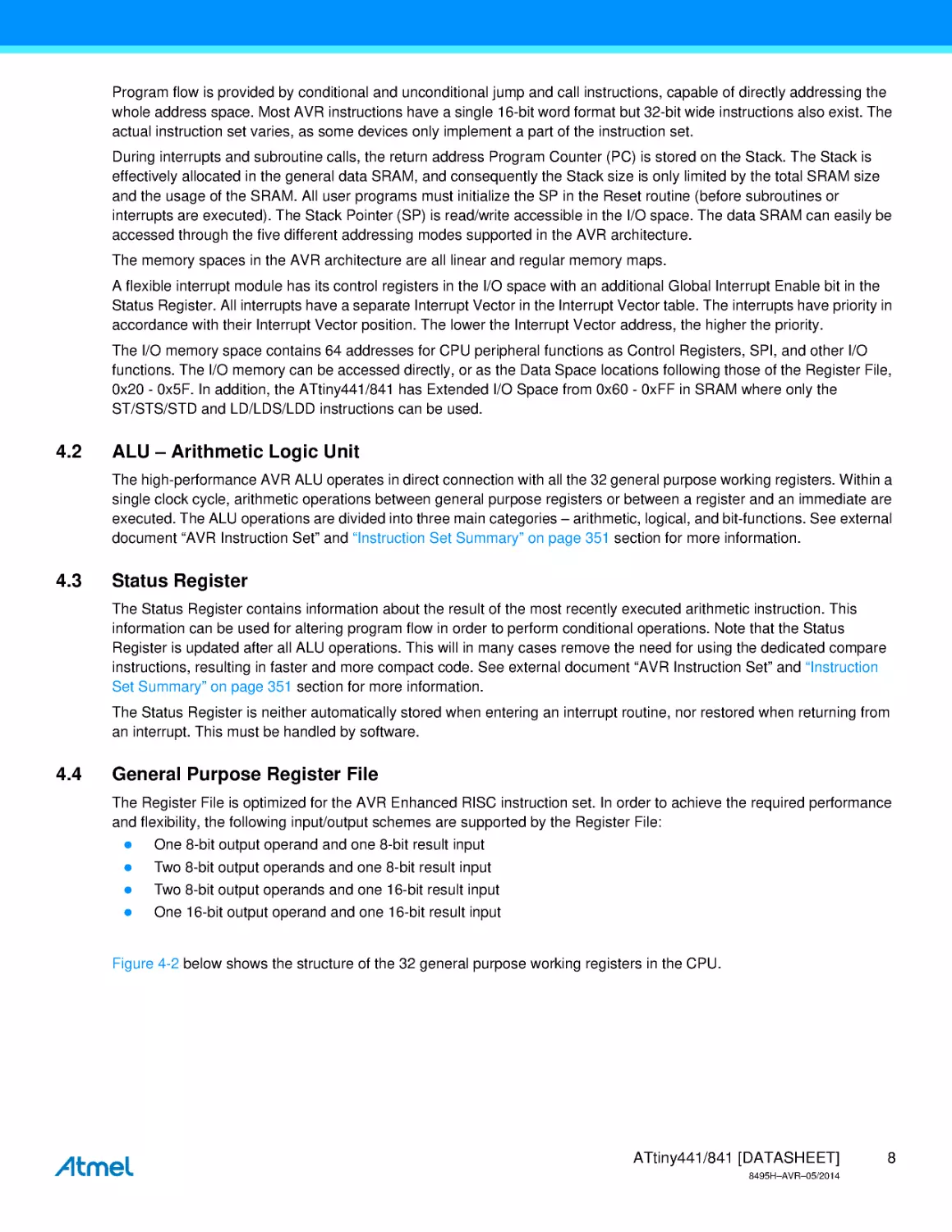
General Purpose Register File
The Register File is optimized for the AVR Enhanced RISC instruction set. In order to achieve the required performance
and flexibility, the following input/output schemes are supported by the Register File:
One 8-bit output operand and one 8-bit result input
Two 8-bit output operands and one 8-bit result input
Two 8-bit output operands and one 16-bit result input
One 16-bit output operand and one 16-bit result input
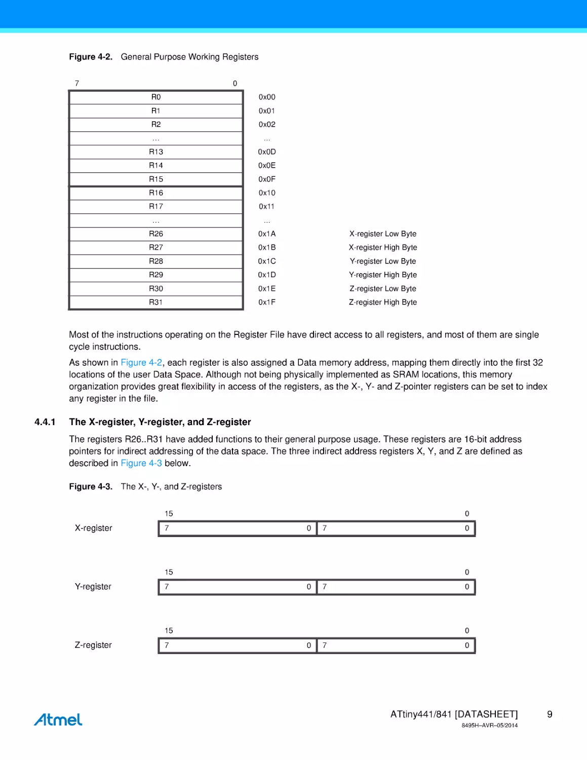
Figure 4-2 below shows the structure of the 32 general purpose working registers in the CPU.
ATtiny441/841 [DATASHEET]
8495H–AVR–05/2014
8
Figure 4-2. General Purpose Working Registers
7
0
Addr.
Special Function
R0
0x00
R1
0x01
R2
0x02
…
...
R13
0x0D
R14
0x0E
R15
0x0F
R16
0x10
R17
0x11
…
...
R26
0x1A
X-register Low Byte
R27
0x1B
X-register High Byte
R28
0x1C
Y-register Low Byte
R29
0x1D
Y-register High Byte
R30
0x1E
Z-register Low Byte
R31
0x1F
Z-register High Byte
Most of the instructions operating on the Register File have direct access to all registers, and most of them are single
cycle instructions.
As shown in Figure 4-2, each register is also assigned a Data memory address, mapping them directly into the first 32
locations of the user Data Space. Although not being physically implemented as SRAM locations, this memory
organization provides great flexibility in access of the registers, as the X-, Y- and Z-pointer registers can be set to index
any register in the file.
4.4.1
The X-register, Y-register, and Z-register
The registers R26..R31 have added functions to their general purpose usage. These registers are 16-bit address
pointers for indirect addressing of the data space. The three indirect address registers X, Y, and Z are defined as
described in Figure 4-3 below.
Figure 4-3. The X-, Y-, and Z-registers
15
X-register
7
0
XH
0
7
R27
XL
R26
15
Y-register
7
0
YH
0
7
R29
YL
7
0
R28
15
Z-register
0
0
ZH
R31
0
7
ZL
0
R30
ATtiny441/841 [DATASHEET]
8495H–AVR–05/2014
9
In the different addressing modes these address registers have functions as fixed displacement, automatic increment,
and automatic decrement (see the instruction set reference for details).
4.5
Stack Pointer
The stack is mainly used for storing temporary data, local variables and return addresses after interrupts and subroutine
calls. The Stack Pointer registers (SPH and SPL) always point to the top of the stack. Note that the stack grows from
higher memory locations to lower memory locations. This means that the PUSH instructions decreases and the POP
instruction increases the stack pointer value.
The stack pointer points to the area of data memory where subroutine and interrupt stacks are located. This stack space
must be defined by the program before any subroutine calls are executed or interrupts are enabled.
The pointer is decremented by one when data is put on the stack with the PUSH instruction, and incremented by one
when data is fetched with the POP instruction. It is decremented by two when the return address is put on the stack by a
subroutine call or a jump to an interrupt service routine, and incremented by two when data is fetched by a return from
subroutine (the RET instruction) or a return from interrupt service routine (the RETI instruction).
The AVR stack pointer is typically implemented as two 8-bit registers in the I/O register file. The width of the stack pointer
and the number of bits implemented is device dependent. In some AVR devices all data memory can be addressed using
SPL, only. In this case, the SPH register is not implemented.
The stack pointer must be set to point above the I/O register areas, the minimum value being the lowest address of
SRAM. See Table 5-2 on page 16.
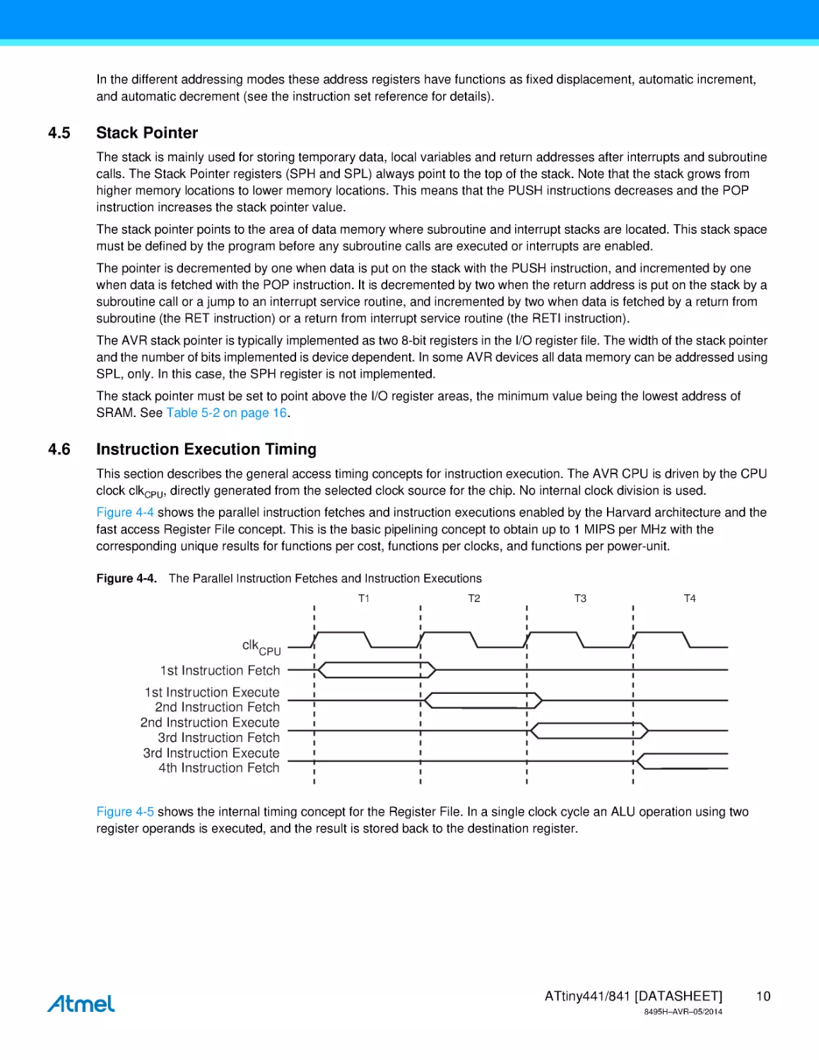
4.6
Instruction Execution Timing
This section describes the general access timing concepts for instruction execution. The AVR CPU is driven by the CPU
clock clkCPU, directly generated from the selected clock source for the chip. No internal clock division is used.
Figure 4-4 shows the parallel instruction fetches and instruction executions enabled by the Harvard architecture and the
fast access Register File concept. This is the basic pipelining concept to obtain up to 1 MIPS per MHz with the
corresponding unique results for functions per cost, functions per clocks, and functions per power-unit.
Figure 4-4. The Parallel Instruction Fetches and Instruction Executions
T1
T2
T3
T4
clkCPU
1st Instruction Fetch
1st Instruction Execute
2nd Instruction Fetch
2nd Instruction Execute
3rd Instruction Fetch
3rd Instruction Execute
4th Instruction Fetch
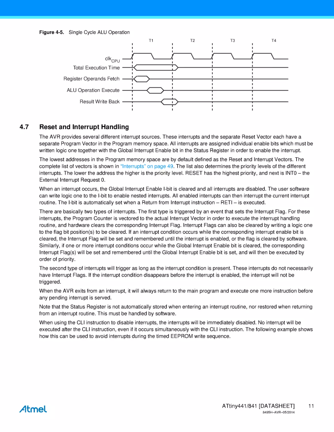
Figure 4-5 shows the internal timing concept for the Register File. In a single clock cycle an ALU operation using two
register operands is executed, and the result is stored back to the destination register.
ATtiny441/841 [DATASHEET]
8495H–AVR–05/2014
10
Figure 4-5. Single Cycle ALU Operation
T1
T2
T3
T4
clkCPU
Total Execution Time
Register Operands Fetch
ALU Operation Execute
Result Write Back
4.7
Reset and Interrupt Handling
The AVR provides several different interrupt sources. These interrupts and the separate Reset Vector each have a
separate Program Vector in the Program memory space. All interrupts are assigned individual enable bits which must be
written logic one together with the Global Interrupt Enable bit in the Status Register in order to enable the interrupt.
The lowest addresses in the Program memory space are by default defined as the Reset and Interrupt Vectors. The
complete list of vectors is shown in “Interrupts” on page 49. The list also determines the priority levels of the different
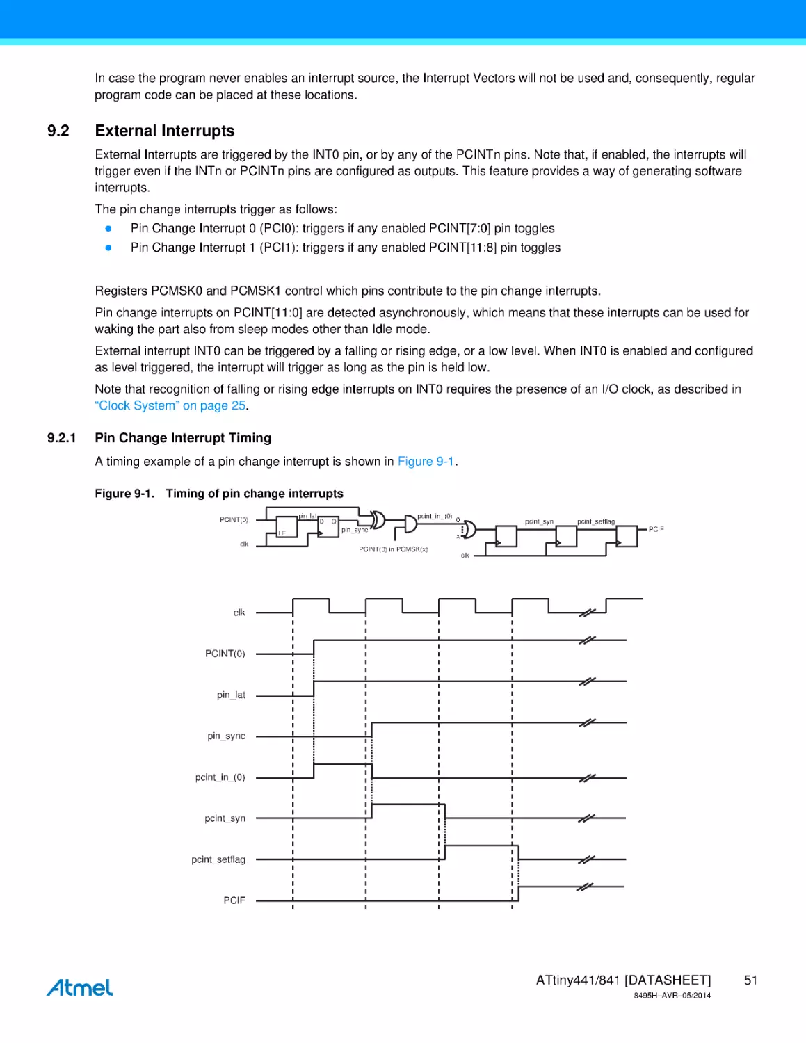
interrupts. The lower the address the higher is the priority level. RESET has the highest priority, and next is INT0 – the
External Interrupt Request 0.
When an interrupt occurs, the Global Interrupt Enable I-bit is cleared and all interrupts are disabled. The user software
can write logic one to the I-bit to enable nested interrupts. All enabled interrupts can then interrupt the current interrupt
routine. The I-bit is automatically set when a Return from Interrupt instruction – RETI – is executed.
There are basically two types of interrupts. The first type is triggered by an event that sets the Interrupt Flag. For these
interrupts, the Program Counter is vectored to the actual Interrupt Vector in order to execute the interrupt handling
routine, and hardware clears the corresponding Interrupt Flag. Interrupt Flags can also be cleared by writing a logic one
to the flag bit position(s) to be cleared. If an interrupt condition occurs while the corresponding interrupt enable bit is
cleared, the Interrupt Flag will be set and remembered until the interrupt is enabled, or the flag is cleared by software.
Similarly, if one or more interrupt conditions occur while the Global Interrupt Enable bit is cleared, the corresponding
Interrupt Flag(s) will be set and remembered until the Global Interrupt Enable bit is set, and will then be executed by
order of priority.
The second type of interrupts will trigger as long as the interrupt condition is present. These interrupts do not necessarily
have Interrupt Flags. If the interrupt condition disappears before the interrupt is enabled, the interrupt will not be
triggered.
When the AVR exits from an interrupt, it will always return to the main program and execute one more instruction before
any pending interrupt is served.
Note that the Status Register is not automatically stored when entering an interrupt routine, nor restored when returning
from an interrupt routine. This must be handled by software.
When using the CLI instruction to disable interrupts, the interrupts will be immediately disabled. No interrupt will be
executed after the CLI instruction, even if it occurs simultaneously with the CLI instruction. The following example shows
how this can be used to avoid interrupts during the timed EEPROM write sequence.
ATtiny441/841 [DATASHEET]
8495H–AVR–05/2014
11
Assembly Code Example
in
cli
sbi
sbi
out
bit)
r16, SREG
; store SREG value
; disable interrupts during timed sequence
EECR, EEMPE
; start EEPROM write
EECR, EEPE
SREG, r16
; restore SREG value (I-
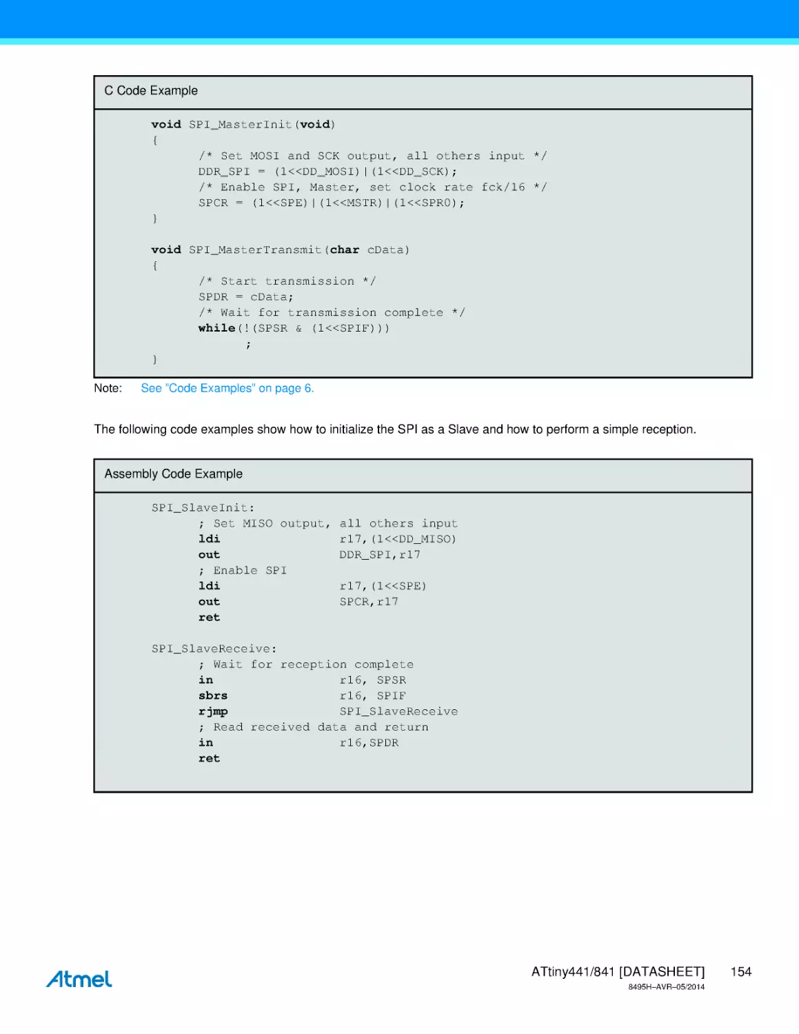
C Code Example
char cSREG;
cSREG = SREG;
/* disable interrupts during timed sequence */
_CLI();
EECR |= (1<<EEMPE); /* start EEPROM write */
EECR |= (1<<EEPE);
SREG = cSREG; /* restore SREG value (I-bit) */
Note:
/* store SREG value */
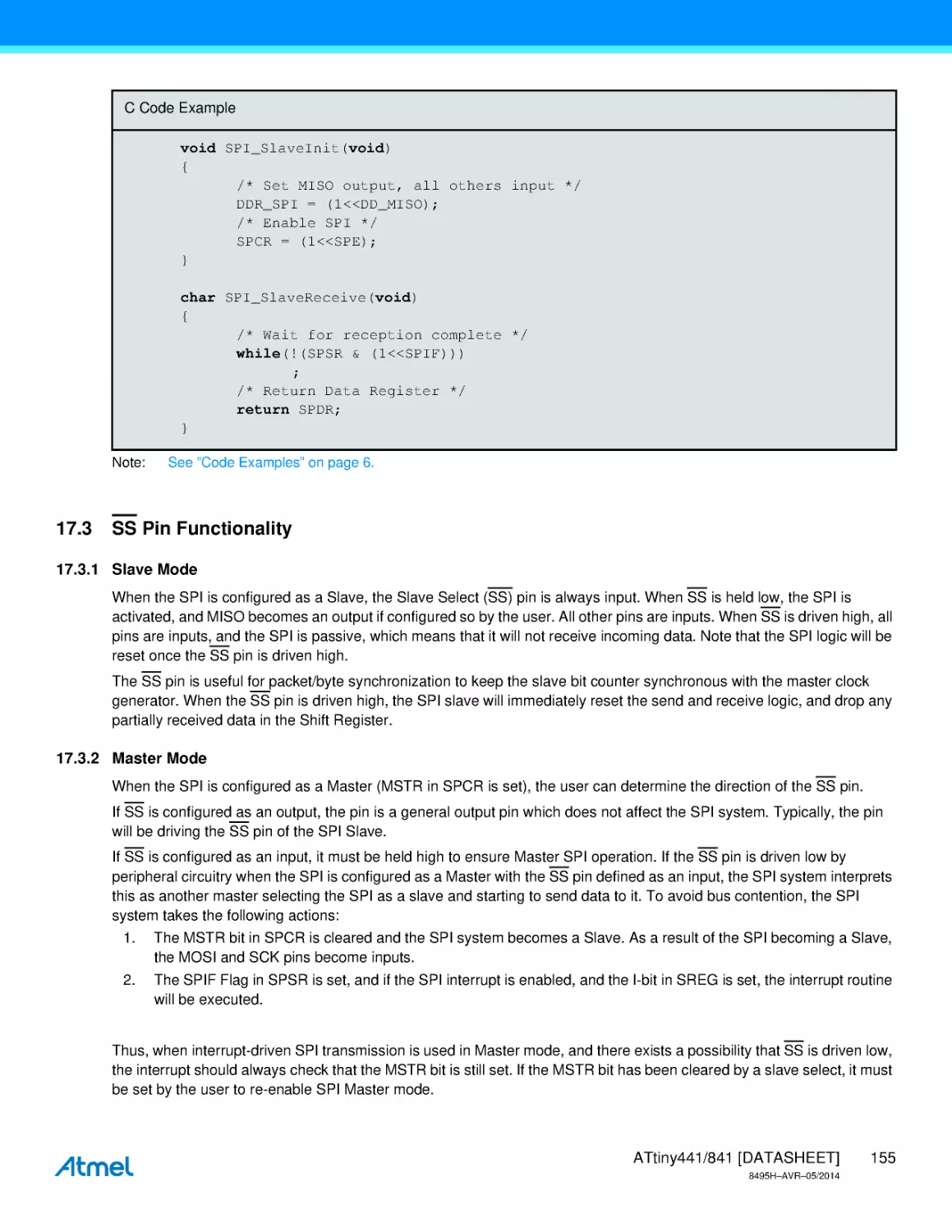
See “Code Examples” on page 6.
When using the SEI instruction to enable interrupts, the instruction following SEI will be executed before any pending
interrupts, as shown in the following example.
Assembly Code Example
sei
; set Global Interrupt Enable
sleep
; enter sleep, waiting for interrupt
; note: will enter sleep before any pending
; interrupt(s)
C Code Example
_SEI(); /* set Global Interrupt Enable */
_SLEEP(); /* enter sleep, waiting for interrupt */
/* note: will enter sleep before any pending interrupt(s) */
Note:
4.7.1
See “Code Examples” on page 6.
Interrupt Response Time
The interrupt execution response for all the enabled AVR interrupts is four clock cycles minimum. After four clock cycles
the Program Vector address for the actual interrupt handling routine is executed. During this four clock cycle period, the
Program Counter is pushed onto the Stack. The vector is normally a jump to the interrupt routine, and this jump takes
three clock cycles. If an interrupt occurs during execution of a multi-cycle instruction, this instruction is completed before
the interrupt is served. If an interrupt occurs when the MCU is in sleep mode, the interrupt execution response time is
increased by four clock cycles. This increase comes in addition to the start-up time from the selected sleep mode.
A return from an interrupt handling routine takes four clock cycles. During these four clock cycles, the Program Counter
(two bytes) is popped back from the Stack, the Stack Pointer is incremented by two, and the I-bit in SREG is set.
ATtiny441/841 [DATASHEET]
8495H–AVR–05/2014
12
4.8
Register Description
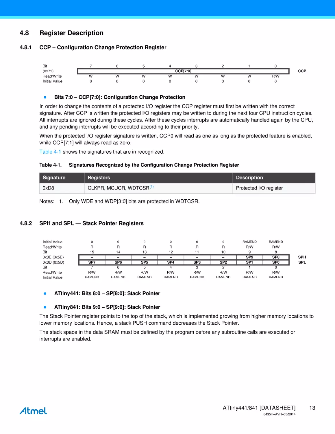
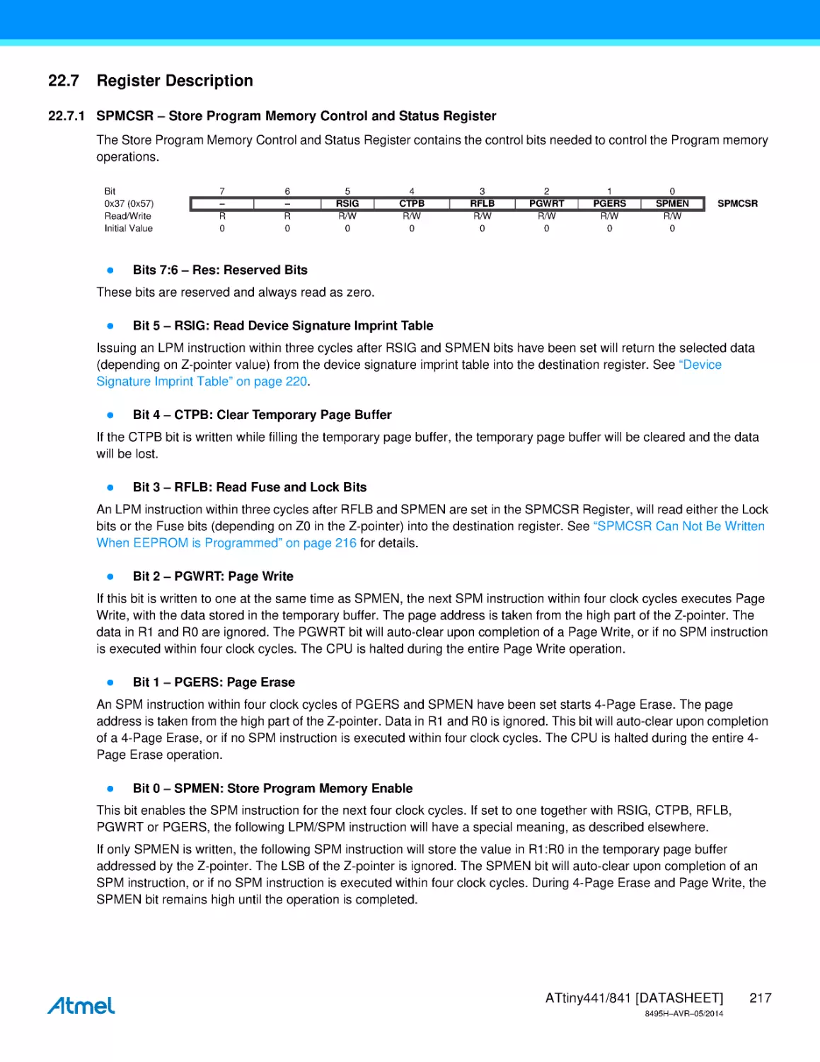
4.8.1
CCP – Configuration Change Protection Register
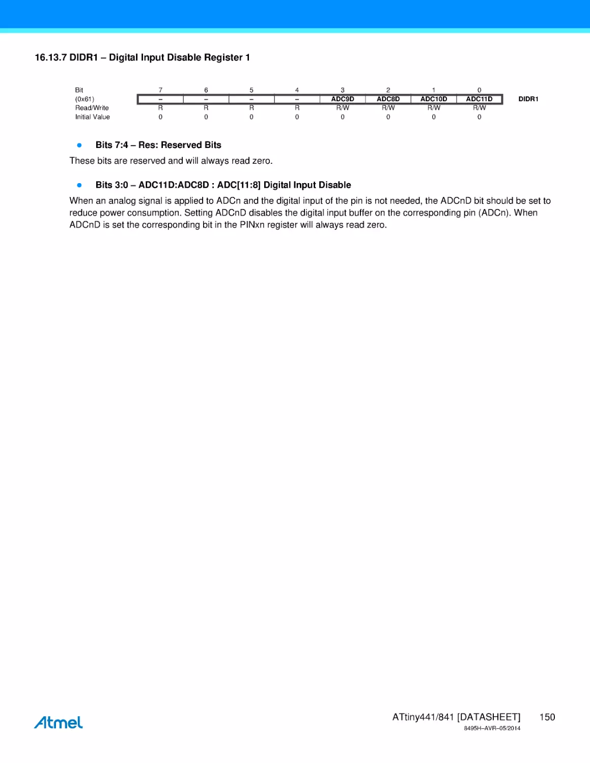
Bit
(0x71)
Read/Write
Initial Value
7
6
5
4
3
2
1
0
W
0
W
0
W
0
R/W
0
CCP[7:0]
W
0
W
0
W
0
W
0
CCP
Bits 7:0 – CCP[7:0]: Configuration Change Protection
In order to change the contents of a protected I/O register the CCP register must first be written with the correct
signature. After CCP is written the protected I/O registers may be written to during the next four CPU instruction cycles.
All interrupts are ignored during these cycles. After these cycles interrupts are automatically handled again by the CPU,
and any pending interrupts will be executed according to their priority.
When the protected I/O register signature is written, CCP0 will read as one as long as the protected feature is enabled,
while CCP[7:1] will always read as zero.
Table 4-1 shows the signatures that are in recognized.
Table 4-1.
Signature
Registers
Description
0xD8
CLKPR, MCUCR, WDTCSR(1)
Protected I/O register
Notes: 1.
4.8.2
Signatures Recognized by the Configuration Change Protection Register
Only WDE and WDP[3:0] bits are protected in WDTCSR.
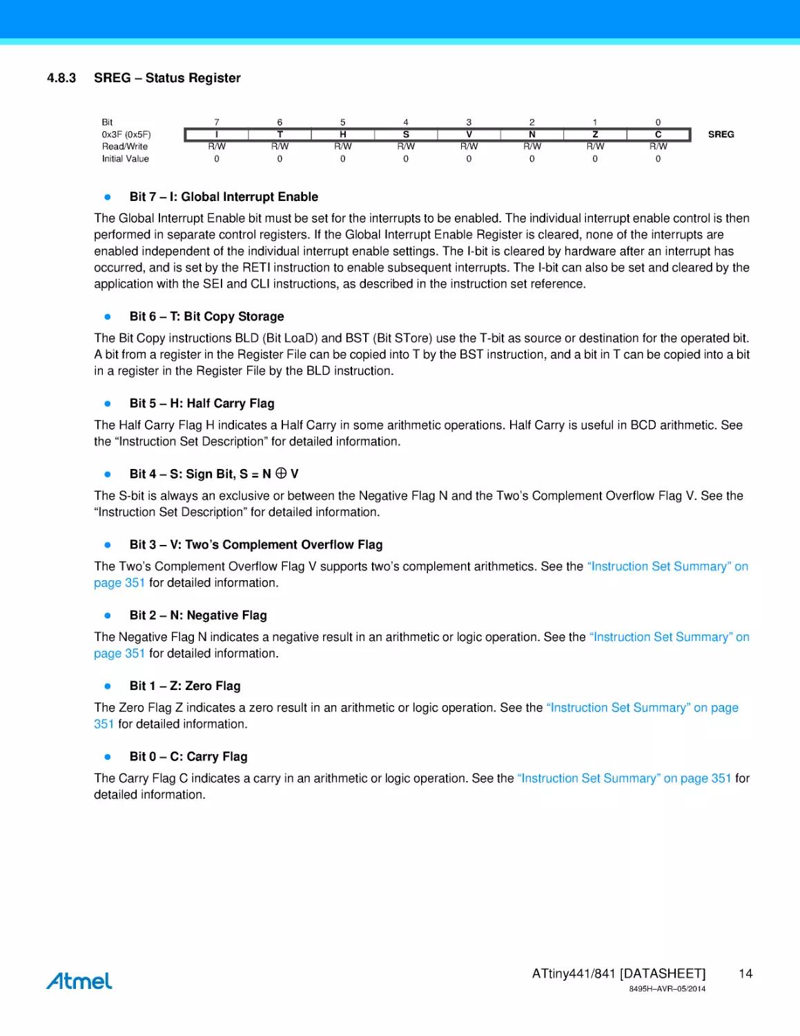
SPH and SPL — Stack Pointer Registers
Initial Value
Read/Write
Bit
0x3E (0x5E)
0x3D (0x5D)
Bit
Read/Write
Initial Value
0
0
0
0
0
0
RAMEND
RAMEND
R
15
–
SP7
7
R/W
R
14
–
SP6
6
R/W
R
13
–
SP5
5
R/W
R
12
–
SP4
4
R/W
R
11
–
SP3
3
R/W
R
10
–
SP2
2
R/W
R/W
9
SP9
SP1
1
R/W
R/W
8
SP8
SP0
0
R/W
RAMEND
RAMEND
RAMEND
RAMEND
RAMEND
RAMEND
RAMEND
RAMEND
ATtiny441: Bits 8:0 – SP[8:0]: Stack Pointer
ATtiny841: Bits 9:0 – SP[9:0]: Stack Pointer
SPH
SPL
The Stack Pointer register points to the top of the stack, which is implemented growing from higher memory locations to
lower memory locations. Hence, a stack PUSH command decreases the Stack Pointer.
The stack space in the data SRAM must be defined by the program before any subroutine calls are executed or
interrupts are enabled.
ATtiny441/841 [DATASHEET]
8495H–AVR–05/2014
13
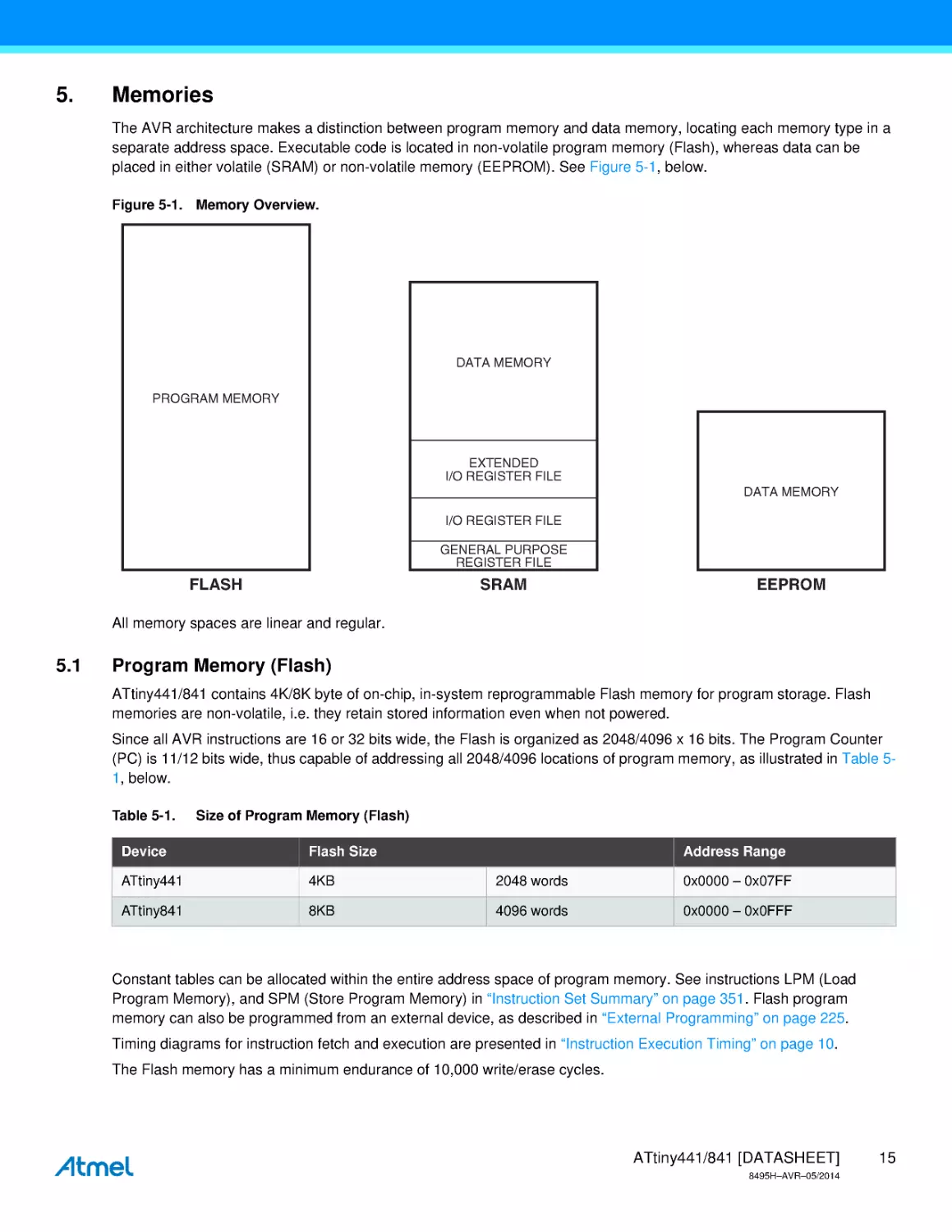
4.8.3
SREG – Status Register
Bit
0x3F (0x5F)
Read/Write
Initial Value
7
I
R/W
0
6
T
R/W
0
5
H
R/W
0
4
S
R/W
0
3
V
R/W
0
2
N
R/W
0
1
Z
R/W
0
0
C
R/W
0
SREG
Bit 7 – I: Global Interrupt Enable
The Global Interrupt Enable bit must be set for the interrupts to be enabled. The individual interrupt enable control is then
performed in separate control registers. If the Global Interrupt Enable Register is cleared, none of the interrupts are
enabled independent of the individual interrupt enable settings. The I-bit is cleared by hardware after an interrupt has
occurred, and is set by the RETI instruction to enable subsequent interrupts. The I-bit can also be set and cleared by the
application with the SEI and CLI instructions, as described in the instruction set reference.
Bit 6 – T: Bit Copy Storage
The Bit Copy instructions BLD (Bit LoaD) and BST (Bit STore) use the T-bit as source or destination for the operated bit.
A bit from a register in the Register File can be copied into T by the BST instruction, and a bit in T can be copied into a bit
in a register in the Register File by the BLD instruction.
Bit 5 – H: Half Carry Flag
The Half Carry Flag H indicates a Half Carry in some arithmetic operations. Half Carry is useful in BCD arithmetic. See
the “Instruction Set Description” for detailed information.
Bit 4 – S: Sign Bit, S = N V
The S-bit is always an exclusive or between the Negative Flag N and the Two’s Complement Overflow Flag V. See the
“Instruction Set Description” for detailed information.
Bit 3 – V: Two’s Complement Overflow Flag
The Two’s Complement Overflow Flag V supports two’s complement arithmetics. See the “Instruction Set Summary” on
page 351 for detailed information.
Bit 2 – N: Negative Flag
The Negative Flag N indicates a negative result in an arithmetic or logic operation. See the “Instruction Set Summary” on
page 351 for detailed information.
Bit 1 – Z: Zero Flag
The Zero Flag Z indicates a zero result in an arithmetic or logic operation. See the “Instruction Set Summary” on page
351 for detailed information.
Bit 0 – C: Carry Flag
The Carry Flag C indicates a carry in an arithmetic or logic operation. See the “Instruction Set Summary” on page 351 for
detailed information.
ATtiny441/841 [DATASHEET]
8495H–AVR–05/2014
14
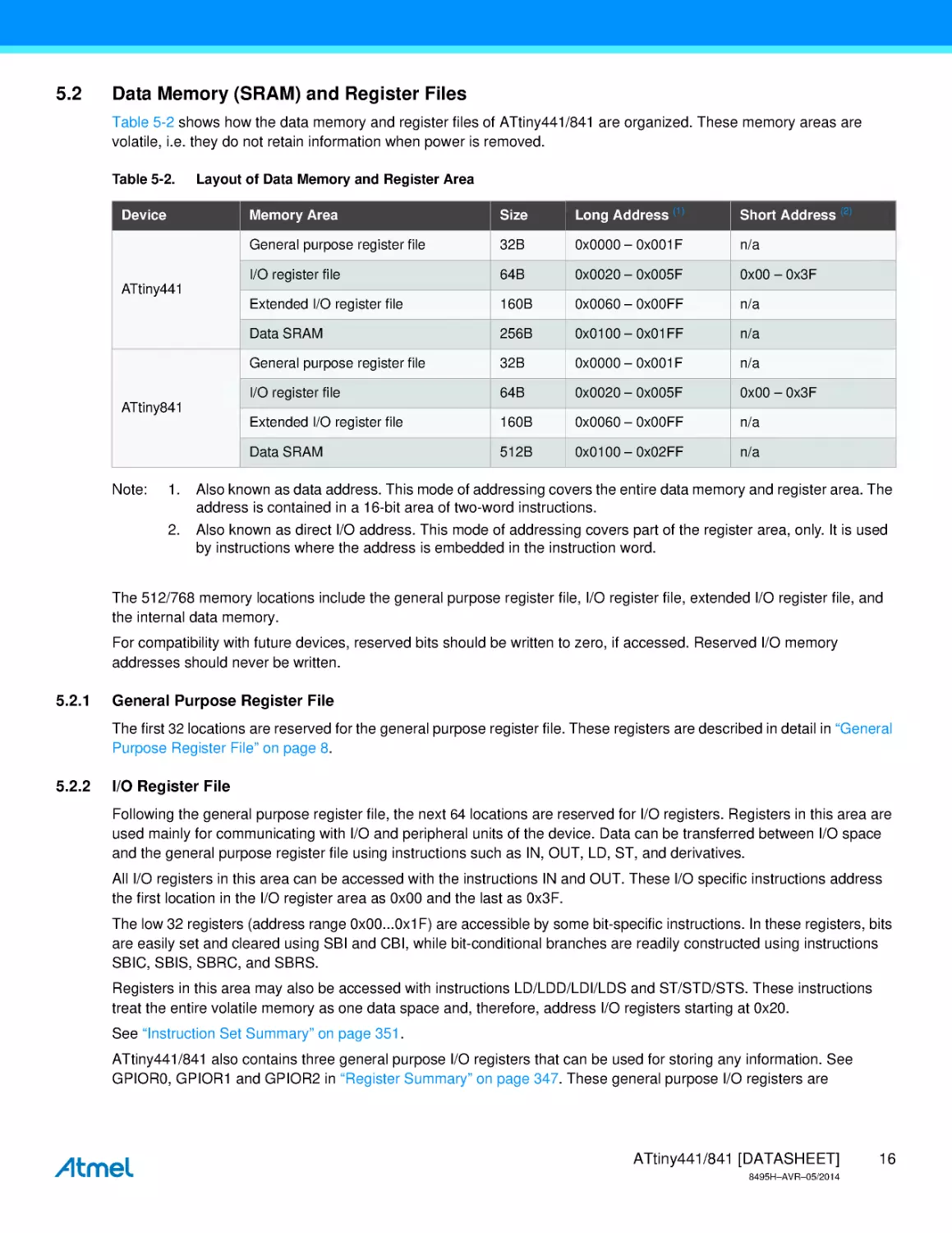
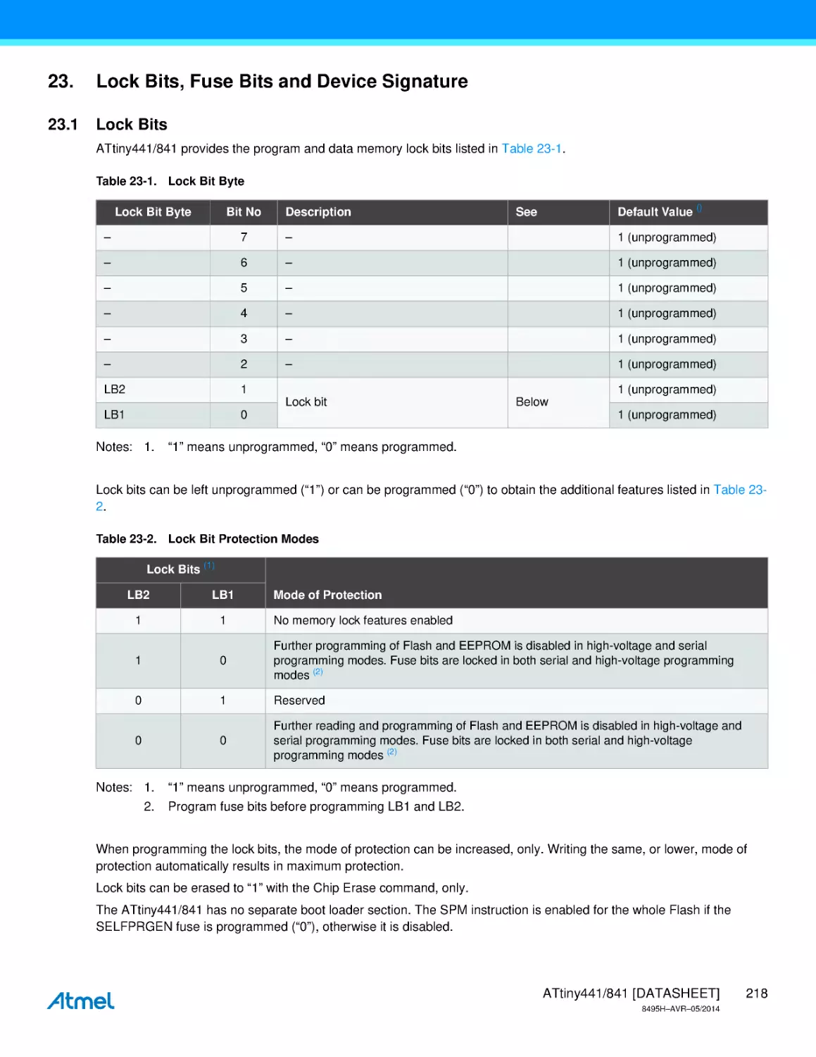
5.
Memories
The AVR architecture makes a distinction between program memory and data memory, locating each memory type in a
separate address space. Executable code is located in non-volatile program memory (Flash), whereas data can be
placed in either volatile (SRAM) or non-volatile memory (EEPROM). See Figure 5-1, below.
Figure 5-1. Memory Overview.
DATA MEMORY
PROGRAM MEMORY
EXTENDED
I/O REGISTER FILE
DATA MEMORY
I/O REGISTER FILE
GENERAL PURPOSE
REGISTER FILE
FLASH
SRAM
EEPROM
All memory spaces are linear and regular.
5.1
Program Memory (Flash)
ATtiny441/841 contains 4K/8K byte of on-chip, in-system reprogrammable Flash memory for program storage. Flash
memories are non-volatile, i.e. they retain stored information even when not powered.
Since all AVR instructions are 16 or 32 bits wide, the Flash is organized as 2048/4096 x 16 bits. The Program Counter
(PC) is 11/12 bits wide, thus capable of addressing all 2048/4096 locations of program memory, as illustrated in Table 51, below.
Table 5-1.
Size of Program Memory (Flash)
Device
Flash Size
Address Range
ATtiny441
4KB
2048 words
0x0000 – 0x07FF
ATtiny841
8KB
4096 words
0x0000 – 0x0FFF
Constant tables can be allocated within the entire address space of program memory. See instructions LPM (Load
Program Memory), and SPM (Store Program Memory) in “Instruction Set Summary” on page 351. Flash program
memory can also be programmed from an external device, as described in “External Programming” on page 225.
Timing diagrams for instruction fetch and execution are presented in “Instruction Execution Timing” on page 10.
The Flash memory has a minimum endurance of 10,000 write/erase cycles.
ATtiny441/841 [DATASHEET]
8495H–AVR–05/2014
15
5.2
Data Memory (SRAM) and Register Files
Table 5-2 shows how the data memory and register files of ATtiny441/841 are organized. These memory areas are
volatile, i.e. they do not retain information when power is removed.
Table 5-2.
Layout of Data Memory and Register Area
Device
Memory Area
Size
Long Address (1)
Short Address (2)
General purpose register file
32B
0x0000 – 0x001F
n/a
I/O register file
64B
0x0020 – 0x005F
0x00 – 0x3F
Extended I/O register file
160B
0x0060 – 0x00FF
n/a
Data SRAM
256B
0x0100 – 0x01FF
n/a
General purpose register file
32B
0x0000 – 0x001F
n/a
I/O register file
64B
0x0020 – 0x005F
0x00 – 0x3F
Extended I/O register file
160B
0x0060 – 0x00FF
n/a
Data SRAM
512B
0x0100 – 0x02FF
n/a
ATtiny441
ATtiny841
Note:
1.
Also known as data address. This mode of addressing covers the entire data memory and register area. The
address is contained in a 16-bit area of two-word instructions.
2.
Also known as direct I/O address. This mode of addressing covers part of the register area, only. It is used
by instructions where the address is embedded in the instruction word.
The 512/768 memory locations include the general purpose register file, I/O register file, extended I/O register file, and
the internal data memory.
For compatibility with future devices, reserved bits should be written to zero, if accessed. Reserved I/O memory
addresses should never be written.
5.2.1
General Purpose Register File
The first 32 locations are reserved for the general purpose register file. These registers are described in detail in “General
Purpose Register File” on page 8.
5.2.2
I/O Register File
Following the general purpose register file, the next 64 locations are reserved for I/O registers. Registers in this area are
used mainly for communicating with I/O and peripheral units of the device. Data can be transferred between I/O space
and the general purpose register file using instructions such as IN, OUT, LD, ST, and derivatives.
All I/O registers in this area can be accessed with the instructions IN and OUT. These I/O specific instructions address
the first location in the I/O register area as 0x00 and the last as 0x3F.
The low 32 registers (address range 0x00...0x1F) are accessible by some bit-specific instructions. In these registers, bits
are easily set and cleared using SBI and CBI, while bit-conditional branches are readily constructed using instructions
SBIC, SBIS, SBRC, and SBRS.
Registers in this area may also be accessed with instructions LD/LDD/LDI/LDS and ST/STD/STS. These instructions
treat the entire volatile memory as one data space and, therefore, address I/O registers starting at 0x20.
See “Instruction Set Summary” on page 351.
ATtiny441/841 also contains three general purpose I/O registers that can be used for storing any information. See
GPIOR0, GPIOR1 and GPIOR2 in “Register Summary” on page 347. These general purpose I/O registers are
ATtiny441/841 [DATASHEET]
8495H–AVR–05/2014
16
particularly useful for storing global variables and status flags, since they are accessible to bit-specific instructions such
as SBI, CBI, SBIC, SBIS, SBRC, and SBRS.
5.2.3
Extended I/O Register File
Following the standard I/O register file, the next 160 locations are reserved for extended I/O registers. ATtiny441/841 is a
complex microcontroller with more peripheral units than can be addressed with the IN and OUT instructions. Registers in
the extended I/O area must be accessed using instructions LD/LDD/LDI/LDS and ST/STD/STS. See “Instruction Set
Summary” on page 351.
See “Register Summary” on page 347 for a list of I/O registers.
Data Memory (SRAM)
Following the general purpose register file and the I/O register files, the remaining 128/256/512 locations are reserved for
the internal data SRAM.
There are five addressing modes available:
Direct. This mode of addressing reaches the entire data space.
Indirect.
Indirect with Displacement. This mode of addressing reaches 63 address locations from the base address given by
the Y- or Z-register.
Indirect with Pre-decrement. In this mode the address register is automatically decremented before access.
Address pointer registers (X, Y, and Z) are located in the general purpose register file, in registers R26 to R31. See
“General Purpose Register File” on page 8.
Indirect with Post-increment. In this mode the address register is automatically incremented after access. Address
pointer registers (X, Y, and Z) are located in the general purpose register file, in registers R26 to R31. See
“General Purpose Register File” on page 8.
All addressing modes can be used on the entire volatile memory, including the general purpose register file, the I/O
register files and the data memory.
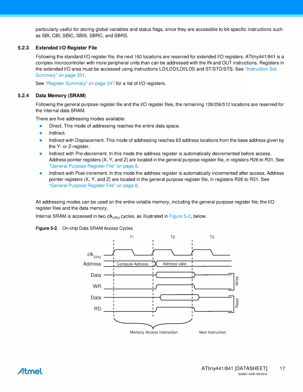
Internal SRAM is accessed in two clkCPU cycles, as illustrated in Figure 5-2, below.
Figure 5-2. On-chip Data SRAM Access Cycles
T1
T2
T3
clkCPU
Address
Compute Address
Address valid
Write
Data
WR
Data
Read
5.2.4
RD
Memory Access Instruction
Next Instruction
ATtiny441/841 [DATASHEET]
8495H–AVR–05/2014
17
5.3
Data Memory (EEPROM)
ATtiny441/841 contains 256/512 bytes of non-volatile data memory. This EEPROM is organized as a separate data
space, in which single bytes can be read and written. All access registers are located in the I/O space.
The EEPROM memory layout is summarized in Table 5-3, below.
Table 5-3.
Size of Non-Volatile Data Memory (EEPROM)
Device
EEPROM Size
Address Range
ATtiny441
256B
0x00 – 0xFF
ATtiny841
512B
0x00 – 0x01FF
The internal 8MHz oscillator is used to time EEPROM operations. The frequency of the oscillator must be within the
requirements described in “OSCCAL0 – Oscillator Calibration Register” on page 33.
When powered by heavily filtered supplies, the supply voltage, VCC, is likely to rise or fall slowly on power-up and powerdown. Slow rise and fall times may put the device in a state where it is running at supply voltages lower than specified. To
avoid problems in situations like this, see “Preventing EEPROM Corruption” on page 19.
The EEPROM has a minimum endurance of 100,000 write/erase cycles.
5.3.1
Programming Methods
There are two methods for EEPROM programming:
Atomic byte programming. This is the simple mode of programming, where target locations are erased and written
in a single operation. In this mode of operation the target is guaranteed to always be erased before writing but
programming times are longer.
Split byte programming. It is possible to split the erase and write cycle in two different operations. This is useful
when short access times are required, for example when supply voltage is falling. In order to take advantage of this
method target locations must be erased before writing to them. This can be done at times when the system allows
time-critical operations, typically at start-up and initialization.
The programming method is selected using the EEPROM Programming Mode bits (EEPM1 and EEPM0) in EEPROM
Control Register (EECR). See Table 5-4 on page 23. Write and erase times are given in the same table.
Since EEPROM programming takes some time the application must wait for one operation to complete before starting
the next. This can be done by either polling the EEPROM Program Enable bit (EEPE) in EEPROM Control Register
(EECR), or via the EEPROM Ready Interrupt. The EEPROM interrupt is controlled by the EEPROM Ready Interrupt
Enable (EERIE) bit in EECR.
5.3.2
Read
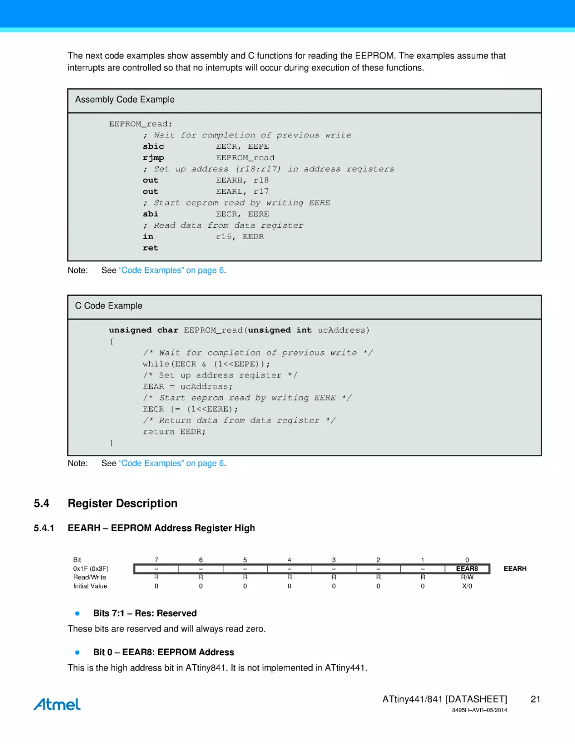
To read an EEPROM memory location follow the procedure below:
Poll the EEPROM Program Enable bit (EEPE) in EEPROM Control Register (EECR) to make sure no other
EEPROM operations are in process. If set, wait to clear.
Write target address to EEPROM Address Registers (EEARH/EEARL).
Start the read operation by setting the EEPROM Read Enable bit (EERE) in the EEPROM Control Register
(EECR). During the read operation, the CPU is halted for four clock cycles before executing the next instruction.
Read data from the EEPROM Data Register (EEDR).
ATtiny441/841 [DATASHEET]
8495H–AVR–05/2014
18
5.3.3
Erase
In order to prevent unintentional EEPROM writes, a specific procedure must be followed to erase memory locations. To
erase an EEPROM memory location follow the procedure below:
1.
Poll the EEPROM Program Enable bit (EEPE) in EEPROM Control Register (EECR) to make sure no other
EEPROM operations are in process. If set, wait to clear.
2.
Set mode of programming to erase by writing EEPROM Programming Mode bits (EEPM0 and EEPM1) in
EEPROM Control Register (EECR).
3.
Write target address to EEPROM Address Registers (EEARH/EEARL).
4.
Enable erase by setting EEPROM Master Program Enable (EEMPE) in EEPROM Control Register (EECR). Within
four clock cycles, start the erase operation by setting the EEPROM Program Enable bit (EEPE) in the EEPROM
Control Register (EECR). During the erase operation, the CPU is halted for two clock cycles before executing the
next instruction.
The EEPE bit remains set until the erase operation has completed. While the device is busy programming, it is not
possible to perform any other EEPROM operations.
5.3.4
Write
In order to prevent unintentional EEPROM writes, a specific procedure must be followed to write to memory locations.
Before writing data to EEPROM the target location must be erased. This can be done either in the same operation or as
part of a split operation. Writing to an un-erased EEPROM location will result in corrupted data.
To write an EEPROM memory location follow the procedure below:
1.
Poll the EEPROM Program Enable bit (EEPE) in EEPROM Control Register (EECR) to make sure no other
EEPROM operations are in process. If set, wait to clear.
2.
Set mode of programming by writing EEPROM Programming Mode bits (EEPM0 and EEPM1) in EEPROM Control
Register (EECR). Alternatively, data can be written in one operation or the write procedure can be split up in erase,
only, and write, only.
3.
Write target address to EEPROM Address Registers (EEARH/EEARL).
4.
Write target data to EEPROM Data Register (EEDR).
5.
Enable write by setting EEPROM Master Program Enable (EEMPE) in EEPROM Control Register (EECR). Within
four clock cycles, start the write operation by setting the EEPROM Program Enable bit (EEPE) in the EEPROM
Control Register (EECR). During the write operation, the CPU is halted for two clock cycles before executing the
next instruction.
The EEPE bit remains set until the write operation has completed. While the device is busy with programming, it is not
possible to do any other EEPROM operations.
5.3.5
Preventing EEPROM Corruption
During periods of low VCC, the EEPROM data can be corrupted because the supply voltage is too low for the CPU and
the EEPROM to operate properly. These issues are the same as for board level systems using EEPROM, and the same
design solutions should be applied.
At low supply voltages data in EEPROM can be corrupted in two ways:
The supply voltage is too low to maintain proper operation of an otherwise legitimate EEPROM program
sequence.
The supply voltage is too low for the CPU and instructions may be executed incorrectly.
ATtiny441/841 [DATASHEET]
8495H–AVR–05/2014
19
EEPROM data corruption is avoided by keeping the device in reset during periods of insufficient power supply voltage.
This is easily done by enabling the internal Brown-Out Detector (BOD). If BOD detection levels are not sufficient for the
design, an external reset circuit for low VCC can be used.
Provided that supply voltage is sufficient, an EEPROM write operation will be completed even when a reset occurs.
5.3.6
Program Examples
The following code examples show one assembly and one C function for erase, write, or atomic write of the EEPROM.
The examples assume that interrupts are controlled (e.g., by disabling interrupts globally) so that no interrupts occur
during execution of these functions.
Assembly Code Example
EEPROM_write:
; Wait for completion of previous write
sbic
EECR, EEPE
rjmp
EEPROM_write
; Set Programming mode
ldi
r16, (0<<EEPM1)|(0<<EEPM0)
out
EECR, r16
; Set up address (r18:r17) in address registers
out
EEARH, r18
out
EEARL, r17
; Write data (r19) to data register
out
EEDR, r19
; Write logical one to EEMPE
sbi
EECR, EEMPE
; Start eeprom write by setting EEPE
sbi
EECR, EEPE
ret
Note:
See “Code Examples” on page 6.
C Code Example
void EEPROM_write(unsigned int ucAddress, unsigned char ucData)
{
/* Wait for completion of previous write */
while(EECR & (1<<EEPE));
/* Set Programming mode */
EECR = (0<<EEPM1)|(0<<EEPM0);
/* Set up address and data registers */
EEAR = ucAddress;
EEDR = ucData;
/* Write logical one to EEMPE */
EECR |= (1<<EEMPE);
/* Start eeprom write by setting EEPE */
EECR |= (1<<EEPE);
}
Note:
See “Code Examples” on page 6.
ATtiny441/841 [DATASHEET]
8495H–AVR–05/2014
20
The next code examples show assembly and C functions for reading the EEPROM. The examples assume that
interrupts are controlled so that no interrupts will occur during execution of these functions.
Assembly Code Example
EEPROM_read:
; Wait for completion of previous write
sbic
EECR, EEPE
rjmp
EEPROM_read
; Set up address (r18:r17) in address registers
out
EEARH, r18
out
EEARL, r17
; Start eeprom read by writing EERE
sbi
EECR, EERE
; Read data from data register
in
r16, EEDR
ret
Note:
See “Code Examples” on page 6.
C Code Example
unsigned char EEPROM_read(unsigned int ucAddress)
{
/* Wait for completion of previous write */
while(EECR & (1<<EEPE));
/* Set up address register */
EEAR = ucAddress;
/* Start eeprom read by writing EERE */
EECR |= (1<<EERE);
/* Return data from data register */
return EEDR;
}
Note:
See “Code Examples” on page 6.
5.4
Register Description
5.4.1
EEARH – EEPROM Address Register High
Bit
0x1F (0x3F)
Read/Write
Initial Value
7
–
R
0
6
–
R
0
5
–
R
0
4
–
R
0
3
–
R
0
2
–
R
0
1
–
R
0
0
EEAR8
R/W
X/0
EEARH
Bits 7:1 – Res: Reserved
These bits are reserved and will always read zero.
Bit 0 – EEAR8: EEPROM Address
This is the high address bit in ATtiny841. It is not implemented in ATtiny441.
ATtiny441/841 [DATASHEET]
8495H–AVR–05/2014
21
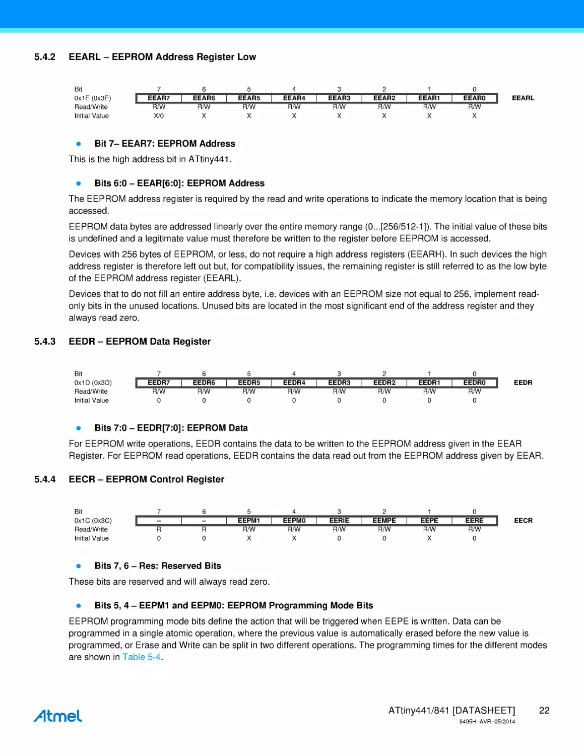
5.4.2
EEARL – EEPROM Address Register Low
Bit
0x1E (0x3E)
Read/Write
Initial Value
7
EEAR7
R/W
X/0
6
EEAR6
R/W
X
5
EEAR5
R/W
X
4
EEAR4
R/W
X
3
EEAR3
R/W
X
2
EEAR2
R/W
X
1
EEAR1
R/W
X
0
EEAR0
R/W
X
EEARL
Bit 7– EEAR7: EEPROM Address
This is the high address bit in ATtiny441.
Bits 6:0 – EEAR[6:0]: EEPROM Address
The EEPROM address register is required by the read and write operations to indicate the memory location that is being
accessed.
EEPROM data bytes are addressed linearly over the entire memory range (0...[256/512-1]). The initial value of these bits
is undefined and a legitimate value must therefore be written to the register before EEPROM is accessed.
Devices with 256 bytes of EEPROM, or less, do not require a high address registers (EEARH). In such devices the high
address register is therefore left out but, for compatibility issues, the remaining register is still referred to as the low byte
of the EEPROM address register (EEARL).
Devices that to do not fill an entire address byte, i.e. devices with an EEPROM size not equal to 256, implement readonly bits in the unused locations. Unused bits are located in the most significant end of the address register and they
always read zero.
5.4.3
EEDR – EEPROM Data Register
Bit
0x1D (0x3D)
Read/Write
Initial Value
7
EEDR7
R/W
0
6
EEDR6
R/W
0
5
EEDR5
R/W
0
4
EEDR4
R/W
0
3
EEDR3
R/W
0
2
EEDR2
R/W
0
1
EEDR1
R/W
0
0
EEDR0
R/W
0
EEDR
Bits 7:0 – EEDR[7:0]: EEPROM Data
For EEPROM write operations, EEDR contains the data to be written to the EEPROM address given in the EEAR
Register. For EEPROM read operations, EEDR contains the data read out from the EEPROM address given by EEAR.
5.4.4
EECR – EEPROM Control Register
Bit
0x1C (0x3C)
Read/Write
Initial Value
7
–
R
0
6
–
R
0
5
EEPM1
R/W
X
4
EEPM0
R/W
X
3
EERIE
R/W
0
2
EEMPE
R/W
0
1
EEPE
R/W
X
0
EERE
R/W
0
EECR
Bits 7, 6 – Res: Reserved Bits
These bits are reserved and will always read zero.
Bits 5, 4 – EEPM1 and EEPM0: EEPROM Programming Mode Bits
EEPROM programming mode bits define the action that will be triggered when EEPE is written. Data can be
programmed in a single atomic operation, where the previous value is automatically erased before the new value is
programmed, or Erase and Write can be split in two different operations. The programming times for the different modes
are shown in Table 5-4.
ATtiny441/841 [DATASHEET]
8495H–AVR–05/2014
22
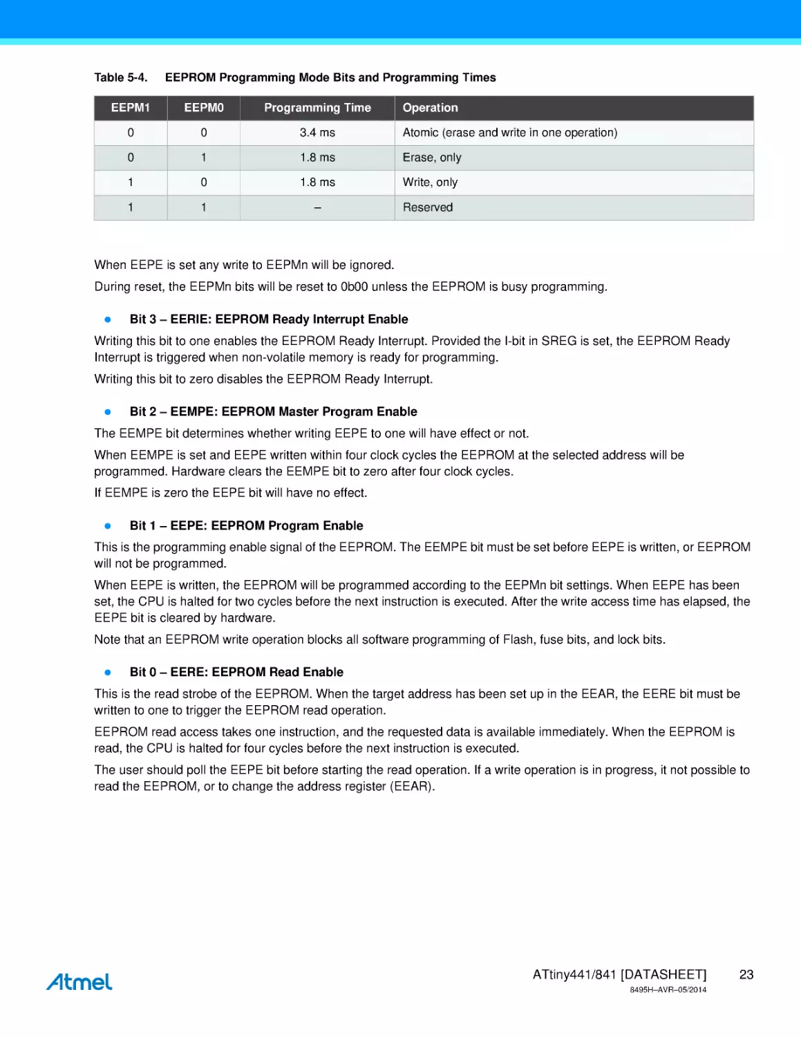
Table 5-4.
EEPROM Programming Mode Bits and Programming Times
EEPM1
EEPM0
Programming Time
Operation
0
0
3.4 ms
Atomic (erase and write in one operation)
0
1
1.8 ms
Erase, only
1
0
1.8 ms
Write, only
1
1
–
Reserved
When EEPE is set any write to EEPMn will be ignored.
During reset, the EEPMn bits will be reset to 0b00 unless the EEPROM is busy programming.
Bit 3 – EERIE: EEPROM Ready Interrupt Enable
Writing this bit to one enables the EEPROM Ready Interrupt. Provided the I-bit in SREG is set, the EEPROM Ready
Interrupt is triggered when non-volatile memory is ready for programming.
Writing this bit to zero disables the EEPROM Ready Interrupt.
Bit 2 – EEMPE: EEPROM Master Program Enable
The EEMPE bit determines whether writing EEPE to one will have effect or not.
When EEMPE is set and EEPE written within four clock cycles the EEPROM at the selected address will be
programmed. Hardware clears the EEMPE bit to zero after four clock cycles.
If EEMPE is zero the EEPE bit will have no effect.
Bit 1 – EEPE: EEPROM Program Enable
This is the programming enable signal of the EEPROM. The EEMPE bit must be set before EEPE is written, or EEPROM
will not be programmed.
When EEPE is written, the EEPROM will be programmed according to the EEPMn bit settings. When EEPE has been
set, the CPU is halted for two cycles before the next instruction is executed. After the write access time has elapsed, the
EEPE bit is cleared by hardware.
Note that an EEPROM write operation blocks all software programming of Flash, fuse bits, and lock bits.
Bit 0 – EERE: EEPROM Read Enable
This is the read strobe of the EEPROM. When the target address has been set up in the EEAR, the EERE bit must be
written to one to trigger the EEPROM read operation.
EEPROM read access takes one instruction, and the requested data is available immediately. When the EEPROM is
read, the CPU is halted for four cycles before the next instruction is executed.
The user should poll the EEPE bit before starting the read operation. If a write operation is in progress, it not possible to
read the EEPROM, or to change the address register (EEAR).
ATtiny441/841 [DATASHEET]
8495H–AVR–05/2014
23
5.4.5
GPIOR2 – General Purpose I/O Register 2
Bit
0x15 (0x35)
Read/Write
Initial Value
7
MSB
R/W
0
6
5
4
3
2
1
R/W
0
R/W
0
R/W
0
R/W
0
R/W
0
R/W
0
0
LSB
R/W
0
GPIOR2
This register may be used freely for storing any kind of data.
5.4.6
GPIOR1 – General Purpose I/O Register 1
Bit
0x14 (0x34)
Read/Write
Initial Value
7
MSB
R/W
0
6
5
4
3
2
1
R/W
0
R/W
0
R/W
0
R/W
0
R/W
0
R/W
0
0
LSB
R/W
0
GPIOR1
This register may be used freely for storing any kind of data.
5.4.7
GPIOR0 – General Purpose I/O Register 0
Bit
0x13 (0x33)
Read/Write
Initial Value
7
MSB
R/W
0
6
5
4
3
2
1
R/W
0
R/W
0
R/W
0
R/W
0
R/W
0
R/W
0
0
LSB
R/W
0
GPIOR0
This register may be used freely for storing any kind of data.
ATtiny441/841 [DATASHEET]
8495H–AVR–05/2014
24
6.
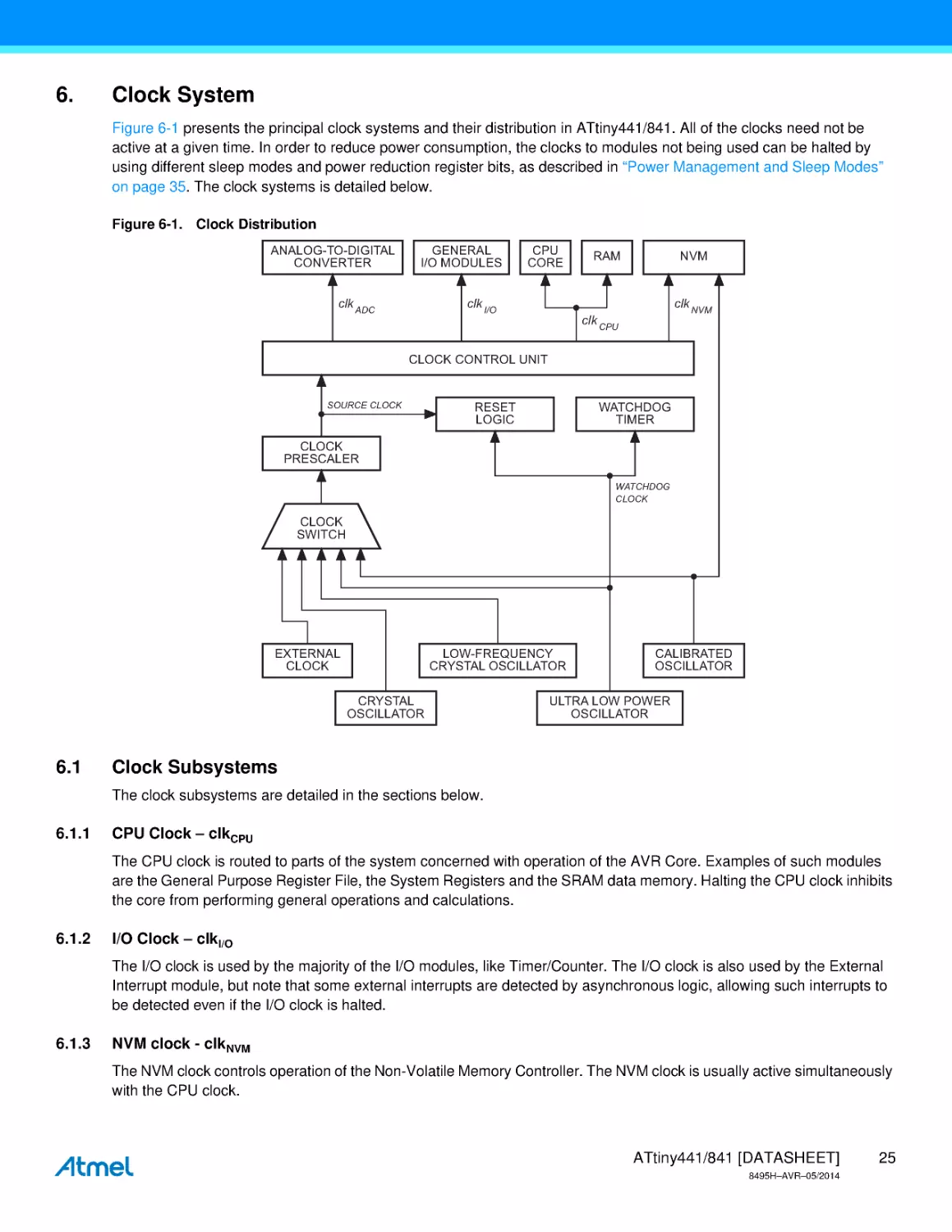
Clock System
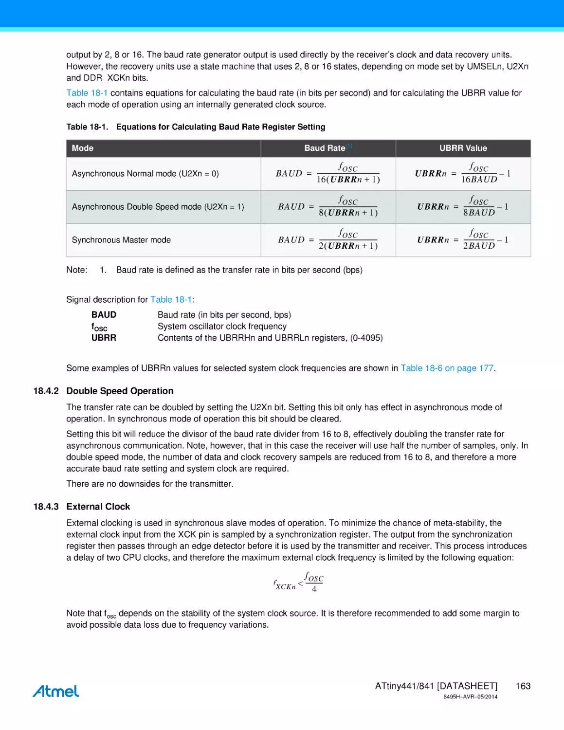
Figure 6-1 presents the principal clock systems and their distribution in ATtiny441/841. All of the clocks need not be
active at a given time. In order to reduce power consumption, the clocks to modules not being used can be halted by
using different sleep modes and power reduction register bits, as described in “Power Management and Sleep Modes”
on page 35. The clock systems is detailed below.
Figure 6-1. Clock Distribution
ANALOG-TO-DIGITAL
CONVERTER
GENERAL
I/O MODULES
clk ADC
CPU
CORE
clk I/O
RAM
NVM
clk NVM
clk CPU
CLOCK CONTROL UNIT
SOURCE CLOCK
RESET
LOGIC
WATCHDOG
TIMER
CLOCK
PRESCALER
WATCHDOG
CLOCK
CLOCK
SWITCH
EXTERNAL
CLOCK
LOW-FREQUENCY
CRYSTAL OSCILLATOR
CRYSTAL
OSCILLATOR
6.1
CALIBRATED
OSCILLATOR
ULTRA LOW POWER
OSCILLATOR
Clock Subsystems
The clock subsystems are detailed in the sections below.
6.1.1
CPU Clock – clkCPU
The CPU clock is routed to parts of the system concerned with operation of the AVR Core. Examples of such modules
are the General Purpose Register File, the System Registers and the SRAM data memory. Halting the CPU clock inhibits
the core from performing general operations and calculations.
6.1.2
I/O Clock – clkI/O
The I/O clock is used by the majority of the I/O modules, like Timer/Counter. The I/O clock is also used by the External
Interrupt module, but note that some external interrupts are detected by asynchronous logic, allowing such interrupts to
be detected even if the I/O clock is halted.
6.1.3
NVM clock - clkNVM
The NVM clock controls operation of the Non-Volatile Memory Controller. The NVM clock is usually active simultaneously
with the CPU clock.
ATtiny441/841 [DATASHEET]
8495H–AVR–05/2014
25
6.1.4
ADC Clock – clkADC
The ADC is provided with a dedicated clock domain. This allows halting the CPU and I/O clocks in order to reduce noise
generated by digital circuitry. This gives more accurate ADC conversion results.
6.2
Clock Sources
The device can use any of the following sources for the system clock:
External Clock (see page 26)
Calibrated Internal 8MHz Oscillator (see page 27)
Internal Ultra Low Power (ULP) Oscillator (see page 27)
Low-Frequency Crystal Oscillator (see page 28)
Crystal Oscillator / Ceramic Resonator (see page 28)
The clock source is selected using CKSEL fuses, as shown in Table 6-1 below.
Table 6-1.
CKSEL Fuse Bits and Device Clocking Options
CKSEL[3:0]
(1)
Frequency
Device Clocking Option
0000
Any
External Clock (see page 26)
0001
—
(not used)
0010
8MHz
Calibrated Internal 8MHz Oscillator (see page 27) (2)
0011
—
(not used)
0100
32 – 512kHz
Internal Ultra Low Power (ULP) Oscillator (see page 27)
0101
—
(not used)
0110
32kHz
Low-Frequency Crystal Oscillator (see page 28)
0111
—
(not used)
100X
0.4 – 0.9MHz
101X
0.9 – 3MHz
110X
3 – 8MHz
111X
> 8MHz
Crystal Oscillator / Ceramic Resonator (see page 28)
Note:
1.
For all fuses “1” means unprogrammed and “0” means programmed.
2.
This is the default setting. The device is shipped with this fuse combination.
.
CKSEL fuse bits can be read by firmware (see “Reading Lock, Fuse and Signature Data from Software” on page 222),
but firmware can not write to fuse bits.
When the device wakes up from power-down the selected clock source is used to time the start-up, ensuring stable
oscillator operation before instruction execution starts. When the CPU starts from reset, the internal 32kHz oscillator is
used for generating an additional delay, allowing supply voltage to reach a stable level before normal device operation is
started.
System clock alternatives are discussed in the following sections.
6.2.1
External Clock
To drive the device from an external clock source, CLKI should be connected as shown in Figure 6-2, below.
ATtiny441/841 [DATASHEET]
8495H–AVR–05/2014
26
Figure 6-2. External Clock Drive Configuration
EXTERNAL
CLOCK
SIGNAL
CLKI
GND
Start-up time for this clock source is determined by the SUT fuse bit, as shown in Table 6-5 on page 30.
To ensure stable operation of the MCU it is required to avoid sudden changes in the external clock frequency . A
variation in frequency of more than 2% from one clock cycle to the next can lead to unpredictable behavior. It is required
to ensure that the MCU is kept in Reset during such changes in the clock frequency.
Stable operation for large step changes in system clock frequency is guaranteed when using the system clock prescaler.
See “System Clock Prescaler” on page 29.
6.2.2
Calibrated Internal 8MHz Oscillator
The internal 8MHz oscillator operates with no external components and, by default, provides a clock source with an
approximate frequency of 8MHz. Though voltage and temperature dependent, this clock can be very accurately
calibrated by the user. See Table 25-2 on page 239 and “Internal Oscillator Speed” on page 292 for more details.
During reset, hardware loads the pre-programmed calibration value into the OSCCAL0 register and thereby
automatically calibrates the oscillator. The accuracy of this calibration is referred to as “Factory Calibration” in Table 25-2
on page 239. For more information on automatic loading of pre-programmed calibration value, see section “Calibration
Bytes” on page 222.
It is possible to reach higher accuracies than factory defaults, especially when the application allows temperature and
voltage ranges to be narrowed. The firmware can reprogram the calibration data in OSCCAL0 either at start-up or during
run-time. The continuous, run-time calibration method allows firmware to monitor voltage and temperature and
compensate for any detected variations. See “OSCCAL0 – Oscillator Calibration Register” on page 33, “Temperature
Measurement” on page 143, and Table 16-4 on page 146. The accuracy of this calibration is referred to as “User
Calibration” in Table 25-2 on page 239.
The oscillator temperature calibration registers, OSCTCAL0A and OSCTCAL0B, can be used for one-time temperature
calibration of oscillator frequency. See “OSCTCAL0A – Oscillator Temperature Calibration Register A” on page 33 and
“OSCTCAL0B – Oscillator Temperature Calibration Register B” on page 34.
When this oscillator is used as the chip clock, it will still be used for the Watchdog Timer and for the Reset Time-out.
Start-up time for this clock source is determined by the SUT fuse bit, as shown in Table 6-5 on page 30.
6.2.3
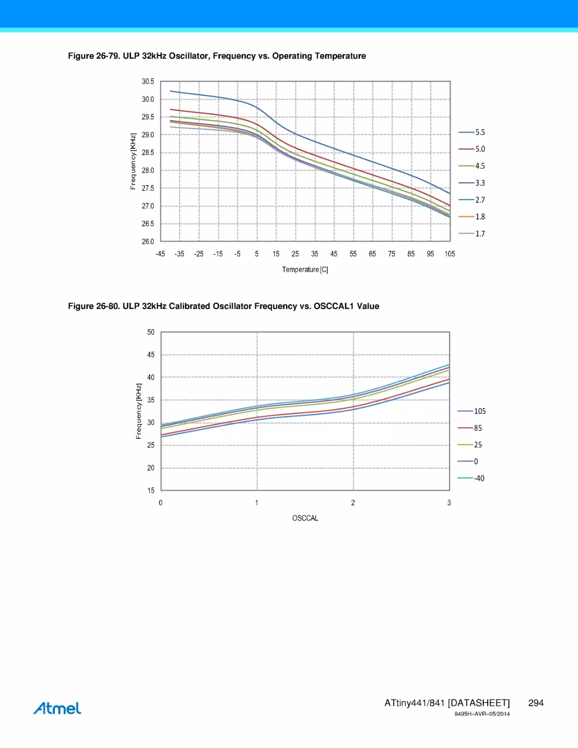
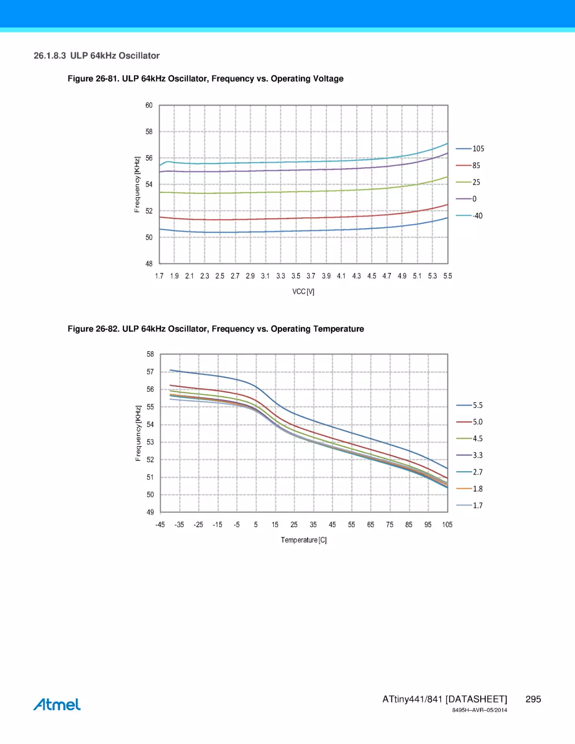
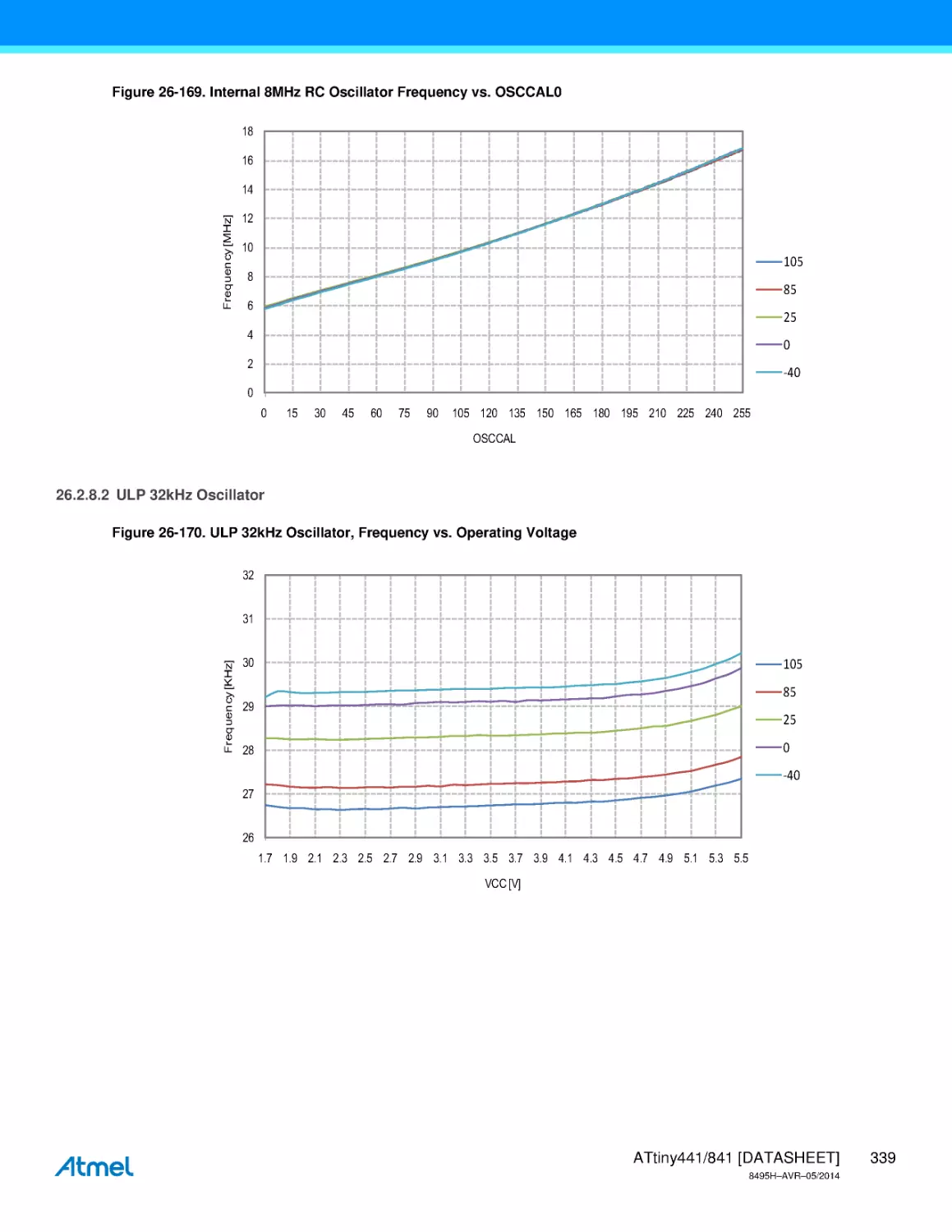
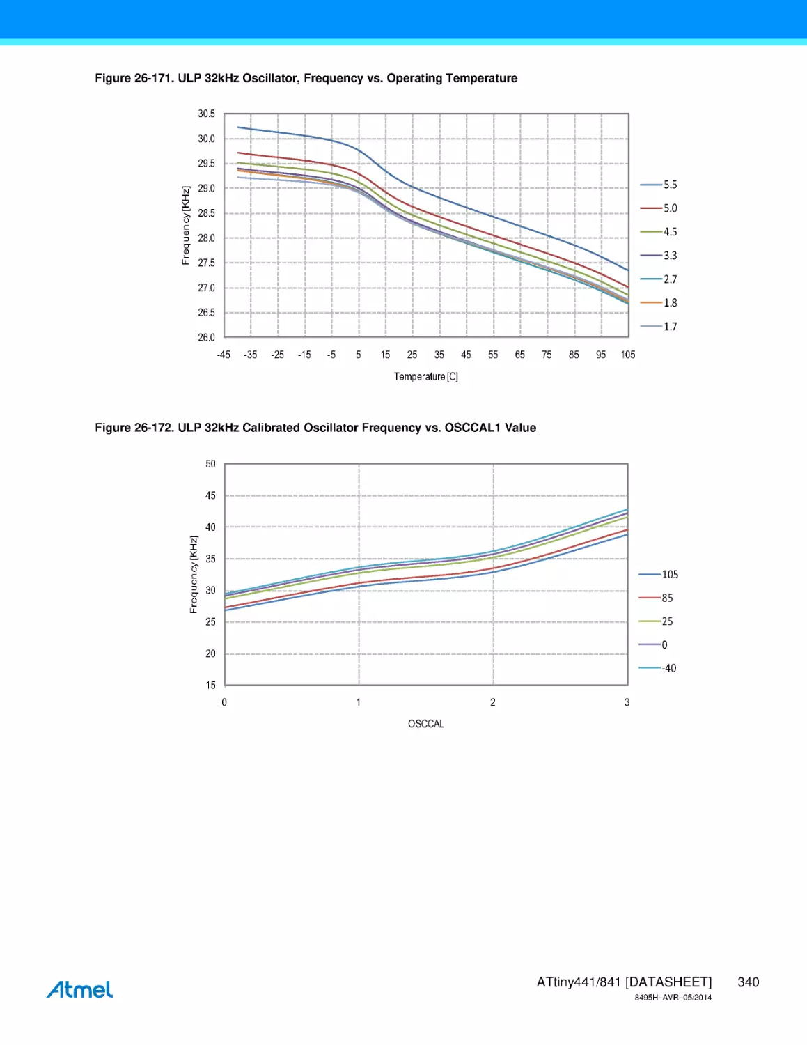
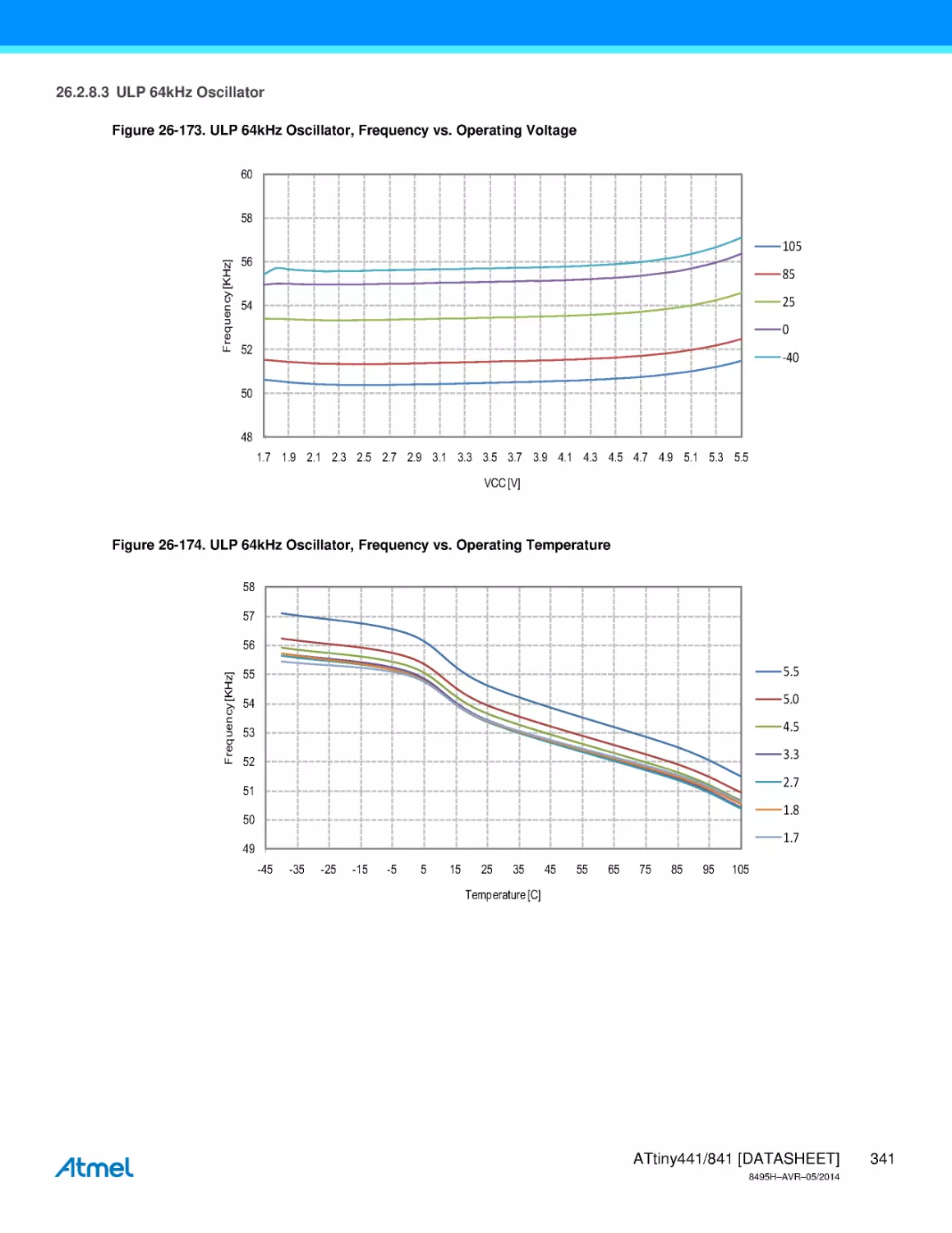
Internal Ultra Low Power (ULP) Oscillator
The internal Ultra Low Power (ULP) oscillator is a low power oscillator that operates with no external components. It
provides a clock source with an approximate frequency of 32kHz. The frequency depends on supply voltage,
temperature and batch variations. See Table 25-3 on page 239 for accuracy details.
During reset, hardware loads the pre-programmed calibration value into the OSCCAL1 register and thereby
automatically calibrates the oscillator. The accuracy of this calibration is referred to as “Factory Calibration” in Table 25-3
on page 239. For more information on automatic loading of pre-programmed calibration value, see section “Calibration
Bytes” on page 222.
ATtiny441/841 [DATASHEET]
8495H–AVR–05/2014
27
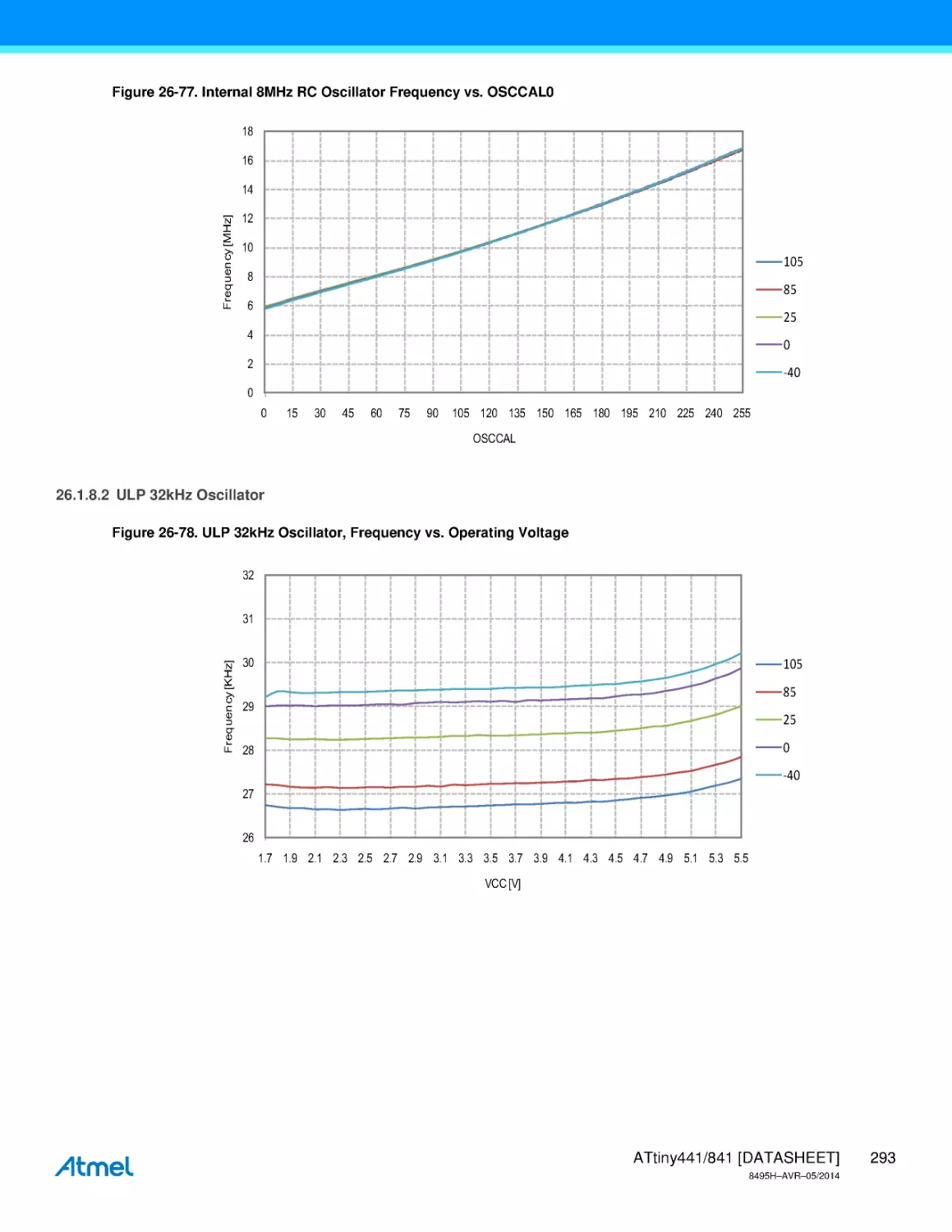
When the ULP oscillator is used as a system clock, the operating frequency can be programmed using ULPOSC2..0
fuses. The available frequencies are shown in Table 6-2. Note that higher frequencies are available for system clock,
only. Even when a higher frequency is selected the watchdog and the reset time-out counter still use 32 kHz.
Table 6-2.
Selecting ULP Oscillator Frequency
ULPOSCSEL[2:0]
ULP Frequency
111
32 kHz
110
64 kHz
101
128 kHz
100
256 kHz
011
512 kHz
000 – 010
Reserved
Start-up time for this clock source is determined by the SUT fuse bit, as shown in Table 6-5 on page 30.
6.2.4
Low-Frequency Crystal Oscillator
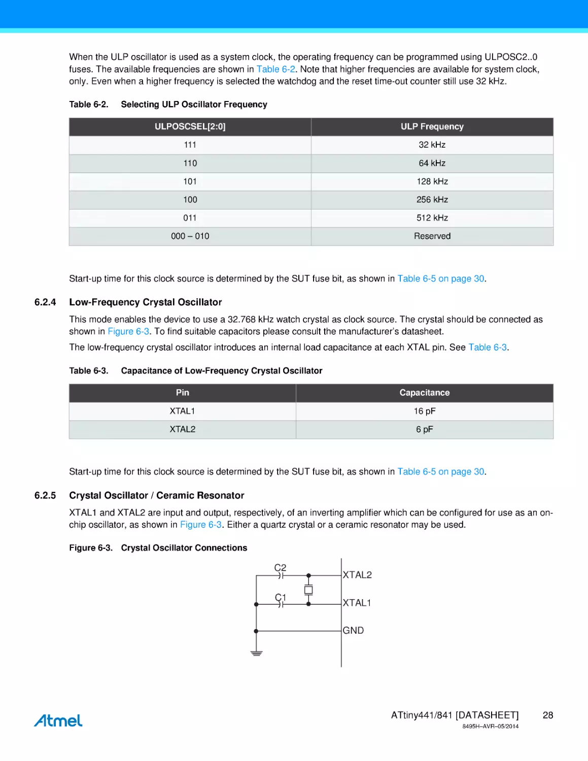
This mode enables the device to use a 32.768 kHz watch crystal as clock source. The crystal should be connected as
shown in Figure 6-3. To find suitable capacitors please consult the manufacturer’s datasheet.
The low-frequency crystal oscillator introduces an internal load capacitance at each XTAL pin. See Table 6-3.
Table 6-3.
Capacitance of Low-Frequency Crystal Oscillator
Pin
Capacitance
XTAL1
16 pF
XTAL2
6 pF
Start-up time for this clock source is determined by the SUT fuse bit, as shown in Table 6-5 on page 30.
6.2.5
Crystal Oscillator / Ceramic Resonator
XTAL1 and XTAL2 are input and output, respectively, of an inverting amplifier which can be configured for use as an onchip oscillator, as shown in Figure 6-3. Either a quartz crystal or a ceramic resonator may be used.
Figure 6-3. Crystal Oscillator Connections
C2
C1
XTAL2
XTAL1
GND
ATtiny441/841 [DATASHEET]
8495H–AVR–05/2014
28
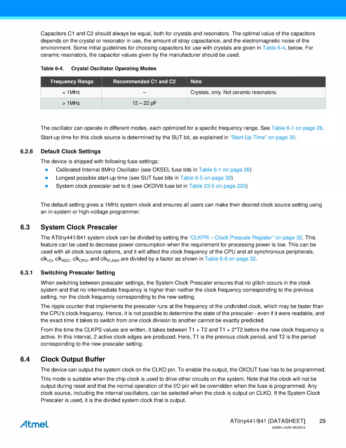
Capacitors C1 and C2 should always be equal, both for crystals and resonators. The optimal value of the capacitors
depends on the crystal or resonator in use, the amount of stray capacitance, and the electromagnetic noise of the
environment. Some initial guidelines for choosing capacitors for use with crystals are given in Table 6-4, below. For
ceramic resonators, the capacitor values given by the manufacturer should be used.
Table 6-4.
Crystal Oscillator Operating Modes
Frequency Range
Recommended C1 and C2
< 1MHz
–
> 1MHz
12 – 22 pF
Note
Crystals, only. Not ceramic resonators.
The oscillator can operate in different modes, each optimized for a specific frequency range. See Table 6-1 on page 26.
Start-up time for this clock source is determined by the SUT bit, as explained in “Start-Up Time” on page 30.
6.2.6
Default Clock Settings
The device is shipped with following fuse settings:
Calibrated Internal 8MHz Oscillator (see CKSEL fuse bits in Table 6-1 on page 26)
Longest possible start-up time (see SUT fuse bits in Table 6-5 on page 30)
System clock prescaler set to 8 (see CKDIV8 fuse bit in Table 23-5 on page 220)
The default setting gives a 1MHz system clock and ensures all users can make their desired clock source setting using
an in-system or high-voltage programmer.
6.3
System Clock Prescaler
The ATtiny441/841 system clock can be divided by setting the “CLKPR – Clock Prescale Register” on page 32. This
feature can be used to decrease power consumption when the requirement for processing power is low. This can be
used with all clock source options, and it will affect the clock frequency of the CPU and all synchronous peripherals.
clkI/O, clkADC, clkCPU, and clkFLASH are divided by a factor as shown in Table 6-6 on page 32.
6.3.1
Switching Prescaler Setting
When switching between prescaler settings, the System Clock Prescaler ensures that no glitch occurs in the clock
system and that no intermediate frequency is higher than neither the clock frequency corresponding to the previous
setting, nor the clock frequency corresponding to the new setting.
The ripple counter that implements the prescaler runs at the frequency of the undivided clock, which may be faster than
the CPU's clock frequency. Hence, it is not possible to determine the state of the prescaler - even if it were readable, and
the exact time it takes to switch from one clock division to another cannot be exactly predicted.
From the time the CLKPS values are written, it takes between T1 + T2 and T1 + 2*T2 before the new clock frequency is
active. In this interval, 2 active clock edges are produced. Here, T1 is the previous clock period, and T2 is the period
corresponding to the new prescaler setting.
6.4
Clock Output Buffer
The device can output the system clock on the CLKO pin. To enable the output, the CKOUT fuse has to be programmed.
This mode is suitable when the chip clock is used to drive other circuits on the system. Note that the clock will not be
output during reset and that the normal operation of the I/O pin will be overridden when the fuse is programmed. Any
clock source, including the internal oscillators, can be selected when the clock is output on CLKO. If the System Clock
Prescaler is used, it is the divided system clock that is output.
ATtiny441/841 [DATASHEET]
8495H–AVR–05/2014
29
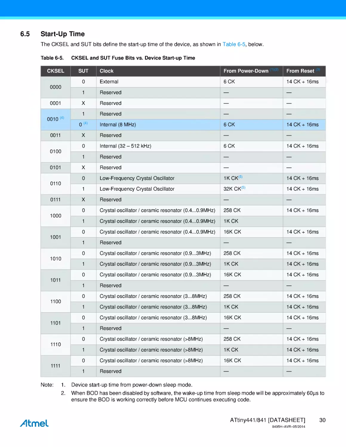
6.5
Start-Up Time
The CKSEL and SUT bits define the start-up time of the device, as shown in Table 6-5, below.
Table 6-5.
CKSEL
CKSEL and SUT Fuse Bits vs. Device Start-up Time
Clock
From Power-Down (1)(2)
From Reset (3)
0
External
6 CK
14 CK + 16ms
1
Reserved
—
—
X
Reserved
—
—
1
Reserved
—
—
Internal (8 MHz)
6 CK
14 CK + 16ms
X
Reserved
—
—
0
Internal (32 – 512 kHz)
6 CK
14 CK + 16ms
1
Reserved
—
—
X
Reserved
—
—
0
Low-Frequency Crystal Oscillator
1K CK(5)
14 CK + 16ms
1
Low-Frequency Crystal Oscillator
32K CK(5)
14 CK + 16ms
X
Reserved
—
—
0
Crystal oscillator / ceramic resonator (0.4...0.9MHz)
258 CK
14 CK + 16ms
1
Crystal oscillator / ceramic resonator (0.4...0.9MHz)
1K CK
0
Crystal oscillator / ceramic resonator (0.4...0.9MHz)
16K CK
14 CK + 16ms
1
Reserved
—
—
0
Crystal oscillator / ceramic resonator (0.9...3MHz)
258 CK
14 CK + 16ms
1
Crystal oscillator / ceramic resonator (0.9...3MHz)
1K CK
14 CK + 16ms
0
Crystal oscillator / ceramic resonator (0.9...3MHz)
16K CK
14 CK + 16ms
1
Reserved
—
—
0
Crystal oscillator / ceramic resonator (3...8MHz)
258 CK
14 CK + 16ms
1
Crystal oscillator / ceramic resonator (3...8MHz)
1K CK
14 CK + 16ms
0
Crystal oscillator / ceramic resonator (3...8MHz)
16K CK
14 CK + 16ms
1
Reserved
—
—
0
Crystal oscillator / ceramic resonator (>8MHz)
258 CK
14 CK + 16ms
1
Crystal oscillator / ceramic resonator (>8MHz)
1K CK
14 CK + 16ms
0
Crystal oscillator / ceramic resonator (>8MHz)
16K CK
14 CK + 16ms
1
Reserved
—
—
SUT
0000
0001
0010 (4)
0011
0 (4)
0100
0101
0110
0111
1000
1001
1010
1011
1100
1101
1110
1111
Note:
1.
Device start-up time from power-down sleep mode.
2.
When BOD has been disabled by software, the wake-up time from sleep mode will be approximately 60µs to
ensure the BOD is working correctly before MCU continues executing code.
ATtiny441/841 [DATASHEET]
8495H–AVR–05/2014
30
3.
Device start-up time after reset.
4.
The device is shipped with this option selected.
5.
These options should be used only if frequency stability at start-up is not important.
6.
Recommended use: fast rising power or BOD enabled.
6.6
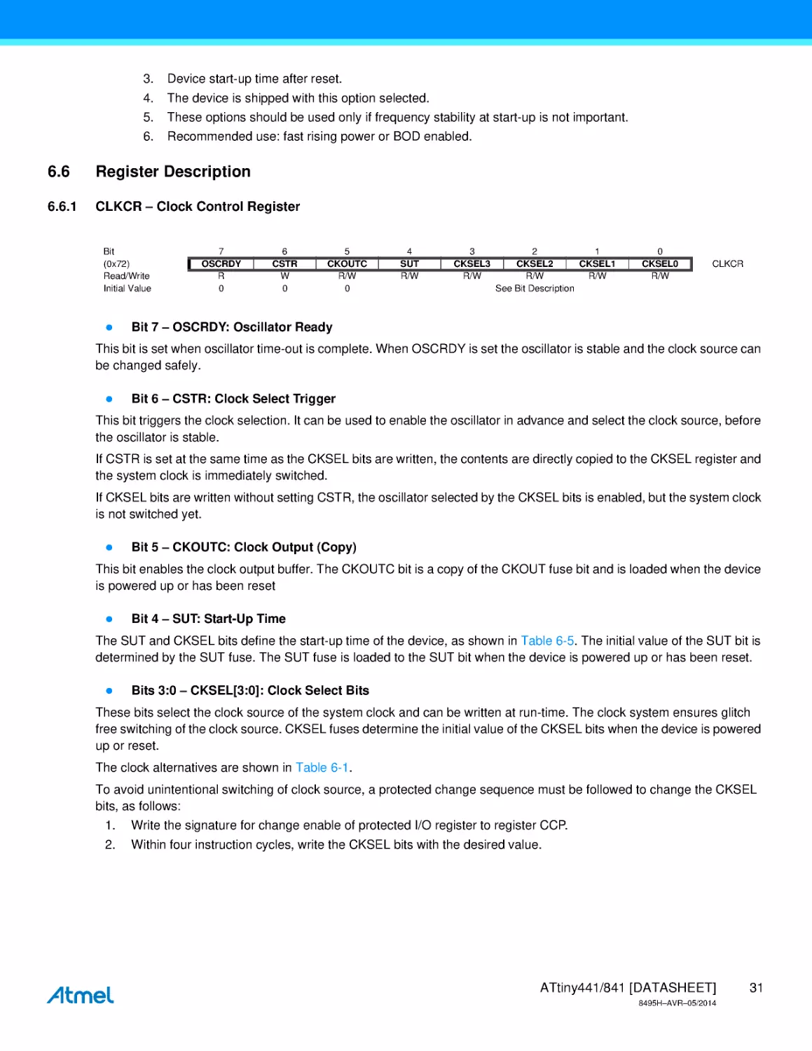
Register Description
6.6.1
CLKCR – Clock Control Register
Bit
(0x72)
Read/Write
Initial Value
7
OSCRDY
R
0
6
CSTR
W
0
5
CKOUTC
R/W
0
4
SUT
R/W
3
CKSEL3
R/W
2
1
CKSEL2
CKSEL1
R/W
R/W
See Bit Description
0
CKSEL0
R/W
CLKCR
Bit 7 – OSCRDY: Oscillator Ready
This bit is set when oscillator time-out is complete. When OSCRDY is set the oscillator is stable and the clock source can
be changed safely.
Bit 6 – CSTR: Clock Select Trigger
This bit triggers the clock selection. It can be used to enable the oscillator in advance and select the clock source, before
the oscillator is stable.
If CSTR is set at the same time as the CKSEL bits are written, the contents are directly copied to the CKSEL register and
the system clock is immediately switched.
If CKSEL bits are written without setting CSTR, the oscillator selected by the CKSEL bits is enabled, but the system clock
is not switched yet.
Bit 5 – CKOUTC: Clock Output (Copy)
This bit enables the clock output buffer. The CKOUTC bit is a copy of the CKOUT fuse bit and is loaded when the device
is powered up or has been reset
Bit 4 – SUT: Start-Up Time
The SUT and CKSEL bits define the start-up time of the device, as shown in Table 6-5. The initial value of the SUT bit is
determined by the SUT fuse. The SUT fuse is loaded to the SUT bit when the device is powered up or has been reset.
Bits 3:0 – CKSEL[3:0]: Clock Select Bits
These bits select the clock source of the system clock and can be written at run-time. The clock system ensures glitch
free switching of the clock source. CKSEL fuses determine the initial value of the CKSEL bits when the device is powered
up or reset.
The clock alternatives are shown in Table 6-1.
To avoid unintentional switching of clock source, a protected change sequence must be followed to change the CKSEL
bits, as follows:
1.
Write the signature for change enable of protected I/O register to register CCP.
2.
Within four instruction cycles, write the CKSEL bits with the desired value.
ATtiny441/841 [DATASHEET]
8495H–AVR–05/2014
31
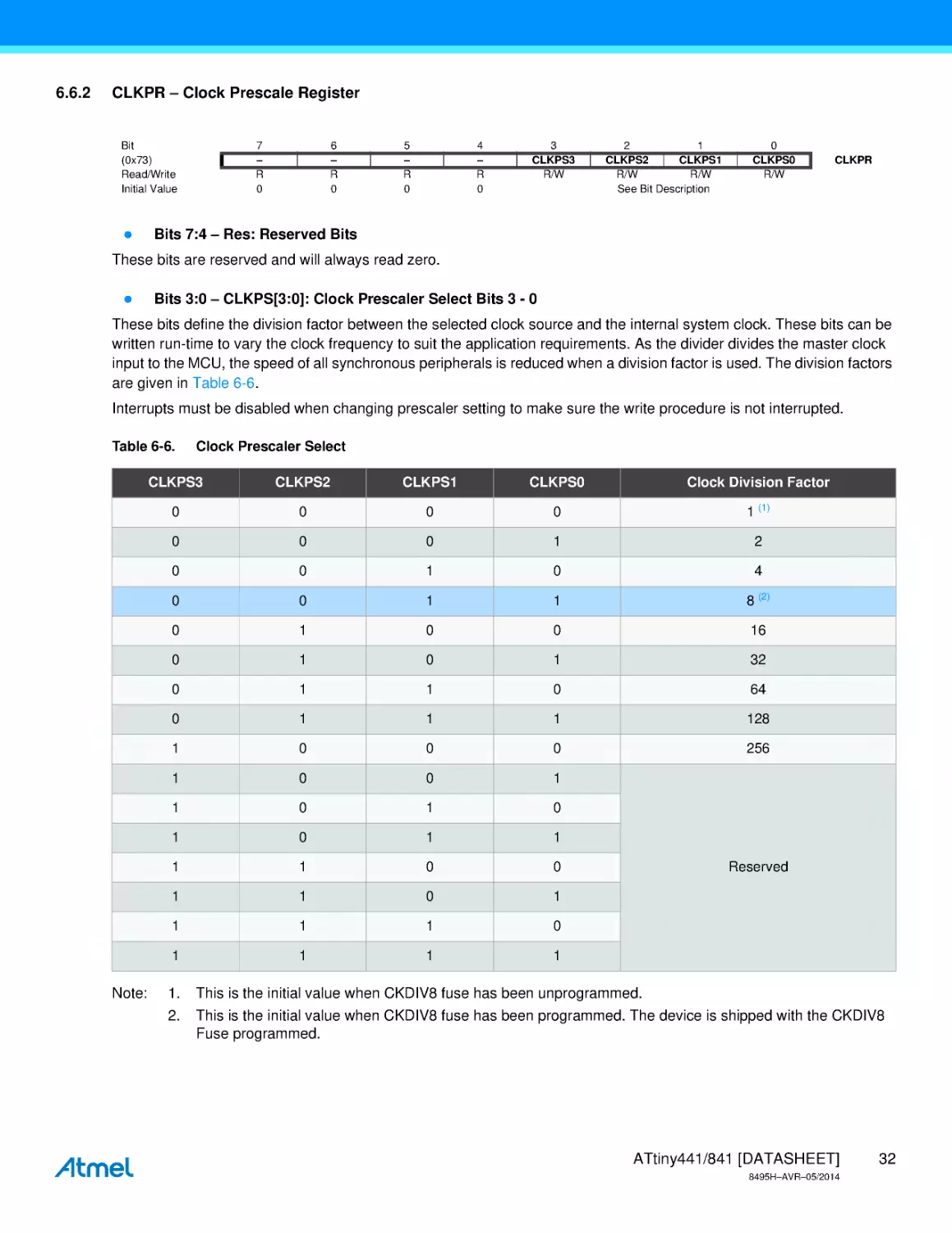
6.6.2
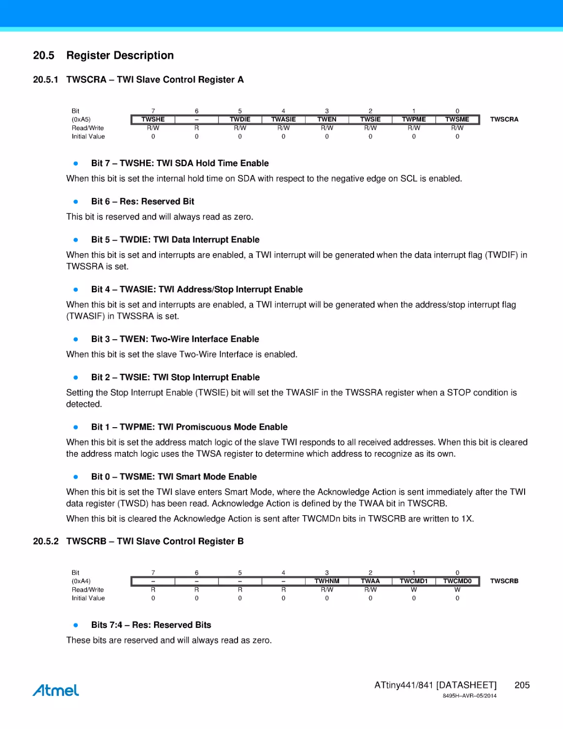
CLKPR – Clock Prescale Register
Bit
(0x73)
Read/Write
Initial Value
7
–
R
0
6
–
R
0
5
–
R
0
4
–
R
0
3
CLKPS3
R/W
2
1
CLKPS2
CLKPS1
R/W
R/W
See Bit Description
0
CLKPS0
R/W
CLKPR
Bits 7:4 – Res: Reserved Bits
These bits are reserved and will always read zero.
Bits 3:0 – CLKPS[3:0]: Clock Prescaler Select Bits 3 - 0
These bits define the division factor between the selected clock source and the internal system clock. These bits can be
written run-time to vary the clock frequency to suit the application requirements. As the divider divides the master clock
input to the MCU, the speed of all synchronous peripherals is reduced when a division factor is used. The division factors
are given in Table 6-6.
Interrupts must be disabled when changing prescaler setting to make sure the write procedure is not interrupted.
Table 6-6.
Note:
Clock Prescaler Select
CLKPS3
CLKPS2
CLKPS1
CLKPS0
Clock Division Factor
0
0
0
0
1 (1)
0
0
0
1
2
0
0
1
0
4
0
0
1
1
8 (2)
0
1
0
0
16
0
1
0
1
32
0
1
1
0
64
0
1
1
1
128
1
0
0
0
256
1
0
0
1
1
0
1
0
1
0
1
1
1
1
0
0
1
1
0
1
1
1
1
0
1
1
1
1
Reserved
1.
This is the initial value when CKDIV8 fuse has been unprogrammed.
2.
This is the initial value when CKDIV8 fuse has been programmed. The device is shipped with the CKDIV8
Fuse programmed.
ATtiny441/841 [DATASHEET]
8495H–AVR–05/2014
32
The initial value of clock prescaler bits is determined by the CKDIV8 fuse (see Table 23-5 on page 220). When CKDIV8
is unprogrammed, the system clock prescaler is set to one and, when programmed, to eight. Any value can be written to
the CLKPS bits regardless of the CKDIV8 fuse bit setting.
When CKDIV8 is programmed the initial value of CLKPS bits give a clock division factor of eight at start up. This is useful
when the selected clock source has a higher frequency than allowed under present operating conditions. See “Speed” on
page 238.
To avoid unintentional changes to clock frequency, the following sequence must be followed:
6.6.3
1.
Write the required signature to the CCP register. See page 13.
2.
Within four instruction cycles, write the desired value to CLKPS bits.
OSCCAL0 – Oscillator Calibration Register
Bit
(0x74)
Read/Write
Initial Value
7
CAL07
R/W
6
CAL06
R/W
5
4
3
CAL05
CAL04
CAL03
R/W
R/W
R/W
Device Specific Calibration Value
2
CAL02
R/W
1
CAL01
R/W
0
CAL00
R/W
OSCCAL0
Bits 7:0 – CAL0[7:0]: Oscillator Calibration Value
The oscillator calibration register is used to trim the internal 8MHz oscillator and to remove process variations from the
oscillator frequency. A pre-programmed calibration value is automatically written to this register during chip reset, giving
the factory calibrated frequency specified in Table 25-2 on page 239.
The application software can write this register to change the oscillator frequency. The oscillator can be calibrated to
frequencies specified in Table 25-2 on page 239. Calibration outside that range is not guaranteed.
The lowest oscillator frequency is reached by programming these bits to zero. Increasing the register value increases the
oscillator frequency. A typical frequency response curve is shown in Figure 26-77 on page 293.
Note that this oscillator is used to time EEPROM and Flash write accesses, and write times will be affected accordingly.
Do not calibrate to more than 8.8MHz if EEPROM or Flash is to be written. Otherwise, the EEPROM or Flash write may
fail.
To ensure stable operation of the MCU the calibration value should be changed in small steps. A step change in
frequency of more than 2% from one cycle to the next can lead to unpredictable behavior. Also, the difference between
two consecutive register values should not exceed 0x20. If these limits are exceeded the MCU must be kept in reset
during changes to clock frequency.
6.6.4
OSCTCAL0A – Oscillator Temperature Calibration Register A
Bit
(0x75)
Read/Write
Initial Value
7
6
R/W
R/W
5
4
3
2
Oscillator Temperature Calibration Data
R/W
R/W
R/W
R/W
Device Specific Calibration Value
1
0
R/W
R/W
OSCTCAL0A
Bits 7:0 – Oscillator Temperature Calibration Value
The temperature calibration value can be used to trim the calibrated 8MHz oscillator and remove temperature variations
from the oscillator frequency.
ATtiny441/841 [DATASHEET]
8495H–AVR–05/2014
33
6.6.5
OSCTCAL0B – Oscillator Temperature Calibration Register B
Bit
(0x76)
Read/Write
Initial Value
7
6
R/W
R/W
5
4
3
2
Oscillator Temperature Calibration Data
R/W
R/W
R/W
R/W
Device Specific Calibration Value
1
0
R/W
R/W
OSCTCAL0B
Bits 7:0 – Oscillator Temperature Calibration Value
The temperature calibration value can be used to trim the calibrated 8MHz oscillator and remove temperature variations
from the oscillator frequency.
6.6.6
OSCCAL1 – Oscillator Calibration Register
Bit
(0x77)
Read/Write
Initial Value
7
–
R
0
6
–
R
0
5
–
R
0
4
–
R
0
3
–
R
0
2
–
R
0
1
0
CAL11
CAL10
R/W
R/W
Calibration Value
OSCCAL1
Bits 7:0 – CAL[11:10]: Oscillator Calibration Value
The oscillator calibration register is used to trim the internal 32kHz oscillator and to remove process variations from the
oscillator frequency. A pre-programmed calibration value is automatically written to this register during chip reset, giving
the factory calibrated frequency as specified in Table 25-2 on page 239.
The application software can write this register to change the oscillator frequency. The oscillator can be calibrated to
frequencies as specified in Table 25-2 on page 239. Calibration outside that range is not guaranteed.
The lowest oscillator frequency is reached by programming these bits to zero. Increasing the register value increases the
oscillator frequency. A typical frequency response curve is shown in Figure 26-80 on page 294.
ATtiny441/841 [DATASHEET]
8495H–AVR–05/2014
34
7.
Power Management and Sleep Modes
The high performance and industry leading code efficiency makes the AVR microcontrollers an ideal choice for low
power applications. In addition, sleep modes enable the application to shut down unused modules in the MCU, thereby
saving power. The AVR provides various sleep modes allowing the user to tailor the power consumption to the
application’s requirements.
7.1
Sleep Modes
Figure 6-1 on page 25 presents the different clock systems and their distribution in ATtiny441/841. The figure is helpful in
selecting an appropriate sleep mode. Table 7-1 shows the different sleep modes and the sources that may be used for
wake up.
ADC Noise Reduction
X
Standby
X
Power-down
Note:
1.
Start frame detection, only.
2.
Address match interrupt, only.
3.
For INT0 level interrupt, only.
X
X
X
X
X
X
X(3)
X
X
X
X(2)
X
X(3)
X
X
X
X(3)
X
X
TWI Slave (2)
X
Other I/O
SPM/EEPROM
Ready Interrupt
X
INT0 and
Pin Change
X
clkIO
X
Watchdog
Interrupt
USART (1)
X
ADC Interrupt
Idle
Wake-up Sources
clkADC
Active Clock Domains
clkFLASH
Sleep Mode
Source
clkCPU
Active Clock Domains and Wake-up Sources in Different Sleep Modes
Main Clock
Source Enabled
Table 7-1.
X
To enter a sleep mode, the SE bit in MCUCR must be set and a SLEEP instruction must be executed. The SMn bits in
MCUCR select which sleep mode will be activated by the SLEEP instruction. See Table 7-2 on page 38 for a summary.
If an enabled interrupt occurs while the MCU is in a sleep mode, the MCU wakes up. The MCU is then halted for four
cycles in addition to the start-up time, executes the interrupt routine, and resumes execution from the instruction
following SLEEP. The contents of the Register File and SRAM are unaltered when the device wakes up from sleep. If a
reset occurs during sleep mode, the MCU wakes up and executes from the Reset Vector.
Note that if a level triggered interrupt is used for wake-up the changed level must be held for some time to wake up the
MCU (and for the MCU to enter the interrupt service routine). See “External Interrupts” on page 51 for details.
7.1.1
Idle Mode
This sleep mode basically halts clkCPU and clkFLASH, while allowing other clocks to run. In Idle Mode, the CPU is stopped
but the following peripherals continue to operate:
Watchdog and interrupt system
Analog comparator, and ADC
USART, TWI, and timer/counters
ATtiny441/841 [DATASHEET]
8495H–AVR–05/2014
35
Idle mode allows the MCU to wake up from external triggered interrupts as well as internal ones, such as Timer Overflow.
If wake-up from the analog comparator interrupt is not required, the analog comparator can be powered down by setting
the ACD bit in ACSRA. See “ACSR1A – Analog Comparator 1 Control and Status Register” on page 129. This will reduce
power consumption in Idle mode.
If the ADC is enabled, a conversion starts automatically when this mode is entered.
7.1.2
ADC Noise Reduction Mode
This sleep mode halts clkI/O, clkCPU, and clkFLASH, while allowing other clocks to run. In ADC Noise Reduction mode, the
CPU is stopped but the following peripherals continue to operate:
Watchdog (if enabled), and external interrupts
ADC
USART start frame detector, and TWI
This improves the noise environment for the ADC, enabling higher resolution measurements. If the ADC is enabled, a
conversion starts automatically when this mode is entered.
The following events can wake up the MCU:
7.1.3
Watchdog reset, external reset, and brown-out reset
External level interrupt on INT0, and pin change interrupt
ADC conversion complete interrupt, and SPM/EEPROM ready interrupt
USART start frame detection, and TWI slave address match
Power-Down Mode
This sleep mode halts all generated clocks, allowing operation of asynchronous modules, only. In Power-down Mode the
oscillator is stopped, while the following peripherals continue to operate:
Watchdog (if enabled), external interrupts
The following events can wake up the MCU:
7.1.4
Watchdog reset, external reset, and brown-out reset
External level interrupt on INT0, and pin change interrupt
USART start frame detection, and TWI slave address match
Standby Mode
Standby Mode is identical to power-down, with the exception that the oscillator is kept running. From Standby mode, the
device wakes up in six clock cycles.
7.2
Power Reduction Register
The Power Reduction Register (PRR), see “PRR – Power Reduction Register” on page 38, provides a method to reduce
power consumption by stopping the clock to individual peripherals. When the clock for a peripheral is stopped then:
The current state of the peripheral is frozen.
The associated registers can not be read or written.
Resources used by the peripheral will remain occupied.
The peripheral should in most cases be disabled before stopping the clock. Clearing the PRR bit wakes up the peripheral
and puts it in the same state as before shutdown.
Peripheral shutdown can be used in Idle mode and Active mode to significantly reduce the overall power consumption. In
all other sleep modes, the clock is already stopped.
ATtiny441/841 [DATASHEET]
8495H–AVR–05/2014
36
7.3
Minimizing Power Consumption
There are several issues to consider when trying to minimize the power consumption in an AVR controlled system. In
general, sleep modes should be used as much as possible, and the sleep mode should be selected so that as few as
possible of the device’s functions are operating. All functions not needed should be disabled. In particular, the following
modules may need special consideration when trying to achieve the lowest possible power consumption.
7.3.1
Analog to Digital Converter
If enabled, the ADC will be enabled in all sleep modes. To save power, the ADC should be disabled before entering any
sleep mode. When the ADC is turned off and on again, the next conversion will be an extended conversion. See “Analog
to Digital Converter” on page 132 for details on ADC operation.
7.3.2
Analog Comparator
When entering Idle mode, the Analog Comparator should be disabled if not used. When entering ADC Noise Reduction
mode, the Analog Comparator should be disabled. In the other sleep modes, the Analog Comparator is automatically
disabled. However, if the Analog Comparator is set up to use the Internal Voltage Reference as input, the Analog
Comparator should be disabled in all sleep modes. Otherwise, the Internal Voltage Reference will be enabled,
independent of sleep mode. See “Analog Comparator 0” on page 124 and “Analog Comparator 1” on page 128 for details
on how to configure the Analog Comparator.
7.3.3
Brown-out Detector
If the Brown-out Detector is not needed in the application, this module should be turned off. If the Brown-out Detector is
enabled by the BODPD Fuses, it will be enabled in all sleep modes, and hence, always consume power. In the deeper
sleep modes, this will contribute significantly to the total current consumption. If the Brown-out Detector is needed in the
application, this module can also be set to Sampled BOD mode to save power. See “Brown-out Detection” on page 42 for
details on how to configure the Brown-out Detector.
7.3.4
Internal Voltage Reference
The Internal Voltage Reference will be enabled when needed by the Brown-out Detection, the Analog Comparator or the
ADC. If these modules are disabled as described in the sections above, the internal voltage reference will be disabled
and it will not be consuming power. When turned on again, the user must allow the reference to start up before the output
is used. If the reference is kept on in sleep mode, the output can be used immediately. See Internal Bandgap Reference
in Table 25-5 on page 240 for details on the start-up time.
7.3.5
Watchdog Timer
If the Watchdog Timer is not needed in the application, this module should be turned off. If the Watchdog Timer is
enabled, it will be enabled in all sleep modes, and hence, always consume power. In the deeper sleep modes, this will
contribute to the total current consumption. See “Brown-out Detection” on page 42 for details on how to configure the
Watchdog Timer.
7.3.6
Port Pins
When entering a sleep mode, all port pins should be configured to use minimum power. The most important thing is then
to ensure that no pins drive resistive loads. In sleep modes where both the I/O clock (clkI/O) and the ADC clock (clkADC)
are stopped, the input buffers of the device will be disabled. This ensures that no power is consumed by the input logic
when not needed. In some cases, the input logic is needed for detecting wake-up conditions, and it will then be enabled.
See the section “Digital Input Enable and Sleep Modes” on page 59 for details on which pins are enabled. If the input
buffer is enabled and the input signal is left floating or has an analog signal level close to VCC/2, the input buffer will use
excessive power.
For analog input pins, the digital input buffer should be disabled at all times. An analog signal level close to VCC/2 on an
input pin can cause significant current even in active mode. Digital input buffers can be disabled by writing to the Digital
ATtiny441/841 [DATASHEET]
8495H–AVR–05/2014
37
Input Disable Registers. See “DIDR0 – Digital Input Disable Register 0” on page 149 and “DIDR1 – Digital Input Disable
Register 1” on page 150 for details.
7.4
Register Description
7.4.1
MCUCR – MCU Control Register
Bit
0x35 (0x55)
Read/Write
Initial Value
7
–
R
0
6
–
R
0
5
SE
R/W
0
4
SM1
R/W
0
3
SM0
R/W
0
2
–
R
0
1
ISC01
R/W
0
0
ISC00
R/W
0
MCUCR
Bit 7:6 – Res: Reserved Bits
These bits are reserved and will always read zero.
Bit 5 – SE: Sleep Enable
The SE bit must be written logic one to make the MCU enter the sleep mode when the SLEEP instruction is executed. To
avoid the MCU entering the sleep mode unless it is the programmer’s purpose, it is recommended to write the Sleep
Enable (SE) bit to one just before the execution of the SLEEP instruction and to clear it immediately after waking up.
Bits 4:3 – SM[1:0]: Sleep Mode Select Bits 1 and 0
These bits select between available sleep modes, as shown in Table 7-2.
Table 7-2.
Note:
Sleep Mode Select
SM1
SM0
0
0
Idle
0
1
ADC Noise Reduction
1
0
Power-down
1
1
Standby (1)
1.
Sleep Mode
Only recommended with external crystal or resonator as clock source
Bit 2 – Res: Reserved Bit
This bit is reserved and will always read zero.
7.4.2
PRR – Power Reduction Register
The Power Reduction Register provides a method to reduce power consumption by allowing peripheral clock signals to
be disabled.
Bit
(0x70)
Read/Write
Initial Value
7
PRTWI
R/w
0
6
PRUSART1
R
0
5
PRUSART0
R/W
0
4
PRSPI
R/W
0
3
PRTIM2
R/W
0
2
PRTIM1
R/W
0
1
PRTIM0
R/W
0
0
PRADC
R/W
0
PRR
Bit 7 – PRTWI: Power Reduction Two-Wire Interface
Writing a logic one to this bit shuts down the Two-Wire Interface module.
ATtiny441/841 [DATASHEET]
8495H–AVR–05/2014
38
Bit 6 – PRUSART1: Power Reduction USART1
Writing a logic one to this bit shuts down the USART1 module. When the USART is re-enabled, operation will continue
like before the shutdown.
Bit 5 – PRUSART0: Power Reduction USART0
Writing a logic one to this bit shuts down the USART0 module. When the USART is re-enabled, operation will continue
like before the shutdown.
Bit 4 – PRSPI: Power Reduction SPI
Writing a logic one to this bit shuts down the SPI by stopping the clock to the module. When waking up the SPI again, the
SPI should be re-initialized to ensure proper operation.
Bit 3 – PRTIM2: Power Reduction Timer/Counter2
Writing a logic one to this bit shuts down the Timer/Counter2 module. When the timer/counter is re-enabled, operation
will continue like before the shutdown.
Bit 2 – PRTIM1: Power Reduction Timer/Counter1
Writing a logic one to this bit shuts down the Timer/Counter1 module. When the timer/counter is re-enabled, operation
will continue like before the shutdown.
Bit 1 – PRTIM0: Power Reduction Timer/Counter0
Writing a logic one to this bit shuts down the Timer/Counter0 module. When the timer/counter is re-enabled, operation
will continue like before the shutdown.
Bit 0 – PRADC: Power Reduction ADC
Writing a logic one to this bit shuts down the ADC. The ADC must be disabled before shut down. The analog comparator
cannot be used when the ADC is shut down.
ATtiny441/841 [DATASHEET]
8495H–AVR–05/2014
39
8.
System Control and Reset
8.1
Resetting the AVR
During reset, all I/O registers are set to their initial values, and the program starts execution from the Reset Vector. The
instruction placed at the Reset Vector should be a JMP (two-word, direct jump) instruction to the reset handling routine,
although other one- or two-word jump instructions can be used. If the program never enables an interrupt source, the
interrupt vectors are not used, and regular program code can be placed at these locations.
The circuit diagram in Figure 8-1 shows the reset logic. Electrical parameters of the reset circuitry are defined in section
“System and Reset Characteristics” on page 240.
Figure 8-1. Reset Logic
DATA BUS
PULL-UP
RESISTOR
RESET
WDRF
BROWN OUT
RESET CIRCUIT
VCC
EXTRF
BORF
PORF
RESET FLAG REGISTER
(RSTFLR)
BODLEVEL2...0
S
POWER-ON
RESET CIRCUIT
Q
COUNTER RESET
TIMEOUT
SPIKE
FILTER
EXTERNAL
RESET CIRCUIT
INTERNAL
RESET
R
DELAY
COUNTERS
CK
WATCHDOG
TIMER
RSTDISBL
WATCHDOG
OSCILLATOR
CLOCK
GENERATOR
The I/O ports of the AVR are immediately reset to their initial state when a reset source goes active. This does not require
any clock source to be running.
After all reset sources have gone inactive, a delay counter is invoked, stretching the internal reset. This allows the power
to reach a stable level before normal operation starts.
8.2
Reset Sources
The ATtiny441/841 has four sources of reset:
8.2.1
Power-on Reset. The MCU is reset when the supply voltage is below the Power-on Reset threshold (VPOT)
External Reset. The MCU is reset when a low level is present on the RESET pin for longer than the minimum pulse
length
Watchdog Reset. The MCU is reset when the Watchdog Timer period expires and the Watchdog is enabled
Brown Out Reset. The MCU is reset when the Brown-Out Detector is enabled and supply voltage is below the
brown-out threshold (VBOT)
Power-on Reset
A Power-on Reset (POR) pulse is generated by an on-chip detection circuit. The detection level is defined in section
“System and Reset Characteristics” on page 240. The POR is activated whenever VCC is below the detection level. The
POR circuit can be used to trigger the Start-up Reset, as well as to detect a failure in supply voltage.
A Power-on Reset (POR) circuit ensures that the device is reset from Power-on. Reaching the Power-on Reset threshold
voltage invokes the delay counter, which determines how long the device is kept in reset after VCC rise. The reset signal
is activated again, without any delay, when VCC decreases below the detection level.
ATtiny441/841 [DATASHEET]
8495H–AVR–05/2014
40
Figure 8-2. MCU Start-up, RESET Tied to VCC
V CC
V POT
RESET
V RST
TIME-OUT
t TOUT
INTERNAL
RESET
Figure 8-3. MCU Start-up, RESET Extended Externally
V CC
V POT
> t TOUT
RESET
TIME-OUT
V RST
t TOUT
INTERNAL
RESET
8.2.2
External Reset
An External Reset is generated by a low level on the RESET pin if enabled. Reset pulses longer than the minimum pulse
width (see section “System and Reset Characteristics” on page 240) will generate a reset, even if the clock is not
running. Shorter pulses are not guaranteed to generate a reset. When the applied signal reaches the Reset Threshold
Voltage – VRST – on its positive edge, the delay counter starts the MCU after the time-out period – tTOUT – has expired.
ATtiny441/841 [DATASHEET]
8495H–AVR–05/2014
41
Figure 8-4. External Reset During Operation
CC
8.2.3
Watchdog Reset
When the Watchdog times out, it will generate a short reset pulse. On the falling edge of this pulse, the delay timer starts
counting the time-out period tTOUT. See page 42 for details on operation of the Watchdog Timer and Table 25-5 on page
240 for details on reset time-out.
Figure 8-5. Watchdog Reset During Operation
CC
CK
8.2.4
Brown-out Detection
The Brown-Out Detection (BOD) circuit monitors that the VCC level is kept above a configurable trigger level, VBOT. When
the BOD is enabled, a BOD reset will be given when VCC falls and remains below the trigger level for the length of the
detection time, tBOD. The reset is kept active until VCC again rises above the trigger level.
ATtiny441/841 [DATASHEET]
8495H–AVR–05/2014
42
Figure 8-6. Brown-out Reset During Operation
VCC
VBOT-
VBOT+
RESET
tTOUT
TIME-OUT
INTERNAL
RESET
The BOD circuit will not detect a drop in VCC unless the voltage stays below the trigger level for the detection time, tBOD
(see “System and Reset Characteristics” on page 240).
The BOD circuit has three modes of operation:
Disabled: In this mode of operation VCC is not monitored and, hence, it is recommended only for applications
where the power supply remains stable.
Enabled: In this mode the VCC level is continuously monitored. If VCC drops below VBOT for at least tBOD a brownout reset will be generated.
Sampled: In this mode the VCC level is sampled on each negative edge of a 1kHz clock that has been derived
from the 32kHz ULP oscillator. Between each sample the BOD is turned off. Compared to the mode where BOD is
constantly enabled this mode of operation reduces power consumption but fails to detect drops in VCC between
two positive edges of the 1kHz clock. When a brown-out is detected in this mode, the BOD circuit is set to enabled
mode to ensure that the device is kept in reset until VCC has risen above VBOT . The BOD will return to sampled
mode after reset has been released and the fuses have been read in.
The BOD mode of operation is selected using BODACT and BODPD fuse bits. The BODACT fuse bits determine how
the BOD operates in active and idle mode, as shown in Table 8-1.
Table 8-1.
Setting BOD Mode of Operation in Active and Idle Modes
BODACT1
BODACT0
Mode of Operation
0
0
Reserved
0
1
Sampled
1
0
Enabled
1
1
Disabled
The BODPD fuse bits determine the mode of operation in all sleep modes except idle mode, as shown in Table 8-2.
ATtiny441/841 [DATASHEET]
8495H–AVR–05/2014
43
Table 8-2.
Setting BOD Mode of Operation in Sleep Modes Other Than Idle
BODPD1
BODPD0
Mode of Operation
0
0
Reserved
0
1
Sampled
1
0
Enabled
1
1
Disabled
See “Fuse Bits” on page 219.
8.3
Internal Voltage Reference
ATtiny441/841 features an internal bandgap reference. This reference is used for Brown-out Detection, and it can be
used as an input to the Analog Comparator or the ADC. The bandgap voltage varies with supply voltage and
temperature.
8.3.1
Voltage Reference Enable Signals and Start-up Time
The voltage reference has a start-up time that may influence the way it should be used. The start-up time is given in
“System and Reset Characteristics” on page 240. To save power, the reference is not always turned on. The reference is
on during the following situations:
1.
When the BOD is enabled (by programming the BODACT or BODPD fuses).
2.
When the internal reference is connected to the Analog Comparator (by setting the ACBG bit in ACSR).
3.
When the ADC is enabled.
Thus, when the BOD is not enabled, after setting the ACBG bit or enabling the ADC, the user must always allow the
reference to start up before the output from the Analog Comparator or ADC is used. To reduce power consumption in
Power-down mode, the user can avoid the three conditions above to ensure that the reference is turned off before
entering Power-down mode.
8.4
Watchdog Timer
The Watchdog Timer is clocked from the internal 32kHz ultra low power oscillator (see page 27). By controlling the
Watchdog Timer prescaler, the Watchdog Reset interval can be adjusted as shown in Table 8-5 on page 48. The WDR –
Watchdog Reset – instruction resets the Watchdog Timer. The Watchdog Timer is also reset when it is disabled and
when a Chip Reset occurs. Ten different clock cycle periods can be selected to determine the reset period. If the reset
period expires without another Watchdog Reset, the ATtiny441/841 resets and executes from the Reset Vector. For
timing details on the Watchdog Reset, refer to Table 8-5 on page 48.
The Watchdog Timer can also be configured to generate an interrupt instead of a reset. This can be very helpful when
using the Watchdog to wake-up from Power-down.
To prevent unintentional disabling of the Watchdog or unintentional change of time-out period, two different safety levels
are selected by the fuse WDTON as shown in Table 8-3 See “Timed Sequences for Changing the Configuration of the
Watchdog Timer” on page 45 for details.
ATtiny441/841 [DATASHEET]
8495H–AVR–05/2014
44
Table 8-3.
WDT Configuration as a Function of the Fuse Settings of WDTON
WDTON
Safety Level
WDT Initial State
How to Disable the WDT
How to Change Time-out
Unprogrammed
1
Disabled
Timed sequence
No limitations
Programmed
2
Enabled
Always enabled
Timed sequence
Figure 8-7. Watchdog Timer
WDP0
WDP1
WDP2
WDP3
OSC/256K
OSC/64K
OSC/128K
OSC/32K
OSC/8K
OSC/16K
OSC/2K
OSC/1K
OSC/512
WATCHDOG
RESET
OSC/4K
WATCHDOG
PRESCALER
32 kHz
ULP OSCILLATOR
MUX
WDE
MCU RESET
8.4.1
Timed Sequences for Changing the Configuration of the Watchdog Timer
The sequence for changing configuration differs slightly between the two safety levels. Separate procedures are
described for each level.
Safety Level 1
In this mode, the Watchdog Timer is initially disabled, but can be enabled by writing the WDE bit to one without
any restriction. A timed sequence is needed when disabling an enabled Watchdog Timer. To disable an enabled
Watchdog Timer, the following procedure must be followed:
1.
Write the signature for change enable of protected I/O registers to register CCP
2.
Within four instruction cycles, in the same operation, write WDE and WDP bits
Safety Level 2
In this mode, the Watchdog Timer is always enabled, and the WDE bit will always read as one. A timed sequence
is needed when changing the Watchdog Time-out period. To change the Watchdog Time-out, the following procedure must be followed:
8.4.2
1.
Write the signature for change enable of protected I/O registers to register CCP
2.
Within four instruction cycles, write the WDP bit. The value written to WDE is irrelevant
Code Examples
The following code example shows how to turn off the WDT. The example assumes that interrupts are controlled (e.g., by
disabling interrupts globally) so that no interrupts will occur during execution of these functions.
ATtiny441/841 [DATASHEET]
8495H–AVR–05/2014
45
Assembly Code Example
WDT_off:
wdr
; Clear WDRF in MCUSR
in
r16, MCUSR
andi r16, ~(1<<WDRF)
out
MCUSR, r16
; Write signature for change enable of protected I/O register
ldi
r16, 0xD8
out
CCP, r16
; Within four instruction cycles, turn off WDT
ldi
r16, (0<<WDE)
out
WDTCSR, r16
ret
Note:
See “Code Examples” on page 6.
8.5
Register Description
8.5.1
MCUSR – MCU Status Register
The MCU Status Register provides information on which reset source caused an MCU Reset.
Bit
0x34 (0x54)
Read/Write
Initial Value
7
–
R
0
6
–
R
0
5
–
R
0
4
–
R
0
3
WDRF
R/W
2
1
BORF
EXTRF
R/W
R/W
See Bit Description
0
PORF
R/W
MCUSR
Bits 7:4 – Res: Reserved Bits
These bits are reserved and will always read zero.
Bit 3 – WDRF: Watchdog Reset Flag
This bit is set if a Watchdog Reset occurs. The bit is reset by a Power-on Reset, or by writing a logic zero to the flag.
Bit 2 – BORF: Brown-out Reset Flag
This bit is set if a Brown-out Reset occurs. The bit is reset by a Power-on Reset, or by writing a logic zero to the flag.
Bit 1 – EXTRF: External Reset Flag
This bit is set if an External Reset occurs. The bit is reset by a Power-on Reset, or by writing a logic zero to the flag.
Bit 0 – PORF: Power-on Reset Flag
This bit is set if a Power-on Reset occurs. The bit is reset only by writing a logic zero to the flag.
To make use of the Reset Flags to identify a reset condition, the user should read and then reset the MCUSR as early as
possible in the program. If the register is cleared before another reset occurs, the source of the reset can be found by
examining the Reset Flags.
ATtiny441/841 [DATASHEET]
8495H–AVR–05/2014
46
8.5.2
WDTCSR – Watchdog Timer Control and Status Register
Bit
0x21 (0x41)
Read/Write
Initial Value
7
WDIF
R/W
0
6
WDIE
R/W
0
5
WDP3
R/W
0
4
–
R/W
0
3
WDE
R/W
X
2
WDP2
R/W
0
1
WDP1
R/W
0
0
WDP0
R/W
0
WDTCSR
Bit 7 – WDIF: Watchdog Timeout Interrupt Flag
This bit is set when a time-out occurs in the Watchdog Timer and the Watchdog Timer is configured for interrupt. WDIF is
cleared by hardware when executing the corresponding interrupt handling vector. Alternatively, WDIF is cleared by
writing a logic one to the flag. When the I-bit in SREG and WDIE are set, the Watchdog Time-out Interrupt is executed.
Bit 6 – WDIE: Watchdog Timeout Interrupt Enable
When this bit is written to one, WDE is cleared, and the I-bit in the Status Register is set, the Watchdog Time-out
Interrupt is enabled. In this mode the corresponding interrupt is executed instead of a reset if a timeout in the Watchdog
Timer occurs.
If WDE is set, WDIE is automatically cleared by hardware when a time-out occurs. This is useful for keeping the
Watchdog Reset security while using the interrupt. After the WDIE bit is cleared, the next time-out will generate a reset.
To avoid the Watchdog Reset, WDIE must be set after each interrupt.
Table 8-4.
Note:
Watchdog Timer Configuration
WDE
WDIE
Watchdog Timer State
Action on Time-out
0
0
Stopped
None
0
1 (1)
Running
Interrupt
1
0
Running
Reset
1
1 (1)
Running
Interrupt
1.
In safety level 2, WDIE can not be set.
Bit 4 – Res: Reserved
This bit is reserved and will always read zero.
Bit 3 – WDE: Watchdog Enable
When the WDE is written to logic one, the Watchdog Timer is enabled, and if the WDE is written to logic zero, the
Watchdog Timer function is disabled.
In safety level 2, it is not possible to disable the Watchdog Timer, even with the algorithm described above. See “Timed
Sequences for Changing the Configuration of the Watchdog Timer” on page 45.
In safety level 1, WDE is overridden by WDRF in MCUSR. See “MCUSR – MCU Status Register” on page 46 for
description of WDRF. This means that WDE is always set when WDRF is set. To clear WDE, WDRF must be cleared
before disabling the Watchdog with the procedure described above. This feature ensures multiple resets during
conditions causing failure, and a safe start-up after the failure.
If the watchdog timer is not going to be used in the application, it is important to go through a watchdog disable procedure
in the initialization of the device. If the Watchdog is accidentally enabled, for example by a runaway pointer or brown-out
condition, the device will be reset, which in turn will lead to a new watchdog reset. To avoid this situation, the application
software should always clear the WDRF flag and the WDE control bit in the initialization routine.
ATtiny441/841 [DATASHEET]
8495H–AVR–05/2014
47
Bits 5, 2:0 – WDP[3:0]: Watchdog Timer Prescaler 3 - 0
The WDP[3:0] bits determine the Watchdog Timer prescaling when the Watchdog Timer is enabled. The different
prescaling values and their corresponding Timeout Periods are shown in Table 8-5.
Table 8-5.
Watchdog Timer Prescale Select
WDP3
WDP2
WDP1
WDP0
Number of WDT Oscillator Cycles
Typical Time-out at VCC = 5.0V
0
0
0
0
512 cycles
16 ms
0
0
0
1
1K cycles
32 ms
0
0
1
0
2K cycles
64 ms
0
0
1
1
4K cycles
0.125 s
0
1
0
0
8K cycles
0.25 s
0
1
0
1
16K cycles
0.5 s
0
1
1
0
32K cycles
1.0 s
0
1
1
1
64K cycles
2.0 s
1
0
0
0
128K cycles
4.0 s
1
0
0
1
256K cycles
8.0 s
1
0
1
0
1
0
1
1
1
1
0
0
1
1
0
1
1
1
1
0
1
1
1
1
Note:
1.
Reserved(1)
If selected, one of the valid settings below 0b1010 will be used.
To avoid unintentional changes of these bits, the following sequence must be followed:
1.
Write the required signature to the CCP register. See page 13.
2.
Within four instruction cycles, write the desired bit value.
ATtiny441/841 [DATASHEET]
8495H–AVR–05/2014
48
9.
Interrupts
For a general explanation of interrupt handling, see “Reset and Interrupt Handling” on page 11.
9.1
Interrupt Vectors
The interrupt vectors of ATtiny441/841 are described in Table 9-1 below.
Table 9-1.
Reset and Interrupt Vectors
Vector No.
Address
Label
Interrupt Source
1
0x0000
RESET
External, Power-on, Brown-out & Watchdog Reset
2
0x0001
INT0
External Interrupt Request 0
3
0x0002
PCINT0
Pin Change Interrupt Request 0
4
0x0003
PCINT1
Pin Change Interrupt Request 1
5
0x0004
WDT
Watchdog Time-out
6
0x0005
TIM1_CAPT
Timer/Counter1 Capture Event
7
0x0006
TIM1_COMPA
Timer/Counter1 Compare Match A
8
0x0007
TIM1_COMPB
Timer/Counter1 Compare Match B
9
0x0008
TIM1_OVF
Timer/Counter1 Overflow
10
0x0009
TIM0_COMPA
Timer/Counter0 Compare Match A
11
0x000A
TIM0_COMPB
Timer/Counter0 Compare Match B
12
0x000B
TIM0_OVF
Timer/Counter0 Overflow
13
0x000C
ANA_COMP0
Analog Comparator 0
14
0x000D
ADC_READY
ADC Conversion Complete
15
0x000E
EE_RDY
EEPROM Ready
16
0x000F
ANA_COMP1
Analog Comparator 1
17
0x0010
TIM2_CAPT
Timer/Counter2 Capture Event
18
0x0011
TIM2_COMPA
Timer/Counter2 Compare Match A
19
0x0012
TIM2_COMPB
Timer/Counter2 Compare Match B
20
0x0013
TIM2_OVF
Timer/Counter2 Overflow
21
0x0014
SPI
SPI Serial Transfer Complete
22
0x0015
USART0_RXS
USART0 Rx Start
23
0x0016
USART0_RXC
USART0 Rx Complete
24
0x0017
USART0_DRE
USART0 Data Register Empty
25
0x0018
USART0_TXC
USART0 Tx Complete
26
0x0019
USART1_RXS
USART1 Rx Start
27
0x001A
USART1_RXC
USART1 Rx Complete
28
0x001B
USART1_DRE
USART1 Data Register Empty
ATtiny441/841 [DATASHEET]
8495H–AVR–05/2014
49
Vector No.
Address
Label
Interrupt Source
29
0x001C
USART1_TXC
USART1 Tx Complete
30
0x001D
TWI
Two-Wire Interface
31
0x001E
RESERVED
Reserved
A typical setup for interrupt vector addresses in is shown in the program example below.
Assembly Code Example
.org 0x0000
rjmp
rjmp
rjmp
rjmp
rjmp
rjmp
rjmp
rjmp
rjmp
rjmp
rjmp
rjmp
rjmp
rjmp
rjmp
rjmp
rjmp
rjmp
rjmp
rjmp
rjmp
rjmp
rjmp
rjmp
rjmp
rjmp
rjmp
rjmp
rjmp
rjmp
rjmp
; Set address of next statement
RESET
INT0_ISR
PCINT0_ISR
PCINT1_ISR
WDT_ISR
TIM1_CAPT_ISR
TIM1_COMPA_ISR
TIM1_COMPB_ISR
TIM1_OVF_ISR
TIM0_COMPA_ISR
TIM0_COMPB_ISR
TIM0_OVF_ISR
ANA_COMP0_ISR
ADC_ISR
EE_RDY_ISR
ANA_COMP1_ISR
TIM2_CAPT_ISR
TIM2_COMPA_ISR
TIM2_COMPB_ISR
TIM2_OVF_ISR
SPI_ISR
USART0_RXS_ISR
USART0_RXC_ISR
USART0_DRE_ISR
USART0_TXC_ISR
USART1_RXS_ISR
USART1_RXC_ISR
USART1_DRE_ISR
USART1_TXC_ISR
TWI_ISR
RESERVED
RESET:
<instr>
...
Note:
;
;
;
;
;
;
;
;
;
;
;
;
;
;
;
;
;
;
;
;
;
;
;
;
;
;
;
;
;
;
;
Address
Address
Address
Address
Address
Address
Address
Address
Address
Address
Address
Address
Address
Address
Address
Address
Address
Address
Address
Address
Address
Address
Address
Address
Address
Address
Address
Address
Address
Address
Address
0x0000
0x0001
0x0002
0x0003
0x0004
0x0005
0x0006
0x0007
0x0008
0x0009
0x000A
0x000B
0x000C
0x000D
0x000E
0x000F
0x0010
0x0011
0x0012
0x0013
0x0014
0x0015
0x0016
0x0017
0x0018
0x0019
0x001A
0x001B
0x001C
0x001D
0x001E
; Main program start
; Address 0x001A
See “Code Examples” on page 6.
ATtiny441/841 [DATASHEET]
8495H–AVR–05/2014
50
In case the program never enables an interrupt source, the Interrupt Vectors will not be used and, consequently, regular
program code can be placed at these locations.
9.2
External Interrupts
External Interrupts are triggered by the INT0 pin, or by any of the PCINTn pins. Note that, if enabled, the interrupts will
trigger even if the INTn or PCINTn pins are configured as outputs. This feature provides a way of generating software
interrupts.
The pin change interrupts trigger as follows:
Pin Change Interrupt 0 (PCI0): triggers if any enabled PCINT[7:0] pin toggles
Pin Change Interrupt 1 (PCI1): triggers if any enabled PCINT[11:8] pin toggles
Registers PCMSK0 and PCMSK1 control which pins contribute to the pin change interrupts.
Pin change interrupts on PCINT[11:0] are detected asynchronously, which means that these interrupts can be used for
waking the part also from sleep modes other than Idle mode.
External interrupt INT0 can be triggered by a falling or rising edge, or a low level. When INT0 is enabled and configured
as level triggered, the interrupt will trigger as long as the pin is held low.
Note that recognition of falling or rising edge interrupts on INT0 requires the presence of an I/O clock, as described in
“Clock System” on page 25.
9.2.1
Pin Change Interrupt Timing
A timing example of a pin change interrupt is shown in Figure 9-1.
Figure 9-1. Timing of pin change interrupts
pin_lat
PCINT(0)
LE
clk
D
pcint_in_(0)
Q
pin_sync
PCINT(0) in PCMSK(x)
0
pcint_syn
pcint_setflag
PCIF
x
clk
clk
PCINT(0)
pin_lat
pin_sync
pcint_in_(0)
pcint_syn
pcint_setflag
PCIF
ATtiny441/841 [DATASHEET]
8495H–AVR–05/2014
51
9.2.2
Low Level Interrupt
A low level interrupt on INT0 is detected asynchronously. This means that the interrupt source can be used for waking
the part also from sleep modes other than Idle (the I/O clock is halted in all sleep modes except Idle).
Note that if a level triggered interrupt is used for wake-up from Power-down, the required level must be held long enough
for the MCU to complete the wake-up to trigger the level interrupt. If the level disappears before the end of the Start-up
Time, the MCU will still wake up, but no interrupt will be generated. The start-up time is defined as described in “Clock
System” on page 25.
If the low level on the interrupt pin is removed before the device has woken up then program execution will not be
diverted to the interrupt service routine but continue from the instruction following the SLEEP command.
9.3
Register Description
9.3.1
MCUCR – MCU Control Register
Bit
0x35 (0x55)
Read/Write
Initial Value
7
–
R
0
6
–
R
0
5
SE
R/W
0
4
SM1
R/W
0
3
SM0
R/W
0
2
–
R
0
1
ISC01
R/W
0
0
ISC00
R/W
0
MCUCR
Bits 1:0 – ISC0[1:0]: Interrupt Sense Control 0 Bit 1 and Bit 0
External Interrupt 0 is triggered by activity on pin INT0, provided that the SREG I-flag and the corresponding interrupt
mask are set. The conditions required to trigger the interrupt are defined in Table 9-2.
Table 9-2.
ISC01
ISC00
0
0
The low level of INT0 generates an interrupt request (1)
0
1
Any logical change on INT0 generates an interrupt request (2)
1
0
The falling edge of INT0 generates an interrupt request (2)
1
1
The rising edge of INT0 generates an interrupt request (2)
Note:
9.3.2
External Interrupt 0 Sense Control
Description
1.
If low level interrupt is selected, the low level must be held until the completion of the currently executing
instruction to generate an interrupt.
2.
The value on the INT0 pin is sampled before detecting edges. If edge or toggle interrupt is selected, pulses
that last longer than one clock period will generate an interrupt. Shorter pulses are not guaranteed to generate an interrupt.
GIMSK – General Interrupt Mask Register
Bit
0x3B (0x5B)
Read/Write
Initial Value
7
–
R
0
6
INT0
R/W
0
5
PCIE1
R/W
0
4
PCIE0
R/W
0
3
–
R
0
2
–
R
0
1
–
R
0
0
–
R
0
GIMSK
Bit 7 – Res: Reserved Bit
This bit is reserved and will always read zero.
ATtiny441/841 [DATASHEET]
8495H–AVR–05/2014
52
Bit 6 – INT0: External Interrupt Request 0 Enable
The external interrupt for pin INT0 is enabled when this bit and the I-bit in the Status Register (SREG) are set. The trigger
conditions are set with the ISC0n bits.
Activity on the pin will cause an interrupt request even if INT0 has been configured as an output.
Bit 5 – PCIE1: Pin Change Interrupt Enable 1
When this bit and the I-bit of SREG are set the Pin Change Interrupt 1 is enabled. Any change on an enabled
PCINT[11:8] pin will cause a PCINT1 interrupt. See Table 9-1 on page 49.
Each pin can be individually enabled. See “PCMSK1 – Pin Change Mask Register 1” on page 54.
Bit 4 – PCIE0: Pin Change Interrupt Enable 0
When this bit and the I-bit of SREG are set the Pin Change Interrupt 0 is enabled. Any change on an enabled PCINT[7:0]
pin will cause a PCINT0 interrupt. See Table 9-1 on page 49.
Each pin can be individually enabled. See “PCMSK0 – Pin Change Mask Register 0” on page 54.
Bits 3:0 – Res: Reserved Bits
These bits are reserved and will always read zero.
9.3.3
GIFR – General Interrupt Flag Register
Bit
0x3A (0x5A)
Read/Write
Initial Value
7
–
R
0
6
INTF0
R/W
0
5
PCIF1
R/W
0
4
PCIF0
R/W
0
3
–
R
0
2
–
R
0
1
–
R
0
0
–
R
0
GIFR
Bit 7 – Res: Reserved Bit
This bit is reserved and will always read zero.
Bit 6 – INTF0: External Interrupt Flag 0
This bit is set when activity on INT0 has triggered an interrupt request. Provided that the I-bit in SREG and the INT0 bit
are set, the MCU will jump to the corresponding interrupt vector.
The flag is cleared when the interrupt service routine is executed. Alternatively, the flag can be cleared by writing a
logical one to it.
This flag is always cleared when INT0 is configured as a level interrupt.
Bit 1 – PCIF1: Pin Change Interrupt Flag 1
This bit is set when a logic change on any PCINT[11:8] pin has triggered an interrupt request. Provided that the I-bit in
SREG and the PCIE1 bit in PCICR are set, the MCU will jump to the corresponding interrupt vector.
The flag is cleared when the interrupt routine is executed. Alternatively, the flag can be cleared by writing a logical one to
it.
Bit 0 – PCIF0: Pin Change Interrupt Flag 0
This bit is set when a logic change on any PCINT[7:0] pin has triggered an interrupt request. Provided that the I-bit in
SREG and the PCIE0 bit in PCICR are set, the MCU will jump to the corresponding interrupt vector.
The flag is cleared when the interrupt routine is executed. Alternatively, the flag can be cleared by writing a logical one to
it.
ATtiny441/841 [DATASHEET]
8495H–AVR–05/2014
53
Bits 3:0 – Res: Reserved Bits
These bits are reserved and will always read zero.
9.3.4
PCMSK1 – Pin Change Mask Register 1
Bit
0x20 (0x40)
Read/Write
Initial Value
7
–
R
0
6
–
R
0
5
–
R
0
4
–
R
0
3
PCINT11
R/W
0
2
PCINT10
R/W
0
1
PCINT9
R/W
0
0
PCINT8
R/W
0
PCMSK1
Bits 3:0 – PCINT[11:8] : Pin Change Interrupt Mask Bits
Each PCINTn bit selects if the pin change interrupt of the corresponding I/O pin is enabled. Pin change interrupt on a pin
is enabled by setting the mask bit for the pin (PCINTn) and the corresponding group bit (PCIEn) in PCICR.
When this bit is cleared the pin change interrupt on the corresponding pin is disabled.
9.3.5
PCMSK0 – Pin Change Mask Register 0
Bit
0x12 (0x32)
Read/Write
Initial Value
7
PCINT7
R/W
0
6
PCINT6
R/W
0
5
PCINT5
R/W
0
4
PCINT4
R/W
0
3
PCINT3
R/W
0
2
PCINT2
R/W
0
1
PCINT1
R/W
0
0
PCINT0
R/W
0
PCMSK0
Bits 7:0 – PCINT[7:0] : Pin Change Interrupt Mask Bits
Each PCINTn bit selects if the pin change interrupt of the corresponding I/O pin is enabled. Pin change interrupt on a pin
is enabled by setting the mask bit for the pin (PCINTn) and the corresponding group bit (PCIEn) in PCICR.
When this bit is cleared the pin change interrupt on the corresponding pin is disabled.
ATtiny441/841 [DATASHEET]
8495H–AVR–05/2014
54
10.
I/O Ports
10.1
Overview
All AVR ports have true Read-Modify-Write functionality when used as general digital I/O ports. This means that the
direction of one port pin can be changed without unintentionally changing the direction of any other pin with the SBI and
CBI instructions. The same applies when changing drive value (if configured as output) or enabling/disabling of pull-up
resistors. Each output buffer has sink and source capability. The pin driver is strong enough to drive LED displays
directly. All port pins have individually selectable pull-up resistors with a supply-voltage invariant resistance. All I/O pins
have protection diodes to both VCC and Ground as indicated in Figure 10-1 on page 55. See “Electrical Characteristics”
on page 236 for a complete list of parameters.
Figure 10-1. I/O Pin Equivalent Schematic
Rpu
Logic
Pxn
Cpin
See Figure
"General Digital I/O" for
Details
All registers and bit references in this section are written in general form. A lower case “x” represents the numbering letter
for the port, and a lower case “n” represents the bit number. However, when using the register or bit defines in a program,
the precise form must be used. For example, PORTB3 for bit no. 3 in Port B, here documented generally as PORTxn.
The physical I/O Registers and bit locations are listed in “Register Description” on page 71.
Four I/O memory address locations are allocated for each port, one each for the Data Register – PORTx, Data Direction
Register – DDRx, Pull-up Enable Register – PUEx, and the Port Input Pins – PINx. The Port Input Pins I/O location is
read only, while the Data Register, the Data Direction Register, and the Pull-up Enable Register are read/write. However,
writing a logic one to a bit in the PINx Register, will result in a toggle in the corresponding bit in the Data Register.
Using the I/O port as General Digital I/O is described in “Ports as General Digital I/O” on page 55. Most port pins are
multiplexed with alternative functions for the peripheral features on the device. How each alternative function interferes
with the port pin is described in “Alternative Port Functions” on page 60. Refer to the individual module sections for a full
description of the alternative functions.
Note that enabling the alternative function of some of the port pins does not affect the use of the other pins in the port as
general digital I/O.
10.2
Ports as General Digital I/O
The ports are bi-directional I/O ports with optional internal pull-ups. Figure 10-2 shows a functional description of one I/Oport pin, here generically called Pxn.
ATtiny441/841 [DATASHEET]
8495H–AVR–05/2014
55
Figure 10-2. General Digital I/O(1)
REx
Q
D
PUExn
Q CLR
RESET
Q
WEx
D
DDxn
Q CLR
WDx
RESET
DATA BUS
RDx
1
Q
Pxn
D
0
PORTxn
Q CLR
RESET
WPx
WRx
RRx
SLEEP
SYNCHRONIZER
D
Q
L
Q
D
RPx
Q
PINxn
Q
clk I/O
SLEEP:
clk I/O :
Note:
SLEEP CONTROL
I/O CLOCK
WEx:
REx:
WDx:
RDx:
WRx:
RRx:
RPx:
WPx:
WRITE PUEx
READ PUEx
WRITE DDRx
READ DDRx
WRITE PORTx
READ PORTx REGISTER
READ PORTx PIN
WRITE PINx REGISTER
1. WEx, WRx, WPx, WDx, REx, RRx, RPx, and RDx are common to all pins within the same port. clkI/O, and SLEEP
are common to all ports.
10.2.1 Configuring the Pin
Each port pin consists of four register bits: DDxn, PORTxn, PUExn, and PINxn. As shown in “Register Description” on
page 71, the DDxn bits are accessed at the DDRx I/O address, the PORTxn bits at the PORTx I/O address, the PUExn
bits at the PUEx I/O address, and the PINxn bits at the PINx I/O address.
The DDxn bit in the DDRx Register selects the direction of this pin. If DDxn is written logic one, Pxn is configured as an
output pin. If DDxn is written logic zero, Pxn is configured as an input pin.
If PORTxn is written logic one when the pin is configured as an output pin, the port pin is driven high (one). If PORTxn is
written logic zero when the pin is configured as an output pin, the port pin is driven low (zero).
ATtiny441/841 [DATASHEET]
8495H–AVR–05/2014
56
The pull-up resistor is activated, if the PUExn is written logic one. To switch the pull-up resistor off, PUExn has to be
written logic zero.
Table 10-1 summarizes the control signals for the pin value.
Table 10-1. Port Pin Configurations
DDxn
PORTxn
PUExn
I/O
Pull-up
Comment
0
X
0
Input
No
Tri-state (hi-Z)
0
X
1
Input
Yes
Sources current if pulled low externally
1
0
0
Output
No
Output low (sink)
1
0
1
Output
Yes
NOT RECOMMENDED.
Output low (sink) and internal pull-up active. Sources
current through internal pull-up resistor and consumes
power constantly
1
1
0
Output
No
Output high (source)
1
1
1
Output
Yes
Output high (source) and internal pull-up active
Port pins are tri-stated when a reset condition becomes active, even when no clocks are running.
10.2.2 Toggling the Pin
Writing a logic one to PINxn toggles the value of PORTxn, independent on the value of DDRxn. Note that the SBI
instruction can be used to toggle one single bit in a port.
10.2.3 Break-Before-Make Switching
In Break-Before-Make mode, switching the DDRxn bit from input to output introduces an immediate tri-state period
lasting one system clock cycle, as indicated in Figure 10-3. For example, if the system clock is 4MHz and the DDRxn is
written to make an output, an immediate tri-state period of 250 ns is introduced before the value of PORTxn is seen on
the port pin.
To avoid glitches it is recommended that the maximum DDRxn toggle frequency is two system clock cycles. The BreakBefore-Make mode applies to the entire port and it is activated by the BBMx bit. For more details, see “PORTCR – Port
Control Register” on page 71.
When switching the DDRxn bit from output to input no immediate tri-state period is introduced.
ATtiny441/841 [DATASHEET]
8495H–AVR–05/2014
57
Figure 10-3. Switching Between Input and Output in Break-Before-Make-Mode
SYSTEM CLK
r16
0x02
r17
0x01
INSTRUCTIONS
out DDRx, r16
nop
PORTx
DDRx
0x55
0x02
0x01
Px0
Px1
out DDRx, r17
0x01
tri-state
tri-state
tri-state
intermediate tri-state cycle
intermediate tri-state cycle
10.2.4 Reading the Pin Value
Independent of the setting of Data Direction bit DDxn, the port pin can be read through the PINxn Register bit. As shown
in Figure 10-2 on page 56, the PINxn Register bit and the preceding latch constitute a synchronizer. This is needed to
avoid metastability if the physical pin changes value near the edge of the internal clock, but it also introduces a delay.
Figure 10-4 on page 58 shows a timing diagram of the synchronization when reading an externally applied pin value. The
maximum and minimum propagation delays are denoted tpd,max and tpd,min respectively.
Figure 10-4. Synchronization when Reading an Externally Applied Pin value
SYSTEM CLK
INSTRUCTIONS
XXX
XXX
in r17, PINx
SYNC LATCH
PINxn
r17
0x00
0xFF
t pd, max
t pd, min
Consider the clock period starting shortly after the first falling edge of the system clock. The latch is closed when the
clock is low, and goes transparent when the clock is high, as indicated by the shaded region of the “SYNC LATCH”
signal. The signal value is latched when the system clock goes low. It is clocked into the PINxn Register at the
succeeding positive clock edge. As indicated by the two arrows tpd,max and tpd,min, a single signal transition on the pin
will be delayed between ½ and 1½ system clock period depending upon the time of assertion.
ATtiny441/841 [DATASHEET]
8495H–AVR–05/2014
58
When reading back a software assigned pin value, a nop instruction must be inserted as indicated in Figure 10-5. The out
instruction sets the “SYNC LATCH” signal at the positive edge of the clock. In this case, the delay tpd through the
synchronizer is one system clock period.
Figure 10-5. Synchronization when Reading a Software Assigned Pin Value
SYSTEM CLK
r16
INSTRUCTIONS
0xFF
out PORTx, r16
nop
in r17, PINx
SYNC LATCH
PINxn
r17
0x00
0xFF
t pd
10.2.5 Digital Input Enable and Sleep Modes
As shown in Figure 10-2 on page 56, the digital input signal can be clamped to ground at the input of the schmitt-trigger.
The signal denoted SLEEP in the figure, is set by the MCU Sleep Controller in Power-down Mode and Standby Mode (if
supported) to avoid high power consumption if some input signals are left floating, or have an analog signal level close to
VCC/2.
SLEEP is overridden for port pins enabled as external interrupt pins. If the external interrupt request is not enabled,
SLEEP is active also for these pins. SLEEP is also overridden by various other alternative functions as described in
“Alternative Port Functions” on page 60.
If a logic high level (“one”) is present on an asynchronous external interrupt pin configured as “Interrupt on Rising Edge,
Falling Edge, or Any Logic Change on Pin” while the external interrupt is not enabled, the corresponding External
Interrupt Flag will be set when resuming from sleep mode above, as the clamping in these sleep mode produces the
requested logic change.
10.2.6 Unconnected Pins
If some pins are unused, it is recommended to ensure that these pins have a defined level. Even though most of the
digital inputs are disabled in the deep sleep modes as described above, floating inputs should be avoided to reduce
current consumption in all other modes where the digital inputs are enabled (Reset, Active mode and Idle mode).
The simplest method to ensure a defined level of an unused pin, is to enable the internal pull-up. In this case, the pull-up
will be disabled during reset. If low power consumption during reset is important, it is recommended to use an external
pull-up or pull-down. Connecting unused pins directly to VCC or GND is not recommended, since this may cause
excessive currents if the pin is accidentally configured as an output.
10.2.7 Program Example
The following code example shows how to set port B pin 0 high, pin 1 low, and define the port pins from 2 to 3 as input
with a pull-up assigned to port pin 2. The resulting pin values are read back again, but as previously discussed, a nop
instruction is included to be able to read back the value recently assigned to some of the pins.
ATtiny441/841 [DATASHEET]
8495H–AVR–05/2014
59
Assembly Code Example
...
; Define pull-ups and set outputs high
; Define directions for port pins
ldi
r16,(1<<PUEB2)
ldi
r17,(1<<PB0)
ldi
r18,(1<<DDB1)|(1<<DDB0)
out
PUEB,r16
out
PORTB,r17
out
DDRB,r18
; Insert nop for synchronization
nop
; Read port pins
in
r16,PINB
...
Note:
10.3
See “Code Examples” on page 6.
Alternative Port Functions
Most port pins have alternative functions in addition to being general digital I/Os. In Figure 10-6 below is shown how the
port pin control signals from the simplified Figure 10-2 on page 56 can be overridden by alternative functions.
ATtiny441/841 [DATASHEET]
8495H–AVR–05/2014
60
Figure 10-6. Alternative Port Functions
PUOExn
REx
PUOVxn
1
Q
0
D
PUExn
Q CLR
DDOExn
RESET
WEx
DDOVxn
1
Q
D
DDxn
0
Q CLR
WDx
PVOExn
RESET
RDx
1
DATA BUS
PVOVxn
1
Pxn
Q
0
D
0
PORTxn
PTOExn
Q CLR
DIEOExn
WPx
DIEOVxn
RESET
WRx
1
0
RRx
SLEEP
SYNCHRONIZER
D
SET
Q
RPx
D
Q
PINxn
L
CLR
Q
CLR
Q
clk
I/O
DIxn
AIOxn
PUOExn:
PUOVxn:
DDOExn:
DDOVxn:
PVOExn:
PVOVxn:
DIEOExn:
DIEOVxn:
SLEEP:
PTOExn:
Note:
Pxn PULL-UP OVERRIDE ENABLE
Pxn PULL-UP OVERRIDE VALUE
Pxn DATA DIRECTION OVERRIDE ENABLE
Pxn DATA DIRECTION OVERRIDE VALUE
Pxn PORT VALUE OVERRIDE ENABLE
Pxn PORT VALUE OVERRIDE VALUE
Pxn DIGITAL INPUT-ENABLE OVERRIDE ENABLE
Pxn DIGITAL INPUT-ENABLE OVERRIDE VALUE
SLEEP CONTROL
Pxn, PORT TOGGLE OVERRIDE ENABLE
WEx:
REx:
WDx:
RDx:
RRx:
WRx:
RPx:
WPx:
clk I/O :
DIxn:
AIOxn:
WRITE PUEx
READ PUEx
WRITE DDRx
READ DDRx
READ PORTx REGISTER
WRITE PORTx
READ PORTx PIN
WRITE PINx
I/O CLOCK
DIGITAL INPUT PIN n ON PORTx
ANALOG INPUT/OUTPUT PIN n ON PORTx
WEx, WRx, WPx, WDx, REx, RRx, RPx, and RDx are common to all pins within the same port. clkI/O, and SLEEP are
common to all ports. All other signals are unique for each pin.
ATtiny441/841 [DATASHEET]
8495H–AVR–05/2014
61
The illustration in the figure above serves as a generic description applicable to all port pins in the AVR microcontroller
family. Some overriding signals may not be present in all port pins.
Table 10-2 summarizes the function of the overriding signals. The pin and port indexes from Figure 10-6 on page 61 are
not shown in the succeeding tables. The overriding signals are generated internally in the modules having the alternative
function.
Table 10-2. Generic Description of Overriding Signals for Alternative Functions
Signal
Full Name
Description
PUOE
Pull-Up Override Enable
If this signal is set, the pull-up enable is controlled by the PUOV signal. If
this signal is cleared, the pull-up is enabled when PUExn = 0b1.
PUOV
Pull-Up Override Value
If PUOE is set, the pull-up is enabled/disabled when PUOV is set/cleared,
regardless of the setting of the PUExn Register bit.
DDOE
Data Direction Override Enable
If this signal is set, the Output Driver Enable is controlled by the DDOV
signal. If this signal is cleared, the Output driver is enabled by the DDxn
Register bit.
DDOV
Data Direction Override Value
If DDOE is set, the Output Driver is enabled/disabled when DDOV is
set/cleared, regardless of the setting of the DDxn Register bit.
PVOE
Port Value Override Enable
If this signal is set and the Output Driver is enabled, the port value is
controlled by the PVOV signal. If PVOE is cleared, and the Output Driver is
enabled, the port Value is controlled by the PORTxn Register bit.
PVOV
Port Value Override Value
If PVOE is set, the port value is set to PVOV, regardless of the setting of the
PORTxn Register bit.
PTOE
Port Toggle Override Enable
If PTOE is set, the PORTxn Register bit is inverted.
DIEOE
Digital Input Enable Override
Enable
If this bit is set, the Digital Input Enable is controlled by the DIEOV signal. If
this signal is cleared, the Digital Input Enable is determined by MCU state
(Normal mode, sleep mode).
DIEOV
Digital Input Enable Override
Value
If DIEOE is set, the Digital Input is enabled/disabled when DIEOV is
set/cleared, regardless of the MCU state (Normal mode, sleep mode).
DI
Digital Input
This is the Digital Input to alternative functions. In the figure, the signal is
connected to the output of the schmitt-trigger but before the synchronizer.
Unless the Digital Input is used as a clock source, the module with the
alternative function will use its own synchronizer.
AIO
Analog Input/Output
This is the Analog Input/Output to/from alternative functions. The signal is
connected directly to the pad, and can be used bi-directionally.
The following subsections shortly describe the alternative functions for each port, and relate the overriding signals to the
alternative function. Refer to the alternative function description for further details.
10.3.1 Alternative Functions of Port A
The alternative functions of port A are shown in Table 10-3.
ATtiny441/841 [DATASHEET]
8495H–AVR–05/2014
62
Table 10-3. Alternative Functions of Port A
Pin
Function
Description of Alternative Function
PCINT0
Pin change interrupt source
ADC0
Input channel for analog to digital converter (ADC)
AREF
External voltage reference
MISO
Master Input / Slave Output of SPI (alternative location)
PCINT1
Pin change interrupt source
ADC1
Input channel for analog to digital converter (ADC)
AIN00
Positive input of analog comparator 0
TOCC0
Timer/counter Output Compare Channel 0
TXD0
Serial data output of USART0 (default location)
MOSI
Master Output / Slave Input of SPI (alternative location)
PCINT2
Pin change interrupt source
ADC2
Input channel for analog to digital converter (ADC)
AIN01
Negative input channel of analog comparator 0
TOCC1
Timer/counter Output Compare Channel 1
RXD0
Serial data input of USART0 (default location)
SS
Slave Select input of SPI (alternative location)
PCINT3
Pin change interrupt source
ADC3
Input channel for analog to digital converter (ADC)
AIN10
Positive input of analog comparator 1
TOCC2
Timer/counter Output Compare Channel 2
T0
Timer/Counter0 clock source
XCK0
Transfer clock of USART0
SCK
Master clock output / slave clock input of SPI (alternative location)
PCINT4
Pin change interrupt source
ADC4
Input channel for analog to digital converter (ADC)
AIN11
Negative input channel of analog comparator 1
TOCC3
Timer/counter Output Compare Channel 3
T1
Timer/Counter1 clock source
RXD1
Serial data input of USART1
SCL
Clock line of TWI
SCK
Master clock output / slave clock input of SPI (default location)
PA0
PA1
PA2
PA3
PA4
ATtiny441/841 [DATASHEET]
8495H–AVR–05/2014
63
Pin
PA5
PA6
Function
Description of Alternative Function
PCINT5
Pin change interrupt source
ADC5
Input channel for analog to digital converter (ADC)
ACO0
Output of analog comparator 0
TOCC4
Timer/counter Output Compare Channel 4
T2
Timer/Counter2 clock source
TXD1
Serial data output of USART1
MISO
Master Input / Slave Output of SPI (default location)
PCINT6
Pin change interrupt source
ADC6
Input channel for analog to digital converter (ADC)
ACO1
Output of analog comparator 1
TOCC5
Timer/counter Output Compare Channel 5
XCK1
Transfer clock of USART1
SDA
Data line of TWI
MOSI
Master Output / Slave Input of SPI (default location)
PCINT7
Pin change interrupt source
ADC7
Input channel for analog to digital converter (ADC)
TOCC6
Timer/counter Output Compare Channel 6
ICP1
Input capture
TXD0
Serial data output of USART0 (alternative location)
SS
Slave Select input of SPI (default location)
PA7
Table 10-4, below, summarizes the override signals used by the alternative functions of the port. For an illustration on
how signals are used, see Figure 10-6 on page 61.
ATtiny441/841 [DATASHEET]
8495H–AVR–05/2014
64
Table 10-4. Override Signals of Port A
Pin
PA0
PA1
Signal
Composition
PUOE
RESET • REFS2
PUOV
0
DDOE
(RESET • REFS2) + (SPE • MSTR • SPIMAP)
DDOV
0
PVOE
(RESET • REFS2) + (SPE • MSTR • SPIMAP)
PVOV
(RESET + REFS2) • SPI_SLAVE_OUT
PTOE
0
DIEOE
(PCINT0 • PCIE0) + ADC0D
DIEOV
PCINT0 • PCIE0
DI
PCINT0 INPUT / SPI_MASTER_IN
AIO
ADC0 INPUT / AREF
PUOE
TXEN0 • U0MAP
PUOV
0
DDOE
(TXEN0 • U0MAP) + (SPE • MSTR • SPIMAP)
DDOV
MUXEN1 + XEN1 • (TXEN0 • U0MAP)
PVOE
TOCC0OE + ( TXEN0 • U0MAP) + (SPE • MSTR • SPIMAP)
PVOV
TOCC0OE • TOCC0_OUT + TOCC0OE • (TXEN0 • U0MAP) • TXD0_OUT +
TOCC0OE • (TXEN0 + U0MAP) • SPI_MSTR_OUT
PTOE
0
DIEOE
(PCINT1 • PCIE0) + ADC1D
DIEOV
PCINT1 • PCIE0
DI
PCINT1 INPUT / SPI_SLAVE_IN
AIO
ADC1 INPUT / AC0 POSITIVE INPUT
ATtiny441/841 [DATASHEET]
8495H–AVR–05/2014
65
Pin
PA2
PA3
PA4
Signal
Composition
PUOE
0
PUOV
0
DDOE
(RXEN0 • U0MAP) + (SPE • MSTR • SPIMAP)
DDOV
0
PVOE
TOCC1OE
PVOV
TOCC1_OUT
PTOE
0
DIEOE
(PCINT2 • PCIE0) + ADC2D + (RXEN0 • SFDE0 • U0MAP)
DIEOV
(PCINT2 • PCIE0) + (RXEN0 • SFDE0 • U0MAP)
DI
PCINT2 INPUT / RXD0_IN / SS
AIO
ADC2 INPUT / AC0 NEGATIVE INPUT
PUOE
0
PUOV
0
DDOE
(SPE • MSTR • SPIMAP)
DDOV
0
PVOE
TOCC2OE + XCK0_MASTER + (SPE • MSTR • SPIMAP)
PVOV
TOCC2OE • TOCC2_OUT + TOCC2OE • XCK0_MASTER • XCK0_OUT +
TOCC2OE • XCK0_MASTER • SCK_OUT
PTOE
0
DIEOE
(PCINT3 • PCIE0) + ADC3D + (XCK0_SLAVE • RXEN0 • SFDE0)
DIEOV
(PCINT3 • PCIE0) + (XCK0_SLAVE • RXEN0 • SFDE0)
DI
PCINT3 INPUT / T0_IN / SCK_IN
AIO
ADC3 INPUT / AC1 POSITIVE INPUT
PUOE
0
PUOV
0
DDOE
TWEN + RXEN1 + (SPE • MSTR • SPIMAP)
DDOV
TWEN • SCLOUT
PVOE
TWEN + TOCC3OE + (SPE • MSTR • SPIMAP)
PVOV
TWEN • TOCC3OE • TOCC3_OUT + TWEN • TOCC3OE • SCK_OUT
PTOE
0
DIEOE
(PCINT4 • PCIE0) + ADC4D + (RXEN1 • SFDE1)
DIEOV
(PCINT4 • PCIE0) + (RXEN1 • SFDE1)
DI
PCINT4 INPUT / T1_IN / SCK_IN / RXD1_IN
AIO
ADC4 INPUT / AC1 NEGATIVE INPUT / SCL_IN
ATtiny441/841 [DATASHEET]
8495H–AVR–05/2014
66
Pin
PA5
PA6
Signal
Composition
PUOE
TXEN1
PUOV
0
DDOE
TXEN1 + (SPE • MSTR • SPIMAP)
DDOV
TXEN1
PVOE
TOCC4OE + TXEN1 + (SPE • MSTR • SPIMAP)
PVOV
TOCC4OE • TOCC4_OUT + TOCC4OE • TXEN1 • TXD1_OUT + TOCC4OE •
TXEN1 • SPI_SLAVE_OUT
PTOE
0
DIEOE
(PCINT5 • PCIE0) + ADC5D
DIEOV
PCINT5 • PCIE0
DI
PCINT5 INPUT / SPI_MASTER_IN
AIO
ADC5 INPUT / AC0 OUTPUT
PUOE
0
PUOV
0
DDOE
TWEN + (SPE • MSTR • SPIMAP)
DDOV
TWEN • SDA_OUT
PVOE
TWEN + TOCC5OE + XCK1_MASTER + (SPE • MSTR • SPIMAP)
PVOV
TWEN • TOCC5OE • TOCC5_OUT + TWEN • TOCC5OE • XCK1_MASTER •
XCK0_OUT + TWEN • TOCC5OE • XCK1_MASTER • SPI_MSTR_OUT
PTOE
0
DIEOE
(PCINT6 • PCIE0) + ADC6D + (XCK1_SLAVE • RXEN1 • SFDE1)
DIEOV
(PCINT6 • PCIE0) + (XCK1_SLAVE • RXEN1 • SFDE1)
DI
PCINT6 INPUT / SPI_SLAVE_IN
AIO
ADC6 INPUT / AC1 OUTPUT
ATtiny441/841 [DATASHEET]
8495H–AVR–05/2014
67
Pin
PA7
Signal
Composition
PUOE
TXEN0 • U0MAP
PUOV
0
DDOE
(TXEN0 • U0MAP) + (SPE • MSTR • SPIMAP)
DDOV
(TXEN0 • U0MAP)
PVOE
TOCC6OE + (TXEN0 • U0MAP)
PVOV
TOCC6OE • TOCC6_OUT + TOCC6OE • TXD1_OUT
PTOE
0
DIEOE
(PCINT7 • PCIE0) + ADC7D
DIEOV
PCINT7 • PCIE0
DI
PCINT7 INPUT / ICP1 INPUT / SS INPUT
AIO
ADC7 INPUT
10.3.2 Alternative Functions of Port B
The alternative functions of port B are shown in Table 10-5.
Table 10-5. Alternative Functions of Port B
Pin
Function
Description of Alternative Function
PCINT8
Pin change interrupt source
ADC11
Input channel for analog to digital converter (ADC)
PB0
XTAL1
CLKI
Clock input from external source
PCINT9
Pin change interrupt source
ADC10
Input channel for analog to digital converter (ADC)
PB1
XTAL2
INT0
External interrupt request 0
PCINT10
Pin change interrupt source
ADC8
Input channel for analog to digital converter (ADC)
CLKO
System clock output
TOCC7
Timer/counter Output Compare Channel 7
ICP2
Input capture
RXD0
Serial data input of USART0 (alternative location)
PB2
ATtiny441/841 [DATASHEET]
8495H–AVR–05/2014
68
Pin
Function
Description of Alternative Function
PCINT11
Pin change interrupt source
ADC9
Input channel for analog to digital converter (ADC)
RESET
External reset input, active low
dW
debugWire input/output
PB3
Table 10-6, below, summarizes the override signals used by the alternative functions of the port. For an illustration on
how signals are used, see Figure 10-6 on page 61.
Table 10-6. Override Signals of Port B
Pin
PB0
PB1
Signal
Composition
PUOE
EXT_CLOCK + EXT_OSC
PUOV
0
DDOE
EXT_CLOCK + EXT_OSC
DDOV
0
PVOE
EXT_CLOCK + EXT_OSC
PVOV
0
PTOE
0
DIEOE
EXT_CLOCK + EXT_OSC + (PCINT8 • PCIE1) + ADC11D
DIEOV
(EXT_CLOCK • PWR_DOWN) + (EXT_CLOCK • EXT_OSC • PCINT8 • PCIE1)
DI
CLOCK / PCINT8 INPUT
AIO
XTAL1 / ADC11 INPUT
PUOE
EXT_OSC
PUOV
0
DDOE
EXT_OSC
DDOV
0
PVOE
EXT_OSC
PVOV
0
PTOE
0
DIEOE
EXT_OSC + (PCINT9 • PCIE1) + ADC10D
DIEOV
EXT_OSC + PCINT9 • PCIE1
DI
PCINT9 INPUT
AIO
ADC10 INPUT
ATtiny441/841 [DATASHEET]
8495H–AVR–05/2014
69
Pin
PB2
PB3
Signal
Composition
PUOE
CKOUT
PUOV
0
DDOE
CKOUT + (RXEN0 • U0MAP)
DDOV
CKOUT
PVOE
TOCC7E + CKOUT
PVOV
CKOUT • SYSTEM_CLOCK + CKOUT • TOCC7_OUT
PTOE
0
DIEOE
(PCINT10 • PCIE1) + ADC8D + INT0 + (RXEN0 • SFDE0 • U0MAP)
DIEOV
(PCINT10 • PCIE1) + INT0 + (RXEN0 • SFDE0 • U0MAP)
DI
PCINT10 INPUT / ICP2_IN / RXD0_IN
AIO
ADC8 INPUT
PUOE
RSTDISBL
PUOV
1
DDOE
RSTDISBL
DDOV
0
PVOE
RSTDISBL
PVOV
0
PTOE
0
DIEOE
(PCINT11 • PCIE1) + ADC9D + RSTDISBL
DIEOV
PCINT11 • PCIE1 • RSTDISBL
DI
PCINT11 INPUT
AIO
ADC9 INPUT / RESET INPUT
ATtiny441/841 [DATASHEET]
8495H–AVR–05/2014
70
10.4
Register Description
10.4.1 PORTCR – Port Control Register
Bit
(0x64)
Read/Write
Initial Value
7
–
R
0
6
–
R
0
5
–
R
0
4
–
R
0
3
–
R
0
2
–
R
0
1
BBMB
R/W
0
0
BBMA
R/W
0
PORTCR
Bits 7:2 – Res: Reserved Bits
These bits are reserved and will always read zero.
Bit 1 – BBMB: Break-Before-Make Mode Enable
When this bit is set the Break-Before-Make mode is activated for the entire Port B. The intermediate tri-state cycle is then
inserted when writing DDRBn to make an output. For further information, see “Break-Before-Make Switching” on page
57.
Bit 0 – BBMA: Break-Before-Make Mode Enable
When this bit is set the Break-Before-Make mode is activated for the entire Port A. The intermediate tri-state cycle is then
inserted when writing DDRAn to make an output. For further information, see “Break-Before-Make Switching” on page
57.
10.4.2 PHDE – Port High Drive Enable Register
Bit
(0x6A)
Read/Write
Initial Value
7
–
R
0
6
–
R
0
5
–
R
0
4
–
R
0
3
–
R
0
2
–
R/W
0
1
PHDEA1
R/W
0
0
PHDEA0
R/W
0
2
PUEB2
R/W
0
1
PUEB1
R/W
0
0
PUEB0
R/W
0
PHDE
Bits 7:2 – Res: Reserved Bits
These bits are reserved and will always read zero.
Bit 1 – PHDEA1: Pin PA7 High Drive Enable
When this bit is set the extra high sink capability of pin PA7 is enabled.
Bit 0 – PHDEA0: Pin PA5 High Drive Enable
When this bit is set the extra high sink capability of pin PA5 is enabled.
10.4.3 PUEB – Port B Pull-Up Enable Control Register
Bit
(0x62)
Read/Write
Initial Value
7
–
R
0
6
–
R
0
5
–
R
0
4
–
R
0
3
PUEB3
R/W
0
PUEB
Bits 7:4 – Res: Reserved Bits
These bits are reserved and will always read zero.
ATtiny441/841 [DATASHEET]
8495H–AVR–05/2014
71
Bits 3:0 – PUEB[3:0]: Pull-Up Enable Bits
When a pull-up enable bit, PUEBn, is set the pull-up resistor on the equivalent port pin, PBn, is enabled.
10.4.4 PORTB – Port B Data Register
Bit
0x18 (0x38)
Read/Write
Initial Value
7
–
R
0
6
–
R
0
5
–
R
0
4
–
R
0
3
PORTB3
R/W
0
2
PORTB2
R/W
0
1
PORTB1
R/W
0
0
PORTB0
R/W
0
PORTB
Bits 7:4 – Res: Reserved Bits
These bits are reserved and will always read zero.
Bits 3:0 – PORTB[3:0]: Port Data Bits
When pin PBn is configured as an output, setting PORTBn will drive PBn high. Clearing PORTBn will drive PBn low.
When the pin is configured as an input the value of the PORTxn bit doesn’t matter. See Table 10-1 on page 57.
10.4.5 DDRB – Port B Data Direction Register
Bit
0x17 (0x37)
Read/Write
Initial Value
7
–
R
0
6
–
R
0
5
–
R
0
4
–
R
0
3
DDB3
R/W
0
2
DDB2
R/W
0
1
DDB1
R/W
0
0
DDB0
R/W
0
DDRB
Bits 7:4 – Res: Reserved Bits
These bits are reserved and will always read zero.
Bits 3:0 – DDB[3:0]: Data Direction Bits
When DDBn is set, the pin PBn is configured as an output. When DDBn is cleared, the pin is configured as an input.
10.4.6 PINB – Port B Input Pins
Bit
0x16 (0x36)
Read/Write
Initial Value
7
–
R
N/A
6
–
R
N/A
5
–
R
N/A
4
–
R
N/A
3
PINB3
R/W
N/A
2
PINB2
R/W
N/A
1
PINB1
R/W
N/A
0
PINB0
R/W
N/A
PINB
Bits 7:4 – Res: Reserved Bits
These bits are reserved and will always read zero.
Bits 3:0 – PINB[3:0]: Port Input Data
Regardless of the setting of the data direction bit, the value of the port pin PBn can be read through the PINBn bit.
Writing a logic one to PINBn toggles the value of PORTBn, regardless of the value in DDBn.
ATtiny441/841 [DATASHEET]
8495H–AVR–05/2014
72
10.4.7 PUEA – Port A Pull-Up Enable Control Register
Bit
(0x63)
Read/Write
Initial Value
7
PUEA7
R/W
0
6
PUEA6
R/W
0
5
PUEA5
R/W
0
4
PUEA4
R/W
0
3
PUEA3
R/W
0
2
PUEA2
R/W
0
1
PUEA1
R/W
0
0
PUEA0
R/W
0
PUEA
Bits 7:0 – PUEA[7:0]: Pull-Up Enable Bits
When a pull-up enable bit, PUEAn, is set the pull-up resistor on the equivalent port pin, PAn, is enabled.
10.4.8 PORTA – Port A Data Register
Bit
0x1B (0x3B)
Read/Write
Initial Value
7
PORTA7
R/W
0
6
PORTA6
R/W
0
5
PORTA5
R/W
0
4
PORTA4
R/W
0
3
PORTA3
R/W
0
2
PORTA2
R/W
0
1
PORTA1
R/W
0
0
PORTA0
R/W
0
PORTA
Bits 7:0 – PORTA[3:0]: Port Data Bits
When pin PAn is configured as an output, setting PORTAn will drive PAn high. Clearing PORTAn will drive PAn low.
When the pin is configured as an input the value of the PORTxn bit doesn’t matter. See Table 10-1 on page 57.
10.4.9 DDRA – Port A Data Direction Register
Bit
0x1A (0x3A)
Read/Write
Initial Value
7
DDA7
R/W
0
6
DDA6
R/W
0
5
DDA5
R/W
0
4
DDA4
R/W
0
3
DDA3
R/W
0
2
DDA2
R/W
0
1
DDA1
R/W
0
0
DDA0
R/W
0
DDRA
Bits 7:0 – DDA[7:0]: Data Direction Bits
When DDAn is set, the pin PAn is configured as an output. When DDAn is cleared, the pin is configured as an input.
10.4.10 PINA – Port A Input Pins
Bit
0x19 (0x39)
Read/Write
Initial Value
7
PINA7
R/W
N/A
6
PINA6
R/W
N/A
5
PINA5
R/W
N/A
4
PINA4
R/W
N/A
3
PINA3
R/W
N/A
2
PINA2
R/W
N/A
1
PINA1
R/W
N/A
0
PINA0
R/W
N/A
PINA
Bits 7:0 – PINA[7:0]: Port Input Data
Regardless of the setting of the data direction bit, the value of the port pin PAn can be read through the PINAn bit.
Writing a logic one to PINAn toggles the value of PORTAn, regardless of the value in DDAn.
ATtiny441/841 [DATASHEET]
8495H–AVR–05/2014
73
11.
8-bit Timer/Counter0 with PWM
11.1
Features
Two Independent Output Compare Units
Double Buffered Output Compare Registers
Clear Timer on Compare Match (Auto Reload)
Glitch Free, Phase Correct Pulse Width Modulator (PWM)
Variable PWM Period
Frequency Generator
Three Independent Interrupt Sources (TOV0, OCF0A, and OCF0B)
Overview
Timer/Counter0 is a general purpose 8-bit Timer/Counter module, with two independent Output Compare Units, and with
PWM support. It allows accurate program execution timing (event management) and wave generation.
A simplified block diagram of the 8-bit Timer/Counter is shown in Figure 11-1.
Figure 11-1. 8-bit Timer/Counter Block Diagram
Count
Clear
Direction
TOVn
(Int.Req.)
Control Logic
clkTn
Clock Select
Edge
Detector
TOP
Tn
BOTTOM
( From Prescaler )
Timer/Counter
TCNTn
=
=0
OCnA
(Int.Req.)
Waveform
Generation
=
OCnA
OCRnA
DATA BUS
11.2
Fixed
TOP
Value
OCnB
(Int.Req.)
Waveform
Generation
=
OCnB
OCRnB
TCCRnA
TCCRnB
ATtiny441/841 [DATASHEET]
8495H–AVR–05/2014
74
CPU accessible I/O Registers, including I/O bits and I/O pins, are shown in bold. The device-specific I/O Register and bit
locations are listed in the “Register Description” on page 84.
For actual placement of I/O pins, refer to Figure 1-1 on page 2, and Figure 1-2 on page 2. Also, see “TOCPMSA1 and
TOCPMSA0 – Timer/Counter Output Compare Pin Mux Selection Registers” on page 115, and “TOCPMCOE –
Timer/Counter Output Compare Pin Mux Channel Output Enable” on page 116.
11.2.1 Registers
The Timer/Counter (TCNT0) and Output Compare Registers (OCR0A and OCR0B) are 8-bit registers. Interrupt request
(abbreviated to Int.Req. in Figure 11-1) signals are all visible in the Timer Interrupt Flag Register (TIFR). All interrupts are
individually masked with the Timer Interrupt Mask Register (TIMSK). TIFR and TIMSK are not shown in the figure.
The Timer/Counter can be clocked internally, via the prescaler, or by an external clock source on the T0 pin. The Clock
Select logic block controls which clock source and edge the Timer/Counter uses to increment (or decrement) its value.
The Timer/Counter is inactive when no clock source is selected. The output from the Clock Select logic is referred to as
the timer clock (clkT0).
The double buffered Output Compare Registers (OCR0A and OCR0B) is compared with the Timer/Counter value at all
times. The result of the compare can be used by the Waveform Generator to generate a PWM or variable frequency
output on the Output Compare pins (OC0A and OC0B). See “Output Compare Unit” on page 76 for details. The Compare
Match event will also set the Compare Flag (OCF0A or OCF0B) which can be used to generate an Output Compare
interrupt request.
11.2.2 Definitions
Many register and bit references in this section are written in general form. A lower case “n” replaces the Timer/Counter
number, in this case 0. A lower case “x” replaces the Output Compare Unit, in this case Compare Unit A or Compare Unit
B. However, when using the register or bit defines in a program, the precise form must be used, i.e., TCNT0 for
accessing Timer/Counter0 counter value and so on.
The definitions in Table 11-1 are also used extensively throughout the document.
Table 11-1. Definitions
11.3
Constant
Description
BOTTOM
The counter reaches BOTTOM when it becomes 0x00
MAX
The counter reaches its MAXimum when it becomes 0xFF (decimal 255)
TOP
The counter reaches the TOP when it becomes equal to the highest value in the count sequence. The
TOP value can be assigned to be the fixed value 0xFF (MAX) or the value stored in the OCR0A Register.
The assignment depends on the mode of operation
Clock Sources
The Timer/Counter can be clocked by an internal or an external clock source. The clock source is selected by the Clock
Select logic which is controlled by the Clock Select (CS0[2:0]) bits located in the Timer/Counter Control Register
(TCCR0B). For details on clock sources and prescaler, see “Timer/Counter Prescaler” on page 121.
11.4
Counter Unit
The main part of the 8-bit Timer/Counter is the programmable bi-directional counter unit. Figure 11-2 on page 76 shows
a block diagram of the counter and its surroundings.
ATtiny441/841 [DATASHEET]
8495H–AVR–05/2014
75
Figure 11-2. Counter Unit Block Diagram
TOVn
(Int.Req.)
DATA BUS
Clock Select
count
clear
TCNTn
Control Logic
clkTn
Edge
Detector
Tn
direction
( From Prescaler )
bottom
top
Signal description (internal signals):
count
direction
clear
clkTn
top
bottom
Increment or decrement TCNT0 by 1.
Select between increment and decrement.
Clear TCNT0 (set all bits to zero).
Timer/Counter clock, referred to as clkT0 in the following.
Signalize that TCNT0 has reached maximum value.
Signalize that TCNT0 has reached minimum value (zero).
Depending of the mode of operation used, the counter is cleared, incremented, or decremented at each timer clock
(clkT0). clkT0 can be generated from an external or internal clock source, selected by the Clock Select bits (CS0[2:0]).
When no clock source is selected (CS0[2:0] = 0) the timer is stopped. However, the TCNT0 value can be accessed by
the CPU, regardless of whether clkT0 is present or not. A CPU write overrides (has priority over) all counter clear or count
operations.
The counting sequence is determined by the setting of the WGM01 and WGM00 bits located in the Timer/Counter
Control Register (TCCR0A) and the WGM02 bit located in the Timer/Counter Control Register B (TCCR0B). There are
close connections between how the counter behaves (counts) and how waveforms are generated on the Output
Compare output OC0A. For more details about advanced counting sequences and waveform generation, see “Modes of
Operation” on page 79.
The Timer/Counter Overflow Flag (TOV0) is set according to the mode of operation selected by the WGM0[1:0] bits.
TOV0 can be used for generating a CPU interrupt.
11.5
Output Compare Unit
The 8-bit comparator continuously compares TCNT0 with the Output Compare Registers (OCR0A and OCR0B).
Whenever TCNT0 equals OCR0A or OCR0B, the comparator signals a match. A match will set the Output Compare Flag
(OCF0A or OCF0B) at the next timer clock cycle. If the corresponding interrupt is enabled, the Output Compare Flag
generates an Output Compare interrupt. The Output Compare Flag is automatically cleared when the interrupt is
executed. Alternatively, the flag can be cleared by software by writing a logical one to its I/O bit location. The Waveform
Generator uses the match signal to generate an output according to operating mode set by the WGM0[2:0] bits and
Compare Output mode (COM0x[1:0]) bits. The max and bottom signals are used by the Waveform Generator for
handling the special cases of the extreme values in some modes of operation. See “Modes of Operation” on page 79.
Figure 11-3 on page 77 shows a block diagram of the Output Compare unit.
ATtiny441/841 [DATASHEET]
8495H–AVR–05/2014
76
Figure 11-3. Output Compare Unit, Block Diagram
DATA BUS
OCRnx
TCNTn
8-BIT COMPARATOR
OCFnx (Int.Req.)
top
bottom
WAVEFORM GENERATOR
OCnx
FOCn
WGMn[2:0]
COMnX[1:0]
The OCR0x Registers are double buffered when using any of the Pulse Width Modulation (PWM) modes. For the normal
and Clear Timer on Compare (CTC) modes of operation, the double buffering is disabled. The double buffering
synchronizes the update of the OCR0x Compare Registers to either top or bottom of the counting sequence. The
synchronization prevents the occurrence of odd-length, non-symmetrical PWM pulses, thereby making the output glitchfree.
The OCR0x Register access may seem complex, but this is not case. When the double buffering is enabled, the CPU
has access to the OCR0x Buffer Register, and if double buffering is disabled the CPU will access the OCR0x directly.
11.5.1 Force Output Compare
In non-PWM waveform generation modes, the match output of the comparator can be forced by writing a one to the
Force Output Compare (0x) bit. Forcing Compare Match will not set the OCF0x Flag or reload/clear the timer, but the
OC0x pin will be updated as if a real Compare Match had occurred (the COM0x[1:0] bits settings define whether the
OC0x pin is set, cleared or toggled).
11.5.2 Compare Match Blocking by TCNT0 Write
All CPU write operations to the TCNT0 Register will block any Compare Match that occur in the next timer clock cycle,
even when the timer is stopped. This feature allows OCR0x to be initialized to the same value as TCNT0 without
triggering an interrupt when the Timer/Counter clock is enabled.
11.5.3 Using the Output Compare Unit
Since writing TCNT0 in any mode of operation will block all Compare Matches for one timer clock cycle, there are risks
involved when changing TCNT0 when using the Output Compare Unit, independently of whether the Timer/Counter is
running or not. If the value written to TCNT0 equals the OCR0x value, the Compare Match will be missed, resulting in
incorrect waveform generation. Similarly, do not write the TCNT0 value equal to BOTTOM when the counter is downcounting.
The setup of the OC0x should be performed before setting the Data Direction Register for the port pin to output. The
easiest way of setting the OC0x value is to use the Force Output Compare (0x) strobe bits in Normal mode. The OC0x
Registers keep their values even when changing between Waveform Generation modes.
ATtiny441/841 [DATASHEET]
8495H–AVR–05/2014
77
Be aware that the COM0x[1:0] bits are not double buffered together with the compare value. Changing the COM0x[1:0]
bits will take effect immediately.
11.6
Compare Match Output Unit
The Compare Output mode (COM0x[1:0]) bits have two functions. The Waveform Generator uses the COM0x[1:0] bits
for defining the Output Compare (OC0x) state at the next Compare Match. Also, the COM0x[1:0] bits control the OC0x
pin output source. Figure 11-4 on page 78 shows a simplified schematic of the logic affected by the COM0x[1:0] bit
setting. The I/O Registers, I/O bits, and I/O pins in the figure are shown in bold. Only the parts of the general I/O Port
Control Registers (DDR and PORT) that are affected by the COM0x[1:0] bits are shown. When referring to the OC0x
state, the reference is for the internal OC0x Register, not the OC0x pin. If a system reset occur, the OC0x Register is
reset to “0”.
Figure 11-4. Compare Match Output Unit, Schematic
COMnx1
COMnx0
FOCn
Waveform
Generator
D
Q
1
OCnx
DATA BUS
D
0
OCn
Pin
Q
PORT
D
Q
DDR
clk I/O
The general I/O port function is overridden by the Output Compare (OC0x) from the Waveform Generator if either of the
COM0x[1:0] bits are set. However, the OC0x pin direction (input or output) is still controlled by the Data Direction
Register (DDR) for the port pin. The Data Direction Register bit for the OC0x pin (DDR_OC0x) must be set as output
before the OC0x value is visible on the pin. The port override function is independent of the Waveform Generation mode.
The design of the Output Compare pin logic allows initialization of the OC0x state before the output is enabled. Note that
some COM0x[1:0] bit settings are reserved for certain modes of operation, see “Register Description” on page 84
11.6.1 Compare Output Mode and Waveform Generation
The Waveform Generator uses the COM0x[1:0] bits differently in Normal, CTC, and PWM modes. For all modes, setting
the COM0x[1:0] = 0 tells the Waveform Generator that no action on the OC0x Register is to be performed on the next
Compare Match. For compare output actions in the non-PWM modes refer to Table 11-2 on page 85. For fast PWM
mode, refer to Table 11-3 on page 85, and for phase correct PWM refer to Table 11-4 on page 86.
ATtiny441/841 [DATASHEET]
8495H–AVR–05/2014
78
A change of the COM0x[1:0] bits state will have effect at the first Compare Match after the bits are written. For non-PWM
modes, the action can be forced to have immediate effect by using the Force Output Compare bits. See “TCCR0B –
Timer/Counter Control Register B” on page 88.
11.7
Modes of Operation
The mode of operation, i.e., the behavior of the Timer/Counter and the Output Compare pins, is defined by the
combination of the Waveform Generation mode (WGM[2:0]) and Compare Output mode (COM0x[1:0]) bits. The
Compare Output mode bits do not affect the counting sequence, while the Waveform Generation mode bits do. The
COM0x[1:0] bits control whether the PWM output generated should be inverted or not (inverted or non-inverted PWM).
For non-PWM modes the COM0x[1:0] bits control whether the output should be set, cleared, or toggled at a Compare
Match (See “Modes of Operation” on page 79).
For detailed timing information refer to Figure 11-8 on page 83, Figure 11-9 on page 83, Figure 11-10 on page 84 and
Figure 11-11 on page 84 in “Timer/Counter Timing Diagrams” on page 83.
11.7.1 Normal Mode
The simplest mode of operation is the Normal mode (WGM0[2:0] = 0). In this mode the counting direction is always up
(incrementing), and no counter clear is performed. The counter simply overruns when it passes its maximum 8-bit value
(TOP = 0xFF) and then restarts from the bottom (0x00). In normal operation the Timer/Counter Overflow Flag (TOV0) will
be set in the same timer clock cycle as the TCNT0 becomes zero. The TOV0 Flag in this case behaves like a ninth bit,
except that it is only set, not cleared. However, combined with the timer overflow interrupt that automatically clears the
TOV0 Flag, the timer resolution can be increased by software. There are no special cases to consider in the Normal
mode, a new counter value can be written anytime.
The Output Compare Unit can be used to generate interrupts at some given time. Using the Output Compare to generate
waveforms in Normal mode is not recommended, since this will occupy too much of the CPU time.
11.7.2 Clear Timer on Compare Match (CTC) Mode
In Clear Timer on Compare or CTC mode (WGM0[2:0] = 2), the OCR0A Register is used to manipulate the counter
resolution. In CTC mode the counter is cleared to zero when the counter value (TCNT0) matches the OCR0A. The
OCR0A defines the top value for the counter, hence also its resolution. This mode allows greater control of the Compare
Match output frequency. It also simplifies the operation of counting external events.
The timing diagram for the CTC mode is shown in Figure 11-5 on page 79. The counter value (TCNT0) increases until a
Compare Match occurs between TCNT0 and OCR0A, and then counter (TCNT0) is cleared.
Figure 11-5. CTC Mode, Timing Diagram
OCnx Interrupt Flag Set
TCNTn
OCnA
(Toggle)
Period
(COMnA[1:0] = 1)
1
2
3
4
An interrupt can be generated each time the counter value reaches the TOP value by using the OCF0A Flag. If the
interrupt is enabled, the interrupt handler routine can be used for updating the TOP value. However, changing TOP to a
ATtiny441/841 [DATASHEET]
8495H–AVR–05/2014
79
value close to BOTTOM when the counter is running with none or a low prescaler value must be done with care since the
CTC mode does not have the double buffering feature. If the new value written to OCR0A is lower than the current value
of TCNT0, the counter will miss the Compare Match. The counter will then have to count to its maximum value (0xFF)
and wrap around starting at 0x00 before the Compare Match can occur.
For generating a waveform output in CTC mode, the OC0A output can be set to toggle its logical level on each Compare
Match by setting the Compare Output mode bits to toggle mode (COM0A[1:0] = 1). The OC0A value will not be visible on
the port pin unless the data direction for the pin is set to output. When OCR0A is set to zero (0x00) the waveform
generated will have a maximum frequency of fclk_I/O/2. The waveform frequency is defined by the following equation:
f clk_I/O
f OCnx = -------------------------------------------------2 N 1 + OCRnA
The N variable represents the prescale factor (1, 8, 64, 256, or 1024).
As for the Normal mode of operation, the TOV0 Flag is set in the same timer clock cycle that the counter counts from
MAX to 0x00.
11.7.3 Fast PWM Mode
The fast Pulse Width Modulation or fast PWM mode (WGM0[2:0] = 3 or 7) provides a high frequency PWM waveform
generation option. The fast PWM differs from the other PWM option by its single-slope operation. The counter counts
from BOTTOM to TOP then restarts from BOTTOM. TOP is defined as 0xFF when WGM0[2:0] = 3, and OCR0A when
WGM0[2:0] = 7. In non-inverting Compare Output mode, the Output Compare (OC0x) is cleared on the Compare Match
between TCNT0 and OCR0x, and set at BOTTOM. In inverting Compare Output mode, the output is set on Compare
Match and cleared at BOTTOM. Due to the single-slope operation, the operating frequency of the fast PWM mode can
be twice as high as the phase correct PWM mode that use dual-slope operation. This high frequency makes the fast
PWM mode well suited for power regulation, rectification, and DAC applications. High frequency allows physically small
sized external components (coils, capacitors), and therefore reduces total system cost.
In fast PWM mode, the counter is incremented until the counter value matches the TOP value. The counter is then
cleared at the following timer clock cycle. The timing diagram for the fast PWM mode is shown in Figure 11-6 on page 81.
The TCNT0 value is in the timing diagram shown as a histogram for illustrating the single-slope operation. The diagram
includes non-inverted and inverted PWM outputs. The small horizontal line marks on the TCNT0 slopes represent
Compare Matches between OCR0x and TCNT0.
ATtiny441/841 [DATASHEET]
8495H–AVR–05/2014
80
Figure 11-6. Fast PWM Mode, Timing Diagram
OCRnx Interrupt Flag Set
OCRnx Update and
TOVn Interrupt Flag Set
TCNTn
OCnx
(COMnx[1:0] = 2)
OCnx
(COMnx[1:0] = 3)
Period
1
2
3
4
5
6
7
The Timer/Counter Overflow Flag (TOV0) is set each time the counter reaches TOP. If the interrupt is enabled, the
interrupt handler routine can be used for updating the compare value.
In fast PWM mode, the compare unit allows generation of PWM waveforms on the OC0x pins. Setting the COM0x[1:0]
bits to two will produce a non-inverted PWM and an inverted PWM output can be generated by setting the COM0x[1:0] to
three: Setting the COM0A[1:0] bits to one allows the OC0A pin to toggle on Compare Matches if the WGM02 bit is set.
This option is not available for the OC0B pin (See Table 11-3 on page 85). The actual OC0x value will only be visible on
the port pin if the data direction for the port pin is set as output. The PWM waveform is generated by setting (or clearing)
the OC0x Register at the Compare Match between OCR0x and TCNT0, and clearing (or setting) the OC0x Register at
the timer clock cycle the counter is cleared (changes from TOP to BOTTOM).
The PWM frequency for the output can be calculated by the following equation:
f clk_I/O
f OCnxPWM = ---------------------------------N TOP + 1
The N variable represents the prescale factor (1, 8, 64, 256, or 1024).
The extreme values for the OCR0x Register represents special cases when generating a PWM waveform output in the
fast PWM mode. If OCR0x is set equal to BOTTOM, the output will be a narrow spike for each TOP+1 timer clock cycle.
Setting the OCR0x equal to TOP will result in a constantly high or low output (depending on the polarity of the output set
by the COM0x[1:0] bits.)
A frequency (with 50% duty cycle) waveform output in fast PWM mode can be achieved by setting OC0A to toggle its
logical level on each Compare Match (COM0A[1:0] = 1). The waveform generated will have a maximum frequency of 0 =
fclk_I/O/2 when OCR0A is set to zero. This feature is similar to the OC0A toggle in CTC mode, except the double buffer
feature of the Output Compare unit is enabled in the fast PWM mode.
11.7.4 Phase Correct PWM Mode
The phase correct PWM mode (WGM0[2:0] = 1 or 5) provides a high resolution phase correct PWM waveform generation
option. The phase correct PWM mode is based on a dual-slope operation. The counter counts repeatedly from BOTTOM
to TOP and then from TOP to BOTTOM. TOP is defined as 0xFF when WGM0[2:0] = 1, and OCR0A when WGM0[2:0] =
5. In non-inverting Compare Output mode, the Output Compare (OC0x) is cleared on the Compare Match between
TCNT0 and OCR0x while up-counting, and set on the Compare Match while down-counting. In inverting Output Compare
ATtiny441/841 [DATASHEET]
8495H–AVR–05/2014
81
mode, the operation is inverted. The dual-slope operation has lower maximum operation frequency than single slope
operation. However, due to the symmetric feature of the dual-slope PWM modes, these modes are preferred for motor
control applications.
Figure 11-7. Phase Correct PWM Mode, Timing Diagram
OCnx Interrupt Flag Set
OCRnx Update
TOVn Interrupt Flag Set
TCNTn
OCnx
(COMnx[1:0] = 2)
OCxn
(COMnx[1:0] = 3)
Period
1
2
3
In phase correct PWM mode the counter is incremented until the counter value matches TOP. When the counter reaches
TOP, it changes the count direction. The TCNT0 value will be equal to TOP for one timer clock cycle. The timing diagram
for the phase correct PWM mode is shown on Figure 11-7. The TCNT0 value is in the timing diagram shown as a
histogram for illustrating the dual-slope operation. The diagram includes non-inverted and inverted PWM outputs. The
small horizontal line marks on the TCNT0 slopes represent Compare Matches between OCR0x and TCNT0.
The Timer/Counter Overflow Flag (TOV0) is set each time the counter reaches BOTTOM. The Interrupt Flag can be used
to generate an interrupt each time the counter reaches the BOTTOM value.
In phase correct PWM mode, the compare unit allows generation of PWM waveforms on the OC0x pins. Setting the
COM0x[1:0] bits to two will produce a non-inverted PWM. An inverted PWM output can be generated by setting the
COM0x[1:0] to three: Setting the COM0A0 bits to one allows the OC0A pin to toggle on Compare Matches if the WGM02
bit is set. This option is not available for the OC0B pin (See Table 11-4 on page 86). The actual OC0x value will only be
visible on the port pin if the data direction for the port pin is set as output. The PWM waveform is generated by clearing
(or setting) the OC0x Register at the Compare Match between OCR0x and TCNT0 when the counter increments, and
setting (or clearing) the OC0x Register at Compare Match between OCR0x and TCNT0 when the counter decrements.
The PWM frequency for the output when using phase correct PWM can be calculated by the following equation:
f clk_I/O
f OCnxPCPWM = ------------------------------2 N TOP
The N variable represents the prescale factor (1, 8, 64, 256, or 1024).
The extreme values for the OCR0x Register represent special cases when generating a PWM waveform output in the
phase correct PWM mode. If the OCR0x is set equal to BOTTOM, the output will be continuously low and if set equal to
ATtiny441/841 [DATASHEET]
8495H–AVR–05/2014
82
TOP the output will be continuously high for non-inverted PWM mode. For inverted PWM the output will have the
opposite logic values.
At the very start of period 2 in Figure 11-7 on page 82 OCnx has a transition from high to low even though there is no
Compare Match. The point of this transition is to guarantee symmetry around BOTTOM. There are two cases that give a
transition without Compare Match.
11.8
OCR0x changes its value from TOP, like in Figure 11-7 on page 82. When the OCR0x value is TOP the OCnx pin
value is the same as the result of a down-counting Compare Match. To ensure symmetry around BOTTOM the
OCnx value at TOP must correspond to the result of an up-counting Compare Match.
The timer starts counting from a value higher than the one in OCR0x, and for that reason misses the Compare
Match and hence the OCnx change that would have happened on the way up.
Timer/Counter Timing Diagrams
The Timer/Counter is a synchronous design and the timer clock (clkT0) is therefore shown as a clock enable signal in the
following figures. The figures include information on when Interrupt Flags are set. Figure 11-8 on page 83 contains timing
data for basic Timer/Counter operation. The figure shows the count sequence close to the MAX value in all modes other
than phase correct PWM mode.
Figure 11-8. Timer/Counter Timing Diagram, no Prescaling
clkI/O
clkTn
(clkI/O /1)
TCNTn
MAX - 1
MAX
BOTTOM
BOTTOM + 1
TOVn
Figure 11-9 on page 83 shows the same timing data, but with the prescaler enabled.
Figure 11-9. Timer/Counter Timing Diagram, with Prescaler (fclk_I/O/8)
clkI/O
clkTn
(clkI/O /8)
TCNTn
MAX - 1
MAX
BOTTOM
BOTTOM + 1
TOVn
Figure 11-10 on page 84 shows the setting of OCF0B in all modes and OCF0A in all modes except CTC mode and PWM
mode, where OCR0A is TOP.
ATtiny441/841 [DATASHEET]
8495H–AVR–05/2014
83
Figure 11-10.Timer/Counter Timing Diagram, Setting of OCF0x, with Prescaler (fclk_I/O/8)
clkI/O
clkTn
(clkI/O /8)
TCNTn
OCRnx - 1
OCRnx
OCRnx
OCRnx + 1
OCRnx + 2
OCRnx Value
OCFnx
Figure 11-11 on page 84 shows the setting of OCF0A and the clearing of TCNT0 in CTC mode and fast PWM mode
where OCR0A is TOP.
Figure 11-11.Timer/Counter Timing Diagram, Clear Timer on Compare Match mode, with Prescaler (fclk_I/O/8)
clkI/O
clkTn
(clkI/O /8)
TCNTn
(CTC)
TOP - 1
TOP
OCRnx
BOTTOM
BOTTOM + 1
TOP
OCFnx
11.9
Register Description
11.9.1 TOCPMSA1 and TOCPMSA0 – Timer/Counter Output Compare Pin Mux Selection Registers
Bit
(0x68)
(0x67)
Read/Write
Initial Value
7
TOCC7S1
TOCC3S1
R/W
0
6
TOCC7S0
TOCC3S0
R/W
0
5
TOCC6S1
TOCC2S1
R/W
0
4
TOCC6S0
TOCC2S0
R/W
0
3
TOCC5S1
TOCC1S1
R/W
0
2
TOCC5S0
TOCC1S0
R/W
0
1
TOCC4S1
TOCC0S1
R/W
0
0
TOCC4S0
TOCC0S0
R/W
0
TOCPMSA1
TOCPMSA0
See page 115.
ATtiny441/841 [DATASHEET]
8495H–AVR–05/2014
84
11.9.2 TCCR0A – Timer/Counter Control Register A
Bit
0x30 (0x50)
Read/Write
Initial Value
7
COM0A1
R/W
0
6
COM0A0
R/W
0
5
COM0B1
R/W
0
4
COM0B0
R/W
0
3
–
R
0
2
–
R
0
1
WGM01
R/W
0
0
WGM00
R/W
0
TCCR0A
Bits 7:6 – COM0A[1:0] : Compare Match Output A Mode
These bits control the Output Compare pin (OC0A) behavior. If one or both of the COM0A[1:0] bits are set, the OC0A
output overrides the normal port functionality of the I/O pin it is connected to. However, note that the Data Direction
Register (DDR) bit corresponding to the OC0A pin must be set in order to enable the output driver.
When OC0A is connected to the pin, the function of the COM0A[1:0] bits depends on the WGM0[2:0] bit setting. Table
11-2 shows the COM0A[1:0] bit functionality when the WGM0[2:0] bits are set to a normal or CTC mode (non-PWM).
Table 11-2. Compare Output Mode, non-PWM Mode
COM0A1
COM0A0
Description
0
0
Normal port operation, OC0A disconnected.
0
1
Toggle OC0A on Compare Match
1
0
Clear OC0A on Compare Match
1
1
Set OC0A on Compare Match
Table 11-3 shows COM0A[1:0] bit functionality when WGM0[2:0] bits are set to fast PWM mode.
Table 11-3. Compare Output Mode, Fast PWM Mode
COM0A1
COM0A0
0
0
Normal port operation, OC0A disconnected
0
1
WGM02 = 0: Normal Port Operation, OC0A Disconnected
WGM02 = 1: Toggle OC0A on Compare Match
1
0
Clear OC0A on Compare Match
Set OC0A at BOTTOM (non-inverting mode)
1
1
Note:
Description
Set OC0A on Compare Match
Clear OC0A at BOTTOM (inverting mode)
A special case occurs when OCR0A equals TOP and COM0A1 is set. In this case, the Compare Match is
ignored, but the set or clear is done at BOTTOM. See “Fast PWM Mode” on page 80 for more details.
Table 11-4 shows COM0A[1:0] bit functionality when WGM0[2:0] bits are set to phase correct PWM mode.
ATtiny441/841 [DATASHEET]
8495H–AVR–05/2014
85
Table 11-4. Compare Output Mode, Phase Correct PWM Mode
COM0A1
COM0A0
0
0
Normal port operation, OC0A disconnected.
0
1
WGM02 = 0: Normal Port Operation, OC0A Disconnected.
WGM02 = 1: Toggle OC0A on Compare Match.
1
0
Clear OC0A on Compare Match when up-counting. Set OC0A on Compare Match
when down-counting.
1
1
Set OC0A on Compare Match when up-counting. Clear OC0A on Compare Match
when down-counting.
Note:
Description
When OCR0A equals TOP and COM0A1 is set, the Compare Match is ignored, but the set or clear is done at
TOP. See “Phase Correct PWM Mode” on page 81 for more details.
Bits 5:4 – COM0B[1:0] : Compare Match Output B Mode
These bits control the Output Compare pin (OC0B) behavior. If one or both of COM0B[1:0] bits are set, the OC0B output
overrides the normal port functionality of the I/O pin it is connected to. The Data Direction Register (DDR) bit
corresponding to the OC0B pin must be set in order to enable the output driver.
When OC0B is connected to the pin, the function of COM0B[1:0] bits depend on WGM0[2:0] bit setting. Table 11-5
shows COM0B[1:0] bit functionality when WGM0[2:0] bits are set to normal or CTC mode (non-PWM).
Table 11-5. Compare Output Mode, non-PWM Mode
COM0B1
COM0B0
Description
0
0
Normal port operation, OC0B disconnected.
0
1
Toggle OC0B on Compare Match
1
0
Clear OC0B on Compare Match
1
1
Set OC0B on Compare Match
Table 11-6 shows COM0B[1:0] bit functionality when WGM0[2:0] bits are set to fast PWM mode.
Table 11-6. Compare Output Mode, Fast PWM Mode
COM0B1
COM0B0
0
0
Normal port operation, OC0B disconnected.
0
1
Reserved
1
0
Clear OC0B on Compare Match, set OC0B at BOTTOM
(non-inverting mode)
1
1
Set OC0B on Compare Match, clear OC0B at BOTTOM
(inverting mode)
Note:
Description
A special case occurs when OCR0B equals TOP and COM0B1 is set. In this case, the Compare Match is
ignored, but the set or clear is done at BOTTOM. See “Fast PWM Mode” on page 80 for more details.
ATtiny441/841 [DATASHEET]
8495H–AVR–05/2014
86
Table 11-7 shows the COM0B[1:0] bit functionality when the WGM0[2:0] bits are set to phase correct PWM mode.
Table 11-7. Compare Output Mode, Phase Correct PWM Mode
COM0B1
COM0B0
0
0
Normal port operation, OC0B disconnected.
0
1
Reserved
1
0
Clear OC0B on Compare Match when up-counting. Set OC0B on Compare Match
when down-counting.
1
1
Set OC0B on Compare Match when up-counting. Clear OC0B on Compare Match
when down-counting.
Note:
Description
A special case occurs when OCR0B equals TOP and COM0B1 is set. In this case, the Compare Match is
ignored, but the set or clear is done at TOP. See “Phase Correct PWM Mode” on page 81 for more details.
Bits 3:2 – Res: Reserved Bits
These bits are reserved and will always read zero.
Bits 1:0 – WGM0[1:0] : Waveform Generation Mode
Combined with the WGM02 bit found in the TCCR0B Register, these bits control the counting sequence of the counter,
the source for maximum (TOP) counter value, and what type of waveform generation to be used, see Table 11-8. Modes
of operation supported by the Timer/Counter unit are: Normal mode (counter), Clear Timer on Compare Match (CTC)
mode, and two types of Pulse Width Modulation (PWM) modes (see “Modes of Operation” on page 79).
Table 11-8. Waveform Generation Mode Bit Description
Mode of Operation
TOP
Update of
OCRx at
TOV Flag
Set on(1)
0
Normal
0xFF
Immediate
MAX
0
1
PWM, Phase Correct
0xFF
TOP
BOTTOM
0
1
0
CTC
OCRA
Immediate
MAX
3
0
1
1
Fast PWM
0xFF
BOTTOM
MAX
4
1
0
0
Reserved
–
–
–
5
1
0
1
PWM, Phase Correct
OCRA
TOP
BOTTOM
6
1
1
0
Reserved
–
–
–
7
1
1
1
Fast PWM
OCRA
BOTTOM
TOP
Mode
WGM02
WGM01
WGM00
0
0
0
1
0
2
Note:
1.
MAX
= 0xFF
BOTTOM = 0x00
ATtiny441/841 [DATASHEET]
8495H–AVR–05/2014
87
11.9.3 TCCR0B – Timer/Counter Control Register B
Bit
0x33 (0x53)
Read/Write
Initial Value
7
FOC0A
W
0
6
FOC0B
W
0
5
–
R
0
4
–
R
0
3
WGM02
R/W
0
2
CS02
R/W
0
1
CS01
R/W
0
0
CS00
R/W
0
TCCR0B
Bit 7 – FOC0A: Force Output Compare A
The FOC0A bit is only active when the WGM bits specify a non-PWM mode.
However, for ensuring compatibility with future devices, this bit must be set to zero when TCCR0B is written when
operating in PWM mode. When writing a logical one to the FOC0A bit, an immediate Compare Match is forced on the
Waveform Generation unit. The OC0A output is changed according to its COM0A[1:0] bits setting. Note that the FOC0A
bit is implemented as a strobe. Therefore it is the value present in the COM0A[1:0] bits that determines the effect of the
forced compare.
A FOC0A strobe will not generate any interrupt, nor will it clear the timer in CTC mode using OCR0A as TOP.
The FOC0A bit always reads as zero.
Bit 6 – FOC0B: Force Output Compare B
The FOC0B bit is only active when the WGM bits specify a non-PWM mode.
However, for ensuring compatibility with future devices, this bit must be set to zero when TCCR0B is written when
operating in PWM mode. When writing a logical one to the FOC0B bit, an immediate Compare Match is forced on the
Waveform Generation unit. The OC0B output is changed according to its COM0B[1:0] bits setting. Note that the FOC0B
bit is implemented as a strobe. Therefore it is the value present in the COM0B[1:0] bits that determines the effect of the
forced compare.
A FOC0B strobe will not generate any interrupt, nor will it clear the timer in CTC mode using OCR0B as TOP.
The FOC0B bit always reads as zero.
Bits 5:4 – Res: Reserved Bits
These bits are reserved bits in ATtiny441/841 and will always read as zero.
Bit 3 – WGM02: Waveform Generation Mode
See the description in the “TCCR0A – Timer/Counter Control Register A” on page 85.
Bits 2:0 – CS0[2:0]: Clock Select
The three Clock Select bits select the clock source to be used by the Timer/Counter.
Table 11-9. Clock Select Bit Description
CS02
CS01
CS00
Description
0
0
0
No clock source (Timer/Counter stopped)
0
0
1
clkI/O/(No prescaling)
0
1
0
clkI/O/8 (From prescaler)
0
1
1
clkI/O/64 (From prescaler)
1
0
0
clkI/O/256 (From prescaler)
ATtiny441/841 [DATASHEET]
8495H–AVR–05/2014
88
CS02
CS01
CS00
Description
1
0
1
clkI/O/1024 (From prescaler)
1
1
0
External clock source on T0 pin. Clock on falling edge.
1
1
1
External clock source on T0 pin. Clock on rising edge.
If external pin modes are used for the Timer/Counter0, transitions on the T0 pin will clock the counter even if the pin is
configured as an output. This feature allows software control of the counting.
11.9.4 TCNT0 – Timer/Counter Register
Bit
0x32 (0x52)
Read/Write
Initial Value
7
6
5
R/W
0
R/W
0
R/W
0
4
3
TCNT0[7:0]
R/W
R/W
0
0
2
1
0
R/W
0
R/W
0
R/W
0
TCNT0
The Timer/Counter Register gives direct access, both for read and write operations, to the Timer/Counter unit 8-bit
counter. Writing to the TCNT0 Register blocks (removes) the Compare Match on the following timer clock. Modifying the
counter (TCNT0) while the counter is running, introduces a risk of missing a Compare Match between TCNT0 and the
OCR0x Registers.
11.9.5 OCR0A – Output Compare Register A
Bit
0x36 (0x56)
Read/Write
Initial Value
7
6
5
R/W
0
R/W
0
R/W
0
4
3
OCR0A[7:0]
R/W
R/W
0
0
2
1
0
R/W
0
R/W
0
R/W
0
OCR0A
The Output Compare Register A contains an 8-bit value that is continuously compared with the counter value (TCNT0). A
match can be used to generate an Output Compare interrupt, or to generate a waveform output on the OC0A pin.
11.9.6 OCR0B – Output Compare Register B
Bit
0x3C (0x5C)
Read/Write
Initial Value
7
6
5
R/W
0
R/W
0
R/W
0
4
3
OCR0B[7:0]
R/W
R/W
0
0
2
1
0
R/W
0
R/W
0
R/W
0
OCR0B
The Output Compare Register B contains an 8-bit value that is continuously compared with the counter value (TCNT0). A
match can be used to generate an Output Compare interrupt, or to generate a waveform output on the OC0B pin.
ATtiny441/841 [DATASHEET]
8495H–AVR–05/2014
89
11.9.7 TIMSK0 – Timer/Counter Interrupt Mask Register
Bit
0x39 (0x59)
Read/Write
Initial Value
7
–
R
0
6
–
R
0
5
–
R
0
4
–
R
0
3
–
R
0
2
OCIE0B
R/W
0
1
OCIE0A
R/W
0
0
TOIE0
R/W
0
TIMSK0
Bits 7:3 – Res: Reserved Bits
These bits are reserved and will always read zero.
Bit 2 – OCIE0B: Timer/Counter Output Compare Match B Interrupt Enable
When the OCIE0B bit is written to one, and the I-bit in the Status Register is set, the Timer/Counter Compare Match B
interrupt is enabled. The corresponding interrupt is executed if a Compare Match in Timer/Counter occurs, i.e., when the
OCF0B bit is set in the Timer/Counter Interrupt Flag Register – TIFR.
Bit 1 – OCIE0A: Timer/Counter0 Output Compare Match A Interrupt Enable
When the OCIE0A bit is written to one, and the I-bit in the Status Register is set, the Timer/Counter0 Compare Match A
interrupt is enabled. The corresponding interrupt is executed if a Compare Match in Timer/Counter0 occurs, i.e., when
the OCF0A bit is set in the Timer/Counter Interrupt Flag Register – TIFR.
Bit 0 – TOIE0: Timer/Counter0 Overflow Interrupt Enable
When the TOIE0 bit is written to one, and the I-bit in the Status Register is set, the Timer/Counter0 Overflow interrupt is
enabled. The corresponding interrupt is executed if an overflow in Timer/Counter0 occurs, i.e., when the TOV0 bit is set
in the Timer/Counter Interrupt Flag Register – TIFR.
11.9.8 TIFR0 – Timer/Counter Interrupt Flag Register
Bit
0x38 (0x58)
Read/Write
Initial Value
7
–
R
0
6
–
R
0
5
–
R
0
4
–
R
0
3
–
R
0
2
OCF0B
R/W
0
1
OCF0A
R/W
0
0
TOV0
R/W
0
TIFR0
Bits 7:3 – Res: Reserved Bits
These bits are reserved and will always read zero.
Bit 2 – OCF0B: Output Compare Flag 0 B
The OCF0B bit is set when a Compare Match occurs between the Timer/Counter and the data in OCR0B. OCF0B is
cleared by hardware when executing the corresponding interrupt handling vector. Alternatively, OCF0B is cleared by
writing a logic one to the flag. When the I-bit in SREG, OCIE0B (Timer/Counter Compare B Match Interrupt Enable), and
OCF0B are set, the Timer/Counter Compare Match Interrupt is executed.
Bit 1 – OCF0A: Output Compare Flag 0 A
The OCF0A bit is set when a Compare Match occurs between the Timer/Counter0 and the data in OCR0A – Output
Compare Register0. OCF0A is cleared by hardware when executing the corresponding interrupt handling vector.
Alternatively, OCF0A is cleared by writing a logic one to the flag. When the I-bit in SREG, OCIE0A (Timer/Counter0
Compare Match Interrupt Enable), and OCF0A are set, the Timer/Counter0 Compare Match Interrupt is executed.
Bit 0 – TOV0: Timer/Counter0 Overflow Flag
The bit TOV0 is set when an overflow occurs in Timer/Counter0. TOV0 is cleared by hardware when executing the
corresponding interrupt handling vector. Alternatively, TOV0 is cleared by writing a logic one to the flag. When the SREG
ATtiny441/841 [DATASHEET]
8495H–AVR–05/2014
90
I-bit, TOIE0 (Timer/Counter0 Overflow Interrupt Enable), and TOV0 are set, the Timer/Counter0 Overflow interrupt is
executed.
The setting of this flag is dependent of the WGM0[2:0] bit setting. See Table 11-8 on page 87.
ATtiny441/841 [DATASHEET]
8495H–AVR–05/2014
91
12.
16-bit Timer/Counters (Timer/Counter 1 & Timer/Counter 2)
12.1
Features
True 16-bit Design (i.e., Allows 16-bit PWM)
Two independent Output Compare Units
Double Buffered Output Compare Registers
One Input Capture Unit
Input Capture Noise Canceler
Clear Timer on Compare Match (Auto Reload)
Glitch-free, Phase Correct Pulse Width Modulator (PWM)
Variable PWM Period
Frequency Generator
External Event Counter
Four independent interrupt Sources (TOVn, OCFnA, OCFnB, and ICFn)
12.2
Timer/Counter 1 and Timer/Counter 2
The ATtiny441/841 has two 16-bit timer/counters; Timer/Counter1 and Timer/Counter2.
The 16-bit timer/counters are functionally identical and therefore share the description provided in the below sections.
Most register names and bit references used include a lower case “n”, where “n” is used to denote a timer/counter
number, i.e. 1 or 2. Actual register and bit names include the timer/counter number, not the letter “n”.
Timer/Counter1 and Timer/Counter2 have different I/O registers, as shown in “Register Summary” on page 347.
12.3
Overview
The 16-bit timer/counter unit allows accurate program execution timing (event management), wave generation, and
signal timing measurement.
A simplified block diagram of the 16-bit timer/counter is shown in Figure 12-1. CPU accessible I/O Registers, including
I/O bits and I/O pins, are shown in bold. The device-specific I/O Register and bit locations are listed in section “Register
Description” on page 111.
ATtiny441/841 [DATASHEET]
8495H–AVR–05/2014
92
Figure 12-1. 16-bit Timer/Counter Block Diagram
Count
Clear
Direction
TOVn
(Int.Req.)
Control Logic
clkTn
Clock Select
Edge
Detector
TOP
Tn
BOTTOM
( From Prescaler )
Timer/Counter
TCNTn
=
=0
OCnA
(Int.Req.)
Waveform
Generation
=
OCnA
DATA BUS
OCRnA
OCnB
(Int.Req.)
Fixed
TOP
Values
Waveform
Generation
=
OCRnB
OCnB
( From Analog
Comparator Ouput )
ICFn (Int.Req.)
Edge
Detector
ICRn
Noise
Canceler
ICPn
TCCRnA
TCCRnB
For actual placement of I/O pins, refer to Figure 1-1 on page 2, and Figure 1-2 on page 2. Also, see “TOCPMSA1 and
TOCPMSA0 – Timer/Counter Output Compare Pin Mux Selection Registers” on page 115, and “TOCPMCOE –
Timer/Counter Output Compare Pin Mux Channel Output Enable” on page 116.
Most register and bit references in this section are written in general form. A lower case “n” replaces the timer/counter
number, and a lower case “x” replaces the Output Compare unit channel. However, when using the register or bit defines
in a program, the precise form must be used. For example, TCNT1 for accessing Timer/Counter1 counter value and so
on.
12.3.1 Registers
The Timer Counter (TCNTn), Output Compare Registers (OCRnA/B), and Input Capture Register (ICRn) are all 16-bit
registers. Special procedures must be followed when accessing the 16-bit registers. These procedures are described in
section “Accessing 16-bit Registers” on page 108. The Timer/Counter Control Registers (TCCRnA/B) are 8-bit registers
and have no CPU access restrictions. Interrupt requests (abbreviated to Int.Req. in the figure) signals are all visible in the
Timer Interrupt Flag Register (TIFR). All interrupts are individually masked with the Timer Interrupt Mask Register
(TIMSK). TIFR and TIMSK are not shown in the figure.
ATtiny441/841 [DATASHEET]
8495H–AVR–05/2014
93
The timer/counter can be clocked internally, via the prescaler, or by an external clock source on the Tn pin. The Clock
Select logic block controls which clock source and edge the timer/counter uses to increment (or decrement) its value.
The timer/counter is inactive when no clock source is selected. The output from the Clock Select logic is referred to as
the timer clock (clkTn).
The double buffered Output Compare Registers (OCRnA/B) are compared with the timer/counter value at all time. The
result of the compare can be used by the Waveform Generator to generate a PWM or variable frequency output on the
Output Compare pin (OCnA/B). See “Output Compare Units” on page 97. The compare match event will also set the
Compare Match Flag (OCFnA/B) which can be used to generate an Output Compare interrupt request.
The Input Capture Register can capture the timer/counter value at a given external (edge triggered) event on either the
Input Capture pin (ICPn) or on the Analog Comparator pins (see “Analog Comparator 0” on page 124 and “Analog
Comparator 1” on page 128). The Input Capture unit includes a digital filtering unit (Noise Canceler) for reducing the
chance of capturing noise spikes.
The TOP value, or maximum timer/counter value, can in some modes of operation be defined by either the OCRnA
Register, the ICRn Register, or by a set of fixed values. When using OCRnA as TOP value in a PWM mode, the OCRnA
Register can not be used for generating a PWM output. However, the TOP value will in this case be double buffered
allowing the TOP value to be changed in run time. If a fixed TOP value is required, the ICRn Register can be used as an
alternative, freeing the OCRnA to be used as PWM output.
12.3.2 Definitions
The following definitions are used extensively throughout the section:
Table 12-1. Definitions
12.4
Constant
Description
BOTTOM
The counter reaches BOTTOM when it becomes 0x00
MAX
The counter reaches its MAXimum when it becomes 0xFFFF (decimal 65535)
TOP
The counter reaches TOP when it becomes equal to the highest value in the count sequence. The TOP
value can be assigned to be the fixed value 0xFFFF (MAX), the value stored in the OCRnA register, or the
value stored in the ICRn register. The assignment depends on the mode of operation
Timer/Counter Clock Sources
The timer/counter can be clocked by an internal or an external clock source. The clock source is selected by the Clock
Select logic which is controlled by the Clock Select (CSn[2:0]) bits located in the Timer/Counter Control Register B
(TCCRnB). For details on clock sources and prescaler, see “Timer/Counter Prescaler” on page 121.
12.5
Counter Unit
The main part of the 16-bit timer/counter is the programmable 16-bit bi-directional counter unit. Figure 12-2 shows a
block diagram of the counter and its surroundings.
ATtiny441/841 [DATASHEET]
8495H–AVR–05/2014
94
Figure 12-2. Counter Unit Block Diagram
DATA BUS
(8-bit)
TOVn
(Int.Req.)
TEMP (8-bit)
Clock Select
Count
TCNTnH (8-bit)
TCNTnL (8-bit)
TCNTn (16-bit Counter)
Clear
Direction
Control Logic
Edge
Detector
clkTn
Tn
( From Prescaler )
TOP
BOTTOM
Description of internal signals used in Figure 12-2:
Count
Direction
Clear
clkTn
TOP
BOTTOM
Increment or decrement TCNTn by 1.
Select between increment and decrement.
Clear TCNTn (set all bits to zero).
Timer/Counter clock.
Signalize that TCNTn has reached maximum value.
Signalize that TCNTn has reached minimum value (zero).
The 16-bit counter is mapped into two 8-bit I/O memory locations: Counter High (TCNTnH) containing the upper eight
bits of the counter, and Counter Low (TCNTnL) containing the lower eight bits. The TCNTnH Register can only be
indirectly accessed by the CPU. When the CPU does an access to the TCNTnH I/O location, the CPU accesses the high
byte temporary register (TEMP). The temporary register is updated with the TCNTnH value when the TCNTnL is read,
and TCNTnH is updated with the temporary register value when TCNTnL is written. This allows the CPU to read or write
the entire 16-bit counter value within one clock cycle via the 8-bit data bus. It is important to notice that there are special
cases of writing to the TCNTn Register when the counter is counting that will give unpredictable results. The special
cases are described in the sections where they are of importance.
Depending on the mode of operation used, the counter is cleared, incremented, or decremented at each timer clock
(clkTn). The clkTn can be generated from an external or internal clock source, selected by the Clock Select bits (CSn[2:0]).
When no clock source is selected (CSn[2:0] = 0) the timer is stopped. However, the TCNTn value can be accessed by
the CPU, independent of whether clkTn is present or not. A CPU write overrides (has priority over) all counter clear or
count operations.
The counting sequence is determined by the setting of the Waveform Generation mode bits (WGMn[3:0]) located in the
Timer/Counter Control Registers A and B (TCCRnA and TCCRnB). There are close connections between how the
counter behaves (counts) and how waveforms are generated on the Output Compare outputs OCnx. For more details
about advanced counting sequences and waveform generation, see “Modes of Operation” on page 100.
The Timer/Counter Overflow Flag (TOVn) is set according to the mode of operation selected by the WGMn[3:0] bits.
TOVn can be used for generating a CPU interrupt.
12.6
Input Capture Unit
The timer/counter incorporates an Input Capture unit that can capture external events and give them a time-stamp
indicating time of occurrence. The external signal indicating an event, or multiple events, can be applied via the ICPn pin
or alternatively, via the analog-comparator unit. The time-stamps can then be used to calculate frequency, duty-cycle,
and other features of the signal applied. Alternatively the time-stamps can be used for creating a log of the events.
The Input Capture unit is illustrated by the block diagram shown in Figure 12-3. The letters “n” and “m” in register and bit
names indicate the timer/counter and analog comparator number.
ATtiny441/841 [DATASHEET]
8495H–AVR–05/2014
95
Figure 12-3. Input Capture Unit Block Diagram
DATA BUS
(8-bit)
TEMP (8-bit)
ICRnH (8-bit)
WRITE
ICRnL (8-bit)
TCNTnH (8-bit)
ICRn (16-bit Register)
ACOm
Analog
Comparator
TCNTnL (8-bit)
TCNTn (16-bit Counter)
ACICm
ICNCn
ICES1
Noise
Canceler
Edge
Detector
ICFn (Int.Req.)
ICPn
When a change of the logic level (an event) occurs on the Input Capture pin (ICPn), alternatively on the Analog
Comparator output (ACOm), and this change confirms to the setting of the edge detector, a capture will be triggered.
When a capture is triggered, the 16-bit value of the counter (TCNTn) is written to the Input Capture Register (ICRn). The
Input Capture Flag (ICFn) is set at the same system clock as the TCNTn value is copied into ICRn Register. If enabled
(ICIEn = 1), the Input Capture Flag generates an Input Capture interrupt. The ICFn flag is automatically cleared when the
interrupt is executed. Alternatively the ICFn flag can be cleared by software by writing a logical one to its I/O bit location.
Reading the 16-bit value in the Input Capture Register (ICRn) is done by first reading the low byte (ICRnL) and then the
high byte (ICRnH). When the low byte is read the high byte is copied into the high byte temporary register (TEMP). When
the CPU reads the ICRnH I/O location it will access the TEMP Register.
The ICRn Register can only be written when using a Waveform Generation mode that utilizes the ICRn Register for
defining the counter’s TOP value. In these cases the Waveform Generation mode (WGMn[3:0]) bits must be set before
the TOP value can be written to the ICRn Register. When writing the ICRn Register the high byte must be written to the
ICRnH I/O location before the low byte is written to ICRnL.
For more information on how to access the 16-bit registers refer to “Accessing 16-bit Registers” on page 108.
12.6.1 Input Capture Trigger Source
The main trigger source for the Input Capture unit is the Input Capture pin (ICPn). The timer/counter can alternatively use
the analog comparator output as trigger source for the Input Capture unit. The analog comparator is selected as trigger
source by setting the Analog Comparator Input Capture (ACICn) bit in the Analog Comparator Control and Status
Register (ACSRn). Be aware that changing trigger source can trigger a capture. The Input Capture Flag must therefore
be cleared after the change.
Both the Input Capture pin (ICPn) and the Analog Comparator Output (ACOm) inputs are sampled using the same
technique as for the Tn pin (Figure 13-2 on page 122). The edge detector is also identical. However, when the noise
canceler is enabled, additional logic is inserted before the edge detector, which increases the delay by four system clock
cycles. Note that the input of the noise canceler and edge detector is always enabled unless the timer/counter is set in a
Waveform Generation mode that uses ICRn to define TOP.
ATtiny441/841 [DATASHEET]
8495H–AVR–05/2014
96
An Input Capture can be triggered by software by controlling the port of the ICPn pin.
12.6.2 Noise Canceler
The noise canceler uses a simple digital filtering technique to improve noise immunity. Consecutive samples are
monitored in a pipeline four units deep. The signal going to the edge detecter is allowed to change only when all four
samples are equal.
The noise canceler is enabled by setting the Input Capture Noise Canceler (ICNCn) bit in Timer/Counter Control Register
B (TCCRnB). When enabled, the noise canceler introduces an additional delay of four system clock cycles to a change
applied to the input and before ICRn is updated.
The noise canceler uses the system clock directly and is therefore not affected by the prescaler.
12.6.3 Using the Input Capture Unit
The main challenge when using the Input Capture unit is to assign enough processor capacity for handling the incoming
events. The time between two events is critical. If the processor has not read the captured value in the ICRn Register
before the next event occurs, the ICRn will be overwritten with a new value. In this case the result of the capture will be
incorrect.
When using the Input Capture interrupt, the ICRn Register should be read as early in the interrupt handler routine as
possible. Even though the Input Capture interrupt has relatively high priority, the maximum interrupt response time is
dependent on the maximum number of clock cycles it takes to handle any of the other interrupt requests.
Using the Input Capture unit in any mode of operation when the TOP value (resolution) is actively changed during
operation, is not recommended.
Measurement of an external signal’s duty cycle requires that the trigger edge is changed after each capture. Changing
the edge sensing must be done as early as possible after the ICRn Register has been read. After a change of the edge,
the Input Capture Flag (ICFn) must be cleared by software (writing a logical one to the I/O bit location). For measuring
frequency only, the clearing of the ICFn flag is not required (if an interrupt handler is used).
12.7
Output Compare Units
The 16-bit comparator continuously compares TCNTn with the Output Compare Register (OCRnx). If TCNTn equals
OCRnx the comparator signals a match. A match will set the Output Compare Flag (OCFnx) at the next timer clock cycle.
If enabled (OCIEnx = 1), the Output Compare Flag generates an Output Compare interrupt. The OCFnx flag is
automatically cleared when the interrupt is executed. Alternatively the OCFnx flag can be cleared by software by writing
a logical one to its I/O bit location. The Waveform Generator uses the match signal to generate an output according to
operating mode set by the Waveform Generation mode (WGMn[3:0]) bits and Compare Output mode (COMnx[1:0]) bits.
The TOP and BOTTOM signals are used by the Waveform Generator for handling the special cases of the extreme
values in some modes of operation (“Modes of Operation” on page 100).
A special feature of Output Compare unit A allows it to define the Timer/Counter TOP value (i.e., counter resolution). In
addition to the counter resolution, the TOP value defines the period time for waveforms generated by the Waveform
Generator.
Figure 12-4 on page 98 shows a block diagram of the Output Compare unit. The small “n” in the register and bit names
indicates the device number (for example, n = 1 for Timer/Counter1), and the “x” indicates Output Compare unit (A/B).
The elements of the block diagram that are not directly a part of the Output Compare unit are gray shaded.
ATtiny441/841 [DATASHEET]
8495H–AVR–05/2014
97
Figure 12-4. Output Compare Unit, Block Diagram
DATA BUS
(8-bit)
TEMP (8-bit)
OCRnxH Buf. (8-bit)
OCRnxL Buf. (8-bit)
TCNTnH (8-bit)
OCRnx Buffer (16-bit Register)
OCRnxH (8-bit)
TCNTnL (8-bit)
TCNTn (16-bit Counter)
OCRnxL (8-bit)
OCRnx (16-bit Register)
= (16-bit Comparator )
OCFnx (Int.Req.)
TOP
BOTTOM
Waveform Generator
WGMn[3:0]
OCnx
COMnx[1:0]
The OCRnx Register is double buffered when using any of the twelve Pulse Width Modulation (PWM) modes. For the
Normal and Clear Timer on Compare (CTC) modes of operation, the double buffering is disabled. The double buffering
synchronizes the update of the OCRnx Compare Register to either TOP or BOTTOM of the counting sequence. The
synchronization prevents the occurrence of odd-length, non-symmetrical PWM pulses, thereby making the output glitchfree.
The OCRnx Register access may seem complex, but this is not case. When the double buffering is enabled, the CPU
has access to the OCRnx Buffer Register, and if double buffering is disabled the CPU will access the OCRnx directly.
The content of the OCRnx (Buffer or Compare) Register is only changed by a write operation (the timer/counter does not
update this register automatically as the TCNTn and ICRn Register). Therefore OCRnx is not read via the high byte
temporary register (TEMP). However, it is a good practice to read the low byte first as when accessing other 16-bit
registers. Writing the OCRnx Registers must be done via the TEMP Register since the compare of all 16 bits is done
continuously. The high byte (OCRnxH) has to be written first. When the high byte I/O location is written by the CPU, the
TEMP Register will be updated by the value written. Then when the low byte (OCRnxL) is written to the lower eight bits,
the high byte will be copied into the upper 8-bits of either the OCRnx buffer or OCRnx Compare Register in the same
system clock cycle.
For more information of how to access the 16-bit registers refer to “Accessing 16-bit Registers” on page 108.
12.7.1 Force Output Compare
In non-PWM Waveform Generation modes, the match output of the comparator can be forced by writing a one to the
Force Output Compare (nx) bit. Forcing compare match will not set the OCFnx flag or reload/clear the timer, but the
OCnx pin will be updated as if a real compare match had occurred (the COMn[1:0] bits settings define whether the OCnx
pin is set, cleared or toggled).
ATtiny441/841 [DATASHEET]
8495H–AVR–05/2014
98
12.7.2 Compare Match Blocking by TCNTn Write
All CPU writes to the TCNTn Register will block any compare match that occurs in the next timer clock cycle, even when
the timer is stopped. This feature allows OCRnx to be initialized to the same value as TCNTn without triggering an
interrupt when the timer/counter clock is enabled.
12.7.3 Using the Output Compare Unit
Since writing TCNTn in any mode of operation will block all compare matches for one timer clock cycle, there are risks
involved when changing TCNTn when using any of the Output Compare channels, independent of whether the
timer/counter is running or not. If the value written to TCNTn equals the OCRnx value, the compare match will be missed,
resulting in incorrect waveform generation. Do not write the TCNTn equal to TOP in PWM modes with variable TOP
values. The compare match for the TOP will be ignored and the counter will continue to 0xFFFF. Similarly, do not write
the TCNTn value equal to BOTTOM when the counter is down-counting.
The setup of the OCnx should be performed before setting the Data Direction Register for the port pin to output. The
easiest way of setting the OCnx value is to use the Force Output Compare (nx) strobe bits in Normal mode. The OCnx
Register keeps its value even when changing between Waveform Generation modes.
Be aware that the COMnx[1:0] bits are not double buffered together with the compare value. Changing the COMnx[1:0]
bits will take effect immediately.
Compare Match Output Unit
The Compare Output Mode (COMnx[1:0]) bits have two functions. The Waveform Generator uses the COMnx[1:0] bits
for defining the Output Compare (OCnx) state at the next compare match. Secondly the COMnx[1:0] bits control the
OCnx pin output source.
Figure 12-5. Compare Match Output Unit, Schematic (non-PWM Mode)
COMnx1
COMnx0
FOCnx
Waveform
Generator
D
Q
1
OCnx
D
DATA BUS
12.8
0
OCnx
Pin
Q
PORT
D
Q
DDR
clk I/O
Figure 12-5 shows a simplified schematic of the logic affected by the COMnx[1:0] bit setting. The I/O Registers, I/O bits,
and I/O pins in the figure are shown in bold. Only the parts of the general I/O port control registers (DDR and PORT) that
ATtiny441/841 [DATASHEET]
8495H–AVR–05/2014
99
are affected by the COMnx[1:0] bits are shown. When referring to the OCnx state, the reference is for the internal OCnx
Register, not the OCnx pin. If a system reset occur, the OCnx Register is reset to “0”.
The general I/O port function is overridden by the Output Compare (OCnx) from the Waveform Generator if either of the
COMnx[1:0] bits are set. However, the OCnx pin direction (input or output) is still controlled by the Data Direction
Register (DDR) for the port pin. The Data Direction Register bit for the OCnx pin (DDR_OCnx) must be set as output
before the OCnx value is visible on the pin. The port override function is generally independent of the Waveform
Generation mode, but there are some exceptions. See Table 12-2 on page 112, Table 12-3 on page 112 and Table 12-4
on page 112 for details.
The design of the Output Compare pin logic allows initialization of the OCnx state before the output is enabled. Note that
some COMnx[1:0] bit settings are reserved for certain modes of operation. See “Register Description” on page 111
The COMnx[1:0] bits have no effect on the Input Capture unit.
12.8.1 Compare Output Mode and Waveform Generation
The Waveform Generator uses the COMnx[1:0] bits differently in normal, CTC, and PWM modes. For all modes, setting
the COMnx[1:0] = 0 tells the Waveform Generator that no action on the OCnx Register is to be performed on the next
compare match. For compare output actions in the non-PWM modes refer to Table 12-2 on page 112. For fast PWM
mode refer to Table 12-3 on page 112, and for phase correct and phase and frequency correct PWM refer to Table 12-4
on page 112.
A change of the COMnx[1:0] bits state will have effect at the first compare match after the bits are written. For non-PWM
modes, the action can be forced to have immediate effect by using the FOCnx strobe bits.
12.9
Modes of Operation
The mode of operation, i.e., the behavior of the timer/counter and the Output Compare pins, is defined by the
combination of the Waveform Generation mode (WGMn[3:0]) and Compare Output mode (COMnx[1:0]) bits. The
Compare Output mode bits do not affect the counting sequence, while the Waveform Generation mode bits do. The
COMnx[1:0] bits control whether the PWM output generated should be inverted or not (inverted or non-inverted PWM).
For non-PWM modes the COMnx[1:0] bits control whether the output should be set, cleared or toggle at a compare
match (“Compare Match Output Unit” on page 99)
For detailed timing information refer to “Timer/Counter Timing Diagrams” on page 106.
12.9.1 Normal Mode
The simplest mode of operation is the Normal mode (WGMn[3:0] = 0). In this mode the counting direction is always up
(incrementing), and no counter clear is performed. The counter simply overruns when it passes its maximum 16-bit value
(MAX = 0xFFFF) and then restarts from the BOTTOM (0x0000). In normal operation the Timer/Counter Overflow Flag
(TOVn) will be set in the same timer clock cycle as the TCNTn becomes zero. The TOVn flag in this case behaves like a
17th bit, except that it is only set, not cleared. However, combined with the timer overflow interrupt that automatically
clears the TOVn flag, the timer resolution can be increased by software. There are no special cases to consider in the
Normal mode, a new counter value can be written anytime.
The Input Capture unit is easy to use in Normal mode. However, observe that the maximum interval between the external
events must not exceed the resolution of the counter. If the interval between events are too long, the timer overflow
interrupt or the prescaler must be used to extend the resolution for the capture unit.
The Output Compare units can be used to generate interrupts at some given time. Using the Output Compare to
generate waveforms in Normal mode is not recommended, since this will occupy too much of the CPU time.
12.9.2 Clear Timer on Compare Match (CTC) Mode
In Clear Timer on Compare or CTC mode (WGMn[3:0] = 4 or 12), the OCRnA or ICRn Register are used to manipulate
the counter resolution. In CTC mode the counter is cleared to zero when the counter value (TCNTn) matches either the
OCRnA (WGMn[3:0] = 4) or the ICRn (WGMn[3:0] = 12). The OCRnA or ICRn define the top value for the counter, hence
ATtiny441/841 [DATASHEET]
8495H–AVR–05/2014
100
also its resolution. This mode allows greater control of the compare match output frequency. It also simplifies the
operation of counting external events.
The timing diagram for the CTC mode is shown in Figure 12-6 on page 101. The counter value (TCNTn) increases until a
compare match occurs with either OCRnA or ICRn, and then counter (TCNTn) is cleared.
Figure 12-6. CTC Mode, Timing Diagram
OCnA Interrupt Flag Set
or ICFn Interrupt Flag Set
(Interrupt on TOP)
TCNTn
OCnA
(Toggle)
Period
(COMnA[1:0] = 1)
1
2
3
4
An interrupt can be generated at each time the counter value reaches the TOP value by either using the OCFnA or ICFn
flag according to the register used to define the TOP value. If the interrupt is enabled, the interrupt handler routine can be
used for updating the TOP value. However, changing the TOP to a value close to BOTTOM when the counter is running
with none or a low prescaler value must be done with care since the CTC mode does not have the double buffering
feature. If the new value written to OCRnA or ICRn is lower than the current value of TCNTn, the counter will miss the
compare match. The counter will then have to count to its maximum value (0xFFFF) and wrap around starting at 0x0000
before the compare match can occur. In many cases this feature is not desirable. An alternative will then be to use the
fast PWM mode using OCRnA for defining TOP (WGMn[3:0] = 15) since the OCRnA then will be double buffered.
For generating a waveform output in CTC mode, the OCnA output can be set to toggle its logical level on each compare
match by setting the Compare Output mode bits to toggle mode (COMnA[1:0] = 1). The OCnA value will not be visible on
the port pin unless the data direction for the pin is set to output (DDR_OCnA = 1). The waveform generated will have a
maximum frequency of nA = fclk_I/O/2 when OCRnA is set to zero (0x0000). The waveform frequency is defined by the
following equation:
f clk_I/O
f OCnA = -------------------------------------------------2 N 1 + OCRnA
The N variable represents the prescaler factor (1, 8, 64, 256, or 1024).
As for the Normal mode of operation, the TOVn flag is set in the same timer clock cycle that the counter counts from MAX
to 0x0000.
12.9.3 Fast PWM Mode
The fast Pulse Width Modulation or fast PWM mode (WGMn[3:0] = 5, 6, 7, 14, or 15) provides a high frequency PWM
waveform generation option. The fast PWM differs from the other PWM options by its single-slope operation. The counter
counts from BOTTOM to TOP then restarts from BOTTOM. In non-inverting Compare Output mode, the Output Compare
(OCnx) is cleared on the compare match between TCNTn and OCRnx, and set at BOTTOM. In inverting Compare
Output mode output is set on compare match and cleared at BOTTOM. Due to the single-slope operation, the operating
frequency of the fast PWM mode can be twice as high as the phase correct and phase and frequency correct PWM
modes that use dual-slope operation. This high frequency makes the fast PWM mode well suited for power regulation,
ATtiny441/841 [DATASHEET]
8495H–AVR–05/2014
101
rectification, and DAC applications. High frequency allows physically small sized external components (coils, capacitors),
hence reduces total system cost.
The PWM resolution for fast PWM can be fixed to 8-, 9-, or 10-bit, or defined by either ICRn or OCRnA. The minimum
resolution allowed is 2-bit (ICRn or OCRnA set to 0x0003), and the maximum resolution is 16-bit (ICRn or OCRnA set to
MAX). The PWM resolution in bits can be calculated by using the following equation:
log TOP + 1
R FPWM = ---------------------------------log 2
In fast PWM mode the counter is incremented until the counter value matches either one of the fixed values 0x00FF,
0x01FF, or 0x03FF (WGMn[3:0] = 5, 6, or 7), the value in ICRn (WGMn[3:0] = 14), or the value in OCRnA (WGMn[3:0] =
15). The counter is then cleared at the following timer clock cycle. The timing diagram for the fast PWM mode is shown in
Figure 12-7 on page 102. The figure shows fast PWM mode when OCRnA or ICRn is used to define TOP. The TCNTn
value is in the timing diagram shown as a histogram for illustrating the single-slope operation. The diagram includes noninverted and inverted PWM outputs. The small horizontal line marks on the TCNTn slopes represent compare matches
between OCRnx and TCNTn. The OCnx interrupt flag will be set when a compare match occurs.
Figure 12-7. Fast PWM Mode, Timing Diagram
OCRnx/TOP Update and
TOVn Interrupt Flag Set and
OCnA Interrupt Flag Set
or ICFn Interrupt Flag Set
(Interrupt on TOP)
TCNTn
OCnx
(COMnx[1:0] = 2)
OCnx
(COMnx[1:0] = 3)
Period
1
2
3
4
5
6
7
8
The Timer/Counter Overflow Flag (TOVn) is set each time the counter reaches TOP. In addition the OCnA or ICFn flag is
set at the same timer clock cycle as TOVn is set when either OCRnA or ICRn is used for defining the TOP value. If one
of the interrupts are enabled, the interrupt handler routine can be used for updating the TOP and compare values.
When changing the TOP value the program must ensure that the new TOP value is higher or equal to the value of all of
the Compare Registers. If the TOP value is lower than any of the Compare Registers, a compare match will never occur
between the TCNTn and the OCRnx. Note that when using fixed TOP values the unused bits are masked to zero when
any of the OCRnx Registers are written.
The procedure for updating ICRn differs from updating OCRnA when used for defining the TOP value. The ICRn Register
is not double buffered. This means that if ICRn is changed to a low value when the counter is running with none or a low
prescaler value, there is a risk that the new ICRn value written is lower than the current value of TCNTn. The result will
then be that the counter will miss the compare match at the TOP value. The counter will then have to count to the MAX
value (0xFFFF) and wrap around starting at 0x0000 before the compare match can occur. The OCRnA Register
however, is double buffered. This feature allows the OCRnA I/O location to be written anytime. When the OCRnA I/O
location is written the value written will be put into the OCRnA Buffer Register. The OCRnA Compare Register will then
ATtiny441/841 [DATASHEET]
8495H–AVR–05/2014
102
be updated with the value in the Buffer Register at the next timer clock cycle the TCNTn matches TOP. The update is
done at the same timer clock cycle as the TCNTn is cleared and the TOVn flag is set.
Using the ICRn Register for defining TOP works well when using fixed TOP values. By using ICRn, the OCRnA Register
is free to be used for generating a PWM output on OCnA. However, if the base PWM frequency is actively changed (by
changing the TOP value), using the OCRnA as TOP is clearly a better choice due to its double buffer feature.
In fast PWM mode, the compare units allow generation of PWM waveforms on the OCnx pins. Setting the COMnx[1:0]
bits to two will produce a non-inverted PWM and an inverted PWM output can be generated by setting the COMnx[1:0] to
three (see Table 12-3 on page 112). The actual OCnx value will only be visible on the port pin if the data direction for the
port pin is set as output (DDR_OCnx). The PWM waveform is generated by setting (or clearing) the OCnx Register at the
compare match between OCRnx and TCNTn, and clearing (or setting) the OCnx Register at the timer clock cycle the
counter is cleared (changes from TOP to BOTTOM).
The PWM frequency for the output can be calculated by the following equation:
f clk_I/O
f OCnxPWM = ---------------------------------N 1 + TOP
The N variable represents the prescaler divider (1, 8, 64, 256, or 1024).
The extreme values for the OCRnx Register represents special cases when generating a PWM waveform output in the
fast PWM mode. If the OCRnx is set equal to BOTTOM (0x0000) the output will be a narrow spike for each TOP+1 timer
clock cycle. Setting the OCRnx equal to TOP will result in a constant high or low output (depending on the polarity of the
output set by the COMnx[1:0] bits.)
A frequency (with 50% duty cycle) waveform output in fast PWM mode can be achieved by setting OCnA to toggle its
logical level on each compare match (COMnA[1:0] = 1). The waveform generated will have a maximum frequency of nA =
fclk_I/O/2 when OCRnA is set to zero (0x0000). This feature is similar to the OCnA toggle in CTC mode, except the double
buffer feature of the Output Compare unit is enabled in the fast PWM mode.
12.9.4 Phase Correct PWM Mode
The phase correct Pulse Width Modulation or phase correct PWM mode (WGMn[3:0] = 1, 2, 3, 10, or 11) provides a high
resolution phase correct PWM waveform generation option. The phase correct PWM mode is, like the phase and
frequency correct PWM mode, based on a dual-slope operation. The counter counts repeatedly from BOTTOM (0x0000)
to TOP and then from TOP to BOTTOM. In non-inverting Compare Output mode, the Output Compare (OCnx) is cleared
on the compare match between TCNTn and OCRnx while up-counting, and set on the compare match while downcounting. In inverting Output Compare mode, the operation is inverted. The dual-slope operation has lower maximum
operation frequency than single slope operation. However, due to the symmetric feature of the dual-slope PWM modes,
these modes are preferred for motor control applications.
The PWM resolution for the phase correct PWM mode can be fixed to 8-, 9-, or 10-bit, or defined by either ICRn or
OCRnA. The minimum resolution allowed is 2-bit (ICRn or OCRnA set to 0x0003), and the maximum resolution is 16-bit
(ICRn or OCRnA set to MAX). The PWM resolution in bits can be calculated by using the following equation:
log TOP + 1
R PCPWM = ---------------------------------log 2
In phase correct PWM mode the counter is incremented until the counter value matches either one of the fixed values
0x00FF, 0x01FF, or 0x03FF (WGMn[3:0] = 1, 2, or 3), the value in ICRn (WGMn[3:0] = 10), or the value in OCRnA
(WGMn[3:0] = 11). The counter has then reached the TOP and changes the count direction. The TCNTn value will be
equal to TOP for one timer clock cycle. The timing diagram for the phase correct PWM mode is shown on Figure 12-8.
The figure shows phase correct PWM mode when OCRnA or ICRn is used to define TOP. The TCNTn value is in the
timing diagram shown as a histogram for illustrating the dual-slope operation. The diagram includes non-inverted and
inverted PWM outputs. The small horizontal line marks on the TCNTn slopes represent compare matches between
OCRnx and TCNTn. The OCnx interrupt flag will be set when a compare match occurs.
ATtiny441/841 [DATASHEET]
8495H–AVR–05/2014
103
Figure 12-8. Phase Correct PWM Mode, Timing Diagram
OCRnx/TOP Update and
OCnA Interrupt Flag Set
or ICFn Interrupt Flag Set
(Interrupt on TOP)
TOVn Interrupt Flag Set
(Interrupt on Bottom)
TCNTn
OCnx
(COMnx[1:0] = 2)
OCnx
(COMnx[1:0] = 3)
Period
1
2
3
4
The Timer/Counter Overflow Flag (TOVn) is set each time the counter reaches BOTTOM. When either OCRnA or ICRn
is used for defining the TOP value, the OCnA or ICFn flag is set accordingly at the same timer clock cycle as the OCRnx
Registers are updated with the double buffer value (at TOP). The interrupt flags can be used to generate an interrupt
each time the counter reaches the TOP or BOTTOM value.
When changing the TOP value the program must ensure that the new TOP value is higher or equal to the value of all of
the Compare Registers. If the TOP value is lower than any of the Compare Registers, a compare match will never occur
between the TCNTn and the OCRnx. Note that when using fixed TOP values, the unused bits are masked to zero when
any of the OCRnx Registers are written. As the third period shown in Figure 12-8 illustrates, changing the TOP actively
while the timer/counter is running in the phase correct mode can result in an unsymmetrical output. The reason for this
can be found in the time of update of the OCRnx Register. Since the OCRnx update occurs at TOP, the PWM period
starts and ends at TOP. This implies that the length of the falling slope is determined by the previous TOP value, while
the length of the rising slope is determined by the new TOP value. When these two values differ the two slopes of the
period will differ in length. The difference in length gives the unsymmetrical result on the output.
It is recommended to use the phase and frequency correct mode instead of the phase correct mode when changing the
TOP value while the timer/counter is running. When using a static TOP value there are practically no differences between
the two modes of operation.
In phase correct PWM mode, the compare units allow generation of PWM waveforms on the OCnx pins. Setting the
COMnx[1:0] bits to two will produce a non-inverted PWM and an inverted PWM output can be generated by setting the
COMnx[1:0] to three (See Table 12-4 on page 112). The actual OCnx value will only be visible on the port pin if the data
direction for the port pin is set as output (DDR_OCnx). The PWM waveform is generated by setting (or clearing) the
OCnx Register at the compare match between OCRnx and TCNTn when the counter increments, and clearing (or
setting) the OCnx Register at compare match between OCRnx and TCNTn when the counter decrements. The PWM
frequency for the output when using phase correct PWM can be calculated by the following equation:
f clk_I/O
f OCnxPCPWM = ---------------------------2 N TOP
The N variable represents the prescaler divider (1, 8, 64, 256, or 1024).
ATtiny441/841 [DATASHEET]
8495H–AVR–05/2014
104
The extreme values for the OCRnx Register represent special cases when generating a PWM waveform output in the
phase correct PWM mode. If the OCRnx is set equal to BOTTOM the output will be continuously low and if set equal to
TOP the output will be continuously high for non-inverted PWM mode. For inverted PWM the output will have the
opposite logic values.
12.9.5 Phase and Frequency Correct PWM Mode
The phase and frequency correct Pulse Width Modulation, or phase and frequency correct PWM mode (WGMn[3:0] = 8
or 9) provides a high resolution phase and frequency correct PWM waveform generation option. The phase and
frequency correct PWM mode is, like the phase correct PWM mode, based on a dual-slope operation. The counter
counts repeatedly from BOTTOM (0x0000) to TOP and then from TOP to BOTTOM. In non-inverting Compare Output
mode, the Output Compare (OCnx) is cleared on the compare match between TCNTn and OCRnx while upcounting, and
set on the compare match while down-counting. In inverting Compare Output mode, the operation is inverted. The dualslope operation gives a lower maximum operation frequency compared to the single-slope operation. However, due to
the symmetric feature of the dual-slope PWM modes, these modes are preferred for motor control applications.
The main difference between the phase correct, and the phase and frequency correct PWM mode is the time the OCRnx
Register is updated by the OCRnx Buffer Register, (see Figure 12-8 on page 104 and Figure 12-9 on page 105).
The PWM resolution for the phase and frequency correct PWM mode can be defined by either ICRn or OCRnA. The
minimum resolution allowed is 2-bit (ICRn or OCRnA set to 0x0003), and the maximum resolution is 16-bit (ICRn or
OCRnA set to MAX). The PWM resolution in bits can be calculated using the following equation:
log TOP + 1
R PFCPWM = ---------------------------------log 2
In phase and frequency correct PWM mode the counter is incremented until the counter value matches either the value
in ICRn (WGMn[3:0] = 8), or the value in OCRnA (WGMn[3:0] = 9). The counter has then reached the TOP and changes
the count direction. The TCNTn value will be equal to TOP for one timer clock cycle. The timing diagram for the phase
correct and frequency correct PWM mode is shown on Figure 12-9.
Figure 12-9. Phase and Frequency Correct PWM Mode, Timing Diagram
OCnA Interrupt Flag Set
or ICFn Interrupt Flag Set
(Interrupt on TOP)
OCRnx/TOP Updateand
TOVn Interrupt Flag Set
(Interrupt on Bottom)
TCNTn
OCnx
(COMnx[1:0] = 2)
OCnx
(COMnx[1:0] = 3)
Period
1
2
3
4
ATtiny441/841 [DATASHEET]
8495H–AVR–05/2014
105
The figure shows phase and frequency correct PWM mode when OCRnA or ICRn is used to define TOP. The TCNTn
value is in the timing diagram shown as a histogram for illustrating the dual-slope operation. The diagram includes noninverted and inverted PWM outputs. The small horizontal line marks on the TCNTn slopes represent compare matches
between OCRnx and TCNTn. The OCnx interrupt flag will be set when a compare match occurs.
The Timer/Counter Overflow Flag (TOVn) is set at the same timer clock cycle as the OCRnx Registers are updated with
the double buffer value (at BOTTOM). When either OCRnA or ICRn is used for defining the TOP value, the OCnA or
ICFn flag set when TCNTn has reached TOP. The interrupt flags can then be used to generate an interrupt each time the
counter reaches the TOP or BOTTOM value.
When changing the TOP value the program must ensure that the new TOP value is higher or equal to the value of all of
the Compare Registers. If the TOP value is lower than any of the Compare Registers, a compare match will never occur
between the TCNTn and the OCRnx.
As Figure 12-9 shows the output generated is, in contrast to the phase correct mode, symmetrical in all periods. Since
the OCRnx Registers are updated at BOTTOM, the length of the rising and the falling slopes will always be equal. This
gives symmetrical output pulses and is therefore frequency correct.
Using the ICRn Register for defining TOP works well when using fixed TOP values. By using ICRn, the OCRnA Register
is free to be used for generating a PWM output on OCnA. However, if the base PWM frequency is actively changed by
changing the TOP value, using the OCRnA as TOP is clearly a better choice due to its double buffer feature.
In phase and frequency correct PWM mode, the compare units allow generation of PWM waveforms on the OCnx pins.
Setting the COMnx[1:0] bits to two will produce a non-inverted PWM and an inverted PWM output can be generated by
setting the COMnx[1:0] to three (See Table 12-4 on page 112). The actual OCnx value will only be visible on the port pin
if the data direction for the port pin is set as output (DDR_OCnx). The PWM waveform is generated by setting (or
clearing) the OCnx Register at the compare match between OCRnx and TCNTn when the counter increments, and
clearing (or setting) the OCnx Register at compare match between OCRnx and TCNTn when the counter decrements.
The PWM frequency for the output when using phase and frequency correct PWM can be calculated by the following
equation:
f clk_I/O
f OCnxPFCPWM = ---------------------------2 N TOP
The N variable represents the prescaler divider (1, 8, 64, 256, or 1024).
The extreme values for the OCRnx Register represents special cases when generating a PWM waveform output in the
phase correct PWM mode. If the OCRnx is set equal to BOTTOM the output will be continuously low and if set equal to
TOP the output will be set to high for non-inverted PWM mode. For inverted PWM the output will have the opposite logic
values.
12.10 Timer/Counter Timing Diagrams
The timer/counter is a synchronous design and the timer clock (clkTn) is therefore shown as a clock enable signal in the
following figures. The figures include information on when interrupt flags are set, and when the OCRnx Register is
updated with the OCRnx buffer value (only for modes utilizing double buffering). Figure 12-10 shows a timing diagram for
the setting of OCFnx.
ATtiny441/841 [DATASHEET]
8495H–AVR–05/2014
106
Figure 12-10.Timer/Counter Timing Diagram, Setting of OCFnx, no Prescaling
clkI/O
clkTn
(clkI/O /1)
TCNTn
(CTC and FPWM)
TCNTn
(PC and PFC PWM)
TOP - 1
TOP
BOTTOM
BOTTOM + 1
TOP - 1
TOP
TOP - 1
TOP - 2
TOVn (FPWM)
and ICFn (if used
as TOP)
OCRnx
Old OCRnx Value
(Update at TOP)
New OCRnx Value
Figure 12-11 shows the same timing data, but with the prescaler enabled.
Figure 12-11.Timer/Counter Timing Diagram, Setting of OCFnx, with Prescaler (fclk_I/O/8)
clkI/O
clkTn
(clkI/O /8)
TCNTn
OCRnx
OCRnx - 1
OCRnx
OCRnx + 1
OCRnx + 2
OCRnx Value
OCFnx
Figure 12-12 shows the count sequence close to TOP in various modes. When using phase and frequency correct PWM
mode the OCRnx Register is updated at BOTTOM. The timing diagrams will be the same, but TOP should be replaced
by BOTTOM, TOP-1 by BOTTOM+1 and so on. The same renaming applies for modes that set the TOVn flag at
BOTTOM.
ATtiny441/841 [DATASHEET]
8495H–AVR–05/2014
107
Figure 12-12.Timer/Counter Timing Diagram, no Prescaling
clkI/O
clkTn
(clkI/O /1)
TCNTn
OCRnx - 1
OCRnx
OCRnx
OCRnx + 1
OCRnx + 2
OCRnx Value
OCFnx
Figure 12-13 shows the same timing data, but with the prescaler enabled.
Figure 12-13.Timer/Counter Timing Diagram, with Prescaler (fclk_I/O/8)
clkI/O
clkTn
(clkI/O /8)
TCNTn
OCRnx - 1
OCRnx
OCRnx
OCRnx + 1
OCRnx + 2
OCRnx Value
OCFnx
12.11 Accessing 16-bit Registers
The TCNTn, OCRnA/B, and ICRn are 16-bit registers that can be accessed by the AVR CPU via the 8-bit data bus. The
16-bit register must be byte accessed using two read or write operations. Each 16-bit timer has a single 8-bit register for
temporary storing of the high byte of the 16-bit access. The same temporary register is shared between all 16-bit
registers within each 16-bit timer. Accessing the low byte triggers the 16-bit read or write operation. When the low byte of
a 16-bit register is written by the CPU, the high byte stored in the temporary register, and the low byte written are both
ATtiny441/841 [DATASHEET]
8495H–AVR–05/2014
108
copied into the 16-bit register in the same clock cycle. When the low byte of a 16-bit register is read by the CPU, the high
byte of the 16-bit register is copied into the temporary register in the same clock cycle as the low byte is read.
Not all 16-bit accesses uses the temporary register for the high byte. Reading the OCRnA/B 16-bit registers does not
involve using the temporary register.
To do a 16-bit write, the high byte must be written before the low byte. For a 16-bit read, the low byte must be read before
the high byte.
The following code examples show how to access the 16-bit timer registers assuming that no interrupts updates the
temporary register. The same principle can be used directly for accessing the OCRnA/B and ICRn Registers. Note that
when using “C”, the compiler handles the 16-bit access.
Assembly Code Example
...
; Set TCNTn to 0x01FF
ldi
r17,0x01
ldi
r16,0xFF
out
TCNTnH,r17
out
TCNTnL,r16
; Read TCNTn into r17:r16
in
r16,TCNTnL
in
r17,TCNTnH
...
C Code Example
unsigned int i;
...
/* Set TCNTn to 0x01FF */
TCNTn = 0x1FF;
/* Read TCNTn into i */
i = TCNTn;
...
Note:
See “Code Examples” on page 6.
The assembly code example returns the TCNTn value in the r17:r16 register pair.
It is important to notice that accessing 16-bit registers are atomic operations. If an interrupt occurs between the two
instructions accessing the 16-bit register, and the interrupt code updates the temporary register by accessing the same
or any other of the 16-bit timer registers, then the result of the access outside the interrupt will be corrupted. Therefore,
when both the main code and the interrupt code update the temporary register, the main code must disable the interrupts
during the 16-bit access.
The following code examples show how to do an atomic read of the TCNTn Register contents. Reading any of the
OCRnA/B or ICRn Registers can be done by using the same principle.
ATtiny441/841 [DATASHEET]
8495H–AVR–05/2014
109
Assembly Code Example
TIM16_ReadTCNTn:
; Save global interrupt flag
in
r18,SREG
; Disable interrupts
cli
; Read TCNTn into r17:r16
in
r16,TCNTnL
in
r17,TCNTnH
; Restore global interrupt flag
out
SREG,r18
ret
C Code Example
unsigned int TIM16_ReadTCNTn( void )
{
unsigned char sreg;
unsigned int i;
/* Save global interrupt flag */
sreg = SREG;
/* Disable interrupts */
_CLI();
/* Read TCNTn into i */
i = TCNTn;
/* Restore global interrupt flag */
SREG = sreg;
return i;
}
Note:
See “Code Examples” on page 6.
The assembly code example returns the TCNTn value in the r17:r16 register pair.
The following code examples show how to do an atomic write of the TCNTn Register contents. Writing any of the
OCRnA/B or ICRn Registers can be done by using the same principle.
Assembly Code Example
TIM16_WriteTCNTn:
; Save global interrupt flag
in
r18,SREG
; Disable interrupts
cli
; Set TCNTn to r17:r16
out
TCNTnH,r17
out
TCNTnL,r16
; Restore global interrupt flag
out
SREG,r18
ret
ATtiny441/841 [DATASHEET]
8495H–AVR–05/2014
110
C Code Example
void TIM16_WriteTCNTn( unsigned int i )
{
unsigned char sreg;
unsigned int i;
/* Save global interrupt flag */
sreg = SREG;
/* Disable interrupts */
_CLI();
/* Set TCNTn to i */
TCNTn = i;
/* Restore global interrupt flag */
SREG = sreg;
}
Note:
See “Code Examples” on page 6.
The assembly code example requires that the r17:r16 register pair contains the value to be written to TCNTn.
12.11.1 Reusing the Temporary High Byte Register
If writing to more than one 16-bit register where the high byte is the same for all registers written, then the high byte only
needs to be written once. However, note that the same rule of atomic operation described previously also applies in this
case.
12.12 Register Description
12.12.1 TCCRnA – Timer/Countern Control Register A
Bit
0x2F (0x4F)
Read/Write
Initial Value
7
COM1A1
R/W
0
6
COM1A0
R/W
0
5
COM1B1
R/W
0
4
COM1B0
R/W
0
3
–
R
0
2
–
R
0
1
WGM11
R/W
0
0
WGM10
R/W
0
Bit
(0xCA)
Read/Write
Initial Value
7
COM2A1
R/W
0
6
COM2A0
R/W
0
5
COM2B1
R/W
0
4
COM2B0
R/W
0
3
–
R
0
2
–
R
0
1
WGM21
R/W
0
0
WGM20
R/W
0
Bits 7:6 – COMnA[1:0] : Compare Output Mode for Channel A
Bits 5:4 – COMnB[1:0] : Compare Output Mode for Channel B
TCCR1A
TCCR2A
The COMnA[1:0] and COMnB[1:0] control the Output Compare pins (OCnA and OCnB respectively) behavior. If one or
both of the COMnA[1:0] bits are written to one, the OCnA output overrides the normal port functionality of the I/O pin it is
connected to. If one or both of the COMnB[1:0] bit are written to one, the OCnB output overrides the normal port
functionality of the I/O pin it is connected to. However, note that the Data Direction Register (DDR) bit corresponding to
the OCnA or OCnB pin must be set in order to enable the output driver.
ATtiny441/841 [DATASHEET]
8495H–AVR–05/2014
111
When OCnA or OCnB is connected to the pin, the function of the COMnx[1:0] bits is dependent of the WGMn[3:0] bits
setting. Table 12-2 shows COMnx[1:0] bit functionality when WGMn[3:0] bits are set to Normal or a CTC mode (nonPWM).
Table 12-2. Compare Output Mode, non-PWM
COMnA1
COMnB1
COMnA0
COMnB0
0
0
Normal port operation, OCnA/OCnB disconnected
0
1
Toggle OCnA/OCnB on Compare Match
1
0
Clear OCnA/OCnB on Compare Match
(Set output to low level)
1
1
Set OCnA/OCnB on Compare Match
(Set output to high level).
Description
Table 12-3 shows COMnx[1:0] bit functionality when WGMn[3:0] bits are set to fast PWM mode.
Table 12-3. Compare Output Mode, Fast PWM
Note:
COMnA1
COMnB1
COMnA0
COMnB0
0
0
Normal port operation, OCnA/OCnB disconnected
0
1
WGMn3=0: Normal port operation, OCnA/OCnB disconnected
WGMn3=1: Toggle OCnA on Compare Match, OCnB reserved
1
0
Clear OCnA/OCnB on Compare Match, set OCnA/OCnB at BOTTOM (noninverting mode)
1
1
Set OCnA/OCnB on Compare Match, clear OCnA/OCnB at BOTTOM
(inverting mode)
Description
A special case occurs when OCRnA/OCRnB equals TOP and COMnA1/COMnB1 is set. In this case the compare match is ignored, but the set or clear is done at BOTTOM. See “Fast PWM Mode” on page 101 for more
details.
Table 12-4 shows COMnx[1:0] functionality when WGMn[3:0] are set to phase or phase and frequency correct PWM.
Table 12-4. Compare Output Mode, Phase Correct and Phase & Frequency Correct PWM
COMnA1
COMnB1
COMnA0
COMnB0
0
0
Normal port operation, OCnA/OCnB disconnected
0
1
WGMn3=0: Normal port operation, OCnA/OCnB disconnected
WGMn3=1: Toggle OCnA on Compare Match, OCnB reserved
1
0
Clear OCnA/OCnB on Compare Match when up-counting
Set OCnA/OCnB on Compare Match when downcounting
1
1
Set OCnA/OCnB on Compare Match when up-counting
Clear OCnA/OCnB on Compare Match when downcounting
Description
ATtiny441/841 [DATASHEET]
8495H–AVR–05/2014
112
Note:
A special case occurs when OCRnA/OCRnB equals TOP and COMnA1/COMnB1 is set. “Phase Correct PWM
Mode” on page 103 for more details.
Bits 1:0 – WGMn[1:0]: Waveform Generation Mode
Combined with the WGMn[3:2] bits found in the TCCRnB Register, these bits control the counting sequence of the
counter, the source for maximum (TOP) counter value, and what type of waveform generation to be used, see Table 125. Modes of operation supported by the timer/counter unit are: Normal mode (counter), Clear Timer on Compare match
(CTC) mode, and three types of Pulse Width Modulation (PWM) modes. (“Modes of Operation” on page 100).
Table 12-5. Waveform Generation Modes
Mode of
Operation
TOP
Update of
OCRnx at
TOVn Flag Set at
0000
Normal
0xFFFF
Immediate
MAX
1
0001
PWM, Phase Correct, 8-bit
0x00FF
TOP
BOTTOM
2
0010
PWM, Phase Correct, 9-bit
0x01FF
TOP
BOTTOM
3
0011
PWM, Phase Correct, 10-bit
0x03FF
TOP
BOTTOM
4
0100
CTC (Clear Timer on Compare)
OCRnA
Immediate
MAX
5
0101
Fast PWM, 8-bit
0x00FF
TOP
TOP
6
0110
Fast PWM, 9-bit
0x01FF
TOP
TOP
7
0111
Fast PWM, 10-bit
0x03FF
TOP
TOP
8
1000
PWM, Phase & Freq. Correct
ICRn
BOTTOM
BOTTOM
9
1001
PWM, Phase & Freq. Correct
OCRnA
BOTTOM
BOTTOM
10
1010
PWM, Phase Correct
ICRn
TOP
BOTTOM
11
1011
PWM, Phase Correct
OCRnA
TOP
BOTTOM
12
1100
CTC (Clear Timer on Compare)
ICRn
Immediate
MAX
13
1101
(Reserved)
–
–
–
14
1110
Fast PWM
ICRn
TOP
TOP
15
1111
Fast PWM
OCRnA
TOP
TOP
Mode
WGMn[3:0]
0
ATtiny441/841 [DATASHEET]
8495H–AVR–05/2014
113
12.12.2 TCCRnB – Timer/Countern Control Register B
Bit
0x2E (0x4E)
Read/Write
Initial Value
7
ICNC1
R/W
0
6
ICES1
R/W
0
5
–
R
0
4
WGM13
R/W
0
3
WGM12
R/W
0
2
CS12
R/W
0
1
CS11
R/W
0
0
CS10
R/W
0
Bit
(0xC9)
Read/Write
Initial Value
7
ICNC2
R/W
0
6
ICES2
R/W
0
5
–
R
0
4
WGM23
R/W
0
3
WGM22
R/W
0
2
CS22
R/W
0
1
CS21
R/W
0
0
CS20
R/W
0
TCCR1B
TCCR2B
Bit 7 – ICNCn: Input Capture Noise Canceler
Setting this bit to one activates the Input Capture Noise Canceler. When the noise canceler is activated, the input from
Input Capture pin (ICPn) is filtered. The filter function requires four successive equal valued samples of the ICPn pin for
changing its output. The Input Capture is therefore delayed by four oscillator cycles when the noise canceler is enabled.
Bit 6 – ICESn: Input Capture Edge Select
This bit selects which edge on the Input Capture pin (ICPn) that is used to trigger a capture event. When the ICESn bit is
written to zero, a falling (negative) edge is used as trigger, and when the ICESn bit is written to one, a rising (positive)
edge will trigger the capture.
When a capture is triggered according to the ICESn setting, the counter value is copied into the Input Capture Register
(ICRn). The event will also set the Input Capture Flag (ICFn), and this can be used to cause an Input Capture Interrupt, if
this interrupt is enabled.
When the ICRn is used as TOP value (see description of the WGMn[3:0] bits located in the TCCRnA and the TCCRnB
Register), the ICPn is disconnected and consequently the Input Capture function is disabled.
Bit 5 – Res: Reserved Bit
This bit is reserved for future use. For ensuring compatibility with future devices, this bit must be written to zero when
register is written.
Bits 4:3 – WGMn[3:2]: Waveform Generation Mode
See TCCRnA Register description.
Bits 2:0 – CSn[2:0]: Clock Select
The three Clock Select bits select the clock source to be used by the timer/counter, see Figure 12-10 on page 107 and
Figure 12-11 on page 107.
Table 12-6. Clock Select Bit Description
CSn2
CSn1
CSn0
Description
0
0
0
No clock source (timer/counter stopped).
0
0
1
clkI/O/1 (No prescaling)
0
1
0
clkI/O/8 (From prescaler)
0
1
1
clkI/O/64 (From prescaler)
1
0
0
clkI/O/256 (From prescaler)
ATtiny441/841 [DATASHEET]
8495H–AVR–05/2014
114
CSn2
CSn1
CSn0
Description
1
0
1
clkI/O/1024 (From prescaler)
1
1
0
External clock source on Tn pin. Clock on falling edge.
1
1
1
External clock source on Tn pin. Clock on rising edge.
If external pin modes are used for the timer/counter, transitions on the Tn pin will clock the counter even if the pin is
configured as an output. This feature allows software control of the counting.
12.12.3 TCCRnC – Timer/Countern Control Register C
Bit
0x22 (0x42)
Read/Write
Initial Value
7
FOC1A
W
0
6
FOC1B
W
0
5
–
R
0
4
–
R
0
3
–
R
0
2
–
R
0
1
–
R
0
0
–
R
0
Bit
(0xC8)
Read/Write
Initial Value
7
FOC2A
W
0
6
FOC2B
W
0
5
–
R
0
4
–
R
0
3
–
R
0
2
–
R
0
1
–
R
0
0
–
R
0
Bit 7 – FOCnA: Force Output Compare for Channel A
Bit 6 – FOCnB: Force Output Compare for Channel B
TCCR1C
TCCR2C
The FOCnA/FOCnB bits are only active when the WGMn[3:0] bits specifies a non-PWM mode. However, for ensuring
compatibility with future devices, these bits must be set to zero when TCCRnA is written when operating in a PWM mode.
When writing a logical one to the FOCnA/FOCnB bit, an immediate compare match is forced on the Waveform
Generation unit. The OCnA/OCnB output is changed according to its COMnx[1:0] bits setting. Note that the
FOCnA/FOCnB bits are implemented as strobes. Therefore it is the value present in the COMnx[1:0] bits that determine
the effect of the forced compare.
A FOCnA/FOCnB strobe will not generate any interrupt nor will it clear the timer in Clear Timer on Compare match (CTC)
mode using OCRnA as TOP.
The FOCnA/FOCnB bits are always read as zero.
Bits 5:0 – Res: Reserved Bit
These bits are reserved. To ensure compatibility with future devices, these bits must be zero when the register is written.
12.12.4 TOCPMSA1 and TOCPMSA0 – Timer/Counter Output Compare Pin Mux Selection Registers
Bit
(0x68)
(0x67)
Read/Write
Initial Value
7
TOCC7S1
TOCC3S1
R/W
0
6
TOCC7S0
TOCC3S0
R/W
0
5
TOCC6S1
TOCC2S1
R/W
0
4
TOCC6S0
TOCC2S0
R/W
0
3
TOCC5S1
TOCC1S1
R/W
0
2
TOCC5S0
TOCC1S0
R/W
0
1
TOCC4S1
TOCC0S1
R/W
0
0
TOCC4S0
TOCC0S0
R/W
0
TOCPMSA1
TOCPMSA0
Bits 7:0 – TOCCnS1 and TOCCnS0: Timer/Counter Output Compare Channel Select
TOCCnS1 and TOCCnS bits select which timer/counter compare output is routed to the corresponding TOCCn
pin. The three timer/counters provide six possible compare outputs that can be routed to output pins, as shown in the
ATtiny441/841 [DATASHEET]
8495H–AVR–05/2014
115
table below. Note, that every second TOCCn pin can be routed to output compare channel A and every second TOCCn
pin to output compare channel B.
Table 12-7. Selecting Timer/Counter Compare Output for TOCCn Pins
TOCCnS1:0
TOCCn Output
00
01
1X
TOCC0
OC0B
OC1B
OC2B
TOCC1
OC0A
OC1A
OC2A
TOCC2
OC0B
OC1B
OC2B
TOCC3
OC0A
OC1A
OC2A
TOCC4
OC0B
OC1B
OC2B
TOCC5
OC0A
OC1A
OC2A
TOCC6
OC0B
OC1B
OC2B
TOCC7
OC0A
OC1A
OC2A
12.12.5 TOCPMCOE – Timer/Counter Output Compare Pin Mux Channel Output Enable
Bit
(0x66)
Read/Write
Initial Value
7
TOCC7OE
R/W
0
6
TOCC6OE
R/W
0
5
TOCC5OE
R/W
0
4
TOCC4OE
R/W
0
3
TOCC3OE
R/W
0
2
TOCC2OE
R/W
0
1
TOCC1OE
R/W
0
0
TOCC0OE
R/W
0
TOCPMCOE
Bits 7:0 – TOCCnOE: Timer/Counter Output Compare Channel Output Enable
These bits enable the selected output compare channel on the corresponding TOCCn pin, regardless if the output
compare mode is selected, or not.
12.12.6 TCNTnH and TCNTnL – Timer/Countern
Bit
0x2D (0x4D)
0x2C (0x4C)
Read/Write
Initial Value
Bit
(0xC7)
(0xC6)
Read/Write
Initial Value
7
6
5
R/W
0
R/W
0
R/W
0
7
6
5
R/W
0
R/W
0
R/W
0
4
3
TCNT1[15:8]
TCNT1[7:0]
R/W
R/W
0
0
4
3
TCNT2[15:8]
TCNT2[7:0]
R/W
R/W
0
0
2
1
0
TCNT1H
TCNT1L
R/W
0
R/W
0
R/W
0
2
1
0
TCNT2H
TCNT2L
R/W
0
R/W
0
R/W
0
The two timer/counter I/O locations (TCNTnH and TCNTnL, combined TCNTn) give direct access, both for read and for
write operations, to the timer/counter unit 16-bit counter. To ensure that both the high and low bytes are read and written
simultaneously when the CPU accesses these registers, the access is performed using an 8-bit temporary high byte
register (TEMP). This temporary register is shared by all the other 16-bit registers. See “Accessing 16-bit Registers” on
page 108.
ATtiny441/841 [DATASHEET]
8495H–AVR–05/2014
116
Modifying the counter (TCNTn) while the counter is running introduces a risk of missing a compare match between
TCNTn and one of the OCRnx Registers.
Writing to the TCNTn Register blocks (removes) the compare match on the following timer clock for all compare units.
12.12.7 OCRnAH and OCRnAL – Output Compare Register n A
Bit
0x2B (0x4B)
0x2A (0x4A)
Read/Write
Initial Value
Bit
(0xC5)
(0xC4)
Read/Write
Initial Value
7
6
5
R/W
0
R/W
0
R/W
0
7
6
5
R/W
0
R/W
0
R/W
0
4
3
OCR1A[15:8]
OCR1A[7:0]
R/W
R/W
0
0
4
3
OCR2A[15:8]
OCR2A[7:0]
R/W
R/W
0
0
2
1
0
OCR1AH
OCR1AL
R/W
0
R/W
0
R/W
0
2
1
0
OCR2AH
OCR2AL
R/W
0
R/W
0
R/W
0
2
1
0
See description below.
12.12.8 OCRnBH and OCRnBL – Output Compare Register n B
Bit
0x29 (0x49)
0x28 (0x48)
Read/Write
Initial Value
Bit
(0xC3)
(0xC2)
Read/Write
Initial Value
7
6
5
R/W
0
R/W
0
R/W
0
7
6
5
R/W
0
R/W
0
R/W
0
4
3
OCR1B[15:8]
OCR1B[7:0]
R/W
R/W
0
0
4
3
OCR2B[15:8]
OCR2B[7:0]
R/W
R/W
0
0
OCR1BH
OCR1BL
R/W
0
R/W
0
R/W
0
2
1
0
OCR2BH
OCR2BL
R/W
0
R/W
0
R/W
0
The Output Compare Registers contain a 16-bit value that is continuously compared with the counter value (TCNTn). A
match can be used to generate an Output Compare interrupt, or to generate a waveform output on the OCnx pin.
The Output Compare Registers are 16-bit in size. To ensure that both the high and low bytes are written simultaneously
when the CPU writes to these registers, the access is performed using an 8-bit temporary high byte register (TEMP). This
temporary register is shared by all the other 16-bit registers. See “Accessing 16-bit Registers” on page 108.
ATtiny441/841 [DATASHEET]
8495H–AVR–05/2014
117
12.12.9 ICRnH and ICRnL – Input Capture Register n
Bit
0x25 (0x45)
0x24 (0x44)
Read/Write
Initial Value
Bit
(0xC1)
(0xC0)
Read/Write
Initial Value
7
6
5
R/W
0
R/W
0
R/W
0
7
6
5
R/W
0
R/W
0
R/W
0
4
3
ICR1[15:8]
ICR1[7:0]
R/W
R/W
0
0
4
3
ICR2[15:8]
ICR2[7:0]
R/W
R/W
0
0
2
1
0
ICR1H
ICR1L
R/W
0
R/W
0
R/W
0
2
1
0
ICR2H
ICR2L
R/W
0
R/W
0
R/W
0
The Input Capture is updated with the counter (TCNTn) value each time an event occurs on the ICPn pin (or optionally on
the Analog Comparator output). The Input Capture can be used for defining the counter TOP value.
The Input Capture Register is 16-bit in size. To ensure that both the high and low bytes are read simultaneously when the
CPU accesses these registers, the access is performed using an 8-bit temporary high byte register (TEMP). This
temporary register is shared by all the other 16-bit registers. “Accessing 16-bit Registers” on page 108.
12.12.10 TIMSKn – Timer/Counter Interrupt Mask Register
Bit
0x0F (0x2F)
Read/Write
Initial Value
7
–
R
0
6
–
R
0
5
ICIE1
R/W
0
4
–
R
0
3
–
R
0
2
OCIE1B
R/W
0
1
OCIE1A
R/W
0
0
TOIE1
R/W
0
Bit
0x11 (0x31)
Read/Write
Initial Value
7
–
R
0
6
–
R
0
5
ICIE2
R/W
0
4
–
R
0
3
–
R
0
2
OCIE2B
R/W
0
1
OCIE2A
R/W
0
0
TOIE2
R/W
0
TIMSK1
TIMSK2
Bits 7, 6, 4, 3 – Res: Reserved Bit
These bits are reserved for future use. To ensure compatibility with future devices, these bits must be set to zero when
the register is written.
Bit 5 – ICIEn: Timer/Counter, Input Capture Interrupt Enable
When this bit is written to one, and the I-flag in the Status Register is set (interrupts globally enabled), the
Timer/Counter Input Capture interrupt is enabled. The corresponding Interrupt Vector (See “Interrupts” on page
66.) is executed when the ICFn Flag, located in TIFR, is set.
Bit 2 – OCIEnB: Timer/Counter, Output Compare B Match Interrupt Enable
When this bit is written to one, and the I-flag in the Status Register is set (interrupts globally enabled), the
Timer/Countern Output Compare B Match interrupt is enabled. The corresponding Interrupt Vector (see “Interrupts” on
page 49) is executed when the OCFnB flag, located in TIFR, is set.
ATtiny441/841 [DATASHEET]
8495H–AVR–05/2014
118
Bit 1 – OCIEnA: Timer/Counter, Output Compare A Match Interrupt Enable
When this bit is written to one, and the I-flag in the Status Register is set (interrupts globally enabled), the Timer/Counter
Output Compare A Match interrupt is enabled. The corresponding Interrupt Vector (see “Interrupts” on page 49) is
executed when the OCFnA flag, located in TIFR, is set.
Bit 0 – TOIEn: Timer/Counter, Overflow Interrupt Enable
When this bit is written to one, and the I-flag in the Status Register is set (interrupts globally enabled), the Timer/Counter
Overflow interrupt is enabled. The corresponding Interrupt Vector (see “Interrupts” on page 49) is executed when the
TOVn flag, located in TIFR, is set.
12.12.11 TIFRn – Timer/Counter Interrupt Flag Register
Bit
0x0E (0x2E)
Read/Write
Initial Value
7
–
R
0
6
–
R
0
5
ICF1
R/W
0
4
–
R
0
3
–
R
0
2
OCF1B
R/W
0
1
OCF1A
R/W
0
0
TOV1
R/W
0
Bit
0x10 (0x30)
Read/Write
Initial Value
7
–
R
0
6
–
R
0
5
ICF2
R/W
0
4
–
R
0
3
–
R
0
2
OCF2B
R/W
0
1
OCF2A
R/W
0
0
TOV2
R/W
0
TIFR1
TIFR2
Bits 7, 6, 4, 3 – Res: Reserved Bit
These bits are reserved for future use. To ensure compatibility with future devices, these bits must be set to zero when
the register is written.
Bit 5 – ICFn: Timer/Counter, Input Capture Flag
This flag is set when a capture event occurs on the ICPn pin. When the Input Capture Register (ICRn) is set by the
WGMn[3:0] to be used as the TOP value, the ICFn flag is set when the counter reaches the TOP value.
ICFn is automatically cleared when the Input Capture Interrupt Vector is executed. Alternatively, ICFn can be cleared by
writing a logic one to its bit location.
Bit 2 – OCFnB: Timer/Counter, Output Compare B Match Flag
This flag is set in the timer clock cycle after the counter (TCNTn) value matches the Output Compare Register B
(OCRnB).
Note that a Forced Output Compare (nB) strobe will not set the OCFnB flag.
OCFnB is automatically cleared when the Output Compare Match B Interrupt Vector is executed. Alternatively, OCFnB
can be cleared by writing a logic one to its bit location.
Bit 1 – OCFnA: Timer/Counter, Output Compare A Match Flag
This flag is set in the timer clock cycle after the counter (TCNTn) value matches the Output Compare Register A
(OCRnA).
Note that a Forced Output Compare (nA) strobe will not set the OCFnA flag.
OCFnA is automatically cleared when the Output Compare Match A Interrupt Vector is executed. Alternatively, OCFnA
can be cleared by writing a logic one to its bit location.
ATtiny441/841 [DATASHEET]
8495H–AVR–05/2014
119
Bit 0 – TOVn: Timer/Counter, Overflow Flag
The setting of this flag is dependent of the WGMn[3:0] bits setting. In Normal and CTC modes, the TOVn flag is set when
the timer overflows. See Table 12-5 on page 113 for the TOVn flag behavior when using another WGMn[3:0] bit setting.
TOVn is automatically cleared when the Timer/Counter Overflow Interrupt Vector is executed. Alternatively, TOVn can be
cleared by writing a logic one to its bit location.
ATtiny441/841 [DATASHEET]
8495H–AVR–05/2014
120
13.
Timer/Counter Prescaler
All timer/counters share the same prescaler module, but each timer/counter may have different prescaler settings. The
following description applies to all timer/counters. Tn is used as a general name, where n = 0, 1, 2.
The fastest timer/counter operation is achieved when the timer/counter is clocked directly by the system clock.
Alternatively, one of four taps from the prescaler can be used as a clock source. The prescaled clock taps are:
fCLK_I/O/8
fCLK_I/O/64
fCLK_I/O/256
fCLK_I/O/1024
Figure 13-1 shows a block diagram of the timer/counter prescaler.
Figure 13-1. Timer/Counter Prescaler
10-BIT PRESCALER
CK/64
PSR
Tn
CK/1024
CK/256
CLEAR
CK/8
clk I/O
SYNC
0
CSn0
CSn1
CSn2
TIMER/COUNTER
CLOCK SOURCE
clk Tn
The synchronization logic on the input pin (Tn) is shown in Figure 13-2 on page 122.
13.1
Prescaler Reset
The prescaler is free running, i.e. it operates independently of the clock select logic of the timer/counter. Since the
prescaler is not affected by the clock selection of timer/counters the state of the prescaler will have implications where a
prescaled clock is used. One example of prescaling artifacts occurs when the timer/counter is enabled while clocked by
the prescaler. The time between timer/counter enable and the first count can be from 1 to N+1 system clock cycles,
where N equals the prescaler divisor (8, 64, 256, or 1024).
To avoid prescaling artifacts, the Prescaler Reset can be used for synchronizing the timer/counter to program execution.
ATtiny441/841 [DATASHEET]
8495H–AVR–05/2014
121
13.2
External Clock Source
An external clock source applied to the Tn pin can be used as timer/counter clock (clkTn). The Tn pin is sampled once
every system clock cycle by the pin synchronization logic. The synchronized (sampled) signal is then passed through the
edge detector. Figure 13-2 shows a block diagram of the Tn synchronization and edge detector logic.
Figure 13-2. Tn Pin Sampling
D
Tn
Q
D
Q
D
Tn_sync
(To Clock
Select Logic)
Q
LE
clk I/O
Synchronization
Edge Detector
The registers are clocked at the positive edge of the internal system clock (clkI/O). The latch is transparent in the high
period of the internal system clock.
Depending on the Clock Select bits of the timer/counter, the edge detector generates one clkTn pulse for each positive or
negative edge it detects.
The synchronization and edge detector logic introduces a delay of 2.5 to 3.5 system clock cycles from an edge has been
applied to the Tn pin to the counter is updated.
Enabling and disabling of the clock input must be done when Tn has been stable for at least one system clock cycle,
otherwise it is a risk that a false Timer/Counter clock pulse is generated.
To ensure correct sampling, each half period of the external clock applied must be longer than one system clock cycle.
Given a 50/50 duty cycle the external clock must be guaranteed to have less than half the system clock frequency (fExtClk
< fclk_I/O/2). Since the edge detector uses sampling, the Nyquist sampling theorem states that the maximum frequency of
an external clock it can detect is half the sampling frequency. However, due to variation of the system clock frequency
and duty cycle caused by oscillator source tolerances, it is recommended that maximum frequency of an external clock
source is less than fclk_I/O/2.5.
An external clock source can not be prescaled.
13.3
Register Description
13.3.1 GTCCR – General Timer/Counter Control Register
Bit
0x23 (0x43)
Read/Write
Initial Value
7
TSM
R/W
0
6
–
R
0
5
–
R
0
4
–
R
0
3
–
R
0
2
–
R
0
1
–
R
0
0
PSR
R/W
0
GTCCR
Bit 7 – TSM: Timer/Counter Synchronization Mode
Writing the TSM bit to one activates the Timer/Counter Synchronization Mode. In this mode, the value that is written to
the PSR bit is kept, hence keeping the Prescaler Reset signal asserted. This ensures that the Timer/Counter is halted
and can be configured without the risk of advancing during configuration.
When the TSM bit is written to zero, the PSR bit is cleared by hardware, and the timer/counter starts counting.
ATtiny441/841 [DATASHEET]
8495H–AVR–05/2014
122
Bits 6:1 – Res: Reserved Bits
These bits are reserved for future use. To ensure compatibility with future devices, these bits must be set to zero when
the register is written.
Bit 0 – PSR: Prescaler Reset
When this bit is one, the timer/counter prescaler is reset.
This bit is normally cleared immediately by hardware, except if the TSM bit is set.
ATtiny441/841 [DATASHEET]
8495H–AVR–05/2014
123
14.
Analog Comparator 0
The analog comparator compares the input values on the positive and negative pin. When voltage on the positive pin is
higher than voltage on the negative pin the analog comparator output is set.
The comparator output can trigger a separate interrupt, exclusive to the analog comparator. The user can select interrupt
triggering on rise, fall or toggle of comparator output.
A block diagram of the comparator and its surrounding logic is shown in Figure 14-1.
Figure 14-1. Analog Comparator 0 Block Diagram
ACPMUX[2:0]
AIN00
VCC
BANDGAP
REFERENCE
ACD0
ACIE0
ANALOG
COMPARATOR 0
IRQ
AIN01
ACNMUX[1:0]
ACI0
ACIS01
ADC MUX
OUTPUT
ACIS00
ACIC0
HSEL0
TO T/C CAPTURE
TRIGGER MUX
HLEV0
ACO0
Input options for the analog comparator are listed in Table 14-1, below.
Table 14-1. Analog Comparator 0 Input Options
Input
Option
Note
AIN00 pin (1)
See Figure 1-1 on page 2
Positive
Bandgap
AIN01 pin (1)
See Figure 1-1 on page 2
ADC multiplexer output
See Table 16-3 on page 144
Negative
Note:
1.
To avoid interference from digital port functions the analog comparator port pins should be configured as
inputs with the internal pull-up switched off.
In order to use the ADC multiplexer, the ADC Power Reduction bit must be disabled . See “PRR – Power Reduction
Register” on page 38 for more details.
ATtiny441/841 [DATASHEET]
8495H–AVR–05/2014
124
14.1
Register Description
14.1.1 ACSR0A – Analog Comparator 0 Control and Status Register
Bit
0x0A (0x2A)
Read/Write
Initial Value
7
ACD0
R/W
0
6
ACPMUX2
R/W
0
5
ACO0
R
N/A
4
ACI0
R/W
0
3
ACIE0
R/W
0
2
ACIC0
R/W
0
1
ACIS01
R/W
0
0
ACIS00
R/W
0
ACSR0A
Bit 7 – ACD0: Analog Comparator Disable
When this bit is written logic one, the power to the analog comparator is switched off. This will reduce power consumption
in Active and Idle mode.
When changing this bit, the analog comparator interrupt must be disabled (see ACIE0 bit). Otherwise, an interrupt can
occur when the bit is changed.
Bit 6 – ACPMUX2: Analog Comparator Positive Input Multiplexer
Together with ACPMUX1 and ACPMUX0, these bits select the source for the positive input of the analog converter. See
“ACSR0B – Analog Comparator Control and Status Register B” on page 126.
Bit 5 – ACO0: Analog Comparator Output
The output of the analog comparator is synchronized and then directly connected to this bit. The synchronization
introduces a delay of 1 - 2 clock cycles.
Bit 4 – ACI0: Analog Comparator Interrupt Flag
This bit is set by hardware when a comparator output event triggers the interrupt mode defined by ACIS01 and ACIS00.
The analog comparator interrupt routine is executed if the ACIE0 bit is set and the I-bit in SREG is set.
This bit is cleared by hardware when executing the corresponding interrupt handling vector. Alternatively, the bit is
cleared by writing a logic one to the flag.
Bit 3 – ACIE0: Analog Comparator Interrupt Enable
When this bit is set and the I-bit in the Status Register is set, the analog comparator interrupt is activated. When this bit is
cleared the interrupt is disabled.
Bit 2 – ACIC0: Analog Comparator Input Capture Enable
When this bit is set the input capture function of Timer/Counter1 can be triggered by the analog comparator. The
comparator output (ACO0) is then directly connected to the input capture front-end logic, making the comparator utilize
the noise canceler and edge select features of the Timer/Counter1 input capture interrupt. To make the comparator
trigger the Timer/Counter1 input capture interrupt the ICIEn bit must be set (see “ TIMSKn – Timer/Counter Interrupt
Mask Register” on page 118).
When this bit is cleared, no connection between the analog comparator and the input capture function exists.
Bits 1:0 – ACIS0[1:0]: Analog Comparator Interrupt Mode Select
These bits determine which comparator events that trigger the analog comparator interrupt. The different settings are
shown in Table 14-2.
ATtiny441/841 [DATASHEET]
8495H–AVR–05/2014
125
Table 14-2. Analog Comparator Interrupt Mode Select
ACIS01
ACIS00
Interrupt Mode
0
0
Comparator Interrupt on Output Toggle.
0
1
Reserved
1
0
Comparator Interrupt on Falling Output Edge.
1
1
Comparator Interrupt on Rising Output Edge.
When changing these bits, the analog comparator interrupt must be disabled. Otherwise, an interrupt can occur when the
bits are changed.
14.1.2 ACSR0B – Analog Comparator Control and Status Register B
Bit
0x0B (0x2B)
Read/Write
Initial Value
7
HSEL0
R/W
0
6
HLEV0
R/W
0
5
–
R/W
0
4
ACOE0
R
0
3
ACNMUX1
R/W
0
2
ACNMUX0
R/W
0
1
ACPMUX1
R/W
0
0
ACPMUX0
R/W
0
ACSR0B
Bit 7 – HSEL0: Hysteresis Select
When this bit is written logic one, the hysteresis of the analog comparator is enabled. The level of hysteresis is selected
by the HLEV0 bit.
Bit 6 – HLEV0: Hysteresis Level
When enabled via the HSEL0 bit, the level of hysteresis can be set, as shown in Table 14-3.
Table 14-3. Selecting Level of Hysteresis for Analog Comparator 0
HSEL0
HLEV0
Hysteresis of Analog Comparator
0
X
Not enabled
0
20 mV
1
50 mV
1
Bit 4 – ACOE0: Analog Comparator Output Enable 0
When this bit is set, the analog comparator output is connected to the ACO0 pin.
Bits 3:2 – ACNMUX[1:0]: Analog Comparator Negative Input Multiplexer
These bits select the source for the negative input of the analog comparator, as shown in Table 14-4, below.
ATtiny441/841 [DATASHEET]
8495H–AVR–05/2014
126
Table 14-4. Source Selection for Analog Comparator Negative Input
ACNMUX1
ACNMUX0
Analog Comparator Negative Input
0
0
AIN01 pin
0
1
Output of ADC multiplexer
1
0
1
1
Reserved
Bits 1:0 – ACPMUX[1:0]: Analog Comparator Positive Input Multiplexer
Together with ACPMUX2, these bits select the source for the positive input of the analog comparator, as shown in Table
14-5, below.
Table 14-5. Source Selection for Analog Comparator Positive Input
ACPMUX2
ACPMUX1
ACPMUX0
Analog Comparator Positive Input
0
0
0
AIN00 pin
0
0
1
Reserved
0
1
0
Reserved
0
1
1
Reserved
1
0
0
Internal bandgap reference voltage
1
0
1
Reserved
1
1
0
Reserved
1
1
1
Reserved
14.1.3 DIDR0 – Digital Input Disable Register 0
Bit
(0x60)
Read/Write
Initial Value
7
ADC7D
R/W
0
6
ADC6D
R/W
0
5
ADC5D
R/W
0
4
ADC4D
R/W
0
3
ADC3D
R/W
0
2
ADC2D
R/W
0
1
ADC1D
R/W
0
0
ADC0D
R/W
0
DIDR0
Bit 2 – ADC2D: ADC2/AIN01 Digital input buffer disable
When used as an analog input but not required as a digital input the power consumption of the digital input buffer can be
reduced by writing this bit to logic one.
When this bit is set, the digital input buffer on the AIN01 pin is disabled and the corresponding pin register bit will always
read zero.
Bits 1 – ADC1D: ADC1/AIN00 Digital input buffer disable
When used as an analog input but not required as a digital input the power consumption of the digital input buffer can be
reduced by writing this bit to logic one.
When this bit is set, the digital input buffer on the AIN00 pin is disabled and the corresponding pin register bit will always
read zero.
ATtiny441/841 [DATASHEET]
8495H–AVR–05/2014
127
15.
Analog Comparator 1
The analog comparator compares the input values on the positive and negative pin. When voltage on the positive pin is
higher than voltage on the negative pin the analog comparator output is set.
The comparator output can trigger a separate interrupt, exclusive to the analog comparator. The user can select interrupt
triggering on rise, fall or toggle of comparator output.
A block diagram of the comparator and its surrounding logic is shown in Figure 15-1.
Figure 15-1. Analog Comparator 1 Block Diagram
ACBG
AIN10
VCC
BANDGAP
REFERENCE
ACD1
ACIE1
ANALOG
COMPARATOR 1
IRQ
ACME1
ACI1
ADEN1
ACIS11
ACIS10
AIN11
ACIC1
HSEL1
ADC MUX
OUTPUT
TO T/C CAPTURE
TRIGGER MUX
HLEV1
ACO1
Input options for the analog comparator are listed in Table 15-1, below.
Table 15-1. Analog Comparator 1 Input Options
Input
Option
Note
AIN10 pin (1)
See Figure 1-1 on page 2
Positive
Bandgap
AIN11 pin (1)
See Figure 1-1 on page 2
ADC multiplexer output
See Table 16-3 on page 144
Negative
Note:
1.
To avoid interference from digital port functions the analog comparator port pins should be configured as
inputs with the internal pull-up switched off.
In order to use the ADC multiplexer, the ADC Power Reduction bit must be disabled . See “PRR – Power Reduction
Register” on page 38 for more details.
ATtiny441/841 [DATASHEET]
8495H–AVR–05/2014
128
15.1
Register Description
15.1.1 ACSR1A – Analog Comparator 1 Control and Status Register
Bit
0x0C (0x2C)
Read/Write
Initial Value
7
ACD1
R/W
1
6
ACBG1
R/W
0
5
ACO1
R
N/A
4
ACI1
R/W
0
3
ACIE1
R/W
0
2
ACIC1
R/W
0
1
ACIS11
R/W
0
0
ACIS10
R/W
0
ACSR1A
Bit 7 – ACD1: Analog Comparator Disable
When this bit is written logic one, the power to the analog comparator is switched off. This will reduce power consumption
in Active and Idle mode.
When changing this bit, the analog comparator interrupt must be disabled (see ACIE1 bit). Otherwise, an interrupt can
occur when the bit is changed.
Bit 6 – ACBG1: Analog Comparator Bandgap Select
This bit selects the positive input for the analog comparator. See Table 15-2.
Table 15-2. Analog Comparator 1 Positive Input
ACBG1
Analog Comparator Positive Input
0
AIN10
1
Internal bandgap reference voltage
Bit 5 – ACO1: Analog Comparator Output
The output of the analog comparator is synchronized and then directly connected to this bit. The synchronization
introduces a delay of 1 - 2 clock cycles.
Bit 4 – ACI1: Analog Comparator Interrupt Flag
This bit is set by hardware when a comparator output event triggers the interrupt mode defined by ACIS11 and ACIS10.
The analog comparator interrupt routine is executed if the ACIE1 bit is set and the I-bit in SREG is set.
This bit is cleared by hardware when executing the corresponding interrupt handling vector. Alternatively, the bit is
cleared by writing a logic one to the flag.
Bit 3 – ACIE1: Analog Comparator Interrupt Enable
When this bit is set and the I-bit in the Status Register is set, the analog comparator interrupt is activated. When this bit is
cleared the interrupt is disabled.
Bit 2 – ACIC1: Analog Comparator Input Capture Enable
When this bit is set the input capture function of Timer/Counter2 can be triggered by the analog comparator. The
comparator output (ACO1) is then directly connected to the input capture front-end logic, making the comparator utilize
the noise canceler and edge select features of the Timer/Counter2 input capture interrupt. To make the comparator
trigger the Timer/Counter2 input capture interrupt the ICIEn bit must be set (see “ TIMSKn – Timer/Counter Interrupt
Mask Register” on page 118).
When this bit is cleared, no connection between the analog comparator and the input capture function exists.
ATtiny441/841 [DATASHEET]
8495H–AVR–05/2014
129
Bits 1:0 – ACIS1[1:0]: Analog Comparator Interrupt Mode Select
These bits determine which comparator events that trigger the analog comparator interrupt. The different settings are
shown in Table 15-3.
Table 15-3. Analog Comparator Interrupt Mode Select
ACIS11
ACIS10
Interrupt Mode
0
0
Comparator Interrupt on Output Toggle.
0
1
Reserved
1
0
Comparator Interrupt on Falling Output Edge.
1
1
Comparator Interrupt on Rising Output Edge.
When changing these bits, the analog comparator interrupt must be disabled. Otherwise, an interrupt can occur when the
bits are changed.
15.1.2 ACSR1B – Analog Comparator 1 Control and Status Register B
Bit
0x0D (0x2D)
Read/Write
Initial Value
7
HSEL1
R/W
0
6
HLEV1
R/W
0
5
–
R
0
4
ACOE1
R
0
3
–
R
0
2
ACME1
R/W
0
1
–
R
0
0
–
R
0
ACSR1B
Bit 7 – HSEL1: Hysteresis Select
When this bit is written logic one, the hysteresis of the analog comparator is enabled. The level of hysteresis is selected
by the HLEV1 bit.
Bit 6 – HLEV1: Hysteresis Level
When enabled via the HSEL1 bit, the level of hysteresis can be set, as shown in Table 15-4.
Table 15-4. Selecting Level of Hysteresis for Analog Comparator 1
HSEL1
HLEV1
Hysteresis of Analog Comparator
0
X
Not enabled
0
20 mV
1
50 mV
1
Bit 5 – Reserved
This bit is reserved and will always read zero.
Bit 4 – ACOE1: Analog Comparator Output Enable 1
When this bit is set, the analog comparator output is connected to the ACO1 pin.
Bit 3 – Reserved
This bit is reserved and will always read zero.
ATtiny441/841 [DATASHEET]
8495H–AVR–05/2014
130
Bit 2 – ACME1: Analog Comparator Multiplexer Enable
When this bit is set and the ADC is switched off (ADEN in ADCSRA is zero), the ADC multiplexer is selected as the
negative input for the analog comparator. When this bit is zero, AIN11 is applied to the negative input of the analog
comparator. See Table 15-5.
Table 15-5. Analog Comparator 1 Negative Input
ACME1
ADEN
Analog Comparator Negative Input
0
X
AIN11
1
0
ADC multiplexer. See Table 16-3 on page 144
1
1
AIN11
Bits 1:0 – Reserved
These bits are reserved and will always read zero.
15.1.3 DIDR0 – Digital Input Disable Register 0
Bit
(0x60)
Read/Write
Initial Value
7
ADC7D
R/W
0
6
ADC6D
R/W
0
5
ADC5D
R/W
0
4
ADC4D
R/W
0
3
ADC3D
R/W
0
2
ADC2D
R/W
0
1
ADC1D
R/W
0
0
ADC0D
R/W
0
DIDR0
Bit 4 – ADC4D: ADC4/AIN11 Digital input buffer disable
When used as an analog input but not required as a digital input the power consumption of the digital input buffer can be
reduced by writing this bit to logic one.
When this bit is set, the digital input buffer on the AIN11 pin is disabled and the corresponding pin register bit will always
read zero.
Bits 3 – ADC3D: ADC3/AIN10 Digital input buffer disable
When used as an analog input but not required as a digital input the power consumption of the digital input buffer can be
reduced by writing this bit to logic one.
When this bit is set, the digital input buffer on the AIN10 pin is disabled and the corresponding pin register bit will always
read zero.
ATtiny441/841 [DATASHEET]
8495H–AVR–05/2014
131
16.
Analog to Digital Converter
16.1
Features
10-bit Resolution
1 LSB Integral Non-linearity
± 2 LSB Absolute Accuracy
15µs Conversion Time
15 kSPS at Maximum Resolution
12 Multiplexed Single Ended Input Channels
10 Differential Ended Input Channel
46 Differential Input Pairs
Selectable Gain (1x / 20x / 100x)
Temperature Sensor Input Channel
Optional Left Adjustment for ADC Result Readout
0 - VCC ADC Input Voltage Range
ADC Reference Voltages: 1.1V, 2.2V, and 4.096V
Free Running or Single Conversion Mode
ADC Start Conversion by Auto Triggering on Interrupt Sources
Interrupt on ADC Conversion Complete
Sleep Mode Noise Canceler
16.2
Overview
ATtiny441/841 features a 10-bit, successive approximation Analog-to-Digital Converter (ADC). The ADC is wired to a 16channel analog multiplexer, which allows the ADC to measure the voltage at 12 single-ended input pins, from 46
differential input pairs, or from four internal, single-ended voltage channels coming from the internal temperature sensor,
internal voltage reference, analog ground, or supply voltage. Voltage inputs are referred to 0V (GND).
The ADC contains a Sample and Hold circuit which ensures that the input voltage to the ADC is held at a constant level
during conversion. A block diagram of the ADC is shown in Figure 16-1 on page 133.
Internal reference voltage of nominally 1.1V, 2.2V, and 4V is provided on-chip. Alternatively, VCC can be used as
reference voltage for single ended channels.
ATtiny441/841 [DATASHEET]
8495H–AVR–05/2014
132
Figure 16-1. Analog to Digital Converter Block Schematic
8-BIT DATA BUS
ADMUXA
ADCSRB
ADCH+ADCL
ADCSRA
ADIE
ADEN
ADPS0
ADPS1
ADPS2
ADATE
ADSC
ADTS[2:0]
ADLAR
MUX[5:0]
GSEL
REFS[2:0] & REFEN
INTERRUPT FLAGS
ADMUXB
ADC IRQ
TRIGGER
SELECT
START
ADIF
ADC[9:0]
PRESCALER
AREF
CONVERSION LOGIC
VCC
10-BIT DAC
INTERNAL
REFERENCE
+
SAMPLE & HOLD
COMPARATOR
TEMPERATURE
SENSOR
ADC0
ADC1
ADC MUX OUTPUT
ADC2
INPUT
MUX
...
(POS)
ADC8
+
-
ADC9
GAIN AMPLIFIER
ADC10
ADC11
...
AGND
INPUT MULTIPLEXER
(NEGATIVE)
ATtiny441/841 [DATASHEET]
8495H–AVR–05/2014
133
16.3
Operation
In order to be able to use the ADC the Power Reduction bit, PRADC, in the Power Reduction Register must be disabled.
This is done by clearing the PRADC bit. See “PRR – Power Reduction Register” on page 38 for more details.
The ADC is enabled by setting the ADC Enable bit, ADEN in ADCSRA. Voltage reference and input channel selections
will not go into effect until ADEN is set. The ADC does not consume power when ADEN is cleared, so it is recommended
to switch off the ADC before entering power saving sleep modes.
The ADC converts an analog input voltage to a 10-bit digital value using successive approximation. The minimum value
represents GND and the maximum value represents the reference voltage. The ADC voltage reference is selected by
writing the REFS bits in the ADMUXB register.
The analog input channel is selected by writing to the MUX bits in ADMUXA. Any of the ADC input pins can be selected
as single ended inputs to the ADC.
The ADC generates a 10-bit result which is presented in the ADC Data Registers, ADCH and ADCL. By default, the
result is presented right adjusted, but can optionally be presented left adjusted by setting the ADLAR bit in ADCSRB.
If the result is left adjusted and no more than 8-bit precision is required, it is sufficient to read ADCH, only. Otherwise,
ADCL must be read first, then ADCH, to ensure that the content of the data registers belongs to the same conversion.
Once ADCL is read, ADC access to data registers is blocked. This means that if ADCL has been read, and a conversion
completes before ADCH is read, neither register is updated and the result from the conversion is lost. When ADCH is
read, ADC access to the ADCH and ADCL Registers is re-enabled.
The ADC has its own interrupt which can be triggered when a conversion completes. When ADC access to the data
registers is prohibited between reading of ADCH and ADCL, the interrupt will trigger even if the result is lost.
16.4
Starting a Conversion
Make sure the ADC is powered by clearing the ADC Power Reduction bit, PRADC, in the Power Reduction Register,
PRR (see “PRR – Power Reduction Register” on page 38).
A single conversion is started by writing a logical one to the ADC Start Conversion bit, ADSC. This bit stays high as long
as the conversion is in progress and will be cleared by hardware when the conversion is completed. If a different data
channel is selected while a conversion is in progress, the ADC will finish the current conversion before performing the
channel change.
Alternatively, a conversion can be triggered automatically by various sources. Auto Triggering is enabled by setting the
ADC Auto Trigger Enable bit, ADATE in ADCSRA. The trigger source is selected by setting the ADC Trigger Select bits,
ADTS in ADCSRB (see description of the ADTS bits for a list of the trigger sources). When a positive edge occurs on the
selected trigger signal, the ADC prescaler is reset and a conversion is started. This provides a method of starting
conversions at fixed intervals. If the trigger signal still is set when the conversion completes, a new conversion will not be
started. If another positive edge occurs on the trigger signal during conversion, the edge will be ignored. Note that an
Interrupt Flag will be set even if the specific interrupt is disabled or the Global Interrupt Enable bit in SREG is cleared. A
conversion can thus be triggered without causing an interrupt. However, the Interrupt Flag must be cleared in order to
trigger a new conversion at the next interrupt event.
ATtiny441/841 [DATASHEET]
8495H–AVR–05/2014
134
Figure 16-2. ADC Auto Trigger Logic
ADTS[2:0]
PRESCALER
CLKADC
START
ADIF
ADATE
SOURCE 1
.
.
.
.
CONVERSION
LOGIC
EDGE
DETECTOR
SOURCE n
ADSC
Using the ADC Interrupt Flag as a trigger source makes the ADC start a new conversion as soon as the ongoing
conversion has finished. The ADC then operates in Free Running mode, constantly sampling and updating the ADC Data
Register. The first conversion must be started by writing a logical one to the ADSC bit in ADCSRA. In this mode the ADC
will perform successive conversions independently of whether the ADC Interrupt Flag, ADIF is cleared or not.
If Auto Triggering is enabled, single conversions can be started by writing ADSC in ADCSRA to one. ADSC can also be
used to determine if a conversion is in progress. The ADSC bit will be read as one during a conversion, independently of
how the conversion was started.
Prescaling and Conversion Timing
By default, the successive approximation circuitry requires an input clock frequency between 50 kHz and 200 kHz to get
maximum resolution. If a lower resolution than 10 bits is needed, the input clock frequency to the ADC can be higher than
200 kHz to get a higher sample rate. It is not recommended to use a higher input clock frequency than 1 MHz.
Figure 16-3. ADC Prescaler
ADEN
START
Reset
7-BIT ADC PRESCALER
CK/64
CK/128
CK/32
CK/8
CK/16
CK/4
CK
CK/2
16.5
ADPS0
ADPS1
ADPS2
ADC CLOCK SOURCE
The ADC module contains a prescaler, as illustrated in Figure 16-3 on page 135, which generates an acceptable ADC
clock frequency from any CPU frequency above 100 kHz. The prescaling is set by the ADPS bits in ADCSRA. The
prescaler starts counting from the moment the ADC is switched on by setting the ADEN bit in ADCSRA. The prescaler
keeps running for as long as the ADEN bit is set, and is continuously reset when ADEN is low.
When initiating a single ended conversion by setting the ADSC bit in ADCSRA, the conversion starts at the following
rising edge of the ADC clock cycle.
ATtiny441/841 [DATASHEET]
8495H–AVR–05/2014
135
A normal conversion takes 15 ADC clock cycles, as summarized in Table 16-1 on page 138. The first conversion after
the ADC is switched on (ADEN in ADCSRA is set) takes 26 ADC clock cycles in order to initialize the analog circuitry, as
shown in Figure 16-4 below.
Figure 16-4. ADC Timing Diagram, First Conversion (Single Conversion Mode)
Next
Conversion
First Conversion
Cycle Number
1
2
13
14
15
16
17
18
19
20
21
22
23
24
25
26
1
2
3
ADC Clock
ADEN
ADSC
ADIF
Sign and MSB of Result
ADCH
LSB of Result
ADCL
MUX and REFS
Update
Conversion
Complete
Sample & Hold
MUX and REFS
Update
The actual sample-and-hold takes place 4 ADC clock cycles after the start of a normal conversion and 15 ADC clock
cycles after the start of a first conversion. See Figure 16-5. When a conversion is complete, the result is written to the
ADC Data Registers, and ADIF is set. In Single Conversion mode, ADSC is cleared simultaneously. The software may
then set ADSC again, and a new conversion will be initiated on the first rising ADC clock edge.
Figure 16-5. ADC Timing Diagram, Single Conversion
One Conversion
Cycle Number
1
2
3
4
5
6
7
8
11
Next Conversion
12
13
14
15
1
2
3
ADC Clock
ADSC
ADIF
ADCH
Sign and MSB of Result
ADCL
LSB of Result
Sample & Hold
MUX and REFS
Update
Conversion
Complete
MUX and REFS
Update
When Auto Triggering is used, the prescaler is reset when the trigger event occurs, as shown in Figure 16-6 below. This
assures a fixed delay from the trigger event to the start of conversion. In this mode, the sample-and-hold takes place 4.5
ADC clock cycles after the rising edge on the trigger source signal. Two additional CPU clock cycles are used for
synchronization logic.
ATtiny441/841 [DATASHEET]
8495H–AVR–05/2014
136
Figure 16-6. ADC Timing Diagram, Auto Triggered Conversion
One Conversion
1
Cycle Number
2
3
4
5
6
7
8
Next Conversion
13
9
14
15
1
2
ADC Clock
Trigger
Source
ADATE
ADIF
ADCH
Sign and MSB of Result
ADCL
LSB of Result
Prescaler
Reset
Sample &
Hold
Prescaler
Reset
Conversion
Complete
MUX and REFS
Update
In Free Running mode, a new conversion will be started immediately after the conversion completes, while ADSC
remains high. See Figure 16-7.
Figure 16-7. ADC Timing Diagram, Free Running Conversion
One Conversion
Cycle Number
13
14
Next Conversion
15
1
2
3
4
5
ADC Clock
ADSC
ADIF
ADCH
Sign and MSB of Result
ADCL
LSB of Result
Conversion
Complete
Sample & Hold
MUX and REFS
Update
For a summary of conversion times, see Table 16-1.
ATtiny441/841 [DATASHEET]
8495H–AVR–05/2014
137
Table 16-1. ADC Conversion Time
Sample & Hold
(Cycles from Start of Conversion)
Conversion Time
(Cycles)
First conversion (1)
15
26
Normal conversions
4
15
4.5
15.5
4
15
Condition
Auto Triggered conversions
Free Running conversion
Note:
16.6
1.
When gain amplifier is active, also includes the first conversion after a change in channel, reference or gain
setting.
Changing Channel, Gain, and Reference
The MUXn, REFSn and GSELn bits are single buffered through a temporary register to which the CPU has random
access. This ensures that the channels and reference selection only takes place at a safe point during the conversion.
The channel and reference selection is continuously updated until a conversion is started. Once the conversion starts,
the channel and reference selection is locked to ensure a sufficient sampling time for the ADC. Continuous updating
resumes after the conversion completes (ADIF in ADCSRA is set). Note that the conversion starts on the following rising
ADC clock edge after ADSC is written. The user is thus advised not to write new channel or reference selection values to
until one ADC clock cycle after ADSC is written.
If Auto Triggering is used, the exact time of the triggering event can be indeterministic. Special care must be taken when
updating the ADMUXA and ADMUXB registers, in order to control which conversion will be affected by the new settings.
If both ADATE and ADEN is written to one, an interrupt event can occur at any time. If the register is changed in this
period, the user cannot tell if the next conversion is based on the old or the new settings. The register can be safely
updated in the following ways:
When ADATE or ADEN is cleared.
During conversion, minimum one ADC clock cycle after the trigger event.
After a conversion, before the Interrupt Flag used as trigger source is cleared.
The new settings will affect the next ADC conversion.
16.6.1 ADC Input Channels
When changing channel selections, the user should observe the following guidelines to ensure that the correct channel is
selected:
In Single Conversion mode, always select the channel before starting the conversion. The channel selection may
be changed one ADC clock cycle after writing one to ADSC. However, the simplest method is to wait for the
conversion to complete before changing the channel selection.
In Free Running mode, always select the channel before starting the first conversion. The channel selection may
be changed one ADC clock cycle after writing one to ADSC. However, the simplest method is to wait for the first
conversion to complete, and then change the channel selection. Since the next conversion has already started
automatically, the next result will reflect the previous channel selection. Subsequent conversions will reflect the
new channel selection.
16.6.2 ADC Voltage Reference
The ADC reference voltage (VREF) indicates the conversion range for the ADC. Single ended channels that exceed VREF
will result in codes close to 0x3FF. VREF can be selected from VCC, internal reference, or external reference pin. The
internal voltage reference can be set to 1.1, 2.2, or 4V and is generated from the internal bandgap reference (VBG)
through an internal amplifier.
ATtiny441/841 [DATASHEET]
8495H–AVR–05/2014
138
The first ADC conversion result after switching reference voltage source may be inaccurate, and the user is advised to
discard this result.
16.7
ADC Noise Canceler
The ADC features a noise canceler that enables conversion during sleep mode. This reduces noise induced from the
CPU core and other I/O peripherals. The noise canceler can be used with ADC Noise Reduction and Idle mode. To make
use of this feature, the following procedure should be used:
Make sure that the ADC is enabled and is not busy converting. Single Conversion mode must be selected and the
ADC conversion complete interrupt must be enabled.
Enter ADC Noise Reduction mode (or Idle mode). The ADC will start a conversion once the CPU has been halted.
If no other interrupts occur before the ADC conversion completes, the ADC interrupt will wake up the CPU and
execute the ADC Conversion Complete interrupt routine. If another interrupt wakes up the CPU before the ADC
conversion is complete, that interrupt will be executed, and an ADC Conversion Complete interrupt request will be
generated when the ADC conversion completes. The CPU will remain in active mode until a new sleep command
is executed.
Note that the ADC will not automatically be turned off when entering other sleep modes than Idle mode and ADC Noise
Reduction mode. The user is advised to write zero to ADEN before entering such sleep modes to avoid excessive power
consumption.
16.8
Analog Input Circuitry
The analog input circuitry for single ended channels is illustrated in Figure 16-8. An analog source applied to ADCn is
subjected to the pin capacitance and input leakage of that pin, regardless of whether that channel is selected as input for
the ADC. When the channel is selected, the source must drive the S/H capacitor through the series resistance (combined
resistance in the input path).
The ADC is optimized for analog signals with an output impedance of approximately 10k or less. If such a source is
used, the sampling time will be negligible. If a source with higher impedance is used, the sampling time will depend on
how long time the source needs to charge the S/H capacitor, which can vary widely. The user is recommended to only
use low impedance sources with slowly varying signals, since this minimizes the required charge transfer to the S/H
capacitor.
In order to avoid distortion from unpredictable signal convolution, signal components higher than the Nyquist frequency
(fADC/2) should not be present. The user is advised to remove high frequency components with a low-pass filter before
applying the signals as inputs to the ADC.
Figure 16-8. Analog Input Circuitry
IIH
ADCn
1..100 kohm
CS/H= 14 pF
IIL
VCC/2
Note:
The capacitor in the figure depicts the total capacitance, including the sample/hold capacitor and any stray or parasitic
capacitance inside the device. The value given is worst case.
ATtiny441/841 [DATASHEET]
8495H–AVR–05/2014
139
16.9
Noise Canceling Techniques
Digital circuitry inside and outside the device generates EMI which might affect the accuracy of analog measurements.
When conversion accuracy is critical, the noise level can be reduced by applying the following techniques:
Keep analog signal paths as short as possible.
Make sure analog tracks run over the analog ground plane.
Keep analog tracks well away from high-speed switching digital tracks.
If any port pin is used as a digital output, it mustn’t switch while a conversion is in progress.
Place bypass capacitors as close to VCC and GND pins as possible.
Where high ADC accuracy is required it is recommended to use ADC Noise Reduction Mode, as described in Section
16.7 on page 139. This is especially the case when system clock frequency is above 1 MHz, or when the ADC is used for
reading the internal temperature sensor, as described in Section 16.12 on page 143. A good system design with properly
placed, external bypass capacitors does reduce the need for using ADC Noise Reduction Mode
16.10 ADC Accuracy Definitions
An n-bit single-ended ADC converts a voltage linearly between GND and VREF in 2n steps (LSBs). The lowest code is
read as 0, and the highest code is read as 2n-1.
Several parameters describe the deviation from the ideal behavior, as follows:
Offset: The deviation of the first transition (0x000 to 0x001) compared to the ideal transition (at 0.5 LSB). Ideal
value: 0 LSB.
Figure 16-9. Offset Error
Output Code
Ideal ADC
Actual ADC
Offset
Error
VREF Input Voltage
ATtiny441/841 [DATASHEET]
8495H–AVR–05/2014
140
Gain Error: After adjusting for offset, the Gain Error is found as the deviation of the last transition (0x3FE to 0x3FF)
compared to the ideal transition (at 1.5 LSB below maximum). Ideal value: 0 LSB
Figure 16-10.Gain Error
Gain
Error
Output Code
Ideal ADC
Actual ADC
VREF Input Voltage
Integral Non-linearity (INL): After adjusting for offset and gain error, the INL is the maximum deviation of an actual
transition compared to an ideal transition for any code. Ideal value: 0 LSB.
Figure 16-11.Integral Non-linearity (INL)
Output Code
INL
Ideal ADC
Actual ADC
VREF
Input Voltage
ATtiny441/841 [DATASHEET]
8495H–AVR–05/2014
141
Differential Non-linearity (DNL): The maximum deviation of the actual code width (the interval between two
adjacent transitions) from the ideal code width (1 LSB). Ideal value: 0 LSB.
Figure 16-12.Differential Non-linearity (DNL)
Output Code
0xFF
1 LSB
DNL
0x00
0
VREF
Input Voltage
Quantization Error: Due to the quantization of the input voltage into a finite number of codes, a range of input
voltages (1 LSB wide) will code to the same value. Always ± 0.5 LSB.
Absolute Accuracy: The maximum deviation of an actual (unadjusted) transition compared to an ideal transition for
any code. This is the compound effect of offset, gain error, differential error, non-linearity, and quantization error.
Ideal value: ± 0.5 LSB.
16.11 ADC Conversion Result
After the conversion is complete (ADIF is high), the conversion result can be found in the ADC Result Registers (ADCL,
ADCH). The form of the conversion result depends on the type of conversion.
16.11.1 Single-Ended Conversion
For single-ended conversion, the result is as follows
V IN 1024
ADC = ------------------------V REF
... where VIN is the voltage on the selected input pin and VREF the selected voltage reference. 0x000 represents analog
ground, and 0x3FF represents the selected voltage reference minus one LSB. The result is presented in one-sided form,
from 0x3FF to 0x000.
16.11.2 Differential-Ended Conversion
In differential input mode, two-sided voltage differences are allowed and therefore the voltage on the negative input pin
can also be larger than the voltage on the positive input pin. In differential-ended input mode the result is as follows
... where VPOS is the voltage on the positive input pin, VNEG the voltage on the negative input pin, and VREF the selected
voltage reference. The result is presented in two’s complement form, from 0x200 (-512d) through 0x000 (+0d) to 0x1FF
(+511d). The GAIN is either 1x, 8x, 20x or 32x.
ATtiny441/841 [DATASHEET]
8495H–AVR–05/2014
142
V POS – V NEG 512
ADC = ---------------------------------------------------- GAIN
V REF
If the measured signal is not bipolar by nature (9 bits + sign as the 10th bit), this method of conversion loses one bit of the
converter dynamic range.
16.12 Temperature Measurement
The temperature measurement is based on an on-chip temperature sensor that is coupled to a single ended ADC
channel. See Table 16-3 on page 144.
The internal 1.1V reference must also be selected for the ADC reference source in the temperature sensor
measurement. When the temperature sensor is enabled, the ADC converter can be used in single conversion mode to
measure the voltage over the temperature sensor.
The measured voltage has a linear relationship to the temperature as described in Table 16-2 The sensitivity is
approximately 1 LSB / C and the accuracy depends on the method of user calibration. Typically, the measurement
accuracy after a single temperature calibration is ±10C, assuming calibration at room temperature. Better accuracies
are achieved by using two temperature points for calibration.
Table 16-2. Temperature vs. Sensor Output Voltage (Typical Case)
Temperature
ADC
-40C
+25C
+85C
235 LSB
300 LSB
360 LSB
The values described in Table 16-2 are typical values. However, due to process variation the temperature sensor output
voltage varies from one chip to another. To be capable of achieving more accurate results the temperature measurement
can be calibrated in the application software. The software calibration can be done using the formula:
T = k * [(ADCH << 8) | ADCL] + TOS
where ADCH and ADCL are the ADC data registers, k is the fixed slope coefficient and TOS is the temperature sensor
offset. Typically, k is very close to 1.0 and in single-point calibration the coefficient may be omitted. Where higher
accuracy is required the slope coefficient should be evaluated based on measurements at two temperatures.
16.13 Register Description
16.13.1 ADMUXA – ADC Multiplexer Selection Register A
Bit
0x09 (0x29)
Read/Write
Initial Value
7
–
R
0
6
–
R
0
5
MUX5
R/W
0
4
MUX4
R/W
0
3
MUX3
R/W
0
2
MUX2
R/W
0
1
MUX1
R/W
0
0
MUX0
R/W
0
ADMUXA
Bits 5:0 – MUX[5:0] : Analog Channel and Gain Selection Bits
These bits select which analog input is connected to the ADC. See Table 16-3.
ATtiny441/841 [DATASHEET]
8495H–AVR–05/2014
143
Table 16-3. Configuring the ADC Input Multiplexer
Differential-Ended
MUX[5:0]
Single-Ended
Positive
Negative
00 0000
ADC0
—
—
00 0001
ADC1
—
—
00 0010
ADC2
—
—
00 0011
ADC3
—
—
00 0100
ADC4
—
—
00 0101
ADC5
—
—
00 0110
ADC6
—
—
00 0111
ADC7
—
—
00 1000
ADC8
—
—
00 1001
ADC9
—
—
00 1010
ADC10
—
—
00 1011
ADC11
—
—
—
—
00 1100
Temperature sensor
(1)
00 1101
Internal 1.1V reference (2)
—
—
00 1110
0V (AGND)
—
—
00 1111
Supply voltage
—
—
01 0000
—
ADC0
ADC1
01 0001
—
ADC0
ADC3
01 0010
—
ADC1
ADC2
01 0011
—
ADC1
ADC3
01 0100
—
ADC2
ADC3
01 0101
—
ADC3
ADC4
01 0110
—
ADC3
ADC5
01 0111
—
ADC3
ADC6
01 1000
—
ADC3
ADC7
01 1001
—
ADC4
ADC5
01 1010
—
ADC4
ADC6
01 1011
—
ADC4
ADC7
01 1100
—
ADC5
ADC6
01 1101
—
ADC5
ADC7
01 1110
—
ADC6
ADC7
01 1111
—
ADC8
ADC9
ATtiny441/841 [DATASHEET]
8495H–AVR–05/2014
144
Differential-Ended
MUX[5:0]
Single-Ended
Positive
Negative
10 0000
—
ADC0
ADC0
10 0001
—
ADC1
ADC1
10 0010
—
ADC2
ADC2
10 0011
—
ADC3
ADC3
10 0100
—
ADC4
ADC4
10 0101
—
ADC5
ADC5
10 0110
—
ADC6
ADC6
10 0111
—
ADC7
ADC7
10 1000
—
ADC8
ADC8
10 1001
—
ADC9
ADC9
10 1010
—
ADC10
ADC8
10 1011
—
ADC10
ADC9
10 1100
—
ADC11
ADC8
10 1101
—
ADC11
ADC9
10 1110
—
—
—
10 1111
—
—
—
11 0000
—
ADC1
ADC0
11 0001
—
ADC3
ADC0
11 0010
—
ADC2
ADC1
11 0011
—
ADC3
ADC1
11 0100
—
ADC3
ADC2
11 0101
—
ADC4
ADC3
11 0110
—
ADC5
ADC3
11 0111
—
ADC6
ADC3
11 1000
—
ADC7
ADC3
11 1001
—
ADC5
ADC4
11 1010
—
ADC6
ADC4
11 1011
—
ADC7
ADC4
11 1100
—
ADC6
ADC5
11 1101
—
ADC7
ADC5
11 1110
—
ADC7
ADC6
11 1111
—
ADC9
ADC8
Notes: 1.
See “Temperature Measurement” on page 143.
ATtiny441/841 [DATASHEET]
8495H–AVR–05/2014
145
2.
After switching to internal voltage reference the ADC requires a settling time of 1ms before measurements
are stable. Conversions starting before this may not be reliable. The ADC must be enabled during the settling time.
If these bits are changed during a conversion, the change will not go into effect until the conversion is complete (ADIF in
ADCSRA is set).
16.13.2 ADMUXB – ADC Multiplexer Selection Register
Bit
0x08 (0x28)
Read/Write
Initial Value
7
REFS2
R/W
0
6
REFS1
R/W
0
5
REFS0
R/W
0
4
–
R
0
3
–
R
0
2
–
R
0
1
GSEL1
R/W
0
0
GSEL0
R/W
0
ADMUXB
Bits 7:5 – REFS[2:0]: Reference Selection Bits
These bits select the voltage reference for the ADC, as shown in Table 16-4.
Table 16-4. ADC Voltage Reference Selection
REFS[2:0]
Voltage Reference
AREF Pin
000
VCC
Disconnected
001
Internal 1.1V reference
010
Internal 2.2V reference
011
Internal 4.096V reference
100
AREF pin (internal reference turned off)
101
Internal 1.1V reference
110
Internal 2.2V reference
111
Internal 4.096V reference
Disconnected
Connected
Connected, with external bypass
capacitor connected to pin
If these bits are changed during a conversion, the change will not go in effect until this conversion is complete (ADIF in
ADCSR is set).
Bit 2 – Res: Reserved Bit
ThIs bit is reserved and will always read zero.
Bits 1:0 – GSEL[1:0]: Gain Selection
These bits set the gain for differential inputs, as shown in Table 16-5.
ATtiny441/841 [DATASHEET]
8495H–AVR–05/2014
146
Table 16-5. Gain Selection
GSEL1
GSEL0
Gain
0
0
1
0
1
20
1
0
100
1
1
Reserved
16.13.3 ADCL and ADCH – ADC Data Register
16.13.3.1ADLAR = 0
Bit
0x07 (0x27)
0x06 (0x26)
Read/Write
Initial Value
15
–
ADC7
7
R
R
0
0
14
–
ADC6
6
R
R
0
0
13
–
ADC5
5
R
R
0
0
12
–
ADC4
4
R
R
0
0
11
–
ADC3
3
R
R
0
0
10
–
ADC2
2
R
R
0
0
9
ADC9
ADC1
1
R
R
0
0
8
ADC8
ADC0
0
R
R
0
0
15
ADC9
ADC1
7
R
R
0
0
14
ADC8
ADC0
6
R
R
0
0
13
ADC7
–
5
R
R
0
0
12
ADC6
–
4
R
R
0
0
11
ADC5
–
3
R
R
0
0
10
ADC4
–
2
R
R
0
0
9
ADC3
–
1
R
R
0
0
8
ADC2
–
0
R
R
0
0
ADCH
ADCL
16.13.3.2ADLAR = 1
Bit
0x07 (0x27)
0x06 (0x26)
Read/Write
Initial Value
ADCH
ADCL
When an ADC conversion is complete, the result is found in these two registers.
When ADCL is read, the ADC Data Register is not updated until ADCH is read. Consequently, if the result is left adjusted
and no more than 8-bit precision is required, it is sufficient to read ADCH. Otherwise, ADCL must be read first, then
ADCH.
The ADLAR bit in ADCSRB, and the MUX bits in ADMUXA affect the way the result is read from the registers. If ADLAR
is set, the result is left adjusted. If ADLAR is cleared (default), the result is right adjusted.
ADC[9:0]: ADC Conversion Result
These bits represent the result from the conversion, as detailed in “ADC Conversion Result” on page 142.
ATtiny441/841 [DATASHEET]
8495H–AVR–05/2014
147
16.13.4 ADCSRA – ADC Control and Status Register A
Bit
0x05 (0x25)
Read/Write
Initial Value
7
ADEN
R/W
0
6
ADSC
R/W
0
5
ADATE
R/W
0
4
ADIF
R/W
0
3
ADIE
R/W
0
2
ADPS2
R/W
0
1
ADPS1
R/W
0
0
ADPS0
R/W
0
ADCSRA
Bit 7 – ADEN: ADC Enable
Writing this bit to one enables the ADC. By writing it to zero, the ADC is turned off. Turning the ADC off while a
conversion is in progress, will terminate this conversion.
Bit 6 – ADSC: ADC Start Conversion
In Single Conversion mode, write this bit to one to start each conversion. In Free Running mode, write this bit to one to
start the first conversion. The first conversion after ADSC has been written after the ADC has been enabled, or if ADSC
is written at the same time as the ADC is enabled, will take 26 ADC clock cycles instead of the normal 15. This first
conversion performs initialization of the ADC.
ADSC will read as one as long as a conversion is in progress. When the conversion is complete, it returns to zero.
Writing zero to this bit has no effect.
Bit 5 – ADATE: ADC Auto Trigger Enable
When this bit is written to one, Auto Triggering of the ADC is enabled. The ADC will start a conversion on a positive edge
of the selected trigger signal. The trigger source is selected by setting the ADC Trigger Select bits, ADTS in ADCSRB.
Bit 4 – ADIF: ADC Interrupt Flag
This bit is set when an ADC conversion completes and the data registers are updated. The ADC Conversion Complete
Interrupt is executed if the ADIE bit and the I-bit in SREG are set. ADIF is cleared by hardware when executing the
corresponding interrupt handling vector. Alternatively, ADIF is cleared by writing a logical one to the flag.
Beware that if doing a Read-Modify-Write on ADCSRA, a pending interrupt can be disabled.
Bit 3 – ADIE: ADC Interrupt Enable
When this bit is written to one and the I-bit in SREG is set, the ADC Conversion Complete Interrupt is activated.
Bits 2:0 – ADPS[2:0]: ADC Prescaler Select Bits
These bits determine the division factor between the system clock frequency and the input clock to the ADC.
Table 16-6. ADC Prescaler Selections
ADPS2
ADPS1
ADPS0
Division Factor
0
0
0
2
0
0
1
2
0
1
0
4
0
1
1
8
1
0
0
16
1
0
1
32
1
1
0
64
1
1
1
128
ATtiny441/841 [DATASHEET]
8495H–AVR–05/2014
148
16.13.5 ADCSRB – ADC Control and Status Register B
Bit
0x04 (0x24)
Read/Write
Initial Value
7
–
R
0
6
–
R
0
5
–
R
0
4
–
R
0
3
ADLAR
R/W
0
2
ADTS2
R/W
0
1
ADTS1
R/W
0
0
ADTS0
R/W
0
ADCSRB
Bits 7:5 – Res: Reserved Bits
These bits are reserved. For compatibility with future devices always write to zero.
Bit 3 – ADLAR: ADC Left Adjust Result
The ADLAR bit affects the presentation of the ADC conversion result in the ADC Data Register. Write one to ADLAR to
left adjust the result. Otherwise, the result is right adjusted. Changing the ADLAR bit will affect the ADC Data Register
immediately, regardless of any ongoing conversions. For a complete the description of this bit, see “ADCL and ADCH –
ADC Data Register” on page 147.
Bits 2:0 – ADTS[2:0] : ADC Auto Trigger Source
If ADATE in ADCSRA is written to one, the value of these bits selects which source will trigger an ADC conversion. If
ADATE is cleared, the ADTS[2:0] settings will have no effect. A conversion will be triggered by the rising edge of the
selected Interrupt Flag. Note that switching from a trigger source that is cleared to a trigger source that is set, will
generate a positive edge on the trigger signal. If ADEN in ADCSRA is set, this will start a conversion. Switching to Free
Running mode (ADTS[2:0]=0) will not cause a trigger event, even if the ADC Interrupt Flag is set.
Table 16-7. ADC Auto Trigger Source Selections
ADTS2
ADTS1
ADTS0
Trigger Source
0
0
0
Free Running mode
0
0
1
Analog Comparator 0
0
1
0
External Interrupt Request 0
0
1
1
Timer/Counter0 Compare Match A
1
0
0
Timer/Counter0 Overflow
1
0
1
Timer/Counter1 Compare Match A
1
1
0
Timer/Counter1 Overflow
1
1
1
Timer/Counter1 Capture Event
16.13.6 DIDR0 – Digital Input Disable Register 0
Bit
(0x60)
Read/Write
Initial Value
7
ADC7D
R/W
0
6
ADC6D
R/W
0
5
ADC5D
R/W
0
4
ADC4D
R/W
0
3
ADC3D
R/W
0
2
ADC2D
R/W
0
1
ADC1D
R/W
0
0
ADC0D
R/W
0
DIDR0
Bits 7:0 – ADC7D:ADC0D : ADC[7:0] Digital Input Disable
When an analog signal is applied to ADCn and the digital input of the pin is not needed, the ADCnD bit should be set to
reduce power consumption. Setting ADCnD disables the digital input buffer on the corresponding pin (ADCn). When
ADCnD is set the corresponding bit in the PINxn register will always read zero.
ATtiny441/841 [DATASHEET]
8495H–AVR–05/2014
149
16.13.7 DIDR1 – Digital Input Disable Register 1
Bit
(0x61)
Read/Write
Initial Value
7
–
R
0
6
–
R
0
5
–
R
0
4
–
R
0
3
ADC9D
R/W
0
2
ADC8D
R/W
0
1
ADC10D
R/W
0
0
ADC11D
R/W
0
DIDR1
Bits 7:4 – Res: Reserved Bits
These bits are reserved and will always read zero.
Bits 3:0 – ADC11D:ADC8D : ADC[11:8] Digital Input Disable
When an analog signal is applied to ADCn and the digital input of the pin is not needed, the ADCnD bit should be set to
reduce power consumption. Setting ADCnD disables the digital input buffer on the corresponding pin (ADCn). When
ADCnD is set the corresponding bit in the PINxn register will always read zero.
ATtiny441/841 [DATASHEET]
8495H–AVR–05/2014
150
17.
SPI – Serial Peripheral Interface
17.1
Features
Full-duplex, Three-wire Synchronous Data Transfer
Master or Slave Operation
LSB First or MSB First Data Transfer
Seven Programmable Bit Rates
End of Transmission Interrupt Flag
Write Collision Flag Protection
Wake-up from Idle Mode
Double Speed (CK/2) Master SPI Mode
Overview
The Serial Peripheral Interface (SPI) allows high-speed synchronous data transfer between ATtiny441/841 and
peripheral devices, or between several AVR devices. The SPI module is illustrated in Figure 17-1.
Figure 17-1. SPI Block Diagram
CLKIO
DIVIDER
/2/4/8/16/32/64/128
SS
SPI2X
SPI2X
17.2
Note:
For SPI pin placement, see Figure 1-1 on page 2, and Table 17-1 on page 153.
ATtiny441/841 [DATASHEET]
8495H–AVR–05/2014
151
To enable the SPI module, the PRSPI bit in the Power Reduction Register must be written to zero. See “PRR – Power
Reduction Register” on page 38.
The interconnection between Master and Slave CPUs with SPI is shown in Figure 17-2 on page 152. The system
consists of two shift Registers, and a Master clock generator. The SPI Master initiates the communication cycle when
pulling low the Slave Select SS pin of the desired Slave. Master and Slave prepare the data to be sent in their respective
shift Registers, and the Master generates the required clock pulses on the SCK line to interchange data. Data is always
shifted from Master to Slave on the Master Out – Slave In, MOSI, line, and from Slave to Master on the Master In – Slave
Out, MISO, line. After each data packet, the Master will synchronize the Slave by pulling high the Slave Select, SS, line.
When configured as a Master, the SPI interface has no automatic control of the SS line. This must be handled by user
software before communication can start. When this is done, writing a byte to the SPI Data Register starts the SPI clock
generator, and the hardware shifts the eight bits into the Slave. After shifting one byte, the SPI clock generator stops,
setting the end of Transmission Flag (SPIF). If the SPI Interrupt Enable bit (SPIE) in the SPCR Register is set, an
interrupt is requested. The Master may continue to shift the next byte by writing it into SPDR, or signal the end of packet
by pulling high the Slave Select, SS line. The last incoming byte will be kept in the Buffer Register for later use.
When configured as a Slave, the SPI interface will remain sleeping with MISO tri-stated as long as the SS pin is driven
high. In this state, software may update the contents of the SPI Data Register, SPDR, but the data will not be shifted out
by incoming clock pulses on the SCK pin until the SS pin is driven low. As one byte has been completely shifted, the end
of Transmission Flag, SPIF is set. If the SPI Interrupt Enable bit, SPIE, in the SPCR Register is set, an interrupt is
requested. The Slave may continue to place new data to be sent into SPDR before reading the incoming data. The last
incoming byte will be kept in the Buffer Register for later use.
Figure 17-2. SPI Master-Slave Interconnection
SHIFT
ENABLE
The system is single buffered in the transmit direction and double buffered in the receive direction. This means that bytes
to be transmitted cannot be written to the SPI Data Register before the entire shift cycle is completed. When receiving
data, however, a received character must be read from the SPI Data Register before the next character has been
completely shifted in. Otherwise, the first byte is lost.
In SPI Slave mode, the control logic will sample the incoming signal of the SCK pin. To ensure correct sampling of the
clock signal, the minimum low and high periods should be:
Low periods: Longer than 2 CPU clock cycles.
High periods: Longer than 2 CPU clock cycles.
ATtiny441/841 [DATASHEET]
8495H–AVR–05/2014
152
When the SPI is enabled, the data direction of the MOSI, MISO, SCK, and SS pins is overridden according to Table 171. For more details on automatic port overrides, refer to “Alternative Port Functions” on page 60.
Table 17-1. SPI Pin Overrides
Pin
Note:
Direction, Master SPI
Direction, Slave SPI
MOSI
User Defined
Input
MISO
Input
User Defined
SCK
User Defined
Input
SS
User Defined
Input
See “Alternative Port Functions” on page 60 for a detailed description of how to define the direction of the user
defined SPI pins.
The following code examples show how to initialize the SPI as a Master and how to perform a simple transmission.
DDR_SPI in the examples must be replaced by the actual Data Direction Register controlling the SPI pins. DD_MOSI,
DD_MISO and DD_SCK must be replaced by the actual data direction bits for these pins. E.g. if MOSI is placed on pin
PB5, replace DD_MOSI with DDB5 and DDR_SPI with DDRB.
Assembly Code Example
SPI_MasterInit:
; Set MOSI and SCK output, all others input
ldi
r17,(1<<DD_MOSI)|(1<<DD_SCK)
out
DDR_SPI,r17
; Enable SPI, Master, set clock rate fck/16
ldi
r17,(1<<SPE)|(1<<MSTR)|(1<<SPR0)
out
SPCR,r17
ret
SPI_MasterTransmit:
; Start transmission of data (r16)
out
SPDR,r16
Wait_Transmit:
; Wait for transmission complete
in
r16, SPSR
sbrs
r16, SPIF
rjmp
Wait_Transmit
ret
ATtiny441/841 [DATASHEET]
8495H–AVR–05/2014
153
C Code Example
void SPI_MasterInit(void)
{
/* Set MOSI and SCK output, all others input */
DDR_SPI = (1<<DD_MOSI)|(1<<DD_SCK);
/* Enable SPI, Master, set clock rate fck/16 */
SPCR = (1<<SPE)|(1<<MSTR)|(1<<SPR0);
}
void SPI_MasterTransmit(char cData)
{
/* Start transmission */
SPDR = cData;
/* Wait for transmission complete */
while(!(SPSR & (1<<SPIF)))
;
}
Note:
See ”Code Examples” on page 6.
The following code examples show how to initialize the SPI as a Slave and how to perform a simple reception.
Assembly Code Example
SPI_SlaveInit:
; Set MISO output,
ldi
out
; Enable SPI
ldi
out
ret
all others input
r17,(1<<DD_MISO)
DDR_SPI,r17
r17,(1<<SPE)
SPCR,r17
SPI_SlaveReceive:
; Wait for reception complete
in
r16, SPSR
sbrs
r16, SPIF
rjmp
SPI_SlaveReceive
; Read received data and return
in
r16,SPDR
ret
ATtiny441/841 [DATASHEET]
8495H–AVR–05/2014
154
C Code Example
void SPI_SlaveInit(void)
{
/* Set MISO output, all others input */
DDR_SPI = (1<<DD_MISO);
/* Enable SPI */
SPCR = (1<<SPE);
}
char SPI_SlaveReceive(void)
{
/* Wait for reception complete */
while(!(SPSR & (1<<SPIF)))
;
/* Return Data Register */
return SPDR;
}
Note:
17.3
See ”Code Examples” on page 6.
SS Pin Functionality
17.3.1 Slave Mode
When the SPI is configured as a Slave, the Slave Select (SS) pin is always input. When SS is held low, the SPI is
activated, and MISO becomes an output if configured so by the user. All other pins are inputs. When SS is driven high, all
pins are inputs, and the SPI is passive, which means that it will not receive incoming data. Note that the SPI logic will be
reset once the SS pin is driven high.
The SS pin is useful for packet/byte synchronization to keep the slave bit counter synchronous with the master clock
generator. When the SS pin is driven high, the SPI slave will immediately reset the send and receive logic, and drop any
partially received data in the Shift Register.
17.3.2 Master Mode
When the SPI is configured as a Master (MSTR in SPCR is set), the user can determine the direction of the SS pin.
If SS is configured as an output, the pin is a general output pin which does not affect the SPI system. Typically, the pin
will be driving the SS pin of the SPI Slave.
If SS is configured as an input, it must be held high to ensure Master SPI operation. If the SS pin is driven low by
peripheral circuitry when the SPI is configured as a Master with the SS pin defined as an input, the SPI system interprets
this as another master selecting the SPI as a slave and starting to send data to it. To avoid bus contention, the SPI
system takes the following actions:
1.
The MSTR bit in SPCR is cleared and the SPI system becomes a Slave. As a result of the SPI becoming a Slave,
the MOSI and SCK pins become inputs.
2.
The SPIF Flag in SPSR is set, and if the SPI interrupt is enabled, and the I-bit in SREG is set, the interrupt routine
will be executed.
Thus, when interrupt-driven SPI transmission is used in Master mode, and there exists a possibility that SS is driven low,
the interrupt should always check that the MSTR bit is still set. If the MSTR bit has been cleared by a slave select, it must
be set by the user to re-enable SPI Master mode.
ATtiny441/841 [DATASHEET]
8495H–AVR–05/2014
155
17.4
Data Modes
There are four combinations of SCK phase and polarity with respect to serial data, which are determined by control bits
CPHA and CPOL. The SPI data transfer formats are shown in Figure 17-3 on page 156 and Figure 17-4 on page 156.
Figure 17-3. SPI Transfer Format with CPHA = 0
SCK (CPOL = 0)
mode 0
SCK (CPOL = 1)
mode 2
SAMPLE I
MOSI/MISO
CHANGE 0
MOSI PIN
CHANGE 0
MISO PIN
SS
MSB first (DORD = 0) MSB
LSB first (DORD = 1) LSB
Bit 6
Bit 1
Bit 5
Bit 2
Bit 4
Bit 3
Bit 3
Bit 4
Bit 2
Bit 5
Bit 1
Bit 6
LSB
MSB
Figure 17-4. SPI Transfer Format with CPHA = 1
SCK (CPOL = 0)
mode 1
SCK (CPOL = 1)
mode 3
SAMPLE I
MOSI/MISO
CHANGE 0
MOSI PIN
CHANGE 0
MISO PIN
SS
MSB first (DORD = 0)
LSB first (DORD = 1)
MSB
LSB
Bit 6
Bit 1
Bit 5
Bit 2
Bit 4
Bit 3
Bit 3
Bit 4
Bit 2
Bit 5
Bit 1
Bit 6
LSB
MSB
Data bits are shifted out and latched in on opposite edges of the SCK signal, ensuring sufficient time for data signals to
stabilize. This is shown in Table 17-2, which is a summary of Table 17-3 on page 157 and Table 17-4 on page 158.
ATtiny441/841 [DATASHEET]
8495H–AVR–05/2014
156
Table 17-2. SPI Modes
SPI Mode
17.5
Conditions
Leading Edge
Trailing eDge
0
CPOL=0, CPHA=0
Sample (Rising)
Setup (Falling)
1
CPOL=0, CPHA=1
Setup (Rising)
Sample (Falling)
2
CPOL=1, CPHA=0
Sample (Falling)
Setup (Rising)
3
CPOL=1, CPHA=1
Setup (Falling)
Sample (Rising)
Register Description
17.5.1 SPCR – SPI Control Register
Bit
(0xB2)
Read/Write
Initial Value
7
SPIE
R/W
0
6
SPE
R/W
0
5
DORD
R/W
0
4
MSTR
R/W
0
3
CPOL
R/W
0
2
CPHA
R/W
0
1
SPR1
R/W
0
0
SPR0
R/W
0
SPCR
Bit 7 – SPIE: SPI Interrupt Enable
This bit causes the SPI interrupt to be executed if
When this bit is set, the SPI interrupt is enabled. Provided the Global Interrupt Enable bit in SREG is set, the SPI interrupt
service routine will be executed when the SPIF bit in SPSR is set.
Bit 6 – SPE: SPI Enable
When this bit is set, the SPI is enabled. This bit must be set to enable any SPI operations.
Bit 5 – DORD: Data Order
When this bit is set, the LSB of the data word is transmitted first.
When this bit is cleared, the MSB of the data word is transmitted first.
Bit 4 – MSTR: Master/Slave Select
This bit selects Master SPI mode when written to one, and Slave SPI mode when written logic zero. If SS is configured as
an input and is driven low while MSTR is set, MSTR will be cleared, and SPIF in SPSR will become set. The user will
then have to set MSTR to re-enable SPI Master mode.
Bit 3 – CPOL: Clock Polarity
When this bit is set, SCK is high when idle. When this bit is cleared, SCK is low when idle. Refer to Figure 17-3 and
Figure 17-4 for an example. The CPOL functionality is summarized below:
Table 17-3. CPOL Functionality
CPOL
Leading Edge
Trailing Edge
0
Rising
Falling
1
Falling
Rising
ATtiny441/841 [DATASHEET]
8495H–AVR–05/2014
157
Bit 2 – CPHA: Clock Phase
The settings of the Clock Phase bit (CPHA) determine if data is sampled on the leading (first) or trailing (last) edge of
SCK. Refer to Figure 17-3 and Figure 17-4 for an example. The CPOL functionality is summarized below:
Table 17-4. CPHA Functionality
CPHA
Leading Edge
Trailing Edge
0
Sample
Setup
1
Setup
Sample
Bits 1:0 – SPR[1:0]: SPI Clock Rate Select 1 and 0
These two bits control the SCK rate of the device configured as a Master. SPR1 and SPR0 have no effect on the Slave.
The relationship between SCK and the I/O clock frequency fclk_I/O is shown in the following table:
Table 17-5. Relationship Between SCK and the I/O Clock Frequency
SPI2X
SPR1
SPR0
SCK Frequency
0
0
0
fclk_I/O/4
0
0
1
fclk_I/O/16
0
1
0
fclk_I/O/64
0
1
1
fclk_I/O/128
1
0
0
fclk_I/O/2
1
0
1
fclk_I/O/8
1
1
0
fclk_I/O/32
1
1
1
fclk_I/O/64
17.5.2 SPSR – SPI Status Register
Bit
(0xB1)
Read/Write
Initial Value
7
SPIF
R/W
0
6
WCOL
R/W
0
5
–
R
0
4
–
R
0
3
–
R
0
2
–
R
0
1
–
R
0
0
SPI2X
R/W
0
SPSR
Bit 7 – SPIF: SPI Interrupt Flag
This bit is set when a serial transfer is complete. An interrupt is generated if SPIE in SPCR is set and global interrupts are
enabled. If SS is an input and is driven low when the SPI is in Master mode, this will also set the SPIF Flag. SPIF is
cleared by hardware when executing the corresponding interrupt handling vector. Alternatively, the SPIF bit is cleared by
first reading the SPI Status Register with SPIF set, then accessing the SPI Data Register (SPDR).
Bit 6 – WCOL: Write COLlision Flag
This bit is set if the SPI Data Register (SPDR) is written during a data transfer. The WCOL bit (and the SPIF bit) are
cleared by first reading the SPI Status Register with WCOL set, and then accessing the SPI Data Register.
Bits 5:1 – Res: Reserved Bits
These bits are reserved and will always read as zero.
ATtiny441/841 [DATASHEET]
8495H–AVR–05/2014
158
Bit 0 – SPI2X: Double SPI Speed Bit
When this bit is set the SPI speed (SCK Frequency) will be doubled when the SPI is in Master mode (see Table 17-5).
This means that the minimum SCK period will be two I/O clock periods. When the SPI is configured as Slave, the SPI is
only guaranteed to work at fclk_I/O/4 or lower.
17.5.3 SPDR – SPI Data Register
Bit
(0xB0)
Read/Write
Initial Value
7
MSB
R/W
X
6
5
4
3
2
1
R/W
X
R/W
X
R/W
X
R/W
X
R/W
X
R/W
X
0
LSB
R/W
X
SPDR
Undefined
The SPI Data Register is a read/write register used for data transfer between the Register File and the SPI Shift Register.
Writing to the register initiates data transmission. Reading the register causes the Shift Register Receive buffer to be
read.
17.5.4 REMAP – Remap Port Pins
Bit
(0x65)
Read/Write
Initial Value
7
–
R
0
6
–
R
0
5
–
R
0
4
–
R
0
3
–
R
0
2
–
R
0
1
SPIMAP
R/W
0
0
U0MAP
R/W
0
REMAP
Bits 7:2 – Res: Reserved Bits
These bits are reserved and will always read zero.
Bit 1 – SPIMAP: SPI Pin Mapping
This bit controls how SPI pins are mapped to pins, as shown in Table 17-6 below.
Table 17-6. SPI Pin Mapping
SMAP
SS
MOSI
MISO
SCK
Note
0
PA7
PA6
PA5
PA4
Default
1
PA2
PA1
PA0
PA3
Remapped
ATtiny441/841 [DATASHEET]
8495H–AVR–05/2014
159
18.
USART (USART0 & USART1)
18.1
Features
Full Duplex Operation (Independent Serial Receive and Transmit Registers)
Asynchronous or Synchronous Operation
Master or Slave Clocked Synchronous Operation
High Resolution Baud Rate Generator
Supports Serial Frames with 5, 6, 7, 8, or 9 Data Bits and 1 or 2 Stop Bits
Odd or Even Parity Generation and Parity Check Supported by Hardware
Data OverRun Detection
Framing Error Detection
Noise Filtering Includes False Start Bit Detection and Digital Low Pass Filter
Three Separate Interrupts on TX Complete, TX Data Register Empty and RX Complete
Multi-processor Communication Mode
Double Speed Asynchronous Communication Mode
Start Frame Detection
18.2
USART0 and USART1
The ATtiny441/841 has two Universal Synchronous and Asynchronous serial Receiver and Transmitters; USART0 and
USART1.
The functionality for all USART’s is described below, most register and bit references in this section are written in general
form. A lower case “n” replaces the USART number.
USART0 and USART1 have different I/O registers as shown in “Register Summary” on page 347.
18.3
Overview
The Universal Synchronous and Asynchronous serial Receiver and Transmitter (USART) is a highly flexible serial
communication device.
A simplified block diagram of the USART Transmitter is shown in Figure 18-1 on page 161. CPU accessible I/O Registers
and I/O pins are shown in bold.
The Power Reducion USART0 bit, PRUSART0, in “PRR – Power Reduction Register” on page 38 must be disabled by
writing a logical zero to it.
The Power Reducion USART1 bit, PRUSART1, in “PRR – Power Reduction Register” on page 38 must be disabled by
writing a logical zero to it.
ATtiny441/841 [DATASHEET]
8495H–AVR–05/2014
160
Figure 18-1. USART Block Diagram
Clock Generator
UBRR[H:L]
OSC
BAUD RATE GENERATOR
SYNC LOGIC
PIN
CONTROL
XCK
Transmitter
TX
CONTROL
UDR (Transmit)
DATA BUS
PARITY
GENERATOR
PIN
CONTROL
TRANSMIT SHIFT REGISTER
TxD
Receiver
UCSRA
CLOCK
RECOVERY
RX
CONTROL
RECEIVE SHIFT REGISTER
DATA
RECOVERY
PIN
CONTROL
UDR (Receive)
PARITY
CHECKER
UCSRB
UCSRC
RxD
UCSRD
For USART pin placement, see Figure 1-1 on page 2 and “Alternative Port Functions” on page 60.
The dashed boxes in the block diagram of Figure 18-1 illustrate the three main parts of the USART, as follows (listed
from the top):
Clock generator
Transmitter
Receiver
The clock generation logic consists of synchronization logic (for external clock input in synchronous slave operation), and
the baud rate generator. The transfer clock pin (XCKn) is only used in synchronous transfer mode.
The transmitter consists of a single write buffer, a serial shift register, a parity generator and control logic for handling
different serial frame formats. The write buffer allows a continuous transfer of data without delay between frames.
The receiver is the most complex part of the USART module due to its clock and data recovery units. The recovery units
are used for asynchronous data reception. In addition to the recovery units, the receiver includes a parity checker, control
logic, a shift register and a two level receive buffer (UDRn). The receiver supports the same frame formats as the
transmitter, and can detect the following errors:
Frame Error
Data Overrun Error
Parity Errors.
ATtiny441/841 [DATASHEET]
8495H–AVR–05/2014
161
In order for the USART to be operative the USARTn power reduction bit must be disabled. See “PRR – Power Reduction
Register” on page 38.
18.4
Clock Generation
The clock generation logic creates the base clock for the transmitter and receiver. A block diagram of the clock
generation logic is shown in Figure 18-2.
Figure 18-2. Clock Generation Logic, Block Diagram
UBRR
U2X
fosc
Prescaling
Down-Counter
UBRR+1
/2
/4
/2
0
1
0
OSC
DDR_XCK
xcki
XCK
Pin
Sync
Register
Edge
Detector
0
UCPOL
txclk
UMSEL
1
xcko
DDR_XCK
1
1
0
rxclk
Signal description for Figure 18-2:
txclk
rxclk
xcki
xcko
fOSC
Transmitter clock (Internal Signal)
Receiver base clock (Internal Signal)
Input from XCKn pin (internal Signal). Used for synchronous slave operation
Clock output to XCKn (Internal Signal). Used for synchronous master operation
XTAL pin frequency (System Clock)
The USART supports four modes of clock operation, as follows:
Normal asynchronous mode
Double speed asynchronous mode
Master synchronous mode
Slave synchronous mode
The UMSELn bit selects between asynchronous and synchronous operation. In asynchronous mode, the speed is
controlled by the U2X bit.
In synchronous mode, the direction bit of the XCKn pin (DDR_XCKn) in the Data Direction Register where the XCKn pin
is located (DDRx) controls whether the clock source is internal (master mode), or external (slave mode). The XCKn pin is
active in synchronous mode, only.
18.4.1 Internal Clock Generation – The Baud Rate Generator
Internal clock generation is used in asynchronous and synchronous master modes of operation. The description in this
section refers to Figure 18-2 on page 162.
The USART Baud Rate Register (UBRRn) and the down-counter connected to it function as a programmable prescaler,
or baud rate generator. The down-counter, running at system clock (fosc) is loaded with the UBRRn value each time the
counter has counted down to zero, or when UBRRnL is written.
A clock is generated each time the counter reaches zero. This is the baud rate generator clock output and has a
frequency of fosc/(UBRRn+1). Depending on the mode of operation the transmitter divides the baud rate generator clock
ATtiny441/841 [DATASHEET]
8495H–AVR–05/2014
162
output by 2, 8 or 16. The baud rate generator output is used directly by the receiver’s clock and data recovery units.
However, the recovery units use a state machine that uses 2, 8 or 16 states, depending on mode set by UMSELn, U2Xn
and DDR_XCKn bits.
Table 18-1 contains equations for calculating the baud rate (in bits per second) and for calculating the UBRR value for
each mode of operation using an internally generated clock source.
Table 18-1. Equations for Calculating Baud Rate Register Setting
Baud Rate(1)
UBRR Value
Asynchronous Normal mode (U2Xn = 0)
f OSC
BAUD = ----------------------------------------16 UBRRn + 1
f OSC
UBRRn = ----------------------- – 1
16BAUD
Asynchronous Double Speed mode (U2Xn = 1)
f OSC
BAUD = -------------------------------------8 UBRRn + 1
f OSC
UBRRn = -------------------- – 1
8BAUD
Synchronous Master mode
f OSC
BAUD = -------------------------------------2 UBRRn + 1
f OSC
UBRRn = -------------------- – 1
2BAUD
Mode
Note:
1.
Baud rate is defined as the transfer rate in bits per second (bps)
Signal description for Table 18-1:
BAUD
fOSC
UBRR
Baud rate (in bits per second, bps)
System oscillator clock frequency
Contents of the UBRRHn and UBRRLn registers, (0-4095)
Some examples of UBRRn values for selected system clock frequencies are shown in Table 18-6 on page 177.
18.4.2 Double Speed Operation
The transfer rate can be doubled by setting the U2Xn bit. Setting this bit only has effect in asynchronous mode of
operation. In synchronous mode of operation this bit should be cleared.
Setting this bit will reduce the divisor of the baud rate divider from 16 to 8, effectively doubling the transfer rate for
asynchronous communication. Note, however, that in this case the receiver will use half the number of samples, only. In
double speed mode, the number of data and clock recovery sampels are reduced from 16 to 8, and therefore a more
accurate baud rate setting and system clock are required.
There are no downsides for the transmitter.
18.4.3 External Clock
External clocking is used in synchronous slave modes of operation. To minimize the chance of meta-stability, the
external clock input from the XCK pin is sampled by a synchronization register. The output from the synchronization
register then passes through an edge detector before it is used by the transmitter and receiver. This process introduces
a delay of two CPU clocks, and therefore the maximum external clock frequency is limited by the following equation:
f OSC
f XCKn ----------4
Note that fosc depends on the stability of the system clock source. It is therefore recommended to add some margin to
avoid possible data loss due to frequency variations.
ATtiny441/841 [DATASHEET]
8495H–AVR–05/2014
163
18.4.4 Synchronous Clock Operation
In synchronous mode (UMSELn = 1), the XCKn pin is used as either clock input (slave mode) or clock output (master
mode). The dependency between clock edges and data sampling or data change is the same. The basic principle is that
data input (on RxDn) is sampled on the opposite XCKn clock edge when data output (TxDn) is changed.
Which XCKn clock edge is used for data sampling and which is used for data change can be changed with the UCPOLn
bit.
Figure 18-3. Synchronous Mode XCKn Timing.
UCPOL = 1
XCK
RxD / TxD
Sample
XCK
UCPOL = 0
RxD / TxD
Sample
As shown in Figure 18-3, when UCPOLn is set, the data is changed at falling XCKn edge and sampled at rising XCKn
edge. When UCPOLn is cleared, the data is changed at rising XCKn edge and sampled at falling XCKn edge.
18.5
Frame Formats
A serial frame is defined to be one character of data bits with synchronization bits (start and stop bits), and optionally a
parity bit for error checking. The USART accepts all 30 combinations of the following as valid frame formats:
Start bit: 1
Data bits: 5, 6, 7, 8, or 9
Parity bit: no, even, or odd parity
Stop bits: 1, or 2
A frame begins with the start bit followed by the least significant data bit. Then follows the other data bits, the last one
being the most significant bit. If enabled, the parity bit is inserted after the data bits, before the stop bits. When a
complete frame has been transmitted it can be directly followed by a new frame, or the communication line can be set to
an idle (high) state.
Figure 18-4 illustrates the possible combinations of the frame formats. Bits inside brackets are optional.
Figure 18-4. Frame Formats
FRAME
(IDLE)
St
0
1
2
3
4
[5]
[6]
[7]
[8]
[P]
Sp1 [Sp2]
(St / IDLE)
ATtiny441/841 [DATASHEET]
8495H–AVR–05/2014
164
Signal description for Figure 18-4:
St
(n)
P
Sp
IDLE
Start bit (always low)
Data bits (0 to 4/5/6/7/8)
Parity bit, if enabled (odd or even)
Stop bit (always high)
No transfers on the communication line (RxDn or TxDn). (high)
The frame format used by the USART is set by the UCSZn, UPMn and USBSn bits, as follows:
The USART Character SiZe bits (UCSZn) select the number of data bits in the frame
The USART Parity Mode bits (UPMn) choose the type of parity bit
The selection between one or two stop bits is done by the USART Stop Bit Select bit (USBSn). The receiver
ignores the second stop bit. An FE (Frame Error) will therefore only be detected in the cases where the first stop
bit is zero.
The receiver and transmitter use the same setting. Note that changing the setting of any of these bits will corrupt all
ongoing communication for both the receiver and transmitter.
18.5.1 Parity Bit Calculation
The parity bit is calculated by doing an exclusive-or of all the data bits. If odd parity is used, the result of the exclusive or
is inverted. The relation between the parity bit and data bits is as follows:
P EVEN = d n – 1 d 3 d 2 d 1 d 0 0
P ODD = d n – 1 d 3 d 2 d 1 d 0 1
... where:
PEVEN
PODD
dn
Parity bit using even parity
Parity bit using odd parity
Data bit n of the character
If used, the parity bit is located between the last data bit and the first stop bit of a serial frame.
18.6
USART Initialization
The USART has to be initialized before any communication can take place. The initialization process normally consists of
setting the baud rate, setting frame format and, depending on the method of use, enabling the transmitter or the receiver.
For interrupt driven USART operation, the global interrupt flag should be cleared and the USART interrupts should be
disabled.
Before re-initializing baud rate or frame format, it should be checked that there are no ongoing transmissions during the
period the registers are changed. The TXCn flag can be used to check that the transmitter has completed all transfers,
and the RXCn flag can be used to check that there are no unread data in the receive buffer. Note that, if used, the TXCn
flag must be cleared before each transmission (before UDRn is written).
The following simple USART initialization code examples show one assembly and one C function that are equal in
functionality. The examples assume asynchronous operation using polling (no interrupts enabled) and a fixed frame
ATtiny441/841 [DATASHEET]
8495H–AVR–05/2014
165
format. The baud rate is given as a function parameter. For the assembly code, the baud rate parameter is assumed to
be stored in registers R17:R16.
Assembly Code Example(1)
USART_Init:
; Set baud rate
out
UBRRnH, r17
out
UBRRnL, r16
; Enable receiver and transmitter
ldi
r16, (1<<RXENn)|(1<<TXENn)
out
UCSRnB,r16
; Set frame format: 8data, 2stop bit
ldi
r16, (1<<USBSn)|(3<<UCSZn0)
out
UCSRnC,r16
ret
C Code Example(1)
void USART_Init( unsigned int baud )
{
/* Set baud rate */
UBRRnH = (unsigned char)(baud>>8);
UBRRnL = (unsigned char)baud;
/* Enable receiver and transmitter */
UCSRnB = (1<<RXENn)|(1<<TXENn);
/* Set frame format: 8data, 2stop bit */
UCSRnC = (1<<USBSn)|(3<<UCSZn0);
}
Note:
1. See “Code Examples” on page 6.
More advanced initialization routines can be made that include frame format as parameters, disable interrupts and so on.
However, many applications use a fixed setting of the baud and control registers, and for these types of applications the
initialization code can be placed directly in the main routine, or be combined with initialization code for other I/O modules.
18.7
Data Transmission – The USART Transmitter
The USART transmitter is enabled by setting the Transmit Enable bit (TXENn). When the transmitter is enabled, the
normal port operation of the TxDn pin is overridden by the USART and given the function as the transmitter’s serial
output. The baud rate, mode of operation and frame format must be set up once before doing any transmissions. If
synchronous operation is used, the clock on the XCKn pin will be overridden and used as transmission clock.
18.7.1 Sending Frames with 5 to 8 Data Bits
A data transmission is initiated by loading the transmit buffer with the data to be transmitted. The CPU can load the
transmit buffer by writing to the UDRn register. The buffered data in the transmit buffer will be moved to the shift register
when the it is ready to send a new frame. The shift register is loaded with new data if it is in idle state (no ongoing
transmission), or immediately after the last stop bit of the previous frame is transmitted. When the shift register is loaded
with new data, it will transfer one complete frame at the rate given by the Baud Rate Register, the U2Xn bit or by XCKn,
depending on the mode of operation.
The following code examples show a simple USART transmit function based on polling of the Data Register Empty flag
(UDREn). When using frames with less than eight bits, the most significant bits written to UDRn are ignored. The USART
ATtiny441/841 [DATASHEET]
8495H–AVR–05/2014
166
has to be initialized before the function can be used. For the assembly code, the data to be sent is assumed to be stored
in register R16
Assembly Code Example(1)
USART_Transmit:
; Wait for empty transmit buffer
sbis
UCSRnA,UDREn
rjmp
USART_Transmit
; Put data (r16) into buffer, sends the data
out
UDRn,r16
ret
C Code Example(1)
void USART_Transmit( unsigned char data )
{
/* Wait for empty transmit buffer */
while ( !( UCSRnA & (1<<UDREn)) )
;
/* Put data into buffer, sends the data */
UDRn = data;
}
Note:
1. See “Code Examples” on page 6.
The function simply waits for the transmit buffer to be empty by checking the UDREn flag, before loading it with new data
to be transmitted. If the Data Register Empty interrupt is utilized, the interrupt routine writes the data into the buffer.
18.7.2 Sending Frames with 9 Data Bit
If 9-bit characters are used, the ninth bit must be written to the TXB8 bit in UCSRnB before the low byte of the character
is written to UDRn. The following code examples show a transmit function that handles 9-bit characters. For the
assembly code, the data to be sent is assumed to be stored in registers R17:R16.
Assembly Code Example(1)(2)
USART_Transmit:
; Wait for empty transmit buffer
sbis
UCSRnA,UDREn
rjmp
USART_Transmit
; Copy 9th bit from r17 to TXB8
cbi
UCSRnB,TXB8
sbrc
r17,0
sbi
UCSRnB,TXB8
; Put LSB data (r16) into buffer, sends the data
out
UDRn,r16
ret
ATtiny441/841 [DATASHEET]
8495H–AVR–05/2014
167
C Code Example(1)(2)
void USART_Transmit( unsigned int data )
{
/* Wait for empty transmit buffer */
while ( !( UCSRnA & (1<<UDREn))) )
;
/* Copy 9th bit to TXB8 */
UCSRnB &= ~(1<<TXB8);
if ( data & 0x0100 )
UCSRnB |= (1<<TXB8);
/* Put data into buffer, sends the data */
UDRn = data;
}
Notes: 1.
2.
These transmit functions are written to be general functions. They can be optimized if the contents of the
UCSRB is static. For example, only the TXB8 bit of UCSRB is used after initialization.
See “Code Examples” on page 6.
The ninth bit can be used for indicating an address frame when using multi processor communication mode or for other
protocol handling as for example synchronization.
18.7.3 Transmitter Flags and Interrupts
The USART transmitter has two flags that indicate its state: USART Data Register Empty (UDREn) and Transmit
Complete (TXCn). Both flags can be used for generating interrupts.
The Data Register Empty flag (UDREn) indicates whether the transmit buffer is ready to receive new data. This bit is set
when the transmit buffer is empty, and cleared when the transmit buffer contains data to be transmitted that has not yet
been moved into the shift register. For compatibility with future devices, always write this bit to zero.
When the Data Register Empty Interrupt Enable bit (UDRIEn) is set, the USART Data Register Empty Interrupt will be
executed as long as UDREn is set (and provided that global interrupts are enabled). UDREn is cleared by writing UDRn.
When interrupt-driven data transmission is used, the Data Register Empty interrupt routine must either write new data to
UDRn in order to clear UDREn or disable the Data Register Empty interrupt, otherwise a new interrupt will occur once the
interrupt routine terminates.
The Transmit Complete flag (TXCn) is set when the entire frame in the transmit shift register has been shifted out and
there are no new data currently present in the transmit buffer. The TXCn flag is automatically cleared when a transmit
complete interrupt is executed, or it can be cleared by writing a one to its location. The TXCn flag is useful in half-duplex
communication interfaces (like the RS-485 standard), where a transmitting application must enter receive mode and free
the communication bus immediately after completing the transmission.
When the Transmit Compete Interrupt Enable bit (TXCIEn) is set, the USART Transmit Complete Interrupt will be
executed when the TXCn flag becomes set (and provided that global interrupts are enabled). When the transmit
complete interrupt is used, the interrupt handling routine does not have to clear the TXCn flag, since this is done
automatically when the interrupt is executed.
18.7.4 Parity Generator
The parity generator calculates the parity bit for the serial frame data. When parity bit is enabled (UPMn1 = 1), the
transmitter control logic inserts the parity bit between the last data bit and the first stop bit of the frame that is sent.
ATtiny441/841 [DATASHEET]
8495H–AVR–05/2014
168
18.7.5 Disabling the Transmitter
Clearing TXENn will disable the transmitter but the change will not become effective before any ongoing and pending
transmissions are completed, i.e. not before the transmit shift register and transmit buffer register are cleared of data to
be transmitted. When disabled, the transmitter will no longer override the TxDn pin.
18.8
Data Reception – The USART Receiver
The USART receiver is enabled by writing the Receive Enable bit (RXENn). When the receiver is enabled, the normal
operation of the RxDn pin is overridden by the USART and given the function as the receiver’s serial input. The baud
rate, mode of operation and frame format must be set up once before any serial reception can be done. If synchronous
operation is used, the clock on the XCKn pin will be used as transfer clock.
18.8.1 Receiving Frames with 5 to 8 Data Bits
The receiver starts data reception when it detects a valid start bit. Each bit that follows the start bit will be sampled at the
baud rate, or XCKn clock, and then shifted into the receive shift register until the first stop bit of a frame is received. A
second stop bit will be ignored by the receiver. When the first stop bit is received, i.e., a complete serial frame is present
in the receive shift register, the contents of it will be moved into the receive buffer. The receive buffer can then be read by
reading UDRn.
The following code example shows a simple USART receive function based on polling of the Receive Complete flag
(RXCn). When using frames with less than eight bits the most significant bits of the data read from the UDRn will be
masked to zero. The USART has to be initialized before the function can be used.
Assembly Code Example(1)
USART_Receive:
; Wait for data to be received
sbis
UCSRnA, RXCn
rjmp
USART_Receive
; Get and return received data from buffer
in
r16, UDRn
ret
C Code Example(1)
unsigned char USART_Receive( void )
{
/* Wait for data to be received */
while ( !(UCSRnA & (1<<RXCn)) )
;
/* Get and return received data from buffer */
return UDRn;
}
Note:
1.
See “Code Examples” on page 6.
The function simply waits for data to be present in the receive buffer by checking the RXCn flag, before reading the buffer
and returning the value.
18.8.2 Receiving Frames with 9 Data Bits
If 9-bit characters are used the ninth bit must be read from the RXB8n bit before reading the low bits from UDRn. This
rule applies to the FEn, DORn and UPEn status flags, as well. Status bits must be read before data from UDRn, since
ATtiny441/841 [DATASHEET]
8495H–AVR–05/2014
169
reading UDRn will change the state of the receive buffer FIFO and, consequently, state of TXB8n, FE, DORn and UPEn
bits.
The following code example shows a simple USART receive function that handles both nine bit characters and the status
bits.
Assembly Code Example(1)
USART_Receive:
; Wait for data to be received
sbis
UCSRnA, RXCn
rjmp
USART_Receive
; Get status and 9th bit, then data from buffer
in
r18, UCSRnA
in
r17, UCSRnB
in
r16, UDRn
; If error, return -1
andi
r18,(1<<FEn)|(1<<DORn)|(1<<UPEn)
breq
USART_ReceiveNoError
ldi
r17, HIGH(-1)
ldi
r16, LOW(-1)
USART_ReceiveNoError:
; Filter the 9th bit, then return
lsr
r17
andi
r17, 0x01
ret
C Code Example(1)
unsigned int USART_Receive( void )
{
unsigned char status, resh, resl;
/* Wait for data to be received */
while ( !(UCSRnA & (1<<RXCn)) )
;
/* Get status and 9th bit, then data */
/* from buffer */
status = UCSRnA;
resh = UCSRnB;
resl = UDRn;
/* If error, return -1 */
if ( status & (1<<FEn)|(1<<DORn)|(1<<UPEn) )
return -1;
/* Filter the 9th bit, then return */
resh = (resh >> 1) & 0x01;
return ((resh << 8) | resl);
}
Note:
1.
See “Code Examples” on page 6.
The receive function example reads all the I/O registers into the register file before any computation is done. This gives
an optimal receive buffer utilization since the buffer location read will be free to accept new data as early as possible.
ATtiny441/841 [DATASHEET]
8495H–AVR–05/2014
170
18.8.3 Receive Compete Flag and Interrupt
The USART receiver has one flag that indicates the receiver state.
The Receive Complete flag (RXCn) indicates if there are unread data present in the receive buffer. This flag is set when
unread data exist in the receive buffer, and cleared when the receive buffer is empty (i.e., it does not contain any unread
data). If the receiver is disabled (RXENn = 0), the receive buffer will be flushed and, consequently, the RXCn bit will
become zero.
When the Receive Complete Interrupt Enable (RXCIEn) is set, the USART Receive Complete interrupt will be executed
as long as the RXCn flag is set (and provided that global interrupts are enabled). When interrupt-driven data reception is
used, the receive complete routine must read the received data from UDRn in order to clear the RXCn flag, otherwise a
new interrupt will occur once the interrupt routine terminates.
18.8.4 Receiver Error Flags
The USART receiver has three error flags: Frame Error (FEn), Data OverRun Error (DORn) and Parity Error (UPEn). All
error flags are located in the receive buffer together with the frame for which they indicate the error status. Due to the
buffering of error flags, they must be read before the receive buffer (UDRn), since reading UDRn changes the buffer.
Error flags can not be changed by software, however, for upward compatibility of future USART implementations all flags
must be cleared when UCSRnA is written . None of the error flags can generate an interrupt.
The Frame Error flag (FEn) indicates the state of the first stop bit of the next readable frame stored in the receive
buffer. The flag is zero when the stop bit was correctly read (as one), and the flag is one when the stop bit was
incorrect (zero). This flag can be used for detecting out-of-sync conditions, for detecting break conditions and for
protocol handling. The flag is not affected by the USBSn bit, since the receiver ignores all stop bits, except the first.
For compatibility with future devices, this bit must always be cleared when writing UCSRnA.
The Data OverRun flag (DORn) indicates data loss due to a receiver buffer full condition. A data overrun situation
occurs when the receive buffer is full (two characters), there is a new character waiting in the receive shift register,
and a new start bit is detected. If the flag is set there was one or more serial frames lost between the frame last
and the next frame read from UDRn. For compatibility with future devices, this bit must always be cleared when
writing to UCSRnA. The flag is cleared when the frame received was successfully moved from the shift register to
the receive buffer.
The Parity Error flag (UPEn) indicates that the next frame in the receive buffer had a parity error. If parity check is
not enabled the flag will always be zero. For compatibility with future devices, this bit must always be cleared when
writing UCSRnA. For more details, see “Parity Bit Calculation” on page 165 and “Parity Checker” on page 171.
18.8.5 Parity Checker
The parity checker is active when the high USART Parity Mode bit (UPMn1) is set. The type of parity check to be
performed (odd or even) is selected by the UPMn0 bit. When enabled, the parity checker calculates the parity of the data
bits in incoming frames and compares the result with the parity bit from the serial frame. The result of the check is stored
in the receive buffer together with the received data and stop bits. The Parity Error flag (UPEn) can then be read by
software to check if the frame had a parity error.
If parity checking is enabled, the UPEn bit is set if the next character that can be read from the receive buffer had a parity
error when received. This bit is valid until the receive buffer (UDRn) is read.
18.8.6 Disabling the Receiver
Unlike the transmitter, the receiver is disabled immediately and any data from ongoing receptions will be lost. When
disabled (RXENn = 0), the receiver will no longer override the normal function of the RxDn port pin and the FIFO buffer is
flushed, with any remaining data in the buffer lost.
ATtiny441/841 [DATASHEET]
8495H–AVR–05/2014
171
18.8.7 Flushing the Receive Buffer
The receiver buffer FIFO will be flushed when the receiver is disabled, i.e., the buffer will be emptied of its contents.
Unread data will be lost. To flush the buffer during normal operation, due to for instance an error condition, read the
UDRn until the RXCn flag is cleared.
The following code example shows how to flush the receive buffer.
Assembly Code Example(1)
USART_Flush:
sbis
ret
in
rjmp
UCSRnA, RXCn
r16, UDRn
USART_Flush
C Code Example(1)
void USART_Flush( void )
{
unsigned char dummy;
while ( UCSRnA & (1<<RXCn) ) dummy = UDRn;
}
Note:
18.9
1.
See “Code Examples” on page 6.
Asynchronous Data Reception
The USART includes a clock recovery and a data recovery unit for handling asynchronous data reception. The clock
recovery logic is used for synchronizing the internally generated baud rate clock to the incoming asynchronous serial
frames at the RxDn pin. The data recovery logic samples and low pass filters each incoming bit, thereby improving the
noise immunity of the receiver. The asynchronous reception operational range depends on the accuracy of the internal
baud rate clock, the rate of the incoming frames, and the frame size in number of bits.
18.9.1 Asynchronous Clock Recovery
The clock recovery logic synchronizes the internal clock to the incoming serial frames. Figure 18-5 illustrates the
sampling process of the start bit of an incoming frame. In normal mode the sample rate is 16 times the baud rate, in
double speed mode eight times. The horizontal arrows illustrate the synchronization variation due to the sampling
process. Note the larger time variation when using the double speed mode of operation (U2Xn = 1). Samples denoted
zero are samples done when the RxDn line is idle (i.e., no communication activity).
Figure 18-5. Start Bit Sampling
RxD
IDLE
START
BIT 0
Sample
(U2X = 0)
0
0
1
2
3
4
5
6
7
8
9
10
11
12
13
14
15
16
1
2
3
Sample
(U2X = 1)
0
1
2
3
4
5
6
7
8
1
2
When the clock recovery logic detects a high (idle) to low (start) transition on the RxDn line, the start bit detection
sequence is initiated. In Figure 18-5, samples are indicated with numbers inside boxes and sample number 1 denotes
ATtiny441/841 [DATASHEET]
8495H–AVR–05/2014
172
the first zero-sample. The clock recovery logic then uses samples 8, 9, and 10 (in normal mode), or samples 4, 5, and 6
(in double speed mode), to decide if a valid start bit is received. If two or more of these three samples have logical high
levels (the majority wins), the start bit is rejected as a noise spike and the receiver starts looking for the next high to lowtransition. If, however, a valid start bit is detected, the clock recovery logic is synchronized and the data recovery can
begin. The synchronization process is repeated for each start bit.
18.9.2 Asynchronous Data Recovery
When the receiver clock is synchronized to the start bit, the data recovery can begin. The data recovery unit uses a state
machine that has 16 states for each bit in normal mode and eight states for each bit in double speed mode. Figure 18-6
shows the sampling of the data bits and the parity bit. Each of the samples is given a number that is equal to the state of
the recovery unit.
Figure 18-6. Sampling of Data and Parity Bit
RxD
BIT n
Sample
(U2X = 0)
1
2
3
4
5
6
7
8
9
10
11
12
13
14
15
16
1
Sample
(U2X = 1)
1
2
3
4
5
6
7
8
1
The decision of the logic level of the received bit is taken by doing a majority voting of the logic value to the three samples
in the center of the received bit. In the figure, the center samples are emphasized by having the sample number inside
boxes. The majority voting process is done as follows: If two or all three samples have high levels, the received bit is
registered to be a logic one. If two, or all three samples have low levels, the received bit is registered to be a logic zero.
This majority voting process acts as a low pass filter for the incoming signal on the RxDn pin. The recovery process is
then repeated until a complete frame is received. Including the first stop bit.
Note that the receiver only uses the first stop bit of a frame.
Figure 18-7 shows the sampling of the stop bit and the earliest possible beginning of the start bit of the next frame.
Figure 18-7. Stop Bit Sampling and Next Start Bit Sampling
RxD
STOP 1
(A)
(B)
(C)
Sample
(U2X = 0)
1
2
3
4
5
6
7
8
9
10
0/1
0/1
0/1
Sample
(U2X = 1)
1
2
3
4
5
6
0/1
The stop bit is subject to the same majority voting as the other bits in the frame. If the stop bit is registered to have a logic
low value, the Frame Error flag (FEn) will be set.
A new high to low transition indicating the start bit of a new frame can come right after the last of the bits used for majority
voting. In normal speed mode, the first low level sample can be at point marked (A) in Figure 18-7. In double speed mode
the first low level must be delayed to (B). Point (C) marks the full length of a stop bit.
The early start bit detection influences the operational range of the receiver.
ATtiny441/841 [DATASHEET]
8495H–AVR–05/2014
173
18.9.3 Asynchronous Operational Range
The operational range of the receiver depends on the mismatch between the received bit rate and the internally
generated baud rate. If the transmitter is sending frames at too fast or too slow bit rates, or the internally generated baud
rate of the receiver does not have a similar base frequency (see Table 18-2), the receiver will not be able to synchronize
the frames to the start bit.
The following equations can be used to calculate the ratio of the incoming data rate and internal receiver baud rate.
D + 1 S
R slow = -----------------------------------------S – 1 + D S + SF
D + 2 S
R fast = ---------------------------------- D + 1 S + S M
... where:
D
S
SF
SM
Rslow
Sum of character size and parity size (D = 5 to 10 bit)
Samples per bit, 16 for normal speed mode, or 8 for double speed mode.
First sample number used for majority voting, 8 (normal speed), or 4 (double)
Middle sample number for majority voting, 9 (normal speed), or 5 (double speed)
The ratio of the slowest incoming data rate that can be accepted with respect to
the receiver baud rate
The ratio of the fastest incoming data rate that can be accepted with respect to
the receiver baud rate
Rfast
Table 18-2 and Table 18-3 list the maximum receiver baud rate error that can be tolerated. Note that normal speed mode
has higher toleration of baud rate variations.
Table 18-2. Recommended Maximum Receiver Baud Rate Error in Normal Speed Mode
D
# (Data+Parity Bit)
Rslow
(%)
Rfast
(%)
Max Total Error
(%)
Recommended Max
Receiver Error (%)
5
93.20
106.67
+6.67 / -6.8
± 3.0
6
94.12
105.79
+5.79 / -5.88
± 2.5
7
94.81
105.11
+5.11 / -5.19
± 2.0
8
95.36
104.58
+4.58 / -4.54
± 2.0
9
95.81
104.14
+4.14 / -4.19
± 1.5
10
96.17
103.78
+3.78 / -3.83
± 1.5
Table 18-3. Recommended Maximum Receiver Baud Rate Error in Double Speed Mode
D
# (Data+Parity Bit)
Rslow
(%)
Rfast
(%)
Max Total Error
(%)
Recommended Max Receiver
Error (%)
5
94.12
105.66
+5.66 / -5.88
± 2.5
6
94.92
104.92
+4.92 / -5.08
± 2.0
7
95.52
104,35
+4.35 / -4.48
± 1.5
ATtiny441/841 [DATASHEET]
8495H–AVR–05/2014
174
D
# (Data+Parity Bit)
Rslow
(%)
Rfast
(%)
Max Total Error
(%)
Recommended Max Receiver
Error (%)
8
96.00
103.90
+3.90 / -4.00
± 1.5
9
96.39
103.53
+3.53 / -3.61
± 1.5
10
96.70
103.23
+3.23 / -3.30
± 1.0
The recommendations of the maximum receiver baud rate error are made under the assumption that the receiver and
transmitter divide the maximum total error equally.
There are two possible sources for the receivers baud rate error:
The system clock of the receiver will always have some minor instability over the supply voltage range and the
temperature range
The second source for error is more controllable. The baud rate generator can not always do an exact division of
the system frequency to get the baud rate wanted. In this case an UBRR value that gives an acceptable low error
should be used, if possible
18.9.4 Start Frame Detection
The USART start frame detector can wake up the MCU from Power-down, Standby or ADC Noise Reduction sleep mode
when it detects a start bit.
When a high-to-low transition is detected on RxDn, the internal 8 MHz oscillator is powered up and the USART clock is
enabled. After start-up the rest of the data frame can be received, provided that the baud rate is slow enough in relation
to the internal 8 MHz oscillator start-up time. Start-up time of the internal 8 MHz oscillator varies with supply voltage and
temperature.
The USART start frame detection works both in asynchronous and synchronous modes. It is enabled by writing the Start
Frame Detection Enable bit (SFDEn). If the USART Start Interrupt Enable (RXSIE) bit is set, the USART Receive Start
Interrupt is generated immediately when start is detected.
When using the feature without start interrupt, the start detection logic activates the internal 8 MHz oscillator and the
USART clock while the frame is being received, only. Other clocks remain stopped until the Receive Complete Interrupt
wakes up the MCU.
The maximum baud rate in synchronous mode depends on the sleep mode the device is woken up from, as follows:
Idle or ADC Noise Reduction sleep mode: system clock frequency divided by four.
Standby or Power-down: 500 kbps.
The maximum baud rate in asynchronous mode depends on the sleep mode the device is woken up from, as follows:
Idle sleep mode: the same as in active mode.
Other sleep modes: see Table 18-4 and Table 18-5.
ATtiny441/841 [DATASHEET]
8495H–AVR–05/2014
175
Table 18-4. Maximum Total Baudrate Error in Normal Speed Mode
Frame Size
Baudrate
5
6
7
8
9
10
0 – 28.8 kbps
+6.67
-5.88
+5.79
-5.08
+5.11
-4.48
+4.58
-4.00
+4.14
-3.61
+3.78
-3.30
38.4 kbps
+6.63
-5.88
+5.75
-5.08
+5.08
-4.48
+4.55
-4.00
+4.12
-3.61
+3.76
-3.30
57.6 kbps
+6.10
-5.88
+5.30
-5.08
+4.69
-4.48
+4.20
-4.00
+3.80
-3.61
+3.47
-3.30
76.8 kbps
+5.59
-5.88
+4.85
-5.08
+4.29
-4.48
+3.85
-4.00
+3.48
-3.61
+3.18
-3.30
115.2 kbps
+4.57
-5.88
+3.97
-5.08
+3.51
-4.48
+3.15
-4.00
+2.86
-3.61
+2.61
-3.30
Table 18-5. Maximum Total Baudrate Error in Double Speed Mode
Frame Size
Baudrate
5
6
7
8
9
10
0 – 57.6 kbps
+5.66
-4.00
+4.92
-3.45
+4.35
-3.03
+3.90
-2.70
+3.53
-2.44
+3.23
-2.22
76.8 kbps
+5.59
-4.00
+4.85
-3.45
+4.29
-3.03
+3.85
-2.70
+3.48
-2.44
+3.18
-2.22
115.2 kbps
+4.57
-4.00
+3.97
-3.45
+3.51
-3.03
+3.15
-2.70
+2.86
-2.44
+2.61
-2.22
18.10 Multi-processor Communication Mode
Setting the Multi-processor Communication Mode bit (MPCMn) enables a filtering function of incoming frames received
by the USART receiver. Frames that do not contain address information will be ignored and not put into the receive
buffer. In a system with multiple MCUs that communicate via the same serial bus this effectively reduces the number of
incoming frames that has to be handled by the CPU. The transmitter is unaffected by the MPCMn bit, but has to be used
differently when it is a part of a system utilizing the multi-processor communication mode.
If the receiver is set up to receive frames that contain 5 to 8 data bits, then the first stop bit indicates if the frame contains
data or address information. If the receiver is set up for frames with nine data bits, then the ninth bit (RXB8n) is used for
identifying address and data frames. When the frame type bit (the first stop or the ninth bit) is one, the frame contains an
address. When the frame type bit is zero the frame is a data frame.
The multi-processor communication mode enables several slave MCUs to receive data from a master MCU. This is done
by first decoding an address frame to find out which MCU has been addressed. If a particular slave MCU has been
addressed, it will receive the following data frames as normal, while the other slave MCUs will ignore the received frames
until another address frame is received.
For an MCU to act as a master MCU, it can use a 9-bit character frame format. The ninth bit (TXB8) must be set when an
address frame is transmitted, and cleared when a data frame is transmitted. In this case, the slave MCUs must be set to
use a 9-bit character frame format.
ATtiny441/841 [DATASHEET]
8495H–AVR–05/2014
176
The following procedure should be used to exchange data in multi-processor communication mode:
1.
All slave MCUs are set to multi-processor communication mode (MPCMn = 1)
2.
The master MCU sends an address frame, and all slaves receive and read this frame. In the slave MCUs, the
RXCn flag is set as normal
3.
Each slave MCU reads UDRn and determines if it has been selected. If so, it clears the MPCMn bit. Else, it waits
for the next address byte and keeps the MPCMn setting
4.
The addressed MCU will receive all data frames until a new address frame is received. The other slave MCUs,
which still have the MPCMn bit set, will ignore the data frames
5.
When the last data frame is received by the addressed MCU it sets the MPCMn bit and waits for a new address
frame from master. The process then repeats from step 2
It is possible but impractical to use any of the 5- to 8-bit character frame formats, since the receiver must change
between using n and n+1 character frame formats. This makes full-duplex operation difficult since the transmitter and
receiver use the same character size setting. If 5- to 8-bit character frames are used, the transmitter must be set to use
two stop bits, since the first stop bit is used for indicating the frame type.
Do not use Read-Modify-Write instructions (SBI and CBI) to set or clear the MPCMn bit. The MPCMn bit shares the same
I/O location as the TXCn flag and this might accidentally be cleared when using SBI or CBI instructions.
18.11 Examples of Baud Rate Setting
Commonly used baud rates for asynchronous operation can be generated by using the UBRR settings in Table 18-6 to
Table 18-9. UBRR values which yield an actual baud rate differing less than 0.5% from the target baud rate, are shown in
bold. Higher error ratings are acceptable, but the receiver will have less noise resistance when the error ratings are high,
especially for large serial frames (see “Asynchronous Operational Range” on page 174). The error values are calculated
using the following equation:
BaudRate Closest Match
Error[%] = -------------------------------------------------- – 1 100%
BaudRate
Table 18-6. Examples of UBRR Settings for Commonly Used Oscillator Frequencies
fosc = 1.0000MHz
fosc = 1.8432MHz
fosc = 2.0000MHz
Baud
Rate
(bps)
UBRR
Error
UBRR
Error
UBRR
Error
UBRR
Error
UBRR
Error
UBRR
Error
2400
25
0.2%
51
0.2%
47
0.0%
95
0.0%
51
0.2%
103
0.2%
4800
12
0.2%
25
0.2%
23
0.0%
47
0.0%
25
0.2%
51
0.2%
9600
6
-7.0%
12
0.2%
11
0.0%
23
0.0%
12
0.2%
25
0.2%
14.4k
3
8.5%
8
-3.5%
7
0.0%
15
0.0%
8
-3.5%
16
2.1%
19.2k
2
8.5%
6
-7.0%
5
0.0%
11
0.0%
6
-7.0%
12
0.2%
28.8k
1
8.5%
3
8.5%
3
0.0%
7
0.0%
3
8.5%
8
-3.5%
38.4k
1
-18.6%
2
8.5%
2
0.0%
5
0.0%
2
8.5%
6
-7.0%
57.6k
0
8.5%
1
8.5%
1
0.0%
3
0.0%
1
8.5%
3
8.5%
76.8k
–
–
1
-18.6%
1
-25.0%
2
0.0%
1
-18.6%
2
8.5%
U2Xn = 0
U2Xn = 1
U2Xn = 0
U2Xn = 1
U2Xn = 0
U2Xn = 1
ATtiny441/841 [DATASHEET]
8495H–AVR–05/2014
177
fosc = 1.0000MHz
fosc = 1.8432MHz
fosc = 2.0000MHz
Baud
Rate
(bps)
UBRR
Error
UBRR
Error
UBRR
Error
UBRR
Error
UBRR
Error
UBRR
Error
115.2k
–
–
0
8.5%
0
0.0%
1
0.0%
0
8.5%
1
8.5%
230.4k
–
–
–
–
–
–
0
0.0%
–
–
–
–
250k
–
–
–
–
–
–
–
–
–
–
0
0.0%
Max
(1)
1.
U2Xn = 0
62.5 kbps
U2Xn = 1
125 kbps
U2Xn = 0
115.2 kbps
U2Xn = 1
U2Xn = 0
230.4 kbps
U2Xn = 1
125 kbps
250 kbps
UBRR = 0, Error = 0.0%
Table 18-7. Examples of UBRR Settings for Commonly Used Oscillator Frequencies
fosc = 3.6864MHz
fosc = 4.0000MHz
fosc = 7.3728MHz
Baud
Rate
(bps)
UBRR
Error
UBRR
Error
UBRR
Error
UBRR
Error
UBRR
Error
UBRR
Error
2400
95
0.0%
191
0.0%
103
0.2%
207
0.2%
191
0.0%
383
0.0%
4800
47
0.0%
95
0.0%
51
0.2%
103
0.2%
95
0.0%
191
0.0%
9600
23
0.0%
47
0.0%
25
0.2%
51
0.2%
47
0.0%
95
0.0%
14.4k
15
0.0%
31
0.0%
16
2.1%
34
-0.8%
31
0.0%
63
0.0%
19.2k
11
0.0%
23
0.0%
12
0.2%
25
0.2%
23
0.0%
47
0.0%
28.8k
7
0.0%
15
0.0%
8
-3.5%
16
2.1%
15
0.0%
31
0.0%
38.4k
5
0.0%
11
0.0%
6
-7.0%
12
0.2%
11
0.0%
23
0.0%
57.6k
3
0.0%
7
0.0%
3
8.5%
8
-3.5%
7
0.0%
15
0.0%
76.8k
2
0.0%
5
0.0%
2
8.5%
6
-7.0%
5
0.0%
11
0.0%
115.2k
1
0.0%
3
0.0%
1
8.5%
3
8.5%
3
0.0%
7
0.0%
230.4k
0
0.0%
1
0.0%
0
8.5%
1
8.5%
1
0.0%
3
0.0%
250k
0
-7.8%
1
-7.8%
0
0.0%
1
0.0%
1
-7.8%
3
-7.8%
0.5M
–
–
0
-7.8%
–
–
0
0.0%
0
-7.8%
1
-7.8%
1M
–
–
–
–
–
–
–
–
–
–
0
-7.8%
Max (1)
230.4 kbps
1.
U2Xn = 0
U2Xn = 1
460.8 kbps
U2Xn = 0
250 kbps
U2Xn = 1
0.5 Mbps
U2Xn = 0
U2Xn = 1
460.8 kbps
921.6 kbps
UBRR = 0, Error = 0.0%
ATtiny441/841 [DATASHEET]
8495H–AVR–05/2014
178
Table 18-8. Examples of UBRR Settings for Commonly Used Oscillator Frequencies
fosc = 8.0000MHz
fosc = 11.0592MHz
fosc = 14.7456MHz
Baud
Rate
(bps)
UBRR
Error
UBRR
Error
UBRR
Error
UBRR
Error
UBRR
Error
UBRR
Error
2400
207
0.2%
416
-0.1%
287
0.0%
575
0.0%
383
0.0%
767
0.0%
4800
103
0.2%
207
0.2%
143
0.0%
287
0.0%
191
0.0%
383
0.0%
9600
51
0.2%
103
0.2%
71
0.0%
143
0.0%
95
0.0%
191
0.0%
14.4k
34
-0.8%
68
0.6%
47
0.0%
95
0.0%
63
0.0%
127
0.0%
19.2k
25
0.2%
51
0.2%
35
0.0%
71
0.0%
47
0.0%
95
0.0%
28.8k
16
2.1%
34
-0.8%
23
0.0%
47
0.0%
31
0.0%
63
0.0%
38.4k
12
0.2%
25
0.2%
17
0.0%
35
0.0%
23
0.0%
47
0.0%
57.6k
8
-3.5%
16
2.1%
11
0.0%
23
0.0%
15
0.0%
31
0.0%
76.8k
6
-7.0%
12
0.2%
8
0.0%
17
0.0%
11
0.0%
23
0.0%
115.2k
3
8.5%
8
-3.5%
5
0.0%
11
0.0%
7
0.0%
15
0.0%
230.4k
1
8.5%
3
8.5%
2
0.0%
5
0.0%
3
0.0%
7
0.0%
250k
1
0.0%
3
0.0%
2
-7.8%
5
-7.8%
3
-7.8%
6
5.3%
0.5M
0
0.0%
1
0.0%
–
–
2
-7.8%
1
-7.8%
3
-7.8%
1M
–
–
0
0.0%
–
–
–
–
0
-7.8%
1
-7.8%
Max (1)
1.
U2Xn = 0
U2Xn = 1
0.5 Mbps
1 Mbps
U2Xn = 0
691.2 kbps
U2Xn = 1
U2Xn = 0
1.3824 Mbps
U2Xn = 1
921.6 kbps
1.8432 Mbps
UBRR = 0, Error = 0.0%
Table 18-9. Examples of UBRR Settings for Commonly Used Oscillator Frequencies
fosc = 16.0000MHz
fosc = 18.4320MHz
fosc = 20.0000MHz
Baud
Rate
(bps)
UBRR
Error
UBRR
Error
UBRR
Error
UBRR
Error
UBRR
Error
UBRR
Error
2400
416
-0.1%
832
0.0%
479
0.0%
959
0.0%
520
0.0%
1041
0.0%
4800
207
0.2%
416
-0.1%
239
0.0%
479
0.0%
259
0.2%
520
0.0%
9600
103
0.2%
207
0.2%
119
0.0%
239
0.0%
129
0.2%
259
0.2%
14.4k
68
0.6%
138
-0.1%
79
0.0%
159
0.0%
86
-0.2%
173
-0.2%
19.2k
51
0.2%
103
0.2%
59
0.0%
119
0.0%
64
0.2%
129
0.2%
28.8k
34
-0.8%
68
0.6%
39
0.0%
79
0.0%
42
0.9%
86
-0.2%
38.4k
25
0.2%
51
0.2%
29
0.0%
59
0.0%
32
-1.4%
64
0.2%
57.6k
16
2.1%
34
-0.8%
19
0.0%
39
0.0%
21
-1.4%
42
0.9%
76.8k
12
0.2%
25
0.2%
14
0.0%
29
0.0%
15
1.7%
32
-1.4%
U2Xn = 0
U2Xn = 1
U2Xn = 0
U2Xn = 1
U2Xn = 0
U2Xn = 1
ATtiny441/841 [DATASHEET]
8495H–AVR–05/2014
179
fosc = 16.0000MHz
fosc = 18.4320MHz
fosc = 20.0000MHz
Baud
Rate
(bps)
UBRR
Error
UBRR
Error
UBRR
Error
UBRR
Error
UBRR
Error
UBRR
Error
115.2k
8
-3.5%
16
2.1%
9
0.0%
19
0.0%
10
-1.4%
21
-1.4%
230.4k
3
8.5%
8
-3.5%
4
0.0%
9
0.0%
4
8.5%
10
-1.4%
250k
3
0.0%
7
0.0%
4
-7.8%
8
2.4%
4
0.0%
9
0.0%
0.5M
1
0.0%
3
0.0%
–
–
4
-7.8%
–
–
4
0.0%
0
0.0%
1
0.0%
–
–
–
–
–
–
–
–
U2Xn = 0
1M
Max.
1.
(1)
U2Xn = 1
1 Mbps
2 Mbps
U2Xn = 0
U2Xn = 1
1.152 Mbps
U2Xn = 0
2.304 Mbps
1.25 Mbps
U2Xn = 1
2.5 Mbps
UBRR = 0, Error = 0.0%
18.12 Register Description
18.12.1 UDRn – USART I/O Data Register
Bit
(0x80)
(0x80)
Read/Write
Initial Value
Bit
(0x90)
(0x90)
Read/Write
Initial Value
7
6
5
4
3
2
1
0
RXB[7:0]
TXB[7:0]
R/W
0
R/W
0
R/W
0
R/W
0
7
6
5
4
UDR0 (Read)
UDR0 (Write)
R/W
0
R/W
0
R/W
0
R/W
0
3
2
1
0
RXB[7:0]
TXB[7:0]
R/W
0
R/W
0
R/W
0
R/W
0
UDR1 (Read)
UDR1 (Write)
R/W
0
R/W
0
R/W
0
R/W
0
The USART transmit data buffer and USART receive data buffer registers share the same I/O address, referred to as
USART Data Register, or UDRn. Data written to UDRn goes to the Transmit Data Buffer register (TXB). Reading UDR
returns the contents of the Receive Data Buffer register (RXB).
For 5-, 6-, or 7-bit characters the upper, unused bits will be ignored by the transmitter and set to zero by the receiver.
The transmit buffer can only be written when the UDREn flag is set. Data written to UDRn when the UDREn flag is not set
will be ignored. When the transmitter is enabled and data is written to the transmit buffer, the transmitter will load the data
into the transmit shift register when it is empty. The data is then serially transmitted on the TxDn pin.
The receive buffer consists of a two level FIFO. The FIFO will change its state whenever the receive buffer is accessed.
Due to this behavior of the receive buffer, Read-Modify-Write instructions (SBI and CBI) should not be used to access
this location. Care should also be taken when using bit test instructions (SBIC and SBIS), since these also change the
state of the FIFO.
ATtiny441/841 [DATASHEET]
8495H–AVR–05/2014
180
18.12.2 UCSRnA – USART Control and Status Register A
Bit
(0x86)
Read/Write
Initial Value
7
RXC0
R
0
6
TXC0n
R/W
0
5
UDRE0n
R
1
4
FE0
R
0
3
DOR0
R
0
2
UPE0
R
0
1
U2X0
R/W
0
0
MPCM0
R/W
0
Bit
(0x96)
Read/Write
Initial Value
7
RXC1
R
0
6
TXC1
R/W
0
5
UDRE1
R
1
4
FE1
R
0
3
DOR1
R
0
2
UPE1
R
0
1
U2X1
R/W
0
0
MPCM1
R/W
0
UCSR0A
UCSR1A
Bit 7 – RXCn: USART Receive Complete
This flag is set when there is unread data in the receive buffer, and cleared when the receive buffer is empty (i.e., does
not contain any unread data). If the receiver is disabled, the receive buffer will be flushed and consequently the RXCn
flag will become zero. The flag can be used to generate a Receive Complete interrupt (see RXCIEn bit).
Bit 6 – TXCn: USART Transmit Complete
This flag is set when the entire frame in the transmit shift register has been shifted out and there is no new data currently
present in the transmit buffer (UDRn). The TXCn flag bit is automatically cleared when a transmit complete interrupt is
executed, or it can be cleared by writing a one to its bit location. The flag can generate a Transmit Complete interrupt
(see TXCIEn bit).
Bit 5 – UDREn: USART Data Register Empty
This flag indicates the transmit buffer (UDRn) is ready to receive new data. If UDREn is one, the buffer is empty, and
therefore ready to be written. The UDREn flag can generate a Data Register Empty interrupt (see UDRIEn bit).
The UDREn flag is set after a reset to indicate that the transmitter is ready.
Bit 4 – FEn: Frame Error
This flag is set if the next character in the receive buffer had a frame error when received (i.e. when the first stop bit of the
next character in the receive buffer is zero). This bit is valid until the receive buffer (UDRn) is read. The FEn bit is zero
when the stop bit of received data is one.
Always set this bit to zero when writing the register.
Bit 3 – DORn: Data OverRun
This bit is set if a Data OverRun condition is detected. A data overrun occurs when the receive buffer is full (two
characters), there is a new character waiting in the receive shift register, and a new start bit is detected. This bit is valid
until the receive buffer (UDRn) is read.
Always set this bit to zero when writing the register.
Bit 2 – UPEn: USART Parity Error
This bit is set if the next character in the receive buffer had a parity error when received and the parity checking was
enabled at that point (UPMn1 = 1). This bit is valid until the receive buffer (UDRn) is read.
Always set this bit to zero when writing the register.
Bit 1 – U2Xn: Double the USART Transmission Speed
This bit only has effect for the asynchronous operation. Write this bit to zero when using synchronous operation.
ATtiny441/841 [DATASHEET]
8495H–AVR–05/2014
181
Writing this bit to one will reduce the divisor of the baud rate divider from 16 to 8, effectively doubling the transfer rate for
asynchronous communication.
Bit 0 – MPCMn: Multi-processor Communication Mode
This bit enables the Multi-processor Communication Mode. When the bit is written to one, all the incoming frames
received by the USART receiver that do not contain address information will be ignored. The transmitter is unaffected by
the MPCMn bit. For more detailed information, see “Multi-processor Communication Mode” on page 176.
18.12.3 UCSRnB – USART Control and Status Register B
Bit
(0x85)
Read/Write
Initial Value
7
RXCIE0
R/W
0
6
TXCIE0
R/W
0
5
UDRIE0
R/W
0
4
RXEN0
R/W
0
3
TXEN0
R/W
0
2
UCSZ02
R/W
0
1
RXB80
R
0
0
TXB80
R/W
0
Bit
(0x95)
Read/Write
Initial Value
7
RXCIE1
R/W
0
6
TXCIE1
R/W
0
5
UDRIE1
R/W
0
4
RXEN1
R/W
0
3
TXEN1
R/W
0
2
UCSZ12
R/W
0
1
RXB81
R
0
0
TXB81
R/W
0
UCSR0B
UCSR1B
Bit 7 – RXCIEn: RX Complete Interrupt Enable
Writing this bit to one enables interrupt on the RXCn flag.
A USART Receive Complete interrupt will be generated only if the RXCIEn bit, the Global Interrupt Flag, and the RXCn
bits are set.
Bit 6 – TXCIEn: TX Complete Interrupt Enable
Writing this bit to one enables interrupt on the TXCn flag.
A USART Transmit Complete interrupt will be generated only if the TXCIEn bit, the Global Interrupt Flag, and the TXCn
bit are set.
Bit 5 – UDRIEn: USART Data Register Empty Interrupt Enable
Writing this bit to one enables interrupt on the UDREn flag.
A Data Register Empty interrupt will be generated only if the UDRIEn bit, the Global Interrupt Flag, and the TXCn bit are
set.
Bit 4 – RXENn: Receiver Enable
Writing this bit to one enables the USART Receiver. When enabled, the receiver will override normal port operation for
the RxDn pin.
Writing this bit to zero disables the receiver. Disabling the receiver will flush the receive buffer, invalidating FEn, DORn,
and UPEn Flags.
Bit 3 – TXENn: Transmitter Enable
Writing this bit to one enables the USART Transmitter. When enabled, the transmitter will override normal port operation
for the TxDn pin.
Writing this bit to zero disables the transmitter. Disabling the transmitter will become effective after ongoing and pending
transmissions are completed, i.e., when the transmit shift register and transmit buffer register do not contain data to be
transmitted. When disabled, the transmitter will no longer override the TxDn port.
ATtiny441/841 [DATASHEET]
8495H–AVR–05/2014
182
Bit 2 – UCSZn2: Character Size
The UCSZn2 bit combined with the UCSZn[1:0] bits set the number of data bits (Character SiZe) in the frame the
receiver and transmitter use.
Bit 1 – RXB8n: Receive Data Bit 8
RXB8n is the ninth data bit of the received character when operating with serial frames with nine data bits. It must be
read before reading the low bits from UDRn.
Bit 0 – TXB8n: Transmit Data Bit 8
TXB8n is the ninth data bit in the character to be transmitted when operating with serial frames with nine data bits. It must
be written before writing the low bits to UDRn.
18.12.4 UCSRnC – USART Control and Status Register C
Bit
(0x84)
Read/Write
Initial Value
7
UMSEL01
R
0
6
UMSEL00
R/W
0
5
UPM01
R/W
0
4
UPM00
R/W
0
3
USBS0
R/W
0
2
UCSZ01
R/W
1
1
UCSZ00
R/W
1
0
UCPOL0
R/W
0
Bit
(0x94)
Read/Write
Initial Value
7
UMSEL11
R
0
6
UMSEL10
R/W
0
5
UPM11
R/W
0
4
UPM10
R/W
0
3
USBS1
R/W
0
2
UCSZ11
R/W
1
1
UCSZ10
R/W
1
0
UCPOL1
R/W
0
UCSR0C
UCSR1C
Bits 7:6 – UMSELn[1:0]: USART Mode Select
These bits select the mode of operation of the USART, as shown in Table 18-10.
Table 18-10. USART Mode of Operation
Note:
UMSELn1
UMSELn0
0
0
Asynchronous USART
0
1
Synchronous USART
1
0
Reserved
1
1
Master SPI (MSPIM)(1)
1.
Mode
For full description of the Master SPI Mode (MSPIM) Operation, see “USART in SPI Mode” on page 187.
Bits 5:4 – UPMn1:0: Parity Mode
These bits enable and set type of parity generation and check. If enabled, the transmitter will automatically generate and
send the parity of the transmitted data bits within each frame. The receiver will generate a parity value for the incoming
data and compare it to the UPMn setting. If a mismatch is detected, the UPEn flag is set
ATtiny441/841 [DATASHEET]
8495H–AVR–05/2014
183
Table 18-11. Parity Mode Selection.
UPMn1
UPMn0
Parity Mode
0
0
Disabled
0
1
Reserved
1
0
Enabled, Even Parity
1
1
Enabled, Odd Parity
Bit 3 – USBSn: Stop Bit Select
This bit selects the number of stop bits to be inserted by the transmitter. The receiver ignores this setting.
Table 18-12. Stop Bit Selection
USBSn
Stop Bit(s)
0
1-bit
1
2-bit
Bits 2:1 – UCSZn[1:0]: Character Size
Together with the UCSZn2 bit, the UCSZn[1:0] bits set the number of data bits (Character Size) in a frame the receiver
and transmitter use. See Table 18-13.
Table 18-13. Character Size Settings
UCSZn2
UCSZn1
UCSZn0
Character Size
0
0
0
5-bit
0
0
1
6-bit
0
1
0
7-bit
0
1
1
8-bit
1
0
0
Reserved
1
0
1
Reserved
1
1
0
Reserved
1
1
1
9-bit
Bit 0 – UCPOLn: Clock Polarity
This bit is used for synchronous mode only. Write this bit to zero when asynchronous mode is used. The UCPOLn bit
sets the relationship between data output change and data input sample, and the synchronous clock (XCKn).
ATtiny441/841 [DATASHEET]
8495H–AVR–05/2014
184
Table 18-14. Clock Polarity Settings
Transmitted Data Changed
(Output of TxDn Pin)
Received Data Sampled
(Input on RxDn Pin)
0
Rising XCK Edge
Falling XCK Edge
1
Falling XCK Edge
Rising XCK Edge
UCPOL
18.12.5 UCSRnD – USART Control and Status Register D
Bit
(0x83)
Read/Write
Initial Value
7
RXSIE0
R/W
0
6
RXS0
R/W
0
5
SFDE0
R/W
0
4
–
R
0
3
–
R
0
2
–
R
0
1
–
R
0
0
–
R
0
Bit
(0x93)
Read/Write
Initial Value
7
RXSIE1
R/W
0
6
RXS1
R/W
0
5
SFDE1
R/W
0
4
–
R
0
3
–
R
0
2
–
R
0
1
–
R
0
0
–
R
0
UCSR0D
UCSR1D
Bit 7 – RXSIEn: USART RX Start Interrupt Enable
Writing this bit to one enables the interrupt on the RXSn flag. In sleep modes this bit enables start frame detector that can
wake up the MCU when a start condition is detected on the RxDn line.
The USART RX Start Interrupt is generated only, if the RXSIEn bit, the Global Interrupt Enable flag, and RXSn are set.
Bit 6 – RXSn: USART RX Start
This flag is set when a start condition is detected on the RxDn line. If the RXSIEn bit and the Global Interrupt Enable flag
are set, an RX Start Interrupt will be generated when this flag is set. The flag can only be cleared by writing a logical one
to the RXSn bit location.
If the start frame detector is enabled and the Global Interrupt Enable Flag is set, the RX Start Interrupt will wake up the
MCU from all sleep modes.
Bit 5 – SFDE: Start Frame Detection Enable
Writing this bit to one enables the USART Start Frame Detection mode. The start frame detector is able to wake up the
MCU from sleep mode when a start condition, i.e. a high (IDLE) to low (START) transition, is detected on the RxDn line
Table 18-15. USART Start Frame Detection modes.
SFDEn
RXSIEn
RXCIEn
Description
0
X
X
Start frame detector disabled
1
0
0
Reserved
1
0
1
Start frame detector enabled. RXCn flag wakes up MCU from all sleep modes
1
1
0
Start frame detector enabled. RXSn flag wakes up MCU from all sleep modes
1
1
1
Start frame detector enabled. RXCn and RXSn wake up MCU from all sleep modes
ATtiny441/841 [DATASHEET]
8495H–AVR–05/2014
185
For more information, see “Start Frame Detection” on page 175.
Bits 4:0 – Res: Reserved Bits
These bits are reserved and will always read zero.
18.12.6 UBRRnL and UBRRnH – USART Baud Rate Registers
Initial Value
Read/Write
Bit
(0x82)
(0x81)
Bit
Read/Write
Initial Value
0
R
15
–
0
R
13
–
0
R
12
–
0
R/W
11
0
0
R/W
R/W
10
9
UBRR0[11:8]
0
R/W
8
UBRR0H
UBRR0L
UBRR0[7:0]
Initial Value
Read/Write
Bit
(0x92)
(0x91)
Bit
Read/Write
Initial Value
0
R
14
–
7
R/W
0
6
R/W
0
5
R/W
0
4
R/W
0
3
R/W
0
2
R/W
0
1
R/W
0
0
R/W
0
0
R
15
–
0
R
14
–
0
R
13
–
0
R
12
–
0
R/W
11
0
0
R/W
R/W
10
9
UBRR1[11:8]
0
R/W
8
2
R/W
0
0
R/W
0
UBRR1H
UBRR1L
UBRR1[7:0]
7
R/W
0
6
R/W
0
5
R/W
0
4
R/W
0
3
R/W
0
1
R/W
0
Bits 15:12 – Res: Reserved Bits
These bits are reserved for future use. For compatibility with future devices, these bits must be cleared when UBRRnH is
written.
Bits 11:0 – UBRR[11:0]: USART Baud Rate Register
This is a 12-bit register which contains the USART baud rate. UBRRnH contains the four most significant bits, and
UBRRnL contains the eight least significant bits of the USART baud rate.
Writing UBRRnL will trigger an immediate update of the baud rate prescaler. Ongoing transmissions by the transmitter
and receiver will be corrupted when the baud rate is changed.
18.12.7 REMAP – Remap Port Pins
Bit
(0x65)
Read/Write
Initial Value
7
–
R
0
6
–
R
0
5
–
R
0
4
–
R
0
3
–
R
0
2
–
R
0
1
SPIMAP
R/W
0
0
U0MAP
R/W
0
REMAP
Bit 0 – U0MAP: USART0 Pin Mapping
This bit controls how USART0 pins are mapped to input and output pins, as shown in Table 18-16 below.
Table 18-16. USART0 Pin Mapping
U0MAP
RXD0
TXD0
Note
0
PA2
PA1
Default
1
PB2
PA7
Remapped
ATtiny441/841 [DATASHEET]
8495H–AVR–05/2014
186
19.
USART in SPI Mode
19.1
Features
Full Duplex, Three-wire Synchronous Data Transfer
Master Operation
Supports all four SPI Modes of Operation (Mode 0, 1, 2, and 3)
LSB First or MSB First Data Transfer (Configurable Data Order)
Queued Operation (Double Buffered)
High Resolution Baud Rate Generator
High Speed Operation (fXCKmax = fCK/2)
Flexible Interrupt Generation
19.2
Overview
The Universal Synchronous and Asynchronous serial Receiver and Transmitter (USART) can be set to a master SPI
compliant mode of operation.
Setting both UMSELn[1:0] bits to one enables the USART in MSPIM logic. In this mode of operation the SPI master
control logic takes direct control over the USART resources. These resources include the transmitter and receiver shift
register and buffers, and the baud rate generator. The parity generator and checker, the data and clock recovery logic,
and the RX and TX control logic is disabled. The USART RX and TX control logic is replaced by a common SPI transfer
control logic. However, the pin control logic and interrupt generation logic is identical in both modes of operation.
The I/O register locations are the same in both modes. However, some of the functionality of the control registers
changes when using MSPIM.
19.3
Clock Generation
The clock generation logic generates the base clock for the transmitter and receiver. For USART MSPIM mode of
operation only internal clock generation (i.e. master operation) is supported. Therefore, for the USART in MSPIM to
operate correctly, the Data Direction Register (DDRx) where the XCK pin is located must be configured to set the pin as
output (DDR_XCKn = 1) . Preferably the DDR_XCKn should be set up before the USART in MSPIM is enabled (i.e.
before TXENn and RXENn bits are set).
The internal clock generation used in MSPIM mode is identical to the USART synchronous master mode. The baud rate
or UBRR setting can therefore be calculated using the same equations, see Table 19-1:
Table 19-1. Equations for Calculating Baud Rate Register Setting
Operating Mode
Synchronous Master mode
Note:
1.
Calculating Baud Rate(1)
Calculating UBRR Value
f OSC
BAUD = -------------------------------------2 UBRRn + 1
f OSC
UBRRn = -------------------- – 1
2BAUD
The baud rate is defined as the transfer rate in bits per second (bps)
BAUD
fOSC
UBRRn
Baud rate (in bits per second, bps)
System oscillator clock frequency
Contents of UBRRnH and UBRRnL, (0-4095)
ATtiny441/841 [DATASHEET]
8495H–AVR–05/2014
187
19.4
SPI Data Modes and Timing
There are four combinations of XCKn (SCK) phase and polarity with respect to serial data, which are determined by
control bits UCPHAn and UCPOLn. The data transfer timing diagrams are shown in Figure 19-1. Data bits are shifted out
and latched in on opposite edges of the XCK signal, ensuring sufficient time for data signals to stabilize. The UCPOLn
and UCPHAn functionality is summarized in Table 19-2. Note that changing the setting of any of these bits will corrupt all
ongoing communication for both the receiver and transmitter.
Table 19-2. UCPOLn and UCPHAn Functionality
UCPOLn
UCPHAn
SPI Mode
Leading Edge
Trailing Edge
0
0
0
Sample (Rising)
Setup (Falling)
0
1
1
Setup (Rising)
Sample (Falling)
1
0
2
Sample (Falling)
Setup (Rising)
1
1
3
Setup (Falling)
Sample (Rising)
Figure 19-1. UCPHAn and UCPOLn data transfer timing diagrams.
UCPHA=0
UCPHA=1
UCPOL=0
19.5
UCPOL=1
XCK
XCK
Data setup (TXD)
Data setup (TXD)
Data sample (RXD)
Data sample (RXD)
XCK
XCK
Data setup (TXD)
Data setup (TXD)
Data sample (RXD)
Data sample (RXD)
Frame Formats
A serial frame for the MSPIM is defined to be one character of 8 data bits. The USART in MSPIM mode has two valid
frame formats:
8-bit data with MSB first
8-bit data with LSB first
A frame starts with the least or most significant data bit. Then follows the next data bits, up to a total of eight, ending with
the most or least significant bit, accordingly. When a complete frame is transmitted, a new frame can directly follow it, or
the communication line can be set to an idle (high) state.
The UDORDn bit sets the frame format used by the USART in MSPIM mode. The receiver and transmitter use the same
setting. Note that changing the setting of any of these bits will corrupt all ongoing communication for both the receiver
and transmitter.
ATtiny441/841 [DATASHEET]
8495H–AVR–05/2014
188
16-bit data transfer can be achieved by writing two data bytes to UDRn. A USART Transmit Complete interrupt will then
signal that the 16-bit value has been shifted out.
19.5.1 USART MSPIM Initialization
The USART in MSPIM mode has to be initialized before any communication can take place. The initialization process
normally consists of setting the baud rate, setting master mode of operation, setting frame format and enabling the
transmitter and the receiver. Only the transmitter can operate independently. For interrupt driven USART operation, the
Global Interrupt Flag should be cleared (and thus interrupts globally disabled) when doing the initialization.
Note:
To ensure immediate initialization of the XCKn output the baud-rate register (UBRRn) must be zero at the time
the transmitter is enabled. Contrary to the normal mode USART operation the UBRRn must then be written to
the desired value after the transmitter is enabled, but before the first transmission is started. Setting UBRRn to
zero before enabling the transmitter is not necessary if the initialization is done immediately after a reset since
UBRRn is reset to zero.
Before doing a re-initialization with changed baud rate, data mode, or frame format, be sure that there is no ongoing
transmissions during the period the registers are changed. The TXCn flag can be used to check that the transmitter has
completed all transfers, and the RXCn flag can be used to check that there are no unread data in the receive buffer. Note
that the TXCn flag must be cleared before each transmission (before UDRn is written), if it is used for this purpose.
The following simple USART initialization code examples show one assembly and one C function that are equal in
functionality. The examples assume polling (no interrupts enabled). The baud rate is given as a function parameter. For
the assembly code, the baud rate parameter is assumed to be stored in registers R17:R16.
Assembly Code Example(1)
USART_Init:
clr r18
out UBRRnH,r18
out UBRRnL,r18
; Setting the XCKn port pin as output, enables master mode.
sbi XCKn_DDR, XCKn
; Set MSPI mode of operation and SPI data mode 0.
ldi r18, (1<<UMSELn1)|(1<<UMSELn0)|(0<<UCPHAn)|(0<<UCPOLn)
out UCSRnC,r18
; Enable receiver and transmitter.
ldi r18, (1<<RXENn)|(1<<TXENn)
out UCSRnB,r18
; Set baud rate.
; IMPORTANT: The Baud Rate must be set after the transmitter is
enabled!
out UBRRnH, r17
out UBRRnL, r18
ret
ATtiny441/841 [DATASHEET]
8495H–AVR–05/2014
189
C Code Example(1)
void USART_Init( unsigned int baud )
{
UBRRn = 0;
/* Setting the XCKn port pin as output, enables master mode. */
XCKn_DDR |= (1<<XCKn);
/* Set MSPI mode of operation and SPI data mode 0. */
UCSRnC = (1<<UMSELn1)|(1<<UMSELn0)|(0<<UCPHAn)|(0<<UCPOLn);
/* Enable receiver and transmitter. */
UCSRnB = (1<<RXENn)|(1<<TXENn);
/* Set baud rate. */
/* IMPORTANT: The Baud Rate must be set after the transmitter is
enabled
*/
UBRRn = baud;
}
Note:
19.6
1. See “Code Examples” on page 6.
Data Transfer
Using the USART in MSPI mode requires the transmitter to be enabled, i.e. the TXENn bit to be set. When the
transmitter is enabled, the normal port operation of the TxDn pin is overridden and given the function as the transmitter's
serial output. Enabling the receiver is optional and is done by setting the RXENn bit. When the receiver is enabled, the
normal pin operation of the RxDn pin is overridden and given the function as the receiver's serial input. The XCKn will in
both cases be used as the transfer clock.
After initialization the USART is ready for doing data transfers. A data transfer is initiated by writing to UDRn. This is the
case for both sending and receiving data since the transmitter controls the transfer clock. The data written to UDRn is
moved from the transmit buffer to the shift register when the shift register is ready to send a new frame.
Note:
To keep the input buffer in sync with the number of data bytes transmitted, UDRn must be read once for each byte
transmitted. The input buffer operation is identical to normal USART mode, i.e. if an overflow occurs the character last
received will be lost, not the first data in the buffer. This means that if four bytes are transferred, byte 1 first, then byte
2, 3, and 4, and the UDRn is not read before all transfers are completed, then byte 3 to be received will be lost, and not
byte 1.
The following code examples show a simple USART in MSPIM mode transfer function based on polling of the Data
Register Empty flag (UDREn) and the Receive Complete flag (RXCn). The USART has to be initialized before the
function can be used. For the assembly code, the data to be sent is assumed to be stored in register R16 and the data
received will be available in the same register (R16) after the function returns.
ATtiny441/841 [DATASHEET]
8495H–AVR–05/2014
190
The function simply waits for the transmit buffer to be empty by checking the UDREn flag, before loading it with new data
to be transmitted. The function then waits for data to be present in the receive buffer by checking the RXCn flag, before
reading the buffer and returning the value..
Assembly Code Example(1)
USART_MSPIM_Transfer:
; Wait for empty transmit buffer
sbis UCSRnA, UDREn
rjmp USART_MSPIM_Transfer
; Put data (r16) into buffer, sends the data
out UDRn,r16
; Wait for data to be received
USART_MSPIM_Wait_RXCn:
sbis UCSRnA, RXCn
rjmp USART_MSPIM_Wait_RXCn
; Get and return received data from buffer
in r16, UDRn
ret
C Code Example(1)
unsigned char USART_Receive( void )
{
/* Wait for empty transmit buffer */
while ( !( UCSRnA & (1<<UDREn)) );
/* Put data into buffer, sends the data */
UDRn = data;
/* Wait for data to be received */
while ( !(UCSRnA & (1<<RXCn)) );
/* Get and return received data from buffer */
return UDRn;
}
Note:
1. See “Code Examples” on page 6.
19.6.1 Transmitter and Receiver Flags and Interrupts
The RXCn, TXCn, and UDREn flags and corresponding interrupts in USART in MSPIM mode are identical in function to
the normal USART operation. However, the receiver error status flags (FEn, DORn, and PEn) are not in use and always
read zero.
19.6.2 Disabling the Transmitter or Receiver
The disabling of the transmitter or receiver in USART in MSPIM mode is identical in function to the normal USART
operation.
ATtiny441/841 [DATASHEET]
8495H–AVR–05/2014
191
19.7
Compatibility with AVR SPI
The USART in MSPIM mode is fully compatible with the AVR SPI regarding:
Master mode timing diagram
The UCPOLn bit functionality is identical to the SPI CPOL bit
The UCPHAn bit functionality is identical to the SPI CPHA bit
The UDORDn bit functionality is identical to the SPI DORD bit
However, since the USART in MSPIM mode reuses the USART resources, the use of the USART in MSPIM mode is
somewhat different compared to the SPI. In addition to differences of the control register bits, and that only master
operation is supported by the USART in MSPIM mode, the following features differ between the two modules:
The USART in MSPIM mode includes (double) buffering of the transmitter. The SPI has no buffer.
The USART in MSPIM mode receiver includes an additional buffer level.
The SPI WCOL (Write Collision) bit is not included in USART in MSPIM mode.
The SPI double speed mode (SPI2X) bit is not included. However, the same effect is achieved by setting UBRRn
accordingly.
Interrupt timing is not compatible.
Pin control differs due to the master only operation of the USART in MSPIM mode.
A comparison of the USART in MSPIM mode and the SPI pins is shown in Table 19-3.
Table 19-3. Comparison of USART in MSPIM mode and SPI pins
19.8
USART(MSPIM)
SPI
Comment
TxDn
MOSI
Master out, only
RxDn
MISO
Master in, only
XCKn
SCK
Functionally identical
(N/A)
SS
Not supported by USART in MSPIM
Register Description
The following section describes the registers used for SPI operation using the USART.
19.8.1 UDRn – USART MSPIM I/O Data Register
The function and bit description of the USART data register (UDR) in MSPI mode is identical to normal USART operation.
See “UDRn – USART I/O Data Register” on page 180.
ATtiny441/841 [DATASHEET]
8495H–AVR–05/2014
192
19.8.2 UCSRnA – USART MSPIM Control and Status Register A
Bit
(0x86)
Read/Write
Initial Value
7
RXC0
R/W
0
6
TXC0
R/W
0
5
UDRE0
R/W
0
4
–
R
0
3
–
R
0
2
–
R
0
1
–
R
0
0
–
R
0
Bit
(0x96)
Read/Write
Initial Value
7
RXC1
R/W
0
6
TXC1
R/W
0
5
UDRE1
R/W
0
4
–
R
0
3
–
R
0
2
–
R
0
1
–
R
0
0
–
R
0
UCSR0A
UCSR1A
Bit 7 – RXCn: USART Receive Complete
This flag is set when there is unread data in the receive buffer. The flag is cleared when the receive buffer is empty (i.e.,
does not contain any unread data). If the receiver is disabled, the receive buffer will be flushed and consequently the flag
will become zero.
This flag can be used to generate a Receive Complete interrupt (see RXCIEn bit).
Bit 6 – TXCn: USART Transmit Complete
This flag is set when the entire frame in the transmit shift register has been shifted out and there is no new data in the
transmit buffer (UDRn). The flag is automatically cleared when a transmit complete interrupt is executed, or it can be
cleared by writing a one to its bit location.
This flag can generate a Transmit Complete interrupt (see TXCIEn bit).
Bit 5 – UDREn: USART Data Register Empty
This flag indicates the transmit buffer (UDRn) is ready to receive new data. If the flag is one, the buffer is empty, and
ready to be written. The flag is set after a reset to indicate that the transmitter is ready.
The flag can generate a Data Register Empty interrupt (see UDRIEn bit).
Bits 4:0 – Reserved Bits in MSPI mode
In MSPI mode these bits are reserved for future use. For compatibility with future devices, these bits must be written
zero.
ATtiny441/841 [DATASHEET]
8495H–AVR–05/2014
193
19.8.3 UCSRnB – USART MSPIM Control and Status Register n B
Bit
(0x85)
Read/Write
Initial Value
7
RXCIE0
R/W
0
6
TXCIE0
R/W
0
5
UDRIE0
R/W
0
4
RXEN0
R/W
0
3
TXEN0
R/W
0
2
–
R
0
1
–
R
0
0
–
R
0
Bit
(0x95)
Read/Write
Initial Value
7
RXCIE1
R/W
0
6
TXCIE1
R/W
0
5
UDRIE1
R/W
0
4
RXEN1
R/W
0
3
TXEN1
R/W
0
2
–
R
0
1
–
R
0
0
–
R
0
UCSR0B
UCSR1B
Bit 7 – RXCIEn: RX Complete Interrupt Enable
Writing this bit to one enables interrupt on the RXCn flag. A USART Receive Complete interrupt will be generated only if
the RXCIEn bit is written to one, the Global Interrupt Flag in SREG is written to one and the RXCn bit is set.
Bit 6 – TXCIEn: TX Complete Interrupt Enable
Writing this bit to one enables interrupt on the TXCn flag. A USART Transmit Complete interrupt will be generated only if
the TXCIEn bit is written to one, the Global Interrupt Flag in SREG is written to one and the TXCn bit is set.
Bit 5 – UDRIEn: USART Data Register Empty Interrupt Enable
Writing this bit to one enables interrupt on the UDREn flag. A Data Register Empty interrupt will be generated only if the
UDRIEn bit is written to one, the Global Interrupt Flag in SREG is written to one and the UDREn bit is set.
Bit 4 – RXENn: Receiver Enable
Writing this bit to one enables the USART Receiver in MSPIM mode. When enabled, the receiver overrides normal port
operation for the RxDn pin.
Disabling the receiver will flush the receive buffer.
Enabling the receiver, only, and leaving the transmitter disabled has no meaning in MSPI mode since only master mode
is supported and it is the transmitter that controls the transfer clock.
Bit 3 – TXENn: Transmitter Enable
Writing this bit to one enables the USART Transmitter. When enabled, the transmitter overrides normal port operation for
the TxDn pin.
Disabling the transmitter will not become effective until ongoing and pending transmissions are completed, i.e., when the
transmit shift register and transmit buffer register do not contain data to be transmitted. When disabled, the transmitter
will no longer override the TxDn pin.
Bits 2:0 – Reserved Bits in MSPI mode
In MSPI mode these bits are reserved for future use. For compatibility with future devices, these bits must be written
zero.
ATtiny441/841 [DATASHEET]
8495H–AVR–05/2014
194
19.8.4 UCSRnC – USART MSPIM Control and Status Register C
Bit
(0x84)
Read/Write
Initial Value
7
UMSEL01
R/W
0
6
UMSEL00
R/W
0
5
–
R
0
4
–
R
0
3
–
R
0
2
UDORD0
R/W
0
1
UCPHA0
R/W
0
0
UCPOL0
R/W
0
Bit
(0x94)
Read/Write
Initial Value
7
UMSEL11
R/W
0
6
UMSEL10
R/W
0
5
–
R
0
4
–
R
0
3
–
R
0
2
UDORD1
R/W
0
1
UCPHA1
R/W
0
0
UCPOL1
R/W
0
UCSR0C
UCSR1C
Bits 7:6 – UMSELn[1:0]: USART Mode Select
These bits select the mode of operation of the USART as shown in Table 19-4. The MSPIM is enabled when both
UMSEL bits are set to one.
Table 19-4. UMSELn Bit Settings
UMSELn1
UMSELn0
Mode
0
0
Asynchronous USART
0
1
Synchronous USART
1
0
(Reserved)
1
1
Master SPI (MSPIM)
See “UCSRnC – USART Control and Status Register C” on page 183 for full description of the normal USART operation.
Bits UDORDn, UCPHAn, and UCPOLn may be set in the same write operation where the MSPIM is enabled.
Bits 5:3 – Reserved Bits in MSPI mode
In MSPI mode these bits are reserved for future use. For compatibility with future devices, these bits must be written
zero.
Bit 2 – UDORDn: Data Order
When set, the LSB of the data word is transmitted first.
When cleared, the MSB of the data word is transmitted first.
See “Frame Formats” on page 188 for details.
Bit 1 – UCPHAn: Clock Phase
This bit determines if data is sampled on the leading (first), or tailing (last) edge of XCKn.
See “SPI Data Modes and Timing” on page 188 for details.
Bit 0 – UCPOLn: Clock Polarity
This bit sets the polarity of the XCKn clock. The combination of UCPOLn and UCPHAn bits determine the timing of the
data transfer.
See Table 19-2 on page 188 for details.
ATtiny441/841 [DATASHEET]
8495H–AVR–05/2014
195
19.8.5 UBRRnL and UBRRnH – USART MSPIM Baud Rate Registers
The function and bit description of the baud rate registers in MSPI mode is identical to normal USART operation. See
“UBRRnL and UBRRnH – USART Baud Rate Registers” on page 186.
ATtiny441/841 [DATASHEET]
8495H–AVR–05/2014
196
20.
I2C Compatible, Two-Wire Slave Interface
20.1
Features
I2C compatible
SMBus compatible (with reservations)
100kHz and 400kHz support at low system clock frequencies
Slew-Rate Limited Output Drivers
Input Filter provides noise suppression
7-bit, and General Call Address Recognition in Hardware
Address mask register for address masking or dual address match
10-bit addressing supported
Optional Software Address Recognition Provides Unlimited Number of Slave Addresses
Operates in all sleep modes, including Power Down
Slave Arbitration allows support for SMBus Address Resolve Protocol (ARP)
20.2
Overview
The Two Wire Interface (TWI) is a bi-directional, bus communication interface, which uses only two wires. The TWI is I2C
compatible and, with reservations, SMBus compatible (see “Compatibility with SMBus” on page 203).
A device connected to the bus must act as a master or slave.The master initiates a data transaction by addressing a
slave on the bus, and telling whether it wants to transmit or receive data. One bus can have several masters, and an
arbitration process handles priority if two or more masters try to transmit at the same time.
The TWI module in ATtiny441/841 implements slave functionality, only. Lost arbitration, errors, collisions and clock holds
on the bus are detected in hardware and indicated in separate status flags.
Both 7-bit and general address call recognition is implemented in hardware. 10-bit addressing is also supported. A
dedicated address mask register can act as a second address match register or as a mask register for the slave address
to match on a range of addresses. The slave logic continues to operate in all sleep modes, including Power down. This
enables the slave to wake up from sleep on TWI address match. It is possible to disable the address matching and let
this be handled in software instead. This allows the slave to detect and respond to several addresses. Smart Mode can
be enabled to auto trigger operations and reduce software complexity.
The TWI module includes bus state logic that collects information to detect START and STOP conditions, bus collision
and bus errors. The bus state logic continues to operate in all sleep modes including Power down.
20.3
General TWI Bus Concepts
The Two-Wire Interface (TWI) provides a simple two-wire bi-directional bus consisting of a serial clock line (SCL) and a
serial data line (SDA). The two lines are open collector lines (wired-AND), and pull-up resistors (Rp) are the only external
components needed to drive the bus. The pull-up resistors will provide a high level on the lines when none of the
connected devices are driving the bus. A constant current source can be used as an alternative to the pull-up resistors.
The TWI bus is a simple and efficient method of interconnecting multiple devices on a serial bus. A device connected to
the bus can be a master or slave, where the master controls the bus and all communication.
Figure 20-1 illustrates the TWI bus topology.
ATtiny441/841 [DATASHEET]
8495H–AVR–05/2014
197
Figure 20-1. TWI Bus Topology
A unique address is assigned to all slave devices connected to the bus, and the master will use this to address a slave
and initiate a data transaction. 7-bit or 10-bit addressing can be used.
Several masters can be connected to the same bus, and this is called a multi-master environment. An arbitration
mechanism is provided for resolving bus ownership between masters since only one master device may own the bus at
any given time.
A device can contain both master and slave logic, and can emulate multiple slave devices by responding to more than
one address.
A master indicates the start of transaction by issuing a START condition (S) on the bus. An address packet with a slave
address (ADDRESS) and an indication whether the master wishes to read or write data (R/W), is then sent. After all data
packets (DATA) are transferred, the master issues a STOP condition (P) on the bus to end the transaction. The receiver
must acknowledge (A) or not-acknowledge (A) each byte received.
Figure 20-2 shows a TWI transaction.
Figure 20-2. Basic TWI Transaction Diagram Topology
ATtiny441/841 [DATASHEET]
8495H–AVR–05/2014
198
The master provides the clock signal for the transaction, but a device connected to the bus is allowed to stretch the low
level period of the clock to decrease the clock speed.
20.3.1 Electrical Characteristics
The TWI follows the electrical specifications and timing of I2C and SMBus. See “ADC Characteristics” on page 241 and
“Compatibility with SMBus” on page 203.
20.3.2 START and STOP Conditions
Two unique bus conditions are used for marking the beginning (START) and end (STOP) of a transaction. The master
issues a START condition(S) by indicating a high to low transition on the SDA line while the SCL line is kept high. The
master completes the transaction by issuing a STOP condition (P), indicated by a low to high transition on the SDA line
while SCL line is kept high.
Figure 20-3. START and STOP Conditions
Multiple START conditions can be issued during a single transaction. A START condition not directly following a STOP
condition, are named a Repeated START condition (Sr).
20.3.3 Bit Transfer
As illustrated by Figure 20-4 a bit transferred on the SDA line must be stable for the entire high period of the SCL line.
Consequently the SDA value can only be changed during the low period of the clock. This is ensured in hardware by the
TWI module.
Figure 20-4. Data Validity
Combining bit transfers results in the formation of address and data packets. These packets consist of 8 data bits (one
byte) with the most significant bit transferred first, plus a single bit not-acknowledge (NACK) or acknowledge (ACK)
response. The addressed device signals ACK by pulling the SCL line low, and NACK by leaving the line SCL high during
the ninth clock cycle.
ATtiny441/841 [DATASHEET]
8495H–AVR–05/2014
199
20.3.4 Address Packet
After the START condition, a 7-bit address followed by a read/write (R/W) bit is sent. This is always transmitted by the
Master. A slave recognizing its address will ACK the address by pulling the data line low the next SCL cycle, while all
other slaves should keep the TWI lines released, and wait for the next START and address. The 7-bit address, the R/W
bit and the acknowledge bit combined is the address packet. Only one address packet for each START condition is
given, also when 10-bit addressing is used.
The R/W specifies the direction of the transaction. If the R/W bit is low, it indicates a Master Write transaction, and the
master will transmit its data after the slave has acknowledged its address. Opposite, for a Master Read operation the
slave will start to transmit data after acknowledging its address.
20.3.5 Data Packet
Data packets succeed an address packet or another data packet. All data packets are nine bits long, consisting of one
data byte and an acknowledge bit. The direction bit in the previous address packet determines the direction in which the
data is transferred.
20.3.6 Transaction
A transaction is the complete transfer from a START to a STOP condition, including any Repeated START conditions in
between. The TWI standard defines three fundamental transaction modes: Master Write, Master Read, and combined
transaction.
Figure 20-5 illustrates the Master Write transaction. The master initiates the transaction by issuing a START condition (S)
followed by an address packet with direction bit set to zero (ADDRESS+W).
Figure 20-5. Master Write Transaction
Given that the slave acknowledges the address, the master can start transmitting data (DATA) and the slave will ACK or
NACK (A/A) each byte. If no data packets are to be transmitted, the master terminates the transaction by issuing a STOP
condition (P) directly after the address packet. There are no limitations to the number of data packets that can be
transferred. If the slave signal a NACK to the data, the master must assume that the slave cannot receive any more data
and terminate the transaction.
Figure 20-6 illustrates the Master Read transaction. The master initiates the transaction by issuing a START condition
followed by an address packet with direction bit set to one (ADRESS+R). The addressed slave must acknowledge the
address for the master to be allowed to continue the transaction.
Figure 20-6. Master Read Transaction
ATtiny441/841 [DATASHEET]
8495H–AVR–05/2014
200
Given that the slave acknowledges the address, the master can start receiving data from the slave. There are no
limitations to the number of data packets that can be transferred. The slave transmits the data while the master signals
ACK or NACK after each data byte. The master terminates the transfer with a NACK before issuing a STOP condition.
Figure 20-7 illustrates a combined transaction. A combined transaction consists of several read and write transactions
separated by a Repeated START conditions (Sr).
Figure 20-7. Combined Transaction
20.3.7 Clock and Clock Stretching
All devices connected to the bus are allowed to stretch the low period of the clock to slow down the overall clock
frequency or to insert wait states while processing data. A device that needs to stretch the clock can do this by
holding/forcing the SCL line low after it detects a low level on the line.
Three types of clock stretching can be defined as shown in Figure 20-8.
Figure 20-8. Clock Stretching
If the device is in a sleep mode and a START condition is detected the clock is stretched during the wake-up period for
the device.
A slave device can slow down the bus frequency by stretching the clock periodically on a bit level. This allows the slave
to run at a lower system clock frequency. However, the overall performance of the bus will be reduced accordingly. Both
the master and slave device can randomly stretch the clock on a byte level basis before and after the ACK/NACK bit.
This provides time to process incoming or prepare outgoing data, or performing other time critical tasks.
In the case where the slave is stretching the clock the master will be forced into a wait-state until the slave is ready and
vice versa.
20.3.8 Arbitration
A master can only start a bus transaction if it has detected that the bus is idle. As the TWI bus is a multi master bus, it is
possible that two devices initiate a transaction at the same time. This results in multiple masters owning the bus
simultaneously. This is solved using an arbitration scheme where the master loses control of the bus if it is not able to
transmit a high level on the SDA line. The masters who lose arbitration must then wait until the bus becomes idle (i.e.
wait for a STOP condition) before attempting to reacquire bus ownership. Slave devices are not involved in the arbitration
procedure.
ATtiny441/841 [DATASHEET]
8495H–AVR–05/2014
201
Figure 20-9. TWI Arbitration
Figure 20-9 shows an example where two TWI masters are contending for bus ownership. Both devices are able to issue
a START condition, but DEVICE1 loses arbitration when attempting to transmit a high level (bit 5) while DEVICE2 is
transmitting a low level.
Arbitration between a repeated START condition and a data bit, a STOP condition and a data bit, or a repeated START
condition and STOP condition are not allowed and will require special handling by software.
20.3.9 Synchronization
A clock synchronization algorithm is necessary for solving situations where more than one master is trying to control the
SCL line at the same time. The algorithm is based on the same principles used for clock stretching previously described.
Figure 20-10 shows an example where two masters are competing for the control over the bus clock. The SCL line is the
wired-AND result of the two masters clock outputs.
Figure 20-10.Clock Synchronization
A high to low transition on the SCL line will force the line low for all masters on the bus and they start timing their low
clock period. The timing length of the low clock period can vary between the masters. When a master (DEVICE1 in this
ATtiny441/841 [DATASHEET]
8495H–AVR–05/2014
202
case) has completed its low period it releases the SCL line. However, the SCL line will not go high before all masters
have released it. Consequently the SCL line will be held low by the device with the longest low period (DEVICE2).
Devices with shorter low periods must insert a wait-state until the clock is released. All masters start their high period
when the SCL line is released by all devices and has become high. The device which first completes its high period
(DEVICE1) forces the clock line low and the procedure are then repeated. The result of this is that the device with the
shortest clock period determines the high period while the low period of the clock is determined by the longest clock
period.
20.3.10 Compatibility with SMBus
As with any other I2C-compliant interface there are known compatibility issues the designer should be aware of before
connecting a TWI device to SMBus devices. For use in SMBus environments, the following should be noted:
20.4
All I/O pins of an AVR, including those of the two-wire interface, have protection diodes to both supply voltage and
ground. See Figure 10-1 on page 55. This is in contradiction to the requirements of the SMBus specifications. As a
result, supply voltage mustn’t be removed from the AVR or the protection diodes will pull the bus lines down.
Power down and sleep modes is not a problem, provided supply voltages remain.
The data hold time of the TWI is lower than specified for SMBus. The TWSHE bit of TWSCRA can be used to
increase the hold time. See “TWSCRA – TWI Slave Control Register A” on page 205.
SMBus has a low speed limit, while I2C hasn’t. As a master in an SMBus environment, the AVR must make sure
bus speed does not drop below specifications, since lower bus speeds trigger timeouts in SMBus slaves. If the
AVR is configured a slave there is a possibility of a bus lockup, since the TWI module doesn't identify timeouts.
TWI Slave Operation
The TWI slave is byte-oriented with optional interrupts after each byte. There are separate interrupt flags for Data
Interrupt and Address/Stop Interrupt. Interrupt flags can be set to trigger the TWI interrupt, or be used for polled
operation. There are dedicated status flags for indicating ACK/NACK received, clock hold, collision, bus error and
read/write direction.
When an interrupt flag is set, the SCL line is forced low. This will give the slave time to respond or handle any data, and
will in most cases require software interaction. Figure 20-11. shows the TWI slave operation. The diamond shapes
symbols (SW) indicate where software interaction is required.
Figure 20-11.TWI Slave Operation
The number of interrupts generated is kept at a minimum by automatic handling of most conditions. Quick Command can
be enabled to auto trigger operations and reduce software complexity.
Promiscuous Mode can be enabled to allow the slave to respond to all received addresses.
ATtiny441/841 [DATASHEET]
8495H–AVR–05/2014
203
20.4.1 Receiving Address Packets
When the TWI slave is properly configured, it will wait for a START condition to be detected. When this happens, the
successive address byte will be received and checked by the address match logic, and the slave will ACK the correct
address. If the received address is not a match, the slave will not acknowledge the address and wait for a new START
condition.
The slave Address/Stop Interrupt Flag is set when a START condition succeeded by a valid address packet is detected.
A general call address will also set the interrupt flag.
A START condition immediately followed by a STOP condition, is an illegal operation and the Bus Error flag is set.
The R/W Direction flag reflects the direction bit received with the address. This can be read by software to determine the
type of operation currently in progress.
Depending on the R/W direction bit and bus condition one of four distinct cases (1 to 4) arises following the address
packet. The different cases must be handled in software.
20.4.1.1 Case 1: Address packet accepted - Direction bit set
If the R/W Direction flag is set, this indicates a master read operation. The SCL line is forced low, stretching the bus
clock. If ACK is sent by the slave, the slave hardware will set the Data Interrupt Flag indicating data is needed for
transmit. If NACK is sent by the slave, the slave will wait for a new START condition and address match.
20.4.1.2 Case 2: Address packet accepted - Direction bit cleared
If the R/W Direction flag is cleared this indicates a master write operation. The SCL line is forced low, stretching the bus
clock. If ACK is sent by the slave, the slave will wait for data to be received. Data, Repeated START or STOP can be
received after this. If NACK is indicated the slave will wait for a new START condition and address match.
20.4.1.3 Case 3: Collision
If the slave is not able to send a high level or NACK, the Collision flag is set and it will disable the data and acknowledge
output from the slave logic. The clock hold is released. A START or repeated START condition will be accepted.
20.4.1.4 Case 4: STOP condition received.
Operation is the same as case 1 or 2 above with one exception. When the STOP condition is received, the Slave
Address/Stop flag will be set indicating that a STOP condition and not an address match occurred.
20.4.2 Receiving Data Packets
The slave will know when an address packet with R/W direction bit cleared has been successfully received. After
acknowledging this, the slave must be ready to receive data. When a data packet is received the Data Interrupt Flag is
set, and the slave must indicate ACK or NACK. After indicating a NACK, the slave must expect a STOP or Repeated
START condition.
20.4.3 Transmitting Data Packets
The slave will know when an address packet, with R/W direction bit set, has been successfully received. It can then start
sending data by writing to the Slave Data register. When a data packet transmission is completed, the Data Interrupt Flag
is set. If the master indicates NACK, the slave must stop transmitting data, and expect a STOP or Repeated START
condition.
ATtiny441/841 [DATASHEET]
8495H–AVR–05/2014
204
20.5
Register Description
20.5.1 TWSCRA – TWI Slave Control Register A
Bit
(0xA5)
Read/Write
Initial Value
7
TWSHE
R/W
0
6
–
R
0
5
TWDIE
R/W
0
4
TWASIE
R/W
0
3
TWEN
R/W
0
2
TWSIE
R/W
0
1
TWPME
R/W
0
0
TWSME
R/W
0
TWSCRA
Bit 7 – TWSHE: TWI SDA Hold Time Enable
When this bit is set the internal hold time on SDA with respect to the negative edge on SCL is enabled.
Bit 6 – Res: Reserved Bit
This bit is reserved and will always read as zero.
Bit 5 – TWDIE: TWI Data Interrupt Enable
When this bit is set and interrupts are enabled, a TWI interrupt will be generated when the data interrupt flag (TWDIF) in
TWSSRA is set.
Bit 4 – TWASIE: TWI Address/Stop Interrupt Enable
When this bit is set and interrupts are enabled, a TWI interrupt will be generated when the address/stop interrupt flag
(TWASIF) in TWSSRA is set.
Bit 3 – TWEN: Two-Wire Interface Enable
When this bit is set the slave Two-Wire Interface is enabled.
Bit 2 – TWSIE: TWI Stop Interrupt Enable
Setting the Stop Interrupt Enable (TWSIE) bit will set the TWASIF in the TWSSRA register when a STOP condition is
detected.
Bit 1 – TWPME: TWI Promiscuous Mode Enable
When this bit is set the address match logic of the slave TWI responds to all received addresses. When this bit is cleared
the address match logic uses the TWSA register to determine which address to recognize as its own.
Bit 0 – TWSME: TWI Smart Mode Enable
When this bit is set the TWI slave enters Smart Mode, where the Acknowledge Action is sent immediately after the TWI
data register (TWSD) has been read. Acknowledge Action is defined by the TWAA bit in TWSCRB.
When this bit is cleared the Acknowledge Action is sent after TWCMDn bits in TWSCRB are written to 1X.
20.5.2 TWSCRB – TWI Slave Control Register B
Bit
(0xA4)
Read/Write
Initial Value
7
–
R
0
6
–
R
0
5
–
R
0
4
–
R
0
3
TWHNM
R/W
0
2
TWAA
R/W
0
1
TWCMD1
W
0
0
TWCMD0
W
0
TWSCRB
Bits 7:4 – Res: Reserved Bits
These bits are reserved and will always read as zero.
ATtiny441/841 [DATASHEET]
8495H–AVR–05/2014
205
Bit 3 – TWHNM: TWI High Noise Mode
When this bit is set the high noise mode of TWI inputs is enabled. In this mode, the noise margin of inputs is improved,
especially at low supply voltage levels. See Table 25-10 on page 242.
Bit 2 – TWAA: TWI Acknowledge Action
This bit defines the slave's acknowledge behavior after an address or data byte has been received from the master.
Depending on the TWSME bit in TWSCRA the Acknowledge Action is executed either when a valid command has been
written to TWCMDn bits, or when the data register has been read. Acknowledge action is also executed if clearing
TWAIF flag after address match or TWDIF flag during master transmit. See Table 20-1 for details.
Table 20-1. Acknowledge Action of TWI Slave
TWAA
0
1
Action
TWSME
When
0
When TWCMDn bits are written to 10 or 11
1
When TWSD is read
0
When TWCMDn bits are written to 10 or 11
1
When TWSD is read
Send ACK
Send NACK
Bits 1:0 – TWCMD[1:0]: TWI Command
Writing these bits triggers the slave operation as defined by Table 20-2. The type of operation depends on the TWI slave
interrupt flags, TWDIF and TWASIF. The Acknowledge Action is only executed when the slave receives data bytes or
address byte from the master.
Table 20-2. TWI Slave Command
TWCMD[1:0]
TWDIR
Operation
00
X
No action
01
X
Reserved
Used to complete transaction
10
0
Execute Acknowledge Action, then wait for any START (S/Sr) condition
1
Wait for any START (S/Sr) condition
Used in response to an Address Byte (TWASIF is set)
0
Execute Acknowledge Action, then receive next byte
1
Execute Acknowledge Action, then set TWDIF
11
Used in response to a Data Byte (TWDIF is set)
0
Execute Acknowledge Action, then wait for next byte
1
No action
Writing the TWCMD bits will automatically release the SCL line and clear the TWCH and slave interrupt flags.
TWAA and TWCMDn bits can be written at the same time. Acknowledge Action will then be executed before the
command is triggered.
ATtiny441/841 [DATASHEET]
8495H–AVR–05/2014
206
The TWCMDn bits are strobed and always read zero.
20.5.3 TWSSRA – TWI Slave Status Register A
Bit
(0xA3)
Read/Write
Initial Value
7
TWDIF
R/W
0
6
TWASIF
R/W
0
5
TWCH
R
0
4
TWRA
R
0
3
TWC
R/W
0
2
TWBE
R/W
0
1
TWDIR
R/W
0
0
TWAS
R/W
0
TWSSRA
Bit 7 – TWDIF: TWI Data Interrupt Flag
This flag is set when a data byte has been successfully received, i.e. no bus errors or collisions have occurred during the
operation. When this flag is set the slave forces the SCL line low, stretching the TWI clock period. The SCL line is
released by clearing the interrupt flags.
Writing a one to this bit will clear the flag. This flag is also automatically cleared when writing a valid command to the
TWCMDn bits in TWSCRB.
Bit 6 – TWASIF: TWI Address/Stop Interrupt Flag
This flag is set when the slave detects that a valid address has been received, or when a transmit collision has been
detected. When this flag is set the slave forces the SCL line low, stretching the TWI clock period. The SCL line is
released by clearing the interrupt flags.
If TWASIE in TWSCRA is set, a STOP condition on the bus will also set TWASIF. STOP condition will set the flag only if
system clock is faster than the minimum bus free time between STOP and START.
Writing a one to this bit will clear the flag. This flag is also automatically cleared when writing a valid command to the
TWCMDn bits in TWSCRB.
Bit 5 – TWCH: TWI Clock Hold
This bit is set when the slave is holding the SCL line low.
This bit is read-only, and set when TWDIF or TWASIF is set. The bit can be cleared indirectly by clearing the interrupt
flags and releasing the SCL line.
Bit 4 – TWRA: TWI Receive Acknowledge
This bit contains the most recently received acknowledge bit from the master.
This bit is read-only. When zero, the most recent acknowledge bit from the maser was ACK and, when one, the most
recent acknowledge bit was NACK.
Bit 3 – TWC: TWI Collision
This bit is set when the slave was not able to transfer a high data bit or a NACK bit. When a collision is detected, the
slave will commence its normal operation, and disable data and acknowledge output. No low values are shifted out onto
the SDA line.
This bit is cleared by writing a one to it. The bit is also cleared automatically when a START or Repeated START
condition is detected.
Bit 2 – TWBE: TWI Bus Error
This bit is set when an illegal bus condition has occurred during a transfer. An illegal bus condition occurs if a Repeated
START or STOP condition is detected, and the number of bits from the previous START condition is not a multiple of
nine.
This bit is cleared by writing a one to it.
ATtiny441/841 [DATASHEET]
8495H–AVR–05/2014
207
Bit 1 – TWDIR: TWI Read/Write Direction
This bit indicates the direction bit from the last address packet received from a master. When this bit is one, a master
read operation is in progress. When the bit is zero a master write operation is in progress.
Bit 0 – TWAS: TWI Address or Stop
This bit indicates why the TWASIF bit was last set. If zero, a stop condition caused TWASIF to be set. If one, address
detection caused TWASIF to be set.
20.5.4 TWSA – TWI Slave Address Register
Bit
(0xA2)
Read/Write
Initial Value
7
6
5
R/W
0
R/W
0
R/W
0
4
3
TWSA[7:0]
R/W
R/W
0
0
2
1
0
R/W
0
R/W
0
R/W
0
TWSA
The slave address register contains the TWI slave address used by the slave address match logic to determine if a
master has addressed the slave. When using 7-bit or 10-bit address recognition mode, the high seven bits of the address
register (TWSA[7:1]) represent the slave address. The least significant bit (TWSA0) is used for general call address
recognition. Setting TWSA0 enables general call address recognition logic.
When using 10-bit addressing the address match logic only support hardware address recognition of the first byte of a
10-bit address. If TWSA[7:1] is set to “0b11110nn”, 'nn' will represent bits 9 and 8 of the slave address. The next byte
received is then bits 7 to 0 in the 10-bit address, but this must be handled by software.
When the address match logic detects that a valid address byte has been received, the TWASIF is set and the TWDIR
flag is updated.
If TWPME in TWSCRA is set, the address match logic responds to all addresses transmitted on the TWI bus. TWSA is
not used in this mode.
20.5.5 TWSAM – TWI Slave Address Mask Register
Bit
(0xA1)
Read/Write
Initial Value
7
6
5
R/W
0
R/W
0
R/W
0
4
TWSAM[7:1]
R/W
0
3
2
1
R/W
0
R/W
0
R/W
0
0
TWAE
R/W
0
TWSAM
Bits 7:1 – TWSAM[7:1]: TWI Address Mask
These bits can act as a second address match register, or an address mask register, depending on the TWAE setting.
If TWAE is set to zero, TWSAM can be loaded with a 7-bit slave address mask. Each bit in TWSAM can mask (disable)
the corresponding address bit in the TWSA register. If the mask bit is one the address match between the incoming
address bit and the corresponding bit in TWSA is ignored. In other words, masked bits will always match.
If TWAE is set to one, TWSAM can be loaded with a second slave address in addition to the TWSA register. In this
mode, the slave will match on 2 unique addresses, one in TWSA and the other in TWSAM.
Bit 0 – TWAE: TWI Address Enable
By default, this bit is zero and the TWSAM bits acts as an address mask to the TWSA register. If this bit is set to one, the
slave address match logic responds to the two unique addresses in TWSA and TWSAM.
ATtiny441/841 [DATASHEET]
8495H–AVR–05/2014
208
20.5.6 TWSD – TWI Slave Data Register
Bit
(0xA0)
Read/Write
Initial Value
7
6
5
R/W
0
R/W
0
R/W
0
4
3
TWSD[7:0]
R/W
R/W
0
0
2
1
0
R/W
0
R/W
0
R/W
0
TWSD
The data register is used when transmitting and received data. During transfer, data is shifted from/to the TWSD register
and to/from the bus. Therefore, the data register cannot be accessed during byte transfers. This is protected in hardware.
The data register can only be accessed when the SCL line is held low by the slave, i.e. when TWCH is set.
When a master reads data from a slave, the data to be sent must be written to the TWSD register. The byte transfer is
started when the master starts to clock the data byte from the slave. It is followed by the slave receiving the acknowledge
bit from the master. The TWDIF and the TWCH bits are then set.
When a master writes data to a slave, the TWDIF and the TWCH flags are set when one byte has been received in the
data register. If Smart Mode is enabled, reading the data register will trigger the bus operation, as set by the TWAA bit in
TWSCRB.
Accessing TWSD will clear the slave interrupt flags and the TWCH bit.
ATtiny441/841 [DATASHEET]
8495H–AVR–05/2014
209
21.
debugWIRE On-chip Debug System
21.1
Features
Complete Program Flow Control
Emulates All On-chip Functions, Both Digital and Analog , except RESET Pin
Real-time Operation
Symbolic Debugging Support (Both at C and Assembler Source Level, or for Other HLLs)
Unlimited Number of Program Break Points (Using Software Break Points)
Non-intrusive Operation
Electrical Characteristics Identical to Real Device
Automatic Configuration System
High-Speed Operation
Programming of Non-volatile Memories
21.2
Overview
The debugWIRE On-chip debug system uses a One-wire, bi-directional interface to control the program flow, execute
AVR instructions in the CPU and to program the different non-volatile memories.
21.3
Physical Interface
When the debugWIRE Enable (DWEN) Fuse is programmed and Lock bits are unprogrammed, the debugWIRE system
within the target device is activated. The RESET port pin is configured as a wire-AND (open-drain) bi-directional I/O pin
with pull-up enabled and becomes the communication gateway between target and emulator.
Figure 21-1 shows the schematic of a target MCU, with debugWIRE enabled, and the emulator connector. The system
clock is not affected by debugWIRE and will always be the clock source selected by the CKSEL Fuses.
Figure 21-1. The debugWIRE Setup
1.8 - 5.5V
VCC
dW
dW(RESET)
GND
ATtiny441/841 [DATASHEET]
8495H–AVR–05/2014
210
When designing a system where debugWIRE will be used, the following must be observed:
21.4
Pull-Up resistor on the dW/(RESET) line must be in the range of 10k to 20 k. However, the pull-up resistor is
optional.
Connecting the RESET pin directly to VCC will not work.
Capacitors inserted on the RESET pin must be disconnected when using debugWire.
All external reset sources must be disconnected.
Software Break Points
debugWIRE supports Program memory Break Points by the AVR Break instruction. Setting a Break Point in AVR Studio®
will insert a BREAK instruction in the Program memory. The instruction replaced by the BREAK instruction will be stored.
When program execution is continued, the stored instruction will be executed before continuing from the Program
memory. A break can be inserted manually by putting the BREAK instruction in the program.
The Flash must be re-programmed each time a Break Point is changed. This is automatically handled by AVR Studio
through the debugWIRE interface. The use of Break Points will therefore reduce the Falsh Data retention. Devices used
for debugging purposes should not be shipped to end customers.
21.5
Limitations of debugWIRE
The debugWIRE communication pin (dW) is physically located on the same pin as External Reset (RESET). An External
Reset source is therefore not supported when the debugWIRE is enabled.
The debugWIRE system accurately emulates all I/O functions when running at full speed, i.e., when the program in the
CPU is running. When the CPU is stopped, care must be taken while accessing some of the I/O Registers via the
debugger (AVR Studio). See the debugWIRE documentation for detailed description of the limitations.
The debugWIRE interface is asynchronous, which means that the debugger needs to synchronize to the system clock. If
the system clock is changed by software (e.g. by writing CLKPS bits) communication via debugWIRE may fail. Also,
clock frequencies below 100kHz may cause communication problems.
A programmed DWEN Fuse enables some parts of the clock system to be running in all sleep modes. This will increase
the power consumption while in sleep. Thus, the DWEN Fuse should be disabled when debugWire is not used.
21.6
Register Description
The following section describes the registers used with the debugWire.
21.6.1 DWDR – debugWire Data Register
Bit
0x27 (0x47)
Read/Write
Initial Value
7
6
5
R/W
0
R/W
0
R/W
0
4
3
DWDR[7:0]
R/W
R/W
0
0
2
1
0
R/W
0
R/W
0
R/W
0
DWDR
The DWDR Register provides a communication channel from the running program in the MCU to the debugger. This
register is only accessible by the debugWIRE and can therefore not be used as a general purpose register in the normal
operations.
ATtiny441/841 [DATASHEET]
8495H–AVR–05/2014
211
22.
Self-Programming
22.1
Features
Self-Programming Enables MCU to Erase, Write and Reprogram Application Memory
Efficient Read-Modify-Write Support
Lock Bits Allow Application Memory to Be Securely Closed for Further Access
22.2
Overview
The device provides a self-programming mechanism for downloading and uploading program code by the MCU itself.
Self-Programming can use any available data interface and associated protocol to read code and write (program) that
code into program memory.
22.3
Lock Bits
Program memory can be protected from internal or external access. See “Lock Bits” on page 218.
22.4
Self-Programming the Flash
Program memory is updated in a page by page fashion. Before programming a page with the data stored in the
temporary page buffer, the page must be erased. The temporary page buffer is filled one word at a time using SPM and
the buffer can be filled either before the 4-Page Erase command or between a 4-Page Erase and a Page Write operation:
1.
Either, fill the buffer before a 4-Page Erase:
1.
2.
Fill temporary page buffer
2.
Perform a 4-Page Erase
3.
Perform a Page Write
Or, fill the buffer after 4-Page Erase:
1.
Perform a 4-Page Erase
2.
Fill temporary page buffer
3.
Perform a Page Write
The 4-Page Erase command erases four program memory pages at the same time. If only part of this section needs to
be changed, the rest must be stored before the erase, and then be re-written.
The temporary page buffer can be accessed in a random sequence.
The SPM instruction is disabled by default but it can be enabled by programming the SELFPRGEN fuse (to “0”).
22.4.1 Addressing the Flash During Self-Programming
The Z-pointer is used to address the SPM commands.
Bit
ZH (R31)
ZL (R30)
15
Z15
Z7
7
14
Z14
Z6
6
13
Z13
Z5
5
12
Z12
Z4
4
11
Z11
Z3
3
10
Z10
Z2
2
9
Z9
Z1
1
8
Z8
Z0
0
Since the Flash is organized in pages (see Table 24-1 on page 225), the Program Counter can be treated as having two
different sections. One section, consisting of the least significant bits, is addressing the words within a page, while the
most significant bits are addressing the pages. This is shown in Figure 22-1, below.
ATtiny441/841 [DATASHEET]
8495H–AVR–05/2014
212
Figure 22-1. Addressing the Flash During SPM Load & Write Operations
BIT
15
ZPCMSB
ZPAGEMSB
Z - REGISTER
1 0
0
PCMSB
PROGRAM
COUNTER
PAGEMSB
PCPAGE
PAGE ADDRESS
WITHIN THE FLASH
PROGRAM MEMORY
PCWORD
WORD ADDRESS
WITHIN A PAGE
PAGE
PCWORD[PAGEMSB:0]:
00
01
PAGE
02
INSTRUCTION WORD
PAGEEND
The 4-Page Erase command addresses several program memory pages simultaneously, as shown in Figure 22-2,
below.
ATtiny441/841 [DATASHEET]
8495H–AVR–05/2014
213
Figure 22-2. Addressing the Flash During SPM 4-Page Erase
BIT
15
ZPCMSB
ZPAGEMSB
Z - REGISTER
1 0
0
PCMSB
PROGRAM
COUNTER
PAGEMSB
PCPAGE
PCWORD
PAGE ADDRESS
WITHIN THE FLASH
PROGRAM MEMORY
PAGE
Variables used in above figures are explained in Table 22-1, below.
ATtiny441/841 [DATASHEET]
8495H–AVR–05/2014
214
Table 22-1. Variables Used in Flash Addressing
Variable
Description
PCPAGE
Program Counter page address. Selects program memory page for Page Load & Page Write
commands. Selects a block of program pages for the 4-Page Erase operation.
See Table 24-1 on page 225
PCMSB
ZPCMSB
PCWORD
The most significant bit of the Program Counter.
See Table 24-1 on page 225
The bit in the Z register that is mapped to PCMSB. Because Z[0] is not used, ZPCMSB = PCMSB + 1. Z
register bits above ZPCMSB are ignored
Program Counter word address. Selects the word within a page. This is used for filling the temporary
buffer and must be zero during page write operations.
See Table 24-1 on page 225
PAGEMSB
The most significant bit used to address the word within one page
ZPAGEMSB
The bit in the Z register that is mapped to PAGEMSB. Because Z[0] is not used, ZPAGEMSB =
PAGEMSB + 1
Note that 4-Page Erase and Page Write operations address memory independently. Therefore the software must make
sure the Page Write command addresses a page previously erased by the 4-Page Erase command.
Although the least significant bit of the Z-register (Z0) should be zero for SPM, it should be noted that the LPM instruction
addresses the Flash byte-by-byte and uses Z0 as a byte select bit.
Once a programming operation is initiated, the address is latched and the Z-pointer can be used for other operations.
22.4.2 4-Page Erase
This command erases four pages of program memory. To execute 4-Page Erase:
Set up the address in the Z-pointer
Write “00000011” to SPMCSR
Execute an SPM instruction within four clock cycles after writing SPMCSR
The data in R1 and R0 is ignored. The page address must be written to PCPAGE in the Z-register. PCPAGE[1:0] are
ignored, as are other bits in the Z-pointer.
If an interrupt occurs during the timed sequence above the four cycle access cannot be guaranteed. In order to ensure
atomic operation interrupts should be disabled before writing to SPMCSR.
The CPU is halted during the 4-Page Erase operation.
22.4.3 Page Load
To write an instruction word:
Set up the address in the Z-pointer
Set up the data in R1:R0
Write “00000001” to SPMCSR
Execute an SPM instruction within four clock cycles after writing SPMCSR
The content of PCWORD in the Z-register is used to address the data in the temporary buffer. The temporary buffer will
auto-erase after a Page Write operation, or by writing the CTPB bit in SPMCSR. It is also erased after a system reset.
ATtiny441/841 [DATASHEET]
8495H–AVR–05/2014
215
Note that it is not possible to write more than one time to each address without erasing the temporary buffer.
If the EEPROM is written in the middle of an SPM Page Load operation, all data loaded will be lost.
22.4.4 Page Write
To execute Page Write:
Set up the address in the Z-pointer
Write “00000101” to SPMCSR
Execute an SPM instruction within four clock cycles after writing SPMCSR
The data in R1 and R0 is ignored. The page address must be written to PCPAGE. Other bits in the Z-pointer must be
written to zero during this operation.
The CPU is halted during the Page Write operation.
22.4.5 SPMCSR Can Not Be Written When EEPROM is Programmed
Note that an EEPROM write operation will block all software programming to Flash. Reading fuses and lock bits from
software will also be prevented during the EEPROM write operation. It is recommended that the user checks the status
bit (EEPE) in EECR and verifies that it is cleared before writing to SPMCSR.
22.5
Preventing Flash Corruption
During periods of low VCC, the Flash program can be corrupted because the supply voltage is too low for the CPU and
the Flash to operate properly. These issues are the same as for board level systems using the Flash, and the same
design solutions should be applied.
A Flash program corruption can be caused by two situations when the voltage is too low. First, a regular write sequence
to the Flash requires a minimum voltage to operate correctly. Secondly, the CPU itself can execute instructions
incorrectly, if the supply voltage for executing instructions is too low.
Flash corruption can easily be avoided by following these design recommendations (one is sufficient):
22.6
1.
Keep the AVR RESET active (low) during periods of insufficient power supply voltage. This can be done by
enabling the internal Brown-out Detector (BOD) if the operating voltage matches the detection level. If not, an
external low VCC reset protection circuit can be used. If a reset occurs while a write operation is in progress, the
write operation will be completed provided that the power supply voltage is sufficient.
2.
Keep the AVR core in Power-down sleep mode during periods of low VCC. This will prevent the CPU from attempting to decode and execute instructions, effectively protecting the SPMCSR Register and thus the Flash from
unintentional writes.
Programming Time for Flash when Using SPM
Flash access is timed using the internal, calibrated 8MHz oscillator. Typical Flash programming times for the CPU are
shown in Table 22-2.
Table 22-2. SPM Programming Time
Operation
Min (1)
Max (1)
SPM: Flash 4-Page Erase, Flash Page Write, and lock bit write
3.7 ms
4.5 ms
Note:
1.
Min and max programming times are per individual operation.
ATtiny441/841 [DATASHEET]
8495H–AVR–05/2014
216
22.7
Register Description
22.7.1 SPMCSR – Store Program Memory Control and Status Register
The Store Program Memory Control and Status Register contains the control bits needed to control the Program memory
operations.
Bit
0x37 (0x57)
Read/Write
Initial Value
7
–
R
0
6
–
R
0
5
RSIG
R/W
0
4
CTPB
R/W
0
3
RFLB
R/W
0
2
PGWRT
R/W
0
1
PGERS
R/W
0
0
SPMEN
R/W
0
SPMCSR
Bits 7:6 – Res: Reserved Bits
These bits are reserved and always read as zero.
Bit 5 – RSIG: Read Device Signature Imprint Table
Issuing an LPM instruction within three cycles after RSIG and SPMEN bits have been set will return the selected data
(depending on Z-pointer value) from the device signature imprint table into the destination register. See “Device
Signature Imprint Table” on page 220.
Bit 4 – CTPB: Clear Temporary Page Buffer
If the CTPB bit is written while filling the temporary page buffer, the temporary page buffer will be cleared and the data
will be lost.
Bit 3 – RFLB: Read Fuse and Lock Bits
An LPM instruction within three cycles after RFLB and SPMEN are set in the SPMCSR Register, will read either the Lock
bits or the Fuse bits (depending on Z0 in the Z-pointer) into the destination register. See “SPMCSR Can Not Be Written
When EEPROM is Programmed” on page 216 for details.
Bit 2 – PGWRT: Page Write
If this bit is written to one at the same time as SPMEN, the next SPM instruction within four clock cycles executes Page
Write, with the data stored in the temporary buffer. The page address is taken from the high part of the Z-pointer. The
data in R1 and R0 are ignored. The PGWRT bit will auto-clear upon completion of a Page Write, or if no SPM instruction
is executed within four clock cycles. The CPU is halted during the entire Page Write operation.
Bit 1 – PGERS: Page Erase
An SPM instruction within four clock cycles of PGERS and SPMEN have been set starts 4-Page Erase. The page
address is taken from the high part of the Z-pointer. Data in R1 and R0 is ignored. This bit will auto-clear upon completion
of a 4-Page Erase, or if no SPM instruction is executed within four clock cycles. The CPU is halted during the entire 4Page Erase operation.
Bit 0 – SPMEN: Store Program Memory Enable
This bit enables the SPM instruction for the next four clock cycles. If set to one together with RSIG, CTPB, RFLB,
PGWRT or PGERS, the following LPM/SPM instruction will have a special meaning, as described elsewhere.
If only SPMEN is written, the following SPM instruction will store the value in R1:R0 in the temporary page buffer
addressed by the Z-pointer. The LSB of the Z-pointer is ignored. The SPMEN bit will auto-clear upon completion of an
SPM instruction, or if no SPM instruction is executed within four clock cycles. During 4-Page Erase and Page Write, the
SPMEN bit remains high until the operation is completed.
ATtiny441/841 [DATASHEET]
8495H–AVR–05/2014
217
23.
Lock Bits, Fuse Bits and Device Signature
23.1
Lock Bits
ATtiny441/841 provides the program and data memory lock bits listed in Table 23-1.
Table 23-1. Lock Bit Byte
Lock Bit Byte
Bit No
Description
Default Value ()
See
–
7
–
1 (unprogrammed)
–
6
–
1 (unprogrammed)
–
5
–
1 (unprogrammed)
–
4
–
1 (unprogrammed)
–
3
–
1 (unprogrammed)
–
2
–
1 (unprogrammed)
LB2
1
1 (unprogrammed)
Lock bit
LB1
0
Notes: 1.
Below
1 (unprogrammed)
“1” means unprogrammed, “0” means programmed.
Lock bits can be left unprogrammed (“1”) or can be programmed (“0”) to obtain the additional features listed in Table 232.
Table 23-2. Lock Bit Protection Modes
Lock Bits (1)
LB2
LB1
1
1
No memory lock features enabled
1
0
Further programming of Flash and EEPROM is disabled in high-voltage and serial
programming modes. Fuse bits are locked in both serial and high-voltage programming
modes (2)
0
1
Reserved
0
0
Further reading and programming of Flash and EEPROM is disabled in high-voltage and
serial programming modes. Fuse bits are locked in both serial and high-voltage
programming modes (2)
Notes: 1.
2.
Mode of Protection
“1” means unprogrammed, “0” means programmed.
Program fuse bits before programming LB1 and LB2.
When programming the lock bits, the mode of protection can be increased, only. Writing the same, or lower, mode of
protection automatically results in maximum protection.
Lock bits can be erased to “1” with the Chip Erase command, only.
The ATtiny441/841 has no separate boot loader section. The SPM instruction is enabled for the whole Flash if the
SELFPRGEN fuse is programmed (“0”), otherwise it is disabled.
ATtiny441/841 [DATASHEET]
8495H–AVR–05/2014
218
23.2
Fuse Bits
Fuse bits are described in Table 23-3, Table 23-4, and Table 23-5. Note that programmed fuses read as zero.
Table 23-3. Extended Fuse Byte
Bit #
Bit Name
7
ULPOSCSEL2
6
ULPOSCSEL1
5
ULPOSCSEL0
4
BODPD1
3
BODPD0
2
BODACT1
1
0
Use
See
Default Value
1 (unprogrammed)
Frequency selection for Internal Ultra Low
Power (ULP) Oscillator
Page 28
1 (unprogrammed)
1 (unprogrammed)
Sets BOD mode of operation when device is
in sleep modes other than idle
Page 44
1 (unprogrammed)
Page 43
BODACT0
Sets BOD mode of operation when device is
active or idle
SELFPRGEN
Enables SPM instruction
Page 212
1 (unprogrammed)
Use
See
Default Value
Page 41
1 (unprogrammed)
Page 210
1 (unprogrammed)
1 (unprogrammed)
1 (unprogrammed)
1 (unprogrammed)
Table 23-4. High Fuse Byte
Bit #
Bit Name
(4)
7
RSTDISBL
Disables external reset
6
DWEN
Enables debugWIRE (4)
5
SPIEN
Enables serial programming and
downloading of data to device (2)
4
WDTON
Sets watchdog timer permanently on
Page 47
1 (unprogrammed)
3
EESAVE
Preserves EEPROM memory during Chip
Erase operation
Page 231
1 (unprogrammed) (1)
2
BODLEVEL2
1
BODLEVEL1
0
BODLEVEL0
Notes: 1.
0 (programmed) (3)
1 (unprogrammed)
Sets BOD trigger level
Page 241
1 (unprogrammed)
1 (unprogrammed)
This setting does not preserve EEPROM.
2.
This fuse bit is not accessible in serial programming mode.
3.
This setting enables SPI programming.
4.
Programming this fuse bit will change the functionality of the RESET pin and render further programming via
the serial interface impossible. The fuse bit can be unprogrammed using the high-voltage serial programming algorithm (see page 244).
ATtiny441/841 [DATASHEET]
8495H–AVR–05/2014
219
Table 23-5. Low Fuse Byte
Bit #
Bit Name
Use
See
Default Value
7
CKDIV8
Divides clock by 8 (1)
Page 29
0 (programmed)
6
CKOUT
Outputs system clock on port pin
Page 29
1 (unprogrammed)
5
–
–
–
1 (unprogrammed)
4
SUT
Sets system start-up time
Page 30
0 (programmed) (2)
3
CKSEL3
0 (programmed) (3)
2
CKSEL2
0 (programmed) (3)
1
CKSEL1
1 (unprogrammed) (3)
0
CKSEL0
0 (programmed) (3)
Selects clock source
Note:
Page 26
1.
Unprogramming this fuse at low voltages may result in over-clocking. See Section 25.1.3 on page 238 for
device speed versus supply voltage.
2.
This setting results in maximum start-up time for the default clock source.
3.
This setting selects Calibrated Internal 8MHz Oscillator.
Fuse bits are locked when Lock Bit 1 (LB1) is programmed. Hence, fuse bits must be programmed before lock bits.
Fuse bits are not affected by a Chip Erase.
23.2.1 Latching of Fuses
The fuse values are latched when the device enters programming mode and changes of the fuse values will have no
effect until the part leaves Programming mode. This does not apply to the EESAVE fuse, which will take effect once it is
programmed. The fuses are also latched on Power-up in Normal mode.
23.3
Device Signature Imprint Table
The device signature imprint table is a dedicated memory area used for storing miscellaneous device information, such
as the device signature and oscillator calibration data. Most of this memory segment is reserved for internal use, as
outlined in Table 23-6.
Byte addresses are used when the device itself reads the data with the LPM command. External programming devices
must use word addresses.
ATtiny441/841 [DATASHEET]
8495H–AVR–05/2014
220
Table 23-6. Contents of Device Signature Imprint Table
Word Address
(External)
Byte Address
(Internal)
Description
0x00
Reserved
0x01
Calibration data for internal 8MHz oscillator (OSCCAL0) (1)
0x00
–
Reserved
–
Reserved
0x06
Reserved
0x07
Calibration data for internal 32kHz oscillator (OSCCAL1)(1)
0x01 - 0x02
0x03
–
Reserved
–
Reserved
0x04 - 0x06
0x0E
Lot number 2nd character(5)
0x0F
Lot number 1st character(5)
0x10
Lot number 4th character(5)
0x11
Lot number 3rd character(5)
0x12
Lot number 6th character(5)
0x13
Lot number 5th character(5)
0x14
Reserved
0x15
Wafer number(5)
0x16
Y-coordinate(5)
0x17
X-coordinate(5)
0x07
0x8
0x09
0x0A
0x0B
–
Reserved
–
Reserved
0x0C-0x15
0x2C
Calibration data for temperature sensor (gain)(2)(3)
0x2D
Calibration data for temperature sensor (offset)(2)(4)
0x16
–
Reserved
–
Reserved
0x17-0x3F
Notes: 1.
For more information, see section “Calibration Bytes” below.
2.
See “Temperature Measurement” on page 143.
3.
Unsigned, fixed point, two’s complement: [0:(255/128)].
4.
Signed integer, two’s complement: [-127:+128].
5.
Lot number, Wafer number and X/Y coordinates combined gives a unique serial number for the device.
23.3.1 Signature Bytes
All Atmel microcontrollers have a three-byte signature code which identifies the device. This code can be read in both
serial and high-voltage mode, also when the device is locked.
ATtiny441/841 [DATASHEET]
8495H–AVR–05/2014
221
Signature bytes can also be read by the device firmware. See section “Reading Lock, Fuse and Signature Data from
Software” on page 222.
The three signature bytes reside in a separate address space called the device signature imprint table. The signature
data for ATtiny441/841 is given in Table 23-7.
Table 23-7. Device Signature Bytes
Part
Signature Byte 0
Signature Byte 1
Signature Byte 0
ATtiny441
0x1E
0x92
0x15
ATtiny841
0x1E
0x93
0x15
23.3.2 Calibration Bytes
The device signature imprint table of ATtiny441/841 contains calibration data for the internal oscillators, as shown in
Table 23-6 on page 221. During reset, calibration data is automatically copied to the calibration registers (OSCCAL0,
OSCCAL1) to ensure correct frequency of the calibrated oscillators. See “OSCCAL0 – Oscillator Calibration Register” on
page 33, and “OSCCAL1 – Oscillator Calibration Register” on page 34.
Calibration bytes can also be read by the device firmware. See section “Reading Lock, Fuse and Signature Data from
Software” on page 222.
23.4
Reading Lock, Fuse and Signature Data from Software
Fuse and lock bits can be read by device firmware. Programmed fuse and lock bits read zero. unprogrammed as one.
See “Lock Bits” on page 218 and “Fuse Bits” on page 219.
In addition, firmware can also read data from the device signature imprint table. See “Device Signature Imprint Table” on
page 220.
23.4.1 Lock Bit Read
Lock bit values are returned in the destination register after an LPM instruction has been issued within three CPU cycles
after RWFLB and SPMEN bits have been set in SPMCSR (see page 217). The RWFLB and SPMEN bits automatically
clear upon completion of reading the lock bits, or if no LPM instruction is executed within three CPU cycles, or if no SPM
instruction is executed within four CPU cycles. When RWFLB and SPMEN are cleared LPM functions normally.
To read the lock bits, follow the below procedure:
1.
Load the Z-pointer with 0x0001.
2.
Set RWFLB and SPMEN bits in SPMCSR.
3.
Issue an LPM instruction within three clock cycles.
4.
Read the lock bits from the LPM destination register.
If successful, the contents of the destination register are as follows.
Bit
Rd
7
–
6
–
5
BLB12
4
BLB11
3
BLB02
2
BLB01
1
LB2
0
LB1
See section “Lock Bits” on page 218 for more information.
23.4.2 Fuse Bit Read
The algorithm for reading fuse bytes is similar to the one described above for reading lock bits, only the addresses are
different.
ATtiny441/841 [DATASHEET]
8495H–AVR–05/2014
222
To read the Fuse Low Byte (FLB), follow the below procedure:
1.
Load the Z-pointer with 0x0000.
2.
Set RWFLB and SPMEN bits in SPMCSR.
3.
Issue an LPM instruction within three clock cycles.
4.
Read the FLB from the LPM destination register.
If successful, the contents of the destination register are as follows.
Bit
Rd
7
FLB7
6
FLB6
5
FLB5
4
FLB4
3
FLB3
2
FLB2
1
FLB1
0
FLB0
For a detailed description and mapping of the Fuse Low Byte, see Table 23-5 on page 220.
To read the Fuse High Byte (FHB), replace the address in the Z-pointer with 0x0003 and repeat the procedure above. If
successful, the contents of the destination register are as follows.
Bit
Rd
7
FHB7
6
FHB6
5
FHB5
4
FHB4
3
FHB3
2
FHB2
1
FHB1
0
FHB0
For a detailed description and mapping of the Fuse High Byte, see Table 23-4 on page 219.
To read the Fuse Extended Byte (FEB), replace the address in the Z-pointer with 0x0002 and repeat the previous
procedure. If successful, the contents of the destination register are as follows.
Bit
Rd
7
FEB7
6
FEB6
5
FEB5
4
FEB4
3
FEB3
2
FEB2
1
FEB1
0
FEB0
For a detailed description and mapping of the Fuse Extended Byte, see Table 23-3 on page 219.
23.4.3 Device Signature Imprint Table Read
To read the contents of the device signature imprint table, follow the below procedure:
1.
Load the Z-pointer with the table index.
2.
Set RSIG and SPMEN bits in SPMCSR.
3.
Issue an LPM instruction within three clock cycles.
4.
Read table data from the LPM destination register.
If successful, the contents of the destination register are as described in section “Device Signature Imprint Table” on
page 220.
ATtiny441/841 [DATASHEET]
8495H–AVR–05/2014
223
See program example below.
Assembly Code Example
DSIT_read:
; Uses Z-pointer as table index
ldi
ZH, 0
ldi
ZL, 1
; Preload SPMCSR bits into R16, then write to SPMCSR
ldi
r16, (1<<RSIG)|(1<<SPMEN)
out
SPMCSR, r16
; Issue LPM. Table data will be returned into r17
lpm
r17, Z
ret
Note:
See “Code Examples” on page 6.
ATtiny441/841 [DATASHEET]
8495H–AVR–05/2014
224
24.
External Programming
This section describes how to program and verify Flash memory, EEPROM, lock bits, and fuse bits in ATtiny441/841.
24.1
Memory Parametrics
Flash memory parametrics are summarised in Table 24-1, below.
Table 24-1. Flash Parametrics
Device
Flash Size
Page Size
PCWORD (1)
Pages
PCPAGE (1)
PCMSB (1)
ATtiny441
2K words
(4K bytes)
8 words
PC[2:0]
256
PC[10:3]
10
ATtiny841
4K words
(8K bytes)
8 words
PC[2:0]
512
PC[11:3]
11
Note:
1.
See Table 22-1 on page 215.
EEPROM parametrics are summarised in Table 24-2, below.
Table 24-2. EEPROM Parametrics
EEPROM Size
Page Size
PCWORD (1)
Pages
PCPAGE (1)
EEAMSB
ATtiny441
256 bytes
4 bytes
EEA[1:0]
64
EEA[7:2]
7
ATtiny841
512 bytes
4 bytes
EEA[1:0]
128
EEA[8:2]
8
Device
Note:
24.2
1.
See Table 22-1 on page 215.
Programming Time for Flash and EEPROM
Flash and EEPROM wait times are listed in Table 24-3.
Table 24-3. Typical Wait Delays Before Next Flash or EEPROM Location Can Be Written
24.3
Symbol
Minimum Wait Delay
tWD_FLASH
4.5 ms
tWD_EEPROM
3.6 ms
tWD_ERASE
9.0 ms
Serial Programming
Flash and EEPROM memory arrays can both be programmed using the serial SPI bus while RESET is pulled to GND.
The serial interface consists of pins SCK, MOSI (input) and MISO (output). After RESET is set low, the Programming
Enable instruction needs to be executed before program/erase operations can be executed.
Serial programming signals and connections are illustrated in Figure 24-1, below. The pin mapping is listed in Table 24-4
on page 226.
ATtiny441/841 [DATASHEET]
8495H–AVR–05/2014
225
Figure 24-1. Serial Programming Signals
+1.8 - 5.5V
VCC
MOSI
MISO
SCK
CLKI
RESET
GND
Note:
If the device is clocked by the internal oscillator there is no need to connect a clock source to the CLKI pin.
When programming the EEPROM, an auto-erase cycle is built into the self-timed programming operation and there is no
need to first execute the Chip Erase instruction. This applies for serial programming mode, only.
The Chip Erase operation turns the content of every memory location in Flash and EEPROM arrays into 0xFF.
Depending on CKSEL fuses, a valid clock must be present. The minimum low and high periods for the serial clock (SCK)
input are defined as follows:
Minimum low period of serial clock:
When fck < 12MHz: > 2 CPU clock cycles
When fck >= 12MHz: 3 CPU clock cycles
Minimum high period of serial clock:
When fck < 12MHz: > 2 CPU clock cycles
When fck >= 12MHz: 3 CPU clock cycles
24.3.1 Pin Mapping
The pin mapping is listed in Table 24-4. Note that not all parts use the SPI pins dedicated for the internal SPI interface.
Table 24-4. Pin Mapping Serial Programming
Symbol
Pins
I/O
Description
MOSI
PA6
I
Serial Data in
MISO
PA5
O
Serial Data out
SCK
PA4
I
Serial Clock
ATtiny441/841 [DATASHEET]
8495H–AVR–05/2014
226
24.3.2 Programming Algorithm
When writing serial data to the ATtiny441/841, data is clocked on the rising edge of SCK. When reading data from the
ATtiny441/841, data is clocked on the falling edge of SCK. See Figure 25-4 on page 243 and Figure 25-5 on page 244 for
timing details.
To program and verify the ATtiny441/841 in the serial programming mode, the following sequence is recommended (See
Table 24-5 on page 228):
1.
Power-up sequence: apply power between VCC and GND while RESET and SCK are set to “0”
In some systems, the programmer can not guarantee that SCK is held low during power-up. In this case,
RESET must be given a positive pulse after SCK has been set to '0'. The duration of the pulse must be at
least tRST plus two CPU clock cycles. See Table 25-5 on page 240 for definition of minimum pulse width on
RESET pin, tRST
2.
Wait for at least 20 ms and then enable serial programming by sending the Programming Enable serial instruction
to the MOSI pin
3.
The serial programming instructions will not work if the communication is out of synchronization. When in sync, the
second byte (0x53) will echo back when issuing the third byte of the Programming Enable instruction
4.
5.
Regardless if the echo is correct or not, all four bytes of the instruction must be transmitted
If the 0x53 did not echo back, give RESET a positive pulse and issue a new Programming Enable command
The Flash is programmed one page at a time. The memory page is loaded one byte at a time by supplying the 6
LSB of the address and data together with the Load Program Memory Page instruction
To ensure correct loading of the page, data low byte must be loaded before data high byte for a given
address is applied
The Program Memory Page is stored by loading the Write Program Memory Page instruction with the 7
MSB of the address
If polling (RDY/BSY) is not used, the user must wait at least tWD_FLASH before issuing the next page (See
Table 24-3 on page 225). Accessing the serial programming interface before the Flash write operation
completes can result in incorrect programming.
The EEPROM can be programmed one byte or one page at a time.
A: Byte programming. The EEPROM array is programmed one byte at a time by supplying the address and
data together with the Write instruction. EEPROM memory locations are automatically erased before new
data is written. If polling (RDY/BSY) is not used, the user must wait at least tWD_EEPROM before issuing the
next byte (See Table 24-3 on page 225). In a chip erased device, no 0xFFs in the data file(s) need to be
programmed
B: Page programming (the EEPROM array is programmed one page at a time). The memory page is loaded
one byte at a time by supplying the 6 LSB of the address and data together with the Load EEPROM Memory
Page instruction. The EEPROM memory page is stored by loading the Write EEPROM Memory Page
Instruction with the 7 MSB of the address. When using EEPROM page access only byte locations loaded
with the Load EEPROM Memory Page instruction are altered and the remaining locations remain
unchanged. If polling (RDY/BSY) is not used, the user must wait at least tWD_EEPROM before issuing the next
byte (See Table 24-3 on page 225). In a chip erased device, no 0xFF in the data file(s) need to be
programmed
6.
Any memory location can be verified by using the Read instruction, which returns the content at the selected
address at the serial output pin (MISO)
7.
At the end of the programming session, RESET can be set high to commence normal operation
8.
Power-off sequence (if required): set RESET to “1”, and turn VCC power off
24.3.3 Programming Instruction set
The instruction set for serial programming is described in Table 24-5 and Figure 24-2 on page 229.
ATtiny441/841 [DATASHEET]
8495H–AVR–05/2014
227
Table 24-5. Serial Programming Instruction Set
Instruction Format
Instruction/Operation
Byte 1
Byte 2
Byte 3
Byte4
Programming Enable
$AC
$53
$00
$00
Chip Erase (Program Memory/EEPROM)
$AC
$80
$00
$00
Poll RDY/BSY
$F0
$00
$00
data byte out
Load Extended Address byte (1)
$4D
$00
Extended adr
$00
Load Program Memory Page, High byte
$48
$00
adr LSB
high data byte in
Load Program Memory Page, Low byte
$40
$00
adr LSB
low data byte in
Load EEPROM Memory Page (page
access)
$C1
$00
0000 000aa (2)
data byte in
Read Program Memory, High byte
$28
adr MSB
adr LSB
high data byte
out
Read Program Memory, Low byte
$20
adr MSB
adr LSB
low data byte out
Read EEPROM Memory
$A0
0000 00aa (2)
aaaa aaaa (2)
data byte out
Read Lock bits
$58
$00
$00
data byte out
Read Signature Byte
$30
$00
0000 000aa (2)
data byte out
Read Fuse bits
$50
$00
$00
data byte out
Read Fuse High bits
$58
$08
$00
data byte out
Read Fuse Extended Bits
$50
$08
$00
data byte out
Read Calibration Byte
$38
$00
$00
data byte out
Write Program Memory Page
$4C
adr MSB (4)
adr LSB (4)
$00
Write EEPROM Memory
$C0
0000 00aa (2)
aaaa aaaa (2)
data byte in
Write EEPROM Memory Page (page
access)
$C2
0000 00aa (2)
aaaa aa00 (2)
$00
Write Lock bits (5)
$AC
$E0
$00
data byte in
Write Fuse bits (5)
$AC
$A0
$00
data byte in
$AC
$A8
$00
data byte in
$AC
$A4
$00
data byte in
Load Instructions
Read Instructions
Write Instructions
(3)
Write Fuse High bits (5)
Write Fuse Extended Bits
(5)
Notes: 1. Not all instructions are applicable for all parts.
2. a = address.
3. Instructions accessing program memory use a word address. This address may be random within the page range.
4. Word addressing.
5. To ensure future compatibility, unused fuses and lock bits should be unprogrammed (‘1’) .
ATtiny441/841 [DATASHEET]
8495H–AVR–05/2014
228
If the LSB of RDY/BSY data byte out is ‘1’, a programming operation is still pending. Wait until this bit returns ‘0’ before
the next instruction is carried out.
Within the same page, the low data byte must be loaded prior to the high data byte.
After data is loaded to the page buffer, program the EEPROM page, see Figure 24-2.
Figure 24-2. Serial Programming Instruction example
Serial Programming Instruction
Load Program Memory Page (High/Low Byte)/
Load EEPROM Memory Page (page access)
Byte 1
Byte 2
Adr
A
drr M
MS
MSB
SB
Byte 3
Write Program Memory Page/
Write EEPROM Memory Page
Byte 1
Byte 4
Byte 2
Adr LSB
Bit 15 B
Adr MSB
Bit 15 B
0
Byte 3
Byte 4
Adr
A
dr LS
LSB
SB
0
Page Buffer
Page Offset
Page 0
Page 1
Page 2
Page Number
Page N-1
Program Memory/
EEPROM Memory
24.4
High-Voltage Serial Programming
This section describes how to program and verify Flash Program memory, EEPROM Data memory, Lock bits and Fuse
bits in the ATtiny441/841.
Figure 24-3. High-voltage Serial Programming
+11.5 - 12.5V
SCI
+4.5 - 5.5V
PB3 (RESET)
VCC
PB0
PA4
SDO
PA2:0
PA5
SII
GND
PA6
SDI
ATtiny441/841 [DATASHEET]
8495H–AVR–05/2014
229
Table 24-6. Pin Name Mapping
Signal Name in High-voltage Serial
Programming Mode
Pin Name
SDI
PA6
I
Serial Data Input
SII
PA5
I
Serial Instruction Input
SDO
PA4
O
Serial Data Output
SCI
PB0
I
Serial Clock Input (min. 220ns period)
I/O
Function
The minimum period for the Serial Clock Input (SCI) during High-voltage Serial Programming is 220 ns.
Table 24-7. Pin Values Used to Enter Programming Mode
Pin
Symbol
Value
PA4
Prog_enable[0]
0
PA5
Prog_enable[1]
0
PA6
Prog_enable[2]
0
24.4.1 High-Voltage Serial Programming Algorithm
To program and verify the ATtiny441/841 in the High-voltage Serial Programming mode, the following sequence is
recommended (See instruction formats in Table 24-9 on page 233):
The following algorithm puts the device in High-voltage Serial Programming mode:
1.
Set Prog_enable pins listed in Table 24-7 on page 230 to “000”, RESET pin and VCC to 0V.
2.
Apply 4.5 - 5.5V between VCC and GND. Ensure that VCC reaches at least 1.8V within the next 20 µs.
3.
Wait 20 - 60 µs, and apply 11.5 - 12.5V to RESET.
4.
Keep the Prog_enable pins unchanged for at least 10 µs after the high-voltage has been applied to ensure the
Prog_enable Signature has been latched.
5.
Release the Prog_enable[2] pin after tHVRST has elapsed.
6.
Wait at least 300 µs before giving any serial instructions on SDI/SII.
7.
Exit Programming mode by power the device down or by bringing RESET pin to 0V.
If the rise time of the VCC is unable to fulfill the requirements listed above, the following alternative algorithm can be used:
1.
Set Prog_enable pins listed in Table 24-7 on page 230 to “000”, RESET pin and VCC to 0V.
2.
Apply 4.5 - 5.5V between VCC and GND.
3.
Monitor VCC, and as soon as VCC reaches 0.9 - 1.1V, apply 11.5 - 12.5V to RESET.
4.
Keep the Prog_enable pins unchanged for at least 10 µs after the high-voltage has been applied to ensure the
Prog_enable Signature has been latched.
5.
Release the Prog_enable[2] pin to avoid drive contention with other pin functions.
6.
Wait until VCC actually reaches 4.5 - 5.5V before giving any serial instructions on SDI/SII.
7.
Exit Programming mode by power the device down or by bringing RESET pin to 0V.
ATtiny441/841 [DATASHEET]
8495H–AVR–05/2014
230
Table 24-8. High-voltage Reset Characteristics
RESET Pin High-voltage Threshold
Minimum High-voltage Period for Latching
Prog_enable
VCC
VHVRST
tHVRST
4.5V
11.5V
100 ns
5.5V
11.5V
100 ns
Supply Voltage
24.4.2 Considerations for Efficient Programming
The loaded command and address are retained in the device during programming. For efficient programming, the
following should be considered.
The command needs only be loaded once when writing or reading multiple memory locations.
Skip writing the data value 0xFF that is the contents of the entire EEPROM (unless the EESAVE Fuse is
programmed) and Flash after a Chip Erase.
Address High byte needs only be loaded before programming or reading a new 256 word window in Flash or 256
byte EEPROM. This consideration also applies to Signature bytes reading.
24.4.3 Chip Erase
The Chip Erase will erase the Flash and EEPROM(1) memories plus Lock bits. The Lock bits are not reset until the
Program memory has been completely erased. The Fuse bits are not changed. A Chip Erase must be performed before
the Flash and/or EEPROM are re-programmed.
1.
Load command “Chip Erase” (see Table 24-9 on page 233).
2.
Wait after Instr. 3 until SDO goes high for the “Chip Erase” cycle to finish.
3.
Load Command “No Operation”.
Note:
1. The EEPROM memory is preserved during Chip Erase if the EESAVE Fuse is programmed.
24.4.4 Programming the Flash
The Flash is organized in pages, see “Memory Parametrics” on page 225. When programming the Flash, the program
data is latched into a page buffer. This allows one page of program data to be programmed simultaneously. The following
procedure describes how to program the entire Flash memory:
1.
Load Command “Write Flash” (see Table 24-9 on page 233).
2.
Load Flash Page Buffer.
3.
Load Flash High Address and Program Page. Wait after Instr. 3 until SDO goes high for the “Page Programming”
cycle to finish.
4.
Repeat 2 through 3 until the entire Flash is programmed or until all data has been programmed.
5.
End Page Programming by Loading Command “No Operation”.
When writing or reading serial data to the ATtiny441/841, data is clocked on the rising edge of the serial clock, see Figure
25-6 on page 244, Figure 24-3 on page 229 and Table 25-12 on page 245 for details.
ATtiny441/841 [DATASHEET]
8495H–AVR–05/2014
231
Figure 24-4. Addressing the Flash which is Organized in Pages
PCMSB
PAGEMSB
PROGRAM
COUNTER
PCPAGE
PCWORD
PAGE ADDRESS
WITHIN THE FLASH
WORD ADDRESS
WITHIN A PAGE
PROGRAM MEMORY
PAGE
PAGE
PCWORD[PAGEMSB:0]:
00
INSTRUCTION WORD
01
02
PAGEEND
Figure 24-5. High-voltage Serial Programming Waveforms
SDI
PA6
MSB
LSB
SII
PA5
MSB
LSB
SDO
PA4
SCI
PB0
MSB
0
LSB
1
2
3
4
5
6
7
8
9
10
24.4.5 Programming the EEPROM
The EEPROM is organized in pages, see Table 25-11 on page 244. When programming the EEPROM, the data is
latched into a page buffer. This allows one page of data to be programmed simultaneously. The programming algorithm
for the EEPROM Data memory is as follows (refer to Table 24-9 on page 233):
1.
Load Command “Write EEPROM”.
2.
Load EEPROM Page Buffer.
3.
Program EEPROM Page. Wait after Instr. 2 until SDO goes high for the “Page Programming” cycle to finish.
4.
Repeat 2 through 3 until the entire EEPROM is programmed or until all data has been programmed.
5.
End Page Programming by Loading Command “No Operation”.
ATtiny441/841 [DATASHEET]
8495H–AVR–05/2014
232
24.4.6 Reading the Flash
The algorithm for reading the Flash memory is as follows (refer to Table 24-9 on page 233):
1.
Load Command "Read Flash".
2.
Read Flash Low and High Bytes. The contents at the selected address are available at serial output SDO.
24.4.7 Reading the EEPROM
The algorithm for reading the EEPROM memory is as follows (refer to Table 24-9 on page 233):
1.
Load Command “Read EEPROM”.
2.
Read EEPROM Byte. The contents at the selected address are available at serial output SDO.
24.4.8 Programming and Reading the Fuse and Lock Bits
The algorithms for programming and reading the Fuse Low/High bits and Lock bits are shown in Table 24-9 on page 233.
24.4.9 Reading the Signature Bytes and Calibration Byte
The algorithms for reading the Signature bytes and Calibration byte are shown in Table 24-9 on page 233.
24.4.10 Power-off sequence
Set SCI to “0”. Set RESET to “1”. Turn VCC power off.
Table 24-9. High-voltage Serial Programming Instruction Set
Instruction Format
Instruction
Instr.1/5
Instr.2/6
Instr.3/7
Instr.4
SDI
0_1000_0000_00
0_0000_0000_00
0_0000_0000_00
SII
0_0100_1100_00
0_0110_0100_00
0_0110_1100_00
SDO
x_xxxx_xxxx_xx
x_xxxx_xxxx_xx
x_xxxx_xxxx_xx
SDI
0_0001_0000_00
SII
0_0100_1100_00
SDO
x_xxxx_xxxx_xx
SDI
0_ bbbb_bbbb _00 0_eeee_eeee_00
0_0000_0000_00
0_0000_0000_00
SII
0_0000_1100_00
0_0010_1100_00
0_0110_1101_00
0_0110_1100_00
SDO
x_xxxx_xxxx_xx
x_xxxx_xxxx_xx
x_xxxx_xxxx_xx
x_xxxx_xxxx_xx
SDI
0_dddd_dddd_00
0_0000_0000_00
0_0000_0000_00
SII
0_0011_1100_00
0_0111_1101_00
0_0111_1100_00
SDO
x_xxxx_xxxx_xx
x_xxxx_xxxx_xx
x_xxxx_xxxx_xx
Load Flash
High Address
and Program
Page
SDI
0_0000_000a_00
0_0000_0000_00
0_0000_0000_00
SII
0_0001_1100_00
0_0110_0100_00
0_0110_1100_00
SDO
x_xxxx_xxxx_xx
x_xxxx_xxxx_xx
x_xxxx_xxxx_xx
Load “Read
Flash”
Command
SDI
0_0000_0010_00
SII
0_0100_1100_00
SDO
x_xxxx_xxxx_xx
Chip Erase
Load “Write
Flash”
Command
Load Flash
Page Buffer
Operation Remarks
Wait after Instr.3 until SDO
goes high for the Chip Erase
cycle to finish.
Enter Flash Programming
code.
Repeat after Instr. 1 - 7until the
entire page buffer is filled or
until all data within the page is
filled.(2)
Instr 5-7.
Wait after Instr 3 until SDO
goes high. Repeat Instr. 2 - 3
for each loaded Flash Page
until the entire Flash or all data
is programmed. Repeat Instr. 1
for a new 256 byte page.(2)
Enter Flash Read mode.
ATtiny441/841 [DATASHEET]
8495H–AVR–05/2014
233
Instruction Format
Instruction
Read Flash
Low and High
Bytes
Load “Write
EEPROM”
Command
Load
EEPROM
Page Buffer
Program
EEPROM
Page
Instr.1/5
Write Fuse
High Bits
Write Fuse
Extended Bits
Instr.4
0_bbbb_bbbb_00
0_0000_000a_00
0_0000_0000_00
0_0000_0000_00
SII
0_0000_1100_00
0_0001_1100_00
0_0110_1000_00
0_0110_1100_00
SDO
x_xxxx_xxxx_xx
x_xxxx_xxxx_xx
x_xxxx_xxxx_xx
q_qqqq_qqqx_xx
SDI
0_0000_0000_00
0_0000_0000_00
SII
0_0111_1000_00
0_0111_1100_00
SDO
x_xxxx_xxxx_xx
p_pppp_pppx_xx
SDI
0_0001_0001_00
SII
0_0100_1100_00
SDO
x_xxxx_xxxx_xx
SDI
0_bbbb_bbbb_00
0_aaaa_aaaa_00
SII
0_0000_1100_00
0_0001_1100_00
SDO
x_xxxx_xxxx_xx
x_xxxx_xxxx_xx
SDI
0_0000_0000_00
SII
0_0110_1100_00
SDO
x_xxxx_xxxx_xx
SDI
0_0000_0000_00
0_0000_0000_00
SII
0_0110_0100_00
0_0110_1100_00
SDO
x_xxxx_xxxx_xx
x_xxxx_xxxx_xx
SDI
0_bbbb_bbbb_00
0_aaaa_aaaa_00
0_eeee_eeee_00
0_0000_0000_00
SII
0_0000_1100_00
0_0001_1100_00
0_0010_1100_00
0_0110_1101_00
x_xxxx_xxxx_xx
x_xxxx_xxxx_xx
x_xxxx_xxxx_xx
x_xxxx_xxxx_xx
Operation Remarks
Repeat Instr. 1, 3 - 6 for each
new address. Repeat Instr. 2
for a new 256 byte page.
Instr 5 - 6.
Enter EEPROM Programming
mode.
0_0000_0000_00
0_0000_0000_00
SII
0_0110_0100_00
0_0110_1100_00
SDO
x_xxxx_xxxx_xx
x_xxxx_xxxx_xx
SDI
0_0000_0011_00
SII
0_0100_1100_00
SDO
x_xxxx_xxxx_xx
SDI
Read
SII
EEPROM Byte
SDO
Write Fuse
Low Bits
Instr.3/7
SDI
SDO
Write
EEPROM Byte
SDI
Load “Read
EEPROM”
Command
Instr.2/6
0_eeee_eeee_00
0_0010_1100_00
x_xxxx_xxxx_xx
0_0000_0000_00
0_0110_1101_00
x_xxxx_xxxx_xx
Repeat Instr. 1 - 5 until the
entire page buffer is filled or
until all data within the page is
filled.(3)
Wait after Instr. 2 until SDO
goes high. Repeat Instr. 1 - 2
for each loaded EEPROM
page until the entire EEPROM
or all data is programmed.
Repeat Instr. 1 - 6 for each new
address. Wait after Instr. 6 until
SDO goes high.(4)
Instr. 5-6
Enter EEPROM Read mode.
0_bbbb_bbbb_00
0_aaaa_aaaa_00
0_0000_0000_00
0_0000_0000_00
0_0000_1100_00
0_0001_1100_00
0_0110_1000_00
0_0110_1100_00
x_xxxx_xxxx_xx
x_xxxx_xxxx_xx
x_xxxx_xxxx_xx
Repeat Instr. 1, 3 - 4 for each
new address. Repeat Instr. 2
q_qqqq_qqq0_00 for a new 256 byte page.
SDI
0_0100_0000_00
0_A987_6543_00
0_0000_0000_00
0_0000_0000_00
SII
0_0100_1100_00
0_0010_1100_00
0_0110_0100_00
0_0110_1100_00
SDO
x_xxxx_xxxx_xx
x_xxxx_xxxx_xx
x_xxxx_xxxx_xx
x_xxxx_xxxx_xx
SDI
0_0100_0000_00
0_IHGF_EDCB_00 0_0000_0000_00
0_0000_0000_00
SII
0_0100_1100_00
0_0010_1100_00
0_0111_0100_00
0_0111_1100_00
SDO
x_xxxx_xxxx_xx
x_xxxx_xxxx_xx
x_xxxx_xxxx_xx
x_xxxx_xxxx_xx
SDI
0_0100_0000_00
0_0000_000J_00
0_0000_0000_00
0_0000_0000_00
SII
0_0100_1100_00
0_0010_1100_00
0_0110_0110_00
0_0110_1110_00
SDO
x_xxxx_xxxx_xx
x_xxxx_xxxx_xx
x_xxxx_xxxx_xx
x_xxxx_xxxx_xx
Wait after Instr. 4 until SDO
goes high. Write A - 3 = “0” to
program the Fuse bit.
Wait after Instr. 4 until SDO
goes high. Write F - B = “0” to
program the Fuse bit.
Wait after Instr. 4 until SDO
goes high. Write J = “0” to
program the Fuse bit.
ATtiny441/841 [DATASHEET]
8495H–AVR–05/2014
234
Instruction Format
Instruction
Instr.1/5
SDI
Read Fuse
High Bits
Instr.3/7
Instr.4
0_0010_0000_00
0_0000_0021_00
0_0000_0000_00
0_0000_0000_00
0_0100_1100_00
0_0010_1100_00
0_0110_0100_00
0_0110_1100_00
SDO
x_xxxx_xxxx_xx
x_xxxx_xxxx_xx
x_xxxx_xxxx_xx
x_xxxx_xxxx_xx
SDI
0_0000_0100_00
0_0000_0000_00
0_0000_0000_00
SII
0_0100_1100_00
0_0110_1000_00
0_0110_1100_00
SDO
x_xxxx_xxxx_xx
x_xxxx_xxxx_xx
A_9876_543x_xx
SDI
0_0000_0100_00
0_0000_0000_00
0_0000_0000_00
SII
0_0100_1100_00
0_0111_1010_00
0_0111_1100_00
SDO
x_xxxx_xxxx_xx
x_xxxx_xxxx_xx
I_HGFE_DCBx_xx
Write Lock Bits SII
Read Fuse
Low Bits
Instr.2/6
Reading F - B = “0” means the
Fuse bit is programmed.
0_0000_0100_00
0_0000_0000_00
0_0000_0000_00
SII
0_0100_1100_00
0_0110_1010_00
0_0110_1110_00
SDO
x_xxxx_xxxx_xx
x_xxxx_xxxx_xx
x_xxxx_xxJx_xx
0_0000_0100_00
0_0000_0000_00
0_0000_0000_00
0_0100_1100_00
0_0111_1000_00
0_0110_1100_00
SDO
x_xxxx_xxxx_xx
x_xxxx_xxxx_xx
x_xxxx_x21x_xx
Read
Signature
Bytes
SDI
0_0000_1000_00
0_0000_00bb_00
0_0000_0000_00
0_0000_0000_00
SII
0_0100_1100_00
0_0000_1100_00
0_0110_1000_00
0_0110_1100_00
SDO
x_xxxx_xxxx_xx
x_xxxx_xxxx_xx
x_xxxx_xxxx_xx
q_qqqq_qqqx_xx
Read
Calibration
Byte
SDI
0_0000_1000_00
0_0000_0000_00
0_0000_0000_00
0_0000_0000_00
SII
0_0100_1100_00
0_0000_1100_00
0_0111_1000_00
0_0111_1100_00
SDO
x_xxxx_xxxx_xx
x_xxxx_xxxx_xx
x_xxxx_xxxx_xx
p_pppp_pppx_xx
Load “No
Operation”
Command
SDI
0_0000_0000_00
SII
0_0100_1100_00
SDO
x_xxxx_xxxx_xx
SDI
Read Lock Bits SII
Wait after Instr. 4 until SDO
goes high. Write 2 - 1 = “0” to
program the Lock Bit.
Reading A - 3 = “0” means the
Fuse bit is programmed.
SDI
Read Fuse
Extended Bits
Operation Remarks
Reading J = “0” means the
Fuse bit is programmed.
Reading 2, 1 = “0” means the
Lock bit is programmed.
Repeats Instr 2 4 for each
signature byte address.
Notes: 1. a = address high bits, b = address low bits, d = data in high bits, e = data in low bits, p = data out high bits, q = data
out low bits, x = don’t care, 1 = Lock Bit1, 2 = Lock Bit2, 3 = CKSEL0 Fuse, 4 = CKSEL1 Fuse, 5 = CKSEL2 Fuse, 6
= CKSEL3 Fuse, 7 = SUT0 Fuse, 8 = SUT1 Fuse, 9 = CKOUT Fuse, A = CKDIV8 Fuse, B = BODLEVEL0 Fuse, C =
BODLEVEL1 Fuse, D= BODLEVEL2 Fuse, E = EESAVE Fuse, F = WDTON Fuse, G = SPIEN Fuse, H = DWEN
Fuse, I = RSTDISBL Fuse, J = SELFPRGEN Fuse
2. For page sizes less than 256 words, parts of the address (bbbb_bbbb) will be parts of the page address.
3. For page sizes less than 256 bytes, parts of the address (bbbb_bbbb) will be parts of the page address.
4. The EEPROM is written page-wise. But only the bytes that are loaded into the page are actually written to the
EEPROM. Page-wise EEPROM access is more efficient when multiple bytes are to be written to the same page. Note
that auto-erase of EEPROM is not available in High-voltage Serial Programming, only in SPI Programming.
ATtiny441/841 [DATASHEET]
8495H–AVR–05/2014
235
25.
Electrical Characteristics
25.1
ATtiny441
25.1.1 Absolute Maximum Ratings*
Operating Temperature . . . . . . . . . . . -55C to +125C
Storage Temperature . . . . . . . . . . . . . -65C to +150C
Voltage on any Pin except RESET
with respect to Ground. . . . . . . . . . -0.5V to VCC+0.5V
*Notice: Stresses beyond those listed under “Absolute
Maximum Ratings” may cause permanent damage
to the device. This is a stress rating only and
functional operation of the device at these or other
conditions beyond those indicated in the operational
sections of this specification is not implied. Exposure
to absolute maximum rating conditions for extended
periods may affect device reliability.
Voltage on RESET with respect to Ground-0.5V to +13.0V
Maximum Operating Voltage . . . . . . . . . . . . . . . . 6.0V
DC Current per I/O Pin. . . . . . . . . . . . . . . . . . 40.0 mA
DC Current VCC and GND Pins . . . . . . . . . . 200.0 mA
25.1.2 DC Characteristics
Table 25-1. DC Characteristics. TA = -40 to +85C
Symbol
Parameter
Condition
Min
VIL
Input Low Voltage(12)
VCC = 1.7V – 2.4V
VCC = 2.4V – 5.5V
Input High-voltage
Except RESET pin(12)
Input High-voltage
RESET pin(12)
VIH
Typ (1)
Max
Units
-0.5
0.2VCC(3)
0.3VCC(3)
V
VCC = 1.7V – 2.4V
VCC = 2.4V – 5.5V
0.7VCC(2)
0.6VCC(2)
VCC +0.5
V
VCC = 1.7V to 5.5V
0.9VCC(2)
VCC +0.5
V
ATtiny441/841 [DATASHEET]
8495H–AVR–05/2014
236
Symbol
Parameter
Condition
VCC = 5V, IOL = 2 mA
(4)
Output Low Voltage
RESET pin as I/O (6)(12)
Output Low Voltage
Standard (7) Sink I/O
Output Low Voltage (4)
High (8) Sink I/O Pin
(5)
VCC = 1.8V, IOL = 0.4mA(5)
0.4
VCC = 5V, IOL = 10 mA (5)
0.6
VCC = 3V, IOL = 5 mA
(5)
VOH
Output High-voltage
Except RESET pin(6)
0.5
VCC = 1.8V, IOL = 2mA (5)
0.4
VCC = 5V, IOL = 20 mA (5)
0.6
VCC = 3V, IOL = 10 mA(5)
0.5
V
(5)
0.4
VCC = 5V, IOL = 20 mA (5)
0.6
VCC = 3V, IOL = 20 mA(5)
0.6
VCC = 1.8V, IOL = 8mA (5)
0.5
VCC = 5V, IOH = -10 mA
(4)
Units
0.6
0.5
VCC = 1.8V, IOL = 4mA
Output Low Voltage (4)
Extra High (8) Sink I/O
Max
VCC = 3V, IOL = 1 mA(5)
(4)
VOL
Typ (1)
Min
(5)
4.3
VCC = 3V, IOH = -5 mA (5)
2.5
VCC = 1.8V, IOH = -2 mA (5)
1.4
V
ILIL
Input Leakage Current,
I/O Pin (absolute
value)
VCC = 5.5V, pin low
<0.05
1
µA
ILIH
Input Leakage Current,
I/O Pin (absolute
value)
VCC = 5.5V, pin high
<0.05
1
µA
ILIAC
Input Leakage Current,
Analog Comparator
VCC = 5V
VIN = VCC/2
-50
50
nA
RRST
Reset Pull-up Resistor
VCC = 5.5V, input low
30
60
k
RPU
I/O Pin Pull-up
Resistor
VCC = 5.5V, input low
20
50
k
Power Supply
Current(10)
ICC
Power-down mode(11)
Active 1 MHz, VCC = 2V
0.23
0.6
mA
Active 4 MHz, VCC = 3V
1.25
2
mA
Active 8 MHz, VCC = 5V
4.2
6
mA
Idle 1 MHz, VCC = 2V
0.03
0.2
mA
Idle 4 MHz, VCC = 3V
0.22
0.6
mA
Idle 8 MHz, VCC = 5V
0.94
1.5
mA
WDT enabled, VCC = 3V
1.52
4
µA
WDT disabled, VCC = 3V
0.17
2
µA
Notes: 1. Typical values at 25C.
2. “Min” means the lowest value where the pin is guaranteed to be read as high.
3. “Max” means the highest value where the pin is guaranteed to be read as low.
ATtiny441/841 [DATASHEET]
8495H–AVR–05/2014
237
4. Under steady-state (non-transient) conditions I/O ports can sink/source more current than the test conditions, however, the sum current of PORTA and PORTB must not exceed 100mA. VOL/VOH is not guaranteed to meet
specifications if pin or port currents exceed the limits given.
5. Pins are not guaranteed to sink/source currents greater than those listed at the given supply voltage.
6. The RESET pin must tolerate high voltages when entering and operating in programming modes and, as a consequence, has a weak drive strength as compared to regular I/O pins. See Figure 26-58, Figure 26-59, Figure 26-60,
Figure 26-64, Figure 26-65 and Figure 26-66.
7. Ports with standard sink strength: PORTA6, PORTA[4:0], PORTB[2:0]
8. Ports with high sink strength: PORTA7, PORTA5
9. Ports with extra high sink strength: PORTA7 (when PHDEA1 set), PORTA5 (when PHDEA0 set)
10. Results obtained using external clock and methods described in “Minimizing Power Consumption” on page 37. Power
reduction fully enabled (PRR = 0xFF) and with no I/O drive.
11. BOD Disabled.
12. These parameters are not tested in production.
25.1.3 Speed
The maximum operating frequency of the device is dependent on supply voltage, VCC. The relationship between supply
voltage and maximum operating frequency is piecewise linear, as shown in Figure 25-1.
Figure 25-1. Maximum Operating Frequency vs. Supply Voltage
16 MHz
10 MHz
4 MHz
2 MHz
1.7V 1.8V
2.7V
4.5V
5.5V
25.1.4 Clock Characteristics
25.1.4.1 Accuracy of Calibrated Internal Oscillator
It is possible to manually calibrate the internal oscillator to be more accurate than default factory calibration. Note that the
oscillator frequency depends on temperature and voltage. Voltage and temperature characteristics can be found in
“Internal Oscillator Speed” on page 292.
ATtiny441/841 [DATASHEET]
8495H–AVR–05/2014
238
Table 25-2. Calibration Accuracy of Internal 8MHz Oscillator
Target Frequency
VCC
Temperature
Accuracy at given
Voltage &
Temperature
Factory
Calibration
8.0 MHz
2.7V – 4.0V
0°C – 85C
±2%
User
Calibration
Fixed freq. within:
7.3 – 8.1 MHz
Fixed voltage within:
1.7V – 5.5V
Fixed temp. within:
-40C to +85C
±1%(1)
Calibration
Method
Notes: 1.
Accuracy of oscillator frequency at calibration point (fixed temperature and fixed voltage).
25.1.4.2 Accuracy of Calibrated 32kHz Oscillator
It is possible to manually calibrate the internal 32kHz oscillator to be more accurate than default factory calibration. Note
that the oscillator frequency depends on temperature and voltage. Voltage and temperature characteristics can be found
in “ ULP 32kHz Oscillator” on page 293.
Table 25-3. Calibration Accuracy of Internal 32kHz Oscillator
Calibration
Method
Target Frequency
VCC
Temperature
Accuracy
32kHz
1.7 – 5.5V
-40C to +85C
±30%
Factory
Calibration
25.1.4.3 External Clock Drive
Figure 25-2. External Clock Drive Waveform
V IH1
V IL1
Table 25-4. External Clock Drive Characteristics
VCC = 1.8 – 5.5V
VCC = 2.7 – 5.5V
VCC = 4.5 – 5.5V
Symbol
Parameter
Min
Max
Min
Max
Min
Max
Units
1/tCLCL
Clock Frequency
0
4
0
8
0
12
MHz
tCLCL
Clock Period
250
125
83
ns
tCHCX
High Time
100
40
20
ns
tCLCX
Low Time
100
40
20
ns
ATtiny441/841 [DATASHEET]
8495H–AVR–05/2014
239
VCC = 1.8 – 5.5V
Symbol
Parameter
Min
Max
tCLCH
Rise Time
2.0
tCHCL
Fall Time
tCLCL
Change in period from
one clock cycle to the next
VCC = 2.7 – 5.5V
Min
Max
VCC = 4.5 – 5.5V
Min
Max
Units
1.6
0.5
s
2.0
1.6
0.5
s
2
2
2
%
25.1.5 System and Reset Characteristics
Table 25-5. Reset and Internal Voltage Characteristics
Symbol
Parameter
Condition
Min(1)
Typ(1)
Units
0.9VCC
V
VRST
RESET Pin Threshold Voltage
VBG
Internal bandgap voltage
VCC = 3.3V, TA = 25°C
1.056
1.1
1.144
V
Internal 1.1V reference voltage
VCC=1.7V to 5.5V at
TA=-40°C to 85°C
1.067
1.1
1.133
V
Internal 2.2V reference voltage
VCC=2.3V to 5.5V at
TA=-40°C to 85°C
2.134
2.2
2.266
V
Internal 4.096V reference voltage
VCC=4.2V to 5.5V at
TA=-40°C to 85°C
3.932
4.096
4.260
V
tRST
Minimum pulse width on RESET
Pin
VCC = 1.8V
VCC = 3V
VCC = 5V
tTOUT
Time-out after reset
VREF
Note:
1.
0.2 VCC
Max(1)
2000
700
400
ns
BOD disabled
64
128
BOD enabled
128
256
Min(1)
Typ(1)
Max(1)
Units
ms
Values are guidelines only.
25.1.5.1 Power-On Reset
Table 25-6. Characteristics of Enhanced Power-On Reset. TA = -40 ... +85C
Symbol
Parameter
VPOR
Release threshold of power-on reset (2)
1.1
1.4
1.6
V
VPOA
Activation threshold of power-on reset (3)
0.6
1.3
1.6
V
SRON
Power-On Slope Rate
0.01
Note:
V/ms
1.
Values are guidelines only.
2.
Threshold where device is released from reset when voltage is rising
3.
The Power-on Reset will not work unless the supply voltage has been below VPOA (falling)
ATtiny441/841 [DATASHEET]
8495H–AVR–05/2014
240
25.1.5.2 Brown-Out Detection
Table 25-7. VBOT vs. BODLEVEL Fuse Coding
BODLEVEL[2:0] Fuses
Min(1)
Typ(1)
Max(1)
11X
1.7
1.8
2.0
101
2.5
2.7
2.9
100
4.1
4.3
4.5
0XX
Note:
1.
Units
V
Reserved
VBOT may be below nominal minimum operating voltage for some devices. For devices where this is the
case, the device is tested down to VCC = VBOT during the production test. This guarantees that a Brown-out
Reset will occur before VCC drops to a voltage where correct operation of the microcontroller is no longer
guaranteed.
25.1.6 Analog Comparator Characteristics
Table 25-8. Analog Comparator Characteristics, TA = -40 ... +85C
Symbol
Parameter
Condition
VAIO
Input Offset Voltage
VCC = 5V, VIN = VCC / 2
ILAC
Input Leakage Current
VCC = 5V, VIN = VCC / 2
Analog Propagation Delay
(from saturation to slight overdrive)
VCC = 2.7V
750
VCC = 4.0V
500
Analog Propagation Delay
(large step change)
VCC = 2.7V
100
VCC = 4.0V
75
Digital Propagation Delay
VCC = 1.7V – 5.5
1
tAPD
tDPD
Min
Typ
Max
Units
< 10
40
mV
50
nA
-50
ns
2
CLK
25.1.7 ADC Characteristics
Table 25-9. ADC Characteristics. TA = -40 ... +85C. VCC = 1.7 – 5.5V
Symbol
Parameter
Condition
Min
Typ
Resolution
Absolute accuracy
(Including INL, DNL, and
Quantization, Gain and
Offset Errors)
Max
Units
10
Bits
VREF = VCC = 4V,
ADC clock = 200 kHz
2
LSB
VREF = VCC = 4V,
ADC clock = 1 MHz
3
LSB
VREF = VCC = 4V,
ADC clock = 200 kHz
Noise Reduction Mode
1.5
LSB
VREF = VCC = 4V,
ADC clock = 1 MHz
Noise Reduction Mode
2.5
LSB
ATtiny441/841 [DATASHEET]
8495H–AVR–05/2014
241
Symbol
Parameter
Condition
Min
Integral Non-Linearity
(INL, accuracy after offset
and gain calibration)
VREF = VCC = 4V,
ADC clock = 200 kHz
1
LSB
Differential Non-linearity
(DNL)
VREF = VCC = 4V,
ADC clock = 200 kHz
0.5
LSB
Gain Error
VREF = VCC = 4V,
ADC clock = 200 kHz
2.5
LSB
Offset Error
VREF = VCC = 4V,
ADC clock = 200 kHz
1.5
LSB
Conversion Time
Free Running Conversion
RAIN
Input Voltage
Max
Units
13
260
µs
50
1000
kHz
GND
VREF
V
Clock Frequency
VIN
Typ
Input Bandwidth
38.5
kHz
Analog Input Resistance
100
M
ADC Conversion Output
0
1023
LSB
25.1.8 Two-Wire Serial Interface Characteristics
The following data is based on simulations and characterizations. Parameters listed in Table 25-10 are not tested in production.
Symbols refer to Figure 25-3.
Table 25-10. Two-Wire Serial Interface Characteristics
Symbol
Parameter
VIL
Input Low voltage
VIH
Input High voltage
VHYS
Hysteresis of Schmitt-trigger inputs
VOL
Output Low voltage
fSCL
SCL clock frequency (1)
tSP
Spikes suppressed by input filter
tHD:STA
Hold time (repeated) START Condition
Condition
Min
Max
Unit
TWHNM = 0
-0.5
0.3 VCC
V
TWHNM = 1
-0.5
0.4VCC
V
TWHNM = 0
0.7 VCC
VCC + 0.5
V
TWHNM = 1
0.5VCC
VCC + 0.5
V
TWHNM = 0, VCC > 2.7V
0.05 VCC
–
V
TWHNM = 0, VCC < 2.7V
0
TWHNM = 1, VCC > 2.7V
0.31
0.45
V
TWHNM = 1, VCC < 2.7V
0.39
1.09
V
IOL = 3mA, VCC > 2.7V
0
0.4
V
IOL = 2mA, VCC < 2.7V
0
0.4
V
TWHNM = 0
0
400
kHz
TWHNM = 1
0
400
kHz
0
50
ns
0.6
–
µs
V
ATtiny441/841 [DATASHEET]
8495H–AVR–05/2014
242
Symbol
Parameter
tLOW
Min
Max
Unit
Low period of SCL clock
1.3
–
µs
tHIGH
High period of SCL clock
0.6
–
µs
tSU:STA
Set-up time for repeated START condition
0.6
–
µs
tHD:DAT
Data hold time
0
0.9
µs
tSU:DAT
Data setup time
100
–
ns
tSU:STO
Setup time for STOP condition
0.6
–
µs
tBUF
Bus free time between STOP and START
1.3
–
µs
Notes: 1.
Condition
fCK = CPU clock frequency.
Figure 25-3. Two-Wire Serial Bus Timing
tOF
tHIGH
tLOW
SCL
tSU:STA
tHD:STA
tR
tLOW
tHD:DAT
tSU:DAT
tSU:STO
SDA
tBUF
25.1.9 Serial Programming Characteristics
Figure 25-4. Serial Programming Timing
MOSI
tSHOX
tOVSH
SCK
tSLSH
tSHSL
MISO
ATtiny441/841 [DATASHEET]
8495H–AVR–05/2014
243
Figure 25-5. Serial Programming Waveform
SERIAL DATA INPUT
(MOSI)
MSB
LSB
SERIAL DATA OUTPUT
(MISO)
MSB
LSB
SERIAL CLOCK INPUT
(SCK)
SAMPLE
Table 25-11. Serial Programming Characteristics, TA = -40 ... +85C, VCC = 1.7 – 5.5V
Symbol
1/tCLCL
tCLCL
Parameter
Min
Oscillator Frequency
Typ
Max
Units
4
MHz
0
Oscillator Period
250
ns
1/tCLCL
Oscillator Freq. (VCC = 4.5V - 5.5V)
0
tCLCL
Oscillator Period (VCC = 4.5V - 5.5V)
62.5
ns
tSHSL
SCK Pulse Width High
2 tCLCL(1)
ns
tSLSH
SCK Pulse Width Low
2 tCLCL(1)
ns
tOVSH
MOSI Setup to SCK High
tCLCL
ns
tSHOX
MOSI Hold after SCK High
2 tCLCL
ns
Note:
1.
16
MHz
2 tCLCL for fck < 12MHz, 3 tCLCL for fck >= 12 MHz
25.1.10 High-Voltage Serial Programming Characteristics
Figure 25-6. High-voltage Serial Programming Timing
SDI (PA6), SII (PA5)
tIVSH
SCI (PB0)
tSHIX
tSLSH
tSHSL
SDO (PA4)
tSHOV
ATtiny441/841 [DATASHEET]
8495H–AVR–05/2014
244
Table 25-12. High-voltage Serial Programming Characteristics, TA = 25C, VCC = 5V
Symbol
Parameter
Min
Typ
Max
tSHSL
SCI (PB0) Pulse Width High
125
ns
tSLSH
SCI (PB0) Pulse Width Low
125
ns
tIVSH
SDI (PA6), SII (PB1) Valid to SCI (PB0) High
50
ns
tSHIX
SDI (PA6), SII (PB1) Hold after SCI (PB0) High
50
ns
tSHOV
SCI (PB0) High to SDO (PA4) Valid
16
ns
tWLWH_PFB
Wait after Instr. 3 for Write Fuse Bits
2.5
ms
ATtiny441/841 [DATASHEET]
8495H–AVR–05/2014
Units
245
25.2
ATtiny841
25.2.1 Absolute Maximum Ratings*
Operating Temperature . . . . . . . . . . . -55C to +125C
*Notice: Stresses beyond those listed under “Absolute
Maximum Ratings” may cause permanent damage
to the device. This is a stress rating only and
functional operation of the device at these or other
conditions beyond those indicated in the operational
sections of this specification is not implied. Exposure
to absolute maximum rating conditions for extended
periods may affect device reliability.
Storage Temperature . . . . . . . . . . . . . -65C to +150C
Voltage on any Pin except RESET
with respect to Ground. . . . . . . . . . -0.5V to VCC+0.5V
Voltage on RESET with respect to Ground-0.5V to +13.0V
Maximum Operating Voltage . . . . . . . . . . . . . . . . 6.0V
DC Current per I/O Pin. . . . . . . . . . . . . . . . . . 40.0 mA
DC Current VCC and GND Pins . . . . . . . . . . 200.0 mA
25.2.2 DC Characteristics
Table 25-13. DC Characteristics. TA = -40 to +85C
Symbol
Parameter
Condition
Min
VIL
Input Low Voltage(12)
VCC = 1.7V – 2.4V
VCC = 2.4V – 5.5V
Input High-voltage
Except RESET pin(12)
Input High-voltage
RESET pin(12)
VIH
Max
Units
-0.5
0.2VCC(3)
0.3VCC(3)
V
VCC = 1.7V – 2.4V
VCC = 2.4V – 5.5V
0.7VCC(2)
0.6VCC(2)
VCC +0.5
V
VCC = 1.7V to 5.5V
0.9VCC(2)
VCC +0.5
V
VCC = 5V, IOL = 2 mA (5)
(4)
Output Low Voltage
RESET pin as I/O (6)(12)
Output Low Voltage
Standard (7) Sink I/O
(4)
(5)
Output Low Voltage (4)
High (8) Sink I/O Pin
0.5
VCC = 1.8V, IOL = 0.4mA(5)
0.4
VCC = 5V, IOL = 10 mA (5)
0.6
VCC = 3V, IOL = 5 mA (5)
0.5
(5)
0.4
VCC = 5V, IOL = 20 mA (5)
0.6
VCC = 3V, IOL = 10 mA(5)
0.5
VCC = 1.8V, IOL = 4mA (5)
0.4
(5)
0.6
VCC = 5V, IOL = 20 mA
(4)
Output Low Voltage
Extra High (8) Sink I/O
0.6
VCC = 3V, IOL = 1 mA
VCC = 1.8V, IOL = 2mA
VOL
Typ (1)
V
VCC = 3V, IOL = 20 mA(5)
0.6
VCC = 1.8V, IOL = 8mA (5)
0.5
ATtiny441/841 [DATASHEET]
8495H–AVR–05/2014
246
Symbol
Parameter
Condition
VCC = 5V, IOH = -10 mA
(4)
VOH
Output High-voltage
Except RESET pin(6)
Typ (1)
Min
(5)
Max
Units
4.3
VCC = 3V, IOH = -5 mA (5)
2.5
VCC = 1.8V, IOH = -2 mA (5)
1.4
V
ILIL
Input Leakage Current,
I/O Pin (absolute
value)
VCC = 5.5V, pin low
<0.05
1
µA
ILIH
Input Leakage Current,
I/O Pin (absolute
value)
VCC = 5.5V, pin high
<0.05
1
µA
ILIAC
Input Leakage Current,
Analog Comparator
VCC = 5V
VIN = VCC/2
-50
50
nA
RRST
Reset Pull-up Resistor
VCC = 5.5V, input low
30
60
k
RPU
I/O Pin Pull-up
Resistor
VCC = 5.5V, input low
20
50
k
Power Supply
Current(10)
ICC
Power-down mode(11)
Active 1 MHz, VCC = 2V
0.23
0.6
mA
Active 4 MHz, VCC = 3V
1.25
2
mA
Active 8 MHz, VCC = 5V
4.2
6
mA
Idle 1 MHz, VCC = 2V
0.03
0.2
mA
Idle 4 MHz, VCC = 3V
0.22
0.6
mA
Idle 8 MHz, VCC = 5V
0.94
1.5
mA
WDT enabled, VCC = 3V
1.52
4
µA
WDT disabled, VCC = 3V
0.17
2
µA
Notes: 1. Typical values at 25C.
2. “Min” means the lowest value where the pin is guaranteed to be read as high.
3. “Max” means the highest value where the pin is guaranteed to be read as low.
4. Under steady-state (non-transient) conditions I/O ports can sink/source more current than the test conditions, however, the sum current of PORTA and PORTB must not exceed 100mA. VOL/VOH is not guaranteed to meet
specifications if pin or port currents exceed the limits given.
5. Pins are not guaranteed to sink/source currents greater than those listed at the given supply voltage.
6. The RESET pin must tolerate high voltages when entering and operating in programming modes and, as a consequence, has a weak drive strength as compared to regular I/O pins. See Figure 26-58, Figure 26-59, Figure 26-60,
Figure 26-64, Figure 26-65 and Figure 26-66.
7. Ports with standard sink strength: PORTA6, PORTA[4:0], PORTB[2:0]
8. Ports with high sink strength: PORTA7, PORTA5
9. Ports with extra high sink strength: PORTA7 (when PHDEA1 set), PORTA5 (when PHDEA0 set)
10. Results obtained using external clock and methods described in “Minimizing Power Consumption” on page 37. Power
reduction fully enabled (PRR = 0xFF) and with no I/O drive.
11. BOD Disabled.
12. These parameters are not tested in production.
ATtiny441/841 [DATASHEET]
8495H–AVR–05/2014
247
25.2.3 Speed
The maximum operating frequency of the device is dependent on supply voltage, VCC. The relationship between supply
voltage and maximum operating frequency is piecewise linear, as shown in Figure 25-1.
Figure 25-7. Maximum Operating Frequency vs. Supply Voltage
16 MHz
10 MHz
4 MHz
2 MHz
1.7V 1.8V
2.7V
4.5V
5.5V
25.2.4 Clock Characteristics
25.2.4.1 Accuracy of Calibrated Internal Oscillator
It is possible to manually calibrate the internal oscillator to be more accurate than default factory calibration. Note that the
oscillator frequency depends on temperature and voltage. Voltage and temperature characteristics can be found in
“Internal Oscillator Speed” on page 292.
Table 25-14. Calibration Accuracy of Internal 8MHz Oscillator
Target Frequency
VCC
Temperature
Accuracy at given
Voltage &
Temperature
Factory
Calibration
8.0 MHz
2.7V – 4.0V
0°C – 85C
±2%
User
Calibration
Fixed freq. within:
7.3 – 8.1 MHz
Fixed voltage within:
1.7V – 5.5V
Fixed temp. within:
-40C to +85C
±1%(1)
Calibration
Method
Notes: 1.
Accuracy of oscillator frequency at calibration point (fixed temperature and fixed voltage).
25.2.4.2 Accuracy of Calibrated 32kHz Oscillator
It is possible to manually calibrate the internal 32kHz oscillator to be more accurate than default factory calibration. Note
that the oscillator frequency depends on temperature and voltage. Voltage and temperature characteristics can be found
in “ ULP 32kHz Oscillator” on page 293.
Table 25-15. Calibration Accuracy of Internal 32kHz Oscillator
Calibration
Method
Factory
Calibration
Target Frequency
VCC
Temperature
Accuracy
32kHz
1.7 – 5.5V
-40C to +85C
±30%
ATtiny441/841 [DATASHEET]
8495H–AVR–05/2014
248
25.2.4.3 External Clock Drive
Figure 25-8. External Clock Drive Waveform
V IH1
V IL1
Table 25-16. External Clock Drive Characteristics
VCC = 1.8 – 5.5V
VCC = 2.7 – 5.5V
VCC = 4.5 – 5.5V
Symbol
Parameter
Min
Max
Min
Max
Min
Max
Units
1/tCLCL
Clock Frequency
0
4
0
8
0
12
MHz
tCLCL
Clock Period
250
125
83
ns
tCHCX
High Time
100
40
20
ns
tCLCX
Low Time
100
40
20
ns
tCLCH
Rise Time
2.0
1.6
0.5
s
tCHCL
Fall Time
2.0
1.6
0.5
s
tCLCL
Change in period from
one clock cycle to the next
2
2
2
%
25.2.5 System and Reset Characteristics
Table 25-17. Reset and Internal Voltage Characteristics
Symbol
Parameter
Condition
Min(1)
Typ(1)
Units
0.9VCC
V
VRST
RESET Pin Threshold Voltage
VBG
Internal bandgap voltage
VCC = 3.3V, TA = 25°C
1.056
1.1
1.144
V
Internal 1.1V reference voltage
VCC=1.7V to 5.5V at
TA=-40°C to 85°C
1.067
1.1
1.133
V
Internal 2.2V reference voltage
VCC=2.3V to 5.5V at
TA=-40°C to 85°C
2.134
2.2
2.266
V
Internal 4.096V reference voltage
VCC=4.2V to 5.5V at
TA=-40°C to 85°C
3.932
4.096
4.260
V
VREF
0.2 VCC
Max(1)
ATtiny441/841 [DATASHEET]
8495H–AVR–05/2014
249
Symbol
Parameter
Condition
tRST
Minimum pulse width on RESET
Pin
VCC = 1.8V
VCC = 3V
VCC = 5V
tTOUT
Time-out after reset
Note:
1.
Min(1)
Typ(1)
Max(1)
Units
2000
700
400
ns
BOD disabled
64
128
BOD enabled
128
256
Min(1)
Typ(1)
Max(1)
Units
1.1
1.4
1.6
V
0.6
1.3
1.6
V
ms
Values are guidelines only.
25.2.5.1 Power-On Reset
Table 25-18. Characteristics of Enhanced Power-On Reset. TA = -40 ... +85C
Symbol
VPOR
Parameter
Release threshold of power-on reset (2)
VPOA
Activation threshold of power-on reset
SRON
Power-On Slope Rate
Note:
1.
(3)
0.01
V/ms
Values are guidelines only.
2.
Threshold where device is released from reset when voltage is rising
3.
The Power-on Reset will not work unless the supply voltage has been below VPOA (falling)
25.2.5.2 Brown-Out Detection
Table 25-19. VBOT vs. BODLEVEL Fuse Coding
BODLEVEL[2:0] Fuses
Min(1)
Typ(1)
Max(1)
11X
1.7
1.8
2.0
101
2.5
2.7
2.9
100
4.1
4.3
4.5
0XX
Note:
1.
Units
V
Reserved
VBOT may be below nominal minimum operating voltage for some devices. For devices where this is the
case, the device is tested down to VCC = VBOT during the production test. This guarantees that a Brown-out
Reset will occur before VCC drops to a voltage where correct operation of the microcontroller is no longer
guaranteed.
25.2.6 Analog Comparator Characteristics
Table 25-20. Analog Comparator Characteristics, TA = -40 ... +85C
Symbol
Parameter
Condition
VAIO
Input Offset Voltage
VCC = 5V, VIN = VCC / 2
ILAC
Input Leakage Current
VCC = 5V, VIN = VCC / 2
Min
-50
Typ
Max
Units
< 10
40
mV
50
nA
ATtiny441/841 [DATASHEET]
8495H–AVR–05/2014
250
Symbol
Parameter
Condition
Analog Propagation Delay
(from saturation to slight overdrive)
VCC = 2.7V
750
VCC = 4.0V
500
Analog Propagation Delay
(large step change)
VCC = 2.7V
100
VCC = 4.0V
75
Digital Propagation Delay
VCC = 1.7V – 5.5
1
tAPD
tDPD
Min
Typ
Max
Units
ns
2
CLK
25.2.7 ADC Characteristics
Table 25-21. ADC Characteristics. TA = -40 ... +85C. VCC = 1.7 – 5.5V
Symbol
Parameter
Condition
Min
Typ
Resolution
Absolute accuracy
(Including INL, DNL, and
Quantization, Gain and
Offset Errors)
RAIN
Units
10
Bits
VREF = VCC = 4V,
ADC clock = 200 kHz
2
LSB
VREF = VCC = 4V,
ADC clock = 1 MHz
3
LSB
VREF = VCC = 4V,
ADC clock = 200 kHz
Noise Reduction Mode
1.5
LSB
VREF = VCC = 4V,
ADC clock = 1 MHz
Noise Reduction Mode
2.5
LSB
Integral Non-Linearity
(INL, accuracy after offset
and gain calibration)
VREF = VCC = 4V,
ADC clock = 200 kHz
1
LSB
Differential Non-linearity
(DNL)
VREF = VCC = 4V,
ADC clock = 200 kHz
0.5
LSB
Gain Error
VREF = VCC = 4V,
ADC clock = 200 kHz
2.5
LSB
Offset Error
VREF = VCC = 4V,
ADC clock = 200 kHz
1.5
LSB
Conversion Time
Free Running Conversion
Clock Frequency
VIN
Max
Input Voltage
13
260
µs
50
1000
kHz
GND
VREF
V
Input Bandwidth
38.5
kHz
Analog Input Resistance
100
M
ADC Conversion Output
0
1023
LSB
ATtiny441/841 [DATASHEET]
8495H–AVR–05/2014
251
25.2.8 Two-Wire Serial Interface Characteristics
The following data is based on simulations and characterizations. Parameters listed in Table 25-10 are not tested in production.
Symbols refer to Figure 25-3.
Table 25-22. Two-Wire Serial Interface Characteristics
Symbol
Parameter
VIL
Input Low voltage
VIH
Input High voltage
VHYS
Hysteresis of Schmitt-trigger inputs
Condition
Min
Max
Unit
TWHNM = 0
-0.5
0.3 VCC
V
TWHNM = 1
-0.5
0.4VCC
V
TWHNM = 0
0.7 VCC
VCC + 0.5
V
TWHNM = 1
0.5VCC
VCC + 0.5
V
TWHNM = 0, VCC > 2.7V
0.05 VCC
–
V
TWHNM = 0, VCC < 2.7V
0
TWHNM = 1, VCC > 2.7V
0.31
0.45
V
TWHNM = 1, VCC < 2.7V
0.39
1.09
V
IOL = 3mA, VCC > 2.7V
0
0.4
V
IOL = 2mA, VCC < 2.7V
0
0.4
V
TWHNM = 0
0
400
kHz
TWHNM = 1
0
400
kHz
0
50
ns
V
VOL
Output Low voltage
fSCL
SCL clock frequency (1)
tSP
Spikes suppressed by input filter
tHD:STA
Hold time (repeated) START Condition
0.6
–
µs
tLOW
Low period of SCL clock
1.3
–
µs
tHIGH
High period of SCL clock
0.6
–
µs
tSU:STA
Set-up time for repeated START condition
0.6
–
µs
tHD:DAT
Data hold time
0
0.9
µs
tSU:DAT
Data setup time
100
–
ns
tSU:STO
Setup time for STOP condition
0.6
–
µs
tBUF
Bus free time between STOP and START
1.3
–
µs
Notes: 1.
fCK = CPU clock frequency.
Figure 25-9. Two-Wire Serial Bus Timing
tOF
tHIGH
tLOW
SCL
tSU:STA
tHD:STA
tR
tLOW
tHD:DAT
tSU:DAT
tSU:STO
SDA
tBUF
ATtiny441/841 [DATASHEET]
8495H–AVR–05/2014
252
25.2.9 Serial Programming Characteristics
Figure 25-10.Serial Programming Timing
MOSI
SCK
tSLSH
tSHOX
tOVSH
tSHSL
MISO
Figure 25-11.Serial Programming Waveform
SERIAL DATA INPUT
(MOSI)
MSB
LSB
SERIAL DATA OUTPUT
(MISO)
MSB
LSB
SERIAL CLOCK INPUT
(SCK)
SAMPLE
Table 25-23. Serial Programming Characteristics, TA = -40 ... +85C, VCC = 1.7 – 5.5V
Symbol
1/tCLCL
tCLCL
Parameter
Oscillator Frequency
Oscillator Period
Min
Typ
0
Max
Units
4
MHz
250
1/tCLCL
Oscillator Freq. (VCC = 4.5V - 5.5V)
0
tCLCL
Oscillator Period (VCC = 4.5V - 5.5V)
62.5
ns
16
MHz
ns
(1)
ns
tSHSL
SCK Pulse Width High
2 tCLCL
tSLSH
SCK Pulse Width Low
2 tCLCL(1)
ns
tOVSH
MOSI Setup to SCK High
tCLCL
ns
tSHOX
MOSI Hold after SCK High
2 tCLCL
ns
Note:
1.
2 tCLCL for fck < 12MHz, 3 tCLCL for fck >= 12 MHz
ATtiny441/841 [DATASHEET]
8495H–AVR–05/2014
253
25.2.10 High-Voltage Serial Programming Characteristics
Figure 25-12.High-voltage Serial Programming Timing
SDI (PA6), SII (PA5)
tIVSH
SCI (PB0)
tSHIX
tSLSH
tSHSL
SDO (PA4)
tSHOV
Table 25-24. High-voltage Serial Programming Characteristics, TA = 25C, VCC = 5V
Symbol
Parameter
Min
Typ
Max
tSHSL
SCI (PB0) Pulse Width High
125
ns
tSLSH
SCI (PB0) Pulse Width Low
125
ns
tIVSH
SDI (PA6), SII (PB1) Valid to SCI (PB0) High
50
ns
tSHIX
SDI (PA6), SII (PB1) Hold after SCI (PB0) High
50
ns
tSHOV
SCI (PB0) High to SDO (PA4) Valid
16
ns
tWLWH_PFB
Wait after Instr. 3 for Write Fuse Bits
2.5
ms
ATtiny441/841 [DATASHEET]
8495H–AVR–05/2014
Units
254
26.
Typical Characteristics
26.1
ATtiny441
26.1.1 Current Consumption
26.1.1.1 Active Mode
Figure 26-1. Active Supply Current vs. Low Frequency (0.1 - 1.0MHz)
1200
1000
5.5
5.0
800
ICC [uA]
4.5
600
3.3
2.7
400
1.8
1.7
200
0
0.0
0.1
0.2
0.3
0.4
0.5
0.6
0.7
0.8
0.9
1.0
Frequency [MHz]
Figure 26-2. Active Supply Current vs. Frequency (1 - 16MHz)
12
10
5.5
Icc [mA]
8
5.0
4.5
6
3.3
2.7
4
1.8
2
1.7
0
0
2
4
6
8
10
12
14
16
Frequency [MHz]
ATtiny441/841 [DATASHEET]
8495H–AVR–05/2014
255
Figure 26-3. Active Supply Current vs. VCC, Internal 8MHz RC Oscillator
6
5
ICC [mA]
4
105
3
85
2
25
0
1
-40
0
1.5
2.0
2.5
3.0
3.5
4.0
4.5
5.0
5.5
VCC [V]
Figure 26-4. Active Supply Current vs. VCC, Internal ULP 32kHz Oscillator
35
30
ICC [uA]
25
20
105
15
85
10
25
0
5
-40
0
1.5
2.0
2.5
3.0
3.5
4.0
4.5
5.0
5.5
VCC [V]
ATtiny441/841 [DATASHEET]
8495H–AVR–05/2014
256
Figure 26-5. Active Supply Current vs. VCC, Internal ULP 64kHz Oscillator
70
60
ICC [uA]
50
40
105
30
85
20
25
0
10
-40
0
1.5
2.0
2.5
3.0
3.5
4.0
4.5
5.0
5.5
VCC [V]
Figure 26-6. Active Supply Current vs. VCC, Internal ULP 128kHz Oscillator
120
100
ICC [uA]
80
105
60
85
40
25
0
20
-40
0
1.5
2.0
2.5
3.0
3.5
4.0
4.5
5.0
5.5
VCC [V]
ATtiny441/841 [DATASHEET]
8495H–AVR–05/2014
257
Figure 26-7. Active Supply Current vs. VCC, Internal ULP 256kHz Oscillator
250
ICC [uA]
200
150
105
85
100
25
0
50
-40
0
1.5
2.0
2.5
3.0
3.5
4.0
4.5
5.0
5.5
VCC [V]
Figure 26-8. Active Supply Current vs. VCC, Internal ULP 512kHz Oscillator
450
400
350
ICC [uA]
300
250
105
200
85
150
25
100
0
50
-40
0
1.5
2.0
2.5
3.0
3.5
4.0
4.5
5.0
5.5
VCC [V]
ATtiny441/841 [DATASHEET]
8495H–AVR–05/2014
258
26.1.1.2 Idle Mode
Figure 26-9. Idle Supply Current vs. Low Frequency, (0.1 - 1.0MHz)
Icc [uA]
160
140
5.5
120
5.0
100
4.5
80
3.3
2.7
60
1.8
40
1.7
20
0
0.0
0.1
0.2
0.3
0.4
0.5
0.6
0.7
0.8
0.9
1.0
Frequency [MHz]
Figure 26-10.Idle Supply Current vs. Frequency (1 - 16MHz)
3.0
2.5
5.5
ICC [mA]
2.0
5.0
4.5
1.5
3.3
1.0
2.7
1.8
0.5
1.7
0.0
0
2
4
6
8
10
12
14
16
Frequency [MHz]
ATtiny441/841 [DATASHEET]
8495H–AVR–05/2014
259
Figure 26-11.Idle Supply Current vs. VCC, Internal 8MHz RC Oscillator
1.4
1.2
ICC [mA]
1.0
0.8
105
0.6
85
0.4
25
0
0.2
-40
0.0
1.5
2.0
2.5
3.0
3.5
4.0
4.5
5.0
5.5
VCC [V]
Figure 26-12.Idle Supply Current vs. VCC, Internal ULP 32kHz Oscillator
35
30
ICC [uA]
25
20
105
15
85
10
25
0
5
-40
0
1.5
2.0
2.5
3.0
3.5
4.0
4.5
5.0
5.5
VCC [V]
ATtiny441/841 [DATASHEET]
8495H–AVR–05/2014
260
Figure 26-13.Idle Supply Current vs. VCC, Internal ULP 64kHz Oscillator
14
12
ICC [uA]
10
8
105
6
85
4
25
0
2
-40
0
1.5
2.0
2.5
3.0
3.5
4.0
4.5
5.0
5.5
VCC [V]
Figure 26-14.Idle Supply Current vs. VCC, Internal ULP 128kHz Oscillator
20
18
16
ICC [uA]
14
12
10
105
8
85
6
25
4
0
2
-40
0
1.5
2.0
2.5
3.0
3.5
4.0
4.5
5.0
5.5
VCC [V]
ATtiny441/841 [DATASHEET]
8495H–AVR–05/2014
261
Figure 26-15.Idle Supply Current vs. VCC, Internal ULP 256kHz Oscillator
35
30
ICC [uA]
25
20
105
15
85
10
25
0
5
-40
0
1.5
2.0
2.5
3.0
3.5
4.0
4.5
5.0
5.5
VCC [V]
Figure 26-16.Idle Supply Current vs. VCC, Internal ULP 512kHz Oscillator
70
60
ICC [uA]
50
40
105
30
85
20
25
0
10
-40
0
1.5
2.0
2.5
3.0
3.5
4.0
4.5
5.0
5.5
VCC [V]
ATtiny441/841 [DATASHEET]
8495H–AVR–05/2014
262
26.1.1.3 Standby Mode
Figure 26-17.Standby Supply Current vs. VCC, Watchdog Timer Disabled
300
250
ICC [uA]
200
105
150
85
100
25
0
50
-40
0
1.5
2.0
2.5
3.0
3.5
4.0
4.5
5.0
5.5
VCC [V]
Figure 26-18.IStandby Supply Current vs. VCC, Watchdog Timer Enabled
300
250
ICC [uA]
200
105
150
85
100
25
0
50
-40
0
1.5
2.0
2.5
3.0
3.5
4.0
4.5
5.0
5.5
VCC [V]
ATtiny441/841 [DATASHEET]
8495H–AVR–05/2014
263
26.1.1.4 Power-down Mode
Figure 26-19.Power-down Supply Current vs. VCC, Watchdog Timer Disabled
2.5
ICC [uA]
2.0
1.5
105
85
1.0
25
0
0.5
-40
0.0
1.5
2.0
2.5
3.0
3.5
4.0
4.5
5.0
5.5
Vcc [V]
Figure 26-20.Power-down Supply Current vs. VCC, Watchdog Timer Enabled
6
5
ICC [uA]
4
105
3
85
2
25
0
1
-40
0
1.5
2.0
2.5
3.0
3.5
4.0
4.5
5.0
5.5
VCC [V]
ATtiny441/841 [DATASHEET]
8495H–AVR–05/2014
264
26.1.1.5 Reset and Reset Pulse Width
Figure 26-21.Reset Supply Current vs. VCC, Excluding Current through the Reset Pull-up
0.9
0.8
0.7
ICC [mA]
0.6
0.5
105
0.4
85
0.3
25
0.2
0
0.1
-40
0
1.5
2.0
2.5
3.0
3.5
4.0
4.5
5.0
5.5
Vcc [V]
Figure 26-22.Minimum Reset Pulse Width vs. VCC
3000
Pulsewidth [ns]
2500
2000
105
1500
85
1000
25
0
500
-40
0
1.5
2.0
2.5
3.0
3.5
4.0
4.5
5.0
5.5
VCC [V]
ATtiny441/841 [DATASHEET]
8495H–AVR–05/2014
265
26.1.1.6 BOD - Brownout Detector
Figure 26-23.Brownout Detector Current vs. VCC
30
Icc [uA]
25
20
105
85
15
25
0
10
-40
5
1.5
2.0
2.5
3.0
3.5
4.0
4.5
5.0
5.5
VCC [V]
26.1.1.7 Peripheral Units
Figure 26-24.Analog Comparator 0 (AC0) Current Consumption vs. VCC, Frequency = 1MHz
200
180
160
ICC [uA]
140
120
100
105
80
85
60
25
40
0
20
-40
0
1.5
2.0
2.5
3.0
3.5
4.0
4.5
5.0
5.5
VCC [V]
ATtiny441/841 [DATASHEET]
8495H–AVR–05/2014
266
Figure 26-25.Analog Comparator 1 (AC1) Current Consumption vs. VCC, Frequency = 1MHz
200
180
160
ICC [uA]
140
120
100
105
80
85
60
25
40
0
20
-40
0
1.5
2.0
2.5
3.0
3.5
4.0
4.5
5.0
5.5
VCC [V]
Figure 26-26.ADC Current Consumption vs. VCC
0.450
0.400
0.350
ICC [mA]
0.300
0.250
105
0.200
85
0.150
25
0.100
0
0.050
-40
0.000
1.5
2.0
2.5
3.0
3.5
4.0
4.5
5.0
5.5
VCC [V]
ATtiny441/841 [DATASHEET]
8495H–AVR–05/2014
267
Figure 26-27.ISPI Current Consumption vs. VCC
30
25
ICC [uA]
20
105
15
85
10
25
0
5
-40
0
1.5
2.0
2.5
3.0
3.5
4.0
4.5
5.0
5.5
VCC [V]
Figure 26-28.Timer/Counter 0 (TC0) Current Consumption vs. VCC
18
16
14
ICC [uA]
12
10
105
8
85
6
25
4
0
2
-40
0
1.5
2.0
2.5
3.0
3.5
4.0
4.5
5.0
5.5
VCC [V]
ATtiny441/841 [DATASHEET]
8495H–AVR–05/2014
268
Figure 26-29.Timer/Counter 1 (TC1) Current Consumption vs. VCC
30
25
ICC [uA]
20
105
15
85
10
25
0
5
-40
0
1.5
2.0
2.5
3.0
3.5
4.0
4.5
5.0
5.5
VCC [V]
Figure 26-30.Timer/Counter 2 (TC2) Current Consumption vs. VCC
30
25
ICC [uA]
20
105
15
85
10
25
0
5
-40
0
1.5
2.0
2.5
3.0
3.5
4.0
4.5
5.0
5.5
VCC [V]
ATtiny441/841 [DATASHEET]
8495H–AVR–05/2014
269
Figure 26-31.Two-Wire Interface (TWI) Current Consumption vs. VCC
30
25
ICC [uA]
20
105
15
85
10
25
0
5
-40
0
1.5
2.0
2.5
3.0
3.5
4.0
4.5
5.0
5.5
VCC [V]
Figure 26-32.USART0 Current Consumption vs. VCC
25
ICC [uA]
20
15
105
85
10
25
0
5
-40
0
1.5
2.0
2.5
3.0
3.5
4.0
4.5
5.0
5.5
VCC [V]
ATtiny441/841 [DATASHEET]
8495H–AVR–05/2014
270
Figure 26-33.USART1 Current Consumption vs. VCC
25
ICC [uA]
20
15
105
85
10
25
0
5
-40
0
1.5
2.0
2.5
3.0
3.5
4.0
4.5
5.0
5.5
VCC [V]
26.1.2 Pull-up Resistor Current
26.1.2.1 I/O Pin Pull-Up Resistor Current
Figure 26-34.I/O Pin Pull-Up Resistor Current vs. Input Voltage, VCC = 1.8V
60
50
IOP [uA]
40
105
30
85
20
25
0
10
-40
0
0.0
0.2
0.4
0.6
0.8
1.0
1.2
1.4
1.6
1.8
2.0
VOP [V]
ATtiny441/841 [DATASHEET]
8495H–AVR–05/2014
271
Figure 26-35.I/O Pin Pull-Up Resistor Current vs. Input Voltage, VCC = 2.7V
80
70
60
IOP [uA]
50
40
105
30
85
25
20
0
10
-40
0
0.0
0.5
1.0
1.5
2.0
2.5
3.0
VOP [V]
Figure 26-36.I/O Pin Pull-Up Resistor Current vs. Input Voltage, VCC = 5.0V
160
140
120
IOP [uA]
100
80
105
60
85
25
40
0
20
-40
0
0.0
0.5
1.0
1.5
2.0
2.5
3.0
3.5
4.0
4.5
5.0
VOP [V]
ATtiny441/841 [DATASHEET]
8495H–AVR–05/2014
272
26.1.2.2 Reset Pull-Up Resistor Current
Figure 26-37.Reset Pull-Up Resistor Current vs. Reset Pin Voltage, VCC = 1.8V
40
35
IRESET [uA]
30
25
20
105
15
85
25
10
0
5
-40
0
0.0
0.2
0.4
0.6
0.8
1.0
1.2
1.4
1.6
1.8
2.0
VRESET [V]
Figure 26-38.Reset Pull-Up Resistor Current vs. Reset Pin Voltage, VCC = 2.7V
70
60
IRESET [uA]
50
40
105
30
85
20
25
0
10
-40
0
0.0
0.5
1.0
1.5
2.0
2.5
3.0
VRESET [V]
ATtiny441/841 [DATASHEET]
8495H–AVR–05/2014
273
Figure 26-39.Reset Pull-Up Resistor Current vs. Reset Pin Voltage, VCC = 5.0V
120
100
IRESET [uA]
80
105
60
85
40
25
0
20
-40
0
0.0
0.5
1.0
1.5
2.0
2.5
3.0
3.5
4.0
4.5
5.0
VRESET [V]
26.1.3 Input Threshold and Hysteresis
26.1.3.1 I/O Pin
Figure 26-40.I/O Pin Input Threshold Voltage vs. VCC , VIH I/O Pin Read as “1”
3.5
3.0
Threshold [V]
2.5
2.0
105
1.5
85
1.0
25
0
0.5
-40
0.0
1.5
2.0
2.5
3.0
3.5
4.0
4.5
5.0
5.5
VCC [V]
ATtiny441/841 [DATASHEET]
8495H–AVR–05/2014
274
Figure 26-41.I/O Pin Input Threshold Voltage vs. VCC , VIL I/O Pin Read as “0”
3.0
Threshold [V]
2.5
2.0
105
1.5
85
1.0
25
0
0.5
-40
0.0
1.5
2.0
2.5
3.0
3.5
4.0
4.5
5.0
5.5
VCC [V]
Figure 26-42.II/O Pin Input Hysteresis vs. VCC
0.7
0.6
Hysteresis [V]
0.5
0.4
105
0.3
85
0.2
25
0
0.1
-40
0.0
1.5
2.0
2.5
3.0
3.5
4.0
4.5
5.0
5.5
VCC [V]
ATtiny441/841 [DATASHEET]
8495H–AVR–05/2014
275
26.1.3.2 Reset Pin as I/O
Figure 26-43.Reset as I/O Input Threshold Voltage vs. VCC , VIH I/O Pin Read as “1”
3.5
3.0
Threshold [V]
2.5
2.0
105
1.5
85
1.0
25
0
0.5
-40
0.0
1.5
2.0
2.5
3.0
3.5
4.0
4.5
5.0
5.5
VCC [V]
Figure 26-44.Reset as I/O Input Threshold Voltage vs. VCC , VIL I/O Pin Read as “0”
2.5
Threshold [V]
2.0
1.5
105
85
1.0
25
0
0.5
-40
0.0
1.5
2.0
2.5
3.0
3.5
4.0
4.5
5.0
5.5
VCC [V]
ATtiny441/841 [DATASHEET]
8495H–AVR–05/2014
276
Figure 26-45.Reset Pin as I/O Input Hysteresis vs. VCC
0.9
0.8
Hysteresis [V]
0.7
0.6
0.5
105
0.4
85
0.3
25
0.2
0
0.1
-40
0.0
1.5
2.0
2.5
3.0
3.5
4.0
4.5
5.0
5.5
VCC [V]
26.1.3.3 Reset Pin
Figure 26-46.Reset Input Threshold Voltage vs. VCC , VIH I/O Pin Read as “1”
3.5
3.0
Threshold [V]
2.5
2.0
105
1.5
85
1.0
25
0
0.5
-40
0.0
1.5
2.0
2.5
3.0
3.5
4.0
4.5
5.0
5.5
VCC [V]
ATtiny441/841 [DATASHEET]
8495H–AVR–05/2014
277
Figure 26-47.Reset Input Threshold Voltage vs. VCC , VIL I/O Pin Read as “0”
2.5
Threshold [V]
2.0
1.5
105
85
1.0
25
0
0.5
-40
0.0
1.5
2.0
2.5
3.0
3.5
4.0
4.5
5.0
5.5
VCC [V]
Figure 26-48.Reset Input Hysteresis vs. VCC
0.7
0.6
Hysteresis [V]
0.5
0.4
105
0.3
85
0.2
25
0
0.1
-40
0.0
1.5
2.0
2.5
3.0
3.5
4.0
4.5
5.0
5.5
VCC [V]
ATtiny441/841 [DATASHEET]
8495H–AVR–05/2014
278
26.1.4 Output Driver Strength
26.1.4.1 Sink Current
Figure 26-49.I/O Pin Output Voltage vs. Sink Current, Standard Sink I/O pins, VCC=1.8V
1.0
0.9
0.8
VOL [V]
0.7
0.6
0.5
105
0.4
85
0.3
25
0.2
0
0.1
-40
0.0
0.0
0.5
1.0
1.5
2.0
2.5
3.0
3.5
4.0
4.5
5.0
IOL [mA]
Figure 26-50.I/O Pin Output Voltage vs. Sink Current, Standard Sink I/O pins, VCC=3.0V
1.0
0.9
0.8
VOL [V]
0.7
0.6
0.5
105
0.4
85
0.3
25
0.2
0
0.1
-40
0.0
0
1
2
3
4
5
6
7
8
9
10
IOL [mA]
ATtiny441/841 [DATASHEET]
8495H–AVR–05/2014
279
Figure 26-51.I/O Pin Output Voltage vs. Sink Current, Standard Sink I/O pins, VCC=5.0V
1.0
0.9
0.8
VOL [V]
0.7
0.6
0.5
105
0.4
85
0.3
25
0.2
0
0.1
-40
0.0
0
2
4
6
8
10
12
14
16
18
20
IOL [mA]
Figure 26-52.I/O Pin Output Voltage vs. Sink Current, High Sink I/O pins, VCC=1.8V
0.8
0.7
0.6
VOL [V]
0.5
0.4
105
0.3
85
25
0.2
0
0.1
-40
0.0
0
1
2
3
4
5
6
7
8
9
10
IOL [mA]
ATtiny441/841 [DATASHEET]
8495H–AVR–05/2014
280
Figure 26-53.I/O Pin Output Voltage vs. Sink Current, High Sink I/O pins, VCC=3.0V
0.8
0.7
0.6
VOL [V]
0.5
0.4
105
0.3
85
25
0.2
0
0.1
-40
0.0
0
1
2
3
4
5
6
7
8
9
10
11
12
13
14
15
IOL [mA]
Figure 26-54.I/O Pin Output Voltage vs. Sink Current, High Sink I/O pins, VCC=5.0V
0.8
0.7
0.6
VOL [V]
0.5
0.4
105
0.3
85
25
0.2
0
0.1
-40
0.0
0
2
4
6
8
10
12
14
16
18
20
IOL [mA]
ATtiny441/841 [DATASHEET]
8495H–AVR–05/2014
281
Figure 26-55.I/O Pin Output Voltage vs. Sink Current, Extra High Sink I/O pins, VCC=1.8V
0.8
0.7
0.6
VOL [V]
0.5
0.4
105
0.3
85
25
0.2
0
0.1
-40
0.0
0
1
2
3
4
5
6
7
8
9
10
IOL [mA]
Figure 26-56.I/O Pin Output Voltage vs. Sink Current, Extra High Sink I/O pins, VCC=3.0V
0.8
0.7
0.6
VOL [V]
0.5
0.4
105
0.3
85
25
0.2
0
0.1
-40
0.0
0
2
4
6
8
10
12
14
16
18
20
IOL [mA]
ATtiny441/841 [DATASHEET]
8495H–AVR–05/2014
282
Figure 26-57.I/O Pin Output Voltage vs. Sink Current, Extra High Sink I/O pins, VCC=5.0V
0.8
0.7
0.6
VOL [V]
0.5
0.4
105
0.3
85
25
0.2
0
0.1
-40
0.0
0
2
4
6
8
10
12
14
16
18
20
IOL [mA]
Figure 26-58.Reset as I/O Pin Output Voltage vs. Sink Current, VCC=1.8V
0.8
0.7
0.6
VOL [V]
0.5
0.4
105
0.3
85
25
0.2
0
0.1
-40
0.0
0.0
0.1
0.2
0.3
0.4
0.5
0.6
0.7
0.8
IOL [mA]
ATtiny441/841 [DATASHEET]
8495H–AVR–05/2014
283
Figure 26-59.Reset as I/O Pin Output Voltage vs. Sink Current, VCC=3.0V
0.8
0.7
0.6
VOL [V]
0.5
0.4
105
0.3
85
25
0.2
0
0.1
-40
0.0
0.0
0.2
0.4
0.6
0.8
1.0
1.2
1.4
IOL [mA]
Figure 26-60.Reset as I/O Pin Output Voltage vs. Sink Current, VCC=5.0V
0.8
0.7
0.6
VOL [V]
0.5
0.4
105
0.3
85
25
0.2
0
0.1
-40
0.0
0.0
0.2
0.4
0.6
0.8
1.0
1.2
1.4
1.6
1.8
2.0
IOL [mA]
ATtiny441/841 [DATASHEET]
8495H–AVR–05/2014
284
26.1.4.2 Source Current
Figure 26-61.I/O Pin Output Voltage vs. Source Current, VCC=1.8V
2.0
1.8
1.6
VOH [V]
1.4
1.2
1.0
105
0.8
85
0.6
25
0.4
0
0.2
-40
0.0
0.0
0.5
1.0
1.5
2.0
2.5
3.0
3.5
4.0
4.5
5.0
IOH [mA]
Figure 26-62.I/O Pin Output Voltage vs. Source Current, VCC=3.0V
3.5
3.0
VOH [V]
2.5
2.0
105
1.5
85
1.0
25
0
0.5
-40
0.0
0
1
2
3
4
5
6
7
8
9
10
IOH [mA]
ATtiny441/841 [DATASHEET]
8495H–AVR–05/2014
285
Figure 26-63.I/O Pin Output Voltage vs. Source Current, VCC=5.0V
5.1
5.0
4.9
VOH [V]
4.8
4.7
4.6
105
4.5
85
4.4
25
4.3
0
4.2
-40
4.1
0
2
4
6
8
10
12
14
16
18
20
IOH [mA]
Figure 26-64.Reset as I/O Pin Output Voltage vs. Source Current, VCC=1.8V
1.6
1.4
1.2
VOH [V]
1.0
0.8
105
0.6
85
25
0.4
0
0.2
-40
0.0
0.0
0.1
0.2
0.3
0.4
0.5
0.6
0.7
0.8
0.9
1.0
IOH [mA]
ATtiny441/841 [DATASHEET]
8495H–AVR–05/2014
286
Figure 26-65.Reset as I/O Pin Output Voltage vs. Source Current, VCC=3.0V
3.0
2.5
VOH [V]
2.0
105
1.5
85
1.0
25
0
0.5
-40
0.0
0.0
0.1
0.2
0.3
0.4
0.5
0.6
0.7
0.8
0.9
1.0
IOH [mA]
Figure 26-66.Reset as I/O Pin Output Voltage vs. Source Current, VCC=5.0V
4.5
4.0
3.5
VOH [V]
3.0
2.5
105
2.0
85
1.5
25
1.0
0
0.5
-40
0.0
0.0
0.1
0.2
0.3
0.4
0.5
0.6
0.7
0.8
0.9
1.0
IOH [mA]
ATtiny441/841 [DATASHEET]
8495H–AVR–05/2014
287
26.1.5 BOD - Brown-out Detector
Figure 26-67.BOD Threshold vs. Temperature, BOD Level = 1.8V
1.90
Threshold [V]
1.89
1.88
1.87
1
1.86
0
1.85
1.84
-45
-35
-25
-15
-5
5
15
25
35
45
55
65
75
85
95
105
Temperature [C]
Figure 26-68.BOD Threshold vs. Temperature, BOD Level
BOD= 2.7V
2.7V
2.80
Threshold [V]
2.78
2.76
2.74
1
2.72
0
2.70
2.68
-45
-35
-25
-15
-5
5
15
25
35
45
55
65
75
85
95
105
Temperature [C]
ATtiny441/841 [DATASHEET]
8495H–AVR–05/2014
288
Figure 26-69.BOD Threshold vs. Temperature, BOD Level = 4.3V
4.36
4.34
Threshold [V]
4.32
4.3
4.28
1
4.26
0
4.24
4.22
-45
-35
-25
-15
-5
5
15
25
35
45
55
65
75
85
95
105
Temperature [C]
26.1.6 Bandgap Voltage
Figure 26-70.Bandgap Voltage vs. Operating Voltage, Internal Voltage Reference = 1.1V
1.115
Vref [V]
1.110
1.105
105
85
1.100
25
0
1.095
-40
1.090
1.7 1.9 2.1 2.3 2.5 2.7 2.9 3.1 3.3 3.5 3.7 3.9 4.1 4.3 4.5 4.7 4.9 5.1 5.3 5.5
Vcc [V]
ATtiny441/841 [DATASHEET]
8495H–AVR–05/2014
289
Figure 26-71.Bandgap Voltage vs. Operating Voltage, Internal Voltage Reference = 2.2V
2.206
2.204
2.202
Vref [V]
2.200
2.198
105
2.196
85
25
2.194
0
2.192
-40
2.190
2.3
2.5
2.7
2.9
3.1
3.3
3.5
3.7
3.9
4.1
4.3
4.5
4.7
4.9
5.1
5.3
5.5
Vcc [V]
Figure 26-72.Bandgap Voltage vs. Operating Voltage, Internal Voltage Reference = 4.096V
4.095
Vref [V]
4.090
4.085
105
85
4.080
25
0
4.075
-40
4.070
4.2
4.3
4.4
4.5
4.6
4.7
4.8
4.9
5
5.1
5.2
5.3
5.4
5.5
Vcc [V]
ATtiny441/841 [DATASHEET]
8495H–AVR–05/2014
290
26.1.7 Analog Comparator Offset
Figure 26-73.Analog Comparator Offset vs. Input Pin Voltage, Offset -, VCC = 5.0V
0
-2
Offset- [mV]
-4
-6
105
-8
85
-10
25
0
-12
-40
-14
1.0
1.5
2.0
2.5
3.0
3.5
4.0
4.5
5.0
5.5
6.0
Vin [V]
Figure 26-74.Analog Comparator Offset vs. Input Pin Voltage, Offset +, VCC = 5.0V
11
10
Offset [mV]
9
8
105
7
85
6
25
5
0
-40
4
1.0
1.5
2.0
2.5
3.0
3.5
4.0
4.5
5.0
5.5
6.0
Vin [V]
ATtiny441/841 [DATASHEET]
8495H–AVR–05/2014
291
26.1.8 Internal Oscillator Speed
26.1.8.1 Internal 8MHz RC Oscillator
Figure 26-75. Calibrated Internal 8MHz RC Oscillator, Frequency vs. Operating Voltage
8.5
8.4
Frequency [MHz]
8.3
8.2
8.1
105
8.0
85
25
7.9
0
7.8
-40
7.7
1.7 1.9 2.1 2.3 2.5 2.7 2.9 3.1 3.3 3.5 3.7 3.9 4.1 4.3 4.5 4.7 4.9 5.1 5.3 5.5
VCC [V]
Figure 26-76. Calibrated Internal 8MHz RC Oscillator, Frequency vs. Operating Temperature
Frequency [MHz]
8.5
8.4
5.5
8.3
5.0
4.5
8.2
3.3
8.1
2.7
8.0
1.8
7.9
1.7
7.8
7.7
-45
-35
-25
-15
-5
5
15
25
35
45
55
65
75
85
95
105
Temperature [C]
ATtiny441/841 [DATASHEET]
8495H–AVR–05/2014
292
Figure 26-77. Internal 8MHz RC Oscillator Frequency vs. OSCCAL0
18
16
Frequency [MHz]
14
12
10
105
8
85
6
25
4
0
2
-40
0
0
15
30
45
60
75
90
105 120 135 150 165 180 195 210 225 240 255
OSCCAL
26.1.8.2 ULP 32kHz Oscillator
Figure 26-78. ULP 32kHz Oscillator, Frequency vs. Operating Voltage
32
Frequency [KHz]
31
105
30
85
29
25
0
28
-40
27
26
1.7 1.9 2.1 2.3 2.5 2.7 2.9 3.1 3.3 3.5 3.7 3.9 4.1 4.3 4.5 4.7 4.9 5.1 5.3 5.5
VCC [V]
ATtiny441/841 [DATASHEET]
8495H–AVR–05/2014
293
Figure 26-79. ULP 32kHz Oscillator, Frequency vs. Operating Temperature
30.5
30.0
Frequency [KHz]
29.5
29.0
5.5
28.5
5.0
28.0
4.5
27.5
3.3
2.7
27.0
1.8
26.5
1.7
26.0
-45
-35
-25
-15
-5
5
15
25
35
45
55
65
75
85
95
105
Temperature [C]
Figure 26-80. ULP 32kHz Calibrated Oscillator Frequency vs. OSCCAL1 Value
50
45
Frequency [KHz]
40
35
105
30
85
25
25
0
20
-40
15
0
1
2
3
OSCCAL
ATtiny441/841 [DATASHEET]
8495H–AVR–05/2014
294
26.1.8.3 ULP 64kHz Oscillator
Figure 26-81. ULP 64kHz Oscillator, Frequency vs. Operating Voltage
60
58
Frequency [KHz]
105
56
85
25
54
0
52
-40
50
48
1.7 1.9 2.1 2.3 2.5 2.7 2.9 3.1 3.3 3.5 3.7 3.9 4.1 4.3 4.5 4.7 4.9 5.1 5.3 5.5
VCC [V]
Figure 26-82. ULP 64kHz Oscillator, Frequency vs. Operating Temperature
58
57
Frequency [KHz]
56
55
5.5
54
5.0
53
4.5
52
3.3
51
2.7
1.8
50
1.7
49
-45
-35
-25
-15
-5
5
15
25
35
45
55
65
75
85
95
105
Temperature [C]
ATtiny441/841 [DATASHEET]
8495H–AVR–05/2014
295
Figure 26-83. ULP 64kHz Calibrated Oscillator Frequency vs. OSCCAL1 Value
90
80
Frequency [KHz]
70
60
50
105
40
85
30
25
20
0
10
-40
0
0
1
2
3
OSCCAL
26.1.8.4 ULP 128kHz Oscillator
Figure 26-84. ULP 128kHz Oscillator, Frequency vs. Operating Voltage
115
110
Frequency [KHz]
105
105
85
100
25
0
95
-40
90
85
80
1.7 1.9 2.1 2.3 2.5 2.7 2.9 3.1 3.3 3.5 3.7 3.9 4.1 4.3 4.5 4.7 4.9 5.1 5.3 5.5
VCC [V]
ATtiny441/841 [DATASHEET]
8495H–AVR–05/2014
296
Figure 26-85. ULP 128kHz Oscillator, Frequency vs. Operating Temperature
108
106
Frequency [KHz]
104
102
5.5
100
5.0
98
4.5
96
3.3
94
2.7
92
1.8
1.7
90
-45
-35
-25
-15
-5
5
15
25
35
45
55
65
75
85
95
105
Temperature [C]
Figure 26-86. ULP 128kHz Calibrated Oscillator Frequency vs. OSCCAL1 Value
160
140
Frequency [KHz]
120
100
80
105
60
85
25
40
0
20
-40
0
0
1
2
3
OSCCAL
ATtiny441/841 [DATASHEET]
8495H–AVR–05/2014
297
26.1.8.5 ULP 256kHz Oscillator
Figure 26-87. ULP 256kHz Oscillator, Frequency vs. Operating Voltage
210
Frequency [KHz]
205
200
105
195
85
190
25
0
185
-40
180
175
170
1.7 1.9 2.1 2.3 2.5 2.7 2.9 3.1 3.3 3.5 3.7 3.9 4.1 4.3 4.5 4.7 4.9 5.1 5.3 5.5
VCC [V]
Figure 26-88. ULP 256kHz Oscillator, Frequency vs. Operating Temperature
210
205
Frequency [KHz]
200
5.5
5.0
195
4.5
190
3.3
185
2.7
180
1.8
1.7
175
-45
-35
-25
-15
-5
5
15
25
35
45
55
65
75
85
95
105
Temperature [C]
ATtiny441/841 [DATASHEET]
8495H–AVR–05/2014
298
Figure 26-89. ULP 256kHz Calibrated Oscillator Frequency vs. OSCCAL1 Value
300
Frequency [KHz]
250
200
105
150
85
100
25
0
50
-40
0
0
1
2
3
OSCCAL
26.1.8.6 ULP 512kHz Oscillator
Figure 26-90. ULP 512kHz Oscillator, Frequency vs. Operating Voltage
420
Frequency [KHz]
410
400
105
85
390
25
380
0
-40
370
360
1.7 1.9 2.1 2.3 2.5 2.7 2.9 3.1 3.3 3.5 3.7 3.9 4.1 4.3 4.5 4.7 4.9 5.1 5.3 5.5
VCC [V]
ATtiny441/841 [DATASHEET]
8495H–AVR–05/2014
299
Figure 26-91. ULP 512kHz Oscillator, Frequency vs. Operating Temperature
420
Frequency [KHz]
410
5.5
400
5.0
390
4.5
3.3
380
2.7
1.8
370
1.7
360
-45
-35
-25
-15
-5
5
15
25
35
45
55
65
75
85
95
105
Temperature [C]
Figure 26-92. ULP 512kHz Calibrated Oscillator Frequency vs. OSCCAL1 Value
600
550
Frequency [KHz]
500
450
400
105
350
85
25
300
0
250
-40
200
0
1
2
3
OSCCAL
ATtiny441/841 [DATASHEET]
8495H–AVR–05/2014
300
26.2
ATtiny841
26.2.1 Current Consumption
26.2.1.1 Active Mode
Figure 26-93.Active Supply Current vs. Low Frequency (0.1 - 1.0MHz)
1200
1000
5.5
5.0
800
ICC [uA]
4.5
600
3.3
2.7
400
1.8
1.7
200
0
0.0
0.1
0.2
0.3
0.4
0.5
0.6
0.7
0.8
0.9
1.0
Frequency [MHz]
Figure 26-94.Active Supply Current vs. Frequency (1 - 16MHz)
12
10
5.5
Icc [mA]
8
5.0
4.5
6
3.3
2.7
4
1.8
2
1.7
0
0
2
4
6
8
10
12
14
16
Frequency [MHz]
ATtiny441/841 [DATASHEET]
8495H–AVR–05/2014
301
Figure 26-95.Active Supply Current vs. VCC, Internal 8MHz RC Oscillator
6
5
ICC [mA]
4
105
3
85
2
25
0
1
-40
0
1.5
2.0
2.5
3.0
3.5
4.0
4.5
5.0
5.5
VCC [V]
Figure 26-96.Active Supply Current vs. VCC, Internal ULP 32kHz Oscillator
35
30
ICC [uA]
25
20
105
15
85
10
25
0
5
-40
0
1.5
2.0
2.5
3.0
3.5
4.0
4.5
5.0
5.5
VCC [V]
ATtiny441/841 [DATASHEET]
8495H–AVR–05/2014
302
Figure 26-97.Active Supply Current vs. VCC, Internal ULP 64kHz Oscillator
70
60
ICC [uA]
50
40
105
30
85
20
25
0
10
-40
0
1.5
2.0
2.5
3.0
3.5
4.0
4.5
5.0
5.5
VCC [V]
Figure 26-98.Active Supply Current vs. VCC, Internal ULP 128kHz Oscillator
120
100
ICC [uA]
80
105
60
85
40
25
0
20
-40
0
1.5
2.0
2.5
3.0
3.5
4.0
4.5
5.0
5.5
VCC [V]
ATtiny441/841 [DATASHEET]
8495H–AVR–05/2014
303
Figure 26-99.Active Supply Current vs. VCC, Internal ULP 256kHz Oscillator
250
ICC [uA]
200
150
105
85
100
25
0
50
-40
0
1.5
2.0
2.5
3.0
3.5
4.0
4.5
5.0
5.5
VCC [V]
Figure 26-100.Active Supply Current vs. VCC, Internal ULP 512kHz Oscillator
450
400
350
ICC [uA]
300
250
105
200
85
150
25
100
0
50
-40
0
1.5
2.0
2.5
3.0
3.5
4.0
4.5
5.0
5.5
VCC [V]
ATtiny441/841 [DATASHEET]
8495H–AVR–05/2014
304
26.2.1.2 Idle Mode
Figure 26-101.Idle Supply Current vs. Low Frequency, (0.1 - 1.0MHz)
Icc [uA]
160
140
5.5
120
5.0
100
4.5
80
3.3
2.7
60
1.8
40
1.7
20
0
0.0
0.1
0.2
0.3
0.4
0.5
0.6
0.7
0.8
0.9
1.0
Frequency [MHz]
Figure 26-102.Idle Supply Current vs. Frequency (1 - 16MHz)
3.0
2.5
5.5
ICC [mA]
2.0
5.0
4.5
1.5
3.3
1.0
2.7
1.8
0.5
1.7
0.0
0
2
4
6
8
10
12
14
16
Frequency [MHz]
ATtiny441/841 [DATASHEET]
8495H–AVR–05/2014
305
Figure 26-103.Idle Supply Current vs. VCC, Internal 8MHz RC Oscillator
1.4
1.2
ICC [mA]
1.0
0.8
105
0.6
85
0.4
25
0
0.2
-40
0.0
1.5
2.0
2.5
3.0
3.5
4.0
4.5
5.0
5.5
VCC [V]
Figure 26-104.Idle Supply Current vs. VCC, Internal ULP 32kHz Oscillator
35
30
ICC [uA]
25
20
105
15
85
10
25
0
5
-40
0
1.5
2.0
2.5
3.0
3.5
4.0
4.5
5.0
5.5
VCC [V]
ATtiny441/841 [DATASHEET]
8495H–AVR–05/2014
306
Figure 26-105.Idle Supply Current vs. VCC, Internal ULP 64kHz Oscillator
14
12
ICC [uA]
10
8
105
6
85
4
25
0
2
-40
0
1.5
2.0
2.5
3.0
3.5
4.0
4.5
5.0
5.5
VCC [V]
Figure 26-106.Idle Supply Current vs. VCC, Internal ULP 128kHz Oscillator
20
18
16
ICC [uA]
14
12
10
105
8
85
6
25
4
0
2
-40
0
1.5
2.0
2.5
3.0
3.5
4.0
4.5
5.0
5.5
VCC [V]
ATtiny441/841 [DATASHEET]
8495H–AVR–05/2014
307
Figure 26-107.Idle Supply Current vs. VCC, Internal ULP 256kHz Oscillator
35
30
ICC [uA]
25
20
105
15
85
10
25
0
5
-40
0
1.5
2.0
2.5
3.0
3.5
4.0
4.5
5.0
5.5
VCC [V]
Figure 26-108.Idle Supply Current vs. VCC, Internal ULP 512kHz Oscillator
70
60
ICC [uA]
50
40
105
30
85
20
25
0
10
-40
0
1.5
2.0
2.5
3.0
3.5
4.0
4.5
5.0
5.5
VCC [V]
ATtiny441/841 [DATASHEET]
8495H–AVR–05/2014
308
26.2.1.3 Standby Mode
Figure 26-109.Standby Supply Current vs. VCC, Watchdog Timer Disabled
300
250
ICC [uA]
200
105
150
85
100
25
0
50
-40
0
1.5
2.0
2.5
3.0
3.5
4.0
4.5
5.0
5.5
VCC [V]
Figure 26-110.IStandby Supply Current vs. VCC, Watchdog Timer Enabled
300
250
ICC [uA]
200
105
150
85
100
25
0
50
-40
0
1.5
2.0
2.5
3.0
3.5
4.0
4.5
5.0
5.5
VCC [V]
ATtiny441/841 [DATASHEET]
8495H–AVR–05/2014
309
26.2.1.4 Power-down Mode
Figure 26-111.Power-down Supply Current vs. VCC, Watchdog Timer Disabled
2.5
ICC [uA]
2.0
1.5
105
85
1.0
25
0
0.5
-40
0.0
1.5
2.0
2.5
3.0
3.5
4.0
4.5
5.0
5.5
Vcc [V]
Figure 26-112.Power-down Supply Current vs. VCC, Watchdog Timer Enabled
6
5
ICC [uA]
4
105
3
85
2
25
0
1
-40
0
1.5
2.0
2.5
3.0
3.5
4.0
4.5
5.0
5.5
VCC [V]
ATtiny441/841 [DATASHEET]
8495H–AVR–05/2014
310
26.2.1.5 Reset and Reset Pulse Width
Figure 26-113.Reset Supply Current vs. VCC, Excluding Current through the Reset Pull-up
0.9
0.8
0.7
ICC [mA]
0.6
0.5
105
0.4
85
0.3
25
0.2
0
0.1
-40
0
1.5
2.0
2.5
3.0
3.5
4.0
4.5
5.0
5.5
Vcc [V]
Figure 26-114.Minimum Reset Pulse Width vs. VCC
3000
Pulsewidth [ns]
2500
2000
105
1500
85
1000
25
0
500
-40
0
1.5
2.0
2.5
3.0
3.5
4.0
4.5
5.0
5.5
VCC [V]
ATtiny441/841 [DATASHEET]
8495H–AVR–05/2014
311
26.2.1.6 BOD - Brownout Detector
Figure 26-115.Brownout Detector Current vs. VCC
30
Icc [uA]
25
20
105
85
15
25
0
10
-40
5
1.5
2.0
2.5
3.0
3.5
4.0
4.5
5.0
5.5
VCC [V]
26.2.1.7 Peripheral Units
Figure 26-116.Analog Comparator 0 (AC0) Current Consumption vs. VCC, Frequency = 1MHz
200
180
160
ICC [uA]
140
120
100
105
80
85
60
25
40
0
20
-40
0
1.5
2.0
2.5
3.0
3.5
4.0
4.5
5.0
5.5
VCC [V]
ATtiny441/841 [DATASHEET]
8495H–AVR–05/2014
312
Figure 26-117.Analog Comparator 1 (AC1) Current Consumption vs. VCC, Frequency = 1MHz
200
180
160
ICC [uA]
140
120
100
105
80
85
60
25
40
0
20
-40
0
1.5
2.0
2.5
3.0
3.5
4.0
4.5
5.0
5.5
VCC [V]
Figure 26-118.ADC Current Consumption vs. VCC
0.450
0.400
0.350
ICC [mA]
0.300
0.250
105
0.200
85
0.150
25
0.100
0
0.050
-40
0.000
1.5
2.0
2.5
3.0
3.5
4.0
4.5
5.0
5.5
VCC [V]
ATtiny441/841 [DATASHEET]
8495H–AVR–05/2014
313
Figure 26-119.ISPI Current Consumption vs. VCC
30
25
ICC [uA]
20
105
15
85
10
25
0
5
-40
0
1.5
2.0
2.5
3.0
3.5
4.0
4.5
5.0
5.5
VCC [V]
Figure 26-120.Timer/Counter 0 (TC0) Current Consumption vs. VCC
18
16
14
ICC [uA]
12
10
105
8
85
6
25
4
0
2
-40
0
1.5
2.0
2.5
3.0
3.5
4.0
4.5
5.0
5.5
VCC [V]
ATtiny441/841 [DATASHEET]
8495H–AVR–05/2014
314
Figure 26-121.Timer/Counter 1 (TC1) Current Consumption vs. VCC
30
25
ICC [uA]
20
105
15
85
10
25
0
5
-40
0
1.5
2.0
2.5
3.0
3.5
4.0
4.5
5.0
5.5
VCC [V]
Figure 26-122.Timer/Counter 2 (TC2) Current Consumption vs. VCC
30
25
ICC [uA]
20
105
15
85
10
25
0
5
-40
0
1.5
2.0
2.5
3.0
3.5
4.0
4.5
5.0
5.5
VCC [V]
ATtiny441/841 [DATASHEET]
8495H–AVR–05/2014
315
Figure 26-123.Two-Wire Interface (TWI) Current Consumption vs. VCC
30
25
ICC [uA]
20
105
15
85
10
25
0
5
-40
0
1.5
2.0
2.5
3.0
3.5
4.0
4.5
5.0
5.5
VCC [V]
Figure 26-124.USART0 Current Consumption vs. VCC
25
ICC [uA]
20
15
105
85
10
25
0
5
-40
0
1.5
2.0
2.5
3.0
3.5
4.0
4.5
5.0
5.5
VCC [V]
ATtiny441/841 [DATASHEET]
8495H–AVR–05/2014
316
Figure 26-125.USART1 Current Consumption vs. VCC
25
ICC [uA]
20
15
105
85
10
25
0
5
-40
0
1.5
2.0
2.5
3.0
3.5
4.0
4.5
5.0
5.5
VCC [V]
26.2.2 Pull-up Resistor Current
26.2.2.1 I/O Pin Pull-Up Resistor Current
Figure 26-126.I/O Pin Pull-Up Resistor Current vs. Input Voltage, VCC = 1.8V
60
50
IOP [uA]
40
105
30
85
20
25
0
10
-40
0
0.0
0.2
0.4
0.6
0.8
1.0
1.2
1.4
1.6
1.8
2.0
VOP [V]
ATtiny441/841 [DATASHEET]
8495H–AVR–05/2014
317
Figure 26-127.I/O Pin Pull-Up Resistor Current vs. Input Voltage, VCC = 2.7V
80
70
60
IOP [uA]
50
40
105
30
85
25
20
0
10
-40
0
0.0
0.5
1.0
1.5
2.0
2.5
3.0
VOP [V]
Figure 26-128.I/O Pin Pull-Up Resistor Current vs. Input Voltage, VCC = 5.0V
160
140
120
IOP [uA]
100
80
105
60
85
25
40
0
20
-40
0
0.0
0.5
1.0
1.5
2.0
2.5
3.0
3.5
4.0
4.5
5.0
VOP [V]
ATtiny441/841 [DATASHEET]
8495H–AVR–05/2014
318
26.2.2.2 Reset Pull-Up Resistor Current
Figure 26-129.Reset Pull-Up Resistor Current vs. Reset Pin Voltage, VCC = 1.8V
40
35
IRESET [uA]
30
25
20
105
15
85
25
10
0
5
-40
0
0.0
0.2
0.4
0.6
0.8
1.0
1.2
1.4
1.6
1.8
2.0
VRESET [V]
Figure 26-130.Reset Pull-Up Resistor Current vs. Reset Pin Voltage, VCC = 2.7V
70
60
IRESET [uA]
50
40
105
30
85
20
25
0
10
-40
0
0.0
0.5
1.0
1.5
2.0
2.5
3.0
VRESET [V]
ATtiny441/841 [DATASHEET]
8495H–AVR–05/2014
319
Figure 26-131.Reset Pull-Up Resistor Current vs. Reset Pin Voltage, VCC = 5.0V
120
100
IRESET [uA]
80
105
60
85
40
25
0
20
-40
0
0.0
0.5
1.0
1.5
2.0
2.5
3.0
3.5
4.0
4.5
5.0
VRESET [V]
26.2.3 Input Threshold and Hysteresis
26.2.3.1 I/O Pin
Figure 26-132.I/O Pin Input Threshold Voltage vs. VCC , VIH I/O Pin Read as “1”
3.5
3.0
Threshold [V]
2.5
2.0
105
1.5
85
1.0
25
0
0.5
-40
0.0
1.5
2.0
2.5
3.0
3.5
4.0
4.5
5.0
5.5
VCC [V]
ATtiny441/841 [DATASHEET]
8495H–AVR–05/2014
320
Figure 26-133.I/O Pin Input Threshold Voltage vs. VCC , VIL I/O Pin Read as “0”
3.0
Threshold [V]
2.5
2.0
105
1.5
85
1.0
25
0
0.5
-40
0.0
1.5
2.0
2.5
3.0
3.5
4.0
4.5
5.0
5.5
VCC [V]
Figure 26-134.II/O Pin Input Hysteresis vs. VCC
0.7
0.6
Hysteresis [V]
0.5
0.4
105
0.3
85
0.2
25
0
0.1
-40
0.0
1.5
2.0
2.5
3.0
3.5
4.0
4.5
5.0
5.5
VCC [V]
ATtiny441/841 [DATASHEET]
8495H–AVR–05/2014
321
26.2.3.2 Reset Pin as I/O
Figure 26-135.Reset as I/O Input Threshold Voltage vs. VCC , VIH I/O Pin Read as “1”
3.5
3.0
Threshold [V]
2.5
2.0
105
1.5
85
1.0
25
0
0.5
-40
0.0
1.5
2.0
2.5
3.0
3.5
4.0
4.5
5.0
5.5
VCC [V]
Figure 26-136.Reset as I/O Input Threshold Voltage vs. VCC , VIL I/O Pin Read as “0”
2.5
Threshold [V]
2.0
1.5
105
85
1.0
25
0
0.5
-40
0.0
1.5
2.0
2.5
3.0
3.5
4.0
4.5
5.0
5.5
VCC [V]
ATtiny441/841 [DATASHEET]
8495H–AVR–05/2014
322
Figure 26-137.Reset Pin as I/O Input Hysteresis vs. VCC
0.9
0.8
Hysteresis [V]
0.7
0.6
0.5
105
0.4
85
0.3
25
0.2
0
0.1
-40
0.0
1.5
2.0
2.5
3.0
3.5
4.0
4.5
5.0
5.5
VCC [V]
26.2.3.3 Reset Pin
Figure 26-138.Reset Input Threshold Voltage vs. VCC , VIH I/O Pin Read as “1”
3.5
3.0
Threshold [V]
2.5
2.0
105
1.5
85
1.0
25
0
0.5
-40
0.0
1.5
2.0
2.5
3.0
3.5
4.0
4.5
5.0
5.5
VCC [V]
ATtiny441/841 [DATASHEET]
8495H–AVR–05/2014
323
Figure 26-139.Reset Input Threshold Voltage vs. VCC , VIL I/O Pin Read as “0”
2.5
Threshold [V]
2.0
1.5
105
85
1.0
25
0
0.5
-40
0.0
1.5
2.0
2.5
3.0
3.5
4.0
4.5
5.0
5.5
VCC [V]
Figure 26-140.Reset Input Hysteresis vs. VCC
0.7
0.6
Hysteresis [V]
0.5
0.4
105
0.3
85
0.2
25
0
0.1
-40
0.0
1.5
2.0
2.5
3.0
3.5
4.0
4.5
5.0
5.5
VCC [V]
ATtiny441/841 [DATASHEET]
8495H–AVR–05/2014
324
26.2.4 Output Driver Strength
26.2.4.1 Sink Current
Figure 26-141.I/O Pin Output Voltage vs. Sink Current, Standard Sink I/O pins, VCC=1.8V
1.0
0.9
0.8
VOL [V]
0.7
0.6
0.5
105
0.4
85
0.3
25
0.2
0
0.1
-40
0.0
0.0
0.5
1.0
1.5
2.0
2.5
3.0
3.5
4.0
4.5
5.0
IOL [mA]
Figure 26-142.I/O Pin Output Voltage vs. Sink Current, Standard Sink I/O pins, VCC=3.0V
1.0
0.9
0.8
VOL [V]
0.7
0.6
0.5
105
0.4
85
0.3
25
0.2
0
0.1
-40
0.0
0
1
2
3
4
5
6
7
8
9
10
IOL [mA]
ATtiny441/841 [DATASHEET]
8495H–AVR–05/2014
325
Figure 26-143.I/O Pin Output Voltage vs. Sink Current, Standard Sink I/O pins, VCC=5.0V
1.0
0.9
0.8
VOL [V]
0.7
0.6
0.5
105
0.4
85
0.3
25
0.2
0
0.1
-40
0.0
0
2
4
6
8
10
12
14
16
18
20
IOL [mA]
Figure 26-144.I/O Pin Output Voltage vs. Sink Current, High Sink I/O pins, VCC=1.8V
0.8
0.7
0.6
VOL [V]
0.5
0.4
105
0.3
85
25
0.2
0
0.1
-40
0.0
0
1
2
3
4
5
6
7
8
9
10
IOL [mA]
ATtiny441/841 [DATASHEET]
8495H–AVR–05/2014
326
Figure 26-145.I/O Pin Output Voltage vs. Sink Current, High Sink I/O pins, VCC=3.0V
0.8
0.7
0.6
VOL [V]
0.5
0.4
105
0.3
85
25
0.2
0
0.1
-40
0.0
0
1
2
3
4
5
6
7
8
9
10
11
12
13
14
15
IOL [mA]
Figure 26-146.I/O Pin Output Voltage vs. Sink Current, High Sink I/O pins, VCC=5.0V
0.8
0.7
0.6
VOL [V]
0.5
0.4
105
0.3
85
25
0.2
0
0.1
-40
0.0
0
2
4
6
8
10
12
14
16
18
20
IOL [mA]
ATtiny441/841 [DATASHEET]
8495H–AVR–05/2014
327
Figure 26-147.I/O Pin Output Voltage vs. Sink Current, Extra High Sink I/O pins, VCC=1.8V
0.8
0.7
0.6
VOL [V]
0.5
0.4
105
0.3
85
25
0.2
0
0.1
-40
0.0
0
1
2
3
4
5
6
7
8
9
10
IOL [mA]
Figure 26-148.I/O Pin Output Voltage vs. Sink Current, Extra High Sink I/O pins, VCC=3.0V
0.8
0.7
0.6
VOL [V]
0.5
0.4
105
0.3
85
25
0.2
0
0.1
-40
0.0
0
2
4
6
8
10
12
14
16
18
20
IOL [mA]
ATtiny441/841 [DATASHEET]
8495H–AVR–05/2014
328
Figure 26-149.I/O Pin Output Voltage vs. Sink Current, Extra High Sink I/O pins, VCC=5.0V
0.8
0.7
0.6
VOL [V]
0.5
0.4
105
0.3
85
25
0.2
0
0.1
-40
0.0
0
2
4
6
8
10
12
14
16
18
20
IOL [mA]
Figure 26-150.Reset as I/O Pin Output Voltage vs. Sink Current, VCC=1.8V
0.8
0.7
0.6
VOL [V]
0.5
0.4
105
0.3
85
25
0.2
0
0.1
-40
0.0
0.0
0.1
0.2
0.3
0.4
0.5
0.6
0.7
0.8
IOL [mA]
ATtiny441/841 [DATASHEET]
8495H–AVR–05/2014
329
Figure 26-151.Reset as I/O Pin Output Voltage vs. Sink Current, VCC=3.0V
0.8
0.7
0.6
VOL [V]
0.5
0.4
105
0.3
85
25
0.2
0
0.1
-40
0.0
0.0
0.2
0.4
0.6
0.8
1.0
1.2
1.4
IOL [mA]
Figure 26-152.Reset as I/O Pin Output Voltage vs. Sink Current, VCC=5.0V
0.8
0.7
0.6
VOL [V]
0.5
0.4
105
0.3
85
25
0.2
0
0.1
-40
0.0
0.0
0.2
0.4
0.6
0.8
1.0
1.2
1.4
1.6
1.8
2.0
IOL [mA]
ATtiny441/841 [DATASHEET]
8495H–AVR–05/2014
330
26.2.4.2 Source Current
Figure 26-153.I/O Pin Output Voltage vs. Source Current, VCC=1.8V
2.0
1.8
1.6
VOH [V]
1.4
1.2
1.0
105
0.8
85
0.6
25
0.4
0
0.2
-40
0.0
0.0
0.5
1.0
1.5
2.0
2.5
3.0
3.5
4.0
4.5
5.0
IOH [mA]
Figure 26-154.I/O Pin Output Voltage vs. Source Current, VCC=3.0V
3.5
3.0
VOH [V]
2.5
2.0
105
1.5
85
1.0
25
0
0.5
-40
0.0
0
1
2
3
4
5
6
7
8
9
10
IOH [mA]
ATtiny441/841 [DATASHEET]
8495H–AVR–05/2014
331
Figure 26-155.I/O Pin Output Voltage vs. Source Current, VCC=5.0V
5.1
5.0
4.9
VOH [V]
4.8
4.7
4.6
105
4.5
85
4.4
25
4.3
0
4.2
-40
4.1
0
2
4
6
8
10
12
14
16
18
20
IOH [mA]
Figure 26-156.Reset as I/O Pin Output Voltage vs. Source Current, VCC=1.8V
1.6
1.4
1.2
VOH [V]
1.0
0.8
105
0.6
85
25
0.4
0
0.2
-40
0.0
0.0
0.1
0.2
0.3
0.4
0.5
0.6
0.7
0.8
0.9
1.0
IOH [mA]
ATtiny441/841 [DATASHEET]
8495H–AVR–05/2014
332
Figure 26-157.Reset as I/O Pin Output Voltage vs. Source Current, VCC=3.0V
3.0
2.5
VOH [V]
2.0
105
1.5
85
1.0
25
0
0.5
-40
0.0
0.0
0.1
0.2
0.3
0.4
0.5
0.6
0.7
0.8
0.9
1.0
IOH [mA]
Figure 26-158.Reset as I/O Pin Output Voltage vs. Source Current, VCC=5.0V
4.5
4.0
3.5
VOH [V]
3.0
2.5
105
2.0
85
1.5
25
1.0
0
0.5
-40
0.0
0.0
0.1
0.2
0.3
0.4
0.5
0.6
0.7
0.8
0.9
1.0
IOH [mA]
ATtiny441/841 [DATASHEET]
8495H–AVR–05/2014
333
26.2.5 BOD - Brown-out Detector
Figure 26-159.BOD Threshold vs. Temperature, BOD Level = 1.8V
1.90
Threshold [V]
1.89
1.88
1.87
1
1.86
0
1.85
1.84
-45
-35
-25
-15
-5
5
15
25
35
45
55
65
75
85
95
105
Temperature [C]
Figure 26-160.BOD Threshold vs. Temperature, BOD Level
2.7V
BOD =2.7V
2.80
Threshold [V]
2.78
2.76
2.74
1
2.72
0
2.70
2.68
-45
-35
-25
-15
-5
5
15
25
35
45
55
65
75
85
95
105
Temperature [C]
ATtiny441/841 [DATASHEET]
8495H–AVR–05/2014
334
Figure 26-161.BOD Threshold vs. Temperature, BOD Level = 4.3V
4.36
4.34
Threshold [V]
4.32
4.3
4.28
1
4.26
0
4.24
4.22
-45
-35
-25
-15
-5
5
15
25
35
45
55
65
75
85
95
105
Temperature [C]
26.2.6 Bandgap Voltage
Figure 26-162.Bandgap Voltage vs. Operating Voltage, Internal Voltage Reference = 1.1V
1.115
Vref [V]
1.110
1.105
105
85
1.100
25
0
1.095
-40
1.090
1.7 1.9 2.1 2.3 2.5 2.7 2.9 3.1 3.3 3.5 3.7 3.9 4.1 4.3 4.5 4.7 4.9 5.1 5.3 5.5
Vcc [V]
ATtiny441/841 [DATASHEET]
8495H–AVR–05/2014
335
Figure 26-163.Bandgap Voltage vs. Operating Voltage, Internal Voltage Reference = 2.2V
2.206
2.204
2.202
Vref [V]
2.200
2.198
105
2.196
85
25
2.194
0
2.192
-40
2.190
2.3
2.5
2.7
2.9
3.1
3.3
3.5
3.7
3.9
4.1
4.3
4.5
4.7
4.9
5.1
5.3
5.5
Vcc [V]
Figure 26-164.Bandgap Voltage vs. Operating Voltage, Internal Voltage Reference = 4.096V
4.095
Vref [V]
4.090
4.085
105
85
4.080
25
0
4.075
-40
4.070
4.2
4.3
4.4
4.5
4.6
4.7
4.8
4.9
5
5.1
5.2
5.3
5.4
5.5
Vcc [V]
ATtiny441/841 [DATASHEET]
8495H–AVR–05/2014
336
26.2.7 Analog Comparator Offset
Figure 26-165.Analog Comparator Offset vs. Input Pin Voltage, Offset -, VCC = 5.0V
0
-2
Offset- [mV]
-4
-6
105
-8
85
-10
25
0
-12
-40
-14
1.0
1.5
2.0
2.5
3.0
3.5
4.0
4.5
5.0
5.5
6.0
Vin [V]
Figure 26-166.Analog Comparator Offset vs. Input Pin Voltage, Offset +, VCC = 5.0V
11
10
Offset [mV]
9
8
105
7
85
6
25
5
0
-40
4
1.0
1.5
2.0
2.5
3.0
3.5
4.0
4.5
5.0
5.5
6.0
Vin [V]
ATtiny441/841 [DATASHEET]
8495H–AVR–05/2014
337
26.2.8 Internal Oscillator Speed
26.2.8.1 Internal 8MHz RC Oscillator
Figure 26-167. Calibrated Internal 8MHz RC Oscillator, Frequency vs. Operating Voltage
8.5
8.4
Frequency [MHz]
8.3
8.2
8.1
105
8.0
85
25
7.9
0
7.8
-40
7.7
1.7 1.9 2.1 2.3 2.5 2.7 2.9 3.1 3.3 3.5 3.7 3.9 4.1 4.3 4.5 4.7 4.9 5.1 5.3 5.5
VCC [V]
Figure 26-168. Calibrated Internal 8MHz RC Oscillator, Frequency vs. Operating Temperature
Frequency [MHz]
8.5
8.4
5.5
8.3
5.0
4.5
8.2
3.3
8.1
2.7
8.0
1.8
7.9
1.7
7.8
7.7
-45
-35
-25
-15
-5
5
15
25
35
45
55
65
75
85
95
105
Temperature [C]
ATtiny441/841 [DATASHEET]
8495H–AVR–05/2014
338
Figure 26-169. Internal 8MHz RC Oscillator Frequency vs. OSCCAL0
18
16
Frequency [MHz]
14
12
10
105
8
85
6
25
4
0
2
-40
0
0
15
30
45
60
75
90
105 120 135 150 165 180 195 210 225 240 255
OSCCAL
26.2.8.2 ULP 32kHz Oscillator
Figure 26-170. ULP 32kHz Oscillator, Frequency vs. Operating Voltage
32
Frequency [KHz]
31
105
30
85
29
25
0
28
-40
27
26
1.7 1.9 2.1 2.3 2.5 2.7 2.9 3.1 3.3 3.5 3.7 3.9 4.1 4.3 4.5 4.7 4.9 5.1 5.3 5.5
VCC [V]
ATtiny441/841 [DATASHEET]
8495H–AVR–05/2014
339
Figure 26-171. ULP 32kHz Oscillator, Frequency vs. Operating Temperature
30.5
30.0
Frequency [KHz]
29.5
29.0
5.5
28.5
5.0
28.0
4.5
27.5
3.3
2.7
27.0
1.8
26.5
1.7
26.0
-45
-35
-25
-15
-5
5
15
25
35
45
55
65
75
85
95
105
Temperature [C]
Figure 26-172. ULP 32kHz Calibrated Oscillator Frequency vs. OSCCAL1 Value
50
45
Frequency [KHz]
40
35
105
30
85
25
25
0
20
-40
15
0
1
2
3
OSCCAL
ATtiny441/841 [DATASHEET]
8495H–AVR–05/2014
340
26.2.8.3 ULP 64kHz Oscillator
Figure 26-173. ULP 64kHz Oscillator, Frequency vs. Operating Voltage
60
58
Frequency [KHz]
105
56
85
25
54
0
52
-40
50
48
1.7 1.9 2.1 2.3 2.5 2.7 2.9 3.1 3.3 3.5 3.7 3.9 4.1 4.3 4.5 4.7 4.9 5.1 5.3 5.5
VCC [V]
Figure 26-174. ULP 64kHz Oscillator, Frequency vs. Operating Temperature
58
57
Frequency [KHz]
56
55
5.5
54
5.0
53
4.5
52
3.3
51
2.7
1.8
50
1.7
49
-45
-35
-25
-15
-5
5
15
25
35
45
55
65
75
85
95
105
Temperature [C]
ATtiny441/841 [DATASHEET]
8495H–AVR–05/2014
341
Figure 26-175. ULP 64kHz Calibrated Oscillator Frequency vs. OSCCAL1 Value
90
80
Frequency [KHz]
70
60
50
105
40
85
30
25
20
0
10
-40
0
0
1
2
3
OSCCAL
26.2.8.4 ULP 128kHz Oscillator
Figure 26-176. ULP 128kHz Oscillator, Frequency vs. Operating Voltage
115
110
Frequency [KHz]
105
105
85
100
25
0
95
-40
90
85
80
1.7 1.9 2.1 2.3 2.5 2.7 2.9 3.1 3.3 3.5 3.7 3.9 4.1 4.3 4.5 4.7 4.9 5.1 5.3 5.5
VCC [V]
ATtiny441/841 [DATASHEET]
8495H–AVR–05/2014
342
Figure 26-177. ULP 128kHz Oscillator, Frequency vs. Operating Temperature
108
106
Frequency [KHz]
104
102
5.5
100
5.0
98
4.5
96
3.3
94
2.7
92
1.8
1.7
90
-45
-35
-25
-15
-5
5
15
25
35
45
55
65
75
85
95
105
Temperature [C]
Figure 26-178. ULP 128kHz Calibrated Oscillator Frequency vs. OSCCAL1 Value
160
140
Frequency [KHz]
120
100
80
105
60
85
25
40
0
20
-40
0
0
1
2
3
OSCCAL
ATtiny441/841 [DATASHEET]
8495H–AVR–05/2014
343
26.2.8.5 ULP 256kHz Oscillator
Figure 26-179. ULP 256kHz Oscillator, Frequency vs. Operating Voltage
210
Frequency [KHz]
205
200
105
195
85
190
25
0
185
-40
180
175
170
1.7 1.9 2.1 2.3 2.5 2.7 2.9 3.1 3.3 3.5 3.7 3.9 4.1 4.3 4.5 4.7 4.9 5.1 5.3 5.5
VCC [V]
Figure 26-180. ULP 256kHz Oscillator, Frequency vs. Operating Temperature
210
205
Frequency [KHz]
200
5.5
5.0
195
4.5
190
3.3
185
2.7
180
1.8
1.7
175
-45
-35
-25
-15
-5
5
15
25
35
45
55
65
75
85
95
105
Temperature [C]
ATtiny441/841 [DATASHEET]
8495H–AVR–05/2014
344
Figure 26-181. ULP 256kHz Calibrated Oscillator Frequency vs. OSCCAL1 Value
300
Frequency [KHz]
250
200
105
150
85
100
25
0
50
-40
0
0
1
2
3
OSCCAL
26.2.8.6 ULP 512kHz Oscillator
Figure 26-182. ULP 512kHz Oscillator, Frequency vs. Operating Voltage
420
Frequency [KHz]
410
400
105
85
390
25
380
0
-40
370
360
1.7 1.9 2.1 2.3 2.5 2.7 2.9 3.1 3.3 3.5 3.7 3.9 4.1 4.3 4.5 4.7 4.9 5.1 5.3 5.5
VCC [V]
ATtiny441/841 [DATASHEET]
8495H–AVR–05/2014
345
Figure 26-183. ULP 512kHz Oscillator, Frequency vs. Operating Temperature
420
Frequency [KHz]
410
5.5
400
5.0
390
4.5
3.3
380
2.7
1.8
370
1.7
360
-45
-35
-25
-15
-5
5
15
25
35
45
55
65
75
85
95
105
Temperature [C]
Figure 26-184. ULP 512kHz Calibrated Oscillator Frequency vs. OSCCAL1 Value
600
550
Frequency [KHz]
500
450
400
105
350
85
25
300
0
250
-40
200
0
1
2
3
OSCCAL
ATtiny441/841 [DATASHEET]
8495H–AVR–05/2014
346
27.
Register Summary
Address
Name
Bit 7
Bit 6
Bit 5
Bit 4
Bit 3
Bit 2
Bit 1
Bit 0
(0xFF)
Reserved
–
–
–
–
–
–
–
–
(0xFE)
Reserved
–
–
–
–
–
–
–
–
(0xFD)
Reserved
–
–
–
–
–
–
–
–
(0xFC)
Reserved
–
–
–
–
–
–
–
–
(0xFB)
Reserved
–
–
–
–
–
–
–
–
(0xFA)
Reserved
–
–
–
–
–
–
–
–
(0xF9)
Reserved
–
–
–
–
–
–
–
–
(0xF8)
Reserved
–
–
–
–
–
–
–
–
(0xF7)
Reserved
–
–
–
–
–
–
–
–
(0xF6)
Reserved
–
–
–
–
–
–
–
–
(0xF5)
Reserved
–
–
–
–
–
–
–
–
(0xF4)
Reserved
–
–
–
–
–
–
–
–
(0xF3)
Reserved
–
–
–
–
–
–
–
–
(0xF2)
Reserved
–
–
–
–
–
–
–
–
(0xF1)
Reserved
–
–
–
–
–
–
–
–
(0xF0)
Reserved
–
–
–
–
–
–
–
–
(0xEF)
Reserved
–
–
–
–
–
–
–
–
Page(s)
(0xEE)
Reserved
–
–
–
–
–
–
–
–
(0xED)
Reserved
–
–
–
–
–
–
–
–
(0xEC)
Reserved
–
–
–
–
–
–
–
–
(0xEB)
Reserved
–
–
–
–
–
–
–
–
(0xEA)
Reserved
–
–
–
–
–
–
–
–
(0xE9)
Reserved
–
–
–
–
–
–
–
–
(0xE8)
Reserved
–
–
–
–
–
–
–
–
(0xE7)
Reserved
–
–
–
–
–
–
–
–
(0xE6)
Reserved
–
–
–
–
–
–
–
–
(0xE5)
Reserved
–
–
–
–
–
–
–
–
(0xE4)
Reserved
–
–
–
–
–
–
–
–
(0xE3)
Reserved
–
–
–
–
–
–
–
–
(0xE2)
Reserved
–
–
–
–
–
–
–
–
(0xE1)
Reserved
–
–
–
–
–
–
–
–
(0xE0)
Reserved
–
–
–
–
–
–
–
–
(0xDF)
Reserved
–
–
–
–
–
–
–
–
(0xDE)
Reserved
–
–
–
–
–
–
–
–
(0xDD)
Reserved
–
–
–
–
–
–
–
–
(0xDC)
Reserved
–
–
–
–
–
–
–
–
(0xDB)
Reserved
–
–
–
–
–
–
–
–
(0xDA)
Reserved
–
–
–
–
–
–
–
–
(0xD9)
Reserved
–
–
–
–
–
–
–
–
(0xD8)
Reserved
–
–
–
–
–
–
–
–
(0xD7)
Reserved
–
–
–
–
–
–
–
–
(0xD6)
Reserved
–
–
–
–
–
–
–
–
(0xD5)
Reserved
–
–
–
–
–
–
–
–
(0xD4)
Reserved
–
–
–
–
–
–
–
–
(0xD3)
Reserved
–
–
–
–
–
–
–
–
(0xD2)
Reserved
–
–
–
–
–
–
–
–
(0xD1)
Reserved
–
–
–
–
–
–
–
–
(0xD0)
Reserved
–
–
–
–
–
–
–
–
(0xCF)
Reserved
–
–
–
–
–
–
–
–
(0xCE)
Reserved
–
–
–
–
–
–
–
–
(0xCD)
Reserved
–
–
–
–
–
–
–
–
(0xCC)
Reserved
–
–
–
–
–
–
–
–
(0xCB)
Reserved
–
–
–
–
–
–
–
–
(0xCA)
TCCR2A
COM2A1
COM2A0
COM2B1
COM2B0
–
–
WGM21
WGM20
Page 111
(0xC9)
TCCR2B
ICNC2
ICES2
–
WGM23
WGM22
CS22
CS21
CS20
Page 114
(0xC8)
TCCR2C
FOC2A
FOC2B
–
–
–
–
–
–
(0xC7)
TCNT2H
Timer/Counter2 – Counter Register High Byte
Page 115
Page 116
(0xC6)
TCNT2L
Timer/Counter2 – Counter Register Low Byte
Page 116
(0xC5)
OCR2AH
Timer/Counter2 – Output Compare Register A High Byte
Page 117
(0xC4)
OCR2AL
Timer/Counter2 – Output Compare Register A Low Byte
Page 117
(0xC3)
OCR2BH
Timer/Counter2 – Output Compare Register B High Byte
Page 117
(0xC2)
OCR2BL
Timer/Counter2 – Output Compare Register B Low Byte
Page 117
(0xC1)
ICR2H
Timer/Counter1 – Input Capture Register High Byte
Page 118
(0xC0)
ICR2L
(0xBF)
Reserved
Timer/Counter1 – Input Capture Register Low Byte
–
–
–
–
–
–
Page 118
–
–
ATtiny441/841 [DATASHEET]
8495H–AVR–05/2014
347
Address
Name
Bit 7
Bit 6
Bit 5
Bit 4
Bit 3
Bit 2
Bit 1
Bit 0
(0xBE)
Reserved
–
–
–
–
–
–
–
–
(0xBD)
Reserved
–
–
–
–
–
–
–
–
(0xBC)
Reserved
–
–
–
–
–
–
–
–
(0xBB)
Reserved
–
–
–
–
–
–
–
–
(0xBA)
Reserved
–
–
–
–
–
–
–
–
(0xB9)
Reserved
–
–
–
–
–
–
–
–
(0xB8)
Reserved
–
–
–
–
–
–
–
–
(0xB7)
Reserved
–
–
–
–
–
–
–
–
(0xB6)
Reserved
–
–
–
–
–
–
–
–
(0xB5)
Reserved
–
–
–
–
–
–
–
–
(0xB4)
Reserved
–
–
–
–
–
–
–
–
(0xB3)
Reserved
–
–
–
–
–
–
–
–
(0xB2)
SPCR
SPIE
SPE
DORD
MSTR
CPOL
CPHA
SPR1
SPR0
Page 157
(0xB1)
SPSR
SPIF
WCOL
–
–
–
–
–
SPI2X
Page 158
(0xB0)
SPDR
(0xAF)
Reserved
–
–
–
SPI Data Register
–
–
–
–
Page(s)
Page 159
–
(0xAE)
Reserved
–
–
–
–
–
–
–
–
(0xAD)
Reserved
–
–
–
–
–
–
–
–
(0xAC)
Reserved
–
–
–
–
–
–
–
–
(0xAB)
Reserved
–
–
–
–
–
–
–
–
(0xAA)
Reserved
–
–
–
–
–
–
–
–
(0xA9)
Reserved
–
–
–
–
–
–
–
–
(0xA8)
Reserved
–
–
–
–
–
–
–
–
(0xA7)
Reserved
–
–
–
–
–
–
–
–
(0xA6)
Reserved
–
–
–
–
–
–
–
–
(0xA5)
TWSCRA
TWSHE
–
TWDIE
TWASIE
TWEN
TWSIE
TWPME
TWSME
Page 205
(0xA4)
TWSCRB
–
–
–
–
TWHNM
TWAA
TWCMD1
TWCMD0
Page 205
(0xA3)
TWSSRA
TWDIF
TWASIF
TWCH
TWRA
TWC
TWBE
TWDIR
TWAS
Page 207
(0xA2)
TWSA
(0xA1)
TWSAM
(0xA0)
TWSD
(0x9F)
Reserved
(0x9E)
Reserved
–
–
–
–
–
–
–
–
(0x9D)
Reserved
–
–
–
–
–
–
–
–
(0x9C)
Reserved
–
–
–
–
–
–
–
–
(0x9B)
Reserved
–
–
–
–
–
–
–
–
(0x9A)
Reserved
–
–
–
–
–
–
–
–
(0x99)
Reserved
–
–
–
–
–
–
–
–
(0x98)
Reserved
–
–
–
–
–
–
–
–
(0x97)
Reserved
–
–
–
–
–
–
–
–
(0x96)
UCSR1A
RXC1
TXC1
UDRE1
FE1
DOR1
UPE1
U2X1
MPCM1
(0x95)
UCSR1B
RXCIE1
TXCIE1
UDRIE1
RXEN1
TXEN1
UCSZ12
RXB81
TXB81
Page 182, 194
(0x94)
UCSR1C
UMSEL11
UMSEL10
UPM11
UPM10
USBS1
UCSZ11
UCSZ10
UCPOL1
Page 183, 195
(0x93)
UCSR1D
RXSIE1
RXS1
SFDE1
–
–
–
–
–
(0x92)
UBRR1H
USART1 Baud Register High Byte
(0x91)
UBRR1L
USART1 Baud Rate Register Low Byte
Page 186, 196
(0x90)
UDR1
USART1 Data Register
Pages 180, 192
TWI Slave Address Register
Page 208
TWI Slave Address Mask Register
TWAE
TWI Slave Data Register
–
–
–
–
Page 208
Page 209
–
–
–
–
Page 181, 193
Page 185
Page 186, 196
(0x8F)
Reserved
–
–
–
–
–
–
–
–
(0x8E)
Reserved
–
–
–
–
–
–
–
–
(0x8D)
Reserved
–
–
–
–
–
–
–
–
(0x8C)
Reserved
–
–
–
–
–
–
–
–
(0x8B)
Reserved
–
–
–
–
–
–
–
–
(0x8A)
Reserved
–
–
–
–
–
–
–
–
(0x89)
Reserved
–
–
–
–
–
–
–
–
(0x88)
Reserved
–
–
–
–
–
–
–
–
(0x87)
Reserved
–
–
–
–
–
–
–
–
(0x86)
UCSR0A
RXC0
TXC0
UDRE0
FE0
DOR0
UPE0
U2X0
MPCM0
(0x85)
UCSR0B
RXCIE0
TXCIE0
UDRIE0
RXEN0
TXEN0
UCSZ02
RXB80
TXB80
Page 182, 194
(0x84)
UCSR0C
UMSEL01
UMSEL00
UPM01
UPM00
USBS0
UCSZ01
UCSZ00
UCPOL0
Page 183, 195
(0x83)
UCSR0D
RXSIE0
RXS0
SFDE0
–
–
–
–
–
(0x82)
UBRR0H
USART0 Baud Register High Byte
(0x81)
UBRR0L
USART0 Baud Rate Register Low Byte
Page 186, 196
(0x80)
UDR0
USART0 Data Register
Pages 180, 192
Page 181, 193
Page 185
Page 186, 196
(0x7F)
Reserved
–
–
–
–
–
–
–
–
(0x7E)
Reserved
–
–
–
–
–
–
–
–
(0x7D)
Reserved
–
–
–
–
–
–
–
–
(0x7C)
Reserved
–
–
–
–
–
–
–
–
(0x7B)
Reserved
–
–
–
–
–
–
–
–
ATtiny441/841 [DATASHEET]
8495H–AVR–05/2014
348
Address
Name
Bit 7
Bit 6
Bit 5
Bit 4
Bit 3
Bit 2
Bit 1
Bit 0
(0x7A)
Reserved
–
–
–
–
–
–
–
–
(0x79)
Reserved
–
–
–
–
–
–
–
–
(0x78)
Reserved
–
–
–
–
–
–
–
–
(0x77)
OSCCAL1
–
–
–
–
–
–
CAL11
CAL10
(0x76)
OSCTCAL0B
Oscillator Temperature Compensation Register B
(0x75)
OSCTCAL0A
Oscillator Temperature Compensation Register A
(0x74)
OSCCAL0
CAL07
CAL06
CAL05
CAL04
CAL03
Page(s)
Page 34
Page 34
Page 33
CAL02
CAL01
CAL00
Page 33
(0x73)
CLKPR
–
–
–
–
CLKPS3
CLKPS2
CLKPS1
CLKPS0
Page 32
(0x72)
CLKCR
OSCRDY
CSTR
CKOUTC
SUT
CKSEL3
CKSEL2
CKSEL1
CKSEL0
Page 31
PRTWI
PRUSART1
PRUSART0
PRTIM1
PRTIM0
PRADC
Page 38
(0x71)
CCP
(0x70)
PRR
CPU Change Protection Register
PRSPI
Page 13
PRTIM2
(0x6F)
Reserved
–
–
–
–
–
–
–
–
(0x6E)
Reserved
–
–
–
–
–
–
–
–
(0x6D)
Reserved
–
–
–
–
–
–
–
–
(0x6C)
Reserved
–
–
–
–
–
–
–
–
(0x6B)
Reserved
–
–
–
–
–
–
–
–
(0x6A)
PHDE
–
–
–
–
–
–
PHDEA1
PHDEA0
(0x69)
Reserved
–
–
–
–
–
–
–
–
(0x68)
TOCPMSA1
TOCC7S1
TOCC7S0
TOCC6S1
TOCC6S0
TOCC5S1
TOCC5S0
TOCC4S1
TOCC4S0
Page 115
(0x67)
TOCPMSA0
TOCC3S1
TOCC3S0
TOCC2S1
TOCC2S0
TOCC1S1
TOCC1S0
TOCC0S1
TOCC0S0
Page 115
(0x66)
TOCPMCOE
TOCC7OE
TOCC6OE
TOCC5OE
TOCC4OE
TOCC3OE
TOCC2OE
TOCC1OE
TOCC0OE
Page 116
(0x65)
REMAP
–
–
–
–
–
–
SPIMAP
U0MAP
Pages 159, 186
(0x64)
PORTCR
–
–
–
–
–
–
BBMB
BBMA
Page 71
(0x63)
PUEA
PUEA7
PUEA6
PUEA5
PUEA4
PUEA3
PUEA2
PUEA1
PUEA0
Page 73
Page 71
(0x62)
PUEB
–
–
–
–
PUEB3
PUEB2
PUEB1
PUEB0
Page 71
(0x61)
DIDR1
–
–
–
–
ADC9D
ADC8D
ADC10D
ADC11D
Page 150
Pages 127, 131, 149
(0x60)
DIDR0
ADC7D
ADC6D
ADC5D
ADC4D
ADC3D
ADC2D
ADC1D
ADC0D
0x3F (0x5F)
SREG
I
T
H
S
V
N
Z
C
Page 14
0x3E (0x5E)
SPH
–
–
–
–
–
–
SP9
SP8
Page 13
0x3D (0x5D)
SPL
SP7
SP6
SP5
SP4
SP3
SP2
SP1
SP0
Page 13
0x3C (0x5C)
OCR0B
0x3B (0x5B)
GIMSK
–
INT0
PCIE1
PCIE0
–
–
–
Page 52
0x3A (0x5A)
GIFR
–
INTF0
PCIF1
PCIF0
–
–
–
–
Page 53
0x39 (0x59)
TIMSK0
–
–
–
–
–
OCIE0B
OCIE0A
TOIE0
Page 90
0x38 (0x58)
TIFR0
–
–
–
–
–
OCF0B
OCF0A
TOV0
Page 90
0x37 (0x57)
SPMCSR
–
–
RSIG
CTPB
RFLB
PGWRT
PGERS
SPMEN
Page 217
0x36 (0x56)
OCR0A
0x35 (0x55)
MCUCR
Page 38, 52
Timer/Counter0 – Output Compare Register B
Page 89
–
Timer/Counter0 – Output Compare Register A
–
–
SE
SM1
Page 89
SM0
–
ISC01
ISC00
0x34 (0x54)
MCUSR
–
–
–
–
WDRF
BORF
EXTRF
PORF
Page 46
0x33 (0x53)
TCCR0B
FOC0A
FOC0B
–
–
WGM02
CS02
CS01
CS00
Page 88
–
–
–
–
–
–
0x32 (0x52)
TCNT0
0x31 (0x51)
Reserved
Timer/Counter0 – Counter Register
–
Page 89
–
0x30 (0x50)
TCCR0A
COM0A1
COM0A0
COM0B1
COM0B0
–
–
WGM01
WGM00
Page 85
0x2F (0x4F)
TCCR1A
COM1A1
COM1A0
COM1B1
COM1B0
–
–
WGM11
WGM10
Page 111
ICNC1
ICES1
–
WGM13
WGM12
CS12
CS11
CS10
Page 114
0x2E (0x4E)
TCCR1B
0x2D (0x4D)
TCNT1H
Timer/Counter1 – Counter Register High Byte
Page 116
0x2C (0x4C)
TCNT1L
Timer/Counter1 – Counter Register Low Byte
Page 116
0x2B (0x4B)
OCR1AH
Timer/Counter1 – Output Compare Register A High Byte
Page 117
0x2A (0x4A)
OCR1AL
Timer/Counter1 – Output Compare Register A Low Byte
Page 117
0x29 (0x49)
OCR1BH
Timer/Counter1 – Output Compare Register B High Byte
Page 117
0x28 (0x48)
OCR1BL
Timer/Counter1 – Output Compare Register B Low Byte
Page 117
0x27 (0x47)
DWDR
debugWire Data Register
Page 211
0x26 (0x46)
Reserved
0x25 (0x45)
ICR1H
Timer/Counter1 – Input Capture Register High Byte
Page 118
0x24 (0x44)
ICR1L
Timer/Counter1 – Input Capture Register Low Byte
Page 118
–
–
–
–
–
–
–
–
0x23 (0x43)
GTCCR
TSM
–
–
–
–
–
–
PSR
Page 122
0x22 (0x42)
TCCR1C
FOC1A
FOC1B
–
–
–
–
–
–
Page 115
0x21 (0x41)
WDTCSR
WDIF
WDIE
WDP3
–
WDE
WDP2
WDP1
WDP0
Page 47
0x20 (0x40)
PCMSK1
–
–
–
–
PCINT11
PCINT10
PCINT9
PCINT8
Page 54
0x1F (0x3F)
EEARH
EEPROM Address Register High Byte
Page 21
0x1E (0x3E)
EEARL
EEPROM Address Register Low Byte
Page 22
0x1D (0x3D)
EEDR
0x1C (0x3C)
EECR
–
–
EEPM1
EEPM0
EERIE
EEMPE
EEPE
EERE
0x1B (0x3B)
PORTA
PORTA7
PORTA6
PORTA5
PORTA4
PORTA3
PORTA2
PORTA1
PORTA0
Page 73
0x1A (0x3A)
DDRA
DDA7
DDA6
DDA5
DDA4
DDA3
DDA2
DDA1
DDA0
Page 73
0x19 (0x39)
PINA
PINA7
PINA6
PINA5
PINA4
PINA3
PINA2
PINA1
PINA0
Page 73
0x18 (0x38)
PORTB
–
–
–
–
PORTB3
PORTB2
PORTB1
PORTB0
Page 72
0x17 (0x37)
DDRB
–
–
–
–
DDB3
DDB2
DDB1
DDB0
Page 72
EEPROM Data Register
Page 22
Page 22
ATtiny441/841 [DATASHEET]
8495H–AVR–05/2014
349
Note:
Address
Name
Bit 7
Bit 6
Bit 5
Bit 4
Bit 3
Bit 2
Bit 1
Bit 0
Page(s)
0x16 (0x36)
PINB
–
–
–
–
PINB3
PINB2
PINB1
PINB0
Page 72
0x15 (0x35)
GPIOR2
General Purpose I/O Register 2
Page 24
0x14 (0x34)
GPIOR1
General Purpose I/O Register 1
Page 24
0x13 (0x33)
GPIOR0
General Purpose I/O register 0
0x12 (0x32)
PCMSK0
PCINT7
PCINT6
PCINT5
PCINT4
Page 24
PCINT3
PCINT2
PCINT1
PCINT0
Page 54
0x11 (0x31)
TIMSK2
–
–
ICIE2
–
–
OCIE2B
OCIE2A
TOIE2
Page 118
0x10 (0x30)
TIFR2
–
–
ICF2
–
–
OCF2B
OCF2A
TOV2
Page 119
0x0F (0x2F)
TIMSK1
–
–
ICIE1
–
–
OCIE1B
OCIE1A
TOIE1
Page 118
0x0E (0x2E)
TIFR1
–
–
ICF1
–
–
OCF1B
OCF1A
TOV1
Page 119
0x0D (0x2D)
ACSR1B
HSEL1
HLEV1
–
ACOE1
–
ACME1
–
–
Page 130
0x0C (0x2C)
ACSR1A
ACD1
ACBG1
ACO1
ACI1
ACIE1
ACIC1
ACIS11
ACIS10
Page 129
0x0B (0x2B)
ACSR0B
HSEL0
HLEV0
–
ACOE0
ACNMUX01
ACNMUX00
ACPMUX01
ACPMUX00
Page 126
0x0A (0x2A)
ACSR0A
ACD0
ACPMUX02
ACO0
ACI0
ACIE0
ACIC0
ACIS01
ACIS00
Page 125
0x09 (0x29)
ADMUXA
–
–
MUX5
MUX4
MUX3
MUX2
MUX1
MUX0
Page 143
0x08 (0x28)
ADMUXB
REFS2
REFS1
REFS0
–
–
–
GSEL1
GSEL0
0x07 (0x27)
ADCH
ADC – Conversion Result High Byte
Page 146
Page 147
0x06 (0x26)
ADCL
0x05 (0x25)
ADCSRA
ADEN
ADSC
ADATE
ADC – Conversion Result Low Byte
ADIF
ADIE
ADPS2
ADPS1
ADPS0
Page 148
Page 147
0x04 (0x24)
ADCSRB
–
–
–
–
ADLAR
ADTS2
ADT1
ADTS0
Page 149
0x03 (0x23)
Reserved
–
–
–
–
–
–
–
–
0x02 (0x22)
Reserved
–
–
–
–
–
–
–
–
0x01 (0x21)
Reserved
–
–
–
–
–
–
–
–
0x00 (0x20)
Reserved
–
–
–
–
–
–
–
–
1. For compatibility with future devices, reserved bits should be written to zero if accessed. Reserved I/O memory
addresses should never be written.
2. I/O Registers within the address range 0x00 - 0x1F are directly bit-accessible using the SBI and CBI instructions. In
these registers, the value of single bits can be checked by using the SBIS and SBIC instructions.
3. Some of the Status Flags are cleared by writing a logical one to them. Note that, unlike most other AVRs, the CBI and
SBI instructions will only operation the specified bit, and can therefore be used on registers containing such Status
Flags. The CBI and SBI instructions work with registers 0x00 to 0x1F only.
ATtiny441/841 [DATASHEET]
8495H–AVR–05/2014
350
28.
Instruction Set Summary
Mnemonics
Operands
Description
Operation
Flags
#Clocks
1
ARITHMETIC AND LOGIC INSTRUCTIONS
ADD
Rd, Rr
Add two Registers
Rd Rd + Rr
Z,C,N,V,H
ADC
Rd, Rr
Add with Carry two Registers
Rd Rd + Rr + C
Z,C,N,V,H
1
ADIW
Rdl,K
Add Immediate to Word
Rdh:Rdl Rdh:Rdl + K
Z,C,N,V,S
2
SUB
Rd, Rr
Subtract two Registers
Rd Rd - Rr
Z,C,N,V,H
1
SUBI
Rd, K
Subtract Constant from Register
Rd Rd - K
Z,C,N,V,H
1
SBC
Rd, Rr
Subtract with Carry two Registers
Rd Rd - Rr - C
Z,C,N,V,H
1
SBCI
Rd, K
Subtract with Carry Constant from Reg.
Rd Rd - K - C
Z,C,N,V,H
1
SBIW
Rdl,K
Subtract Immediate from Word
Rdh:Rdl Rdh:Rdl - K
Z,C,N,V,S
2
1
AND
Rd, Rr
Logical AND Registers
Rd Rd Rr
Z,N,V
ANDI
Rd, K
Logical AND Register and Constant
Rd Rd K
Z,N,V
1
OR
Rd, Rr
Logical OR Registers
Rd Rd v Rr
Z,N,V
1
ORI
Rd, K
Logical OR Register and Constant
Rd Rd v K
Z,N,V
1
EOR
Rd, Rr
Exclusive OR Registers
Rd Rd Rr
Z,N,V
1
COM
Rd
One’s Complement
Rd 0xFF Rd
Z,C,N,V
1
NEG
Rd
Two’s Complement
Rd 0x00 Rd
Z,C,N,V,H
1
SBR
Rd,K
Set Bit(s) in Register
Rd Rd v K
Z,N,V
1
CBR
Rd,K
Clear Bit(s) in Register
Rd Rd (0xFF - K)
Z,N,V
1
INC
Rd
Increment
Rd Rd + 1
Z,N,V
1
DEC
Rd
Decrement
Rd Rd 1
Z,N,V
1
1
TST
Rd
Test for Zero or Minus
Rd Rd Rd
Z,N,V
CLR
Rd
Clear Register
Rd Rd Rd
Z,N,V
1
SER
Rd
Set Register
Rd 0xFF
None
1
Relative Jump
PC PC + k + 1
None
2
Indirect Jump to (Z)
PC Z
None
2
Relative Subroutine Call
PC PC + k + 1
None
3
ICALL
Indirect Call to (Z)
PC Z
None
3
RET
Subroutine Return
PC STACK
None
4
BRANCH INSTRUCTIONS
RJMP
k
IJMP
RCALL
k
Interrupt Return
PC STACK
I
4
Rd,Rr
Compare, Skip if Equal
if (Rd = Rr) PC PC + 2 or 3
None
1/2/3
CP
Rd,Rr
Compare
Rd Rr
Z, N,V,C,H
1
CPC
Rd,Rr
Compare with Carry
Rd Rr C
Z, N,V,C,H
1
CPI
Rd,K
Compare Register with Immediate
Rd K
Z, N,V,C,H
1
SBRC
Rr, b
Skip if Bit in Register Cleared
if (Rr(b)=0) PC PC + 2 or 3
None
1/2/3
SBRS
Rr, b
Skip if Bit in Register is Set
if (Rr(b)=1) PC PC + 2 or 3
None
1/2/3
SBIC
P, b
Skip if Bit in I/O Register Cleared
if (P(b)=0) PC PC + 2 or 3
None
1/2/3
SBIS
P, b
Skip if Bit in I/O Register is Set
if (P(b)=1) PC PC + 2 or 3
None
1/2/3
BRBS
s, k
Branch if Status Flag Set
if (SREG(s) = 1) then PCPC+k + 1
None
1/2
BRBC
s, k
Branch if Status Flag Cleared
if (SREG(s) = 0) then PCPC+k + 1
None
1/2
BREQ
k
Branch if Equal
if (Z = 1) then PC PC + k + 1
None
1/2
BRNE
k
Branch if Not Equal
if (Z = 0) then PC PC + k + 1
None
1/2
BRCS
k
Branch if Carry Set
if (C = 1) then PC PC + k + 1
None
1/2
BRCC
k
Branch if Carry Cleared
if (C = 0) then PC PC + k + 1
None
1/2
BRSH
k
Branch if Same or Higher
if (C = 0) then PC PC + k + 1
None
1/2
BRLO
k
Branch if Lower
if (C = 1) then PC PC + k + 1
None
1/2
BRMI
k
Branch if Minus
if (N = 1) then PC PC + k + 1
None
1/2
BRPL
k
Branch if Plus
if (N = 0) then PC PC + k + 1
None
1/2
BRGE
k
Branch if Greater or Equal, Signed
if (N V= 0) then PC PC + k + 1
None
1/2
BRLT
k
Branch if Less Than Zero, Signed
if (N V= 1) then PC PC + k + 1
None
1/2
BRHS
k
Branch if Half Carry Flag Set
if (H = 1) then PC PC + k + 1
None
1/2
BRHC
k
Branch if Half Carry Flag Cleared
if (H = 0) then PC PC + k + 1
None
1/2
BRTS
k
Branch if T Flag Set
if (T = 1) then PC PC + k + 1
None
1/2
BRTC
k
Branch if T Flag Cleared
if (T = 0) then PC PC + k + 1
None
1/2
RETI
CPSE
BRVS
k
Branch if Overflow Flag is Set
if (V = 1) then PC PC + k + 1
None
1/2
BRVC
k
Branch if Overflow Flag is Cleared
if (V = 0) then PC PC + k + 1
None
1/2
BRIE
k
Branch if Interrupt Enabled
if ( I = 1) then PC PC + k + 1
None
1/2
BRID
k
Branch if Interrupt Disabled
if ( I = 0) then PC PC + k + 1
None
1/2
BIT AND BIT-TEST INSTRUCTIONS
SBI
P,b
Set Bit in I/O Register
I/O(P,b) 1
None
2
CBI
P,b
Clear Bit in I/O Register
I/O(P,b) 0
None
2
LSL
Rd
Logical Shift Left
Rd(n+1) Rd(n), Rd(0) 0
Z,C,N,V
1
LSR
Rd
Logical Shift Right
Rd(n) Rd(n+1), Rd(7) 0
Z,C,N,V
1
ROL
Rd
Rotate Left Through Carry
Rd(0)C,Rd(n+1) Rd(n),CRd(7)
Z,C,N,V
1
ROR
Rd
Rotate Right Through Carry
Rd(7)C,Rd(n) Rd(n+1),CRd(0)
Z,C,N,V
1
ATtiny441/841 [DATASHEET]
8495H–AVR–05/2014
351
Mnemonics
Operands
Description
Operation
Flags
ASR
Rd
Arithmetic Shift Right
Rd(n) Rd(n+1), n=0..6
Z,C,N,V
#Clocks
1
SWAP
Rd
Swap Nibbles
Rd(3..0)Rd(7..4),Rd(7..4)Rd(3..0)
None
1
BSET
s
Flag Set
SREG(s) 1
SREG(s)
1
BCLR
s
Flag Clear
SREG(s) 0
SREG(s)
1
BST
Rr, b
Bit Store from Register to T
T Rr(b)
T
1
BLD
Rd, b
Bit load from T to Register
Rd(b) T
None
1
SEC
Set Carry
C1
C
1
CLC
Clear Carry
C0
C
1
SEN
Set Negative Flag
N1
N
1
CLN
Clear Negative Flag
N0
N
1
SEZ
Set Zero Flag
Z1
Z
1
CLZ
Clear Zero Flag
Z0
Z
1
SEI
Global Interrupt Enable
I1
I
1
CLI
Global Interrupt Disable
I 0
I
1
SES
Set Signed Test Flag
S1
S
1
CLS
Clear Signed Test Flag
S0
S
1
SEV
Set Twos Complement Overflow.
V1
V
1
CLV
Clear Twos Complement Overflow
V0
V
1
SET
Set T in SREG
T1
T
1
CLT
Clear T in SREG
T0
T
1
SEH
Set Half Carry Flag in SREG
H1
H
1
CLH
Clear Half Carry Flag in SREG
H0
H
1
DATA TRANSFER INSTRUCTIONS
MOV
Rd, Rr
Move Between Registers
Rd Rr
None
1
MOVW
Rd, Rr
Copy Register Word
Rd+1:Rd Rr+1:Rr
None
1
LDI
Rd, K
Load Immediate
Rd K
None
1
LD
Rd, X
Load Indirect
Rd (X)
None
2
LD
Rd, X+
Load Indirect and Post-Inc.
Rd (X), X X + 1
None
2
LD
Rd, - X
Load Indirect and Pre-Dec.
X X - 1, Rd (X)
None
2
2
LD
Rd, Y
Load Indirect
Rd (Y)
None
LD
Rd, Y+
Load Indirect and Post-Inc.
Rd (Y), Y Y + 1
None
2
LD
Rd, - Y
Load Indirect and Pre-Dec.
Y Y - 1, Rd (Y)
None
2
LDD
Rd,Y+q
Load Indirect with Displacement
Rd (Y + q)
None
2
LD
Rd, Z
Load Indirect
Rd (Z)
None
2
2
LD
Rd, Z+
Load Indirect and Post-Inc.
Rd (Z), Z Z+1
None
LD
Rd, -Z
Load Indirect and Pre-Dec.
Z Z - 1, Rd (Z)
None
2
LDD
Rd, Z+q
Load Indirect with Displacement
Rd (Z + q)
None
2
LDS
Rd, k
Load Direct from SRAM
Rd (k)
None
2
ST
X, Rr
Store Indirect
(X) Rr
None
2
ST
X+, Rr
Store Indirect and Post-Inc.
(X) Rr, X X + 1
None
2
2
ST
- X, Rr
Store Indirect and Pre-Dec.
X X - 1, (X) Rr
None
ST
Y, Rr
Store Indirect
(Y) Rr
None
2
ST
Y+, Rr
Store Indirect and Post-Inc.
(Y) Rr, Y Y + 1
None
2
ST
- Y, Rr
Store Indirect and Pre-Dec.
Y Y - 1, (Y) Rr
None
2
STD
Y+q,Rr
Store Indirect with Displacement
(Y + q) Rr
None
2
ST
Z, Rr
Store Indirect
(Z) Rr
None
2
ST
Z+, Rr
Store Indirect and Post-Inc.
(Z) Rr, Z Z + 1
None
2
ST
-Z, Rr
Store Indirect and Pre-Dec.
Z Z - 1, (Z) Rr
None
2
STD
Z+q,Rr
Store Indirect with Displacement
(Z + q) Rr
None
2
STS
k, Rr
LPM
Store Direct to SRAM
(k) Rr
None
2
Load Program Memory
R0 (Z)
None
3
3
LPM
Rd, Z
Load Program Memory
Rd (Z)
None
LPM
Rd, Z+
Load Program Memory and Post-Inc
Rd (Z), Z Z+1
None
3
Store Program Memory
(Z) R1:R0
None
1
SPM
IN
Rd, P
In Port
Rd P
None
OUT
P, Rr
Out Port
P Rr
None
1
PUSH
Rr
Push Register on Stack
STACK Rr
None
2
POP
Rd
Pop Register from Stack
Rd STACK
None
2
None
1
MCU CONTROL INSTRUCTIONS
NOP
No Operation
SLEEP
Sleep
(see specific descr. for Sleep function)
None
1
WDR
Watchdog Reset
(see specific descr. for WDR/timer)
None
1
BREAK
Break
For On-chip Debug Only
None
N/A
ATtiny441/841 [DATASHEET]
8495H–AVR–05/2014
352
29.
Ordering Information
29.1
ATtiny441
Speed
Supply Voltage
Temperature Range
Package(1)
Ordering Code
ATtiny441-SSU
14S1
ATtiny441-SSUR
16 MHz
1.7 – 5.5V
Industrial
(-40C to +85C)(2)
ATtiny441-MU
20M1
ATtiny441-MUR
ATtiny441-MMH
20M2
ATtiny441-MMHR
Notes: 1.
2.
All packages are Pb-free, halide-free and fully green and they comply with the European directive for
Restriction of Hazardous Substances (RoHS).
These devices can also be supplied in wafer form. Please contact your local Atmel sales office for detailed
ordering information and minimum quantities.
Package Type
14S1
14-lead, 0.150" Wide Body, Plastic Gull Wing Small Outline Package (SOIC)
20M1
20-pad, 4 x 4 x 0.8 mm Body, Quad Flat No-Lead / Micro Lead Frame Package (QFN/MLF)
20M2
20-pad, 3 x 3 x 0.85 mm Body, Very Thin Quad Flat No Lead Package (VQFN)
ATtiny441/841 [DATASHEET]
8495H–AVR–05/2014
353
29.2
ATtiny841
Speed
Supply Voltage
Temperature Range
Package(1)
Ordering Code
ATtiny841-SSU
14S1
ATtiny841-SSUR
16 MHz
1.7 – 5.5V
Industrial
(-40C to +85C)(2)
ATtiny841-MU
20M1
ATtiny841-MUR
ATtiny841-MMH
20M2
ATtiny841-MMHR
Notes: 1.
2.
All packages are Pb-free, halide-free and fully green and they comply with the European directive for
Restriction of Hazardous Substances (RoHS).
These devices can also be supplied in wafer form. Please contact your local Atmel sales office for detailed
ordering information and minimum quantities.
Package Type
14S1
14-lead, 0.150" Wide Body, Plastic Gull Wing Small Outline Package (SOIC)
20M1
20-pad, 4 x 4 x 0.8 mm Body, Quad Flat No-Lead / Micro Lead Frame Package (QFN/MLF)
20M2
20-pad, 3 x 3 x 0.85 mm Body, Very Thin Quad Flat No Lead Package (VQFN)
ATtiny441/841 [DATASHEET]
8495H–AVR–05/2014
354
30.
Packaging Information
30.1
14S1
1
E
H
E
N
L
Top View
End View
e
COMMON DIMENSIONS
(Unit of Measure = mm/inches)
b
SYMBOL
A1
A
D
Side View
NOM
MAX
NOTE
A
1.35/0.0532
–
1.75/0.0688
A1
0.1/.0040
–
0.25/0.0098
b
0.33/0.0130
–
0.5/0.0200 5
D
8.55/0.3367
–
8.74/0.3444
2
E
3.8/0.1497
–
3.99/0.1574
3
H
5.8/0.2284
–
6.19/0.2440
L
0.41/0.0160
–
1.27/0.0500
e
Notes:
MIN
4
1.27/0.050 BSC
1. This drawing is for general information only; refer to JEDEC Drawing MS-012, Variation AB for additional information.
2. Dimension D does not include mold Flash, protrusions or gate burrs. Mold Flash, protrusion and gate burrs shall not
exceed 0.15 mm (0.006") per side.
3. Dimension E does not include inter-lead Flash or protrusion. Inter-lead flash and protrusions shall not exceed 0.25 mm
(0.010") per side.
4. L is the length of the terminal for soldering to a substrate.
5. The lead width B, as measured 0.36 mm (0.014") or greater above the seating plane, shall not exceed a maximum value
of 0.61 mm (0.024") per side.
2/5/02
TITLE
R
2325 Orchard Parkway
San Jose, CA 95131
DRAWING NO.
14S1, 14-lead, 0.150" Wide Body, Plastic Gull
Wing Small Outline Package (SOIC)
14S1
ATtiny441/841 [DATASHEET]
8495H–AVR–05/2014
REV.
A
355
30.2
20M1
D
1
Pin 1 ID
2
SIDE VIEW
E
3
TOP VIEW
A2
D2
A1
A
0.08
1
2
Pin #1
Notch
(0.20 R)
3
COMMON DIMENSIONS
(Unit of Measure = mm)
E2
b
L
e
BOTTOM VIEW
SYMBOL
MIN
NOM
MAX
A
0.70
0.75
0.80
A1
–
0.01
0.05
A2
b
0.18
D
D2
E2
L
0.23
0.30
4.00 BSC
2.45
2.60
2.75
4.00 BSC
2.45
e
Reference JEDEC Standard MO-220, Fig. 1 (SAW Singulation) WGGD-5.
NOTE
0.20 REF
E
Note:
C
2.60
2.75
0.50 BSC
0.35
0.40
0.55
12/02/2014
2325 Orchard Parkway
San Jose, CA 95131
TITLE
20M1, 20-pad, 4 x 4 x 0.8 mm Body, Lead Pitch 0.50 mm,
2.6 mm Exposed Pad, Micro Lead Frame Package (MLF)
DRAWING NO.
20M1
ATtiny441/841 [DATASHEET]
8495H–AVR–05/2014
REV.
B
356
30.3
20M2
D
C
y
Pin 1 ID
E
SIDE VIEW
TOP VIEW
A1
A
D2
16
17
18
19
20
COMMON DIMENSIONS
(Unit of Measure = mm)
C0.18 (8X)
15
SYMBOL
1
Pin #1 Chamfer
(C 0.3)
14
2
e
E2 13
3
MIN
NOM
MAX
A
0.75
0.80
0.85
A1
0.00
0.02
0.05
b
0.17
0.22
0.27
C
12
4
11
5
D
b
10
9
8
7
6
K
L
BOTTOM VIEW
0.3 Ref (4x)
NOTE
0.152
2.90
3.00
3.10
D2
1.40
1.55
1.70
E
2.90
3.00
3.10
E2
1.40
1.55
1.70
e
–
0.45
–
L
0.35
0.40
0.45
K
0.20
–
–
y
0.00
–
0.08
10/24/08
Package Drawing Contact:
packagedrawings@atmel.com
GPC
TITLE
20M2, 20-pad, 3 x 3 x 0.85 mm Body, Lead Pitch 0.45 mm,
ZFC
1.55 x 1.55 mm Exposed Pad, Thermally Enhanced
Plastic Very Thin Quad Flat No Lead Package (VQFN)
DRAWING NO.
REV.
20M2
B
ATtiny441/841 [DATASHEET]
8495H–AVR–05/2014
357
31.
Errata
31.1
ATtiny441
31.1.1 Rev. D
No known erratas.
31.1.2 Rev. C
Not sampled
31.1.3 Rev. B
Not sampled.
31.1.4 Rev. A
Not sampled
31.2
ATtiny841
31.2.1 Rev. C
No known erratas.
31.2.2 Rev. B
Issue:
Non-volatile Memories Should Not Be Written at High Temperatures And Low Voltages
Reliability issues have been detected when Flash, EEPROM or Fuse Bytes are programmed at voltages below 3V AND temperatures above 55°C.
Workaround:
Do not write to Flash, EEPROM or Fuse bytes when supply voltage is below 3V AND device temperature is above 55°C.
31.2.3 Rev. A
Issue:
Non-volatile Memories Should Not Be Written at High Temperatures And Low Voltages
Reliability issues have been detected when Flash, EEPROM or Fuse Bytes are programmed at voltages below 3V AND temperatures above 55C.
Workaround:
Do not write to Flash, EEPROM or Fuse bytes when supply voltage is below 3V AND device temperature is above 55C.
ATtiny441/841 [DATASHEET]
8495H–AVR–05/2014
358
32.
Datasheet Revision History
Doc. Rev.
Date
Comments
8495A
09/2012
Initial revision
8495B
12/2012
Updated Figure 1-1 on page 2, Figure 1-2 on page 2, and REMAP register on pages 159,
186 and 347. Added ATtiny241.
8495C
03/2013
Updated “Ordering Information” : All -SU and SUR updated to -SSU and -SSUR.
8495D
07/2013
Removed references to ATtiny241 which will not be offered.
8495E
08/2013
Updated “Device Signature Imprint Table” on page 220.
8495F
10/2013
Added Typical Characterization plots.
8495G
01/2014
System and Reset Characteristics:
Updated min and max limits of Internal bandgap voltage (VBG) in:
Section 25.1.5 on page 240
Section 25.2.5 on page 249
8495H
05/2014
WDT: Updated “Code Examples” on page 45:
RSTFLR register replaced with MCUSR.
ATtiny441/841 [DATASHEET]
8495H–AVR–05/2014
359
ATtiny441/841 [DATASHEET]
8495H–AVR–05/2014
360
Table of Contents
Features . . . . . . . . . . . . . . . . . . . . . . . . . . . . . . . . . . . . . . . . . . . . . . . . . . 1
1. Pin Configurations . . . . . . . . . . . . . . . . . . . . . . . . . . . . . . . . . . . . . . . 2
1.1
Pin Description . . . . . . . . . . . . . . . . . . . . . . . . . . . . . . . . . . . . . . . . . . . . . . . . . 2
2. Overview . . . . . . . . . . . . . . . . . . . . . . . . . . . . . . . . . . . . . . . . . . . . . . 4
3. General Information . . . . . . . . . . . . . . . . . . . . . . . . . . . . . . . . . . . . . . 6
3.1
3.2
3.3
3.4
Resources. . . . . . . . . . . . . . . . . . . . . . . . . . . . . . . . . . . . . . . . . . . . . . . . . . . . .
Code Examples. . . . . . . . . . . . . . . . . . . . . . . . . . . . . . . . . . . . . . . . . . . . . . . . .
Data Retention . . . . . . . . . . . . . . . . . . . . . . . . . . . . . . . . . . . . . . . . . . . . . . . . .
Disclaimer . . . . . . . . . . . . . . . . . . . . . . . . . . . . . . . . . . . . . . . . . . . . . . . . . . . . .
6
6
6
6
4. CPU Core . . . . . . . . . . . . . . . . . . . . . . . . . . . . . . . . . . . . . . . . . . . . . 7
4.1
4.2
4.3
4.4
4.5
4.6
4.7
4.8
Architectural Overview . . . . . . . . . . . . . . . . . . . . . . . . . . . . . . . . . . . . . . . . . . . 7
ALU – Arithmetic Logic Unit . . . . . . . . . . . . . . . . . . . . . . . . . . . . . . . . . . . . . . . 8
Status Register . . . . . . . . . . . . . . . . . . . . . . . . . . . . . . . . . . . . . . . . . . . . . . . . . 8
General Purpose Register File . . . . . . . . . . . . . . . . . . . . . . . . . . . . . . . . . . . . . 8
Stack Pointer. . . . . . . . . . . . . . . . . . . . . . . . . . . . . . . . . . . . . . . . . . . . . . . . . . 10
Instruction Execution Timing. . . . . . . . . . . . . . . . . . . . . . . . . . . . . . . . . . . . . . 10
Reset and Interrupt Handling . . . . . . . . . . . . . . . . . . . . . . . . . . . . . . . . . . . . . 11
Register Description . . . . . . . . . . . . . . . . . . . . . . . . . . . . . . . . . . . . . . . . . . . . 13
5. Memories . . . . . . . . . . . . . . . . . . . . . . . . . . . . . . . . . . . . . . . . . . . . . 15
5.1
5.2
5.3
5.4
Program Memory (Flash) . . . . . . . . . . . . . . . . . . . . . . . . . . . . . . . . . . . . . . . .
Data Memory (SRAM) and Register Files. . . . . . . . . . . . . . . . . . . . . . . . . . . .
Data Memory (EEPROM) . . . . . . . . . . . . . . . . . . . . . . . . . . . . . . . . . . . . . . . .
Register Description . . . . . . . . . . . . . . . . . . . . . . . . . . . . . . . . . . . . . . . . . . . .
15
16
18
21
6. Clock System . . . . . . . . . . . . . . . . . . . . . . . . . . . . . . . . . . . . . . . . . . 25
6.1
6.2
6.3
6.4
6.5
6.6
Clock Subsystems . . . . . . . . . . . . . . . . . . . . . . . . . . . . . . . . . . . . . . . . . . . . .
Clock Sources. . . . . . . . . . . . . . . . . . . . . . . . . . . . . . . . . . . . . . . . . . . . . . . . .
System Clock Prescaler . . . . . . . . . . . . . . . . . . . . . . . . . . . . . . . . . . . . . . . . .
Clock Output Buffer. . . . . . . . . . . . . . . . . . . . . . . . . . . . . . . . . . . . . . . . . . . . .
Start-Up Time . . . . . . . . . . . . . . . . . . . . . . . . . . . . . . . . . . . . . . . . . . . . . . . . .
Register Description . . . . . . . . . . . . . . . . . . . . . . . . . . . . . . . . . . . . . . . . . . . .
25
26
29
29
30
31
7. Power Management and Sleep Modes . . . . . . . . . . . . . . . . . . . . . . 35
7.1
7.2
7.3
7.4
Sleep Modes . . . . . . . . . . . . . . . . . . . . . . . . . . . . . . . . . . . . . . . . . . . . . . . . . .
Power Reduction Register . . . . . . . . . . . . . . . . . . . . . . . . . . . . . . . . . . . . . . .
Minimizing Power Consumption . . . . . . . . . . . . . . . . . . . . . . . . . . . . . . . . . . .
Register Description . . . . . . . . . . . . . . . . . . . . . . . . . . . . . . . . . . . . . . . . . . . .
35
36
37
38
8. System Control and Reset . . . . . . . . . . . . . . . . . . . . . . . . . . . . . . . . 40
8.1
8.2
8.3
8.4
8.5
Resetting the AVR . . . . . . . . . . . . . . . . . . . . . . . . . . . . . . . . . . . . . . . . . . . . .
Reset Sources . . . . . . . . . . . . . . . . . . . . . . . . . . . . . . . . . . . . . . . . . . . . . . . .
Internal Voltage Reference . . . . . . . . . . . . . . . . . . . . . . . . . . . . . . . . . . . . . . .
Watchdog Timer . . . . . . . . . . . . . . . . . . . . . . . . . . . . . . . . . . . . . . . . . . . . . . .
Register Description . . . . . . . . . . . . . . . . . . . . . . . . . . . . . . . . . . . . . . . . . . . .
40
40
44
44
46
9. Interrupts . . . . . . . . . . . . . . . . . . . . . . . . . . . . . . . . . . . . . . . . . . . . . 49
ATtiny441/841 [DATASHEET]
8495H–AVR–05/2014
i
9.1
9.2
9.3
Interrupt Vectors . . . . . . . . . . . . . . . . . . . . . . . . . . . . . . . . . . . . . . . . . . . . . . . 49
External Interrupts. . . . . . . . . . . . . . . . . . . . . . . . . . . . . . . . . . . . . . . . . . . . . . 51
Register Description . . . . . . . . . . . . . . . . . . . . . . . . . . . . . . . . . . . . . . . . . . . . 52
10. I/O Ports . . . . . . . . . . . . . . . . . . . . . . . . . . . . . . . . . . . . . . . . . . . . . . 55
10.1
10.2
10.3
10.4
Overview . . . . . . . . . . . . . . . . . . . . . . . . . . . . . . . . . . . . . . . . . . . . . . . . . . . . .
Ports as General Digital I/O . . . . . . . . . . . . . . . . . . . . . . . . . . . . . . . . . . . . . .
Alternative Port Functions . . . . . . . . . . . . . . . . . . . . . . . . . . . . . . . . . . . . . . . .
Register Description . . . . . . . . . . . . . . . . . . . . . . . . . . . . . . . . . . . . . . . . . . . .
55
55
60
71
11. 8-bit Timer/Counter0 with PWM . . . . . . . . . . . . . . . . . . . . . . . . . . . . 74
11.1
11.2
11.3
11.4
11.5
11.6
11.7
11.8
11.9
Features . . . . . . . . . . . . . . . . . . . . . . . . . . . . . . . . . . . . . . . . . . . . . . . . . . . . .
Overview . . . . . . . . . . . . . . . . . . . . . . . . . . . . . . . . . . . . . . . . . . . . . . . . . . . . .
Clock Sources. . . . . . . . . . . . . . . . . . . . . . . . . . . . . . . . . . . . . . . . . . . . . . . . .
Counter Unit . . . . . . . . . . . . . . . . . . . . . . . . . . . . . . . . . . . . . . . . . . . . . . . . . .
Output Compare Unit . . . . . . . . . . . . . . . . . . . . . . . . . . . . . . . . . . . . . . . . . . .
Compare Match Output Unit . . . . . . . . . . . . . . . . . . . . . . . . . . . . . . . . . . . . . .
Modes of Operation . . . . . . . . . . . . . . . . . . . . . . . . . . . . . . . . . . . . . . . . . . . .
Timer/Counter Timing Diagrams. . . . . . . . . . . . . . . . . . . . . . . . . . . . . . . . . . .
Register Description . . . . . . . . . . . . . . . . . . . . . . . . . . . . . . . . . . . . . . . . . . . .
74
74
75
75
76
78
79
83
84
12. 16-bit Timer/Counters (Timer/Counter 1 & Timer/Counter 2) . . . . . 92
12.1
12.2
12.3
12.4
12.5
12.6
12.7
12.8
12.9
12.10
12.11
12.12
Features . . . . . . . . . . . . . . . . . . . . . . . . . . . . . . . . . . . . . . . . . . . . . . . . . . . . . 92
Timer/Counter 1 and Timer/Counter 2 . . . . . . . . . . . . . . . . . . . . . . . . . . . . . . 92
Overview . . . . . . . . . . . . . . . . . . . . . . . . . . . . . . . . . . . . . . . . . . . . . . . . . . . . . 92
Timer/Counter Clock Sources. . . . . . . . . . . . . . . . . . . . . . . . . . . . . . . . . . . . . 94
Counter Unit . . . . . . . . . . . . . . . . . . . . . . . . . . . . . . . . . . . . . . . . . . . . . . . . . . 94
Input Capture Unit. . . . . . . . . . . . . . . . . . . . . . . . . . . . . . . . . . . . . . . . . . . . . . 95
Output Compare Units . . . . . . . . . . . . . . . . . . . . . . . . . . . . . . . . . . . . . . . . . . 97
Compare Match Output Unit . . . . . . . . . . . . . . . . . . . . . . . . . . . . . . . . . . . . . . 99
Modes of Operation . . . . . . . . . . . . . . . . . . . . . . . . . . . . . . . . . . . . . . . . . . . 100
Timer/Counter Timing Diagrams. . . . . . . . . . . . . . . . . . . . . . . . . . . . . . . . . . 106
Accessing 16-bit Registers . . . . . . . . . . . . . . . . . . . . . . . . . . . . . . . . . . . . . . 108
Register Description . . . . . . . . . . . . . . . . . . . . . . . . . . . . . . . . . . . . . . . . . . . 111
13. Timer/Counter Prescaler . . . . . . . . . . . . . . . . . . . . . . . . . . . . . . . . 121
13.1
13.2
13.3
Prescaler Reset . . . . . . . . . . . . . . . . . . . . . . . . . . . . . . . . . . . . . . . . . . . . . . 121
External Clock Source . . . . . . . . . . . . . . . . . . . . . . . . . . . . . . . . . . . . . . . . . 122
Register Description . . . . . . . . . . . . . . . . . . . . . . . . . . . . . . . . . . . . . . . . . . . 122
14. Analog Comparator 0 . . . . . . . . . . . . . . . . . . . . . . . . . . . . . . . . . . . 124
14.1
Register Description . . . . . . . . . . . . . . . . . . . . . . . . . . . . . . . . . . . . . . . . . . . 125
15. Analog Comparator 1 . . . . . . . . . . . . . . . . . . . . . . . . . . . . . . . . . . . 128
15.1
Register Description . . . . . . . . . . . . . . . . . . . . . . . . . . . . . . . . . . . . . . . . . . . 129
16. Analog to Digital Converter . . . . . . . . . . . . . . . . . . . . . . . . . . . . . . 132
16.1
16.2
16.3
16.4
16.5
Features . . . . . . . . . . . . . . . . . . . . . . . . . . . . . . . . . . . . . . . . . . . . . . . . . . . .
Overview . . . . . . . . . . . . . . . . . . . . . . . . . . . . . . . . . . . . . . . . . . . . . . . . . . . .
Operation . . . . . . . . . . . . . . . . . . . . . . . . . . . . . . . . . . . . . . . . . . . . . . . . . . .
Starting a Conversion . . . . . . . . . . . . . . . . . . . . . . . . . . . . . . . . . . . . . . . . . .
Prescaling and Conversion Timing . . . . . . . . . . . . . . . . . . . . . . . . . . . . . . . .
ATtiny441/841 [DATASHEET]
8495H–AVR–05/2014
132
132
134
134
135
ii
16.6
16.7
16.8
16.9
16.10
16.11
16.12
16.13
Changing Channel, Gain, and Reference . . . . . . . . . . . . . . . . . . . . . . . . . . .
ADC Noise Canceler . . . . . . . . . . . . . . . . . . . . . . . . . . . . . . . . . . . . . . . . . . .
Analog Input Circuitry . . . . . . . . . . . . . . . . . . . . . . . . . . . . . . . . . . . . . . . . . .
Noise Canceling Techniques . . . . . . . . . . . . . . . . . . . . . . . . . . . . . . . . . . . .
ADC Accuracy Definitions. . . . . . . . . . . . . . . . . . . . . . . . . . . . . . . . . . . . . . .
ADC Conversion Result . . . . . . . . . . . . . . . . . . . . . . . . . . . . . . . . . . . . . . . .
Temperature Measurement . . . . . . . . . . . . . . . . . . . . . . . . . . . . . . . . . . . . .
Register Description . . . . . . . . . . . . . . . . . . . . . . . . . . . . . . . . . . . . . . . . . . .
138
139
139
140
140
142
143
143
17. SPI – Serial Peripheral Interface . . . . . . . . . . . . . . . . . . . . . . . . . . 151
17.1
17.2
17.3
17.4
17.5
Features . . . . . . . . . . . . . . . . . . . . . . . . . . . . . . . . . . . . . . . . . . . . . . . . . . . .
Overview . . . . . . . . . . . . . . . . . . . . . . . . . . . . . . . . . . . . . . . . . . . . . . . . . . . .
SS Pin Functionality . . . . . . . . . . . . . . . . . . . . . . . . . . . . . . . . . . . . . . . . . . .
Data Modes. . . . . . . . . . . . . . . . . . . . . . . . . . . . . . . . . . . . . . . . . . . . . . . . . .
Register Description . . . . . . . . . . . . . . . . . . . . . . . . . . . . . . . . . . . . . . . . . . .
151
151
155
156
157
18. USART (USART0 & USART1) . . . . . . . . . . . . . . . . . . . . . . . . . . . . 160
18.1
18.2
18.3
18.4
18.5
18.6
18.7
18.8
18.9
18.10
18.11
18.12
Features . . . . . . . . . . . . . . . . . . . . . . . . . . . . . . . . . . . . . . . . . . . . . . . . . . . .
USART0 and USART1 . . . . . . . . . . . . . . . . . . . . . . . . . . . . . . . . . . . . . . . . .
Overview . . . . . . . . . . . . . . . . . . . . . . . . . . . . . . . . . . . . . . . . . . . . . . . . . . . .
Clock Generation . . . . . . . . . . . . . . . . . . . . . . . . . . . . . . . . . . . . . . . . . . . . .
Frame Formats . . . . . . . . . . . . . . . . . . . . . . . . . . . . . . . . . . . . . . . . . . . . . . .
USART Initialization . . . . . . . . . . . . . . . . . . . . . . . . . . . . . . . . . . . . . . . . . . .
Data Transmission – The USART Transmitter . . . . . . . . . . . . . . . . . . . . . . .
Data Reception – The USART Receiver. . . . . . . . . . . . . . . . . . . . . . . . . . . .
Asynchronous Data Reception . . . . . . . . . . . . . . . . . . . . . . . . . . . . . . . . . . .
Multi-processor Communication Mode . . . . . . . . . . . . . . . . . . . . . . . . . . . . .
Examples of Baud Rate Setting . . . . . . . . . . . . . . . . . . . . . . . . . . . . . . . . . .
Register Description . . . . . . . . . . . . . . . . . . . . . . . . . . . . . . . . . . . . . . . . . . .
160
160
160
162
164
165
166
169
172
176
177
180
19. USART in SPI Mode . . . . . . . . . . . . . . . . . . . . . . . . . . . . . . . . . . . 187
19.1
19.2
19.3
19.4
19.5
19.6
19.7
19.8
Features . . . . . . . . . . . . . . . . . . . . . . . . . . . . . . . . . . . . . . . . . . . . . . . . . . . .
Overview . . . . . . . . . . . . . . . . . . . . . . . . . . . . . . . . . . . . . . . . . . . . . . . . . . . .
Clock Generation . . . . . . . . . . . . . . . . . . . . . . . . . . . . . . . . . . . . . . . . . . . . .
SPI Data Modes and Timing . . . . . . . . . . . . . . . . . . . . . . . . . . . . . . . . . . . . .
Frame Formats . . . . . . . . . . . . . . . . . . . . . . . . . . . . . . . . . . . . . . . . . . . . . . .
Data Transfer . . . . . . . . . . . . . . . . . . . . . . . . . . . . . . . . . . . . . . . . . . . . . . . .
Compatibility with AVR SPI . . . . . . . . . . . . . . . . . . . . . . . . . . . . . . . . . . . . . .
Register Description . . . . . . . . . . . . . . . . . . . . . . . . . . . . . . . . . . . . . . . . . . .
187
187
187
188
188
190
192
192
20. I2C Compatible, Two-Wire Slave Interface . . . . . . . . . . . . . . . . . . 197
20.1
20.2
20.3
20.4
20.5
Features . . . . . . . . . . . . . . . . . . . . . . . . . . . . . . . . . . . . . . . . . . . . . . . . . . . .
Overview . . . . . . . . . . . . . . . . . . . . . . . . . . . . . . . . . . . . . . . . . . . . . . . . . . . .
General TWI Bus Concepts . . . . . . . . . . . . . . . . . . . . . . . . . . . . . . . . . . . . .
TWI Slave Operation. . . . . . . . . . . . . . . . . . . . . . . . . . . . . . . . . . . . . . . . . . .
Register Description . . . . . . . . . . . . . . . . . . . . . . . . . . . . . . . . . . . . . . . . . . .
197
197
197
203
205
21. debugWIRE On-chip Debug System . . . . . . . . . . . . . . . . . . . . . . . 210
21.1
21.2
21.3
21.4
Features . . . . . . . . . . . . . . . . . . . . . . . . . . . . . . . . . . . . . . . . . . . . . . . . . . . .
Overview . . . . . . . . . . . . . . . . . . . . . . . . . . . . . . . . . . . . . . . . . . . . . . . . . . . .
Physical Interface . . . . . . . . . . . . . . . . . . . . . . . . . . . . . . . . . . . . . . . . . . . . .
Software Break Points . . . . . . . . . . . . . . . . . . . . . . . . . . . . . . . . . . . . . . . . .
ATtiny441/841 [DATASHEET]
8495H–AVR–05/2014
210
210
210
211
iii
21.5
21.6
Limitations of debugWIRE . . . . . . . . . . . . . . . . . . . . . . . . . . . . . . . . . . . . . . 211
Register Description . . . . . . . . . . . . . . . . . . . . . . . . . . . . . . . . . . . . . . . . . . . 211
22. Self-Programming . . . . . . . . . . . . . . . . . . . . . . . . . . . . . . . . . . . . . 212
22.1
22.2
22.3
22.4
22.5
22.6
22.7
Features . . . . . . . . . . . . . . . . . . . . . . . . . . . . . . . . . . . . . . . . . . . . . . . . . . . .
Overview . . . . . . . . . . . . . . . . . . . . . . . . . . . . . . . . . . . . . . . . . . . . . . . . . . . .
Lock Bits . . . . . . . . . . . . . . . . . . . . . . . . . . . . . . . . . . . . . . . . . . . . . . . . . . . .
Self-Programming the Flash . . . . . . . . . . . . . . . . . . . . . . . . . . . . . . . . . . . . .
Preventing Flash Corruption . . . . . . . . . . . . . . . . . . . . . . . . . . . . . . . . . . . . .
Programming Time for Flash when Using SPM . . . . . . . . . . . . . . . . . . . . . .
Register Description . . . . . . . . . . . . . . . . . . . . . . . . . . . . . . . . . . . . . . . . . . .
212
212
212
212
216
216
217
23. Lock Bits, Fuse Bits and Device Signature . . . . . . . . . . . . . . . . . . 218
23.1
23.2
23.3
23.4
Lock Bits . . . . . . . . . . . . . . . . . . . . . . . . . . . . . . . . . . . . . . . . . . . . . . . . . . . .
Fuse Bits . . . . . . . . . . . . . . . . . . . . . . . . . . . . . . . . . . . . . . . . . . . . . . . . . . . .
Device Signature Imprint Table. . . . . . . . . . . . . . . . . . . . . . . . . . . . . . . . . . .
Reading Lock, Fuse and Signature Data from Software. . . . . . . . . . . . . . . .
218
219
220
222
24. External Programming . . . . . . . . . . . . . . . . . . . . . . . . . . . . . . . . . . 225
24.1
24.2
24.3
24.4
Memory Parametrics . . . . . . . . . . . . . . . . . . . . . . . . . . . . . . . . . . . . . . . . . . .
Programming Time for Flash and EEPROM . . . . . . . . . . . . . . . . . . . . . . . . .
Serial Programming . . . . . . . . . . . . . . . . . . . . . . . . . . . . . . . . . . . . . . . . . . .
High-Voltage Serial Programming . . . . . . . . . . . . . . . . . . . . . . . . . . . . . . . .
225
225
225
229
25. Electrical Characteristics . . . . . . . . . . . . . . . . . . . . . . . . . . . . . . . . 236
25.1
25.2
ATtiny441 . . . . . . . . . . . . . . . . . . . . . . . . . . . . . . . . . . . . . . . . . . . . . . . . . . . 236
ATtiny841 . . . . . . . . . . . . . . . . . . . . . . . . . . . . . . . . . . . . . . . . . . . . . . . . . . . 246
26. Typical Characteristics . . . . . . . . . . . . . . . . . . . . . . . . . . . . . . . . . . 255
26.1
26.2
ATtiny441 . . . . . . . . . . . . . . . . . . . . . . . . . . . . . . . . . . . . . . . . . . . . . . . . . . . 255
ATtiny841 . . . . . . . . . . . . . . . . . . . . . . . . . . . . . . . . . . . . . . . . . . . . . . . . . . . 301
27. Register Summary . . . . . . . . . . . . . . . . . . . . . . . . . . . . . . . . . . . . . 347
28. Instruction Set Summary . . . . . . . . . . . . . . . . . . . . . . . . . . . . . . . . 351
29. Ordering Information . . . . . . . . . . . . . . . . . . . . . . . . . . . . . . . . . . . 353
29.1
29.2
ATtiny441 . . . . . . . . . . . . . . . . . . . . . . . . . . . . . . . . . . . . . . . . . . . . . . . . . . . 353
ATtiny841 . . . . . . . . . . . . . . . . . . . . . . . . . . . . . . . . . . . . . . . . . . . . . . . . . . . 354
30. Packaging Information . . . . . . . . . . . . . . . . . . . . . . . . . . . . . . . . . . 355
30.1
30.2
30.3
14S1 . . . . . . . . . . . . . . . . . . . . . . . . . . . . . . . . . . . . . . . . . . . . . . . . . . . . . . . 355
20M1 . . . . . . . . . . . . . . . . . . . . . . . . . . . . . . . . . . . . . . . . . . . . . . . . . . . . . . . 356
20M2 . . . . . . . . . . . . . . . . . . . . . . . . . . . . . . . . . . . . . . . . . . . . . . . . . . . . . . . 357
31. Errata . . . . . . . . . . . . . . . . . . . . . . . . . . . . . . . . . . . . . . . . . . . . . . . 358
31.1
31.2
ATtiny441 . . . . . . . . . . . . . . . . . . . . . . . . . . . . . . . . . . . . . . . . . . . . . . . . . . . 358
ATtiny841 . . . . . . . . . . . . . . . . . . . . . . . . . . . . . . . . . . . . . . . . . . . . . . . . . . . 358
32. Datasheet Revision History . . . . . . . . . . . . . . . . . . . . . . . . . . . . . . 359
Table of Contents . . . . . . . . . . . . . . . . . . . . . . . . . . . . . . . . . . . . . . . . . . . . i
ATtiny441/841 [DATASHEET]
8495H–AVR–05/2014
iv
ATtiny441/841 [DATASHEET]
8495H–AVR–05/2014
v
Atmel Corporation
1600 Technology Drive
Atmel Asia Limited
Unit 01-5 & 16, 19F
Atmel Munich GmbH
Business Campus
Atmel Japan G.K.
16F Shin-Osaki Kangyo Bldg
San Jose, CA 95110
BEA Tower, Millennium City 5
Parkring 4
1-6-4 Osaki, Shinagawa-ku
USA
418 Kwun Tong Roa
D-85748 Garching b. Munich
Tokyo 141-0032
Tel: (+1) (408) 441-0311
Kwun Tong, Kowloon
GERMANY
JAPAN
Fax: (+1) (408) 487-2600
HONG KONG
Tel: (+49) 89-31970-0
Tel: (+81) (3) 6417-0300
www.atmel.com
Tel: (+852) 2245-6100
Fax: (+49) 89-3194621
Fax: (+81) (3) 6417-0370
Fax: (+852) 2722-1369
© 2014 Atmel Corporation. All rights reserved. / Rev.: 8495H–AVR–05/2014
Atmel®, Atmel logo and combinations thereof, Enabling Unlimited Possibilities®,AVR®, and others are registered trademarks or trademarks of Atmel Corporation or
its subsidiaries. Other terms and product names may be trademarks of others.
Disclaimer: The information in this document is provided in connection with Atmel products. No license, express or implied, by estoppel or otherwise, to any intellectual property right is granted by this
document or in connection with the sale of Atmel products. EXCEPT AS SET FORTH IN THE ATMEL TERMS AND CONDITIONS OF SALES LOCATED ON THE ATMEL WEBSITE, ATMEL ASSUMES
NO LIABILITY WHATSOEVER AND DISCLAIMS ANY EXPRESS, IMPLIED OR STATUTORY WARRANTY RELATING TO ITS PRODUCTS INCLUDING, BUT NOT LIMITED TO, THE IMPLIED
WARRANTY OF MERCHANTABILITY, FITNESS FOR A PARTICULAR PURPOSE, OR NON-INFRINGEMENT. IN NO EVENT SHALL ATMEL BE LIABLE FOR ANY DIRECT, INDIRECT,
CONSEQUENTIAL, PUNITIVE, SPECIAL OR INCIDENTAL DAMAGES (INCLUDING, WITHOUT LIMITATION, DAMAGES FOR LOSS AND PROFITS, BUSINESS INTERRUPTION, OR LOSS OF
INFORMATION) ARISING OUT OF THE USE OR INABILITY TO USE THIS DOCUMENT, EVEN IF ATMEL HAS BEEN ADVISED OF THE POSSIBILITY OF SUCH DAMAGES. Atmel makes no
representations or warranties with respect to the accuracy or completeness of the contents of this document and reserves the right to make changes to specifications and products descriptions at any time
without notice. Atmel does not make any commitment to update the information contained herein. Unless specifically provided otherwise, Atmel products are not suitable for, and shall not be used in,
automotive applications. Atmel products are not intended, authorized, or warranted for use as components in applications intended to support or sustain life.