/


Текст
~uwo~
~uwo~
Service
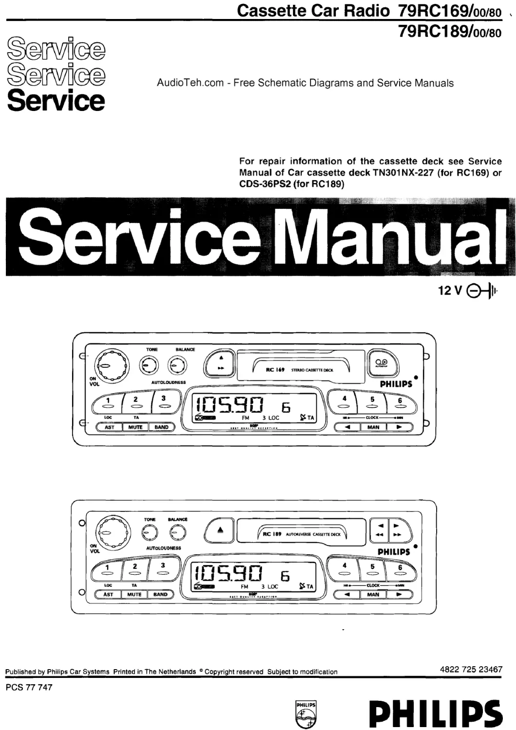
Cassette Car Radio 79RC169/00180 ,
79RC189/00180
AudioTeh.com
-
Free Schematic Diagrams and Service Manuals
For repair information of the cassette deck see Service
Manual of Car cassette deck TN301 NX-227 (for RC169) or
CDS-36PS2 (for RC189)
12v9111·
ID6~~QI f n -~; 1Jt~ls·
<Ir~r~11os.9o 6 c~)~)~
LOC
TA
~
FM
3 LOC
~TA
..o---CLOCK----o-
-
~I MUTE IQANO
........ ~"""'°'
~~
0
0 5'5 8[f0£...-°"7~1
.
~~ AUTOLOUDNESS
PHILIPS
GTITlJ 1os.9o 6 Cli~Th
Loe
TA
~
FM
3 LOC
~TA
0 ~~Ll*O
HR-CLOCK-MIN
Published by Philips Car Systems Printed in The Netherlands "Copyright reserved Subject to modification
4822 725 23467
PCS 77 747
e PHILIPS
Table of contents
Page
Technical specifications ............................................ 1
Direction for use ........................................................ 2
Electrical architecture ................................................ 3
Wiring diagram .......................................................... 4
Circuit diagram
Main board & Audio board ........................................ 5
Service hints .............................................................. 5
Component layout
Main board & Audio board ........................................ 6
Exploded View ........................................................... 7
Electrical Partslist ...................................................... 8
Technical Specifications
General
Power Supply
Quiescent Current (at 12.6V)
Fuse
Radio
FM
LW
MW
Aerial input impedence
IF-FM (1/2)
IF-AM(1/2)
a-3dB
SOS (10 dB channel separation)
Stereo channel separation
FM sensitivity for 26dB S/N
MW sensitivity for 26dB S/N
LW sensitivity for 26dB S/N
Cassette Deck
Number of tracks
Tapespeed
Wow and Flutter
Amplifier
Output Power (0=10%)
Loudness (auto)
Tone
~
ESD ~
WARNING
9.5
-
15.6V
< 4.0mA
3A
87.5
-
108MHz, 50kHz step
144 - 288kHz, 1kHz step
531 - 1629kHz, 9kHz step
75 ohm
10.7MHz/72.2MHz
10. 7MHz/450kHz
6-10μV
150uV ± 3dB
> 21d8
< 4.4μV
< 22μV
< 35μV
2X2
4.76 cm/second +3% -1%
< 0.35%
2x4.5W ± 1dB/40
4-8dB at 100Hz
8-24dB at 1OkHz
ESD Equipment:
All IC's and many semiconductors are
susceptible to electronic discharges (ESD).
Careless handling during repair can reduce life
drastically.
Anti-static table mat large 1200x650x1 .25mm
small 600x650x1 .25mm
Anti-static wrist band
Connection box (1 MOhm)
Extendible cable (to connect wrist band to conn. box)
Connecting cable (to connect table mat to conn. box)
Earth cable (to connect any product to mat or box)
Complete kit ESD3 (combining all above products)
Wristband tester
When repairing, make sure that you care
connected to the same potential as the mass of
the set via a wrist wrap with resistance. Keep
components and tools also at this potential.
PCS 77 748
4822 466 10953
4822 466 10958
4822 395 10223
4822 320 11307
4822 320 11305
4822 320 11306
4822 320 11308
4822 310 10671
4822 344 13999
11
[iQS.~MOHoc 6 ~1.I
........ ~.·~······
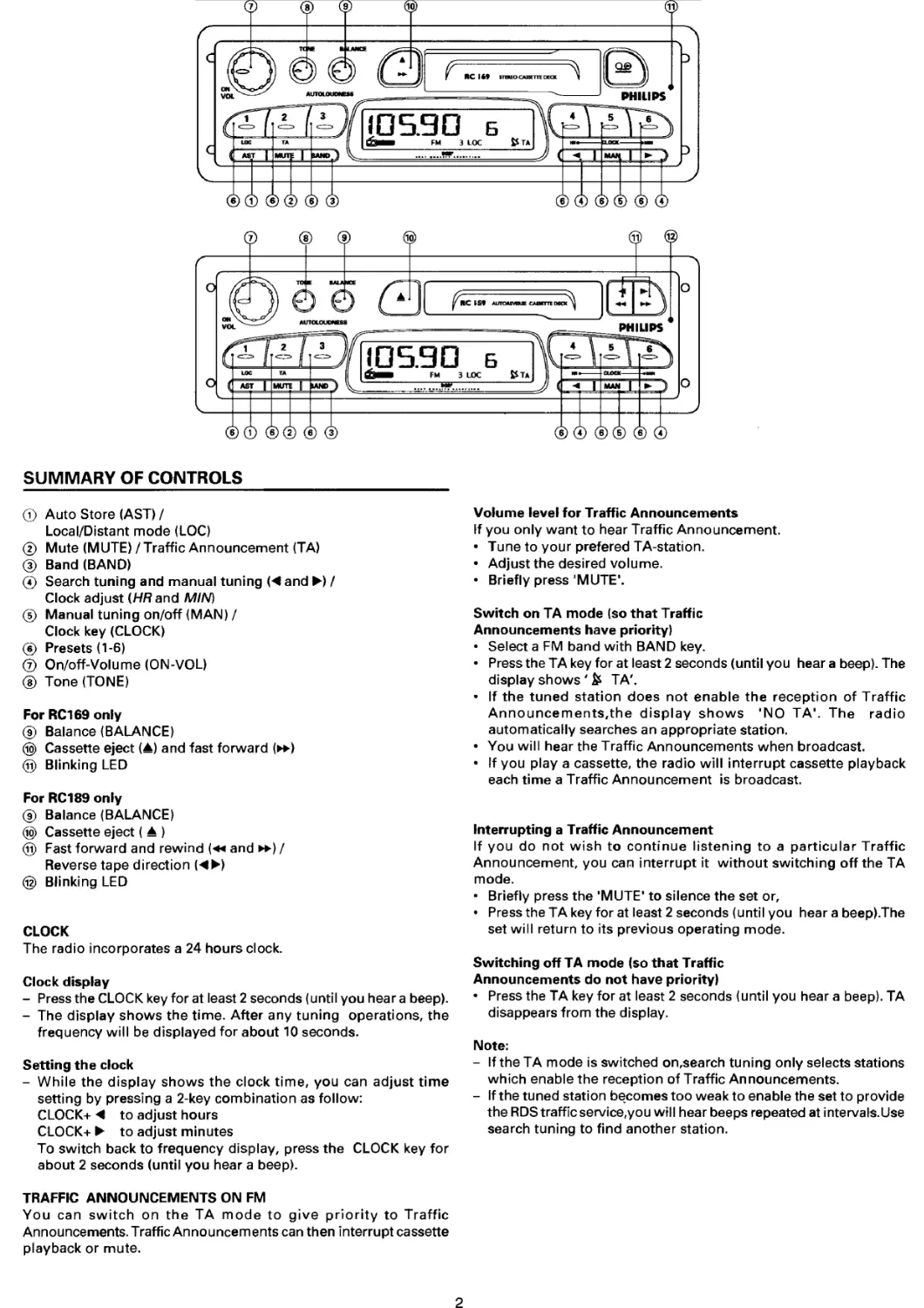
SUMMARY OF CONTROLS
CD Auto Store (AST) I
Local/Distant mode (LOC)
@ Mute (MUTE) I Traffic Announcement (TA)
@ Band (BAND)
© Search tuning and manual tuning (<C and ..) I
Clock adjust (HR and M/M
® Manual tuning on/off (MAN) I
Clock key (CLOCK)
® Presets (1-6)
(j) On/off-Volume (ON-VOL)
@ Tone (TONE)
For RC169 only
® Balance (BALANCE)
@ Cassette eject l•l and fast forward (~)
@ Blinking LED
For RC189 only
® Balance (BALANCE)
@> Cassette eject ( • )
@ Fast forward and rewind(~ and~) I
Reverse tape direction (<C. _)
@ Blinking LED
CLOCK
The radio incorporates a 24 hours clock.
Clock display
-
Press the CLOCK key for at least 2 seconds (until you hear a beep).
-
The display shows the time. After any tuning operations, the
frequency will be displayed for about 10 seconds.
Setting the clock
-
While the display shows the clock time, you can adjust time
setting by pressing a 2-key combination as follow:
CLOCK+ <C to adjust hours
CLOCK+.. to adjust minutes
To switch back to frequency display, press the CLOCK key for
about 2 seconds (until you hear a beep).
TRAFFIC ANNOUNCEMENTS ON FM
You can switch on the TA mode to give priority to Traffic
Announcements. Traffic Announcements can then interrupt cassette
playback or mute.
2
Volume level for Traffic Announcements
If you only want to hear Traffic Announcement.
• Tune to your prefered TA-station.
• Adjust the desired volume.
• Briefly press 'MUTE '.
Switch on TA mode (so that Traffic
Announcements have priority)
Select a FM band with BAND key.
Press the TA key for at least 2 seconds (until you hear a beep). The
display shows•~ TA' .
If the tuned station does not enable the reception of Traffic
Announcements.the display shows 'NO TA '. The radio
automatically searches an appropriate station.
You will hear the Traffic Announcements when broadcast.
If you play a cassette, the radio will interrupt cassette playback
each time a Traffic Announcement is broadcast.
Interrupting a Traffic Announcement
If you do not wish to continue listening to a particular Traffic
Announcement, you car:i interrupt it without switching off the TA
mode.
• Briefly press the 'MUTE ' to silence the set or,
• Press the TA key for at least 2 seconds (until you hear a beep).The
set will return to its previous operating mode.
Switching off TA mode (so that Traffic
Announcements do not have priority)
• Press the TA key for at least 2 seconds (until you hear a beep). TA
disappears from the display.
Note:
-
If the TA mode is switched on,search tuning only selects stations
which enable the reception of Traffic Announcements.
-
If the tuned station b~comes too weak to enable the set to provide
the RDS traffic service,you will hear beeps repeated at intervals.Use
search tuning to find another station.
5
12v
~,--,,
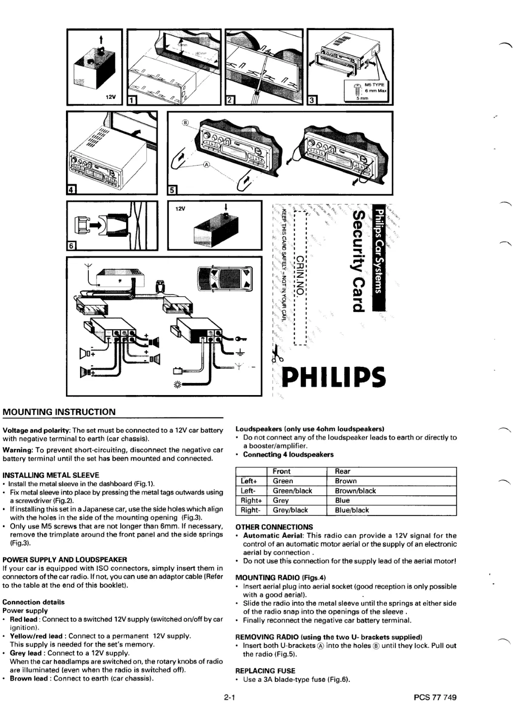
MOUNTING INSTRUCTION
Voltage and polarity: The set must be connected to a 12V car battery
with negative terminal to earth (car chassis).
Warning: To prevent short-circuiting, disconnect the negative car
battery terminal until the set has been mounted and connected.
INSTALLING METAL SLEEVE
• Install the metal sleeve in the dashboard (Fig.1 ).
• Fix metal sleeve into place by pressing the metal tags outwards using
a screwdriver (Fig.2).
• If installing this set in a Japanese car, use the side holes which align
with the holes in the side of the mounting opening (Fig.3).
• Only use M5 screws that are not longer than 6mm. If necessary,
remove the trim plate around the front panel and the side springs
(Fig.3).
POWER SUPPLV AND LOUDSPEAKER
If your car is equipped with ISO connectors, simply insert them in
connectors of the car radio. If not, you can use an adaptor cable (Refer
to the table at the end of this booklet).
Connection details
Power supply
Red lead: Connect to a switched 12V supply (switched on/off by car
ignition).
Yellow/red lead: Connect to a permanent 12V supply.
This supply is needed for the set's memory.
Grey lead: Connect to a 12V supply.
When the car headlamps are switched on, the rotary knobs of radio
are illuminated (even when the radio is switched off).
Brown lead: Connect to earth (car chassis).
•
2-1
i;,-~,;; ""7 '? .
I," ;'<
,__
"'
r,', <,fi,~
I
I
's!
,I
Cl
I (jj
g
I•'
):
I
~
c
I'
' ""I
'¥: I
I
r,
,:o:
-·
, "Tl
....
I, ,~
' 1JJ•
'<
I
>,)
,-•
r,
''··~ .z.
0
I
1"
I
...
,z,
,~
:9:
D>
,<§
I
' ""I
·~
Q.
,~
I ·?"
I
~ ~-~
PHILIPS
Loudspeakers (only use 4ohm loudspeakers)
• Do not connect any of the loudspeaker leads to earth or directly to
a booster/amplifier.
• Connecting 4 loudspeakers
Front
Rear
Left+
Green
Brown
Left-
Green/black
Brown/black
Right+ Grey
Blue
Right- Grey/black
Blue/black
OTHER CONNECTIONS
• Automatic Aerial: This radio can provide a 12V signal for the
control of an automatic motor aerial or the supply of an electronic
aerial by connection .
• Do not use this connection for the supply lead of the aerial motor!
MOUNTING RADIO (Figs.4)
• Insert aerial plug into aerial socket (good reception is only possible
with a good aerial).
Slide the radio into the metal sleeve until the springs at either side
of the radio snap into the openings of the sleeve .
• Finally reconnect the negative car battery terminal.
REMOVING RADIO (using the two U- brackets supplied)
• Insert both U-brackets@ into the holes® until they lock. Pull out
the radio (Fig.5).
REPLACING FUSE
Use a 3A blade-type fuse (Fig.6).
PCS 77 749
PART A: ELECTRICAL ARCHITECTURE
AUDIO PCB
LINE-OUT
,.....
DISCRETE
MAIN PCB
SOURCE SELECTOR
•
I
I
AUDIOffONE CONTROL
I
I
::-
I
I
-- -i;.
7801 - HEF4053BT
~
-
DISCRETE
I
I
\V
I
I
I
I
'
I
I
DLMS
I
L
I
I
L-
-
""
TUNER MODULE (7SV/9SV)
-
AMIFM
7004 - TEA6810V
MICRO-CONTROLLER
::- 7101 - TEA6820T
-
-
TUNER_SDA I SCL
MPX_RDS
I
RDS_DATA I CLK _
*
-
7701 - TMP47C820
RDS DECODER
7821 - SAA6579T
-
-
-
I
I
I
I
I
30 LINES
I
I
CASSETTE
*
LCD
I
I
QDI
-
7501 - UPC1228H
1751 - LCDl/2/3/4
'
-
i
FIXED FRONT PCB (LEFT)
KEY MATRIX
ILLUMINATION
8 LINES
TACT SWITCHES
DISCRETE
I
PCS 77 750
3
1-·- ----- - --- -
------1
I
I
FLY-LEAD
POWER AMPLIFIER (2X6W)
I---------
7601 - HA13119
I
I
EEPROM
I
I
-
I
I
7731 - ST24W04B6
I
-
I
I
I
EEP_SDA I SCL I \'/RITE
I
I
I
I CONNECTOR BLOCK
+V
I
I
t
I
I
SUPPLY I CONTROL
I
I
I
DISCRETE
-
-
!
I
-
J
J
BLINKING LED
*
DISCRETE
I
I
I
I
*=OPTION
--
-
-,
FIXED FRONT PCB (RIGHT)
ILLUMINATION
KEY MATRIX
DISCRETE
TACT SWITCHES
--
---
-
____ ____ ___ ____ __ , !
3-1
PART B : WIRING DIAGRAM
CONNE
~
.....:I
CXl
~
r:r:i
U)
L
U)
..:x:: '
CXl '
REFER PARTS
u'
p_,
'
'
""
~'
~ ''''
1501
-
-
1nm.J'l'- FORWARD
-
I
-
qr,NAL RETrn"'
2
LEF'l'- FORWARD
-
3
.
~
~
'
CASSETTE DECK
'
~
'
1502
-
-
* CAQ TRArK
:-I
r,w1rn.m
2
rA~ PLAY
-
3
-
-
rA~ MnTnR
4
rA~ MUTE
5
N.C.
6
'
~
~
'
'
# NOT CONNECTED FOR LOW P01
1601
I- ....
..,
....
"'"',_
~
* NOT CONNECTED FOR TN-301
11I ~
'
E-<
~ ::; E-< E-<
"'
:r: "'- <
E-<
'-"
::;: '- """
§8
E-<
......
.....
:;:i....,
"'-< <>::
......
......
~~
++
~~ oe>::
~
~
~~
......
"'
0 <>::
~ <>::
+ + g;"'-<
-
-
17
I- ....
..,
....
"' "'
,_~
1861
Al
4
2TOR BLOCK
1900
1 &3 FOR CONNECTIONS
0
1801
-
Rl
-
I
R2
-
2
R1
3
r1
4
C4
5
V UMp r+14Vl
-
6
BLINK LED
-
7
1702
r.RrnThTJ)
8
-
-
1
r
I
I
2
I
RIGHT FRONT PCB
3
I
4
I
I
5
I
I
6
I
~IN PCB
I
7
I
I
8-
I
9-
I
10
1803
I
11
-
I
r.R()]ThTJ)
r~
I
8
I
VI.AMP r+14Vl
I
7
I
C2
I
6
I
I
ri
5
I
I
R4
4
I
R1
I
-
3
I
R2
I
2
'/ER SETS
Rl
I
-
1701
' '"'
1--""'"""'"""tn I
LEFT FRONT PCB
I''
I
8
""
~
Cl)
""'
""'
U"1
~~
,_,
ii;
Cl)
~
""'~
+
~§
~
z0
po;
""
,:Q 0
;§ ff
+
,_,
*
t--.,
,.,
711,,
I-N
" ""'
"""
Wl
1862
rnro PCB
4-
PCS 77 751
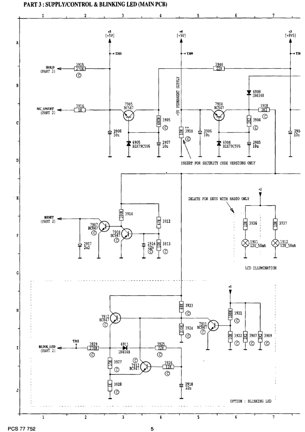
PART 3: SUPPLY/CONTROL &BLINKING LED (MAIN PCB)
A
B
c
D
'E
F
G
H
I
J
r-
'
I
I
PCS 77 752
1
2
+S
[+5V]
T310
HOLD
3915
(PART 2)
2K
©
3916
MC ON/OFF
(PART 2)
lK
2908
I'~
RESET E--------~
(PART 2)
BLINK_LED
(PART 2)
1
2917
I 2u2
T312
2
7~12
BC 47
©
©
©
3
4
7905
BC547
~ 3905
...,
©
2907
IlOu
©
3925
K
©
©
stm
3
4
5
5
6
7
+4
[+5V]
><,..::i
0..
0..
t=>
U)
I"'
0..
>Ln
+
T309
3940
R
6908
1N4148
7904
BC547
++
~ 3910
2906
.. ....
r\
2905
IlOu
INSERT FOR SECURITY CODE VERSIONS ONLY
DELETE FOR SETS WITH RADIO ONLY
\_
+2
1911
12V_50mA
LCD ILLUMINATION
+I
©
©
7§11
BC 47
©©
©©©
2918
I 22u
OPTION : BLINKING LED
s
6
7
+3
{+8V5]
T30
290·
r
1912
12V_50rnA
10
11
12
13
14
1900 A13
1911 F6
1912 F7
+2
+I
1900
2901 Bl2
[+14V4]
[+14V4]
CONNECTOR BLOCK
2902 Bll
2903 D9
A 2904 c8
2905 D7
2906 c5
T307
2907 D4
2908 c3
2909 DlO
T301
1901
2915 E12
_SJ~l-
14
E3
A7
IGNITION PLUS
2916 F4
"LU019
- (+14V4)
2917 F2
5A
2918J5
2902
6901
2901
2921 GlO
2922 Gl2
12~ 1. 5KE27
I~p
B 2923 Jl2
3901 Dll
3903 c9
3904 c7
3905 c4
3906 ClO
7903
3907I6
BD241A
-
-
-
-
-
-
-
3908 c7
3909 I7
T302
3910 c5
. e; 3906
6902
~
AS
POWER
3911 Dll
1N4002GPE
GROUND
c 3912 F4
©'©
3913 F4
3914 E3
3915 A2
3916 c2
2903 '
2909
3921 H6
3922I6
IlOOu
'
I lOOOu '
3923 H5
©
3924I5
3925I4
3926I4
D3927I3
FOR LOW POWER ONLY
T303
3928J3
3929I2
6909
12
A4
PERMANENT
3930 Ill
- PLUS (+14V4)
3931 Ill
3932 FlO
2915
3933 GlO
3934 F9
+2
I~p
3935 FlO
3936 F6
E 3937 F7
3938 B9
3939 B9
6913
3940 A6
1N4002GPE
5901 B12
6901 Bll
T304
6902 Cll
6903 D8
A6
PILOT/EXTERNAL
6904 D6
ILLUMINATION
6905 D3
6908 B7
F 6909 D12
6911I3
6912 no
6913 ElO
V LAMP
6914
6914 Fll
7903 c8
(PART 2)
1N4 02GPE
7904 c5
7905 c3
2921
2922
7907 F2
I 22u
I~
7908 F3
G 7911 H5
7914 H3
7913J3
H
TJOS
2923
©
IlOOn
J
++ ITEM NOT USED - PROVISION IN PCB LAYOUT ONLY
I ______ _
9
10
11
12
13
14
5"1
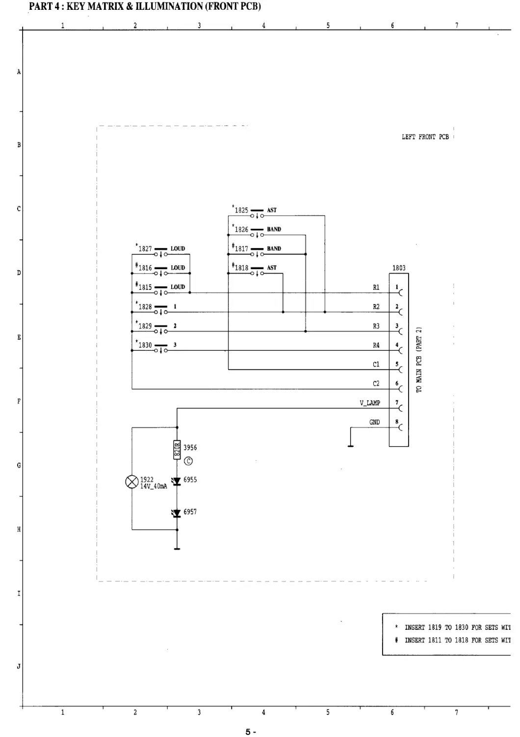
.PART 4: KEY MATRIX & ILLUMINATION (FRONT PCB)
1
2
4
A
B
c
*1825 - AST
~i~
'1826 - BAND
:: '-
*
#1817 - BAND
1827 -
LOUD
-------0'::
:: '::
D
#1816 -
WUD
#1818 - AST
:: '::
_,o--
*1315 - wvo
:: '::
*
1828* 1
*
1829 '.:"'i"".: 2
E
*1330 T 3
F
~ 3956
=
G
©
1922
~1 , 6955
14V_40mA •
..
~:6957
H
J
2
4
5-
5
Rl
R2
R3
R4
Cl
C2
V_LAMP
GND
1
5
LEFT FRONT PCB 1
1803
~
1
2
3
4
'-
5
6
7
8
~
* INSERT 1819 TO 1830 FOR SETS WI1
# INSERT 1811 TO 1818 FOR SETS WI1
10
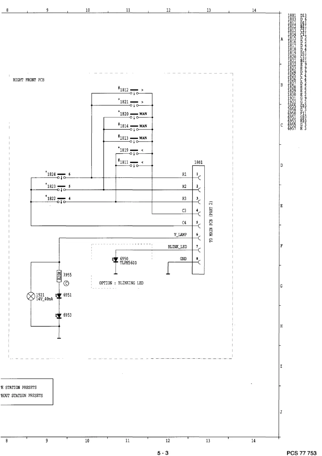
RIGHT FRONT PCB
*
11
*1s12 -
>
*1821- >
10-----4
*1820 -MAN
~-----01-
*1014 -MAN
-- - - -01.:;
#1813 -MAN
-----0.:1.:
*1819 -
<
.: I~,.,_____ __ .,
*1s11 -
<
. :; 10-----4
12
13
--
~
~
~
~
~
-- ---- ,
1801
~
Rl
1
R2
2
R33
1822 *',__4
_____________,_______..__,
~ 3955
<X>
©
1921
~r6951
14V_40mA ; ""
H STATION PRESETS
HOUT STATION PRESETS
9
\t6953
10
1-------~
-
-
-
-
-
-
~------I
'
'
'
'
'
'
'
::~, 6950
·~ "' TLPH5600
·-
OPTION : BLINKING LED
--------
11
C3
4
~~
C4
s
<Q
CJ
""'
zH
V_LAMP
6
~
0
E-<
BLINK_LED
7
GND 8
\..
~
12
13
5-3
14
1801 D13
1803 D6
1811 Dll
1812 Bll
1813 Cll
1814 Cll
A 1815 D2
1816 D2
1817 D4
1818 D4
1819 Dll
1820 Cll
1821 Bll
1822 E9
1823 E9
1824 D9
1825 c4
1826 c4
B 1827 D2
1828 E2
1829 E2
1830 E2
1921 G9
1922 G2
3955 GlO
3956 G3
6950 Fll
6951 GlO
6953 HlO
c 6955 G3
6957 H3
D
E
F
G
H
I
J
14
PCS 77 753
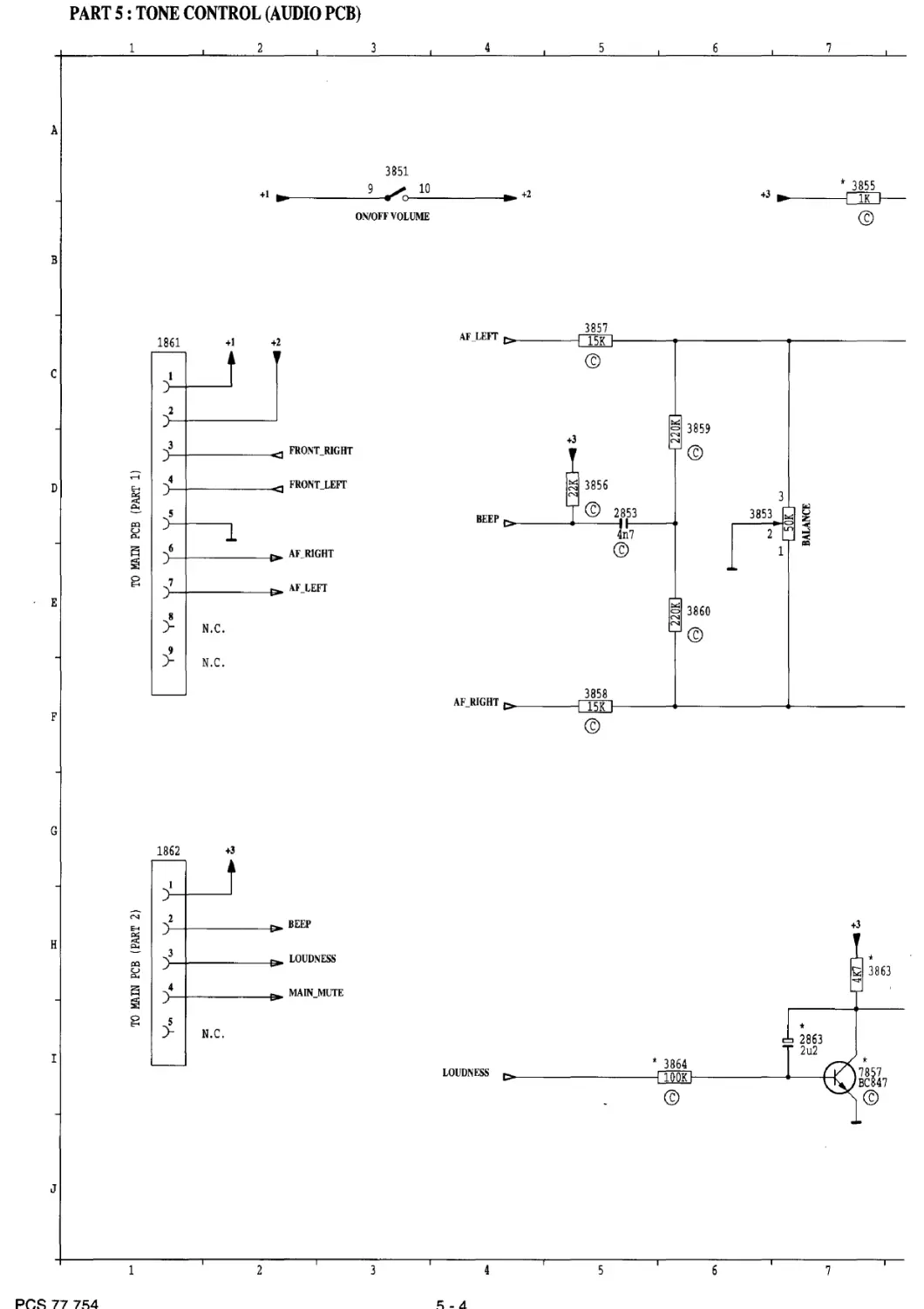
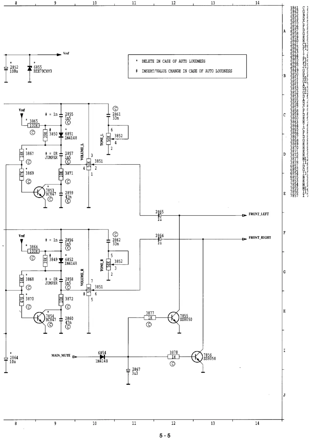
PART 5 : TONE CONTROL (AUDIO PCB)
2
4
5
A
3851
+I•
_______.; 10
... .
rrc
+2
3
* 3855
+~
ON/OFF VOLUME
©
B
AF_LEIT
3857
1861
+I
+2
15K
©
c
2
+3
~ 3859
N
FRONT_RIGHT
©
;::::;
D
~
FRONT_LEIT
© 2853
3853
~
BEEP
~
""
Ln :l
u
n7
2
p..
;1l
z
©
H
AF_RIGHT
Sll
0
E-<
AF_LEIT
E
~ 3860
->- N.C.
N
©
-]-
N.C .
AF_RIGHT
3858
15K
F
©
G
1862
+3
""
E-<
BEEP
+3
H
~
""
LOUDNESS
u
""'
z
4
MAIN_MUTE
H
Sll
0
j_
E-<
N.C .
2863
I
2u2
* 3864
LOUDNESS
1K
©
J
2
4
PCS 77 754
~-4
8
2852
I lOOu
2864
IlOu
8
vrer
vrer
©
©
9
10
11
12
13
Vref
• DELETE IN CASE OF AUTO LOUDNESS
6855
BZX79C4V3
INSERT/VALUE CHANGE IN CASE OF AUTO LOUDNESS
©
#=ln
2861
33n
~·~
#=OR
JUMPER
2859
©
I 47n
285
u
©
26
2862
33n
u
i>li
~·~
#=OR
JUMPER
2860
~~~55o
I (f)
MA!N_MUTE l>-----
6
•8~
54
___-+---------1
1N4148
2867
I3u3
10
11
12
13
5-5
14
1861 cl
1862 Gl
2852 BE
2853 D:
2855 cs
2856 FS
A 2857 DS
2858 GS
2859 ES
2860 HS
2861 Cll
2862 Fll
2863I!
2864IE
2865 m
2866 Fli
2867 Jl]
3849 GS
B 3850 DS
3851 DlC
3851 GlC
3851 A~
3852 Dll
3852 Gll
3853 DE
3855 A!
3856 D:
3857 c:
3858 F:
c 3859 DE
3860 EE
3863 H!
3864IE
3865 CE
3866 FE
3867 DE
3868 GE
3869 EE
3870 HE
3871 ES
D 3872 HS
3877 Hll
3878 m
6851 DS
6852 GS
6854 I1C
6855 BS
7853 ES
7854 HS
7855 H12
E 7856 I13
7857I!
FRONT_LEFT
F
FRONT_R!GHT
G
H
J
14
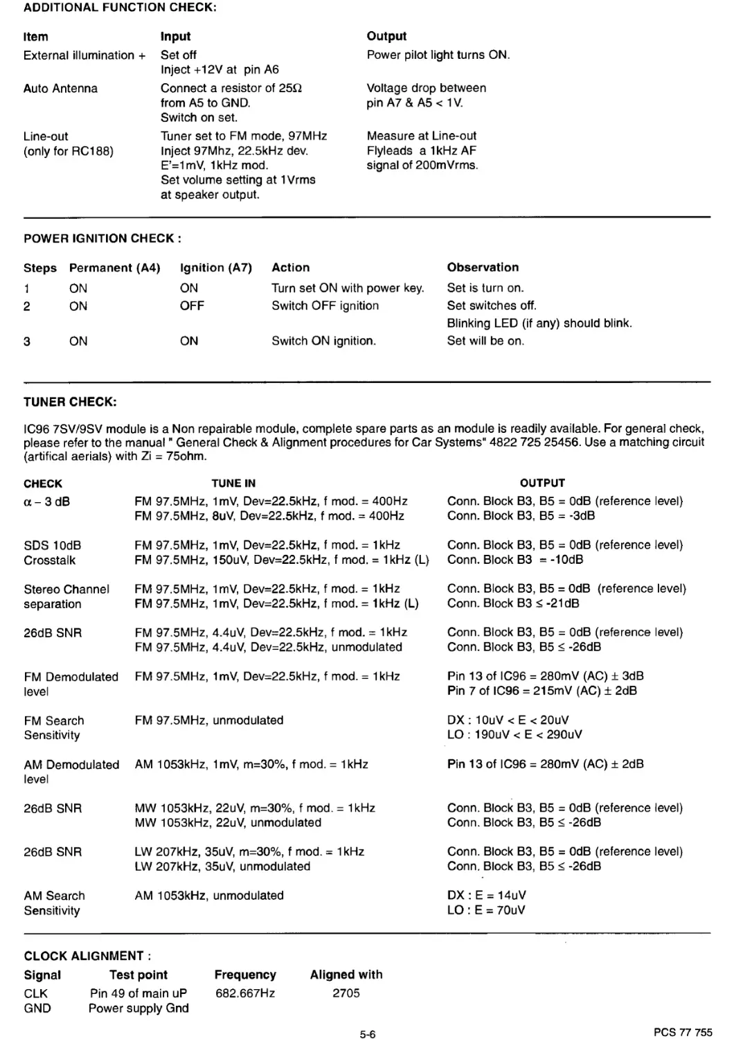
ADDITIONAL FUNCTION CHECK:
Item
Input
Output
External illumination + Set off
Power pilot light turns ON.
Inject +12V at pin A6
Auto Antenna
Connect a resistor of 25!1
from A5 to GND.
Voltage drop between
pinA7 &AS<1V.
Switch on set.
Line-out
(only for RC188)
Tuner set to FM mode, 97MHz
Inject 97Mhz, 22.5kHz dev.
E'=1 mV, 1kHz mod.
Measure at Line-out
Flyleads a 1kHz AF
signal of 200mVrms.
Set volume setting at 1Vrms
at speaker output.
POWER IGNITION CHECK:
Steps Permanent (A4)
1
ON
2
ON
3
ON
TUNER CHECK:
Ignition (A 7)
ON
OFF
ON
Action
Turn set ON with power key.
Switch OFF ignition
Switch ON ignition.
Observation
Set is turn on.
Set switches off.
Blinking LED (if any) should blink.
Set will be on.
IC96 7SV/9SV module is a Non repairable module, complete spare parts as an module is readily available. For general check,
please refer to the manual " General Check & Alignment procedures for Car Systems" 4822 725 25456. Use a matching circuit
(artifical aerials) with Zi = 75ohm.
CHECK
a-3dB
SOS 10dB
Crosstalk
Stereo Channel
separation
26dB SNR
FM Demodulated
level
FM Search
Sensitivity
AM Demodulated
level
26dB SNR
26dB SNR
AM Search
Sensitivity
TUNE IN
FM 97.5MHz, 1mV, Dev=22.5kHz, f mod.= 400Hz
FM 97.5MHz, 8uV, Dev=22.5kHz, f mod.= 400Hz
FM 97.5MHz, 1mV, Dev=22.5kHz, f mod.= 1kHz
FM 97.5MHz, 150uV, Dev=22.5kHz, f mod.= 1kHz (L)
FM 97.5MHz, 1mV, Dev=22.5kHz, f mod.= 1kHz
FM 97.5MHz, 1mV, Dev=22.5kHz, f mod.= 1kHz (L)
FM 97.5MHz, 4.4uV, Dev=22.5kHz, f mod.= 1kHz
FM 97.5MHz, 4.4uV, Dev=22.5kHz, unmodulated
FM 97.5MHz, 1 mV, Dev=22.5kHz, f mod.= 1kHz
FM 97.5MHz, unmodulated
AM 1053kHz, 1mV, m=30%, f mod. = 1kHz
MW 1053kHz, 22uV, m=30%, f mod.= 1kHz
MW 1053kHz, 22uV, unmodulated
LW 207kHz, 35uV, m=30%, f mod. = 1kHz
LW 207kHz, 35uV, unmodulated
AM 1053kHz, unmodulated
CLOCK ALIGNMENT :
Signal
CLK
GND
Test point
Pin 49 of main uP
Power supply Gnd
Frequency
682.667Hz
Aligned with
2705
5-6
OUTPUT
Conn. Block B3, B5 = OdB (reference level)
Conn. Block B3, B5 = -3dB
Conn. Block B3, B5 = OdB (reference level)
Conn. Block B3 = -10dB
Conn. Block 83, B5 = OdB (reference level)
Conn. Block B3 s -21 dB
Conn. Block B3, B5 = OdB (reference level)
Conn. Block B3, B5 s -26dB
Pin 13 of IC96 = 280mV (AC) ± 3dB
Pin7ofIC96=215mV(AC)±2dB
DX:10uV<E<20uV
LO: 190uV < E < 290uV
Pin 13 of IC96 = 280mV (AC) ± 2dB
Conn. Block B3, B5 = OdB (reference level)
Conn. Block B3, B5 s -26dB
Conn. Block B3, B5 =OdB (reference level)
Conn. Block B3, B5 s -26dB
DX:E=14uV
LO:E=70uV
PCS 77 755
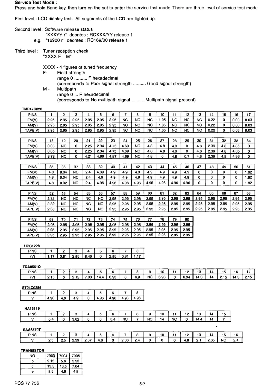
Service Test Mode :
Press and hold Band key, then turn on the set to enter the service test mode. There are three level of service test mode
First level : LCD display test. All segments of the LCD are lighted up.
Second level : Software release status
"XXXYY r" deontes : RCXXXNY release 1
e.g.
"16900 r" deontes : RC169/00 release 1
Third level : Tuner reception check
"XXXX F
M"
XXXX - 4 figures of tuned frequency
F-
Field strength
range 0 .......... F hexadecimal
(corresponds to Poor signal strength .......... Good signal strength)
M - Multipath
range 0 ... F hexadecimal
(corresponds to No multipath signal .......... Multipath signal present)
TMP47C820
PINS
1
2
3
4
5
6
7
8
9
10
11
12
FM(V)
2.95 2.95 2.95 2.95 2.95 2.95 NC
NC
NC 1.05 NC
NC
AM(V)
2.95 2.95 2.95 2.95 2.95 2.95 NC
NC
NC 1.05 NC
NC
TAPE(V)
2.95 2.95 2.95 2.95 2.95 2.95 NC
NC
NC 1.05 NC
NC
PINS
18
19
20
21
22
23
24
25
26
27
28
29
FM(V)
0.05 NC
0
2.25 2.34 4.75 4 .69 NC 4.8
4.8 4.8
0
AM(V)
0.05 NC
0
2.25 2.34 4.75 4 .69 NC 4.8
4.8 4.8
0
TAPE(V)
8.78 NC
0
4.21 4.96 4.87 4.69 NC 4.8
0
4.8
0.7
PINS
35
36
37
38
39
40
41
42
43
44
45
46
FM(V)
4.8 0 .04 NC 2.4 4.89 4.9 4.9
4.9
4.9
4.9 4.9
4.9
AM(V)
4.8 0.04 NC 2.4
4.9
4.9 4.9
4.9
4.9
4.9 4.9
4.9
TAPE(V)
4.8 0.02 NC 2.4 4.96 4.96 4.96 4.96 4.96 4.96 4.96 4.96
PINS
52
53
54
55
56
57
58
59
60
61
62
63
FM(Vl
2.32 NC NC
NC
NC 2.95 2.95 2.95 2.95 2.95 2.95 2.95
AMIV)
2.32 NC NC
NC
NC 2.95 2.95 2.95 2.95 2.95 2.95 2.95
TAPE(V)
2.38 NC NC
NC
NC 2.95 2.95 2.95 2.95 2.95 2.95 2.95
PINS
69
70
71
72
73
74
75
76
77
78
79
80
FM(V)
2.95 2.95 2.95 2.95 2.95 2.95 2.95 2.95 2.95 2.95 2.95 2.95
AM(V)
2.95 2.95 2.95 2.95 2.95 2.95 2.95 2.95 2.95 2.95 2.95 2.95
TAPE(V)
2.95 2.95 2.95 2.95 2.95 2.95 2.95 2.95 2.95 2.95 2.95 2.95
UPC1228
PINS
2
3
4
5
6
7
8
v
1.17 0.81 2.95 8.46
0
2.95 0.81 1.17
2
3
4
5
6
7
8
9
10
11
12
2.15
0 2.15 7.03 14.4 6.93
0
6.9
NC 6.93
0 6.94
ST24C0286
PINS
2
3
4
5
6
7
8
v
4.96 4.9
4.9
0 4.96 4.96 4.96 4.96
HA13119
PINS
2
3
4
5
6
7
8
9
10
11
12
v
0.4
0
3.62
0
0
0.4 NC
7
NC
14
NC
0
SAA6579T
PINS
2
3
4
5
6
7
8
9
10
11
12
v
2.5
2.5 2.39 2 .37 4.8
0
2.36 2 .4
0
0
0
4.8
TRANSISTOR
NO
7903 7904 7905
b
9.15 5.6 5.53
c
13.5 13.5 7.04
e
8.5
4.9
4.8
PCS 77 756
5-7
13
14
15
16
17
NC 0.22
0
0.03 0.03
NC 0.22
0
0.03 0.03
NC 0.22
0
0.03 0.03
30
31
32
33
34
4.8 2.39 4.8 4.85
0
4.8 2 .39 4.8 4.85
0
4.8 2 .39 4.8 4.96
0
47
48
49
50
51
0
0
0
0
1.82
0
0
0
0
1.82
0
0
0
0
1.82
64
65
66
67
68
2.95 2.95 2.95 2.95 2.95
2.95 2.95 2.95 2.95 2.95
2.95 2.95 2.95 2.95 2.95
13
14
15
16
17
14.3 14 2.15 14.3 2 .15
13
14
15
14.4 14
7
13
14
15
16
2.1 2.35 NC 2.4
5-8
7
8
TUNER IC96 7SV I 9SV
__J
L)
(f)
'-'
N
~ d~Ult-
"
'"'
~~~
z:~
::J
'---
'-'
z
N.C.
7501
UPCl228H
+2
T105
T104
T1~
CAS_LEFT
T107
CAS_RIGHT
+5
~35'1
r© <J CAS _f'IOTOR
----------<.---~ (PART 2J
7
B
9
9
TUNER_LEFT
TUNER _RIGHT
""
<...1
CL
a
g<t
c:>
I 60!
7
6
s
4
10
N.C.
NC.
N.C
N.C,
AF_LEFT
AF_RIGHT
FRONT _LEFT
3 FRONT _R !GHT
2
10
11
MPX/ROS
lOE 3802
0R
©
+5
HEF4053BT
8
7
6
** 3803
0R
©
T132
T131
mo
T113
T114
+1
+2
II
5-9
<PART 2)
AO
N.C.
N.C.
+3
~3800
2827
4u7
2828
4u7
12
13
14
©
2826
15
782!
SAA6579T
~--~--+-----1
ANTl-
ALlASING
FIL T.ER
30p
2825
I
6
I iTM~
1182'
T2u2
lDPTl~S INFO
260 !
3601
2615
-to-
! 00u
~----o [2K7l r
1,,
©
... 2605
rl
l© ~~
I 22u
I
1 -~-
2607 l
T©
2603
3603
~
Iu
""-
~1
** :NSERT FOR SETS ~ITH RADIO ONLY - N/OUT CASSETTE I RDS
~ VALUE CHANGE TO 12K ~DR TONE CONTROL VERSIONS ONLY
•+ !TEM NOT USEO - PROV:SION IN PCB LAYOUT ONLY
12
13
14
15
i6
17
19
20
21
3823
-----------------------.j 22RI-----------
l
'Pl
124
?601
57 KhZ
BANDPASS
(8th ORDEP)
RECONSTRUCTiON
FILTER
COSTAS LOOP
BIDHASE
VARIABLE AND ,_ _ _ ____ .
SYMBOL
0 1xrn DIVIDER
DECODER
QUALITY
BIT
GENERATOR
©
3821
,--------- .- -- 1 22<2~RR· ~__,._-...+S
©
12
T121 J. 2821
r~n
DIFFERENTIAL
RDS_DATA
DECODER c----ttt-----1t---------1~ cPART 2)
T123
r--::--~::::=::=::=::=::=::~~16-t---*-----__..,RDS_C~
,----__i_--"L'--,
CPART 2 )
OSCILLATOR
N~D
DIVIDER
13
~ 3822
(\J
I~~@
4.3~MHi
.L 2823
2822
I
4,Ze -s2
~) l©
CLOCK
REGENERATION
AND SYNC
IEST LOGIC AND OUTPUT
SELECTOR SWiTCH
N.C.
10
11
+2
r
-1~. !3! 19
-- ----i
1900
I
13
__
2_---;+
3
5
6
12
16
z
"'
>- CJ
LlD
w'
>- >-
Cl ::::;
erI
CL <fl
w ---'
"' ""'
"'"'
::::; 0::
Ulw
I
>-
14
2617
100u
15
N.C.
N.C.
11
NC
I::
T116
T
6
I
NNECTOR BLOCK
STANDARD POWER ~/OUT FADER
FRONT
LEFT
(s8) T117
I
)n
2
BB~
REAR
LEFT
Ti
~rel
e---e.-----<11-...._------I
I
>-----8-111 -- ___.. .. __ ,lc""' -- -- J 26 I2
:
•'
4I
B3
.~1--+--_._.__•• _....__~c-1--__..____ +
~~~~ tJI ~~ ®T11B
100u
i?
1000u
)
~~
B4~
(J'.
4 1~ T119
1~1••1 5(
__J
++ 1602
B2 T120
•
3
B1
+
82~
4-----~
FRONT
RIGHT
REAR _
RIGHT
__ ___ _J
18
19
20
21
5-10
110ei
1101
1501
1502
i60i
1602
A 1851
1900
2501
2502
2503
2504
2505
2506
2507
2508
2510
2513
B 2601
2603
2605
2607
261~
2611
2612
2614
2615
2616
2617
c 2618
2619
2620
2821
2822
2823
2824
2825
2826
2827
0
2828
2829
3501
35~2
3503
3504
3505
3506
3510
3511
3512
E 3513
3514
3515
3516
3517
3518
3601
3603
3618
3619
3620
F 3621
3622
3623
3801
3802
3803
3809
3821
3822
3823
750i
G 7502
7503
7601
7801
7821
H
J
A3
CI
E3
G3
F9
JIB
016
E20
E4
F4
E5
F5
E8
G8
05
G5
04
J4
Fl4
Hl4
G'S
HIS
I15
F'S
H:B
E!B
FIS
117
Fl7
HIS
GIB
Gl5
A20
016
016
Cl4
B14
A14
Gl2
Hl2
C14
D5
F5
07
F7
D8
F8
D4
G4
H4
J4
j8
I7
I7
j7
G4
F14
HI4
HIS
GIB
!15
Fl5
115
El5
BlI
Al:
ElI
E12
A20
Cl6
A!9
E7
I6
J6
EIS
ClI
Al5
PCS 77 757
17
]
I
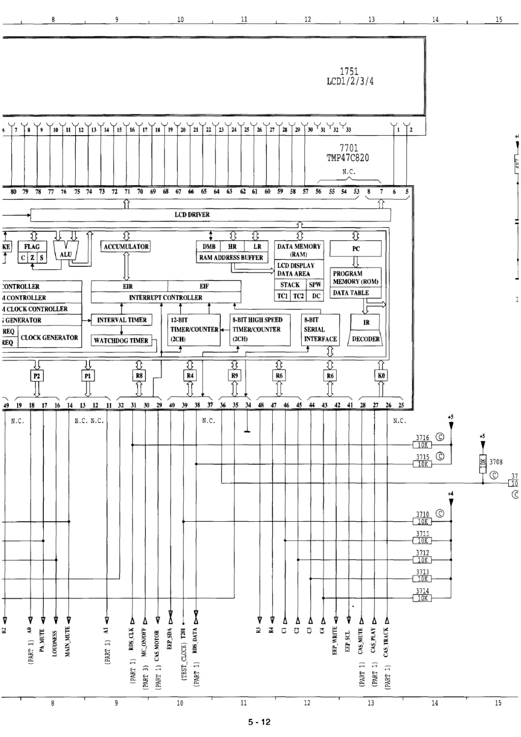
PART 2: MICRO-CONTROLLER, EEPROM & LCD (MAIN PCB)
5
7
A
+4
5701
5
B
lm
2701
2702
rw IIB
+S
432
c
33
VDD
15
vss
© VLCD
10
[
D
©
(PART 3) HOLD
24
(PART 3) RESET
23
20
E
21
22
1711
6MHz
F
5251so
INSERT IN CASE OF
2705
CLOCK
-----
50p
G
1712
D
32.768kHz
INSERT IN CASE OF
-- ---
2704
2703
NON-CLOCK
Iti) IIB
+5
H
+5
+5
SDA
I
SCL
TUNER SCL
3703
2707 2706
(PART 11
lK
IlOOp I lOOp
3704
©©
a:
TUNER_SDA
K
(PART 1)
J
4
7
PCS 77 758
5. 11
10
11
12
13
14
15
1751
LCDl/2/3/4
.J
.J
.J
.J
.J
.J
.J
.J
.J
.J
30 Y31 Y32 Y33
.J
678910ll121314151617181920212223242526272829
I2
~
7701
TMP47C820
r-
"
""
N.C .
~
80797877767574737271706968676'i656463626160595857565554538765
'-
/
·1
I
I
LCD DRIVER
I
I
-
H
-
rlWJg
l~
t
g
IFLAG I
ACCUMULATOR
DMB HR
LR
DATA MEMORY
PC
I
lei~ sl ALU
RAM ADDRESS BUFFER
(RAM)
H
LCD DISPLAY
DATAAREA
PROGRAM
MEMORY (ROM)
-
~ONTROLLER
ElR
EIF
STACK SPW
4 CONTROLLER
INTERRUPT CONTROLLER
TC! TC2 DC DATA TABLE
~
I
4 CLOCK CONTROLLER
TTf
-~
I
;GENERATOR
~ INTERVAL TIMER 12-BIT
8-BIT HIGH SPEED
8-BIT
IIR
~
i
TIMER/COUNTER ~ TIMER/COUNTER
SERIAL
CLOCK GENERATOR
WATCHDOG TIMER~ (2CH)
(2CH)
INTERFACE I DECODER\
~
f
f
~~R8
R4
R9
R6
R6
KO
"/
/
'
/
'/
/
'
/
'
/
4919181716141312113231302940393837363534484746454443424128272625
N.C.
N.C. N.C.
N.C .
1
N.C.
+5
,,
3716 ©
+5
aru-=-
3715 ©
~3708
~
©37
10
+4
,,
~
3710 ©
ruKJ-=-
3711
rnD---
3712
-[ill}-
ddb-
K
3714
rnD--
~
17
·~.
"
1
·~ .'•
p
17I~BJl1l11
'
l
~
llll•l
:;;!
=
"'
"'
:;;;
:..: t::
<
-
<
....,
;:::uN
....,
~ ""'
"'
...
:..:
<....~
.. ..
.. ...
=Q
= ....
=
uu
t: .....
....
<u
=>
=>
u >;'.
0
"'
N
<
=i;; =>
.....
<
"'
::;:
.. ..
::;:
I
z ....
.._1
Q
~I ::;:,
..
l=i,
z
z'
"'
0
I
.. ..
I
I
-:;'
Q
.. ....
Q
o,::;:"'~
~
"'
"'
=>
"'
"'
<
E-<
0 :;:
~=u
"''
u
"'
"'
<uVJ
;;!
::;:
::;:
0
""'
u
<
...
<
...
u
P..
u
ul
E-<
......
E-<
U)
;;!
""'
E-<
~ E-<
E-<
E-<
~ !:::!. ;;!
~
P..
~
;;!
P..
~
~
8
10
11
12
13
14
15
5-12
16
17
18
19
20
21
1701 Gl8
1702 F21
1711 F5
1712 G5
1751 Al2
2701 B5
A 2702 B6
2703 H6
2704 H5
2705 F5
2706J5
2707J5
2731 Cl5
3701 c5
3702 D5
3703J2
3704J2
3706I5
+4
B3707 I5
3708 Gl5
37 09 Gl5
~ 3731
3710 Hl4
3711 Hl4
3712 Il4
©
3713 !14
©
EEP_WRITE
3714 Il4
3715 Gl4
+4
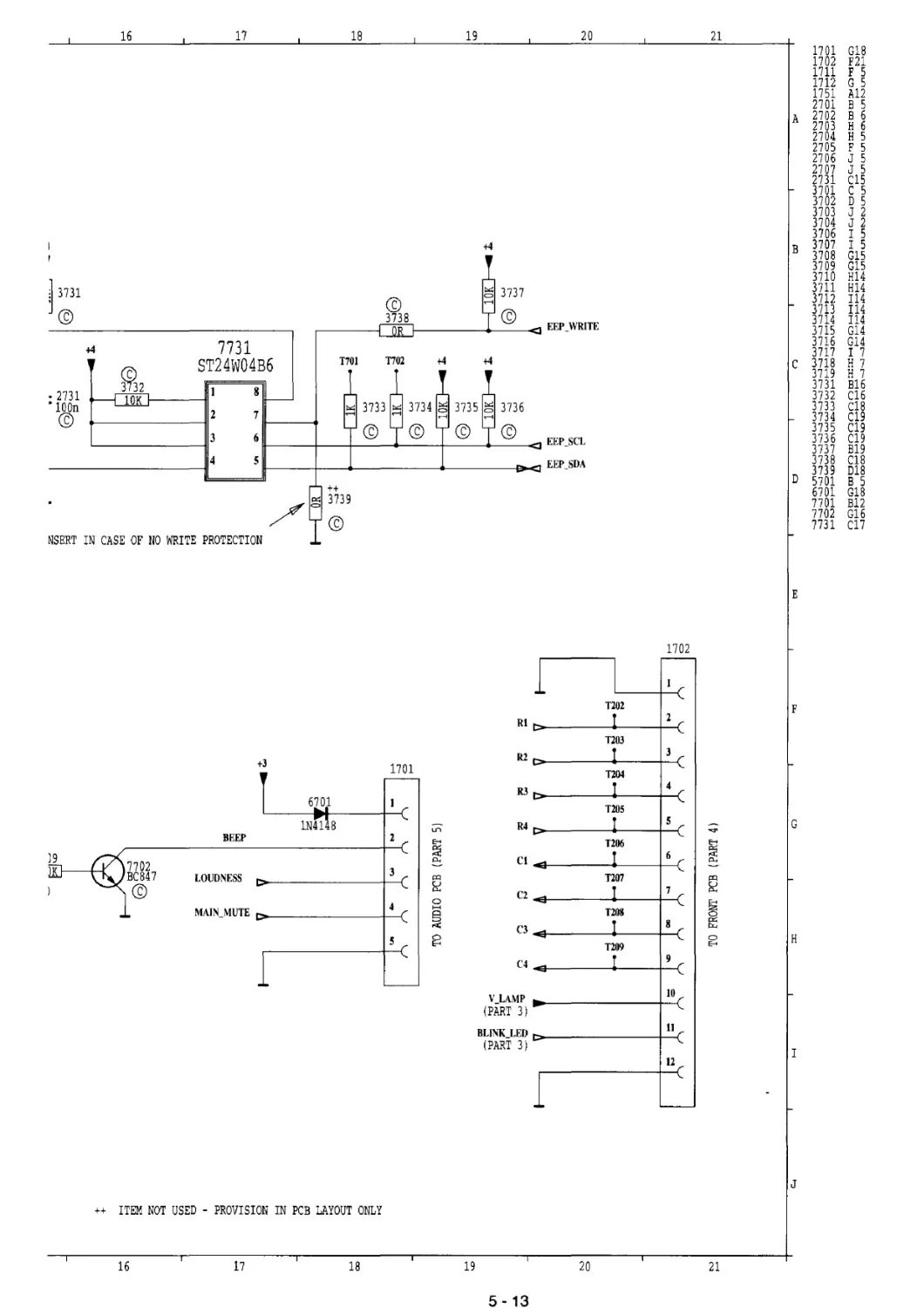
7731
3716 Gl4
3717 I7
ST24W04B6
T701
T702
+4
+4
c 3718 H7
3719 H7
8
3731 Bl6
• 2731
3732 Cl6
• 1oon
2
3733 Cl8
©
7
3734 C19
3735 Cl9
3
6
EEP_SCL
3736 Cl9
3737 Bl9
4
5
EEP_SDA
3738 Cl8
3739 D18
D 5701 B5
++
6701 Gl8
/
15 3739
7701 812
©
7702 Gl6
7731 Cl?
NSERT IN CASE OF NO WRITE PROTECTION
E
1702
T202
F
RI
T203
+3
R2
1701
T204
R3
4
6701
T205
1N41 8
R4
"""
G
BEEP
E-<
T206
~
~
7702
p..
Cl
"'
BC847
LOUDNESS
3
""
T207
""
©
CJ
CJ
p..
C2
"'
0
~
MAIN_ MUTE
H
T208
~
,,,;
C3
"'"'
0
0
H
E-<
T209
E-<
C4
V_LAMP
10
(PART 3)
BLINK LED
11
(PART 3)
12
J
++ ITEM NOT USED - PROVISION IN PCB LAYOUT ONLY
16
17
18
19
20
21
5-13
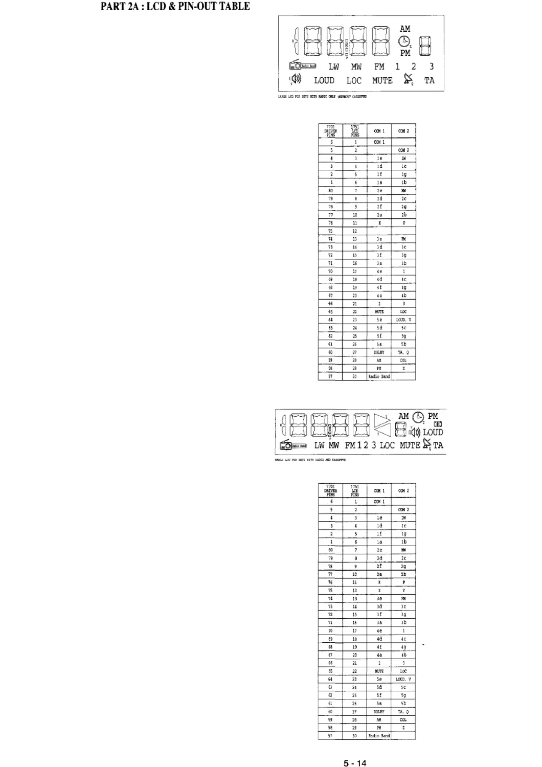
PART 2A: LCD & PIN-OUT TABLE
·~88188 AM
®,
8
PM
~
p
LWMWFM123
o~>))v
LOUD LOC MUTE ~ TA
LARGELC!JFORSETSWIT'llRADIOOHLY1WIT11CJUTCAS:SET'l'El
7701
1751
DRIVER
LCD
CCM l
COM l
PINS
PINS
6
1
COM l
s
2
COM l
I
J
le
LW
3
4
ld
le
l
5
lf
lg
l
6
la
lb
80
7
2e
..
79
8
2d
2C
78
9
2f
2g
77
10
2a
2b
76
11
K
p
7S
12
71
lJ
le
FM
73
14
Jd
JC
7l
15
Jf
Jg
71
16
la
lb
70
17
4e
l
'9
18
4d
4C
08
19
4f
4g
!7
20
4a
4b
!6
ll
2
3
IS
l2
MUTE
LOC
!I
23
Se
LOUD, V
63
l4
Sd
5c
ll
l5
5f
5g
n
l6
5a
5b
60
l7
DOLBY
TA, 0
59
l8
AM
COL
58
l9
PM
z
57
JO
Radio Band
SMALLLCDFORSETSWI'l 'HRADIO.ANDCASSE 'M 'E
7701
1151
DR:tvER
LCD
COM l
COM 2
PINS
PINS
6
l
COM l
5
l
CON 2
I
J
le
LW
3
I
ld
IC
l
5
lf
lg
l
6
la
lb
80
7
le
..
79
8
2d
2C
78
9
lf
lg
77
10
la
lb
76
11
K
p
75
ll
x
y
71
lJ
Je
FM
73
11
Jd
Jc
72
15
Jf
Jg
71
16
la
lb
70
17
4e
l
69
18
4d
4C
68
19
4f
4g
67
20
la
41;
6!
21
2
J
is
ll
MUTE
LOC
61
23
Se
LOUD, V
ii
24
5d
SC
'2
25
5f
5g
i1
26
5a
5b
oO
l7
DOLBY
TA, 0
59
28
AM
COL
58
29
PM
z
57
JO
Radio Band
5-14
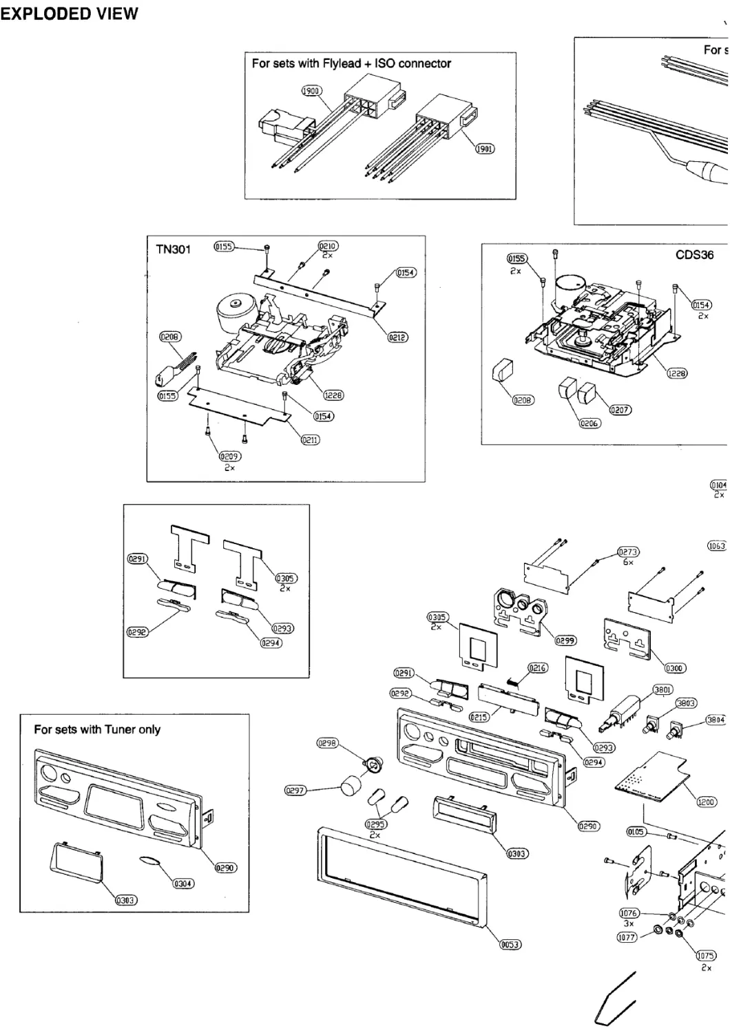
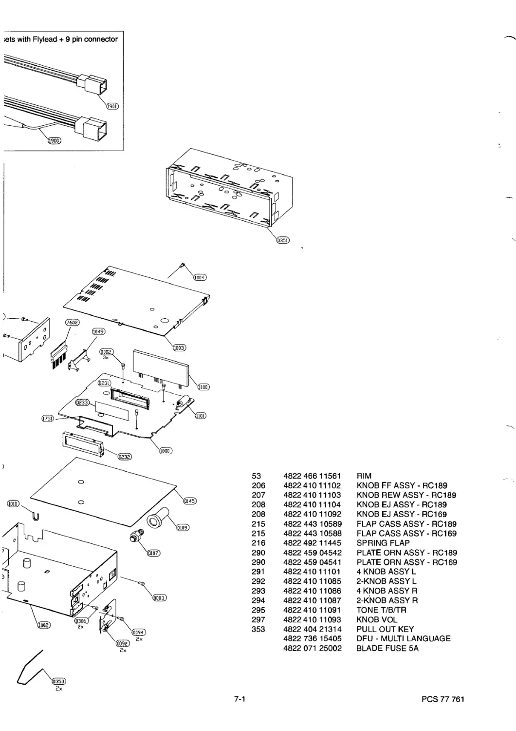
EXPLODED VIEW
For sets with Flylead + ISO connector
For sets with Tuner only
Fors
~
CDS36
~
~@ ~~cg@
@Qi
2x
@m--~fe
3x~~~
@TI)
1075
2x
;ets with Flylead + 9 pin connector
7-1
53
206
207
208
208
215
215
216
290
290
291
292
293
294
295
297
353
4822 466 11561
4822 41 0 11102
4822 410 11103
4822 410 111 04
4822 410 11092
4822 443 10589
4822 443 10588
4822 492 11445
4822 459 04542
4822 459 04541
482241011101
4822 410 11085
4822 410 11 086
4822 410 11087
482241011091
4822410 11093
4822 404 21314
4822 736 15405
4822 071 25002
RIM
KNOB FF ASSY- RC189
KNOB REW ASSY- RC189
KNOB EJ ASSY - RC189
KNOB EJ ASSY - RC169
FLAP CASS ASSY - RC189
FLAP CASS ASSY - RC169
SPRING FLAP
PLATE ORN ASSY - RC189
PLATE ORN ASSY - RC169
4 KNOB ASSY L
2-KNOB ASSY L
4 KNOBASSY R
2-K-NOB ASSY R
TONE T/BfrR
KNOB VOL
PULL OUT KEY
DFU - MULTI LANGUAGE
BLADE FUSE SA
PCS 77 761
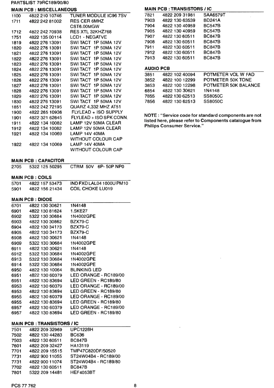
PARTSLIST 79RC189/00/80
MAIN PCB : MISCELLANEOUS
1100 4822 210 10746 TUNER MODULE IC96 7SV
1711
4822 242 81002 RES CER 6MHZ
CST6.00MGW
1712 4822 242 70938 RES XTL 32KHZ768
1751 4822 135 00114 LCD1 - NEGATVE
1819 4822 276 13091
SWI TACT 1P 50MA 12V
1820 4822 276 13091
SWI TACT 1P 50MA 12V
1821 4822 276 13091
SWI TACT 1P 50MA 12V
1822 4822 276 13091
SWI TACT 1P 50MA 12V
1823 4822 276 13091
SWI TACT 1P 50MA 12V
1824 4822 276 13091
SWI TACT 1P 50MA 12V
182S 4822 276 13091
SWI TACT 1P 50MA 12V
1826 4822 276 13091
SWI TACT 1P SOMA 12V
1827 4822 276 13091
SWI TACT 1P 50MA 12V
1828 4822 276 13091
SWI TACT 1P SOMA 12V
1829 4822 276 13091
SWI TACT 1P 50MA 12V
1830 4822 276 13091
SWI TACT 1P SOMA 12V
18S1 4822 242 72195 QUARZ 4,332 MHZ ATS 1
1900 4822 26S 10936
FLYLEAD + ISO SUPPLY
1901 4822 321 62645
FLYLEAD +ISO SPK CONN.
1911 4822 134 10082 LAMP 12V SOMA CLEAR
1912 4822 134 10082 LAMP 12V SOMA CLEAR
1921 4822 134 10069 LAMP 14V 40MA
WITHOUT COLOUR CAP
1922 4822 134 10069 LAMP 14V 40MA
WITHOUT COLOUR CAP
MAIN PCB : CAPACITOR
2705 S322 12S S029S CTRM 50V SP- 50P NPO
MAIN PCB: COILS
5701 4822 1S7 S3473 IND FXD LAL04 1OOOU PM 10
5901 4822 1S6 21434 COIL CHOKE LU019
MAIN PCB : DIODE
6701 4822 130 30621
1N4148
6901 4822130 81624 1.5KE27
6902 S322 130 30684 1N4002GPE
6903 4822 130 30862 BZX79-C
6904 4822 130 34173 BZX79-C
690S 4822 130 34173 BZX79-C
6908 4822 130 30621
1N4148
6909 5322 130 30684 1N4002GPE
6911
4822 130 30621
1N4148
6912 S322 130 30684 1N4002GPE
6913 5322 130 30684 1N4002GPE
6914 S322 130 30684 1N4002GPE
6950 4822 130 10064 BLINKING LED
6951 4822 130 60379 LED ORANGE - RC189/00
6951 4822 130 83694 LED GREEN - RC189/80
6953 4822 130 60379 LED ORANGE - RC189/00
6953 4822 130 83694 LED GREEN - RC189/80
6955 4822 130 60379 LED ORANGE - RC189/00
6955 4822 130 83694 LED GREEN - RC189/80
6957 4822 130 60379 LED ORANGE - RC189/00
6957 4822 130 83694 LED GREEN - RC189/80
MAIN PCB : TRANSISTORS / IC
7501 4822 209 32969 UPC1228H
7502 4822 130 44283 BC636
7503 4822 130 60511
BC847B
7601 4822 209 32427 HA13119
7701 4822 209 15515 TMP47C820DF/50520
7731 4822 900 11055 ST24W04B4 - RC189/00
7731 4822 900 11074 ST24W0484 - RC189/80
7702 4822 130 60511
BC847B
7801 5322 209 14481 HEF40S3BT
PCS 77 762
8
MAIN PCB : TRANSISTORS / IC
7821 4822 209 31981
SAA6579T
7903 4822 130 63539 BD241 A
7904 4822 130 409S9 BCS4 7B
790S 4822 130 409S9 BCS47B
7907 4822 130 60511
BC84 78
7908 4822 130 60511
BC847B
7911
4822 130 60511
BC847B
7912 4822 130 60511
BC847B
7913 4822 130 60511
BC8478
AUDIO PCB
38S1
3852
3853
68S4
7855
7856
4822 102 40094
4822 100 12299
4822 100 12298
4822 130 30621
4822130 62513
4822 130 62513
POTMETER VOL W FAD
POTMETER SOK TONE
POTMETER 50K BALANCE
1N4148
SS8050C
SS8050C
NOTE: "Service code for standard components are not
listed here, please refer to Components catalogue from
Philips Consumer Service."
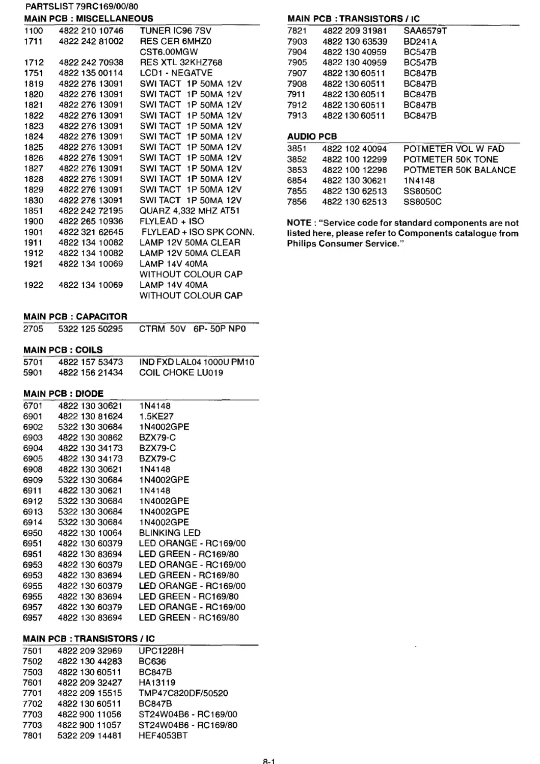
PARTSLIST 79RC169/00/80
MAIN PCB : MISCELLANEOUS
1100 4822 210 10746 TUNER IC96 7SV
1711 4822 242 81002 RES CER 6MHZO
CST6.00MGW
1712 4822 242 70938 RES XTL 32KHZ768
1751 4822 135 00114 LCD1 - NEGATVE
1819 4822 276 13091
SWI TACT 1P 50MA 12V
1820 4822 276 13091
SWI TACT 1P 50MA 12V
1821 4822 276 13091
SWI TACT 1P SOMA 12V
1822 4822 276 13091
SWI TACT 1P 50MA 12V
1823 4822 276 13091 SWI TACT 1P 50MA 12V
1824 4822 276 13091
SWI TACT 1P SOMA 12V
1825 4822 276 13091
SWI TACT 1P 50MA 12V
1826 4822 276 13091 SWI TACT 1P 50MA 12V
1827 4822 276 13091
SWI TACT 1P 50MA 12V
1828 4822 276 13091
SWI TACT 1P SOMA 12V
1829 4822 276 13091
SWI TACT 1P 50MA 12V
1830 4822 276 13091
SWI TACT 1P 50MA 12V
1851 4822 242 72195 QUARZ 4,332 MHZ AT51
1900 4822 265 10936 FLYLEAD + ISO
1901 4822 321 62645
FLYLEAD +ISO SPK CONN.
1911 4822 134 10082 LAMP 12V 50MA CLEAR
1912 4822 134 10082 LAMP 12V 50MA CLEAR
1921 4822 134 10069 LAMP 14V 40MA
WITHOUT COLOUR CAP
1922 4822 134 10069 LAMP 14V 40MA
WITHOUT COLOUR CAP
MAIN PCB : CAPACITOR
2705 5322 125 50295 CTRM 50V 6P- 50P NPO
MAIN PCB : COILS
5701 4822 157 53473 IND FXD LAL04 1OOOU PM10
5901 4822 156 21434 COIL CHOKE LU019
MAIN PCB: DIODE
6701 4822 130 30621
1N4148
6901 4822 130 81624 1.5KE27
6902 5322 130 30684 1N4002GPE
6903 4822 130 30862 BZX79-C
6904 4822 130 34173 BZX79-C
6905 4822 130 34173 BZX79-C
6908 4822 130 30621
1N4148
6909 5322 130 30684 1N4002GPE
6911 4822 130 30621
1N4148
6912 5322 130 30684 1N4002GPE
6913 5322 130 30684 1N4002GPE
6914 5322 130 30684 1N4002GPE
6950 4822 130 10064 BLINKING LED
6951 4822 130 60379 LED ORANGE - RC169/00
6951 4822 130 83694 LED GREEN - RC169/80
6953 4822 130 60379 LED ORANGE - RC169/00
6953 4822 130 83694 LED GREEN - RC169/80
6955 4822 130 60379 LED ORANGE - RC169/00
6955 4822 130 83694 LED GREEN - RC169/80
6957 4822 130 60379 LED ORANGE - RC169/00
6957 4822 130 83694 LED GREEN - RC169/80
MAIN PCB : TRANSISTORS / IC
7S01 4822 209 32969 UPC1228H
7S02 4822 130 44283 BC636
7503 4822 130 60511
BC847B
7601 4822 209 32427 HA13119
7701 4822 209 15515 TM P4 7C820DF/50520
7702 4822 130 60511
BC847B
7703 4822 900 11056 ST24W0486 - RC169/00
7703 4822 900 11057 ST24W04B6 - RC169/80
7801 5322 209 14481
HEF4053BT
8-1
MAIN PCB : TRANSISTORS/ IC
7821
7903
7904
7905
7907
7908
7911
7912
7913
4822 209 31981
4822 130 63539
4822 130 40959
4822 130 40959
4822 130 60S11
4822 130 60511
4822 130 60511
4822130 60S11
4822130 60511
AUDIO PCB
3851
3852
38S3
6854
7855
7856
4822 102 40094
4822 100 12299
4822 100 12298
4822 130 30621
4822 130 62513
4822 130 62S 13
SAA6579T
BD241A
BC547B
BC547B
BC847B
BC847B
BC847B
BC847B
BC847B
POTMETER VOL W FAD
POTMETER 50K TONE
POTMETER 50K BALANCE
1N4148
SS8050C
SS8050C
NOTE : "Service code for standard components are not
listed here, please refer to Components catalogue from
Philips Consumer Service."
MEMO