/


Теги: electronics car radio
Год: 2008
Текст
MODEL : LAC5800R
CAUTION
BEFORE SERVICING THE UNIT, READ THE "SAFETY PRECAUTIONS"
IN THIS MANUAL.
MODEL : LAC5800R
SERVICE MANUAL
P/NO : AFN36957760
APRIL, 2008
Website http://biz.lgservice.com
CAR CD/MP3/WMA
RECEIVER
SERVICE MANUAL
Internal Use Only
1-1
Copyright © 2008 LG Electronics. Inc. All right reserved.
Only for training and service purposes
LGE Internal Use Only
CONTENTS
SECTION 1 SUMMARY
SERVICING PRECAUTIONS .........................................................................................................................1-2
ESD PRECAUTIONS ......................................................................................................................................1-3
SPECIFICATIONS ...........................................................................................................................................1-4
FIRMWARE UPGRADE METHOD.................................................................................................................1-5
HOW TO CONNECT AUDIO SET TO POWER SUPPLY ............................................................................1-7
SECTION 2 ELECTRICAL
ELECTRICAL TROUBLESHOOTING GUIDE & WAVEFORMS.................................................................2-1
1. MAIN, FRONT & TUNER PART ................................................................................................................2-1
2. CDP PART.................................................................................................................................................2-4
3. USB PART.................................................................................................................................................2-7
CIRCUIT VOLTAGE CHART ......................................................................................................................2-9
WAVEFORMS ...........................................................................................................................................2-10
INTERNAL BLOCK DIAGRAM OF ICs ......................................................................................................2-12
1. IC301 (HA13173AH) ...............................................................................................................................2-12
2. IC402 (μPD78F1165) ..............................................................................................................................2-14
3. IC503 (LC786923W) ...............................................................................................................................2-17
4. IC504 (AM5810) ......................................................................................................................................2-22
5. IC601 (BD3805F) ....................................................................................................................................2-24
6. IC801 (TB2926HQ) .................................................................................................................................2-25
7. IC901 (PT6524).......................................................................................................................................2-26
BLOCK DIAGRAM ........................................................................................................................................2-29
CIRCUIT DIAGRAMS....................................................................................................................................2-31
1. MAIN CIRCUIT DIAGRAM ......................................................................................................................2-31
2. FRONT CIRCUIT DIAGRAM...................................................................................................................2-33
3. CDP-1 CIRCUIT DIAGRAM ....................................................................................................................2-35
4. CDP-2 CIRCUIT DIAGRAM ....................................................................................................................2-37
5. AUX CIRCUIT DIAGRAM ........................................................................................................................2-39
PRINTED CIRCUIT BOARD DIAGRAMS ...................................................................................................2-41
1. MAIN P.C.BOARD(TOP VIEW) ...............................................................................................................2-41
2. MAIN P.C.BOARD(BOTTOM VIEW) .......................................................................................................2-43
3. FRONT P.C.BOARD................................................................................................................................2-45
4. CDP P.C.BOARD.....................................................................................................................................2-47
5. AUX P.C. BOARD ....................................................................................................................................2-49
SECTION 3 EXPLODED VIEWS
1. CABINET AND MAIN FRAME SECTION..................................................................................................3-1
2. MECHANISM(PICK-UP) SECTION ..........................................................................................................3-3
SECTION 4 REPLACEMENT PARTS LIST.................................................4-1
1-2
Copyright © 2008 LG Electronics. Inc. All right reserved.
Only for training and service purposes
LGE Internal Use Only
1. Always disconnect the power source before:
1) Removing or reinstalling any component, circuit board, module or any other instrument assembly.
2) Disconnecting or reconnecting any instrument electrical plug or other electrical connection.
3) Connecting a test substitute in parallel with an electrolytic capacitor in the instrument.
CAUTION: A wrong part substitution or incorrect polarity installation of electrolytic capacitors may result in an
explosion hazard.
2. Do not defeat any plug/socket B+ voltage interlocks with which instruments covered by this service
manual might be equipped.
3. Do not apply power to this instrument and or any of its electrical assemblies unless all solid-state
device heat sinks are correctly installed.
4. Always connect a test instrument's ground lead to the instrument chassis ground before connecting
the test instrument positive lead. Always remove the test instrument ground lead last.
1) The service precautions are indicated or printed on the cabinet, chassis or components. When servicing,
follow the printed or indicated service precautions and service materials.
2) The Components used in the unit have a specified conflammability and dielectric strength. When replacing
any components, use components which have the same ratings. Components marked in the circuit diagram
are important for safety or for the characteristics of the unit. Always replace with the exact components.
3) An insulation tube or tape is sometimes used and some components are raised above the printed writing
board for safety. The internal wiring is sometimes clamped to prevent contact with heating components.
Install them as they were.
4) After servicing always check that the removed screws, components and wiring have been installed correctly
and that the portion around the service part has not been damaged. Further check the insulation between
the blades of attachment plug and accessible conductive parts.
SECTION 1 SUMMARY
SERVICING PRECAUTIONS
1-3
ESD PRECAUTIONS
Copyright © 2008 LG Electronics. Inc. All right reserved.
Only for training and service purposes
LGE Internal Use Only
Electrostatically Sensitive Devices (ESD)
Some semiconductor (solid state) devices can be damaged easily by static electricity. Such components
commonly are called electrostatically sensitive devices (ESD). Examples of typical ESD devices are inte-
grated circuits and some field-effect transistors and semiconductor chip components. The following tech-
niques should be used to help reduce the incidence of component damage caused by static electricity.
1. Immediately before handling any semiconductor component or semiconductor-equipped assembly,
drain off any electrostatic charge on your body by touching a know earth ground. Alternatively, obtain
and wear a commercially available discharging wrist strap device, which should be removed for poten-
tial shock reasons prior to applying power to the unit under test.
2. After removing an electrical assembly equipped with ESD devices, place the assembly on a conductive
surface such as aluminum foil, to prevent electrostatic charge buildup or exposure of the assembly.
3. Use only a grounded-tip soldering iron to solder or unsolder ESD devices.
4. Use only an anti-static solder removal device. Some solder removal devices not classified as "anti-stat-
ic" can generate electrical charges sufficient to damage ESD devices.
5. Do not use freon-propelled chemicals These can generate electrical charges sufficient to damage ESD
devices.
6. Do not remove a replacement ESD device from its protective package until immediately before you are
ready to install it. (Most replacement ESD devices are packaged with leads electrically shorted together
by conductive foam, aluminum foil or comparable conductive materials).
7. Immediately before removing the protective material from the leads of a replacement ESD device, touch
the protective material to the chassis or circuit assembly into which the device will by installed.
CAUTION : BE SURE NO POWER IS APPLIED TO THE CHASSIS OR CIRCUIT, AND OBSERVE
ALL OTHER SAFETY PRECAUTIONS.
8. Minimize bodily motions when handing unpackaged replacement ESD devices. (Otherwise harmless
motion such as the brushing together of your clothes fabric or the lifting of your foot from a carpeted
floor can generate static electricity sufficient to damage an ESD device).
CAUTION. GRAPHIC SYMBOLS
THE LIGHTNING FLASH WITH ARROWHEAD SYMBOL. WITHIN AN EQUILATERAL
TRIANGLE, IS INTENDED TO ALERT THE SERVICE PERSONNEL TO THE PRESENCE
OF UNINSULATED "DANGEROUS VOLTAGE" THAT MAY BE OF SUFFICIENT MAGNI-
TUDE TO CONSTITUTE A RISK OF ELECTRIC SHOCK.
THE EXCLAMATION POINT WITHIN AN EQUILATERAL TRIANGLE IS INTENED TO
ALERT THE SERVICE PERSONNEL TO THE PRESENCE OF IMPORTANT SAFETY
INFORMATION IN SERVICE LITERATURE.
1-4
SPECIFICATIONS
Copyright © 2008 LG Electronics. Inc. All right reserved.
Only for training and service purposes
LGE Internal Use Only
GENERAL
Output Power
50W x 4CH (Max.)
Power Source
DC 12V
Speaker impedance
4Ω
Ground System
Negative
Dimensions (WxHxD)
180 x 50 x 176 mm (Without Control Panel)
Net Weight
1.3 kg
CD SECTION
Frequency Response
20 Hz-20 kHz
S/N Ratio
80 dB
Distortion
0.12%
Channel Separation (1kHz) 55 dB
RADIO SECTION
FM
Frequency Range
87.5-107.9, 87.5-108, 65-74 or 87.5-108 MHz
S/N Ratio
55 dB
Distortion
0.7%
Usable Sensitivity
12 dBμV
AM (MW)
Frequency Range
520-1720 or 522-1620 kHz
S/N Ratio
50 dB
Distortion
1.0%
Usable Sensitivity
28 dBμV
AUX
Frequency Response
20 Hz-20 kHz
S/N Ratio
80 dB
Distortion
0.12 %
Channel Separation (1kHz) 45 dB
Max Input Level (1kHz) 1.2V (35KΩ)
1-5
Copyright © 2008 LG Electronics. Inc. All right reserved.
Only for training and service purposes
LGE Internal Use Only
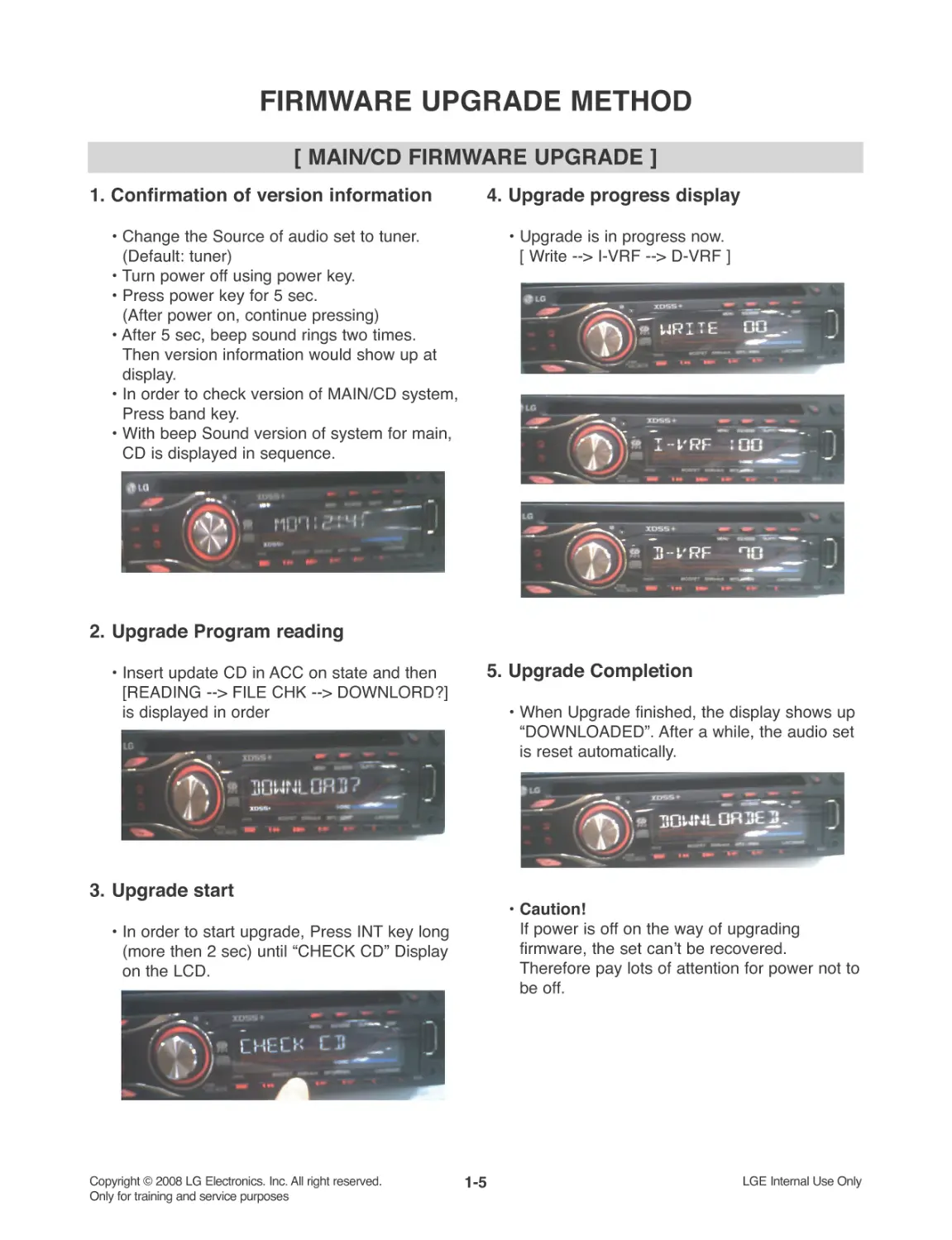
[ MAIN/CD FIRMWARE UPGRADE ]
FIRMWARE UPGRADE METHOD
1. Confirmation of version information
Change the Source of audio set to tuner.
(Default: tuner)
Turn power off using power key.
Press power key for 5 sec.
(After power on, continue pressing)
After 5 sec, beep sound rings two times.
Then version information would show up at
display.
In order to check version of MAIN/CD system,
Press band key.
With beep Sound version of system for main,
CD is displayed in sequence.
2. Upgrade Program reading
Insert update CD in ACC on state and then
[READING --> FILE CHK --> DOWNLORD?]
is displayed in order
3. Upgrade start
In order to start upgrade, Press INT key long
(more then 2 sec) until "CHECK CD" Display
on the LCD.
4. Upgrade progress display
Upgrade is in progress now.
[ Write --> I-VRF --> D-VRF ]
5. Upgrade Completion
When Upgrade finished, the display shows up
"DOWNLOADED". After a while, the audio set
is reset automatically.
Caution!
If power is off on the way of upgrading
firmware, the set can't be recovered.
Therefore pay lots of attention for power not to
be off.
1-6
Copyright © 2008 LG Electronics. Inc. All right reserved.
Only for training and service purposes
LGE Internal Use Only
1. Confirmation of version information
Change the source of audio set to tuner.
(default : tuner)
Turn power off using power key.
Press power key for 5 secs.
(After power is on, continue pressing)
After 5 secs, beep sound rings two times.
Then the version information would show up
at display.
In order to check version of USB system,
press band key. With beep sound, version of
systems for main, CD and USB is displayed in
sequence.
2. Upgrade Preparation
At first check that audio set is in tuner mode.
With power key, turn it off. Make it sure to
insert USB device which has upgrade file.
3. Upgrade start
Press SRC key for 5 secs. After power is on,
continue pressing. And then the audio set is
changed to USB upgrade mode.
4. Upgrade progress display
Upgrade is in progress now.
It takes about 10 secs.
5. Upgrade completion
Upgrade finished, the right display shows up.
After a while, the audio set is reset automati-
cally.
Caution!
If power is off on the way of upgrading
firmware, the set can't be recovered.
Therefore pay lots of attention for power not to
be off.
[ USB FIRMWARE UPGRADE ]
1-7
Copyright © 2008 LG Electronics. Inc. All right reserved.
Only for training and service purposes
LGE Internal Use Only
HOW TO CONNECT AUDIO SET TO POWER SUPPLY
It is sufficient only to supply power for upgrade.
Shown from the right figure, connect yellow line (Battery) and red line (Ignition) to plus and
minus terminal respectively.
Jack is connected to the audio set via its shapes matched each other.
We need power supply for operation of audio set (Voltage : 12~15V Current : Over 2A)
Before connection between set and power supply, adjust voltage level to 15V typically
(It is okay up to 12V.)
Power Supply has a variety of shapes and capacity of voltage and current.
At first check these things.
1-8
Copyright © 2008 LG Electronics. Inc. All right reserved.
Only for training and service purposes
LGE Internal Use Only
2-1
SECTION 2 ELECTRICAL
Copyright © 2008 LG Electronics. Inc. All right reserved.
Only for training and service purposes
LGE Internal Use Only
ELECTRICAL TROUBLESHOOTING GUIDE & WAVEFORMS
SYSTEM CONTROL
1. MAIN, FRONT & TUNER PART
No
Symptom
Check Point
Location No.
1 No Power
Checked the Fuse.
CN302
Checked the Back up Vdd, Gnd.
CN302(15,16)
Checked the Micom Back Up Vdd. IC301(14), D428,
IC402(30,47,50,99,100)
Checked the Micom Ground.
IC402(20,51,97,98)
Checked the Reset.
IC401, IC402(90)
Checked the X-tal.
X401, X402
Checked the ACC In.
Q301, Q302, IC402(40), CN302(14)
Checked the Detachable Switch.
SW400, IC402(70)
Checked the Flipdown Switch.
CN407(24), IC402(69)
Checked the Key Line.
IC402(52,53)
2 Not available Remocon
Checked the Remocon Sens Vdd, Line. CN404(5), IC402(81), RM901
3 Not available to Volume Control Checked the Encoder Volume.
EV901, IC402(74,75)
4 Not available to Key Control
Checked Tact Switch.
SW901 ~ SW909, SW911 ~ SW919
Checked Key Line.
IC402(52,53)
5 No sound
Checked the E-VR Vdd.
IC601(15)
Checked the E-VR Ground.
IC601(1,22)
Checked the E-VR Control.
IC601(20,21), IC402(3,4)
Checked the E-VR Signal In/Out.
IC601(3,4,5,6,7,10,11)
IC601(12,13,14,15)
Checked the E-VR Mute Control
IC601(19), IC402(14)
Checked the Power IC Vdd.
IC801(6,20)
Checked the Power IC Ground.
IC801(1,2,8,13,18,24)
Checked the Power IC Control.
IC801(4,22), IC402(17,18)
Checked the Power IC Signal In/Out. IC801(11,12,14,15)
IC801(3,5,7,9,17,19,21,23)
6 No Line out signal
Checked the E-VR Output.
IC601(12,13,14,15)
Checked the Output.
JK601
7 Not avaliable to Telephone Mute Checked the Telephone Mute Control. CN406(2)
Checked the Mute Control.
IC402(38), Q312, Q313
8 Not avaliable to
Checked the ANT Control.
CN302(10), IC301(12,13), IC402(35)
ANT(Motor Type) Control
9 Not avaliable to Remote
Checked the Remote Control.
IC301(2), CN406(1), Q311
(Power AMP)
10 No output Beep sound.
Checked the Beep Control.
IC402(80), R801
DISPLAY & LIGHTING
TUNER FUNCTION
2-2
Copyright © 2008 LG Electronics. Inc. All right reserved.
Only for training and service purposes
LGE Internal Use Only
No
Symptom
Check Point
Location No.
1 No Display or Some
Checked the LCD DRV Vdd.
Q307, D425, IC901(56,57,58)
Display is Broken
Checked the LCD DRV Ground.
IC901(59)
Checked the LCD DRV OSC.
IC901(60)
Checked the LCD DRV Control.
IC402(73,76,78,79)
IC901(61,62,63,64)
Checked the LCD DRV to
IC901(1~55)
LCD Pattern.
2 No LCD Lighting or
Checked the LCD Lighting VDD.
IC301(4,9), Q303
Color is different
Checked the LED.
LD961, LD962
3 Not avaliable to
Checked the LCD Lighting Control. Q305, ZD426, CN302(11)
LCD Lighting Control
Checked the LED.
LD901 ~ LD923, LD931 ~ LD953
4 Don't moved Level Bar
Checked the Level Meter Control.
IC402(56,57,58)
5 Not avaliable to Dimmer Control Chekced the Dimmer Control.
IC402(49), CN302(11), ZD426, Q305
1 Not available to Tuner
Checked the Tuner Vdd.
TU201(6,17), Q309, Q310
Checked the Tuner Ground.
TU201(3,7,12,16)
Checked the PLL data.
TU201(9,14,15,19,20)
IC402(1,2,5,6,55)
Checked the RF signal in.
TU201(1,2)
Checked the S-Meter Control
TU201(5)
2T
uner no sound
Checked the Tuner Signal Out.
TU201(10,11,12), IC601(10,11)
Checked the AF mute.
TU201(8), IC402(7)
3 Not available to RDS
Checked the RDS data.
TU201(19,20), IC402(5,6)
2-3
Copyright © 2008 LG Electronics. Inc. All right reserved.
Only for training and service purposes
LGE Internal Use Only
CAUTION - Tip for repair
Before exchange power amp IC(TB2926) for no audio problem, you have to check
below list.
1. Check VCC (pin 20,6) & GND
2. Check input pin 11,12,14,15
3. Check Standby, pin 4
: Follow the below list.
4. Check Mute function, pin 22
: Follow the below list.
5. Check Ripple pin 10.
: Normally it is high (about 10V)
6. Re-soldering all the pin of IC.
: Prevent crack of solder line.
* Keep changed IC, We request that you send it to HQ.
R
L
R
L
R
L
11
9
8
7
5
2
3
17
18
19
21
24
23
12
15
14
1206
R
L
IN1
IN2
IN3
IN4
13
C
1
C
1
C
1
C
1
PRE-GND
10
25
22
OUT1
+
+
+
+
-
-
-
-
()
PW-GND1
OUT1()
OUT2()
PW-GND2
OUT2()
OUT3()
PW-GND3
OUT3()
OUT4()
PW-GND4
OUT4()
TAB V
CC1
V
CC2
C
3
C
4
C
2
: PRE-GND
: PW-GND
STBY
RIP
MUTE
C
5
16
C
6
4
OFF-SET
DET
MUTE
PLAY
5V
R
1
AC-GND
Stand-by Power Sound Voltage
ON
OFF
OFF
0to1.5
OFF
ON
ON 3.5to6V
Mute Sound Voltage
ON
OFF 0to1.5
OFF
ON 3.5to6V
Picture 1) Power IC desc.
2-4
Copyright © 2008 LG Electronics. Inc. All right reserved.
Only for training and service purposes
LGE Internal Use Only
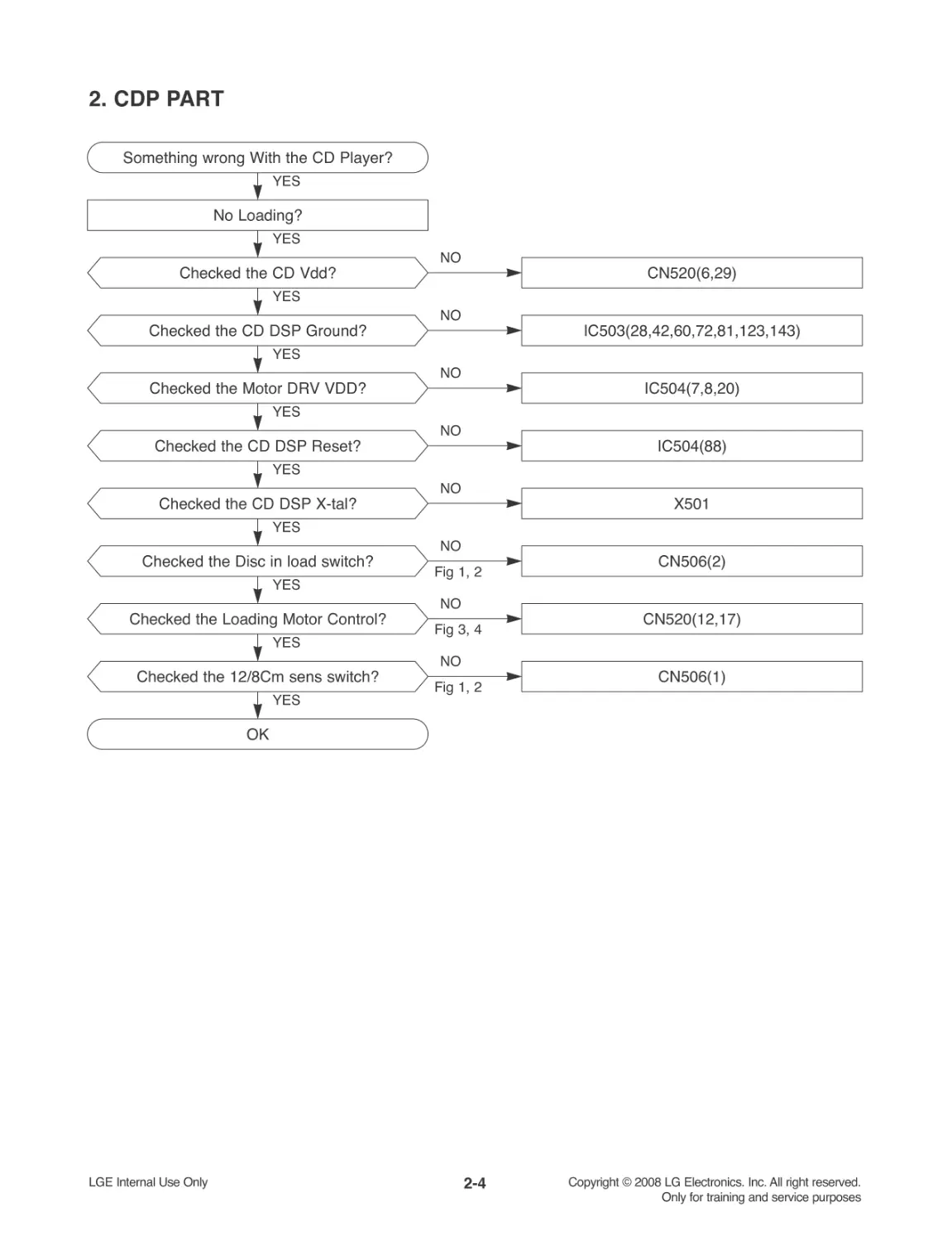
2. CDP PART
YES
YES
NO
CN520(6,29)
NO
IC503(28,42,60,72,81,123,143)
NO
IC504(7,8,20)
NO
IC504(88)
NO
NO
X501
Fig1,2
Fig3,4
Fig1,2
CN506(2)
NO
CN520(12,17)
NO
CN506(1)
No Loading?
YES
Checked the CD Vdd?
YES
Checked the CD DSP Ground?
YES
Checked the Motor DRV VDD?
YES
Checked the CD DSP Reset?
YES
Checked the CD DSP X-tal?
YES
Checked the Disc in load switch?
YES
Checked the Loading Motor Control?
YES
Checked the 12/8Cm sens switch?
OK
Something wrong With the CD Player?
2-5
Copyright © 2008 LG Electronics. Inc. All right reserved.
Only for training and service purposes
LGE Internal Use Only
YES
YES
NO
CN506(8)
NO
IC504(21)
NO
CN520(12,17)
NO
IC503(84,85,86,87)
NO
NO
IC503(38), IC504(15,16)
Fig 5
Fig 5
Fig 10~ 11
Fig3,4
Fig1,2
Fig 12
Fig 9
IC503(17)
NO
CN520(25)
NO
NO
IC503(8)
Fig 7
IC503(41), IC504(11,12)
NO
Fig 8
IC503(40), IC504(13,14)
NO
Fig 6
IC503(39), IC504(17,18)
No Reading & "FILE CHECK" DISPLAY?
YES
Checked the Limit switch?
YES
Checked the Motor DRV mute control?
YES
Checked the Motor LODING Control?
YES
Checked the CD DSP Control?
YES
Checked the focus control?
YES
Checked the focus error level out.(FE Mon)?
YES
Checked the PLL locking.(FSEQ)?
YES
Checked the RF signal out check?
YES
Checked the spindle motor control?
YES
Checked the SLED control?
YES
Checked the tracking control?
OK
Something wrong With the CD Player?
2-6
Copyright © 2008 LG Electronics. Inc. All right reserved.
Only for training and service purposes
LGE Internal Use Only
YES
YES
NO
IC503(140,141)
CD no sound?
YES
Checked the DSP signal out?
OK
Something wrong With the CD Player?
YES
YES
NO
CN403(1)[MAIN]
NO
CN520(12,17)
Fig 3,4
No ejected the CD?
YES
Checked the Eject key?
YES
Checked the Loading Motor Control?
OK
Something wrong With the CD Player?
2-7
Copyright © 2008 LG Electronics. Inc. All right reserved.
Only for training and service purposes
LGE Internal Use Only
3. USB PART
YES
YES
NO
IC711(8,18,39)
NO
IC711(5,19,40)
NO
PN703(5)
NO
X701
NO
NO
IC711(38,37)
Fig 13
PN703(4)
NO
IC711(9,10,11,14)
Only "NO USB" or "USB CHECK" Display?
YES
Checked the USB Vdd?
YES
Checked the USB interface IC Ground?
YES
Checked the USB interface IC reset?
YES
Checked the USB interface IC X-tal?
YES
Checked the D+/D Port?
YES
Checked the USB indication Port?
YES
Checked the USB interface IC control?
OK
Something wrong with the USB?
2-8
Copyright © 2008 LG Electronics. Inc. All right reserved.
Only for training and service purposes
LGE Internal Use Only
YES
YES
NO
IC503(28,42,60,72,81,123,143)
NO
IC504(88)
NO
X501
NO
IC503(84,85,86,87)
NO
IC711(9,10,11,14)
NO
IC503(140,141)
Fig10 ~ 11
"FILE CHECK" DISPLAY?
YES
Checked the CD DSP Ground?
YES
Checked the CD DSP Reset?
YES
Checked the CD DSP X-tal?
YES
Checked the CD DSP Control?
YES
Checked the USB data?
YES
USB no sound?
YES
Checked the CD DSP signal out?
OK
Something wrong with the USB?
YES
YES
NO
IC503(140,141)
Checked the CD DSP signal out?
OK
Something wrong with the USB?
2-9
Copyright © 2008 LG Electronics. Inc. All right reserved.
Only for training and service purposes
LGE Internal Use Only
IC801_TB2926
CIRCUIT VOLTAGE CHART
Operating
Voltage (V)
Pin No.
IC301_HA13173
IC401_S7133SF
IC601_BD3805
CN302_ISO 16Pin
10
2
13.92
30
4
8.46
50
6
8.05
7
3.284
8
13.99
9
4.5
10
8.4
11
4.31
12
13.98
13
4.94
14
5.76
15
13.99
1
4.93
20
35
10
2
4.2
3
4.2
4
4.2
5
4.2
6
4.2
7
4.2
8
4.2
9
4.2
10
4.2
11
4.2
12
4.2
13
4.2
14
4.2
15
4.2
16
8.4
17
0.7
18
0
19
5
20
5
21
5
22
0
10
20
3
6.56
45
5
6.56
6
13.96
7
6.54
8
0.01
9
6.53
10
8.05
11
6.47
Operating
Voltage (V)
Pin No.
TU201_TUNER
12
6.51
13
0
14
6.54
15
6.54
16
6.58
17
6.58
18
0
19
6.55
20
13.97
21
6.52
22
4.97
23
6.56
24
0
25
1.24
10
20
30
40
5
0.28
6
0.28
70
8
4.98
9
4.96
10
0
11
0
12
0
13
0
14
5.05
15
5.01
16
0
17
5.06
18
0
19
0.063
20
2.5
1
6.56
2
6.57
3
6.53
4
6.54
50
60
70
8
6.54
9
6.546
10
13.47
11
0
12
6.53
13
6.58
14
14.05
15
0
16
14
Operating
Voltage (V)
Pin No.
CN402_CD
10
20
30
40
50
6
3.259
70
8
4.99
9
4.98
10
4.98
11
0
12
0
13
8.05
14
0
15
0
16
4.78
17
0
18
5
19
4.98
20
0
21
4.99
22
5.02
23
0
24
4.76
25
4.76
26
1.54
27
2.52
28
2.52
29
5.06
30
0.02
2-10
Copyright © 2008 LG Electronics. Inc. All right reserved.
Only for training and service purposes
LGE Internal Use Only
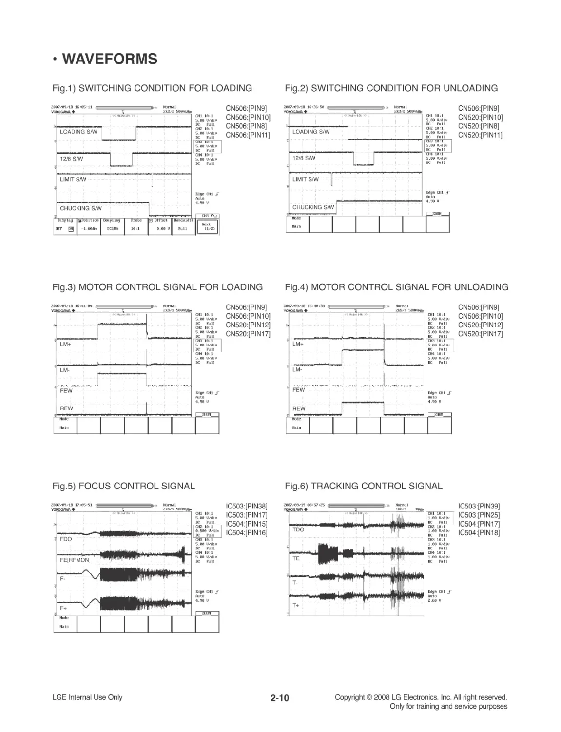
WAVEFORMS
Fig.1) SWITCHING CONDITION FOR LOADING
CN506:[PIN9]
CN506:[PIN10]
CN506:[PIN8]
CN506:[PIN11]
LOADING S/W
12/8 S/W
CHUCKING S/W
LIMIT S/W
Fig.2) SWITCHING CONDITION FOR UNLOADING
CN506:[PIN9]
CN520:[PIN10]
CN520:[PIN8]
CN520:[PIN11]
LOADING S/W
12/8 S/W
CHUCKING S/W
LIMIT S/W
Fig.3) MOTOR CONTROL SIGNAL FOR LOADING
CN506:[PIN9]
CN506:[PIN10]
CN520:[PIN12]
CN520:[PIN17]
LM+
LM-
REW
FEW
Fig.4) MOTOR CONTROL SIGNAL FOR UNLOADING
CN506:[PIN9]
CN506:[PIN10]
CN520:[PIN12]
CN520:[PIN17]
LM+
LM-
REW
FEW
Fig.5) FOCUS CONTROL SIGNAL
IC503:[PIN38]
IC503:[PIN17]
IC504:[PIN15]
IC504:[PIN16]
FDO
FE[RFMON]
F+
F-
Fig.6) TRACKING CONTROL SIGNAL
IC503:[PIN39]
IC503:[PIN25]
IC504:[PIN17]
IC504:[PIN18]
TDO
TE
T+
T-
2-11
Copyright © 2008 LG Electronics. Inc. All right reserved.
Only for training and service purposes
LGE Internal Use Only
Fig.13) USB
PN703:PIN8 [D+]
PN703:PIN10 [D-]
PN703:PIN1
[UART RX]
PN703:PIN2
[UART TX]
Fig.7) SPINDLE CONTROL SIGNAL
IC503:[PIN41]
IC503:[PIN25]
IC504:[PIN11]
IC504:[PIN12]
SPOUT
SP-
SP+
Fig.8) SLED CONTROL SIGNAL
IC503:[PIN40]
IC504:[PIN13]
IC504:[PIN14]
SLOUT
SL-
SL+
Fig.9) MD, RFOUT, LD
CN519:PIN[15]
IC503:PIN[8]
CN519:PIN[16]
MD
RFOUT
LD
Fig.10) DI, DO, CL, CE
IC503:DO(PIN87)
IC503:DI(PIN86)
IC503:CL(PIN85)
IC503:CE(PIN84)
Fig.11) DI, DO, CL, CE [Detail]
IC503:DO(PIN87)
IC503:DI(PIN86)
IC503:CL(PIN85)
IC503:CE(PIN84)
Fig.12) FSEQ, WRQ
CN520:(PIN24)
CN520:(PIN25)
2-12
Copyright © 2008 LG Electronics. Inc. All right reserved.
Only for training and service purposes
LGE Internal Use Only
INTERNAL BLOCK DIAGRAM OF ICs
1. IC301 (HA13173AH)
1-1. BLOCK DIAGRAM
GND
BIAS
VB
+B
VDDOUT
AUDIOOUT
ILMOUT
CTL 1
GND
TAB
V
REF
1.5V
Over voltage detect
TSD
V
REF
CDOUT
V
REF
EXTOUT
VBUP
DSPOUT
CTL 2
2.5V
CTL 3
2.5V
CTL 4
2.5V
15
FREG F
RFREG3
FREG B
13
12
11
10
9
8
7
6
5
4
3
2
1
14
3.5V
DBUP
CBUP
100uF
CVDD
10uF
CDSP
10uF
CAUDIO
10uF
CCD
0.1uF
CEXT
10uF
CILM
0.1uF
CFREG
10uF
QFREG
RFREG1
RFREG2
DEXT1
DEXT2
C1
100uF
C2
0.1uF
2-13
Copyright © 2008 LG Electronics. Inc. All right reserved.
Only for training and service purposes
LGE Internal Use Only
1-2. PIN FUNCTION (Note1)
1 GND
Ground
-
-
-
-
2 FREG_B External Trs bass drive (Note4)
On/Off On/Off
Off
Off
3 FREG_F FREG feedback terminal
On/Off On/Off
Off
Off
4 ILMOUT 8.4V output for JLM/500mAmax
On/Off
Off
Off
Off
5 CTL4
FREG control terminal
-
-
-
-
6 CDOUT
8.0V output for CD/1.3Amax (Note4)
On/Off
Off
Off
Off
7 DSPOUT 3.3V output for DSP/250mAmax (Note4)
On/Off
Off
Off
Off
8V
B
Battery
-
-
-
-
9 CTL3
ILM control terminal
-
-
-
-
10 AUDIOOUT 8.4V output for AUDIO/500mAmax (Note4) On/Off
Off
Off
Off
11 CTL1
DSP, CD, Audio control terminal
-
-
-
-
12 EXTOUT High side output/600mAmax (Note4)
On/Off
Off
Off
Off
13 CTL2
EXT control terminal
-
-
-
-
14 VDDOUT 5.7V output for micro controller (Note4)
On
On
On
Off
15 VBUP
Back up
-
-
-
-
Note1. In the uper table. "On" means always On. "Off" means compulsory Off and "On/Off" means that it can control by con-
trol terminal.
Note2. Thermal protection circuit
A built-in thermal protection circuit (TSD:Thermal shut down) prevents thermal damage to the IC. All outputs except
VDD(pin14) and FREG (pin2&3) are switched off when the circuit operates, revert to the original state when the tem-
perature drops to a certain level.
Note3. Overvoltage protection circuit
The overvoltage protection circuit (surge protector) turns off all outputs without Vdd, when VB voltage is more than
about 21V. And the overvoltage protection circuit (surge protector) turns off Vdd output with other all outputs, when
VB voltage is more than about 26V. When the overvoltage protection operates on VB>=18V condition, the stand by
current increases.
Note4. Overcurrent protection circuit
FREG_B (pin2), ILMOUT (pin4), CDOUT (pin6), DSPOUT (pin7), AUDIOOUT (pin10), EXITOUT (pin12), VDDOUT
(pin14) output circuits are built-in overcurrent protection circuit based on the respective output current. These over-
current protection circuits limit the current with a curve shape of "7" in the voltage-current graph. This prevents IC
destruction due to overcurrent.
Normal
operation
Protection function
Pin No. Pin name
Function
(Note2)
(Note3)
(Note3)
TSD On VB=24V VB=50V
2-14
Copyright © 2008 LG Electronics. Inc. All right reserved.
Only for training and service purposes
LGE Internal Use Only
2. IC402 (μPD78F1165)
2-1. PIN CONFIGURATION
P140/PCLBUZ0/INTP6
P141/PCLBUZ1/INTP7
P142/SCK20/SCL2
P143/SI20/RxD2/SDA2
P144/SO20/TxD2
P145/TI07/TO07
P00/TI00
P01/TO00
P02/SO10/TxD1
P03/SI10/RxD1/SDA1
P04/SCK10/SCL1
P131/TI06/TO06
P130
P20/ANI0
P21/ANI1
P22/ANI2
P23/ANI3
P24/ANI4
P25/ANI5
P26/ANI6
P27/ANI7
P150/ANI8
P151/ANI9
P152/ANI10
P153/ANI11
P154/ANI12
P155/ANI13
P156/ANI14
P157/ANI15
AVSS
P50/EX8
P51/EX9
P52/EX10
P53/EX11
P54/EX12
P55/EX13
P56/EX14
P57/EX15
P17/EX31TI02/TO02
P16/EX30/TI01/TO01/INTP5
P15/EX29/RTCDIV/RTCCL
P14/EX28/RxD3
P13/EX27/TxD3
P12/EX26/SO00/TxD0
P11/EX25/SI00/RxD0
P10/EX24/SCK00
AVREF1
P110/ANO0
P111/ANO1
AVREF0
EVDD0
VDD
EVSS0
VSS
REGC
P121/X1
P122/X2/EXCLK
FLMD0
P123/XT1
P124/XT2
RESET
P40/TOOL0
P41/TOOL1
P42/TI04/TO04
P43/SCK01
P44/SI01
P45/SO01
P46/INTP1/TI05/TO05
P47/INTP2
P120/INTP0/EXLVI
P60/SCL0
P61/SDA0
P62
P63
P31/TI03/TO03/INTP4
P64/RD
P65/WR0
P66/WR1
P67/ASTB
P77/EX23/KR7/INTP11
P76/EX22/KR6/INTP10
P75/EX21/KR5/INTP9
P74/EX20/KR4/INTP8
P73/EX19/KR3
P72/EX18/KR2
P71/EX17/KR1
P70/EX16/KR0
P06/WAIT
P05/CLKOUT
EVSS1
P80/EX0
P81/EX1
P82/EX2
P83/EX3
P84/EX4
P85/EX5
P86/EX6
P87/EX7
P30/INTP3/RTC1HZ
EVDD1
80
79
78
77
76
75
74
73
72
71
70
69
68
67
66
65
64
63
62
61
60
59
58
57
56
55
54
53
52
51
1
2
3
4
5
6
7
8
9
10
11
12
13
14
15
16
17
18
19
20
21
22
23
24
25
26
27
28
29
30
3132333435363738394041424344454647484950
10099989796959493929190898887868584838281
2-15
Copyright © 2008 LG Electronics. Inc. All right reserved.
Only for training and service purposes
LGE Internal Use Only
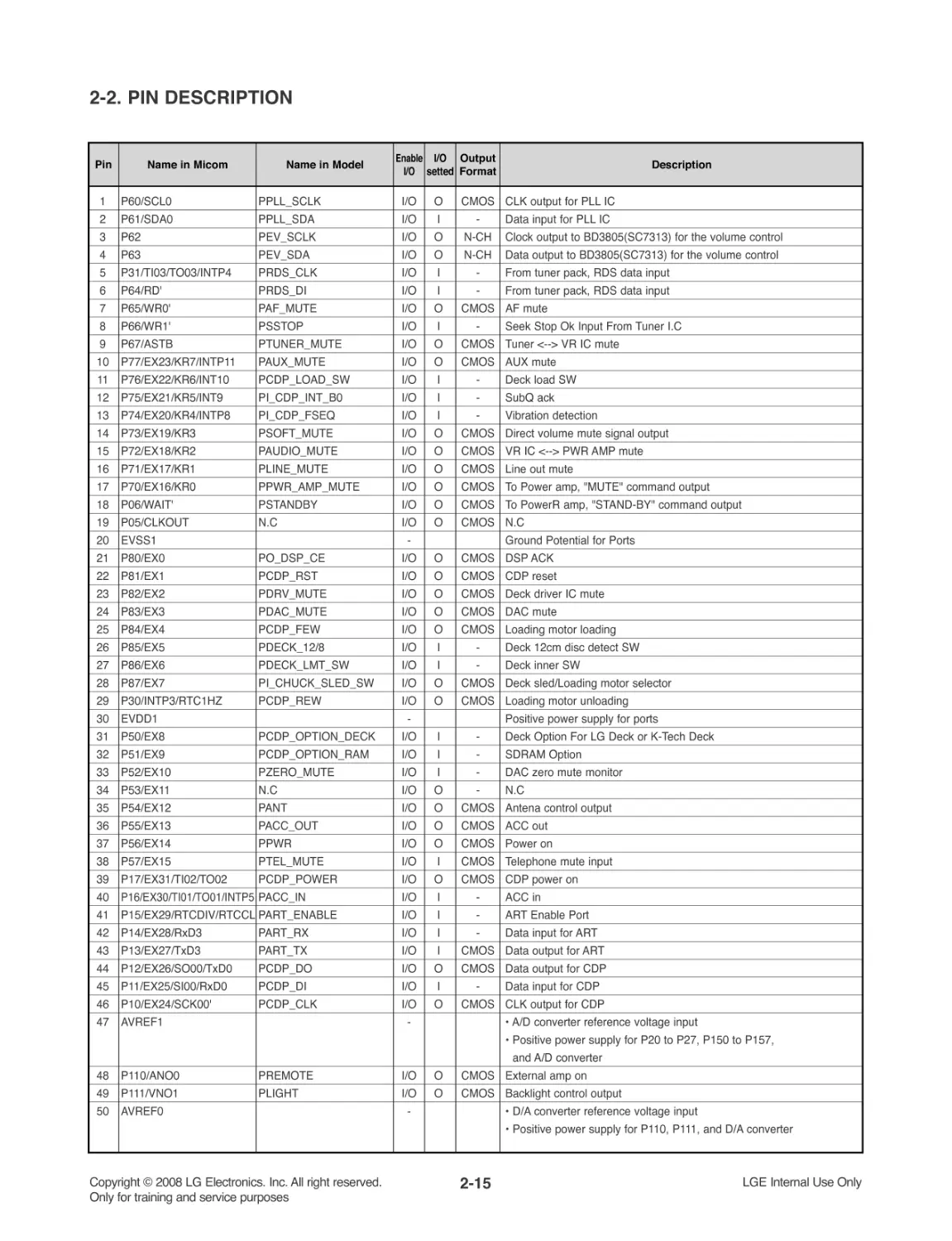
2-2. PIN DESCRIPTION
Pin
Name in Micom
Name in Model
Enable
I/O
I/O
setted
Output
Format
Description
1 P60/SCL0
PPLL_SCLK
I/O O CMOS CLK output for PLL IC
2 P61/SDA0
PPLL_SDA
I/O I
- Data input for PLL IC
3 P62
PEV_SCLK
I/O O N-CH Clock output to BD3805(SC7313) for the volume control
4 P63
PEV_SDA
I/O O N-CH Data output to BD3805(SC7313) for the volume control
5 P31/TI03/TO03/INTP4 PRDS_CLK
I/O I
- From tuner pack, RDS data input
6 P64/RD'
PRDS_DI
I/O I
- From tuner pack, RDS data input
7 P65/WR0'
PAF_MUTE
I/O O CMOS AF mute
8 P66/WR1'
PSSTOP
I/O I
- Seek Stop Ok Input From Tuner I.C
9 P67/ASTB
PTUNER_MUTE
I/O O CMOS Tuner <--> VR IC mute
10 P77/EX23/KR7/INTP11 PAUX_MUTE
I/O O CMOS AUX mute
11 P76/EX22/KR6/INT10 PCDP_LOAD_SW
I/O I
- Deck load SW
12 P75/EX21/KR5/INT9
PI_CDP_INT_B0
I/O I
- SubQ ack
13 P74/EX20/KR4/INTP8 PI_CDP_FSEQ
I/O I
- Vibration detection
14 P73/EX19/KR3
PSOFT_MUTE
I/O O CMOS Direct volume mute signal output
15 P72/EX18/KR2
PAUDIO_MUTE
I/O O CMOS VR IC <--> PWR AMP mute
16 P71/EX17/KR1
PLINE_MUTE
I/O O CMOS Line out mute
17 P70/EX16/KR0
PPWR_AMP_MUTE
I/O O CMOS To Power amp, "MUTE" command output
18 P06/WAIT'
PSTANDBY
I/O O CMOS To PowerR amp, "STAND-BY" command output
19 P05/CLKOUT
N.C
I/O O CMOS N.C
20 EVSS1
-
Ground Potential for Ports
21 P80/EX0
PO_DSP_CE
I/O O CMOS DSP ACK
22 P81/EX1
PCDP_RST
I/O O CMOS CDP reset
23 P82/EX2
PDRV_MUTE
I/O O CMOS Deck driver IC mute
24 P83/EX3
PDAC_MUTE
I/O O CMOS DAC mute
25 P84/EX4
PCDP_FEW
I/O O CMOS Loading motor loading
26 P85/EX5
PDECK_12/8
I/O I
- Deck 12cm disc detect SW
27 P86/EX6
PDECK_LMT_SW
I/O I
- Deck inner SW
28 P87/EX7
PI_CHUCK_SLED_SW I/O O CMOS Deck sled/Loading motor selector
29 P30/INTP3/RTC1HZ
PCDP_REW
I/O O CMOS Loading motor unloading
30 EVDD1
-
Positive power supply for ports
31 P50/EX8
PCDP_OPTION_DECK I/O I
- Deck Option For LG Deck or K-Tech Deck
32 P51/EX9
PCDP_OPTION_RAM I/O I
- SDRAM Option
33 P52/EX10
PZERO_MUTE
I/O I
- DAC zero mute monitor
34 P53/EX11
N.C
I/OO-N.C
35 P54/EX12
PANT
I/O O CMOS Antena control output
36 P55/EX13
PACC_OUT
I/O O CMOS ACC out
37 P56/EX14
PPWR
I/O O CMOS Power on
38 P57/EX15
PTEL_MUTE
I/O I CMOS Telephone mute input
39 P17/EX31/TI02/TO02 PCDP_POWER
I/O O CMOS CDP power on
40 P16/EX30/TI01/TO01/INTP5 PACC_IN
I/O I
- ACCin
41 P15/EX29/RTCDIV/RTCCL PART_ENABLE
I/O I
- ART Enable Port
42 P14/EX28/RxD3
PART_RX
I/O I
- Data input for ART
43 P13/EX27/TxD3
PART_TX
I/O I CMOS Data output for ART
44 P12/EX26/SO00/TxD0 PCDP_DO
I/O O CMOS Data output for CDP
45 P11/EX25/SI00/RxD0 PCDP_DI
I/O I
- Data input for CDP
46 P10/EX24/SCK00'
PCDP_CLK
I/O O CMOS CLK output for CDP
47 AVREF1
-
A/D converter reference voltage input
Positive power supply for P20 to P27, P150 to P157,
and A/D converter
48 P110/ANO0
PREMOTE
I/O O CMOS External amp on
49 P111/VNO1
PLIGHT
I/O O CMOS Backlight control output
50 AVREF0
-
D/A converter reference voltage input
Positive power supply for P110, P111, and D/A converter
2-16
Copyright © 2008 LG Electronics. Inc. All right reserved.
Only for training and service purposes
LGE Internal Use Only
Pin
Name in Micom
Name in Model
Enable
I/O
I/O
setted
Output
Format
Description
51 AVSS
52 P157/ANI15
PKEY1
I/O I
- Key #1 line input
53 P156/ANI14
PKEY2
I/O I
- Key #2 line input
54 P155/ANI13
PSMETER
I/O I
- Radio station's strength signal input
55 P154/ANI12
PQUALTY
I/O I
- Connect to tuner pack QUALITY
56 P153/ANI11
PTUNER_LEVEL
I/O I
- Tuner Level meter input
57 P152/ANI10
PCD/USB_LEVEL
I/O I
- CD/USB Level meter input
58 P151/ANI9
PAUX_LEVEL
I/O I
AUX Level meter input
59 P150/ANI8
PREMOTE_DETECT
I/O I
- REMOTE Power Voltage Drop Detect
60 P27/ANI7
PB+Detect
I/O I
- B+ Detect Input
61 P26/ANI6
PANT_SHORT_DET
I/O I
- ANTENNA SHORT DETECT INPUT
62 P25/ANI5
PUSB_POWER
I/O O CMOS USB power on/BT power on(3.3V Ctrl)
63 P24/ANI4
PUSB_COMMON_SW I/O I
-
64 P23/ANI3
PUSB_RESET
I/O O CMOS USB HOST I.C reset
65 P22/ANI2
PUSB_SW
I/O I
- USB device detect sw
66 P21/ANI1
PO_USB_CANCEL
I/O O CMOS USB Flash upgrade enable
67 P20/ANI0
PUSB_PROTECT
I/O I
- Protection IC overcurrent detection
68 P130
N.C
OOCMOSN.C
69 P131/TI06/TO06
PFRT_DETECT
I/O I
- Front detaching/attaching detect
70 P04/SCK10'/SCL1
PFRT_DETACH_SW
I/O I
- In LAC6730 Front Detect
71 P03/SI10/RxD1/SDA1 PUSB_RX
I/O I
- Data input for USB/BT
72 P02/SO10/TXD1
PUSB_TX
I/O O CMOS Data output for USB/BT
73 P01/TO00
PFRT_RST
I/O O CMOS Front micom(LCD drv) reset
74 P00/TI00
PVOL_A
I/O I
- Encoder Volume A Input
75 P145/TI07/TO07
PVOL_B
Encoder Volume B Input
76 P144/SO20/TxD2
PFRT_DO
I/O O CMOS Data output to front micom(LCD drv)
77 P143/SI20/RxD2/SDA2 PLED_COLOR
I/O O CMOS LED Color Select Output
78 P142/SCK20'/SCL2
PFRT_CLK
I/O O CMOS CLK output to front micom(LCD drv)
79 P141/PCLBUZ1/INTP7 PFRT_CE
I/O I
- Data enable output to front micom(LCD drv)
80 P140/PCLBUZ0/INTP6 PBEEP
I/O O CMOS Buzzer output
81 P120/INTP0/EXLVI
PRMC
I/O I
- Remocon input
82 P47/INTP2
POPT_IN0
I/O I
- For diode option check, signal 1 or 2 input0
83 P46/INTP1/TI05/TO05 POPT_IN1
I/O I
- For diode option check, signal 1 or 2 input1
84 P45/SO01
POPT_IN2
I/O I
- For diode option check, signal 1 or 2 input2
85 P44/SI01
POPT_OUT0
I/O O CMOS For diode option check, signal 1 output
86 P43/SCK01'
POPT_OUT1
I/O O CMOS For diode option check, signal 2 output
87 P42/TI04/TO04
POPT_OUT2
I/O O CMOS For diode option check, signal 3 output
88 P41/TOOL1
Download_CLK
I/O -
- CLK for onboard debugger
89 P40/TOOL0
Download_IO
I/O -
- Data I/O for flash memory programmer (Pull-up register(10K))
90 RESET'
-
-
-
- System reset input
91 P124/XT2
-
II
- Sub clock 32.768 KHz
92 P123/XT1
-
II
- Sub clock 32.768 KHz
93 FLMD0
Download control
-
Flash memory programming mode setting
94 P122/X2/EXCLK
-
II
- X'tal 19.2 MHz
95 P121/X1
-
II
- X'tal 19.2 MHz
96 REGC
-
-
Connect to VSS via a capacitor (0.47 to 1 μF)
97 VSS
-
Ground
98 EVSS0
-
Ground Potential for Ports
99 VDD
-
Positive power supply (+5V)
100 EVDD0
-
Positive power supply (+5V) For Ports
2-17
Copyright © 2008 LG Electronics. Inc. All right reserved.
Only for training and service purposes
LGE Internal Use Only
3. IC503 (LC786923W)
3-1. PIN ASSIGNMENT
2-18
Copyright © 2008 LG Electronics. Inc. All right reserved.
Only for training and service purposes
LGE Internal Use Only
3-2. BLOCK DIAGRAM
2-19
Copyright © 2008 LG Electronics. Inc. All right reserved.
Only for training and service purposes
LGE Internal Use Only
3-3. DESCRIPTION
2-20
Copyright © 2008 LG Electronics. Inc. All right reserved.
Only for training and service purposes
LGE Internal Use Only
2-21
Copyright © 2008 LG Electronics. Inc. All right reserved.
Only for training and service purposes
LGE Internal Use Only
2-22
Copyright © 2008 LG Electronics. Inc. All right reserved.
Only for training and service purposes
LGE Internal Use Only
4. IC504 (AM5810)
4-1. PIN CONFIGURATION
4-2. BLOCK DIAGRAM
8
9
10
11
12
13
14
1
2
3
4
5
6
7
21
20
19
18
17
16
15
28
27
26
25
24
23
22
LOADING PRE
FWD REV
x3
POWER
SAVE
+
-
7.5K
PREVCC
(PRE, LOADING)
16K
+
-
16K
7.5K
POWVCC12
(CH1, CH2)
10K
LEVEL
SHIFT
_
+
10K
10K
+
-
10K
10K
10K
+
-
LEVEL
SHIFT
+
-
10K
10K
+
-
_
+
10K
10K
+
-
10K
10K
10K
10K
+
-
+
-
LEVEL
SHIFT
+
-
10K
10K
_
+
POWVCC34
(CH3, CH4)
CH1~CH4
MUTE
+
-
7.5K
16K
+
-
+
-
7.5K
16K
LEVEL
SHIFT
_
+
+
-
15
16
17
18
19
20
21
22
23
24
25
26
27
14
12
11
10
9
7
6
5
4
3
2
1
8
13
28
AM5810
VO2(+)
FWD
REV
IN2
VO2(-)
VO1(+)
LDCONT
PS
IN1
PREVCC
POWVCC12
VOL(-)
VOL(+)
VO1(-)
BIAS
OPIN4(+)
OPIN4(-)
MUTE
GND
VO3(-)
VO3(+)
OPOUT4
OPIN3(+)
OPIN3(-)
OPOUT3
POWVCC34
VO4(-)
VO4(+)
2-23
Copyright © 2008 LG Electronics. Inc. All right reserved.
Only for training and service purposes
LGE Internal Use Only
4-3. PIN DESCRIPTION
Pin No.
Pin Name
Pin Description
1
FWD
Input for loading forward
2
REV
Input for loading reverse
3
LDCONT
Output control terminal for loading
4P
S
Control terminal for power saving mode
5
IN1
Input 1 of CH1
6
IN2
Input 2 of CH2
7
PREVCC
Pre and loading unit power supply input terminal
8
POWVCC12
Power unit power supply input terminal (CH1, CH2)
9
VOL(-)
Inverted output of loading
10
VOL(+)
Not inverted output of loading
11
VO2(-)
Inverted output of CH2
12
VO2(+)
Not inverted output of CH2
13
VO1(-)
Inverted output of CH1
14
VO1(+)
Not inverted output of CH1
15
VO4(+)
Not inverted output of CH4
16
VO4(-)
Inverted output of CH4
17
VO3(+)
Not inverted output of CH3
18
VO3(-)
Inverted output of CH3
19
GND
Substrate ground
20
POWVCC34
Power unit power supply input terminal (CH3, CH4)
21
MUTE
Input for mute control
22
OPOUT3
Output of CH3 OP-AMP
23
OPIN3 ( - ) Inverting input of CH3 OP-AMP
24
OPIN3 ( + ) Not inverting input of CH3 OP-AMP
25
OPOUT4
Output of CH4 OP-AMP
26
OPIN4 ( - ) Inverting input of CH4 OP-AMP
27
OPIN4 ( + ) Not inverting input of CH4 OP-AMP
28
BIAS
Input for reference voltage
2-24
Copyright © 2008 LG Electronics. Inc. All right reserved.
Only for training and service purposes
LGE Internal Use Only
5. IC601 (BD3805F)
5-1. BLOCK DIAGRAM
11
10
9
8
7
6
5
4
3
2
1
100k
D2
100k
D1
100k
C2
100k
C2
100k
B2
100k
B1
DGND
I
2
BUS
Logic
VCO
SDA SCL
SEL ADJ VCC
OUTF1 OUTR1 OUTF2 OUTR2
MUTE
Fader
(0~-58,
- dB)
Fader
(0~-58,
- dB)
Fader
(0~-58,
- dB)
Fader
(0~-58,
- dB)
Tone
Pass
Bass, Treble, Middle
(-15dB~+15dB, 1dB step)
Volume
(+23~-79dB, - dB
1dB step)
Bass, Treble, Middle
(-15dB~+15dB, 1dB step)
Tone
Pass
Input Gain
(0~15dB, 1dB step)
Mute
Volume
(+23~-79dB, - dB
1dB step)
Input Gain
(0~15dB, 1dB step)
Mute
Input Selector
(4 stereo include 1 isolation input)
AGND FIL AP1
AP2
AN
VCC/2
50k
50k
50k
50k
50k
50k
50k
50k
Bass
fo: 60, 70, 80, 100, 120, 140, 160, 200Hz
Q: 0.5, 0.75, 1, 1.25
Middle
fo: 500Hz, 1kHz
Q:1
Treble
fo: 5, 7.5, 10, 12.5kHz
22
21
20
19
18
17
16
15
14
13
12
2-25
Copyright © 2008 LG Electronics. Inc. All right reserved.
Only for training and service purposes
LGE Internal Use Only
6. IC801 (TB2926HQ)
6-1. BLOCK DIAGRAM
5V
1
10
6
20
V
CC1
V
CC2
TAB
Ripple
C2
B
C3
C5
9
Out1 (+)
11
C1
8
7
PW-GND1
Out1 (-)
IN1
5
Out2 (+)
12
C1
2
3
PW-GND2
Out2 (-)
IN2
17
Out3 (+)
15
18
19
PW-GND3
Out3 (-)
IN3
21
Out4 (+)
14
C1
24
23
PW-GND4
Out4 (-)
IN4
13
16
C1
C6
4
Stby
25
22
Mute
C4
R1
Play
Mute
R
L
R
L
R
L
R
L
Pre-GND
AC-GND
Offset/short
2-26
Copyright © 2008 LG Electronics. Inc. All right reserved.
Only for training and service purposes
LGE Internal Use Only
7. IC901 (PT6524)
7-1. PIN CONFIGURATION
1
2
3
4
5
6
7
12
8
13
9
14
10
15
11
16
SG1/P1
SG2/P2
SG3/P3
SG4/P4
SG5/P5
SG6/P6
SG7/P7
SG12/P12
SG8/P8
SG13
SG9/P9
SG14
SG10/P10
SG15
SG11/ P11
SG16
17
18
19
20
21
22
23
28
24
29
25
30
26
31
27
32
38
33
39
34
40
35
41
36
42
37
43
44
45
46
47
48
54
49
55
50
56
51
57
52
58
53
59
60
61
62
63
64
SG17
SG18
SG19
SG20
SG21
SG24
SG29
SG23
SG28
SG22
SG25
SG30
SG26
SG31
SG27
SG32
SG38
SG33
SG39
SG34
SG40
SG35
SG41
SG36
SG42
SG37
SG43
SG44
SG45
SG46
SG47
SG48
COM3
SG49
COM4
SG50
VDD
SG51
VDD1
COM1
VDD2
COM2
VSS
/I NH
CE
CLK
DI
OSC
PT6524
2-27
Copyright © 2008 LG Electronics. Inc. All right reserved.
Only for training and service purposes
LGE Internal Use Only
7-2. BLOCK DIAGRAM
COMMON
DRIVER
CLOCK
GENERATOR
SEGMENT DRIVER & LATCH
SHIFT REGISTER
ADD RESS
DETECTOR
VDD1
COM1
DI CLK CE
COM2 COM3 COM4
SG51 SG50
SG13 SG12/P12
SG2/P2 SG1/P1
VDD2
/INH
OSC
VDD
VSS
7-3. PIN DESCRIPTION
Pin Name
I/O
Pin Description
Pin No.
SG1/P1 ~ SG12/P12 O Segment Driver Output/General Purpose Output Ports
1~12
SG13 ~ SG51
O Segment Driver Output Pins
13~51
COM1 ~ COM4
O Common Driver Output Pins
52 ~55
VDD
-
Power Supply
56
VDD1
-
Power Supply
57
This pin is used to apply a 2/3 LCD Drive Bias Voltage.
If the 1/2 Bias Drive Technique is used, this pin must be short to VDD2.
VDD2
-
Power Supply
58
This pin is used to apply a 1/3 LCD Drive Bias Voltage.
If the 1/2 Bias Drive Technique is used, this pin must be short to VDD1.
VSS
-
Ground
59
OSC
I/O Oscillation Input / Output Pin
60
/INH
I
Display OFF Control Pin
61
If this pin is set to "LOW" (VSS), the display is forced to turn OFF. Output
driver pins -- SG1/P1 to SG12/P12, SG13 to SG51, COM1 to COM4 are
set to "LOW". If this pin is set to "HIGH" (VDD), the display is turned ON.
(see Note)
CE
I
Chip Enable Pin
62
CLK
I
Clock Input Pin
63
DI
I
Data Input Pin
64
2-28
Copyright © 2008 LG Electronics. Inc. All right reserved.
Only for training and service purposes
LGE Internal Use Only
Copyright © 2008 LG Electronics. Inc. All right reserved.
Only for training and service purposes
LGE Internal Use Only
2-29
2-30
BLOCK DIAGRAM
Copyright © 2008 LG Electronics. Inc. All right reserved.
Only for training and service purposes
LGE Internal Use Only
2-31
2-32
CIRCUIT DIAGRAMS
1. MAIN CIRCUIT DIAGRAM
A
1
2
3
4
5
6
7
8
9
10
11
12
B
C
D
E
F
G
H
I
J
K
L
M
N
O
P
Q
R
ST
Copyright © 2008 LG Electronics. Inc. All right reserved.
Only for training and service purposes
LGE Internal Use Only
2-33
2-34
2. FRONT CIRCUIT DIAGRAM
A
1
2
3
4
5
6
7
8
9
10
11
12
B
C
D
E
F
G
H
I
J
K
L
M
N
O
P
Q
RST
Copyright © 2008 LG Electronics. Inc. All right reserved.
Only for training and service purposes
LGE Internal Use Only
2-35
2-36
3. CDP-1 CIRCUIT DIAGRAM
A
1
2
3
4
5
6
7
8
9
10
11
12
B
C
D
E
F
G
H
I
J
K
L
M
N
O
PQRST
Copyright © 2008 LG Electronics. Inc. All right reserved.
Only for training and service purposes
LGE Internal Use Only
4. CDP-2 CIRCUIT DIAGRAM
A
1
2
3
4
5
6
7
8
9
10
11
12
B
C
D
E
F
G
H
I
J
K
L
M
N
O
PQRS T
2-37
2-38
2-39
2-40
5. AUX CIRCUIT DIAGRAM
A
1
2
3
4
5
6
7
8
9
10
11
12
B
C
D
E
F
G
H
I
J
K
L
M
N
O
P
Q
RST
Copyright © 2008 LG Electronics. Inc. All right reserved.
Only for training and service purposes
LGE Internal Use Only
2-41
2-42
Copyright © 2008 LG Electronics. Inc. All right reserved.
Only for training and service purposes
LGE Internal Use Only
MAIN PRINTED CIRCUIT DIAGRAMS
1. MAIN P.C. BOARD (TOP VIEW)
Copyright © 2008 LG Electronics. Inc. All right reserved.
Only for training and service purposes
LGE Internal Use Only
2. MAIN P.C. BOARD (BOTTOM VIEW)
2-43
2-44
Copyright © 2008 LG Electronics. Inc. All right reserved.
Only for training and service purposes
LGE Internal Use Only
2-45
2-46
3. FRONT P.C. BOARD
(TOP VIEW)
(BOTTOM VIEW)
Copyright © 2008 LG Electronics. Inc. All right reserved.
Only for training and service purposes
LGE Internal Use Only
4. CDP P.C. BOARD
2-47
2-48
Copyright © 2008 LG Electronics. Inc. All right reserved.
Only for training and service purposes
LGE Internal Use Only
2-49
2-50
5. AUX P.C. BOARD
(TOP VIEW)
(BOTTOM VIEW)
SECTION 3 EXPLODED VIEWS
1. CABINET AND MAIN FRAME SECTION
293
451
450
451
456
455
297
A41
458
458
A26
292
A46
A43
A50
A45
274
453
A44
451
451
290
291
451
298
294
258
255
257
254
259
256
252
253
457
251
454
A42
250
CABLE2
CABLE3
CDP
MAIN
279
281
282
280
LCD901
277
FRONT
264
265
266
273
270
267
285
284
272
271
260
261
286
268
269
262
263
276
283
CABLE1
Accessory
Loc.No.
Loc.No.
Loc.No.
Loc.No.
Loc.No.
Loc.No.
801
808
818
835
850
900
Copyright © 2008 LG Electronics. Inc. All right reserved.
Only for training and service purposes
LGE Internal Use Only
3-1
3-2
3-3
3-4
Copyright © 2008 LG Electronics. Inc. All right reserved.
Only for training and service purposes
LGE Internal Use Only
2. MECHANISM(PICK-UP) SECTION
2
1
A26
A03