/


Текст
Single Photon Avalanche Diode with Monte Carlo
Simulations: PDE, Jitter and Quench Probability
D. Rideau, Y. Oussaiti, J. Grebot,
R. Helleboid, A. Lopez*, G. Mugny,
E. Bourreau, D. Golanski, B. Mamdy ,
H. Wehbe Alause, I. Nicholson*, S. Pellegrini*,
C.E. Vlimant* and M. Agnew*
T. Cazimajou, M. Pala, J. Saint-Martin
and P. Dollfus
Centre de Nanosciences et de Nanotechnologies
Université Paris-Saclay, Palaiseau, France
Email: marco.pala@c2n.upsaclay.fr
STMicroelectronics Crolles, France
*STMicroelectronics Edinburgh, UK
Email: denis.rideau@st.com
I. Introduction
Single Photon Avalanche Diodes (SPAD) are key
optoelectronic detectors for medical imaging, camera
ranging and automotive laser imaging detection and
ranging (LiDAR) applications. Today, most of SPADs
in the Time Of Flight (TOF) market are composed
of a micrometric Silicon PN junction associated to
a proximity CMOS electronics biasing the system
above the breakdown voltage. These devices present
low noise, high pixel-matrix integration capabilities,
but their Photon Detection Efficiency (PDE) is relatively modest in the near infrared operating region
(achieving typically only few percent at a wavelength
of 940 nm). A considerable optimisation of the SPAD
design is currently on going at an industrial level with
a view of increasing the PDE without compromising
the timing statistic response to avalanche (Jitter)
and its quench probability. Within these perspectives,
standard commercial Technology-Computer-AssistedDesign (TCAD) simulations can only provide a limited guidance for technological and design splits optimisation since they are based on deterministic solvers
that are unable to capture these stochastic figures of
merit. Since the seminal work from Spinelli [1] clearly
showing that Monte Carlo simulations predictions can
compare favourably with experimental measurements
of PDE and timing resolution, the Monte Carlo
method can be considered to be a useful one for the
design of improved structures. It has been recently
applied to optimize the PDE and Jitter of Silicon
[3] and InGaAs SPADs [4], [5]. In this abstract we
0
978-1-6654-0685-7/21/$31.00 ©2021 IEEE
report a rigorous comparison between Monte Carlo
predictions and measurements of PDE and Jitter.
We also discuss in detail, the quench probability of
these diodes once in avalanche. This latter point has
rarely been discussed in literature and to the best of
our knowledge never addressed within a Monte Carlo
perspective.
II. Monte Carlo simulation setup
A successful methodology for Monte Carlo simulation, combines accurate descriptions of the Design
Layouts, Process simulations [6], followed by the
device simulation itself. In what follows, for PDE and
Jitter simulations we used the full band ensemble
Monte Carlo solver of Ref [7] within the frozen
field approximation, providing an accurate description
of the carrier diffusion within the device and the
few ps following the onset of the avalanche. The
entire transient response of the device, including the
quenching of the avalanche, is obtained with a mixedmode analysis coupling self consistently the efficient
Effective-Mass-based ensemble Monte Carlo solver [8],
with the so called ’passive quench’ biasing circuit
(Figure 7). Monte Carlo solvers account for impurity
scattering, phonon scattering and Impact Ionization
(II) and have been calibrated in order to accurately
reproduce mobility, and II coefficients measured in
bulk silicon [7], [8] ( full band Montre Carlo solver
see e.g. Figure 1).
III. PDE, and Jitter
Figure 2 shows simulations of the avalanche currents in a typical SPAD device. As can be seen, the
Fig. 1. Simulated II coefficients for electrons (left) and holes
(right) compared to measurements in bulk silicon (see [7] for
details).
−4
10
CURRENT (A)
Additional Pulses
Fig. 4. Photo-generated carrier random trajectories within
a SPAD device (1/4 of the structure is shown). The carriers
energy depends on the position in the device: low energy values
are shown with green segments, higher energy values are shown
with red segments. The electric field is shown with transparent
colors from bleu (low field) to red (high field); T = 300K
−6
10
Avalanche build up
no Avalanche
−8
10
0
100
200
300
TIME (ps)
Longitudinal Dist
Fig. 2. Statistical Monte Carlo simulation of the current in
a SPAD device during the avalanche build up and its quench
(corresponding to the SPAD recharge phase for t > 100ps ).
0.4
0.1ns
0.2ns
0.3
0.3ns
0.4ns
0.5ns
0.6ns
0.2
0.1
0
2
4
6
8
10
12
14
16
x (um)
1.5
Radial Dist
0.1ns
MonteCarlo
Drift Diffusion
0.2ns
0.3ns
0.4ns
0.5ns
0.6ns
1
0.5
0
0.5
1
1.5
2
2.5
3
3.5
4
4.5
r (um)
Fig. 3. Solution of the drift and diffusion carriers equation
(dashed lines) along (and transvers to) the applied electric field
Fx = 0.04M V /cm compared to the Monte Carlo distributions
(lines) for carriers injected at x = 0 for t = 0. The field value
is lower than the avalanche one of Fav ≈ 0.6M V /cm at T =
300K.
avalanche build up shows a clear temporal statistical
spread and in certain simulations avanlanche does
not occurs. The latter case is related to the PDE
measuring the detection efficiency of the SPAD, while
the former is related to the timing Jitter. This later
is usually defined as Full-Width a Half-Maximum
(FWHM) statistical distribution of time to detect
avalanche breakdown, but reducing the distribution
tail also matters as it can impact the TOF measurement accuracy. Jitter can be inferred from the
avalanche build up time itself, but also from the carrier
transit time within the device toward the junction [2].
While the build up typically occurs within few tens
of ps (see e.g. the spread of the build up current
in Figure 2 or the onset of the voltage across the
diode in Figure 8), the carrier drift and diffusion
can be longer, specially for depleted SPAD [10] (in
which a large collection region extend beyond the
high field avalanche region). Such random carrier
motion is highlighted in Figure 3 in which the electron
spacial distribution is calculated by means of Monte
Carlo simulations (lines) at various simulation time
along (and transfers to) the electric field direction.
At relatively low field values (F < 0.1M V /cm) these
distributions can be accurately predicted using the
solution of the carrier drift and diffusion equation
[2] (dashed lines). However, in a real device, with
position-dependent field, the value of which can extend beyond the avalanche one of Fav ≈ 0.6M V /cm
at T = 300K , the situation is more subtle as shown
in Figure 4. Several photo-generated carriers random
trajectories are shown together with their energy. In
the low field regions, a low energy (shown with green
segments) and a random diffusive motion can be seen,
while in the SPAD high field region, the energy rapidly
increases (red segments) and the carriers drift along
the field lines. This is in this latter region that the
avalanche can occur.
Figures 5 and 6 show a comparison between Monte
Carlo predictions and measurements. The PDE and
the Jitter are obtained from a large (typically 5000)
set of simulations using a random position within the
device for the initial photo-generated electron-hole
pair (we verified [9] that at the studied wavelength
of 940 nm the carrier absorption is nearly uniform
along the depth of the studied devices).
Vex: +4V
9
DIST [a.u.]
10
Measurements
Monte Carlo
V : +2V
ex
Vex: +0.5V
8
10
7
10
0
500
1000
1500
2000
TIME [ps]
2500
3000
Fig. 5. Measurement and simulation of the Jitter tail due
to carrier diffusion within the collection volume of a nonoptimized SPAD. In that case, and for the lower excess voltage
Vex a long carrier transit time toward the junction can occur,
giving rise to a clear increase of the jitter tail.
5
PDE (%)
4
3
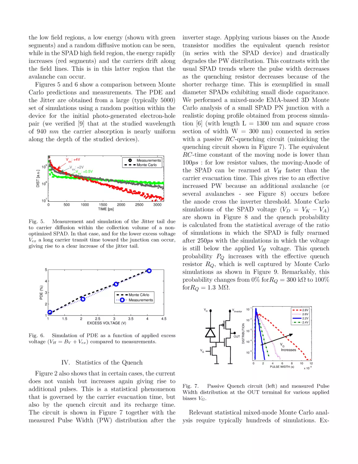
inverter stage. Applying various biases on the Anode
transistor modifies the equivalent quench resistor
(in series with the SPAD device) and drastically
degrades the PW distribution. This contrasts with the
usual SPAD trends where the pulse width decreases
as the quenching resistor decreases because of the
shorter recharge time. This is exemplified in small
diameter SPADs exhibiting small diode capacitance.
We performed a mixed-mode EMA-based 3D Monte
Carlo analysis of a small SPAD PN junction with a
realistic doping profile obtained from process simulation [6] (with length L = 1300 nm and square cross
section of width W = 300 nm) connected in series
with a passive RC -quenching circuit (mimicking the
quenching circuit shown in Figure 7). The equivalent
RC -time constant of the moving node is lower than
100ps : for low resistor values, the moving-Anode of
the SPAD can be rearmed at VH faster than the
carrier evacuation time. This gives rise to an effective
increased PW because an additional avalanche (or
several avalanches - see Figure 8) occurs before
the anode cross the inverter threshold. Monte Carlo
simulations of the SPAD voltage (VD = VK − VA )
are shown in Figure 8 and the quench probability
is calculated from the statistical average of the ratio
of simulations in which the SPAD is fully rearmed
after 250ps with the simulations in which the voltage
is still below the applied VH voltage. This quench
probability PQ increases with the effective quench
resistor RQ , which is well captured by Monte Carlo
simulations as shown in Figure 9. Remarkably, this
probability changes from 0% forRQ = 300 kΩ to 100%
forRQ = 1.3 MΩ.
Monte CArlo
Measurements
2
VH
1
1.5
2
2.5
3
3.5
EXCESS VOLTAGE (V)
4
4.5
−2
Fig. 6. Simulation of PDE as a function of applied excess
voltage (VH = BV + Vex ) compared to measurements.
OUT
VG
IV. Statistics of the Quench
Figure 2 also shows that in certain cases, the current
does not vanish but increases again giving rise to
additional pulses. This is a statistical phenomenon
that is governed by the carrier evacuation time, but
also by the quench circuit and its recharge time.
The circuit is shown in Figure 7 together with the
measured Pulse Width (PW) distribution after the
2.8V
2.6V
2.2V
2.4V
10
DISTRIBUTION
1
−1
10
VInvertor
−3
10
−4
10
VG
Increases
−5
10
0
2
4
6
8
PULSE WIDTH (s)
10
12
−8
x 10
Fig. 7.
Passive Quench circuit (left) and measured Pulse
Width distribution at the OUT terminal for various applied
biases VG .
Relevant statistical mixed-mode Monte Carlo analysis require typically hundreds of simulations. Ex-
tensive studies in larger and more realistic SPAD
diodes, the diameter of which can be several tens
of microns (and the capacitance several tens of fF),
would require a drastic increase of the CPU simulation
time. Instead, we used an empirical version of the
Monte Carlo code, in which the carrier motion is
randomly assessed according to the distribution probability shown in Figure 3, and the impact ionization
probability computed using ionization integrals along
the random carrier trajectory. Such efficient empirical
statistical methods make possible detailed analysis
of the Quench probability dependence on the SPAD
architecture and design at an industrial level. More
details on empirical Monte Carlo and its calibration
using full band Monte Carlo simulation results will
be presented at the conference.
Fig. 8. Monte Carlo simulations of the SPAD biasing with
a passive quench resistor of RQ = 700kΩ. Equivalent SPAD
capacitance of CSP AD = 20.7aF and external quench capacitance of CQ = 0.1f F . Dashed line represents the Breakdown
voltage BV .
Fig. 9. Monte Carlo simulation of the quench probability PQ
as a function of the equivalent quench resistor RQ (see text for
details).
References
[1] A. Spinelli and A. L. Lacaita, “Physics and numerical
simulation of single photon avalanche diodes,” IEEE
Trans. Electron Devices, vol. 44, no. 11, pp. 1931–1943,
1997
[2] C. Jacoboni, P. Lugli, ”Monte Carlo Method for Semiconductor Device Simulation”, Springer Vienna, ISBN-10:
3211821104, 1989
[3] J. D Petticrew, S. J Dimler, X. Zhou, A. P Morrison,
C. H. Tan, J. S. Ng, ” Avalanche Breakdown Timing
Statistics for Silicon Single Photon Avalanche Diodes”,
IEEE Journal of Selected Topics in Quantum Electronics,
24(2), 1–6, 2018
[4] D. Dolgos, H. Meier, A. Schenk and B. Witzigmann, ”Fullband Monte Carlo simulation of single photon avalanche
diodes,” 2013 IEEE Photonics Conference, Bellevue, WA,
pp. 360-361, 2013
[5] D. Dolgos, H. Meier, A. Schenk and B. Witzigmann”Fullband Monte Carlo simulation of high-energy carrier transport in single photon avalanche diodes with multiplication
layers made of InPInAlAsand GaAs” Journal of Applied
Physics, vol. 111, no. 10, p. 104508, 2012
[6] Present
process
simulations
have
been
performed
using
Sentaurus
SProcess,
https://www.synopsys.com/silicon/tcad/processsimulation/sentaurus-process.html
[7] M Michaillat, D. Rideau, F. Aniel , C. Tavernier and H.
Jaouen, ”Monte Carlo simulation of high-energy transport
of electrons and holes in bulk SiGeC alloys”, J. Phys.:
Conf. Ser. 193 012037, 2009
[8] P. Dollfus, A. Bournel, S. Galdin-Retailleau, S. Barraud,
and P. Hesto, ”Effect of discrete impurities on electron
transport in ultra-short MOSFET using 3D Monte Carlo
simulation”, IEEE Trans. Electron Devices, vol. 51 (5),
749-756, 2004
[9] For light absorption we used Lumerical (simulations results not shown here)
[10] M. Hofbauer, B. Steindl, and H. Zimmermann, ”Temperature Dependence of Dark Count Rate and After Pulsing
of a Single-Photon Avalanche Diode with an Integrated
Active Quenching Circuit in 0.35 µm CMOS”,Journal of
Sensors, Vol 2018, Article ID 9585931, 7, 2018