/


Текст
Physics and Applications
of the Josephson Effect
ANTONIO BARONE
Consiglio Nazionale delle Ricerche
and
Universita di Napoli
GIANFRANCO PATERNO
Comitato Nazionale Energia Nucleare
A WILEY-INTERSCIENCE PUBLICATION
JOHN WILEY & SONS
New York • Chichester • Brisbane • Toronto • Singapore
Copyright © 1982 by John Wiley & Sons, Inc.
All rights reserved. Published simultaneously in Canada.
Reproduction or translation of any part of this work
beyond that permitted by Section 107 or 108 of the
1976 United States Copyright Act without the permission
of the copyright owner is unlawful. Requests for
permission or further information should be addressed to
the Permissions Department, John Wiley & Sons, Inc.
Library of Congress Cataloging in Publication Data:
Barone, Antonio, 1939-
Physics and applications of the Josephson effect.
"A Wiley-Interscience publication."
Bibliography: p.
Includes index.
1. Josephson effect. I. Paterno, Gianfranco.
II. Title.
QC176.8.T8B37 530.44 81-7554
ISBN 0-471-01469-9 AACR2
Printed in the United States of America
10 987654321
ToSVEVA
and
to GIANNA
Preface
This book surveys all aspects of the Josephson effect—from the underly-
underlying physical theory to actual and proposed engineering applications. Both ends
of this spectrum are interesting. The physical theory is novel and important for
many macroscopic quantum effects, which have a rich and yet untapped
potential for technical development. We attempt here to present more than a
survey and less than an exhaustive exposition of this wide field. Rather than to
cover everything, we have tried to uncover those aspects of theory, fabrication
technology, and device application that will be of lasting value.
Chapter 1 briefly surveys Josephson junction phenomenology. Although
the reader is assumed to have a basic knowledge of superconductivity, we
begin with the simplest possible description of Josephson structures and their
dynamic behavior. Chapter 2 presents microscopic theory in simple terms. We
discuss salient features of the underlying theory that are most useful in
appreciating experimental results. To some extent the chapters are self-
contained; for example, the reader could skip the microscopic theory (at least
on a first reading) without seriously impairing continuity. In Chapter 3 we
discuss the dependence of critical current on temperature and on junction
parameters. The static (i.e., zero voltage) behavior of "small" and "large"
junctions is considered in Chapters 4 and 5. Chapter 6 presents several
important results on the current voltage behavior of small weak links, and a
variety of weak link structures is described in Chapter 7.
What we discuss in Chapter 8 are those basic technological considerations
and certain advanced techniques that have been found useful in several
laboratories throughout the world over the past decade. We expect such
techniques to continue to be of value, especially for those who are beginning to
experiment with Josephson junctions.
Chapters 9 and 10 discuss self-resonant modes in small junctions and the
dynamical behavior of extended junctions from the perspective of modern
"soliton" theory.
The last three chapters are directed toward applications of Josephson
junctions. Chapter 11 discusses the various features of junction interactions
with periodic signals and considers such applications as mixing, parametric
amplification, and the voltage standard. Chapters 12 and 13 deal with quan-
quantum interference loops and their application to measurement of very small
magnetic fields. Finally, in Chapter 14, we describe the potential of the
Josephson junction as the basic logic and memory element in a very large
digital computer system.
vii
viii PREFACE
Throughout the book our choice of theoretical material has been guided
by our later discussions of device applications. In this way we have tried to
achieve a large scale coherence in a range of subject matter that at first glance
might appear to be rather diffuse. We hope that the book will be useful in
graduate courses in the theory and applications of superconductive devices, as
well as for research scientists and engineers. Although extensive, the bibliogra-
bibliography is not exhaustive, and we apologize to those whose work may have been
overlooked.
Antonio Barone
glanfranco paterno
Naples, Italy
Rome, Italy
December 1981
Acknowledgements
It is our pleasure to acknowledge the kind and generous assistance that
has been offered throughout the preparation of this book. Without such help
our task would not have been possible.
It is hard to adequately express our gratitude to A. C. Scott for his
continuous encouragement and advice, and to R. Vaglio and R. D. Parmentier
for their careful reading of the manuscript and invaluable contributions.
We warmly acknowledge A. Baratoff for reviewing and suggesting im-
improvements in Chapters 2 and 3; N. F. Pedersen, in Chapter 6; Y. Ovchinnikov
and A. L. Aslamazov, in Chapter 7; T. F. Finnegan, in Chapter 11; S. N. Erne
and J. E. Zimmerman, in Chapters 12 and 13; and P. Wolf, in Chapter 14.
Thanks are due to M. Russo for his helpful cooperation and suggestions
and to L. Solymar for his encouragement during the early stages of preparing
this book.
We are indebted to many colleagues for permission to cite and use their
published and unpublished results. In particular, we greatly benefited from the
preprints and original material of S. Basavaiah, A. N. Broers, P. Carelli, J.
Clarke, D. Cohen, С M. Falco, M. J. Feldman, С H. Hamilton, R. E. Harris,
D. J. Herrel, W. J. Johnson, I. O. Kulik, R. B. Laibowitz, D. N. Langenberg,
Li Kong Wang, H. Liibbig, I. Modena, J. E. Nordman, D. E. Prober, M. Ricci,
G. L. Romani, N. Sacchetti, R. D. Sandell, I. Schuller, Y. Taur, and I. K.
Yanson, to whom we express our deep gratitude.
Discussions with W. Anacker, B. S. Deaver, Jr., S. Callegari, T. A. Fulton,
K. Gray, J. Kurkijarvi, J. Matisoo, D. J. Scalapino, E. P. Balsamo, R.
Cristiano, O. Natoli, and R. Vitiello are also acknowledged, as well as the
useful suggestions given by K. K. Likharev, J. E. Mooij, and M. Tinkham.
Thanks are due to the Landau Institute for Theoretical Physics of the
Academy of Sciences of USSR for providing several opportunities to one of us
(A. B.) to meet with Soviet scientists during the preparation of the book.
We thank A. M. Mazzarella for her competence, skill, and dedication
throughout the preparation of the manuscript and С Salvia for his invaluable
technical assistance.
Finally, we are thankful to L. Crescentini, A. De Feo, M. Izzo, L. Mendia,
S. Piantedosi, С Salinas for helping with the manuscript in different ways and
to A. DeLuca and S. Termini for friendly encouragement and suggestions.
A. B.
G. P.
ix
Contents
CHAPTER 1
WEAK SUPERCONDUCTIVITY—PHENOMENOLOGICAL
ASPECTS
1.1 Macroscopic quantum system, 1
1.2 Coupled superconductors, 3
1.3 Single electron tunneling, 4
1.4 Josephson equations, 9
1.5 Magnetic field effects, 14
1.6 Barrier free energy, 18
1.7 Electrodynamics of the Josephson junction, 19
1.8 Other Josephson structures, 22
CHAPTER 2
MICROSCOPIC THEORY 25
2.1 Tunneling Hamiltonian formalism, 25
2.2 General expression for the total current, 29
2.2.1 The total current expression in the time domain, 31
2.2.2 The total current expression in the frequency domain, 33
2.3 Tunneling current for constant voltage, 35
2.4 Expression of IqPi, Iqp, /yi, /y2, 35
2.4.1 The quasiparticle terms Iqp, IqP[, 37
2.4.2 The phase dependent terms IJX and IJ2, 38
2.5 Tunneling current in the B.C.S. approximation, 39
2.6 The "cos qp" problem, 47
xi
Xii CONTENTS
CHAPTER 3
MAGNITUDE AND TEMPERATURE DEPENDENCE
OF THE CRITICAL CURRENT 50
3.1 Josephson current for V — 0, 50
3.2 B.C.S. approximation, 51
3.3 Strong coupling effects, 56
3.4 Effects of paramagnetic impurities, 59
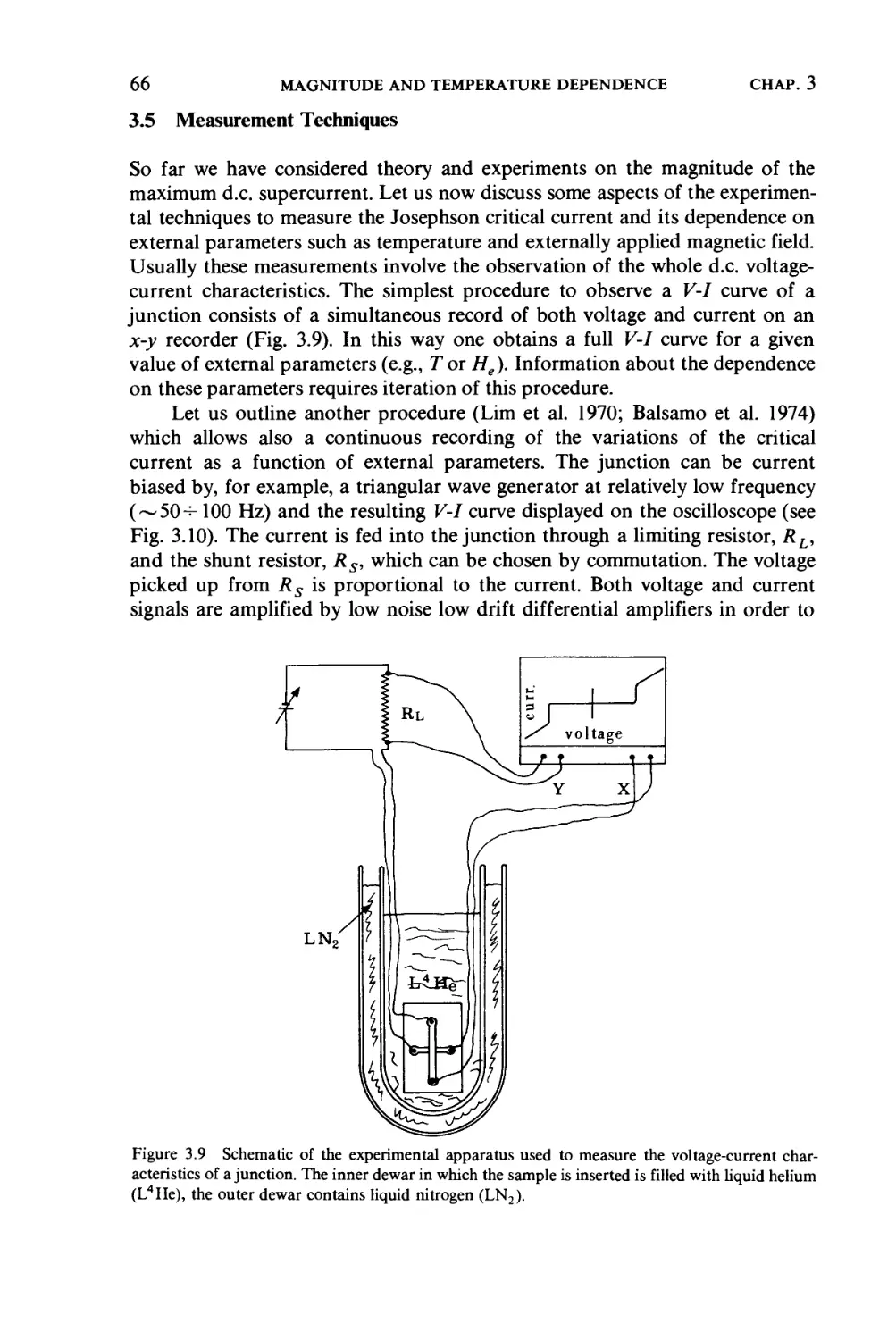
3.5 Measurement techniques, 66
CHAPTER 4
"SMALL" JUNCTIONS IN A MAGNETIC FIELD 69
4.1 Josephson penetration depth, 69
4.2 Small junctions, 70
4.3 Uniform tunneling current distribution, 74
4.3.1 Rectangular junctions, 74
4.3.2 Circular junctions, 76
4.3.3 Magnetic field with arbitrary orientation, 77
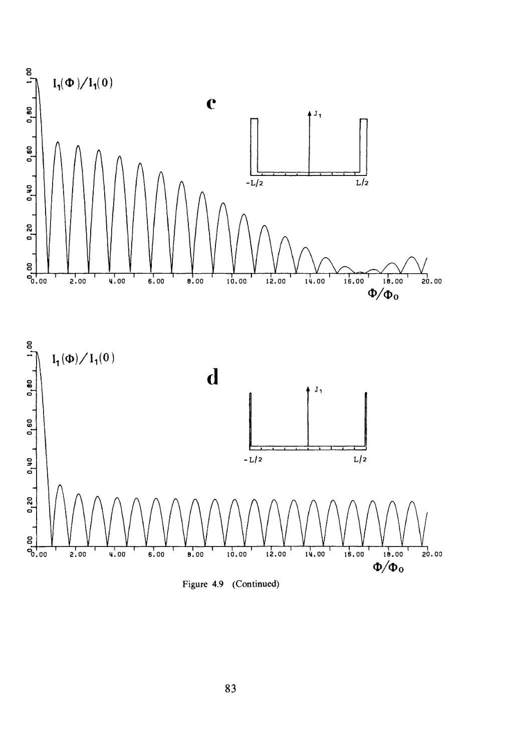
4.4 Non-uniform tunneling current density, 79
4.4.1 Various current density profiles, 80
4.4.2 Structural fluctuations, 91
CHAPTER 5
LARGE JUNCTIONS—STATIC SELF-FIELD EFFECTS 96
5.1 Approximate analysis, 96
5.2 Analysis of Owen and Scalapino, 100
5.3 Effects of the junction geometrical configuration, 112
CHAPTER 6
CURRENT VOLTAGE CHARACTERISTICS 121
6.1 V-I curves of various weak links, 121
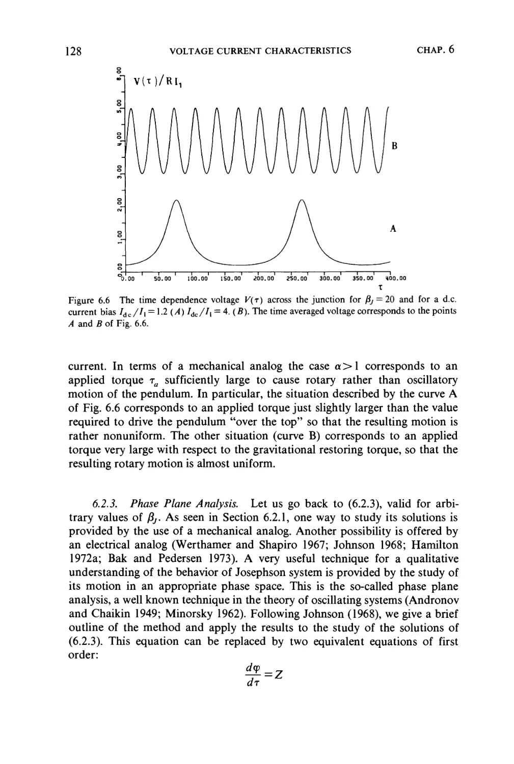
6.2 Resistively shunted junction model: autonomous case, 122
6.2.1 Mechanical model, 123
6.2.2 Small capacitance limit (fij »1), 126
contents xiii
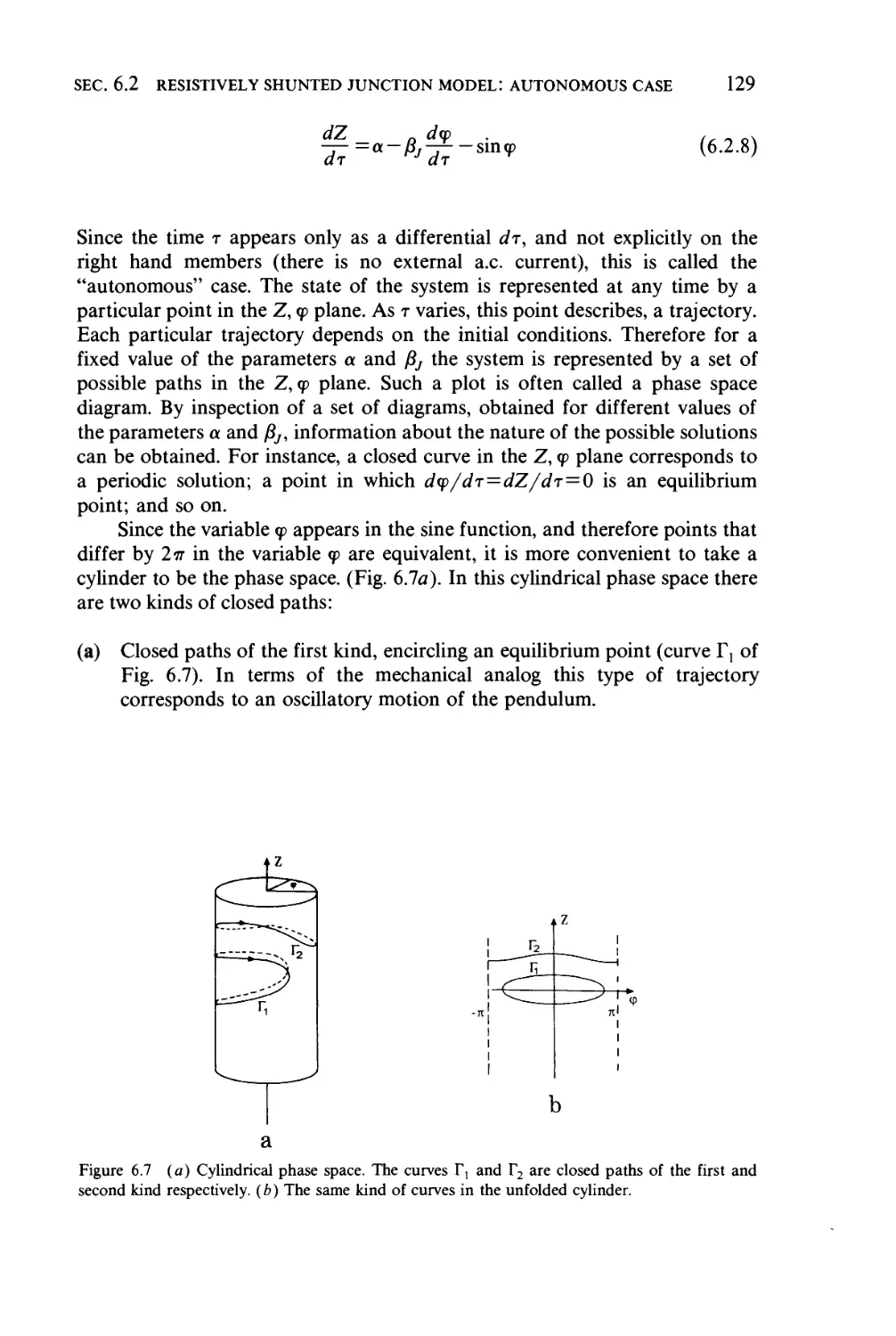
6.2.3 Phase plane analysis, 128
6.2.4 D.C. voltage-current characteristics for
finite capacitance, 131
6.3 Current biased tunneling junction, 136
6.3.1 Adiabatic approximation, 137
6.3.2 General case, 138
6.4 Effects of thermal fluctuations, 143
6.4.1 Negligible capacitance, 147
6.4.2 Finite capacitance, 153
6.4.3 Large capacitance, 157
6.4.4 Other noise considerations, 158
CHAPTER 7
OTHER SUPERCONDUCTING WEAK LINK STRUCTURES 161
7.1 Metal barrier junctions, 161
7.1.1 Proximity effect, 161
7.1.2 S-N-S junctions, 164
7.1.3 S-I-N-S structures, 166
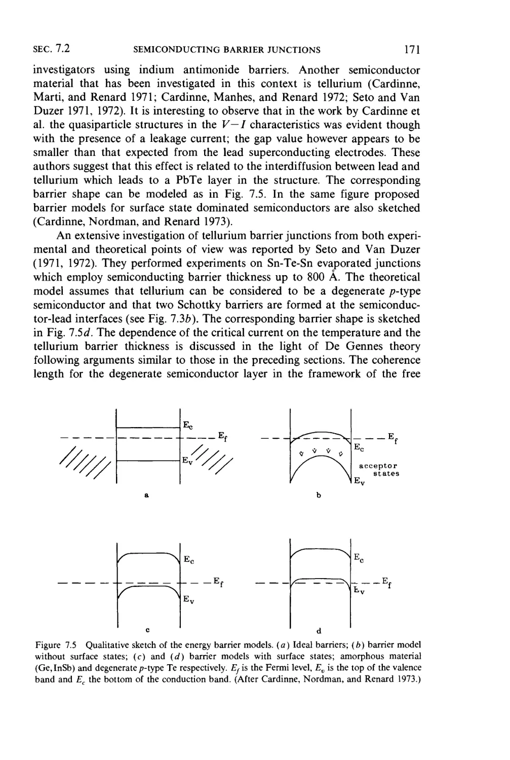
7.2 Semiconducting barrier junctions, 169
7.2.1 Barrier layers of various semiconductor materials, 170
7.2.2 Light sensitive semiconducting barrier junctions, 172
7.3 Bridge-type junctions, 177
7.3.1 Static behavior, 181
7.3.2 Voltage-current characteristics, 186
7.3.3 Interpretation of voltage carrying states, 187
7.3.4 Aspects of nonequilibrium superconductivity, 193
7.4 Point contact weak links, 196
CHAPTER 8
DEVICE FABRICATION TECHNOLOGY 198
8.1 Josephson tunneling junctions, 198
8.2 Junction electrodes, 199
8.2.1 Soft metals, 199
8.2.2 Soft metal alloys, 200
8.2.3 Hard materials (Transition metals), 204
XIV CONTENTS
8.3 Oxide barriers, 205
8.3.1 Thermal oxidation, 206
8.3.2 D.C. glow discharge, 207
8.3.3 R. F. glow discharge, 210
8.4 Junction patterning, 211
8.4.1 Metal masks, 212
8.4.2 Photolithography, 212
8.4.3 Lift-off technique, 214
8.4.4 Electron lithography, 216
8.4.5 X-Ray lithography, 217
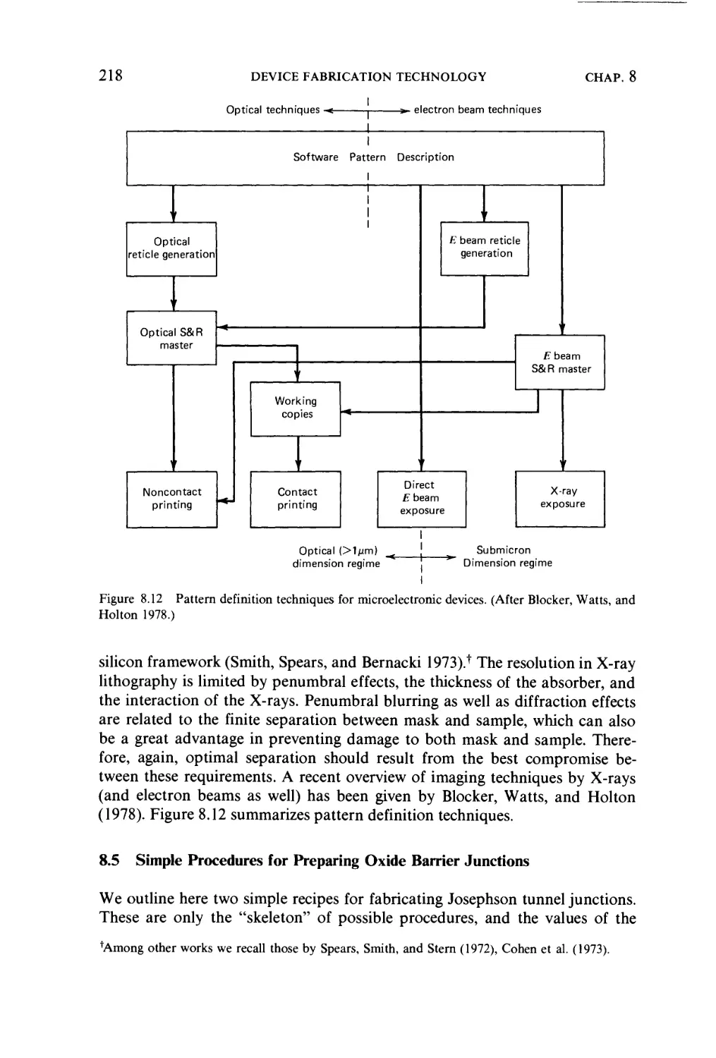
8.5 Simple procedures for preparing oxide barrier junctions, 218
8.5.1 Evaporated junctions, 219
8.5.2 Sputtered base layer junctions, 220
8.5.3 Other oxide barrier structures, 221
8.6 Semiconductor barriers, 222
8.6.1 Various semiconductors, 223
8.6.2 Light sensitive barriers, 224
8.6.3 Single crystal barrier junctions, 225
8.7 Bridge-type weak links, 228
8.8 Point contact structures, 232
CHAPTER 9
RESONANT MODES IN TUNNELING STRUCTURES 235
9.1 Josephson junction as a transmission line, 235
9.2 Resonant modes for low Q junctions, 238
9.3 Junctions of infinite length, 248
9.4 Nonuniform current density distribution, 251
9.5 Resonant modes for high Q Josephson junctions, 256
CHAPTER 10
FLUXON DYNAMICS 264
10.1 The sine Gordon equation, 264
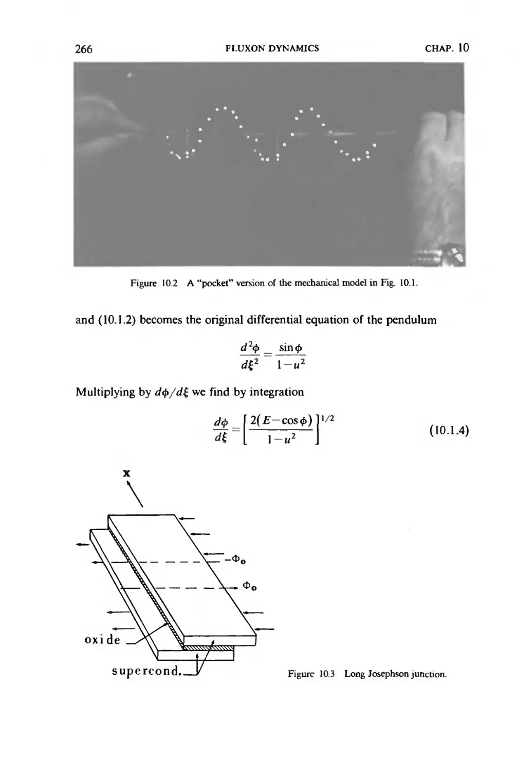
10.1.1 Traveling wave solutions, 265
10.1.2 Energy functions, 269
CONTENTS XV
10.2 Nonlinear standing waves on a rectangular junction, 271
10.3 Effects of losses and bias, 274
10.4 Zero field steps, 278
10.5 Perturbative analysis of fluxon dynamics, 279
10.5.1 Single fluxon dynamics, 280
10.5.2 Fluxon-antifluxon annihilation, 284
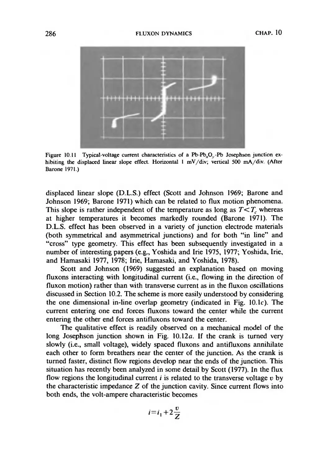
10.6 Effects of flux flow on D.C. voltage-current characteristics, 285
10.7 Two dimensional junctions, 288
CHAPTER 11
HIGH FREQUENCY PROPERTIES AND APPLICATIONS
OF THE JOSEPHSON EFFECT 291
11.1 Simple voltage source model, 291
11.1.1 Microwave induced steps, 291
11.1.2 Effect of fluctuations on the induced voltage steps, 293
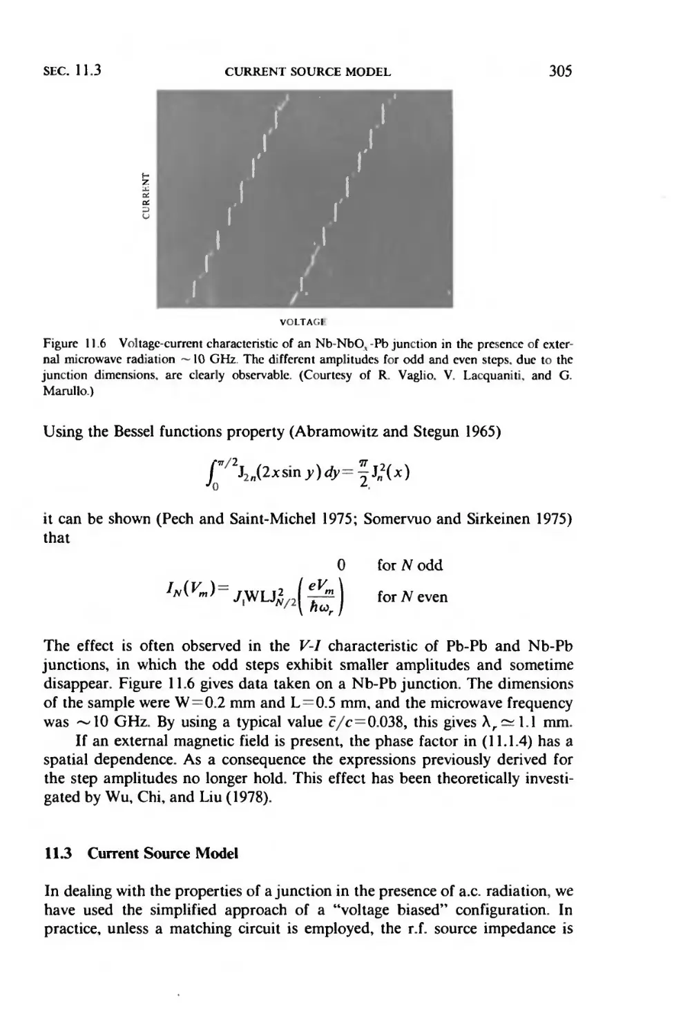
11.2 Tunneling junctions in external microwave radiation, 294
11.2.1 The "Riedel" peak, 296
11.2.2 Finite dimension effects, 304
11.3 Current source model, 305
11.4 Emission of radiation, 309
11.5 Detection of radiation, 318
77.5.7 Wide band detectors, 318
11.5.2 Narrow band detectors, 324
11.6 Parametric amplification, 330
11.6.1 Parametric amplifiers with externally pumped
Josephson elements, 332
11.6.2 Internally pumped parametric amplifiers, 343
11.7 The determination of 2e/h and the voltage standard, 344
CHAPTER 12
JOSEPHSON JUNCTIONS IN SUPERCONDUCTING LOOPS 354
12.1 Fluxoid quantization, 354
12.2 Superconducting loop with a single junction, 359
xvi CONTENTS
12.2.1 Metastable states, 360
12.2.2 Applied external field, 360
12.2.3 Dynamics of flux transitions for Pe>\, 364
12.3 Superconducting interferometer, 369
12.3.1 Zero inductance case, 370
12.3.2 Metastable states, 373
12.3.3 Asymmetric double junction configuration, 375
CHAPTER 13
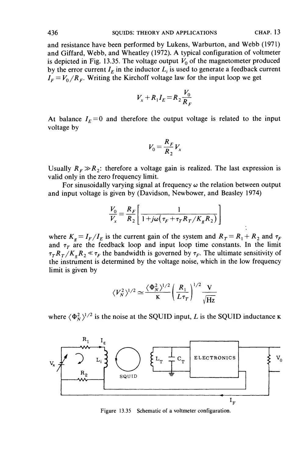
SQUIDs: THEORY AND APPLICATIONS 383
13.1 Radio Frequency SQUID, 383
13.1.1 Effects of the parametric inductance, 384
13.1.2 R.F. SQUID in the dispersive mode, 388
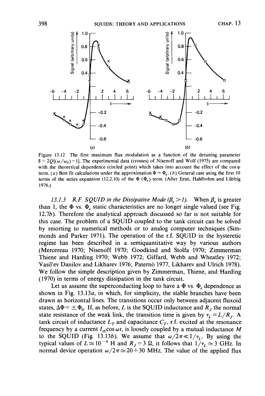
13.1.3 R.F. SQUID in the dissipative mode фе > 1) 398
13.2 D.C. SQUID, 403
13.3 Noise and maximum sensitivity, 409
13.3.1 R.F. magnetometers, 410
13.3.2 D.C. magnetometers, 413
13.3.3 Ultimate sensitivity of practical devices, 415
13.4 Practical superconducting sensor configurations, 416
13.4.1 Single weak link devices, 416
13.4.2 Two weak link configurations, 421
13.5 Measurement techniques, 424
75.5.7 Flux locked configuration, 424
13.5.2 Superconducting transformers, 426
13.6 The resistive SQUID, 429
13.6.1 The resistive loop device in the
presence of a D. С bias, 429
13.6.2 The resistive loop device in the
presenceof an R.F. bias, 431
13.7 Applications, 434
13.7.1 Measurements of current, voltage and resistance, 435
13.7.2 Magnetic susceptibility measurements, 437
13.7.3 Medical applications, 439
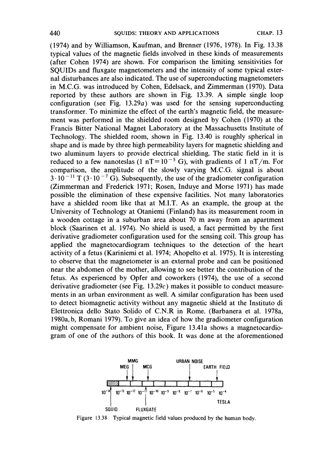
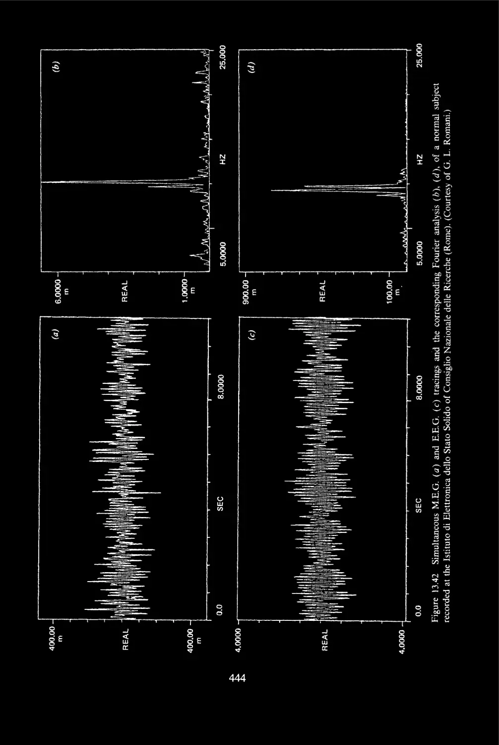
13.7.4 Magnetotellurics, 445
CONTENTS XV11
CHAPTER 14
COMPUTER ELEMENTS 446
14.1 Cryotrons, 446
14.2 Matisoo's experiments, 449
14.2.1 Tunneling cryotron, 449
14.2.2 Flip-flop circuit, 451
14.3 Operation times, 454
14.4 Different switching modes, 456
14.5 Interference switching devices, 459
14.6 Memory Cells, 461
14.6.1 Flip-flop memory configuration, 461
14.6.2 Single flux quantum storage devices, 462
14.7 Examples of Josephson logic and memory circuits, 465
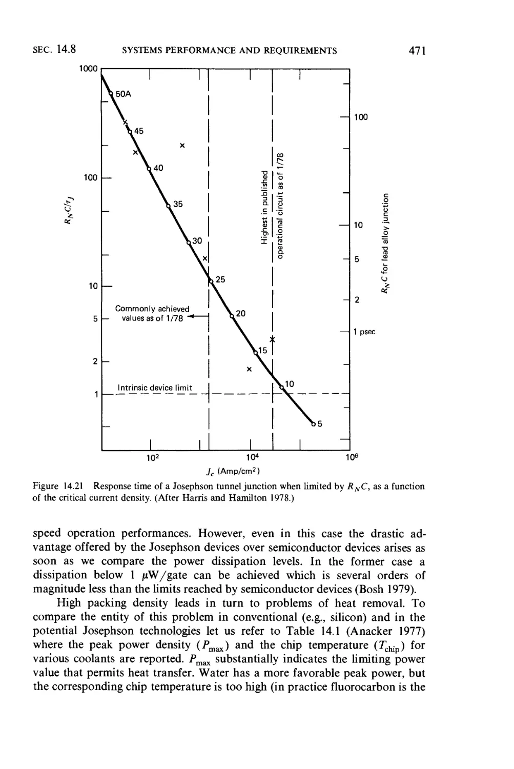
14.8 Systems performance and requirements, 470
14.9 Conclusions and perspectives, 473
APPENDIX
SYSTEMS OF UNITS 474
A.I Comments on systems of units, 474
A.2 Conversion Tables, 474
REFERENCES 477
INDEX 525
Every explanation is an hypothesis.
L. W. WITTEGENSTEIN
Remarks on Frazer's Golden Bough
Physics and Applications
of the Josephson Effect
CHAPTER 1
Weak Superconductivity—
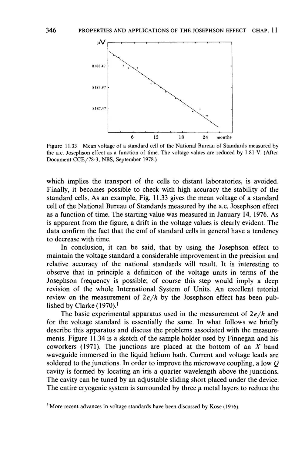
Phenomenological Aspects
In this chapter we briefly review the phenomenology of the Josephson effect,
outlining the basic experimental results and providing a qualitative interpreta-
interpretation on the basis of very simple models. However, first let us say a few words
about its history.
The discovery of what is usually referred to as the Josephson effect dates
back about 20 years A961-1962). At that time Brian Josephson was a research
student at the Royal Society Mond Laboratory in Cambridge under the
supervision of Brian Pippard. There is no doubt, as reported by Josephson in
his Nobel lecture, that the stimulating oven of the Mond Laboratory, the
presence at that time of Phil Anderson, the development of new researches,
both on experiments (Giaever, 1960a,b; Nicol, Shapiro, and Smith 1960) and
on theory (Cohen, Falicov, and Phillips 1962) of superconductive tunneling,
provided an ideal ground for Josephson's intuition and outstanding conclu-
conclusions. Josephson's prediction and the following experimental confirmation
(Anderson and Rowell 1963) opened not only a new important chapter of
physics but also new horizons for a wide variety of stimulating applications.
We shall not dwell further on the history of the discovery of the Josephson
effect, though it certainly deserves adequate space and a deep analysis. Instead,
we prefer to refer the reader to the historical surveys given by Josephson
himself A974) and other protagonists (Anderson 1970; Pippard 1976), thus
avoiding any possible deformation of the fascinating atmosphere in which
those events took place.
1.1 Macroscopic Quantum System
The interpretation of superconductivity as a quantum phenomenon on a
macroscopic scale was introduced by F. London A935). The theory of
Ginzburg and Landau A950) provided an enormous insight into the nature of
superconductivity. They developed a modification of the London theory (F.
London and H. London 1935a,b) by introducing a position dependent param-
parameter, ty, which gives a measure of the order in the superconducting phase.
Unlike the earlier two fluid models proposed by Gorter and Casimir A934),
such an order parameter is complex and can be regarded as a wave function
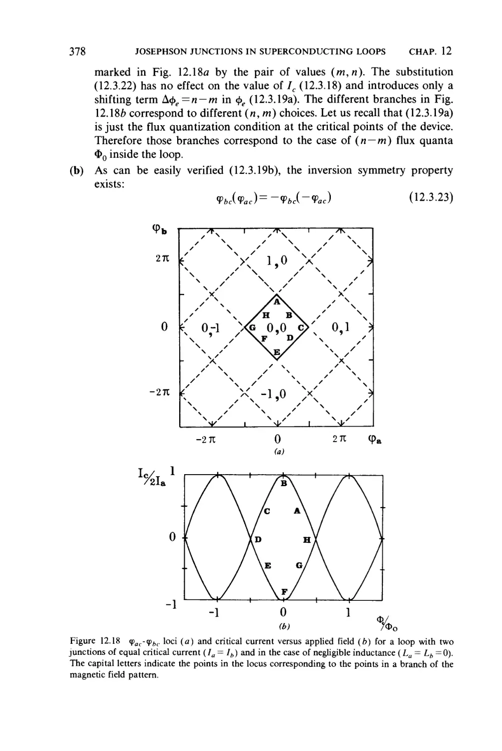
1
Physics and Applications of the Josephson Effect. A. Barone, G. Paterno
Copyright © 1982 by John Wiley & Sons, Inc. ISBN: 0-471-01469-9
2 WEAK SUPERCONDUCTIVITY—PHENOMENOLOGICAL ASPECTS CHAP. 1
for superconducting electrons. As shown by Gor'kov A959), ^ is proportional
to the local value of the energy gap function Д. In this framework a single wave
function is associated with a macroscopic number of electrons which are
assumed to "condense" in the same quantum state. In this sense, the supercon-
superconductive state can be regarded as a "macroscopic quantum state." Therefore we
are dealing with particles, having effective mass and charge m* and e*
respectively, which can be described as a "whole" by a macroscopic wave
function of the form
^pi/V3 A.1.1)
where <p is the phase common to all the particles and p represents, in this
macroscopic picture, their actual density in the macrostate \s > :
The electric current density can be written, in the presence of a vector potential
A:
where с is the velocity of the light.
As follows from flux quantization, the charge e* is twice the electronic
charge e, since the "particles" we are dealing with are in fact pairs of coupled
electrons. This is contained within the framework of the microscopic theory of
superconductivity first derived by Bardeen Cooper and Schrieffer A957) and
usually referred as B.C.S. theory. It is assumed that m* = 2m (m = electronic
mass), but, it is easy to see that the choice of m is arbitrary, since it depends
essentially on the normalization assumed for the pair wave function »//.*
Thus with the ^ given by A.1.1) the expression for J becomes
J=p-f/iV(p--A) A.1.2)
Gauge invariance requires that under the transformations of the vector
potential A and scalar potential U
at
the observable physical quantities remain unchanged. This implies the phase
transformation
Ф^Ф+^Х A.1.3)
tSee also the microscopic derivation of the Ginzburg Landau theory by Gor'kov A959).
SEC. 1.2 COUPLED SUPERCONDUCTORS 3
as can be readily verified for the current density J by A.1.2). The choice of
constant values for the scalar quantity x does not affect potentials but just
implies different values of the phase factor. This corresponds to the unobserva-
bility of i|/.
We can arbitrarily assign a phase value at a given point; however, because
of the occurrence of the so-called long range order the value of the phase is
fixed in all points. Obviously, as is evident from A.1.2), spatial variations of
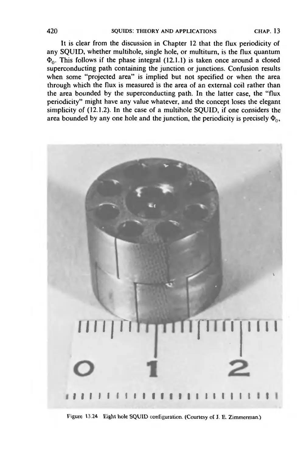
the phase <p describe carrying current states of the superconductor.
For a system in equilibrium the required gauge invariance leads neces-
necessarily to a time dependent \p. It is clear in fact that, even assuming a constant ^
in one gauge, any transformation to another gauge would imply a change of <p
as in A.1.3) in which x is time dependent. The time evolution of \p in stationary
conditions obeys the usual quantum mechanical equation of the form
As can be seen from the microscopic theory (Gor'kov 1959) the quantity E
is equal to twice the electrochemical potential ц. This value represents the
minimum energy required to add a Cooper pair to the system. Thus ^(r, t) =
^{r)e'lj^t/h (See also Anderson 1963, 1966).
Since the number of pairs N and the phase <p are conjugate variables
(Anderson 1963) there is an uncertainty relation, A7VA<p~277-, which corre-
corresponds to the circumstance that within an isolated superconductor N will be
fixed and, consequently, the phase <p undefined.
1.2 Coupled Superconductors
Let us now consider two superconductors SL and SR separated by a macro-
macroscopic distance. In this situation, the phase of the two superconductors can
change independently. As the two superconductors are moved closer, so that
their separation is reduced to about 30 A, quasiparticles can flow from one
superconductor to the other by means of tunneling (single electron tunneling).
If we reduce further the distance between SL and SR down to say 10 A, then, as
we shall see, also Cooper pairs can flow from one superconductor to the other
(Josephson tunneling). In this situation if we assign a given phase in SL is the
possibility of altering independently the phase in SR still allowed? The answer
is no! This degree of freedom is removed, since phase correlation is realized
between the two superconductors; that is, the long range order is "transmitted"
across the boundary. Therefore we expect that the whole system of the two
superconductors separated by a thin (~ 10 A) dielectric barrier will behave, to
some extent, as a single superconductor. Unlike ordinary superconductivity,
this phenomenon is often called "weak superconductivity" (Anderson 1963)
because of the much lower values of the critical parameters involved. The
4 WEAK SUPERCONDUCTIVITY—PHENOMENOLOGICAL ASPECTS CHAP. 1
above-quoted work by Anderson should be considered a milestone in the
development of the field.
Josephson theory A962a,b, 1964, 1965, 1969, 1974) deals with such
systems of weakly coupled superconductors. We devote our attention mostly to
tunneling structures although Josephson effects take place in various types of
superconducting "weak links" (Dayem bridge, point contacts, etc.; see Section
1.8). To begin, we recall the basic concepts of single electron tunneling within a
simple phenomenological approach. An account of both single electron tunnel-
tunneling and Josephson phenomenology can be found in Solymar A972).
1.3 Single Electron Tunneling
The history of superconductive tunneling began with the experiments per-
performed by Giaever A960a,b) and by Nicol, Shapiro, and Smith A960). A
tunneling structure consists essentially of two metal films separated by a thin
(~30 A) dielectric barrier as sketched in Fig. 1.1. The behavior of such a
structure can be investigated by studying the dependence of the tunneling
current / on the voltage V across the junction.
To "visualize" the tunneling process, we adopt a simple representation in
terms of the energy (E)- momentum (k) diagrams. The normal metal is
represented in the E-k plane by the curve of Fig. 1.2a. The dashed line
corresponds to the portion of the parabola below the Fermi energy EF (hole
states) which has been reflected across the Fermi level. In this picture the
electron hole pair creation is regarded as excitations of two states of energy
?/ = 16/1 and Eh = \eh\ respectively. That is, all excited states have positive
energy measured with respect to EF. In the case of the superconductor, all the
condensed pairs are at the Fermi level and a minimum threshold energy Д
(energy gap) is required by an excitation as shown in Fig. Mb. In this case
there exists a particle which is "partially" in the hole state and "partially" in
the electron state. These are the quasiparticle excitations which have energy
Figure 1.1 Tunneling junction of cross-type geometry. The dimensions are L and W; a and b are
the two superconducting films.
SEC. 1.3
SINGLE ELECTRON TUNNELING
Figure 1.2 Energy momentum diagrams, (a) Normal metal; (b) superconducting metal; (c)
electron tunneling process between two normal metal electrodes.
E=(e2 +Д2I/2. From this one-to-one correspondence between E and e it
follows that N(E) dE-(%{e)de where N(E) and 9t(e) are the density of states
in the superconductor and in the normal metal respectively. Thus we have
&(E)[dA(E)/dE]
N(E) = N@)
where we have indicated with N@) the value of 91 for e = 0 assumed constant.
In the case of energy independent gap (B.C.S. approximation) we have the
following expression for the density of states:
N(E)=N@)-
N(E) =
|?|<Д
A.3.1)
Let us outline now the phenomenological theory of tunneling proposed by
Giaever and Megerle A961). In this approach, we assume that we are dealing
with normal electrons rather than quasiparticles. The tunneling current IL_+R
6 WEAK SUPERCONDUCTIVITY—PHENOMENOLOGICAL ASPECTS CHAP. 1
from the left to the right electrode is given by
^ + 0CE A.3.2)
where fL(E)(fR) is the Fermi factor fL(E)= 1/A + ^т?)* and NL(NR) is the
density of states in the left (right) metal; |T| is the tunneling matrix element
between states of equal energy. The expression A.3.2) merely signifies that the
current from L to R is proportional to A) the tunneling probability, B) the
number of electrons "available" on the left (fraction of filled states, NLfL), and
C) the number of possible states on the right (fraction of empty states
NR(\—fR)). Changing the subscript L with R we get similarly the current IR_+L
from the right to the left side. The net current / is thus
If we consider an applied voltage V across the junction the Fermi energy levels
fxL and fxR will be relatively shifted by an energy eV and thus
/=^|T|2/ NL(E)NR(E+eV)[fL(E)-fR(E+eV)]dE
where T is assumed to be energy independent.
Let us consider first two normal metals. We make the further hypothesis
of considering NL and Л^л to be constant and equal to the densities of states at
the Fermi energy level. * Therefore the tunneling current between two normal
metals is given by
/+00
[f(E)-f(E+eV)]dE
-oo
which is
*NN ~aN*
The constant aN can be regarded as a normal conductance, that is, a metal-
dielectric metal structure behaves for low applied voltage as an ohmic element.
In the E-k plane the tunneling process between normal metals is repre-
represented as in Fig. 1.2 c. The transfer of an electron from the left to the right
metal creates a hole excitation on the left and an electron state on the right.
*Pt= \/kBT where T is the absolute temperature and kB is the Boltzmann constant.
* The assumptions we have made on the energy independence of the tunneling matrix element and
of the densities of states can be justified by considering that the quantity [fL(E)~ fR(E + eV)] in
the integral contributes significantly only within an energy range of the order of e V near the Fermi
level. On the other hand we are interested in values of eV of the order of a few millielectronvolts
whereas the Fermi energy level is of the order of a few electronvolts.
SEC. 1.3
SINGLE ELECTRON TUNNELING
When the two metals are in the superconducting state the situation is
greatly altered. In fact the densities of states are now given by the expression
A.3.1). Therefore the tunneling current in a junction with the electrodes both
superconductors is given by
Iss = constant X
+ 00
\E\
\E+eV\
-Д2Л|1/2
r f(F)-
(b)
Figure 1.3 (a) Sketch of the theoretical V-I characteristic of a junction with different
superconducting electrodes. Vx - \&L - Дл|/е; V2 = AL + Дл/е). (b) Observed V-I characteristic
for a Sn-Sn^Oy-Pb junction.
8
WEAK SUPERCONDUCTIVITY—PHENOMENOLOGICAL ASPECTS CHAP. 1
This integral, solved by numerical calculations, leads, for T=?Q, to a
logarithmic singularity for the current Iss at a voltage V— ±|AL — A«|A and
to a finite discontinuity at К=±|Дл+Д^|/е (Nicol, Shapiro, and Smith,
1960; Shapiro et al. 1962; Taylor, Burstein, and Langenberg 1962). In Fig. 1.3
is reported the resulting voltage-current (V-I) characteristic (Fig. \3a) com-
compared to an experimental one (Fig. 1.36). The single particle tunneling between
two superconductors is illustrated in Fig. 1.4a. The process is shown as the
destruction of a pair on the left and creation of an excitation both on the left
and on the right. By equating the energies involved in the initial and final state
2eV=EL+eV+ER, the minimum voltage at which the process is possible is
given by eV=AL + ДЛ. For Г>0 or in the presence of injected particles in one
side of the barrier, a process like that of Fig. 1 Ab is also possible. The relation
between the applied voltage and the energy of the quasiparticle in the initial
and final state (we are assuming specular tunneling) is eV=ER — EL.
The minimum value of V in this case is zero. When eV— ±|ДЛ — AL\ the
singularity in the density of states in the two superconductors at ER = Дл and
eV
Figure 1.4 Quasiparticle tunneling processes between superconductors for finite d.c. applied
bias. AL and Дл are the energy gaps of the two electrodes, (a) Process involving the breaking of a
pair, (b) Direct tunneling of a thermally excited quasiparticle.
SEC. 1.4 JOSEPHSON EQUATIONS 9
EL = AL give rise to the mentioned logarithmic singularity in the V-I character-
characteristics (Fig. 1.3). The finite discontinuity observed at еК=Дл+Д^ is also
related to the behavior of the density of states near the gap.
1.4 Josephson Equations
It is possible to follow several different approaches in order to obtain the basic
Josephson relations. We discuss first a very simple derivation, due to Feynman
(Feynman, Leighton and Sands 1965), which is based on a "two level system"
picture. This approach, despite its simplicity, offers a powerful key for the
understanding of the peculiar features of Josephson phenomena.* A discussion
of this treatment in the framework of the B.C.S. theory has been given by
Rogovin and Scully A974). In addition Rogovin has extended this kind of
analysis to investigate various other aspects of the Josephson effect (Rogovin
1975a, b,c, 1976). Further work has been recently developed by Di Rienzo et
al. A977) and Bonifacio, Milani, and Scully A979), Lugiato and Milani A980).
Let us consider the tunneling structure superconductor-barrier-
superconductor. We call \pR (\pL) the pair wave function for the right (left)
superconductor. As discussed earlier, we are dealing with macroscopic quan-
quantum states. Therefore, each superconducting electrode can be described by a
single quantum state and the ^'s can be regarded as macroscopic wave
functions, so that |^|2 represents the actual Cooper pair density p. Following
the notation of Rogovin and Scully we indicate with the ket|/?)(|L>) the base
state for the right (left) superconductor. Then
If we now take into account the weak coupling existing between the two
superconductors, "transitions" between the two states \R) and \L) can occur.
This coupling is essentially related to the finite overlap of the two pair wave
functions \}/L and \}/R. This situation is schematically depicted in Fig. 1.5. A
state vector of this two base states system can be described as
That is, the particle can be either in a "left" or "right" state with amplitude \}/L
or \}/R respectively. The time evolution of the system is described by the
Schrodinger equation:
,*»!>. =ЗСЮ A.4.1)
* This phenomenological model has been considered extensively by many authors (see for instance
Mercereau 1969; De Bruyn Ouboter and De Waele, 1970; De Bruyn Ouboter, 1976).
10
WEAK SUPERCONDUCTIVITY—PHENOMENOLOGICAL ASPECTS CHAP. 1
R
Figure 1.5 Schematic of a Josephson junction. SL
and SR are the left and right superconductors. ipL and
}pR are the left and right pair wavefunctions.
with the Hamiltonian given by
where %L=EL\L) (L\ and %R = ER\R)(R\ are relative to the unperturbed
states \L > and \R >.
%T=K[\L)(R\ + \R)(L\]
is the term of interaction (tunneling Hamiltonian) between the two states. EL
and ER are the ground state energies of the two superconductors. К is the
coupling amplitude of the two state system which gives a measure of the
coupling interaction between the two superconductors and depends on
the specific junction structure (electrode geometry, tunneling barrier, etc.). In
the absence of a vector potential A, the quantity К can be assumed to be real.
Considering the projections on the two base states, A.4.1) can be written
in terms of amplitudes as
As we have seen in the two isolated superconductors, the energy terms are
given by ER = 2(xR and EL = 2(xL where (xR and (xL are the two chemical
potentials. If we consider a d.c. potential difference V across the junction these
chemical potentials are shifted by an amount eV and consequently it is
EL—ER = 2eV. We can choose the zero of the energy halfway between the two
values on the right and on the left, so that
A.4.2)
SEC. 1.4 JOSEPHSON EQUATIONS
We can substitute for \}/L and ^R their expressions
11
Separating real and imaginary terms in each equation we get
' >P, 2
dpR
—
sin Ф
2 /
= -jK]}pLpRsm<p
A.4.2a)
9<pL К ГрТ , eV
-г1"- = — . / —- cos <p + —
bt h]j pR h
9<p« _ к ГрТ
where <p now is
4> = 4>l~4>r
The pair current density / is given by
A.4.2b)
dt dt
and, therefore, from A.4.2) it follows that
, 2K
A.4.3)
If we assume pL = PR=P\ where px is constant, A.4.3) becomes
/=/1sin<p A-4.4)
where Jx =2K/hpx.
Let us note that although pR and pL are considered constant their time
derivative / is not zero. There is no contradiction if we take into account the
presence of the current source which continuously replaces the pairs tunneling
across the barrier. These feeding currents are not included in the equations;
however, this would not change the expressions of the tunnel pair current
density. This point has been discussed by Ohta A976) who gives a self-consistent
model that accounts for the role of the external source.
From the two equations A.4.2b) it follows:
2eV
dt
A.4.5)
12 WEAK SUPERCONDUCTIVITY—PHENOMENOLOGICAL ASPECTS CHAP. 1
Equations 1.4.4 and 1.4.5 are the constitutive relations of the Josephson effect.
Assuming K=0 the phase difference <p results, from A.4.5), to be constant not
necessarily zero, so that [from A.4.4)] a finite current density with a maximum
value Jl can flow through the barrier with zero voltage drop across the
junction. This is the essence of the d.c. Josephson effect (Josephson 1962). The
first observation was made by Anderson and Rowell in 1963. An experimental
evaluation of the voltage across the junction in the d.c. Josephson regime was
given by Smith A965). This author investigated the persistent current in a
wholly superconducting loop with a junction inserted and measured an upper
bound of 4ХКГ16 V.
In terms of the energy-momentum diagrams, d.c. Josephson tunneling can
be described as in Fig. 1.6. In this picture the pairs are located at the Fermi
level. A typical voltage-current (V-I) characteristics of a Josephson junction is
reported in Fig. 1.7. The zero voltage current is clearly displayed. When the
current flowing through the junction exceeds its maximum value /, (corre-
(corresponding to the current density /,) a finite voltage suddenly appears across the
junction. Indeed a switching occurs from the zero voltage state to the quasipar-
ticle branch of the V-I characteristic.
As mentioned in the preceding section, we observe that the existence of a
supercurrent (current at K=0) suggests that the Josephson effect can be
regarded qualitatively as an extension of the superconductive properties over
the whole structure including the barrier. In the bulk superconductor the
current is related to the gradient of the phase by A.1.2); in the Josephson
junction the pair current is related to the phase difference between the two
coupled superconductors by A.4.4).
If we apply a constant voltage V=?Q, it follows by integration of A.4.5)
that the phase <p varies in time as <p = (p0 +Be/h)Vt and therefore there
appears an alternating current
/ 2e
/=/,sin 4>c\ + -r
\ u h }
with a frequency u = 27rv = 2eV/h. This is called a.c. Josephson effect. The
Q. Figure 1.6 Cooper pair tunneling for V=0.
SEC. 1.4
JOSEPHSON EQUATIONS
13
Figure 1.7 Typical voltage-current characteristic for a Sn-Sn ^0,,-Sn Josephson junction at T= 1.52
K. Horizontal scale: 0.5 mV/div; vertical scale: 2 mA/div.
ratio between frequency and voltage is given by
-p =483.6 MHz/juV
Experimental evidence of this phenomenon arises in various situations. One
possibility is to observe the effect of microwave irradiation on the d.c. V-I
characteristics of the junction. In fact there is an interaction between the a.c.
Josephson current and the impressed microwave signal which leads to the
appearance of current steps at constant voltages (see Fig. 1.8). The steps occur
at voltages
K. = ?,o („=±1,±2,...)
where v0 is the frequency of the applied radiation. The first observation of this
phenomenon was by Shapiro A963).
Before proceeding further, let us observe that the derivation of A.4.4) and
A.4.5), although referred to a tunneling junction, can hold for other kinds of
weak links between superconductors. In fact the parameters of the specific
structure are essentially included in the coupling factor K, which can be
assumed not necessarily as a "tunneling" interaction term. In connection with
this point we consider also other weak links in which deviations from the
purely sinusoidal current-phase relationship can occur, however (see Chapter
7).
14 WEAK SUPERCONDUCTIVITY—PHENOMENOLOGICAL ASPECTS CHAP. 1
о
Voltage
Figure 1.8 Microwave power at 9300 Mc/sec(/l) and 24850 Mc/secE) produces many zero
slope regions spaced at hv/2e or hv/e. For A, hv/e = 38.5; for B, 103 /xV. For A, horizontal scale
is 58.8 /xV/cm and vertical scale is 67 nA/cm; for B, horizontal scale is 50 /xV/cm and vertical
scale is 50 /xA/cm. (After Shaprio 1963.)
Let us note finally that the description given for the quasiparticle and
Josephson tunneling results from the hybridization of two uncorrelated phe-
nomenological approaches, whereas a unified view of tunneling phenomena
can be obtained only by recourse to the microscopic theory. As we see in the
chapters that follow, such a theory accounts also for the temperature depen-
dependence of the Josephson current.
Finally it is worth mentioning the elegant derivation of Josephson relation
due to Bloch A970).
1.5 Magnetic Field Effects
Let us consider now the effect of a magnetic field H applied to the junction
along they direction* (see Fig. 1.9). For this purpose we can calculate the gauge
invariant phase difference between two points (with coordinates x and x + dx)
of the barrier by resorting to A.1.2):
2e
+ In the two level picture it is possible to take into account the presence of a vector potential A as
follows. The "coupling amplitude" К is modified by a phase factor as
SEC. 1.5
MAGNETIC FIELD EFFECTS
15
Figure 1.9 Contours of integration CL and CR used to derive the magnetic field dependence of
the phase difference <p. The field Hy is in they direction. The dashed zones indicate the regions in
which the field penetrates into the superconducting electrodes.
which is valid in each superconductor. A is the vector potential related to the
magnetic field by the usual relation v X A = H. By integration along the
contours CL and CR (see Fig. 1.9) we get
A.5.1)
Assuming the thickness of the superconducting films to be much larger
than the London depths we can extend the contours CL and CR outside the
The integral is to be taken across the barrier between two points r of the right superconductor and
/ of the left one. For convenience we assume a constant A within the barrier and choose the points
r and / such that \r—l\=8, where 8 is the barrier thickness. Thus in the presence of a vector
potential A A.4.2) are modified as follows (de Waele and de Bruyn Ouboter 1969):
jh±k = eV
In this case, making the same calculations, we get the Josephson equations in the gauge invariant
form:
v-ф-т- /A«ds= —
16 WEAK SUPERCONDUCTIVITY—PHENOMENOLOGICAL ASPECTS CHAP. 1
penetration region where the shielding current density Js vanishes, thus avoid-
avoiding also a possible reduction of the pair density p which can occur near the
barrier. The portions of CL and CR in the penetration region can be chosen
perpendicular to Js. With this assumption the second term in the integrals in
A.5.1) can be neglected and we have
(p(x + dx) — <p(x)=[<p
= |ч/ A-dl+J A-dl
Furthermore, neglecting the barrier thickness, we can write
The line integral can be replaced by the surface integral of the magnetic field
dl = Hy(XL + XR +1) dx
so that we have, in differential terms,
^ ^ A.5.2)
where XL and XR are the London depths in the two superconductors and t the
dielectric barrier thickness. By integration A.5.2) gives
where d=(XL +XR +t) is the magnetic penetration. Thus A.4.4) becomes
A.5.3)
which indicates that the tunneling supercurrent is spatially modulated by the
magnetic field. Then, due to the periodic character of the expression A.5.3),
situations can be realized in which the net tunneling current is zero. In
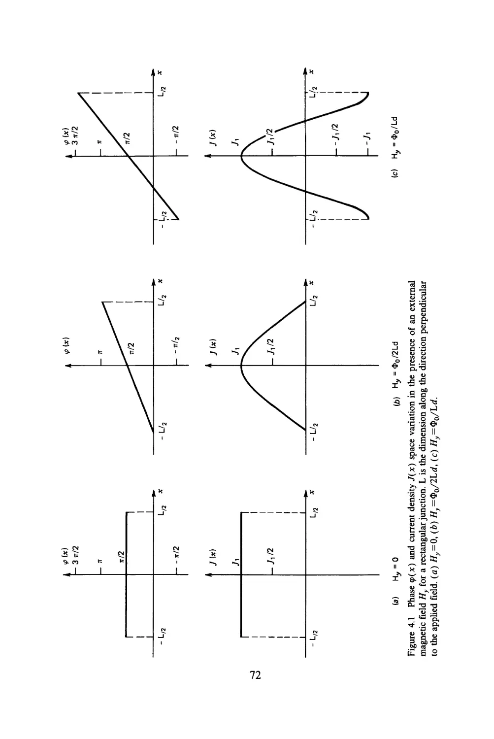
particular, as is extensively discussed in Chapter 4, a rectangular junction with
a uniform zero field tunneling current distribution exhibits a dependence of
the maximum supercurrent on the applied magnetic field in the form of a
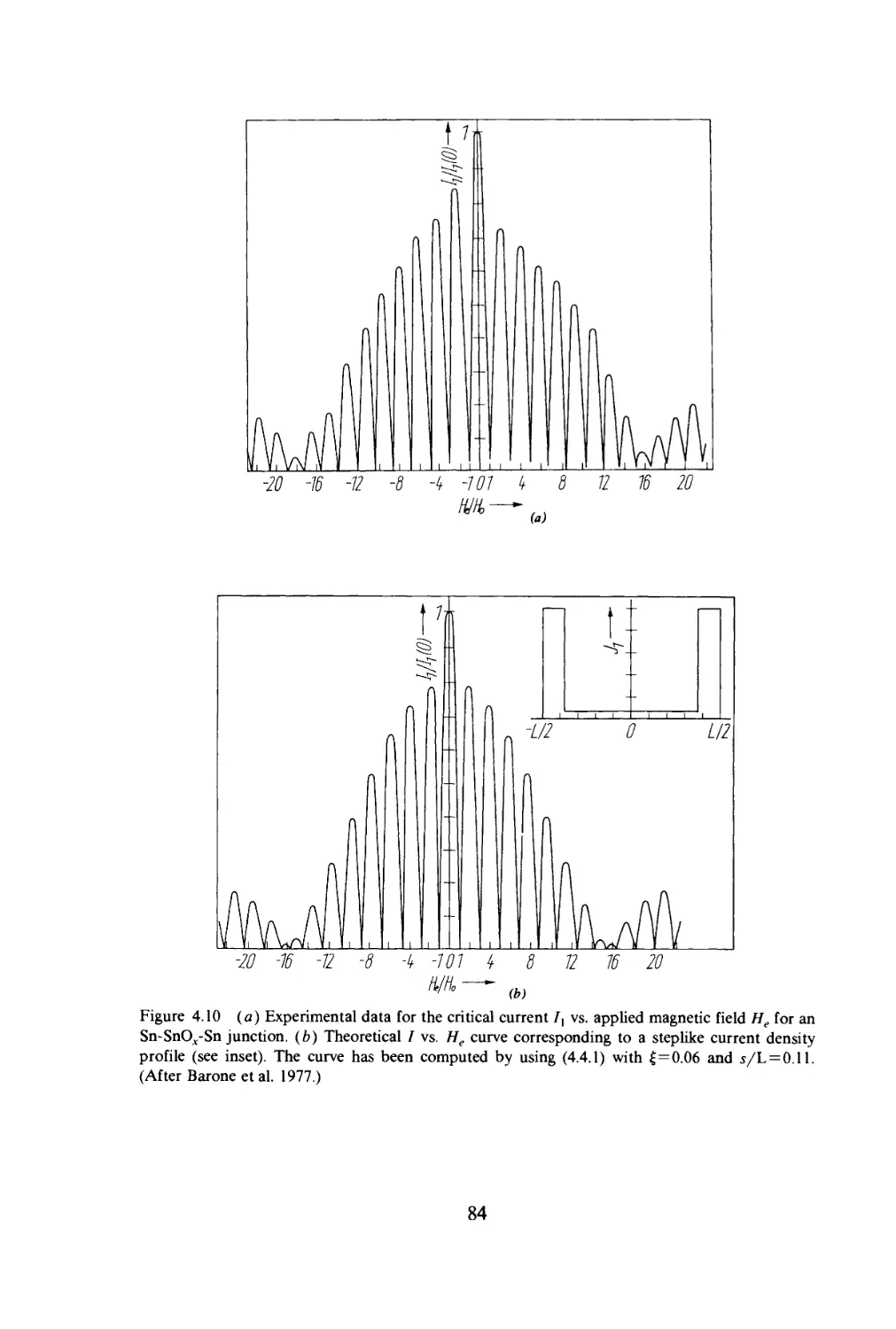
Fraunhofer-like diffraction pattern (see Fig. 1.10a). The first observation of
this effect was made by Rowell A963). It is interesting to consider the close
analogy with optical diffraction phenomena produced by a slit of the same
shape as the barrier.
SEC. 1.5
MAGNETIC FIELD EFFECTS
17
-500 -400 -300 -200 -100 0 100 200 300 400 500
Magnetic field (milligauss)
(b)
Figure 1.10 {a) Experimental magnetic field dependence of the maximum Josephson current for
a Nb-NbOx-Pb junction. (Barone and Paterno, unpublished.) (b) Experimental trace of the
maximum d.c. Josephson current for a double junction configuration like that shown in the inset.
The field periodicity is 39.5 and 16 m G for A and В respectively. Approximate maximum currents
are 1 тА(Л) and 0.5 mA(B). The junction separation is 3 mm and junction width 0.5 mm for both
cases. (After Jaklevic et al. 1965.)
The analytical expression of the IX(H) dependence is given, in terms of
magnetic flux Ф threading the junction, by (Hy = #)
Sin 77
Фп
where Ф=НЫ and Фо =hc/2e is the flux quantum B.07 X10 ~7 G cm2). Thus
the minima in the pattern occur at values of the magnetic flux which are
multiples of the flux quantum. When two Josephson weak links are connected
18 WEAK SUPERCONDUCTIVITY—PHENOMENOLOGICAL ASPECTS CHAP. 1
in parallel by a superconductive path, effects due to quantum interference can
be observed (Jaklevic et al. 1964a). Such a two "slit" structure is sketched in
the inset of Fig. \.\0b. The relative phase in one junction is related to the
relative phase in the other junction through the magnetic flux enclosed in the
superconducting loop. The total maximum supercurrent resulting from
the interference between the supercurrents in the two links is given by the
expression
/=2/,
COS 77
where Фе is the flux enclosed in the superconducting loop. This phenomenon is
often referred as the "Mercereau effect" (Anderson 1967). The magnetic field
dependence of the maximum supercurrent for a double junction configuration
is reported in Fig. 1.10b. We observe that the interference modulation is in this
case superimposed on the diffraction-like behavior of the single junctions. Let
us observe that the characteristic periodicity involved in this phenomenon is
given by a flux quantum and that, depending on the experimental circum-
circumstances, a rather small fraction of the period can be detected. This extremely
high sensitivity of the Josephson current to the magnetic field is the key point
to many important applications of the Josephson effects. These aspects are
discussed in detail in the following chapters.
1.6 Barrier Free Energy
Let us now make a few remarks on the free energy associated with the junction
barrier. This quantity was evaluated by Anderson A963) on the basis of
microscopic theory; we instead follow here the simple thermodynamical de-
derivation due to Josephson A965). The junction is assumed to have a uniform
tunneling current distribution. We consider two separated systems L and R,
the former containing the barrier, the other not. Furthermore we imagine these
two systems each connected with a current source and assume an equal feeding
current / for both parts. The free energy change due to the work done by the
current generators is
dFL=IVLdt and dFR=IVRdt
so that the energy associated with the barrier itself is
dF=d(FR-FL) = l(VR-VL)dt
VR — VL is the voltage across the barrier, and from the Josephson constitutive
relations A.4.4) and A.4.5) we have
dF= — Ix sin <p d(p
SEC. 1.7 ELECTRODYNAMICS OF THE JOSEPHSON JUNCTION
19
0.
Figure 1.11 Current phase relation J(<p) and barrier free energy/(cp) for a Josephson junction.
Thus by integration the free energy per unit area is
p.
/(Ф)= ~~ у ^icos Ф + constant
The constant is chosen by imposing /=0 for <p = 2«77 (« = 0,1,2) (no
current flowing into the junction). Therefore
where El —hJx/2e.
In Fig. 1.11 are sketched both the dependences of the supercurrent and
the free energy upon the phase. We see that a given value of the current
corresponds to two different values of the phase (for each cycle). The stable
state corresponds to the one of minimum energy.
1.7 Electrodynamics of the Josephson Junction
Assuming nonzero magnetic field in both x and у directions we can write
Эх he y
Зф_ 2е
ay nc
A.7.1)
20
WEAK SUPERCONDUCTIVITY—PHENOMENOLOGIСAL ASPECTS CHAP. 1
These relations together with A.4.4) can be combined with the Maxwell
equation:
с at
which in our case reduces to
Эх ду с
| 1
ЭД
с dt
giving:
he2 /Э2<р 92<p\ .
Л ^H =/Si
Sired
by
dV
where C=er/4irt is the junction capacitance per unit area; er is the relative
dielectric constant and t the dielectric barrier thickness.
Thus using A.4.5) we can write
oyz cz dt
where
and
l/2
he
Sired J i
1/2
A.7.3b)
Equation 1.7.2 wholly governs the electrodynamics of the junction
(Josephson 1965). This equation has the character of & penetration equation as
evident in the stationary limit of small <p(sin<p~<p). In this case in fact it
reduces to a London-type equation; with a one dimensional solution <p~e~x/Xj.
The penetration length Xj gives a measure of the distance in which d.c.
Josephson currents are confined at the edges of the function and for this
reason is called "Josephson penetration depth." It occurs as a consequence of a
current screening due to the magnetic field self generated by the supercurrents
in the junction. It recalls the Meissner-Ochsenfeld effect in a type 1 supercon-
superconductor; however the typical values of the London penetration depths, XL, are
of the order of hundreds of angstroms whereas Xj is of the order of hundreds
of microns. This lower effect of screening is another aspect consistent with the
definition of "weak superconductivity."
SEC. 1.7 ELECTRODYNAMICS OF THE JOSEPHSON JUNCTION 21
As we have mentioned, A.7.2) describes the phenomenology of a
Josephson tunnel junction. An even greater generality can be considered using
the results of the microscopic theory. In fact, taking into account the role of
quasiparticles, it follows (see Chapter 2) that the expression of the current
density is more precisely given by
J=Jx(V)sin<p+[ox(V)cos<p + o0(V)]V
In this relation o0(V)V represents the quasiparticle tunneling current and
ox(V)Vcos(p a quasiparticle pairs interference current. For most cases the last
expression can be well approximated by
J=Jxsin<p +
Therefore taking into account the dissipative term, A.7.2) becomes
Э2<р Э2<р 1 Э2<р p Э<р 1 1л n ..
^ ^^i (L7'4)
where /3=o0/C.
This is a rather complicated equation for which general analytical solu-
solutions have not been found. It has been widely investigated, and will be
discussed in the following chapters, considering special solutions correspond-
corresponding to specific situations of physical interest.
Let us consider now just the case, first discussed by Anderson A963), of a
spatially independent <p. The general lossless equation A.7.2) reduces to the
ordinary differential equation of the pendulum:
+ co2sin<p = 0 A.7.5)
df
with coj =c/Xj. The resulting oscillations, in the small amplitude limit (sin<p~
<p), occur with a frequency pj=(cj/2'7t which is typically of the order of
109—1011 Hz (as is easily verified by assuming realistic values as c — ^c and
\j ~ 100 fim). This situation is characterized by the same phase value all over
the barrier, that is the magnetic field is zero and the electric field normal to the
plane of the barrier. Thus we recognize that such oscillations have the peculiar
feature of longitudinal plasma waves (Josephson 1965, 1966). These plasma
oscillations come from a pulsating interchange of energy between the barrier
and the electrostatic energy terms: hJx{\ — cos<p)/2e and jBenJ/C. This new
excitation, the Anderson plasmon, was observed first by Dahm et al. A968).
From the explicit expressions of с and \j A.7.3a,b) we have
с BeI,V/2
со, = т— =[
he
Here /, and С are the total pair current and the total capacitance respectively.
22 WEAK SUPERCONDUCTIVITY—PHENOMENOLOGICAL ASPECTS CHAP. 1
Figure 1.12 Dispersion relation « vs. к for a
Josephson junction in the limit <p -> 0. «y is the
value of the plasma frequency for zero current
к and in the absence of magnetic field.
We observe that the relatively low frequency of this collective mode is
related to the small density of charge carriers in the barrier (peculiar to weak
superconductivity). Since the value of coy is below the cutoff frequency of the
plasma mode in the superconductors the oscillations are confined within the
barrier.
In the limit of small variations about the value <p = 0 we can consider
solutions of A.7.2) of the form <p~eJ'(wt~kx\ The resulting dispersion relation
between со and к
is sketched in Fig. 1.12. Therefore coy represents the lowest frequency which
allows the propagation of electromagnetic waves inside the junction. In terms
of circuit parameters the characteristic plasma frequency is given by
coj = \/{LC where L—h/2elx is the equivalent inductance of the junction in
the zero current limit. The expression of coy just derived is strictly valid only in
the limit of zero Josephson current. As we see later (Section 11.6) the
equivalent inductance (and therefore the plasma frequency) is a function of the
total supercurrent flowing in the junction and of the applied magnetic field.
Detailed experimental measurements on the plasma frequency have been
performed by Pedersen, Finnegan, and Langenberg A972a,b). These authors
have experimentally confirmed the existence of the quasiparticle-pair inter-
interference term (see Section 2.6). Experimental and theoretical investigations on
nonlinear effects on the plasma resonance have been performed by Dahm and
Langenberg A975).
1.8 Other Josephson Structures
As we have seen, for the occurrence of the Josephson effect it is necessary that
the two superconductors be weakly connected by some means. In thin film
SEC. 1.8
OTHER JOSEPHSON STRUCTURES
23
junctions the quantum mechanical tunneling considered so far realizes this
circumstance. However other configurations of weakly coupled superconduc-
superconductors can be considered, such as those sketched in Fig. 1.13. The first one (Fig.
1.13a) is called the "Dayem bridge" (Anderson and Dayem 1964) and consists
of a single superconducting layer in which two regions are linked by a very
narrow (~ 1 fim or less) constriction. The condition required for the coherent
transmission of Cooper pairs from one region to the other is roughly given by:
L<? where L is the maximum dimension of the link and ? the coherence length
of the specific superconductive material. It is worth pointing out that this
condition can be satisfied or not depending on the operating temperature since
| is a temperature dependent quantity. In the last few years significant progress
has been made on these superconducting links regarding both the development
of a sophisticated technology and theoretical approaches which account for
their behavior. A different kind of film bridge structure has been designed by
Notarys and Mercereau A969). In this case the superconductivity in the bridge
region is "weakened" by a proximity effect due to a superimposed normal
metal layer. This allows the making of larger bridges and reduces the problem
of the geometrical definition (Fig. 1.13b). To date the most promising bridge-
type weak link is represented by the variable thickness bridges (see Chapter 7).
Superc.
point
Superconductor
Superconductor
Constriction
Substrate
(b)
Flat superconductor
(c)
Superconductor
Nb wire
(d)
Wires
Figure 1.13 Different Josephson structures, (a) Dayem bridge, (b) proximity effect bridge, (c)
point contact, (d) Clarke solder blob, and (e) crossed wire weak link.
24 WEAK SUPERCONDUCTIVITY—PHENOMENOLOGICAL ASPECTS CHAP. 1
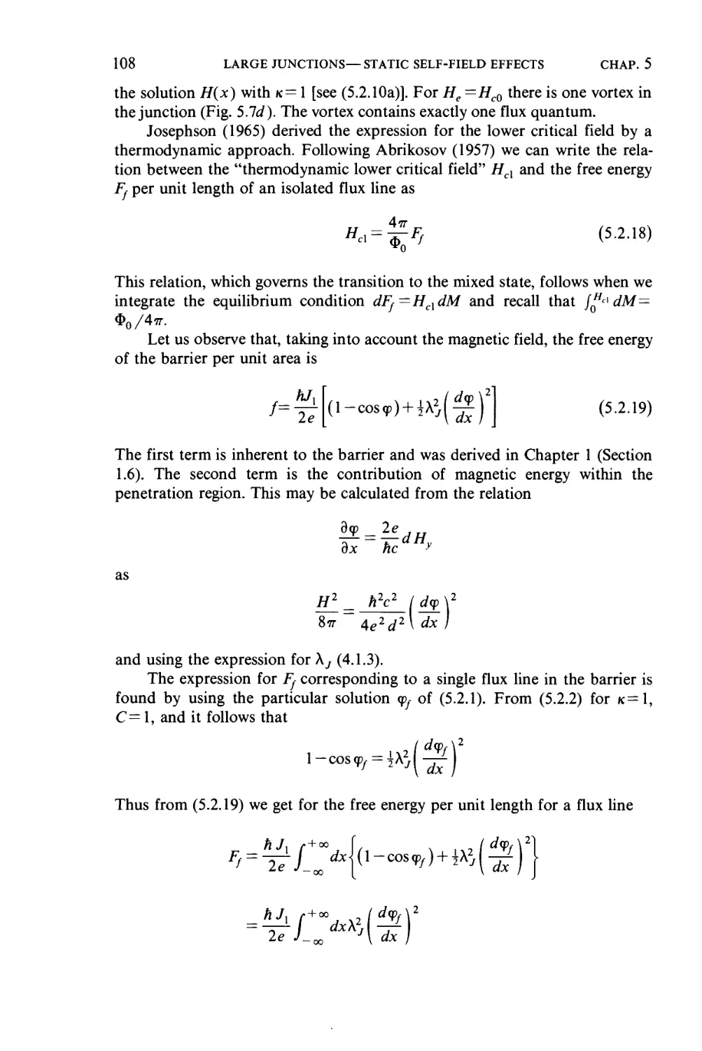
Another structure of importance is represented by the "point contact"
junction (Zimmerman and Silver 1966a; Levinstein and Kunzler 1966). In this
case, a very fine superconducting point is pressed onto a flat superconductor as
in Fig. 1.13c. It is possible either to establish the link by a direct metal contact
between the point and the superconducting layer or to make the contact with a
point previously oxidized. In the latter circumstance a structure is realized
which falls more properly in the category of tunneling-type junctions. More
likely intermediate situations will occur in which the conductance is provided
by both mechanisms. In both cases the adjustment of the point contact
pressure is extremely critical and this represents in some sense both the
advantage (adjustability) and the limit (mechanical instability) of these links
over the other structures.
In Fig. 1.13d, e "crossed wire" weak link proposed by Pankove A966) and
the "solder blob" investigated by Clarke A966) are illustrated. The latter,
however, usually behaves as a double junction. It is useful at this stage to make
a remark on the nomenclature of the various Josephson structures. It is
possible to cover with the definition of "weak links" all kinds of weak coupling
between superconductors including tunneling junctions, Dayem bridges, and
so on. More often however in the current literature the term "weak link" is
intended only for those structures in which the link is not realized by tunneling
effect. Here we adopt the expression "weak link" in the more general sense
and, whenever necessary, specify the particular structure with which we are
concerned.
Finally we remark that other materials rather than dielectrics can be used
as barriers in Josephson junctions. The weak coupling can be realized by
employing semiconducting layers having thicknesses of a few hundreds of
angstroms or metal layers with thicknesses of the order of a few thousand
angstroms.
The structures briefly mentioned here are discussed in Chapter 7 and 8 in
more detail.
CHAPTER 2
Microscopic Theory
In his original work Josephson A962a,b) developed the microscopic theory of
the superconductive tunnel junction taking into account also pair transfer
across the barrier (see also Anderson 1963). He used the transfer Hamiltonian
formalism suggested by Bardeen A961) and by Cohen, Falicov, and Phillips
A962). Later it became evident that the Josephson effect could occur also in
other kinds of superconducting weak links. However, to date the tunneling
structure seems to be the only one for which there is a complete description in
terms of a microscopic theory.
In the present chapter we discuss the basic aspects of the microscopic
theory for a Josephson tunneling structure following, basically, the approach
given by Ambegaokar and Baratoff A963). The tunneling process is described
by time dependent perturbation theory which involves a properly defined
coupling Hamiltonian between the two superconductors.
There exist various excellent articles which consider different theoretical
approaches. We recall, among others, the derivations due to De Gennes A963)
and Josephson A965, 1969). More recently, a theoretical analysis of
the tunneling process that avoids the limitations inherent in the transfer
Hamiltonian has been developed by Caroli et al. A971a,b 1972) and with a
greater generality by Feuchtwang A974a,b, 1975, 1976) in several extensive
papers. The theory developed by Feuchtwang has been extended to supercon-
superconducting junctions by Arnold A978).
Finally we mention the general approach based on the boson method in
superconductivity (Leplae, Mancini, and Umezawa 1970; Leplae, Umezawa,
and Mancini 1974).
2.1 Tunneling Hamiltonian Formalism
From a quantum mechanical point of view a tunneling junction is usually
described by the following Hamiltonian (Cohen, Falicov and Phillips 1962):
%=%L+%R+%T B.1.1)
Here %R and %L are the complete Hamiltonians of the right and left metal
respectively which commute with the particle number of operators NL and Л^
25
Physics and Applications of the Josephson Effect. A. Barone, G. Paternd
Copyright © 1982 by John Wiley & Sons, Inc. ISBN: 0-471-01469-9
26
given by
MICROSCOPIC THEORY
qa qa
CHAP. 2
B.1.2)
k,a
q,a
%T is the tunneling interaction term which transfers electrons from one metal
to the other:
B.1.3)
kqa
where ckha(ck a) creates (destroys) one electron with momentum к and spin a in
left metal; dq+a (dqa) creates (destroys) one electron with momentum q and spin
о in the right metal. For clarity we refer to Fig. 2.1. Tkq is a matrix element
connected to the transition probability for an electron from a k-state on the
left to a q-state on the right. Making the W.K.B. approximation and neglecting
the energy dependence of the tunneling probability, one finds that
|T
kq|
U and t are the height and the width of the barrier: kz and qz are the
components of the momenta к and q normal to the barrier. The Kronecker
symbols account for the conservation of the momentum parallel to the plane of
the barrier. As long as one considers voltage up to a few mV (the scale fixed by
the energy gap of typical superconductors) and the ratio of the tunneling
currents obtained with electrodes in the normal or superconducting state, this
approximation is justified.
Let us make a few remarks about the expressions B.1.1) and B.1.3). The
possibility of writing the total Hamiltonian by adding the Hamiltonians of the
two noninteracting metals plus the interaction term %T implies the existence of
a set of single electron wave functions <pk and xq for the left and right metal
respectively. Such functions should have the following properties: as a first <pk
and xq should form together a complete orthonormal set and, on the other
hand, the wave function for an electron in the left (right) metal should be
expressed only in terms of the <pk's (xq's). Unfortunately these two require-
requirements cannot be simultaneously satisfied. However it is possible to proceed in
the following way. The states <pk(xq) are defined by assuming that the barrier
HL
HR
©
-V(t)
О
Figure 2.1 Schematic of a tunneling junction. %L
and %R are the left and right Hamiltonians for the
two superconducting electrodes. %T is the tunneling
Hamiltonian c^ and dq are a creation and an
annihilation operator for an electron in the left and
right metal respectively.
SEC. 2.1 TUNNELING HAMILTONIAN FORMALISM 27
extends to + oo(— oo) (Bardeen 1961). With this assumption the <pk's and xq's
possess an exponential tail in the barrier region and are not orthogonal.
Therefore the ck and dq operators do not commute in a rigourous sense. As
discussed by Prange A963) under the assumption of specular tunneling be-
between states of equal energy the anticommutation relations {ck, dq] = (ck, dq]
=0 may be assumed to hold to the lowest order in %T.
The expression chosen for the tunneling Hamiltonian B.1.3) neither takes
into account the occurrence of processes involving "spin-flip" (coupled crea-
creation and annihilation operators of equal spin) nor of tunneling processes
accompanied by absorption and emission of energy (ckadqa act at the same
time, that is, the tunneling occurs instantaneously). Furthermore, time reversal
symmetry implies
T-k.-q = Tk,q B.1.4)
Let us consider now a voltage V(t) applied to the junction such that the
left electrode is positive with respect to the right one (Fig. 2.1). Assuming that
the voltage drop occurs entirely across the barrier, the two Fermi levels, /iL and
jar will be relatively shifted by [xL—[xR = —eV^ This situation can be de-
described assuming an additional energy for the electrons on the left side. Thus
the Hamiltonian of that electrode will be
%L(V)=%L@)-eVNL
where NL is given by B.1.2).
Let us denote by cka(t) and cka(t) the destruction operator of an electron
in the left metal for V=0 and V^O respectively. In the Heisenberg representa-
representation the equations of the motion for these two operators are
ф evcka(t)
Therefore (Rickayzen 1965):
ha(t) = eJ2<ncka(t) B.1.5a)
where
dw 2e
B.1.5b)
The tunneling current I(V,T) for DOK and V^=0 is obtained from the
*e= e is the absolute value of the electron charge.
28 MICROSCOPIC THEORY CHAP. 2
expectation value of the rate of change of the electron number of operator NR:
I(V,T)=-e(NR) B.1.6)
where NR is the time derivative of NR and the positive direction for the current
is assumed from the left to the right (Fig. 2.1). The expectation value is defined
as
{ R>
where % is the total Hamiltonian for the system, kfi is the Boltzman constant,
and Tr{ } denotes the trace of the operator inside the brackets.
From the equation of the motion for NR we have
since NR commute with %L and %R. The expression B.1.3) for %T yields
NR(t)= j. [TkqCkV4a -Тк*ч<Аа] BЛ.7)
where we have used the commutation relations
[dq+adqa,dqa] = ~dqo; [dqodqo, dq+o] =dq+o
which follow from the anticommutation relations for ck, dq. Inserting B.1.7) in
B.1.6) we get for the tunneling current
qq] B.1.8)
kqa
where we have taken into account that
The expression B.1.8) is easily evaluated (Ambegaokar and Baratoff 1963) to
the first order in %T (linear response in %T). Since the term %T in the
Hamiltonian is considered as a perturbation, it is convenient to use the
interaction representation in which the time dependence of the operators is
determined by the unperturbed Hamiltonian %0=%L(V) + %R, whereas the
time evolution of the eigenstates is determined by the perturbation term %T.
SEC. 2.2 GENERAL EXPRESSION FOR THE TOTAL CURRENT 29
To first order in %T:
where tj-»O + , that is, tj tends to zero through positive values; the time
argument of %T indicates that this operator is taken in the interaction
representation. Here \\p(t)) is an eigenfunction of the total Hamiltonian
%=%0 +%T; \ф(оо) is an eigenfunction of the unperturbed Hamiltonian %0.
The factor eVT implies that the perturbation is "turned on" adiabatically
starting from t— — 00. In this approximation relation B.1.8) becomes
kqo
where the symbol ( >0 denotes an expectation value referred to the unper-
unperturbed Hamiltonian %0. The first term of this expression vanishes since it
represents the current when %T is zero. Thus
B.1.9)
kqo '-°°
Inserting B.1.3) in the last expression we obtain
T- ~2e r» V т П J vt(
I-—rRe 1 Tkqj dre*{
п kqo "'-oo
k'q'o'
2.2 General Expression for the Total Current
We may use the relations B.1.5) to extract the dependence on V(t) and write
the last expression
B.2.1)
where the two functions S(t—т) and R(t — т) are defined as follows
30 MICROSCOPIC THEORY CHAP. 2
(Rickayzen 1965):
kqa
k'q'a
>о} B.2.2а)
" kqa
k'q'a'
-<4a'(T)^@>o<^04,v@>o} B.2.2b)
where 0(x) is the step function defined as в(х)= 1, x^O; 0(x) = O, x<0. Let
us observe that the factorization is exact, since the expectation values are in the
unperturbed ensemble (Hamiltonian %0 =%L +%R) that is, they refer to the
two electrodes separately. If we consider these electrodes as two infinite
homogeneous superconducting metals, in S(t — т) only the diagonal terms
(k = k',q = q') are different from zero.
Introducing the single particle Green functions (Kadanoff and Baym,
1962)
G>(k,T-t)=-j(ck(T)ct(t)); G<(k,T-0=X<-k+(>K(O>
The function S(t — т) can be written as
k,q
where the summation over the spin has been performed, using the property
(скт скт ) = (cki cki )• In tne expression of R(t — т), only the term for which
к = —к, q'= —q, a'— —a which describes B.C.S. pairing in bulk supercon-
superconductors is kept. In terms of the anomalous (pairing) Green functions intro-
introduced by Gor'kov A958):
SEC. 2.2 GENERAL EXPRESSION FOR THE TOTAL CURRENT 31
— t) becomes:
" kq
-F<(k,/-T)F>(q,T-/)}
where the summation over the spin has been performed and the relations
F^ = — F^ ¦ F ^ = — F ^
ГП r IT ' r IT rU
have been used.
Let us introduce the Fourier transform of the Green functions:
, to), F^(k, to), F^(k, <o) defined by
> 1 f +
2irJ-.
and the corresponding spectral functions
, to) = ± e -^?L(k, to)/ ±( to
where
/±(co) = (^^ + l) and /+(<o)=l-/-(<o)
with ^т = 1/квГ. In the expression for F^ and F^ we have taken out
explicitly the phase factors in the spectral functions Z?(k, to) (Rickayzen 1965).
These phase factors have been factorized because otherwise the spectral
functions BR, BL are proportional to the complex superconducting order
parameter Дл on the right side and its conjugate Д* on the left, respectively.
2.2.1 The Total Current Expression in the Time Domain. Let us now
make the change in the variable
t' = t~T
Expression B.2.1) becomes
{/•+00 r
e -Л*@]/2 f dt'e^-'')[e^'-''^2S(t')
U B.2.3)
32 MICROSCOPIC THEORY CHAP. 2
where we have defined:
the two functions S(t) and R'(t) can be expressed in terms of the real spectral
functions introduced above:
kq
B.2.4a)
* kq
X Ял(я, «')[/-(«')-/ "(«)] 1 B.2.4b)
The phase factor e~j(<PL~'f>R) which appears in the expression of R(t) has been
introduced in the present derivation in a rather formal way. However, the
physics underlying this quantity deserves more attention. Let us recall that a
second order transition implies the appearance of a new ordered state
characterized by a reduction in symmetry; that is, the system goes into a
state which does not exhibit the full symmetry properties of the original
Hamiltonian. A convenient example to clarify this concept of broken symme-
symmetry is represented by the ferromagnetic transition. The ground state of an
isotropic ferromagnet corresponds to a situation in which all the spins are
aligned in the same direction. Thus the system has lost the rotational symmetry
which is present in the Heinsenberg Hamiltonian. The ensemble of all the
states of reduced symmetry is called a restricted ensemble. In the case of a
superconductor, the situation is less obvious. The symmetry property which is
broken in that case is local gauge invariance. That is, the phase of the order
parameter cannot be changed arbitrarily at each point since a chosen value at
one point fixes the phase at all other points. An excellent discussion of the
relation between the concept of broken symmetry in superconductors and the
Josephson effect is due to Anderson A963). From a given restricted ensemble,
we can generate another one by applying a unitary transformation that leaves
the Hamiltonian invariant. For a homogeneous superconductor: such a trans-
transformation is given, for instance, by ejN(p where N is the number operator (the
total number of electrons) and <p is a real constant. It leaves the Hamiltonian
invariant because the Hamiltonian commutes with the operator N, but changes
the wave functions by a constant phase factor. This factor is different for states
SEC. 2.2 GENERAL EXPRESSION FOR THE TOTAL CURRENT 33
with different numbers of particles. It is easy to see from the definitions of the
Green functions G^ and F^, that the transformation ejN<p leaves the G's
invariant because ckck and dqd^ couple states with the same number of
particles. On the other hand we have
because ckc±k and ckc_k couple states of different number of particles (two
particles).
Therefore under this transformation we have
F(k,t)-*e2j<pF(k, t)
Thus each restricted ensemble is characterized by a different value of the factor
е2]Ц>. For a single superconductor one can always choose <p=0; but this simple
assumption is too restrictive when, as in a junction, we consider two different
superconductors coupled together. In that case, it is, in fact, imperative to keep
the phase factors eJ<PL and eJ<PR corresponding to the two superconductors
although measureable properties can only depend on the phase difference
<Pl~<Pr-
2.2.2 The Total Current Expression in the Frequency Domain. Introduc-
Introducing the spectral decomposition (Werthamer 1966):
+ oo A(л
~ W(io)e~Ju" B.2.5)
-oo 27Г
and the Fourier transform of 5@ and R'(t)
/+00 f + 00
dtS(t)eJiOt; R'(u)= dtR'{t)ejult
-oo — oo
expression B.2.3) becomes
f r + 00 /-+00 ,
l(t)= Im I / doo I dco'\W(co)W*(co')e~^w~w''S(jT} — co')
17—»0+ v*' —00 "' — 00
B.2.6)
where a=<pL—<pR. Referring to Chapter 1 (Section 1.4) we observe that here
<pL — <pR accounts for the time independent part of the relative phase. Let us
34 MICROSCOPIC THEORY CHAP. 2
assume that the coefficients in the expansion B.2.5) are real. This condition is
satisfied in the cases of physical interest that we shall consider later on. From
the expression B.2.6) it follows:
+OO /. + 00
/+OO /. + 00
dw \ dw'W(w)W(to'){f / (<o')cos(«-«')/
-oo •'-oo
-/9Pi(<o')sin(<o-<o')/]
+ [IJ2(o>')cos(a + (o> + o>')t) + IJ](o>')sin(a + (o> + u>')t)]} B.2.7)
where we have defined
„,(«) = Re+S(yi|-«)
17—»0
IJ2(a)= Im R'(jii + a)
O +
/,,(«) = -Re/?'(/4 + u) B.2.8)
17 —0
Therefore in the presence of a time varying potential V(t) both real and
imaginary parts of S(co) and R'(co) contribute to the expression for the time
dependent current I{t). Since S(t) and R'(t) are both real and vanishing for
t<0 the following relations hold:
Furthermore as it has been pointed out first by Werthamer A966) the real and
imaginary parts of S(<o) and R'(oo) are correlated by the Kramers-Kronig or
dispersion relations (Mathews and Walker 1965):
, x 1 r + oo ImS(co')
ReS(<o)=-P/ du'—-r^-!-
ImS«=--P| du'—^—^ B.2.9)
Analogous relations can be written for Re/?'(w) ап(* Im R'(co)? In the case of
slow varying or constant voltage applied the term IJ2{u>) gives no contribution
(Larkin and Ovchinnikov 1966). The case of constant voltage is considered in
detail in the sections that follow.
tp indicates the principal part of the integral.
SEC. 2.4 EXPRESSIONS OF Iqp[, Iqp, /yl, Ij2 35
2.3 Tunneling Current for Constant Voltage
Let us assume V{t)= Vo = constant. In this case:
where ay =Be/h)V0. From B.2.5) it is easy to see that the Fourier coefficients
are now
Therefore expressions B.2.6) and B.2.7) become
(^)} B.3.1)
and
In(V0,T)sin<p(t)+IJ2(V0,T)cos<p(t) B.3.2)
where <p(t) = a + co^t and the dependence of the coefficients on the voltage bias
and the temperature has been explicitely indicated. Thus the total tunneling
current results from three different contributions. Iqp is related to S(t) and
therefore represents the quasiparticle tunneling. The phase dependent terms IJX
sin<p and IJ2cos<p are connected to R(t) and describe processes in which phase
coherent tunneling of Cooper pairs occurs. As will be soon apparent, / =Iji
= 0 if Fo=0, and the only nonvanishing contribution to the total current is
given by /yi@, T)sin<p which represents the d.c. Josephson current. If F^O the
phase dependent terms describe a.c. currents of frequency cof =2(e/h)V0. If we
introduce the conductivities defined by
°i(Vo>T)Vo=IJ2(Vo,T); o0(V0,T)V0=Iqp(V0,T) B.3.3)
B.3.3) can be written as
I(t,V0,T) = IJ](V0,T)sm<p(t)+[a](V0,T)cos<p(t) + a0(V0,T)]V0
B.3.4)
This is the expression of the total current as presented for the first time by
Josephson A962).
2.4 Expressions of Iqp (, Iqp, /yx, IJ2
In this section we derive explicit expressions for the different contributions
B.2.8) in the case of a constant voltage bias Vo applied to the junction. In
order to do this it is necessary to calculate the Fourier transforms of the
36 MICROSCOPIC THEORY CHAP. 2
quantities S(t) and R'(t) defined by B.2.4). Assuming specular transmission,
integrating over the components of к and q parallel to the plane of the barrier,
and neglecting the energy dependence in |Tkq|2, expressions B.2.4) can be
written as
+ 00 /.+ 00
L
+ 00 /- + 00
/
fc /.+ 00 /- + 00
«'<')=*('W-.'•/-.."
C tCd~?e~i{
x (C
where we have defined
r =
N
NR@) and jVl(O) are the densities of states at the Fermi level in the right and
left metal respectively. We have omitted the minus sign in the Fermi functions.
Following Baratoff A964) we introduce the quasiparticles and pair densities of
states:
o>) B.4.1)
The expressions of S(t) and R'(t) become
0(t) h r + oo r + °°
S(t)= -j-^- А Г daj da'e*«-«'»nL(a)nR(
+ <»
B.4.2)
SEC. 2.4 EXPRESSIONS OF Iqpi, Iqp, /,,, Ij2 37
2.4.1 The Quasiparticle Terms Iqp,I We have to compute the
Fourier transform of S{t) inyrj - ay/2 for tj -» 0+. Defining <oo = ay/2, it is
+ 00 . /.+ 00
diC
• + 00
X /
Since
¦ + 00
and
lim —^~ = p\-\+j7T8(x) B.4.3)
where P indicates the principal part of the remaining integral, we obtain
fe ( л + ОО /. + 00
5 (Уч-ыо)=—— P/ rfco/ ^'п^ы)пл(ы')[/(ы)-/(ы')]
/+ 00 J. + CC
dco I dco'8(co — со' — oo0)nL(u))nR(co')[f(w)— /(w')
- oo •'— oo
That is,
TTeRN
«)-/(«')] B.4.4)
+ 00
^)()()-/(ы-ы0)] B.4.5)
Note (Werthamer 1966) that Re S(yTj-<oo) diverges for <oo ->0(Vo ->0). This
can be understood by realizing that the real and the imaginary parts of
S(JT} — <oo) are connected by the Kramers-Kronig relations B.2.9) and that Iqp,
the quasiparticle current, increases linearly with <oo for <oo -> oo. To overcome
this problem we can define S{jt\ — <oo) by subtracting [ReSO'rj — wo)]«o=o-
This does not affect the quasiparticle current since it is only related to the
imaginary part of S(jt} — <oo).
38 MICROSCOPIC THEORY CHAP. 2
The expression B.4.5) is analogous to that derived within the phenomeno-
logical theory (Section 1.3).
Let us apply B.4.5) to the case where both junction electrodes are in the
normal state. In this situation:
/
Then
+ 00
+ 00
Jqp = INN = ~ ТБ- /
Actually, since
/•+00
and
we get
*NN
Therefore the constant RN, defined at beginning of the section, can be
interpreted as the resistance of the junction when both metals are in the
normal state. Such an ohmic behavior was also obtained by the simple
approach of Section 1.3.
2.4.2 The Phase Dependent Terms In and IJ2. Let us calculate the
Fourier transform of R'(t) in (./tj + <oo). From expression B.4.b):
+ 00 /-+00
WWf du>
/+ 00
/+
-
Proceeding as in the preceding section, we arrive at
h i r+QO /• + <» p r (to) p n( to'
)% P/ d f d'FLy ;RK
ireRN
i r+QO
P/ da
/+00 /- + 00 1
da / da' 8( to - to' - <oo )/?L( со )/?л( to') [ /(to') -/(to)] [
-oo •' — oo J
SEC. 2.5 TUNNELING CURRENT IN THE B.C.S. APPROXIMATION 39
Thus from B.2.8):
In = -
7J—> 00
ireR
N " -
«')-Л«)] B.4.6)
IJ2= lm
7)-»0
Let us remark that the expressions B.4.4), B.4.5), B.4.6), and B.4.7) for Iqp,
IqpX, /,,, and IJ2, respectively, hold in general even when strong coupling
effects are included. In fact we have not made any specific restriction so far on
the expressions for n(co) and p{o>). The case of the B.C.S. approximation is
considered in the next section. A few general comments on the different
contributions of the total current are in order. The term /yisin<p describes the
coherent tunneling of pairs. The resulting d.c. and a.c. Josephson effects are
illustrated in Figs. 1.7 and 1.8.
What is the meaning of the cos<p term? If we compare B.4.5) with B.4.7)
we notice a close analogy; while B.4.5) contains the quasiparticle densities of
states, B.4.7) contains the "pair densities" p(co). As already observed, both
terms, Iqp and IJ2, vanish for V— 0. It is possible to interpret the term IJ2cos<p
as describing a quasiparticle tunneling process which involves a concomitant
destruction and creation of pairs on different sides, therefore involving phase
coherence effects. Let us again observe that the expression of R(t — т), from
which both the sin<p and cos<p terms are derived, includes only terms like
скт(О^чт(Ос-к1(т)^-€ц(т) which manifestly describe such events. The
meaning of this term becomes more apparent if the transformation from
electron operator to quasiparticle and pairs operators is performed (Stephen
1969a).
2.5 Tunneling Current in the B.C.S. Approximation
For convenience let us summarize the expressions obtained for the various
current terms derived in the previous sections:
B.5.1b)
'IV'-
40
MICROSCOPIC THEORY
CHAP. 2
fc л + ОО
1
B.5.1с)
where o)o=eVo/h; the energies are referred to the Fermi levels and are
measured in units of h.
In the B.C.S. approximation:
",-(«)=
I со I
2_Л2
/со2-Д'
¦0(\a\-\bt\)
B.5.2а)
2_Л2
/со2-Д
Д, is the energy gap and
=l for x>0
0 for
x>0 sgn(x)= !
x<0 g ЩХ) -1
i = L,R B.5.2b)
for x>0
for x<0
These expressions are plotted in Fig. 2.2. For T=0 Werthamer A966) has
obtained analytical expressions in terms of elliptic integrals using the exchange
of variables (Anderson 1963):
e,=ALsinh?
where е,=у<о2— A2L and e2 = /co'2— Д2Л . In the case of a junction with
identical electrodes, AL=AR=Ahis expressions reduce to
К(х)
-К(х)
X V
х2-1
2xE
sgn(w0)
--K
B.5.4a)
B.5.4b)
B.5.4c)
SEC. 2.5 TUNNELING CURRENT IN THE B.C.S. APPROXIMATION
41
П(«о)
Figure 2.2 Theoretical energy dependence for the pair density р(оз) and the quasiparticle density
n(w) in the B.C.S. approximation.
where x= |<оо|/2Д and K(z) and E(z) are the complete elliptic integral of
first and second kind, respectively, and modulus z. The expressions B.5.4) are
plotted in Fig. 2.3. For T=0 and eV^* kL + kR, as pointed out by Harris
A974a), Iqp and IJ2 have opposite sign whereas IJX and IJ2 have the same sign.
From Fig. 2.3 the most evident features are the following:
(a)
(b)
|/yi@,0)| = |/У2B Д,0)| = |/„
/y, exhibits a singularity at К=2Д/е. Analytically this arises from K(x)
since K(l)=oo. This singularity, called the Riedel peak after the author
who first pointed it out (Riedel 1964), is connected to the singularity of
the density of states in the superconductor at w = Д. Indeed p(co) has the
same singularity at Д. Harris A974a) suggests that it could be interpreted
as a "resonance" between quasiparticle and pair tunneling.
42
MICROSCOPIC THEORY
CHAP. 2
4.0
3.0
2.0
о 1.0
сГ
о
ts
с
3
1.0
2.0
-
-
/
—х
\
/
1.0
Y
а
/
/
/
шо/2Д
2.0 3.0 4.0
Figure 2.3 Cooper pair term 1л(ы0)(а), quasiparticle-pair interference term IJ2(<>>o)(b), and
quasiparticle term 1др(ш0)(с) computed from B.5.4a, b, c) derived in the B.C.S. approximation
and for T=0. The curves are normalized to //,@,0).
Larkin and Ovchinnikov A966), by a slightly different formalism, have
also derived expressions for the four quantities Ij\,Ij2>Iqp>IqPs similar to
B.5.1). In particular these authors report for IJX and Iqpi, expressions which
involve a single rather than a double integral. In the B.C.S. approximation
their expressions are
doi-
B.5.5а)
h/eR
B.5.5Ь)
0.25 —
_ 0.0
о
t -0.25 —
-0.50
-0.75 —
1
»
'—^ у
t = 0.98 J
К
0.90
/
/
1 1
4=
/0.72У
1
i_
'0.0
1 1
0.5
1.0
1.5
(а)
Figure 2.4 Real and imaginary components of the functions S(w) and Л'(со) in the B.C.S.
approximation for different values of the reduced temperature t = T/Tc. (a) Reactive part Iqp{( Vo)
of the quasiparticle current, (b) Quasiparticle current /9/J(K0). (c) Amplitude of the sine term
/ДО), (d) Amplitude of the cosine term IJ2(VU). The data refer to the case of a symmetrical
junction (Д^ = ДЛ = Д). Ais the energy gap of the superconducting electrodes. (After R. E. Harris
1974a, 1975a.)
43
44
MICROSCOPIC THEORY
T
CHAP. 2
0.0
0.050
0.025 -,
S 0.0
^ -0.25 1—
-0.50 —
-0.75
s—s '
fT
^\
—
—
1
Note
scale
1 1 1
t = 0.98
0.90 _
0.72 _
\°—
0.0
0.5
1.0
1.5
(d)
Figure 2.4 (Continued)
At finite temperatures (T>0) the expressions B.5.1) and B.5.5) must be
computed numerically. Analytical solutions are possible only in limiting cases
(Larkin and Ovchinnikov 1966). To avoid the problem of the singularities in
the calculations, Shapiro et al. A962) introduced a convenient transformation
of the coordinate system. In the same work both numerical values and
experimental data for Iqp{V, T) are presented. Numerical results for identical
0.25
~ -0.25
-0.50
-0.75 —
-—
———
t, = 1.
1 1
Z9
Z5
0.7211
090 ill
—imp
#
i
10
1
1
—
1
0.5
1.0
1.5
(a)
1.0 —
as
*¦
0.0
F)
Figure 2.5 Real and imaginary components of the functions S(w) and R'(u) for a junction with
different superconducting metals (ДЛ = ЗДД). (a) Reactive part IqPl(Vo) of the quasiparticle
current, (b) Quasiparticle current Iqp(V0). (c) Amplitude of the sine term 1Л(УО). (d) Amplitude
of the cosine term //2(*o)- 1\ = Т/ТСК is the reduced temperature (ДL = Д,; ДЛ = Д2). (After
R. E. Harris 1974a, 1975a.)
45
46
MICROSCOPIC THEORY
CHAP. 2
0.25 —
о
~ -0.25
-0.50 —
-0.75 —
0.0
1
—
1 1 I
1 _
t, = 0.98
0.90 —
1
0.5
1.0
1.5
(d)
Figure 2.5 (Continued)
metals (Д^=ДЛ) have been reported by Poulsen A972, 1973a, b) and by
Schlup A973).
An extensive work on the expressions of the total current has been
performed by Harris A974a,b; 1975a). His numerical results are plotted in
Figs. 2.4 and 2.5 for the case of symmetrical (Д^=ДЛ) and asymmetrical
junctions respectively. In the computations the expressions B.5.5)
for IJ{ and Iqpi have been used. In Figs. 2.4 and 2.5 we see that for T>0 both
SEC. 2.6 THE "COS ф" PROBLEM 47
Iqp and IJ2 are nonzero even for eV<LL +ДЛ. In the case AL = Дл = Д (Fig.
2.4), /^ and //2 go to zero with infinite slope as F—>0. In fact for Fo <Д or Г
it can be shown (Larkin and Ovchinnikov 1966) that
_ h A Vo /min(r,A)
¦» /. И ¦» f> 1П
* 4cosh2(A/2)tfir) VI Fo
Therefore in symmetrical junctions the conductances ao(V,T) and a,(F, 71)
defined by the expressions B.3.3) go to infinity when F goes to zero. This
behavior for <xo(F, T) has been experimentally observed by Soerensen A971).
The logarithmic singularity at eV0=AL+AR is still present at finite tempera-
temperature. In real samples this singularity is rounded by gap anisotropy and finite
quasiparticle lifetime. We return on this point in Section 11.2.1 when we
discuss the experimental measurements of the Riedel peak.
In Fig. 2.5a,b,c,d the case of asymmetrical junctions is considered for the
particular situation of Дл@)=ЗД^0). In this case Iqp and IJ2 do not approach
zero for F—»0 with infinite slope, but they exhibit a logarithmic singularity at
eV=LR— AL. The term In(V) shows a jump at eV=LR—LL which, (Harris
1974a), is due to the circumstance that IJX is connected through the Kramers-
Kronig relations to IJ2 which has a logarithmic singularity at eV=LR — AL. As
pointed out by Harris A974a) such a discontinuity in IJX should be observable,
possibly with the same technique used for the Riedel peak, but to our
knowledge this has not been accomplished so far.
At this point it is worthwhile to make a comment on the expression of
/ plotted in Figs. 2.4a and 2.5a. As has been already remarked in Section
2.4.1, ReS(yTj —w0) diverges as too goes to zero. Therefore the quantity that is
plotted in these figures [i.e., expression B.5.5)] is more precisely: IqPi =
limn_0 + {ReS'GTj — озо) — ReSij-q — 0) — ReS(j-q— oo)}. This corresponds to a
choice for the normalization constant such that IqpX goes to zero as F goes to
infinity.
2.6 The "cosqp" Problem
As we have already shown, in the presence of a fixed d.c. voltage bias F the
expression of the total current in a Josephson junction is given by the sum of
three terms:
l(t,V,T) = In(V,T)sm<p(t)+Vo0(V,T)[\+e(V,T)cos<p(t)]
where
and a, and a0 are the conductivities defined by the expressions B.3.3).
48
MICROSCOPIC THEORY
CHAP. 2
Therefore the quasiparticle current contains also a phase dependent term. This
is the so called "cos<p" term, originally predicted by Josephson A962a,b).
More recently the question has been reexamined in several works (Langenberg
1973; Poulsen 1973a,b; Harris 1974a,b; Schlup 1973). It is interesting to
observe that until recently this term has been essentially ignored. The first
experimental observations on the "cos<p" term have been performed by
Pedersen, Finnegan, and Langenberg A972a,b), by measuring the plasma
frequency <oy in a tunneling junction. Since then there has been a growing
interest in the problem (more than 100 papers from 1972 to 1978). One of the
main reasons is that since first experiments the observed value for e, for V and
71—»0, was e~ — 1 while the value predicted by the theory is e@,0) = 1. In Fig.
2.6 numerical data for e(V, T) computed by Poulsen A973a,b) for a symmetri-
symmetrical junction in the B.C.S. approximation are reported. Let us observe in
passing that the curves reported can be obtained from the ratio between the
two quantities displayed in Figs. 2Ad and 2.46. Subsequent experiments
performed by different techniques and using various kinds of samples have
also given a value e@,0)c^ — 1 (Vincent and Deaver 1974; Rifkin et al. 1976;
Falco, Parker, and Trullinger 1973; Nisenoff and Wolf 1975; Halse and
Taunton 1976; Balkashin and Yanson 1976). Measurements of the "cos<p"
term as a function of the temperature very near to the superconducting
transition temperature Tc have been carried out by the group at the Technical
University of Denmark (Soerensen, Mygind, and Pedersen 1977; Pedersen,
Soerensen, and Mygind 1978) and by Rudner, Claeson, and Wahlsten A978).
-0.8 —
-1.0 —
0.2 0.4
0.6 0.8
1.2
1.4
Figure 2.6 The ratio O|(K)/o0(K) for the B.C.S. value of the gap parameter A(T) for different
values of the reduced temperature t = T/Tc; a,/cr0 —> 1 as K—>0. (After Poulsen 1973a.)
SEC. 2.6
THE COS ф PROBLEM
Normalized temperature, T/Tc
49
1.0
0.5
0.0
-0.5
-1.0
0.99 0.97
1 ' 1
" I
[ TI
1 1
0.95
1 1
I
0.93
1 1
—
I l~
250
1000
500 750
Critical current, /c/(//A)
Figure 2.7 The measured cos <p amplitude, e vs. junction critical current or normalized tempera-
temperature. Tc=3.813 ±0.0005 K. (After Soerensen, Mygind, and Pedersen 1977.)
The samples used were tunneling oxide Josephson junctions. Some experi-
experimental data on Sn-SnO^-Sn junctions are reported in Fig. 2.7. By varying the
temperature the values of e change from — 1 to +1. Therefore the microscopic
theory for a tunneling junction that, we have considered in this chapter seems
to predict a sign for the "cos<p" term which is in disagreement with the
experiments. Different theoretical approaches based on the time dependent
Ginzburg Landau theory (Hejgaard, Jensen, and Lindelof 1976; Hida and Ono
1977) which take into account the finite relaxation time of the order parameter
(Deaver, Boone, and Rifkin 1976) have given a negative value for the cos<p
term. Likharev A978) has suggested that by introducing a broadening and a
linewidth in the Riedel peak it is possible to obtain negative values for the
cos <p term. This broadening may arise as a consequence of the finite lifetimes
of the quasiparticles (which leads to an imaginary part for the energy gap), of
gap anisotropy, and of renormalization. Samuelsen A978) starting from simple
functions that approximate the results of the microscopic theory, has intro-
introduced phenomenlogically broadening effects. In this way he has shown that
any value for e@,0) within — 1 and +1 can be obtained, depending on the
degree of broadening. Unfortunately to introduce effects like finite relaxation
time or broadening in the Riedel peak in the microscopic theory, based on the
tunneling Hamiltonian formalism, appears to be a very difficult task. Thus the
sign of the "cos<p" at present is still an unsolved problem in the theory of
Josephson tunneling junctions. Very recently the effect of broadening of the
Riedel peak on the amplitude of cos <p term has been extensively investigated
by Zorin et al. A979).
CHAPTER 3
Magnitude and Temperature Dependence of the
Critical Current
In Chapter 2 the microscopic theory for a Josephson tunneling junction was
discussed. In particular we derived the general expressions for the quasiparticle
terms Iqp and IqpX and the pair dependent terms IJX and IJ2 as a function of
voltage and temperature. We now examine in more detail the expression for
the sin<p term IJX in the zero voltage case. As we know, IJX @, T) is the
maximum d.c. Josephson supercurrent observable in the V-I characteristic of a
junction. Various assumptions about the superconducting electrodes are con-
considered. We begin by assuming that the two superconductors forming the
junction can be described under the simple B.C.S. approximation. In this case
expression B.5.1a) for V=0 reduces to the one computed by Ambegaokar and
Baratoff A963). Further effects due to "strong coupling" and to the presence
of paramagnetic impurities in the superconductors are examined. The mag-
magnitude and temperature dependence of IJX are also investigated in these
situations. Finally, effects that can arise from the presence of paramagnetic
impurities in the barrier are briefly discussed.
3.1 Josephson Current for F=0
Although IJX can be expressed as the single integral B.5.5a) it was originally
evaluated starting from expression B.5.1a) for V=0:
+ 00 /. + 00
j
C.1.1)
where P indicates the principal part of the integral. Separating contributions
from positive and negative frequencies and using the relation/( —<o)= 1 — /(to)
and p( — w)= — р(ы), C.1.1) becomes
/•+00 /- + 00
— P/ du> I doi'pL(o3)pR(o3')
Х|л«)-Д;') + i-M-M 1 C.,.2)
50
Physics and Applications of the Josephson Effect. A. Barone, G. Paterno
Copyright © 1982 by John Wiley & Sons, Inc. ISBN: 0-471-01469-9
SEC. 3.2
B.C.S. APPROXIMATION
51
Let us observe that this expression has been derived without assuming
pure weak coupling superconductors. This formula can be applied in different
situations by choosing for the/?(w)'s the particular expressions that correctly
describe the superconducting electrodes.
3.2 B.C.S. Approximation
Let us consider the case in which the two superconductors forming the
junction can be described by the B.C.S. theory. In the preceding chapter we
reported the expression of р(оз) valid in this case B.5.2b): For w>0:
C.2.1)
/<о2-Д2
By inserting this expression for /?,(<o) into C.1.2) we have
X
+
2<o'/(<o) 2<o/(<o')
C.2.2)
Making the change of variables:
E2 =(o2 =e2
E2 =a>'2 =
do)= —de, =
(O
C.2.2) becomes
2ЛДЛДЯ r°° de, r°o de2
^P/ -r / -~
ireKN j0 hx j0 z2
+
2E2f(Ex) 2?,
C.2.3)
Thus we recover the expression originally derived by Ambegaokar and
BaratoffA963).
Let us consider C.2.3) when T=0. In this case because the Fermi factors
f(E) are zero for ?>0, both second and third terms of C.2.3) give no
contribution and thus
ireRN Jo Ex Jo E2 Ex+E2
C.2.4)
52 MAGNITUDE AND TEMPERATURE DEPENDENCE CHAP. 3
Following Anderson A963) let us make the substitution:
E\ 2 =^L /{C°sh#i 2 el 2 =^L
The integral in C.2.4) becomes
/•+00 f+00
Jo v0 2 AL
which, by the change of variables:
0.+I
and using the relations:
reduces, after the integration respect to v, to the expression
du
•I
To do the integration with respect to v the substitution y = ev has been used.
The last integral can be changed into the standard form for the complete
elliptic integral of the first kind by the substitution cosh2« = jc; C.2.4)
becomes
C.2.5)
where K(x) is the abovementioned complete elliptic integral of the first kind.
If Д^ДЛ using the asymptotic expression K(jc)^7t/2 for jc->0, C.2.5)
becomes
N LR
This approximate expression can be used as long as Дл and AL differ by no
more than a factor 2 or 3. For a symmetric junction, in which AL =ДЛ =Д,
C.2.5) reduces to the exact relation
/,@)=§Jf C.2.7)
This expression is very useful in practice. In fact it allows a ready estimation of
the expected maximum value for the d.c. Josephson current just by looking at
SEC. 3.2 B.C.S. APPROXIMATION 53
the V-I characteristic of the junction. It says that the maximum zero voltage
current is equal to the one at the voltage (v/2)h L/e in the V-I characteristic
when both metals are in the normal state*. Let us observe incidentally that
C.2.7) can be easily obtained from B.5.4a) by taking jc = O. In the case Г>0,
as shown by Ambegaokar and Baratoff A963), the integral in C.2.3) can be
transformed in a sum over the poles of the Fermi function/(?). To show this,
we follow a slightly different derivation. Let us start from the single integral
expression B.5.5a). For zero voltage (<o0 =0) introducing the quantities
n,(co)=? i=L,R
this expression can be written as
/„(О.Г)
h/eRN Jo \
</<otanh „, „ Im
°*t)]
1
/«?(«)-1 i/u*(«)-l
C.2.8)
where the following relations have been used:
l-2/r((o) = tanh| "
2kBT,
and
1 _ \/]/x2-\ jc>1
]jx2 — l —j/y\— x2 x<\
The expression in the right side of C.2.8) is equivalent to (Baratoff 1964)
where the contour Го is sketched in Fig. 3.1. The Fermi function/(z) = (ePz +
I) has poles at zn = ja>n = уGг//?7-)Bл+ 1) with residues — l/j8r where
fiT = \/kBT. Therefore the integral can be computed deforming the contour Го
into the contour Г to include these poles (see Fig. 3.1). Then C.2.8) becomes
(Baratoff 1964)
C.2.9)
tLet us recall that here Д is measured in units of ft.
54
MAGNITUDE AND TEMPERATURE DEPENDENCE
CHAP. 3
i
i
i
<
{
\
г
y»1
(
1
1
1
<
1
1
(
1
JO),
JO),
1
1
\
\
1
1
г„
-J@o
-j<o,
Figure 3.1 The contours Го and Г in the complex z plane. Г encloses the poles of the Fermi
function/(z) at zn = 7B" + \)nkBT. (After Baratoff 1964.)
For AL = Дл = Д the last expression reduces to
IЛ л I — „ п
-l
It can be computed analytically and gives
2kBTJ
C.2.10)
The first experimental results on the temperature dependence of the
Josephson critical current are due to Fiske A964) who investigated Sn-Sn and
Pb-Sn junctions obtaining a substantial agreement with the theory. Similar
agreement was obtained in the results by Yanson, Svistunov and Dmitrenko
A964) on tin-tin samples. Recently, further experiments (Balsamo et al. 1974)
performed with a more sophisticated technique have demonstrated an excellent
agreement with the Ambegaokar and Baratoff theory. In Fig. 3.2 we present
sec. 3.2
B.C.S. APPROXIMATION
55
OS
O.6
O.7
O8
OB
1.O
т/тс
1.0
0.5
0.1
0.2
О 3
0.4
O5
Об
O7
О 8
О.9
1.О
Т/Тс
Figure 3.2 Temperature dependence of the maximum (d.c.) Josephson current, (a) Sn-SnO^-Sn
junction; (b) Sn-SnO^-Pb junction. The experimental data (solid circles) are compared with the
theoretical curves (solid lines) calculated using the Ambegaokar and Baratoff results. The maxi-
maximum error in the data is smaller than the dimensions of the solid circles. (After Balsamo et al.
1974.)
experimental results which refer to (a) symmetric and (b) asymmetric junc-
junctions. The data are compared with the Ambegaokar and Baratoff theoretical
curves obtained as follows. The dimensionless ratio 7,G")//,(()) is obtained
from C.2.9) and C.2.5). Expressing the energy gaps in degrees Kelvin, it is
useful to rewrite C.2.9) in terms of reduced gaps di^ = Д/(Г)/Д/(О) and
temperatures г( = Т/Ты where Tci denotes the critical temperature of either
56 MAGNITUDE AND TEMPERATURE DEPENDENCE
L(T)/L(O)
CHAP. 3
1.O
O.5
O.2
O.4
O.6
O.8
1.O.
Т/Тс
Figure 3.3 Theoretical temperature dependence of the maximum d.c. Josephson current for
junctions with different superconducting electrodes computed by using the Ambegaokar and
Baratoff results, (а) Д,/Д2 = 1.00, Tcl/Tc2 = 1.00; (b) Д,/Д2 = 0.95, Tcl/Tc2 = 0.91; (с) Д,/Д2
= 1.03, Гс1/Гс2 = 0.81; (d) Д,/Д2 = 0.43, Tcl/Tc2 = 0.41. Д„Гс1,Д2,Гс2 are energy gap and
critical temperature of the two electrodes. Data are normalized to the zero temperature critical
current and to TcV (L = l,/? = 2).
electrode (i = R, L):
X
-1 -1/2
/=0,1,2...
This expression can be computed numerically as a function of the parameters
Tci and Д,@). The gaps ratio dt{T) were obtained by polynomial interpolation
of the numerical results given by Muhlschlegel A959). In Fig. 3.3 we present
curves of /,(Г) (normalized) vs. the reduced temperature for different super-
superconducting electrodes. Finally we observe that good agreement with the theory
by Ambegaokar and Baratoff has been found in "some" point contact struc-
structures. For example, we mention the Ta-Ta point-contacts investigated by
Taguchi and Yoshioka A970).
3.3 Strong Coupling Effects
Let us now consider the influence on the critical current value of so-called
strong coupling effects.
SEC. 3.3
STRONG COUPLING EFFECTS
57
A realistic treatment of the electron-phonon interactions in the supercon-
superconductors leads in fact to a complex energy dependent gap in contrast to the
B.C.S. approximation. In this general case the pairing density is given by
C.3.1)
where Д,(<о) is the frequency dependent, complex energy gap. In Fig. 3.4 are
reported the real and imaginary parts of Д(<о) for lead which is a markedly
strong coupling superconductor. The zero voltage current IX(T) can be com-
computed by inserting C.3.1) into C.1.2).
Fulton and McCumber A968) have shown that this expression for a
symmetric junction, can be transformed into
aA0[tanh(A0/2A:gr)l
eRN[ l-A'.(Ao) J
eR,
+00
A2(<o)
(O2-A2((o)
C.3.2)
where
(o) = Re[A((o)];
and Ao is that value of to for which A,(to) =
4.0
3.0
2.0
1.0
о
-1.0
-2.0
-3.0
1
- }\
- \
1
\
1 1
\д2
V
/
1 1
Pb
T/Tc
1 ,
1 '_
-
= 0 —
—
1 i"
10
20
30
40
meV
Figure 3.4 Frequency dependence of the real Д,(со) and imaginary Д2(«) part of the energy gap
for T=0 K. (After Lim et al. 1970.)
58
MAGNITUDE AND TEMPERATURE DEPENDENCE
CHAP. 3
The approximation |Im Д(Д0)|<?:Д0, which is valid for physical systems,
has been used. These authors have performed numerical computations at T=0
К for two superconductors, lead and tin, using for Д(<о) values inferred by
MacMillan and Rowell A969) from an inversion of their measurements of
/ (V). They found for Pb and Sn, respectively, values of 78.8 and 91.1% of
ЧР
the values 7,@) computed using the B.C.S. approximation. For Pb-Pb junctions
Lim et al. A970) have performed both theoretical and experimental investiga-
investigations of the temperature dependence of the Josephson critical current. These
authors have extended the analysis to finite temperature by iteration of the
Eliasberg A962) gap equations at various temperatures using the numerical
data of McMillan and Rowell. In Fig. 3.5 we present their experimental results
for the maximum current density versus temperature (both in normalized
units) together with their theoretical values. The crosses are strong coupling
values calculated from C.1.5); the solid triangles and circles refer to the values
obtained by putting into C.2.4) the B.C.S. Д(Г) and the strong coupling Д(Г),
respectively.
In conclusion, strong coupling among other effects reduces the critical
current, as confirmed by many careful experiments; see for instance, Schwidtal
and Finnegan A970) and Fulton and Dunkleberger A974b) for lead-lead and
tin-tin junctions respectively. The authors of the present book did not find any
reduction other than that predicted by Fulton and McCumber. Recently,
Paley, Wilson and Gayley A975) have reported experimental data on Sn-Sn
junctions which exhibit an unusually high maximum d.c. Josephson current,
namely in agreement with the B.C.S. rather than strong coupling predictions.
0 0.1
777V
Figure 3.5 Plot of the normalized d.c. Josephson current, /,(Г)//,@) vs. reduced temperature
T/Tc. The solid line is the experimental temperature variation observed for Pb-Pb junctions. The
crosses are the strong coupling values calculated from C.3.2). The solid triangles are the
predictions of C.2.10) using the B.C.S. Д(Г), while the solid circles are the result of putting the
strong coupling Д(Г) into C.2.10). (After Lim et al. 1970.)
SEC. 3.4 EFFECTS OF PARAMAGNETIC IMPURITIES 59
3.4 Effects of Paramagnetic Impurities
Another aspect which deserves great attention is the effect on the behavior of a
Josephson junction due to the presence of impurities in the superconductors or
in the tunneling barrier. We begin by discussing the former possibility. To find
the dependence of the critical current on the concentration of impurities in the
superconductor, nt, it is necessary to introduce the Green functions for impure
superconductors whose expressions contain the electron mean free time in the
normal state. Baratoff A964) was the first to discuss the influence of impurities
in the superconductors on the Josephson effect. Nonmagnetic impurities were
found not to affect the Josephson supercurrent. This is in agreement with
Anderson's theorem on dirty superconductors (Anderson 1959) which states
that static properties of the superconductor are unaffected by an external
perturbation that does not break time reversal symmetry (it should also not
produce long range spatial variation of the order parameter (Maki 1969).
Let us observe that this result has an important implication, that is, it
legitimizes the use of C.2.9) [and C.2.10)] for films of thickness comparable
with the superconducting coherence length (Kulik and Yanson 1970).
In the case of superconductors containing paramagnetic impurities there is
an exchange interaction (which breaks time reversal symmetry) coupling the
spin of the conduction electrons with the magnetic impurity spin. The spin of
the impurities polarizes the spins of the electrons and interferes with their
tendency for pair formation in a single state.
In the presence of randomly distributed paramagnetic impurities, the
expressions for л (to) and р(оз), the quasiparticles and pairing densities are
given by
n(<o) = Re — C.4.1a)
[2A2()]'/2
CAlb)
where in lowest Born approximation (Abrikosov and Gor'kov 1960)
^^C.4.2a)
(A2-<o2I/2
C.4.2b)
The relaxation times т, and т2 differ because of the possibility of scattering.
The probability Г of scattering with spin flip is given by Г= \/ts =A/2t,) —
60 MAGNITUDE AND TEMPERATURE DEPENDENCE CHAP. 3
A/2t2). Dividing C.4.2a) and C.4.2b) by <o and A respectively and subtracting
(b) from (a) we get
ДГ
to _ со
A~A
C.4.3)
Thus besides being a function of the temperature Д depends on the concentra-
concentration of magnetic impurities through Г. Higher order effects (Kondo anomaly,
spin fluctuations) as well as correlations between impurities lead to complica-
complications (Maple 1973). Introducing the parameter Z=(F/AJ/3 and substituting
(Fulde 1965):
Equation C.4.3) becomes
or, in equivalent form:
4 лгт 1 i 21 l I w \ l i rz2l 1*4 г, п /^ л л\
Л Ь?-.Л ТЛ — I ~Г" I =TZ/ |"TZ,A Z/—U ^J.4.4^
To find л (со) and р(оэ) this fourth order equation has to be solved for a given
value of Z.
When a complex conjugate solution, 3c, exists the densities/?(со) and л(со)
are different from zero and are given by
' ч COl,l . .
n-=~^ C.4.5a)
4 CA5b)
Equation 3.4.4 can be solved analytically.* An extensive discussion on the way
to find the complex conjugate solution is given by Baker and Paterno A972).
In Fig. 3.6 л (to) and р(оз) are plotted for different values of the parameter
Г/Д. It is interesting to observe that, in the presence of depairing by magnetic
impurities, the density of quasiparticles is different from zero also for values of
*Let us observe in passing that the pair breaking effect of the paramagnetic impurities is analogous
to the one produced by a current flowing into the superconductor and can be treated in the same
way (Fulde 1965; Paterno, Ricci, and Sacchetti 1971).
SEC. 3.4
EFFECTS OF PARAMAGNETIC IMPURITIES
61
/""г/д=1
I \ Г/Л =0.032
д/Д
IK»)
2
/ Г/Д=1
/ \ Г/д = 0.032
1 2 ш/д
b
Figure 3.6 Quasiparticle n(w) and pair^(w) density in the presence of paramagnetic impurities
for two different value of the parameter Г/Д. For Гг*1 the superconductor is in the "gapless"
state.
the energy to lower than Д. The value at which the onset of the quasiparticle
density occurs is given as a function of Г by the expression (Abrikosov and
Gor'kov 1960):
Д(Г, Г))
2/3
3/2
In particular for Г/Дз* 1 the sample enters into the so-called gapless region in
which the energy gap is equal to zero while the order parameter is still different
from zero. With a further increase in Г, that is, in the impurity concentration, a
value is reached at which the superconductivity is destroyed. This critical value
for Г is given by
r = A@,0)
62 MAGNITUDE AND TEMPERATURE DEPENDENCE CHAP. 3
Д@,0) being the order parameter for the superconductor at zero temperature in
the absence of impurities.
To compute the d.c. Josephson current in the presence of impurities, we
have to insert in C.1.5) the densities of pairs pL(o>) and pR(u), evaluated by
using C.4.5b). It is obvious that to solve the integral one has to resort to
numerical computation. The first calculations of the effect of paramagnetic
impurities were made by Вага toff A964) who assumed such impurities to be
present on the left side of an otherwise symmetric junction. Substituting C.4.1)
and C.4.3) into the general expression C.1.1) one finds (see also Kulik and
Yanson 1970).
? Д,G\Г)ДЛ(Г)
w -га I/2
where
—; со„=Bп+1)^вГ
Baratoff A964) also showed how the convergence of such sums can be speeded
up by subtracting the corresponding expression with LL — Дл =0 which can be
expressed analytically in terms of polygamma functions. His results for
/,(Г, Г)//,@,0) are shown on Fig. 3.7a as a function of the reduced tempera-
temperature t= T/Tc@) and the parameterp — ni,/nc = Г/ГС.
In Fig. 3.76 the maximum supercurrent г/=/,(Г,О)//1(О,О), the order
parameter 5 = Д(Г,0)/Д@,0) as well as the energy gap 50=(оя(Г,0)/Д@,0),
computed by the above mentioned author are also shown. The case of a
symmetrical junction with impurities in both the electrodes has been consid-
considered at Г=0 by Kulik A966a) and at finite temperatures by Nam A967a,b).
As discussed above, spin-flip processes reduce the binding of pairs; these
acquire finite lifetime ts which implies Д?=Л/т5; energy levels originate within
the gap which eventually vanishes if &E~oig (see also Claeson 1967). Figure
3.76 implies the existence of Josephson effect also in the region of gapless
superconductivity. In fact we see that when the concentration of paramagnetic
impurities is such that the parameter Г reaches the value 0.912ГС, the gap tog
vanishes whereas the Josephson critical current is still nonzero.
Shiba A968) and Rusinov A969a,b) have extended the theory to the case
of strong exchange interaction between the electrons and the paramagnetic
impurity spins. In this case there are states of energy lower than Д(Г, Т) also
for low impurity concentration; that is, л(<о) and р(оз) are nonzero for w<tog
even for values of Г/Д<§:1. Lo and Nagi have calculated both the order
parameter and the Josephson critical current at finite temperatures in that case
(Nagi and Lo 1973; Lo and Nagi 1974). Figure 3.8 summarizes the main
results of interest. It shows the temperature dependence of the maximum
¦ I. (r.T)/Lfo.o)
(a)
T/TC(O)
1.0
0.5
0.5 0.912 1.0
р=г/гс
Figure 3.7 (a) The temperature dependence of the reduced maximum zero voltage current
/,(Г, Г)//,@,0) for various values of the parameter р = Г/Гс. (b) The dependence of the reduced
order parameter 8 = Д(Г,0)/Д@,0), energy gap 8о = со?(Г,0)/Д@,0), and maximum d.c. Josephson
current /у=/,(Г,0)//@,0) at T=0 К on the parameter p = T/Tc. /,(Г,Г)//,@,0) refer to a
symmetric junction with paramagnetic impurities in one side only. (After Baratoff 1964.)
63
64
MAGNITUDE AND TEMPERATURE DEPENDENCE
CHAP. 3
/,@10)
l.U
0.8
0.6
0.4
0.2
1
——¦ >
--^
4
\
N
1
~
\
n;
\
I—
\
\
\
N
x
\\
^\
\\
, \
1 Л
1
v
\
\
1
4
\
\
\
>
\
1
A)
B)
C)
D)
E)
1)
\
\
|\
1
Г
o.o-
0.2
0.4—
0.6
0.8-
Y
i \
0.0
0.2
0.4
0.6
0.8
1.0
Figure 3.8 Normalized maximum d.c. Josephson current vs. normalized temperature for a
symmetric junction with paramagnetic impurities in both electrodes. Solid line: Shiba and Rusinov
model; dashed line: Abrikosov-Gorkov model. (After Lo and Nagi 1974.)
Josephson current (in normalized units) taking the impurity concentration as
parameter; the dashed curves refer to the Abrikosov and Gor'kov theory.
Experiments on the effect of paramagnetic impurities on the Josephson
current have been performed by Hauser A967). This author, however, instead
of dissolving suitable magnetic impurities in the superconducting electrodes
realized a gapless configuration by proximity effect with a magnetic element.
The samples used were Cr-Pb-PbO-Pb-Cr structures in which, by varying the
lead film thickness, it was possible to vary the degree of depairing and,
ultimately, the critical supercurrent. These experiments however are not con-
conclusive since, as pointed out by the author, the difficulty of making good
quality lead films of thickness less than 800 A did not allow the observation of
marked effects.
We have so far discussed the effect of paramagnetic impurities in the
superconducting electrodes. Let us consider now the effect on the critical
current of paramagnetic impurities localized within the tunneling barrier. The
theory developed in Chapter 2 assumes, among other hypotheses, interaction
Hamiltonian %T, describing tunneling through the barrier with spin conserva-
conservation:
kqo
+^-qac_ka) + hermitian conjugate
To take into account violations of this hypothesis Kulik A965b) approached
SEC. 3.4 EFFECTS OF PARAMAGNETIC IMPURITIES 65
the problem starting from a different phenomenological Hamiltonian given by
in which the two terms
kq
and
kq
describe, respectively, tunneling with and without spin conservation (arrows
clearly indicate spin direction); the matrix elements obey the relations
Akq^A-k-q' ХкЧ—1-к-Ч
implied by time reversal invariance of %T (Anderson 1963). The tunneling
processes through the channels are accompanied by spin reversal which can
occur either through the presence of paramagnetic impurities in the barrier or
as a consequence of the spin-orbit coupling interaction. For the development
of the calculations the reader is referred to the work cited above. We here give
just the final expression of the Josephson current (at T=0) resulting from
Kulik's analysis:
Неге <|Т„|2> (<|TJ2>) is the average of |T^q|2 (|Ту2) taken over the angles
between к and q vectors on the Fermi surface. Since
<|TJ2>-<|TJ2>
<|TJ2>+<|TJ2>
the maximum supercurrent is smaller than the value given by C.2.7).
Other reasons for a reduced critical current are the possibility of tunneling
under conditions of no reflection symmetry of the barrier or of trap centers
present in the dielectric which make the "in" and "out" channels of the
electrons traversing the barrier uncorrelated. These circumstances lead to
T?q=?T_k_q, that is, breaking of the time reversal invariance assumed in the
original expression of %T.
Recently the effect of magnetic impurities localized into the barrier has
been discussed in a different context by Bulaevskii, Kuzii, and Sobyanin
A978).
66 MAGNITUDE AND TEMPERATURE DEPENDENCE
3.5 Measurement Techniques
CHAP. 3
So far we have considered theory and experiments on the magnitude of the
maximum d.c. supercurrent. Let us now discuss some aspects of the experimen-
experimental techniques to measure the Josephson critical current and its dependence on
external parameters such as temperature and externally applied magnetic field.
Usually these measurements involve the observation of the whole d.c. voltage-
current characteristics. The simplest procedure to observe a V-I curve of a
junction consists of a simultaneous record of both voltage and current on an
x-y recorder (Fig. 3.9). In this way one obtains a full V-I curve for a given
value of external parameters (e.g., T or He). Information about the dependence
on these parameters requires iteration of this procedure.
Let us outline another procedure (Lim et al. 1970; Balsamo et al. 1974)
which allows also a continuous recording of the variations of the critical
current as a function of external parameters. The junction can be current
biased by, for example, a triangular wave generator at relatively low frequency
(~ 50-^-100 Hz) and the resulting V-I curve displayed on the oscilloscope (see
Fig. 3.10). The current is fed into the junction through a limiting resistor, RL,
and the shunt resistor, Rs, which can be chosen by commutation. The voltage
picked up from Rs is proportional to the current. Both voltage and current
signals are amplified by low noise low drift differential amplifiers in order to
LN.
Figure 3.9 Schematic of the experimental apparatus used to measure the voltage-current char-
characteristics of a junction. The inner dewar in which the sample is inserted is filled with liquid helium
(L4He), the outer dewar contains liquid nitrogen (LN2).
в вП 1OOm A
DO lOmA-y MAX CURRENT BIAS
W в
ЭП 1mA.
ISHi
SQUARE WAVE
TO X INPUT
OF X-v O8CILLOSO
TO V(Irl METER OR
RECOttOER
(a)
Voltage
Figure 3.10 (a) Schematic of the circuit used to measure junction V-I characteristic and
Josephson current variation. (After Balsamo et al. 1974.) (b) Oscilloscope display. The horizontal
line corresponds to the reference voltage VR.
67
68 MAGNITUDE AND TEMPERATURE DEPENDENCE CHAP. 3
decouple the sample from the external instrumentation. The voltage across the
junction is continuously applied to the * input of an oscilloscope. On the у
input is applied the voltage across Rs and a reference voltage VR which can be
manually varied and alternatively displayed. Therefore on the oscilloscope it
appears as the V-I curve of the junction and a horizontal line corresponding to
VR. The Josephson current is appreciated by making the VR line coincident
with the top vertical trace of the supercurrent. VR is measured by a digital
voltmeter or by using an x-y plotted. In this procedure since it is not necessary
to observe the whole supercurrent on the oscilloscope it is possible to obtain a
greater precision. An example of the direct recording of the critical current vs.
applied magnetic field by this technique is shown in Fig. 1.10д.
Another simple way to measure the maximum d.c. Josephson current is to
use in the у axis of the oscilloscope a differential comparator. The calibrated
d.c. voltage Vc supplied by this instrument can be added differentially to the
voltage input signal which is proportional to the current. The V-I characteristic
on the oscilloscope can be shifted so that the maximum Josephson current
corresponds to the zero on the vertical axis. By monitoring Vc, a measure of the
d.c. Josephson current is obtained.
CHAPTER 4
'Small" Junctions in a Magnetic Field
One of the most striking features of the behavior of Josephson structures is the
occurrence of diffraction and interference phenomena of supercurrents when
magnetic fields are applied. This is a consequence of the wavelike nature of
Cooper pairs and the phase coherence through Josephson links.
The extremely high sensitivity of the Josephson current to magnetic fields
is the key to the most important applications of the Josephson effect. This fact
will grow clearer through this and the following chapters. Furthermore, a
careful study of the dependence of the maximum d.c. Josephson current on the
applied magnetic field represents a very powerful method to investigate
important aspects of the junction behavior. In particular, important informa-
information can be obtained on the current density distribution inside the junction.
4.1 Josephson Penetration Depth
Let us consider here the basic Josephson relations A.4.4), A.4.5) and A.7.1) in
the stationary case:
D.1.1a)
?=0 D.1.1b)
{^) D.1.1c)
where d=\LX +XL2 +t and XL1 and XL2 are ^e effective London penetration
depths of the two superconductors forming the junction and t is the physical
barrier thickness. H represents the actual magnetic field in the plane of the
junction including both externally applied magnetic field and the field gener-
generated by the currents flowing in the junction; n is the unit vector normal to the
plane of the junction. By V* y<p we denote the vector whose components are
д<р/дх, д<р/ду. Equation 1.7.2 reduces to
Э2 32<p 1 , _ч
D.1.2)
7^ + 7^ т
Ъх1 Ъу1
69
Physics and Applications of the Josephson Effect. A. Barone, G. Paternd
Copyright © 1982 by John Wiley & Sons, Inc. ISBN: 0-471-01469-9
70 "small" junctions in a magnetic field chap. 4
with Xj given by
/ *, i \ V2
DЛ.З)
As already pointed out in Chapter 1, Xy gives a measure of the length
within which d.c. Josephson currents are confined near the edges of the
junction. This implies the occurrence of a nonuniform current distribution in
junctions with the largest transverse dimension L greater than Xy even in the
absence of externally applied magnetic field. Thus two classes of junctions can
be identified: "small" junctions (L<Xy), which have uniform current distribu-
distribution since self-induced magnetic fields can be neglected, and "large" (L>Xy)
junctions in which the currents are essentially confined to the edges of the
junction. By means of Table 2 of the Appendix we can convert the expression
4.1.3, which is in Gaussian units, to its equivalent in MKSA units:
1/2
For Nb-NbOx-Pb junctions typical values for d and У, are d= 1400 A, and
У,=5 A/cm2 (Lacquaiti, Marullo, and Vaglio 1978). Therefore for Xy we
obtain: Xy = 1.618X10~5(l/1.400X 10~10 X5X 104I/2 =0.193 mm where for
the typical constants the values given in the Appendix have been used. From
D.1.3) it can be observed that changes in the barrier thickness t strongly affect
Xj since У, depends on t exponentially. Therefore junctions of equal area can
be either small or large depending on the value of the current density /,. On
the other hand, uncertainty about the t value to be used in the expression of d
is not relevant since t is negligible compared with the whole value d=Xu +XL2
+1. It should also be noted that Xy depends on the temperature through У, and
the London penetrations (see the next chapter).
4.2 Small Junctions
We now consider junctions with dimensions that are small compared to the
Josephson penetration depth. We refer to a coordinate system with the z axis
normal to the plane of the junction, Fig. 1.1. Let us consider an external
magnetic field He applied in the j> direction; inside the junction the magnetic
field is constant and equal to the external value (absence of self-fields). Thus
D.1.1c) gives by integration
, ч 2ird
SEC. 4.2 SMALL JUNCTIONS 71
Фо =hc/2e is the flux quantum B.07 X 10 ~7 G cm2; 2.07X 10 ~15 weber) and
Фо is an integration constant.
The phase shows a linear spatial variation along the * direction, the rate
of variation being proportional to the externally applied magnetic field He.
Furthermore from D.1.1a) it follows that
/(*)=./,sin!
V
Therefore the Josephson current density exhibits a periodic distribution inside
the junction. In Fig. 4.1 spatial variations of <p(x) and J(x) are sketched for
different values of the external field Hy, assuming a rectangular junction
geometry with the origin of the axes in the center of the junction (Fig. 4.2a).
We can see that the periodic behavior of J(x) leads, for particular values of the
external magnetic field, to situations of zero net current through the junction
(see Fig. 4.1c).
The total current in the junction is given by
^ D.2.1)
where the integral is calculated over the junction area. For a greater generality
a spatial dependence (У, =J}(x, y)) of the maximum current density has been
introduced in order to take into account effects due to nonuniformity in the
tunneling barrier (see Section 4.4).
Let us define
^y D.2.2)
and
where the integral is taken on the junction dimension along the у direction.
From D.2.1) it follows:
dx 5 (* ) sin( kx+<p0 )
'-L/2
where L is the largest junction dimension along л:.
i
1
1
1
-L/2
-Зя/2
_ я
я/2
- -я/2
1
1
1 ,
L/2 Х
' Jix)
(a)
(Ь)
Figure 4.1 Phase <p(x) and current density J(x) space variation in the presence of an external
magnetic field Hy for a rectangular junction. L is the dimension along the direction perpendicular
to the applied field, (a) Hy = 0, (b) Hy=%/2Ld, (c) Hy = %/Ld.
у
/
-L/2 /
- Зя/2
— я >/^
/я/2
- -я/2
1
1
1
1
1
1
1
1 ,
L/2 Х
sec. 4.2
SMALL JUNCTIONS
73
¦ z
(a)
-k
(b)
-R
Figure 4.2 Geometrical configurations and the corresponding linear current density ?T(x) for
uniform current density distribution, (a), (b) Rectangular geometry, (c), (d) Circular geometry.
This expression, maximized with respect to <p0, gives the maximum
Josephson current Ix(k):
/.(*) =
+ L/2
-L/2
For convenience we can calculate this integral between — oo and + oo assum-
assuming %x) = 0 for |*| >L/2, so that
/.+ 00
dx$(x)ejkx
— nr\
D.2.3)
Thus the maximum Josephson current, at a given applied magnetic field, is
represented by the modulus of the Fourier transform of $(x) (Dynes and
Fulton 1971).
74 "small" junctions in a magnetic field
4.3 Uniform Tunneling Current Distribution
CHAP. 4
We apply the results just obtained to specific junction geometries, assuming in
D.2.1) for the total current a constant tunneling current density Jv
4.3.1 Rectangular Junctions. Let us consider now the geometrical con-
configuration of Fig. 4.2a, where the barrier region is defined by \x\ < L/2, \ y\<
W/2, \z| < t/2. Assuming Jx(x) = Jx = constant, it follows (see Fig. 4.2b) that
where
4- oo
W>L/2
Thus
'.(*) =
For the Fourier transform of ph/2(x) we find (Papoulis 1962, p. 20)
/ dx pL/2(x)eJkx = f coskxdx + jf sin kxdx = т~—
•' —oo J— л n * — \.п_ к
Thus
-L/2
-L/2
sin A:(L/2)
k(L/2)
where /] =j
Using D.2.2) we have
Sin 7Г
Ф.
D.3.1)
where Ф = HyLd is the magnetic flux through the junction.
Equation 4.3.1 represents a Fraunhofer pattern as shown in Fig. 4.3.
The analogy with the Fraunhofer diffraction pattern produced by a slit of
the same shape as the barrier is evident. As shown in Fig. 4.3, the minima
symmetric with respect to the origin are evenly spaced and occur at values of
the magnetic flux within the barrier equal to multiples of the flux quantum.
SEC. 4.3
UNIFORM TUNNELING CURRENT DISTRIBUTION
75
Ф/Ф,
-2 -1 12 3 ф/ф„
Figure 4.3 Theoretical magnetic field dependence of the maximum Josephson current /, D.3.1)
for a rectangular junction.
A first observation of this effect was reported by Rowell A963). Subse-
Subsequently, other careful measurements have been performed by various authors
(e.g. Fiske 1964; Yamashita, Kunita and Onodera 1968a,b; Schwidtal and
Finnegan 1969, 1970; Schwidtal 1972; Balsamo et al. 1976b). Experimental
results together with the theoretical fitting by Balsamo et al. 1976b are
reported in Fig. 4.4. Ho is the field value corresponding to the first minimum.
Let us observe that the suppression of the Josephson current occurs for
small values of the applied magnetic field (order of a few gauss) and therefore
a careful shielding against the earth's magnetic field is required during the
measurements. In terms of magnetic field the periodicity of the pattern is given
1
f.8
/ '6
1 Л
y I.(H)
Г
\
\
-к -3 -1 о 1
Sn-Snxay
3
-In
. 5
Figure 4.4 Magnetic field dependence of the maximum Josephson current /, for an Sn-S^O^-In
rectangular junction. The circles are the experimental data; the solid line is the theoretical
dependence computed from D.3.1). (After Balsamo etal. 1976b.)
76
by
"small" junctions in a magnetic field
дя=
L(XL1+XL2+t)
CHAP. 4
D.3.2)
When the two superconductors are equal (Xli~^z.2) this periodicity
furnishes a method for the determination of the London penetration depth. It
should be remembered, however, that D.3.2) holds as long as the thicknesses of
the superconducting films are large compared with XL. When this condition is
no longer satisfied, D.3.2) is modified as
ДЯ=
lLl
2Л
L2
where dx and d2 are the thicknesses of the superconducting electrodes
(Weihnacht 1969).
4.3.2 Circular Junctions. We consider now a junction of circular geome-
geometry (Fig. 4.2c, d). In this case
where R is the radius of the junction. The maximum Josephson current is given
by
/.(*) =
Since 5(л:) is an even function, one obtains
f* dx^R2 -x2 eJkx = 2 [R]/R2 -x2 cos kxdx
Making the substitution: x = Rcosd, we have
f ]/R2-x2 cos kxdx=-R2 Г cos(kRcos в)sin2 вdB
Jo Jo
This integral can be solved in terms of Bessel functions giving (Matisoo 1969)
3{(kR)
where Ix =itR2Jx and ix(x) is a Bessel function of the first kind. This expres-
expression is plotted in Fig. 4.5 with magnetic field values normalized to the first
sec. 4.3
UNIFORM TUNNELING CURRENT DISTRIBUTION
77
H/H.
Figure 4.5 Theoretical magnetic field dependence of the maximum d.c. Josephson current /, for
a circular junction.
minimum. Experimental results on circular tin-tin junctions by Matisoo A969)
are reported in Fig. 4.6.
More recently other measurements on Nb-Pb circular junctions have been
also performed by Paterno, Rissman and Vaglio A975).
4.3.3 Magnetic Field with Arbitrary Orientation. In Section 4.3.1 we
considered a rectangular junction with external magnetic field applied in the j>
direction. Let us now suppose that the magnetic field has components Hx and
-3
Figure 4.6 Magnetic field dependence of the maximum d.c. Josephson current /, for a junction
of circular geometry. The points are the experimental data; the solid line is the theoretical
dependence. (After Matisoo 1969.)
78 "small" junctions in a magnetic field
Hy both nonzero. By integration of D.1.1c), we have
chap. 4
and from D.1.1a) the total current in the junction is
The maximum d.c. Josephson current is therefore:
where
,j(kxx-kvy)
-W/2 J-\*/1
Фп
= /,
sinA^L/2
kxL/2
sinfcW/2
/cW/2
К» Л. "v
D.3.3)
Figure 4.7 Magnetic field dependence of the maximum d.c. Josephson current /, for a junction
of square geometry and for different orientations of the applied field He. a is the angle between He
and the x direction.
SEC. 4.4 NONUNIFORM TUNNELING CURRENT DENSITY 79
and
Ix =JXWL
Incidentally, we observe that, in the experimental context, the value of the
applied magnetic field is typically calculated directly from the circulating
current in the coils producing the field. As a consequence the actual measured
quantity is He = ]1Щ + Hy . Therefore if Hx=Hesina, Hy =Hecosa where a is
the angle between the applied field direction and the у axis, the maximum
critical current can be expressed by
sinG7-(<I>/<I>0)cosa)
ф" "' = '
¦o
where Ф = HeLd.
Thus a field, applied to the junction, which has nonzero components along
* and у leads to a dependence of Ix vs. He which is given by the product of two
Fraunhofer patterns. The resulting behavior for various values of a is reported
in Fig. 4.7. The curves refer to a square junction (W/L = 1).
4.4 Nonunifoim Tunneling Current Density
In actual junctions it is important to take into account effects of the Josephson
current density distribution due to nonuniform tunneling barriers. Investiga-
Investigations of the dependence of the maximum Josephson current, on the external
magnetic field, provide a useful means to make evident spatial variations of
Jx =Jx(x, y), since these are reflected in peculiar features of the Ix vs. H
patterns. We discuss this aspect in some detail and show that the analysis of
the Ix vs. H dependence has a relevant diagnostic power in the study of
Josephson structures (Paterno and Vaglio 1975; Barone et al. 1977).
Dynes and Fulton A971) have shown the relation between the shape of
the Ix —He pattern for a rectangular junction geometry and the corresponding
current distribution with the aid of Fourier transform formalism. A different
approach to the problem, based on the formalism of information theory, has
been discussed by Zappe A970, 1975c). As pointed out by this author, the
procedure for obtaining $(x) from Ix vs. He experiments is not univocal unless
additional physical hypotheses on the peculiar features of the barrier are
supplied. For details of the two methods just mentioned the reader is referred
to the papers cited above. In Section 4.4.1 we adopt a different point of view:
we consider various current density profiles which account for nonuniformities
localized in the barrier layer and calculate the corresponding Ix — He patterns.
This is performed for simple §{x) distributions which can be indicative of
more realistic situations. In Section 4.4.2 we discuss the effect of nonuniformi-
nonuniformities assumed to be randomly distributed over the barrier layer. These represent
80
"small" junctions in a magnetic field
CHAP. 4
the so called structural fluctuations (Yanson 1970a) which arise from the
unavoidable intrinsic nonuniformity of any real barrier.
4.4.1 Various Current Density Profiles. Let us assume the junction
geometry sketched in Fig. 4.2a. The magnetic field is applied in the j> direction.
The total Josephson current is given by D.2.3) where
0
dyJ{(x,y) |*|<L/2
In Section 4.3 we supposed that the Josephson tunneling current density J{ was
spatially constant. Now we consider for Jx(x, y) the profile reported in Fig. 4.8
(variations along * only). The corresponding analytical expression is
where ? is a parameter (?«Sl) whose meaning is clarified in Fig. 4.8 and
/= L — 2s. The meaning of Jo is clear from the figure.
The function pT{x) is defined by
Pr(x)={0 \х\>т
The maximum Josephson current is
г
Since the Fourier transform of f(x—x0) is given by the Fourier transform of
X
в
J,(x
Jo
Л Jo
—л
У)
F"
X
L \у
Figure 4.8 Steplike current density profile.
SEC. 4.4 NONUNIFORM TUNNELING CURRENT DENSITY
f(x) times a phase factor e~jkx°, it follows that
81
/.(*) =
2smks/2(e_MI+s)/2
=/0WL
For /c = 0 we have the maximum Josephson current
and, finally,
2s
?l+2s
/ Ф
sin I чт
a
2s l Ф
s Ф
s Ф
L Фп
¦COS 7Г
D.4.1)
where
Thus it is evident from D.4.1) that the higher tunneling current value assumed
at the edges of a rectangular junction (see Fig. 4.8) leads to Ix vs. He
dependence which is markedly different from what obtained assuming uniform
current density distribution. In Fig. 4.9 we report the dependence given by
D.4.1) for several values of the parameters ? and s'=s/L. It is clear that s'
influences the period of the superimposed modulation (see Fig. 4.9b).
In Fig. 4.10a is reported the experimental Ix vs. He dependence for a
Sn-Sn^Oy-Sn junction with the field applied along the direction of the bottom
layer. It is interesting to observe the very good agreement between experiments
and calculations (Fig. 4.106) obtained assuming a steplike current density
distribution as reported in the inset.
Let us consider now another current distribution peaked at the edges of
the junction given by (Fig. 4.11):
cosh(flx)
l/lW~l/lcosh(eL/2)
а
0.00
2.00
8.00
12.00
Ф/Фо
b
Ц.00
6.00
8.00
10.00
12.00
18.00
Ф/Ф
Ф/Фо
Figure 4.9 Magnetic field dependence of /( D.4.1) for a junction with a steplike current density
distribution (see insets) like that of Fig. 4.8. The parameters values are: (a) ? = 0.20, s/L = 0.01;
(b) ?=0.20, s/L=0.20; (c) ? = 0.06, s/L = 0.06; (d) ?=0.06, s/L = 0.01.
82
10.00 12.00 14.00 16.00 18.00 20.00
0.00 2.00 4.00 6.00
Ф/Фо
Ф/Фо
Figure 4.9 (Continued)
83
-k -101 k 8 11 Id 20
Figure 4.10 (a) Experimental data for the critical current /, vs. applied magnetic field He for an
Sn-SnO^-Sn junction, (b) Theoretical / vs. He curve corresponding to a steplike current density
profile (see inset). The curve has been computed by using D.4.1) with ?=0.06 and s/L = 0.11.
(After Barone et al. 1977.)
84
sec. 4.4
NONUNIFORM TUNNELING CURRENT DENSITY
85
Figure 4.11 Current density profile: one parameter model.
where the parameter a has the dimension of the inverse of a length and gives a
measure of the peak to valley ratio in the profile of Fig. 4.11.
In this case we have
y,w
cosh{ax)ejkx dx
coshM
/ cosh(ax)cos(kx)dx
J—i /i
aL\ J-L/2
since cosh(aA:) is an even function. By integration, it is easy to show that
where
a2+k2
Л(о)=
к sin(A:L/2)
a tanh(aL/2)
+ cos
kL
D.4.2)
Defining x=(L/2)/(l/a), D.4.2) becomes
x2
2
Ф . / Ф
7T-z- Sin 77"^—
Фо \ Фо
Xtanhx
Ф
+ COS| 7Г —
D.4.3)
I, (ФУ/, @)
(в)
0.00
2.00
4.00
6.00
8.00
10.00
12.00
14.00
Ф/Фо
(b)
0.00
2.00
Figure 4.12 Magnetic field dependence of Ix D.4.3) for a junction with a "one parameter"
current density profile (see insets) like that of Fig. 4.11. The parameter values are: (a) x= 100; (b)
X = 5.00; (c)x= Ю.00; (d) x= 100.00.
86
I Т Т Т 1 Т Т 1
.00 2.00 П.00 6.00 8.00
10.00 12.00 14.00
Ф/Фп
/, (ФУ/, @)
Л А Л л л
A J
.00 2.00 4.00 6.00 8.00 10.00 12.00 14.00
Ф/Фп
Figure 4.12 (Continued)
87
SMALL JUNCTIONS IN A MAGNETIC FIELD
CHAP. 4
This dependence, computed for different values of the parameter x, is reported
in Fig. 4.12. By equating D.4.3) to zero we get for the minima
тг^-tan 7г^- = -xtanh(x)
It is possible to solve this equation by a simple graphical construction (see Fig.
4.13). The minima are given by the intersection of a horizontal line corre-
corresponding to a given value of x^*0. Figure 4.13 (top) shows that for x~*0>
which is a uniform current density distribution, we find the expected positions
for the minima in the Fraunhofer pattern, that is, the distance between the first
two minima (symmetric with respect to zero) is twice the distance between
consecutive minima. In the limit of large x> the distance between all the
consecutive minima is the same. The latter situation is typical of interference
phenomena occurring in the double junction configuration as will be exten-
extensively discussed in Chapter 12. Thus we have, as expected, results similar to
those obtained assuming the current density profile of Fig. 4.8. However, in
order to clarify the passage from "single" to "double" junction behavior, the
one free parameter model displayed in Fig. 4.11 is more convenient.
Current density distributions peaked at the edges, like those we have just
discussed, can occur in real situations. For instance, in the case of junctions of
cross geometry (see the next chapter, Fig. 5A5d) this effect can occur because
of possible damage in the oxide barrier at the edges of the bottom film
(Schwidtal and Finnegan 1969). In Fig. 4.13b are reported experimental data
(dots) which can be interpreted within this framework (Barone et al. 1977). The
solid line in the figure is the theoretical curve computed using the current
-6-54-3-2-10123
5 S
Figure 4.13 Top: Graphical determination of
the position of the current minima in the "one
parameter" model. Bottom: Experimental data
(dots) for the critical current vs. applied magnetic
field for an Nb-NbO^-Pb junction. The solid line
refers to the theoretical dependence correspond-
corresponding to the exponential current density profile
sketched in the inset. (After Barone etal. 1977.)
SEC. 4.4 NONUNIFORM TUNNELING CURRENT DENSITY 89
density distribution sketched in the inset. The experimental measurements
shown in Fig. 4.14 refer to a single sample of cross type geometry. The
magnetic field was applied either along the upper film direction (Fig. 4.14a) or
along the bottom film direction (Fig. 4.14ft). In the latter case an edge effect is
evident which may be accounted for by a current profile in the x direction such
as that of Fig. 4.8 or Fig. 4.11. In the former case a Fraunhofer-like pattern is
obtained as a consequence of the uniform current density distribution along
the у direction (Fig. 4.14a). A striking evidence of this "double" junction
behavior has been reported by Barone et al. A975) using light sensitive
junctions. In this article enhancement of the Josephson current density at the
edges of the junction was deliberately induced by light exposure (see Section
7.2.2).
Let us consider now the opposite situation in which the current density
distribution is maximum at the center of the junction. Let us assume a simple
triangular profile, such that
/ ч 1т4г
J,{x)=Jxawl{x) aL/2(x)=\ L/2
[0 |x|>L/2
In this case it is easy to show that
WL sin2(A:L/4)
',(*) =
2 A:L/4
This dependence is shown in Fig. 4.15. When current density distributions
decreasing from the center to the edges of the junction are considered, a
lowering of the secondary maxima occurs in the Ix vs. He patterns. This agrees
with the experimental observation by Dynes and Fulton A971) who have
calculated also the corresponding current density profile. We recall, inciden-
incidentally, that the lowering of the secondary maxima occurs also in circular
junctions with a uniform current density distribution (see Section 4.3.2). This is
important, although expected, since the character of the Ix vs. He dependence is
essentially related to the quantity $(x) [see D.2.3)], so that similar results can
be obtained by changing either the form ofJl(x,y)or the junction geometrical
configuration (Balsamo et al. 1976a; Cucolo, Pace, and Vaglio 1979; Moser
1979; Broom, Kotyczka, and Moser 1980).
The whole subject of nonuniform current density distribution in the
magnetic field patterns has been investigated by Barone et al. A977) from both
theoretical and experimental point of view. More recently, further theoretical
work has been reported by Richter and Seidel A978).
Finally, we remark that when the minima of IX{H) do not occur at zero
current, this can be interpreted as the presence of short circuits or of an
asymmetric current density distribution in the junction. In the former case a
Figure 4.14 Magnetic field dependence for a cross-type Nb-NbOx-Sn junction showing edge
effects (direct recording). Vertical axis current, horizontal magnetic field, (a) The field is along the
upper film direction. The curves refer to different temperatures, (b) The field is along the bottom
film direction, perpendicular to the direction along which the current density is peaked at the
edges.
90
SEC. 4.4 NONUNIFORM TUNNELING CURRENT DENSITY 91
l.f 1
0.5
Figure 4.15 Magnetic field dependence of the maximum
Josephson current for a junction with a current density profile
oeaked at the center (see inset).
1 2 3
He/H0 peaked at the center (see inset).
constant current contribution to the pattern is present whereas in the latter
case a field dependent current background is generally observed. As we see in
the next section, similar effects can be related to the presence of structural
fluctuations.
4.4.2 Structural Fluctuations. So far we have discussed the problem of a
nonuniform current density distribution arising from localized nonuniformities
in the barrier. Now we consider the effect related to inhomogeneities assumed
to be randomly distributed all over the barrier, so-called structural fluctuations
(Yanson 1970a,b). Although the stochastic approach to the problem would
suggest including this argument within the more general context of fluctuations
(thermal, quantum mechanical, etc.), we prefer to discuss here these results to
give an overall picture of the effects of the barrier nonuniformities in a
Josephson tunnel junction.
To account for the presence of structural fluctuation we follow Yanson's
analysis in a slightly modified form.
We assume that the maximum current density can be written in one
dimension as
n=\
Jl(x)=Ji(x)+Jf(x)=Jl(x) + f (^cos^+^sin^p) D.4.4)
where Jj(x) is the fluctuation free current density and Jf(x) describes the
random distribution of the inhomogeneities. This stochastic function is char-
characterized by the properties
Jf(x)=0 and J{t) = Jf{x + t)Jf(x) =J?e-Wr D.4.5)
where the bar indicates spatial averaging over the junction area. J(i-) is the
spatial autocorrelation function, Jf is the constant mean square amplitude of
fluctuations, and r is the correlation radius, which gives a measure of the
92
'small junctions in a magnetic field
CHAP. 4
nonuniformity. The expression for the autocorrelation function /(?) is ob-
obtained as follows. We assume that the barrier, along the x direction, consists of
a sequence of small sections whose relative average length is r/L so that L/r
gives the average number of these sections. The probability of having a number
/ of sections in the barrier (within L) is given by the Poisson statistics:
T \/
ALy4 (/-l)!lr
analogously, the probability of having / sections within | ? | is
\J[\
'~l
-\t\/r
We assume a Gaussian distribution for the amplitudes of Jf in each section:
\2itJf
where Jj is the mean square deviation.
We can write:
= 2 Pt(l)Jftl(x)JfJ{x
whenever /> 1 in the interval ? (length of the section less than ?), we have:
that is, no correlation between values of Jf(x) in different sections. For / = 1
we have
and
so that:
Let us write the relation between suppercurrent and applied magnetic field:
f
+ L/2
L/2
where ф=Ф/Ф0. By inserting D.4.4) into this expression and using the
SEC. 4.4 NONUNIFORM TUNNELING CURRENT DENSITY
properties of Jf we have
93
where ^(ф) is the usual Fourier transform of Jj(x) and
/2=4W2 2 (-1)'
m, n= 1
ф2-п2 ф2-т2
X / ' dxx I dx2Jf(xx)Jf(x2)cos—-—-cos——
-L/2 J--L/1 L L
I2=W2
m, i = 1
i +L/2
-«2 ф2-т
lirmx-
r+L/2 , \ , \ ¦ ?1ТПХХ . АТТГП
xl dx2Jf(xl)Jf(x2)sm—-—Lsin——
j-l/2 L L
The average values of these expressions can be found by introducing the
autocorrelation function for JF(i-=xx — x2) defined above. By evaluating the
integrals one finally obtains:
. 2 1
1/2
D.4.6)
where /0 = WLBr'X2); r'=—. The functions a(r', ф) and b(r', ф) are given by
л2
X
oo ,2
2 1 t;—
п=\\ф —n ) \+Birnr')
1
X
пф lirnr'
For small fluctuations (r'<l) and small applied fields Bкг'ф<:1) D.4.7)
94 "small" junctions in a magnetic field chap. 4
become
so that
{ (^)}'/2 D-4.8)
From the last equation we see that the usual dependence 1\(Ф) = \($(Ф)\ is
modified by the presence of fluctuations. In particular we observe that, along
with a field modulated contribution, there is present a constant current
background of amplitude /0. We also see that the zero field current is not
modified by the fluctuations. In the more general case of D.4.6) it is possible to
show, by inspection of D.4.7), that the main difference is the presence of a
background current which is no longer constant but vanishes for increasing
field.
In the case of small fluctuations it is not possible to decouple the average
amplitude of the fluctuation from its average correlation radius. In fact, as
follows from D.4.8), all the information concerning the fluctuations is con-
contained in /0. On the other hand, in the large fluctuation limit, the decrease of
the background current allows an independent determination of r' and Jj.
Yanson A970a) has carried out investigations on tin-tin oxide-tin
junctions, which indicate that the experimental condition was that of
small fluctuations. In this work a value 0.066 for the ratio у = /0//,@) was
found. Recently, investigations on the effect of fluctuations in light sensitive
Josephson junctions (see Chapter 7) have been carried out by Barone et al.
A978). In this case the light induced Josephson current vs. the applied field
was measured in junctions which did not exhibit zero voltage current in dark
conditions. This guarantees the absence of background currents in the I{(H)
patterns due to shorts. Typical experimental results are reported in Fig. 4.16
(dots). It is evident that the presence of a small constant current background
which suggests that we are in the small fluctuation limit. The full line in the
figure is the theoretical curve obtained by D.4.8) with у = 0.06. Furthermore,
using the argument developed in Section 4.4.6 it is possible to take into
account also the interferential contributions due to edge effects. In this case a
steplike current density profile is assumed with ?=0.01 and s' = 0.01.
As we have seen, this value of у is similar to the one found by Yanson.
However, current measurements at relatively high values of the magnetic field
sec. 4.4
NONUNIFORM TUNNELING CURRENT DENSITY
95
He (arbitrary units)
Figure 4.16 Experimental results (dots) for the magnetic field dependence of the photoinduced
Josephson current in a Pb-CdS-In junction, exhibiting small scale spatial fluctuations. The solid
line is the theoretical dependence computed by D.4.8) assuming у=/0//1@)=0.06. ^(</>) has been
computed assuming a steplike current density profile with ?=0.01 and i'=i/L=0.01. (After
Baroneetal. 1978.)
permit quantitative inferences regarding r' and Jf. For this purpose the two
dimensional nature of the problem should be taken into account. This leads to
the same dependence of the Josephson current upon the applied field in which,
however ^(ф) is the Fourier transform of the integral of the current density
along the j> direction and /0=WL тттгЛ2 , where a now gives a measure of
the average area of the structural nonuniformities (see the reference above).
Large scale fluctuation effects will be mentioned in Chapter 8 in a techno-
technological context.
CHAPTER 5
Large Junctions— Static Self-Field Effects
In the preceding chapter we considered the effect of the magnetic field on
junctions smaller than the Josephson penetration depth.
In that case, the self field due to the current flowing in the junction
electrodes was completely disregarded. We now discuss the / vs. He depen-
dependence for a junction whose dimensions are of the same order of magnitude as
the Josephson penetration depth. Section 5.1 contains an approximate analysis
for L —Ay designed to give an intuitive feeling of the problem. An exact
analysis for the case L>Xy is developed in Section 5.2.
5.1 Approximate Analysis
Let us refer to the simple geometry of Fig. 5.1a. If / is the total current flowing
into the junction and У, is the Josephson current density assumed to be
uniform, from current conservation it follows that
№\J E 1П
dx\ W JA {5ЛЛ)
$(x) is the current at a point x of the junction electrode. In the chosen
coordinate system it satisfies the boundary conditions
From E.1.1) we get
is plotted in Fig. 5ЛЬ.
The magnetic field due to $(x) is directed along the>- axis and is given by
To take into account the effect of such a self-field Hs(x) following Yamashita
96
Physics and Applications ofthe Josephson Effect. A. Barone, G. Patemo
Copyright © 1982 by John Wiley & Sons, Inc. ISBN: 0-471-01469-9
SEC. 5.1
APPROXIMATE ANALYSIS
97
I ..
Vo
L/9
(b)
Figure 5.1 (a) Schematic of the simple junction geometry used to evaluate self-field effects, (b)
Current distribution 5( x) in the superconducting films along the x direction.
and OnoderaA967), we replace E.1.3) by its mean value Hs=Bv/c)(I/W). If
He is the external magnetic field, applied in the у direction, the total field in
the junction is H=He +HS and the maximum current is given by (see Section
4.3):
E.1.4)
с W
It is easy to see that the maximum value of /(#) is /0=WLy,. Such a
maximum does not occur at He=0, but at a value of the external field
Expression 5.1.4 can be written in terms of flux as
/(Ф/Фо)
Sin 77
Ф
1
0
Ф 1
Фо'
ф
<|
Фо
Г АФ/Фо
*О ^0
/(ф/ф0)
'о
>1
J
E.1.5)
where
с W
lL2'
he
Фо = — (flux quantum)
98 LARGE JUNCTIONS—STATIC SELF-FIELD EFFECTS
It is also straightforward to show that in this simple case
CHAP. 5
,A/
L2 lSireJld\ 1 / L
In Fig. 5.2a it is shown I/Io vs Ф/Фо for L/Xy = 2. For the simple geometry
just assumed, we see that the self-field produces a shift of the maxima in the
magnetic field pattern. In Fig. 5.2b 1@)/Io is reported as a function of the
I I
.5
-2
-1
Ф/Фп
Figure 5.2 (a) Magnetic field dependence of the Josephson current E.1.5) for a junction of the
geometry of Fig. 5.1a. The external field is perpendicular to the x direction. The curve corresponds
to the case L/Xj =2. /0 is the maximum current value that occurs at Ф = ФД/ ^0. (/>) The ratio
between the zero field current 7@) and the maximum Josephson current /0 as a function of L/Xj.
L is the junction dimension; Xj is the Josephson penetration depth.
SEC. 5.1
APPROXIMATE ANALYSIS
99
dimensionless parameter L/Xy. A two dimensional cross-type geometry was
considered by Yamashita and Onodera A967). The self-field then has nonzero
components in both the x and у direction and the / vs. H pattern that results is
the product of two Fraunhofer-like factors. The maximum current I(HM) is no
longer given by /0 but is depressed because of the presence of self-fields in the
у direction.
Thus when the dimensions of the junction become larger than Лу, the
effects from the fields associated with the currents in the junction strongly
modify its behavior. These effects can be significant even for the ratio L/Xy
near the unity. Furthermore, as we shall see in detail, the geometry of the
junction plays a crucial role, since the self-field can be different for different
configurations of the junction electrodes.
It is interesting to note that the Josephson penetration length Лу depends
on the temperature through the London penetration depth XL and the maxi-
maximum current density Jx. In Fig. 5.3 is shown the temperature dependence of Лу
for a junction with equal superconducting electrodes using for JX(T) the
Ambegaokar and Baratoff calculations (see Chapter 3) and for the London
depth, XL(T), the relation
-1/2
E.1.6)
Thus as long as the reduced temperature is below 0.5 the normalized
junction dimension L/Xy can be assumed to be constant; whereas for T/Tc>
0.8 0.9 1.0
T/Tc
Figure 5.3 Temperature dependence of the Josephson penetration depth \j(T) for a symmetric
junction. Tc is the critical temperature of the superconducting electrodes.
100 LARGE JUNCTIONS—STATIC SELF-FIELD EFFECTS CHAP. 5
0.5 a junction which is "large" (L>Xy) at low temperature becomes smaller
and smaller (increasingly Лу) as T approaches Tc. Incidentally we observe that
from this it is easy to deduce how the temperature dependence of /,, discussed
in Chapter 3, can be affected by the presence of self-field.
5.2 Analysis of Owen and Scalapino
In the simple example considered in Section 5.1 a uniform current density
distribution in the junction was assumed. As we will show in detail, this
assumption is no longer valid if L>Xy; in fact, because of the presence of the
self-field the current density can be highly nonuniform even in zero external
field. Therefore in this case the problem of determining the / vs. He depen-
dependence requires the solution of D.1.2) with suitable boundary conditions. This
equation, however, cannot be solved analytically in general; therefore one
often has to resort to approximate procedures and numerical computation.
Let us confine our attention to the one dimensional case:
= —sin<p(x) E.2.1)
dx
The corresponding junction configuration can be realized by a rectangular
junction in which one dimension (y) is small compared to Лу.
Multiplying both sides of E.2.1) by 2(dy/dx) we get
d ( d<p\2 Id
Тх\^х-)='^Тх
By integration:
where y0 =cp(x0). Defining
we can write
E.2.2)
SEC. 5.2 ANALYSIS OF OWEN AND SCALAPINO 101
Let us introduce the parameter к defined by С=B — к2)/к2 so that
dx
,.2\ Г/2
21 —г— \— 2cos<p
and since cos<p=2cos2(p/2— 1, it becomes
By integration we have
'__ f<p(x) d<p'/2
and by the change of variable
E.2.3)
we arrive at (Owen and Scalapino 1967; Scalapino 1967)
X — Xn Лр/2-я-/2 dB
¦*0 _ ГЧ
j Jq
]/\-K2sm2e
Furthermore, with the substitution: sin6=t, E.2.4) reduces to
X-^n r — cosKp/2 dt
j Jo
1/2
E.2.4)
E.2.5)
The last expression for к<1 can be solved in terms of the Jacobian elliptic
functions, sn(M|»c2), сп(м|к2), dn(M|>c2), of argument и and modulus к
(Whittaker and Watson 1969). We get
x—x(
E.2.6a)
and since
it follows that
sin2y = 1 —cos2y = 1 —sn2=cn2
E.2.6b)
102 LARGE JUNCTIONS—STATIC SELF-FIELD EFFECTS CHAP. 5
If к> 1, by the substitution t—t'/к E.2.5) becomes
X — Xo _ r-KCOsy/2 dt'
Xj
(\-t'2/K2)X/\\-t'2)X/2
E.2.7)
which gives
^r = sn
2 к
1 I x-x0
sn|
Using the relation sin <p/2= 1 — cos <p/2= 1 — sn /к = dn , we have
sin^j- =dn
x—xf
1
E.2.8a)
E.2.8b)
The current density J(x) and the magnetic field H(x) in the junction can
be calculated using the Josephson relations:
J(x)=Jxsinw(x); -fa=
Let us consider the case к< 1. On differentiating E.2.6a) we have
*2)dn
1 / dw \ . w d
2 \ dx ) 2 dx
— x
21 1 1х-х(
kz = r-cn
which follows from the property of the elliptic function: (<//</M)sn(M|K) =
Considering this expression together with E.2.6b) it follows that
d<P___2_.Jx-x0
dx kXj
E.2.9)
and using E.2.6a) and E.2.6b) we have
X Xn
sin w = — 2 sn
k2 |cn
x—
Therefore the expressions for J(x) and H(x) that we obtain (for к< 1) are
к2 Icn
X —
kX,
E.2.10a)
E.2.10b)
SEC. 5.2 ANALYSIS OF OWEN AND SCALAPINO 103
where we have defined
Фп
It is easy to show that for к> 1:
1
,2
E.2.11a)
/(*)=-^зп(±рЦЦ±рЦ) E.2.11b)
K \ AJ К / \ AJ К /
Looking at the behavior of the Jacobian elliptic functions we can see that
the solutions obtained for к < 1 and к > 1 are quite different (Ivanchenko,
Svidzinskii, and Slyusarev 1966). In particular we observe that for к<1, Н(х)
never reverses sign, since dn is always positive. This behavior is peculiar to
situations in which the external applied field (uniform) dominates over the
self-field. Since en goes through both positive and negative values, if к>1,
H(x) reverses its sign. Therefore the case к > 1 describes situations in which the
self-field dominates over the external field. An example of the latter situation is
represented by the case He = 0.
Let us consider the situation in which the self-field is negligible with
respect to the external applied field He. The solution is given by E.2.10). If we
assume к —»0 and Xj —»oo with the condition that the product kXj remains
finite, we get from E.2.10a)
ф |
t— —Ho — constant
because dn(M|jc2)—»1 for к—>0. Therefore
КЛ, = ^_ E.2.12)
In the same limit from the asymptotic expressions of sn and en for к—»0,
E.2.10b) becomes
E-2.13)
That is,
104
LARGE JUNCTIONS—STATIC SELF-FIELD EFFECTS
CHAP. 5
This is a sinusoidal variation of a period given by X=ttk\j. Using E.2.12), we
get
2ndHo
which is just the usual dependence of the maximum supercurrent on the
external field for a small junction obtained in Chapter 4.
With respect to the periodicity of the solutions, we observe that en and sn
have periodicity given by 4К(к2) and dn by 2К(к2), where
n/2
dB
/l-K2sin20
is the complete elliptic integral of the first kind. However, because of the
relations:
sn(w+2K)=-sn(w); cn(w+2K) = -cn(w)
the product sn(«)cn(M) has periodicity given by 2К(к2). Therefore it is easy to
see that the current density J(x) has periodicity given by 2кЛуК(к2) for
0<к<1 and 4ЛуКA/к2) for к>1. When к=\ in particular, K(l)=oo and
the period becomes infinite. In E.2.10) and E.2.11) we have two parameters x0
and к, which can be determined by assuming suitable boundary conditions for
the field and the current. Obviously such boundary conditions depend on the
specific geometrical configuration of the junction.
Let us begin to consider the simple case of an asymmetric "in-line"
junction geometry of infinite length as sketched in Fig. 5.4a. The junction is in
the semispace x^O and the transversal dimension W is such that W<Xy. This
model was considered by Ferrel and Prange A963) who derived a particular
He '
©
I *"
\ Z
wwwWV
t\\\\\\\\>
Л\\\\\\\\\\\\\' ъ
чЧ\Ч\ЧЧЧ\\Х\ЧЧ\ *"
a b
Figure 5.4 Simple one dimensional configurations, (a) Asymmetric in-line junction of infinite
length. (/>) symmetric in-line geometry.
SEC. 5.2 ANALYSIS OF OWEN AND SCALAPINO
solution of E.2.1). They assumed the boundary conditions to be
105
= 0 and
= 0 for x —> + oo
It is easy to see from E.2.3) that this corresponds to the particular choice of
к=\. From E.2.6a) and E.2.6b), using the asymptotic expression for the
Jacobian elliptic functions for к—» 1, we get
H(x)=Hc0
E.2.14a)
E.2.14b)
The total current carried by the junction is given by
1=
=2/,W
sech
The maximum value of the total current is obtained for x0 =0
E.2.15)
Thus in zero magnetic field, while the tunneling current density for small
junctions (Chapter 4) is uniform over the junction area, in the case of large
junctions the tunneling current tends to remain confined within the character-
characteristic distance Xj from the edge (see Fig. 5.5). Relation 5.2.15 gives the
maximum tunneling current that can be carried for a long (L/Xy —»oo),
narrow (W<Xy) junction. (See also Fig. 5.12.)
Let us consider now the one dimensional junction configuration sketched
in Fig. 5Ab. This problem was extensively investigated by Owen and Scalapino
A967). The boundary conditions in this case are
я(о)- ф°
tf(L) =
d(p
2TTd\\~dx
d<p
~dx
E.2.16)
where He is the external applied field along у and / is the current flowing into
the junction. The origin x=0 is taken at the left edge of the junction. From
LARGE JUNCTIONS— STATIC SELF-FIELD EFFECTS
CHAP. 5
Figure 5.5 Josephson current density along the x direction for a junction of the geometry of Fig.
5.4a.
E.2.16) we can derive the equivalent relations:
фо
2**пd \
Фо |
d(p
dx
dtp
dx
L
T
d(p
dx
dy
dx
с W
= 2tf
E.2.17)
From these it is possible, in principle, to determine the parameters к and x0 of
the general solutions; however, this is not straightforward. The procedure used
is to fix the value of the external field and numerically look for values of к and
x0 that satisfy E.2.17) and give rise to the maxima for the current /. The results
of the magnetic field dependence for a junction with L/Xy = 10 are reported in
Fig. 5.6. The curve is qualitatively different from that of a small junction, for
which the self-field is negligible and the field inside is constant and equal to
the external field. If we examine J(x) and H(x), corresponding to the different
values of / and He, we can distinguish two different behaviors. In the region of
Fig. 5.6 from He=0; /=W#cOc/277- to He=Hc0; 1=0 the junction acts as a
superconductor of the first type (Meissner region). It tends to shield the
external magnetic field. The current is related to the field by the linear relation
We
~~ We
Thus the solutions for/(.x) and H(x) describe situations in which both current
density and field approach zero inside the junction (Fig. 5.7). The correspond-
corresponding values of к are near к=\. The maximum value of the external field that
allows this solution is Hc0 ("lower critical field"). As observed by Anderson
A967), this corresponds to the maximum value of He that can be matched by
1.0
2.0
3.0
4.0
Figure 5.6 Theoretical magnetic field dependence for a large junction of the symmetric in-line
geometry (Fig. 5.4/?) for L/\j = 10. (After Owen and Scalapino 1967.)
(a)
-i.o
0.70
CO
-i.o1-
-1.0
= 1.30
'c0
= 2.0
cO
-i.o
Figure 5.7 Current density (solid) and local magnetic field (dashed) within the junction for
various He values on the 0-1 mode corresponding to the linear segment ranning from @,1) to A,0)
in Fig. 5.6. (After Owen and Scalapino 1967.)
107
108 LARGE JUNCTIONS—STATIC SELF-FIELD EFFECTS CHAP. 5
the solution H(x) with к= 1 [see E.2.10a)]. For He =Hc0 there is one vortex in
the junction (Fig. 5.7d). The vortex contains exactly one flux quantum.
Josephson A965) derived the expression for the lower critical field by a
thermodynamic approach. Following Abrikosov A957) we can write the rela-
relation between the "thermodynamic lower critical field" HcX and the free energy
Fj per unit length of an isolated flux line as
477
Ис1=ф-Ъ E.2.18)
This relation, which governs the transition to the mixed state, follows when we
integrate the equilibrium condition dFf—HcXdM and recall that /0Яс1 dM—
Ф0/4тг
Let us observe that, taking into account the magnetic field, the free energy
of the barrier per unit area is
Г / j__ \2l
E.2.19)
The first term is inherent to the barrier and was derived in Chapter 1 (Section
1.6). The second term is the contribution of magnetic energy within the
penetration region. This may be calculated from the relation
as
Я2 _ h2c2 I d<p \
and using the expression for Лу D.1.3).
The expression for Ff corresponding to a single flux line in the barrier is
found by using the particular solution yf of E.2.1). From E.2.2) for к=\,
C=\, and it follows that
Thus from E.2.19) we get for the free energy per unit length for a flux line
sec. 5.2
ANALYSIS OF OWEN AND SCALAPINO
109
From E.2.9), using the asymptotic expression for к= 1 of dn[(x—xo)/k\j\k2'
it follows that
where x0 is assumed to be zero. Hence
2hJ
/'"•" °° X
dxsech2^—
-oo ЛУ
which gives
Therefore the lower critical field #cl given by condition E.2.18) is
Фл
н -2
cl -n
In Fig. 5.8 is shown the temperature dependence of HcX for symmetrical
junctions using for ЛУ(Г) the data reported in Section 5.1 (Fig. 5.3).
It is interesting to observe that the thermodynamic critical field is smaller
than Hc0 and is equal to B/7т)Нс0. Нс] represents the lowest field at which the
Meissner solution becomes unstable and vortex penetration is energetically
favored. For a further increase of the external field the current begins to follow
the next branch of the pattern (see Fig. 5.6) which corresponds to a situation of
one vortex in the junction (one vortex mode configuration). The various
HC1(T>1
1.0
0.9
0.8|
0.7
0.6
0.5
0.4
0.3
0.2
0.1
0.1
0.2 0.3 0.4 0.5 0.6 0.7 0.8 0.9 1.0
T/Tc
Figure 5.8 The lower critical field #cl as a function of the reduced temperature T/Tc.
по
LARGE JUNCTIONS—STATIC SELF-FIELD EFFECTS
CHAP. 5
branches of the curve correspond to modes that describe configurations from n
to я+l vortices. Therefore we see that for magnetic fields exceeding HcX a
large junction behaves like a type 2 superconductor allowing vortices to enter.
For each vortex entering the junction the relative phase <p across the barrier
changes by 2 тт. Correspondingly the total flux increases by a flux quantum Фо.
From the Josephson-relation
Ъц> _2ird , ,
by integration we have
ф
that is, for (р(Ь)-<р(О) = 2т7-л it follows that Ф = лФ0. J(x) and H(x) for
I.Oi-
-I.O1-
Г Я
/л
//
/ /
//
\
\
\
N.
/
V
^
(а)
I.Or-
Г\
(c)
•I.O»-
-I.O1-
(Ы
-1.0
(d)
Figure 5.9 Current density J(x)/Jl (solid line) and magnetic field 2H(x)/Hc0 for different
values of the normalized field %=He/2HcQ. (a) at 3C=0.06 the one vortex solution at its lowest
level, (b) at %= 1.08 when Ix is at its maximum for the 1-2 mode of solution, (c) at %=\.12 when
/, is greater for the 2-3 mode, (d) at %=2M the three vortex solution at its greatest possible DC.
(After Owen and Scalapino 1967.)
sec. 5.2
ANALYSIS OF OWEN AND SCALAPINO
111
(Ы
8.24,
0 0.5 1.0 15 2.0
Figure 5.10 Magnetic field dependence of the maximum critical current for an in-line geometry
junction (see Fig. 5.4b) for L/Xj =8.24. Dots are the experimental data. The solid lines are the
theoretical results of Owen and Scalapino (Fig. 5.6) for L/Xj = 10. (After Schwidtal 1970.)
particular values of He are sketched in Fig. 5.9. In particular in the branch
starting at He/Hc0 = 0.03 (Fig. 5.6) the current density distribution goes from
a one vortex mode to a two vortex mode. For the second branch the junction
goes from a two to a three vortex configuration, and so on. In experiments we
expect to observe the envelope of the curve in Fig. 5.6.
The first measurements on large junctions were made by Goldman and
Kreisman A967).* They also reported the temperature dependence of the
critical field Hc0. Experimental results on lead-lead junctions by Schwidtal
A970) are shown in Fig. 5.10. The agreement with the Owen and Scalapino
calculations is excellent. Comparing these data with theoretical pattern re-
reported for L/Xj = 10 in Fig. 5.6 we see that the spacings between the maxima
are slightly different. This can be well accounted for, since the experiments
refer to a junction with a ratio L/Xy = 8.24. Let us observe that in these
measurements the junction geometry was of a cross type; however, the boundary
conditions of the theoretical model were provided by a suitable symmetrical
current feeding. It is interesting to see in Fig. 5.10 that some "metastable"
states (data points under the envelope) are also observable. Such behavior can
arise from the interaction between a flux line and the edge of the junction; this
gives rise to a sort of potential barrier to overcome in order for a fluxon to get
into (or out of) the junction. This "hysteretic" behavior is peculiar to type 2
superconductors.
In conclusion, we have seen in this section that a large Josephson junction
behaves in many respects as a type 2 superconductor. However, this analogy
cannot be pushed too far; there are some differences between the two systems.
There is no upper critical field for a long Josephson junction. Hc2 can be taken
to be that of the superconductive electrodes forming the junction. The vortex
structure is in this case one dimensional, whereas in a type 2 superconductor
Abrikosov vortices describe a two dimensional lattice. The nature of the vortex
* Large junction behavior as predicted by Owen and Scalapino was observed also by Clarke A968,
1969) on metal barrier junctions.
112
LARGE JUNCTIONS—STATIC SELF-FIELD EFFECTS
H<x)
CHAP. 5
H(X)
Figure 5.11 The isolated vortex of a Josephson
junction compared schematically in one dimension
with that of a type 2 superconductor. H(x) and
\^(x)\ are the magnetic field and the amplitude of
order parameters, respectively.
is also different, since there is no normal core. In Fig. 5.11 the vortex of a
Josephson junction is compared with that one of a superconductor of second
type. The analogies between the two systems have been studied by Yamashita
and Rinderer A975), using a mechanical analog model. In particular, they have
considered phenomena like pinning effect and magnetization curve.
5.3 Effects of the Junction Geometrical Configuration
As we just saw, the behavior of large Josephson junctions is strongly affected
by geometrical factors. Owen and Scalapino in the previously quoted work
have solved E.2.1) for the one dimensional in-line junction geometry (Fig.
5ЛЬ) and reported the saturation curve for the normalized maximum Joseph-
son current versus the normalized length L/Xy in the absence of external
magnetic field (see Fig. 5.12). This curve clearly shows a linear increase of the
current (uniform distribution) as long as L<Xy and a subsequent saturation
(confinement to the edges) for increasing values of L/Xy. Experimentally,
current saturation curves have been obtained by Mahutte et al. A969), Schroen
and Pritchard A969), and Johnson and Barone A970). These experiments
qualitatively agree with Owen and Scalapino's calculations.
It is important to observe that the actual junction geometries employed in
the experiments and in various technological applications are of different types
and specific experimental results therefore cannot straightforwardly be matched
with such calculations.
In particular, in various experiments an in-line configuration with a
"ground plane" is adopted (Matisoo 1969), that is, the bottom film of the
junction is placed onto a large superconducting sheet and isolated from it by a
suitable dielectric layer of thickness dt (typically a few thousand angstroms).
SEC. 5.3 EFFECTS OF THE JUNCTION GEOMETRICAL CONFIGURATION
113
2\jJ,
3.0
2.0
1.0
10
L/X,
Figure 5.12 Maximum total current vs. junction length L for He — 0. (After Owen and Scalapino
1967.)
To see the effect of the ground plane, we can consider a film of thickness de
much smaller than its width W and much larger than the London depth XL
(i.e., W»de»XL). The surface current density distribution Js{y) without a
ground plane (Newhouse, Bremer, and Edwards 1960) is shown in Fig. 5.13д.
The effect of the ground plane is schematically described in Fig. 5.13b (for
dj <W). We see that the surface current distribution is now almost completely
uniform along the у dimension because of an image current line that is formed
under the superconducting ground plane in the x direction. The result is a
vanishingly small net field above the film. As a consequence of the presence of
the ground plane, the boundary conditions are modified. We observe that in
the junction region we can assume a uniform current distribution in the
superconducting films even in the absence of a ground plane. We can suppose
Js(y)
-W/2
A J.(y)
W/2
-W/2
_©_
c:::r?f~_~"~j
(a) (b)
Figure 5.13 Current density distribution Js(y) in a superconducting film (a) without and (b)
with a ground plane.
114
LARGE JUNCTIONS—STATIC SELF-FIELD EFFECTS
CHAP. 5
in fact that the bottom and top films of the junction can perform a reciprocal
action of a ground plane. In this case the current is no longer evenly split
through both ends of the junction, but is essentially carried by one end only.
Recently Basavaiah and Broom A974) have carried out an extensive
investigation with carefully designed in-line junctions employing a ground
plane. They report, among other results, a current saturation curve. In agree-
agreement with the argument above, the saturation value in this case was one half of
that obtained with Owen and Scalapino boundary conditions. Theoretical
works on current and magnetic field distributions in Josephson junctions have
been performed more recently by Zharkov and Vasenko A978) and Vasenko
and Zharkov A978).
An approximate approach to the problem of current flow in junctions of
various geometries has been discussed by Barone, Johnson, and Vaglio A975).
A piecewise linear current-phase relationship is assumed and a one dimen-
dimensional analysis is developed in which rather general boundary conditions are
used to account for different kinds of electrode configurations. The starting
equation is then
E.3.1)
dx2 X2j T
where x is a positive constant. The expression for the linear current-phase
relationship can be assumed to be J(y) = (Jx/4)(p. This and the correct
sinusoidal dependence are sketched in Fig. 5.14. This choice for x together
with the condition J<JX fixes the same magnetic energy stored (crosshatched
regions with the same area).
To account for various situations of current splitting through the junction
edges let us consider E.3.1) where x= i) with the general boundary conditions
where a and ft are nonnegative constants (for a given current direction) such
Ф
Figure 5.14 Linear and sinusoidal current phase relations. Dashed regions have the same area.
SEC. 5.3 EFFECTS OF THE JUNCTION GEOMETRICAL CONFIGURATION
115
that a + /3^ 1 as a consequence of Ampere's law. Accordingly, different values
of a and ft give a measure of the fraction of the current flowing in each edge.
The corresponding solution for the current density distribution is
J(x) =
sinh(L/2Xy)
с He I cosh{x/2\j)-Qosh[{h-x)/2\j\
^ 7 sinh(L/2Ay)
L/2Ay
E.3.2)
We observe that the quantity (//WL)A— a — /8) that follows from the condi-
condition f™dyj^dxJ(x)=I represents the fraction of the current through the
junction that does not produce a field in the у direction. Let us summarize the
boundary conditions corresponding to the four geometries sketched in Fig.
5.15a, b, c, d.
(a) It is easy to show that for the in-line symmetric junction configuration, is
a = /3=j and the condition Jmax(x)=Jx gives for He=0
I 2sinh(L/2X/)
cosh(L/2Xy) +
(a)
(b)
(c) [d)
Figure 5.15 Sketch of typical junction geometries, (a) In-line symmetric configuration, (b)
In-line asymmetric configuration . (c) Overlap geometry, (d) Cross-type geometry. (After Barone
Johnson and Vaglio 1976.)
116
LARGE JUNCTIONS— STATIC SELF-FIELD EFFECTS
CHAP. 5
(b)
(c)
The normalized supercurrent vs. the normalized junction length is
reported in Fig. 5.16 (curve 1). The result agrees with the essential
features of the current saturation curve of Owen and Scalapino.
For the geometry of Fig. 5.15b the boundary conditions (Stuehm and
Wilmsen 1974) are a = 1, /8 = 0, and we have
2WXyJ,
In this case (Fig. 5.16, curve 2) The saturation of the current occurs
at half of the value of the previous case. This, as already mentioned, is
also valid for the in-line configuration with a ground plane (Basavaiah
and Broom 1974).
For the overlap geometry of Fig. 5.15c we can assume the boundary
conditions a = ft = 0 which express the circumstance that the current flows
in they direction. In this case we have (Fig. 5.16, curve 3)
That is,
/=WLJ,=/1
10
12
14
Lfkj
Figure 5.16 Normalized maximum Josephson current vs. normalized junction length. Curves 1-3
correspond to the geometrical configuration of Fig. 5.15a, b, с respectively. Saturation curve for
cross-junctions (Fig. 5.\5d) should fall in the shaded region. (After Barone, Johnson, and Vaglio
1976.)
SEC. 5.3 EFFECTS OF THE JUNCTION GEOMETRICAL CONFIGURATION 117
Thus we expect that the effect of current saturation should not occur;
instead, a linear increase of the normalized Josephson current vs. normal-
normalized junction length indicates a uniform current distribution. This is
rather consistent with the experimental results of Johnson and Barone
A970) and with the further discussion given by Stuehm and Wilmsen
A971).
(d) Finally, let us consider the cross geometry configuration. In this case the
choice of suitable boundary conditions is not intuitive. We could assume
a+fi=\ and leave a completely free condition a>ft(ft>a) which sig-
signifies that, depending on the relative values of the junction dimensions
and therefore on the particular current "splitting," a(ft) could take all
values between \ and 1. Experiments on cross junctions generally reflect
situations were one edge carries the current. However, it should be
possible for intermediate situations to occur also. Correspondingly the
current saturation curves will lie between the two curves a, b (shaded
region). We see that if a>/3, for L/Xy—»oo we have the limiting
condition I/2W\jJ{ — \/a. The results of Johnson and Barone A970)
probably reflect this situation in which the current is unevenly divided
between the two ends. This circumstance can occur also for different
reasons, such as the presence of barrier nonuniformities as observed by
Mahutte et al. A969) on in-line symmetric junctions. We should also take
into account the effects on cross junctions due to the presence of
relatively large films as bottom layers which can play the role of a ground
plane (Clarke 1969; Schwidtal 1970).
Using the linearized model we can also have some indications on the / vs.
He dependence within the Meissner-like region for these various geometries.
From the condition Jmax(x)<Jx it follows that J@)<Jx and J(L)<Jv It is easy
to show from E.3.2) in the limit of large junctions that
yJx cl\ Ho I' 2WXyJ, ft \ Ho
where H0 = D7t/c)XjJx represents the lower critical field discussed in Section
5.2.
For the symmetric in-line geometry we get (see Fig. 5.17a curve 1)
which agrees with the calculations of Owen and Scalapino. For the asymmetric
in-line geometry of Fig. 5.15b or, more generally, whenever <x=\,ft = 0(a = 0, ft
= 1) we obtain the /, vs. He dependence represented by curve 2 (curve 3) of
Fig. 5.17a. In fact, curves 2 and 3 are both also obtained for symmetric in-line
118
LARGE JUNCTIONS—STATIC SELF-FIELD EFFECTS
CHAP. 5
-Ho (O-P)HO 0
Ho Hi
"Ho 0 Ho He
Figure 5.17 Normalized maximum Josephson current vs. external magnetic field for large
Josephson junctions, (a) Curve 1 refers to the geometry of Fig. 5.15a (boundary conditions
a=P={); curves 2 and 3 refer to the geometry of Fig. 5.15/7 (a=l, /? = 0; a=0, 0=1,
respectively). For cross-geometries intermediate situations should also occur (dashed curve), (b)
The curves are referred to the junction geometry of Fig. 1.15c (a = /? = 0) and correspond to three
different values of the dimension L. (After Barone, Johnson, and Vaglio 1976.)
junctions with the ground plane (Matisoo 1969; Basavaiah and Broom 1975*).
Furthermore, let us recall that Schwidtal A970) obtained experimental results
on the cross junction geometry realizing both asymmetric a=l,/8 = 0(a = 0, ft
= 1) and symmetric a=ft = j boundary conditions. In these experiments the
values of a and /8 were controlled by a suitable arrangement of the external
current bias. The dashed line in Fig. 5.17a corresponds to an intermediate
situation of current splitting. Finally, in Fig. 5.17b is reported /, vs. He for the
junction configuration sketched in Fig. 5.15c. For a = /3=0 we have from
t-We see that the current has its maximum value I\(H0) at HC = HO, whereas in zero field
/,@) = /1(Я0)/2. This accounts for the current saturation value in curve 2 of Fig. 5.16 in
agreement with the experimental results reported in this reference.
.89 .90
.0007
.1.2.3.4.5
(b)
Figure 5.18 Current density maps inside a square junction (L = W) for various W/Xy ratios for
zero applied field (He=0). (a) Symmetric feeding, (b) Asymmetric feeding. The ratio J(x,y)/Jx
is constant along each curve (its value is indicated near the corresponding curve). The arrows in
(a) and (b) represent the direction of the current in the electrodes. (Courtesy of R. Vaglio.)
119
120 LARGE JUNCTIONS—STATIC SELF-FIELD EFFECTS CHAP. 5
E.3.2)
A(tfe)='i(l-^)
The various curves correspond to different values of the dimension L. We
observe that a similar behavior was also observed in the case of the "window"
junction geometry investigated experimentally by Schroen and Pritchard A969).
In concluding this section we emphasize again the limits of the linearized
model used. Obviously in a linear approximation the penetration profile loses
its correct structure within the scale of Xj (namely, the maxima of J(x) occur
at jc=O and x = L; however "integral" results such as the dependences /, vs.
L/Xj and /, vs. He are not significantly affected.
As we have seen, this approximate procedure, although rather crude, can
supply useful indications of the behavior of specific junction geometries. The
extension of this model in two dimensions has been recently discussed by
Vaglio A976). In particular, the case of square junctions including useful
comparisons with available experimental results has been investigated. Some of
the results are summarized in Fig. 5.18 in which the current density map inside
a square junction is shown.
Finally, we recall for completeness the case of a junction with a circular
cross section. If Ro is the radius, we have a uniform current density Jx — Ix/tnR\
as long as the condition 2R0 "СЛУ is satisfied. This is the case discussed in
Chapter 4. When R0>Xj we must take into account self-field limiting effects
which introduce a spatial dependence in Jx. The two dimensional problem in
this case is simplified by the circular symmetry. The phase is just a function of
the radial variable R (we are always in the time independent case) and the two
dimensional equation V<p=l/Aysin(p reduces to
^ IfE E.3.3)
which is expressed in terms of the dimensionless variable r—R/Xj. The total
current is
1=
Taguchi and Yoshioka A971) have calculated the current density distribution
vs. the normalized radius r=R/Xj for different values of the junction dimen-
dimensions in zero external field. These curves closely reproduce the Owen and
Scalapino results for one dimensional in-line junctions. In the present case the
current is confined to an anular region of the junction.
CHAPTER 6
Voltage Current Characteristics
In this chapter we examine a simple equivalent circuit model for a Josephson
device in order to derive the theoretical voltage-current characteristics. In
Section 6.2 the case in which the current in the Josephson element is given by
the A.4.4) is considered. In Section 6.3 we take into account effects due to the
frequency dependence of the pair current, resorting to the general expression
derived by the microscopic theory B.2.3) for the time dependent current in a
tunneling junction. The effect of fluctuations mainly of thermal nature are
considered in Section 6.4, in the simple case of constant quasiparticle conduc-
conductance G and Josephson current /,.
6.1 V-I Curves of Various Weak Links
As we have previously mentioned (Section 1.8), the Josephson phenomena
occur in various kinds of structures. A system of two weakly coupled supercon-
superconductors can in fact be realized by a tunneling junction, as discussed in the
previous chapters, a superconducting film with a constriction, a point contact,
and so on (see Chapter 7).
Looking at the V-I characteristics of all these devices, a great variety of
behaviors is observed. Tunneling junctions can exhibit voltage-current char-
characteristics that are markedly hysteretic (see Fig. 1.7); namely, there are two
voltage states (F=0 and V^=0) for current values lower than the maximum
current /,. In point contacts or bridge structures V-I curves are usually single
valued, at least for temperatures not too far from the critical one. As an
example, data on an aluminum bridge are reported in Fig. 6.1. The different
curves refer to different temperature values. Now the following question arises:
are these peculiar differences in the V-I curves of the various weak links
inherent in the different physical nature of these structures? The answer is: not
completely. In fact many of the features of the V-I characteristics of the weak
links can be accounted for in terms of a simple lumped circuit model in which
the distributed capacitance and quasiparticle conductance of the device are
considered as lumped elements in parallel with a nonlinear Josephson element.
121
Physics and Applications of the Josephson Effect. A. Barone, G. Paterno
Copyright © 1982 by John Wiley & Sons, Inc. ISBN: 0-471-01469-9
122
VOLTAGE CURRENT CHARACTERISTICS
CHAP. 6
Figure 6.1 Experimental voltage-current characteristics for an aluminum bridge. The three
curves refer to different values of the reduced temperature T/Tc. (After P. Carelli and I. Modena,
unpublished.)
6.2 Resistively Shunted Junction Model: Autonomous Case
Following McCumber A968a,b), Stewart A968), and Johnson A968), who
independently discussed the problem, we can represent a weak link by the
simple equivalent circuit of Fig. 6.2. Since for practical devices the impedance
is usually much smaller than the source impedance, we assume the circuit to be
current biased. We also assume that only a d.c. current /dc is present. The
curren balance equation for the circuit is
'dc =
F.2.1)
where CdV/dt is the displacement current through the capacitor C,GV(t) is
the current through the resistor R(G=\/R), and Ixsin<p is the Josephson
supercurrent. V(t) is the actual voltage developed across the device and is
related to the phase difference <p(t) by A.4.5). We note that this equation refers
to situations in which the phase difference <p across the weak link has no
spatial variations. By using A.4.5) the expression F.2.1) can be transformed
into an equation for the phase <p:
_ h „d2y h 1 dtp
F.2.2)
Let us introduce for convenience dimensionless variables. Following Johnson
A968) we define:
1 1
со, RC
SEC. 6.2 RESISTIVELY SHUNTED JUNCTION MODEL: AUTONOMOUS CASE 123
R
T
I
Figure 6.2 Equivalent circuit of a real Josephson junction with a current bias.
and the normalized voltage:
where
a'=\Tc)
is the plasma frequency.* By this choice F.2.2) can be written as
0^ F.2.3)
where a = /dc //, is the normalized current. Since in the literature different
dimensionless variables are used, to facilitate their comparison we report in
Table 6.1 the parameters used by McCumber and Stewart together with our
parameters used here. Equation 6.2.3 in general is not analytically solvable
except in the case in which the second derivative term can be neglected
(negligible capacitance С -»0). In the other cases solutions of F.2.3) can be
studied either by digital computation or by using different types of analog
models. A very useful tool is provided also by the phase plane analysis.
6.2.1 Mechanical Model. Let us consider the simple pendulum of mass
m and length / sketched in Fig. 6.3 if в is the angle from the vertical, the
equation describing its time variation is
where тт is the total torque and Mx the moment of inertia. тт has three
components: the applied torque which in our case is ra =mwrg, the restoring
torque due to gravity equal to —mglsind, and the opposing torque due to the
friction which we assume to be given by — D{(de/dt), where D{ is the damping
*Моге correctly Uj is the plasma frequency value in the small amplitude limit and for /dc-^0
(Dahm et al. 1968).
124
VOLTAGE CURRENT CHARACTERISTICS
CHAP. 6
TABLE 6.1 Dimensionless variables used in the R.S.J. model by different
authors, and their correspondence
Author
Stewart
Variable
Frequency
Time
Current
Voltage
Parameter
Johnson
w -B^MI/2
Л
_ V
Pj .. jff^
toy nt
McCumber
a
V
coefficient, g as usual is the acceleration due to gravity. Therefore the equation
for 0 as a function of / is
F.2.4)
If we compare this equation with F.2.2) derived for the electrical model, it is
easy to see the close analogy between the simple pendulum and the Josephson
weak link. The angle from the vertical в plays the role of the phase difference
(p. Therefore a mechanical analog can be used in order to gain a better insight
into the behavior of the Josephson device.
mv
Figure 6.3 The simple pendulum with an applied torque.
SEC. 6.2 RESISTIVELY SHUNTED JUNCTION MODEL: AUTONOMOUS CASE 125
The analogy between the Josephson weak link and a rigid pendulum was
first pointed out by Anderson A963). Mechanical models have been con-
constructed and operated by many authors to describe the behavior of long
junctions (Scott 1969) and the small junctions described by the R.S.J. model
(Sullivan and Zimmerman 1971; Rochlin and Hansma 1973: Pedersen and
Soerensen 1977). An excellent review on junction analogs has been given by
Fulton A976). In Table 6.2 the corresponding elements of the electrical and
mechanical analogs are reported.
Expression 6.2.4 can be written in dimensionless units:
dr
where
and
By using typical values, say m ^ 5 g, / = 9 cm, M — ml2, we get coM — 10 see"'.
This value is a factor ~ 109 lower than the characteristic values of <oy, which, as
we saw in Section 1.7, ranges in the microwave region (~ few GHz). Therefore
the nonlinearities in the time dependence of в in the mechanical analog occur
sufficiently slowly and are directly observable. In Fig. 6.4 a practical configura-
configuration for a mechanical analog is reported. The linear damping is realized by an
TABLE 6.2 Equivalence between physical quantities in the
electrical and mechanical analogs
Electrical Analog Mechanical Analog
D.c. current=/dc та = applied torque
Capacitance = С MY = moment of inertia
1
Conductance = 17 D{ = damping coefficient
Maximum Josephson current=/, rngl= maximum torque due to gravity
Phase difference=<p B = angle from the vertical
126
VOLTAGE CURRENT CHARACTERISTICS
CHAP. 6
Electric motor
Bar magnet
Figure 6.4 The mechanical analog of a simple junction biased by a constant source. The eddy
current drive produces a torque on the disk that is proportional to the motor speed. (After Sullivan
and Zimmerman 1971.)
aluminum disk and a permanent magnet. The applied torque та in this model is
realized by a motor driven bar magnet which rotates near the aluminum disk.
6.2.2 Small Capacitance Limit (fij » 1). Let us consider the simple case
in which the shunt conductance is so large as to short completely the capaci-
capacitance. The ratio G/ujC is very large and so is the parameter /3j. In the
mechanical model this corresponds to a situation in which damping effects
dominate inertial effects. This case has been extensively examined also by
Aslamazov and Larkin A968) and Waldram, Pippard, and Clarke A970).
Under this approximation the second derivative term related to the displace-
displacement current can be neglected, and F.2.3) reduces to
dw
p,——bsincp
«т
F.2.5)
This equation is analytically solvable. By simple integration for |/dc| >/, we get
-l
1/2
tan(y)-a
F.2.6)
where T is the period and is given by
T=
The d.c. voltage across the device is proportional to the time average of dy/dr,
that is, to
SEC. 6.2 RESISTIVELY SHUNTED JUNCTION MODEL: AUTONOMOUS CASE
127
where the dot indicates the derivative with respect to т. Therefore the relation
between normalized voltage and current is
F.2.7)
This dependence is indicated in Fig. 6.5. We see that the time averaged voltage
is zero as long as the current /dc does not exceed the critical value /,(a< 1). A
further increase of the driving current brings the junction to finite voltage
states. This branch of the curve follows a single valued voltage current
correspondence given by F.2.7). For large current values (a»l) the curve
approaches asymptotically the normal resistance slope. This behavior is due to
the presence of the a.c. Josephson current at finite voltage. It can be under-
understood considering the expression of the voltage V(t) as a function of the
normalized time т. Taking the time derivative of <р(т), from F.2.6) we get
V(t) {a2-\)/a
7 " ¦ i '¦ill л • " ¦ " ¦
cosz—+ —- va — 1 sin — -cos —
This expression is reported in Fig. 6.6 for two different values of the normal-
normalized current a. For /dc close to Ix the voltage time dependence is like a set of
periodic pulses and has a high number of harmonics. On increasing the current
/dc, the distance between pulses, which is determined by T, decreases. The
behavior tends to be closer and closer to a simple sinusoidal oscillation plus a
d.c. background nearly equal to IdcR. Therefore the time average of the a.c.
current tends to zero and gives no significant contribution to the d.c. total
Figure 6.5 Time averaged voltage-current characteristic computed in the R.S.J. model in the
limit Pj »1. (Zero capacitance limit.)
128
VOLTAGE CURRENT CHARACTERISTICS
CHAP. 6
150.00 200.00 250.00 300.00 350.00 400.00
Figure 6.6 The time dependence voltage К(т) across the junction for j8y = 20 and for a d.c.
current bias /dc//i = 1.2 (A) Iic/Ix = 4. (B). The time averaged voltage corresponds to the points
A and В of Fig. 6.6.
current. In terms of a mechanical analog the case a > 1 corresponds to an
applied torque ra sufficiently large to cause rotary rather than oscillatory
motion of the pendulum. In particular, the situation described by the curve A
of Fig. 6.6 corresponds to an applied torque just slightly larger than the value
required to drive the pendulum "over the top" so that the resulting motion is
rather nonuniform. The other situation (curve B) corresponds to an applied
torque very large with respect to the gravitational restoring torque, so that the
resulting rotary motion is almost uniform.
6.2.3. Phase Plane Analysis. Let us go back to F.2.3), valid for arbi-
arbitrary values of ftj. As seen in Section 6.2.1, one way to study its solutions is
provided by the use of a mechanical analog. Another possibility is offered by
an electrical analog (Werthamer and Shapiro 1967; Johnson 1968; Hamilton
1972a; Bak and Pedersen 1973). A very useful technique for a qualitative
understanding of the behavior of Josephson system is provided by the study of
its motion in an appropriate phase space. This is the so-called phase plane
analysis, a well known technique in the theory of oscillating systems (Andronov
and Chaikin 1949; Minorsky 1962). Following Johnson A968), we give a brief
outline of the method and apply the results to the study of the solutions of
F.2.3). This equation can be replaced by two equivalent equations of first
order:
SEC. 6.2 RESISTIVELY SHUNTED JUNCTION MODEL: AUTONOMOUS CASE
^Z= _ d^ .
dr J dr
129
F.2.8)
Since the time т appears only as a differential dr, and not explicitly on the
right hand members (there is no external a.c. current), this is called the
"autonomous" case. The state of the system is represented at any time by a
particular point in the Z, ф plane. As т varies, this point describes, a trajectory.
Each particular trajectory depends on the initial conditions. Therefore for a
fixed value of the parameters a and fij the system is represented by a set of
possible paths in the Z, q> plane. Such a plot is often called a phase space
diagram. By inspection of a set of diagrams, obtained for different values of
the parameters a and fij, information about the nature of the possible solutions
can be obtained. For instance, a closed curve in the Z, ф plane corresponds to
a periodic solution; a point in which dq>/dT=dZ/dT=O is an equilibrium
point; and so on.
Since the variable q> appears in the sine function, and therefore points that
differ by 2tt in the variable ц> are equivalent, it is more convenient to take a
cylinder to be the phase space. (Fig. 6.7a). In this cylindrical phase space there
are two kinds of closed paths:
(a) Closed paths of the first kind, encircling an equilibrium point (curve Г, of
Fig. 6.7). In terms of the mechanical analog this type of trajectory
corresponds to an oscillatory motion of the pendulum.
Figure 6.7 (a) Cylindrical phase space. The curves Г, and Г2 are closed paths of the first and
second kind respectively, (b) The same kind of curves in the unfolded cylinder.
130 VOLTAGE CURRENT CHARACTERISTICS CHAP. 6
(b) Closed paths of the second kind, which go around the cylinder without
encircling an equilibrium point (curve Г2 of Fig. 6.7). In terms of the
mechanical analog this type of trajectory corresponds to a rotary motion
of the pendulum.
To avoid complications in making the drawings of the phase space diagram, it
is more convenient to present the phase space as an unfolded cylinder (see Fig.
6.7b). For the system described by F.2.8) it can be shown that only one closed
path (and therefore a periodic solution) of the second kind can exist lying
entirely in the Z>0 region. Since Z=y, this solution corresponds to a state in
which the mean value of the voltage with respect to the time is different from
zero.
In the plane of the parameters /?у and a the situation can be summarized
as follows:
(a) For a>l(/dc>/,) and arbitrary fij value no equilibrium point exists;
there is only a periodic solution of the second kind. Therefore the junction
will be in the finite voltage state.
(b) For a<l(/dc</,) the situation is more complicated. The behavior de-
depends on the particular value of fij.
In the plane a, fij, a curve can be identified, denoted by ac(Pj), which divides
the plane into two regions corresponding to one or two stable state solutions,
respectively. This ac(fij) dependence calculated by analog computer by
Johnson A968) is reported in Fig. 6.8. Some authors have determined analyti-
analytical relations that approximate the bifurcation curve olc(Pj) (Stewart 1968;
Zappe 1973; Schlup 1974; Zil'berman 1975; Belykh, Pedersen, and Soerensen
1977).
For Pj<0.2 the simple relation holds (Stewart 1968):
«c(Pj)^Pj F-2.9)
In Fig. 6.9 a typical phase space diagram for a fixed value of fij and different
values of a is shown. It can be seen that for a<ac(ftj) only one equilibrium
point exists (Fig. 6.9a). The system has only one stable state corresponding to
the zero voltage state. As a increases to the value ac(fij), the stable separatrix
loop appears (Fig. 6.9b). For ac(f$j)<a<\ a stable equilibrium periodic
solution appears and coexists with the stable equilibrium point. Therefore the
states of zero and finite voltage are both possible. The junction is in either one
depending on the initial conditions. A great number of phase space diagrams
for the Josephson weak link have been also reported and discussed by Falco
A976).
SEC. 6.2 RESISTIVELY SHUNTED JUNCTION MODEL: AUTONOMOUS CASE 131
Рз '
1.0
0.5
А
/
в/
j
/
0.5
1.0
Figure 6.8 Analog computer results for the hysteresis parameter ac as a function of fa. In the
region above the ac(fa) curve only one stable solution exists. In the region below the curve two
stable solutions exist. (After Johnson 1968.)
6.2.4 D.C. Voltage-Current Characteristics for Finite Capacitance. Let
us consider the time averaged value of the voltage К as a function of the
normalized current. For /?у</?уA) —1.15, a curve like that of Fig. 6.10 is
obtained. If we start from a = 0, V=0 and increase the current, no voltage
drop develops until the critical value /,(a = 1) is reached. At this point a switch
to the finite voltage state occurs and the V-I curve follows this branch of the
characteristic. On decreasing the current, the weak link stays in the finite
voltage state until /dc is reduced to the value I{ac(fij). Comparing the curve of
Fig. 6.10 with that of Fig. 6.5 obtained in the zero capacitance limit, we
observe that in the present case (finite capacitance) the V-I characteristic is
hysteretic. In the limit fij -»0(G « wyC) a full hysteresis is exhibited. Average
voltage-current characteristics, which Johnson A968) obtained by solving
ABC
Figure 6.9 Qualitative phase-plane portraits, corresponding to the three different situations
(A, B,C) in the fa -a plane in Fig. 6.8. (After Belykh, Pedersen, and Soerensen 1977a.)
132 VOLTAGE CURRENT CHARACTERISTICS CHAP. 6
pj=0.58
Figure 6.10 Averaged voltage-current characteristic com-
2- pJ<p = V/RI1 puted by the R.SJ. model for finite capacitance.
F.2.8) by analog computer, are reported in Fig. 6.11. The values of olc(Pj) at
which the junction reaches the zero voltage state agree with the curve of Fig.
6.8. Let us observe that the switching occurs at a finite voltage Vm which is a
function of ftj. It is possible to make an estimation valid for /?y <0.2 of the
maximum theoretical value for Vm. In fact from the V-I curves computed for
values of the parameter /?y in this range it is observed that (Johnson 1968)
From F.2.9) it follows for /?y <0.2 that
By using the expressions for /?у and <oy, we have
This linear dependence of the switching voltage Vm on the plasma frequency
has been observed experimentally by Fulton A973) on tunneling junctions.
Recently Pedersen and coworkers A978a) have performed measurements on
the switching voltage in Sn-SnO^-Sn junctions near the critical temperature for
different values of /?y. By independent measurement of <oy by plasma resonance
Figure 6.11 Analog computed averaged voltage-current
characteristics for different values of the parameter /?,. (After
Johnson 1968.)
SEC. 6.2 RESISTIVELY SHUNTED JUNCTION MODEL: AUTONOMOUS CASE 133
experiments for each value of fij, they have observed that the relation:
Vm =kh/2eu>j holds, where к is a constant of the order of unity.
Another way to solve F.3.5) has been to substitute the linear relation GV
by a nonlinear form of the kind GV" and to look for analytical solutions.
Pedersen and Saemark A973) have considered the case и = 2; Stewart A974)
has examined the case « = 2 and n—>oo. In particular, for the case и = 2
(Pedersen and Saermark 1973) equation F.2.2) reduces to
\~dt)
where it is assumed that R = const./V— кx/{dy/dt) and A:=(A:!C)~l. From
this equation the solution of the time dependent voltage can be derived. The
result is:
where dn[«] is a Jacobian elliptic function and ao = 2k/(\+4k2)l/2. Taking
0 1.0 0 1.0
v/v0 v/v0
(a) (b)
Figure 6.12 The time averaged voltage-current curves (solid lines) obtained by solving F.2.2)
using the nonlinear resistance characteristic v/vo = a^2 (dashed lines), (a) k = \; (b) k = \.
(After Pedersen and Saermark 1973.)
134
VOLTAGE CURRENT CHARACTERISTICS
CHAP. 6
the time average of V(t) we have the average V-I characteristics shown in Fig.
6.12. The result is essentially analogous to that obtained with the linear
resistance model (Fig. 6.11).
The first difficulty encountered in comparing theoretical V-I curves and
experimental data on tunneling junctions is due to the strongly nonlinear
voltage dependence of quasiparticle resistance in these samples. In the R.S.J.
model a linear voltage dependence has in fact been assumed. Scott A970a) has
numerically solved F.2.2) by taking into account the actual shape of the
quasiparticle. conductance. A comparison between experimental V-I curves of
15.0
/(mA)
10.0
50
1 1
—
*i0 Theory}//
I,. Exp]/
— /
-/ Е*°л
1 7/
^—Exp.
1
Illy
/
Pb- INS-Pb
T=4.2K
Exp_ j
1 1
/ —
—
-Theory
I
15.0
10.0
5.0
—
-
Я=0у
Theory I/
f/
'o Exp.,1/
• Less
/ than
0.01 mA_,
I 7
(a)
I
/
/
/
IRnn
Exp.-,
I ^
/ /
/
L Exp.
Pb-
T
—-T
- INS-
= 1.39
Exp.—
Л 0
(b)
Pb /
к /
/
—
J^-A—^Theory
2
@
2
id)
Figure 6.13 (a) Experimental and theoretical quasiparticle tunneling curves at 4.2 K. (b)
Experimental and theoretical hysteresis in V-f curve at 4.2 К. (с) Experimental and theoretical
quasiparticle tunneling curves at 1.39 K. (d) Experimental and theoretical hysteresis in V-f curve
at 1.39 K. (After W. C. Scott 1970a.)
SEC. 6.2 RESISTIVELY SHUNTED JUNCTION MODEL: AUTONOMOUS CASE
135
Sn-SnO^-Sn junctions and theoretical data is reported in Fig. 6.13. It can be
observed that the agreement between experimental and numerical data is
excellent. A slight discrepancy is related to the "switchback" to zero voltage
state which occurs at voltage values higher than those theoretically expected.
This point can be related to the effect of thermal fluctuations, as will be
discussed in Section 6.4.
The strong nonlinearity in the quasiparticle V-I curve of a tunneling
junction can be removed by the use of thin normal film deposited across the
electrodes (Hansma, Rochlin, and Sweet 1971; Hansma and Rochlin, 1972;
Gundlach and Kadlec 1978). In this case the effective resistance is a parallel
combination of the junction and shunt resistance. As pointed out by Fulton
A973), great attention must be given to the effect of the lead inductance
between the junction and the shunt. This inductance must be minimized if the
1000
100 —
Figure 6.14 Experimental results for the hysteresis parameter ac as a function of the McCumber
parameter /?c for an externally shunted Sn-SnO^-Sn junction. Д, was varied by decreasing the
critical current /( with a small magnetic field. Let us note that Pc = \/P} (see Table 6.1). (After
Hansma and Rochlin 1972.)
136 VOLTAGE CURRENT CHARACTERISTICS CHAP. 6
R.S.J. model is to be applicable. Experimental data for the hysteresis parame-
parameter ac in an externally shunted Sn-SnOx-Sn junction are reported in Fig. 6.14
(Hansma and Rochlin 1972). The solid line is the theoretical dependence
computed by the R.S.J. model. The data are plotted as a function of the
McCumber parameter /?c = \/$j (see Table 6.1).
The normal metal shunt was realized by a small silver rectangle deposited
on the top of the junction. The parameter fic, which is directly related to the
maximum Josephson current /, (see Table 6.1), was varied by changing the
latter by applying a magnetic field (as in the data of Fig. 6.14) or by changing
the temperature. Let us observe, incidentally, that the use of an external shunt
permits employing tunneling junctions in device applications in which nonhys-
teretic V-I characteristics are required (e.g. in SQUIDs; see Chapter 13).
6.3 Current Biased Tunneling Junction
In the R.S.J. model discussed in the preceding section, the Josephson element
was described by the simple sinusoidal current phase relation ^^sincp. The
quasiparticle conductance was accounted for by an external parallel resistance.
For a tunneling junction, however, we have derived from the microscopic
theory a more general expression for the current which includes the effects of
both quasiparticles and pairs. This expression is an integrodifferential equation
B.2.3) which, assuming that there are no spatial phase variations, can be
written as
7@= Im
¦»)-»0
F.3.1a)
or in an equivalent form:
F.3.1b)
S(t) and R'(t) are two real oscillating decaying functions. The frequency of the
oscillation is the gap frequency 2Д/Л. Their expressions, in the B.C.S. ap-
approximation and for a symmetric junction (identical superconducting elec-
electrodes), have been computed by Harris A976a) for T=0 and by Schlup
A978a) for finite temperatures. Numerical solutions of F.3.1) have been
considered by Harris A977) to describe the response of a junction connected to
an arbitrary circuit. In Section 2.3 the case of a constant voltage bias was
considered. It was shown that the pair current gives no observable contribution
to the total current for finite voltage values.
SEC. 6.3 CURRENT BIASED TUNNELING JUNCTION 137
lf<P(t)j
v(t
Figure 6.15 Equivalent circuit for a current biased
tunneling junction.
Let us now assume that the junction s driven by a constant current /dc and
has a capacitance С The equivalent circuit is sketched in Fig. 6.15. The current
balance equation is
where I(q>) is given by F.3.1). The phase q> is related to the voltage through
B.1.5b), which can be written as
To get a time averaged V-I characteristic, therefore, F.3.2) has to be solved.
6.3.1 Adiabatic Approximation. Let us consider the case in which the
voltage V{t) is small or has time variations small compared with the gap
frequency. The following approximation can be made (Larkin and Ovchinni-
kov 1966):
order terms F.3.3)
which gives for the phase factors:
Ф@= KO('-'o); 4>(t-t')=Ht)(t-t0)- v(ty
The expression 6.3.1a becomes
f /• + 00 /• + 00 ^
l(t\— Tm I I Ht'i*J(J7l~ v@/2)'\( t'\-\-p~J'P@ I dt'p.KJT)+V{t)/2)t n'( t'\ (
By using the Fourier transform of S(t) and R'(t') (Section 2.2.2) and the
definitions 2.2.8, F.3.2) reduces to:
*. i?
F.3.4)
This is the so-called adiabatic approximation. The case V(t)= Vo = constant is
a special case of this approximation in which F.3.3) is identically valid.
138 VOLTAGE CURRENT CHARACTERISTICS CHAP. 6
Iqp{V), IJX(V), IJ2(V) are related to the Fourier transforms of 5@ and
R'(t) and were defined in Section 2.2.2. Their expressions are as discussed for
finite voltage (Section 2.4). Current voltage characteristics computed by solving
F.3.4) have been reported by Hahlbohm, Lubbig, and Luther A975).
A discussion on this kind of approximation has been given by Schlup
A978). If we assume that
IJV) = GV; IJ2(V) = eGV; In(V) = I{
where G and /, are constants, F.3.4) becomes
h ^d ф , h
For e=0 this equation reduces to F.2.2) derived for the R.S.J. model discussed
in the preceding section. Let us remark that F.3.5) has been directly deduced
from the microscopic theory. Therefore it provides a sort of justification for the
use of the R.S.J. model, introduced empirically in Section 6.2. For e=?0 F.3.5)
provides an "extension" of the R.S.J. model to include the effect of the
quasiparticle-pair interference term (the so-called cos <p term). The extension of
the analysis of the R.S.J. model, taking into account the cos ф term (— 1 <e< 1),
has been performed by Schlup A974), using perturbation theory and numerical
calculations.
An extensive analysis of the general R.S.J. model, including the costp
term, is given by Belykh, Pedersen, and Soerensen A977a).
6.3.2 General Case. The complete equations for the current biased
junction, F.3.1) and F.3.2), have been considered by McDonald, Johnson, and
Harris A976) in the case of zero temperature. Voltage-current characteristics
for a symmetric junction numerically computed by these authors are reported
in Fig. 6.16. Different curves refer to different values of the parameter RC/rg
where С is the junction capacitance and Tg=/i/A is a time constant related to
the gap frequency.
The essential features of the V-I curve can be summarized as follows:
(a) For small values of the parameter RC/rg (small capacitance limit) large
values of the d.c. current are present at voltages lower than the energy gap
voltage. The main contribution to this excess current comes from the pair
tunneling term R(t).
(b) A singularity at К=2Д/е is present in the d.c. characteristics, which
becomes stronger for junctions of smaller capacitance. Therefore the
Riedel peak in the R'(oi) is directly displayed in the V-I curves.
(c) Singularities are also observed at voltages given by
" en
where n is an odd integer.
SEC. 6.3
CURRENT BIASED TUNNELING JUNCTION
139
1.57
Figure 6.16 Effect of shunt capacitance С on the V-I curve. R is the junction normal state
resistance and rg =h/A. Each curve is plotted with a displaced origin for clarity and with the zero
voltage current going vertically from zero to 1.57 in all cases. (After McDonald, Johnson and
Harris 1976.)
These are the subharmonic gap structures observed for the first time
by Giaever and Zeller A970) and subsequently investigated theoretically
by Strassler and Zeller A971) and Hasselberg, Levinsen, and Samuelsen
A974, 1975) and experimentally by Soerensen and coworkers A974). In
the present model the Riedel peak is also responsible for these singulari-
singularities.
(d) In the high capacitance limit (RC/rg —> 1) the V-I curves for finite voltage
tend to the quasiparticle term and are very similar to those obtained in
the voltage biased case.
Zorin and Likharev A977) have theoretically investigated the zero capaci-
capacitance limit (RC/Tg = 0) for finite temperature values. The complete analysis
for finite temperature and arbitrary values of the parameter RC/t% has been
given by Schlup A978a).
It is interesting to observe that the effect of the Riedel peak had been
previously considered in the adiabatic approximation F.3.4) by Hahlbohm,
Liibbig, and Luther A975) and by Schlup A978b). In Fig. 6.17 the V-I
characteristic obtained in the adiabatic approximation for T = 0 and С = 0 is
compared with that obtained by solving the general equation F.3.2).
A quantitative comparison between the theoretical results derived for a
current biased junction and experiments is not very easy to do. In fact the
rounding in the Riedel singularity has not been taken into account in the
140
VOLTAGE CURRENT CHARACTERISTICS
CHAP. 6
7=0
0 2 4 6 a
Figure 6.17 Averaged voltage-current characteristic for a current biased tunneling junction
computed from the full expression F.3.2) (full line) compared with the corresponding curve
derived in the adiabatic approximation (dashed curve) for T = 0 and RC/rg = 0 (zero capacitance
limit). The result for RC/rg (dotted) coincides with the quasiparticle current Iqp( V). (After Schlup
1978a.)
theory. Furthermore, for the junctions usually encountered in the literature the
parameter RC/jg is greater than 0.5 (McDonald, Johnson, and Harris 1976).
In this case (see Fig. 6.16) the V-I curves do not differ markedly from the ones
obtained when the junction is voltage biased.
Large excess currents have been observed in high current density, current
biased Josephson junctions, by Niemeyer and Kose A976a, b). In fact, by using
for the capacitance an expression similar to that of a parallel plate capacitor, it
can be shown that
RC _tt ere0 Д2
т¦ ~ h t У,
F.3.6)
where e0 is the vacuum permittivity, er and t are relative permeability and
thickness of the oxide barrier, Д the energy gap, and Jx the maximum
Josephson current density. Current voltage characteristics for these high cur-
current density junctions are reported in Fig. 6.18. It is interesting that, as usual,
both odd and even subharmonic structures (Fig. 6.18я) are observed in the
experimental data although the theoretical analysis predicts only the odd
series. Furthermore, no singularity is observed at the gap voltage. The effect of
the Riedel peak at the gap voltage in the V-I characteristic of current biased
tunneling junction has never been observed.
SEC. 6.3
CURRENT BIASED TUNNELING JUNCTION
141
(c)
Figure 6.18 Influence of the critical d.c. supercurrent density /0 on the V-I characteristic of
tunnel junctions. The hysteresis is characterized by the ratio of the reverse switching current IR and
the critical d.c. supercurrent /0. Temperature 7= 4.2 K. (a)J0 = 3.1 X10³ A/cm2; /0 = 0.68 mA.
(b)J0 = 3.4X 10⁴ A/cm2; /0 = 3.4 mA. (c)J0 = 2.1 X 10⁵ A/cm1; /0 = 6.4 mA. (After Niemeyer
and Kose 1976b.)
In junctions with a niobium base layer an excess current like a "bump" at
the gap voltage is often observed (Nordman and Keller 1971, Keller and
Nordman 1973, Paterno, Rissman, and Vaglio 1975: Broom et al 1975). Some
authors (Zorin and Likharev 1977) claim that this bump is related to the Riedel
peak. On the other hand, it seems that such a structure is not related to the
excess current at finite voltage in the V-I curves but rather to the physical
nature of the niobium film. In fact it is observed in conditions in which a high
hysteresis is exhibited in the V-I characteristics and therefore the parameter
RC/t% is high. Also, it is found to be related to the deposition technique of the
base layer. Indeed, a qualitative explanation can be given in term of the
presence of a normal layer of "dirty" niobium on the film surface which is
proximized (see Chapter 7) by the underlying pure film (Shen 1972). The
nature of this normal layer depends strongly on deposition parameters. This
explanation is supported by the following experimental observations:
(a) Shen A972) has fabricated Nb-NbOx-Pb junctions using high purity
niobium foil. When the niobium foil was carefully outgased at 10 ~ n torr
for a few days the samples were showing no bump in the V-I characteris-
characteristics.
(b) Proximity effect junctions exhibit V-I curves with the "bump" (Gilabert
Romagnan and Guyon 1972). The curve of the temperature dependence
of the maximum Josephson current for these structures falls below that
predicted by Ambegaokar and Baratoff A963) and Romagnan et al.
A974). This "lowering" effect has been observed in Nb-NbOxPb junc-
junctions (Paterno, Rissman, and Vaglio 1975), in Nb junctions with and
142
VOLTAGE CURRENT CHARACTERISTICS
CHAP. 6
a
dV
11 1
54 3
Figure 6.19 (a), (b) Averaged voltage current curves theoretically computed by using an
analytical approach for two different values of the junction capacitance, (c) First derivative
dV/dIdc for the curve of (b) exhibiting multiparticle steps. (After Erne and Lubbig, 1979.)
without aluminum (Cucolo, Pace, and Parmentierl977), and in Nb-NbO/
Nb samples (Broom 1976) when the bump was present in the V-I
characteristics. Recently extensive work that confirms this behavior for
both Nb-NbOx-Pb and Nb-NbOxNb junctions has been carried out by
Matsuda, Inamura, and Yoshikiyo A980).
The numerical results reported for the solution of the integrodifferential
equation F.3.2) have been usually obtained by the method of subsequential
approximations. The limitation of this technique is that the stationary solution
can be evaluated only if the frequency of this solution is known. Furthermore,
no information is obtained on the transient solution, on its stability, or on the
existence condition of the stationary solution.
Recently Erne and Lubbig A979,1980a,b) have developed a technique to
transform F.3.2) into a system of differential equations. In this way, although
numerically, the complete analytical solution can be computed. A typical V-I
curve computed by this method for T=0 is shown in Fig. 6A9a. Comparing
this curve with those reported in Fig. 6.16, we see that the most striking
difference is that in the present case, near the gap voltage, there is no
singularity. A further difference that emerges wherever a higher degree of
hysteresis is present is that multiparticle steps are observable for both odd and
SEC. 6.4
EFFECTS OF THERMAL FLUCTUATIONS
143
ar=IK/Ii
Figure 6.20 The hysteresis parameter ac as a function of ^
The theoretical curve (solid line) computed using an analytical
approach is compared with the data of Niemeyer and Kose A976).
The dashed line is the theoretical dependence computed for the
R.S.J. model by McCumber A968). (After Erne and Lubbig 1979.)
even values (Fig. 6.19/?, c). In Fig. 6.20 the hysteresis parameter ac is reported
as a function of RC/rg. The theoretical curve is compared with the experimen-
experimental data of Niemeyer and Kose A976); the dashed line is the theoretical
dependence computed for the R.S.J. model by McCumber A968).
In plotting the experimental data, the value of the parameter er/t in
F.3.6) has been chosen to get the best agreement with the theoretical curve.
6.4 Effects of Thermal Fluctuations
Thus far we have discussed the macroscopic voltage-current characteristics
from a deterministic point of view (i.e., zero noise case). However, the
Josephson junction is a good example of the case where the effects of thermal
fluctuations produce a macroscopic effect in the critical region. We now
consider the influence of thermal fluctuations on the voltage-current character-
characteristic using, once again, the R.S.J. model for the zero noise limit. As we shall
see, the effect of thermal fluctuations results in a "rounding" of the V-I curves
(Ivanchenko and Zil'berman 1968a, b; Ambegaokar and Halperin 1969). Be-
Before embarking on an analysis of thermal fluctuations, a brief review of the
basic concepts for analyzing fluctuating phenomena will be instructive (see, for
instance, Lee 1960; Stratonovich 1967).
In time the current I(t) undergoes small changes, fluctuating about its
mean value which, for simplicity, we take to be zero. The values of I{t) at
different times are correlated, so that the value of I(t) has an effect on the
value of the current at a later time, t+т say. We denote (I(t)I(t + r)) as the
time correlation function where the angular brackets specify an average over
the probabilities of all the values that the current can take at the two times.
For a stationary process it does not matter at which point in time we begin our
observations; the only thing that is of importance is the time interval т
(stationarity). Statistical averaging allows us to obtain the correlation between
different values of the current without following their variation in time.
144 VOLTAGE CURRENT CHARACTERISTICS CHAP. 6
For fluctuating phenomena, can either be given a temporal description or
a spectral description. This corresponds to two types of experiments: we can
either take readings at close intervals in time or use a frequency analyzer. In
the frequency description, the important quantity is power spectrum P(w)
which is the average power per unit interval of frequency. It is not unexpected
that the two descriptions (in the time domain and in the frequency domain) are
related, and this is the essence of the well-known Wiener-Khintchine theorem:
(I(t + r)l(t))= I P(w)coswt^w
•'o
This theorem, expressed in words, states that the power spectrum and the time
correlation function are reciprocal Fourier transforms of one another.
For the quasiparticle current, the power spectrum is given by (Scalapino
1967):
/ coth
it \ \e\ I \2kBT
At a temperature for which T^>hco/kB we have coth(ho}/2kBT)~2kBT/hu>,
and the power spectrum takes the form
The R.S.J. model assumes that the conductance is frequency independent and
consequently the power spectrum reduces to the expression
ЧТЯ
in which Planck's constant has disappeared. This testifies to the fact that the
fluctuations are now classical and P is just the Johnson noise associated with
the resistor, R. Finally, we can calculate the time correlation function using the
Wiener-Khintchine theorem
where we have used the S function definition 5(т) = l/nf™
a greater generality we could start from the relation between the autocovariance and the
power spectrum:
Re(I(t+T)I(t)) -
In our case the second term on the left side is zero because of the thermal equilibrium and the time
average (indicated by the bar) does not appear, since the system is stationary (Rogovin and
Scalapino 1974).
SEC. 6.4 EFFECTS OF THERMAL FLUCTUATIONS 145
The effect of thermal fluctuations is accounted for by adding a noise term
to the equations of motion describing the junction:
dV V
C-^ =1-1, sin(p- - +/@ F.4.1b)
Apart from the noise term I(t), the last equation represents the current
continuity equation of the R.S.J. model that we have already considered
(Equation 6.2.1). Roughly speaking, the reason why the noise term is added
only to the second equation is that dissipation goes hand in hand with
fluctuations and since there is no dissipative term in the first equation there
can be no noise term. I{(T) is the temperature dependent critical current that
we calculated in Chapter 3 in the absence of noise. The resistance R is assumed
to have the constant value corresponding to the normal tunneling resistance
RN. This is a good approximation for temperature near the critical Tc. Our
interest is confined to precisely this case.
Since the appearance of a term in the governing equations is defined only
statistically, we can no longer ask for the solution of the equations (how q> and
V change as a function of time), but must content ourselves with knowing the
probabilities for the values of these variables at any given instant in time. This
requires a knowledge of the probability density, and to determine it we must
specify the statistical features of I{t). The quantity I(t) represents the noise
due to the resistive flow of the quasiparticle current which is phenomenologi-
cally described by V/R. For our purpose, it suffices to consider the high
temperature limit and model the stochastic current I{t) after "white noise"
which has the following statistical properties:
Ik T
</@>=0 and </(h)/()> ^
That the mean value of I(t) be zero is reasonable; indeed, the average behavior
of the fluctuations must coincide with the macroscopic behavior described by
the deterministic equations. The S function correlation function means that the
values of I(t) are completely uncorrelated; the probability for a value of I(t) at
any instant in time is not influenced by any other value that it may have had at
an earlier time. This implies that the spectrum is flat like white light or,
equivalently, that the correlation function is very sharply peaked.
We now follow the approach of Ambegaokar and Halperin A969) (see
also the work carried out by Ivanchenko and Zil'berman 1968a, b) which is
based on the original derivation due to Stratonovich A958) and Tikhonov
146 VOLTAGE CURRENT CHARACTERISTICS CHAP. 6
A959)+ and write F.4.1) in the form
Ф=М
where
U(<p)= — jy к BT(aq> +cos q>)
"-' *\* / 2p RC
with the dimensionless parameters
= MX(T) =l_
У ekBT ' a /, '
The reason for writing F.4.1) in the form F.4.2) is to capitalize on the
analogy with mechanics; that is, ц> represents a coordinate and p represents the
momentum. Thus F.4.2) describe the Brownian motion of a particle of mass M
in a potential Щц>). Carrying the analogy still further, it will be appreciated
that C~l is related to the viscosity and the mass M is proportional to the
capacitance. The potential U((p) is shown in Fig. 6.21 which is a modification
of Fig. 1.11 due to the polarization current. Increasing the current value (i.e.,
its normalized value, a) causes the average slope of the curve to increase as
well.
Equations 6.4.2 are the typical Langevin stochastic differential equations
which can be written in the form
t) F.4.3)
where
L2{t)=i{t)
Equations 6.4.3 describe stochastic processes of Markovian type. The mathe-
mathematical description for our system is given by the Fokker-Planck equation
fSee also the volume by Kuznetsov, Stratonovich, and Tikhonov A965).
SEC. 6.4
EFFECTS OF THERMAL FLUCTUATIONS
147
U(q>h
a=0.2
Figure 6.21 Shape of the potential U(q>) as in Fig. I.I I but modified by the polarization current.
Current increase corresponds to an increase of the average slope. The curves refer to different
values of the parameter a. — I/Ix and are shifted so that ?/@)=0.
(F.P.E.) associated with F.4.3) for a probability distribution <$(?, y, t). It can
be shown (Blaquiere 1966) that in our case the F.P.E. is
-^ F.4.4)
p
We consider this equation for the description of three different situations:
A) negligible capacitance, B) small capacitance, and C) large capacitance.
6.4.1 Negligible Capacitance. The equations above represent a Markov
process in phase space which under appropriate conditions reduces to a
Markov process in configuration space. This is simply the Smoluchowski
approximation for the relative phase q>. The precise conditions for the validity
of the Smoluchowski approximation are obtained by writing F.4.2) as a single
second order equation:
dU
M
=0
which can be considered to be a projection of a Markov process. It reduces to a
148 VOLTAGE CURRENT CHARACTERISTICS CHAP. 6
Markov process if the junction capacitance happens to be very small. For then
we invoke the Smoluchowski approximation on the basis that the external
force per unit mass (\/M)(dU/dq>) varies slowly over times much greater than
the relaxation time т]. This means that our imaginary Brownian particle
acquires the limiting velocity (\/7]0M)(dU/dq>) and suggest the equation:
Ф=—тт ~г + —Tji(t) F.4.5)
where the last term includes the effects of random fluctuations due to Brownian
motion. Defining
this equation can be cast in the standard form of a Langevin equation:
F.4.7)
which is the basic equation of the Smoluchowski theory (Chandrasekhar 1943).
Assuming the fluctuations to be continuous, it can be described as a
diffusion process in <p space using the forward Fokker-Planck equation. The
point is that because of the random term in F.4.5) the best we can do is to
determine the probability for a value of ф and the probability density is a
solution of the F.P.E. We assume, moreover, that the first two differential
moments exist and are given by
lim
where the angular brackets denote a conditional average, that is, that the value
of ф at time t was actually q>(t) and D is the diffusion coefficient. Conse-
Consequently, the probability density function o(q>, t), for a single event, satisfies the
equation
? ? g F.4.8)
where we have assumed that we are dealing with a constant diffusion process.
This can also be cast in the form of a continuity equation:
SEC. 6.4 EFFECTS OF THERMAL FLUCTUATIONS 149
where the probability current, ^ is defined as
^) F.4..0)
In defining the probability current, we have reverted to our original notation
[cf. F.4.6)] and have used the Einstein formula which expresses the diffusion
coefficient D in terms of the viscosity tj0, namely, D = kBT/i)QM.
In order to compare theory with experiment, we need to determine some
measurable quantity such as the d.c. current-voltage characteristic. What is
measured is the average voltage and to obtain an expression for it we proceed
as follows. On averaging F.4.5) we have
l dU\\ l f2ndU
which, using the expression of %, can be written as
ri<n кdT ri<n do
(ф)= I ^liSdw-l — I -7—dw
In the stationary case da/dt = 0 (i.e., %=const.) and using the boundary
conditions a@) = aB7r), we have
and Г^-с1<р=0
^ d
where %~] represents the average time in which a 27r phase change occurs.
Thus the relation between the mean voltage and the probability current is
An explicit expression for the mean voltage can be found by integrating twice
F.4.8) in the stationary case.
By the first integration we have
By the second integration, imposing the periodicity condition а@) = аB7г) with
C,=B/y)C| we obtain
2 , . ехр(тгуа) г y i f4>+2ir
-() Сехр[1/()]^
150 VOLTAGE CURRENT CHARACTERISTICS CHAP. 6
where Ux((p)~ — (aqp + cos ф — 1). The constant of integration C, is evaluated
by the normalization conditions /027W<p= 1. The result is:
= 2 1-ехр(тгуа) Т,'1
1
у ехр(тгуа) 27г
where
T,=
=J "exp^-l
with Io modified Bessel function.
Comparing F.4.10) with the result of the first integration of F.4.8) it is
found that
2
Substituting the last expression in F.4.11) we have
and recalling the definitions of C,, tj0, and M we finally have
2
*7
Here the average symbol stands for double averaging (ensemble and time
averages). There are various limiting cases. At high temperature, for instance,
y—»0, V^IRN. When the temperature goes to zero, y—»oo, the zero noise case
is reproduced: V=0 for /</,; V=IxRy/a2-\ =л//2-/,2 for />/,.
The voltage-current characteristics obtained by a numerical computation
of F.4.12) are shown in normalized units in Fig. 6.2.2. As a result of thermal
fluctuations a "rounding" effect is present in the V-I curve, and at finite
temperature the average voltage across the junction is nonvanishing no matter
how small the current. We can discuss our results by referring to the curve of
U(y) in Fig. 6.21. For Г=0 the stable state for the system corresponds to one
of the relative minima of U(y), say at ф0. The necessary condition
{dU/d4>)<f=<fo=Q corresponds to the Josephson relation /=/,sin()p0. At finite
temperature, the system undergoes thermal noise and the phase can "slip"
from one potential well to the next. The resulting time phase variation
produces ultimately a nonzero mean voltage across the junction. Thus in the
absence of noise the switching from the zero voltage to a finite voltage state
occurs at /=/,, whereas in the presence of fluctuations the transition occurs at
SEC. 6.4 EFFECTS OF THERMAL FLUCTUATIONS 151
random values of the current smaller than /,. It is clear that in the mechanical
analogy the zero current condition corresponds to the situation in which the
particle remains (oscillates) in a valley of U(<p). As a is continuously increased,
the particle "sees" a lower and lower barrier until it escapes from the throat
and begins to move down the sloped Actually, the character of the motion is
governed by dissipative factors. High or low viscosity, that is, small or large
capacitance, depicts the two limiting cases of overdamped and underdamped
conditions respectively. The analysis previously developed refers to the former
situation (C=0). Of course to obtain the complete V-I curve the current is
progressively reduced, that is, the average slope of U(<p) decreases and our
"particle" slows down—the voltage goes continuously to zero (nonhysteretic
path in the V-I characteristics).
The voltage-current curves obtained by the theory discussed above have
been very closely reproduced by a numerical approach based on pseudoran-
pseudorandom-number generation techniques (Tesche and Clarke 1977). They observe
that the phase fluctuates around the equilibrium positions (minima of U(y))
and randomly perfomrs jumps of 27Г to another equilibrium position, as
previously discussed. The corresponding variations of the voltage appear as
marked spikes even in the region of small variations of the phase, since the
voltage is related to the derivative of ф.
The first experimental results that confirm, at least qualitatively, the
theoretical calculations discussed above are due to Anderson and Goldman
A969a, b) (see also Galkin et al. 1968, 1971). These authors have reported
voltage-current characteristics, comparing experiments and theory, for small
Sn-SnO^-Sn junctions. The various curves obtained correspond to different
values of the parameter у within a range of temperatures very near the critical.
In the theoretical fitting an effective noise temperature of 10 К was considered.
Among other factors, such as the external noise, the discrepancy can be due to
the assumption fl= 1//?7 <1 stated in the theory which was not satisfied to a
sufficient degree in these experiments. In fact, junction capacitance and
resistance were С=245 pF and R = 1.3 ft, respectively. This implies that the
theory becomes adequate only for extremely small values for the critical
current (/, < 10~6-10~7A).
The situation is markedly different for other kinds of superconducting
weak links as point contacts, Dayem bridges, or metal barrier junctions. These
structures, in fact, display much lower values of the capacitance with respect to
tunneling structures with dielectric barriers and therefore better fit into the
picture of the overdamped regime. As an example we recall the work by
Simmonds and Parker A970) on Dayem bridges with a capacitance of ~3 pF.
The agreement with the theory is in this case fairly close. As mentioned in
do not consider here quantum processes, that is, transition from one metastable state to
another (at Г=0) via tunneling with conservation of energy [see, for instance, early works by
Anderson A963) and Ivanchenko and Zil'berman A968b)]. In connection with fluctuation phe-
phenomena, a quantum field theory of a long (L>\j) Josephson junction has been developed by
Fetter and Stephen A968).
152
VOLTAGE CURRENT CHARACTERISTICS
CHAP. 6
0.75
0.50.
0.25.
0.25
0.50
0.7 5
1.0
(a)
Figure 6.22 Voltage-current characteristics in the presence of thermal fluctuations obtained by
numerical integration of F.4.12) (zero capacitance case). The various curves correspond to
different values of the parameter у — hIi(T)/(ekBT). Voltage and current are in reduced units:
«=///, and (r\) = (V)/I\R. (a) and (b) correspond to the same values of у but in different
scales.
Chapter 1 and discussed in Chapter 7, for this category of weak links
deviations of the current phase relation from the purely sinusoidal can occur.
This deserves some attention in the context of fluctuations, since the shape of
U(y) is modified.* In the fitting of the experimental results just mentioned the
authors have carefully considered this point. Other measurements have been
performed by Falco, Parker, and Trullinger A973) on weak link structures
made by the Notarys-Mercereau normal-metal underlay technique (see the
tAn extensive discussion of this effect for a variety of current phase relations is given by Auracher
and Van Duzer A972a).
EFFECTS OF THERMAL FLUCTUATIONS
1.50.
1.00.
.500.
.500 1.00 1.50 2.00
(b)
Figure 6.22 (Continued)
2.50
3.00
next chapter).* In that reference, an extension of the theory that accounts for
the effect of the cosqp term was also given. It has been also investigated the
noise effect on externally shunted tunnel junctions. In this way the results
agreed very well with the theory (Falco et al. 1974).
6.4.2 Finite Capacitance. Thus far we have restricted our discussion to
the case where the capacitance of the junction is zero. It is important to know
under what conditions we may neglect the capacitance. This requires that we
return to our original set of equations in the form F.4.2) and find a proper
expansion parameter that will allow us to obtain the lowest order correction
for a junction with finite capacitance. This was first treated correctly by Lee
+ See also the detailed works by Kirschman and Mercereau A971) and by Decker and Mercereau
A974, 1975).
154 VOLTAGE CURRENT CHARACTERISTICS CHAP. 6
A971), whose treatment we follow, using a result obtained by Stratonovich
A967) (see also Ivanchenko and Zil'berman 1968b).
Let ^Р(ф, V, t) be the probability density in phase space, that is, qp and V
spaces. It is easily shown that the phase space probability density satisfies the
two dimensional F.P.E. F.4.4).
By introducing the dimensionless parameters
2e , 2e r _
The F.P.E. can be written in the dimensionless form
Зт flv ' ov ft2 3d ft Эф U2 д
F.4.13)
То evaluate this equation in the case of a small, but finite capacitance we
use an expansion technique proposed by Stratonovich A967). The idea is that
for large viscosity, or equivalently for small ft, the "velocity" distribution
should not be very different from the equilibrium one (Maxwell-Boltzmann
distribution). In this case, the velocity space is orthogonal to the configuration
space and we need only consider the Markov process for the phase ф. Lee
A971) has found that when the phase space probability density ^(q>,v,t) is
expanded in terms of Hermite polynomials, which is the only expansion
consistent with an integrable and everywhere finite probability density, п2
emerges as the natural expansion parameter and not fiD/yI/2, as has been
attributed to a physical argument of Kramers A940) by Ambegaokar and
Halperin A969). That is, defining A(<p) = a — sin qp as
and not
4\'/2
Ql-J «1 F.4.14b)
should be the criterion that permits us to neglect the capacitance. The
interesting point is that Lee's criterion F.4.14a) corresponds to the condition
that is necessary to apply the Smoluchowski approximation, which we dis-
discussed earlier. More precisely, the condition for the Smoluchowski approxima-
approximation is that for time intervals of the order of the relaxation time, tj^ '
Чо-
SEC. 6.4 EFFECTS OF THERMAL FLUCTUATIONS 155
permits a description of phase fluctuations as a diffusion process in configura-
configuration space. Physically speaking, inequality F.4.15) states that a Fokker-Planck
description of phase fluctuations is valid when the external force varies very
slowly over fluctuating path trajectories of the order of the relaxation time.
This aspect was clarified by B. Lavenda A979). The same physical content is
contained in Lee's condition F.4.14a).
Thus, to first order in the small expansion parameter ft2, the following
F.P.E. in configuration space is obtained:
3a 3 Г 2аи1Г . ч 2 3 1 . ч
—1 = 1—ft — Л(ф) a F.4.16)
3f Эф I flip 11 у Эф I
where a is the probability density in configuration space, that is,
o=fdv($(<p,v,T) F.4.17)
It will now be appreciated that in the limit ft—>0, the case of zero capacitance,
the F.P.E. F.4.16) reduces to the F.P.E. F.4.8). Following the same mathemati-
mathematical procedure as for ft=0 we can evaluate the modified current-voltage
characteristic due to the first order effects of a finite capacitance:
-1
where
T, = j2"d<p 10( у sin ^) exp | - (| а) <p J
T2 = f^dysin^ysin^exp^-la)^ F.4.19)
and lo(x) and I,(x) are modified Bessel functions.
For ft2 =0, the current-voltage characteristic F.4.18) reduces to F.4.12).
Thus the correction for the finite capacitance is given by ft2T2/T,. The ratio
T2/T, as function of the normalized current is shown in Fig. 6.23 for various
values of y? The effect on the V-I characteristics, due to this correction, leads
to a closer agreement with the experiments previously reported.
Among the contributions to the problem of fluctuations in the case of
finite capacitance we recall the pioneering work by Ivanchenko and Zil'berman
A968b). It is also worth recalling the theoretical investigation by Kurkijarvi
and Ambegaokar A970) in which the montecarlo method was employed. The
underlying physics of their approach, roughly speaking, lies in a description of
specific curves, as well as those reported in Fig. 6.22, are computed by F. Esposito A978).
156
VOLTAGE CURRENT CHARACTERISTICS
CHAP. 6
= 1000
0.50.
0.25.
0.25
0.50
Figure 6.23 Ratio T2/T{ F.4.19) vs. normalized current, a, obtained by numerical integration
(finite capacitance case, fi= 1). The various curves correspond to different values of the parameter
the fluctuating term L(t) by random pulses corresponding to collisions with a
gas of particles assumed to be in equilibrium. In this work several important
features of the V-I curves (For fl^O) were indicated. The most important are
the faster approach to the v=V/IxR line with respect to the curves corre-
corresponding to п = 0 and the crossing of the curves including noise with those in
absence of noise (for equal values of ft). Detailed calculations have been also
given in the work of Biswas and Jha A970). Experimental results in good
SEC. 6.4 EFFECTS OF THERMAL FLUCTUATIONS 157
agreement with the Kurkijarvi and Ambegaokar analysis have been obtained in
the detailed work by Falco et al. A974).
6.4.3 Large Capacitance. As far as the phenomenology is concerned, we
have already mentioned that the main feature of the voltage-current character-
characteristics of large capacitance junctions is the presence of the hysteresis. Referring
once more to the mechanical analogy, we can say that this corresponds to the
case of small friction. Starting with a "zero average slope" in the curve of U(y)
(zero current) let us gradually increase the slope up to a value (critical current)
such that the "particle" begins to move down the curve (appearance of finite
voltage across the junction). In regard to our hypothesis of small friction, we
can assume that the particle can freely run down the slope without being
retrapped in a following valley. To describe the full V-I curve we have to go
backward, that is, we reverse the slope which is significant in continually
decreasing the current. To account for the presence of hysteresis in the V-I
curve, we can make the following qualitative argument. We have seen that
when the current increases and approaches /,, the transition from the zero
voltage to a finite voltage state can be "switched on" by the noise that supplied
the residual amount of energy necessary to escape from the trough. Conversely,
as soon as we begin to reduce the current, we expect the motion of the particle
with finite average velocity (finite voltage state) to be much more stable against
noise, since a trapping in a valley as a consequence of random fluctuations is
unlikely to occur. Thus when the slope is reduced the particle "tends" to
remain in motion, that is, when the current is reduced the junction tends to
remain in the finite voltage state (hysteretic behavior).
In the case of large capacitance, F.4.13) in the limit fi»l must be
considered (Stratonovich 1967). We just mention the result. It is found that the
time in which the particle remains in a valley is given by (Lee 1971):
where
is the value of the potential barrier height as function of a. From this we see
that as long as у is large, that is, the temperature is low, the zero voltage
current step is extremely stable even at current values rather close to the
critical value; in fact, the lifetime 5" depends exponentially on the ratio
\Em\/kBT. Fulton and Dunkleberger A974b) have performed detailed mea-
measurements on Sn-Sn^Oy-Sn tunnel junctions, in underdamped regime, which
led to the evaluation of the lifetime for the metastable zero voltage state as a
function of the current bias IB. Values were found ranging within jq second
and -j^ microsecond decreasing roughly exponentially by increasing IB. To the
same extent, this work can be considered to be complementary to those by
Jackel et al. A972, 1974b), which refer to the overdamped case and show good
158 VOLTAGE CURRENT CHARACTERISTICS CHAP. 6
agreement with theoretical predictions due to Kurkijarvi A972). We mention
that the problem of thermal fluctuations in extended (L>X7) junctions has
been approached theoretically (e.g. Zil'berman and Ivanchenko 1970).The
analogy between the mean thermal-noise voltage near the critical current and
an order parameter for a classical mean-field phase transition has been
discussed in a recent interesting paper by Bishop and Trullinger A978).
6.4.4 Other Noise Considerations. The problem of the noise effect on the
properties of Josephson weak links (tunnel junctions, point contacts, bridges,
etc.) has attracted and still deserves great attention both in theoretical and in
experimental contexts. The reason lies not only in the interest of the underlying
physics, which cannot be considered to be completely understood in all
aspects, but also in the paramount importance of noise in determining the
ultimate limits of the sensitivity in actual devices based on the Josephson
effect.
Several detailed studies have been developed taking into account the
effects of the intrinsic and or the extrinsic noise in Josephson structures (e.g.
Dahm et al. 1969; Zil'berman and Ivanchenko 1971; Likharev and Semenov
1972, 1973; Kalashnik et al. 1972). Among the experiments we recall, besides
those already quoted in this section, early works on various types of noise
effects carried out by Vant-Hull and Mercereau A966), Vant-Hull A968),
Buckner, Chen and Langenberg A970a,b), Kanter and Vernon A970a,b,c),
Vernet and Adde A971), Henkels and Webb A971), Vystavkin et al. A973)
Likharev and Ulrich A978), the recent study on flicker noise due to Clarke and
Voss A974), Kurdyumov A976), Voss and Clarke A976), and Clarke and
Hawkins A976).
All the problems concerning fluctuations cannot be considered completely
solved. The interested reader going through the papers listed so far and further
literature reported therein will find not only detailed explanations and convinc-
convincing experimental results but also some open questions and stimulating prob-
problems.
Before concluding the chapter we outline some results and considerations
concerning the expressions of the power spectra related to various noise
contributions (see the extensive paper by Rogovin and Scalapino 1974).
The effect of the single particle tunneling to the current noise spec-
spectrum has been investigated by various authors (Scalapino 1967; Larkin and
Ovchinnikov 1967; Rogovin and Scalapino 1968; Dahm et al. 1969). The
expression of this power spectrum is
eV0+hu
SEC. 6.4 EFFECTS OF THERMAL FLUCTUATIONS 159
which in the limit of Vo —»0 (unbiased junction) reduces to the Johnson-Nyquist
formula used at the beginning of this section. When a d.c. bias Vo is applied
across the junction, the system is no longer in equilibrium but just in a
steady-state regime. Therefore F.4.20) has to be regarded as an extension of
the Callen-Welton A951) fluctuations-dissipation theorem (see Rogovin and
Scalapino 1974). In the limit eV0 »й<о expression F.4.20) reduces to the shot
noise formula
e eV
^ F.4.21)
When eV0 exceeds kBT (let us observe that kBT/e^ 360 /xV at 4.2K) we have
the usual expression of shot noise in a diode
such a temperature-independent noise is related to a random motion of
quasiparticle crossing the barrier junction independently. In the limit kBT~>eVQ
(in addition to the condition еКо»Йсо which is inherent in the validity of
6.4.21) the power spectrum F.4.21) gives a classical Johnson noise expression
P(w) = 2kbT/ttRn, since thermal fluctuations dominate. This is an approxi-
approximate result in that it assumes very small voltage values so that a linear
current-voltage relation holds (i.e., a constant value for the differential resis-
resistance RD =RN is taken).
There is also a contribution to the current power spectrum that arises
from the dissipative quasiparticle pair interference term IJ2. It is found for
unbiased junctions that
1 he
which in the limit hu>^kBT reduces to
with RD differential resistence for quasiparticles, and for biased junctions
160 VOLTAGE CURRENT CHARACTERISTICS CHAP. 6
Another contribution is that arising from the Cooper pair current (see the
pioneering works by Anderson 1963; Stephen 1968, 1969b, c). The correspond-
corresponding power spectrum can be written in general as (Rogovin and Scalapino 1969)
2тг^'
1
X coth
kBT
We observe that this expression is, as in the previous case, in the form of a
Callen-Welton fluctuation dissipation relation. This circumstance is extensively
discussed by Rogovin and Scalapino A974) using the nonequilibrium thermo-
dynamic approach given by Bernard and Callen A951).+ The similarity with
relation F.4.20) for the quasiparticle current noise is complete except for the
charge 2e, which accounts for the Cooper pair current. In the low frequency
limit, hu^:eV0 the expression of Pn(oo) is just
whereas for kBT<^eV0 is Pn(u)=4\e\In(V0). The origin of this noise lies in the
coupling of coherent pair tunneling to stochastic fluctuations in the thermal
photon field.
Another contribution relative to a nonequilibrium steady-state process is
due to the couping of coherent pair tunneling to low density charge fluctua-
fluctuations into the barrier (Anderson plasmons). The corresponding power spec-
spectrum is given by
huj Г/7Г , ha,
гтг- — г coth —
2квт
where T = Uj/2Q is a damping term.
We observe that the supercurrent is not dissipative and coherent that is,
pairs cannot fluctuate independently and so cannot be intrisically a source of
noise. However, the contribution to the power spectrum results from the
interaction of pairs with barrier excitations: thermal photon field and plasma
modes for biased and unbiased junctions, respectively.
*It is worth observing that the d.c. pair current process is indeed a nonequilibrium process,
although steady state. Equilibrium in fact would imply a minimum junction energy which
corresponds to a zero relative phase and thus to the absence of driven supercurrent through the
barrier.
CHAPTER 7
Other Superconducting Weak Link Structures
In this chapter we consider Josephson structures that are different from
dielectric barrier junctions. We present only the basic ideas rather than an
exhaustive discussion of their behavior and the underlying physics.
As we pointed out at the beginning of this book, the Josephson effect
occurs in a variety of weakly coupled superconducting structures. The whole
phenomenology takes the general definition of "weak superconductivity"
(Anderson 1963) which reflects the circumstance that relatively low values of
some critical parameters are involved with respect to those in the ordinary
superconductivity.
7.1 Metal Barrier Junctions
Let us discuss first a sandwich-type junction which is made by a normal metal
barrier layer (S-N-S structure).
Since the first "historical" experiments due to Meissner A958, 1960), in
which measurements were performed on the resistance between two copper-
plated tin wires held tightly together at right angles, many investigations have
been carried out on normal-superconductor contacts (e.g. Smith et al. 1961;
Hilsh 1962; Minnigerode 1966). Some theoretical works to recall are the paper
by Parmenter A960) and among others, those by Fulde and Maki A965), De
Gennes and Mauro A965), and McMillan A968a).f
7.1.1 Proximity Effect. In a superconductor-normal metal sandwich the
two adjacent layers (providing a good electrical contact) influence each other,
reducing the superconductive character of the superconductor, that is, of the
Cooper pair density near the boundary and, conversely, "extending" the
superconducting properties across the boundary into the normal metal.* This is
roughly the essence of the so-called proximity effect. It is clear, therefore, that
this peculiar behavior implies that both the density of states and the effective
electron-electron interaction are varying parameters across the N — S structure.
Such inhomogeneous systems cannot be described in the framework of the
f The reader is referred to the extensive discussions of the proximity effect given by Deutscher and
De Gennes A969) and by Gilabert A977) and to the references cited there.
161
Physics and Applications of the Josephson Effect. A. Barone, G. Paterno
Copyright © 1982 by John Wiley & Sons, Inc. ISBN: 0-471-01469-9
162 OTHER SUPERCONDUCTING WEAK LINK STRUCTURES CHAP. 7
B.C.S. theory which assumes translational invariance for the gap. Rather, this
problem can be treated by using the theory developed by Gor'kov A958, 1959).
In such a theory the statistical Green functions G and F + are used, which are
defined as
where ф(г; t)(\p+(r; t)) is the usual destruction (creation) operator of an
electron at point r and time t. T is the time ordering operator. G is a single
particle Green function in the normal state, and F + is related to the existence
of the Cooper pairs. In Chapter 2 we considered the Green functions G and F
in terms of momentum and energy. Moreover, it can be defined the quantity
which represents a spatially dependent generalization of the order parameter.
F(r) is the effective electron-electron interaction and F(r) = (\p^(r)\p ^ (r)> is the
pair condensation amplitude. \F(r)\2 represents the probability amplitude of
finding a pair at point r. F(r) is thus related to the local density of pairs and
therefore is a actual parameter that gives a measure of the "degree of
superconductivity."
On the basis of the Gor'kov results De Gennes, Guyon, and Werthamer
(De Gennes and Guyon 1963; Werthamer 1963; De Gennes 1963, 1964, 1966)
have developed an extensive theory of the proximity effect.
The spatially dependent order parameter is the solution of Gor'kov's
self-consistent linear equation:
which is valid for small Д(г), that is, when the system is sufficiently close to its
critical temperature TCns. More precisely, it is assumed that at T—Tc (Tc
being the critical temperature of the sandwich) a second order phase transition
occurs so that when T^>TC ^ Д(г) is small for all r. Figure 7.1a shows a
qualitative picture of the order parameter near the S-N interface. The coherence
length is
2ттквТ
fIf we consider a sandwich structure of two superconductors S, and S2 having critical tempera-
temperatures Tc\ and Tc2, respectively, with Tci<Tc2, then the critical current of the whole system is
expected to have a transition temperature higher than ТсЛ.
SEC. 7.1
METAL BARRIER JUNCTIONS
163
Д(х)
«Д(х|
-eU
«In
Figure 7.1 Qualitative sketch of the order parameter behavior at temperature close to the critical
(see, for instance De Gennes 1964.) (a) N-S system; (b) S-N-S junction.
where
the diffusion coefficient with tv the Fermi
'дг ? 3 Up »дг ?
velocity and lN s the electron mean free path. N and S refer to the normal and
superconductor respectively. In the De Gennes-Werthamer theory it is as-
assumed that lN s <?дг s (dirty limit) and that the films are relatively thick. With
this assumption the actual details of the structure at the interface N — S
become less important and the motion of superconducting electrons can be
well described by a diffusion process.1"
For a semiinfinite normal region N( — oo<jc<0) the condensation ampli-
amplitude "transmitted" across the boundary into the normal metal is
FN(x)^FN(Q_)e
-K»
for large |jc|
where
2ттк„Т
represents the penetration depth of pairs into the normal metal. When the
"normal" metal N is itself a superconductor (VN > 0) with a relatively low
transition temperature TcN (TcN <TcS), the exponential dependence for FN(x)
is retained and KN takes the form (Г< TcN):
^ ' 2ттквТ
\og(T/TcN)
In the general case of arbitrary |jc|, FN should be written as FN(x)
2^ AK t~K»\x\ where KN are the roots of the equation
log
+As an alternative to the diffusion theory, it has been also considered a variational theory approach
(see Silvert 1974 and references reported).
164 OTHER SUPERCONDUCTING WEAK LINK STRUCTURES CHAP. 7
The function ф is the logarithmic derivative of the Г function, that is, of Euler's
integral of the second kind (Ryzhik and Gradsteyn 1965).
In the dirty limit, to which we are confined, the boundary conditions for F
are (De Gennes 1964) at a metal vacuum (or metal-insulator) surface at the
normal-superconductor interface (*=0)
and Dl^\ =D№\ G.u)
"\ dx /o_ \ dx /o +
NN Ns
The problem of the boundary conditions has been discussed in detail also
by Zaitsev A965, 1966) and more recently by Ivanov et al. A978) and by
Barone and Ovchinnikov A979).
In concluding this brief discussion on the N—S sandwich it is worth
recalling the theory by McMillan A968a) which assumes the existence of a
potential barrier at the N—S interface and films, in the clean limit, of
thickness small compared to ?s thus preserving the uniformity of the supercon-
superconductor properties. The passage of electrons across such a barrier is treated by a
tunneling Hamiltonian approach. In this model the pair current is governed by
the low transmission across the barrier. For experimental verification of the
theory we can mention, among others, the work by Gilabert, Romagnan, and
Guy on A971) (see also below).
7.1.2 S — N — S Junctions. Let us consider a superconductor-normal
metal-superconductor sandwich (S — N — S) with the two N — S boundaries
at 1*1=^ (i.e., metal thickness equal to 2dN) (Fig. 7.16). The analysis based
on the diffusion approximation previously discussed and the boundary condi-
condition 7.1.1. lead to the same current phase relation 1 = Ix sin ф as for dielectric
barrier junctions (S — I — S). The expression of /, (Г), valid for temperatures
near the critical TcS (TcS~T^TcS) in the dirty limit and for both S and N
metal layers larger than the coherence length, can be written in the form (De
Gennes 1964):
Ix(T)cz(TcS-TJexp(-2dNKN) G.1.2)
Aslamazov, Larkin, and Ovchinnikov A968) have considered extensively
the problem of metal barrier junctions and have found a full solution,
assuming a small transparency at the N — S boundary. In their work the
current is obtained by perturbation theory for all temperatures and normal
metal layer thicknesses. Among other results they found limiting behaviors,
including the one reported above.1"
It is instructive to give a brief outline of the approach proposed by Clarke
A969) which is an oversimplified version of De Gennes analysis. This model
assumes that NS=NN and ?s =t-N which implies through 7.1.1 conservation of
the theory of S — N—S junctions the reader is also referred to the papers by Galaiko,
Svidzinskii, and Slyusarev A969), Svidzinskii, Antsygina, and Bratus A971), and Ishii A970, 1972).
SEC. 7.1
METAL BARRIER JUNCTIONS
165
F and dF/dx at the N — S boundaries. It is also assumed that TcN =0 so that
^л7' =ZN- Moreover, a simple linear variation of FN(x) near the boundary, as
sketched in Fig. 7.2a, is adopted. The final expression for the maximum
supercurrent is found to be
Ix(T)cc\F0(T)f
On the other hand, F0{T), the condensation amplitude inside the bulk super-
superconductors, and ?GL(T) vary as (TcS - ГI/2 and (TcS - туУ1 respectively, so
that the expression of IX(T) reproduces that by De Gennes G.1.2) (here ?N has
replaced KN~x because of the assumption TcN = 0). The temperature depen-
dependence of ?N is neglected since in our hypothesis near TcS the Tx/1 dependence
of ?дг is rather small with respect to those of Fo and iCL. Let us recall that in
the case of dielectric barrier (S — I — S structures) the critical current /, (Г)
can be written near the critical temperature TcS as Ix(T)cc\F0(T)\2 (De
Gennes 1966). Thus for a S — I — S junction /, depends on the temperature as
I{(T)cc(TcS — T) whereas, as we have seen, for a S — N — S structure it is
Ix(T)cc(TcS-TJ.
From the experimental point of view the first and most extensive investi-
investigation on S—N — S structures was carried out by Clarke and reported in the
reference quoted above. The junctions were lead-copper-lead sandwiches made
by a simple evaporation technique. The choice of the metals that form the
S—N interface is limited by various stringent requirements such as a very low
mutual solubility to avoid interdiffusion and the necessity of not forming
intermetallic compounds. The thickness of the metal (Cu) layer was of the
order of several thousand angstroms; alloying with about 3% of aluminum
provided a shortening of the electron mean free path (see below). Typically the
corresponding junction resistance is in the range of 10 ~7 ohms. Such low
100
60
20
1 / °
V»gl/
60 30
I(mA)
20
60
100
30 60
V(nV)
Figure 7.2 (a) Clarke's simple model for the condensation amplitude at the N-S interface, (b)
Voltage-current characteristics of an SNS junction at Г=2.98 К. Normal metal thickness-5520 A;
mean free path /= 140 A. (After Clarke 1969.)
166 OTHER SUPERCONDUCTING WEAK LINK STRUCTURES CHAP. 7
values of the resistance require very accurate voltage measurements to indicate
whether the sample is in the zero or a finite voltage (~10~10 V) state and
thereby to detect the critical current value. This is clear from the current-voltage
characteristic reported in Fig. 1.2b. For the purpose the voltage drop across the
sandwich was measured by a superconducting galvanometer in series with a
10 ohms resistance (Clarke 1966) with a sensitivity of 10~13 V and a time
constant of 0.3 second. In Clarke's work are also reported measurements of the
maximum critical current density Jx vs. the barrier thickness in the range of
3Xl03-7X10³ A and its temperature dependence. These data are compared
with the results of the simplified theory mentioned above which in spite of its
crudeness, allows a reasonable fitting. It is found both that the critical current
/, near TcS depends on (TcS — TJ and decreases exponentially with increasing
thickness of the copper layer. Moreover, it is found that at low temperatures
the exponential factor dominates the IX(T) dependence, that is, /1(Г)сс
exp( —const ./Г). The effect of the electron mean free path lN is also clearly
observed (/, decreases with decreasing lN). Furthermore, the supercurrent
magnetic field pattern (Ix vs. Ha) was investigated, showing the peculiar shape
expected for "large" tunneling junctions (see Chapter 5). The finite voltage
current carrying states have been also investigated in detail (Clarke 1971).
A Josephson S—N — S junction behavior can be also observed in more
complex structures. It is possible in fact to realize by directional solidification,
lamellar eutectic alloys as Pb-Sn (Dupart and Baixeras 1975, 1977) or In-Bi-In
(Bi) (Truong and Baixeras 1978). These structures are formed in a S—N—S
periodic configuration. These series of metal barrier junctions exhibit different
behaviors depending on the working temperature T, namely the two situations
S-N-S or S-S'-S can be realized for T>TcN and T<TcN respectively.
Finally we recall, among others, the careful work on the effect of impurities in
the normal barrier layer performed by Niemeyer and Minnigerode A979) and
the very recent paper by Hsiang and Finnemore A980) (see also references
reported therein).
7.1.3 S—I—N—S Structures. An interesting structure, which is related
to that previously discussed, consists of a superconductor-insulator-normal-
superconductor sandwich (Greenspoon and Smith 1971). In this S—I—N—S
structure the coupling of the pair wave function in the superconductor S with
that in the proximized sandwich (N — S) is realized through a dielectric
barrier.* Since the Josephson supercurrent is indeed given by the product of
the two wave functions in the two sides of the barrier (De Gennes 1966), such
structures appear to be particularly useful in studying the proximity effect in
the normal region. From the experimental point of view the S—I—N—S
junction configuration allows the investigation of the proximity effect by
Josephson tunneling, avoiding the problems due to the extremely low resis-
resistance of S—N—S structures. From a theoretical point of view this circum-
circumstance permits a greater consistency with the theoretical analysis developed
^SNINS structures have also been considered (e.g., Zaikin and Zharkov 1978).
SEC. 7.1
METAL BARRIER JUNCTIONS
167
Pb
Те
Pb
Figure 7.3 (a) Sketch of a S-I-N-S structure with the assumed order parameter throughout the
left superconducting layer and the N-S sandwich. (After Rowell and Smith 1976.) (b) Qualitative
model of a superconductor-semiconductor-superconductor junction with the assumed position
dependent pair potential. (After Seto and Van Duzer 1972.)
within the assumption of low transparency. Theoretical implications of the
analysis of these sandwiches are important also in the context of semiconduc-
semiconductor barrier junctions.
We outline here the simplified picture given by Rowell and Smith A976).
(The system is that sketched in Fig. 7.3a.) As before, the x axis is taken to be
normal to the sandwich structure, with its origin at the N—S boundary. It is
assumed that the order parameter in the superconducting layer SR (i.e.,
0<x<ds) is described by the linear Ginzburg-Landau equation Д =
ko(T/Tc)sin7T[(x + b)/2?GL] within the region 0<x<a and by the B.C.S.
theory ^ = ^Q{T/TC) within the region "far" from the N-S interface. The
expression for the order parameter in the normal metal (i.e., — dN<x<0) is
that of Werthamer for a finite layer previously discussed. Moreover, the
boundary conditions used in this analysis are those of De Gennes G.1.1). The
final expression of the d.c. supercurrent is then found in which Ix is propor-
proportional to the product of the two order parameters: one holds throughout the
superconductor layer SL and the other is in the N region at the free surface of
the normal metal (x = — dN). (For details see Rowell and Smith 1976.)
In spite of the simplicity of this scheme, the experimental results obtained
by Rowell and Smith A976) on the temperature dependence of the d.c.
Josephson current can be well fitted by the theoretical calculations as shown in
Fig. 7.4. The data refer to Sn-Sn/^-Zn-Sn structures. The full lines are the
theoretical behaviors. Dots indicate experimental data. The figure is self-
explanatory; we might just point out that the curves a to f correspond to
increasing values of the ratio dN/lN. For smaller values of this ratio, that is, as
long as dN~lN, a behavior close to that predicted by Ambegaokar and
Baratoff for S—I—S structures, is found. At larger values the depression of
the order parameter emerges. Details of these experiments and various theoret-
theoretical aspects on the generalized Ginzburg-Landau equation in the context of the
proximity effect can be found in the paper by Blackburn, Smith, and Rowell
A975).
0.4
< 0.3
E
0.2
0.1
15
^ 10
о
15 i—
1 10
— Theory
о Experiment 20
1.0
— Theory
о Experiment
0.2 0.4 0.6 0.8
— Theory
о Experiment
1.0
0.2
0.4
0.6
0.8
1.0
— Theory
о Experiment
if)
0.2
0.4
0.6
0.8
1.0
Figure 7.4 The Josephson current vs. reduced temperature for S-I-N-S structures. Data refer to
Sn-Sn^-Zn-Sn structures, (а) Гс = 3.68 К, dN = 600 A, /„ = 845 A. (b) Tc = 3.60 K, </„ = 1200
A, /„ = 1180 А. (с) Гс = 3.34 K, </„ = 2400 A, /„ = 916 A. (d) Гс = 3.43 К, dN = 3600 A,
/„ = 1130 A. (e) Tc = 3.44 K, dN = 3600 A, /„ = 1110 A. (/) Tc = 3.32 K, dN = 3600 A, /„ = 725
A. (After Rowell and Smith 1976.) (Reproduced by permission of the National Research Council
of Canada.)
168
SEC. 7.2 SEMICONDUCTING BARRIER JUNCTIONS 169
Regarding the investigations of these inhomogeneous sandwich structures
S — I — N — S we recall the work, previously mentioned by Greenspoon and
Smith A971), on Pb-PbO-Cu-Pb junctions* and by Romagnan et al. A974) in
which the proximity occurs between a superconductor (N = SN) and a
"stronger" superconductor (S = Pb) in a Pb-PbO-Sn-Pb sandwich.
Aluminum-lead superimposed films (N= Al, S = Pb) have been employed as
counterelectrodes in niobium based junctions. A detailed investigation on these
structures has been carried out by Folens, Schwidtal, and Bruynseraede
A976).* It is also worth recalling the results obtained by Hauser A967) on
structures in which N is magnetic. The actual samples were in this case
CrPb-I-PbCr and Pb-I-Pb (see also Chapter 3).§
So far we have considered experiments on the temperature dependence of
the critical current in S — I—N—S junctions whose results were interpreted
essentially in the framework of the Ginzburg-Landau theory. Such a theory
stems from the hypothesis that the temperatures are near the critical and that
the dirty limit conditions are verified. However, in actual experiments with
proximized structures these assumptions are not, or are only to some extent,
verified. It is interesting therefore to resort to the McMillan theory A968a)
which does not require these conditions. It is worth observing that the two
types of theories, although different in nature and starting from the opposite
limits of "clean" and "dirty" conditions, lead essentially to the same qualitative
features of the IX{T) dependence (see, for instance, recent calculations by
Mori, Kodama, and Ozaki 1978). In a recent detailed work on Nb-Nb/)^-
Al/Pb and Nb-Nb/)v-Cu/Pb proximized structures (Gilabert et al. 1979) the
experimental dependence of the Josephson critical current was investigated
and the results were found in good agreement with the McMillan theory.
Finally, we mention a peculiar effect expected in S — I—N—S structures
by some theoretical considerations (McMillan 1968b). This model in fact
assumes that the discontinuity of the pair potential at N—S produces spatial
oscillations of the pair amplitude F(x) that invert the sign at x= —dN when
the temperature changes. This in turn would lead to an anomalous behavior of
the critical current. This effect has not been experimentally confirmed. There
are some results that could be interpreted in this framework (e.g., Clarke and
G. A. Hawkins 1974); however, the extensive experiments by Van den Dries et
al. A979) seem to exclude unambiguously any anomaly.
7.2 Semiconducting Barrier Junctions
Another class of sandwich-type junctions employs semiconductors as a barrier
layer. One of the reasons why such structures have been investigated is the
+See also Vrba and Woods A971a,b) for Cu-Pb and Al-Sn proximized electrodes.
*See also Cucolo, Pace, and Parmentier A977) and the recent paper by Matsuda, Inamura and
YoshikiyoA980).
§Other features that can be interpreted in the framework of the proximity effect are often observed
in niobium based junctions (see also Section 6.3.2).
170 OTHER SUPERCONDUCTING WEAK LINK STRUCTURES CHAP. 7
inherently large capacitance of the oxide barrier junctions, which can be
viewed as a drawback in some applications. In the case of a semiconductor
because of the reduced barrier height, it is expected to get reasonable values of
the maximum current density without critically decreasing the junction barrier
thickness. The results collected so far are, however, not yet satisfying enough to
make such structures competitive with oxide junctions. Nevertheless, devices
using deposited semiconductor barrier have potential.
7.2.1 Barrier Layers of Various Semiconductor Materials. The semicon-
semiconductors that have been employed as a tunneling barrier include CdS, CdSe, C,
Те, Ge, InSb, Tl, ZnS, PbTe, GaAs, and PbS. Josephson tunneling was
observed using CdS, Те, PbTe, Ge, InSb and Si. We point out here the main
features and performances of these structures and postpone to Chapter 8 the
various aspects of their preparation.
As will be discussed, devices of particular physical interest are obtained
using photosensitive semiconductor materials, which are also the first semicon-
semiconducting barrier junctions ever investigated (Giaever 1968; Giaever and Zeller
1970).
In semiconducting barrier junctions both their performance and a suitable
interpretation of their behavior are limited by such problems as interdiffusion
at the barrier boundaries, existence of surface states, uncontrolled doping, the
amorphous-polycrystalline structure of many deposited semiconductor films,
and the presence of pinholes even in films as thick as 1000 A. These pinholes
in turn lead to parallel shunting paths for the current. To avoid this problem,
an oxidation step after the semiconductor layer deposition can be performed.
However, this procedure for filling the pinholes is not innocuous; the oxygen
in fact can produce drastic modifications in the structure, such as doping and a
series of oxide barriers either by oxidation of the semiconductor layer or by
oxidation of the top electrode (this would be caused by the underlying oxygen
adsorbed by the semiconductor). These and other problems lead us to conclude
that the knowledge of various parameters, such as the effect of the doping in
bulk materials and the values of the work function in semiconductors and
superconducting electrodes, is only relatively significant, since the behavior of
the whole junction drastically depends on the structure of the film, which is
mainly related to the specific deposition technique, the actual details of the
semiconductor-superconductor interface, and so on.
Leaving aside the CdS barrier junctions, which are extensively discussed
in the next section, let us consider now the most common semiconductors
employed in the context of the Josephson effect. By using germanium in very
thin layers (~50 A), junctions that exhibit critical current density above 30
A/cm2 can be obtained. We recall the earlier observations by Lipson and
Stupel A970) on Sn-Ge-Sn junctions. Keller and Nordman A971) realized
niobium based junctions (with Pb or Sn counterelectrode) which exhibit rather
clean voltage-current characteristics with a defined gap structure and a cur-
current-magnetic field periodicity. Similar results were also obtained by these
sec. 7.2
SEMICONDUCTING BARRIER JUNCTIONS
171
investigators using indium antimonide barriers. Another semiconductor
material that has been investigated in this context is tellurium (Cardinne,
Marti, and Renard 1971; Cardinne, Manhes, and Renard 1972; Seto and Van
Duzer 1971, 1972). It is interesting to observe that in the work by Cardinne et
al. the quasiparticle structures in the V—I characteristics was evident though
with the presence of a leakage current; the gap value however appears to be
smaller than that expected from the lead superconducting electrodes. These
authors suggest that this effect is related to the interdiffusion between lead and
tellurium which leads to a PbTe layer in the structure. The corresponding
barrier shape can be modeled as in Fig. 7.5. In the same figure proposed
barrier models for surface state dominated semiconductors are also sketched
(Cardinne, Nordman, and Renard 1973).
An extensive investigation of tellurium barrier junctions from both experi-
experimental and theoretical points of view was reported by Seto and Van Duzer
A971, 1972). They performed experiments on Sn-Te-Sn evaporated junctions
which employ semiconducting barrier thickness up to 800 A. The theoretical
model assumes that tellurium can be considered to be a degenerate />-type
semiconductor and that two Schottky barriers are formed at the semiconduc-
semiconductor-lead interfaces (see Fig. 1.3b). The corresponding barrier shape is sketched
in Fig. 7.5 d. The dependence of the critical current on the temperature and the
tellurium barrier thickness is discussed in the light of De Gennes theory
following arguments similar to those in the preceding sections. The coherence
length for the degenerate semiconductor layer in the framework of the free
acceptor
states
Ec
Er
Figure 7.5 Qualitative sketch of the energy barrier models, (a) Ideal barriers; (b) barrier model
without surface states; (c) and (d) barrier models with surface states; amorphous material
(GeJnSb) and degenerate p-type Те respectively. Ef is the Fermi level, Ev is the top of the valence
band and Ec the bottom of the conduction band. (After Cardinne, Nordman, and Renard 1973.)
172 OTHER SUPERCONDUCTING WEAK LINK STRUCTURES CHAP. 7
electron model can be defined as
where /x is the temperature independent electron mobility, m* is the electron
effective mass, and n the carrier density. As before, it is assumed that T is
higher than the transition temperature of the semiconductor. The barrier is
supposed to be thick enough so that the pair potentials can be assumed to be
constant inside the superconductors. The resulting Ix vs. T dependence ob-
obtained by Seto and Van Duzer appears to be characterized by three different
behaviors. The first recalls the Ambegaokar and Baratoff dependence of the
oxide barrier junctions and corresponds to the Schottky barrier dominated
region. The second consists of an exponential decrease of the current and
corresponds to the region in which it is the bulk semiconductor that "drives"
through the variations of the pair potential A(r). Finally, there is a region that
corresponds to intermediate behaviors. Seto and Van Duzer gave the fitting of
their experimental data and those by Cardinne, Manhes, and Renard A972).
Of course the quality of the fitting of the latter results also depends on the
value adopted for the coherence length in the semiconductor, which can be
more or less realistic depending on the actual carrier concentrations and
mobilities. The behavior of the supercurrent as a function of the barrier
thickness for these structures produces the exponential dependence as in oxide
barrier junctions if carrier concentration and mobility can be assumed to be
constant. In practice this is not the case because of the lack of a suitable
control of these parameters in evaporated sandwiches.
Finally, the single crystal silicon membrane structures realized by Huang
and Van Duzer A974a,b) are worth mentioning. These structures are of
particular interest, since they avoid many of the problems related to the
deposition of semiconductor layer (see the next chapter).
7.2.2 Light Sensitive Semiconducting Barrier Junctions. Since the pio-
pioneering experiments carried out by Giaever A968) on light sensitive CdS
barrier junctions, there has been an increasing interest in these investigations
(Giaever and Zeller 1969a,b; Russo 1971; Dynes and Fulton 1971; Barone,
Rissman, and Russo 1973).
Light sensitive semiconductors provide for the making of superconductive
tunnel junctions with an adjustable barrier height. As we shall see, depending
on the specific optical inputs, the light induced modifications of the barrier can
lead to a wide number of situations for a given sample, which offers an
important physical insight of the behavior of a Josephson junction. Moreover,
it indicates a stimulating perspective of possible components that can be
optically controlled. In practice light sensitive Josephson junctions have been
obtained only by using the CdS barrier, whereas photosensitivity was observed
sec. 7.2
SEMICONDUCTING BARRIER JUNCTIONS
173
id)
Figure 7.6 Optical response of Pb-CdS-Pb junctions. All V-I characteristics are at 4.2 K; the
optical input is realized by an electronic flash, (a) Light induced resistance change on a structure
with t>500 A. (b) Light sensitive quasiparticle tunneling, (c) "Dark" V-I characteristics of a low
impedance junction, (d) Light induced Josephson effect in the junction shown in (c). (After
Barone, Rissman, and Russo 1973.)
also in quasiparticle tunneling junctions employing CdSe (Rissman 1973).1"
Detailed experimental investigations were reported by Barone, Rissman, and
Russo A973) on CdS and CdSe barriers using also various electrode materials
such as Sn, Pb, and Nb and by Barone and Russo A974) using In. In Fig. 7.6
is reported the optical response of Pb-CdS-Pb sandwiches. Figure 7.6a shows
light induced resistance change in a structure with a semiconductor barrier
thicker than 500 A. In Fig. 1.6b is shown a fully developed tunneling structure
(t~200 A) and its light sensitive behavior. The various curves from lower to
higher resistance correspond to an increasing number of light flashes. Figure
7.6c shows V—I characteristics of a junction (t<150 A) in dark conditions.
Figure 7.6d refers to the same junction with a light induced Josephson current.
Thus exposure to light modifies the barrier characteristics leading to a decrease
of the junction tunnel resistance. In Fig. 7.7 are reported more recent results
using various electrode materials. Giaever and Zeller gave a rather simplified
tAmong other works on photosensitive tunnel junctions it is worth recalling the papers by Mehbod,
Thijs, and Bruynseraede A975), Tsuboi A976), and Deutscher and Rappaport A979).
174
OTHER SUPERCONDUCTING WEAK LINK STRUCTURES CHAP. 7
mV/div]
(a)
11S 23 A3 dark
mV/div]
(b)
11S Q3 A3 light
Figure 7.7 Optical response of light sensitive junctions. V-I characteristics at 4.2 K. (a) Gap
structure of a Pb-CdS-Pb sample with a thin (~ 100 A) CdS barrier layer, (b) Effect of the light on
the normal resistance of a Pb-CdS-In sample, (c) and (d) In-CdS-In junction in dark condition
and after light exposure respectively. (After Barone, Russo, and Vaglio 1978.)
explanation of this behavior (see also Radhakrishnan 1970) in terms of an
effective barrier lowering due to trap states for photoholes. The extremely long
recombination time of these traps (Bube 1963) leads to the conductivity storage
effect that is observed in the experiments. It is possible to reset the sample to
its original state (dark conditions) either by pulsing it with high current or by
warming it up to above 100 K. The underlying physical mechanisms are not
clearly established in the two cases; it is not clear whether both effects are
thermal.
It is also worth remembering that in cadmium sulfide barriers a competi-
competition of different tunneling mechanisms can occur. There can be, in fact, not
only a "straightforward passage" of electrons through the semiconductor, but
also an "indirect passage" through cadmium particles imbedded in the CdS.
This has been clearly demonstrated by the experiments of Josefowicz and
Smith A973).
As we shall see in Chapter 8, CdS barrier junctions can employ quite
different values of the semiconductor layer thickness depending on the super-
superconducting electrode material: 100 to 200 A for Pb-CdS-Pb junctions up to
700- 800 A or more for In-CdS-In sandwiches. This indicates that the nature of
SEC. 7.2 SEMICONDUCTING BARRIER JUNCTIONS 175
the contact superconductor-semiconductor plays an essential role. In the case
of a Pb-CdS interface, the difference in the work functions leads to the
presence of a significant potential barrier, whereas interdiffusion occurring
between In and CdS leads to a stable ohmic contact In-CdS (Bube 1960). Let
us consider a Pb-CdS-In junction. We can assume that such a structure
possesses a very asymmetric barrier which under conditions of light should be
confined to the Pb-CdS boundary. The In-CdS interface can be roughly
considered as a degenerate layer and to some extent approximated to a normal
metal layer. Hence we can regard the Pb-CdS-In junction as a superconductor
-insulator-normal metal-superconductor (S — I—N — S') and discuss its be-
behavior in the framework of the proximity effect. Such a sandwich configuration
is similar to that employed by Rowell and Smith (Section 7.1.3). Following a
slightly modified version of their analysis it is possible to obtain the value of
the supercurrent with its explicit dependence on the temperature (Andreozzi et
al. 1978). Experimental results compared with theoretical behavior predicted
by this approach are reported in Fig. 7.8a, b. Similar results were obtained by
Gilabert et al A979) and interpreted by the McMillan A968a) model. The data
refer to the temperature dependence of the light induced d.c. Josephson
current in In-CdS-In and Pb-CdS-In junctions (a and b respectively). We
observe that in the case of asymmetric junction (Pb-CdS-In) the curve sud-
suddenly increases near Tc, whereas in the case of symmetric junction (In-CdS-In)
the supercurrent increases almost linearly with temperature near Tc. Thus,
within the high temperature range (T~TC), the behavior expected for both
symmetrical and asymmetrical oxide barrier structures is reproduced (see
Chapter 3). However, as for other proximized structures discussed in this
chapter, at lower temperatures the curves do not exhibit, any saturation.
Indeed, in a proximity S—I—N — S structure the unobservability of current
saturation can be related to the circumstance that N layers of relatively large
thickness are considered in combination with not low enough temperatures
(Gilabert 1979 et al.). In Fig. 7.8c the supercurrent vs. temperature dependence
for a given junction is reported for two different light exposure levels.
Recently a microscopic approach to describing the behavior of this type of
junctions has been discussed by Aslamazov and Fistul A979). (See also Alfeev,
1979 and Alfeev et al. 1979).
As mentioned at the beginning, because of the possibility of adjusting the
effective barrier by means of light exposure, a light sensitive junction may
simulate various situations though studying a single sample. It is possible for
instance, as demonstrated by Barone et al. A975b), to observe in a given
junction the behavior of both a small and a large junction (i.e., L/Xy < 1 or
L/Xy>l, respectively) depending on the light exposure level. The transition
between the two behaviors is clearly shown in the supercurrent-magnetic field
dependences reported in Fig. 7.9. We see in fact the two limiting cases of a
Fraunhofer-like pattern typical of a small junction and the quasilinear depen-
dependence expected for a large cross geometry junction (see Chapter 5). The
interpretation of the transition from a small to a large junction is obvious.
1 I I Г
1.0
I I I I I I I
Figure 7.8 Temperature dependence of the light induced d.c. Josephson current. Experimental
data are compared with the theoretical behavior (solid curve) predicted by a proximity effect
model, (a) In-CdS-In structure, (b) Pb-CdS-In structure, (c) The two curves refer to two different
values of the light induced critical current in the same sample (Pb-CdS-In). (After Andreozzi et al.
1978.)
176
sec. 7.3
BRIDGE-TYPE JUNCTIONS
_ jL [mA]
177
-4
H [mA]
Figure 7.9 Critical current vs. externally applied magnetic field for increasing light induced
current level in a given sample (Pb-CdS-In). It is interesting to observe the transition from "small"
(a) to "large" junction behavior (b, c, d). (After Barone et al. 1975b.)
The increase in the light input level enhances the supercurrent; correspond-
correspondingly the Josephson length decreases and the ratio L/Xy increases.
Furthermore, by varying the transparency of the top film layer (by
changing its thickness) it is possible to observe, through the /, vs. H depen-
dependence, a single junction behavior (Fraunhofer diffraction pattern) or a double
junction behavior (interferential pattern), which correspond to situations of
uniform illumination or edge localized illumination, respectively. The last
circumstance also suggests the possibility of making two (or more) junction
interferometers like those employed in computer circuits (see Chapter 14) by
suitable selective illumination of the sample but keeping constant the physical
barrier thickness. Furthermore, we mention the interest of light sensitive
junctions in studying the effect of structural fluctuations in the barrier (Chapter
3, Section 4.4.2). The potential of light sensitive Josephson junctions has been
discussed by Barone, Russo, and Vaglio A978), together with a summary of the
various investigations performed on these structures.
7.3 Bridge-Type Junctions
An important class of Josephson weak links is that employing planar config-
configurations, that is, when the electrodes and the link lie in the same planed The
first weak link of this kind was investigated by Anderson and Dayem A964)
the whole section the reader is referred also to the excellent review by Likharev A979).
178 OTHER SUPERCONDUCTING WEAK LINK STRUCTURES CHAP. 7
and almost simultaneously by Lambe et al. A964) and by Parks, Mochel, and
Surgent A964). The structure is in this case a single thin film in which two
relatively large superconducting regions (electrodes or banks) are linked by a
narrow bridge. Such a thin film constriction-type weak link behaves as a
Josephson element whenever the dimensions of the bridge linking the two
electrodes are smaller than (or at least comparable with) the temperature
dependent coherence length of the bridge ?{T). There is a large variety
of techniques for producing these structures, including mechanical proce-
procedures, fiber masking techniques, and photo or electron beam lithography (see
Chapter 8).
In Fig. 7.10 are sketched two different thin film structures: (a) constant
thickness bridge (C.T.B.) or "Dayem bridge" and (b.c) variable thickness
bridge (V.T.B.). The latter can be realized either by a reduction of the film
thickness in the link region (b) or by both a thickness and width constriction
(c).
In Fig. 7.11 is shown an actual variable thickness indium microbridge
made by using a two step electron beam lithography process (Sandell, Dolan,
and Lukens 1976; Lukens, Sandell, and Varmazis 1978). The bridge itself is
500 A thick and the banks are 2000 to 3000 A thick.
In our discussion we often use the symbol L to indicate the physical length
of the bridge (spacing between the banks) although the actual parameter may
be some effective length Le larger than the geometrical length because of the
extension of the modifications of the order parameter into the electrodes,
which can be due to link-electrode proximity effects and to currents flowing in
the electrodes. Indeed, besides geometrical ones, the lengths that characterize
these weak link structures are the following: the effective length of the link Le,
the coherence length ?(Г), the electron mean free path /, and the magnetic
field penetration X(T). The relation between Le and ?, Le<?, and L>?
provides a classification of "short" and "long" links respectively, whereas
/<Le and l>he define "dirty" and "clean" structures.
Let us observe that the actual bridge region in the weak link structure can
be either a normal metal (S — N—S link) or a superconducting metal (S — S' — S
link) with a critical temperature Tc smaller than that TcB, of the banks. Indeed
even for Tc > TcB it is possible to realize a weak link structure by varying the
С Т В V T В
Figure 7.10 Different thin film bridge structures, (a) Constant thickness bridge (C.T.B.) or
"Dayem bridge", (b), (c) variable thickness bridges (V.T.B.).
SEC. 7.3
BRIDGE-TYPE JUNCTIONS
179
« i .
Figure 7.11 Variable thickness indium microbridge made using a two step electron beam
lithography process. Bridge and banks approximately 500 and 2000 Л thick respectively. (Courtesy
of R. D. Sandell, S.U.N.Y, Stony Brook.)
relative magnitudes of the critical currents of the bank IcB and the bridge /,. In
this case it has to be /, <IcB-
In a C.T.B. Josephson link the conditions to be satisfied are that both the
length and the width of the bridge be smaller than or of the same order as the
coherence length, that is Lc^max[L,W]t:?. This condition implies that dif-
difficult technological procedures are needed to fabricate links with both planar
dimensions of about, say, ^ /irn, which is a rather typical value of the
coherence length. V.T.B. link structures overcome such difficulties. In this case,
in fact, the condition to be satisfied (see below) is
where dL indicates the film thickness and subscripts L and В refer to bridge
and banks, respectively.
180 OTHER SUPERCONDUCTING WEAK LINK STRUCTURES CHAP. 7
Thus in the V.T.B. link there would be no restriction in the width of the
structure provided that a superconducting ground plane underlies the link,
which guarantees uniform current distribution (see Chapter 5) both below and
above the critical current, avoiding vortex penetration. However, when a
bridge becomes very wide, it approaches a C.T.B.-like behavior since it can be
regarded more like a very thick C.T.B. link turned on its side.
Another important class of weak links is represented by the Notarys-
Mercereau A969, 1973) proximity effect bridges. In these structures the link is
realized by overlaying a superconducting film substrate with a normal layer
(this is one possibility) and varying locally the relative thickness of the films. In
this way one can use the peculiarities of the proximity effect to modify, for
example, the critical temperature in a region of the superconducting film only
and thus create the weak link structure. A local modification of the properties
of a superconducting film can be also realized by ion etching and ion
implantation techniques (Palmer, Notarys, and Mercereau 1974; Harris, 1975;
Arrington and Deaver 1975; Kirshmann et al. 1976). All these links can be
viewed to some extent as the S — N—S structures considered in Section 7.1, but
with the "barrier" fixed by the cross-section rather than the area of the metal
layer.
Historically the first contribution to the theory of bridge-type weak links
can be considered to have been the original investigations (e.g., Ginzburg 1958)
of the infinitely long superconducting films and filaments, namely supercon-
superconductor sample, in which the cross-section is small enough so that variations of
the meaningful parameters can be considered only along one dimension. In
actual weak links boundary conditions must be taken into account—because
of the finite length of the link and the presence of the electrodes which, in
practice, always have a transverse cross-section larger than that of the link
itself. In the case of link and banks of equal cross-section the boundary
conditions discussed in Section 7.1 can be directly applied.
For the theoretical handling of real weak links it is convenient to assume a
quasi one dimensional link joining two banks very large compared with the
link, namely a V.T.B. structure (Likharev 1971).1" As discussed and justified by
Likharev and Yakobson A975 a), the latter circumstance permits the considera-
consideration of the order parameter at the boundary fixed at its equilibrium value in
the electrodes. Obviously this corresponds to a situation in which all variations
of the order parameter are localized within the physical length of the bridge,
that is, when the effective length is identical with L. The actual link configura-
configuration which well satisfies the model above is thus the variable thickness bridge
(and to some extent the point contact structures). It is important to observe
that such V.T.B. links also guarantee a more efficient heat removal over
Dayem bridges by virtue of the "three dimensional" character of their config-
configuration (Klapwijk and Veenstra 1974; Klapwijk and Mooij 1974; Octavio,
Skocpol, and Tinkham 1976). As already pointed out this is no longer true
also early experimental work by Gubankov et al. A973).
sec. 7.3
BRIDGE-TYPE JUNCTIONS
181
when a V.T.B. link is very wide. In that case the link loses its structure of a
three-dimensional constriction.
As a first approach to studying the behavior of thin films and bridges (and
point contact structures as well) the simple resistively shunted junction (R.S.J.)
model can be used; as we shall see later it does not explain several peculiar
features of these weak links, however. As discussed in Chapter 6, such a two
fluid picture is described by the equation
or more generally by
G.3.1)
and
d^ =2e_v
dt h
where the symbols have their usual meaning.
7.3.1 Static Behavior. Aslamazov and Larkin A968) first provided a
simple theoretical explanation of the Josephson behavior by these super
conducting weak links (it more properly applies to V.T.B. links and point
contacts), which also legitimates the picture of the R.S.J. model. Following
these authors let us consider the stationary case and start from the simple time
independent Ginzburg-Landau equations (valid for Г~ГС i.e., small Д) in the
form*
д=о
J=
4ekBTRN
/JA'lv-fT^AlA
G.3.2)
G.3.3)
assuming that the relations
simultaneously hold. A is the vector potential and До the equilibrium value of
Д. These conditions imply that the gradient terms dominate over the other
tThis follows from the microscopic theory (Gor'kov 1959; see also the volumes by De Gennes
1966 and Tinkham 1975).
182 OTHER SUPERCONDUCTING WEAK LINK STRUCTURES CHAP. 7
terms so that G.3.2) reduces to the Laplace equation (in the gauge A = 0):
V2A = 0
with the condition on the superconductor surface:
bn
The solution is written as a combination of two terms:
^«A-/(г)) G.3.4)
L and R label quantities referred to the left and right banks, respectively. The
spatial function/(r) is solution of the Laplace equation tending toward 1@) on
the left (right) side of the link.
Using the solution G.3.4), G.3.3) for A = 0 gives the expression of the
supercurrent density:
To obtain the normal current density we observe that V E=0 and E= — V U
is V2U=O with the condition Э?//Эл = 0 on the superconductor surface. This
Laplace equation for the scalar potential U admits a unic solution that can be
expressed [analogously to G.3.4)] as U=f(r)V+ UR with V= UL — VR being the
voltage across the link so that v^=~Kv/(r) (UR and UL are spatially
independent in the respective banks).
Thus we can write the "two fluid" expression for the current density as
V
— -СД
and by integration over the cross section of the link we get for the total current
the expression
V 77
with Л =
In the banks we have dq>L R/dt=(h/2e)UL R and thus we find the
fundamental relation d<p/dt=Be/h)V.
Whether the current phase relation G.3.1) is sinusoidal or not in the time
independent (V=0) case has been discussed in detail by Baratoff, Blakburn,
and Schwartz A970) within the framework of the Ginzburg-Landau theory for
a one dimensional model of the weak link structure. (See also Christiansen,
Hansen and Sjostrom A971); Gregers-Hansen, Levinsen, and Pedersen 1972.)*
*See also the recent paper by Lubbig A980).
SEC. 7.3 BRIDGE-TYPE JUNCTIONS 183
The solutions of the time independent Ginzburg-Landau equations can be
summarized as follows (Likharev et al. 1974; Likharev and Yakobson 1975a).
For very short bridges L«? the Aslamazov and Larkin result is reproduced
apart from small corrections. If L>?, then one should distinguish the two
cases T>TC and T<TC which correspond to the two situations S — N — S and
S — S'— S respectively. In the former case as the ratio L/? increases there is an
exponential decay of the modulus of the order parameter at the center of the
bridge and the current has essentially a form that, as expected, is similar to
that discussed in Section 7.1 in connection with the S — N—S sandwich
junction (Aslamazov, Larkin, and Ovchinnikov 1968).
For T<TC (i.e., S — S' — S) the supercurrent phase dependence as a
function of the length of the link is reported in Fig. 7 12a for different values
of the parameter L' = L/?. It is clear from the figure that /(<p) is sinusoidal as
long as the normalized length L' is smaller than unity, that is, the link is short
compared to the coherence length. On increasing L, the / vs. <p dependence
deviates from the sinusoidal and the maximum supercurrent (normalized)
tends toward the constant value 0.385 when L2*8?, that is, the critical current
approaches that of an infinite superconducting wire having the coherence
length of the weak link (Ginzburg 1958).
The sinusoidal /(<p) dependence has been experimentally confirmed by
Fulton and Dynes A970) at Г~ Tc and for /, ~ 10/xA using a double weak link
interferometer. Among others we recall also the recent detailed measurements
performed by Jackel et al. A976a, b).
It is interesting to observe that a convenient description of two and three
dimensional constriction weak links can be obtained by choosing elliptic
cylindrical (Volkov 1973) and oblate spheroidal coordinates (e.g. Klapwijk,
Sepers, and Mooij 1977). The Ginzburg-Landau equations using such coordi-
coordinate systems have been solved in the static limit (Mooij and Dekker 1978)
leading to a sinusoidal current phase relation in the three dimensional case.
This result also agrees with the detailed work by Kulik and Omel'yanchuk
A975a).
Let us observe that all these approaches, as well as the work by Aslamazov
and Larkin previously discussed assume temperatures near the critical Tc, since
they are based on the Ginzburg-Landau theory. To get information on the
behavior of the superconducting links at arbitrary temperatures one can resort
to the Eilenberger A968) theory of superconductivity. Indeed it is possible to
use in the dirty limit (/<?0) tne Usadel A970) simple equations for the order
parameter which in the one dimensional case* can be written (Kulik and
Omel'yanchuk 1975b) as
A
dx
| 1 F d\F}<
dx ^ 2 (, IE12V/2 Ay1
*By a different choice of the functions (Kupriyanov) this restriction can be avoided (see Likharev
1979).
I I ШШ I M I Ml I
Figure 7.12 (a) Supercurrent vs. phase difference, <jp, at the bridge-bank boundary in an S-S'-S
bridge (T<TC) for different values of L/?. (After Likharev and Yakobson 1975a.) (b) Supercur-
Supercurrent vs. phase relationship for a short dirty weak link at different temperatures obtained by the
theory of Kulik and Omel'yanchuk A975). (c) Temperature dependence of the critical current for
tunnel junction (curve A), that is, Ambegaokar and Baratoff A963) theory (see Chapter 3), and for
short weak link in the dirty limit (curve B) and in the clean limit (curve C) according to the
theories of Kulik and Omel'yanchuk A975, 1977). I0(T) represents here the critical current given
by the Ambegaokar and Baratoff formula. (Redrawn from Likharev 1979.)
184
SEC. 7.3 BRIDGE-TYPE JUNCTIONS 185
Here F(x, со) is the Gor'kov function, u> = {тт/h)kBTBn + 1), and D = \vFl.
The supercurrent density is given by
2irkRT „ / dF dF*
j — — j ?— yip*— p.
Rne ^\ dx dx
Kulik and Omel'yanchuk solved the equations with the proper boundary
conditions. As for the case of the Aslamazov and Larkin theory, the condition
L«?(!T) implies that can be considered only the gradient terms, since they
dominate the other terms. The final expression for the total current is found to
be
2 л _<P_,, ^v 1 tan AQsin(P/2
For T-> Tc the Kulik-Omel'yanchuk theory for short bridges reproduces that
by Aslamazov and Larkin. At higher temperatures, however, the current phase
relationship is no longer sinusoidal and for T=0 tends to become markedly
asymmetric (Fig. 7.126). As far as the temperature dependence of the critical
current is concerned, the theory gives a linear dependence near Tc as predicted
by Ambegaokar and Baratoff for tunnel junctions (see Chapter 3) but at lower
temperatures (say, below 0.85) the curves move apart (see Fig. 7.12c).
Let us observe that the Usadel equations have been used also to study the
effect of the temperature on the current phase relation of a S — N — S weak link
when TcN = 0 (Likharev 1976). Also worth mentioning is the case of large mean
free paths (clean structures, L</, ?) recently investigated by Kulik and
Omel'yanchuk A977). This theory cannot employ Usadel equations but has to
resort necessarily to the more general equations by Eilenberger A968). Figure
7.12 reports the results of this theory for the /, vs. T dependence.
Finally, we observe that two distinct behaviors are found in the short and
long weak link limits (Skocpol 1976). In the former case the linear /, vs. T
dependence expected by the theoretical analysis has been experimentally
confirmed within a rather wide temperature range as observed by Daalmans,
Klapwijk, and Mooij A976) in aluminum microbridges, by Gregers-Hansen,
Levinsen, and Pedersen A972) and Song and Rochlin A972) in tin and indium
microbridges, and by Yeh and Buhrman A977) in lead links.1^ Some dis-
discrepancy at temperatures near Tc can be accounted for by the different
temperatures of contact and banks. In addition, in the immediate vicinity of Tc
thermal fluctuations, films thickness effects, specific technological fabrication
procedures, and so on, can lead to deviations from the linearity of IX(T). As
predicted by the Ginzburg-Landau theory (see, for instance, De Gennes 1966,
Section 6-5) in the case of long one dimensional links the critical supercurrent
varies with temperature as Ix oc(l - T/TcK/1 (e.g., Dayem and Wiegand 1967;
^Among others see also the early work by Wyatt et al. A966) and the extensive article by Levinsen
A973).
186
OTHER SUPERCONDUCTING WEAK LINK STRUCTURES
CHAP. 7
2.0-
0.0
2 00
400 600
0.4.
100
Figure 7.13 Typical voltage-current characteristics at various temperatures which refer to Sn
V.T.B. samples. (Redrawn from Octavio, Skocpol, and Tinkham 1978.)
Skocpol, Beasley, and Tinkham 1974a). Such a dependence has also been
found in a variety of bridge-type weak links (e.g., Kofoed and Saemark 1974;
Harris 1976a; Boone et al. 1976; Kirschman et al. 1976).
7.3.2 Voltage-Current Characteristics. Let us review now the peculiar
features of the voltage-current characteristics of thin films bridges. In Fig.
7.13a are reported typical V—I curves (Octavio, Skocpol, and Tinkham 1978)
at different temperatures which refer to tin V.T.B. samples. Starting from V=0
we observe the supercurrent followed by a finite voltage branch, up to about
50 juV, characterized by a small differential resistance Rd<?RN. This region, as
shown in expanded scale (Fig. 7.136), exhibits a characteristic "foot" which is
present at temperatures up to roughly 3.75 K. Increasing further the tempera-
temperature (Г~ Тс) this footlike structure disappears and the curve begins rising from
Ix with a constant slope. At higher voltages the V—I characteristics follow
a curve of higher resistance exhibiting a subharmonic gap structure (see,
for instance, Greger-Hansen and Pickett 1973; Hasselberg, Levinsen, and
Samuelsen 1974, 1975; and references cited therein). At even larger voltage
values this structure is smeared out and the V— I curve shows a characteristic
bending due to heating.
* We have chosen the word "foot" as reported in the recent literature although when, as in the
figure, the current is displayed in the vertical axis, it should be rather called "knee."
SEC. 7.3 BRIDGE-TYPE JUNCTIONS 187
We observe that the curve in the resistive region at high voltages intercepts
the zero voltage state at a current value /e>0, or, in other words, the high
voltage branch approaches the dependence I=V/R + Ie. In the pure R.S.J.
model Ie = 0; any shift in current is usually referred to as "excess current."
Furthermore, we observe that by lowering the temperature the V—I curve
tends progressively to increase its initial slope which, within the range of a few
ju,V, develops into a steep linear branch. Above this branch, at low enough
temperature, the characteristic exhibits also an abrupt transition to the finite
voltage state. Thus a reduction of the temperature leads to a negative differen-
differential resistance which gives rise to hysteretical behavior. How the hysteresis
develops and increases by decreasing the temperature is clearly shown in Fig.
7.14 where V—I curves are reported which refer to the work by Daalmans,
Klapwijk and Mooij A976) on the same kind of junctions (Sn V.T.B. links).
Consistently with the results of Fig. 7.13, we observe the displaced straight line
in the initial portion of the characteristics at lower temperatures. At even lower
temperature this branch disappears.
In Fig. 1.ЫЬ,с are shown V—I curves of aluminum weak links corre-
corresponding to microbridge (b) and long strip bridge (c). These results show also
a number of features whose interpretation has been subject to speculation (see
below). Finally, we recall that there is also evidence of other phenomena that
arise when investigations are performed on samples under microwave irradia-
irradiation. There is in fact the occurrence of subharmonic steps, effects of frequency
dependence, and enhancement of the maximum supercurrent (e.g. Levinsen
1973; Clark 1976; see also Section 11.3).
7.3.3 Interpretation of Voltage Carrying States. Thus far we have given
a brief outline of the phenomenology of superconducting bridges through the
inspection of their voltage-current characteristics. Let us now briefly discuss
the possible interpretation of these results. Recently several effects have been
invoked and various theoretical explanations proposed to account for the
various phenomenological aspects of these structures, but a complete under-
understanding of the whole subject has not yet been reached.
As we have seen, the R.S.J. picture provides a description of bridges in
terms of Josephson-like behavior (at least under some conditions); however,
the peculiar features of the voltage-current characteristics discussed above
cannot find a satisfactory explanation within the framework of this simple two
fluid model. Indeed, many attempts have been made to describe these links by
a suitable equivalent circuit. In the original McCumber paper A968a) an
equivalent circuit configuration was proposed in which the link has a series
inductance (self-inductance) and is driven by a constant voltage source.
Sophisticated modifications of the R.S.J. scheme to explain the behavior of
superconducting links as a whole have been discussed, among others, by
Gregers-Hansen, Levinsen, and Pedersen A972) and by Gregers-Hansen et al.
A972).
2 —
mA
20
Figure 7.14 (a) Voltage-current characteristics of a variable thickness tin microbridge at various
temperatures. (After Daalmans, Klopwijk, and Mooij 1976.) (b) Voltage-current characteristics of
an aluminum microbridge at various temperatures. (Same reference.) (c) Voltage-current char-
characteristics of a tin whisker. (Redrawn from Meyer 1973.)
188
sec. 7.3
BRIDGE-TYPE JUNCTIONS
189
Figure 7.15 Sketch of vortex motion in a
link structure.
One of the most significant phenomena that must be considered in dealing
with the interpretation of the voltage carrying states is flux flow. Such a
process is present also in Josephson tunneling structures (Chapter 10) both
with dielectric and metal barriers. In a large bridge-type weak link without a
superconducting ground plane the current is no longer uniformly distributed
and, as soon as the critical supercurrent is reached, the zero voltage state
becomes unstable and vortices* begin to move under the Lorentz force toward
the center of the bridge, as sketched in Fig. 7.15. In the pioneering work by
Anderson and Dayem A964) the origin of subharmonic steps induced by
microwaves was related to the occurrence of flux motion in the link. In this
scheme the steps result from the synchronization of this motion by the
microwave radiation. This concept has been widely developed by Likharev
A971a) and by Aslamazov and Larkin A975).*
The flux flow seems to explain very consistently the displaced linear
branch in the V—I curves of the tin links reported in Fig. 7.14a (Daalmans,
Klapwijk, and Mooij 1976). A similar behavior was found also for Nb V.T.B.
trrhis assumption can hold also for type 1 superconductors, since it has been demonstrated that a
thin film made by this superconductor below a critical thickness behaves as a type 2 material
(Burger and Saint-James 1969).
*See also the paper by Golovashkin and Lykov A978), Golovashkin,et al. A979) and references
reported therein. In that work high temperature superconducting weak links (Nb3Sn type) are
investigated and experimental results are found which are in agreement with the Aslamazov and
Larkin theory. Such a theory has been also used to explain some of the unusual properties of long
V.T.B. bridges formed by pulse electrical breakdown in monocristalline silicon (Benacka et al.
1978a,b).
190 OTHER SUPERCONDUCTING WEAK LINK STRUCTURES CHAP. 7
links (Wang, Dae, and Deaver 1978) and in this case, too, was ascribed to flux
flow.*
A naive picture of the theoretical model can be summarized as follows
(Klapwijk, Sepers, and Mooij 1977). It is assumed that the dynamics of the flux
motion is governed by the presence of the Lorentz force per unit length
FL =/Ф0 because of the interaction between current and vortex and a pinning
force F given by Fp =Jp<b0. Moreover, the vortex moving at a constant
velocity, v, undergoes viscous force Ff proportional to the velocity Ff—t]v>,
because of the friction between normal core of the vortex and the crystal
lattice.
Assuming for the viscosity parameter the expression
_q/ Фо \2
with a being the normal state conductivity of the core the balance condition of
the forces FL = Fp + Ff is
If v is the number of vortices crossing the bridge per unit time, У=уФ0 and
v=v/W. Thus we can write
where Z=^2(T)/oW2d, Ip=JpWd, and I=JWd. Thus with the aid of this
qualitative argument we found the linear relation between current and voltage
above the critical current as experimentally observed and the change in the
slope due to the temperature dependent impedance. Finally, among different
results on flux dynamics in superconducting bridges, we recall the work by
Guthmann et al. A975) in which the plateau region of the V—I curves is
explained by a flux flow model.
In Fig. 7.16 the values of both length and width are given (normalized to
?{T)) corresponding to the occurrence of flux motion. The region below the
horizontal dashed line indicates bridge sizes which allow single valued current
phase relation corresponding to the result of Fig. 7.12. The remaining region
indicates the one dimensional phase slip regime (see below). It is worth
observing that flux flow can exist only in the case of a multivalued /, vs. cp
dependence (Kupriyanov, Likharev, and Maslova 1975), which in turn implies
that such a phenomenon cannot take place in S — N—S links which, as
+Extensive work on V.T.B. structures was performed by Gubankov et al. A973) and Gubankov,
Koshlets, and Ovsyannikov A975, 1976b, 1977).
sec. 7.3
BRIDGE-TYPE JUNCTIONS
191
30
10
L
MT)
single valued I(q>)
-3.49
10
30
Figure 7.16 Single valued current-phase dependence, phase-slip regime, and flux flow regime.
(Redrawn from Kupriyanov, Likharev, and Maslova 1975.)
previously discussed, by increasing their length exhibit only an exponential
reduction of the critical current. Let us consider now the set of experimental
V—I characteristics of small aluminum bridges shown in Fig. l.\4b. We
observe that although the curves, as a whole, are similar to those of the tin
samples reported in Fig. 7.13, there are in fact significant differences in their
detailed structure. The data refer to an aluminum sample whose size is too
small to allow vortex penetration, making the flux flow hypothesis inapplica-
inapplicable. At relatively higher voltages it is evident that a temperature dependent
structure can be related to the subharmonic gap structure. This should occur in
fact at voltage values given by A/л)BД/е). Moreover, steps at fixed voltages
are also present which can be related to self-resonant modes. This phenomenon
is clearly recognized in tunneling structures (see Chapter 9) where the steps
arise as a consequence of the interaction between the electromagnetic field
associated with the supercurrent width and the junction cavity. In the case of
bridges the "resonator" is provided by some sort of effective cavity created by
the external environment of the sample. On inspecting the V— I curves we see
also the large values of the excess current.
In order to explain the dynamic behavior of links narrower than both ?
and \ one can resort to the time dependent superconductivity (Reiger,
Scalapino, and Mercereau 1971, 1972) through the concept of relaxation
oscillations of the order parameter (Notarys and Mercereau 1969) associated
with the Josephson frequency. This phenomenon was interpreted as a phase
slip process in which the increase in the relative phase <p=Xl~Xr 1S com-
compensated by 27Г jumps in the local phase of the complex order parameter
ty = ejx as the amplitude falls to zero. At this moment the superconducting
order is destroyed and the current flows normally, then the order parameter
restores itself, and the process of decay and restoration goes on. This process
can be viewed as a one dimensional limit of flux flow in the sense that a vortex
crossing the bridge corresponds in this situation to a collapse of ^ at some
192 OTHER SUPERCONDUCTING WEAK LINK STRUCTURES CHAP. 7
points along the bridge. The theory is based on the time dependent Ginzburg-
Landau (T.D.G.L.) equations written in the simple form*
(A=0)
where ? is the order parameter Д normalized to its equilibrium value and т is
the order parameter relaxation time which in the aforementioned paper was
taken as zero. Later the dynamics of the links was developed and clarified by
Lihkarev and Yakobson A974, 1975b) under the assumption of finite т.
Referring the reader to these papers, we observe that the analysis by the
T.D.G.L. equation provides, among other things, an explanation of the pres-
presence of the excess current in the V—I curves. Roughly we can say that this
feature is due to a proximity effect at the bank-bridge boundary. Indeed, at
high current the order parameter is vanishing into the link; however, the
extension of the superconducting properties into the normal bridge, because of
the proximity effect, "holds" the order parameter at the ends of the link away
from zero. This circumstance allows to carry at a given voltage a higher current
than expected. In connection with Likharev and Yakobson work a voltage
dependent current-phase relation for short microbridges has been discussed
(Hojgaard-Jensen and Lindelof 1976), considering also the effect of the relaxa-
relaxation parameter т. This scheme consists basically of a resistively shunted
junction model with a voltage dependent supercurrent (R.S.J. т model).
Furthermore, an explanation of the presence of hysteresis in the V—I
curves has been proposed by Song A976) in which this phenomenon is related
to a temperature dependent "effective capacitance." As opposed to tunnel
structures, the interelectrode capacitance of the bridge is too small to justify
the hysteretical behavior of the / vs. V dependence. In this case the dominant
time constant is indeed a finite relaxation time required by growth and decay
processes of the order parameter that comes into play.
A further insight into the effects of the relaxation parameter in determin-
determining the essential feature of the voltage carrying states of one dimensional links
has been given in the extensive works by Baratoff (B) and Kramer (К) (В and
К 1976; К and В 1977). Relaxation effects have been considered also in a
simple phenomenological model by Deaver, Rifkin, and Sandell A976) which
gives an account of the phase dependent conductivity expressed as o(<p) = oN +
a, sin cp.
For completeness we now consider the V—I characteristic of Fig. 7.14c
which refers to a long (L»?(!T)) superconducting "bridge". The structure is
actually a Sn crystal whisker (Meyer and Minnigerode, 1972; Meyer, 1973).
The peculiar step-like shape can be explained by the existence of localized and
+ For the time dependent generalization of the Ginzburg-Landau equation see Gor'kov
and Eliashberg A968,1970) and other important contributions by Schmid and Shon A975),
Ovchinnikov A977), Kramer and Watts-Tobin A978), Baratoff and Kramer A978), and Watts-
Tobin and Kramer A978).
SEC. 7.3 BRIDGE-TYPE JUNCTIONS 193
essentially equal voltage units in series along the structure in agreement with
the theory developed by Skocpol, Beasley, and Tinkham A974a) and their
experimental results. The basic idea is that in each of such units a relaxation
oscillation process of the order parameter occurs so that these voltage drops
are interpreted as voltages across quantum phase slip centers.
Indeed the presence of resistive centers along the bridge gives rise to finite
voltages which in turn correspond to a different varying rates of the order
parameter at the two sides of the center.
As predicted by the theory, the voltage unit Vu is found to be governed by
inelastic scattering of quasiparticles. The dashed lines in Fig. 7.14c indicate the
differential resistances given by и/?, (/?, is that relative to the first finite slope
and и =1,2,...). It is Vu =2ApN(I— Is)/S where Л is the quasiparticle diffu-
diffusion length, pN the normal resistivity, S the local cross-sectional area. The
various finite current slopes are given by I=IS + V/Rn with Rn=nRv This is
in agreement with the theory above which predicts essentially equal voltage
units, each contributing to the differential resistance with 2Apn/S. All the
linear branches in the V—I curve intercept the current axis at /s which
represents the time averaged supercurrent carried by the phase slip region.
Dolan and Jackel A977) using a measurement technique that employed tunnel
probes near these regions in a long Sn bridge have shown experimentally the
different spatial variations of the superconducting potential (almost abrupt)
and normal electron potential (over a distance of many microns). The results
for long strips obtained by Skocpol, Beasley, and Tinkham are obviously
relevant also for short bridges, at least for the key role of the phase slip process
which attains the Josephson-like behavior in the voltage carrying states.
Huebener and Watson A974) have reported interesting results which can be
viewed as the outgrowth of the three dimensional case of this phenomenon of
the steplike V—I curve. In this case, however, the role of the single flux quanta
is played by flux tubes.*
It is important to observe that heat dissipation related to voltage carrying
processes increases the local temperature which in turn gives rise, in the limit
of high dissipation, to normal "hot spots." This idea was present in early works
on superconducting films and has been successfully adopted by Skocpol,
Beasley, and Tinkham A974b) to explain the hysteresis in the voltage-current
characteristics at low temperatures and a voltage upper bound on the a.c.
Josephson effect. A detailed quantitative analysis of self-heating effects and
their influence in limiting the performances of weak link devices has also been
given by the same authors (Tinkham, Octavio, and Skocpol 1977; see also the
recent review by Tinkham 1978).
7.3.4 Aspects of Nonequilibrium Superconductivity. A striking conse-
consequence of the investigations of the nonequilibrium superconductivity is the
+Such a magnetic flux structure has been investigated in detail also using high-resolution magneto-
optical techniques (see Watson, Kampwirth, and Huebener 1974 and references cited therein).
194 OTHER SUPERCONDUCTING WEAK LINK STRUCTURES CHAP. 7
change of superconducting parameters induced by modifications of the distri-
distribution function of quasip article excitations.
On the basis of these concepts Eliashberg A970, 1971) has developed a
detailed study which predicted an increase in the energy gap of a superconduc-
superconductor when irradiated by high frequency field (see Ivlev and Eliashberg 1971;
Ivlev, Lisitsyn, and Eliashberg 1973). As a consequence, a Josephson weak link
would exhibit an enhancement of the critical current.* This phenomenon was
indeed observed many years ago on superconducting bridges (Wyatt et al
1966; Dayem and Wiegand 1967) and is referred to as the Dayem-Wyatt
effect* (see also Chapter 11, Section 11.3). Such an effect appears to be a true
Josephson-like behavior (see, for instance, Jillie, Lukens, and Kao 1974).
Moreover, it is found that at a given temperature, frequency lower and upper
bounds do exist (Latyshev and Nad 1974) for the occurrence of the effect. The
latter can be related to the presence of the gap; at a frequency higher than the
gap frequency a pair breaking mechanism is expected which leads to a
quenching rather than an enhancement of the superconductivity. More recently
a modification of the theory for phonon absorption has been developed and
experimentally tested by Tredwell and Jacobsen A976). In this case the
enhancement of the gap and consequently of the critical Josephson current was
found by irradiating a junction with 10 GHz phonon excitation.§
The idea that nonequilibrium superconductivity can be considered to
account for the peculiar features of V— I curves has been recently discussed by
Octavio, Skocpol and Tinkham A978) in connection with detailed experimen-
experimental results Fig. 7.12. Recent works by Aslamazov and Larkin A978a,b) show
that in short bridges there is a special mechanism which gives rise to a
nonequilibrium electron energy distribution. Roughly, the physics of this
phenomenon can be explained as follows. The value of the gap (order parame-
parameter) in the contact region (between the banks) is less than in the banks because
of a larger concentration of supercurrent. Therefore, electrons with energies
less than the gap in the banks are confined in the contact region (they are
trapped in a potential well). When the link is in an external high frequency
field the supercurrent through the link has oscillating components. As a result,
the bottom and the edges of the potential well are oscillating as well. Electrons
are reflected from the oscillating well and their energy (on the average) is
increased. When the energy becomes larger than the gap in the banks, the
electrons can diffuse from the link to the banks, where the electron distribution
+ This effect was investigated among others by Hunt and Mercereau A967) (see also Christiansen,
Hansen, and Sjostrom 1971; Dmitriev, Khristenko and Shapiro 1973). These authors ascribe such
enhancement to the suppression of thermal fluctuations because of a synchronization effect by the
incident microwaves.
*This effect has been observed by a large number of investigators (e.g., Dmitriev et al. 1970;
Greger-Hansen, and Levinsen 1971; Jahn and Kao 1973; Levinsen 1973).
§Excellent reviews of nonequilibrium superconductivity in connection with weak links are given by
Langenberg A975), Chang and Scalapino A976), Schmid A978), Lindelof A978), Ivlev A979), and
references reported therein.
SEC, 7.3 BRIDGE-TYPE JUNCTIONS 195
function is in equilibrium because of the small concentration of supercurrent.
Therefore, the action of the h.f. field results in a reduction of the number of
quasiparticles into the contact, which is equivalent to an effective cooling of
the link. Thus the critical current of the link in the h.f. field is enhanced. The
experimental check of this theory was made by Gubankov, Koshelets, and
Ovsyannikov A978, 1980) and by Latyshev and Nad A979), showing that in
sufficiently short contacts the energy diffusion due to oscillation of the
potential well is larger than that which could result from a direct action
(acceleration) of the electric field (Eliashberg mechanism for spatially homoge-
homogeneous superconductor). Nonequilibrium effects are also essential to explain the
shape of the V— I curves of the links. Nonequilibrium in this case is caused by
the Josephson oscillations of the supercurrent and the corresponding oscilla-
oscillation of the order parameter in the contact region, which appear when the
current exceeds the maximum. Analogously to the case when contact is in the
external h.f. field, these oscillations lead to a nonequilibrium electron energy
distribution, which in turn produces a superconductivity enhancement.
As a result, at low voltages (which are inversely proportional to the energy
relaxation times) the supercurrent through the contact increases drastically. In
the V—I curves of the link characteristic "foot" appears (Aslamazov and
Larkin 1976). In Fig. 7.13a the dots correspond to this theory; it can be seen
that they give a rather good fitting of the shape of the curve after the foot. At
lower voltages there is agreement with the Golub A976) theory, which also
takes into account nonequilibrium effects.*
The theory shows that the role of the nonequilibrium effect depends
essentially on the temperature. The "foot" appears only when the contact is
longer than the characteristic distance /D/Д (D is the diffusion coefficient).
We see that this condition (Ь>у/1)/Д) is verified only when the temperature is
far enough from the critical one. Correspondingly, only in this temperature
region should the V— I curve exhibit the characteristic foot. The experimental
temperature dependence of the "foot point" (Gubankov, Koshlets, and
Ovsyannikov 1977) is in good agreement with the theory. Experimentally the
correlation between the enhancement of the critical current by the external h.f.
field and the appearance of the foot in the V—I curve of the bridge is also
observed.
It should also be mentioned that very recently there has been essential
progress in the understanding of the physical nature of the excess current. In
the extensive theoretical work developed by Artemenko, Volkov, and Zaitsev
A978a,b; 1979a,b) the following expression for the excess current was ob-
obtained:
Г A i*1 Л U
/ =— -;— 1 tanh
e eR\ 4 )
tin a very recent work Schmid, Schon, and Tinkham A980) gave an extensive picture of the
problem, pointing out some limitations of the papers quoted above and reaching quantitatively
different conclusions.
196 OTHER SUPERCONDUCTING WEAK LINK STRUCTURES CHAP. 7
which explains the proportionality between the excess current and the value of
the order parameter. This expression is in good agreement with the experi-
experiments performed by Divin and Nad A978,1979). At voltages larger than the
energy gap the normal current in the superconducting links is due to the same
process as in tunnel contacts. Namely, current is caused by transition between
occupied energy states in one bank and empty states in another bank. The
difference between S — S' — S links and the tunnel junctions is that the contri-
contribution to the current is made also by the quasiparticles whose energy corre-
corresponds to the forbidden band in the other bank. Such particles move, for
instance, from the left bank, reflect, and become "holes" that move backward
(Andreev-like reflection).* The current is carried by these electrons and holes in
the left electrode, whereas in the right electrode the current is carried by
Cooper pairs.
Finally, we mention that for a long one dimensional inhomogeneous
superconducting bridge, which consists of parts with slightly different critical
temperatures, the width of the transition (ДГС) changes in high frequency
fields. By increasing the power of the radiation ДГС—>0 a step structure
appears in the R vs. Г curve (Lathishev and Nad 1977, 1978). This effect can
be also explained by nonequilibrium phenomena, which tend to equalize the
critical temperature of the various sections, as very recently proposed by
AslamazovA978).
7.4 Point Contact Weak Links
A superconducting point contact consists, roughly, of two superconductors
weakly coupled by a small area contact, which is realized by pressing a sharp
superconducting point on a flat superconductor (actual configurations are
discussed in Section 8.8). The resulting structure is not well defined because of
the almost unpredictable actual configuration of the contact region between
the two superconductors. This in fact depends strongly on the mechanical
properties of the two superconductors, the pressure between them, the more or
less unavoidable oxide growth, and so on. In principle, one could envisage two
different cases. In one the point contact is realized exclusively by a metal
contact between the electrodes thereby creating a current concentration weak
link closely resembling those discussed in the preceding section.* In the other
the two superconductors are separated by a thin oxide layer so that the point
contact structure is just a " small" tunnel-type junction. Unfortunately, these
two situations have to be considered as ideal limiting cases. The most realistic
picture should correspond to intermediate situations, that is, it should be
assumed that in a point contact structure the actual "link" between the two
tSee AndreevA964).
* We recall in particular the simple theoretical model by Aslamazov and Larkin outlined in Section
7.6.1.
SEC. 7.4 POINT CONTACT WEAK LINKS 197
superconductors results from several parallel paths, either metallic or through
oxide barriers. In spite of the uncertain weak coupling mechanism, point
contacts have found a large variety of applications in both low and high
frequency devices and exhibited good properties of reliability. An excellent
review on properties and applications of these structures is due to Zimmerman
A972b) Among the pioneering studies of superconducting point contacts in the
context of the Josephson effect we recall those by Zimmerman and Silver
A964, 1966), Zimmerman and Mercereau A964,1965), Omar and De Bruyn
Ouboter A966), and Dayem and Grimes A966).+
Certainly one of the reasons for the wide use of such structures lies in the
simplicity of their fabrication. A drawback in the use of point contacts for
years has been their lack of reproducibility and to some extent their limited
stability. Significant progress has been made, as is briefly discussed in Chapter
8 (Section 8.8).
A large number of papers have been devoted to various aspects of point
contact weak links. Among others we recall that by Taguchi and Yoshioka
A969, 1970) in which their basic properties are discussed, including tempera-
temperature and magnetic field dependence on the critical current* and details of the
voltage-current characteristic effect on the microwave power level. The hystere-
hysteresis that often appears in the V— I curves has been ascribed to self-heating
effect (Fulton and Dunklenberger 1974a). The role of fluctuations has been
also investigated, among others, by Vystavkin et al. A973, 1974) and Tolner
and Andresse A974a,b). Furthermore, a current phase relation has been
investigated in detail (e.g., Jackel, Buhrman, and Webb 1974; Rifkin and
Deaver 1976), and evidence of phase dependent conductivity (the "coscp
term") shown by Vincent and Deaver A974), and more recently dicussed and
discussed by Callegari, Atwater, and Deaver A976).§
In conclusion, we stress once more the character of a rough outline of
what we called "other types of Josephson structures." Some aspects of these
weak links are reconsidered throughout this book in specific contexts: fabrica-
fabrication, applications, and so on; details can be found in the quoted references,
some of which include extensive bibliographies.
t Further works are reported in the bibliography to the paper by Zimmerman A972b). The reader
is also referred to the extensive articles by Vystavkin et al. A973) and by De Bruyn Ouboter and
De Waele( 1967a,b).
* Recently, niobium point contacts investigated by Divin and Nad A978) have shown a tempera-
temperature dependence of the critical current in very good agreement with the theory of Kulik and
Omelyanchuck A975b) developed for current constriction weak links.
§ For the latest developments of point contact structures see also Weitz, Skocpol, and Tinkham
A978), Taur and Keer A978a,b, and Skocpol A978).
CHAPTER 8
Device Fabrication Technology
In this chapter we discuss the various technological aspects involved in the
preparation of Josephson tunneling structures and other kinds of supercon-
superconducting weak links. We attempt to give an overall view of existing technologies
and to describe in some detail the fabrication steps of the more common
procedures to provide simple "recipes" for the fabrication of whole samples.
8.1 Josephson Tunneling Junctions
Let us first discuss the preparation of the "sandwich" type Josephson junc-
junctions, that is, superconductor- tunnel barrier- superconductor. Such a structure
consists of two superconducting electrodes made by thin film deposition
techniques separated by a suitable tunneling barrier layer that can be made
following various procedures. The preparation of reliable junction barriers is
crucial. The best results have been generally obtained by using natural rather
than artificial barriers. The former result from the growth of a dielectric oxide
of the first deposited metal sheet, the base layer; the latter include barriers
obtained by the "addition" of films of suitable materials such as metal oxide,
carbon, organic compounds, and various kinds of semiconductors. Josephson
tunneling requires an oxide barrier thickness of about 10-20 A. Semiconductor
and metal barriers are typically about 100 and 1000 A thick, respectively. In all
cases, nonuniformity can be a problem. In fact, within a relatively wide range
of values the thickness of the superconducting films (a few thousand angstroms)
is not critical. Conversely, even slight variations in the oxide thickness, t,
drastically affect the behavior of the junction. As shown in the theory, the
normal tunneling resistance RN is exponential in the barrier thickness; hence
when t is decreased, the maximum Josephson current increases exponentially.
Recall (Chapter 4) that measurements of the Josephson supercurrent vs. the
applied magnetic field can serve as a powerful method for checking the actual
degree of uniformity of the tunneling barrier layer in the final sample. The
junction pattern definition can be obtained by supporting, during evaporation,
substrate slides in close contact with thin metal masks that are made either
mechanically or by photoresist techniques. Sophisticated photo or electron
lithography technologies, depending on the desired specification, are widely
198
Physics and Applications of the Josephson Effect. A. Barone, G. Paterno
Copyright © 1982 by John Wiley & Sons, Inc. ISBN: 0-471-01469-9
SEC. 8.2 JUNCTION ELECTRODES 199
and successfully employed in junction patterning. We discuss later some of the
aspects of the various procedures for defining junction geometries also in
connection with the specific film deposition technique.
8.2 Junction Electrodes
As we already know, the junction superconducting electrodes are prepared in
the form of thin films by a suitable vacuum deposition technique. Various
kinds of superconductors have been employed in the context of the Josephson
effect. Table 8.1 lists typical superconducting materials and their most relevant
parameters. Superconductors that can be employed in the preparation of
tunneling junctions fall into two categories. One is that of soft metals, such as
Pb, Sn, and In. These materials can be easily evaporated under vacuum from
simple resistance heaters. The second category includes transition metals, such
as Nb, V, and Та. As we shall see, niobium in particular can be successfully
employed (mainly as the base electrode). These materials have high melting
points and their use requires sophisticated thin film deposition techniques such
as electron gun evaporation or sputtering.
We discuss first some aspects of the various metals, referring to junctions
that employ oxide barriers.
8.2.1 Soft Metals. Soft metals, particularly tin and lead, have been
widely used since the early pioneering experiments on superconductive tunnel-
tunneling. They are very easy to handle and, as we have seen, result in junctions
whose experimental behavior generally allows excellent and straightforward
comparison with the theory. However, for applications where "long life" and
"thermal cyclability"* are paramount, these materials are no longer recom-
recommended. In fact, soft metals during thermal cycling between room and helium
operation temperatures D-300 K) undergo mechanical stresses. These can
produce dislocation flow and grain boundary deformations, which lead to
hillocks and, in some cases, to one dimensional overgrowths referred to as
whiskers. Ultimately these protrusions on the metal film cause substantial
damages in the oxide barrier. In fact, the size of these localized nonuniformi-
ties* can be orders of magnitude larger than the barrier thickness and therefore
can pierce through the oxide layer. This is likely to occur when, for instance,
tin or lead films are deposited onto the usual glass slides. The thermal
expansion mismatch between the film and the substrate produces tensile
stresses during cooling and compressive stresses during heating which are
relieved through the formation of protrusions. A growing or shrinking of the
+ These two properties are related and, to some extent, can even be identified.
*The expression "localized nonuniformities" is used in contrast with the inhomogeneities related to
unavoidable fluctuations of the barrier thickness ("structural fluctuations") discussed in the last
section of Chapter 4.
200 DEVICE FABRICATION TECHNOLOGY CHAP. 8
TABLE 8.1 Typical parameter for superconducting metals
(Data refer to bulk samples)
Critical Critical Penetration Melting
Material Temperature Tc (K) Field #c@e) Depth \L (A) Point (°C)
Cd
Al
In
Sn
Та
V
Pb
Nb
0.56
1.20
3.40
3.72
4.48
5.30
7.19
9.26
30
99
293
305
830
1020
803
1980
1300
515
515
510
E00)
398
390
440
321
659
156
232
3000
1920
328
2415
hillocks may also be observed, depending on the sign of the temperature
variation (Lahiri and Wells 1969, Lahiri 1970).
Among the techniques for improving the performance of soft metal
electrodes are a more controlled operation, such as better vacuum conditions
during evaporation, and care in choosing the substrate material and tempera-
temperature. Damage due to thermal cycling can be minimized by reducing the
temperature excursion by a low temperature storage, that is, keeping the
junction, when not in operation, in liquid nitrogen. Further improvements can
be obtained by flooding the whole sample with a protective material such as
SiO or photoresist in order to keep out unwanted atmospheric effects. Experi-
Experience shows, however, that despite these precautions within the context of the
applications the results are to be considered rather unsatisfactory. It appears to
be most realistic to use either soft metal alloys or transition metals, among
which niobium is particularly promising.
In applications, whether a junction is "good" or not strictly depends on
the purpose to which the device is devoted. These specifications are discussed
case by case in the chapters dedicated to applications. Here we confine our
attention to more general requirements such as easily controllable procedures,
great reliability, and a high degree of reproducibility.
8.2.2. Soft Metal Alloys. An IBM patent (Anacker et al. 1973) reported
data on junctions in which the cyclability was definitely improved by using
lead electrodes with the addition of indium or In-Sn to prevent hillock
formation. These binary and ternary alloys in fact make it possible to produce
very stable junctions. It is worth pointing out that such "additions" in the soft
metal base layer can play a role both in the structure of the electrode and in
the growing process of the oxide. It can also improve the adherence of the film
to the substrate. In a subsequent IBM patent Eldrige and Matisoo A974)
sec. 8.2
JUNCTION ELECTRODES
201
~ 10
= 10
0 20 40 60 80 100
At.% In in Pb- In Alloy
Figure 8.1 Josephson current density as a function of the indium percentage in the Pb-In alloy.
(After Anacker et al. 1973.)
reported further interesting results concerning "Pb-PbO^-Pb" junctions made
by alloying the lead base electrode with indium. Among other things it was
suggested that by varying the partial concentrations of the alloy it is possible to
realize an array of junctions of different barrier heights on a single chip and in
a single oxidation step. The decrease of the effective barrier is indeed an
essential aspect of indium alloying. It is possible to make junctions in which a
thicker oxide is obtained without greatly sacrificing the value of the maximum
supercurrent. This is evident from Fig. 8.1 which shows the critical supercur-
rent for this kind of structure as a function of the indium percentage in the
alloy. The data refer to an oxide thickness of 32 A. The role of indium in the
lead superconducting electrodes has been discussed also by Emmanuel et al.
A974). In this work surface studies demonstrated the influence of the anneal-
annealing temperature and sputter etching both on the quality and the quantity of
hillocks, whereas no appreciable effect was found in connection with the
nature of the substrate, which appears to contradict the idea of the prominent
role played by the different thermal expansions of the metallic films and the
substrates.
As mentioned above, good results can be achieved by using binary and
ternary alloys. The thermal stability of lead alloy films improves with the use
of ternary (Pb-In-Au) rather than binary alloys. Lahiri A976) observed the
onset of the first hillock in a lead film of a given area A cm2) after one thermal
cycle B98-4.2 K). In Pb-2%Au and Pb-8%In films the first hillock was formed
after two such thermal cycles. Ternary alloy films as Pb-8%In-4%Au showed
hillock growth after being cycled seven times. Furthermore, these films when
subjected to high temperature G5°C) annealing clearly show the effect of the
alloying against hillock formation. The effect of gold in preventing hillocks has
202
DEVICE FABRICATION TECHNOLOGY
CHAP. 8
9990
9900
9500
9000
7000
•5 5000
E
J 3000
2000
1000
500
100
0.10
0.01
I 1 I I I I II I
A - no Au
L/, =750 A/cm2]
В - 4% Au
L/, = 1500 A/cm2]
I I
I I I I I I I
I I
10 100
Number of thermal cycles
(a)
Figure 8.2 (a) Dependence of the percent cumulative failure as a function of thermal cycles
C00-4.2 K) for junctions having zero and 4 wt% Au in the base electrode layer. (After Basavaiah
and Greiner 1977.)
been pointed out also by Fu and Van Duzer A976).+ Detailed results on
thermal cycling stability of Josephson junctions have been recently reported by
Basavaiah and Greiner A977) (Fig. 8.2a).
From this it is possible to infer unambiguously the improvement due, at
least primarily, to the addition of gold. In both sets of data (curves A and В)
the counterelectrodes were of Pb-1.7 wt% Au. It is interesting to observe that a
thickness reduction of the junction electrodes can also lead to improvement
(Lahiri and Basavaiah 1978 see also Chaudari 1974; Caswell, Priest, and Budo
1963). Recent investigations on the role of the thickness of the superconducting
junction layers in connection with film stress and deformation provided further
insight into the problem of cyclability (e.g., Murakami and Kirker 1978;
+As cited by Lahiri A976), Chaudari (and other workers) independently observed the effect of the
addition of gold to lead films to avoid hillocks.
SEC. 8.2 JUNCTION ELECTRODES 203
6 12 18
TIME (MONTHS)
(b)
Figure 8.2 (b) Effect of room tempertature storage and thermal cycling on properties of
niobium-based Josepson junctions (Nb-NbxOy-Pb). The junction normal tunneling resistance
R NN is used as a quality index. The resitance of each junction is normalized to the value measured
in the first liquid helium test. Each point corresponds to an average over many E-20) junctions
fabricated in the same run under nominally identical conditions resulting in approximately equal
maximum supercurrents densities. (Courtesy of V. Lacquaniti, G. Marullo and R. Vaglio).
Basavaiah, Murakami, and Kirker 1978). In the latest development injunction
fabrication technology, gold has also been replaced by bismuth in the junction
top layers. Counterelectrodes of Pb-29 wt% Bi have been successfully used not
only because of their higher efficiency in preventing hillock formation, but also
for the resulting junction V-l characteristics which show a lower excess current
at voltages below the gap. Such a sharpness in the V-I curve is a significant
property in the context of computer applications. For details and further
references concerning the whole topic the reader is referred to the special issue
of the IBM Journal of Research and Development (Vol. 24, No. 2, pp. 105-264,
March 1980) describing the status of IBM's research project on Josephson
computer technology.
8.2.3 Hard Materials (Transition Metals). "Hard" elemental supercon-
superconductors can also be used as the base layer and possibly as the counterelectrode
204 DEVICE FABRICATION TECHNOLOGY CHAP. 8
in a Josephson junction. There are several reasons for considering these
materials: high mechanical strength, chemical stability, high critical tempera-
temperature, good adherence to glass substrates, no formation of protrusions during
thermal cycling, and high stability of the oxides. A drawback lies in the high
gettering action of these metals for various gaseous contaminants such as water
vapor and oxygen. The latter can significantly alter the superconductive
properties so that in thin films a different (lower) critical temperature with
respect to that of the pure bulk can be observed. High purity thin films of Nb,
Та, and V can be deposited by electron beam evaporation (Neugebauer and
Ekvall 1964; see also references cited there). In the context of tunnel junctions
very good results were first reported by Nordman A969) and by Mullen and
Sullivan A969) on Nb-NbOx-Pb junctions. Other important works are due to
Nordman and Keller A971), Graeffe and Wiik A971), Greiner A971), Schwidtal
A972), and Hansma A974). Of interest is also the paper by Hoel et al. A972),
which discusses a niobium technology for preparing junction arrays with a high
pattern definition obtained by using integration circuit photoresist techniques.
Among others we recall also the extensive paper by Rissman and Palholmen
A974) in which a detailed description of a simple fabrication procedure is
given. More recently niobium based junction integrated arrays have been
investigated by Owen and Nordman A974) with excellent results. Thus the
literature on Josephson junctions employing a niobium base layer is quite rich;
moreover, other papers that refer to this kind of structure are discussed in
other chapters of this book in various contexts. Such junctions exhibit a very
great stability, as demonstrated also by life test measurements performed by
various authors (as an example see Fig. 8.26). Besides IBM work let us recall
for instance recent work carried out by Waho, Kuroda and Ishida A980).
In almost all the cases just considered the junctions were made by sputter
deposition of the niobium base layer oxidation and an overlaying of the
niobium oxide either by lead or a tin metal sheet.* However, it is desirable, at
least for some applications, to get symmetric Nb-Nb junctions. The first
successful work in this direction was carried out by Laibowitz and Cuomo
A970) and by Laibowitz and Mayadas A972). In the former case the structure
was obtained by epitaxially growing a single crystal niobium layer onto a single
crystal A12O3 substrate and making the tunneling barrier by sulphuric acid
anodization. In the latter investigation a structure Nb-Al-Al2O3-Nb was
realized. Broom et al. A975) have reported excellent results on Nb-NbO^-Nb
junctions. A careful investigation of the properties of Nb-NbOx-Pb and
Nb-NbOj.-Nb junctions in the range of temperature 2-9 К has been per-
performed by Broom A976). Hawkins and Clarke A976) also obtained reliable
Nb-Nb junctions by overlaying the oxidized barrier (NbOx) with a very thin
(~ 10-20 A) copper layer before depositing the second niobium electrode.
Hansma's work the counterelectrode is actually made by a Pb-In alloy.
SEC. 8.3 OXIDE BARRIERS 205
A very stimulating result has been obtained by Moore, Rowell, and
Beasley A976). These authors have reported experiments on Josephson junc-
junctions made by using a Nb3-Sn thin film as the base layer and lead as the
counterelectrode. They reported very "clean" V-I characteristics of junctions
made with the Nb-Sn films of various composition. On increasing the tin
concentration toward Nb3Sn, a critical temperature of 17.2 К and a gap of 3.2
meV were observed. More recent work is due to Howard, Rudman, and
Beasley A978) (see also Beasley, 1978).
Some investigations have been reported also on vanadium based junc-
junctions. We just recall the work by Seifarth and Rentsch A973) in which
V-V^Oy-Pb Josephson junctions made by using electron beam evaporation are
discussed. The dependence of the critical current vs. the magnetic field showed
some discrepancy from the ideal pattern. The life test measurements for a
period of more than one year indicate a rather high stability. Other investiga-
investigations on vanadium based junction are due to Albrecht et al. A974), Yanson
and Rybal'chenko A975, 1977), Dettmann A975), Dettmann et al. A977),
Rybal'chenko and Bondarenko A978), Dettmann and Albrecht A979), Di
Chiara, Peluso, and Russo A979), and Barone et al. A980).
8.3 Oxide Barriers
Metals can react more or less strongly with oxygen depending on the value of
the free energy decrease that is involved in the reaction. The first requirement
for making reliable barriers is to deal with nonporous oxide; in this case the
oxide is protective, that is, the metal is preserved against further oxidation.
Conversely, in some metals a contraction of the oxide volume with respect to
the consumed metal volume occurs, causing contractive stresses that lead to
porosity. A further passage of oxygen molecules is then possible, which react at
the oxide-metal interface and allow the oxidation to proceed. In protective
oxides the mechanisms of the oxide growth can be essentially described by a
migration of positive metal ions through the oxide, which leads to a reaction at
the boundary between the oxide and the oxidizing atmosphere. A competitive
mechanism of oxidation can be the reaction at the metal-oxide interface
produced by oxygen ions crossing the oxide film. In both cases electrons
diffuse from the metal to the oxidizing atmosphere. The occurrence of the
various processes is governed by transport and electrical properties such as
metal and oxygen ionic diffusivity, electrical conductivity of the oxide, and
effects of charge distribution at the interfaces.
The time dependence of the oxide growth can be described by different
equations depending on the range of thicknesses considered (see, for instance,
Kubaschewski and Hopkins 1962; Hauffe 1965). In fact, linear, parabolic,
cubic, logarithmic, and inverse logarithmic relationships can hold and, for a
206 DEVICE FABRICATION TECHNOLOGY CHAP. 8
given metal, a combination of these dependences may be required in order to
describe the oxidation rate over a wide thickness and temperature range. In the
very thin film region A0-20 A) of interest to us the situation is quite
complicated and the theoretical interpretation rather incomplete. It is clear
that even the assumption of a continuous oxide growth process is quite
arbitrary; when oxide thicknesses of few angstroms formed in several hours are
considered, a steplike rather than a continuous growth is expected. As a
consequence, whatever is the measurement technique it gives some average
oxide thickness value.
On the basis of an earlier idea due to Mott (see references quoted above),
Hauffe and Ilschener suggested a mechanism of oxidation that straightfor-
straightforwardly leads to a direct logarithmic relationship for the oxidation rate. It
follows from the assumption that the slowest process, which represents the rate
determining step, is the tunneling of electrons instead of the ionic transfer as
assumed in the Cabrera-Mott model which should be valid in the ~40-50 A
thickness region (see reference above).
The typical methods for producing oxide tunneling barriers for junction
structures are A) thermal oxidation, B) d.c. oxygen glow discharge, and C) r.f.
glow discharge. Some other less common techniques also deserve attention.
8.3.1 Thermal Oxidation. One way, theoretically the easiest, to prepare
an oxide tunneling barrier is by exposure of the first deposited superconduct-
superconducting layer to an oxidizing atmosphere as air or pure oxygen. Several parameters
can play a role in this procedure: oxygen pressure, exposure time, substrate
temperature, presence of water vapor, organic impurities, and so on. When a
clean surface is exposed to the oxidizing atmosphere the oxygen can be in a
first stage either chemisorbed (monoatomic layer) or combined in a stoichio-
metric oxide at the surface. The growth of the oxide film increases the
separation between the oxygen-oxide, and oxide-metal interfaces, decreasing
the effect of the oxygen ion distribution on the migration of metal ions. This
leads to the peculiar self-limiting character of the thermal oxidation process. It
is important to observe that although this self-limiting growth is a great
advantage for the required uniformity, it implies that only relatively thin oxide
films can be obtained. As we have mentioned, temperature is an important
parameter in the oxidation process. Generally the rate v of a chemical reac-
reaction increases with temperature following the Arrhenius equation v =
Cexp( — Ea/T) (C is a constant and Ea is the activation energy). The oxidation
of soft metals in the preparation of superconductive junctions can generally be
done at room temperature. For junctions with a niobium base layer the oxide
barriers can be obtained with the aid of high temperature (range 100-200 °C)
within minutes (see below).
Figure 8.3a shows the lead oxide thickness, measured by ellipsometry,
versus oxidation time. These data obtained by Eldridge and Matisoo, A970)
clearly indicate a logarithmic growth rate of the oxide. Thermal oxidation
sec. 8.3
OXIDE BARRIERS
207
Time (min)
10
Time (sec)
Figure 8.3 Oxide thickness vs. time. Lead oxide thermal growth (data taken from Eldridge and
Matisoo 1970) and aluminum oxide d.c. glow discharge growth (data taken from Miles and Smith
1963).
requires a rather long time for the preparation of the barrier layer; this in
principle permits greater control of the oxidation time and consequently of the
barrier thickness. However, it increases the probability of external contamina-
contaminations such as pickup of organic impurities, effect of water vapor,* and so on. In
Fig. 8.4 the data reported in the reference above are replotted in the oxygen
pressure thickness plane for a given oxidation time and at a given temperature.
We recall that the oxidation can be performed using either pure oxygen or air.
It is difficult to understand in detail the difference between the two cases. The
presence of the "nonreactive" part of the air can in fact either decrease
the oxidation rate or speed it up because of the possible effect of catalysis. In
the case of oxide growth on lead alloy (Pb-In) rather than pure lead, there is a
reduction in the oxidation rate and the saturation thickness (see, for instance,
Donaldson and Faghihi-Nejad, 1978).
8.3.2 D.C. Glow Discharge. Let us discuss now a simple and widely
employed method of oxidation. As previously mentioned, the negative charge
distribution of the oxygen ions at the oxygen-oxide interface allows the
migration of metal ions and produces further growth of the oxide film. As the
oxide thickness increases, however, the effect of this electrical field decreases
since the two interfaces, oxygen-oxide and oxide-metal, move apart. Thus the
migration of metal ions can be enhanced with the aid of an externally applied
electrical field.
* Recently a simple humidity controlled oxidation procedure was proposed by Garno A977).
208
DEVICE FABRICATION TECHNOLOGY
CHAP. 8
— 10
Ю-4 Ю-3 Ю-2 10-1 10° 101 102
Pressure (torr)
Figure 8.4 Lead oxide thickness vs. oxygen pressure (time exposure 100 min). This dependence is
obtained using the data reported by Eldridge and Matisoo A970).
In practice it is convenient to follow the plasma oxidation procedure in
which the potential of the metal base layer is floating rather than the plasma
anodization procedure in which the film is held at a fixed potential and the
strong electrical field that is present across the thin oxide layer can lead to
damages of the barrier itself. Among others, we recall here the pioneering work
by Schroen A968) and by Pritchard and Schroen A972) on the combined
technology of glow discharge oxidation and lithography for junction prepara-
preparation.
To produce oxygen plasma, a negative potential of a few hundred volts is
applied to a single electrode or to a set of electrodes of suitable geometry
(typically cylindrical) in the oxidation chamber. The distribution of the poten-
potential near a negative cylindrical electrode can be depicted as in Fig. 8.5.
Obviously in the vicinity of the negative electrode there is a high concentration
V
1
—1 V
I /
I/
f
1
1
1
1
1
1
1
1
1
1
1
X
Figure 8.5 Sketch of the potential distribution near
a negative electrode.
sec. 8.3
OXIDE BARRIERS
209
of positive ions, which decreases rapidly with distance. The quasi-neutral
region corresponds to a distribution in which electrons "compensate" positive
ions. The ionization mostly occurs within a transitional region via the process
e~+O2 —»O2+ +2e~. A slight contribution to the oxygen ionization can
derive from a process that involves slow electrons in the quasi-neutral region:
e ~ + O2 —> O2~. The figure shows that the potential drop is essentially confined
to the transitional region and that the potential in the quasi-neutral region is
close to the ground. The samples (metal base layers) are placed in the
quasi-neutral region. In Fig. 8.6 is sketched the metal-oxide-plasma system
during the oxidation process in which inward diffusion of oxygen atoms and
outward diffusion of oxygen vacancies are assumed.
The reason why a negative electrode potential should be preferred over a
positive one is twofold: higher stability and no contamination. In fact, with
positive electrode potential the ion current is much higher. The positive ions
accelerated toward the walls of the oxidation chamber produce a strong
sputtering action, extracting various impurities and thus introducing a danger-
dangerous contamination into the sample. In the case of a negative electrode potential
the plasma is negative with respect to the chamber so that positive ions cannot
be accelerated toward its walls.
Typically, oxidation by a glow discharge is performed with an oxygen
pressure of tens ju,m of Hg. It is worth pointing out, however that the values for
each parameter—discharge potential, electrode geometry, oxygen pressure,
and so on—separately given, can be meaningless since these factors are
intimately related. Glow discharge procedure is a much faster process with
respect to thermal oxidation (Fig. 8.3Z>). Whether an oxidation procedure is to
be preferred over another is difficult to decide. To some extent the answer is to
be found in the combination of the chosen metal as base layer and the
oxidation process, since all the data on quality and reliability are deduced from
the behavior of the whole sample.
substrate
•— metal layer
— oxide
О О" О+ О+ O~ — plasma
2' 2 ' 2
Figure 8.6 Qualitative sketch of the metal oxide plasma system.
210
DEVICE FABRICATION TECHNOLOGY
CHAP. 8
8.3.3 R.F. Glow Discharge. Greiner A971, 1974) has developed an
oxidation procedure that consists of a glow discharge technique employing an
r.f. potential. In this oxidation process two competitive mechanisms are
involved which follow the half cycles of the r.f. potential: the oxide growth and
the oxide reduction by sputter etching effect. The rate of the former process is
roughly logarithmic, whereas the sputter etching rate is almost independent of
the oxide thickness. The two mechanisms can be separately controlled by
varying the oxygen pressure and the r.f. power, respectively. In this way, it is
possible to reach a dynamic "equilibrium" condition between the two antagonist
processes in which the oxide thickness is time independent. Fig. 8.7 reports
experimental measurements of oxide growth on lead film by ellipsometry. The
rotation angle of polarized light, which is proportional to the oxide thickness,
is plotted as a function of time. The rapid oxide growth and its saturation at
the equilibrium condition previously discussed are evident. As soon as the
pressure is increased, the oxidation proceeds (growth is faster than removal).
When the oxygen pressure is lowered to its initial value, the sputter etching
prevails on the growth and the oxide reverts to its original thickness equi-
equilibrium value. Thus such a procedure permits one to keep the oxidation process
under control and therefore to carefully "plan" the desired oxide thickness.
This technique has been widely studied and employed by various authors (e.g.,
Emmanuel et al. 1974; Kuroda, Waho, and Ishida 1980; Karulkar and
Nordman 1979, 1980; Matsuda, Inamura, and Yoshikiyo 1980).
Furthermore, we recall the successful reactive-ion-beam oxidation proce-
procedure in the realization of submicron junctions by Kleinsasser and Buhrman
A980).
Typical data of junctions obtained using different superconducting
materials and oxidation procedures are shown in Table 8.2. As far as the
22°
20
10
1 Г
I Г I
-0, pressure = 5 X 10
2 • 10-Ц-«5 X
12 —
о
I I I I I
20 40
60
80 100 120 140 160 180 200
Time (min)
Figure 8.7 R.f. oxidation process. The rotation angle of polarized light which is proportional to
the oxide thickness as function of time. It is clear the change in До — Д after the achievement of
steady state by first increasing and then decreasing the oxygen pressure. (After Greiner 1974.)
sec. 8.4
JUNCTION PATTERNING
211
TABLE 8.2 Current density (/t), magnetic field penetration depth (</), and ratio
between the wave velocity in the oxide and in the empty space ( c/c) for different
oxide barrier junctions, t and er are thickness and relative dielectric permeability of
the oxide. All the data refer to Г— 4.2 К except the data on tin junctions, for which
T^ 135 К
Electrode
Materials
(A/cm2)
(A)
t Oxidation
zrd Process
Sn-Sna
Pb-Pb*
Nb-Pbc
Nb-Pb'
Nb-Nbe
PbAuIn-PbAue
0.7-
io-2-
3-
30-
524-
50-
-13.9
-102
-5
-320
-1570
-1760
970
860
1400
1300
1760
1900
0.058
0.066
0.038
0.027
0.010
0.036
glow discharge
thermal
thermal
r.f. glow discharge
as above
as above
aWang and Gayley A978).
''Finnegan, Wilson, and Toots A976).
cLacquaniti, Marullo, and Vaglio A978).
Basavaiah and Greiner A976).
* Broom and Wolf A977).
critical current density is concerned the highest values obtained so far are in
the range of 105 A/cm2 (Niemeyer and Kose 1976a,b; Howard et al. 1979)
and even above 106 A/cm2 (Kleinsasser and Buhrman 1980).
8.4 Junction Patterning
In dealing with thin film devices, one major problem is the shaping of the film
into the desired pattern. We discuss here briefly only some aspects of the
subject.^ Of great importance is the goal of making the devices as small as
possible, especially when large arrays of such devices are considered. For
instance, in the case of logic operations, high packing densities ultimately
reduce delay times related to the transfer of the information between the
elements of the array. We have witnessed over the years a progressive shrinking
of electronic device dimensions. So far 10,000 or more transistors can be
assembled on a single chip of a few millimeters, and this limit will be soon
overcome. As discussed in the final chapter, Josephson devices are very serious
candidates for computer applications. Because such devices dissipate much less
power than semiconductor components, their packing density limits are ulti-
ultimately fixed by geometrical factors (besides "wire-in and wire-out" problems).
tAn excellent account of this topic has been given by Smith A974); see also references reported
there.
212 DEVICE FABRICATION TECHNOLOGY CHAP. 8
8.4.1 Metal Masks. To prepare junctions of rather simple geometry and
with electrodes of dimensions down to 0.1 mm, it is sufficient to use metal
stencil masks in which the pattern is cut by a careful machine shop procedure
or by conventional photoresist techniques. The film is shaped by the deposition
through the mask which is put into close contact with the substrate to improve
the pattern definition. The best results are obtained by using stainless steel
sheets thick enough to be rigid and thin enough to be easily processed and to
avoid shadowing effects; a thickness of about 0.05 mm can be a good
compromise. Moreover, a large variety of more sophisticated techniques has
been developed, including the high performance multilayer metal masks that
are widely employed in semiconductor technology.
8.4.2 Photolithography. To achieve film dimensions in the submillime-
ter range down to 1-2 ju,m, photolithographic procedures are employed. The
most commonly used technique consists of contact printing (or "shadow
printing") onto a photoresist coated substrate through a high resolution, high
contrast photographic plate (photomask).* Two types of photoresists can be
adopted depending on the specific procedure. Using positive or negative resist,
either the regions exposed to light or those not exposed to light will be washed
away by suitable developers.
Indeed, photolithography can be performed optically either by contact
printing or, less commonly, by projection of the pattern through an optical
system onto the resist layer (projection lithography). The photomask for
contact printing can be prepared by starting from a suitable large size drawing
of the pattern and transferring it, via a photoreduction process, onto a small
(e.g., 5X5 cm2 is a standard size) glass photographic slide. For sophisticated
patterns the usual mask fabrication facility includes an artwork cutting board.
Here the desired pattern is cut through a red semitransparent plastic sheet
which is supported by a thicker transparent plastic base layer. This operation
can be either hand controlled or computer controlled. At this point a shrinking
of the pattern is provided by a careful photoreduction process, possibly
through several stages (a two step reduction is most common) depending on
the required specifications. Finally the pattern (several hundred times smaller
than the original) is transferred onto a glass slide that constitutes the photo-
photomask; "step and repeat" machines can provide iteration of the simple pattern
to achieve more complex arrays. Presently the photomasks are straightfor-
straightforwardly made by means of direct computer controlled exposure.
Let us discuss the major steps in a photolithographic process assuming
that a negative resist is used. These are sketched in Fig. 8.8 (on the left side).
After a careful cleaning of the substrate a superconductor layer is vacuum
deposited all over the substrate. The substrate with the metal film can be
flooded with photoresist; by "spinning" it at high velocity a smooth, thin and
*То avoid a gap between the photomask and the top of the resist layer and provide intimate
contact, suitable conformable photomasks can be used (see Smith reference quoted above).
sec. 8.4
JUNCTION PATTERNING
213
(a)
(e)
(b)
Ф
¦BUHL
(e)
(g)
W
(h)
substrate
metal
n—re si st
p — reeist
Figure 8.8 Main steps in a patterning process by photolithography. On the left negative resist is
used. On the right posisive resist is used in a liftoff technique (see text).
uniform layer is obtained (a). The parameters that govern the quality of the
photoresist layer are the viscosity of the resist and the angular velocity, the
acceleration, and the time of the spinning. A thinning and a higher uniformity
of the layer are obtained by higher acceleration. Typical thicknesses are about
1 цт. At this point exposure through the photomask is performed using a
mercury lamp. Selected areas of the photoresist layer, namely those protected
by the dark areas of the photomask, are removed by the appropriate developer
(b). For a given photoresist layer thickness, optimal exposure and developing
times must be found that give the best resolution in the developed photoresist.
Thus the superconductor is etched off chemically or by a sputter etching
technique (c) and the residual resist removed by a suitable solvent (d).
Of course it is possible, at least in principle, to obtain the same film
pattern by employing a positive resist with a complementary mask of the one
used in the negative resist process.
214 DEVICE FABRICATION TECHNOLOGY CHAP. 8
8.4.3 Lift-Off Technique. A widely used procedure that results from the
combination of lithography (not necessarily photolithography) and a metal
"lift-off" process should be mentioned now. This method avoids the problems
related to the etching of the superconducting film. As an example we outline a
technical procedure to obtain the same film pattern as in the process previously
described (Fig. 8.8) assuming the use of the same photomask but a positive
resist. The first step is coating the substrate with the resist (e). Then, by
photoprinting, the resist is shaped in the desired pattern (/). The supercon-
superconductor film is then deposited (g). Finally, the developer removes the resist
under the metal together with the metal itself so that there remains just the
metal film in contact with the substrate (/?). The last step, which is usually
referred to as "lift-off," is rather delicate, since the desired patterned metal (or
at least its edges) can easily be torn off the substrate during the process. To
overcome this problem it is necessary to break the continuity of the metal layer
by some means so that the patterned film is not affected by the lift-off of the
metal on the photoresist. This can be realized in several ways. One possibility
is profiling the photoresist by immersion in chlorobenzene after exposure
(Canavello, Hatzakis, and Shaw 1977). This treatment produces a reverse bevel
profile of the order of 20° in the photoresist edges. This is sufficient to produce
a "clean" lift-off, if the deposition source is almost normal to the substrate (see
also Hatzakis, Canavello and Shaw 1980). To get a better resolution more
sophisticated methods must be employed.
We now outline two methods, which are skematically described in Figs.
8.9 and 8.10. In one method (Grebe, Ames, and Ginsberg 1974) the substrate is
first coated with a positive resist approximately 1.5 цт thick; then an
aluminum film of about 1 ju,m is evaporated, which in turn is covered by a
second resist layer (equal to the first one). The top resist is then exposed to get
the desired pattern (Fig. 8.9Ь, с) and the aluminum is chemically etched
through the windows produced in the resist (Fig. S.9d). This etching is perhaps
the most critical step of the procedure. At this point by a suitable overexposure
(e) the bottom layer of resist undercuts the aluminum by about 1 ju,m. Thus, on
developing away the resist, there remains only the patterned aluminum (Fig.
8.9/) which plays the role of a stencil mask on the undercut bottom resist.
Now the chosen superconducting metal can be deposited without fear of
tearing effects, since the desired patterned metal is not connected to the
remaining part of the film.
A second procedure developed at Bell Laboratories (Dunkleberger 1976,
1978) is illustrated in Fig. 8.10. The bottom photoresist layer is first exposed
(a). Then a suitable metal layer (say aluminum 1-2X 10³ A thick) is deposited,
separating the bottom from a second resist layer (b). The top resist is then
exposed through a mask (a negative of the desired pattern) and developed
(c,d). Then we have the aluminum etching step (e) and the development of
the bottom resist (exposed in the first step). In this way, playing on the
exposure and development procedures, it is possible to get the appropriate
undercut (/). In contrast to the previous method, here the deposition of the
Mask
(a)
(b)
(c)
(d)
Ф
(h)
Al layer p- resist
Figure 8.9 Sketch of the photolithographic process used by Grebe, Ames, and Ginsberg A974).
(a)
(b)
Mask
(O
(d)
(e)
(h)
шшшшшм
p-resist
Substrate Al layer p-resist rnetal
Figure 8.10 Sketch of the photolithographic process used by Dunkleberger A978).
215
216
DEVICE FABRICATION TECHNOLOGY
CHAP. 8
desired metal (g) occurs through the top resist rather than the aluminum. The
aluminum layer serves only as a suitable separation of the two resist layers,
and the ultimate resolution is related to that inherent to the resist technology.
Finally, we recall that the lift-off technique can be employed also in the
preparation of high Tc junctions such as Nb3Sn (e.g., Howard 1978).
A quite different approach has been followed by Feuer, Prober, and
Cogdell A978) in the preparation of submicron bridges. This procedure
consists of an optical projection lithography and a lift-off technique. It is
exposure that is different—in this case it is performed from the back, that is,
the light goes through the substrate and crosses the resist layer from the
bottom. The projection exposure is provided by a reflected light microscope.
The "back-exposure" technique permits a very sharp resist profile, and, possi-
possibly, such a "reversed path" in the resist leads to the desired undercut. The
essential aspects of the whole procedure are summarized in Fig. 8.11.
Among the most important procedures developed for "lift-off processing
of thin films we recall also processes employing offset masks from the substrate
and oblique angle film deposition by Nyemeyer A974), Nyemeyer and Kose
A976a,b), Dolan A977).
8.4.4 Electron Lithography. Regarding the best achievable geometrical
resolution, let us observe that lithography is a process inherently limited by the
wavelength of the source radiation. In fact, when the light wavelength and the
size of the pattern lines become comparable, diffraction effects arise that lead
V/TX Y777P,
(b)
Pb ALLOY METAL LAYER
(с)
FRONT
SURFACE
GLASS OR SAPPHIRE
SUBSTRATE
(d)
(a)
Figure 8.11 Optical projection lithography and liftoff using "back exposure" technique. (After
Feuer, Prober, and Cogdell 1978.)
SEC. 8.4 JUNCTION PATTERNING 217
to a blurring of the contours of the pattern. In the most advanced photolitho-
photolithographic procedures this limit is about 1 jiim. To go down to the 0.1-1 цт range
it is necessary to use a beam of electrons, since their associated wavelength is
about a thousand times less than the wavelength of visible light.^ Furthermore,
electron beams can be "steered" by electric or magnetic deflection. This
control, which can be performed by a computer, leads to the possibility of
choosing and changing patterns with great flexibility, thus eliminating all the
problems related to the preparation of a large number of photomasks, each one
purposely made for a given specification. Thus the actual system for electron
lithography consists of an electron microscope on-line with a suitable computer
which controls the optical exposure following the instruction of the pro-
programmed pattern. Of course, in contrast to photolithography, the exposure is
no longer made in parallel; rather, time is needed for the scanning of the beam
to delineate the pattern. The exposure time in electron lithography can
therefore be relatively long whenever large areas (compared with the beam size)
are considered. To overcome this problem, electron optical systems with
parallel exposure capability have been realized (at the University of Tubingen)
which allow the simultaneous exposure of a great number of elements in a
large pattern array. This procedure consists of a transmission electron micro-
microscope in which the roles of the mask and of the sample are reversed in the
sense that the magnification of the object formed by the sample is replaced by
the demagnification of the object formed by the mask. A striking example of
the possibility of electron lithography in the context of Josephson devices is the
bridge-type weak link realized by Broers and Laibowitz A978) (see Fig. 8.20).
8.4.5 X-Ray Lithography. X-ray lithography is a very important replica-
replication technique for making high resolution patterns (Spears and Smith 1972a,b).
It consists basically of a shadow printing technique, similar in principle to that
of photolithography previously discussed. The associated wavelength is much
shorter, however (typically soft X-rays), thus allowing much smaller limitations
with respect to diffraction effects which, along with finite mask-sample separa-
separation as we have discussed, determine the ultimate pattern resolution. Moreover,
X-rays, in contrast to electrons, travel in straight paths essentially unaffected
by contaminations, stray fields, and deviating or scattering mechanisms. The
masks for such a process consist of semitransparent membranes in which the
required pattern is prepared in a thin X-ray absorbing layer. Thus the mask
substrates should possess a combination of properties: transparent to X-ray
radiation just in the area of the pattern, rigid enough to be self-supporting,
smooth, flat, distorsion free, and rugged. Successful masks have been made by
using gold adsorbing patterns of silicon membrane windows supported by a
^ Pioneering experiments have to be considered those by Buck and Shoulders A958). Other
references can be found in Smith A974). For a simple and general account the reader is referred to
Broers and Hatzakis A972).
218
DEVICE FABRICATION TECHNOLOGY
Optical techniques -< 1 >- electron beam techniques
I
CHAP. 8
Software
Optical
reticle generation
i
Optica
i
S&R
ster
Noncontact
printing
i
Working
copies
у
Contact
printing
1
Pattern Description
1
1
1
1
i
E beam reticle
generation
?b
S&Rr
1
Direct
E beam
exposure
эат
naster
r
X-ray
exposure
Optical
dimension regime
Submicron
Dimension regime
Figure 8.12 Pattern definition techniques for microelectronic devices. (After Blocker, Watts, and
Holton 1978.)
silicon framework (Smith, Spears, and Bernacki 1973).1" The resolution in X-ray
lithography is limited by penumbral effects, the thickness of the absorber, and
the interaction of the X-rays. Penumbral blurring as well as diffraction effects
are related to the finite separation between mask and sample, which can also
be a great advantage in preventing damage to both mask and sample. There-
Therefore, again, optimal separation should result from the best compromise be-
between these requirements. A recent overview of imaging techniques by X-rays
(and electron beams as well) has been given by Blocker, Watts, and Holton
A978). Figure 8.12 summarizes pattern definition techniques.
8.5 Simple Procedures for Preparing Oxide Barrier Junctions
We outline here two simple recipes for fabricating Josephson tunnel junctions.
These are only the "skeleton" of possible procedures, and the values of the
tAmong other works we recall those by Spears, Smith, and Stern A972), Cohen et al. A973).
SEC. 8.5 SIMPLE PROCEDURES FOR PREPARING OXIDE BARRIER JUNCTIONS 219
parameter are rough indications. Details of these procedures can be found in
the literature and will be suggested by the necessary direct experience in the
laboratory.
8.5.1 Evaporated Junctions. We do not go into the details of the specific
vacuum technology. We know from previous discussion that reliable junctions
require very good vacuum conditions. The vacuum system should therefore
have a low ultimate pressure and should be able to keep low pressure
conditions during evaporation. Furthermore, it must be as free as possible of
such contaminants as organic impurities and water vapor. In the literature it is
possible to find data on Josephson junctions obtained by using pressures
during evaporation in a very wide range of values A0~5-10~9 torr) and often
without information on the relative quantities of possible contaminants.
The evaporation chamber is a stainless steel box with resistance heaters
that provide thin film evaporation. To select the electrode geometry, a remotely
controlled mechanical system must be used for changing masks and substrate
relative positions without breaking the vacuum. The films (say tin or lead) can
be deposited on more or less sophisticated substrates. In the simplest proce-
procedure ordinary glass microscope slides can be used or Corning 7059 glass slides
A X j in.) previously cleaned by conventional techniques. In addition, whenever
the system is equipped for oxygen plasma glow discharge, ion cleaning in air
atmosphere of low pressure (—10—20 torr) can be performed. The junction
pattern definition is provided by supporting the substrates in close contact to
the masks. These are preferably made of stainless steel (thickness of about 0.1
mm) by photoresist technique or, for very simple purposes, mechanically. A
suitable thickness monitor provides information on growth and the final film
thickness. After the first superconducting layer is deposited, the dielectric
tunneling barrier can be obtained by oxidizing this film either thermally or by
glow discharge. In the former procedure pure dry oxygen at atmospheric
pressure is introduced in the bell jar for a period of say 1-3 hours depending
on the metal. As previously discussed, these values are indicative only. In the
literature it is possible to find a very wide range of values for the oxygen
pressure and oxidation times. If a d.c. glow discharge procedure is adopted,
pure dry oxygen at a pressure in the range of 10~2-10 ~3 torr is ionized from
tens of seconds to a few minutes at a voltage in the range of 300-1000 V.
These parameters, too, are rough indications only, since they are strongly
interrelated and depend critically on the particular geometry of the electrode
used. It is important, however, to keep the voltage reasonably low, because the
ions can become energetic enough to "clean off the oxide as it is formed,
producing drastic damage in the barrier. As discussed in some detail, it is
convenient to use a negative electrode potential to avoid contaminants from
the walls of the oxidation chamber. After the oxidation step the system is
pumped down again and the mask changer is adjusted in the correct position
for the deposition of the counterelectrode. The sample is then ready; the last
step in order to test the junction is making electrical connections.
220
DEVICE FABRICATION TECHNOLOGY
CHAP. 8
8.5.2 Sputtered Base Layer Junctions. As a second example we describe
a fabrication procedure of niobium based junctions following the technology
developed by Hoel et al. A972) and modified by Reible A975). The main steps
are illustrated in Fig. 8.13. A niobium film about 1000 A thick is r.f. sputtered
onto Corning 7059 substrate glass. The niobium is covered by a much thicker
(order of 104 A) aluminum layer also deposited by r.f. sputtering (Fig. 8.13a).
The aluminum sheet with a pattern defined by photoresist technique and
chemical etching (Fig. 8.13Ь, с) plays the role of a mask. The photoresist is
removed and the niobium film is patterned by this aluminum mask using r.f.
back sputtering. This process is controlled by the different rates of the sputter
etching of the two metals. Residual aluminum can be removed by chemical
etching. At this stage we have the desired niobium pattern on which the oxide
barrier layer can be grown either thermally or by plasma oxidation (Fig.
8.13d) following the procedures previously described. At this point, in order to
realize the counterelectrode a superconducting layer (in practice lead or tin) is
deposited by evaporation. A photoresist pattern is developed on this layer (Fig.
Nb
Nb
Nb
(a)
(b)
(c)
Nb
Nb oxide
Nb
Nb
(d)
(e)
Ф
substrate Al P-resist Pb or Sn
Figure 8.13 Fabrication procedure of niobium based junctions.
SfcC. 8.5 SIMPLE PROCEDURES FOR PREPARING OXIDE BARRIER JUNCTIONS 221
С ;••
w
и
! t
Figure 8.14 Niobium based junction technology Integrated circuit realized by Owen and
NordmanA974).
8.13e) Figure 8.13/represents the final sample in which the pattern of the
counterelectrode has been etched chemically and the photoresist removed by a
suitable solvent. An outgrowth of this procedure is represented by the in-
integrated circuit technology developed by Owen and Nordman A974); an
example is shown in Fig. 8.14.
8.5.3 Other Oxide Barrier Structures. Before concluding our necessarily
incomplete discussion of oxide barrier junctions we wish to recall the prepara-
preparation of samples using In^Oy barrier layers proposed by Aspen and Goldman
A976). Furthermore, it is worthwhile to mention the simple and ingenious
technique to fabricate niobium based junctions without deposition of niobium
films (Cardinne and Nordman 1973). The procedure uses as base electrode the
polished end of a niobium wire supported by insulating material inside a small
copper cylinder. The junction is formed at the end of this niobium wire, which
222
DEVICE FABRICATION TECHNOLOGY
CHAP. 8
Figure 8.15 Top view of 13 niobium wire junctions. (Courtesy of J. E. Nordman.)
after a suitable sputter etching is oxidized, and then covered by an evaporated
lead counterelectrode. Details of the procedure can be found in the work
quoted above. Figure 8.15 shows the top view of a structure that contains 13
such junctions.
8.6 Semiconductor Barriers
Semiconducting barrier layers can be vacuum deposited by the various tech-
techniques previously discussed for metal layers. In general, however, some prob-
problems related to the nature of semiconductor materials make the fabrication
process of such junctions in some cases quite hard to control. Among others,
we mention the possible presence in a semiconductor film of surface states,
interface problems, uncontrolled doping, occurrence of pinholes, and non-
stoichiometry. It should be noted that in dealing with semiconductor thin
films, in many cases amorphous, a wide variety of properties can be observed
SEC. 8.6 SEMICONDUCTOR BARRIERS 223
as a consequence of slight modifications of the parameters in the deposition
procedures. Once more the V-I characteristics can supply a useful "first look"
indication of the actual situation. For example, among other features, a
reduction of the superconducting gap may reveal the possible occurrence of
interdiffusion between the semiconductor barrier material and the supercon-
superconducting electrodes. A serious and rather general problem is the presence of
pinholes in deposited semiconductor barriers, which result in metallic paths
through the barrier. The usual way to overcome the problem is to perform an
oxidation step just after the deposition of the semiconductor layer to fill the
pinholes, thus avoiding shorts. However, such an oxidation step can have no
trivial consequences such as altering the properties of the semiconductor. In
addition, an absorbed oxygen layer on the tunneling barrier can lead to a
continuation of the oxidation in the upper electrode, with a resulting addi-
additional barrier reducing the critical current density.
8.6.1 Various Semiconductors. As discussed in Chapter 7, various semi-
semiconductors can be used to make tunneling barriers. The CdS first employed by
Giaever A968) is discussed within the framework of the preparation of light
sensitive junctions. Tellurium can be easily vacuum deposited (Cardinne,
Marti, and Renard 1971, Seto and Van Duzer 1971) although the results are
not yet satisfactory. Furthermore, Ge and InSb barriers can also be considered.
Good results can be obtained by sputtering these materials as demonstrated by
Keller and Nordman A973) and Cardinne, Manhes, and Nordman A973) in
niobium based junctions (Nb-Ge-Pb and Nb-InSb-Pb sandwiches). Very thick
films (above 1000 A) can be sputtered at the same rate adopted for the
preparation of the tunneling barriers in order to check, via measurements of
resistivity, the nature of the films. Most likely Ge and InSb films appear to be
amorphous (see the last quoted reference). Thus although these semiconduc-
semiconductors, when in bulk form, are suitable for a controlled doping to adjust the
Fermi level position in the forbidden gap, in the preparation of barrier layers,
that is, films, such control is no longer possible. Deposition rate, pressure,
temperature, substrate conditions, and so on, will play a role in determining
the actual properties. It is interesting to observe that the life test measurements
by Keller and Nordman have shown for these structures results that are rather
close to those obtained for the corresponding (Hoel et al. 1972) oxide barrier
junctions. Also, PbTe has been employed (Cardinne, Manhes, and Renard
1972), but junctions with high leakage current were obtained.
In almost all cases the deposited semiconductor films present the problem
of pinholes; hence oxidation after deposition of the semiconductor must be
performed with the drawbacks previously discussed. Regarding critical current
densities, even using barrier thicknesses as thin as 50 A, there is no conclusive
evidence so far of the feasibility of high current density, low capacitance
junctions. We observe that it is possible to obtain either hysteretic or nonhys-
teretic current voltage characteristics depending on the semiconductor thick-
thickness (Seto and Van Duzer 1971) and other parameters (Barone and Russo
1974; Balsamo et al. 1976a). Finally, we recall the evidence of the Josephson
224 DEVICE FABRICATION TECHNOLOGY CHAP. 8
effect in junctions using the formvar barrier reported by Faraci, Giaquinta,
andManciniA969).t
8.6.2 Light Sensitive Barriers. As discussed in Chapter 7, using II-VI
compounds to make photosensitive barrier junctions is of great interest. CdSe
films can be more easily deposited than CdS films. In particular, CdSe layers
can be deposited in ultrahigh vacuum systems without fear of contamination,
whereas CdS film preparation appears to be a rather dirty process. The main
problem with the latter semiconductor lies in the different vapor pressure of
the constituents. In spite of it, CdS represents the most successfully employed
material in light sensitive junctions. Indeed, it should be noted that the
abovementioned disparity in vapor pressures of Cd and S, which makes control
of the process critical, is also a great advantage, since junctions of various
desirable characteristics can deliberately be prepared.
We outline some aspects of the preparation technique of Pb-CdS-Pb and
Pb-CdS-Sn junctions followed by Russo A971) (see also Barone, Rissman, and
Russo 1973; Magee and Russo 1974). In this procedure a turbopump was used
and all steps were performed without breaking the vacuum. After the deposi-
deposition of the first superconductive electrode onto normal microscope slides at
room temperature, high purity cadmium sulfide powder is evaporated. The
semiconductor must be preheated for some minutes. Pressure during the
evaporation of the semiconductor ranges within 10~5-107 torr. Among
the various factors that contribute to the determination of the optoelectronics
properties of light sensitive structures the pressure during the semiconductor
evaporation is very critical. Before the deposition of the counterelectrode
oxidation in dry air at a pressure of 1 atm for 1 hour is necessary to avoid
pinholes (see below). Oxidation by glow discharge has been also employed for
CdSe barrier junctions (Rissman 1973; Barone, Rissman, and Russo 1973)
indicating a drastic effect on the junction impedance. We recall also the
method for determining pinhole area discussed in the excellent paper by
Lubberts and Shapiro A972).
The effect of the CdS barrier thickness t in Pb-CdS-Pb structures is shown
by the V-I curves in Fig. 8.16. We observe that the quasiparticle tunneling
structure appears only for t = 500 A and the Josephson effect only for t^ 150
A. As discussed in Chapter 7, it is presently possible to realize light sensitive
Josephson structures, namely Pb-CdS-In and In-CdS-In structures, using very
thick CdS barriers (up to 700 A) (Barone and Russo 1974) and up to 1000 A
(Barone, Russo, and Vaglio 1978), respectively. In this case it is also possible to
avoid the oxidation step that, as mentioned, can affect the properties of the
semiconductor.
In dealing with these structures, the absence of pinholes can be established
in a much more controllable way. In fact, the junctions can be prepared as
do not consider here carbon barriers (Mac Vicar, Freake, and Adkins 1969; Mac Vicar 1970)
since in our knowledge no Josephson tunneling has been observed in this case.
SEC. 8.6
SEMICONDUCTOR BARRIERS
225
2mV/div
2mV/&iv
Figure 8.16 Effect of the semiconductor thickness on the V-I characteristics at 4.2 К of
Pb-CdS-Pb junctions of same area. (After Barone, Rissman, and Russo, 1973.)
"non Josephson" in dark conditions so that any current contribution at zero
voltage must be absent. This guarantees that, after light exposure, the zero
voltage current coincides with the light induced Josephson current (see Chapter
7). Moreover, as discussed in the last section of Chapter 4, it is also possible to
investigate the fluctuations of the barrier thickness with particular care in this
type of junction by careful /, vs. H measurements (see Fig. 4.16). The result in
the case of large fluctuations is reported in Fig. 8.17 where the direct record
(down) very well agrees with the theoretical model (up). (For the details of this
argument the reader is referred to Barone et al. 1978.)
Finally we observe that these CdS barrier structures, when employing
indium electrodes, exhibit lifetime and cyclability performances that are defi-
definitely better than those observed in Pb-CdS-Pb junctions. In particular,
thermal cycling up to 10 times in the range 4.2-300 К and hundred times
within 4.2-100 К over a period of a few months has been performed without
appreciable change in the V-I characteristics; even better results have been
recently obtained using vanadium base layers by Di Chiara, Peluso, and Russo
A979) and by Barone et al. A980).
8.6.3 Single Crystal Barrier Junctions. Huang and Van Duzer A974a,b)
developed a novel technology to make Josephson junctions that consists in the
to
Figure 8.17 Magnetic field dependence of the d.c. Josephson current in a CdS barrier junction. Direct record
(down) and theoretical model (up) assuming the presence of "structural fluctuations" (see text).
SEC. 8.6
SEMICONDUCTOR BARRIERS
I II I I I I I I I I I I I I I I I |-e- SiO2
к Si
227
T I I I I I I I I I I I I I I I I I I I I I I I
Si В
-H
(a)
NA = 7 X 1019 cm-3
F)
(c)
Sputtered SiO2
| W2 = W, -,
id)
Superconductor
ie)
_j-*— Superconductor
Figure 8.18 Main steps of the fabrication procedure of single crystal junctions. (After Huang and
Van Duzer 1974.)
fabrication of silicon wafers in which the barrier is realized by a membrane
resulting from a local thinning of a silicon crystal. The Josephson tunneling has
been observed in such structure through silicon barriers with thickness of 400
and 1250 A.
The main point of this procedure is that the barrier layer is a single crystal
material. The basic steps of the technology are sketched in Fig. 8.18. A silicon
A00) oriented wafer 250 ju,m thick is used as the starting material. Both
polished surfaces of the wafer are thermally oxidized by wet oxidation at 1150
C. The top oxide layer (silicon dioxide, SiO2, 7500 A thick) is protected by
photoresist, whereas the oxide on the other side is etched off (Fig. 8.18a). A
saturated diborane atmosphere provides a boron diffusion from the "bottom"
side, as shown in Fig. 8.18&.*
At this point a square window is made in the top layer by patterning with
usual photoresist technique (Fig. 8.18c). Both the boron glass and the Si-B
the details of the preparation and a careful discussion of the diffusion impurity profile the
reader is referred to the works by Huang and Van Duzer.
228 DEVICE FABRICATION TECHNOLOGY CHAP. 8
phase layer are removed by suitable techniques, and a SiO2 layer is sputtered in
order to protect the diffused layer. The wafer is now ready for the thinning
process. This is done by a suitable ternary solution (ethylenediamine-water-
pyrocatechol) which etches the silicon preferentially (faster) in the A00)
direction than along the A11) direction. The effect of the etchant is progres-
progressively reduced as the boron concentration increases and essentially stops at a
certain concentration value (Fig. 8.18d). In this way the desired membrane of
boron doped silicon is obtained in the range of ~ 400- 4000 A in thickness,
depending on the parameters of the diffusion process such as time and
temperature. The dimension Xj of the membrane depends on the wafer
thickness. To get submicron dimensions this technology has been improved by
adopting a double etching procedure (see quoted references above and the
excellent reviews by Ulrich and Van Duzer 1976; Van Duzer 1976). The actual
junction (Fig. 8.18e) is obtained after the removal of the SiO2 residual silicon
membrane by depositing the superconducting electrodes. With this structure a
high value of the product Ix С has been obtained, even larger than the
theoretically achievable value of the corresponding oxide tunnel junction.
Silicon barriers have been also employed in Josephson junctions of coplanar
electrode configuration (Schyfter et al. 1976).
8.7 Bridge-Type Weak Links
The first superconducting bridges were made by Anderson and Dayem A964),
Parks, Mochel, and Surgent A964), and Lambe et al. A964). Their techniques,
in the light of modern technology, seem naive, but even in these pioneering
works bridges of a few microns were already obtained. In the simplest
procedure, one can proceed by a deposition of a suitable metal layer and then
obtain the desired pattern by cutting this film with a sharp point (Fulton and
Dynes 1970). In the reference of Parks et al. quoted above another simple
technique was employed. A thin fiber of GE7031 varnish is stretched on a glass
microscope slide. A microknife provides a well defined cut of the fiber. The
metal film is then deposited all over the substrate and the fiber. By a suitable
technique the varnish fiber is then removed together with the metal deposited
on the fiber itself, leaving the metal deposited in the region of the cut.
Modifications of this method and other alternative procedures, including the
use of suitable metal masks, have been successfully investigated by various
authors (e.g., Wyatt et al. 1966; Dayem and Wiegand 1967; Seraphim 1970;
Bondarenko et al. 1970). The reader is also referred to the important works by
Gregers-Hansen and Levinsen A971), Gregers-Hansen, Levinsen, and Fog
Pedersen A972), and Gregers-Hansen et al. A972). Other references on bridges
are quoted in Section 7.6. More recently, however, superconducting weak links
have been produced by the sophisticated lithographic techniques discussed in
Section 8.4 which, as we have seen, also allow the fabrication of micron and
submicron metal bridges by electron beam lithography and lift-off techniques.
SEC. 8.7 BRIDGE-TYPE WEAK LINKS 229
Figure 8.19 Example of V.T.B. niobium link. (Courtesy of L. K. Wang, et al., 1977.)
The first microbridge made by the electron beam lithographic technique is due
to Laibowitz A973) who made niobium bridges of uniform thickness down to
the 0.3 fxm size.
We saw in Chapter 7 that bridges of variable thickness (V.T.B.) are of
particular importance because of their "three dimensional" configuration
which permits better heat exchange (Klapwijk and Mooij, 1974; Klapwijk and
Veenstra 1974) and serve as a suitable model for a theoretical description
(Likharev 1971). An example of an indium V.T.B. weak link is shown in Fig.
7.11. This structure was realized by electron beam lithography.
Among the various procedures for fabricating superconducting bridges we
recall also the work by Daalmans and Zwier A978) and the technique adopted
by Feuer, Prober and Cogdell A978) outlined in section 8.4.3.
In Fig. 8.19 is shown a V.T.B. niobium link made by a rather simple
procedure (Wang et al. 1977).+ A quartz fiber of 1 /urn diameter is placed on a
niobium film 500 A thick. The surface is sputter etched and a thicker E000 A)
fSee also Boone et al. A976), Barr et al. A978), and Galfo, Wang and Deaver A978). Other high
quality niobium V.T.B. bridges (e.g., Octavio, Skocpol, and Tinkham 1978) have been discussed in
Chapter 7. Among others it is worth to recall also the V.T.B. lead bridges made by Yeh and
BuhrmanA977).
230
DEVICE FABRICATION TECHNOLOGY
CHAP. 8
Figure 8.20 Micrograph of niobium nanobridges made at the IBM T. J. Watson Research
Center, Yorktown Heights. Up: 250 A wide nanobridge E-beam fabricated on window substrate.
Niobium banks are separated by 0.8 jam. Down: 600 A wide nanobridge made with same
procedure. Niobium banks are separated by 0.25 цт. (Courtesy of A. N. Broers and R. B.
Laibowitz.)
niobium layer is than deposited. The fiber is removed, leaving the variable
A:10 ratio) thickness structure. The actual bridge shape and the whole chock
structure is obtained by chemical etching.
Among the latest development in the miniaturization of superconducting
devices we show in Fig. 8.20 a nanobridge recently made by electron beam on
window substrate by Broers and Laibowitz A978).* In the top micrograph is a
niobium strip 250 A wide and 200 A thick with niobium banks separated by
0.8 jam. The micrograph below represents a 600 A wide nanobridge with banks
separated by 0.25 цт.
*See also Broers A964), Broers et al. A976), and Laibowitz et al. A978).
SEC. 8.7 BRIDGE-TYPE WEAK LINKS 231
Another category of bridges of relevant importance are those based on the
proximity effect (Notarys and Mercereau 1973; Mercereau 1973; Kirschman,
Notarys, and Mercereau 1974). These structures are made by superimposing a
normal film on a superconducting layer (or vice versa) so that the resulting
S/N sandwich exhibits, because of the proximity effect, a critical temperature
lower than that of the superconductor, whereas superconducting properties are
to some extent transmitted to the normal metal across the S/N boundary. In
the thin film limit the transition temperature of the sandwich can be adjusted,
playing on the relative thickness of the normal and superconducting films.
Similarly, one can consider two superconducting films S and 5" of different Tc,
creating a relative enhancement or reduction of the superconducting proper-
properties. Such weak links can be realized using a variety of superconductors either
soft (Pb, Sn, In, and alloys) or hard metals (Nb, Та) and using as the normal
metal Au and Cu or Та and Zr respectively. The theory of such bridges has
been also discussed by Kasatkin and Volkov A974).
An alternative to the Notarys-Mercereau proximity structures is the ion
implanted bridge in which a suitable metal film is locally modified in its
superconducting properties. The basic idea is to modify the order parameters
in a metal film by doping it with suitable ions and thus create a region of a
relatively lower transition temperature connecting two regions of higher Tc.
The ion implantation technique has been successfully used by Harris A974,
1975, 1976) to fabricate ion (N+ and/or S+) implanted molibdenum weak
links and by Arlington and Deaver A975) to produce niobium links by
implanting iron ions into niobium films.
All these types of weak links realized by sequential layering, ion implanta-
implantation, and so on, show the same superconducting quantum device behavior,
provided that their lengths are appropriately scaled to the effective length.*
It is interesting also to mention weak links that deserve particular interest
for the underlying physics involved. These are made by superconducting
bridges in which the weak coupling can be created by realizing a local
nonequilibrium excess quasiparticle population, which in turn tends to quench
the superconducting properties. Indeed, this effect can be achieved by quasi-
quasiparticle injection, phonon injection, or photoinjection. The results obtained are
particularly stimulating (Wong, Yeh, and Langenberg, 1976a,b; Yeh and
Langenberg 1978), suggesting the possibility of realizing weak links that can be
continuously "adjusted" in their superconducting behavior. In this sense these
structure recall the light sensitive sandwich junctions discussed in Chapter 7.
Theoretically the weak links realized by photoexcitation of quasiparticles have
been discussed since 1971 by Volkov A971). Depression of the critical current
in superconducting weak links (films and points) by laser irradiation has been
reported also by Janik et al. A974).
Finally let us observe that the research toward high temperature supercon-
superconductors has been transferred into the Josephson context. Since 1972 (Janoko,
*A comparison of these various structures can be found in the work by Kirschman et al. A976).
232 DEVICE FABRICATION TECHNOLOGY CHAP. 8
Gavaler, and Jones 1972) Dayem bridges with a Tc above 12 К were realized
by using Mo-Re alloy. More recently sputtered thin films of Nb3Ge have been
realized leading to bridge structures with critical temperatures up to 21 К
(Janoko, Gavaler, and Jones 1974; Laibowitz et al. 1974).+ Moreover, NbN
and Nb3Sn* have been employed (Palmer, Notarys, and Mercereau 1974)
reaching Tc values of 14.7 and 17.5 К respectively.
8.8 Point Contact Structures
As discussed in the preceding chapter (Section 7.7), point contact structures
deserve great attention for their important role in applications, in spite of the
not well established interpretation of the underlying physics. More precisely,
because of the undefined character of the contact the actual conduction
mechanism is unclear. It is reasonable to assume in general the presence of
metal bridgelike and tunnel junctionlike parallel "channels."
The fabrication technology of the point contacts includes numerous
procedures (Zimmerman 1972b) whose differences are also strongly related to
the specifications required for the particular application. In Fig. 8.21 are
sketched three possible methods to make point contacts. The first is the widely
employed screw-type contact, the second consists of a finely etched point
realized at the end of a wire of a suitable material (e.g., Nb), and the third
makes use of two superconducting sheets separated by a plastic insulation and
sustained by a backing plate; these sheets are pressed together by a pushrod or
a suitable screw creating the contact in a small region. Among others we recall
also two types of stable point contact structures. The former (Zimmerman,
Thiene, and Harding 1970) is realized by a niobium screw contact in a niobium
structure (an r.f. biased SQUID; see Chapter 13) which is carefully designed to
get high rigidity and to avoid problems related to expansion mismatch.
Buhrman, Strait, and Webb A971) have obtained point contacts (both single
and double point structures) of high mechanical stability and with excellent
properties of cyclability. Basically the structure consists of two superconduct-
superconducting niobium parts insulated by a glass layer. The connection between the two
pieces is realized by a sharpened screw contact. The crucial point of such a
structure lies in the use of an insulating glass whose thermal expansion matches
that of the niobium.8
An excellent example of a preset, recyclable niobium point contact made
by Taur at NASA/GISS is shown in Fig. 8.22. It is produced by a wire and a
foil, both of niobium, between two substrates. The point of radius < 0.25 ju,m
tSee also Benacka et al. A978b) which discusses the preparation and properties of long supercon-
superconducting links formed by pulse electrical breakdown in monocristalline silicon.
*We recall the values of Tc up to 18 К reported by Golovashkin et al. A976, 1979) and
Golovashkin and Lykov A978) and in the references given there.
§See also the point contact structures obtained by Bondarenko et al. A970), Dupart, Bodin, and
Pech A975), and Divin and Nad A978).
Nb
oxide
my lard.
pushing
rod
foils
backing plate
Figure 8.21 Sketch of three different point contact structures.
50 ^
BEFORE CONTACT
AFTER CONTACT
2/im
Figure 8.22 Scanning electron microscope picture of a recyclable niobium point contact made at
NASA/GISS Laboratory, New York. (Courtesy of Y. Taur.)
233
234 DEVICE FABRICATION TECHNOLOGY CHAP. 8
is obtained by electrochemical etching of the niobium wire. The substrate
material (Corning 8260 glass) matches, as discussed above, the thermal expan-
expansion of the niobium. For details and applications of such structures see Taur
and Kerr(l 978a, b).
A completely different point contact configuration is represented by the
array of junctions realized by Clark A968)—a close packed array of tin
superconducting balls in which it can be assumed that point contact-like
coupling is achieved where the balls touch each other. Another structure that
can be regarded as pointlike has been proposed by Lum and Van Duzer
A975). This is obtained by two superconducting layers separated by a suitable
resist. The two superconductors are linked through holes opened in the
photoresist. The actual diameter of the hole defines the diameter of the
"point," which is therefore fixed by the possibilities of the specific lithographic
process employed.
CHAPTER 9
Resonant Modes In Tunneling Structures
9.1 Josephson Junction as a Transmission Line
A tunneling junction made by two superconducting films separated by a thin
dielectric layer can be regarded, as far as its electromagnetic behavior is
concerned, as a transmission line. The electric field is essentially confined
within the oxide region of thickness t. The magnetic field, because of the
penetration into the superconductors, fills a larger region of thickness d=t +
Al1 + AL2(^l are tne London penetration depths in the two superconducting
regions). This field configuration makes the velocity of an electromagnetic
wave lower than in an equivalent stripline of nonsuperconducting films (this
behavior was pointed out by Pippard in 1947). An extensive analysis of this
configuration, in the absence of Josephson current, was carried out by Swihart
A961). When the two superconducting electrodes are thick compared with the
corresponding penetration depths, the wave velocity for the electromagnetic
radiation in such a superconducting transmission line can be very easily
computed.
Let us refer to the simple configuration in Fig. 9.1. It is convenient to
assume that the electric field is in the z direction, the magnetic field is in the jc
direction, and both are uniform in the jc direction. The current density has a
nonzero у component in the superconducting regions and a nonzero z compo-
component in the oxide region (quasiparticle and Josephson current). Under these
assumptions the Maxwell equations reduce to
±Ez(y,t)=-±lHx(z,y,t) (9.1.1a)
Hx(z,y,t)=b±Ez(y,t) + ^Jz(y,t) (9.1.1b)
j-Hx(z,y,t)=^Jy(y,t) (9.1.1c)
where er = relative dielectric permeability and с = light velocity in free space.
235
Physics and Applications of the Josephson Effect. A. Barone, G. Paterno
Copyright © 1982 by John Wiley & Sons, Inc. ISBN: 0-471-01469-9
236
RESONANT MODES IN TUNNELING STRUCTURE
CHAP. 9
Figure 9.1 Schematic of the Josephson junction transmission line. The magnetic field He is in the
x direction. The shaded region is the dielectric oxide.
Let us integrate (9.1.1a) on the surface S, on the y, z plane delimited by
two straight lines dy apart and parallel to the z axis:
Recalling that Ez is confined to the oxide region and assuming no z depen-
dependence in that region, we get
where E(y,t) and H(y,t) indicate the electric and magnetic fields in the oxide
region, which are independent of z. To avoid confusion we have indicated now
the oxide thickness by /. Introducing the magnetic field penetration depths
defined by
the last expression becomes:
where
Э.у
с Ы
(9.1.2)
(9.1.3)
Let us integrate (9.1.1c) on a surface 5", which lies in a plane perpendicular to
the у axis and is formed by a strip of width W extending from 0 to + oo in the
SEC. 9.1 JOSEPHSON JUNCTION AS A TRANSMISSION LINE 237
z direction. We have
+ w/2 r + 0° , 3//' (z, y,t) Ait r
dx I dz г = — / daJJ y,t)
Jn dz с Л' у
That is,
°° , dHY 477
Finally:
AfTT
) (9-1.4)
I(y,t) is the current at pointy in the superconducting electrode. From (9.1.3)
and (9.1.4) it follows that
W{y,t) _ 4tt d dl(y,t)
dy C2 w Э/ K }
where V(y,t)=lE(y,t) is the voltage across the junction. Combining (9.1.4)
and (9.1.1b) we have in the dielectric region
Let us neglect the current through the oxide GZ=O). Under this assumption
(9.1.5) and (9.1.6) can be interpreted as the current-voltage relations of a
lossless transmission line (Ramo, Whinnery, and Van Duzer 1967). By intro-
introducing the capacitance and the inductance per unit length, defined by
477/' C2 W
we get
dV(y,t) fdl(y,t}
Э^ =~L' di
V =-C а/ 9Л-7)
dy dt v '
The wave velocity for such a transmission line is given by
l П
L'C
(9.1.8)
238 RESONANT MODES IN TUNNELING STRUCTURE CHAP. 9
By using typical values /-20 A, d-\000 A, er = 4, we obtain for the ratio
between the wave velocity in the superconducting transmission line and in the
empty space the value c/c- 0.05. (See table 8.2.) If one of the two supercon-
superconducting films has a thickness 8 comparable with the London penetration depth
\L, the expression for с becomes (Swihart 1961):
c = с
9.2 Resonant Modes for Low Q Junctions
Let us consider a tunneling junction of a finite length in the wave propagation
direction. Because of reflection at the edges, it behaves like a resonant
transmission line and supports self-resonant modes of the electromagnetic
field. For an open ended transmission line the standing wave voltage pattern
for the /Uh mode is
^ (9.2.1)
where L is the length of the junction, and
^ (9.2.2)
When a Josephson current is present, for V finite, electromagnetic power of
frequency w=2eV/h is radiated into the junction. This excites the resonant
modes of the cavity, which in turn interact with the Josephson current. Thus a
nonlinear interaction between the cavity and the Josephson current is estab-
established. When the Josephson frequency matches the frequency wn of one of the
junction modes, a zero frequency current appears. As we shall see, in order to
have a stronger interaction the Josephson current must be spatially modulated
in the у direction. For small junctions (L«cAy) this is achieved only by an
external magnetic field perpendicular to that direction. Therefore in an exter-
external magnetic field He there will be a set of current singularities in the V-I
characteristic at voltages
V <923>
These singularities were first observed by Fiske A964) and are generally called
Fiske steps. In fact, since the junctions are current biased, these are normally
observed as steps in the V-I characteristic (Fig. 9.2). However, using a variable
d.c. bias superimposed on the low frequency a.c. bias employed to trace the
sec. 9.2
RESONANT MODES FOR LOW Q JUNCTIONS
239
20
15
10
5
n
I I
— и=2 /
—
I I
n =
= 4
—
Hn = 1 9 G
Sn -Sn
T= 1.2K
I
10
20 30
Voltage (/Л/)
40
50
60
Figure 9.2 A typical V-I curve for an Sn-SnC^-Sn junction showing self-steps in the presence of a
magnetic field. The curve is traced using a variable d.c. current bias. (After Langenberg, Scalapino,
and Taylor 1966.)
V-I characteristic, a display like that shown in Fig. 9.3 can be obtained. In this
case the picture was obtained by multiple exposure. Each singularity was
selected by adjusting the value of the d.c. current bias. This procedure allows a
better detection of the singularities independently of their relative amplitudes
and locations.
We now derive the theoretical dependence of the step amplitude on both
the voltage and the magnetic field. We assume that we are dealing with a small
junction and with step amplitudes much smaller than the maximum Josephson
current1 (Eck, Scalapino, and Taylor 1964a, b; Kulik 1965a). Let us refer to the
simple one dimensional junction of Fig. 9.1. In this case (9.1.5) and (9.1.6) can
be written as
,t)_
bt
by
Ш1Л=_ат1Л-шЛу,1}
(9.2.4a)
(9.2.4b)
in which a nonzero current through the barrier has been assumed. These
equations can be combined into a single second order equation for V:
= L,c,*2v(y,t) + ь
ду2 Ы2
3/
we shall see, this corresponds to low Q situations.
240
RESONANT MODES IN TUNNELING STRUCTURE
CHAP. 9
Figure 9.3 Voltage-current characteristic of an Nb-NbO^-Pb junction showing self-steps in an
applied magnetic field. Vertical scale 0.1 mA/div; horizontal scale in arbitrary units. The curve has
been traced using a variable d.c. bias overimposed on a low frequency a.c. bias. The picture was
taken by multiple exposure.
Using (9.1.8) and the definition of Z/, it follows that
d2V(y,t) 1
2 —2
dt
We assume:
,t) = V0 + v(y,t)
(9.2.5)
(9.2.6)
where v(y, /)<K0. The total current density J2 = Jj + Jq is the sum of the
Josephson and the quasiparticle current density. For the quasiparticle current
we take the expression (see section 1.7)
Л =
1
V{y,t)
(9.2.7)
^7-(^o)~ l/°o(*o) *s l^e voltage dependent nonlinear tunneling resistance of
the junction. The Josephson current is written as
(9.2.8)
where
SEC. 9.2 RESONANT MODES FOR LOW Q JUNCTIONS 241
with
2e 2-rrd
k kH
He is the external magnetic field assumed to be constant, ф,(.у, t) is related to
v(y, t) by the equation
By inserting (9.2.6), (9.2.7), (9.2.8), and (9.2.9) into (9.2.5) we obtain the
following equation for ф,(у, t):
_ Э \2e Aw
- 7[T^
F э,
i .
= tt sin<p (9-2Л°)
Эг2 CRT .dt
where Ay is the Josephson penetration depth A.7.3b) and С is the capacitance
per unit area. The integration constant is assumed to be zero. As observed by
Kulik A967), this assumption is justified since we are interested in the
asymptotic (t -»oo) solutions of (9.2.10) which are independent of the initial
conditions because of the presence of the damping term. We can use (9.2.10) to
derive an expression for (p,(^, t). As a first approximation we can consider <p,
as a small perturbation and neglect it in the forcing term. Therefore we have
for <p, the equation
where y = \/CRT.
Furthermore, <p^(y, t) is directly related to v(y, t) and can be expanded in
terms of the normal modes of the junction (9.2.1):
(9.2.12)
n = 0 L J
(gn are complex numbers). Let us observe that this particular choice for they
dependence implies the boundary conditions for ф, (Kulik 1967):
Эф) \ _/Зф, \ _t
dy
242 RESONANT MODES IN TUNNELING STRUCTURE CHAP. 9
From the relation between the phase difference <p and the magnetic field,
it is easy to recognize that (9.2.13) implies that at the boundaries the magnetic
field is equal to the external applied field He. That is, the contribution of the
self-field is not taken into account. This is justified for junctions of length
L«:Ay. The d.c. Josephson current as a function of the voltage and of the
external magnetic field is given by
Jdc= lim -Глг (V/1sin[<o;-/qy + <p1(.y,O] (9.2.14)
T^oo -* J0 Ь •'О
Since we are considering <p, as a perturbation, we can expand sincp in terms of
<p,. To the first order:
У, sin(wf - /су + <р,) = У, sin(wf - ky) + /, cos(wf - ky)<px(y, t) (9.2.15)
Therefore the d.c. current is given by
•Uro,tfe)= lim \,(Tdtj fdyJ.cosiut-ky^^yj) (9.2.16)
T - oo -» •'o L •'O
where we have used the relation
lim — ( dt— ( dyJ,sm(cot-ky)=O
To compute Jdc at a given voltage and magnetic field, we must determine
(p,(^, t), that is, the coefficients gn of the series expansion (9.2.12). By inserting
(9.2.12) into (9.2.11) we get straightforwardly
in which exponential notation has been used. Let us further assume the time
dependence of <p\(y, t) to be essentially determined by the forcing term. In this
case:
The expression (9.2.17) becomes:
n=0
SEC. 9.2 RESONANT MODES FOR LOW Q JUNCTIONS 243
Multiplying by cos(/*77y/L) and integrating, we obtain for the Hth coefficient
-jsinky) (9.2.18)
оз (пттс/L) —
The integrals in this expression can be easily computed. On defining the
quantities:
Вп(к)=т [Ldycos ^ cosky (9.2.19a)
Cn{k)= у \ dy cos—r^-sin ky (9.2.19b)
(9.2.18) becomes
where we have introduced the quality factor Qn = wn / у = o>nC'R T. Let us
remember that Qn is voltage dependent through RT. The real and imaginary
part of gn are
(9.2.20a)
(9.2.20b)
Thus from (9.2.16) it follows that
Jdc(V0,He)= lim — f dtT [ dyj^cosutcosky + si
where
;'0= 2
n=0
244 RESONANT MODES IN TUNNELING STRUCTURE CHAP. 9
Finally:
JAVo,He)=A 2 {^(*)Img>,*) + K(*)Reg|I(co,*)} (9.2.21)
where we have used the relations
1 Ст ] я
lim — / dtcos2 Ш= lim — / dt sir? ut =
Г-оо J •'О Г-00 1 Jq
— 1
2
1 /^
lim — / dtsinootcosoot =0
Inserting (9.2.20a) and (9.2.20b) into (9.2.21), we have
(9.2.22)
To get the magnetic field dependence of Jdc, we have to compute the coeffi-
coefficients Bn and Cn (9.2.19a, b). Let us observe that
T.№t~""a*Sir
= Fn2W
The integral can be easily calculated, and we obtain
f4*:Lcos(fcL/2)]2 _
f4*Lsin(*L/2)l2
Since кЪ = 2ттФ/Ф0=27тф it can be written as
2
2 (9.2.23)
«=2,4,6,...
SEC. 9.2 RESONANT MODES FOR LOW Q JUNCTIONS 245
and (9.2.22) becomes
Й 2 *?(¦) (9.2.24)
This expression was derived independently by Kulik A965a) and by Eck,
Scalapino and Taylor A964 a,b).
At a fixed value of the external field this expression is essentially a sum of
many Lorentian lines centered at voltages
л/ h hn -
However, in the usual experimental configurations because of the low imped-
impedance of the junction it is very difficult to observe the shape of the lines in the
V-I characteristic. From (9.2.24) the maximum amplitude of the «th step, as a
function of the external field, is given by
The index n in Qn recalls that Qn is voltage dependent through RT(V0).
At this point it is worthwhile to make few remarks on the quality factor
Qn. In the present derivation it accounts only for the losses due to the
quasiparticle tunneling current through the dielectric barrier. In real devices
many other mechanisms contribute to these losses: surface resistance in the
superconducting films, geometrical nonuniformities, radiation from the junc-
junction.
The total quality factor QT can be computed by the expression
where Qt is the quality factor and refers to each one of the abovementioned
mechanisms.
Usually the most important contribution to the losses comes from the
surface resistance of the electrodes. An expression for the quality factor due to
this mechanism has been derived by Ngai A969), under the approximation of
short mean free path for the electrons.
First experimental investigation on the quality factor in Josephson junc-
junctions has been performed by Schwidtal and Smiley A972) through the study
of the magnetic field dependence of self-induced steps, and by Soerensen,
Finnegan, and Pedersen A973) from the response of the junction cavity to
246 RESONANT MODES IN TUNNELING STRUCTURE CHAP. 9
TABLE 9.1 The absolute maxima of the function Fn(<}>) and the field values фм
at which they occur, for different values of na
n = \ n—2 n=3 n=A n=5
Fn{$M) 1.091 1.031 1.015 1.008 1.006
фм 0.70 1.15 1.60 2.05 2.55
external microwave radiation. Subsequent experimental investigation on this
problem has been performed more recently by Broom and Wolf A977) and
Wang and Gayley A978).
Expressions (9.2.24) and (9.2.25) are valid as long as
{9226)
Equation 9.2.23 can be equivalently written
ф + п/2 ТТф — «77/2
In this expression ^„(ф) is written as the product of the two functions. It is
easy to see that for large values of n the principal maximum tends to occur at
ф ^ n/2. Table 9.1 gives the maxima of ^„(ф) for n from 1 to 5, together with
the corresponding values фм at which they occur. The function Г*(ф)/п2 is
reported in Fig. 9.4 for different values of n.
Figure 9.5 shows a typical experimental dependence for the d.c. Josephson
current and steps 1, 2, and 3. The data refer to a Nb-Pb junction and were
taken in the same experimental run. Let us remark that in the usual samples
the condition (9.2.26) is generally satisfied only for higher order steps (n>2).
In Section 9.5 we discuss a more general theory developed by Kulik A967)
which is valid also for high Q junctions. Therefore we shall postpone until then
the comparison between theory and experiments.
The first observation of self-resonances in tunneling junctions was re-
reported by Fiske in 1964 on Sn-Sn and Pb-Sn junctions. The data were
presented at the conference on the Science of Superconductivity held at
Colgate University (Hamilton, N.Y.) in August 1963. On the same occasion
Pippard A964) suggested a possible explanation of the phenomenon.
Subsequent experimental investigations have been performed by the same
Fiske (Coon and Fiske 1965) and by two groups at, respectively, the University
of Pennsylvania (Eck, Scalapino, and Taylor 1964a,b; Langenberg, Scalapino,
and Taylor 1966) and the Physico-technical Institute of Low Temperatures in
афм is in units of the flux quantum Фо.
sec. 9.2
RESONANT MODES FOR LOW Q JUNCTIONS
247
0
Figure 9.4 Theoretical magnetic field dependence of the Fiske steps (9.2.23)
2 ^ =/„м(Ф) /L/,(L/\7J-^ for different values of n and for small Qn values.
USSR (Yanson, Svistunov, and Dmitrenko 1964; Dmitrenko, Yanson, and
Svistunov 1965; Dmitrenko and Yanson 1965a, b). The magnetic field depen-
dependence of resonant mode amplitudes was investigated by Dmitrenko and
Yanson A965b) on both small and large Sn-Sn cross type junctions. These
authors also report data on the temperature dependence of the voltage position
of a particular step, together with the theoretical dependence computed assum-
assuming the usual expression oi\L(T) E.1.6). Data on the temperature dependence
of the step position in Nb-NbOx-Pb and Nb-NbOx-In junctions were reported
by Satterthwaite and coworkers A964). In the same paper a set of V-I
characteristics of a Nb-In junctions showing voltage steps, obtained using a
low impedance voltage source, are also discussed. Recently experimental
investigations on the magnetic field dependence of the step amplitude have
been extended to semiconducting barrier junctions (Russo 1977). In particular,
a light sensitive CdS barrier layer was considered and a rather good agreement
was obtained with the theory for oxide barrier junctions developed in this
section. Further theoretical and experimental investigation on resonances in
semiconductor barrier Josephson junctions has been reported by Lum and Van
Duzer A978).
248 RESONANT MODES IN TUNNELING STRUCTURE CHAP. 9
- Л - -
„ ! _ _ _
Figure 9.5 Experimental magnetic field de-
dependence for the d.c. Joseph son current (a)
and the first (b), second (c), and third (d)
steps. The data refer to a rectangular Nb-NbOx
-Pb junction.
Let us observe that the whole analysis so far discussed is based on an one
dimensional model. Fiske modes in structures of circular geometry have been
considered experimentally by Bermon and Mesak A971) and theoretically by
Neremberg and Blackburn A974). Theoretical investigation has been per-
performed by Neremberg, Forsyth, and Blackburn A976) on a rectangular junc-
junction and arbitrary orientation (on the plane of the barrier) of the applied field.
When the field direction is along one edge of the junction cavity the results of
the linear model are obtained, whereas for an applied field with nonzero
components in both directions other resonances are expected at different
voltages. The effect of these new modes should be enhanced for an applied
field directed corner to corner.
9.3 Junction of Infinite Length
In the case of a junction of infinite length (L = oo) there are no standing waves
for the electric field in the superconducting transmission line. As we have seen,
(9.2.11) can be written in the form:
(9.3.1)
by2 c2[ dt2 ' Э;
SEC. 9.3 JUNCTION OF INFINITE LENGTH 249
We look for a traveling wave solution for <p, as:
Viiy, t) = lm A(k, ы)ел"'~ky) (9.3.2)
(A is a complex number). By inserting (9.3.2) into (9.3.1) it is easy to show that
Therefore:
„(,,,)=im(-?L (*-W)J/Q ,„¦,-»„} (9.з.3)
The dc current is given, as before, by
1 (T 1 /-L
Jdc= lim ¦=/ dtT) dyJicos(o3t-ky)(pl(y,t)
L-oo
Using (9.3.3), the expression for the d.c. current becomes
2Л/<° [\-к2с2/оз2] +\/Q2
Thus for a junction of infinite dimensions only one resonance in the V-I
characteristic is obtained.
At a given value of the external field, the maximum of this resonance
occurs at a voltage such that оз/к = с. This condition implies that the phase
velocity of the Josephson current density distribution оз/к matches the phase
velocity с of the electromagnetic fields in the junction. Let us define by Vм the
voltage at which the peak of the resonance occurs. Since 03=2eV/h, k —
(l-nd/Ф0)Не the relation between the applied magnetic field He and Vм is
given by
VM = dC-He (9.3.5)
It is interesting to observe that in the previous case too (finite L) for n large,
one finds a relation like (9.3.5). In fact, the wavelength of the electromagnetic
field in the junction becomes much smaller than L (remember that Л„ = с/озп
= L/мг). For n large the field H" at which the maximum of the «th step
occurs is given by
.5 1.0 1.5 2.0 2.5
Voltage (X 10-з V) (a)
4 6
Ho (G) (b)
Figure 9.6 (a) Voltage-current characteristics for а Pb-PbO^-Pb junction for different value of
the applied field Ho. (b) The dependence of the peak position Vм on the applied magnetic field
He. The experimental data (dots) are compared with the linear relation given by (9.3.8). (After Eck,
Scalapino, and Taylor 1964a.)
250
SEC. 9.4 NONUNIFORM CURRENT DENSITY DISTRIBUTION 25 1
The corresponding voltage VnM is given by
and thus
VnM=d-cH: (9.3.8)
The first experimental results exhibiting a behavior typical of a junction of
infinite dimensions were reported by Eck, Scalapino, and Taylor A964). In
Fig. 9.6л the V-I characteristic for different values of the applied magnetic
field are shown. The data refer to a Pb-Pb junction of dimensions 0.25X0.25
mm2. These results are in good agreement with the previously described model
for an infinite length transmission line. However, the wavelength of the
electromagnetic radiation in the junction that results from the experimental
data is of the same order of magnitude as the junction length. Therefore the
condition L -»oo, under which the theoretical model has been derived, is not
satisfied. The behavior can be related to the presence of nonuniformities in the
oxide barrier. In fact, when the spacing of these oxide nonuniformities is
comparable to the wavelength of the radiation, reflection at the edges is no
longer effective. Thus no standing wave pattern is established, and the junction
behaves like an infinite length strip line. In Fig. 9.66 the dependence of the
peak position Vм on the applied magnetic field is shown. The linear relation
previously derived (9.3.5) is well verified. The small discrepancy for high
voltage values can be explained in terms of the frequency dependence of с
through the penetration depth (Ngay 1969).
9.4 Nonuniform Current Density Distribution
Let us consider now the effect of a nonuniform current density distribution in
the у direction in a junction of finite length. We discuss this problem as an
extension of the theory for low Q junctions developed in Section 9.2. In this
case (9.2.11) becomes
о opi l/o <P| "*Pi 1 "\У)
"э7 ~ i* \ "эТ2" + Y~97)" <л7>2</>sin(w'
where (J) is the mean value of the Josephson current density along the у
direction and (A7J = (he2/Sired (J)). The expression for the dc current is
252 RESONANT MODES IN TUNNELING STRUCTURE
where now
2
CHAP. 9
\tdye~ik
(-0
COS
Я77У
and
Therefore the maximum step height is given by
<Ы
(9.4.1)
where
COS
Let us consider the simple current density profile peaked at the junction edges
that we looked at in chapter 4 (Fig. 4.11):
J(y)=
/,coshx(l-2.y/L)
cosh x
With the change of variables B/L)j> = y' we get for the integrals
(9.4.2)
forwodd
and
Finally:
/¦• , , , / л / , л / п<пУ' \ с
f dy cosh^x^ ) cos( -пфу ) cos —-r— for n even
о V ^ /
X
чг(ф-п/2)
COS 7Тф
sec. 9.4
NONUNIFORM CURRENT DENSITY DISTRIBUTION
„2
253
for «odd (9.4.3a)
X
тт(ф-п/2)
(-1)" tanhx /
п/2J
cos77<b^ for «even (9.4.3b)
For x -»0 the last expression reduces to our earlier expression for a uniform
barrier. For x -* °o (current density confined at the edges) we find
Q»
«-2,4,6,...
« = 1,3,5,...
Since
we have:
where
_ T tanhx
Qn r,;
2 sin -пф « = 1,3,5,...
«=2,4,6,... .
It is interesting to observe that for # = 0, that is, ф=0 from (9.4.3 a,b), it
254
follows that
RESONANT MODES IN TUNNELING STRUCTURE
CHAP. 9
Qn
(Xj)J 477 V
«=2,4,6,
zero field steps for n even
for all values of x- Therefore as soon as
appear.
Figure 9.7 gives the magnetic field dependences of the Josephson current
and of the first Fiske steps, computed assuming current density profiles like
that of (9.4.2). In particular, the case x =5 is considered. Data are normalized
to the value of the corresponding maximum current amplitude. Recently Russo
o.
2. 4. 6. 8. 0
Figure 9.7 Theoretical magnetic field dependence of the maximum Josephson current (и=0)
and of the first four self-induced steps (n = 1,2,3,4) for a junction with a current density profile
peaked at the edges (see the inset). Each curve is normalized to its maximum value.
sec. 9.4
1.0
NONUNIFORM CURRENT DENSITY DISTRIBUTION
255
Figure 9.8 Top: Magnetic field dependence of the light induced maximum zero voltage Joseph-
son current /У(Ф/ФО) of an In-CdS-In junction. The full circles are the experimental data
normalized to the maximum value of the current. The solid line is the theoretical behavior of a
nonuniform current density profile computed by using the one parameter model D.4.3) for x = 18.
Bottom: Magnetic field dependence, for the same junction, of the light induced first Fiske step
amplitude. Full circles are the experimental data normalized to the maximum current value. The
solid line is the behavior predicted by (9.4.3) for x = 18. The dashed line is the theoretical
dependence of the second step amplitude. (After Russo and Vaglio 1978.)
and Vaglio A978) have performed measurements on CdS barrier junctions in
which the peaking of the current density at the edges of the junction was
obtained by a nonuniform illumination (see below). Experimental data are
reported in Fig. 9.8, together with the theoretical curve computed by using the
theoretical analysis developed above.
Further experimental and theoretical analysis of the influence of barrier
nonuniformities on the magnetic field dependence of self-induced steps has
been carried out by Balsamo and coworkers A978) on high Q Josephson
junctions. In that work the experimental data are compared with the general
Kulik's theory (see next section) modified to account for a nonuniform current
density distribution. An extensive analysis on the problem has been reported
by Paterno and Vaglio A979). Further theoretical work has been reported by
Wang A979).
256 RESONANT MODES IN TUNNELING STRUCTURE CHAP. 9
9.5 Resonant Modes for High Q Josephson Junctions
The theory just considered for Fiske steps is strictly valid under the restriction
that
That is
Kulik A967) has considered the situation in which Qn can assume an arbitrary
large value. The starting point is (9.2.10) for the phase <p,(.y, 0; m tne forcing
term on the right side, the approximation of considering <p, as a small
perturbation is not performed.
For simplicity we assume that the voltage is close to one of the resonances
of the junction: со — со„. We write for <р{(у, t) the expression
<Pl(y,t)^Q(t)coskny (9.5.1)
where kn = n7T/L. Here we consider only one component of the Fourier
expansion in the modes of the junction. Under this approximation (9.2.10)
becomes
For the factor ejScosk"y we take a Fourier-Bessel expansion in terms of the
exponentials e~jmk"y (see, for example, Jahmke and Emde 1945):
+ oo
^ Jmk*y (9.5.3)
where Jm(x) is a Bessel function of order m. Inserting (9.5.1) and (9.5.3) into
(9.5.2) one obtains:
с2 Г +0°
SEC. 9.5 RESONANT MODES FOR HIGH Q JOSEPHSON JUNCTIONS 257
Multiplying both sides by cosA:^^ and integrating between 0 and L:
Э20 х Э0Х 2.2 c2 2
Г + °° L 1
Xlmj<?¦""' 2 (jTW)j dye~Jkycos(kny)e-JmkA
I m = — oo 0 J
where we have used the relation f^cos2(kny)dy = L/2. Following Kulik we
define:
f (9.5.4)
The last expression becomes
^ (9.5.5)
bt1 ot
where со2 = &2c2, a = c2/\2j, and
+ 00
As observed by Kulik A967), (9.5.5) is a standard differential equation well
known in the theory of nonlinear oscillations (Bogolyubov and Mitropolskii
1961). Under the hypothesis a^O, that is, \7^oo, it is possible to find an
asymptotic solution for 0(r) in the form
0@ = a(t) cos(cor + b)+au(a,b,u)t)+ • • •
where a(t) and b(t) are slowly varying functions whose time derivative is
related to the forcing term of (9.5.5). Under the assumption da/dt — db/dt =0
e(t)-acos(ut + b) (9.5.6)
with a and b constants.
If we neglect the time dependence in F@) taking only the time indepen-
independent term it can be shown (Kulik 1967):
,o (9-5-7)
\ z. /
where
258 RESONANT MODES IN TUNNELING STRUCTURE CHAP. 9
By inserting (9.5.6) and (9.5.7) into (9.5.5) it is easy to derive the relation:
1
aeJ =
(co2-co2)
From this we get for the amplitude a:
a a
Jo2(f) Jtf-Jf + J
where
\FM\ (9-5.8)
Fn(x) is the function that we introduced previously. Expression (9.5.8) can be
written as
a - с1 ! "У v/,\
J02(a/2) Л2
The d.c. Josephson current is:
1 гт. 1
(9-5.9)
Jdc(u,k)= lim — / dtrr- I dyJxsin(o:t — ky + <d(t)coskny)
T-*oo 1 J0 L -4)
If we take a Fourier expansion of the sine in terms of e~jk"y and consider the
lowest order terms, we get
7
— со )
It is very easy to see that in the limit of small amplitude for the electromag-
electromagnetic wave excited into the junction, that is, for a ^0, we recover from (9.5.9)
and (9.5.10) the expression (9.2.24) derived in the preceding section. In fact, by
using the asymptotic expression for Jo(*) and J,(jc) for a -^0 we have
J°(!H
and
k
SEC. 9.5 RESONANT MODES FOR HIGH Q JOSEPHSON JUNCTIONS 259
Combining these expressions we obtain the nth term of (9.2.24). In the general
case the maximum step amplitude as a function of the magnetic field is
obtained from (9.5.9) and (9.5.10) for со = со„. In this case:
where a is the first solution of the nonlinear equation:
If we again introduce the Q of the junction defined by Qn —
un/c = n7T/L the last expression becomes
since
which is valid for arbitrary large values of Qn, but only under the assumption
that L/Xj ->0. Introducing the parameter
Qn
(9.5.12)
the last expression can be written as
ZnFn(<»
(9.5.13)
From (9.5.11) and (9.5.13) it is easy to see that JnM/JlFn as a function of ZnFn is
a universal function independent of n and ф. This function is shown in Fig. 9.9.
I....I....I .1.1.1.1...I . . . . I.... I L .1,1.1,1.1.1 . , , . I,,.,I..,,I .1.1
10*
ZnFn
Figure 9.9 The universal function J™/JxFn@) vs. ZnFn @) numerically computed by (9.5.11)
and (9.5.13). (After Paterno and Nordman 1978.)
260
RESONANT MODES IN TUNNELING STRUCTURE
CHAP. 9
Figure 9.10 Theoretical magnetic field dependence of the first self-induced step (n = 1) for a high
Q junction, computed by (9.5.11) and (9.5.13). The two curves refer to the two values of Zn for
which a maximum value of 0.33 for the step amplitude is obtained from the universal function of
Fig. 9.9.
It is very useful to compare experimental data with the theory. Figure 9.10
shows the curves for n — 1 and for a given value of max J^/J\ corresponding
to the two particular values of Zn that are found from the curve of Fig. 9.9.
The first comparison between experimental data and Kulik's theory
previously discussed was performed by Schwidtal A972) and Schwidtal and
Smiley A972). In this work, however, the analysis was confined to the
He [mA]
Figure 9.11 Magnetic field dependence of the first (a), second (b), and third (c) self-induced
step for an Nb-NbO^-Pb junction. The experimental data (circles) refer to a sample whose
dimension perpendicular to the applied field was slightly larger than the Josephson penetration
depth Xj. The theoretical dependences computed from (9.5.11) and (9.5.13) are also shown. For
n = 1 (a) the theoretical curves corresponding to Zn = 1.91 (solid line) and Zn = 8.15 (dashed line)
which give rise to the same maximum value for the step are shown. For n = 2, Zn =0.51; for n = 3,
Zn =0.16. (After Paterno and Nordman 1978.)
SEC. 9.5 RESONANT MODES FOR HIGH Q JOSEPHSON JUNCTIONS
"j
261
1 2 3
He (mA)
Figure 9.12 Magnetic field dependence for the maximum Josephson current /ДФ) (a), and for
the first (b) and second (c) self-induced step for an Nb-NbC^-Pb junction. The experimental data
(circles) are compared with the theoretical dependence (solid line) computed from D.3.1) and from
(9.5.11) and (9.5.13) respectively. For this sample a ratio L/Xy = 0.6 was estimated. (After Paterno
and Nordman 1978.)
dependence of the maximum step amplitude on the corresponding Qn value.
Investigations on the magnetic field dependence of the step amplitude on high
Q junctions has been reported by Gou and Gayley A974). Recently extensive
measurements on the magnetic field dependence of the "Fiske" steps have
been performed by Paterno and Nordman A978). The junction samples were
of Nb-NbO^-Pb type with different values for the ratio L/\7 (L perpendicular
to the applied field). The experimental results are reported in Fig. 9.11 together
with the theoretical curve. The data refer to a sample with a ratio L/\7 slightly
larger than unity consistently with the shape of the / vs. H pattern relative to
the same sample reported in Fig. 9.5. The theoretical dependences for the step
amplitudes have been numerically computed from (9.5.11) and (9.5.13). The
values of Zn were determined by means of the universal function plotted in
Fig. 9.9 using the theoretical values of Fn(<$>) (see Table 9.1) and using for
J^/J\ the ratio /„ //0 between the measured maximum step amplitude and the
maximum d.c. Josephson current. For Zn < 1, the theoretical data were com-
computed by using (9.2.25). The data of the Fig. 9.11 refer to steps 1, 2, and 3.
Figure 9.12 reports data for junctions with L/\7<l(~0.6). The agree-
agreement with the theory is excellent. In the previous case (experimental data of
Fig. 9.11) the slight discrepancy is well explained by the relatively large value
262
RESONANT MODES IN TUNNELING STRUCTURE
CHAP. 9
10 20
Figure 9.13 Magnetic field behavior of a rectangular junction whose maximum lateral dimension
L was greater than the Josephson penetration depth \j(L/\j = 1.3). The sample was an Nb-NbO^
-Pb cross-type junction. The field was perpendicular to the larger dimension, (a) D.c. Josephson
current compared with the theoretical dependence (solid line) derived by using E.1.5). (b), (c),
(d), (e), and (/) Self-induced steps 1 through 5. The solid lines are the theoretical dependences
computed from (9.5.11) and (9.5.13). (After Paterno and Nordman 1978.)
of L/Xj of the sample whereas Kulik's theory holds in the limit of L/\7 ->0.
Figure 9.13 shows results concerning a junction with a ratio L/\J = \.3.j> As
expected, there is a marked discrepancy with the theory. For n = 2 the
maximum amplitude of the current step occurs at zero external magnetic field.
These singularities are the so called zero field steps first observed by Chen,
Finnegan, and Langenberg A971). Subsequent experimental results are due to
Chen and Langenberg A972), Fulton and Dynes A973), and Gou and Gayley
A974). These zero field steps usually occur at voltages corresponding to even n
Fiske modes. An explanation of the existence of these singularities has been
proposed by Fulton and Dynes A973) on the basis of vortex motion inside the
t The theoretical dependence of the maximum Josephson current on the applied field is computed
using the approximate analysis for the self-field by Yamashita and Onodera A967) discussed in
Chapter 5 (Section 5.1.).
SEC. 9.5 RESONANT MODES FOR HIGH Q JOSEPHSON JUNCTIONS 263
junction. This model predicts that these steps occur for even n and up to a
limiting voltage value given by Vo =(с/\7)Ф0. This model, however, does not
supply indications on the magnetic field dependence of these current singulari-
singularities. Experimentally the step amplitude appears to be a decreasing function of
the magnetic field and independent of its direction. We shall further discuss
the problem of zero field steps in Section 10.4.
CHAPTER 10
Fluxon Dynamics
10.1 The Sine Gordon Equation
As we have seen, the electrodynamics of a long Josephson junction is described
by the nonlinear partial differential equation A.7.4), which in the one dimen-
dimensional case can be written as^
Э2<р 1 Э2<р p Э<р 1 ,1Л л n
A0.1.1)
We have already examined particular solutions of this equation. In the
preceding chapter some approximate oscillatory solutions were investigated in
the presence of dissipation. Exact stationary (i.e., time independent) solutions
were considered in Chapter 5.
Now we discuss general solutions of A0.1.1), neglecting dissipative effects.
In this case, measuring distance x in units of \j and time t in units of \j/c,
A0.1.1) reduces to*
фхх-ф„=$тф A0.1.2)
This very important equation is widely used throughout applied science
(Barone et al. 1971; Scott, Chu, and McLaughlin 1973). It is referred to in the
current literature as the "sine-Gordon" equation (S.G.E) (Rubinstein 1970).§
This equation has solitary wave solutions, with the peculiar character of a
particle-like or "soliton" solutions. One of the most striking features of these
solutions is that when two solitons collide, they emerge after the collision with
the initial speed and shape, the consequence of the collision being merely a
time delay. In A0.1.2) ф can be interpreted either as the phase difference, <p, or
as a normalized measure of the magnetic flux. This follows directly from the
integration of the fundamental Josephson equation for the time dependence of
the phase A.4.5):
27Г /• , „ Ф
*Here the x-axis is along the junction and z is perpendicular to the barrier.
*The subscript notation for partial derivatives is used in this chapter.
§For a general account on the nonlinear wave propagation see Witham A974).
264
Physics and Applications of the Josephson Effect. A. Barone, G. Paterno
Copyright © 1982 by John Wiley & Sons, Inc. ISBN: 0-471-01469-9
SEC. 10.1
THE SINE GORDON EQUATION
265
0.04 in.
21 in.
(Л)
ШШШШШШШШ1ШШШШШШШШШШ1Г
6 in.
Figure 10.1 Mechanical model of the Sine-Gordon equation, (a) Spring, (b) solder, (c) brass,
(d) tap and thread, (e) wire, (/) nail, (g) and (h) ball bearings, and (/) base. (After Scott 1969.)
A qualitative appreciation for solutions of the sine-Gordon equation can
be obtained by playing with the mechanical model shown in Fig. 10.1 (Scott
1969). In this model the фхх term is represented by the restoring torque of the
spring, the фп term by the moments of inertia of the pendula, and the sin<?
corresponds to the gravitational torque. The reader who chooses to make a
simple mechanical model (using dressmaker's pins and a rubber band) will find
the experience rewarding. Such a "pocket" version of the mechanical model is
shown in Fig. 10.2. A sketch of the junction is given in Fig. 10.3.
10.1.1 Traveling Wave Solutions. Time dependent solutions of A0.1.2)
that are traveling waves or waves of permanent profile of the form
ф=ф(х-ш) A0.1.3)
were investigated in connection with Josephson junctions by Kulik A967),
Scott A967), and Lebwohl and Stephen A967).* In A0.1.3) the parameter и
represents an arbitrary constant velocity of propagation. If we write the
argument of A0.1.3) as ?=x — ut then
д d
d di
— м-
also the volume by Scott A970).
266
FLUXON DYNAMICS
CHAP. 10
Figure 10.2 A "pocket" version of the mechanical model in Fig. 10.1.
and A0.1.2) becomes the original differential equation of the pendulum
\-u2
Multiplying by d$/d? we find by integration
1-й2 J
A0.1.4)
oxide
supercond
Figure 10.3 Long Josephson junction.
SEC. 10.1
THE SINE GORDON EQUATION
267
with E a constant of integration. Equation 10.1.4 has the following two
solutions:
(x-ut)
(x-ut)
<?=4tan Чехр
for E=\, and |m|< 1 and
<?=4tan~4exp
for E=-\ and |m|>1.
The first solution is the single "kink" or soliton solution corresponding to
a rotation in ф by 2tr shown in the mechanical analog in Fig. 10.4a. The sign
+ or — indicates the sense of rotation and corresponds to a kink (soliton) or
antikink (antisoliton) respectively. In the framework of the junction this
solution is representative of the motion of a single fluxon or antifluxon (see
Fig. 10.3). The second solution is clearly unstable because it describes a
situation in which the equilibrium state has all of the pendula in the upward
position.
When E is different from unity we can get periodic solutions. Equation
10.1.4 can be integrated giving
which is a typical elliptic integral. Let us consider two solutions. For E>\;
\u\<\:
±cn
where en is an elliptic function of modulus k, with 0<A:< 1 (in the limit k-* 1
we recover the single kink solution). This solution corresponds to an evenly
spaced array of fluxons in the junction. The mechanical analogy is depicted in
Fig. 10.4b. This solution in the case of ?> 1, namely high density of "kinks,"
reduces to
Figure 10.4 Photographs of the mechanical analog, (a) Single soliton solution; (b) evenly spaced
array of solitons; (c) large amplitude waves; (d) small amplitude waves (Courtesy of A. C. Scott.)
268
SEC. 10.1 THE SINE GORDON EQUATION
When —\<E< + \ and \u\> 1 the solution becomes
A:sn
269
where sn is an elliptic function of modulus k>\. This represents large
amplitude periodic waves (see Fig. 10.4c). In the limit E-+ + 1, and ф—»0
reduces to the case of small amplitude waves reported in Fig. 10.4<i. These
correspond to the "plasma waves."
10.1.2 Energy Functions. Let us observe that if the Lagrangian density
function
A0.1.5)
A0.1.6)
1 — cos ф
is substituted into the Lagrange-Euler equation
э / эе \ э / эе\ эе
дх\дфх) эД Эф,/ Эф
the sine-Gordon equation is obtained. Therefore any solution of this equation
satisfies Hamilton's principle, that is, the integral
jtdxdt
is an extremum. We note that the negative of A0.1.5) also satisfies this
condition; however, with the chosen sign as in A0.1.6) the stable solutions give
a minimum whereas unstable ones give a maximum.
By introducing the corresponding momentum density
п_эе
we obtain the Hamilton density % through the Legendre transformation
that is, the total energy is
H= fh0°%dx= f
We recognize in the three terms of the Hamiltonian the various contributions,
in normalized units, to the junction energy; the electric energy stored in the
270 FLUXON DYNAMICS CHAP. 10
insulating barrier region, the magnetic energy stored within the London
penetration depth, and the energy associated with the superconducting phase
difference across the junction barrier.
In analogy with the quantity П introduced above we can define a rotation
density p
and we can write
where
Equation 10.1.7 can be interpreted as follows. % is the density of a
conserved quantity per unit length in the x direction and <$ is the power flow of
that quantity past a point per unit of time. We observe that an explicit
dependence of the Lagrangian on time would lead to an additional term in
A0.1.7) and consequently the conservation law for energy would no longer
hold. The Lagrangian density A0.1.5) and consequently the sine-Gordon
equation are invariant under a Lorentz transformation of the independent
variables. Then if ф(х, t) is a solution of A0.1.2), so is ф(х', t') where
t-u rx
and t-^t'= —
Here ur represents the relative velocity of the two reference frames (x,t) and
(x>,t>).
Presently there is a wide variety of mathematical tools for constructing
and analyzing soliton solutions of the sine-Gordon equation. These include
Whitham's averaged Lagrangian method for computing slow variations of
periodic wave parameters (Whitham 1974) and the Backlund transformation
(Miura 1976) which can be used to create a soliton solution from the vacuum
state, thus introducing a constant of the motion that can be interpreted as the
velocity of the soliton (Barone et al. 1971). Moreover, the "machinery" of
iteration of Backlund transformations allows the creation of a hierarchy of
A/-soliton solutions of the sine-Gordon equation and, correspondingly, addi-
additional constants of the motion (see also Lamb 1971). Solutions containing an
arbitrary number of solitons have also been discussed by Hirota A972). This
analysis has been recently extended by Currie A977), providing a further
powerful technique.*
+ Besides the various papers cited throughout the chapter, the reader is referred to the account on
soliton theory given by Zakharov and Manakov A979).
SEC. 10.2 NONLINEAR STANDING WAVES ON A RECTANGULAR JUNCTION 271
Exact solutions of A0.1.2) with given initial conditions can be found by
using the "inverse scattering transform method" (Ablowitz et al. 1974; Calogero
1977) which can be viewed as a generalization of the Fourier transform
method. More precisely, this general procedure describes a nonlinear wave in a
combination of soliton and radiative components, the former being a nonlinear
version of the corresponding Fourier modes in a linear wave. A discussion of
both the inverse scattering and the averaged Lagrangian methods in the
context of flux propagation in Josephson junctions was given by Scott, Chu,
and Reible A976). Finally, we recall the exact solution for a finite long
Josephson junction by Costabile et al. A978), the perturbation methods
proposed by McLaughlin and Scott A978), and the numerical results (for
junctions with loss and bias) reported by Nakajima et al. A974), Christiansen
and Olsen A980), and Erne and Parmentier A980). In the remainder of this
chapter we do not claim to be exhaustive on the flux flow dynamics in a
Josephson junction; we merely introduce some of the possibilities emerging
from the application of these powerful research tools.
10.2 Nonlinear Standing Waves on a Rectangular Junction
We have just considered solutions of the sine-Gordon equation corresponding
to traveling waves of fixed shape propagating with constant velocity. The
translational invariant nature of such solutions (ф=ф(л; — ut)) requires for
their existence, a junction of infinite length. Although the investigation of these
solutions provides a deep physical insight into the nonlinear wave propagation
in Josephson structures it is obvious that a more realistic approach implies a
study of solutions that account for finite boundary conditions.
For waves in a one dimensional junction of finite length L, neglecting
dissipation, the problem to be solved is described by A0.1.2):
with the boundary conditions
фх@,0=Ф,(Ь,0=0 A0.2.1)
which represent open circuit ends since фх is proportional to the current. We
follow here the recent approach to the problem given by Costabile et al. A978).
As shown by Lamb A971), A0.1.2) admits solutions of the form
where/(jc) and g(t) are in general Jacobian elliptic functions defined by the
relations
= cg4+bg2-a
272 FLUXON DYNAMICS CHAP. 10
with a, b, and с arbitrary constants. Such types of solutions have been
qualitatively described in great detail by Fulton A976).
In the framework of the approach outlined above the analytical solution
corresponding to the plasma wave oscillation is given by
ф = 4 tan"' [ A cn( Px\ kf )cn( fo\ kg)]
with
2 =
f
P2(\+a2J a2!
where A, /?, and п are connected by the nonlinear dispersion relation
Q2_p2 = lzA_ A0.2.2)
The spatial periodicity determined by A0.2.1) is given by
K{kf) is the complete elliptic integral of the first kind; «=1,2,... is the
number of nodes in the standing wave. The time periodicity is related to the
normalized frequency
«(*,) =
For the case n = 0, which in terms of the mechanical analog corresponds to a
situation of all pendula oscillating in phase, the solution is
where k=A2 and u = (\+A2)~l. We see that for small deviations of ф about
zero, that is, Л—»0, the dispersion relation A0.2.2) reduces (in unnormalized
units) to the relation
introduced in Section 1.7 and sketched in Fig. 1.12.
Another analytical solution of A0.1.2) is a bound state oscillation of a
vortex-antivortex pair (Fulton 1976). This is the so-called breather oscillation,
which can be formed either by a fluxon-antifluxon pair in the central region of
SEC. 10.2 NONLINEAR STANDING WAVES ON A RECTANGULAR JUNCTION 273
the junction or by a fluxon bound to a virtual fluxon at the junction edges.
Such breather oscillations are described by
where
2\ / л2
\-p2(\+A2)/A
^2[l-fl2(l+^2)]
fl2(l+^2J
The nonlinear dispersion equation in this case is
and the periodicity condition is
A = ¦?(*/)
with two possible values for jc0:
Px0 =K(kf), n even for breathers at the center of the junction
jc0 =0 for fluxon-virtual antifluxon at the junction ends
It is worth observing that breather oscillations can exist only above a minimum
value of amplitude A whereas plasma oscillations can occur for arbitrarily
small amplitudes (Costabile et al. 1978).
A different type of oscillation is that corresponding to a single kink or
fluxon traveling along the junction. After reflection at the junction end the
kink moves backward and is representative of an "antifluxon." This solution is
given by
= 4 tan"' [ A dn( px\kf )tn( to\kg)]
A0.2.3)
where
*/ =
(Ц2/А2){А2-\)-\
Ц2{А2-\)
k=\-
а2[п{а2-\)-\]
п2(а2-\)
with {}=пА and Pn=(n/L)K(kf). The fluxon oscillations are of particular
interest because ф increases monotonically with time at any value of x. Thus
d.c. current bias can provide a source of power to the oscillation that will
sustain it in the presence of dissipation effects. The solution A0.2.3) also
describes symmetric multifluxon propagation.
274 FLUXON DYNAMICS CHAP. 10
У V V
Figure 10.5 (a) Breather oscillation; (b) fluxon
oscillation.
The three types of analytical solutions discussed so far—plasma, breather,
and fluxon oscillation—are shown in Figs. \0Ad and 10.5a, b respectively.
10.3 Effects of Losses and Bias
Up to now we used the S.G.E. to describe the flux dynamics in the Josephson
structure. However, in dealing with real junctions one must take into account
losses, bias, and junction irregularities which influence the motion of real
fluxons. In this section we discuss steady state propagation when bias and
losses are included in the model. In Section 10.4 an important physical
consequence (namely the occurrence of zero field steps) of these effects is
considered and in Sections 10.5 and 10.6 a general perturbative approach is
discussed together with other types of structural perturbations.
In A0.1.1) dissipation was accounted for by a first derivative term which
corresponds to a linear resistive loss. So far analytic solutions of this equation
have not been found; on the other hand Costabile and Parmentier A975) have
demonstrated that if the loss term is assumed to be quadratic, rather than
linear, it is possible to find analytical solutions for steady propagation. The
equation considered was in the form
Ф**-ф«-Г|Ф,|Фг+У = япф A0.3.1)
where Г|ф,|ф, accounts for dissipation and у represents the normalized current
bias that supplies energy to sustain the fluxon oscillation. The solution
representing steady propagation of fluxon array is (Parmentier and Costabile
1978):
where en is a Jacobian elliptic function with modulus к given by
SEC. 10.3 EFFECTS OF LOSSES AND BIAS 275
and
_ 2Ги2
[(i-M2J+r2M4]1/2
is an arbitrary constant of integration. In this solution CXsin 'у<7г/2, but
the second term is not limited to its principal value. In the limit к -н» 1 this
solution becomes that of a single fluxon propagating in an infinite line.
Dissipative effects and bias can be introduced in a quite general way by
considering the equation
РФх«+Фхх ~Фп -<*Ь -Y = sin4> A0.3.2)
where the terms P<t>xxl and аф, represent normal electron current flow along
and across the junction respectively (longitudinal and shunt losses). The
quantity у is the normalized current bias as before, With the restriction of
considering traveling wave solutions ф=ф(х — ut) this equation reduces to an
ordinary nonlinear third order differential equation which can be integrated
numerically. This has been carried out by Johnson A968) using a hybrid
(analog-digital) computer. The results suggest that traveling wave solutions
exist for A0.3.2) which correspond to bundles of flux quanta propagating
along the junction. These in turn give rise to voltage pulses. From this
computer analysis a large number of d.s.s. solutions were found, all containing
an integral number of flux quanta, the actual number depending on the initial
conditions. The first order pulse solution (i.e., corresponding to one fluxon)
can propagate at any velocity from 0 to c=(LC)~]//2 (L and С being the series
inductance and shunt capacitance, both per unit length). This velocity depends
on the bias (see Fig. 10.6a) and on the losses. The latter tend to reduce the
velocity. Higher order pulses (i.e., containing more fluxons) propagate only at
velocities near (LC)~1//2. For pulses with more than one flux quantum the
velocity is double valued in the current bias. The solution loci for various
pulses in the velocity-bias plane for a lead-lead junction at 4.2 К are shown in
Fig. 10.66. Figures 10.7a, b show the change in pulse waveform as the velocity
and the bias are varied along the solution locus. We observe that in both
figures (actually this is true for all n) a fluxon "begins to split" from the
trailing edge. Whether or not these pulses exist in the actual physical junction
depends on their stability. In the lossless case (S.G.E.) the stability of the first
order solution has been discussed by Scott A969). For пф 1 the problem of the
stability requires further study.
A sophisticated mechanical analogue of A0.3.2) and a detailed numerical
simulation have been reported more recently by Yamashita and Onodera
A974), Nakajima et al. A974), Nakajima, Sawada, and Onodera A975), Cirillo,
Parmentier and Savo A981). This work indicates that flux quanta tend to
attract each other. This should suggest that states on the high velocity branch
Figure 10.6 (a) Analog computer results for a n = 1 pulse solution at various temperatures.
Normalized current bias у vs. normalized velocity п= u/LC. (b) Loci of и = 1,2,... 10 pulse
solutions at 4.2 K. (After Johnson 1968.)
276
10mm
xj
.25 т
V
О
(mv)
.25 -L
A
п 0.900
Y 0229
В
Q 0.832
Y 0191
с
п 0.905
Y 0.295
.25-r
V
(mv)
.251
u
Y
A
0.970
0.240
U
Y
в
0.690
0.155
u
Y
С
0.910
0.188
(b)
Figure 10.7 Change in л=3 (a) and и =5 (b) pulse waveforms as the velocity and bias are
varied along the solution locus. (After Johnson 1968.)
278
FLUXON DYNAMICS
CHAP. 10
in Fig. 10.7a, b (full line) are stable while those on the low velocity branch
(dashed line) are unstable.
10.4 Zero Field Steps
As mentioned at the end of the preceding chapter, current singularities in the
V—I characteristics have been observed in the absence of external applied
magnetic field. Such singularities appear in junctions of dimensions larger than
\j. These were first observed by Chen, Finnegan, and Langenberg A971) and
(a)
1.0 —
0.5 —
1
II
R
1
II
к
1
го
II
в
н
в
1 1
О)
II
к
1 1
о
и
—'
0 —
0.5
1.0 <V>
1.5
2.0
Figure 10.8 Zero field steps in voltage-current characteristics of Josephson junctions, (a) Experi-
Experimental V-l curve for an Nb-Nb^Oj.-Pb junction of dimensions 1../Лу^13. (Courtesy of R.
Vaglio.) F) Voltage-current characteristics obtained from A0.4.1). (After Parmentier 1978)
SEC. 10.5 PERTURBATIVE ANALYSIS OF FLUXON DYNAMICS 279
Chen and Langenberg A972). Figure 10.8a shows experimental result obtained
at the Institute of Physics of the University of Salerno for a Nb —Nb^O^ — Pb
junction. As we anticipated in Chapter 9, this effect can be accounted for in
terms of fluxon oscillation inside the junction (Fulton and Dynes 1973).
To calculate these singularities Costabile et al. use A0.3.1). They assume
that Г and у are sufficiently small that ф(х, t) is still adequately described by
A0.2.3), which holds strictly only in the absence of bias and dissipation.
The balance between the total power input уф, and the power dissipation
\ gives
6E(kf), i+(/g21
K(kf)
where K(x) and E(x) are the complete elliptic integrals of the first and second
kind respectively. The voltage is given by
i _ о
F=—Ф =
The bar indicates the average over both space and time. The resulting current
voltage characteristics, that is, the dependence of у on V, is reported in Fig.
10.8^» (Parmentier, 1978). Let us observe that n, used to indicate the order of
the corresponding Fiske step, in this case represents the number of fluxons
engaged in the oscillation. The curve у — и discussed in the preceding section is
essentially the V — 1 curve for the zero field step.
Chen and Langenberg in the reference quoted above have also measured
A'-band power output under various bias conditions. Under these experimental
conditions a fine structure with hysteresis in the V—I characteristics and
significant changes in the level of power output are observed. A pure fluxon
oscillation, on the other hand, has a theoretical power output that increases in
a modest and monotonic way with the bias current. Finally we recall the
interesting discussion by Mkrtchyan and Shmidt A979) on the radiation
produced by a single fluxon moving on a long inhomogeneous junction.
10.5 Perturbative Analysis of Fluxon Dynamics
The fluxon oscillation discussed in the preceding section can be viewed as a
nonlinear standing wave arising from the interaction of two equally spaced
trains of fluxons traveling to the right and left. It is also of interest to consider
the propagation of a single fluxon on an infinitely long Josephson transmission
line. This can be described by the sine-Gordon equation with structural
perturbations to account for bias energy input, dissipation, microschorts, and
so on.
280 FLUXON DYNAMICS CHAP. 10
As discussed in Chapter 14, these lines have possible applications for
information transmission (Fulton, Dynes, and Anderson 1973; Likharev 1976),
storage (Gueret 1975), and processing (Nakajima, Onodera, and Ogawa 1976).
10.5.1 Single Fluxon Dynamics. The effects of structural perturbations
on the dynamics of single fluxons have been considered in some detail by
Fogel et al. A976, 1977). The perturbation scheme we describe here has been
developed in the work by McLaughlin and Scott A977, 1978) and can be
readily generalized to the multifluxon case. It proceeds in two stages. In the
first stage the fluxon speeds and phases are modulated in order to remove
secularities (i.e., linear growth with time) from the first order perturbation.
This requirement leads to a direct calculation of the acceleration or deceler-
deceleration of the fluxons under the influence of the structural perturbation. In the
second stage, the radiation caused by this acceleration or deceleration is
calculated as a first order correction.
To undertake a perturbation analysis, it is convenient to describe the
junction transmission line as a system that is first order in time:
,Дф,/ \efj-
Here e/is a general representation of a structural perturbation. If e is small, we
can expand the solution as a power series
whereupon ф0 must satisfy the unperturbed sine-Gordon equation
Фохх-Фо,,,-^фо=0 A0.5.1)
and ф, must satisfy the linear equation
x,t) Э, ]\4>UI] [f
or, in a more compact form,
LW=F
This linear equation can be solved using a Green's function G(x, t\x', t') so
that
/ <f>, \ /• + 00 ft
W=[ P =/ G(x,t\x',tf)F(xf,t')dxfdtf
\*l,r/ •'-oo J0
sec. 10.5
PERTURBATIVE ANALYSIS OF FLUXON DYNAMICS
281
The rows of G, as functions of x' and t', must lie in the null space %(L+) of
the operator
L+ = -
1
dx.x.-cos<t>o(xf,tf)
Э,,
That is, L+GT where GT is the transpose of G. If the source F(x', t') is not
orthogonal to 9l(L+), W will have (secular) components growing linearly with
time. This is undesirable because it invalidates our original perturbation
expansion in a time of order 1/e. To eliminate these secular effects we can
proceed as follows (Keener and McLaughlin 1977; McLaughlin and Scott
1977).
Assume <j>0 to represent a single fluxon:
<?0=4tan
-l
exp
x-X
\-u2(t)
A0.5.2)
where
=xo(t) + fu(t')dt'
Thus both the velocity of the fluxon, u, and its phase, x0, are allowed to be
slowly varying (i.e., order e) functions of time. Then additional terms appear in
the first order source augmenting it to
е аи е дх0
и
е dudt e dxodt °
Imposition of the abovementioned orthogonality condition
then yields two ordinary differential equations for the slow variation of и and
x0. Assuming structural perturbation of the form
e/= -аф( +C<t>xxt -y-
282
FLUXON DYNAMICS
CHAP. 10
which represents dissipation (a and /?), bias current (y), and a single micro-
short (ju) located at x = 0, these equations are
tanh
A0.5.3a)
and
d-«2I/2
tanh
X
A0.5.3b)
Such equations are obtained as follows. Let us start from A0.5.1) where ф0 is
given by A0.5.2). Assuming x0 and и as parameters it is straightforward to
obtain the vectors of the null space L+. These are given by
and
where
Equations 10.5.3 are obtained by imposing the orthogonality conditions.
Let us consider A0.5.3) by phase plane analysis in the (u, x) plane. Figure
10.9 describes a situation corresponding to the parameter values a=0.033,
/? = 0, and у = 0.5 (McLaughlin and Scott 1977). Different curves refer to
different values of the bias current (y). We see that in the case of small values
of у each trajectory in the phase plane encircles a given point (pinning point).
From A0.5.3a) it follows for u = u=0 that
A0.5.4)
Therefore coordinates of the steady state pinning point in the phase plane are
и = 0 and X= Xo where Xo is solution of the last equation. Physically this
situation corresponds to a pinning of the flux at the microshort. For lower
values of a (smaller dissipation) large amplitude oscillations around the
pinning point can occur. The result of the calculations is a zero order (or
adiabatic) acceleration or deceleration of the fluxon because of the structural
sec. 10.5
PERTURBATIVE ANALYSIS OF FLUXON DYNAMICS
283
-0.3 -0.2 -0.1
j i
0.1 0.2 0.3 0.4 0.5 0.6
Figure 10.9 Trajectories in the (м, x) plane for a fluxon approaching a microshort of magnitude
ц =0.5 with a=0.033 and /3=0 for various values of y. Pinning occurs at и =0 and X a solution of
A0.5.4). (After McLaughlin and Scott 1977)
perturbation e/. McLaughlin and Scott A978) have shown how radiation of a
multifluxon interaction into the junction plasma modes can be calculated from
the radiative part of the Green's function GR(x, t\x't'). Thus
J
GR(x,t\x',t')<5(x',tf)dxfdt'
For <j>0 a single fluxon (as in 10.5.2)
gl2]exp[-j[k(\)(x-x') + <
Jx, t\x , t )=-.—:
_00 [g2\
=(f2 +X2 +2f\tanh jc)[y«(i:2 +X2
-2f Xtanh jc') - 2 yf \w(f )sech2 Jc']
2 +\2 -2fXtanh Jc')
g12 =(f2
284
In these formulas, co(f ) =
FLUXON DYNAMICS
={Щ2
and и={Щ2 +
CHAP. 10
- 1). Also
X =
and x is given by the same equation with the primes dropped.
10.5.2 Fluxon-Antifluxon Annihilation. Another important aspect of the
flux dynamics is the study of the interactions between fluxons and antifluxons.
They can occur either as nondestructive collisions or as fluxon-antifluxon
annihilation. Besides the fundamental interest concerning the physics of the
junction these events have suggested the possibility of realizing logic functions
(Nakajima, Onodera, and Ogawa 1976) (see Chapter 14).
Let us suppose that ef= — a<j>t — у and that a fluxon and an antifluxon are
each initially moving at the velocity
1
/l+Da/VyJ
where иж = lim u(t) is the velocity at which the power loss from dissipation is
t—* 00
just equal to the power input from the bias current. A zero order description of
the event is
-l
sinh-
X
x-x(t)
where
X=xo{t)+ f'u(t')dt'.
Proceeding with a perturbation calculation, just as in the preceding section,
McLaughlin and Scott A977) show that x, = 0 (preserving symmetry), x0 =O(a)
and
u = F(y,a,fi,T)
A0.5.5)
SEC. 10.6 EFFECTS OF FLUX FLOW ON D.C. VOLTAGE-CURRENT
285
0.1
0.01
ПП1
III II
—
~ Destructive
: /
i i I i i
yS Nakajima et al., _
Nondestructive —
I I I I I
0.0001
0.001
0.01
Figure 10.10 Values of bias current у and dissipation a for destructive and nondestructive
fluxon-antifluxon collision. (After McLaughlin and Scott 1977.)
where
77-y A ~ u2K/2coshT аи3A-й2)cos2T
~ 4 Jsinh2 T+u2 sinh2 T+u2
X
ln|(l/w)[(sinh2r+M2I/2-sinhr]|
with T=X[\-u2(t)]~l/2. Since T-u/yj\-u2 to zero order in a, the last
equation can be directly integrated with respect to T. A nondestructive
collision between fluxon and antifluxon introduces some delay time. Indeed,
the velocity during the interaction decreases to a minimum value after which it
increases again so that the fluxon and the antifluxon emerge with the initial
velocity иж. In a destructive collision the velocity falls to zero and the
fluxon-antifluxon become a "breather" (bound state). This in turn decays and
finally radiates emitting photons of energy hcoj.
By numerical integration A0.5.1) readily yields the threshold locus be-
between the two types of collisions: the а —у plane. This is shown in Fig. 10.10
together with the data obtained by Nakajima et al. A974) integrating the full
partial differential equation.
10.6 Effects of Flux Flow on D.C. Voltage-Current Characteristics
The voltage-current characteristics of a large @.6X1.7 mm) crossed strip
Josephson junction displaying a peculiar branch starting from the top of the
maximum zero voltage current is reported in Fig. 10.11. This is the so-called
286
FLUXON DYNAMICS
CHAP. 10
Figure 10.11 Typical-voltage current characteristics of a Pb-Pb^O^-Pb Josephson junction ex-
exhibiting the displaced linear slope effect. Horizontal 1 mV/div; vertical 500 mA/div. (After
Barone 1971.)
displaced linear slope (D.L.S.) effect (Scott and Johnson 1969; Barone and
Johnson 1969; Barone 1971) which can be related to flux motion phenomena.
This slope is rather independent of the temperature as long as T< Tc whereas
at higher temperatures it becomes markedly rounded (Barone 1971). The
D.L.S. effect has been observed in a variety of junction electrode materials
(both symmetrical and asymmetrical junctions) and for both "in line" and
"cross" type geometry. This effect has been subsequently investigated in a
number of interesting papers (e.g., Yoshida and Irie 1975, 1977; Yoshida, Irie,
and Hamasaki 1977, 1978; Irie, Hamasaki, and Yoshida, 1978).
Scott and Johnson A969) suggested an explanation based on moving
fluxons interacting with longitudinal current (i.e., flowing in the direction of
fluxon motion) rather than with transverse current as in the fluxon oscillations
discussed in Section 10.2. The scheme is more easily understood by considering
the one dimensional in-line overlap geometry (indicated in Fig. 10.1c). The
current entering one end forces fluxons toward the center while the current
entering the other end forces antifluxons toward the center.
The qualitative effect is readily observed on a mechanical model of the
long Josephson junction shown in Fig. 10.12a. If the crank is turned very
slowly (i.e., small voltage), widely spaced fluxons and antifluxons annihilate
each other to form breathers near the center of the junction. As the crank is
turned faster, distinct flow regions develop near the ends of the junction. This
situation has recently been analyzed in some detail by Scott A977). In the flux
flow regions the longitudinal current / is related to the transverse voltage v by
the characteristic impedance Z of the junction cavity. Since current flows into
both ends, the volt-ampere characteristic becomes
1=1,+2§
SEC. 10.6
EFFECTS OF FLUX FLOW ON D.C. VOLTAGE-CURRENT
287
Flow
(a)
Annihilation
Flow
Flow
(b)
Ann ihilation
Flow
(с)
Figure 10.12 Flux flow and fluxon annihilation domain shown on a mechanical analog (Courtesy
of A. C. Scott.)
where /, is the maximum value of current attaining to the zero voltage (i.e., no
flux motion). The factor 2 accounts for current flow into both ends of the long
junction.
Near the center of the junction, as modeled in Fig. 10.12, an annihilation
region is observed. This region is characterized by a rather random state of
activity because breathers (i.e., bound fluxon-antifluxon pairs) are continually
being formed through mutual annihilation of fluxons (coming from the left) by
antifluxons coming from the right).
In general we expect the propagation of flux to be governed by a
dissipative sine-Gordon equation фхх — ф„— аф, =sin<?+Y- In the discussion
by Scott and Johnson and by Barone A971) it is assumed that a«cl so that
dissipative effects are not taken into account although they play a central role
in the flux motion. The opposite limit a» 1 is that of equation
which describes well flux flow in metal barrier junctions. In this case, in fact,
the first order time derivative term which accounts for transverse losses
(normal electrons across the junction) dominates over the second order time
derivative term which is related to the electric energy storage in the junction.
288 FLUXON DYNAMICS CHAP. 10
This situation has been considered in detail in the paper by Waldram, Pippard,
and Clarke A970).
Finally we observe that investigations of light sensitive junctions (such as
those considered in Chapter 6) could supply a further insight into the flux
dynamics in a Josephson junction. In fact, the possibility of adjusting by light
the junction barrier height allows investigations on propagation structures with
modifiable parameters and a more controllable comparison between theory
and experiments.
10.7 Two Dimensional Junctions
In concluding this chapter it is worth commenting on the flux dynamics in a
Josephson "surface" described by the two dimensional S.G.E.:
32<f> 32<f> 92<f>
Such an equation is, as A0.1.2), invariant under the Lorentz transformation:
. x — ut
x^x =-—=-; y^y =y
It is of interest to see whether soliton type of solutions similar to those
previously discussed exist for A0.7.1). To this purpose we can look for time
independent solutions; steady motion in fact can always be introduced by the
transformation A0.7.2). Furthermore, let us consider solutions having circular
symmetry (i.e., flux lines closed on themselves). Thus A0.7.1) reduces to
T + rsin<t> A0.7.3a)
dr2 r dr v }
It is easy to verify that for large values of r this equation has the asymptotic
solution
— e~r
fr
Making the change of variable p—> \/r A0.7.3) becomes
dp2 f> dp p4 K '
SEC. 10.7 TWO DIMENSIONAL JUNCTIONS
with the corresponding asymptotic solution (for p—»0)
289
A0.7.4a)
From this we can calculate numerically on a digital computer ф=ф(р) the
various values of the arbitrary constant K. Such curves are reported in Fig.
10.13 for six values of K. The values of p ranges within the interval 0.1-10. For
larger values of К the second member of A0.7.3b) becomes vanishingly small
so that the equation reduces to
d2<j> 1 d<f>
— -| - <~u
dp2 P dp
102
10° —
ю-1 —
ю-2
1
1.45
>
**^ 0.145
*-0.0145
- "\
>
I
I
A"
14.5
\
\
\
\
I I
= 145
\
I \
—
\ \ \ ~
\ \ \ l
0.1
1
r/t
10
10 1 e 0.1
Figure 10.13 Solutions of A0.7.3b) for selected values of К in A0.7.4). (After Barone et al. 1971.)
290 FLUXON DYNAMICS CHAP. 10
with a solution such as
<J>~alogp+0 A0.7.4b)
The computer integration "curves" range within the two asymptotic solutions.
As discussed in the reference quoted above it can be seen that solutions of
A0.7.3) are found only when the boundary condition is supplied by the current
through a short at the origin.
Solutions of the S.G.E. in two spatial dimensions have been investigated
by various authors. Among these we recall, Ben-Abraham A976), Zagrodzinski
A976, 1979) Leibbrandt A977), Grella and Marinaro A978), Grella and
Parmentier A979).
CHAPTER 11
High Frequency Properties and Applications of
the Josephson Effect
11.1 Simple Voltage Source Model
In chapter 1 we briefly considered the effect of an external microwave
radiation on a Josephson junction. We saw that current "steps" appear on the
V-I characteristic, at voltages, related to the frequency of the applied radiation
cor by the expression
For a tunneling junction it is easy to understand how this contribution to the
d.c. current arises (Josephson 1962a, b, 1964). In fact, when the d.c. voltage
across the junction is equal to Vn, there is a difference in energy of 2eVn
between the pairs on one side and those on the other side of the barrier. When
external radiation is present, pair tunneling processes are possible in which a
pair absorbs or radiates n photons of frequency cor. The maximum probability
for this process is realized when the relation A1.1.1) is satisfied.
11.1.1 Microwave Induced Steps. Let us consider now in more detail
how the amplitude of the current steps and their dependence on the power of
the applied radiation can be computed. The starting hypothesis is the assump-
assumption that the effect of external radiation is to produce an alternating electric
field of the same frequency across the junction (voltage bias model). Also, we
assume both the electric field and the current density to be constant all over
the sample. We consider a small junction (L<\7) and zero external magnetic
field. Under this assumption the effective voltage applied to the junction is
V{t) = VQ + vcosart A1.1.2)
where Vo is the d.c. voltage. From the Josephson relations A.4.4) and A.4.5),
we get for the phase difference the expression
<p( 0 = uft + — tt sin urt+<p0
291
Physics and Applications of the Josephson Effect. A. Barone, G. Paterno
Copyright © 1982 by John Wiley & Sons, Inc. ISBN: 0-471-01469-9
292 PROPERTIES AND APPLICATIONS OF THE JOSEPHSON EFFECT CHAP. 11
where we have defined
For the current:
/ w/ v
/(?)=/,sin uft-\ — sinco
This expression can be written as
J{t)=Jx [sin( coy? + <p0 )cos( a sin urt) + cos( ay f + <p0 )sin( a sin cor?)]
where
/
Let us introduce the Fourier-Bessel expansions for cos(asincoO and
sin(asincor)- The following expressions are valid (Abramowitz and Stegun
1970):
k=\
sin(acoswO = 2 2 (-l)*J2*+i(fl)«>s[B*+l)wf] A1.1.3)
A: = 0
where Jk(x) are Bessel functions of the first kind of integer order. The
expression for the current becomes:
A=l
2 J2*+1(a)sin[B/:+lKf]cos(<y+<p0)
A: = 0
Using trigonometric relations:
J( t) = У, \ Jo{ a )sin( wy / + <p0;
/=i
A1.1.4)
SEC. 11.1 SIMPLE VOLTAGE SOURCE MODEL 293
Therefore, whenever the relation
2e
is satisfied, a d.c. current component is present whose magnitude is
/„=/,!„( ^jsinvo A1.1.5)
This current is added to or subtracted from the quasiparticle current, depend-
depending on the value of <p0, the phase difference between the Josephson radiation,
/,(sincoy7), and the external microwave signal. The value of <p0 is determined by
the current feeding into the junction. A positive value of the current step
corresponds to the tunneling of a pair with emission of photons, and a negative
value to a tunneling process with absorption of photons (Langenberg, Scalapino
and Taylor 1966). The maximum amplitude of the nth step is given by
A1.1.6)
which is a function of the microwave applied voltage v and therefore of the
square root of the microwave power.
The first experimental data on the dependence of the induced steps on the
microwave power in Al-A10x-Sn junctions were reported by Shapiro and
coworkers in 1964 (Shapiro, Janus, and Holly 1964). However, in that case the
Bessel function behavior for the step amplitude was not very well satisfied. The
origin of the discrepancy can be understood by recalling that expression
A1.1.6) has been derived assuming that the applied a.c. field was constant
along the junction. As we have seen (Chapter 9) the wave velocity of the
electromagnetic radiation in a tunneling structure is lower than in the free
space. Therefore to avoid spatial variations the dimensions of the junction
must be very small (Hamilton and Shapiro 1970). Another assumption was
that of neglecting any frequency dependence of the Josephson current Jx. As
we shall see, this assumption for a tunneling junction holds for voltages much
smaller than the energy gap of the superconductor.
Figure 11.1a, b gives data on Nb-Nb point contact (Grimes and Shapiro
1968) for which a satisfactory agreement is obtained. It is interesting to observe
that for point contact structures the coupling with the waveguide is much
easier.
11.1.2 Effect of Fluctuations on the Induced Voltage Steps. Stephen
A968, 1969b, c) has investigated intrinsic fluctuations in the a.c. Josephson
effect both in the "autonomous" junction A968, 1969b) and in a driven
oscillator A969c). In the last case a microwave monochromatic radiation is
applied to the junction. The signal is strong enough so that the Josephson
294
PROPERTIES AND APPLICATIONS OF THE JOSEPHSON EFFECT CHAP. 11
600
450
> 300
О)
g> 150
"о
о
S -150
с
* -300
-450
-600
-Max -50 -45 -40 -38 -36 -34 -32 -30 -29 -28 -26 -24
Junction current (arbitrary units)
Nb-Nb
T =4.2° К
f = 72 Gc/SEC
Figure 11.1 (a) Voltage-current curves for an Nb-Nb point contact Josephson junction exposed
to a 72 Gc/sec signal at various power levels, (b) Data from (a) plotted to show how the current
in several constant voltage steps varies as the applied r.f. voltage is varied. The data points from
the rtth step are compared with the amplitude of the nth order Bessel function. The data are fitted
to the theoretical curves at the two points denoted by double circles. The r.f. voltage across the
junction is expressed in units of hv/2e or 149 /xV/div. (After Grimes and Shapiro 1968.)
oscillator is "locked" on to the external source. In this situation the fluctua-
fluctuations can be treated as those on the zero voltage step previously discussed
(Chapter 6). The mechanical analogy is now with a Brownian motion of a
particle in a periodic potential whose maxima are related to the strength of
locking (external) signal. Also in this case a "slippage" from one potential
valley to the next will cause a rounding of the (finite voltage) induced step. As
in the work by Ambegaokar and Halperin A969) here too the large viscosity
(negligible capacitance) hypothesis is assumed. As already discussed, Lee
A971) gives the correct criterion to establish the low capacitance limit. Fur-
Furthermore, this author takes into account the effect of the finite bandwidth of
the external oscillator. Detailed experimental results on the "rounding off of
the induced steps, which are in quite good agreement with Stephen's theory,
have been reported by Kose and Sullivan A970) and by Henkels and Webb
A971).
11.2 Tunneling Junctions in External Microwave Radiation
As we saw from the microscopic theory developed in Chapter 2, the Josephson
current is frequency dependent. In particular, near the gap this dependence has
a singularity: the Riedel peak. This behavior is reflected in the step amplitude
and, specifically, in the step microwave power dependence.
SEC. 11.2 TUNNELING JUNCTIONS IN EXTERNAL MICROWAVE RADIATION 295
2.0
Л
1.6 —
1.2 —
-г: 0.8 —
2 0.4
0.8 —
0.4
0.8
0.4
0.8
0.4
Nb-Nb
T = 4.2° К
f = 72 Gc/sec
° Experimental points
-l/nBeV/hf)l
n= 1
и = 2
6 8
R.f. voltage
(b)
Figure 11.1 (Continued)
12
14
We know (Chapter 9) that a junction is a resonant cavity like structure
with frequencies of resonance depending on the junction's dimensions and on
the dielectric barrier. Furthermore, the wavelength in such a superconducting
structure is related to the wavelength \0 in free space by the formula (Swihart
1961)
296 PROPERTIES AND APPLICATIONS OF THE JOSEPHSON EFFECT CHAP. 11
where t is the oxide thickness, er is the dielectric permeability, and d, previ-
previously defined, is the usual magnetic field penetration in the junction. Typical
values for the factor X/Xo are °f trie order of ~4X10~2. Therefore for a
frequency of about 30 GHz we have a wavelength \~0.4 mm, which can be of
the same order of magnitude as the dimensions of junctions normally used in
experiments.
We now discuss the effect of the frequency dependence of the Josephson
current. We take into account the effects related to the spatial variations of the
electromagnetic field and the Josephson current density inside the junction. In
particular, such effects are considered for the case of a small junction in which
the frequency dependence of Jx is not included.
77.2.7 The "Riedel" Peak. The general case of a junction in a time
dependent external voltage has been investigated by Werthamer A966) and
Larkin and Ovchinnikov A966). This situation was discussed in Chapter 2 in
regard to the case of an arbitrary time varying potential B.2.7). We now
consider a simplified situation in which the time dependent voltage is assumed
to be sinusoidal. This particular case has been discussed by Hamilton A971,
1972b). We start from B.2.3) that we derived for the total current when a time
dependent voltage V{t) across the junction is present:
{
where
S(t) and R'(t) were defined in Chapter 2 and are related to the quasiparticles
and pair tunneling respectively. In particular, the case V(t)= Vo = constant was
examined. Let us assume now that there is, in addition, an a.c. voltage vcoscort.
The total voltage applied to the junction is
The expression
where
for
the
V(t) =
phase factor
Ф(Г) = И/
V0+vcoscort
Ф@ is found
t + asino:rt + <l
lev (
a hoir <
by
>o
simple
V
К
integration:
A1.2.2)
SEC. 11.2 TUNNELING JUNCTIONS IN EXTERNAL MICROWAVE RADIATION 297
by inserting A1.2.2) into A1.2.1) we have
I
I(t)= Im I e-J(a/2)sinu>rt
(<->f/2)t'e-j(a/2)sinur(t-t')e-J<*]i'(t'\\ I A1.2.3)
Let us introduce the Fourier expansion for the sin(corf) term:
+ 00
A1.2.4)
The coefficients are given in terms of Bessel functions of the integer order Jn(x)
(Mathews and Walker 1965):
AH=A*H=JH(±) A1.2.5)
By inserting A1.2.4) and A1.2.5) into A1.2.3) and by introducing (as in
Chapter 2) the Fourier transforms of S(t) and R^t):
(Ц.2.6)
where <р = Ф0+а.
Let us introduce the quantities, Iqp(u>),IqpX(u), /л(со), IJ2(u) B.2.8)
related to the real and imaginary parts of 5(co) and R'(o:). The expression for
the current becomes
*>= +?+? *(!)*(!)(¦
n= — oo /= —oo
A1.2.7)
298 PROPERTIES AND APPLICATIONS OF THE JOSEPHSON EFFECT CHAP. 11
For tor=0 and v = 0, we recover B.3.2). In this limit, as we have already
observed, IqpX gives no contribution.
The expression A1.2.7) is the general expression for the tunneling current;
it includes the cos<p term, IJ2, and the contribution that arises from the real
part of the quasiparticle current for an a.c. voltage applied to the junction.
The effect of IqpX and its interpretation has been discussed by Larkin and
Ovchinnikov A966) and by Harris A975a). We here neglect (as usual) this term
together with the cos<p term IJ2. Under this assumption the expression for the
current is
+ 00 +00
/ \ / \ ( / ?0 \
/(',«/)= 2 2 Mf)J/(f) Uf+4 COS[(/-/lK*]
n= — oo /= — oo
A1.2.8)
The first term describes the quasiparticle current and the second term the pair
current. From the last expression the d.c. current contribution can be easily
derived. For the first term a d.c. component arises from all the terms in the
sum for which the condition l—n is satisfied. The quasiparticle d.c. current is
given by the expression
/ n \ I CO/ \
»2 f Ч^+Л@'
Since Iqp(u) has a strong discontinuity at to = 2A//i,t the last expression
predicts a set of current steps in the quasiparticle current branch. These steps
occur at voltage values Von given by
n_ 2Д hcor
0 e ~ e
and have an amplitude proportional to J^(a/2). They correspond to the
photon assisted single particle process first observed by Dayem and Martin
A962) and theoretically described by Tien and Gordon A963). The d.c.
contribution of the pair current is derived from the second term in A1.2.8) if
the condition
is satisfied. It is given by
Ij(Vo)= 2 +2 J/(f
A1.2.10)
+ We refer to the Г=0К case.
SEC. 11.2 TUNNELING JUNCTIONS IN EXTERNAL MICROWAVE RADIATION 299
where
()? ^n and N=n + l
1 со — U
Therefore the maximum amplitude of the Nth r.f. induced step, taking into
account the frequency dependence of the Josephson current, is
A1.2.11)
i— ^^ \a*/ ?* t |_\ ^* / J
where
" 2И
Figure 11.2 gives experimental data from Hamilton A972b). The sample
investigated was a very small Sn-SnOx-Sn junction of the in-line point overlap
configuration (Hamilton and Shapiro 1970; Buckner, Chen, and Langenberg
1970a,b). In Fig. 11.2a a typical V-I characteristic is shown in the absence of
microwave radiation. As the microwave amplitude v (via the microwave power)
is increased, quasiparticle steps appear in the region around К0 = 2Д/е (see
Fig. 11.2b). The Josephson steps that start to appear near Vo=0 are not
observable, since the junction is current biased and they cannot be traced out.
The number of observable steps increases with the applied microwave power
(Fig. 11.2c), and the V-I curve tends to assume a staircase-like form (Fig.
11.2*/). The power dependence of the maximum amplitude for a particular
Josephson step and the corresponding quasiparticle step are shown in Fig. 11.3
(Hamilton 1972b). The solid lines are the theoretical curves computed by using
A1.2.9) and A1.2.11). Because of the presence of the singularity in 1п(оз), the
amplitude variation of the Josephson steps has small deviations from the usual
|1дг(а)| dependence A1.1.6). The effect is more apparent for higher values of
the applied microwave power. This behavior can be deduced also by inspecting
A1.2.1). In fact, from the general properties of Bessel functions, JN(a) = 0 for
all a<\N\, it follows that in A1.2.11) the terms that give the more significant
contribution are those for which \l\<a/2 and \N— l\<a/2. Thus for small
value of the applied power, that is, for v<2k/e, the argument of /j^to) is less
than 2Д/Л for all significant terms.
Assuming that /л(со) = /л(О)=У1 and using the identity (Mathews and
Walker 1965)
/=-oo
A1.2.11) reduces to |У^дг(а)|, which coincides with A1.1.6), previously derived.
For larger values of the applied microwave voltage (v>2h/e) some of the
.2-
0-Г
I
VOLTAGE (mV)
Figure 11.2 (a) Oscilloscope trace of the V-1 curve
for a typical superconducting Sn-SnOx-Sn junction
in the absence of microwave radiation, (b), (c), and
(d) V-I curves for increasing amplitude of the
applied radiation at 25 GHz. The microwave voltage
amplitudes are: ©=0.6(Д/е) (fo); и=2Д/е (с);
v =ЗД/е (d). (After Hamilton 1972b.)
300
SEC. 11.2 TUNNELING JUNCTIONS IN EXTERNAL MICROWAVE RADIATION 301
.4-1
f ¦ 23.5GH*
T ¦ 1.3* К
N ¦ 3 JOSEPHSON STEP
Figure 11.3 Power dependence of the maximum amplitude for the N = 3 microwave induced
Josephson step and for the corresponding quasiparticle step. The experimental data (open circles)
are compared with the theoretical curves (solid lines) computed from A1.2.11) and A1.2.9). (After
Hamilton 1972b).
significant terms in A1.2.5) contain values of /yi(w) near the singularity;
therefore significant deviations from Bessel-function behavior are apparent for
every step. An estimation of the value of v at which the effect of the Riedel
singularity becomes evident can be obtained in the following way (Hamilton
and Shapiro 1971). Let us assume that M is the number of the step that falls
nearest the gap voltage. This means that the condition
A1.2.12)
is satisfied. The first significant contribution of the summation in A1.2.11), for
which the argument of /л(со) is nearest the singularity, will be the «th term,
where n satisfies the relations
§*¦;
N
2Д
Combining these expressions with expression A1.2.12) we have
v>
302
PROPERTIES AND APPLICATIONS OF THE JOSEPHSON EFFECT CHAP. 11
This is the value of v at which the effect of the Riedel singularity begins to be
evident for the jVth step. By carefully measuring the step heights as a function
of the frequency and voltage amplitude of the microwave radiation, it is
possible to determine the value of In(u) near <о=2Д/Л. Experimental ob-
observations of the Riedel peak based on this method have been performed by
Hamilton and Shapiro A971) and by Hamilton A972b). Data from the latter
work are reported in Fig. 11.4. The samples investigated were very small
Sn-SnO^-Sn junctions. The frequency of the applied radiation ranged between
20 and 26 GHz and the temperature was ~ 1 K. From the figure it is apparent
that the peak is broadened and has a maximum value of about 3.0.7,@). A
possible explanation of the rounding of the singularity can be found in terms
of gap anisotropy and quasiparticle damping. Scalapino and Wu A966) have
analyzed the behavior of a Josephson junction in the presence of high frequency
radiation, taking into account the effect of the quasiparticle damping in terms
of a temperature dependent complex energy gap parameter A = Aj +у'Д2. From
their theory it is possible to derive the following approximate expression for
the amplitude of the jVth microwave induced step which holds when the Mth
step occurs at a voltage near the gap (Buckner, Finnegan, and Langenberg
//M
//@)
0 0.95
1.05
1.00
Ъиз/2А
Figure 11.4 Riedel peak function Ij(u) (solid line) and data (points) computed from experimen-
experimental measurements of the Josephson step amplitudes. The dashed box in the insert shows the region
plotted. (After Hamilton 1972b.)
SEC. 11.2 TUNNELING JUNCTIONS IN EXTERNAL MICROWAVE RADIATION 303
1972):
F(f)"^^(f)ln(
\Nhar-Ab0(T)\
г
32ДО(Г) 4Д0(Г)
A1.2.13)
where Д0(Г) is the real part of the energy gap parameter computed at the gap
edge, F(a/2) and FN M(a/2) are two functions of the parameter a = 2ev/hur
whose analytical expressions can be given in terms of Bessel functions, and
IX(T) is the temperature dependent d.c. maximum Josephson current C.2.9)
evaluated by using Ao(^)- Expression A1.2.13) does not include effects due to
gap anisotropy. Buckner, Finnegan, and Langenberg A972) have investigated
the Riedel singularity in Sn-Sn junctions, taking advantage of the temperature
dependence exhibited by A1.2.13). Microwave radiation at a frequency near
135 GHz was applied to the sample. The r.f. power was held constant while the
temperature was varied in order to cross the Riedel peak. Figure 11.5 presents
data for the zero voltage Josephson current. By comparing experiments and
theory it is possible to evaluate the damping parameter 5 = |Д2|/Д0. Further
investigations on the damping mechanism of the Riedel peak have been
performed by Buckner and Langenberg A976) on Sn-Sn junctions. These
authors have shown that at low temperature, effects due to gap anisotropy give
_ 4
<
I I f
For theoretical curve:
/0 = 14.5 mA
a = 2.37
i>=1373Ghz
5 = 4(|A2|/A0)theorv
\ I
0.40 0.42 0.44 0.46 0.48 0.50 0.52 0.54 0.56 0.58 0.60
T/Tc
Figure 11.5 Zero voltage current versus temperature in the presence of a microwave radiation of
a frequency v related to the zero temperature energy gap of the superconducting junction
electrodes До by the expression: hv = До. The sudden drop in current near T/Tc — 0.58 is believed
to be due to substrate heating when the temperature of the helium bath passes through the Л point.
(After Buckner, Finnegan, and Langenberg 1972.)
304 PROPERTIES AND APPLICATIONS OF THE JOSEPHSON EFFECT CHAP. 11
the most important contribution. At high temperature a quantitative agreement
is found with the Scalapino and Wu theory based only on quasiparticle
damping processes.
Effects of the Riedel singularity have been observed in point contact
structures too (Thome and Couder 1975). A direct observation of the maxi-
maximum peak height has been performed by Vernet and Adde A976) on Ta-Ta
point contact. The value 3.57,@) for the Riedel peak has been reported by
these authors. It is of the same order of magnitude as that observed for
tunneling junctions.
11.2.2 Finite Dimension Effects. Let us consider a junction whose di-
dimensions are small compared with the Josephson penetration length X7,
though comparable with the wavelength of the applied radiation. For the sake
of simplicity we refer to a junction of in-line geometry (Fig. 5.49) of width W
and length L. The direction of propagation of the microwave signal is along L,
and the electric field is perpendicular to the plane of the junction. We neglect
the frequency dependence of the Josephson current. G/1(io)=/1 = const.). The
frequency <or of the external radiation is chosen so that
where n is an integer and \r is the wavelength of the applied microwave signal
inside the oxide barrier. Taking into account the existence of a standing wave
pattern for the voltage along the L direction, A1.1.2) becomes
V(t)=V0+v{z)coso>rt A1.2.14)
where
and the z axis has been chosen along the L dimension.* The current density
J(t) is given by an expression analogous to A1.1.4) in which the variable a
must be replaced by a space dependent function:
The amplitude of the Nth induced step is given by
^his approach has been used by Hamilton and Shapiro A970) to account for the discrepancies in
the power dependence of the photon induced quasiparticle steps.
SEC. 11.3 CURRENT SOURCE MODEL 305
VOLTAGI
Figure 11.6 Voltage-current characteristic of an Nb-NbOx -Pb junction in the presence of exter-
external microwave radiation ~ 10 GHz. The different amplitudes for odd and even steps, due to the
junction dimensions, are clearly observable. (Courtesy of R. Vaglio. V. Lacquaniti, and G.
Marullo.)
Using the Bessel functions property (Abramowitz and Stegun 1965)
it can be shown (Pech and Saint-Michel 1975; Somervuo and Sirkeinen 1975)
that
0 for N odd
even
The effect is often observed in the V-I characteristic of Pb-Pb and Nb-Pb
junctions, in which the odd steps exhibit smaller amplitudes and sometime
disappear. Figure 11.6 gives data taken on a Nb-Pb junction. The dimensions
of the sample were W=0.2 mm and L=0.5 mm, and the microwave frequency
was ~10 GHz. By using a typical value c/c=0.038, this gives Ar c^ 1.1 mm.
If an external magnetic field is present, the phase factor in A1.1.4) has a
spatial dependence. As a consequence the expressions previously derived for
the step amplitudes no longer hold. This effect has been theoretically investi-
investigated by Wu, Chi, and Liu A978).
11.3 Current Source Model
In dealing with the properties of a junction in the presence of a.c. radiation, we
have used the simplified approach of a "voltage biased" configuration. In
practice, unless a matching circuit is employed, the r.f. source impedance is
306 PROPERTIES AND APPLICATIONS OF THE JOSEPHSON EFFECT CHAP. 11
higher compared with the junction impedance. Therefore a constant current
source model is more realistic.
The junction can be described in terms of the R.S.J. model considered in
Chapter 6, by adding to the d.c. current, /dc, a time dependent current
/rfsin<or?. This case is usually referred to as the nonautonomous case. A
thorough discussion in the framework of the phase plane analysis has been
reported by Belykh, Pedersen, and Soerensen A977b). In the case of zero
capacitance the equation that gives the time dependence of the phase dif-
difference across the weak link is
^+sin<p A1.3.1)
where the dimensionless time т is now defined by
and Я is the dimensionless frequency given by
2eRIx
Equation 11.3.1 can be solved by recourse to analog computer (Hamilton
1972a; Russer 1972; Hahlbohm et al. 1972). In the case of small r.f. signal,
perturbation methods have been used (Aslamazov and Larkin 1968; Kanter
and Vernon 1972). A simple-to-build analog, which includes the cos<p, term
has been presented by Bak and Pedersen A973). Recently a way to solve
A1.3.1) analytically has been presented by Yao A978). This is based on the
substitution
which leads to an equation for f that can be solved by standard methods of
series solution, f can be expressed by a series whose coefficients satisfy a three
term recursion formula and are given in the form of continued fractions.
(Morse and Feshback 1953).
By solving A1.3.1), we can compute the dependence of the r.f. induced
steps on the V-I characteristic as a function of the amplitude /rf (and therefore
of the power) of the applied radiation. As shown by Russer A972), the
behavior depends on the value of the normalized frequency fl. For low values
of Я the r.f. power dependence differs markedly from the Bessel function
behavior obtained by the voltage source model (see Section 11.1). In Fig. 11.7
the behavior of the zero voltage current and the first induced step, evaluated
by using an electrical analog for two different values of fi, are shown.
SEC. 11.3
CURRENT SOURCE MODEL
307
0.5 _
1.00
2.00
3.00
4.00
Ipf/
Figure 11.7 Theoretical microwave power dependence of the d.c. Josephson current (n = 0) and
of the first step for a weak link computed by using an electrical analog. (я)й = 0.16;(/>)й = 0.64.
(Balsamo and Patemo 1981.)
Experimental data on small Dayem bridges and on point contact junctions can
be accounted for in terms of this simple R.S.J. current biased model. Experi-
Experimental results on Nb point contacts have been reported by Taur, Richards,
and Auracher A972). The best agreement with the theory is obtained for small
values of п. For Dayem bridges the situation is slightly more complicated. The
microwave power dependence for a cross scratched tin bridge (Greger-Hansen,
Levinsen, and Fog Pedersen 1972) is shown in Fig. 11.8 (Greger-Hansen and
Levinsen 1971). An enhancement effect of the zero voltage current when the
microwave radiation is applied is evident. This effect was observed in the early
experiments on the a.c. properties of Dayem bridges by Wyatt and coworkers
A966) and by Dayem and Wiegand A967). This phenomenon and its interpre-
interpretation have already been mentioned in Chapter 7. An explanation in terms of
the microscopic theory of superconductivity has been given by Eliashberg
A970). According to this author, when a radiation of frequency too small to
cause pair breaking is present, quasiparticles are pushed up in energy. The
situation is described by a nonequilibrium distribution function different from
the equilibrium Fermi-Dirac distribution function. Inserting this nonequi-
nonequilibrium distribution function in the B.C.S. integral equation for the energy gap
Д leads to a value of Д larger than the equilibrium value.
In the V-I curves of superconducting bridges current steps are often
observed at voltage values that are not an integer multiple of the frequency of
308
PROPERTIES AND APPLICATIONS OF THE JOSEPHSON EFFECT CHAP. 11
(rf powerI'2
Figure 11.8 The magnitudes of the supercurrent and the first and second current steps as a
function of relative microwave field amplitude for a Dayem bridge. сог/2тг =9.054 GHz, 7 = 3.677
K. The solid lines are computed by using the equivalent circuit, shown in the insert, assuming for
the dimensionless parameter fi the value fi =0.22. (After Gregers-Hansen and Levinsen 1971.)
the applied radiation. These are the so-called subharmonic steps (see Section
7.6) and cannot be explained in terms of the simple R.S.J. model with a
sinusoidal current phase relation as in A1.3.1). The simplest way to obtain
subharmonic steps is to assume a nonsinusoidal current phase relation (Greger-
Hansen, Levinsen, and Fog Pedersen 1972). Gundlach and Kadlec A977) have
considered A1.3.1) assuming for the Josephson element a linear periodic
current phase relation. This gives a relatively simple way in which to obtain an
analytical solution for <p. The abovementioned authors have also compared,
under the same approximation, the results of the current biased and voltage
SEC. 11.4 EMISSION OF RADIATION 309
biased models (Kadlec and Gundlach 1977). Expression A1.3.1) does not
contain the cos <p term. The effect of this term on the power dependence of the
microwave induced steps has been investigated by Auracher, Richards, and
Rochlin A973).
11.4 Emission of Radiation
As mentioned in Chapter 1 and at the beginning of this chapter, in the
presence of a finite d.c. voltage Vo an alternating current flows back and forth
inside the junction. Therefore a process in which d.c. energy is converted to a.c.
energy takes place. In the framework of the simple voltage source model used
in Section 11.1 the expression for the a.c. current is
I(t) = I isin(uf t + <p0)
where the frequency icy is related to the voltage by the fundamental relation
The existence of the a.c. Josephson current was first observed experimentally
by way of the effects induced on the d.c. V-I characteristics in the presence of
external magnetic field (Fiske 1964) or of external microwave radiation (Shapiro
1963) in tunneling junctions. These two aspects were examined in great details
in Chapter 9 and at the beginning of this chapter.
A rough estimate of the maximum available radiation power can be
obtained if we assume that all the d.c. power is converted to a.c. radiation. For
a device whose V-I curve can be described in terms of the R.S.J. model in the
limit of flj > 1 (see Fig. 6.3), a reasonable bias point can be
where /, is the maximum d.c. Josephson current and RN is the normal state
resistance. The maximum radiation power at this point is
For practical devices RNI\ ~0.3Д where Д is the energy gap of the material,
which is of the order of ~10~3 V. Assuming that /,~10~3 A, we get
Рш~10~7 W. In trying to detect this small amount of energy, a very big
problem arises related to the coupling of the device to the detection system. As
an example let us consider a Josephson tunneling junction. As we have
previously seen (Chapter 9) this structure can be regarded as a transmission
line. The characteristic impedance for electromagnetic wave propagation is
310 PROPERTIES AND APPLICATIONS OF THE JOSEPHSON EFFECT CHAP. 11
given by (Swihart 1961):
where Zo = 377 п is the impedance of the free space, W is the width of the
junction, and the other symbols are as defined in Section 9.1. Using the typical
values of c/c~0.03, /~3.10~7 cm, W~10~2 cm, er~4, we get
z,~io-4z0
The power transmission coefficient from the junction to the external circuit is
given from the theory of the transmission line (Ramo, Whinnery, and Van
Duzer 1965):
rri
where Zs is the impedance of the detection system. Assuming that ZS~ZO, the
maximum radiation power available in the detector is
Prf~4-/P(O~4X10-11 W
An ingenious experiment to investigate qualitatively the radiation emitted by a
Josephson junction has been performed by Giaever A965). He used as a
detector a tunneling junction realized on top of the radiating Josephson
junction (see Fig. 11.9). The presence of the radiation was revealed by the
occurrence in the V-I curve of the junction detector of the r.f. induced
quasiparticle steps (Dayem and Martin 1962). The coupling in a structure like
that used by Giaever and depicted in Fig. 11.9 can occur through the oxide or
directly through the intermediate film, if this film is not too thick. The problem
has been theoretically investigated by Owen and Scalapino A970).
The first direct detection of emitted Josephson radiation has been re-
reported by Yanson, Svistunov, and Dmitrenko A965), by Dmitrenko
and Yanson A965b), and by the group at the University of Pennsylvania
(Langenberg et al. 1965; Langenberg, Scalapino, and Taylor 1966). The
detected power at -j- 9 GHz was of the order of 10 ~12 W. A sketch of a typical
experimental apparatus used in these experiments appears in Fig. 11.10. The
samples used were tunneling junctions. In these structures the Josephson
radiation is coupled to the resonant cavity formed by the junction. The
maximum coupling is realized at the characteristic frequencies of the cavity, as
is apparent from the Fiske steps exhibited in the V-I curve (Chapter 9).
Therefore the maximum radiation emission occurs when the junction is biased
SEC. 11.4
EMISSION OF RADIATION
311
/У/////////Л
r/////////////
W////////A
SUPERCONDUCTOR OXIDE
Figure 11.9 Schematic drawing of the experimental arrangement used by Giaever to detect the
radiation emitted by a Josephson junction.
on these current singularities. Microwave radiation emission from point con-
contact structures has been observed by Day em and Grimes A966) and Kras-
nopolin and Khaikin A967). Experimental observations on thin film bridges
have been carried out by Gubankov, Koshelets, and Ovsyannikov A975,
1976a) and by Pedersen and coworkers A976a, b). In all these experiments the
Josephson element was coupled to a microwave cavity. In this case, too,
Balanced
mixer and
preamplifier
If amplifier and
video
detector
/
[
i -
\l
/
/
^—
—.
V
f
V
I-v
plotter
D.c.
amplifier
x-y
Recorder
Figure 11.10 Cutaway view of the waveguide sample holder and short circuit plunger and a block
diagram of one of the detection systems used. The insert shows the electric field distribution in the
junction when it is biased on the n =2 mode. (After Langenberg et al. 1965.)
312
PROPERTIES AND APPLICATIONS OF THE JOSEPHSON EFFECT CHAP. 11
singularities are present in the V-I characteristics at voltages related to the
frequencies of resonance of the cavity. The maximum output power is obtained
when the Josephson radiator is d.c. biased on these singularities.
The coupling between a Josephson junction and a resonant cavity has
been examined theoretically by Werthamer and Shapiro A967) and by Smith
A974). Experimental data on a thin film microbridge (Pedersen et al. 1976a)
are reported in Fig. 11.11. The bridge was mounted at the end wall of an X
band rectangular microwave cavity. The receiver used was a superheterodyne
detector. As clearly shown in the dV/dl curve (Fig. 11.11 .b), two cavity
induced steps exist in the V-I characteristic: at 17.5 and 19.9 juV. They
0.8
<
I 0.6
0.4
0.2
100
40
5 20
Ъ 10
? 4
о
0.15
0.10
0.05
25
0 5 10 15 20
Voltage K(mV)
Figure 11.11 (a) Voltage current (V-I) characteristic, (b) first derivative characteristic dV/dl,
and (c) detected microwave power output as a function of bias voltage V for a superconducting
thin film indium microbridge. (After Pedersen et al. 1976a.)
SEC. 11.4 EMISSION OF RADIATION 313
correspond to the two cavity resonances at 8.5 and 9.7 GHz. The emitted
power detected at vL0 = 8.450 GHz as a function of the d.c. voltage across the
bridge is shown in Fig. 11.11c. The peaks in the detected signal occur at
voltages Vn = hvR/2ne, where vR is the receiver central frequency and n is an
integer. The signal at Vn is due to the presence of the «th harmonic of the
Josephson fundamental frequency corresponding to that voltage. Since the
linewidth of the radiation was comparable to the sideband separation of
the receiver, the splitting of the peak in two sidebands is not observable. The
maximum power detected was of the order of 103 W.
The presence of harmonics in the emitted Josephson radiation can be
accounted for in terms of the R.S.J. model (Fack and Kose 1971; Vystavkin et
al. 1973; Likes and Falco 1977). It is essentially due to the high nonlinearity
exhibited in the voltage vs time dependence when the junction is current biased
(see Fig. 6.6). Microwave harmonics generation was also observed by Shapiro
A967) under different experimental conditions. The junction was irradiated
with a small power signal of frequency p0 and the signal induced at 2v0 and 3v0
was detected. It is interesting to observe that this author used a wideband
nonresonant system to couple the junction (a solder blob of the kind described
by De Bruin Ouboter et al. 1966) to the detector.
The linewidth of the radiation emitted by a Josephson junction has been
theoretically investigated by Larkin and Ovchinnikov A967), by Stephen
A968), and by Dahm and coworkers A969). By using the simple voltage bias
model, the effect of the noise can be accounted for in terms of a noise voltage
which frequency modulates the Josephson radiation. For small voltage values,
that is, kBT^>eV0 where Vo is the voltage corresponding to the central
frequency, and at a temperature T it is (Dahm et al. 1969):
Rd —dV/dl is the dynamic resistance, Iq and /, are the quasiparticle and pair
currents, and kB is the Boltzman constant. Experimental data on tunneling
junctions have been reported by the same authors (Dahm et al. 1969). A
qualitative agreement with the theoretical expression was found. Experimental
data on point contact junction (Vernet and Adde 1971) have shown a more
satisfactory agreement with the same theoretical expression. In the latter
experiment the sample was coupled to the detector via a nonresonant system.
It is worthwhile to point out that in linewidth measurements it is crucial to
avoid resonances in the coupling system. In fact, when the device is coupled to
a resonant cavity a high regenerative interaction is established. Because of this
interaction, the linewidth of the Josephson radiation can be narrowed. Another
phenomenon often observed in resonant systems is the presence of the so
called non-Josephson radiation (Langenberg, Parker, and Taylor 1966b;
Vystavkin et al. 1973, 1974; Gubankov et al. 1975). This radiation is at a
frequency v, which is not related to the voltage V across the Josephson device,
314
PROPERTIES AND APPLICATIONS OF THE JOSEPHSON EFFECT CHAP. 11
by the usual relation v = 2eV/h. Nonresonant detection of radiation from
microbridges at microwave frequency has been reported by Soerensen and
coworkers A977). The coupling to the X band waveguide was realized by a
broadband waveguide transformer. Experimental data for two different values
of the temperature are shown in Fig. 11.12. In the same figure the / vs. V and
dV/dl vs. V curves are reported. As can be noted, there are no structures in
these curves, since the coupling is nonresonant. As usual, the peaks of the
radiation spectrum are centered at Vn —hvR/2ne where n is an integer and vR
is the detector frequency. Close to the critical temperature Tc (Fig. 11.12a)
only the peak corresponding to n = 1 is observable. On decreasing the tempera-
temperature the linewidth increases considerably. The expression for the linewidth of
the nth peak derived from the R.S.J. model (Vystavkin et al. 1973; Likharev
and Ulrich 1978) is
24ekBT*R
R
2 /
A1.4.2)
1Ь0
100
50
0
000
400
200
n
ll
1Р/ЛР
— о
¦
—
—
—
—
1
1
10
.
I
I
I
(a) I
20^---*"^ II
Лаа- • • ». a J MM
F) /4
/\
Л
-
—
АИ
— 8
— 4 °
— 0
— 4
2 2
6
о ?
10
15
20
Figure 11.12 D.c. current and r.f. power as a function of d.c. voltage at two different tempera-
temperatures, (a) T= 3.42 К and (b) T= 3.35 K. The left and right hand vertical scales are for current
and measured r.f. power, respectively. The inset in (a) shows the differential resistance dV/dl at a
temperature near Tc. Local oscillator frequency —9.199 GHz; Tc = 3.44 K. (After Soerensen et al.
1977.)
SEC. 11.4
EMISSION OF RADIATION
315
where T* is an effective noise temperature, R is the normal state resistance, Rd
the dynamic resistance, /, is the critical current, and / is the d.c. bias current.
In Fig. 11.13 the linewidth for the principal peak (n=\) is reported as a
function of R2e=R2d П + КЛЛО2]- The quadratic dependence predicted by
A1.4.2) is well verified for values of T not too far from Tc. From the figure an
effective noise temperature Г* = 19:±3 К is derived. A strong discrepancy is
observed at lower temperatures (large values of Rd).
Varmazis, Lukens, and Finnegan A977) have detected microwave radia-
radiation between 2 and 12 GHz for nonresonant coupling to a microbridge via a
broadband microstrip geometry. The data reported by these authors for
radiated microwave power and linewidth show no frequency dependence and
are in disagreement with the theoretical results derived on the basis of the
R.S.J. model.
The method for coupling to Josephson devices via microstripline tech-
techniques has been introduced by Finnegan, Wilson, and Toots A973, 1974). It is
particularly useful with thin film structures, as tunneling junctions or micro-
bridges, when the integrated circuit fabrication technology is employed. The
device is readily integrated into the microstrip transmission line by using the
substrate itself as the dielectric of the microwave structure. Many integrated
circuit components such as low pass filters and resonators can be adapted for
use at low temperatures.
> 2.0 —
«I (ft2)
Figure 11.13 The measured line width at half-peak power AVl as a function of R2e = R2d[l
+ {(I\/IJ]- The horizontal bars at the large values of Re reflect the observed variation of Rd
across the linewidth. The initial slope of the curve (corresponding to high temperatures) defines an
effective noise temperature T = 19 ±3 K. (After Soerensen et al. 1977.)
316
PROPERTIES AND APPLICATIONS OF THE JOSEPHSON EFFECT CHAP. 11
An example of the microwave integrated circuit realized by Finnegan,
Holdeman, and Wahlsten A976) is shown in Fig. 11.37. The design, operation,
and construction of a microwave integrated circuit holder for use with thin film
Josephson devices have been recently intensively discussed by Finnegan A980).
The amount of power emitted by a single Josephson junction is rather
small for many applications. Recently considerable interest has been devoted
to the use of arrays of junctions as generators and detectors of microwave
radiation. Such structures can behave coherently if the interaction between the
junctions is sufficiently strong. Experimental investigations on arrays formed
by pressing together small superconducting spheres have been performed by
Clark A968, 1969, 1973a, b) and by Saxena, Crow, and Strongin A972). The
problem of an array of M junctions in series coupled to a cavity mode has been
theoretically analyzed by Tilley A970). This author has shown that all the
junctions can radiate coherently, the number of photons emitted being propor-
proportional to M2. The first experimental observations of this "superradiant" state
on a two junctions array (M=2) have been reported by Finnegan and
Wahlsten A972). The samples used consisted of four identical Pb-PbO^-Pb,
junctions connected in series. The dimensions of the junctions were 0.8X0.3
mm. The fundamental frequency of resonance v0 along the 0.8 mm dimensions
was about 9 GHz at 4.2 K. The device was mounted in an X band waveguide
holder. A sensitive superheterodyne receiver was used to detect the emitted
radiation. A block diagram of the apparatus is sketched in Fig. 11.14.
Scope
(video output)
Coaxial
isolator
Junction
array
Mixer
preamplifier
Calibrated
attenuator
i
Low pass
filter
I
Coaxial
isolator
i
Low pass
filter
D.c. block
30 MHz
i.f. amplifier
Spectrum
analyzer
Local
oscillator
Figure 11.14 Block diagram of the experimental setup used by Finnegan and Wahlsten to detect
the Josephson radiation emitted by a two junction array. (After Finnegan and Wahlsten 1972.)
Figure 11.15 Video detected output as a function of frequency for a pair of junctions, (a)
Junction frequencies v, and v2 separated so that v2 is 10 MHz greater than vv(b) v^ equals v2; (c)
»>, is about 10 MHz greater than v2. The apparent linewidth is determined by the 2 MHz
bandwidth of the filter in the intermediate frequency amplifier. (After Finnegan and Wahlsten
1972.)
318 PROPERTIES AND APPLICATIONS OF THE JOSEPHSON EFFECT CHAP. 11
The video detected output from the adjacent junctions is reported in Fig.
11.15. The two junctions were about 1 mm apart and were biased indepen-
independently on the n — 2 zero field step (Chapter 10). The output from each junction
is displaced as two sidebands separated by twice the 30 MHz i.f. frequency.
When the current in junction 2 is adjusted so that the frequency of the
radiation from the two junctions is the same (Fig. 11.156), the emitted signals
add coherently. In fact the detected radiation power in this case is 4.2-10 ~n
W and is greater than the sum of the power Px +P2 emitted by junctions 1 and
2 separately: P1 = 1.05 10 "n W and P2 = 1.1 101 W. Sometimes, however,
the interaction between the junctions manifested itself in the disappearance of
the signal when the two samples were radiating at the same frequency. This
behavior can be understood in terms of a phaselocking of the two signals with
a shift of тт. The detailed mechanism by which the phase between the two
Josephson oscillators adjusts itself is not clear. Coherent radiation from thin
film bridge arrays has been observed by Lindelof et al. A977) and by Lindelof
and Hansen A977).
Varmazis and coworkers A978) have observed tunable coherent radiation
with narrowed linewidth from two identical junctions coupled via a shunt
resistor. The thin film sample consisted of two microbridges in series. A gold
film resistor was placed in parallel connecting the two external ends of the
structure. Without this shunt resistor, coherent radiation effects were only
observed for samples in which the distance between the two microbridges was
less than 2 jum.
Collective synchronization of arrays of superconducting weak links has
been experimentally investigated by Palmer and Mercereau A974, 1977) and
Jillie, Lukens, and Kao A974, 1976). Clark and Lindelof A976) have investi-
investigated by analog computer the coherent behavior of multiply connected two
dimensional arrays of weak links. They have also performed measures on 2 X 2,
3X3, and 4X4 indium microbridge arrays. Data on the 3X3 array show that
the junctions are synchronized. However, it is not fully understood if this
strong collective synchronization is due to a better impedance match with the
external applied microwave source or to better coupling between the junctions.
11.5 Detection of Radiation
The high sensitivity to electromagnetic radiation makes it possible to use
Josephson weak links as low noise detectors in the microwave to far infrared
ranges. We now discuss briefly some of the principal configuration that have
been employed. For more details the reader is referred to the review papers by
Richards A977) and Adde and Vernet A976).
11.5.1 Wide Band Detectors. In the presence of small amplitude exter-
external radiation, the maximum zero voltage Josephson current Ix decreases
quadratically with the applied signal (see Fig. 11.76). Assuming a current bias
SEC. 11.5
DETECTION OF RADIATION
319
Figure 11.16 Schematic V-I curve showing how applied radiation causes a change in zero
voltage current which is converted to a voltage output by constant current external bias. Dashed
curve is for radiation on; solid curve for radiation off. (After Grimes, Richard, and Shapiro 1968.)
model, this dependence can be written as
A1.5.1)
where /rf is the amplitude of the external radiation and у is a constant. If the
V-I characteristic of the weak link is nonhysteretic, the variations of the d.c.
Josephson current can be detected by current biasing the device at a value
slightly greater than 7^0) and by measuring the d.c. voltage developed across it
(see Fig. 11.16).
This configuration is called a video square law detector; in it a Josephson
device was first used to detect radiation up to the far infrared region (Grimes,
Richards, and Shapiro 1968). Figure 11.17 is a schematic of the experimental
setup employed in the first experiments. The sensing element is an adjustable
point contact. When the input signal to be measured is amplitude modulated
(by a chopper, for example), the voltage output at the modulation frequency is
8V=8IRd = -yIx@)I?{Rd A1.5.2)
where Rd=dV/dI is the dynamic resistance at the bias point and A1.5.1) has
been used. In the limit where the source impedance Rs is much greater than
the radio frequency impedance R rf of the weak link, the coupled power is
Pc = {I^Rri A1.5.3)
From A1.5.2) and A1.5.3) it follows that the responsivity of the device defined
as the ratio between output voltage and applied power is
At high frequency, that is, for u = hur/2eRIx > 1, the expression for the zero
320
PROPERTIES AND APPLICATIONS OF THE JOSEPHSON EFFECT CHAP. 11
Light source < / ч Li9ht ch°PPer
Light pipe-
Cry ostat-
Light cone-
Adjustable-
junction
Recorder
Lock-in
amplifier
Preamplifier
Junction bias
Figure 11.17 Schematic of far infrared detection experiment. (After Grimes, Richard, and
Shapiro 1968.)
voltage current as a function of the applied signal approaches the Bessel
function dependence derived for the simple voltage biased model (see Section
11.3.1):
Comparing the last expression with A1.5.1), we obtain for у the value
e2R2 1
where it is assumed that v = RIT[. Therefore in this limit
ity is given by
s=-
R.
2LR&
1) the responsitiv-
A1.5.4)
A more detailed analysis of the video detectors has been performed by Kanter
and Vernon A972), Vystavkin and coworkers A973), Ohta and coworkers
A973), and Likharev and Ulrich A978). By a second order perturbation
calculation the expression for the d.c. voltage variation induced by the external
SEC. 11.5 DETECTION OF RADIATION 321
radiation in the absence of fluctuations is given by Kanter and Vernon A972):
/2» //2 \"V2 ^2
sv=Hfr) rt (iL5-5)
where uo=Be/h)Vo. Ib is the d.c. current bias and V0 = V(t) is the time
averaged value of the voltage across the device. Let us introduce the expression
for the dynamic resistance:
-dV°-
dh
-1/2
A1.5.6)
This relation follows directly from the V, Ib dependence for fij »1 F.2.8) in
the absence of external radiation.
In the two limits <or <<oo and u>r »<oo A1.5.5) reduces to a more simplified
form:
(a) For wr < w0 the average voltage corresponding to the bias point is greater
than the voltage at which the first induced step would appear. The
expression A1.5.5) reduces to
A1.5.7)
where the relation
dil
which directly follows from A1.5.6) has been used. In this limit the value
of the junction impedance Rxi reduces to the dynamic resistance Rd.
Therefore the coupled power, assuming that the coupling factor is 1,
becomes
Pc = WtRd (П.5.8)
From A1.5.7) and A1.5.8) we obtain the responsivity S for wr
Ql
Since the signal is proportional to the curvature of the current voltage
characteristics, that is, to d2VQ/dIb, the detection is said to be "classical"
in this case.
322 PROPERTIES AND APPLICATIONS OF THE JOSEPHSON EFFECT CHAP. 11
(b) For <or»<oo A1.5.5) becomes
,2
A1.5.9)
«r
where A1.5.6) and F.2.8) have been taken into account. Since RT[^R in
this limit, the coupled power can be written as
and the expression for the responsitivity in terms of the normalized
frequency Sl = ho}r/2eRIl is
\^ A1.5.10)
2 IbRU2
Therefore with <oo <§C ur we have for the responsivity an expression very
similar to A1.5.4) which was previously obtained in the simple approxi-
approximation Я »1.
(с) For wr = w0 the response has a singularity. However, when the effect of
fluctuations is taken into account, this singularity is washed out.
Experimental data obtained by Kanter and Vernon A972) with a point
contact irradiated with a 90 GHz signal are reported in Fig. 11.18. The
agreement with the theoretical predictions is satisfactory. As can be observed
from the figure, the maximum sensitivity for a detector operating with the zero
voltage step, is obtained for uo<^ur.
The maximum sensitivity for a device is determined by the signal value for
which the signal-to-noise ratio is 1. Assuming that the noise is due only to
thermal fluctuations in the weak link normal resistance R, the r.m.s. noise
voltage can be written (Likharev and Semenov 1972) as
R
1/V2
2Ui
1/2
DА:ВГЛД»'I/2 A1.5.11)
where kv is the bandwidth of the postdetection system. To express the
sensitivity in units of incident power, the noise equivalent power is used, which
is defined by
N.E.P.= ^ A1.5.12)
In the limit of small voltage (<oo <<or) from A1.5.10), A1.5.11), and A1.5.12) it
SEC. 11.5
DETECTION OF RADIATION
323
D.c. current
о о
Response dV/dl
о о
—
(a)
J" 1
It 1
1
Kb)
1
r
¦ I 1
300 200 100
100 200 300
Average voltage {y\l)
Figure 11.18 Measured V-I characteristic, dV/dl, and the voltage response at 90 GHz for a
point contact. The arrows indicate the bias equivalent to applied frequency. (After Kanter and
Vemon, Jr. 1972.)
N.E.P.
— 2i/ — -г—
G3Z
w//Hz
IS
The last expression states that in order to have optimum sensitivity (i.e.,
minimum value for N.E.P.), junctions with a high value of IXR are required.
Table 11.1 compares experimental data for a Nb-Nb video detector
(Kanter and Vernon 1972) and the theoretical performance of a detector
biased on the step n=\ (i.e., for <oo=<or). Experimental data for a super-
Schottky barrier detector (McColl, Millea, and Silver 1973) are also shown.
Point contact junctions as wideband detectors have been employed by
Ulrich A970, 1973) for astronomical applications and by Tolner, Andriesse,
and Schaeffer A976) as far infrared detectors. The spectral response of this
kind of device has been investigated experimentally by Tolner A977). Finally,
we mention a configuration in which the point contact is coupled to the
radiation via the magnetic field, which has been considered by So and
Hamilton A977). Clark A968, 1973a,b) has investigated the behavior of square
arrays of junctions made by pressing superconducting spheres. He has sug-
suggested the use of such structures as far infrared detectors.
324 PROPERTIES AND APPLICATIONS OF THE JOSEPHSON EFFECT CHAP. 11
TABLE 11.1 Video detectors performances
Super-Schottky
Characteristic Josephson Detectors Diode
Parameter Experiments0 Theory'' Experiments6
v 90 GHz 150 GHz 10 GHz
IXR 4X1O~4V 9X1O~4V
S,=Sv/Rj 2X1O2A/W 6X1O3A/W 1.1X1O3A/W
N.E.P. 5X10~15W/-/Hz 4.84XlO~16W/yHz 2X 10~15 W^/Hz
T 4K 2K IK
"Kanter and Vernon A972).
^Ohtaetal. A973).
'McColl, Millea, and Silver A973).
Junction arrays can be useful to improving the matching of the source to
the detector impedance. However, the impedance of square arrays is indepen-
independent of their size: therefore they are more useful as detectors for multimode
sources (Richards 1977).
Another way in which Josephson weak links have been used as wide band
detectors is as bolometers. In these devices the output voltage is directly
proportional to the temperature variation produced by the absorbed radiation.
Clarke, Hoffer, and Richards A973) taking advantage of the temperature
dependence of the Josephson d.c. supercurrent have used a Pb-Cu-Al-Pb
sandwich as the sensing element in a bolomemter. The best sensitivity of this
detector was a N.E.P. = 5X 10 ~15 W/VHz" with a time constant т=3 seconds.
11.5.2 Narrow Band Detectors. Josephson elements are also used as
mixers in heterodyne detectors. In these devices the signal at a frequency <os,
which has to be detected, is mixed with another signal (local oscillator) at a
frequency coLO slightly different. The resulting signal at intermediate frequency
oiIF is detected by the intermediate frequency amplifier. Two different modes
of operation are possible: with an external or an internal local oscillator. In the
last configuration the local oscillator signal is generated by the Josephson
element itself. Josephson junction mixer behavior has been extensively dis-
discussed in terms of the R.S.J. model by Auracher and Van Duzer A972b, 1973);
Taur, Claassen and Richards A973,1974a,b); Vystavkin et al. A973); and
Claassen and Richards A978a). We now briefly describe the operating princi-
principles of a Josephson mixer with an external local oscillator. This is in fact the
most often employed configuration. A simplified equivalent circuit for a
Josephson mixer is sketched in Fig. 11.19. The r.f. current applied to the
Josephson element is
SEC. 11.5
DETECTION OF RADIATION
325
I8 SIN0)8t
О
Joseph
Device
о Tv1*
ILSINQ)Lt
Figure 11.19 Simple equivalent circuit for a Josephson mixer.
Let us assume that the amplitude of the signal to be detected is much smaller
than the local oscillator amplitude (Is </L) and that \u>s — wLO|<wLO. Under
this approximation the r.f. current applied to the junction is
where
JLO
Therefore the effect of the small signal is to amplitude modulate the local
oscillator signal at a frequency that is much smaller than that of the two
applied signals. Once again we can take advantage of the dependence of the
zero voltage current II by the external a.c. radiation (Fig. 11.7). The amplitude
IL of the local oscillator is chosen to depress the d.c. Josephson current to
~ 1^@1)/2. Around this point Ix(ITi) varies linearly with the applied r.f. signal
amplitude. Therefore /, will have a variation Д/@ at a frequency <o/F and with
an amplitude proportional to Is. It is
AI=ISScos со
IF1
where
S=
3/
rf//
is the slope in the /, vs. /rf dependence (Fig. 11.7) for /rf =IL. If the junction is
current biased between the zero voltage state and the first microwave induced
step, and there is no hysteresis in the V-I curve, the amplitude of the voltage
variation detected at the frequency coIF is
VIF=RdSIs
where Rd is the dynamic resistance at the d.c. bias point. Let us observe that
this mixing mode is similar to the wide band detection mechanism described in
Section 11.5.1. A useful parameter to describe the mixer performances is the
326
PROPERTIES AND APPLICATIONS OF THE JOSEPHSON EFFECT CHAP. 11
overall conversion efficiency rj defined as the ratio between the power PIF
delivered to the IF amplifier and available signal power Ps. The value of
r\ — P1F/Ps computed for a nonresonant coupled junction in the R.S.J. model
approximation (Auracher and Van Duzer 1972b) can be written in the form
(Taur, Claassen, and Richards 1974b)
_ CIFa2Rt
V —
R
A1.5.13)
where CIF is the coupling efficiency at the IF amplifier and Rd and R are the
dynamic and normal state resistances of the Josephson element. The dimen-
sionless parameter a is defined by
a =
Hh/',)
b[(SPLO/RI?)'/2\
where Ib is the d.c. bias current. This parameter can be computed using the
R.S.J. model approximation. It is a function of PLO, the source resistance Rs,
and the normalized frequency й = Й<о5 /2eRIx.Figure 11.20 gives theoretical
data (Taur, Claassen, and Richards 1974a) for the values of Rs, which
maximizes a2 as a function of Й. The dependence of a^ on Й is also shown. If
we assume that PLO =l[oRs/S the conversion efficiency can be written as
,2Rd
A1.5.14)
1.0
Normalized frequency П
Figure 11.20 The maximum value of the mixer coupling parameter a and the optimum r.f. source
impedance Rs computed from the R.S.J. model as a function of the dimensionless frequency Й.
(After Taur, Claassen, and Richard 1974.)
SEC. 11.5
DETECTION OF RADIATION
327
where S is the slope of the Ix vs. ILO dependence and has been previously
defined. This is the expression for rj given by Auracher and Van Duzer
A972b). Using A1.5.13), the best values for the conversion efficiency, as seen
in Fig. 11.20, are obtained for й< 1. This result follows also from A1.5.14). In
fact (Auracher and Van Duzer 1973), S2 approaches 1 for Й—»0 and goes like
@.581/ЙJ for large Й values. The dynamic resistance for small value of Й can
be made very high by a proper choice of the local oscillator current IL and is
only noise limited. For large values of the normalized frequency Й, Rd is noise
independent and has a low value (Rd~R). Therefore, to get higher values for
tj, the parameter RIX of the device used must be very large compared to
hcos/2e. Another very useful parameter for comparing mixer performances is
the noise temperature TM defined by
7V, =
-IF
where TN is the temperature at the input of the IF amplifier. If we assume that
the only source of noise is thermal noise across the normal resistance R of the
junction, TN can be written as (Claassen, Taur, and Richards 1974)
where /3^ is a dimensionless parameter, which is relatively insensitive to Rd and
to the ambient temperature T. It is a function of the bias point and of the
normalized frequency Й.
The first experimental investigations of the mixing properties of Joseph-
son devices have been carried out by Grimes and Shapiro A968) on point
contact junctions. The most extensive investigation has been performed at 36
GHz by Taur, Claassen, and Richards A973, 1974a, 1974b). The apparatus
used is sketched in Fig. 11.21. The point contacts were made of niobium or
vanadium. The microwave radiation was resonantly coupled to the point
0-80 niobium screw
Choke
plunger
Glass
spacers
Choke / / °-26 mm thick
grooves
Figure 11.21 Niobium waveguide assembly for a 36 GHz Josephson junction mixer. (After Taur,
Claassen, and Richards 1974.)
328
PROPERTIES AND APPLICATIONS OF THE JOSEPHSON EFFECT CHAP. 11
Figure 11.22 Junction current (a) without and (b) with 36 GHz r.f. local oscillator and
conversion efficiency (c) for a niobium point contact mixer. (After Taur 1974.)
contact with a choke plunger and a tuning stub. In Fig. 11.22 typical experi-
experimental values of the conversion efficiency rj as a function of the voltage bias
are reported. As can be observed, the largest values of rj are achieved between
steps where Rd has its maximum value. The peak values of rj range up to 4 and
are in good agreement (±20%) with the theoretical data computed using the
R.S.J. model approximation.
Table 11.2 lists typical experimental data for a vanadium point contact
mixer, together with the best performance for a super-Shottky diode mixer
(McColletal. 1976).
TABLE 11.2 Comparison between Mixer performances
Material
T
V
V
TM
Plo
Josephson Mixer"
(V Point Contact)
1.4 К
36 GHz
1.35
54 К
1(T9W
Super-Schottky Mixer*
(Pb-Ga As Diode)
1.1 К
9 GHz
0.12
13 К
2X1O"8W
"Claassen, Taur, and Richards A974).
йМсСо11 et al. A976).
SEC. 11.5
DETECTION OF RADIATION
329
Harmonic mixing has also been investigated by the abovementioned
authors (Taur, Claassen, and Richards 1973). In this case the external local
oscillator has a frequency much lower than the signal frequency. The mixing
occurs between a harmonic component at a frequency near the signal frequency
<o5, generated inside the Josephson element by the local oscillator signal. The
theory for this kind of mixing has been considered by Levinsen and Ulrich
A974) and by Claassen and Richards A978a). Further experimental investiga-
investigation has been carried out on point contacts at 95 GHz by Kanter A973b) and
at 891 GHz by Blaney A973). Mixing experiments on niobium variable
thickness bridges have been performed by Wang et al. A977). Typical data for
this kind of sample are reported in Fig. 11.23. Usually in all the experiments
-200
200
Figure 11.23 Bridge characteristics at 6.57 К showing V-I curves without and with microwaves,
dynamic resistance, and intermediate frequency output at 60 MHz with local oscillator power at
9.90 GHz. (After Wang et al. 1977.)
330 PROPERTIES AND APPLICATIONS OF THE JOSEPHSON EFFECT CHAP. 11
mentioned a qualitative agreement with the R.S.J. model is found. The values
obtained for the conversion efficiency are much smaller than those theoreti-
theoretically expected, probably because of the poor coupling or the nonideal proper-
properties of the weak links used.
Experiments at 140 GHz by Richards, Claassen, and Taur A975) and at
130 GHz by Claassen and Richards A978b) are in good agreement with the
theory, as are the results of these authors at 36 GHz.
A Josephson mixer with a niobium point contact that is permanently
adjusted has been designed by Taur and Kerr A978a,b). The device is cyclable
and exhibits a noise temperature TM ~ 120 К and a conversion efficiency rj ~ 1
at vs ~ 115 GHz. Fundamental and harmonic mixing have been observed with
HCN laser radiation at 891 GHz by McDonald et al. A969). The highest
frequency fundamental mixing experiments so far reported are those by
McDonald et al. A973). These authors have investigated the properties of
niobium point contact junctions with 9.5 jum C2 THz) radiation from two CO2
lasers. The data are analyzed in terms of the Werthamer theory, since the
frequency used is much greater than the energy gap frequency. Although at
this frequency heating is a serious problem and can be responsible for the IF
signal observed, it is probable that mixing has been observed.
Considerable effort has been devoted to the investigation of harmonic
mixing of microwave local oscillator signals with infrared laser radiation
(McDonald et al. 1971; Lourtioz et al. 1977; Blaney and Knight 1974;
McDonald et al. 1972). The purpose is to extend the applicability of Josephson
mixers to this range. Since the devices are used mainly for frequency compari-
comparison, a relatively high input power is available and the coupling problem
imposes a less severe limitation.
Finally, we mention the potential properties of series arrays to solve the
problem of impedance matching between the Josephson weak link and the
input and output circuit (Richards 1977; Claassen and Richards 1978a).
Configurations of this kind may help to make possible the use as mixers of thin
film structures, which have impedances that are too low.
11.6 Parametric Amplification
From the two expressions A.4.4) and A.4.5) which hold for the pure Josephson
element it is easy to derive the relation
where V is the voltage across the junction and / the total current. The quantity
Lj is defined by
A1.6.1)
SEC. 11.6
where
PARAMETRIC AMPLIFICATION
331
~> 2elx
and is the equivalent inductance. Ix as usual is the maximum d.c. Josephson
current. Therefore at zero bias the Josephson element behaves as a nonlin-
nonlinear inductor of zero current value equal to L x. Equation 11.6.1 is plotted in
Fig. 11.24. As can be observed, the nonlinear behavior is stronger for bias
current values near Ix. Because of the presence of this nonlinear reactance
when the Josephson element is subjected to external radiation, frequency
mixing can occur with consequent transfer of power from one frequency to
another. In the absence of dissipation, the power flow is governed by the
Manley-Rowe A956) relations.
In the case in which only two external signals at frequencies сор and <o5 are
applied to the device, these relations can be written as
+ oo +00
mtOn=
+oo
= 0 m = —oo
=0
=0
A1.6.2)
where Pmn is the power flow at a frequency mcop+ncos and is positive or
negative depending on whether it is flowing into or from the inductor.
Therefore a Josephson element can be employed to realize parametric devices.
Its behavior is analogous to that of varactors. The theory developed for these
0.5
-1
Figure 11.24 Zero d.c. voltage equivalent inductance of a Josephsor element as a function of the
supercurrent.
332 PROPERTIES AND APPLICATIONS OF THE JOSEPHSON EFFECT CHAP. 11
nonlinear inductors can be applied to the Josephson elements (Blackwell and
Kotzebue 1961; Pennfield and Rafuse 1962). However, there are some im-
important differences from passive elements. For example, since the Josephson
element is an active element, it can convert d.c. power to a.c. power directly.
Also, a dissipative term is present in parallel with the Josephson inductance.
In what follows we are concerned essentially with the properties of
Josephson junction parametric amplifiers. Two different general configurations
are possible depending on whether the source of the pump frequency cop is
external or internal to the Josephson element. Since more progress has been
made with externally pumped devices, this class of amplifiers is examined in
more detail.
11.6.1 Parametric Amplifiers with Externally Pumped Josephson Elements.
As is usual in analyzing these devices, we assume that the circuit to which the
Josephson inductor is coupled is designed to be a short circuit for any
frequency different from the pump, signal, and idler frequencies u>p, <o5, and <o;.
Depending on the relations among these three characteristic frequencies,
different configurations are possible. If we assume that 2up =cos +<o;, we have
the doubly degenerate parametric amplifier. The other configuration investi-
investigated has been the singly degenerate amplifier for which oip =<o5 +<o;. It can be
shown that both kinds are negative resistance amplifiers (Blackwell and
Kotzebue 1961). In fact, let us consider as an example the doubly degenerate
device. The Manley-Rowe relation A1.6.2) reduces to
Pn p
P P
-^ = -^ A1.6.3)
<o5 <o;.
If the power is supplied at the pump frequency only, Pp is positive and from
A1.6.3) Pt and Ps are negative. Therefore power is coming out from the
nonlinear Josephson reactance at the signal and idler frequency. The maximum
power transfer between pump and signal is given by
Therefore, since power at cos is extracted also in the absence of imput power at
<o5, the power gain at the signal frequency can be infinite. As an example of
this kind of behavior, Fig. 11.25 shows the spectrum analyzer pictures of the
reflected power from a doubly degenerate point contact configuration (Taur
and Richards 1977). Only the signal at the pump frequency (central peak at
~ 36 GHz) is applied to the device. The parametric generated signal and idler
signals are clearly evident.
SEC. 11.6
PARAMETRIC AMPLIFICATION
333
Figure 11.25 Reflected microwave power vs. frequency for a junction in the presence of radiation
at the pump frequency. Parametric excitation is clearly evident. (Courtesy of Y. Taur.)
Let us consider now in more details the doubly degenerate parametric
amplifier. To lake advantage of the symmetry in the Josephson рататешс
inductance, no d.c. bias is applied. Since the relation 2up=us+ui holds, the
pump, signal, and idler frequency are close sidebands and the same resonant
circuit can be used for them. The device has been called SUPARAMP
(Feldman, Parrish, and Chiao 1975). The theoretical analysis can be worked
out in the small signal approximation by using the simple voltage bias model
for the Josephson element (Parrish et al. 1973; Feldman, Parrish, and Chiao
1975; Feldman 1975, 1977). Let us assume that the a.c. voltage across the
Josephson device is
= t^cos up
st + 0s
,7 4- 6i
From the Josephson relation A.4.5) the phase difference is
where we have assumed that no d.c. voltage bias is present and have defined
the normalized signal amplitudes as
_2evp
2evs
2ev{
Л СО;
A1.6.4)
334
PROPERTIES AND APPLICATIONS OF THE JOSEPHSON EFFECT CHAP. 11
let us assume now that the signal and idler voltages are small. This restriction
is expressed by imposing
as < 1; a, < 1
In this "small signal" approximation the Josephson current is
+ a t sin( о) i t + dj)] cos( ap sin cop t)
By using the Fourier-Bessel expansion A1.1.3), we get for the amplitude of the
currents at the three characteristic frequencies:
I=-2jIxJx(ap)
2eL
со.
V*
со,
2eL
A1.6.5a)
A1.6.5b)
A1.6.5c)
where complex notation is used. Jn(x) are Bessel functions of integer order. Let
us observe that Vs and Vt are complex numbers and that the phase factors 6S
and 6t with respect to the pump signal have been included in them. Equations
11.6.5b and 11.6.5c which relate the signal and idler voltages can be expressed
in terms of an admittance matrix:
Y*
SI
Y*;
К
V*
A1.6.6)
where
Y., = -/¦
Yis = ~y
Yti = -j-
Therefore there are two contributions to the current at each frequency. One is
induced by the voltage at the same frequency through the inductance L{/J0(ap)
where Lx is the Josephson inductance. The other is a cross coupling term
induced by the other frequency signal. This process is regulated by the
inductance L1/J2(ap) and is responsible for the parametric amplification. The
terms Yss and Yu are called self-coupling susceptances, and Ysi and Yis cross
SEC. 11.6
PARAMETRIC AMPLIFICATION
335
coupling susceptances. These terms are strongly dependent on the pump power
through the parameter ap in the Bessel function argument.
So far we have examined the behavior of an ideal isolated Josephson
element. To compute the properties of a real parametric amplifier the Joseph-
son device must be coupled to an external circuit in order to supply and extract
power from it. The circuit model used for the theoretical analysis is reported in
Fig. 11.26. The transmission line is terminated by YT which is purely imagin-
imaginary. Go represents the effect of source and load impedance which are supposed
to be perfectly matched to the transmission line impedance Z0 = l/G0. In a
physical circuit a circulator would be required to separate source and load. С
and Rj are the junction capacitance and equivalent shunt resistance. The index
к in the figure stands for p, s, and / respectively. The transmitted and reflected
traveling waves of Fig. 11.26 must satisfy the relations
1— — G V —
lk ~uoyk
The resulting current and voltage at the junction terminals are
The incident and reflected powers at the signal frequency u>s are
A1.6.7)
The signal power gain Ts can be computed by the ratio of the incident to
reflected power:
- p'~ -
A1.6.8)
where we have defined the signal input admittance Ys =IS/VS. To evaluate Ts,
Ik Ik I.
k I
VJ!
i I
R,* i
Figure 11.26 Equivalent circuit for the doubly degenerate parametric amplifier.
336 PROPERTIES AND APPLICATIONS OF THE JOSEPHSON EFFECT CHAP. 11
we must compute the expression for Ys. This can be done by observing that the
total signal current Is is given by
IS=IS+IT A1.6.9)
where Is is the signal current flowing in the Josephson admittance and can be
computed by the admittance matrix A1.6.6). IT is the current flowing in the
other elements and is given by
Dividing A1.6.9) by Vs and inserting the expression for Is and /r, we get
^ *^ A1.6.10)
v
In the case of small value of the pump power (ap<l), the cross coupling
admittance Y* is negligible. The junction admittance becomes
Y,=Gj+j\<*sC-
¦UO
A1.6.11)
where the termination admittance has also been neglected and the explicit
expression for Yss has been inserted.
From A1.6.11) we find the resonance condition
from which the resonant frequency follows:
о т
"=
If С is the intrinsic capacitance of the Josephson element, the resonance
frequency is just the plasma frequency in which the dependence of the
maximum Josephson current Ix on the pump power is explicitly taken into
account. In the general case, for arbitrary values of ap the expression V* /Vs in
A1.6.10) can be evaluated computing the expression for If. The procedure is
analogous to that used to compute Is. By inserting A1.6.10) in A1.6.8) we get
the general expression for the power signal gain valid for wp=w;=w5=w
(Feldman 1975; Feldman, Parrish, and Chiao 1975):
A1.6.12)
SEC. 11.6 PARAMETRIC AMPLIFICATION 337
where
pr 4g2G2J22(ap)
s L)
is called the idler conversion gain. The expression for D is
p)-nBTJ-J2(ap) A1.6.14)
where g and Й are dimensionless parameters defined by
Zo
A1.6.15)
and BT has been defined (Wahlsten, Rudner, and Claeson 1977) as
jBT=Rj(jaC+YT)
When a series array of N identical junctions is used instead of just one
junction, the dimensionless parameter g must be replaced by
gN
_ G0N _
Zo
Arrays of junctions are desirable for improving the matching to the transmis-
transmission line. Another important point is that in order to reduce saturation
problems one must require gN^>\ (Feldman 1975, 1977), which can be more
easily achieved by using a large number of junctions in series. The quantity D
appears in the denominator of both Ts and Г;5. When D—0, the condition of
infinite gain is realized. In this limit, as can be seen from A1.6.12) and
A1.6.13), the signal gain Ts approaches the idler conversion gain Г/5. In the
plane of the parameters Й and g the curve of infinite gain D(u, g)=0 defines
two regions. In the one under the curve the gain vs. pump power is hysteretic,
while in the external region the curve is nonhysteretic. The situation is
illustrated in Fig. 11.27. The maximum gain condition is realized for points as
close as possible to the curve Z>(fi, g)=0. This curve is often referred to as the
I.N.G. curve (infinite, nonreentrant gain). In a real device, as shown in the
inserts in Fig. 11.27, the gain is finite on the I.N.G. curve. In the theoretical
analysis for the SUPARAMP we have just reported, effects of the cos<p term in
the Josephson current have not been considered. It has been assumed that
6=0] /a0 =0. A complete derivation which accounts also for the cos <p term has
been given by Feldman A975) and by Feldman, Parrish, and Chiao A975).
338
PROPERTIES AND APPLICATIONS OF THE JOSEPHSON EFFECT CHAP. 11
1.0
0.1
0.01
I ГТТТТ
I I Г
ТГ
TII I I I I I]
I I Г
20
20
2и 10
0
с
-
I I
^20
5
2и 10
0
- ft
—
1
\
1
-61 -59
P% (dBm)
-47 -45
П (dBm)
I I I I I I I I I I I I I I I I
I I I
0.1
1.0
g=NRs/Z0
Figure 11.27 The behavior of the SUPARAMP in the plane of the two dimensionless parameters
g and U. The curve of infinite nonreentrant gain (I.N.G.) divides the (g, fi) plane into two regions.
Above that curve, the signal gain Г, has a smooth maximum as a function of the applied pump
power Po+, with a fairly large power width. This is illustrated with data from an array of junctions
in inset (a). As the I.N.G. curve is approached, the gain increases at the expense of the power
width, inset (b). For values of (g, Й) lying on the I.N.G. curve, the gain peak becomes infinitely
high over a diminishing power width in the ideal case. Below the I.N.G. curve, the signal gain is a
reentrant function of pump power, inset (c). It displays a hysteretic behavior, and an amplifier
operated in this region is unstable. To operate the SUPARAMP with a high stable gain, g and Й
should be chosen to lie slightly above the I.N.G. curve. (After Wahlsten, Rudner, and Claeson
1978.)
Expressions for Ts and Г;5, which include the cos<p dependence and the
dependence of the Josephson current on the magnetic field, have been reported
by Wahlsten, Rudner, and Claeson A978).
First preliminary experimental observations of parametric effects in tun-
tunneling junctions have been reported by Zimmer A967). The device was coupled
to a rutile resonator and was working in the doubly degenerate mode. The first
thorough experimental investigation on this kind of parametric amplifier has
been performed by Parrish and Chiao A974). The device employed a series
array of tin Day em bridges. The pump frequency was 10 GHz, and it was
coupled to the array by a parallel plate stripline with an open circuit at a
distance Л/4 from the array. The schematic of the experimental apparatus is
shown in Fig. 11.28. As can be seen in the inset, a tuning stub consisting of an
open ended Л/12 orthogonal stripline is employed to short out unwanted
harmonics. A typical spectrum analyzer of the reflected signal from the
SEC. 11.6
PARAMETRIC AMPLIFICATION
339
о
SCOPE
SPECTRUM
ANALYZER
IF AMP
f
MIXER
1
1
KLYSTRON
L О
1
swo
(signal)
-•-
1
KLYSTRON
(pump)
1
A
290°K
LOAD
20 dfi coupler
V /
A
A
S»mingid coaxial cable
80 %»n»$ connected
junctions, 4цт
spacing
ISOLATOR
ATTENUATOR
20 dR со
SPOT Switch A
Woveguide-coox transition
Го vacuum ¦•— ==a L_J
lo vacuum
pump
y~ - Coox-srripline transition
Figure 11.28 Schematic of the experimental apparatus for the parametric amplifier. X band
waveguide components were used everywhere up to the Dewar inset, where coaxial and microstrip
components were used. The width of the microstrip is 22 mils and the thickness of its fused quartz
substrate 10 mils. (After Parrish and Chiao 1974.)
parametric amplifier is shown in Fig. 11.29. The experimental data on bridge
arrays have been compared with the theory developed using the voltage bias
model which is not very adequate for samples of this kind. (Feldman, Parrish,
and Chiao 1975). However, a satisfactory agreement between experiments and
theory has been obtained. Successful operation of a bridge array at 33 GHz
(Chiao and Parrish 1976) has been reported. Experiments on point contacts at
36 GHz have been carried out by Taur and Richards A977), who have also
developed a theoretical analysis valid for current biased devices based on the
R.S.J. model approximation. In these current biased devices a sharp rise in the
noise output associated with the presence of gain in the parametric amplifica-
amplification process is often observed.
As Chiao and coworkers A978) have shown, this phenomenon appears to
be related to phase instability and does not occur in voltage biased devices.
Wahlsten, Rudner, and Claeson A977, 1978) have operated at 10 GHz a
SUPARAMP with a series array of tunnel junctions (see Fig. 11.30). In this
340
PROPERTIES AND APPLICATIONS OF THE JOSEPHSON EFFECT CHAP. 11
Pump: bjp
Idler: 2cop—r со
rSignal
10 dB
Figure 11.29 (a) Output spectrum of parametric amplifier. The vertical scale is logarithmic in
power A0 dB/div); the horizontal is linear in frequency B MHz/div). The resolution was 0.1
MHz; the pump power was 0.17 fiW. (b) Input spectrum of parametric amplifier. (After Parrish
and Chiao 1974.)
device each junction is r.f. voltage biased by the parallel capacitance. A
magnetic field parallel to the junctions was used to conveniently tune the
amplifier. In fact, since /, is magnetic field dependent, it is possible in this way
to adjust the parameter Й A1.6.15). In Fig. 11.31 experimental data for the
signal gain dependence on the pump power for different input noise tempera-
temperature are reported. The agreement between the performance of this tunnel
junction SUPARAMP and the theoretical analysis based on the voltage biased
model is excellent. Preliminary results on a junction array parametric amplifier
operated at 33 GHz have been reported by Goodall and coworkers A978). A
gain greater than 13 dB has been observed.
Another very interesting configuration of an externally pumped paramet-
parametric amplifier has been developed by the group at the Technical University of
Denmark. This work started with the discovery made with an electrical analog
that a signal at the plasma frequency <oy was parametrically excited when the
junction was biased by an r.f. signal at a frequency equal to 2wy (Pedersen,
Samuelsen, and Saermark 1973a,b). This effect was experimentally observed
Figure 11.30 Geometry of the microstrip and tunnel junction array. Thirty tunnel junctions
(8X8/nm) cover a 0.8 mm space between the 50 Й, 1.2 mm wide lead microstrip and a ground
plane, both 300 nm thick. The latter is grounded via a nonsuperconducting short at the lower end
of the holder. A detail of the array is shown to the right. The junctions are formed in the shaded
intersections between the strips. (After Wahlsten, Rudner, and Claeson 1978.)
-55.0 -54.5 -54.0
Pump power (dBm)
Figure 11.31 Signal gain of the junction array parametric amplifier for different input noise
temperatures. Note the shift toward lower pump levels for the peak gain and the broadening of the
curves as the input noise temperature increases. Г53/4-ДР//>0= 0.30±0.03 for the four curves.
(After Wahlsten, Rudner, and Claeson 1978.)
341
342 PROPERTIES AND APPLICATIONS OF THE JOSEPHSON EFFECT CHAP. 11
on tunneling junctions first indirectly (Bak et al. 1975) and later by direct
detection of the generated plasma frequency radiation (Mygind, Pedersen, and
Soerensen 1976). The device is called singly degenerate parametric amplifier.
In fact, the relation between the three characteristic frequencies is
Therefore in this case only one pump photon decays in one signal and idler
photon. A d.c. current bias is applied to the junction to tune the amplifier. The
signal power conversion gain for this device, computed in the framework of the
R.S.J. model, is (Soerensen, Mygind, and Pedersen 1978)
D
where now the denominator is
The frequency in the dimensionless parameter Й is co = cop/2 and is half the
pump frequency. The parameter A accounts for the detuning from the plasma
frequency <oy and is defined by
2<o0 / \ <o0
со
where Ц5 = 2eIx/hC is the zero d.c. current value of the plasma frequency and
is related to <oy by the expression
=<oE cos sin —
in which I/Ix is the d.c. current flowing into the junction normalized to the
maximum value of the Josephson current Ix.
The term В is responsible for the parametric amplification and is given by
where Jx(x) is the Bessel function of order 1 and accounts for the pump power
dependence.
Experimental results on a singly degenerate parametric amplifier at a
pump frequency of 18 GHz have been reported by Mygind, Pedersen, and
Soerensen A978). The sample used was a single Sn-Ox-Sn junction coupled to
the microwave system by a two section binomial microwave transformer. The
SEC. 11.6
PARAMETRIC AMPLIFICATION
343
Frequency AMhz/div)
Figure 11.32 A frequency display of the singly degenerate parametric amplifier output, (a) The
input signal applied directly to the receiver; (b) the signal after amplification in the junction; (c)
the signal reflected from the junction in a "nonparametric" state. (After Mygind, Pedersen, and
Soerensen 1978.)
signal and idler frequencies were approximately equal to озр /2 (c^ 9 GHz). The
received power from the parametric amplifier as a function of the frequency is
reported in Fig. 11.32. The local oscillator frequency in the detection system
was 8.67 GHz, the signal frequency was 8.60 GHz, and the pump frequency
was 17.20 GHz. Parametric amplification at 35 GHz has been reported by
Mygind and coworkers A979) in a single Josephson junction operating in the
singly degenerate mode.
Finally, we mention a different mode of operation of an externally
pumped parametric amplifier which has been theoretically investigated by
Pedersen A976). It is a zero voltage nondegenerated parametric mode in which
the signal frequency is at the plasma resonance and the idler frequency at a
geometrical resonance of the junction. To give an idea of the performances
achieved with externally pumped Josephson parametric amplifiers, typically
obtained experimental results are reported in Table 11.3.
11.6.2 Internally Pumped Parametric Amplifiers. In this class of devices
the pump frequency is internally generated by voltage biasing the Josephson
element. Therefore an energy conversion process in which d.c. power is
344 PROPERTIES AND APPLICATIONS OF THE JOSEPHSON EFFECT CHAP. 11
TABLE 11.3 Experimental performances of Josephson parametric amplifiers
Sample Used
80 tin microbridges"
Niobium single point
contact*
30 lead tunnel junctionsc
10 and 40 tunnel junctions''
Single tunnel junction*"
Signal Frequency
w, (GHz)
10
36
10
10
35
Signal Gain
Г, (dB)
12
-13
23
20
4-12
Bandwidth
(MHz)
-1X10³
12
15
15
Noise
Temperature (K)
26
<50
30 ±20
>50
"Parrish and Chiao A974).
*Taur and Richards A977).
'Wahlsten, Rudner, and Claeson A977).
''Wahlsten, Rudner, and Claeson A978).
eMygind et al. A979).
converted to a.c. power is present. The Manley-Rowe relations have been
generalized to account for this process by Russer A971) and by Thompson
A973). The properties of this kind of parametric amplifiers have been theoreti-
theoretically investigated for different equivalent circuit configurations (Vystavkin et
al. 1970, 1973). Parametric gain of 11 dB has been measured at a signal
frequency of 30 MHz by Kanter and Silver A971). Experiments at 9 GHz have
been performed by Kanter A973a) who has reported also, with a similar
apparatus, observation of parametric upconversion A975). A thorough theoret-
theoretical and experimental analysis of the performance of a nondegenerate intern-
internally pumped parametric amplifier has been carried out by Vystavkin and
coworkers A976).
11.7 The Determination of 2e/h and the Voltage Standard
As we saw in Chapter 1 and earlier in this chapter, when a Josephson junction
is irradiated by a microwave signal at a frequency cor, a set of current steps
appears in the V-I characteristic. The voltage at which the nth step occurs is
directly proportional to the applied frequency through A1.1.1), the constant of
proportionality being the fundamental constant 2e/h. The relation A1.1.1) is
quite general and follows directly from the macroscopic quantum properties of
the superconducting state. It is independent of the temperature or the magnetic
field and of the particular kind of weakly coupled Josephson structure used
(Langenberg, Parker and Taylor 1966a; Parker et. al. 1969; Clarke 1968;
Finnegan, Denestein and Langenberg 1971; Bracken and Hamilton 1972).
Therefore by an independent measure of the step voltage and of the frequency
oir of the applied radiation a very accurate determination of the value oBe/h
SEC. 11.7 THE DETERMINATION OF 2e/h AND THE VOLTAGE STANDARD
345
can be performed (Parker, Taylor and Langenberg 1967). Parker and co-
workers (reference quoted above) using this method in 1969 found a value of
2e/h, in absolute units, 38 ppm smaller than the previously known one. The
measurement of e/h by the Josephson effect had a dramatic impact on the
knowledge of the physical constants and played a prominent role in the least
mean square readjustment of the fundamental constants performed in 1969
(Taylor, Parker, and Langenberg 1969, 1970). In fact, the associated errors at
that time were a factor from 3 to 5 smaller than those of the previous
determination performed in 1963 (Cohen and DuMond 1965). A comparison
between the values of some of the physical constants obtained in the two
measurements is reported in Table 11.4. It must be observed that the fine
structure constant a is determined in this way independently by the quantum
electrodynamic theory and therefore a more consistent comparison between
that theory and the experiments is possible. Using the Josephson effect, it is
now possible to get an accuracy in the measure oi2e/h better than 0.02 ppm
in terms of the local standard voltage.
Assuming a known value for the constant 2e/h, from A1.1.1) it follows
that the voltage output from a Josephson device can be measured by simply
measuring the frequency vr of the applied signal. Let us observe that this
measurement can be done with a precision better than 10 ~3 ppm. Therefore
the a.c. Josephson effect can be used to set up a voltage standard to maintain
and compare the various standard reference cells (Taylor et al. 1967). At
present the value adopted by most countries for 2e/h, as suggested in October
1972 by the Comite Consultif d'Electricite, is
Y =483594.0
GHz/V
A1.7.1)
The use of an irradiated Josephson junction as a voltage reference offers many
advantages. Only relatively simple experimental techniques are required. The
comparison between the reference standard cells of the various countries,
Table 11.4 Comparison between the values of some important physical constant
obtained by the measurement of 2e/h (Taylor, Parker, and Langenberg 1969) and
the values resulting from the 1963 adjustment (Cohen and Du Mondl965)a
Constant
Inverse of fine
structure constant
Electron charge
Electron mass
Plank's constant
Units
a
el(T19C
m 10~31kg
h 10~34J-sec
1963
Adjustments
137.038F)
1.60210B)
9.10908A3)
6.62559A6)
1969
Adjustment
137.03602B1)
1.6021917G0)
9.109558E4)
6.626196E0)
Change
(ppm)
-20
+ 57
+ 52
+ 91
"The data are taken from Taylor, Parker, and Langenberg A969).
346
PROPERTIES AND APPLICATIONS OF THE JOSEPHSON EFFECT CHAP. 11
18
24
nonths
Figure 11.33 Mean voltage of a standard cell of the National Bureau of Standards measured by
the a.c. Josephson effect as a function of time. The voltage values are reduced by 1.81 V. (After
Document CCE/78-3, NBS, September 1978.)
which implies the transport of the cells to distant laboratories, is avoided.
Finally, it becomes possible to check with high accuracy the stability of the
standard cells. As an example, Fig. 11.33 gives the mean voltage of a standard
cell of the National Bureau of Standards measured by the a.c. Josephson effect
as a function of time. The starting value was measured in January 14, 1976. As
is apparent from the figure, a drift in the voltage values is clearly evident. The
data confirm the fact that the emf of standard cells in general have a tendency
to decrease with time.
In conclusion, it can be said, that by using the Josephson effect to
maintain the voltage standard a considerable improvement in the precision and
relative accuracy of the national standards will result. It is interesting to
observe that in principle a definition of the voltage units in terms of the
Josephson frequency is possible; of course this step would imply a deep
revision of the whole International System of Units. An excellent tutorial
review on the measurement of 2e/h by the Josephson effect has been pub-
published by Clarke A970).*
The basic experimental apparatus used in the measurement of 2e/h and
for the voltage standard is essentially the same. In what follows we briefly
describe this apparatus and discuss the problems associated with the measure-
measurements. Figure 11.34 is a sketch of the sample holder used by Finnegan and his
coworkers A971). The junctions are placed at the bottom of an X band
waveguide immersed in the liquid helium bath. Current and voltage leads are
soldered to the junctions. In order to improve the microwave coupling, a low Q
cavity is formed by locating an iris a quarter wavelength above the junctions.
The cavity can be tuned by an adjustable sliding short placed under the device.
The entire cryogenic system is surrounded by three jn metal layers to reduce the
+ More recent advances in voltage standards have been discussed by Kose A976).
SEC. 11.7 THE DETERMINATION OF 2e/h AND THE VOLTAGE STANDARD 347
UG-39/U
flange
_Copper
tube
\V/Lj Voltage comparison
>^ InaH*
leads
Figure 11.34 Waveguide holder, with Josephson device in place, used in the measurement of
2e/h. Some of the bias leads have been omitted for clarity. (After Finnegan, Denestein, and
Langenberg 1971.)
effects of the earth's magnetic field. The devices used in the experiments are
tunneling oxide junctions. Niobium point contacts can be used, but are less
desirable because of their poor cyclability and mechanical stability. The
samples typically used are Pb-Pb-O^-Pb junctions for the high critical tempera-
temperature and the good electromagnetic properties and Nb-NbO^-Pb junctions for
the extremely good cyclability and the long life characteristics (see Chapter 8).
A typical sample (see Fig. 11.35) consists of more than four junctions de-
deposited on a glass substrate. A schematic of the d.c. current bias circuit and of
the voltage comparator is shown in Fig. 11.36. The junction is biased on the
«th microwave induced current step, and the output voltage is compared
348 PROPERTIES AND APPLICATIONS OF THE JOSEPHSON EFFECT CHAP. 11
Figure 11.35 Typical sample used for the voltage standard. The device consists of four Nb-
NbOj.-Pb junctions. (Courtesy of R. Vaglio, V. Lacquaniti, and G. Marullo.)
through a well calibrated resistive divider with the standard cell whose emf is
equal to VR. When both the null detectors are balanced, we have
2к = Л= Jla.
Л, R2 2e R2
The frequency рг=озг/2чт of the applied microwave signal can be measured
Figure 11.36 A schematic of the d.c. current bias circuit and of the voltage comparator. N.D. are
null detectors.
SEC. 11.7 THE DETERMINATION OF 2e/h AND THE VOLTAGE STANDARD 349
within an accuracy of kvr/vr better than 10~9. The main source of errors is
related to the presence of parasitic thermal emf's and to the determination and
the stability of the ratio R]/R2. The effect of the thermal emfs can be
compensated for by measuring both values of the «th step in the positive and
negative part of the V-I characteristic (a null point can be taken with zero
current and no applied microwave power). In each experimental run the same
measurements are repeated a certain number of times. A least mean square
method is used to get the final results. Since each experiment can take a rather
long time, the temperature of the helium bath has to be carefully stabilized,
otherwise the characteristics of the junction change and tiresome fine readjust-
readjustments of the current are required. Another way to minimize errors is to reduce
the ratio Rx/R2, that is, to increase the voltage output of the device. Since the
stable microwave generators are most readily available in the X band (~10
GHz), the only way to use a lower Rx/R2 ratio is to work with a high step
number « or with more junctions connected in series. For example, working
with one junction at about 10 GHz and « = 50, a ratio R]/R2 = 1000 must be
used, whereas when using two junctions in series and « = 250 we have Rx/R2
= 100. Therefore a considerable gain in the accuracy of the measure results.
As \<e have shown in Section 11.1 and 11.2 the amplitude /„ of the «th
microwave i iuced current step is related to the amplitude of the applied
radiation (and therefore to the power) through a Bessel function of integer
order. Since these functions have the property that J4(x)^0 if the argument is
lower than the order n(x<n), it follows that in order to get high amplitude
current steps at large d.c. voltage values Vn, a large value for the microwave
power coupled to the junction is required. An arbitrary increase of the total
power supplied by the microwave source will give rise to instabilities related to
local heating in the helium bath. Therefore it is the coupling between the
junction and the microwave system that has to be optimized. In the apparatus
shown in Fig. 11.34 the optimum coupling condition is achieved by external
adjustment of the sliding short. Because of the presence of the current and
voltage leads in the waveguide, spurious resonances exist. Therefore the
optimal coupling condition depends critically on the particular device and the
particular arrangement of the biasing leads. Better results have been obtained
by the use of thin film integrated superconducting microstripline structures
(Finnegan, Wilson, and Toots 1974; Finnegan, Holdeman, and Wahlsten
1976).
To have a good coupling, the junction impedance must be made as large
as possible to match the external impedance of the guide (or microstripline).
This suggests the use of a high normal tunneling resistance junction. However
RNN cannot be increased arbitrarily because the amplitude of the microwave
induced step In is proportional to /, and so to \/RNN; on the other hand, to
avoid problems related to thermal fluctuations and noise In must be at least of
the order of 20 /a A. Typical values of the normal tunneling resistance in the
devices employed in the experiments range from 0.1 to 1 fl. When optimal
coupling conditions are achieved, "useful" (i.e., 20 /a A) steps can be rather
350 PROPERTIES AND APPLICATIONS OF THE JOSEPHSON EFFECT CHAP. 11
easily obtained up to Vn ~ 10 mV. The maximum possible value for Vn is
related to the noise rounding effect of the current steps. This problem has been
considered by Kose and Sullivan A970).
For resonant junctions, a condition that must be satisfied is that the
frequency of the applied signal cor match the frequency of one of the internal
resonant modes of the junction cavity (see Section 9.2). For the first resonant
mode from (9.2.2) we get the relation
4=f (H.7.2)
where L is the junction dimension parallel to the direction of propagation of
the applied electromagnetic radiation. For иг/2тг= 10 GHz typical values for
L are L=0.2 — 1.0 mm depending on the material used for the junctions. The
main difficulty that arises in trying to satisfy A1.7.2) is that the value of the
Swihart velocity is not exactly predictable but can slightly vary from sample to
sample and from junction to junction in the same sample. This fact can cause
problems whenever more than one high Q junction in a series configuration is
used to get a higher output voltage. To give a numerical example, the
frequencies of resonance of different junctions on the same substrate can differ
by 2%. Recently very promising results have been obtained by Lacquaniti,
Marullo and Vaglio A978). These authors have been able to adjust the
resonant frequency of a Nb-NbO^-Pb junction within an accuracy of 2%, after
it had been tested at 4.2 K, by simply varying the dimension of the lead film by
photolithographic techniques.
Finally, useful information on the Q of a resonant junction can be
obtained by the magnetic field dependence of the Fiske steps (see Chapter 9)
or by observing the frequency dependence of the junction response at a fixed
microwave input power. At low temperature typical values observed are
6 = 300-450 for Pb-PbCVPb junctions and 0=100-250 for Nb-NbO^-Pb
junctions (Finnegan, Wilson, and Toots 1976; Marullo, Lacquaniti, and Vaglio
1978).
At present most of the developed countries maintain the voltage standard
through the Josephson effect. At the National Bureau of Standards (N.B.S.)
the U.S. standard emf has been maintained since July 1, 1972, by means of an
apparatus consisting of two resonant series connected Pb-PbOx-Pb small
junctions producing a 10 mV output. The precision and estimated accuracy of
this system are about 0.02 and 0.04 ppm, respectively. At the Bureau Interna-
International des Poids et Mesures (B.I.P.M.) essentially the same system is used while
at the National Physical Laboratory (N.P.L.) a single resonant Pb-Pb tunnel
junction is used with a 2.5 mV output. At the Physikalisch-Technische Bunde-
sanstalt (P.T.B.) a nonresonant Pb-Pb junction is used at 3.2 mV level. The
laboratories maintaining a Josephson voltage standard are listed in Table 11.5.
Some of the previously mentioned systems (N.P.L., P.T.B., etc.) are
entirely cryogenic, characterized by the presence of cryogenic resistors with
TABLE 11.5 Some laboratories using Josephson devices for voltage standard maintenance
Laboratory
Bureau International des Poids
et Mesures—B.I.P.M. (France)
National Bureau of Standards—
N.B.S. (U.S.A.)
National Measurement
Laboratory—N.M.L. (Australia)
National Physical Laboratory—
N.P.L. (U.K.)
Laboratoire Central des Industries
Electriques—L.C.I.E. (France
National Research Council—
N.R.C. (Canada)
Physikalisch-Technische
Bundesanstalt—P.T.B. (West
Germany)
Electrotechnical Laboratory—
E.T.L. (Japan)
Institute of Metrology "D. F.
Mendeleev"—I.M.M. (U.R.S.S.)
Istituto Elettrotecnico Nazionale
"G. Ferraris"—I.E.N. (Italy)
Sample Used
Two series connected Pb-Pb
self-resonant junctions
Same as above
Nb point contact
Single Pb-Pb self-resonant
junction
Single Nb-Pb self-resonant
junction
Single Pb-Pb self-resonant
junction
Single Pb-Pb nonresonant
junction
Two series connected Pb-Pb
self-resonant junctions
Single Pb-Pb self-resonant
junction
Single Nb-Pb self-resonant
junction
Output
Voltage (mV)
10
10
1
2.5
4.5
2.5
3
10
4
5
Input
Frequency (GHz)
9
9
9.3
10.3
10
10
70
10
8.7
10
Comments
Room temperature system;
cryogenic system
and microstripline
in progress
Same as above
Same as above
Cryogenic system
(microstripline in
progress)
Room temperature system;
cryogenic system
in progress
Same as above
Cryogenic system
Room temperature system
Room temperature system
Room temperature system;
cryogenic system
and microstripline
in progress
352
PROPERTIES AND APPLICATIONS OF THE JOSEPHSON EFFECT CHAP. 11
very low temperature and load coefficients. The resistors are calibrated at low
temperature by a superconducting d.c. comparator. This is a recently devel-
developed instrument based on the perfect diamagnetism of a superconducting
shield (Harvey 1972). A superconducting quantum interference device (SQUID)
(see Chapter 13) is used as a null detector for the various operations and
superconducting switching is employed to change the operative configuration.
Many of the national standards laboratories are now developing all cryogenic
systems (Dziuba, Field, and Finnegan 1974) as well as improved microstrip
coupled junctions. Coupling of the junctions to the microstrip via thin film
superconducting resonator appears to be a particularly promising technique
(Finnegan, Holdeman and Wahlsten 1976; Finnegan and Wahlsten 1978;
Finnegan 1980). Integrated microwave filters can be deposited together with
the junctions and the microstrip to form the current and voltage leads, to
minimize interactions of the microwave radiation with the SQUID system.
Figure 11.37 shows an integrated microstrip coupled device, which was made
at N.B.S. (Finnegan, Wilson, and Toots 1974). An "in-line" Pb-Pb junction is
Figure 11.37 Microwave integrated circuit box with cover removed to show experimental device.
A single in-line junction (near the center) and filtered bias leads are shown. (Courtesy of T.
Finnegan.)
SEC. 11.7 THE DETERMINATION OF 2e/h AND THE VOLTAGE STANDARD 353
located near the center of the structure. The stripline is formed between the
film deposited on the substrate and a copper ground plane under that, the
glass substrate being the dielectric. Two multisection low pass filters made by
evaporated gold films are inserted in the current and voltage leads.
There are also many possibilities for improving the voltage standard
maintenance methods that are now being studied. Among others we can
mention the design proposed by the I.E.N. (Am 1976; Andreone et al. 1976),
in which the junction biased on a current step acts as an ideal d.c. voltage
generator which is loaded by a stable cryogenic resistor. An external voltage
generator calibrated on the local voltage standards feeds an identical cryogenic
resistor. The currents flowing in the two resistors are in the same ratio as the
Josephson voltage and the standard cell voltage and are directly compared by a
superconducting current comparator.
Another interesting proposal is based on the use of the so-called inverse
a.c. Josephson effect (Levinsen et al. 1977, Kautz 1980). This effect is based on
the fact that an unbiased Josephson tunnel junction irradiated with micro-
microwaves can spontaneously develop quantized d.c. voltages. First observations of
this effect have been reported by Langenberg and coworkers A966); subse-
subsequent experimental investigation has been performed by Chen, Todd, and Kim
A972). The voltage level is low (no more than 100 /aV) but, since no current
feeding is required, several junctions exhibiting this property could be con-
connected in series giving a high overall output voltage.
Recently a commercial prototype version of the Josephson effect voltage
standard has been realized at N.B.S. (Holdeman et al. 1978). Because of its
simplicity and ease of use this system is expected to be particularly suitable for
use outside national standards laboratories. A single resonant Pb-PbO^-Pb
Josephson junction, coupled to a 9 GHz microwave signal via a microstripline,
works at 4.2 К and gives an output level of 5 mV. The reported overall
accuracy is better than 1 ppm and special features of the device allow a very
low power dissipation, required to reduce the liquid helium waste. Great
importance is given to the development of such a class of instruments, since it
has been estimated that more than 6000 laboratories need to maintain an in
situ d.c. voltage standard in the United States alone (Holdeman and Chang
1978). Large scale use of d.c. voltage references based on the Josephson effect
is also connected to the development of cryocoolers (Zimmerman 1978) if both
the d.c. and r.f. power input required for the Josephson junction can be
reduced to less than 1 mW and/or if high quality junctions with high Tc
electrodes are developed.
A comparison between B.I.P.M. and P.T.B. was made in 1975 involving
two room temperature voltage measuring systems; B.I.P.M. and N.P.L. were
compared in 1978, involving the room temperature system of B.I.P.M and the
cryogenic comparator of the N.P.L. (Hartland et al. 1978). The observation of
small but significant differences at the parts in 108 level indicates the direct
comparison of 2e/h voltage measuring systems will be useful when relative
accuracies below about 1 part in 107 are required.
CHAPTER 12
Josephson Junctions in Superconducting Loops
In this chapter we examine the behavior of multiply connected superconduc-
superconducting structures that contain one or more Josephson elements. In Section 12.1
we consider the properties of simple superconducting loops in order to recall
the phenomenon of fluxoid quantization. Superconducting loops with one or
two Josephson elements are analyzed in Sections 12.2 and 12.3. Structures of
this kind are fundamental either to their application as SQUIDs and computer
elements that we consider in the next two chapters or to the investigation of
the physical nature of the Josephson element itself.
12.1 Fluxoid Quantization
As we have seen, the superconducting state is characterized by the presence of
bound electron pairs (Cooper pairs). All the pairs are described by the same
"wave function" or "order parameter" which in general is a complex quantity
of the kind: \^(г) = р1//2(г)е^. The density of pairs at a given point г (in the
superconductor) is given by 4>*(тL>(т)=p(r). Therefore, in order to have
physical meaning, the function \p(r) must be single valued. This implies that on
a closed loop in the superconductor the phase <p can change only by a quantity
lirn, where n is an integer. By using A.1.2) it is easy to see that the phase <p is
related to the supercurrent density Js and the vector potential A, by the
equation
where Фо —h/2e is the flux quantum and we are using MKS units.
By integration over a closed loop we have
^4 $Adl+(?^
Фо [7 7 2e2
354
Physics and Applications of the Josephson Effect. A. Barone, G. Paterno
Copyright © 1982 by John Wiley & Sons, Inc. ISBN: 0-471-01469-9
SEC. 12.1 FLUXOID QUANTIZATION 355
from which it follows that
A2.1.2)
zpJr
where В is the magnetic field related to the vector potential A by the usual
relation B= V X A and Green's theorem of vector integration has been used.
The quantity on the left side of A2.1.2) is called the "fluxoid." It is important
to remark that while the system is in the superconducting state n is constant
and time independent. If the closed loop Г encircles a superconducting region
(Fig. 12.1a) the only possible choice for n is /? = 0. In this case A2.1.2) states
that the flux inside a bulk superconductor is zero, except in a region near the
surface to which the shielding supercurrents are confined. Therefore, it repre-
represents just a more correct formulation of the Meissner-Ochsenfeld effect, which
takes into account the finite penetration of the magnetic field. If the loop Г
encloses a normal spot or an empty space (Fig. 12.16) all the values are
possible for n. Expression A2.1.2) states that the fluxoid is quantized in units
of Фо. If the integration path in the contour integral can be taken in a region
far from the surface of the superconductor where the supercurrent is negligible,
A2.1.2) reduces to
Ф= f [в-йо=пФ0 A2.1.3)
jsj
which states that the flux Ф enclosed by the superconducting loop is quantized.
Flux quantization was first predicted by F. London A950) and verified
experimentally later by Deaver and Fairbank A961) and Doll and Nabauer
A961). It is interesting to note that since at that time the concept of a pair had
not yet been established, the value predicted by London was twice that later
observed experimentally.
To clarify the behavior of a superconducting loop, we consider the simple
cylindrical geometry sketched in Fig. 12.1c. Let us assume the sample to be
initially at a temperature lower than its critical temperature Tc and in the zero
flux state. If an external field Be is applied, a supercurrent / starts to circulate
to compensate for the increase of the geometrical flux Фе inside the hole. The
presence of the supercurrent /, however, causes an increase of free energy. For
the simple geometry assumed it can be shown that the Gibbs free energy (per
unit length) is given by (Ginzburg 1962):
A2л-4)
This expression is shown in Fig. 12.2, where each branch corresponds to a
different value «Фо for the flux Ф in the cylinder. On increasing the applied
356
JOSEPHSON JUNCTIONS IN SUPERCONDUCTING LOOPS CHAP. 12
Figure 12.1 (a) Singly connected superconductor; (b) multiply connected superconductor; (c)
superconducting cylinder in the presence of external field Be.
field Be, the value of the internal flux does not change; the free energy
increases along its n = const, branch (« = 0 in our case). A transition to a state
with a different number of flux quanta can occur when the free energy of the
sample is equal to the one in the normal state GN (see Fig. 12.2), that is, the
system is no longer superconducting. In fact, this process requires a rearrange-
rearrangement of the carried momentum for all the pairs. The final state will not
necessarily be the one with minimum energy value. This lowest energy state
can be reached if the same field is applied to the sample in the normal state
and the temperature is subsequently lowered below Tc. It is easy to see from
Fig. 12.2 that the state Ф = «Ф0 is obtained if the applied flux Фе is in the range
(n — ^)Ф0 <Фе <(л + {)Ф0. Figure 12.3 gives experimental data on flux quanti-
quantization obtained using this procedure (Goodman and Deaver, Jr. 1970).
If the wall thickness гг—гх of the cylinder becomes smaller than the
London penetration depth XL, it is no longer possible to find a path for which
Gn
ел
uni
СП
О
\
\
" \ n=3
v \
\ \ '
\ \ n /
i \ П.6 \ /
\"\A
\ /\ /
\YY
vv\
X X
\ЛЛ/
XXX
XX
i \ 1 1
yiV'IY/y.
/ V V \/ ¦
/ V Y V
лЛАА
АЛЛ/
0 +1
+2
+ 3
+ 4
+ 5
+6
+ 7
Figure 12.2 Gibbs free energy (per unit length) for the superconducting cylinder (Fig. 12. lc)asa
function of the applied flux Фе of the applied field. Each branch corresponds to a constant value
иФ0 of the flux Ф in the cylinder.
4.0
2.0
n
-2.0
_ | 1 | 1
<
a
""'" 1 1 1
1 1 1
>
1 1 1 1
1 1
>
1 1
1 |...J..
1 1 !
-
-
| "
-4.0
20.0
24.0
0 4.0 8.0 12.0 16.0
Magnetic field A0 Oe)
Figure 12.3 Trapped flux as a function of the magnetic field in which the cylinder was cooled
below the superconducting transition temperature. (After Goodman and Deaver 1970.)
357
u>
00
Figure 12.4 The resistance of an aluminum microcylinder as a function of the applied magnetic
field. Each curve refers to a different value of the temperature in the vicinity of the critical
temperature of the sample. (After Sacchetti, Ricci, and Paterno, 1973.)
SEC. 12.2 SUPERCONDUCTING LOOP WITH A SINGLE JUNCTION 359
the contour integral of the current density Js in A2.1.2) is negligible. In this
condition the fluxoid is to be quantized rather than the flux. The main
contribution to the quantization comes from the integral of the current density
Js. An ingenious experiment to demonstrate the fluxoid quantization on thin
walled cylinder was performed by Little and Parks (Little and Parks 1962;
Parks and Little 1964). They measured the resistance R of superconducting
hollow microcylinders as a function of the applied field Be at temperatures very
close to the critical temperature Tc. In this range the condition r2 — r, <^\L is
satisfied and the field inside the sample (parallel) is just equal to Be. To adjust
the value of the fluxoid the circulating current in the cylinder will have a
periodic dependence on the external field. As Tinkham has shown (Tinkham
1964, 1975), this gives rise to the appearance of a periodic contribution in the
free energy of the system, which in turn will cause a periodic variation in the
Tc—Bc curve. In Fig. 12.4 typical data for aluminum microcylinders are shown.
The R vs. Be dependence can be better understood by considering the shape of
the surface R(He, T). The curves in Fig. 12.4 are obtained by the interception
of the R, Be plane with this surface for different values of T. For more details
the reader is referred to the paper of Groff and Parks A968).
12.2 Superconducting Loop with a Single Junction
Let us consider now a superconducting loop in which a single Josephson
junction is inserted (see Fig. 12.5). The condition for the single valuedness of
the wave function \p still holds. By integrating A2.1.1) on a closed loop we get
\-й\ A2.2.1)
where <pj is the phase difference across the junction and we have assumed that
on the chosen path Г the supercurrent density Js is negligible. By introducing
the gauge invariant expression (De Bruyn Ouboter 1976) for the phase dif-
difference1"
we recover the missing part of the closed loop integral of A in A2.2.1).
Therefore we get straightforwardly the relation
<р*=2тг«-2тг^- A2.2.2)
t The integration path is taken just across the barrier.
360
JOSEPHSON JUNCTIONS IN SUPERCONDUCTING LOOPS
CHAP. 12
which relates the phase difference across the junction to the effective flux in
the superconducting loop. When an external field is applied, it produces a
geometrical flux Фе inside the loop. However, because of the flux quantization
condition, a circulating current / is induced which tends to screen the applied
flux. By introducing the inductance L of the loop the actual flux Ф is given by
Ф = Ф„ + Li
A2.2.3)
The circulating supercurrent / is determined by the junction. Assuming the
usual sinusoidal phase dependence A.4.4) in the static case (с(Фе/Ж=0) we
get, using A2.2.2),
Ф
i = — L sin27r-^
1 Ф
A2.2.4)
where /, is the maximum Josephson current as well as the maximum value of
the supercurrent which the loop can carry to adjust the fluxoid value.
12.2.1 Metastable States. At this point let us examine the behavior of
the loop when there is no applied field (Goldman, Kreisman and Scalapino
1965). The effective flux is given by
Combining A2.2.3) and A2.2.4) we get the relation
/ . 2 it Li
— — = sin —-—
/ Ф
A2.2.5)
A2.2.6)
The solutions of this equation correspond to the values of the circulating
current which the structure can sustain in zero external field. Therefore a set of
metastable states are possible. Equation 12.2.6 can be solved graphically by
Figure 12.5 Superconducting loop interrupted by a
Josephson junction.
sec. 12.2
SUPERCONDUCTING LOOP WITH A SINGLE JUNCTION
361
plotting the two members as a function of /'//, and looking at the interceptions
of the two curves. Not all the values correspond to stationary states, but only
those for which the free energy has a local minimum. For a loop with a
junction the free energy is given by
A2.2.7)
where the first term is the junction coupling energy and the second the
magnetic energy. By using A2.2.2) and A2.2.5) we can write A2.2.7) as
2e
фо
In normalized units, the energy as a function of ///, is given by
2
A2.2.8)
where we have introduced the parameter /?е=27г/,/,/Ф0. Figure 12.6 is the
graphical solution of A2.2.5) for /?e = 107r. The stable states are marked by
circles. In the same figure the free energy as a function of the current is also
shown. For /?e<37r/2 only the solution corresponding to zero current in the
cylinder is stable.
Figure 12.6 (a) Free energy function for a loop with a junction, (b) Graphical solution of
A2.2.6). Both curves refer to the case Ре = 2тгЫ1/Ф0 = \Отг. The circles indicate the metastable
states of the system, which correspond to the relative minima of the free energy function.
362
JOSEPHSON JUNCTIONS IN SUPERCONDUCTING LOOPS CHAP. 12
12.2.2 Applied External Field. In the presence of external field (Феф0>)
from A2.2.3) and A2.2.4) we get the relations (Silver and Zimmerman 1967)
Ф =4>+^
I— —>
- ф
2*ж
i
A2.2.9a)
A2.2.9b)
which give the dependence of the currents / and the effective flux Ф on the
geometrical flux Фе. These dependences are shown in Fig. 12.7 for two
different values of fie. Let us observe that the / vs. Фе curve can be obtained by
computing, for each value of Фе, the difference between the corresponding Ф
vs. Фе curve and the dashed line Ф = Фе.
Two different kinds of behavior are recognized. For fie < 1 the curves are
single valued: on increasing the external flux Фе, the effective flux Ф increases
continuously (Fig. 12.7a). Furthermore dФ/dФe is periodic with respect to Фе
within a period Фо. The analytical expression of Ф(Фе) satisfying A2.2.9a) is
-1 0 1
-1 0 1
-\ 0 1
-1 0 1
e
-l
V
0
v/\
1 Фе/Фо
f
A/
-i о i фе/фо
Figure 12.7 Internal flux Ф, circulating current /, and free energy <7 versus external flux Фе for a
superconducting loop of inductance L with a single junction, (a), (c), and (e) Ре = 2тгЫ]/Ф0<1.
(b),(d), and (/)&>!.
SEC. 12.2 SUPERCONDUCTING LOOP WITH A SINGLE JUNCTION 363
given by (Erne, Hahlbohm, and Lubbig 1976):
„=i
A2.2.10)
where the coefficients Mn(fie) are determined in terms of Bessel functions of
the first kind Jn(x):
In this condition the flux is not quantized inside the ring. This means that in
the quantization condition A2.2.2) the contribution of the junction (i.e., <p*) is
not negligible and plays an important role.
For fie > 1 the curves are multivalued: on increasing Фе, only the branches
with positive slope are traced (solid lines in Fig. 12.76). From A2.2.9a) it is
easy to see that the slope с(Ф/с(Фе of these regions for Фе = пФ0 is given by
AФ \ 1 1
On increasing fie this slope tends to zero; the stable regions approach horizon-
horizontal lines, showing that flux quantization is more effective.
The Gibbs free energy for the ring can be computed as
G
= -fid<be A2.2.11)
The complete expression for the geometry that we consider to be valid for
arbitrary values of fie has been given by Silver and Zimmerman A967). We
now examine the two particular cases &<1 and Д,»1. For /?e«cl we'can
make the approximation Ф^Фе, that is, the current /' depends only on the
applied flux Фе. Therefore it is
From this, introducing the parameter fie, we have
) (,2.2.12)
where Gc is the Gibbs energy for the superconducting open loop, that is, for
/ = /,. This dependence is shown in Fig. 12.7e for a particular value of fie. In
364 JOSEPHSON JUNCTIONS IN SUPERCONDUCTING LOOPS CHAP. 12
the other case (&»1), we assume that the flux quantization condition is
completely satisfied, that is, Ф = «Ф0. Therefore A2.2.3) reduces to
Ёу using the last expression we get the Gibbs free energy:
From this, with our previous normalization, we get
Ф1/А^Ь
This expression is given in Fig. 12.7/. The zero of the Gibbs energy corre-
corresponds to the configuration in which the circulating current is just equal to the
critical value /,. At this point the junction switches to the normal state, the
superconducting loop is interrupted, and the flux quantization ceases to hold.
Therefore the flux in the hole adjusts to a different value, corresponding to a
lower value of the Gibbs energy. With a particular choice of the parameters of
the superconductive loop and of the Josephson element, configurations can be
realized in which transitions occur only between adjacent fluxoid states. In this
case Ф undergoes changes of ± Фо only. As we see in the next chapter, this is
the range of behavior that is used in magnetometer applications. Measure-
Measurements of the internal flux vs. applied field in a superconducting loop with a
weak link have been performed by Zimmerman and Silver A966b). The sample
investigated was a bulk niobium cylinder in which an adjustable point contact
was inserted. Figure 12.8 shows experimental data obtained with different
values of the critical current /, of the link and therefore with different fie
values. The field was measured using a SQUID magnetometer (see Chapter
13). The axes are taken in such a way as to compensate for the field picked up
by the magnetometer directly from the field coil.
12.2.3 Dynamics of Flux Transitions for fie>\. As we have just seen in
the case fie > 1, the Ф vs. Фе curve is a multiple valued function. Now we must
describe the behavior of the loop when the value of the applied flux corre-
corresponds to an extreme of one of the stable regions shown in Fig. 12.76. In this
case A2.2.9), valid in the static case, no longer hold. Let us recall that in
deriving these equations the Josephson element has been described by the
simple sinusoidal current phase relation A.4.4). A more suitable way to
describe the junction in dynamical process is in terms of the R.S.J. model
considered in Section 6.2. Combining F.2.2) with A2.2.2) we obtain for the
loop current /(/) the expression
?( Ца») A2.2,4)
SEC. 12.2 SUPERCONDUCTING LOOP WITH A SINGLE JUNCTION
365
Figure 12.8 Tracing of the magnetometer output Ф/Фо as a function of the applied external flux
Фе/Ф0. The four tracings A through D represent decreasing values of L/, and each curve
represents one full cycle of Фе. The axis Ф/Фо= constant is slanted to compensate for leakage
coupling of the field coil to the magnetometer ring. The axes are marked in integral steps, but the
absolute calibrations are arbitrary within an integral number of Фо. The straight line labeled
Ф = Фе indicates the unity slope line expected for /, =0. (After Zimmerman and Silver 1966b.)
where С and Rj are the capacitance and the normal state resistance of the
Josephson element.
By inserting A2.2.14) into A2.2.3) we obtain
ф 1
sin
\=±
A2.2.15)
where tl=L/Rj and the relation Фо =h/2e has been used. Equation 12.2.15 is
homologous (Jackel et al. 1974), with the equation for a particle moving in a
sinusoidally modulated parabolic potential and having a damping coefficient
366 JOSEPHSON JUNCTIONS IN SUPERCONDUCTING LOOPS CHAP. 12
¦t)— \/RjC. The shape of the potential is similar to the E(i) dependence shown
in Fig. 12.6. On increasing the applied flux Фе the particle is carried into one of
the lateral minima of the curve, until for a certain value Фе0 it rolls down. The
final state reached will depend on the value of the damping coefficient. For
high damping it will stop in the next lowest state. This situation corresponds to
flux variations of one single flux quantum Фо. The problem has been analyzed
(Sullivan and Zimmerman 1971) by using a mechanical analog. Smith and
Blackburn A975) have considered numerical solutions of A2.2.15) in order to
investigate the problem of the final state reached by the single junction loop
after the transition. These authors have shown that for large values of fie the
number of flux quanta entering the loop is a function of the parameter
yL = t)yjLC and therefore is a predictable quantity. When yL goes to zero this
number tends to the value (\/2чт)^е (Fig. 12.9). Experimental results per-
performed by the same authors are in satisfactory agreement with the theoretical
predictions. However, as Wang and Gayley A977) have shown, this predictable
behavior is only valid for yL greater than a critical value y0 ^ 2. For lower
damping the flux enter the loop in an erratic way. In A2.2.14) the cos <p term
has not been taken into account. Effects of this phase dependent conductivity
term on flux transitions have been examined by Blackburn, Smith, and Keith
A977).
Let us examine in more detail the case in which a flux transition occurs
between adjacent fluxoid states (ДФ= ±Ф0). In particular, we are interested in
the transition time and in the energy dissipated during this transition. This
problem has been analyzed by Erne and Lubbig A976). The time dependence
of the effective flux Ф into the loop can be found by solving A2.2.15).
Numerical results are shown in Fig. 12.10 (top). The initial condition Ф = Ф0/4
has been used and the applied flux has been set under the equilibrium
conditions d$/dt=d2$/dt2=Q adding a small quantity 8Фе to start the
transition. In the same figure the barrier free energy (see Section 1.6) that,
using A2.2.2), can be written as
F(t) =
2тг
1 — cosl 27Г-Г-
and the magnetic energy
are also shown.
The curves have been computed by using the numerical results shown for
Ф(/) and A2.2.14) for /(/). As is apparent from Fig. 12.10, two characteristic
times т, and т2 can be identified. During т, only negligible dissipation occurs,
and the energy of the inductance is transferred to the junction. The barrier
energy drops to the next lower state energy, such as the magnetic energy,
during т2. Therefore the maximum dissipation occurs during this time interval.
800
700
600
500
400
300
200
100
0
= 2000
0 20 40 60 80 100 120 140
F)
Figure 12.9 (a) Plot of the number of flux quanta that enter a superconducting loop containing
a Josephson junction as a function of the damping of the circuit (/? = )8f/2w). (b) Universal curve,
which may be extracted from (a). (After Smith and Blackburn 1975.)
367
368
JOSEPHSON JUNCTIONS IN SUPERCONDUCTING LOOPS CHAP. 12
*- t
5 ps 6
т, т, +r2
Figure 12.10 Typical time dependence of the flux in the single junction loop during a transition;
the lower part contains the corresponding dependence of the barrier energy F{t) and magnetic
energy EL{t). (After Erne and Lubbig 1976.)
т, and т2 are related to the characteristic parameters of the system in a
different way. In the zero capacitance limit and for constant applied flux
(Фе= const.) it can be shown (Erne and Lubbig 1976) that in the range
, <207г, Ti is related to the loop time constant tl through the expression
0.47ft -
where 8Фе is the flux variation used to start the flux transition. A typical value
used is
т2 is related to the intrinsic gap response time ту = Ф0/Лу7,. It can be shown
that increasing fie, т2 becomes independent of fie. For fie > lOw it tends to the
limit value т2 ~0.3ту. In the same framework the energy dissipated during the
flux transition can be computed. It can be shown (Erne and Lubbig 1976) that
SEC. 12.3 SUPERCONDUCTING INTERFEROMETER
in the case of large values of fie it has the expression
369
2тг
2L
The last expression can be reasonably approximated by
A2.2.16)
Therefore if fie increases, maintaining the junction critical current 7] constant,
the energy dissipation does not increase, whereas the area of the hysteresis loop
increases.
12.3 Superconducting Interferometer
Let us consider a superconducting loop interrupted by two weak links or,
equivalently, two junctions in parallel. We assume a "symmetric configuration"
(Fig. 12.11). In this case the two superconducting branches connecting the two
weak links have the same inductance L/2. The two weak links generally can
have different maximum critical currents. In this configuration, on increasing
the current / a value Ic will be reached in which both junctions are in the
normal state. At this point a voltage V is developed across the device. We now
investigate the dependence of Ic on the external applied field Be. The single
valuedness condition for the phase around the loop A2.2.2) now becomes
Ф
A2.3.1)
where ц>* and ц>* are the gauge invariant phase differences across the junctions
-> I
а УМ Фе Ш
©B
¦* I
¦Ji
<+ L +>
(a) (b)
Figure 12.11 (a) Symmetric two junctions configuration. (b) Equivalence of a two junction loop
with zero inductance to a single junction peaked at the edges. The current density distribution is
shown in the lower part of the figure.
370 JOSEPHSON JUNCTIONS IN SUPERCONDUCTING LOOPS CHAP. 12
a and b respectively. Ф is the effective flux in the loop and is given, as before,
by
A2.3.2)
where L is the ring inductance and is indicates the shielding circulating
current. The latter is related to the Josephson currents through the two weak
links by the expression
2is=/esin<p*-/6sin<p2; A2.3.3)
The total current / flowing into the device is given by
A2.3-4)
12.3.1 Zero Inductance Case. Let us assume that the loop inductance
can be neglected. In this case the effective flux is equal to the geometrical flux:
Thus combining A2.3.1) and A2.3.4) we get
^ ^J A2.3.5)
In order to find Ic(®e) we must compute the maximum value of the current
with respect to (p*. However, we follow a different approach. When the
inductance of the ring is negligible, the double junction configuration is
equivalent to a single junction with current density peaked at the edges. We
discussed this problem in Chapter 4. Using the symbols introduced there, we
assume the current density to be given by
l^\ A2.3.6)
where the parameter ? is assumed to be zero and ps/1{x) are the square wave
function. For the sake of generality the parameter 17 is introduced to account
for the difference in the critical currents of the two weak links (Fig. 12.116).
The equivalence with the double junction configuration is straightforward:
*j=Besd A2.3.7)
SEC. 12.3
SUPERCONDUCTING INTERFEROMETER
371
where W is the width of the junction in the direction of the applied field, d is
the magnetic penetration (d=Xu +XL2 +t), and Фу accounts for the coupling
between the external field Be and the junctions. The maximum Josephson
current is the modulus of the Fourier transform of A2.3.6):
B_i)Jsinfa^cos;t/+?
717
2sinA:s/2 . , l+s
' sinfc^r-
This can be written as
sin 7гфу
I B -17) cos 7T4>e-J
A2.3.8)
where
Assuming that 17 = 0, that is, Ia=Ib, A2.3.8) reduces to
A2.3.9)
If the flux Фу threading the junctions is negligible, the last expression gives
A2.3.10)
This is shown in Fig. 12.12a. Thus when the two junctions are identical, the
maximum current exhibits a modulation by the external field, from zero up to
2Ia. The periodicity is the flux quantum Фо. When the critical currents of the
two junctions are different, it is easy to derive from A2.3.8) the relation
or
1/2
A2.3.11)
This expression is shown in Fig. 12.12c. The maximum current varies between
\la +Ib\ and \Ia —Ib\. The general expressions that account for the effect of the
field coupled to the junctions are shown in Fig. 12.126 and \2.\2d for
First experimental observations on double junction loops have been
carried out by Jaklevic et al. A964a, 1965). The samples investigated were
formed by two tunneling junctions (see Fig. 12.13). Typical experimental data
are shown in Fig. 1.106. Effects due to the field coupled to the junction and to
372
JOSEPHSON JUNCTIONS IN SUPERCONDUCTING LOOPS CHAP. 12
L/2I.
12 16
(a)
l ,
le/21.
8 12
(b)
1 6 0e
12
(c) (d)
Figure 12.12 Critical current versus external flux for a two junction loop of negligible induc-
inductance, (а) /в = /л,Фу = 0: (b) /о = /„,Ф7/Ф^0.2; (с) /в = /„/2,Фу = 0; (d) /а = /л/2,Фу/Ф,
-0.2.
the difference between the critical currents (Ia=?Ib) are evident. Subsequent
investigations on point contact devices have been performed by Zimmerman
and Silver A964, 1966a).
As is apparent from A2.3.9) and A2.3.10) and from the experimental
results, the behavior of the double junction loop for L=0 can be understood in
terms of the interference of the two phase differences across the junctions. This
is a quantum interference phenomenon, related to the macroscopic quantum
nature of the Cooper pairs. This aspect has been further demonstrated by
Figure 12.13 Cross section of a Josephson junction pair vacuum deposited on a quartz substrate
(d). A thin oxide layer (<:) separates thin (~ 1000 A) tin films (a) and (b). The junctions A) and
B) are connected in p-jallel by superconducting thin film links forming an enclosed area (A)
between junctions. Current flow is measured between films (a) and (b). (After Jaklevic et al.
1964a.)
sec. 12.3
SUPERCONDUCTING INTERFEROMETER
2
373
Figure 12.14 Cross-section of a Josephson junction pair vacuum deposited on a quartz substrate
(d). A thin oxide layer (<:) separates thin (~ 1000 A) tin films (a and b). The junctions A) and B)
are connected in parallel by superconducting thin film links enclosing the solenoid (A) embedded
in Formvar (e). Current flow is measured between films a and b. (After Jaklevic et al. 1964b.)
Jaklevic et al. A964b). In their experiment a solenoid A was placed within the
superconducting loop (see Fig. 12.14). In this way the field at the supercon-
superconducting electrodes was negligible, while the flux inside the loop was nonzero.
In varying the flux an interference pattern was observed similar to the one
obtained in the case of flux produced by an external solenoid. This shows that
the system was effectively sensitive to the vector potential, A, which is different
from zero around the superconducting loop even if the field at the junctions is
zero. It is indeed the contour integral $A*dl which has physical meaning. This
behavior is quantum mechanical in nature and can be explained in terms of the
existence of a single valued wave function (Aharonov and Bohm 1959, 1961).
A different experiment in which the modulation of the current was produced
without applied field to the loop was performed by Jaklevic et al. A965). In the
configuration adopted, a region of the superconducting loop was thinner than
the London penetration depth. When a current was flowing into this region a
modulation was observed in the critical current of the device. The effect can be
understood by observing that in this case it is not the flux but the fluxoid that
has to be taken into account in A2.3.1) in order to compute the difference
Ф* — (p*. In fact, for the assumed geometry the value of the fluxoid is just
determined by the line integral of the current density.
Finally, within the context of structures of negligible loop inductance, we
mention the experimental and theoretical work carried out by Dmitrenko,
Bondarenko and Narbut A969) on point contact junctions.
12.3.2 Metastable States. Let us examine the case of zero external field
and current applied to the two junction loops (Ф^. =0, /=0). The inductance L
is assumed to be different from zero. We restrict our analysis to the case
Ia =Ib. From A2.3.4) it follows that
Therefore the single valuedness condition A2.3.1) becomes
2^
A2.3.12)
374 JOSEPHSON JUNCTIONS IN SUPERCONDUCTING LOOPS
The circulating current A2.3.3) is given by
is=Iasinq>*
Combining the last two expressions, we have
i =/ sin(™-i3
which can be written as
CHAP. 12
A2.3.13)
A2.3.14)
where $е=2ттИа/Ф0. Figure 12.15 is the graphical solution of A2.3.14). As in
the previous case (single junction loop), for high fie values a set of metastable
states are possible corresponding to the local minima of the free energy of the
system.
The first investigations of these metastable states have been performed by
Goldman A964, 1965). The samples consisted of two coupled, two junction
loops. Thin lead films were used as the superconducting material. One of the
loops was employed as a magnetometer (see Chapter 13) to measure the
applied field. The technique used was to warm up the device above the critical
temperature in the presence of a known magnetic field. Subsequently the
sample was cooled and the field was removed. The trapped flux was detected
by measuring the critical current of a tin strip placed near the lead ring.
Further investigations have been performed, by way of a simpler technique,
by Goldman, Kreisman and Scalapino A965) and Jaklevic et al. A965). In
these experiments the V—I characteristic of the two junction loop was mea-
measured. In fact, if the device is in one of these metastable states, a circulating
current is present. As a consequence the maximum zero voltage current is
lower than the one observable when no circulating current is flowing. Figure
12.16 gives experimental data after Jaklevic et al. A965) which show the
different metastable states.
Finally, we mention the work of Wilson and Gayley A972) on planar
configurations employing Sn-SnO^-Sn junctions. In particular, these authors
present a way to preselect the quantum state of the two junction loop.
-0.8
Figure 12.15 Graphical solution of A2.3.14). The circles correspond to the metastable states of
the two junction loop.
sec. 12.3
SUPERCONDUCTING INTERFEROMETER
375
д/
Figure 12.16 Representation of experimentally ob-
observed multiple valued maximum Josephson current
displayed on an oscilloscope at 350 cps. The current at
V— 0 can attain three possible maximum values before
switching along the circuit load line (dashed lines) to the
normal tunneling characteristics. (After Jaklevic et al.
1965.)
12.3.3 Asymmetric Double Junction Configuration. In the preceding sec-
section the behavior of the double junction configuration was analyzed under
particular restrictive assumptions. Let us consider now the general case, in
which the inductance L of the loop is different from zero and an external field
is applied. The only restriction we make is to assume that the field coupled to
the junctions is negligible. To introduce a greater generality we consider a
configuration in which the current is fed to the junctions asymmetrically (see
Fig. 12.17a). In this case, as discussed by Fulton, Dunkleberger and Dynes
A972), the flux induced by the shielding current is can be written as
Lis = La Ia sin cpa - Lb Ib sin <pb
A2.3.15)
where La and Lb are coefficients with the dimensions of an inductance. They
are related to the inductance of the loop L by the expression
L=La+Lb
In general, La and Lb cannot be interpreted as the inductances of the two
arms; however, they are useful parameters. The device is represented now by
the equivalent circuit of Fig. \2.\lb.
Ia sin(p8
sin
La
Ia sin (pa
Lb
Ib sin (pb
Figure 12.17 (a) Asymmetric double junction configuration, (b) Equivalent circuit for the
asymmetric configuration.
376 JOSEPHSON JUNCTIONS IN SUPERCONDUCTING LOOPS CHAP. 12
By using A2.3.15) and A2.3.2) we obtain from A2.3.1):
в|^^ A2.3.16)
Introducing the parameters:
the last equation can be written as
A2.3.17)
The current flowing into the device is given by A2.3.4), which is rewritten for
convenience:
l(<Pa,<Pb) = Iasin4>a+Ibsin4>b A2.3.18)
Considering фе and / as external parameters, A2.3.17) and A2.3.18) form a set
of two nonlinear equations in the two variables ц>а and <pb. We are interested
essentially in the critical current Ic as a function of the external field фе. The
problem is reduced to a search for the maximum value of I(<pa, <pb) with ц>а and
<pb subjected to the constrain A2.3.17). For this purpose different methods
have been employed; these have been discussed and compared recently by B.
Landman A976). The most suitable method is that of Lagrange multipliers
used by Tsang and Van Duzer A975). Following these authors we introduce
the new variable a, and consider the function:
I\ % » Фб» «) = Ja Sin 4>a + h Sin <Pb + «( <Pa ~ <Pb + 2 ™l>e +
+ & sin <pa - fib sin <pb - 2 irn)
The problem is therefore reduced to that of finding the critical points of /' as a
function of %, q>b, and a. Hence we take the derivatives of the last expression
and equate them to zero:
Л Tt
-fa ( % » Фб» «) = <Pa ~ Ч>Ь + 2^Фе + Pa sin <Pa ~ fib sin <Pb ~ 2^« = 0
л г/
gZ- ( % » Фб» «) = 7a COS ФД + «( 1 + &COS фд ) = О
г)/'
()
SEC. 12.3 SUPERCONDUCTING INTERFEROMETER 377
By eliminating a we get two equations:
(+Pip) A2.3.19a)
A2.3.19b)
where the subscript с indicates that <pa and <pb are the values corresponding to
the critical current Ic of the device and the parameter fiT, defined by
A2-3.20)
has been introduced.
The integer n has been taken to be equal to zero, because we are interested
in the zero flux quantum state. For a fixed value of the external applied flux,
A2.3.19a) and A2.3.19b) are a set of two equations in the variables 4>ac,ybc.
After a solution is found for the pair ц>ас, ц>Ьс, these values can be substituted
into A2.3.18) to find the current. In this way the Ic vs. 4>e dependence can be
computed. A numerical method, such as a multidimensional Newton-Rapson
iteration, can be used (Landman 1976). However, since we are interested in the
1с(Фе) dependence for all the values of фе, a different approach is possible
(Tsang and Van Duzer 1975). First, from A2.3.19b) we find all the pairs
yac, q>bc. They form a locus in the q>a, <pb plane. Subsequently, each pair on that
locus is used in A2.3.19a) to find 4>e and in C.3.4) to find the corresponding
value for Ic. In a similar way the effective flux Ф as a function of the applied
flux Ф^., when the system is at its critical state, can be found. In fact, from
A2.3.1) it follows that
Ф =Vac-<Pbc +n A2.3.21)
In Fig. 12.18a and b the yac — q>bc locus and the corresponding IcD>e) pattern
are shown for the simple case Ia=Ib,fia=fib=fiT = 0 (i.e., L=0). There is
always a correspondence between the Ic($e) and ф(фе) dependences and the
properties of the locus.
The following general properties are valid:
(a) The <pac, <pbc locus is periodic. By the substitution
<Pac^<Pac+2mi*'> <Pbc^<Pbc+2nV A2.3.22)
where m and n are integers, different branches are obtained. They are
378
JOSEPHSON JUNCTIONS IN SUPERCONDUCTING LOOPS CHAP. 12
marked in Fig. 12.18a by the pair of values (m,n). The substitution
A2.3.22) has no effect on the value of Ic A2.3.18) and introduces only a
shifting term Афе = п — т in фе A2.3.19a). The different branches in Fig.
12.18b correspond to different (n,m) choices. Let us recall that A2.3.19a)
is just the flux quantization condition at the critical points of the device.
Therefore those branches correspond to the case of (n — m) flux quanta
Фо inside the loop.
(b) As can be easily verified A2.3.19b), the inversion symmetry property
exists:
<Pbc(<Pac)=-<Pbc(-<Pac) A2-3.23)
Фь
271
-271
-2 7X
0
(a)
27C
Figure 12.18 <pac-<phc loci (a) and critical current versus applied field (b) for a loop with two
junctions of equal critical current (/„ = Ih) and in the case of negligible inductance (La = Lh =0).
The capital letters indicate the points in the locus corresponding to the points in a branch of the
magnetic field pattern.
sec. 12.3
From this:
SUPERCONDUCTING INTERFEROMETER
379
A2.3.24)
(с) From A2.3.19b) it follows that for any value of fiT, Ia, Ib on the locus the
values (pac = 2w77-+77-/2 will correspond to the values (pbc = 2m7T + 7T/2. At
these points the critical current is given by Ic = ±(Ia ±Ib). Therefore the
maximum value for Ic is given by Ia +Ib.
In Fig. \2A9a,b,c the theoretical dependences Ic vs. 4>e are reported,
together with the corresponding q>ac, <pbc locus, for different values of L. The
curve refers to the case la—Ib and to a symmetric configuration (La=Lb).
л
b
0
-Л
-
0
Figure 12.19 The locus in the <pa,4>h plane and the corresponding magnetic pattern for a two
junction loop with a symmetric configuration {La — Lh) and in the case of equal critical currents
(Ia = /„). (в) Д, = ph =0.1тг; рт=02тг; (b) pa = ph =О.Зтг; рт =0.6тг; (с) Pa=Ph = К pT = 2ir.
380
JOSEPHSON JUNCTIONS IN SUPERCONDUCTING LOOPS CHAP. 12
2L
1,
o.s
/
.-
10
1
10
Figure 12.20 Theoretical values of the minimum modulation current /™n in the 1С-Фе pattern as
a function of the loop inductance (PT/2n = 1аЬ/Ф0). The case refers to a symmetric double
junctions configuration (La = Lh). Ia is the critical Josephson current which is assumed to be the
same for both junctions.
Increasing the loop inductance, the depth of the modulation in the 1с(Фе)
pattern decreases. In this case the minimum value of the current in the loop,
/cmin, occurs for фе = B/i + l)/2 (n = 0, ± 1,...). The dependence of /™п on the
loop inductance L, that is, on 0т = 2тт1аЬ/Фо is reported in Fig. 12.20. For
$T -> oo, I™n^2Ia -%/L (Zimmerman and Silver 1966a). The effect of the
loop inductance in symmetric double junction configurations has been exten-
extensively analyzed both theoretically and experimentally by De Bruyn Ouboter
and De Waele (De Waele and De Bruyn Ouboter 1969; De Bruyn Ouboter and
De Waele 1970). The samples investigated were point contact devices. In Fig.
12.21 the data reported by these authors are shown. The solid line is the
theoretical dependence computed by using a graphical method. Experimental
B. Ga
Figure 12.21 Experimental Ic vs. Be dependence for a symmetrical double junction configuration.
To get the best fit of the theoretical curve (solid line) with the experimental data (circles) the values
/„ = 185 jiA, >3y- = 1 have been chosen. Thus L = 1.8-10~12 H, /с = 2/„=370 цА, /cmin = 84 цА,
and АВ = Ф0/А =0.86 G where the value Л=24Х10~8 cm2 has been used for the loop area.
(After De Brain Ouboter and De Waele 1970.)
sec. 12.3
к
0
-к
SUPERCONDUCTING
|( )
1
2U
0
-1
INTERFEROMETER
/^\ / \ / \
/\ /ч N
/ ^
\ X X
\/\/\y
381
-п
Фа
-1
(а)
(Ь)
Figure 12.22 Theoretical magnetic field dependence of the maximum critical current (b) and the
corresponding <pa, <ph locus (a) for an asymmetric configuration (La?= Lh). The two junctions are
assumed to have the same critical current (Ia = Ih). The values of the characteristic parameters are
pa = 0.5K, fih = 0.17Г, and pT = О.бтг.
investigation of symmetric configurations has been carried out more recently
by Lum and Van Duzer A975) and Carelli and Modena A976) using Dayem
bridge structures.
When the configuration is asymmetric (La^Lb) the 1с(Фе) dependence
tends to be tilted (see Fig. 12.22). The effect becomes stronger as more La is
different from Lb. It is interesting to observe by comparing Figs. 12.22 and
12.19b that the locus <pec, ybc is the same. In fact, from A2.3.19b) it is easy to
see that only the value of fiT enters in the <pec, <pbc dependence. Asymmetric
double junction configurations have been investigated by Clarke and Paterson
A971). The samples used were Pb-Cu/Al-Pb (SNS) junctions, connected by
lead films. The theoretical dependence was computed by using numerical
methods.
The /с(Фе) dependence for the most general case 1аф1ь,ЬафЬь is
reported in Fig. 12.23. The envelope is not too different from the previous case
(Ia=Ib); however, the shape of curve in the metastable state region is rather
different.
-71
Figure 12.23 Theoretical magnetic field dependence of the maximum critical current (b) and the
corresponding <ро, уь locus (a) for an asymmetric configuration (La Ф Lh) in the case of junctions
with different critical current (/„ Ф Ih). pa = 0.5тг, fib = ОЛтг, рт = 0.5тг, and Ib = 0.8/a.
382
JOSEPHSON JUNCTIONS IN SUPERCONDUCTING LOOPS CHAP. 12
-70 —
Figure 12.24 Positive and negative Ic vs. Be pattern for an Sn-Sn double junction near Tc. (After
Fulton, Dunkleberger, and Dynes 1972.)
The most complete analysis of double junctions configuration has been
performed by Fulton, Dunkleberger, and Dynes A972). These authors have
carried out a theoretical analysis valid for a general current phase relation.
Experimental data on Sn-Sn junctions are reported in that work, and a
comparison with the theory is performed. In Fig. 12.24 some data are given for
a configuration with Ia/Ib = 0.22 ±0.005, pT = 0.55 ±0.03, /5a=(O.O52dz
0.025O7, /8fe = @.173±0.10Or.
Further theoretical and experimental work has been carried out more
recently by Peterson and Hamilton A979).
CHAPTER 13
SQUIDs: Theory and Applications
The configurations we described in Chapter 12 are the basic elements for a
class of devices that usually are referred to as SQUID. The acronym stands for
"superconducting quantum interference devices." These devices in the operat-
operating conditions give rise to an output voltage signal, which is a periodic function
of the flux threading a superconducting loop in which one or two weak links
are inserted. The minimum flux variation they can measure is of the order of
fractions (~ 10~5) of the flux quantum Ф0(Ф0 = 2.07X 10~15 weber).
For the single junction SQUID the junction is shorted by a superconduct-
superconducting path; therefore, the voltage response is obtained by coupling the loop to a
radio frequency biased tank circuit. For this reason this kind of device is
usually called an r.f. SQUID. In the double junction configuration the two
weak links are not shorted by a superconducting path; therefore, the d.c.
current-voltage characteristics can be observed. In the operating conditions the
device is current biased at a value slightly greater than the critical current, and
the voltage drop across it is monitored. These kinds of devices are usually
called "d.c. SQUIDs." An excellent review of both kinds of SQUIDs has been
given by Clarke A973, 1976). We here describe the basic principles of opera-
operation of both r.f. and d.c. SQUIDs. The maximum sensitivity and practical
measurement techniques are discussed. Furthermore, the configuration in
which the superconducting loop is interrupted by a resistive section, the
so-called resistive SQUID, is briefly discussed. Some of the principal applica-
applications of the devices discussed in this chapter are also described.
13.1 Radio Frequency SQUID
An r.f. SQUID is basically made by a superconducting loop with a single
junction (see Section 12.2) coupled to a radio frequency biased tank circuit.
There are essentially two different modes in which the device can operate,
depending on the Ф vs. Ф^. dependence (Silver and Zimmerman 1967; Good-
kind and Stolfa 1970). The parameter that characterizes the behavior is
Ре = 2тт(Ы1/Ф0) (see the preceding chapter).
If Д.<1, the internal flux increases monotonically with the applied
external flux Ф^. (Fig. 12.7a). The mode is usually called "dispersive."
383
Physics and Applications of the Josephson Effect. A. Barone, G. Paterno
Copyright © 1982 by John Wiley & Sons, Inc. ISBN: 0-471-01469-9
384 SQUIDS: THEORY AND APPLICATIONS CHAP. 13
If fie>\, the Ф vs. Ф^. dependence is hysteretic (Fig. 12.7b). When the
amplitude of the r.f. applied flux is greater than a given value, the hysteresis
loops are spanned. Therefore energy is dissipated by the system and the mode
is called "dissipative."
We describe in some detail both operating modes of the SQUID for the
cases &«1 and fie>\. Before going through the analytic derivation of the
behavior of the single junction loop coupled to the r.f. circuit, we examine
some particular features that follow from the presence of the nonlinear element
in the superconducting loop.
13.1.1 Effects of the Parametric Inductance. As we saw in Section 11.6,
in the limit of zero bias the Josephson element can be described in terms of a
parametric inductance. When the junction is inserted in the superconducting
loop, its behavior affects the total inductance of the loop. In the case of small
signal variation, that is, when the amplitude of the time varying component of
the applied flux is small compared to the flux quantum Фо, the expression of
the effective inductance Leff of the system can be obtaind directly from the
static characteristics discussed in Section 12.2.2.
In fact, in this approximation following Silver and Zimmerman A967,
1975) we can define
Taking the derivative with respect to i of A2.2.3) we obtain the relation
^ = -L+—-f-r- A3.1.2)
di di/d<b v '
From A2.2.4) it follows that
di 277-/
Combining A3.1.1), A3.1.2), and A3.1.3) we obtain
1
=L
1 +
A3.1.4)
From the last expression we can identify the junction equivalent inductance:
A3.1.5)
An analogous expression for Ly has been derived by Josephson A964) in a
different way. The effect of the parametric inductance can be observed by
SEC. 13.1
RADIO FREQUENCY SQUID
385
coupling the SQUID to a tank circuit of inductance LT and capacitance CT
(Fig. 13.1). If L is the inductance of the superconducting loop, the system can
be described by the equivalent circuit of Fig. 13.2 (Goodkind and Stolfa 1970).
The weak link is represented by the parametric inductance Ly and the
resistance Rj. We are assuming that the resistance Rj is small enough to
"shunt" the capacitance of the link. In terms of the resistively shunted model
(Section 6.2) this implies that the parameter ($j = \/u>jCRj is much greater
than 1. The effective inductance of the tank circuit coupled to the SQUID,
computed using the equivalent circuit of Fig. 13.2, is given by
LT = LT\ 1-]
1
A3.1.6)
where к is the coupling coefficient defined by M2 =K2LTL and ф=Ф/Ф0.
Let us assume that fie < 1. In such a case A2.2.9a) can be approximated as
A3.1.7)
Therefore A3.1.6) becomes
The effective tank circuit inductance, because of its coupling to the SQUID, is
a periodic function of the magnetic flux фе coupled to the loop. This depen-
dependence can be observed by measuring the variation of the effective resonance
frequency of the tank circuit v— \/(LTCT)l/2 as a function of the applied
magnetic field (Silver and Zimmerman 1967).
In the limit of K2fte < 1, it is easy to derive the following expression:
v ~ 2 LT - l ™
The theoretical dependence Hv/v as a function of the applied flux is shown in
-L с
SQUID
Figure 13.1 SQUID coupled to the tank circuit via a
mutual inductance Л/.
386
squids: theory and applications
CHAP. 13
:r. l;
J
Figure 13.2 Equivalent circuit of SQUID coup-
coupled to tank circuit.
Fig. 13.3 together with experimental data (circles) after Silver and Zimmerman
A967). For the theoretical expression the value (Зек2 ~ 10 ~2 has been assumed.
A different method for observing the effect of the parametric inductance
in the limit fie < 1 has been more recently employed by Pascal and Sauzade
A974). These authors have analyzed the noise spectrum of a preamplifier
connected to the tank circuit. The preamplifier was working at a temperature
of 4.2 K. The frequency at which the peak in the noise spectrum occurs varies
with the applied flux Ф^..
If f$e>\, the situation is rather different. The static characteristics are
hysteretic. The contribution of Ly becomes negligible compared to the ring
inductance L. This circumstance can be easily verified by looking at A3.1.1)
for Leff and by observing that on increasing fie the stable branches of the / vs.
Ф^. dependence (Fig. \2.1d) approach progressively straight lines. However, at
the edges of these regions where transitions between different branches occur
the shape of the curve changes. This effect is more evident for fie not much
greater than 1.
-1 —
Figure 13.3 Experimental magnetic field dependence (circles) of the effective resonance frequency
of the tank circuit coupled to the SQUID, for &«1. (After Silver and Zimmerman 1967). The
solid line is the theoretical dependence Av/v computed in the same approximation.
SEC. 13.1
RADIO FREQUENCY SQUID
387
The same argument holds for the Ф vs.
fact, deriving A2.2.3) with respect to Ф^. we get
dependence (Fig. 12.76). In
Combining the last expression with A3.1.1):
= 1-
Therefore the slope of the Ф vs. Ф^. curve is related to the effective
inductance Leff of the device. The change in this slope can be detected (Pascal
and Sauzade 1974) by biasing the tank circuit by a slow varying sawtooth
current with a superimposed r.f. signal of small amplitude. The r.f. signal VT
detected across the tank circuit is proportional to d<&/dt and therefore to
d<&/d<&e. The slowly varying signal is proportional to the quasistatic flux. The
VT vs. Ф^, dependence is reported in Fig. 13.4. The Ф vs. Ф^. dependence is also
shown. It is interesting to note that this kind of measurement supplies a way to
measure the ratio L/, /Фо, that is, the value of fie (see Fig. 13.5).
\
Figure 13.4 Llx/<bQ measurement for a dissipative SQUID (fle> 1). (After Pascal and Sauzade
1974.)
388
squids: theory and applications
CHAP. 13
10Ф0
-2Llv
= 250
Figure 13.5 Experimental curves for measuring Ы]/Фо =b. (After Pascal and Sauzade 1974.)
13.1.2 R.F. SQUID in the Dispersive Mode. In the case Pe<\ it is
possible to derive an analytical solution for the single junction loop coupled to
the r.f. current biased tank circuit (Erne, Hahlbohm, and Liibbig 1976). The
starting point is A2.2.15) which describes the single junction loop in dynamical
conditions. The substitution is made,
¦1-1=2-2
which directly follows from A2.2.9a), and from A2.2.10), valid for 0e < 1.
Instead of considering the general analytical solution we now examine the
simplified case /?e<l. This case has been analyzed by Hansma A973). We
present a simple generalization of Hansma's theory by which it is possible to
derive both the in-phase and out-of-phase components of the r.f. voltage
output across the tank circuit (Balsamo and Paternd 1979).
The superconducting ring is coupled to the inductance LT via the mutual
inductance M (See Fig. 13.6). An r.f. current
ir =/i
is fed into the tank circuit. The frequency w is near the resonant frequency of
the circuit <o0 = l]JLTCT. The r.f. current in the inductor LT is
iT =
The SQUID is subjected to a d.c. flux Ф6с and to a r.f. flux MITsm(o)
The total flux is
where Фг(=М1т.
SEC. 13.1
RADIO FREQUENCY SQUID
Ir sin cot
389
IT sin(cot + 0)
Vr(t)
J
Figure 13.6 SQUID coupled to the r.f. biased tank circuit.
The assumption fle < 1 ensures that the shielding current in the ring is
negligible; therefore the effective flux Ф is essentially given by the external flux
Фе. The current in the ring A2.2.9b) is
/@— —
2тг
^0
A3.1.8)
In the presence of a time varying flux Фе@ the total current in the
superconducting loop includes a contribution due to the normal junction
resistance Rj. In this derivation we assume this normal current, ;„, to be
negligible compared to the Josephson current i(t). This corresponds to the
assumption that
/J =
1 ЛФ.
dt
The high frequency limit has been considered by Notarys, Wang and Mercereau
A973). More recently this problem has been investigated theoretically by
Buhrman and Jackel A976) and Soerensen A976) and both theoretically and
experimentally by Callegari and Deaver, Jr. A977).
Expression A3.1.8) is a single valued function. Using trigonometric rela-
relations and Fourier-Bessel expansion A1.1.3) it can be written as
'@= — AJsin«jp0 J0(«jp,)-h2
I L /
+ cos<p0 2
A3.1.9)
390 SQUIDS: THEORY AND APPLICATIONS CHAP. 13
where Jn(x) are Bessel functions of integer order and
,
This oscillating current through the mutual inductance M causes an induced
voltage in the tank circuit:
1 dt
This voltage in turn produces an induced current in the inductor given by
where
\^ \Zs\e* A3.1.10)
is the complex series impedance of the tank circuit. We assume that <o ~ <o0 and
that the Q of the tank circuit is reasonably large. Therefore in computing the
induced current ir(t) we can only consider the effect of the fundamental <o
component in the expression of /@ A3.1.9). The components with frequency
multiple of <o are in fact strongly attenuated. Using complex notations, the
induced current into the inductor LT is
A3.1.11)
and the total current in the inductor LT is
The voltage Vr across the tank circuit is given by
At the first order, assuming that the contribution of the induced current is
small, the following relations hold:
SEC. 13.1
where
RADIO FREQUENCY SQUID
391
zP =
! — = |Z,|
J'wLt+t:7^+R
A3.1.12)
is the complex parallel impedance of the tank circuit. The expression for the
voltage Vr{t) becomes
A3.1.13)
An analogous expression for Vr(t) was derived by Silver and Zimmerman
A975). The first term on the right side is just the contribution of the tank
circuit when the coupling with the SQUID is negligible. From A3.1.13) it can
be seen that at the resonance (<o = «0), Bp=Bs=O and the two terms are in
quadrature. For ?>»1 and «~<o0 the following approximations are valid
(Terman 1951):
\ZS
where
@
= 2Q\--\
<or
Therefore A3.1.13) becomes
+ .
By using the dimensionless units
M
• / =
392 SQUIDS: THEORY AND APPLICATIONS CHAP. 13
the last expression can be written as
= lm{ZeJat) A3.1.14)
where for convenience the quantities
id
L' E2 + lI/2
have been introduced. Therefore the in-phase and in-quadrature components
of the output voltage are
Re[ Z ] = /(8) cos(tan~' 8) - A cos <p0 F( ID, 8) sinB tan"' 8)
= /E)sin(tan~15)+v4cos<p0F(/Z),5)cosBtan".e15)
In Fig. 13.7, a vector representation of the SQUID response in the plane
x = Re[Z], >> = Im[Z] is shown. Different values of the parameter 8 are consid-
considered. For each value of 8 the two limiting cases Ф6с=пФ0 (triangles) and
Ф6с = [Bя + 1)/2]Ф0 (crosses) are shown. Each segment joining these two
limiting cases corresponds to a fixed value of the current ID. The vector joining
the origin with the middle point of each segment corresponds to the SQUID
response for Ф6с — Фо /4. Since in this case cos <p0 = 0, this vector represents the
response of the tank circuit when the coupling to the SQUID is negligible. The
value used for the quantity A was A =0.2. As is apparent, for 5 = 0 (i.e., w = w0)
the two contributions of the SQUID and of the tank circuit are in quadrature.
The situation is symmetric around 5 = 0, although the <&dc dependence is
reversed.
If the voltage across the tank circuit is measured by using a peak detector,
the quantity of interest is the modulus of A3.1.14):
A3.1.15)
In Fig. 13.8 | VD\ as a function of ID is shown for different values of 8. For each
value of 8 the two curves corresponding to Ф6с =пФЕ>, and Ф6с=(п + {)Ф0 are
given. For a fixed value of ID the depth of the d.c. field modulation &VD is a
function of the detuning parameter 8. This dependence is reported in Fig. 13.9
SEC. 13.1
1.00
0.60
0.60
0.40
0.20
0.00
-0.20
-0.40
-0.60
-0.60
-1.00
RADIO FREQUENCY SQUID
393
6 = -1
A<i>dc = n Фо
! • i i i i • i!
6 = 0
6 = 1
0.00
0.20
0.40
0.60
0.80
1.00
1.20
1.40
Re[Z]
Figure 13.7 The response of the r.f. SQUID in the dispersive mode, in the complex plane for
different values of the detuning parameter 8 =2Q(w/w0 — 1). Each segment corresponds to a fixed
value of the amplitude of the r.f. bias current. The value A =0.2 has been assumed.
for A =0.2, ID =0.4. The peak voltage across the tank circuit \VD\ as a function
of a d.c. field applied to the SQUID exhibits a periodic dependence. In Fig.
13.10 | VDI vs. Ф6с is shown for ID =0.2 and ID =0.4, for two different values of
the detuning parameter 8. It is interesting to observe that at the resonance, that
is, for 5=0, the periodicity is Фо/2 instead of Фо. This "anomalous" behavior
has been experimentally observed recently by Erne and Luther A978). The
1.80
1.60
1.40
1.20
1.00
0.80
0.60
0.50
0.40
0.20
0.00
WD
I I I I I I I I I I I I I I I
2.00
1.80
1.60
1.40
1.20
1.00
0.80
0.60
0.40
0.20
0.00
— WD
/
hi iii ii i
0.00
2.00
1.80
1.60
1.40
1.20
1.00
0.80
0.60
0.40
0.20
0.00
:
—
—
—
—
—
—
0.00
0.25
WD\
'1 1
0.25
0.75
1 1 1 1
0.50 0.75
1.00 1.25
a
I 1 I I
1.00 1.25
(c)
1.50 1.75 2.00
Ь
A^
I I I 1 I
1.50 1.75 2.00
С
2.00
1.80
1.60
1.40
1.20
1.00
0.80
0.60
0.40
0.20
0.00
0.00 0.25 0.50 0.75 1.00 1.25 1.50 1.75 2.00
(b) ID
- WD\
***
;^ i i i i i i i i i i i i i i i
0.00 0.25 0.50 0.75 1.00 1.25 1.50 1.75 2.00
Figure 13.8 Theoretical | VD\ vs. ID dependence computed from A3.1.15) for different values of
the detuning parameter 8. The two curves refer to the two limiting cases Фас=(« + 2)Фо and
2пФ0. (a) 8 =0; (b) 8 =0.5; (c) 8 = 1 -; (d) 8 = - 1. The value used for A is the same as in Fig.
13.7.
394
SEC. 13.1
RADIO FREQUENCY SQUID
0.20 i—
395
-10.00
10.00
-0.20 I—
Figure 13.9 Maximum flux modulation Д VD as a function of 8 for a fixed value of the r.f. current
amplitude ID. The curve has been computed assuming that ID =0.4, A =0.2.
percentage of modulation, assuming that F(ID,8)~\, as can be derived from
A3.1.15), is of the order of A. Therefore the maximum voltage variation is
A3.1.16)
*Vd~a m -Ь м
where we have used the approximation: к2?>~тг.
WD\
0.50 i—
0.40
0.30
0.20
0.10
0.00
In = 0.4
0.50 i—
0.40
0.30
In = 0.2 0.20
0.10
0.00
1.00
2.00
3.00
0.00
= 0.4
In = 0.2
0.00
1.00
2.00
3.00
(a)
(b)
Figure 13.10 Theoretical dependence of the peak voltage across the tank circuit \VD\ as a
function of the external d.c. flux Odc, for two different values of the r.f. current amplitude ID. (a)
8 = 1; (b)8=0.
396 SQUIDS: THEORY AND APPLICATIONS CHAP. 13
If the restriction fle < 1 is not imposed, it is possible to derive an
expression analogous to A3.1.13) which is valid in the whole range Д, ^1. In
this case the voltage across the tank circuit is given by (Erne 1978a):
where G(<po,<p,) can be expressed in terms of Bessel functions:
G(<Po»<Pi)= 2 (-1)"+1 " R e
n=\ lpe
For Д, < 1
and we recover A3.1.13).
A detailed experimental investigation of the r.f. SQUID in the dispersive
regime has been performed by Rifkin et al. A974, 1976). The sample used was
a niobium point contact into a ring of toroidal configuration (see Section 13.4).
The total measured inductance of the loop was 1.0 10 ~10 H. Because of this
low value of L, critical currents as high as 3 /xA for the weak link were
possible, while the condition /3e < 1 was satisfied. The tank circuit was tuned at
a frequency of 30 MHz, and it was current biased by an r.f. oscillator coupled
to it through a small capacitor and a stainless steel coaxial line. The experimen-
experimental apparatus is schematically shown in Fig. 13.11a. In the same figure (Fig.
13.1 \b) the dependence of the tank circuit voltage vs. applied flux is reported.
The data refer to the case /3e < 1. Circled points are theoretical data computed
under this approximation using the theory developed by Hansma A973). When
the condition Ce < 1 is not satisfied, the screening flux cannot be neglected and
the approximation Ф~Фе is not possible. The theoretical analysis of the r.f.
SQUID, taking into account the shielding current, has been carried out by
Rifkin et al. A974, 1976). Soerensen A976), and Erne Hahlbohm and Lubbig
A976). In this case, the \VD\ vs. Ф6с and \VD\ vs. ID curves are no longer
symmetrical with respect to 8. Furthermore, the patterns show appreciable
effects depending on the kind of dissipative terms in the link conductance. As
Hansma A973, 1975) has shown, the quasiparticle pair conductance (Section
1.7) in this case becomes important. If we write this term as eo0cos<p, it can be
shown, for example, that the voltage modulation as a function of 8 has no
longer a zero crossing for 5=0 but has a finite value that is positive or negative
depending on the sign of e. Experimental observations of the effect of the cos <p
term have been reported by Nisenoff and Wolf A975). These data are shown in
Fig. 13.12 (cross points) together with the theoretical dependence computed by
Erne, Hahlbohm, and Lubbig A976), taking into account the cos<p term and in
the generalization for fle < 1.
" 1-
osc. i
- SYNCHRONIZER
CURRENT
CONTROLLED
ATTENUATOR
Г "'
1
rf VOLTMETER -
p.
J^>
DET.
. T
Vn
U-* r f '
*PLIFIER
1 .
R1 f/T\
1 *? xT
4.2 К
T
1 SUPERCONDUCTING
! RING WITH
I WEAK LINK
S -¦ 1.35
Figure 13.11 (a) Schematic diagram of experimental setup for an r.f. SQUID in the dispersive
mode, (b) Experimental | VD\ vs. Фёс dependence (solid line) compared with the theoretical results
(circled points). (After Rifkin et al. 1976.)
398
I i i I i i i i
squids: theory and applications
1.0
CHAP. 13
0.6 '— -0.6
(а) (Л)
Figure 13.12 The first maximum flux modulation as a function of the detuning parameter
8 = 2Q[(w/wQ)— 1]. The experimental data (crosses) of Nisenoff and Wolf A975) are compared
with the theoretical dependence (circled point) which takes into account the effect of the coscp
term, (a) Best fit calculations under the approximation Ф — Фе.(Ь) General case using the first 10
terms of the series expansion A2.2.10) of the Ф (Ф,,) term. (After Erne, Hahlbohm and Liibbig
1976.)
13.1.3 R.F. SQUID in the Dissipative Mode фе > 1). When /3e is greater
than 1, the Ф vs. Фе static characteristics are no longer single valued (see Fig.
12.76). Therefore the analytical approach discussed so far is not suitable for
this case. The problem of a SQUID coupled to the tank circuit can be solved
by resorting to numerical methods or to analog computer techniques (Sim-
monds and Parker 1971). The operation of the r.f. SQUID in the hysteretic
regime has been described in a semiquantitative way by various authors
(Mercereau 1970; Nisenoff 1970; Goodkind and Stolfa 1970; Zimmerman
Thiene and Harding 1970; Webb 1972; Giffard, Webb and Wheatley 1972;
Vasil'ev Danilov and Likharev 1976; Paterno 1977, Likharev and Ulrich 1978).
We follow the simple description given by Zimmerman, Thiene, and Harding
A970) in terms of energy dissipation in the tank circuit.
Let us assume the superconducting loop to have а Ф vs. Фе dependence as
shown in Fig. 13.13a, in which, for simplicity, the stable branches have been
drawn as horizontal lines. The transitions occur only between adjacent fluxoid
states, ДФ= ±Ф0. If, as before, L is the SQUID inductance and Rj the normal
state resistance of the weak link, the transition time is given by rL =L/Rj. A
tank circuit of inductance LT and capacitance CT, r.f. excited at the resonance
frequency by a current /rfcos<of, is loosely coupled by a mutual inductance M
to the SQUID (Fig. 13.136). We assume that w/2tt<1/tl. By using the
typical values of L^IO"9 H and Rj = 3 Я, it follows that 1/tl~3 GHz. In
normal device operation <о/27г~ 20-^30 MHz. The value of the applied flux
SEC. 13.1
RADIO FREQUENCY SQUID
b)
399
a)
i ¦
SQUID
Vff COS (cube)
-2
Figure 13.13 Radio frequency SQUID in the dissipative mode (& = 2ttL/,/Фо> 1). (a) Inter-
Internal flux Ф vs. external flux Фе for a superconducting loop with a junction, (b) Schematic of the
SQUID coupled to the r.f. tank circuit, (c) Effective time varying flux applied to the SQUID. The
two amplitudes A and В correspond respectively to the situation in which one or two hysteresis
circles are spanned, (d) Tank circuit voltage Vr{ vs. r.f. current amplitude /rf. The two curves refer
to the case Фёс =2лФ0/2 {ABEbranch) and Фас =Bп+ 1)Ф0/2 (ACD branch). In the inset the
external flux dependence is reported, showing the characteristic triangular shape with a flux
quantum Фо periodicity.
Фе at which the first transition between the states Ф = 0 and Ф = Ф0 occurs is
ФС^ЫХ A3.1.17)
where /, is the weak link critical current. If Q is the quality factor of the tank
circuit, the r.f. flux sensed by the SQUID is
Let us consider the case in which a d.c. flux Ф6с = Ф0/2 is also applied. The r.f.
voltage across the tank circuit is a linear function of /rf (see Fig. 13.13c) as
long as
The peak value is given by
Vtt=aLTQItt
The maximum value for which this regime holds is
M
A3.1.18)
400 SQUIDS: THEORY AND APPLICATIONS CHAP. 13
When Iri>IA, transitions to the state Ф = Ф0 and back to the Ф=0 state begin
to occur. Because of these transitions dissipation starts to occur and energy is
subtracted from the tank circuit. Therefore, the amplitude of the r.f. current
decreases, and a number of cycles are needed to recover its initial value. The
energy dissipated depends on the number of transitions made. Since in
traversing one hysteresis loop only two transitions occur, the total dissipation
Д? is twice the expression A2.2.16):
2фффо A3.1.19)
where A3.1.17) has been used.
The recovery time depends on the Q of the tank circuit and the value of
/rf. The r.f. signal exhibits a low frequency sawtooth amplitude modulation.
On increasing /rf, the mean value Vri of the voltage across the circuit is
constant (this is the step region from A to С in Fig. 13.13d) until /rf =/c. At
this point one hysteresis loop is traversed during every r.f. cycle, and the
energy Д? is supplied by the tank circuit. Increasing /rf further, the amplitude
Vri starts to increase again and the "riser" from С to D on the Vri — /rf
characteristics is described (Fig. 13.13d). A new "step" region is encountered
when /rf has a value for which more than one hysteresis is traversed by the r.f.
modulation. The second step ends when three hysteresis loops are traversed
during every r.f. cycle and its length is twice that of the first step. The Vl( —/rf
dependence for the case ФAс=0 is indicated by the solid line in Fig. 13.13d.
The first "step" occurs for
(oZyr-
VB = ^f*c A3.1.20)
Ф
and has a length twice the first step of the Ф6с = — case. The first "riser"
occurs when two hysteresis loops are traced during each r.f. cycle. For values
ф
of the d.c. flux Фдс between 0 and -y- (or equivalently МФ0 and (« + |)Ф0) the
K( ~1Г( dependence is contained within the two curves shown in Fig. 13.13d.
Fixing the value of /rf on one step and varying the external field, one gets for
Vl( the triangular dependence sketched in Fig. 13.13d, whose periodicity is a
flux quantum Фо. The amplitude of this variation is easily computed by
subtracting A3.1.20) from A3.1.18):
AK=^| (.3.1.21)
On the linear branches of the triangular Vl( vs. Ф6с dependence the variation in
Vr{ for a small variation 8Ф6с of the d.c. applied flux is
{nx22)
SEC. 13.1 RADIO FREQUENCY SQUID 401
By using the typical values of <о/2тг = 20 MHz, LT = 0.2 /Ш, L ^ 10"9 H, and
к = 0.2, a sensitivity of ~18 уУ/Ф0 is obtained. From this expression it is
evident that the flux sensitivity could be made arbitrarily high by decreasing
M, that is, the coupling coefficient к between the SQUID and the inductor LT
(as usual, к is defined by M2 = k2LtL). However, it is obvious that for its
operation the SQUID must have a finite coupling to the resonant circuit.
Therefore a lower limit for к2 must exist.
Simmonds and Parker A971), by analog computer techniques, have found
that the condition of optimum coupling is realized when K2Q>\. In the
framework of the model just described this condition can be derived (Giffard,
Webb, and Wheatley 1972) by requiring that point С on the Vd — /rf depen-
dependence be on the right of point В (see Fig. 13.13d). In other words, the length
Ф
IC — IA of the first step (for Ф6с = —) must be greater than IB—IA. However,
we have seen before that the increase in the power moving on the first step is
equal to
Furthermore, it is easy to see that
ф°
в А 2MQ
Therefore, by using A3.1.18) and A3.1.19), it follows from the condition
that
Optimum operating conditions have been discussed by Pascal and Sauzade
A974) and Vasil'ev, Danilov and Likharev A974).
The simple model we have used predicts an overshoot at the initial point
of each step in the Vri—Iri dependence. Its height should be equal to half the
peak-to-peak amplitude of the sawtooth modulation in the r.f. voltage. How-
However this overshoot is much smaller than ДК and has never been observed
experimentally. For this reason, in Fig. 13.13d it has been neglected.
Our analysis of the system is valid only if the energy loss of the tank
circuit per cycle is much smaller than the energy dissipated by the SQUID in
describing a hysteresis loop.
In Fig. 13.14 a typical experimental arrangement for the operation of the
r.f. SQUID in the hysteretic regime is shown. A stainless steel coaxial line is
used to feed the tank circuit and to support the SQUID itself. This is immersed
A.F
MODULATOR
Step»
I
Triangle»
AF
OSCILLATOR
VF
OSCILLATOR
4.2 К
OSCILLOSCOPE
Figure 13 14 Typical experimenta] arrangement for r.f. SQUID operation.
<l
(a)
rf drive, /rf
dc field, 0dc
Figure 13.15 Experimental response of an r.f. SQUID in the dissipative mode, (a) Detected tank
circuit voltage Vxl vs. r.f. current bias amplitude /rf. The two curves are the two limiting cases for
applied flux Фйс=2пФ0/2 and Bл + 1)Ф0/2. (b) Detected tank circuit voltage vs. applied
magnetic field. The different curves refer to different values of the r.f. current bias /rf. (After
Zimmerman 1972a.)
SEC. 13.2 D.C. SQUIDS 403
in liquid helium at 4.2 K. The r.f. voltage is amplified by a low noise amplifier
and demodulated, integrated, and displayed on the у axis of an oscilloscope. A
FET preamplifier in a cascode configuration is generally used and a diode
serves as a detector. When the switch is in the "step" position, the r.f. bias is
amplitude modulated by the audiofrequency oscillator. Therefore this signal is
proportional to the amplitude of the r.f. current. When the switch is in the
"triangles" position, the low frequency signal is used to produce a quasistatic
field into the SQUID in order to observe the characteristic triangular depen-
dependence. Figure 13.15a shows the characteristic "staircase" dependence for a 27
MHz operated device. The two curves correspond to the limiting cases for the
static external flux. The triangular dependence is shown in Fig. 13.156. The
different curves refer to different values of the r.f. current amplitude /rf.
13.2 D.C. SQUID
The double junction configuration of Section 12.3 is the basic element for the
so-called d.c. SQUID. In the operational configuration the device is current
biased and the voltage across it is monitored. For values of the current bias
greater than the critical current /c, a voltage signal periodic with the applied
field is obtained. The problem has been considered extensively by De Waele
and De Bruyn Ouboter A969) and recently by Tesche and Clarke A976, 1977).
In order to derive the response of the device we have to compute the current
voltage dependence of the two junction loop in the presence of an external flux
Фе applied to the loop. The system is described by the equivalent circuit
sketched in Fig. 13.16a\ Since we are interested to the finite voltage behavior,
the complete equivalent circuit for the two junctions must be considered. We
use the simple R.S.J. model that we discussed in Chapter 6.
It is assumed that the parameter /3j = \/U]RC is much greater than 1.
This means that for each junction the capacitance С is completely shorted by
the small resistance R. As we have seen, in this condition (/?y»l) the V— I
characteristic for a single junction is reversible and shows no hysteresis. The
same occurs for the current voltage dependence of the two junction configura-
configuration. The device is current biased by a d.c. current /. Let us indicate with /,(f),
i2{t) the time dependent currents in the two arms. The following relations are
valid:
/=/,@ + /2@ A3.2.1a)
i2@~'i@ A3.2.1b)
where is is the circulating current in the loop. The two currents /,@ and /2@
are related to the voltage drops across the junctions, Va and Vb, and to the
404 SQUIDS: THEORY AND APPLICATIONS CHAP. 13
supercurrents by
+-?L A3.2.2a)
+^ A3.2.2b)
Kb
The time dependence of <pa and yb is given by the usual relations:
%=2iK (.3.2.3a)
^=т^ A32-3b)
Let us assume that the two arms have equal inductances (La =Lb=L/2). The
voltage V across the device is related to Va and Vb by
K=K»+f§ A3-2-4b)
where the mutual inductance between the two arms has been neglected. From
A3.2.4), A3.2.3), and A3.2.1) for /=const. it follows that
where
У(О= 2 A3.2.5a)
By using A3.2.2) and A3.2.4) we can write A3.2.1a) and A3.2.1b):
V(t)
A3.2.6a)
i5=/0[smyfl@-siny»@]+ {Va~RVb) A3.2.6b)
where it has been assumed that Ia=Ib=I0.
To simplify the calculations, following De Waele and De Bruyn Ouboter
A969), we neglect in A3.2.6b) the contribution due to the quasiparticles. The
sec. 13.2
last expressions
From A2.3.1)
become:
/-2/0
*"s-2/0
sin I
cosl
D.C.
2
' Ф +Ф1
, 2
Фа~Ф,
2
SQUIDS
jco^
\ ( *P
)Sml
2
~Фб
2
Ф
)
V{t)
R
405
A3.2.7a)
A3.2.7b)
where Ф = Фе+Ы5 is the effective flux into the loop and Фе the geometrical
applied flux.
After simple manipulations A3.2.7a) and A3.2.7b) can be written as
- A3.2.8a)
Ф—Ф Вт Ф
, e=-^-Isin7r—cosy@ A3.2.8b)
where Вт=2ттЫ0/Ф0. When the loop inductance L is negligible, A3.2.8b)
reduces (BT^>0) to
which, inserted in A3.2.8a), gives
where
^0
and A3.2.5) has been used.
Equation 13.2.9 was examined in Chapter 6. In the present case it gives
V(t) = 0
И>/с(Фе) F@=fl//2-/t2 A3.2.10)
When the loop inductance is nonnegligible (Вт^=0), the situation is more
406
squids: theory and applications
CHAP. 13
complicated. For |/|</c, V(t) = 0 as before. The IC vs. Фе dependence is the
same as that computed in Chapter 12. When |/|>/с(Фе) for a given value of
the geometrical flux Фе, from A3.2.8b) Ф can be derived as a function of <p@-
Therefore from A3.2.8a) V{t) can be obtained as a function of <p@- ^@ nas a
periodic dependence on <p, with a period 2тг. From A3.2.5) it follows that
V(t)dt=— / d<p= —
o 2eJ0 T 2e
A3.2.11)
1.
0.8
0.5
1.5
0.5 1 1.5
V/I0R
ib)
V/I0R
^ V
0.5 1 1.5
(с) М
Figure 13.16 D.c. SQUID operation, (a) Typical magnetic field dependence of the supercurrent
for a two junction loop, (b) Current voltage characteristic in the two limiting conditions
Фе=2пФ0/2 and Фе-Bп + 1)Ф0/2. (с) Detected voltage vs. applied magnetic field for different
values of the d.c. current bias. (After De Bruyn Ouboter and De Waele 1970.) (d) Equivalent
circuit for the two junction loops.
60
40
•1
2500 цА
2000 ixA
: / ,= 1700 mA
Sn(/C * 1700 *iA)
Г=1.7К
1.05
///0 = 0.89 -
A
i
A
о ве
20
(о)
С 40
Figure I3.I7 Voltage vs. applied magnetic field dependence of a d.c. SQUID for different values
of d.c. current bias: (a) Two solder droplet junctions configuration (After De Bruyn Ouboter and
De Waele 1970.) (b) Thin film planar configuration with two resistively shunted lead-alloy
junctions. (Courtesy of P. Carelli.)
407
408 squids: theory and applications chap. 13
Therefore V(t) is a periodic function of t, with a period T given by
The average time of the voltage can be computed by the average over one
period T:
V(t)=UTV(t)dt= 2" A3.2.13)
i
From this expression, for a given value of the current /, the_F— Фе dependence
can also be computed. In Fig. 13.16 the Ic — Фе and V— Фе dependences
numerically computed by De Bruyn Ouboter and De Waele A970) are re-
reported. The data refer to a configuration for which /3T — Зтг. The V— Фе curves
correspond to two different values for the current /.In the same figure the
V— I dependence is shown for different values of the applied flux Фе = пФ0
and Фе = (п + \)Ф0.
Experimental data obtained by De Bruyn Ouboter and De Waele A970)
on solder-droplet junctions (Omar et al. 1967) are reported in Fig. 13.17a. The
voltage response for a thin film planar d.c. SQUID recently designed by
Cromar and Carelli A981) is shown in Fig. 13.176. The device is made by two
resistively shunted lead alloy junctions inserted in a multiloop configuration.
An order of magnitude estimate of the maximum voltage modulation in the V
vs. Фе dependence can be obtained as follows. For practical devices the
parameter fiT is much greater than 1; therefore, the maximum critical current
modulation is A/c ^ Фо/Ь (see section 12.3.3). The maximum voltage variation
across the device then is
AF^y^ A3.2.14)
where R is the normal resistance of each weak link and L is the loop
inductance. For bias current / slightly greater than /c, the У-Фе dependence
can be approximated as a triangular dependence. On the linear branches of
this dependence the voltage response to a small variation 8Фе of the external
flux is given by
By using the typical values Л^1 Q and L^10~9 H, a sensitivity of ~1
/хУ/Ф0 is obtained.
SEC. 13.3 NOISE AND MAXIMUM SENSITIVITY 409
13.3 Noise and Maximum Sensitivity
The r.f. and d.c. SQUID devices we have just described are generally employed
as magnetic flux detectors. It is therefore important to estimate the flux noise
level generated in working conditions. This level gives the value of the
minimum external signal observable by these devices. Noise contributions are
due to different sources. There is the intrinsic noise due to the SQUID; the
noise associated with the circuit directly coupled to the SQUID; noise gener-
generated in the preamplifier; external noise such as that peaked up by normal
enclosure surrounding the device or caused by radio sources or electrical
machineries. A simple estimate of the intrinsic noise for both kind of devices
can be obtained if we assume that the source of the fluctuation is the Johnson
noise in the normal state resistance R of the weak link in the superconducting
loop (Zimmerman 1972a). At a temperature T and for a frequency bandwidth
5w/2tt, the mean square value of the noise voltage across R is
where kB is the Boltzman constant. This voltage causes a fluctuating quasipar-
ticle current to flow in the loop. The mean square value of this current is
, 2kBTR8u
and the mean square value of the flux noise is
<M>*)=L2<g/*) = f^ff" A3.3.1)
where L is the loop inductance.
By integration over all frequencies this expression gives for the total flux
noise:
(Ф2м)=квТЬ A3.3.2)
If (Ф^)^Ф,2, the periodicity in the response of the device would be com-
completely wiped out by the noise. By imposing this restriction from A3.3.2) the
following limitation for the allowed values of the SQUID inductance can be
derived:
410 SQUIDS: THEORY AND APPLICATIONS CHAP. 13
In the low frequency limit for o><^L/R, from A3.3.1) it follows that
which is the so-called classical limit for the minimum observable magnetic flux.
By using the typical values of L = \0~10 H, R — 5 fl, and Г=4К,а sensitivity
of 3-10~7 Ф0/\/Нг is obtained. This value is a few orders of magnitude below
the maximum sensitivity of real devices. In fact, there are other mechanisms
that contribute to the intrinsic noise of the device. In what follows we examine
in more detail the problem of the noise for the different kinds of devices that
we have discussed.
13.3.1 R.F. Magnetometers. We begin with the r.f. SQUID in the
hysteretic regime (fie > 1). In fact, this has been the most used configuration in
flux sensor applications of the r.f. device.
In real SQUIDs, thermal fluctuations prevent transitions between adjac-
adjacent fluxoid states at a fixed value Фс of the external flux, as we assumed in our
description (Section 13.1.3). As Kurkijarvi A972) has shown, the distribution
of applied flux at which the jump occurs has a width о and is peaked around a
value Ф?', which is different from Фс.. Both Ф^ and о depend on how Фе varies
with time and on the SQUID parameters. When (d<be/dt)/<b0=consl<R/L
(L = loop inductance and R is the weak link resistance), it is (Kurkijarvi 1972):
< = oJLI' *B
kBT
2/3
2/2 I
1/6
A3.3.5)
where a0 is typically about 1, for a usual device, and T is the SQUID
temperature. For L^10~9 H, Г~4 К, /,/,~Ф0 it is: а^0.13Ф0. The
transition distribution has been experimentally investigated (Jackel et al. 1972,
1974), and the Kurkijarvi theory has been confirmed. This distribution of value
has two important consequences (Kurkijarvi and Webb 1972). First, it causes a
voltage noise across the tank circuit, giving in the low frequency limit an
equivalent flux noise:
2? I Ътг \2/3BvV/\JkBT^3
-^0.7i/— a^a0 — — LlA^-\ A3.3.6)
Hz V <° \ 2/2 / l <° I \ фо7> / ^
where и/2тт is the r.f. pumping frequency of the tank circuit. The last
expression is the "intrinsic" noise of the device. For и/2тт — 20 MHz and the
value of а ^ 0.13Ф0 previously computed, we get EФ;2I/2 — 3- 10~5Ф0/у^Нг.
Second, the intrinsic noise_generated gives rise to a rounding and to a tilting of
the "step" regions in the VT[ — /rf curve (see Fig. 13.18). The induced step slope
SEC. 13.3
NOISE AND MAXIMUM SENSITIVITY
411
Vr
Irf
Figure 13.18 The response of an r.f. SQUID in the presence of intrinsic noise.
is proportional to the amplitude of the intrinsic noise. Because of this slope the
maximum voltage amplitude ДКA3.1.21) is reduced to
A3.3.7)
where а = Д1^/ДК0 is the ratio between the voltage step increase and the
voltage difference at two consecutive steps (see Fig. 13.18). As Jackel and
Burhman A975) have shown, this ratio a is directly related to the intrinsic
noise by the expression
a —
0.7Ф.
A3.3.8)
Therefore, it is possible by the experimental Vrf — /rf curve to get a measure of
the intrinsic noise of the device.
Another important source of noise, which can be optimized but not
eliminated, is the tank circuit. Johnson noise currents in its load resistance
cause a fluctuation of the r.f. current biasing point. Because of the finite slope
this gives rise to fluctuations in the voltage Vx[ detected. As Kurkijarvi A973)
has shown, the tank circuit noise is related to the intrinsic noise of the device.
In terms of flux it is given by the expression:
~4
kBTL
A3.3.9)
where T is the effective temperature of the tank circuit, Q is its quality factor,
and к is the coupling constant defined, as usual by, к2 =M/(LLT). In general
T is higher than 4 K; a typical value can be T~ 200 K. By using the value
412 SQUIDS: THEORY AND APPLICATIONS CHAP. 13
L~ 10 ~9 H and assuming K2Q^ 1, it is:
Hz
A detailed analysis of the noise problem and its optimization in r.f. SQUID in
the hysteretic mode has been carried out by Jackel and Buhrman A975). In
particular, these authors have shown that the current phase relation of the link
in the superconducting loops also plays a significant role.
For the r.f. SQUID in the dispersive mode (/3e<\) the Ф vs. Де depen-
dependence is reversible and therefore no flux jumps occur. The intrinsic noise has
been computed for fie < 1 by Danilov and Likharev A975) and it is essentially
due to the Johnson noise across the equivalent shunt resistance R of the weak
link. For a quality factor Q of the tank circuit sufficiently large and in the low
frequency limit it is:
4kBT
Hz 0.58/2&
R{\+o>2L2/R2)
where ic/lv is the frequency of the r.f. biasing current. For u<^R/L, the last
expression becomes
It is interesting to compare the last expression with A3.3.4). The only dif-
difference is the factor 1.22/Д,, which for /3e not much lower than 1 is of the
order of unity. Therefore the intrinsic noise of the r.f. SQUID in this regime is
closer to the classical limit. Assuming that 7=4.2 K, R = 5 fl, and L- 10~10 H
(a value necessary in order to satisfy the condition Д,<1, with a value of
/, ^3 /xA) it is (8Ф2у/2//Ш ~A.24/&I0-^0//h7).
Let us observe at this point that A3.3.10) has been derived under the
assumption that Д, < 1; however, it is at least qualitatively valid for fie «? 1
(Danilov and Likharev 1975; Buhrman 1976). The tank circuit noise can be
computed in the framework of the Kurkijarvi theory (Kurkijarvi 1973). The
only difference is that in the present case (/?e<l) the slope of the Vd—Ir{
curve is not determined by the intrinsic noise of the SQUID. The voltage noise
spectral density across the tank circuit is given by (Buhrman 1976):
A3.з.п)
iHz ^ "! D
where Te is the effective tank circuit temperature, w is the r.f. pumping
SEC. 13.3
NOISE AND MAXIMUM SENSITIVITY
413
frequency, and d\ VD\/d\ID| is the slope of the | VD| — \ID| curve at the particular
chosen value for the r.f. biasing current. The equivalent flux noise in the case
& < 1 is
EФ2I/2
\
2kBTe
1/2
M
2AicLT
where A3.1.16) has been used and A = K2Qfie/TT. Assuming for the slope
d\VD\/d\ID\ the value o>LTQ/J~82 + 1 corresponding to the limit к2 -^0 for
the coupling between SQUID and tank circuit, we have
EФ2)'/
where the usual relation М—щЬ Lt
has been used.
A3.3.12)
in which L is the SQUID inductance,
13.3.2 D.C. Magnetometers. In these devices the source of the intrinsic
noise is the Johnson noise across the shunt resistance of the Josephson element.
This noise has two consequences: first, it produces a voltage noise across the
two links; second, it induces a flux noise into the superconducting loop.
Generally the second effect is lower than the first one and can be neglected. A
detailed analysis of noise in d.c. SQUIDs has been given by Tesche and Clarke
A976, 1977). We here follow a simpler approach (Clarke, Goubau and Ketchen
1976). We start by considering the expression for the voltage noise power
spectrum Sv@) for a resistively shunted junction. In the absence of hysteresis
{Ej »1), in the low frequency limit, and for /,Ф0/77-А:вГ»0 it is (Likharev and
Semenov 1972):
Hz
A3.3.13)
where rD(Ib) = (dV/dI)T is the dynamic resistance of the weak link, at the bias
current Ib, and /, is the critical current.
Using A3.3.13), for a double junction configuration we get for the
intrinsic flux noise:
1 +
1 j
-
2
' Ib
D
Jc
\2
/
r I r
A3.3.14)
where r is the normal resistance. Assuming for the V— I dependence the simple
414 SQUIDS: THEORY AND APPLICATIONS CHAP. 13
parabolic expression derived in Section 13.2 for L=0 A3.2.10), it is
and A3.3.14) becomes
where ib=Ib/Ic. By using typical values L=10~9H,
ib cz. 1.1 we get
^5 fl, Т=4 K, and
A typical configuration for a d.c. magnetometer is shown in Fig. 13.19a.
The bias current Ib or the flux current /ф is a.c. modulated, and the a.c. signal
across the device is detected. A matching circuit is used between the SQUID
and the preamplifier to raise the low output impedance (given by the dynamic
resistance rD) to the value of the preamplifier. The simplest circuits used for
this purpose are sketched in Fig. 13.19b: tank circuit, resonant transformer,
and transformer. The tank circuit configuration has been used by Clarke ,
Goubau, and Ketchen A974, 1975, 1976), and its performance is extensively
discussed by those authors. A typical noise power spectrum for this d.c.
SQUID is shown in Fig. 13.20. All the three configurations have been
theoretically analyzed by Danilov et al. A976). The conclusion that can be
dc SQUID
MATCHING
CIRCUIT
Figure 13.19 (a) Schematic circuit for a d.c. SQUID, (b) Different matching circuit configura-
configurations.
SEC. 13.3
NOISE AND MAXIMUM SENSITIVITY
415
10
1С
10'
(Иг)
Figure 13.20 Noise power spectrum for a tunnel junction d.c. SQUID. (After Clarke, Goubau,
and Ketchen 1975.)
drawn for the noise contribution of matching circuit and preamplifier is that
by an appropriate choice of the parameters, such as voltage transformation
factor TV and quality factor Q, that contribution can be sufficiently reduced to
the instrinsic flux noise level. Therefore the minimum sensitivity can be very
high and is comparable with the sensitivity of r.f. SQUID in the dispersive
mode.
13.3.3 Ultimate Sensitivity of Practical Devices. In practical devices the
external flux is coupled to the SQUID through a superconducting coil (see
Section 13.5.2). If Ls is the inductance of this coil, Ms the mutual inductance
between that and the SQUID of inductance L, and Ks = Ms/]jLLs the
coupling coefficient, it can be shown (Claassen 1975) that the minimum
noise-to-signal ratio in optimum coupling conditions is proportional to the
quantity
?SN~
Кп/L
A3.3.16)
where (ЬФ\)Х/2 is the SQUID total noise. Therefore to get the best signal-to-
noise ratio it is the quantity eSN that must be minimized. As observed by
Claassen, the parameter eSN is very useful for comparing the performance of all
kinds of magnetometers in the low frequency regime.
Table 13.1 lists typical values for flux noise and the figure of merit of
different SQUIDS. A derivation of the minimum sensitivity of SQUIDs from
uncertainty principle arguments has been recently reported by Voss A981).
In the usual mode of operation in the r.f. SQUID in the hysteretic regime,
the frequency ranges between 20 and 30 MHz. However, as is apparent from
A3.1.21), the signal output is proportional to the pumping frequency. There-
Therefore it has been speculated that increasing the frequency would in principle
lead to an increase in the signal-to-noise ratio. Many experiments have
operated r.f. devices in the range of hundreds of MHz (Zimmerman and
416 squids: theory and applications
Table 13.1. Flux noise figure of merit and other characteristic
parameters of different SQUIDs
CHAP. 13
SQUID
Type
D.c. cilindricala)
D.c. planar, unlocked'''
Toroidal 19 MHzc)
Two hole 19 MHzd)
430 MHze)
9GHz7)
(8Ф:
(Фо/-
3.5X
1.6X
7X
4X
4X
7X
i \ 1 /2
/№)
Ю-5
10~7
10
10
10
10
L
(H)
1X10"9
6.2X10²
4X100
5X100
3X100
L.
(H)
356X10"9
1.6X10
2X10
18X10
20X10
28X10
к.
0.61
0.43
0.83
0.40
0.7
2 _<«Ф2г)
(J/Hz)
1.4X10⁹
9.6X10²
10.4X10⁹
2.5X10⁹
1.7X100
1.4X10~30
a) Ketchen, Clarke and Goubau A978).
h) Cromar and Carelli A981).
c) SHE Corporation Mod. 330X.
d) Erne and Romani A980).
e) Long, Clark and Prance A980).
f) Hollenorst and Giffard A978).
Frederick 1971; Corrucini 1973; Clark and Jackel 1974, 1975; Duret, Bernard,
and Zenatti 1975; Long et al 1979; Long, Clark, and Prance 1980) up to the
range of a few GHz (Kamper and Simmond 1972; Pierce, Opfer, and Rorden
1974, Hollenorst and Giffard 1978, Rachford and Cukauskas 1979). However,
as it is also apparent from Table 13.1 the signal-to-noise ratio is usually not too
much improved. This in part is due to the fact that increasing the frequency
tends to increase the noise in the amplifier and it can become necessary to use
helium temperature cooled devices.
13.4 Practical Superconducting Sensor Configurations
In SQUID devices the sensing element, as we have seen, is a superconducting
loop in which one or two weak links are inserted. Usually the loop is realized
by evaporated thin metal films or by machined bulk metal. In thin film
structures the weak links used are Dayem bridges, proximity effect bridges, or
resistively shunted junctions. In bulk metal devices the most commonly em-
employed material is niobium, for its high critical temperature (>4.2 K) and its
mechanical characteristics, and the weak links are point contact devices.
13.4.1 Single Weak Link Devices. In Fig. 13.21 a variety of r.f. SQUIDs
are shown. The thin film structure of Fig. 13.21a was first employed by
Mercereau A970) and Nisenoff A970). The superconducting loop was realized
by vacuum depositing a superconducting film onto a rotating dielectric rod
SEC. 13.4 PRACTICAL SUPERCONDUCTING SENSOR CONFIGURATIONS
417
000-120 screw
(not to scale)
Section A-A
(a)
|-«—1 cm—^
(b)
Lt t-
I
I
о
p
t
i
¦ Coupling
¦Coil
> 000-120 screw
1 cm
(c) (d)
Figure 13.21 Different configuration for single junction loop devices, (a) Thin film configura-
configuration, (b) Point contact configuration. (After Zimmerman, Thiene, and Harding 1970.) (c) Two
holes point contact device. (After Zimmerman, Thiene, and Harding 1970.) (d) Toroidal point
contact structure. (After Rifkin et al. 1976.)
(usually of glass or quartz) of 1-2 mm in diameter. The weak link was
produced by removing the undesired material by mechanical scratching or by
photoresist techniques. In some configurations a Notarys proximity effect
bridge was used instead of a simple Dayem bridge. These structures in fact
permit the device to operate at a temperature far below the critical temperature
of the film forming the superconducting loop. Furthermore, because of their
larger dimensions A0-50 /xm) they are easier to achieve. Thin-film r.f. biased
large diameter SQUIDs have been investigated by Falco and Parker A975).
418 SQUIDS: THEORY AND APPLICATIONS CHAP. 13
A bulk metal structure equivalent to the thin film configuration just
described is shown in Fig. \3.2\b. It was designed by Zimmerman, Thiene and
Harding A970) and consists of а С shaped niobium block. The link was a
point contact formed by two @00-120) niobium screws and usually was
adjusted to get the correct value for the critical current while the device was in
the helium bath. Figure 13.21c shows the very popular two hole symmetrical
point contact device introduced by Zimmerman and his coworkers (Zimmer-
(Zimmerman, Thiene and Harding; Zimmerman 1973). The device is very stable with
respect to thermal cycling, if moisture contamination is avoided; the point
contact can be adjusted at room temperature. This structure is sensitive only to
differences in the flux in the two holes, and therefore is a better shield against
unwanted external fields. Usually the r.f. coil is inserted in one hole, and the
field to be measured is coupled to the other one by a flux transformer (see
Section 13.5.2). Recently two hole SQUID structures have been realized in
planar configurations using resistively shunted tunneling junctions as a link
(Ehnholm, Soini and Wiik 1975) and high critical temperature material for the
loop (Fujita et al. 1974; Wu and Falko 1977, 1978). Another very interesting
bulk metal structure is the toroidal SQUID sketched in Fig. 13.2\d (Goodman
et al. 1973; Rifkin et al. 1974, 1976). It has the advantage of being completely
self-shielded and makes it possible to realize sufficiently low values (~ 10 ~10
H) for the loop inductance L. For these reasons this configuration has been
used to study the behavior of the r.f. SQUID in the dispersive mode (Rifkin et
al. 1976). With a low value of L the condition Д,<1 can be satisfied with a
reasonable value for the critical current of the link of the order of few /xA.
If the magnetic field to be measured is directly coupled to the SQUID, the
field sensitivity is essentially determined by the area A of the superconducting
loop. An increase in field sensitivity cannot be accomplished by a simple
increase of that area, because this results in an increase in the SQUID
inductance L. As it is apparent from A3.1.21), which in an equivalent form can
be written as
AK~^T
an increase in L will lead to a reduction in the output voltage signal of the
SQUID. An ingenious structure for overcoming this difficulty is the fractional
turn configuration designed by Zimmerman A971), in which many loops in
parallel are closed by the same link.
A simple example of a fractional turn device is the two hole symmetrical
SQUID we have previously considered (Fig. 13.21c). Let us consider the two
cylindrical structures depicted in Fig. 13.22. We assume that they have the
same length / and the same total cross-section A. The inductance of the double
loop configuration is given by
where L0=n0A/l is the single loop inductance and N=j. Therefore the
SEC. 13.4 PRACTICAL SUPERCONDUCTING SENSOR CONFIGURATIONS 419
L = Co M L = 1 (i0A/i
Figure 13.22 Single hole and double hole loop with the same total area A.
structure is formally equivalent to a single loop structure with equal area A and
with a fractional number of turn N={. To better clarify the behavior of
multiturn or fractional turn structures, half turn, one turn, and two turn
SQUIDs are schematically shown in Fig. 13.23. The overall dimension and the
r.f. coupling are assumed to be the same for each configuration. Since L is
proportional to N, the voltage amplitude AKis proportional to \/N. The field
periodicity too is proportional to \/N. The corresponding voltage magnetic
field patterns are also shown in Fig. 13.23. It is interesting to observe that the
small field sensitivity that is related to the slope of the ДК— H dependence is
just the same. This result can be physically understood by observing that we
expect the field sensitivity to be proportional to the effective volume, which we
have assumed to be the same for the three structures.
At this point it is worthwhile to make a comment about the flux
periodicity in multihole structures (Zimmerman 1978), since some authors have
derived different values for it.
N=1
N = 2
wwv
Яо/2-Н K-
/WVWW
Figure 13.23 "Half-turn," one turn, and two-turn r.f. biased devices with identical overall
dimensions. If the coupling coefficient of the r.f. coil is the same for all three, the relative
amplitude and periodicities of the interference patterns should be as shown. (After Zimmerman
1971.)
420
squids: theory and applications
CHAP. 13
It is clear from the discussion in Chapter 12 that the flux periodicity of
any SQUID, whether multihole, single hole, or multiturn, is the flux quantum
Фо. This follows if the phase integral A2.1.1) is taken once around a closed
superconducting path containing the junction or junctions. Confusion results
when some "projected area" is implied but not specified or when the area
through which the flux is measured is the area of an external coil rather than
the area bounded by the superconducting path. In the latter case, the "flux
periodicity" might have any value whatever, and the concept loses the elegant
simplicity of A2.1.2). In the case of a multihole SQUID, if one considers the
area bounded by any one hole and the junction, the periodicity is precisely Фо,
filljll
О
пи
Figure 13.24 Eight hole SQUID configuration. (Courtesy of J. E. Zimmerman.)
SEC. 13.4 PRACTICAL SUPERCONDUCTING SENSOR CONFIGURATIONS 421
even if the holes are unequal in size and geometrically distorted in any way
whatever. On the other hand, if one takes the total projected area, the
periodicity might be approximately Л^Ф0, but not precisely because of flux
leakage between holes or overlap of holes, depending on geometry. By the use
of a fractional turn configuration, the dimension of the device can be increased
without increasing the value of the inductance. In this way the magnetic field
sensitivity can be enhanced while the signal-to-noise ratio is the same. In Fig.
13.24 an eight hole SQUID is shown.
A 24 hole bulk configuration has been recently operated by Zimmerman
A977). A planar configuration in which eight holes are closed in parallel across
a Nb-Nb-Ox-Pb resistively shunted junction has been realized by Ehnholm,
Soini, and Wiik( 1975).
13.4.2 Two Weak Link Configurations. The first configurations de-
developed were the two tunneling junction loops we discussed in Chapter 12
(Jaklevic et al. 1964a, b). However, this kind of device is not suitable as a
magnetometer because the loop area is very small, the coupling of the external
field is difficult, and the V—I characteristic exhibited is markedly hysteretic.
The first practical configurations for a d.c. SQUID were point contact struc-
structures (see Fig. 13.25a) (Zimmerman and Silver 1966, Silver and Zimmerman
1966a). The device was made by two niobium bulk pieces, insulated by a mylar
sheet. After the two pieces were clamped together (by a nylon thread, for
example) the two niobium screws were inserted in such a way as to make two
point contact regions with the other niobium flat surface. The current adjust-
adjustment is made while the device is at helium temperature, and only after a
certain number of thermal cycles is a readjustment necessary.
Another type of bulk metal structure is shown in Fig. 13.25&, (Beasley and
Webb 1967); here the point contact is realized by pressing together two
niobium foils insulated by a mylar foil in which a small hole has been made.
Among the earliest versions, of SQUIDs a rather different structure was
the SLUG, designed by Clarke A966). The name stands for superconducting
low-inductance undulating galvanometer. The device (Fig. 13.25c) was made
by immersing a niobium wire @.004 in. in diameter) in a melted Sn-Pb solder.
A solder blob, a few mm large, is formed around the wire. The natural oxide
present on the niobium surface forms an insulating layer between niobium and
the outer blob. However, at the edges two weak link regions are formed. The
loop is the anular portion in which niobium oxide is present. The device is
completely shielded from outside disturbances; however, a flux can be applied
to the area enclosed by the superconducting loop by passing a current through
the niobium wire.
It is interesting to observe that for a long time no great effort has been
spent on improving two junction configuration devices. The first sophisticated
d.c. magnetometer was realized in 1967 by Forgacs and Warnick A966, 1967).
After that, interest was focused more on single junction loops and r.f. magne-
magnetometers. Recently attention is again being devoted to this kind of device.
Planar configurations have been developed by different authors (Decker and
Coil
Wind tightly with
nylon thread
000-120 niobium
2-56 cap screws
brass
screws kJWAx. Spring washer
МУ
0.0005 in. mylar v
(c)
Open
Open
Open
Weak
links
г=0.6м С,
Open
Юм
(d)
Figure 13.25 Different two junction loop configurations, (a) Point contact device. (After Silver
and Zimmerman 1967.) (b) Niobium foil structure. (After Beasley and Webb 1967.) (c) Solder
blob configuration. (After Clarke 1966.) (d) Thin film configuration. (After Decker and Mercereau
1973.)
422
SEC. 13.4 PRACTICAL SUPERCONDUCTING SENSOR CONFIGURATIONS
423
Mercereau 1973; Palmer, Notarys, and Mercereau 1974; Kirschman, Notarys,
and Mercereau 1974; Richter and Albrecht 1975). However, these planar
structures, because of the small area enclosed by the superconducting loop, are
more suitable as galvanometers than magnetometers. Figure 13.25d shows
schematically the device designed by Decker and Mercereau A973).
A thin film structure in which resistively shunted junctions are used as
weak links has been developed by Clarke, Goubau, and Ketchen A974, 1975).
The superconducting loop is made by a 10 mm long Pb E% In) film
evaporated on a 3 mm outer diameter quartz tube (see Fig. 13.26). Two Nb-Pb
junctions of an area ~10~2 mm2 are inserted inside the loop. To have a
nonhysteretic V—I curve, the junctions are shunted by a gold film. To
minimize the film's inductance and to reduce flux leakage a lead ground plane
(not shown in the figure) insulated from the structure by a cement layer is
deposited on the front side of the device. In the figure the matching circuit
used is also shown; it consists of a tank circuit resonant at the frequency of the
low modulation signal. Since the performances of the shunted junctions d.c.
SQUID of Clarke and coworkers are comparable and to some extent even
superior to those of R.F. SQUIDS (see Table 13.1), new effort is presently
devoted to the fabrication of devices of this kind. Planar gradiometer config-
configurations have been developed by Ketchen and coworkers A978). Small area
planar d.c. SQUIDs employing 100 /хт2 Nb-NbOx-Pb shunted junctions
(Koch and Clarke 1979) and 3 /xm2 junctions with GeSn barrier (Hu et al.
1978) have been realized. Ketchen and Voss A979) have employed the Pb alloy
fabrication process (Greiner Basavaiah and Ames 1974) developed at IBM
Laboratory in the context of logic circuits to realize low noise d.c. SQUIDs
with 10 /хт2 junctions. Recently, electron-beam lithography (see Section 8.4.4)
has been used to fabricate devices with 1 /xm tunnel junctions with both
AC MODULATION
AND FEEDBACK COIL
QUARTZ TUBE
LEAD BAND
GOLD SHUNT
NIOBIUM
LEAOT
Figure 13.26 Cylindrical d.c. SQUID with tank circuit and modulation coil. (After Clarke,
Goubau, and Ketchen 1975.)
424 squids: theory and applications chap. 13
niobium electrodes (Voss, Laibowitz, and Raider 1980) and niobium nano-
bridges (Voss, Laibowitz, and Broers 1980; Voss et al. 1980). All the planar
configurations realized so far are in general not well coupled to the primary
coil of a superconducting transformer (see Section 13.5.2). A well coupled
(k5 ~0.43) planar d.c. SQUID configuration has been realized at the National
Bureau of Standards by Cromar and Carelli A981). The compromise between
small total inductance and good coupling is achieved by using a fractional turn
configuration (Zimmerman 1971) with 68 large inductance loops in parallel.
13.5 Measurement Techniques
The d.c. SQUID, and the r.f. SQUID in the dissipative regime, are employed
to measure magnetic flux variations. As we saw in Section 13.3, the maximum
achievable flux sensitivity is of the order of 10 ~6 Ф0/у777 where Ф0=2.07Х
10~15 Wb B.07X 10 G cm2) is the flux quantum. When the device is used as
a magnetometer, a magnetic field sensitivity as fine as 10 ~14 T/JHz
A0~10G/\/7fc) is possible. Under normal operating conditions a flux locked
configuration is used for the detecting system, and the flux to be measured is
coupled to the SQUID via a "superconducting transformer."
13.5.1 Flux Locked Configuration. The principal characteristic of both
r.f. and d.c. SQUIDs, which makes possible their use as practical instruments
for the detection of magnetic flux variations, is the output voltage response
which exhibits a periodic dependence with the applied flux. To increase the
sensitivity and to "linearize" the response of the instrument, a low frequency
A-50 kHz) flux modulation is used. The a.c. modulation is realized by a
sinusoidal or square wave signal which generates a peak-to-peak flux into the
SQUID of the order of Фо/2. In the r.f. device this modulation appears as a
sideband of the r.f. pumping frequency. It is recovered at the output of the
peak detector. A feedback configuration, such as that reported in Fig. 13.27, is
usually employed. The synchronous detector peaks up only the component at
the frequency ыт of the modulation signal. In our discussion we refer to a r.f.
device; however, an analogous circuit can be used with a d.c. SQUID. In fact,
the closed loop configuration has been operated for the first time on a device
of this kind (Forgacs and Warnick 1966, 1967). In order to briefly sketch the
principle of operation of the circuit depicted in the Fig. 13.27 let us assume
that initially the feedback loop is open. If the ambient field generates in the
SQUID a flux Фе=(л + ^)Ф0 corresponding to a minimum in the Vrf vs. Фе
curve (see Fig. 13.28a), the low frequency signal at the input of the lock-in
detector will have only a 2com component, where wm is the frequency of the
modulation signal. If the static external field is increased or decreased and the
working point is shifted on the quasi-linear regions of the V vs. Фе curve, the
amplitude of the first harmonic component produced by the modulation
LOCK-IN
SQUID
INTEGRATOR
Figure 13.27 Simplified schematic of r.f. SQUID in the flux locked loop configuration.
V
Figure 13.28 (a) Voltage response of the
SQUID produced by the a.c. modulation flux.
(b) Voltage output at the modulation frequency,
K, as a function of external flux.
425
426 SQUIDS: THEORY AND APPLICATIONS CHAP. 13
increases. This component has a maximum value in the two points Ф^ and Фв
corresponding to the external d.c. flux Фе = (л + |)Ф0 and Фе = (л + ^)Ф0.
At this point the amplitude of the second harmonic is zero. Let us observe
that the signals in Ф^ and Фв are 180° out of phase. The d.c. signal at the
output of the integrator (see Fig. 13.27) as a function of the external applied
flux Фе is shown in Fig. 13.28&. For Фе~(л + ^)Ф0 the voltage response is
linear with the applied field. When the feedback loop is closed, the output of
the integrator is connected by a resistor to the modulation coil. Under
equilibrium conditions the system will be locked at a value corresponding to a
minimum or a maximum in the У-Фе curve depending on the sign of the
feedback.
When the external flux is varied, the current in the control loop will
change in order to produce a counterflux in the SQUID, which will com-
compensate the flux variation 8Фе. The voltage variation produced across the
feedback resistance RF is proportional to 8Фе.
The feedback configuration, in addition to giving an output signal propor-
proportional to the flux variation, has the advantage of minimizing the effect of the
low frequency noise in the preamplifier, of the drift in the temperature or in
other SQUID's parameters such as the weak link critical current, and so on.
An important characteristic of the system is the maximum dynamic range,
that is, the maximum "slewing rate" of flux which is possible while the
feedback loop is locked. If V™ is the maximum output voltage of the
integrator, the maximum flux variation that can be measured is
where MF is the mutual inductance between the SQUID and the modulation
coil and RF is the feedback resistance. (For the circuit of Fig. 13.27 MF=M)
Typical values of the dynamic range are EФе)тах~±500Ф0.
The slewing rate is determined by the maximum rate at which the
feedback loop can generate the counterflux into the SQUID. Its value depends
on the frequency o>m of the modulation signal. When the system is optimized
the maximum "slewing rate" is given by (Giffard, Webb and Wheatley 1972):
d 18Ф
dt\ Фо J 16
The values of the modulation frequency in practical devices usually range
between сот/2тт^\ kHz and сот/2тт^5О kHz. This corresponds to slewing
rates of ~ 103-104 Фо/second. An extensive discussion of the operation of the
feedback configuration can be found in the paper of Giffard, Webb and
Wheatley A972).
13.5.2 Superconducting Transformers. To increase the magnetic field
sensitivity, to decouple the SQUID from the region in which the sample to be
sec. 13.5
MEASUREMENT TECHNIQUES
427
measured is placed, or when the sample is too large to be inserted directly into
the SQUID, it is of fundamental importance to use a superconducting trans-
transformer. This consists essentially of a closed loop of superconducting wire
(insulated niobium wire 100 jum in diameter is generally used). Let us indicate
by Lp the inductance of the pickup coil coupled to the external field and by Ls
the inductance of the secondary coil tightly coupled to the SQUID (See Fig.
13.29a). If a flux ДФ is applied to the primary coil Lp, because of flux
quantization a circulating current is will be established in order to maintain
unchanged the flux enclosed by the entire superconducting loop. If Np is the
number of turns in the primary coil and the flux couples in the same way to
each turn, the value of the shielding current is
/„ =
The flux sensed by the SQUID is
A3.5.1)
where Ms =ks\]Ls L is the mutual inductance between the secondary coil Ls
and the SQUID of inductance L. Let us observe, in passing, that the last
equation is valid for static field variations too. To achieve maximum flux
transfer conditions A3.5.1) must be maximized. By taking the derivative with
respect to Ls, it is easy to see that this maximum condition is realized when
Figure 13.29 Superconducting transformer configurations, (a) Magnetometer configuration, (b)
First derivative gradiometer. (c) Second derivative gradiometer.
428 SQUIDS: THEORY AND APPLICATIONS CHAP. 13
Ls =Lp (Zimmerman 1971). Therefore the optimum flux transfer coefficient is
ДФ 2
In the presence of the superconducting transformer the minimum flux resolu-
resolution of the system is determined by the value of the flux in the primary coil Lp
which generates in the secondary coil Ls a flux equal to the total flux noise
EФ2-I/2 of the SQUID. Therefore in the optimum coupling condition (Lp =
Ls) from A3.5.2) it follows for the maximum flux sensitivity that
m
Let us observe that ДФЖ is proportional to the parameter esn A3.3.16) which
we introduced in Section 13.3.3 in order to compare the performances of
different SQUIDs.
A detailed discussion of optimum coupling conditions with superconduct-
superconducting transformers has been given by Claassen A975).
Let us observe that in those applications that require a large inductance
primary coil, the matching condition (Lp=Ls) is hardly achievable. In fact the
value of Ls is generally limited by the geometrical dimensions of the SQUID
cavity. One way to overcome this problem, at least partially, is by using
ferromagnetic cores for the secondary inductance Ls. (Cerdonio, Romani, and
Pace 1975; Cerdonio, Ricci, and Romani 1977).
Other configurations can be used for the primary coil Lp. If it is made by
two identical coils wound in opposition and Az apart (see Fig. 13.29&) it will
be sensitive only to field gradients in the z direction and insensitive to uniform
fields in that direction. This configuration is called the first derivative gradiom-
eter configuration and was first introduced by Zimmerman and Frederick
A971) and by Rosen, Induie and Morse A971). In real devices it can occur
that, for example, the two loops in the primary coil are not perfectly identical
or parallel; therefore, care must be taken in balancing them. This can be done
either by inserting a superconducting bulk piece in one coil or by adding small
coils oriented along different directions. All these procedures have been
described by Wynn et al. A974). Balance factors of 10 ~6 ppm are achieved.
The sensitivity of first derivative gradiometers can be as high as 10 ~13
T/mv/Hz A0~" G/cmv/Hz).
If the primary coil is made by two first derivative gradiometers in
opposition (see Fig. 13.29c) a second derivative gradiometer (Opfer et al. 1974;
Brenner Williamson and Kaufman 1975 Barbanera et al. 1978a, 1980c) is
obtained that is sensitive only to second derivative field variations along z.
Also in the gradiometer configuration, the optimum coupling condition is
achieved when the primary and secondary inductances are matched. Therefore
SEC. 13.6
THE RESISTIVE SQUID
429
the magnetic field sensitivity of a gradiometer is lower than that of a magne-
magnetometer configuration (with the same Lp value for the primary coil). In fact, the
magnetic energy picked up by the primary coil is now shared by all of the
inductances from which it is made. For example, in the first derivative
configuration the reduction factor would be \/y/2. As observed by Zimmer-
Zimmerman A977), this inconvenience can be virtually eliminated by resorting to
nonsymmetric configurations in which the area enclosed by each coil in the
primary inductance is the same but the inductances are different.
13.6 The Resistive SQUID
In another very interesting class of SQUID devices the superconducting loop
in which the Josephson element is inserted is interrupted by a small resistive
section. These devices are usually referred to as resistive SQUIDs. A practical
configuration for a point contact device is shown in Fig. 13.30. The resistive
section is realized by a dilute Cu-Ge alloy inserted into the niobium block in
which the superconducting loop is formed.
These structures were originally designed to maintain a fixed voltage bias
across a Josephson junction employed as a radiation generator (Zimmerman,
Cowen, and Silver 1966). When the structure is coupled to an r.f. circuit such
as that used for the radio frequency SQUID (see Section 13.1) the behavior is
formally indentical (Erne 1978b) to that of a superconducting loop device in
the presence of a steadily increasing flux. A schematic representation of a
resistive SQUID coupled to a typical electronic circuit appears in Fig. 13.32.
We briefly discuss here the properties of the resistive loop devices. For further
details the reader is referred to the papers by Silver and Zimmerman A975)
and by Park A974, 1976).
13.6.1 The Resistive Loop Device in the Presence of a D.C. Bias. The
equivalent circuit for a resistive SQUID in the absence of r.f. bias is that given
in Fig. 13.31. The voltage bias is V0=I0R0. By applying Kirchhoff's voltage
Figure 13.30 A resistive loop device. Material is
niobium with a copper alloy resistive section. (After
Zimmerman, Thiene, and Harding 1970.)
430
squids: theory and applications
CHAP. 13
I Д, Josephson
v(t)X element
Figure 13.31 Equivalent circuit for the resistive
loop SQUID.
law we obtain the relation
di
Vo-i(t)Ro-Ljt-V(t) =
A3.6.1)
where i(t) and V(t) are the time dependent current and voltage in the
Josephson element. Using the fundamental Josephson relation A.4.5) and
assuming that the circulating current /@ is determined only by the pair
current in the point contact, A3.6.1) reduces to (Zimmerman, Cowen, and
Silver 1966):
— wo(l — asin<p) = 0
where <p is the phase difference across the Josephson element and
= 2tt-
Фо is the flux quantum.
2e/h Фо
/, ад
lrf ein(o,t
Figure 13.32 Schematic circuit configuration for a resistive SQUID.
SEC. 13.6 THE RESISTIVE SQUID 431
Equation 13.6.1 can be integrated and gives for the current i(t) the exact
solution
/, a '., =sm\ooJ\-a2 t + — cosf 1 -a-^- I \\ A3.6.2)
Let us observe that this expression is valid only for a=/,//0 < 1, because only
in this range is it possible to neglect the quasiparticle conductance G=\/Rj.
For a» 1 it is reasonable in A3.6.1) to neglect the term i(t)R0, in which case
that expression reduces to
This case has been analyzed by McCumber A968b), assuming also a finite
value for the quasiparticle conductance \/Rj. In the other extreme limit,
a-»0, A3.6.2) reduces to
A3.6.3)
Comparing the last expression with A2.2.9b), it can be seen that the
solution is identical to that of a superconducting ring with an applied external
flux Фе = Vot. For fie <1 the oscillations tend to be sinusoidal and their
frequency is co0. Increasing a causes a reduction of a factor yj\—a2 in their
frequency. Both when fie becomes greater than 1 or a approaches 1, the
harmonic content increases. The d.c. biased resistive loop device can be used as
a generator of radiation. The circuit used to detect such radiation is sketched in
Fig. 13.32. In this case no r.f. is sent to the tank circuit. Coherent radiation at
30 MHz and 10 GHz has been detected by Zimmerman, Cowen, and Silver
A966). The device used had characteristic values for the parameters /?0 ~26
/xfl, L=^10~10 H. Oscillations corresponding to multiple flux transitions have
been reported by Zimmerman and Silver A967). In the resistive loop, Johnson
noise across the resistance gives rise to an additional voltage which adds to the
applied voltage V. The linewidth of the emitted radiation, due to this voltage
noise, is given by (Burgess 1967):
4ttJcbTR0
ov—
The validity of the last expression has been verified by Silver, Zimmerman, and
Kamper A967) in resistive ring oscillating at 30 MHz.
13.6.2 The Resistive Loop Device in the Presence of an R.F. Bias. Let us
assume that an r.f. current /rfsinco,/ is applied to the resonant circuit coupled
432 SQUIDS: THEORY AND APPLICATIONS CHAP. 13
to the device (see Fig. 13.32). This will cause a time varying flux in the loop
given by
where M is the mutual inductance between the tank circuit coil and the
SQUID. As shown by Harding and Zimmerman A970), the device responds to
the flux modulation in a way very similar to that of the superconducting loop
SQUID.
Let us derive the equation that determines the time dependence of the
phase difference <p across the Josephson element. Following Erne A978b) we
start from the equation for the voltage drop in the resistive loop A3.6.1) which,
including the effect of the applied flux ФД0» is written as
Lft+Roi(t)+V(t)-Vo + ^=O A3.6.4)
Let us assume that the junction is described in terms of the R.S.J. model shown
in Fig. 6.2. The current-phase relation is
H]iU??$ (I3-6'5)
By integrating A3.6.4) we obtain
L
where t=L/R0 and the fundamental Josephson equation A.4.5) has been
used. The integral in the last expression can be transformed into
If we consider only stationary states with periodic voltage at the junction,
we can write
=^-Vt + 2 %sm(<on
n—\
Under the conditions со,т»1 and сот»1, we obtain for the resistive loop
SEC. 13.6 THE RESISTIVE SQUID 433
SQUID the equation
r ^d\ , L dw , 2e r _ . , 2e , , ч , 2e /т, „ Г\
A3.6.6)
Comparing the last equation with A2.2.15):
(a) Under dynamical conditions the resistive loop device is described by an
equation which is identical to that for the superconducting loop SQUID.
(b) The effect of the d.c. bias Vo is equivalent to the application of a linearly
increasing flux given by
to a superconducting loop SQUID.
The term Roi accounts for the fact that the current in the junction has a
nonvanishing d.c. component. Assuming the typical values of L ^ 10~9 H and
R0 = \0~5 fl, a lower limit of frequency of a few KHz in which A3.6.6) is still
valid can be estimated. The properties of r.f. biased resistive SQUID have been
experimentally investigated by Zimmerman, Thiene, and Harding A970).
Figure 13.33 shows the Vri vs. /rf response for a device biased at со/2тг = 30
MHz. The resistance of the normal region was^/?0 = 18 цп and the condition
со, »/?0/L was satisfied. The corresponding Vd vs. /rf curves for a supercon-
superconducting loop of the same geometry are sketched in Fig. 13.33c. When a fixed
d.c. voltage is present across the normal section the response of the resistive
SQUID oscillates between the two limiting curves <p = 0 and <p = к (that is,
Фе = пФ0 and Фе = (п + ^)Ф0). This behavior is clearly observable in Fig.
13.33a. In this case the d.c. bias was provided by a thermal emf in the circuit.
When a d.c. bias is applied in order to compensate for the thermal emf, the
curve of Fig. 13.336 is obtained. In this case on increasing /rf the system goes
from point A to point В of the curves of Fig. 13.33c. The oscillations observed
are due to Johnson noise in the 18 /xfi resistance in the loop. Their amplitude is
maximum when the device is biased at point С in the middle of a plateau. The
behavior of a resistive SQUID in the absence of d.c. current bias has been
investigated by Park and Kendall A975), by a computer model, neglecting the
effect of voltage noise across Ro. Experiments on resistive loop devices of
toroidal configuration have been performed by Park, Farrell, and Kendall
A973). The behavior of this type of SQUID was independent of the frequency
even though it was made entirely of normal metal, apart from the niobium
point contact. This is a consequence of the fact that the dynamical behavior
of SQUIDs is due to the interaction of weak link / = /, sin <p and ring
inductance L.
434
squids: theory and applications
CHAP. 13
(c)
Figure 13.33 R.f. voltage-current curves for a resistive loop device. (After Zimmerman, Thiene,
and Harding 1970.)
13.7 Applications
The devices we have just described have been employed in many different
areas. Usually r.f. and d.c. SQUIDs have been the most widely used. The field
of applications has been growing and at present there are few small companies
manufacturing commercial devices. As magnetometers and gradiometers
SQUIDs have been used in geophysics to measure the magnetic field fluctua-
fluctuations at the earth's surface (Clarke, Gamble, and Goubau 1978).
The extremely low sensitivity has allowed to detect the magnetic field
variations associated with heart and brain activity in humans. Another im-
important application has been to measure small variations of magnetic field
susceptibility. As laboratory instruments these devices have shown a great
versatility and have been used as high sensitivity voltmeters and amperometers
and in measuring very small resistances. A striking example of the application
of a SQUID in fundamental research is its use as ultrahigh sensitive transducer
in the antenna for the detection of gravitational waves (Amaldi and Pizzella
1979). Resistive SQUIDs have been used as radiation generators and in noise
thermometry to measure temperatures in the microkelvin range (Kamper and
Zimmerman 1971).
sec. 13.7
APPLICATIONS
435
We now discuss briefly a few of the most important applications of the
SQUIDs. For a more detailed discussion the reader is referred to the proceed-
proceedings of the 1С SQUID conferences A976, 1980), to the proceedings of the
conference on Future Trends in Superconductive Electronics (FTSE 1978), and
the references cited there.
13.7.1 Measurements of Current, Voltage and Resistance. If the flux
coupled to the SQUID is generated by a current flowing into an inductance
coupled to the device, the system operates as a galvanometer (Fig. 13.34a). If
the current is produced by a voltage applied to the inductance through a
resistor, the output is proportional to the applied voltage and the system is
essentially a voltmeter (Fig. 13.346). If the voltage is generated by a current
flowing into a resistance Rx, the device can operate as an ohmmeter (Fig.
13.34c). Galvanometers have been realized by Clarke A966) and Decker and
Mercereau A973). Sensitivities of 10~9 A/v/Hz are achieved.
Recently Barbanera and coworkers A978) have designed a device that is
capable of measuring a.c. currents with a possible sensitivity of 10 ~14 A. By
using a tuned input circuit it is possible to measure a.c. currents down to
8.10 ~15 A in 1 Hz bandwidth (Bordoni et al. 1978). Measurements of voltage
SQUID
R:
Figure 13.34 Simplified circuits for galvanometer (a), voltmeter (b), and ohmmeter (c).
436
squids: theory and applications
CHAP. 13
and resistance have been performed by Lukens, Warburton, and Webb A971)
and Giffard, Webb, and Wheatley A972). A typical configuration of voltmeter
is depicted in Fig. 13.35. The voltage output Vo of the magnetometer produced
by the error current IE in the inductor L, is used to generate a feedback current
IF = VQ/RF. Writing the Kirchoff voltage law for the input loop we get
VX+RJE=R2-
At balance
voltage by
= 0 and therefore the output voltage is related to the input
R, x
Usually RF^>R2: therefore a voltage gain is realized. The last expression is
valid only in the zero frequency limit.
For sinusoidally varying signal at frequency со the relation between output
and input voltage is given by (Davidson, Newbower, and Beasley 1974)
V0_RF
1
Vx R2\ \+ju(rF+rTRT/KgR2)
where Kg = IF/IE is the current gain of the system and RT = /?, + R2 and tf
and тт are the feedback loop and input loop time constants. In the limit
rTRT/KgR2 «rf the bandwidth is governed by tf. The ultimate sensitivity of
the instrument is determined by the voltage noise, which in the low frequency
limit is given by
•/2 л,
Ltt
where (Ф#I/2 is the noise at the SQUID input, L is the SQUID inductance к
Figure 13.35 Schematic of a voltmeter configuration.
SEC. 13.7 APPLICATIONS 437
is the coupling constant between L, and L, and we haveassumed that RT ~Л,.
By taking the usual values (Ф#I/2 — 10~4Ф0/\/Н7 and L^ 10~9 and assum-
assuming that /?, ^ 10 fl we get for a time contants rT ~ 1 second:
/K2 4l/2_2xl0-14_^
Hz
An extensive analysis of the noise characteristics of superconducting voltme-
voltmeters, compared to conventional preamplifiers, has been reported by Davidson,
Newbower, and Beasley A974). Their analysis indicates that SQUID voltme-
voltmeters are superior for source impedance at liquid helium temperature lower than
10 п.
13.7.2 Magnetic Susceptibility Measurements. SQUIDs can be em-
employed for the study of the magnetic susceptibility of very weakly magnetic
materials or of samples containing small amounts of magnetic impurities.
Susceptometers have been used to measure the electronic and nuclear mag-
magnetism of solids at low temperature and under low magnetic field; Hirschkoff,
Symko, and Wheatley 1970, 1971; Giffard, Webb, and Wheatley 1972; Goodk-
ingand Stolfa 1970).
Mercereau and coworkers (Hoenig et al. 1972; Cerdonio et al. 1972) have
employed SQUID susceptometers in the investigation of the magnetochemistry
of metalloproteins in biological samples. The magnetic moment of a metal ion
in a molecule is related to the geometrical arrangement of its nearest neighbors.
From a measurement of the susceptibility as a function of temperature and
magnetic field, information can be derived about the geometric arrangement of
the molecule. Since a metalloprotein usually contains just one or a few metal
ions for a molecule of molecular weight of 105 and is usually available in small
amounts (of the order of a few tens of milligrams), a very high sensitivity
instrument is needed. Superconducting susceptometers seem to be the most
promising instruments for such measurements. In fact, at least for low field
measurements, their ultimate sensitivity can be at least one or two orders of
magnitude greater than that of conventional instruments. A sensitivity of
10 ~10 emu for a 1 cm3 cample in a field of 100 G, has been achieved by
Cukauskas, Vincent, and Deaver, Jr. A974). Cerdonio and Messana A974)
have achieved a resolution of 6 10 ~" emu for a 0.5 cm3 sample in a field of
200 G.
We now briefly discuss the susceptibility system of Cerdonio and co-
workers A976). Figure 13.36 depicts the experimental apparatus designed by
those authors. The magnetic field He is generated by a superconducting
solenoid operating in the persistent mode. The maximum field used is well
below the critical field HcX of the superconducting wire. The sample is inserted
into the primary coil of a superconducting gradiometer whose secondary coil is
coupled to an r.f. SQUID. When the sample is moved through the pickup coils,
438
squids: theory and applications
CHAP. 13
Motor
Counter
D V M
Punch Tape
Readout
of
thermometers
Magnetometer
electronics
To exchange
gas
To vacuum
Figure 13.36 Schematic of the experimental apparatus for magnetic susceptibility measurements
including the detection and recording system. A—thermometers; В—magnet; С—pickup coils;
D—sample; E—heaters; F—lead shield; G—mumetal shield. (After Cerdonio et al. 1976.)
a flux variation is generated which is a function of the position of the sample.
The magnetometer output and a signal proportional to the sample position are
sent to the у and x axes of an xy recorder. Typical experimental curves for
different values of the temperature are reported in Fig. 13.37. The two peaks
correspond to the sample at the center of the two oppositely wound coils
forming the pickup coil. Care must be taken with the residual signal due to the
sample holder. The system is calibrated by using a sample of known magnetic
susceptibility. After the magnetometer output at the two peaks is measured by
a digital voltmeter, from the peak-to-peak magnetometer reading МФ0 (Фо is
the flux quantum) the magnetic susceptibility of the sample is derived by using
the following relation:
where ? is a calibration constant, He is the applied magnetic field, n and \м аге
sec. 13.7
APPLICATIONS
439
_ 12
?
В
I 10
ч- о
6 —
4 —
2 —
— A
— / /
—
I
I
T
T
T
T
1
I
= 260.1 К
= 215.6 К
= 178.3 К
= 142.0 К
I
I
IFU instrument
v = 0.13 cm3
H= 11.25 0
i i \J
i i
—
/
/
i i
0 1 2 3 4 5 6 7
Sample position (cm)
Figure 13.37 Typical plots of the magnetometer signal in units of flux quantum versus sample
position for a 475 mM NiCl solution in a quartz holder at various temperatures. (After Cerdonio et
al. 1976.)
the total number of moles and the molar susceptibility, and Q is the contribu-
contribution from the sample holder.
To reduce noise due to vibrations the overall system was placed on an
antivibration platform. To reduce electrical noise the apparatus and the
electronics were operated in an electromagnetically shielded room. The sensi-
sensitivity achieved was Дх = 2.2Х10~9 emu/cm3 at a field He = 11.25 Oe in the
temperature range between 100 and 300 K.
An improved version of the apparatus just described has been recently
designed by Cerdonio and coworkers A977). In this system the sample
executes small amplitude oscillations at a frequency of 5 Hz while it is moved
across the pickup coils. The signal from the SQUID magnetometer is fed to a
lock-in amplifier using the 5 Hz oscillation signal as a reference. The ratio
between the rms magnetic flux change to the rms oscillation amplitude can be
directly related through a calibration constant to the value of the volume
susceptibility.
13.7.3 Medical Applications. A very interesting field in which supercon-
superconducting magnetometers have found application is that related to the measure-
measurement of magnetic fields produced by humans. Among the phenomena that
have been observed are magnetic field produced by heart activity (magneto-
cardiogram), muscle action (Magnetomyogram), and brain activity (magneto-
encephalogram). An excellent review on this subject has been given by Cohen
440 SQUIDS: THEORY AND APPLICATIONS CHAP. 13
A974) and by Williamson, Kaufman, and Brenner A976, 1978). In Fig. 13.38
typical values of the magnetic fields involved in these kinds of measurements
(after Cohen 1974) are shown. For comparison the limiting sensitivities for
SQUIDs and fluxgate magnetometers and the intensity of some typical exter-
external disturbances are also indicated. The use of superconducting magnetometers
in M.C.G. was introduced by Cohen, Edelsack, and Zimmerman A970). Data
reported by these authors are shown in Fig. 13.39. A simple single loop
configuration (see Fig. 13.29a) was used for the sensing superconducting
transformer. To minimize the effect of the earth's magnetic field, the measure-
measurement was performed in the shielded room designed by Cohen A970) at the
Francis Bitter National Magnet Laboratory at the Massachusetts Institute of
Technology. The shielded room, shown in Fig. 13.40 is roughly spherical in
shape and is made by three high permeability layers for magnetic shielding and
two aluminum layers to provide electrical shielding. The static field in it is
reduced to a few nanoteslas A nT= 10 G), with gradients of 1 nT/m. For
comparison, the amplitude of the slowly varying M.C.G. signal is about
3 • 10 ~'' T C • 10 ~7 G). Subsequently, the use of the gradiometer configuration
(Zimmerman and Frederick 1971; Rosen, Induye and Morse 1971) has made
possible the elimination of these expensive facilities. Not many laboratories
have a shielded room like that at M.I.T. As an example, the group at the
University of Technology at Otaniemi (Finland) has its measurement room in
a wooden cottage in a suburban area about 70 m away from an apartment
block (Saarinen et al. 1974). No shield is used, a fact permitted by the first
derivative gradiometer configuration used for the sensing coil. This group has
applied the magnetocardiogram techniques to the detection of the heart
activity of a fetus (Kariniemi et al. 1974; Ahopelto et al. 1975). It is interesting
to observe that the magnetometer is an external probe and can be positioned
near the abdomen of the mother, allowing to see better the contribution of the
fetus. As experienced by Opfer and coworkers A974), the use of a second
derivative gradiometer (see Fig. 13.29c) makes it possible to conduct measure-
measurements in an urban environment as well. A similar configuration has been used
to detect biomagnetic activity without any magnetic shield at the Instituto di
Elettronica dello Stato Solido of C.N.R in Rome. (Barbanera et al. 1978a,
1980a,b, Romani 1979). To give an idea of how the gradiometer configuration
might compensate for ambient noise, Figure 13.41a shows a magnetocardio-
magnetocardiogram of one of the authors of this book. It was done at the aforementioned
MMG URBAN NOISE
MEG I MCG I EARTH FIELD
EG I MCG I EARTH
10
Г14
ю~13 кг12 ю-11 ю-10 ю-3 кг8 ю-7 кг6 ю-5 ю'4
TESLA
SQUID FLUXGATE
Figure 13.38 Typical magnetic field values produced by the human body.
sec. 13.7
APPLICATIONS
441
Figure 13.39 Upper trace: an M.C.G. taken inside the shielded room with the point contact
magnetometer: the T wave is visible but the P wave seems masked by detector noise. Lower trace:
for comparison, an E.C.G. of good medical quality taken the next day on the same subject. The
chart speed for both traces was 25 mm/sec and bandwidth was about 0.5 to about 40 Hz.
Assuming 3X 10 ~7 G at the peak of Q.R.S., the magnetometer noise is estimated to be about
1 X 10 ~9 G (rms per root cycle). (After Gohen, Edelsack, and Zimmerman 1970.)
Institute. The pickup coil was a second derivative gradiometer. No shields were
used, the only precaution requested being the removal of belt, buckles, and the
contents of the left shirt pocket.
An example of a typical standard 36-spot MCG map of a normal subject
is reported in Fig. 13.416. Such maps are usually recorded during rush hours
on normal and pathological subjects (Barbanera et al. 1980c).
An interesting possibility for providing low frequency shielding at a
medium cost is the use of thick walled enclosures of very high conducting
nonmagnetic materials, such as that recently designed by Zimmerman A977) at
the National Bureau of Standards in Boulder (Colorado). The majority of the
magnetocardiograms reported have been made by measuring only one of the
components of the heart's magnetic field around the chest. Recently Wikswo
and Fairbank A976) have designed at Stanford University a system to make a
vector Magnetocardiogram. The gradiometer they used has the two coils in the
primary inductance tilted at an angle of 55° with respect to its axis. Simple
successive 120 rotations allow measuring the three ortogonal component of the
field. A linear transformation is used to reduce the data to a body related
coordinate system. The measurements are made in a shielded enclosure, and
the data are recorded and processed by an online minicomputer (Wikswo et al.
1976).
The sensitivity achievable by means of superconducting magnetometer is
good enough to study much weaker biological signals; indeed, neuromagnetic
fields generated by the spontaneous brain activity are of the order of a few
picoteslas A pT=10 8 G), while the amplitude of magnetically evoked re-
responses may even be 10 times lower. These signals were previously investigated
in shielded environments (Cohen 1972, 1974). The use of more and more
sophisticated spatial discriminating gradiometers allowed the investigation of
these phenomena even without the aid of magnetic shielding. Williamson and
Figure 13.40 The shielded room at the Francis Bitter National Magnet Laboratory of Mas-
Massachusetts Institute of Technology. (Courtesy of D. Cohen.)
442
—
(о)
--
-t
—г
:-".:
V'~
-::
....
— -
-г:.
jj
•::
4
Г"-
¦••:
V
-
—
1
i
:г'^г1: -г-:
-¦.:
- •
'. it"i ~i".- i¦ ;
- -•]• -f-
Figure 13.41 (a) The magnetic cardiogram of one of the authors of the present book. (G.P.) (b)
Typical 36-spot M.C.G. map of a normal subject. The data were recorded by a second derivative
gradiometer at the Instituto di Elettronica dello Stato Solido of the Consiglio Nazionale delle
Ricerche (Rome). (Courtesy of S. Barbanera, P. Carelli, I. Modena, and G. L. Romani.)
443
Figure 13.42 Simultaneous M.E.G. (a) and E.E.G. (c) tracings and the corresponding Fourier analysis (b), (d), of a normal subject
recorded at the Istituto di Elettronica dello Stato Solido of Consiglio Nazionale delle Ricerche (Rome). (Courtesy of G. L. Romani.)
SEC. 13.7 APPLICATIONS 445
coworkers studied neuromagnetically evoked responses in urban environments
since 1975 (Brenner, Williamson, and Kaufman, 1975; Williamson and
Kaufman 1980).
Detailed studies about visually and auditory evoked signals have been
carried out by the Helsinki group as well (Aittoniemi et al. 1979). At the
Instituto di Elettronica dello Stato Solido del C.N.R. in Rome systematic
investigations of the spontaneous brain activity of normal and pathological
subjects are preformed by means of a simultaneous recording of the magnetic
signal and of a standard (8-lead) electroencephalogram (Barbanera et al.
1980b).
Tracings are studied both in the time and in the frequency domain. An
example of such an analysis for a normal subject is shown in Fig. 13.42. The
high-resolution Fourier analysis clearly shows that different components con-
constitute the electric and magnetic signals. This circumstance suggests that
electrical and magnetic activities are at least partially uncorrelated; therefore
different generators may be responsible for the two phenomena.
13.7.4 Magnetotellurics. Among the various applications of SQUID
there is the measurement of the surface impedance of the earth through the
simultaneous detection of both magnetic and electric field fluctuations. This
topic, namely magnetotellurics, is indeed a tool of increasing interest and
perspective, also in connection with investigations on petroleum and geother-
mal sources as well as for the study of seismic activity. The technique involves
the evaluation of the impedance tensor Z as function of frequency from the
relations
where is, (со) and Ht(co) are the Fourier transforms of the horizontal orthogonal
components of electric and magnetic field fluctuations ?,(/)> Д-@> 0=л:> У)
which are the actual quantities that have to be measured. Moreover, measure-
measurements of the vertical component H{t) can also be performed, obtaining further
useful informations.
Without going into detail, the role of the SQUID is to substitute success-
successfully the conventional induction coils typically employed to improve sensitiv-
sensitivity. In this direction 3-axis SQUID magnetometers can be used, as in the work
by Clarke, Gamble, and Goubau A978) (for early studies see the work by
Frederick et al. cited therein).
Clarke and coworkers have analyzed and compared data using a standard
least-squares method with a novel technique that employs a remote reference
magnetometer. The high level reached with this technique improves the control
of long-term variations in the apparent resistivity that can be used in the
perspective of the prediction of seismic events.
CHAPTER 14
Computer Elements
Increasing computer performance is a well known example of one continuous
objective in applied science. In the past three decades progress in semiconduc-
semiconductor integrated circuit technology has led to an extremely rapid growth in
computer capabilities. New approaches based on other technological solutions
are also being investigated in various laboratories; in particular, the Josephson
effect has stimulated new ideas and perspectives. As we shall see throughout
the chapter, various junction configurations have been considered for digital
Josephson technology. We follow a somewhat historical track, beginning with
early attempts to make computer components based on the properties of a
superconductor.
14.1 Cryotrons
The idea of employing a superconductor in computer devices is rather old.
Buck A956) proposed a new component, called the cryotron, which operates as
a superconducting current switch. This simple system is shown in Fig. 14.1a.
The superconductor S1, acting as a gate, can be changed to the normal state by
means of an applied magnetic field produced by a current Ic in the winding
control. The characteristic time of operation for this device was in the range of
tens of microseconds.
Newhouse and Bremer A959) discussed a higher speed superconductive
component using thin film technology. A crossed film configuration was
adopted (Fig. 14.16). The gate was a thin superconducting line (of width W)
insulated from a perpendicular film control line (of width Wc). Unfortunately,
in this case as well the gain-speed problem remained unsolved, since higher
gain was obtained at a cost of longer operating time. In fact, an increase in the
ratio Wc/Wc necessary to achieve a larger gain leads also to a longer time
constant L/R (L is the total inductance of the loop and R the gate resistance).
A further improvement was achieved by Brennemann A963) who adopted an
in-line geometry (the in-line cryotron). In this device the widths of gate and
control lines are equal (Wg = Wc) see Fig. 14.2a. The main advantage of the
in-line over the cross-line cryotron is a substantial increase of R, since the
446
Physics and Applications of the Josephson Effect. A. Barone, G. Paterno
Copyright © 1982 by John Wiley & Sons, Inc. ISBN: 0-471-01469-9
0.01
0.009 in. /Single layer 0.003in. niobium
tantalum
V—lin.
0.0075 -
0.005-
O.O025 -
(a)
SiO insulator
Lead control
100 200 300 400
Ic (mA)
Lead connectors
Tin gate
Glass substrate
(b)
Figure 14.1 (a) Gate resistance vs. control current for a Ta-Nb wire wound cryotron at 4.2 К
(Buck 1956). (b) Schematic of a crossed film cryotron (Newhouse and Bremer 1959). (After
Newhouse 1964.)
447
448
COMPUTER ELEMENTS
CHAP. 14
Lead
control
-Lead ground plane
{a)
Gate
current, /„
In-line cryotron
in opposition to Ig
(b)
Figure 14.2 (a) Sketch of an in-line cryotron, (b) Comparison of characteristic curves of crossed
films and in-line cryotrons. (After Brennemann 1963.)
whole gate line is involved in the transition to the normal state. A reduction in
L is also obtained by increasing Wc (up to Wg).
Figure 14.26 compares gain curves of the cross-line and in-line cryotrons
for a given ratio Wg/Wc (equal to unity). It is clear that the curve referring to
the in-line device has a higher slope (higher gain). It is possible, in fact, biasing
the gate with an additional control line, to achieve an incremental gain
(Д/ /Д/с ratio) up to 10.
SEC. 14.2 MATISOO'S EXPERIMENTS 449
Although the cryotron technology (Newhouse 1964), including high geo-
geometrical resolution, seemed for several years to be rather promising, it did not
achieve competitive levels of performance. Also, this early generation of
cryotrons had strong limitations (Brenneman, McNichol and Seraphym 1963)
related to the normal-superconducting phase transition which is inherent in
their basic functioning. Two factors limited the speed of the operation: the
presence of latent heat in the superconductive-normal transition and the finite
propagation time of the phase boundary between nucleation sites. To conclude
our brief outline of the state of the art "before Josephson tunneling," we recall
the application of superconductive tunneling to switching elements proposed
by Giaever and Megerle A962).
14.2 Matisoo's Experiments
The double valued structure of the current-voltage characteristics of a Joseph-
son junction, together with the possibility of switching between zero voltage
and quasiparticle tunneling states by means of applied magnetic field, sug-
suggested a new potential logic element. This is a new cryotron the so-called
tunneling cryotron (Matisoo 1967a). Such a device (Fig. 14.3a) does not
involve, in its operation, problems connected with the superconductive-normal
phase transition.
14.2.1 Tunneling Cryotron. Matisoo A966) first reported experimental
results on the transition between the two stable states at V=0 and К=2Д/е,
with switching times of less than 1 nsec. We now outline some aspects of these
pioneering experiments. The measurements were performed using in-line
Sn-Sn^O^-Sn tunneling structures with dimensions of 0.13X0.13 mm and
displaying a maximum Josephson current of about 1 mA (at 1.7 K). A lead
ground plane under the junction provided a substantial reduction of the
inductance of the films. The scheme of the measuring apparatus is shown in
Fig. 14.36. Matisoo observed both transitions from the zero voltage state to the
quasiparticle tunneling state and vice versa. In Fig. 14.3c the former process is
shown as observed on the oscilloscope. The measured rise time established an
upper limit for the switching time of 0.8 nsec. For the inverse transition, a
switching time of about 1 nsec was measured. The larger value of the latter
transition time is due to the less sharp threshold involved. In fact, it was
necessary to reach, approximately, the value V=h/e in order to switch from
the quasiparticle to the zero voltage state. As will be discussed later, this
"reverse" switching presents rather complicated aspects. As predicted by
Matisoo, much lower values of the transition time have been found in
subsequent experiments (Zappe and Grebe 1971, 1973; Jutzi et al. 1972).
In practice, in order to "drive" the switching, the gate junction is over-
layed by a superconductive control line which is electrically insulated from it.
The magnetic field produced by the control current Ic modulates the maximum
Sn and SnO
Control-
SiO
-insulation /Gate
/ 7
^-Ground ^-S
-Ground
plane
Substrate
(a)
HP 1858
188Aplugin
HP215A
pulse
generator
(b)
(c)
6'
3R874-A2 GR to microdot
cable
Figure 14.3 (a) Schematic of tunneling cryotron geometry. (After Matisoo 1967a.) (b) Block
diagram of apparatus used for measurements, (c) Oscilloscope trace showing voltage across the
Sn-Sn^Oy-Sn junction below threshold (lower trace) and the transition from pair tunneling state
(zero voltage) to single particle voltage state (finite voltage). Horizontal scale 0.4 nsec/div; vertical
scale 1 mV/div; tfu=0; T=\.l K. (After Matisoo 1966.)
450
sec. 14.2
MATISOO'S EXPERIMENTS
451
Josephson current, /,. When this threshold current /, is reduced just below /
the junction switches to the finite voltage curve at К=2Д/е, or, more
precisely, to the intersection of the quasiparticle curve with the external load
line (see Section 14.4). The dependence of the gate current Ig on the control
current /c, that is, the gain curve, for an in-line configuration is shown in Fig.
14.4a. Data points in the figure are obtained by coincident pulses in control
and gate. It represents the locus of gate and corresponding control amplitudes
at which the transition was observed (Matisoo 1967a). We note that the shape
of the curve is the typical one of a large Josephson junction (in this particular
case L/Xj ~ 10). The asymmetry is produced by the presence of the ground
plane. Pritchard and Schroen A968) investigated a cross-control gate config-
configuration with a "window" geometry and found the Ig vs. Ic dependence reported
in Fig. 14.46. We do not extend here the interpretation of the results, since
these are essentially contained in the discussion given in Chapters 4 and 5 on
the applied and self-generated magnetic field in Josephson junctions, ground
plane effect, and so on.
14.2.2 Flip-Flop Circuit. A basic mode of operation of cryotrons in the
context of the processing and storage of information is current steering. This
90 -r
Ig (mA)
/„ (mA)
\-In
50
40
/0 =52
WH0 = 34
/0/2 = 26
J I
-40 -30 -20 -10 0 10 20 30 40 -30 -20 -10 0 10 20 30
lc (mA)
(а)
(Ь)
Figure 14.4 (a) Gate vs. control current for an in-line configuration with a ground plane. (After
Matisoo 1967a.) (b) Same for a "window" geometry. (After Pritchard and Schroen 1968.)
452
COMPUTER ELEMENTS
CHAP. 14
kind of operation was investigated by Matisoo A967b, 1969), who considered
two tunneling cryotrons in a "flip-flop" configuration. The sketch of Matisoo's
original flip-flop circuit is given in Fig. 14.5. The incoming current can be
steered from one branch of the superconductive loop to the other, acting
alternatively on the two switching gates with the aid of suitable control lines. A
bistable logic circuit behavior is thus obtained. The various steps of the device
operation can be roughly described as in Fig. 14.6. Let us consider first a
superconducting film loop. Under conditions of complete symmetry (equal
inductances) the current will be equally divided in the two branches of the
loop. It is the same if we consider two identical Josephson junctions A and В
inserted in the circuit as in Fig. 14.6a. The current /0 entering the device splits
into two parallel paths and crosses the two junctions which operate in the
Josephson current region (zero voltage state). The maximum Josephson current
/, is supposed to be such that IQ<IX- Now we can apply through the control
line of junction A a current pulse Ica which, by the effect of the associated
magnetic field, reduces the maximum Josephson current to a value less than
/0/2. This produces the switching from V=0 to Vo =2Д/е, that is, to the only
other possible state at the current level /0/2. Thus, because of the appearance
of resistance (in A), the current across junction A decreases and across junction
В increases. Current is therefore diverted from one side to the other ("current
steering"). As soon as the current reduces to lm junction A switches back to a
Josephson state at a lower current level (Im) with respect to the initial state
(Fig. 14.66, c). Even when the control pulse is removed, the system remains in
this new state, which is also stable because of the fluxoid conservation in
superconducting loop. Acting on the control line of В it is possible to follow
the symmetric operation. In conclusion, in this circuit, current can be steered
from one branch to the other by means of an external control pulse. The
control current can steer a significantly larger gate current, which is important
for low power logic system operation. The gain of this device is given by the
Device A
0.010 in.
Device В
0.41 in.
|< 0.16 in.—J[
in Link
Figure 14.5 Sketch of a tunneling cryotron flip-flop circuit. The junctions are indicated by
circles. Under the loop but insulated from it (typically by several thousand A thick SiO layer) there
is a ground plane. (After Matisoo 1967b.)
sec. 14.2
MATISOO'S EXPERIMENTS
453
I 4
Io
2
п
ca
1 '
1
Г"
К
(a)
U
(b)
t
\ | | В
1
(с)
A] [U Ц
Io
2
1
Io.
2
Io
i
¦c
В
В
в
fc.
(d)
Figure 14.6 Various steps in the operation of two tunneling cryotrons in a flip-flip configuration.
ratio of the current steered to the control current necessary to produce the gate
transition between the zero and finite voltage states. To evaluate the current
steering time it is possible to measure the time during which junction A is in
the resistive state (it is during this time that current is diverted to B). If we are
in the condition that the current transferred Is is sufficient to switch В (that is,
Is=I0—Im>I]), then the steering time is given by the delay between the
switching of the two gates. In the last quoted reference both methods have
been employed and steering of 20 mA in a time Д/<2 nsec has been observed
from which a junction transition time less than 0.8 nsec was also deduced.
454
14.3 Operation Times
COMPUTER ELEMENTS
CHAP. 14
As we have seen, two different operation times must be taken into account: the
switching time and the steering time. For a rough evaluation of the switching
time from V=0 to V0=2k/e it is possible to refer to the time necessary to
charge the junction capacitance С to a voltage Vo by a constant current source
I . The simple electronic equivalent circuit is sketched in Fig. 14.7a. Let us
assume that the resistance R is in the region 0<К<2Д/е, as the average
resistance value, R = B/e)(k/Im) (see Fig. 14.7b). Therefore V tends toward
IgR with a time constant RC, that is:
However, because of the drastic change in the resistance, a voltage clipping at
V— Vo occurs, so that the junction switching time is given by
t=-RC\og 1-
(a)
2 t
(b)
2Д
V
Figure 14.7 (a) Equivalent circuit for a Josephson tunnel junc-
junction, (b) Voltage-current characteristics.
SEC. 14.3 OPERATION TIMES 455
and since Vo </g/?, it follows that
V С
t^-f- A4.3.1)
g
From this we observe that, since Vo is fixed by the gap of the supercon-
superconductor, the enhancement of switching speed can be achieved by reducing the
junction capacitance and increasing /g. This is obtained, for a given optimized
miniaturization, by reducing the barrier thickness t. In fact, the capacitance is
proportional to t, whereas the Josephson current increases exponentially
with decreasing t. Thus, minimum junction size and maximum current density
are the two conditions to be satisfied. Using the approximate relation A4.3.1)
we can roughly estimate the order of magnitude of the switching time.
Assuming the rather typical values of Vo = 1 mV, C= 10 ~10 F, and Ig = 10 mA,
we have /« 10 psec.
Experiments performed by Zappe and Grebe A971, 1973) on large
junctions established a switching time of 60 psec. Jutzi et al. A972), investigat-
investigating a small junction, 1X3 jum, observed a switching time of ~38 psec. These
values are larger than expected since measurements were limited by instrument
resolution. We note that with respect to the earlier "historical" (non-Josephson)
cryotrons, a reduction of a factor of eight orders of magnitude in the switching
time can be presently achieved.
Let us consider now the simple equivalent circuit of the flip-flop shown in
Fig. 14.8 in order to evaluate the current steering time. In this case we have a
constant voltage source Vo in series with the dynamic resistance of the junction.
L indicates the loop inductance. Therefore the current in the circuit is
Let us note that V0/Rd is much larger than the current transferred Д/
because Rd represents the small dynamic resistance (typically less than a 10 ~3
п) of the junction at K« Vo. Thus
ML
Figure 14.8 Simple flip-flop equivalent circuit.
456 COMPUTER ELEMENTS CHAP. 14
If we assume, for example, as typical values /=10 mA, Vo = 1 mV, and
L = 5X10~" H, a steering time of 500 psec follows in agreement with
experimental values reported in the literature (Matisoo 1966, 1967b; Zappe
and Grebe 1971).
14.4 Different Switching Modes
We now discuss some aspects of the switching operation of a single gate in
connection with the external junction loading conditions. This includes the
problem, previously mentioned, of the reverse switching from the finite voltage
to the zero voltage state. We can state roughly that the junction undergoes such
a transition as soon as the instantaneous voltage given by the addition of d.c.
and a.c. contributions is equal to zero.
When a resistive loading is considered such that the load line intersects the
quasiparticle branch at a voltage value lower than Vm (see Fig. 14.9), the
junction switches back to the zero voltage state independently of the control
current /c. This "self-resetting" behavior is accounted for by the instability of
the V-I characteristics for finite voltages below Vm as discussed in Chapter 6. A
second mode of operation occurs when the load resistance is larger than a
certain value RL (Fig. 14.9). In this case the voltage does not switch back to
zero but remains at a finite value corresponding to the intercept of the load
line with the quasiparticle branch. This process is usually referred to as the
latching mode. The resetting in this case can be accomplished by lowering the
gate current Ig to a value for which the load line intercepts the quasiparticle
branch in the self-resetting region. Intermediate values of the loading (Rr<R
<RL) lead to a "nonlatching" behavior. In this case the resetting occurs as
soon as the control current /c is removed. This can be understood by consider-
considering that the removal of the control current implies an increase of the maximum
Josephson current and consequently an increase of the amplitudes of the a.c.
Josephson voltage oscillations. Of course these oscillations are present also in
the two previous cases; however in the "nonlatching" situation the instanta-
instantaneous voltage reaches the zero value causing the locking of the junction into
the zero voltage state. The dynamic switching characteristics corresponding to
Figure 14.9 Different resistive loading for various switching
vo V! v modes.
sec. 14.4
DIFFERENT SWITCHING MODES
457
these three modes of operation described by the instantaneous junction V-I
curve are reported in the detailed paper by Lum, Chan, and Van Duzer A976).
The reader is also referred to the fundamental articles by Zappe A973, 1975a,
1976) and Henkels A974). A discussion of the switching dynamics has been
also given by Chan, Ulrich, and Van Duzer A977) in terms of the R.S.J. model
with a shunt capacitance, including the effect of an output line connecting the
junction to a load.
In dealing with switching problems it should also be observed that in real
junctions self-resonant modes can be excited which manifest themselves as
current peaks superimposed on the quasiparticle current branch. As discussed
in Chapter 9, the amplitudes of these current steps can be rather large
compared with the maximum zero voltage current especially when large
junctions (L>Xj) are considered. When the load line intersects such current
steps, problems can arise in the resetting process. Taking advantage of the
geometry of the junction (Matisoo and Zappe 1975), it is possible to avoid
the presence of these current steps. Another possibility is connected with the
development of Josephson devices that employ semiconducting barriers. In this
case the inherent low Q character of these structures can remove such current
singularities. High speed unlatching-type circuits, of this kind are discussed by
Chan. Lum, and Van Duzer A974). Moreover, Barone, Russo, and Vaglio
A978) have reported some preliminary results regarding the possibility of using
devices with light sensitive semiconductor tunnel barrier.
Another effect that arises in the switching from the finite to the zero
voltage state, especially in small junctions, is the so-called punchthrough effect
(Fulton 1971; Fulton and Dynes 1971). This occurs when, in order to get a fast
reset, the current is lowered to negative values ("overdrive") such that |/g| > |/, |.
In this case, in fact, the junction voltage can go to negative values along the
quasiparticle branch "punching through" the V=0 state.
In considering the flip-flop circuit of Fig. 14.10, it is clear that the current
steering operation will be determined by the switching properties of the gates
just discussed and by the effect of the loop. This problem was discussed in an
"(А)
1
;> И
J
L
Г"
hi
A
1 ^j
1
Figure 14.10 Flip-flop circuit.
458
COMPUTER ELEMENTS
CHAP. 14
earlier paper by Gueret A973). In a first approximation it is possible to neglect
one junction (say, junction B) and consider junction A and the loop induc-
inductance. It is clear that even with this assumption we may observe an oscillatory
behavior. The probability of locking into the V=0 state will be related to the
occurrence of the zeros (of voltage) during such LC oscillations. This, of
course, will produce problems in the current steering. The amount of the
transferred current will depend more or less randomly on the specific cycle at
which V will jump to zero. It is possible that, as soon as the average voltage
(V) across the junction reduces to a value such that (VA)<(VL), a
punchthrough effect occurs because of the presence of the energy storage
element (inductance L), which "forces" the junction into a voltage state of
opposite polarity. Figure 14.11 shows (VA) vs. time. The voltage locking value
is indicated as the amplitude of the damped sinusoid envelope corresponding
to VL. The damping factor is -r\ = LG2/AC.
Let us consider now the effect of the Josephson term previously neglected.
In this case the effective inductance L of the equivalent circuit is given by the
parallel combination of L and the Josephson inductance Lj. L is a constant
fixed by geometrical factors of the loop. The total feeding current is related to
the effect of the flux Ф as follows (see Chapter 12):
Ф
Ll-Llx sin 2 77 -j-
and therefore the equivalent inductance is
e I
<УЛ)
Figure 14.11 Average junction voltage locks to zero at t = /0 when the amplitude of the envelope
becomes <Kmin. (After Gueret 1973.)
SEC. 14.5 INTERFERENCE SWITCHING DEVICES 459
That is, the damping factor becomes
Therefore, the presence of the sine leads to the possibility of changing
from an under damped behavior (т)е<1) when L is neglected to an over-
damped behavior (т)е > 1) when the Josephson inductance is included. Gueret
A973) investigated this aspect and found that, taking into account the effect of
the Josephson current, variations of just 0.25% of the loop inductance can lead
to drastic differences in the current transfer process. As discussed by this
author, the effect is related to the flux quantization which becomes important
even when large inductance loops (many flux quanta) are considered.
14.5 Interference Switching Devices
Increasing packing density in logic circuits implies a further reduction of
linewidth and correspondingly an increase of the impedances values. Ulti-
Ultimately for the given junction voltages this imposes a severe limitation in the
current levels. It is important therefore to conceive switching devices requiring
low control currents. This argument suggests the adoption of interference
devices that exhibit a higher sensitivity to magnetic field. In a single in-line
gate (large junction, i.e., L>Xy) the magnetic field dependence on the critical
current is fixed by the junction dimensions, whereas in interferometer struc-
structures magnetic field sensitivity is independent of junction size, which permits a
greater flexibility in the loop design of the component. We observe that with
this device configuration a drastic reduction of the capacitance can be achieved,
the limit being related to the minimum junction size that can be realized with
the available technology. The threshold curve Ig vs. Ic of two interferometers
and a simple equivalent circuit for each are reported in Fig. 14.12a together
with a sketch of the device. The shape of the threshold curve of these
interferometer devices is fixed just by the product LI0. Increasing such a
product increases the magnetic field sensitivity of /,.
As previously mentioned, a reduction of the product LI0 in the two
junction interferometer configuration leads to a reduction in the sensitivity of
the device. On the other hand, an increase in LI0 to get higher sensitivity leads
to an increasing overlap of the lobes in the threshold curve. The latter
circumstance implies a reduction of the region (in the Ic — Ig plane) where logic
devices switch to the finite voltage state and imposes operations at higher
current values. This problem has been successfully overcome by a three
junction interferometer originally described by Zappe A975). In this case the
spacing between lobes drastically increases (Fig. 14.12b) (Stuehm and Wilmsen
1972). The configuration employs three junctions having threshold current
460
COMPUTER ELEMENTS
CHAP. 14
Junction
ICI
h
h»
М к
n=-l
n=0
n= +1
Ic
Figure 14.12 Two and three junction interferometer configurations with equivalent circuits and
threshold curves /„ vs. Ic.
values in the ratio 1-2-1. Latching and nonlatching circuits with such inter-
interference devices have been discussed in detail from both theoretical and
experimental points of view (Zappe 1975a, 1976).
A different switching device has been proposed by Fans and Davidson
A979) in which the switching operation does not occur between the lobes and
the open region above quantum modes but uses the extremely asymmetric
critical points beneath such modes.
SEC. 14.6 MEMORY CELLS 461
14.6 Memory Cells
The persistence of circulating current in superconductive rings (Quinn and
Ittner 1962) has suggested the possibility of new memory elements (Matisoo
1967a; Clark and Baldwin 1967; Anacker 1969).
14.6.1 Flip-Flop Memory Configuration. In practice the operation of
such devices is based on both the switching properties of the Josephson
junction and the flux quantization in the superconducting loop. We can
roughly divide the memory elements into two categories depending on the
value of the critical supercurrent /, and the loop inductance L. In the former,
the condition L/, > Фо is satisfied and, because of the large number of flux
quanta into the loop, the discreteness of the flux value is unimportant. In the
latter category is L/, ~Ф0 and the flux is stored in the cell as a single flux
quantum.
The flip-flop circuit discussed in Section 14.2.2 represents a potential
memory cell; the storage of the information is realized in the last step of Fig.
14.6. The clockwise or counterclockwise circulating current gives the binary
representation of Boolean 1 and 0 respectively. Many years ago Anacker A969,
1972) discussed extensively the possibility of employing such a structure in
high performance computers. The memory cell he proposed also includes two
junctions for writing and one for nondestructive readout (see Fig. 14.13).
Zappe A975b) successfully realized such a memory using a superconductive
loop of 20X25 mils. The current transfer time in such device was about 600
psec. The writing repetition rate was larger than 1 GHz and the energy
dissipation less than 2 fJ per writing cycle. For a discussion of the device and
Figure 14.13 Memory cell comprising Josephson tunneling gates (fi0 and Bx) for coincidence
selection and nondestructive readout (S). (After Anacker 1969.)
462 COMPUTER ELEMENTS CHAP. 14
its details the reader is referred to the article. A Josephson memory cell made
with a high degree of miniaturization was made by Broom, Jutzi, and Mohr
A974). The cell area in this case is 5 X 5 jum2 and the Josephson current density
is 30 kA/cm2. An upper bound of 80 psec for the transfer time, during the
writing operation, was estimated. This memory differs from the one previously
discussed not only in size but also in the actual design; this difference concerns
in particular a new technical solution for the writing lines.
14.6.2 Single Flux Quantum Storage Devices. The peculiar features of
the overlapping vortex modes that arise in other Josephson devices suggest a
different approach to the storing of information (Gueret 1974a,b; Zappe 1974;
Gueret, Mohr, and Wolf 1976). In this case a single bit can be stored in the
form of a fluxon. Let us refer to the configuration sketched in Fig. 14.12a. The
static behavior of such structures has been extensively discussed in Chapter 12.
For the condition @е = 2'тгЫ]/Ф0 «1 the Ig vs. Ic threshold curves display an
overlapping vortex mode structure as depicted in this figure. In the overlap
regions two states corresponding to the values пФ0 and (л + 1)Ф0 for the flux
are possible. In order to describe the operation of the device let us refer to the
first overlapping region, in which the 0 and 1 vortex states will correspond to
the binary representation of the two memory states 0 and 1 (see Fig. 14.14).
When the information is stored in the cell, the device is biased in such a
region by a suitable control current Icb. Let us assume that the cell is in the 0
state; in order to write 1 (WR1) the control current must be varied in such a
way that the threshold line of the n = 0 mode is crossed. The result of this
operation is that the value of the flux in the loop has changed by one unit, Фо.
Restoring the control current to the initial value Icb, the device goes back
to the original point in the overlapping zone; however, the cell now is in the
state n = 1. Conversely, if the original state was n = 1 the previous operation
would not produce any change in the state of the cell since the operation point
remains within the threshold line corresponding to n = 1 vortex state. Obvi-
Obviously in order to write 0 (WRO) the procedure is the same except for the sign of
the change in the control current which must be reversed. Let us observe that
in the writing process we are describing, associated with the transition between
the two different vortex states in the cell, a voltage spike across the device
occurs as soon as the threshold curve is crossed. This voltage decays within a
time that depends on the specific features of the device and is of the order of
tens of psec. By using a small junction as the sensor it is possible to detect the
occurrence of this voltage spike providing a reading mechanism.
When the vortex-to-vortex transition is performed at a value of the gate
current, Ig, larger than a critical value /cr (see Fig. 14.14) the cross of the
threshold curve brings the cell permanently into the finite voltage state. This
effect has been observed and explained by Fulton, Dunkleberger, and Dynes
A972) and provides another possible method of reading (Zappe 1974). Details
of the operation of the memory cells just described and experimental data can
be found in the paper by Gueret, Mohr, and Wolf A976). The whole subject of
SEC. 14.6
MEMORY CELLS
463
single flux quantum memory cells discussed so far is reviewed in the extensive
paper by Wolf A976).
Obviously the simplest structure which exhibits overlapping vortex modes
is represented by a single "long" Josephson junction (see Chapter 5). Therefore
such devices could also be employed as single flux memory cells. However, the
two junction configurations must be preferred over these single junction cells
for various aspects. In fact, as we have seen, the former show threshold curves,
corresponding to different modes, of almost equal shape and offer more
possibilities as far as the reading mechanism is concerned.
A different kind of single flux quantum (SQF) memory element has been
recently proposed by Likharev A976a); see also Likharev and Ulrich A978).
This device, called the "parametric quantron," uses a superconducting loop
interrupted by a single junction (Fig. 14.15a, b). As we saw in Chapter 12, the
.Voltoge
[_staje_ Z. _
-1
V [mv]
- (A) Vortex to vortex transition
,A /V s\
10
J \y ^
20 30
40
T [psec]
50
V [mV]
Vortex to voltoge transition
10
30
40
T [psec]
50
Figure 14.14 Vortex modes and vortex transitions in a two junction SQUID used for single flux
quantum storage. Operating currents for writing (WRO and WRl) are given. Computer simulations
of voltage transients for vortex-to-vortex transitions and vortex-to-voltage transitions are also
shown. (After Wolf 1976.)
464
COMPUTER ELEMENTS
CHAP. 14
ftl
(d)
Л
Figure 14.15 Parametric quantron. Equivalent circuits of simple (a) and parametric (b)
quantrons; (c) dependence of Ф on Фе in quantrons. (d) possible design of a parametric quantron
with a variable thickness bridge as a Josephson gate. (After Likharev 1976a.)
dependence of the internal flux, Ф vs. the applied flux Фе, is related to the
value of the characteristic parameter Д,. If fie is greater than unity a set of
stable states, corresponding to different numbers of fluxons in the loop, is
possible for a fixed value of Фе. If fie is smaller than unity the Ф vs. Фе
dependence is single valued (see Fig. 14.15c). Let us refer to the configuration
sketched in Fig. \4A5d. The control current produces a net zero flux in the
loop. Its role is to reduce the critical supercurrent of the junction and therefore
the value of the parameter fie. This suggests the name "parametric quantron"
for this device. The external flux Фе is produced by the current /. Let us
assume a control current applied such that fie < 1. If Фе = Фо/2, the system will
be in the state Ф = ^Ф0 (point A). By a slight increase of the current / it is
possible to reach point A on the nonhysteretic curve. By removing the control
current the parameter Д, will increase to a value larger than unity and the
system will reach point A corresponding to a stable state at Ф = Ф0 on the
hysteretic curve. As is clear from the figure, symmetric operation can be
performed to bring the quantron into the Ф zero state. These two stable states
(Ф~0 and Ф~Ф0) will represent the 0 and 1 in the binary memory descrip-
description. As discussed by Likharev, a single logic operation in this device involves
an extremely small energy dissipation.
SEC. 14.7 EXAMPLES OF JOSEPHSON LOGIC AND MEMORY CIRCUITS
465
1
R
Figure 14.16 Equivalent electronic circuit of the "flux shuttle" discussed by Anderson, Dynes,
and Fulton.
As a matter of fact, a logic element operating on the principle of a single
flux quantum storage was already proposed in a different context (Anderson
1970). The so-called flux shuttle (Anderson, Dynes, and Fulton 1971; Fulton
and Dunkleberger 1973) has been widely discussed in connection with its
application as a shift register (Fulton, Dynes, and Anderson 1973). In this
system each flux quantum represents a bit of information. The equivalent
electronic circuit for the flux shuttle is reported in Fig. 14.16. The parameters
are such that the condition
is satisfied, so that a single flux quantum can be stored in the inductor between
two adjacent junctions. A current bias IB of about 0.7/, "drives" the flux
quantum from one loop to the next. For a typical Josephson current density of
2X 10² A/cm2 with a junction area of 10 X 10 jum2, which is well within the
capabilities of the present photoresist technology, it follows that /, = 0.2 mA
and L= 10~" H. A few tens of picoseconds per single shift should be expected
with an energy dissipation of the order of 10 ~19 J/shift. A different version of
the single flux quantum shift register in which the parameters vary periodically
along the structure has been recently proposed by Likharev A977b); see also
Lapir, Likharev, and Semenov A977). A different sort of "manipulation" of
fluxons has been also proposed in a computing network by Nakajima, Onodera,
and Ogawa A976) which employs interaction of fluxons and antifluxons on a
Josephson transmission line (J.T.L.) to realize the logic functions AND, OR,
and NOT. Finally, Josephson vortices have been considered (playing the role
of electric charge carriers in the conventional transistor) in a "vortex transistor"
configuration by Likharev et al. A978).
14.7 Examples of Josephson Logic and Memory Circuits
Toward the objective of a computer entirely based on the Josephson junction
technology, rather complex circuits have been realized which include the
466
COMPUTER ELEMENTS
CHAP. 14
various devices previously discussed. We can refer schematically to two main
categories: logic and memory circuits.
Let us begin by recalling the logic circuits of fundamental importance
which have been investigated in the last few years and are still under study.
These include circuits employing Josephson junction gates which can perform
the basic logic functions of AND, OR, INVERT, and CARRY. It is easy to
understand the principle of operation of such devices. Superconductive lines
are arranged in such a way that (for instance) the gate switches only when all
inputs are simultaneously present (AND), that is, when the sum of the control
currents (actually the resulting magnetic field) is sufficient to drive the junction
gate transition. Incidentally let us observe that gate switching can be also
realized by adding current in the junction, to the bias current Ig (Fulton,
Magerlein, and Dunkleberger 1976). Details of the design of various logic
circuits based on Josephson gates can be found in the papers by Herrel
1974a,b).
A superconducting logic circuit of a remarkable complexity is that by
Herrel A975). It consists of a 4 bit multiplier ("add and shift" multiplier)
whose multiplication time, limited by the testing apparatus, was of ~ 27 nsec
and is expected to be as low as 12 nsec. Among the logic circuits recently
designed and tested we recall those based on Josephson three junction inter-
interferometers operating in a latching mode (Section 14.4) (Klein and Herrel
1978); see also Herrell, Arnett, and Klein A978); Davidson A978). The scheme
of the device, which is essentially Zappe's three junction interferometer dis-
discussed in Section 14.5, is more accurately sketched in Fig. 14.17 and indicated
by the symbol in the inset. The role of the resistors is to introduce a damping
to remove self-resonant steps as suggested by Zappe and Landman A978a,b).
In fact, such Josephson interferometers exhibit the same resonant behavior as
Figure 14.17 Scheme of Zappe's three junction interferometer. (After Herrell, Arnett, and Klein,
1978.)
Figure 14.18 (a) Actual interferometer device made at the IBM T. J. Watson Research Center,
Yorktown Heights, as it appears in a micrograph of a section of an OR chain. The circuit includes
power supply bus (I), dropping resistor B), current dividing inductor C), control line D),
interferometer E), load resistor F), and output line G). (b) Interferometer structures inserted in an
AND chain. (Courtesy of D. J. Herrell and M. Klein.) For details see Klein aid Herrell A978) and
Herrell, Arnctt. and Klein A978).
468
COMPUTER ELEMENTS
CHAP. 14
25
(a)
OR A+B
О О
AND
(Л)
INVERT
(с)
A • T
(A before Г)
Figure 14.19 A logic family, (a) Two input OR circuit, (b) Two input AND circuit, (c) Timed
INVERTER. (After Klein and Herrell 1978.)
long junctions. There are as many resonances in the current voltage character-
characteristic as meshes in the device. Theoretical and experimental investigation on
these phenomena has been performed by Zappe and Landman A978a,b). A
simple theory of resonance amplitudes has been presented by Gueret A979).
The actual device as it appears in a photo micrograph is shown in Fig. 14.18.
Figure 14.19 shows the schematics of three different logic gates: OR, AND,
INVERT. The first operation (OR) is achieved by a single interferometer with
two control lines so that the switching occurs when either of these lines is
activated. To realize the AND we see from the figure that there are two
interferometers connected in parallel, each with a single control line. The AND
gate operates only if both input control currents are applied. The INVERT
gate consists, as shown in the figure, of an OR gate which basically plays the
role of an inhibitory circuit; this in combination with an AND gate allows a
timed inversion function. Fanout from a logic gate (Fig. 14.19a) is serial via
terminated superconducting lines. The average logic delay per stage of gauge
SEC. 14.7 EXAMPLES OF JOSEPHSON LOGIC AND MEMORY CIRCUITS
469
Figure 14.20 SFQ cell memory array realized at the IBM Zurich Research Laboratory. (After
Broom et al. 1978.) It contains 2048 SFQ memory cells including drivers and decoders to address
read (DRO) the memory array. (Courtesy of P. Wolf.)
operations can be a few tens of psec. In the abovementioned work by Klein
and Herrel a value of 55 psec was found and analysis of the results leads to an
evaluation of a whole machine cycle time /ш<5 nsec. The power dissipation
was about 2.6 pW per gate from which can be extrapolated an average power
density for a LSI chip less than 10 mW/cm2.
Among the latest developments, of Josephson logic devices we mention
the outstanding performances of a new family of logic circuits referred to as
current injection logic (CIL) circuits obtained by Gheewala A978, 1979, 1980).
Among other results is a logic delay of 13 psec/stage in a chain of a 2 input
OR gate with a power dissipation of 2.6 /iW.
In regard to the development of memory circuits we recall some of the
recent work carried out at the IBM Laboratories. Henkels and Zappe A978)
470 COMPUTER ELEMENTS CHAP. 14
have demonstrated the feasibility of a fully decoded Josephson memory. In
their experiments a 8X8 bit nondestructive readout, random access memory
was successfully investigated. The device was built on a 6.35X6.35 mm chip
using in-line gates. The individual cells were basically those originally de-
described by Zappe (Section 14.6). The access to memory cells was achieved by
three decoders.* Full memory cycle times were between 5 and 3.5 nsec.
A different type of memory circuit is that employing the single flux
quantum (SFQ) cells previously described. In Fig. 14.20 is shown an array
consisting of 2048 SFQ memory cells along with the necessary decode and
drive circuits (about 4500 Josephson junctions in total) (Broom et al. 1978).
The 2048 cells are located on the lower part of the chip. The upper half shows
2048 dummy cells. This memory circuit was purposely made to demonstrate
the feasibility of a 16 К memory. The experimental results indicate an access
time for such a memory of ~ 15 nsec and a cycle time of ~ 30 nsec. Moreover,
the power dissipation is expected to be about 40 juW.
14.8 Systems Performance and Requirements
In Chapter 8 we discussed the various technological procedures to fabricate
junctions and complex circuits. Hence we do not reconsider here the problems
of the barrier preparation or the sophisticated lithographic technique for the
pattern definition; instead we comment on the Josephson digital technology
with respect to operation speed, power dissipation, heat removal, and cryogen-
cryogenics requirements. Figure 14.21 summarizes the dependence of the response time
of a Josephson tunnel junction when limited by RNC for lead alloy junction
(also the values normalized to the intrinsic response time т,) upon the critical
current density; the corresponding barrier thickness values (Harris and Hamil-
Hamilton 1978) are also indicated.
Let us observe that a signal propagating at the speed of the light would
cover a distance of 3 mm in 10 psec. On the other hand, such a time is of the
order of the expected logic delay so that we should, at least in principle, look
toward the objective of having the whole logic array within ~ 1 cm, say, as the
maximum dimension in order to remain within such limits of delay times.
Thus ultrafast logic operation requires, besides the intrinsic high speed
device, small size of individual components and high packing density to reduce
delay when the information is transmitted between individual elements of the
circuit. In the existing semiconductor technology the packing density is indeed
limited by power dissipation. Figure 14.22 shows the power dissipation per
logic gate as a function of the propagation delay for a Josephson junction and
a variety of semiconductor devices (roughly indicated by the dashed area).
Gallium arsenide transferred electron devices (TEDs) exhibit comparable
tAmong other circuits let us recall the successful decoder for Josephson memory arrays proposed
by Fans A979).
sec. 14.8
SYSTEMS PERFORMANCE AND REQUIREMENTS
471
1000
100 —
10 —
\ х
Л
\>40
\
\
\35
\
\
\зо
\
\
\х
\25
Commonly achieved
\
- values as of 1/78 "* I
I
1
\
X
|
-a
ш
lish
-Q
с
*-*
I
00
s
no.
О
nal
.o
2
Ш
a.
о
\
1
—
-
-
-
1
— 100
— 10
- 5
- 2
— 1 psec
2 -
102
Ю6
104
yc (Amp/cm2)
Figure 14.21 Response time of a Josephson tunnel junction when limited by RNC, as a function
of the critical current density. (After Harris and Hamilton 1978.)
speed operation performances. However, even in this case the drastic ad-
advantage offered by the Josephson devices over semiconductor devices arises as
soon as we compare the power dissipation levels. In the former case a
dissipation below 1 juW/gate can be achieved which is several orders of
magnitude less than the limits reached by semiconductor devices (Bosh 1979).
High packing density leads in turn to problems of heat removal. To
compare the entity of this problem in conventional (e.g., silicon) and in the
potential Josephson technologies let us refer to Table 14.1 (Anacker 1977)
where the peak power density (Pmax) and the chip temperature (Tchip) for
various coolants are reported. Pmax substantially indicates the limiting power
value that permits heat transfer. Water has a more favorable peak power, but
the corresponding chip temperature is too high (in practice fluorocarbon is the
472
COMPUTER ELEMENTS
CHAP. 14
100
10 100
power dissipation
Figure 14.22 Sketch of the power dissipation per logic gate as a function of the propagation
delay for Josephson and semiconductor devices. Squares and circles refer to semiconductor and
Josephson devices respectively. Empty and full symbols indicate measurements and theoretical
extrapolations. Dashed region (roughly above the 10 fJ line) corresponds to "non-Josephson"
devices, (a) Jutzi et al. A972); (b) Baechtold A975); (c) Herrel A975); (</) Zappe A975b); (e)
Klein and Herrel A978).
most suitable for silicon). Assuming a power dissipation per gate of 10 mW a
silicon circuit density of 2X 10³/cm2 would reach the prohibitive limit of 20
W/cm2. Conversely we see that with an equal Josephson gates density of
2X 10³/cm2, the power dissipation is just 3% of the Pmax for liquid helium at
4.6 К and 2% at temperatures below the lambda point.
Regarding the implications of the liquid helium environment necessary for
a potential Josephson computer it should be noted that, in spite of the typical
problems inherent in the actual cryogenic system or those that derive from
TABLE 14.1 Liquid Cooling
Coolant
'chip
Water
Freon
Helium
Superfluid helium
100 W cm
20Wcm
0.6 W cm
8Wcm~2
~138°C
~32°C
-4.6 К
~2K
SEC. 14.9 CONCLUSIONS AND PERSPECTIVES 473
thermal cycling up to room temperature, the low temperature requirements are
well within the capabilities of modern technology.
14.9 Conclusions and Perspectives
In this chapter we illustrated the main steps in the evolution of the original
concept of the cryotron from its infant state to today. We hope that we have
given at least the "flavor" of the potential of Josephson device technology in
the context of computer applications.
As we have seen, the most serious limiting factor in the operational speed
of a Josephson device lies in its intrinsic capacitance. However, the highly
developed technology for achieving micron and submicron dimensions (see
Chapter 8) together with the possibility of making devices with high critical
current densities (<104 A/cm2) should allow switching times down to about
1 psec. Perhaps subpicosecond values for the RC time of the junctions can be
reached approaching the intrinsic (not limited by the RC) response time т( of a
Josephson junction. Such a value is expected to be given by the uncertainty
principle Д?Д/~й where Д/ = т( and Д?=2Д (e.g., Harris 1976a; McDonald,
Peterson, and Bender 1977).
For a system with a large number of components the "overall" operating
speed depends also on the time involved in the communication between the
elements of the array. Again this leads naturally to the objective of a size
reduction of the components and to a high packing density in the system.* The
microminiaturization of superconductive devices can be obtained by using,
essentially, all the advanced semiconductor technologies. In conventional tech-
technology a limiting factor in increasing the component packing density is heat
removal. As we have seen, the power dissipation involved in the operation of
Josephson devices is extremely low. Hence the three fundamental factors,
strongly related, that is, high speed, small size, and low power dissipation,
appear to be very encouraging and, in spite of the required cryogenic facilities,
indicate the Josephson junction technology as a promising candidate for
application in a future computer.*
Of course, a concrete discussion of the perspectives for this new tech-
technology deserves great attention and requires a careful analysis of the actual
competitivity from a cost versus performance standpoint. Such a discussion of
the actual marketplace of these Josephson devices exceeds the competence of
the authors. They can only give a prediction that lies halfway between caution
and optimism.
*1п a recent article Anacker A979) has illustrated the overall packing of the ultrahigh speed
Josephson computer in a compact card-on-board tridimensional configuration.
*A collection of articles devoted to the various aspects of the IBM research project concerning the
Josephson computer technology is contained in a recent special issue of the IBM Journal of
Research and Development (Vol. 24, No. 2, March 1980).
Appendix
Systems of Units
A.I Comments on Systems of Units
Since the material treated in this book covers a very wide spectrum (from
microscopic theory to modern applications), the appropriate units of measure-
measurements must be carefully chosen. It would be just as impractical to use MKS
units in a discussion of microscopic theory as it would be to use gaussian units
for engineering applications. Therefore, instead of imposing an artificial uni-
uniformity, we adopt gaussian units for Chapters 1 through 9 and MKSA units
for the chapters devoted to applications. For the convenience of the reader we
give a list of the expressions for some of the main quantities in both systems of
units.
A.2 Conversion Tables
Conversion Table Iе
Quantity
Symbol
M.K.S.A.
Gaussian
Flux quantum
Josephson penetration
depth
Swihart velocity
Plasma frequency
Lower critical field
Phase gradient into
the superconductor
Capacitance
per unit area
h_
2e
i—
Г
hC
Vqp
С
?o \ 2e2p
<v?o
t
hc_
2e
he
2 \'/2
1 \'/2
A-nCd)
2e/,\1/2
he
2%/>n2d\J
\2e2p
477t
"e=electron charge; /i = Plank's constant; c=speed of light in vacuum; /xo =
permeability of free space; eo= dielectric constant of free space; er = relative
dielectric constant; d=t + XLi+Xl2 = magnetic field depth; XL=London penetra-
penetration depth; t = oxide barrier thickness; C= capacitance per unit area; J, = maximum
Josephson current density; and A = vector potential.
474
Physics and Applications of the Josephson Effect. A. Barone, G. Paterno
Copyright © 1982 by John Wiley & Sons, Inc. ISBN: 0-471-01469-9
APPENDIX
475
Conversion Table 2. Conversion table for symbols and formulas"
The symbols for mass, length, time, force, and other not specifically
electromagnetic quantities are unchanged. To convert any equation in
Gaussian variables to the corresponding equation in MKS quantities, on
both sides of the equation replace the relevant symbols listed below under
"gaussian" by the corresponding "MKS" symbols listed on the right. The
reverse transformation is also allowed. Since the length and time symbols
are unchanged, quantities that differ dimensionally from one another only
by powers of length and/or time are grouped together where possible.
Quantity
Gaussian
MKS
Velocity of light
Electric field
(potential, voltage)
Displacement
Charge density
(charge, current density,
current, polarization)
Magnetic induction
Magnetic field
Magnetization
Conductivity
Dielectric constant
Permeability
Resistance (impedance)
Inductance
Capacitance
D
P(<7,J,/,P)
В
H
м
R (Z)
L
С
4<тте0
JL
Mo
4ire0R(Z)
с
1
"After J. D. Jackson A967).
476
APPENDIX
PHYSICAL CONSTANTS (MKSA units)
Vacuum permittivity
Vacuum permeability
Velocity of light"
Electron charge"
Electron rest mass"
Magnetic flux quantum"
Planck's constant"
e0
До
с
e
m
%
h
= 8.854 XlO~12Farad/m
— Am X10" Henrys/m
= 2.99792Xl08m/sec
= 1.60219X 10 -19 Coulombs
= 9.1095 X1O~31 Kg
= 2.06785 X 10 ~15 Weber
= 6.6262 X10 ~34 Joule X sec
Boltzman's constant'
i= ^- = 1.05459 X 10 4 Joule X sec
277
kB =1.3806 Xl0"3Joule/K
"Values resulting from the 1969 adjustment. (After Taylor, Parker,
and Langenberg 1969.)
Conversion Table 3. Conversion Table for given amounts of physical quantities"
Physical Quantity
Length
Mass
Time
Force
Work
Energy
Power
Charge
Charge density
Current
Current density
Electric field
Potential
Polarization
Displacement
Conductivity
Resistance
Capacitance
Magnetic flux
Magnetic induction
Magnetic field
Magnetization
Inductance
Symbol
/ ]
m ]
t ]
F ]
Z) -
p ]
4 ]
P 1
/ 1
J 1
E ]
V
P ]
D
a
R
С 1
Ф 1
В
H ]
M ]
L 1
Rationalized MKS
meter (m)
kilogram (kg)
second (sec)
newton
joule
watt
coulomb
coulomb m~3
ampere (coulomb sec""'
ampere m"
volt m""'
volt
coulomb m
coulomb m~2
mho m
ohm
farad
weber
weber m"
ampere-turn m~'
ampere m"
henry
102
103
1
105
107
107
3xio9
3xio3
) 3xio9
3xio5
jxio
300
3X1O5
1277X105
9X10⁹
^xio"1
9ХЮ11
108
104
477X10"
t-x1°"
ixio-11
Gaussian
centimeters (cm)
grams (g)
second (sec)
dynes
ergs
ergs sec""'
statcoulombs
statcoulombs cm
statamperes
statamperes cm"
statvolt cm"'
statvolt
dipole moment
cm
statvolt cm""'
(statcoulomb
cm)
sec"
sec cm""'
cm
gauss cm2 or
maxwells
gauss
oersted
3 magnetic
moment cm~3
"After J. D. Jackson A967).
References
Abbreviations
LT 8 Proceedings of the 8th International Conference on Low Temper-
Temperature Physics, London, September 1962 (R. D. Davies, Ed.),
Butterworths, London, 1963.
LT 9 Proceedings of the 9th International Conference on Low Temper-
Temperature Physics, Columbus, August 1964 (J. G. Daunt, D. O.
Edwards, F. J. Milford, and M. Yaqub, Eds.), Plenum, New
York, 1965.
LT 10 Proceedings of the 10th International Conference on Low Tem-
Temperature Physics, Moscow, August 1966 (M. P. Malkov, Ed.),
Viniti, Moscow, 1967.
LT 11 Proceedings of the 11th International Conference on Low Tem-
Temperature Physics, St. Andrews, 1968 (J. F. Allen, D. M. Finlay-
son, and D. M. McCall, Eds.), University of St. Andrews, St.
Andrews, 1968.
LT 12 Proceedings of the 12th International Conference on Low Tem-
Temperature Physics, Kyoto, September 1970 (E. Kanda, Ed.),
Keigaku, Tokyo, 1971.
LT 13 Proceedings of the 13th International Conference on Low Tem-
Temperature Physics, Boulder, August 1972 (K. D. Timmerhaus,
W. J. O'Sullivan, and E. F. Hammel, Eds.), Plenum, New
York, 1974.
LT 14 Proceedings of the 14th International Conference on Low Tem-
Temperature Physics, Otaniemi, August 1975 (M. Krusius and M.
Vuorio, Eds.), North-Holland, Amsterdam, 1975, Vol. 4.
LT 15 Proceedings of the 15th International Conference on Low Tem-
Temperature Physics, Grenoble, August 1978, J. Phys., Colloque
C-6 Suppl., 39 (8) A978).
SPSD Proceedings of the Symposium on the Physics of Superconduct-
Superconducting Devices, Charlottesville, April 1967, University of Virginia,
Charlottesville, 1967.
FTSE Proceedings of the Conference on Future Trends in Superconduc-
Superconductive Electronics, Charlottesville, March 1978 (B. S. Deaver, Jr.,
С M. Falco, J. H. Harris, and S. A. Wolf, Eds.), AIP Conf.
Proc. no. 44, American Institute of Physics, New York, 1978.
477
Physics and Applications oftheJosephson Effect. A. Barone, G. Paternd
Copyright © 1982 by John Wiley & Sons, Inc. ISBN: 0-471-01469-9
478
REFERENCES
ICSS-69 Proceedings of the International Conference on the Science of
Superconductivity, Stanford, August 1969 (F. Chilton, Ed.),
Physica, 55, 1971.
DEJJ Proceedings of the Conference Internationale sur la Detection et
Г Emission d'Ondes Electromagnetiques par des Jonctions
Josephson, Perros-Guirec, September 1973 (H. A. Combet and
B. T. Ulrich, Eds.) Rev. Phys. Appl., 9 A) A974).
IC-SQUID 76 Proceedings of the International Conference on Superconducting
Quantum Devices, Berlin (West), October 1976.
SQUID, Superconducting Quantum Interference Devices and
Their Applications (H. D. Hahlbohm and H. Lubbig, Eds.), W.
de Gruyter, Berlin, 1977.
IC-SQUID 80 Proceedings of the International Conference on Superconducting
Quantum Devices, Berlin (West), May 1980 SQUID' 80 Super-
Superconducting Quantum Interference Devices and Their Applica-
Applications (H. D. Hahlbohm and H. Lubbig, Eds.), W. de Gruyter,
Berlin, 1981.
ASC72 Proceedings of the Applied Superconductivity Conference,
Annapolis, May 1972, IEEE Pub. no. 72CH0682-5-TABSC,
Institute of Electrical and Electronics Engineers, New York,
1972.
ASC74 Proceedings of the Applied Superconductivity Conference,
Oakbrook, September 1974, IEEE Trans. Magn., MAG-11 B)
A975).
ASC76 Proceedings of the Applied Superconductivity Conference, Stan-
Stanford, August 1976, IEEE Trans. Magn., MAG-13 A) A977).
ASC78 Proceedings of the Applied Superconductivity Conference, Pitts-
Pittsburgh, September 1978, IEEE Trans. Magn., MAG-15 A)
A979).
ASC80 Proceedings of the Applied Superconductivity Conference, Santa
Fe, September 1980-1EEE Trans. Mag. (in press).
NASI67 Nato Advanced Study Institute, Riso, July 1967, Tunneling
Phenomena in Solids (E. Burstein and S. Lundquist, Eds.),
Plenum, New York, 1969.
NASI73 Nato Advanced Study Institute, Entreves, September 1973,
Superconducting Machine and Devices: Large System Applica-
Applications (S. Foner and В. В. Schwartz, Eds.), Plenum, New York,
1974.
NASI76 Nato Advanced Study Institute, Gardone, Riviera, September
1976, Superconductor Applications: SQUIDs and Machines (B.
B. Schwartz and S. Foner, Eds.), Plenum, New York, 1977.
NASI80 Nato Advanced Study Institute, Acquafredda di Maratea,
1980. Nonequilibrium Superconductivity, Phonons and Kapitza
Boundaries (К. Е. Gray, Ed.), Plenum, New York, 1981.
REFERENCES 479
The year of a citation in the text refers to original publication. The list of
references includes both the original and English translations when available.
Ablowitz M. J., D. J. Каир, А. С Newell, and H. Segur. The inverse scattering transform-Fourier
analysis for nonlinear problems. Studies Appl. Math., 53, 249-315 A974).
Abramowitz M. and I. Stegun. Handbook of Mathematical Functions. 9th ed., Dover, New York,
1970, p. 361.
Abrikosov A. A. On the magnetic properties of superconductors of the second group. Zh. Eksp.
Teor. Fiz., 32, 1442-1452 A957). Sov. Phys. JETP, 5, 1174-1182 A957).
Abrikosov A. A. and L. P. Gorkov. Contribution to the theory of superconducting alloys with
paramagnetic impurities. Zh. Eksp. Teor. Fiz., 39, 1781-1796 A960). Sov. Phys. JETP, 12,
1243-1253 A961).
Adde R. and G. Vernet. High frequency properties and applications of Josephson junctions from
microwave to far-infrared. NASI 76, A976), chap. 6.
Aharonov Y. and D. Bohm. Significance of electromagnetic potentials in the quantum theory.
Phys. Rev., 115, 485-491 A959).
Aharonov Y. and D. Bohm. Further considerations on electromagnetic potentials in the quantum
theory. Phys. Rev., 123, 1511-1521 A961).
Ahopelto J., P. J. Karp. T. E. Katila, R. Lukander, and P. Makipaa. An UHF SQUID gradiometer
for biomagnetic measurements. LT 15, 4, 262-265 A975).
Aittoniemi K., R. Hari, T. Katila, M. L. Kuusela, and T. Varpula. Magnetic fields of human brain
evoked by long auditory stimuli. In Proceedings of the 3rd National Meeting on Biophysics and
Medical Engineering in Finland, Lappeenranta (Finland), June 1979.
Albrecht G., K. Bluthner, K. Dettman, and P. Pertsch. Properties of tunnel junctions with niobium
and vanadium base films. In Proceedings of the 5th International Cryogenic Engineering
Conference, E7, 121-123 A974).
Alfeev В. Н. Semiconductors, superconductors, paraelectrics in cryoelectronics. Sovietskaia Radio,
1979.
Alfeev V. N., A. V. Verbilio, D. P. Kolesnikov and V. A. Ryzhkov. Josephson effect in film
structures with degenerate semiconducting barrier. Fiz. Tekh. Poluprovodn. 13, 164-166
A979). Sov. Phys. Semicond. 13, 93-94 A979).
Amaldi E. and G. Pizzella. Search for gravitational waves. In Relativity Quanta and Cosmology,
Johnson Reprint Corporation, 1, 9-139 A979).
Ambegaokar V. and A. Baratoff. Tunneling between superconductors. Phys. Rev. Lett., 10,
486-489 A963). Errata, Phys. Rev. Lett., 11, 104 A963).
Ambegaokar V. and B. J. Halperin. Voltage due to thermal noise in the d.c. Josephson effect. Phys.
Rev. Lett., 22, 1364-1366 A969).
Anacker W. Potential of superconductive Josephson tunneling technology for ultrahigh perfor-
performance memories and processors. IEEE Trans. Magn., MAG-5, 968-975 A969).
Anacker W. Josephson tunneling devices—A new technology with potential for high performance
computers. In Proceedings of the Fall Joint Computer Conference, Vol. 41, AFIPS Press,
Montvale, 1972, 1269-1277.
Anacker W. Josephson junctions as computer elements. In ESSDERC Proceedings of Conference
Series No. 32, Institute of Physics, London, 1977, 39-55.
Anacker W. Computing at 4 degrees Kelvin. IEEE Spectrum, 16, 26-37 A979).
Anacker W., K. R. Grebe, J. H. Greiner, S. K. Lahiri, К. С Park, and H. H. Zappe. Lead alloy
Josephson junctions. U.S. Patent 3,733,526, May 15, 1973.
Anderson J. T. and A. M. Goldman. Thermal fluctuations and the Josephson supercurrent. Phys.
Rev. Lett., 23, 128-131 A969a).
480 REFERENCES
Anderson J. T. and A. M. Goldman. Thermal fluctuations and the Josephson supercurrent. ICSS,
256-264 A969b).
Anderson P. W. Theory of dirty superconductors. J. Phys. Chem. Solids, 11, 26-30 A959).
Anderson P. W. Special effects in superconductivity. In Lectures on the Manybody Problem,
Ravello, 1963 (E. R. Caianiello, Ed.). Vol. 2, Academic, 1964, pp. 113-135.
Anderson P. W. Flow of superfluid helium. Rev. Mod. Phys., 38, 298-310 A966).
Anderson P. W. The Josephson effect and quantum coherence measurements in superconductors
and superfluids. In Progress in Low Temperature Physics (C. J. Gorter, Ed.). Vol. 5, North-
Holland, Amsterdam, 1967, pp. 1-43.
Anderson P. W. How Josephson discovered his effect. Phys. Today, 23, 29 A970).
Anderson P. W. and A. H. Dayem. Radio-frequency effects in superconducting thin film bridges.
Phys. Rev. Lett., 13, 195-197 A964).
Anderson P. W. and J. M. Rowell. Probable observation of the Josephson superconducting tunnel
effect. Phys. Rev. Lett., 10, 230-232 A963).
Anderson P. W., R. C. Dynes, and T. A. Fulton. Josephson flux quantum shuttle. Bull. Am. Phys.
Soc, 16, 399 A971).
Anderson P. W., N. R. Werthamer, and J. M. Luttinger. An additional equation in the phenome-
phenomenology of superconductivity resistive effects. Phys. Rev., 138, A1157-A1159 A965).
Andreev A. F. The thermal conductivity of the intermediate state in superconductors. Zh. Eksp.
Teor. Fiz., 46, 1823-1828 A964). Sov. Phys. JETP, 19, 1228-1229 A964).
Andreone D., E. Arri, G. Boella, and G. Marullo. A novel cryogenic voltage standard. IEEE
Trans. Instrum. Meas., IM-25, 512-515 A976).
Andreozzi F., A. Barone, M. Russo, G. Paterno, and R. Vaglio. Measurements of the dc Josephson
current in light-sensitive junctions. Phys. Rev., B18, 6035-6040 A978).
Andronov A. A. and С. Е. Chaikin. Theory of Oscillation. Princeton University Press, Princeton,
1949.
Arnold G. B. Theory of tunneling in superconductors. Phys. Rev., B17, 3576-3588 A978).
Arri E. Proposal for a cryogenic voltage comparator for 2e/h measurement. Aha Freq., 45,
53E-55EA976).
Arlington С H. and B. S. Deaver, Jr. Superconducting weak links formed by ion implantation.
Appl. Phys. Lett., 26, 204-206 A975).
Artemenko S. N. and A. F. Volkov. Stationary electric field in superconductors with nonzero
energy gap. Phys. Lett., 55A, 113-114 A975).
Artemenko S. N., A. F. Volkov, and A. V. Zaitsev. Josephson effect and collective excitations in
thin-film superconducting bridges. Pis. Zh. Ebp. Teor. Fiz., 27, 122-125 A978a).7?TP Lett.,
27, 113-117A978).
Artemenko S. N., A. F. Volkov, and A. V. Zaitsev. The excess current in superconducting point
junctions. Pis. Zh. Eksp. Teor. Fiz., 28, 637-640 A978b); Sov. Phys. JETP, 28, 589-591
A979).
Artemenko S. N., A. F. Vokov, and A. V. Zaitsev. Theory of nonstationary Josephson effect in
short superconducting contacts. Zh. Ebp. Teor. Fiz., 76, 1816-1833 A979a). Sov. Phys.
JETP, 49, 924-931 A979a).
Artemenko S. N., A. F. Volkov, and A. V. Zaitsev. On the excess current in microbridges S-c-S and
S-c-N. Solid State Comm., 30, 771-773 A979b).
Aslamazov L. G. Superconducting transition of an inhomogeneous bridge in a microwave field.
Zh. Eksp. Teor. Fiz., 75, 1778-1785 A978). Sov. Phys. JETP, 48, 896-899 A978).
Aslamazov L. G. and A. I. Larkin. Josephson effect in superconducting point contacts. Zh. Ebp.
Teor. Fiz. Pis. Red., 9, 150-154 A968). JETP Lett., 9, 87-91 A969).
REFERENCES 481
Aslamazov L. G. and A. I. Larkin. Josephson effect in wide superconducting bridges. Zh. Eksp.
Teor. Fiz., 68, 766-775 A975). Sov. Phys. JETP, 41, 381-386 A975).
Aslamazov L. G. and A. I. Larkin. Superconducting contacts with a nonequilibrium electron
distribution function. Zh. Ebp. Teor. Fiz., 70, 1340-1349 A976). Sov. Phys. JETP, 43,
698-703 A976).
Aslamazov L. G. and A. I. Larkin. The critical current of superconducting contacts in a microwave
field. Phys. Lett., 67A, 226-228 A978a).
Aslamazov L. G. and A. I. Larkin. Influence of microwave field on the critical current of
superconducting contacts. Zh. Eksp. Teor. Fiz., 74, 2184-2195 A978b). Sov. Phys. JETP, 47,
1136-1142A978).
Aslamazov L. G. and M. V. Fistul. Critical current of Josephson junctions with a semiconductor
layer. Pis'ma Zh. Eksp. Teor. Fiz., 30, 233-236 A979). JETP Lett., 30, 213-217 A979).
Aslamazov L. G., A. I. Larkin, and Yu. N. Ovchinnikov. Josephson effect in superconductors
separated by a normal metal. Zh. Ebp. Teor. Fiz., 55, 323-335 A968). Sov. Phys. JETP, 28,
171-176A969).
Aspen F. and A. M. Goldman. Superconducting tunnelling junctions with In^.0^ barriers.
Cryogenics, 16, 721-722 A976).
Auracher F. and T. Van Duzer. Influence of the current-phase relationship on the /- V characteris-
characteristics of superconducting weak links. Appl. Phys. Lett., 21, 515-518 A972a).
Auracher F. and T. Van Duzer. Numerical calculations of mixing with superconducting weak links.
ASC 72, 603-607 A972b).
Auracher F. and T. Van Duzer.-Mixing in superconducting weak links: Numerical calculations and
experimental results. DEJJ, 233-241 A973a).
Auracher F. and T. Van Duzer. RF impedance of superconducting weak links. J. Appl. Phys., 44,
848-851 A973b).
Auracher F., P. L. Richards, and G. I. Rochlin. Observability of quasiparticle-pair interference
current in superconducting weak links. Phys. Rev., B8, 4182-4185 A973).
Baechtold W. A flip-flop and logic gate with Josephson junctions. IEEE Int. Solid State Circuits
Conf., February 1975. Digests of Technical Papers 18, 164-165 A975).
Bak С. К. An electric equivalent scheme of a Josephson junction. DEJJ 15-18 A973).
Bak С. К. and N. F. Pedersen. Josephson junction analog and quasiparticle-pair current. Appl.
Phys. Lett., 22, 149-150 A973).
Bak C. K., B. Kofoed, N. F. Pedersen, and K. Saermark. Parametric excitation of plasma
oscillations in a Josephson tunnel junction. J. Appl. Phys., 46, 886-889 A975).
Baker K. and G. Paterno. Numerical calculation of the zero bias conductivity for a supercon-
superconducting tunnel junction in the presence of depairing. CNEN Internal Rep. LNF-72/10,
February 1972.
Balkashin O. P. and J. K. Yanson. Nonlinear plasma oscillations in Josephson tunnel junctions.
Fiz. Nizk. Temp., 2, 289-298 A976). Sov. J. Low Temp. Phys., 2, 143-147 A976b).
Balsamo E. P. and G. Paterno. R.F. SQUID in the dispersive mode. In Proceedings of XV
International Congress of Refrigeration, Venezia, 1979 (edited by the Organizing Committee),
the Istituto Tecnica del Freddo C.N.R., Padova, Vol. 1, 275-279 A979).
Balsamo E. P. and G. Paterno. Electrical analog simulation of a superconducting Josephson weak
link. CNEN Internal Report A981).
Balsamo E. P., G. Paterno, A. Barone, P. Rissman, and M. Russo. Temperature dependence of the
maximum (dc) Josephson current. Phys. Rev., B10, 1881-1884 A974).
Balsamo E. P., G. Paterno, A. Barone, M. Russo, and R. Vaglio. Supercurrent interference
patterns in a tunneling junction structure. IC-SQUID 76, 193-197 A976a).
482 REFERENCES
Balsamo E. P., G. Paterno, A. Barone, M. Russo, and R. Vaglio. Temperature and magnetic field
dependence of the critical current in Sn-Sn^.-In Josephson junctions. Phys. Status Solidi (a),
35, K173-175 A976b).
Balsamo E. P., G. Paterno, A. Barone, M. Russo, and R. Vaglio. Influence of barrier nonuniformi-
ties on the resonance amplitudes of high Q Josephson tunnel junctions. LT 15, 571-572
A978).
Bano W. T. Superconducting tunneling devices. Thin Solid Films, 34, 225-228 A976).
Baratoff A. Tunneling between superconductors the Josephson effect. Ph.D. Thesis, Cornell
University, Ithaca A964).
Baratoff A. and L. Kramer. Order parameter relaxation and Josephson effects in superconducting
weak links. IC-SQUID 76, 51-62c A976).
Baratoff A. and L. Kramer. Dynamics of gapless superconducting weak links. LT 15, 548-549
A978).
Baratoff A., J. A. Blackburn, and В. В. Schwartz. Current-phase relationship in short supercon-
superconducting weak links. Phys. Rev. Lett., 25, 1096-1099 A970).
Barbanera S., P. Carelli, I. Modena, and G. L. Romani. A gradiometer for the study of magnetic
fields generated by the human heart in a magnetically unshielded environment: Preliminary
results. J. Phys. E: Sci. Instrum., 11, 297-298 A978a).
Barbanera S., P. Carelli, I. Modena, and G. L. Romani. A SQUID device for ac current
measurements down to 10 ~14 A. J. Appl. Phys., 49, 905-909 A978b).
Barbanera S., P. Carelli, R. Leoni, G. L. Romani, F. Bordoni, I. Modena, R. Fenici, and P.
Zeppilli. Magnetocardiographic study of some human cardioelectrophysiological phenomena:
preliminary observations. IC-SQUID 80, A980a, in press).
Barbanera S., P. Carelli, R. Fenici, I. Modena, and G. L. Romani. Use of a superconducting
instrumentation for biomagnetic measurements performed in a hospital. ASC 80, A980b, in
press).
Barbanera S., P. Carelli, R. Leoni, G. L. Romani, F. Bordoni, I. Modena, R. Fenici, and P.
Zeppilli. Biomagnetism measurements in unshielded, normally noisy environments. IC-SQUID
80, A980c).
Bardeen J. Tunneling from a many-particle point of view. Phys. Rev. Lett., 6, 57-59 A961).
Bardeen J., L. N. Cooper, and J. R. Schrieffer. Theory of superconductivity. Phys. Rev., 108,
1175-1204A957).
Barone A. Flux flow effect in Josephson tunnel junctions. J. Appl. Phys., 42, 2747 A971).
Barone A. Thermal effect in U-I characteristics of large Josephson junctions. Phys. Status Solidi
(a), 13, K93-95 A972).
Barone A. and W. J. Johnson. Some aspects in the preparation and measurements of Josephson
junctions. Vuoto Sci. Tec, 2, 215-225 A969).
Barone A. and Yu. N. Ovchinnikov. Boundary conditions and critical current of SNS junctions.
Zh. Eksp. Teor. Fiz., 11, 1463-1470 A979). Sov. Phys. JETP, 50, 735-738 A979).
Barone A. and M. Russo. Observation of light induced Josephson current through "thick" CdS
barriers. Phys. Lett., 49A, 45-46 A974).
Barone A., W. J. Johnson, and R. Vaglio. Current flow in large Josephson junctions. J. Appl. Phys.,
46, 3628-3632 A975).
Barone A., P. Rissman, and M. Russo. Effect of preparation parameters on light sensitivity in
superconductive tunnel junctions. DEJJ, 73-77 A973).
Barone A., M. Russo, and R. Vaglio. Light-sensitive Josephson junctions: Ten years ago, ten years
from now. FTSE, 340-344 A978).
Barone A., F. Esposito, С J. Magee, and A. C. Scott. Theory and application of the sine-Gordon
equation. Riv. Nuovo Cimento, 1, 227-267 A971).
REFERENCES 483
Barone A., G. Paterno, M. Russo, and R. Vaglio. Experimental results on temperature and
magnetic field dependence of light induced Josephson current. LT 14, 88-91 A975a).
Barone A., G. Paterno, M. Russo, and R. Vaglio. Light-induced transition from "small" to "large"
Josephson junctions. Phys. Lett., 53A, 393-394 A975b).
Barone A., G. Paterno, M. Russo, and R. Vaglio. Differentiation and interference phenomena in
single Josephson junctions. Phys. Status Solidi (a), 41, 393-401 A977).
Barone A., G. Paterno, M. Russo, and R. Vaglio. Experimental results and analysis of structural
fluctuations in photosensitive Josephson junctions. Zh. Eksp. Teor. Fiz., 74, 1483-1488
A978). Sov. Phys. JETP, 4П, 776-778 A979).
Barone A., A. Di Chiara, G. Peluso, and M. Russo. Preparation parameters and characterization of
vanadium based Josephson junctions. IC-SQUID 80 A980).
Barr D. W., R. J. Mattauch, L.-K. Wang, and B. S. Deaver, Jr. Millimeter wave response of Nb
variable thickness bridges. FTSE, 345-348 A978).
Basavaiah S. and R. F. Broom. Characteristics of in-line Josephson tunneling gates. ASC 74,
759-762 A974).
Basavaiah S. and J. H. Greiner. Capacitance and ellipsometrically determined oxide thickness of
Nb-oxide-Pb Josephson tunnel junctions. J. Appl. Phys., 47, 4201-4202 A976).
Basavaiah S. and J. H. Greiner. An investigation of the thermal cycling of Pb-alloy Josephson
tunneling gates. J. Appl. Phys., 48, 4630-4633 A977).
Basavaiah S., J. M. Eldridge, and J. Matisoo. Tunneling in lead-lead oxide-lead junctions. J. Appl.
Phys., 45, 457-464 A974).
Basavaiah S., M. Murakami, and C. J. Kircher. Strain relaxation effects in Pb-alloy Josephson
tunnel junctions. LT 15, 1247-1249 A978).
Beasley M. R. Improved materials for superconducting electronics. FTSE, 389-396 A978).
Beasley M. R. and W. W. Webb. Operation of superconducting interference devices in appreciable
magnetic fields. SPSD, 1-8 A967), paper V.
Bedard F. and H. Meissner. Measurements of contact resistance between normal and supercon-
superconducting metals. Phys. Rev., 101, 26-30 A956).
Belykh V. N., N. F. Pedersen, and О. Н. Soerensen. Shunted-Josephson-junction model. I. The
autonomous case. Phys. Rev., B16, 4853-4859 A977a).
Belykh V. N., N. F. Pedersen and О. Н. Soerensen. Shunted-Josephson-junction model. II. The
non-autonomous case. Phys. Rev., B16, 4860-4871 A977b).
Ben-Abraham S. I. Exact solution to the sine-Gordon equation in two space dimensions. Phys.
Lett.,55A, 383-384A976).
Benacka S., L. Bezakova, S. Gazi, and S. Takacs. Properties of long superconducting variable
thickness bridges. I. DC and AC Josephson effect. Czech. J. Phys. B, 28, 192-202 A978a).
Benacka S., L. Bezakova, S. Gazi, and S. Takacs. Properties of long superconducting variable
thickness bridges. II. Influence of static magnetic field. Czech. J. Phys. B, 28, 203-215
A978b).
Bermon S. and R. M. Mesak. Observation of cylindrical cavity modes in circular Josephson
weak-link junctions. У. Appl. Phys., 42, 4488-4492 A971).
Bernard W. and H. B. Callen. Irreversible thermodynamics of nonlinear processes and noise in
driven systems. Rev. Mod. Phys., 31, 1017-1044 A959).
Bishop A. R. and S. E. Trullinger. Josephson junction threshold viewed as a critical point. Phys.
Rev., B17, 2175-2182A978).
Biswas A. C. and S. Jha. Effect of thermal noise on the d.c. Josephson effect. Phys. Rev., B2,
2543-2547 A970).
Blackburn J. A. and M. A. H. Nerenberg. Relative self-phase in resonant Josephson junctions.
Phys. Lett., 46A, 15-16 A973).
484 REFERENCES
Blackburn J. A. and H. J. T. Smith. Flow penetration into doubly connected loops containing two
Josephson junctions./. Appl. Phys., 48, 2961-2964 A977),
Blackburn J. A., J. D. Leslie, and H. J. Smith. Self-resonant current peaks in Josephson junctions.
J. Appl. Phys., 42, 1047-1054 A971).
Blackburn J. А., В. В. Schwartz, and A. Baratoff. Single and multiple superconducting weak-link
systems. J. Low Temp. Phys., 20, 523-543 A975).
Blackburn J. A., H. J. T. Smith, and V. Keith. Probing the phase-dependent conductance and
nonequilibrium properties of Josephson junctions by means of flux entry into weakly closed
loops. Phys. Rev., B15, 4211-4213 A977).
Blackburn J. A., H. J. T. Smith, and N. L. Rowell. Proximity effects and the generalized
Ginzburg-Landau equation. Phys. Rev., Bll, 1053-1058 A975).
Blackwell L. A. and K. L. Kotzebue. Semiconductors-Diode Parametric Amplifiers. Prentice Hall,
Englewood Cliffs, 1961.
Blaney T. G. Heterodyne laser radiation detection at 891 GHz using Josephson point contact.
DEJJ, 279-284A973).
Blaney T. G. and D. J. E. Knight. Direct 825th harmonic mixing of a 1 GHz source with an HCN
laser in a Josephson junction. J. Phys. D: Appl. Phys., 7, 1882-1886 A974).
Blaquiere A. Nonlinear System Analysis. Academic, New York, 1966.
Bloch F. Josephson effect in a superconducting ring. Phys. Rev., B2, 109-121 A970).
Blocker T. G., R. K. Watts, and W. С Holton. Advanced imaging techniques for submicrometer
devices. FTSE, 280-288 A978).
Bogoliubov N. N. and Y. A. Mitropolsky. Asymptotic Methods in the Theory of Non-Linear
Oscillations. Hindustan, Delhi, and Gordon and Breach, New York, 1961.
Bondarenko S. I., I. M. Dmitrienko, and T. P. Narbut. Intrinsic steps on the current-voltage
characteristics of Josephson point contacts. Fiz Tverd. Tela, 14, 354-359 A972). Sov. Phys.
Solid State, 14, 295-299 A972).
Bondarenko S. I., E. I. Balanov, L. E. Kolinko, and T. P. Narbut. A superconducting point contact
having the properties of a Josephson junction. Cryogenics, 10, 508-510 A970).
Bondarenko S. I., V. A. Matveeva, N. M. Loboda, К. В. Loganov, and A. S. Shulman. Stable
Josephson junctions fabricated by fritting. Zh. Tekh. Fiz., 46, 2440-2443 A976). Sov. Phys.
Tech. Phys., 21, 1440-1442 A976).
Bonifacio R., M. Milani, and M. Scully. Use of a coherent-state formalism in superconductivity
and Josephson-junction calculations. Nuovo Cimento, B50, 152-160 A979).
Boone B. G., C. H. Arlington, III, L.-K. Wang, and B. S. Deaver, Jr. Properties of new types of
niobium weak links. ASC 76, 735-738 A976).
Bordoni F., P. Carelli, I. Modena, and G. L. Romani. Narrow-band ultra-low current measure-
measurements with a r.f. SQUID. LT 15, 1213-1214 A978).
Bosch B. G. Gigabit electronics. A review. Proc. IEEE, 67, 340-379 A979).
Brachen T. D. and W. O. Hamilton. Comparison of microwave-induced constant-voltage steps in
Pb and Sn Josephson junctions. Phys. Rev., B6, 2603-2609 A972).
Brennemann A. E. The in-line cryotron. Proc. IEEE, 51, 442-451 A963).
Brennemann A. E., J. J. McNichol, and D. P. Seraphim. Delay times for switching in-line
cryotrons. Proc. IEEE, 51, 1009-1014 A963).
Brenner D., L. Kaufman, and S. J. Williamson. Applications of a SQUID for monitoring magnetic
response of the linear brain. ASC 76, 365-368 A976).
Brenner D., S. J. Williamson, and L. Kaufman. SQUID system for detecting evoked magnetic
fields of the human brain. LT 14, 266-269 A975).
Broers A. N. Electron beam fabrication. J. Vac. Sci. Tech., 8, 550-551 A971).
Broers A. N. and M. Hatzakis. Microcircuits by electron beam. Sci. Am., 227, 34-44 A972).
REFERENCES 485
Broers A. N. and R. B. Laibowitz. High resolution electron beam lithography and applications to
superconducting devices. FTSE, 289-297 A978).
Broers A. N., W. Molzen, J. Cuomo, and W. Wittels. Electron beam fabrication of 80 A metal
structures. Appl. Phys. Lett., 29, 596-598 A976).
Broom R. F. Some temperature-dependent properties of niobium tunnel junctions. J. Appl. Phys.,
47, 5432-5439 A976).
Broom R. F. and P. Wolf. Q factor and resonance amplitude of Josephson tunnel junctions. Phys.
Rev., B16, 3100-3107A977).
Broom R. F., W. Jutzi, and Т. О. Mohr. A 1.4 mil2 memory cell with Josephson junctions. ASC 74,
755-758 A974).
Broom R. F., W. Kotyczka, and A. Moser. Modeling of characteristics for Josephson junctions
having nonuniform width or Josephson current density. IBM J. Res. Develop., 24, 178-187
A980).
Broom R. F., R. Jaggi, R. B. Laibowitz, and W. Walter, Thin-film Josephson junctions with
niobium electrodes. LT 14, 4, 172-175 A975).
Broom R. F., P. Gueret, W. Kotyczka, T. O. Mohr, A. Moser, A. Oosenbrug, and P. Wolf. Model
for a 15 ns 16 К RAM with Josephson junctions. In IEEE International Solid State Circuits
Conference, February 1978, pp. 60-62; in IEEE J. Solid State Cir., SC-14, 690-699 A979).
Bube R. H. Photoconductivity of Solids. Wiley, New York A960).
Buck D. A. The cryotron—A superconductive computer component. Proc. IRE, 44, 482-493
A956).
Buck D. A. and K. R. Shoulder. An approach to microminiature printed systems. In Proceedings of
the Eastern Joint Computer Conference, (special publication, Tl 14), 1958.
Buckner S. A. and D. N. Langenberg. Riedel singularity in tin-tin oxide-tin tunnel junctions. J.
Low Temp. Phys., 22, 569-596 A976).
Buckner S. A., J. T. Chen, and D. N. Langenberg. Electrodynamic and noise properties of very
small Josephson tunnel junctions. LT 12, 453-454 A970a).
Buckner S. A., J. T. Chen, and D. N. Langenberg. Current-voltage characteristics of small
Josephson tunnel junctions. Phys. Rev. Lett., 25, 738-741 A970b).
Buckner S. A., T. F. Finnegan, and D. N. Langenberg. Riedel singularity in Sn-Sn oxide-Sn
Josephson tunnel junctions. Phys. Rev. Lett., 28, 150-154 A972).
Buhrman R. A. Noise limitation of rf Squid's. 1С-SQUID 76, 395-431 A976).
Buhrman R. A. and L. D. Jackel. Performance factors in rf SQUIDs, high frequency limit. ASC
76, 879-882 A976).
Buhrman R. A., S. F. Strait, and W. W. Webb. Stable superconducting point-contact weak links. J.
Appl. Phys., 42, 4527-4528 A971).
Buhrman R. A., J. E. Lukens, L. D. Jackel, S. F. Strait, J. M. Warlaumont, and W. W. Webb.
SQUID techniques. I. Obtaining reliability in Point-contact SQUID's. J. Appl. Phys., 45,
4045-4048 A974).
Bulaevskii L. N., V. V. Kuzii, and A. A. Sobyanin. On possibility of the spontaneous magnetic flux
in a Josephson junction containing magnetic impurities. Solid State Comm., 25, 1053-1057
A978).
Burger J. P. and D. Saint-James. Boundary effects and small specimens. In Superconductivity
(R. D. Parks, Ed.). Vol. II, Marcel Dekker, New York, 1969, Chap. 16.
Burgess R. E. Quantization and fluctuations in superconductors. SPSD, HI-12 A967).
Callegari A. and B. S. Deaver, Jr. Temperature dependence of microwave SQUID response. J.
Appl. Phys., 48, 5328-5333 A977).
Callegari A., H. A. Atwater, and B. J. Deaver, Jr. Phase dependent conductance of superconduct-
superconducting point contacts at microwave frequencies. Phys. Lett., A59, 55-58 A976).
486 REFERENCES
Callen H. B. and T. A. Welton. Irreversibility and generalized noise. Phys. Rev. 83, 34-40 A951).
Calogero F. Nonlinear evolution equations solvable by the inverse spectral transform. Proceedings
of the International Conference on Mathematical Problems in Theoretical Physics, Rome. June
1977 (G. Dell'Antonio, J. Doplicher, and G. Jona Lasinio, Eds.), in Lecture Notes in Physics
80, 235-269 A978).
Canavello B. J., M. Hatzakis, and J. M. Shaw. Process for obtaining undercutting of photoresist to
facilitate lift-off. IBM Tech. Disc. Bull., 19, 4048- A977).
Cardinne P. and J. E. Nordman. A simple technique for fabrication of tunnel junctions using Nb
wire. Rev. Phys. Appl., 8, 467-470 A973).
Cardinne P., B. Marines, and J. E. Nordman. Recents progres dans la fabrication de jonctions
Josephson. Utilisation de niobium obtenu par pulverisation cathodique. Rev. Phys. Appl., 8,
463-466 A973).
Cardinne P., B. Marines, and M. Renard. Josephson and Giaever effects with a semiconducting
barrier of variable height. ASC 72, 565-569 A972).
Cardinne P., M. Marti, and M. Renard. Jonctions Josephson a barrier semicondutrice. Rev. Phys.
Appl., 6, 547-550A971).
Cardinne P., J. Nordmann, and M. Renard. On the use of low barrier potential materials to
improve high frequency coupling to Josephson tunnel junctions. DEJJ, 167-171 A973).
Carelli P. and I. Modena. Josephson-like behavior in double Dayem bridge structures. J. Appl.
Phys., 47, 4649-4652 A976).
Caroli C, R. Combescot, P. Nozieres, and D. Saint-James. Direct calculation of the tunneling
current. J. Phys. C: Solid State Phys., 4, 916-929 A971a).
Caroli C, R. Combescot, D. Lederer, P. Nozieres, and D. Saint-James. A direct calculation of the
tunneling current. II. Free electron description. J. Phys. C: Solid State Phys., 4, 2598-2610
A971b).
Caroli C, R. Combescot, P. Nozieres, and D. Saint-James. A direct calculation of the tunneling
current: IV: Electron-phonon interaction effects. J. Phys. C: Solid State Phys., 5, 21-42
A972).
Caswell H. L., J. R. Priest, and Y. Budo. Low-temperature properties of evaporated lead films. J.
Appl. Phys., 34, 3261-3266 A963).
Cerdonio M. and С Messana. Superconducting magnetometer for high resolution susceptibility
measurements. ASC 74, 728-731 A974).
Cerdonio M., F. F. Ricci, and G. L. Romani. Toroidal SQUID with ferromagnetic core supercon-
superconducting transformer. J. Appl. Phys., 48, 4799-4802 A977).
Cerdonio M., G. L. Romani, and S. Pace. SQUID operation with ferromagnetic core supercon-
superconducting d.c. transformers. Cryogenics, 15, 278-282 A975).
Cerdonio M., R. H. Wang, G. R. Rossman, and J. E. Mercereau. Magnetochemical measurements
of biochemical compounds with a superconducting magnetometer. LT 12, 4, 525-534 A972).
Cerdonio M., С Cosmelli, G. L. Romani, С Messana, and C. Gramaccioni. Superconducting
magnetometer for high resolution susceptibility measurements. Rev. Sci. Instrum., 47, 1-5
A976).
Cerdonio M., F. Mogno, G. L. Romani, С Messana, and С Gramaccioni. Oscillating sample
superconducting magnetometer. Rev. Sci. Instrum., 48, 300-306 A977).
Chan H. W., W. Y. Lum, and T. Van Duzer. High speed switching and logic circuits using
Josephson devices. ASC 74, 770-773 A974).
Chan H. W., B. T. Ulrich, and T. Van Duzer. Switching dynamics of Josephson junction logic
circuits. IC-SQUID 76, 555-565 A976).
Chandrasekhar S. Stochastic problem in physics and astronomy. Rev. Mod. Phys., 15, 1-89 A943).
Chang J. J. and D. J. Scalapino. Hot superconductors: The physics and applications of nonequi-
librium superconductivity. NASI 76, 447-485 A976).
REFERENCES 487
Chaudhari P. Hillock growth in thin films. J. Appl. Phys., 45, 4339-4346 A974).
Cheishvili O. D. Theory of a cylindrical Josephson junction. Fiz. Tverd. Tela, 11, 185-186 A968).
Sov. Phys. Solid State, 11, 138-139 A969).
Chen J. T. and D. N. Langenberg. Fine structure in the anomalous d.c. current singularities of a
Josephson tunnel junction. LT 13, 3, 289-292 A972).
Chen J. Т., Т. F. Finnegan, and D. N. Langenberg. Anomalous d.c. current singularities in
Josephson tunnel junctions. ICSS, 413-420 A969).
Chen J. Т., R. J. Todd, and Y. W. Kim. Investigation of microwave induced dc voltages across
unbiased Josephson tunnel junctions. Phys. Rev., B5, 1843-1849 A972).
Chiao R. Y. and P. T. Parrish. Operation of the SUPARAMP at 33 GHz. J. Appl. Phys., 47,
2639-2644 A976).
Chiao R. Y., M. J. Feldman, D. W. Peterson, B. A. Tucker, and M. T. Levinsen. Phase instability
noise in Josephson junctions. FTSE, 259-263 A978).
Christiansen P. L. and О. Н. Olsen. Fluxons on a Josephson line with loss and bias. Wave Motion,
2, 185-196A980).
Christiansen P. V., E. B. Hansen, and C. J. Sjostrom. Negative self-inductance in superconducting
thin wires and weak links. J. Low Temp. Phys., 4, 349-389 A971).
Cirillo M., R. D. Parmentier, and B. Savo. Mechanical analog studies of a perturbed Sine-Gordon
equation. Physica D A981, in press).
Claassen J. H. Coupling considerations for SQUID devices. J. Appl. Phys., 46, 2268-2275 A975).
Claassen J. H. and P. L. Richards. Performance limits of a Josephson junction mixer. J. Appl.
Phys., 49, 4117-4129 A978a).
Claassen J. H. and P. L. Richards. Point-contact Josephson mixers at 130 GHz. J. Appl. Phys., 49,
4130-4140 A978b).
Claassen J. H., Y. Taur, and P. L. Richards. Noise in Josephson point contacts with and without rf
bias. Appl. Phys. Lett., 25, 759-761 A974).
Claeson T. Gapless superconductor tunneling experiment. NASI 67, 443-459 A967).
Clark T. D. Experiments on coupled Josephson junctions. Phys. Lett., 27A, 585-586 A968).
Clark T. D. Generation and detection experiments using point contact junction arrays. ICSS,
432-438 A969).
Clark T. D. Electromagnetic properties of point-contact Josephson junction array. Phys. Rev., B8,
137-162 A973a).
Clark T. D. Detection and emission of radiation by arrays of junctions. DEJJ, 207-216 A973b).
Clark T. D. Frequency dependence of the a.c. Josephson effect in small Dayem bridges. Phys. Rev.
Lett., 37, 368-371 A976).
Clark T. D. and J. P. Baldwin. Superconducting memory device using Josephson junctions.
Electron. Lett.,3, 178-179 A967).
Clark T. D. and L. D. Jackel. Low noise, permanently adjusted UHF SQUID magnetometer. ASC
74, 736-738 A974).
Clark T. D. and L. D. Jackel. Simple, low-noise uhf SQUID magnetometer. Rev. Sci. Instrwn., 46,
1249-1252A975).
Clark T. D. and P. E. Lindelof. Collective synchronization of arrays of superconducting thin film
microbridges. App. Phys. Lett., 29, 751-753 A976).
Clarke J. A superconducting galvanometer employing Josephson tunneling. Phil. Mag., 13,
115-127A966).
Clarke J. Experimental comparison of the Josephson voltage-frequency relation in different
superconductors. Phys. Rev. Lett., 21, 1566-1569 A968).
Clarke J. Supercurrents in lead-copper-lead sandwiches. Proc. Roy. Soc, A308, 447-471 A969).
Clarke J. The Josephson effect and e/h. Am. J. Phys., 38, 1071-1095 A970).
488 REFERENCES
Clarke J. Finite-voltage behavior of lead-copper-lead junctions. Phys. Rev., B4, 2963-2976 A971).
Clarke J. Low-frequency applications of superconducting quantum interference devices. Proc.
IEEE, 61, 8-19A973).
Clarke J. Superconducting quantum inteference devices for low frequency measurements. NASI
76,67-124A976).
Clarke J. and T. A. Fulton. Origin of low-voltage structure and asymmetry in the /- V character-
characteristics of multiply connected superconducting junctions. J. Appl. Phys., 40, 4470-4476
A969).
Clarke J. and G. Hawkins. Low frequency noise in Josephson junctions. ASC 74, 841-844 A974).
Clarke J. and G. Hawkins. Flicker A//) noise in Josephson tunnel junctions. Phys. Rev., B14,
2826-2831 A976).
Clarke J. and J. L. Paterson. Josephson junction amplifier. Appl. Phys. Lett., 19, 469-471 A971).
Clarke J. and R. F. Voss. 1//noise from thermal fluctuations in metal films. Phys. Lett., 33, 24-27
A974).
Clarke J., T. D. Gamble, and W. M. Goubau. SQUIDS and magnetotellurics with a remote
reference. FTSE, 87-94 A978).
Clarke J., W. M. Goubau, and M. B. Ketchen. A reliable d.c. SQUID made with tunnel junctions.
ASC 74, 724-727 A974).
Clarke J., W. M. Goubau, and M. B. Ketchen. Thin-film d.c. SQUID with low noise and drift.
Appl. Phys. Lett., 27, 155-156 A975).
Clarke J. W. M. Goubau, and M. B. Ketchen. Tunnel junction d.c. SQUID: Fabrication, operation
and performance./. Low Temp. Phys., 25, 99-144 A976).
Clarke J., G. I. Hoffer, and P. L. Richards. Superconducting tunnel junction bolometers. DEJJ,
69-71 A973).
Clarke J., W. E. Tennant, and D. Woody. Impedance matching a Josephson galvanometer by
means of a superconducting transformer. J. Appl. Phys., 42, 3859-3865 A971).
Cohen D. Large volume conventional magnetic shields. Rev. Phys. Appl., 5, 53-58 A970).
Cohen D. Magnetoencephalography: detection of the brain's electrical activity with a supercon-
superconducting magnetometer. Science, 175, 664-666 A972).
Cohen D. Measurements of the magnetic fields produced by the human heart, brain and lungs.
ASC 74,694-700A974).
Cohen D., E. A. Edelsack, and J. E. Zimmerman. Magnetocardiograms taken inside a shielded
room with a superconducting point-contact magnetometer. Appl. Phys. Lett., 16, 278-280
A970).
Cohen E. R. and J. W. M. Dumond. Our knowledge of the fundamental constants of physics and
chemistry in 1965. Rev. Mod. Phys., 37, 537-594 A965).
Cohen M. H., L. M. Falicov, and J. С Phillips. Superconductive tunneling. Phys. Rev. Lett., 8,
316-318 A962).
Cohen R. A., R. W. Mountain, H. I. Smith, M. A. Lemma, D. L. Spears, and S. E. Bernacki.
Fabrication procedure for silicon membrane X-ray lithography masks. M.I.T. Lincoln Lab.,
Lexington, Tech. Note 1973-38, September 20, 1973.
Consadori F., A. A. Fiee, R. E. Frindt, and S. Gygax. Construction and properties of weak-link
detectors using superconducting layer structures. Appl. Phys. Lett., 18, 233-235 A971).
Coon D. D. and M. D. Fiske. Josephson ac and step structure in the supercurrent tunneling
characteristic. Phys. Rev., A138, 744-746 A965).
Corrucini L. R. Helical resonator for VHF SQUID operation. Rev. Sci. Instrum., 44, 1256-1257
A973).
Costabile G. and R. D. Parmentier. Analytic solution for fluxon propagation in Josephson
junctions with bias and loss. LT 14, 4, 112-115 A975).
REFERENCES 489
Costabile G., R. D. Parmentier, B. Savo, D. W. McLaughlin, and A. C. Scott, Exact solutions of
the sine-Gordon equation describing oscillations on a long (but finite) Josephson junction.
Appl. Phys. Lett., 32, 587-589 A978).
Cromar M. W. and P. Carelli. Low noise tunnel junction d.c. SQUIDs. Appl. Phys. Lett. A981, to
be published).
Cucolo A. M., S. Pace, and R. D. Parmentier. Surface effects on the tunneling characteristics of
Nb-Pb Josephson junctions. Phys. Status Solidi (a), 42, Kill-114 A977).
Cucolo A. M., S. Pace, and R. Vaglio. Measurements of physical properties of superconductors by
Josephson devices. Proceedings of XV International Congress of Refrigeration, Venezia 1979
(edited by the Organizing Committee), the Istituto Tecnica del Freddo del C.N.R., Padova,
Vol. 2, 224-227 A979).
Cukauskas E. I., D. A. Vincent, and B. S. Deaver, Jr. Magnetic susceptibility measurements using a
superconducting magnetometer. Rev. Sci. Instrum., 45, 1-6 A974).
Currie J. F. Aspects of exact dynamics for general solutions of the sine-Gordon equation with
applications to domain walls. Phys. Rev., A16, 1692-1699 A977).
Daalmans G. M. and J. Zwier. Alternatives in fabricating submicron niobium Josephson junctions.
FTSE, 312-316A978).
Daalmans G. M., T. M. Klapwijk, and J. E. Mooij. Superconducting microbridges in Delft. ASC
76, 719-723 A976).
Dahm A. J. and D. N. Langenberg. Nonlinear effects in the Josephson plasma resonance. J. Low
Temp. Phys., 19, 145-167 A975).
Dahm A. J., A. Denestein, T. F. Finnegan, D. N. Langenberg, and D. J. Scalapino. Study of the
Josephson plasma resonance. Phys. Rev. Lett., 20, 859-863 A968). Errata. Phys. Rev. Lett.,
20, 1020A968).
Dahm A. J., A. Denestein, D. N. Langenberg, W. H. Parker, D. Rogovin, and D. J. Scalapino.
Linewidth of the radiation emitted by a Josephson junction. Phys. Rev. Lett., 22, 1416-1420
A969).
Danilov V. V. and К. К. Likharev. Limiting characteristics of a superconducting quantum
magnetometer. Zh. Tekh. Fiz., 45, 1110-1116 A975). Sov. Phys. Tech. Phys., 20, 697-700
A976).
Danilov V. V., K. K. Likharev, D. V. Sniguiriev, and E. S. Soldatov. Limit characteristics of
two-junction magnetic flux detector. ASC 76, 240-241 A976).
Davidson A. A Josephson lach. IEEE J. Solid State dr., SC-43, 583-590 A978).
Davidson A., R. S. Newbower, and M. R. Beasley. An ultra-low-noise preamplifier using
superconducting quantum devices. Rev. Sci. Instrum., 45, 838-846 A974).
Dayem A. H. and С. С. Grimes. Microwave emission from superconducting point-contacts. Appl.
Phys. Lett., 9, 47-49 A966).
Dayem A. H. and R. J. Martin. Quantum interaction of microwave radiation with tunneling
between superconductors. Phys. Rev. Lett., 8, 246-248 A962).
Dayem A. H. and J. J. Wiegand. Behavior of thin-film superconducting bridges in a microwave
field. Phys. Rev., 155, 419-428 A967).
Deaver B. S., Jr. and W. M. Fairbank. Experimental evidence for quantized flux in supercon-
superconducting cylinders. Phys. Rev. Lett., 7, 43-46 A961).
Deaver B. S., Jr., R. G. Boone, and R. Rifkin. Nonequilibrium effects in superconducting weak
links. Phys. Lett., A57, 186-188 A976).
Deaver B. S., Jr., R. Rifkin, and R. D. Sand ell. A simple phenomenological model of the Josephson
effects in superconducting weak-links. J. Low Temp. Phys., 25, 409-419 A976).
Deaver B. S., Jr., R. D. Sandell, and D. A. Vincent. A simple phenomenological approach to the
phase-dependent conductivity of a superconducting weak link. Phys. Lett., A46, 411-412
A974).
490 REFERENCES
De Bruyn Ouboter R. Macroscopic quantum phenomena in superconductors. NASI 76, 21-65
A976).
De Bruyn Ouboter R. and А. Т. А. М. De Waele. Superconducting point contacts weakly
connecting two superconductors. In Progress in Low Temperature Physics (C. J. Gorter, Ed.).
North-Holland, Amsterdam, 1970, chap. 6, pp. 243-290.
De Bruyn Ouboter, R., M. H. Omar, P. T. Arnold, T. Guinan, and K. W. Taconis. Oscillations in
the voltage between two weakly connected current carrying superconductors, as a function of
the applied magnetic field. Physica, 32, 1448-1458 A966).
Decker S. K. and J. E. Mercereau. Superconducting thin-film quantum galvanometer. Appl. Phys.
Lett., 23, 347-349A973).
Decker S. K. and J. E. Mercereau. Noise measurements on proximity effect bridges. ASC 74,
848-851 A974).
Decker S. K. and J. E. Mercereau. Noise measurements in superconducting proximity bridges.
Appl. Phys. Lett., 27, 466-469 A975).
De Gennes P. G. Self-consistent calculation of the Josephson current. Phys. Lett., 5, 22-24 A963).
De Gennes P. G. Boundary effects in superconductors. Rev. Mod. Phys., 36, 225-237 A964).
De Gennes P. G. Superconductivity of Metals and Alloys. Benjamin, New York, 1966.
De Gennes P. G. and E. Guyon. Superconductivity in "normal" metals. Phys. Lett., 3, 168-169
A963).
De Gennes P. G. and S. Mauro. Excitation spectrum of superimposed normal and superconducting
films. Solid State Comm., 3, 381-384 A965).
Dettman F. Hysteresis of vanadium-insulation-lead Josephson tunnel junctions. Phys. Status
Solidi, (aJ8, K, 21-24 A975).
Dettman F. Properties of quantum interference with V-VO^-Pb tunnel junctions. Phys. Status
Solidi, (aL9, 193-298 A978).
Dettman F. and G. Albrecht. The influence of vanadium oxide on the properties of Josephson
tunnel junctions. Phys. Status Solidi, (aM3, 541-548 A979).
Dettman F., K. Bluthner, P. Pertsch, P. Weber, and G. Albrecht. A study of V-VO^-Pb Josephson
tunnel junctions. Phys. Status Solidi, (aL4, 577-581 A977).
Deutscher G. and P. G. De Gennes. Proximity effects. In Superconductivity (R. D. Parks, Ed.). Vol.
2, Marcel Dekker, New York, 1969, chap. 17, pp. 1005-1034.
Deutscher G. and M. L. Rappaport. A granular photo-superconductor. Phys. Lett., 71A, 471-472
A979).
De Waele А. Т. А. М. and R. De Bruyn Ouboter. Quantum-interference phenomena in point
contacts between two superconductors. Physica, 41, 225-254 A969).
Di ChiaraA., G. Peluso, and M. Russo. Vanadium-based light-sensitive Josephson junctions. Phys.
Lett.,13\, 218-220A979).
Di Rienzo A., D. Rogovin, M. Scully, R. Bonifacio, L. Lugiato, and M. Milani. Superconductivity
and quantum optics. In Proceedings of NATO Advanced Study Institute on Coherence in
Spectroscopy and Modern Physics, Villa Le Pianore, Italy, July 1977 (F. T. Arecchi, R.
Bonifacio, and M. O. Scully, Eds.), Plenum, New York, 1978, p. 231.
Divin Yu. Ya. and F. Ya. Nad. On conduction mechanism of high-quality superconducting point
contacts. LT 15, 599-601 A978).
Divin Yu. Ya. and F. Ya. Nad. Dependence of the excess current in superconducting point
contacts on temperature and voltage. Pis. Zh. Eksp. Teor. Fiz., 29, 567-570 A979). JETP
Lett., 29, 516-519 A979).
Dmitrenko I. M. and I. K. Yanson. Certain singularities of electromagnetic radiation generated by
a superconducting tunnel structure. Pis. Zh. Eksp. Teor. Fiz., 2, 242 A965a); JETP Lett., 2,
154-156 A965a).
REFERENCES 491
Dmitrenko I. M. and I. K. Yanson. Investigation of the high-frequency Josephson current. Zh.
Eksp. Teor. Fiz., 49, 1741-1753 A965b). Sov. Phys. JETP, 22, 1190-1197 A966).
Dmitrenko I. M., S. I. Bondarenko, and T. P. Narbut. A superconducting interferometer with
resistive point contacts. Zh. Exp. Teor. Fiz., 57, 1513-1523 A969). Sov. Phys. JETP, 30,
817-822A970).
Dmitrenko I. M., I. K. Yanson, and V. M. Svistunov. Interaction of the alternating Josephson
current with resonant modes in a superconducting tunnel structure. Pis. Zh. Eksp. Teor. Fiz.,
2, 17 A965). JETP Lett., 2, 10-13 A965).
Dmitriev V. M, E. V. Christenko, and S. Shapiro. Microwave enhanced critical parameters of
superconducting weakly coupled contacts. Fiz. Kond. Sost., 28, 3-15 A973).
Dmitriev V. M., E. V. Christenko, A. V. Trubitsyn, and F. F. Mende. Influence of the microwave
radiation on the behaviour of thin film superconducting bridges. Fiz. Kond. Sost., 28, 128-138
A970).
Dolan G. J. Offset masks for lift-off photoprocessing. Appl. Phys. Lett., 31, 337-339 A977).
Dolan G. J. and L. D. Jackel. Voltage measurements within the nonequilibrium region near
phase-slip centers. Phys. Rev. Lett., 39, 1628-1631 A977).
Doll R. and M. Nabauer. Experimental proof of magnetic flux quantization in a superconducting
ring. Phys. Rev. Lett., 7, 51-52 A961).
Donaldson G. B. and H. Faghihi-Nejad. RF sputter anodization of lead-indium. FTSE, 407-411
A978).
Dunkleberger L. N. A stencil technique for the preparation of thin film Josephson devices. Bell
Laboratories, Rep. TM-76-1151-25, 1976.
Dunkleberger L. N. Stencil technique for the preparation of thin-film Josephson devices. J. Vac.
Sci. Tech., 15, 88-90A978).
Dupart J. M. and J. Baixeras. New effects observed in the dynamical behaviour of wide S-N-S
junctions in series. LT 14, 4, 132-135 A975).
Dupart J. M. and J. Baixeras. Series arrays of superconducting-normal-superconducting junctions
in the Pb-Sn lamellar eutectic alloy. Appl. Phys. Lett., 30, 123-125 A977).
Dupart J. M., C. Bodin, and T. Pech. Reliable point contact preparation and adjustment for
SQUIDs. Cryogenics, 15, 227 A975).
Duret D., Bernard P., and D. Zenatti. A uhf superconducting magnetometer utilizing a new thin
film sensor. Rev. Sci. Instrum., 46, 474-480 A975).
Dynes R. С and T. A. Fulton. Supercurrent density distribution in Josephson junctions. Phys.
Rev., B3, 3015-3023A971).
Dziuba R. F., B. F. Field, and T. F. Finnegan. Cryogenic voltage comparator system for 2e/h
measurements. IEEE Trans. Instrum. Meas., IM-23, 264-267 A974).
Eck R. E., D. J. Scalapino, and B. N. Taylor. Self-detection of the ac Josephson current. Phys. Rev.
Lett., 13, 15-18 A964a).
Eck R. E., D. J. Scalapino, and B. N. Taylor. Tunnel junction rf modes driven by the ac Josephson
current. LT 9, part A, 415-420 A964b).
Ehnolm G. J., J. K. Soini, and T. Wiik. Thin film SQUIDs using superconducting tunnel junctions.
LT 14,4,234-237 A975).
Eilenberger G. Transformation of Gor'kov equation for type II superconductors into transport-like
equations. Z. Phys., 214, 195-213 A968).
Eldridge J. M. and J. Matisoo. Measurement of tunnel current density in a metal-oxide-metal
system as a function of oxide thickness. LT 12, 427-428 A970).
Eldridge J. M. and J. Matisoo. Fabrication of variable current density Josephson junctions. U.S.
Patent No. 3, 816, 173, June 11, 1974.
492 REFERENCES
Eliashberg G. M. The low temperature specific heat of metals. Zh. Eksp. Teor. Fiz., 43, 1005-1007
A962). Sov. Phys. JETP, 16, 780-781 A963).
Eliashberg G. M. Films superconductivity stimulated by high frequency field. Zh. Eksp. Teor. Fiz.
Pis. Red., 11, 186-188 A970). JETP Lett., 11, 114-116 A970).
Eliashberg G. M. Inelastic electron collisions and nonequilibrium stationary states in superconduc-
superconductors. Zh. Ebp. Teor. Fiz., 61, 1254-1272 A971). Sov. Phys. JETP, 34, 668-676 A972).
Emmanuel A., G. B. Donaldson, W. T. Band, and D. Dew-Hughes. Barriers formation in
lead-based tunnel junctions studied by surface techniques. ASC 74, 763-765 A974).
Erne S. N. Private communication A978a).
Erne S. N. On the theory of the resistive-SQUID-thermometer. In Proceedings of the 5th
International Conference on Noise in Physical System (D. Wolf, Ed.). Springer, Berlin,
Heidelberg, New York, 1978b, pp. 260-265.
Erne S. N. and H. Liibbig. Dynamics of flux transitions in the SQUID for the hysteretic case.
1С-SQUID 76, 579-585 A976).
Erne S. N. and H. Liibbig. Private communication, 1979.
Erne S. N. and H. Liibbig. A solution of the Werthamer equation for superconducting tunneling
junctions at vanishing temperature (T=0). J. Appl. Phys., 51, 4927-4929 A980a).
Erne S. N. and H. Liibbig. Influence of self-coupling in small Josephson tunnel junction on the
lower threshold of the hysteretic I-V characteristic. ASC 80 A980b).
Erne S. N. and H. Luther. Anomalous behavior of the rf-SQUID in the non-hysteretic case: dc
flux dependence of the output signal with period фо/2. LT15, 1208-1209 A978).
Erne S. N. and R. D. Parmentier. Microwave oscillators based on the resonant propagation of
fluxons in long Josephson junctions. J. Appl. Phys., 51, 5025-5029 A980).
Erne S. N. and G. L. Romani, private communication, 1980.
Erne S. N., H. D. Hahlbohm, and H. Liibbig. Theory of rf-biased superconducting quantum
interference device for nonhysteretic regime. J. Appl. Phys., 47, 5440-5442 A976).
Esposito F. Computation of V-I characteristics of Josephson junctions in the presence of
fluctuations. Laboratorio diCibernetica CNR, Arco Felice, Italy, Internal Report LC78, April
23, 1978.
Fack H. and V. Kose. Maximal output power of point-contact Josephson junctions. J. Appl. Phys.,
42, 322-323 A971).
Falco C. M. Phase-space of a driven, damped pendulum (Josephson weaklink). Am. J. Phys., 44,
733-740 A976).
Falco С M. and W. H. Parker. Operating Characteristics of thin film r.f. biased SQUID's. J. Appl.
Phys., 46, 3238-3243 A975).
Falco С M., W. H. Parker, and S. E. Trullinger. Observation of a phase-modulated quasi-particle
current in superconducting weak links. Phys. Rev. Lett., 31, 933-936 A973). Erratum. Phys.
Rev. Lett.,31, 1476A973).
Falco C. M., W. H. Parker, S. E. Trullinger, and P. K. Hansma. Effect of thermal noise on
current-voltage characteristics of Josephson junctions. Phys. Rev., B10, 1865-1873 A974).
Faraci G., G. Giaquinta, and N. A. Mancini. Superconducting tunnel junctions with a nonconven-
tional insulator. Phys. Lett., 30A, 400-401 A969).
Faris S. M. Loop decoder for Josephson memory arrays. IEEEJ. Sol. State Ore, SC-14, 699-707
A979).
Faris S. M. and A. Davidson. Josephson edge detector, a novel switching element. IEEE Trans.
Mag., MAG-15, 416-419 A979).
Feldman M. J. Theory of the unbiased Josephson junction parametric amplifier. Ph.D. Thesis,
University of California, Berkeley A975).
Feldman M. J. The thermally saturated SUPARAMP. J. Appl. Phys., 48, 1301-1310 A977).
REFERENCES 493
Feldman M. J., P. T. Parrish, and R. Y. Chiao. Parametric amplification by unbiased Josephson
junctions. J. Appl. Phys., 46, 4031-4042 A975).
Ferrell R. A. and R. E. Prange. Self-field limiting of Josephson tunneling of superconducting
electron pairs. Phys. Rev. Lett., 10, 479-481 A963).
Fetter A. L. and M. J. Stephen. Fluctuations in a Josephson junction. Phys. Rev., 168, 475-480
A968).
Feuchtwang Т. Е. Tunneling theory without the transfer Hamiltonian formalism. I. Phys. Rev.,
BIO, 4121-4134 A974a).
Feuchtwang Т. Е. Tunneling theory without the transfer Hamiltonian formalism. II. Resonant and
inelastic tunneling across a junction of finite width. Phys. Rev., BIO, 4135-4150 A974b).
Feuchtwang Т. Е. Theory of tunneling without transfer Hamiltonian: Relation between continuum
and discrete formalisms, and equivalence with elementary theory for noninteracting systems.
Phys. Rev., B12, 3979-3983 A975).
Feuchtwang Т. Е. Tunneling theory without the transfer Hamiltonian formalism. IV. The abrupt
(zero-width) three-dimensional junction. Phys. Rev., B13, 517-530 A976). Errata. Phys. Rev.,
B13, 3665 A976).
Feuer M. D., D. E. Prober, and J. W. Cogdell. Fabrication of submicron Josephson microbridges
using optical projection lithography and liftoff technique. FTSE, 317-321 A978).
Feynman R. P., R. B. Leighton, and M. Sands. The Schrddinger equation in a classical context: A
seminar on superconductivity. In The Feynman Lectures on Physics. Vol. Ill, Addison-Wesley,
1965, chap. 21.
Finnegan T. F. Versatile microwave integrated circuit holder for thin film superconducting devices.
J. Phys. E: Sci. Instrum., 13, 49-52 A980).
Finnegan T. F. and S. Wahlsten. Observation of coherent microwave radiation emitted by coupled
Josephson junctions. Appl. Phys. Lett., 21, 541-544 A972).
Finnegan T. F. and S. Wahlsten. Electromagnetic properties of small Josephson junctions coupled
to micros trip resonators. Physica, 94B, 219-222 A978).
Finnegan T. F., A. Denestein, and D. N. Langenberg. AC-Josephson effect determination of e/h:
A standard of electrochemical potential. Phys. Rev., B4, 1487-1522 A971).
Finnegan T. F., L. B. Holdeman, and S. Wahlsten. Microwave phenomena on thin film Josephson
junctions coupled to a contiguous microstrip resonator. ASC 76, 392-395 A976).
Finnegan T. F., J. Wilson, and J. Toots. Interactions in small system of coupled Josephson
junction, at microwave frequencies. DEJJ, 199-205 A973).
Finnegan T. F., J. Wilson, and J. Toots. Coupling between Josephson junctions and microstrip-
lines. ASC 74, 821-824 A974).
Finnegan T. F., J. Wilson, and J. Toots. High frequency properties of stable Nb-Nb oxide-Pb
Josephson tunnel junctions. IC-SQUID 76, 381-394 A976).
Fiske M. D. Temperature and magnetic field dependence of the Josephson tunneling current. Rev.
Mod. Phys., 36, 221-222 A964).
Fogel M. В., S. E. Trullinger, A. R. Bishop, and J. A. Krumhansl. Classical particle-like behavior
of sine-Gordon solitons in scattering potentials and applied fields. Phys. Rev. Lett., 36,
1411-1414A976).
Fogel M. В., S. E. Trullinger, A. R. Bishop, and J. A. Krumhansl. Dynamics of sine-Gordon
solitons in the presence of perturbations. Phys. Rev., B15, 1578-1592 A977).
Folens G., K. Schwidtal, and Y. Bruynseraede. Study of superconducting proximity effect in the
aluminium-lead system by electron tunnelling. Thin Solid Films, 34, 255-258 A976).
Forgacs R. L. and A. Warnick. Lock-on magnetometer utilizing a superconducting sensor. IEEE
Trans. Instrum. Meas., IM-15, 113-120 A966).
Forgacs R. L. and A. Warnick. Digital-analog magnetometer utilizing superconducting sensor.
Rev. Sci. Instrum., 38, 214-220 A967).
494 REFERENCES
Fu С. Y. and T. Van Duzer. Thermally cyclable lead-alloy Josephson junctions. Bull. Am. Phys.
Soc., 21, 339 A976).
Fujita T, S. Kosaka, T. Ohtsuka, and Y. Onodera. Fabrication and performance of NbN thin film
planar SQUIDs. ASC 74, 739-742 A974).
Fulde P. Tunneling density of states for a superconductor carrying a current. Phys. Rev., A137,
783-787 A965).
Fulde P. and K. Maki. Gapless superconductivity induced by metallic contacts. Phys. Rev. Lett.,
15, 675-677 A965).
Fulton T. A. Punchthrough and the tunneling cryotron. Appl. Phys. Lett., 19, 311-313 A971).
Fulton T. A. Externally shunted Josephson junctions. Phys. Rev., B7, 1189-1193 A973).
Fulton T. A. Equivalent circuits and analogs of the Josephson effect. NASI 76, 125-187 A976).
Fulton T. A. and L. N. Dunkleberger. Experimental flux shuttle. Appl. Phys. Lett., 22, 232-233
A973).
Fulton T. A. and L. N. Dunkleberger. Origin of hysteresis in the I-V curves of point-contact
junctions. J. Appl. Phys., 45, 2283-2285 A974a).
Fulton T. A. and L. N. Dunkleberger. Lifetime of the zero-voltage state in Josephson tunnel
junctions. Phys. Rev., B9, 4760-4768 A974b).
Fulton T. A. and R. С Dynes. Current-phase relations in superconducting bridges. Phys. Rev.
Lett., 25, 794-797 A970).
Fulton T. A. and R. C. Dynes. Switching to zero voltage in Josephson tunnel junctions. Solid State
Comm.,9, 1069-1073 A971).
Fulton T. A. and R. C. Dynes. Single vortex propagation in Josephson tunnel junctions. Solid State
Comm., 12, 57-61 A973).
Fulton T. A. and D. E. McCumber. DC Josephson effect for strong-coupling superconductors.
Phys. Rev., 175, 585-586 A968).
Fulton T. A., L. N. Dunkleberger, and R. C. Dynes. Quantum interference properties of double
Josephson junctions. Phys. Rev., B6, 855-875 A972).
Fulton T. A., R. C. Dynes, and P. W. Anderson. The flux shuttle. A Josephson junction shift
register employing single flux quanta. Proc. IEEE, 61, 28-35 A973).
Fulton T. A., J. H. Magerlein, and L. N. Dunkleberger. A Josephson logic design employing
current-switched junctions. ASC 76, 56-58 A976).
Galaiko V. P., A. V. Svidzinskii, and V. A. Slyusarev. Zh. Eksp. Teor. Fiz., 56, 835-840 A969).
Sov. Phys. JETP, 29, 454-456 A969).
Galfo С H., L.-K. Wang, and B. S. Deaver, Jr. Properties of variable thickness bridges on GaAs
substrates. FTSE, 349-353 A978).
Galkin, A. A., B. U. Borodai, V. M. Svistunov, and V. N. Tarasenko. Concerning certain features
of the stationary Josephson effect. Zh. Eksp. Teor. Fiz. Pis. Red., 8, 521-524 A968). JETP
Lett.,%, 318-320A968).
Galkin A. A., B. I. Borodai, L. A. Zilberman, Yu. M. Ivanchenko, and V. M. Svistunov. Influence
of low-frequency fluctuations on superconducting tunneling. Zh. Eksp. Teor. Fiz., 60, 651-658
A971). Sou. Phys. JETP, 33, 354-357 A971).
Garno J. P. Oxidation of lead tunnel barriers in a humidity-controlled oxygen-regulated atmo-
atmosphere. J. Appl. Phys., 48, 4627-4629 A977).
Gheewala T. R. Josephson logic circuits based on nonlinear current injection in interferometer
device. Appl. Phys. Lett., 33, 781-783 A978).
Gheewala T. R. A 30-ps Josephson current injection logic (CIL). IEEEJ. Solid State dr., SC-14,
787-793 A979).
Gheewala T. R. Design of 2.5-micrometer Josephson current injection logic (CIL). IBM J. Res.
Develop., 24, 130-142 A980).
REFERENCES 495
Giaever I. Energy gap in superconductors measured by electron tunneling. Phys. Rev. Lett., 5,
147-148 A960a).
Giaever I. Electron tunneling between two superconductors. Phys. Rev. Lett., 5, 464-466 A960b).
Giaever I. Detection of the ac Josephson effect. Phys. Rev. Lett., 22, 904-906 A965).
Giaever I. Photosensitive tunneling and superconductivity. Phys. Rev. Lett., 20, 1286-1289 A968).
Giaever I. and K. Megerle. Study of superconductors by electron tunneling. Phys. Rev., 122,
1101-1111A961).
Giaever I. and K. Megerle. The superconducting tunnel junction as an active device. IRE Trans.
Electron Devices, ED-9, 459-461 A962).
Giaever I. and H. R. Zeller. Subharmonic gap structure in superconducting tunnel junctions. ICSS,
455-461 A969a).
Giaever I. and H. R. Zeller. Tunneling into and through evaporated semiconducting films. J. Vac.
Sci. Tech., 6, 502-508 A969b).
Giaever I. and H. R. Zeller. Subharmonic structure in superconducting tunneling. Phys. Rev., Bl,
4278-4288 A970).
Giffard R. P., R. A. Webb, and J. C. Wheatley. Principles and methods of low-frequency electrical
and magnetic measurements using an rf-biased point-contact superconducting device. J. Low
Temp. Phys., 6, 533-611 A972).
Gilabert A. Effect de proximite entre un metal normal et un supraconducteur. Ann. Phys., 2,
203-252 A977).
Gilabert A., J. P. Romagnan, and E. Guyon. Determination of the energy gap of a superconduct-
superconducting tin-lead sandwich by electron tunneling. Solid State Comm., 9, 1295-1297 A971).
Gilabert A., J. P. Romagnan, and E. Guyon. Tunneling and Josephson experiments in normal-
superconducting sandwiches. LT 13, 3, 312-315 A972).
Gilabert A., C. Van Haesendonck, L. Van den Dries, and Y. Bruynseraede. Temperature
dependence of the maximum d.c. Josephson current in superconducting proximity junctions.
Solid State Comm., 31, 109-111 A979).
Ginzburg V. L. Critical current for superconducting films. Dokl. Adad. Nauk SSSR, 118, 464
A958). Sov. Phys. Dokl., 3, 102-105 A958).
Ginzburg V. L. Magnetic flux quantization in a superconducting cylinder. Zh. Eksp. Teor. Fiz., 42,
299-302 A962). Sov. Phys. JETP, 15, 207-209 A962).
Ginzburg V. L. and L. G. Landau. On the theory of superconductivity. Zh. Eksp. Teor. Phys., 20,
1064 A950). Also in Collected Papers of L. D. Landau (D. Ter Haar, Ed.). Gordon and Breach,
New York, 1965, pp. 546-568.
Goldman A. M. Persistent currents and flux quantization in superconducting rings interrupted by
Josephson junctions. LT 9, part A, 421-423 A964).
Goldman A. M. Macroscopic quantum effects in superconducting rings interrupted by Josephson
junctions. Ph.D. Thesis, Stanford University, Stanford A965).
Goldman A. M. and P. J. Kreisman. Meissner effect and vortex penetration in Josephson
junctions. Phys. Rev., 164, 544-547 A967).
Goldman A. M., P. J. Kreisman, and D. J. Scalapino. Metastable current-carrying states of weakly
coupled superconductors. Phys. Rev. Lett., 15, 495-499 A965).
Golovashkin A. I. and A. N. Lykov. Investigation of bridge junctions made of the high
temperature superconductor Nb3Sn. Zh. Eksp. Teor. Fiz., 74, 214-223 A978). Sov. Phys.
JETP, 47, 110-115A978).
Golovashkin A. I., I. S. Levchenko, A. N. Lykov, and A. N. Makhashvili. Quantum interference on
Nb3Sn film contacts at hydrogen temperatures. Pis. Zh. Eksp. Teor. Fiz., 24, 565-569 A976).
JETP Lett., 24, 521-525 A976).
Golovashkin A. I., A. N. Lykov, V. I. Novikov, and B. G. Zhurkin. AC Josephson effect in Nb3Sn
thin film bridges. J. Phys. Lett., 40, L77-L79 A979).
496 REFERENCES
Golub A. A. Dynamic properties of short superconducting filaments. Zh. Eksp. Teor. Fiz., 71,
341-347 A976). Sov. Phys. JETP, 44, 178-181 A976).
Goodall F., F. Bale, S. Rudner, T. Claeson, and T. F. Finnegan. Parametric amplification in
Josephson tunnel junction arrays at 33 GHz. ASC 78, 458-461 A978).
Goodkind J. M. and D. L. Stolfa. The superconducting magnetic flux detector. Rev. Sci. Instrum.,
41, 799-807 A970).
Goodman W. L. and B. S. Deaver, Jr. Detailed measurements of the quantized flux states of
hollow superconducting cylinders. Phys. Rev. Lett., 1A, 870-873 A970).
Goodman W. L., V. W. Hesterman, L. H. Rorden, and W. S. Goree. Superconducting instrument
systems. Proc. IEEE, 61, 20-27 A973).
Gor'kov L. P. On the energy spectrum of superconductors. Zh. Eksp. Teor. Fiz., 34, 735-739
A958). Sov. Phys. JETP, 34, 505-508 A958).
Gor'kov L. P. Microscopic derivation of the Ginzburg-Landau equations in the theory of
superconductivity. Zh. Eksp. Teor. Fiz., 36, 1918-1923 A959). Sov. Phys. JETP, 36, 1364-
1367 A959).
Gor'kov L. P. and G. M. Eliashberg. Generalization of the Ginzburg-Landau equations for
non-stationary problems in the case of alloys with paramagnetic impurities. Zh. Eksp. Teor.
Fiz., 54, 612-625 A968). Sov. Phys. JETP, 27, 328-334 A968).
Gor'kov L. P. and G. M. Eliashberg. Dynamical properties of gapless superconductors. J. Low
Temp. Phys., 2, 161-172 A970).
Gorter С J. and H. B. G. Casimir. On Supraconductivity. Physica, 1, 306-320 A934).
Gou Y. S. and R. I. Gayley. Self-resonant modes in high-(? Josephson tunnel junctions. Phys. Rev.,
B10, 4584-4592A974).
Gradshteyn I. S. and I. M. Ryshik. Table of Integrals, Series and Products, Academic Press, 1980.
Graeffe R. and T. Wiik. Preparation of Josephson junctions by plasma oxidation of Nb. J. Appl.
Phys., 42, 2146-2147A971).
Gray K. E. ISS depth profile analysis of anodized niobium. Appl. Phys. Lett., 27, 462-464 A975).
Grebe K., I. Ames, and A. Ginzberg. Making of deposited thin films by means of an aluminium-
photoresist composite./. Vac. Sci. Tech., 11, 458-460 A974).
Greenspoon S. and H. J. T. Smith. Study of the superconducting proximity effects by Josephson
tunneling. Can. J. Phys., 49, 1350-1360 A971).
Greger-Hansen P. E. and M. T. Levinsen. Normal-state resistance as the determining parameter in
the behaviour of Dayem bridges with sinusoidal current-phase relations. Phys. Rev. Lett., 27,
847-849 A971).
Greger-Hansen P. E. and G. R. Pickett. Subharmonic energy gap structure and gap-enhancement
by the Josephson radiation in small Dayem bridges. DEJJ, 145-152 A973).
Greger-Hansen P. E., M. T. Levinsen, and G. F. Pedersen. A sinusoidal current-phase relation for
superconducting thin-film microbridges./. Low Temp. Phys., 7, 99-117 A972).
Greger-Hansen P. E., E. Hendriks, M. T. Levinsen, and G. F. Pedersen. Equivalent circuits for
small Dayem bridges. ASC 72, 597-607 A972).
Greiner J. H. Josephson tunneling barriers by rf sputter etching in an oxygen plasma. J. Appl.
Phys.,42, 5151-5155A971).
Greiner J. H. Oxidation of lead films by sputter etching in an oxygen plasma. J. Appl. Phys., 45,
32-37A974).
Greiner J. H., S. Basavaiah, and I. Ames. Fabrication of experimental tunneling circuits. J. Vac.
Sci. Tech., 11, 81-84A974).
Grella G. and M. Marinaro. Special solutions of the Sine-Gordon equation in 2+1 dimensions.
Lett. Nuovo Cimento, 23, 459-464 A978).
REFERENCES 497
Grella G. and R. D. Parmentier. Solutions of the Sine-Gordon equation in 24-0 dimensions. Lett.
Nuovo Cimento, 25, 294-296 A979).
Grimes С. С. and S. Shapiro. Millimeter-wave mixing with Josephson junctions. Phys. Rev., 169,
397-406 A968).
Grimes С. С, P. L. Richards, and S. Shapiro. Josephson-effect far-infrared detector./. Appl. Phys.,
39, 3905-3912 A968).
Groff R. P. and R. D. Parks. Fluxoid quantization and field induced depairing in a hollow
superconducting microcylinder. Phys. Rev., 176, 567-580 A968).
Gubankov V. N., V. P. Koshelets, and G. A. Ovsyannikov. Observation of microwave Josephson
radiation in thin-film superconducting bridges. Zh. Eksp. Teor. Fiz. Pis. Red., 21, 489-494
A975). JETP Lett., 21, 226-227 A975).
Gubankov V. N., V. P. Koshelets, and G. A. Ovsyannikov. Experimental investigation of the
microwave-impedance peculiarities of superconducting thin-film bridges. ASC 76, 228-232
A976a).
Gubankov V. N., V. P. Koshelets, and G. A. Ovsyannikov. Coherent effects in superconducting
bridges of variable thickness. Zh. Eksp. Teor. Fiz., 71, 348-358 A976b). Sov. Phys. JETP, 44,
181-186A976).
Gubankov V. N., V. P. Koshelets, and G. A. Ovsyannikov. Properties of Josephson thin film
variable-thickness microbridges. Zh. Eksp. Teor. Fiz., 73, 1435-1444 A977). Sov. Phys.
JETP, 46, 755-760 A977).
Gubankov V. N., V. P. Koshelets, and G. A. Ovsyannikov. Nonequilibrium phenomena in variable
thickness bridges of submicron dimensions. LT 15, 535-536 A978).
Gubankov V. N., V. P. Koshelets, К. К. Likharev, and G. A. Ovsyannikov. Coherent motion of
vortices in superconducting bridges of large dimensions. Zh. Eksp. Teor. Fiz. Pis. Red., 18,
292-295 A973). JETP Lett., 18, 171-173 A973).
Gubankov V. N., L. S. Kuz'min, K. K. Likharev, and V. K. Semenov. Non-Josephson generation
in a resonator with a superconducting Josephson junction. Zh. Eksp. Teor. Fiz., 68, 2301-2314
A975). Sov. Phys. JETP, 41, 1150-1156 A975).
Gueret P. Flux-quantization effects in large inductance loops containing Josephson junctions. J.
Appl. Phys., 44, 1771-1773 A973).
Gueret P. Experimental observation of the switching transients resulting from single flux quantum
transitions in superconducting Josephson devices. Appl. Phys. Lett., 426-428 A974a).
Gueret P. Storage and detection of a single flux quantum in Josephson junction devices. ASC 74,
751-754 A974b).
Gueret P. A simple theory of resonance amplitudes in Josephson interferometers. Appl. Phys. Lett.,
35, 889-891 A979).
Gueret P., T. O. Mohr, and P. Wolf. Single flux-quantum memory cells. ASC 76, 52-55 A976).
Gundlach K. H. and J. Kadlec. a.c. Josephson-like effect with linear periodic current phase
relation. /. Low Temp. Phys., 26, 603-612 A977).
Gundlach K. H. and J. Kadlec. Resistively shunted Josephson tunnel junctions. Solid State Comm.,
25, 1149-1151 A978).
Guthmann C, J. Maurier, M. Berlin, J. Bok, and A. Libchaber. Dynamic behavior of supercon-
superconducting microbridges. Phys. Rev., Bll, 1909-1913 A975).
Hahlbohm H. D., H. Liibbig, and H. Luther, Possible influence of the voltage dependence of the
Josephson tunneling current I[V, ц>] on the corresponding current-voltage characteristic.
LT14, 4, 140-143A975).
Hahlbohm H. D., A. Hoffmann, H. Liibbig, H. Luther, and S. Seeck. Calculation of rf-induced
current-voltage characteristics of a measured Josephson tunnel junction. Phys. Status Solidi
(a), 13, 607-612 A972).
498 REFERENCES
Halse M. R. and J. С Taunton. Measurement of the cos<p term in Josephson tunneling.
IC-SQUID76, 171-178A976).
Hamilton C. A. R.F. induced effects in Josephson tunnel junctions. Ph.D. Thesis, University of
Rochester, Rochester (New York) A971), unpublished.
Hamilton C. A. Analog simulation of a Josephson junction. Rev. Sci. Instrum., 43, 445-447
A972a).
Hamilton С A. Frequency dependence of the Josephson current. Phys. Rev., B5, 912-923 A972b).
Hamilton C. A. and S. Shapiro. RF-induced effects in superconducting tunnel junctions. Phys.
Rev., B2, 4494-4503 A970).
Hamilton С A. and S. Shapiro. Experimental demonstration of the Riedel peak. Phys. Rev. Lett.,
26, 426-428 A971).
Hansma P. K. Superconducting single-junction interferometer with small critical currents. J. Appl.
Phys., 44, 4191-4194A973).
Hansma P. K. A new method for fabricating niobium oxide barrier Josephson junctions. J. Appl.
Phys., 45, 1472-1473A974).
Hansma P. K. and G. I. Rochlin. Josephson weak links: Shunted-junction and mechanical-model
results. /. Appl. Phys., 43, 4721-4727 A972).
Hansma P. K., G. I. Rochlin, and J. N. Sweet. Externally shunted Josephson junctions: Gener-
Generalized weak links. Phys. Rev., B4, 3003-3014 A971).
Harding J. I. and J. E. Zimmerman. Quantum phase fluctuations in resistive circuits containing
weakly superconducting junctions. J. Appl. Phys., 41, 1581-1588 A970).
Harris E. P. Preparation of superconducting weak links in molybdenum films by ion implanation.
ASC 74, 785-788 A974).
Harris E. P. Properties of superconducting weak links produced by ion implantation. J. Vac. Sci.
Tech., 12, 1383-1386A975).
Harris E. P. Transition from Josephson behavior to depairing behavior in ion-implanted
molybdenum weak links. Solid State Comm., 20, 449-451 A976).
Harris R. E. Cosine and other terms in the Josephson tunneling current. Phys. Rev., B10, 84-94
A974a).
Harris R. E. Comments on the roles of the cosine term and the reactive part of the quasiparticle
term in the Josephson tunneling current. ASC 74, 856-857 A974b).
Harris R. E. Josephson tunneling current in the presence of a time-dependent voltage. Phys. Rev.,
Bll, 3329-3333 A975a).
Harris R. E. Intrinsic response time of a Josephson tunnel junction. Phys. Rev., B13, 3818-3821
A976a).
Harris R. E. Numerical evaluation of the response of a Josephson tunnel junction in an arbitrary
circuit. /. Appl. Phys., 48, 5188-5190 A977).
Harris R. E. and С A. Hamilton. Fast superconducting instruments. FTSE, 448-458 A978).
Hartland A., T. J. Witt, D. Reymann, and T. F. Finnegan. An international direct comparison of
two Josephson-effect voltage standards. IEEE Trans. Instrum. Meas., IM-27, 470-474 A978).
Harvey I. K. A precise low temperature dc ratio transformer. Rev. Sci. Instrum., 43, 1626-1629
A972).
Hasselberg L. E., M. T. Levinsen, and M. R. Samuelsen. Theories of subharmonic gap structures in
superconducting junctions. Phys. Rev., B9, 3757-3765 A974).
Hasselberg L. E., M. T. Levinsen, and M. R. Samuelsen. Subharmonic gap structure and
subharmonic Josephson steps. J. Low Temp. Phys., 21, 567-587 A975).
Hatzakis M, B. J. Canavello, and J. M. Shaw. Single-step optical lift-off process. IBM J. Res.
Develop. 24, 452-460 A980).
Hauffe K. Oxidation of Metals. Plenum, New York, 1965.
REFERENCES 499
Hauser J. J. Gapless superconductivity induced by the proximity effect. Phys. Rev., 164, 558-565
A967).
Hawkins G. and J. Clarke. Nb-Nb thin-film Josephson junctions. /. Appl. Phys., 47, 1616-1619
A976).
Henkels W. H. An elementary logic circuit employing superconducting Josephson tunneling. ASC
74, 860-863 A974).
Henkels W. H. and W. W. Webb. Intrinsic fluctuations in the driven Josephson oscillator. Phys.
Rev. Lett. 26, 1164-1167 A971).
Henkels W. H. and H. H. Zappe. An experimental 64-bit decoded Josephson NDRO random
access memory. IEEEJ. Solid State Or., SC-13, 591-599 A978).
Herrel D. J. A Josephson tunneling logic adder. ASC 74, 864-867 A974a).
Herrel D. J. Femtojoule Josephson tunneling logic gates. IEEEJ. Solid State dr., SC-9, 277-282
A974b).
Herrel D. J. An experimental multiplier circuit based on superconducting Josephson devices. IEEE
J. Solid State Cir., SC-10, 360-368 A975).
Herrel D. J., P. C. Arnett, and M. Klein. High-performance Josephson interferometer latching
logic and power supplies. FTSE, 470-478 A978).
Hida K. and Y. Ono. Theory of the cos<p term in the Josephson tunneling current. J. Low Temp.
Phys., 29, 355-367 A977).
Hilsh P. Zumverhalten von Supraletem im kontakt mit Normalleitern. Z. Phys., 167, 511-524
A962).
Hirota R. Exact solution of the sine-Gordon equation for multiple collisions of solitons. J. Phys.
Soc. (Japan), 33, 1459-1463 A972).
Hirschkoff E. C, O. G. Symko, and J. С Wheatley. Magnetization of dilute Cu-Mn alloys at very
low temperatures. Phys. Lett., 33A, 19-20 A970).
Hirschkoff E. C, O. G. Symko, and J. C. Wheatley. Magnetic behaviour of dilute Cu (Mn) alloys
at very low temperatures./. Low Temp. Phys., 5, 155-176 A971).
Hoel L. S., W. H. Keller, J. E. Nordman, and A. C. Scott. Niobium superconductive tunnel diode
integrated circuit arrays. Solid State Electron., 15, 1167-1173 A972).
Hoenig H. E., R. M. Wang, G. R. Rossman, and J. E. Mercereau. Magnetochemical studies with a
new ultrasensitive superconducting quantum magnetometer. ASC 72, 570-574 A972).
Hojgaard Jensen H. and P. E. Lindelof. Comparison between the resistively shunted Josephson
junction model incorporating a voltage-dependent current-phase relation and experiments on
superconducting thin-film microbridges. J. Low Temp. Phys., 23, 469-476 A976).
Holdeman L. В., and С. С Chang. Josephson voltage standards: An application for cryocoolers?
In Applications of Closed-Cycle Cryocoolers to Small Superconducting Devices (J. E. Zimmer-
Zimmerman and Т. М. Flynn, Eds.). N.B.S., Washington, 1978, pp. 243-245.
Holdeman L. В., В. F. Field, J. Toots, and С. С. Chang. Prototype for a commercial Josephson-effect
voltage standard. FTSE, 182-186 A978).
Hollenorst J. N. and R. P. Giffard. High sensitivity microwave SQUID. ASC 78, 474-477 A978).
Holm R. and W. Meissner. Messungen mit hilfe von flussingem helium XIII. kontaktwiderstand
zwischen supraleitern und nichtsupraleiteitern. Z. Phys., 74, 715-736 A932).
Howard R. E. A refractory lift-off process with applications to high TC superconducting circuits.
Appl. Phys. Lett. 33, 1034-1035 A978).
Howard R. E., D. A. Rudman, and M. R. Beasley. Josephson properties of Nb3Sn/Pb tunnel
junction. Appl. Phys. Lett., 33, 671-673 A978).
Howard R. E., E. L. Hu, L. D. Jackel, L. A. Fetter, and R. H. Bosworth. Small area high-current-
density Josephson junctions. Appl. Phys. Lett. 35, 879-881 A979).
500 REFERENCES
Hsiang Т. Y. and D. K. Finnemore. Superconducting critical currents for thick, clean superconduc-
superconductor normal metal-superconductor junctions. Phys. Rev. B22, 154-163 A980).
Hu E. L., L. D. Jackel, and R. W. Epworth. Josephson tunneling through Ge-Sn barriers. FTSE,
380-388 A978).
Hu E. L., L. D. Jackel, R. W. Epworth, and L. A. Fetter. Experiments on Ge-Sn barrier Josephson
junctions. ASC 78, 585-588 A978).
Huang С L. and T. Van Duzer. Single-crystal silicon-barrier Josephson junctions. ASC 74,
766-769 A974a).
Huang C. L. and T. Van Duzer. Josephson tunneling through locally thinned silicon wafers. Appl.
Phys. Lett., 25, 753-756 A974b).
Huebener R. P. and H. L. Watson. Voltage steps in the current-induced resistive state of thin-film
type-I superconductors. Phys. Rev. B9, 3725-3729 A974).
Hunt T. K. and J. E. Mercereau. Quantum phase correlation in small superconductors. Phys. Rev.
Lett. 18, 551-553A967).
Irie F., K. Hamasaki, and K. Yoshida. Current-steps in large Josephson tunnel junctions. LT 15,
1236-1237A978).
Ishii C. Josephson current through a junction with normal metal barrier. LT 12, 435-436 A970).
Ishii С Thermodynamical properties of Josephson junction with a normal metal barrier. Prog.
Theor. Phys., 47, 1466-1481 A972).
Ivanchenko Yu. M. and L. A. Zil'berman. Destruction of Josephson current by fluctuations. Zh.
Eksp. Teor. Fiz. Pis. Red., 8, 189-192 A968a). JETP Lett., 8, 113-115 A968).
Ivanchenko Yu. M. and L. A. Zil'berman. The Josephson effect in small tunnel contacts. Zh. Eksp.
Teor. Fiz., 55, 2395-2402 A968b). Sov. Phys. JETP, 28, 1272-1276 A969).
Ivanchenko Yu. M, A. V. Svidzinskii, and V. A. Slyusarev. Electrodynamics of the Josephson
effect. Zh. Eksp. Teor. Fiz., 51, 194-200 A966). Sov. Phys. JETP, 24, 131-135 A967).
Ivanov Z. G., M. Yu. Kupriyanov, K. K. Likharev, and O. V. Snigrev. Boundary conditions for the
Usadel equations and properties of dirty S-N-S sandwiches. LT 15, 556-557 A978).
Ivlev B. I. Resistive states in superconductor junctions. Zh. Eksp. Teor. Fiz., 75, 1771-1777 A978).
Sov. Phys. JETP, 48, 893-895 A978).
Ivlev B. I. Nonequilibrium phenomena in superconductors. Physics Reviews—Sov. Sci. Rev. A
(I. M. Khalatnikov, Ed.), Vol. 1, pp. 85-132 A979).
Ivlev B. I. and G. M. Eliashberg. Influence of nonequilibrium excitations on the properties of
superconducting films in a high-frequency field. Zh. Eksp. Teor. Fiz. Pis. Red., 13, 464-468
(\91\).JETP Lett., 13, 333-336 A971).
Ivlev B. I., S. G. Lisitsyn, and G. M. Eliashberg. Nonequilibrium excitations in superconductors in
high-frequency fields./. Low Temp. Phys., 10, 449-468 A973).
Jackel L. D. and R. A. Buhrman. Noise in the rf SQUID. /. Low Temp. Phys., 19, 201-246 A975).
Jackel L. D., R. A. Buhrman, and W. W. Webb. Direct measurement of current-phase relations in
superconducting weak links. Phys. Rev., B10, 2782-2785 A974).
Jackel L. D., J. Kurkijarvi, J. E. Lukens, and W. W. Webb. Intrinsic fluctuations in a supercon-
superconducting "flux detector" ring closed by a Josephson junctions: Theory and experiment. LT 13,
3, 705-708 A972).
Jackel L. D., W. W. Webb, J. E. Lukens, and S. S. Pei. Measurement of the probability distribution
of thermally excited fluxoid quantum transitions in a superconducting ring closed by a
Josephson junction. Phys. Rev., B9, 115-118 A974).
Jackel L. D., J. M. Warlaumont, T. D. Clark, J. С Brown, R. A. Buhrman, and M. T. Levinsen.
Superconducting weak-link current-phase relations. Appl. Phys. Lett., 28, 353-355 A976a).
Jackel L. D., W. H. Henkels, J. M. Warlaumont, and R. A. Buhrman. Current-phase relations as
determinants of superconducting thin-film weak-link /- V characteristics. Appl. Phys. Lett., 29,
214-216 A976b).
REFERENCES 501
Jackson J. D. Classical Electrodynamics. John Wiley, New York, 1967.
Jacobson D. A. Ginzburg-Landau equations and the Josephson effect. Phys. Rev., A138, 1066-1070
A965).
Jahn M. T. and Y. H. Kao. Temperature dependence and microwave enhancement of the critical
current of superconducting microbridges. J. Low Temp. Phys., 13, 175-183 A973).
Jahnke E. and F. Emde. Tables of Functions. 4th ed., Dover, New York, 1945.
Jaklevic R. C, J. Lambe, A. H. Silver, and J. E. Mercereau. Quantum interference effects in
Josephson tunneling. Phys. Rev. Lett., 12, 159-160 A964a).
Jaklevic R. C, J. J. Lambe, A. H. Silver, and J. E. Mercereau. Quantum interference from a static
vector potential in a field-free region. Phys. Rev. Lett., 12, 274-275 A964b).
Jaklevic R. C, J. Lambe, J. E. Mercereau, and A. H. Silver. Macroscopic quantum interference in
superconductors. Phys. Rev., A140, 1628-1637 A965).
Janik R., L. Morelli, N. С Cirillo, Jr., J. N. Lechevet, W. D. Gregory, and W. L. Goodman.
Effects of laser irradiation on weak link devices. ASC 74, 687-689 A974).
Janocko M. A., J. R. Gavaler, and С. К. Jones. Observation of microwave induced steps in the /- V
characteristics of Mo-Re Dayem bridges at temperatures above 12 K. ASC 72, 608-612
A972).
Janocko M. A., J. R. Gavaler, and С. К. Jones. Observation of the Josephson effect in Nb3Ge
Dayem bridges. ASC 74, 880-882 A974).
Jillie D. W., J. E. Lukens, and Y. H. Kao. Observation of microwave syncronization of thin film
microbridge arrays. ASC 74, 671-673 A974).
Jillie D. W., J. E. Lukens, and Y. H. Kao. Voltage locking in two coupled microbridges Josephson
junctions. ASC 76, 578-580 A976).
Johnson W. J. Nonlinear wave propagation on superconducting tunneling junctions. Ph.D. Thesis,
University of Wisconsin, Madison A968).
Johnson W. J. and A. Barone. Effect of junction geometry on maximum zero-voltage Josephson
current. /. Appl. Phys., 41, 2958-2960 A970).
Josephowicz J. and H. J. T. Smith. Tunneling in junctions with CdS barriers. J. Appl. Phys., 44,
2813-2815 A973).
Josephson B. D. The relativistic shift in the Mossbauer effect and coupled superconductors.
Dissertation for the annual election of fellows, Trinity College, Cambridge A962a).
Josephson B. D. Possible new effects in superconductive tunneling. Phys. Lett., 1, 251-253
A962b).
Josephson B. D. Coupled superconductors. Rev. Mod. Phys., 36, 216-220 A964).
Josephson B. D. Supercurrents through barriers. Adv. Phys., 14, 419-451 A965).
Josephson B. D. Superconducting barriers: The plasma resonance and related properties. In
Quantum Fluids (D. F. Brewer, Ed.). North Holland, Amsterdam, 1966, pp. 174-179.
Josephson B. D. Weakly coupled superconductors. In Superconductivity (R. D. Parks, Ed.). Vol. 1,
Marcel Dekker, New York, 1969, chap. 9, pp. 423-448.
Josephson B. D. The discovery of tunneling supercurrents. Rev. Mod. Phys., 46, 251-254 A974).
Jutzi W. An inductively coupled memory cell for NDRO with two Josephson junctions. Cryogen-
Cryogenics, 16,81-88A976).
Jutzi W., T. O. Mohr, M. Gasser, and H. P. Gschwind. Josephson junctions with 1 /im dimensions
and with picosecond switching times. Electron. Lett., 8, 589-591 A972).
Kadanoff L. P. and G. Baym. Quantum Statistical Mechanics. Benjamin, New York, 1962.
Kadlec J. and К. Н. Gundlach. Current versus voltage source model in Josephson effect. Phys.
Lett., 63A, 149-150A977).
Kalashnik L. I., A. M. Kislov, I. O. Kulik, E. M. Livshits, K. V. Maslov, and A. A. Motornaya.
Influence of fluctuations on the electromagnetic properties of the Josephson tunnel junction.
Zh. Tekh. Fiz., 42, 1296-1305 A972). Sov. Phys. Tech. Phys., 17, 1029-1035 A972).
502 REFERENCES
Kamper R. A. and M. Simmonds. Broadband superconducting quantum magnetometer. Appl.
Phys. Lett., 20, 270-272 A972).
Kamper R. A. and J. E. Zimmerman. Noise thermometry with the Josephson effect. J. Appl. Phys.,
42, 132-136A971).
Kanter H. A novel parametric negative-resistance effect in Josephson junctions. Appl. Phys. Lett.,
23, 350-352 A973a).
Kanter H. Josephson junction mixer using an external local oscillator. DEJJ, 255-262 A973b).
Kanter H. Low noise parametric upconversion with a self-pumped Josephson junction. J. Appl.
Phys., 46, 2261-2263 A975).
Kanter H. and A. H. Silver. Self-pumped Josephson parametric amplification. Appl. Phys. Lett.,
19, 515-517A971).
Kanter H. and F. L. Vernon, Jr. Shot noise in Josephson point contacts. Appl. Phys. Lett., 16,
115-117 A970a).
Kanter H. and F. L. Vernon, Jr. Noise voltage in Josephson junctions. Phys. Lett., 32A, 155-156
A970b).
Kanter H. and F. L. Vernon, Jr. Current noise in Josephson point contacts. Phys. Rev. Lett., 25,
588-590 A970c).
Kanter H. and F. L. Vernon. High-frequency response of Josephson point contacts. J. Appl. Phys.,
43,3174-3183A972).
Kariniemi V., J. Ahopelto, P. J. Karp, and T. E. Katila. The fetal magnetocardiogram. J. Perinat.
Med., 2, 214-216 A974).
Karulkar P. C. and J. E. Nordman. Fabrication of Nb-NbOx-Pb Josephson tunnel junctions using
rf glow discharge oxidation. /. Appl. Phys., 50, 7051-7059 A979).
Karulkar P.C. and J. E. Nordman. Study of thin Nb oxide films.,/. Vac. Sci. Technol. 17, 462-465
A980).
Kasatkin A. L. and A. F. Volkov, Theory of the Josephson effect in Notarys Mercereau bridges,
Report on ASC 74 A974), unpublished.
Kautz R. L. On a proposed Josephson-effect voltage standard at zero current bias. Appl. Phys.
Lett., 36, 386-388 A980).
Keener J. P. and D. W. McLaughlin, A Green's function for a linear equation associated with
solitons. /. Math. Phys., 14, 2008-2013 A977).
Keller W. H. and J. E. Nordman. Sputtered thin-film superconductor-semiconductor tunnel
junctions. /. Appl. Phys., 42, 137 A971) (abstract only).
Keller W. H. and J. E. Nordman. Niobium thin-film Josephson junctions using a semiconductor
barrier. /. Appl. Phys., 44, 4732-4738 A973).
Ketchen M. B. and R. F. Voss. An ultra-low-noise tunnel junction d.c. SQUID. Appl. Phys. Lett.
35, 812-815 A979).
Ketchen M. В., J. Clarke, and W. M. Goubau. Present status and future of the d.c. SQUID. FTSE,
22-27A978).
Ketchen M. В., W. M. Goubau, J. Clarke, and G. B. Donaldson. Superconducting thin-film
gradiometer. /. Appl. Phys., 49, 4111-4116 A978).
Kirschman R. K. and J. E. Mercereau. Current noise in weak superconductors. Phys. Lett. 35A,
177-178A971).
Kirschman R. K., H. A. Notarys, and J. E. Mercereau. Advances in superconducting quantum
electronic microcircuit fabrication. ASC 74, 778-781 A974).
Kirschman R. K., J. A. Hutchby, J. W. Burgess, R. P. McNamara, and H. A. Notarys.
Comparative studies of ion-implant Josephson effect structures. ASC 76, 731-734 A976).
Klapwijk T. M. and J. E. Mooij. Extension of the operating range of superconducting micro-
bridges. ASC 74, 858-859 A974).
REFERENCES 503
Klapwijk Т. M. and Т. В. Veenstra. Superconducting Al microbridges with reduced self-heating.
Phys. Lett., 47A, 351-352 A974).
Klapwijk T. M., M. Sepers, and J. E. Mooij. Regimes in the behavior of superconducting
microbridges. /. Low Temp. Phys., 27, 801-835 A977).
Klapwijk T. M, J. N. Van den Bergh, and J. E. Mooij. Radiation-stimulated superconductivity. J.
Low Temp. Phys., 26, 385-405 A977).
Klein M. and D. J. Herrel. Sub-100 ps experimental Josephson interferometer logic gates. IEEEJ.
Solid State Cir., SC-13, 577-583 A978).
Kleinsasser A. W. and R. A. Buhrman. High-quality submicron niobium tunnel junctions with
reactive ion-beam oxidation. Appl. Phys. Lett., 37, 841-843 A980).
Koch R. and J. Clarke. Small area tunnel junction d.c. SQUID. Bull. Amer. Phys. Soc, 24, 264
A979).
Kofoed B. and K. Saermak. A note on superconducting weak-links. Phys. Lett., 49A, 91-92 A974).
Kose V. Recent advances in Josephson voltage standards. IEEE Trans. Instrum. Meas., IM-25,
483-489 A976).
Kose V. E. and D. B. Sullivan. Influce of external noise on microwave-induced Josephson steps. J.
Appl. Phys., 41, 169-174 A970).
Kramer L. and A. Baratoff. Lossless and dissipative current-carrying states in quasi one-dimensional
superconductors. Phys. Rev. Lett., 38, 518-521 A977).
Kramer L. and R. J. Watts-Tobin. Theory of dissipative current-carrying states in superconducting
filaments. Phys. Rev. Lett., 40, 1041-1044 A978).
Kramers H. Brownian motion in a field of force and the diffusion model of chemical reactions.
Physica, 7, 284-304 A940).
Krasnopolin I. Ya. and M. S. Khaikin. Generation and detection of microwave radiation by a
superconducting point contact of tin electrodes. Zh. Eksp. Teor. Fiz. Pis. Red., 6, 533-637
A967). JETP Lett., 6, 129-132 A967).
Kubaschewski O. and В. Е. Hopkins. Oxidation of Metals and Alloys. Butterworths, London, 1962.
Kulik I. O. Theory of "steps" of voltage-current characteristics of the Josephson tunnel current.
Zh. Eksp. Teor. Fiz. Pis. Red., 2, 134 A965a). JETP Lett., 2, 84-87 A965).
Kulik I. O. Magnitude of the critical Josephson tunnel current. Zh. Eksp. Teor. Fiz., 49,
1211-1214 A965b). Sov. Phys. JETP, 22, 841-843 A966).
Kulik I. O. The Josephson tunnel effect in superconductors with paramagnetic impurities. Zh.
Eksp. Teor. Fiz., 50, 799-806 A966a). Sov. Phys. JETP, 23, 529-533 A966).
Kulik I. O. Wave propagation in a Josephson tunnel junction in the presence of vortices and the
electrodynamics of weak superconductivity. Zh. Eksp. Teor. Fiz., 51, 1952-1969 A966b). Sov.
Phys. JETP, 24, 1307-1317 A967).
Kulik I. O. Theory of resonance phenomena in superconducting tunneling. Zh. Tekh. Fiz., 37,
157-166 A967). Sov. Phys. Tech. Phys., 12, 111-116 A967).
Kulik I. O. and A. N. Omel'yanchuk. Current flow in long superconducting junctions. Zh. Eksp.
Teor. Fiz., 68, 2139-2148 A975a). Sov. Phys. JETP, 41, 1071-1075 A976).
Kulik I. O. and A. N. Omel'yanchuk. Contribution to the microscopic theory of the Josephson
effect in superconducting bridges. Zh. Eksp. Teor. Fiz. Pis. Red., 21, 216-219 A975b). JETP
Lett., 21, 96-97 A975).
Kulik I. O. and A. N. Omel'yanchuk. Properties of superconducting microbridges in the pure limit.
Fiz. Nizk. Temp., 3, 945-948 A977). Sov. J. Low Temp. Phys., 3, 459-461 A978).
Kulik I. O. and I. K. Yanson. The Josephson Effect in Superconductive Tunneling Structures.
Izdatel'stvo "Nauka", Moskow, 1970. Israel Program for Scientific Translations, Jerusalem,
1972.
Kupriyanov M. Yu., K. K. Likharev, and L. A. Maslova. The Js(<f>) relationship, Abrikosov
vortices, and Josephson vortices in variable thickness bridges. LT 14, 4, 104-107 A975).
504 REFERENCES
Kurdyumov N. N. Low-frequency fluctuations at superconducting point junctions. Pis. Zh. Tekh.
Fiz., 2, 973-976 A976). Sov. Tech. Phys. Lett., 2, 381-382 A976).
Kurkijarvi J. Intrinsic fluctuations in a superconducting ring closed with a Josephson junction.
Phys. Rev., B6, 832-835 A972).
Kurkijarvi J. Noise in the superconducting quantum flux detector. J. Appl. Phys., 44, 3729-3733
A973).
Kurkijarvi J. and V. Ambegaokar. Numerical calculations of thermal noise-voltage in a Josephson
junction of finite capacitance. Phys. Lett., 31 A, 314-315 A970).
Kurkijavi J. and W. W. Webb. Thermal fluctuation noise in a superconducting flux detector. ASC
72, 581-587A972).
Kuroda K., T. Waho, and A. Ishida. Ellipsometric study on rf-plasma oxidized tunnel barriers for
In/Pb/Au-alloy Josephson junctions. /. Appl. Phys., 51, 4513-4517 A980).
Kuznetsov P. I., R. L. Stratonovich, and V. I. Tikhonov. non-linear Transformations of Stochastic
Processes. 1st English ed., Pergamon, Oxford, 1965.
Lacquaniti V., G. Marullo, and R. Vaglio. A.C. properties of Nb-Nb^Oy-Pb Josephson tunnel
junctions. ASC 78, 593-594 A978).
Lahiri S. K. Stress relief and hillock formation in thin lead film. /. Appl. Phys., 41, 3172-3176
A970).
Lahiri S. K. Metallurgical considerations with respect to electrodes and interconnection lines for
Josephson tunneling circuits. J. Vac. Sci. Tech., 13, 148-151 A976).
Lahiri S. K. and S. Basavaiah. Lead alloy Josephson tunneling gates with improved stability upon
thermal cycling. /. Appl. Phys., 49, 2880-2884 A978).
Lahiri S. K. and О. С Wells. Reversible hillock growth in thin films. Appl. Phys. Lett., 15,
324-325 A969).
Lahiri S. K., S. Basavaiah, and C. J. Kircher. Lead alloy Josephson junctions with Pb-Bi
counterelectrodes. Appl. Phys. Lett., 36, 334-336 A980).
Laibowitz R. B. Properties of Nb Josephson microbridges. Appl. Phys. Lett., 23, 407-408 A973).
Laibowitz R. B. and J. J. Cuomo. Tunneling sandwich structures using single-crystal niobium
films. /. Appl. Phys., 41, 2748-2750 A970).
Laibowitz R. B. and A. F. Mayadas. Josephson junctions with Nb/Al composite electrodes. Appl.
Phys. Lett., 20, 254-256 A972).
Laibowitz R. В., С. С. Tsuei, J. С. Cuomo, J. F. Ziegler, and M. Hatzakis. Fabrication and
Josephson properties of Nb3Ge. ASC 74, 883-884 A974).
Laibowtz R. В., A. N. Broers, J. M. Viggiano, J. J. Cuomo, and W. W. Molzen. Fabrication and
properties of superconducting Nb nanostripes. Bull. Am. Phys. Soc, 23, 357 A978).
Lamb G. L., Jr. Analytical descriptions of ultrashort optical pulse propagation in a resonant
medium. Rev. Mod. Phys., 43, 99-124 A971).
Lambe J., A. H. Silver, J. E. Mercereau, and R. C. Jaklevic. Microwave observation of quantum
interference effects in superconductors. Phys. Lett., 11, 16-17 A964).
Landman B. S. Calculation of threshold curves for Josephson quantum interference devices. ASC
76, 871-874A976).
Langenberg D. N. Physical interpretation of the cos <p term and implication for detectors. DEJJ,
35-40 A973).
Langenberg, D. N. Nonequilibrium phenomena in superconductivity. LT 14, 223-263 A975).
Langenberg D. N., W. H. Parker, and B. N. Taylor. Experimental test of the Josephson
frequency-voltage relation. Phys. Rev., 150, 186-188 A966a).
Langenberg D. N., W. H. Parker, and B. N. Taylor. "Non-Josephson" radiation from Josephson
tunnel junctions. Phys. Lett., 22, 259-260 A966b).
REFERENCES 505
Langenberg D. N., D. J. Scalapino, and B. N. Taylor. Josephson-type superconducting tunnel
junctions as generators of microwave and submillimeter wave radiation. Proc. IEEE, 54,
560-575 A966).
Langenberg D. N., D. J. Scalapino, B. N. Taylor, and R. E. Eck. Investigation of microwave
radiation emitted by Josephson junctions. Phys. Rev. Lett., 15, 294-297 A965).
Langenberg D. N., D. J. Scalapino, B. N. Taylor, and R. E. Eck. Microwave-induced dc voltages
across Josephson junctions. Phys. Lett., 20, 563-565 A966).
Lapir G. M, K. K. Likharev, and V. K. Semenov. Magnetic flux dynamics in inhomogeneous
distributed Josephson structures. Zh. Tekh. Fiz., 47, 1069-1072 A977). Sov. Phys. Tech.
Phys., 22, 638-639 A977).
Larkin A. I. and Yu. N. Ovchinnikov. Tunnel effect between superconductors in an alternating
field. Zh. Eksp. Teor. Fiz., 51, 1535-1040 A966). Sov. Phys. JETP, 24, 1035-1040 A967).
Larkin A. I. and Yu. N. Ovchinnikov. Radiations line width in the Josephson effect. Zh. Eksp.
Teor. Fiz., 53, 2159-2163 A967). Sov. Phys. JETP, 26, 1219-1221 A968).
Latyshev Yu. I. and F. Ya. Nad. Enhancement of the critical current of superconducting bridges
by microwave radiation. ASC 74, 877-879 A974).
Latyshev Yu. I. and F. Ya. Nad. Steplike structure produced on the superconducting transition of
a tin film by microwave radiation. Pis Zh. Eksp. Teor. Fiz. 26, 488-491 A977). JETP Lett.,
26, 354-357 A978).
Latyshev Yu. I. and F. Ya. Nad. Nonequilibrium phenomena in superconducting Al bridges under
the microwave radiation. LT 15, 531-532 A978).
Latyshev Yu. I. and F. Ya. Nad. On the dependence of UHF radiation stimulated superconductiv-
superconductivity in film bridges on their length. Pis. Zh. Eksp. Teor. Fiz., 29, 54-58 A979). JETP Lett., 29,
49-53 A979).
Lavenda В., private communication, 1979.
Lebwol P. and M. J. Stephen. Properties of vortex lines in superconducting barriers. Phys. Rev.,
163,376-379A967).
Lee P. A. Effect of noise on the current-voltage characteristics of a Josephson junction. J. Appl.
Phys., 42, 325-334 A971).
Lee Y. W. Statistical Theory of Communication. Wiley, New York, 1960.
Leibbrandt G. Exact solutions of the elliptic sine equation in two space dimensions with
applications to the Josephson effect. Phys. Rev., B15, 3353-3361 A977).
Leplae L., F. Mancini, and H. Umezawa. New approach to the Josephson effect. Lett. Nuovo
Cimento, 4, 963-968 A970).
Laplae L., H. Umezawa, and F. Mancini. Derivation and application of the boson method in
superconductivity. Phys. Rep., 10, 151-272 A974).
Levinsen M. T. Electromagnetic properties of the Dayem bridge. DEJJ, 135-144 A973).
Levinsen M. T. ane В. Т. Ulrich. Perturbation treatment of mixing in Josephson junctions. ASC
74, 807-810A974).
Levinsen M. Т., R. Y. Chiao, M. J. Feldman, and B. A. Tucker. An inverse ac Josephson effect
voltage standard. Appl. Phys. Lett., 31, 776-778 A977).
Levinstein H. J. and J. E. Kunzler. Observation of energy gaps in /Mungstens and other
superconductors using a simplified tunneling technique. Phys. Lett., 20, 581-583 A966).
Likes R. S. and С. М. Falco. Power spectrum of radiation from a Josephson junction. J. Appl.
Phys., 48, 5370-5371 A977).
Likharev К. К. Vortex motion and the Josephson effect in superconducting thin bridges. Zh. Eksp.
Teor. Fiz., 61, 1700-1711 A971); Sov. Phys. JETP, 34, 906-912 A972).
Likharev K. K. Dynamics of some single flux quantum devices: I. Parametric quantron. ASC 76,
242-244 A976a).
506 REFERENCES
Likharev К. К. Dynamics of some single flux quantum devices: II. Inhomogeneous flux schuttle.
ASC 76, 245-247 A976b).
Likharev K. K. The relation /s(<p) for SNS bridges of variable thickness. Pis. Zh. Tekh. Fiz., 2,
29-34 A976c); Sov. Tech. Phys. Lett., 2, 12- 14 A976).
Likharev К. К. Private communication, 1978.
Likharev К. К. Superconducting weak links. Rev. Mod. Phys., 51, 101-159 A979).
Likharev K. K. and V. K. Semenov. Fluctuation spectrum in superconducting point junctions. Zh.
Eksp. Teor. Fiz. Pis. Red., 15, 625-629 A972). JETP Lett., 15, 442-445 A972).
Likharev K. K. and V. K. Semenov. The effect of fluctuations on the microwave impedance of
superconducting point contacts. Radiotekhnika i Elektronika, 18, 2390-2397 A973). Radio
Engin. Electron. Phys., 18, 1290-1297 A973).
Likharev K. K. and В. Т. Ulrich. Josephson Junction Circuits and Applications. Izd. Mosk.
Universiteta, Moscow, 1978. (English edition to be published.)
Likharev K. K. and L. A. Yakobson. Dynamic properties of variable thickness bridges. ASC 74,
860-865 A974).
Likharev K. K. and L. A. Yakobson. Steady-state properties of superconducting bridges. Zh. Tech.
Fiz., 45, 1503-1509 A975a). Sov. Phys. Tech. Phys., 20, 950-954 A976).
Likharev K. K. and L. A. Yakobson. Dynamical properties of superconducting filaments of finite
length. Zh. Eksp. Teor. Fiz., 68, 1150-1160 A975b). Sov. Phys. JETP, 41, 570-575 A976).
Likharev K. K., G. M. Lapir, V. K. Semenov, and L. A. Yakobson. Some properties of variable
thickness bridges. Report on ASC 74 A974) (unpublished).
Likharev K. K., V. K. Semenov, O. V. Snigirev, and B. N. Tedorov. Josephson junction with lateral
injection as a vortex transistor. ASC 78, 420-423 A978).
Lim С S., J. D. Leslie, H. J. T. Smith, P. Vashishta, and J. P. Carbotte. Temperature variation of
the dc Josephson current in Pb-Pb tunnel junctions. Phys. Rev., B2, 1651-1656 A970).
Lindelof P. E. Non-equilibrium effects in constricted superconductors. LT 15, 1411- 1420 A978).
Lindelof P. E. and J. B. Hansen. Coherent behavior of two interacting Dayem bridges. J. Low
Temp. Phys., 29, 369-396 A977).
Lindelof P. E., J. B. Hansen, J. Mygind, N. F. Pedersen, and О. Н. Sorensen. Coherent Josephson
radiation from an array of two Dayem bridges. Phys. Lett., 60A, 451-452 A977).
Lipson S. G. and M. M. Stupel. Induced superconductivity in germanium films. Phys. Lett., 33A,
493-494A970).
Little W. A. and R. D. Parks. Observation of quantum periodicity in the transition temperature of
a superconducting cylinder. Phys. Rev. Lett., 9, 9-12 A962).
Lo S. С and A. D. S. Nagi. Josephson tunnel effect and the order parameter of superconducting
alloys containing paramagnetic impurities with local states within the gap. Phys. Rev., B9,
2090-2096A974).
London F. Macroscopical interpretation of supraconductivity. Proc. Roy. Soc, 152, 23-24 A935).
London F. Superfluids. Vol. I, Wiley, New York, 1950.
London F. and H. London. The electromagnetic equations of the superconductors. Proc. Roy. Soc,
A149, 71 A935a).
London F. and H. London. Supraleitung und Diamagnetismus. Physica, 2, 341 A935b).
Long A. P., T. D. Clark, and R. J. Prance. Varactor tuned ultrahigh frequency SQUID magnetom-
magnetometer. Rev. Sci. Instrum., 51, 8- 13 A980).
Long A., T. D. Clark, R. J. Prance, and M. G. Richards. High-performance UHF SQUID
magnetometer. Rev. Sci. Instrum., 50, 1376-1381 A979).
Lourtioz J. M., R. Adde, G. Vernet, and J. C. Henaux. Harmonic mixing with Josephson point
contacts. Rev. Phys. Appl., 12, 487-492 A977).
REFERENCES 507
Lubberts G. and S. Shapiro. Cadmium selenide films deposited at high substrate temperature as
tunneling barriers between tin electrodes. /. Appl. Phys., 43, 3958-3963 A972).
Liibbig H. Progress in physics of Josephson junctions. 1С-SQUID 80 A980) (in press).
Lugiato L. A. and M. Milani. On the quantum mechanical description of Josephson junctions.
Nuovo Cimento B55, 417-434 A980).
Lukens J. E., R. D. Sandell, and С Varmazis. Fabrication of microbridge Josephson junctions
using electron beam lithography. FTSE, 298-311 A978).
Lukens J. E., R. J. Warburton, and W. W. Webb. Versatile superconducting femtovolt amplifier
and multimeter. /. Appl. Phys., 42, 27-30 A971).
Lum W Y. and T. Van Duzer. New configuration for a superconducting weak link. J. Appl. Phys.,
46, 3216-3218A975).
Lum W. Y. and T. Van Duzer. Resonances in semiconductor-barrier Josephson junctions. J. Appl.
Phys., 49, 4560-4563 A978).
Lum W. Y., H. W. Chan, and T. Van Duzer. Memory and logic circuits using semiconductor-barrier
Josephson junctions. ASC 76, 48-51 A976).
Lum W. Y., H. W. K. Chan and T. Van Duzer. Switching measurements on Josephson memory
loops. /. Appl. Phys., 49, 4302-4303 A978).
Mac Vicar M. L. A. Amorphous carbon films: Conduction across metal/carbon/metal sandwiches.
/. Appl. Phys., 41, 4765-4768 A970).
MacVicar M. L. A., S. M. Freake, and C. J. Adkins. Thin semiconducting films as tunneling
barriers./. Vac. Sci. Tech., 6, 717-719 A969).
Magee C. J. and M. Russo. Some aspects in the preparation of light-sensitive superconducting
tunnel junctions. Vuoto Sci. Tec, 7, 4-13 A974).
Mahutte C. K., J. D. Leslie, and H. J. T. Smith. Self-field limiting of Josephson tunnel current.
Can. J. Phys., 47, 627-629 A969).
Maki K. Gapless superconductivity. In Superconductivity (R. D. Parks, Ed.). Vol. 2, Marcel
Dekker, New York, 1969, chap. 18, pp. 1035- 1105.
Manley J. M. and H. E. Rowe. Some general properties of nonlinear elements— Part I. General
energy relations. Proc. IRE, 44, 904-913 A956).
Maple M. B. Paramagnetic impurities in superconductors. In Magnetism (G. T. Rado and H. Suhl,
Eds.). Vol. V, Academic, New York, 1973, pp. 289-325.
Mathews J. and R. L. Walker. Mathematical Methods of Physics. Benjamin, New York, 1965.
Matisoo J. Sub-nanosecond pair tunneling to single-particle tunneling transition in Josephson
junctions. Appl. Phys. Lett., 9, 167-168 A966).
Matisoo J. The tunneling cryotron—A superconductive logic element based on electron tunneling.
Proc. IEEE, 55, 172- 180 A967a).
Matisoo J. Measurement of current transfer time in a tunneling cryotron flip-flop. Proc. IEEE, 55,
2052-2053 A967b).
Matisoo J. Critical currents and current distributions in Josephson junctions. J. Appl. Phys., 40,
1813-1820A969).
Matisoo J. Josephson tunnel junctions. ASC 72, 535-543 A972).
Matisoo J. Josephson computer technology. LT 15, 1590- 1597 A978).
Matisoo J. and H. H. Zappe. Techniques for minimizing resonance amplitudes of Josephson
junction. U. S. Patent 3,906,538, Sept. 16, 1975.
Matsuda A., T. Inamura, and H. Yoshikiyo. Study of Nb-based Josephson tunnel junctions. J.
Appl. Phys., 51, 4310-4316 A980).
McColl M., M. F. Millea, and A. H. Silver. The superconductor-semiconductor Schottky barrier
diode detector. Appl. Phys. Lett., 23, 263-264 A973).
508 REFERENCES
McColl M., R. J. Pedersen, M. F. Bottjer, M. F. Millea, A. H. Silver, and F. L. Vernon, Jr. The
super-Schottky diode microwave mixer. Appl. Phys. Lett., 28, 159- 162 A976).
McCumber D. E. Tunneling and weak-link superconductor phenomena having potential device
applications./. Appl. Phys., 39, 2503-2508 A968a).
McCumber D. E. Effect of ac impedance on dc voltage-current characteristics of superconductor
weak-link junctions. /. Appl. Phys., 39, 3113-3118 A968b).
McDonald D. G., E. G. Johnson, and R. E. Harris. Modeling Josephson junctions. Phys. Rev.,
B13, 1028-1031 A976).
McDonald D. G., R. L. Peterson, and В. К. Bender, Design of a Josephson-junction picosecond
pulser. /. Appl. Phys., 48, 5366-5369 A977).
McDonald D. G., V. E. Kose, K. M. Evenson, J. S. Wells, and J. D. Cupp. Harmonic generation
and submillimeter wave mixing with the Josephson effect. Appl. Phys. Lett., 15, 121-122
A969).
McDonald D. G., A. S. Risley, J. D. Cupp, and К. М. Evenson, Harmonic mixing of microwave
and far-infrared laser radiation using a Josephson junction. Appl. Phys. Lett., 18, 162-164
A971).
McDonald D. G., A. S. Risley, J. D. Cupp, K. M. Evenson, and J. R. Ashley. Four-hundreth-order
harmonic mixing of microwave and infrared laser radiation using a Josephson junction and a
maser. Appl. Phys. Lett., 20, 296-299 A972).
McDonald D. G., F. R. Petersen, J. D. Cupp, B. L. Danielson, and E. G. Johnson. Detection
mechanisms in superconducting point contacts at frequencies of 44 times the energy gap.
DEJJ, 273 A973) (abstract only).
McLaughlin D. W. and A. C. Scott. Fluxon interaction. Appl. Phys. Lett., 30, 545-547 A977).
McLaughlin D. W. and A. C. Scott. Perturbation analysis of fluxon dynamics. Phys. Rev., A18,
1652-1680A978).
McMillan W. L. Tunneling model of the superconducting proximity effect. Phys. Rev., 175,
537-542 A968a).
McMillan W. L. Theory of superconductor-normal-metal interfaces. Phys. Rev., 175, 559-568
A968b).
McMillan W. L. and J. M. Rowell. Tunneling and strong-coupling superconductivity. In Supercon-
Superconductivity (R. D. Parks, Ed.) Vol. 1, Marcel Dekker, New York, 1969, chap. 11, pp. 561-613.
Mehbod M., W. Thijs, and Y. Bruynseraede. Electron tunneling through semiconducting barriers.
Phys. Status Solidi (a), 32, 203-211 A975).
Meissner H. Measurements on superconducting contacts. Phys. Rev., 109, 686-694 A958).
Meissner H. Superconductivity of contacts with interposed barriers. Phys. Rev., 117, 672-680
A960).
Mercereau J. E. Macroscopic quantum phenomena. In Superconductivity (R. D. Parks, Ed.). Vol. 1,
Marcel Dekker, New York, 1969, chap. 8, pp. 393-421.
Mercereau J. E. Superconducting magnetometers. Rev. Phys. Appl., 5, 13-20 A970).
Mercereau J. E. Physical processes in proximity microbridges. DEJJ, 47-52 A973).
Meyer J. D. Spannungsstufen in den U(T)-Ubergangskurven und U(I)-Kennlinien stromtragender
Zinn-Whisker. Appl. Phys., 2, 303-320 A973).
Meyer J. and G. v. Minnigerode. Instabilities in the transition curve of current-carrying one-
dimensional superconductors. Phys. Lett., 38A, 529-530 A972).
Minnigerode G. v. Zur Kontaktwirkung in supraeleitenden Dopplschichten aus Cu/Pb. Z. Phys.,
192, 379-408A966).
Miles J. L. and P. H. Smith. The formation of metal oxide films using gaseous and solid
electrolytes. /. Electroch. Soc, 110, 1240- 1245 A963).
Minorsky N. Nonlinear Oscillations. Van Nostrand, Princeton, 1962.
REFERENCES 509
Mkrtchyan G. S. and V. V. Shmidt, On the radiation from inhomogeneous Josephson junction.
Solid State Comm., 30, 791-793 A979).
Mooij J. E. and P. Dekker. Static properties of two and three-dimensional superconducting
constrictions./. Low Temp. Phys., 33, 551-576 A978).
Moore D. F., J. M. Rowell, and M. R. Beasley. Superconductive tunneling into niobium-tin thin
films. Solid State Comm., 20, 305-308 A976).
Mori M., S. Kodama, and H. Ozaki. The d.c. Josephson effect for superconducting proximity
systems. LT 15, 6561-6562 A978).
Morse P. M. and H. Feshbach. Methods of Theoretical Physics. Vol. 32, McGraw-Hill, New York,
1953, p. 555.
Moser A. Logic gates with shaped Josephson junctions. IEEEJ. Sol. St. Circuits SC 14, 672-679
A979).
Muhlschlegel B. Z. Die thermodynamischen funktionen des supraleiters. Z. Phys., 155, 313-327
A959).
Mullen L. O. and D. B. Sullivan. Fabrication of tunnel junctions on niobium films. J. Appl. Phys.,
40,2115-2117A969).
Murakami M. and C. J. Kircher. Strain relaxation in Pb alloy Josephson junction electrode
material. ASC 78, 443-445 A979).
Mygind J., N. E. Pedersen, and О. Н. Soerensen. Direct detection of the parametrically generated
half-harmonic voltage in a Josephson tunnel junction. Appl. Phys. Lett., 29, 317-319 A976).
Mygind J., N. F. Pedersen, and О. Н. Soerensen. A'-band singly degenerate parametric amplifica-
amplification in a Josephson tunnel junction. Appl. Phys. Lett., 32, 70-72 A978).
Mygind J., N. F. Pedersen, O. H. Soerensen, B. Dueholm, and M. T. Levinsen. Low noise
parametric amplification at 35 GHz in a single Josephson tunnel junction. Appl. Phys. Lett.
35. 91-93 A979).
Nagi S. A. D. and S. С Lo. Josephson tunnel effect in superconducting alloy with local states
within the gap. Phys. Lett., 42A, 387-388 A973).
Nakajima K., Y. Onodera, and Y. Ogawa. Logic design of Josephson network. J. Appl. Phys., 47,
1620-1627A976).
Nakajima K., Y. Sawada, and Y. Onodera. Nonequilibrium stationary coupling of solitons. J.
Appl. Phys., 46, 5277-5279 A975).
Nakajima К., Т. Yamashita, and Y. Onodera. Mechanical analogue of active Josephson transmis-
transmission line. /. Appl. Phys., 45, 3141-3145 A974).
Nakajima K., Y. Onodera, T. Nakamura, and R. Sato. Numerical analysis of vortex motion on
Josephson structure. /. Appl. Phys., 45, 4095-4099 A974).
Nam S. B. Theory of electromagnetic properties of superconducting and normal systems. I. Phys.
Rev., 156, 470-486 A967a).
Nam S. B. Theory of electromagnetic properties of strong-coupling and impure superconductors.
Phys. Rev., 156, 487-493 A967b).
Nerenberg M. A. H. and J. A. Blackburn. Self-resonance in cylindrical Josephson junctions. Phys.
Rev., B9, 3735-3738A974).
Nerenberg M. A. H., P. A. Forsyth, Jr. and J. A. Blackburn. Excitation of cavity modes in
rectangular Josephson junctions. J. Appl. Phys., 47, 4148-4150 A976).
Neugebauer С A. and R. A. Ekvall. Vapor-deposited superconductive films of Nb, Та and V.
/. Appl. Phys., 35, 547-553 A964).
Newhouse V. L. Applied Superconductivity. Wiley, New York, 1964.
Newhouse V. L. and J. W. Bremen High-speed superconductive switching element suitable for
two-dimensional fabrication. /. Appl. Phys., 30, 1458-1459 A959).
Newhouse V. L., J. W. Bremer, and H. H. Edwards. An improved film cryotron and its application
to digital computers. Proc. Г RE, 48, 1395- 1404 A960).
510 REFERENCES
Ngai К. L. Interaction of ac Josephson currents with surface plasmons in thin superconducting
films. Phys. Rev., 182, 555-568 A969).
Nicol J., S. Shapiro, and P. H. Smith. Direct measurement of the superconducting energy gap.
Phys. Rev. Lett., 5, 461-464 A960).
Niemeyer J. Eine einfache methode zur herstellung kleinster Josephson-elemente. PTB-Mitt., 84,
251-253 A974).
Niemeyer J. and V. Kose. Effects in high critical current density Josephson tunnel junctions.
IC-SQUID76, 179-191 A976a).
Niemeyer J. and V. Kose. Observation of large dc supercurrents at non zero voltages in Josephson
tunnel junctions. Appl. Phys. Lett., 29, 380-382 A976b).
Niemeyer J. and G. v. Minnigerode. Effects of nonmagnetic and magnetic impurities in the normal
metal layer of SNS junctions. Z. Phys., B36, 57-66 A979).
Nisenoff M. Superconducting magnetometers with sensitivities approaching 10 ~10 Gauss. Rev.
Phys. Appl., 5, 21-24 A970).
Nisenoff M. and S. Wolf. Observation of a cos<? term in the current phase relation for
"Dayem"-type weak link contained in an rf-biased superconducting quantum interference
device. Phys. Rev., B12, 1712-1714 A975).
Nordman J. E. Thin-film Josephson junctions using getter-sputtered niobium. J. Appl. Phys., 40,
2111-2115 A969).
Nordman J. E. and W. H. Keller. Controlled fabrication of Nb superconducthe tunnel junctions
with anomalous negative resistance. Phys. Lett., 36A, 52-53 A971).
Notarys H. A. and J. E. Mercereau. Dynamics of small superconductors. ICSS-69, 424-431 A969).
Notarys H. A. and J. E. Mercereau. Proximity effect bridge and superconducting microcircuitry. J.
Appl. Phys., 44, 1821- 1830 A973).
Notarys H. A., R.H. Wang, and J. E. Mercereau. Weakly superconducting circuits. Proc. IEEE, 61,
79-84A973).
Octavio M., W. J. Skocpol, and M. Tinkham. Improved performance of tin variable-thickness
superconducting microbridges. ASC 76, 739-742 A976).
Octavio M., W. J. Skocpol, and M. Tinkham. Nonequilibrium-enhanced supercurrents in short
superconducting weak links. Phys. Rev., B17, 159-169 A978).
Ohta H. Sensitivity of Josephson junctions in video detection of microwave and millimeter-wave
radiation./. Appl. Phys., 43, 5161-5163 A972).
Ohta H. A self-consistent model of the Josephson junction. IC-SQUID 76, 35-49 A976).
Ohta H., M. J. Feldman, P. T. Parrish, and R. Y. Chiao. Sensitivity of Josephson-effect
millimeter-wave radiometer. DEJJ, 61-64 A973).
Omar M. H. and R. de Bruyn Ouboter. Oscillations on the voltage between two weakly connected
current-carrying superconductors as a function of the applied magnetic field. Physica, 32,
2044-2050 A966).
Omar M. H., W. H. Kraan, А. Т. А. М. de Waele, and R. de Bruyn Ouboter. On the existence of a
corrugated surface representing the relationship between current, voltage and magnetic field
for weakly-connected superconductors. Physica, 34, 525-533 A967).
Opfer J. E., Y. K. Yeo, J. M. Pierce, and L. H. Rorden. A superconducting second-derivative
gradiometer. IEEE Trans. Magn., MAG-10, 536-539 A974).
Ovchinnikov Yu. N. Penetration of an electrical field into a superconductor. J. Low Temp. Phys.,
28,43-60A977).
Owen S. and J. E. Nordman. Application of integrated circuit technology to the fabrication of
large numbers of niobium based Josephson junctions. ASC 74, 774-777 A974).
Owen C. S. and D. J. Scalapino. Vortex structure and critical currents in Josephson junctions.
Phys. Rev., 164, 538-544 A967).
REFERENCES 511
Owen С. S. and D. J. Scalapino. Inductive coupling of Josephson junctions to external circuits. J.
Appl. Phys., 41, 2047-2056 A970).
Paley S., J. Wilson, and R. I. Gayley. Studies of the Josephson junctions of anomalously high
supercurrent. Phys. Rev., B12, 157-162 A975).
Palmer D. W. and J. E. Mercereau. Coherent effects in large arrays of superconducting bridges.
Appl. Phys. Lett., 25, 467-469 A974).
Palmer D. W. and J. E. Mercereau. Mode locking in arrays of superconducting weak-links. Phys.
Lett., 61 A, 135-137A977).
Palmer D. W., H. A. Notarys, and J. E. Mercereau. Quantum interference effects in high-transi-
tion-temperature thin-film materials. Appl. Phys. Lett., 25, 527-528 A974).
Pankove J. J. New effect at superconducting contacts. Phys. Lett., 21, 406-407 A966).
Papoulis A. The Fourier Integral and its Applications. McGraw-Hill, New York, 1962.
Park J. G. The physics of resistive SQUIDs modulated at low frequency. J. Phys. F: Metal Phys., 4
2239-2263 A974).
Park J. G. Resistive devices. NASI 76, chap. 10, 415-446 A976).
Park J. G. and J. P. Kendall. Resistive SQUIDs in the absence of modulation current. LT 14, 4,
164-167A975).
Park J. G., D. E. Farrell, and J. P. Kendall. The response of a toroidal resistive SQUID to
modulation by magnetic flux. /. Phys. F: Metal Phys., 3, 2169-2173 A973).
Parker W. H., B. N. Taylor, and D. N. Langenberg. Measurement of 2 e/h using the ac Josephson
effect and its implications for quantum electrodynamics. Phys. Rev. Lett., 18, 287-291 A967).
Parker W. H., D. N. Langenberger, A. Denestein, and B. N. Taylor. Determination of e/h using
macroscopic quantum phase coherence in superconductors, I. Experiment. Phys. Rev., 177,
639-664A969).
Parks R. D. and W. A. Little. Fluxoid quantization in a multiply connected superconductor. Phys.
Rev., 133A, 97-103 A964).
Parks R. D., J. M. Mocheland, and L. V. Surgent, Jr. Critical-field behavior at a microscopic
superconducting bridge. Phys. Rev. Lett., 13, 331-333 A964).
Parmenter R. H. Theory of superconducting contacts. Phys. Rev., 118, 1174-1182 A960).
Parmentier R. D. Fluxons in long Josephson junctions. In Solitons in Action (K. Lonngren and
A. C. Scott, Eds.). Academic, New York, 1978, pp. 173- 199.
Parmentier R. D. and G. Costabile. Fluxon propagation and d.c. current singularities in long
Josephson junctions. Rocky Mountain J. Math., 8, 117- 124 A978).
Parrish P. T. and R. Y. Chiao. Amplification of microwaves by superconducting microbridges in a
fourwave parametric mode. Appl. Phys. Lett., 25, 627-629 A974).
Parrish P. Т., M. H. Feldman, H. Ohta, and R. Y. Chiao. Four photon parametric amplification.
DEJJ, 229-232A973).
Pascal D. and M. Sauzade. Experimental determination of optimum operating conditions of a
superconducting interferometer/. Appl. Phys., 45, 3085-3090 A974).
Paterno G. Techniques for very low magnetic fields: Superconducting magnetometer. In Pro-
Proceedings of the 6th International Conference on Magnet Technology (MT-6), Bratislava, August
1977, Alfa Bratislava, 1978, pp. 917-928.
Paterno G. and J. Nordman. Self-resonant modes in Nb-NbO^-Pb Josephson junctions. J. Appl.
Phys., 49, 2456-2460A978).
Paterno G. and R. Vaglio. On the magnetic field dependence of dc Josephson current in tunneling
junctions. CNEN, Rep. LNF-75/20(R), October 1975.
Paterno G. and R. Vaglio. On the theory of resonant modes in Josephson junctions. CNEN,
Centro di Frascati, Rep. 79.4, 1979. Available from: CNEN—Edizioni Scientifiche, C.P.
65-00044 Frascati, Rome, Italy.
512 REFERENCES
Paternb G., M. V. Ricci, and N. Sacchetti. Experimental test of the microscopic theory of a
current-carrying superconductor by measurement of the zero-bias conductivity of tunnel
junctions. Phys. Rev., B3, 3792-3796 A971).
Paterno G., P. Rissman, and R. Vaglio. Temperature dependence of the maximum Josephson
current for Nb-NbO^-Pb. /. Appl. Phys., 46, 1419- 1420 A975).
Pech T. and J. Saint-Michel. Design of stable thin-film Josephson tunnel junctions for the
maintenance of voltage standards. ASC 74, 817-820 A974).
Pedersen N. F. Zero-voltage nondegenerate parametric mode in Josephson tunnel junctions. J.
Appl. Phys., 47, 696-699 A976).
Pedersen N. F. and K. Saermark. Analytical solution for a Josephson junction model with
capacitance. Physica, 69, 572-578 A973).
Pedersen N. F. and O. H. Soerensen. An introductory course in the compound pendulum. Am. J.
Phys., 45, 994-998 A977).
Pedersen N. F., T. F. Finnegan, and D. N. Langenberg. Magnetic field dependence and Q of the
Josephson plasma resonance. Phys. Rev., B6, 4151-4159 A972a).
Pedersen N. F., T. F. Finnegan, and D. N. Langenberg. Evidence for the existence of the
Josephson quasiparticle-pair interference current. LT 13, 3, 268-271 A972b).
Pedersen N. F., M. R. Samuelsen, and K. Saermark. Parametric excitation of plasma oscillations in
Josephson junctions. /. Appl. Phys., 44, 5120-5124 A973a).
Pedersen N. F., M. R. Samuelsen, and K. Saermark. Parametric excitation of plasma oscillations in
Josephson junctions. DEJJ, 223-225 A973b).
Pedersen N. F., О. Н. Soerensen, and J. Mygind. Temperature dependence of the cos<p conduc-
conductance in Josephson tunnel junctions determined from plasma resonance experiments. Phys.
Rev., B18, 3220-3230 A978).
Pedersen N. F., O. H. Soerensen, J. Mygind, P. E. Lindelof, M. T. Levinsen, and T. D. Clark.
Direct detection of the Josephson radiation emitted from superconducting thin-film micro-
bridges. Appl. Phys. Lett., 28, 562-564 A976a).
Pedersen N. F., O. H. Soerensen, J. Mygind, P. E. Lindelof, M. T. Levinsen, T. D. Clark, and M.
Danielsen. Microwave generation and complex microwave responsivity measurements on
small Dayem bridges. ASC 76, 248-251 A976b).
Pedersen N. F., J. Mygind, О. Н. Soerensen, and B. Dueholm. A simple qualitative determination
of Josephson tunnel junction parameters near the transition temperature. LT 15, 1232-1233
A978).
Penfield P., Jr and R. P. Rafuse. Varactor Applications. MIT Press, Cambridge, 1962, pp. 160-177.
Peterson R. L. and С A. Hamilton. Analysis of threshold curves for superconducting interferome-
interferometers. /. Appl. Phys., 50, 8135-8142 A979).
Pierce J. M., J. E. Opfer, and L. H. Rorden. A broadband thin-film SQUID magnetometer
pumped at 10 GHz. IEEE Trans. Magn., MAG-10, 599-602 A974).
Pippard, A. B. The surface impedance of superconductors and normal metals at high frequencies.
HI. The relation between impedance and superconducting penetration depth. Proc. Roy. Soc,
A191, 399-415 A947).
Pippard A. B. Rev. Mod. Phys., 36, 225 A964), discussion 34.
Pippard A. B. The historical context of Josephson's discovery. NASI 76, 1-20 A976).
Poulsen U. K. Quasiparticle interference current in Josephson junctions. Phys. Lett., 41A, 195- 196
A972).
Poulsen U. K. On the cos <p term in Josephson's expression for the tunneling current. DEJJ, 41-44
A973a).
Poulsen U. K. A theoretical treatment of tunneling currents in superconducting junctions.
Technical University of Denmark, Lyngby, Internal Rep. 121, 1973b.
REFERENCES 513
Prange R. E. Tunneling from a many-particle point of view. Phys. Rev., 131, 1083-1086 A963).
See also: Lectures in the Many-body Problem, Ravello 1963 (E. R. Caianiello, Ed.). Vol. 2,
Academic, 1964, p. 139.
Pritchard J. P. and W. H. Schroen. Superconductive tunneling device characteristics for array
applications. IEEE Trans. Magn., MAG-4, 320-323 A968).
Pritchard J. M, Jr., and W. H. Schroen. Process for preparation of tunneling barriers. U.S. Patent
3,673,071, June 27, 1972.
Quinn D. J. and W. B. Ittner, Resistance in superconductor./. Appl. Phys., 33, 748-749 A962).
Rachford F. J. and J. Cukauskas. High Tc refractory thin-flim microwave SQUID's. Appl. Phys.
Lett., 35, 881-884A979).
Radhakrishnan V. Photosensitive tunneling in superconductivity. Can. J. Phys., 48, 630-631
A970).
Ramo S., J. R. Whinnery, and T. Van Duzer. Fields and Waves in Communication Electronics.
Wiley, New York, 1967.
Reible S. A. Pulse propagation on superconductive tunnel transmission lines. Ph.D. Thesis,
University of Wisconsin, Madison, 1975.
Reiger T. J., D. J. Scalapino, and J. E. Mercereau. Charge conservation and chemical potentials in
time-dependent Ginzburg-Landau theory. Phys. Rev. Lett., 27, 1787- 1790 A971).
Reiger T. J., D. J. Scalapino, and J. E. Mercereau. Time-dependent superconductivity and
quantum dissipation. Phys. Rev., B6, 1734- 1743 A972).
Richards P. L. The Josephson junction as a detector of microwave and far-infrared radiation. In
Semiconductors and Semimetals, (R. K. Willardson and A. C. Beer, Eds.). Vol. 12, Academic,
New York, 1977, chap. 6.
Richards P. L., J. H. Claassen, and Y. Taur. Josephson effect mm-wave receivers. LT 14, 4,
238-241 A975).
Richter J. and P. Seidel. Theoretical studies of the influence of barrier inhomogeneities on the
behavior of Josephson junctions. Exp. Tech. Physk, 26, 217-228 A978), in German.
Richter W. and G. Albrecht. Thin film superconducting quantum interferometers. Cryogenics, 15,
148-149A975).
Rickayzen G. Theory of Superconductivity. Wiley-Interscience, New York, 1975, chap. 10.
Riedel E. Zum tunneleffekt bei supraleitern in mikrowellenfeld. Z. Naturforsch., 19A, 1634-1635
A964).
Rifkin R. and B. S. Deaver, Jr. Current-phase relation and phase-dependent conductance of
superconducting point contacts from rf impedance measurements. Phys. Rev., B13, 3894-3901
A976).
Rifkin R., D. A. Vincent, P. K. Hansma, and B. S. Deaver, Jr. Detailed measurements of the
response of an rf SQUID in the regime //с<Ф0/2тг. ASC 74, 873-876 A974).
Rifkin R., D A. Vincent, B. S. Deaver, Jr., and P. K. Hansma. R.F. SQUID's in the nonhysteretic
mode. Detailed comparison of theory and experiment. J. Appl. Phys., 47, 2645-2650 A976).
Rissman P. Photosensitivity in superconducting tunnel junctions with cadmium selenide barrier. J.
Appl. Phys., 44, 1893- 1894 A973).
Rissman P. and T. Palholmen. Preparation and lifetest of niobium Josephson junction tunnel
diodes and arrays. Solid State Comm., 17, 611-615 A974).
Rochlin G. I. and P. K. Hansma. Inexpensive mechanical model of a Josephson weak-link. Am. J.
Phys., 41, 878-887A973).
Rogovin D. The Josephson junction as a macroscopic radiating atom. Ann. Phys., 90, 18-47
A975a).
Rogovin D. Electrodynamics of Josephson junctions. Phys. Rev., Bll, 1906- 1908 A975b).
514 REFERENCES
Rogovin D. Josephson tunneling: an example of steady-state superradiance. Phys. Rev., B12,
130-133 A975c).
Rogovin D. Further studies on the two-level-atom picture of the Josephson effect. Phys. Rev., B13,
1980-1991 A976).
Rogovin D. and D. J. Scalapino. Power spectrum for superconducting tunnel junction. Bull. Am.
Phys.Soc, 13,475 A968).
Rogovin D. and D. J. Scalapino. Tunnel junction current fluctuations. ICSS, 399-404 A969).
Rogovin D and D. J. Scalapino. Fluctuation phenomena in tunnel junctions. Ann. Phys., 86, 1-90
A974).
Rogovin D. and M. O. Scully. Does the two-level atom picture of a Josephson junction have a
theoretical foundation in B.C.S.? Ann. Phys., «8, 371-396 A974).
Romagnan J. P., A. Gilabert, J. С Noiray, and E. Guyon. Study of superconducting tin-lead
proximity sandwich by Josephson tunneling. Sol. State Comm., 14, 83-86 A974).
Romani G. L. Superconducting instrumentation for biomagnetism. Int. J. of Refrigeration, 2,
215-219A979).
Rosen A., G. T. Induye, and A. L. Morse. Magnetic recordings of the heart's electrical activity
with a cryogenic magnetometer. J. Appl. Phys., 42, 3682-3684 A971).
Rowell J. M. Magnetic field dependence of the Josephson tunnel current. Phys. Rev. Lett., 11,
200-202A963).
Rowell N. L. and H. J. T. Smith. Investigation of the superconducting proximity effect by
Josephson tunneling. Can. J. Phys., 54, 223-226 A976).
Rubinstein J. Sine-Gordon equation. /. Math. Phys., 11, 258-266 A970).
Rudner S., T. Claeson, and S. Wahlsten. Temperature and magnetic field variations in the
resistance, cos <p conductance, and effective capacitance of small Josephson junctions. Solid
State Comm., 16, 953-956 A978).
Rusinov A. I. Superconductivity near a paramagnetic impurity. Zh. Eksp. Teor. Fiz. Pis. Red., 9,
146-149 A969a). JETP Lett., 9, 85-87 A969).
Rusinov A. I. On the theory of gapless superconductivity in alloys containing paramagnetic
impurities. Zh. Eksp. Teor. Fiz., 56, 2047-2056 A969b). Sov. Phys. JETP, 29, 1101-1106
A969).
Russer P. General energy relations for Josephson junctions. Proc. IEEE (Lett.), 59, 282-283
A971).
Russer P. Influence of microwave radiation on current-voltage characteristic of superconducting
weak links. /. Appl. Phys., 43, 2008-2010 A972).
Russo M. Fotosensibilita in giunzioni tunnel superconduttrici. Atti Congresso Cibernetica, GRC,
Casciana Terme, Pisa, 1971, pp. 424-435, in Italian.
Russo M. Self-resonant modes in light-sensitive Josephson tunnel junctions. Phys. Lett., 61A,
191-192A977).
Russo M. and R. Vaglio. Self-resonant modes in Josephson junctions exhibiting a nonuniform
maximum current distribution. Phys. Rev., B17, 2171-2174 A978).
Rybal'chenko L. F. and S. I. Bondarenko. SQUID with two V-V^-Pb tunnel junctions. Zh.
Tech. Fiz., 48, 578-582 A978). Sov. Phys. Tech. Phys., 23, 339-349 A978).
Saarinen M., P. J. Karp, Т. Е. Katila, and P. Siltanen. The magnetocardiogram in cardiac
disorders. Cardiovasc. Res., 8, 820-834 A974).
Sacchetti N., M. V. Ricci, and G. Paterno. Unpublished, 1973.
Samuelsen M. R. Unpublished A978).
Sandell R. D., G. J. Dolan, and J. E. Lukens. Preparation of variable thickness microbridges using
electron beam lithography and ion etching. IC-SQUID 76, 93- 100 A976).
REFERENCES 515
Satterthwaite С. В., M. G. Craford, R. N. Peacock, and R. P. Ries. D.C. pair tunneling between
two superconductors at finite voltages. LT 9, Part A, 443-445 A964).
Saxena A., J. E. Crow, and M. Strongin. Coherent behavior in Josephson junction arrays. LT 13, 3,
696-700A972).
Scalapino D. J. Current fluctuation in superconducting tunnel junctions. SPSD, G1-G19 A967).
Scalapino D. J. and T. M. Wu. Radiation-induced structure in the dc Josephson current. Phvs.
Rev. Lett., 17, 315-318A966).
Schlup W. Possible influence of the quasiparticle-pair interference term on the current-voltage
characteristics of oxide barrier Josephson junctions. Solid State Comm., 12, 631-634 A973).
Schlup W. A. I-V characteristics and stationary dynamics of a Josephson junction including the
interference term in the current phase relation. J. Phys. C. Solid State Phys., 7, 736-748
A974).
Schlup W. A. Solution of the Werthamer equation at finite temperatures. Phys. Rev., B18,
6132-6138 A978a).
Schlup W. A. Adiabatic and pendulum approximations to the retarded Josephson equation. J.
Appl. Phys., 49, 3011-3017 A978b).
Schmid A. Superconductors out of thermal equilibrium. LT 15, 1360- 1367 A978).
Schmid A. and G. Shon. Linearized kinetic equations and relaxation processes of a superconductor
near Tc. /. Low Temp. Phys., 20, 207-227 A975).
Schmid A., G. Schon, and M. Tinkham. Dynamic properties of superconducting weak links. Phys.
Rev., B21, 5076-5086 A980).
Schroen W. Physic of preparation of Josephson barriers. /. Appl. Phys., 39, 2671-2678 A968).
Schroen W. and J. P. Pritchard, Jr. Maximum tunneling supercurrents through Josephson barriers.
/. Appl. Phys., 40, 2118-2122 A969).
Schulz-Du Bois E. O. and P. Wolf. Static characteristics of Josephson interferometers. Appl. Phys.,
16, 317-338 A978).
Schwidtal K. Type I and type II superconductivity in wide Josephson junctions. Phys. Rev., B2,
2526-2532A970).
Schwidtal K. Dc and ac Josephson effect in sputtered Nb-NbO^-Pb junctions. J. Appl. Phys., 43,
202-208 A972).
Schwidtal K. and R. D. Finnegan. Barrier-thickness dependence of the dc quantum interference
effect in thin-film lead Josephson junctions. /. Appl. Phys., 40, 2123-2127 A969).
Schwidtal K. and R. D. Finnegan. Maximum dc Josephson current in Pb-PbO^-Pb junctions. Phys.
Rev.,B2, 148-154A970).
Schwidtal K. and С F. Smiley, Magnetic field and Q dependence of self-induced current peaks in
resonant Josephson tunnel junctions. LT 13, 4, 575-579 A972).
Schyfter M., J. Maah-Sango, N. Raley, R. Ruby, B. T. Verich, and T. Van Duzer. Silicon-barrier
Josephson junctions in coplanar and sandwich configuration. ASC 76, 862-865 A976).
Scott A. C. Steady propagation of long Josephson junctions, Bull. Am. Phys. Soc, 12, 308 A967).
Scott A. C. A nonlinear Klein-Gordon equation. Am. J. Phys., 37, 52-61 A969).
Scott A. C. Active and Nonlinear Wave Propagation. Wiley-Interscience, New York, 1970.
Scott A. C. Magnetic flux annihilation in large Josephson junctions. 1978. Proc. Conference on
Stochastic Systems (J. Ford, Ed.), Como, June 1977.
Scott A. C. and W. J. Johnson. Internal flux motion in large Josephson junctions. Appl. Phys. Lett.,
14,316-318A969).
Scott A. C, F. Y. F. Chu, and D. W. McLaughlin. The soliton: A new concept in applied science.
Proc. IEEE, 61, 1443-1483 A973).
516 REFERENCES
Scott A. C, F. Y. F. Chu, and S. A. Reible. Magnetic flux propagation on a Josephson
transmission line. /. Appl. Phys., 47, 3272-3286 A976).
Scott W. С Hysteresis in the dc switching characteristics of Josephson junctions. Appl. Phys. Lett.,
17, 166-169 A970a).
Seifarth H. and W. Rentsch. V-V^O^-Pb Josephson tunnel junctions of high stability. Phys. Status
Solidi, (a) 18, 135- 146 A973).
Seraphim G. R. S. Weak links between superconductors. Ph.D. Thesis, St. Catherine's College,
Oxford University, Oxford A970).
Seto J. and T. Van Duzer. Supercurrent tunneling junctions with tellurium barriers. Appl. Phys.
Lett., 19,488-491 A971).
Seto J. and T. Van Duzer. Theory and measurements on lead-tellurium-lead supercurrent junc-
junctions. LT 13, 3, 328-333 A972).
Shapiro S. Josephson currents in superconducting tunneling: The effect of microwaves and other
observations. Phys. Rev. Lett., 11, 80-82 A963).
Shapiro S. Microwave harmonic generation from Josephson junctions. J. Appl. Phys., 38, 1879- 1884
A967).
Shapiro S., P. H. Smith, J. Nicol, J. L. Miles, and P. F. Strong. Superconductivity and electron
tunneling. IBM J. Res. and Develop., 6, 34-43 A962).
Shapiro S., A. R. Janus, and S. Holly. Effect of microwaves on Josephson currents in supercon-
superconducting tunneling. Rev. Mod. Phys., 36, 223-225 A964).
Shen L. Y. L. Superconductivity of tantalum, niobium and lanthanum studied by electron
tunneling: Problems of surface contamination. In Superconductivity in d and f band metals (D.
H. Douglass, Ed.). AIP Conference Proceedings No. 4, American Institute of Physics, New
York, 1972.
Shiba H. Classical spins in superconductors. Prog. Theor. Phys., 40, 435-451 A968).
Silver A. H. and J. E. Zimmerman. Quantum states and transitions in weakly connected
superconducting rings. Phys. Rev., 157, 317-341 A967).
Silver A. H. and J. E. Zimmerman. Josephson weak-link devices. In Applied Superconductivity (V.
L. Newhouse, Ed.). Vol. 1, Academic, New York, 1975, chap. 1, pp. 1-112.
Silver A. H., J. E. Zimmerman, and R. A. Kamper. Contribution of thermal noise to the line-width
of Josephson radiation from superconducting point contacts. Appl. Phys. Lett., 11, 209-211
A967).
Silvert W. Variational solution of the superconducting proximity effect for arbitrary mean free
path. Solid State Comm., 14, 635-638 A974).
Simmonds M. and W. H. Parker. Thermal fluctuations in superconducting weak links. Phys. Rev.
Lett., 24, 876-879 A970).
Simmonds M. B. and W. H. Parker. Analog computer simulation of weakly connected supercon-
superconducting rings. J. Appl. Phys., 42, 38-45 A971).
Skocpol W. J. Critical currents of superconducting microbridges. Phys. Rev., B14, 1045-1051
A976).
Skocpol W. J. High-frequency properties of microbridge and point contact Josephson junctions.
FTSE, 335-339A978).
Skocpol W. J., M. R. Beasley, and M. Tinkham. Phase-slip centers and nonequilibrium processes
in superconducting tin microbridges. J. Low Temp. Phys., 16, 145- 167 A974a).
Skocpol W. J., M. R. Beasley, and M. Tinkham. Self-heating hotspots in superconducting thin-film
microbridges. J. Appl. Phys., 45, 4054-4066 A974b).
Smith H. I. Fabrication techniques for surface-acoustic-wave and thin-film optical devices. Proc.
IEEE, 62, 1361-1387A974).
REFERENCES 517
Smith H. I., D. L. Spears, and S. E. Bernacki. X-Ray lithography: A complementary technique to
electron beam lithography. J. Vac. Sci. Tech., 10, 913-917 A973).
Smith H. J. T. and J. A. Blackburn. Multiple quantum flux penetration in superconducting loops.
Phys. Rev., B12, 940-942 A975).
Smith H. J. T. and N. L. Rowell. Proximity effects and the generalized Ginzburg-Landau equation.
Phys. Rev., Bll, 1053-1058 A975).
Smith P. H., S. Shapiro, J. L. Miles, and J. Nicol. Superconducting characteristics of superimposed
metal films. Phys. Rev. Lett., 6, 686-688 A961).
Smith T. I. Observation of persistent currents in a superconducting circuit containing a Josephson
junction. Phys. Rev. Lett., 15, 460-462 A965).
Smith T. I. Superconducting microwave cavities and Josephson junctions. J. Appl. Phys., 45,
1875-1878A974).
So C. K. and W. O. Hamilton. Untuned Josephson detectors of microwave and millimeterwave
radiation. J. Appl. Phys., 48, 2037-2042 A977).
Soerensen О. Н. Unpublished A971).
Soerensen О. Н. Analysis of the ac-SQUID with low inductance and low critical current. J. Appl.
Phys., 47, 5030-5037A976).
Soerensen O. H., T. F. Finnegan and N. F. Pedersen. Study of the geometrical resonances of
superconducting tunnel junctions. Appl. Phys. Lett., 22, 129-131 A973).
Soerensen O. H., J. Mygind and N. F. Pedersen. Measured temperature dependence of the cosqp
conductance in Josephson tunnel junctions. Phys. Rev. Lett., 39, 1018- 1021 A977).
Soerensen О. Н., J. Mygind, and N. F. Pedersen. Microwave parametric amplifiers using externally
pumped Josephson junctions. FTSE, 246-253 A978).
Soerensen O. H., B. Kofoed, N. F. Pedersen, and S. Shapiro. Microwave dependence of sub-
harmonic gap structure in superconducting junctions. Phys. Rev., B9, 3746-3756 A974).
Soerensen O. H., J. Mygind, N. F. Pedersen, V. N. Gubankov, M. T. Levinsen and P. E. Lindelof.
Nonresonant detection of Josephson radiation from thin-film microbridges. J. Appl. Phys., 48,
5372-5374A977).
Solymar L., Superconductive Tunnelling and Applications, Chapman and Hall, London, 1972.
Somervuo P. and Y. Sirkeinen. Simple method of determining the external signal voltage in
Josephson junctions. J. Appl. Phys., 46, 1415- 1416 A975).
Song Y. Origin of "capacitance", in superconducting microbridges. J. Appl. Phys., 47, 2651-2655
A976).
Song Y. and G. I. Rochlin. Transition from bulk-like behavior to Josephson-junction-like behavior
in superconducting microbridges. Phys. Rev. Lett., 29, 416-419 A972).
Spears D. L. and H. I. Smith. High-resolution pattern replication using soft x-rays. Electron. Lett.,
8, 102-104 A972a).
Spears D. L. and H. I. Smith. X-ray lithography—A new high resolution replication process. Solid
State Tech., 15, 21-26 A972b).
Spears D. L., H. I. Smith, and E. Stern. X-ray replication of scanning electron microscope
generated patterns. In Proc. 5th International Conference on Electron and Ion Beam Science
and Technology, Houston 7- 11 May 1972 (R. Bakish, Ed.) published by The Electrochemical
Society, Princeton, N.J., 1972, pp. 80-91.
Stephen M. J. Theory of a Josephson oscillator. Phys. Rev. Lett., 21, 1629- 1632 A968).
Stephen M. J. Lectures on Josephson tunneling. In Superconductivity (Wallace, Ed.). Vol. I,
Gordon and Breach, New York, 1969a, pp. 297-326.
Stephen M. J. Noise in the a.c. Josephson effect. Phys. Rev., 182, 531-538 A969b).
Stephen M. J. Noise in a driven Josephson oscillator. Phys. Rev., 186, 393-397 A969c).
518 REFERENCES
Stewart J. L. The power spectrum of a carried frequency modulated by Gaussian noise. Proc. IRE,
14, 1539-1542A954).
Stewart W. С Current-voltage characteristics of Josephson junctions. Appl. Phys. Lett., 12,
277-280 A968).
Stewart W. C. Current-voltage characteristics of superconducting tunnel junctions. J. Appl. Phys.,
45,452-456 A974).
Strassler S. and H. R. Zeller. Subharmonic structure in superconducting tunnel junctions. Phys.
Rev., B3, 226-228 A971).
Stratonovich R. L. Oscillator synchronization in the presence of noise. Radioteck. Elektr., 3, 497
A958). Also in Nonlinear Transformations of Stochastic Processes (P. I. Kuznetsov, R. L.
Stratonovich, and V. I. Tikhonov, Eds.). Pergamon, 1965, pp. 269-282.
Stratonovich R. L. Topics in the Theory of Random Noise. Gordon and Breach, New York, 1967.
Stuehm D. L. and C. W. Wilmsen. Geometrical dependence of the maximum dc Josephson
current. J. Appl. Phys., 42, 869-870 A971).
Stuehm D. L. and С W. Wilmsen. Diffraction patterns and vortex structure of asymmetrical and
cross Josephson junctions. J. Appl. Phys., 45, 429-433 A974).
Sullivan D. B. and J. E. Zimmerman. Mechanical analogs of time dependent Josephson phenom-
phenomena. Am. J. Phys., 39, 1504- 1517 A971).
Svidzinskii A. V., T. N. Antsygina, and E. N. Bratus. Superconducting current in wide S-N-S
junctions. Zh. Eksp. Teor. Fiz., 61, 1612-1619 A971). Sov. Phys. JETP, 34, 860-863 A972).
Swihart J. С Field solution for a thin-film superconducting strip transmission line. J. Appl. Phys.,
32,461-469A961).
Taguchi I. and H. Yoshioka. Josephson effect like behavior of point contacts between normal and
superconducting metals. J. Phys. Soc. (Japan), 27, 1074 A969).
Taguchi I. and H. Yoshioka. Properties of superconducting point contacts. J. Phys. Soc. (Japan),
29, 371-379 A970).
Taur Y. Josephson junctions as microwave heterodyne detectors. Ph.D. Thesis, University of
California, Berkeley A974).
Taur Y. and A. R. Kerr. Progress on millimeter wave Josephson junction mixers. FTSE, 254-258
A978a).
Taur Y. and A. R. Kerr. Low-noise Josephson mixers at 115 GHz using recyclable point contact.
Appl. Phys. Lett., 32, 775-777 A978b).
Taur Y. and P. L. Richards. Parametric amplification and oscillation at 36 GHz using a
point-contact Josephson junction. J. Appl. Phys., 48, 1321-1326 A977).
Taur Y., J. H. Claassen, and P. L. Richards. Conversion gain and noise in a Josephson mixer.
DEJJ, 263-268A973).
Taur Y., J. H. Claassen, and P. L. Richards. Conversion gain in a Josephson effect mixer. Appl.
Phys. Lett., 24, 101-103 A974a).
Taur Y., J. H. Claassen, and P. L. Richards. Josephson junctions as heterodyne detectors. IEEE
Trans. Micr. Theory Tech., MTT-22, 1005- 1009 A974b).
Taur Y., P. L. Richards, and F. Auracher. Application of the shunted junction model to
point-contact Josephson junctions. LT 13, 3, 276-280 A972).
Taylor B. N., E. Burstein, and D. N. Langenberg. Electron tunneling between identical supercon-
superconductors. Bull. Am. Phys. Soc, 7, 190 A962).
Taylor B. N., D. N. Langenberg, and W. H. Parker. The fundamental physical constants. 5c/. Am.,
223 D), 62-78 A970).
Taylor B. N., W. H. Parker, and D. N. Langenberg. Determination of e/h using macroscopic
quantum phase coherence in superconductors: Implications for quantum electrodynamics and
the fundamental physical constants. Rev. Mod. Phys., 41, 375-496 A969).
REFERENCES 519
Taylor В. N., W. H. Parker, D. N. Langenberg, and A. Denestein. On the use of the ac Josephson
effect to maintain standards of electromotive force. Metrologia, 3, 89-98 A967).
Terman F. E. Radio Engineering. McGraw-Hill, New York, 1951.
Tesche С D. and J. Clarke. A computer model for noise in the d.c. SQUID. ASC 76, 859-861
A976).
Tesche С D. and J. Clarke. D.c. SQUID: noise and optimization./. Low Temp. Phys. 29, 301-331
A977).
Tholfsen P. and H. Meissner. Flux flow in thin type-I superconducting films. Phys. Rev., 185,
653-663 A969).
Thome H. and Y. Couder. High frequency Josephson effect and Riedel anomaly at the gap
frequency. LT 14, 4, 156-159 A975).
Thompson E. D. Power flow for Josephson elements. IEEE Trans. Electron Dev., ED-20, 680-683
A973).
Tien P. K. and J. P. Gordon. Multiphoton process observed in the interaction of microwave fields
with the tunneling between superconductor films. Phys. Rev., 129, 647-651 A963).
Tikhonov V. I. The effect of noise on the operation of a phase AFC circuit. Autom. Telemekh., 20,
1188 A959). Also in Nonlinear Transformations of Stochastic Processes (P. I. Kuznetsov, R. L.
Stratonovich, and V. I. Tikhonov, Eds.). Pergamon, Oxford, 1965, pp. 298-309.
Tilley D. R. Superradiance in arrays of superconducting weak links. Phys. Lett., 33A, 205-206
A970).
Tinkham M. Consequence of fluxoid quantization in the transitions of superconducting films. Rev.
Mod. Phys., 36, 268-276 A964).
Tinkham M. Introduction to superconductivity. McGraw-Hill, New York, 1975.
Tinkham M. Junctions—Types, properties and limitations. FTSE, 269-279 A978).
Tinkham M,, M. Octavio, and W. J. Skocpol. Heating effects in high-frequency metallic Josephson
devices: Voltage limit, bolometric mixing, and noise. J. Appl. Phys., 48, 1311- 1320 A977).
Tolner H. Spectral response of point-contact Josephson junctions. J. Appl. Phys., 48, 691-701
A977).
Tolner H. and C. D. Andriesse. Microwave response of Josephson junctions in the presence of
strong fluctuations. Phys. Lett., 49A, 255-256 A974a).
Tolner H. and С D. Andriesse. High impedance point contact Josephson junctions. ASC 74,
866-869 A974b).
Tolner H., C. D. Andriesse, and H. H. A. Schaeffer. Wide-band detection with high impedance
Josephson junctions. Infrared Phys., 16, 213-223 A976).
Tredwell T. J. and E. H. Jacobsen. Phonon-induced increase in the energy gap of superconducting
films. Phys. Rev., B13, 2931-2942 A976).
Truong V. K. and J. Baixeras. Comportement type Josephson d'un alliage eutectique lamellaire
In2Bi-In(Bi)formant une structure SNS periodique. LT 15, 195-203 A978).
Tsang W.-T. and T. Van Duzer. D.C. analysis of parallel arrays of two and three Josephson
junctions. J. Appl. Phys., 46, 4573-4580 A975).
Tsuboi T. Photosensitive tunnel junctions and photosensitive granular films with Те or Se barriers.
Phys. Lett., 56A, 472-474 A976).
Ulrich В, Т. Josephson junctions in astronomy. LT 12, 867-869 A970).
Ulrich В. Т, Josephson junction detector for astronomical applications. DEJJ, 111-118 A973).
Ulrich B. T. and T. Van Duzer. Fabrication of Josephson junctions. NASI 76, 321-353 A976).
Usadel K. D. Generalized diffusion equation for superconducting alloys. Phys. Rev. Lett., 25,
507-509A970).
Vaglio R. Approximate analysis for stationary current flow in two-dimensional Josephson tunnel
junctions. J. Low Temp. Phys., 25, 299-315 A976).
520 REFERENCES
Van den Dries L., C. Van Haesendonck, Y. Bruynseraede, and A. Gilabert. Thickness dependence
of the maximum D.C. Josephson current in superconducting proximity junctions. Phys. Lett.,
72A, 45-47 A979).
Van Duzer T. Junction fabrication techniques. 1С SQUID 76, 63-92 A976).
Vant-Hull L. Effects of fluctuations on junction characteristics. In Proceedings of the Conference on
Fluctuations in Superconductors, Asilomar Conference Grounds, Pacific Grove, California,
March 1968 (W. S. Gorel and F. Chilton, Eds.), pp. 291-203. Stanford Research Institute,
Palo Alto, 1968.
Vant-Hull L. L. and J. E. Mercereau. Normal Josephson junctions and quantum coherence. Phys.
Rev. Lett., 17, 629-631 A966).
Varmazis C, J. E. Lukens, and T. F. Finnegan. Broadband generation of tunable Josephson
radiative at microwave frequencies. Appl. Phys. Lett., 30, 660-661 A977).
Varmazis C, R. D. Sandell, A. K. Jain, and J. E. Lukens. Generation of coherent tunable
Josephson radiation at microwave frequency with narrowed linewidth. Appl. Phys. Lett., 33,
357-359A978).
Vasenko S. A. and G. F. Zharkov. Passage of current through a Josephson barrier of finite
dimensions. Zh. Eksp. Teor. Fiz. 75, 180-190 A978). Sov. Phys., JETP 48, 89-94 A979).
Vasil'ev B. V., V. V. Danilov, and К. К. Likharev. On some aspects of superconducting quantum
interferometer optimization. ASC 74, 743-748 A974).
Vasil'ev B. V., V. V. Danilov, and К. К. Likharev. SQUID signal in the hysteresis mode. Zh. Tekh.
Fiz,, 46, 2409-2414 A976). Sov. Phys. Tech. Phys., 21, 1419-1421 A976).
Vernet G. and R. Adde. Linewidth of the radiation emitted by a Josephson point contact. Appl.
Phys. Lett., 19, 195-197 A971).
Vernet G. and R. Adde. Direct observation of the Riedel singularity in a superconducting point
contact. Appl. Phys. Lett., 28, 559-561 A976).
Vincent D. A. and B. S. Deaver, Jr. Observation of a phase-dependent conductivity in supercon-
superconducting point contacts. Phys. Rev. Lett., 32, 212-215 A974).
Volkov A. F. Weak coupling produced in superconductors by irradiation. Zh. Eksp. Teor. Fiz., 60,
1500-1508A971). Sov. Phys. JETP, 33, 811-815 A971).
Volkov A. F. Critical current in narrow superconducting links. Fiz. Tverd. Tela., 15, 1364-1368
A973). Sov. Phys. Solid State, 15, 925-927 A973).
Volkov A. F. Nonequilibrium states in superconducting tunnel structures. Sov. Phys. JETP, 41,
376-380 A975). Zh. Eksp. Teor. Fiz., 68, 756-765 A975).
Voss R. F. Uncertainty principle limit to the energy sensitivity of SQUID's and other linear
amplifiers. Appl. Phys. Lett. 38, 182-184 A981).
Voss R, F. and J, Clarke. Flicker A//) noise: Equilibrium temperature and resistance fluctuations.
Phys. Rev., B13, 556-573 A976).
Voss R. F., R. B. Laibowitz, and A. N. Broers. Niobium nanobridges d.c. SQUID. Appl. Phys.
Le//. 37, 656-658A980).
Voss R. F., R. B. Laibowitz, and S. I. Raider, All-Nb low-noise d.c. SQUID with 1 fim tunnel
junctions. J. Appl. Phys. 51, 2306-2309 A980).
Voss R. F., R. B. Laibowitz, M. B. Ketchen, and A. N. Broers. Ultra low noise d.c. SQUIDs. 1С
SQUID 80, A980, to be published).
Vrba J, and S. B. Woods. Tunneling into weakly coupled films of tin and aluminum in proximity II
from the tin side. Phys. Rev., B4, 87-94 A971a).
Vrba J. and S. B. Woods. Tunneling into weakly coupled films of aluminum and tin in proximity,
Phys. Rev., B3, 2243-2252 A971b).
Vystavkin A. N., V. N. Gubankov, G. F. Leshchenko, K. K. Likharev, and V. V. Migulin,
Parametric conversion and amplification using the superconducting point contacts. Radiotekh.
Elektron, 15, 2404-2407 A970), Radio Engin. Electron. Phys. 15, 2121-2124 A970).
REFERENCES 521
Vystavkin A. N.. V. N. Gubankov, L. S. Kuzmin, K. K. Likharev, V. V. Migulin, and V. K.
Semenov. S-c-S junctions as nonlinear elements of microwave receiving devices. DEJJ, 79- 109
A973).
Vystavkin A. N., V. N. Gubankov, L. S. Kuzmin, K. K. Likharev, V. V. Migulin, and V. K.
Semenov. Non-Josephson radiation from the cavity containing superconducting point contact
junction. ASC 74, 834-837 A974).
Vystavkin A. N.. V. N. Gubankov, L. S. Kuzmin, K. K. Likharev, V. V. Migulin, and V. K.
Semenov. One-frequency parametric amplifier using self-pumped Josephson junction. ASC 76,
233-236A976).
Wahlsten S., S. Rudner, and T. Claeson. Parametric amplification in arrays of Josephson tunnel
junctions. Appl. Phys. Lett., 30, 298-300 A977).
Wahlsten S., S. Rudner, and T. Claeson. Arrays of Josephson tunnel junctions as parametric
amplifiers. J. Appl. Phys., 49, 4248-4263 A978).
Waho Т., К. Kuroda, and A. Ishida. Aging phenomena of plasma oxidized Pb-alloy Josephson
junctions. J. Appl. Phys. 51, 4508-4512 A980).
Waldram J. R., A. B. Pippard, and J. Clarke. Theory of current-voltage characteristics of SNS
junctions and other superconducting weak links. Phil. Trans. Roy. Soc, A268, 265-287
A970).
Wang L. K., D. J. Hyun, and B. S. Deaver, Jr. Heating and flux flow in niobium variable-thickness
bridges. J. Appl. Phys., 49, 5602-5609 A978).
Wang L. K., A Callegari, and B. S. Deaver, Jr., D. W. Barr and R. J. Mattauch. Microwave mixing
with niobium variable thickness bridges. Appl. Phys. Lett., 31, 306-308 A977).
Wang Т. С Current-density distribution in Josephson tunnel junctions. J. Appl. Phys., 50,
2859-2862A979).
Wang Т. С and R. I. Gayley. Erratic behaviour of superconducting loops with Josephson
junctions. Phys. Rev., B15, 3401-3404 A977).
Wang Т. С and R. I. Gayley. High-frequency losses in tin Josephson tunnel junctions. Phys. Rev.,
B18, 293-300A978).
Watson, H. L., R. T. Kampwirth, and R. P. Huebener. Current-induced magnetic-flux structures in
a type-I superconducting constriction. J. Appl. Phys. 45, 3634-3637 A974).
Watts-Tobin R. J. and L. Kramer. Theory of the phase-slip state in superconducting filaments. LT
15, 554-555A978).
Webb W. W. Superconducting quantum magnetometers. IEEE Trans. Magn., MAG-8, 51-60
A972).
Weihnacht M. Influence of film thickness on dc Josephson current. Phys. Status Solidi, 32,
К169-172 A969).
Weitz D. A., W. J. Skocpol, and M. Tinkham. High-frequency behavior of "ideal" superconducting
point contacts. Phys. Rev. Lett., 40, 253-256 A978).
Werthamer N. R. Theory of the superconducting transition temperature and energy gap function
of superposed metal films. Phys. Rev., 132, 2440-2445 A963).
Werthamer N. R. Nonlinear self-coupling of Josephson radiation in superconducting tunnel
junctions. Phys. Rev., 147, 255-263 A966).
Werthamer N. R. and S. Shapiro. Analog-computer studies of Josephson radiation effects. Phys.
Rev., 164,523-535A967).
Whittaker E. T. and G. N. Watson. A Course of Modern Analysis. Cambridge University Press,
Cambridge, 1952.
Wikswo J. P., Jr. and W. M. Fairbank. Application of superconducting magnetometers to the
measurement of the vector magnetocardiogram. ASC 76, 354-357 A976).
Wikswo J. P., Jr., G. E. Crawford, W. H. Barry, W. M. Fairbank, and D. С Harrison. Computer
data acquisition and signal processing techniques for magnetocardiography. In Proceedings of
the Conference: Computers in Cardiology, St Louis, October 1976.
522 REFERENCES
Williamson, S. J. and L. Kaufman. Magnetic field of the cerebral cortex. 1С SQUID 80, A980 in
press).
Williamson S. J., D. Brenner, and L. Kaufman. Biomedical applications of SQUIDs. FTSE,
106-116A978).
Williamson S. J., L. Kaufman, and D. Brenner. Biomagnetism. NASI 76, 355-402 A976).
Wilson J. and R. I. Gayley. Behaviour of multiple-quantum-state superconducting ring with
Josephson tunnel junctions. Solid State Comm., 11, 1183-1185 A972).
Witham G. B. Linear and Nonlinear Waves. Wiley-Interscience, New York, 1975.
Wolf P. SQUIDs as computer elements. IC-SQUID 76, 519-540 A976).
Wong T. W., J. Т. С Yeh, and D. N. Langenberg. Quasiparticle-injection-induced superconducting
weak links. Phys. Rev. Lett., 37, 150-153 A976).
Wong T. W., J. Т. С Yeh, and D. N. Langenberg. Controllable superconducting weak links. ASC
76, 743-746 A976).
Wu С. Т. and С. М. Falco. High-temperature Nb3Sn thin-film SQUIDs. Appl. Phys. Lett., 30,
609-613A977).
Wu С. Т. and С. М. Falco. Fabrication and properties of high-temperature weak links and
SQUID's. J. Appl. Phys., 49, 361-365 A978).
Wu H. S., К. Т. Chi, and F. S. Liu. The effect of the magnetic field on the height of
microwave-induced step of a Josephson tunneling junction. Presented at LT 15, 1978
(unpublished).
Wyatt A. F. G., V. M. Dmitriev, W. S. Moore, and F. W. Sheard. Microwave-enhanced critical
supercurrents in constricted films. Phys. Rev. Lett., 16, 1166-1169 A966).
Wynn W. M., С P. Frahm, P. J. Carroll, R. H. Clark, J. Wellhoner, and M. J. Wynn. Advanced
superconducting gradiometer/magnetometer arrays and a novel signal processing technique.
ASC 74, 701-707A974).
Yamashita T. and Y. Onodera. Magnetic field dependence of Josephson current influenced by
self-field. J. Appl. Phys., 38, 3523-3525 A967).
Yamashita T. and L. Rindereer. Magnetization and pinning effect of a Josephson junction. J. Low
Temp. Phys., 21, 153- 167 A975).
Yamashita Т., М. Kunita, and Y. Onodera. Magnetic field dependence of Josephson current
modified by self-field. J. Appl. Phys., 39, 5396-5400 A968a).
Yamashita Т., M. Kunita, and Y. Onodera. Josephson current limited by self-field. Japan J. Appl.
Phys., 7, 288-290 A968b).
Yanson I. K. Effect of fluctuations on the dependence of the Josephson current on the magnetic
field. Zh. Eksp. Teor Fiz., 58, 1497- 1510 A970a). Sov. Phys. JETP, 31, 800-807 A970).
Yanson I. K. Influence of barrier inhomogeneities on the Josephson critical current. Tr. Fiz. Tekh.
Inst. Nizk. Temp. N. 8, 19-26 A970b).
Yanson I. K. and L. F. Rybal'chenko. Tunnel effect in films of vanadium and its oxides. Phys.
Status Solidi, (a) 28, 663-671 A975).
Yanson I. K. and L. F. Rybal'chenko. Josephson effect in tunnel junctions with vanadium and
vanadium oxide. Fiz. Nizk. Temp., 3, 44-56 A977). Sov.J. Low Temp. Phys., 3, 21-27 A977).
Yanson T. K., V. M. Svistunov, and I. M. Dmitrenko. Experimental observation of Cooper pair
tunneling between thin layers of superconducting tin. Zh. Eksp. Teor. Fiz., 47, 2091-2094
A964). Sov. Phys. JETP, 20, 1404- 1406 A965).
Yanson I. K., V. M. Svistunov, and I. M. Dmitrenko. Experimental observation of the tunnel
effect for Cooper pairs with the emission of photons. Zh. Eksp. Teor. Fiz., 48, 976-979
A965). Sov. Phys. JETP, 21, 650-653 A965).
Yao S.-S. Analytical solution of resistively shunted Josephson junctions. Presented at LT 15, 1978
(unpublished).
REFERENCES 523
Yeh J. Т. С and R. A. Buhrman. Superconducting lead van able-thickness microbridges. J. Appl.
Phys., 48, 5360-5361 A977).
Yeh, J. Т. С and D. N. Langerberg. Light-induced superconducting weak-links. Appl. Phys. Lett.,
32, 191-192A978).
Yoshida K. and F. Irie. Frequency conversion in a long Josephson junction with a moving vortex
array. Appl. Phys. Lett., 27, 469-470 A975).
Yoshida K. and F. Irie. Driving of a single vortex in a long Josephson junction. Phys. Lett., 61A,
253-255 A977).
Yoshida K., F. Irie, and K. Hamasaki. Current-voltage characteristics of large Josephson tunnel
junctions. Phys. Lett., 63A, 144- 146 A977).
Yoshida K., F. Irie, and K. Hamasaki. Flux flow characteristics of a large Josephson junction, J.
Appl. Phys., 49, 4468-4474 A978).
Zagrodzinski J. The solutions of the two dimensional sine-Gordon equation. Phys. Lett., 57A,
213-214A976).
Zagrodzinski J. Particular solutions of SGE in 2+ 1 dimensions. Phys. Lett A72, 284-286 A979).
Zaikin A. D. and G. F. Zharkov. Contribution to the theory of weak superconductivity in SNINS
systems. Zh. Eksp. Teor. Fiz. 78, 721-732 A978). Sov. Phys. JETP 51, 364-369 A980).
Zaitsev R. O. Boundary conditions for the superconductivity equations at temperatures close to
critical. Zh. Eksp. Teor. Fiz., 48, 1759- 1771 A965). Sov. Phys. JETP, 21, 1178- 1185 A965).
Zaitsev R. O. Boundary conditions and surface superconductivity. Zh. Eksp. Teor. Fiz., 50,
1055-1063 A966). Sov. Phys. JETP, 23, 702-707 A966).
Zakharov, V. E. and S. V. Manakov. Soliton theory. Physics Reviews-Sov. Sci. Rev. A (I. M.
Khalatnikov, Ed.), Vol. 1, pp. 133- 190 A979).
Zappe H. H. Evaluation of tunnel junction barriers using the magnetic field dependence of the dc
Josephson current. IBM, Research Rep. RC 2974 A3854), July 23, 1970.
Zappe H. H. Minimum current and related topics in Josephson tunnel junction devices. J. Appl.
Phys., 44, 1371-1377A973).
Zappe H. H. A single flux quantum Josephson junction memory cell. Appl. Phys. Lett., 25,
424-426A974).
Zappe H. H. Quantum interference Josephson logic devices. Appl. Phys. Lett., 27, 432-434
A975a).
Zappe H. H. A subnanosecond Josephson tunneling memory cell with nondestructive readout.
IEEEJ. Solid State dr., SC-10, 12-19 A975b).
Zappe H. H. Determination of the current density distribution in Josephson tunnel junctions.
Phys. Rev., Bll, 2535-2538 A975c).
Zappe H. H. Josephson quantum interference computer devices. ASC 76, 41-47 A976).
Zappe H. H. and K. R. Greebe. Ultra-high-speed operation of Josephson tunneling devices. IBM
J Res. Develop., 15, 405-407 A971).
Zappe H. H. and K. R. Greebe. Dynamic behavior of Josephson tunnel junctions in the
subnanosecond range. J. Appl. Phys., A4, 865-874 A973).
Zappe H. H. and B. S. Landman. Analysis of resonance phenomena in Josephson interferometer
devices. J. Appl. Phys., 49, 344-350 A978a).
Zappe H. H. and B. S. Landman. Experimental investigation of resonances in low Q Josephson
interferometer devices. J. Appl. Phys. 49, 4149-4154 A978b).
Zharkov G. F. and S. A. Vasenko. Penetration of a magnetic field into a Josephson junction. Zh.
Eksp. Teor. Fiz. 74, 665-680 A978). Sov. Phys. JETP, 47, 350-357 A978).
Zil'berman L. A. The stability of the dc Josephson current. Phys. Lett., 51A, 95-96 A975).
Zil'berman L. A. and Yu. M. Ivanchenko. Josephson coupling energy in the presence of thermal
fluctuations. Fiz. Tverd. Tela. 12, 1922-1930 A970). Sov. Phys. Solid State, 12, 1530-1535
A971).
524 REFERENCES
Zil'berman L. A. and Yu. M. Ivanchenko. Effect of external fluctuations on the properties of
superconducting microjunctions near critical temperature. Zh. Eksp. Teor. Fiz., 60, 2286-2295
A971). Sov. Phys. JETP, 33, 1229- 1233 A971).
Zimmer H. Parametric amplification of microwaves in superconducting Josephson tunnel junc-
junctions. Appl. Phys. Lett., 10, 193- 195 A967).
Zimmerman J. E. Sensitivity enhancement of superconducting quantum interference devices
through the use of fractional-turn loops. J. Appl. Phys., 42, 4483-4487 A971).
Zimmerman J. E. Josephson effect devices and low-frequency field sensing. Cryogenics, 12, 19-31
A972a).
Zimmerman J. E. A review of the properties and applications of superconducting point contacts.
ASC 72, 544-561 A972b).
Zimmerman J. E. Superconductive quantum interference device having two cavities isolated by a
superconductive weak link. U.S. Patent 3,758,854, September 11, 1973.
Zimmerman J. E. SQUID instruments and shielding for low-level magnetic measurements. J. Appl.
Phys., 48, 702-710A977).
Zimmerman J. E. Private communication A978a).
Zimmerman J. E. Cryocoolers for superconductive electronics. FTSE, 412-420 A978b).
Zimmerman J. E. and N. V. Frederick. Miniature ultrasensitive superconducting magnetic
gradiometer and its use in cardiography and other applications. Appl. Phys. Lett., 19, 16-19
A971).
Zimmerman J. E. and J. E. Mercereau. Compton wavelength of superconducting electrons. Phys.
Rev. Lett., 14, 887-888 A965).
Zimmerman J. E. and A. H. Silver. Quantum effects in type II Superconductors. Phys. Lett., 10,
47-48A964).
Zimmerman J. E. and A. H. Silver. Macroscopic quantum interference effects through supercon-
superconducting point contacts. Phys. Rev., 141, 367-375 A966a).
Zimmerman J. E. and A. H. Silver. Flux entry in macroscopic superconducting rings. Solid State
Comm.,4, 133-136 A966b).
Zimmerman J. E. and A. H. Silver. Coherent radiation from high-order quantum transitions in
small-area superconducting contacts. Phys. Rev. Lett., 19, 14-16 A967).
Zimmerman J. E., J. A. Cowen, and H. Silver. Coherent radiation from voltage-biased weakly
connected superconductors. Appl. Phys. Lett., 9, 353-355 A966).
Zimmerman J. E., P. Thiene, and J. T. Harding. Design and operation of stable rf-biased
superconducting point-contact quantum devices, and a note on the properties of perfectly
clean metal contacts. J. Appl. Phys., 41, 1572- 1580 A970).
Zorin A. B. and К. К. Likharev. Current-voltage characteristics of low-capacitance Josephson
junctions. Fiz. Nizk. Temp., 3, 148- 151 A977). Sov. J. Low Temp. Phys., 3, 70-71 A977).
Zorin А. В., I. O. Kulik, K. K. Likharev, and J. R. Schrieffer. On the sign of the quasiparticle-pair
interference current in superconducting tunnel junctions. Fiz. Nizk. Temp., 5, 1138-1157
A979). Sov. J. Low Temp. Phys., 5, 537-546 A979).
Index
A.C. Josephson effect, 12, 291-318
inverse, 353
Adiabatic approximation, 137, 139
Analog:
long junction, mechanical, 265-268,
272-275, 286-287
small junction, mechanical, 123-126
Array structures, 234, 316, 318
microwave radiation in, 316
mixing and, 330
Backlund transformation, 270
Bolometers, 324
Bridge structures:
of constant thickness (C.T.B.), 177-179
fabrication of, 228-232
Ginzburg Landau theory of, 181-185
proximity effect, 23, 180
R.S.J. model in, 181, 187
variable thickness (V.T.B.), 23, 177-181
see also Dayem bridges
Coherence length:
for degenerate semiconductor layer, 172
for superconductor-normal metal interface,
162
Computer elements, 446-473
power dissipation for, 471-472
logic circuits, 465-469
memory cells, 461-465
"Cos ф" term, 39, 47^49, 153
Coupling of Josephson junction:
to microstripline, 315, 349, 352, 353
to resonant cavity, 312
Critical fields for large junction, 106, 108, 109
Cryotron:
thin film, 446-449
tunneling junction, 449-451
Cryotron tunneling:
current steering for, 455, 457
flip-flop configuration, 451-453
Current density and vector potential, 2
Current distribution in large junctions:
effects of geometrical configurations in,
112-120
of one-dimensional geometry, 96-112
Current phase relation:
for bridge structures, 182-185, 191
piecewise linear, 114
sinusoidal, 11, 19, 69
Current steps:
microwave induced:
current source model for, 305-309
fluctuations effects on, 293-294, 350
voltage source model for, 291-293
voltage standard and, 347
self-induced, see Self-resonant modes
Cyclability:
junctions thermal, 199-205, 225
point contact, 232
Dayem bridges, 23, 178, 228, 229
see also Bridge structures
Detection of electromagnetic radiation,
318-330
see also Radiation detectors
Double-junction configuration, see
Interferometer
Electrodynamics of Josephson junction, 19-22,
235-290
Electron-beam lithography, 178, 216-217
Energy functions for long junction, 269-271
Energy gap, 4, 40, 41
current biased junction and, 136, 138, 140
enhancement of, 194, 307
paramagnetic impurities effects, 60, 63
single particle tunneling and, 8
strong coupling effects on, 57
sub-harmonic structures, 186, 191
Fabrication technology, 198-234
Fluctuations:
structural, 91-95, 225-226
thermal, 143-158
525
Physics and Applications of the Josephson Effect, A. Barone, G. Paterno
Copyright © 1982 by John Wiley & Sons, Inc. ISBN: 0-471-01469-9
526
INDEX
Flux flow:
in bridge structures, 189-191
effects on voltage current characteristics,
285-288
in long junctions, 264-271, 273-288
in metal barrier junctions, 287, 288
Fluxoid, 355
quantization of, 354-359, 361, 369
Fluxon dynamics, 264-290
losses and bias effects on, 274-278, 287,
288
perturbative analysis of, 279-285
see also Flux flow
Них quantum, 17, 71, 108, 110, 354, 366,
400, 420, 462
Flux shuttle, 465
Free energy for junction barrier, 18-19
flux line and, 108-109
Galvanometer, 435
Gauge in variance, 2-3, 14-15
and broken symmetry, 32
Ginzburg-Landau theory, 1, 167, 169,
181-183, 185
time-dependent, 192
Green functions, 30, 162
Fourier transform of, 31
Ground plane effects, 112, 113, 118
Inductance, equivalent, for Josephson junction,
22,331, 384,458
Interferometer, 369-382
of asymmetric two-junction configuration,
375-382
critical current for, 18, 371-372, 376-382,
406
fluxoid quantization in, 369
magnetic field patterns for, 17, 378-382,
406, 460
as magnetometers, 403-408
as memory cells, 461-463
metastable states in, 373-375
practical configurations for, 421-424, 467
self-resonant steps in, 466, 467
as switching devices, 459-460
Inverse scattering transform method, 271
Jacobian elliptic functions, 101, 102, 103,
267, 269, 272, 273
Josephson current:
enhancement of, 187, 194-195, 307
magnetic field dependence of:
in large junctions, 96-120, 175, 177
for nonuniform current density
distribution, 79-95
in small junctions, 69-95
for uniform current density distribution,
74-79
measurement techniques of, 66-68
with paramagnetic impurities, 59-65
temperature dependence of,
B.C.S. approximation, 50-56
in bridge structures, 183-185
in light-sensitive junctions, 175-176
and paramagnetic impurities, 62-64
in proximity effect structures, 164,
167-168
strong coupling effects for, 56-58
Josephson current density:
in magnetic field, 14-17, 70-72
self field effects, 102-103, 106, 107
Josephson effect:
constitutive relations of, 11, 15
discovery of, 1
gapless superconductivity and, 62
microscopic theory of, 25-39
phenomenological theory of, 9-14, 181-182
Josephson junctions:
characteristic impedance for electromagnetic
radiation, 309-310
different geometrical configurations of, 112-120
long, electrodynamics of, 264-290
mechanical analog, see Analog
mixing in, 324-330
Josephson penetration depth, 20, 69-70
temperature dependence of, 99
Josephson radiation:
detection of, 13-14, 318-330
emission of, 309-318
emitted, harmonics in, 313
linewidthof, 313-315, 317
Junction electrodes, see Superconductors
Kramers-Kronig relations, 34, 37, 47
Lift-off technique, 214-216
Light-sensitive junctions:
optical response of, 173-174
preparation of, 224-225
temperature dependence of, 175-176
Logic functions, 284, 465^470
see also Computer elements
London penetration depth, 15, 16, 20
measure of, 76
temperature dependence of, 99
typical values of, 200
INDEX
527
Magnetic susceptibility measurements,
437^439
Magnetocardiogram, 439-441, 443
Magnetoencephalogram, 441, 444, 445
Magnetometers:
applications of, 434-445
coupling to superconducting transformer,
428
d.c.-biased, 403^408
in feedback configuration, 424-426
noise in, 409^415
r.f.-biased, 398^403
sensor configurations for, 416—424
Magnetotellurics, 445
Manley-Rowe relations, 331, 332
Memory cells, 461-465
flip-flop circuit as, 461, 469
flux quantization and, 462, 465
single flux quantum, 462^465, 469^470
Metal barrier junctions, 161-169
Mixers, Josephson junction as, 324-330
Mixing between harmonics, 329-330
Noise power spectrum, 158-160, 413
Nonequilibrium superconductivity, 191,
193-195, 307
Oxide tunneling barrier:
d.c. glow discharge for, 207-209, 219-220
r.f. glow discharge for, 210-211
thermal oxidation for, 206-207, 219-220
Pair current, microscopic expression for, 38-39
Pair current density, see Josephson current
density
Pair density, 9, 36
B.C.S. approximation of, 39, 40, 41
with paramagnetic impurities, 59, 60, 62
and strong coupling, 57
Pair tunneling, energy momentum diagram for,
12
Parametric amplification, 330-344
Parametric amplifiers:
doubly degenerate, 333-340
externally pumped, 332-343
internally pumped, 343-344
singly degenerate, 340, 342-343
Parametric inductance, Josephson junction, 22,
331, 384, 458
Parametric quantron, 463-464
Penetration depth:
Josephson, 20, 69-70, 99
London, 15, 16, 20, 76, 99, 200
magnetic, 16, 69, 235, 238
Phase plane analysis, 128-131, 282, 283
Phase slip process, 191, 193
Photolithography, 178, 212-216
Physical constants determination of, 345
Plasma frequency, 21-22, 48, 123, 336, 340,
342
parametric excitation of, 340
Point contact devices, 24, 196-197
fabrication of, 232-234
phenomenological theory for, 181-182
Power dissipation, in Josephson devices, 465,
469, 470-473
Preparation procedure, see Fabrication
technology
Proximity effect, 23, 141, 161-169, 175
Proximity-effect bridges, fabrication of, 231
Quantum interference, 18, 369-382
Quantum interference devices, see
Interferometers; SQUID
Quasiparticle current:
microscopic expression of, 37-38
phenomenological expression of, 7
Quasiparticle density, 36
B.C.S. approximation of, 40
with paramagnetic impurities, 59-61
Quasiparticle tunneling:
energy momentum diagrams, 4, 6, 8
microscopic theory of, 25-47
phenomenological theory of, 4-9
photon-assisted, 298, 310
Radiation detectors:
narrow-band, 324-330
wide-band, 318-324
Resistive loop devices:
d.c.-biased, 429^431
r.f.-biased, 431^433
Resistively shunted junction model (R.S.J.):
autonomous case, 122-123, 126-128, 145
for bridges and point contacts, 181-182
nonautonomous case, 306
Resonant modes in tunneling junctions,
235-263, 350
see also Self-resonant modes
Riedel peak, 41, 47
broadening of, 49, 303
in current-biased junctions, 138, 139
microwave-induced steps and, 296-304
Self field, in large junctions:
approximate analysis of, 96-100
theoretical analysis of, 100-112
528
INDEX
Self-resonant modes:
in bridge structures, 188, 191
in high Q junctions, 256-263
for junction of infinite length, 248-251
in low Q junctions, 238-248
non-uniform current density effects in,
251-255
in zero magnetic field, see Zero field step
Semiconducting barrier junctions, 169-177
light-sensitive, 172-177
Semiconductor barrier, fabrication of, 222-228
Sine Gordon equation, 264
solutions for finite boundary conditions of,
271-274
in two-dimensional junctions, 288-290
Single-junction loop:
in applied magnetic field, 362-364
free energy for, 361
fiuxoid quantization in, 359
flux transitions in, 364-369
Gibbs free energy for, 363, 364
as magnetometers, 401
as memory elements, 463-464
metastable states in, 360-361
parametric inductance effect in, 384-388
practical configurations for, 416-421
r.f.-biased, 383^403
Singularities current, microwave-induced, see
Current steps
Solder blob, 24, 421^422
Soliton solution of Sine Gordon equation, 267,
270, 271
SQUID:
d.c.-biased, 403^408
flux sensitivity of, 408, 415—416
r.f.-biased, 383^403
in dispersive mode, 388-398
in dissipative mode, 398-403
flux sensitivity of, 401, 415—416
Subharmonic gap structure, 186, 191
SUPARAMP, 333-340
Superconducting loop, 354-382
fractional turn configuration for, 418-419
Gibbs free energy for, 355
with single junction, see Single-junction
loop
with two junctions, see Interferometers
Superconducting pairs, macroscopic wave
function, 2
Superconducting transformer, 426-429
Superconductor-insulator-normal metal-
superconductor (S-I-N-S) structures,
166-169
Superconductor-normal metal-superconductor
(S-N-S) junctions, 164-166
Superconductors:
hard materials, 204-205, 220-221
soft-metal alloys, 200-204
soft metals, 199-200, 219
typical parameters of, 200
Switching devices, interferometer as, 459-460
Switching time:
external load effects on, 456, 457
Josephson inductance effects on, 458-459
for junction gate, 449-451, 454-457
self-resonant modes and, 457
Thermal fluctuations, see Fluctuations
Thin-film patterning, 211-218
Thin films, superconducting, see
Superconductors
Time reversal symmetry, 27, 59, 65
Transmission line:
Josephson junction as, 235-238, 264-290
wavelength for electromagnetic radiation in,
295
wave velocity in, 237
Tunneling, Hamiltonian for, 10, 25-27
Tunneling current, microscopic expression of,
21,28-34
B.C.S. approximation, 39-47
for constant voltage, 35
Tunneling junction:
capacitance, 20, 237
with current bias, 136-143
inductance, 237
in external microwave radiation, 294-305
preparation of, 198-211, 218-222
quality factor Q for, 245, 350
with shunt resistance, 135, 153
switching time of, 449^451, 454, 455, 471,
473
wave velocity in, 20, 237
Voltage current characteristics, 121-160
for bridge structures, 122, 186-188
of high-current density junctions, 141
for Josephson junction, 13, 134, 285, 286
for light-sensitive junctions, 173, 174, 224,
225
measurement of, 66-68
for metal barrier junctions, 165, 166
in presence of thermal fluctuations, 150-153
and R.S.J. model, 127, 131-135
Voltage standard, 344-352
INDEX 529
Voltmeter, 436 Wave velocity in superconducting transmission
Vortex motion, see Flux flow line, 237
Vortex structure: Weak superconductivity, 3, 20
in bridges, 189-191
in large junctions, 105-111 Zero field step, 262, 278-279