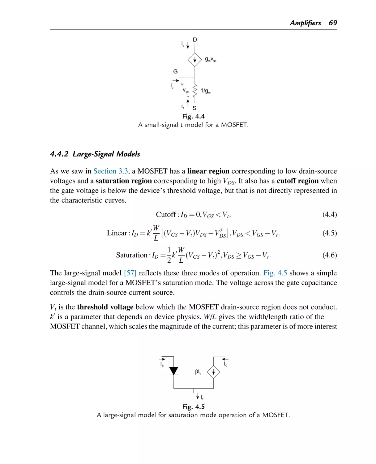
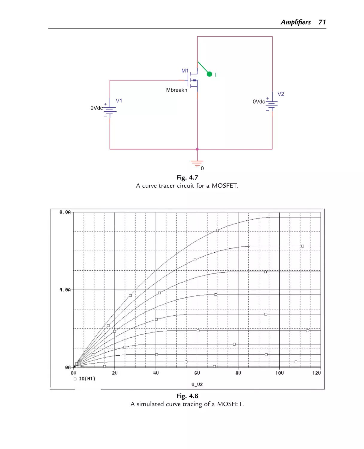
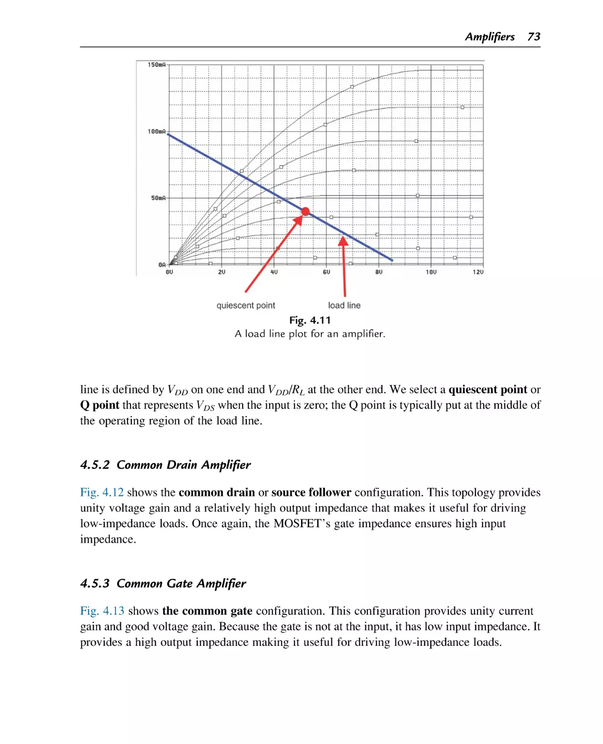
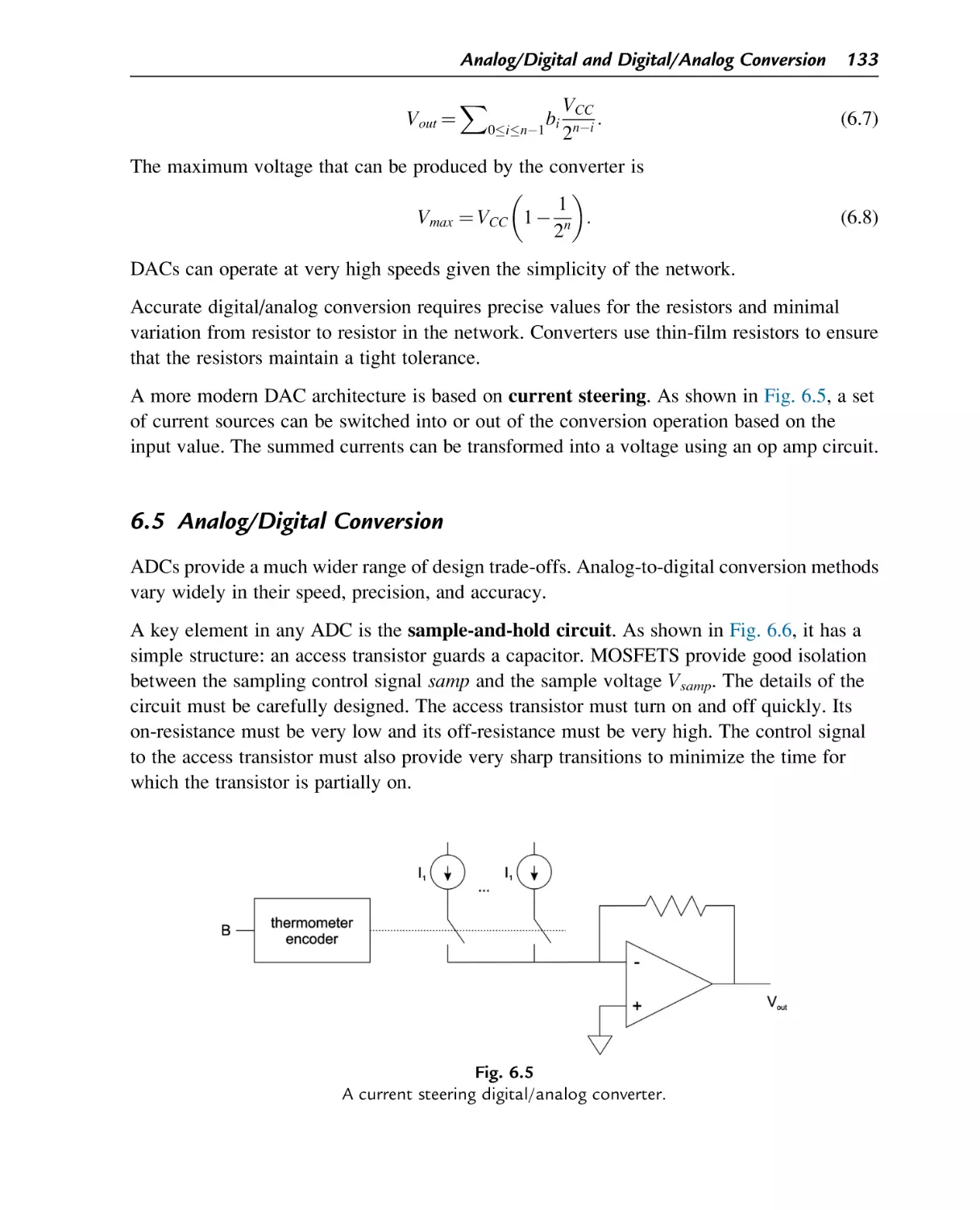
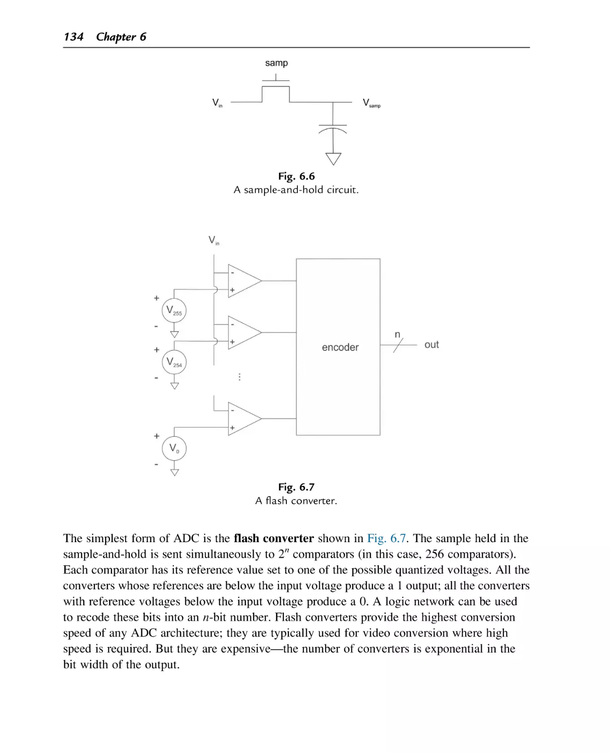
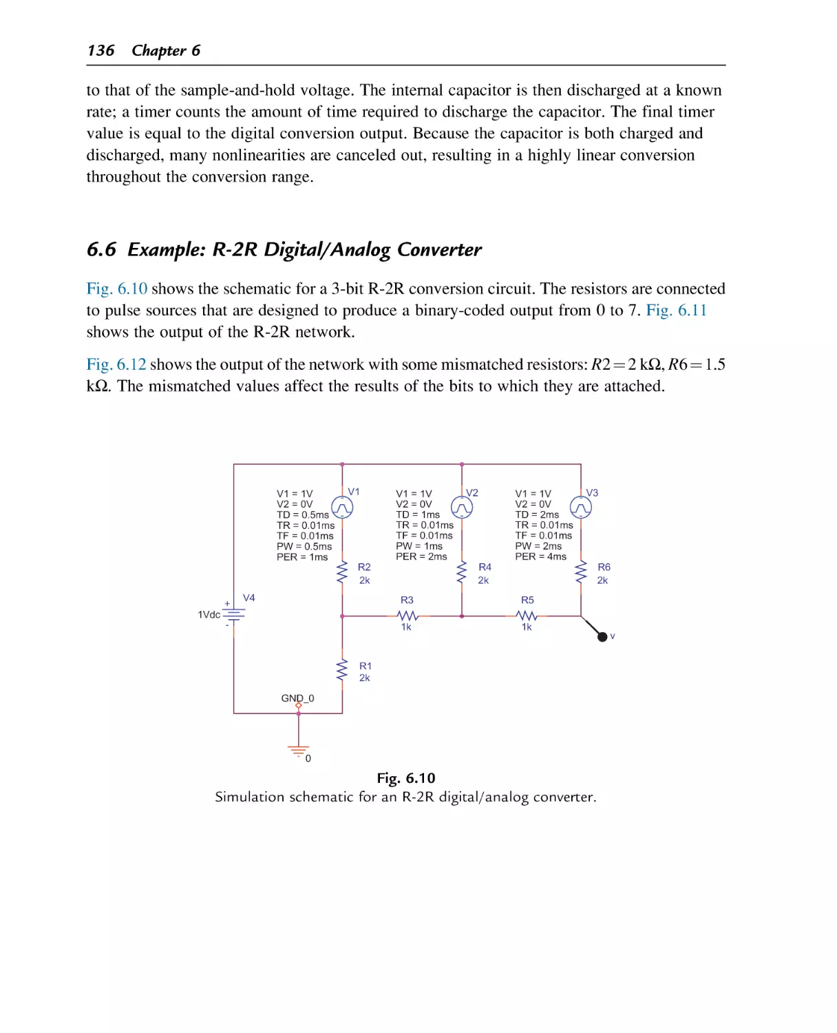
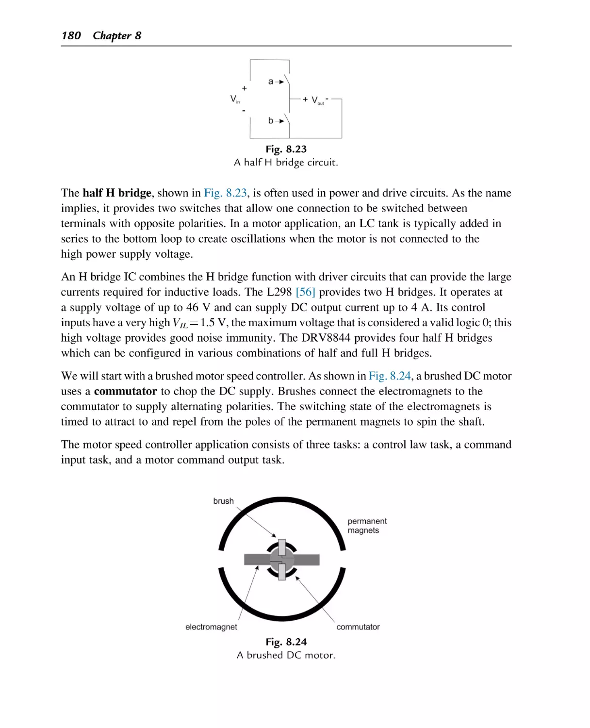
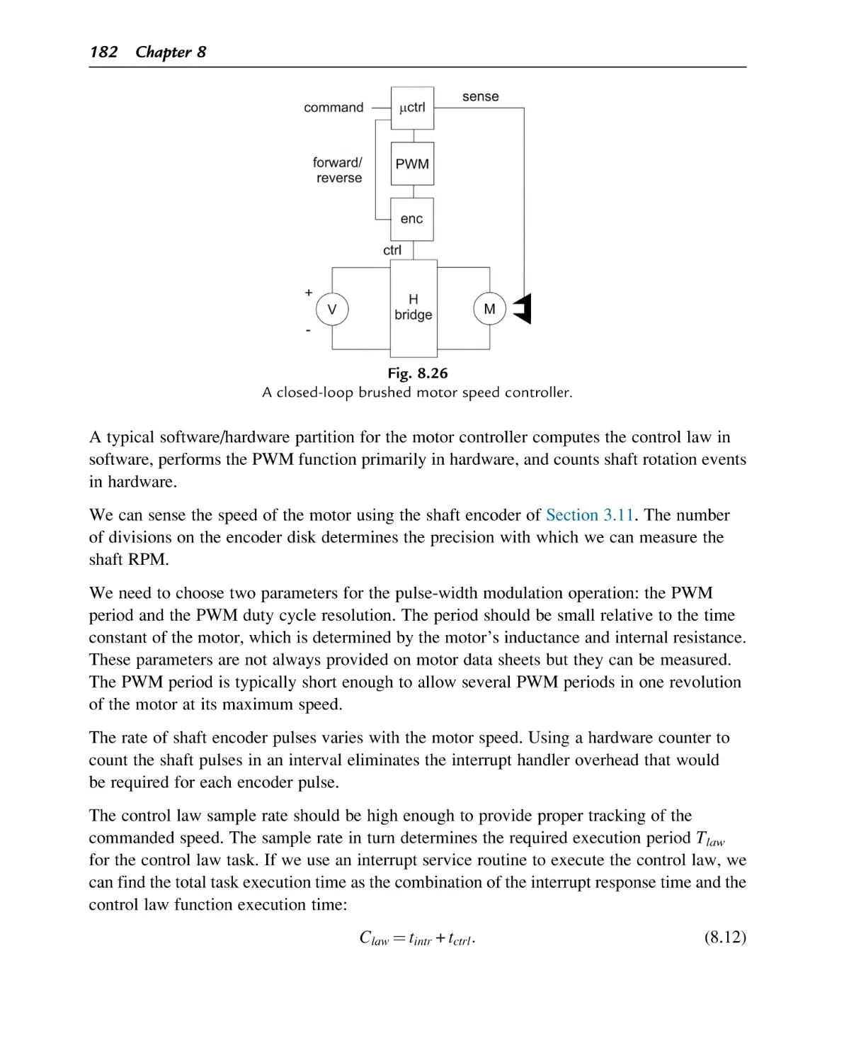
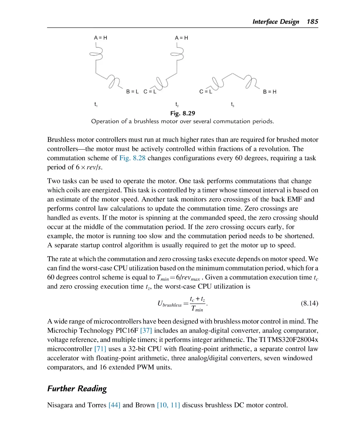
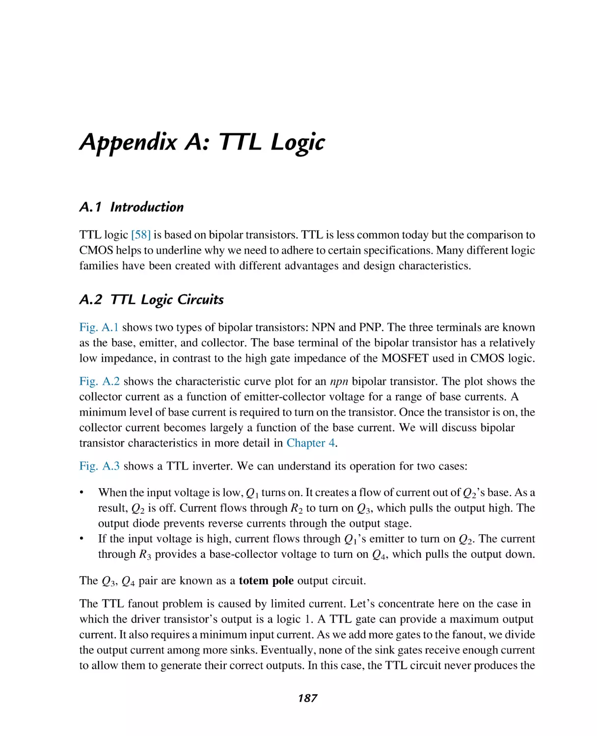
/


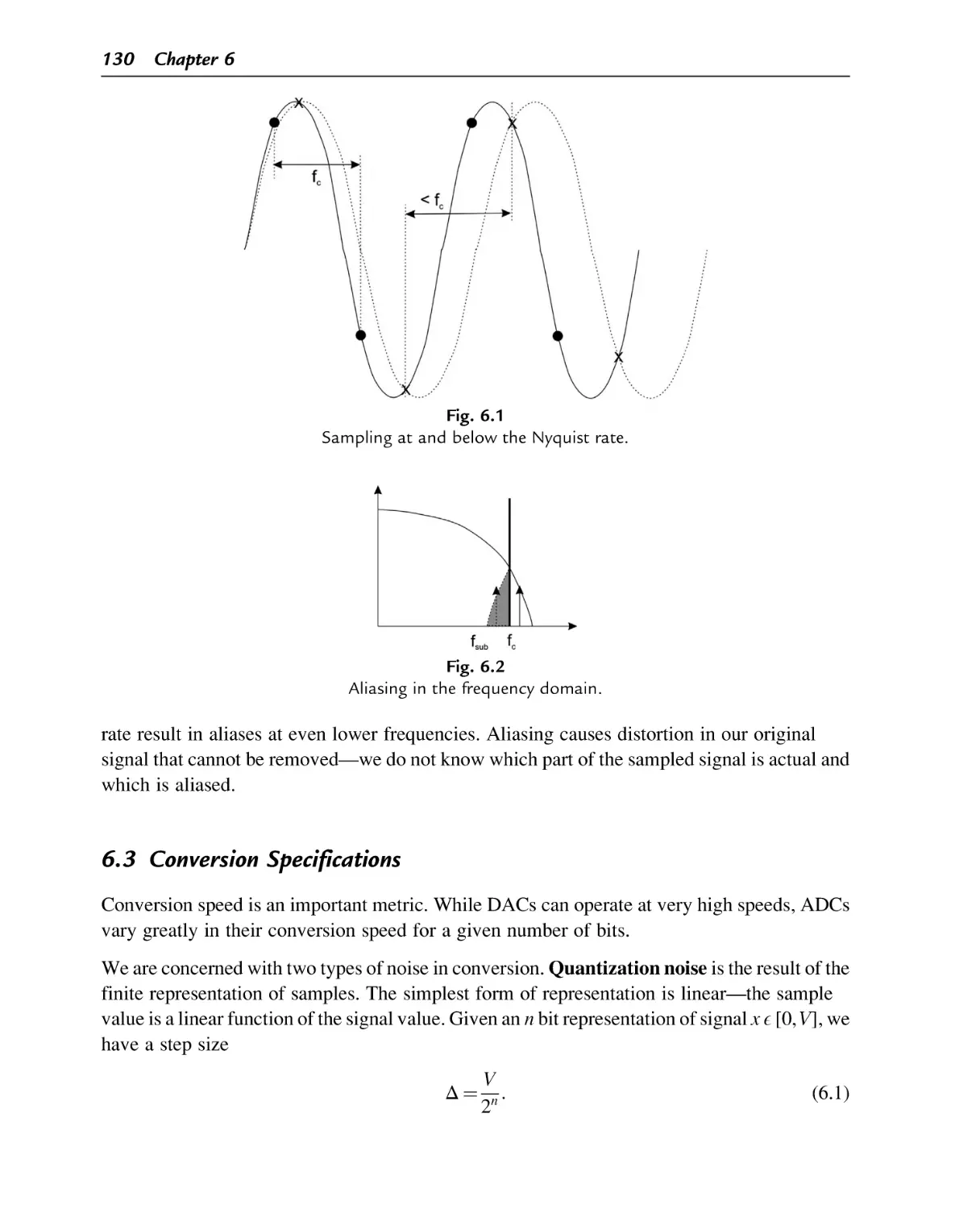


Автор: Wolf M.
Теги: programming languages programming computer science computer graphics morgan kaufmann publisher
Год: 2019


Текст
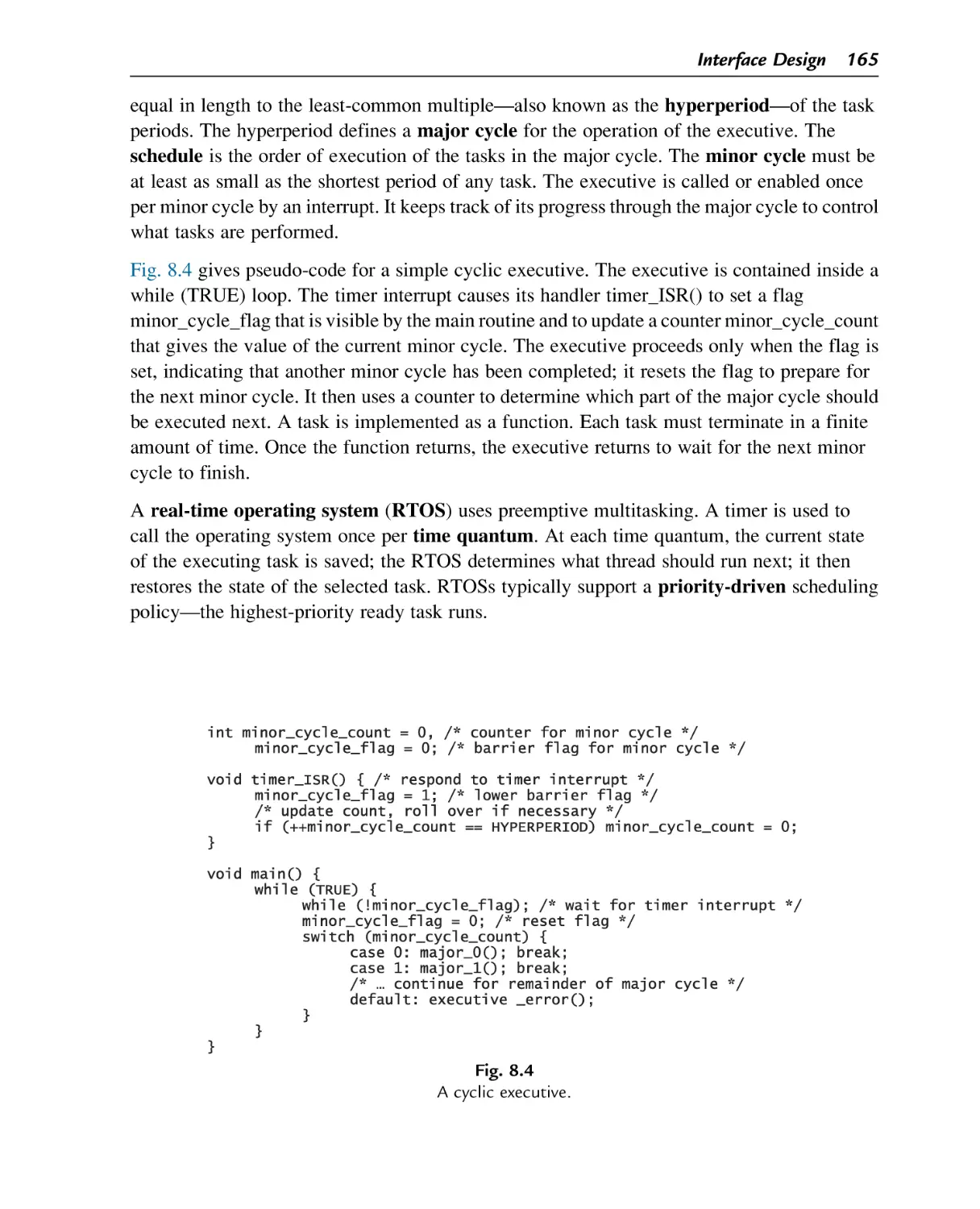
Embedded System Interfacing
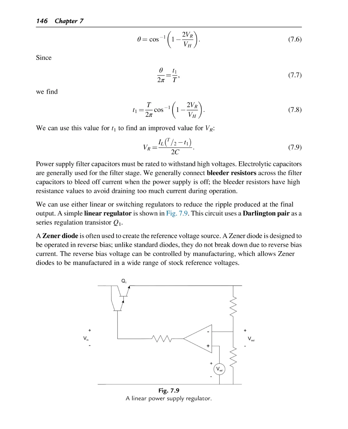
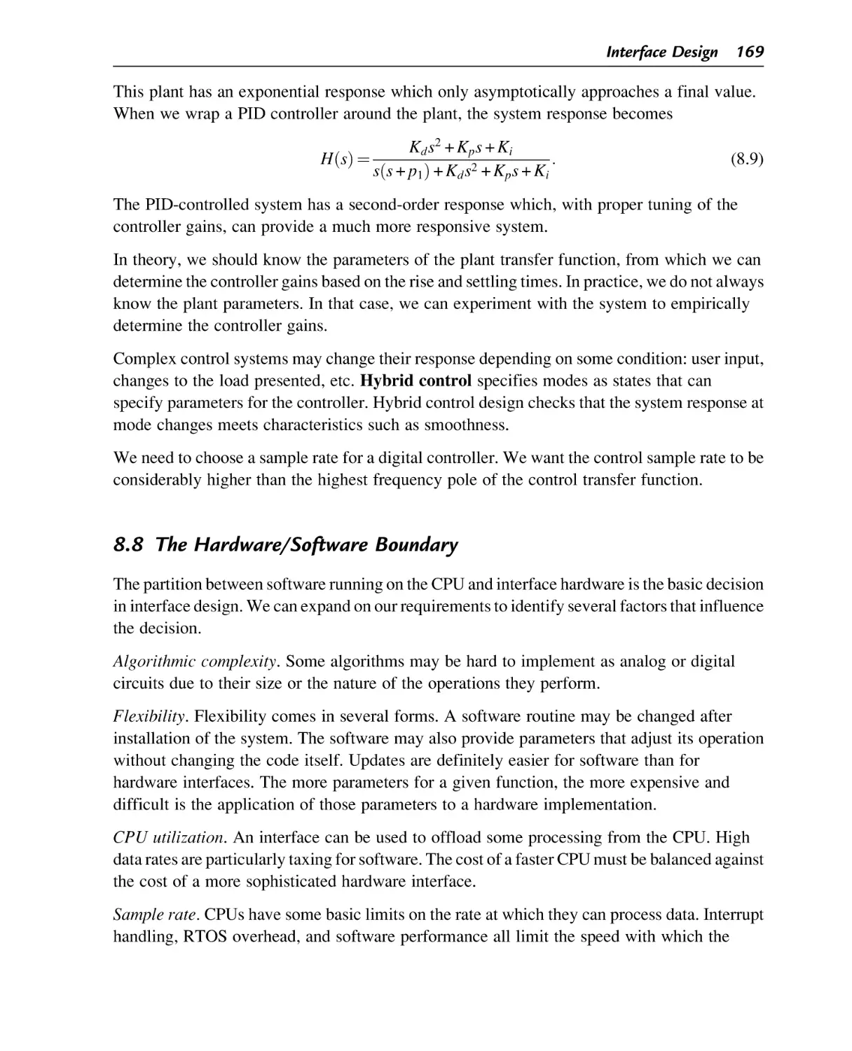
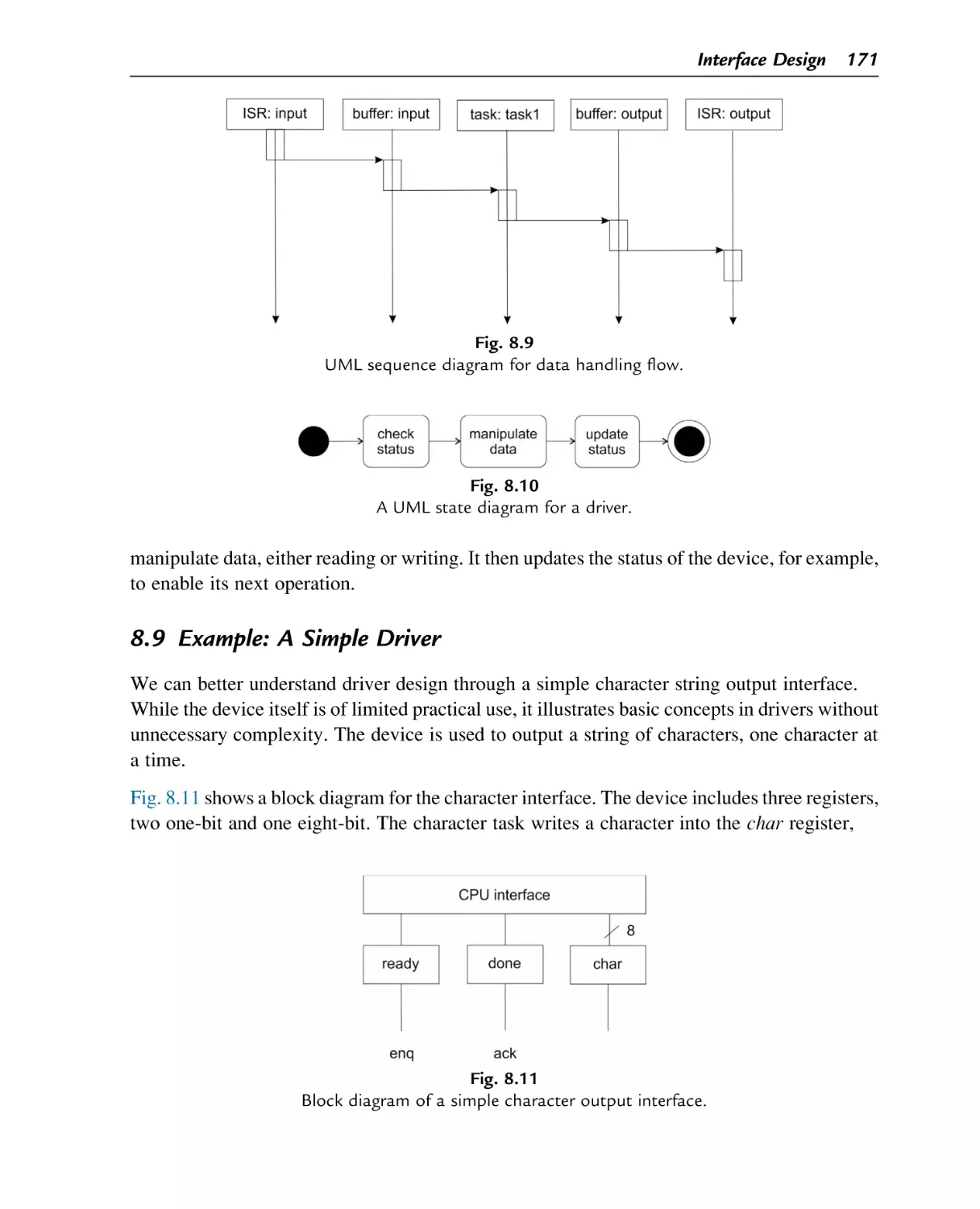
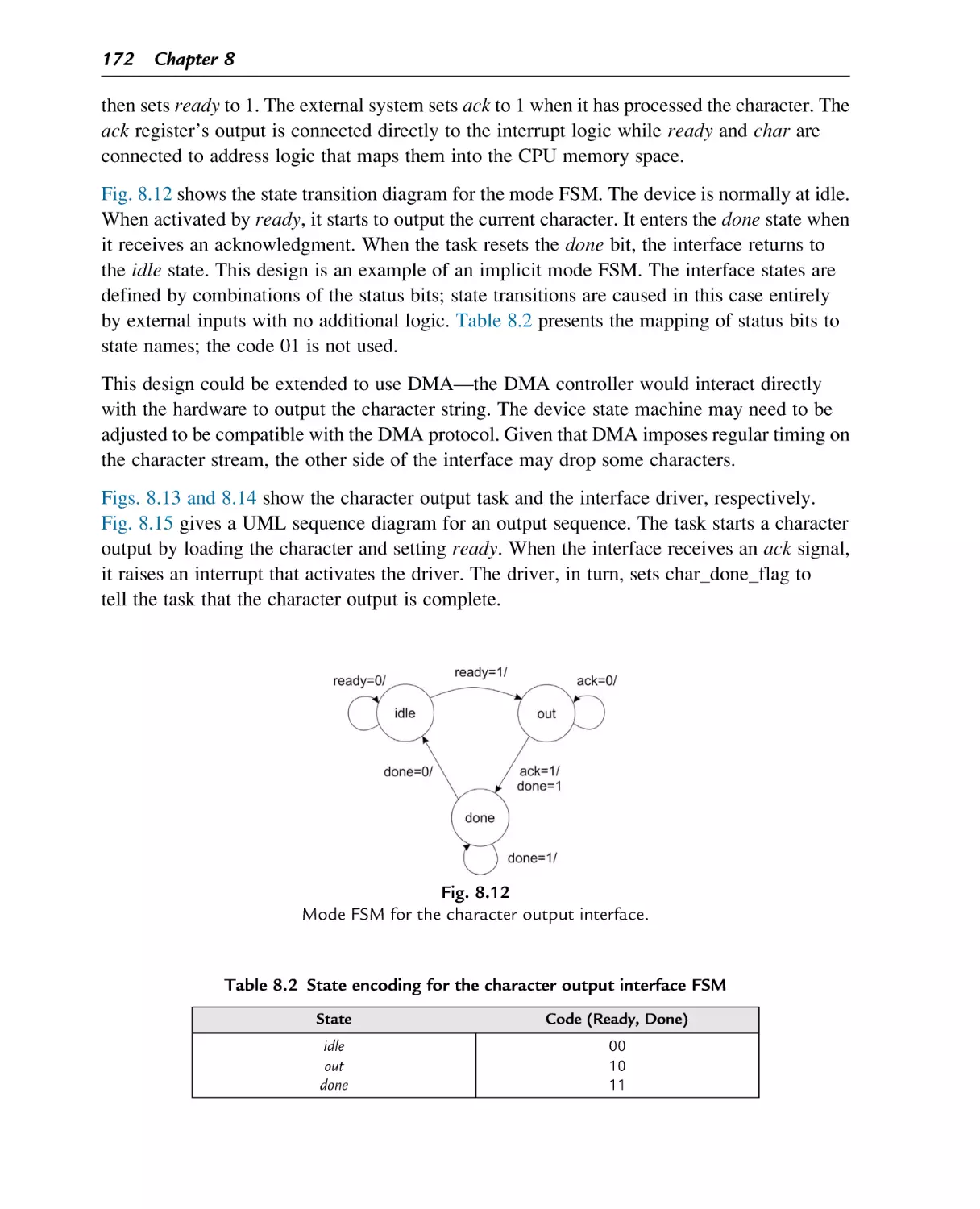
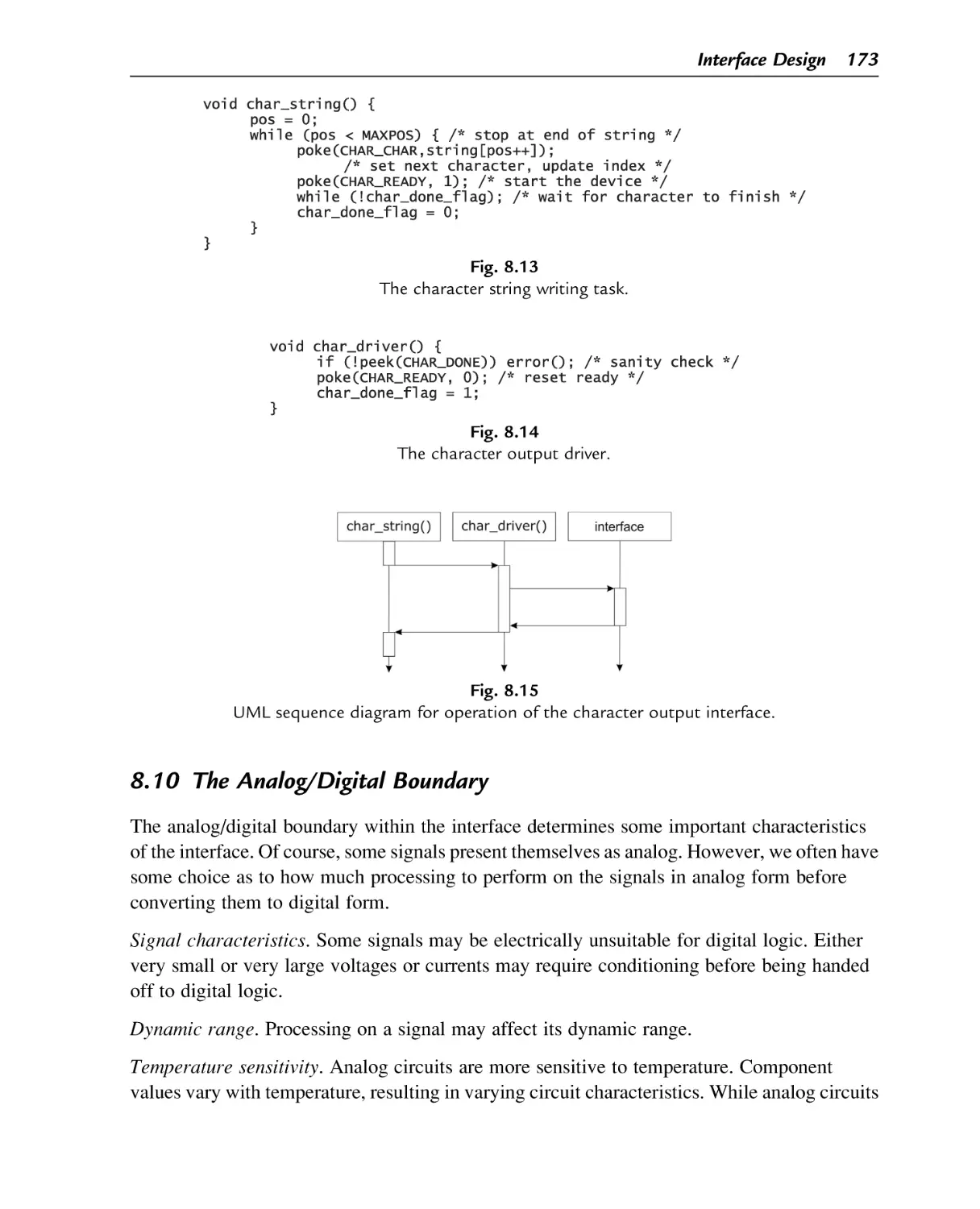
Embedded System Interfacing
Design for the Internet-of-Things (IoT) and
Cyber-Physical Systems (CPS)
Marilyn Wolf
Morgan Kaufmann is an imprint of Elsevier
50 Hampshire Street, 5th Floor, Cambridge, MA 02139, United States
#
2019 Elsevier Inc. All rights reserved.
No part of this publication may be reproduced or transmitted in any form or by any means, electronic or
mechanical, including photocopying, recording, or any information storage and retrieval system, without permission
in writing from the publisher. Details on how to seek permission, further information about the Publisher’s
permissions policies and our arrangements with organizations such as the Copyright Clearance Center and the
Copyright Licensing Agency, can be found at our website: www.elsevier.com/permissions.
This book and the individual contributions contained in it are protected under copyright by the Publisher (other than
as may be noted herein).
Notices
Knowledge and best practice in this field are constantly changing. As new research and experience broaden our
understanding, changes in research methods, professional practices, or medical treatment may become necessary.
Practitioners and researchers must always rely on their own experience and knowledge in evaluating and using any
information, methods, compounds, or experiments described herein. In using such information or methods they
should be mindful of their own safety and the safety of others, including parties for whom they have a professional
responsibility.
To the fullest extent of the law, neither the Publisher nor the authors, contributors, or editors, assume any
liability for any injury and/or damage to persons or property as a matter of products liability, negligence or otherwise,
or from any use or operation of any methods, products, instructions, or ideas contained in the material herein.
Library of Congress Cataloging-in-Publication Data
A catalog record for this book is available from the Library of Congress
British Library Cataloguing-in-Publication Data
A catalogue record for this book is available from the British Library
ISBN: 978-0-12-817402-9
For information on all Morgan Kaufmann publications visit our
website at https://www.elsevier.com/books-and-journals
Publisher: Katey Birtcher
Acquisition Editor: Steve Merken
Editorial Project Manager: Susan Ikeda
Production Project Manager: Punithavathy Govindaradjane
Cover Designer: Christian Bilbow
Typeset by SPi Global, India
To Alec
Preface
All computers need input and output to perform useful work. I/O systems are particularly
important to embedded computers. While we may use standard devices in embedded systems,
we often need to design specialized interfaces. Even when we do make use of standard devices,
we need to be sure that the chosen interface meets the system’s requirements. This book is
dedicated to the art, science, and craft of embedded system interfacing.
I built my own Heathkit radios: a GR-64 shortwave receiver, an HD-10 electronic keyer, and an
HW-16 novice transceiver. My friend Art Witulski and I tried to build a switch-based adder; we
gave up when we realized that our PCB patterning technology far outpaced our soldering skills.
My hobbies and hanging around my Dad taught me a lot. My Stanford professors turned me into
a competent electrical engineer. Let me pay homage to the professors who taught me about
circuits over my 8 years there: Aldo Da Rosa, Robert Dutton, Umram Inan, Malcolm
McWhorter, Ralph Smith, David Tuttle.
Perry Cook and I taught Pervasive Information Systems at Princeton for many years.
We coached our students through the design of embedded systems. The term Internet-of-Things
had not yet been coined but our students gained early exposure to many IoT concepts. Perry was
the master hardware designer, building at one point an inductive coupler loop for a power plug
to ensure that one student team did not electrocute themselves as part of their power line
networking project.
But building your own electronics makes much less sense than it did a half-century ago. The
decline of hand-built electronics in favor of highly integrated equipment has several causes:
radios operate at much higher frequencies, many components are surface mount, integrated
circuits provide much higher levels of integration. Integrated electronics are simply better than
what you can design on a board: lower noise, lower distortion due to better matching, and lower
power consumption.
Quite a few embedded interfacing books take the form of cookbooks—they provide example
designs for particular applications. While cookbooks certainly have their place, I thought
that a compendium of techniques was an important complement to the cookbook approach.
The solutions found in a cookbook may not come with enough explanation to allow you to
xi
Preface
modify their design for your purposes. Principles help you understand how to make design
decisions. Principles can help you modify an existing design or build a new design from scratch.
I ignored some of the traditional electrical engineering pedagogy in pursuit of my goal of a
relatively short, stand-alone introduction to circuit design. I was not interested in the traditional
passive/active circuit distinction; to some extent, I was not worried about digital versus analog.
My guiding principle was function, moving from simple to complex. Logic is very simple in the
sense that our set of values is limited; I also concentrated on the electrical characteristics of
drive and load. Amplifiers simply change the power of a signal. Filters and detectors modify
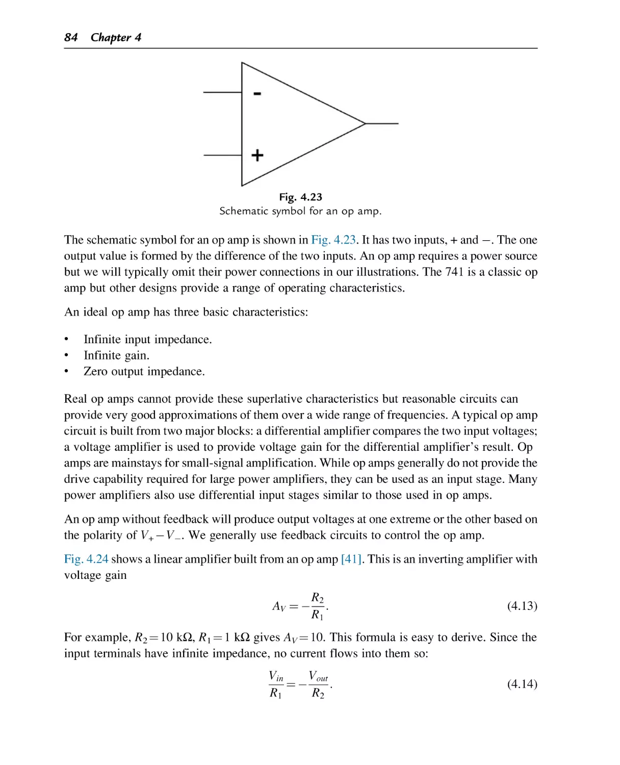
signals. Data conversion builds on these techniques to bridge the gap between analog and
digital. Power also makes use of these circuit principles; a knowledge of circuit characteristics
also help us to specify the important characteristics of power supplies.
Along the way, I emphasized a top-down approach. The specifications for a given function need
to be clearly understood before we can design.
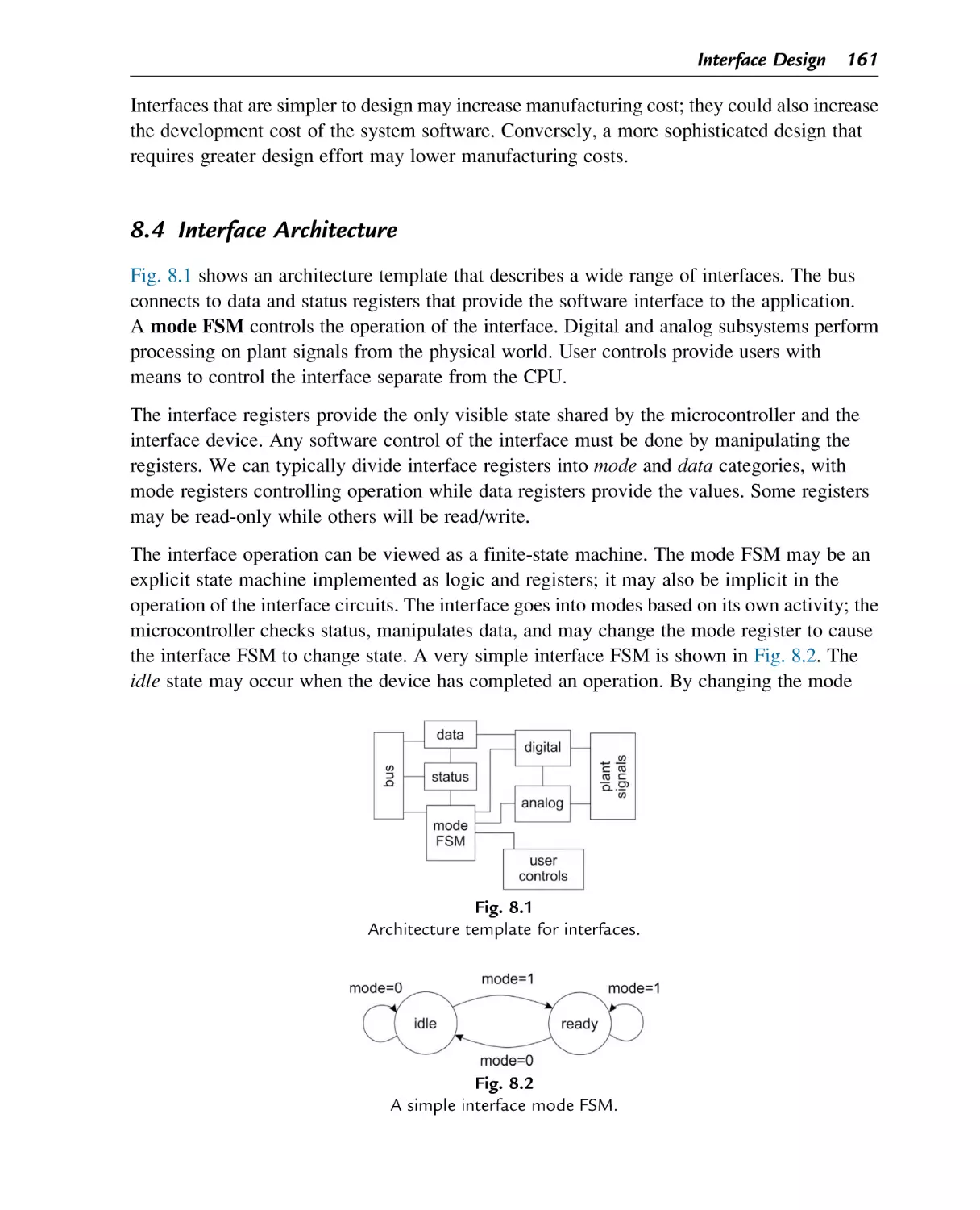
As I wrote, I realized that the critical decisions in interface design place two boundaries: the
software/hardware boundary between software running on the CPU and the interface connected
to the CPU, and the analog/digital boundary within the interface. The system specifications
help to determine where to place these boundaries—a set of decisions for a high-speed,
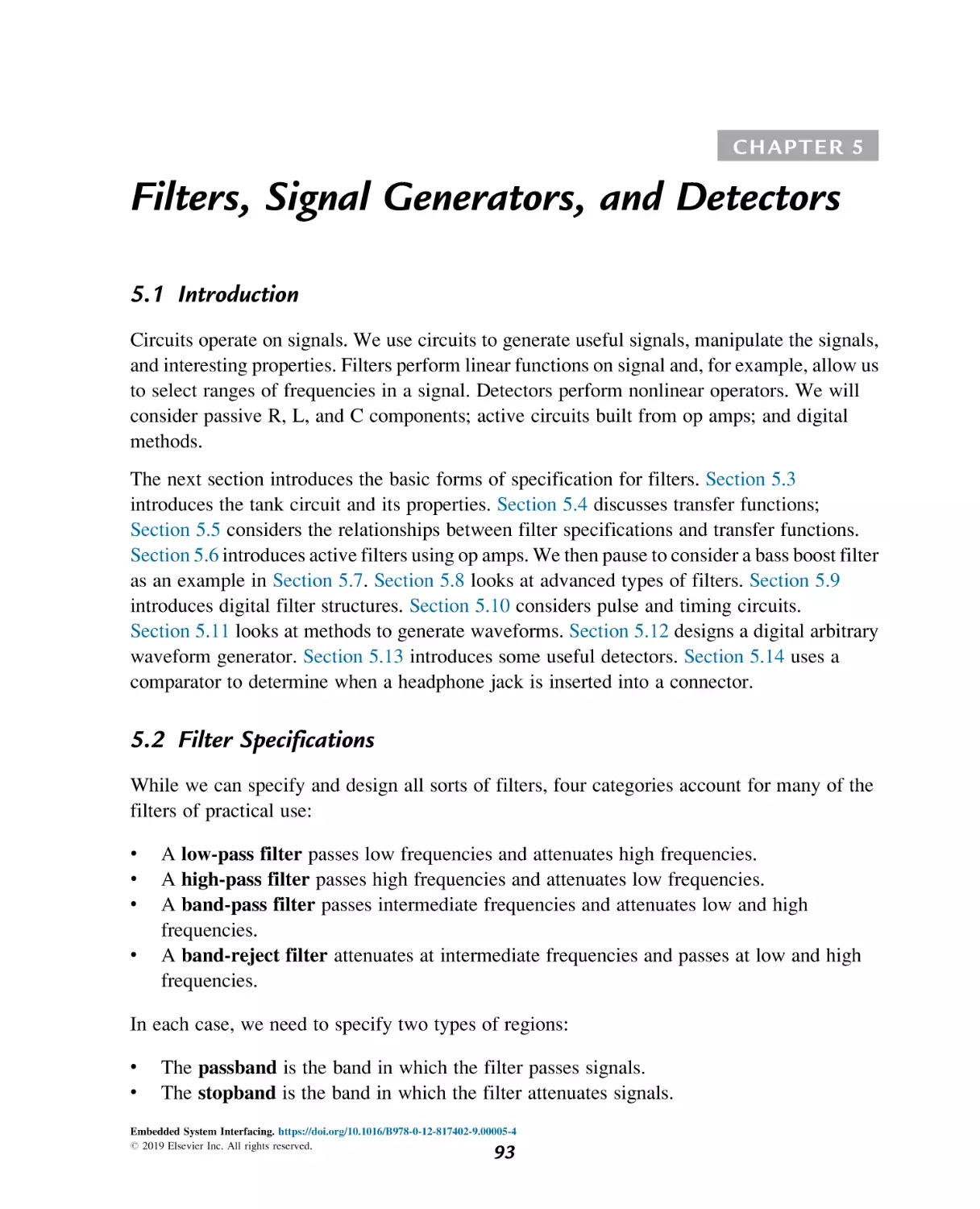
high-value system may not make sense for a simple consumer electronics device.
This book is designed as a precis, a short course in mixed-signal design. Consider this an outline
of interesting and important topics. If you want to know more about a topic, dive in. The
references provide some starting points on a number of topics; the Internet makes a wide variety
of materials easily available.
Some of this technology has not changed since the 1970s and 1980s. In those cases, the oldies
are still goodies. Here are some useful books:
•
•
•
The ARRL Handbook, updated yearly, has been a go-to guide for all things EE for nearly a
century.
Lancaster’s Active Filter Cookbook balances theory and practice for active filters. The
book also provides a cornucopia of 1970’s electronics, including biofeedback and
psychedelic lighting.
IC Op-Amp Cookbook by Walter G. Jung covers all aspects of linear and nonlinear op amp
circuits.
In other cases, our techniques have changed profoundly. FPGAs have fundamentally changed
our approach to logic design. Field-programmable analog arrays (FPAAs) have allowed
microcontrollers to provide simple, integrated, configurable analog capabilities.
My Web site marilynwolf.us provides lab exercises that provide concrete forms of the exercises
in this book. It also includes overheads for this material.
xii
Preface
Many thanks to Prof. Robert Dick of the University of Michigan for his thorough and thoughtful
comments.
Electronic design has given me a lifetime of pleasure. I hope you enjoy this pursuit as much
as I have.
Marilyn Wolf, W2MCW
Atlanta, Georgia
xiii
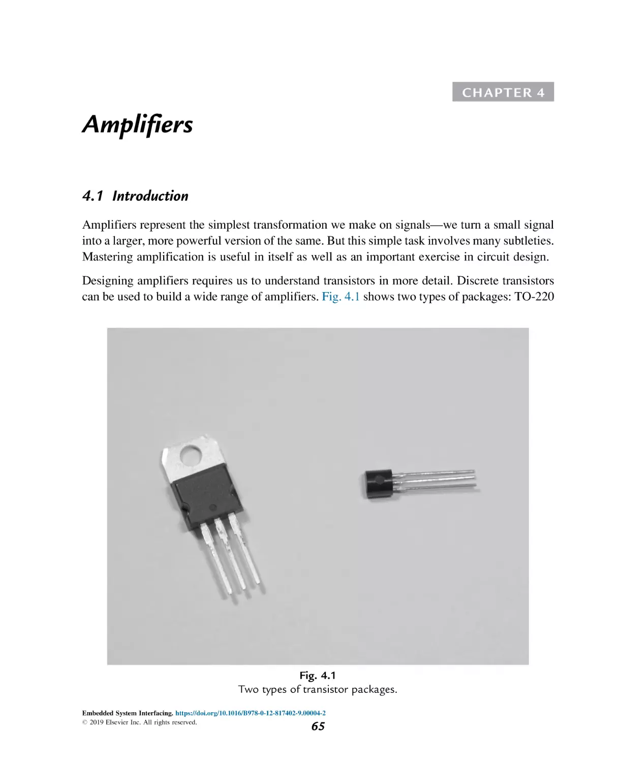
CHAPTER 1
Introduction
1.1 Interfacing Computers to the Physical World
Useful computers need some sort of input and output. Computation that we can’t see doesn’t
provide much attraction. Early computers used primitive I/O devices: lights, paper tape, crude
displays. The development of new I/O devices has paralleled the development of CPUs.
I/O is particularly important to embedded computing systems. Embedded computers are
responsible for a wide range of devices, ranging from simple appliances to complex vehicles
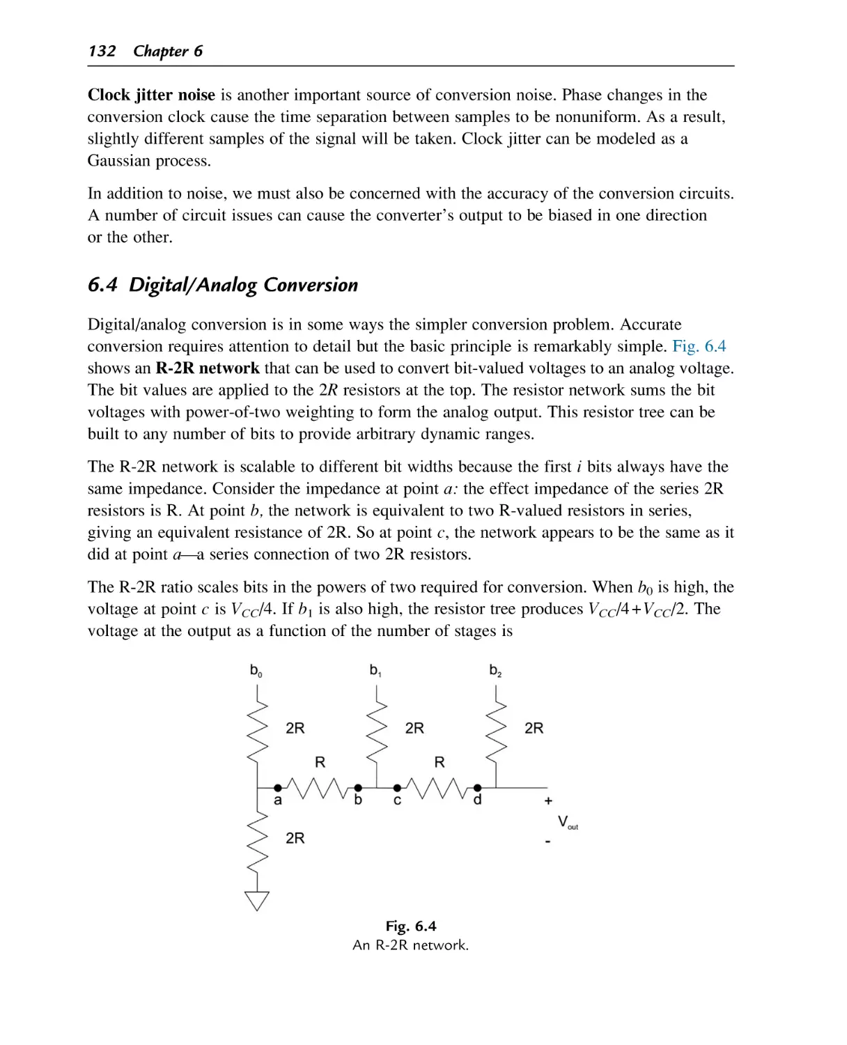
and industrial equipment. This range of I/O requirements calls for a comprehensive
playbook of interfacing techniques.
Embedded system interfacing is the conceptual interface between electrical and computer
engineering—we require the skills of both fields to design good, practical interfaces. Computer
engineers don’t always have a lot of experience with traditional electrical engineering. As a
result, we will cover this territory thoroughly. Readers with expertise in circuits should feel free
to skip some sections and get straight to the use of circuits as interfaces to computers.
Embedded system interfacing is a good example of mixed-signal design—the design of
circuits that combine analog and digital elements. Mixing analog and digital provides powerful
capabilities but must be done carefully. Among other concerns, we must take care with the
circuit characteristics of digital logic such as drive and load, something that is less of a
problem in a purely digital design. Interfacing also requires hardware/software codesign,
mixing the capabilities of software running on the CPU with mixed-signal circuits.
First, Section 1.2 surveys the goals of interface design and the techniques we use to achieve
those goals. Section 1.3 surveys microprocessors. Section 1.4 signals introduces electrical
signals. Sections 1.5 and 1.6 review the laws of electrical engineering: first for resistors, then
generalizing to capacitors and inductors. Section 1.7 describes basic techniques for circuit
analysis. Section 1.8 looks at nonlinear and active devices. Section 1.9 steps back to consider
methodologies and tools for the design of interfaces. Section 1.10 walks through an outline
of the remainder of the book. These sections will outline some basic concepts and terms in
electrical engineering for later reference; we will flesh out these concepts as needed in
later chapters.
Embedded System Interfacing. https://doi.org/10.1016/B978-0-12-817402-9.00001-7
# 2019 Elsevier Inc. All rights reserved.
1
2
Chapter 1
1.2 Goals and Techniques
Embedded computer systems are used in all sorts of applications; one interesting way to think
about the categories of embedded computers and their interfaces is the numbers of copies of the
system that will be built. Experimenters and hobbyists build one system or perhaps a few.
Industrial applications such as factories may build one-off devices but they also make use
of specialized equipment that is manufactured at modest levels: hundreds to tens of thousands.
Consumer products are manufactured in much larger volumes, from tens of thousands to
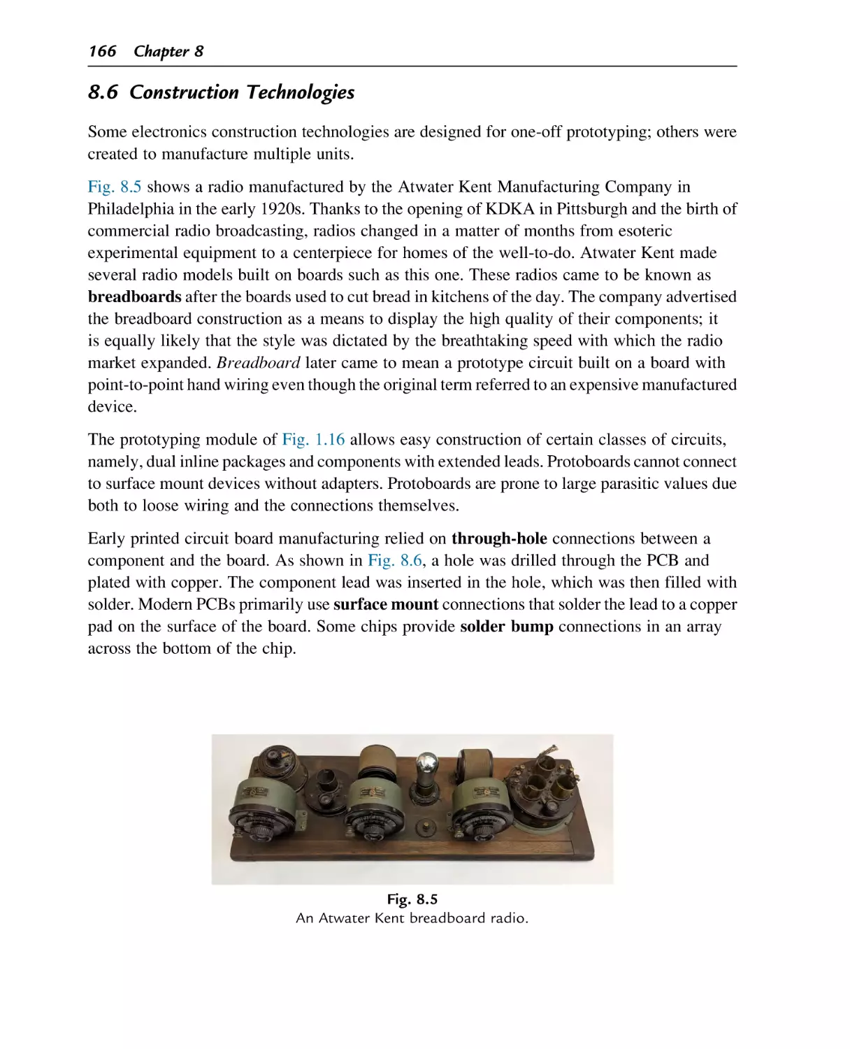
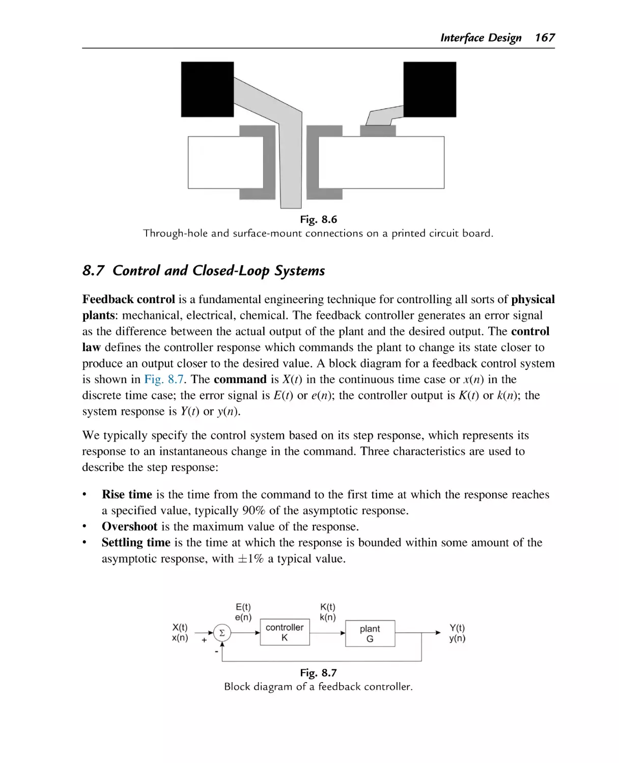
tens of millions of units. Interface design skills are useful in all of these categories.
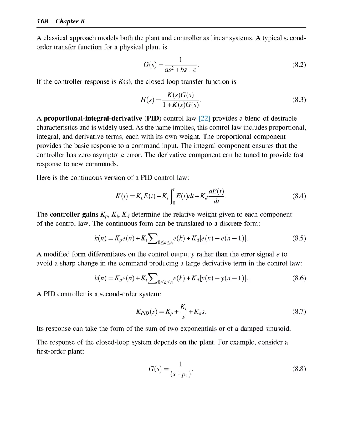
Many integrated circuits are systems-on-chip (SoCs) that include processing, I/O devices, and
some amount of onboard memory. The design of these devices and their connections to the
computing system is a critical aspect of the design of the SoC. While many SoCs do not include
analog circuits, the digital devices must be designed with the characteristics of the analog
devices to which they will be connected. Advanced packaging techniques allow the complete
system to be composed of multiple chips built with different manufacturing technologies.
However, not all design is focused on integrated circuits. Many high-volume devices are built
largely out of standard parts assembled on printed circuit boards—what engineers typically
call board-level design. The printed circuit board also is a mainstay of industrial electronic
design. A board design allows the design of a custom circuit with control over the components
and manufacturing technology, all with substantially less cost and time commitment than
is required to design an integrated circuit.
However, many designs require only a handful of the traditional primitives of electrical
engineering: transistors, resistors, capacitors, inductors. Most board-level design puts together
integrated circuits, each of which performs a specialized function. The op amp is a classic
example of an integrated circuit that encapsulates a sophisticated circuit in an easy-to-use form.
While designing circuits using transistors is fun, it is often not realistic. Not only do integrated
circuits save us time, but also they often provide better characteristics than circuits made
from discrete components. But it is still important and useful to understand the basic principles
of circuit design: we need to know how to evaluate the appropriateness of an integrated
circuit for a particular application; and we need to be able to verify that we have designed
the proper circuit connections to them. Providing insufficient current to the input of a logic gate,
for example, will cause it to malfunction.
In order to design board-level systems properly, we need to be able to write the specifications
for the design. We also need to understand the specifications of the components we use to
build the board. These specifications are fundamental characteristics of circuits:
•
•
Gain;
Frequency response;
Introduction 3
•
•
Nonlinear characteristics such as rise time, ringing;
Noise.
Design is the process of finding an embodiment of those specifications using available
components. Circuit theory gives us important concepts in design:
•
•
•
Drive and load;
Filtering;
Amplification gain and bandwidth.
We design the entire interface, which we often break down into smaller designs for the pieces of
the interface. We use top-down design techniques to refine the specifications into realizations;
bottom-up design methods allow us to estimate the characteristics of candidate designs.
We will see in Chapter 8 that an embedded system interface requires us to answer two
questions:
•
•
Where is the software/hardware boundary? What goes in software on the CPU and what
goes into the interface?
Where is the digital/analog boundary? What parts of the interface are performed with
digital hardware and which with analog circuits?
1.3 Varieties of Microprocessors
A microprocessor is a CPU on an integrated circuit; in the modern era, virtually all CPUs are
microprocessors. A computer system is more than a CPU—it requires memory, I/O devices,
and interconnect between them. The term platform is often used to describe the complete
computing hardware (and perhaps lower levels of the software stack as well). We often
categorize platforms based on their size and complexity.
A microcontroller is a complete computer system on a chip: CPU, memory, I/O devices, and
bus. We typically use this term for smaller systems: simpler CPUs, modest amounts of memory,
and basic I/O. Many microcontrollers provide 4-bit or 8-bit CPUs; some of them provide
less than a kilobyte of memory. The Cypress PSoC 5LP [16] is a microcontroller, although
one with a 32-bit CPU. It provides an ARM Cortex-M3 CPU, three types of memory (flash,
RAM, EPROM), and digital and analog peripherals.
A digital signal processor (DSP) is a microprocessor optimized for signal processing
applications. The original use of the term referred to the combination of a hardware multiplier
and Harvard-style separate program and data memories. Today, DSP optimizations include
addressing modes useful for array calculations.
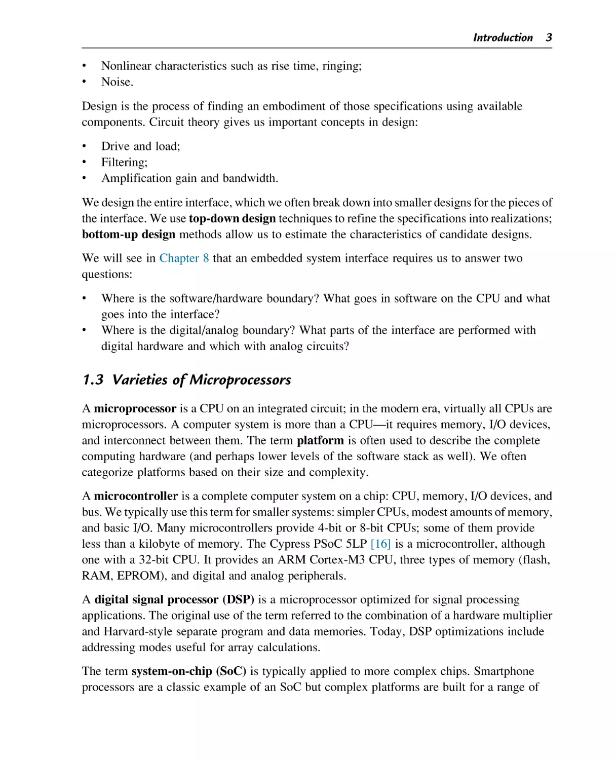
The term system-on-chip (SoC) is typically applied to more complex chips. Smartphone
processors are a classic example of an SoC but complex platforms are built for a range of
4
Chapter 1
applications, including multimedia and automotive. The NXP S32V234 [46] is an SoC—a
vision processor for automotive applications. It includes four ARM Cortex-A53 CPUs with
SIMD instructions, two ARM Cortex-M4 CPUs, a vision accelerator, GPU, image sensor
processor, image sensor interfaces, and support for safety and security.
1.4 Signals
A signal is a physical state over an extended period. We represent a signal mathematically as a
value defined by a function over time.
We talk about signals with respect to their time values:
•
•
DC (direct current) values do not change over time. Practically speaking, they change
only slowly.
AC (alternating current) values change over time. The term comes from sinusoidal
signals but we apply it more generally to time-varying values.
We make this distinction because we use different techniques to analyze DC and AC
signals and circuits. DC analysis makes use of simpler techniques.
AC signals can have arbitrary waveforms or shapes. For purposes of analysis, we deal
with two major forms of signals. The sinusoidal signal is determined by its amplitude A,
frequency ω, and phase φ:
vðtÞ ¼ Asinωt + φ:
(1.1)
The exponential signal is determined by its amplitude A and time constant τ:
vðtÞ ¼ Aet=τ :
(1.2)
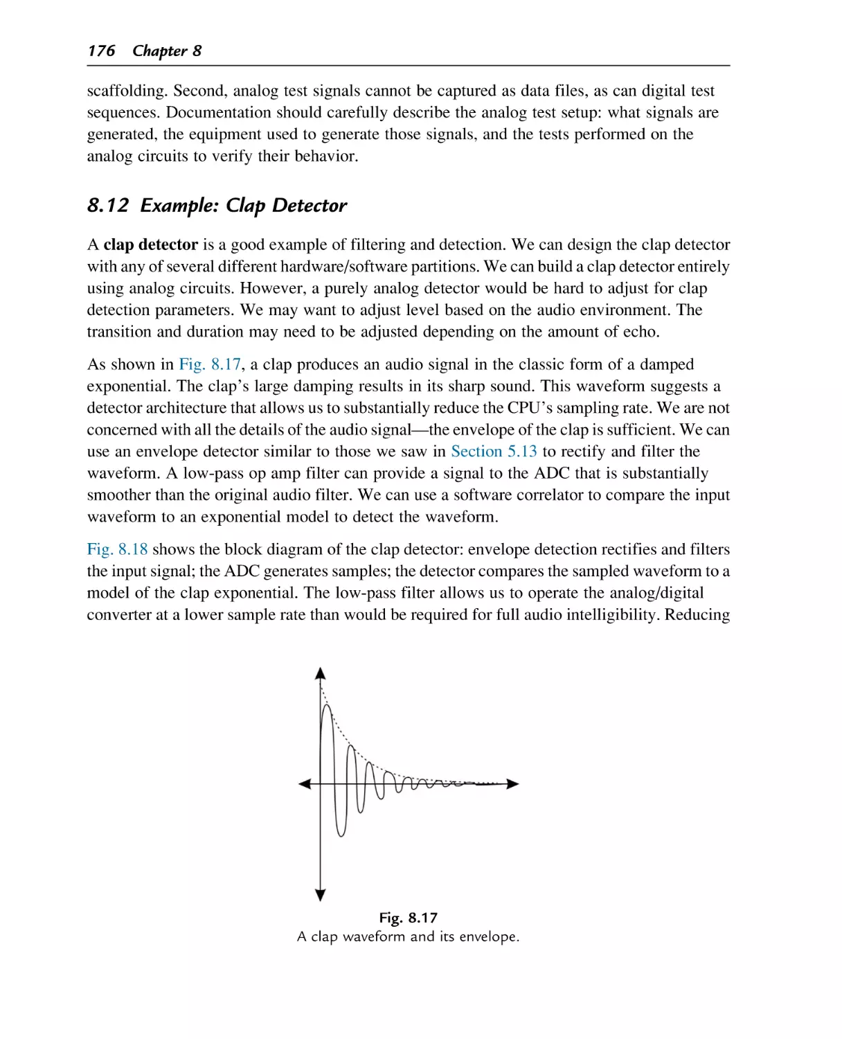
Fig. 1.1 shows examples of sinusoidal and exponential signals.
Noise is like weeds—any sort of undesired signal. Noise may come from random sources
that we cannot predict or sources that we understand. When undesired signals come from
predictable sources, we may use other terms, such as interference or crosstalk, to describe it.
We also talk about signals relative to the domain in which we view them:
•
•
Time-domain signals are functions of time.
Frequency-domain signals are functions of frequency.
These two representations are equivalent—we can transform a time-domain signal into its
frequency-domain equivalent and vice versa. We can use the Fourier transform and its
computational form the fast Fourier transform (FFT) to move between the time and
frequency domains. Fig. 1.2 shows both representations of a signal which is formed by the
product of two sinusoids, one fast and one slow. The frequency domain form shows the
Introduction 5
Sinusoid
Exponential
Fig. 1.1
Sinusoidal and exponential signals.
two sinusoidal components. (A frequency-domain signal includes both magnitude and phase
components; we concentrate here on the magnitude part of the signal.)
Digital circuit designers rely almost exclusively on time-domain techniques—the nonlinear
nature of digital circuits is not well suited to time-domain analysis. In contrast, linear circuits
use both frequency-domain and time-domain methods; frequency-domain analysis is
particularly useful for many aspects of linear circuit design. Fig. 1.2 shows examples of time
and frequency representations of a simple signal.
We can refer to frequencies in either of two units: the variable ω is used for radians/s; the
variable f is used for Hertz. By definition, 1 Hz ¼ 2π rad/s.
6
Chapter 1
time domain
ω1
ω2
frequency domain
Fig. 1.2
Time- and frequency-domain representation of a signal.
Signals can traverse large dynamic ranges that result in some very large numbers. We can
reduce the magnitude of our values by using decibels (dB). This unit is one-tenth of a Bel, a unit
of power named after Alexander Graham Bell. We can use decibels to express either ratios
of values or to express a value relative to some reference. Since decibels refer to power,
we should refer to voltage ratios as dBV although we often revert to using dB for these
values as an abuse of notation.
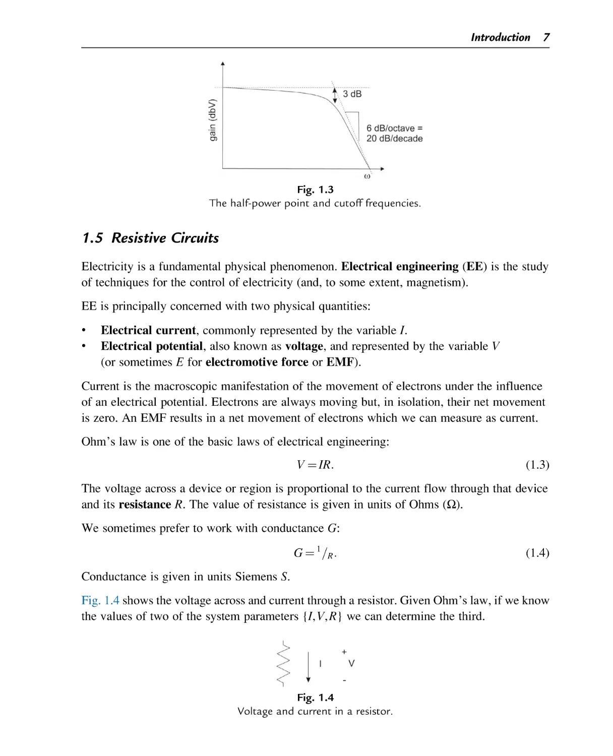
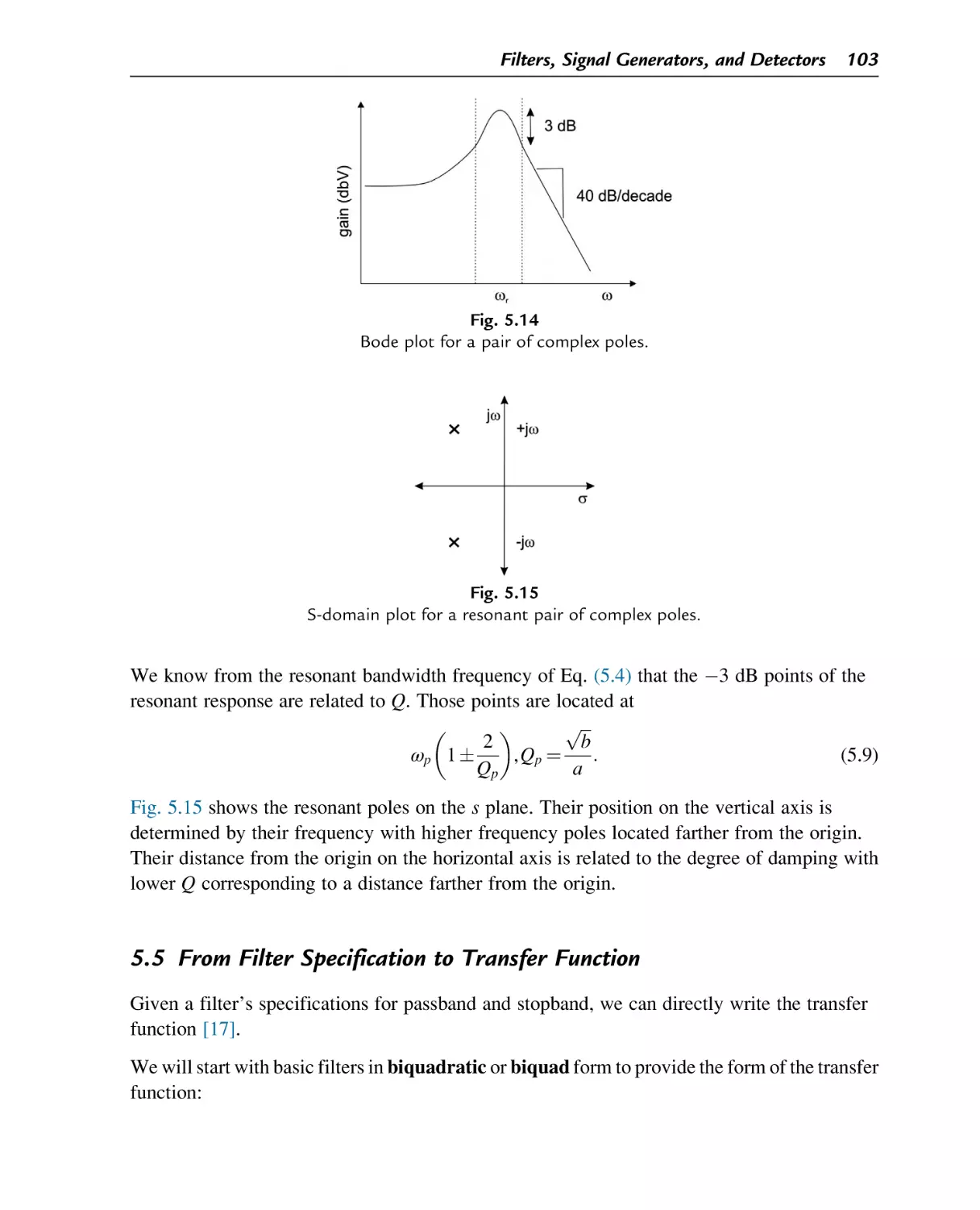
Decibel curves are used to describe the response of filters and amplifiers. One common
specification is the half-power point, also known as the 3 dB point or the corner frequency, as
shown in Fig. 1.3. The plot shows power as a function of frequency. The Bode plot method
allows us to approximate frequency response curves using their asymptotes. The curve is
defined by two asymptotes: a flat line to the left and a line descending at 20 dB per decade
to the right; that rate is equal to 6 dB per octave. The point on the curve that is 3 dB below the
left-hand asymptote has a power value 1/2 that of the asymptote. Since
pffiffiffi power is related to
the square of voltage, the corresponding voltage has dropped by 1= 2 ¼ :7071. We often
refer to the half-power frequency as the corner frequency. We will discuss Bode plots in
more detail in Section 5.4.
Introduction 7
Fig. 1.3
The half-power point and cutoff frequencies.
1.5 Resistive Circuits
Electricity is a fundamental physical phenomenon. Electrical engineering (EE) is the study
of techniques for the control of electricity (and, to some extent, magnetism).
EE is principally concerned with two physical quantities:
•
•
Electrical current, commonly represented by the variable I.
Electrical potential, also known as voltage, and represented by the variable V
(or sometimes E for electromotive force or EMF).
Current is the macroscopic manifestation of the movement of electrons under the influence
of an electrical potential. Electrons are always moving but, in isolation, their net movement
is zero. An EMF results in a net movement of electrons which we can measure as current.
Ohm’s law is one of the basic laws of electrical engineering:
V ¼ IR:
(1.3)
The voltage across a device or region is proportional to the current flow through that device
and its resistance R. The value of resistance is given in units of Ohms (Ω).
We sometimes prefer to work with conductance G:
G ¼ 1 =R :
(1.4)
Conductance is given in units Siemens S.
Fig. 1.4 shows the voltage across and current through a resistor. Given Ohm’s law, if we know
the values of two of the system parameters {I, V, R} we can determine the third.
Fig. 1.4
Voltage and current in a resistor.
8
Chapter 1
Two other laws describe the relationship between voltages and currents when we connect
several resistors into networks. Kirchoff’s voltage law (KVL) says that the sum of voltages
around a loop is zero:
V1 + ⋯Vn ¼ 0:
(1.5)
Kirchoff’s current law (KCL) states that the sum of currents into a node is zero:
I12 + ⋯I1n ¼ 0:
(1.6)
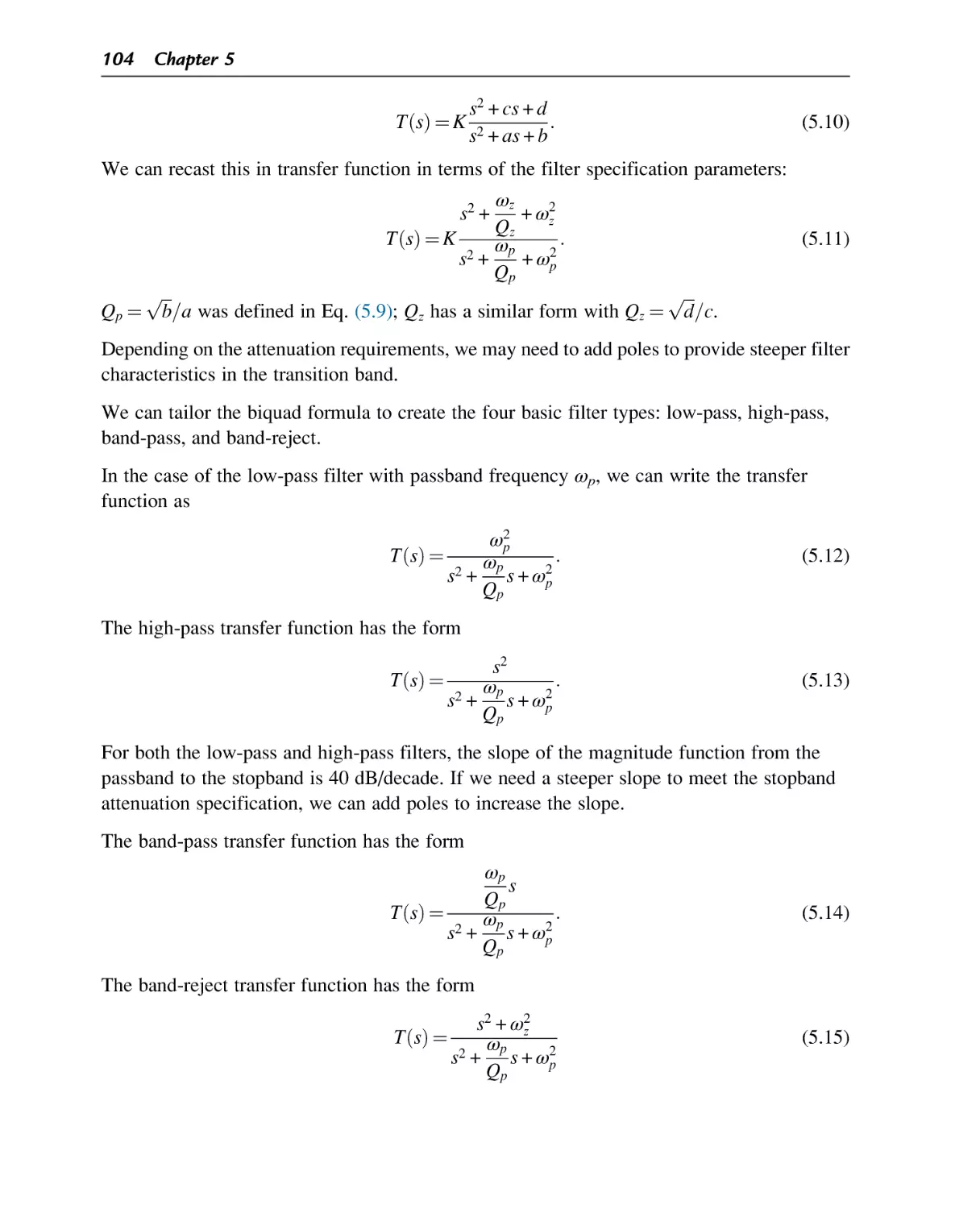
Fig. 1.5 gives an example circuit in the form of a graph: the nodes {1, 2, 3} represent the points
at which we evaluate Kirchoff’s current law; the edges {12,13,23} are where we evaluate
Kirchoff’s voltage law. We can define voltage variables along the edges and currents into or
out of the nodes. When we make these labels, we choose which side or direction is positive and
which is negative. So long as we are consistent in our labeling, the choice doesn’t matter.
The figure shows two polarities for the currents: I13 ¼ I31 with the subscript gives the
source and sink node for the current. In practice, we often choose a polarity for each current
and give it a single subscript; we use the double-subscript notation here to emphasize the
source and sink nodes for each current. We could also define reverse-polarity voltages
across the resistors.
The voltages around the loop {V12, V23, V32} always sum to zero according to KVL. For any
P
closed path through the circuit that does not repeat any circuit elements, Vij ¼ 0.
The currents into each node always sum to zero thanks to KCL: for example, I21 + I31 ¼ 0.
When comparing the KCL equations for different nodes, we must be sure that the polarities
P
are consistent between the nodes. Given a consistent labeling, we know that Iij ¼ 0 for
all the nodes in the circuit.
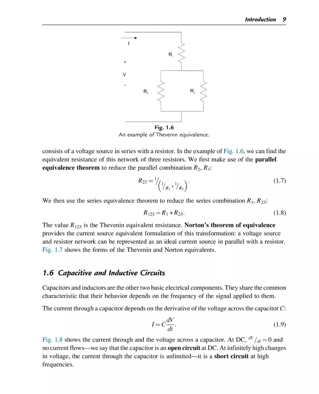
Thevenin’s theorem of equivalence tells us that, given two nodes for which we can identify a
voltage and current, we can find an equivalent network looking into those two nodes that
Fig. 1.5
An example of Kirchoff’s voltage and current laws.
Introduction 9
Fig. 1.6
An example of Thevenin equivalence.
consists of a voltage source in series with a resistor. In the example of Fig. 1.6, we can find the
equivalent resistance of this network of three resistors. We first make use of the parallel
equivalence theorem to reduce the parallel combination R2, R3:
:
R23 ¼ 1 1
(1.7)
=R2 + 1=R3
We then use the series equivalence theorem to reduce the series combination R1, R23:
R123 ¼ R1 + R23 :
(1.8)
The value R123 is the Thevenin equivalent resistance. Norton’s theorem of equivalence
provides the current source equivalent formulation of this transformation: a voltage source
and resistor network can be represented as an ideal current source in parallel with a resistor.
Fig. 1.7 shows the forms of the Thevenin and Norton equivalents.
1.6 Capacitive and Inductive Circuits
Capacitors and inductors are the other two basic electrical components. They share the common
characteristic that their behavior depends on the frequency of the signal applied to them.
The current through a capacitor depends on the derivative of the voltage across the capacitor C:
I¼C
dV
:
dt
(1.9)
Fig. 1.8 shows the current through and the voltage across a capacitor. At DC, dV =dt ¼ 0 and
no current flows—we say that the capacitor is an open circuit at DC. At infinitely high changes
in voltage, the current through the capacitor is unlimited—it is a short circuit at high
frequencies.
10
Chapter 1
Thevenin
Norton
Fig. 1.7
Forms of the Thevenin and Norton equivalents.
Fig. 1.8
Voltage and current through a capacitor.
The behavior of an inductor is complementary: its voltage depends on the derivative of the
current through the inductor L:
V ¼L
dI
:
dt
(1.10)
Fig. 1.9 shows the current through and voltage across an inductor. The inductor is a short circuit
at DC and an open circuit at high frequencies.
We can relate the behavior of these components more directly to a resistor by describing each
as a reactance X which is a function of frequency ω, in units r/s (radians per second).
The capacitor’s reactance decreases with frequency:
Fig. 1.9
Voltage and current through an inductor.
Introduction 11
1
:
ωC
(1.11)
1
:
2πfC
(1.12)
XC ¼
Since ω ¼ 2πf, we can write this as
XC ¼
The inductor’s reactance increases with frequency:
XL ¼ ωL
(1.13)
XL ¼ 2πfL:
(1.14)
or, in terms of Hertz,
We use units of Ohms for reactance.
As will see shortly, we can create a uniform representation for both resistance and reactance
known as impedance Z or its inverse, admittance Y.
1.7 Circuit Analysis
Impedance elements are linear—their behavior can be represented in the form y ¼ mx. The
graph of this function is a line through the origin with slope m. Although lines in general do not
have to go through the origin, that property is critical to the notion of linearity in physical
systems. We have also assumed that our circuits are time-invariant—the signals vary with
time but not the component values. Systems that are linear time-invariant (LTI) obey
superposition: their response to an input which is a sum of other inputs is the sum of the
responses to the individual input components.
We have seen that we can write a set of equations for the voltages and currents in a circuit and
solve for the unknowns. The form of the equations depends on the structure of the circuit and on
the values of its components. When solving by hand, we generally use standard algebraic
methods to manipulate and reduce the equations.
A more general approach is based on linear algebra. The nodal analysis method (also known
as the branch current method) is particularly well suited to solution by a computer. It
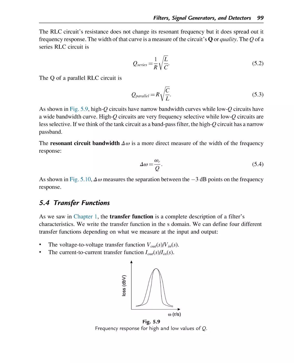
writes the branch currents in terms of the node voltages and the admittances of the devices:
2
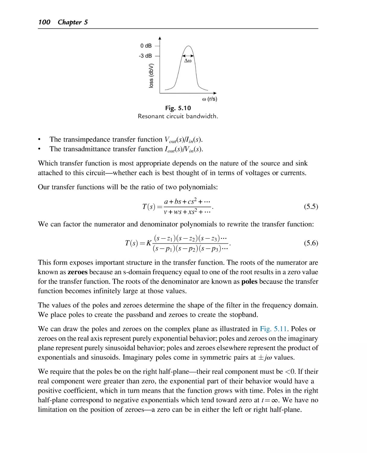
3
2
I ¼ YV:
32
3
Y11 Y21 ⋯
v1
i1
4 i2 5 ¼ 4 Y12 Y22
54 v2 5:
⋯
⋮
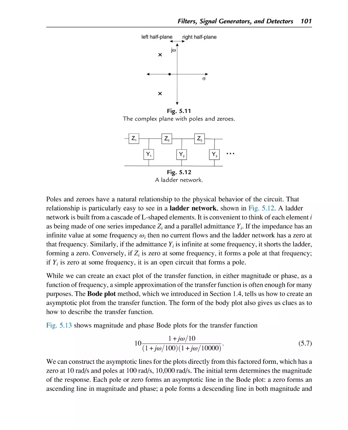
⋱
⋯
(1.15)
(1.16)
12
Chapter 1
Given the voltages, we can solve for the currents. For a purely resistive circuit, these equations
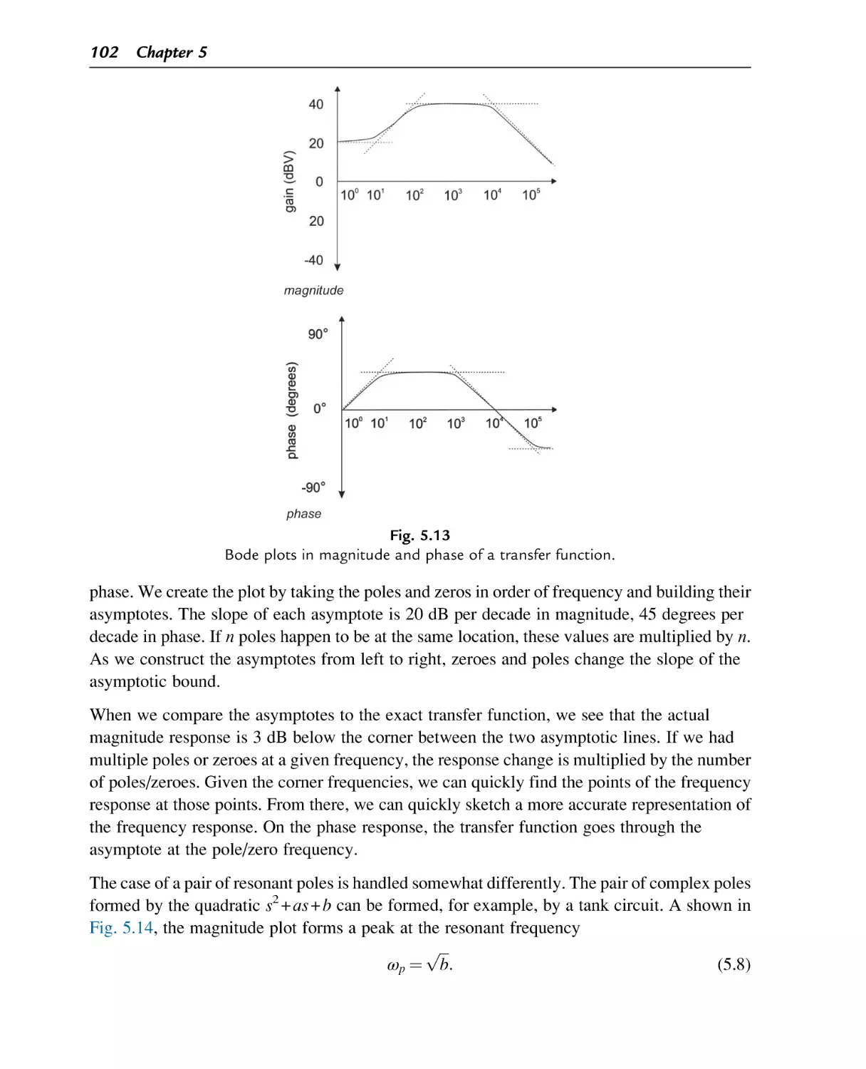
are simple. When the circuit includes reactive components, the system of equations
includes differential or integral equations.
We also need more abstract representations of circuits and signals than are provided by
nodal analysis and Kirchoff’s laws. We can use the Laplace transform to translate the
differential equations into the s domain and simplify analysis. The s parameter is complex
with s ¼ σ jω. (We traditionally write the imaginary number as j to avoid confusion with
current.) The Laplace transform integrates with an exponential:
ð∞
(1.17)
FðsÞ ¼ est f ðtÞdt:
0
Many operations are easier to perform in the s domain; we can invert the transformation back
into the time domain when we are done. The frequency-dependence reactance formulas of
Eqs. 1.11 and 1.13 are special cases of the s domain.
We can combine s domain impedances using the series and parallel equivalences:
Zser ðsÞ ¼ Z1 ðsÞ + Z2 ðsÞ:
Zpar ðsÞ ¼ 1
1
:
+ 1 Z2 ðsÞ
Z1 ðsÞ
(1.18)
(1.19)
We use voltage sources to describe the initial condition of capacitors and current sources for
the initial condition of inductors; each has its own representation in the s domain. We can
solve for the variable of interest in the s domain and then use inverse transforms to translate
back into the time domain. The s-domain form of impedances allows us to algebraically
manipulate resistances and reactances uniformly.
The impulse response is another key description of its behavior. An impulse δ(t) has a duration
of zero time and it has unbounded value over that time; the integral of the impulse over all
time is 1:
ð∞
δðtÞdt ¼ 1:
(1.20)
∞
The impulse response is interesting in itself—ringing a bell is a practical example of an
impulse response. But we are also interested in the impulse response because we can derive
the circuit’s response to other forms of input from its impulse response.
The order of a circuit or its functional model is given by the number of energy storing devices
in the circuit. A first-order impulse response has the form (given here using voltage variables):
V ðtÞ ¼ V ð0Þet=τ + Vf :
(1.21)
Introduction 13
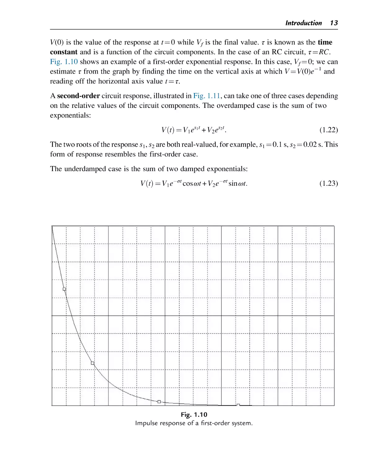
V(0) is the value of the response at t ¼ 0 while Vf is the final value. τ is known as the time
constant and is a function of the circuit components. In the case of an RC circuit, τ ¼ RC.
Fig. 1.10 shows an example of a first-order exponential response. In this case, Vf ¼ 0; we can
estimate τ from the graph by finding the time on the vertical axis at which V ¼ V(0)e1 and
reading off the horizontal axis value t ¼ τ.
A second-order circuit response, illustrated in Fig. 1.11, can take one of three cases depending
on the relative values of the circuit components. The overdamped case is the sum of two
exponentials:
V ðtÞ ¼ V1 es1 t + V2 es2 t :
(1.22)
The two roots of the response s1, s2 are both real-valued, for example, s1 ¼ 0.1 s, s2 ¼ 0.02 s. This
form of response resembles the first-order case.
The underdamped case is the sum of two damped exponentials:
V ðtÞ ¼ V1 eσt cos ωt + V2 eσt sin ωt:
Fig. 1.10
Impulse response of a first-order system.
(1.23)
14
Chapter 1
overdamped
underdamped
Fig. 1.11
Overdamped and underdamped responses of second-order systems.
The two response values are complex conjugates: s ¼ σ jω. This response is very different
from the first-order case—the response rises and falls around the steady-state value.
The critically damped case has the same form as the overdamped case but the two roots
are identical.
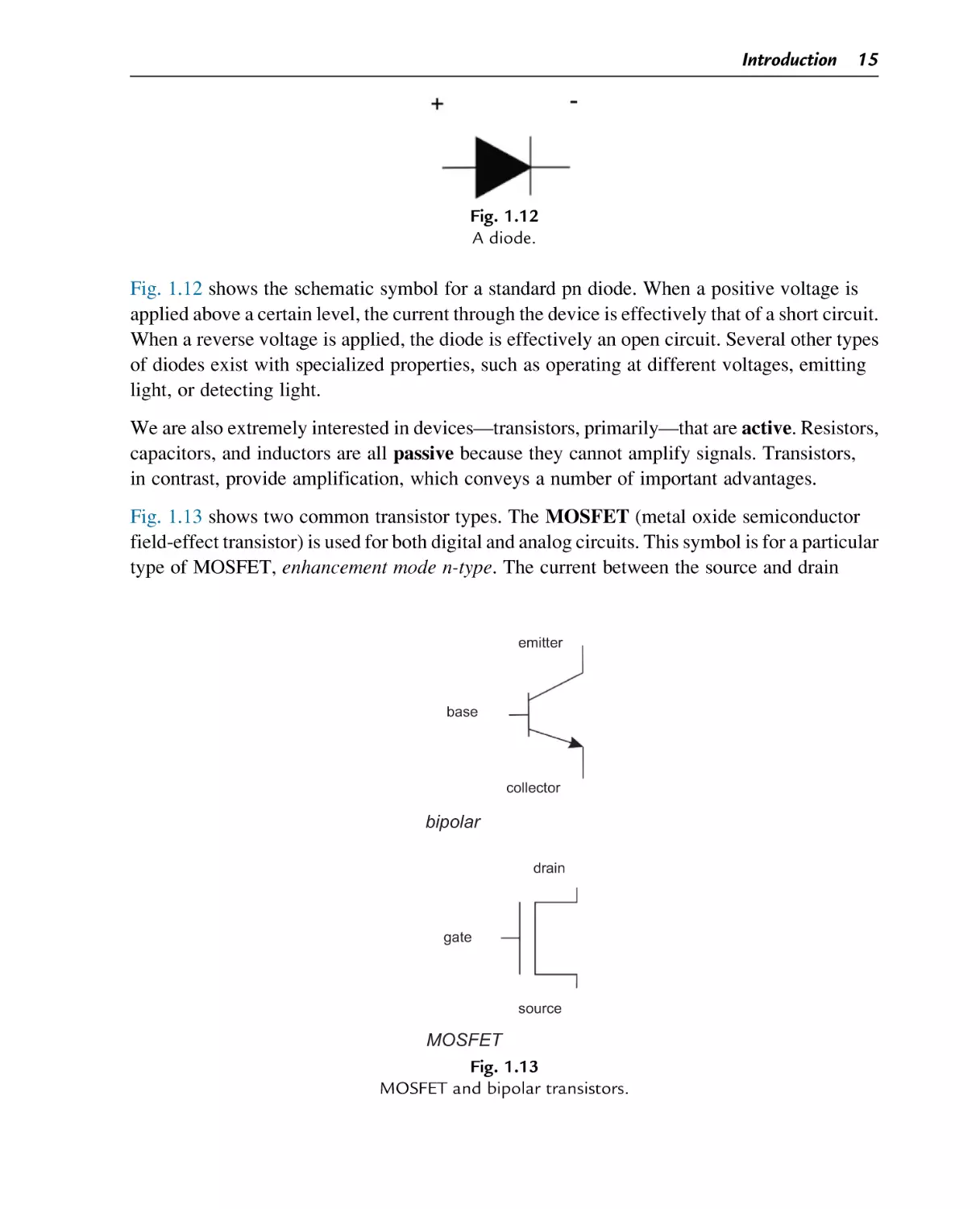
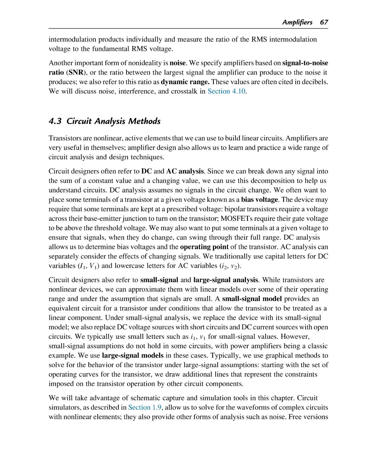
1.8 Nonlinear and Active Devices
We are very interested in devices that are nonlinear: diodes, transistors, etc. The nonlinearity
of diodes can be used for decisions, such as whether a given voltage represents a logic 0 or 1.
Introduction 15
Fig. 1.12
A diode.
Fig. 1.12 shows the schematic symbol for a standard pn diode. When a positive voltage is
applied above a certain level, the current through the device is effectively that of a short circuit.
When a reverse voltage is applied, the diode is effectively an open circuit. Several other types
of diodes exist with specialized properties, such as operating at different voltages, emitting
light, or detecting light.
We are also extremely interested in devices—transistors, primarily—that are active. Resistors,
capacitors, and inductors are all passive because they cannot amplify signals. Transistors,
in contrast, provide amplification, which conveys a number of important advantages.
Fig. 1.13 shows two common transistor types. The MOSFET (metal oxide semiconductor
field-effect transistor) is used for both digital and analog circuits. This symbol is for a particular
type of MOSFET, enhancement mode n-type. The current between the source and drain
emitter
base
collector
bipolar
drain
gate
source
MOSFET
Fig. 1.13
MOSFET and bipolar transistors.
16
Chapter 1
terminals depends on the voltage at the gate. The bipolar transistor used to be widely used
for both digital and analog circuits; today, it is primarily used for analog applications. The
emitter-collector current is a function of the base current. In both cases, one signal can be
used to control another, stronger signal. MOSFETs and bipolar transistors differ in several
important ways that we will study in succeeding chapters.
Both MOSFETs and bipolar transistors can be considered at least roughly linear over a portion
of their range; that linearity is used to build many types of amplifiers. However, their nonlinear
characteristic cannot be ignored and they complicate the solution of the circuit equations.
Circuit simulators use iterative methods to evaluate the behavior of circuits with nonlinear
devices. The simulator alternates between using an estimate of the node voltages and
branch currents to estimate the state of the nonlinear device, then using the device values to
update the voltages and currents. Each evaluation, known as a time step, stops when the
differences between successive sets of values become sufficiently small.
1.9 Design Methodologies and Tools
Ultimately, we need to move beyond circuit theory to the design of useful interfaces.
A design methodology is a sequence of steps we perform during design. Some parts of the
methodology will be automated while others will be manual.
We start with a set of loosely formulated requirements for the interface. We then refine
those requirements into a specification that includes specific values and other details of what
the interface should do.
Analysis is an important first step. We may propose some rough designs and then use our
analytic tools—Kirchoff’s laws, s domain analysis, etc.—to characterize the design and to
select some component values. Most of our analysis will be done by hand.
Simulation complements analysis. Simulators can analyze circuits, particularly nonlinear
circuits, much more accurately than we can do by hand. Simulators can also be given a long list
of input signals to help us better understand the design space. Digital logic simulation is usually
done with hardware description languages (HDLs) such as Verilog or VHDL. The HDL
description is fed to a simulator, which then provides waveform or tabular outputs.
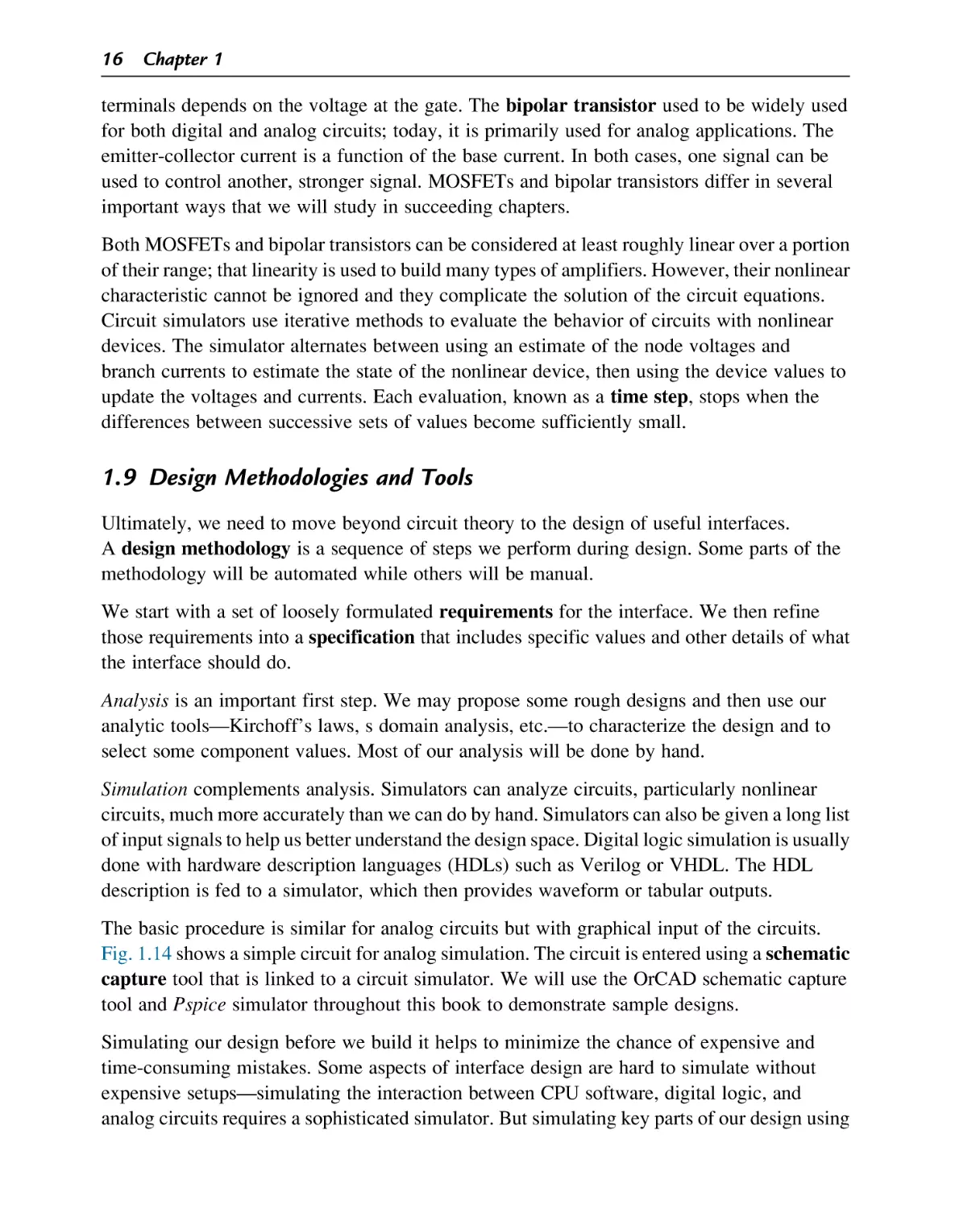
The basic procedure is similar for analog circuits but with graphical input of the circuits.
Fig. 1.14 shows a simple circuit for analog simulation. The circuit is entered using a schematic
capture tool that is linked to a circuit simulator. We will use the OrCAD schematic capture
tool and Pspice simulator throughout this book to demonstrate sample designs.
Simulating our design before we build it helps to minimize the chance of expensive and
time-consuming mistakes. Some aspects of interface design are hard to simulate without
expensive setups—simulating the interaction between CPU software, digital logic, and
analog circuits requires a sophisticated simulator. But simulating key parts of our design using
Introduction 17
12.00V
R1
47k
R3
1.5k
C2
RS
8.788V
v
1.279V
1u
1k
VOFF = 0
VAMPL = 2m
FREQ = 1k
AC =
Q1
C1
470
R2
5.6k
GND_0
12Vdc
RL
1k
Qbreakn
V1
0V
+ V2
–
595.3mV
R4
270
C3
47u
0V
0
Fig. 1.14
A circuit design for simulation.
either digital or analog simulators can build confidence in the design before we buy parts
and spend time building.
At some point, we have created our design: analog circuits, digital logic, software. Unless we are
very experienced, we probably want to prototype our design to be sure it is up to snuff.
Prototyping helps us ensure that the boundaries between the computer and the circuits are
properly designed. Prototyping also lets us evaluate the characteristics of the circuit. While we
may be able to perform simple tests of the interface without the microcontroller, we need to
connect the interface to the microcontroller to fully test the system. Modern manufacturing
techniques rely on advanced packages for integrated circuits that are difficult to work with
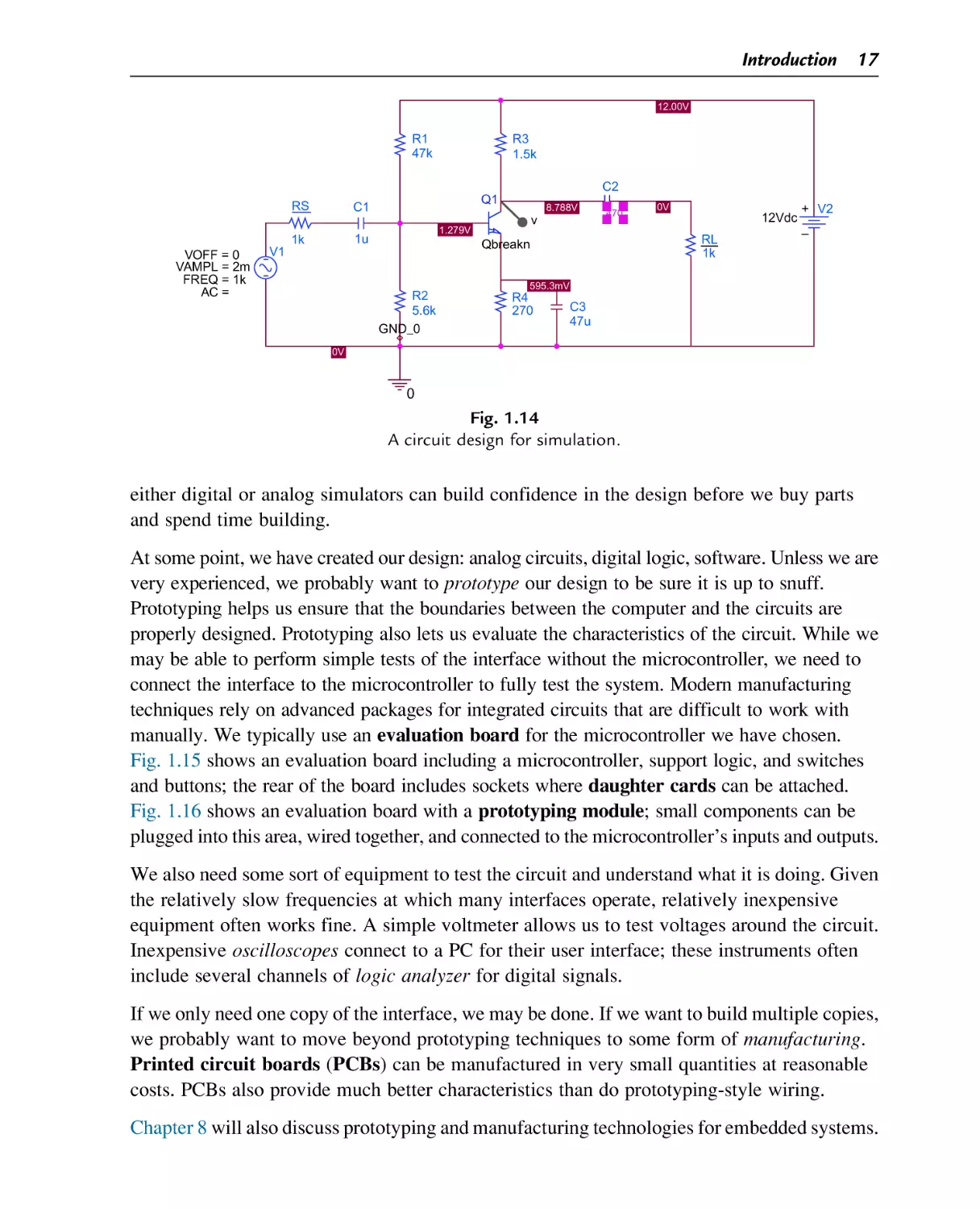
manually. We typically use an evaluation board for the microcontroller we have chosen.
Fig. 1.15 shows an evaluation board including a microcontroller, support logic, and switches
and buttons; the rear of the board includes sockets where daughter cards can be attached.
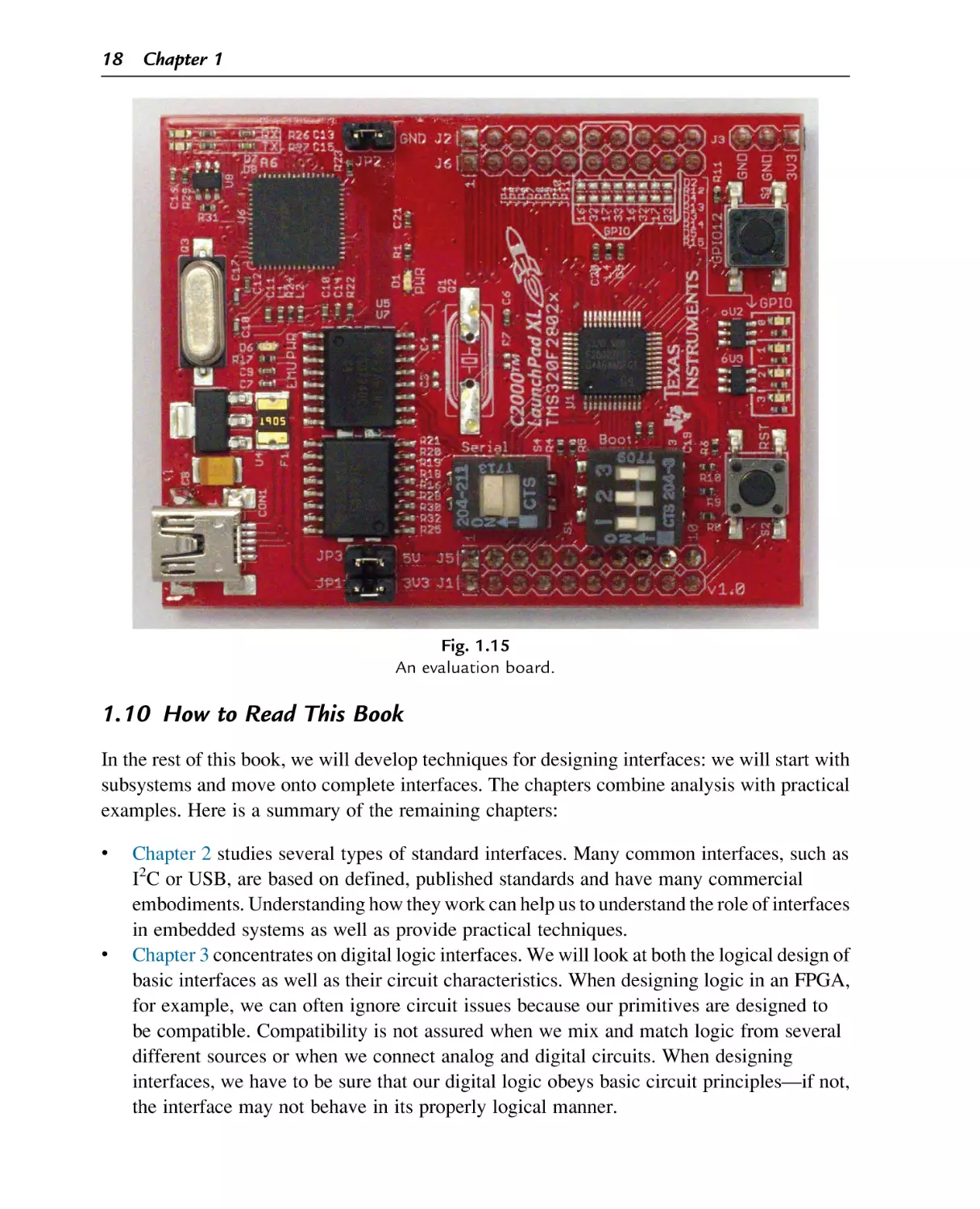
Fig. 1.16 shows an evaluation board with a prototyping module; small components can be
plugged into this area, wired together, and connected to the microcontroller’s inputs and outputs.
We also need some sort of equipment to test the circuit and understand what it is doing. Given
the relatively slow frequencies at which many interfaces operate, relatively inexpensive
equipment often works fine. A simple voltmeter allows us to test voltages around the circuit.
Inexpensive oscilloscopes connect to a PC for their user interface; these instruments often
include several channels of logic analyzer for digital signals.
If we only need one copy of the interface, we may be done. If we want to build multiple copies,
we probably want to move beyond prototyping techniques to some form of manufacturing.
Printed circuit boards (PCBs) can be manufactured in very small quantities at reasonable
costs. PCBs also provide much better characteristics than do prototyping-style wiring.
Chapter 8 will also discuss prototyping and manufacturing technologies for embedded systems.
18
Chapter 1
Fig. 1.15
An evaluation board.
1.10 How to Read This Book
In the rest of this book, we will develop techniques for designing interfaces: we will start with
subsystems and move onto complete interfaces. The chapters combine analysis with practical
examples. Here is a summary of the remaining chapters:
•
•
Chapter 2 studies several types of standard interfaces. Many common interfaces, such as
I2C or USB, are based on defined, published standards and have many commercial
embodiments. Understanding how they work can help us to understand the role of interfaces
in embedded systems as well as provide practical techniques.
Chapter 3 concentrates on digital logic interfaces. We will look at both the logical design of
basic interfaces as well as their circuit characteristics. When designing logic in an FPGA,
for example, we can often ignore circuit issues because our primitives are designed to
be compatible. Compatibility is not assured when we mix and match logic from several
different sources or when we connect analog and digital circuits. When designing
interfaces, we have to be sure that our digital logic obeys basic circuit principles—if not,
the interface may not behave in its properly logical manner.
Introduction 19
Fig. 1.16
An evaluation board with a prototyping area.
•
•
•
•
Chapter 4 studies on amplification using transistors. Amplification is a key operation
in all sorts of interfaces. Some basic principles will allow us to design and build amplifiers
suited to our particular requirements.
Chapter 5 considers filtering, signal generation, and detection. Filtering is a critical
complement to amplification. We can filter using both analog and digital techniques,
each with its own advantages. We make use of several different types of controlled,
precision waveforms: sine waves, square waves, etc. We may want to generate a signal
directly for output; we may also use generated signals to control other parts of our interface.
Detecting signals is a nonlinear operation that complements filtering.
Chapter 6 studies circuits that convert between analog and digital representations.
Conversion is at the heart of interfacing. We need to understand how converters work
in order to apply them properly and choose the best type for our application.
Chapter 7 looks at power delivery and conversion. Real circuits do not provide ideal
power sources. We need to understand the limitations of realistic power circuits and their
effects on both analog and digital circuits. Studying the design of power conversion
circuits helps us understand what they do; in some cases, we may want to design our
own as well.
20
•
Chapter 1
Chapter 8 puts together these techniques to create mixed-signal systems that combine
analog and digital systems. Mixed-signal design is the heart of interfacing. It requires
us to deploy all of our design skills, both analog and digital.
The body of the book emphasizes MOSFETs. Two appendices concentrate on bipolar devices
and circuits:
•
•
Appendix A describes TTL logic.
Appendix B analyzes bipolar amplifiers.
Please don’t limit your reading of this book to these pages. The book Web site contains
additional material. A set of presentations summarizes the material in this book. Lab exercises
complement and extend the descriptions in this text. Lab procedures can change, particularly
where software is involved; the Web site provides a forum for sharing updated materials.
Questions
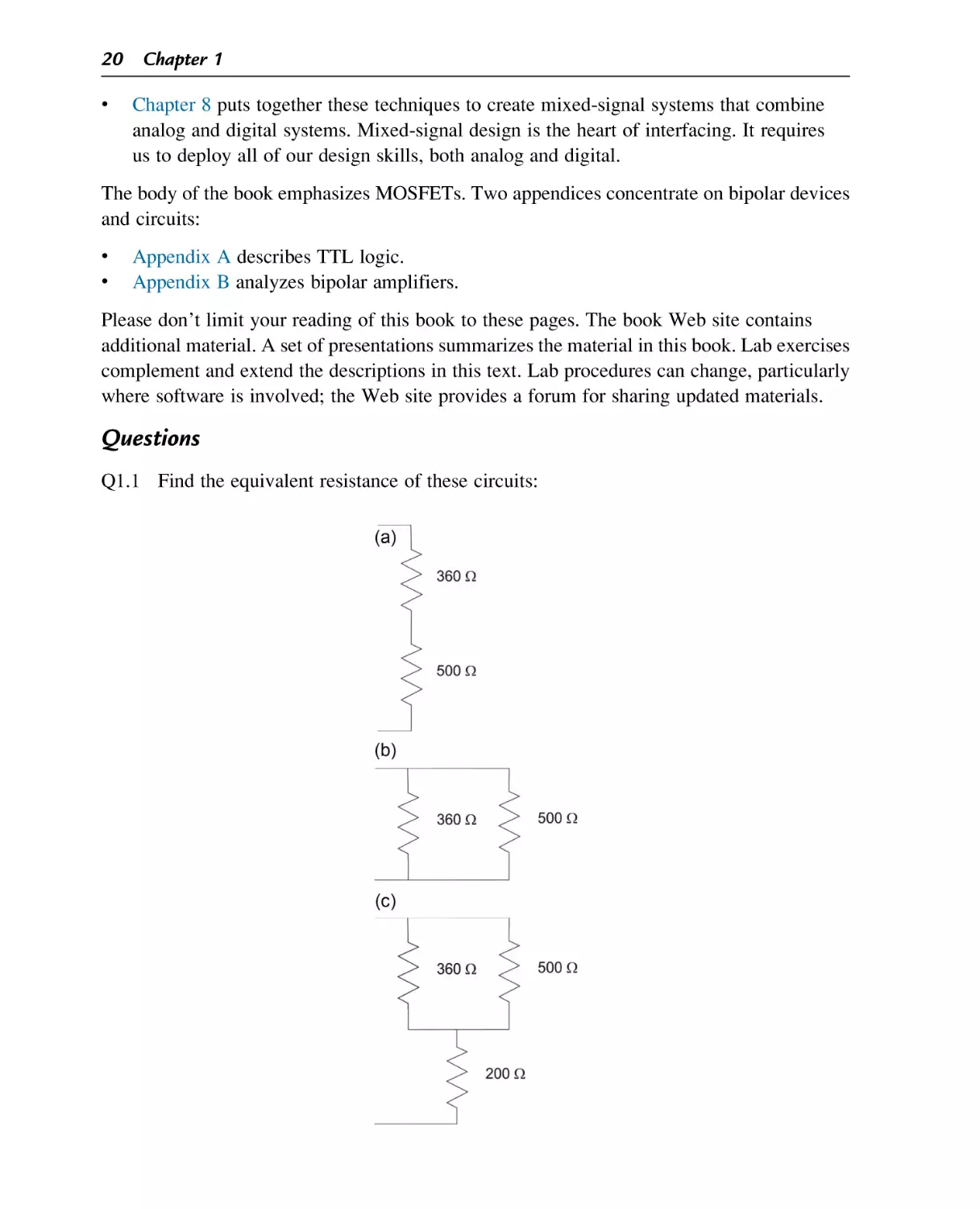
Q1.1 Find the equivalent resistance of these circuits:
Introduction 21
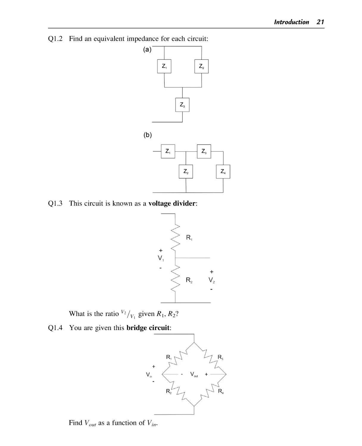
Q1.2 Find an equivalent impedance for each circuit:
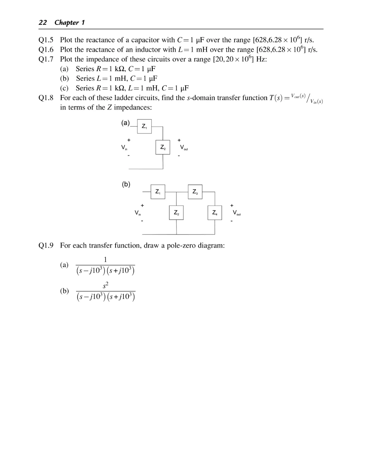
Q1.3 This circuit is known as a voltage divider:
What is the ratio V2 =V1 given R1, R2?
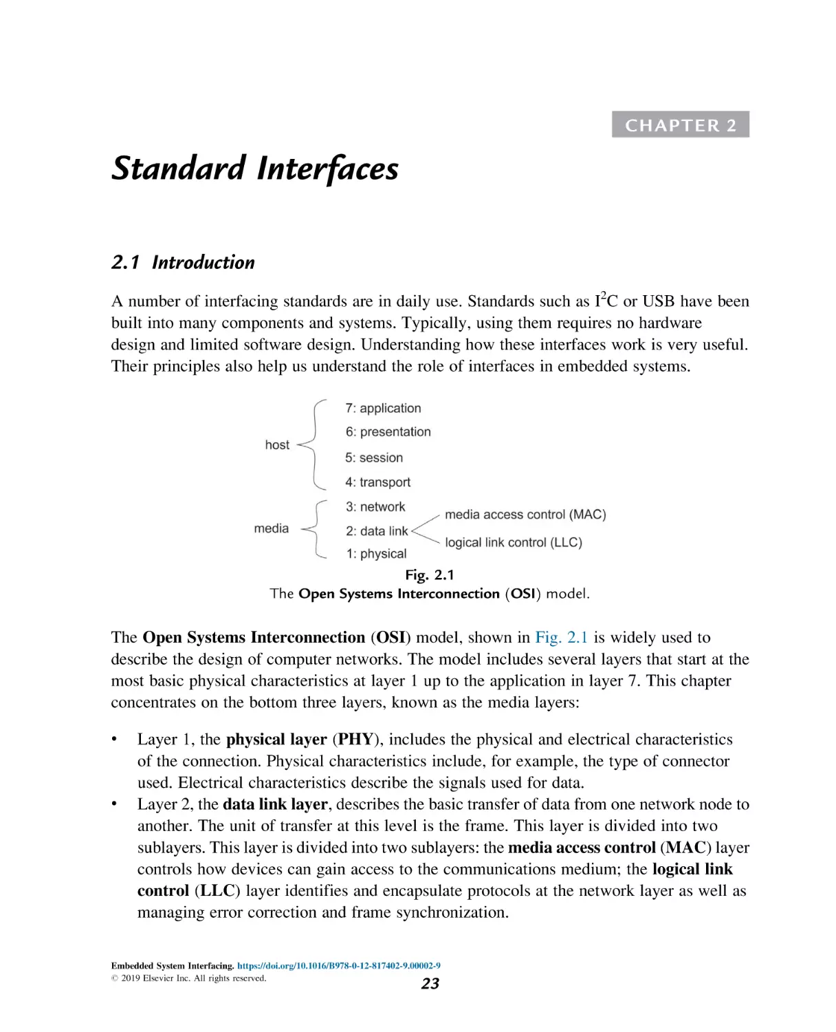
Q1.4 You are given this bridge circuit:
Find Vout as a function of Vin.
22
Chapter 1
Q1.5 Plot the reactance of a capacitor with C ¼ 1 μF over the range [628,6.28 106] r/s.
Q1.6 Plot the reactance of an inductor with L ¼ 1 mH over the range [628,6.28 106] r/s.
Q1.7 Plot the impedance of these circuits over a range [20, 20 106] Hz:
(a) Series R ¼ 1 kΩ, C ¼ 1 μF
(b) Series L ¼ 1 mH, C ¼ 1 μF
(c) Series R ¼ 1 kΩ, L ¼ 1 mH, C ¼ 1 μF
Q1.8 For each of these ladder circuits, find the s-domain transfer function T ðsÞ ¼ Vout ðsÞ Vin ðsÞ
in terms of the Z impedances:
Q1.9 For each transfer function, draw a pole-zero diagram:
(a)
1
s j10 s + j103
(b)
3
s2
s j103 s + j103
CHAPTER 2
Standard Interfaces
2.1 Introduction
A number of interfacing standards are in daily use. Standards such as I2C or USB have been
built into many components and systems. Typically, using them requires no hardware
design and limited software design. Understanding how these interfaces work is very useful.
Their principles also help us understand the role of interfaces in embedded systems.
Fig. 2.1
The Open Systems Interconnection (OSI) model.
The Open Systems Interconnection (OSI) model, shown in Fig. 2.1 is widely used to
describe the design of computer networks. The model includes several layers that start at the
most basic physical characteristics at layer 1 up to the application in layer 7. This chapter
concentrates on the bottom three layers, known as the media layers:
•
•
Layer 1, the physical layer (PHY), includes the physical and electrical characteristics
of the connection. Physical characteristics include, for example, the type of connector
used. Electrical characteristics describe the signals used for data.
Layer 2, the data link layer, describes the basic transfer of data from one network node to
another. The unit of transfer at this level is the frame. This layer is divided into two
sublayers. This layer is divided into two sublayers: the media access control (MAC) layer
controls how devices can gain access to the communications medium; the logical link
control (LLC) layer identifies and encapsulate protocols at the network layer as well as
managing error correction and frame synchronization.
Embedded System Interfacing. https://doi.org/10.1016/B978-0-12-817402-9.00002-9
# 2019 Elsevier Inc. All rights reserved.
23
24
•
Chapter 2
Layer 3, the network layer, moves data sequences from one node to another,
potentially across several different types of networks.
In this chapter, we will look at six different standard interfaces:
•
•
•
•
•
•
•
The RS-232 serial interface commonly used on personal computers.
The I2C interface which is used to communicate with devices along a relatively simple
bus; we also discuss the I2S bus used for digital audio and the CAN bus used in
automotive systems.
The Universal Serial Bus (USB), which has gone through several revisions as a
common standard for PC interfacing.
WiFi, a wireless network widely used for PCs and also for IoT systems.
Zigbee, a wireless network designed for embedded systems.
Two wireless interfaces, Bluetooth and Bluetooth Low Energy (BLE). Despite sharing a
common root name, these two interfaces vary in some interesting and important ways.
LoRaWAN, a low power wide area network.
In Section 2.9, we will consider Internet connections that rely on communications interfaces.
2.2 RS-232
Serial interfaces are some of the oldest computer interfaces, predating many features of
modern computer systems, including the OSI model. A number of different serial interfaces and
protocols have been defined over the years. The RS-232 standard was created in 1960 and
was provided on most personal computers for many years. Today, few PCs provide a serial port
but RS-232 is still used in some types of industrial equipment. Serial ports do not run at
high speeds by modern standards but their hardware and software requirements are both
minimal.
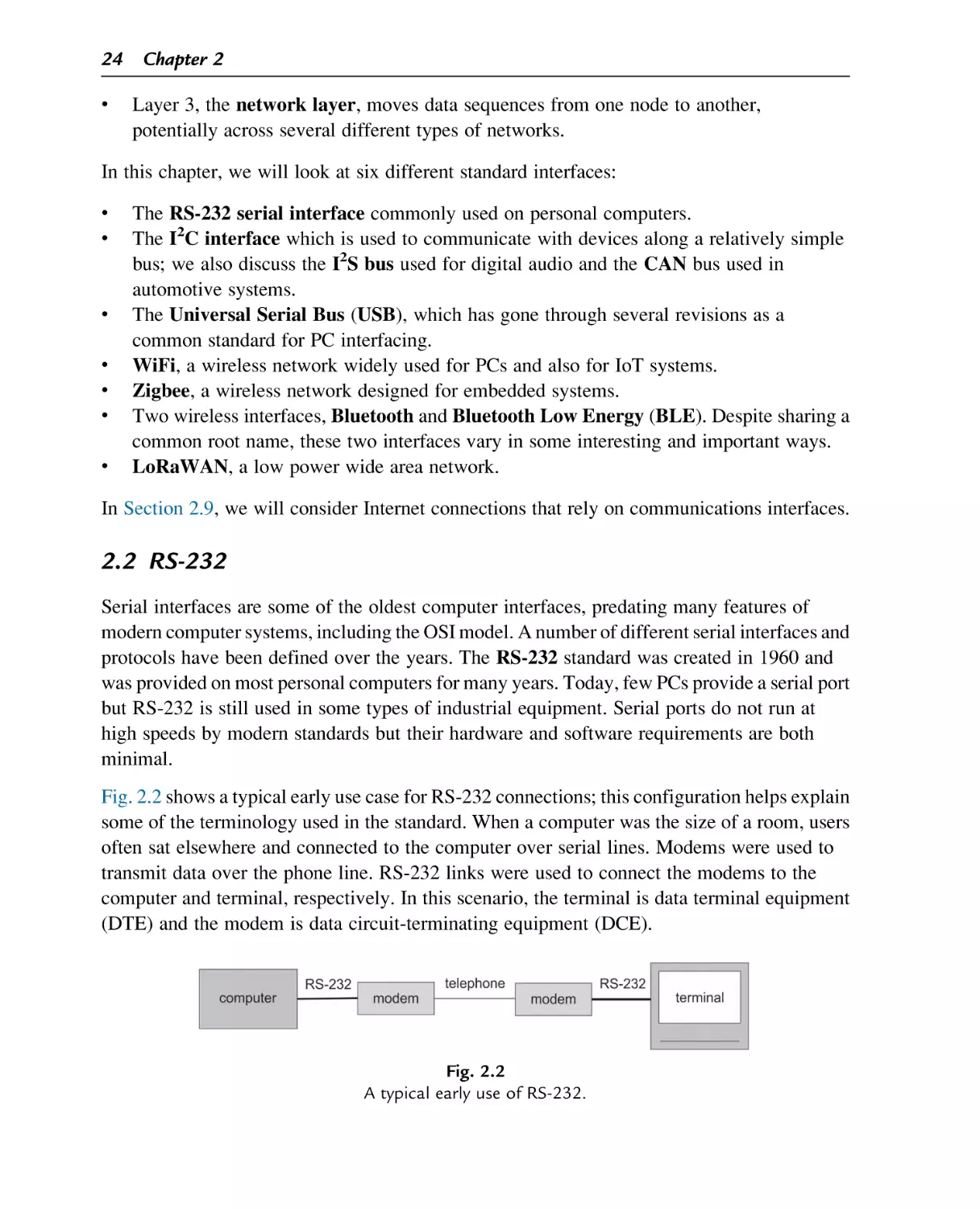
Fig. 2.2 shows a typical early use case for RS-232 connections; this configuration helps explain
some of the terminology used in the standard. When a computer was the size of a room, users
often sat elsewhere and connected to the computer over serial lines. Modems were used to
transmit data over the phone line. RS-232 links were used to connect the modems to the
computer and terminal, respectively. In this scenario, the terminal is data terminal equipment
(DTE) and the modem is data circuit-terminating equipment (DCE).
Fig. 2.2
A typical early use of RS-232.
Standard Interfaces 25
The RS-232 electrical standard uses much higher voltages than are typically used today. Those
high voltages often require specialized circuits; however, they do provide some amount of
resistance to noise in challenging environments. The standard allows signals of up to 25 V;
both positive and negative voltages are used and voltages around ground are not valid levels.
The mark data signal is sent as a low voltage level while the space is a high voltage level.
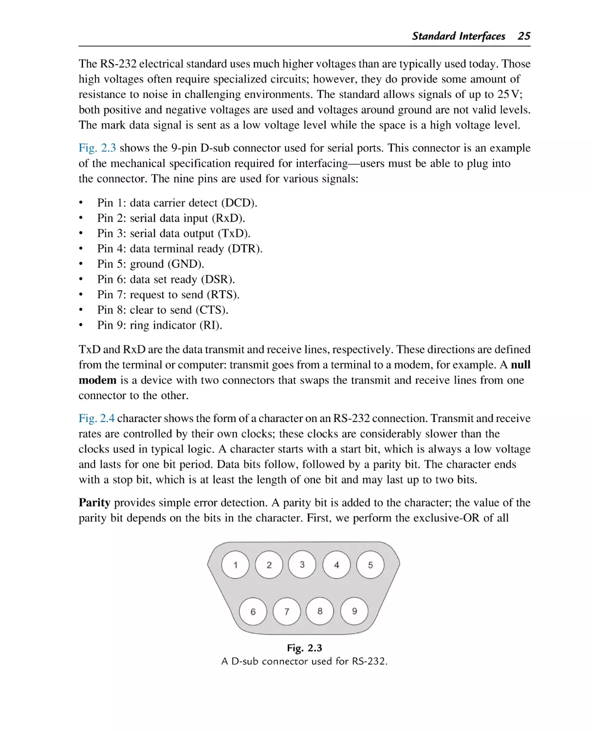
Fig. 2.3 shows the 9-pin D-sub connector used for serial ports. This connector is an example
of the mechanical specification required for interfacing—users must be able to plug into
the connector. The nine pins are used for various signals:
•
•
•
•
•
•
•
•
•
Pin
Pin
Pin
Pin
Pin
Pin
Pin
Pin
Pin
1:
2:
3:
4:
5:
6:
7:
8:
9:
data carrier detect (DCD).
serial data input (RxD).
serial data output (TxD).
data terminal ready (DTR).
ground (GND).
data set ready (DSR).
request to send (RTS).
clear to send (CTS).
ring indicator (RI).
TxD and RxD are the data transmit and receive lines, respectively. These directions are defined
from the terminal or computer: transmit goes from a terminal to a modem, for example. A null
modem is a device with two connectors that swaps the transmit and receive lines from one
connector to the other.
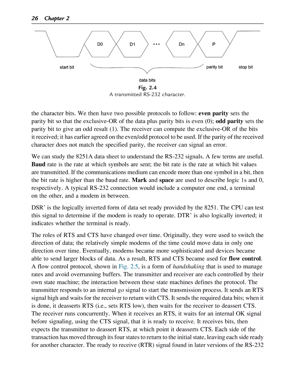
Fig. 2.4 character shows the form of a character on an RS-232 connection. Transmit and receive
rates are controlled by their own clocks; these clocks are considerably slower than the
clocks used in typical logic. A character starts with a start bit, which is always a low voltage
and lasts for one bit period. Data bits follow, followed by a parity bit. The character ends
with a stop bit, which is at least the length of one bit and may last up to two bits.
Parity provides simple error detection. A parity bit is added to the character; the value of the
parity bit depends on the bits in the character. First, we perform the exclusive-OR of all
Fig. 2.3
A D-sub connector used for RS-232.
26
Chapter 2
Fig. 2.4
A transmitted RS-232 character.
the character bits. We then have two possible protocols to follow: even parity sets the
parity bit so that the exclusive-OR of the data plus parity bits is even (0); odd parity sets the
parity bit to give an odd result (1). The receiver can compute the exclusive-OR of the bits
it received; it has earlier agreed on the even/odd protocol to be used. If the parity of the received
character does not match the specified parity, the receiver can signal an error.
We can study the 8251A data sheet to understand the RS-232 signals. A few terms are useful.
Baud rate is the rate at which symbols are sent; the bit rate is the rate at which bit values
are transmitted. If the communications medium can encode more than one symbol in a bit, then
the bit rate is higher than the baud rate. Mark and space are used to describe logic 1s and 0,
respectively. A typical RS-232 connection would include a computer one end, a terminal
on the other, and a modem in between.
DSR’ is the logically inverted form of data set ready provided by the 8251. The CPU can test
this signal to determine if the modem is ready to operate. DTR’ is also logically inverted; it
indicates whether the terminal is ready.
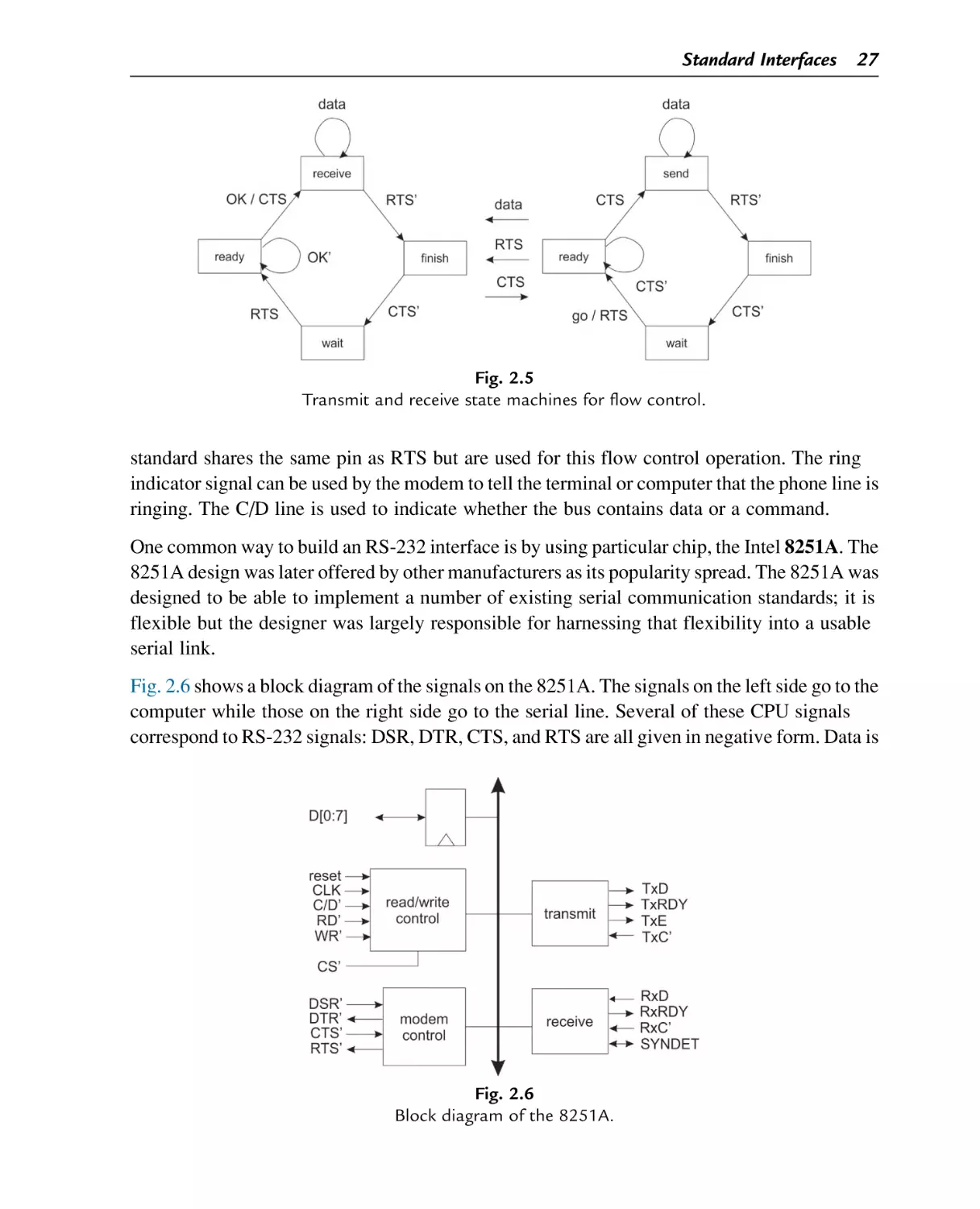
The roles of RTS and CTS have changed over time. Originally, they were used to switch the
direction of data; the relatively simple modems of the time could move data in only one
direction over time. Eventually, modems became more sophisticated and devices became
able to send larger blocks of data. As a result, RTS and CTS became used for flow control.
A flow control protocol, shown in Fig. 2.5, is a form of handshaking that is used to manage
rates and avoid overrunning buffers. The transmitter and receiver are each controlled by their
own state machine; the interaction between these state machines defines the protocol. The
transmitter responds to an internal go signal to start the transmission process. It sends an RTS
signal high and waits for the receiver to return with CTS. It sends the required data bits; when it
is done, it deasserts RTS (i.e., sets RTS low), then waits for the receiver to deassert CTS.
The receiver runs concurrently. When it receives an RTS, it waits for an internal OK signal
before signaling, using the CTS signal, that it is ready to receive. It receives bits, then
expects the transmitter to deassert RTS, at which point it deasserts CTS. Each side of the
transaction has moved through its four states to return to the initial state, leaving each side ready
for another character. The ready to receive (RTR) signal found in later versions of the RS-232
Standard Interfaces 27
Fig. 2.5
Transmit and receive state machines for flow control.
standard shares the same pin as RTS but are used for this flow control operation. The ring
indicator signal can be used by the modem to tell the terminal or computer that the phone line is
ringing. The C/D line is used to indicate whether the bus contains data or a command.
One common way to build an RS-232 interface is by using particular chip, the Intel 8251A. The
8251A design was later offered by other manufacturers as its popularity spread. The 8251A was
designed to be able to implement a number of existing serial communication standards; it is
flexible but the designer was largely responsible for harnessing that flexibility into a usable
serial link.
Fig. 2.6 shows a block diagram of the signals on the 8251A. The signals on the left side go to the
computer while those on the right side go to the serial line. Several of these CPU signals
correspond to RS-232 signals: DSR, DTR, CTS, and RTS are all given in negative form. Data is
Fig. 2.6
Block diagram of the 8251A.
28
Chapter 2
supplied on eight parallel, bidirectional lines. The C/D’ signal is used to determine whether the
data lines represent data (0) or control (1) information. The reset signal allows the chip to
be reset. CLK provides the clock. RD’ and WR’ are used to tell the 8251A that the CPU is
reading or writing words. On the serial line side, we have transmitted serial signals. TxD is
transmitting data, TxRDY signals whether the transmitter is ready, TxE signals that the
transmitter has no characters ready to send. TxC’ is a clock used to determine the rate of the data
symbols. RxD is the receive data, RxRDY indicates that the receiver is ready, RxC’ is the
receive data clock. The SYNDET/BRKDET signal is used as either an output (sync detect)
or an input (break detect).
The 8251A has seven internal eight-bit registers. Two of the registers—the transmit and receive
buffers—are used for the data that is transmitted or received. The sync1 and 2 characters are
used in synchronous mode only. The status register gives status and error information. The
mode register determines whether synchronous or asynchronous mode will be used along with
their parameters. The command register is used for enabling, disabling, and error handling.
After the 8251A is reset, the CPU needs to send two words: first, a mode instruction which
specifies synchronous or asynchronous along with some operating parameters; next, a
command instruction which sets up the transmit and receive modes.
The mode instruction bits are used as follows:
•
•
•
•
Bits 0-1 specify the baud rate factor: synchronous mode (00), 1X (01), 16X (10), or 64X
(11). This factor determines the conversion rate between the mark/space rates and the
transmit or receive clocks.
Bits 2-3 specify the character length: 5 (00), 6 (01), 7 (10), or 8 (11) bits.
Bits 4-5 specify parity: even (11), odd (00), or disabled (10, 01).
Bits 6-7 specify the length of the stop bit: 1 (01), 1.5 (10), or 2 (10).
The command register bits include:
•
•
•
•
•
•
•
•
Bit 0,
Bit 1,
Bit 2,
Bit 3,
Bit 4,
Bit 5,
Bit 6,
Bit 7,
TXEN, enables (1) or disables (0) the transmitter.
DTR sends an nDTR output value in negated form (1 for 0, 0 for 1).
RXE, enables (1) or disables (0) the transmitter.
SBRK, sends a break character (1) or specifies normal operation (0).
ER, sets (1) or keeps (0) error flags.
RTS, sets an nRTS value in negated form.
IR, performs an internal reset (1) or normal operation (0).
EH, enables hunt mode (1), or normal operation.
The status bits include:
•
•
Bit 0, TXRDY, signals whether the transmitter is busy (0) or ready (1).
Bit 1, RXRDY, signals whether the receiver is busy (0) or ready (1).
Standard Interfaces 29
•
•
•
•
•
•
Bit
Bit
Bit
Bit
Bit
Bit
2,
3,
4,
5,
6,
7,
TXEMPTY, indicates whether the transmitter is busy (0) or done (1).
PE, indicates a parity error (1) or OK (0).
OE, indicates an overrun error (1) or OK (0).
FE, indicates a frame error (1) or OK (0).
SYNDET, indicates whether a sync char was detected (1).
DSR, indicates the DSR value in negated form.
One of the charms of RS-232 is that it is slow and simple enough that we can watch it operate.
A breakout box is a simple device with a pair of D-sub connectors. The RS-232 signals flow
through but they are also shown on LEDs. The data is usually too fast to read directly but
the control signals can be seen; watching them allows us to see how the serial line is operating.
2.3 I2C, CAN, and I2S
I2C [45] is widely used to connect multiple chips in systems. The bus provides relatively
low data rates, so its uses are primarily for mode control and similarly low-speed uses.
However, its extremely low cost has helped to make it ubiquitous. The CAN bus [8] is widely
used in automotive electrical and electronics (EE) systems. Its structure is very similar to I2C.
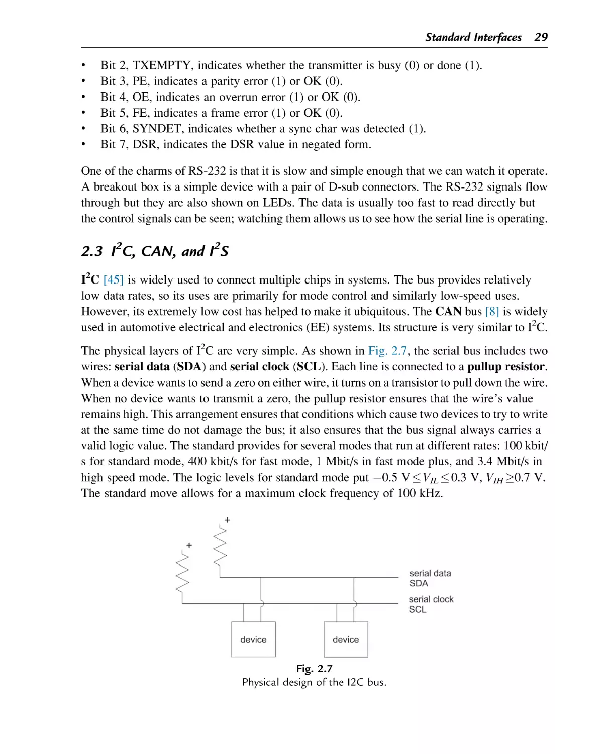
The physical layers of I2C are very simple. As shown in Fig. 2.7, the serial bus includes two
wires: serial data (SDA) and serial clock (SCL). Each line is connected to a pullup resistor.
When a device wants to send a zero on either wire, it turns on a transistor to pull down the wire.
When no device wants to transmit a zero, the pullup resistor ensures that the wire’s value
remains high. This arrangement ensures that conditions which cause two devices to try to write
at the same time do not damage the bus; it also ensures that the bus signal always carries a
valid logic value. The standard provides for several modes that run at different rates: 100 kbit/
s for standard mode, 400 kbit/s for fast mode, 1 Mbit/s in fast mode plus, and 3.4 Mbit/s in
high speed mode. The logic levels for standard mode put 0.5 V VIL 0.3 V, VIH 0.7 V.
The standard move allows for a maximum clock frequency of 100 kHz.
Fig. 2.7
Physical design of the I2C bus.
30
Chapter 2
The CAN bus uses a similar physical layer that can transmit at 1 Mb/s over a maximum length
of 50 m; a variation using an optical link has also been developed.
All data is sent as eight-bit bytes. As shown in Fig. 2.8, the data is transmitted from mostsignificant bit (MSB) to least-significant bit (LSB). The receiving slave acknowledges
each bite: the master temporarily releases SDA; the slave pulls SDA low for an
acknowledgment or leaves it high for a negative acknowledgment.
As shown in Fig. 2.9, a data transfer consists of a start bit, a sequence of bytes, and a final stop
bit. A start bit is signaled by a high-to-low transition on SDA while a stop bit is signaled by
a low-to-high transition on SDA. The first part of the data transfer is the address, plus a
read/write bit. This figure shows the original 7-bit address mode: the first seven bits of the first
byte are address, with the eighth bit indicating read/write’. A 10-bit address mode uses the
first two bytes for address and read/write’; the high-order five bits of the high address byte are
11,110. A master can generate successive data transfers by sending another start signal
without having sent a stop; this feature allows the master to send to several different slaves
without the overhead of intermediate stop bits.
Because the bus may have more than one master, mastership must be arbitrated to determine
who can transmit. Unlike some busses, arbitration occurs during the transmission of the address
bit. The protocol takes advantage of the physical layer design to simplify arbitration.
A device may start to write when the bus is inactive. When two devices try to write at the same
time, each cannot tell that another device is trying to transmit until the two devices try to
send different bits. Both devices monitor the bus as they transmit. When they detect a
conflict, the device with the lower priority immediately stops transmitting. The bus clock is
slow enough that the valid bit can be properly transmitted during the remainder of the
clock period. The standard reserves some addresses, including a general call address. Sending a
general call, followed by a second byte value of 00000110 signals a software reset. CAN uses
a similar arbitration method. Nodes listen to the bus to determine when a new transmission
begins.
Fig. 2.8
Format of a byte in I2C.
Fig. 2.9
Data transfers in I2C.
Standard Interfaces 31
Devices typically come from the manufacturer with a default address. Some devices do not
allow the address to be changed at all; others allow a limited range of address reprogramming;
some allow for arbitrary reprogramming of the address. If the device does not provide for
sufficient address reprogramming, a common solution is to assign each device a unique
identifier in the data section of the device. Each data transfer to this class of device starts with
the device address, followed by a byte which gives the identifier for which the transfer is
intended. This solution comes at the cost of bus bandwidth.
The I2S bus [47] has a very similar name and was developed by the same company but is
used for very different purposes. This bus is one of several designed solely as a streaming audio
interface for communication between chips in consumer audio systems. The bus includes
three lines: clock SCK, word select WS, and data SD. Word select is used to indicate
whether the data is for the left or right channels, implicitly limiting the standard to stereo.
Any device that drives the clock effectively serves as master but the standard provides no
mechanism for switching between bus masters.
2.4 USB
The Universal Serial Bus, more commonly known as USB, is used in billions of computing
devices. Given its ubiquity in computing, it should be no surprise that it is used for embedded
system interfacing, either to connect to a host PC or to connect the embedded computer to
other devices.
USB [14, 26] has evolved over several versions over the past two decades, offering higher
performance and other features over time. USB 1.1 ran at 12 Mbit/s, USB 2.0 at 480 Mbit/s,
USB 3.0 at 5 Gbit/s, USB 3.1 at 10 Gbit/s, and USB 3.2 at 20 Gbit/s.
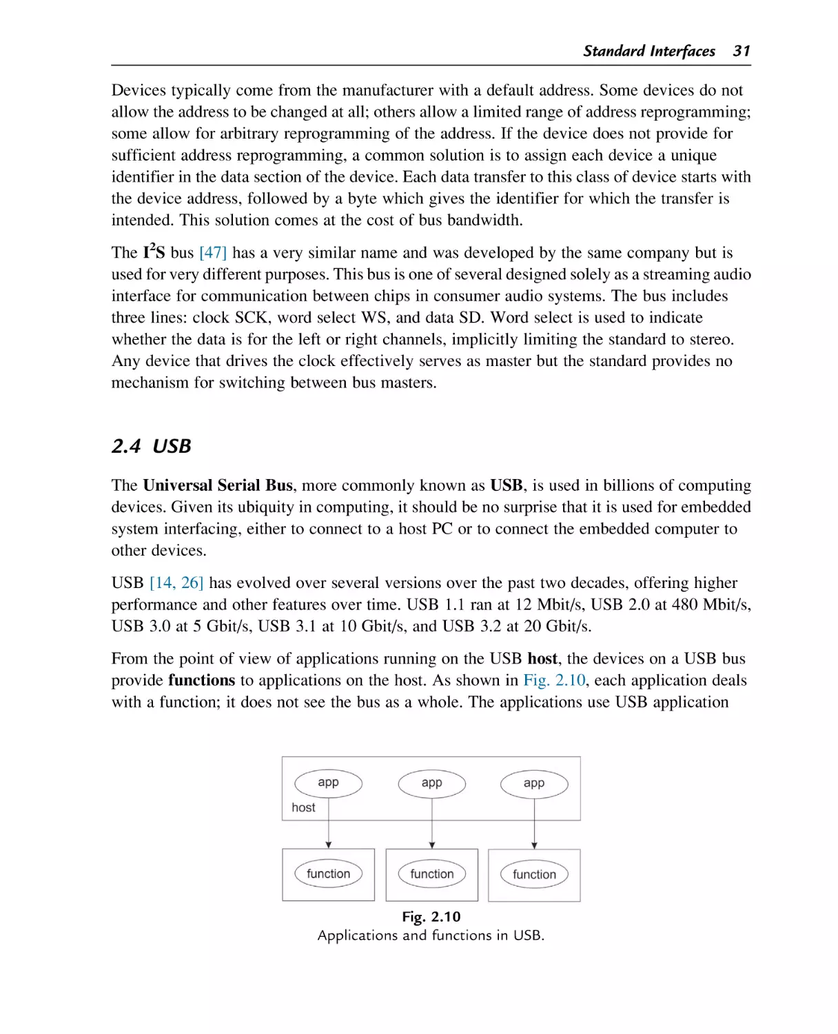
From the point of view of applications running on the USB host, the devices on a USB bus
provide functions to applications on the host. As shown in Fig. 2.10, each application deals
with a function; it does not see the bus as a whole. The applications use USB application
Fig. 2.10
Applications and functions in USB.
32
Chapter 2
programming interfaces (APIs) to deal with the functions, not low-level device operations. We
will discuss USB APIs in more detail later.
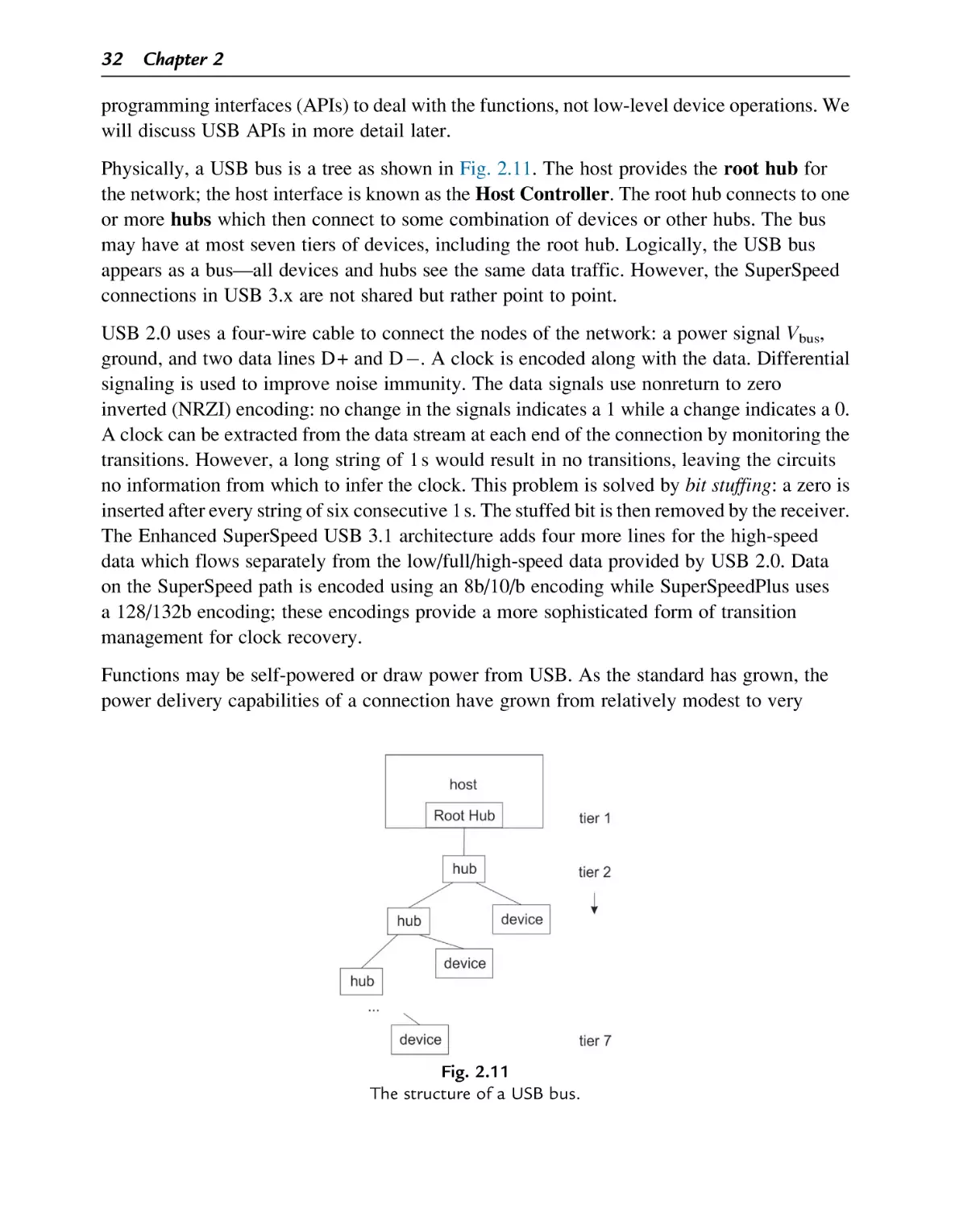
Physically, a USB bus is a tree as shown in Fig. 2.11. The host provides the root hub for
the network; the host interface is known as the Host Controller. The root hub connects to one
or more hubs which then connect to some combination of devices or other hubs. The bus
may have at most seven tiers of devices, including the root hub. Logically, the USB bus
appears as a bus—all devices and hubs see the same data traffic. However, the SuperSpeed
connections in USB 3.x are not shared but rather point to point.
USB 2.0 uses a four-wire cable to connect the nodes of the network: a power signal Vbus,
ground, and two data lines D+ and D . A clock is encoded along with the data. Differential
signaling is used to improve noise immunity. The data signals use nonreturn to zero
inverted (NRZI) encoding: no change in the signals indicates a 1 while a change indicates a 0.
A clock can be extracted from the data stream at each end of the connection by monitoring the
transitions. However, a long string of 1 s would result in no transitions, leaving the circuits
no information from which to infer the clock. This problem is solved by bit stuffing: a zero is
inserted after every string of six consecutive 1 s. The stuffed bit is then removed by the receiver.
The Enhanced SuperSpeed USB 3.1 architecture adds four more lines for the high-speed
data which flows separately from the low/full/high-speed data provided by USB 2.0. Data
on the SuperSpeed path is encoded using an 8b/10/b encoding while SuperSpeedPlus uses
a 128/132b encoding; these encodings provide a more sophisticated form of transition
management for clock recovery.
Functions may be self-powered or draw power from USB. As the standard has grown, the
power delivery capabilities of a connection have grown from relatively modest to very
Fig. 2.11
The structure of a USB bus.
Standard Interfaces 33
substantial: 0.5 W for USB 1.0, 2.5 W for USB 2.0, and 100 W in the new USB Power Delivery
specification. (USB 2.0 did allow for a charging downstream port that was not compliant
with the standard but could supply more power.) Enhanced SuperSpeed provides additional
power management capabilities. Because the SuperSpeed data is routed to its destination, not
broadcast, devices that are not the target of the communication can remain in a low-power state.
Fig. 2.12 shows the layer diagram for the host and device sides of a USB bus. On the host side,
the client application logically interacts with the device’s function layer. The host’s USB
system software layer and the USB logical device layer provide functions to perform the
necessary operations on the host and device sides, respectively. The USB host controller and
USB bus interface are physically connected on the USB bus to perform the required
communication.
The host controller initiates all transfers. The bus protocol is based on polling. The protocol
used to connect between the host and a function endpoint is known as a pipe. Pipes can be
one of several types:
•
•
Stream pipes flow data from source to destination. The order of bytes is maintained
and no structure is imposed by USB.
Message pipes operate on a request/data/status model and provide bidirectional
communication.
A message pipe has a well-defined structure; a stream pipe does not. Pipes can be
configured with bandwidth, transfer service type, and endpoint characteristics.
A device presents a set of endpoints to the host, each of which is a destination for
communication. An endpoint provides several parameters to the application software to
manage communication: endpoint number, bus access frequency and latency requirements,
Fig. 2.12
Layer diagram for USB host and device.
34
Chapter 2
required bandwidth, maximum packet size, error handling, transfer type, direction of transfer.
The Default Control Pipe is required to be endpoint zero on each device; it is used in
status and control.
Transfers are one of four types:
•
•
•
•
Control transfers are host initiated and used for status queries and commands.
Isochronous transfers are periodic, streaming transfers.
Interrupt transfers provide bounded-latency communication and are intended to be used
infrequently.
Bulk transfers are nonperiodic and intended for large data transfers that are not time
sensitive.
If a device requires several different types of connections, each is established in a different pipe.
Communication on the bus is structured into packets. Bits are sent on the bus least-significant
bit first; bytes are sent in little-endian order with the LSB first. A packet includes a SYNC field,
a packet identifier (PID), a function address field, an endpoint field, a frame number field,
a data field of length ranging from zero to 1024 bytes, and cyclic redundancy checks (CRCs)
for tokens and data. A PID may be of one of four types: token, data, handshake, or special.
Each type is subdivided into categories. Data is divided into frames or microframes in USB
2.0. A frame is marked by a Start-of-Frame (SOF) token on the bus. At full speed, SOF
tokens are generated at 1 ms intervals; at high speed, they are generated at 125 μs intervals.
Frame numbers are used to identify frames or microframes. A separate packet format is used
for Enhanced SuperSpeed USB.
USB supports split transactions which separate the request from the response. Split transactions
allow other devices to use the bus while the request is being processed.
A device can be in one of several states:
•
•
•
•
•
•
A device enters the attached state when it is connected to the USB bus.
When power is applied to the device, it is in the powered state.
When the device has been reset, it is in the default state.
Once an address has been assigned to the device by the Host Controller, it is in the
address state.
After other required configuration operations have been performed, the device is in the
configured state.
A device may be suspended, in which case the host may not use its function.
When a device is attached to the bus, the Host Controller enumerates the device:
•
The Host Controller receives an event on its status change pipe. The device is in the
attached state.
Standard Interfaces 35
•
•
•
•
•
•
•
The host queries the hub to determine the nature of the change and identify the port
being used.
The host then waits for at least 100 ms as the device powers up. The device is in the
powered state.
The host issues a reset command to the port. The device is in the default state.
The host uses the Default Control Pipe to determine the device’s maximum data payload.
The host assigns a unique address to the device, putting the device in the address state.
The host reads the possible configurations of the device; it may have more than one
possible configuration.
The host determines a configuration value for the device, based on the device’s possible
configurations and how it will be used. Once the device has finished its configuration
process, it is in the configured state.
In addition to their particular functions, each USB device must provide several common
operations:
•
•
•
•
•
•
•
•
Dynamic attachment and removal at any time.
Address assignment.
Configuration.
Data transfer.
Power management.
Power budgeting—the configuration process selects the power mode for the device in part
based on the available power on the bus, given the power needs of other devices.
Remote wakeup to take a device out of its suspend state.
Request processing.
USB imposes some timing limits on operations: 5 s to process a command, 10 ms recover
time between attachment to the bus and starting transfers; 50 ms for the Status stage of
setting an address and 2 ms for recovery after setting the address; 50 ms for the Status stage of a
device request with no Data stage; 500 ms to start data transfers for a request with data.
A hub connects one upstream port with several downstream ports. A hub includes of three
major subsystems: the Hub Controller, the Hub Repeater, and the Transaction Translator.
The host is responsible for detecting when devices are attached and removed, managing
control and data flow to and from the devices, collecting status and activity statistics, and
providing power. These services are managed by the USB System Software which has
three components: the Host Controller Driver, the USB Driver, and the Host Software or
application. The Host Controller performs several types of operations:
•
•
•
Management and reporting of its own state.
Serializing output data and deserializing input data.
Generation of microframes.
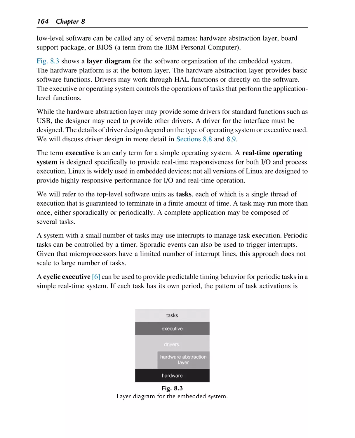
36
•
•
•
•
•
•
Chapter 2
Managing data requests to and from the host.
Performing the USB protocol operations.
Detecting and reacting to error messages.
Place the bus into a Suspended state and be able to wake up the bus.
Perform Root Hub functions.
Provide a Host System Interface.
2.5 WiFi
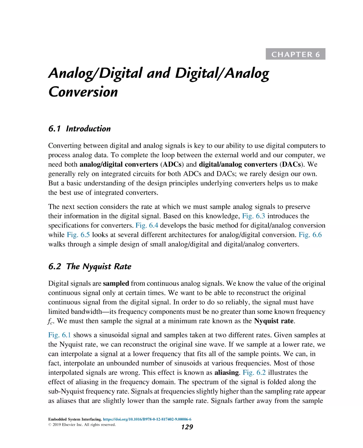
WiFi is the brand name for a set of wireless data standards. The standards are part of the
IEEE 802.11 family. This set of standards defines MAC and PHY for wireless local area
networks; the standards operate over several bands. Data rates depend on the member of the
family; examples include at 6–54 Mbits/s and 802.11n at 54–600 Mbits/s.
Data is organized into frames consisting of a MAC header, payload, and frame check sequence.
Management frames are used for maintenance operations.
WiFi was created for fixed and mobile computing applications which generally operate at
higher power levels than do modern Internet-of-Things devices. Techniques have been
developed to reduce the power consumption of WiFi for use in embedded applications.
2.6 Zigbee
Zigbee is a network- and application-level wireless standard. It makes use of PHY and MAC
layers from the IEEE 802.15.4 standard. It provides data rates of up to 250 kbits/s.
Each Zigbee network has one Zigbee Coordinator (ZC) to form the root of the network.
A Zigbee End Device (ZED) provides only basic functionality and cannot send or receive
directly with other devices. A Zigbee Router (ZR) passes data between devices and/or the
coordinator; it can also run applications. A network can run in either a beacon or beaconless
mode. If operating in beacon-enabled mode, routers periodically transmit; devices may turn
off in between beacon transmissions to save energy.
Zigbee adds two layers above the PHY and MAC layers supplied by 802.15.4: network
data service (NWK) and application (APS). The PHY layer operates on packets while the MAC
layer operates on frames.
The network layer provides data and management. The network layer discovers nodes in
the network. It forms a network: it identifies a channel on which it can operate; it then assigns a
16-bit network address to each device in the network. Communication may be broadcast,
multicast, or unicast. A network may be organized as a tree or a mesh. The network layer
limits the number of hops, known as the radius, across which a frame may travel. The network
Standard Interfaces 37
layer is responsible for discovering routes through the network and building a routing table.
After formation of the network, the coordinator manages the process of devices joining or
leaving the network.
The application layer includes three major components. The application support (APS)
sublayer interfaces to the network layer. The Zigbee Device Object (ZDO) is responsible for
device management and services, including defining whether it operates as coordinator, router,
or device. ZDO also manages security operations.
The application framework provides several services, including a message service for data
transfers and a key-value pairs (KVPs) for service attributes. Application profiles can be
used to manage the configuration of application; several profiles for common applications have
been defined. A profile is named by a 16-bit profile identifier which must be issued by the
Zigbee Alliance. A profile includes clusters and device descriptions. A cluster has its own
16-bit identifier; it consists of a set of attributes organized as key-value pairs. The clusters are
used to organize the attributes. The device description is kept separate from the application
profile itself. It consists of five components: the node descriptor (type, manufacturer code);
power (battery powered or wall powered, battery state); simple descriptor (profile identifier,
clusters); complex descriptor (serial number, etc.); and a user descriptor of up to 16 ASCII
characters for additional information.
Security is based on AES 128-bit keys. Master keys are preinstalled into a trust center which
then provides keys to other nodes in the network for secure communications.
2.7 Bluetooth and Bluetooth Low Energy
Bluetooth [23] was developed in the mid-to-late 1990s for applications such as telephony and
PC device operation.
The physical layer operates on the Industrial-Scientific-Medical (ISM) band, a radio frequency
band that is allocated globally for license-free operation. Data is modulated using frequencyhop spread spectrum, which changes frequencies according to a schedule in order to both
improve security and reduce interference. Hops are performed at a rate of 1600 hops/s. The
interval between hops defines a slot during which one packet can be transmitted. Packets
have a fixed format, including an access code, packet header, and data payload of up to
2745 bits. Multislot packets can also be sent using up to five slots. It offers a peak data rate of
1 Mbit/s.
Bluetooth supports two types of links:
•
Synchronous connection-oriented (SCO) links provide symmetrical, streaming links for
services such as voice.
38
•
Chapter 2
Asynchronous connectionless (ACL) links are designed for bursty transmissions; they
can operate either symmetrically or asymmetrically.
Establishing a connection between devices is known as pairing.
Bluetooth devices can organize ad hoc networks known as piconets. One device, usually
the device that set up the network, operates as the master. The master coordinates frequency
hopping by transmitting a master clock.
Bluetooth systems can be divided into a controller, host, and applications. The controller
includes several layers:
•
•
•
•
The physical layer provides the radio and air interface.
Direct test mode can be used to test the physical layer.
The link layer provides data link services.
The host/controller interface (HCI) is the interface to the host.
The host includes:
•
•
•
•
•
The logical link control and adaptation protocol (L2CAP) provides a channel
abstraction and multiplexes channels onto the data link.
The security manager manages pairing and key distribution.
The attribute protocol defines the data access on peer devices.
The generic attribute profile defines attributes types and their use.
The generic access profile defines discovery and connection services.
The application layer defines several components:
•
•
•
Characteristics are data in a known format and a universally unique identifier (UUID).
A service is a set of characteristics and their associated behavior.
Profiles describe the use of services.
Bluetooth Low Energy (BLE) is defined under the Bluetooth umbrella but it differs in
many ways. BLE has been optimized for low energy operation, which means in part using the
radio as little as possible. BLE devices are stateful—they maintain state between radio
operations. BLE operations are connectionless, a significant change from classic Bluetooth.
BLE is organized as a client–server system. It provides a service-oriented architecture to
access information on the server.
2.8 LoRaWAN
Internet-of-Things applications have motivated the design of new networks designed to cover
large geographic areas but still provide low-power operation for battery-powered devices.
LoRaWAN [35] is an example of such a network. The network makes use of spread spectrum
Standard Interfaces 39
techniques. Communications can be set to various data rates; the network server manages
the data rate and radio power of the link for both battery life and available bandwidth. Data
rates may fall between 0.3 and 50 kbits/s. LoRaWAN is designed for much longer range
operation than is typical for wireless networks. A LoRaWAN link can operate over a mile
(2 km) in urban environments with a great deal of interference and over 10 miles (20 km) in
areas with low interference.
A LoRaWAN device operates in one of three classes. A Class A device communicates only
when initiated by the end device; all communication is asynchronous using the Aloha protocol.
A Class B device synchronizes to network beacons; synchronization can reduce latency at
the cost of higher power consumption. A Class C device keeps its receiver on at all times,
providing lower latency for downlink transmissions but resulting in higher power consumption.
A LoRa gateway connects to a set of devices in a star architecture; the gateway is connected to
the Internet and translates data between the LoRaWAN link and the Internet. The network
defines both network session keys and application session keys based on the AES standard.
2.9 Internet-Enabled Devices
Internet-enabled devices are used in all sorts of applications and at almost every level of
system complexity. The design of an Internet-enabled device requires us to span the software/
hardware boundary.
The Internet Protocol (IP) was developed to provide internetworking communications.
Early computer communications networks were islands; multiple standards complicated
efforts to build large-scale networks. The Internet Protocol allows data to be moved across
networking boundaries in a consistent manner. A number of services have been built on
top of IP:
•
•
•
The Transmission Control Protocol (TCP) augments IP by providing error correction,
ensuring end-to-end delivery, and allowing recipients to reconstruct the order of data
spread across multiple packets. TCP operates at layer 4 and provides connection-oriented
service.
The User Datagram Protocol (UDP) is a connectionless service for datagrams.
The Hypertext Transfer Protocol (HTTP) provides request-response service for
distributed applications with the World Wide Web as a classic example.
The Internet Protocol can be performed on a wide range of communications media. The
higher-level, host-oriented operations are generally performed in software. The choice of media
for an Internet-enabled device can take into account a number of considerations:
•
•
Communications bandwidth.
CPU resources required.
40
•
•
•
Chapter 2
Cost and physical size.
Power consumption.
Compatibility with available communication networks.
Design of an Internet-enabled device also needs to consider the relationship between
networking and applications. Few applications will directly make use of IP. Higher-level
protocols provide useful distributed services in a standard way. The publish/subscribe design
pattern is widely used for IoT systems. The publishers in the system generate messages but
do not specify particular recipients. Subscribers can identify what types of messages are of
interest to them. Brokers are typically used to decide which messages should be sent to each
subscriber. The publish/subscribe model allows easy entry and exit of nodes in the system;
many IoT systems allow nodes to enter and exit the network at will.
Several different protocols are used to build IoT devices. HTTP is often used to provide
device-oriented services and simple device interfaces. CoAP [28] provides stateless HTTP
transfers and is designed for use on IoT devices. MQTT [27] is an IoT-oriented protocol based
on a publish/subscribe model. It can operate on TCP/IP; it can also run on other protocols that
provide connections that are ordered (data can be reassembled in the order in which it was
transmitted), lossless (data may be retransmitted until it is received at the destination), and
bidirectional. MQTT was designed as an alternative to HTTP for IoT applications: MQTT
uses a simpler data model that does not introduce document-oriented concepts; MQTT
clients do not need to know what devices receive their data, thanks to the publish/subscribe
model; MQTT is simpler than HTPP, with fewer operations as well smaller and simpler
messages; MQTT provides quality-of-service (QoS) levels; and the MQTT publish/subscribe
model provides multipoint communication.
Questions
Q2.1
Q2.2
Q2.3
Q2.4
Q2.5
Q2.6
Q2.7
Compare and contrast PHY, LLC, and MAC layer roles in the OSI model.
Compare bandwidth of I2C in standard mode and USB 3.0.
Compare the physical layer network topologies of I2C and USB 3.0.
What is the purpose of device enumeration in USB?
Compare bandwidth of WiFi 802.11a, Zigbee, Bluetooth.
How do the network behaviors of devices on Bluetooth and BLE differ?
Describe the roles of the major components in a publish/subscribe system.
CHAPTER 3
Logic
3.1 Introduction
Logic design is a critical component in embedded interfaces. When we design logic using
components that have been designed to work together, we can concentrate on their logical
function. But interfacing often requires us to mix and match components, exposing
incompatibilities. In these cases, an understanding of the circuit characteristics of logic is
essential to ensuring that the logic works as intended.
The next section discusses specifications for digital logic. Section 3.3 introduces CMOS logic,
based on MOSFETs, and its circuit characteristics. Section 3.4 introduces the high-impedance
output gate. Section 3.5 looks at two structures for busses: open drain and high impedance.
Section 3.6 discusses registers used to hold state. Section 3.7 examines programmable logic
devices. Section 3.8 looks at logic structures we use to connect to CPUs. Section 3.9 discusses
steps we must take to protect logic circuits from both electrostatic discharge and noise.
Section 3.10 discusses common auxiliary devices such as LEDs. Section 3.11 designs a simple
shaft encoder.
3.2 Digital Logic Specifications
The most basic specification for a digital logic circuit is its logical function. Function is
specified as Boolean formulas in the case of combinational circuits—logic with no internal
state. A state transition diagram or register-transfers can be used to specify sequential machines.
However, a practical digital logic circuit must meet other specifications. Those nonfunctional
specifications are the primary concern of this chapter.
Timing is a key parameter for interface logic—the interface may not produce the right
functional result if its logic does not meet certain timing parameters. Timing parameters come
in several forms:
•
•
Delay from a specified input to a specified output.
Relative timing from one signal event to another signal event.
Bus operations are often specified using timing diagrams as shown in Fig. 3.1. Signals in the
timing diagram may be given either as absolute values or as stable/changing regions.
Embedded System Interfacing. https://doi.org/10.1016/B978-0-12-817402-9.00003-0
# 2019 Elsevier Inc. All rights reserved.
41
42
Chapter 3
Fig. 3.1
A timing diagram.
The arrows in the timing diagram specify timing constraints—one event must occur before
another. If an event is labeled with a time value, the second event must occur at least that
period of time after the first event. We will study some important timing parameters for
registers in Section 3.6.
Logic signal levels are also related to the proper functioning of logic. Some logic families
define signal requirements relative to voltages, others to currents. If the input to a logic gate
does not meet the required signal levels, the gate will not produce the correct logical output
signal. We will study logic signal levels in Section 3.3.
Power consumption is often specified as a maximum value. The logic must live within the
available power from the power supply.
3.3 CMOS Logic Circuits
A logic family is a circuit technology that can be used to create many different types of gates:
inverter, NAND, NOR, etc. Most logic today is based on CMOS logic families based on
MOSFETs.
Fig. 3.2 shows two types of CMOS transistors. CMOS transistors are MOSFETs; the C stands
for complementary. The two types of transistors provide opposite polarities: when a gate
voltage is applied, it enables current to flow between the source and drain. The n-type transistor
conducts when its gate voltage is positive while the p-type transistor conducts on a negative
gate voltage. Both of these devices are known as enhancement mode because current increases
with larger gate voltages. (Depletion mode transistors conduct less current as their gate voltage
increases. Some logic families use depletion transistors but standard CMOS uses only
enhancement devices.) The gate terminal is capacitive and has a high input impedance.
The characteristic curve plot of Fig. 3.3 shows the drain current as a function of drain-source
voltage for several different gate-substrate voltages. At each gate voltage, no current flows
below a threshold voltage. When the gate voltage crosses the threshold, the drain current
Logic 43
Fig. 3.2
CMOS transistors.
Fig. 3.3
Characteristic curves of an nMOS transistor.
44
Chapter 3
increases in the linear region until it peaks in the saturation region. We will study MOSFET
characteristics in more detail in Chapter 4.
Logic gates are amplifiers but highly nonlinear ones. We will discuss linear amplifiers in
Chapter 4, which we use for amplifying signals while preserving their details. Logic gates are
designed to provide reliable digital values by taking advantage of nonlinearity.
Fig. 3.4 shows the schematic for a CMOS inverter built from one n-type (the pulldown M2) and
one p-type (the pullup, M1) transistor. The schematic also shows a capacitor connected to its
output as a load. The input is connected to the gates of both transistors. (Unfortunately, we use
gate to refer both to a logic gate and a transistor gate.) The source of each transistor is attached
to a power supply terminal, VSS for the n-type and VDD for the p-type. The gate voltage is
measured relative to that power supply level. When a high voltage is applied to the input, M2 is
on (high Vgs) and the p-type is off (low Vgs). As a result, M2 discharges the load capacitor. If a
low voltage is applied to the input, M2 is off and M1 is on, charging the load capacitor.
Given this basic understanding of how these logic families work, we can set up a scenario in
which each logic families fail. CMOS is sensitive to fanout—the number of gates attached to
the output of a driver gate. Fig. 3.5 shows a NAND gate whose output is connected to three other
gates; this connection is sometimes called a fanout tree. The mechanisms by which they fail are
different thanks to the different operating characteristics of the families. Fanin is the number of
gates connected to the input of a given gate; some logic families are also sensitive to fanin
constraints.
Capacitance is at the root of the fanout problem. In practice, the load capacitance is the gate
capacitance of the transistors that form the next logic gate. As fanout increases, the capactive
load increases. As shown in Fig. 3.6, we can model this situation with a current source for the
driver gate’s output and a capacitance for the load. One of the driver gate’s transistors is on and
Fig. 3.4
A CMOS inverter.
Logic 45
Fig. 3.5
Fanout of a gate.
Fig. 3.6
A model for fanout in CMOS logic.
operates in its saturation region. The input capacitances of the load gates are in parallel so we
can add them to find the total load capacitance. The voltage across this capacitance is equal to
the input voltage at each fanout gate; all fanout gates see the same input voltage. That voltage
waveform is simple—a ramp until it reaches the power supply voltage, at which point the driver
transistor turns off. The slope of the ramp depends on the ratio of the load capacitance and the
driver current:
Vout ¼ Id Cout t, Vout VDD
(3.1)
The output current is determined by the logic family. As the load capacitance increases, the
slope decreases and the time required for the voltage to reach its final value increases. Interfaces
have timing requirements—a maximum delay from the change of an input to the change at its
46
Chapter 3
output. If the slope of the voltage waveform is shallow enough, the logic fails to satisfy its
timing requirement.
Given these illustrations of the importance of electrical specifications to the proper function of
logic gates, we can now look at the specifications themselves. Most logic families represent
logic values as voltages; a few logic families use currents to represent logical values. We talk
informally about a high voltage representing a logic 1 and a low voltage representing a logic 0.
In fact, a range of voltages can be used to represent logic values. Accepting a range of signal
values protects the logic functions against noise, which is inevitable in real circuits.
Intermediate values represent invalid logic values, which we often refer to as X. Leaving a gap
between the valid logic 0 and logic 1 levels also contributes to noise immunity. Without an
X value in between, a small amount of logic would flip the logical value. If noise pushes a valid
logic value into the X range, we can at least detect that the value is invalid.
The data sheet for each component is a critical part of your design: without a data sheet, you
don’t know the component’s characteristics. The data sheet for a logic gate or family specifies
characteristics of input and output signals: for input signals, the required voltages and currents
to signal a valid logic value; for output signals, guarantees on the signals that the output
generates. Fig. 3.7 illustrates the relationships between logic levels when one gate drives
another. The highest voltage that represents a logic 0 is VOL; the lowest input voltage that
represents a logic 0 is VIL. If VIL < VOL, we know that any valid logic 0 produced by the output
gate will be interpreted as a logic 0 by the next gate. Similarly, if VOH > VIH, we are guaranteed
that any logic 1 produced by the output gate will be treated as a logic 1 by the input gate. The
high and low ranges do not have to be the same and the input and output ranges do not have to
be equal.
Fig. 3.8 shows some of the specifications from a data sheet for a CMOS NAND gate. CMOS
logic can operate over a wide range of voltages. The input voltages VIL, VIH and the output
currents IOL, IOH are both specified. CMOS output voltages asymptotically approach the power
supply voltages so their worst-case levels do not need to be specified.
If we mix logic from two different logic families, we need to be careful to obey the input and
output signal specifications. These specifications also limit our ability to connect logic gates to
nonlogic circuits. For example, a logic gate may not be able to supply enough current to directly
drive a speaker.
Fig. 3.7
Logic levels and logic gates.
Logic 47
Fig. 3.8
Selected data sheet entries for a CMOS logic gate [62].
Fig. 3.9
Signal level incompatibilities across power supply boundaries.
If we mix logic that operates at different power supply levels, we also need to be careful about
signal levels. Many digital systems use multiple power supply voltages, which they use to trade
off power consumption and performance. Since the range of valid logic 0 and 1 voltages
depends on the power supply voltage, changing power supply levels leads to changing the range
of valid logic values. As illustrated in Fig. 3.9, if we connect the output of a gate at a low power
supply voltage to the input of another gate at a higher power supply voltage, a voltage produced
by the first gate as a logic 1 may be too low to be interpreted as a 1 by the next gate; instead, it
could be treated as a logic X.
3.4 High-Impedance and Open-Drain Outputs
Some logic gates offer another form of output, known as high impedance, three-stating, or
tri-stating™. Three states are useful in connecting gates together to form a bus. Fig. 3.10 shows
two three-state gates connected to a bus. Each gate has its data input as well as an enable
input: if enable ¼ 1, the gate’s output is the inverse of the data input; if enable ¼ 0, the gate’s
48
Chapter 3
Fig. 3.10
Common connections using three-state logic outputs.
output is set to high impedance. We often refer to the high impedance output value as Z. We can
select which gate writes its value on the bus by setting the values of the two enable inputs. Of
course, if both gates are enabled, they will both be electrically connected, which is particularly
bad when the data values are different. Not only can this cause a bad logical value to appear on
the bus but it may damage the circuits due to large short circuit currents.
Fig. 3.11 shows a CMOS inverter with a three-state output. The inverter’s output is guarded by
n-type and p-type transistors M3, M4. When enable ¼ 0 (and enable’ ¼ 1), both of these
transistors are off, defeating both M1 and M2. When enable ¼ 1 and enable’ ¼ 0, both transistors
are on and the pullup and pulldown transistors can effectively determine the proper
output value.
Some logic families do not include a pullup device or resistor. Instead, the bus or external
connection is connected to a pullup resistor R1 as illustrated in Fig. 3.12. Pulldown transistors
inside the gates will, when turned on, cause the bus voltage to go low. If no gate tries to pull the
Fig. 3.11
A CMOS inverter with three-state output.
Logic 49
Fig. 3.12
An open-drain bus circuit.
bus voltage down, the pullup maintains the bus at a high logic level. The MOS version of this
circuit is known as open drain since the transistors’ drain connections are left unconnected.
In the case of TTL, this configuration is known as open collector. The maximum current
supplied by the pullup resistor must be no larger than the maximum sink current of one gate and
the current flowing from the inputs of the n fanout gates [58]:
RL
VCC VOL, max
IOL nIIL
(3.2)
3.5 Example: Open-Drain and High-Impedance Busses
Busses are common connections that are used for data communication between various
combinations of devices. Only one device at a time may write the bus. The destination for the
data may be one or several devices. We can use two different circuit families to design busses
with different characteristics.
We can use pullup resistors to build busses that allow easy connection and disconnection of
devices. If the transistors used on the bus are bipolar, we refer to the bus as open collector; if the
transistors are MOSFETs, the bus is open drain. A classic example of the open-drain/opencollector bus is I2C, which we discussed in Section 2.3.
Fig. 3.13 shows an open-drain bus circuit. The bus is a wire connected to pullup resistor Rpu.
Each module on the bus has a pulldown transistor M1, M2, etc. If any of the devices turns on its
pulldown transistor, the bus voltage is pulled to a low voltage. If no modules are on, the bus is
kept at a high voltage thanks to the pullup resistor. If two modules turn on their pulldown
transistors, the bus continues to operate normally. Open-collector and open-drain busses are
robust because they are insensitive to multiple devices writing on the bus. However, the pullup
transistor causes the bus to be relatively slow.
50
Chapter 3
Fig. 3.13
An open-drain bus.
Fig. 3.14
A high-impedance bus.
Fig. 3.14 shows a high-impedance bus. Consider first a bus that is only a wire without a pullup
resistor. Each module uses a three-state gate to connect to the bus. (We use inverting gates here
but the polarity of the bus logic is not important to its circuit characteristics.) If one three-state
gate is enabled, it controls the value on the bus. If two three-state gates are enabled and they
output the same value, the bus continues to operate. If the two gates have opposite values, they
will fight each other, resulting in at least a bad logic value on the bus and perhaps damage to the
circuits. If no three-state gate is enabled, the bus is floating and does not have a reliable digital
value. We can use a weak pullup to keep the bus at a valid logic value; the pullup is chosen to
provide a small enough current that if a three-state gate can overcome it and determine the
bus value.
3.6 Registers
We use the term register for any type of circuit used to locally store a bit value.
The simplest type of register is the SR latch, shown in Fig. 3.15. This latch does not have a clock
input. Instead, its internal value is determined by the values of the set (S) and reset (R) inputs.
SR latches are not widely used today because they may not reliably capture the intended value.
Logic 51
Fig. 3.15
Schematic symbols for SR and D registers.
SR latches made by hand from a pair of NOR or NAND gates are particularly unreliable—the
parasitics of wiring affect the behavior of the latch too much.
Clocked registers are more reliable: a clock input determines when the data input value is read.
The D register, also shown in Fig. 3.15, is one form of this type of register; other options also
exist. Two major variants on the relationship between the clock and the internal state exist.
A level-sensitive register, which we refer to as a latch, reads the data input into the register state
so long as the clock signal is enabled. Once the clock signal is disabled, the internal state
conforms to the last state on the data input. We call this form of register transparent. An
edge-triggered register, which we refer to as a flip-flop, loads the register value only in a
narrow interval around a clock edge.
Both types of registers must obey two timing constraints setup and hold times. Fig. 3.16 shows
these timing requirements for the case of a positive edge-triggered registered. The setup time ts
Fig. 3.16
Setup and hold times.
52
Chapter 3
Fig. 3.17
Metastability.
is the time before the clock edge during which the data input must be stable. The hold time th is
the time after the clock edge during which the data input must remain stable. In the case of a
level-sensitive register, these times would be measured relative to the end of the active clock. If
the data signal does not obey the setup and hold times, the register may store the wrong value.
These times are often quoted as a combined setup-and-hold time.
A register’s performance is given by its propagation delay from input to output: tPLH for
low-to-high transitions and tPHL for high-to-low transitions.
Setup-and-hold time is an important design constraint because all registers can suffer from
metastability. If the data value changes around the clock event, then the register may store an
intermediate X state. As shown in Fig. 3.17, the register will eventually settle to a valid logic
value but the time to do so is random and can be extremely long. When it does settle, it may
settle on the wrong value. This phenomenon is often compared to a ball poised at the top of a
hill; it may sit at the top for quite some time before a random wind blows it to one side of the hill
or the other. We cannot eliminate metastability, we can only minimize it. Metastability is a
particular concern when a register connects two regions that operate on different clocks—in this
situation, some fraction of the inputs will inevitably fall in the metastability danger window.
We compute the probability of a metastable output based on a settling time S. The register has a
time constant τ and setup/hold time tSH. We also need to know the clock period. The probability
of a metastable output failure at the end of the settling time is
PF ¼
tSH S=τ
:
e
T
(3.3)
The double-register structure of Fig. 3.18 is often used to minimize the effect of metastability.
The logic must be designed to take into account the extra clock cycle of delay. The two levels of
Fig. 3.18
Reducing metastability with a double-register.
Logic 53
register give the signal extra time to settle. The signal may settle to the wrong value, and there is
still a chance that the second register may end up with an X. Occasionally, three levels of
register are used to further reduce the chance of saving a metastable value.
3.7 Programmable Logic
We often need to design glue logic to perform basic operations in the interface. While
small-scale integrated (SSI) circuits may be useful in some situations, chips that can implement
more logic are often useful. Complex programmable logic devices (CPLDs).
A field-programmable gate array (FPGA) can implement multilevel logic—logical
functions of varying depth. The two basic elements in an FPGA are programmable
logic and programmable interconnect. A programmable logic element can be configured to
represent a given logical function; typically an element has a limit on the number of inputs it can
handle but can compute any logical function within that range of inputs. Programmable logic
elements also include registers to store values. Programmable interconnect can be configured
to make connections from the output of one logical element to the input of another. The most
common means of configuring an FPGA uses static RAM (SRAM). Since SRAM loses its
values when the power supply is removed, the FPGA must be configured whenever it is
powered up. A configuration file is loaded into the FPGA to set the configuration of the logic
elements and interconnect; specialized memories can be used to automatically load the
configuration into the FPGA. We often refer to the configuration process as programming but
this process is very different from programming a computer—an FPGA does not fetch and
execute instructions.
We create a configuration file using computer-aided design (CAD) tools and hardware
description languages (HDLs). Fig. 3.19 shows a simple HDL description in the Verilog
Fig. 3.19
A simple Verilog description.
54
Chapter 3
language; VHDL is the other major hardware description language. CAD tools first optimize
the logic design, then determine where to place functions into logic elements and how to route
elements between the logic elements. The result is a configuration file.
Programmable logic demands programmable I/O pins. FPGA and CPLD pins can be configured
as input, output, or high impedance. Other aspects of the pin may also be configured.
A common example is slew rate—the speed at which the output changes from 0 to 1 or 1 to 0.
Fast signals demand high slew rates but signals that do not need to be fast can use a slow rate to
reduce power consumption and electromagnetic interference.
Many advanced FPGAs are organized as a system-on-chip (SoC). In addition to a fabric of
programmable logic elements and interconnect, they provide embedded memory, multipliers,
one or several CPUs, and specialized I/O subsystems such as Ethernet.
3.8 CPU Interface Structures
CPUs may provide any of several different types of logic structures as interfaces to the CPU
itself.
General-purpose I/O (GPIO) is a set of pins that are uncommitted to a particular purpose.
GPIO pins can usually be configured to be either an input or an output.
Some microprocessors expose a bus to system designers, either their main bus or a bus
specifically designed for I/O. The bus operates a protocol that determines what actions are
taken by each device on the bus. The bus has a master that initiates operations. By default, the
CPU is the master. The bus may provide a bus request signal to allow another device to
temporarily become bus master.
Busses require different devices to drive some signals at different times—the CPU and
memory, for example, may each write data onto the bus at different times. High-impedance or
common drain/emitter circuits are often used at bus interfaces.
A simple example is shown in Fig. 3.20, which gives a timing diagram for a bus read operation.
(Read/write directions are relative to the CPU when describing CPU busses.) The bus master
presents an address on adrs and asserts address ena; the signals are timed to be valid before the
rising clk edge. When the device is ready, it asserts data and data ready. In this simple protocol,
the data is asserted for one clock cycle; some protocols may use a signal for the CPU to assert
when it has captured the data.
Fig. 3.21 shows a logic schematic that provides the device’s responsibilities for this protocol.
The interface is designed to wait for the data to arrive from the interior of the device as signaled
by avail. The cmp block compares the adrs value to the device’s value. A protocol FSM
controls the operation of the bus-side logic.
Logic 55
Fig. 3.20
Timing diagram for a bus read operation.
Fig. 3.21
Schematic for bus read logic.
Fig. 3.22 shows the state transition diagram for the protocol FSM. When req is asserted, the
FSM waits for a data input from the remainder of the device. When that data is ready, the
machine asserts data ready for one clock cycle to signal the bus master.
3.9 Logic Protection and Noise
Logic requires two types of protection from the outside world and from itself: static electricity
and electromagnetic interference (EMI).
CMOS logic is particularly sensitive to static electrical discharge. The gate oxide of a MOSFET
is necessarily thin. Large voltages from static discharge can breakdown the MOSFET,
56
Chapter 3
Fig. 3.22
State transition diagram for bus read protocol FSM.
rendering the circuit inoperative. When working on circuits, we should connect ourselves to
ground using a ground strap.
The electrical signals on any wire generate electromagnetic fields. Wires also act as antennas
that can receive the electromagnetic signals around them. We need to take steps to minimize
both the EMI generated by circuits and the effect of EMI on our circuits. Reducing the slew rate
of signals is an example of an active method of EMI minimization. Shielding—putting circuits
in a metal box—both prevents generated EMI from being transmitted to the environment
and protecting the circuits from external sources of EMI. We will discuss noise in more
detail in Section 4.10.
Power supplies are an important source of noise for digital circuits. We have seen that our
circuit models for logic gates depend on power supply voltages. Violating the power supply
requirements will inevitably cause problems. We can reduce power supply noise, often called
power supply ripple, using decoupling capacitors that is placed between the VDD and VSS
power supply connections. Each decoupling capacitor serves a particular set of logic. As shown
in Fig. 3.23, we may place decoupling capacitors at several points in the circuit. In many cases,
we add a separate decoupling capacitor at each significant integrated circuit. The decoupling
capacitor acts as a low-pass filter on the power supply; we can also view it as a charge reservoir
for short-term use when the logic’s current draw becomes too high for the power supply. Given
logic current for n gates of nImax and a maximum power supply ripple of 4 V over an interval
tmax, the required decoupling capacitance is [74]:
CD ¼ nI max
tmax
4V
Fig. 3.23
Decoupling capacitors.
(3.4)
Logic 57
3.10 Auxiliary Devices and Circuits
The light-emitting diode (LED) is a common and very useful output device. Not only is an
LED a useful indicator for the end user, but it can also be used during debugging to indicate
signal state. Wiring an LED to a logic signal is straightforward but requires a little care. As
shown in Fig. 3.24, the LED is connected in series with a resistor. The LED’s orientation allows
current to flow from the positive supply to ground. We can control the LED with the logic signal
by using the logic signal as the positive terminal for the LED/resistor assembly. The current
supplied by the driving logic gate determines the brightness of the LED. The resistor’s role is to
regulate current and provide a voltage drop. The LED’s voltage is 0.7 V when it is on. The
remaining voltage drop between the power supply terminals occurs over the resistor. We
choose the value for the resistor based on the desired voltage drop and the current available
from the driving gate:
VR ¼ VDD 0:7 V
R¼
Iout
:
VR
(3.5)
(3.6)
Unless we need a particularly bright LED, we probably want to use a value for Iout lower than
the data sheet maximum in order to avoid overstressing the driving gate.
The optoisolator combines an LED and a photosensitive transistor (in this case, a bipolar
transistor) to create a logical signal path with no direct electrical connection. Fig. 3.25 shows
the schematic symbol for an optoisolator. The output transistor’s base acts as an optical
detector; light from the input LED determines the output transistor’s emitter-collector current.
Optoisolators can be used to provide separate power supply circuits for different parts of the
circuit, isolating one from the noise in the other circuit. As we will see in Section 3.11, we can
use an optoisolator as a detector.
Fig. 3.24
An LED circuit.
58
Chapter 3
Fig. 3.25
Schematic symbol for an optoisolator.
Switches are often used for input. We have to take the mechanical characteristics of the
switch into account within the interface. When a switch is closed—the contacts are pushed
together to make a connection—the metal contacts bounce several times. As shown in Fig. 3.26,
the switch will open and close many times in a short interval before it settles to its stable, closed
value. We do not want to send all these events as a string of 1s and 0s to the CPU. Instead,
we want to debounce the switch—temporarily force it to a single value until it settles. Of
course, we want the user to be able to open the switch and turn off the connection. Given the
short time scale of switch bouncing, the user does not observe any delay in being able to reopen
the switch. We can any of several techniques to debounce a switch. We can do so in software
using a CPU timer. At the other end of the spectrum, we can use the circuit in Fig. 3.27. When
switch S1 is open, R1 charges C1, providing a stable value logic 1 on the output. When the switch
is closed, C1 is drained through R2, bringing the output voltage to a low level. We can easily
manage the sense of the switch (logic 1 means open switch) in software.
A third option is a debouncer based on an integrated circuit known as a one-shot. The one-shot,
also known as a monostable multivibrator, responds to a transition on its input by
setting its output high for a given amount of time. At the end of the pulse, the one-shot’s output
returns to its original state. The length of the pulse is determined by a capacitor. By ORing
(or NORing) together the raw switch signal with the one-shot pulse, we can smooth over the
switch bounces. We will discuss one-shots in more detail in Section 5.10.
Fig. 3.26
Bouncing in a switch.
Logic 59
Fig. 3.27
A simple debouncing circuit.
Fig. 3.28
Schematic symbol for a Hall effect sensor.
A Hall effect sensor uses the interaction of magnetic fields and electric currents to detect the
position of a magnet. Fig. 3.28 shows the schematic symbol for a Hall effect sensor. S magnetic
field H imposes a force on an electric current I. The force causes the current t deflected,
changing the voltage across the sensor. The Hall effect produces a linear variation in voltage
from the magnetic field which we can use either for fine position of a magnet or as a nonlinear
detector. For example, Hall effect sensors are commonly used to detect whether car doors are
open or closed: a permanent magnet is placed on the door and the sensor body is placed in the
door frame. The sensor reading indicates whether the magnet is next to the sensor—the door is
closed—or whether the magnet is away from the sensor—the door is open. Hall effect sensors
are also used in brushless DC motors to detect the position of the motor shaft.
3.11 Example: Shaft Encoder
We often need to detect the movement of a shaft: knobs on equipment turn shafts that are
intended to control the equipment’s operation; the position of a servo motor needs to be
determined as an input to control. The optical shaft encoder is widely used thanks to its
superior characteristics compared to mechanical or electromechanical alternatives: it provides
low noise and low friction at a low cost.
60
Chapter 3
Fig. 3.29
A simple shaft encoder mechanism.
Fig. 3.29 shows a simple shaft encoder. The shaft, made in this case from a paperclip, is fitted
with a target of alternating white and black areas. That target is positioned in the middle of a
variation of an optoisolator known as an optical detector or a reflective optical switch. This
device points its LED output outward and provides a lens to capture reflected light. The target
modulates the light that is reflected from the LED to the photodetector. The white and black
areas of the target reflect different amounts of light depending on the position of the shaft. The
output of the photodetector produces a signal that indicates when the target has been rotated
from one area to the next. Optical detectors come in several configurations of the emitter and
detector: parallel to each other, pointed at each other, and in this case reflected at an angle.
These different arrangements are suited to different physical environments.
Fig. 3.30 shows a simple pattern for the target. The alternating black and white regions
allow the detector to determine when the shaft has moved from one region to another; we
can increase the resolution of the encoder by dividing the target into narrower slices. However,
this target pattern gives us only a relative position for the shaft. The pattern of Fig. 3.31 encodes
a three-bit position over the radius of the target (the white spacers between the target
patterns were inserted for clarity and are not strictly necessary). We can use three optical
detectors to read the three bits of the position. Those bits give us enough information to
Logic 61
Fig. 3.30
A simple shaft encoder pattern.
Fig. 3.31
An absolute position shaft encoder pattern.
determine which direction the shaft has turned and its absolute position to within 45 degrees.
More tracks to the pattern and more detectors allow us to measure position more precisely. We
can also add a separate track with a fiducial mark at a fixed position to provide a reference. This
target uses a standard binary up-down code; a Gray code provides protection against mis-reads
and glitches.
62
Chapter 3
Fig. 3.32
Schematic for an optical detector circuit.
Our setup uses the OPB703WZ detector [72]. Fig. 3.32 shows the schematic for the detector
circuits with the colors of the leads from the detectors as shown. We need to choose the values
of the two resistors: RD determines the amount of light produced by the LED; RT determines the
output current of the photodetector for a given amount of light. If the LED produces too much
light for the photodetector, the detector’s output will always be on; if the LED produces too
little light for the photodetector, the detector will always be off. The two resistor values are
related: the ratio RD/RT determines the relationship between LED output and photodetector
sensitivity. The data sheet gives us some guidance to the proper resistor values.
•
•
The LED forward DC current is ID ¼ 40 mA at a forward voltage of VD ¼ 1.7 V.
The phototransistor collector DC current is 3.5 mA at an emitter-collector voltage of 5 V.
Once we choose the power supply voltage, we can find
RD ¼
VDD VD
:
ID
(3.7)
On the output side, we need to check two conditions: the logic 0 output value produced by the
photodetector is compatible with the next stage of logic; and that the on current produced by the
photodetector is sufficient to drive the next stage.
Further Reading
Wakerly [73] provides a thorough introduction to logic design.
Questions
Q3.1
A CMOS gate has a maximum current of 4 mA at a power supply voltage of 5 V. Given
an LED on voltage of 0.7 V, what value of resistor should be used if we want to draw
half the maximum allowable current to light the LED?
Logic 63
Q3.2
An LED is driven by an inverter to display a logic value. The inverter can supply a
maximum output current of 2.5 mA. The power supply voltage is 3.3 V. What value of
resistor should be used to draw an on current of half the inverter’s maximum rating?
Q3.3 An LED is driven by a series 5 kΩ resistor. Given a power supply voltage of 3.3 V, what
is the diode current?
Q3.4 What conditions govern the value of a pullup resistor for an open-drain connection?
Q3.5 A CMOS gate operates at VCC ¼ 3.3 V, VIH ¼ 3.15 V, VIL ¼ 1.35 V. How much drive
current must the gate provide on a 1 ! 0 transition to a gate with input capacitance of
15 pF to achieve a delay of 10 ns?
Q3.6 A CMOS gate rising input follows an exponential curve with time constant τ ¼ 3 ns.
The gate operates on a power supply of 3.3 V. If the logic levels are VIH ¼ 3.15 V,
VIL ¼ 1.35 V, how long is the gate input in the unknown region?
Q3.7 A CMOS logic family has an input capacitance of 15 pF and an output current of
20 mA. It operates at a power supply voltage of 3.3 V. What is the maximum fanout to
ensure transition times less than 15 ns?
Q3.8 Draw a timing diagram for the operation of a D register. The timing diagram should
include a setup time of 20 ns and hold time of 7 ns.
Q3.9 A register has a time constant of τ ¼ 3 ns, a setup/hold time of tSH ¼ 27 ns. Its input
clock has a period of 50 ns. How long must it be given to settle to ensure a metastability
probability below 1020?
Q3.10 A CMOS logic family draws current of 10 mA at a power supply voltage of 3 V. You
are given a block of logic with 20 gates. How much decoupling capacitance is required
to ensure a maximum power supply drop of 10% over 5 ns?
Q3.11 Design a modified form of the bus interface of Section 3.8 that allows for variable
timing of the register read.
(a) Modify the timing diagram to use a data ack signal to acknowledge the read by
the CPU.
(b) Draw a state transition diagram for the FSM.
CHAPTER 4
Amplifiers
4.1 Introduction
Amplifiers represent the simplest transformation we make on signals—we turn a small signal
into a larger, more powerful version of the same. But this simple task involves many subtleties.
Mastering amplification is useful in itself as well as an important exercise in circuit design.
Designing amplifiers requires us to understand transistors in more detail. Discrete transistors
can be used to build a wide range of amplifiers. Fig. 4.1 shows two types of packages: TO-220
Fig. 4.1
Two types of transistor packages.
Embedded System Interfacing. https://doi.org/10.1016/B978-0-12-817402-9.00004-2
# 2019 Elsevier Inc. All rights reserved.
65
66
Chapter 4
on the left and TO-92 on the right. We will also study integrated amplifiers in the form of
op amps.
The next section introduces the basic specifications for amplifiers. Section 4.3 discusses
analysis methods for circuits. Section 4.4 develops circuit models for the MOSFET. Section 4.5
introduces amplifier topologies. Section 4.6 designs an amplifier for a low-impedance load.
Section 4.7 briefly introduces concepts in power amplifiers. Section 4.8 considers integrated
amplifiers as useful components. Section 4.9 introduces the op amp, a versatile component.
Section 4.10 considers noise, interference, and crosstalk. Section 4.11 looks at the design of an
amplifier for a microphone.
4.2 Amplifier Specifications
We use amplifiers because they provide gain, represented by the variable A. We can talk about
power, voltage, or current gain, depending on how we prefer to think about the signals. The
most common form used in amplifier design is voltage gain:
AV ¼
Vout
:
Vin
(4.1)
A negative value for gain means that the output is 180 degrees out of phase with the input: when
the input is high, the output is low; when the input is low, the output is high. Many amplifier
topologies naturally produce inverted outputs and are characterized by negative gain.
We are particularly concerned with the load impedance that the amplifier is able to drive. The
input characteristics of the amplifier are also of interest.
Since neither the devices nor circuits that make up the amplifier are ideal, we are also interested
in specifying the tolerable level of variations from the ideal. When we compare the output of an
amplifier to a known input, such as a sinusoid, we measure its distortion. Some forms of
distortion are linear; they generate harmonic distortion. When we inject a sinusoidal signal PF
at the fundamental frequency into the amplifier’s input, harmonic distortion appears as a set of
harmonic signals PH, i. We can define total harmonic distortion (THD) as
X
P
i H, i
THD ¼
:
(4.2)
PF
Nonharmonic distortions are known as intermodulation distortion (IM). When we inject two
sinusoids that are not harmonically related into the amplifier’s input, intermodulation generates
signals at other frequencies. If the input signals are at frequencies f1, f2, f2 > f1, the
intermodulation products include sums and products of multiples of the input frequencies:
mf1 + nf2 , n, m ¼ 1,2,…:
The order of the harmonic is given by m + n. Intermodulation products that are near the
frequency of interest are of particular concern. We generally measure the different
(4.3)
Amplifiers 67
intermodulation products individually and measure the ratio of the RMS intermodulation
voltage to the fundamental RMS voltage.
Another important form of nonideality is noise. We specify amplifiers based on signal-to-noise
ratio (SNR), or the ratio between the largest signal the amplifier can produce to the noise it
produces; we also refer to this ratio as dynamic range. These values are often cited in decibels.
We will discuss noise, interference, and crosstalk in Section 4.10.
4.3 Circuit Analysis Methods
Transistors are nonlinear, active elements that we can use to build linear circuits. Amplifiers are
very useful in themselves; amplifier design also allows us to learn and practice a wide range of
circuit analysis and design techniques.
Circuit designers often refer to DC and AC analysis. Since we can break down any signal into
the sum of a constant value and a changing value, we can use this decomposition to help us
understand circuits. DC analysis assumes no signals in the circuit change. We often want to
place some terminals of a transistor at a given voltage known as a bias voltage. The device may
require that some terminals are kept at a prescribed voltage: bipolar transistors require a voltage
across their base-emitter junction to turn on the transistor; MOSFETs require their gate voltage
to be above the threshold voltage. We may also want to put some terminals at a given voltage to
ensure that signals, when they do change, can swing through their full range. DC analysis
allows us to determine bias voltages and the operating point of the transistor. AC analysis can
separately consider the effects of changing signals. We traditionally use capital letters for DC
variables (I1, V1) and lowercase letters for AC variables (i2, v2).
Circuit designers also refer to small-signal and large-signal analysis. While transistors are
nonlinear devices, we can approximate them with linear models over some of their operating
range and under the assumption that signals are small. A small-signal model provides an
equivalent circuit for a transistor under conditions that allow the transistor to be treated as a
linear component. Under small-signal analysis, we replace the device with its small-signal
model; we also replace DC voltage sources with short circuits and DC current sources with open
circuits. We typically use small letters such as i1, v1 for small-signal values. However,
small-signal assumptions do not hold in some circuits, with power amplifiers being a classic
example. We use large-signal models in these cases. Typically, we use graphical methods to
solve for the behavior of the transistor under large-signal assumptions: starting with the set of
operating curves for the transistor, we draw additional lines that represent the constraints
imposed on the transistor operation by other circuit components.
We will take advantage of schematic capture and simulation tools in this chapter. Circuit
simulators, as described in Section 1.9, allow us to solve for the waveforms of complex circuits
with nonlinear elements; they also provide other forms of analysis such as noise. Free versions
68
Chapter 4
of CAD tools are limited in capability relative to paid tools but still provide valuable
capabilities.
4.4 MOSFET Transistor Models
We can model the MOSFET using both small-signal and large-signal models. For each model,
we need to determine the model parameters from the given parameters of the particular
transistor we want to use. Data sheets may or may not directly give us the required parameters;
in such cases we need to derive the model parameters from the given values.
We will use as an example the Fairchild BS170 n-type MOSFET [18]. Fig. 4.2 gives some of
this transistor’s parameters.
4.4.1 Small-Signal Models
Figs. 4.3 and 4.4 show two small-signal models for a MOSFET: the pi model takes the form of
the Greek letter; the t model uses a T-shaped circuit topology. These two models are equivalent;
in any given situation, one may be more convenient than the other. The diamond-shaped current
source represents a controlled source—the current depends on another circuit variable.
The transistor’s transconductance gm relates input voltage to output current. The MOSFET
gate’s high capacitance gives an open circuit in this model. The resistance r0 models the
resistance between the drain and source. In the t model form, the gate current is always zero.
Threshold voltage
Drain-source on resistance
Transconductance
Gate capacitance
Maximum drain-source voltage
Maximum continuous current
2.1
1.2Ω
/
320
24
60
500
Fig. 4.2
Characteristics of the BS170 n-type MOSFET.
Fig. 4.3
A small-signal pi model for a MOSFET.
Amplifiers 69
Fig. 4.4
A small-signal t model for a MOSFET.
4.4.2 Large-Signal Models
As we saw in Section 3.3, a MOSFET has a linear region corresponding to low drain-source
voltages and a saturation region corresponding to high VDS. It also has a cutoff region when
the gate voltage is below the device’s threshold voltage, but that is not directly represented in
the characteristic curves.
Cutoff : ID ¼ 0,VGS < Vt :
Linear : ID ¼ k0
W
2
,VDS < VGS Vt :
ðVGS Vt ÞVDS VDS
L
1 W
Saturation : ID ¼ k0 ðVGS Vt Þ2 ,VDS VGS Vt :
2 L
(4.4)
(4.5)
(4.6)
The large-signal model [57] reflects these three modes of operation. Fig. 4.5 shows a simple
large-signal model for a MOSFET’s saturation mode. The voltage across the gate capacitance
controls the drain-source current source.
Vt is the threshold voltage below which the MOSFET drain-source region does not conduct.
k0 is a parameter that depends on device physics. W/L gives the width/length ratio of the
MOSFET channel, which scales the magnitude of the current; this parameter is of more interest
Fig. 4.5
A large-signal model for saturation mode operation of a MOSFET.
70
Chapter 4
Fig. 4.6
PSpice model for the BS170 n-type MOSFET.
to integrated circuit designers who can choose the sizes of their transistors. When using discrete
MOSFETs we are generally given the drain current for a given gate voltage.
To properly simulate this transistor in PSpice, we need to set the MOSFET model parameter
using the Model Editor shown in Fig. 4.6. The PSpice model was designed for integrated circuit
design in which we know the width and length of the transistor
channel. In this case, we set the
0
2ID, max
transistor width and length to 1. We estimate k ¼
ðVDS, max Vt Þ ¼ 152 mS.
We can trace the characteristic curves of a MOSFET. Fig. 4.7 shows the setup. In this case, the
gate is driven by a voltage source. We sweep both the drain-source voltage and the gate voltage.
The results are shown in Fig. 4.8. These curves clearly show the linear and saturation regions of
the transistor’s operation.
4.5 MOSFET Amplifier Topologies
We can incorporate the MOSFET into amplifiers with several different topologies. Each has its
own advantages and disadvantages.
4.5.1 Common Source Amplifier
Fig. 4.9 shows a common source amplifier. This topology provides good voltage gain. The
high gate impedance of the MOSFET gives this topology a high input impedance.
Amplifiers 71
M1
I
Mbreakn
0Vdc
+
V1
0Vdc
+
–
–
0
Fig. 4.7
A curve tracer circuit for a MOSFET.
Fig. 4.8
A simulated curve tracing of a MOSFET.
V2
72
Chapter 4
Fig. 4.9
A common source amplifier.
We can analyze the voltage gain of the common source amplifier using AC analysis and the
MOSFET small-signal model of Fig. 4.10. The input source and power supply become shorts in
AC analysis. The model circuit is shown in Fig. 4.10. If r0 ≫ RD, the output voltage is
Vds ¼ gmVgsRD; the input voltage is Vgs ¼ (gm + 1)VgsRS. When we substitute these terms into the
definition of voltage gain, we find
Av ¼
gm Vgs RD
RD
:
ðgm + 1ÞVgs RS RS
(4.7)
Large-signal analysis starts with a load line for the circuit—the load line describes the drainsource current over a range of drain-source voltages. Fig. 4.11 shows that in this case the load
Fig. 4.10
A small-signal model for common source amplifier gain.
Amplifiers 73
Fig. 4.11
A load line plot for an amplifier.
line is defined by VDD on one end and VDD/RL at the other end. We select a quiescent point or
Q point that represents VDS when the input is zero; the Q point is typically put at the middle of
the operating region of the load line.
4.5.2 Common Drain Amplifier
Fig. 4.12 shows the common drain or source follower configuration. This topology provides
unity voltage gain and a relatively high output impedance that makes it useful for driving
low-impedance loads. Once again, the MOSFET’s gate impedance ensures high input
impedance.
4.5.3 Common Gate Amplifier
Fig. 4.13 shows the common gate configuration. This configuration provides unity current
gain and good voltage gain. Because the gate is not at the input, it has low input impedance. It
provides a high output impedance making it useful for driving low-impedance loads.
74
Chapter 4
Fig. 4.12
A common drain or source follower amplifier.
Fig. 4.13
A common gate amplifier.
4.5.4 Cascode Amplifier
We can also design a cascode amplifier using MOSFETs as shown in Fig. 4.14. M1 is
configured as a common emitter while M2 is used as an emitter follower. The signal input is
provided to the gate of M2.
4.5.5 Differential Amplifier
Fig. 4.15 shows the differential amplifier. This topology is widely used to compare two signals
and amplify the difference between them. The currents of the two legs defined by M1, M2 are
related to each other through the current source—the sum of the currents through the two legs is
constant. Differences in the input voltages V+, V result in amplified differences in the output
voltages V1, V2.
4.5.6 Current Sources
The differential amplifier makes use of a current source as do many other circuits. An ideal current
source produces a known current independent of load. We can build realistic current sources with
various degrees of fidelity to that goal, each with its own advantages and disadvantages.
Amplifiers 75
Fig. 4.14
A MOSFET cascode amplifier.
Fig. 4.15
A MOSFET differential amplifier.
Fig. 4.16 shows a basic current source circuit. The voltage divider provides a gate voltage for
the MOSFET that governs its drain-source current. This circuit is adequate for simple
applications but is prone to several problems: variations in the power supply voltage will cause
variations in the output current; temperature variations will cause the transistor gain to change,
resulting in a change in the output current; inaccuracies in the resistor values will cause an
unanticipated output current.
76
Chapter 4
Fig. 4.16
A simple current source.
Fig. 4.17
A Widlar current mirror.
A current mirror is used to copy an input current to an output current while isolating the input
from the output. Current mirrors are designed with low input impedance to minimize input
voltage variations; they provide high output impedance to reduce variations caused by the load.
Several current mirror circuits have been designed; one example is the Widlar current mirror of
Fig. 4.17. Accurate current mirrors require matched transistors so building one out of discrete
transistors may be counterproductive. Several integrated circuit current mirrors are available
that take advantage of the good matching characteristics of ICs.
4.6 Example: Driving a Low-Impedance Load
We can use the basic amplifier circuits to build a two-stage amplifier designed to drive a
low-impedance load using MOSFETs. Given a circuit topology for the amplifier, we can
derive several models for different analytical purposes. For each stage, we establish some
large-signal parameters and then use those values to determine the component values.
Amplifiers 77
This example gives us the chance to consider some practicalities. While we may calculate
particular values for our components, we can’t procure components with those exact values.
Resistors, inductors, and capacitors all come in standard values. Those values are chosen to
provide a good range of values and avoid gaps in coverage. Nonetheless, we must make use of
the available values, which is one reason to design robust circuits that are tolerant of variations.
Beyond choosing fixed values, we must take into account the fact that passive components are
manufactured to certain tolerances. For example, a 47 kΩ resistor with a tolerance of 10%
could have an actual value ranging from 42.3 to 5.17 kΩ. Components are generally available in
several different tolerances; tighter tolerances cost more money. Matching of component
values is particularly important for symmetric circuits. For example, the difference in value of
the two resistors on the legs of a differential amplifier has a greater effect on the performance of
the amplifier than does their absolute values, at least within reasonable tolerances. Unmatched
resistors in the two legs of the differential pair lead to different voltages and currents in the legs
even when the input voltages are identical.
Passive components are also given maximum power ratings. A component should not be
operated at a power level higher than its rating. In general, some amount of headroom should be
left in the power rating. Given the variation of component values and other operating
conditions, devices operating at close to their rated power level may occasionally exceed that
level, causing reliability problems.
4.6.1 Amplifier Specifications and Topology
Fig. 4.18 shows the OrCAD schematic for the amplifier, which is organized into two stages. The
first stage uses M1 in a common-source configuration; the second stage uses M2 as a source
follower/common-drain.
The amplifier is designed around a 12 V power supply. Our specifications include a voltage
gain Av ¼ 10 and the ability to drive an 8 Ω load, which is the typical impedance for a large
speaker (smaller speakers generally have a 4 Ω impedance). The amplifier should work over the
standard audio range of [fL, fH] ¼ [100 Hz, 20 kHz]. We assume that the impedance of the source
is 1 kΩ. We can choose the component values starting at the input and, for the most part, move
through to the output. We will simulate the circuit using the transistor model we used in
Section 4.4.1.
4.6.2 Input and First Stage
We will use the BS170 MOSFET for both stages [18]; it has a maximum voltage of 60 V and
gm ¼ 320 mS, k0 ¼ 17 mS, VT ¼ 2.1 V, ID,SAT ¼ 0.5 A.
78
Chapter 4
12.00V 12.00V
RD
33
R1
1e6
0V
FREQ = 1kHz
VAMPL = 0.1
VOFF = 0
AC =
–
5.651V
RS
CS
M1
1k
66u
6.000V
Mbreakn
M2
12
R2
1e6
V1
+
VDD
–
Mbreakn
2.309V
CS1
RS1
25
188u
0V
2.707V
RS2
20
0V
COUT
188u
0V
RL
8
0V
0
Fig. 4.18
A two-stage MOSFET amplifier.
The first stage will supply all of the voltage gain for the amplifier. Given that we use the
second stage for current amplification, we have some freedom in how we choose the
maximum drain current, so we choose a value of Imax ¼ 0.4 A which occurs at Vmin ¼ 2.3 V.
Fig. 4.19 shows the load line based on the transistor curves, the power supply voltage, and the
chosen drain current. We choose VQ ¼ 7.25 V as an quiescent point, the midpoint of the
operating region of the load line.
We use the voltage gain and collector current to determine the values for RD and RS1. Within the
desired frequency response of the amplifier, RS1 is shorted out by CS1. We can determine the
value for RD by substituting the small-signal MOSFET model into a small-signal model of the
amplifier. As shown in Fig. 4.20, the power supply appears as a short in the small-signal model,
so RD is connected in parallel with the MOSFET’s internal resistance ro. Since RD ≫ ro, we can
approximate the gain as
Av ¼
vds
gm RD :
vgs
(4.8)
Substituting our values for Av and gm, we find that RF ¼ 33 Ω.
We choose RS1 to provide a reasonable voltage between the MOSFET’s source and ground, one
large enough to allow for the maximum output swing of the first stage. If we allow a maximum
swing of V1max ¼ 5 V at a current of ID1max ¼ 0.2 A, then
RS1 ¼
V1max
¼ 25 Ω:
ID1max
(4.9)
The resistors R1 and R2 are the bias network for M1. They form a voltage divider to set the gate
voltage for M1: their ratio determines the bias voltage while their sum determines the current
Amplifiers 79
Fig. 4.19
Load line for the first stage of the two-stage amplifier.
Fig. 4.20
Small-signal model for first stage gain.
running through the bias circuit. We have chosen a bias voltage for the gate of 6 V. Given the
MOSFET’s high impedance, we have a great deal of freedom in choosing the bias resistor
values. A good approach is to choose large values that result in a small current in the bias
network. We choose R1 ¼ R2 ¼ 1 MΩ.
We also need to find a value for the source bypass capacitor CS1. The parallel combination of
RS1, CS1 should appear as a short within the operating frequency range of the amplifier. We
achieve this by setting the 3 dB point of CS, RS should be at fL ¼ 100 Hz. We know from
80
Chapter 4
pffiffiffi
Section 1.4 that the 3 dB point occurs at half power or 1= 2 voltage. This condition occurs
when the resistance equals the capacitive reactance:
CS1 ¼
1
2πfLS RS1
:
(4.10)
We also need to find a value for the input coupling capacitor CS. This capacitor DC-decouples
the input from the transistor’s bias network. We substitute into Eq. (4.10) to find that CS ¼ 63 μF
which we round to CS ¼ 66 μF.
Fig. 4.21 shows the output of the first stage. The measured gain is approximately 5, lower than the
target value for the gain. The initial drift in voltage is due to the charging of the capacitors.
4.6.3 Second Stage and Output
The second stage does not need a bias network because the first stage output maintains a
reasonable operating voltage for M2. This stage uses a common drain topology, also known as a
source follower, to provide strong drive to the low-impedance output without increasing
voltage gain. This topology means that there is no drain resistor.
Fig. 4.21
Output of the first stage of the two-stage amplifier.
Amplifiers 81
Fig. 4.22
Output of the second stage of the two-stage amplifier.
We choose the source resistance RS2 to ensure that the worst-case voltage swing does not push
the MOSFET’s source voltage to the negative power supply:
VDD Vmin
:
(4.11)
RS2 ¼
IDmax ILmax
We choose a minimum source voltage of Vmin ¼ 3 V and a maximum drain current of
IDmax ¼ 0.5 A. If we allow a maximum current to the load of ILmax ¼ 0.05 A, then we find
RS2 ¼ 20 Ω which we approximate as RS2 ¼ 25 Ω.
We set the value of C2 to provide an appropriate rolloff frequency given the load resistance of
8 Ω, giving us C2 ¼ 199 μF which we approximate as C2 ¼ 188 μF.
Fig. 4.22 shows output waveform for the amplifier’s second stage as measured across RL.
4.7 Power Amplifiers
The amplifier techniques from Section 4.6 are not always suited to the design of large power
amplifiers. We do not often need to build our own power amplifiers for computer interfaces but
a brief discussion helps to highlight some interesting aspects of amplifier design.
82
Chapter 4
Linear amplifiers generate higher-powered output signals that follow their lower-powered
inputs. By biasing the amplifier in different ways, we can create different classes of amplifier
with different characteristics.
A Class A amplifier is biased to the middle of its operating range, allowing symmetric input
signal swings. The amplifiers of Section 4.small-signal-amp were designed for Class
A operation. Class A amplifiers offer the least distortion but also the highest power
consumption. When the input voltage is zero, the Class A amplifier produces a large output
current and consuming power.
A Class B amplifier is biased so that it operates for only half of the waveform. Since we
often want to amplify both sides of the input waveform, we can connect two Class
B drivers in a push-pull configuration. One driver pulls up for positive outputs while the
other driver pulls down for negative outputs. The Class B amplifier stages do not produce
output currents when the input voltage is zero. The tradeoff for lower power
consumption is somewhat higher distortion. We can build Class AB amplifiers by
biasing the drivers so that each operates for more than half of the input cycle, somewhat
reducing distortion.
A Class C amplifier amplifies for less than half of the input cycle.
Class D amplifiers are not linear. The D does not stand for digital, however. These amplifiers
use pulse width modulation to modulate the power supplied to the output [29]. An output filter
transforms the pulse-modulated train into the desired continuous signal. Class D amplifiers are
extremely power efficient; they can be operated without heat sinks up to a surprisingly high
output power level. Class D amplifiers for speakers, which present inductive loads, share some
design issues with motor controllers; we will discuss motor controllers in more detail in
Section 8.13.
Thermal dissipation is an important design consideration for power amplifiers. Most of
the electrical energy put into the circuit comes out as heat. If the components become too
hot, they will degrade and eventually fail. While all components are subject to heat
problems, transistors are most critical to protect. When the interior of the transistor
reaches the maximum junction temperature Tj ¼ 85°C, the semiconductor junctions of
the device are damaged. We use heat sinks to help dissipate the heat energy generated by
transistors.
We can calculate the junction temperature using a steady-state model. Each component has a
thermal resistance which describes the flow of heat. The transistor data sheet provides a
thermal resistance from junction to case; in the case of our example transistor, RθJC ¼ 83.3°C/W
[20]. The heat sink has its own thermal resistance RθHS. For our simple model, we can consider
these two thermal resistances to be in series, much as electrical resistances. Power dissipation in
the heat equation is analogous to current in electrical circuits. The amplifier operates in an
Amplifiers 83
environment at an ambient temperature; the environment is analogous to ground in an
electrical circuit. We can find the junction temperature as the increase in temperature above the
ambient given the thermal resistance and power consumption:
TJ ¼ TA + PðRθJC + RθHS Þ:
(4.12)
4.8 Integrated Amplifiers
As much fun as it is to design and build your own transistor amplifiers, using an integrated
amplifier often makes more sense. Integrated circuits provide much better matching of
components and lower parasitic values, improving amplifier performance. Integrated
amplifiers are also physically small.
The TPA6138A2 [64] is designed to drive headphones, providing 40 mW into 32 Ω. External
resistors are used to set the amplifier gain. It includes circuitry to reduce clicks and pops caused
by plugging and unplugging the headphones.
The LM380 [40] is a 2.5 W power amplifier for audio. It provides a fixed gain of 50 (34 dB) to
reduce the cost of the circuit; volume control can be provided by preamplifier stages feeding
the LM380.
The TPA6404-Q1 [69] is designed for automotive audio systems. At its core is a 50 W class
D amplifier. It provides control and diagnostics using the I2C bus. Some amplifiers provide
digital input. The TAS6424L-Q1 [68], for example, provides I2C input of the audio channels as
well as control and diagnostics.
The WM9801 [13] combines a DAC with an amplifier. The chip provides both class AB and
class D amplifier modes. Digital logic is used for filtering, volume control, parametric
equalization, and dynamic range control.
The LM386 [70] is a widely used low-voltage audio power amplifier. It can operate on power
supply voltages in the range 4–12 V with gains in the range 20–200. Its low power supply
voltage and reasonable gain make it popular in small guitar amplifiers and portable consumer
audio equipment.
4.9 Op Amps
Integrated audio amplifiers are designed for particular applications. The operational amplifier
or op amp, in contrast, is designed as a general-purpose component used to build specific
circuits. Op amps are used in all sorts of ways in circuit design. We will cover more
sophisticated uses of op amps in more detail in Chapter 5; here we concentrate on their
use as amplifiers.
84
Chapter 4
Fig. 4.23
Schematic symbol for an op amp.
The schematic symbol for an op amp is shown in Fig. 4.23. It has two inputs, + and . The one
output value is formed by the difference of the two inputs. An op amp requires a power source
but we will typically omit their power connections in our illustrations. The 741 is a classic op
amp but other designs provide a range of operating characteristics.
An ideal op amp has three basic characteristics:
•
•
•
Infinite input impedance.
Infinite gain.
Zero output impedance.
Real op amps cannot provide these superlative characteristics but reasonable circuits can
provide very good approximations of them over a wide range of frequencies. A typical op amp
circuit is built from two major blocks: a differential amplifier compares the two input voltages;
a voltage amplifier is used to provide voltage gain for the differential amplifier’s result. Op
amps are mainstays for small-signal amplification. While op amps generally do not provide the
drive capability required for large power amplifiers, they can be used as an input stage. Many
power amplifiers also use differential input stages similar to those used in op amps.
An op amp without feedback will produce output voltages at one extreme or the other based on
the polarity of V+ V. We generally use feedback circuits to control the op amp.
Fig. 4.24 shows a linear amplifier built from an op amp [41]. This is an inverting amplifier with
voltage gain
AV ¼
R2
:
R1
(4.13)
For example, R2 ¼ 10 kΩ, R1 ¼ 1 kΩ gives AV ¼ 10. This formula is easy to derive. Since the
input terminals have infinite impedance, no current flows into them so:
Vin
Vout
¼
:
R1
R2
(4.14)
Amplifiers 85
Fig. 4.24
An inverting linear amplifier based on an op amp.
We can rearrange the terms and obtain the gain formula of Eq. (4.13).
Fig. 4.25 shows a noninverting topology for an amplifier. The gain in this case is
Av ¼
R1 + R2
:
R1
(4.15)
In the noninverting case, R2 ¼ 10 kΩ, R1 ¼ 1 kΩ gives AV ¼ 11.
Fig. 4.26 shows an op amp used to generate the difference between the two inputs. When all
four resistors have the same value, the output is VB VA. We can generate weighted differences
by changing the relative values of the resistors.
Real op amps have nonideal characteristics that will affect circuit design to some degree [32].
The most important is its finite bandwidth. We evaluate bandwidth using open loop gain. While
an op amp has a very high (albeit finite) gain, that gain starts to roll off quickly: the 3 dB point
of the μA741 op amp is about 5 Hz [60]; other op amps may roll off at hundreds of hertz. The
gain rolls off at 6 dB per decade. The unity gain point is the frequency at which the op amp’s
gain is 1. The μA741, for example, has a unity gain frequency of about 1 MHz. When we use the
Fig. 4.25
A noninverting linear amplifier based on an op amp.
86
Chapter 4
Fig. 4.26
An op amp difference amplifier.
op amp in a closed-loop circuit, we want to be sure that the closed loop gain at the maximum
required frequency is considerably larger than the op amp’s open loop gain at that frequency.
A good rule of thumb is that the op amp should have an open loop bandwidth of at least 10X the
required closed-loop bandwidth [32].
Slew rate describes the large-signal behavior of the op amp; slew rate is also used to
evaluate other types of amplifiers. Slew rate is defined as the ratio of change in output voltage
per unit time:
SR ¼
4Vmax
:
4t
(4.16)
Slew rate is limited by the amplifier’s maximum output current. The μA741 has a slew rate at
unity gain of 0.5 V/μs.
The noise of an op amp will limit the dynamic range through which it can be operated.
Common mode rejection ratio (CMRR) measures the response of the op amp to the same
voltage on both its input terminals. The magnitude of CMRR is equal to the inverse of the ratio
of the common mode output voltage to the common mode input.
In any feedback circuit we need to be concerned about stability. Parasitics internal to the op amp
can create undesired feedback that results in instability. In some cases, we may need to add
compensation capacitors to ensure the stability of the op amp.
4.10 Noise, Interference, and Crosstalk
Noise in its most general sense refers to any unwanted signal. Noise can come from many
different sources, including from the components we use to build our electronic systems.
Amplifiers 87
Statistical models help us to understand noise. Physical systems exhibit noise that can be
classified under several different models. White noise is uncorrelated from moment to
moment; as a result, it has a flat power spectrum with equal levels of power at all frequencies.
We often use a Gaussian distribution to model the amplitude of a white noise signal:
2
1
2
wðxÞ ¼ pffiffiffiffiffiffiffiffiffiffi eðxμÞ =2σ ,
2πσ 2
(4.17)
where μ, σ are the mean and variance, respectively. Shot noise is generated by the discrete
nature of electrons. This form of noise is modeled as a Poisson distribution. 1/f noise or pink
noise is widely observed in nature but its physical basis is poorly understood. As its name
implies, its power spectral density is proportional to 1/f.
Thermal noise is inherent in physical systems. In electronic systems, this form of noise in
conductors is known as Johnson noise or Johnson-Nyquist noise. This form of noise depends
on the resistance of the component and is defined as a power spectral density per hertz of
bandwidth:
v2n ¼ 4kTR,
(4.18)
where k is Boltzmann’s constant, T is temperature in Kelvin, and R is resistance in Ohms. Since
this formulation results in an infinite noise power level over an unbounded bandwidth, we
define the noise relative to the bandwidth of interest in the circuit.
We sometimes want to generate noise. As one example, music synthesizers use random noise as
input to synthesizer functions to create more natural sounds. We can generate noise either using
analog or digital methods. In the case of digital methods, we often use pseudorandom
algorithms that are deterministic but create sequences of outputs that obey a desired
distribution. A common approach is to first generate a uniformly distributed sequence and then
shape the sequence to the desired distribution.
We will use the term interference to refer to an unwanted signal that comes from outside
of our circuit of interest. Interference may come from another part of our circuit or from a
completely outside source. Designers have to worry both about generating interference and
dealing with interference from other devices. Depending on their application, some circuits
may require certification by the Federal Communications Commission (FCC) or other
regulatory bodies.
Radio frequency interference (RFI) results in both digital and analog circuits. The wires and
electrical leads in electronic systems act as antennas that can both emit radio signals caused by
the signals that flow through them and can pick up signals emitted by other electronic systems.
We are particularly concerned with RFI at higher frequencies. The optimum length of an
antenna to receive a signal is inversely proportional to the frequency of the signal; as a result,
short wires are better at transmitting and receiving high frequencies. Digital signals are prone to
88
Chapter 4
emitting RFI because logic transitions contain significant spectral components in the megahertz
range. We can reduce RFI by shaping digital signals to reduce their rise/fall times. Analog
circuits can also generate and receive RFI. Audio signals are at low frequencies that are less
prone to interference but other types of analog circuits may operate in bands that allow them to
create significant amounts of interference.
We can reduce both emissions and reception by adding shielding. A metal box provides radio
frequency shielding; however, even relatively small gaps and holes in the box may leak
noticeable amounts of RFI. If we can identify a part of the circuit that is receiving interfering
signals, we can use a ferrite bead as a radio frequency choke to prevent the interfering signal
from entering other parts of the circuit.
Crosstalk is interference between one part of a circuit and another. Crosstalk typically refers to
signals carried by parasitic capacitance and inductance. The mutual capacitance between
parallel wires, for example, can provide a path for significant crosstalk currents. We can use
capacitance to ground to reduce the effects of crosstalk. Ground is a stable signal and a parasitic
capacitance to ground can be used to overwhelm the effect of parasitics to other signals. We
often construct a ground plane on circuit boards to help control crosstalk.
4.11 Example: Amplifying an Electret Microphone
Electret microphones [51] are widely used to pick up audio signals. The microphone itself
uses permanently charged capacitor plates, one of which is flexible; audio waves that hit the
microphone diaphragm cause the capacitor plate spacing to change, resulting in a change in
capacitance that follows the sound pressure level.
A typical electret microphone is packaged with a transistor to provide gain as shown in
Fig. 4.27. The transistor is configured in a common source configuration. However, the
microphone needs external power to provide a useful signal.
Fig. 4.28 shows a simple amplifier for an electret microphone based on an op amp [12].
R1 provides the bias current required by the microphone package. C1 decouples the op amp
input from the microphone at DC. R4, R5 form a voltage divider to provide a reference voltage
for the op amp. R2 provides feedback across the op amp and its value determines the gain; C3
shorts at high frequencies, rolling off the op amp response. C3 decouples the op amp from the
output while R5 discharges C3 to prevent charge buildup.
To choose the values, we need to know the current drawn by the microphone, both AC and DC.
The data sheet for microphones typically quotes a sensitivity value in dbV, or the voltage
generated at 1 Pascal of air pressure. From that value, we can find the current produced by the
microphone given the impedance used to make the sensitivity measurement.
Amplifiers 89
Fig. 4.27
An electret microphone package.
Fig. 4.28
An op amp-based electret microphone amplifier.
A typical value for the maximum AC microphone current Isp—the current generated by an
audio input—is in the tens of microamps. A typical maximum output voltage level for input to
audio equipment would be about 1.2 V. The value of R2 is
R2 ¼
Vout
:
Isp
(4.19)
90
Chapter 4
The value for R1 is set to provide the required DC bias current Imic to the microphone, as given in
the data sheet. We also need to know the microphone operating voltage VMIC:
R1 ¼
VCC VMIC
:
IS
(4.20)
We want the R4, R5 voltage divider to produce an output in the middle of the power supply
voltage range to provide equal sized swings in both directions. As a result, R4 ¼ R5. This
voltage divider does not need to draw large amounts of current so we can use large-valued
resistors.
We can choose a value for C1 similar to the approach we used in Eq. (4.10), with the selected
corner frequency that cuts off only very low frequencies, for example, fc < 10 Hz.
The feedback capacitor C2 helps to stabilize the op amp and forms an RC filter with R2. We
want this filter to roll off at a frequency fp high enough to pass the desired audio band. Since R2
and C2 are in parallel, we can determine C2 based on R2 and the cutoff frequency:
C2 ¼
1
:
2πfp R2
(4.21)
The coupling capacitor C3 is designed with a high cutoff frequency fHI to allow audio signals
to pass through. It forms an RC filter with the parallel combination of R6 and the load
impedance RL:
C3 ¼
1
:
2π ðR6 k RL ÞfHI
(4.22)
Further Reading
The ARRL Handbook [5] is a compendium of information on circuit design; the ARRL RFI
Book [24] discusses radio frequency interference in detail. IC Op-Amp Cookbook [32] provides
a comprehensive guide to op amp circuits. Prof. Marshall Leach of Georgia Tech was a highly
regarded expert on analog and audio system design; his course Notes and papers can be found at
https://leachlegacy.ece.gatech.edu.
Questions
Q4.1 Show the boundary between the linear and saturation regions for this set of MOSFET
characteristic curves.
Amplifiers 91
Q4.2 An amplifier input has a 100 Ω resistance in parallel with a capacitor C. What value for
C gives the RC series a 3 dB cutoff frequency of f ¼ 20 Hz?
Q4.3 Draw a schematic for a small-signal pi MOSFET model of a source follower amplifier.
Q4.4 A MOSFET has gm ¼ 300 mA =V . Find its small-signal gain when used in a common
source configuration with RS ¼ 1 kΩ, RD ¼ 200 Ω.
Q4.5 An inverting opamp has a feedback resistor R2 ¼ 5000 Ω. What value should the input
resistor R1 have to give a gain of 10?
Q4.6 Prove that for equal resistor values R ¼ R1 ¼ R2 ¼ R3 ¼ R4, the output of the op amp
difference amplifier is proportional to VB VA.
CHAPTER 5
Filters, Signal Generators, and Detectors
5.1 Introduction
Circuits operate on signals. We use circuits to generate useful signals, manipulate the signals,
and interesting properties. Filters perform linear functions on signal and, for example, allow us
to select ranges of frequencies in a signal. Detectors perform nonlinear operators. We will
consider passive R, L, and C components; active circuits built from op amps; and digital
methods.
The next section introduces the basic forms of specification for filters. Section 5.3
introduces the tank circuit and its properties. Section 5.4 discusses transfer functions;
Section 5.5 considers the relationships between filter specifications and transfer functions.
Section 5.6 introduces active filters using op amps. We then pause to consider a bass boost filter
as an example in Section 5.7. Section 5.8 looks at advanced types of filters. Section 5.9
introduces digital filter structures. Section 5.10 considers pulse and timing circuits.
Section 5.11 looks at methods to generate waveforms. Section 5.12 designs a digital arbitrary
waveform generator. Section 5.13 introduces some useful detectors. Section 5.14 uses a
comparator to determine when a headphone jack is inserted into a connector.
5.2 Filter Specifications
While we can specify and design all sorts of filters, four categories account for many of the
filters of practical use:
•
•
•
•
A low-pass filter passes low frequencies and attenuates high frequencies.
A high-pass filter passes high frequencies and attenuates low frequencies.
A band-pass filter passes intermediate frequencies and attenuates low and high
frequencies.
A band-reject filter attenuates at intermediate frequencies and passes at low and high
frequencies.
In each case, we need to specify two types of regions:
•
•
The passband is the band in which the filter passes signals.
The stopband is the band in which the filter attenuates signals.
Embedded System Interfacing. https://doi.org/10.1016/B978-0-12-817402-9.00005-4
# 2019 Elsevier Inc. All rights reserved.
93
94
Chapter 5
The transition band falls between the passband and stopband. We do not explicitly specify the
transition band; its characteristics are inferred.
The most basic specification for a filter is a filter specification diagram which is used to
describe its amplitude characteristics. An example is shown in Fig. 5.1. This example shows a
low-pass filter. The y-axis represents loss—large values mean low output levels. The white
areas of the plot are the allowable range for filter response while the gray regions are forbidden
regions. The passband is specified by two parameters: Amax is the passband attenuation; ωp is
the maximum frequency in the passband. Similarly, the stopband is specified by Amin and ωs.
The region in between the passband and stopband is the transition band.
Any particular filter can be plotted on these axes as a line showing that filter’s loss versus
frequency response. As shown in Fig. 5.2, any response curve that falls in the white area meets
the specification; any filter whose response curve enters the shaded areas does not meet the
specification.
Fig. 5.3 shows an example diagram for a high-pass filter. In this case, ωs < ωp. Fig. 5.4 shows a
band-pass filter diagram: the passband frequency range is [ω1, ω2], the lower passband stops at
ωe, and the upper passband starts at ω4. Fig. 5.5 shows a band-reject diagram.
Audio applications vary in their application characteristics. High-fidelity audio corresponds to
a bandwidth of 20 Hz to 20 kHz. Voice-quality audio corresponds to a frequency range of 20 Hz
to 4 kHz.
Fig. 5.1
A low-pass filter specification diagram.
Filters, Signal Generators, and Detectors 95
good filter
bad filter
Fig. 5.2
Filter frequency response and specification.
We may also want to specify the filter’s ripple in the stopband, passband, or both. Some filter
structures result in a ripped rather than smooth characteristic. Some applications are not
particularly sensitive to ripple but in some cases we may want to specify a maximum ripple.
In some cases we may also specify phase delays at various frequencies. Audio applications are
generally less sensitive to phase but digital signals can be easily distorted by phase delays.
5.3 The RLC Tank Circuit
The RLC oscillator, known as the tank circuit, is an important type of passive circuit. Not only
is it useful in itself but its characteristics provide us with some characteristics we can use to
describe filters.
Fig. 5.3
A high-pass filter specification diagram.
Fig. 5.4
A band-pass filter specification diagram.
Fig. 5.5
A band-reject filter specification diagram.
Filters, Signal Generators, and Detectors 97
Fig. 5.6
A series LC tank circuit.
Fig. 5.6 shows an ideal tank circuit consisting of an inductor and a capacitor with no resistor.
The figure shows a series form of the LC tank; we can also build a parallel form. If we provide
the circuit with energy—for example, by sending a pulse—the voltages and currents in the
inductor and capacitor will oscillate. Because the circuit has no resistance, it does not dissipate
energy and the tank circuit oscillates forever.
The formal name for a tank circuit is a resonant circuit. The frequency at which the circuit
oscillates is known as its resonant frequency. The resonant frequency in radians per second is
1
ωr ¼ pffiffiffiffiffiffi :
LC
(5.1)
The LC circuit has infinite impedance at its resonant frequency. It appears as an open circuit at
that frequency.
Fig. 5.7 shows parallel and series version of the RLC tank. Even if we do not add a discrete
resistor to the circuit, capacitors and inductors have parasitic resistances; inductors are
particularly prone to parasitic resistance given that they are built from coiled wires.
Fig. 5.8 shows the current and voltage waveforms for the inductor in a parallel RLC circuit. The
circuit’s resonant frequency is ωr ¼ 6282 r/s or fr ¼ 1 kHz. The waveforms show the largest
current at the resonant frequency and lower current values both below and above.
series
parallel
Fig. 5.7
Series and parallel RLC tank circuits.
98
100mA
L1
C1
10
1.6e-4
Chapter 5
R1
1.6e-4
I
V1
VOFF = 0
VAMPL = 1
FREQ = 1k
AC =
0A
GND_0
-100mA
0s
0
schematic
10ms
20ms
100 Hz
100mA
100mA
0A
0A
30ms
40ms
50ms
300us
400us
500us
Time
-100mA
-100mA
0s
1.0ms
2.0ms
3.0ms
4.0ms
5.0ms
0s
100us
200us
Time
Time
1 kHZ
10 kHz
Fig. 5.8
Response of a parallel RLC circuit at several frequencies.
Filters, Signal Generators, and Detectors 99
The RLC circuit’s resistance does not change its resonant frequency but it does spread out it
frequency response. The width of that curve is a measure of the circuit’s Q or quality. The Q of a
series RLC circuit is
rffiffiffiffi
1 L
:
(5.2)
Qseries ¼
R C
The Q of a parallel RLC circuit is
rffiffiffiffi
C
:
Qparallel ¼ R
L
(5.3)
As shown in Fig. 5.9, high-Q circuits have narrow bandwidth curves while low-Q circuits have
a wide bandwidth curve. High-Q circuits are very frequency selective while low-Q circuits are
less selective. If we think of the tank circuit as a band-pass filter, the high-Q circuit has a narrow
passband.
The resonant circuit bandwidth Δω is a more direct measure of the width of the frequency
response:
Δω ¼
ωr
:
Q
(5.4)
As shown in Fig. 5.10, Δω measures the separation between the 3 dB points on the frequency
response.
5.4 Transfer Functions
As we saw in Chapter 1, the transfer function is a complete description of a filter’s
characteristics. We write the transfer function in the s domain. We can define four different
transfer functions depending on what we measure at the input and output:
•
•
The voltage-to-voltage transfer function Vout(s)/Vin(s).
The current-to-current transfer function Iout(s)/Iin(s).
Fig. 5.9
Frequency response for high and low values of Q.
100 Chapter 5
Fig. 5.10
Resonant circuit bandwidth.
•
•
The transimpedance transfer function Vout(s)/Iin(s).
The transadmittance transfer function Iout(s)/Vin(s).
Which transfer function is most appropriate depends on the nature of the source and sink
attached to this circuit—whether each is best thought of in terms of voltages or currents.
Our transfer functions will be the ratio of two polynomials:
T ðsÞ ¼
a + bs + cs2 + ⋯
:
v + ws + xs2 + ⋯
(5.5)
We can factor the numerator and denominator polynomials to rewrite the transfer function:
T ðsÞ ¼ K
ðs z1 Þðs z2 Þðs z3 Þ⋯
:
ðs p1 Þðs p2 Þðs p3 Þ⋯
(5.6)
This form exposes important structure in the transfer function. The roots of the numerator are
known as zeroes because an s-domain frequency equal to one of the root results in a zero value
for the transfer function. The roots of the denominator are known as poles because the transfer
function becomes infinitely large at those values.
The values of the poles and zeroes determine the shape of the filter in the frequency domain.
We place poles to create the passband and zeroes to create the stopband.
We can draw the poles and zeroes on the complex plane as illustrated in Fig. 5.11. Poles or
zeroes on the real axis represent purely exponential behavior; poles and zeroes on the imaginary
plane represent purely sinusoidal behavior; poles and zeroes elsewhere represent the product of
exponentials and sinusoids. Imaginary poles come in symmetric pairs at jω values.
We require that the poles be on the right half-plane—their real component must be <0. If their
real component were greater than zero, the exponential part of their behavior would have a
positive coefficient, which in turn means that the function grows with time. Poles in the right
half-plane correspond to negative exponentials which tend toward zero at t ¼ ∞. We have no
limitation on the position of zeroes—a zero can be in either the left or right half-plane.
Filters, Signal Generators, and Detectors 101
Fig. 5.11
The complex plane with poles and zeroes.
Fig. 5.12
A ladder network.
Poles and zeroes have a natural relationship to the physical behavior of the circuit. That
relationship is particularly easy to see in a ladder network, shown in Fig. 5.12. A ladder
network is built from a cascade of L-shaped elements. It is convenient to think of each element i
as being made of one series impedance Zi and a parallel admittance Yi. If the impedance has an
infinite value at some frequency ωi then no current flows and the ladder network has a zero at
that frequency. Similarly, if the admittance Yi is infinite at some frequency, it shorts the ladder,
forming a zero. Conversely, if Zi is zero at some frequency, it forms a pole at that frequency;
if Yi is zero at some frequency, it is an open circuit that forms a pole.
While we can create an exact plot of the transfer function, in either magnitude or phase, as a
function of frequency, a simple approximation of the transfer function is often enough for many
purposes. The Bode plot method, which we introduced in Section 1.4, tells us how to create an
asymptotic plot from the transfer function. The form of the body plot also gives us clues as to
how to describe the transfer function.
Fig. 5.13 shows magnitude and phase Bode plots for the transfer function
10
1 + jω=10
:
ð1 + jω=100Þð1 + jω=10000Þ
(5.7)
We can construct the asymptotic lines for the plots directly from this factored form, which has a
zero at 10 rad/s and poles at 100 rad/s, 10,000 rad/s. The initial term determines the magnitude
of the response. Each pole or zero forms an asymptotic line in the Bode plot: a zero forms an
ascending line in magnitude and phase; a pole forms a descending line in both magnitude and
102 Chapter 5
magnitude
phase
Fig. 5.13
Bode plots in magnitude and phase of a transfer function.
phase. We create the plot by taking the poles and zeros in order of frequency and building their
asymptotes. The slope of each asymptote is 20 dB per decade in magnitude, 45 degrees per
decade in phase. If n poles happen to be at the same location, these values are multiplied by n.
As we construct the asymptotes from left to right, zeroes and poles change the slope of the
asymptotic bound.
When we compare the asymptotes to the exact transfer function, we see that the actual
magnitude response is 3 dB below the corner between the two asymptotic lines. If we had
multiple poles or zeroes at a given frequency, the response change is multiplied by the number
of poles/zeroes. Given the corner frequencies, we can quickly find the points of the frequency
response at those points. From there, we can quickly sketch a more accurate representation of
the frequency response. On the phase response, the transfer function goes through the
asymptote at the pole/zero frequency.
The case of a pair of resonant poles is handled somewhat differently. The pair of complex poles
formed by the quadratic s2 + as + b can be formed, for example, by a tank circuit. A shown in
Fig. 5.14, the magnitude plot forms a peak at the resonant frequency
pffiffiffi
(5.8)
ωp ¼ b:
Filters, Signal Generators, and Detectors 103
Fig. 5.14
Bode plot for a pair of complex poles.
Fig. 5.15
S-domain plot for a resonant pair of complex poles.
We know from the resonant bandwidth frequency of Eq. (5.4) that the 3 dB points of the
resonant response are related to Q. Those points are located at
pffiffiffi
b
2
,Qp ¼
:
(5.9)
ωp 1
a
Qp
Fig. 5.15 shows the resonant poles on the s plane. Their position on the vertical axis is
determined by their frequency with higher frequency poles located farther from the origin.
Their distance from the origin on the horizontal axis is related to the degree of damping with
lower Q corresponding to a distance farther from the origin.
5.5 From Filter Specification to Transfer Function
Given a filter’s specifications for passband and stopband, we can directly write the transfer
function [17].
We will start with basic filters in biquadratic or biquad form to provide the form of the transfer
function:
104 Chapter 5
T ðsÞ ¼ K
s2 + cs + d
:
s2 + as + b
(5.10)
We can recast this in transfer function in terms of the filter specification parameters:
ωz
+ ω2z
Qz
T ðsÞ ¼ K
:
ωp
s2 +
+ ω2p
Qp
s2 +
(5.11)
pffiffiffi
pffiffiffi
Qp ¼ b=a was defined in Eq. (5.9); Qz has a similar form with Qz ¼ d=c.
Depending on the attenuation requirements, we may need to add poles to provide steeper filter
characteristics in the transition band.
We can tailor the biquad formula to create the four basic filter types: low-pass, high-pass,
band-pass, and band-reject.
In the case of the low-pass filter with passband frequency ωp, we can write the transfer
function as
T ðsÞ ¼
ω2p
:
ωp
s2 + s + ω2p
Qp
(5.12)
The high-pass transfer function has the form
T ðsÞ ¼
s2
:
ωp
s2 + s + ω2p
Qp
(5.13)
For both the low-pass and high-pass filters, the slope of the magnitude function from the
passband to the stopband is 40 dB/decade. If we need a steeper slope to meet the stopband
attenuation specification, we can add poles to increase the slope.
The band-pass transfer function has the form
ωp
s
Qp
:
T ðsÞ ¼
ωp
s2 + s + ω2p
Qp
(5.14)
The band-reject transfer function has the form
T ðsÞ ¼
s2 + ω2z
ωp
s2 + s + ω2p
Qp
(5.15)
Filters, Signal Generators, and Detectors 105
where ωz ¼ ωp. Each of these filter types uses a pair of complex poles to shape the filter
response. The different positions of their zeroes form the shape of the filter response.
In the case of the band-pass and band-reject filters, the slope between passbands and stopbands
is 20 dB/decade on each side. We can add poles to increase the slope to meet the stopband
attenuation requirement.
5.6 Op Amp Filters
We can build op amp filters in several forms, all of which use feedback. We can use the
noninverting and inverting forms of op amp amplifiers from Section 4.9 to build filters by using
complex impedances rather than simple resistances. We can also build filters using other
topologies.
Integration and differentiation are two useful functions that illustrate the use of op amp filters.
Fig. 5.16 shows an integrator circuit. The feedback resistor Rf is used to prevent the DC gain
from becoming infinite, given that the capacitor is an open at DC. We set R2 ¼ R1 to correct for
input bias current. The feedback impedance is
Zf ¼ Rf k C1 ¼
Rf
:
1 + sRf C1
Fig. 5.16
An op amp integrator.
(5.16)
106 Chapter 5
We know from EQ 4.14 that the transfer function of the filter is
Ti ðsÞ ¼
Z2 ðsÞ Zf Rf
1
¼ ¼
:
Z1 ðsÞ R1 R1 1 + sRf C1
(5.17)
An integrator is a low-pass filter, which is consistent with this transfer function. The integrator
rolls off at a frequency of 1/2πRfC1.
Fig. 5.17 shows the Pspice simulation results for an op amp integrator with R1 ¼ 10 kΩ,
R2 ¼ 1 kΩ, Rf ¼ 10 kΩ, C1 ¼ 1 nF. The figure shows both the magnitude and phase
response. These plots are in the form of a Bode plot with frequency on the x-axis and log
voltage output or phase on the y-axis.
The phase response of a filter can be an important aspect of its operation; we will see a
simple example of the importance of phase in Section 5.7. At low frequencies, the integrator
introduces a 180° phase shift; at high frequencies, it introduces less of a phase shift. The
transition between these two regions is centered on the corner frequency of the filter, 10 kHz in
this case.
A differentiator is a high-pass filter. Fig. 5.18 shows a differentiator circuit [41]. The basic
differentiation function is provided by C1, R2. Both legs of the filter are built as RC sections to
create a band-pass filter. Its transfer function is
Td ðsÞ ¼
Z2 ðsÞ
sC1 R2
¼
:
Z1 ðsÞ ð1 + sR1 C1 Þð1 + sR2 C2 Þ
(5.18)
The low-frequency rolloff occurs at 1/2πR2C1. The filter has two high-frequency rolloff points.
We can increase the sharpness of the cutoff by choosing the component values such that
1
1
¼
:
2πR1 C1 2πR2 C2
(5.19)
Fig. 5.19 shows the Pspice simulation output of an op amp differentiator with R1 ¼ 10 kΩ, ,
C1 ¼ 1 nF, Rf ¼ 10 kΩ, C2 ¼ 1 nF. The output magnitude goes up with frequency, indicating
that it sees more change on the input, then rolls off thanks to the feedback capacitor.
The phase response has a shape similar to that of Fig. 5.17 but with different absolute values.
5.7 Example: Bass Boost Filter
Bass boost filters are commonly used to emphasize bass for audio systems. Fig. 5.20 shows the
schematic for a simple bass booster that operates in two phases. The input signal goes directly to
the second stage in one fork; in the other fork, it goes to a low-pass filter. As we will see shortly,
we should pay attention to the phase of the low-pass filter’s output. The second stage is a
summing circuit that adds together the two signals.
Filters, Signal Generators, and Detectors 107
-0
-20
-40
-60
1.0Hz
100Hz
DB(V(V1 : OUT))
10KHz
1.0MHz
100MHz
Frequency
magnitude
180.0d
166.7d
133.3d
100.0d
80.0d
1.0Hz
P(V(RL:2))
phase
100Hz
10KHz
1.0MHz
Frequency
Fig. 5.17
Simulation output for a sample op amp integrator.
100MHz
108 Chapter 5
Fig. 5.18
An op amp differentiator.
Fig. 5.21 shows the Pspice schematic for the complete bass boost filter. The first stage is a
low-pass filter with a corner frequency of 1/Rf C1 ¼ 20 Hz. This op amp is configured as a
noninverting amplifier so its output is in phase with its input—the output is shifted in phase but
is still close in phase to the input. We want the phases of the two signals to be similar so that they
do not subtract when combined. We use a summing amplifier as the final stage to combine the
bass signal with the input signal; we use a fixed resistor here for simplicity.
Fig. 5.22 shows the frequency response of the bass boost filter. This simulation uses the AC
sweep mode of Pspice: the input source V1 is a voltage source whose frequency is swept over a
specified range; the output shows the dB voltage levels over that frequency range. The result is
similar to a Bode plot but shows measured values rather than asymptotes. In this case, the
bottom curve is the response of the first stage and the top curve is the final output. The bass
boost output shows the contribution of the low-pass filter.
The second stage uses an inverting topology. The resistor tree at the negative input delivers a
voltage to the negative terminal determined by the sum of the signals into the two branches of
the tree. If we use equal-valued resistors in the tree and the feedback circuit, the sum is equally
weighted. If we use a potentiometer at the branch fed by the low-pass filter, we can vary the
amount of bass boost.
We can generalize the structure of the bass boost to create an audio equalizer as shown in
Fig. 5.23. An equalizer divides the audio range into bands and provides adjustable levels in each
band. This example uses three bands but more are possible. Each band has its own filter. We
choose the passband frequencies for adjacent filters at the same point to provide reasonably flat
coverage—the 3 dB points at the passband edge add together. We use potentiometers in the
resistor tree at the final stage to control the level of each stage.
Filters, Signal Generators, and Detectors 109
0
-50
-100
1.0Hz
100Hz
DB(V(V1 : OUT))
10KHz
1.0MHz
100MHz
Frequency
magnitude
-0d
-100d
-200d
-300d
1.0Hz
P(V(RL:2))
100Hz
10KHz
1.0MHz
Frequency
phase
Fig. 5.19
Simulation output for a sample op amp differentiator.
100MHz
110 Chapter 5
Fig. 5.20
A simple bass boost filter.
0V
R5
U1
+
0V
VDB
1Vac
0Vdc
–
V1
1k
R3
OUT
1k
OPAMP
Rf
0V
–
R4
OPAMP
0V
OUT
10k
500
C1
0V
GND_0
5uF
+
U2
VDB
RL
10k
R2
10k
0V
0V
0
Fig. 5.21
Schematic for a bass boost filter.
5.8 Advanced Filter Types
If we are willing to move beyond the biquadratic form and allow for a larger number of poles
and zeroes, we can create several different types of filters that provide more dramatic response
curves. These different types of filters each has its own advantages and disadvantages. We refer
to the different filter configurations as approximations because they approximate the
characteristics of a perfect brick-wall filter. For all these filters, we can choose the order of the
filter: higher order means stronger filter behavior but also more expensive implementation.
Each of these approximations is formulated in terms of a low-pass filter. If we want a filter of
another type, we can apply transformations from the low-pass form to the desired form.
The Butterworth approximation distributed the zeroes of the transfer function equally around
a circle on the s plane. This results in a transfer function whose slope is maximally flat at DC.
The transfer function rolls at a rate proportional to the number of zeroes. The result can be a
strong drop-off from DC to the edge of the passband.
Filters, Signal Generators, and Detectors 111
15
10
5
0
1.0Hz
DB(V(R5 : 2))
10Hz
DB(V(V1 : OUT))
100Hz
1.0KHz
Frequency
Fig. 5.22
Simulation output of the bass boost filter.
Fig. 5.23
An audio equalizer circuit.
The Chebyshev approximation uses ripple in the passband to achieve maximal flatness. The
ripple means that the filter gain alternates between decreasing and increasing with frequency
through the passband. The number of ripples is equal to the order of the filter. This
configuration provides higher stopband loss than is possible with the smoother Butterworth
filter. The Chebyshev zeroes are distributed along an ellipse.
The elliptic approximation uses a combination of poles and zeroes in the stopband to provide a
maximally flat stopband. As a result, the stopband loss is closer to the specified loss, unlike the
112 Chapter 5
Chebyshev filter which gives greater than required stopband attenuation. The elliptic filter is
widely used due to its efficiency satisfaction of the filter specification.
Although audio applications are generally insensitive to phase, digital signals require careful
control of phase characteristics. The Bessel approximation is used to provide a flat passband
and good control of phase characteristics in the passband.
5.9 Digital Filters
Digital filters do not suffer from parasitic or temperature variations that affect analog filters. As
we will see in Chapter 6, digital waveforms do suffer from sampling limitations; we must also
consider numerical effects. We often use a combination of analog and digital filtering.
Digital filters can be designed in either of two forms: finite impulse response (FIR) or infinite
impulse response (IIR). IIR filters are smaller but also suffer from more numerical issues.
Both are synchronous systems that operate under the control of a clock. We can build digital
filters in software or directly in logic; we concentrate here on logic implementations.
Fig. 5.24 shows the structure of an FIR filter. The z1 operators are unit delay operators that are
implemented as registers. Coefficients bi are multiplied along some some paths. The products
are added together to produce the filter output. The structure can be written as
X
bi xðn iÞ:
(5.20)
f ðnÞ ¼
0in
The order of the filter is equal to n. An FIR filter has no feedback. As a result, its impulse
response is finite—if we put a unit impulse into the filter’s input, the filter’s output will return to
zero after n cycles. The lack of feedback also means that the maximum value of a signal is limited.
Several different algorithms can be used to design the coefficients of an FIR filter from its
specification including the window method and the Parks–McClellan algorithm.
Fig. 5.25 shows one type of structure that can be used for an IIR filter; other types of structures
can also be used. The IIR filter includes feedback which results in the potentially timeunbounded response of the filter. IIR filters generally require less hardware than do equivalent
Fig. 5.24
Structure of an FIR filter.
Filters, Signal Generators, and Detectors 113
Fig. 5.25
One type of structure for an IIR filter.
filters. The coefficients of an IIR filter are generally found by transformation from an analog
transfer function, for example, an elliptical approximation.
Digital filters operate on finite-sized words. We must choose word size to allow for the range of
values that can be computed. The dynamic range of the filter depends not only on that of the
input signal but also the coefficients in the filter. The dynamic range of the input signal can be
represented as
Rin ¼ ½v, +v:
(5.21)
The most extreme values that can be generated in an FIR filter are
"
Rout ¼ v
X
0in
bi , +v
X
#
bi :
(5.22)
0in
IIR filters require more care since feedback means that the signal can grow to unbounded levels.
Digital filters can be built using word-parallel or word-serial arithmetic. Word-serial structures
introduce latency since a single word operation takes several clock cycles. But word-serial
structures can be built.
Many FPGAs include hardware multipliers in their logic elements. The combination of native
multipliers and a large number of registers makes FPGAs well suited to digital filtering.
5.10 Pulse and Timing Circuits
The LM555 timer [19, 66], generally known as the 555 timer, is a popular IC thanks to its
versatility. It can generate pulses over as many as seven orders of magnitude of time. It can
generate either a single pulse or a pulse train. It operates over a wide range of voltages and is
designed to provide stable timing over a large temperature range.
114 Chapter 5
Fig. 5.26
The 555 timer.
Fig. 5.26 shows a schematic for the 555. The trigger input greater than VCC/3 causes a pulse to
be generated: the flip-flop state is set; the flip-flop drives an output stage to provide a large
current to the output. When the threshold voltage reaches 2VCC/3, the flip-flop is reset. This
causes the discharge transistor to be turned on—it can sink a large current. The flip-flop can
also be reset with a negative pulse. A control voltage can be used to adjust the threshold.
Fig. 5.27 shows a 555 timer configured to operate as a one shot, also known as a monostable
multivibrator. A trigger input causes an output pulse of a known length to be generated. One
shot is widely used to condition short pulses and ensure that be sure that they satisfy a known
duration. The duration of the pulse is determined by the value of capacitor C1. A pulse causes
the output to be driven high, providing a current to charge C1. When the output voltage reaches
2VCC/3, it sets off the threshold comparator. As a result, the internal flip-flop is reset, the output
drive stops, and the discharge transistor is turned on to discharge C1. The control input is not
used here; its value is maintained at C2.
Fig. 5.28 shows the relationship between time delay and the values of C1 and RA. A wide range
of time delays can be implemented using various combinations of component values.
5.11 Signal Generators
Fig. 5.29 shows a 555 timer configured as an astable or multistable multivibrator [66]. This
circuit generates a stable train of pulses. It does so thanks to feedback—the timing capacitor is
connected to the trigger. A trigger input causes C1 to start to charge through RA + RB; when it
reaches 2VCC/3, it triggers a discharge through RB, which continues until the voltage reaches
Fig. 5.27
A 555 timer configured as a one shot.
Fig. 5.28
555 time delay as a function of resistance and capacitance [19].
116 Chapter 5
Fig. 5.29
A 555 timer configured as an astable multivibrator.
VCC/3. Since the trigger is negative, this low voltage causes a trigger that starts another cycle.
The period of the pulse is given by the sum of the charge and discharge times:
T ¼ tchg + tdis ¼ 0:69ðRA + RB ÞC1 + 0:69RB C1 ¼ 0:69ðRA + 2RB ÞC1 :
(5.23)
The control input can be used to modify the duty cycle of the pulse. Changing the control
voltage modifies the threshold voltage that determines when a pulse is triggered.
We sometimes want to generate a pulse train at a higher frequency relative to an input pulse train,
for example, when we translate a low-frequency reference signal into a high frequency clock. The
phase-locked loop (PLL) can be used to generate signals at multiples of an input frequency. As
shown in Fig. 5.30, the phase-locked loop is a closed-loop control system which compares the
difference in phase between the reference signal and output signal; that error signal is used to
adjust the frequency of a voltage controlled oscillator (VCO). PLLs must be carefully designed to
provide required accuracies but integrated PLL generators are widely available.
Triangle waves and sawtooth waves have a variety of uses. Triangle waves are sometimes
used as substitutes for sine waves as driving waveforms. An accurate triangle wave is easier to
generate than a high-quality sine wave. As shown in Fig. 5.31, a triangle waveform has
Fig. 5.30
Architecture of a phase-locked loop.
Filters, Signal Generators, and Detectors 117
triangle
time
sawtooth
Fig. 5.31
Triangle and sawtooth waveforms.
approximately equal upward and downward slopes while a sawtooth has one side of the tooth
much steeper than the other. Some authors treat the two terms as synonymous but maintaining a
distinction between the two types of waveforms is useful.
We can build a sawtooth or triangle waveform generator based on the astable multivibrator.
Feeding the pulse train into an op amp integrator results in a sawtooth waveform whose up and
down slopes depend on the duty cycle of the pulse.
We can also generate a triangle waveform using the circuit of Fig. 5.32 [59]. The op amp O1 is
configured as an integrator and generates the triangle waveform. The two comparators C1, C2
determine when O1 switches between positive and negative slope segments: C2 causes the
switch from negative to positive slope; C1 causes the transition from positive to negative slope.
The diode in the C1 feedback loop allows it to latch its state.
We can use diodes to build circuits that generate piecewise linear approximations of
waveforms. Fig. 5.33 shows a waveform and its piecewise linear approximation. Each linear
segment has a characteristic slope that we will trace by changing the gain of the output
amplifier. The breakpoints are represented by voltages.
Fig. 5.34 shows the waveshaper circuit [63]; additional breakpoints can be added with more
diodes and resistors. The input to the circuit is a simpler waveform such as a triangle.
The diodes are used to enable and disable resistors on the input leg to the op amp; by changing
the input leg resistance, we modulate the gain of the op amp and change the slope of the
output. We solve equations for the slopes of the curves and breakpoint values to find
the values of the resistors.
118 Chapter 5
Fig. 5.32
A triangle generator waveform [59].
The slopes of the piecewise linear segments are determined by the op amp gain. Since
Av ¼ RF/RD where RD is the resistance of the input leg resistor network, enabling and
disabling different resistors in the network changes the slope of the output waveform. The
feedback capacitor provides a small amount of smoothing for the waveform.
The breakpoint values are determined by the voltage dividers formed by the AB pairs of
resistors. At low values of Vin, both diodes are off and the input leg resistance is
RD ¼ ðR1A + R2A Þ k ðR1B + R2B Þ:
(5.24)
Let the voltage divider ratio D2 ¼ R2B/(R2A + R2B). When V2 ¼ VinD2 ¼ VA 0.7V, the right-hand
control diodes turn on and shorts out R2B, resulting in a change in the input leg resistance to the
Filters, Signal Generators, and Detectors 119
Fig. 5.33
Piecewise linear approximation of a waveform.
Fig. 5.34
A diode waveform shaping circuit.
op amp. Similarly, when V1 ¼ VinD1 ¼ VA 0.7V, the left-hand control diodes turn on, shorts out
R2B, and once again changes the op amp’s input leg resistance.
The standard method to build an accurate frequency reference, short of an atomic clock, is a
crystal oscillator. Crystals exhibit the piezoelectric effect which trades mechanical stress and
electrical oscillation: put a crystal under mechanical stress and it causes an electrical signal
through it to oscillate; put an oscillatory signal into the crystal and it produces a small
mechanical deformation. Crystals have two important properties that make them excellent
frequency references. First, they provide a very accurate frequency that is determined by the
properties of the crystal and how it is cut. Second, the crystal’s behavior is stable under a broad
range of environmental and operating conditions. Crystals also have very high Q.
Fig. 5.35 shows an equivalent circuit for a simple model of a crystal [5]. The crystal operates at
a base frequency modeled by C0 while the series RLC stage models harmonic imperfections.
(A more accurate model would also include additional RLC stages for higher-order harmonics,
120 Chapter 5
Fig. 5.35
Equivalent circuit for a crystal.
which occur at odd multiples.) Overall, the impedance of the crystal falls with increasing
frequency. The crystal exhibits two resonant frequencies that are close together: one results in a
low reactance while the other results in a high reactance.
Fig. 5.36 shows a crystal Colpitts oscillator [5]. The crystal provides an oscillatory input. The
tank circuit consists of a radio frequency inductor and a pair of capacitors connected in a voltage
divider.
5.12 Example: Arbitrary Waveform Generator
A digital block provides a good way to build an arbitrary waveform generator. This device
periodically generates samples from a table; changing the table contents changes the output
waveform. We will concentrate here on the digital design; the samples can be sent to an analog/
digital converter for conversion to an analog waveform.
As shown in Fig. 5.37, the samples are stored in an SRAM. To simplify the design, we use it
strictly as a ROM; its contents are initialized by the FPGA configuration. We could add an
interface to the waveform generator to allow new sample values to be downloaded while the
FPGA is powered on. The sample controller maintains a counter to cycle through the samples in
the SRAM. The speed at which it generates the waveform is controlled by the clock input.
A separate counter is used to provide a multiplication factor for sample generation. Given a
multiplication factor of M, the sample controller waits M clock cycles between samples. The
waveform generator module instantiates these two components, wires them together, and wires
them to the clock and reset inputs.
Filters, Signal Generators, and Detectors 121
Fig. 5.36
A Colpitts crystal oscillator [5].
Fig. 5.37
A digital arbitrary waveform generator.
5.13 Signal Detectors
A comparator IC [61] is used to generate a discrete signal based on the difference of its two
inputs V+, V. A comparator uses a differential pair at its input, much like an op amp, but its
output stage is designed to produce a discrete output, not a linear one. Unfortunately, we use the
same schematic symbol for a comparator and an op amp.
We can also use op amps to compare two voltages. We are not in these cases using the linear
characteristics of the op amp, but rather saturating its outputs to one or the other power supply
rail. While an op amp is not specifically designed to drive logic gates, their voltage levels and
122 Chapter 5
Fig. 5.38
An op amp comparator.
current output are more than enough to provide valid signals for many logic families.
A comparator provides a good way to make a decision in the analog domain and translate the
result to a digital value.
Fig. 5.38 shows an op amp comparator. The V+ input is fed by a voltage divider that provides the
reference voltage to which Vin is compared. R3 is a pullup resistor that ensures the output goes to
VCC when the output is supposed to be high.
Amplitude modulation (AM) is used in broadcast radio and other forms of communication.
As shown in Fig. 5.39, the amplitude of a carrier signal at a higher frequency is modulated
Fig. 5.39
An amplitude modulated (AM) waveform.
Filters, Signal Generators, and Detectors 123
Fig. 5.40
An AM detector.
using another signal. The peak-to-peak smoothed version of the modulated signal, known as the
envelope, traces the modulating signal. AM is used in radio because audio frequencies cannot
be efficiently transmitted; the carrier signal allows for propagation at higher frequencies.
Fig. 5.40 shows an AM detector circuit, also known as an envelope detector. The diode provides
the nonlinear element required for detection; the RC filter smooths the waveform. This circuit is
very similar to the rectifier circuit we will see in Chapter 7 for AC-DC power conversion.
With the proper selection of time constants, we can use this detector to measure the envelope of
other types of waveforms. Envelope values can be used, for example, as level controls.
Thresholding the envelope can also provide a signal to initiate some other action.
Frequency modulation, shown in Fig. 5.41, modifies the frequency of the carrier rather than its
amplitude. FM provides higher signal-noise ratios since physical noise sources tend not to
disrupt the frequency modulation effect.
Fig. 5.41
A frequency modulated (FM) waveform.
124 Chapter 5
Fig. 5.42
An FM quadrature detector [5].
FM detection requires more sophisticated circuits and several different types of detectors have
been invented. Fig. 5.42 shows a quadrature detector: it mixes the signal with a version of the
signal that is delayed 90 degrees relative to the carrier frequency. The mixer produces several
products. A low-pass filter is used to select a version of the baseband signal.
5.14 Example: Headphone Jack Detector
Comparing to a reference voltage allows us to detect events such as plugging in or unplugging a
signal. A very common example is detecting when a headset has been plugged into an audio
device.
Fig. 5.43 shows a circuit used to detect when external devices are plugged into a headphone port
[1]. The V input is connected to a voltage divider formed by R1, R2 that generates a reference
voltage; capacitor C1 shorts out AC signals. The V+ input has its own voltage divider formed by
resistors 212 and 214; it also has a shunt capacitor to filter out transients. The R3, R4 voltage
divider is used not only to test whether something is plugged into the port, but also with C2
shorting out AC signals. If nothing is plugged into the port, the R3, R4 voltage divider directly
determines the V+ voltage.
The voltage dividers are used to define a known voltage. The comparator compares that known
voltage to the voltage at the jack—if the jack voltage is higher than the reference, nothing is
plugged in. We can choose the relative values of the two voltage dividers to ensure that the op
amp’s output will be high. If we plug a speaker into the port, its low impedance, along with the
current-limiting transistor R5, will be in parallel with R4. As a result, the V+ will go down to a
low enough value to be below the V level, causing the op amp’s output to switch to the
opposite value. The output of the detector can, for example, be connected to one of the CPU’s
interrupt signals. Detecting a plug event can then signal the driver to perform the required
housekeeping operations to respond to the signal.
Fig. 5.44 shows the Pspice schematic for the jack detection circuit. A MOSFET is used to model
the connection and disconnection of the 8Ω speaker; a voltage pulse circuit is used to drive the
MOSFET’s gate and turn the transistor on and off. Fig. 5.45 shows the behavior of the circuit—
when the MOSFET is on and the speaker resistance is connected to the input, the op amp output
goes negative, indicating a connection.
Fig. 5.43
A headphone port detection circuit.
R2
10k
R1
v
V1 = 0
V2 = 12
TD = 0.1s
TR = 0.001s
TF = 0.001s
PW = 0.1s
PER = 0.2s
V2
M1
MbreakN
RS
8
100
R3
10k
C1
1pF
U1
+
OUT
–
R4
10k
R5
10k
C2
1pF
GND_0
0
Fig. 5.44
Schematic for the jack detection circuit.
OPAMP
12Vdc +
–
v
V1
126 Chapter 5
20V
0V
-20V
0s
200ms
100ms
V(V1 : OUT)
V(V2 : +)
300ms
400ms
500ms
600ms
Time
Fig. 5.45
Simulation output of the jack detection circuit.
We can build several detectors with different thresholds to detect which of several different
devices has been plugged in, assuming that the different devices have sufficiently different
impedances that we can reliably distinguish between them.
An example 3.5 mm headphone jack is shown in Fig. 5.46. The jack is divided into four
different conducting areas separated by insulators. This arrangement, known as a TRRS jack
for tip/ring/ring/sleeve, allows for three different signals and a ground/signal return. The ability
Fig. 5.46
A four-conductor headphone jack.
Filters, Signal Generators, and Detectors 127
Fig. 5.47
China versus Apple configurations for TRRS jacks.
to detect multiple devices is particularly useful with modern headsets that include both
microphone and speakers. First, we need to be able to distinguish between a headset that has
only stereo speakers versus one that includes a microphone as well as speakers. Second, two
different configurations of the four-conductor speakers-plus-microphone arrangement exist. As
shown in Fig. 5.47, headphones differ as to where they put the signal return relative to the other
signals. One configuration is known as the China headset configuration while the other is
known as the Apple configuration. Neither configuration provides a functional advantage; the
two configurations exist simply because no industry standard was developed. Since both types
of headsets are in common usage, audio devices must first detect a jack insertion, then test the
terminals to see which configuration is in use, then connect their internal circuits to the proper
sections of the jack. The combination of connections can be sequenced using either a digital
finite-state machine or a software controller.
The TPA6166A2 [65] is an audio amplifier chip that also detects when accessories are
connected and their TRRS configuration. When a jack is detected as having been insertion, the
chip runs an algorithm to determine its TRRS configuration; it requires two consecutive
configuration operations to determine the same type for it to consider the result reliable.
Further Reading
Lancaster’s Active Filter Cookbook [33] provides a thorough introduction to active filters. Jung
[32] discusses a wide variety of precision op amp circuits. Daryanani [17] describes the design
of op amp filters in detail. McClellan et al. [39] describe digital filters in detail.
Questions
Q5.1
Q5.2
Draw a filter specification diagram for a low-pass filter with ωp ¼ 4k, ωs ¼ 5k, Amax ¼ 3
dB, Amin ¼ 50 dB.
Draw a filter specification diagram for a high-pass filter with ωp ¼ 10 k, ωs ¼ 8 k,
Amax ¼ 1 dB, Amin ¼ 60 dB.
128 Chapter 5
Draw a filter specification diagram for a band-pass filter with [ω1, ω2] ¼ [1k, 4k],
[ω3, ω4] ¼ [500, 5k], Amax ¼ 3 dB, Amin ¼ 50 dB.
Q5.4 Draw a filter specification diagram for a band-reject filter [ω1, ω2] ¼ [2k, 10k],
[ω3, ω4] ¼ [1.5k, 10k], Amax ¼ 1 dB, Amin ¼ 50 dB.
Q5.5 Draw a Bode plot for a low-pass filter with a gain of 20 dB at ω ¼ 0 and one pole at
ω ¼ 2kr/s.
Q5.6 Draw a Bode plot for a high-pass filter with a pole at ω ¼ 0, gain of zero at ω ¼ 0, and
one pole at ω ¼ 2kr/s.
Q5.7 A series RLC circuit has R ¼ 1 kΩ, L ¼ 1 μH, C ¼ 1 μF.
(a) What is its resonant frequency ωr?
(b) What is its Q?
Q5.8 Give a biquadratic transfer function for a low-pass filter with ωp ¼ 4k, Qp ¼ 25.
Q5.9 Give a biquadratic transfer function for a high-pass filter with ωp ¼ 10k, Qp ¼ 50.
Q5.10 Find feedback component values for an active RC low-pass filter with R1 ¼ Rf ¼ 1 kΩ,
fp ¼ 5 kHz.
Q5.3
CHAPTER 6
Analog/Digital and Digital/Analog
Conversion
6.1 Introduction
Converting between digital and analog signals is key to our ability to use digital computers to
process analog data. To complete the loop between the external world and our computer, we
need both analog/digital converters (ADCs) and digital/analog converters (DACs). We
generally rely on integrated circuits for both ADCs and DACs; we rarely design our own.
But a basic understanding of the design principles underlying converters helps us to make
the best use of integrated converters.
The next section considers the rate at which we must sample analog signals to preserve
their information in the digital signal. Based on this knowledge, Fig. 6.3 introduces the
specifications for converters. Fig. 6.4 develops the basic method for digital/analog conversion
while Fig. 6.5 looks at several different architectures for analog/digital conversion. Fig. 6.6
walks through a simple design of small analog/digital and digital/analog converters.
6.2 The Nyquist Rate
Digital signals are sampled from continuous analog signals. We know the value of the original
continuous signal only at certain times. We want to be able to reconstruct the original
continuous signal from the digital signal. In order to do so reliably, the signal must have
limited bandwidth—its frequency components must be no greater than some known frequency
fc. We must then sample the signal at a minimum rate known as the Nyquist rate.
Fig. 6.1 shows a sinusoidal signal and samples taken at two different rates. Given samples at
the Nyquist rate, we can reconstruct the original sine wave. If we sample at a lower rate, we
can interpolate a signal at a lower frequency that fits all of the sample points. We can, in
fact, interpolate an unbounded number of sinusoids at various frequencies. Most of those
interpolated signals are wrong. This effect is known as aliasing. Fig. 6.2 illustrates the
effect of aliasing in the frequency domain. The spectrum of the signal is folded along the
sub-Nyquist frequency rate. Signals at frequencies slightly higher than the sampling rate appear
as aliases that are slightly lower than the sample rate. Signals farther away from the sample
Embedded System Interfacing. https://doi.org/10.1016/B978-0-12-817402-9.00006-6
# 2019 Elsevier Inc. All rights reserved.
129
130 Chapter 6
Fig. 6.1
Sampling at and below the Nyquist rate.
Fig. 6.2
Aliasing in the frequency domain.
rate result in aliases at even lower frequencies. Aliasing causes distortion in our original
signal that cannot be removed—we do not know which part of the sampled signal is actual and
which is aliased.
6.3 Conversion Specifications
Conversion speed is an important metric. While DACs can operate at very high speeds, ADCs
vary greatly in their conversion speed for a given number of bits.
We are concerned with two types of noise in conversion. Quantization noise is the result of the
finite representation of samples. The simplest form of representation is linear—the sample
value is a linear function of the signal value. Given an n bit representation of signal x E [0, V], we
have a step size
Δ¼
V
:
2n
(6.1)
Analog/Digital and Digital/Analog Conversion 131
The quantization noise for the sample s is
1
Ns ¼ Δ:
2
(6.2)
The mean squared error for quantization is
MSE ¼
Δ2
:
12
(6.3)
Adding one bit to the representation decreases noise by 1/4 or 6 dB. The signal-to-noise
ratio (SNR) of an ideal analog-digital converter is
20log
RMSðVin Þ
:
RMSðNs Þ
(6.4)
Given characteristics of the signal, we can determine RMS(Ns).
We do not need to be limited to a linear conversion function. Some converters make use of
nonlinear conversion laws as a form of data compression. The μ-law used in telecommunication
is one example. Fig. 6.3 compares linear and μ-law characteristics. The μ-law, which is
defined over 8-bit values, takes advantage of the semilogarithmic response of the human
auditory system to use larger steps at lower volumes and smaller steps at higher volumes.
The continuous form of μ-law is [9]
FðxÞ ¼ sgnðxÞ
lnð1 + μjxjÞ
, 1 x 1,
lnð1 + μÞ
(6.5)
where μ ¼ 255 in the United States and Japan. The A-law is used in Europe:
FðxÞ ¼ sgnðxÞ
Ajxj
1
, 0 jxj < ,
1 + ln A
A
1 + ln ðAjxjÞ 1
¼ sgnðxÞ
,
jxj < 1:
1 + ln A
A
Fig. 6.3
Linear and μ-law characteristics.
(6.6)
132 Chapter 6
Clock jitter noise is another important source of conversion noise. Phase changes in the
conversion clock cause the time separation between samples to be nonuniform. As a result,
slightly different samples of the signal will be taken. Clock jitter can be modeled as a
Gaussian process.
In addition to noise, we must also be concerned with the accuracy of the conversion circuits.
A number of circuit issues can cause the converter’s output to be biased in one direction
or the other.
6.4 Digital/Analog Conversion
Digital/analog conversion is in some ways the simpler conversion problem. Accurate
conversion requires attention to detail but the basic principle is remarkably simple. Fig. 6.4
shows an R-2R network that can be used to convert bit-valued voltages to an analog voltage.
The bit values are applied to the 2R resistors at the top. The resistor network sums the bit
voltages with power-of-two weighting to form the analog output. This resistor tree can be
built to any number of bits to provide arbitrary dynamic ranges.
The R-2R network is scalable to different bit widths because the first i bits always have the
same impedance. Consider the impedance at point a: the effect impedance of the series 2R
resistors is R. At point b, the network is equivalent to two R-valued resistors in series,
giving an equivalent resistance of 2R. So at point c, the network appears to be the same as it
did at point a—a series connection of two 2R resistors.
The R-2R ratio scales bits in the powers of two required for conversion. When b0 is high, the
voltage at point c is VCC/4. If b1 is also high, the resistor tree produces VCC/4 + VCC/2. The
voltage at the output as a function of the number of stages is
Fig. 6.4
An R-2R network.
Analog/Digital and Digital/Analog Conversion 133
Vout ¼
X
VCC
b
:
0in1 i 2ni
The maximum voltage that can be produced by the converter is
1
Vmax ¼ VCC 1 n :
2
(6.7)
(6.8)
DACs can operate at very high speeds given the simplicity of the network.
Accurate digital/analog conversion requires precise values for the resistors and minimal
variation from resistor to resistor in the network. Converters use thin-film resistors to ensure
that the resistors maintain a tight tolerance.
A more modern DAC architecture is based on current steering. As shown in Fig. 6.5, a set
of current sources can be switched into or out of the conversion operation based on the
input value. The summed currents can be transformed into a voltage using an op amp circuit.
6.5 Analog/Digital Conversion
ADCs provide a much wider range of design trade-offs. Analog-to-digital conversion methods
vary widely in their speed, precision, and accuracy.
A key element in any ADC is the sample-and-hold circuit. As shown in Fig. 6.6, it has a
simple structure: an access transistor guards a capacitor. MOSFETS provide good isolation
between the sampling control signal samp and the sample voltage Vsamp. The details of the
circuit must be carefully designed. The access transistor must turn on and off quickly. Its
on-resistance must be very low and its off-resistance must be very high. The control signal
to the access transistor must also provide very sharp transitions to minimize the time for
which the transistor is partially on.
Fig. 6.5
A current steering digital/analog converter.
134 Chapter 6
Fig. 6.6
A sample-and-hold circuit.
Fig. 6.7
A flash converter.
The simplest form of ADC is the flash converter shown in Fig. 6.7. The sample held in the
sample-and-hold is sent simultaneously to 2n comparators (in this case, 256 comparators).
Each comparator has its reference value set to one of the possible quantized voltages. All the
converters whose references are below the input voltage produce a 1 output; all the converters
with reference voltages below the input voltage produce a 0. A logic network can be used
to recode these bits into an n-bit number. Flash converters provide the highest conversion
speed of any ADC architecture; they are typically used for video conversion where high
speed is required. But they are expensive—the number of converters is exponential in the
bit width of the output.
Analog/Digital and Digital/Analog Conversion 135
Fig. 6.8
A successive approximation ADC.
At the other end of the spectrum is the successive approximation converter shown in Fig. 6.8.
This converter compares the sample-and-hold value to a candidate voltage held in an
internal capacitor. It performs binary search to assign each bit of the digital value moving from
the most-significant to the least-significant bit. At each step i, the converter compares the
candidate voltage to the input voltage. If the candidate voltage is below the input voltage,
then the internal DAC generates a voltage of VCC/2ni to add to the internal capacitor and
on1 ¼ 1; if the candidate voltage is already above the input voltage then nothing is added to the
internal capacitor and on1 ¼ 0. After n estimation steps, the value of each bit has been
determined. The successive approximation converter is slow but requires only a small amount
of hardware.
Fig. 6.9 shows the architecture of a dual-slope converter. This converter uses an interesting
approach that provides high precision. An internal capacitor is charged to a voltage equal
Fig. 6.9
A dual-slope ADC.
136 Chapter 6
to that of the sample-and-hold voltage. The internal capacitor is then discharged at a known
rate; a timer counts the amount of time required to discharge the capacitor. The final timer
value is equal to the digital conversion output. Because the capacitor is both charged and
discharged, many nonlinearities are canceled out, resulting in a highly linear conversion
throughout the conversion range.
6.6 Example: R-2R Digital/Analog Converter
Fig. 6.10 shows the schematic for a 3-bit R-2R conversion circuit. The resistors are connected
to pulse sources that are designed to produce a binary-coded output from 0 to 7. Fig. 6.11
shows the output of the R-2R network.
Fig. 6.12 shows the output of the network with some mismatched resistors: R2 ¼ 2 kΩ, R6 ¼ 1.5
kΩ. The mismatched values affect the results of the bits to which they are attached.
V1
V1 = 1V
V2 = 0V
TD = 0.5ms TR = 0.01ms
TF = 0.01ms
PW = 0.5ms
PER = 1ms
R2
2k
+
V4
V1 = 1V
- V2
V2 = 0V
TD = 1ms
TR = 0.01ms
TF = 0.01ms
PW = 1ms
PER = 2ms
R4
2k
V1 = 1V
- V3
V2 = 0V
TD = 2ms
TR = 0.01ms
TF = 0.01ms
PW = 2ms
PER = 4ms
R6
2k
R3
R5
1k
1k
1Vdc
-
R1
2k
GND_0
0
Fig. 6.10
Simulation schematic for an R-2R digital/analog converter.
v
Fig. 6.11
Output of the R-2R circuit.
Fig. 6.12
Output of the R-2R circuit with mismatched resistors.
138 Chapter 6
Questions
Q6.1
Q6.2
An AM signal occupies the band [600 kHz, 610 kHz].
(a) What sample rate is required for this signal?
(b) The AM signal is converted down to baseband so that its bandwidth starts at DC.
What sample rate is required?
A signal occupies the band [0 Hz, 20 kHz]. It is sampled at 35 kHz. At what
frequency does each of these components appear in the sampled signal?
(a) 15 kHz
(b) 18 kHz
Q6.3
(c) 19 kHz
These samples correspond to a sinusoid at the Nyquist rate:
Draw a second sinusoid at a higher frequency that can be represented by these
samples.
Q6.4
You are given this three-bit R-2R digital/analog conversion network.
Analog/Digital and Digital/Analog Conversion 139
A logic 1 at each bit is represented by voltage V. Give the voltages at V1, V2, V3 for each
of these inputs:
(a) b2b1b0 ¼ 101
(b) b2b1b0 ¼ 011
(c) b2b1b0 ¼ 110
Q6.5
How many clock cycles are required for an 8-bit successive approximation DAC?
CHAPTER 7
Power
7.1 Introduction
The power supply is the unheralded hero of circuit design. The importance of a high-quality
power supply becomes apparent only when we try to use a bad power supply. We sometimes
build our own power supply. As with most types of circuits, a solid understanding of their
design helps us to choose the proper power supply even when we use a prebuilt supply.
The next section considers the specifications for a power supply. Section 7.3 analyzes the
design of AC-to-DC power supplies. Section 7.4 looks at the design of DC-DC power
converters. Section 7.5 discusses batteries as power supplies. Section 7.6 designs a simple
AC-to-DC power supply using discrete components. Section 7.7 considers thermal
characteristics of electronics and heat dissipation. Fig. 7.8 discusses power management.
7.2 Power Supply Specifications
The most basic specification of a DC power supply is its output voltage and maximum output
current. The maximum output current is typically specified relative to a load impedance. Many
power supplies provide several different output voltages all derived from a common core.
Output voltage ripple is a very important specification for digital and particularly for analog
circuits. Ripple does not have to be periodic; in this case, it refers to any variation in the output
voltage. While digital circuits tend to be relatively insensitive to power supply voltage, large
amounts of ripple may cause errors. Analog circuits are particularly sensitive to power supply
ripple. Since output voltages are produced relative to the power supply, variations in the power
supply result in variations in those outputs.
Conversion efficiency measures the ratio of power delivered to the load to the total power
consumed by the power supply. As shown in Fig. 7.1, efficiency varies with the power delivered
to the load. Most power supplies are less efficient at low loads—the overhead power
consumption of the supply generally does not scale well with load power.
Heat dissipation is an important metric that may determine the case used for the system or
whether it needs some form of active cooling such as a fan. Power supplies do not always
directly specify their heat output. However, we do know that for a given power output, more
efficient power supplies will produce less heat.
Embedded System Interfacing. https://doi.org/10.1016/B978-0-12-817402-9.00007-8
# 2019 Elsevier Inc. All rights reserved.
141
142 Chapter 7
Fig. 7.1
Power supply conversion efficiency versus power delivered to the load.
The ground voltage is often used as a reference voltage throughout the circuit. The term ground
is not chosen arbitrarily. A true earthed ground is directly connected to the Earth through a
low-resistance connection. The voltage of the Earth is very difficult to change—Gauss’s Law
tells us that any charge sent to the earthed ground will be equally distributed across the surface
of the Earth. Since a great deal of charge is required to noticeably change the voltage of the
Earth, it provides a very good reference voltage.
Power supplies for mixed-signal systems generally provide a separate analog ground that is
distinct from the digital ground. Digital signals can generate large swings that produce
variations from the nominal ground voltage. Since analog signals are particularly sensitive to
power supply noise, we want to isolate the analog circuits from noise created by the digital
circuits.
Safety is a critical requirement for power supplies. Shocks from AC utility lines can be fatal.
Improper design of power supplies can lead to fires. Even low voltages can damage other
devices. We must carefully design power supplies to minimize their risk of dangerous operation
and failure.
Batteries require some specialized specifications; we will defer their discussion to Section 7.5.
7.3 AC-to-DC Power Supplies
As shown in Fig. 7.2, an AC-to-DC power supply operates in four stages. The transformer
stage transforms AC from one voltage to another. The rectifier stage converts the AC voltage
from voltages both above and below ground to a waveform that is always nonnegative. The
filter stage filters the rectified waveform into a DC waveform with ripple. The regulator stage
reduces the ripple of the waveform.
A transformer is a pair of coupled conductors. The transformer windings are generally made
around a metal core to increase their efficiency. The two windings are known as the primary
Power 143
Fig. 7.2
Architecture of an AC-to-DC power supply.
winding at the input and the secondary winding at the output. The secondary voltage is
determined by the ratio of primary to secondary windings:
Vs ¼ Vp
Ns
:
Np
(7.1)
We can rectify the AC waveform using either half-wave or full-wave rectification. Fig. 7.3
shows examples of each: The half-wave rectified waveform includes only half of each sinusoid;
the full-wave rectified version flips the lower half of each sinusoid.
As shown in Fig. 7.4, a diode is sufficient for half-wave rectification. The lower half of the
waveform is cut off by the diode when it is in its reverse bias region. In the forward bias region,
it conducts the AC waveform. Full-wave rectification makes use of a diode bridge shown in
Fig. 7.3
Half-wave and full-wave rectification.
144 Chapter 7
Fig. 7.4
A half-wave rectifier.
Fig. 7.5
A full-wave rectifier.
Fig. 7.5. The output of the rectifier is taken from its two interior terminals. On the positive side
of the input waveform, one pair of diodes conducts; on the negative side, the other diode pair
conducts. This clever configuration flips the negative half of the waveform to create the
full-wave rectified waveform. A full-wave rectifier is much more efficient than the half-wave
version because the half-wave rectifier throws away half of the waveform.
One or more capacitors are used to filter the rectified waveform as shown in Fig. 7.6. The
capacitor acts as a low-pass filter on the rectified waveform. The larger the capacitor, the lower
Fig. 7.6
A capacitive filter stage.
Power 145
Fig. 7.7
A filtered rectified sinusoid.
the ripple. After the rectified waveform reaches its maximum value, the filter capacitor is
discharged at a constant rate by the load current as shown in Fig. 7.7.
We can find the ripple at the filter output for a given load current IL. As shown in Fig. 7.8,
the voltage moves between VH and VL with 2VR ¼ VH VL. The ripple waveform has a period
equal to half of the sinusoid period:
T
t1 + t2 ¼ :
2
(7.2)
A simple estimate for the ripple voltage is given by the capacitor law:
IL ¼ C
VR ¼
4V
;
4t
IL t2 IL T
:
2C 4C
(7.3)
(7.4)
A more accurate estimate comes from finding the intercept between the current discharge ramp
and the sinusoid:
VL ¼ VH cos θ;
Fig. 7.8
Estimating ripple in the filtered power supply.
(7.5)
146 Chapter 7
θ ¼ cos
1
2VR
:
1
VH
(7.6)
Since
we find
θ t1
¼ ,
2π T
(7.7)
T
2VR
1
t1 ¼ cos
:
1
VH
2π
(7.8)
We can use this value for t1 to find an improved value for VR:
IL T =2 t1
VR ¼
:
2C
(7.9)
Power supply filter capacitors must be rated to withstand high voltages. Electrolytic capacitors
are generally used for the filter stage. We generally connect bleeder resistors across the filter
capacitors to bleed off current when the power supply is off; the bleeder resistors have high
resistance values to avoid draining too much current during operation.
We can use either linear or switching regulators to reduce the ripple produced at the final
output. A simple linear regulator is shown in Fig. 7.9. This circuit uses a Darlington pair as a
series regulation transistor Q1.
A Zener diode is often used to create the reference voltage source. A Zener diode is designed to
be operated in reverse bias; unlike standard diodes, they do not break down due to reverse bias
current. The reverse bias voltage can be controlled by manufacturing, which allows Zener
diodes to be manufactured in a wide range of stock reference voltages.
Fig. 7.9
A linear power supply regulator.
Power 147
A voltage divider is used to measure the output voltage that is compared to the reference
voltage. The voltage divider resistors are chosen based on the Zener diode reference voltage
chosen. The Zener diode controls the regulation transistor. When the output is below the
reference voltage, the regulation transistor supplies current proportional to the difference
between the output and reference voltage. When the output is above the reference voltage, the
regulation transistor is off, allowing the power supply output to droop as it supplies current to
the load.
We can also build switching regulators that perform on-off control of the output voltage.
A comparator is used to compare the output voltage to a reference value. The regulation
transistor is used in switching mode rather than linear mode. Switching regulators provide
higher efficiency than do linear regulators. But switching regulators must be carefully designed
to avoid oscillation.
Many power supplies make use of integrated regulators, which provide good power quality as
well as protection and other features. The LM340 [40] is a common three-terminal power
regulator. It can be used as a fixed regulator by connecting capacitors to its input and output.
The output voltage can be adjusted by replacing the output capacitor with a voltage divider.
It can be used as a current regulator by using a resistor to turn the output current into a voltage
for regulation. The LTC 3780 [34] combines buck and boost converters to provide DC-DC
conversion at voltages both below and above the input voltage.
7.4 Power Converters
Power converters are used to convert one DC voltage level to another; the term is also used for
DC-to-AC converters. While a power supply may be designed to supply several different
voltage levels, we often make use of voltage converters to supply a specialized voltage for part
of the circuit rather than find a power supply that provides all the required voltages.
Three common types of switching power converters are the buck converter (which converts a
higher voltage to a lower one) and the boost converter (which converts a lower voltage into a
higher one) and the flyback converter (which can be designed to supply multiple voltages). All
these converters are nonlinear regulators; they are very efficient but also require careful design
to avoid feedback-induced instability.
Fig. 7.10 shows a buck converter circuit [36]. We close the switch during the on portion of the
duty cycle ton, 0 D ¼ ton/(ton + toff) 1. When the switch is closed, the inductor is energized
with current. The charging current through the inductor increases with time as given by the
inductor law:
VL Vin Vout dIL
¼
¼
:
L
L
dt
(7.10)
148 Chapter 7
Fig. 7.10
A buck power converter.
The current waveform is a ramp whose maximum value is
Imax ¼
ton ðVin Vout Þ
:
L
(7.11)
When the switch is turned off, the inductor current discharges into the capacitor. The diode
provides current continuity. The current decreases at a rate
dIL
VL
Vin Vout
¼ ¼
:
dt
L
L
(7.12)
The inductor current goes to zero when the voltage across the inductor reaches zero. The net
change in voltage across the inductor over the duty cycle is zero. While the slopes of the charge
and discharge waveforms may differ, we know that the charge and discharge phases balance:
Vin ton ¼ ðVout + Vin Þtoff :
(7.13)
Rewriting,
Vin
ton
¼ Vout ¼ DVin :
ton + toff
(7.14)
The analysis of the boost converter, shown in Fig. 7.11, is similar, but in that case
Vin ton ¼ Vout toff.
As shown in Fig. 7.12, a flyback regulator makes use of a transformer. (The term flyback
transformer comes from the cathode ray tubes used in early television, where it was used to
generate the sawtooth waveform used to return the cathode ray across the screen.) The winding
ratio of the transformer determines the relationship between the input and output voltage. The
dots on the transformer indicate that its windings provide opposite polarities. The ctrl input is a
pulse width modulated signal that switches the transformer primary on and off. When the
Power 149
Fig. 7.11
A boost power converter.
Fig. 7.12
A flyback power converter.
primary is on, the diode prevents secondary current from charging the capacitor. When the
primary is off, the energy stored in the secondary is used to charge the output capacitor. We can
provide several different power supplies using a transformer with multiple secondary windings,
each with its own winding ratio and connected to its own diode and capacitor.
7.5 Batteries
An electrochemical cell can provide electrical energy to a circuit. A battery is a group of
electrically connected cells, but we often use the term battery to describe any electrochemical
storage device.
The most basic characteristic of a battery is its capacity, measured in Amp-hours. The battery’s
C rate is equal in value to its capacity; designers sometimes scale charge and discharge currents
by C. The energy density of a battery describes its capacity per unit weight.
Fig. 7.13 shows a typical battery discharge curve [53] which we can use to understand some
other battery specifications. As the battery is used to supply power, its voltage drops slowly.
150 Chapter 7
Fig. 7.13
A typical battery discharge curve.
The midpoint voltage VMP is at the middle of the battery’s operating region and is used to
characterize the battery. The slope of the discharge region varies considerably for different
types of batteries. As the battery nears its discharge limits, its voltage drops much more quickly.
The end-of-discharge voltage VEOD, also known as the end-of-life voltage, marks the point at
which the battery ends its useful discharge.
A battery has an equivalent series resistance that limits its peak current. The
self-discharge rate of the battery determines the length of time over which it will hold a
charge.
The details of battery specifications vary widely with the battery chemistry. A number of
different chemistries have been developed over a period of several centuries. Alkaline
batteries, for example, are commonly used in devices that make use of replaceable batteries.
The most common chemistries for rechargeable batteries in electronics are nickel-cadmium
(NiCD), nickel-metal hydride (NiMH), and lithium ion (LiIon).
When discharging a battery, we can monitor voltage to determine when the battery is about to
reach its end-of-discharge voltage. Many battery management ICs provide signals that indicate
when the battery has reached the dropout voltage at which the battery is no longer useful
without recharging.
Recharge schemes can be classified into three categories [75]:
•
•
•
Trickle charging provides a low discharge current.
Constant voltage charging operates at a constant battery voltage.
Constant current charging provides a constant charge current.
The exact type of recharge cycle required for a battery depends on its chemistry. A LiIon
charging cycle starts with a precharge trickle charging phase, followed by constant current fast
charging, and finally a constant voltage taper charge [2]. Fast charging—charging at high C
values—can damage a battery by generating excessive heat. Fast chargers must sense when the
battery is fully charged and switch to a slow charging mode to avoid damage to the battery; the
end of the charging cycle is often determined by a combination of voltage and temperature [54].
Power 151
Fast charging rates can also cause the battery to charge less fully as the chemical processes for
charging vary with charge rate.
7.6 Example: Linear Regulated Power Supply
An AC-to-DC power supply designed to regulate 120 V introduces notable safety risks. We can
safely explore power supply circuits using Pspice. We will build up a linear regulated supply in
stages.
Fig. 7.14 shows the schematic of a simple circuit with a transformer and full-wave rectifier. The
transformer is specified with a 1:10 ratio of primary to secondary windings to reduce the 120 V
input to 12 V. The transformer secondary is connected to the full-wave rectifier. Fig. 7.15 shows
the rectified output across a 1 kΩ load resistor.
Fig. 7.16 shows the Pspice schematic for an unregulated supply, which adds an output capacitor
in parallel with the load resistor. The value of the capacitor was chosen for this example to give
a noticeable ripple. Fig. 7.17 shows the unregulated output.
Fig. 7.18 shows the regulated power supply. This circuit uses a Zener diode as the voltage
reference; its breakdown voltage is 5.1 V. The resistor feeding the Zener diode is chosen to give
a 20 mA current. The R1, R3 voltage divider is designed to divide the desired output voltage of
10 V to a level equal to the Zener reference voltage; their series resistance is chosen to be a high
value to minimize their current draw on the power supply output. Fig. 7.19 shows that the
133.6e-27V
V–
TX1
D1
D2
Dbreak
Dbreak
0V
V1
VOFF = 0
VAMPL = 120
FREQ = 60
AC =
-50.96e-21V
V–
D3
D4
Dbreak
Dbreak
Two Winding Transformer
0V
R1
1k
GND_0
133.6e-27V
0
V–
-50.96e-21V
V–
Fig. 7.14
Simulation schematic for a full-wave rectifier circuit.
152 Chapter 7
20V
0V
–20V
0s
40ms
20ms
V(TX1:3, TX1:4)
V(D4:2, R1:1)
60ms
80ms
100ms
Time
Fig. 7.15
Output of the full-wave rectifier circuit.
TX1
V1
D1
D2
Dbreak
Dbreak
D3
D4
Dbreak
Dbreak
V–
VOFF = 0
VAMPL = 120
FREQ = 60
AC =
V–
Two Winding Transformer
V–
C1
50uF
R1
1k
GND_0
0
V–
Fig. 7.16
Simulation schematic for an unregulated power supply.
20V
0V
–20V
0s
20ms
V(R1:2, D1:1)
40ms
60ms
V(TX1:3, TX1:4)
80ms
100ms
120ms
Time
Fig. 7.17
Output of the unregulated power supply.
15V
10V
0V
–10V
–15V
20ms
0s
V(TX1:3, D3:2)
V(Q1:c)
40ms
V(Q1:e)
60ms
80ms
V(U1:OUT)
Time
Fig. 7.18
Simulation schematic for a regulated power supply.
100ms
154 Chapter 7
-11.77nV
TX1
D1
D2
Dbreak
Dbreak
V–
0V
Q1
1 QDarBeakN
-4.269uV
V1
VOFF = 0
VAMPL = 120
FREQ = 60
AC =
V
D3
R4
250
Two Winding Transformer
0V
Dbreak
Dbreak
V–
GND_0
-55.33pV
0
OPAMP
R2
–
C1
50uF
-28.97pV
RL
1K
OUT
-4.268V
D5
V
100
+
U1
-11.77nV
0
0V
V
R1
91K
R
D4
Zener Voltage = 5.1
R3
100K
-4.268uV
0V
0
Fig. 7.19
Output of the regulated power supply.
regulated output is very smooth without the need for an additional capacitor across the load. The
plot also shows the op amp output that controls the regulator transistor.
7.7 Thermal Characteristics and Heat Dissipation
We need to control the temperature of electronics for several reasons: circuit characteristics
may vary significantly over wide temperature ranges, high temperatures cause components to
fail more rapidly, and very high temperatures may pose a fire hazard.
A critical thermal parameter for semiconductors is maximum junction temperature Tj, max.
Junction temperature refers to the semiconductor junctions; if these junctions go above a
specified temperature, either the device quickly destroys itself or its thermal protection circuits
shut down the device. A value of Tj, max ¼ 150°C is common for digital VLSI while power
semiconductors may see ratings of Tj, max ¼ 85°C. We maintain all the semiconductors below
Tj, max using a combination of low-power design to reduce the heat generated and heat
dissipation to efficiently remove heat from the devices.
The TO-220 heat sink, shown in Fig. 7.20 , is designed to be mechanically compatible with the
TO-220 package, used by a number of electronic components. The component can be bolted
onto the heat sink. The thermal connection to the heat sink allows for improved heat dissipation.
Fan vs. fanless design is an important design decision in many systems. Fans greatly improve
cooling but introduce acoustic noise. If fans are used to reduce component temperatures, the
enclosure must be properly designed to allow for airflow into and out of the cooling region.
We can analyze the temperature of components using a thermal resistance model [74]. In this
model, thermal resistance is analogous to electrical resistance, heat is analogous to current, and
Power 155
Fig. 7.20
A TO-220 heat sink and device.
Fig. 7.21
A circuit model for thermal dissipation.
temperature is analogous to voltage. The ambient temperature—the temperature of the
surroundings—can be treated as analogous to electrical ground if the circuit cannot generate
enough heat to substantially increase the ambient temperature.
Many components are rated with a thermal resistance by manufacturers. When a component is
connected to a heat sink, the system has a lower thermal resistance. We can also use various
thermal compounds between the component and the heat sink to reduce the thermal resistance
from the core device to the ambient.
Fig. 7.21 shows the circuit model for a simple thermal dissipation problem: the component
dissipates power P and has a thermal resistance θ to the ambient. The ambient is shown as a
ground but it has a nonzero reference value TA. The temperature difference T from the
component temperature TC to the ambient TA is
TC ¼ TA + Pθ:
Our goal for semiconductor cooling is to ensure that TC < Tj, max.
(7.15)
156 Chapter 7
When a device is not mounted on a heat sink, we use the junction-ambient thermal resistance
θJA. This value is given by the manufacturer in many cases.1 In the case of the LM340
voltage regulator in a TO-220 package, θJA ¼ 54°C/W [40]. At a power dissipation of 5
W and an ambient temperature of 25°C, the LM340’s junction temperature is 295°C, clearly
too high.
When we connect the device to a heat sink, we just compute the thermal resistance of the
assembly [3]:
θJA ¼ θJC + θCS + θSA
(7.16)
where θJC is the junction-to-case thermal resistance, θCS is the case-to-heat sink thermal
resistance determined by the thermal paste applied between the device and heat sink, and θSA is
the heat sink-to-ambient thermal resistance. In the case of the LM340 and TO-220 package,
θJC ¼ 4°C/W. We can use a typical value of θCS ¼ 0.1°C/W. The TO-220 heat sink data sheet
quotes θSA ¼ 12°C/W for no airflow [30]. This gives θJA ¼ 16.1°C/W and TJ ¼ 105.5°C, well
within the safe zone for this device.
Active cooling using fans makes a big difference in junction temperatures. If we provide an
airflow of 5m/s, θSA ¼ 4°C/W and TJ ¼ 65.5°C.
Heat causes electrical and electronic components to age and fail faster. Aging mechanisms can
be traced back to chemical and physical processes. The Arrhenius equation describes the
relationship between the rate of a physical mechanism and temperature [52]; it has been shown
to apply to a wide variety of processes related to aging. The equation has the form
r ¼ AeEa =kT
(7.17)
where r is the rate of the process, A is the Arrhenius prefactor for a given physical mechanism,
and Ea is the activation energy. The exponential dependence of rate on temperature means that
rate doubles for a 10°C temperature rise.
The aging of electrolytic capacitors is an example of the application of the Arrhenius equation
[49]. The lifetime of an electrolytic capacitor as a function of operating and ambient
temperature is
L ¼ L0 2ðTmax Ta Þ=10
(7.18)
where L0 is the capacitor’s specified lifetime, Tmax is the maximum temperature, and Ta is the
ambient temperature.
1
They do not always make finding those values easy, however. The LM340 datasheet from National
Semiconductor relegated the thermal resistance values to a footnote.
Power 157
Aluminum electrolytic capacitor has higher losses than do some types of capacitors. As a result,
ripple currents generate heat. The ripple current at an arbitrary frequency is referenced to a
standard frequency by the formula
I¼
Ix
k
(7.19)
where Ix is the actual ripple frequency and k is a coefficient specified for the part. The increase
in temperature at the surface of the capacitor caused by ripple current is
4Tc ¼
I2R
βS
(7.20)
where I is the ripple current, R is the equivalent series resistance of the capacitor, and S is the
capacitor’s surface area, and
β ¼ 2:3 103 S0:2 :
The temperature increase at the capacitor’s core is
2
I
4Tj ¼ 4Ts
I0
(7.21)
(7.22)
where I0 is the rated ripple current of the capacitor.
7.8 Power Management
Most computer systems make use of power management implemented through a combination
of hardware and software. The system may turn off units that are not currently in use; it may
also run some units at lower voltages and clock speeds to conserve power.
An interface may need to accept power management signals and shut off some circuits. Powerup is often the trickiest part of power management. Any state that was held in dynamic devices
must be restored from a nonvolatile memory; in some cases it can be recomputed by running the
system. Analog circuits may display transients as the circuits power up or down—the click of an
audio system during power up/down or when headphones are connected or disconnected are a
classic example of annoying transients.
Further Reading
Sauvageau [50] describes testing procedures for USB power adapters and the design
characteristics that affect both power performance and safety. Battery Reference Book [15]
describes a broad range of battery chemistries.
158 Chapter 7
Questions
Q7.1
You are given this diode bridge with a sinusoidal input:
(a) Which diodes are on in region a?
(b) Which diodes are on in region b?
Q7.2
Q7.3
Q7.4
Q7.5
A 12 V, 60 Hz power supply includes an output-stage capacitor of 50 μF. What is the
maximum allowable load current to keep the ripple within 2%?
Draw the waveforms for the operation of a buck converter, including the switch, VC,
and IL.
Draw the waveforms for the operation of a boost converter, including the switch, VC,
and IL.
An IC dissipates 10 W and has a maximum junction temperature Tj, max ¼ 150°C. The
ambient temperature is 20°C.
If the device is exposed directly to the ambient without a heat sink, what is the required
thermal resistance of the package to keep the device’s junction temperature below the
specified maximum?
What must the package’s thermal resistance if it is used with a heat sink with thermal
resistance θSA ¼ 12°C/W and θCS ¼ 0.1°C/W?
CHAPTER 8
Interface Design
8.1 Introduction
We now have a toolbox of techniques, both analog and digital, for interface design. It is time
to put these techniques together to design complete interfaces. The interface is itself a part
of a larger embedded system and the interface design process is one part of the overall
embedded system design.
The design of an embedded system interface can be seen as the placement of two boundaries:
•
•
The boundary between the software on the CPU and the interface’s digital hardware.
The boundary between the interface’s digital hardware and its analog hardware.
Section 8.2 develops characteristics of common use cases for embedded devices. Section 8.3
looks at requirements on interfaces. Section 8.4 introduces the architecture of an embedded
system interface. Section 8.5 considers how to choose a good computing platform. Fig. 8.6
discusses circuit construction technologies. Section 8.7 considers closed-loop control systems.
Section 8.8 examines the hardware/software boundary. Section 8.9 develops a simple
driver. Section 8.10 looks at the digital/analog boundary. Section 8.11 puts together these
concepts as part of the interface design methodology. We then develop two examples: a
clap detector in Section 8.12 and a simple motor controller in Section 8.13.
8.2 Embedded System Use Cases
Understanding the characteristics of use cases for embedded systems helps us to identify
the important characteristics of their interfaces.
We can infer some basic requirements on the processor and interfaces based on characteristics
of the application:
•
CPU performance is a key driver of software development; the class of CPU required
to meet performance requirements also constraints the available microcontroller or
system-on-chip platforms and their associated interfaces.
Embedded System Interfacing. https://doi.org/10.1016/B978-0-12-817402-9.00008-X
# 2019 Elsevier Inc. All rights reserved.
159
160 Chapter 8
Table 8.1 System requirements for common embedded use cases.
•
•
Requirements
Audio-Rate Signal
Processing
Closed-Loop Control
Event Processing
CPU performance
Sample rate
Network bandwidth
High
High
Medium
Medium to high
Medium to high
Low
Low
Low
Low
Sample rate is related to the software load but also to the performance requirements
on the interfaces.
Network bandwidth requirements to the outside world may constrain the interconnection
bandwidth available within the embedded platform.
Table 8.1 estimates these requirements for several common embedded applications: audio-rate
signal processing, in the range of several kilohertz, could be applied to applications other
than audio; closed-loop control uses a microcontroller to provide commands to a machine to
perform in a specified manner; event processing generates data when a specified change
in the environment is registered.
8.3 Interface Specifications
We can identify two types of specifications on interfaces: requirements on the interface
characteristics and properties of the design process.
Given that interfaces process signals, we are certainly interested in the requirements on that
signal processing as determined by the application. Signal processing requirements may
relate to both time and resolution.
The data rate or sample rate limits the frequency characteristics of our signal. The latency
of processing is often critical; analog/digital and hardware/software design choices may be
determined by how long we have to process a signal.
The precision and dynamic range of a signal reflect the required resolution of the signal.
Interface design needs to preserve enough dynamic range of the signal to allow the required
processing to be completed.
Power consumption is a key parameter for many designs. Battery-operated devices should
be designed to maximize battery life. High power consumption may also lead to excessive
heat dissipation.
The design process must consider both the manufacturing cost and the design time of the
interface. Both are important and the two may be at odds with each other. The cost of the
interface depends on the components selected as well as the costs of fabricating the associated
circuit board. Design time is itself a cost; design time may also delay deployment of the product.
Interface Design 161
Interfaces that are simpler to design may increase manufacturing cost; they could also increase
the development cost of the system software. Conversely, a more sophisticated design that
requires greater design effort may lower manufacturing costs.
8.4 Interface Architecture
Fig. 8.1 shows an architecture template that describes a wide range of interfaces. The bus
connects to data and status registers that provide the software interface to the application.
A mode FSM controls the operation of the interface. Digital and analog subsystems perform
processing on plant signals from the physical world. User controls provide users with
means to control the interface separate from the CPU.
The interface registers provide the only visible state shared by the microcontroller and the
interface device. Any software control of the interface must be done by manipulating the
registers. We can typically divide interface registers into mode and data categories, with
mode registers controlling operation while data registers provide the values. Some registers
may be read-only while others will be read/write.
The interface operation can be viewed as a finite-state machine. The mode FSM may be an
explicit state machine implemented as logic and registers; it may also be implicit in the
operation of the interface circuits. The interface goes into modes based on its own activity; the
microcontroller checks status, manipulates data, and may change the mode register to cause
the interface FSM to change state. A very simple interface FSM is shown in Fig. 8.2. The
idle state may occur when the device has completed an operation. By changing the mode
Fig. 8.1
Architecture template for interfaces.
Fig. 8.2
A simple interface mode FSM.
162 Chapter 8
register, the microcontroller can signal the interface to move to the ready state and perform
another operation.
8.5 Choosing the Right Platform
The interface designer doesn’t always have the ability to choose the computing platform on
the other side of the interface. We sometimes have to live with the characteristics of a
microcontroller or SoC which was chosen for reasons beyond the characteristics of the
embedded interface. No matter who chooses the platform, its characteristics shape the design
of the interface.
The hardware platform includes several related components:
•
•
•
•
The processor or, in the case of high-performance systems, several processors. Some
of the processors may provide only limited programmability, as is the case for many video
accelerators.
The set of I/O devices provided by the platform.
The bus interface.
The software development environment.
The software platform includes:
•
•
•
A hardware abstraction layer (HAL), board support package (BSP), or basic input/output
system (BIOS).
Device drivers.
An executive or operating system.
If our platform is built from several chips, we may be able to separate these choices to
some degree. However, modern platforms often take the form of a single-chip microcontroller
or system-on-chip. In these cases, the platform selection process must balance these potentially
competing factors.
CPU performance determines what part of the system functionality can be put in software.
CPU performance may enforce absolute limits—it may not run fast enough to perform, for
example, digital filtering operations. But performance can also be evaluated relative to the rest
of the application. A system with a large software load may leave few cycles for interfaceoriented operations, no matter how much performance it provides.
We should keep in mind that CPU performance depends on a number of factors. There is no
one best choice for a CPU instruction set or microarchitecture. A CPU that works well for
one workload may perform poorly for another workload. CPU performance should be evaluated
not on the basis of generic workloads but by using workloads that reflect the characteristics
of the target application.
Interface Design 163
CPU utilization is a key metric for real-time embedded systems. Utilization is defined as
the fractional amount of CPU execution time of a set of tasks Ci over a given interval T:
U¼
1X
C:
i i
T
(8.1)
We often express utilization as a percentage. Utilization may vary over the course of operation
as the workload varies. We are generally interested in worst-case utilization over any interval.
We cannot exceed 100% utilization that would require more CPU time than is available.
The maximum available utilization of the CPU depends in part on the real-time scheduling
algorithm used.
Interrupt latency is a critical design parameter for high-speed I/O processing. CPUs
themselves can introduce dozens of clock cycles of processing time into the interrupt; the
interrupt driver itself adds more overhead as it saves and restores registers.
The arithmetic precision required for I/O processing is affected by the choice of CPU.
We can always combine smaller words to perform wider integer operations or to perform
floating-point operations in software, but software-implemented extended arithmetic requires
additional CPU time.
The platform comes with some set of I/O devices and interfaces. Any devices or interfaces that
are required for the project but not part of the basic platform must be designed into the
interface. Relatively few modern chips directly expose the CPU bus. General-purpose I/O
(GPIO) pins are a common form of interface; these pins are easy to use but provide only
modest speeds. Some chips may provide an external DRAM interface that could also be used
for other devices; such interfaces are much faster but also much more challenging design
targets.
Bus performance of the I/O system. The bus throughput is proportional to the product of
bus width and bus clock cycle time. CPU busses come at many different design points
providing different cost/performance trade-offs. While high-performance busses provide
faster I/O, they also require more complex interface designs for the peripherals attached
to them.
The software development environment (SDE) will influence the overall development
process. Not only do the features of the SDE determine how code will be developed, but its
debugging capabilities will influence how much of the interface debugging can be
accomplished from the software side vs. using test instruments such as logic analyzers. An
integrated development environment (IDE) provides a graphical user interface for the tools
in the software development environment.
On the software side of the platform, we can identify several basic components, some of
which may be supplied with the CPU or board while others may be acquired separately.
Most systems use low-level routines to provide basic functions: boot, real time clock, etc. This
164 Chapter 8
low-level software can be called any of several names: hardware abstraction layer, board
support package, or BIOS (a term from the IBM Personal Computer).
Fig. 8.3 shows a layer diagram for the software organization of the embedded system.
The hardware platform is at the bottom layer. The hardware abstraction layer provides basic
software functions. Drivers may work through HAL functions or directly on the software.
The executive or operating system controls the operations of tasks that perform the applicationlevel functions.
While the hardware abstraction layer may provide some drivers for standard functions such as
USB, the designer may need to provide other drivers. A driver for the interface must be
designed. The details of driver design depend on the type of operating system or executive used.
We will discuss driver design in more detail in Sections 8.8 and 8.9.
The term executive is an early term for a simple operating system. A real-time operating
system is designed specifically to provide real-time responsiveness for both I/O and process
execution. Linux is widely used in embedded devices; not all versions of Linux are designed to
provide highly responsive performance for I/O and real-time operation.
We will refer to the top-level software units as tasks, each of which is a single thread of
execution that is guaranteed to terminate in a finite amount of time. A task may run more than
once, either sporadically or periodically. A complete application may be composed of
several tasks.
A system with a small number of tasks may use interrupts to manage task execution. Periodic
tasks can be controlled by a timer. Sporadic events can also be used to trigger interrupts.
Given that microprocessors have a limited number of interrupt lines, this approach does not
scale to large number of tasks.
A cyclic executive [6] can be used to provide predictable timing behavior for periodic tasks in a
simple real-time system. If each task has its own period, the pattern of task activations is
Fig. 8.3
Layer diagram for the embedded system.
Interface Design 165
equal in length to the least-common multiple—also known as the hyperperiod—of the task
periods. The hyperperiod defines a major cycle for the operation of the executive. The
schedule is the order of execution of the tasks in the major cycle. The minor cycle must be
at least as small as the shortest period of any task. The executive is called or enabled once
per minor cycle by an interrupt. It keeps track of its progress through the major cycle to control
what tasks are performed.
Fig. 8.4 gives pseudo-code for a simple cyclic executive. The executive is contained inside a
while (TRUE) loop. The timer interrupt causes its handler timer_ISR() to set a flag
minor_cycle_flag that is visible by the main routine and to update a counter minor_cycle_count
that gives the value of the current minor cycle. The executive proceeds only when the flag is
set, indicating that another minor cycle has been completed; it resets the flag to prepare for
the next minor cycle. It then uses a counter to determine which part of the major cycle should
be executed next. A task is implemented as a function. Each task must terminate in a finite
amount of time. Once the function returns, the executive returns to wait for the next minor
cycle to finish.
A real-time operating system (RTOS) uses preemptive multitasking. A timer is used to
call the operating system once per time quantum. At each time quantum, the current state
of the executing task is saved; the RTOS determines what thread should run next; it then
restores the state of the selected task. RTOSs typically support a priority-driven scheduling
policy—the highest-priority ready task runs.
Fig. 8.4
A cyclic executive.
166 Chapter 8
8.6 Construction Technologies
Some electronics construction technologies are designed for one-off prototyping; others were
created to manufacture multiple units.
Fig. 8.5 shows a radio manufactured by the Atwater Kent Manufacturing Company in
Philadelphia in the early 1920s. Thanks to the opening of KDKA in Pittsburgh and the birth of
commercial radio broadcasting, radios changed in a matter of months from esoteric
experimental equipment to a centerpiece for homes of the well-to-do. Atwater Kent made
several radio models built on boards such as this one. These radios came to be known as
breadboards after the boards used to cut bread in kitchens of the day. The company advertised
the breadboard construction as a means to display the high quality of their components; it
is equally likely that the style was dictated by the breathtaking speed with which the radio
market expanded. Breadboard later came to mean a prototype circuit built on a board with
point-to-point hand wiring even though the original term referred to an expensive manufactured
device.
The prototyping module of Fig. 1.16 allows easy construction of certain classes of circuits,
namely, dual inline packages and components with extended leads. Protoboards cannot connect
to surface mount devices without adapters. Protoboards are prone to large parasitic values due
both to loose wiring and the connections themselves.
Early printed circuit board manufacturing relied on through-hole connections between a
component and the board. As shown in Fig. 8.6, a hole was drilled through the PCB and
plated with copper. The component lead was inserted in the hole, which was then filled with
solder. Modern PCBs primarily use surface mount connections that solder the lead to a copper
pad on the surface of the board. Some chips provide solder bump connections in an array
across the bottom of the chip.
Fig. 8.5
An Atwater Kent breadboard radio.
Interface Design 167
Fig. 8.6
Through-hole and surface-mount connections on a printed circuit board.
8.7 Control and Closed-Loop Systems
Feedback control is a fundamental engineering technique for controlling all sorts of physical
plants: mechanical, electrical, chemical. The feedback controller generates an error signal
as the difference between the actual output of the plant and the desired output. The control
law defines the controller response which commands the plant to change its state closer to
produce an output closer to the desired value. A block diagram for a feedback control system
is shown in Fig. 8.7. The command is X(t) in the continuous time case or x(n) in the
discrete time case; the error signal is E(t) or e(n); the controller output is K(t) or k(n); the
system response is Y(t) or y(n).
We typically specify the control system based on its step response, which represents its
response to an instantaneous change in the command. Three characteristics are used to
describe the step response:
•
•
•
Rise time is the time from the command to the first time at which the response reaches
a specified value, typically 90% of the asymptotic response.
Overshoot is the maximum value of the response.
Settling time is the time at which the response is bounded within some amount of the
asymptotic response, with 1% a typical value.
Fig. 8.7
Block diagram of a feedback controller.
168 Chapter 8
A classical approach models both the plant and controller as linear systems. A typical secondorder transfer function for a physical plant is
GðsÞ ¼
as2
1
:
+ bs + c
(8.2)
If the controller response is K(s), the closed-loop transfer function is
H ðsÞ ¼
K ðsÞGðsÞ
:
1 + K ðsÞGðsÞ
(8.3)
A proportional-integral-derivative (PID) control law [22] provides a blend of desirable
characteristics and is widely used. As the name implies, this control law includes proportional,
integral, and derivative terms, each with its own weight. The proportional component
provides the basic response to a command input. The integral component ensures that the
controller has zero asymptotic error. The derivative component can be tuned to provide fast
response to new commands.
Here is the continuous version of a PID control law:
ðt
dEðtÞ
:
K ðtÞ ¼ Kp EðtÞ + Ki EðtÞdt + Kd
dt
0
(8.4)
The controller gains Kp, Ki, Kd determine the relative weight given to each component
of the control law. The continuous form can be translated to a discrete form:
X
(8.5)
kðnÞ ¼ Kp eðnÞ + Ki 0kn eðkÞ + Kd ½eðnÞ eðn 1Þ:
A modified form differentiates on the control output y rather than the error signal e to
avoid a sharp change in the command producing a large derivative term in the control law:
X
(8.6)
kðnÞ ¼ Kp eðnÞ + Ki 0kn eðkÞ + Kd ½yðnÞ yðn 1Þ:
A PID controller is a second-order system:
KPID ðsÞ ¼ Kp +
Ki
+ Kd s:
s
(8.7)
Its response can take the form of the sum of two exponentials or of a damped sinusoid.
The response of the closed-loop system depends on the plant. For example, consider a
first-order plant:
GðsÞ ¼
1
:
ðs + p1 Þ
(8.8)
Interface Design 169
This plant has an exponential response which only asymptotically approaches a final value.
When we wrap a PID controller around the plant, the system response becomes
HðsÞ ¼
Kd s2 + Kp s + Ki
:
sðs + p1 Þ + Kd s2 + Kp s + Ki
(8.9)
The PID-controlled system has a second-order response which, with proper tuning of the
controller gains, can provide a much more responsive system.
In theory, we should know the parameters of the plant transfer function, from which we can
determine the controller gains based on the rise and settling times. In practice, we do not always
know the plant parameters. In that case, we can experiment with the system to empirically
determine the controller gains.
Complex control systems may change their response depending on some condition: user input,
changes to the load presented, etc. Hybrid control specifies modes as states that can
specify parameters for the controller. Hybrid control design checks that the system response at
mode changes meets characteristics such as smoothness.
We need to choose a sample rate for a digital controller. We want the control sample rate to be
considerably higher than the highest frequency pole of the control transfer function.
8.8 The Hardware/Software Boundary
The partition between software running on the CPU and interface hardware is the basic decision
in interface design. We can expand on our requirements to identify several factors that influence
the decision.
Algorithmic complexity. Some algorithms may be hard to implement as analog or digital
circuits due to their size or the nature of the operations they perform.
Flexibility. Flexibility comes in several forms. A software routine may be changed after
installation of the system. The software may also provide parameters that adjust its operation
without changing the code itself. Updates are definitely easier for software than for
hardware interfaces. The more parameters for a given function, the more expensive and
difficult is the application of those parameters to a hardware implementation.
CPU utilization. An interface can be used to offload some processing from the CPU. High
data rates are particularly taxing for software. The cost of a faster CPU must be balanced against
the cost of a more sophisticated hardware interface.
Sample rate. CPUs have some basic limits on the rate at which they can process data. Interrupt
handling, RTOS overhead, and software performance all limit the speed with which the
170 Chapter 8
CPU can perform a computation. An interface can be used to recognize events or to
downsample the signals.
Numerical precision and dynamic range. The range between minimum and maximum values
on a signal determines both the number of bits required to represent the signal as well as
whether that representation is fixed point or floating point. While floating-point units can be
built in hardware, such designs are relatively complex. Number representations with larger
bit widths increase the size of hardware data paths. In contrast, software number representations
may take up more memory but CPU mechanisms exist for several different number
representations of varying accuracy.
Latency. Software processing adds latency for interrupt processing and RTOS mechanisms;
individual operations may require multiple instructions. Digital interfaces may provide low
latency and analog interfaces can be highly responsive.
Many devices will make use of the microcontroller’s interrupt interface. The interrupt
system allows devices to change the flow of execution in the CPU to an interrupt handler, also
known as the interrupt service routine (ISR). Operations in the ISR are performed at the
hardware priority level defined by the interrupt—the operating system has no control over those
priorities. Hardware interrupts will block other software tasks, including the operating
system. As a result, the real-time properties of the system may be violated. The ISR should
perform the minimum operations required to service the interrupt; other tasks can be performed
in a software task that is under control of the operating system.
As shown in Fig. 8.8, several different software objects are involved in the processing flow of
data as it moves from input to output. Interrupt service routines handle the input and
output tasks themselves. A software task performs processing. The data flowing into the
task goes through one buffer while another buffer handles the flow of data out of the task.
Fig. 8.9 shows a UML sequence diagram for the flow of data.
Fig. 8.10 shows a UML state diagram for a driver. Upon entry, the driver typically checks
the status of the device to understand what type of service needs to be performed. It may
Fig. 8.8
UML object diagram for data handling objects.
Interface Design 171
Fig. 8.9
UML sequence diagram for data handling flow.
Fig. 8.10
A UML state diagram for a driver.
manipulate data, either reading or writing. It then updates the status of the device, for example,
to enable its next operation.
8.9 Example: A Simple Driver
We can better understand driver design through a simple character string output interface.
While the device itself is of limited practical use, it illustrates basic concepts in drivers without
unnecessary complexity. The device is used to output a string of characters, one character at
a time.
Fig. 8.11 shows a block diagram for the character interface. The device includes three registers,
two one-bit and one eight-bit. The character task writes a character into the char register,
Fig. 8.11
Block diagram of a simple character output interface.
172 Chapter 8
then sets ready to 1. The external system sets ack to 1 when it has processed the character. The
ack register’s output is connected directly to the interrupt logic while ready and char are
connected to address logic that maps them into the CPU memory space.
Fig. 8.12 shows the state transition diagram for the mode FSM. The device is normally at idle.
When activated by ready, it starts to output the current character. It enters the done state when
it receives an acknowledgment. When the task resets the done bit, the interface returns to
the idle state. This design is an example of an implicit mode FSM. The interface states are
defined by combinations of the status bits; state transitions are caused in this case entirely
by external inputs with no additional logic. Table 8.2 presents the mapping of status bits to
state names; the code 01 is not used.
This design could be extended to use DMA—the DMA controller would interact directly
with the hardware to output the character string. The device state machine may need to be
adjusted to be compatible with the DMA protocol. Given that DMA imposes regular timing on
the character stream, the other side of the interface may drop some characters.
Figs. 8.13 and 8.14 show the character output task and the interface driver, respectively.
Fig. 8.15 gives a UML sequence diagram for an output sequence. The task starts a character
output by loading the character and setting ready. When the interface receives an ack signal,
it raises an interrupt that activates the driver. The driver, in turn, sets char_done_flag to
tell the task that the character output is complete.
Fig. 8.12
Mode FSM for the character output interface.
Table 8.2 State encoding for the character output interface FSM
State
Code (Ready, Done)
idle
out
done
00
10
11
Interface Design 173
Fig. 8.13
The character string writing task.
Fig. 8.14
The character output driver.
Fig. 8.15
UML sequence diagram for operation of the character output interface.
8.10 The Analog/Digital Boundary
The analog/digital boundary within the interface determines some important characteristics
of the interface. Of course, some signals present themselves as analog. However, we often have
some choice as to how much processing to perform on the signals in analog form before
converting them to digital form.
Signal characteristics. Some signals may be electrically unsuitable for digital logic. Either
very small or very large voltages or currents may require conditioning before being handed
off to digital logic.
Dynamic range. Processing on a signal may affect its dynamic range.
Temperature sensitivity. Analog circuits are more sensitive to temperature. Component
values vary with temperature, resulting in varying circuit characteristics. While analog circuits
174 Chapter 8
can be designed to be resistant to temperature variations, digital logic is much more
tolerant of temperature variation.
Power consumption. Analog circuits often consume less power to perform a given function
than is the case for an equivalent digital logic circuit.
Cost. Some important operations can be performed by very simple analog circuits with a very
small number of components. The equivalent digital design may be more expensive.
Latency. The small number of components in an analog circuit often translates to very low
latency.
8.11 Interface Design Methodologies
Interface design is one phase of embedded system design. As with any subsystem, we want
to separate its detailed design from the rest of the system to the extent possible. But we need
to inform the interface design process from the system design: requirements, specification,
architecture, and testing.
System requirements and specification include requirements on the signals that will be
processed by the interface:
•
•
•
•
Input and output signals.
Analog vs. digital values.
For analog signals, signal levels and dynamic range.
For digital values, logic levels and timing parameters.
Requirements and specification also capture the processing to be performed on those signals:
•
•
•
Sample rate.
Algorithm.
Latency.
The requirements phase also captures the economic factors of design effort and
manufacturing cost.
Based on these requirements, the architecture phase sets the software/hardware boundary.
This design partitioning process determines what part of the processing will be performed in
the CPU versus the interface. This hardware/software boundary is determined in part by
technical factors such as sample rate and algorithmic complexity. These factors define a design
space which describes the set of feasible designs. Economic factors further constrain the
feasible design space.
Fig. 8.16 illustrates a decision process for design partitioning. The sample rate for the signal is a
key factor in determining what can be done using software on the CPU versus what needs to be
Interface Design 175
Fig. 8.16
Interface design partitioning process.
done in the interface hardware. Once we have decided what part of the system will reside in
hardware, component cost and noise are two important factors that help to determine what
functions should be built with digital logic or analog circuits.
Component selection is a critical part of the design process. While some components can be
selected later, the selection of major components is part of the architecture phase—the
characteristics of some analog and digital components will shape the design of the rest of
the interface. Components are selected from catalogs, usually online but occasionally on
paper. A catalog may come from a manufacturer and describe the range of components
they make. A catalog may also come from a supplier who carries the products of several
manufacturers. Search tools are a valuable aid in narrowing down the set of possible
components. Many Web sites allow you to enter one or more specifications that are used
to narrow the search. Typically entering a few parameters narrows the set of components down
to a handful. If a given search results in no results, you need to rethink those parameters and
find a set value that is inhabited by a suitable component. Schematic capture tools also provide
databases of components and their parameters; these databases allow you to experiment
with components before you order.
At this point, design on the interface can proceed relatively independently. Some aspects of
the design may be performed relatively independently of the processor platform. Analog design
can proceed using a combination of simulators and breadboard circuits. Digital computation
units can be designed using standard HDL techniques. However, design of the processor
interface may require a prototype. Manufacturers do not often provide HDL models for
the CPU bus interface. While a model can be constructed as part of the design process, running
the interface against a working bus helps to build confidence in the design.
Interface testing introduces several complexities beyond software testing. First, as we just saw,
we may not have an executable or simulatable model of the CPU bus interface. The only way to
test the bus interface may be to plug it into the system; this step will also require software
176 Chapter 8
scaffolding. Second, analog test signals cannot be captured as data files, as can digital test
sequences. Documentation should carefully describe the analog test setup: what signals are
generated, the equipment used to generate those signals, and the tests performed on the
analog circuits to verify their behavior.
8.12 Example: Clap Detector
A clap detector is a good example of filtering and detection. We can design the clap detector
with any of several different hardware/software partitions. We can build a clap detector entirely
using analog circuits. However, a purely analog detector would be hard to adjust for clap
detection parameters. We may want to adjust level based on the audio environment. The
transition and duration may need to be adjusted depending on the amount of echo.
As shown in Fig. 8.17, a clap produces an audio signal in the classic form of a damped
exponential. The clap’s large damping results in its sharp sound. This waveform suggests a
detector architecture that allows us to substantially reduce the CPU’s sampling rate. We are not
concerned with all the details of the audio signal—the envelope of the clap is sufficient. We can
use an envelope detector similar to those we saw in Section 5.13 to rectify and filter the
waveform. A low-pass op amp filter can provide a signal to the ADC that is substantially
smoother than the original audio filter. We can use a software correlator to compare the input
waveform to an exponential model to detect the waveform.
Fig. 8.18 shows the block diagram of the clap detector: envelope detection rectifies and filters
the input signal; the ADC generates samples; the detector compares the sampled waveform to a
model of the clap exponential. The low-pass filter allows us to operate the analog/digital
converter at a lower sample rate than would be required for full audio intelligibility. Reducing
Fig. 8.17
A clap waveform and its envelope.
Interface Design 177
Fig. 8.18
Block diagram of a clap detector.
the sample rate reduces both the CPU utilization and the sizes of buffers required for the
condition operations.
8.13 Example: Motor Controller
Motor control circuits add capabilities and greater precision. We can use feedback to control the
speed of the motor—rather than just providing a given amount of power and assuming that
it runs at the desired rate, we can measure the speed of the motor and adjust its drive to
maintain the speed we want. We can go one step further to build a motor that stops at a
commanded position and can be turned to a new position at will.
DC motors come in any of several different designs:
•
•
•
•
A brushed DC motor is the old-fashioned style of motor with commutator brushes that
provide alternating connections to the motor windings to keep the motor spinning.
A brushless DC motor does not have commutator brushes. Instead, it uses a controller
to switch the connections to the motor windings.
A servo motor is designed to stop at various positions.
A stepper motor has more poles than does a servo motor, providing finer control.
The torque produced by a motor is proportional to its current [10]:
T ¼ Kt I:
(8.10)
The movement of the motor coils induces a back electromotive force or back EMF that
counters the voltage applied to the motor. The back EMF Ve depends on the rotation speed
or angular velocity of the motor shaft:
_
Ve ¼ Ke θ:
(8.11)
A motor has several specifications, some of which are independent of the control. The operating
voltage, maximum current, and maximum rotating speed of the motor are all characteristics
that depend on the motor design and are independent of the control we apply to it. The motor
characteristics need to be matched to the requirements of the mechanism that the motor
will drive.
Selecting a motor is a simple example of the use of online catalogs. A variety of sites allow
users to first select DC motors as a category, then specify several search filters: speed,
178 Chapter 8
Fig. 8.19
Pulse-width modulation determination of motor speed.
torque, voltage, etc. Our example design will use a motor [43] that operates at 0.23 W at 6 V;
at its maximum efficiency point it spins at 2089 RPM.
As shown in Fig. 8.19, we use pulse-width modulation to vary the speed of a motor; we can
apply this technique to both brushed and brushless motors. If we applied the power supply
voltage continuously, the motor would run at some maximum speed. As we reduce the duty
cycle D of the power supply, the motor coasts during the off interval. The result is an
average speed which depends linearly on the power supply duty cycle. We can reverse the
rotational direction of the motor by reversing the polarity of the power supply relative to
the motor’s terminals.
The duty cycle resolution is the minimum allowable change to the duty cycle. This resolution
determines the precision with which we can adjust the motor speed.
The PWM function is often implemented as a hardware block. Performing the PWM
function entirely in software would require a responsive CPU to keep up with time ticks. As
shown in Fig. 8.20, a PWM unit consists of a timer and a comparator. The timer counts clock
pulses; its period determines the PWM period. A separate register holds a compare value
that determines when the PWM output switches from high to low. Since the timer period in real
time is the product of the timer clock period and the counting range of the timer, we can
adjust the resolution of the PWM unit by choosing the proper combination of timer clock period
and timer bit width. Pulse-width modulation can be implemented with a combination of
hardware and software: two timers keep track of the PWM period and compare period; software
is responsible for switching the PWM output value based on the states of the two timers.
Fig. 8.20
Block diagram of a pulse-width modulation (PWM) unit.
Interface Design 179
Two characteristics are directly related to the design of the motor controller. Motor speed
accuracy depends in part on the control algorithm but also depends on the accuracy of the
sensing system used to measure the shaft RPM. We want the shaft rotation speed to be slow
relative to the accuracy of the timer used to measure shaft speed; if the shaft rotates at a
rate similar to the timer, small variations in shaft speed may result in large measurement errors.
The response time measures the time between a command for a new speed and the time at
which the motor achieves that speed within some specified accuracy. We can model
response time as a step response and use classical control theory methods to design the
controller from the response time specification.
The H bridge is widely used to control motors and to allow the power supply to be supplied to
the motor in either polarity. The logical organization of the H bridge is shown in Fig. 8.21. It is
a relative of the full-wave diode bridge used to rectify AC signals. The voltage across the
middle of the H depends on the control signal values a, b of the four switches on the legs of the
H. As shown in Fig. 8.22, setting a ¼ 1, b ¼ 0 applies the input voltage V to the bridge with
the positive voltage on the left side. Setting a ¼ 0, b ¼ 1 reverses the polarity of the voltage
on the bridge by reversing its connection to the input voltage. In some applications, we want to
be able to disconnect the bridge from the input, so we do not necessarily require that a ¼ b.
Fig. 8.21
An H bridge.
Fig. 8.22
Operation of an H bridge.
180 Chapter 8
Fig. 8.23
A half H bridge circuit.
The half H bridge, shown in Fig. 8.23, is often used in power and drive circuits. As the name
implies, it provides two switches that allow one connection to be switched between
terminals with opposite polarities. In a motor application, an LC tank is typically added in
series to the bottom loop to create oscillations when the motor is not connected to the
high power supply voltage.
An H bridge IC combines the H bridge function with driver circuits that can provide the large
currents required for inductive loads. The L298 [56] provides two H bridges. It operates at
a supply voltage of up to 46 V and can supply DC output current up to 4 A. Its control
inputs have a very high VIL ¼ 1.5 V, the maximum voltage that is considered a valid logic 0; this
high voltage provides good noise immunity. The DRV8844 provides four half H bridges
which can be configured in various combinations of half and full H bridges.
We will start with a brushed motor speed controller. As shown in Fig. 8.24, a brushed DC motor
uses a commutator to chop the DC supply. Brushes connect the electromagnets to the
commutator to supply alternating polarities. The switching state of the electromagnets is
timed to attract to and repel from the poles of the permanent magnets to spin the shaft.
The motor speed controller application consists of three tasks: a control law task, a command
input task, and a motor command output task.
Fig. 8.24
A brushed DC motor.
Interface Design 181
Fig. 8.25
An open-loop motor speed controller.
The simplest motor speed controller, shown in Fig. 8.25, operates open loop—it drives the
motor based on a speed command without checking the actual speed of the motor. In this case,
the control law maps a command speed to a PWM level. The control law can take one of
several forms. The simplest open-loop control law is a linear function that maps the
command speed to a PWM duty cycle value. However, the motor may not operate entirely
linearly. We can create an open-loop control law to adjust for motor nonlinearities using either
a functional description or table lookup.
The motor M is connected to its power supply VM through an H bridge. We use the two control
inputs a, b of the H bridge to both control the polarity of the motor voltage and to modulate
its pulse width. If a ¼ b ¼ 0, the motor will be disconnected from its power supply. We can
use an encoder to turn the PWM duty cycle waveform into the H bridge control signals; a
separate input determines whether the motor runs in forward or reverse.
If we allow the motor to operate in either direction, we need to be careful when we switch
rotational directions. Commanding the H bridge to immediately from forward to reverse
configuration can cause excessive transients that can damage components. We can design
the logic of the H bridge encoder to provide a disconnected mode. We can then design the
control law with short-term memory to insert a dead zone in between changes in direction.
The sample rate for the microcontroller should be fast relative to the top rotational speed of
the motor.
Fig. 8.26 shows the block diagram for a closed-loop brushed motor speed controller. We use the
microcontroller to execute the control law. It reads the shaft encoder at sense to monitor the
speed of the motor.
182 Chapter 8
Fig. 8.26
A closed-loop brushed motor speed controller.
A typical software/hardware partition for the motor controller computes the control law in
software, performs the PWM function primarily in hardware, and counts shaft rotation events
in hardware.
We can sense the speed of the motor using the shaft encoder of Section 3.11. The number
of divisions on the encoder disk determines the precision with which we can measure the
shaft RPM.
We need to choose two parameters for the pulse-width modulation operation: the PWM
period and the PWM duty cycle resolution. The period should be small relative to the time
constant of the motor, which is determined by the motor’s inductance and internal resistance.
These parameters are not always provided on motor data sheets but they can be measured.
The PWM period is typically short enough to allow several PWM periods in one revolution
of the motor at its maximum speed.
The rate of shaft encoder pulses varies with the motor speed. Using a hardware counter to
count the shaft pulses in an interval eliminates the interrupt handler overhead that would
be required for each encoder pulse.
The control law sample rate should be high enough to provide proper tracking of the
commanded speed. The sample rate in turn determines the required execution period Tlaw
for the control law task. If we use an interrupt service routine to execute the control law, we
can find the total task execution time as the combination of the interrupt response time and the
control law function execution time:
Claw ¼ tintr + tctrl :
(8.12)
Interface Design 183
The total CPU utilization is then
Ulaw ¼
tintr + tctrl
:
Tlaw
(8.13)
The numerical precision required for the control law function depends in part on the range of
motor speeds at which the control system must operate. For a speed range [Rmin, Rmax], the
dynamic range of the values must be at least d log2(Rmax Rmin)e. We must also take into
account the controller gains, which increase the dynamic range to d log2Kpid(Rmax Rmin)e
where Kpid is the maximum of the three controller gains. Our control law does not include any
division which helps to limit the required dynamic range. Many small microcontrollers support
hardware floating-point operations. If the microcontroller does not support floating-point
arithmetic, we can carefully design the code and the controller parameters to use entirely
integer arithmetic. Multiplying and dividing by powers of two allows us to use bit-level
operations as substitutes, although at the cost of reduced accuracy of the control law, since
the parameters must be rounded to powers of two.
Brushless DC motors were made possible by high-speed power electronics. As shown in
Fig. 8.27, a brushless motor does not have a mechanical commutator—it uses a controller to
directly energize the coils of the motor [10]. The fixed magnets are on the motor shaft; the
electromagnets push and pull relative to those magnets to spin the motor shaft. The figure
shows a three-phase motor with two phases per coil. The three ABC leads allow each pair
of coils to be separately energized. The controller must precisely time the coil energization.
Directly controlling the coils allows the controller to more precisely control the position
and speed of the shaft.
As with brushed motors, we use pulse-width modulation to regulate the motor speed.
Whenever the PWM duty interval is active, we must provide the energizing signals to the coils
Fig. 8.27
A brushless DC motor.
184 Chapter 8
at the appropriate times. Each phase of the commutation period TC is used in both push and
pull mode by applying positive and negative voltages.
Fig. 8.28 shows the timing of the drive signals for the brushless motor phases. The motor coils
are configured as a Y circuit with a common connection. The connections for the three
phases are labeled A, B, C. The positive energizing voltages are labeled H and the negative
energizing voltages as L. Each phase also has an undriven dead time interval, shown in the
figure as Z regions. Fig. 8.29 illustrates the operation of the motor at three times shown in
the timing diagram. Switching the coils between high side and low side in the proper order
provides a rotating magnetic field that pulls the rotor’s permanent magnet around the motor.
As with the brushed DC motor, the pulse-width modulator signal is used as input to the decoder
that controls the H bridge. But in this case, the code used to control the H bridge configuration is
determined by the shaft position sensor. While we could use a shaft encoder, the motor
itself provides sensing opportunities. In a sensor-controlled brushless motor, a set of
Hall effect sensors are used to determine when the electromagnets pass known points. In a
sensorless brushless motor, the back EMF produced by the motor can be used to determine its
position. In this case, the back EMF is sensed as a voltage on an undriven terminal of the
motor using an analog-digital converter. We can compare the back EMF to a reference
voltage to generate a zero-crossing event.
Fig. 8.28
Timing of drive signals in a brushless DC motor.
Interface Design 185
Fig. 8.29
Operation of a brushless motor over several commutation periods.
Brushless motor controllers must run at much higher rates than are required for brushed motor
controllers—the motor must be actively controlled within fractions of a revolution. The
commutation scheme of Fig. 8.28 changes configurations every 60 degrees, requiring a task
period of 6 rev/s.
Two tasks can be used to operate the motor. One task performs commutations that change
which coils are energized. This task is controlled by a timer whose timeout interval is based on
an estimate of the motor speed. Another task monitors zero crossings of the back EMF and
performs control law calculations to update the commutation time. Zero crossings are
handled as events. If the motor is spinning at the commanded speed, the zero crossing should
occur at the middle of the commutation period. If the zero crossing occurs early, for
example, the motor is running too slow and the commutation period needs to be shortened.
A separate startup control algorithm is usually required to get the motor up to speed.
The rate at which the commutation and zero crossing tasks execute depends on motor speed. We
can find the worst-case CPU utilization based on the minimum commutation period, which for a
60 degrees control scheme is equal to Tmin ¼ 6/revmax . Given a commutation execution time tc
and zero crossing execution time tz, the worst-case CPU utilization is
Ubrushless ¼
tc + tz
:
Tmin
(8.14)
A wide range of microcontrollers have been designed with brushless motor control in mind. The
Microchip Technology PIC16F [37] includes an analog-digital converter, analog comparator,
voltage reference, and multiple timers; it performs integer arithmetic. The TI TMS320F28004x
microcontroller [71] uses a 32-bit CPU with floating-point arithmetic, a separate control law
accelerator with floating-point arithmetic, three analog/digital converters, seven windowed
comparators, and 16 extended PWM units.
Further Reading
Nisagara and Torres [44] and Brown [10, 11] discuss brushless DC motor control.
186 Chapter 8
Questions
Q8.1
Q8.2
Q8.3
Q8.4
What must be added to the jack detector circuit of Section 5.14 to create a
complete interface?
What must be added to the electret microphone amplifier circuit of Section 4.11
to create a complete interface?
We need to build an 8-tap digital filter with 16-bit data values to run at a rate of 40 kHz.
Is an 8-bit, 32 MHz microcontroller with 256 bits of RAM likely to be able
to implement the filter in software? Explain.
Which is likely to be a cheaper way to implement a two-pole low-pass filter: analog
or digital programmable logic? Explain.
Appendix A: TTL Logic
A.1 Introduction
TTL logic [58] is based on bipolar transistors. TTL is less common today but the comparison to
CMOS helps to underline why we need to adhere to certain specifications. Many different logic
families have been created with different advantages and design characteristics.
A.2 TTL Logic Circuits
Fig. A.1 shows two types of bipolar transistors: NPN and PNP. The three terminals are known
as the base, emitter, and collector. The base terminal of the bipolar transistor has a relatively
low impedance, in contrast to the high gate impedance of the MOSFET used in CMOS logic.
Fig. A.2 shows the characteristic curve plot for an npn bipolar transistor. The plot shows the
collector current as a function of emitter-collector voltage for a range of base currents. A
minimum level of base current is required to turn on the transistor. Once the transistor is on, the
collector current becomes largely a function of the base current. We will discuss bipolar
transistor characteristics in more detail in Chapter 4.
Fig. A.3 shows a TTL inverter. We can understand its operation for two cases:
•
•
When the input voltage is low, Q1 turns on. It creates a flow of current out of Q2’s base. As a
result, Q2 is off. Current flows through R2 to turn on Q3, which pulls the output high. The
output diode prevents reverse currents through the output stage.
If the input voltage is high, current flows through Q1’s emitter to turn on Q2. The current
through R3 provides a base-collector voltage to turn on Q4, which pulls the output down.
The Q3, Q4 pair are known as a totem pole output circuit.
The TTL fanout problem is caused by limited current. Let’s concentrate here on the case in
which the driver transistor’s output is a logic 1. A TTL gate can provide a maximum output
current. It also requires a minimum input current. As we add more gates to the fanout, we divide
the output current among more sinks. Eventually, none of the sink gates receive enough current
to allow them to generate their correct outputs. In this case, the TTL circuit never produces the
187
Appendix A: TTL Logic
Fig. A.1
Bipolar transistors.
Fig. A.2
Characteristic curves for a bipolar transistor.
188
Appendix A: TTL Logic
Fig. A.3
A TTL inverter.
4.5 V £ VCC £ 5.5 V
2.0 V
0.8 V
2.7 V
0.25 V
0.1 mA
–0.4 mA
VCC
VIH
VIL
VOH
VOL
IIH
IIL
Fig. A.4
Specifications for a TTL logic gate [38].
proper value; in contrast, the CMOS gates will eventually produce a valid output if we give
them enough time.
Fig. A.4 gives specifications for a TTL logic gate, in this case a 74-series low-power Schottky
gate. TTL logic is more sensitive to power supply voltage and the allowable range here is
smaller than that for the CMOS gate. While the CMOS logic levels were fairly symmetric, the
TTL logic levels are not, with the logic 1 voltage range much larger than the logic 0
voltage range.
A.3 High-Impedance and Open Outputs
In the case of TTL, a high impedance configuration is known as open collector. The maximum
current supplied by the pullup resistor must be no larger than the maximum sink current of one
gate and the current flowing from the inputs of the n fanout gates [58]:
189
Appendix A: TTL Logic
RL
VCC VOL, max
IOL nIIL
(A.1)
A.4 Example: Open-Collector and High-Impedance Busses
Busses are common connections that are used for data communication between various
combinations of devices. Only one device at a time may write the bus. The destination for the
data may be one or several devices. We can use two different circuit families to design busses
with different characteristics.
We can use pullup resistors to build busses that allow easy connection and disconnection of
devices. If the transistors used on the bus are bipolar, we refer to the bus as open-collector. A
classic example of the open-collector bus is I2C, which we discussed in Section 2.3.
Fig. A.5 shows an open-collector bus circuit. The bus is a wire connected to pullup resistor Rpu.
Each module on the bus has a pulldown transistor Q1, Q2, etc. If any of the devices turns on its
pulldown transistor, the bus voltage is pulled to a low voltage. If no modules are on, the bus is
kept at a high voltage thanks to the pullup resistor. If two modules turn on their pulldown
transistors, the bus continues to operate normally. Open-collector and open-drain busses are
robust because they are insensitive to multiple devices writing on the bus. However, the pullup
transistor causes the bus to be relatively slow.
Fig. A.6 shows a high-impedance bus. Consider first a bus that is only a wire without a pullup
resistor. Each module uses a three-state gate to connect to the bus. (We use inverting gates here
but the polarity of the bus logic is not important to its circuit characteristics.) If one three-state
gate is enabled, it controls the value on the bus. If two three-state gates are enabled and they
output the same value, the bus continues to operate. If the two gates have opposite values, they
will fight each other, resulting in at least a bad logic value on the bus and perhaps damage to the
circuits. If no three-state gate is enabled, the bus is floating and does not have a reliable digital
Fig. A.5
An open-collector bus.
190
Appendix A: TTL Logic
Fig. A.6
A high-impedance bus.
value. We can use a weak pullup to keep the bus at a valid logic value; the pullup is chosen to
provide a small enough current that if a three-state gate can overcome it and determine the
bus value.
Questions
QA.1 A TTL gate has a maximum output current of 16 mA and maximum input current of
1.6 mA. What is the maximum fanout of this gate when it drives other gates of the
same type?
QA.2 A bipolar family has a maximum output current of 1.6 mA and minimum input current
of 40 μA. What is the maximum fanout?
191
Appendix B: Bipolar Amplifiers
B.1 Introduction
Section B.2 develops models for bipolar transistors while Section 3.5 introduces standard
circuit topologies for bipolar amplifiers. Section B.4 uses these models and circuits to analyze
the design of a simple bipolar amplifier. Section B.5 works through the design of a two-stage
amplifier.
B.2 Bipolar Transistor Models
The large current gain of bipolar transistors still find uses in amplifier design thanks to their
large current gain.
Fig. B.1 shows a simple small signal model for a bipolar transistor. This form of the small signal
model is known as the pi model due to the shape of the schematic. This model can be extended
with additional resistors and capacitors to more accurately model some characteristics of the
bipolar transistor. The base-emitter path is modeled as a resistance rπ . The collector-emitter
path is modeled as a current source; it is shown as a diamond to indicate that its value is
controlled by another parameter. The current produced by the collector-emitter current source
depends on the voltage across the base-emitter resistor. The value gm is the transconductance of
the transistor, which relates the base-emitter voltage to the collector-emitter current. Since
β ¼ gmrπ , an equivalent value for the current source is βib.
Fig. B.2 shows an alternate, equivalent model known as the t model. We can use standard
circuit transformations to turn the pi model into the t model for and vice versa. The resistor re
models the dependency between VBE and IB [5]:
re ¼
kT kT 26 mV
¼
:
qIc qIe
Ie
(B.1)
In this formula, k is Boltzmann’s constant, T is temperature, and q is the charge of the electron.
Fig. B.3 gives some important parameters for a typical NPN transistor [20]. By convention, we
use small letters for small-signal values and capital letters for DC values. Of particular interest
193
Appendix B: Bipolar Amplifiers
Fig. B.1
A small signal pi model for a bipolar transistor.
Fig. B.2
A small signal t model for a bipolar transistor.
SPICE model:
NPN (Is=6.734f Xti=3 Eg=1.11 Vaf=74.03 Bf=416.4 Ne=1.259 Ise=6.734 Ikf=66.78m Xtb=1.5 Br=.7371 Nc=2
Isc=0 Ikr=0 Rc=1 Cjc=3.638p Mjc=.3085 Vjc=.75 Fc=.5 Cje=4.493p Mje=.2593 Vje=.75 Tr=239.5n Tf=301.2p
Itf=.4 Vtf=4 Xtf=2 Rb=10)
Fig. B.3
Selected data sheet entries for a bipolar transistor [20].
is hFE, the DC current gain, which is another name for β. We will use the median value
hFE ¼ 200 for our calculations. The value fT is the gain-bandwidth product, the product of the
small signal gain at some reference frequency and the transistor’s 3 dB cutoff frequency. This
data sheet also gives a SPICE model for the transistor. The parameters given by different
manufacturers for a given type of component can vary; we may have to estimate the parameter
we want based on the values we are given.
Large signal transistor models take into account the device characteristics over a wide range
of voltages and currents. A bipolar transistor’s operation is described by its characteristic
194
Appendix B: Bipolar Amplifiers
curve plot which gives IC vs. VCE as a set of characteristic curves, each at a different IB
operating point for the device. Operating curves are often measured experimentally using a
curve tracer that applies sequences of swept voltages to the device and measures its
response. We can use OrCAD and PSpice to simulate the operation of a curve tracer. Fig. B.4
shows the setup. The transistor’s base is driven by a current source. We sweep two variables:
the collector-emitter voltage and the base current. The resulting curves are shown in Fig. B.5.
Q1
I
12
+
Qbreakn
I1
1u
0
Fig. B.4
A curve tracer circuit for a bipolar transistor.
Fig. B.5
A simulated curve tracing of a bipolar transistor.
195
–
V1
Appendix B: Bipolar Amplifiers
BJTs are described as having several different operating regions. The cutoff region
corresponds to base voltages too low to turn on the base-emitter junction, the saturation region
corresponds to very small collector-emitter voltages, and the forward active region gives a
collector current that is approximately independent of the collector-emitter voltage.
One of the most basic parameters of a bipolar transistor is β, a measure of current gain:
β¼
IB
:
IC
(B.2)
Bipolar transistors typically provide β 100 – 200. Some data sheets may distinguish between
DC and small-signal β. Some data sheets quote hFE; while this parameter has a slightly different
definition, for basic design purposes we can treat it as being equal to β at DC. hfe is the smallsignal version of hFE.
The Ebers-Moll model [57] is a widely used model for bipolar transistors:
IE ¼ IFO eqVEB =kT 1 αI IFO eqVCB =kT 1 ,
(B.3)
IC ¼ αI IRO eqVEB =kT 1 + IRO eqVCB =kT 1 :
(B.4)
The parameters IFO, IRO are the forward- and reverse-biased currents of the diodes formed by
the transistor junctions; αN, αI are the fprward amd reverse common-base current gains.
We are primarily concerned with the BJT’s behavior in the forward active region. Fig. B.6
signal gives a model for that region of operation. The collector current is equal to βIB. The base
current follows a diode law:
IS
IC ¼ eqVBE =kT :
β
(B.5)
The parameter IS depends on several device parameters; for our purposes, it is sufficient to
know that it is exponentially dependent on temperature.
B.3 Bipolar Amplifier Topologies
In this section, we will introduce the basic circuit topologies for low-power amplifier circuits
using bipolar transistors. We can build three different circuit types out of a single transistor,
each of which uses a different transistor terminal as its common connection between the input
and output sides of the amplifier. Other topologies are also possible by using more than one
transistor.
196
Appendix B: Bipolar Amplifiers
Fig. B.6
A large signal model for a bipolar transistor.
B.3.1 Common Emitter Amplifier
We can use several different circuit topologies to build bipolar amplifiers. Fig. B.7 shows the
common emitter amplifier, so-called because the emitter is part of both the input and output
current flows.
We can find the voltage gain of the common emitter amplifier by performing AC analysis on the
circuit and substituting the bipolar small signal model for the device. Fig. B.8 shows the
schematic for the model. The input source and power supply are reduced to shorts for AC
analysis. We assume that the load resistance is disconnected. This gives the output voltage to
fall across RC. The resistance at the base is gmvbe.Voltage gain is the ratio of output voltage to
input voltage:
Fig. B.7
A common emitter amplifier.
197
Appendix B: Bipolar Amplifiers
Fig. B.8
A small signal model for common emitter gain.
Av ¼
Vce
:
Vbe
(B.6)
The output voltage is Vce ¼ gmVbeRC ¼ βibRC. The input voltage is due to the voltage drop across
re which has two components: the drop across the input resistance which is a function of base
current; and the drop across RE which depends on the emitter current. The total input voltage is
Vbe ¼ (β + 1)re + βIbRE. Substituting,
Av ¼
gm Vbe RC
RC
:
ðβ + 1Þre + βIb RE RE
(B.7)
B.3.2 Common Collector Amplifier
Fig. B.9 shows a common collector circuit, more commonly known as an emitter follower. It
gives a voltage gain of 1 but it provides high current gain with the input and output signals in
phase. The emitter follower is used when we want to buffer or separate a signal without
requiring any voltage gain.
B.3.3 Common Base Amplifier
The common base amplifier is shown in Fig. B.10. It has a low input impedance and high
output impedance. It provides a current gain of 1.
B.3.4 Cascode Amplifier
While the common base configuration is uncommon, the cascode amplifier of Fig. B.11 is
widely used. It uses a pair of transistors to create two stages: the first stage is in the common
emitter configuration while the second stage is in the common base configuration. This
amplifier provides good signal gain, good bandwidth, and high impedance for both the input
and output. Without going into too much detail, this presence of the common base stage reduces
198
Fig. B.9
A common collector or emitter follower circuit.
Fig. B.10
A common base amplifier.
Fig. B.11
A cascode amplifier.
199
Appendix B: Bipolar Amplifiers
the effect of the parasitic coupling between the base and collector in the first stage transistor,
thereby providing strong gain at higher frequencies than would be possible from a simple
common emitter amplifier.
B.3.5 Differential Amplifier
A bipolar differential amplifier, also known as the differential pair, is shown in Fig. B.12.
The current through Q1 + Q2 is constant; differences in the input voltages V+, V result in
amplified differences in the output voltages V1, V2.
Fig. B.12
A bipolar differential amplifier.
B.3.6 Current Sources
The differential amplifier makes use of a current source. A practical circuit that provides a
circuit independent of load is useful in many amplifiers and other circuits. Fig. B.13 shows a
basic current source built with a bipolar transistor. The voltage divider provides a base voltage
for the bipolar transistor that governs its collector-emitter current. This circuit is adequate for
simple applications but is prone to several problems: variations in the power supply voltage will
cause variations in the output current; temperature variations will cause the transistor β to
change, resulting in a change in the output current; inaccuracies in the resistor values will cause
an unanticipated output current.
A current mirror is used to copy an input current to an output current while isolating the input
from the output. Current mirrors are designed with low input impedance to minimize input
voltage variations; they provide high output impedance to reduce variations caused by the load.
Several current mirror circuits have been designed; one example is the Widlar current mirror of
Fig. B.14. Accurate current mirrors require matched transistors so building one out of discrete
200
Appendix B: Bipolar Amplifiers
Fig. B.13
A simple bipolar current source.
Fig. B.14
A Widlar current mirror using bipolar transistors.
transistors may be counterproductive. Several integrated circuit current mirrors are available
that take advantage of the good matching characteristics of ICs.
B.4 Low-Power Bipolar Amplifiers
We have two primary requirements for an amplifier: its voltage gain AV and the current it can
deliver for a given load impedance. We also have some requirements on the minimum
frequency of operation of the amplifier.
201
Appendix B: Bipolar Amplifiers
Given a circuit topology for the amplifier, we can derive several models for different analytical
purposes. We use a load line to determine the current through the output stage transistors. Based
on that calculation, we derive the values for the passive components.
B.4.1 Bipolar Amplifier Models
To make the common emitter amplifier of Fig. B.15 work in practice, we need a few more
components. This schematic includes some biasing and other interfacing circuits around the
core of the common emitter, which consists of the output transistor Q1 and the output resistor
Fig. B.15
A common emitter amplifier with associated circuitry.
202
Appendix B: Bipolar Amplifiers
RE. The figure shows three versions of the circuit: the full circuit with biasing and other
components, the DC circuit with capacitors treated as open circuits, and the AC circuit with
capacitors and the power supply treated as short circuits.
B.4.2 Load Line Analysis
The transistor in isolation can operate at many different combinations of voltages and currents.
We can constrain our analysis by putting it into a circuit. Fig. B.16 shows the load line for a
common emitter amplifier. The load resistor RL restricts the possible set of voltages and
currents across and through the transistor: Kirchoff’s current law tells us that IR ¼ ICE;
Kirchoff’s voltage law tells us that VR + VCE ¼ VCC. The load line intercepts the y-axis where
VCE ¼ 0 and the current depends entirely on the load transistor: ICE ¼ VCC/RL. It intercepts the
x-axis when there is no collector-emitter current, namely, VCC.
Fig. B.16
A load line for a bipolar common emitter amplifier.
203
Appendix B: Bipolar Amplifiers
B.4.3 Large Signal Analysis
We can now consider large signal analysis to choose the values of the remaining components.
To choose the component values for the resistors and capacitors in this amplifier, we need to
take into account the transistor characteristics. The value of VCE follows the load line thanks to
R3 and R4:
VCE ¼ VCC IC R3 IE R4 VCC IC ðR3 + R4 Þ:
(B.8)
The collector and emitter current are related by the parameter α which is close to 1. As we
change the base current, the amplifier moves up and down the load line.
The x-axis intercept for the load line is given by the power supply voltage VCC. We want to
choose a power supply voltage that is bigger than the maximum voltage swing we require for
the output; we are usually restricted to a few standard available output voltages from our power
supply. The y-axis intercept is found by assuming that the voltage across RL is equal to the full
power supply voltage:
IC0 ¼
VCC
:
RL
(B.9)
We will not run the load at this maximum voltage, however. As we move toward very low VCE
values, the transistor falls out of saturation and eventually turns off. The load line is only an
approximation at both ends of the scale.
B.4.4 Component Value Formulas
Let’s now use the DC circuit to derive the resistor voltages. R1, R2 act as a voltage divider to set
the DC voltage at the base of Q1. We can choose the voltage we want to use at this point; that
selection will define a point on the load line known as the quiescent point. We will choose a
quiescent point halfway between ground and VCC. That choice means gives us this formula for
the voltage divider:
VCC
R2
:
¼ VCC
2
R1 + R2
(B.10)
This formula tells us that R1 ¼ R2 but does not fully specify the resistor values; in many design
problems, the component values are underspecified and we use several different criteria to
come up with final values. One rule of thumb is that the current through R1, R2 should be about
ten times larger than the base current. Since IB ¼ IC/β, if we assume that β ¼ 100, then
IR1R2 ¼
IC0
VCC
:
¼
10 R1 + R2
204
(B.11)
Appendix B: Bipolar Amplifiers
Given that R1 ¼ R2,
R1 ¼ R2 ¼
IC0
:
5VCC
(B.12)
The role of RE is to provide negative feedback to stabilize the amplifier against temperaturedependent effects. If the collector current goes up, for example, because the transistor heats up
and so produces more current, then the voltage drop across RE will go up. This means that the
base-collector current goes down, which means that the base current goes down, which means
that Q1’s output current goes down, correcting the problem.
The values for Rc and RE are also underspecified. One common heuristic is to choose the values
by splitting the power supply equally among RC, RE, and VCE. This gives
Rc ¼ RE ¼
VCC
:
3IC0
(B.13)
We also need to find values for the two capacitors. CE shorts RE at high frequencies. We do not
need to stabilize the amplifier at high frequencies, only DC. Shorting out RE increases the AC
gain of the amplifier.
We use the 3 dB point of the RC combination as the transition frequency. Given a capacitor C
and resistor R, the 3 dB point occurs at
XC ¼ 0:414R:
(B.14)
We saw in Section 1.6 that the reactance of a capacitive component is a function of frequency.
The 3 dB frequency in Hertz is
f3 dB ¼
2:42
:
2πRC
(B.15)
The resistance of importance for the value of CE is the transistor’s internal emitter resistance re.
Its formula in EQ B.1-re depends on kT/q. At room temperature, re ¼ 26/IC. We can estimate IC
as the small signal emitter current Ie.
Given a cutoff frequency f0 for the amplifier, we can choose CE ¼ RE at that frequency:
CE ¼
1
:
2πf0 rE
(B.16)
In the case of Cin, we want to choose its value based on the parallel combination of R1, R2:
Cin ¼
1
:
2πf ðR1 k R2 Þ
205
(B.17)
Appendix B: Bipolar Amplifiers
B.5 Driving a Low-Impedance Load Using Bipolar Amplifiers
We can use the basic amplifier circuits to build a two-stage amplifier designed to drive a
low-impedance load using bipolar transistors.
This example gives us the chance to consider some practicalities. While we may calculate
particular values for our components, we can’t procure components with those exact values.
Resistors, inductors, and capacitors all come in standard values. Those values are chosen to
provide a good range of values and avoid gaps in coverage. Nonetheless, we must make use of
the available values, which is one reason to design robust circuits that are tolerant of
variations.
Beyond choosing fixed values, we must take into account the fact that passive components are
manufactured to certain tolerances. For example, a 47 kΩ resistor with a tolerance of 10%
could have an actual value ranging from 42.3 to 5.17 kΩ. Components are generally available in
several different tolerances; tighter tolerances cost more money.
Passive components are also given maximum power ratings. A component should not be
operated at a power level higher than its rating. In general, some amount of headroom should be
left in the power rating. Given the variation of component values and other operating
conditions, devices operating at close to their rated power level may occasionally exceed that
level, causing reliability problems.
Fig. B.17 shows the OrCAD schematic for the two-stage amplifier. The first stage uses Q1 in
a common-emitter configuration; the second stage uses Q2 as an emitter follower. The amplifier
is designed around a 12 V power supply. Our specifications include a voltage gain Av ¼ 5
and the ability to drive an 8 Ω load, which is the typical impedance for a large speaker (smaller
speakers generally have a 4 Ω impedance). The amplifier should work over the standard
12.00V
RC
680
R1
43k
RIN
12.00V
Q1
C1
Q2
9.346V
+
12Vdc
1mF
1k
0V
VOFF = 0
VAMPL = 2m
FREQ = 1k
AC =
965.8mV
9.346V
Qbreakn
–
C2
Qbreakn
V1
8.539V
v
282.6rnV
R2
5.6k
GND_0
RE1
130
CE1
330mF
RE2
130
0V
0
Fig. B.17
A two-stage bipolar amplifier.
206
470uF
0V
R1
v
8
VCC
Appendix B: Bipolar Amplifiers
audio range of [fL, fH] ¼ [100 Hz, 20 kHz]. We assume that the impedance of the source is
1 kΩ. We can choose the component values starting at the input and, for the most part,
move through to the output. We will simulate the circuit using the transistor model we used
in Section B.2-bjt-model.
The first stage will supply all of the voltage gain for the amplifier. Given that we use the second
stage for current amplification, we have some freedom in how we choose the collector current,
so we choose a value of IC ¼ 5 mA.
We also want to choose the quiescent point voltage for Q1, which we want to be near the middle
of the power supply range. Fig. B.18 shows the load line based on the transistor curves, the
power supply voltage, and the chosen collector current. We choose VEQ1 ¼ 8 V as an
operating point.
We use the voltage gain and collector current to determine the values for RC and RE1. The power
supply voltage is dropped across the series combination of RC, the collector-emitter region of
Q1, and RE1. This gives RC + RE1 ¼ (VCC VEQ1)/IC1. We know that for a common emitter
configuration,
Av
RC
:
RE
Fig. B.18
Load line for the first stage of the two-stage amplifier.
207
(B.18)
Appendix B: Bipolar Amplifiers
This gives us RC ¼ 5RE1. When we combine this with the formula for RC + RE1, we find that
RE1 ¼ 130 Ω. As a result, RC ¼ 650 Ω which we approximate as 680 Ω. When we substitute these
rounded values into the gain formula, we find that we should expect a voltage gain of 5.2.
The resistors R1 and R2 are the bias network for Q1. They form a voltage divider to set the base
voltage for Q1: their ratio determines the bias voltage while their sum determines the current
running through the bias circuit. We want the bias network to supply enough current that
changes in Q1 do not cause enough variation in the current flowing through R1 and R2 to change
the bias voltage. This condition is satisfied when R1 k R2 ≪ hFERE1. The transistor’s
amplification causes the resistance at its emitter to be seen through the base with an effective
impedance amplified by hFE. A good rule of thumb is that the bias network current should be
10 the base current. The base current, in turn, is determined by the collector current. As a
result, IB ¼ IC/hFE ¼ 25 μA. We therefore want the 12 V power supply to produce 10IB ¼ 250 μA
through the series combination of R1 and R2. As a result, R1 + R2 ¼ 48 kΩ. The voltage across
R2 ¼ V12/IR12 equals the sum of the voltage across RE1 and the transistor’s base-emitter voltage
of 0.7 V: R2 ¼ (VBE + IC1RE1)/IR12 ¼ 5400 Ω which we round to 5.6 kΩ As a result, R1 ¼ 42.6 kΩ
which we round to 43 kΩ.
We choose the value of C1 to provide a 3 dB rolloff at our fL ¼ 100 Hz; this capacitance is in
series with RIN. The impedance of a series RC is
Z¼R+
1
:
sC
(B.19)
At high frequencies, the capacitor is a short and this equation reduces to Z ¼ R. We want to find
a value of C such
pffiffiffi that a frequency of s ¼ 2πfL, the magnitude of the RC impedance is
j Zð2πfL Þj ¼ R 2. The magnitude of the impedance is
sffiffiffiffiffiffiffiffiffiffiffiffiffiffiffiffiffiffiffiffiffi
1
:
(B.20)
jZj ¼ R2 +
ðsCÞ2
Substituting, we find that
C¼
1
:
2πRfL
(B.21)
In our case, C1 ¼ 8 μF.
We want to choose CE1 to roll off at our cutoff frequency fL. In this case, our target is
pffiffiffi Rc Rc
2 ¼ :
re XE
Substituting the formula for the parallel impedance of CE1 and re,
208
(B.22)
Appendix B: Bipolar Amplifiers
re
1
XE ¼ pffiffiffi ¼ rffiffiffiffiffiffiffiffiffiffiffiffiffiffiffiffiffiffiffiffiffiffiffiffiffiffiffi :
1
2
+ ðsCE1Þ2
re 2
(B.23)
Solving for CE1,
CE1 ¼
1
:
2πf re
(B.24)
re ¼ 5 Ω and substituting into EQ B.24-ce1-3, we find a value of 318 μF which we round to
330 μF.
The second stage does not need a bias network because the first stage output maintains a
reasonable operating voltage for Q2. We choose a quiescent voltage of VCEQ ¼ 8 V and collector
current of ICQ ¼ 30 mA. The emitter resistor RE2 ¼ (VCC VCEQ)/ICQ ¼ 133 Ω which we
approximate as 130 Ω.
We set the value of C2 to provide an appropriate rolloff frequency given the load resistance of
8 Ω, giving us C2 ¼ 470 μF.
Fig. B.19 shows the input and output waveforms for this amplifier. The simulation results show
the actual gain to be about AV ¼ 4.5, somewhat lower than the estimated value.
10mV
0V
–10mV
0s
0.5ms
V(RL:2)
V(V1:+)
1.0ms
1.5ms
2.0ms
2.5ms
Time
Fig. B.19
Input and output waveforms for the two-stage bipolar amplifier.
209
3.0ms
Appendix B: Bipolar Amplifiers
Questions
QB.1
QB.2
A bipolar transistor has β ¼ 150, rπ ¼ 4 Ω. What is its gm?
You are given this curve tracing for a bipolar transistor:
At approximately what value of VCE does the transistor saturate?
QB.3
QB.4
QB.5
QB.6
Draw a schematic for a small signal pi model of an emitter follower amplifier.
A bipolar transistor has β ¼ 150, re ¼ 5 Ω. Find its small signal gain when used in a
common emitter configuration with RC ¼ 1 kΩ, RE ¼ 250 Ω.
In the differential amplifier of Fig. B.12,
VCC ¼ 10 V, R1 ¼ R2 ¼ 1 kΩ, gm1 ¼ gm2 ¼ 0:05 VA ,IF ¼ 10 mA. Plot V12 ¼ V1 V2 with
V+ ¼ 2 V and 1.9 V V 2.1 V.
You are given this common emitter amplifier with VCC ¼ 12 V:
210
Appendix B: Bipolar Amplifiers
Choose R1, R2 to give a DC base voltage VBE1 ¼ 5 V and a current through the resistors
I12 ¼ 50 mA.
211
References
[1] J. Adams, Headset/Radio Auto Sensing Jack, U. S. Patent 6,594,366, July 15, 2003.
[2] T. Allag, W. Liu, Battery-charging considerations for high-power portable devices, Analog Appl. J. 2014.
Texas Instruments, 2Q.
[3] Altera, Thermal management, July 30, 2012. http://www.altera.com/support/devices/power/thermal/powthermal.html.
[4] Analog Devices, Chapter 11: The current mirror, August 20, 2017. https://wiki.analog.com/university/courses/
electronics/text/chapter-11.
[5] ARRL, The ARRL Handbook for Radio Communications, 95th ed., ARRL, Newington, CT, 2018.
[6] T.P. Baker, A. Shaw, The cyclic executive model and Ada, in: Proceedings, Real-Time Systems Symposium,
IEEE, 1998, pp. 120–129.
[7] J.R. Black, Electromigration—a brief survey and some recent results, in: IEEE Trans. Electron Devices 16 (4)
(1969) 338–347.
[8] G.M.B.H. Robert Bosch, Automotive Electrics Automotive Electronics, fifth ed., Bentley Publishers,
Cambridge, MA, 2007.
[9] C.W. Brokish, M. Lewis, A-Law and mu-Law Companding Implementations Using the TMS320C54x, Digital
Signal Processing Solutions, Texas Instruments, 1997. SPRA163A.
[10] W. Brown, Brushless DC Motor Control Made Easy, Microchip Technology, 2002. AN857.
[11] W. Brown, Sensorless 3-Phase Brushless Motor Control With the PIC16FXXX, Microchip Technology, 2009.
AN1305.
[12] J. Caldwell, Single-supply, electret microphone pre-amplifier reference design, Texas Instruments, TIDU765,
2015.
[13] Cirrus Logic, WM9801 Mono DAC With 2.6W Class AB/D Speaker Driver, Dynamic Range Controller and
ReTuneTM Mobile Parametric Equalizer, Revision 4.0, 2016.
[14] Compaq, Hewlett-Packard, Intel, Lucent, Microsoft, NEC, Philips, Universal serial bus specification, revision
2.0, 27, 2000.
[15] T.R. Crompton, Battery Reference Book, third ed., Newnes, Oxford, 2000.
[16] Cypress, PSoC 5LP: CY8C52LP Family Datasheet, 001-84933, Revision L, June 13, 2017.
[17] G. Daryanani, Principles of Active Network Synthesis and Design, John Wiley and Sons, New York, 1976.
[18] Fairchild Semiconductor, BS170/MMBF170 n-Channel Enhancement Mode Field Effect Transistor, 1995.
[19] Fairchild Semiconductor, LM555 Single Timer, Revision 1.1.0, 2002.
[20] Fairchild Semiconductor, 2n3904 NPN General Purpose Amplifier, 2001.
[21] S. Farahani, Zigbee Wireless Networks and Transceivers, Newnes, Amsterdam, 2008.
[22] G.F. Franklin, J. David Powell, M.L. Workman, Digital Control of Dynamic Systems, third ed., Ellis-Kagle
Press, Half Moon Bay, CA, 1998. Reprinted 2010.
[23] J. Haartsen, Bluetooth—the universal radio for ad hoc, wireless connectivity, Ericsson Rev. 3 (1998) 110–117.
[24] E. Hare, The ARRL RFI Book, ARRL, 1998.
[25] R. Heydon, Bluetooth Low Energy: The Developer’s Handbook, Prentice Hall, Upper Saddle River, NJ, 2013.
[26] Hewlett-Packard Company, Intel Corporation, Microsoft Corporation, Renesas Corporation, ST-Ericsson,
Texas Instruments, Universal Serial Bus 3.1 Specification, Revision 1.0, July 26, 2013.
213
References
[27] IBM International Technical Support Organization, Building Smarter Planet Solutions With MQTT and IBM
WebSphere MQ Telemetry, Redbooks, September, 2012.
[28] Z. Shelby, K. Hartke, C. Bormann, The Constrained Application Protocol (CoAP), Internet Engineering Task
Force RFC 7252, June, 2014.
[29] International Rectifier, “Designing practical high performance Class D audio amplifier, undated,” Available
from http://www.irf.com/product-info/audio.
[30] Jameco, TO-220 Data Sheet, Part No. BK-T220-0022-02, undated.
[31] D. Jarman, A Brief Introduction to Sigma Delta Conversion, Intersil, 1995. AN9504.
[32] W.G. Jung, IC Op-Amp Cookbook, third ed., Upper Saddle River, NJ, Prentice Hall PTR, 1997.
[33] D. Lancaster, Lancaster’s Active Filter Cookbook, second ed., 1996. Newnes, New York.
[34] Linear Technology, LTC3780 High Efficiency, Synchronous, 4-Switch Buck-Boost Controller, 2005.
[35] LoRa Alliance, Technical Committee, LoRaWAN™ 1.1 Specification, version 1.1, October 11, 2017.
[36] Maxim Integrated, DC-DC Converter Tutorial, Tutorial 2031, November 29, 2001.
[37] Microchip Technology Inc., PIC16F/LF1824/1828 Data Sheet, 14/20-Pin Flash Microcontrollers with
nanoWatt XLP Technology, Preliminary, DS4149A, 2010.
[38] Motorola, SN54/74LS04 Hex Inverter, undated.
[39] J.H. McClellan, R.W. Schaefer, M.A. Yoder, DSP First, second ed., Pearson, 2015.
[40] National Semiconductor, LM340/LM78MXX Series 3-Terminal Positive Regulators, DS007781, 2000.
[41] National Semiconductor, Op amp circuit collection, Application Note 31, 2002.
[42] National Semiconductor, LM380 2.5W Audio Power Amplifier, 2000.
[43] Nichibo Taiwan Corporation, RF-500TB-12560-R-S Nichibo DC motor, September 28, 2013.
[44] B. Nisagara, D. Torres, Sensored 3-Phase BLDC Motor Control Using MSP430, SLAA503, Texas
Instruments, 2011.
[45] NXP Semiconductors, UM10204, I2C-Bus Specification and User Manual, Rev. 03, 19 June, 2007.
[46] NXP Semiconductors, S32V234 Data Sheet, Document Number S22V234, Rev. 4, 2017.
[47] Philips Semiconductors, I2S bus specification, 1986. Revised June 5, 1996.
[48] B. Razavi, The current-steering DAC, IEEE Solid-State Circuits Mag. (2018) 11–15. Witner.
[49] Rubycon Corporation, Technical Notes for Electrolytic Capacitor, undated.
[50] D. Sauvageau, How (and why) we test USB power adapters, Tom’s Hardware, 2018. January 21, http://www.
tomshardware.com/reviews/usb-power-adapters-testing,5328.html.
[51] G.M. Sessler, J.E. West, Electrostatic Transducer, U. S. Patent 3,118,979, January 21, 1964.
[52] D.P. Siewiorek, R.S. Swarz, The Theory and Practice of Reliable System Design, Digital Press, 1982.
[53] C. Simpson, Characteristics of Rechargeable Batteries, SNAV533. Texas Instruments, 2011.
[54] C. Simpson, Battery Charging, SNAV557, Texas Instruments, 2011.
[55] R.J. Smith, R.C. Dorf, Circuits, Devices, and Systems: A First Course in Electrical Engineering, fifth ed., John
Wiley and Sons, 1991.
[56] ST Microelectronics, L298 Dual Full-Bridge Driver, 2000.
[57] S.M. Sze, Physics of Semiconductor Devices, second ed., John Wiley and Sons, New York, 1981.
[58] Texas Instruments (Ed.), The TTL Data Book for Design Engineers, second ed., Texas Instruments
Incorporated, 1987.
[59] Texas Instruments, Precise Tri-Wave Generation, SNOA854, Previously National Semiconductor Linear Brief
23, 1986.
[60] Texas Instruments, μA741, μA741Y General-Purpose Operational Amplifiers, 1970. SLOS094B, Revised
September 2000.
[61] Texas Instruments, Op Amp and Comparators—Don’t Confuse Them, 2001. SLOA067.
[62] Texas Instruments, 74AC11000 Quadruple 2-Input Positive-NAND Gate, 1987. SCLS054B, Revised
June 2005.
[63] Texas Instruments, AN-263 Sine Wave Generation Techniques, SNOA665C, 2013.
[64] Texas Instruments, TPA6138A2 DirectPath™ Headphone Driver with Adjustable Gain, SLOS704B, 2015.
214
References
[65] Texas Instruments, TPA6166A2 3.5mm Jack Detect and Headset Interface IC, SLAS997B, revised January,
2015.
[66] Texas Instruments, LM555 Timer, SNAS548D, 2015.
[67] Texas Instruments, Switching Regulator Fundamentals, SNVA559A, 2016.
[68] Texas Instruments, TAS6424L-Q1 27-W, 2-MHz Digital Input 4-Channel Automotive Class-D Audio Amplifier
With Load-Dump Protection and I2C Diagnostics, SLOS809, 2017.
[69] Texas Instruments, TPA6464-01 50-W, 2-MHz Analog Input-Channel Automotive Class-D Audio Amplifier
With Load Dump Protection and I2C Diagnostics, SLOS995, 2017.
[70] Texas Instruments, LM386 Low Voltage Audio Power Amplifier, SNAS545C, revised May, 2017.
[71] Texas Instruments, TMS320F28004x Piccolo™ Microcontrollers, SPRS945C, revised December 2017, 2017.
[72] TT Electronics, Reflective Object Sensor: OPB703 through OPB705, OPB703WZ through OPB705WZ,
OPB703AWZ through OPB705AWZ, 2016.
[73] J.F. Wakerly, Digital Design: Principles and Practices, fourth ed., Pearson, 2005.
[74] M. Wolf, The Physics of Computing, Morgan Kaufman, San Francisco, 2017.
[75] S. Wong, Dynamic power management for faster, more efficient battery charging, Analog Appl. J. (2013).
Texas Instruments, 4Q.
215
Index
Note: Page numbers followed by f indicate figures.
A
Analog/digital converters (ADCs)
Activation energy, 156
flash convener,
A-law algorithm.131
Aliasing dfecl, 129-130, 130!
Alkaline balleries.150
Alternating current (Ae)
analysis.67
65-66.83
low-impedance load. MOSFETs
input and first stage, 77-80
passive components, 77
second siage and output,
80-81.811
specifications :md topology, 77
tolerances, 77
noise, interrerence and crosstalk,
86- 88
cnpacity, 149
integrated circuits, 129
chemistry, 150
internal cnpncitor. 135-136
constant current charging, ISO
constant voltage charging.
Nyquist rute. 129-130
discharge curve, 102f 149-150
on-resistnllce und off-resistance,
dropout voltage, �
electrochcmical cell. 149
end-of-discharge voltage.
149-150
end-of-life voltage, 149-150
COllverter, 135. 135/
energy dcnsity. 149
Analog simuhUion,..!.§.
equivalent series resistance.150
Apple configuration, 126-127
fast charging.150
-151
Applicatioll profiles, 37
-150
midpoint voltage, 149
Arbitrary waveform genenuor,
120.
Amplitude modulation (AM),
122-123, 1221
self-disch'.lfge. ...!.1Q
-
Arbitration. 30
Baud. 26
ARM Cortex-M3 CPU.3-4
Bel. Ii
Arrhenius equation, 156
Bessel approximation.112
Arrhenius prefaclOr.156
Bias voltage.67
Astablemultistable l1lullivibralor.
BIOS. See Busi c input/output
114-117
Asynchronous connectionless
(ACL) links. 38
Attribute protocol. 38
Atwater Kent Manufacturing
Company, 166
sySiem (BIOS)
Bipolar amplifiers
low-impedance load, bipolar
transistors.206-209
low-power
AC circllil. 202-203
component value formulas.
power amplifiers, 81-83
transistor p;:Icbgcs, 65-66.65f
-
trickle charging. ISO
1211
op amps, 83-86
spccilic;'lliol1s,66-67
150
MOSFETS. 133
successivc approximation
Amplifiers
integrated amplifiers,
Ballcry. 149
1341
154-155
discrete transistors. 65-66
134f
sample·,md·llOld circuit, 133.
Ambient temperalure. 82-83,
electret microphones, 88-90
134,
133
signals, �
circlIit design, 65
Bass boost lilters. 106-109, 1101
dual·slope converter. 135-136
converters (ADes)
Aging mechanisms.156
67-68
162-164
130-132
ADCs. See Analog/digital
circuit analysis methods,
Basic input/output system (BIOS).
conversion specifications.
204-206
B
DC circuit, 202-203
Back electromotive force (Back
EMF),I77
217
large signal analysis, 204
loud line analysis, 203
Index
Bipolar amplifiers (ColITilllled)
topologies
cascode amplifier, 198-200
common base amplifier, 198
common collector amplifier,
198
common emitter amplifier,
197-198
current sources, 200-20 I
differential amplifier, 200
transistor models
base-emitter path, 193
BJTs, 196
characteristic curve plot,
194-195
collector-emitter path, 193
curve Iracer circuit, 194-195
cutofr region, 196
Ebers-Moll lllodcl, 196
forward active region, 196
gain-bandwidth product.
193-194
large signal model, 196, 197/
pi Illodel. 193. 194f
saturation region, 196
simulated curve tracing of,
194-195,195f
Illodel, 19 3, 194f
Bipolar junction transistor (BlTs),
15-16,IS}; 187, 188f, 196
Biquadraticbiquad form, 103-104
Bleeder resistors, 146
BluCIOOlh, 24, 37-38
Bluctooth Low Energy (BLE), 38
Board-level design. 2-3
Board support package (BSP), 162
Bode plol l11elhod,� 101-102, 102f
Boltzmann's constant, 87, 193
Boost converter. 147-148. 149/
Bouncing, in switch, 58, 58!
Branch current method, 11
Breadboards, 166
Buck converter. 147. 148!
Bulk transfers, 34
Bultcrworth approximation, 110
I
C
CAN blls. 29-30
Capacitive and inductive circuits,
9-11
Capacitor law, 145
Cascode amplifier, 74, 75/,
198-200
Chcbyshcv approximation, III
China headset configuration,
126-127
Circuit analysis, 11-14
Class A amplificr, 82
Class B amplifier. 82
Class C amplifier, 82
Class D amplifier, 82
Cle,,, 10 send (CfS), 26-27
Clock jitter noise. 132
CMOS logic circuits
auxiliary devices and circuits,
57-59
dilla sheel, 46, 47f
fallin, 44
fanoUl. 44-45. 45f
input and output signal
specifications, 46
inverter, 44, 44!
load cllpacitance, 44-46
logic gates. 44. 46, 46-47/
logic levels, 46. 46f
logic values, 46
nMOS transistor, characteristic
curves of. 42-44, 43/
noise immunity, 46
n-type transistor, 42, 43/, 44
output current, 45-46
power supply boundaries, signal
level incompatibilities, 47,
47f
p·type transistor. 42. 43/. 44
static electrical discharge,
sensitive \0, 55- 56
Colpitts oscillator, 120
Common base amplifier. 198
Common collector amplifier, 198
Common drain amplifier, 73
COlllmon emitter amplifier,
197-198
Common gate amplifier, 73, 74/
Common mode rejection ratio
(CMRR),86
Common source amplifier, 70-73,
72f
Complex programmable logic
devices (CPLDs), 53-54
218
Computer-aided design (CAD),
53-54
Conductance, 1
Configuration file, 53--54
Constant current charging, 150
Constant voltage charging, 150
Controlled source, 68
Control transfers, 34
Conversion efficiency, ill 142/
Comer frequency, �
CPLDs. See Complex
progml11ll1able logic devices
(CPLDs)
Crosstalk,88
Cryst;.d oscilialOr, 119
Current gain, 66
Current mirrors. 7 6. 200-20 I
Cyclic redundancy checks
(CRCs), 34
Cypress PSoC 5 LP, 1
D
See Digital/analog
converters (DACs)
Darlington pair. 146
Data circuit-terminating equipment
(DCE),24
Data link layer, 23
Data set rcady (DSR). 26
Data terminal equipmcnt (DTE), 24
Data temlinal ready (DTR), 26
Daughter cards, .!1
Debouncing circuit, 58, 59!
Decibels (dB). � 7f
Dccollpling capacitors, 56 56/
Design methodology, 16-17
Design partitioning process, 174
Differential amplifier (differential
pair). 74, 75f. 200
Digital/analog converters (DACs)
conversion specifications,
DACs.
,
130-132
current steering, 133, 133/
impedance, 132
int.egrated circuits, 129
maximulll voltage, 133
Nyquist rate, 129-130
op amp circuit, 133
R-2R nelwork, 132, 132/,
136-137
Index
thin-film resistors, 133
Electromagnetic interference
pulse and timing circuits
(EM I), 55-56
Electromotive forcc (EMF), 1
112-113
Digital logic, I. 83
Digital filters,
111-112
function, 41
Elliptic approximation,
logic signal levels, 42
Embedded system interface
LM555 timer, 113
114
signal generalOrs, 114-120
555 limer, 113,115-116f
onc shot.
power consumption, 42
board-level design, 2-3
Siale transition diagram/register
bottom-up design mcthods,l
circuit oscil1ation, 97
capacitive and inductive circuits,
high-Q circuits, 99,
transfers, 41
timing, 41 -42 .
4�r
(DSP),1
Diode bridge, 143-144
Diodes, 14-15, 15f
circuit theory,l
passive circuit,95
computer system appiieations,l
resonant circuit, 97
electrical and computer
resonant circuit b<lndwidlh, 99,
engineering. conceptual
half-wave rectirication,1 43-144,
law, 196
piecewise linear approximations,
117
Diode wavefonn shaping circuit,
microprocessors, varieties of,3-4
mixed-signal design,!
specific'lIions. 103-105
systems-on-chip,1-
band-pass filter, 93, 96f
band-reject filter, 93, 96f
top-down design techniques, 1.
filter specification dingram, 94
149-150
End-of-life voltage, 149-150
Endpoints, 33-34
Energy density, 149
Direct current (DC)
analysis, 67
slgl1<lls, �
Distortion, 66
172
DRAM interface, 163
D register, 51,51/
Dropout vollagc, �
aTMiog/(ilglt,l! bOllI1Ct.UY.
circuit analysis methods,
precision and,
173
160
160
E
Edge-triggered register,
passband, 93
Fairchild BS170 n-Iype MOSFET,
68, 68f, 70f
ladder network, 101,
numerator and denominator
polynomials, 100
10 If
resonant bandwidth frequency.
COTllmission (FCC), 87
103
transadmittance transfer
(FPGA),53-54
function, 100
transimpeciance transfer
advanced filter types, 110-112
arbitrary waveform generator,
120,
121f
bass boost filters, 106-109,
resistance, 1
digital filters,
voltage and current in resistor.
headphone jack detector,
112-113
124-127,125-127f
146
poles, 100-10 I,
1011
Field-programmable gate array
Ohm's law.1
Electrolytic capacitors,
4-5
Filters
EMF,l
102f
current-to-current.99
Fanout tree, 44
Electrical engineering (EE)
electrical current.].
electrical potential/voltage, 1.
103-105
101-102,
Fanin,44
51
conduclance·l
transition band, 94
voice-quality audio, 94
Bode plot method,
Federal COI1lTllunications
Electret microphones. 88-90
stopband,93
transfer function, 99.
Fast Fourier transform (FFr),
Ebers-Moll Illodel, 196
low-pass filter, 93, 94f
ripple, 95
Fast charging, 150-151
Em1hed ground. J 42
high-pass filter,
loss. 94
150
Evaluation board, l.2c 18-19/
Even parity. 2 5 -26
Exponcntial signal, � 5f
F
Dynamic range, 67, 113
94
93, 96/
high-fidelity audio,
Envelope detector, 123
Eqlllvalent series reSistance,
Drain-source voltage, 70
98f
series and parallel of, 97,97/
signal detectors, 121�124
End-of-discharge voltage,
117.119f
resonant rrcqucncy. 97.
h�lrdware/software codesign, 1
signals. 4-6
transistor junctions, 196
L. 7f
lOaf
interface between,1
l44f
99f
low-Q circuits, 99, 99f
9-11
Digital signal processor
DMA protocol,
RLC tank circuit
op amp filters, 105-106
219
function,
100
voltage-to-voltage,
99
zeroes, 100-101, lOll
II0f
Finite impulse response ( FIR ), 112,
112f
First-order impulse response,
12- 1 3,13f
555 timer,
113-114, 114f
Index
Flow control, 26--27
Flyback converter, 147-149. 149/
l.L[ noise, 87
Fourier transform, 4-5
FPGA. See Ficld-programmable
gate ,In'ay (FPGA)
Frequency-domain signals, 4-5, 6/
Frequency modulation (FM), 123,
123J
Full-wave rectification, 143,
151-152J
Fundamental frequency, 66
G
Gain, 66
Gain-bandwidth product. 193-194
Gate voltage, 70
Gaussian distribution, 87
Gauss's Law, 142
General-purpose 110 (GPIO), 54,
163
Generic access profile, 38
Generic allribulc profile. 38
Glue logiC. 53
Ground plane, 88
Ground strap, 55-56
Ground voltage, 142
H
Half-power point, � 71
Half-wave rectification, 143
Hall effect sensor, 59, 59!
Hardware abstraction layer
(HAL), 162
Hardware description
languages (1-I0Ls), �
53-54,53! 175
Hannonic distortion, 66
Headphoncjack detector, 124-127,
125-127J
Heat dissipation, .141,154-157
High-impedance bus, 47-48, 48f, 50
I-lost Controller, 32
Hubs, 32
Hypertext Transfer Protocol
(HlTP), 39-40
1
12C interface, 24, 29-31, 49
Impulse response, 11
Infinite impulse response (IlR),
112-113
Integrated circuits,1.
Integrated development
environment (IDE), 163
Intel 8251A, 27-28, 27/
Interface design
analog/digital boundary, 173-174
architecture, 161-162
arithmetic precisioll, 163
bus pcrfonnancc, 163
clap detector, 176-177
computing platfonn. 162
construction technologies
breadboards, 1 66, 166J
prOioboards, 166
solder bump connections, 166
surface mount connections,
166
through-hole connections, 166,
167J
control and closed-loop systems
cOlllmand, 167-168
control law, 167
controller gains, 168
feedback control, 167, 167f
hybrid control, 169
overshoot, 167
physical plants, 167
PID control law, 168-169
plant tnlllsfer function, 169
rise time, 167
settling time, 167
CPU performance. 162
CPU utilization, 163, 183
cyclic executive, 164-165, 1651
driver design, simple character
string output interface,
171-172
embedded system use cases,
159-160
hardware platform, 162
hardware/software boundary,
169-171
hypcrpcriod, 164-165
IDE, 163
interrupt latency, 163
I/O devices and interfaces, 163
layer diagram, 164
methodologies, 174-176
220
motor controller
back EMF, 177, 184
brushed DC mOlOr. 177
brush less DC motor, 177, 183,
184/"
commutation period, 183-184,
185J
commutator, 180
control law task. 182-183
dead zone, 181
half.!:! bridge circuit, 180, 1801
II bridge, 179, 179J
Microchip Technology
PICI6F, 185
mOlor speed accuracy, l12
pulse-width Illodulillion, 178
,
178J,181-184
response time, 179
sensor-comrolled brush less
motor, 184
sensorless brushless motor,
184
servo motor. 177
stepper motor, 177
zero crossings, 185
real-time operating system, 164
RTOS, 165
SDE, 163
software platform, 162
specifications
data rate/sample rate, 160
design time, 160-161
latency, 160
manufacturing COS1, 160-161
precision and dynamic range,
160
tasks. 164
lime quantum, 165
Interference. 87
Intennodulation distortion (1M), 66
Intemct-enabled devices, 39-40
Intemet Protocol (lP). 39
Intemetworking communications,
39
Interrupt handler, 170
Interrupt service routine (ISR), 170
Interrupt transfers, 34
Inverting linear amplifier, 84, 85/
12S bus, 31
Isochronous transfers, 34
Index
high-impedance bus. 47-48, 481.
J
Johnson-Nyquist noise, 87
transistor models
Fairchild BS170 'Hype,68,68!
large-signal models. 69-70
50
open-drain bus circuit, 49-501
small-signal Illodels, 68
r2c, 49
K
pulldown transistors, 48-49
pullup resistors, 48-49
Key-value pairs (KYPs), 37
Kirchoff's current law (KCL),1!: 8f,
203
Kirchoff's voltage law (KVL),� 8f
programmable logic,53-54
protection and noise,55-56
register
Midpoint voltage, 149-150
�I-Iaw, 131, 131!
Mode FSM, 161-162, 161/
double-register, reducing
L
Microcontrollers,l
Microprocessor,3-4
metastability with, 5 2-53,
Monostable lllultivibratOf,58, 114
MOSFET. See Metal oxide
semiconductor field-effect
52!
Ladder network. 101. lOll
o register,5 1, 511
Laplace transronn, �
transistor (MOSFET)
Large-signal models. 67,69/
edge-triggered register. 51
MQ1T publish/subscribe model, 40
Level-sensitive register. 51-52
level-sensitive register, 51-52
metastability,52, 521
N
setup and hold times. 51-52,
Neg�llive gain, 66
Network layer, 23
Linear region, 69
51!
SR latch, 50-51, 51!
Linear regulator, 146
transparent, 5 I
Nickel-metal hydride (NiMH),..!.2.Q
Nodal "lI1alysis method, ..!..!.
Light-emitting diode (LED),57,
57!,62
Linear conversion function. 131
Linear time-invariant ( LTI).11
Linux,164
shaft encoder, 5 9-62
Logical link control and adaptation
protocol (L2CAP),38
Lithium ion (Lilon),j1Q
Nickel-cadmium (NiCD), 150
Noise,� 67, 86-88
Noise immunity, 46
NOJlh�Ulnonic distOJ1ions.
LM340, 147, 156
Logical link control (LLC) layer. 23
LM380,83
Logic analyzer, 12
LM386,83
LoRaWAN, 24, 38-39
LM555 limer, 113
LTC 3780,147
distortion (1M)
Noninverting linear amplifier, 85,
M
85!
Nonlinear conversion laws, 131
Logic
auxiliary devices and circuits,
57-59
CMOS (see CMOS logic circuits)
CPU interrace structures
bus master, 54
bus read logic. schematic for,
54,55!
bus rcad operation, timing
diagram for, 5 4, 55!
bus read protocol FSM, state
transition diagram for,55.
56!
GPIO,54
protocol,54
digital logic
function, 41
logic signal levels, 42
power consumption. 42
shUc transition diagram/
register�transfers, 41
timing, 41-42. 421
gates,types of, 42
Mark,26
Maximumjullction temperature,82.
See Intennodulation
Nonlinear devices, 14-16
NometuOl to zero inverted (NRZI)
enCOding, 32
154
Maximum output current,ill
Media access control (MAC) layer,
Norton's theorem of equivalence,�
10f
Null modem, 2S
.ll
Message pipes,33
Metal oxide semiconductor field
effect transistor (MOSFET).
NXP S32V234, 3-4
Nyquist rate, 1 29-130
15-16. IS!,42. 49. 55-56.
o
124. 133
Odd parity,25-26
cascode amplifier, 74
Ohm's law,l
One-shot, 58
common drain amplifier, 73
OPB703WZ detector, 62, 62!
cOlllmon gate amplifier, 73
Open circuit.� 68,202-203
Open collector, 49, 189-191
amplifier topologies
COllllllon source amplifier.
Open-drain/open collector bus,
70-73
current sources, 74-76, 76[
differential amplifier. 74
49 -50f
in CMOS logic, 187
12C,49
pulldown transistors, 48-49
curve tracer circuit, 70,711
pullup resistors,48-49
221
Index
Proport ional.integral·derivat ive
Open Systems Interconnection
(prO) control law,
(OSI) Illodel. 23-24, 23J
Operating point, 67
Protoboards, 166
Operati on al amplifier (01' amp ).b
Prototyping mod ule,
circuit osc illatio n,97
168
high-Q circuits, 99, 99f
low-Q circuits, 99, 99f
evaluation
passive circuit,95
board,J2, 19J
83-86
comparator, 122,
resonant circuit,97
Pseudorandom algorithms, 87, 168
122!
resonant circuit bandwidth,
PSpice Illodel, 70, 7Clj; �
filters, 105-106
99,
100J
Pullup resistor, 29
resonant frequency,
Opti cal shaft encoder,59
Pullup resistors, 190
series and parallel of,97,97/
Optoisoialors, 57, 58!
Pulse and ti ming circui ts
Opti cal detector circuit,
60,
62, 62/
9 7,
RMS intermodulation voltage,
Oscil loscopes, ll
LM555 tim er,
Outp ut volt ag e ripple, l:!!
one »hot, I 14
Root hub, 32
signJI gene rator s. 114-120
R-2R network.
555 timer. 113. 115-116/
RS-232 serial in te r fa ce,
p
66-67
113
178,178J
Pairing.38
Parallel equival en ce theorem, 8-9
Parks-McClellan algorithm. 112
Quantization noise, 130-131
(I'll), 116,
116J
Pi conel s, 3 8
Piecewise linear approximations,
Pi
now control, 26-27. 27f
Intel 8251 A, 27-28,27J
Quiescen t poin t (Q point),72-73 ,
mark and space, 26
mode instruct ion. 28
204
null modem.2S
R
parity, 25 -26
9-pin O-sub connector, 25. 25/
Radio frequency interference (RFI),
117.119J
Pi ezoel ec tric
effect, 119
Ill odel,68, 68J, 193, 1941
�Iatus bits, 28-29
Radius, 36 -37
Iypical early use of,24, 24/
Reactance,.10-11
P ipes. 33
Ready 10 receive (RTR) signal,
26-27
Real-time operating system
Power
AC-Io-DC power supp lies,
142-147
batteries,149-151
converters,147-149
gain, 66
(RTOS), 165
151-154
voltage s, 25
s
Sa fety, 142
Rechargeable batteri es,.!2Q.
Sawtooth waves. 116-117, 117/
Rellective op tical
Schematic capture tool,..!&.
Regi slers. logic
switch. 60
circuits, 50
double·regiSler,re du cing
linear regulated power supply,
RTS and crs, 26-27
87-88
Pink noise, 87
Poisson distribution. 87
24
command register bits, 28
Q
Physical layer (PHY), 23
I 32J, 136-137
OTE and DCE, 24
P arity . 25 -26
Phase-locked loop
132,
character, 25, 26/
Pulse·width modulation (PWM),
Packet identifier (pID), 34
98/
metastability with, 52-53,
Secondary winding, 142-143
Second·order circuit response,
13-14.14J
Sclf·dis cltarge, ..!1Q
52J
management, 157
o register, 51,51/
specificutions,141-142
edge-triggered regist er, S I
S erial data (SDA), 29-30
supply, 151-154
level-sensitive r egiste r,51-52
Serial data in put (RxO). 25
thelmal characteristics and heat
dissipation.154-157
metastabil ity, 52, 52f
Serial data output (TxD), 25, 27-28
setup and hold limes, 51-52, 51/
74·series low·power Schottky gate,
Power supply ripp le.56
SR latch , 50-51, 51J
Power supp ly voltage,J..±!
transparent, 51
Primary win ding. 142-143
Printed circuit boards
(P CBs ) , 1.: .!1
Priority·driven scheduling policy,
165
Serial clock (SCl), 29
189
Shaft encoder.59-62
Regulated power supply, 151-154,
153J
ShOl1 circllil, .2
Shot noise, 87
Request to send
(R TS ),
Resistive circuits. 7-9
26-27
Signals, 4-6
AC signals, �
Programmable interconnect. 53
Ripple waveform, 145
DC signals, �
Programmable logic. 53-54
RLC lank circuit
decibels. � 7J
222
Index
Three-state logic outputs, 50
dCTccwrs, 121-124
exponenti.al signal. 4, Sf
frequency-domain signal s, 4-5.
logic gate, 189, 189/
Threshold v oltage, 69-70
interfereTlce/cros�talk, 4
Time constant, 13
4
74- seri e s low-power Schot1ky
ga.te, 189
Time-dom;.tin signal. 4-5, 6/
s inus o idal sig nal,
4, Sf
time-domain signal, 4-5. 61
totem pole, 187
Timing, digital logic
constraints, 41-2
4 , 42/
Sinllsoidal s ignal, 4,
diagram, 41-42, 42/
5/;
129-130
Slew rate, 54, 86
high-impedance and open
outp uts, 189-190
open-collector ;.md high
impedance busses, 190-191
fonns,41
Sm all-s cale i ntegra t ed (SS!)
t:ircuils,53
T model, 6S, 69}, 193
Transmiss i on Control Protocol
TO-220 heat sink, 154. 155!. 15 6
Small-signal modeL'), 67, 72, 721
SIllilr1phone processors,
3--4
Sol1ware development environment
Total harmonic distortion (THO),
66
Trickle charging.
(SDE). 163
TPA6166A2.127
TPA6404-QI,
Unity gain point, 85-86
Transconductance, 68
Standard interfaces, 23
T ransformer , 142-143, 148-149
Tr.ansistors, 2
I'C. CAN. and I'S. 24, 29-31
amplificaTion, 15
models, bipolar amplifiers
base-emitter path, 193
USB bus, 24, 31-36
BJTs, 196
WiFi. 24. 36
characteristic curve plot,
Zigbee, 24, 36-37
194-195
Start-of-Frame (SOF) loken, 34
collector-eminer path, 193
Sl�llic elec tricity, 55-56
curve tnlcer circuit, 194-195
Static RAM (SRAM), 53
E bers-Mall model, 196
Stream pipes, .33
gain·bandwidth proChIC!,
Switching regulators. 147
Synchronous connection-oriented
links. 37
System-nn-chip (SoC). 2- 4, S4
1 9 3 - 194
large signal model, 196, 197/
pi model, 193, 1941
simulated curve traCing of,
Thermal noi �e ,
87
Thernml resistance, 82-83, 154--155
Thevenin's theorem of equivalence,
S-9,9-10/
MOSFETs tlnd bipobr
tra nsistors. 15-16.
packages, 65-66,
152-153[
Uscr Datagram Protocol (UDP), 39
v
Veri log language, 53-54,53/
Voltage controlled osciU,ttor
(VCO), Il6
Voltage. gain, 66, 72
w
White noise,
87
Widlar currellt mir ror, 76, 76J
WiFi, 24, 36
World Wide Web, 39
t model. 193. 194f
Thcmlal dissipation, 82, 155, l5S!
31-36
WM980J,83
194-195, 1951
T
Universal Serial Bus (USB), 24,
Unregulated power supply, 151,
LoRaWAN, 24, 38-39
RS-232 serial interface, 24-29
150
u
83
SR register. 51, 51!
Bluetoolh and BLE. 24. 37-38
(TCP),39
Triangle waves, 116-117,117-118/
TPA6138A2, 83
26
(SeO)
terminals. 187
Time SICp, 16
Signal - to-noise ralio (SNR), 67, 131
Space,
fanout problem. 187-189
in v erter , 187
47-48,481
61
half-power poinlf3dB po int , 6, 7/
noise,
bipolar transistors. 187, 188!
CMOS inverter, 48, 481
common connections using,
15f
651
Transistor-transistor logic (TTL)
z
Zcncrdiode, 146-147,151-154
Zigbee. 24. 36-37
Zigbce Device Objecl (ZDO), 37
circuits
223