/


Текст
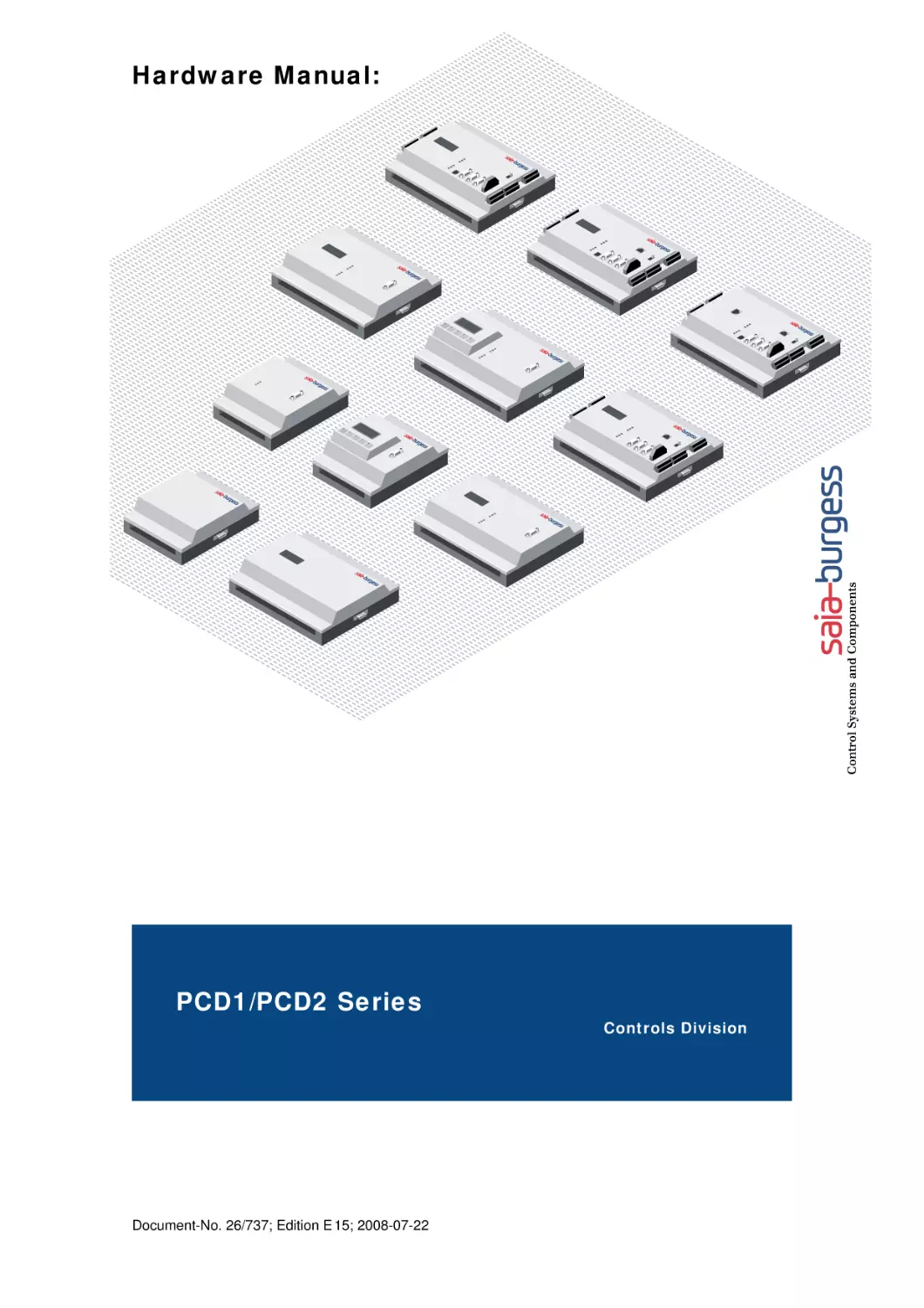
Hardware Manual:
PCD1/PCD2 Series
Document-No. 26/737; Edition E 15; 2008-07-22
Controls Division
Saia-Burgess Controls AG
Contents
0 Index
0 Index
0.1
0.2
1
Graphical index
1.1
PCD1.M110/M120/M130/M125/M135 ............................................................
1.2
PCD2.M110/M120/M150..................................................................................
1.3
PCD2.M170.....................................................................................................
1.4
PCD2.M480.....................................................................................................
1-1
1-2
1-3
1-4
Guidance
Introduction......................................................................................................
Planning an application with PCD1/2/3 components.......................................
Cabling.............................................................................................................
2.3.1 Cable routing..................................................................................................
2-1
2-2
2-4
2-4
2
2.1
2.2
2.3
3
Document history............................................................................................. 0-6
Trademarks...................................................................................................... 0-6
PCD Classic CPUs and expansion housings
System overview..............................................................................................
General technical details..................................................................................
System resources............................................................................................
3.3.1 Program blocks..............................................................................................
3.3.2 Computation ranges for count types..............................................................
3.3.3 Media.............................................................................................................
3.3.4 Program structure for the PCD Classic family...............................................
3.4
CPU overview..................................................................................................
3.4.1 PCD1.M1xx....................................................................................................
3.4.2 Block diagram : PCD1.M1xx..........................................................................
3.4.3 Hardware and firmware versions for the PCD1.............................................
3.4.4 Firmware Upgrade for the PCD1.M110, PCD1.M120 and PCD1.M130.........
3.4.5 Firmware Upgrade for the PCD1.M125 and PCD1.M135..............................
3.4.6 PCD2.M1x0/M480 Hardware and Firmware..................................................
3.4.7 Block diagram : PCD2.Mxx0..........................................................................
3.4.8 Hardware and firmware versions for the PCD2.M110/M120..........................
3.4.9 Hardware and firmware versions for the PCD2.M150...................................
3.4.10 Hardware and firmware versions for the PCD2.M170/M480.........................
3.5
Mounting..........................................................................................................
3.5.1 Mounting position and ambient temperature..................................................
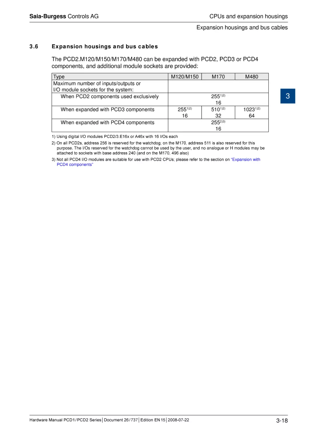
3.6
Expansion housings and bus cables................................................................
3.6.1 Expansion with PCD2 components................................................................
3.6.2 Expansion with PCD3 components................................................................
3.6.3 Expansion with PCD4 components................................................................
3.7
Installation and addressing of PCD2 I/O modules...........................................
3.7.1 Insertion of I/O modules.................................................................................
3.7.2 Address and terminal designation..................................................................
3.7.3 Cable layout...................................................................................................
3.8
Dimensions......................................................................................................
3.9
Power supply and connection plan..................................................................
3.1
3.2
3.3
Hardware Manual PCD 1 / PCD 2 Series│Document 26 / 737│Edition EN 15│2008-07-22
0
3-1
3-2
3-4
3-4
3-4
3-5
3-6
3-7
3-7
3-8
3-9
3-10
3-10
3-11
3-14
3-15
3-16
3-16
3-17
3-17
3-18
3-19
3-21
3-22
3-23
3-23
3-23
3-24
3-25
3-26
0-1
Saia-Burgess Controls AG
Contents
4
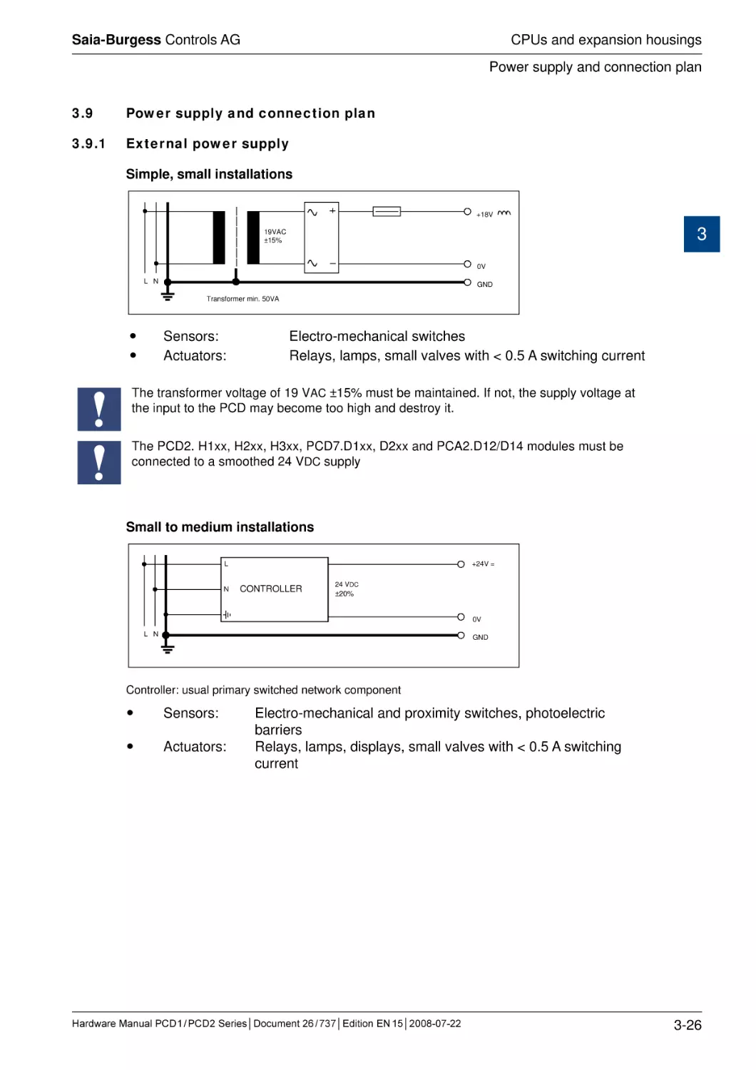
3.9.1 External power supply....................................................................................
3.9.2 Earthing and connection plan........................................................................
3.9.3 Internal power supply.....................................................................................
3.9.4 Capacity of internal power supply..................................................................
3.11
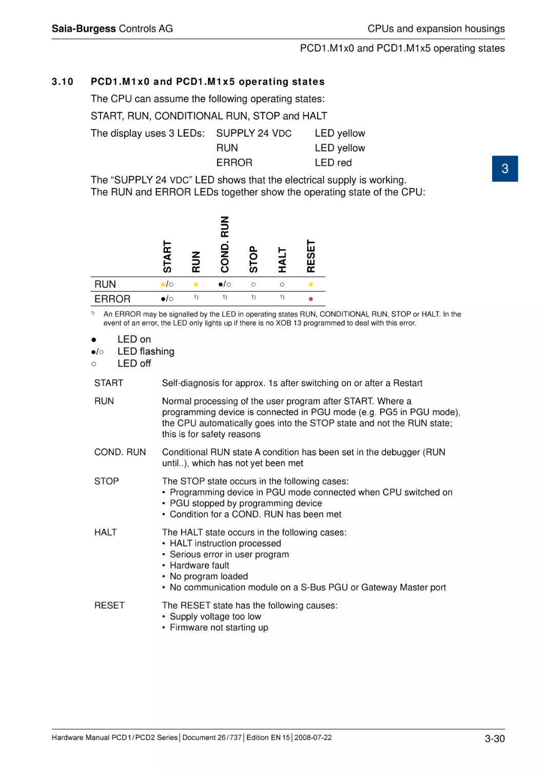
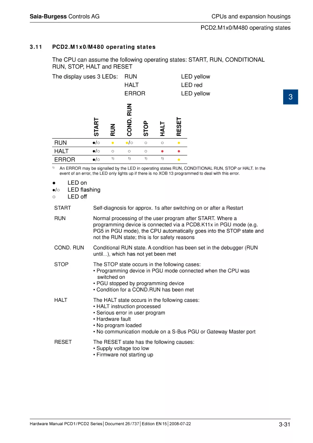
PCD2.M1x0/M480 operating states.................................................................
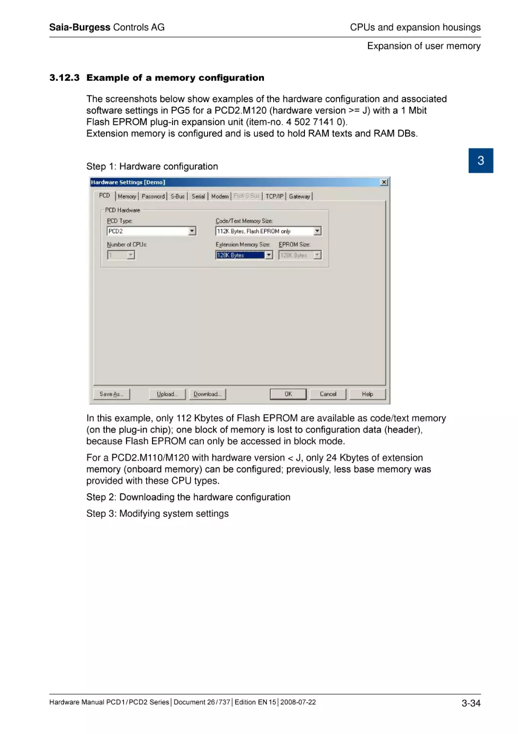
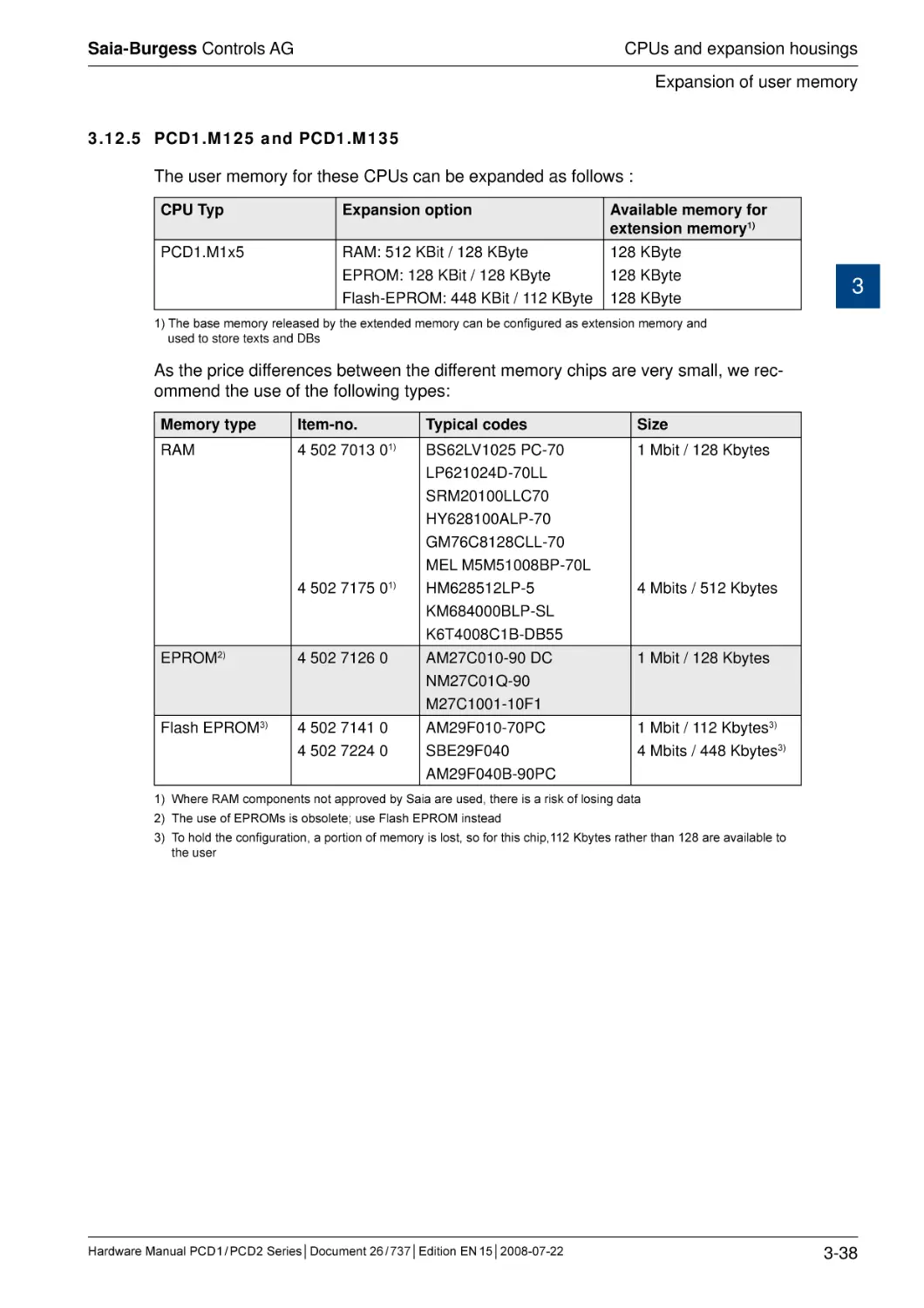
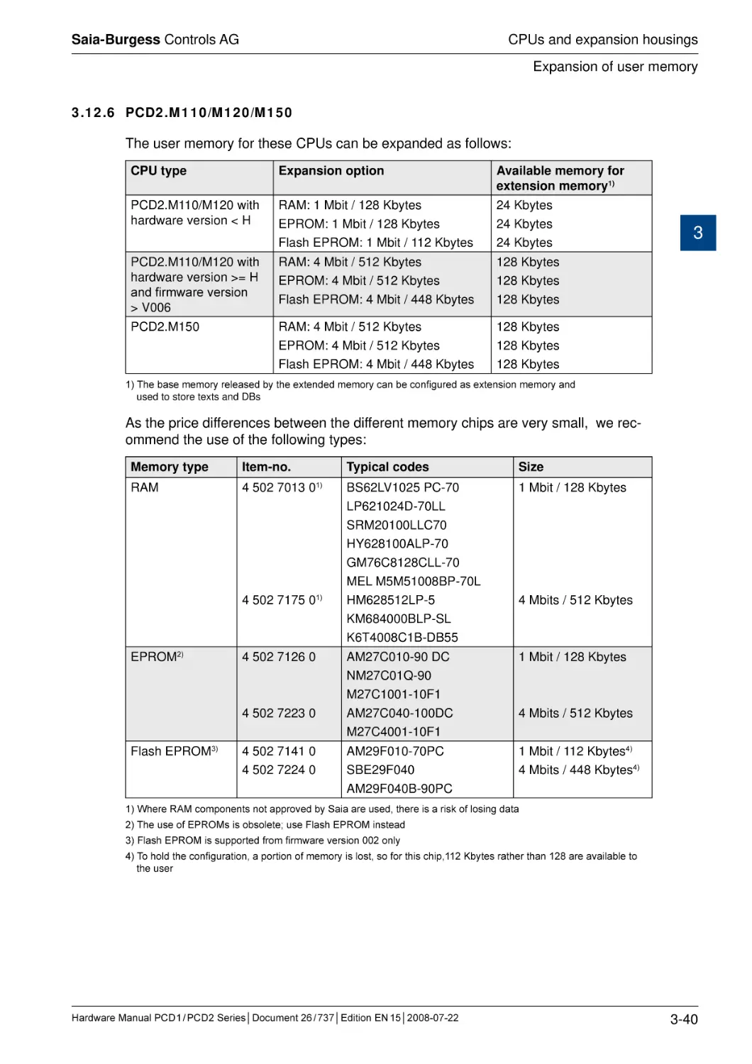
3.12
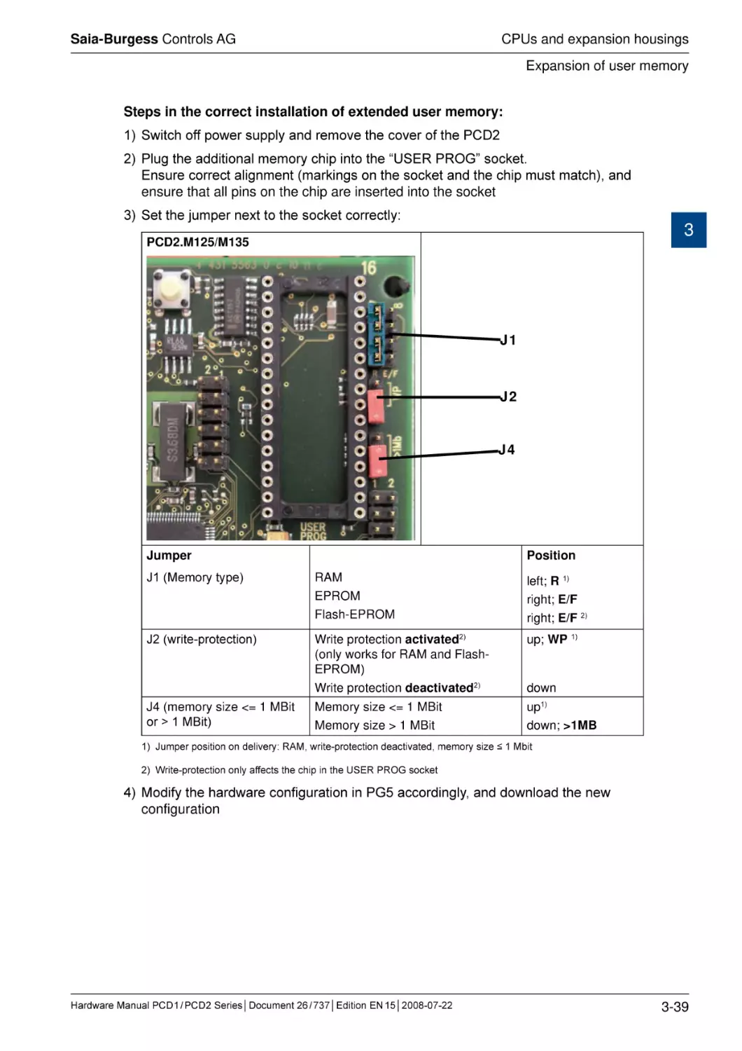
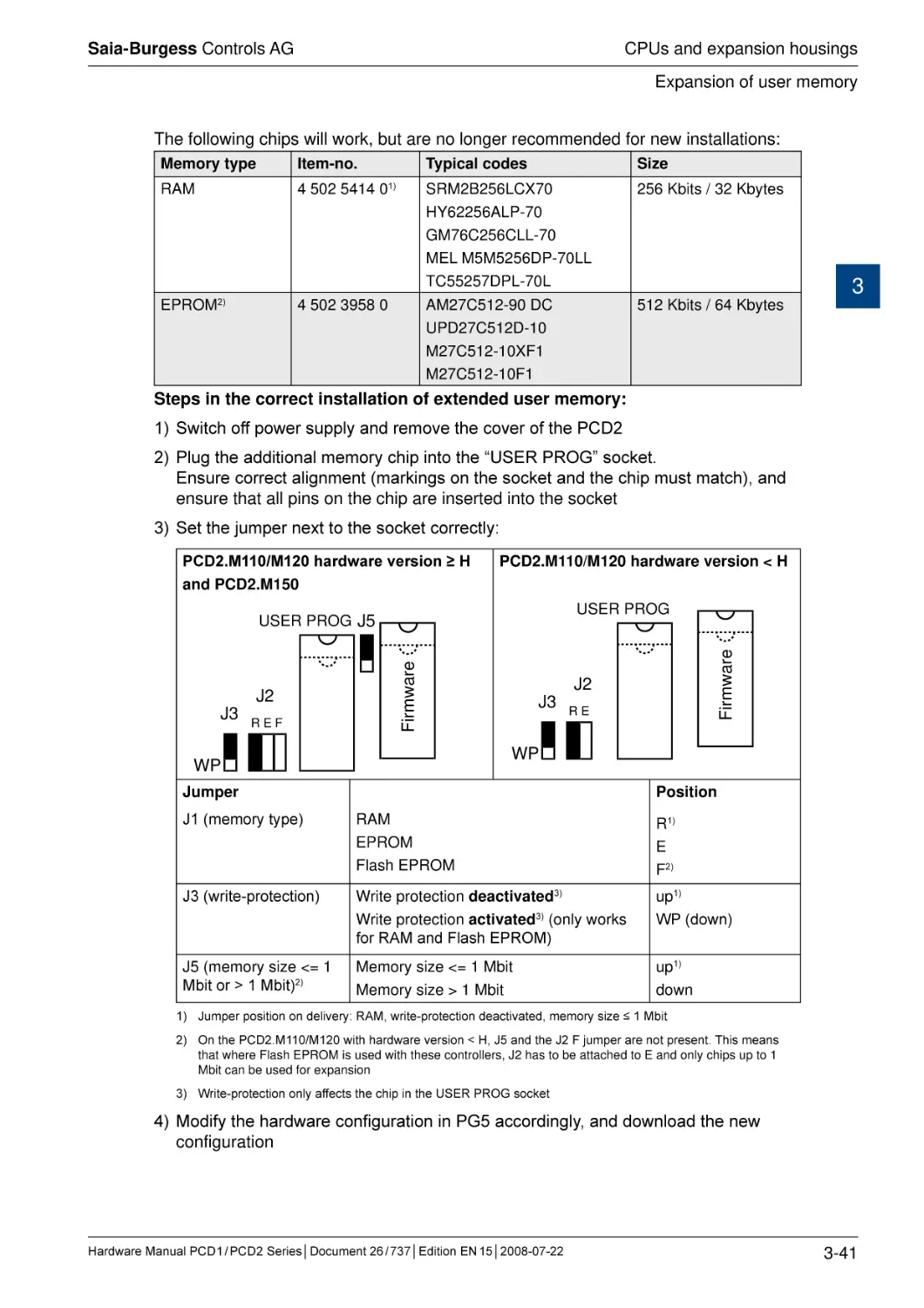
Expansion of user memory..............................................................................
3.12.1 Basics............................................................................................................
3.12.2 Memory location of the user program, the resources, texts and DBs............
3.12.3 Example of a memory configuration..............................................................
3.12.4 PCD1.M1x0....................................................................................................
3.12.5 PCD1.M125 and PCD1.M135........................................................................
3.12.6 PCD2.M110/M120/M150................................................................................
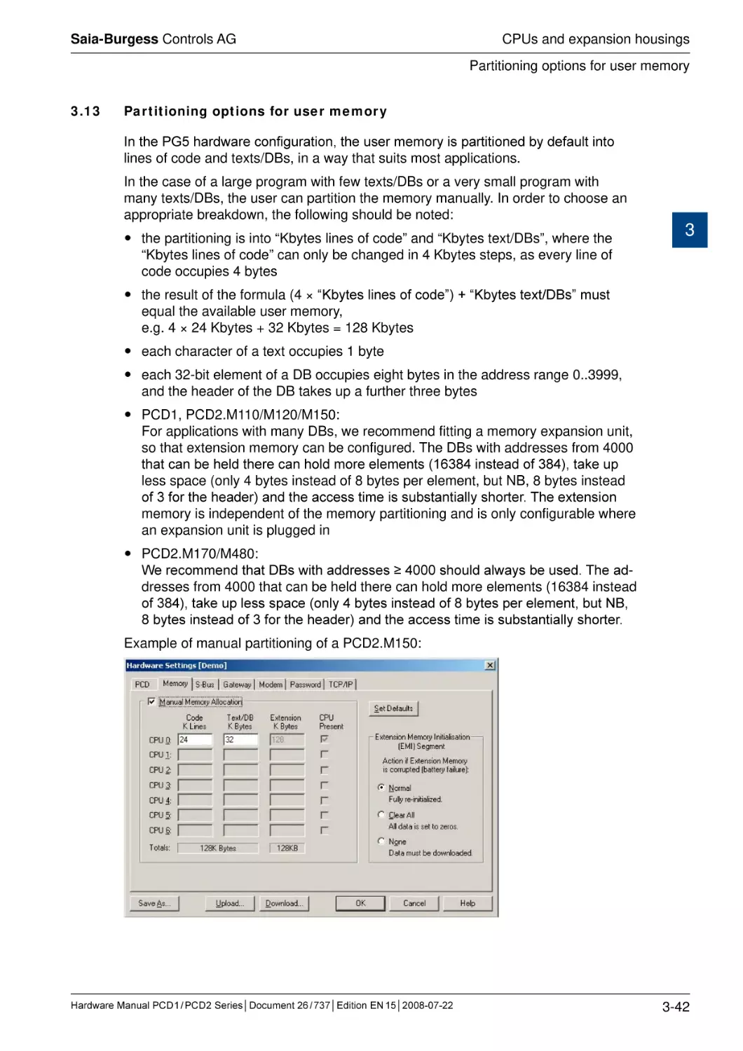
3.13
Partitioning options for user memory ..............................................................
3.14
Data storage in case of power outage.............................................................
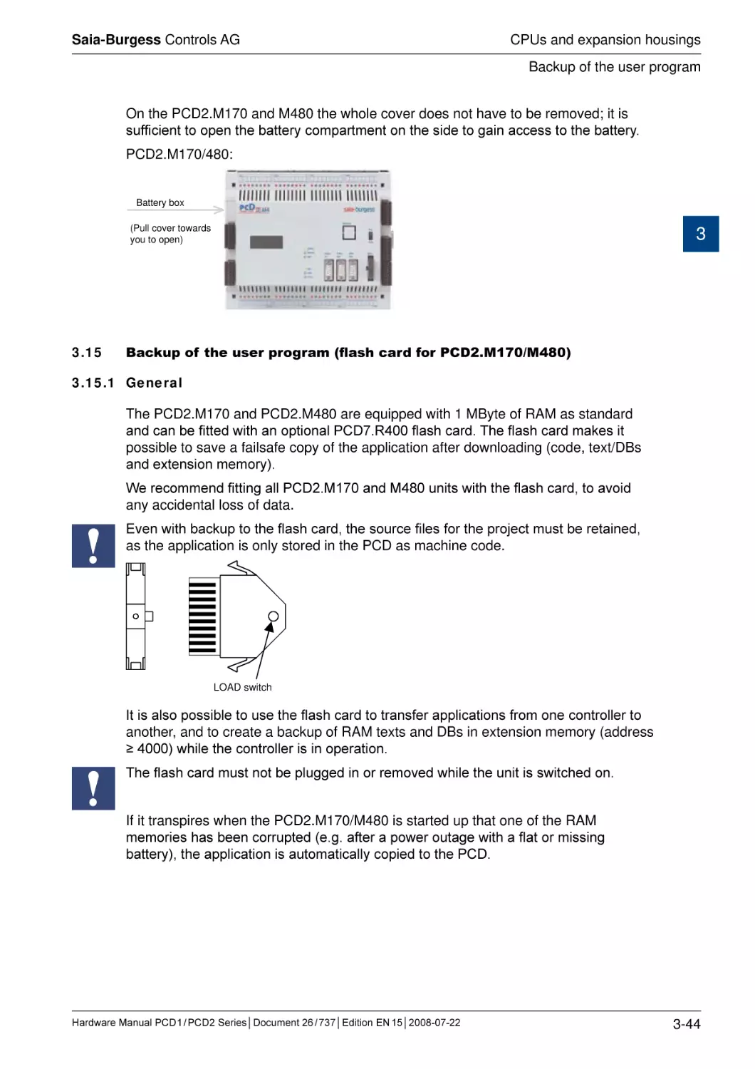
3.15
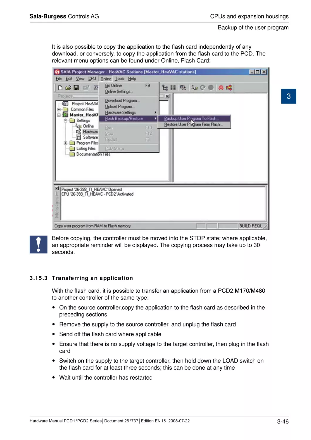
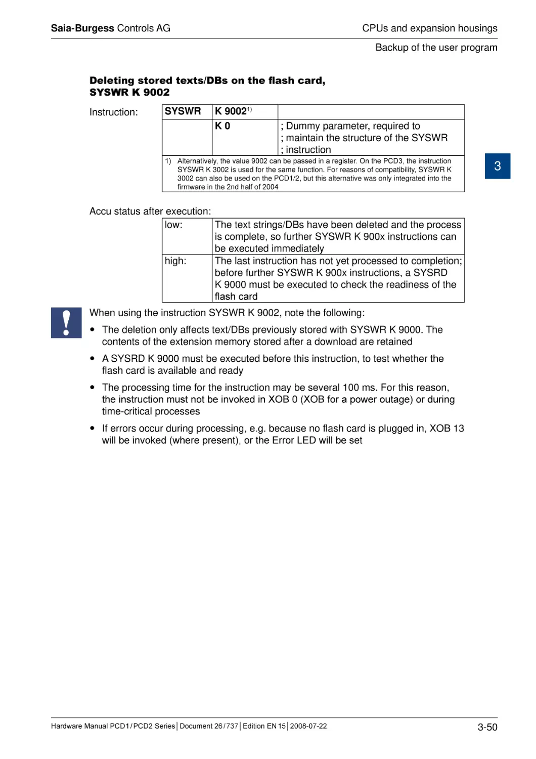
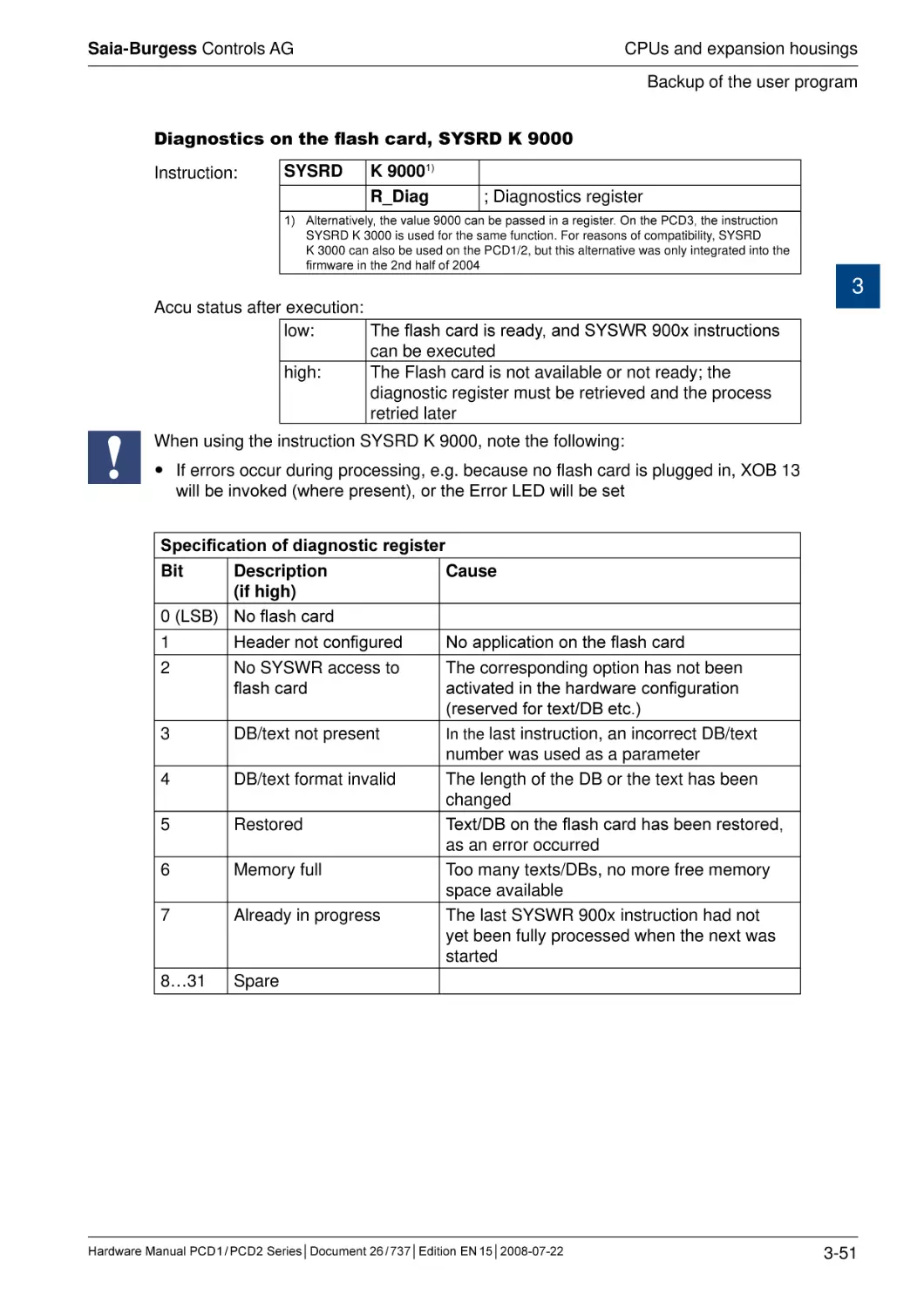
Backup of the user program (flash card for PCD2.M170/M480)......................
3.15.1 General..........................................................................................................
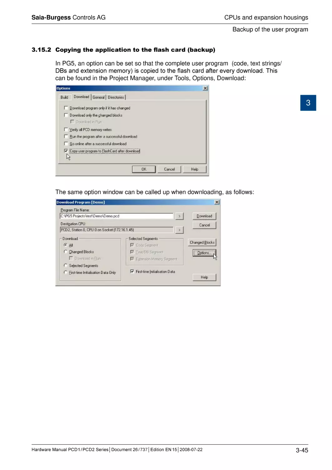
3.15.2 Copying the application to the flash card (backup)........................................
3.15.3 Transferring an application.............................................................................
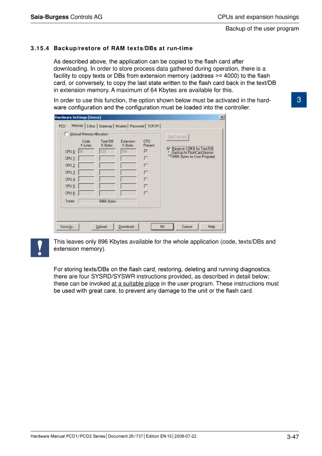
3.15.4 Backup/restore of RAM texts/DBs at run-time...............................................
3.16
Hardware clock (Real Time Clock)...................................................................
3.16.1 Clock module PCD2.F500 (obsolete, PCD2.M110/M120 only)......................
3.17
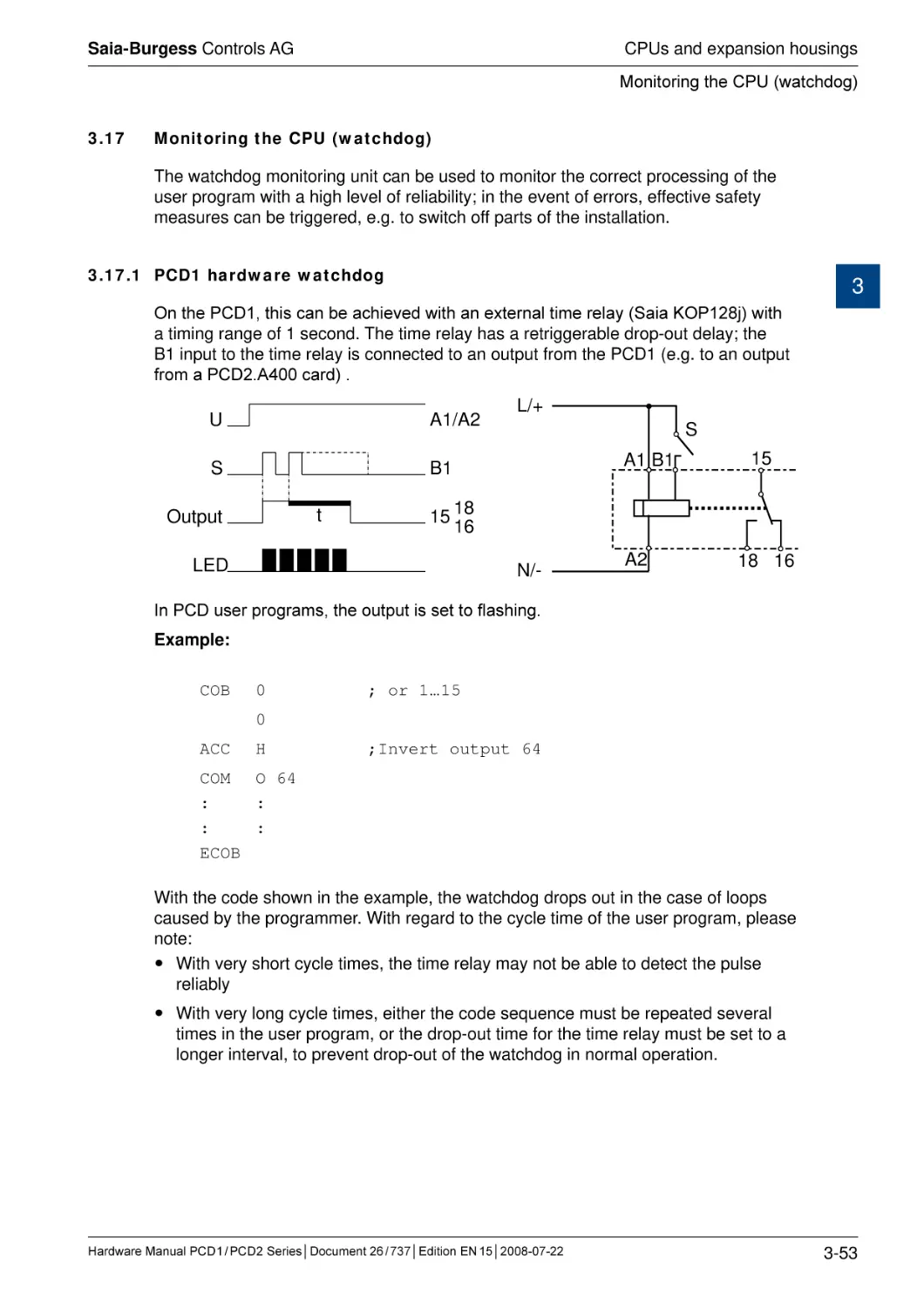
Monitoring the CPU (watchdog).......................................................................
3.17.1 PCD1 hardware watchdog.............................................................................
3.17.2 PCD2 hardware watchdog.............................................................................
3.17.3 Software watchdog for PCD1 and PCD2.......................................................
3.18
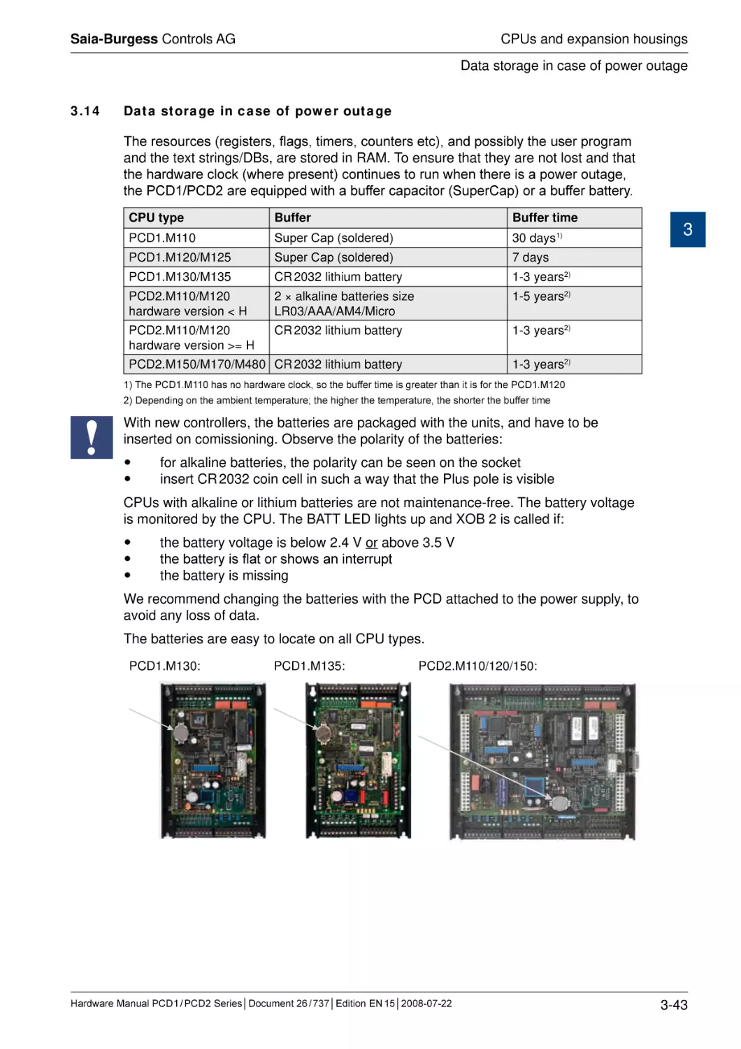
Internal LED displays and small terminals.......................................................
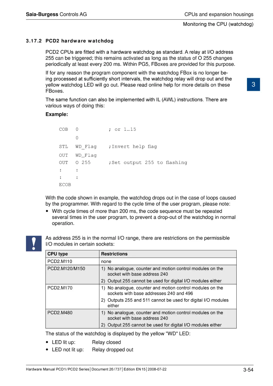
3.18.1 PCD2.F510 7-segment LED display (PCD2.M110/M120/M150 only)............
3.18.2 PCD2.F530 7-Segment LED display (PCD2.M120/M150 only).....................
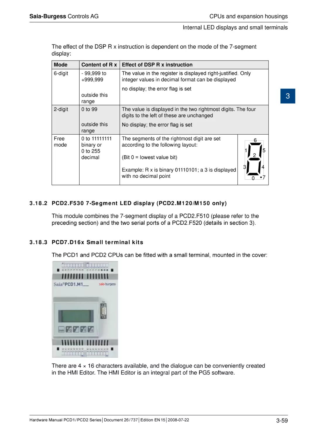
3.18.3 PCD7.D16x Small terminal kits .....................................................................
3.19
Interrupt inputs.................................................................................................
3.19.1 Basics............................................................................................................
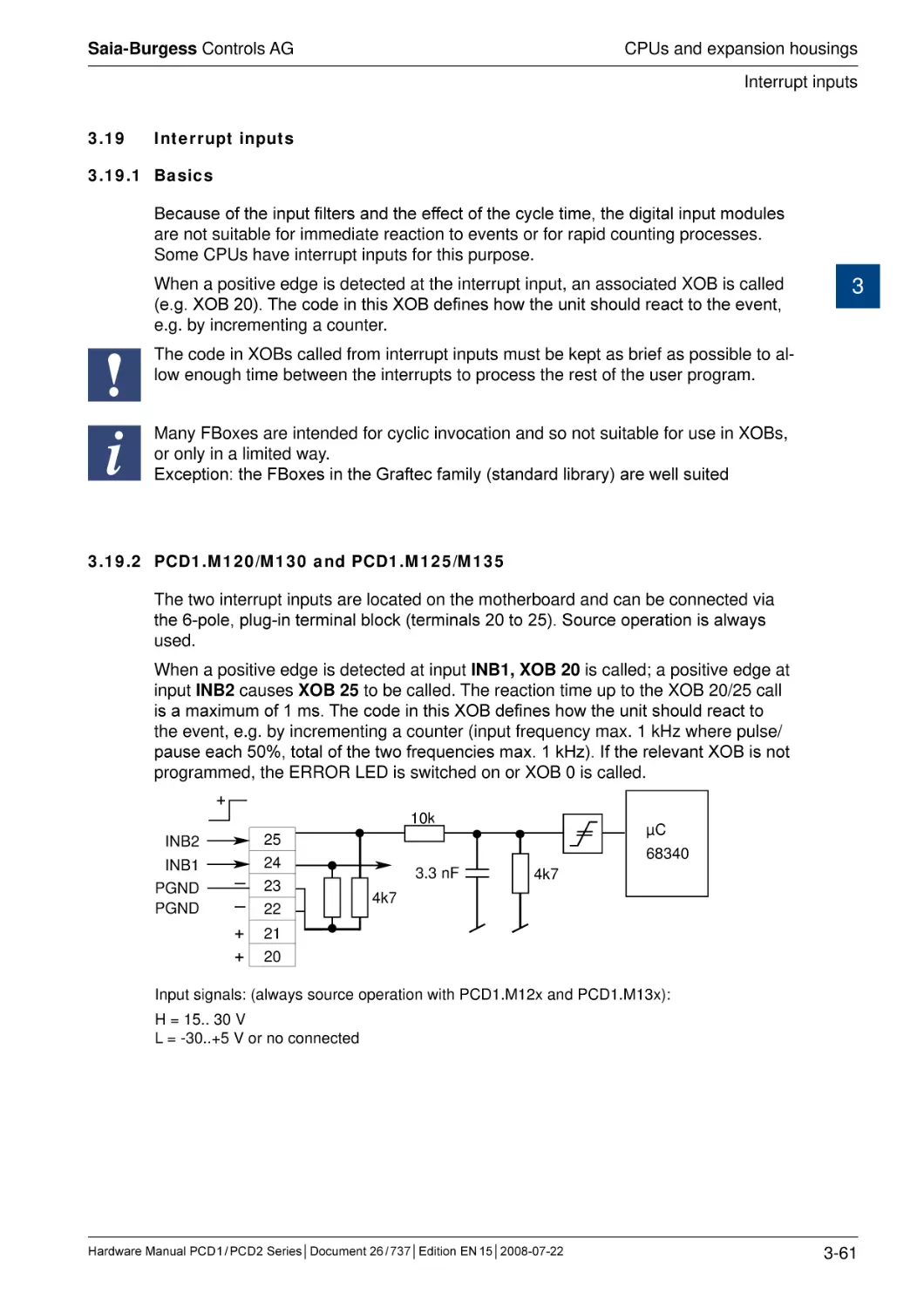
3.19.2 PCD1.M120/M130 and PCD1.M125/M135....................................................
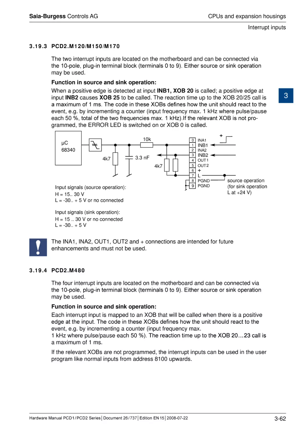
3.19.3 PCD2.M120/M150/M170...............................................................................
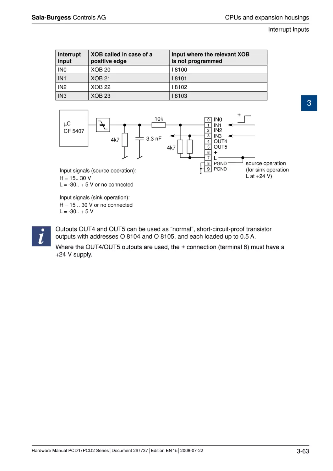
3.19.4 PCD2.M480...................................................................................................
3.20
Run/Stop or Run/Halt switch (PCD2.M170/M480 only)...................................
3.21
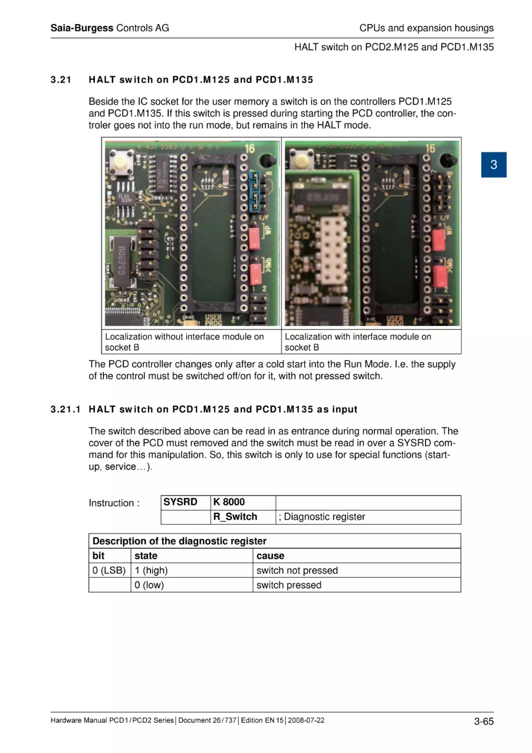
HALT switch on PCD1.M125 and PCD1.M135................................................
3.21.1 HALT switch on PCD1.M125 and PCD1.M135 as input................................
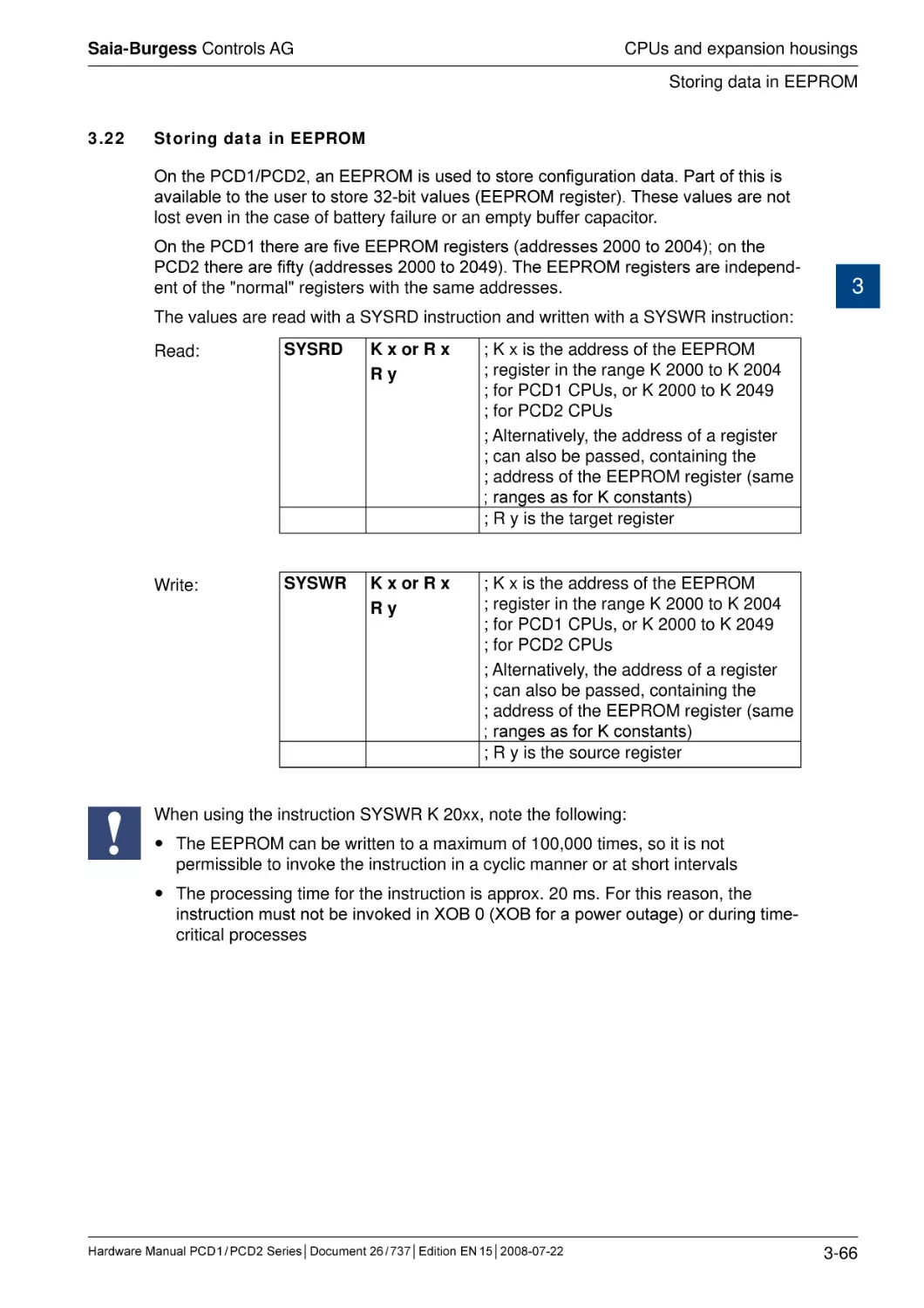
3.22
Storing data in EEPROM.................................................................................
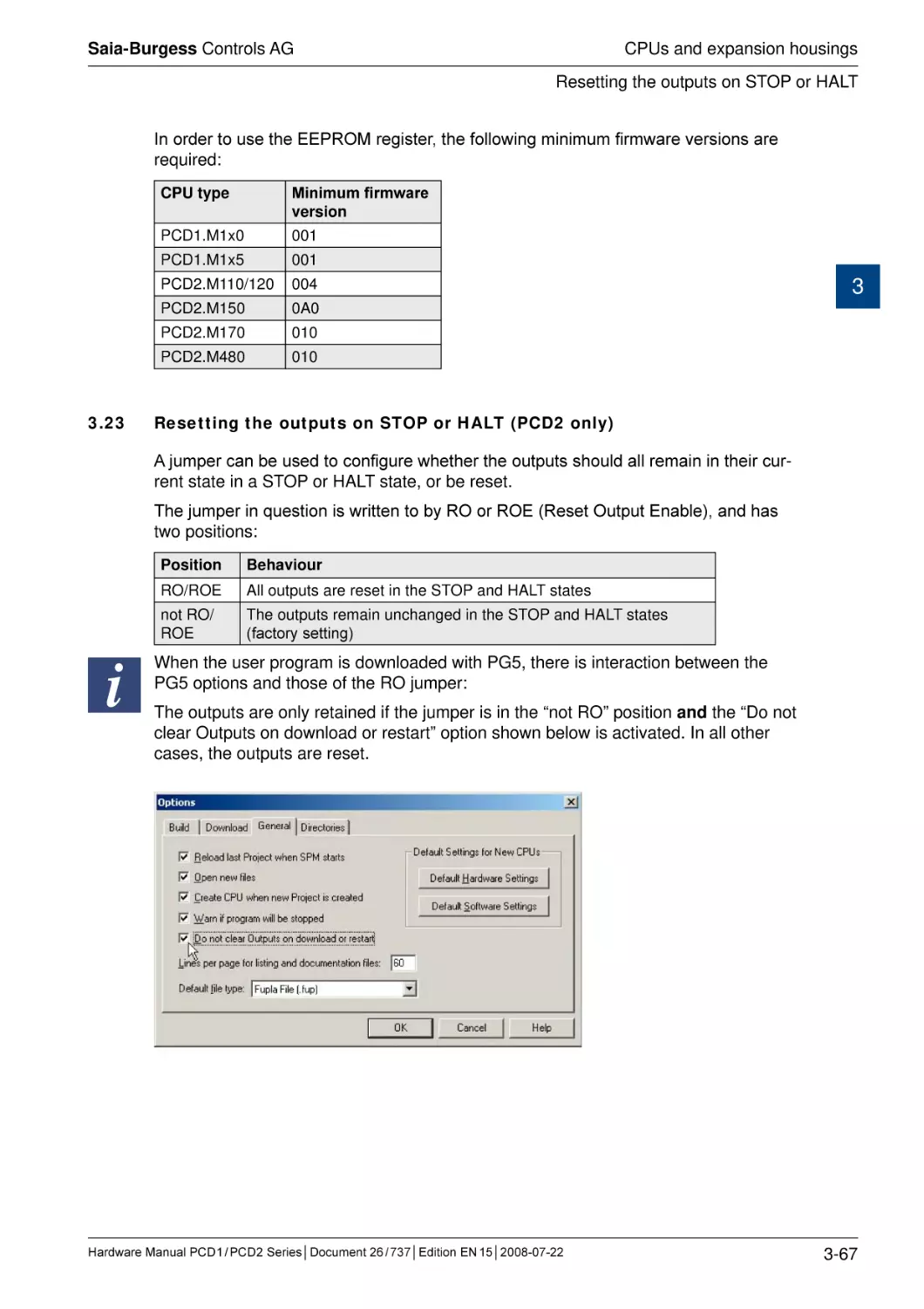
3.23
Resetting the outputs on STOP or HALT (PCD2 only).....................................
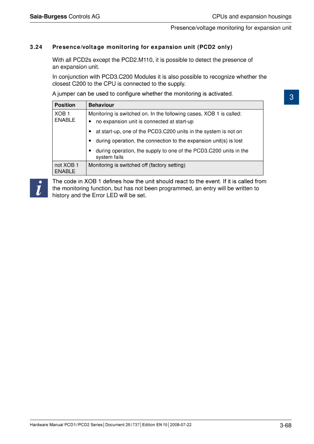
3.24
Presence/voltage monitoring for expansion unit (PCD2 only).........................
3-26
3-27
3-29
3-29
3-31
3-32
3-32
3-33
3-34
3-36
3-38
3-40
3-42
3-43
3-44
3-44
3-45
3-46
3-47
3-52
3-52
3-53
3-53
3-54
3-56
3-57
3-57
3-59
3-59
3-61
3-61
3-61
3-62
3-62
3-64
3-65
3-65
3-66
3-67
3-68
PCD Classic communication interfaces
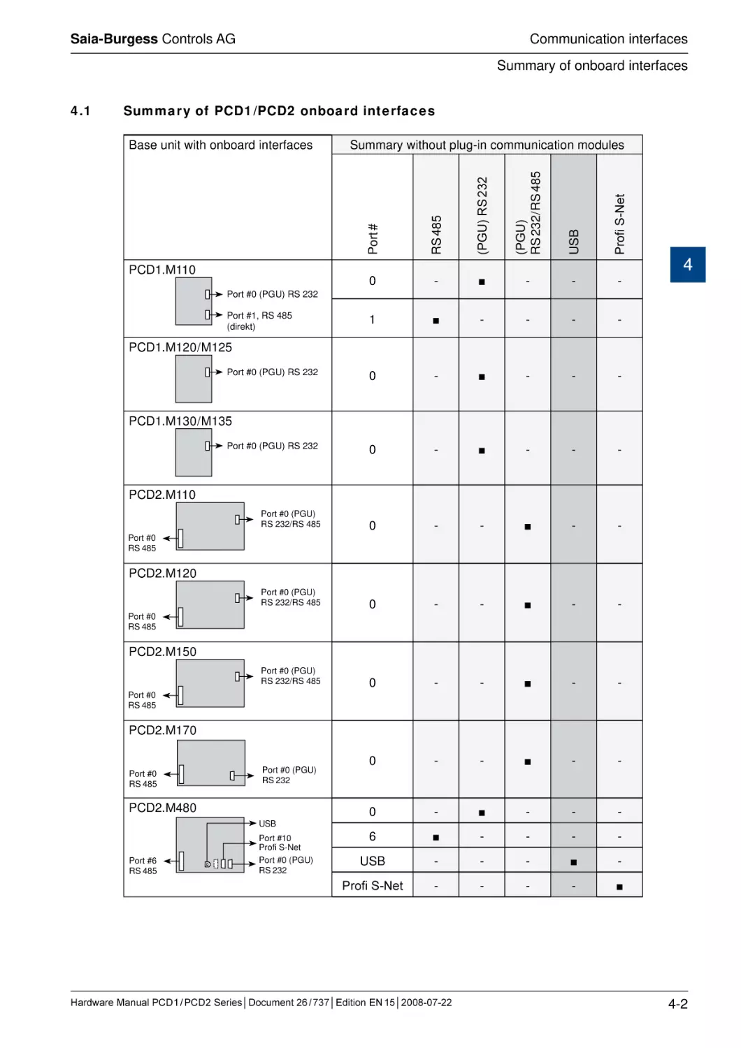
4.1
Summary of PCD1 / PCD2 onboard interfaces.................................................
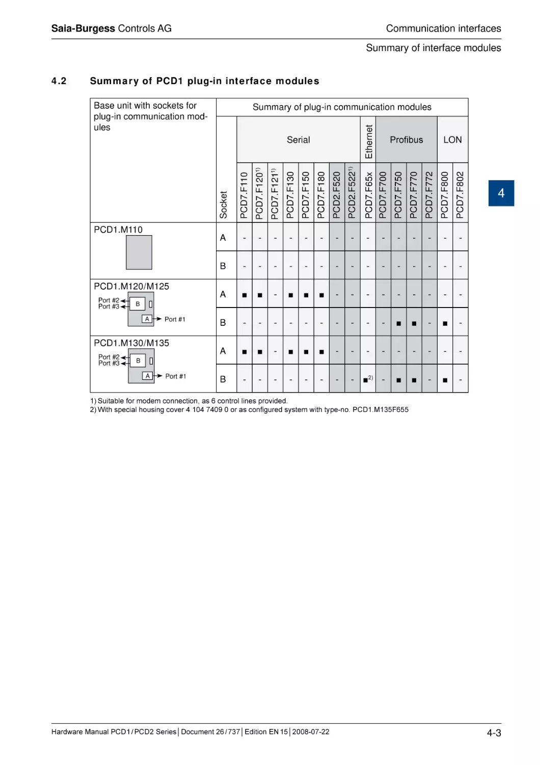
4.2
Summary of PCD1 plug-in interface modules..................................................
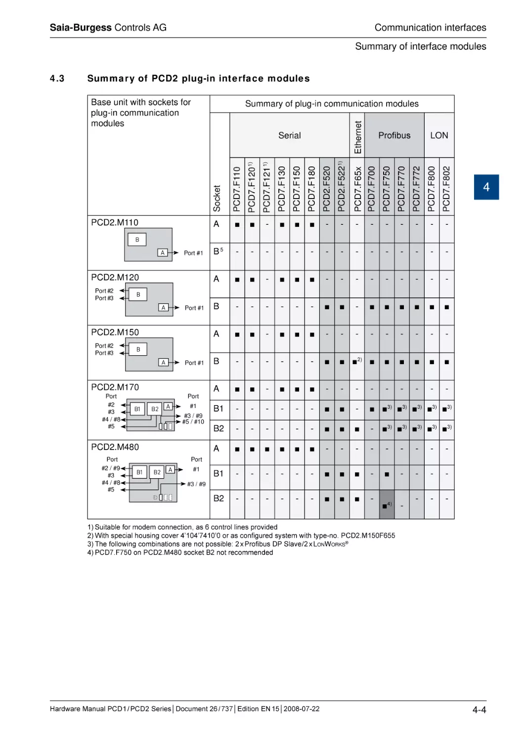
4.3
Summary of PCD2 plug-in interface modules..................................................
4.4
Onboard interfaces..........................................................................................
4-2
4-3
4-4
4-5
Hardware Manual PCD 1 / PCD 2 Series│Document 26 / 737│Edition EN 15│2008-07-22
0
0-2
Saia-Burgess Controls AG
Contents
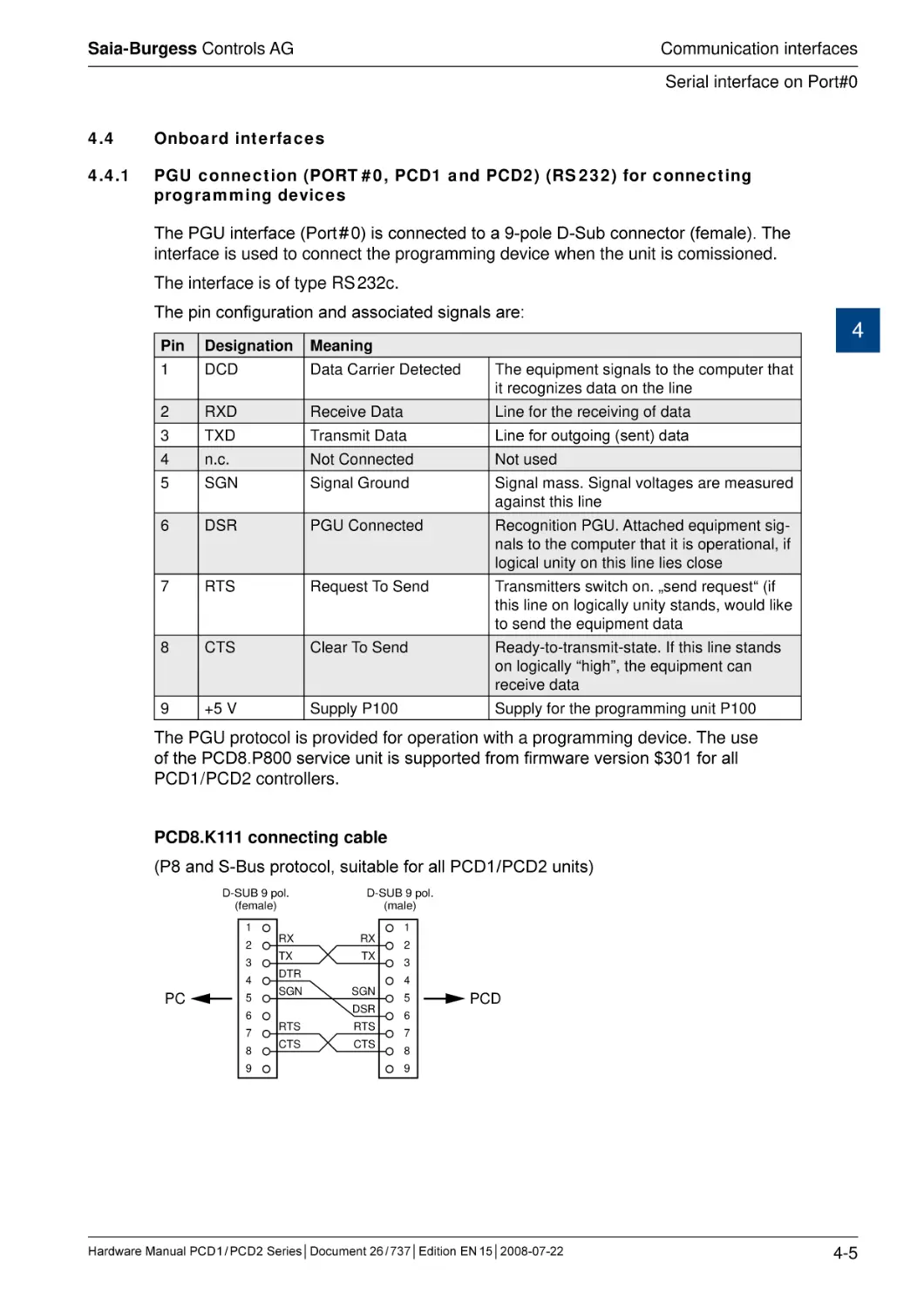
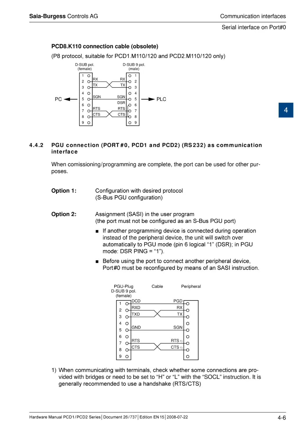
PGU connection (PORT # 0, PCD1 and PCD2)
(RS 232) for connecting programming devices..............................................
PGU connection (PORT # 0, PCD1 and PCD2)
(RS 232) as communication interface............................................................
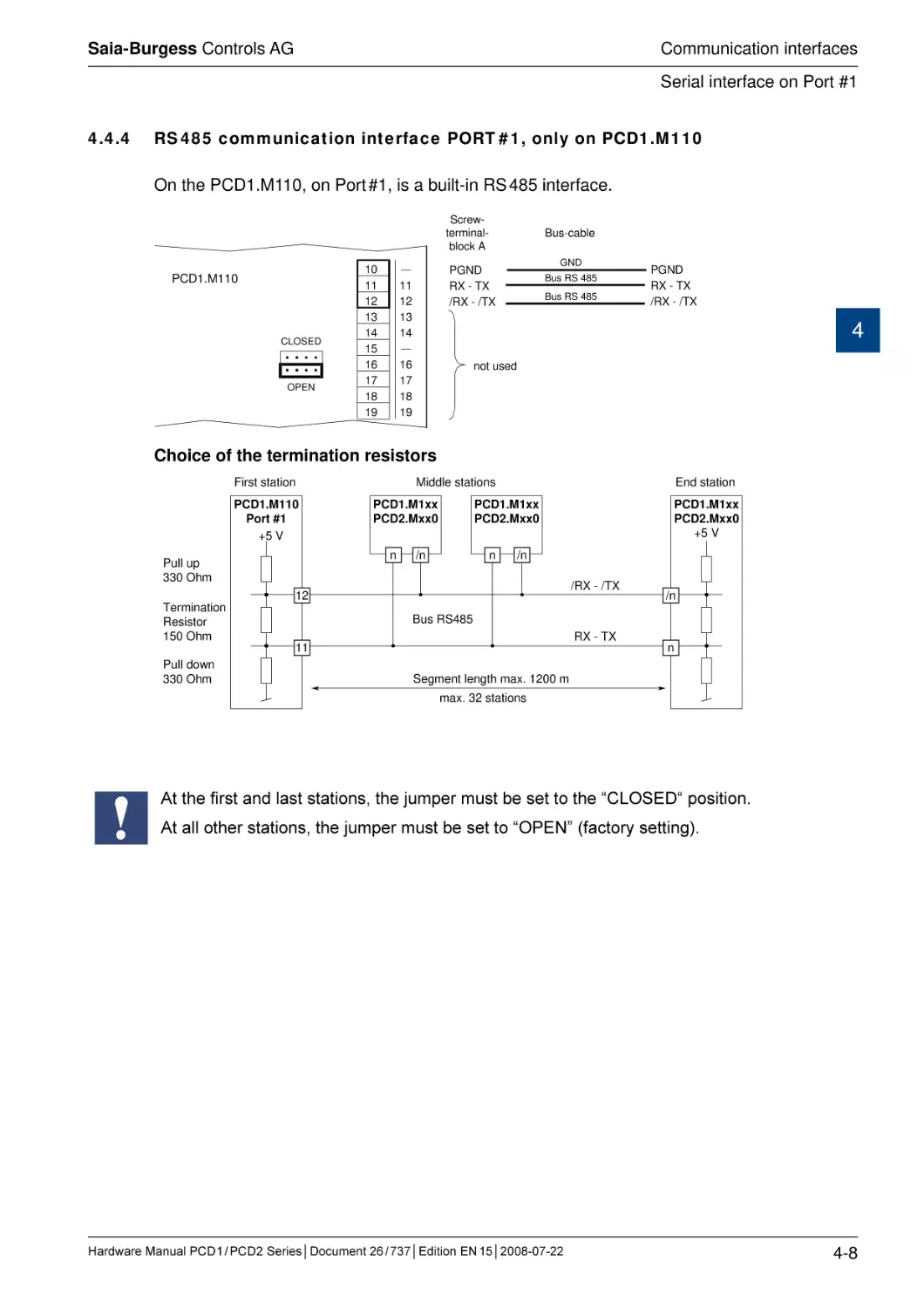
PGU connection (PORT # 0, only on PCD2.M1x0)
(RS 485) as communication interface............................................................
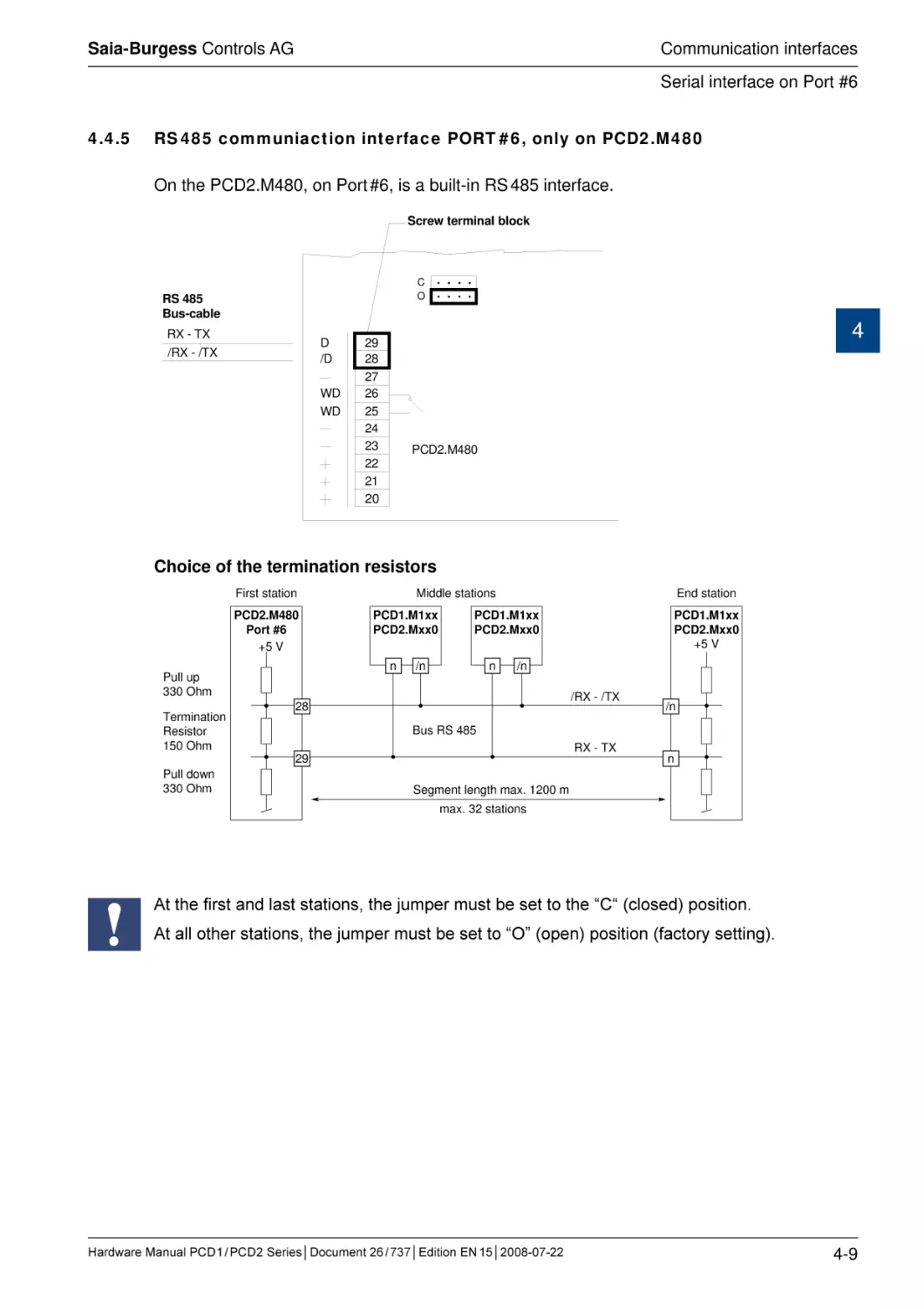
RS 485 communication interface PORT # 1, only on PCD1.M110..................
RS 485 communiaction interface PORT # 6, only on PCD2.M480..................
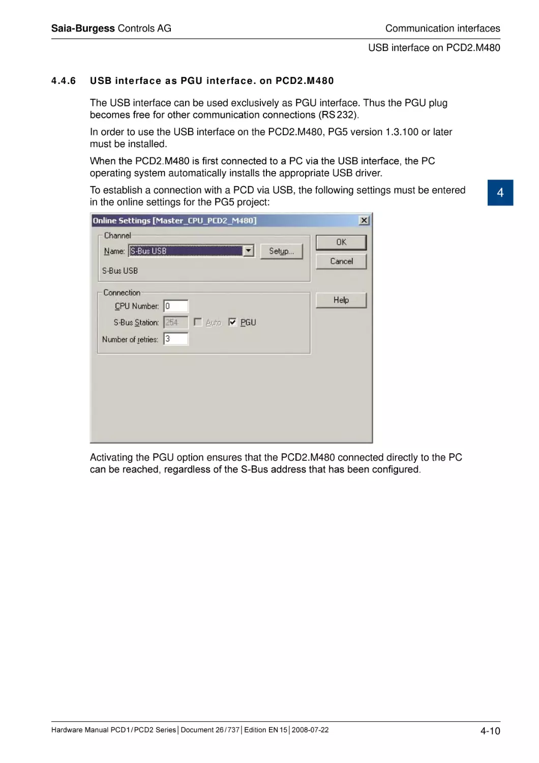
USB interface as PGU interface. on PCD2.M480..........................................
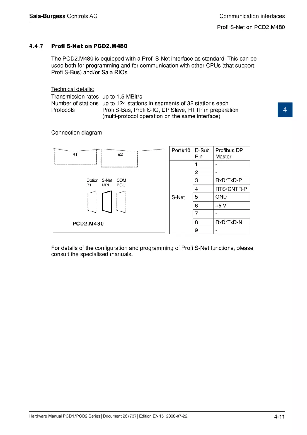
Profi S-Net on PCD2.M480............................................................................
4.5
Plug-in interfaces modules: Socket A...............................................................
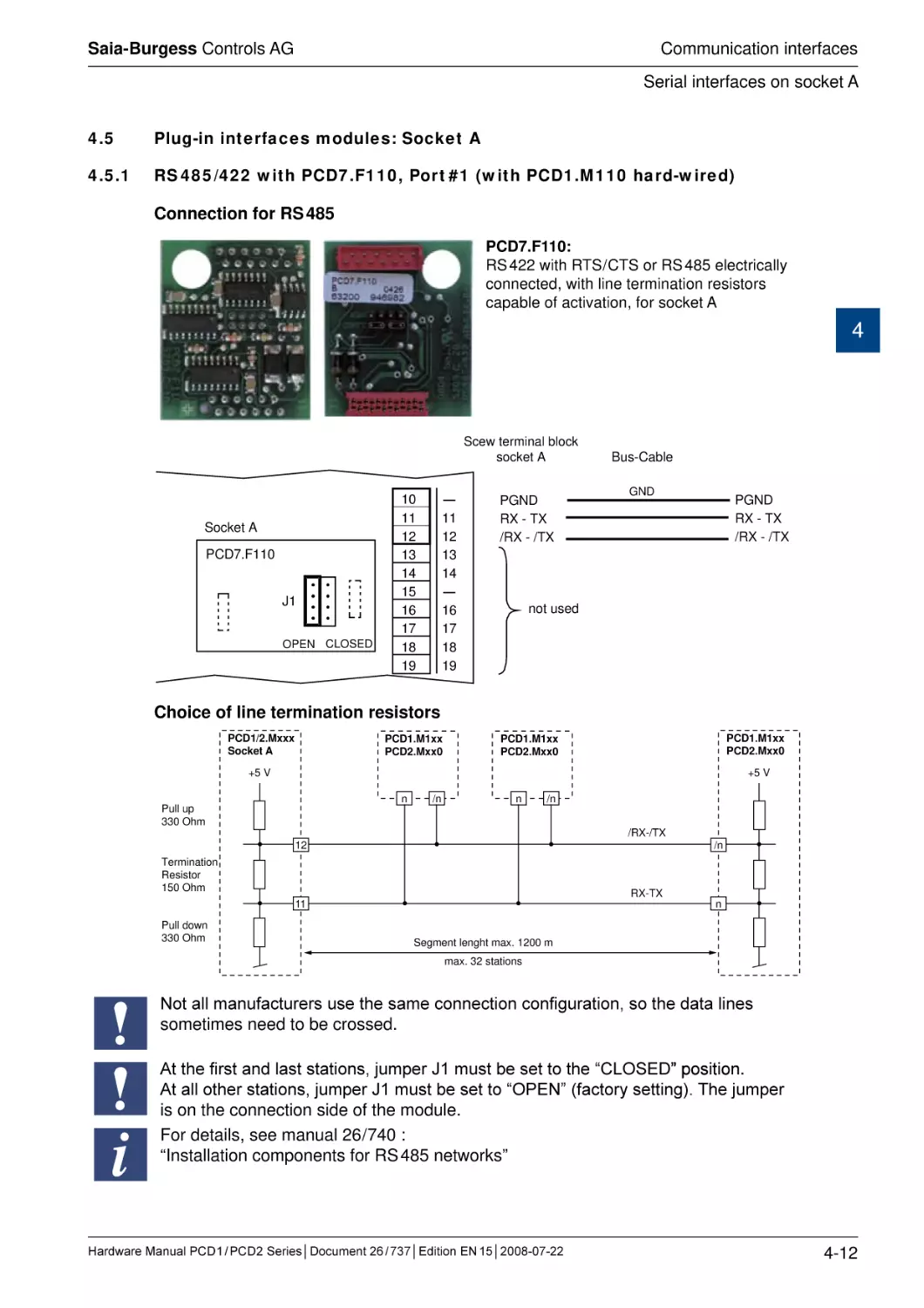
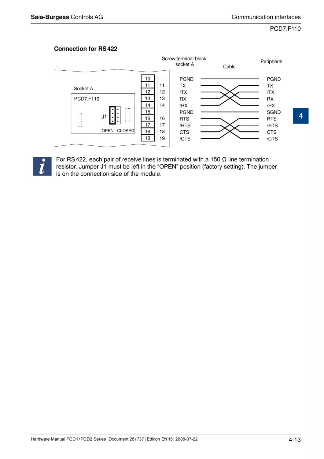
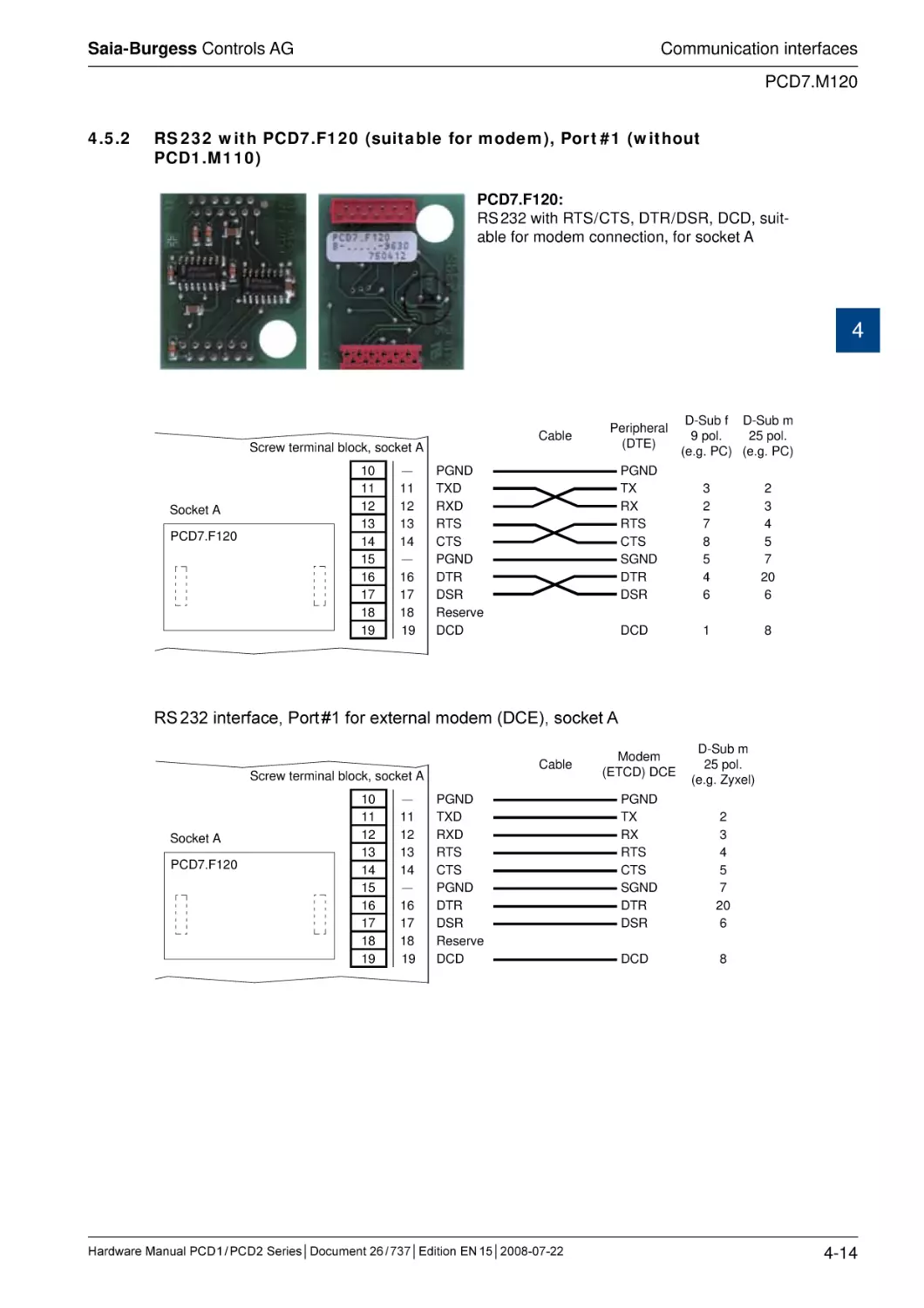
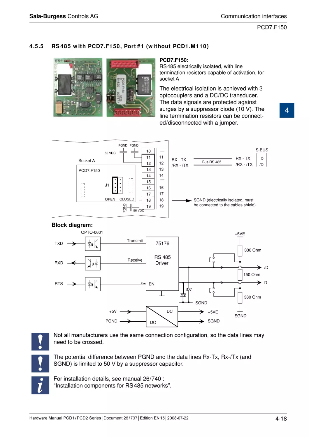
4.5.1 RS 485 / 422 with PCD7.F110, Port #1 (with PCD1.M110 hard-wired)............
4.5.2 RS 232 with PCD7.F120 (suitable for modem),
Port #1 (without PCD1.M110).........................................................................
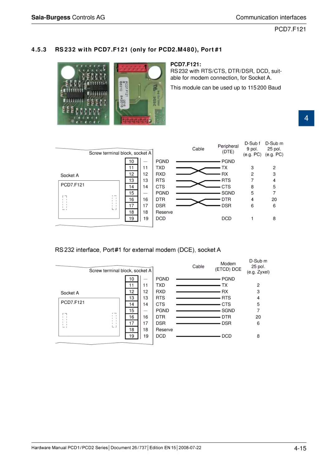
4.5.3 RS 232 with PCD7.F121 (only for PCD2.M480), Port #1................................
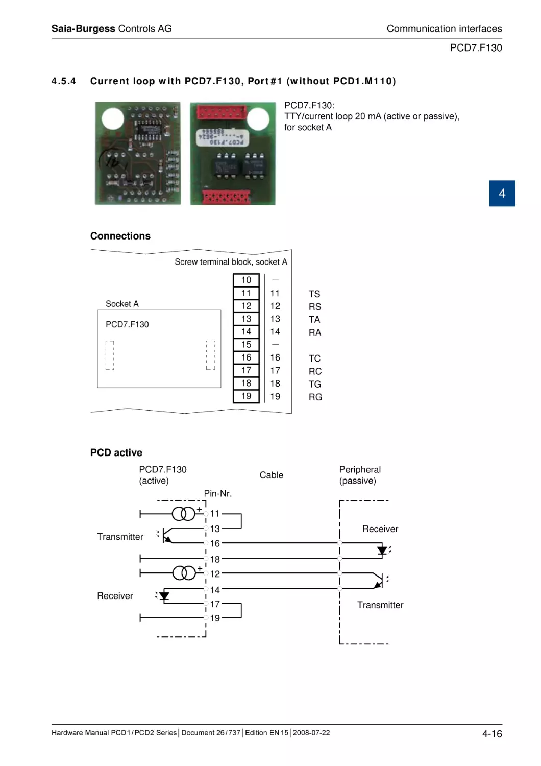
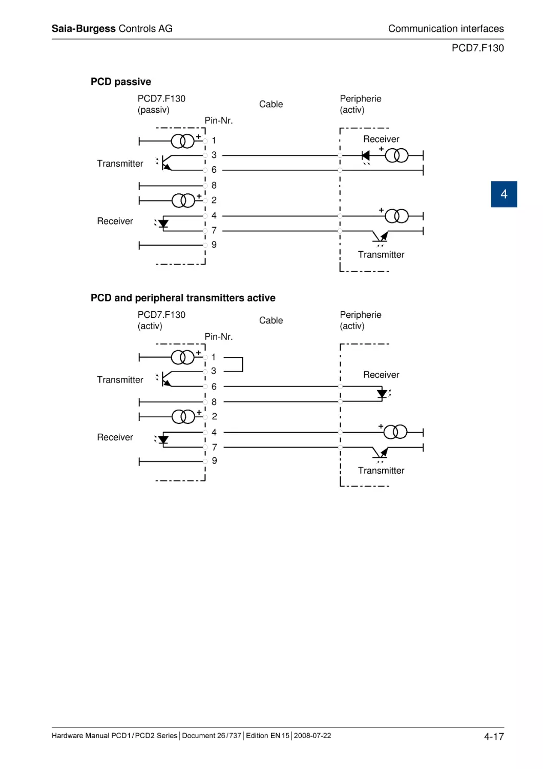
4.5.4 Current loop with PCD7.F130, Port #1 (without PCD1.M110)........................
4.5.5 RS 485 with PCD7.F150, Port #1 (without PCD1.M110)................................
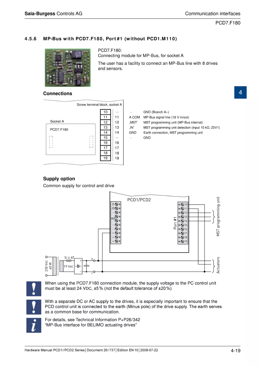
4.5.6 MP-Bus with PCD7.F180, Port #1 (without PCD1.M110)...............................
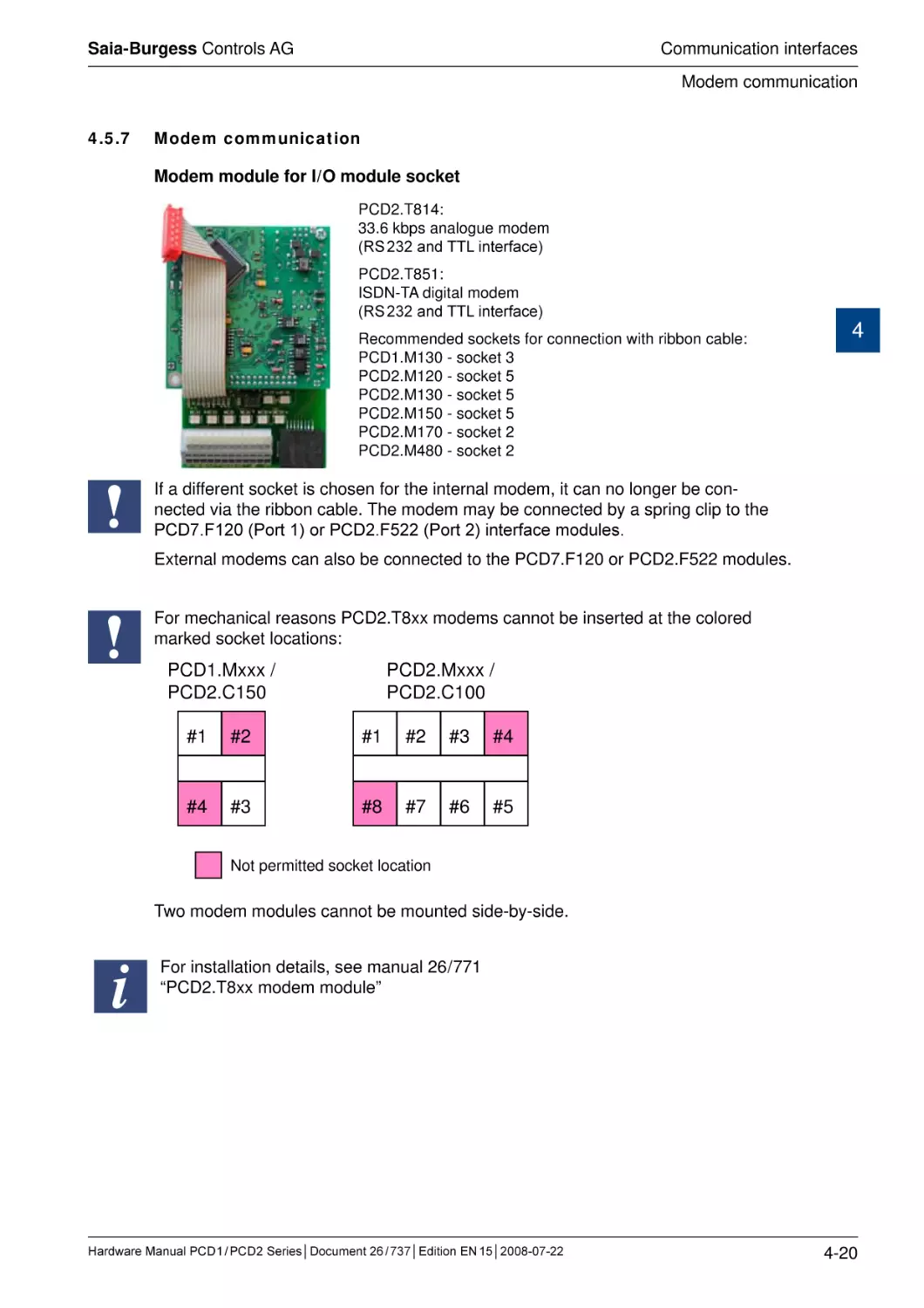
4.5.7 Modem communication..................................................................................
4.6
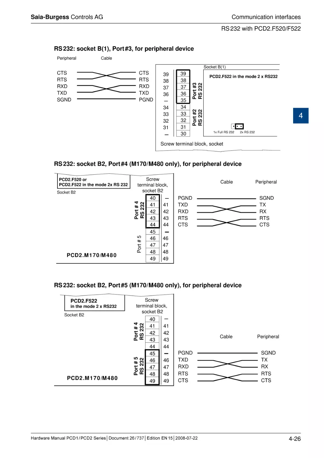
Serial interfaces: socket B(1) or B2 ................................................................
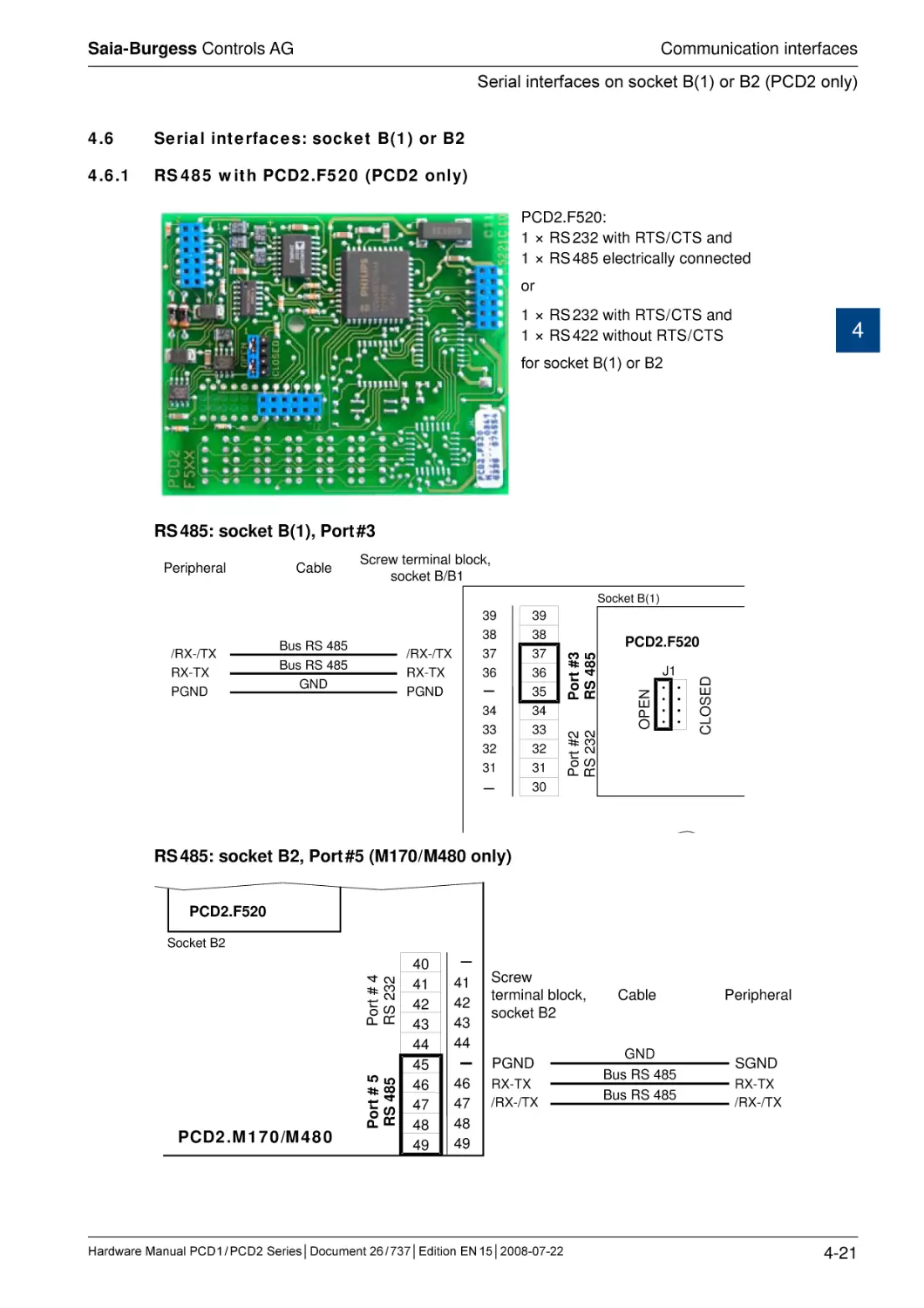
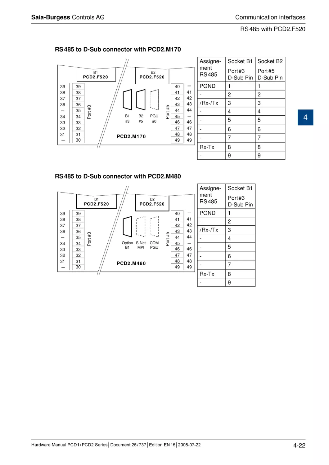
4.6.1 RS 485 with PCD2.F520 (PCD2 only) . .........................................................
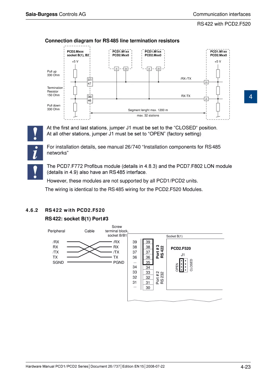
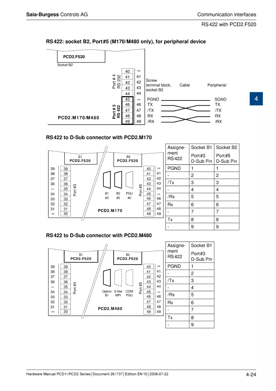
4.6.2 RS 422 with PCD2.F520................................................................................
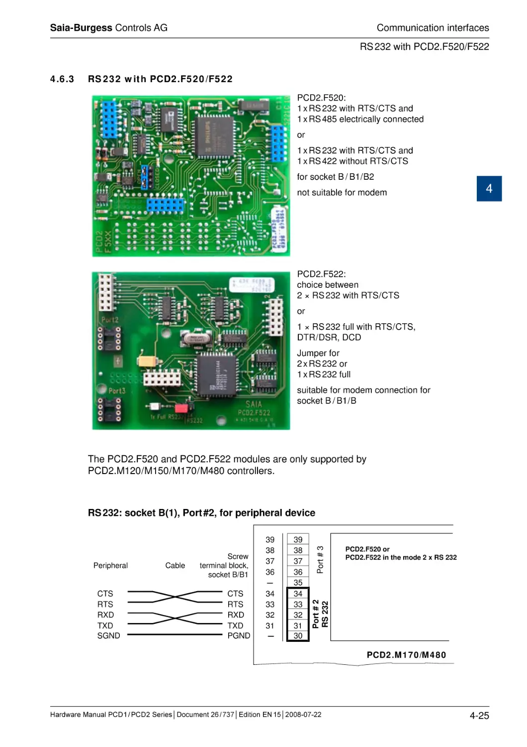
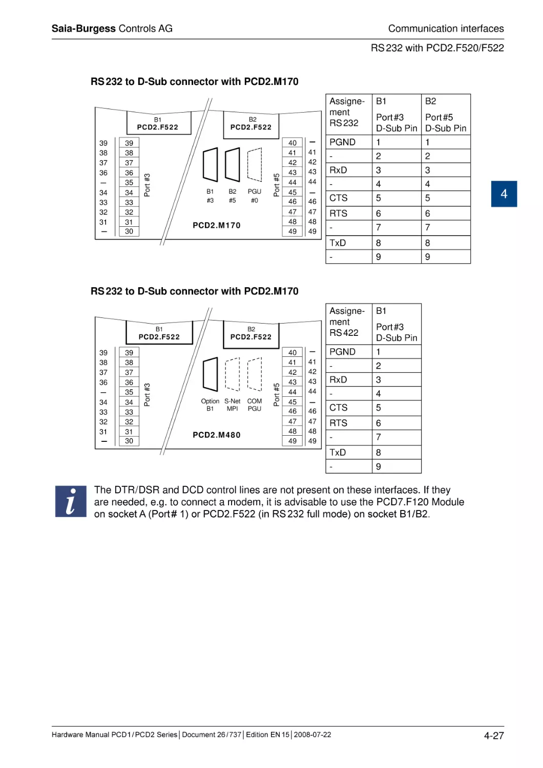
4.6.3 RS 232 with PCD2.F520 / F522.......................................................................
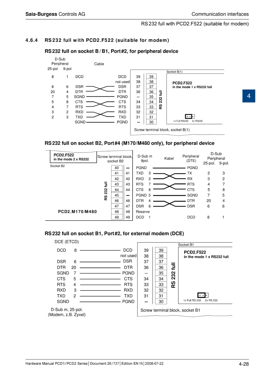
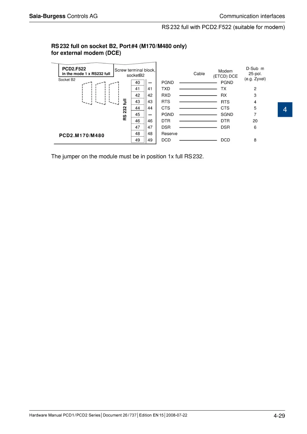
4.6.4 RS 232 full with PCD2.F522 (suitable for modem).........................................
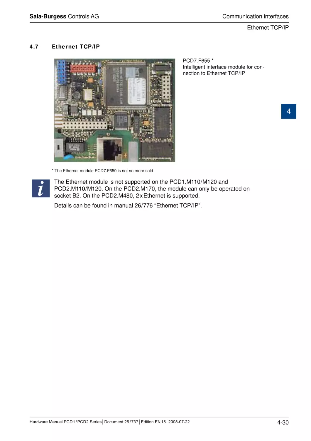
4.7
Ethernet TCP/ IP...............................................................................................
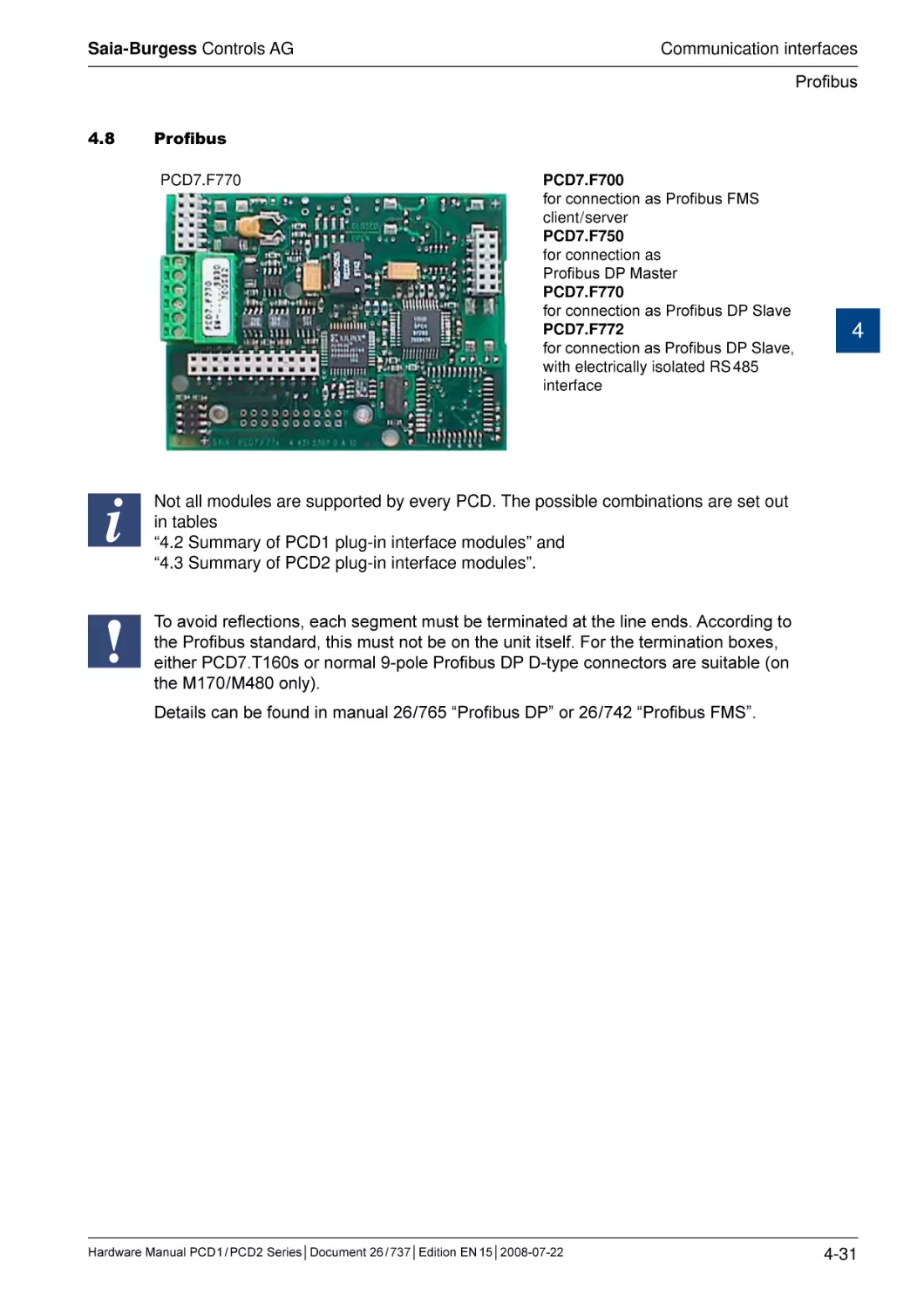
4.8
Profibus............................................................................................................
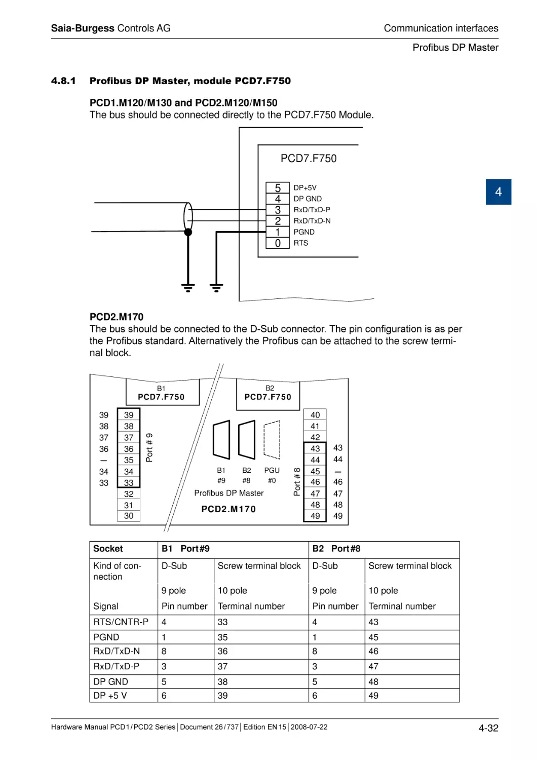
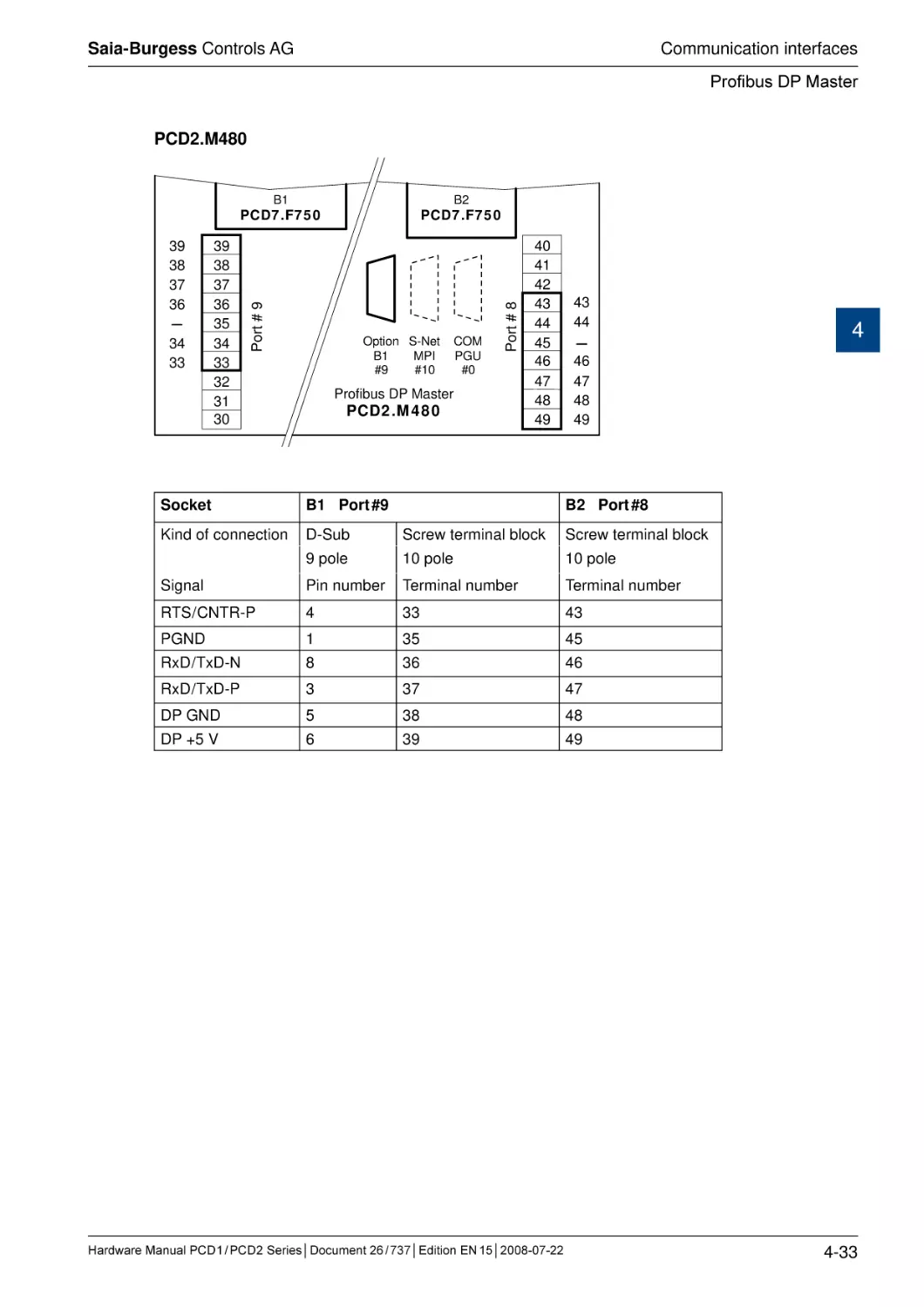
4.8.1 Profibus DP Master, module PCD7.F750.......................................................
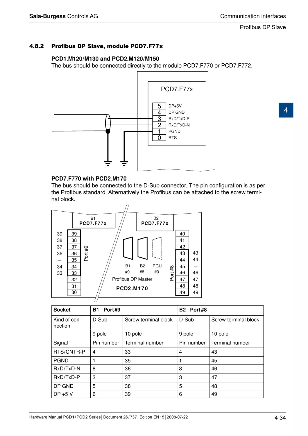
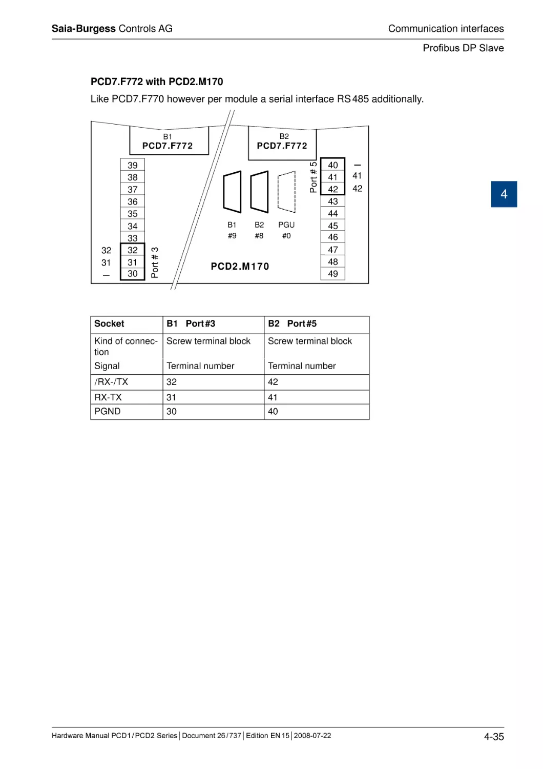
4.8.2 Profibus DP Slave, module PCD7.F77x.........................................................
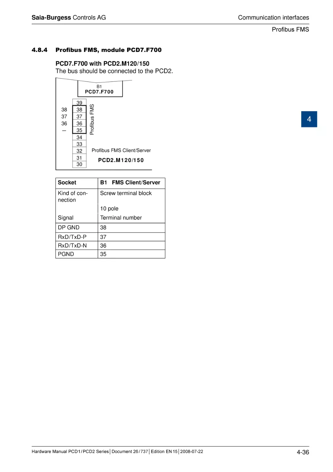
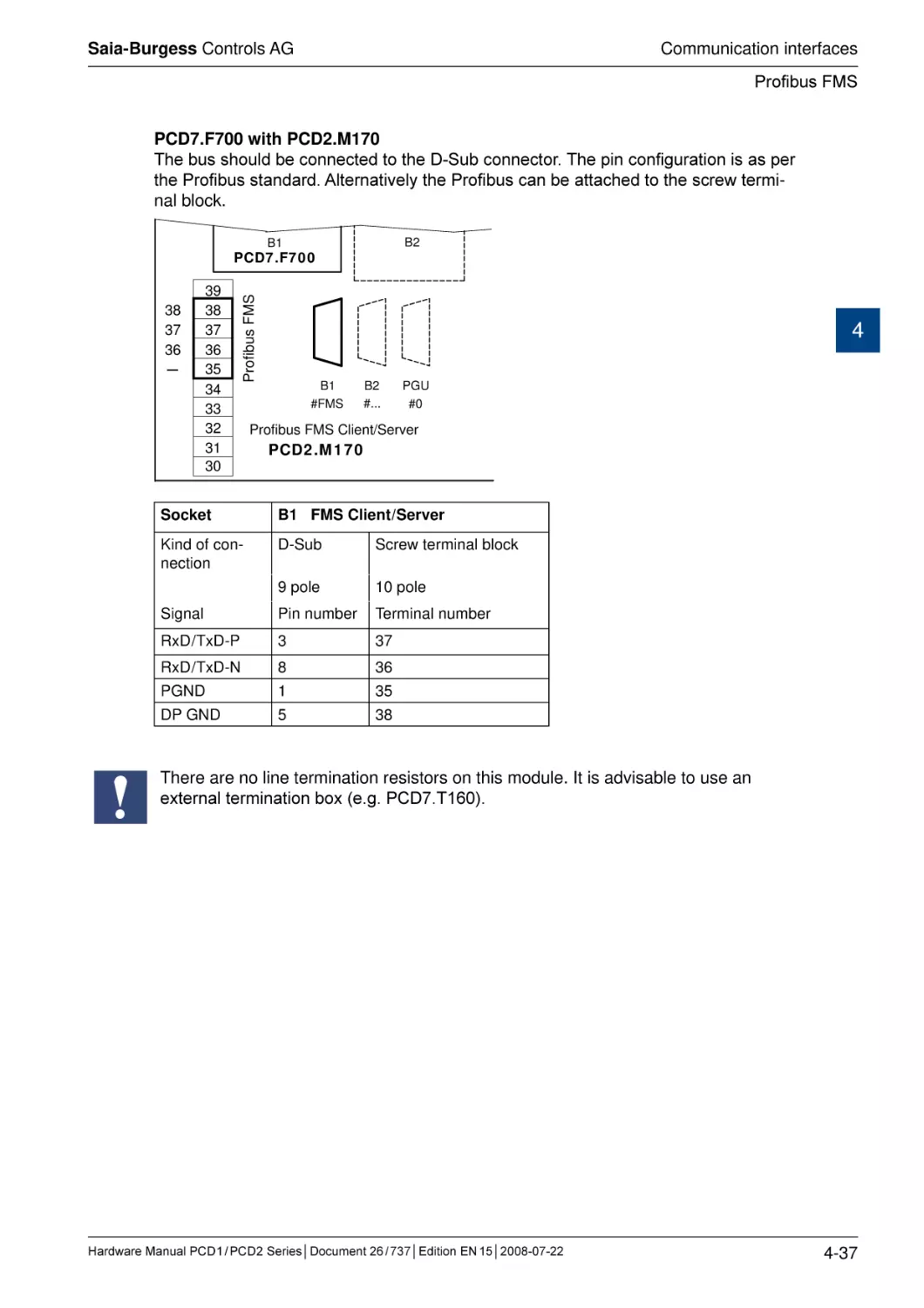
4.8.4 Profibus FMS, module PCD7.F700................................................................
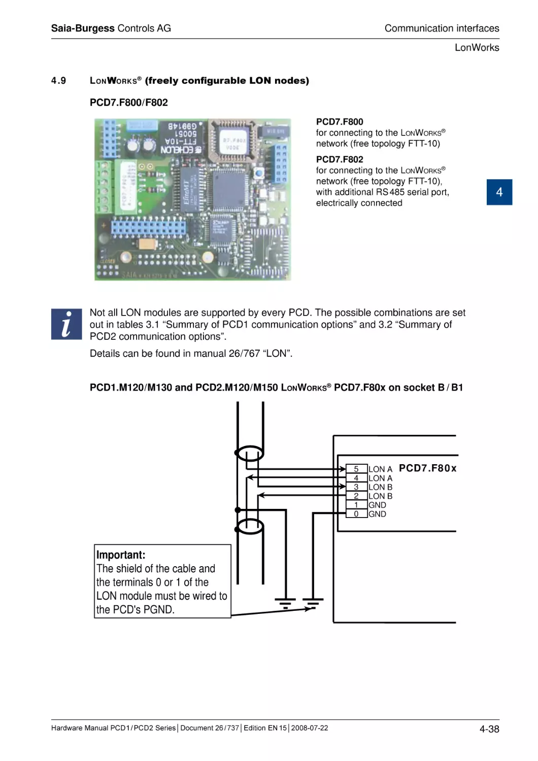
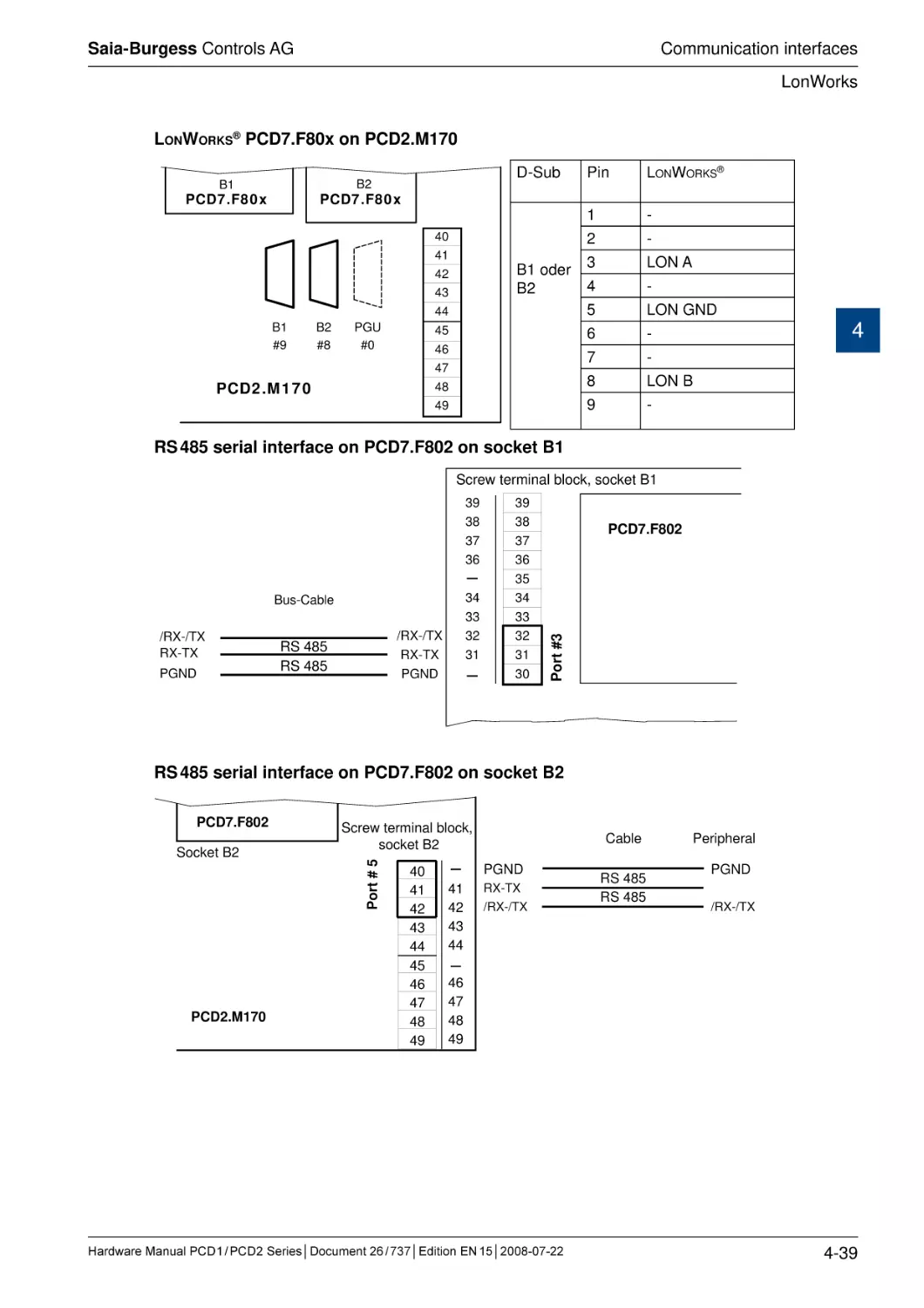
4.9
LonWorks® (freely configurable LON nodes)...................................................
4.10
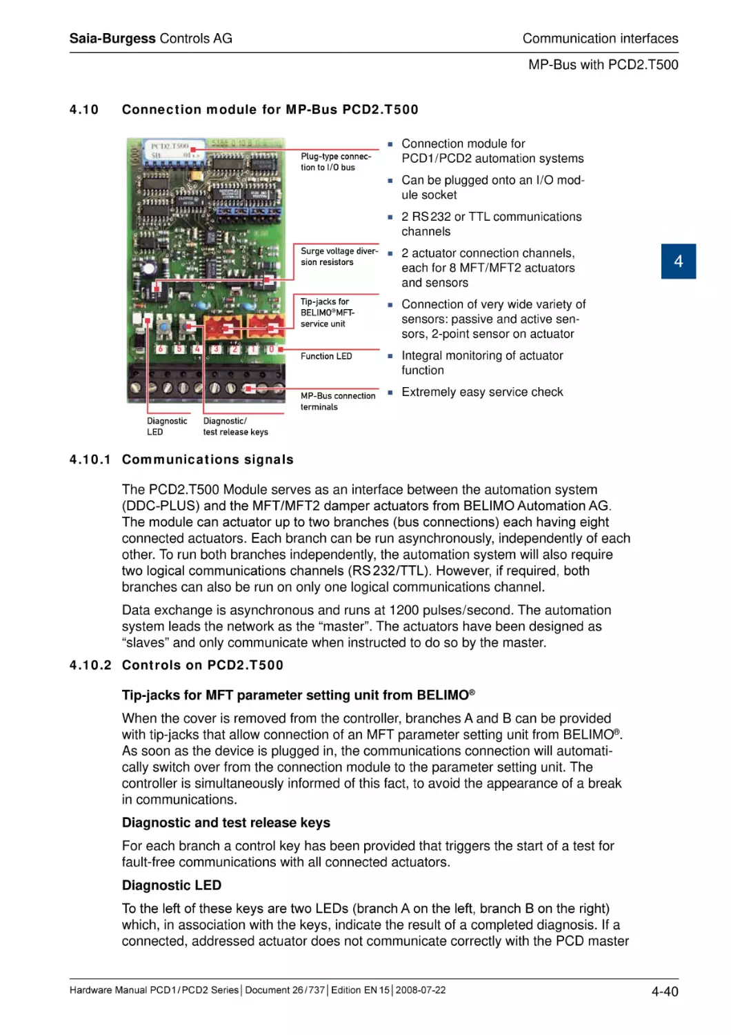
Connection module for MP-Bus PCD2.T500...................................................
4.10.1 Communications signals................................................................................
4.10.2 Controls on PCD2.T500.................................................................................
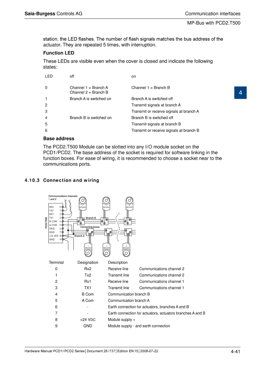
4.10.3 Connection and wiring...................................................................................
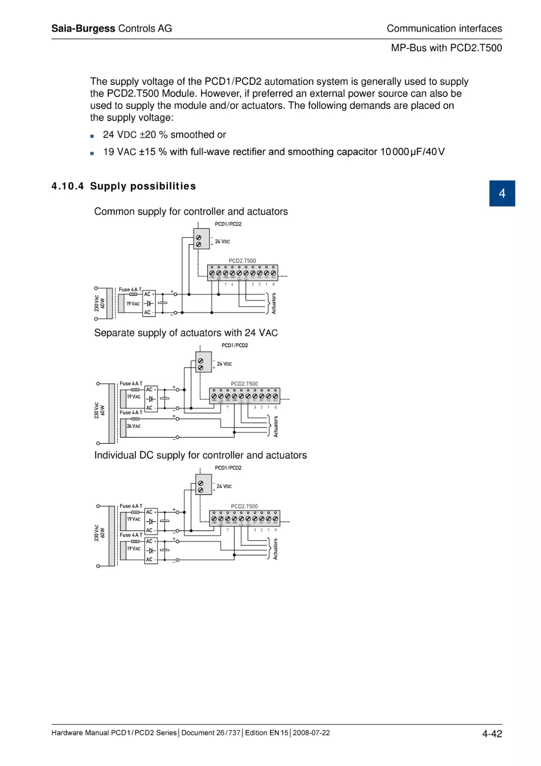
4.10.4 Supply possibilities.........................................................................................
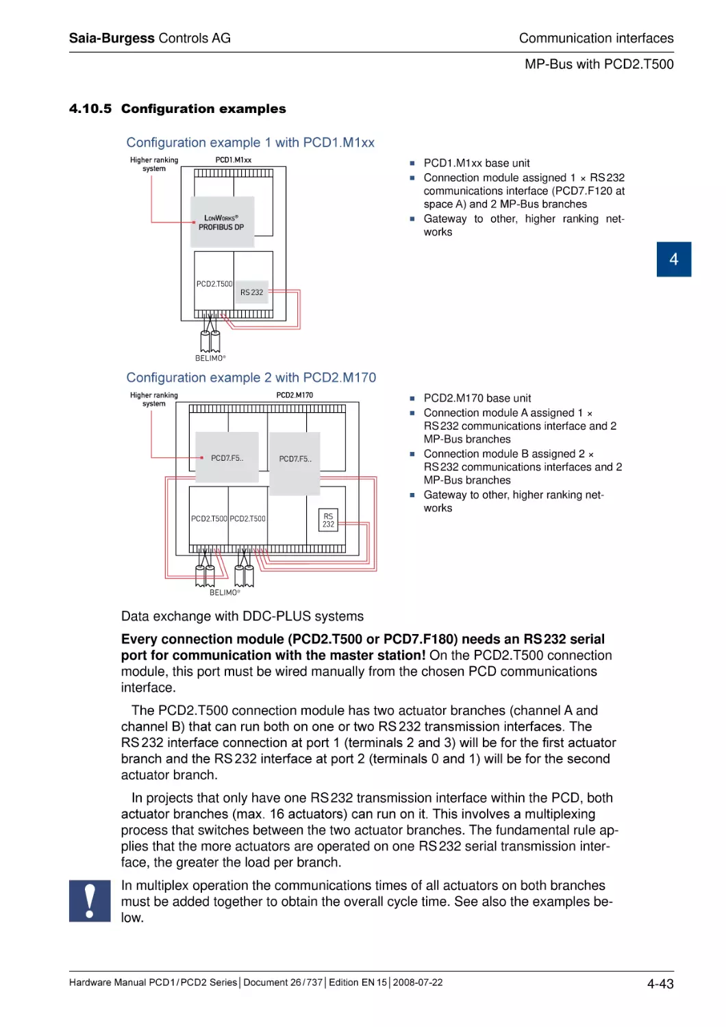
4.10.5 Configuration examples.................................................................................
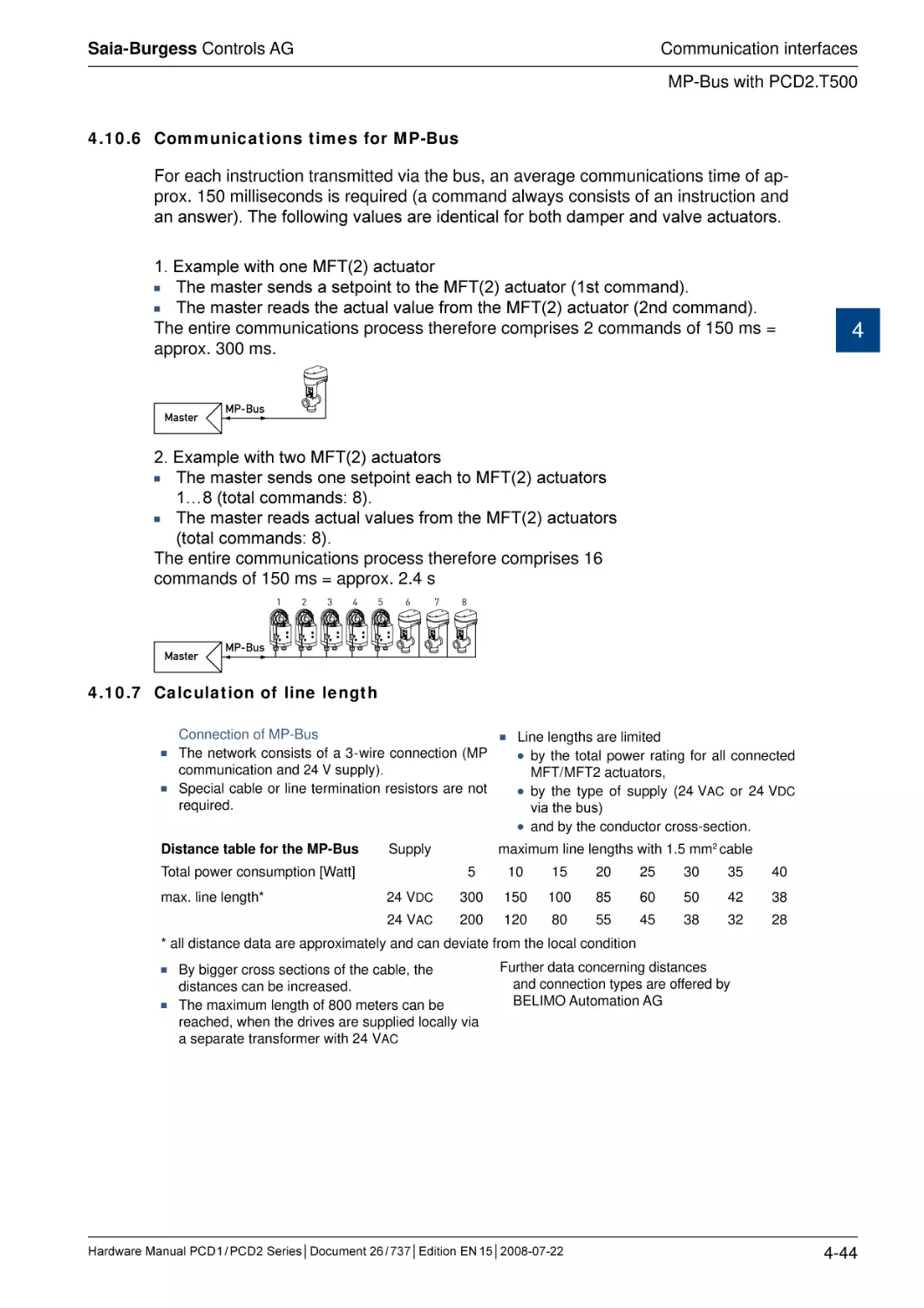
4.10.6 Communications times for MP-Bus................................................................
4.10.7 Calculation of line length................................................................................
4.10.8 Maximum line length for 24 VAC supply ........................................................
4.10.9 Maximum line length for 24 VDC supply.........................................................
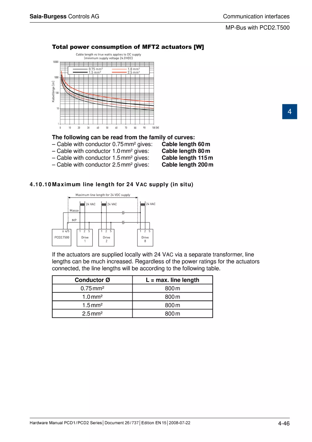
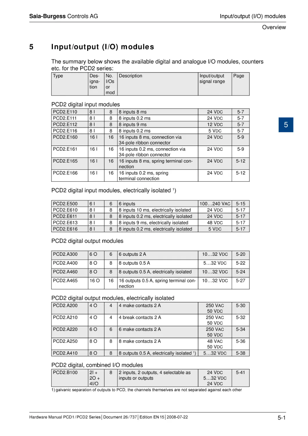
4.10.10Maximum line length for 24 VAC supply (in situ)...........................................
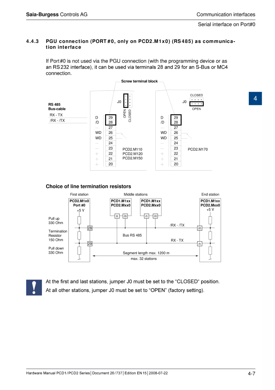
4.4.1
4.4.2
4.4.3
4.4.4
4.4.5
4.4.6
4.4.7
5
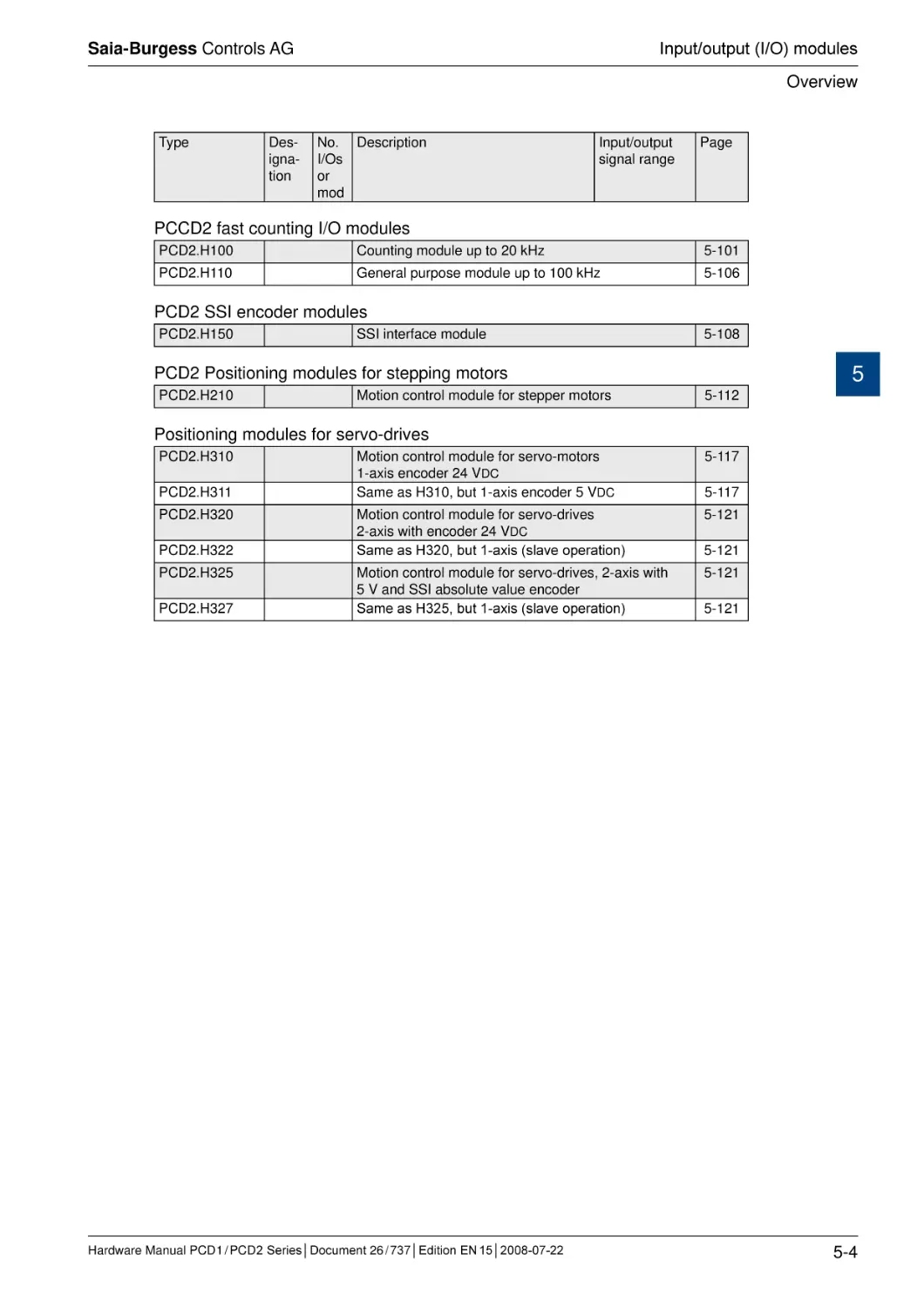
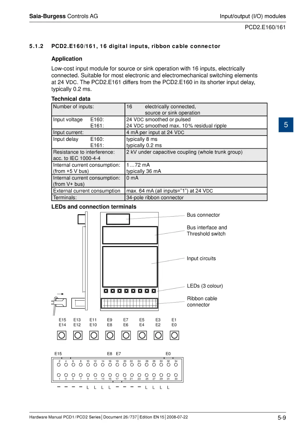
Input/output (I/O) modules
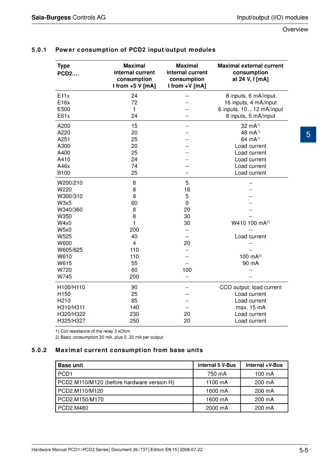
5.0.1 Power consumption of PCD2 input/output modules......................................
5.0.2
Maximal current consumption from base units................................................
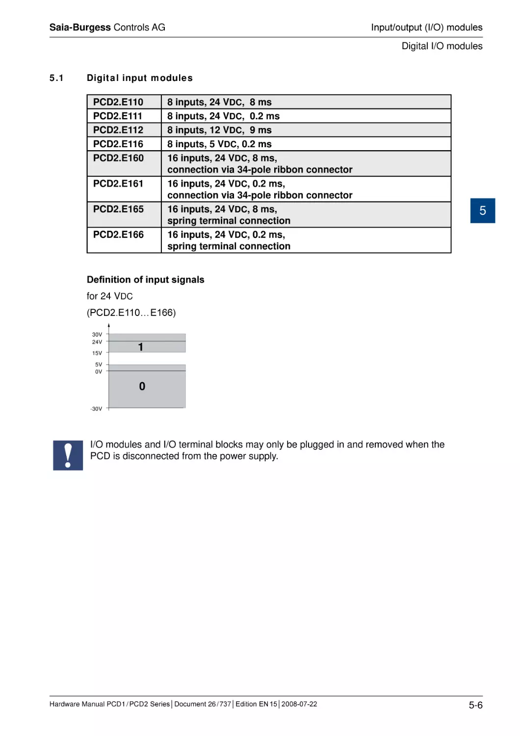
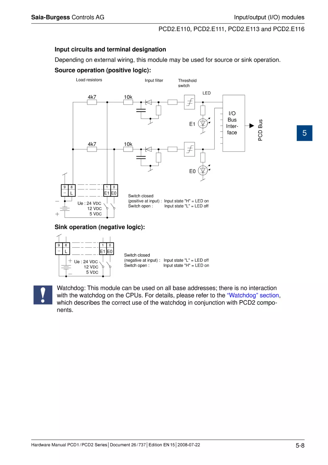
5.1
Digital input modules........................................................................................
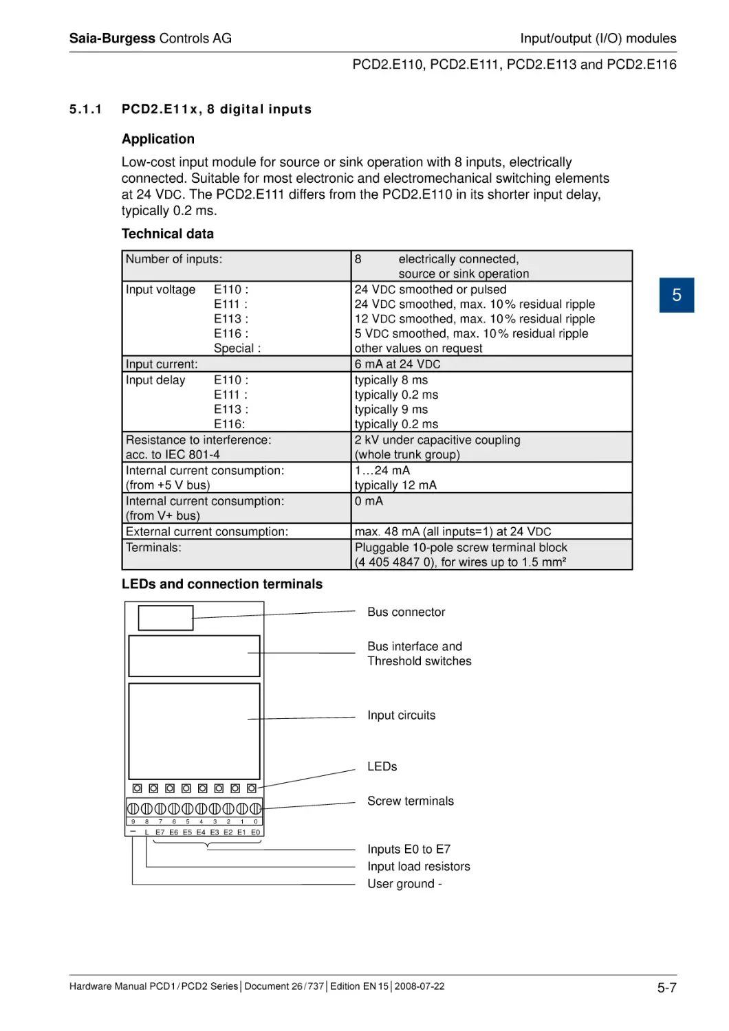
5.1.1 PCD2.E11x, 8 digital inputs............................................................................
Hardware Manual PCD 1 / PCD 2 Series│Document 26 / 737│Edition EN 15│2008-07-22
4-5
0
4-6
4-7
4-8
4-9
4-10
4-11
4-12
4-12
4-14
4-15
4-16
4-18
4-19
4-20
4-21
4-21
4-23
4-25
4-28
4-30
4-31
4-32
4-34
4-36
4-38
4-40
4-40
4-40
4-41
4-42
4-43
4-44
4-44
4-45
4-45
4-46
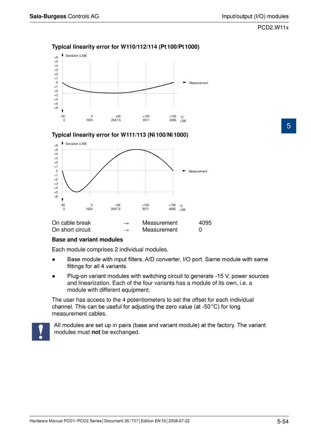
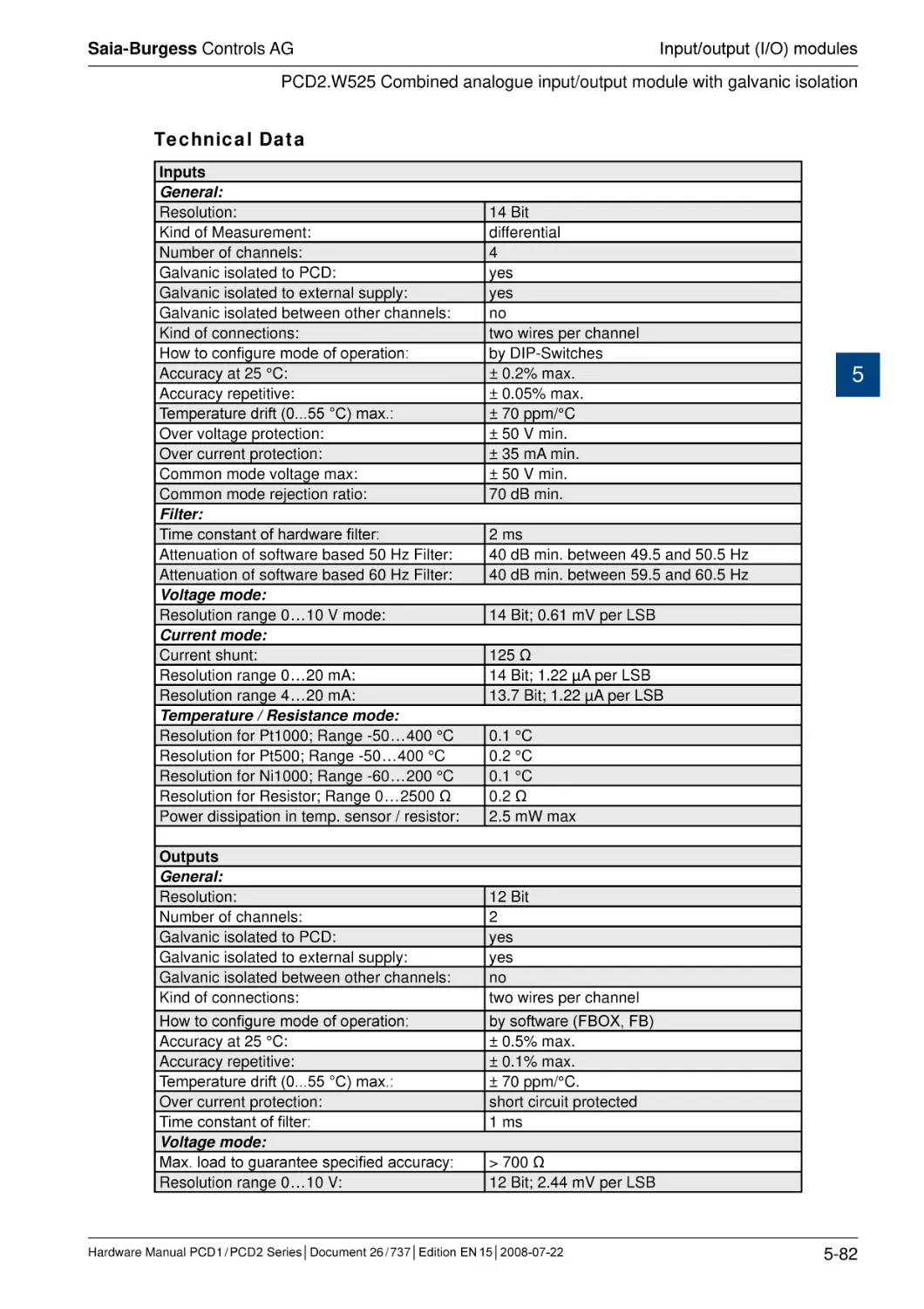
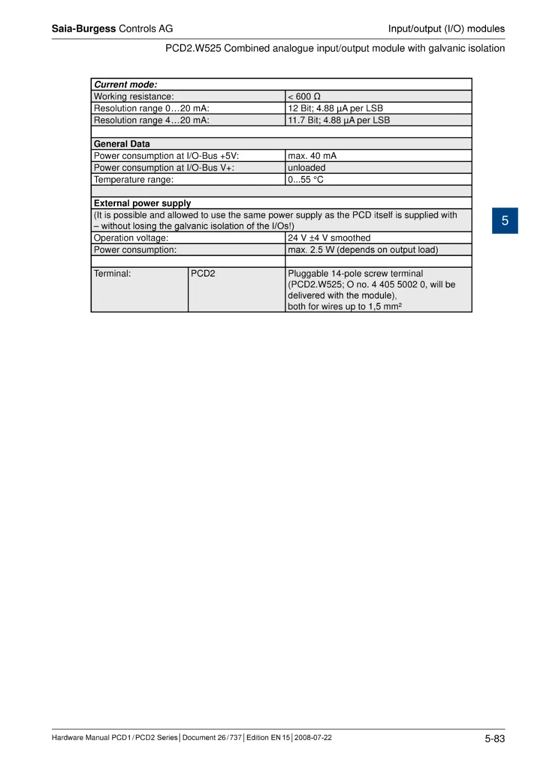
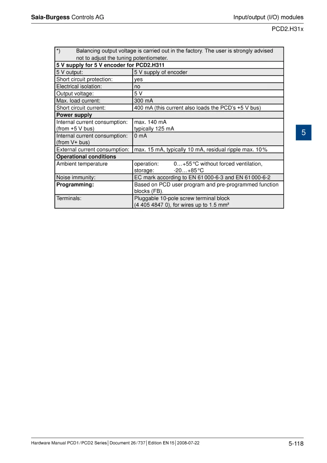
5-5
5-5
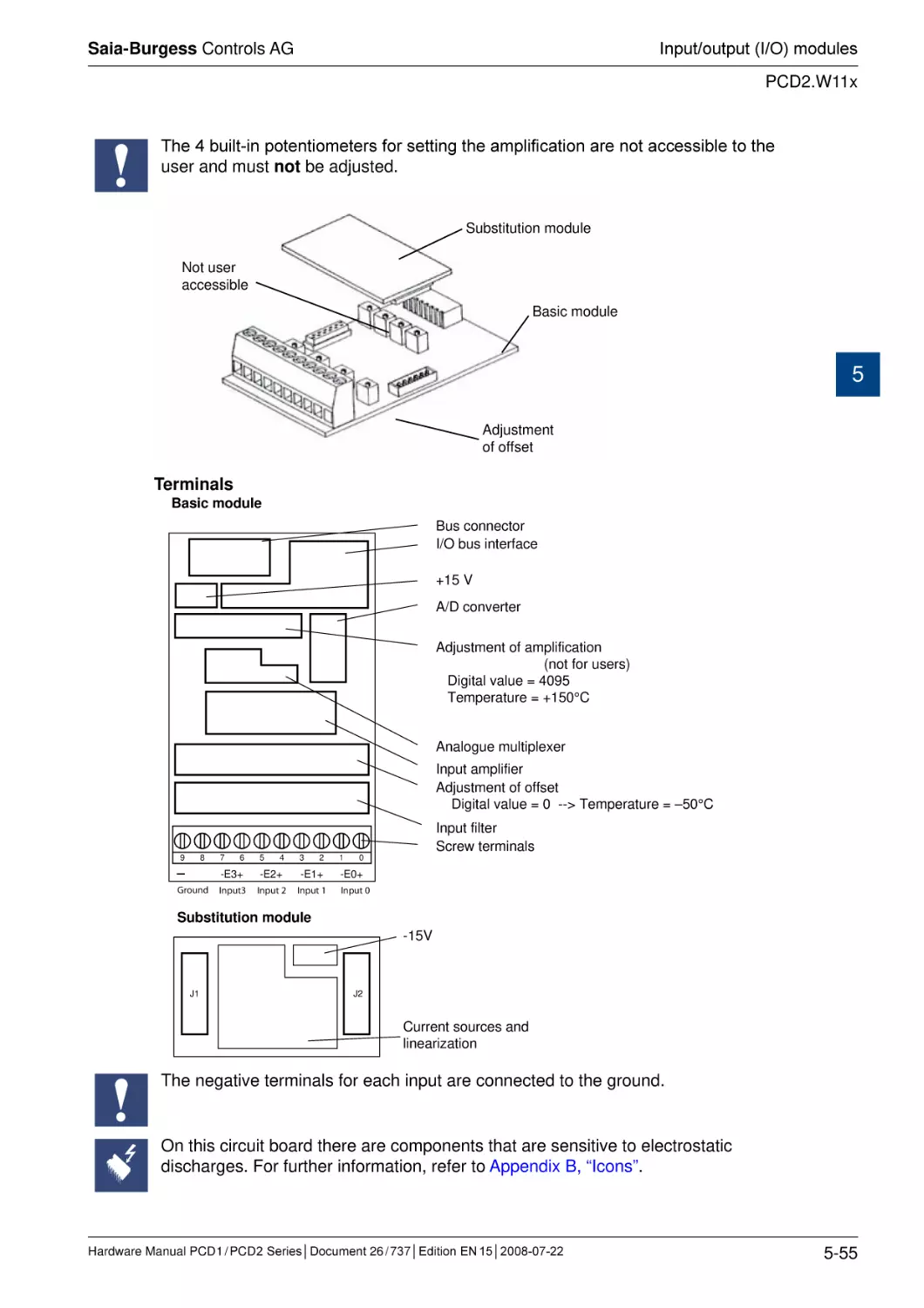
5-6
5-7
0-3
Saia-Burgess Controls AG
Contents
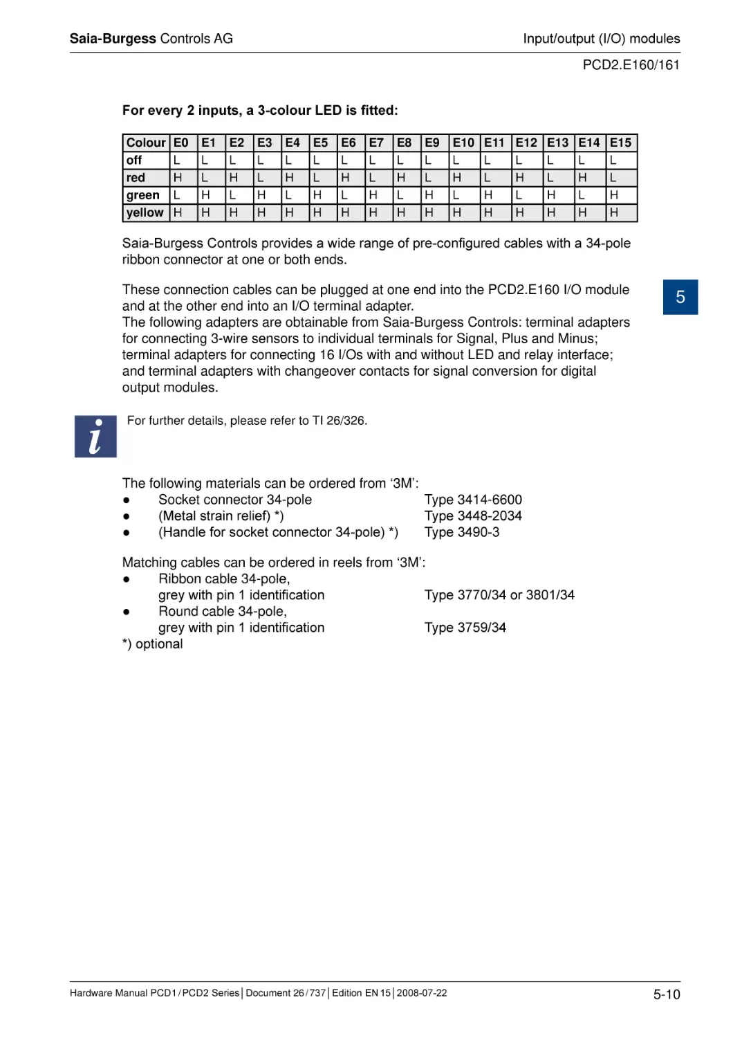
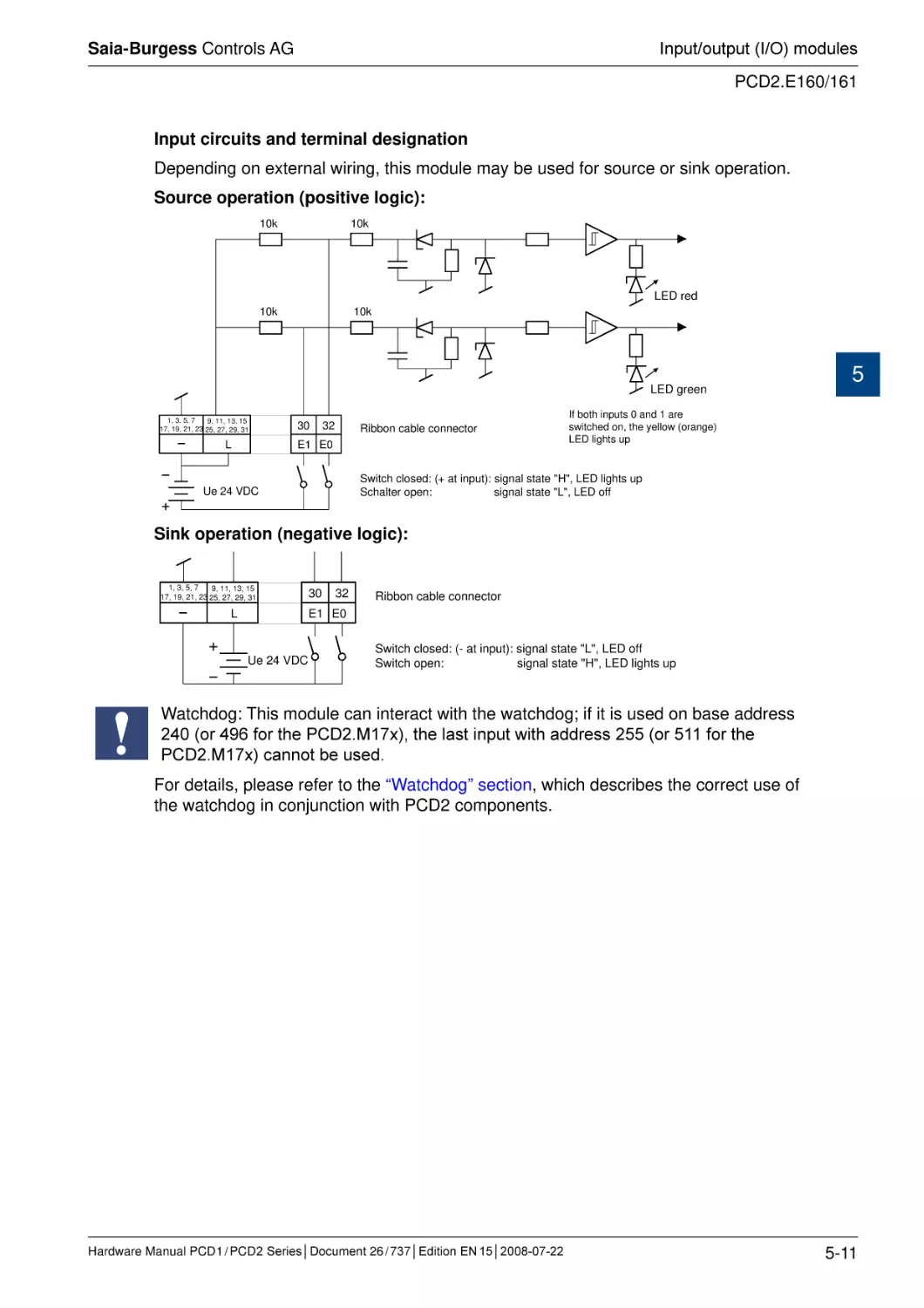
5.1.2 PCD2.E160/161, 16 digital inputs, ribbon cable connector............................
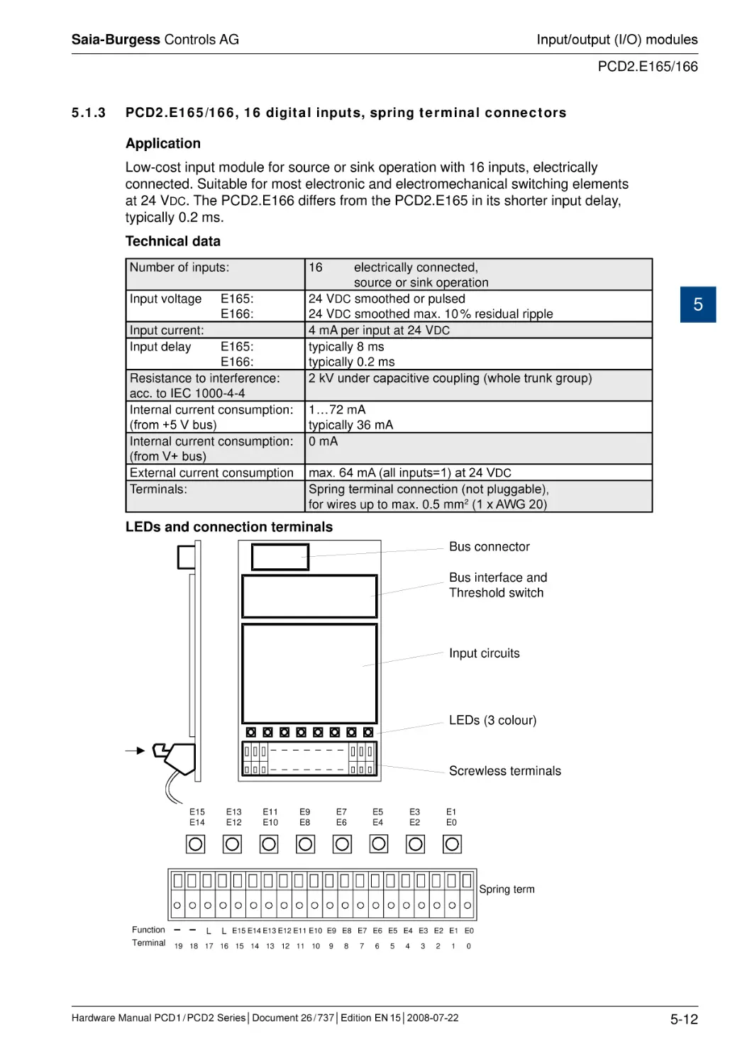
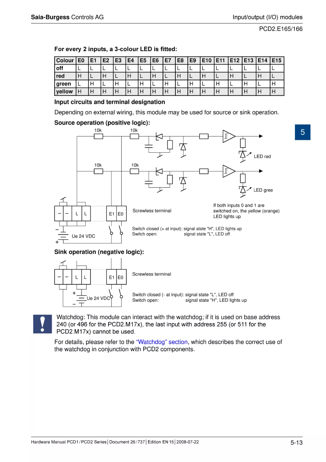
5.1.3 PCD2.E165/166, 16 digital inputs, spring terminal connectors......................
5.2
Digital input modules, electrically isolated.......................................................
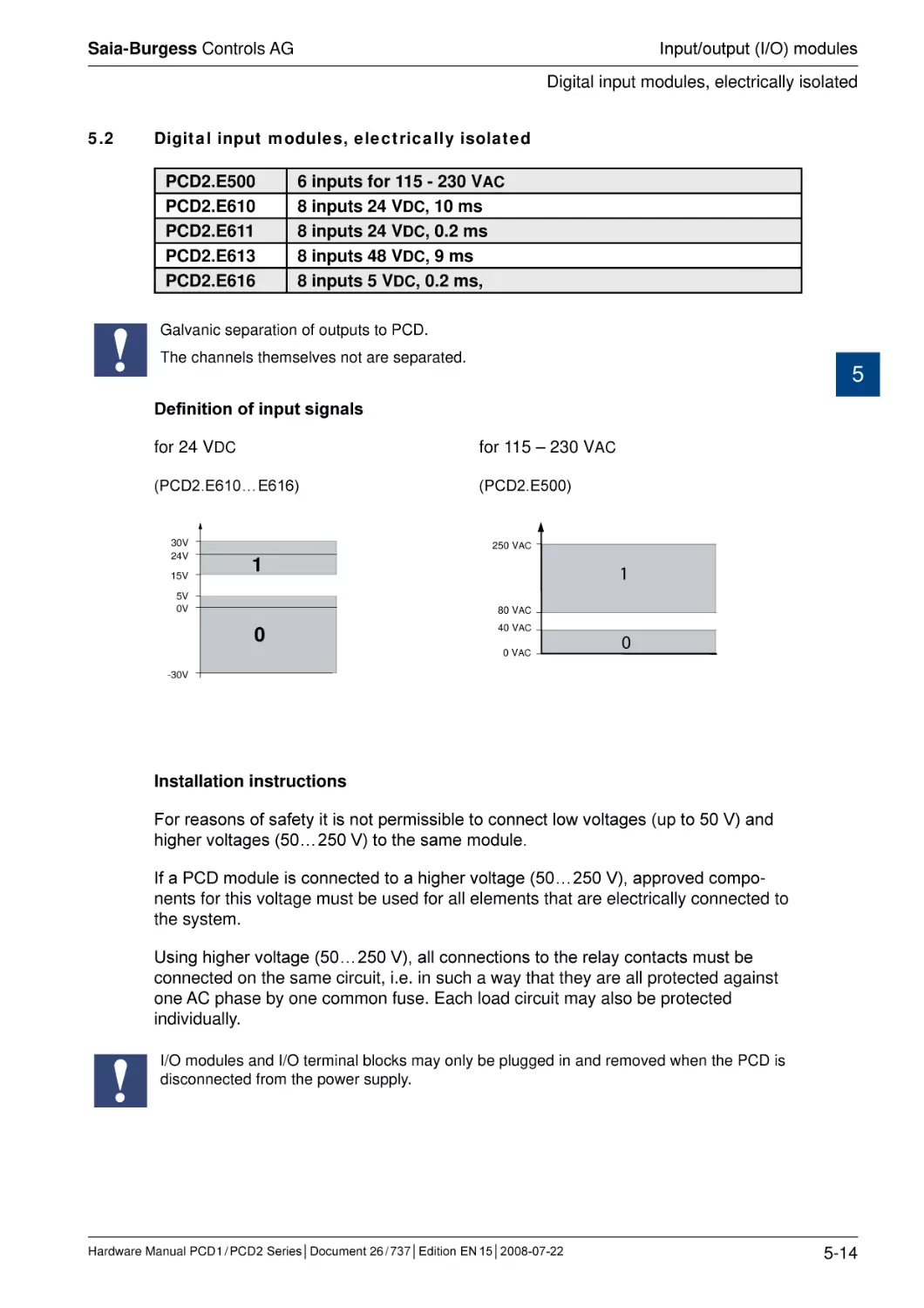
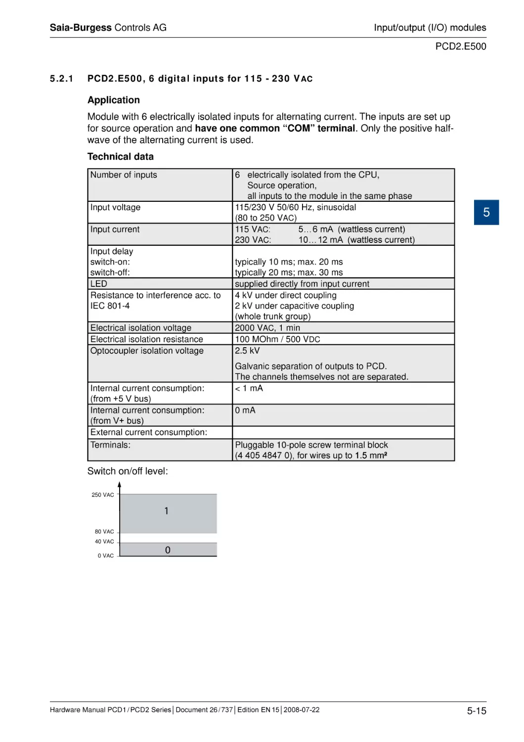
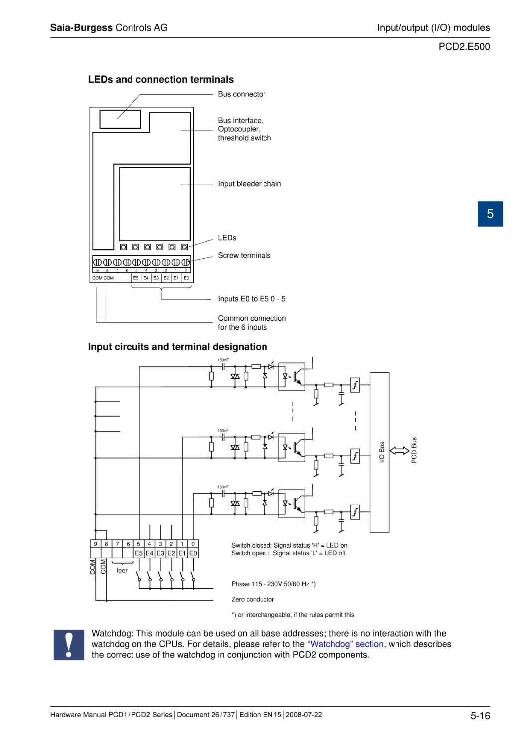
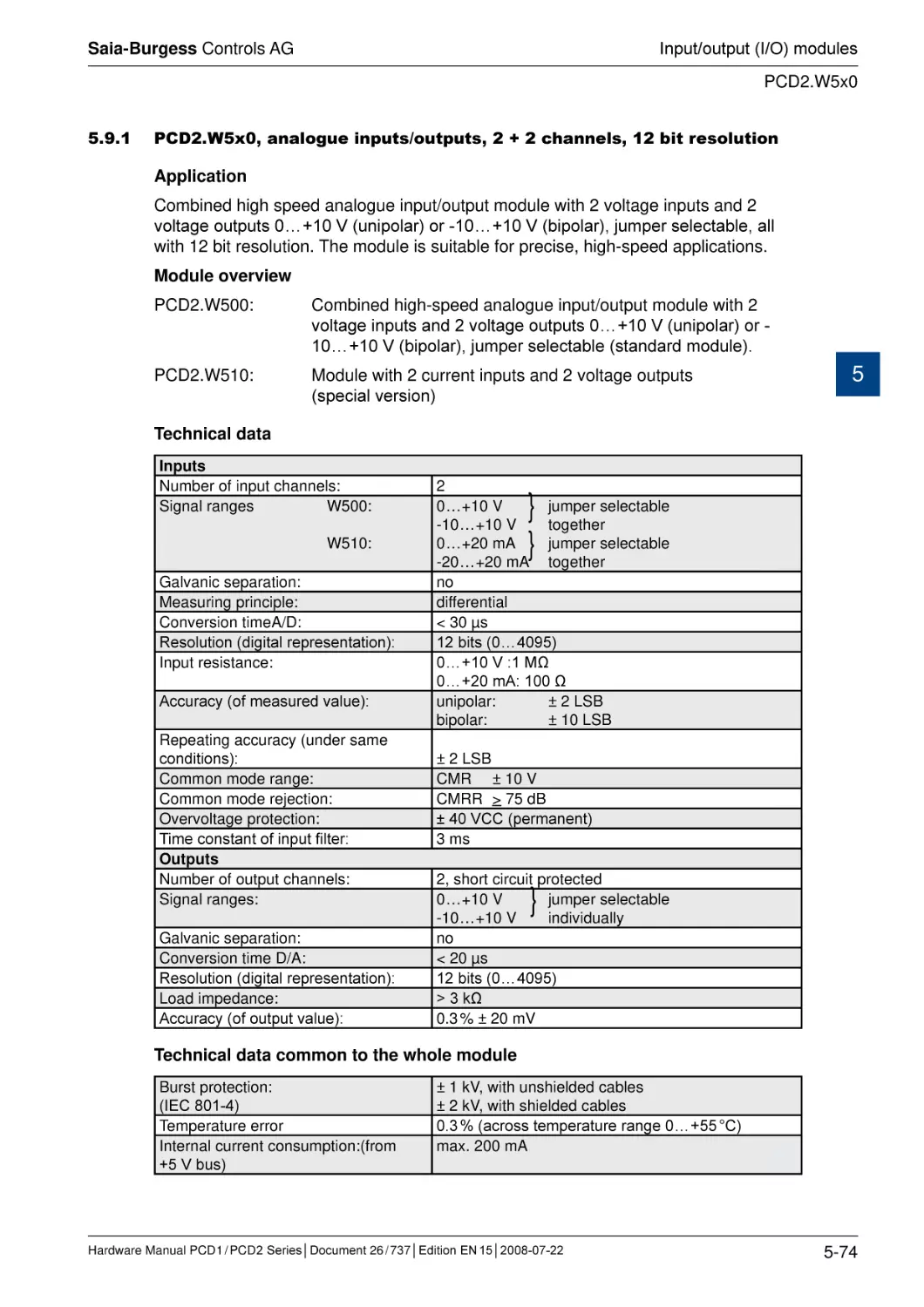
5.2.1 PCD2.E500, 6 digital inputs for 115 - 230 VAC.........................................................
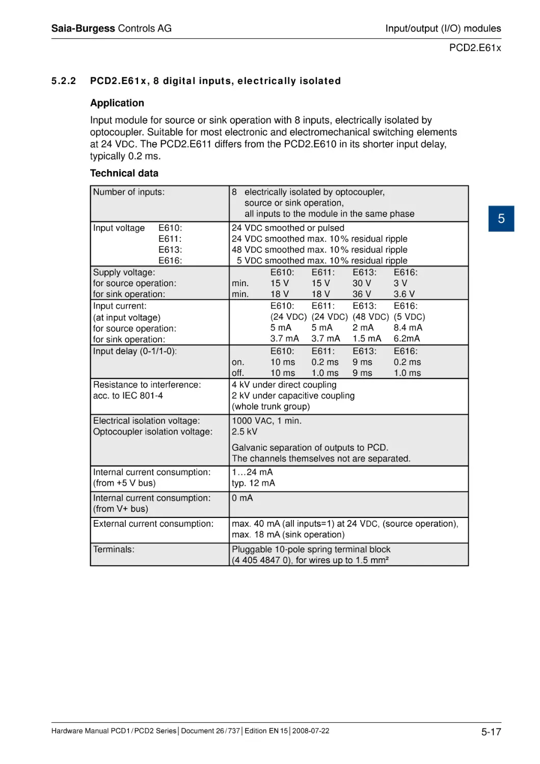
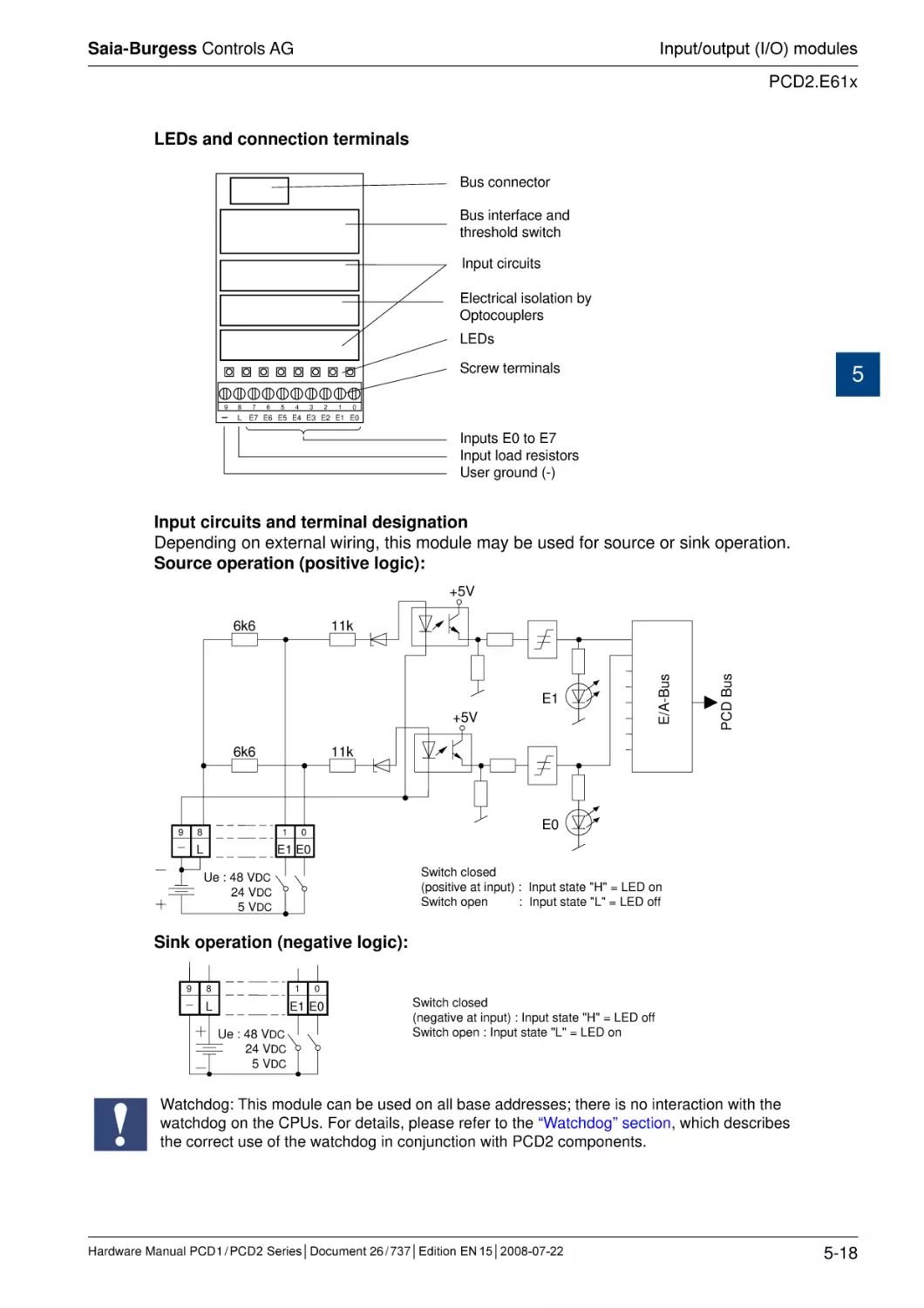
5.2.2 PCD2.E61x, 8 digital inputs, electrically isolated...........................................
5.3
Digital output modules.....................................................................................
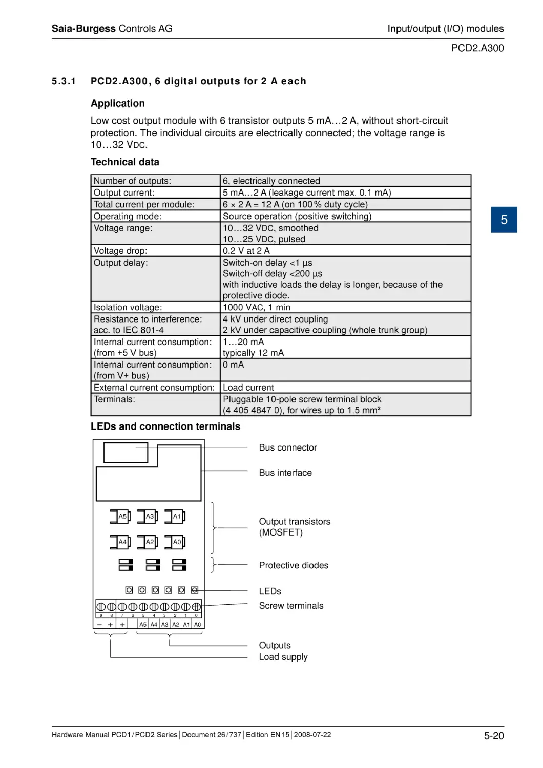
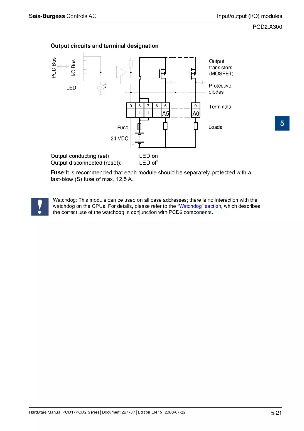
5.3.1 PCD2.A300, 6 digital outputs for 2 A each.....................................................
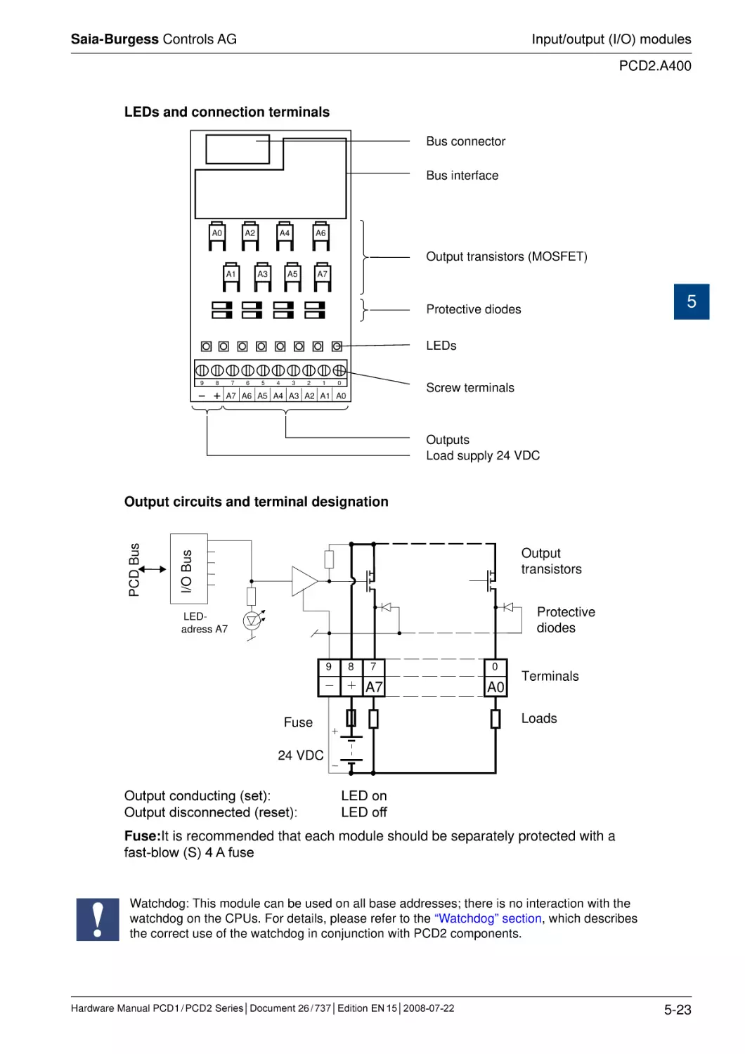
5.3.2 PCD2.A400, 8 digital outputs for 0.5 A each..................................................
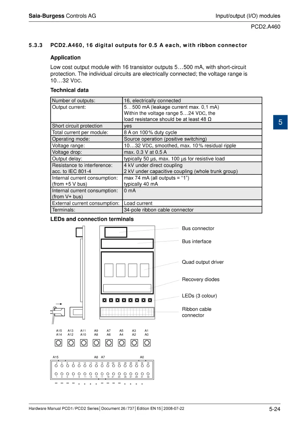
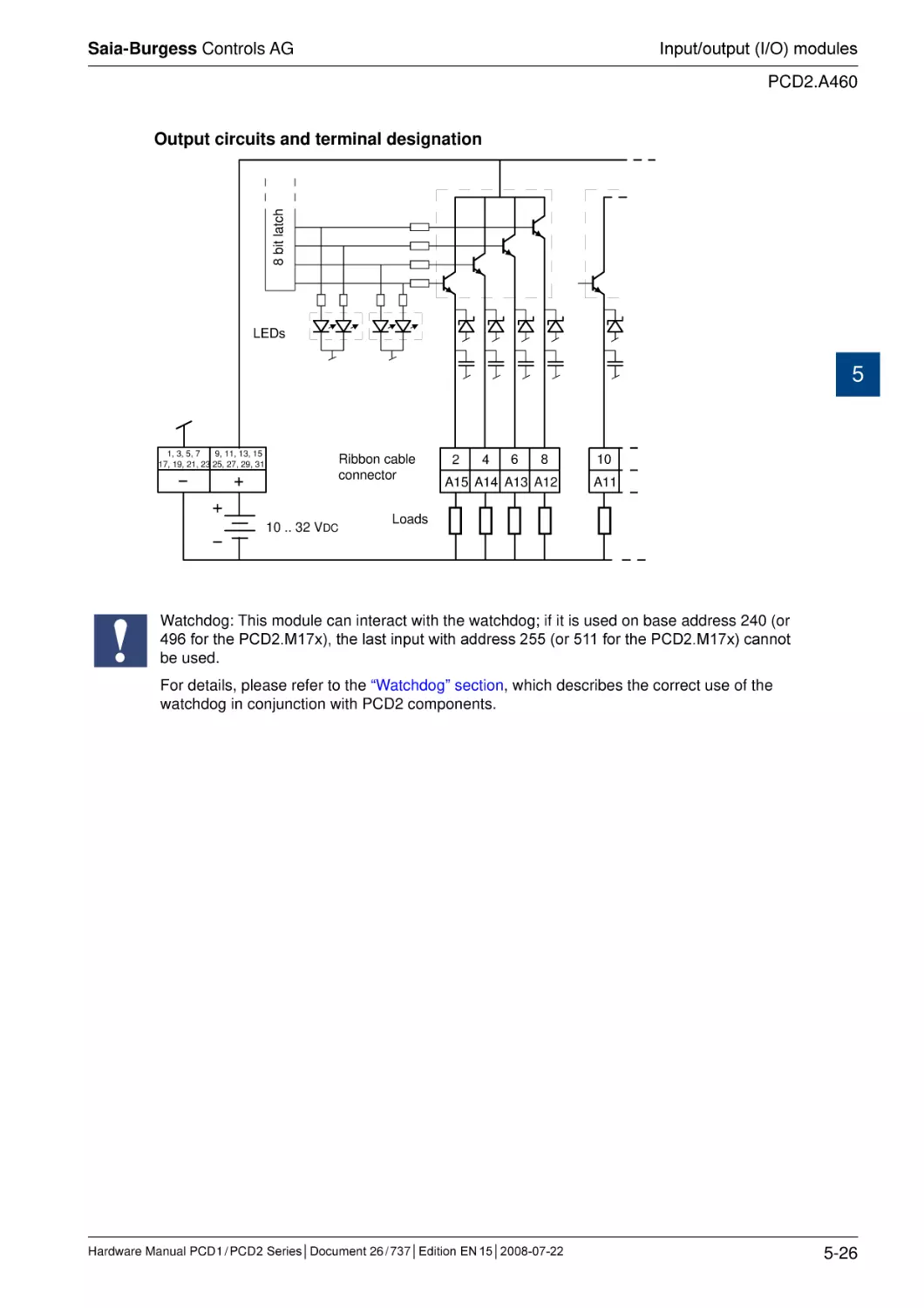
5.3.3 PCD2.A460, 16 digital outputs for 0.5 A each, with ribbon connector............
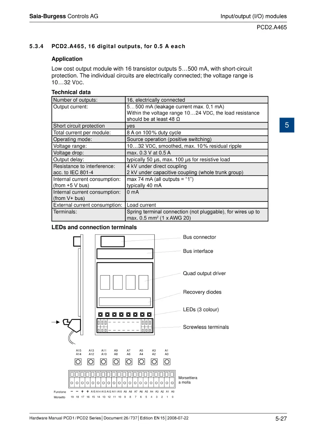
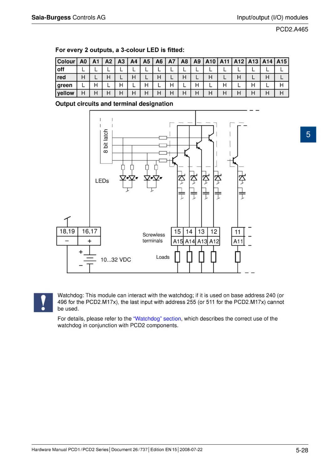
5.3.4 PCD2.A465, 16 digital outputs, for 0.5 A each...............................................
5.4
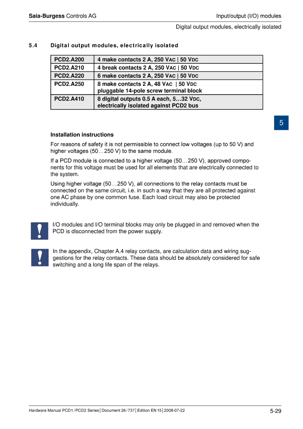
Digital output modules, electrically isolated.....................................................
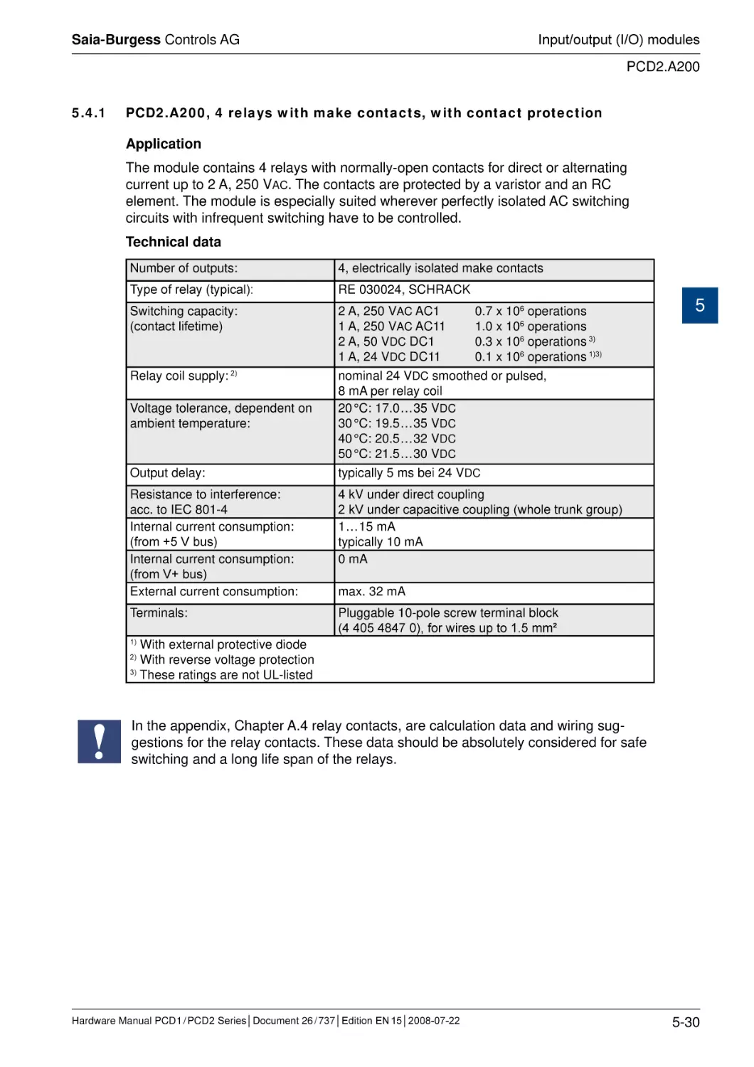
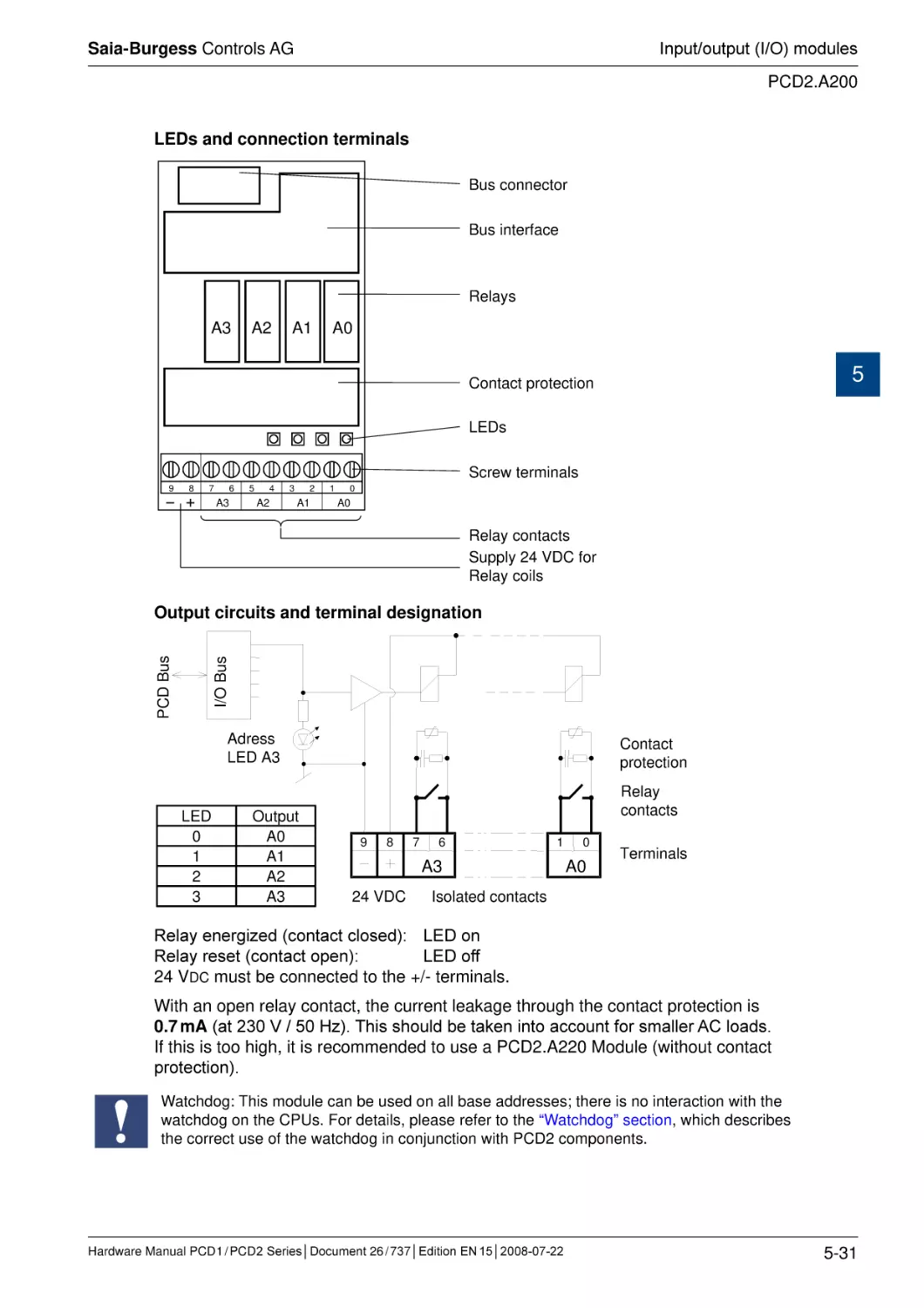
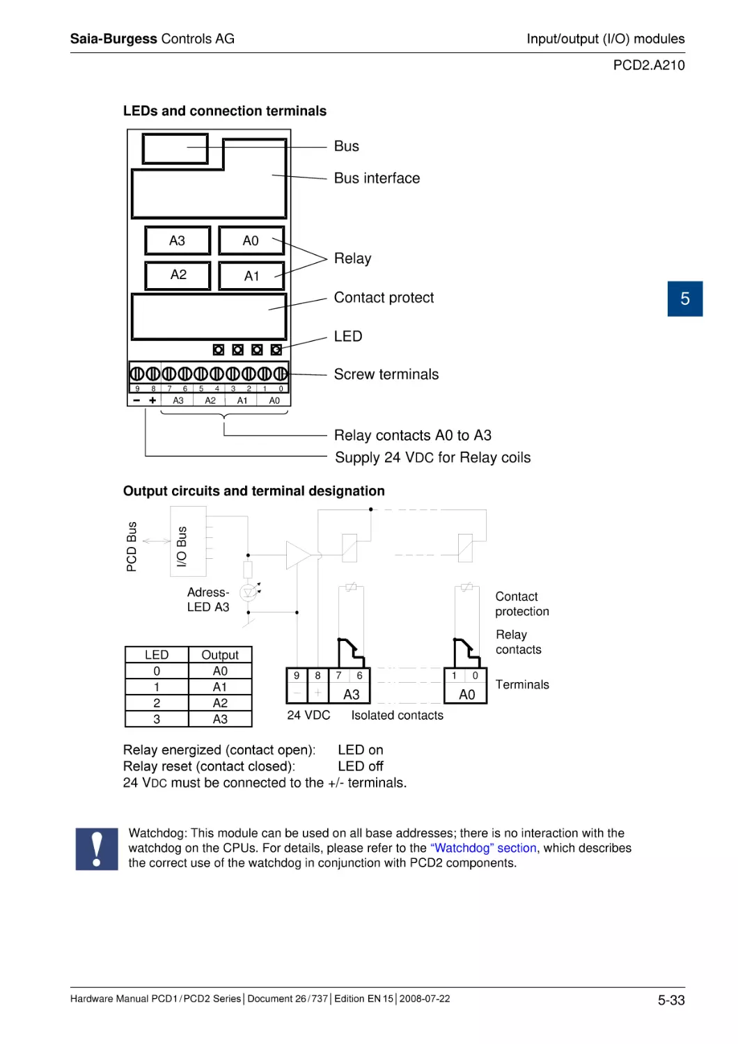
5.4.1 PCD2.A200, 4 relays with make contacts, with contact protection................
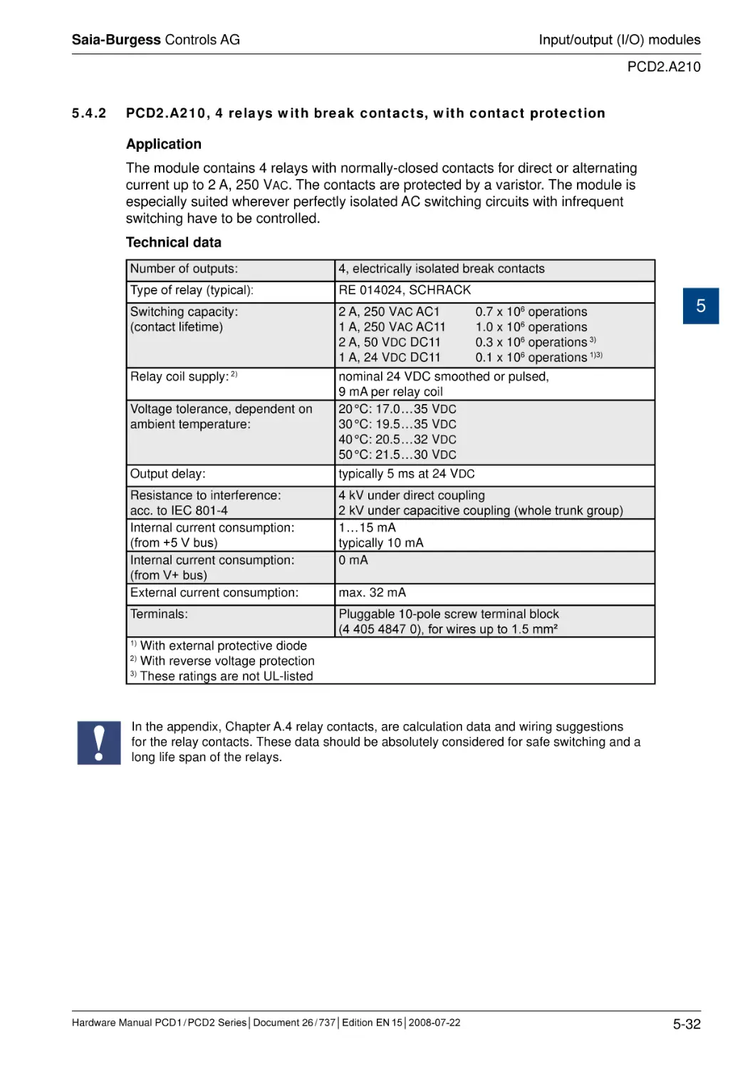
5.4.2 PCD2.A210, 4 relays with break contacts, with contact protection................
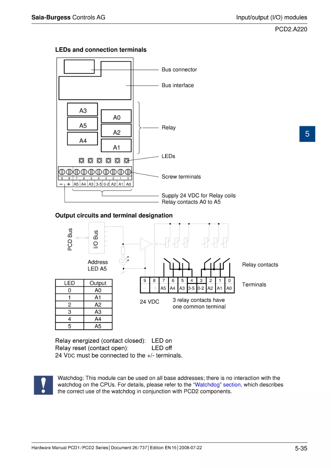
5.4.3 PCD2.A220, 6 relays with make contacts, without contact protection...........
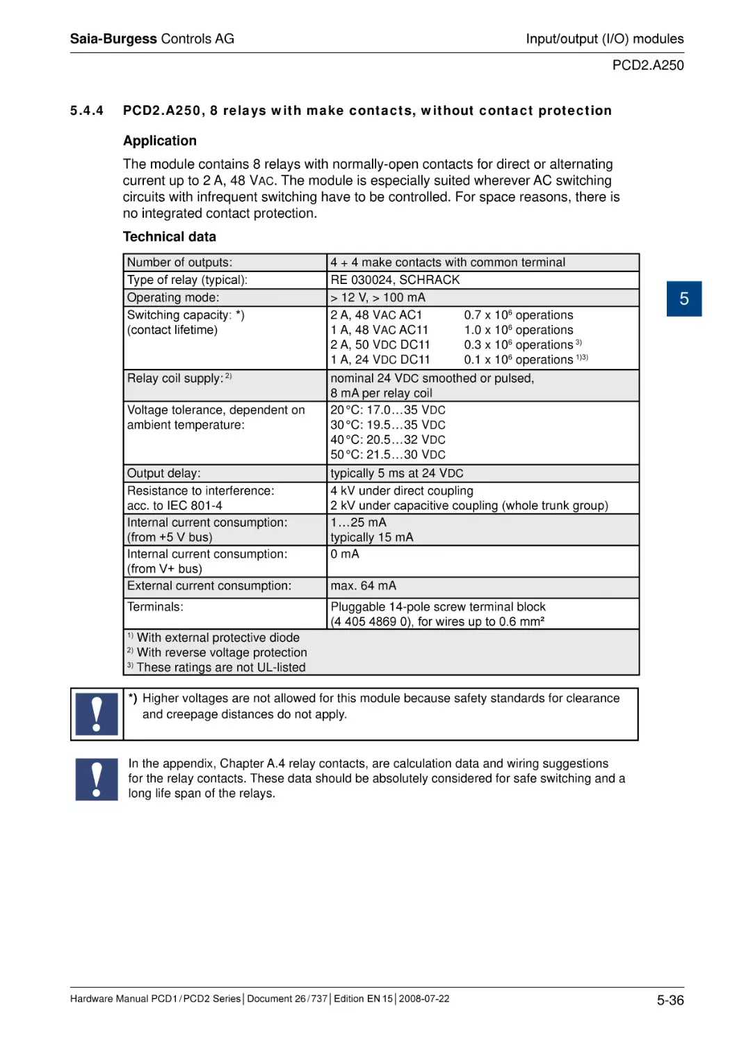
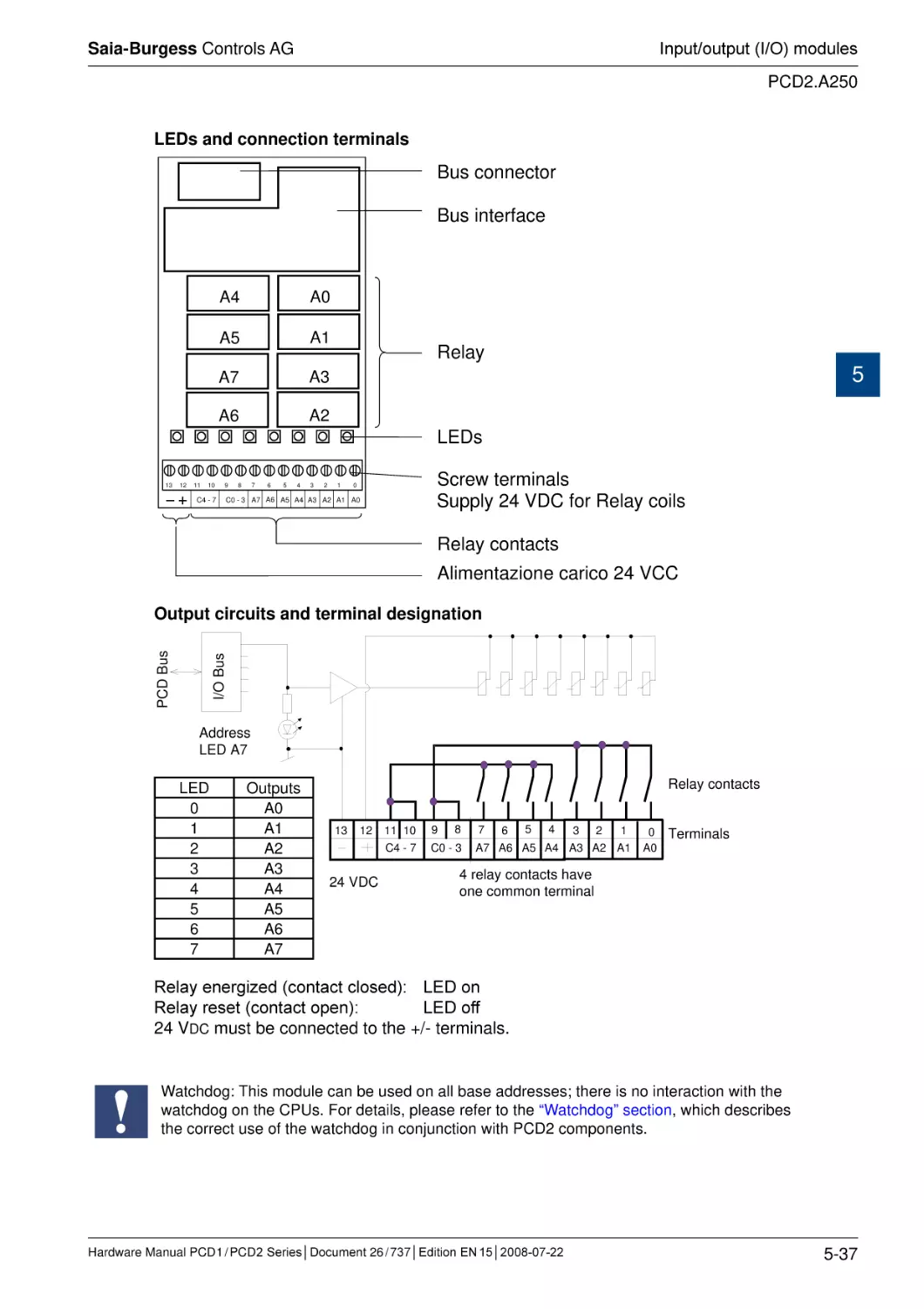
5.4.4 PCD2.A250, 8 relays with make contacts, without contact protection...........
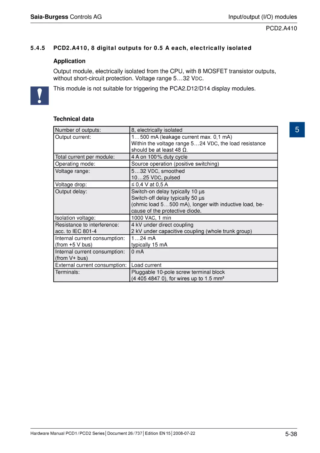
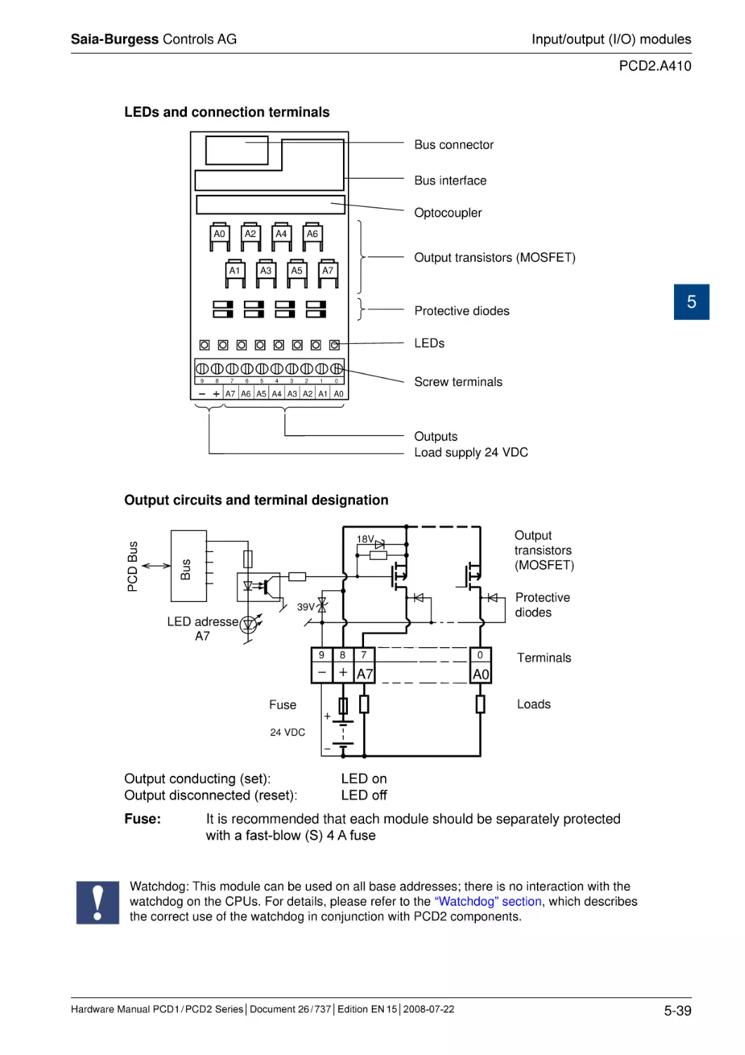
5.4.5 PCD2.A410, 8 digital outputs for 0.5 A each, electrically isolated..................
5.5
Digital combined input and output modules.....................................................
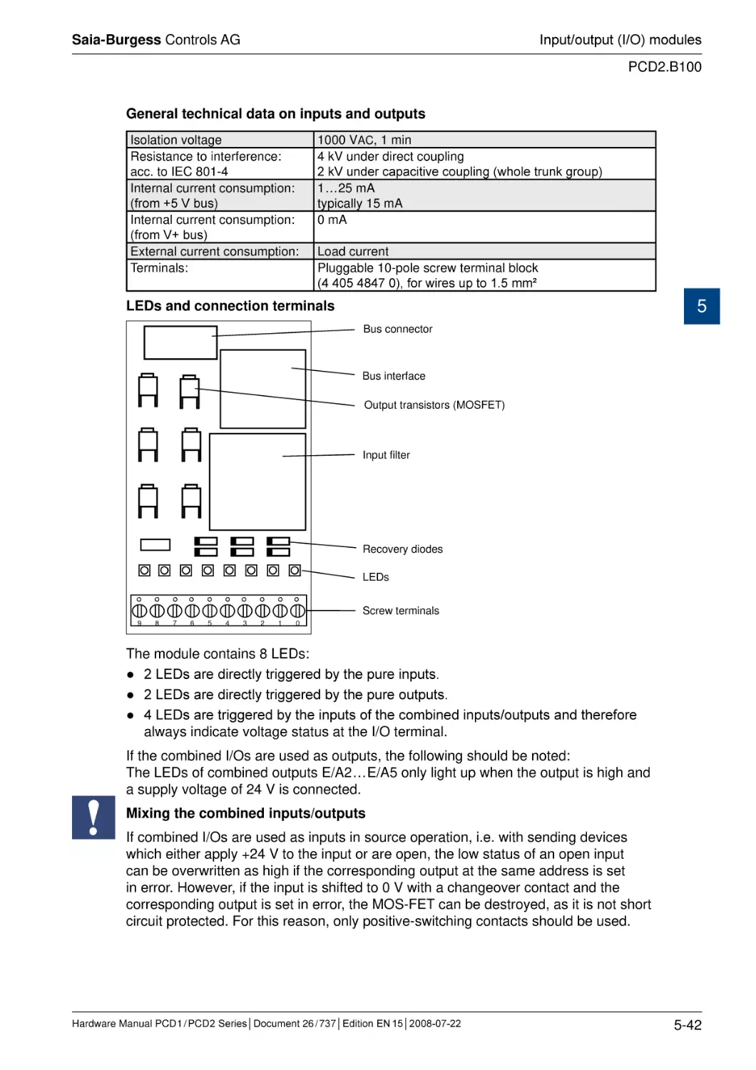
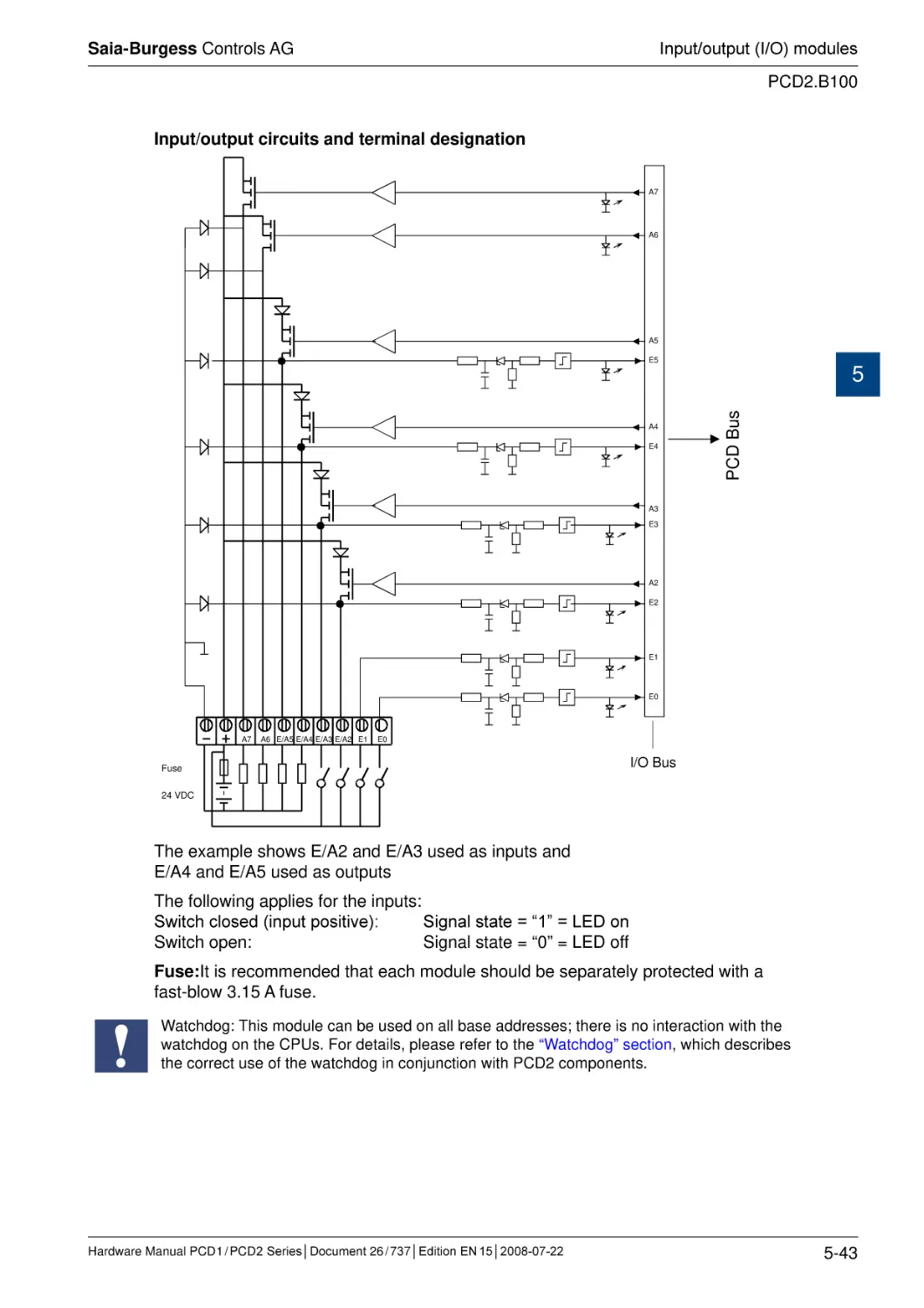
5.5.1 PCD2.B100, 2 inputs + 2 outputs + 4 digital inputs/outputs (selectable).......
5.6
Multi-functional input/output modules..............................................................
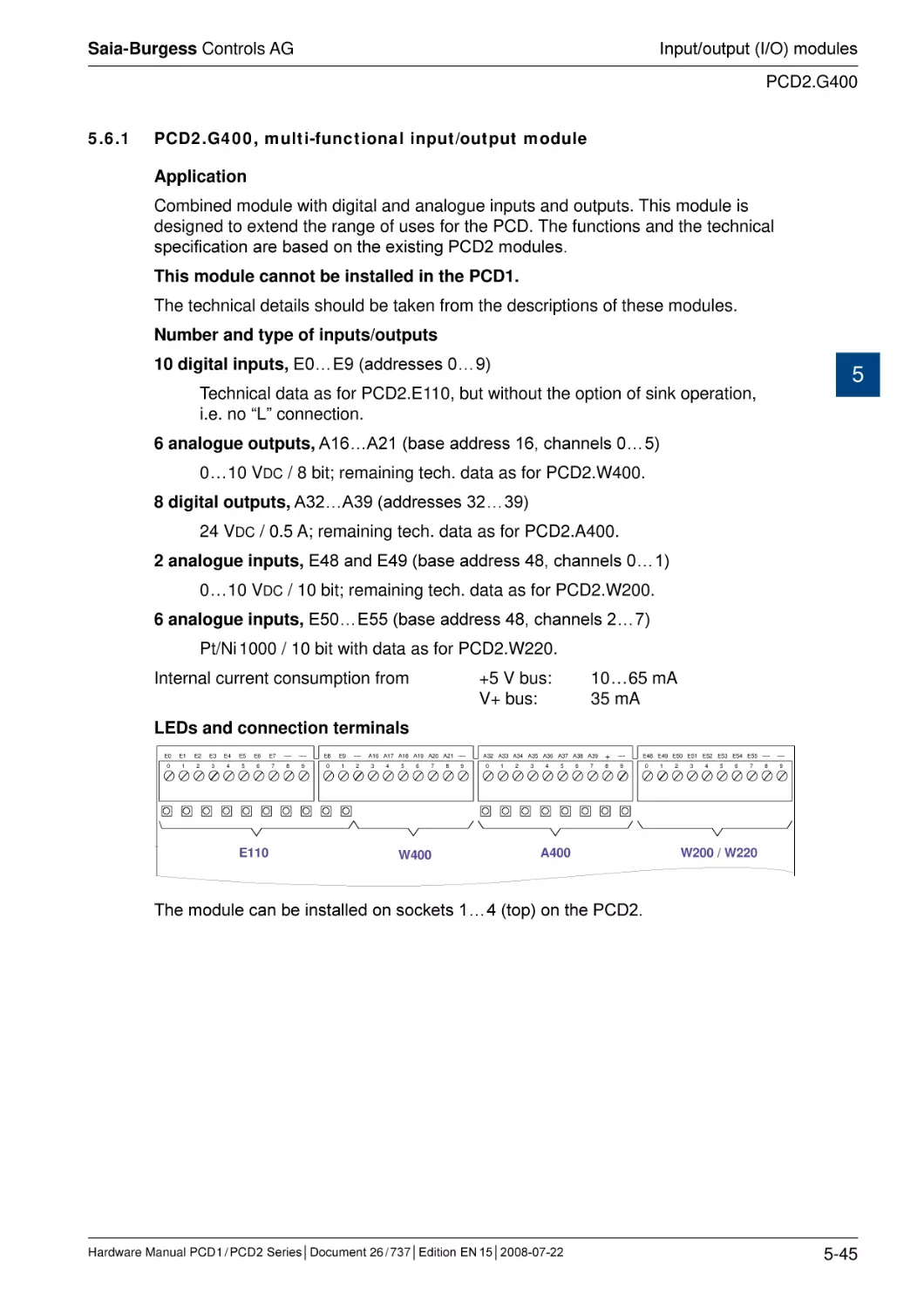
5.6.1 PCD2.G400, multi-functional input/output module.........................................
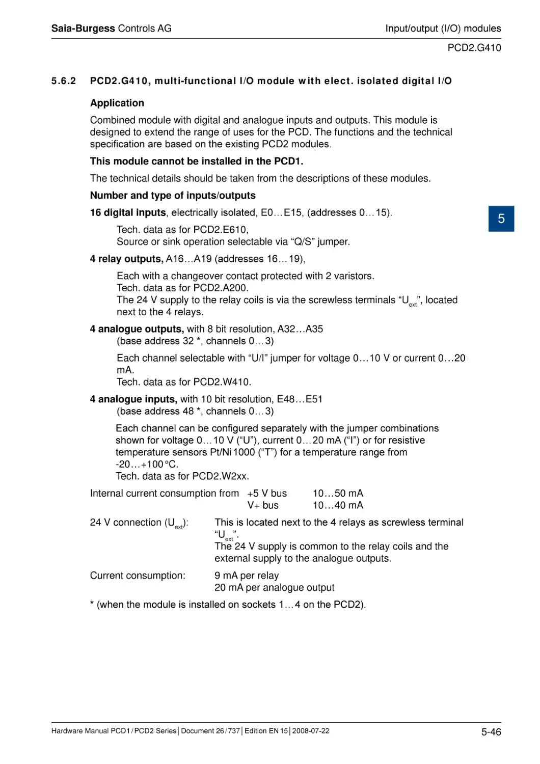
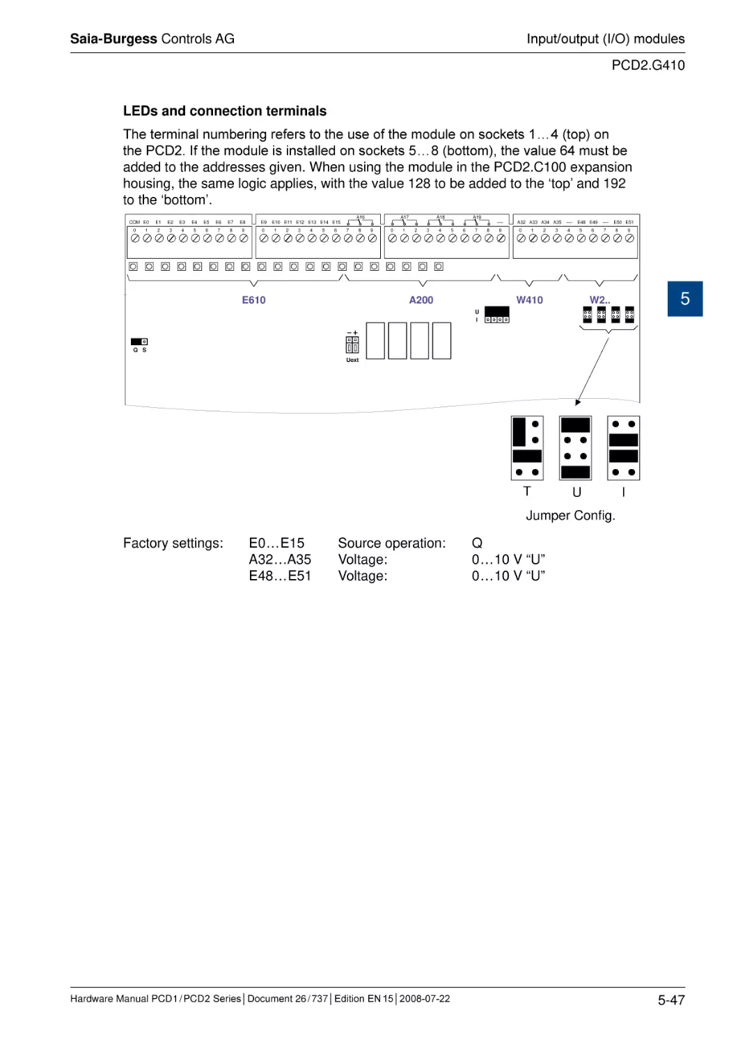
5.6.2 PCD2.G410, multi-functional I/O module with elect. isolated digital I/O........
5.7
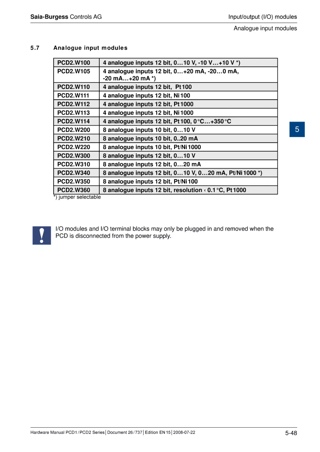
Analogue input modules..................................................................................
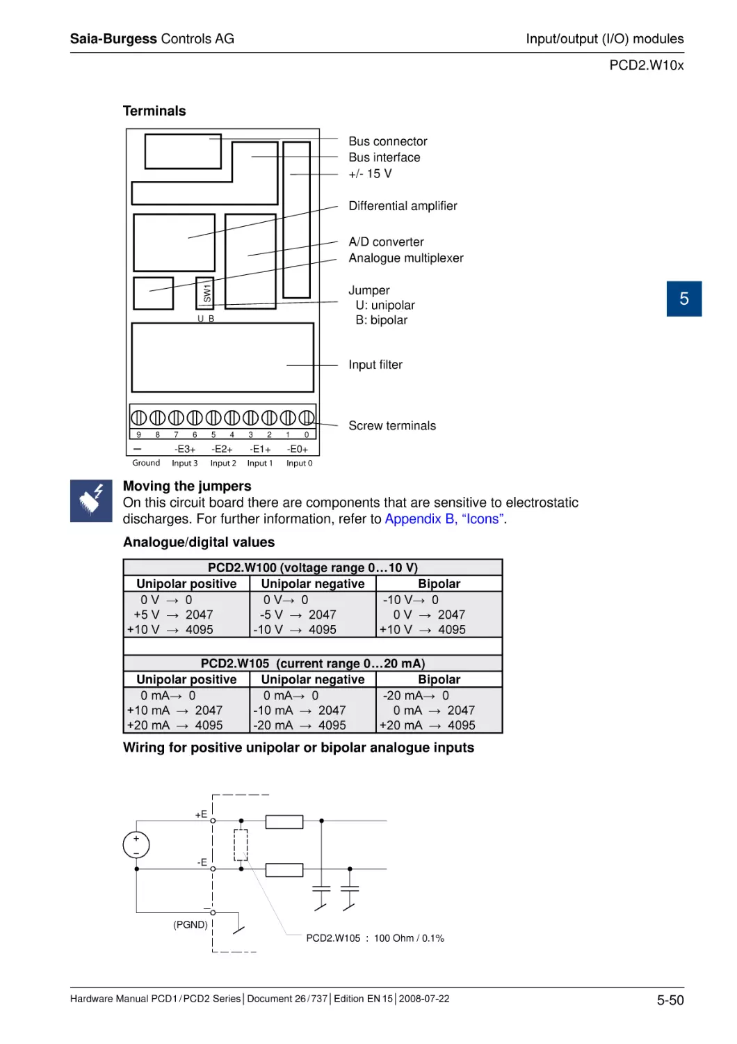
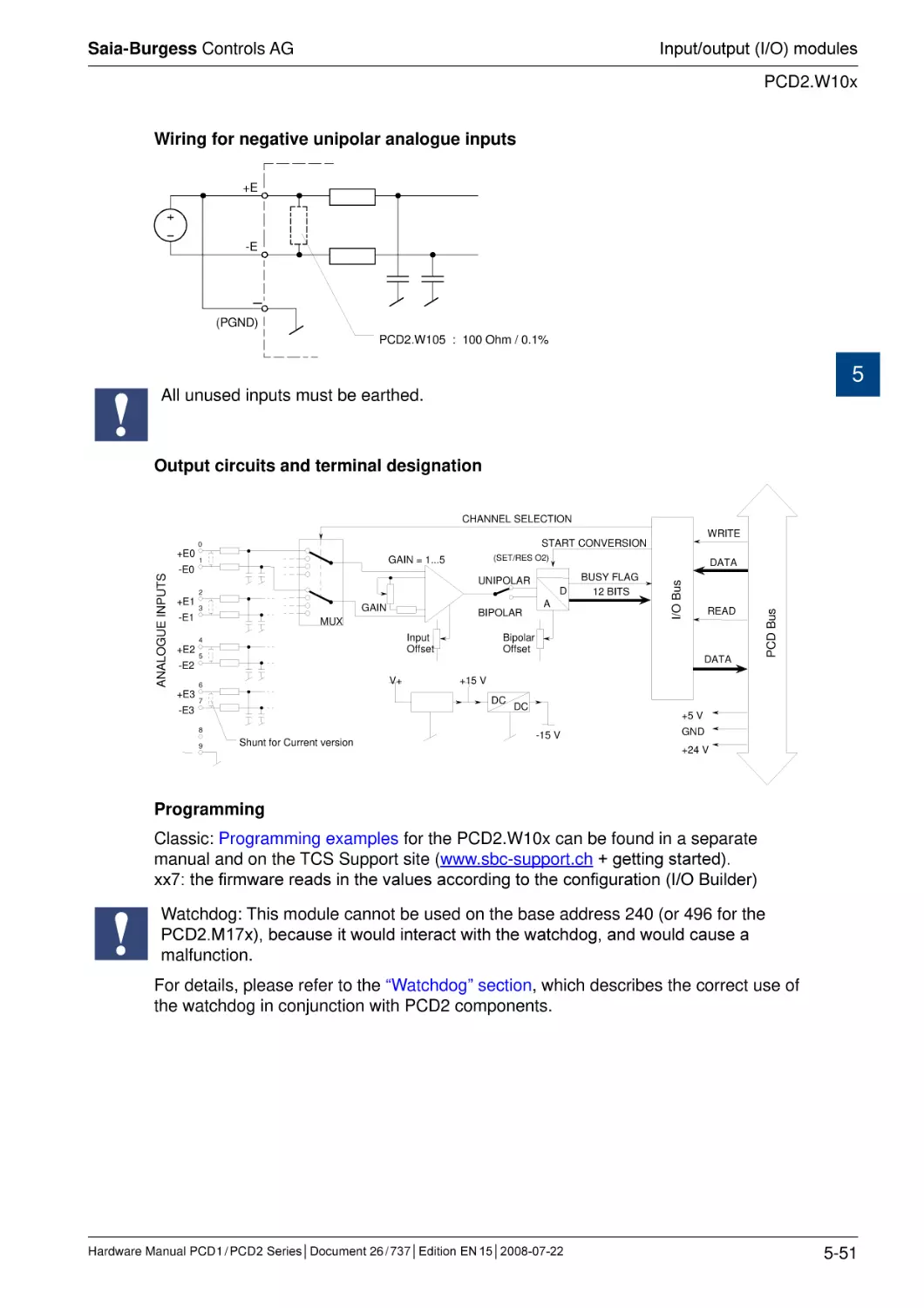
5.7.1 PCD2.W10x, analogue inputs, 4 channels, 12 bit resolution.........................
5.7.2 PCD2.W11x, analogue inputs, 4 channels, 12 bit resolution.........................
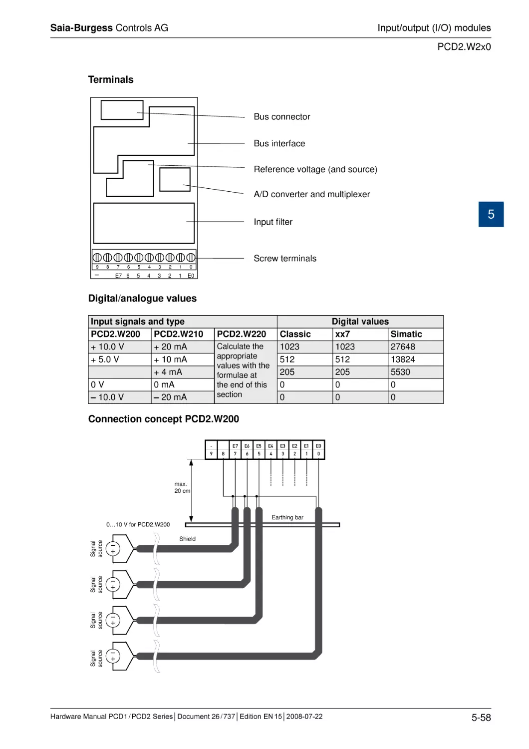
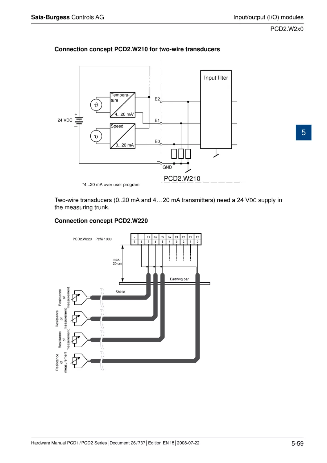
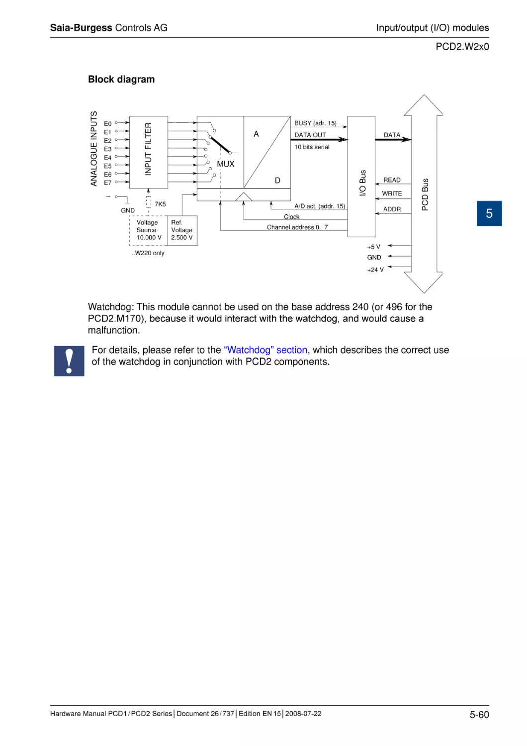
5.7.3 PCD2.W2x0, analogue inputs, 8 channels, 10 bit resolution.........................
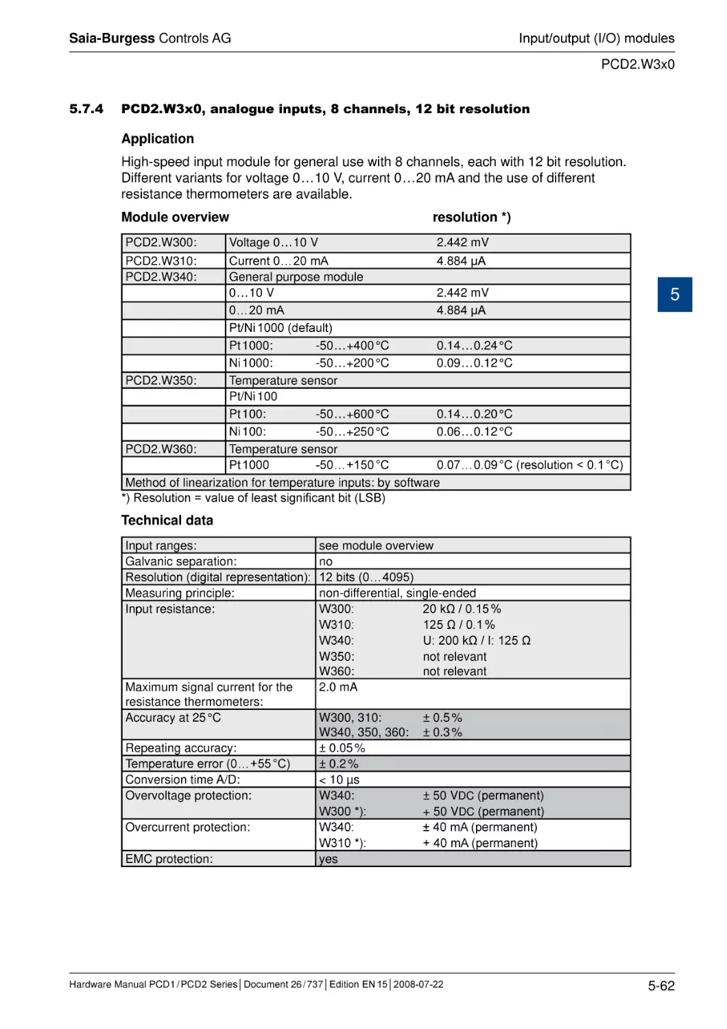
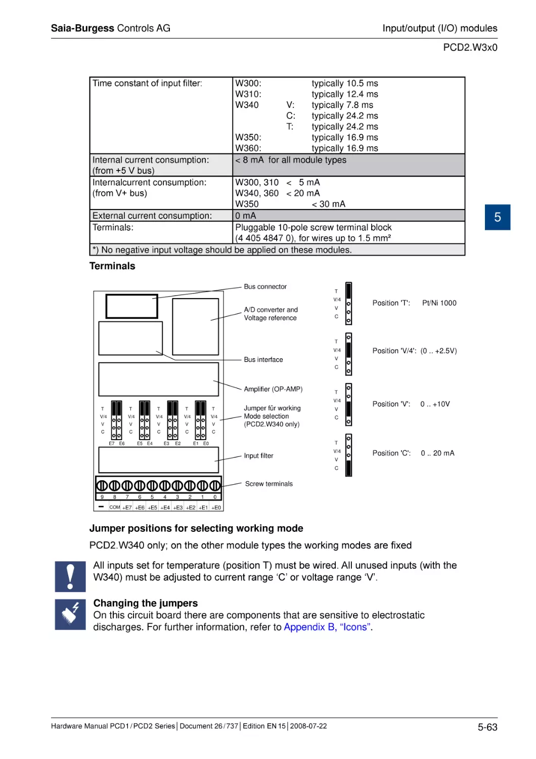
5.7.4 PCD2.W3x0, analogue inputs, 8 channels, 12 bit resolution.........................
5.8
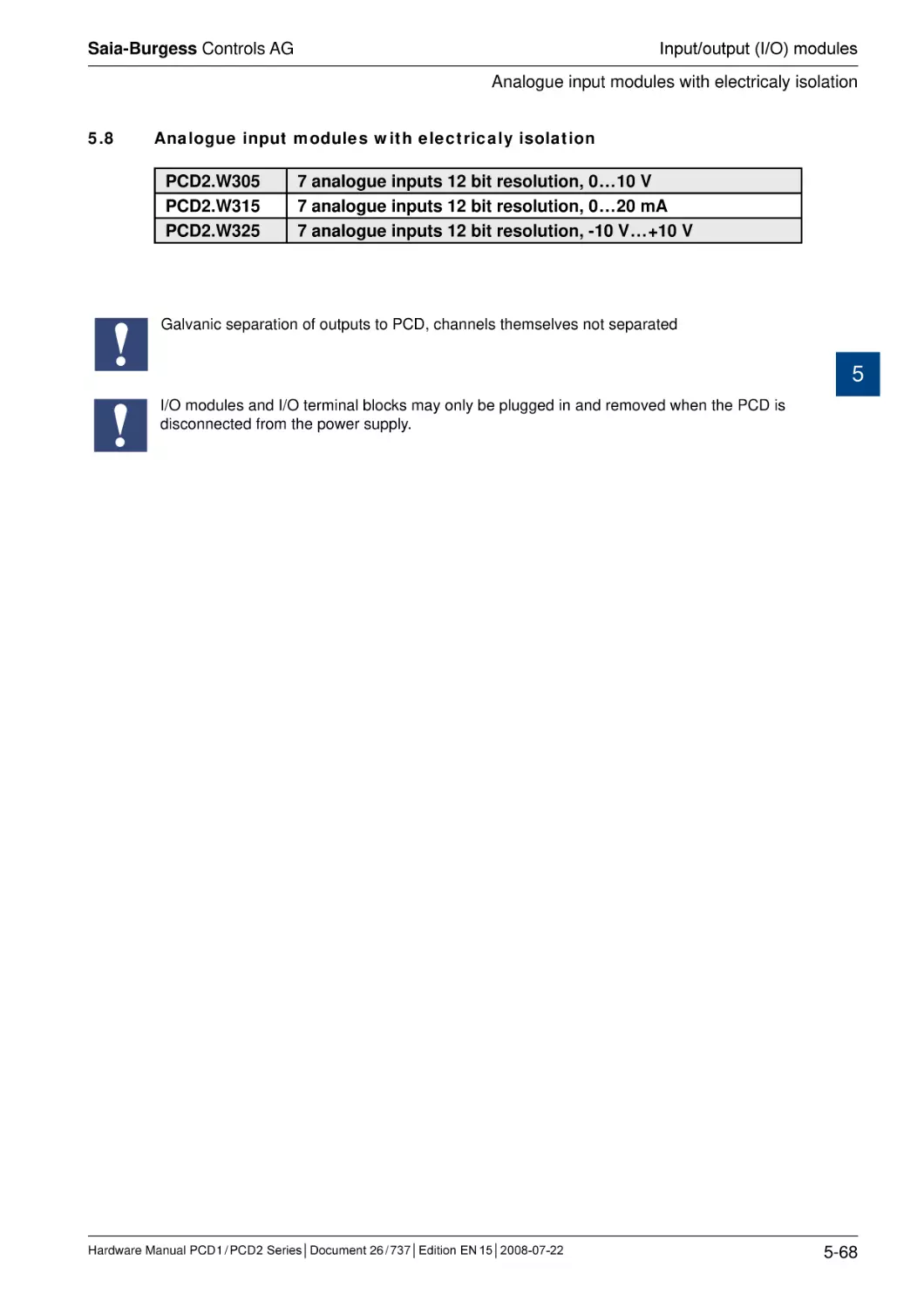
Analogue input modules with electricaly isolation............................................
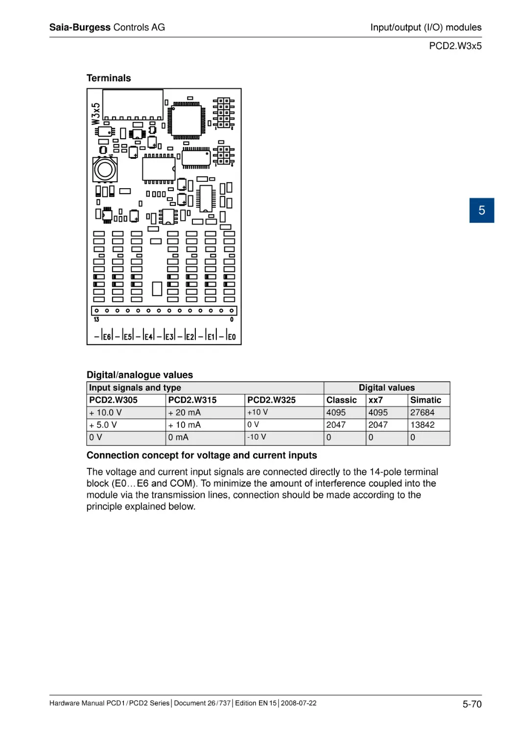
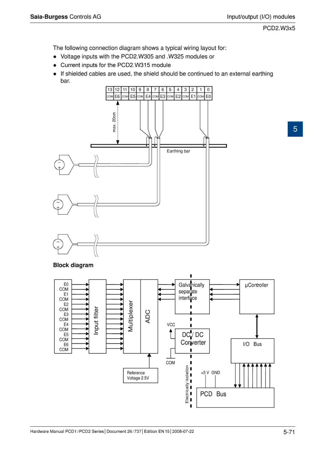
5.8.1 PCD2.W3x5, analogue inputs, 7 channels, 12 bit resolution, elect. isol........
5.9
Analogue input and output modules................................................................
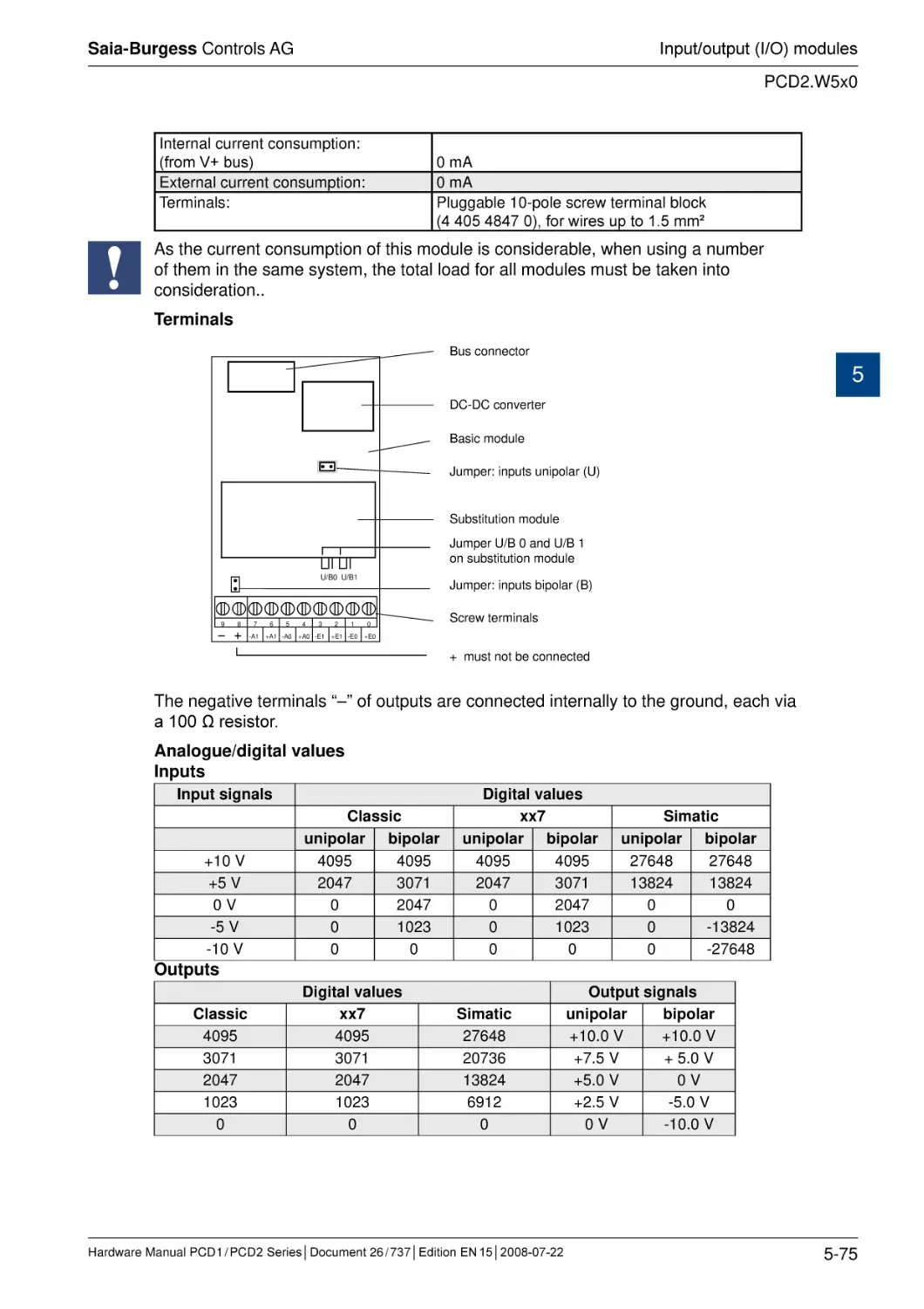
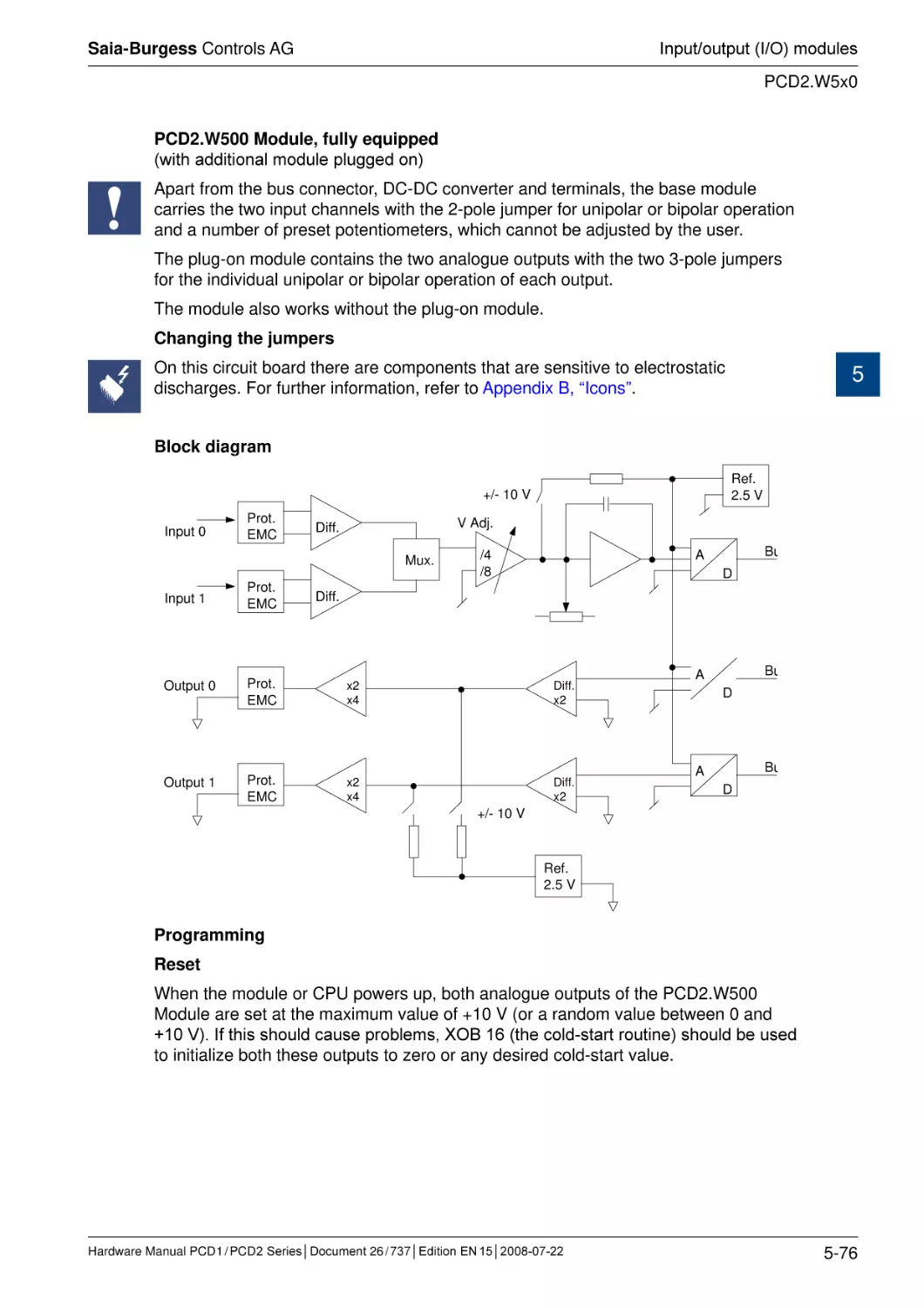
5.9.1 PCD2.W5x0, analogue inputs/outputs, 2 + 2 channels, 12 bit resolution......
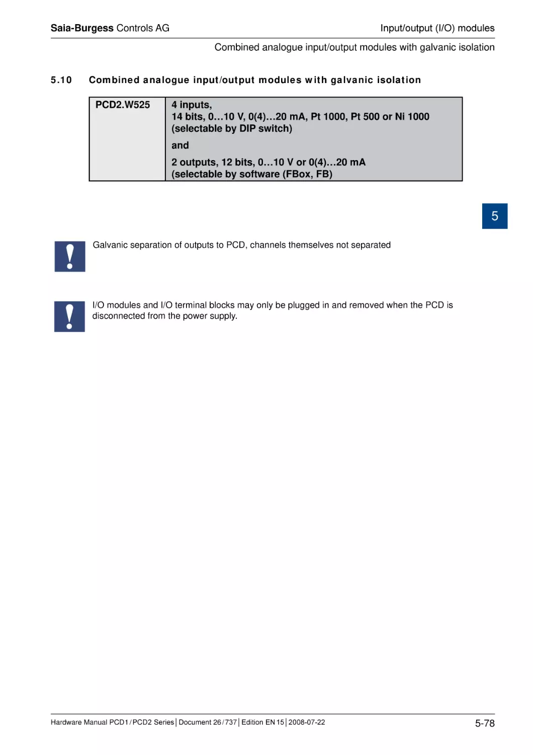
5.10
Combined analogue input/output modules with galvanic isolation...................
5.10.1 PCD2.W525 Combined analogue input/output modules
with galvanic isolation....................................................................................
5.11
Analogue output modules................................................................................
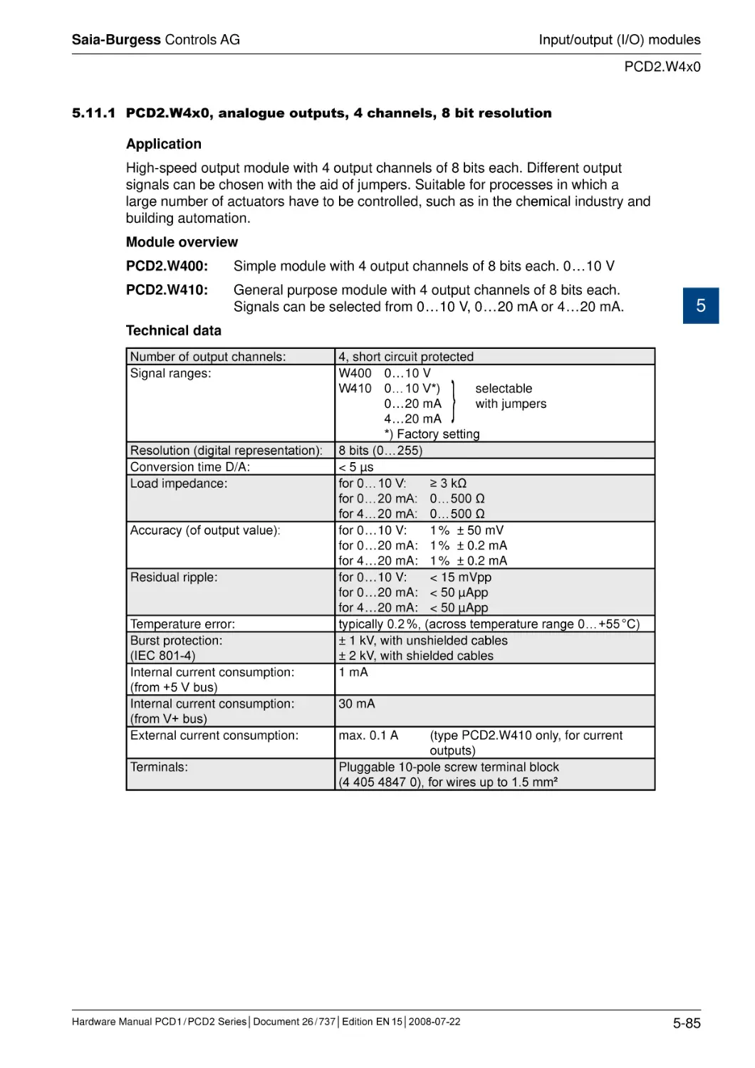
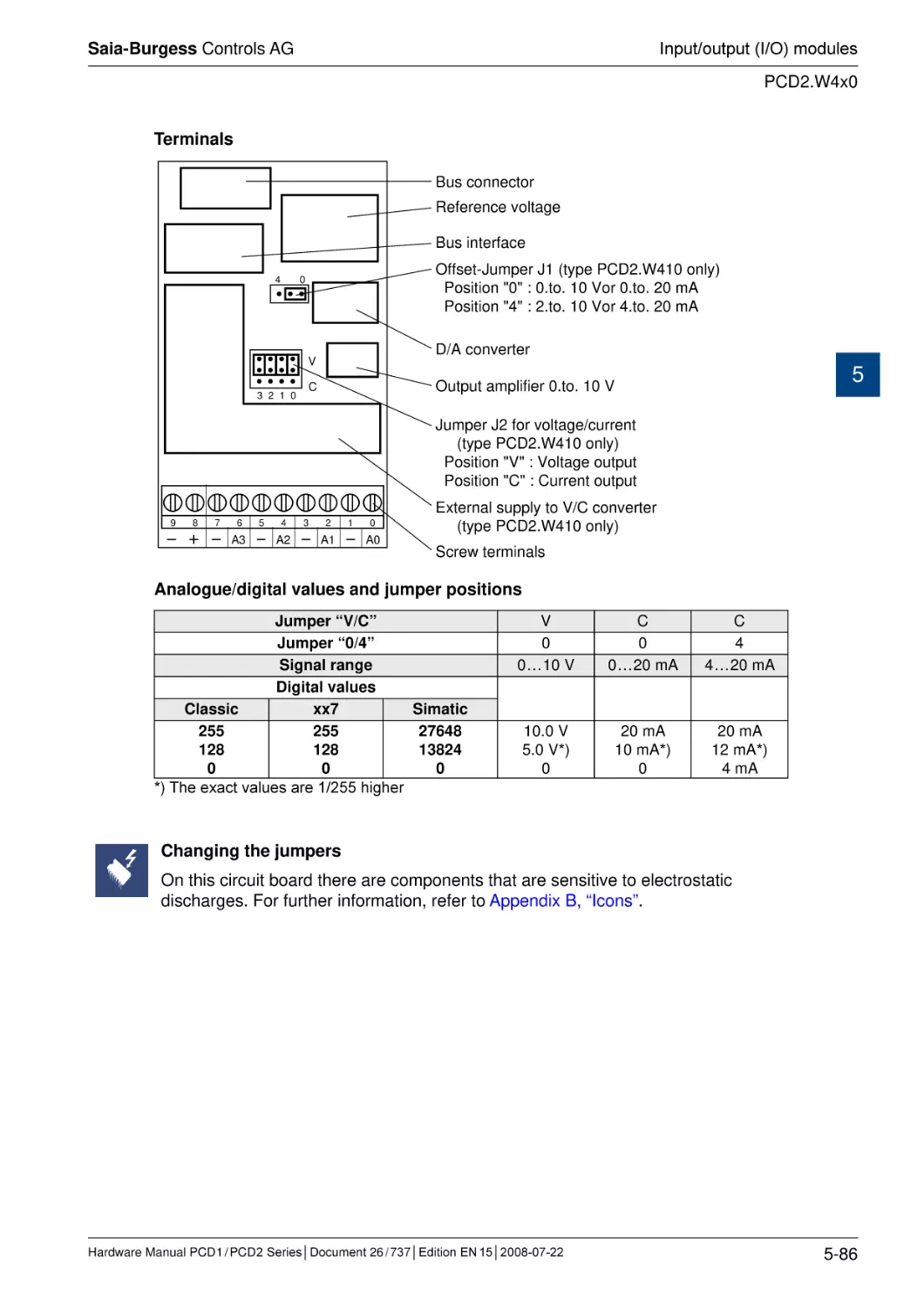
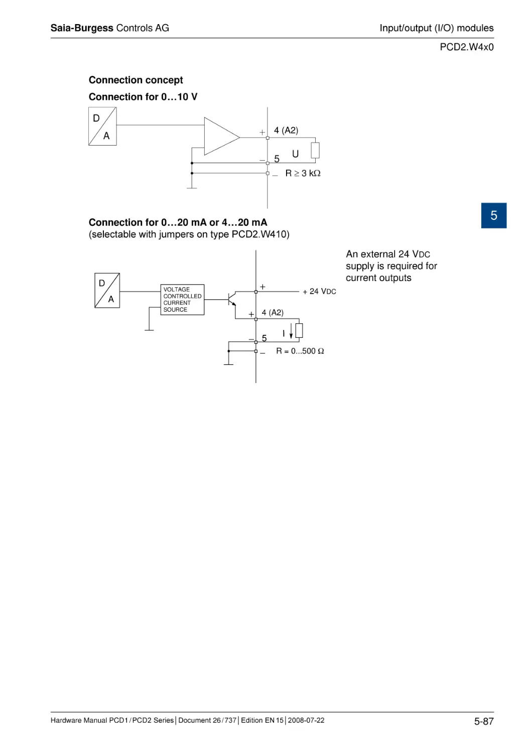
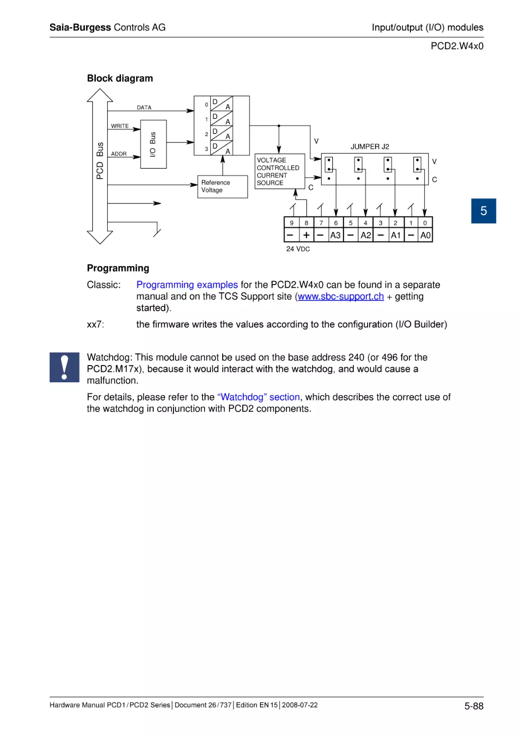
5.11.1 PCD2.W4x0, analogue outputs, 4 channels, 8 bit resolution.........................
5.11.2 PCD2.W6x0, analogue outputs, 4 channels, 12 bit resolution.......................
5.12
Analogue output modules with electrically isolation.........................................
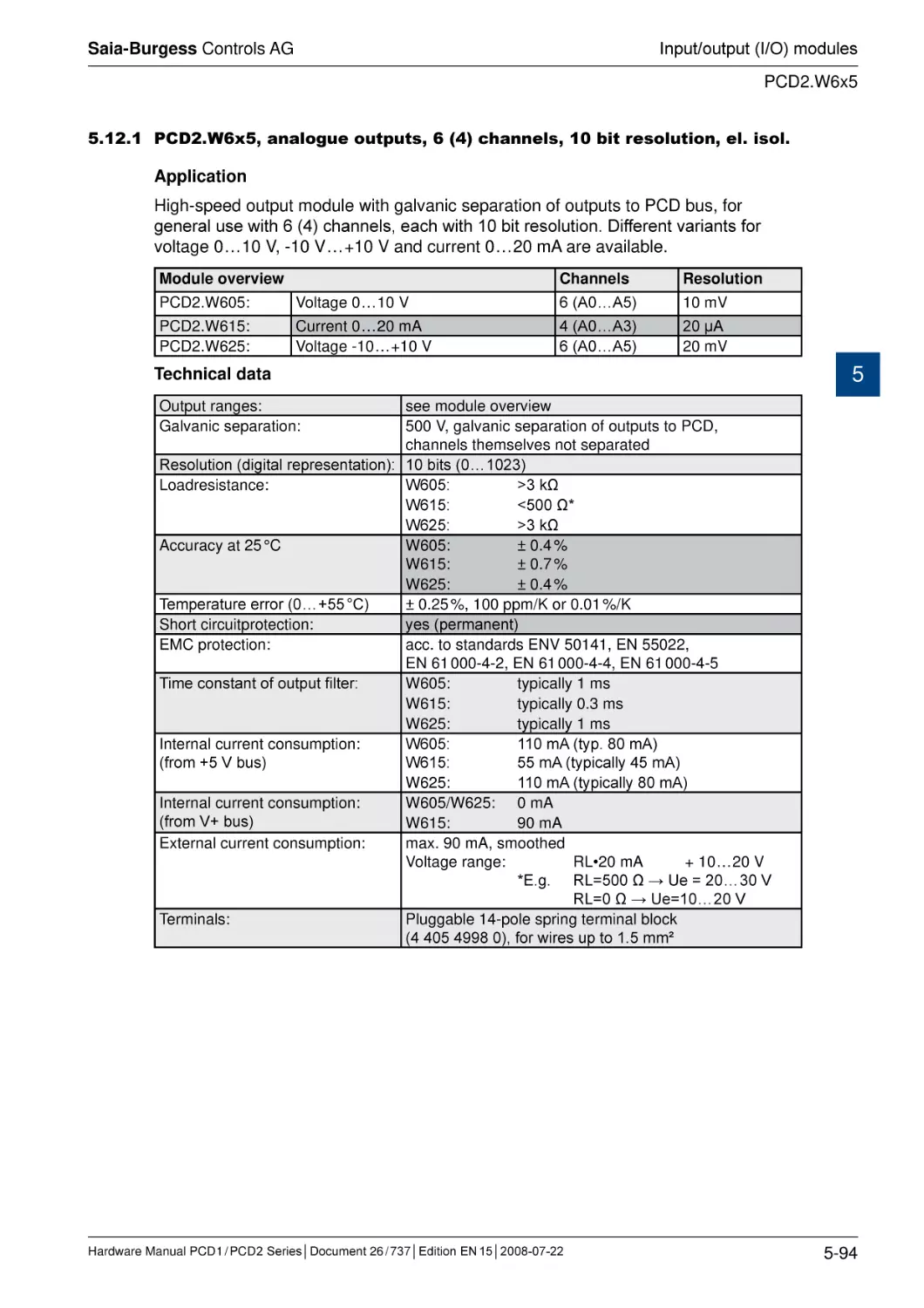
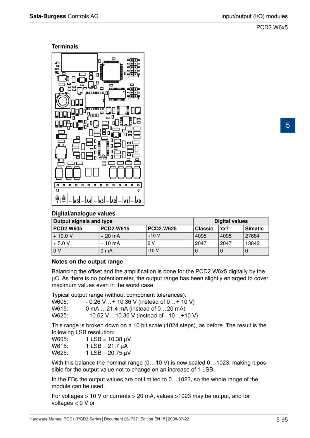
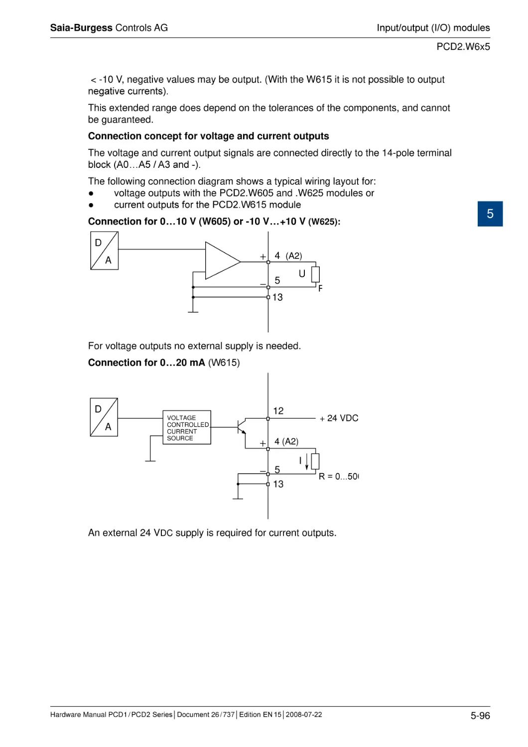
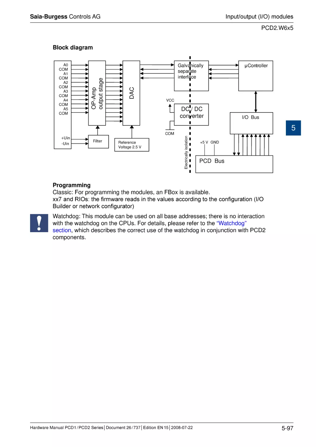
5.12.1 PCD2.W6x5, analogue outputs, 6 (4) channels, 10 bit resolution, el. isol.....
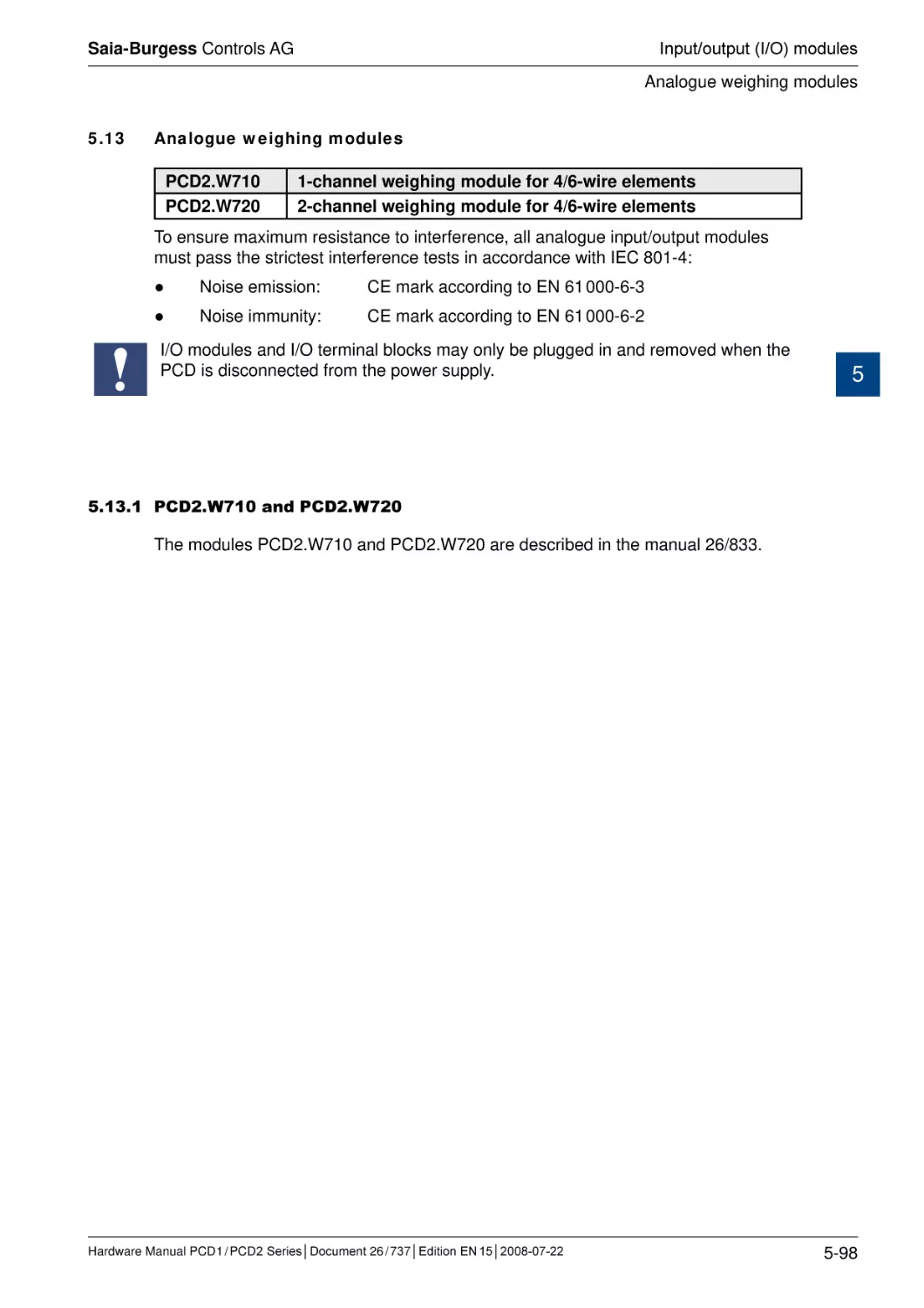
5.13
Analogue weighing modules............................................................................
5.13.1 PCD2.W710 and PCD2.W720.......................................................................
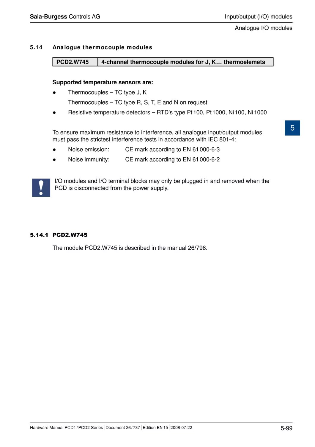
5.14
Analogue thermocouple modules....................................................................
5.14.1 PCD2.W745...................................................................................................
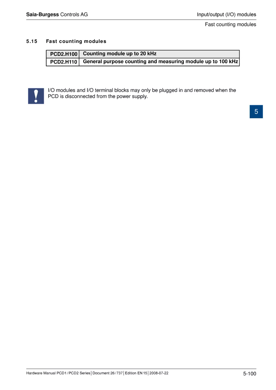
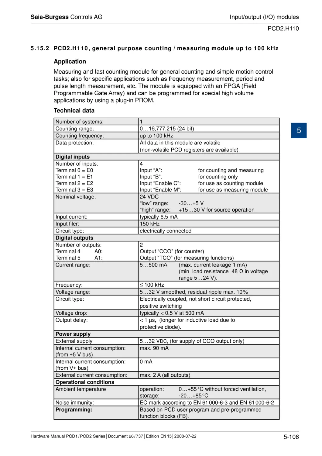
5.15
Fast counting modules.....................................................................................
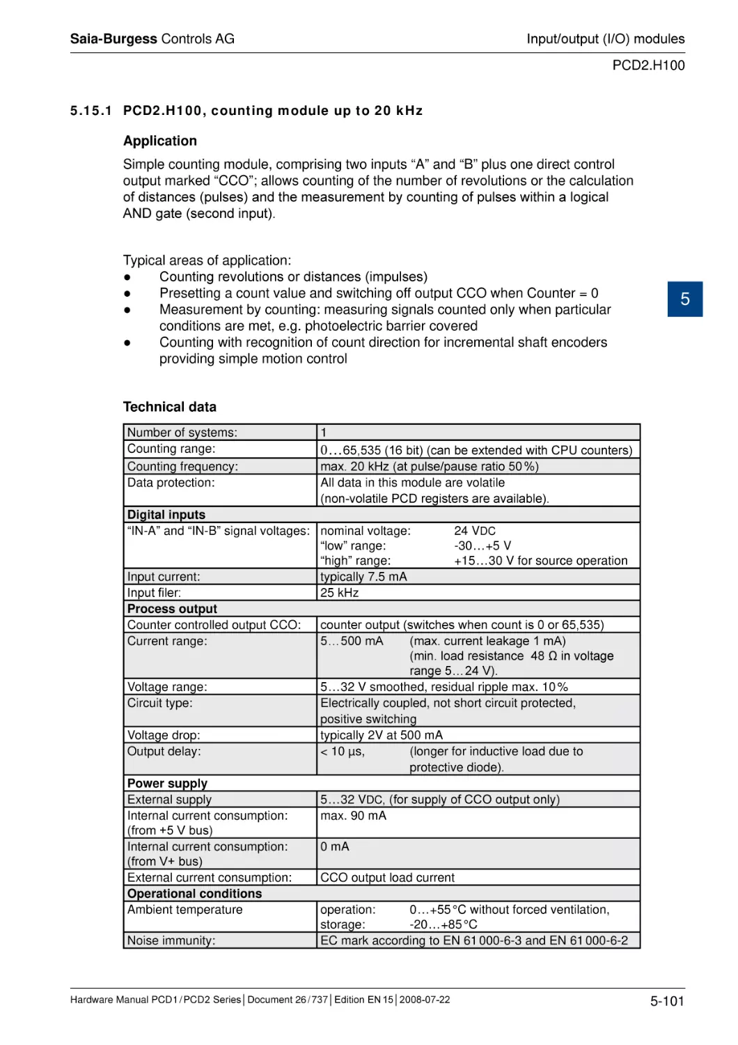
5.15.1 PCD2.H100, counting module up to 20 kHz..................................................
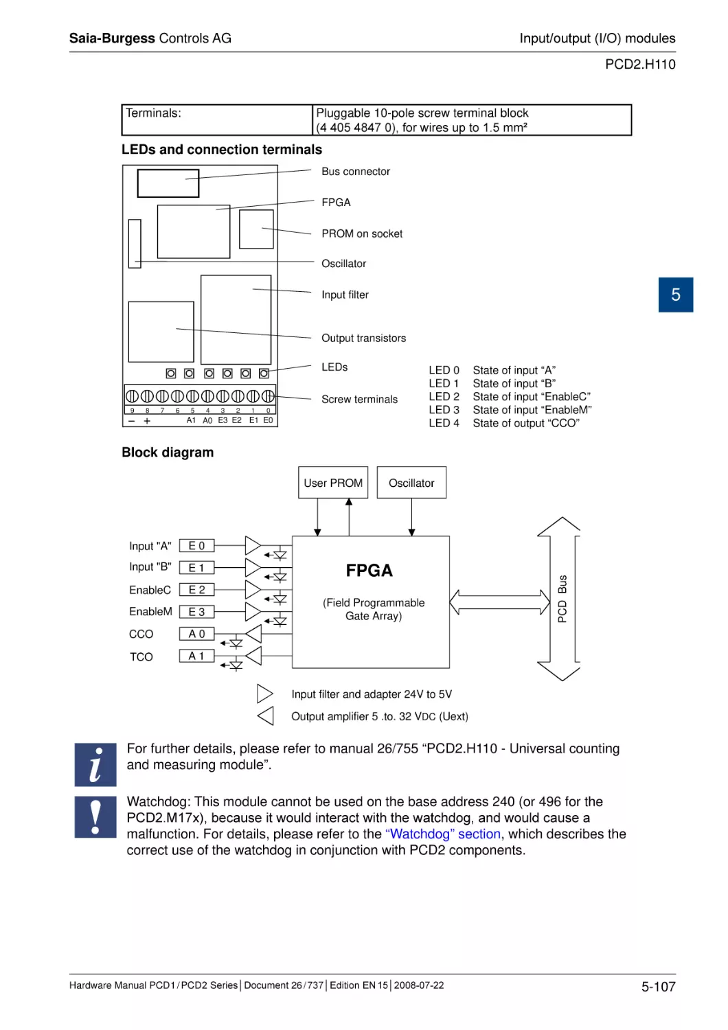
5.15.2 PCD2.H110, general purpose counting / measuring module up to 100 kHz..
5.16
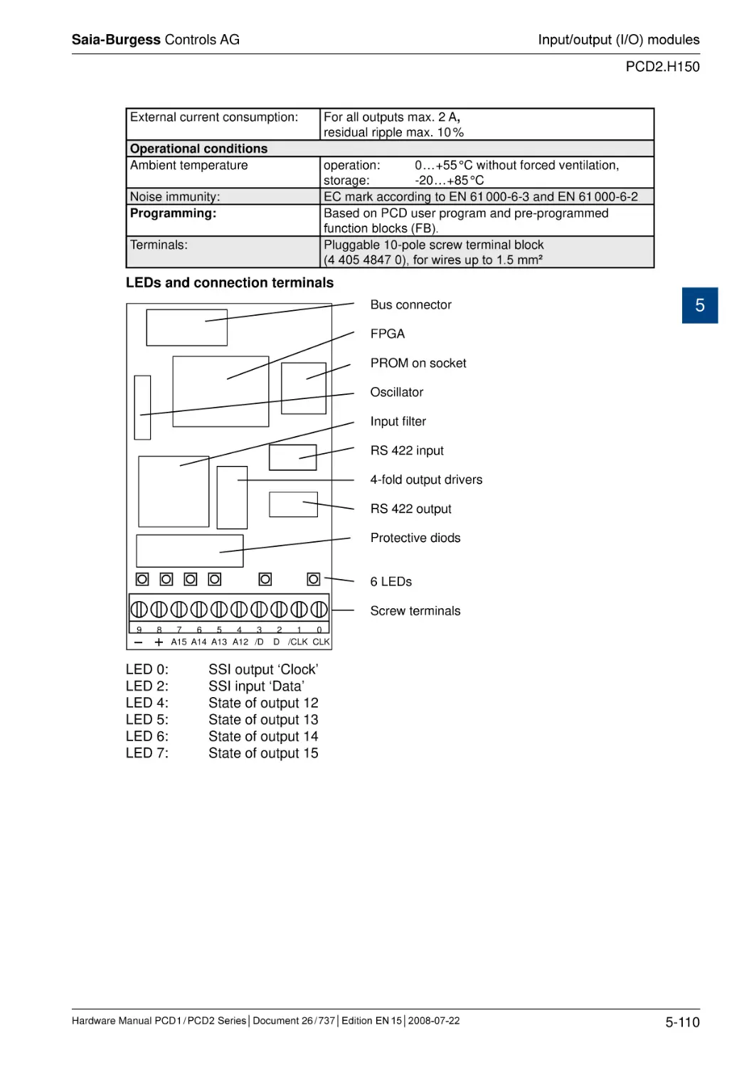
SSI interface modules......................................................................................
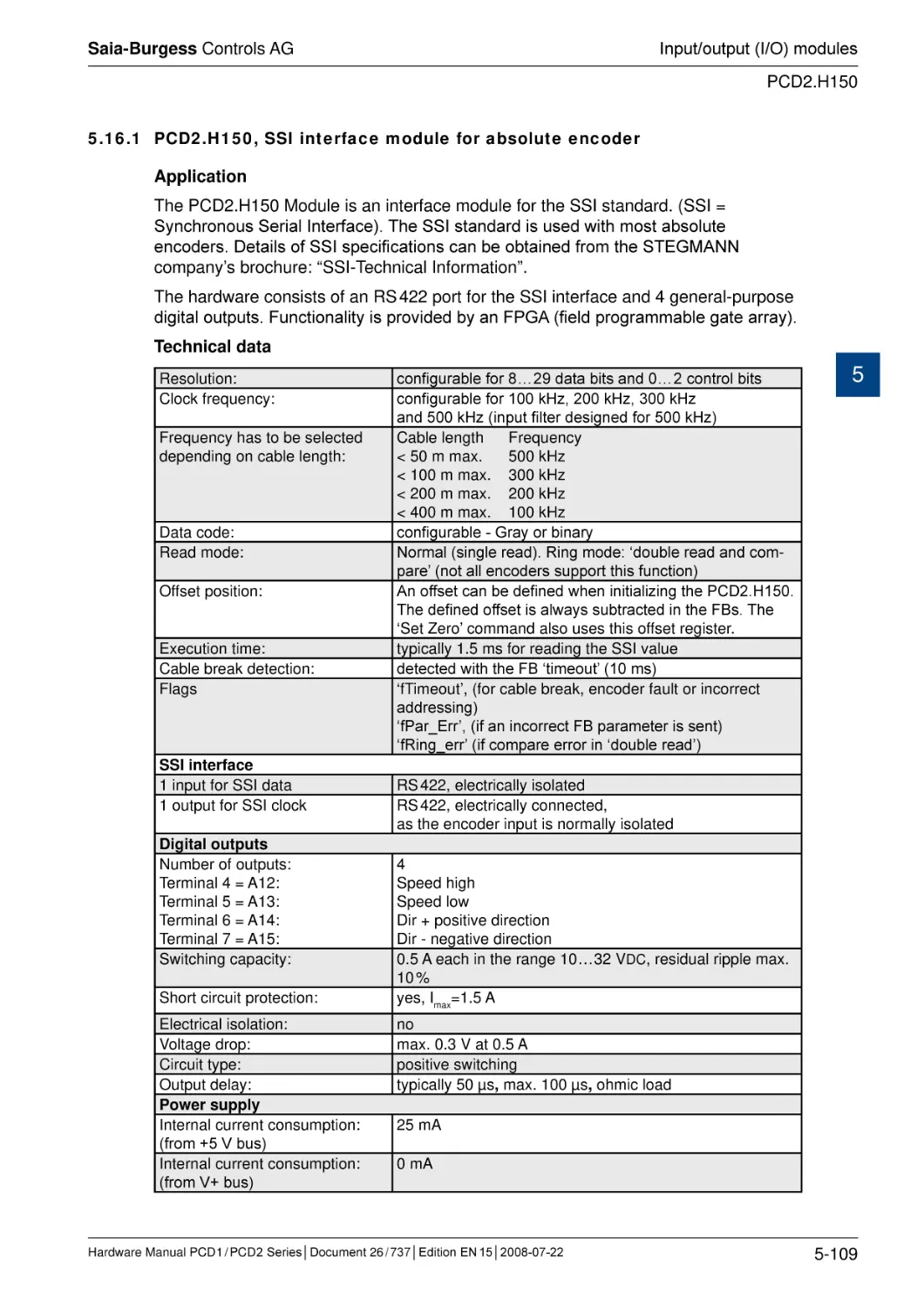
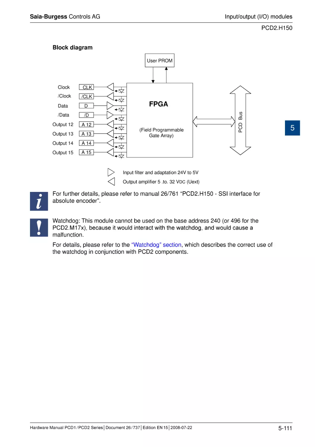
5.16.1 PCD2.H150, SSI interface module for absolute encoder...............................
Hardware Manual PCD 1 / PCD 2 Series│Document 26 / 737│Edition EN 15│2008-07-22
5-9
5-12
5-14
0
5-15
5-17
5-19
5-20
5-22
5-24
5-27
5-29
5-30
5-32
5-34
5-36
5-38
5-40
5-41
5-44
5-45
5-46
5-48
5-49
5-52
5-57
5-62
5-68
5-69
5-73
5-74
5-78
5-79
5-84
5-85
5-89
5-93
5-94
5-98
5-98
5-99
5-99
5-100
5-101
5-106
5-108
5-109
0-4
Saia-Burgess Controls AG
Contents
6
A
5.17
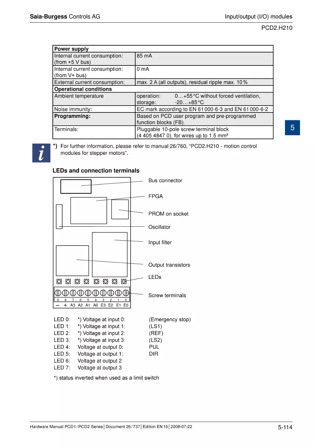
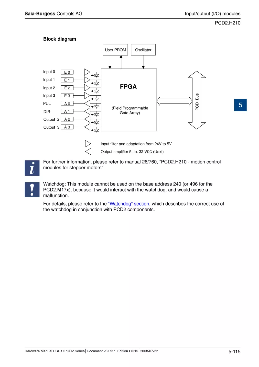
Motion control modules for stepper motors......................................................
5.17.1 PCD2.H210, Motion control module for stepper motors................................
5.18
Motion control modules for servo-motors.........................................................
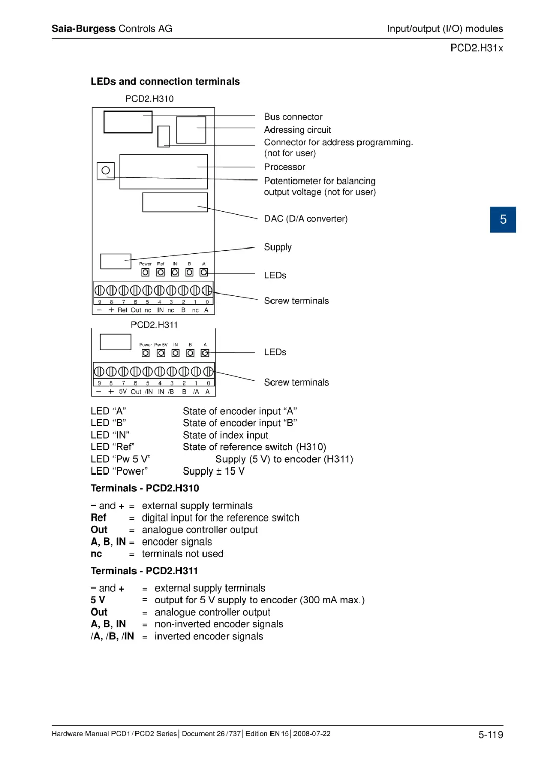
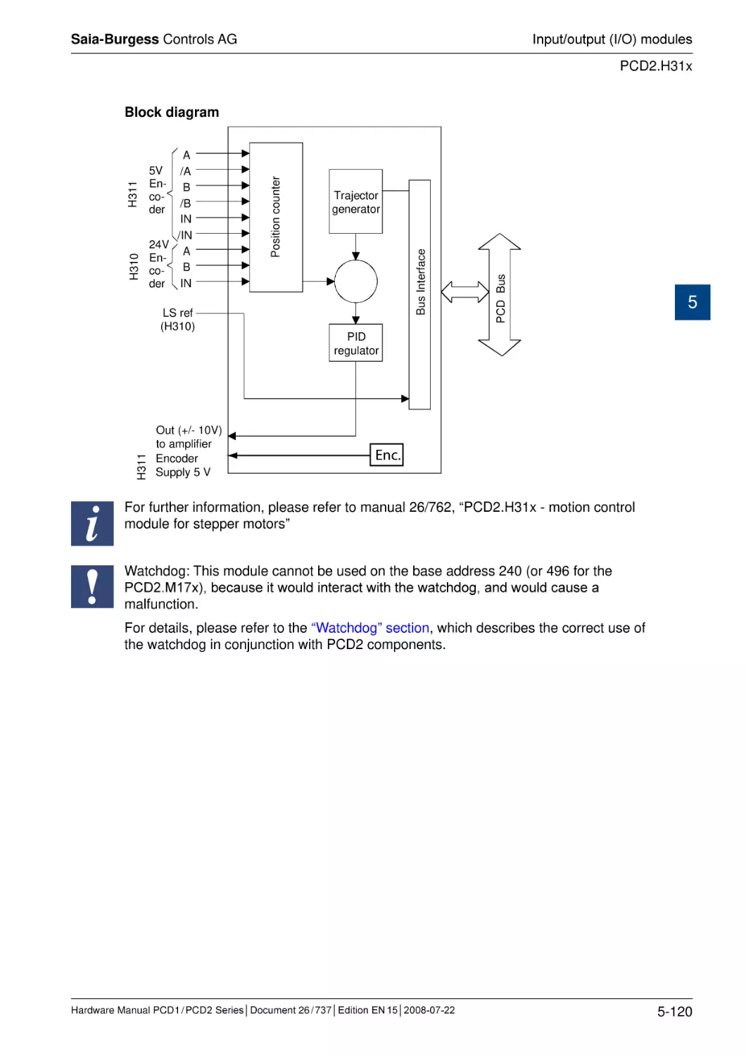
5.18.1 PCD2.H31x, motion control module for servo-motors, 1-axis encoder..........
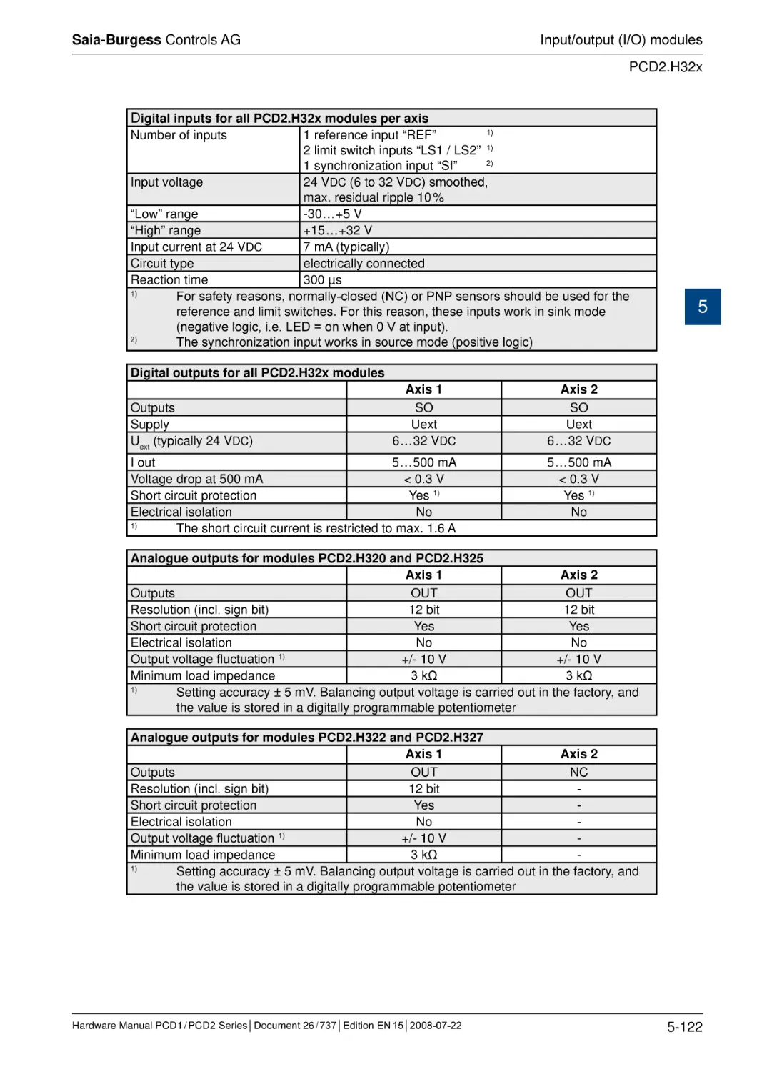
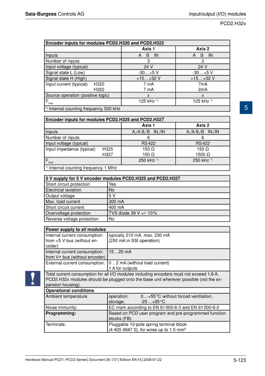
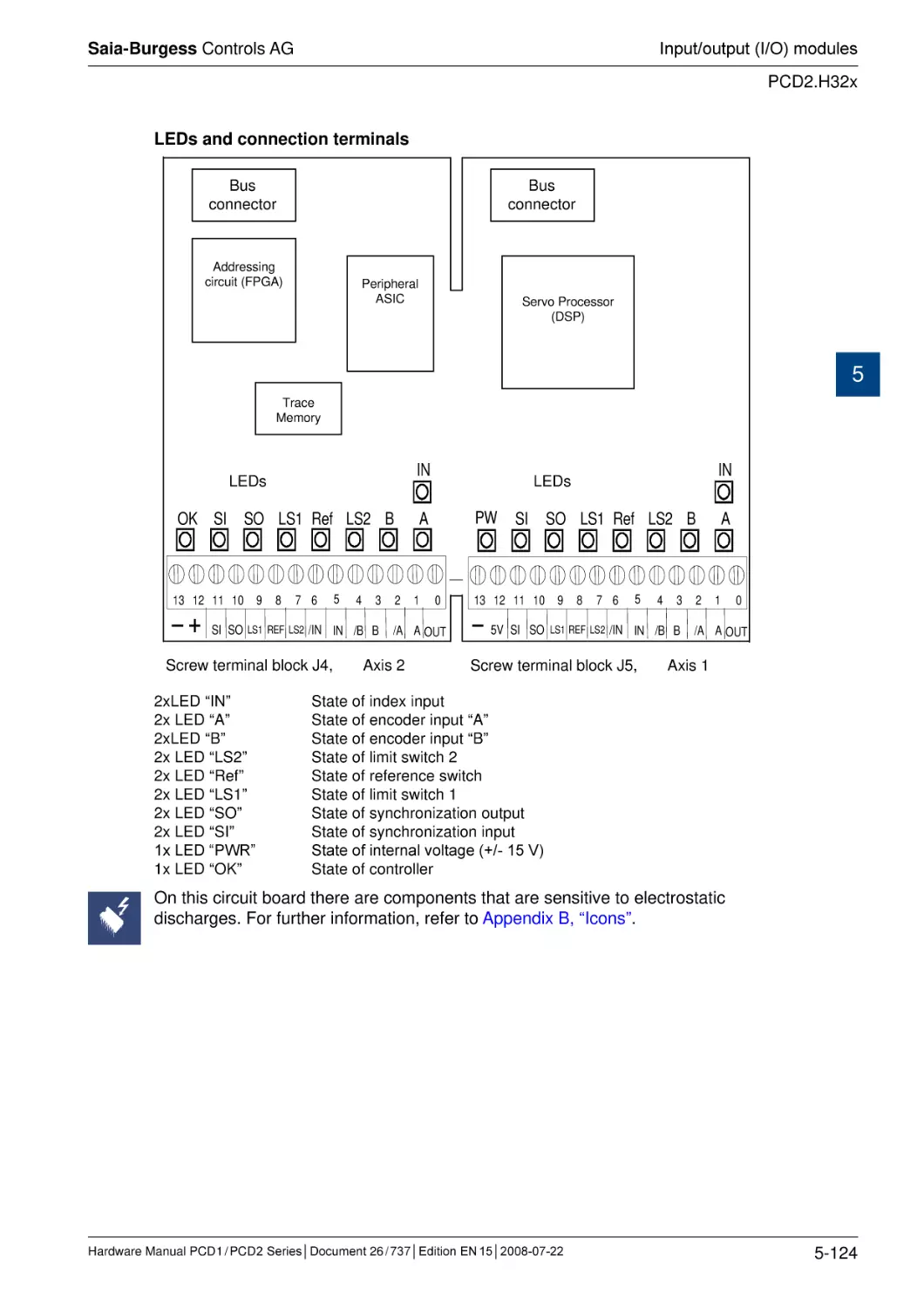
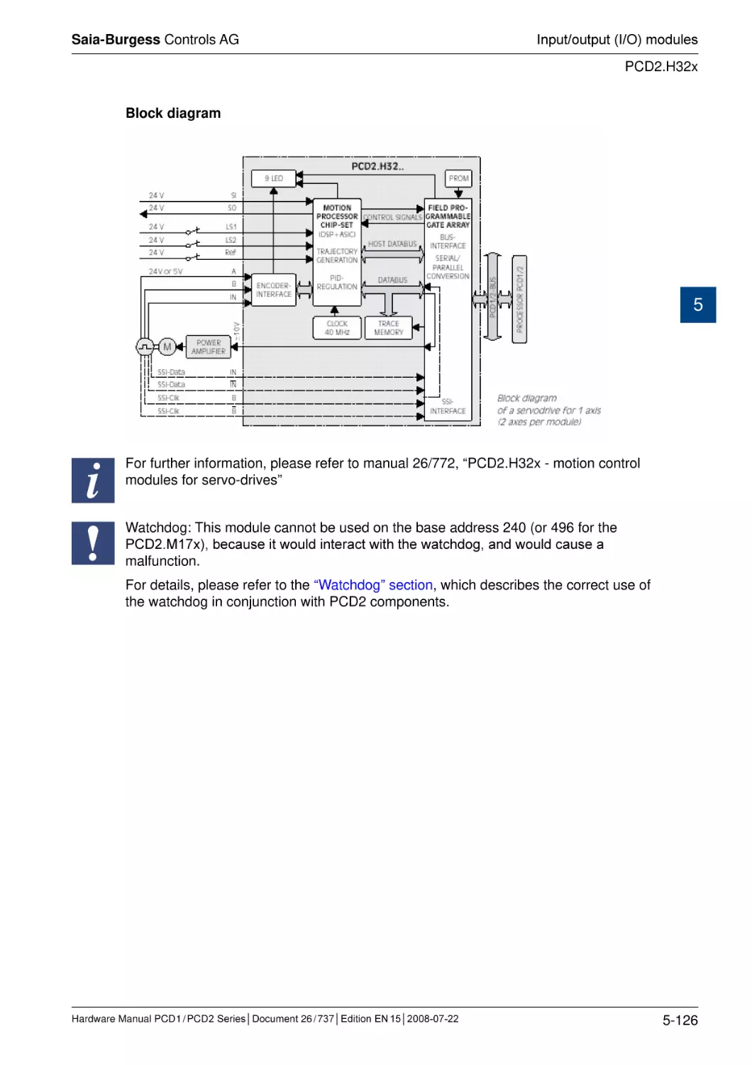
5.18.2 PCD2.H32x, motion control modules for servo-drives...................................
5-112
5-113
5-116
5-117
5-121
System cables and adapters
6.1
System cables with I/O module connections to the PCD.................................
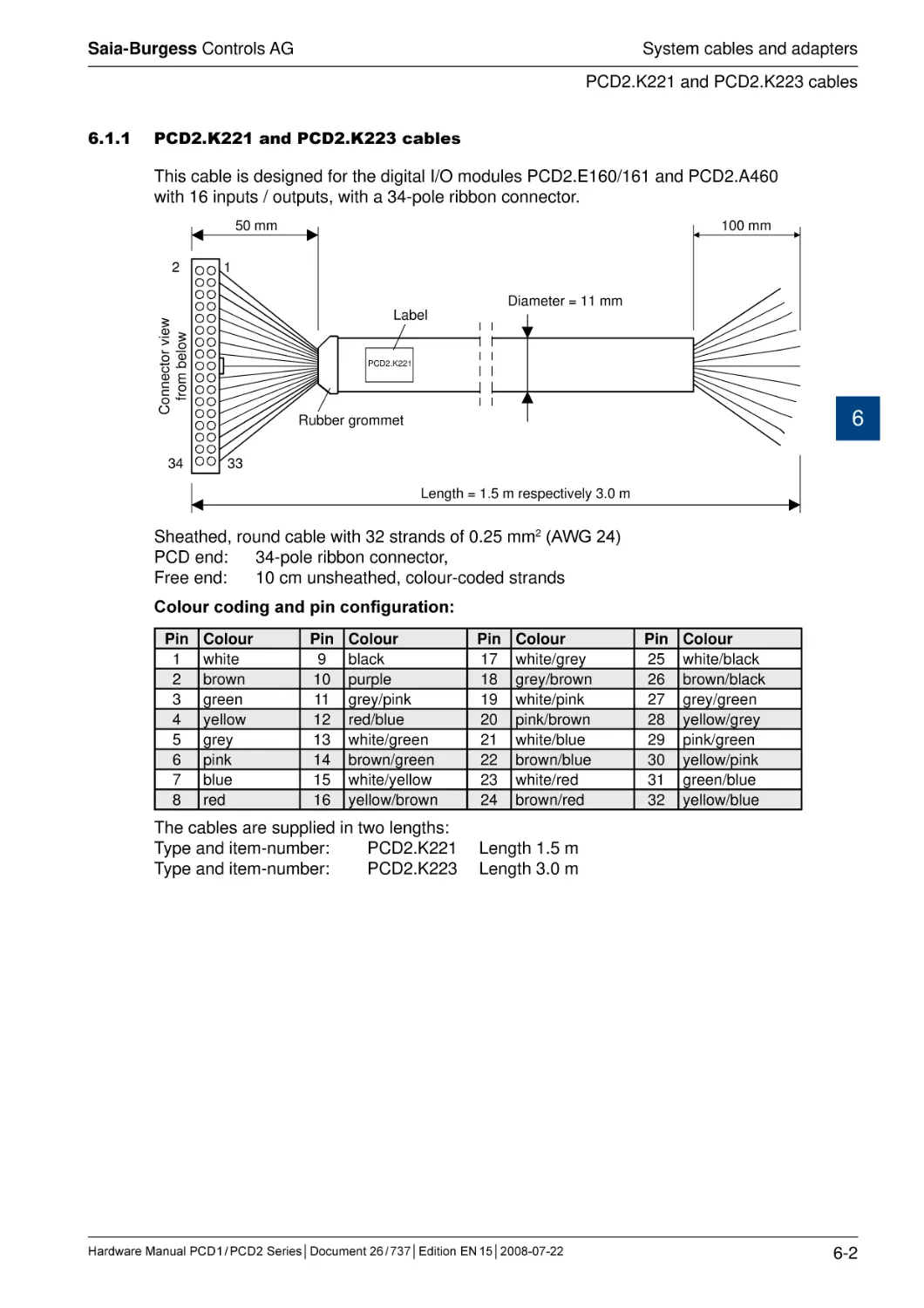
6.1.1 PCD2.K221 and PCD2.K223 cables..............................................................
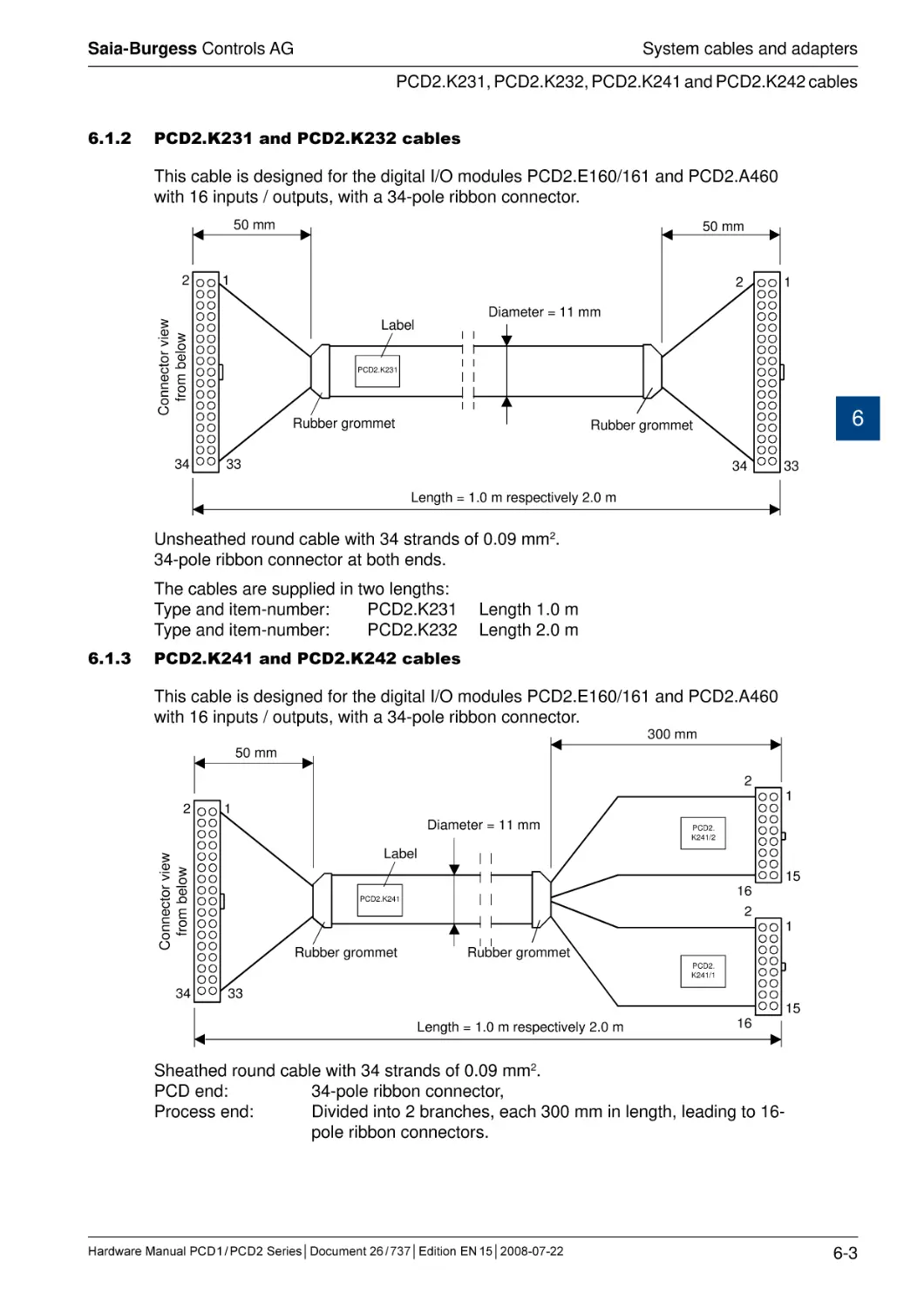
6.1.2 PCD2.K231 and PCD2.K232 cables..............................................................
6.1.3 PCD2.K241 and PCD2.K242 cables..............................................................
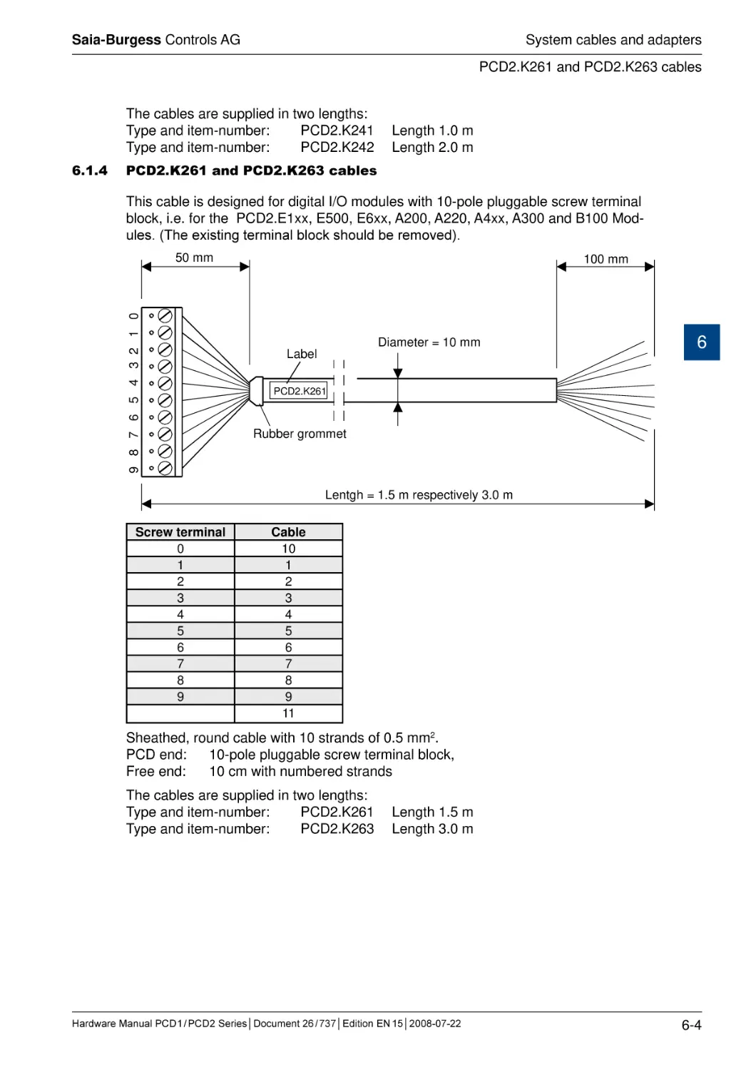
6.1.4 PCD2.K261 and PCD2.K263 cables..............................................................
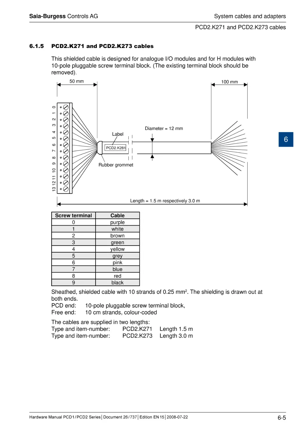
6.1.5 PCD2.K271 and PCD2.K273 cables..............................................................
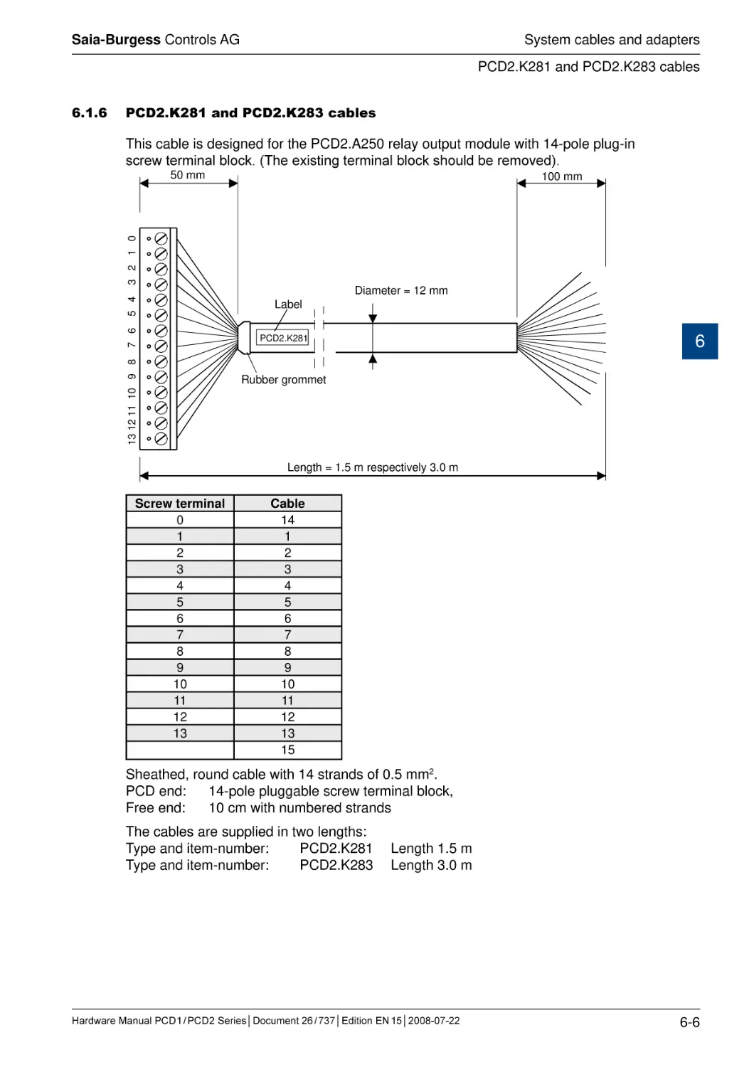
6.1.6 PCD2.K281 and PCD2.K283 cables..............................................................
6.2
Ribbon/screw terminal adapters (external terminal blocks).............................
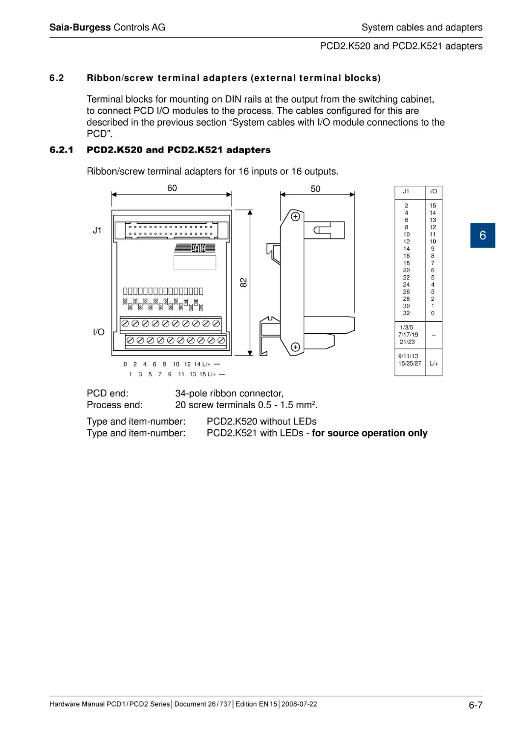
6.2.1 PCD2.K520 and PCD2.K521 adapters..........................................................
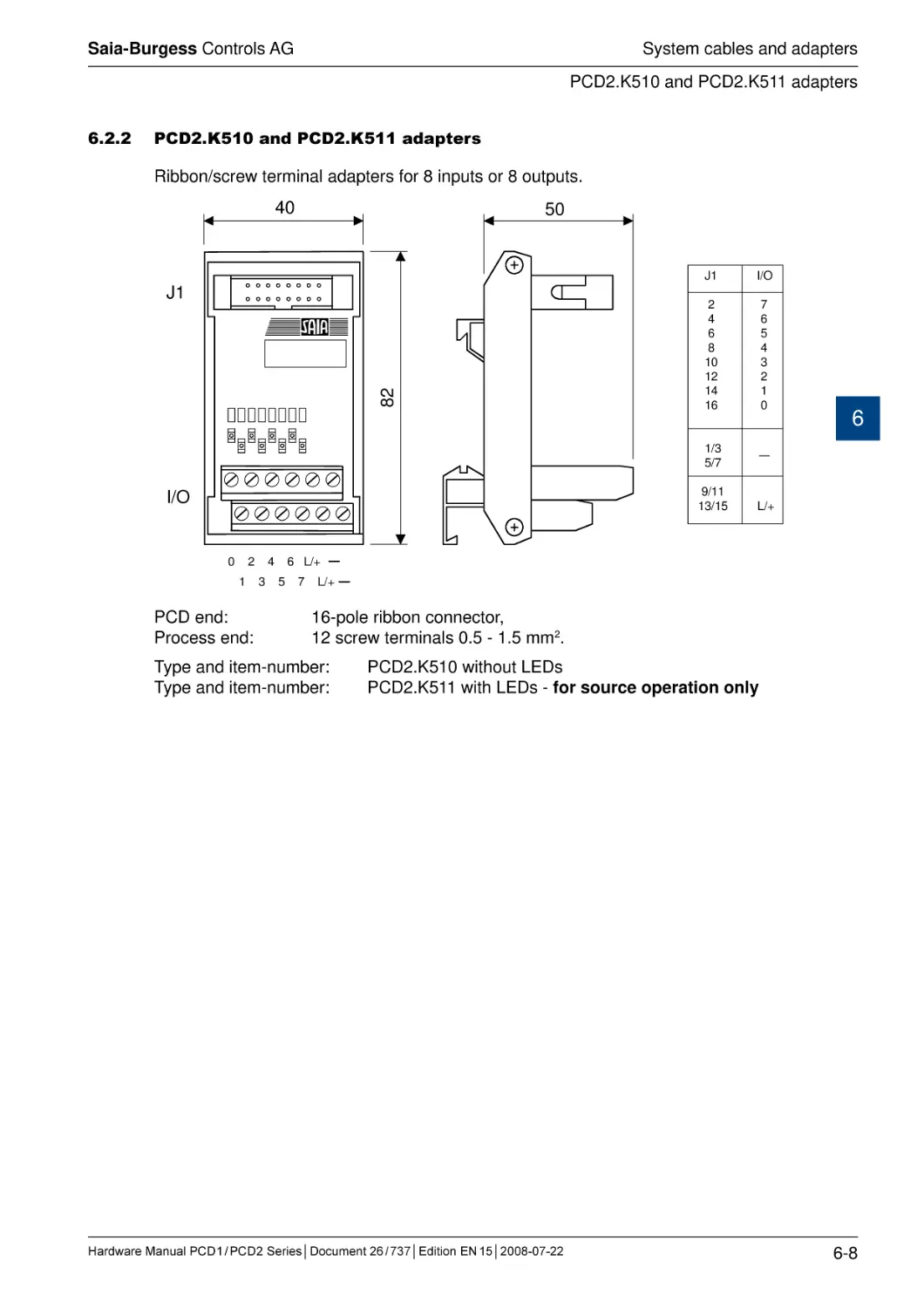
6.2.2 PCD2.K510 and PCD2.K511 adapters..........................................................
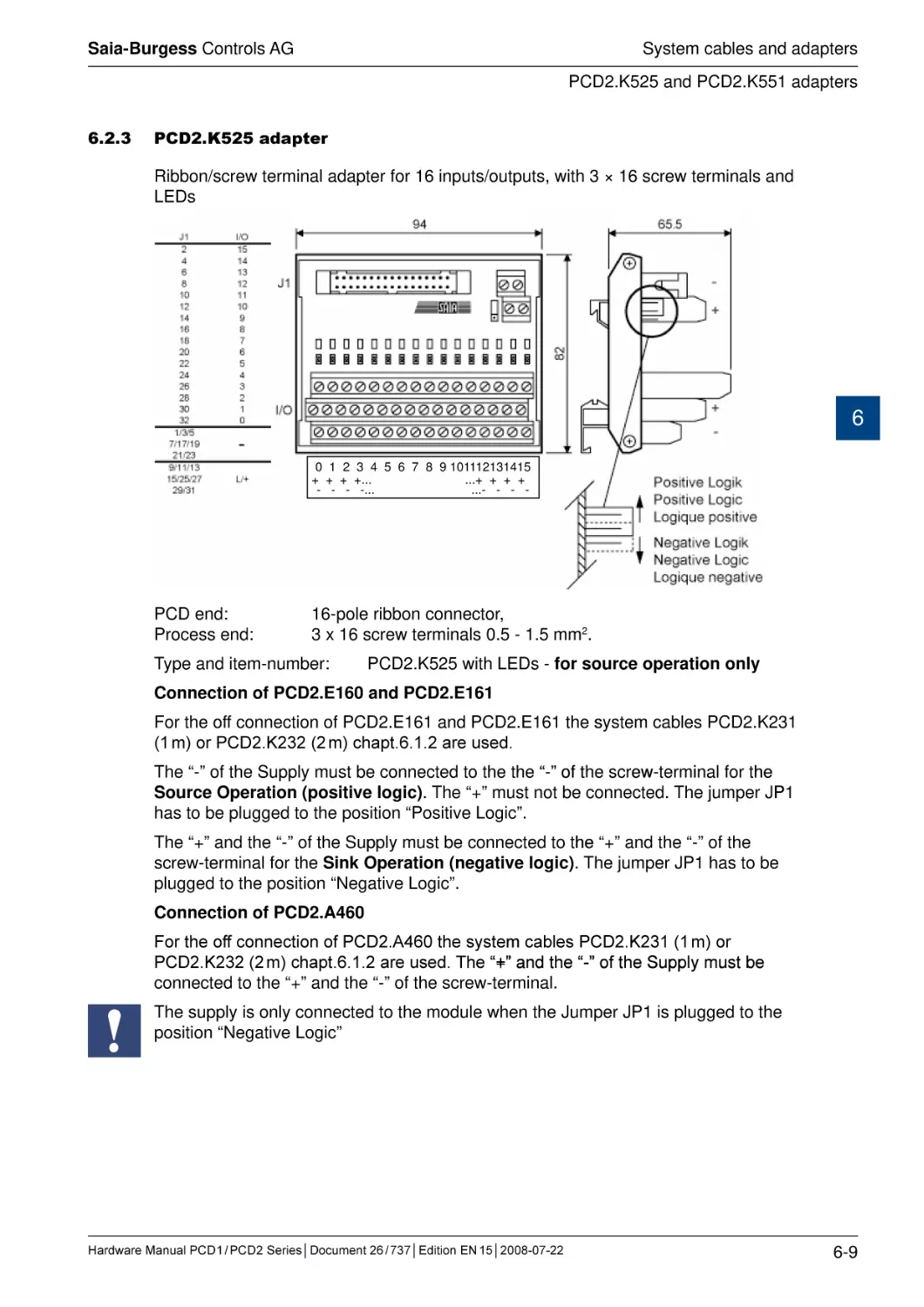
6.2.3 PCD2.K525 adapter ......................................................................................
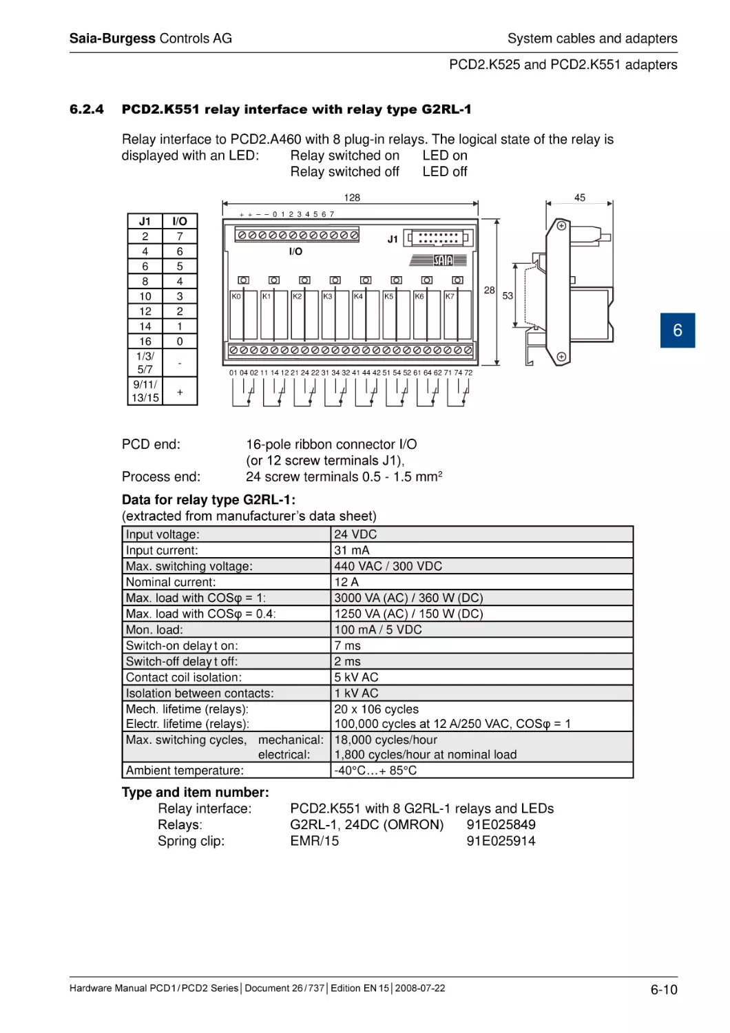
6.2.4 PCD2.K551 relay interface with relay type G2RL-1.......................................
6.3
Old product versions........................................................................................
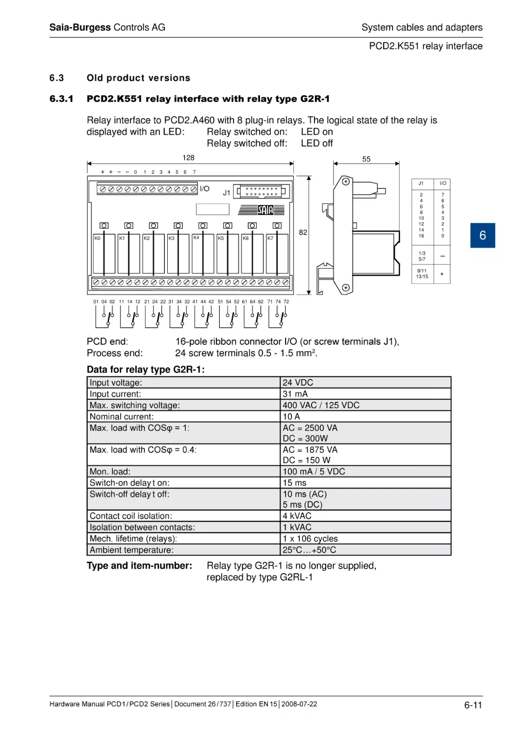
6.3.1 PCD2.K551 relay interface with relay type G2R-1.........................................
7.1
Changing the battery on the PCD1.M13x and PCD2.Mxxx CPUs...................
7.2
Updating firmware............................................................................................
7.2.1 Updating firmware on the PCD2.M110/M120.................................................
7.2.2 Updating firmware on the PCD2.M150..........................................................
7.2.3 Updating firmware on the PCD1.M1x5, PCD2.M170 and PCD2.M480.........
6-1
6-2
6-3
6-3
6-4
6-5
6-6
6-7
6-7
6-8
6-9
6-10
6-11
6-11
7-1
7-3
7-3
7-3
7-3
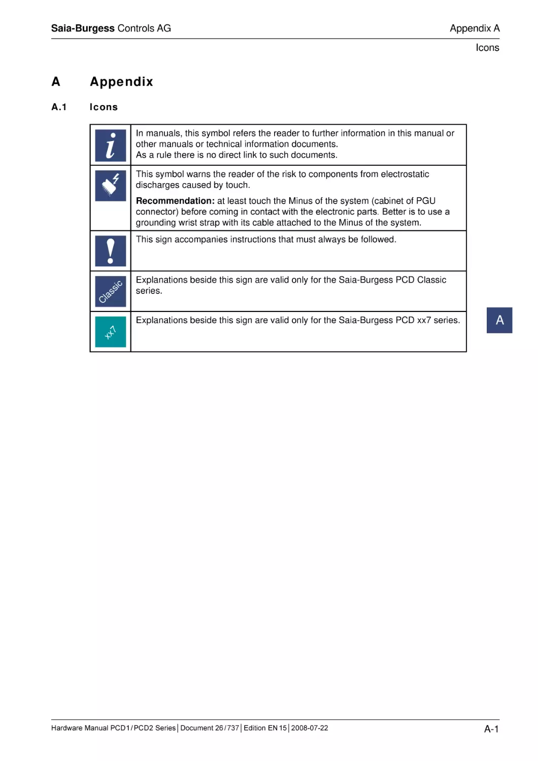
Appendix
Icons................................................................................................................
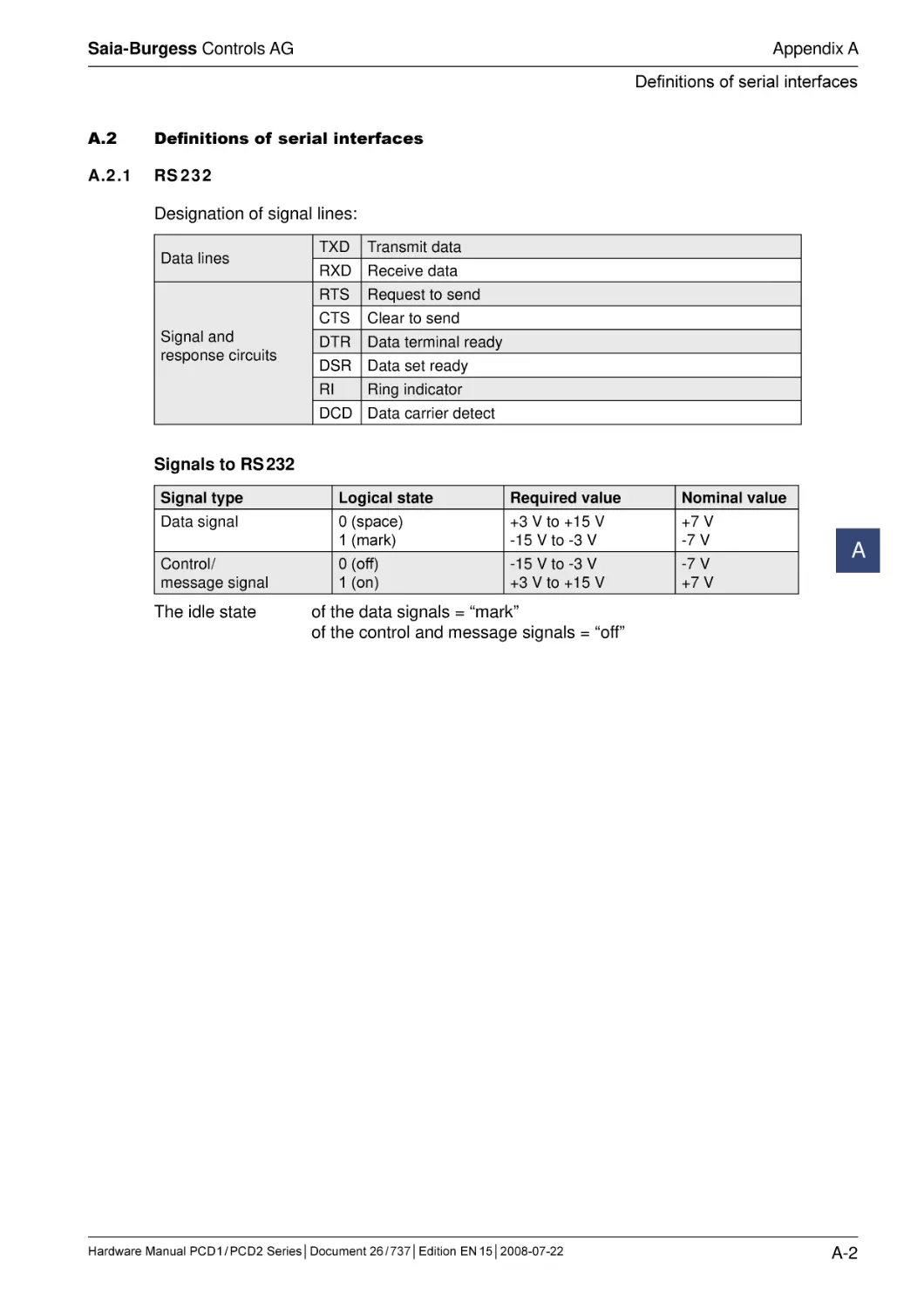
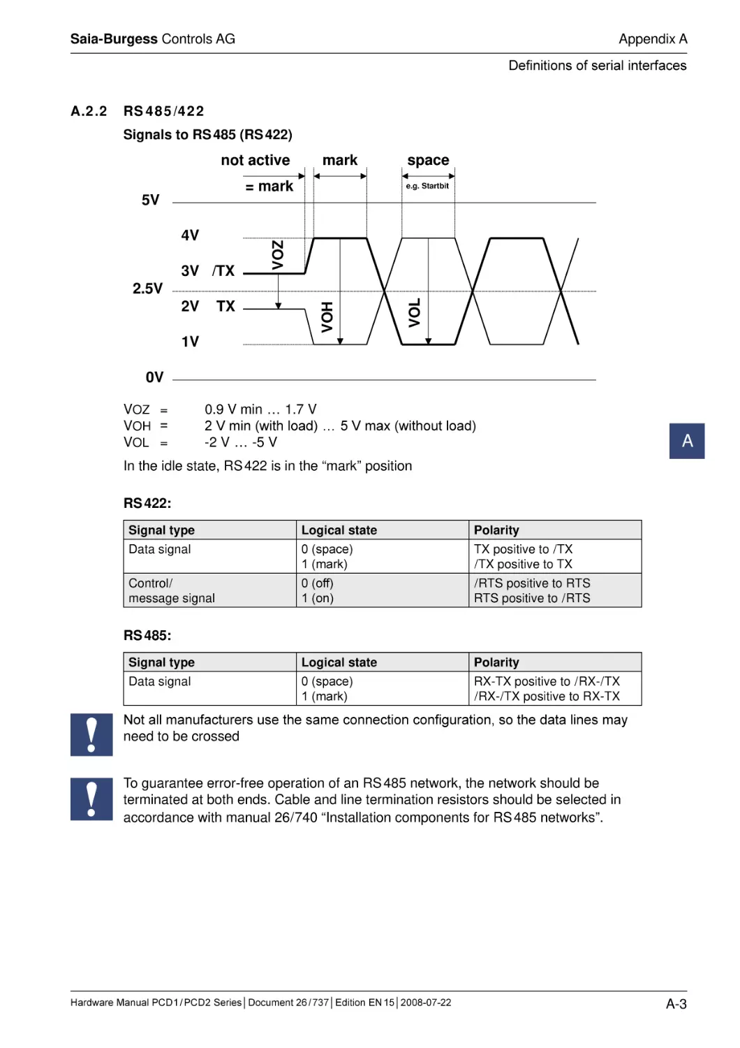
Definitions of serial interfaces..........................................................................
A.2.1 RS 232............................................................................................................
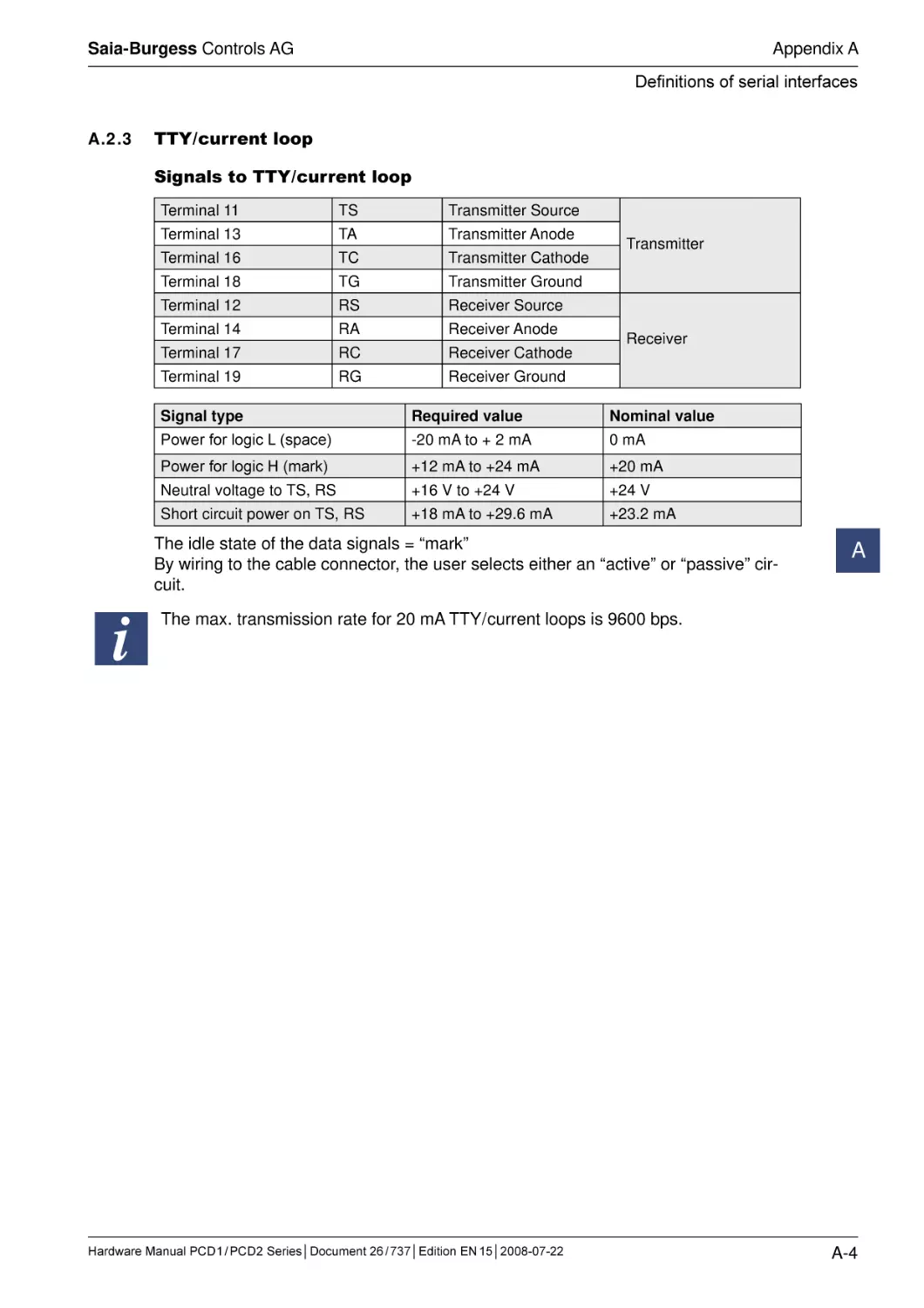
A.2.3 TTY/ current loop............................................................................................
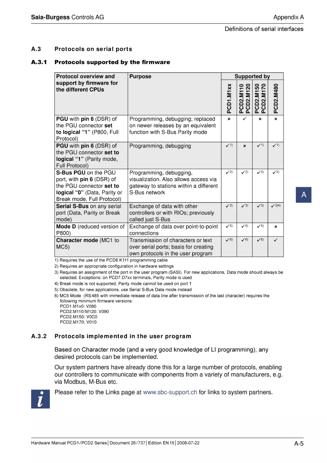
A.3
Protocols on serial ports..................................................................................
A.3.1 Protocols supported by the firmware.............................................................
A.3.2 Protocols implemented in the user program..................................................
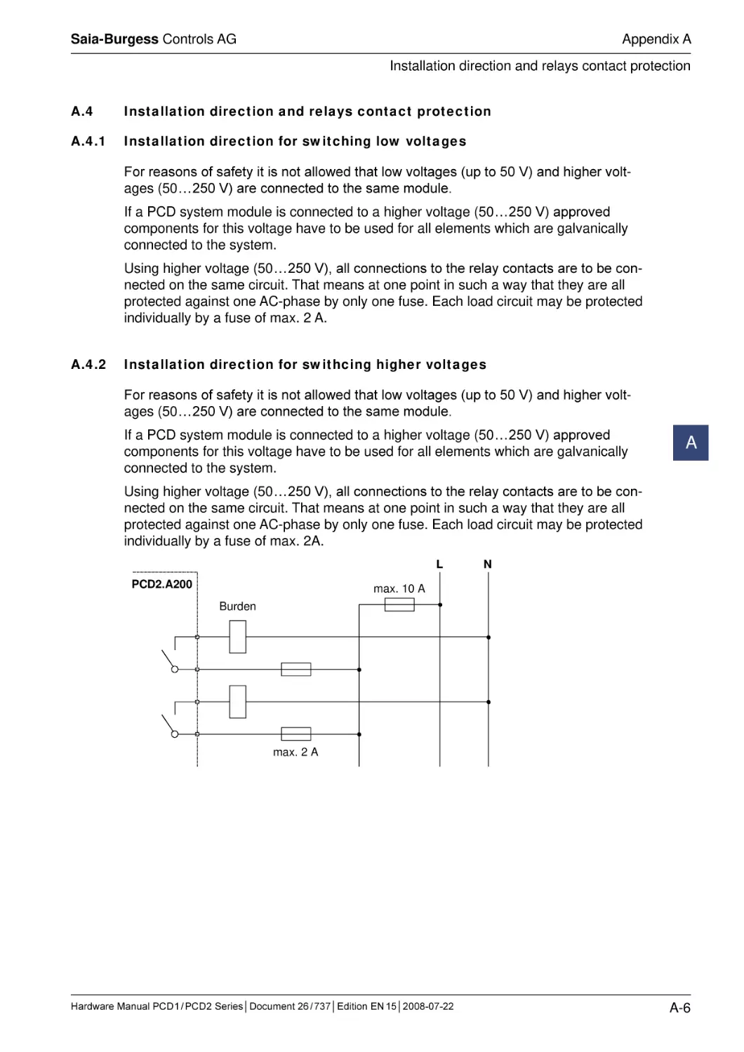
A.4
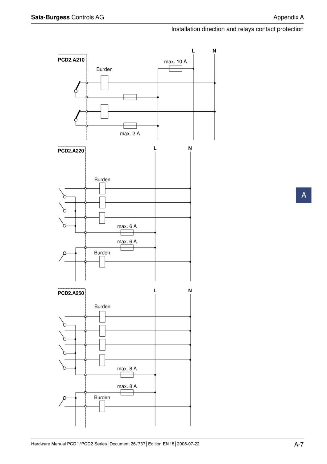
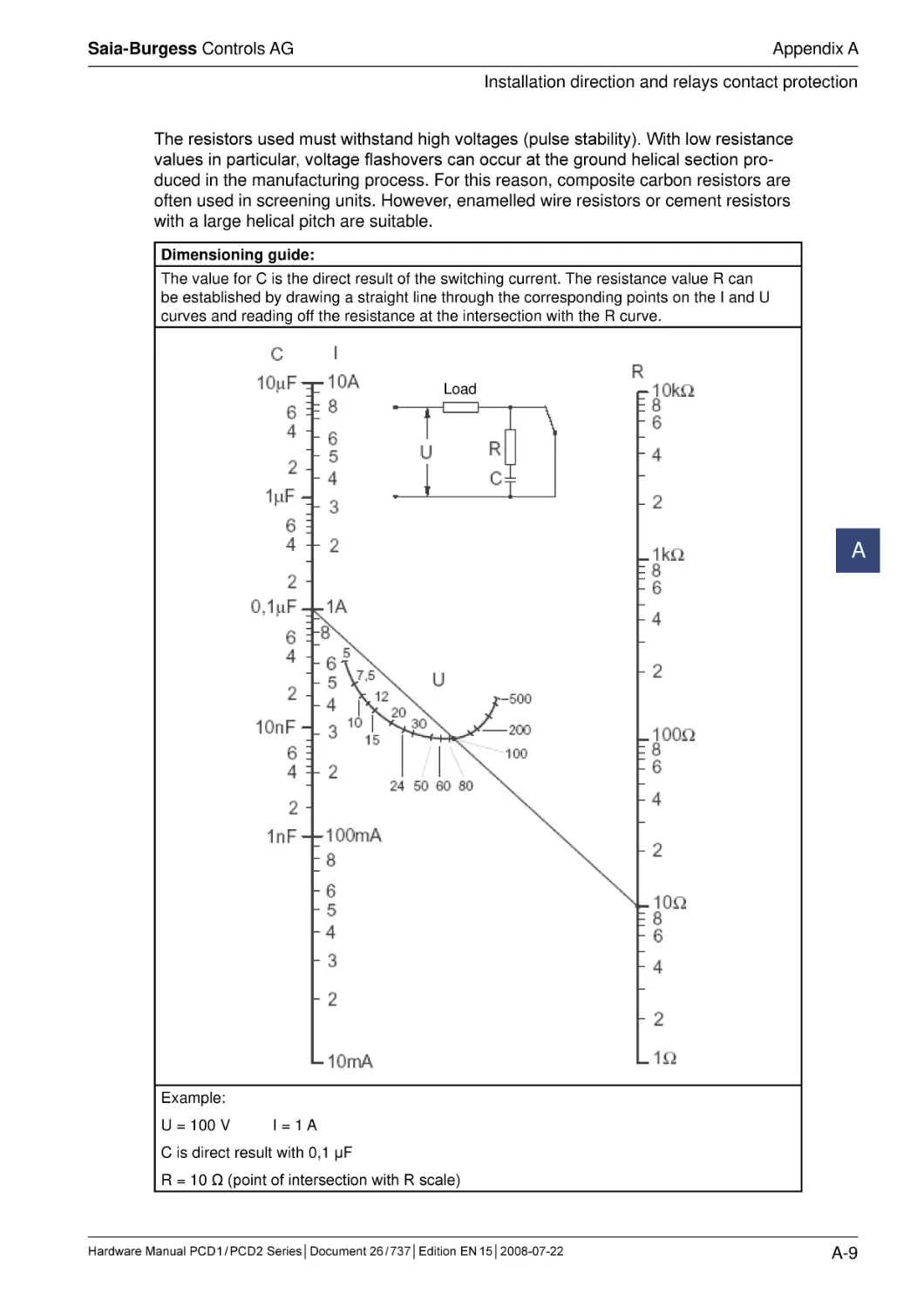
Installation direction and relays contact protection..........................................
A.4.1 Installation direction for switching low voltages.............................................
A.4.2 Installation direction for swithcing higher voltages.........................................
A.4.3 Switching inductive loads...............................................................................
A.4.4 Relay manufacturer’s information on RC unit dimensioning..........................
A.4
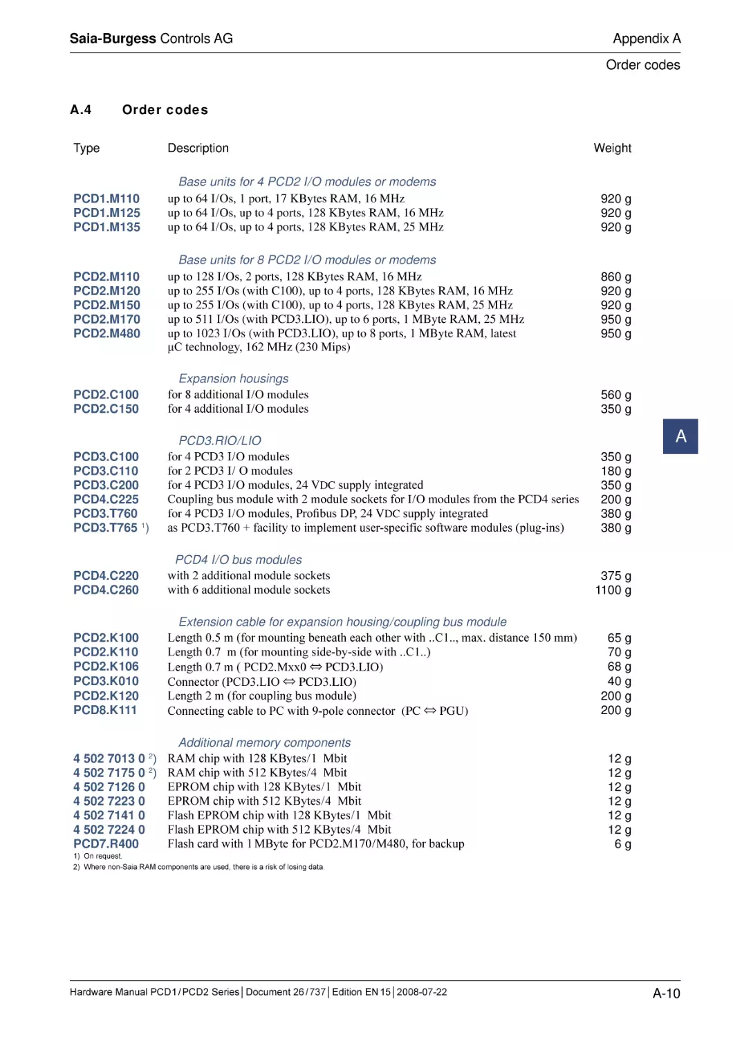
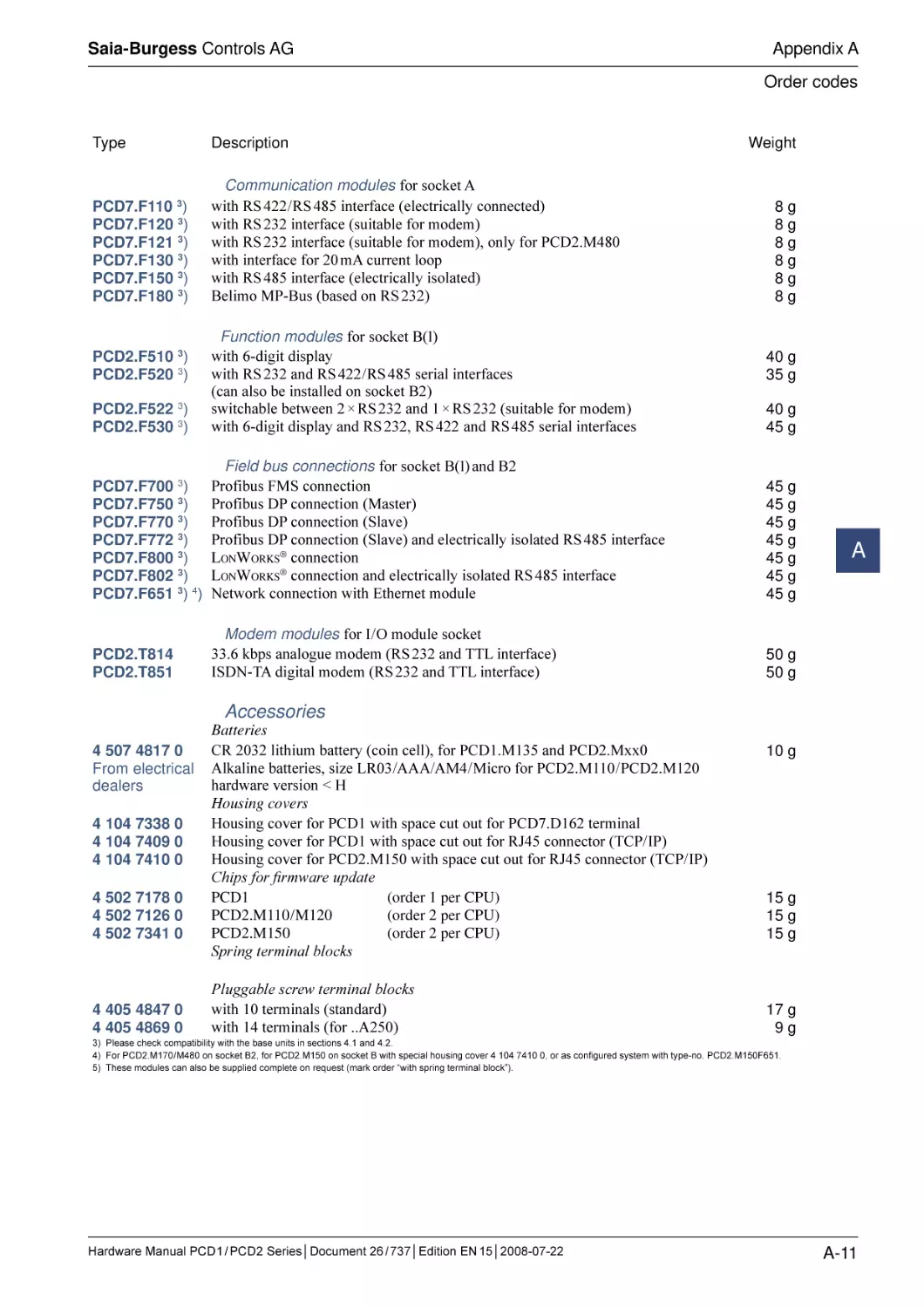
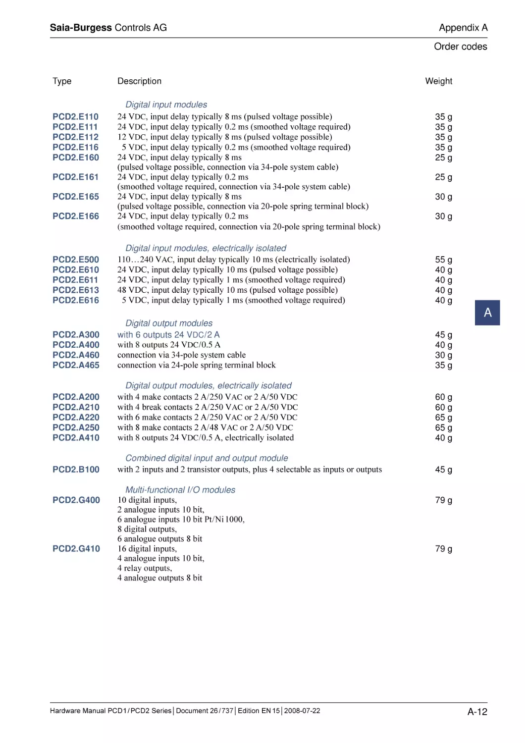
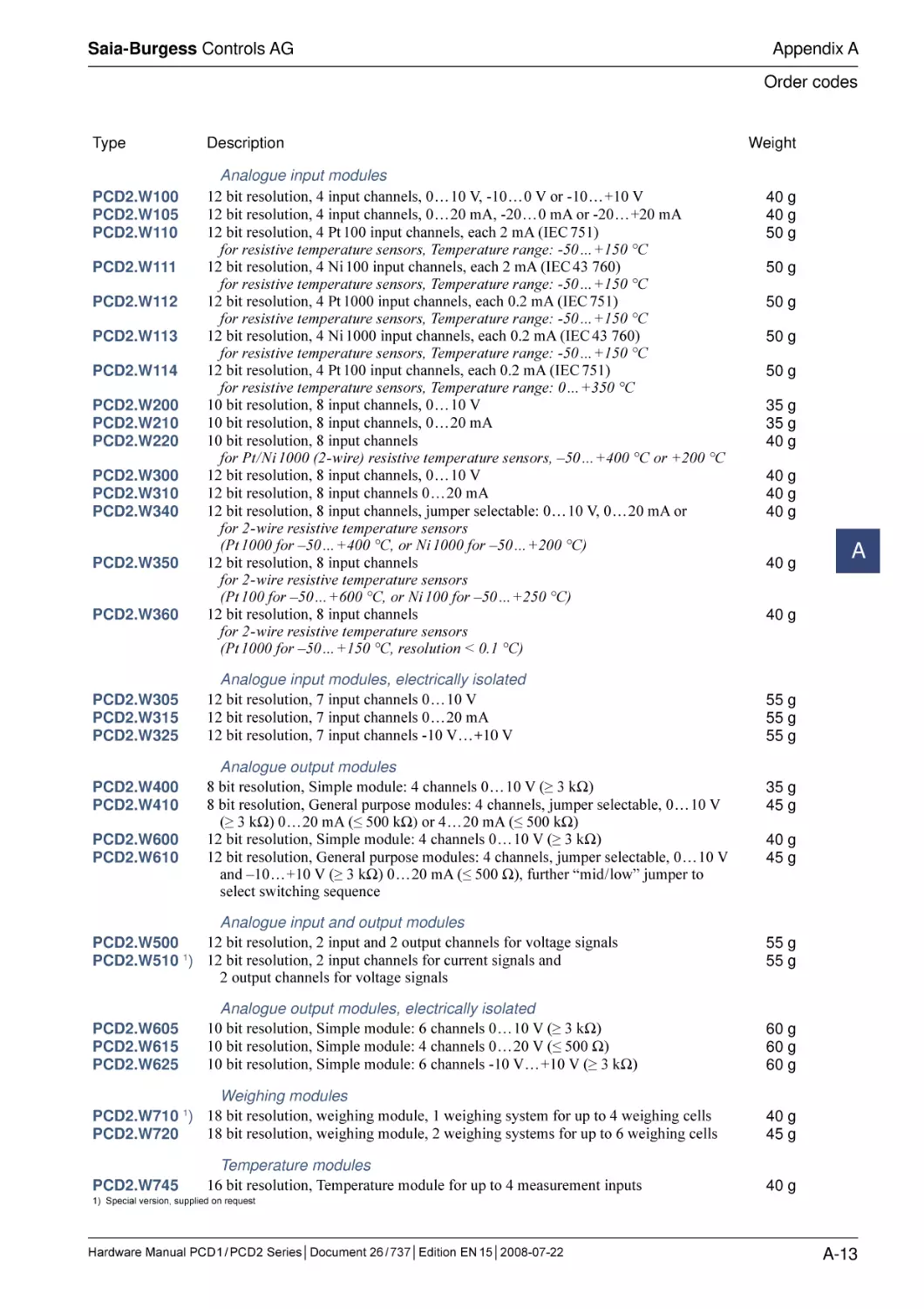
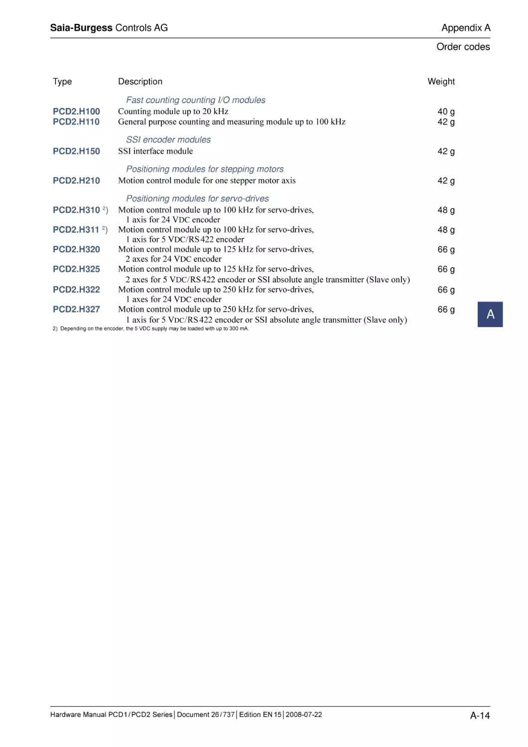
Order codes.....................................................................................................
A.5
Address of Saia-Burgess Controls AG.............................................................
A-1
A-2
A-2
A-4
A-5
A-5
A-5
A-6
A-6
A-6
A-8
A-8
A-10
A-15
A.1
A.2
Hardware Manual PCD 1 / PCD 2 Series│Document 26 / 737│Edition EN 15│2008-07-22
0
0-5
Saia-Burgess Controls AG
Contents
0.1 ����������������
Document history
Published
Version
24.12.2004
E11a
01.02.2005
E12
11.10.2005
E13
2007-07-25
E14
0
Changed
Whole Doc.
Chapt. 4.8.1
Page 57
Chapt. 0
Chapt. 1
Chapt. 3
Chapt. 5
Chapt. 3
Chapt. 4
Chapt. 5
Chapt. A
2008-07-22
0.2
E15
Chapt. 5
Remarks
-
translation from D11
error in Profibus: 4.8.1 new
error in formulas: Page 57
error in index (Acrobat)
error in graphical index M480
watch-Dog IL-Example.: new
corrected error in pin allocation PCD2.A465
- inserted new controllers PCD1.M1x5
- added communications modules PCD7.F121
and PCD2.T500
- new order for the I/O-modules, according to
the price list
- maximal current of the I/O-modules instead
of typical current.
- added new I/O-Modules PCD2.E112, PCD2.
E116, PCD2.E613, PCD2.E616
- PCD2.A465 pinout corrected
- new TIP by PCD2.W2x0, wrong polarity on
input
- description of the Jumper positions for
PCD2.K525
- calculation of the spark deletion in the appendix
- Added new module PCD2.W525
Trademarks
Saia® and Saia® PCD are registered trademarks of Saia-Burgess Controls AG.
STEP7® ,SIMATIC®, S7-300®, S7-400®, and Siemens® are registered trademarks of
Siemens AG.
Technical changes are subject to the state of technology.
Saia-Burgess Controls AG, 2003. © All rights reserved.
Published in Switzerland
Hardware Manual PCD 1 / PCD 2 Series│Document 26 / 737│Edition EN 15│2008-07-22
0-6
Saia-Burgess Controls AG
Graphical index
PCD1.M1xx
1 ���������������
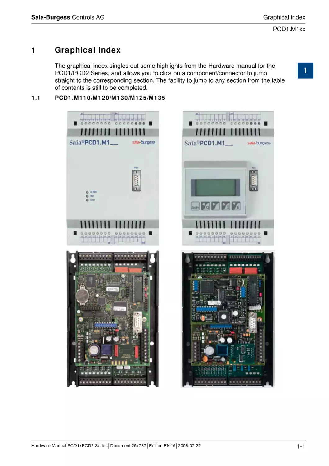
Graphical index
The graphical index singles out some highlights from the Hardware manual for the
PCD1/PCD2 Series, and allows you to click on a component/connector to jump
straight to the corresponding section. The facility to jump to any section from the table
of contents is still to be completed.
1.1
1
PCD1.M110/M120/M130/M125/M135
Hardware Manual PCD 1 / PCD 2 Series│Document 26 / 737│Edition EN 15│2008-07-22
1-1
Saia-Burgess Controls AG
Graphical index
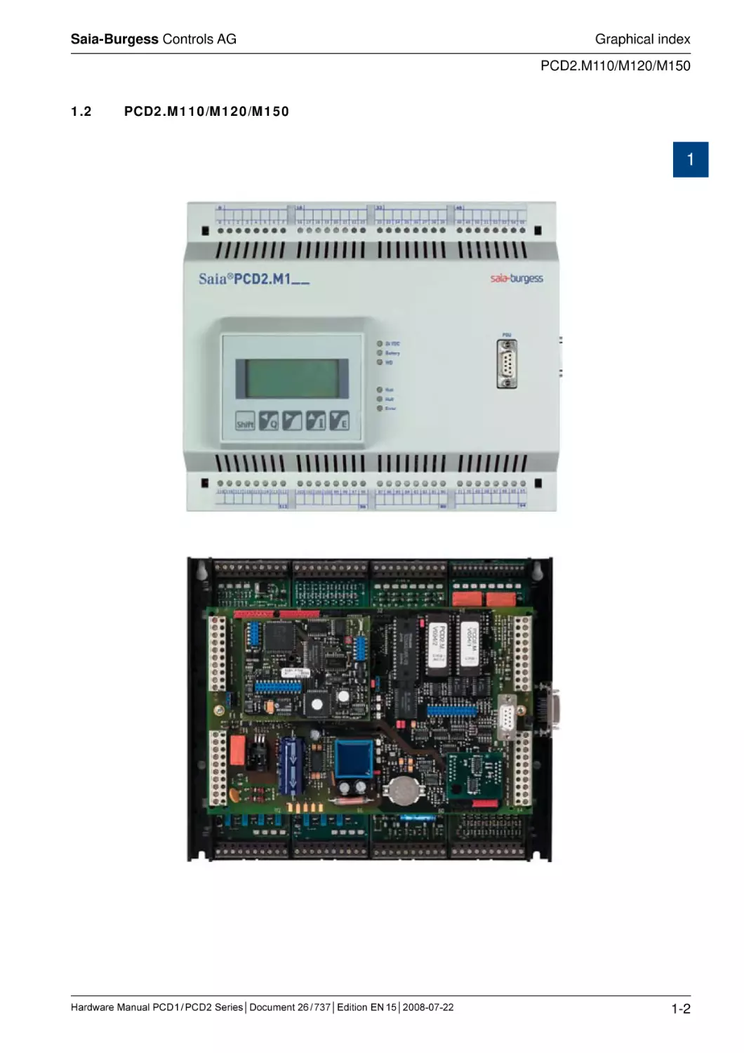
PCD2.M110/M120/M150
1.2
PCD2.M110/M120/M150
1
Hardware Manual PCD 1 / PCD 2 Series│Document 26 / 737│Edition EN 15│2008-07-22
1-2
Saia-Burgess Controls AG
Graphical index
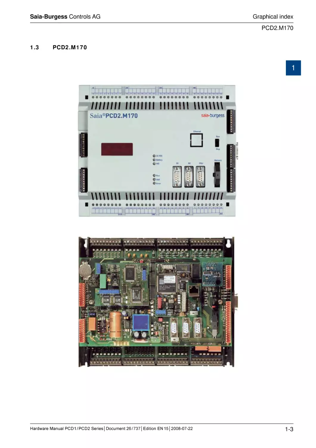
PCD2.M170
1.3
PCD2.M170
1
Hardware Manual PCD 1 / PCD 2 Series│Document 26 / 737│Edition EN 15│2008-07-22
1-3
Saia-Burgess Controls AG
Graphical index
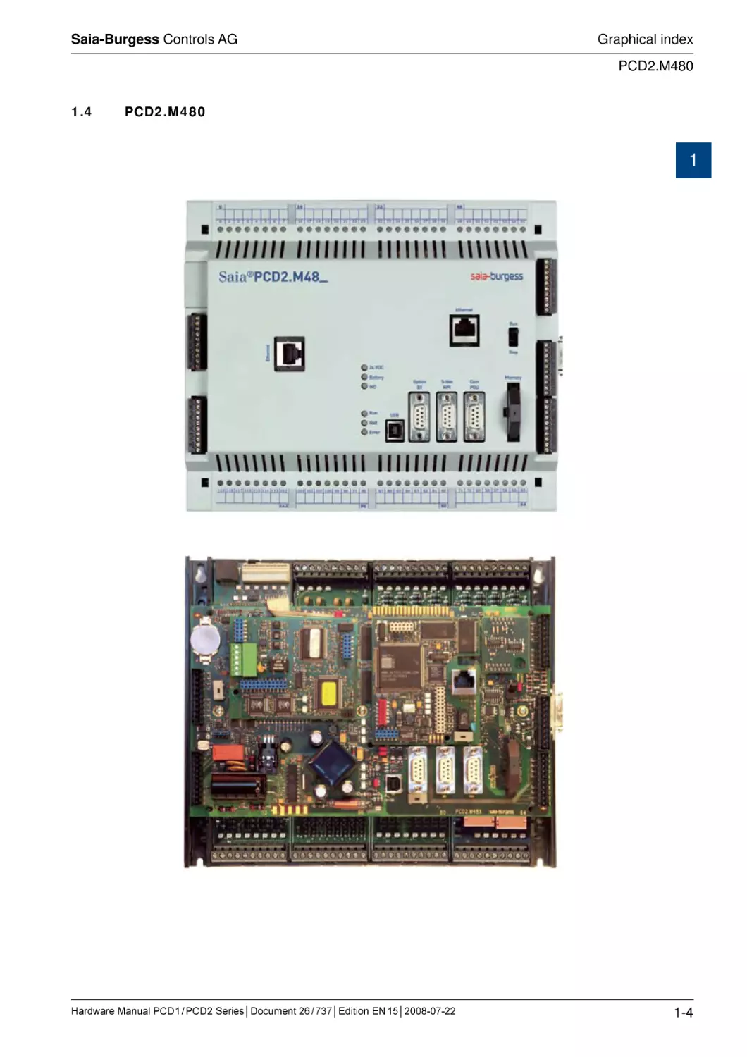
PCD2.M480
1.4
PCD2.M480
1
Hardware Manual PCD 1 / PCD 2 Series│Document 26 / 737│Edition EN 15│2008-07-22
1-4
Saia-Burgess Controls AG
Guidance
Introduction
2
Guidance
2.1
Introduction
This manual covers the technical aspects of the PCD1 and PCD2 components. The
following terms are used frequently:
● CPU
Central processing unit: the heart of the PCD
● RIOs
Remote I/Os: inputs and outputs connected to the CPU via a
field bus such as Profibus
● LIOs
Local I/Os: these are connected to the CPU via the I/O bus or a
RIO (i.e. with the shortest possible cables)
● Modules
Input/output elements, mounted in a housing, matched to the
PCD1/2 system
2
● Module holders CPUs, RIOs or LIOs, to which modules may be attached
The aim of the Overview section is to present the essentials of planning and installing
control systems with PCD1/2 components. It covers the following topics:
●
Planning an application
●
Cabling
Details of hardware, software, configuration, maintenance and troubleshooting are
described in separate sections.
Hardware Manual PCD 1 / PCD 2 Series│Document 26 / 737│Edition EN 15│2008-07-22
2-1
Saia-Burgess Controls AG
Guidance
Planning an application with PCD1/2/3 components
2.2
Planning an application with PCD1/2/3 components
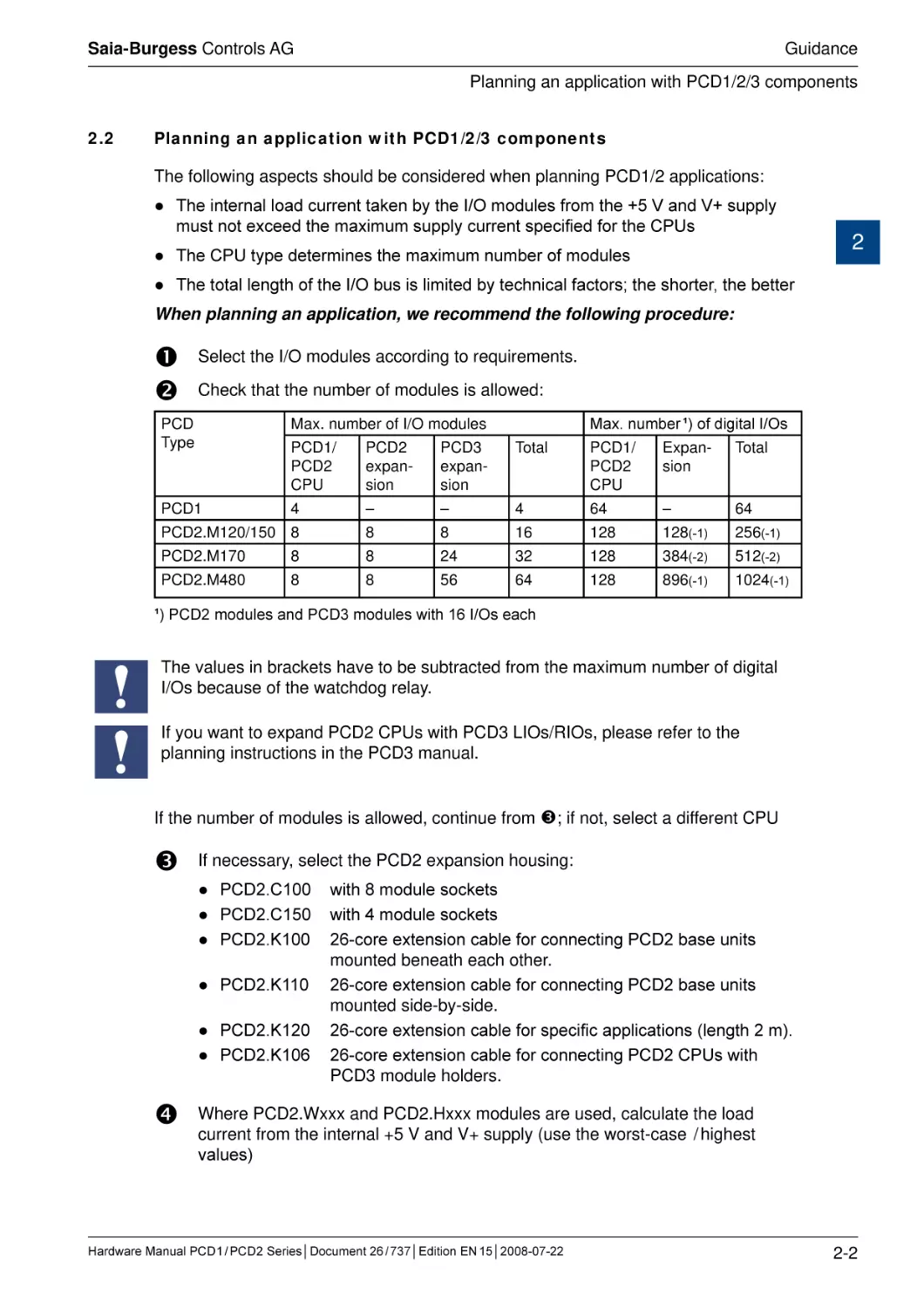
The following aspects should be considered when planning PCD1/2 applications:
● The internal load current taken by the I/O modules from the +5 V and V+ supply
must not exceed the maximum supply current specified for the CPUs
● The CPU type determines the maximum number of modules
2
● The total length of the I/O bus is limited by technical factors; the shorter, the better
When planning an application, we recommend the following procedure:
Select the I/O modules according to requirements.
Check that the number of modules is allowed:
Max. number ¹) of digital I/Os
PCD
Type
Max. number of I/O modules
PCD1/
PCD2
CPU
PCD2
expansion
PCD3
expansion
Total
PCD1/
PCD2
CPU
Expansion
Total
PCD1
4
–
–
4
64
–
64
PCD2.M120/150 8
8
8
16
128
128(-1)
256(-1)
PCD2.M170
8
8
24
32
128
384(-2)
512(-2)
PCD2.M480
8
8
56
64
128
896(-1)
1024(-1)
¹) PCD2 modules and PCD3 modules with 16 I/Os each
The values in brackets have to be subtracted from the maximum number of digital
I/Os because of the watchdog relay.
If you want to expand PCD2 CPUs with PCD3 LIOs/RIOs, please refer to the
planning instructions in the PCD3 manual.
If the number of modules is allowed, continue from ; if not, select a different CPU
If necessary, select the PCD2 expansion housing:
● PCD2.C100
● PCD2.C150
● PCD2.K100
● PCD2.K110
● PCD2.K120
● PCD2.K106
with 8 module sockets
with 4 module sockets
26-core extension cable for connecting PCD2 base units
mounted beneath each other.
26-core extension cable for connecting PCD2 base units
mounted side-by-side.
26-core extension cable for specific applications (length 2 m).
26-core extension cable for connecting PCD2 CPUs with
PCD3 module holders.
Where PCD2.Wxxx and PCD2.Hxxx modules are used, calculate the load
current from the internal +5 V and V+ supply (use the worst-case / highest
values)
Hardware Manual PCD 1 / PCD 2 Series│Document 26 / 737│Edition EN 15│2008-07-22
2-2
Saia-Burgess Controls AG
Guidance
Planning an application with PCD1/2/3 components
Check that the max. supply current for the CPU is sufficient; it generally should
be. In extreme cases, switch to PCD3 expansion units.
Estimate consumption from the 24 V supply. Use estimated values from the
section on “Hardware”.
These estimated values can be found in section 3.8.5, “Power consumption of
PCD2/PCD3 input/output modules”.
2
Note that in most applications the outputs place the heaviest load on the 24 V supply. For 16 outputs with a load current of 0.5 A each, the loading will be 8 A with all
outputs connected.
Hardware Manual PCD 1 / PCD 2 Series│Document 26 / 737│Edition EN 15│2008-07-22
2-3
Saia-Burgess Controls AG
Guidance
Cabling
2.3
Cabling
2.3.1
Cable routing
● 230 V supply lines and signal lines must be laid in separate cables at least 10 cm
apart. Even within the switching cabinet, it is advisable to leave space between
power and signal lines.
2
● Digital signal / bus lines and analogue signal / sensor lines should be laid in
separate cables
● It is advisable to use shielded cables for analogue signal lines.
● The shield should be earthed at the entry or exit to the switching cabinet. The
shields should be as short as possible and of the largest possible cross-section.
The central earthing point should be > 10 mm² and connected to the PE ground
wire by the shortest route
● The shield is generally connected to one side of the switching cabinet only, unless
there is a potential equalization with significantly lower resistance than the shield
resistance
● Inductivities installed in the same switching cabinet, e.g. contactor coils, should be
provided with suitable suppressors (RC elements)
● Switching cabinet components with high field intensity, e.g. transformers or
frequency inverters, should be shielded with separator plates with a good ground
connection.
Surge protection for long distances or external lines
● Where lines are laid outside the building, or over longer distances, suitable surge
protection measures should be applied. For bus lines in particular, these measures
are essential.
● With lines laid outside, the shield must have adequate current-carrying capacity
and be earthed at both ends.
● The surge conductors should be installed at the input to the switching cabinet.
Hardware Manual PCD 1 / PCD 2 Series│Document 26 / 737│Edition EN 15│2008-07-22
2-4
Saia-Burgess Controls AG
CPUs and expansion housings
System overview
3 ���������������������������������������
PCD Classic CPUs and expansion housings
The CPUs in the xx7 Series are described in a separate manual, 26/757.
3.1
System overview
Saia® PCD Web-Server
3
The Saia® PCD controllers PCD1.M125, PCD1.M135, PCD2.M150, PCD2.M170,
PCD2.M480 and PCD3.Mxxx0 come with an integrated web server as standard:
●
Web browser as a tool for ����������������������������������������
comissioning����������������������������
, support and visualization:
®
Access to the Saia Web server is via standard web browsers such as Internet
Explorer or Netscape Navigator. This makes the web browser, which can be
operated intuitively by anyone, the standard tool for comissioning, service,
support and visualization of machines, units and installations. The user can
retrieve pre-defined device and system-specific HTML pages, giving access to
all data on controllers and RIOs. Graphical elements (images, diagrams etc.) as
well as text documents (operating and repair manuals) can also be integrated
into the HTML pages, to provide a personalized user interface
●
General access to any desired interfaces and networks:
Access to the web server is available not only via Ethernet TCP/IP, but also via
cost-effective standard serial interfaces (RS 232, RS 485, modem etc.) and via
Profibus networks, throughout the system and at different levels in the network.
This makes it economical to use web technology to operate and monitor even
the smallest applications.
●
The Saia® PCD web server is integrated into all products:
Having a web server integrated as standard eliminates the cost of run-time
licenses or additional modules. In the Saia® PCD3 controllers enumerated
above and the Saia® PCD3 RIOs, the web server is already included in the
base units, at no extra cost.
Hardware Manual PCD 1 / PCD 2 Series│Document 26 / 737│Edition EN 15│2008-07-22
3-1
Saia-Burgess Controls AG
CPUs and expansion housings
General technical details
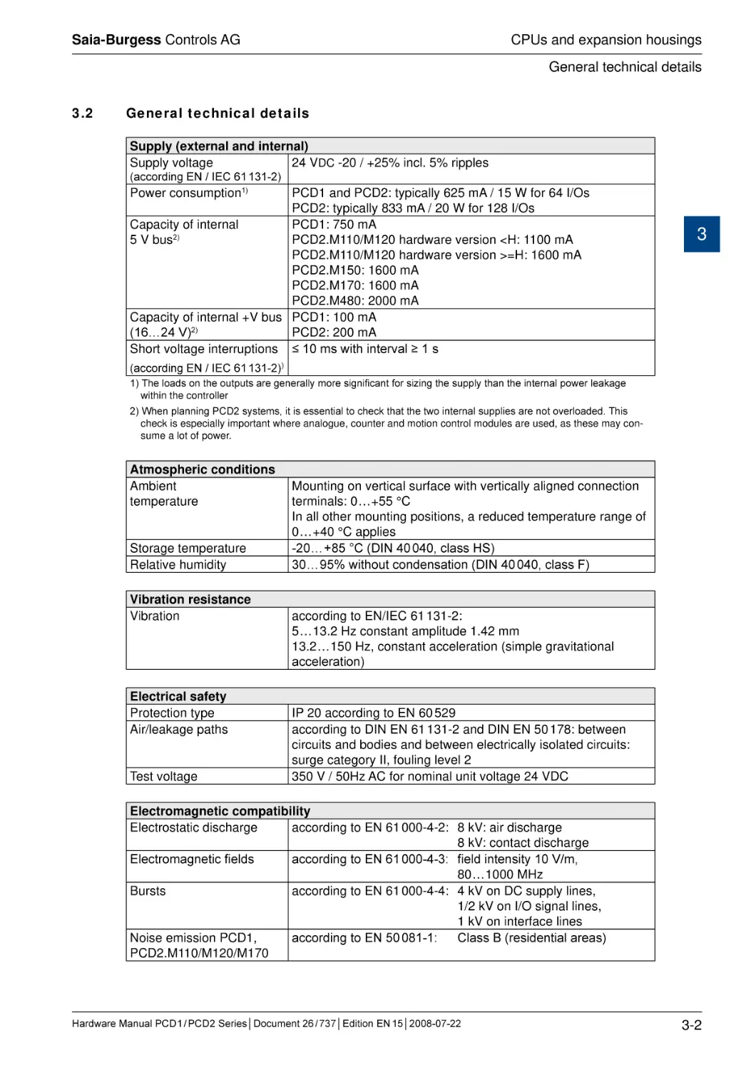
3.2
General technical details
Supply (external and internal)
Supply voltage
24 VDC -20 / +25% incl. 5% ripples
(according EN / IEC 61 131-2)
Power consumption1)
PCD1 and PCD2: typically 625 mA / 15 W for 64 I/Os
PCD2: typically 833 mA / 20 W for 128 I/Os
Capacity of internal
PCD1: 750 mA
5 V bus2)
PCD2.M110/M120 hardware version <H: 1100 mA
PCD2.M110/M120 hardware version >=H: 1600 mA
PCD2.M150: 1600 mA
PCD2.M170: 1600 mA
PCD2.M480: 2000 mA
Capacity of internal +V bus PCD1: 100 mA
(16…24 V)2)
PCD2: 200 mA
Short voltage interruptions ≤ 10 ms with interval ≥ 1 s
3
(according EN / IEC 61 131-2))
1) The loads on the outputs are generally more significant for sizing the supply than the internal power leakage
within the controller
2) When planning PCD2 systems, it is essential to check that the two internal supplies are not overloaded. This
check is especially important where analogue, counter and motion control modules are used, as these may consume a lot of power.
Atmospheric conditions
Ambient
temperature
Storage temperature
Relative humidity
Vibration resistance
Vibration
Electrical safety
Protection type
Air/leakage paths
Test voltage
Mounting on vertical surface with vertically aligned connection
terminals: 0 … +55 °C
In all other mounting positions, a reduced temperature range of
0 … +40 °C applies
-20 … +85 °C (DIN 40 040, class HS)
30 … 95% without condensation (DIN 40 040, class F)
according to EN/IEC 61 131-2:
5 … 13.2 Hz constant amplitude 1.42 mm
13.2 … 150 Hz, constant acceleration (simple gravitational
acceleration)
IP 20 according to EN 60 529
according to DIN EN 61 131-2 and DIN EN 50 178: between
circuits and bodies and between electrically isolated circuits:
surge category II, fouling level 2
350 V / 50Hz AC for nominal unit voltage 24 VDC
Electromagnetic compatibility
Electrostatic discharge
according to EN 61 000-4-2: 8 kV: air discharge
8 kV: contact discharge
Electromagnetic fields
according to EN 61 000-4-3: field intensity 10 V/m,
80 … 1000 MHz
Bursts
according to EN 61 000-4-4: 4 kV on DC supply lines,
1/2 kV on I/O signal lines,
1 kV on interface lines
Noise emission PCD1,
according to EN 50 081-1:
Class B (residential areas)
PCD2.M110/M120/M170
Hardware Manual PCD 1 / PCD 2 Series│Document 26 / 737│Edition EN 15│2008-07-22
3-2
Saia-Burgess Controls AG
CPUs and expansion housings
General technical details
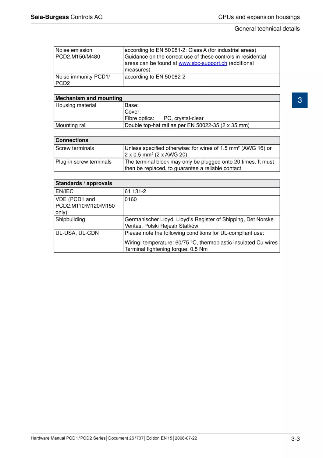
Noise emission
PCD2.M150/M480
Noise immunity PCD1/
PCD2
according to EN 50 081-2: Class A (for industrial areas)
Guidance on the correct use of these controls in residential
areas can be found at www.sbc-support.ch (additional
measures).
according to EN 50 082-2
Mechanism and mounting
Housing material
Base:
Cover:
Fibre optics:
PC, crystal-clear
Mounting rail
Double top-hat rail as per EN 50022-35 (2 x 35 mm)
Connections
Screw terminals
Plug-in screw terminals
Standards / approvals
EN/IEC
VDE (PCD1 and
PCD2.M110/M120/M150
only)
Shipbuilding
UL-USA, UL-CDN
3
Unless specified otherwise: for wires of 1.5 mm2 (AWG 16) or
2 x 0.5 mm2 (2 x AWG 20)
The terminal block may only be plugged onto 20 times. It must
then be replaced, to guarantee a reliable contact
61 131-2
0160
Germanischer Lloyd, Lloyd’s Register of Shipping, Det Norske
Veritas, Polski Rejestr Statków
Please note the following conditions for UL-compliant use:
Wiring: temperature: 60/75 °C, thermoplastic insulated Cu wires
Terminal tightening torque: 0.5 Nm
Hardware Manual PCD 1 / PCD 2 Series│Document 26 / 737│Edition EN 15│2008-07-22
3-3
Saia-Burgess Controls AG
CPUs and expansion housings
System resources
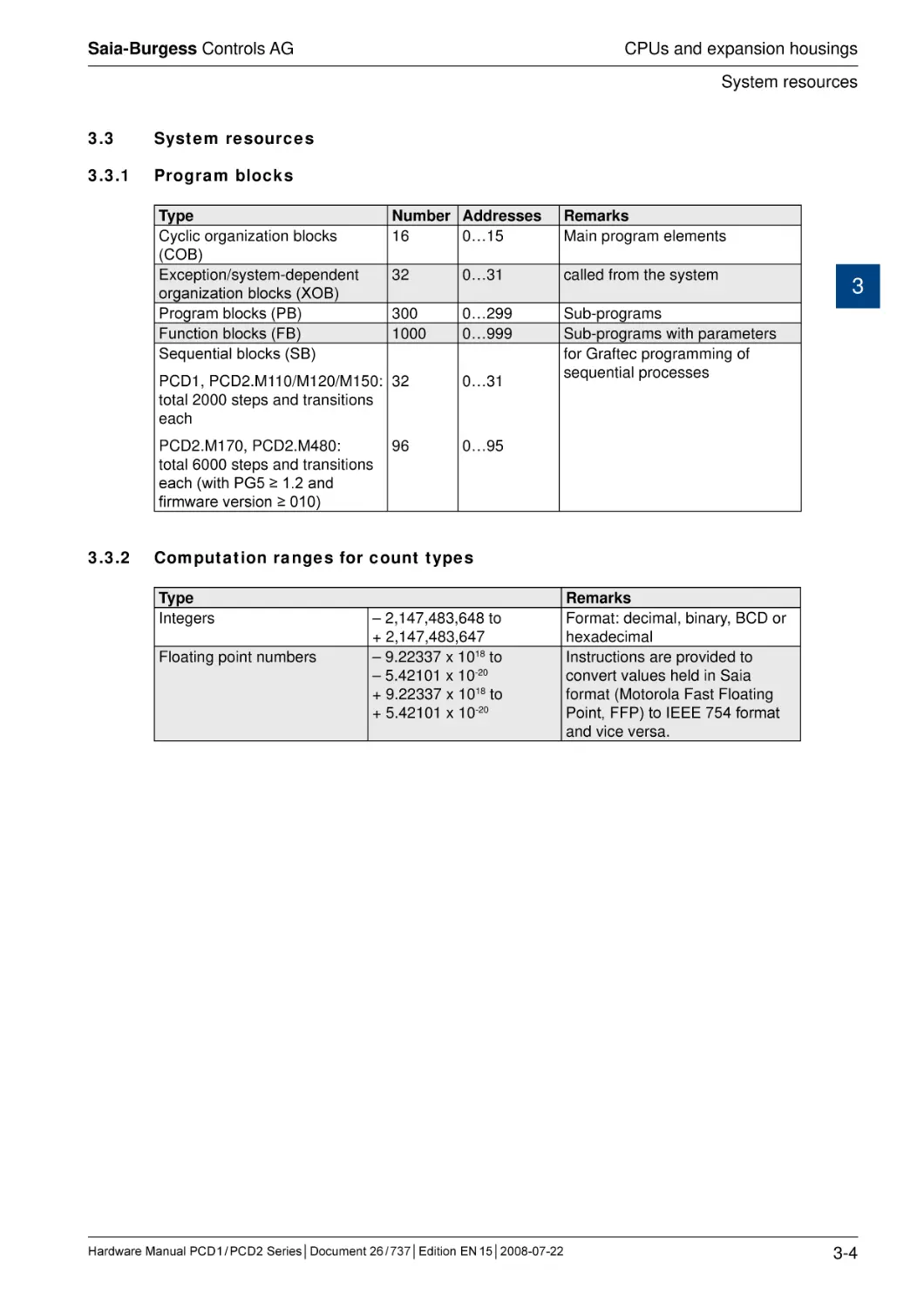
3.3
System resources
3.3.1
Program blocks
Type
Cyclic organization blocks
(COB)
Exception/system-dependent
organization blocks (XOB)
Program blocks (PB)
Function blocks (FB)
Sequential blocks (SB)
3.3.2
Number Addresses
16
0…15
Remarks
Main program elements
32
0…31
called from the system
300
1000
0…299
0…999
Sub-programs
Sub-programs with parameters
for Graftec programming of
sequential processes
PCD1, PCD2.M110/M120/M150: 32
total 2000 steps and transitions
each
0…31
PCD2.M170, PCD2.M480:
total 6000 steps and transitions
each (with PG5 ≥ 1.2 and
firmware version ≥ 010)
0…95
96
3
Computation ranges for count types
Type
Integers
Floating point numbers
– 2,147,483,648 to
+ 2,147,483,647
– 9.22337 x 10¹⁸ to
– 5.42101 x 10⁻²⁰
+ 9.22337 x 10¹⁸ to
+ 5.42101 x 10⁻²⁰
Hardware Manual PCD 1 / PCD 2 Series│Document 26 / 737│Edition EN 15│2008-07-22
Remarks
Format: decimal, binary, BCD or
hexadecimal
Instructions are provided to
convert values held in Saia
format (Motorola Fast Floating
Point, FFP) to IEEE 754 format
and vice versa.
3-4
Saia-Burgess Controls AG
CPUs and expansion housings
System resources
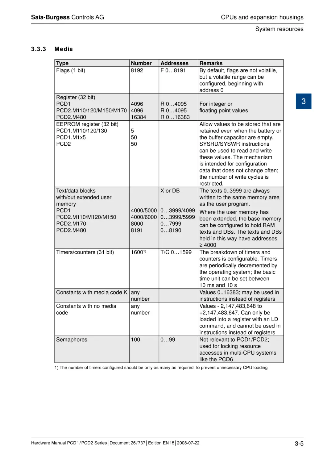
3.3.3
Media
Type
Flags (1 bit)
Register (32 bit)
PCD1
PCD2.M110/120/M150/M170
PCD2.M480
EEPROM register (32 bit)
PCD1.M110/120/130
PCD1.M1x5
PCD2
Number
8192
Addresses
F 0…8191
Remarks
By default, flags are not volatile,
but a volatile range can be
configured, beginning with
address 0
4096
4096
16384
R 0…4095
R 0…4095
R 0…16383
For integer or
floating point values
3
Allow values to be stored that are
retained even when the battery or
the buffer capacitor are empty.
SYSRD/SYSWR instructions
can be used to read and write
these values. The mechanism
is intended for configuration
d���������������������������������
ata that does not change often;
the number of write cycles is
restricted.
Text/data blocks
X or DB
The texts 0..3999 are always
with/out extended user
written to the same memory area
memory
as the user program.
PCD1
4000/5000 0…3999/4099 Where the user memory has
PCD2.M110/M120/M150
4000/6000 0…3999/5999 been extended, the base memory
PCD2.M170
8000
0…7999
can be configured to hold RAM
PCD2.M480
8191
0…8190
texts and DBs. The texts and DBs
held in this way have addresses
≥ 4000
Timers/counters (31 bit)
16001)
T/C 0…1599 The breakdown of timers and
counters is configurable. Timers
are periodically decremented by
the operating system; the basic
time unit can be set between
10 ms and 10 s
Constants with media code K any
Values 0..16383; may be used in
number
instructions instead of registers
Constants with no media
any
Values - 2,147,483,648 to
code
number
+2,147,483,647. Can only be
loaded into a register with an LD
command, and cannot be used in
instructions instead of registers
Semaphores
100
0…99
Not relevant to PCD1/PCD2;
used for locking resource
accesses in multi-CPU systems
like the PCD6
5
50
50
1) The number of timers configured should be only as many as required, to prevent unnecessary CPU loading
Hardware Manual PCD 1 / PCD 2 Series│Document 26 / 737│Edition EN 15│2008-07-22
3-5
Saia-Burgess Controls AG
CPUs and expansion housings
System resources
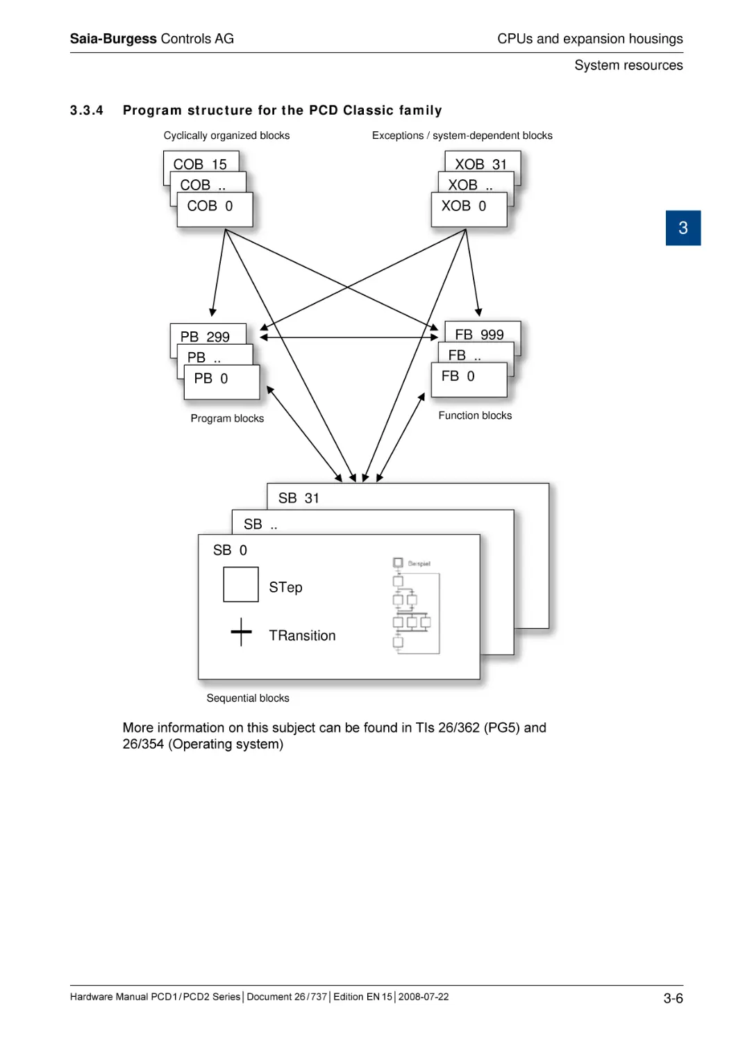
3.3.4
Program structure for the PCD Classic family
Cyclically organized blocks
COB 15
COB ..
COB 0
Exceptions / system-dependent blocks
XOB 31
XOB ..
XOB 0
3
FB 999
FB ..
FB 0
PB 299
PB ..
PB 0
Function blocks
Program blocks
SB 31
SB ..
SB 0
STep
TRansition
Sequential blocks
More information on this subject can be found in TIs 26/362 (PG5) and
26/354 (Operating system)
Hardware Manual PCD 1 / PCD 2 Series│Document 26 / 737│Edition EN 15│2008-07-22
3-6
Saia-Burgess Controls AG
CPUs and expansion housings
CPU overview
3.4
CPU overview
3.4.1
PCD1.M1xx
3
Differentiation of
PCD1.M110 PCD1.M120 PCD1.M130 PCD1.M125 PCD1.M135
base units (general)
Number of inputs/outputs or
641)
I/O module sockets
4
I/O modules
all PCD2 I/O modules except PCD2.Gxxx
Processor
68340 @ 16 MHz
Processing time
Bit instruction
z.B.
ANH F 0
5 µs2)
����������������
Word instruction
Firmware
Minimum PG5 version
User memory
RAM basic set up
Expansion with RAM,
EPROM or
Flash EPROM
�����
Clock (RTC)
Data protection
Interrupt inputs
Maximum input frequency
z.B.
ADD R 0
20 µs2)
R1
R2
1 PROM in socket; from first
soldered Flash Memory
half of 2004 soldered PROMs
modules7)
1.0, for TCP/IP 1.1
1.3.120
1.3.120
17 Kbytes3)
128 KByte
up to 128 Kbytes added
128 … 512 KBytes
up to 128 Kbytes added
128 KBytes
up to 112 Kbytes added
112 … 448 KBytes
no4)
yes, deviation < 30 ppm (80 secs/month)
30 days 7 days with 1-3 years5) 7 days with 1-3 years5)
with
Super Cap
with
Super Cap
with
Super Cap
CR 2032
CR 2032
lithium
lithium
battery
battery
no
2
1 kHz6)
1) Using digital I/O modules PCD2.E16x or A46x with 16 I/Os each
2) Typical values; the processing time is dependent on the load on the communication ports
3) When extended memory is used, 13 Kbytes of the base memory can be used to store RAM texts and DBs (text/DB
addresses ≥ 4000)
4) When the HeaVAC library is used: The absence of the clock is reported as an error when processing the HeaVAC
initialization block, and the clock timers cannot be used
5) The period given is a buffer time; it is dependent on the ambient temperature (a higher temperature means a
shorter buffer time)
6) The 1 kHz applies with a pulse/pause ratio of 1:1 and refers to the total frequencies of the two inputs
7) Updates of the firmware via PGU possible
Hardware Manual PCD 1 / PCD 2 Series│Document 26 / 737│Edition EN 15│2008-07-22
3-7
Saia-Burgess Controls AG
CPUs and expansion housings
CPU overview
Differentiation of
base units (ports)
Programming interface
PCD1.M110
PCD1.M120 PCD1.M130 PCD1.M125 PCD1.M135
PGU port D-Sub socket, 9-pole1)
(for PCD8.K111 programming cable)
1
1
RS 422,
RS 232, RS 422/485, MP bus or
RS 485,
TTY current loop 20mA, plug-in (PCD7.F1xx
built-in
modules)
Saia® S-Bus
EthernetEthernetTCP/IP
TCP/IP
(Ether-S(Ether-SBus)2
Bus)2)
Profibus DP
LonWorks®
for
yes3)
PCD7.D162
terminal kit
only3)
Serial data port
Socket A
Field bus connections
Socket B for network
and/or data port, LED
display, small terminal
3
1) Can also be used as a serial data port, e.g. to connect a terminal; but this hampers troubleshooting with the
debugger
2) Ethernet TCP/IP available as a configured system: PCD1.M130F655 / PCD1.M135F655. If installed later, the cover
must be replaced (item-no. 4 104 7409 0)
3) We recommend ordering the PCD2.D16x terminal kit mounted on the controller. If installed later, the cover must be
replaced (item-no. 4 104 7338 0)
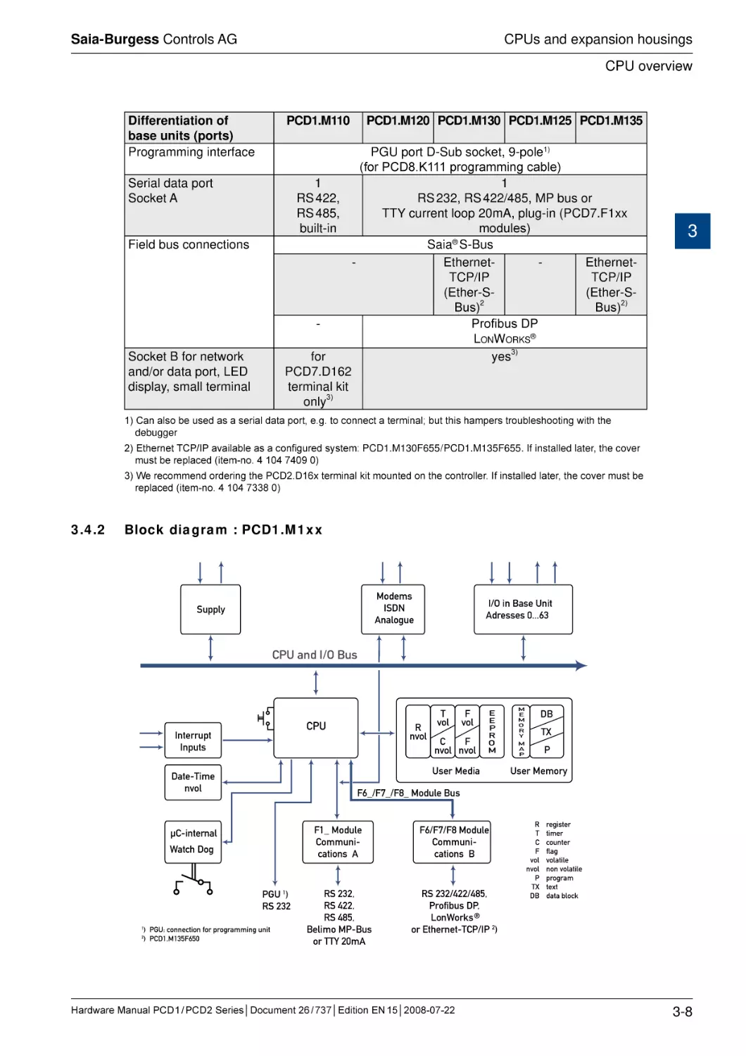
3.4.2
Block diagram : PCD1.M1xx
Modems
ISDN
Analogue
Supply
I/O in Base Unit
Adresses 0...63
CPU and I/O Bus
CPU
Interrupt
Inputs
C
F
nvol nvol
E
E
P
R
O
M
M
E
M
O
R
Y
DB
TX
M
A
P
P
User Memory
F6_/F7_/F8_ Module Bus
µC-internal
Watch Dog
PGU 1)
RS 232
2
F
vol
User Media
Date-Time
nvol
1
R
nvol
T
vol
) PGU: connection for programming unit
) PCD1.M135F650
F1_ Module
Communications A
F6/F7/F8 Module
Communications B
RS 232,
RS 422,
RS 485,
Belimo MP-Bus
or TTY 20mA
RS 232/422/485,
Profibus DP,
LonWorks ®
or Ethernet-TCP/IP 2)
Hardware Manual PCD 1 / PCD 2 Series│Document 26 / 737│Edition EN 15│2008-07-22
R
T
C
F
vol
nvol
P
TX
DB
register
timer
counter
flag
volatile
non volatile
program
text
data block
3-8
Saia-Burgess Controls AG
CPUs and expansion housings
CPU overview
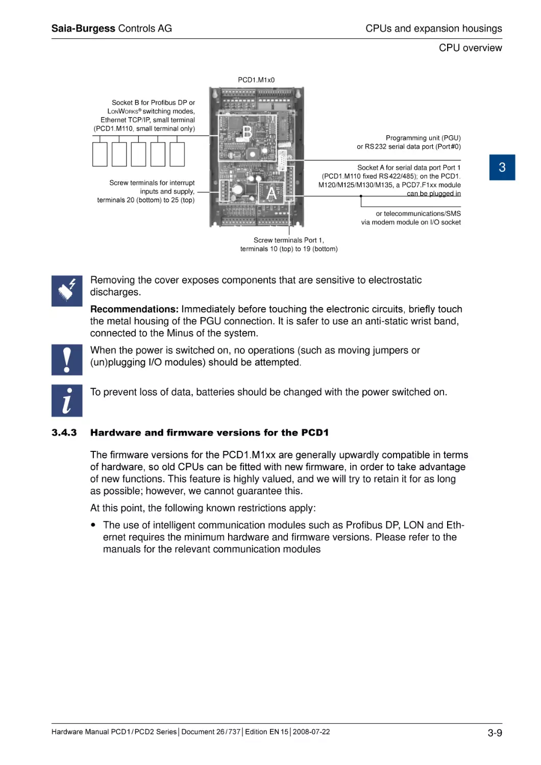
PCD1.M1x0
Socket B for Profibus DP or
LonWorks® switching modes,
Ethernet TCP/IP, small terminal
(PCD1.M110, small terminal only)
Screw terminals for interrupt
inputs and supply,
terminals 20 (bottom) to 25 (top)
B
Programming unit (PGU)
or RS 232 serial data port (Port #0)
A
Socket A for serial data port Port 1
(PCD1.M110 fixed RS 422/485); on the PCD1.
M120/M125/M130/M135, a PCD7.F1xx module
can be plugged in
3
or telecommunications/SMS
via modem module on I/O socket
Screw terminals Port 1,
terminals 10 (top) to 19 (bottom)
Removing the cover exposes components that are sensitive to electrostatic
discharges.
Recommendations: Immediately before touching the electronic circuits, briefly touch
the metal housing of the PGU connection. It is safer to use an anti-static wrist band,
connected to the Minus of the system.
When the power is switched on, no operations (such as moving jumpers or
(un)plugging I/O modules) should be attempted.
i
3.4.3
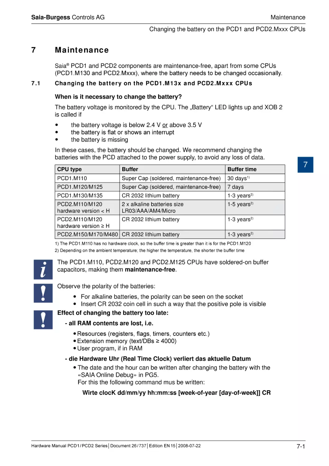
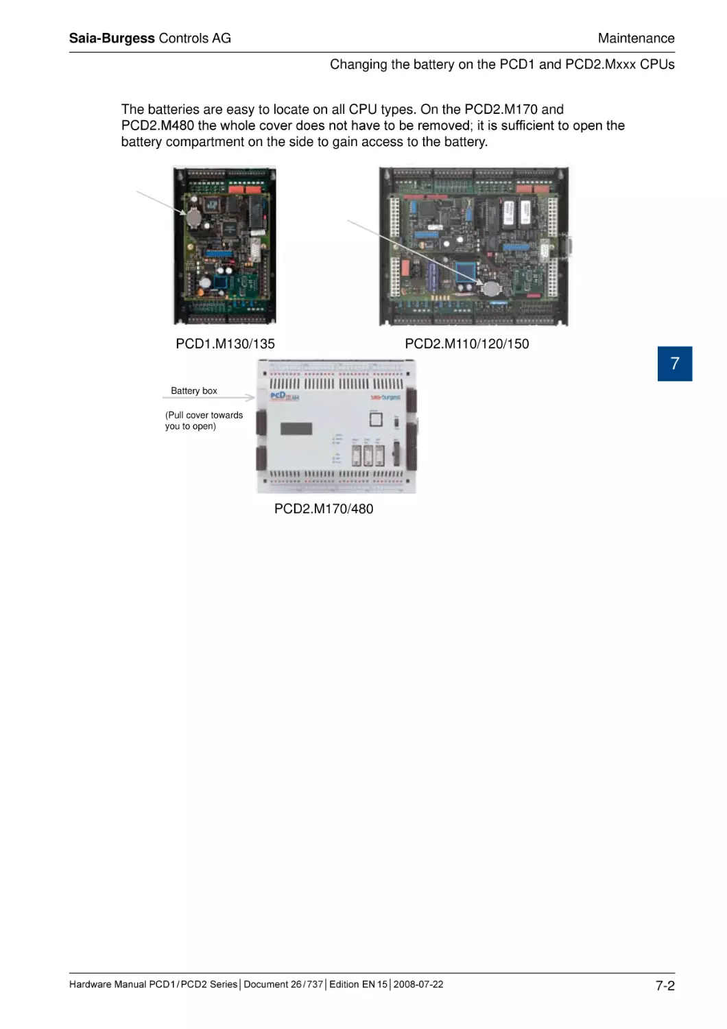
To prevent loss of data, batteries should be changed with the power switched on.
Hardware and firmware versions for the PCD1
The firmware versions for the PCD1.M1xx are generally upwardly compatible in terms
of hardware, so old CPUs can be fitted with new firmware, in order to take advantage
of new functions. This feature is highly valued, and we will try to retain it for as long
as possible; however, we cannot guarantee this.
At this point, the following known restrictions apply:
The use of intelligent communication modules such as Profibus DP, LON and Ethernet requires the minimum hardware and firmware versions. Please refer to the
manuals for the relevant communication modules
Hardware Manual PCD 1 / PCD 2 Series│Document 26 / 737│Edition EN 15│2008-07-22
3-9
Saia-Burgess Controls AG
CPUs and expansion housings
CPU overview
3.4.4
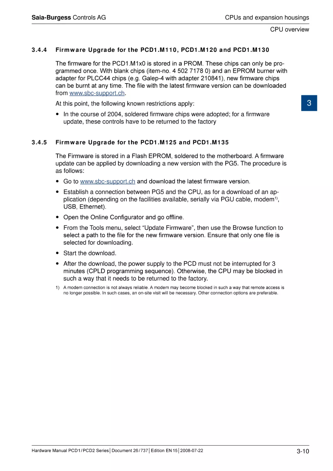
Firmware Upgrade for the PCD1.M110, PCD1.M120 and PCD1.M130
The firmware for the PCD1.M1x0 is stored in a PROM. These chips can only be programmed once. With blank chips (item-no. 4 502 7178 0) and an EPROM burner with
adapter for PLCC44 chips (e.g. Galep-4 with adapter 210841), new firmware chips
can be burnt at any time. The file with the latest firmware version can be downloaded
from www.sbc-support.ch.
At this point, the following known restrictions apply:
3
In the course of 2004, soldered firmware chips were adopted; for a firmware
update, these controls have to be returned to the factory
3.4.5
Firmware Upgrade for the PCD1.M125 and PCD1.M135
The Firmware is stored in a Flash EPROM, soldered to the motherboard. A firmware
update can be applied by downloading a new version with the PG5. The procedure is
as follows:
Go to www.sbc-support.ch and download the latest firmware version.
Establish a connection between PG5 and the CPU, as for a download of an application (depending on the facilities available, serially via PGU cable, modem1),
USB, Ethernet).
Open the Online Configurator and go offline.
From the Tools menu, select “Update Firmware”, then use the Browse function to
select a path to the file for the new firmware version. Ensure that only one file is
selected for downloading.
Start the download.
After the download, the power supply to the PCD must not be interrupted for 3
minutes (CPLD programming sequence). Otherwise, the CPU may be blocked in
such a way that it needs to be returned to the factory.
1) A modem connection is not always reliable. A modem may become blocked in such a way that remote access is
no longer possible. In such cases, an on-site visit will be necessary. Other connection options are preferable.
Hardware Manual PCD 1 / PCD 2 Series│Document 26 / 737│Edition EN 15│2008-07-22
3-10
Saia-Burgess Controls AG
CPUs and expansion housings
CPU overview
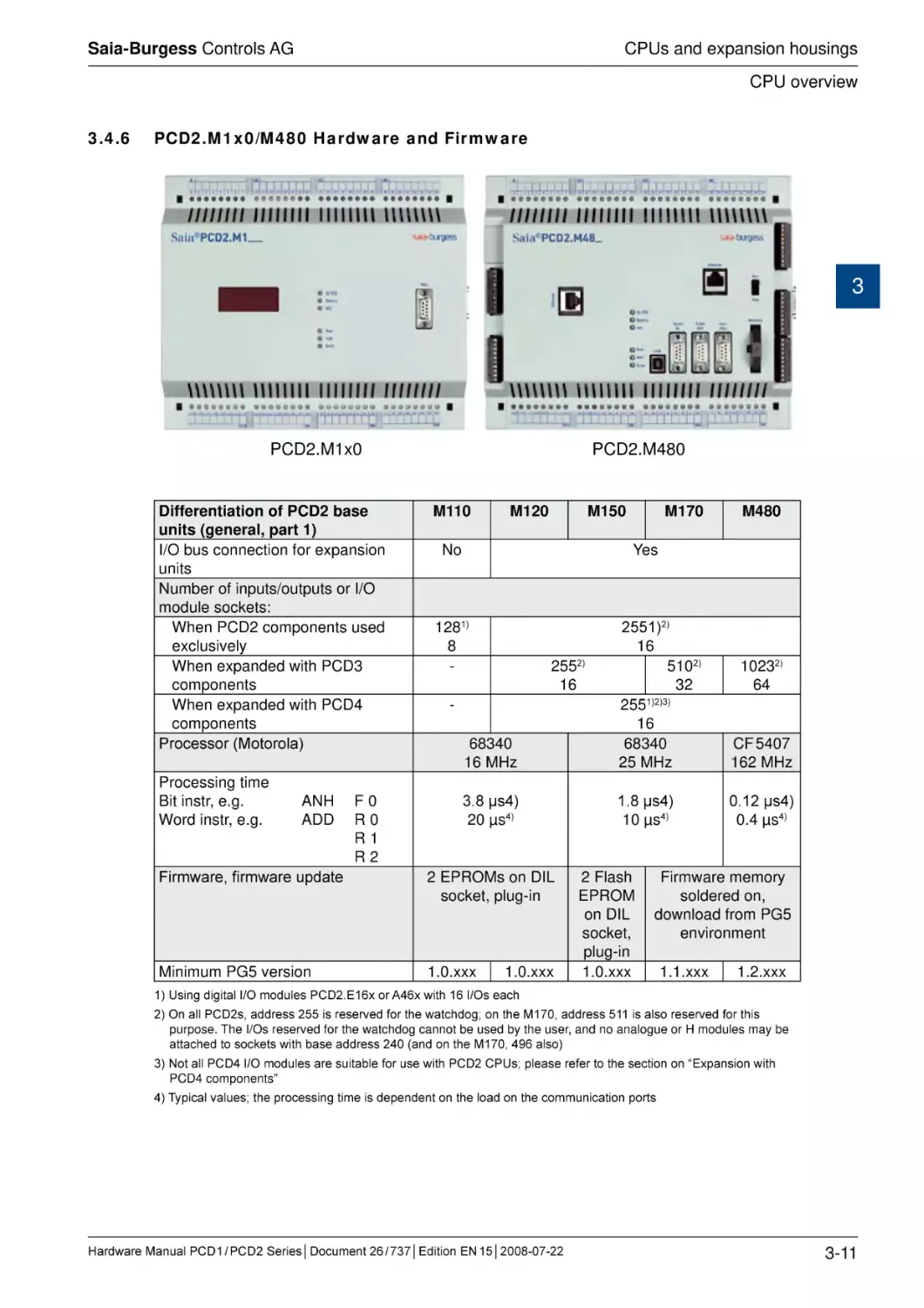
3.4.6
PCD2.M1x0/M480 Hardware and Firmware
3
PCD2.M1x0
Differentiation of PCD2 base
units (general, part 1)
I/O bus connection for expansion
units
Number of inputs/outputs or I/O
module sockets:
When PCD2 components used
exclusively
When expanded with PCD3
components
When expanded with PCD4
components
Processor (Motorola)
Processing time
Bit instr, e.g.
ANH
Word instr, e.g.
ADD
Firmware, firmware update
Minimum PG5 version
F0
R0
R1
R2
PCD2.M480
M110
M120
M150
No
M170
M480
Yes
68340
16 MHz
2551)2)
16
5102)
32
2551)2)3)
16
68340
25 MHz
CF 5407
162 MHz
3.8 µs4)
20 µs4)
1.8 µs4)
10 µs4)
0.12 µs4)
0.4 µs4)
1281)
8
-
2552)
16
-
2 EPROMs on DIL
socket, plug-in
1.0.xxx
1.0.xxx
2 Flash
EPROM
on DIL
socket,
plug-in
1.0.xxx
10232)
64
Firmware memory
soldered on,
download from PG5
environment
1.1.xxx
1.2.xxx
1) Using digital I/O modules PCD2.E16x or A46x with 16 I/Os each
2) On all PCD2s, address 255 is reserved for the watchdog; on the M170, address 511 is also reserved for this
purpose. The I/Os reserved for the watchdog cannot be used by the user, and no analogue or H modules may be
attached to sockets with base address 240 (and on the M170, 496 also)
3) Not all PCD4 I/O modules are suitable for use with PCD2 CPUs; please refer to the section on “Expansion with
PCD4 components”
4) Typical values; the processing time is dependent on the load on the communication ports
Hardware Manual PCD 1 / PCD 2 Series│Document 26 / 737│Edition EN 15│2008-07-22
3-11
Saia-Burgess Controls AG
CPUs and expansion housings
CPU overview
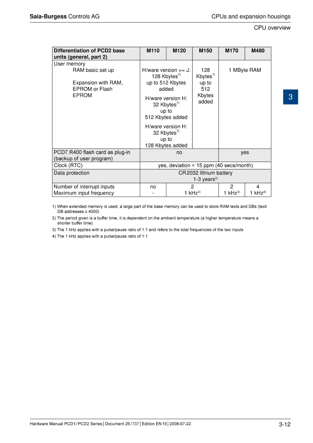
Differentiation of PCD2 base
units (general, part 2)
User memory
RAM basic set up
Expansion with RAM,
EPROM or Flash
EPROM
PCD7.R400 flash card as plug-in
(backup of user program)
Clock (RTC)
Data protection
M110
M120
H/ware version >= J:
128 Kbytes1)
up to 512 Kbytes
added
H/ware version H:
32 Kbytes1)
up to
512 Kbytes added
H/ware version H:
32 Kbytes1)
up to
128 Kbytes added
no
Number of interrupt inputs
Maximum input frequency
M150
128
Kbytes1)
up to
512
Kbytes
added
M170
M480
1 MByte RAM
3
yes
yes, deviation < 15 ppm (40 secs/month)
CR 2032 lithium battery
1-3 years2)
no
2
2
4
1 kHz3)
1 kHz3)
1 kHz4)
1) When extended memory is used, a large part of the base memory can be used to store RAM texts and DBs (text/
DB addresses ≥ 4000)
2) The period given is a buffer time; it is dependent on the ambient temperature (a higher temperature means a
shorter buffer time)
3) The 1 kHz applies with a pulse/pause ratio of 1:1 and refers to the total frequencies of the two inputs
4) The 1 kHz applies with a pulse/pause ratio of 1:1
Hardware Manual PCD 1 / PCD 2 Series│Document 26 / 737│Edition EN 15│2008-07-22
3-12
Saia-Burgess Controls AG
CPUs and expansion housings
CPU overview
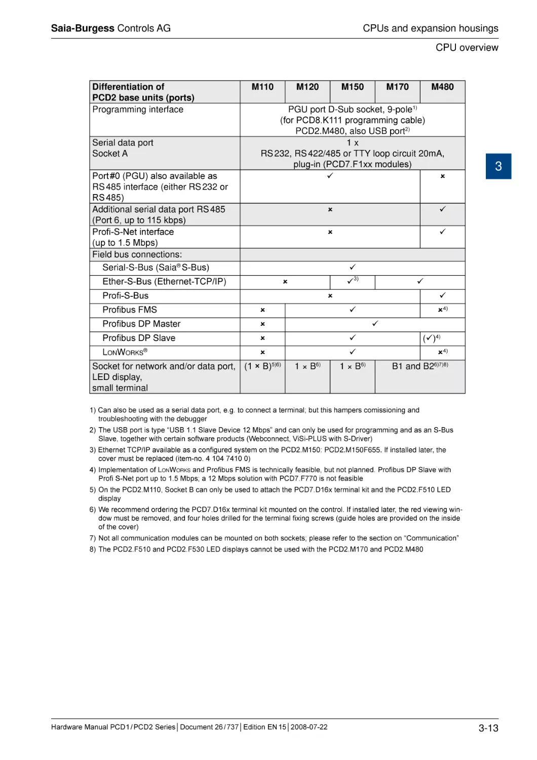
Differentiation of
PCD2 base units (ports)
Programming interface
Serial data port
Socket A
Port #0 (PGU) also available as
RS 485 interface (either RS 232 or
RS 485)
Additional serial data port RS 485
(Port 6, up to 115 kbps)
Profi-S-Net interface
(up to 1.5 Mbps)
Field bus connections:
Serial-S-Bus (Saia® S-Bus)
M110
M120
M150
M170
M480
PGU port D-Sub socket, 9-pole1)
(for PCD8.K111 programming cable)
PCD2.M480, also USB port2)
1x
RS 232, RS 422/485 or TTY loop circuit 20mA,
plug-in (PCD7.F1xx modules)
3
Ether-S-Bus (Ethernet-TCP/IP)
3)
Profi-S-Bus
Profibus FMS
Profibus DP Master
Profibus DP Slave
LonWorks®
Socket for network and/or data port, (1 × B)5)6)
LED display,
small terminal
4)
1 × B6)
1 × B6)
()4)
4)
B1 and B26)7)8)
1) Can also be used as a serial data port, e.g. to connect a terminal; but this hampers comissioning and
troubleshooting with the debugger
2) The USB port is type “USB 1.1 Slave Device 12 Mbps” and can only be used for programming and as an S-Bus
Slave, together with certain software products (Webconnect, ViSi-PLUS with S-Driver)
3) Ethernet TCP/IP available as a configured system on the PCD2.M150: PCD2.M150F655. If installed later, the
cover must be replaced (item-no. 4 104 7410 0)
4) Implementation of LonWorks and Profibus FMS is technically feasible, but not planned. Profibus DP Slave with
Profi S-Net port up to 1.5 Mbps; a 12 Mbps solution with PCD7.F770 is not feasible
5) On the PCD2.M110, Socket B can only be used to attach the PCD7.D16x terminal kit and the PCD2.F510 LED
display
6) We recommend ordering the PCD7.D16x terminal kit mounted on the control. If installed later, the red viewing window must be removed, and four holes drilled for the terminal fixing screws (guide holes are provided on the inside
of the cover)
7) Not all communication modules can be mounted on both sockets; please refer to the section on “Communication”
8) The PCD2.F510 and PCD2.F530 LED displays cannot be used with the PCD2.M170 and PCD2.M480
Hardware Manual PCD 1 / PCD 2 Series│Document 26 / 737│Edition EN 15│2008-07-22
3-13
Saia-Burgess Controls AG
CPUs and expansion housings
CPU overview
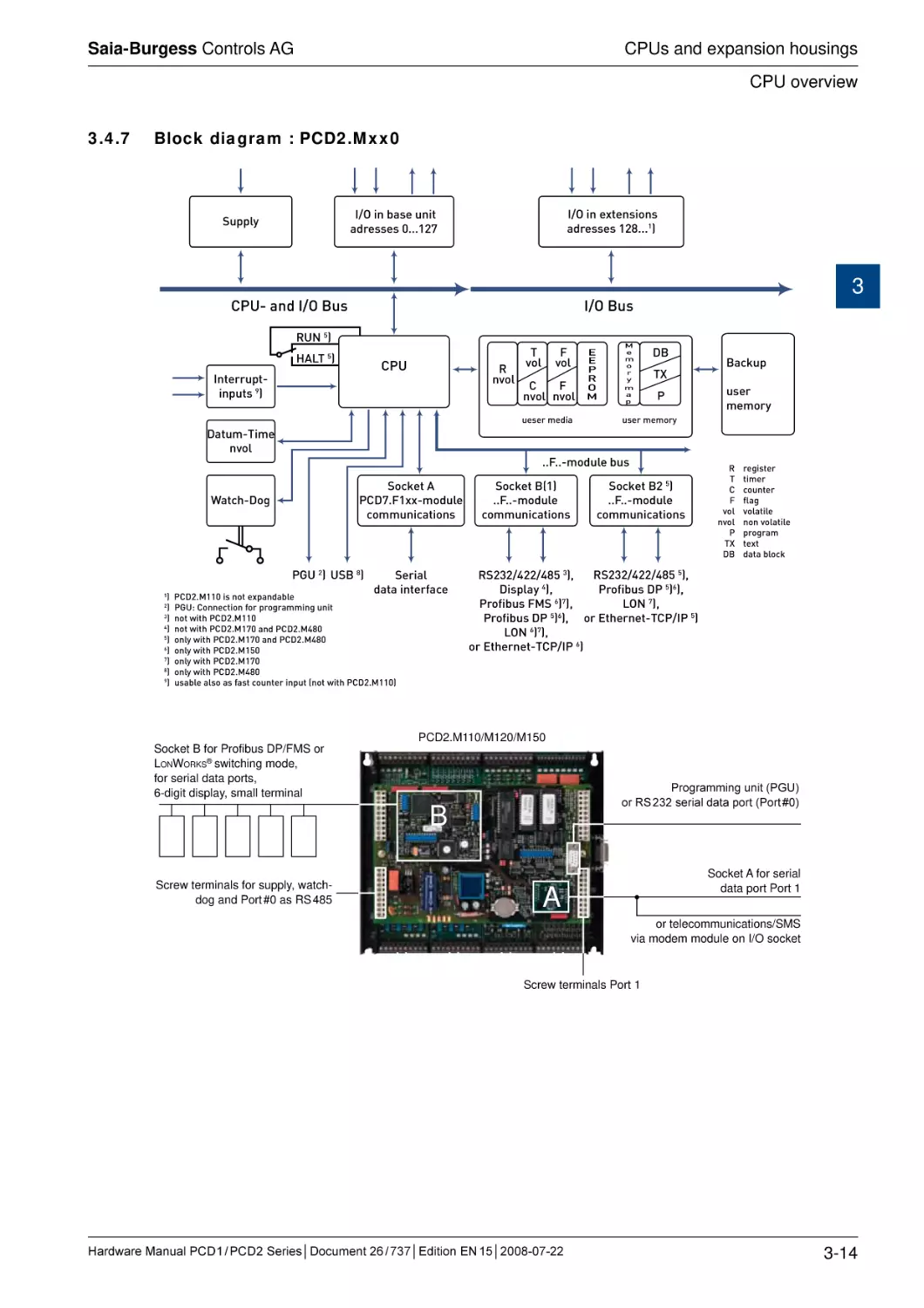
3.4.7
Block diagram : PCD2.Mxx0
>$D^cZmiZch^dch
VYgZhhZh&'-###&
>$D^cWVhZjc^i
VYgZhhZh%###&',
Hjeean
3
>$D7jh
8EJ"VcY>$D7jh
GJC*
=6AI*
8EJ
>ciZggjei"
^cejih.
G
ckda
I
kda
;
kda
8
;
ckda ckda
jZhZgbZY^V
9Vijb"I^bZ
ckda
:
:
E
G
D
B
B
Z
b
d
g
n
b
V
e
97
IM
E
LViX]"9d\
E<J'
JH7-
HZg^Va
YViV^ciZg[VXZ
E89'#B&&%^hcdiZmeVcYVWaZ
E<J/8dccZXi^dc[dgegd\gVbb^c\jc^i
cdil^i]E89'#B&&%
)
cdil^i]E89'#B&,%VcYE89'#B)-%
*
dcanl^i]E89'#B&,%VcYE89'#B)-%
+
dcanl^i]E89'#B&*%
,
dcanl^i]E89'#B&,%
dcanl^i]E89'#B)-%
.
jhVWaZVahdVh[VhiXdjciZg^ceji
cdil^i]E89'#B&&%
'
(
HdX`Zi7
&
##;##"bdYjaZ
Xdbbjc^XVi^dch
jhZg
bZbdgn
jhZgbZbdgn
##;##"bdYjaZWjh
HdX`Zi6
E89,#;&mm"bdYjaZ
Xdbbjc^XVi^dch
7VX`je
HdX`Zi7'*
##;##"bdYjaZ
Xdbbjc^XVi^dch
G
I
8
;
kda
ckda
E
IM
97
gZ\^hiZg
i^bZg
XdjciZg
[aV\
kdaVi^aZ
cdckdaVi^aZ
egd\gVb
iZmi
YViVWadX`
GH'('$)''$)-**
!
GH'('$)''$)-*(
!
Egd[^Wjh9E*
+
!
9^heaVn)
!
ADC,
!
Egd[^Wjh;BH+
,
!
Egd[^Wjh9E*
+
! dg:i]ZgcZi"I8E$>E*
ADC+
,
!
dg:i]ZgcZi"I8E$>E+
PCD2.M110/M120/M150
Socket B for Profibus DP/FMS or
LonWorks® switching mode,
for serial data ports,
6-digit display, small terminal
Programming unit (PGU)
or RS 232 serial data port (Port #0)
B
Screw terminals for supply, watchdog and Port #0 as RS 485
Socket A for serial
data port Port 1
A
or telecommunications/SMS
via modem module on I/O socket
Screw terminals Port 1
Hardware Manual PCD 1 / PCD 2 Series│Document 26 / 737│Edition EN 15│2008-07-22
3-14
Saia-Burgess Controls AG
CPUs and expansion housings
CPU overview
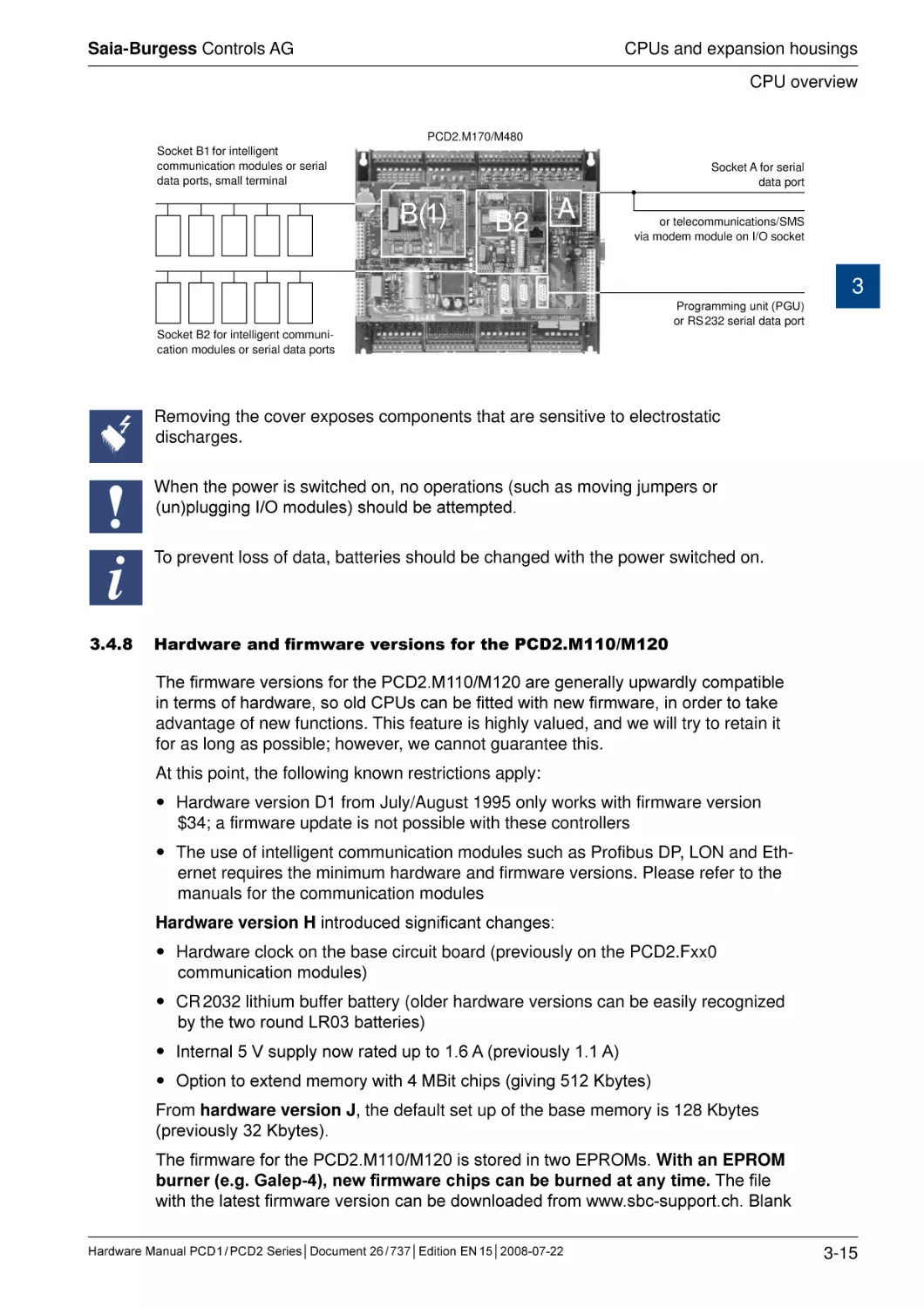
PCD2.M170/M480
Socket B1 for intelligent
communication modules or serial
data ports, small terminal
Socket A for serial
data port
B(1)
B2
A
or telecommunications/SMS
via modem module on I/O socket
3
Programming unit (PGU)
or RS 232 serial data port
Socket B2 for intelligent communication modules or serial data ports
Removing the cover exposes components that are sensitive to electrostatic
discharges.
When the power is switched on, no operations (such as moving jumpers or
(un)plugging I/O modules) should be attempted.
i
3.4.8
To prevent loss of data, batteries should be changed with the power switched on.
Hardware and firmware versions for the PCD2.M110/M120
The firmware versions for the PCD2.M110/M120 are generally upwardly compatible
in terms of hardware, so old CPUs can be fitted with new firmware, in order to take
advantage of new functions. This feature is highly valued, and we will try to retain it
for as long as possible; however, we cannot guarantee this.
At this point, the following known restrictions apply:
Hardware version D1 from July/August 1995 only works with firmware version
$34; a firmware update is not possible with these controllers
The use of intelligent communication modules such as Profibus DP, LON and Ethernet requires the minimum hardware and firmware versions. Please refer to the
manuals for the communication modules
Hardware version H introduced significant changes:
Hardware clock on the base circuit board (previously on the PCD2.Fxx0
communication modules)
CR 2032 lithium buffer battery (older hardware versions can be easily recognized
by the two round LR03 batteries)
Internal 5 V supply now rated up to 1.6 A (previously 1.1 A)
Option to extend memory with 4 MBit chips (giving 512 Kbytes)
From hardware version J, the default set up of the base memory is 128 Kbytes
(previously 32 Kbytes).
The firmware for the PCD2.M110/M120 is stored in two EPROMs. With an EPROM
burner (e.g. Galep-4), new firmware chips can be burned at any time. The file
with the latest firmware version can be downloaded from www.sbc-support.ch. Blank
Hardware Manual PCD 1 / PCD 2 Series│Document 26 / 737│Edition EN 15│2008-07-22
3-15
Saia-Burgess Controls AG
CPUs and expansion housings
CPU overview
firmware chips can be obtained under item-no. 4 502 7126 0 (two chips per CPU
need to be ordered).
3.4.9
Hardware and firmware versions for the PCD2.M150
The firmware versions for the PCD2.M150 are generally upwardly compatible in
terms of hardware, so old CPUs can be fitted with new firmware, in order to take advantage of new functions. This feature is highly valued, and we will try to retain it for
as long as possible; however, we cannot guarantee this.
3
The firmware for the PCD2.M150 is stored in two Flash EPROMs. With an EPROM
burner (e.g. Galep-4), new firmware chips can be burned at any time; updating via download, as with the M170/M480 is not possible. The file with the latest
firmware version can be downloaded from www.sbc-support.ch. Blank firmware chips
can be obtained under item-no. 4 502 7341 0 (two chips per CPU need to be ordered).
3.4.10 Hardware and firmware versions for the PCD2.M170/M480
The firmware versions for the PCD2.M170/M480 are generally upwardly compatible
in terms of hardware, so old CPUs can be fitted with new firmware, in order to take
advantage of new functions. This feature is highly valued, and we will try to retain it
for as long as possible; however, we cannot guarantee this.
The firmware for the PCD2.M170/M480 is stored in a Flash EPROM, soldered to the
motherboard. A firmware update can be applied by downloading a new version with
the PG5. The procedure is as follows:
Go to www.sbc-support and download the latest firmware version.
Establish a connection between PG5 and the CPU, as for a download of an application (depending on the facilities available, serially via PGU cable, modem1),
USB, Ethernet).
Open the Online Configurator and go offline.
From the Tools menu, select “Update Firmware”, then use the Browse function to
select a path to the file for the new firmware version. Ensure that only one file is
selected for downloading.
Start the download.
After the download, the power supply to the PCD must not be interrupted for 3
minutes (CPLD programming sequence). Otherwise, the CPU may be blocked in
such a way that it needs to be returned to the factory.
1) A modem connection is not always reliable. A modem may become blocked in such a way that remote access is
no longer possible. In such cases, an on-site visit will be necessary. Other connection options are preferable.
Hardware Manual PCD 1 / PCD 2 Series│Document 26 / 737│Edition EN 15│2008-07-22
3-16
Saia-Burgess Controls AG
CPUs and expansion housings
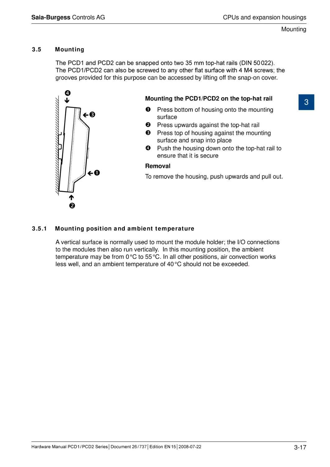
Mounting
3.5
Mounting
The PCD1 and PCD2 can be snapped onto two 35 mm top-hat rails (DIN 50 022).
The PCD1/PCD2 can also be screwed to any other flat surface with 4 M4 screws; the
grooves provided for this purpose can be accessed by lifting off the snap-on cover.
Mounting the PCD1/PCD2 on the top-hat rail
Press bottom of housing onto the mounting
3
surface
Press upwards against the top-hat rail
Press top of housing against the mounting
surface and snap into place
Push the housing down onto the top-hat rail to
ensure that it is secure
Removal
To remove the housing, push upwards and pull out.
3.5.1
Mounting position and ambient temperature
A vertical surface is normally used to mount the module holder; the I/O connections
to the modules then also run vertically. In this mounting position, the ambient
temperature may be from 0 °C to 55 °C. In all other positions, air convection works
less well, and an ambient temperature of 40 °C should not be exceeded.
Hardware Manual PCD 1 / PCD 2 Series│Document 26 / 737│Edition EN 15│2008-07-22
3-17
Saia-Burgess Controls AG
CPUs and expansion housings
Expansion housings and bus cables
3.6
Expansion housings and bus cables
The PCD2.M120/M150/M170/M480 can be expanded with PCD2, PCD3 or PCD4
components, and additional module sockets are provided:
Type
Maximum number of inputs/outputs or
I/O module sockets for the system:
When PCD2 components used exclusively
M120/M150
M170
When expanded with PCD3 components
2551)2)
16
2551)2)
16
5101)2)
32
2552)3)
16
When expanded with PCD4 components
M480
3
10231)2)
64
1) Using digital I/O modules PCD2/3.E16x or A46x with 16 I/Os each
2) On all PCD2s, address 256 is reserved for the watchdog; on the M170, address 511 is also reserved for this
purpose. The I/Os reserved for the watchdog cannot be used by the user, and no analogue or H modules may be
attached to sockets with base address 240 (and on the M170, 496 also)
3) Not all PCD4 I/O modules are suitable for use with PCD2 CPUs; please refer to the section on “Expansion with
PCD4 components”
Hardware Manual PCD 1 / PCD 2 Series│Document 26 / 737│Edition EN 15│2008-07-22
3-18
Saia-Burgess Controls AG
CPUs and expansion housings
Expansion housings and bus cables
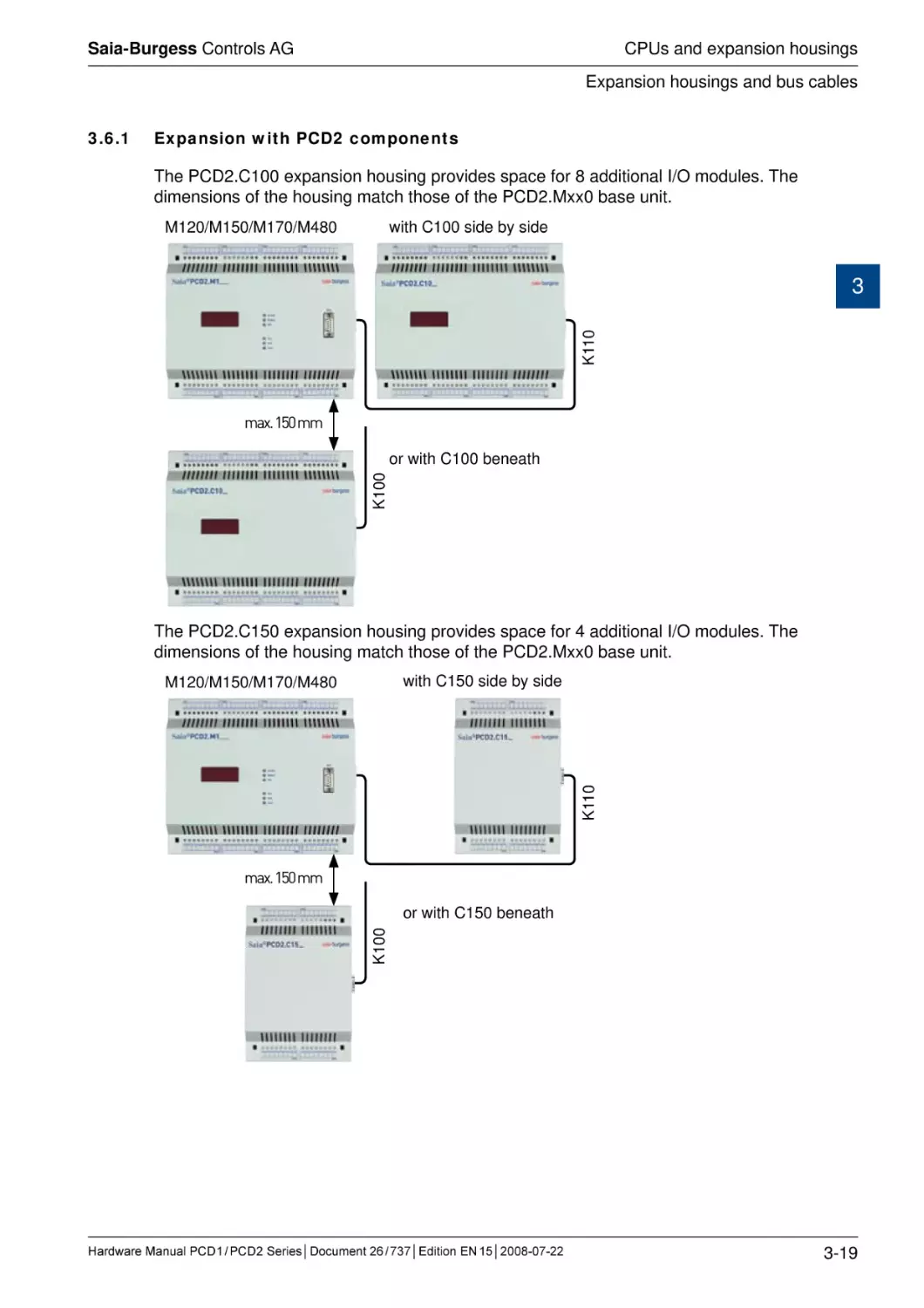
3.6.1
Expansion with PCD2 components
The PCD2.C100 expansion housing provides space for 8 additional I/O modules. The
dimensions of the housing match those of the PCD2.Mxx0 base unit.
M120/M150/M170/M480
with C100 side by side
K110
3
�����������
K100
or with C100 beneath
The PCD2.C150 expansion housing provides space for 4 additional I/O modules. The
dimensions of the housing match those of the PCD2.Mxx0 base unit.
with C150 side by side
K110
M120/M150/M170/M480
�����������
K100
or with C150 beneath
Hardware Manual PCD 1 / PCD 2 Series│Document 26 / 737│Edition EN 15│2008-07-22
3-19
Saia-Burgess Controls AG
CPUs and expansion housings
Expansion housings and bus cables
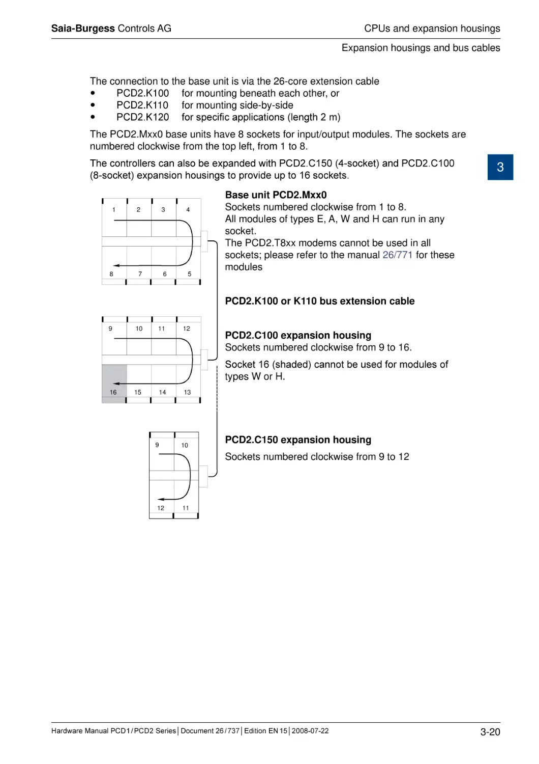
The connection to the base unit is via the 26-core extension cable
PCD2.K100 for mounting beneath each other, or
PCD2.K110 for mounting side-by-side
PCD2.K120 for specific applications (length 2 m)
The PCD2.Mxx0 base units have 8 sockets for input/output modules. The sockets are
numbered clockwise from����������������������������
the top left, from 1 to 8.
The controllers can also be expanded with PCD2.C150 (4-socket) and PCD2.C100
(8-socket) expansion housings to provide up to 16 sockets.
1
8
2
3
4
7
6
5
3
Base unit PCD2.Mxx0
Sockets numbered clockwise from 1 to 8.
All modules of types E, A, W and H can run in any
socket.
The PCD2.T8xx modems cannot be used in all
sockets; please refer to the manual 26/771 for these
modules
PCD2.K100 or K110 bus extension cable
9
10
11
12
PCD2.C100 expansion housing
Sockets numbered clockwise from 9 to 16.
Socket 16 (shaded) cannot be used for modules of
types W or H.
16
15
14
9
13
10
PCD2.C150 expansion housing
Sockets numbered clockwise from 9 to 12
12
11
Hardware Manual PCD 1 / PCD 2 Series│Document 26 / 737│Edition EN 15│2008-07-22
3-20
Saia-Burgess Controls AG
CPUs and expansion housings
Expansion housings and bus cables
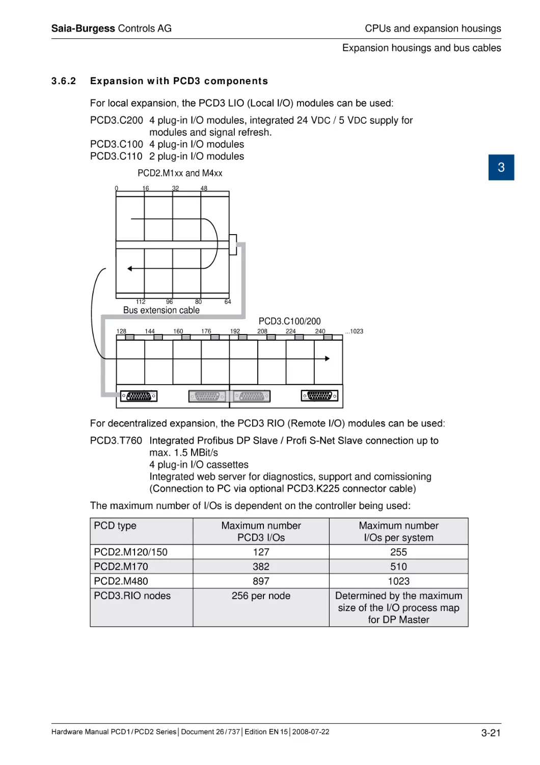
3.6.2
Expansion with PCD3 components
For local expansion, the PCD3 LIO (Local I/O) modules can be used:
PCD3.C200
PCD3.C100
PCD3.C110
4 plug-in I/O modules, integrated 24 VDC / 5 VDC supply for
modules and signal refresh.
4 plug-in I/O modules
2 plug-in I/O modules
3
PCD2.M1xx and M4xx
0
16
32
112
96
48
80
Bus extension cable
144
160
176
192
PCD3.C100/200
208
224
240
...1023
Frontview
128
64
Frontview
Frontview
Frontview
For decentralized expansion, the PCD3 RIO (Remote I/O) modules can be used:
PCD3.T760
Integrated Profibus DP Slave / Profi S-Net Slave connection up to
max. 1.5 MBit/s
4 plug-in I/O cassettes
Integrated web server for diagnostics, support and comissioning
(Connection to PC via op����������������������������������
tional PCD3.K225 connector cable)
The maximum number of I/Os is dependent on the controller being used:
PCD type
PCD2.M120/150
PCD2.M170
PCD2.M480
PCD3.RIO nodes
Maximum number
PCD3 I/Os
127
382
897
256 per node
Hardware Manual PCD 1 / PCD 2 Series│Document 26 / 737│Edition EN 15│2008-07-22
Maximum number
I/Os per system
255
510
1023
Determined by the maximum
size of the I/O process map
for DP Master
3-21
Saia-Burgess Controls AG
CPUs and expansion housings
Expansion housings and bus cables
When selecting I/O cassettes, ensure that the internal 5 V and +V supply is not
overloaded.
Detailed information on planning combined PCD2/PCD3 systems can be found in the
PCD3 manual 26/789.
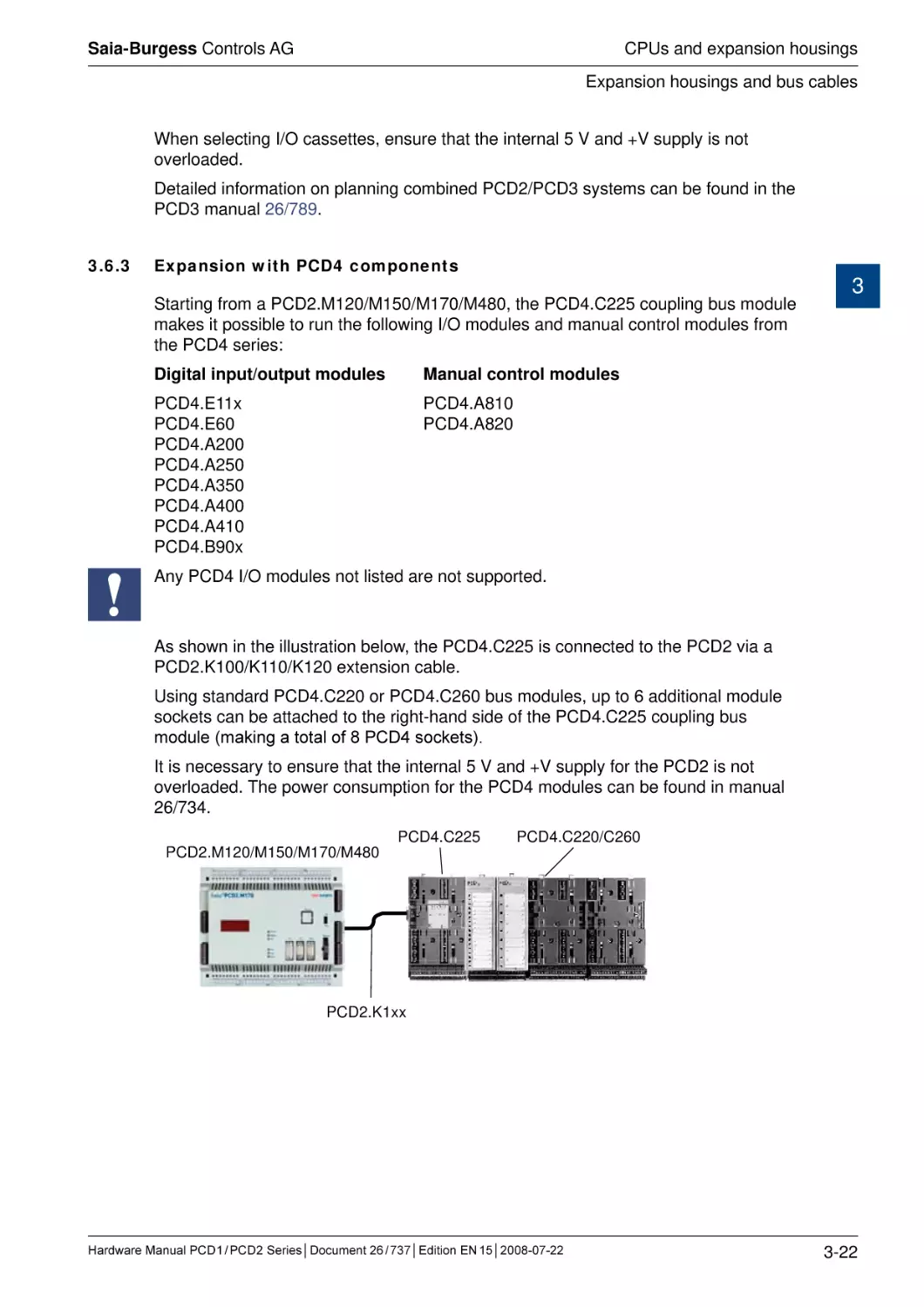
3.6.3
Expansion with PCD4 components
Starting from a PCD2.M120/M150/M170/M480, the PCD4.C225 coupling bus module
makes it possible to run the following I/O modules and manual control modules from
the PCD4 series:
Digital input/output modules
Manual control modules
PCD4.E11x
PCD4.E60
PCD4.A200
PCD4.A250
PCD4.A350
PCD4.A400
PCD4.A410
PCD4.B90x
PCD4.A810
PCD4.A820
3
Any PCD4 I/O modules not listed are not supported.
As shown in the illustration below, the PCD4.C225 is connected to the PCD2 via a
PCD2.K100/K110/K120 extension cable.
Using standard PCD4.C220 or PCD4.C260 bus modules, up to 6 additional module
sockets can be attached to the right-hand side of the PCD4.C225 coupling bus
module (making a total of 8 PCD4 sockets).
It is necessary to ensure that the internal 5 V and +V supply for the PCD2 is not
overloaded. The power consumption for the PCD4 modules can be found in manual
26/734.
PCD2.M120/M150/M170/M480
PCD4.C225
PCD4.C220/C260
PCD2.K1xx
Hardware Manual PCD 1 / PCD 2 Series│Document 26 / 737│Edition EN 15│2008-07-22
3-22
Saia-Burgess Controls AG
CPUs and expansion housings
Installation and addressing of PCD2 I/O modules
3.7
Installation and addressing of PCD2 I/O modules
3.7.1
Insertion of I/O modules
The I/O module is inserted from the side, pushed towards the middle of the unit until it
reaches the end stop, and snapped into the retaining catch.
3
Retaining catch
Bus connector
When the power is switched on, no operations (such as moving jumpers or
(un)plugging I/O modules) should be attempted.
3.7.2
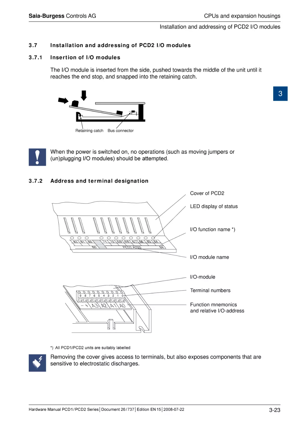
Address and terminal designation
Cover of PCD2
LED display of status
I/O function name *)
I/O module name
I/O-module
9
Terminal numbers
8 7
6
5
4
3
2
1
0
Function mnemonics
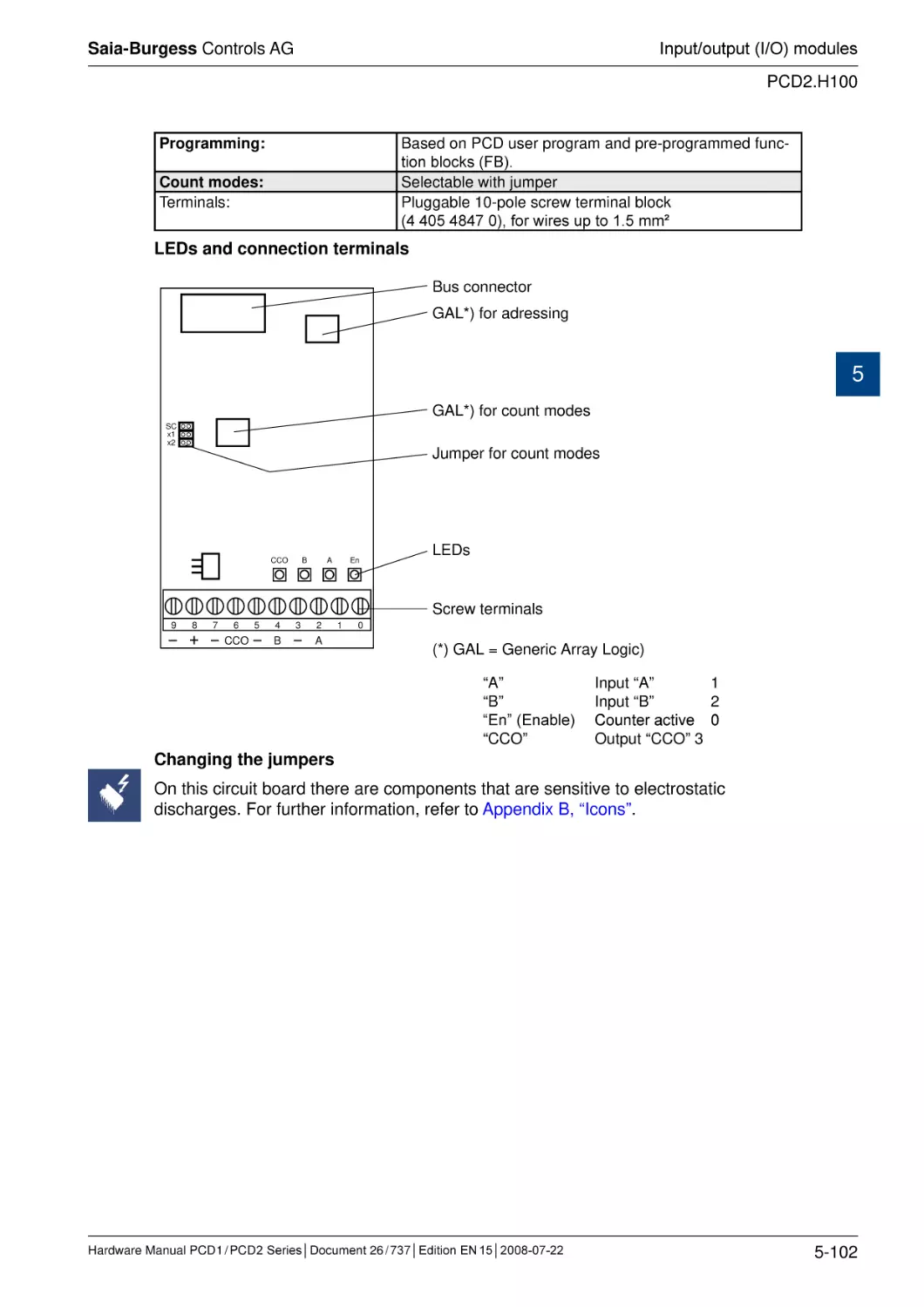
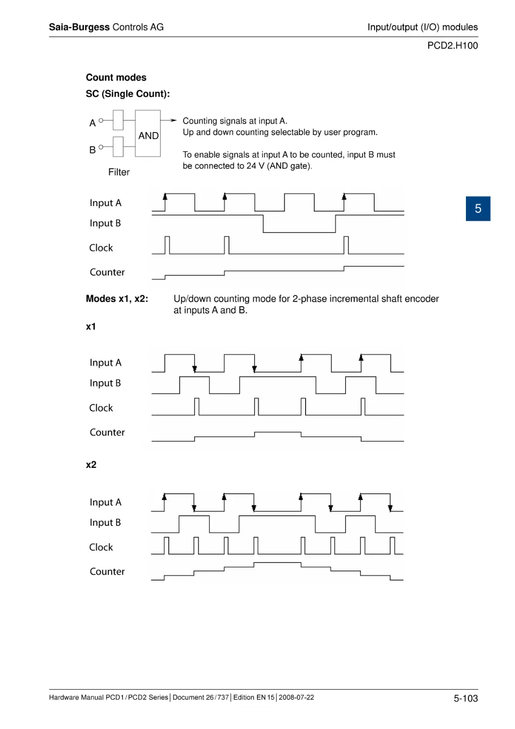
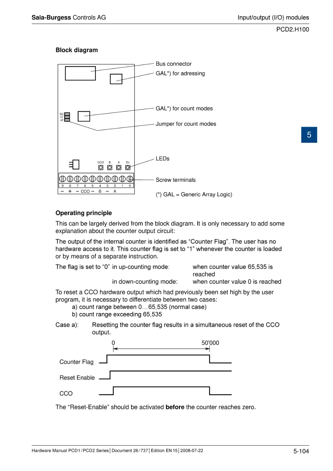
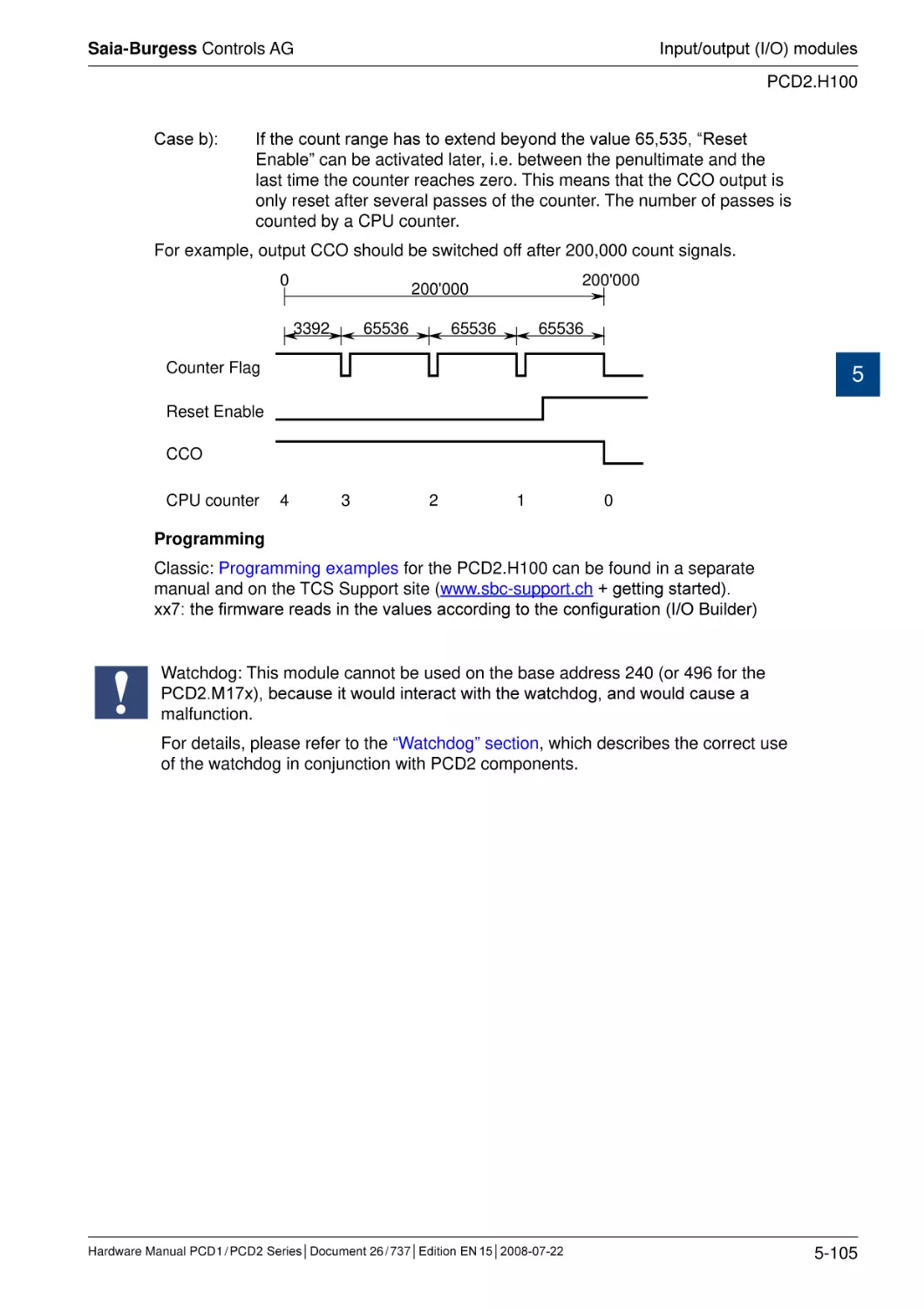
and relative I/O-address
*) All PCD1/PCD2 units are suitably labelled
Removing the cover gives access to terminals, but also exposes components that are
sensitive to electrostatic discharges.
Hardware Manual PCD 1 / PCD 2 Series│Document 26 / 737│Edition EN 15│2008-07-22
3-23
Saia-Burgess Controls AG
CPUs and expansion housings
Installation and addressing of PCD2 I/O modules
3.7.3
Cable layout
Wiring to the I/O modules can be laid in the cable channels on both sides.
3
Exxx
Exxx
Axxx
CPU
Axxx
Interrupt
24 VDC
Battery
WD
Run
Halt
Error
_
_
+
+
+
PGU
_
F1xx
Supply
Wxxx
_
Wxxx
Axxx
Axxx
The cables to the terminals on the motherboard are run through the two side channels from the bottom or from the top.
On the PCD2.M170 and the PCD2.M480, the terminals on the motherboard are accessible without removing the cover.
Following these rules will ensure that the LEDs are visible and the bus connections
remain accessible.
Hardware Manual PCD 1 / PCD 2 Series│Document 26 / 737│Edition EN 15│2008-07-22
3-24
Saia-Burgess Controls AG
CPUs and expansion housings
Dimensions
3.8
Dimensions
PCD1.M1xx/PCD2.C150
70
Ø 4.5
124
68
70
208
200
3
34
125
141.4
5.5
59
PCD2.Mxx0/PCD2.C100
74
PCD7.R400
64
124
68
70
200
208
70
Ø 4.5
230
248
34
5.5
Hardware Manual PCD 1 / PCD 2 Series│Document 26 / 737│Edition EN 15│2008-07-22
59
3-25
Saia-Burgess Controls AG
CPUs and expansion housings
Power supply and connection plan
3.9
Power supply and connection plan
3.9.1
External power supply
Simple, small installations
+18V
3
19VAC
±15%
0V
L N
GND
Transformer min. 50VA
Sensors:
Actuators:
Electro-mechanical switches
Relays, lamps, small valves with < 0.5 A switching current
The transformer voltage of 19 VAC ±15% must be maintained. If not, the supply voltage at
the input to the PCD may become too high and destroy it.
The PCD2. H1xx, H2xx, H3xx, PCD7.D1xx, D2xx and PCA2.D12/D14 modules must be
connected to a smoothed 24 VDC supply
Small to medium installations
+24V =
L
N
CONTROLLER
24 VDC
±20%
0V
L N
GND
Controller: usual primary switched network component
Sensors:
Actuators:
Electro-mechanical and proximity switches, photoelectric
barriers
Relays, lamps, displays, small valves with < 0.5 A switching
current
Hardware Manual PCD 1 / PCD 2 Series│Document 26 / 737│Edition EN 15│2008-07-22
3-26
Saia-Burgess Controls AG
CPUs and expansion housings
Power supply and connection plan
3.9.2
Earthing and connection plan
Ground wire plan with earthing bar
0V +24VDC
Shielding and
grounding plate
3
Exxx
Axxx
CPU
24 VDC
Battery
WD
Run
Halt
Error
_
_
+
+
+
PGU
_
_
Supply
Wxxx
1.5 mm2 / max. 25cm
1.5 mm2
1.5 mm2
Earthing bar
In the bottom part of the PCD1/PCD2 housing there is a shielding and earthing
plate. This constitutes the common, large-area ground for all I/O modules and for the
external power supply.
When a module is plugged in at the I/O level, the blades on this plate ensure a
reliable multi-point contact to the relevant module.
The zero-potential (Minus pole) of the 24 V supply is connected to the Minus
terminal of the PCD1/PCD2 supply. This should be connected to the earthing bar
with the shortest possible wire (< 25 cm) of 1.5 mm2. The same applies to the Minus
connection to the F1xx or the interrupt terminal.
Any shielding of analogue signals or communication cables should also be brought to
the same earth potential, either via a Minus terminal or via the earthing bar.
All Minus connections are linked internally. For problem-free operation, these
connections should be reinforced external������������������������������
ly with short wires of 1.5 mm2.
Hardware Manual PCD 1 / PCD 2 Series│Document 26 / 737│Edition EN 15│2008-07-22
3-27
Saia-Burgess Controls AG
CPUs and expansion housings
Power supply and connection plan
Star-shaped ground wire plan (alternative to earthing bar)
0V +24 VDC
Shielding and
grounding plate
Exxx
3
Axxx
CPU
24 VDC
Battery
WD
Run
Halt
Error
_
_
+
+
+
PGU
_
_
Supply
Wxxx
1.5 mm2 / max. 25cm
1.5 mm2
1.5 mm2
1.5 mm2
Protective grounding clamp
The star-shaped ground wire plan should only be used where there is no earthing
bar.
Examples of ground wire terminals for 35 mm mounting rails1)
Manufacturer
Connection type
Type
End plate
End bracket/
end clamp
Weidmüller
Screw connection
WPE4
101 010 0000
Weidmüller
Screwless spring clip
ZPE4
163 208 0000
ZAP/TB4
163 209 0000
ZEW
954 000 0000
Wago
Screwless cage clamp
default:
281-107
grey: 281-301
6 mm: 249-117
orange: 281-302 10 mm: 249-116
Wieland
Screw connection
WKI4SL/35
AP2.5-4 grey
9708/2 S 35
Wieland
Spring clip
WKI4SL/35
APF2.5-4 GN
WEF 1/35
1) DIN46277, NFC, CENELC
Hardware Manual PCD 1 / PCD 2 Series│Document 26 / 737│Edition EN 15│2008-07-22
3-28
Saia-Burgess Controls AG
CPUs and expansion housings
Power supply and connection plan
3.9.3
Internal power supply
Supply 24 VDC
PCD1
PCD2
20
20
21
21
23
23
24
DC
Voltage
monitor 5 V
39 V
CLR
0V
DC
DC
3.9.4
+5 V
DC
22
22
Bus PCD2
LED
24 V
PTC
3
+V
(16…24 V)
Capacity of internal power supply
Starting from the base units, the following currents are available for the plug-in
modules:
+5 V:
PCD1:
PCD2.M110/M120
PCD2.M150/M170
PCD2.M480
:
:
:
:
750 mA
1600 mA (before hardware version H: 1100 mA)
1600 mA
2000 mA
+V (16…24 V)
PCD1:
PCD2:
:
:
:
100 mA
200 mA
Hardware Manual PCD 1 / PCD 2 Series│Document 26 / 737│Edition EN 15│2008-07-22
3-29
Saia-Burgess Controls AG
CPUs and expansion housings
PCD1.M1x0 and PCD1.M1x5 operating states
3.10
PCD1.M1x0 and PCD1.M1x5 operating states
The CPU can assume the following operating states:
START, RUN, CONDITIONAL RUN, STOP and HALT
The display uses 3 LEDs:
SUPPLY 24 VDC
RUN
ERROR
LED yellow
LED yellow
LED red
3
1)
RUN
COND. RUN
STOP
HALT
RESET
RUN
ERROR
START
The “SUPPLY 24 VDC” LED shows that the electrical supply is working.
The RUN and ERROR LEDs together show the operating state of the CPU:
●/○
●
●/�
○
○
○
●
●��
/○
1)
1)
1)
1)
●
An ERROR may be signalled by the LED in operating states RUN, CONDITIONAL RUN, STOP or HALT. In the
event of an error, the LED only lights up if there is no XOB 13 programmed to deal with this error.
●
●/○
○
LED on
LED flashing
LED off
START
Self-diagnosis for approx. 1s after switching on or after a Restart
RUN
Normal processing of the user program after START. Where a
programming device is connected in PGU mode (e.g. PG5 in PGU mode),
the CPU automatically goes into the STOP state and not the RUN state;
this is for safety reasons
COND. RUN
Conditional RUN state A condition has been set in the debugger (RUN
until..), which has not yet been met
STOP
The STOP state occurs in the following cases:
• Programming device in PGU mode connected when CPU switched on
• PGU stopped by programming device
• Condition for a COND. RUN has been met
HALT
The HALT state occurs in the following cases:
• HALT instruction processed
• Serious error in user program
• Hardware fault
• No program loaded
• No communication module on a S-Bus PGU or Gateway Master port
RESET
The RESET state has the following causes:
• Supply voltage too low
• Firmware not starting up
Hardware Manual PCD 1 / PCD 2 Series│Document 26 / 737│Edition EN 15│2008-07-22
3-30
Saia-Burgess Controls AG
CPUs and expansion housings
PCD2.M1x0/M480 operating states
3.11
PCD2.M1x0/M480 operating states
The CPU can assume the following operating states: START, RUN, CONDITIONAL
RUN, STOP, HALT and RESET
1)
COND. RUN
STOP
HALT
RESET
LED yellow
LED red
LED yellow
RUN
RUN
HALT
ERROR
RUN
HALT
ERROR
START
The display uses 3 LEDs:
●/○
●
●/○
○
○
●
●/○
○
○
○
●
●
●/○
1)
1)
1)
1)
●
3
An ERROR may be signalled by the LED in operating states RUN, CONDITIONAL RUN, STOP or HALT. In the
event of an error, the LED only lights up if there is no XOB 13 programmed to deal with this error.
●
●/○
○
LED on
LED flashing
LED off
START
Self-diagnosis for approx. 1s after switching on or after a Restart
RUN
Normal processing of the user program after START. Where a
programming device is connected via a PCD8.K11x in PGU mode (e.g.
PG5 in PGU mode), the CPU automatically goes into the STOP state and
not the RUN state; this is for safety reasons
COND. RUN
Conditional RUN state. A condition has been set in the debugger (RUN
until...), which has not yet been met
STOP
The STOP state occurs in the following cases:
• Programming device in PGU mode connected when the CPU was
switched on
• PGU stopped by programming device
• Condition for a COND.RUN has been met
HALT
The HALT state occurs in the following cases:
• HALT instruction processed
• Serious error in user program
• Hardware fault
• No program loaded
• No communication module on a S-Bus PGU or Gateway Master port
RESET
The RESET state has the following causes:
• Supply voltage too low
• Firmware not starting up
Hardware Manual PCD 1 / PCD 2 Series│Document 26 / 737│Edition EN 15│2008-07-22
3-31
Saia-Burgess Controls AG
CPUs and expansion housings
Expansion of user memory
3.12
Expansion of user memory
3.12.1 Basics
The main reasons to expand the user memory for a PCD1/PCD2 are:
The base memory is too small to store the user program and the texts
The user program and the non-modifiable texts and data blocks are to be held in
Flash EPROM as a failsafe measure (the base memory is always RAM)
3
The benefits of data blocks with addresses ≥ 4000 are to be used:
- up to 16,384 elements / DBs
- much lower overhead per element: 4 bytes per 32-bit value rather than 8 bytes
- much faster access
i
The PCD2.M170 and PCD2.M480 are equipped with 1 Mbyte of RAM as standard;
this cannot be expanded. To minimize the risk of program loss, we recommend the
use of the optional PCD��������������������������������������������������������
7.R400 flash card, which allows the user program to be
backed up.
The use of EPROMs to expand the user memory is obsolete and is no longer
recommended. Working with Flash EPROMs is much more convenient (no EPROM
programming device required, behaves like RAM for the programmer) and just as
secure as EPROMs.
Hardware Manual PCD 1 / PCD 2 Series│Document 26 / 737│Edition EN 15│2008-07-22
3-32
Saia-Burgess Controls AG
CPUs and expansion housings
Expansion of user memory
3.12.2 Memory location of the user program, the resources, texts and DBs
Depending on whether the user memory of a PCD1/PCD2 has been expanded or
not, the memory location of various parts of the application will vary. When the user
memory is expanded by plugging in a memory chip, the user program and the text
strings/DBs with addresses < 4000 are ����������������������������������������
stored in the additional plug-in chip.
The base memory provided on the CPU is then free, and can optionally be defined in
the hardware configuration as “extension memory” and used to store texts and DBs
with addresses ≥ 4000.
Memory location
Contents
Resources (registers,
flags, counters etc.)
User program
Texts and DBs with
addresses < 4000
Texts and DBs with
addresses ≥ 4000
No expansion of
user memory
3
With expansion of
user memory
The resources are held in a separate RAM memory on
the CPU (always in the same location, buffered by the
SuperCap or the battery)
in base memory
in additional chip in
“USER PROG” socket1)
in base memory
in additional chip in
“USER PROG” socket1)
not available
in extension memory2)
1) i.e. in RAM, EPROM or Flash EPROM depending on the chip used. The use of EPROM is no longer
recommended; use Flash EPROM instead
2) Must be defined in the hardware configuration
Hardware Manual PCD 1 / PCD 2 Series│Document 26 / 737│Edition EN 15│2008-07-22
3-33
Saia-Burgess Controls AG
CPUs and expansion housings
Expansion of user memory
3.12.3 Example of a memory configuration
The screenshots below show examples of the hardware configuration and associated
software settings in PG5 for a PCD2.M120 (hardware version >= J) with a 1 Mbit
Flash EPROM plug-in expansion unit (item-no. 4 502 7141 0).
Extension memory is configured and is used to hold RAM texts and RAM DBs.
Step 1: Hardware configuration
3
In this example, only 112 Kbytes of Flash EPROM are available as code/text memory
(on the plug-in chip); one block of memory is lost to configuration data (header),
because Flash EPROM can only be accessed in block mode.
For a PCD2.M110/M120 with hardware version < J, only 24 Kbytes of extension
memory (onboard memory) can be configured; previously, less base memory was
provided with these CPU types.
Step 2: Downloading the hardware configuration
Step 3: Modifying system settings
Hardware Manual PCD 1 / PCD 2 Series│Document 26 / 737│Edition EN 15│2008-07-22
3-34
Saia-Burgess Controls AG
CPUs and expansion housings
Expansion of user memory
Software settings before modification:
3
After modification (“Set defaults” pressed):
The addresses of the RAM text strings and DBS have been changed.
The “Set Defaults” button is useful in many cases, as the addresses are automatically
set according to the hardware configuration. However, the previous settings are lost.
The new software settings are picked up at the next build.
Hardware Manual PCD 1 / PCD 2 Series│Document 26 / 737│Edition EN 15│2008-07-22
3-35
Saia-Burgess Controls AG
CPUs and expansion housings
Expansion of user memory
3.12.4 PCD1.M1x0
The user memory for PCD1 CPUs can be expanded with RAM, EPROM and, from
firmware version 002, with Flash EPROM, up to a maximum of 1 Mbit.
The base memory thus released can be configured as extension memory and used
to hold 13 Kbytes of texts and DBs.
As the price differences between the different memory chips are very small, we recommend the use of the following types:
Memory type
Item-no.
1)
Typical codes
Size
BS62LV1025 PC-70
LP621024D-70LL
SRM20100LLC70
HY628100ALP-70
GM76C8128CLL-70
MEL M5M51008BP-70L
1 Mbit / 128 Kbytes
RAM
4 502 7013 0
EPROM2)
4 502 7126 0
AM27C010-90 DC
NM27C01Q-90
M27C1001-10F1
1 Mbit / 128 Kbytes
Flash EPROM3)
4 502 7141 0
AM29F010-70PC
1 Mbit / 112 Kbytes4)
3
1) Where RAM components not approved by Saia are used, there is a risk of losing data
2) The use of EPROMs is obsolete; use Flash EPROM instead
3) Flash EPROM is supported from firmware version 002 only
4) To hold the configuration, a portion of memory is lost, so for this chip,112 Kbytes rather than 128 are available to
the user
The following chips will work, but are no longer recommended for new installations:
Memory type
Item-no.
RAM
4 502 5414 0
EPROM2)
4 502 3958 0
1)
Typical codes
Size
SRM2B256LCX70
HY62256ALP-70
GM76C256CLL-70
MEL M5M5256DP-70LL
TC55257DPL-70L
256 Kbits / 32 Kbytes
AM27C512-90 DC
UPD27C512D-10
M27C512-10XF1
M27C512-10F1
512 Kbits / 64 Kbytes
Hardware Manual PCD 1 / PCD 2 Series│Document 26 / 737│Edition EN 15│2008-07-22
3-36
Saia-Burgess Controls AG
CPUs and expansion housings
Expansion of user memory
Steps in the correct installation of extended user memory:
1) Switch off power supply and remove the cover of the PCD1
2) Plug the additional memory chip into the “USER PROG” socket.
Ensure correct alignment (markings on the socket and the chip must match), and
ensure that all pins on the chip are inserted into the socket
3) Set the jumper next to the socket correctly:
USER PROG
Jumper
J1
Position
J1 (memory type)
RAM
EPROM
Flash EPROM
R1)
E
E
J3 (write-protection)
Write protection for
extension memory
deactivated
Write protection for
extension memory
activated
(only works with RAM
and Flash EPROM)
beneath1)
3
RE
J3
WP
WP (up)
1) Jumper position on delivery: RAM, write protection deactivated
4) Modify the hardware configuration in PG5 accordingly, and download the new
configuration
Hardware Manual PCD 1 / PCD 2 Series│Document 26 / 737│Edition EN 15│2008-07-22
3-37
Saia-Burgess Controls AG
CPUs and expansion housings
Expansion of user memory
3.12.5 ������������������������
PCD1.M125 and PCD1.M135
The user memory for these CPUs can be expanded as follows :
CPU Typ
Expansion option
Available memory for
extension memory1)
PCD1.M1x5
RAM: 512 KBit / 128 KByte
EPROM: 128 KBit / 128 KByte
Flash-EPROM: 448 KBit / 112 KByte
128 KByte
128 KByte
128 KByte
3
1) The base memory released by the extended memory can be configured as extension memory and
used to store texts and DBs
As the price differences between the different memory chips are very small, we recommend the use of the following types:
Memory type
RAM
Item-no.
4 502 7013 0
1)
4 502 7175 01)
Typical codes
Size
BS62LV1025 PC-70
LP621024D-70LL
SRM20100LLC70
HY628100ALP-70
GM76C8128CLL-70
MEL M5M51008BP-70L
HM628512LP-5
KM684000BLP-SL
K6T4008C1B-DB55
1 Mbit / 128 Kbytes
4 Mbits / 512 Kbytes
EPROM2)
4 502 7126 0
AM27C010-90 DC
NM27C01Q-90
M27C1001-10F1
1 Mbit / 128 Kbytes
Flash EPROM3)
4 502 7141 0
4 502 7224 0
AM29F010-70PC
SBE29F040
AM29F040B-90PC
1 Mbit / 112 Kbytes3)
4 Mbits / 448 Kbytes3)
1) Where RAM components not approved by Saia are used, there is a risk of losing data
2) The use of EPROMs is obsolete; use Flash EPROM instead
3) To hold the configuration, a portion of memory is lost, so for this chip,112 Kbytes rather than 128 are available to
the user
Hardware Manual PCD 1 / PCD 2 Series│Document 26 / 737│Edition EN 15│2008-07-22
3-38
Saia-Burgess Controls AG
CPUs and expansion housings
Expansion of user memory
Steps in the correct installation of extended user memory:
1) Switch off power supply and remove the cover of the PCD2
2) Plug the additional memory chip into the “USER PROG” socket.
Ensure correct alignment (markings on the socket and the chip must match), and
ensure that all pins on the chip are inserted into the socket
3) Set the jumper next to the socket correctly:
3
PCD2.M125/M135
J1
J2
J4
Jumper
Position
J1 (Memory type)
RAM
EPROM
Flash-EPROM
left; R 1)
right; E/F
right; E/F 2)
J2 (write-protection)
Write protection activated2)
(only works for RAM and FlashEPROM)
Write protection deactivated2)
up; WP 1)
Memory size <= 1 MBit
Memory size > 1 MBit
up1)
down; >1MB
J4 (memory size <= 1 MBit
or > 1 MBit)
down
1) Jumper position on delivery: RAM, write-protection deactivated, memory size ≤ 1 Mbit
2) Write-protection only affects the chip in the USER PROG socket
4) Modify the hardware configuration in PG5 accordingly, and download the new
configuration
Hardware Manual PCD 1 / PCD 2 Series│Document 26 / 737│Edition EN 15│2008-07-22
3-39
Saia-Burgess Controls AG
CPUs and expansion housings
Expansion of user memory
3.12.6 PCD2.M110/M120/M150
The user memory for these CPUs can be expanded as follows:
CPU type
Expansion option
Available memory for
extension memory1)
PCD2.M110/M120 with
hardware version < H
RAM: 1 Mbit / 128 Kbytes
EPROM: 1 Mbit / 128 Kbytes
Flash EPROM: 1 Mbit / 112 Kbytes
24 Kbytes
24 Kbytes
24 Kbytes
PCD2.M110/M120 with
hardware version >= H
and firmware version
> V006
RAM: 4 Mbit / 512 Kbytes
EPROM: 4 Mbit / 512 Kbytes
Flash EPROM: 4 Mbit / 448 Kbytes
128 Kbytes
128 Kbytes
128 Kbytes
PCD2.M150
RAM: 4 Mbit / 512 Kbytes
EPROM: 4 Mbit / 512 Kbytes
Flash EPROM: 4 Mbit / 448 Kbytes
128 Kbytes
128 Kbytes
128 Kbytes
3
1) The base memory released by the extended memory can be configured as extension memory and
used to store texts and DBs
As the price differences between the different memory chips are very small, we recommend the use of the following types:
Memory type
RAM
Item-no.
4 502 7013 0
1)
4 502 7175 01)
EPROM2)
4 502 7126 0
4 502 7223 0
Flash EPROM3)
4 502 7141 0
4 502 7224 0
Typical codes
Size
BS62LV1025 PC-70
LP621024D-70LL
SRM20100LLC70
HY628100ALP-70
GM76C8128CLL-70
MEL M5M51008BP-70L
HM628512LP-5
KM684000BLP-SL
K6T4008C1B-DB55
1 Mbit / 128 Kbytes
AM27C010-90 DC
NM27C01Q-90
M27C1001-10F1
AM27C040-100DC
M27C4001-10F1
1 Mbit / 128 Kbytes
AM29F010-70PC
SBE29F040
AM29F040B-90PC
1 Mbit / 112 Kbytes4)
4 Mbits / 448 Kbytes4)
4 Mbits / 512 Kbytes
4 Mbits / 512 Kbytes
1) Where RAM components not approved by Saia are used, there is a risk of losing data
2) The use of EPROMs is obsolete; use Flash EPROM instead
3) Flash EPROM is supported from firmware version 002 only
4) To hold the configuration, a portion of memory is lost, so for this chip,112 Kbytes rather than 128 are available to
the user
Hardware Manual PCD 1 / PCD 2 Series│Document 26 / 737│Edition EN 15│2008-07-22
3-40
Saia-Burgess Controls AG
CPUs and expansion housings
Expansion of user memory
The following chips will work, but are no longer recommended for new installations:
Memory type
Item-no.
RAM
4 502 5414 0
EPROM2)
4 502 3958 0
1)
Typical codes
Size
SRM2B256LCX70
HY62256ALP-70
GM76C256CLL-70
MEL M5M5256DP-70LL
TC55257DPL-70L
256 Kbits / 32 Kbytes
AM27C512-90 DC
UPD27C512D-10
M27C512-10XF1
M27C512-10F1
512 Kbits / 64 Kbytes
3
Steps in the correct installation of extended user memory:
1) Switch off power supply and remove the cover of the PCD2
2) Plug the additional memory chip into the “USER PROG” socket.
Ensure correct alignment (markings on the socket and the chip must match), and
ensure that all pins on the chip are inserted into the socket
3) Set the jumper next to the socket correctly:
PCD2.M110/M120 hardware version ≥ H
and PCD2.M150
PCD2.M110/M120 hardware version < H
REF
Firmware
J3
J2
J3
Firmware
USER PROG
USER PROG J5
J2
RE
WP
WP
Jumper
Position
J1 (memory type)
RAM
EPROM
Flash EPROM
R1)
E
F2)
J3 (write-protection)
Write protection deactivated3)
Write protection activated3) (only works
for RAM and Flash EPROM)
up1)
WP (down)
J5 (memory size <= 1
Mbit or > 1 Mbit)2)
Memory size <= 1 Mbit
Memory size > 1 Mbit
up1)
down
1) Jumper position on delivery: RAM, write-protection deactivated, memory size ≤ 1 Mbit
2) On the PCD2.M110/M120 with hardware version < H, J5 and the J2 F jumper are not present. This means
that where Flash EPROM is used with these controllers, J2 has to be attached to E and only chips up to 1
Mbit can be used for expansion
3) Write-protection only affects the chip in the USER PROG socket
4) Modify the hardware configuration in PG5 accordingly, and download the new
configuration
Hardware Manual PCD 1 / PCD 2 Series│Document 26 / 737│Edition EN 15│2008-07-22
3-41
Saia-Burgess Controls AG
CPUs and expansion housings
Partitioning options for user memory
3.13
Partitioning options for user memory
In the PG5 hardware configuration, the user memory is partitioned by default into
lines of code and texts/DBs, in a way that suits most applications.
In the case of a large program with few texts/DBs or a very small program with
many texts/DBs, the user can partition the memory manually. In order to choose an
appropriate breakdown, the following should be noted:
the partitioning is into “Kbytes lines of code” and “Kbytes text/DBs”, where the
“Kbytes lines of code” can only be changed in 4 Kbytes steps, as every line of
code occupies 4 bytes
3
the result of the formula (4 × “Kbytes lines of code”) + “Kbytes text/DBs” must
equal the available user memory,
e.g. 4 × 24 Kbytes + 32 Kbytes = 128 Kbytes
each character of a text occupies 1 byte
each 32-bit element of a DB occupies eight bytes in the address range 0..3999,
and the header of the DB takes up a further three bytes
PCD1, PCD2.M110/M120/M150:
For applications with many DBs, we recommend fitting a memory expansion unit,
so that extension memory can be configured. The DBs with addresses from 4000
that can be held there can hold more elements (16384 instead of 384), take up
less space (only 4 bytes instead of 8 bytes per element, but NB, 8 bytes instead
of 3 for the header) and the access time is substantially shorter. The extension
memory is independent of the memory partitioning and is only configurable where
an expansion unit is plugged in
PCD2.M170/M480:
We recommend that DBs with addresses ≥ 4000 should always be used. The addresses from 4000 that can be held there can hold more elements (16384 instead
of 384), take up less space (only 4 bytes instead of 8 bytes per element, but NB,
8 bytes instead of 3 for the header) and the access time is substantially shorter.
Example of manual partitioning of a PCD2.M150:
Hardware Manual PCD 1 / PCD 2 Series│Document 26 / 737│Edition EN 15│2008-07-22
3-42
Saia-Burgess Controls AG
CPUs and expansion housings
Data storage in case of power outage
3.14
Data storage in case of power outage
The resources (registers, flags, timers, counters etc), and possibly the user program
and the text strings/DBs, are stored in RAM. To ensure that they are not lost and that
the hardware clock (where present) continues to run when there is a power outage,
the PCD1/PCD2 are equipped with a buffer capacitor (SuperCap) or a buffer battery.
CPU type
Buffer
Buffer time
PCD1.M110
Super Cap (soldered)
30 days1)
PCD1.M120/M125
Super Cap (soldered)
7 days
PCD1.M130/M135
CR 2032 lithium battery
1-3 years2)
PCD2.M110/M120
hardware version < H
2 × alkaline batteries size
LR03/AAA/AM4/Micro
1-5 years2)
PCD2.M110/M120
hardware version >= H
CR 2032 lithium battery
1-3 years2)
PCD2.M150/M170/M480 CR 2032 lithium battery
1-3 years2)
3
1) The PCD1.M110 has no hardware clock, so the buffer time is greater than it is for the PCD1.M120
2) Depending on the ambient temperature; the higher the temperature, the shorter the buffer time
With new controllers, the batteries are packaged with the units, and have to be
inserted on comissioning. Observe the polarity of the batteries:
for alkaline batteries, the polarity can be seen on the socket
insert CR 2032 coin cell in such a way that the Plus pole is visible
CPUs with alkaline or lithium batteries are not maintenance-free. The battery voltage
is monitored by the CPU. The BATT LED lights up and XOB 2 is called if:
the battery voltage is below 2.4 V or above 3.5 V
the battery is flat or shows an interrupt
the battery is missing
We recommend changing the batteries with the PCD attached to the power supply, to
avoid any loss of data.
The batteries are easy to locate on all CPU types.
PCD1.M130:
PCD1.M135:
PCD2.M110/120/150:
Hardware Manual PCD 1 / PCD 2 Series│Document 26 / 737│Edition EN 15│2008-07-22
3-43
Saia-Burgess Controls AG
CPUs and expansion housings
Backup of the user program
On the PCD2.M170 and M480 the whole cover does not have to be removed; it is
sufficient to open the battery compartment on the side to gain access to the battery.
PCD2.M170/480:
Battery box
(Pull cover towards
you to open)
3.15
3
Backup of the user program (flash card for PCD2.M170/M480)
3.15.1 General
The PCD2.M170 and PCD2.M480 are equipped with 1 MByte of RAM as standard
and can be fitted with an optional PCD7.R400 flash card. The flash card makes it
possible to save a failsafe copy of the application after downloading (code, text/DBs
and extension memory).
We recommend fitting all PCD2.M170 and M480 units with the flash card, to avoid
any accidental loss of data.
Even with backup to the flash card, the source files for the project must be retained,
as the application is only stored in the PCD as machine code.
LOAD switch
It is also possible to use the flash card to transfer applications from one controller to
another, and to create a backup of RAM texts and DBs in extension memory (address
≥ 4000) while the controller is in operation.
The flash card must not be plugged in or removed while the unit is switched on.
If it transpires when the PCD2.M170/M480 is started up that one of the RAM
memories has been corrupted (e.g. after a power outage with a flat or missing
battery), the application is automatically copied to the PCD.
Hardware Manual PCD 1 / PCD 2 Series│Document 26 / 737│Edition EN 15│2008-07-22
3-44
Saia-Burgess Controls AG
CPUs and expansion housings
Backup of the user program
3.15.2 Copying the application to the flash card (backup)
In PG5, an option can be set so that the complete user program (code, text strings/
DBs and extension memory) is copied to the flash card after every download. This
can be found in �����������������������������������������������������
the Project Manager, under Tools, Options, Download:
3
The same option window can be called up when downloading, as follows:
Hardware Manual PCD 1 / PCD 2 Series│Document 26 / 737│Edition EN 15│2008-07-22
3-45
Saia-Burgess Controls AG
CPUs and expansion housings
Backup of the user program
It is also possible to copy the application to the flash card independently of any
download, or conversely, to copy the application from the flash card to the PCD. The
relevant menu options can be found under Online, Flash Card:
3
Before copying, the controller must be moved into the STOP state; where applicable,
an appropriate reminder will be displayed. The copying process may take up to 30
seconds.
3.15.3 Transferring an application
With the flash card, it is possible to transfer an application from a PCD2.M170/M480
to another controller of the same type:
On the source controller,copy the application to the flash card as described in the
preceding sections
Remove the supply to the source controller, and unplug the flash card
Send off the flash card where applicable
Ensure that there is no supply voltage to the target controller, then plug in the flash
card
Switch on the supply to the target controller, then hold down the LOAD switch on
the flash card for at least three seconds; this can be done at any time
Wait until the controller has restarted
Hardware Manual PCD 1 / PCD 2 Series│Document 26 / 737│Edition EN 15│2008-07-22
3-46
Saia-Burgess Controls AG
CPUs and expansion housings
Backup of the user program
3.15.4 Backup/restore of RAM texts/DBs at run-time
As described above, the application can be copied to the flash card after
downloading. In order to store process data gathered during operation, there is a
facility to copy texts or DBs from extension memory (address >= 4000) to the flash
card, or conversely, to copy the last state written to the flash card back in the text/DB
in extension memory. A maximum of 64 Kbytes are available for this.
In order to use this function, the option shown below must be activated in the hardware configuration and the configuration must be loaded into the controller.
3
This leaves only 896 Kbytes available for the whole application (code, texts/DBs and
extension memory).
For storing texts/DBs on the flash card, restoring, deleting and running diagnostics,
there are four SYSRD/SYSWR instructions provided, as described in detail below;
these can be invoked at a suitable place in the user program. These instructions must
be used with great care, to prevent any damage to the unit or the flash card.
Hardware Manual PCD 1 / PCD 2 Series│Document 26 / 737│Edition EN 15│2008-07-22
3-47
Saia-Burgess Controls AG
CPUs and expansion housings
Backup of the user program
Storing a text/DB on the flash card, SYSWR K 9000
Instruction:
SYSWR
K 90001)
K number
; address of the texts/DBs as
; K constant or in a
; register, existing text/DB addresses in
; the range >= 4000 may be used
1) Alternatively, the value 9000 can be passed in a register. On the PCD3, the instruction
SYSWR K 3000 is used for the same function. For reasons of compatibility, SYSWR
K 3000 can also be used on the PCD1/2, but this alternative was only integrated into the
firmware in the 2nd half of 2004
3
Accu status after execution:
low:
the text/DB has been saved, and the flash card is ready
for new SYSWR instructions
high:
the last instruction was not processed to completion;
before further SYSWR K 900x instructions, a SYSRD
K 9000 must be executed to check the readiness of the
flash card
When using the instruction SYSWR K 9000, note the following:
The flash card can be written to a maximum of 100'000 times, so it is not permissible to invoke the instruction in a cyclical manner or at short intervals
A SYSRD K 9000 must be executed before this instruction, to test whether the
flash card is available and ready
the processing time for the instruction may be up to 100 ms. At that point, there is
no guarantee that all of the text/DB has been written (the process will continue in
background). For this reason, the instruction must not be invoked in XOB 0 (XOB
for a power outage) or during time-critical processes
if errors occur during processing, e.g. because no flash card is plugged in, XOB 13
will be invoked (where present), or the Error LED will be set
i
when starting the PCD after a loss of RAM memory, the state of the texts/DBs
after the last download is restored, even where the SYSWR K 9000 instruction has
been used to store newer versions.
Within the maximum number of write cycles, a text/DB can be stored any number
of times, without the flash card becoming over-full.
Hardware Manual PCD 1 / PCD 2 Series│Document 26 / 737│Edition EN 15│2008-07-22
3-48
Saia-Burgess Controls AG
CPUs and expansion housings
Backup of the user program
Restoring a text/DB, SYSWR K 9001
Instruction:
SYSWR
K 90011)
K number
; address of the texts/DBs as
; K constant or in a
; register, existing text/DB addresses in
; the range >= 4000 mAy be used
1) Alternatively, the value 9001 can be passed in a register. On the PCD3, the instruction
SYSWR K 3001 is used for the same function. For reasons of compatibility, SYSWR K
3001 can also be used on the PCD1/2, but this alternative was only integrated into the
firmware in the 2nd half of 2004
3
Accu status after execution:
low:
the text/DB has been restored and the process is
complete, so further SYSWR K 900x instructions can be
executed immediately
high:
the last instruction has not yet processed to completion;
before further SYSWR K 900x instructions, a SYSRD
K 9000 must be executed to check the readiness of the
flash card
When using the instruction SYSWR K 9001, note the following:
A SYSRD K 9000 must be executed before this instruction, to test whether the
flash card is available and ready
If errors occur during processing, e.g. because no flash card is plugged in, XOB 13
will be invoked (where present), or the Error LED will be set
Hardware Manual PCD 1 / PCD 2 Series│Document 26 / 737│Edition EN 15│2008-07-22
3-49
Saia-Burgess Controls AG
CPUs and expansion housings
Backup of the user program
Deleting stored texts/DBs on the flash card,
SYSWR K 9002
Instruction:
SYSWR
K 90021)
K0
; Dummy parameter, required to
; maintain the structure of the SYSWR
; instruction
1) Alternatively, the value 9002 can be passed in a register. On the PCD3, the instruction
SYSWR K 3002 is used for the same function. For reasons of compatibility, SYSWR K
3002 can also be used on the PCD1/2, but this alternative was only integrated into the
firmware in the 2nd half of 2004
3
Accu status after execution:
low:
The text strings/DBs have been deleted and the process
is complete, so further SYSWR K 900x instructions can
be executed immediately
high:
The last instruction has not yet processed to completion;
before further SYSWR K 900x instructions, a SYSRD
K 9000 must be executed to check the readiness of the
flash card
When using the instruction SYSWR K 9002, note the following:
The deletion only affects text/DBs previously stored with SYSWR K 9000. The
contents of the extension memory stored after a download are retained
A SYSRD K 9000 must be executed before this instruction, to test whether the
flash card is available and ready
The processing time for the instruction may be several 100 ms. For this reason,
the instruction must not be invoked in XOB 0 (XOB for a power outage) or during
time-critical processes
If errors occur during processing, e.g. because no flash card is plugged in, XOB 13
will be invoked (where present), or the Error LED will be set
Hardware Manual PCD 1 / PCD 2 Series│Document 26 / 737│Edition EN 15│2008-07-22
3-50
Saia-Burgess Controls AG
CPUs and expansion housings
Backup of the user program
Diagnostics on the flash card, SYSRD K 9000
Instruction:
SYSRD
K 90001)
R_Diag
; Diagnostics register
1) Alternatively, the value 9000 can be passed in a register. On the PCD3, the instruction
SYSRD K 3000 is used for the same function. For reasons of compatibility, SYSRD
K 3000 can also be used on the PCD1/2, but this alternative was only integrated into the
firmware in the 2nd half of 2004
3
Accu status after execution:
low:
The flash card is ready, and SYSWR 900x instructions
can be executed
high:
The Flash card is not available or not ready; the
diagnostic register must be retrieved and the process
retried later
When using the instruction SYSRD K 9000, note the following:
If errors occur during processing, e.g. because no flash card is plugged in, XOB 13
will be invoked (where present), or the Error LED will be set
Specification of diagnostic register
Bit
Description
Cause
(if high)
0 (LSB) No flash card
1
2
Header not configured
No SYSWR access to
flash card
3
DB/text not present
4
DB/text format invalid
5
Restored
6
Memory full
7
Already in progress
8…31
Spare
No application on the flash card
The corresponding option has not been
activated in the hardware configuration
(reserved for text/DB etc.)
In the last instruction, an incorrect DB/text
number was used as a parameter
The length of the DB or the text has been
changed
Text/DB on the flash card has been restored,
as an error occurred
Too many texts/DBs, no more free memory
space available
The last SYSWR 900x instruction had not
yet been fully processed when the next was
started
Hardware Manual PCD 1 / PCD 2 Series│Document 26 / 737│Edition EN 15│2008-07-22
3-51
Saia-Burgess Controls AG
CPUs and expansion housings
Hardware clock (Real Time Clock)
3.16
Hardware clock (Real Time Clock)
Most PCD1/PCD2 CPUs are fitted with a hardware clock:
CPU type
Where is the hardware clock?
PCD1.M110
Not present, and cannot be fitted
PCD1.M120/M130
On the motherboard
PCD1.M125/M135
On the motherboard
PCD2.M110/M120
hardware version < H
On the optional PCD2.F5x0 Modules with hardware version A
(while stocks last)
PCD2.M110/M120
hardware version >= H
On the motherboard. Old PCD2.W5x0 Modules can also be fitted
with a hardware clock; in all cases, the clock on the motherboard
is used
3
PCD2.M150/M170/M480 On the motherboard
The presence of a hardware clock is an absolute requirement where the HeaVAC
library clock timers are used.
3.16.1 Clock module PCD2.F500 (obsolete, PCD2.M110/M120 only)
On the PCD2.M110/M120 with hardware version < H, a PCD2.F5x0 Module with
hardware clock (hardware version A) could be fitted where necessary.
The PCD2.F500 is a clock module without serial ports for socket B and allows a
hardware clock to be added to old controllers. It is no longer obtainable.
Hardware Manual PCD 1 / PCD 2 Series│Document 26 / 737│Edition EN 15│2008-07-22
3-52
Saia-Burgess Controls AG
CPUs and expansion housings
Monitoring the CPU (watchdog)
3.17
Monitoring the CPU (watchdog)
The watchdog monitoring unit can be used to monitor the correct processing of the
user program with a high level of reliability; in the event of errors, effective safety
measures can be triggered, e.g. to switch off parts of the installation.
3.17.1 PCD1 hardware watchdog
3
On the PCD1, this can be achieved with an external time relay (Saia KOP128j) with
a timing range of 1 second. The time relay has a retriggerable drop-out delay; the
B1 input to the time relay is connected to an output from the PCD1 (e.g. to an output
from a PCD2.A400 card) .
U
A1/A2
S
B1
t
Output
L/+
S
A1 B1
15
15 18
16
LED
N/-
A2
18 16
In PCD user programs, the output is set to flashing.
Example:
COB
0
; or 1 … 15
0
ACC
H
;Invert output 64
COM O 64
:
:
:
:
ECOB
With the code shown in the example, the watchdog drops out in the case of loops
caused by the programmer. With regard to the cycle time of the user program, please
note:
With very short cycle times, the time relay may not be able to detect the pulse
reliably
With very long cycle times, either the code sequence must be repeated several
times in the user program, or the drop-out time for the time relay must be set to a
longer interval, to prevent drop-out of the watchdog in normal operation.
Hardware Manual PCD 1 / PCD 2 Series│Document 26 / 737│Edition EN 15│2008-07-22
3-53
Saia-Burgess Controls AG
CPUs and expansion housings
Monitoring the CPU (watchdog)
3.17.2 PCD2 hardware watchdog
PCD2 CPUs are fitted with a hardware watchdog as standard. A relay at I/O address
255 can be triggered; this remains activated as long as the status of O 255 changes
periodically at least every 200 ms. Within PG5, FBoxes are provided for this purpose.
If for any reason the program component with the watchdog FBox is no longer being processed at sufficiently short intervals, the watchdog relay will drop out and the
yellow watchdog LED will go out. Please read online help for more details on these
FBoxes.
3
The same function can also be implemented with IL (AWL) instructions. There are
various ways of doing this:
Example:
COB
0
; or 1 … 15
0
STL
WD_Flag
OUT
OUT
:
:
ECOB
WD_Flag
O 255
:
:
;Invert help flag
;Set output 255 to flashing
With the code shown in example, the watchdog drops out in the case of loops caused
by the programmer. With regard to the cycle time of the user program, please note:
With cycle times of more than 200 ms, the code sequence must be repeated
several times in the user program, to prevent a drop-out of the watchdog in normal
operation.
As address 255 is in the normal I/O range, there are restrictions on the permissible
I/O modules in certain sockets:
CPU type
Restrictions
PCD2.M110
none
PCD2.M120/M150
1) No analogue, counter and motion control modules on the
socket with base address 240
2) Output 255 cannot be used for digital I/O modules either
PCD2.M170
1) No analogue, counter and motion control modules on the
sockets with base addresses 240 and 496
2) Outputs 255 and 511 cannot be used for digital I/O modules
either
PCD2.M480
1) No analogue, counter and motion control modules on the
socket with base address 240
2) Output 255 cannot be used for digital I/O modules either
The status of the watchdog is displayed by the yellow "WD" LED:
LED lit up:
LED not lit up:
Relay closed
Relay dropped out
Hardware Manual PCD 1 / PCD 2 Series│Document 26 / 737│Edition EN 15│2008-07-22
3-54
Saia-Burgess Controls AG
CPUs and expansion housings
Monitoring the CPU (watchdog)
Watchdog - connection diagram
Supply
WD 1)
20 21 22 23 24 25 26
WD WD
0
1
3
+24V
Main switch
Start
Bypass
switch for
commissioning
Process
0V
1) Switching capacity of the watchdog contact: 1 A, 48 VAC/DC
Hardware Manual PCD 1 / PCD 2 Series│Document 26 / 737│Edition EN 15│2008-07-22
3-55
Saia-Burgess Controls AG
CPUs and expansion housings
Monitoring the CPU (watchdog)
3.17.3 Software watchdog for PCD1 and PCD2
The hardware watchdog provides maximum security. However, for non-critical
applications, a software watchdog may be sufficient, whereby the processor monitors
itself and the CPU is restarted in the event of a malfunction or a loop.
The core of the software watchdog is the instruction SYSWR K 1000. When this is
first issued, the software watchdog function is activated. This instruction must then be
issued at least every 200 ms, or the watchdog will trigger and restart the controller.
Instruction:
SYSWR
K 1000
3
; Software watchdog instruction
R/K x
x=0
x=1
x=2
; Parameters as per table below
; K constant or value in
; register
The software watchdog is deactivated
The software watchdog is activated; if the instruction is not
repeated within 200 ms, there is a cold start
The software watchdog is activated; if the command is not
repeated within 200 ms, XOB 0 will be called, followed by a
cold start.
XOB 0 calls are entered in the PCD history as follows:
“XOB 0 WDOG START”
where XOB 0 has been invoked
by the software watchdog
“XOB 0 START EXEC”
where XOB 0 has been invoked
because of a supply fault
In order to use the software watchdog, the following minimum firmware versions are
required:
CPU type
Minimum firmware
version
PCD1.M1x0
001
PCD1.M1x5
001
PCD2.M110/120
080
PCD2.M150
0B0
PCD2.M170
010
PCD2.M480
010
PCD2.M480: The status of the watchdog relay can be read via I 8107
"1" = watchdog relay on
Hardware Manual PCD 1 / PCD 2 Series│Document 26 / 737│Edition EN 15│2008-07-22
3-56
Saia-Burgess Controls AG
CPUs and expansion housings
Internal LED displays and small terminals
3.18
Internal LED displays and small terminals
Outputs / communication interfaces can be used to connect external displays and
terminals to all PCD CPUs. On the PCD1 and PCD2, it is also possible to attach such
a user interface directly to the CPU.
3.18.1 PCD2.F510 7-segment LED display (PCD2.M110/M120/M150 only)
3
The display consists of six 7-segment LED digits with decimal points, and is mounted
on socket B. It is visible from outside through the window in the cover. The DSP
instruction can be used to display the figures 0 … 9 and various other characters:
Examples:
This integrated display can be easily used to show process states, error numbers,
step numbers, dates and times, update information etc. By alternating the display or
setting switches on inputs, several pieces of information can be displayed.
In the Fupla standard library, two FBoxes are provided under "Display", allowing
convenient access to the display.
The following programming rules apply for IL programming:
The display has three modes:
Mode
Properties
6-digit
The whole display is used to show a number (e.g. 123456)
or one of the standard text strings (e.g. Error or HELP)
2-digit
The first four digits have been defined with a previous
instruction (text, e.g. Err), and the last two digits can now
be used to display a number
Free
mode
Within the limitations of the 7-segment display, any
character string can be displayed
The content of the display is managed with a DSP instruction. DSP instructions may
be used with a constant (e.g. DSP K 0) or a register (e.g DSP R 0) as a parameter.
Hardware Manual PCD 1 / PCD 2 Series│Document 26 / 737│Edition EN 15│2008-07-22
3-57
Saia-Burgess Controls AG
CPUs and expansion housings
Internal LED displays and small terminals
The effect of the DSP K x instructions is independent of the mode in which they are
invoked, but many of them do affect the mode:
Instruction
Display
Mode after
instruction
DSP
K0
The whole display is cleared and set to 6-digit
mode
6-digit
DSP
K1
ΞSAIAΞ
6-digit
DSP
K2
ΞPCD2Ξ
6-digit
DSP
K3
HELP
6-digit
1)
HLP
nn
3
DSP
K4
DSP
K5
DSP
K 61)
DSP
2)
K7
The display is cleared and leading zeros are
displayed from the next DSP R x instruction
DSP
K 82)
The display is cleared and the output restricted 2-digit
to 2 digits
DSP
K 102)
Places the decimal point at digit no. 0 (far
right, cleared with DSP K 0)
DSP
K 112)
Places the decimal point at digit no. 1 (cleared no change
with DSP K 0)
DSP
K 122)
In 6-digit mode, places the decimal point at
digit no. 2 (cleared with DSP K 0)
no change
DSP
K 132)
In 6-digit mode, places the decimal point at
digit no. 3 (cleared with DSP K 0)
no change
DSP
K 142)
In 6-digit mode, places the decimal point at
digit no. 4 (cleared with DSP K 0)
no change
DSP
K 152)
In 6-digit mode, places the decimal point at
digit no. 5 (far left, cleared with DSP K 0)
no change
DSP
K 203)
Switch to free mode
Free mode
DSP
K 21
3)
In free mode, all segments are moved one
place to the left, a blank digit is inserted, and
the previously leftmost digit is lost
Free mode
DSP
K 223)
Switch to free mode in 2-digit mode
2-digit
Error
Err
nn
2-digit
6-digit
2-digit
6-digit
no change
1) These instructions must be followed by a second DSP instruction in the format: DSP R x ; x = 0.. 4095. The
register value must be 0.. 99. If the value is outside this range, nothing will be displayed and the error flag will be
set
2) On the PCD2.M110/M120, available from firmware version 002 only
3) On the PCD2.M110/M120, available from firmware version 003 only
Hardware Manual PCD 1 / PCD 2 Series│Document 26 / 737│Edition EN 15│2008-07-22
3-58
Saia-Burgess Controls AG
CPUs and expansion housings
Internal LED displays and small terminals
The effect of the DSP R x instruction is dependent on the mode of the 7-segment
display:
Mode
Content of R x Effect of DSP R x instruction
6-digit
- 99,999 to
+999,999
The value in the register is displayed right-justified. Only
integer values in decimal format can be displayed
no display; the error flag is set
outside this
range
2-digit
Free
mode
3
0 to 99
The value is displayed in the two rightmost digits. The four
digits to the left of these are unchanged
outside this
range
No display; the error flag is set
0 to 11111111
binary or
0 to 255
decimal
The segments of the rightmost digit are set
according to the following layout:
(Bit 0 = lowest value bit)
Example: R x is binary 01110101; a 3 is displayed
with no decimal point
6
1
2
3
5
4
0
7
3.18.2 PCD2.F530 7-Segment LED display (PCD2.M120/M150 only)
This module combines the 7-segment display of a PCD2.F510 (please refer to the
preceding section) and the two serial ports of a PCD2.F520 (details in section 3).
3.18.3 PCD7.D16x Small terminal kits
The PCD1 and PCD2 CPUs can be fitted with a small terminal, mounted in the cover:
There are 4 × 16 characters available, and the dialogue can be conveniently created
in the HMI Editor. The HMI Editor is an integral part of the PG5 software.
Hardware Manual PCD 1 / PCD 2 Series│Document 26 / 737│Edition EN 15│2008-07-22
3-59
Saia-Burgess Controls AG
CPUs and expansion housings
Internal LED displays and small terminals
The terminal communicates with the CPU via a communication module, which occupies socket B or B1. The following variants are available:
Kit
Communication module,
additional interfaces
Suitable for
PCD7.D162
PCD2.F5401)
No additional interfaces; the terminal
occupies Port 2
PCD1.M1xx
PCD2.Mxx0
PCD7.D163
PCD2.F5501)
PCD2.M120/M150/M170/M480
One additional RS 485 / RS 422 interface
(occupies Port 32)), the terminal occupies
Port 2
PCD7.D164
PCD7.F7741)
Profibus DP Slave3) and an additional
RS 485 / RS 422 interface (occupies Port
32)); the terminal occupies Port 2
PCD1.M13x
PCD2.M120/M150/M170
PCD7.D165
PCD7.F8041)
LON interface4) and an additional
RS 485 / RS 422 interface (occupies Port
32)); the terminal occupies Port 2
PCD1.M13x
PCD2.M120/M150/M170
3
1) Only obtainable as part of the PCD7.D16x kit
2) The connection is identical to Port 3 on a PCD2.F520; please refer to section 4 for more details
3) For Profibus DP, minimum hardware and firmware versions are required; please refer to the Profibus DP manual
26/765
4) For LON, minimum hardware and firmware versions are required; please refer to the LON manual 26/767
i
We recommend ordering the PCD7.D16x kits mounted on the CPUs. Mounting later
is possible, but requires:
PCD1: replacing the cover, item-no. 4 104 7338 0
PCD2: removing the red viewing window and drilling 4 mounting holes; the position
of the holes can be seen on the inside of the cover
Hardware Manual PCD 1 / PCD 2 Series│Document 26 / 737│Edition EN 15│2008-07-22
3-60
Saia-Burgess Controls AG
CPUs and expansion housings
Interrupt inputs
3.19
Interrupt inputs
3.19.1 Basics
Because of the input filters and the effect of the cycle time, the digital input modules
are not suitable for immediate reaction to events or for rapid counting processes.
Some CPUs have interrupt inputs for this purpose.
When a positive edge is detected at the interrupt input, an associated XOB is called
(e.g. XOB 20). The code in this XOB defines how the unit should react to the event,
e.g. by incrementing a counter.
3
The code in XOBs called from interrupt inputs must be kept as brief as possible to allow enough time between the interrupts to process the rest of the user program.
i
Many FBoxes are intended for cyclic invocation and so not suitable for use in X������
OBs,
or only in a limited way.
Exception: the FBoxes in the Graftec family (standard library) are well suited
3.19.2 PCD1.M120/M130 and PCD1.M125/M135
The two interrupt inputs are located on the motherboard and can be connected via
the 6-pole, plug-in terminal block (terminals 20 to 25). Source operation is always
used.
When a positive edge is detected at input INB1, XOB 20 is called; a positive edge at
input INB2 causes XOB 25 to be called. The reaction time up to the XOB 20/25 call
is a maximum of 1 ms. The code in this XOB defines how the unit should react to
the event, e.g. by incrementing a counter (input frequency max. 1 kHz where pulse/
pause each 50%, total of the two frequencies max. 1 kHz). If the relevant XOB is not
programmed, the ERROR LED is switched on or XOB 0 is called.
10k
INB2
INB1
PGND
PGND
25
24
23
22
3.3 nF
µC
68340
4k7
4k7
21
20
Input signals: (always source operation with PCD1.M12x and PCD1.M13x):
H = 15.. 30 V
L = -30..+5 V or no connected
Hardware Manual PCD 1 / PCD 2 Series│Document 26 / 737│Edition EN 15│2008-07-22
3-61
Saia-Burgess Controls AG
CPUs and expansion housings
Interrupt inputs
3.19.3 PCD2.M120/M150/M170
The two interrupt inputs are located on the motherboard and can be connected via
the 10-pole, plug-in terminal block (terminals 0 to 9). Either source or sink operation
may be used.
Function in source and sink operation:
When a positive edge is detected at input INB1, XOB 20 is called; a positive edge at
input INB2 causes XOB 25 to be called. The reaction time up to the XOB 20/25 call is
a maximum of 1 ms. The code in these XOBs defines how the unit should react to the
event, e.g. by incrementing a counter (input frequency max. 1 kHz where pulse/pause
each 50 %, total of the two frequencies max. 1 kHz).If the relevant XOB is not programmed, the ERROR LED is switched on or XOB 0 is called.
10k
µC
68340
4k7
3.3 nF
4k7
Input signals (source operation):
H = 15.. 30 V
L = -30.. + 5 V or no connected
0
1
2
3
4
5
6
7
8
3
INA1
INB1
INA2
INB2
OUT 1
OUT2
L
PGND
9 PGND
source operation
(for sink operation
L at +24 V)
Input signals (sink operation):
H = 15 .. 30 V or no connected
L = -30.. + 5 V
The INA1, INA2, OUT1, OUT2 and + connections are intended for future
enhancements and must not be used.
3.19.4 PCD2.M480
The four interrupt inputs are located on the motherboard and can be connected via
the 10-pole, plug-in terminal block (terminals 0 to 9). Either source or sink operation
may be used.
Function in source and sink operation:
Each interrupt input is mapped to an XOB that will be called when there is a positive
edge at the input. The code in these XOBs defines how the unit should react to the
event, e.g. by incrementing a counter (input frequency max.
1 kHz where pulse/pause each 50 %). The reaction time up to �������������������������
the XOB 20 … 23 call is
a maximum of 1 ms.
If the relevant XOBs are not programmed, the interrupt inputs can be used in the user
program like normal inputs from address 8100 upwards.
Hardware Manual PCD 1 / PCD 2 Series│Document 26 / 737│Edition EN 15│2008-07-22
3-62
Saia-Burgess Controls AG
CPUs and expansion housings
Interrupt inputs
Interrupt
input
XOB called in case of a
positive edge
Input where the relevant XOB
is not programmed
IN0
XOB 20
I 8100
IN1
XOB 21
I 8101
IN2
XOB 22
I 8102
IN3
XOB 23
I 8103
3
10k
µC
CF 5407
4k7
3.3 nF
4k7
Input signals (source operation):
H = 15.. 30 V
L = -30.. + 5 V or no connected
0
1
2
3
4
5
6
7
8
IN0
IN1
IN2
IN3
OUT4
OUT5
L
PGND
9 PGND
source operation
(for sink operation
L at +24 V)
Input signals (sink operation):
H = 15 .. 30 V or no connected
L = -30.. + 5 V
i
Outputs OUT4 and OUT5 can be used as “normal”, short-circuit-proof transistor
outputs with addresses O 8104 and O 8105, and each loaded up to 0.5 A.
Where the OUT4/OUT5 outputs are used, the + connection (terminal 6) must have a
+24 V supply.
Hardware Manual PCD 1 / PCD 2 Series│Document 26 / 737│Edition EN 15│2008-07-22
3-63
Saia-Burgess Controls AG
CPUs and expansion housings
Run/Stop or Run/Halt switch
3.20
Run/Stop or Run/Halt switch (PCD2.M170/M480 only)
Traditionally, PCD controllers could only be reliably set to RUN or STOP mode from
the PG3/4/5. With the PCD2.M170 and PCD2.M480 CPUs, it is also possible to influence the operating state with one of the switches accessible on the front.
On the PCD2.M170, the switch is labelled Run/Halt; on the PCD2.M480, it is labelled
Run/Stop, in keeping with the practice for xx7 CPUs.
With both controllers, switching to STOP/HALT causes a change from RUN to HALT
mode; switching to RUN causes a cold start to be executed.
3
As delivered from the factory, the Run/Stop or Run/Halt switch is deactivated; it can
be activated with a jumper located right next to the switch:
Run
Stop/Halt
Switch
Enable
Only move jumpers wit����������������������������
h the supply switched off!
Hardware Manual PCD 1 / PCD 2 Series│Document 26 / 737│Edition EN 15│2008-07-22
3-64
Saia-Burgess Controls AG
CPUs and expansion housings
HALT switch on PCD2.M125 and PCD1.M135
3.21 ���������������������������������������
HALT switch on PCD1.M125 and PCD1.M135
Beside the IC socket for the user memory a switch is on the controllers PCD1.M125
and PCD1.M135. If this switch is pressed during starting the PCD controller, the controler goes not into the run mode, but remains in the HALT mode.
3
Localization without interface module on
socket B
Localization with interface module on
socket B
The PCD controller changes only after a cold start into the Run Mode. I.e. the supply
of the control must be switched off/on for it, with not pressed switch.
3.21.1 ������������������������������������������������
HALT switch on PCD1.M125 and PCD1.M135 as input
The switch described above can be read in as entrance during normal operation. The
cover of the PCD must removed and the switch must be read in over a SYSRD command for this manipulation. So, this switch is only to use for special functions (startup, service … ).
Instruction :
SYSRD
K 8000
R_Switch
; Diagnostic register
Description of the diagnostic register
bit
state
cause
0 (LSB) 1 (high)
switch not pressed
0 (low)
switch pressed
Hardware Manual PCD 1 / PCD 2 Series│Document 26 / 737│Edition EN 15│2008-07-22
3-65
Saia-Burgess Controls AG
CPUs and expansion housings
Storing data in EEPROM
3.22
Storing data in EEPROM
On the PCD1/PCD2, an EEPROM is used to store configuration data. Part of this is
available to the user to store 32-bit values (EEPROM register). These values are not
lost even in the case of battery failure or an empty buffer capacitor.
On the PCD1 there are five EEPROM registers (addresses 2000 to 2004); on the
PCD2 there are fifty (addresses 2000 to 2049). The EEPROM registers are independent of the "normal" registers with the same addresses.
3
The values are read with a SYSRD instruction and written with a SYSWR instruction:
Read:
SYSRD
K x or R x
Ry
; K x is the address of the EEPROM
; register in the range K 2000 to K 2004
; for PCD1 CPUs, or K 2000 to K 2049
; for PCD2 CPUs
; Alternatively, the address of a register
; can also be passed, containing the
; address of the EEPROM register (same
; ranges as for K constants)
; R y is the target register
Write:
SYSWR
K x or R x
Ry
; K x is the address of the EEPROM
; register in the range K 2000 to K 2004
; for PCD1 CPUs, or K 2000 to K 2049
; for PCD2 CPUs
; Alternatively, the address of a register
; can also be passed, containing the
; address of the EEPROM register (same
; ranges as for K constants)
; R y is the source register
When using the instruction SYSWR K 20xx, note the following:
The EEPROM can be written to a maximum of 100,000 times, so it is not
permissible to invoke the instruction in a cyclic manner or at short intervals
The processing time for the instruction is approx. 20 ms. For this reason, the
instruction must not be invoked in XOB 0 (XOB for a power outage) or during timecritical processes
Hardware Manual PCD 1 / PCD 2 Series│Document 26 / 737│Edition EN 15│2008-07-22
3-66
Saia-Burgess Controls AG
CPUs and expansion housings
Resetting the outputs on STOP or HALT
In order to use the EEPROM register, the following minimum firmware versions are
required:
3.23
CPU type
Minimum firmware
version
PCD1.M1x0
001
PCD1.M1x5
001
PCD2.M110/120
004
PCD2.M150
0A0
PCD2.M170
010
PCD2.M480
010
3
Resetting the outputs on STOP or HALT (PCD2 only)
A jumper can be used to configure whether the outputs should all remain in their current state in a STOP or HALT state, or be reset.
The jumper in question is written to by RO or ROE (Reset Output Enable), and has
two positions:
i
Position
Behaviour
RO/ROE
All outputs are reset in the STOP and HALT states
not RO/
ROE
The outputs remain unchanged in the STOP and HALT states
(factory setting)
When the user program is downloaded with PG5, there is interaction between the
PG5 options and those of the RO jumper:
The outputs are only retained if the jumper is in the “not RO” position and the “Do not
clear Outputs on download or restart” option shown below is activated. In all other
cases, the outputs are reset.
Hardware Manual PCD 1 / PCD 2 Series│Document 26 / 737│Edition EN 15│2008-07-22
3-67
Saia-Burgess Controls AG
CPUs and expansion housings
Presence/voltage monitoring for expansion unit
3.24
Presence/voltage monitoring for expansion unit (PCD2 only)
With all PCD2s except the PCD2.M110, it is possible to detect the presence of
an expansion unit.
In conjunction with PCD3.C200 Modules it is also possible to recognize whether the
closest C200 to the CPU is connected to the supply.
A jumper can be used to configure whether the monitoring is activated.
Position
Behaviour
XOB 1
ENABLE
Monitoring is switched on. In the following cases, XOB 1 is called:
no expansion unit is connected at start-up
3
at start-up, one of the PCD3.C200 units in the system is not on
during operation, the connection to the expansion unit(s) is lost
during operation, the supply to one of the PCD3.C200 units in the
system fails
not XOB 1
ENABLE
i
Monitoring is switched off (factory setting)
The code in XOB 1 defines how the unit should react to the event. If it is called from
the monitoring function, but has not been programmed, an entry will be written to
history and the Error LED will be set.
Hardware Manual PCD 1 / PCD 2 Series│Document 26 / 737│Edition EN 15│2008-07-22
3-68
Saia-Burgess Controls AG
Communication interfaces
4
PCD Classic communication interfaces
Saia® S-Net, the networking concept from Saia-Burgess Controls, is based on the
RS 485, Profibus and Ethernet open standards. Ethernet covers layers 1 and 2 of the
ISO layer model. Based on layer 2, a variety of different protocols and applications
can be run in parallel on the same network.
4
For PCD2.M480 only:
Layer 2 (Field Data Link-FDL) from Profibus also allows parallel running of different
application protocols such as DP, FMS and others. The use of this facility allows
Profi S-Net to be used to create a “Private Control Network (PCN)”. This makes all
Saia® units into active network components.
Profibus Layer 2 (FDL) is integrated into the operating system of the PCD2.M480
CPUs, giving these units a Profi S-Net connection with transmission speeds up to
1.5 Mbps.
These units support Profibus DP and S-Net on the same port. In this way, Profibus
can be used to construct networks cheaply and flexibly (detailed notes can be found
in TI 26 / 381).
Transmission rates (Baud rates) of the PCD2.M480:
The controllers of the type PCD2.M480 have a new Saia® NT operating system. With
the new operating system higher transmission rates (Saia® S-Bus up to 115 kBit / s)
can be achieved, however low baud rates (300 and 600 Baud / sec.) are no more supported.
Hardware Manual PCD 1 / PCD 2 Series│Document 26 / 737│Edition EN 15│2008-07-22
4-1
Saia-Burgess Controls AG
Communication interfaces
Summary of onboard interfaces
4.1
Summary of PCD1 / PCD2 onboard interfaces
RS 485
(PGU) RS 232
(PGU)
RS 232 / RS 485
USB
Profi S-Net
Summary without plug-in communication modules
Port #
Base unit with onboard interfaces
0
-
■
-
-
-
1
■
-
-
-
-
0
-
■
-
-
-
0
-
■
-
-
-
Port #0 (PGU)
RS 232/RS 485
0
-
-
■
-
-
Port #0 (PGU)
RS 232/RS 485
0
-
-
■
-
-
Port #0 (PGU)
RS 232/RS 485
0
-
-
■
-
-
0
-
-
■
-
-
0
-
■
-
-
-
6
■
-
-
-
-
USB
-
-
-
■
-
Profi S-Net
-
-
-
-
■
PCD1.M110
Port #0 (PGU) RS 232
Port #1, RS 485
(direkt)
4
PCD1.M120 / M125
Port #0 (PGU) RS 232
PCD1.M130 / M135
Port #0 (PGU) RS 232
PCD2.M110
Port #0
RS 485
PCD2.M120
Port #0
RS 485
PCD2.M150
Port #0
RS 485
PCD2.M170
Port #0
RS 485
Port #0 (PGU)
RS 232
PCD2.M480
USB
Port #6
RS 485
Port #10
Profi S-Net
Port #0 (PGU)
RS 232
Hardware Manual PCD 1 / PCD 2 Series│Document 26 / 737│Edition EN 15│2008-07-22
4-2
Saia-Burgess Controls AG
Communication interfaces
Summary of interface modules
Summary of PCD1 plug-in interface modules
Base unit with sockets for
plug-in communication modules
Summary of plug-in communication modules
Ethernet
4.2
PCD7.F130
PCD7.F150
PCD7.F180
PCD2.F520
PCD2.F5221)
PCD7.F65x
PCD7.F700
PCD7.F750
PCD7.F770
PCD7.F772
PCD7.F800
PCD7.F802
A
-
-
-
-
-
-
-
-
-
-
-
-
-
-
-
B
-
-
-
-
-
-
-
-
-
-
-
-
-
-
-
A
■
■
-
■
■
■
-
-
-
-
-
-
-
-
-
B
-
-
-
-
-
-
-
-
-
-
■
■
-
■
-
A
■
■
-
■
■
■
-
-
-
-
-
-
-
-
-
B
-
-
-
-
-
-
-
- ■2) -
■
■
-
■
-
B
A
Port #1
PCD1.M130 / M135
Port #2
Port #3
PCD7.F1211)
Port #2
Port #3
PCD7.F1201)
PCD1.M120 / M125
B
A
Port #1
LON
PCD7.F110
PCD1.M110
Profibus
Socket
Serial
4
1) Suitable for modem connection, as 6 control lines provided.
2) With special housing cover 4 104 7409 0 or as configured system with type-no. PCD1.M135F655
Hardware Manual PCD 1 / PCD 2 Series│Document 26 / 737│Edition EN 15│2008-07-22
4-3
Saia-Burgess Controls AG
Communication interfaces
Summary of interface modules
Summary of PCD2 plug-in interface modules
Base unit with sockets for
plug-in communication
modules
Summary of plug-in communication modules
Ethernet
4.3
PCD7.F120 1)
PCD7.F121 1)
PCD7.F130
PCD7.F150
PCD7.F180
PCD2.F520
PCD2.F522 1)
PCD7.F65x
PCD7.F700
PCD7.F750
PCD7.F770
PCD7.F772
PCD7.F800
PCD7.F802
LON
PCD7.F110
PCD2.M110
Profibus
Socket
Serial
A
■
■
-
■
■
■
-
-
-
-
-
-
-
-
-
B5
-
-
-
-
-
-
-
-
-
-
-
-
-
-
-
A
■
■
-
■
■
■
-
-
-
-
-
-
-
-
-
B
-
-
-
-
-
-
■
■
-
■
■
■
■
■
■
A
■
■
-
■
■
■
-
-
-
-
-
-
-
-
-
B
-
-
-
-
-
-
■
■ ■2) ■
■
■
■
■
■
A
■
■
-
■
■
■
-
-
-
-
-
-
-
-
-
B1
-
-
-
-
-
-
■
■
-
■ ■3) ■3) ■3) ■3) ■3)
B2
-
-
-
-
-
-
■
■
■
- ■3) ■3) ■3) ■3) ■3)
A
■
■
■
■
■
■
-
-
-
-
-
-
-
-
-
B1
-
-
-
-
-
-
■
■
■
-
■
-
-
-
-
B2
-
-
-
-
-
-
■
■
■
-
-
-
-
4
7
6
Port #1
PCD2.M120
Port #2
Port #3
7
6
Port #1
PCD2.M150
Port #2
Port #3
7
6
Port #1
PCD2.M170
Port
#2
#3
#4 / #8
#5
Port
7&
7'
6
#1
#3 / #9
#5 / #10
PCD2.M480
Port
#2 / #9
#3
#4 / #8
#5
Port
7&
7'
6
#1
#3 / #9
■4) -
1) Suitable for modem connection, as 6 control lines provided
2) With special housing cover 4’104’7410’0 or as configured system with type-no. PCD2.M150F655
3) The following combinations are not possible: 2 x Profibus DP Slave / 2 x LonWorks®
4) PCD7.F750 on PCD2.M480 socket B2 not recommended
Hardware Manual PCD 1 / PCD 2 Series│Document 26 / 737│Edition EN 15│2008-07-22
4-4
Saia-Burgess Controls AG
Communication interfaces
Serial interface on Port#0
4.4
Onboard interfaces
4.4.1
PGU connection (PORT # 0, PCD1 and PCD2) (RS 232) for connecting
programming devices
The PGU interface (Port # 0) is connected to a 9-pole D-Sub connector (female). The
interface is used to connect the programming device when the unit is comissioned.
The interface is of type RS 232c.
The pin configuration and associated signals are:
Pin
Designation
Meaning
1
DCD
Data Carrier Detected
The equipment signals to the computer that
it recognizes data on the line
2
RXD
Receive Data
Line for the receiving of data
3
TXD
Transmit Data
Line for outgoing (sent) data
4
n.c.
Not Connected
Not used
5
SGN
Signal Ground
Signal mass. Signal voltages are measured
against this line
6
DSR
PGU Connected
Recognition PGU. Attached equipment signals to the computer that it is operational, if
logical unity on this line lies close
7
RTS
Request To Send
Transmitters switch on. „send request“ (if
this line on logically unity stands, would like
to send the equipment data
8
CTS
Clear To Send
Ready-to-transmit-state. If this line stands
on logically “high”, the equipment can
receive data
9
+5 V
Supply P100
Supply for the programming unit P100
4
The PGU protocol is provided for operation with a programming device. The use
of the PCD8.P800 service unit is supported from firmware version $301 for all
PCD1 / PCD2 controllers.
PCD8.K111 connecting cable
(P8 and S-Bus protocol, suitable for all PCD1 / PCD2 units)
D-SUB 9 pol.
(female)
1
2
3
4
PC
5
6
7
8
9
D-SUB 9 pol.
(male)
RX
RX
TX
TX
DTR
SGN
SGN
DSR
RTS
RTS
CTS
CTS
1
2
3
4
5
6
PCD
7
8
9
Hardware Manual PCD 1 / PCD 2 Series│Document 26 / 737│Edition EN 15│2008-07-22
4-5
Saia-Burgess Controls AG
Communication interfaces
Serial interface on Port#0
PCD8.K110 connection cable (obsolete)
(P8 protocol, suitable for PCD1.M110 / 120 and PCD2.M110 / 120 only)
D-SUB pol.
(female)
1
2
3
4
PC
5
6
7
8
D-SUB 9 pol.
(male)
RX
RX
TX
TX
SGN
SGN
DSR
RTS
RTS
CTS
CTS
9
4.4.2
1
2
3
4
5
6
PLC
4
7
8
9
PGU connection (PORT # 0, PCD1 and PCD2) (RS 232) as communication
interface
When comissioning / programming are complete, the port can be used for other purposes.
Option 1:
Configuration with desired protocol
(S-Bus PGU configuration)
Option 2:
Assignment (SASI) in the user program
(the port must not be configured as an S-Bus PGU port)
■ If another programming device is connected during operation
instead of the peripheral device, the unit will switch over
automatically to PGU mode (pin 6 logical “1” (DSR); in PGU
mode: DSR PING = “1”).
■ Before using the port to connect another peripheral device,
Port #0 must be reconfigured by means of an SASI instruction.
PGU-Plug
D-SUB 9 pol.
(female)
DCD
1
RXD
2
TXD
3
Cable
Peripheral
PGD
RX
TX
4
5
GND
SGN
RTS
RTS 1)
CTS
CTS 1)
6
7
8
9
1) When communicating with terminals, check whether some connections are provided with bridges or need to be set to “H” or “L” with the “SOCL” instruction. It is
generally recommended to use a handshake (RTS / CTS)
Hardware Manual PCD 1 / PCD 2 Series│Document 26 / 737│Edition EN 15│2008-07-22
4-6
Saia-Burgess Controls AG
Communication interfaces
Serial interface on Port#0
4.4.3
PGU connection (PORT # 0, only on PCD2.M1x0) (RS 485) as communication interface
If Port #0 is not used via the PGU connection (with the programming device or as
an RS 232 interface), it can be used via terminals 28 and 29 for an S-Bus or MC4
connection.
Screw terminal block
CLOSED
D
/D
WD
WD
29
28
27
26
25
24
23
22
21
20
4
OPEN
CLOSED
RX - TX
/RX - /TX
J0
OPEN
J0
RS 485
Bus-cable
D
/D
WD
WD
PCD2.M110
PCD2.M120
PCD2.M150
29
28
27
26
25
24
23
22
21
20
PCD2.M170
Choice of line termination resistors
First station
PCD2.M1x0
Port #0
+5 V
Pull down
330 Ohm
PCD1.M1xx
PCD2.Mxx0
n
Pull up
330 Ohm
Termination
Resistor
150 Ohm
Middle stations
End station
PCD1.M1xx
PCD2.Mxx0
/n
n
PCD1.M1xx
PCD2.Mxx0
+5 V
/n
/RX - /TX
28
/n
Bus RS 485
RX - TX
29
n
Segment length max. 1200 m
max. 32 stations
At the first and last stations, jumper J0 must be set to the “CLOSED“ position.
At all other stations, jumper J0 must be set to “OPEN” (factory setting).
Hardware Manual PCD 1 / PCD 2 Series│Document 26 / 737│Edition EN 15│2008-07-22
4-7
Saia-Burgess Controls AG
Communication interfaces
Serial interface on Port #1
4.4.4 ����������������������������������������������������������
RS 485����������������������������������������������������
���������������������������������������������������
communication interface PORT # 1, only on PCD1.M110
On the PCD1.M110���������������������������������������������
������������������������������������������������������
, on Port #1, is a built-in RS 485 interface.
Screwterminalblock A
PCD1.M110
CLOSED
OPEN
10
11
12
13
14
15
16
17
18
19
Bus-cable
GND
PGND
RX - TX
/RX - /TX
11
12
13
14
Bus RS 485
Bus RS 485
PGND
RX - TX
/RX - /TX
4
16
17
18
19
not used
Choice of the termination resistors
First station
PCD1.M110
Port #1
+5 V
n
Pull up
330 Ohm
Termination
Resistor
150 Ohm
Pull down
330 Ohm
Middle stations
PCD1.M1xx
PCD2.Mxx0
End station
PCD1.M1xx
PCD2.Mxx0
/n
n
PCD1.M1xx
PCD2.Mxx0
+5 V
/n
/RX - /TX
12
/n
Bus RS485
RX - TX
11
n
Segment length max. 1200 m
max. 32 stations
At the first and last stations, the jumper must be set to the “CLOSED“ position.
At all other stations, the jumper must be set to “OPEN” (factory setting).
Hardware Manual PCD 1 / PCD 2 Series│Document 26 / 737│Edition EN 15│2008-07-22
4-8
Saia-Burgess Controls AG
Communication interfaces
Serial interface on Port #6
4.4.5
RS 485 communiaction interface PORT # 6, only on PCD2.M480
On the PCD2.M480, on Port #6, is a built-in RS 485 interface.
Screw terminal block
C
O
RS 485
Bus-cable
RX - TX
/RX - /TX
D
/D
WD
WD
4
29
28
27
26
25
24
23
22
21
20
PCD2.M480
Choice of the termination resistors
First station
PCD2.M480
Port #6
+5 V
Pull up
330 Ohm
Termination
Resistor
150 Ohm
Pull down
330 Ohm
Middle stations
PCD1.M1xx
PCD2.Mxx0
n
End station
PCD1.M1xx
PCD2.Mxx0
/n
n
PCD1.M1xx
PCD2.Mxx0
+5 V
/n
/RX - /TX
28
/n
Bus RS 485
RX - TX
29
n
Segment length max. 1200 m
max. 32 stations
At the first and last stations, the jumper must be set to the “C“ (closed) position.
At all other stations, the jumper must be set to “O” (open) position (factory setting).
Hardware Manual PCD 1 / PCD 2 Series│Document 26 / 737│Edition EN 15│2008-07-22
4-9
Saia-Burgess Controls AG
Communication interfaces
USB interface on PCD2.M480
4.4.6
USB interface as PGU interface. on PCD2.M480
The USB interface can be used exclusively as PGU interface. Thus the PGU plug
becomes free for other communication connections (RS 232).
In order to use the USB interface on the PCD2.M480, PG5 version 1.3.100 or later
must be installed.
When the PCD2.M480 is first connected to a PC via the USB interface, the PC
operating system automatically installs the appropriate USB driver.
To establish a connection with a PCD via USB, the following settings must be entered
in the online settings for the PG5 project:
4
Activating the PGU option ensures that the PCD2.M480 connected directly to the PC
can be reached, regardless of the S-Bus address that has been configured.
Hardware Manual PCD 1 / PCD 2 Series│Document 26 / 737│Edition EN 15│2008-07-22
4-10
Saia-Burgess Controls AG
Communication interfaces
Profi S-Net on PCD2.M480
4.4.7
Profi S-Net on PCD2.M480
The PCD2.M480 is equipped with a Profi S-Net interface as standard. This can be
used both for programming and for communication with other CPUs (that support
Profi S-Bus) and / or Saia RIOs.
Technical details:
Transmission rates
Number of stations
Protocols
up to 1.5 MBit / s
up to 124 stations in segments of 32 stations each
Profi S-Bus, Profi S-IO, DP Slave, HTTP in preparation
(multi-protocol operation on the same interface)
4
Connection diagram
B2
B1
Option S-Net
B1
MPI
Port #10 D-Sub
Pin
COM
PGU
S-Net
PCD2.M480
Profibus DP
Master
1
-
2
-
3
RxD /TxD-P
4
RTS / CNTR-P
5
GND
6
+5 V
7
-
8
RxD /TxD-N
9
-
For details of the configuration and programming of Profi S-Net functions, please
consult the specialised manuals.
Hardware Manual PCD 1 / PCD 2 Series│Document 26 / 737│Edition EN 15│2008-07-22
4-11
Saia-Burgess Controls AG
Communication interfaces
Serial interfaces on socket A
4.5
Plug-in interfaces modules: Socket A
4.5.1
RS 485 / 422 with PCD7.F110, Port #1 (with PCD1.M110 hard-wired)
Connection for RS 485
PCD7.F110:
RS 422 with RTS / CTS or RS 485 electrically
connected, with line termination resistors
capable of activation, for socket A
4
Scew terminal block
socket A
Socket A
PCD7.F110
J1
OPEN CLOSED
10
11
12
13
14
15
16
17
18
19
11
12
13
14
PGND
RX - TX
/RX - /TX
Bus-Cable
GND
PGND
RX - TX
/RX - /TX
not used
16
17
18
19
Choice of line termination resistors
PCD1/2.Mxxx
Socket A
PCD1.M1xx
PCD2.Mxx0
PCD1.M1xx
PCD2.Mxx0
PCD1.M1xx
PCD2.Mxx0
+5 V
+5 V
n
Pull up
330 Ohm
/n
n
/n
/RX-/TX
12
Termination
Resistor
150 Ohm
RX-TX
11
Pull down
330 Ohm
/n
n
Segment lenght max. 1200 m
max. 32 stations
Not all manufacturers use the same connection configuration, so the data lines
sometimes need to be crossed.
At the first and last stations, jumper J1 must be set to the “CLOSED�����������
”����������
position.
At all other stations, jumper J1 must be set to “OPEN” (factory setting). The jumper
is on the connection side of the module.
For details, see manual 26 / 740 :
“Installation components for RS 485 networks”
Hardware Manual PCD 1 / PCD 2 Series│Document 26 / 737│Edition EN 15│2008-07-22
4-12
Saia-Burgess Controls AG
Communication interfaces
PCD7.F110
Connection for RS 422
Screw terminal block,
socket A
Socket A
PCD7.F110
J1
OPEN CLOSED
10
11
12
13
14
15
16
17
18
19
11
12
13
14
16
17
18
19
PGND
TX
/TX
RX
/RX
PGND
RTS
/RTS
CTS
/CTS
Cable
Peripheral
PGND
TX
/TX
RX
/RX
SGND
RTS
/RTS
CTS
/CTS
4
For RS 422, each pair of receive lines is terminated with a 150 Ω line termination
resistor. Jumper J1 must be left in the “OPEN” position (factory setting). The jumper
is on the connection side of the module.
Hardware Manual PCD 1 / PCD 2 Series│Document 26 / 737│Edition EN 15│2008-07-22
4-13
Saia-Burgess Controls AG
Communication interfaces
PCD7.M120
4.5.2
RS 232 with PCD7.F120 (suitable for modem), Port #1 (without
PCD1.M110)
PCD7.F120:
RS 232 with RTS / CTS, DTR / DSR, DCD, suitable for modem connection, for socket A
4
Cable
Screw terminal block, socket A
Socket A
PCD7.F120
10
11
12
13
14
15
16
17
18
19
11
12
13
14
16
17
18
19
Peripheral
(DTE)
PGND
TXD
RXD
RTS
CTS
PGND
DTR
DSR
Reserve
DCD
D-Sub f D-Sub m
25 pol.
9 pol.
(e.g. PC) (e.g. PC)
PGND
TX
RX
RTS
CTS
SGND
DTR
DSR
3
2
7
8
5
4
6
2
3
4
5
7
20
6
DCD
1
8
RS 232 interface, Port #1 for external modem (DCE), socket A
Cable
Screw terminal block, socket A
Socket A
PCD7.F120
10
11
12
13
14
15
16
17
18
19
11
12
13
14
16
17
18
19
PGND
TXD
RXD
RTS
CTS
PGND
DTR
DSR
Reserve
DCD
Hardware Manual PCD 1 / PCD 2 Series│Document 26 / 737│Edition EN 15│2008-07-22
Modem
(ETCD) DCE
D-Sub m
25 pol.
(e.g. Zyxel)
PGND
TX
RX
RTS
CTS
SGND
DTR
DSR
2
3
4
5
7
20
6
DCD
8
4-14
Saia-Burgess Controls AG
Communication interfaces
PCD7.F121
4.5.3 ���������������������������������������������������
RS 232 with PCD7.F121 (only for PCD2.M480), Port #1
PCD7.F121:
RS 232 with RTS / CTS, DTR / DSR, DCD, suitable for modem connection, for Socket A.
This module can be used up to 115 200 Baud
4
Cable
Screw terminal block, socket A
Socket A
PCD7.F121
10
11
12
13
14
15
16
17
18
19
11
12
13
14
16
17
18
19
Peripheral
(DTE)
PGND
TXD
RXD
RTS
CTS
PGND
DTR
DSR
Reserve
DCD
D-Sub f D-Sub m
25 pol.
9 pol.
(e.g. PC) (e.g. PC)
PGND
TX
RX
RTS
CTS
SGND
DTR
DSR
3
2
7
8
5
4
6
2
3
4
5
7
20
6
DCD
1
8
RS 232 interface, Port #1 for external modem (DCE), socket A
Cable
Screw terminal block, socket A
Socket A
PCD7.F121
10
11
12
13
14
15
16
17
18
19
11
12
13
14
16
17
18
19
PGND
TXD
RXD
RTS
CTS
PGND
DTR
DSR
Reserve
DCD
Hardware Manual PCD 1 / PCD 2 Series│Document 26 / 737│Edition EN 15│2008-07-22
Modem
(ETCD) DCE
D-Sub m
25 pol.
(e.g. Zyxel)
PGND
TX
RX
RTS
CTS
SGND
DTR
DSR
2
3
4
5
7
20
6
DCD
8
4-15
Saia-Burgess Controls AG
Communication interfaces
PCD7.F130
4.5.4 ��������������������������������������������������������
Current loop with PCD7.F130, Port #1 (without PCD1.M110)
PCD7.F130:
TTY/ current loop 20 mA (active or passive),
for socket A
4
Connections
Screw terminal block, socket A
10
11
12
13
14
15
16
17
18
19
Socket A
PCD7.F130
11
12
13
14
TS
RS
TA
RA
16
17
18
19
TC
RC
TG
RG
PCD active
PCD7.F130
(active)
Cable
Peripheral
(passive)
Pin-Nr.
11
Transmitter
13
Receiver
16
18
12
Receiver
14
17
Transmitter
19
Hardware Manual PCD 1 / PCD 2 Series│Document 26 / 737│Edition EN 15│2008-07-22
4-16
Saia-Burgess Controls AG
Communication interfaces
PCD7.F130
PCD passive
PCD7.F130
(passiv)
Cable
Peripherie
(activ)
Pin-Nr.
Receiver
1
3
Transmitter
6
8
4
2
4
Receiver
7
9
Transmitter
PCD and peripheral transmitters active
PCD7.F130
(activ)
Cable
Peripherie
(activ)
Pin-Nr.
1
3
Transmitter
Receiver
6
8
2
Receiver
4
7
9
Transmitter
Hardware Manual PCD 1 / PCD 2 Series│Document 26 / 737│Edition EN 15│2008-07-22
4-17
Saia-Burgess Controls AG
Communication interfaces
PCD7.F150
4.5.5
RS 485 with PCD7.F150, Port #1 (without PCD1.M110)
PCD7.F150:
RS 485 electrically isolated, with line
termination resistors capable of activation, for
socket A
The electrical isolation is achieved with 3
optocouplers and a DC / DC transducer.
The data signals are protected against
surges by a suppressor diode (10 V). The
line termination resistors can be connected / disconnected with a jumper.
PGND PGND
S-BUS
10
50 VDC
11
12
11
Socket A
12
13
PCD7.F150
CLOSED
PGND
OPEN
50 VDC
RX - TX
/RX - /TX
13
14
14
15
J1
4
16
16
17
18
17
18
19
19
Bus RS 485
RX - TX
/RX - /TX
D
/D
SGND (electrically isolated, must
be connected to the cables shield)
Block diagram:
OPTO-0601
+5VE
Transmit
TXD
75176
330 Ohm
Receive
RXD
RS 485
Driver
/D
150 Ohm
RTS
D
EN
330 Ohm
SGND
+5V
PGND
DC
DC
+5VE
SGND
SGND
Not all manufacturers use the same connection configuration, so the data lines may
need to be crossed.
The potential difference between PGND and the data lines Rx-Tx, Rx- /Tx (and
SGND) is limited to 50 V by a suppressor capacitor.
For installation details, see manual 26 / 740 :
“Installation components for RS 485 networks”.
Hardware Manual PCD 1 / PCD 2 Series│Document 26 / 737│Edition EN 15│2008-07-22
4-18
Saia-Burgess Controls AG
Communication interfaces
PCD7.F180
4.5.6
MP-Bus with PCD7.F180, Port #1 (without PCD1.M110)
PCD7.F180:
Connecting module for MP-Bus, for socket A
The user has a facility to connect an MP-Bus line with 8 drives
and sensors.
4
Connections
Screw terminal block, socket A
10
11
12
13
14
15
16
17
18
19
Socket A
PCD7.F180
-
11
12
13
14
GND (Branch A–)
A COM
MP-Bus signal line (18 V in/out)
,MST’
MST programming unit (MP-Bus internal)
,IN’
MST programming unit detection (input 10 kΩ, Z5V1)
GND
-
Earth connection, MST programming unit
GND
16
17
18
19
Supply option
"
"
'(%K68
+%L
H^)6I
&.K68
·
·
Edgi&
L9
&%
&&
&'
&(
&)
&*
&+
&,
&&.
6XijVidgh
E89&$E89'
9
$9
"
BHIegd\gVbb^c\jc^i
Common supply for control and drive
When using the PCD7.F180 connection module, the supply voltage to the PC control unit
must be at least 24 VDC, ±5 % (not the default tolerance of ±20 %).
With a separate DC or AC supply to the drives, it is especially important to ensure that the
PCD control unit is connected to the earth (Minus pole) of the drive supply. The earth serves
as a common base for communication.
For details, see Technical Information P+P26 / 342
“MP-Bus interface for BELIMO actuating drives”
Hardware Manual PCD 1 / PCD 2 Series│Document 26 / 737│Edition EN 15│2008-07-22
4-19
Saia-Burgess Controls AG
Communication interfaces
Modem communication
4.5.7
Modem communication
Modem module for I / O module socket
PCD2.T814:
33.6 kbps analogue modem
(RS 232 and TTL interface)
PCD2.T851:
ISDN-TA digital modem
(RS 232 and TTL interface)
Recommended sockets for connection with ribbon cable:
PCD1.M130 - socket 3
PCD2.M120 - socket 5
PCD2.M130 - socket 5
PCD2.M150 - socket 5
PCD2.M170 - socket 2
PCD2.M480 - socket 2
4
If a different socket is chosen for the internal modem, it can no longer be connected via the ribbon cable. The modem may be connected by a spring clip to the
PCD7.F120 (Port 1) or PCD2.F522 (Port 2) interface modules.
External modems can also be connected to the PCD7.F120 or PCD2.F522 modules.
For mechanical reasons PCD2.T8xx modems cannot be inserted at the colored
marked socket locations:
PCD1.Mxxx /
PCD2.C150
PCD2.Mxxx /
PCD2.C100
#1
#2
#1
#2
#3
#4
#4
#3
#8
#7
#6
#5
Not permitted socket location
Two modem modules cannot be mounted side-by-side.
For installation details, see manual 26 / 771
“PCD2.T8xx modem module”
Hardware Manual PCD 1 / PCD 2 Series│Document 26 / 737│Edition EN 15│2008-07-22
4-20
Saia-Burgess Controls AG
Communication interfaces
Serial interfaces on socket B(1) or B2 (PCD2 only)
4.6
Serial interfaces: socket B(1) or B2
4.6.1
RS 485 with PCD2.F520 (PCD2 only)
PCD2.F520:
1 × RS 232 with RTS / CTS and
1 × RS 485 electrically connected
or
1 × RS 232 with RTS / CTS and
1 × RS 422 without RTS / CTS
4
for socket B(1) or B2
RS 485: socket B(1), Port #3
Peripheral
Cable
Screw terminal block,
socket B/B1
34
33
32
31
PCD2.F520
J1
CLOSED
/RX-/TX
RX-TX
PGND
Bus RS 485
GND
OPEN
Bus RS 485
Port #2
RS 232
/RX-/TX
RX-TX
PGND
39
38
37
36
35
34
33
32
31
30
Port #3
RS 485
Socket B(1)
39
38
37
36
RS 485: socket B2, Port #5 (M170 / M480 only)
PCD2.F520
PCD2.M170/M480
Port # 5
RS 485
Port # 4
RS 232
Socket B2
40
41
42
43
44
45
46
47
48
49
41
42
43
44
Screw
terminal block,
socket B2
PGND
46
47
48
49
RX-TX
/RX-/TX
Hardware Manual PCD 1 / PCD 2 Series│Document 26 / 737│Edition EN 15│2008-07-22
Cable
GND
Bus RS 485
Bus RS 485
Peripheral
SGND
RX-TX
/RX-/TX
4-21
Saia-Burgess Controls AG
Communication interfaces
RS 485 with PCD2.F520
RS 485 to D-Sub connector with PCD2.M170
B2
B1
34
33
32
31
39
38
37
36
35
34
33
32
31
30
PCD2.F520
B1
#3
B2
#5
PGU
#0
Port #5
39
38
37
36
Port #3
PCD2.F520
PCD2.M170
40
41
42
43
44
45
46
47
48
49
41
42
43
44
46
47
48
49
Assignement
RS 485
Socket B1 Socket B2
PGND
1
1
-
2
2
/ Rx- /Tx
3
3
-
4
4
-
5
5
-
6
6
-
7
7
Rx-Tx
8
8
-
9
9
Assignement
RS 485
Socket B1
PGND
1
-
2
/ Rx- /Tx
3
-
4
-
5
-
6
-
7
Rx-Tx
8
-
9
Port #3
Port #5
D-Sub Pin D-Sub Pin
4
RS 485 to D-Sub connector with PCD2.M480
34
33
32
31
39
38
37
36
35
34
33
32
31
30
Port #3
39
38
37
36
B2
PCD2.F520
Option S-Net
B1
MPI
PCD2.M480
COM
PGU
Port #5
B1
PCD2.F520
40
41
42
43
44
45
46
47
48
49
41
42
43
44
46
47
48
49
Hardware Manual PCD 1 / PCD 2 Series│Document 26 / 737│Edition EN 15│2008-07-22
Port #3
D-Sub Pin
4-22
Saia-Burgess Controls AG
Communication interfaces
RS 422 with PCD2.F520
Connection diagram for RS 485 line termination resistors
PCD2.Mxxx
socket B(1), B2
PCD1.M1xx
PCD2.Mxx0
PCD1.M1xx
PCD2.Mxx0
PCD1.M1xx
PCD2.Mxx0
+5 V
+5 V
n
Pull up
330 Ohm
Termination
Resistor
150 Ohm
/n
n
/n
37/
47
/RX-/TX
36/
46
RX-TX
Pull down
330 Ohm
/n
n
4
Segment lenght max. 1200 m
max. 32 stations
At the first and last stations, jumper J1 must be set to the “CLOSED“ position.
At all other stations, jumper J1 must be set to “OPEN” (factory setting)
For installation details, see manual 26 / 740 ������������������������������������
“�����������������������������������
Installation components for RS 485
networks�”
The PCD7.F772 Profibus module (details in 4.8.3) and the PCD7.F802 LON module
(details in 4.9) also have an RS 485 interface.
However, these modules are not supported by all PCD1 / PCD2 units.
The wiring is identical to the RS 485 wiring for the PCD2.F520 Modules.
4.6.2
RS 422 with PCD2.F520
RS 422: socket B(1) Port #3
Screw
terminal block,
socket B/B1
Socket B(1)
34
33
32
31
39
38
37
36
35
34
33
32
31
30
Hardware Manual PCD 1 / PCD 2 Series│Document 26 / 737│Edition EN 15│2008-07-22
PCD2.F520
J1
CLOSED
39
38
37
36
OPEN
/RX
RX
/TX
TX
PGND
Port # 3
RS 422
/RX
RX
/TX
TX
SGND
Cable
Port # 2
RS 232
Peripheral
4-23
Saia-Burgess Controls AG
Communication interfaces
RS 422 with PCD2.F520
RS 422: socket B2, Port #5 (M170 / M480 only), for peripheral device
PCD2.F520
Port # 5
RS 422
Port # 4
RS 232
Socket B2
PCD2.M170/M480
40
41
42
43
44
45
46
47
48
49
41
42
43
44
46
47
48
49
Screw
terminal block,
socket B2
Cable
Peripherial
PGND
TX
/TX
RX
/RX
SGND
TX
/TX
RX
/RX
4
RS 422 to D-Sub connector with PCD2.M170
B2
B1
34
33
32
31
39
38
37
36
35
34
33
32
31
30
PCD2.F520
B1
#3
B2
#5
PGU
#0
Port #5
39
38
37
36
Port #3
PCD2.F520
PCD2.M170
40
41
42
43
44
45
46
47
48
49
41
42
43
44
46
47
48
49
Assignement
RS 422
Socket B1 Socket B2
PGND
1
1
-
2
2
Port #3
Port #5
D-Sub Pin D-Sub Pin
/Tx
3
3
-
4
4
/ Rx
5
5
Rx
6
6
-
7
7
Tx
8
8
-
9
9
Assignement
RS 422
Socket B1
PGND
1
-
2
/Tx
3
-
4
/ Rx
5
Rx
6
-
7
Tx
8
-
9
RS 422 to D-Sub connector with PCD2.M480
34
33
32
31
39
38
37
36
35
34
33
32
31
30
Port #3
39
38
37
36
B2
PCD2.F520
Option S-Net
B1
MPI
PCD2.M480
COM
PGU
Port #5
B1
PCD2.F520
40
41
42
43
44
45
46
47
48
49
41
42
43
44
46
47
48
49
Hardware Manual PCD 1 / PCD 2 Series│Document 26 / 737│Edition EN 15│2008-07-22
Port #3
D-Sub Pin
4-24
Saia-Burgess Controls AG
Communication interfaces
RS 232 with PCD2.F520/F522
4.6.3 ����������������������������
RS 232 with PCD2.F520 / F522
PCD2.F520:
1 x RS 232 with RTS / CTS and
1 x RS 485 electrically connected
or
1 x RS 232 with RTS / CTS and
1 x RS 422 without RTS / CTS
for socket B / B1 / B2
not suitable for modem
4
PCD2.F522:
choice between
2 × RS 232 with RTS / CTS
or
1 × RS 232 full with RTS / CTS,
DTR / DSR, DCD
Jumper for
2 x RS 232 or
1 x RS 232 full
suitable for modem connection for
socket B / B1 / B
The PCD2.F520 and PCD2.F522 modules are only supported by
PCD2.M120 / M150 / M170 / M480 controllers.
CTS
RTS
RXD
TXD
SGND
Cable
CTS
RTS
RXD
TXD
PGND
34
33
32
31
39
38
37
36
35
34
33
32
31
30
PCD2.F520 or
PCD2.F522 in the mode 2 x RS 232
Port # 2
RS 232
Peripheral
Screw
terminal block,
socket B/B1
39
38
37
36
Port # 3
RS 232: socket B(1), Port #2, for peripheral device
PCD2.M170/M480
Hardware Manual PCD 1 / PCD 2 Series│Document 26 / 737│Edition EN 15│2008-07-22
4-25
Saia-Burgess Controls AG
Communication interfaces
RS 232 with PCD2.F520/F522
RS 232: socket B(1), Port #3, for peripheral device
Cable
CTS
RTS
RXD
TXD
PGND
Socket B(1)
39
38
37
36
34
33
32
31
39
38
37
36
35
34
33
32
31
30
PCD2.F522 in the mode 2 x RS232
Port #3
RS 232
CTS
RTS
RXD
TXD
SGND
Port #2
RS 232
Peripheral
4
1x Full RS 232
2x RS 232
Screw terminal block, socket B1
RS 232: socket B2, Port #4 (M170 / M480 only), for peripheral device
PCD2.F520 or
PCD2.F522 in the mode 2x RS 232
PCD2.M170/M480
Port # 5
Port # 4
RS 232
Socket B2
Screw
terminal block,
socket B2
40
41
42
43
44
45
46
47
48
49
41
42
43
44
Cable
PGND
TXD
RXD
RTS
CTS
Peripheral
SGND
TX
RX
RTS
CTS
46
47
48
49
RS 232: socket B2, Port #5 (M170 / M480 only), for peripheral device
PCD2.F522
in the mode 2 x RS232
PCD2.M170/M480
Port # 5
RS 232
Port # 4
RS 232
Socket B2
Screw
terminal block,
socket B2
40
41
42
43
44
45
46
47
48
49
41
42
43
44
46
47
48
49
Cable
PGND
TXD
RXD
RTS
CTS
Hardware Manual PCD 1 / PCD 2 Series│Document 26 / 737│Edition EN 15│2008-07-22
Peripheral
SGND
TX
RX
RTS
CTS
4-26
Saia-Burgess Controls AG
Communication interfaces
RS 232 with PCD2.F520/F522
RS 232 to D-Sub connector with PCD2.M170
B2
B1
34
33
32
31
39
38
37
36
35
34
33
32
31
30
PCD2.F522
B1
#3
B2
#5
PGU
#0
Port #5
39
38
37
36
Port #3
PCD2.F522
PCD2.M170
40
41
42
43
44
45
46
47
48
49
41
42
43
44
46
47
48
49
Assignement
RS 232
B1
B2
PGND
1
1
-
2
2
RxD
3
3
-
4
4
CTS
5
5
RTS
6
6
-
7
7
TxD
8
8
-
9
9
Assignement
RS 422
B1
PGND
1
-
2
RxD
3
-
4
CTS
5
RTS
6
-
7
TxD
8
-
9
Port #3
Port #5
D-Sub Pin D-Sub Pin
4
RS 232 to D-Sub connector with PCD2.M170
34
33
32
31
39
38
37
36
35
34
33
32
31
30
Port #3
39
38
37
36
B2
PCD2.F522
Option S-Net
B1
MPI
PCD2.M480
COM
PGU
Port #5
B1
PCD2.F522
40
41
42
43
44
45
46
47
48
49
41
42
43
44
46
47
48
49
Port #3
D-Sub Pin
The DTR / DSR and DCD control lines are not present on these interfaces. If they
are needed, e.g. to connect a modem, it is advisable to use the PCD7.F120 Module
on socket A (Port # 1) or PCD2.F522 (in RS 232 full mode) on socket B1 / B2.
Hardware Manual PCD 1 / PCD 2 Series│Document 26 / 737│Edition EN 15│2008-07-22
4-27
Saia-Burgess Controls AG
Communication interfaces
RS 232 full with PCD2.F522 (suitable for modem)
4.6.4
RS 232 full with PCD2.F522 (suitable for modem)
RS 232 full on socket B / B1, Port #2, for peripheral device
D-Sub
Peripheral
25-pol 9-pol
Cable
Socket B(1)
1
DCD
6
20
7
5
4
3
2
6
4
5
8
7
2
3
DSR
DTR
SGND
CTS
RTS
RXD
TXD
SGND
DCD
not used
DSR
DTR
PGND
CTS
RTS
RXD
TXD
PGND
39
38
37
36
35
34
33
32
31
30
39
38
37
36
34
33
32
31
PCD2.F522
in the mode 1 x RS232 full
RS 232 full
8
4
1x Full RS232
2x RS232
Screw terminal block, socket B(1)
RS 232 full on socket B2, Port #4 (M170 / M480 only), for peripheral device
PCD2.F522
in the mode 2 x RS232
RS 232 full
Socket B2
PCD2.M170/M480
D-Sub m
9pol.
Screw terminal block,
socket B2
Kabel
Peripheral
(DTE)
40
41
41
PGND
TXD 3
PGND
TX
42
43
42
43
RXD
RTS
2
7
RX
RTS
44
8
CTS
D-Sub
Peripheral
25-pol. 9-pol.
44
CTS
45
46
46
PGND 5
DTR 4
SGND
DTR
47
48
47
48
DSR 6
Reserve
DSR
2
3
4
5
7
20
6
49
49
DCD
DCD
8
1
3
2
7
8
5
4
6
1
RS 232 full on socket B1, Port #2, for external modem (DCE)
DCE (ETCD)
8
DSR
6
DTR 20
SGND 7
CTS
5
RTS
4
RXD
3
TXD
2
SGND
D-Sub m, 25-pol.
(Modem, z.B. Zyxel)
Socket B1
DCD
not used
DSR
DTR
PGND
CTS
RTS
RXD
TXD
PGND
39
38
37
36
34
33
32
31
39
38
37
36
35
34
33
32
31
30
PCD2.F522
in the mode 1 x RS232 full
RS 232 full
DCD
1x Full RS 232
2x RS 232
Screw terminal block, socket B1
Hardware Manual PCD 1 / PCD 2 Series│Document 26 / 737│Edition EN 15│2008-07-22
4-28
Saia-Burgess Controls AG
Communication interfaces
RS 232 full with PCD2.F522 (suitable for modem)
RS 232 full on socket B2, Port #4 (M170 / M480 only)
for external modem (DCE)
PCD2.F522
in the mode 1 x RS232 full
RS 232 full
Socket B2
Screw terminal block,
socketB2
PCD2.M170/M480
Cable
40
41
41
PGND
TXD
42
43
42
43
RXD
RTS
44
44
45
46
47
48
49
Modem
(ETCD) DCE
PGND
TX
D-Sub m
25-pol.
(e.g. Zyxel)
2
RX
3
CTS
RTS
CTS
4
5
46
PGND
DTR
SGND
DTR
7
20
47
48
DSR
Reserve
DSR
6
49
DCD
DCD
8
4
The jumper on the module must be in position 1x full RS 232.
Hardware Manual PCD 1 / PCD 2 Series│Document 26 / 737│Edition EN 15│2008-07-22
4-29
Saia-Burgess Controls AG
Communication interfaces
Ethernet TCP/IP
4.7
Ethernet TCP / IP
PCD7.F655 *
Intelligent interface module for connection to Ethernet TCP/ IP
4
* The Ethernet module PCD7.F650 is not no more sold
The Ethernet module is not supported on the PCD1.M110 / M120 and
PCD2.M110 / M120. On the PCD2.M170, the module can only be operated on
socket B2. On the PCD2.M480, 2 x Ethernet is supported.
Details can be found in manual 26 / 776 “Ethernet TCP/ IP”.
Hardware Manual PCD 1 / PCD 2 Series│Document 26 / 737│Edition EN 15│2008-07-22
4-30
Saia-Burgess Controls AG
Communication interfaces
Profibus
4.8
��������
Profibus
PCD7.F770
PCD7.F700
for connection as Profibus FMS
client / server
PCD7.F750
for connection as
Profibus DP Master
PCD7.F770
for connection as Profibus DP Slave
PCD7.F772
for connection as Profibus DP Slave,
with electrically isolated RS 485
interface
4
Not all modules are supported by every PCD. The possible combinations are set out
in tables
“4.2 Summary of PCD1 plug-in interface modules” and
“4.3 Summary of PCD2 plug-in interface modules”.
To avoid reflections, each segment must be terminated at the line ends. According to
the Profibus standard, this must not be on the unit itself. For the termination boxes,
either PCD7.T160s or normal 9-pole Profibus DP D-type connectors are suitable (on
the M170 / M480 only).
Details can be found in manual 26 / 765 “Profibus DP” or 26 / 742 “Profibus FMS”.
Hardware Manual PCD 1 / PCD 2 Series│Document 26 / 737│Edition EN 15│2008-07-22
4-31
Saia-Burgess Controls AG
Communication interfaces
Profibus DP Master
4.8.1
Profibus DP Master, module PCD7.F750
PCD1.M120 / M130 and PCD2.M120 / M150
The bus should be connected directly to the PCD7.F750 Module.
PCD7.F750
5
4
3
2
1
0
DP+5V
4
DP GND
RxD/TxD-P
RxD/TxD-N
PGND
RTS
PCD2.M170
The bus should be connected to the D-Sub connector. The pin configuration is as per
the Profibus standard. Alternatively the Profibus can be attached to the screw terminal block.
B2
B1
PCD7.F750
B1
#9
B2
#8
PGU
#0
Profibus DP Master
Port # 8
34
33
39
38
37
36
35
34
33
32
31
30
Port # 9
39
38
37
36
PCD7.F750
PCD2.M170
40
41
42
43
44
45
46
47
48
49
43
44
46
47
48
49
Socket
B1 Port #9
B2 Port #8
Kind of connection
D-Sub
Screw terminal block
D-Sub
Screw terminal block
9 pole
10 pole
9 pole
10 pole
Signal
Pin number
Terminal number
Pin number
Terminal number
RTS / CNTR-P
4
33
4
43
PGND
1
35
1
45
RxD /TxD-N
8
36
8
46
RxD /TxD-P
3
37
3
47
DP GND
5
38
5
48
DP +5 V
6
39
6
49
Hardware Manual PCD 1 / PCD 2 Series│Document 26 / 737│Edition EN 15│2008-07-22
4-32
Saia-Burgess Controls AG
Communication interfaces
Profibus DP Master
PCD2.M480
B1
B2
34
33
39
38
37
36
35
34
33
32
31
30
Option S-Net
B1
MPI
#9
#10
COM
PGU
#0
Port # 8
39
38
37
36
PCD7.F750
Port # 9
PCD7.F750
Profibus DP Master
PCD2.M480
40
41
42
43
44
45
46
47
48
49
43
44
4
46
47
48
49
Socket
B1 Port #9
B2 Port #8
Kind of connection
D-Sub
Screw terminal block
Screw terminal block
9 pole
10 pole
10 pole
Signal
Pin number
Terminal number
Terminal number
RTS / CNTR-P
4
33
43
PGND
1
35
45
RxD /TxD-N
8
36
46
RxD /TxD-P
3
37
47
DP GND
5
38
48
DP +5 V
6
39
49
Hardware Manual PCD 1 / PCD 2 Series│Document 26 / 737│Edition EN 15│2008-07-22
4-33
Saia-Burgess Controls AG
Communication interfaces
Profibus DP Slave
4.8.2
Profibus DP Slave, module PCD7.F77x
PCD1.M120 / M130 and PCD2.M120 / M150
The bus should be connected directly to the module PCD7.F770 or PCD7.F772.
PCD7.F77x
5
4
3
2
1
0
DP+5V
4
DP GND
RxD/TxD-P
RxD/TxD-N
PGND
RTS
PCD7.F770 with PCD2.M170
The bus should be connected to the D-Sub connector. The pin configuration is as per
the Profibus standard. Alternatively the Profibus can be attached to the screw terminal block.
B2
B1
PCD7.F77x
B1
#9
B2
#8
PGU
#0
Profibus DP Master
Port #8
34
33
39
38
37
36
35
34
33
32
31
30
Port #9
39
38
37
36
PCD7.F77x
PCD2.M170
40
41
42
43
44
45
46
47
48
49
43
44
46
47
48
49
Socket
B1 Port #9
B2 Port #8
Kind of connection
D-Sub
Screw terminal block
D-Sub
Screw terminal block
9 pole
10 pole
9 pole
10 pole
Signal
Pin number
Terminal number
Pin number
Terminal number
RTS / CNTR-P
4
33
4
43
PGND
1
35
1
45
RxD /TxD-N
8
36
8
46
RxD /TxD-P
3
37
3
47
DP GND
5
38
5
48
DP +5 V
6
39
6
49
Hardware Manual PCD 1 / PCD 2 Series│Document 26 / 737│Edition EN 15│2008-07-22
4-34
Saia-Burgess Controls AG
Communication interfaces
Profibus DP Slave
PCD7.F772 with PCD2.M170
Like PCD7.F770 however per module a serial interface RS 485 additionally.
B2
B1
PCD7.F772
Socket
Port # 5
B1
#9
Port # 3
32
31
39
38
37
36
35
34
33
32
31
30
PCD7.F772
B2
#8
PGU
#0
PCD2.M170
B1 Port #3
40
41
42
43
44
45
46
47
48
49
41
42
4
B2 Port #5
Kind of connec- Screw terminal block
tion
Screw terminal block
Signal
Terminal number
Terminal number
/ RX- /TX
32
42
RX-TX
31
41
PGND
30
40
Hardware Manual PCD 1 / PCD 2 Series│Document 26 / 737│Edition EN 15│2008-07-22
4-35
Saia-Burgess Controls AG
Communication interfaces
Profibus FMS
4.8.4
Profibus FMS, module PCD7.F700
PCD7.F700 with PCD2.M120 / 150
The bus should be connected to the PCD2.
B1
38
37
36
39
38
37
36
35
34
33
32
31
30
Profibus FMS
PCD7.F700
4
Profibus FMS Client/Server
PCD2.M120/150
Socket
B1 FMS Client / Server
Kind of connection
Screw terminal block
10 pole
Signal
Terminal number
DP GND
38
RxD /TxD-P
37
RxD /TxD-N
36
PGND
35
Hardware Manual PCD 1 / PCD 2 Series│Document 26 / 737│Edition EN 15│2008-07-22
4-36
Saia-Burgess Controls AG
Communication interfaces
Profibus FMS
PCD7.F700 with PCD2.M170
The bus should be connected to the D-Sub connector. The pin configuration is as per
the Profibus standard. Alternatively the Profibus can be attached to the screw terminal block.
B2
B1
38
37
36
39
38
37
36
35
34
33
32
31
30
Profibus FMS
PCD7.F700
4
B1
#FMS
B2
#...
PGU
#0
Profibus FMS Client/Server
PCD2.M170
Socket
B1 FMS Client / Server
Kind of connection
D-Sub
Screw terminal block
9 pole
10 pole
Signal
Pin number
Terminal number
RxD /TxD-P
3
37
RxD /TxD-N
8
36
PGND
1
35
DP GND
5
38
There are no line termination resistors on this module. It is advisable to use an
external termination box (e.g. PCD7.T160).
Hardware Manual PCD 1 / PCD 2 Series│Document 26 / 737│Edition EN 15│2008-07-22
4-37
Saia-Burgess Controls AG
Communication interfaces
LonWorks
4.9
LonWorks® (freely configurable LON nodes)
PCD7.F800 / F802
PCD7.F800
for connecting to the LonWorks®
network (free topology FTT-10)
PCD7.F802
for connecting to the LonWorks®
network (free topology FTT-10),
with additional RS 485 serial port,
electrically connected
4
Not all LON modules are supported by every PCD. The possible combinations are set
out in tables 3.1 “Summary of PCD1 communication options” and 3.2 “Summary of
PCD2 communication options”.
Details can be found in manual 26 / 767 “LON”.
PCD1.M120 / M130 and PCD2.M120 / M150 LonWorks® PCD7.F80x on socket B / B1
5
4
3
2
1
0
LON A
LON A
LON B
LON B
GND
GND
PCD7.F80x
Important:
The shield of the cable and
the terminals 0 or 1 of the
LON module must be wired to
the PCD's PGND.
Hardware Manual PCD 1 / PCD 2 Series│Document 26 / 737│Edition EN 15│2008-07-22
4-38
Saia-Burgess Controls AG
Communication interfaces
LonWorks
LonWorks® PCD7.F80x on PCD2.M170
Pin
LonWorks®
1
-
2
-
3
LON A
4
-
44
5
LON GND
45
6
-
7
-
48
8
LON B
49
9
-
D-Sub
B2
B1
PCD7.F80x
PCD7.F80x
40
41
B1 oder
B2
42
43
B1
#9
B2
#8
PGU
#0
46
47
PCD2.M170
4
RS 485 serial interface on PCD7.F802 on socket B1
Screw terminal block, socket B1
34
33
32
31
Bus-Cable
/RX-/TX
RX-TX
PGND
/RX-/TX
RX-TX
PGND
RS 485
RS 485
39
38
37
36
35
34
33
32
31
30
PCD7.F802
Port #3
39
38
37
36
RS 485 serial interface on PCD7.F802 on socket B2
Socket B2
PCD2.M170
Screw terminal block,
socket B2
Port # 5
PCD7.F802
40
41
42
43
44
45
46
47
48
49
Cable
PGND
41
42
43
44
RX-TX
/RX-/TX
RS 485
RS 485
Peripheral
PGND
/RX-/TX
46
47
48
49
Hardware Manual PCD 1 / PCD 2 Series│Document 26 / 737│Edition EN 15│2008-07-22
4-39
Saia-Burgess Controls AG
Communication interfaces
MP-Bus with PCD2.T500
4.10
Connection module for MP-Bus PCD2.T500
Connection module for
PCD1 / PCD2 automation systems
Can be plugged onto an I / O module socket
2 RS 232 or TTL communications
channels
2 actuator connection channels,
each for 8 MFT/ MFT2 actuators
and sensors
Connection of very wide variety of
sensors: passive and active sensors, 2-point sensor on actuator
Function LED
Integral monitoring of actuator
function
MP-Bus connection
terminals
Extremely easy service check
Plug-type connection to I / O bus
Surge voltage diversion resistors
Tip-jacks for
BELIMO®MFTservice unit
6
5
Diagnostic
LED
4
3
2
1
0
4
Diagnostic /
test release keys
4.10.1 Communications signals
The PCD2.T500 Module serves as an interface between the automation system
(DDC-PLUS) and the MFT/ MFT2 damper actuators from BELIMO Automation AG.
The module can actuator up to two branches (bus connections) each having eight
connected actuators. Each branch can be run asynchronously, independently of each
other. To run both branches independently, the automation system will also require
two logical communications channels (RS 232 /TTL). However, if required, both
branches can also be run on only one logical communications channel.
Data exchange is asynchronous and runs at 1200 pulses / second. The automation
system leads the network as the “master”. The actuators have been designed as
“slaves” and only communicate when instructed to do so by the master.
4.10.2 Controls on PCD2.T500
Tip-jacks for MFT parameter setting unit from BELIMO®
When the cover is removed from the controller, branches A and B can be provided
with tip-jacks that allow connection of an MFT parameter setting unit from BELIMO®.
As soon as the device is plugged in, the communications connection will automatically switch over from the connection module to the parameter setting unit. The
controller is simultaneously informed of this fact, to avoid the appearance of a break
in communications.
Diagnostic and test release keys
For each branch a control key has been provided that triggers the start of a test for
fault-free communications with all connected actuators.
Diagnostic LED
To the left of these keys are two LEDs (branch A on the left, branch B on the right)
which, in association with the keys, indicate the result of a completed diagnosis. If a
connected, addressed actuator does not communicate correctly with the PCD master
Hardware Manual PCD 1 / PCD 2 Series│Document 26 / 737│Edition EN 15│2008-07-22
4-40
Saia-Burgess Controls AG
Communication interfaces
MP-Bus with PCD2.T500
station, the LED flashes. The number of flash signals matches the bus address of the
actuator. They are repeated 5 times, with interruption.
Function LED
These LEDs are visible even when the cover is closed and indicate the following
states:
LED
off
on
0
Channel 1 = Branch A
Channel 2 = Branch B
Channel 1 = Branch B
1
Branch A is switched on
Branch A is switched off
4
2
Transmit signals at branch A
3
Transmit or receive signals at branch A
4
Branch B is switched on
Branch B is switched off
5
Transmit signals at branch B
6
Transmit or receive signals at branch B
Base address
The PCD2.T500 Module can be slotted into any I / O module socket on the
PCD1 / PCD2. The base address of the socket is required for software linking in the
function boxes. For ease of wiring, it is recommended to choose a socket near to the
communications ports.
4.10.3 Connection and wiring
PCD2.T500
Communications channels
1 and 2
RX2
TX2
RX1
TX1
B COM
A COM
GND
GND
+24 VDC
GND
0
1
2
3
4
5
6
7
8
9
1
BELIMO
2
BELIMO
8
BELIMO
PP
PP
PP
+–
+–
+–
Branch B
Connecting boxes
Branch A
–+
PP
1
BELIMO
–+
PP
2
BELIMO
–+
PP
8
BELIMO
Terminal
Designation
Description
0
Rx2
Receive line
Communications channel 2
1
Tx2
Transmit line
Communications channel 2
2
Rx1
Receive line
Communications channel 1
3
TX1
Transmit line
Communications channel 1
4
B Com
Communication branch B
5
A Com
Communication branch A
6
-
Earth connection for actuators, branches A and B
7
-
Earth connection for actuators, actuators branches A and B
8
+24 VDC
9
GND
Module supply +
Module supply - and earth connection
Hardware Manual PCD 1 / PCD 2 Series│Document 26 / 737│Edition EN 15│2008-07-22
4-41
Saia-Burgess Controls AG
Communication interfaces
MP-Bus with PCD2.T500
The supply voltage of the PCD1 / PCD2 automation system is generally used to supply
the PCD2.T500 Module. However, if preferred an external power source can also be
used to supply the module and / or actuators. The following demands are placed on
the supply voltage:
24 VDC ±20 % smoothed or
19 VAC ±15 % with full-wave rectifier and smoothing capacitor 10 000 µF / 40 V
4.10.4 Supply possibilities
4
Common supply for controller and actuators
PCD1/PCD2
–
+ 24 VDC
PCD2.T500
GND
GND GND
7
AC +
A
B
Com Com
6
Tx1
Rx1
Tx2
Rx2
3
2
1
0
+
Actuators
230 VAC
60 W
Fuse 4 A T
+24
VDC
19 VAC
AC –
–
Separate supply of actuators with 24 VAC
PCD1/PCD2
·
E89'#I*%%
AC
230 VAC
60 W
19 VAC
Fuse 4 A T
<C9
AC ·
')
K98
<C9 <C9
6
7
8db 8db
,
·
Im&
Gm&
Im'
Gm'
(
'
&
%
Actuators
Fuse 4 A T
24 VDC
24 VAC
·
Individual DC supply for controller and actuators
PCD1/PCD2
·
E89'#I*%%
AC
230 VAC
60 W
19 VAC
Fuse 4 A T
<C9
AC ·
·
AC
19 VAC
AC ·
·
')
K98
<C9 <C9
,
6
7
8db 8db
Im&
Gm&
Im'
Gm'
(
'
&
%
Actuators
Fuse 4 A T
24 VDC
Hardware Manual PCD 1 / PCD 2 Series│Document 26 / 737│Edition EN 15│2008-07-22
4-42
Saia-Burgess Controls AG
Communication interfaces
MP-Bus with PCD2.T500
4.10.5 Configuration examples
Configuration example 1 with PCD1.M1xx
Higher ranking
system
PCD1.M1xx
LonWorks®
PROFIBUS DP
PCD1.M1xx base unit
Connection module assigned 1 × RS 232
communications interface (PCD7.F120 at
space A) and 2 MP-Bus branches
Gateway to other, higher ranking networks
4
PCD2.T500
RS 232
BELIMO®
Configuration example 2 with PCD2.M170
Higher ranking
system
PCD2.M170
PCD7.F5..
PCD7.F5..
PCD2.T500 PCD2.T500
RS
232
PCD2.M170 base unit
Connection module A assigned 1 ×
RS 232 communications interface and 2
MP-Bus branches
Connection module B assigned 2 ×
RS 232 communications interfaces and 2
MP-Bus branches
Gateway to other, higher ranking networks
BELIMO®
Data exchange with DDC-PLUS systems
Every connection module (PCD2.T500 or PCD7.F180) needs an RS 232 serial
port for communication with the master station! On the PCD2.T500 connection
module, this port must be wired manually from the chosen PCD communications
interface.
The PCD2.T500 connection module has two actuator branches (channel A and
channel B) that can run both on one or two RS 232 transmission interfaces. The
RS 232 interface connection at port 1 (terminals 2 and 3) will be for the first actuator
branch and the RS 232 interface at port 2 (terminals 0 and 1) will be for the second
actuator branch.
In projects that only have one RS 232 transmission interface within the PCD, both
actuator branches (max. 16 actuators) can run on it. This involves a multiplexing
process that switches between the two actuator branches. The fundamental rule applies that the more actuators are operated on one RS 232 serial transmission interface, the greater the load per branch.
In multiplex operation the communications times of all actuators on both branches
must be added together to obtain the overall cycle time. See also the examples below.
Hardware Manual PCD 1 / PCD 2 Series│Document 26 / 737│Edition EN 15│2008-07-22
4-43
Saia-Burgess Controls AG
Communication interfaces
MP-Bus with PCD2.T500
4.10.6 Communications times for MP-Bus
For each instruction transmitted via the bus, an average communications time of approx. 150 milliseconds is required (a command always consists of an instruction and
an answer). The following values are identical for both damper and valve actuators.
1. Example with one MFT(2) actuator
The master sends a setpoint to the MFT(2) actuator (1st command).
The master reads the actual value from the MFT(2) actuator (2nd command).
The entire communications process therefore comprises 2 commands of 150 ms =
approx. 300 ms.
Master
4
MP-Bus
2. Example with two MFT(2) actuators
The master sends one setpoint each to MFT(2) actuators
1…8 (total commands: 8).
The master reads actual values from the MFT(2) actuators
(total commands: 8).
The entire communic��������������������������������������
ations process therefore comprises 16
commands of 150 ms = approx. 2.4 s
1
Master
2
3
4
5
6
7
8
MP-Bus
4.10.7 Calculation of line length
Connection of MP-Bus
The network consists of a 3 - wire connection (MP
communication and 24 V supply).
Special cable or line termination resistors are not
required.
Distance table for the MP-Bus
max. line length*
Line lengths are limited
● by the total power rating for all connected
MFT/ MFT2 actuators,
● by the type of supply (24 VAC or 24 VDC
via the bus)
● and by the conductor cross-section.
maximum line lengths with 1.5 mm2 cable
Supply
Total power consumption [Watt]
5
10
15
20
25
30
35
40
24 VDC
300
150
100
85
60
50
42
38
24 VAC
200
120
80
55
45
38
32
28
* all distance data are approximately and can deviate from the local condition
By bigger cross sections of the cable, the
distances can be increased.
The maximum length of 800 meters can be
reached, when the drives are supplied locally via
a separate transformer with 24 VAC
Further data concerning distances
and connection types are offered by
BELIMO Automation AG
Hardware Manual PCD 1 / PCD 2 Series│Document 26 / 737│Edition EN 15│2008-07-22
4-44
Saia-Burgess Controls AG
Communication interfaces
MP-Bus with PCD2.T500
4.10.8 Maximum line length for 24 VAC supply
L = max. cable length [m]
Masse
24 VAC
MP
6 4/5
PCD2.T500
1 2 5
1 2 5
1 2 5
Drive
1
Drive
2
Drive
8
Important: For the NVF24-MFT2, dimensional output must be multiplied by
a factor of 2.
4
Determining maximum line lengths
The dimensional outputs [VA] of all MFT (2) actuators used must be added together
and the corresponding line lengths read from the diagram.
Example: 1 × NM.., 1 × AM.., 1 × AF.. and 1 × NV.. are connected to the MP-Bus.
Total dimensional output:
3 VA + 5 VA + 10 VA + 5 VA = 23 VA
Total power consumption of MFT2 actuators [W]
Cable length vs dimensional output applies to AC supply
(minimum transformer voltage 21.6 VAC)
1000
Kabellänge [m]
0.75 mm2
1.5 mm2
1.0 mm2
2.5 mm2
100
10
1
0
20
40
60
80
100
120
140
160
180 [VA]
The following can be read from the family of curves:
– Cable with conductor Ø 0.75 mm² gives: Cable length
– Cable with conductor Ø 1.0 mm² gives: Cable length
– Cable with conductor Ø 1.5 mm² gives: Cable length
– Cable with conductor Ø 2.5 mm² gives: Cable length
25 m
33 m
50 m
85 m
4.10.9 Maximum line length for 24 VDC supply
L = max. cable length [m]
Masse
24 VDC
MP
6 4/5
PCD2.T500
1 2 5
1 2 5
1 2 5
Drive
1
Drive
2
Drive
8
Determining maximum line lengths
Determining maximum line lengths The power consumption values [W] of all
MFT/ MFT2 actuators used must be added together and the corresponding line
lengths read from the diagram.
Example: 1 × NM.., 1 × AM.., 1 × AF.. and 1 × NV.. are connected to the MP-Bus.
Total power consumption:
1.3 W + 2.5 W + 6.0 W + 3.0 W = 12.8 W
Hardware Manual PCD 1 / PCD 2 Series│Document 26 / 737│Edition EN 15│2008-07-22
4-45
Saia-Burgess Controls AG
Communication interfaces
MP-Bus with PCD2.T500
Total power consumption of MFT2 actuators [W]
Cable length vs true watts applies to DC supply
(minimum supply voltage 24.0 VDC)
10000
0.75 mm2
1.5 mm2
1.0 mm2
2.5 mm2
Kabellänge [m]
1000
100
10
4
1
0
10
20
30
40
50
60
70
80
90
100 [W]
The following can be read from the family of curves:
– Cable with conductor 0.75 mm² gives:
Cable length 60 m
– Cable with conductor 1.0 mm² gives:
Cable length 80 m
– Cable with conductor 1.5 mm² gives:
Cable length 115 m
– Cable with conductor 2.5 mm² gives:
Cable length 200 m
4.10.10 Maximum line length for 24 VAC supply (in situ)
Maximum line length for 24 VDC supply
24 VAC
24 VAC
24 VAC
Masse
MP
6 4/5
PCD2.T500
1 2 5
1 2 5
1 2 5
Drive
1
Drive
2
Drive
8
If the actuators are supplied locally with 24 VAC via a separate transformer, line
lengths can be much increased. Regardless of the power ratings for the actuators
connected, the line lengths will be according to the following table.
Conductor Ø
0.75 mm²
1.0 mm²
1.5 mm²
2.5 mm²
L = max. line length
800 m
800 m
800 m
800 m
Hardware Manual PCD 1 / PCD 2 Series│Document 26 / 737│Edition EN 15│2008-07-22
4-46
Input/output (I/O) modules
Saia-Burgess Controls AG
Overview
5
Input/output (I/O) modules
The summary below shows the available digital and analogue I/O modules, counters
etc. for the PCD2 series:
Type
Designation
No. Description
I/Os
or
mod
Input/output
signal range
Page
PCD2 digital input modules
PCD2.E110
PCD2.E111
PCD2.E112
PCD2.E116
PCD2.E160
8I
8I
8I
8I
16 I
8
8
8
8
16
PCD2.E161
16 I
16
PCD2.E165
16 I
16
PCD2.E166
16 I
16
8 inputs 8 ms
8 inputs 0.2 ms
8 inputs 9 ms
8 inputs 0.2 ms
16 inputs 8 ms, connection via
34-pole ribbon connector
16 inputs 0.2 ms, connection via
34-pole ribbon connector
16 inputs 8 ms, spring terminal connection
16 inputs 0.2 ms, spring
terminal connection
24 VDC
24 VDC
12 VDC
5 VDC
24 VDC
5-7
5-7
5-7
5-7
5-9
24 VDC
5-9
24 VDC
5-12
24 VDC
5-12
100 … 240 VAC
24 VDC
24 VDC
48 VDC
5 VDC
5-15
5-17
5-17
5-17
5-17
5
PCD2 digital input modules, electrically isolated 1)
PCD2.E500
PCD2.E610
PCD2.E611
PCD2.E613
PCD2.E616
6I
8I
8I
8I
8I
6
8
8
8
8
6 inputs
8 inputs 10 ms, electrically isolated
8 inputs 0.2 ms, electrically isolated
8 inputs 9 ms, electrically isolated
8 inputs 0.2 ms, electrically isolated
PCD2 digital output modules
PCD2.A300
6O
6
6 outputs 2 A
10 … 32 VDC
5-20
PCD2.A400
8O
8
8 outputs 0.5 A
5 … 32 VDC
5-22
PCD2.A460
8O
8
8 outputs 0.5 A, electrically isolated
10 … 32 VDC
5-24
PCD2.A465
16 O
16
16 outputs 0.5 A, spring terminal connection
10 … 32 VDC
5-27
250 VAC
50 VDC
250 VAC
50 VDC
250 VAC
50 VDC
48 VAC
50 VDC
5 … 32 VDC
5-30
24 VDC
5 … 32 VDC
24 VDC
5-41
PCD2 digital output modules, electrically isolated
PCD2.A200
4O
4
4 make contacts 2 A
PCD2.A210
4O
4
4 break contacts 2 A
PCD2.A220
6O
6
6 make contacts 2 A
PCD2.A250
8O
8
8 make contacts 2 A
PCD2.A410
8O
8
8 outputs 0.5 A, electrically isolated 1)
5-32
5-34
5-36
5-38
PCD2 digital, combined I/O modules
PCD2.B100
2I +
2O +
4I/O
8
2 inputs, 2 outputs, 4 selectable as
inputs or outputs
1) galvanic separation of outputs to PCD, the channels themselves are not separated against each other
Hardware Manual PCD 1 / PCD 2 Series│Document 26 / 737│Edition EN 15│2008-07-22
5-1
Input/output (I/O) modules
Saia-Burgess Controls AG
Overview
Type
Designation
No. Description
I/Os
or
mod
Input/output
signal range
Page
PCD2 multi-functional I/O modules
PCD2.G400
10 digital inputs
2 analogue inputs 10 bit
6 analogue inputs 10 bit
8 digital outputs
6 analogue outputs 8 bit
16 digital inputs
4 analogue inputs 10 bit
4 relay outputs
4 analogue outputs 8 bit
PCD2.G410
24 VDC
0 … 10 V
Pt/Ni 1000
24 VDC
0 … 10 VDC
24 VDC
I/U/T
250 VAC
U/I
5-45
0 … 10 V,
-10 … +10 V
0 … +20 mA
-20 … 0 mA
-20 … +20 mA
Pt 100
Ni 100
Pt 1000
Ni 1000
Pt 100
0 … 10 V
0 … 20 mA
Pt/Ni 1000
NTC 10
4×0 … 10 V
4×Pt/Ni 1000
0 … 10 V
0 … 20 mA
0 … 10 V,
0 … 2,5 V
0 … 20 mA,
Pt/Ni 1000
Pt/Ni 100
Pt 1000
5-49
0 … 10 V
0 … 20 mA
-10 … +10 V
5-68
5-68
5-68
5-46
5
PCD2 analogue input modules
PCD2.W100
4I
4
Analogue inputs 12 bit
PCD2.W105
4I
4
Analogue inputs 12 bit
PCD2.W110
PCD2.W111
PCD2.W112
PCD2.W113
PCD2.W114
PCD2.W200
PCD2.W210
PCD2.W220
PCD2.W220Z02
PCD2.W220Z12
4I
4I
4I
4I
4I
8I
8I
8I
8I
8I
4
4
4
4
4
8
8
8
8
8
Analogue inputs 12 bit
Analogue inputs 12 bit
Analogue inputs 12 bit
Analogue inputs 12 bit
Analogue inputs 12 bit
8 analogue inputs 10 bit
8 analogue inputs 10 bit
8 analogue inputs 10 bit
8 analogue inputs 10 bit
8 analogue inputs 10 bit
PCD2.W300
PCD2.W310
PCD2.W340
8I
8I
8I
8
8
8
8 analogue inputs 12 bit
8 analogue inputs 12 bit
8 analogue inputs 12 bit,
jumper selectable
PCD2.W350
PCD2.W360
8I
8I
8
8
8 analogue inputs 12 bit
8 analogue inputs 12 bit,
resolution ‹ 0.1 °C
5-49
5-52
5-52
5-52
5-52
5-52
5-57
5-57
5-57
5-57
5-57
5-61
5-61
5-61
5-61
5-61
PCD2 analogue input modules, electrically isolated 1)
PCD2.W305
PCD2.W315
PCD2.W325
7I
7I
7I
7
7
7
7 analogue inputs 12 bit
7 analogue inputs 12 bit
7 analogue inputs 12 bit
1) galvanic separation of outputs to PCD, the channels themselves are not separated against each other
Hardware Manual PCD 1 / PCD 2 Series│Document 26 / 737│Edition EN 15│2008-07-22
5-2
Input/output (I/O) modules
Saia-Burgess Controls AG
Overview
Type
Designation
No. Description
I/Os
or
mod
Input/output
signal range
Page
PCD2 analogue combined input/output modules
PCD2.W500
PCD2.W510
2I +
2O
2I +
2O
4
4
2 analogue inputs 12 bit
+ 2 analogue outputs 12 bit
2 analogue inputs 12 bit
+ 2 analogue outputs 12 bit
0 … 10 V,
-10 … +10 V
0 … +20 mA
-20 … +20 mA
5-73
5-73
PCD2 analogue combined input/output modules, electrically isolated 1)
PCD2.W525
4E
4
+2A
4 analogue inputs 14 bit
0 … 10 V,
0(4) … 20 mA
Pt 500 / 1000,
Ni 1000
+ 2 analogue outputs 12 bit
0 … 10 V,
0(4) … 20 mA
5-78
5
PCD2 analogue output modules
PCD2.W400
PCD2.W410
4O
4O
4
4
4 analogue outputs 8 bit
4 analogue outputs 8 bit,
jumper selectable
PCD2.W600
PCD2.W610
4O
4O
4
4
4 analogue outputs 12 bit
4 analogue outputs 12 bit,
jumper selectable
0 … 10 V
0 … 10 V,
0 … 20 mA,
4 … 20 mA
0 … 10 V
0 … 10 V,
-10 V..+10 V
0 … 20 mA,
4 … 20 mA,
Pt 1000
5-85
5-85
0 … 10 V
0 … 20 mA
-10 … +10 V
5-93
5-93
5-93
5-89
5-89
PCD2 analogue output modules, electrically isolated 1)
PCD2.W605
PCD2.W615
PCD2.W615
6O
4O
6O
6
4
6
6 analogue outputs 10 bit
4 analogue outputs 10 bit
6 analogue outputs 10 bit
PCD2 weighing modules
PCD2.W710
1I
1
PCD2.W720
2I
2
1-channel weighing module for 4/6wire weighing cells
2-channel weighing module for 4/6wire weighing cells
5-98
5-98
PCD2 thermocouple modules
PCD2.W745
4I
4
Thermocouple module for J, K …
thermo-elements
5-99
1) Only one weighing cell connected to each channel
Hardware Manual PCD 1 / PCD 2 Series│Document 26 / 737│Edition EN 15│2008-07-22
5-3
Input/output (I/O) modules
Saia-Burgess Controls AG
Overview
Type
Designation
No. Description
I/Os
or
mod
Input/output
signal range
Page
PCCD2 fast counting I/O modules
PCD2.H100
Counting module up to 20 kHz
5-101
PCD2.H110
General purpose module up to 100 kHz
5-106
PCD2 SSI encoder modules
PCD2.H150
SSI interface module
5-108
5
PCD2 Positioning modules for stepping motors
PCD2.H210
Motion control module for stepper motors
5-112
Positioning modules for servo-drives
PCD2.H310
PCD2.H311
PCD2.H320
PCD2.H322
PCD2.H325
PCD2.H327
Motion control module for servo-motors
1-axis encoder 24 VDC
Same as H310, but 1-axis encoder 5 VDC
5-117
Motion control module for servo-drives
2-axis with encoder 24 VDC
Same as H320, but 1-axis (slave operation)
5-121
Motion control module for servo-drives, 2-axis with
5 V and SSI absolute value encoder
Same as H325, but 1-axis (slave operation)
5-121
Hardware Manual PCD 1 / PCD 2 Series│Document 26 / 737│Edition EN 15│2008-07-22
5-117
5-121
5-121
5-4
Input/output (I/O) modules
Saia-Burgess Controls AG
Overview
5.0.1
Power consumption of PCD2 input/output modules
Type
PCD2.…
Maximal
internal current
consumption
I from +5 V [mA]
Maximal
internal current
consumption
I from +V [mA]
Maximal external current
consumption
at 24 V, I [mA]
E11x
E16x
E500
E61x
24
72
1
24
-----
8 inputs, 6 mA/input
16 inputs, 4 mA/input
6 inputs, 10 … 12 mA/input
8 inputs, 5 mA/input
A200
A220
A251
A300
A400
A410
A46x
B100
15
20
25
20
25
24
74
25
---------
32 mA1)
48 mA1)
64 mA1)
Load current
Load current
Load current
Load current
Load current
W200/210
W220
W300/310
W3x5
W340/360
W350
W4x0
W5x0
W525
W600
W605/625
W610
W615
W720
W745
8
8
8
60
8
8
1
200
40
4
110
110
55
60
200
5
16
5
0
20
30
30
--20
---100
--
------W410 100 mA2)
-Load current
--100 mA2)
90 mA
---
H100/H110
H150
H210
H310/H311
H320/H322
H325/H327
90
25
85
140
230
250
----20
20
CCO output: load current
Load current
Load current
max. 15 mA
Load current
Load current
5
1) Coil resistance of the relay 3 kOhm
2) Basic consumption 20 mA, plus 0..20 mA per output
5.0.2
Maximal current consumption from base units
internal 5 V-Bus
internal +V-Bus
750 mA
100 mA
PCD2.M110/M120 (before hardware version H)
1100 mA
200 mA
PCD2.M110/M120
1600 mA
200 mA
PCD2.M150/M170
1600 mA
200 mA
PCD2.M480
2000 mA
200 mA
Base unit
PCD1
Hardware Manual PCD 1 / PCD 2 Series│Document 26 / 737│Edition EN 15│2008-07-22
5-5
Input/output (I/O) modules
Saia-Burgess Controls AG
Digital I/O modules
5.1
Digital input modules
PCD2.E110
PCD2.E111
PCD2.E112
PCD2.E116
PCD2.E160
PCD2.E161
PCD2.E165
PCD2.E166
8 inputs, 24 VDC, 8 ms
8 inputs, 24 VDC, 0.2 ms
8 inputs, 12 VDC, 9 ms
8 inputs, 5 VDC, 0.2 ms
16 inputs, 24 VDC, 8 ms,
connection via 34-pole ribbon connector
16 inputs, 24 VDC, 0.2 ms,
connection via 34-pole ribbon connector
16 inputs, 24 VDC, 8 ms,
spring terminal connection
16 inputs, 24 VDC, 0.2 ms,
spring terminal connection
5
Definition of input signals
for 24 VDC
(PCD2.E110 … E166)
30V
24V
15V
1
5V
0V
0
-30V
I/O modules and I/O terminal blocks may only be plugged in and removed when the
PCD is disconnected from the power supply.
Hardware Manual PCD 1 / PCD 2 Series│Document 26 / 737│Edition EN 15│2008-07-22
5-6
Input/output (I/O) modules
Saia-Burgess Controls AG
PCD2.E110, PCD2.E111, PCD2.E113 and PCD2.E116
5.1.1
PCD2.E11x, 8 digital inputs
Application
Low-cost input module for source or sink operation with 8 inputs, electrically
connected. Suitable for most electronic and electromechanical switching elements
at 24 VDC. The PCD2.E111 differs from the PCD2.E110 in its shorter input delay,
typically 0.2 ms.
Technical data
Number of inputs:
8
Input voltage E110 :
E111 :
E113 :
E116 :
Special :
Input current:
Input delay
E110 :
E111 :
E113 :
E116:
Resistance to interference:
acc. to IEC 801-4
Internal current consumption:
(from +5 V bus)
Internal current consumption:
(from V+ bus)
External current consumption:
Terminals:
electrically connected,
source or sink operation
24 VDC smoothed or pulsed
24 VDC smoothed, max. 10 % residual ripple
12 VDC smoothed, max. 10 % residual ripple
5 VDC smoothed, max. 10 % residual ripple
other values on request
6 mA at 24 VDC
typically 8 ms
typically 0.2 ms
typically 9 ms
typically 0.2 ms
2 kV under capacitive coupling
(whole trunk group)
1 … 24 mA
typically 12 mA
0 mA
5
max. 48 mA (all inputs=1) at 24 VDC
Pluggable 10-pole screw terminal block
(4 405 4847 0), for wires up to 1.5 mm²
LEDs and connection terminals
Bus connector
Bus interface and
Threshold switches
Input circuits
LEDs
Screw terminals
9
8
7
6
5
4
3
2
1
0
L E7 E6 E5 E4 E3 E2 E1 E0
Inputs E0 to E7
Input load resistors
User ground -
Hardware Manual PCD 1 / PCD 2 Series│Document 26 / 737│Edition EN 15│2008-07-22
5-7
Input/output (I/O) modules
Saia-Burgess Controls AG
PCD2.E110, PCD2.E111, PCD2.E113 and PCD2.E116
Input circuits and terminal designation
Depending on external wiring, this module may be used for source or sink operation.
Source operation (positive logic):
Input filter
4k7
Threshold
switch
LED
10k
E1
4k7
10k
I/O
Bus
Interface
PCD Bus
Load resistors
5
E0
9
8
1
0
E1 E0
L
Ue : 24 VDC
12 VDC
5 VDC
Switch closed
(positive at input) : Input state "H" = LED on
Switch open :
Input state "L" = LED off
Sink operation (negative logic):
9
8
1
L
0
E1 E0
Ue : 24 VDC
12 VDC
5 VDC
Switch closed
(negative at input) : Input state "L" = LED off
Switch open :
Input state "H" = LED on
Watchdog: This module can be used on all base addresses; there is no interaction
with the watchdog on the CPUs. For details, please refer to the “Watchdog” section,
which describes the correct use of the watchdog in conjunction with PCD2 components.
Hardware Manual PCD 1 / PCD 2 Series│Document 26 / 737│Edition EN 15│2008-07-22
5-8
Input/output (I/O) modules
Saia-Burgess Controls AG
PCD2.E160/161
5.1.2
PCD2.E160/161, 16 digital inputs, ribbon cable connector
Application
Low-cost input module for source or sink operation with 16 inputs, electrically
connected. Suitable for most electronic and electromechanical switching elements
at 24 VDC. The PCD2.E161 differs from the PCD2.E160 in its shorter input delay,
typically 0.2 ms.
Technical data
Number of inputs:
16
electrically connected,
source or sink operation
24 VDC smoothed or pulsed
24 VDC smoothed max. 10 % residual ripple
4 mA per input at 24 VDC
typically 8 ms
typically 0.2 ms
2 kV under capacitive coupling (whole trunk group)
Input voltage E160:
E161:
Input current:
Input delay
E160:
E161:
Resistance to interference:
acc. to IEC 1000-4-4
Internal current consumption:
(from +5 V bus)
Internal current consumption:
(from V+ bus)
External current consumption
Terminals:
5
1 … 72 mA
typically 36 mA
0 mA
max. 64 mA (all inputs=”1”) at 24 VDC
34-pole ribbon connector
LEDs and connection terminals
Bus connector
Bus interface and
Threshold switch
Input circuits
LEDs (3 colour)
Ribbon cable
connector
E15
E14
E13
E12
E11
E10
E9
E8
E15
E7
E6
E5
E4
E3
E2
E8 E7
E1
E0
E0
2
4
6
8
10
12
14
16
18
20
22
24
26
28
30
32
34
1
3
5
7
9
11
13
15
17
19
21
23
25
27
29
31
33
L
L
L
L
L
L
L
L
Hardware Manual PCD 1 / PCD 2 Series│Document 26 / 737│Edition EN 15│2008-07-22
5-9
Input/output (I/O) modules
Saia-Burgess Controls AG
PCD2.E160/161
For every 2 inputs, a 3-colour LED is fitted:
Colour
off
red
green
yellow
E0
L
H
L
H
E1
L
L
H
H
E2
L
H
L
H
E3
L
L
H
H
E4
L
H
L
H
E5
L
L
H
H
E6
L
H
L
H
E7
L
L
H
H
E8
L
H
L
H
E9
L
L
H
H
E10
L
H
L
H
E11
L
L
H
H
E12
L
H
L
H
E13
L
L
H
H
E14
L
H
L
H
E15
L
L
H
H
Saia-Burgess Controls provides a wide range of pre-configured cables with a 34-pole
ribbon connector at one or both ends.
These connection cables can be plugged at one end into the PCD2.E160 I/O module
and at the other end into an I/O terminal adapter.
The following adapters are obtainable from Saia-Burgess Controls: terminal adapters
for connecting 3-wire sensors to individual terminals for Signal, Plus and Minus;
terminal adapters for connecting 16 I/Os with and without LED and relay interface;
and terminal adapters with changeover contacts for signal conversion for digital
output modules.
5
For further details, please refer to TI 26/326.
The following materials can be ordered from ‘3M’:
●
Socket connector 34-pole
Type 3414-6600
●
(Metal strain relief) *)
Type 3448-2034
●
(Handle for socket connector 34-pole) *)
Type 3490-3
Matching cables can be ordered in reels from ‘3M’:
●
Ribbon cable 34-pole,
grey with pin 1 identification
Type 3770/34 or 3801/34
●
Round cable 34-pole,
grey with pin 1 identification
Type 3759/34
*) optional
Hardware Manual PCD 1 / PCD 2 Series│Document 26 / 737│Edition EN 15│2008-07-22
5-10
Input/output (I/O) modules
Saia-Burgess Controls AG
PCD2.E160/161
Input circuits and terminal designation
Depending on external wiring, this module may be used for source or sink operation.
Source operation (positive logic):
10k
10k
10k
10k
LED red
LED green
1, 3, 5, 7
9, 11, 13, 15
17, 19, 21, 23 25, 27, 29, 31
L
30
Ribbon cable connector
32
E1 E0
5
If both inputs 0 and 1 are
switched on, the yellow (orange)
LED lights up
Switch closed: (+ at input): signal state "H", LED lights up
Schalter open:
signal state "L", LED off
Ue 24 VDC
Sink operation (negative logic):
1, 3, 5, 7
9, 11, 13, 15
17, 19, 21, 23 25, 27, 29, 31
L
30
32
Ribbon cable connector
E1 E0
Ue 24 VDC
Switch closed: (- at input): signal state "L", LED off
Switch open:
signal state "H", LED lights up
Watchdog: This module can interact with the watchdog; if it is used on base address
240 (or 496 for the PCD2.M17x), the last input with address 255 (or 511 for the
PCD2.M17x) cannot be used.
For details, please refer to the “Watchdog” section, which describes the correct use of
the watchdog in conjunction with PCD2 components.
Hardware Manual PCD 1 / PCD 2 Series│Document 26 / 737│Edition EN 15│2008-07-22
5-11
Input/output (I/O) modules
Saia-Burgess Controls AG
PCD2.E165/166
5.1.3
PCD2.E165/166, 16 digital inputs, spring terminal connectors
Application
Low-cost input module for source or sink operation with 16 inputs, electrically
connected. Suitable for most electronic and electromechanical switching elements
at 24 VDC. The PCD2.E166 differs from the PCD2.E165 in its shorter input delay,
typically 0.2 ms.
Technical data
Number of inputs:
16
Input voltage E165:
E166:
Input current:
Input delay
E165:
E166:
Resistance to interference:
acc. to IEC 1000-4-4
Internal current consumption:
(from +5 V bus)
Internal current consumption:
(from V+ bus)
External current consumption
Terminals:
electrically connected,
source or sink operation
24 VDC smoothed or pulsed
24 VDC smoothed max. 10 % residual ripple
4 mA per input at 24 VDC
typically 8 ms
typically 0.2 ms
2 kV under capacitive coupling (whole trunk group)
5
1 … 72 mA
typically 36 mA
0 mA
max. 64 mA (all inputs=1) at 24 VDC
Spring terminal connection (not pluggable),
for wires up to max. 0.5 mm2 (1 x AWG 20)
LEDs and connection terminals
Bus connector
Bus interface and
Threshold switch
Input circuits
LEDs (3 colour)
Screwless terminals
E15
E14
E13
E12
E11
E10
E9
E8
E7
E6
E5
E4
E3
E2
E1
E0
Spring terminal
Function
Terminal
L
L E15 E14 E13 E12 E11 E10 E9 E8 E7 E6 E5 E4 E3 E2 E1 E0
19 18 17 16 15 14 13 12 11 10
9
8
7
6
5
4
3
2
1
Hardware Manual PCD 1 / PCD 2 Series│Document 26 / 737│Edition EN 15│2008-07-22
0
5-12
Input/output (I/O) modules
Saia-Burgess Controls AG
PCD2.E165/166
For every 2 inputs, a 3-colour LED is fitted:
Colour
off
red
green
yellow
E0
L
H
L
H
E1
L
L
H
H
E2
L
H
L
H
E3
L
L
H
H
E4
L
H
L
H
E5
L
L
H
H
E6
L
H
L
H
E7
L
L
H
H
E8
L
H
L
H
E9
L
L
H
H
E10
L
H
L
H
E11
L
L
H
H
E12
L
H
L
H
E13
L
L
H
H
E14
L
H
L
H
E15
L
L
H
H
Input circuits and terminal designation
Depending on external wiring, this module may be used for source or sink operation.
Source operation (positive logic):
10k
10k
5
LED red
10k
10k
LED green
L
L
E1 E0
Screwless terminals
If both inputs 0 and 1 are
switched on, the yellow (orange)
LED lights up
Switch closed (+ at input): signal state "H", LED lights up
Switch open:
signal state "L", LED off
Ue 24 VDC
Sink operation (negative logic):
L
L
E1 E0
Ue 24 VDC
Screwless terminals
Switch closed (- at input): signal state "L", LED off
Switch open:
signal state "H", LED lights up
Watchdog: This module can interact with the watchdog; if it is used on base address
240 (or 496 for the PCD2.M17x), the last input with address 255 (or 511 for the
PCD2.M17x) cannot be used.
For details, please refer to the “Watchdog” section, which describes the correct use of
the watchdog in conjunction with PCD2 components.
Hardware Manual PCD 1 / PCD 2 Series│Document 26 / 737│Edition EN 15│2008-07-22
5-13
Input/output (I/O) modules
Saia-Burgess Controls AG
Digital input modules, electrically isolated
5.2
Digital input modules, electrically isolated
PCD2.E500
PCD2.E610
PCD2.E611
PCD2.E613
PCD2.E616
6 inputs for 115 - 230 VAC
8 inputs 24 VDC, 10 ms
8 inputs 24 VDC, 0.2 ms
8 inputs 48 VDC, 9 ms
8 inputs 5 VDC, 0.2 ms,
Galvanic separation of outputs to PCD.
The channels themselves not are separated.
5
Definition of input signals
for 24 �
VDC
for 115 – 230 �
VAC
(��������������������������������
PCD2.E610 … E616����������������
)
(����������
PCD2.E500�)
30V
24V
15V
1
5V
0V
250 VAC
1
80 VAC
0
40 VAC
0 VAC
0
-30V
Installation instructions
For reasons of safety it is not permissible to connect low voltages (up to 50 V) and
higher voltages (50 … 250 V) to the same module.
If a PCD module is connected to a higher voltage (50 … 250 V), approved components for this voltage must be used for all elements that are electrically connected to
the system.
Using higher voltage (50 … 250 V), all connections to the relay contacts must be
connected on the same circuit, i.e. in such a way that they are all protected against
one AC phase by one common fuse. Each load circuit may also be protected
individually.
I/O modules and I/O terminal blocks may only be plugged in and removed when the PCD is
disconnected from the power supply.
Hardware Manual PCD 1 / PCD 2 Series│Document 26 / 737│Edition EN 15│2008-07-22
5-14
Input/output (I/O) modules
Saia-Burgess Controls AG
PCD2.E500
5.2.1 �������������������������������������������
PCD2.E500����������������������������������
, 6 digital inputs for 115 - 230 VAC
Application
Module with 6 electrically isolated inputs for alternating current. The inputs are set up
for source operation and have one common “COM”���������
������ ��������
terminal. Only the positive halfwave of the alternating current is used.
Technical data
Number of inputs
6 electrically isolated from the CPU,
Source operation,
all inputs to the module in the same phase
115/230 V 50/60 Hz, sinusoidal
(80 to 250 VAC)
115 �
VAC:
5 … 6 mA (wattless current)
230 �
VAC:
10 … 12 mA (wattless current)
Input voltage
Input current
Input delay
switch-on:
switch-off:
LED
Resistance to interference acc. to
IEC 801-4
Electrical isolation voltage
Electrical isolation resistance
Optocoupler isolation voltage
Internal current consumption:
(from +5 V bus)
Internal current consumption:
(from V+ bus)
External current consumption:
Terminals:
5
typically 10 ms; max. 20 ms
typically 20 ms; max. 30 ms
supplied directly from input current
4 kV under direct coupling
2 kV under capacitive coupling
(whole trunk group)
2000 �
VAC, 1 min
100 MOhm / 500 VDC
2.5 kV
Galvanic separation of outputs to PCD.
The channels themselves not are separated.
< 1 mA
0 mA
Pluggable 10-pole screw terminal block
(4 405 4847 0), for wires up to �������
1.5 mm²
Switch on/off level:
250 VAC
1
80 VAC
40 VAC
0 VAC
0
Hardware Manual PCD 1 / PCD 2 Series│Document 26 / 737│Edition EN 15│2008-07-22
5-15
Input/output (I/O) modules
Saia-Burgess Controls AG
PCD2.E500
LEDs�������������������������
and connection terminals
Bus connector
Bus interface,
Optocoupler,
threshold switch
Input bleeder chain
5
LEDs
Screw terminals
9
8
7
6
COM COM
5
4
3
2
1
0
E5
E4
E3
E2
E1
E0
Inputs E0 to E5 0 - 5
Common connection
for the 6 inputs
Input circuits and terminal designation
150nF
PCD Bus
I/O Bus
150nF
150nF
9
8
7
6
5
4
3
2
1
0
COM
COM
E5 E4 E3 E2 E1 E0
Switch closed: Signal status 'H' = LED on
Switch open : Signal status 'L' = LED off
leer
Phase 115 - 230V 50/60 Hz *)
Zero conductor *)
*) or interchangeable, if the rules permit this
Watchdog: This module can be used on all base addresses; there is no interaction with the
watchdog on the CPUs. For details, please refer to the “Watchdog” section, which describes
the correct use of the watchdog in conjunction with ����������������
PCD2������������
components.
Hardware Manual PCD 1 / PCD 2 Series│Document 26 / 737│Edition EN 15│2008-07-22
5-16
Input/output (I/O) modules
Saia-Burgess Controls AG
PCD2.E61x
5.2.2 ��������������������������������������������������
PCD2.E61x, 8 digital inputs, electrically isolated
Application
Input module for source or sink operation with 8 inputs, electrically isolated by
optocoupler. Suitable for most electronic and electromechanical switching elements
at 24 VDC. The PCD2.E611 differs from the PCD2.E610 in its shorter input delay,
typically 0.2 ms.
Technical data
Number of inputs:
8 electrically isolated by optocoupler,
source or sink operation,
all inputs to the module in the same phase
Input voltage E610:
E611:
E613:
E616:
Supply voltage:
for source operation:
for sink operation:
Input current:
(at input voltage)
for source operation:
for sink operation:
Input delay (0-1/1-0):
24 VDC smoothed or pulsed
24 VDC smoothed max. 10 % residual ripple
48 VDC smoothed max. 10 % residual ripple
5 VDC smoothed max. 10 % residual ripple
E610:
E611:
E613:
E616:
min.
15 V
15 V
30 V
3V
min.
18 V
18 V
36 V
3.6 V
E610:
E611:
E613:
E616:
(24 VDC) (24 VDC) (48 VDC) (5 VDC)
5 mA
5 mA
2 mA
8.4 mA
3.7 mA 3.7 mA 1.5 mA 6.2mA
E610:
E611:
E613:
E616:
on.
10 ms
0.2 ms
9 ms
0.2 ms
off.
10 ms
1.0 ms
9 ms
1.0 ms
4 kV under direct coupling
2 kV under capacitive coupling
(whole trunk group)
Resistance to interference:
acc. to IEC 801-4
Electrical isolation voltage:
Optocoupler isolation voltage:
5
1000 VAC, 1 min.
2.5 kV
Galvanic separation of outputs to PCD.
The channels themselves not are separated.
Internal current consumption:
(from +5 V bus)
1 … 24 mA
typ. 12 mA
Internal current consumption:
(from V+ bus)
0 mA
External current consumption:
max. 40 mA (all inputs=1) at 24 VDC, (source operation),
max. 18 mA (sink operation)
Terminals:
Pluggable 10-pole spring terminal block
(4 405 4847 0), for wires up to 1.5 mm²
Hardware Manual PCD 1 / PCD 2 Series│Document 26 / 737│Edition EN 15│2008-07-22
5-17
Input/output (I/O) modules
Saia-Burgess Controls AG
PCD2.E61x
LEDs and connection terminals
Bus connector
Bus interface and
threshold switch
Input circuits
Electrical isolation by
Optocouplers
LEDs
Screw terminals
9
8
7
6
5
4
3
2
1
5
0
L E7 E6 E5 E4 E3 E2 E1 E0
Inputs E0 to E7
Input load resistors
User ground (-)
Input circuits and terminal designation
Depending on external wiring, this module may be used for source or sink operation.
Source operation (positive logic):
+5V
E1
+5V
6k6
9
8
11k
1
L
PCD Bus
11k
E/A-Bus
6k6
E0
0
E1 E0
Switch closed
(positive at input) : Input state "H" = LED on
Switch open
: Input state "L" = LED off
Ue : 48 VDC
24 VDC
5 VDC
Sink operation (negative logic):
9
8
1
L
0
E1 E0
Ue : 48 VDC
24 VDC
5 VDC
Switch closed
(negative at input) : Input state "H" = LED off
Switch open : Input state "L" = LED on
Watchdog: This module can be used on all base addresses; there is no interaction with the
watchdog on the CPUs. For details, please refer to the “Watchdog” section, which describes
the correct use of the watchdog in conjunction with PCD2 components.
Hardware Manual PCD 1 / PCD 2 Series│Document 26 / 737│Edition EN 15│2008-07-22
5-18
Input/output (I/O) modules
Saia-Burgess Controls AG
Digital output modules
5.3
Digital output modules
PCD2.A300
PCD2.A400
PCD2.A460
PCD2.A465
6 outputs 2 A, 10…32 �
VDC
8 outputs 0.5 A, 10…32 VDC
16 outputs 0.5 A, 10…32 VDC
16 outputs 0.5 A, 10..32 VDC
I/O modules and I/O terminal blocks may only be plugged in and removed when the
PCD is disconnected from the power supply.
Hardware Manual PCD 1 / PCD 2 Series│Document 26 / 737│Edition EN 15│2008-07-22
5
5-19
Input/output (I/O) modules
Saia-Burgess Controls AG
PCD2.A300
5.3.1 �����������������������������������������
PCD2.A300, 6 digital outputs for 2 A each
Application
Low cost output module with 6 transistor outputs 5 mA… 2 A, without short-circuit
protection. The individual circuits are electrically connected; the voltage range is
10 … 32 VDC.
Technical data
Number of outputs:
Output current:
Total current per module:
Operating mode:
Voltage range:
6, electrically connected
5 mA… 2 A (leakage current max. 0.1 mA)
6 × 2 A = 12 A (on 100 % duty cycle)
Source operation (positive switching)
10 … ����
32 VDC, smoothed
10 … 25 VDC, pulsed
0.2 V at 2 A
Switch-on delay <1 µs
Switch-off delay <200 µs
with inductive loads the delay is longer, because of the
protective diode.
1000 VAC, 1 min
4 kV under direct coupling
2 kV under capacitive coupling (whole trunk group)
1 … 20 mA
typically 12 mA
0 mA
Voltage drop:
Output delay:
5
Isolation voltage:
Resistance to interference:
acc. to IEC 801-4
Internal current consumption:
(from +5 V bus)
Internal current consumption:
(from V+ bus)
External current consumption: Load current
Terminals:
Pluggable 10-pole screw terminal block
(4 405 4847 0), for wires up to 1.5 mm²
LEDs and connection terminals
Bus connector
Bus interface
A5
A3
A1
A4
A2
A0
Output transistors
(MOSFET)
Protective diodes
LEDs
Screw terminals
9
8
7
6
5
4
3
2
1
0
A5 A4 A3 A2 A1 A0
Outputs
Load supply
Hardware Manual PCD 1 / PCD 2 Series│Document 26 / 737│Edition EN 15│2008-07-22
5-20
Input/output (I/O) modules
Saia-Burgess Controls AG
PCD2.A300
Output
transistors
(MOSFET)
I/O Bus
PCD Bus
Output circuits and terminal designation
Protective
diodes
LED
address A5
9
8
7
6
5
0
A5
A0
Terminals
Loads
Fuse
5
24 VDC
Output conducting (set):
Output disconnected (reset):
LED on
LED off
Fuse:It is recommended that each module should be separately protected with a
fast-blow (S) fuse of max. 12.5 A.
Watchdog: This module can be used on all base addresses; there is no interaction with the
watchdog on the CPUs. For details, please refer to the “Watchdog” section, which describes
the correct use of the watchdog in conjunction with PCD2 components.
Hardware Manual PCD 1 / PCD 2 Series│Document 26 / 737│Edition EN 15│2008-07-22
5-21
Input/output (I/O) modules
Saia-Burgess Controls AG
PCD2.A400
5.3.2
PCD2.A400, 8 digital outputs for 0.5 A each
Application
Low cost output module with 8 transistor outputs 5 … 500 mA, without short circuit
protection. For non-isolated circuits in the voltage range 5 … 32 VDC.
Technical data (for version “B”)*
Number of outputs:
Output current:
Total current per module:
Operating mode:
Voltage range:
Voltage drop:
Output delay:
Resistance to interference:
acc. to IEC 801-4
8, electrically connected
5 … 500 mA (leakage current max. 0,1 mA)
Within the voltage range 5 … 24 VDC, the load resistance
should be at least 48 ��
Ω�
4 A on 100 % duty cycle
Source operation (positive switching)
5 … ����
32 VDC, smoothed
10 … 25 VDC, pulsed
≤ 0.4 V at 0.5 A
Switch-on delay typically 10 µs
Switch-off delay typically 50 µs
(ohmic load 5 … 500 mA), longer with inductive load, because of the protective diode.
4 kV under direct coupling
2 kV under capacitive coupling
(whole trunk group)
1 … 25 mA
typically 15 mA
0 mA
5
Internal current consumption:
(from +5 V bus)
Internal current consumption:
(from V+ bus)
External current consumption: Load current
Terminals:
Pluggable 10-pole screw terminal block
(4 405 4847 0), for wires up to 1.5 mm²
*
Version “B” available since February 1995
(Version “A” was fitted with bipolar transistors. These had a shorter recovery
time, but also a higher residual voltage, resulting in a restriction on 100 %
loading)
Hardware Manual PCD 1 / PCD 2 Series│Document 26 / 737│Edition EN 15│2008-07-22
5-22
Input/output (I/O) modules
Saia-Burgess Controls AG
PCD2.A400
LEDs and connection terminals
Bus connector
Bus interface
A0
A2
A4
A6
Output transistors (MOSFET)
A1
A3
A5
A7
5
Protective diodes
LEDs
9
8
7
6
5
4
3
2
1
0
Screw terminals
A7 A6 A5 A4 A3 A2 A1 A0
Outputs
Load supply 24 VDC
Output
transistors
I/O Bus
PCD Bus
Output circuits and terminal designation
Protective
diodes
LEDadress A7
9
8
7
0
A7
A0
Terminals
Loads
Fuse
24 VDC
Output conducting (set):
Output disconnected (reset):
LED on
LED off
Fuse:It is recommended that each module should be separately protected with a
fast-blow (S) 4 A fuse
Watchdog: This module can be used on all base addresses; there is no interaction with the
watchdog on the CPUs. For details, please refer to the “Watchdog” section, which describes
the correct use of the watchdog in conjunction with PCD2 components.
Hardware Manual PCD 1 / PCD 2 Series│Document 26 / 737│Edition EN 15│2008-07-22
5-23
Input/output (I/O) modules
Saia-Burgess Controls AG
PCD2.A460
5.3.3 �������������������������������������������������������������������
PCD2.A460����������������������������������������������������������
, ��������������������������������������������������������
16 digital outputs for 0.5 A each, with ribbon connector
Application
Low cost output module with 16 transistor outputs 5 … 500 mA, with short-circuit
protection. The individual circuits are electrically connected; the voltage range is
10 … 32 VDC.
Technical data
Number of outputs:
Output current:
16, electrically connected
5 … 500 mA (leakage current max. 0,1 mA)
Within the voltage range 5 … 24 VDC, the
load resistance should be at least 48 ��
Ω�
yes
8 A on 100 % duty cycle
Source operation (positive switching)
10 … ����
32 VDC, smoothed, max. 10 % residual ripple
max. 0.3 V at 0.5 A
typically 50 µs, max. 100 µs for resistive load
4 kV under direct coupling
2 kV under capacitive coupling (whole trunk group)
max 74 mA (all outputs = “1”)
typically 40 mA
0 mA
Short circuit protection
Total current per module:
Operating mode:
Voltage range:
Voltage drop:
Output delay:
Resistance to interference:
acc. to IEC 801-4
Internal current consumption:
(from +5 V bus)
Internal current consumption:
(from V+ bus)
External current consumption: Load current
Terminals:
34-pole ����������������������
ribbon cable connector
5
LEDs and connection terminals
Bus connector
Bus interface
Quad output driver
Recovery diodes
LEDs (3 colour)
Ribbon cable
connector
A15
A14
A13
A12
A11
A10
A9
A8
A15
A7
A6
A5
A4
A3
A2
A8 A7
2
4
6
8
1
3
5
7
10
12
A0
14
16
18
20
22
24
17
19
21
23
9
11
13
15
+
+
+
+
A1
A0
26
28
30
32
34
25
27
29
31
33
+
+
+
+
Hardware Manual PCD 1 / PCD 2 Series│Document 26 / 737│Edition EN 15│2008-07-22
5-24
Input/output (I/O) modules
Saia-Burgess Controls AG
PCD2.A460
For every 2 inputs, a 3-colour LED is fitted:
Colour E0
off
L
red
H
green
L
yellow H
E1
L
L
H
H
E2
L
H
L
H
E3
L
L
H
H
E4
L
H
L
H
E5
L
L
H
H
E6
L
H
L
H
E7
L
L
H
H
E8
L
H
L
H
E9 E10 E11 E12 E13 E14 E15
L
L
L
L
L
L
L
L
H
L
H
L
H
L
H
L
H
L
H
L
H
H
H
H
H
H
H
H
Saia-Burgess Controls provides a wide range of pre-configured cables with a 34-pole
ribbon connector at one or both ends.
These connection cables can be plugged at one end into the PCD2.E460 I/O module
and at the other end into an I/O terminal adapter.
The following adapters are obtainable from Saia-Burgess Controls: terminal adapters
for connecting 3-wire sensors to individual terminals for Signal, Plus and Minus;
terminal adapters for connecting 16 I/Os with and without LED and relay interface;
and terminal adapters with changeover contacts for signal conversion for digital
output modules.
5
For further details, please refer to TI P+P26/326.
The following materials can be ordered from ‘3M’:
● Socket connector 34-pole
Type 3414-6600
● (Metal strain relief) *)
Type 3448-2034
● (Handle for socket connector 34-pole) *) Type 3490-3
Matching cables can be ordered in reels from ‘3M’:
● Ribbon cable 34-pole,
grey with pin 1 identification
Type 3770/34 or 3801/34
● Round cable 34-pole,
grey with pin 1 identification
Type 3759/34
*) optional
Hardware Manual PCD 1 / PCD 2 Series│Document 26 / 737│Edition EN 15│2008-07-22
5-25
Input/output (I/O) modules
Saia-Burgess Controls AG
PCD2.A460
8 bit latch
Output circuits and terminal designation
LEDs
5
9, 11, 13, 15
1, 3, 5, 7
17, 19, 21, 23 25, 27, 29, 31
Ribbon cable
connector
10 .. 32 VDC
2
4
6
8
A15 A14 A13 A12
10
A11
Loads
Watchdog: This module can interact with the watchdog; if it is used on base address 240 (or
496 for the PCD2.M17x), the last input with address 255 (or 511 for the PCD2.M17x) cannot
be used.
For details, please refer to the “Watchdog” section, which describes the correct use of the
watchdog in conjunction with PCD2 components.
Hardware Manual PCD 1 / PCD 2 Series│Document 26 / 737│Edition EN 15│2008-07-22
5-26
Input/output (I/O) modules
Saia-Burgess Controls AG
PCD2.A465
5.3.4
PCD2.A465, 16 digital outputs, ��������������
for 0.5 A each
Application
Low cost output module with 16 transistor outputs 5 … 500 mA, with short-circuit
protection. The individual circuits are electrically connected; the voltage range is
10 … 32 VDC.
Technical data
Number of outputs:
Output current:
16, electrically connected
5 … 500 mA (leakage current max. 0,1 mA)
Within the voltage range 10 … 24 VDC, the load resistance
should be at least 48 ��
Ω�
yes
8 A on 100 % duty cycle
Source operation (positive switching)
10 … ����
32 VDC, smoothed, max. 10 % residual ripple
max. 0.3 V at 0.5 A
typically 50 µs, max. 100 µs for resistive load
4 kV under direct coupling
2 kV under capacitive coupling (whole trunk group)
max 74 mA (all outputs = “1”)
typically 40 mA
0 mA
Short circuit protection
Total current per module:
Operating mode:
Voltage range:
Voltage drop:
Output delay:
Resistance to interference:
acc. to IEC 801-4
Internal current consumption:
(from +5 V bus)
Internal current consumption:
(from V+ bus)
External current consumption: Load current
Terminals:
Spring terminal connection (not pluggable), for wires up to
max. 0.5 mm2 (1 x AWG 20)
5
LEDs and connection terminals
Bus connector
Bus interface
Quad output driver
Recovery diodes
LEDs (3 colour)
Screwless terminals
A15
A14
A13
A12
A11
A10
A9
A8
A7
A6
A5
A4
A3
A2
A1
A0
Morsettiera
a molla
Funzione
Morsetto
A15 A14 A13 A12 A11 A10 A9 A8 A7 A6 A5 A4 A3 A2 A1 A0
19 18 17 16 15 14 13 12 11 10
9
8
7
6
5
4
3
2
1
0
Hardware Manual PCD 1 / PCD 2 Series│Document 26 / 737│Edition EN 15│2008-07-22
5-27
Input/output (I/O) modules
Saia-Burgess Controls AG
PCD2.A465
For every 2 outputs, a 3-colour LED is fitted:
Colour A0 A1 A2 A3 A4 A5 A6 A7 A8 A9 A10 A11 A12 A13 A14 A15
off
L
L
L
L
L
L
L
L
L
L
L
L
L
L
L
L
red
H
L
H
L
H
L
H
L
H
L
H
L
H
L
H
L
green
L
H
L
H
L
H
L
H
L
H
L
H
L
H
L
H
yellow H
H
H
H
H
H
H
H
H
H
H
H
H
H
H
H
8 bit latch
Output circuits and terminal designation
5
LEDs
18,19
16,17
Screwless
terminals
10...32 VDC
15 14 13 12
11
A15 A14 A13 A12
A11
Loads
Watchdog: This module can interact with the watchdog; if it is used on base address 240 (or
496 for the PCD2.M17x), the last input with address 255 (or 511 for the PCD2.M17x) cannot
be used.
For details, please refer to the “Watchdog” section, which describes the correct use of the
watchdog in conjunction with PCD2 components.
Hardware Manual PCD 1 / PCD 2 Series│Document 26 / 737│Edition EN 15│2008-07-22
5-28
Input/output (I/O) modules
Saia-Burgess Controls AG
Digital output modules, electrically isolated
5.4 ���������������������������������������������
Digital output modules, electrically isolated
PCD2.A200
PCD2.A210
PCD2.A220
PCD2.A250
PCD2.A410
4 make contacts 2 A, 250 VAC | 50 VDC
4 break contacts 2 A, 250 VAC | 50 VDC
6 make contacts 2 A, 250 VAC | 50 VDC
8 make contacts 2 A, 48 VAC | 50 VDC
pluggable 14-pole screw terminal block
8 digital outputs 0.5 A each, 5…32 VDC,
electrically isolated against PCD2 bus
5
Installation instructions
For reasons of safety it is not permissible to connect low voltages (up to 50 V) and
higher voltages (50 … 250 V) to the same module.
If a PCD module is connected to a higher voltage (50 … 250 V), approved components for this voltage must be used for all elements that are electrically connected to
the system.
Using higher voltage (50 … 250 V), all connections to the relay contacts must be
connected on the same circuit, i.e. in such a way that they are all protected against
one AC phase by one common fuse. Each load circuit may also be protected
individually.
I/O modules and I/O terminal blocks may only be plugged in and removed when the
PCD is disconnected from the power supply.
In the appendix, Chapter A.4 relay contacts, are calculation data and wiring suggestions for the relay contacts. These data should be absolutely considered for safe
switching and a long life span of the relays.
Hardware Manual PCD 1 / PCD 2 Series│Document 26 / 737│Edition EN 15│2008-07-22
5-29
Input/output (I/O) modules
Saia-Burgess Controls AG
PCD2.A200
5.4.1 ���������������������������������������������������������������
PCD2.A200, 4 relays with make contacts, with contact protection
Application
The module contains 4 relays with normally-open contacts for direct or alternating
current up to 2 A, 250 VAC. The contacts are protected by a varistor and an RC
element. The module is especially suited wherever perfectly isolated AC switching
circuits with infrequent switching have to be controlled.
Technical data
Number of outputs:
4, electrically isolated make contacts
Type of relay (typical):
RE 030024, SCHRACK
Switching capacity:
(contact lifetime)
2 A, 250 VAC AC1
1 A, 250 VAC AC11
2 A, 50 VDC DC1
1 A, 24 VDC DC11
Relay coil supply: 2)
Voltage tolerance, dependent on
ambient temperature:
nominal 24 VDC smoothed or pulsed,
8 mA per relay coil
20 °C: 17.0 … 35 VDC
30 °C: 19.5 … 35 VDC
40 °C: 20.5 … 32 VDC
50 °C: 21.5 … 30 VDC
Output delay:
typically 5 ms bei 24 VDC
Resistance to interference:
acc. to IEC 801-4
Internal current consumption:
(from +5 V bus)
Internal current consumption:
(from V+ bus)
External current consumption:
4 kV under direct coupling
2 kV under capacitive coupling (whole trunk group)
1 … 15 mA
typically 10 mA
0 mA
Terminals:
Pluggable 10-pole screw terminal block
(4 405 4847 0), for wires up to 1.5 mm²
0.7 x 10⁶ operations
1.0 x 10⁶ operations
0.3 x 10⁶ operations 3)
0.1 x 10⁶ operations 1)3)
5
max. 32 mA
1)
With external protective diode
With reverse voltage protection
3)
These ratings are not UL-listed
2)
In the appendix, Chapter A.4 relay contacts, are calculation data and wiring suggestions for the relay contacts. These data should be absolutely considered for safe
switching and a long life span of the relays.
Hardware Manual PCD 1 / PCD 2 Series│Document 26 / 737│Edition EN 15│2008-07-22
5-30
Input/output (I/O) modules
Saia-Burgess Controls AG
PCD2.A200
LEDs and connection terminals
Bus connector
Bus interface
Relays
A3
A2
A1
A0
5
Contact protection
LEDs
9
8
7
6
A3
5
4
A2
3
2
A1
1
Screw terminals
0
A0
Relay contacts
Supply 24 VDC for
Relay coils
I/O Bus
PCD Bus
Output circuits and terminal designation
Adress
LED A3
LED
0
1
2
3
Output
A0
A1
A2
A3
Contact
protection
Relay
contacts
9
8
7
6
1
A3
24 VDC
0
A0
Terminals
Isolated contacts
Relay energized (contact closed): LED on
Relay reset (contact open):
LED off
24 VDC must be connected to the +/- terminals.
With an open relay contact, the current leakage through the contact protection is
0.7 mA (at 230 V / 50 Hz). This should be taken into account for smaller AC loads.
If this is too high, it is recommended to use a PCD2.A220 Module (without contact
protection).
Watchdog: This module can be used on all base addresses; there is no interaction with the
watchdog on the CPUs. For details, please refer to the “Watchdog” section, which describes
the correct use of the watchdog in conjunction with PCD2 components.
Hardware Manual PCD 1 / PCD 2 Series│Document 26 / 737│Edition EN 15│2008-07-22
5-31
Input/output (I/O) modules
Saia-Burgess Controls AG
PCD2.A210
5.4.2 ����������������������������������������������������������������
PCD2.A210, 4 relays with break contacts, with contact protection
Application
The module contains 4 relays with normally-closed contacts for direct or alternating
current up to 2 A, 250 VAC. The contacts are protected by a varistor. The module is
especially suited wherever perfectly isolated AC switching circuits with infrequent
switching have to be controlled.
Technical data
Number of outputs:
4, electrically isolated break contacts
Type of relay (typical):
RE 014024, SCHRACK
Switching capacity:
(contact lifetime)
2 A, 250 VAC AC1
1 A, 250 VAC AC11
2 A, 50 VDC DC11
1 A, 24 VDC DC11
Relay coil supply: 2)
Voltage tolerance, dependent on
ambient temperature:
nominal 24 VDC smoothed or pulsed,
9 mA per relay coil
20 °C: 17.0 … 35 VDC
30 °C: 19.5 … 35 VDC
40 °C: 20.5 … 32 VDC
50 °C: 21.5 … 30 VDC
Output delay:
typically 5 ms at 24 VDC
Resistance to interference:
acc. to IEC 801-4
Internal current consumption:
(from +5 V bus)
Internal current consumption:
(from V+ bus)
External current consumption:
4 kV under direct coupling
2 kV under capacitive coupling (whole trunk group)
1 … 15 mA
typically 10 mA
0 mA
Terminals:
Pluggable 10-pole screw terminal block
(4 405 4847 0), for wires up to 1.5 mm²
0.7 x 10⁶ operations
1.0 x 10⁶ operations
0.3 x 10⁶ operations 3)
0.1 x 10⁶ operations 1)3)
5
max. 32 mA
1)
With external protective diode
With reverse voltage protection
3)
These ratings are not UL-listed
2)
In the appendix, Chapter A.4 relay contacts, are calculation data and wiring suggestions
for the relay contacts. These data should be absolutely considered for safe switching and a
long life span of the relays.
Hardware Manual PCD 1 / PCD 2 Series│Document 26 / 737│Edition EN 15│2008-07-22
5-32
Input/output (I/O) modules
Saia-Burgess Controls AG
PCD2.A210
LEDs and connection terminals
Bus
Bus interface
A3
A0
A2
A1
Relay
Contact protection
5
LED
9
8
7
6
A3
5
4
A2
3
2
A1
1
Screw terminals
0
A0
Relay contacts A0 to A3
Supply 24 VDC for Relay coils
I/O Bus
PCD Bus
Output circuits and terminal designation
AdressLED A3
LED
0
1
2
3
Output
A0
A1
A2
A3
Contact
protection
Relay
contacts
9
8
7
6
A3
24 VDC
1
0
A0
Terminals
Isolated contacts
Relay energized (contact open):
LED on
Relay reset (contact closed):
LED off
24 VDC must be connected to the +/- terminals.
Watchdog: This module can be used on all base addresses; there is no interaction with the
watchdog on the CPUs. For details, please refer to the “Watchdog” section, which describes
the correct use of the watchdog in conjunction with PCD2 components.
Hardware Manual PCD 1 / PCD 2 Series│Document 26 / 737│Edition EN 15│2008-07-22
5-33
Input/output (I/O) modules
Saia-Burgess Controls AG
PCD2.A220
5.4.3 ������������������������������������������������������������������
PCD2.A220, 6 relays with make contacts, without contact protection
Application
The module contains 6 relays with normally-open contacts for direct or alternating
current up to 2 A, 250 VAC. The module is especially suited wherever AC switching
circuits with infrequent switching have to be controlled. For space reasons, there is
no integrated contact protection. Each group of 3 relays has a common connection.
Technical data
Number of outputs:
3 + 3 make contacts with common terminal
Type of relay (typical):
RE 030024, SCHRACK
Switching capacity:
(contact lifetime)
2 A, 250 VAC AC1
1 A, 250 VAC AC11
2 A, 50 VDC DC11
1 A, 24 VDC DC11
Relay coil supply: 2)
Voltage tolerance, dependent on
ambient temperature:
nominal 24 VDC smoothed or pulsed,
8 mA per relay coil
20 °C: 17.0 … 35 VDC
30 °C: 19.5 … 35 VDC
40 °C: 20.5 … 32 VDC
50 °C: 21.5 … 30 VDC
Output delay:
typically 5 ms at 24 VDC
Resistance to interference:
acc. to IEC 801-4
Internal current consumption:
(from +5 V bus)
Internal current consumption:
(from V+ bus)
External current consumption:
4 kV under direct coupling
2 kV under capacitive coupling (whole trunk group)
1 … 20 mA
typically 10 mA
0 mA
Terminals:
Pluggable 10-pole screw terminal block
(4 405 4847 0), for wires up to 1.5 mm²
0.7 x 10⁶ operations
1.0 x 10⁶ operations
0.3 x 10⁶ operations 3)
0.1 x 10⁶ operations 1)3)
5
max. 48 mA
1)
With external protective diode
With reverse voltage protection
3)
These ratings are not UL-listed
2)
In the appendix, Chapter A.4 relay contacts, are calculation data and wiring suggestions
for the relay contacts. These data should be absolutely considered for safe switching and a
long life span of the relays.
Hardware Manual PCD 1 / PCD 2 Series│Document 26 / 737│Edition EN 15│2008-07-22
5-34
Input/output (I/O) modules
Saia-Burgess Controls AG
PCD2.A220
LEDs and connection terminals
Bus connector
Bus interface
A3
A0
A5
Relay
A2
A4
5
A1
LEDs
9
8
7
6
5
4
3
2
1
Screw terminals
0
A5 A4 A3 3-5 0-2 A2 A1 A0
Supply 24 VDC for Relay coils
Relay contacts A0 to A5
I/O Bus
PCD Bus
Output circuits and terminal designation
Address
LED A5
LED
0
1
2
3
4
5
Output
A0
A1
A2
A3
A4
A5
Relay contacts
9
8
7
6
5
4
3
2
1
0
A5 A4 A3 3-5 0-2 A2 A1 A0
24 VDC
Terminals
3 relay contacts have
one common terminal
Relay energized (contact closed): LED on
Relay reset (contact open):
LED off
24 VDC must be connected to the +/- terminals.
Watchdog: This module can be used on all base addresses; there is no interaction with the
watchdog on the CPUs. For details, please refer to the “Watchdog” section, which describes
the correct use of the watchdog in conjunction with PCD2 components.
Hardware Manual PCD 1 / PCD 2 Series│Document 26 / 737│Edition EN 15│2008-07-22
5-35
Input/output (I/O) modules
Saia-Burgess Controls AG
PCD2.A250
5.4.4 ������������������������������������������������������������������
PCD2.A250, 8 relays with make contacts, without contact protection
Application
The module contains 8 relays with normally-open contacts for direct or alternating
current up to 2 A, 48 VAC. The module is especially suited wherever AC switching
circuits with infrequent switching have to be controlled. For space reasons, there is
no integrated contact protection.
Technical data
Number of outputs:
Type of relay (typical):
Operating mode:
Switching capacity: *)
(contact lifetime)
4 + 4 make contacts with common terminal
RE 030024, SCHRACK
> 12 V, > 100 mA
2 A, 48 VAC AC1
0.7 x 10⁶ operations
1 A, 48 VAC AC11
1.0 x 10⁶ operations
2 A, 50 VDC DC11
0.3 x 10⁶ operations 3)
1 A, 24 VDC DC11
0.1 x 10⁶ operations 1)3)
Relay coil supply: 2)
nominal 24 VDC smoothed or pulsed,
8 mA per relay coil
20 °C: 17.0 … 35 VDC
30 °C: 19.5 … 35 VDC
40 °C: 20.5 … 32 VDC
50 °C: 21.5 … 30 VDC
Voltage tolerance, dependent on
ambient temperature:
Output delay:
Resistance to interference:
acc. to IEC 801-4
Internal current consumption:
(from +5 V bus)
Internal current consumption:
(from V+ bus)
External current consumption:
typically 5 ms at 24 VDC
4 kV under direct coupling
2 kV under capacitive coupling (whole trunk group)
1 … 25 mA
typically 15 mA
0 mA
Terminals:
Pluggable 14-pole screw terminal block
(4 405 4869 0), for wires up to 0.6 mm²
5
max. 64 mA
1)
With external protective diode
With reverse voltage protection
3)
These ratings are not UL-listed
2)
*) Higher voltages are not allowed for this module because safety standards for clearance
and creepage distances do not apply.
In the appendix, Chapter A.4 relay contacts, are calculation data and wiring suggestions
for the relay contacts. These data should be absolutely considered for safe switching and a
long life span of the relays.
Hardware Manual PCD 1 / PCD 2 Series│Document 26 / 737│Edition EN 15│2008-07-22
5-36
Input/output (I/O) modules
Saia-Burgess Controls AG
PCD2.A250
LEDs and connection terminals
Bus connector
Bus interface
13
12
11
10
C4 - 7
A4
A0
A5
A1
A7
A3
A6
A2
9
8
7
6
5
4
3
2
Relay
5
LEDs
1
Screw terminals
Supply 24 VDC for Relay coils
0
C0 - 3 A7 A6 A5 A4 A3 A2 A1 A0
Relay contacts
Alimentazione carico 24 VCC
I/O Bus
PCD Bus
Output circuits and terminal designation
Address
LED A7
LED
0
1
2
3
4
5
6
7
Outputs
A0
A1
A2
A3
A4
A5
A6
A7
Relay contacts
13
12
24 VDC
8
11 10
9
C4 - 7
C0 - 3
7
6
5
4
3
2
1
A7 A6 A5 A4 A3 A2 A1
0
A0
Terminals
4 relay contacts have
one common terminal
Relay energized (contact closed): LED on
Relay reset (contact open):
LED off
24 VDC must be connected to the +/- terminals.
Watchdog: This module can be used on all base addresses; there is no interaction with the
watchdog on the CPUs. For details, please refer to the “Watchdog” section, which describes
the correct use of the watchdog in conjunction with PCD2 components.
Hardware Manual PCD 1 / PCD 2 Series│Document 26 / 737│Edition EN 15│2008-07-22
5-37
Input/output (I/O) modules
Saia-Burgess Controls AG
PCD2.A410
5.4.5�������������������������������������������������������������������
PCD2.A410, 8 digital outputs for 0.5 A each, electrically isolated
Application
Output module, electrically isolated from the CPU, with 8 MOSFET transistor outputs,
without short-circuit protection. Voltage range 5 … 32 VDC.
This module is not suitable for triggering the PCA2.D12/D14 display modules.
Technical data
Number of outputs:
Output current:
Total current per module:
Operating mode:
Voltage range:
Voltage drop:
Output delay:
8, electrically isolated
1 … 500 mA (leakage current max. 0,1 mA)
Within the voltage range 5 … 24 VDC, the load resistance
should be at least 48 Ω.
4 A on 100 % duty cycle
Source operation (positive switching)
5 … 32 VDC, smoothed
10 … 25 VDC, pulsed
≤ 0,4 V at 0,5 A
Switch-on delay typically 10 µs
Switch-off delay typically 50 µs
(ohmic load 5 … 500 mA), longer with inductive load, because of the protective diode.
1000 VAC, 1 min
4 kV under direct coupling
2 kV under capacitive coupling (whole trunk group)
1 … 24 mA
typically 15 mA
0 mA
5
Isolation voltage:
Resistance to interference:
acc. to IEC 801-4
Internal current consumption:
(from +5 V bus)
Internal current consumption:
(from V+ bus)
External current consumption: Load current
Terminals:
Pluggable 10-pole screw terminal block
(4 405 4847 0), for wires up to 1.5 mm²
Hardware Manual PCD 1 / PCD 2 Series│Document 26 / 737│Edition EN 15│2008-07-22
5-38
Input/output (I/O) modules
Saia-Burgess Controls AG
PCD2.A410
LEDs and connection terminals
Bus connector
Bus interface
Optocoupler
A0
A2
A1
A4
A3
A6
A5
Output transistors (MOSFET)
A7
5
Protective diodes
LEDs
9
8
7
6
5
4
3
2
1
Screw terminals
0
A7 A6 A5 A4 A3 A2 A1 A0
Outputs
Load supply 24 VDC
Output
transistors
(MOSFET)
18V
Bus
PCD Bus
Output circuits and terminal designation
Protective
diodes
39V
LED adresse
A7
9
8
7
0
A7
A0
Terminals
Loads
Fuse
24 VDC
Output conducting (set):
Output disconnected (reset):
Fuse:
LED on
LED off
It is recommended that each module should be separately protected
with a fast-blow (S) 4 A fuse
Watchdog: This module can be used on all base addresses; there is no interaction with the
watchdog on the CPUs. For details, please refer to the “Watchdog” section, which describes
the correct use of the watchdog in conjunction with PCD2 components.
Hardware Manual PCD 1 / PCD 2 Series│Document 26 / 737│Edition EN 15│2008-07-22
5-39
Input/output (I/O) modules
Saia-Burgess Controls AG
Digital combined input and output modules
5.5 �����������������������������������������
Digital combined input and output modules
PCD2.B100
2 inputs, 2 outputs, 4 selectable as inputs or outputs
Definition of input signals
for 24 �
VDC
(����������
PCD2.B100�)
30V
24V
15V
1
5
5V
0V
0
-30V
I/O modules and I/O terminal blocks may only be plugged in and removed when the PCD is
disconnected from the power supply.
Hardware Manual PCD 1 / PCD 2 Series│Document 26 / 737│Edition EN 15│2008-07-22
5-40
Input/output (I/O) modules
Saia-Burgess Controls AG
PCD2.B100
5.5.1 ��������������������
PCD2.B100�����������
, 2 inputs +
�� 2
����������
outputs +
�� 4
�������������������������������������
digital inputs/outputs (selectable)
Application
Economical combined input/output module with:
● 2 inputs 24 VDC/8 ms for source operation, electrically connected
● 2 transistor outputs 0.5 A/5 … 32 VDC, electrically connected, not short circuit
protected, and
● 4 combined inputs/outputs 24 VDC/8 ms or 0.5 A/5 … 32 VDC on common I/O
terminals.
5
Technical data on inputs
Number of inputs:
6 (2 + 4), electrically connected,
source operation
24 VDC smoothed or pulsed
Input voltage:
2 inputs E0 and E1
low-range:
-30 … +5 V
high-range:
+15 … +32 V
4 inputs E/A2 … E/A5
low-range:
-0.5 … +5 V *)
high-range:
+15 … +32 V
All 6 inputs:
13 V typically
low-high switching threshold:
6 V typically
high-low switching threshold:
7 V typically
hysteresis:
input current (24 VDC):
7 mA typically
switching delay 0-1 (24 VDC):
8 ms typically
switching delay 1-0 (24 VDC):
8 ms typically
*) Negative voltage is restricted by the protective diode (Imax = 0.5 A)
Technical data on outputs
6 (2 + 4)
electrically connected,
source operation
not short circuit protected
Current:
5 … 500 mA steady load
Voltage range:
5 … 32 VDC *)
Voltage drop:
< 0.3 V at 500 mA for A6 and A7
< 0.7 V at 500 mA for E/A2 … E/A5
Total current per module:
3 A steady load
Switch-on delay:
10 µs typically
Switch-off delay:
50 µs typically (100 µs max.), (ohmic load 5 … 500 mA),
longer for inductive load because of protective diode.
*)
If it is intended to read the status of a combined output, the external voltage must be at
least 17 VDC, as both the status and the LED are displayed via the input.
Number of outputs:
Hardware Manual PCD 1 / PCD 2 Series│Document 26 / 737│Edition EN 15│2008-07-22
5-41
Input/output (I/O) modules
Saia-Burgess Controls AG
PCD2.B100
General technical data on inputs and outputs
Isolation voltage
Resistance to interference:
acc. to IEC 801-4
Internal current consumption:
(from +5 V bus)
Internal current consumption:
(from V+ bus)
External current consumption:
Terminals:
1000 VAC, 1 min
4 kV under direct coupling
2 kV under capacitive coupling (whole trunk group)
1 … 25 mA
typically 15 mA
0 mA
Load current
Pluggable 10-pole screw terminal block
(4 405 4847 0), for wires up to 1.5 mm²
5
LEDs and connection terminals
Bus connector
Bus interface
Output transistors (MOSFET)
Input filter
Recovery diodes
LEDs
Screw terminals
9
8
7
6
5
4
3
2
1
0
The module contains 8 LEDs:
● 2 LEDs are directly triggered by the pure inputs.
● 2 LEDs are directly triggered by the pure outputs.
● 4 LEDs are triggered by the inputs of the combined inputs/outputs and therefore
always indicate voltage status at the I/O terminal.
If the combined I/Os are used as outputs, the following should be noted:
The LEDs of combined outputs E/A2 … E/A5 only light up when the output is high and
a supply voltage of 24 V is connected.
Mixing the combined inputs/outputs
If combined I/Os are used as inputs in source operation, i.e. with sending devices
which either apply +24 V to the input or are open, the low status of an open input
can be overwritten as high if the corresponding output at the same address is set
in error. However, if the input is shifted to 0 V with a changeover contact and the
corresponding output is set in error, the MOS-FET can be destroyed, as it is not short
circuit protected. For this reason, only positive-switching contacts should be used.
Hardware Manual PCD 1 / PCD 2 Series│Document 26 / 737│Edition EN 15│2008-07-22
5-42
Input/output (I/O) modules
Saia-Burgess Controls AG
PCD2.B100
Input/output circuits and terminal designation
A7
A6
A5
E5
A4
E4
PCD Bus
5
A3
E3
A2
E2
E1
E0
A7
A6 E/A5 E/A4 E/A3 E/A2 E1
E0
Fuse
I/O Bus
24 VDC
The example shows E/A2 and E/A3 used as inputs and
E/A4 and E/A5 used as outputs
The following applies for the inputs:
Switch closed (input positive):
Signal state = “1” = LED on
Switch open:
Signal state = “0” = LED off
Fuse:It is recommended that each module should be separately protected with a
fast-blow 3.15 A fuse.
Watchdog: This module can be used on all base addresses; there is no interaction with the
watchdog on the CPUs. For details, please refer to the “Watchdog” section, which describes
the correct use of the watchdog in conjunction with PCD2 components.
Hardware Manual PCD 1 / PCD 2 Series│Document 26 / 737│Edition EN 15│2008-07-22
5-43
Saia-Burgess Controls AG
Input/output (I/O) modules
Multi-functional I/O modules
5.6 �������������������������������������
Multi-functional input/output modules
PCD2.G400
PCD2.G410
Multi-functional input/output module
Multi-functional input/output module
The two modules PCD2.G400 and PCD2.G410 are examples of the development
and production of customer-specific versions.
5
The wide range of digital and analogue I/O modules provides optimum adaptability.
● Economic: The modular structure means that it is only necessary to include (and
pay for) those functions that are actually required for a specific application.
● Flexible: All modules at the I/O level can be plugged onto any preferred point on
the bus and are easy to exchange.
● Functional security: Guaranteed by their robust design and excellent reliability
(average field failure rate FFR > 106 hours).
● Time saved in electrical wiring: Due to plug-in screw terminals, spring terminals or
ready-made cables and ribbon cable adapters.
I/O modules and I/O terminal blocks may only be plugged in and removed when the
PCD is disconnected from the power supply.
Hardware Manual PCD 1 / PCD 2 Series│Document 26 / 737│Edition EN 15│2008-07-22
5-44
Input/output (I/O) modules
Saia-Burgess Controls AG
PCD2.G400
5.6.1 �����������������������������������������������
PCD2.G400, multi-functional input/output module
Application
Combined module with digital and analogue inputs and outputs. This module is
designed to extend the range of uses for the PCD. The functions and the technical
specification are based on the existing PCD2 modules.
This module cannot be installed in the PCD1.
The technical details should be taken from the descriptions of these modules.
Number and type of inputs/outputs
10 digital inputs, E0 … E9 (addresses 0 … 9)
5
Technical data as for PCD2.E110, but without the option of sink operation,
i.e. no “L” connection.
6 analogue outputs, A16 …A21 (base address 16, channels 0 … 5)
0 … 10 VDC / 8 bit; remaining tech. data as for PCD2.W400.
8 digital outputs, A32 …A39 (addresses 32 … 39)
24 VDC / 0.5 A; remaining tech. data as for PCD2.A400.
2 analogue inputs, E48 and E49 (base address 48, channels 0 … 1)
0 … 10 VDC / 10 bit; remaining tech. data as for PCD2.W200.
6 analogue inputs, E50 … E55 (base address 48, channels 2 … 7)
Pt/Ni 1000 / 10 bit with data as for PCD2.W220.
Internal current consumption from
+5 V bus:
V+ bus:
10 … 65 mA
35 mA
LEDs and connection terminals
E0
E1
E2
E3
E4
E5
E6
E7
----
----
E8
E9
----
0
1
2
3
4
5
6
7
8
9
0
1
2
E110
A16 A17 A18 A19 A20 A21 ---3
4
5
6
7
W400
8
9
A32 A33 A34 A35 A36 A37 A38 A39
0
1
2
3
4
5
6
7
+
----
8
9
E48 E49 E50 E51 E52 E53 E54 E55 ----
A400
0
1
2
3
4
5
6
7
8
---9
W200 / W220
The module can be installed on sockets 1 … 4 (top) on the PCD2.
Hardware Manual PCD 1 / PCD 2 Series│Document 26 / 737│Edition EN 15│2008-07-22
5-45
Input/output (I/O) modules
Saia-Burgess Controls AG
PCD2.G410
5.6.2 �����������������������������������������������������������������������
PCD2.G410, multi-functional I/O module with elect. isolated digital I/O
Application
Combined module with digital and analogue inputs and outputs. This module is
designed to extend the range of uses for the PCD. The functions and the technical
specification are based on the existing PCD2 modules.
This module cannot be installed in the PCD1.
The technical details should be taken from the descriptions of these modules.
Number and type of inputs/outputs
16 digital inputs, electrically isolated, E0 … E15, (addresses 0 … 15).
5
Tech. data as for PCD2.E610,
Source or sink operation selectable via “Q/S” jumper.
4 relay outputs, A16 …A19 (addresses 16 … 19),
Each with a changeover contact protected with 2 varistors.
Tech. data as for PCD2.A200.
The 24 V supply to the relay coils is via the screwless terminals “Uext”, located
next to the 4 relays.
4 analogue outputs, with 8 bit resolution, A32 …A35
(base address 32 *, channels 0 … 3)
Each channel selectable with “U/I” jumper for voltage 0 … 10 V or current 0 … 20
mA.
Tech. data as for PCD2.W410.
4 analogue inputs, with 10 bit resolution, E48 … E51
(base address 48 *, channels 0 … 3)
Each channel can be configured separately with the jumper combinations
shown for voltage 0 … 10 V (“U”), current 0 … 20 mA (“I”) or for resistive
temperature sensors Pt/Ni 1000 (“T”) for a temperature range from
-20 … +100 °C.
Tech. data as for PCD2.W2xx.
Internal current consumption from +5 V bus
V+ bus
10 … 50 mA
10 … 40 mA
24 V connection (Uext):
This is located next to the 4 relays as screwless terminal
“Uext”.
The 24 V supply is common to the relay coils and the
external supply to the analogue outputs.
Current consumption:
9 mA per relay
20 mA per analogue output
* (when the module is installed on sockets 1 … 4 on the PCD2).
Hardware Manual PCD 1 / PCD 2 Series│Document 26 / 737│Edition EN 15│2008-07-22
5-46
Input/output (I/O) modules
Saia-Burgess Controls AG
PCD2.G410
LEDs and connection terminals
The terminal numbering refers to the use of the module on sockets 1 … 4 (top) on
the PCD2. If the module is installed on sockets 5 … 8 (bottom), the value 64 must be
added to the addresses given. When using the module in the PCD2.C100 expansion
housing, the same logic applies, with the value 128 to be added to the ‘top’ and 192
to the ‘bottom’.
A16
COM E0
0
1
E1
E2
E3
E4
E5
E6
E7
E8
E9
2
3
4
5
6
7
8
9
0
A17
A18
A19
E10 E11 E12 E13 E14 E15
1
2
3
4
5
6
---7
8
E610
9
0
1
2
3
4
5
6
7
A200
8
9
A32 A33 A34 A35
0
1
2
3
---4
E48 E49
5
W410
6
---7
E50 E51
8
9
5
W2..
U
I
Q S
Uext
T
U
I
Jumper Config.
Factory settings:
E0 … E15
A32 …A35
E48 … E51
Source operation:
Voltage:
Voltage:
Hardware Manual PCD 1 / PCD 2 Series│Document 26 / 737│Edition EN 15│2008-07-22
Q
0 … 10 V “U”
0 … 10 V “U”
5-47
Input/output (I/O) modules
Saia-Burgess Controls AG
Analogue input modules
5.7
Analogue input modules
PCD2.W100
PCD2.W105
PCD2.W110
PCD2.W111
PCD2.W112
PCD2.W113
PCD2.W114
PCD2.W200
PCD2.W210
PCD2.W220
PCD2.W300
PCD2.W310
PCD2.W340
PCD2.W350
PCD2.W360
4 analogue inputs 12 bit, 0 … 10 V, -10 V … +10 V *)
4 analogue inputs 12 bit, 0 … +20 mA, -20 … 0 mA,
-20 mA… +20 mA *)
4 analogue inputs 12 bit, Pt 100
4 analogue inputs 12 bit, Ni 100
4 analogue inputs 12 bit, Pt 1000
4 analogue inputs 12 bit, Ni 1000
4 analogue inputs 12 bit, Pt 100, 0 °C … +350 °C
8 analogue inputs 10 bit, 0 … 10 V
8 analogue inputs 10 bit, 0..20 mA
8 analogue inputs 10 bit, Pt/Ni 1000
8 analogue inputs 12 bit, 0 … 10 V
8 analogue inputs 12 bit, 0 … 20 mA
8 analogue inputs 12 bit, 0 … 10 V, 0 … 20 mA, Pt/Ni 1000 *)
8 analogue inputs 12 bit, Pt/Ni 100
8 analogue inputs 12 bit, resolution ‹ 0.1 °C, Pt 1000
5
*) jumper selectable
I/O modules and I/O terminal blocks may only be plugged in and removed when the
PCD is disconnected from the power supply.
Hardware Manual PCD 1 / PCD 2 Series│Document 26 / 737│Edition EN 15│2008-07-22
5-48
Input/output (I/O) modules
Saia-Burgess Controls AG
PCD2.W10x
5.7.1
���������������������������������������������������������
PCD2.W10x, analogue inputs, 4 channels, 12 bit resolution
High-speed module for general use for recording analogue signals with a conversion
time of ≤ 30 µs and a resolution of 12 bits.
Module overview
PCD2.W100
4 channels for signals 0 … 10 V
Unipolar*):
0 V … +10 V or -10 V … 0 V
Bipolar*):
-10 V … +10 V
Input resistance: >10 MΩ
PCD2.W105
4 channels for signals 0 … 20 mA
Unipolar*):
0 … +20 mA or -20 … 0 mA
Bipolar *):
-20 mA… +20 mA
Circuit resistance (Rshunt): 100 Ω/0.1 %
*) Unipolar - bipolar, switchable with jumper
5
Technical data
Signal ranges
Galvanic separation
Resolution (digital representation)
Measuring principle
Conversion time
Input resistance
Accuracy at 25 °C
(of measured value)
Repeating accuracy
Common mode range (CMR)
Common mode rejection (CMRR)
Temperature error (0 … +55 °C)
Overvoltage protection (W100)
Overcurrent protection (W105)
Burst protection
capacitive coupling (IEC 801-4)
Time constant of input filter
Internal current consumption:
(from +5 V bus)
Internal current consumption:
(from V+ bus)
External current consumption:
Terminals:
see module overview
no
12 bits (0 … 4095)
differential
≤ 30 µs
W100: >10 MΩ
W105: 100 Ω/0.1 %
W100: ± 0.1 %
+ ± 1 LSB bipolar
W100: ± 0.05 %
+ ± 1 LSB unipolar
W105: ± 0.2 %
+ ± 1 LSB unip/bip.
± 1 LSB
W100: ± 11 V
W105: ± 8 V
> 70 dB
W100: ± 0.2 % + ± 2 LSB
W105: ± 0.3 % + ± 2 LSB
± 60 VDC (permanent)
± 50 mA (permanent)
± 1 kV, with unshielded cables
± 2 kV, with shielded cables
3 ms
45 mA
typ. 20 mA
15 mA
0 mA
Pluggable 10-pole screw terminal block
(4 405 4847 0), for wires up to 1.5 mm²
Hardware Manual PCD 1 / PCD 2 Series│Document 26 / 737│Edition EN 15│2008-07-22
5-49
Input/output (I/O) modules
Saia-Burgess Controls AG
PCD2.W10x
Terminals
Bus connector
Bus interface
+/- 15 V
Differential amplifier
A/D converter
Analogue multiplexer
SW1
Jumper
U: unipolar
B: bipolar
U B
5
Input filter
9
8
'ROUND
7
6
5
4
3
2
1
0
-E3+
-E2+
-E1+
-E0+
)NPUT
)NPUT
)NPUT
)NPUT
Screw terminals
Moving the jumpers
On this circuit board there are components that are sensitive to electrostatic
discharges. For further information, refer to Appendix B, “Icons”.
Analogue/digital values
PCD2.W100 (voltage range 0 … 10 V)
Unipolar positive
Unipolar negative
Bipolar
0V → 0
0 V→ 0
-10 V→ 0
+5 V → 2047
-5 V → 2047
0 V → 2047
+10 V → 4095
-10 V → 4095
+10 V → 4095
PCD2.W105 (current range 0 … 20 mA)
Unipolar positive
Unipolar negative
Bipolar
0 mA→ 0
0 mA→ 0
-20 mA→ 0
+10 mA → 2047
-10 mA → 2047
0 mA → 2047
+20 mA → 4095
-20 mA → 4095
+20 mA → 4095
Wiring for positive unipolar or bipolar analogue inputs
+E
-E
(PGND)
PCD2.W105 : 100 Ohm / 0.1%
Hardware Manual PCD 1 / PCD 2 Series│Document 26 / 737│Edition EN 15│2008-07-22
5-50
Input/output (I/O) modules
Saia-Burgess Controls AG
PCD2.W10x
Wiring for negative unipolar analogue inputs
+E
-E
(PGND)
PCD2.W105 : 100 Ohm / 0.1%
5
All unused inputs must be earthed.
Output circuits and terminal designation
CHANNEL SELECTION
+E1
-E1
+E2
-E2
+E3
-E3
(SET/RES O2)
GAIN = 1...5
1
UNIPOLAR
2
GAIN
3
BIPOLAR
MUX
Input
Offset
4
5
V+
6
8
9
Shunt for Current version
D
Bipolar
Offset
READ
DATA
+15 V
DC
7
A
DATA
BUSY FLAG
12 BITS
PCD Bus
-E0
WRITE
START CONVERSION
I/O Bus
ANALOGUE INPUTS
+E0
0
DC
+5 V
-15 V
GND
+24 V
Programming
Classic: Programming examples for the PCD2.W10x can be found in a separate
manual and on the TCS Support site (www.sbc-support.ch + getting started).
xx7: the firmware reads in the values according to the configuration (I/O Builder)
Watchdog: This module cannot be used on the base address 240 (or 496 for the
PCD2.M17x), because it would interact with the watchdog, and would cause a
malfunction.
For details, please refer to the “Watchdog” section, which describes the correct use of
the watchdog in conjunction with PCD2 components.
Hardware Manual PCD 1 / PCD 2 Series│Document 26 / 737│Edition EN 15│2008-07-22
5-51
Input/output (I/O) modules
Saia-Burgess Controls AG
PCD2.W11x
5.7.2
���������������������������������������������������������
PCD2.W11x, analogue inputs, 4 channels, 12 bit resolution
for resistive temperature sensors Pt/Ni 100, 1000
High-speed, convenient module for recording absolute temperatures in the range
-50 … +150 °C or +350 °C (W114) using a resistive temperature sensor. (2-wire
connection with zero adjustment) The temperature curves are linearized in the
module itself. The resolution is 12 bits.
Module overview
PCD2.W110
PCD2.W111
PCD2.W112
PCD2.W113
PCD2.W114
4 analogue inputs for temperature measurement
with Pt 100 probes (IEC 751)
4 analogue inputs for temperature measurement
with Ni 100 probes (DIN 43 760)
4 analogue inputs for temperature measurement
with Pt 1000 probes (IEC 751)
4 analogue inputs for temperature measurement
with Ni 1000 probes (DIN 43 760)
4 analogue inputs for temperature measurement
with Pt 100 probes (IEC 751)
5
Technical data
Number of channels
Galvanic separation
Resolution (digital representation)
Measuring principle
Conversion time
Time between 2 measurements
Temperature error:
Repeating accuracy
(multiple measurements with the
same module under the same
conditions)
Probe type
Linearization
Current sources
Offset setting (allows zero value to
be adjusted according to length of
cable)
Sensitivity
Internal current consumption:
(from +5 V bus)
Internal current consumption:
(from V+ bus)
External current consumption:
Terminals:
4
no
12 bits (0 … 4095)
differential
< 30 µs
≥ 1 ms
+10 … +30 °C max. ± 0.4 °C
0 … +55 °C
max. ± 1 °C
± 2 LSB
2-wire
integrated
1 per channel
separate for each channel
20.475 LSB/° C (4095 … 200) or
0.0488 °C/LSB (200 … 4095)
45 mA
typ. 20 mA
30 mA (W110/W111)
20 mA (W112/W113/W114)
0 mA
Pluggable 10-pole screw terminal block
(4 405 4847 0), for wires up to 1.5 mm²
Hardware Manual PCD 1 / PCD 2 Series│Document 26 / 737│Edition EN 15│2008-07-22
5-52
Input/output (I/O) modules
Saia-Burgess Controls AG
PCD2.W11x
Technical data for add-on modules (variant modules)
PCD2.W110
Current sources
Measuring range
Accuracy of measurement
4 inputs for Pt 100 probes
2 mA
-50 °C … +150 °C
better than 0.2 °C
PCD2.W111
Current sources
Measuring range
Accuracy of measurement
4 inputs for Ni 100 probes
2 mA
-50 °C … +150 °C
better than 0.4 °C
PCD2.W112
Current sources
Measuring range
Accuracy of measurement
4 inputs for Pt 1000 probes
0.2 mA
-50 °C … +150 °C
better than 0.2 °C
PCD2.W113
Current sources
Measuring range
Accuracy of measurement
4 inputs for Ni 1000 probes
0.2 mA
-50 °C … +150 °C
better than 0.4 °C
PCD2.W114
Current sources
Measuring range
Accuracy of measurement
4 inputs for Pt 100 probes
0.2 mA
0 °C … +350 °C
better than 0.4 °C
5
Accuracy of measurements
The curves below show the maximum measurement error
(measurement and repeating accuracy).
Total error = linearization error + repeating error
Each channel is calibrated to the minimum and maximum values:
-50 °C
+150 °C
→
→
0
4095
+ 2 LSB
- 2 LSB
For these two values, the measurement error = 0.
Hardware Manual PCD 1 / PCD 2 Series│Document 26 / 737│Edition EN 15│2008-07-22
5-53
Input/output (I/O) modules
Saia-Burgess Controls AG
PCD2.W11x
Typical linearity error for W110/112/114 (Pt 100/Pt 1000)
Deviation (LSB)
+6
+5
+4
+3
+2
+1
0
+1
+2
+3
+4
+5
+6
Measurement
-50
0
0
1024
+50
2047.5
+100
3071
+150
4095
°C
LSB
5
Typical linearity error for W111/113 (Ni 100/Ni 1000)
Deviation (LSB)
+6
+5
+4
+3
+2
+1
0
+1
+2
+3
+4
+5
+6
Measurement
-50
0
0
1024
+50
2047.5
On cable break
On short circuit
+100
3071
→
→
+150
4095
°C
LSB
Measurement
Measurement
4095
0
Base and variant modules
Each module comprises 2 individual modules.
●
Base module with input filters, A/D converter, I/O port. Same module with same
fittings for all 4 variants.
●
Plug-on variant modules with switching circuit to generate -15 V, power sources
and linearization. Each of the four variants has a module of its own, i.e. a
module with different equipment.
The user has access to the 4 potentiometers to set the offset for each individual
channel. This can be useful for adjusting the zero value (at -50 °C) for long
measurement cables.
All modules are set up in pairs (base and variant module) at the factory. The variant
modules must not be exchanged.
Hardware Manual PCD 1 / PCD 2 Series│Document 26 / 737│Edition EN 15│2008-07-22
5-54
Input/output (I/O) modules
Saia-Burgess Controls AG
PCD2.W11x
The 4 built-in potentiometers for setting the amplification are not accessible to the
user and must not be adjusted.
Substitution module
Not user
accessible
Basic module
5
Adjustment
of offset
Terminals
Basic module
Bus connector
I/O bus interface
+15 V
A/D converter
Adjustment of amplification
(not for users)
Digital value = 4095
Temperature = +150°C
Analogue multiplexer
Input amplifier
Adjustment of offset
Digital value = 0 --> Temperature = –50°C
9
8
'ROUND
7
6
5
4
3
2
-E3+
-E2+
-E1+
)NPUT
)NPUT
)NPUT
1
0
-E0+
)NPUT
Substitution module
J1
Input filter
Screw terminals
-15V
J2
Current sources and
linearization
The negative terminals for each input are connected to the ground.
On this circuit board there are components that are sensitive to electrostatic
discharges. For further information, refer to Appendix B, “Icons”.
Hardware Manual PCD 1 / PCD 2 Series│Document 26 / 737│Edition EN 15│2008-07-22
5-55
Input/output (I/O) modules
Saia-Burgess Controls AG
PCD2.W11x
Wiring
All unused inputs must be short-circuited: +I to -I in each case
Output circuits and terminal designation
V REF
Icc 0
5
+15 V
V REF
Icc 1
DC
V REF
Icc 2
DC
V REF
-15 V
Icc 3
LINEARISATION
CHANNEL SELECTION
WRITE
START CONVERSION
DATA
BUSY FLAG
1
-E0
Offset 0
2
READ
PCD - Bus
+E0
E/A-Bus
0
Gain 0
DATA
+E1
3
-E1
Offset 1
12 BITS
Gain 1
4
+E2
+5 V
5
GND
-E2
V REF
Offset 2
+24 V
Gain 2
6
+E3
D
7
MUX
-E3
9
PGND
Offset 3
V+
+15 V
A
Gain 3
Programming
Classic: Programming examples for the PCD2.W11x can be found in a separate
manual and on the TCS Support site (www.sbc-support.ch + getting started).
xx7: the firmware reads in the values according to the configuration (I/O Builder)
Watchdog: This module can be used on all base addresses; there is no interaction with the
watchdog on the CPUs. For details, please refer to the “Watchdog” section, which describes
the correct use of the watchdog in conjunction with PCD2 components.
Hardware Manual PCD 1 / PCD 2 Series│Document 26 / 737│Edition EN 15│2008-07-22
5-56
Input/output (I/O) modules
Saia-Burgess Controls AG
PCD2.W2x0
5.7.3
���������������������������������������������������������
PCD2.W2x0, analogue inputs, 8 channels, 10 bit resolution
Application
With its short conversion time of <50 µs, this module is universally suitable for
recording analogue signals. The only limitations are with weak signals, as with Pt 100
resistive temperature sensors, or with thermocouples.
Module overview
PCD2.W200
PCD2.W210
PCD2.W220
8 channels for signals 0 … 10 V
8 channels for signals 0 … 20 mA
8 channels for resistive temperature sensors Pt/Ni 1000
5
Technical data
Signal ranges:
see module overview
Galvanic separation:
no
Resolution (digital representation):
10 bits (0 … 1023)
Measuring principle:
non-differential, single-ended
Input resistance:
0 … 10 V:
0 … 20 mA:
Pt/Ni 1000:
Maximum signal current for the resistance measurement with W220:
Accuracy:
(of measured value)
Repeating accuracy:
(under same conditions)
Temperature error:
1.5 mA
200 kΩ / 0.15 %
125 Ω / 0,1 %
7,5 kΩ / 0,1 %
± 3 LSB
within 1 LSB
Conversion time A/D:
± 0.3 % ( ± 3 LSB),
<50 µs
(over temperature range from
0° … +55 °C)
Overvoltage protection:
W200/220:
± 50 VDC
Overcurrent protection:
W210:
± 40 mA
Burst protection:
(IEC 1000-4-4)
Time constant of input filter:
± 1 kV, with unshielded cables
± 2 kV, with shielded cables
W200: typically 5 ms
W210: typically 1 ms
W220 : typically 10 ms
Internal current consumption:
(from +5 V bus)
Internal current consumption:
(from V+ bus)
External current consumption:
8 mA (W200/210/220)
Terminals:
Pluggable 10-pole screw terminal block
(4 405 4847 0), for wires up to 1.5 mm²
5 mA (W200/210)
16 mA (W220)
0 mA
A signal with wrong polarity at an input, may cause that the measuring results at the
other channels are significantly falsified.
Hardware Manual PCD 1 / PCD 2 Series│Document 26 / 737│Edition EN 15│2008-07-22
5-57
Input/output (I/O) modules
Saia-Burgess Controls AG
PCD2.W2x0
Terminals
Bus connector
Bus interface
Reference voltage (and source)
A/D converter and multiplexer
5
Input filter
9
8
7
6
5
4
3
2
1
0
E7 6
5
4
3
2
1
E0
Screw terminals
Digital/analogue values
Input signals and type
PCD2.W200
PCD2.W210
+ 10.0 V
+ 20 mA
+ 5.0 V
+ 10 mA
+ 4 mA
0V
0 mA
– 10.0 V
– 20 mA
PCD2.W220
Digital values
xx7
Simatic
1023
27648
512
13824
205
5530
0
0
0
0
Classic
1023
512
205
0
0
Calculate the
appropriate
values with the
formulae at
the end of this
section
Connection concept PCD2.W200
9
8
E7
E6
E5
E4
E3
E2
E1
E0
7
6
5
4
3
2
1
0
max.
20 cm
Earthing bar
Shield
Signal
source
Signal
source
Signal
source
Signal
source
0…10 V for PCD2.W200
Hardware Manual PCD 1 / PCD 2 Series│Document 26 / 737│Edition EN 15│2008-07-22
5-58
Input/output (I/O) modules
Saia-Burgess Controls AG
PCD2.W2x0
Connection concept PCD2.W210 for two-wire transducers
Input filter
*
Temperature
+
E2
4...20 mA*
24 VDC
E1
Speed
5
U
E0
0...20 mA
GND
PCD2.W210
*4...20 mA over user program
Two-wire transducers (0..20 mA and 4 … 20 mA transmitters) need a 24 VDC supply in
the measuring trunk.
Connection concept PCD2.W220
PCD2.W220
-
Pt/Ni 1000
9
8
E7
E6
E5
E4
E3
E2
E1
E0
7
6
5
4
3
2
1
0
max.
20 cm
Shield
Resistance
of
measurement
Resistance
Resistance
Resistance
of
of
of
measurement
measurement
measurement
Earthing bar
Hardware Manual PCD 1 / PCD 2 Series│Document 26 / 737│Edition EN 15│2008-07-22
5-59
Input/output (I/O) modules
Saia-Burgess Controls AG
PCD2.W2x0
BUSY (adr. 15)
DATA OUT
DATA
10 bits serial
MUX
D
7K5
Voltage
Source
10.000 V
A/D act. (addr. 15)
Ref.
Voltage
2.500 V
READ
WRITE
ADDR
Clock
PCD Bus
GND
A
I/O Bus
E0
E1
E2
E3
E4
E5
E6
E7
INPUT FILTER
ANALOGUE INPUTS
Block diagram
5
Channel address 0.. 7
..W220 only
+5 V
GND
+24 V
Watchdog: This module cannot be used on the base address 240 (or 496 for the
PCD2.M170), because it would interact with the watchdog, and would cause a
malfunction.
For details, please refer to the “Watchdog” section, which describes the correct use
of the watchdog in conjunction with PCD2 components.
Hardware Manual PCD 1 / PCD 2 Series│Document 26 / 737│Edition EN 15│2008-07-22
5-60
Input/output (I/O) modules
Saia-Burgess Controls AG
PCD2.W2x0
Temperature measurement with Pt 1000
In the temperature range – 50 °C to + 200 °C, the following formulae can be used for
working to an accuracy of ± 1 % (± 1.5 °C). Repeating accuracy is significantly higher.
T[° C]=
DV
2.08 - (0.509 • 10-³ • DV)
- 261,8
T=temperature in ° C
DV=digital value (0 … 1023)
Example 1: digital value DV=562
temperature T in ° C ?
T[° C]=
DV=
562
2.08 - (0.509 • 10-³ • 562)
5
- 261,8 = 51.5 °C
2.08 • (261.8 + T)
1 + (0.509 • 10-³ • (261.8 + T))
DV=digital value (0 … 1023)
T=temperature in ° C
Example 2: preset temperature T = –10 °C
corresponding digital value DV ?
DV=
2.08 • (261.8 - 10)
= 464
1 + (0.509 • 10-³ • (261.8 - 10))
Resistance measurement up to 2.5 kΩ
Special temperature sensors or any other resistances up to 2.5 kΩ can be connected
to the PCD2.W220. The digital value can be calculated as follows:
DV=
4092 • R
(7500 + R)
where 0 ≤ DV ≤ 1023 and R=the resistance to be measured in Ω.
Hardware Manual PCD 1 / PCD 2 Series│Document 26 / 737│Edition EN 15│2008-07-22
5-61
Input/output (I/O) modules
Saia-Burgess Controls AG
PCD2.W3x0
5.7.4
PCD2.W3x0, analogue inputs, 8 channels, 12 bit resolution
Application
High-speed input module for general use with 8 channels, each with 12 bit resolution.
Different variants for voltage 0 … 10 V, current 0 … 20 mA and the use of different
resistance thermometers are available.
Module overview
PCD2.W300:
resolution *)
Voltage 0 … 10 V
2.442 mV
Current 0 … �������������
20 mA
4.884 ��
μ�
A
General purpose module
0 … 10 V
2.442 mV
0 … 20 mA
4.884 ��
μ�
A
Pt/Ni 1000 (default)
Pt 1000:
-50 … +400 °C
0.14 … 0.24 °C
Ni 1000:
-50 … ����������������������
+200 °C
0.09 … 0.12 °C
PCD2.W350:
Temperature sensor
Pt/Ni 100
Pt 100:
-50 … +600 °C���������������
��������������
0.14 … 0.20 °C
Ni 100:
-50 … ����������������������
+250 °C
0.06 … 0.12 °C
PCD2.W360:
Temperature sensor
Pt 1000
-50 … +150 °C
0.07 … 0.09 °C (resolution < 0.1 °C)
Method of linearization for temperature inputs: by software
*) Resolution = value of least significant bit (LSB)
PCD2.W310:
PCD2.W340:
5
Technical data
Input ranges:
Galvanic separation:
Resolution (digital representation):
Measuring principle:
Input resistance:
Maximum signal current for the
resistance thermometers:
Accuracy at 25 °C
Repeating accuracy:
Temperature error (0 … +55 °C)
Conversion time A/D:
Overvoltage protection:
Overcurrent protection:
EMC protection:
see module overview
no
12 bits (0 … 4095)
non-differential, single-ended
W300:
20 kΩ / 0.15 %
W310:
125 Ω / 0.1 %
W340:
U: 200 kΩ / I: 125 Ω
W350:
not relevant
W360:
not relevant
2.0 mA
W300, 310:
W340, 350, 360:
± 0.05 %
± 0.2 %
< 10 ��
µs
W340:
W300 *):
W340:
W310 *):
yes
± 0.5 %
± 0.3 %
± 50 VDC (permanent)
+ 50 VDC (permanent)
± 40 mA (permanent)
+ 40 mA (permanent)
Hardware Manual PCD 1 / PCD 2 Series│Document 26 / 737│Edition EN 15│2008-07-22
5-62
Input/output (I/O) modules
Saia-Burgess Controls AG
PCD2.W3x0
Time constant of input filter:
W300:
typically 10.5 ms
W310:
typically 12.4 ms
W340
V:
typically 7.8 ms
C:
typically 24.2 ms
T:
typically 24.2 ms
W350:
typically 16.9 ms
W360:
typically 16.9 ms
< 8 mA for
��������������������
all module types
Internal current consumption:�
(��������������
from +5 V bus)
Internalcurrent consumption:
(from V+ bus)
W300, 310 < 5 mA
W340, 360 < 20 mA
W350
< 30 mA
External current consumption:
0 mA
Terminals:
Pluggable 10-pole screw terminal block
(4 405 4847 0), for wires up to 1.5 mm²
*) No negative input voltage should be applied on these modules.
5
Terminals
Bus connector
T
V/4
A/D converter and
Voltage reference
V
Position 'T':
Pt/Ni 1000
C
T
V/4
Bus interface
Position 'V/4': (0 .. +2.5V)
V
C
Amplifier (OP-AMP)
T
V/4
T
T
T
T
T
V/4
V/4
V/4
V/4
V/4
V
V
V
V
V
C
C
E7
E6
C
E5
E4
C
E3
E2
Jumper für working
Mode selection
(PCD2.W340 only)
V
Position 'V':
0 .. +10V
Position 'C':
0 .. 20 mA
C
C
E1
E0
T
Input filter
V/4
V
C
Screw terminals
9
8
7
6
5
4
3
2
1
0
COM +E7 +E6 +E5 +E4 +E3 +E2 +E1 +E0
Jumper positions for selecting working mode
PCD2.W340 only; on the other module types the working modes are fixed
All inputs set for temperature (position T) must be wired. All unused inputs (with the
W340) must be adjusted to current range ‘C’ or voltage range ‘V’.
Changing the jumpers
On this circuit board there are components that are sensitive to electrostatic
discharges. For further information, refer to Appendix B, “Icons”.
Hardware Manual PCD 1 / PCD 2 Series│Document 26 / 737│Edition EN 15│2008-07-22
5-63
Input/output (I/O) modules
Saia-Burgess Controls AG
PCD2.W3x0
Digital/analogue values
Input signals and type
PCD2.W300/W340 PCD2.W310/W340
+ 10.0 V
+ 20 mA
+ 5.0 V
+ 10 mA
0V
0 mA
Digital values
PCD2.W340/50/60 Classic xx7
Simatic
Calculate the appro- 4095
4095
27684
priate values with the 2047
2047
13824
formulae at the end
0
0
0
of this section
Connection concept for voltage and current inputs
The voltage and current input signals are connected directly to the 10-pole terminal
block (E0 … E7). To minimize the amount of interference coupled into the module
via the transmission lines, connection should be made according to the principle
explained below.
5
The following connection diagram shows a typical wiring layout for:
●
voltage inputs with the PCD2.W300 and … W340 Modules or
●
current inputs with the PCD2.W310 and … W340 Modules
9
8
7
max. 20cm
COM
6
5
4
3
2
1
0
E7 E6 E5 E4 E3 E2 E1 E0
Distributor *)
Earthing bar
*) potential free
● The reference potentials of signal sources should be wired to a common GND
connection (“–” and “COM” terminals). To obtain optimum measurement results,
any connection to an earthing bar should be avoided
● If shielded cables are used, the shield should be continued to an external earthing
bar.
Hardware Manual PCD 1 / PCD 2 Series│Document 26 / 737│Edition EN 15│2008-07-22
5-64
Input/output (I/O) modules
Saia-Burgess Controls AG
PCD2.W3x0
Connection concept for temperature sensors
The input signals for the temperature sensors are connected directly to the 10-pole
terminal block (E0 … E7).
The following connection diagram shows a typical layout for temperature sensors with the PCD2.W340, … W350 and … W360 Modules.
9
8
max. 20 cm
COM
7
6
5
4
3
2
1
0
E7 E6 E5 E4 E3 E2 E1 E0
Distributor *)
5
Earthing bar
*) potential free
● The reference potential for temperature measurements is the “COM” terminal,
which should not have any external earth or GND connection.
● If screened cables are used, screening should be continued to an external
earthing bar.
● Unused temperature inputs are to be connected to the logical ground.
Mixed operation
9
8
COM
Distributor
V and C
7
6
5
4
3
2
1
0
E7 E6 E5 E4 E3 E2 E1 E0
Distributor
Temp.
Hardware Manual PCD 1 / PCD 2 Series│Document 26 / 737│Edition EN 15│2008-07-22
5-65
Input/output (I/O) modules
Saia-Burgess Controls AG
PCD2.W3x0
Connection concept for two-wire transducers
Input filter
Pressure
E2
R
+
0...20 mA
24 VDC
*
E1
Temperature
5
E0
4...20 mA*
GND
PCD2.W310/340
*4...20 mA over user program
Two-wire transducers need a 24 VDC-supply in the measuring trunk.
Block diagram
A
/IOOUIT
/IOWRITE
I/MS0
IOA0
IOA1
IOA2
IOA3
PCD Bus
I/O Bus
IODOUT
D
GND
IODIN
Data
MUX
Input filter
and amplifier
E0
E1
E2
E3
E4
E5
E6
E7
R source
Voltage
Source
10.000V
Ref.
Voltage
2.500V
+5V
GND
W340, W350, W360 only
Programming
Classic: Programming examples for the PCD2.W3x0 can be found in a separate
manual and on the TCS Support site (www.sbc-support.ch + getting started).
xx7:
the firmware reads in the values according to the configuration (I/O Builder)
Watchdog: This module cannot be used on the base address 240 (or 496 for the
PCD2.M17x), because it would interact with the watchdog, and would cause a
malfunction.
For details, please refer to the “Watchdog” section, which describes the correct use of
the watchdog in conjunction with PCD2 components.
Hardware Manual PCD 1 / PCD 2 Series│Document 26 / 737│Edition EN 15│2008-07-22
5-66
Saia-Burgess Controls AG
Input/output (I/O) modules
PCD2.W3x0
Formulae for temperature measurement
For Ni 1000 (PCD2.W340)
Validity:
Temperature range - 50 … + 210 °C
Computational error: ± 0.5 °C
T= - 188.5 +
260 • DV
- 4.676 • 10-6 • (DV - 2784)2
2616
For Pt 1000 (PCD2.W340)
Validity:
Temperature range - 50 … +400 °C
Computational error: ± 1.5 °C
5
450 • DV
T= - 366.5 +
+ 18.291 • 10-6 • (DV - 2821)2
2474
Resistance measurement up to 2.5 kΩ (PCD2.W340)
Special temperature sensors or any other resistances up to 2.5 kΩ can be connected
to the PCD2.W340. The digital value can be calculated as follows:
DV=
16 380 • R
(7 500 + R)
where 0 ≤ DV ≤ 4095 and R=the resistance to be measured in Ω.
For Ni 100 (PCD2.W350)
Validity:
Temperature range - 50 … +250 °C
Computational error: ± 1.65 °C
T= - 28.7 +
300 • DV
- 7.294 • 10-6 • (DV - 1850)2
3628
For Pt 100 (PCD2.W350)
Validity:
Temperature range - 50 … +600 °C
Computational error: ± 1 °C
T= - 99.9 +
650 • DV
+ 6.625 • 10-6 • (DV -2114)2
3910
For Pt 1000 (PCD2.W360)
Validity:
Temperature range - 50 … +150 °C
Computational error: ± 0.25 °C
T= - 178.1 +
200 • DV
+ 3.873 • 10-6 • (DV -2786)2
2509
T = temperature
DV = digital value
Hardware Manual PCD 1 / PCD 2 Series│Document 26 / 737│Edition EN 15│2008-07-22
5-67
Input/output (I/O) modules
Saia-Burgess Controls AG
Analogue input modules with electricaly isolation
5.8
Analogue input modules with electricaly isolation
PCD2.W305
PCD2.W315
PCD2.W325
7 analogue inputs 12 bit resolution, 0 … 10 V
7 analogue inputs 12 bit resolution, 0 … 20 mA
7 analogue inputs 12 bit resolution, -10 V … +10 V
Galvanic separation of outputs to PCD, channels themselves not separated
5
I/O modules and I/O terminal blocks may only be plugged in and removed when the PCD is
disconnected from the power supply.
Hardware Manual PCD 1 / PCD 2 Series│Document 26 / 737│Edition EN 15│2008-07-22
5-68
Input/output (I/O) modules
Saia-Burgess Controls AG
PCD2.W3x5
5.8.1
PCD2.W3x5, analogue inputs, 7 channels, 12 bit resolution, elect. isol.
Application
High-speed input module with galvanic separation of outputs to PCD bus, for general
use with 7 channels, each with 12 bit resolution. Different variants for voltage
0 … 10 V, -10 V … +10 V and current 0 … 20 mA are available.
Module overview
PCD2.W305:
Voltage 0 … 10 V
resolution *)
2.5 mV
PCD2.W315:
Current 0 … ���������
20 mA
5 µA
PCD2.W325:
Voltage -10 … +10 V������
5 mV
*) Resolution = value of least significant bit (LSB)
5
Technical data
Input ranges:
Galvanic separation:
see module overview
500 V, galvanic separation of outputs to PCD,
channels themselves not separated
Resolution (digital representation): 12 bits (0 … 4095)
Measuring principle:
non-differential, single-ended
Input resistance:
W305:
13.5 kΩ / 0.1 %
W315:
120 Ω / 0.1 %
W325:
13.7 kΩ / 0.1 %
Accuracy at 25 °C
± 0.15 %
Repeating accuracy:
± 0.05 %
Temperature error (0 … +55 °C)
± 0.25 %
Conversion time A/D:
≤ 2 ms
Overvoltage protection:
W305:
± 40 VDC (permanent)
W325:
± 40 VDC (permanent)
Overcurrent protection:
W315:
± 35 mA (permanent)
EMC protection:
yes
Time constant of input filter:
Typically 2.4 ms
Internal current consumption:
< 60 mA
(from +5 V bus)
Internal current consumption:
0 mA
(from V+ bus)
External current consumption:
0 mA
Terminals:
Pluggable 14-pole cage spring terminal block
(4 405 4998 0), for wires up to 1.5 mm²
Hardware Manual PCD 1 / PCD 2 Series│Document 26 / 737│Edition EN 15│2008-07-22
5-69
Input/output (I/O) modules
Saia-Burgess Controls AG
PCD2.W3x5
Terminals
5
Digital/analogue values
Input signals and type
PCD2.W305
PCD2.W315
+ 10.0 V
+ 20 mA
+ 5.0 V
+ 10 mA
0V
0 mA
PCD2.W325
+10 V
0V
-10 V
Digital values
Classic xx7
Simatic
4095
4095
27684
2047
2047
13842
0
0
0
Connection concept for voltage and current inputs
The voltage and current input signals are connected directly to the 14-pole terminal
block (E0 … E6 and COM). To minimize the amount of interference coupled into the
module via the transmission lines, connection should be made according to the
principle explained below.
Hardware Manual PCD 1 / PCD 2 Series│Document 26 / 737│Edition EN 15│2008-07-22
5-70
Input/output (I/O) modules
Saia-Burgess Controls AG
PCD2.W3x5
The following connection diagram shows a typical wiring layout for:
● Voltage inputs with the PCD2.W305 and .W325 modules or
● Current inputs for the PCD2.W315 module
● If shielded cables are used, the shield should be continued to an external earthing
bar.
13 12 11 10 9
E6
COM
E5
COM
8
7
6
5
4
3
2
1
0
E4
COM
E3
COM
E2
COM
E1
COM
E0
max. 20cm
COM
5
Earthing bar
Galvanically
separate
interface
DC / DC
Converter
COM
Reference
Voltage 2.5V
μController
VCC
Electrically isolation
ADC
Multiplexer
E0
COM
E1
COM
E2
COM
E3
COM
E4
COM
E5
COM
E6
COM
Input filter
Block diagram
Hardware Manual PCD 1 / PCD 2 Series│Document 26 / 737│Edition EN 15│2008-07-22
I/O Bus
+5 V GND
PCD Bus
5-71
Saia-Burgess Controls AG
Input/output (I/O) modules
PCD2.W3x5
Programming
Classic:
For programming the modules, an FBox is available.
xx7 and RIOs:
the firmware reads in the values according to the configuration
(I/O Builder or network configurator)
Watchdog: This module can be used on all base addresses; there is no interaction
with the watchdog on the CPUs. For details, please refer to the “Watchdog”
section, which describes the correct use of the watchdog in conjunction with PCD2
components.
5
Hardware Manual PCD 1 / PCD 2 Series│Document 26 / 737│Edition EN 15│2008-07-22
5-72
Input/output (I/O) modules
Saia-Burgess Controls AG
Analogue input and output modules
5.9
Analogue input and output modules
PCD2.W500
PCD2.W510
2 analogue inputs 12 bit + 2 analogue outputs 12 bit,
0 … 10 V, -10 V … +10 V *)
2 analogue inputs 12 bit + 2 analogue outputs 12 bit,
0 … +20 mA, -20 … +20 mA *)
*) jumper selectable
I/O modules and I/O terminal blocks may only be plugged in and removed when the
PCD is disconnected from the power supply.
Hardware Manual PCD 1 / PCD 2 Series│Document 26 / 737│Edition EN 15│2008-07-22
5
5-73
Input/output (I/O) modules
Saia-Burgess Controls AG
PCD2.W5x0
5.9.1
PCD2.W5x0, analogue inputs/outputs, 2 + 2 channels, 12 bit resolution
Application
Combined high speed analogue input/output module with 2 voltage inputs and 2
voltage outputs 0 … +10 V (unipolar) or -10 … +10 V (bipolar), jumper selectable, all
with 12 bit resolution. The module is suitable for precise, high-speed applications.
Module overview
PCD2.W500:
Combined high-speed analogue input/output module with 2
voltage inputs and 2 voltage outputs 0 … +10 V (unipolar) or 10 … +10 V (bipolar), jumper selectable (standard module).
PCD2.W510:
Module with 2 current inputs and 2 voltage outputs
(special version)
5
Technical data
Inputs
Number of input channels:
Signal ranges
W500:
������
W510:
Galvanic separation:
Measuring principle:
Conversion timeA/D:
Resolution (digital representation):
Input resistance:
Accuracy (of measured value��
):
Repeating accuracy ������������
(�����������
under same
conditions):
Common mode range:
Common mode rejection:
Overvoltage protection:
Time constant of input filter:
Outputs
Number of output channels:
Signal ranges:
Galvanic separation:
Conversion time D/A:
Resolution (digital representation):
Load impedance:
Accuracy (of output value��
):
2
0 … +10 V
jumper selectable
-10 … +10 V
together
0 … +20 mA
jumper selectable
-20 … +20 mA together
no
differential
< 30 µs
12 bits (0 … 4095)
0 … +10 V :1 MΩ
0 … +20 mA: 100��
Ω
unipolar:
± 2 LSB
bipolar: ���������
± 10 LSB
}
}
± 2 LSB
CMR ± 10 V
CMRR > 75 dB
± 40 VCC (permanent)
3 ms
2, short circuit protected
0 … +10 V �����������������
jumper selectable
-10 … +10 V ������������
individually
no
< 20 µs
12 bits (0 … 4095)
> 3 kΩ
0.3 % ± 20 mV
}
Technical data common to the whole module
Burst protection:
(IEC 801-4)
Temperature error
Internal current consumption:������
(�����
from
+5 V bus)
± 1 kV, with unshielded cables
± 2 kV, with shielded cables
0.3 % �������������������������������������
(across temperature range������������
0 … +55 °C)
max. 200 mA
Hardware Manual PCD 1 / PCD 2 Series│Document 26 / 737│Edition EN 15│2008-07-22
5-74
Input/output (I/O) modules
Saia-Burgess Controls AG
PCD2.W5x0
Internal current consumption:
(from V+ bus)
External current consumption:
Terminals:
0 mA
0 mA
Pluggable 10-pole screw terminal block
(4 405 4847 0), for wires up to 1.5 mm²
As the current consumption of this module is considerable, when using a number
of them in the same system, the total load for all modules must be taken into
consideration..
Terminals
Bus connector
5
DC-DC converter
Basic module
Jumper: inputs unipolar (U)
Substitution module
Jumper U/B 0 and U/B 1
on substitution module
U/B0 U/B1
9
8
7
-A1
6
5
+A1 -A0
4
3
+A0 -E1
2
1
+E1 -E0
Jumper: inputs bipolar (B)
0
Screw terminals
+E0
+ must not be connected
The negative terminals “–” of outputs are connected internally to the ground, each via
a 100 Ω resistor.
Analogue/digital values
Inputs
Input signals
+10 V
+5 V
0V
-5 V
-10 V
Classic
unipolar bipolar
4095
4095
2047
3071
0
2047
0
1023
0
0
Digital values
xx7
unipolar bipolar
4095
4095
2047
3071
0
2047
0
1023
0
0
Simatic
unipolar bipolar
27648
27648
13824
13824
0
0
0
-13824
0
-27648
Outputs
Classic
4095
3071
2047
1023
0
Digital values
xx7
4095
3071
2047
1023
0
Simatic
27648
20736
13824
6912
0
Hardware Manual PCD 1 / PCD 2 Series│Document 26 / 737│Edition EN 15│2008-07-22
Output signals
unipolar
bipolar
+10.0 V
+10.0 V
+7.5 V
+ 5.0 V
+5.0 V
0V
+2.5 V
-5.0 V
0V
-10.0 V
5-75
Input/output (I/O) modules
Saia-Burgess Controls AG
PCD2.W5x0
PCD2.W500 Module, fully equipped
(with additional module plugged on)
Apart from the bus connector, DC-DC converter and terminals, the base module
carries the two input channels with the 2-pole jumper for unipolar or bipolar operation
and a number of preset potentiometers, which cannot be adjusted by the user.
The plug-on module contains the two analogue outputs with the two 3-pole jumpers
for the individual unipolar or bipolar operation of each output.
The module also works without the plug-on module.
Changing the jumpers
On this circuit board there are components that are sensitive to electrostatic
discharges. For further information, refer to Appendix B, “Icons”.
5
Block diagram
Ref.
2.5 V
+/- 10 V
Input 0
Prot.
EMC
V Adj.
Diff.
Mux.
/4
/8
Bus
A
D
Input 1
Prot.
EMC
Output 0
Prot.
EMC
x2
x4
Diff.
x2
Output 1
Prot.
EMC
x2
x4
Diff.
x2
Diff.
+/- 10 V
Bus
A
D
Bus
A
D
Ref.
2.5 V
Programming
Reset
When the module or CPU powers up, both analogue outputs of the PCD2.W500
Module are set at the maximum value of +10 V (or a random value between 0 and
+10 V). If this should cause problems, XOB 16 (the cold-start routine) should be used
to initialize both these outputs to zero or any desired cold-start value.
Hardware Manual PCD 1 / PCD 2 Series│Document 26 / 737│Edition EN 15│2008-07-22
5-76
Saia-Burgess Controls AG
Input/output (I/O) modules
PCD2.W5x0
If the debugger is connected or the P100 handheld service device is plugged in,
there is no cold-start when the CPU supply switches on. Both analogue outputs
of the PCD2.W500 are then set to the maximum value of +10 V, despite the reset
routine.
Classic: Programming examples for the PCD2.W500 can be found in a separate
manual and on the TCS Support site (www.sbc-support.ch + getting started).
xx7: the firmware reads and writes the values according to the configuration (I/O
Builder)
Watchdog: This module cannot be used on the base address 240 (or 496 for the
PCD2.M17x), because it would interact with the watchdog, and would cause a
malfunction. For details, please refer to the “Watchdog” section, which describes
the correct use of the watchdog in conjunction with PCD2 components
5
.
Hardware Manual PCD 1 / PCD 2 Series│Document 26 / 737│Edition EN 15│2008-07-22
5-77
Input/output (I/O) modules
Saia-Burgess Controls AG
Combined analogue input/output modules with galvanic isolation
5.10
Combined analogue input/output modules with galvanic isolation
PCD2.W525
4 inputs,
14 bits, 0…10 V, 0(4)…20 mA, Pt 1000, Pt 500 or Ni 1000
(selectable by DIP switch)
and
2 outputs, 12 bits, 0…10 V or 0(4)…20 mA
(selectable by software (FBox, FB)
5
Galvanic separation of outputs to PCD, channels themselves not separated
I/O modules and I/O terminal blocks may only be plugged in and removed when the PCD is
disconnected from the power supply.
Hardware Manual PCD 1 / PCD 2 Series│Document 26 / 737│Edition EN 15│2008-07-22
5-78
Saia-Burgess Controls AG
Input/output (I/O) modules
PCD2.W525 Combined analogue input/output module with galvanic isolation
5.10.1 PCD2.W525 Combined analogue input/output modules with galvanic isolation
General Information
PCD2.W525 is an analogue multipurpose module with four inputs and two outputs.
Each input and each output can be individually configured as one of the standard
industrial interface type like 0 … 10 V, 0 … 20 mA and 4 … 20 mA. In addition, the inputs
can be configured to support Pt/Ni1000 or Pt500 temperature sensors. Furthermore,
the module offers high flexibility in selecting filter types and scaling ranges.
Inputs-14 Bit
●
4 Inputs. Every channel has four modes of operation (configurable by DIPSwitches):
5
○
Differential Voltage Inputs
0 … 10 V, resolution: 0.61 mV per LSB (14 Bit)
○
Differential Current Inputs-measured in differential mode
0 … 20 mA, resolution: 1.2 μA per LSB (14 Bit)
4 … 20 mA, resolution: 1.2 μA per LSB (13.7 Bit)
○
Temperature
Pt1000, -50 … 400 °C, resolution: 0.1 °C
Pt500, -50 … 400 °C, resolution: 0.2 °C
Ni1000, -60 … 200 °C, resolution 0.1 °C
○
Resistance
0 … 2500 Ω, resolution 0.2 Ω
●
Each channel can be configured to have a software based 50 Hz / 60 Hz filter
Outputs-12 Bit
●
2 Outputs. Every channel has three modes of operation (configurable by software):
○
Voltage
0 … 10 V, resolution: 2.44 mV per LSB (12 Bit)
○
Current
0 … 20 mA, resolution: 4.88 μA per LSB (12 Bit)
4 … 20 mA, resolution 4.88 μA per LSB (11.7 Bit)
○
High impedance
Miscellaneous
●
All I/O-Channels are galvanically isolated to the PCD and external power supply. (But all channels are galvanically connected to each other.)
●
Every channel has two connection terminals.
Hardware Manual PCD 1 / PCD 2 Series│Document 26 / 737│Edition EN 15│2008-07-22
5-79
Input/output (I/O) modules
Saia-Burgess Controls AG
PCD2.W525 Combined analogue input/output module with galvanic isolation
Configuration
Module connections/LED
The connections of the module terminal are the following:
Description of the LED:
●
Off:
Module is not powered. Uext (24 V) is missing.
●
On:
Module is running without errors
●
Blinking slow: Channel error (Over range/under range/short circuit/open load)
●
Blinking fast: Uext is lower than specified (< 19 V)
5
How to configure the inputs
Each input channel is configured by a DIP-Switch with four switches. The function of
each switch is the following:
Switch nr. Off
1
Differential Mode
2
3
4
Gain=1
On
Single Ended Mode
Current Shunt On
Supply for external Resistors On
Gain=0.25
According to this table, the configuration for the different modes of operation is as follows:
Voltage mode
0...10 V
Current mode
0...20 mA
4...20 mA
Temperature mode
Pt1000 (-50...400 ˚C)
Pt500 (-50...400 ˚C)
Ni1000 (-60...200 ˚C)
Resistor mode
0...2500 Ω
How to configure the outputs
Since the outputs are configured by software (with the corresponding FBox or FB),
there is no need to configure the mode of operation of the outputs with any kind of
jumpers or DIP-Switches.
Hardware Manual PCD 1 / PCD 2 Series│Document 26 / 737│Edition EN 15│2008-07-22
5-80
Saia-Burgess Controls AG
Input/output (I/O) modules
PCD2.W525 Combined analogue input/output module with galvanic isolation
Function
Power Supply
PCD2.W525 has to be supplied externally! This power supply is galvanically isolated
to both, the PCD and the I/Os of W525. Furthermore, the design allows using the
same power supply for the PCD and for W525 without loosing the galvanic isolation.
These schematics show the different zones of isolation:
5
Timing
●
Inputs
○
○
○
●
Internally, W525 finishes acquiring every 2 ms a new value for every
input channel
This value is always ready to be read by the PCD.
Dependent on the PCD speed, the transmission time of a single 16-Bit
scaled value (of a single input channel) takes typically 100 μs (on a
PCD2.M480) or 600μs (on a PCD2.M170)
Outputs
○
Internally, W525 outputs the last received output value from PCD with a
maximum delay of 2 ms.
○
Dependent on the PCD speed, the transmission time of a single 16-Bit
scaled output value takes typically 100 μs (on a PCD2.M480) or 600 μs
(on a PCD2.M170).
Filter
●
Inputs
There are two factors, which have filtering effects to the acquired values:
○
The base hardware filter with a time constant of 2 ms. This filter attenuates the input signal by 6 dB/decade at a cut-off frequency of 80 Hz.
○
The second influence is caused by software and results in a delay of
the acquired value for 2 ms with a notch filter characteristics at 500 Hz if
no software based 50 Hz / 60 Hz filter is selected.
In case of use of a 50 Hz (60 Hz) filter, the notch filter frequency is 50 Hz
(60 Hz); the delay remains the mentioned 2ms.
●
Outputs
There is only the hardware based filter with a time constant of 1 ms, which is
active
Hardware Manual PCD 1 / PCD 2 Series│Document 26 / 737│Edition EN 15│2008-07-22
5-81
Input/output (I/O) modules
Saia-Burgess Controls AG
PCD2.W525 Combined analogue input/output module with galvanic isolation
Technical Data
Inputs
General:
Resolution:
Kind of Measurement:
Number of channels:
Galvanic isolated to PCD:
Galvanic isolated to external supply:
Galvanic isolated between other channels:
Kind of connections:
How to configure mode of operation:
Accuracy at 25 °C:
Accuracy repetitive:
Temperature drift (0...55 °C) max.:
Over voltage protection:
Over current protection:
Common mode voltage max:
Common mode rejection ratio:
Filter:
Time constant of hardware filter:
Attenuation of software based 50 Hz Filter:
Attenuation of software based 60 Hz Filter:
Voltage mode:
Resolution range 0 … 10 V mode:
Current mode:
Current shunt:
Resolution range 0 … 20 mA:
Resolution range 4 … 20 mA:
Temperature / Resistance mode:
Resolution for Pt1000; Range -50 … 400 °C
Resolution for Pt500; Range -50 … 400 °C
Resolution for Ni1000; Range -60 … 200 °C
Resolution for Resistor; Range 0 … 2500 Ω
Power dissipation in temp. sensor / resistor:
Outputs
General:
Resolution:
Number of channels:
Galvanic isolated to PCD:
Galvanic isolated to external supply:
Galvanic isolated between other channels:
Kind of connections:
How to configure mode of operation:
Accuracy at 25 °C:
Accuracy repetitive:
Temperature drift (0...55 °C) max.:
Over current protection:
Time constant of filter:
Voltage mode:
Max. load to guarantee specified accuracy:
Resolution range 0 … 10 V:
14 Bit
differential
4
yes
yes
no
two wires per channel
by DIP-Switches
± 0.2% max.
± 0.05% max.
± 70 ppm/°C
± 50 V min.
± 35 mA min.
± 50 V min.
70 dB min.
5
2 ms
40 dB min. between 49.5 and 50.5 Hz
40 dB min. between 59.5 and 60.5 Hz
14 Bit; 0.61 mV per LSB
125 Ω
14 Bit; 1.22 µA per LSB
13.7 Bit; 1.22 µA per LSB
0.1 °C
0.2 °C
0.1 °C
0.2 Ω
2.5 mW max
12 Bit
2
yes
yes
no
two wires per channel
by software (FBOX, FB)
± 0.5% max.
± 0.1% max.
± 70 ppm/°C.
short circuit protected
1 ms
> 700 Ω
12 Bit; 2.44 mV per LSB
Hardware Manual PCD 1 / PCD 2 Series│Document 26 / 737│Edition EN 15│2008-07-22
5-82
Input/output (I/O) modules
Saia-Burgess Controls AG
PCD2.W525 Combined analogue input/output module with galvanic isolation
Current mode:
Working resistance:
Resolution range 0 … 20 mA:
Resolution range 4 … 20 mA:
< 600 Ω
12 Bit; 4.88 µA per LSB
11.7 Bit; 4.88 µA per LSB
General Data
Power consumption at I/O-Bus +5V:
Power consumption at I/O-Bus V+:
Temperature range:
max. 40 mA
unloaded
0...55 °C
External power supply
(It is possible and allowed to use the same power supply as the PCD itself is supplied with
– without losing the galvanic isolation of the I/Os!)
Operation voltage:
24 V ±4 V smoothed
Power consumption:
max. 2.5 W (depends on output load)
Terminal:
PCD2
5
Pluggable 14-pole screw terminal
(PCD2.W525; O no. 4 405 5002 0, will be
delivered with the module),
both for wires up to 1,5 mm²
Hardware Manual PCD 1 / PCD 2 Series│Document 26 / 737│Edition EN 15│2008-07-22
5-83
Input/output (I/O) modules
Saia-Burgess Controls AG
Analogue output modules
5.11
Analogue output modules
PCD2.W400
PCD2.W410
PCD2.W600
PCD2.W610
4 analogue outputs 8 bit, 0 … 10 V
4 analogue outputs 8 bit, 0 … 10 V, 0 … 20 mA, 4 … 20 mA *)
4 analogue outputs 12 bit, 0 … 10 V
4 analogue outputs 12 bit, 0 … 10 V, 0 … 20 mA, 4 … 20 mA,
Pt/Ni 1000 *)
*) jumper selectable
5
I/O modules and I/O terminal blocks may only be plugged in and removed when the
PCD is disconnected from the power supply.
Hardware Manual PCD 1 / PCD 2 Series│Document 26 / 737│Edition EN 15│2008-07-22
5-84
Input/output (I/O) modules
Saia-Burgess Controls AG
PCD2.W4x0
5.11.1 ���������������������������������������������������������
PCD2.W4x0, analogue outputs, 4 channels, 8 bit resolution
Application
High-speed output module with 4 output channels of 8 bits each. Different output
signals can be chosen with the aid of jumpers. Suitable for processes in which a
large number o������������������������������������������������������������������������
f actuators have to be controlled, such as in the chemical industry and
building automation.
Module overview
PCD2.W400:
Simple module with 4 output channels of 8 bits each. 0 … 10 V
PCD2.W410:
General purpose module with 4 output channels of 8 bits each.
Signals can be selected from 0 … 10 V, 0 … 20 mA or 4 … 20 mA.
5
Technical data
Number of output channels:
Signal ranges:
4, short circuit protected
W400 0 … 10 V
W410 0 … 10 V*)
selectable
0 … 20 mA
with jumpers
4 … 20 mA
*) Factory setting
8 bits (0 … 255)
< 5 µs
for 0 … 10 V:
≥ 3 kΩ
for 0 … 20 mA: 0 … 500 Ω
for 4 … 20 mA: 0 … 500 Ω
for 0 … 10 V:
1 % ± 50 mV
for 0 … 20 mA: 1 % ± 0.2 mA
for 4 … 20 mA: 1 % ± 0.2 mA
for 0 … 10 V:
< 15 mVpp
for 0 … 20 mA: < 50 µApp
for 4 … 20 mA: < 50 µApp
typically 0.2 %, (across temperature range������������
0 … +55 °C)
± 1 kV, with
�����������������������
unshielded cables
± 2 kV, with
��������������������
shielded cables
1 mA
}
Resolution (digital representation):
Conversion time D/A:
Load impedance:
Accuracy (of output value��
):
Residual ripple:
Temperature error:
Burst protection:
(IEC 801-4)
Internal current consumption:�
(��������������
from +5 V bus)
Internal current consumption:
(from V+ bus)
External current consumption:
Terminals:
30 mA
max. 0.1 A
(type PCD2.W410 only, for current
outputs)
Pluggable 10-pole screw terminal block
(4 405 4847 0), for wires up to 1.5 mm²
Hardware Manual PCD 1 / PCD 2 Series│Document 26 / 737│Edition EN 15│2008-07-22
5-85
Input/output (I/O) modules
Saia-Burgess Controls AG
PCD2.W4x0
Terminals
Bus connector
Reference voltage
Bus interface
4
Offset-Jumper J1 (type PCD2.W410 only)
Position "0" : 0.to. 10 Vor 0.to. 20 mA
Position "4" : 2.to. 10 Vor 4.to. 20 mA
0
D/A converter
V
3 2 1 0
5
Output amplifier 0.to. 10 V
C
Jumper J2 for voltage/current
(type PCD2.W410 only)
Position "V" : Voltage output
Position "C" : Current output
9
8
7
6
A3
5
4
A2
3
2
A1
1
0
A0
External supply to V/C converter
(type PCD2.W410 only)
Screw terminals
Analogue/digital values and jumper positions
Jumper “V/C”
Jumper “0/4”
Signal range
Digital values
Classic
xx7
Simatic
255
255
27648
128
128
13824
0
0
0
*) The exact values are 1/255 higher
V
0
0 … 10 V
C
0
0 … 20 mA
C
4
4 … 20 mA
10.0 V
5.0 V*)
0
20 mA
10 mA*)
0
20 mA
12 mA*)
4 mA
Changing the jumpers
On this circuit board there are components that are sensitive to electrostatic
discharges. For further information, refer to Appendix B, “Icons”.
Hardware Manual PCD 1 / PCD 2 Series│Document 26 / 737│Edition EN 15│2008-07-22
5-86
Input/output (I/O) modules
Saia-Burgess Controls AG
PCD2.W4x0
Connection concept
Connection for 0 … 10 V
D
4 (A2)
A
U
5
R 3 k
5
Connection for 0 … 20 mA or 4 … 20 mA
(selectable with jumpers on type PCD2.W410)
An external 24 VDC
supply is required for
current outputs
D
A
VOLTAGE
CONTROLLED
CURRENT
SOURCE
+ 24 VDC
4 (A2)
5
I
R = 0...500 7
Hardware Manual PCD 1 / PCD 2 Series│Document 26 / 737│Edition EN 15│2008-07-22
5-87
Input/output (I/O) modules
Saia-Burgess Controls AG
PCD2.W4x0
Block diagram
DATA
ADDR
I/O Bus
PCD Bus
WRITE
0
D
1
D
2
D
3
D
A
A
A
A
Reference
Voltage
V
VOLTAGE
CONTROLLED
CURRENT
SOURCE
JUMPER J2
V
C
C
5
9
8
7
6
A3
5
4
A2
3
2
A1
1
0
A0
24 VDC
Programming
Classic:
Programming examples for the PCD2.W4x0 can be found in a separate
manual and on the TCS Support site (www.sbc-support.ch + getting
started).
xx7:
the firmware writes the values according to the configuration (I/O Builder)
Watchdog: This module cannot be used on the base address 240 (or 496 for the
PCD2.M17x), because it would interact with the watchdog, and would cause a
malfunction.
For details, please refer to the “Watchdog” section, which describes the correct use of
the watchdog in conjunction with PCD2 components.
Hardware Manual PCD 1 / PCD 2 Series│Document 26 / 737│Edition EN 15│2008-07-22
5-88
Input/output (I/O) modules
Saia-Burgess Controls AG
PCD2.W6x0
5.11.2 PCD2.W6x0, analogue outputs, 4 channels, 12 bit resolution
Application
High-speed output module for general use with 4 channels, each with 12 bit
resolution. Different variants for voltage 0 … 10 V, -10 … +10 V and current 0 … 20 mA
are available.
Module overview
PCD2.W600:
Unipolar voltage outputs
PCD2.W610:
Bipolar voltage outputs
to unipolar voltage
0 … 10 V
-10 V … +10 V, switchable
0 … 10 V / current 0 … 20 mA
Technical data
Number of output channels:
Signal range:
resolution
5
4, short circuit protected
W600: 0 … +10 V
2.442 mV
W610: -10 V … +10 V 4.884 mV ����������
selectable
0 … +10 V
2.442 mV ����
with
����������������
0 … 20 mA
4.884 μA
���������
jumper
no
12 bits (0 … 4095)
typ. 10 µs
Voltage:
> 3 kΩ
Current:
< 500 Ω
Voltage:
± 0.5 %
Current:
± 0.8 % *)
Voltage:
± 0.1 %
(across temperature range
Current����������
:
± 0.2 %
0 … +55 °C)
W600���������������
:
max. 4 mA
W610:
max. 110 mA
W600:
max. 20 mA
W610:
0 mA
max. 100 mA (type PCD2.W610 only, for current
outputs)
Pluggable 10-pole screw terminal block
(4 405 4847 0), for wires up to 1.5 mm²
}
Galvanic separation:
Resolution (digital representation):
Conversion time �����
D/A:
Load impedance
Accuracy at 25 °C (of output value)
Temperature error:
Internal current consumption:�
(��������������
from +5 V bus)
Internal current consumption:
(from V+ bus)
External current consumption:
Terminals:
*) Note on current outputs:
Since for some applications it is important to be able to reach the outside limit
values of the range (0 mA, 20 mA), current outputs have been laid out according to
the following characteristic line:
During the start, a voltage of 5 V will be at all outputs of the module PCD2.W600.
The starting phase lasts 40 ms, afterwards 0 V will be put to the outputs.
Hardware Manual PCD 1 / PCD 2 Series│Document 26 / 737│Edition EN 15│2008-07-22
5-89
Input/output (I/O) modules
Saia-Burgess Controls AG
PCD2.W6x0
I
20.1 mA
20 mA
19.94 mA
Tolerance +/- 0.5% typ.
Tolerance +/- 0.8% max.
5
0.06 mA
0 mA
DV
0
20
4075 4095
Terminals
Bus connector
Supply +/-15V and -5V (W610 only)
Bus interface
Jumper ‘reset select’ (W610 only)
Jumper ‘unipolar/bipolar’ (W610 only)
mid
B
low
U
D/A converter
Output amplifier
V
C
Jumper ‘voltage/current’ (W610 only)
Stromversorgung Uext (nur W610)
Protection circuit
9
8
7
6
A3
Uext A3
5
4
A2
A2
3
2
A1
A1
1
0
A0
Screw terminals
A0
Digital/analogue values
Classic
4095
4075
2048
20
0
Digital values
xx7
4095
4075
2048
20
0
Output signals
Simatic
27648
27513
13824
135
0
Hardware Manual PCD 1 / PCD 2 Series│Document 26 / 737│Edition EN 15│2008-07-22
+20.1 mA
+20 mA
+10 mA
0 mA
0 mA
5-90
Input/output (I/O) modules
Saia-Burgess Controls AG
PCD2.W6x0
Changing the jumpers
There are components on this circuit board, that are sensitive to electrostatic discharges.
For further information, refer to Appendix B, “Icons”.
Range selection (PCD2.W610)
Jumpers, factory settings: A0 … �����������������
A3:
“V”
(voltage)
U/B:
“B”
(bipolar)
Reset select: “mid“ (reset to mid-scale,
i.e. 0 V in bipolar mode)
Ranges depending on application:
Per module: U/B:
Unipolar or Bipolar operation
��������������������������
������������������������
Reset select:
Reset to low- or mid-scale
����������������������������������
Rec. setting:
Unipolar ����������
→���������
low-scale
Bipolar �����������
→����������
mid-scale
Per channel:
“V”
“C”:
5
Voltage output:
0 … +10 V or -10 V … +10 V
Current output:
0 … 20 mA
Current outputs have been laid out for unipolar mode. Bipolar mode is possible, but
for the negative half of this operation the output is 0 mA.
Connection concept
Connection for 0 … 10 V or -10 V … +10 V: (selectable on the PCD2.W610)
D
4 (A2)
A
U
5
R ≥ 3 kΩ
Connection for 0 … 20 mA: (PCD2.W610 only)
D
A
Contrôle de la
tension de la
source de
courant
+ 24 VDC
4 (A2)
5
I
R = 0.. 500Ω
An external 24 VDC supply is required for current outputs.
Hardware Manual PCD 1 / PCD 2 Series│Document 26 / 737│Edition EN 15│2008-07-22
5-91
Input/output (I/O) modules
Saia-Burgess Controls AG
PCD2.W6x0
Block diagram
A2
A3
U ext
COM
A
/IOOUIT
/IOWRITE
IODOUT
D
I/MS0
IOA0
IOA1
IOA2
IOA3
5
Filter
GND
IODIN
Data
PCD Bus
Output
converter
A1
U1
U2
U3
U4
I/O Bus
A0
+15V
Ref.
voltage
2.500V
Unipolar/
Bipolar
switch
-15V
-5V
DC/DC
+5V
GND
Programming
Classic: Programming examples for the PCD2.W6x0 can be found in a separate
manual and on the TCS Support site (www.sbc-support.ch + getting started).
xx7: the firmware writes the values according to the configuration (I/O Builder)
Watchdog: This module cannot be used on the base address 240 (or 496 for the
PCD2.M17x), because it would interact with the watchdog, and would cause a
malfunction.
For details, please refer to the “Watchdog” section, which describes the correct use of
the watchdog in conjunction with PCD2 components.
Hardware Manual PCD 1 / PCD 2 Series│Document 26 / 737│Edition EN 15│2008-07-22
5-92
Input/output (I/O) modules
Saia-Burgess Controls AG
Analogue output modules with electrically isolation
5.12
Analogue output modules with electrically isolation
PCD2.W605
PCD2.W615
PCD2.W625
6 analogue inputs 10 bit resolution, 0 … 10 V
4 analogue inputs 10 bit resolution, 0 … 20 mA
6 analogue inputs 10 bit resolution, -10 V … +10 V
To ensure maximum resistance to interference, all analogue input/output modules
must pass the strictest interference tests in accordance with IEC 801-4:
●
Noise emission:
CE mark according to EN 61 000-6-3
●
Noise immunity:
CE mark according to EN 61 000-6-2
I/O modules and I/O terminal blocks may only be plugged in and removed when the
PCD is disconnected from the power supply.
Hardware Manual PCD 1 / PCD 2 Series│Document 26 / 737│Edition EN 15│2008-07-22
5
5-93
Input/output (I/O) modules
Saia-Burgess Controls AG
PCD2.W6x5
5.12.1 PCD2.W6x5, analogue outputs, 6 (4) channels, 10 bit resolution, el. isol.
Application
High-speed output module with galvanic separation of outputs to PCD bus, for
general use with 6 (4) channels, each with 10 bit resolution. Different variants for
voltage 0 … 10 V, -10 V … +10 V and current 0 … 20 mA are available.
Module overview
Channels
Resolution
PCD2.W605:
Voltage 0 … 10 V
6 (A0 …A5)
10 mV
PCD2.W615:
PCD2.W625:
Current 0 … �����
20 mA
Voltage -10 … +10 V
4 (A0 …A3)
6 (A0 …A5)
20 ��
μ�
A
20 mV
Technical data
5
Output ranges:
Galvanic separation:
see module overview
500 V, galvanic separation of outputs to PCD,
channels themselves not separated
Resolution (digital representation): 10 bits (0 … 1023)
Loadresistance:
W605:
>3 kΩ
W615:
<500 Ω*
W625:
>3 kΩ
Accuracy at 25 °C
W605:
± 0.4 %
W615:
± 0.7 %
W625:
± 0.4 %
Temperature error (0 … +55 °C)
± 0.25 %, 100 ppm/K or 0.01 %/K
Short circuitprotection:
yes (permanent)
EMC protection:
acc. to standards ENV 50141, EN 55022,
EN 61 000-4-2, EN 61 000-4-4, EN 61 000-4-5
Time constant of output filter:
W605:
typically 1 ms
W615: ����������������
typically 0.3 ms
W625:
typically 1 ms
Internal current consumption:
W605:
110 mA (typ. 80 mA)
(��������������
from +5 V bus)
W615:
55 mA (typically 45 mA)
W625:
110 mA (typically 80 mA)
Internal current consumption:
W605/W625: 0 mA
(from V+ bus)
W615:
90 mA
External current consumption:
max. 90 mA, smoothed
Voltage range:
RL•20 mA
+ 10 … 20 V
*E.g. RL=500 Ω → Ue = 20 … 30 V
RL=0 Ω → Ue=10 … 20 V
Terminals:
Pluggable 14-pole spring terminal block
(4 405 4998 0), for wires up to 1.5 mm²
Hardware Manual PCD 1 / PCD 2 Series│Document 26 / 737│Edition EN 15│2008-07-22
5-94
Input/output (I/O) modules
Saia-Burgess Controls AG
PCD2.W6x5
Terminals
5
Digital/analogue values
Output signals and type
PCD2.W605
PCD2.W615
+ 10.0 V
+ 20 mA
+ 5.0 V
+ 10 mA
0V
0 mA
PCD2.W625
+10 V
0V
-10 V
Classic
4095
2047
0
Digital values
xx7
Simatic
4095
27684
2047
13842
0
0
Notes on the output range
Balancing the offset and the amplification is done for the PCD2.W6x5 digitally by the
µC. As there is no potentiometer, the output range has been slightly enlarged to cover
maximum values even in the worst case.
Typical output range (without component tolerances):
W605:
- 0.26 V … + 10.36 V (instead of 0 … + 10 V)
W615:
0 mA … 21.4 mA (instead of 0 … 20 mA)
W625:
- 10.62 V … 10.36 V (instead of - 10 … +10 V)
This range is broken down on a 10 bit scale (1024 steps), as before. The result is the
following LSB resolution:
W605:
1 LSB = 10.38 µV
W615:
1 LSB = 21.7 µA
W625:
1 LSB = 20.75 µV
With this balance the nominal range (0 … 10 V) is now scaled 0 … 1023, making it possible for the output value not to change on an increase of 1 LSB.
In the FBs the output values are not limited to 0 … 1023, so the whole range of the
module can be used.
For voltages > 10 V or currents > 20 mA, values >1023 may be output, and for
voltages < 0 V or
Hardware Manual PCD 1 / PCD 2 Series│Document 26 / 737│Edition EN 15│2008-07-22
5-95
Input/output (I/O) modules
Saia-Burgess Controls AG
PCD2.W6x5
< -10 V, negative values may be output. (With the W615 it is not possible to output
negative currents).
This extended range does depend on the tolerances of the components, and cannot
be guaranteed.
Connection concept for voltage and current outputs
The voltage and current output signals are connected directly to the 14-pole terminal
block (A0 …A5 / A3 and -).
The following connection diagram shows a typical wiring layout for:
●
voltage outputs with the PCD2.W605 and .W625 modules or
●
current outputs for the PCD2.W615 module
Connection for 0 … 10 V (W605) or -10 V … +10 V (W625):
D
5
4 (A2)
A
5
U
R ≥ 3 kΩ
13
For voltage outputs no external supply is needed.
Connection for 0 … 20 mA (W615)
D
A
VOLTAGE
CONTROLLED
CURRENT
SOURCE
12
+ 24 VDC
4 (A2)
5
13
I
R = 0...500 Ω
An external 24 VDC supply is required for current outputs.
Hardware Manual PCD 1 / PCD 2 Series│Document 26 / 737│Edition EN 15│2008-07-22
5-96
Input/output (I/O) modules
Saia-Burgess Controls AG
PCD2.W6x5
DC / DC
converter
COM
&ILTER
Reference
Voltage 2.5 V
μController
VCC
I/O Bus
5
Electrically isolation
5IN
5IN
Galvanically
separate
interface
DAC
A0
COM
A1
COM
A2
COM
A3
COM
A4
COM
A5
COM
OP-Amp
output stage
Block diagram
+5 V GND
PCD Bus
Programming
Classic: For programming the modules, an FBox is available.
xx7 and RIOs: the firmware reads in the values according to the configuration (I/O
Builder or network configurator)
Watchdog: This module can be used on all base addresses; there is no interaction
with the watchdog on the CPUs. For details, please refer to the “Watchdog”
section, which describes the correct use of the watchdog in conjunction with PCD2
components.
Hardware Manual PCD 1 / PCD 2 Series│Document 26 / 737│Edition EN 15│2008-07-22
5-97
Input/output (I/O) modules
Saia-Burgess Controls AG
Analogue weighing modules
5.13
Analogue weighing modules
PCD2.W710
PCD2.W720
1-channel weighing module for 4/6-wire elements
2-channel weighing module for 4/6-wire elements
To ensure maximum resistance to interference, all analogue input/output modules
must pass the strictest interference tests in accordance with IEC 801-4:
●
Noise emission:
CE mark according to EN 61 000-6-3
●
Noise immunity:
CE mark according to EN 61 000-6-2
I/O modules and I/O terminal blocks may only be plugged in and removed when the
PCD is disconnected from the power supply.
5
5.13.1 PCD2.W710 and PCD2.W720
The modules PCD2.W710 and PCD2.W720 are described in the manual 26/833.
Hardware Manual PCD 1 / PCD 2 Series│Document 26 / 737│Edition EN 15│2008-07-22
5-98
Input/output (I/O) modules
Saia-Burgess Controls AG
Analogue I/O modules
5.14
Analogue thermocouple modules
PCD2.W745
4-channel thermocouple modules for J, K … thermoelemets
Supported temperature sensors are:
●
Thermocouples – TC type J, K
Thermocouples – TC type R, S, T, E and N on request
●
Resistive temperature detectors – RTD’s type Pt 100, Pt 1000, Ni 100, Ni 1000
To ensure maximum resistance to interference, all analogue input/output modules
must pass the strictest interference tests in accordance with IEC 801-4:
●
Noise emission:
CE mark according to EN 61 000-6-3
●
Noise immunity:
CE mark according to EN 61 000-6-2
5
I/O modules and I/O terminal blocks may only be plugged in and removed when the
PCD is disconnected from the power supply.
5.14.1 ���������
PCD2.W745
The module ��������������������������������������������
PCD2.W745�����������������������������������
is described in the manual 26/796.
Hardware Manual PCD 1 / PCD 2 Series│Document 26 / 737│Edition EN 15│2008-07-22
5-99
Saia-Burgess Controls AG
Input/output (I/O) modules
Fast counting modules
5.15
Fast counting modules
PCD2.H100
Counting module up to 20 kHz
PCD2.H110
General purpose counting and measuring module up to 100 kHz
I/O modules and I/O terminal blocks may only be plugged in and removed when the
PCD is disconnected from the power supply.
5
Hardware Manual PCD 1 / PCD 2 Series│Document 26 / 737│Edition EN 15│2008-07-22
5-100
Input/output (I/O) modules
Saia-Burgess Controls AG
PCD2.H100
5.15.1 PCD2.H100, counting module up to 20 kHz
Application
Simple counting module, comprising two inputs “A” and “B” plus one direct control
output marked “CCO”; allows counting of the number of revolutions or the calculation
of distances (pulses) and the measurement by counting of pulses within a logical
AND gate (second input).
Typical areas of application:
●
Counting revolutions or distances (impulses)
●
Presetting a count value and switching off output CCO when Counter = 0
●
Measurement by counting: measuring signals counted only when particular
conditions are met, e.g. photoelectric barrier covered
●
Counting with recognition of count direction for incremental shaft encoders
providing simple motion control
5
Technical data
Number of systems:
Counting range:
Counting frequency:
Data protection:
1
0 … 65,535 (16 bit) (can be extended with CPU counters)
max. 20 kHz (at pulse/pause ratio 50 %)
All data in this module are volatile
(non-volatile PCD registers are available).
Digital inputs
“IN-A” and “IN-B” signal voltages:� nominal voltage:�����
24 VDC
“low” range: �����������
-30 … +5 V
“high” range: ��������������������������������
+15 … 30 V for
��������������������
source operation
Input current:
typically 7.5 mA
Input filer:
25 kHz
Process output
Counter controlled output CCO:
counter output�������������������������������������
(switches
������������������������������������
when count is 0 or 65,535)
Current range:
5 … 500 mA
(max. current leakage 1 mA)
��������������������������
(min. load resistance ����
48 Ω
�� �������������
in�����������
voltage ��
����������
����������������
range 5 … 24 V��
).
Voltage range:
5 … 32 V smoothed, residual
�������������������������
ripple max. 10 %
Circuit type:
Electrically coupled, not short circuit protected,
positive switching
Voltage drop:
typically 2V at 500 mA
Output delay:
< 10 µs,
(longer for inductive load due to ���
protective diode).
Power supply
External supply
5 … 32 VDC, (������������������������������
for supply of CCO output only)
Internal current consumption:�
max. 90 mA
(��������������
from +5 V bus)
Internal current consumption:
0 mA
(from V+ bus)
External current consumption:
CCO output load current
Operational conditions
Ambient temperature
operation:
0 … +55 °C without forced ventilation,
storage:�������������
������������
-20 … +85 °C
Noise immunity:
EC mark according to EN 61 000-6-3 and EN 61 000-6-2
Hardware Manual PCD 1 / PCD 2 Series│Document 26 / 737│Edition EN 15│2008-07-22
5-101
Input/output (I/O) modules
Saia-Burgess Controls AG
PCD2.H100
Programming:
Based on PCD user program and pre-programmed function blocks (FB).
Selectable with jumper
Pluggable 10-pole screw terminal block
(4 405 4847 0), for wires up to 1.5 mm²
Count modes:
Terminals:
LEDs and connection terminals
Bus connector
GAL*) for adressing
5
GAL*) for count modes
SC
x1
x2
Jumper for count modes
CCO
B
A
En
LEDs
Screw terminals
9
8
7
6
CCO
5
4
B
3
2
A
1
0
(*) GAL = Generic Array Logic)
“A” ������������
Input “A”
������
1
“B” ������������
Input “B”
������
2
“En” (Enable) �����������������
Counter active 0
“CCO” ��������������
Output “CCO”
�������
3
Changing the jumpers
On this circuit board there are components that are sensitive to electrostatic
discharges. For further information, refer to Appendix B, “Icons”.
Hardware Manual PCD 1 / PCD 2 Series│Document 26 / 737│Edition EN 15│2008-07-22
5-102
Input/output (I/O) modules
Saia-Burgess Controls AG
PCD2.H100
Count modes
SC (Single Count):
A
AND
B
Filter
Counting signals at input A.
Up and down counting selectable by user program.
To enable signals at input A to be counted, input B must
be connected to 24 V (AND gate).
)NPUT !
5
)NPUT "
#LOCK
#OUNTER
Modes x1, x2:
Up/down counting mode for 2-phase incremental shaft encoder
at inputs A and B.
x1
)NPUT !
)NPUT "
#LOCK
#OUNTER
x2
)NPUT !
)NPUT "
#LOCK
#OUNTER
Hardware Manual PCD 1 / PCD 2 Series│Document 26 / 737│Edition EN 15│2008-07-22
5-103
Input/output (I/O) modules
Saia-Burgess Controls AG
PCD2.H100
Block diagram
Bus connector
GAL*) for adressing
GAL*) for count modes
SC
x1
x2
Jumper for count modes
5
CCO
B
A
En
LEDs
Screw terminals
9
8
7
6
5
CCO
4
3
2
B
A
1
0
(*) GAL = Generic Array Logic)
Operating principle
This can be largely derived from the block diagram. It is only necessary to add some
explanation about the counter output circuit:
The output of the internal counter is identified as “Counter Flag”. The user has no
hardware access to it. This counter flag is set to “1” whenever the counter is loaded
or by means of a separate instruction.
The flag is set to “0” in up-counting mode:
in down-counting mode:
when counter value 65,535 is
reached
when counter value 0 is reached
To reset a CCO hardware output which had previously been set high by the user
program, it is necessary to differentiate between two cases:
a) count range between 0 … 65,535 (normal case)
b) count range exceeding 65,535
Case a):
Resetting the counter flag results in a simultaneous reset of the CCO
output.
0
50'000
Counter Flag
Reset Enable
CCO
The “Reset-Enable” should be activated before the counter reaches zero.
Hardware Manual PCD 1 / PCD 2 Series│Document 26 / 737│Edition EN 15│2008-07-22
5-104
Input/output (I/O) modules
Saia-Burgess Controls AG
PCD2.H100
Case b):
If the count range has to extend beyond the value 65,535, “Reset
Enable” can be activated later, i.e. between the penultimate and the
last time the counter reaches zero. This means that the CCO output is
only reset after several passes of the counter. The number of passes is
counted by a CPU counter.
For example, output CCO should be switched off after 200,000 count signals.
0
200'000
200'000
3392
65536
65536
65536
Counter Flag
5
Reset Enable
CCO
CPU counter
4
3
2
1
0
Programming
Classic: Programming examples for the PCD2.H100 can be found in a separate
manual and on the TCS Support site (www.sbc-support.ch + getting started).
xx7: the firmware reads in the values according to the configuration (I/O Builder)
Watchdog: This module cannot be used on the base address 240 (or 496 for the
PCD2.M17x), because it would interact with the watchdog, and would cause a
malfunction.
For details, please refer to the “Watchdog” section, which describes the correct use
of the watchdog in conjunction with PCD2 components.
Hardware Manual PCD 1 / PCD 2 Series│Document 26 / 737│Edition EN 15│2008-07-22
5-105
Input/output (I/O) modules
Saia-Burgess Controls AG
PCD2.H110
5.15.2 PCD2.H110, ���������������������������������������������������������
general purpose counting / measuring module up to 100 kHz
Application
Measuring and fast counting module for general counting and simple motion control
tasks; also for specific applications such as frequency measurement, period and
pulse length measurement, etc. The module is equipped with an FPGA (Field
Programmable Gate Array) and can be programmed for special high volume
applications by using a plug-in PROM.
Technical data
Number of systems:
Counting range:
Counting frequency:
Data protection:
Digital inputs
Number of inputs:
Terminal 0 = E0
Terminal 1 = E1
Terminal 2 = E2
Terminal 3 = E3
Nominal voltage:�
Input current:
Input filer:
Circuit type:
Digital outputs
Number of outputs:
Terminal 4
A0:
Terminal 5
A1:
Current range:
Frequency:
Voltage range:
Circuit type:
Voltage drop:
Output delay:
Power supply
External supply
Internal current consumption:�
(��������������
from +5 V bus)
Internal current consumption:
(from V+ bus)
External current consumption:
Operational conditions
Ambient temperature
Noise immunity:
Programming:
1
0 … 16,777,215 (24 bit)
up to 100 kHz
All data in this module are volatile
(non-volatile PCD registers are available).
5
4
Input “A”:
for counting and measuring
Input “B”:
for counting only
Input “Enable C”:
for use as counting module
Input “Enable M”: ���������������������������
for use as measuring module
24 VDC
“low” range:
-30 … +5 V
“high” range: �������������������������������
+15 … 30 V for
��������������������
source operation
typically 6.5 mA
150 kHz
electrically connected
2
Output “CCO” (for counter)
Output “TCO” (for measuring functions)
5 … 500 mA
(max. current leakage 1 mA)
��������������������������
(min. load resistance ����
48 Ω
�� �������������
in voltage
range 5 … 24 V��
).
≤ 100 kHz
5 … 32 V smoothed, residual
�������������������������
ripple max. 10 %
Electrically coupled, not short circuit protected,
positive switching
typically < 0.5 V at 500 mA
< 1 µs, (longer for inductive load due to ���
protective diode).
5 … 32 VDC, (������������������������������
for supply of CCO output only)
max. 90 mA
0 mA
max. 2 A (all outputs)
operation:
0 … +55 °C without forced ventilation,
storage:�������������
������������
-20 … +85 °C
EC mark according to EN 61 000-6-3 and EN 61 000-6-2
Based on PCD user program and pre-programmed
function blocks (FB).
Hardware Manual PCD 1 / PCD 2 Series│Document 26 / 737│Edition EN 15│2008-07-22
5-106
Input/output (I/O) modules
Saia-Burgess Controls AG
PCD2.H110
Terminals:
Pluggable 10-pole screw terminal block
(4 405 4847 0), for wires up to 1.5 mm²
LEDs and connection terminals
Bus connector
FPGA
PROM on socket
Oscillator
Input filter
5
Output transistors
LEDs
9
8
7
6
5
4
3
2
1
0
Screw terminals
A1 A0 E3 E2 E1 E0
LED 0
LED 1
LED 2
LED 3
LED 4
State of input “A”
State of input “B”
State of input “EnableC”
State of input “EnableM”
State of output “CCO”
Block diagram
Input "A"
E0
Input "B"
E1
EnableC
E2
EnableM
E3
CCO
A0
TCO
A1
Oscillator
FPGA
(Field Programmable
Gate Array)
PCD Bus
User PROM
Input filter and adapter 24V to 5V
Output amplifier 5 .to. 32 VDC (Uext)
i
For further details, please refer to manual 26/755 “PCD2.H110 - Universal counting
and measuring module”.
Watchdog: This module cannot be used on the base address 240 (or 496 for the
PCD2.M17x), because it would interact with the watchdog, and would cause a
malfunction. For details, please refer to the “Watchdog” section, which describes the
correct use of the watchdog in conjunction with PCD2 components.
Hardware Manual PCD 1 / PCD 2 Series│Document 26 / 737│Edition EN 15│2008-07-22
5-107
Saia-Burgess Controls AG
Input/output (I/O) modules
SSI interface modules
5.16
SSI interface modules
PCD2.H150
SSI interface module
I/O modules and I/O terminal blocks may only be plugged in and removed when the
PCD is disconnected from the power supply.
5
Hardware Manual PCD 1 / PCD 2 Series│Document 26 / 737│Edition EN 15│2008-07-22
5-108
Input/output (I/O) modules
Saia-Burgess Controls AG
PCD2.H150
5.16.1 PCD2.H150, SSI interface module for absolute encoder
Application
The PCD2.H150 Module is an interface module for the SSI standard. (SSI =
Synchronous Serial Interface). The SSI standard is used with most absolute
encoders. Details of SSI specifications can be obtained from the STEGMANN
company’s brochure: “SSI-Technical Information”.
The hardware consists of an RS 422 port for the SSI interface and 4 general-purpose
digital outputs. Functionality is provided by an FPGA (field programmable gate array).
Technical data
Resolution:
Clock frequency:
Frequency has to be selected
depending on cable length:
Data code:
Read mode:
Offset position:
Execution time:
Cable break detection:
Flags
SSI interface
1 input for SSI data
1 output for SSI clock
Digital outputs
Number of outputs:
Terminal 4 = A12:
Terminal 5 = A13:
Terminal 6 = A14:
Terminal 7 = A15:
Switching capacity:
Short circuit protection:
Electrical isolation:
Voltage drop:
Circuit type:
Output delay:
Power supply
Internal current consumption:�
(��������������
from +5 V bus)
Internal current consumption:
(from V+ bus)
configurable for 8 … 29 data bits and 0 … 2 control bits
configurable for 100 kHz, 200 kHz, 300 kHz
and 500 kHz (input filter designed for 500 kHz)
Cable length
Frequency
< 50 m max.
500 kHz
< 100 m max. 300 kHz
< 200 m max. 200 kHz
< 400 m max. 100 kHz
configurable - Gray or binary
Normal (single read). Ring mode: ‘double read and compare’ (not all encoders support this function)
An offset can be defined when initializing the PCD2.H150.
The defined offset is always subtracted in the FBs. The
‘Set Zero’ command also uses this offset register.
typically 1.5 ms for reading the SSI value
detected with the FB ‘timeout’ (10 ms)
‘fTimeout’, (for cable break, encoder fault or incorrect
addressing)
‘fPar_Err’, (if an incorrect FB parameter is sent)
‘fRing_err’ (if compare error in ‘double read’)
5
RS 422, electrically isolated
RS 422, electrically connected,
as the encoder input is normally isolated
4
Speed high
Speed low
Dir + positive direction
Dir - negative ���������
direction
0.5 A each in the range 10 … 32 VDC, residual ripple max.
10 %
yes, Imax=1.5 A
no
max. 0.3 V at 0.5 A
positive switching
typically 50 µs, max. 100 µs, ohmic load
25 mA
0 mA
Hardware Manual PCD 1 / PCD 2 Series│Document 26 / 737│Edition EN 15│2008-07-22
5-109
Input/output (I/O) modules
Saia-Burgess Controls AG
PCD2.H150
External current consumption:
Operational conditions
Ambient temperature
For all outputs max. 2 A,
residual ripple max. 10 %
operation:
0 … +55 °C without forced ventilation,
storage:�������������
������������
-20 … +85 °C
EC mark according to EN 61 000-6-3 and EN 61 000-6-2
Based on PCD user program and pre-programmed
function blocks (FB).
Pluggable 10-pole screw terminal block
(4 405 4847 0), for wires up to 1.5 mm²
Noise immunity:
Programming:
Terminals:
LEDs and connection terminals
Bus connector
5
FPGA
PROM on socket
Oscillator
Input filter
RS 422 input
4-fold output drivers
RS 422 output
Protective diods
6 LEDs
Screw terminals
9
8
LED 0:
LED 2:
LED 4:
LED 5:
LED 6:
LED 7:
7
6
5
4
3
A15 A14 A13 A12 /D
2
1
0
D /CLK CLK
SSI output ‘Clock’
SSI input ‘Data’
State of output 12
State of output 13
State of output 14
State of output 15
Hardware Manual PCD 1 / PCD 2 Series│Document 26 / 737│Edition EN 15│2008-07-22
5-110
Input/output (I/O) modules
Saia-Burgess Controls AG
PCD2.H150
Block diagram
User PROM
CLK
/Clock
/CLK
Data
D
/Data
/D
Output 12
A 12
Output 13
A 13
Output 14
A 14
Output 15
A 15
FPGA
(Field Programmable
Gate Array)
PCD Bus
Clock
5
Input filter and adaptation 24V to 5V
Output amplifier 5 .to. 32 VDC (Uext)
i
For further details, please refer to manual 26/761 “PCD2.H150 - SSI interface for
absolute encoder”.
Watchdog: This module cannot be used on the base address 240 (or 496 for the
PCD2.M17x), because it would interact with the watchdog, and would cause a
malfunction.
For details, please refer to the “Watchdog” section, which describes the correct use of
the watchdog in conjunction with PCD2 components.
Hardware Manual PCD 1 / PCD 2 Series│Document 26 / 737│Edition EN 15│2008-07-22
5-111
Input/output (I/O) modules
Saia-Burgess Controls AG
Motion control modules for stepper motors
5.17
Motion control modules for stepper motors
PCD2.H210
Motion control module for stepper motors
I/O modules and I/O terminal blocks may only be plugged in and removed when the
PCD is disconnected from the power supply.
5
Hardware Manual PCD 1 / PCD 2 Series│Document 26 / 737│Edition EN 15│2008-07-22
5-112
Saia-Burgess Controls AG
Input/output (I/O) modules
PCD2.H210
5.17.1 PCD2.H210, Motion control module for stepper motors
Application
The PCD2.H210 Module provides fully autonomous control and monitoring of stepper
motor travel, with run-up and braking ramps. The commands for stepper motor
motion cycles are transmitted to the module by function blocks in the user program.
During motion, the SM processor monitors the frequency profile and the acceleration
and braking ramps to move the axis to the destination position without loss of steps.
Each module controls an independent axis. The module supplies a monophase pulse
string which is conveyed to a suitable electronic drive. The module has 4 inputs and 4
outputs.
5
Technical data
Number of axes:
1
Positioning distance (counting
0 … 16,777,215 (24 bit)
range):
Frequency ranges (selectable) *): 9.5 … 2,431 Hz
19 … 4,864 Hz
38 … 9,727 Hz
76 … 19,454 Hz
Acceleration *):
0.6 … 1224 kHz/s, non-linear range division depending on
the selected frequency range
Profile generator:
with symmetrical acceleration and braking ramps
Data protection:
All data in this module are volatile
(non-volatile PCD registers are available).
Digital inputs
Number of inputs:
4
Terminal 0 = E0
configurable as emergency stop or for general use
Terminal 1 = E1
configurable as limit switch LS1 or for general use
Terminal 2 = E2
configurable as reference switch or for general use
Terminal 3 = E3
configurable as limit switch LS2 or for general use
Nominal voltage:�
24 VDC
“low” range:
-30 … +5 V
“high” range: �������������������������������������
+15 … 30 V for
��������������������������
source operation only,
for safety reasons, normally-closed contacts (negative
logic) should be used
Input current:
typically 6.5 mA
Input filer:
< 1ms
Circuit type:
electrically connected
Digital outputs
Number of outputs:
4
Terminal 4
A0:
Output “PUL” (pulses for motor)
Terminal 5
A1:
Output “DIR” (direction of motor rotation)
Terminal 6
A2:
programmable as required
Terminal 7
A3:
programmable as required
Switching capacity:
0.5 A each in the range 5 … 32 V, residual ripple max.
Short circuit protection:
no
Electrical isolation:
no
Voltage drop:
max. 0.3 V at 500 mA
Output delay:
< 1 µs, (longer for inductive load due to protective
diode).
Hardware Manual PCD 1 / PCD 2 Series│Document 26 / 737│Edition EN 15│2008-07-22
5-113
Input/output (I/O) modules
Saia-Burgess Controls AG
PCD2.H210
Power supply
Internal current consumption:�
(��������������
from +5 V bus)
Internal current consumption:
(from V+ bus)
External current consumption:
Operational conditions
Ambient temperature
85 mA
0 mA
max. 2 A (all outputs), residual ripple max. 10 %
operation:
0 … +55 °C without forced ventilation,
storage:�������������
������������
-20 … +85 °C
EC mark according to EN 61 000-6-3 and EN 61 000-6-2
Based on PCD user program and pre-programmed
function blocks (FB).
Pluggable 10-pole screw terminal block
(4 405 4847 0), for wires up to 1.5 mm²
Noise immunity:
Programming:
Terminals:
i
5
*) For further information, please refer to manual 26/760, “PCD2.H210 - motion control
modules for stepper motors”.
LEDs and connection terminals
Bus connector
FPGA
PROM on socket
Oscillator
Input filter
Output transistors
LEDs
9
8
7
6
5
4
3
2
1
0
Screw terminals
A3 A2 A1 A0 E3 E2 E1 E0
LED 0:
LED 1:
LED 2:
LED 3:
LED 4:
LED 5:
LED 6:
LED 7:
*) Voltage at input 0:
*) Voltage at input 1:
*) Voltage at input 2:
*) Voltage at input 3:
Voltage at output 0:
Voltage at output 1:
Voltage at output 2
Voltage at output 3
(Emergency stop)
(LS1)
(REF)
(LS2)
PUL
DIR
*) status inverted when used as a limit switch
Hardware Manual PCD 1 / PCD 2 Series│Document 26 / 737│Edition EN 15│2008-07-22
5-114
Input/output (I/O) modules
Saia-Burgess Controls AG
PCD2.H210
Block diagram
User PROM
E0
Input 1
E1
Input 2
E2
Input 3
E3
PUL
A0
DIR
A1
Output 2
A2
Output 3
A3
FPGA
(Field Programmable
Gate Array)
PCD Bus
Input 0
Oscillator
5
Input filter and adaptation from 24V to 5V
Output amplifier 5 .to. 32 VDC (Uext)
i
For further information, please refer to manual 26/760, “PCD2.H210 - motion control
modules for stepper motors”
Watchdog: This module cannot be used on the base address 240 (or 496 for the
PCD2.M17x), because it would interact with the watchdog, and would cause a
malfunction.
For details, please refer to the “Watchdog” section, which describes the correct use of
the watchdog in conjunction with PCD2 components.
Hardware Manual PCD 1 / PCD 2 Series│Document 26 / 737│Edition EN 15│2008-07-22
5-115
Input/output (I/O) modules
Saia-Burgess Controls AG
Motion control modules for servo-motors
5.18
Motion control modules for servo-motors
PCD2.H310
Motion control module for servo-motors, 1-axis encoder, 24 V
PCD2.H311
Motion control module for servo-motors, 1-axis encoder, 5 V
PCD2.H320
Motion control module for servo-drives, 2-axis
�����������������
with 24 V
PCD2.H322
Motion control module for servo-drives, 1-axis with 24 V
encoder (slave operation)
Motion control module for servo-drives, 2-axis with 5 V and SSI
absolute value encoder
Motion control module for servo-drives, 1-axis with 5 V encoder
and SSI absolute value encoder (slave operation)
PCD2.H325
PCD2.H327
5
I/O modules and I/O terminal blocks may only be plugged in and removed when the
PCD is disconnected from the power supply.
Hardware Manual PCD 1 / PCD 2 Series│Document 26 / 737│Edition EN 15│2008-07-22
5-116
Saia-Burgess Controls AG
Input/output (I/O) modules
PCD2.H31x
5.18.1 PCD2.H31x, motion control module for servo-motors, 1-axis encoder
Application
The PCD2.H31x motion control module is an intelligent I/O module. The module is
used to position a single axis with variable speed control DC or AC servomotors.
This requires the drive unit to have a power stage and incremental shaft encoder for
capturing position or speed.
Each module contains a single-chip processor that independently controls every
movement according to parameters supplied by the user program (velocity,
acceleration and destination position). The axes are controlled independently of each
other, which means that no interpolation is possible to trace curved paths. On the
other hand, linking of multiple axes (point-point) in quasi-synchronous operation cane
be programmed.
5
Technical data
Number of axes:
1
Motion parameters
31-bit registers are used for destination position, velocity and acceleration, numerical range
± 230
Position:
Resolution selectable (depending on mechanical factor)
Velocity:
Resolution selectable (depending on mechanical factor)
Acceleration:
Resolution selectable (depending on mechanical factor)
PID controller:
Sample time 341 µs, programmable proportional, integral
and differential factors. Sample time for differential part can
be programmed separately.
Analogue controller output:
Velocity set point ±10 V (resolution 12 bit)
Counting frequency:
max. 50 kHz
Digital inputs to PCD2.H310
Number of inputs:
1 encoder A, B, IN, 1 reference input
Nominal voltage:�
24 V typically
“low” range: ��������
0 … +4 V
“high” range: ������������������������������������
+15 … 30 V for
�������������������������
source operation only
Input current:
typically 6 mA
Circuit type:
electrically connected
Reaction time:
30 ��
µs
Encoder frequency:
max. 100 kHz
Digital inputs to PCD2.H311
Number of inputs:
1 encoder A, /A, B, /B, IN, /IN, (no reference input)
Input voltage:�
5 V typically
Signal level:
antivalent inputs according to RS 422
Hysteresis:
max. 200 mV
Line termination resistance:
150 Ω
Encoder frequency:
max. 100 kHz
Analogue outputs for PCD2.H310/311
Analogue controller output:
resolution 12 bit (with sign bit)
Short circuit protection:
yes
Electrical isolation:
no
Output voltage *):
±10 V, accuracy of adjustment ±5 mV
Circuit type:
positive switching
Minimum load impedance:
3 k�
Ω
Hardware Manual PCD 1 / PCD 2 Series│Document 26 / 737│Edition EN 15│2008-07-22
5-117
Saia-Burgess Controls AG
Input/output (I/O) modules
PCD2.H31x
*)
Balancing output voltage is carried out in the factory. The user is strongly advised��
����������������������������������������
���������������������������������������
not to adjust the tuning potentiometer.
5 V supply for 5 V encoder for PCD2.H311
5 V output:
5 V supply of encoder
Short circuit protection:
yes
Electrical isolation:
no
Output voltage:
5V
Max. load current:
300 mA
Short circuit current:
400 mA (this current also loads��������������������
the PCD’s +5 V bus)
Power supply
Internal current consumption:� max. 140 mA
(��������������
from +5 V bus)
typically 125 mA
Internal current consumption: 0 mA
(from V+ bus)
External current consumption: max. 15 mA, typically 10 mA, residual ripple max. 10 %
Operational conditions
Ambient temperature
operation:
0 … +55 °C without forced ventilation,
storage:�������������
������������
-20 … +85 °C
Noise immunity:
EC mark according to EN 61 000-6-3 and EN 61 000-6-2
Programming:
Based on PCD user program and pre-programmed function
blocks (FB).
Terminals:
Pluggable 10-pole screw terminal block
(4 405 4847 0), for wires up to 1.5 mm²
Hardware Manual PCD 1 / PCD 2 Series│Document 26 / 737│Edition EN 15│2008-07-22
5
5-118
Input/output (I/O) modules
Saia-Burgess Controls AG
PCD2.H31x
LEDs and connection terminals
PCD2.H310
Bus connector
Adressing circuit
Connector for address programming.
(not for user)
Processor
Potentiometer for balancing
output voltage (not for user)
DAC (D/A converter)
5
Supply
Power
Ref
IN
B
A
LEDs
9
8
3
2
Ref Out nc IN nc
7
6
5
4
B
1
0
nc A
Screw terminals
PCD2.H311
Power Pw 5V
9
8
7
6
5
4
IN
B
3
2
5V Out /IN IN /B
B
A
1
LEDs
0
/A A
Screw terminals
LED “A”
State of encoder input “A”
LED “B”
State of encoder input “B”
LED “IN”
State of index input
LED “Ref”
State of reference switch (H310)
LED “Pw 5 V”
Supply (5 V) to encoder (H311)
LED “Power”
Supply ± 15 V
Terminals - PCD2.H310
− and +
Ref
Out
A, B, IN
nc
=
=
=
=
=
external supply terminals
digital input for the reference switch
analogue controller output
encoder signals
terminals not used
Terminals - PCD2.H311
− and +
5V
Out
A, B, IN
/A, /B, /IN
=
=
=
=
=
external supply terminals
output for 5 V supply to encoder (300 mA max.)
analogue controller output
non-inverted encoder signals
inverted encoder signals
Hardware Manual PCD 1 / PCD 2 Series│Document 26 / 737│Edition EN 15│2008-07-22
5-119
Input/output (I/O) modules
Saia-Burgess Controls AG
PCD2.H31x
H311
i
Out (+/- 10V)
to amplifier
Encoder
Supply 5 V
PCD Bus
LS ref
(H310)
Trajector
generator
Bus Interface
A
/A
B
/B
IN
/IN
24V
A
EnB
coder IN
5V
Encoder
Position counter
H310
H311
Block diagram
5
PID
regulator
%NC
For further information, please refer to manual 26/762, “PCD2.H31x - motion control
module for stepper motors”
Watchdog: This module cannot be used on the base address 240 (or 496 for the
PCD2.M17x), because it would interact with the watchdog, and would cause a
malfunction.
For details, please refer to the “Watchdog” section, which describes the correct use of
the watchdog in conjunction with PCD2 components.
Hardware Manual PCD 1 / PCD 2 Series│Document 26 / 737│Edition EN 15│2008-07-22
5-120
Input/output (I/O) modules
Saia-Burgess Controls AG
PCD2.H32x
5.18.2 PCD2.H32x, motion control modules for servo-drives
There are four module types available:
PCD2.H320:
PCD2.H325:
PCD2.H322:
PCD2.H327:
2 axes with 24 V encoder
2 axes with 5 V and SSI absolute value encoder
1 axis (slave operation) with 24 V encoder
1 axis (slave operation) with 5 V and SSI absolute value encoder
The PCD2.H32x motion control modules are intelligent I/O modules in the PCD2
series. They are used to position two independent axes, with one variable speed AC
or DC drive (servo-motor) each, or two axes as an electronic transmission.
This requires the drive unit to have a power stage and incremental shaft encoder for
capturing position or speed. Displacement control may also be achieved with an SSI
absolute value encoder.
Each module contains a DSP processor that independently controls every movement
according to parameters supplied by the user program: velocity, acceleration and
destination position (“PID control”). This enables each axis to execute independent
movements, perform S-curve and trapezoidal motion profiles, change velocity and
acceleration, perform interrupt functions and record the current axis position during
motion.
5
In a PCD2 with expansion housing, up to 7 PCD2.H32x modules can be operated in
parallel.
Technical data
Function-specific data
Number of systems:
2
for H320/5
1
for H322/7 + 1 H100 counter input 4 DI + 1 DO
Motion parameters
31-bit registers are used for destination position, velocity and acceleration, numerical range
± 230)
Position
Units and resolution selectable (depending on mechanical factor)
Velocity
Units and resolution selectable (depending on mechanical factor)
Acceleration
Units and resolution selectable (depending on mechanical factor)
PID controller
Sample time 100 µs / axis, programmable proportional, integral
and differential factors. Sample time for differential part can be
programmed separately. Additional velocity and acceleration feedforward (all 16 bit values)
Analogue controller
Velocity set point ± 10 V
output
(resolution 12 bit)
Counting frequency
max. 125 kHz for H320/5
max. 250 kHz for H322/7
Hardware Manual PCD 1 / PCD 2 Series│Document 26 / 737│Edition EN 15│2008-07-22
5-121
Input/output (I/O) modules
Saia-Burgess Controls AG
PCD2.H32x
Digital inputs for all PCD2.H32x modules per axis
1)
1 reference input “REF”
2 limit switch inputs “LS1 / LS2” 1)
2)
1 synchronization input “SI”
Input voltage
24 VDC (6 to 32 VDC) smoothed,
max. residual ripple 10 %
“Low” range
-30 … +5 V
“High” range
+15 … +32 V
Input current at 24 VDC
7 mA (typically)
Circuit type
electrically connected
Reaction time
300 µs
1)
For safety reasons, normally-closed (NC) or PNP sensors should be used for the
reference and limit switches. For this reason, these inputs work in sink mode
(negative logic, i.e. LED = on when 0 V at input).
2)
The synchronization input works in source mode (positive logic)
Number of inputs
5
Digital outputs for all PCD2.H32x modules
Axis 1
SO
Uext
6 … 32 VDC
Axis 2
SO
Uext
6 … 32 VDC
I out
5 … 500 mA
Voltage drop at 500 mA
< 0.3 V
Short circuit protection
Yes 1)
Electrical isolation
No
1)
The short circuit current is restricted to max. 1.6 A
5 … 500 mA
< 0.3 V
Yes 1)
No
Outputs
Supply
Uext (typically 24 VDC)
Analogue outputs for modules PCD2.H320 and PCD2.H325
Axis 1
Axis 2
Outputs
OUT
OUT
Resolution (incl. sign bit)
12 bit
12 bit
Short circuit protection
Yes
Yes
Electrical isolation
No
No
Output voltage fluctuation 1)
+/- 10 V
+/- 10 V
Minimum load impedance
3 kΩ
3 kΩ
1)
Setting accuracy ± 5 mV. Balancing output voltage is carried out in the factory, and
the value is stored in a digitally programmable potentiometer
Analogue outputs for modules PCD2.H322 and PCD2.H327
Axis 1
Axis 2
Outputs
OUT
NC
Resolution (incl. sign bit)
12 bit
Short circuit protection
Yes
Electrical isolation
No
Output voltage fluctuation 1)
+/- 10 V
Minimum load impedance
3 kΩ
1)
Setting accuracy ± 5 mV. Balancing output voltage is carried out in the factory, and
the value is stored in a digitally programmable potentiometer
Hardware Manual PCD 1 / PCD 2 Series│Document 26 / 737│Edition EN 15│2008-07-22
5-122
Input/output (I/O) modules
Saia-Burgess Controls AG
PCD2.H32x
Encoder inputs for modules PCD2.H320 and PCD2.H322
Axis 1
Inputs
A B IN
Number of inputs
3
Input voltage (typical)
24 V
Signal state L (Low)
-30 … +5 V
Signal state H (High)
+15 … +32 V
Input current (typical) H320
7 mA
H322
7 mA
Source operation (positive logic)
x
Fmax
125 kHz 1)
1)
5
Internal counting frequency 500 kHz
Encoder inputs for modules PCD2.H325 and PCD2.H327
Axis 1
Inputs
A,/A B,/B IN,/IN
Number of inputs
6
Input voltage (typical)
RS 422
Input impedance (typical)
H325
150 Ω
H327
150 Ω
Fmax
250 kHz 1)
1)
Axis 2
B IN
3
24 V
-30 … +5 V
+15 … +32 V
7mA
2mA
x
125 kHz 1)
A
Axis 2
A,/A B,/B IN,/IN
6
RS 422
150 Ω
1500 Ω
250 kHz 1)
Internal counting frequency 1 MHz
5 V supply for 5 V encoder modules PCD2.H325 and PCD2.H327
Short circuit protection
Yes
Electrical isolation
No
Output voltage
5V
Max. load current
300 mA
Short circuit current
400 mA
Overvoltage protection
TVS diode 39 V +/- 10 %
Reverse voltage protection
No
Power supply to all modules
Internal current consumption:�
from +5 V bus (without encoder)
Internal current consumption:
from V+ bus (without encoder)
External current consumption:
typically 210 mA, max. 230 mA
(250 mA in SSI operation)
15 … 20 mA
0 … 2 mA (without load current)
1 A for outputs
Total current consumption for all I/O modules including encoders must not exceed 1.6 A.
PCD2.H32x modules should be plugged onto the base unit wherever possible (not the expansion housing).
Operational conditions
Ambient temperature
operation:
0 … +55 °C without forced ventilation,
storage:�������������
������������
-20 … +85 °C
Noise immunity:
EC mark according to EN 61 000-6-3 and EN 61 000-6-2
Programming:
Based on PCD user program and pre-programmed function
blocks (FB).
Terminals:
Pluggable 10-pole spring terminal block
(4 405 4847 0), for wires up to 1.5 mm²
Hardware Manual PCD 1 / PCD 2 Series│Document 26 / 737│Edition EN 15│2008-07-22
5-123
Input/output (I/O) modules
Saia-Burgess Controls AG
PCD2.H32x
LEDs and connection terminals
Bus
connector
Bus
connector
Addressing
circuit (FPGA)
Peripheral
ASIC
Servo Processor
(DSP)
5
Trace
Memory
IN
LEDs
OK SI
SO LS1 Ref LS2 B
13 12 11 10 9
8
7 6
5
4
3
SI SO LS1 REF LS2 /IN IN /B B
Screw terminal block J4,
2xLED “IN”
2x LED “A”
2xLED “B”
2x LED “LS2”
2x LED “Ref”
2x LED “LS1”
2x LED “SO”
2x LED “SI”
1x LED “PWR”
1x LED “OK”
PW
R
A
2
1
0
/A A OUT
Axis 2
IN
LEDs
SI
SO LS1 Ref LS2 B
13 12 11 10 9
8
7 6
5
4
3
5V SI SO LS1 REF LS2 /IN IN /B B
Screw terminal block J5,
2
A
1
0
/A A OUT
Axis 1
State of index input
State of encoder input “A”
State of encoder input “B”
State of limit switch 2
State of reference switch
State of limit switch 1
State of synchronization output
State of synchronization input
State of internal voltage (+/- 15 V)
State of controller
On this circuit board there are components that are sensitive to electrostatic
discharges. For further information, refer to Appendix B, “Icons”.
Hardware Manual PCD 1 / PCD 2 Series│Document 26 / 737│Edition EN 15│2008-07-22
5-124
Input/output (I/O) modules
Saia-Burgess Controls AG
PCD2.H32x
Inputs per axis
Module type
Terminal 1 = “A”
Terminal 2 = “/A”
Terminal 3 = “B”
Terminal 4 = “/B”
Terminal 5 = IN”
Terminal 6 = /IN”
Terminal 7 = “LS2”
Terminal 8 = REF”
Terminal 9 = “LS1”
Terminal 11 = SI”
Terminal 12 = “5 V”
Terminal 13 = “-”
Terminal 12 =“+”
Terminal 13 = “-”
PCD2.H320
PCD2.H322
PCD2.H325
PCD2.H327
Encoder signal “A”
Not used
Encoder signal “/A”
Encoder signal “B”
Not used
Encoder signal “/B”
Encoder signal “IN”
Not used
Encoder signal “/IN”
Limit switch 2
Reference switch
Limit switch 1
Synchronization input
Screw terminal block J5, axis 1
Not used
Supply output
+ 5 VDC for encoder
Ground (PGND)
Screw terminal block J4, axis 2
External supply + 24 VDC smoothed, for SO
Ground (PGND)
5
Outputs per axis
Module type
Terminal 0 = “OUT”
Terminal 10 = “SO”
PCD2.H320
PCD2.H322
PCD2.H325
PCD2.H327
Analogue control output. (Slave) axis 1 only
Synchronization output
Software queries
The elements listed in the table below can be queried by the user (examples for
module 1). The module type and the FPGA version can be obtained with the ‘FB
Exec’ function and the ‘RdIdent’ instruction.
Inputs
Description
REF_1s2
REFerence switch
LS1_1s2
Limit switch 1
LS2_1s2
Limit switch 2
AxisSelect_1_2 (output)
RES = axis 1, SET = axis 2
AxisIn_1s2
State of axis synchronization input
AxisOut_1s2
State of axis synchronization output
AxisEvent_1_2
Axis event interrupt
PowerError_1_2
Internal supply error
PowerEncError_1_2
Encoder supply error
CableBreak_1s2
Cable break
SSI_timeout_1s2
SSI timeout
OK_LED_1_2
State of controller (OK LED)
HostIOError_1_2
Host I/O error
( _1s2 selection of axis via “Axis Select” output)
( _1_2 affects whole module)
Hardware Manual PCD 1 / PCD 2 Series│Document 26 / 737│Edition EN 15│2008-07-22
5-125
Saia-Burgess Controls AG
Input/output (I/O) modules
PCD2.H32x
Block diagram
5
i
For further information, please refer to manual 26/772, “PCD2.H32x - motion control
modules for servo-drives”
Watchdog: This module cannot be used on the base address 240 (or 496 for the
PCD2.M17x), because it would interact with the watchdog, and would cause a
malfunction.
For details, please refer to the “Watchdog” section, which describes the correct use of
the watchdog in conjunction with PCD2 components.
Hardware Manual PCD 1 / PCD 2 Series│Document 26 / 737│Edition EN 15│2008-07-22
5-126
Saia-Burgess Controls AG
System cables and adapters
System cables with I/O module connections to the PCD
6
System cables and adapters
6.1
System cables with I/O module connections to the PCD
The route to easy, fast connection is via these preconfigured cables. The connector is
ready mounted at the PCD end of the cable, so it just has to be plugged in to connect. At the process end there are ribbon connectors to the terminal adapters or the
relay interface, or 0.5 mm2 or 0.25 mm2 strands, numbered and colour-coded.
6
Hardware Manual PCD 1 / PCD 2 Series│Document 26 / 737│Edition EN 15│2008-07-22
6-1
Saia-Burgess Controls AG
System cables and adapters
PCD2.K221 and PCD2.K223 cables
6.1.1
PCD2.K221 and PCD2.K223 cables
This cable is designed for the digital I/O modules PCD2.E160/161 and PCD2.A460
with 16 inputs / outputs, with a 34-pole ribbon connector.
50 mm
1
34
Diameter = 11 mm
Label
Connector view
from below
2
100 mm
PCD2.K221
6
Rubber grommet
33
Length = 1.5 m respectively 3.0 m
Sheathed, round cable with 32 strands of 0.25 mm2 (AWG 24)
PCD end:
34-pole ribbon connector,
Free end:
10 cm unsheathed, colour-coded strands
Colour coding and pin configuration:
Pin
1
2
3
4
5
6
7
8
Colour
white
brown
green
yellow
grey
pink
blue
red
Pin
9
10
11
12
13
14
15
16
Colour
black
purple
grey/pink
red/blue
white/green
brown/green
white/yellow
yellow/brown
The cables are supplied in two lengths:
Type and item-number:
PCD2.K221
Type and item-number:
PCD2.K223
Pin
17
18
19
20
21
22
23
24
Colour
white/grey
grey/brown
white/pink
pink/brown
white/blue
brown/blue
white/red
brown/red
Pin
25
26
27
28
29
30
31
32
Colour
white/black
brown/black
grey/green
yellow/grey
pink/green
yellow/pink
green/blue
yellow/blue
Length 1.5 m
Length 3.0 m
Hardware Manual PCD 1 / PCD 2 Series│Document 26 / 737│Edition EN 15│2008-07-22
6-2
Saia-Burgess Controls AG
System cables and adapters
PCD2.K231, PCD2.K232, PCD2.K241 and PCD2.K242 cables
6.1.2
PCD2.K231 and PCD2.K232 cables
This cable is designed for the digital I/O modules PCD2.E160/161 and PCD2.A460
with 16 inputs / outputs, with a 34-pole ribbon connector.
50 mm
1
2
34
1
Diameter = 11 mm
Label
Connector view
from below
2
50 mm
PCD2.K231
Rubber grommet
6
Rubber grommet
33
34
33
Length = 1.0 m respectively 2.0 m
Unsheathed round cable with 34 strands of 0.09 mm2.
34-pole ribbon connector at both ends.
The cables are supplied in two lengths:
Type and item-number:
PCD2.K231
Type and item-number:
PCD2.K232
6.1.3
Length 1.0 m
Length 2.0 m
PCD2.K241 and PCD2.K242 cables
This cable is designed for the digital I/O modules PCD2.E160/161 and PCD2.A460
with 16 inputs / outputs, with a 34-pole ribbon connector.
300 mm
50 mm
2
1
34
Diameter = 11 mm
1
PCD2.
K241/2
Label
Connector view
from below
2
16
PCD2.K241
Rubber grommet
2
Rubber grommet
1
PCD2.
K241/1
33
Length = 1.0 m respectively 2.0 m
15
16
15
Sheathed round cable with 34 strands of 0.09 mm2.
PCD end:
34-pole ribbon connector,
Process end:
Divided into 2 branches, each 300 mm in length, leading to 16
pole ribbon connectors.
Hardware Manual PCD 1 / PCD 2 Series│Document 26 / 737│Edition EN 15│2008-07-22
6-3
Saia-Burgess Controls AG
System cables and adapters
PCD2.K261 and PCD2.K263 cables
The cables are supplied in two lengths:
Type and item-number:
PCD2.K241
Type and item-number:
PCD2.K242
6.1.4
Length 1.0 m
Length 2.0 m
PCD2.K261 and PCD2.K263 cables
This cable is designed for digital I/O modules with 10-pole pluggable screw terminal
block, i.e. for the PCD2.E1xx, E500, E6xx, A200, A220, A4xx, A300 and B100 Modules. (The existing terminal block should be removed).
9 8 7 6 5 4 3 2 1 0
50 mm
100 mm
Diameter = 10 mm
Label
6
PCD2.K261
Rubber grommet
Lentgh = 1.5 m respectively 3.0 m
Screw terminal
0
1
2
3
4
5
6
7
8
9
Cable
10
1
2
3
4
5
6
7
8
9
11
Sheathed, round cable with 10 strands of 0.5 mm2.
PCD end:
10-pole pluggable screw terminal block,
Free end:
10 cm with numbered strands
The cables are supplied in two lengths:
Type and item-number:
PCD2.K261
Type and item-number:
PCD2.K263
Length 1.5 m
Length 3.0 m
Hardware Manual PCD 1 / PCD 2 Series│Document 26 / 737│Edition EN 15│2008-07-22
6-4
Saia-Burgess Controls AG
System cables and adapters
PCD2.K271 and PCD2.K273 cables
6.1.5
PCD2.K271 and PCD2.K273 cables
This shielded cable is designed for analogue I/O modules and for H modules with
10-pole pluggable screw terminal block. (The existing terminal block should be
removed).
50 mm
13 12 11 10 9 8
7 6
5 4
3 2 1 0
100 mm
Diameter = 12 mm
Label
6
PCD2.K281
Rubber grommet
Length = 1.5 m respectively 3.0 m
Screw terminal
0
1
2
3
4
5
6
7
8
9
Cable
purple
white
brown
green
yellow
grey
pink
blue
red
black
Sheathed, shielded cable with 10 strands of 0.25 mm2. The shielding is drawn out at
both ends.
PCD end:
10-pole pluggable screw terminal block,
Free end:
10 cm strands, colour-coded
The cables are supplied in two lengths:
Type and item-number:
PCD2.K271
Type and item-number:
PCD2.K273
Length 1.5 m
Length 3.0 m
Hardware Manual PCD 1 / PCD 2 Series│Document 26 / 737│Edition EN 15│2008-07-22
6-5
Saia-Burgess Controls AG
System cables and adapters
PCD2.K281 and PCD2.K283 cables
6.1.6
PCD2.K281 and PCD2.K283 cables
This cable is designed for the PCD2.A250 relay output module with 14-pole plug-in
screw terminal block. (The existing terminal block should be removed).
50 mm
13 12 11 10 9 8
7 6
5 4
3 2 1 0
100 mm
Label
Diameter = 12 mm
PCD2.K281
6
Rubber grommet
Length = 1.5 m respectively 3.0 m
Screw terminal
0
1
2
3
4
5
6
7
8
9
10
11
12
13
Cable
14
1
2
3
4
5
6
7
8
9
10
11
12
13
15
Sheathed, round cable with 14 strands of 0.5 mm2.
PCD end:
14-pole pluggable screw terminal block,
Free end:
10 cm with numbered strands
The cables are supplied in two lengths:
Type and item-number:
PCD2.K281
Type and item-number:
PCD2.K283
Length 1.5 m
Length 3.0 m
Hardware Manual PCD 1 / PCD 2 Series│Document 26 / 737│Edition EN 15│2008-07-22
6-6
Saia-Burgess Controls AG
System cables and adapters
PCD2.K520 and PCD2.K521 adapters
6.2
Ribbon/screw terminal adapters (external terminal blocks)
Terminal blocks for mounting on DIN rails at the output from the switching cabinet,
to connect PCD I/O modules to the process. The cables configured for this are
described in the previous section “System cables with I/O module connections to the
PCD”.
6.2.1
PCD2.K520 and PCD2.K521 adapters
Ribbon/screw terminal adapters for 16 inputs or 16 outputs.
60
50
82
J1
J1
I/O
2
4
6
8
10
12
14
16
18
20
22
24
26
28
30
32
15
14
13
12
11
10
9
8
7
6
5
4
3
2
1
0
6
1/3/5
7/17/19
21/23
I/O
0
2
1
4
3
PCD end:
Process end:
6
5
8
7
10 12 14 L/+
9
9/11/13
15/25/27
L/+
11 13 15 L/+
34-pole ribbon connector,
20 screw terminals 0.5 - 1.5 mm2.
Type and item-number:
Type and item-number:
PCD2.K520 without LEDs
PCD2.K521 with LEDs - for source operation only
Hardware Manual PCD 1 / PCD 2 Series│Document 26 / 737│Edition EN 15│2008-07-22
6-7
Saia-Burgess Controls AG
System cables and adapters
PCD2.K510 and PCD2.K511 adapters
6.2.2
PCD2.K510 and PCD2.K511 adapters
Ribbon/screw terminal adapters for 8 inputs or 8 outputs.
40
50
82
J1
J1
I/O
2
4
6
8
10
12
14
16
7
6
5
4
3
2
1
0
6
1/3
5/7
9/11
13/15
I/O
0
2
1
4
3
PCD end:
Process end:
L/+
6 L/+
5
7
L/+
16-pole ribbon connector,
12 screw terminals 0.5 - 1.5 mm2.
Type and item-number:
Type and item-number:
PCD2.K510 without LEDs
PCD2.K511 with LEDs - for source operation only
Hardware Manual PCD 1 / PCD 2 Series│Document 26 / 737│Edition EN 15│2008-07-22
6-8
Saia-Burgess Controls AG
System cables and adapters
PCD2.K525 and PCD2.K551 adapters
6.2.3
PCD2.K525 adapter
Ribbon/screw terminal adapter for 16 inputs/outputs, with 3 × 16 screw terminals and
LEDs
6
0 1 2 3 4 5 6 7 8 9 101112131415
+ + + +...
...+ + + +
- - - -...
...- - - -
PCD end:
Process end:
16-pole ribbon connector,
3 x 16 screw terminals 0.5 - 1.5 mm2.
Type and item-number:
PCD2.K525 with LEDs - for source operation only
Connection of PCD2.E160 and PCD2.E161
For the off connection of PCD2������������������������������������������������
����������������������������������������������������
.E161 and PCD2.E161 ����������������������������
the system cables ����������
PCD2.K231
(1 m) or PCD2.K232 (2 m) chapt.6.1.2 are used.
The “-”
���������������������������������������������������������������������������������
of the Supply must be connected to the the “-” of the screw-terminal for ����
the
Source Operation (positive logic). The “+”
������������������������������������������
must not be connected. The jumper JP1
has to be plugged to the position “Positive Logic”.
The “+”
������������������������������������������������������������������������������
and the “-” of the Supply must be connected to the “+” and the “-” of the
screw-terminal for ����
the Sink Operation (negative logic). The
�������������������������
jumper JP1 has to be
plugged to the position “Negative Logic”.
Connection of����������
PCD2.A460
For the off connection of PCD2�������������������������������������������
�����������������������������������������������
.A460 �������������������������������������
the system cables �������������������
PCD2.K231 (1 m) or
PCD2.K232 (2 m) chapt.6.1.2 are used. The “+”
��������������������������������������
and the “-” of the Supply must be
connected to the “+” and the “-” of the screw-terminal.
The supply is only connected to the module when the Jumper JP1 is plugged to the
position “Negative Logic”
Hardware Manual PCD 1 / PCD 2 Series│Document 26 / 737│Edition EN 15│2008-07-22
6-9
Saia-Burgess Controls AG
System cables and adapters
PCD2.K525 and PCD2.K551 adapters
6.2.4
PCD2.K551 relay interface with relay type G2RL-1
Relay interface to PCD2.A460 with 8 plug-in relays. The logical state of the relay is
displayed with an LED:
Relay switched on
LED on
Relay switched off
LED off
128
J1
2
4
6
8
10
12
14
16
1/3/
5/7
9/11/
13/15
I/O
7
6
5
4
3
2
1
0
-
45
+ + – – 0 1 2 3 4 5 6 7
J1
I/O
K0
K1
K2
K3
K4
K5
K6
K7
28
53
6
01 04 02 11 14 12 21 24 22 31 34 32 41 44 42 51 54 52 61 64 62 71 74 72
+
PCD end:
Process end:
16-pole ribbon connector I/O
(or 12 screw terminals J1),
24 screw terminals 0.5 - 1.5 mm2
Data for relay type G2RL-1:
(extracted from manufacturer’s data sheet)
Input voltage:
Input current:
Max. switching voltage:
Nominal current:
Max. load with COSφ = 1:
Max. load with COSφ = 0.4:
Mon. load:
Switch-on delay t on:
Switch-off delay t off:
Contact coil isolation:
Isolation between contacts:
Mech. lifetime (relays):
Electr. lifetime (relays):
Max. switching cycles, mechanical:
electrical:
Ambient temperature:
Type and item number:
Relay interface:
Relays:
Spring clip:
24 VDC
31 mA
440 VAC / 300 VDC
12 A
3000 VA (AC) / 360 W (DC)
1250 VA (AC) / 150 W (DC)
100 mA / 5 VDC
7 ms
2 ms
5 kV AC
1 kV AC
20 x 106 cycles
100,000 cycles at 12 A/250 VAC, COSφ = 1
18,000 cycles/hour
1,800 cycles/hour at nominal load
-40°C … + 85°C
PCD2.K551 with 8 G2RL-1 relays and LEDs
G2RL-1, 24DC (OMRON)
91E025849
EMR/15
91E025914
Hardware Manual PCD 1 / PCD 2 Series│Document 26 / 737│Edition EN 15│2008-07-22
6-10
Saia-Burgess Controls AG
System cables and adapters
PCD2.K551 relay interface
6.3
Old product versions
6.3.1
PCD2.K551 relay interface with relay type G2R-1
Relay interface to PCD2.A460 with 8 plug-in relays. The logical state of the relay is
displayed with an LED:
Relay switched on: LED on
Relay switched off: LED off
128
0
1
2
3
4
5
6
55
7
I/O
K0
K1
K2
K4
K3
J1
82
K5
K6
K7
J1
I/O
2
4
6
8
10
12
14
16
7
6
5
4
3
2
1
0
6
1/3
5/7
9/11
13/15
01 04 02 11 14 12 21 24 22 31 34 32 41 44 42 51 54 52 61 64 62 71 74 72
PCD end:
Process end:
16-pole ribbon connector I/O (or screw terminals J1),
24 screw terminals 0.5 - 1.5 mm2.
Data for relay type G2R-1:
Input voltage:
Input current:
Max. switching voltage:
Nominal current:
Max. load with COSφ = 1:
Max. load with COSφ = 0.4:
Mon. load:
Switch-on delay t on:
Switch-off delay t off:
Contact coil isolation:
Isolation between contacts:
Mech. lifetime (relays):
Ambient temperature:
Type and item-number:
24 VDC
31 mA
400 VAC / 125 VDC
10 A
AC = 2500 VA
DC = 300W
AC = 1875 VA
DC = 150 W
100 mA / 5 VDC
15 ms
10 ms (AC)
5 ms (DC)
4 kVAC
1 kVAC
1 x 10⁶ cycles
25°C … +50°C
Relay type G2R-1 is no longer supplied,
replaced by type G2RL-1
Hardware Manual PCD 1 / PCD 2 Series│Document 26 / 737│Edition EN 15│2008-07-22
6-11
Saia-Burgess Controls AG
Maintenance
Changing the battery on the PCD1 and PCD2.Mxxx CPUs
7
Maintenance
Saia® PCD1 and PCD2 components are maintenance-free, apart from some CPUs
(PCD1.M130 and PCD2.Mxxx), where the battery needs to be changed occasionally.
7.�����������������������������������������������������������
1
Changing the battery on the PCD1.M13x and PCD2.Mxxx CPUs
When is it necessary to change the battery?
The battery voltage is monitored by the CPU. The „Battery“ LED lights up and XOB 2
is called if
the battery voltage is below 2.4 V or above 3.5 V
the battery is flat or shows an interrupt
the battery is missing
In these cases, the battery should be changed. We recommend changing the
batteries with the PCD attached to the power supply, to avoid any loss of data.
CPU type
Buffer
Buffer time
PCD1.M110
Super Cap (soldered, maintenance-free)
30 days1)
PCD1.M120/M125
Super Cap (soldered, maintenance-free)
7 days
PCD1.M130/M135
CR 2032 lithium battery
1-3 years2)
PCD2.M110/M120
hardware version < H
2 x alkaline batteries size
LR03/AAA/AM4/Micro
1-5 years2)
PCD2.M110/M120
hardware version ≥ H
CR 2032 lithium battery
1-3 years2)
PCD2.M150/M170/M480 CR 2032 lithium battery
1-3 years2)
7
1) The PCD1.M110 has no hardware clock, so the buffer time is greater than it is for the PCD1.M120
2) Depending on the ambient temperature; the higher the temperature, the shorter the buffer time
i
The PCD1.M110, PCD2.M120 and PCD2.M125 CPUs have soldered-on buffer
capacitors, making them maintenance-free.
Observe the polarity of the batteries:
For alkaline batteries, the polarity can be seen on the socket
Insert CR 2032 coin cell in such a way that the positive pole is visible
Effect of changing the battery too late:
- all RAM contents are lost, i.e.
Resources (registers, flags, timers, counters etc.)
Extension memory (text/DBs ≥ 4000)
User program, if in RAM
- die Hardware Uhr (Real Time Clock) verliert das aktuelle Datum
The date and the hour can be written after changing the battery with the
«SAIA Online Debug» in PG5.
For this the following command mus be written:
Wirte clocK dd/mm/yy hh:mm:ss [week-of-year [day-of-week]] CR
Hardware Manual PCD 1 / PCD 2 Series│Document 26 / 737│Edition EN 15│2008-07-22
7-1
Saia-Burgess Controls AG
Maintenance
Changing the battery on the PCD1 and PCD2.Mxxx CPUs
The batteries are easy to locate on all CPU types. On the PCD2.M170 and
PCD2.M480 the whole cover does not have to be removed; it is sufficient to open the
battery compartment on the side to gain access to the battery.
PCD1.M130/135
PCD2.M110/120/150
7
Battery box
(Pull cover towards
you to open)
PCD2.M170/480
Hardware Manual PCD 1 / PCD 2 Series│Document 26 / 737│Edition EN 15│2008-07-22
7-2
Saia-Burgess Controls AG
Maintenance
Updating firmware
7.2
Updating firmware
7.2.1
Updating firmware on the PCD2.M110/M120
The firmware versions for the PCD2.M110/M120 are generally upwardly compatible
in terms of hardware, so old CPUs can be fitted with new firmware, in order to take
advantage of new functions. Unfortunately, we cannot guarantee to provide this
feature in the future, but it has helped many customers in the past and we will try to
retain it as long as possible.
At this point, the following known restrictions apply:
Hardware version D1 from July/August 1995 only works with firmware version $34;
a firmware update is not possible with these controllers
The use of intelligent communication modules such as Profibus DP, LON and
Ethernet requires the minimum hardware and firmware versions. Please refer to
the manuals for the communication modules
The firmware for the PCD2.M110/M120 is stored in two EPROMs. With an EPROM
burner (e.g. Galep-4), new firmware chips can be burned at any time. The file
with the latest firmware version is available to download from www.sbc-support.
Blank firmware chips can be obtained under item-no. 4 502 7126 0 (two chips per
CPU need to be ordered).
7.2.2
7
Updating firmware on the PCD2.M150
The firmware versions for the PCD2.M150 are generally upwardly compatible in
terms of hardware, so old CPUs can be fitted with new firmware, in order to take
advantage of new functions. Unfortunately, we cannot guarantee to provide this
feature in the future, but it has helped many customers in the past and we will try to
retain it as long as possible.
The firmware for the PCD2.M150 is stored in two Flash EPROMs. With an EPROM
burner (e.g. Galep-4), new firmware chips can be burned at any time; updating
via download, as with the M170/M480 is not possible. The file with the latest firmware
version is available to download from www.sbc-support. Blank firmware chips can be
obtained under item-no. 4 502 7341 0 (two chips per CPU need to be ordered).
7.2.3
Updating firmware on the PCD1.M1x5, PCD2.M170 and PCD2.M480
The firmware versions for the PCD1.M1x5, PCD2.M170 and PCD2.M480 are generally upwardly compatible in terms of hardware, so old CPUs can be fitted with new
firmware, in order to take advantage of new functions. Unfortunately, we cannot guarantee to provide this feature in the future, but it has helped many customers in the
past and we will try to retain it as long as possible.
The firmware for the PCD1.M1x5, PCD2.M170 and PCD2.M480 is stored in a Flash
EPROM, soldered to the motherboard. A firmware update can be applied by downloading a new version within PG5. The procedure is as follows:
Go to www.sbc-support and download the latest firmware version
Establish a connection between the PG5 and the CPU, as for a download of an
application (depending on the facilities available, serially via PGU cable, modem1),
USB, Ethernet)
Open the Online Configurator and go offline
From the Tools menu, select “Update Firmware”, then use the Browse function to
Hardware Manual PCD 1 / PCD 2 Series│Document 26 / 737│Edition EN 15│2008-07-22
7-3
Saia-Burgess Controls AG
Maintenance
Updating firmware
select a path to the file for the new firmware version. Ensure that only one file is
selected for downloading.
Start the download
After the download, the power supply to the PCD must not be interrupted for 2
minutes, or the CPU may become blocked in such a way that it has to be sent
back to the factory
1) A modem connection is not always reliable, and an on-site visit may be necessary. Other connection options are
preferable
7
Hardware Manual PCD 1 / PCD 2 Series│Document 26 / 737│Edition EN 15│2008-07-22
7-4
Saia-Burgess Controls AG
Appendix A
Icons
A
Appendix
A.1
Icons
i
In manuals, this symbol refers the reader to further information in this manual or
other manuals or technical information documents.
As a rule there is no direct link to such documents.
This symbol warns the reader of the risk to comp����������������������������
onents from electrostatic
discharges caused by touch.
Recommendation: at least touch the Minus of the system (cabinet of PGU
connector) before coming in contact with the electronic parts. Better is to use a
grounding wrist strap with its cable attached to the Minus of the system.
Explanations beside this sign are valid only for the Saia-Burgess PCD Classic
series.
C
la
ss
ic
This sign accompanies instructions that must always be followed.
A
xx
7
Explanations beside this sign are valid only for the Saia-Burgess PCD xx7 series.
Hardware Manual PCD 1 / PCD 2 Series│Document 26 / 737│Edition EN 15│2008-07-22
A-1
Saia-Burgess Controls AG
Appendix A
Definitions of serial interfaces
A.2
Definitions of serial interfaces
A.2.1
RS 232
Designation of signal lines:
Data lines
Signal and
response circuits
TXD
Transmit data
RXD
Receive data
RTS
Request to send
CTS
Clear to send
DTR
Data terminal ready
DSR
Data set ready
RI
Ring indicator
DCD Data carrier detect
Signals to RS 232
Signal type
Logical state
Required value
Nominal value
Data signal
0 (space)
1 (mark)
+3 V to +15 V
-15 V to -3 V
+7 V
-7 V
Control /
message signal
0 (off)
1 (on)
-15 V to -3 V
+3 V to +15 V
-7 V
+7 V
The idle state
A
of the data signals = “mark”
of the control and message signals = “off”
Hardware Manual PCD 1 / PCD 2 Series│Document 26 / 737│Edition EN 15│2008-07-22
A-2
Saia-Burgess Controls AG
Appendix A
Definitions of serial interfaces
A.2.2
RS 485 / 422
Signals to RS 485 (RS 422)
not active
= mark
2V
TX
1V
VOL
3V /TX
e.g. Startbit
VOH
4V
space
VOZ
5V
2.5V
mark
0V
VOZ =
VOH =
VOL =
0.9 V min … 1.7 V
2 V min (with load) … 5 V max (without load)
-2 V … -5 V
A
In the idle state, RS 422 is in the “mark” position
RS 422:
Signal type
Logical state
Polarity
Data signal
0 (space)
1 (mark)
TX positive to /TX
/TX positive to TX
Control /
message signal
0 (off)
1 (on)
/ RTS positive to RTS
RTS positive to / RTS
Signal type
Logical state
Polarity
Data signal
0 (space)
1 (mark)
RX-TX positive to / RX- /TX
/ RX- /TX positive to RX-TX
RS 485:
Not all manufacturers use the same connection configuration, so the data lines may
need to be crossed
To guarantee error-free operation of an RS 485 network, the network should be
terminated at both ends. Cable and line termination resistors should be selected in
accordance with manual 26 / 740 “Installation components for RS 485 networks”.
Hardware Manual PCD 1 / PCD 2 Series│Document 26 / 737│Edition EN 15│2008-07-22
A-3
Saia-Burgess Controls AG
Appendix A
Definitions of serial interfaces
A.2.3
TTY / current loop
Signals to TTY / current loop
Terminal 11
TS
Transmitter Source
Terminal 13
TA
Transmitter Anode
Terminal 16
TC
Transmitter Cathode
Terminal 18
TG
Transmitter Ground
Terminal 12
RS
Receiver Source
Terminal 14
RA
Receiver Anode
Terminal 17
RC
Receiver Cathode
Terminal 19
RG
Receiver Ground
Transmitter
Receiver
Signal type
Required value
Nominal value
Power for logic L (space)
-20 mA to + 2 mA
0 mA
Power for logic H (mark)
+12 mA to +24 mA
+20 mA
Neutral voltage to TS, RS
+16 V to +24 V
+24 V
Short circuit power on TS, RS
+18 mA to +29.6 mA
+23.2 mA
The idle state of the data signals = “mark”
By wiring to the cable connector, the user selects either an “active” or “passive” circuit.
A
The max. transmission rate for 20 mA TTY/ current loops is 9600 bps.
Hardware Manual PCD 1 / PCD 2 Series│Document 26 / 737│Edition EN 15│2008-07-22
A-4
Saia-Burgess Controls AG
Appendix A
Definitions of serial interfaces
A.3
Protocols on serial ports
A.3.1
Protocols supported by the firmware
PCD2.M480
Programming, debugging; replaced
on newer releases by an equivalent
function with S-Bus Parity mode
PCD2.M150
PCD2.M170
PGU with pin 6 (DSR) of
the PGU connector set
to logical “1” (P800, Full
Protocol)
PGU with pin 6 (DSR) of
the PGU connector set to
logical “1” (Parity mode,
Full Protocol)
S-Bus PGU on the PGU
port, with pin 6 (DSR) of
the PGU connector set to
logical “0” (Data, Parity or
Break mode, Full Protocol)
Serial S-Bus on any serial
port (Data, Parity or Break
mode)
Mode D (reduced version of
P800)
Character mode (MC1 to
MC5)
Supported by
PCD2.M110
PCD2.M120
Purpose
PCD1.M1xx
Protocol overview and
support by firmware for
the different CPUs
Programming, debugging
1)
1)
1)
Programming, debugging,
visualization. Also allows access via
gateway to stations within a different
S-Bus network
2)
2)
2)
2)
Exchange of data with other
controllers or with RIOs; previously
called just S-Bus
Exchange of data over point-to-point
connections
Transmission of characters or text
over serial ports; basis for creating
own protocols in the user program
3)
3)
3)
3)4)
5)
5)
5)
6)
6)
6)
A
1) Requires the use of the PCD8.K111 programming cable
2) Requires an appropriate configuration in hardware settings
3) Requires an assignment of the port in the user program (SASI). For new applications, Data mode should always be
selected. Exceptions: on PCD7.D7xx terminals, Parity mode is used
4) Break mode is not supported; Parity mode cannot be used on port 1
5) Obsolete; for new applications, use Serial S-Bus Data mode instead
6) MC5 Mode (RS 485 with immediate release of data line after transmission of the last character) requires the
following minimum firmware versions:
PCD1.M1x0: V080
PCD2.M110 / M120: V090
PCD2.M150: V0C0
PCD2.M170: V010
A.3.2
Protocols implemented in the user program
Based on Character mode (and a very good knowledge of LI programming), any
desired protocols can be implemented.
Our system partners have already done this for a large number of protocols, enabling
our controllers to communicate with components from a variety of manufacturers, e.g.
via Modbus, M-Bus etc.
Please refer to the Links page at www.sbc-support.ch for links to system partners.
Hardware Manual PCD 1 / PCD 2 Series│Document 26 / 737│Edition EN 15│2008-07-22
A-5
Saia-Burgess Controls AG
Appendix A
Installation direction and relays contact protection
A.4
Installation direction and relays contact protection
A.4.1
Installation direction for switching low voltages
For reasons of safety it is not allowed that low voltages (up to 50 V) and higher voltages (50 … 250 V) are connected to the same module.
If a PCD system module is connected to a higher voltage (50 … 250 V) approved
components for this voltage have to be used for all elements which are galvanically
connected to the system.
Using higher voltage (50 … 250 V), all connections to the relay contacts are to be connected on the same circuit. That means at one point in such a way that they are all
protected against one AC-phase by only one fuse. Each load circuit may be protected
individually by a fuse of max. 2 A.
A.4.2
Installation direction for swithcing higher voltages
For reasons of safety it is not allowed that low voltages (up to 50 V) and higher voltages (50 … 250 V) are connected to the same module.
If a PCD system module is connected to a higher voltage (50 … 250 V) approved
components for this voltage have to be used for all elements which are galvanically
connected to the system.
A
Using higher voltage (50 … 250 V), all connections to the relay contacts are to be connected on the same circuit. That means at one point in such a way that they are all
protected against one AC-phase by only one fuse. Each load circuit may be protected
individually by a fuse of max. 2A.
L
PCD2.A200
N
max. 10 A
Burden
max. 2 A
Hardware Manual PCD 1 / PCD 2 Series│Document 26 / 737│Edition EN 15│2008-07-22
A-6
Saia-Burgess Controls AG
Appendix A
Installation direction and relays contact protection
L
PCD2.A210
N
max. 10 A
Burden
max. 2 A
L
PCD2.A220
N
Burden
A
max. 6 A
max. 6 A
Burden
L
PCD2.A250
N
Burden
max. 8 A
max. 8 A
Burden
Hardware Manual PCD 1 / PCD 2 Series│Document 26 / 737│Edition EN 15│2008-07-22
A-7
Saia-Burgess Controls AG
Appendix A
Installation direction and relays contact protection
A.4.3 �������������������������
Switching inductive loads
Because of the physical properties of inductive loads, it is not possible to disconnect
inductance without interference. This interference must be minimized as far as possible. Although the PCD is immune to this interference, there are other devices which
may be susceptible.
It should be noted here that, as part of the harmonization of standards throughout the
EU, EMC standards have applied since 1996 (EMC Directive 89 / 336 / EG). Two firm
principles can therefore be stated:
● PROTECTION AGAINST INTERFERENCE FROM INDUCTIVE LOADS IS MANDATORY
● INTERFERENCE SHOULD BE ELIMINATED AS CLOSE AS POSSIBLE TO ITS
SOURCE
Relay contacts on the present module have been wired. However, it is still recommended that a protection circuit should be fitted at the load.
(Often available as normal components on standardized contactors and valves).
A
When switching direct voltage it is urgently recommended that a recovery diode is fitted above the load. This should even take place when, theoretically, an Ohmic load is
switched. In practice, there will always be a proportion which is inductive (connection
cable, resistance coil, etc.). In this case it should be noted that the switch-off time will
be longer.
(Approximate Ta . L/ RL * √ (RL * IL/ 0,7).
For direct voltage, transistor output modules are recommended.
A.4.4
Relay manufacturer’s information on RC unit dimensioning
Wiring contact protection:
The purpose of contact protection wiring is to suppress switch arcing (“sparks”) and
thereby prolong the lifetime of the contacts. All protection wiring has disadvantages
as well as advantages. For the cancellation of arcing by means of an RC unit, see
adjacent diagram.
When switching off load circuits with inductive components (e.g. relay coils and
magnet coils) the interruption of current results in overvoltage (standard inductance)
at the switching contacts. This may amount to many times the operating voltage and
so threaten the insulation of the load circuit. The resultant breaking spark leads to
rapid wear of the relay contacts. For this reason contact protection wiring is particularly important with inductive load circuits. Values for the RC combination can also
be determined from the adjacent diagram. However, for voltage U it is necessary to
use the overvoltage arising from the interruption of current (e.g. measurable with an
oscillograph). Current must be calculated from this voltage and the known resistance,
against which the voltage was measured.
Screening units should only use anti-interference capacitors that comply with VDE
0565 T1 class X2. These capacitors are switchproof and designed for particularly
high switching surges. They can also run directly on mains voltage.
Hardware Manual PCD 1 / PCD 2 Series│Document 26 / 737│Edition EN 15│2008-07-22
A-8
Saia-Burgess Controls AG
Appendix A
Installation direction and relays contact protection
The resistors used must withstand high voltages (pulse stability). With low resistance
values in particular, voltage flashovers can occur at the ground helical section produced in the manufacturing process. For this reason, composite carbon resistors are
often used in screening units. However, enamelled wire resistors or cement resistors
with a large helical pitch are suitable.
Dimensioning guide:
The value for C is the direct result of the switching current. The resistance value R can
be established by drawing a straight line through the corresponding points on the I and U
curves and reading off the resistance at the intersection with the R curve.
Load
A
Example:
U = 100 V
I=1A
C is direct result with 0,1 μF
R = 10 Ω (point of intersection with R scale)
Hardware Manual PCD 1 / PCD 2 Series│Document 26 / 737│Edition EN 15│2008-07-22
A-9
Saia-Burgess Controls AG
Appendix A
Order codes
A.4 �����������
Order codes
Type
Description
PCD1.M110
PCD1.M125
PCD1.M135
Base units for 4 PCD2 I / O modules or modems
up to 64 I / Os, 1 port, 17 KBytes RAM, 16 MHz
up to 64 I / Os, up to 4 ports, 128 KBytes RAM, 16 MHz
up to 64 I / Os, up to 4 ports, 128 KBytes RAM, 25 MHz
PCD2.M110
PCD2.M120
PCD2.M150
PCD2.M170
PCD2.M480
Base units for 8 PCD2 I / O modules or modems
up to 128 I / Os, 2 ports, 128 KBytes RAM, 16 MHz
up to 255 I / Os (with C100), up to 4 ports, 128 KBytes RAM, 16 MHz
up to 255 I / Os (with C100), up to 4 ports, 128 KBytes RAM, 25 MHz
up to 511 I / Os (with PCD3.LIO), up to 6 ports, 1 MByte RAM, 25 MHz
up to 1023 I / Os (with PCD3.LIO), up to 8 ports, 1 MByte RAM, latest
μC technology, 162 MHz (230 Mips)
PCD2.C100
PCD2.C150
Expansion housings
for 8 additional I / O modules
for 4 additional I / O modules
PCD3.C100
PCD3.C110
PCD3.C200
PCD4.C225
PCD3.T760
PCD3.T765 1)
PCD3.RIO / LIO
for 4 PCD3 I / O modules
for 2 PCD3 I / O modules
for 4 PCD3 I / O modules, 24 VDC supply integrated
Coupling bus module with 2 module sockets for I / O modules from the PCD4 series
for 4 PCD3 I / O modules, Profibus DP, 24 VDC supply integrated
as PCD3.T760 + facility to implement user-specific software modules (plug-ins)
PCD4.C220
PCD4.C260
PCD4 I / O bus modules
with 2 additional module sockets
with 6 additional module sockets
PCD2.K100
PCD2.K110
PCD2.K106
PCD3.K010
PCD2.K120
PCD8.K111
Extension cable for expansion housing / coupling bus module
Length 0.5 m (for mounting beneath each other with ..C1.., max. distance 150 mm)
Length 0.7 m (for mounting side-by-side with ..C1..)
Length 0.7 m ( PCD2.Mxx0 ⇔ PCD3.LIO)
Connector (PCD3.LIO ⇔ PCD3.LIO)
Length 2 m (for coupling bus module)
Connecting cable to PC with 9-pole connector (PC ⇔ PGU)
4 502 7013 0 2)
4 502 7175 0 2)
4 502 7126 0
4 502 7223 0
4 502 7141 0
4 502 7224 0
PCD7.R400
Additional memory components
RAM chip with 128 KBytes / 1 Mbit
RAM chip with 512 KBytes / 4 Mbit
EPROM chip with 128 KBytes / 1 Mbit
EPROM chip with 512 KBytes / 4 Mbit
Flash EPROM chip with 128 KBytes / 1 Mbit
Flash EPROM chip with 512 KBytes / 4 Mbit
Flash card with 1 MByte for PCD2.M170 / M480, for backup
Weight
920 g
920 g
920 g
860 g
920 g
920 g
950 g
950 g
560 g
350 g
A
350 g
180 g
350 g
200 g
380 g
380 g
375 g
1100 g
65 g
70 g
68 g
40 g
200 g
200 g
12 g
12 g
12 g
12 g
12 g
12 g
6g
1) On request.
2) Where non-Saia RAM components are used, there is a risk of losing data.
Hardware Manual PCD 1 / PCD 2 Series│Document 26 / 737│Edition EN 15│2008-07-22
A-10
Saia-Burgess Controls AG
Appendix A
Order codes
Type
Description
PCD7.F110 )
PCD7.F120 3)
PCD7.F121 3)
PCD7.F130 3)
PCD7.F150 3)
PCD7.F180 3)
3
PCD2.F510 )
PCD2.F520 3)
3
PCD2.F522 3)
PCD2.F530 3)
Communication modules for socket A
with RS 422 / RS 485 interface (electrically connected)
with RS 232 interface (suitable for modem)
with RS 232 interface (suitable for modem), only for PCD2.M480
with interface for 20 mA current loop
with RS 485 interface (electrically isolated)
Belimo MP-Bus (based on RS 232)
Function modules for socket B(1)
with 6-digit display
with RS 232 and RS 422 / RS 485 serial interfaces
(can also be installed on socket B2)
switchable between 2 × RS 232 and 1 × RS 232 (suitable for modem)
with 6-digit display and RS 232, RS 422 and RS 485 serial interfaces
Field bus connections for socket B(1) and B2
Profibus
FMS connection
PCD7.F700 )
PCD7.F750 3) Profibus DP connection (Master)
PCD7.F770 3) Profibus DP connection (Slave)
PCD7.F772 3) Profibus DP connection (Slave) and electrically isolated RS 485 interface
PCD7.F800 3) LonWorks® connection
PCD7.F802 3) LonWorks® connection and electrically isolated RS 485 interface
PCD7.F651 3) 4) Network connection with Ethernet module
3
PCD2.T814
PCD2.T851
Modem modules for I / O module socket
33.6 kbps analogue modem (RS 232 and TTL interface)
ISDN-TA digital modem (RS 232 and TTL interface)
Weight
8g
8g
8g
8g
8g
8g
40 g
35 g
40 g
45 g
45 g
45 g
45 g
45 g
45 g
45 g
45 g
A
50 g
50 g
Accessories
4 507 4817 0
From electrical
dealers
4 104 7338 0
4 104 7409 0
4 104 7410 0
4 502 7178 0
4 502 7126 0
4 502 7341 0
4 405 4847 0
4 405 4869 0
Batteries
CR 2032 lithium battery (coin cell), for PCD1.M135 and PCD2.Mxx0
Alkaline batteries, size LR03 /AAA/AM4 / Micro for PCD2.M110 / PCD2.M120
hardware version < H
Housing covers
Housing cover for PCD1 with space cut out for PCD7.D162 terminal
Housing cover for PCD1 with space cut out for RJ45 connector (TCP/ IP)
Housing cover for PCD2.M150 with space cut out for RJ45 connector (TCP/ IP)
Chips for firmware update
PCD1
(order 1 per CPU)
PCD2.M110 / M120
(order 2 per CPU)
PCD2.M150
(order 2 per CPU)
Spring terminal blocks
Pluggable screw terminal blocks
with 10 terminals (standard)
with 14 terminals (for ..A250)
10 g
15 g
15 g
15 g
17 g
9g
3) Please check compatibility with the base units in sections 4.1 and 4.2.
4) For PCD2.M170 / M480 on socket B2, for PCD2.M150 on socket B with special housing cover 4 104 7410 0, or as configured system with type-no. PCD2.M150F651.
5) These modules can also be supplied complete on request (mark order “with spring terminal block”).
Hardware Manual PCD 1 / PCD 2 Series│Document 26 / 737│Edition EN 15│2008-07-22
A-11
Saia-Burgess Controls AG
Appendix A
Order codes
Type
PCD2.E110
PCD2.E111
PCD2.E112
PCD2.E116
PCD2.E160
PCD2.E161
PCD2.E165
PCD2.E166
Description
Digital input modules
24 VDC, input delay typically 8 ms (pulsed voltage possible)
24 VDC, input delay typically 0.2 ms (smoothed voltage required)
12 VDC, input delay typically 8 ms (pulsed voltage possible)
5 VDC, input delay typically 0.2 ms (smoothed voltage required)
24 VDC, input delay typically 8 ms
(pulsed voltage possible, connection via 34-pole system cable)
24 VDC, input delay typically 0.2 ms
(smoothed voltage required, connection via 34-pole system cable)
24 VDC, input delay typically 8 ms
(pulsed voltage possible, connection via 20-pole spring terminal block)
24 VDC, input delay typically 0.2 ms
(smoothed voltage required, connection via 20-pole spring terminal block)
Weight
35 g
35 g
35 g
35 g
25 g
25 g
30 g
30 g
PCD2.E500
PCD2.E610
PCD2.E611
PCD2.E613
PCD2.E616
Digital input modules, electrically isolated
110 … 240 VAC, input delay typically 10 ms (electrically isolated)
24 VDC, input delay typically 10 ms (pulsed voltage possible)
24 VDC, input delay typically 1 ms (smoothed voltage required)
48 VDC, input delay typically 10 ms (pulsed voltage possible)
5 VDC, input delay typically 1 ms (smoothed voltage required)
PCD2.A300
PCD2.A400
PCD2.A460
PCD2.A465
Digital output modules
with 6 outputs 24 VDC / 2 A
with 8 outputs 24 VDC / 0.5 A
connection via 34-pole system cable
connection via 24-pole spring terminal block
45 g
40 g
30 g
35 g
PCD2.A200
PCD2.A210
PCD2.A220
PCD2.A250
PCD2.A410
Digital output modules, electrically isolated
with 4 make contacts 2 A/ 250 VAC or 2 A/ 50 VDC
with 4 break contacts 2 A/ 250 VAC or 2 A/ 50 VDC
with 6 make contacts 2 A/ 250 VAC or 2 A/ 50 VDC
with 8 make contacts 2 A/ 48 VAC or 2 A/ 50 VDC
with 8 outputs 24 VDC / 0.5 A, electrically isolated
60 g
60 g
65 g
65 g
40 g
PCD2.B100
Combined digital input and output module
with 2 inputs and 2 transistor outputs, plus 4 selectable as inputs or outputs
45 g
55 g
40 g
40 g
40 g
40 g
A
PCD2.G400
PCD2.G410
Multi-functional I / O modules
10 digital inputs,
2 analogue inputs 10 bit,
6 analogue inputs 10 bit Pt / Ni 1000,
8 digital outputs,
6 analogue outputs 8 bit
16 digital inputs,
4 analogue inputs 10 bit,
4 relay outputs,
4 analogue outputs 8 bit
Hardware Manual PCD 1 / PCD 2 Series│Document 26 / 737│Edition EN 15│2008-07-22
79 g
79 g
A-12
Saia-Burgess Controls AG
Appendix A
Order codes
Type
PCD2.W100
PCD2.W105
PCD2.W110
PCD2.W111
PCD2.W112
PCD2.W113
PCD2.W114
PCD2.W200
PCD2.W210
PCD2.W220
PCD2.W300
PCD2.W310
PCD2.W340
PCD2.W350
PCD2.W360
PCD2.W305
PCD2.W315
PCD2.W325
PCD2.W400
PCD2.W410
PCD2.W600
PCD2.W610
Description
Analogue input modules
12 bit resolution, 4 input channels, 0 … 10 V, -10 … 0 V or -10 … +10 V
12 bit resolution, 4 input channels, 0 … 20 mA, -20 … 0 mA or -20 … +20 mA
12 bit resolution, 4 Pt 100 input channels, each 2 mA (IEC 751)
for resistive temperature sensors, Temperature range: -50 … +150 °C
12 bit resolution, 4 Ni 100 input channels, each 2 mA (IEC 43 760)
for resistive temperature sensors, Temperature range: -50 … +150 °C
12 bit resolution, 4 Pt 1000 input channels, each 0.2 mA (IEC 751)
for resistive temperature sensors, Temperature range: -50 … +150 °C
12 bit resolution, 4 Ni 1000 input channels, each 0.2 mA (IEC 43 760)
for resistive temperature sensors, Temperature range: -50 … +150 °C
12 bit resolution, 4 Pt 100 input channels, each 0.2 mA (IEC 751)
for resistive temperature sensors, Temperature range: 0 … +350 °C
10 bit resolution, 8 input channels, 0 … 10 V
10 bit resolution, 8 input channels, 0 … 20 mA
10 bit resolution, 8 input channels
for Pt / Ni 1000 (2 - wire) resistive temperature sensors, –50 … +400 °C or +200 °C
12 bit resolution, 8 input channels, 0 … 10 V
12 bit resolution, 8 input channels 0 … 20 mA
12 bit resolution, 8 input channels, jumper selectable: 0 … 10 V, 0 … 20 mA or
for 2 - wire resistive temperature sensors
(Pt 1000 for –50 … +400 °C, or Ni 1000 for –50 … +200 °C)
12 bit resolution, 8 input channels
for 2 - wire resistive temperature sensors
(Pt 100 for –50 … +600 °C, or Ni 100 for –50 … +250 °C)
12 bit resolution, 8 input channels
for 2 - wire resistive temperature sensors
(Pt 1000 for –50 … +150 °C, resolution < 0.1 °C)
Analogue input modules, electrically isolated
12 bit resolution, 7 input channels 0 … 10 V
12 bit resolution, 7 input channels 0 … 20 mA
12 bit resolution, 7 input channels -10 V… +10 V
Analogue output modules
8 bit resolution, Simple module: 4 channels 0 … 10 V (≥ 3 kΩ)
8 bit resolution, General purpose modules: 4 channels, jumper selectable, 0 … 10 V
(≥ 3 kΩ) 0 … 20 mA (≤ 500 kΩ) or 4 … 20 mA (≤ 500 kΩ)
12 bit resolution, Simple module: 4 channels 0 … 10 V (≥ 3 kΩ)
12 bit resolution, General purpose modules: 4 channels, jumper selectable, 0 … 10 V
and –10 … +10 V (≥ 3 kΩ) 0 … 20 mA (≤ 500 Ω), further “mid / low” jumper to
select switching sequence
Analogue input and output modules
12 bit resolution, 2 input and 2 output channels for voltage signals
PCD2.W500
PCD2.W510 1) 12 bit resolution, 2 input channels for current signals and
2 output channels for voltage signals
PCD2.W605
PCD2.W615
PCD2.W625
Analogue output modules, electrically isolated
10 bit resolution, Simple module: 6 channels 0 … 10 V (≥ 3 kΩ)
10 bit resolution, Simple module: 4 channels 0 … 20 V (≤ 500 Ω)
10 bit resolution, Simple module: 6 channels -10 V… +10 V (≥ 3 kΩ)
Weighing modules
PCD2.W710 1) 18 bit resolution, weighing module, 1 weighing system for up to 4 weighing cells
18 bit resolution, weighing module, 2 weighing systems for up to 6 weighing cells
PCD2.W720
PCD2.W745
Temperature modules
16 bit resolution, Temperature module for up to 4 measurement inputs
Weight
40 g
40 g
50 g
50 g
50 g
50 g
50 g
35 g
35 g
40 g
40 g
40 g
40 g
40 g
A
40 g
55 g
55 g
55 g
35 g
45 g
40 g
45 g
55 g
55 g
60 g
60 g
60 g
40 g
45 g
40 g
1) Special version, supplied on request
Hardware Manual PCD 1 / PCD 2 Series│Document 26 / 737│Edition EN 15│2008-07-22
A-13
Saia-Burgess Controls AG
Appendix A
Order codes
Type
Description
PCD2.H100
PCD2.H110
Fast counting counting I/O modules
Counting module up to 20 kHz
General purpose counting and measuring module up to 100 kHz
40 g
42 g
PCD2.H150
SSI encoder modules
SSI interface module
42 g
PCD2.H210
Positioning modules for stepping motors
Motion control module for one stepper motor axis
42 g
PCD2.H310 2)
PCD2.H311 2)
PCD2.H320
PCD2.H325
PCD2.H322
PCD2.H327
Positioning modules for servo-drives
Motion control module up to 100 kHz for servo-drives,
1 axis for 24 VDC encoder
Motion control module up to 100 kHz for servo-drives,
1 axis for 5 VDC / RS 422 encoder
Motion control module up to 125 kHz for servo-drives,
2 axes for 24 VDC encoder
Motion control module up to 125 kHz for servo-drives,
2 axes for 5 VDC / RS 422 encoder or SSI absolute angle transmitter (Slave only)
Motion control module up to 250 kHz for servo-drives,
1 axes for 24 VDC encoder
Motion control module up to 250 kHz for servo-drives,
1 axis for 5 VDC / RS 422 encoder or SSI absolute angle transmitter (Slave only)
Weight
48 g
48 g
66 g
66 g
66 g
66 g
A
2) Depending on the encoder, the 5 VDC supply may be loaded with up to 300 mA.
Hardware Manual PCD 1 / PCD 2 Series│Document 26 / 737│Edition EN 15│2008-07-22
A-14
Saia-Burgess Controls AG
Appendix A
Adresse der Saia-Burgess Controls AG
A.5
Address of Saia-Burgess Controls AG
Saia-Burgess Controls AG
Bahnhofstrasse 18
CH-3280 Murten / Switzerland
Tel: +41 26 / 672 71 11
Fax: +41 26 / 672 74 99
E-ma������
il: pcd@saia-burgess.com
Home page: www.saia-pcd.com
Support: www.sbc-support.ch
A
Hardware Manual PCD 1 / PCD 2 Series│Document 26 / 737│Edition EN 15│2008-07-22
A-15