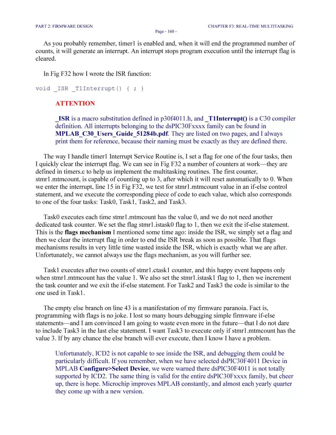
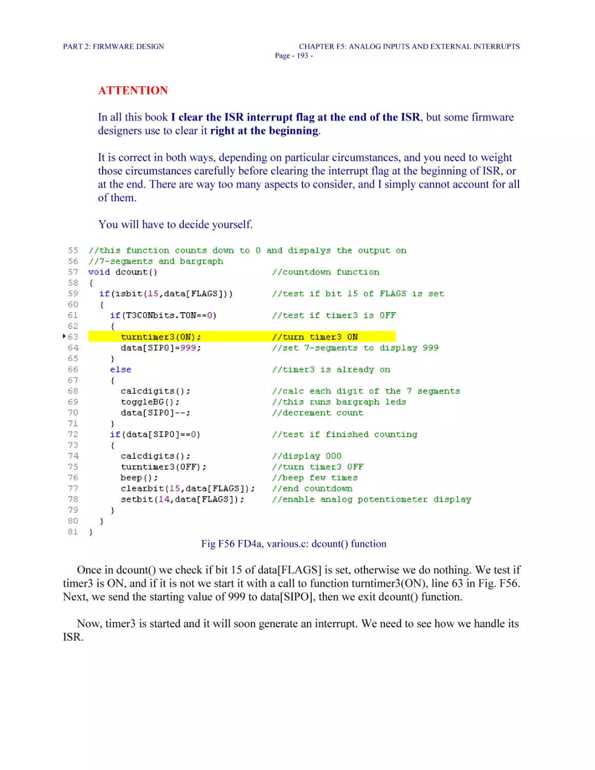
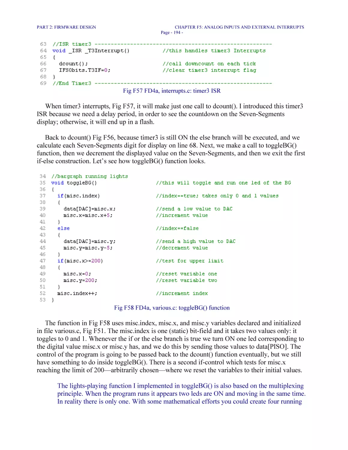
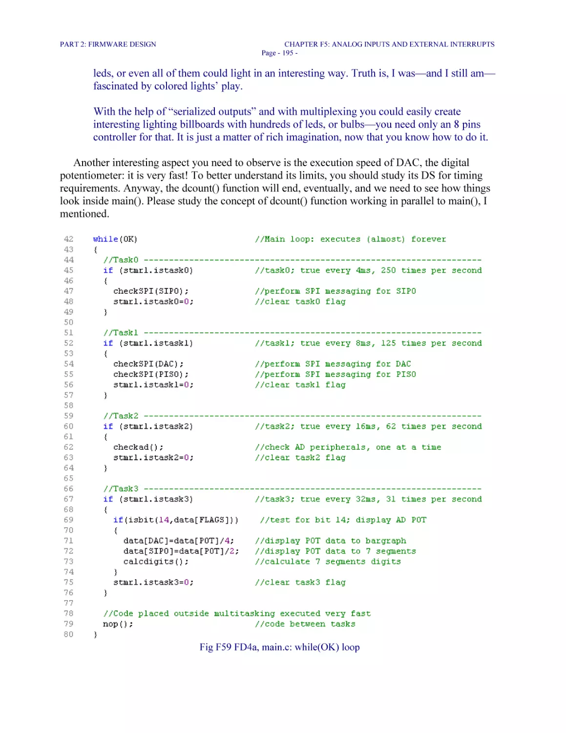
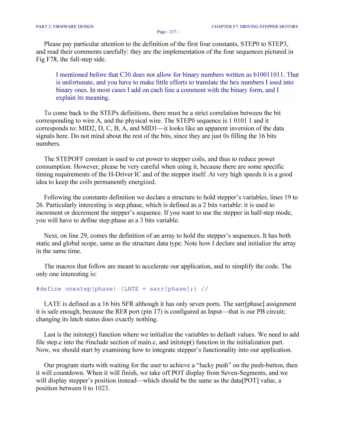
/


Автор: Popa O.G .
Теги: programming software computer systems computer technologies
ISBN: 0-9735678-7-2
Год: 2005


Текст
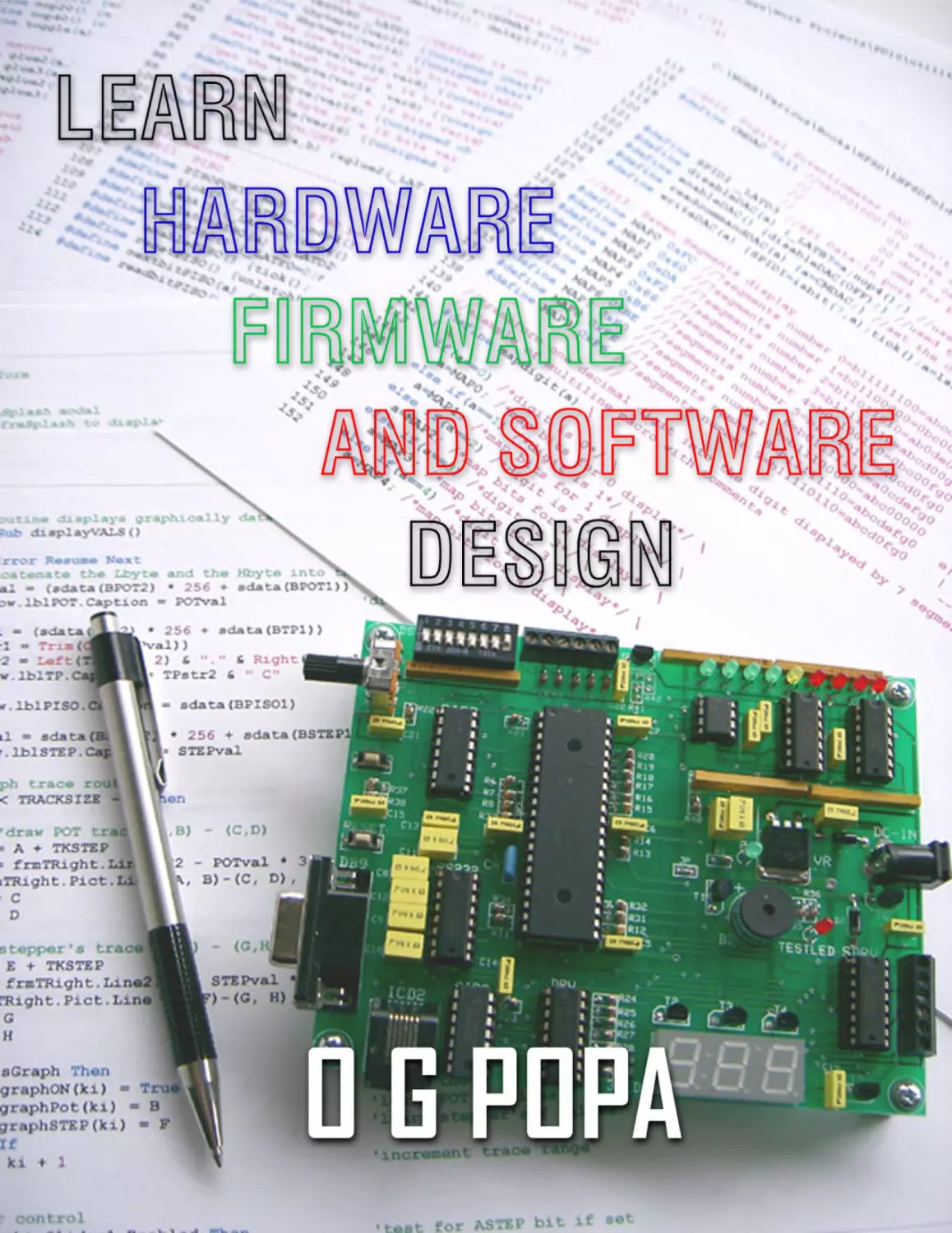
LEARN
HARDWARE FIRMWARE AND SOFTWARE
DESIGN
by
O G POPA
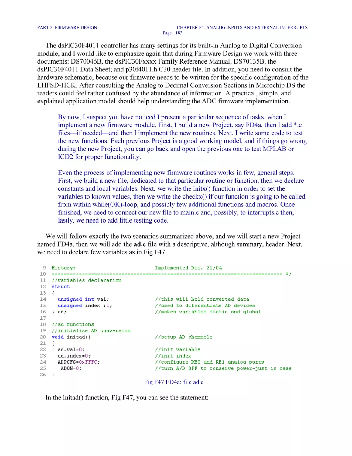
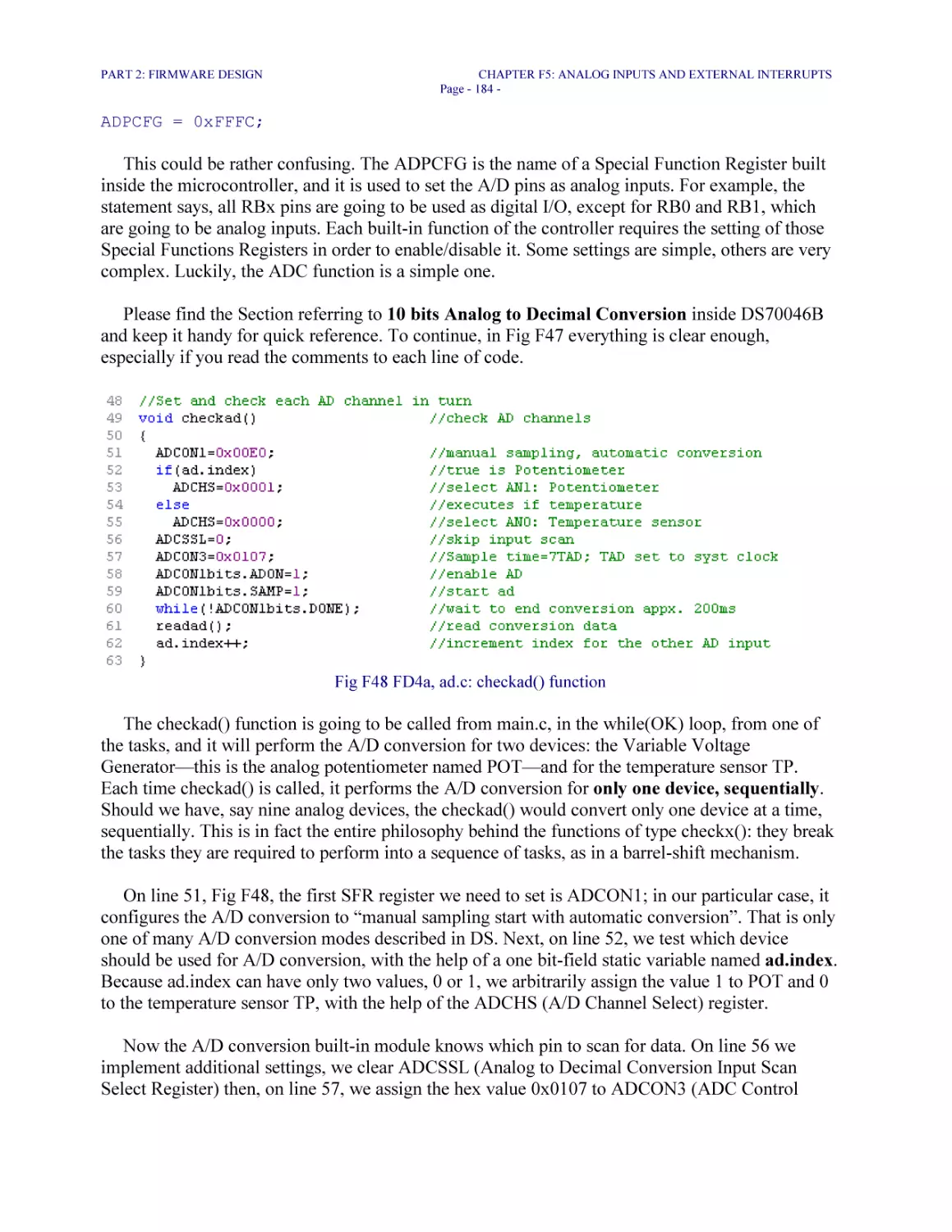
—————————
ISBN 0-9735678-7-2
Corollary Theorems Ltd.
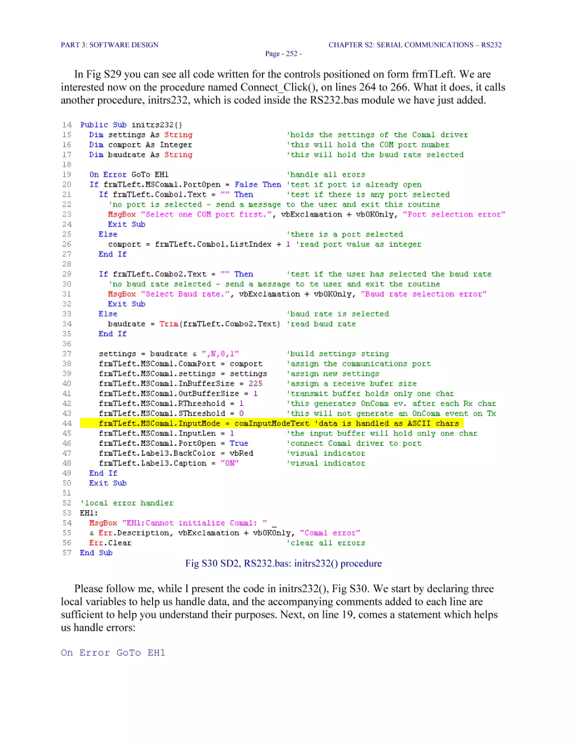
http://www.corollarytheorems.com/
—————————
LEARN HARDWARE FIRMWARE AND SOFTWARE DESIGN ISBN 0-9735678-7-2 Copyright © O G POPA.
Edition compiled by O G POPA. All rights reserved.
No parts of this book may be reproduced in print or electronic format without written permission from O G POPA
Electrical Schematics presented in this book may not be used for production of more than one PCB board per rightful
buyer. The rightful buyer is the person who has paid the required price for this book to Corollary Theorems Ltd. The
rightful buyer has the right to store this book in two different electronic storage locations, and is allowed to print one
paper copy, only.
All firmware and software programs, or fragments of programs, presented in this book are for educational purpose
only, and they must not be included in any commercial product.
Restricted distribution rights of this book are granted only to Corollary Theorems Ltd.
No copies of this book in print or electronic format are allowed without prior written consent from O G POPA
No translations of this book are allowed without prior written consent from O G POPA
Copyrighted Materials and Trademarks Acknowledgements
We have made all efforts to clearly mark all Trademark names in this book by capitalization, and by inserting the
Registered Trademark, Trademark, or Servicemark symbols on the first occurrence. However, we cannot attest to the
accuracy of the information. This book should not be regarded as misinformation, or as an attempt to the validity of
any Registered Trademark, Trademark, or Service Mark. Should there be any unintentional omission on our part, we
will introduce corrections, upon notice, while it is reasonably possible.
No copyrighted materials from external sources were inserted in this book, and we have striven to make it compliant
with the Copyrights and Trademark Legislations.
Warning and Disclaimer
All information in this book is for educational purposes, only. The Author, O G POPA, and Corollary Theorems Ltd.
have made great efforts to make this book complete, accurate, and suitable for study, but this does not imply any
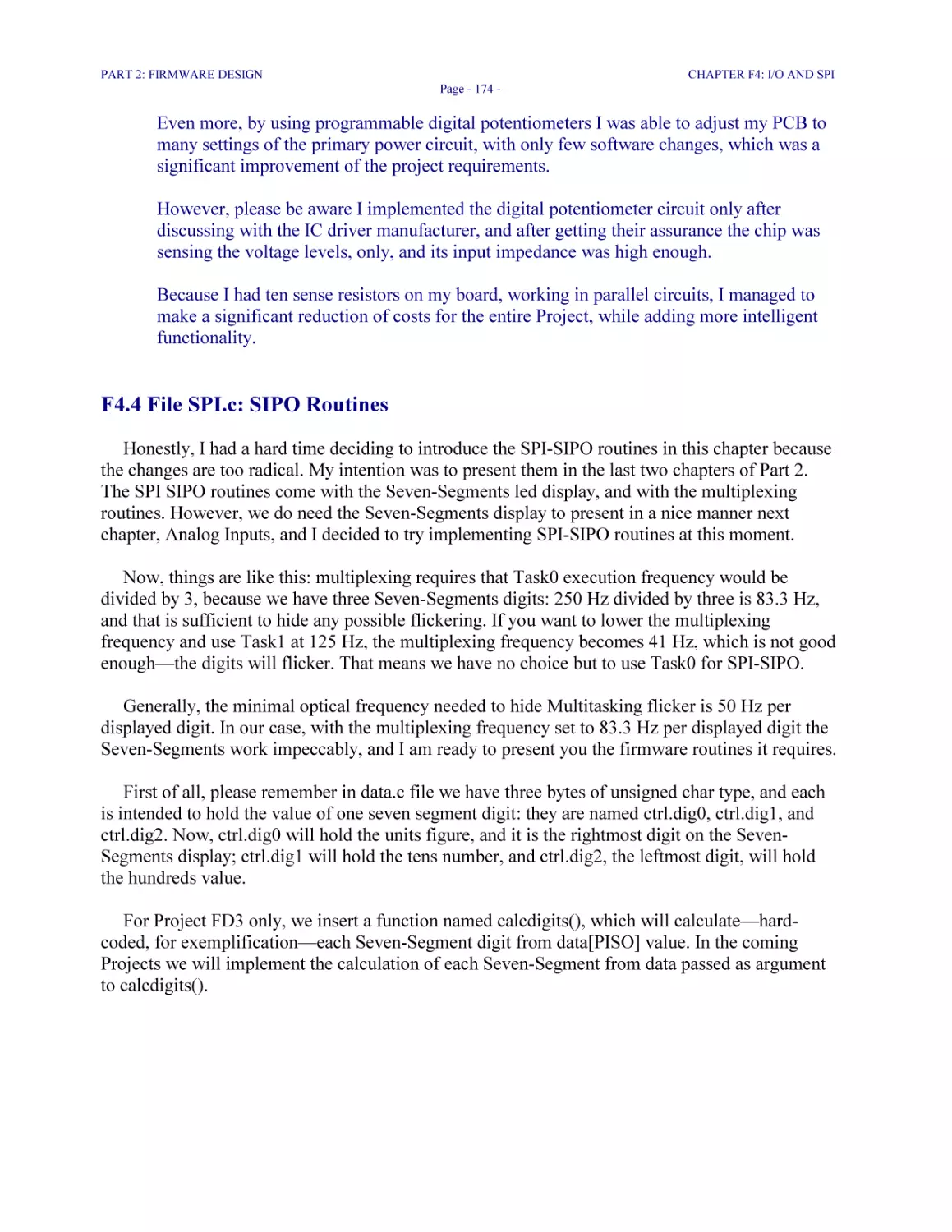
warranty or responsibility on our side.
Due to the special character hardware, firmware, and software design work have, accidents could happen. Under no
circumstance should the Author or Corollary Theorems Ltd. be held liable for any possible loss connected to the
information presented in this book.
For Library Use
This book may not leave the library, and it will not be lent in any way or form.
This book shall not be copied in any form.
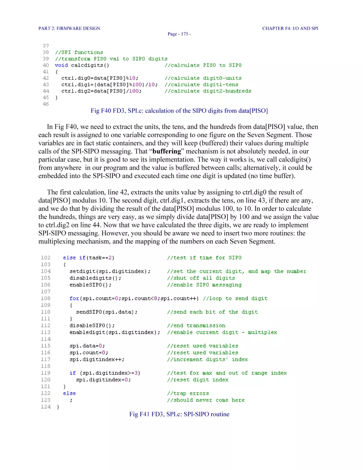
The library reader is allowed to print or copy maximum five pages from this book per library session.
LEARN HARDWARE FIRMWARE AND SOFTWARE DESIGN ISBN 0-9735678-7-2 © O G POPA format
“Business Card” CDR first published May 02, 2005
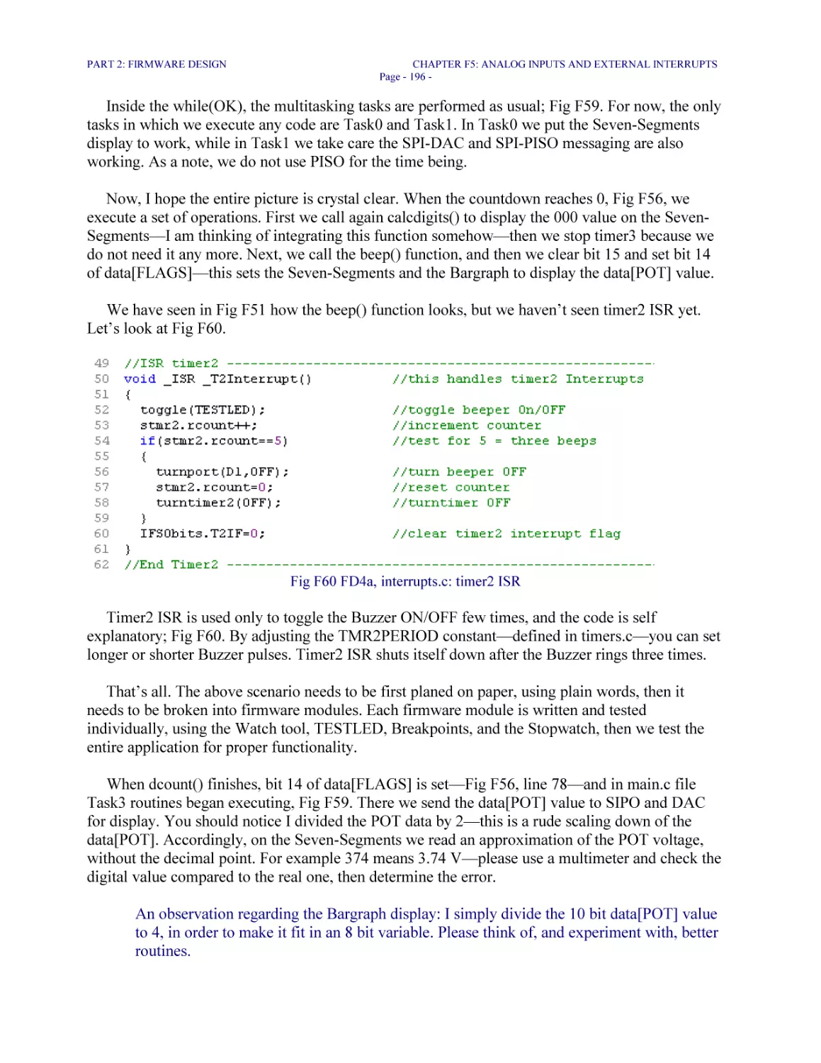
Previously published in “Download eBook” format ISBN 0-9735678-5-6 © O G POPA, April 08, 2005 in
http://www.corollarytheorems.com/
Distributed by:
Corollary Theorems Ltd.
http://www.corollarytheorems.com/
#304 10420 148th Street
Surrey, BC, V3R 3X4
Canada
1 604 581 9214
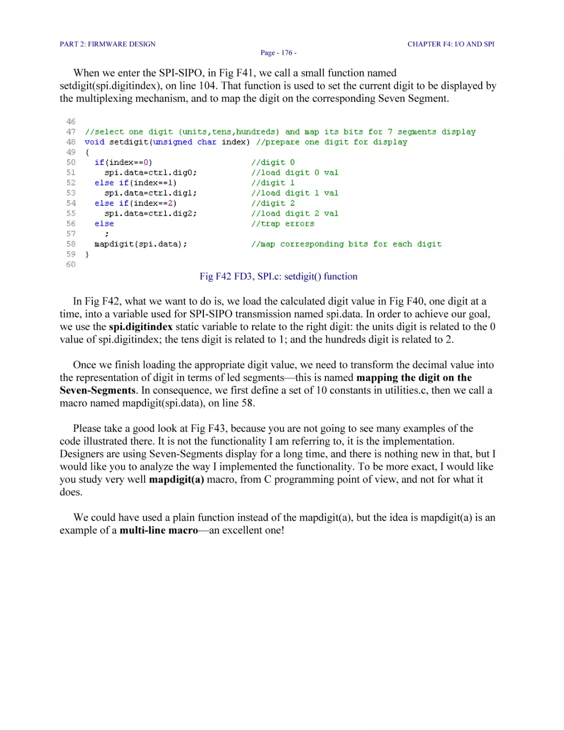
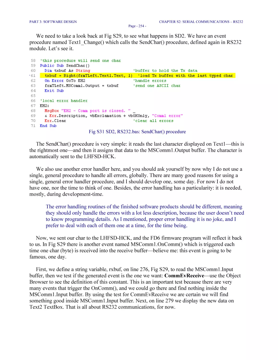
ABOUT THIS BOOK
Naturally, the first question is: “Is it possible to learn hardware, firmware, and software design
in a single, and not very thick book?”
My answer is “Yes”, plain and simple, and I will explain why. Both you and I know very well
it takes long years of hard study of each of the above design fields, and you need a lot of practice
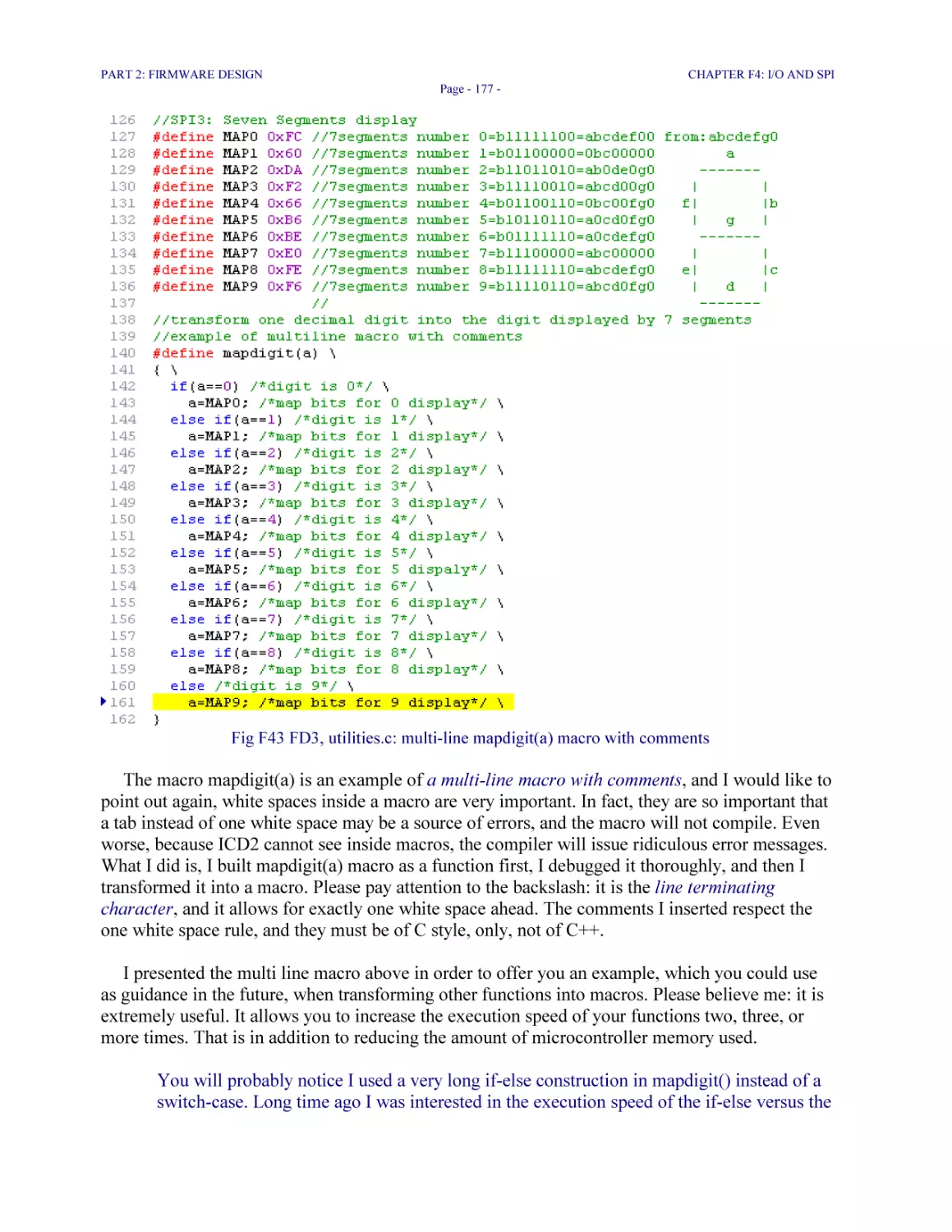
and many supporting books to successfully accomplish those tasks. However, the first step is the
most important one; it needs to be in the right direction, and executed in the proper way. This
book is a practical design example—a good, working one!—and it covers fairly well title topics. It
represents that first, small, and the most important step.
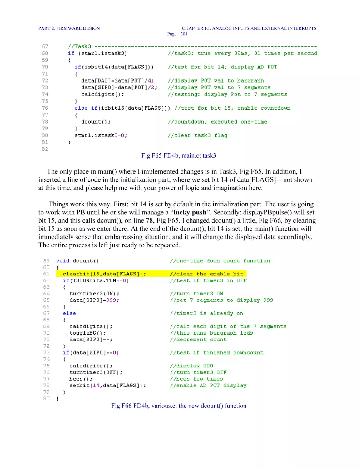
Over the years I bought many books related to various programming languages or to hardware
design, and I always looked for the thickest ones, hoping they contain more precious knowledge.
Unfortunately, many times I was rather disappointed, and I considered myself quite lucky if two
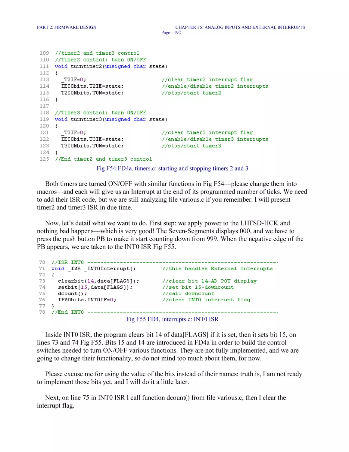
dozens out of twelve hundred printed pages contained any useful, practical information. They are
piled now on shelves, and it is possible I will look for one or two lines of code in any of them,
during the next two or three years.
The tough reality today for writers and publishers is, the best place to find general knowledge
information is the Internet, due to the fact it allows for filtered, fast, computer search. In addition,
that information is totally free!
“Now, wait a minute, Gino,” you might say, “if the Internet is the cheapest and the best place
to find information, why should I make the effort to buy your book?”
Well, my friend, printed or electronic books you buy contain information that goes way beyond
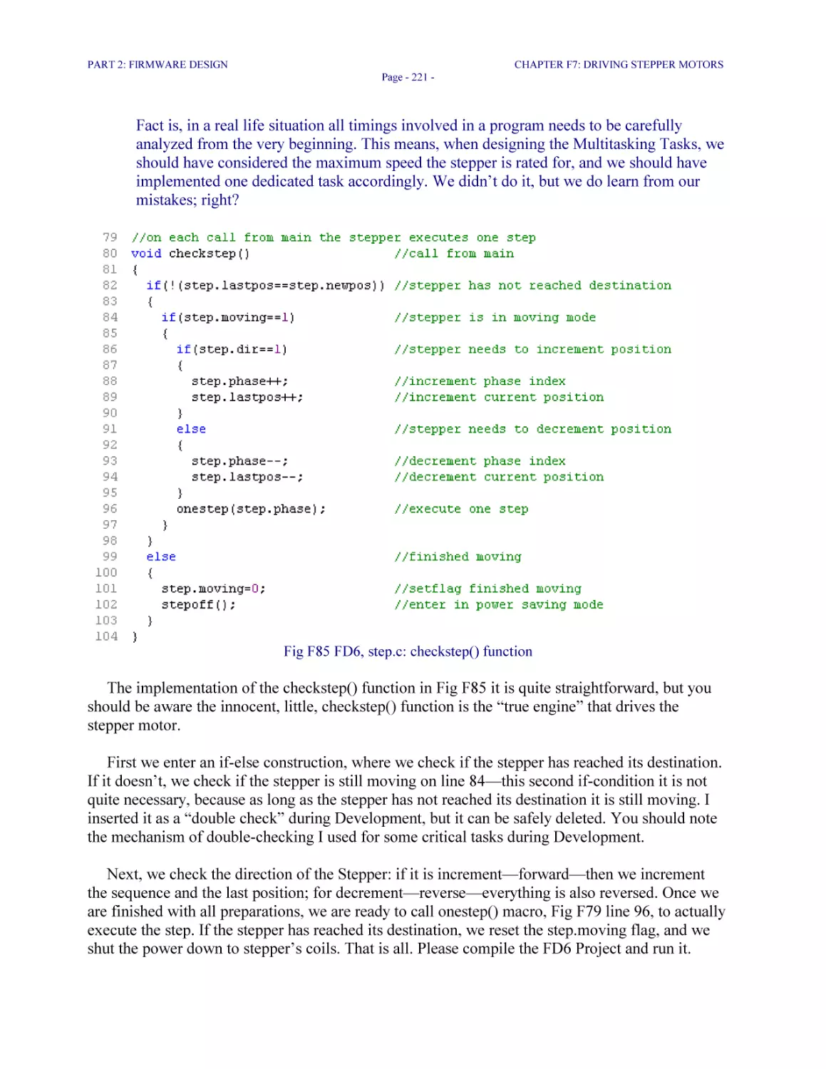
general, basic, and free knowledge you will find on the Internet. Information was, it is, and it will
forever be the most expensive item in existence. If you are serious about learning, expect to invest
little time, efforts, and money for that, same as we all do.
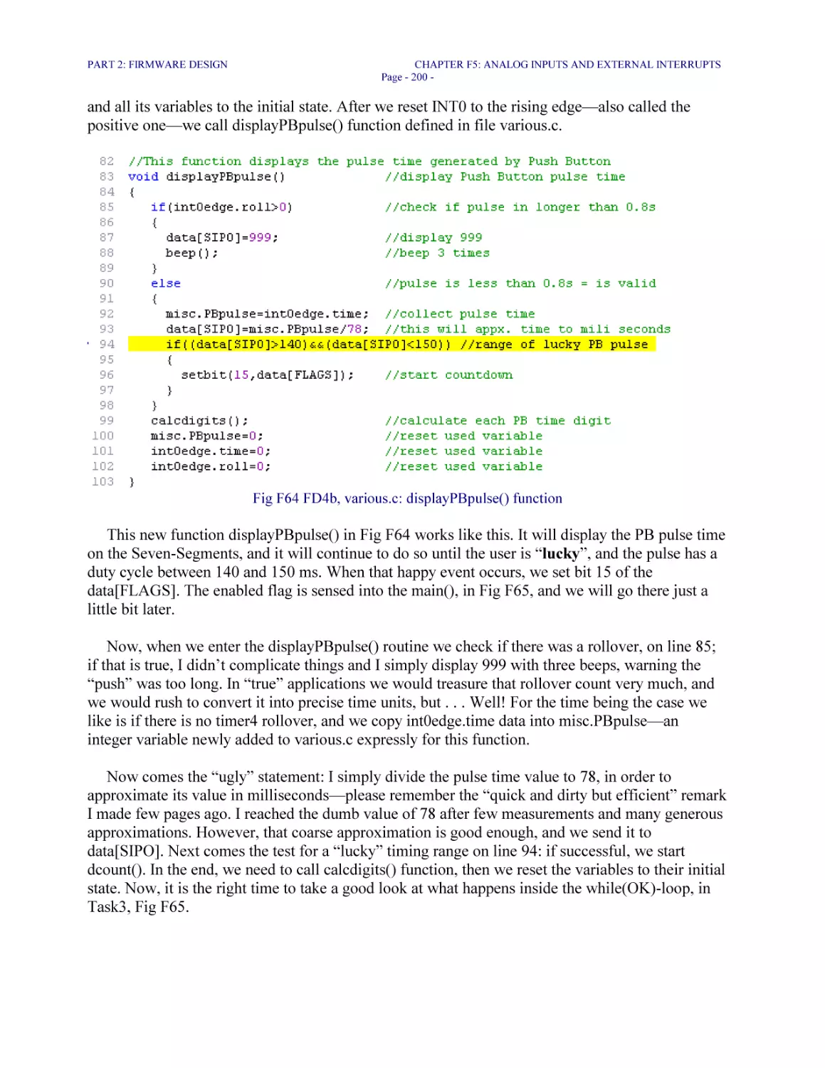
Now, the problem with the available free information on the Internet comes to the readers’
advantage, because it forces Authors and Publishers to come up with competitive books that will
appeal more. Unfortunately, few books manage to do it, and that brings a bad reputation to the
trade. However, I have no doubts the readers will find this book different from any other. I am not
afraid of competition, and I believe this book I present is the best one ever in its domain. I base all
my reasons on the fact I know what is good or bad information, because I searched myself for
years, for good design books. Before being a writer, I am a voracious reader!
Learn Hardware Firmware and Software Design (LHFSD) is in fact a Design Project; an
example of how things work and are done professionally in the industry today. I will guide you
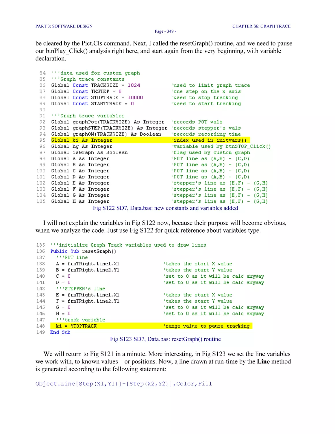
step by step through hardware, firmware, and software design, and we will build, together,
working, useful tools, with a large range of applications. In fact, this book builds a set of templates
LHFSD
ABOUT THIS BOOK
Page - 5 -
which you will reference throughout your future design career, in personal hobby development, or
when you will decide to start building your own commercial product!
To come back to the question of learning hardware, firmware, and software design in a single
book, that is perfectly possible with good Project Management skills. By some strange turns of
events, it happened I worked all my life with prototype projects and new technologies, and I had to
execute tasks that seemed, if not impossible, at least very difficult. After many years, the difficult
tasks of the impossible type fail to impress me anymore. This book is just another technical project
for me, and the only difficult aspect is, I have to finish it within deadlines—you cannot even
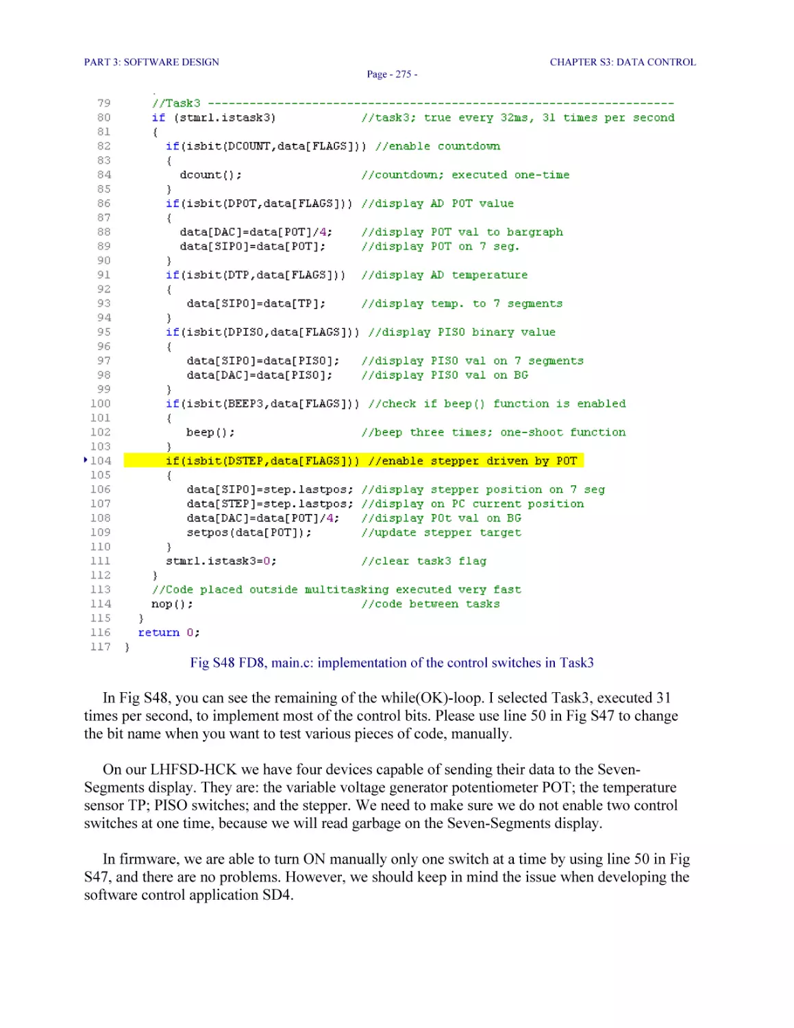
imagine how tight those deadlines are. However, you, the reader, have all good reasons to doubt
my words. Just bear with me throughout the book and you will be the one to decide if I
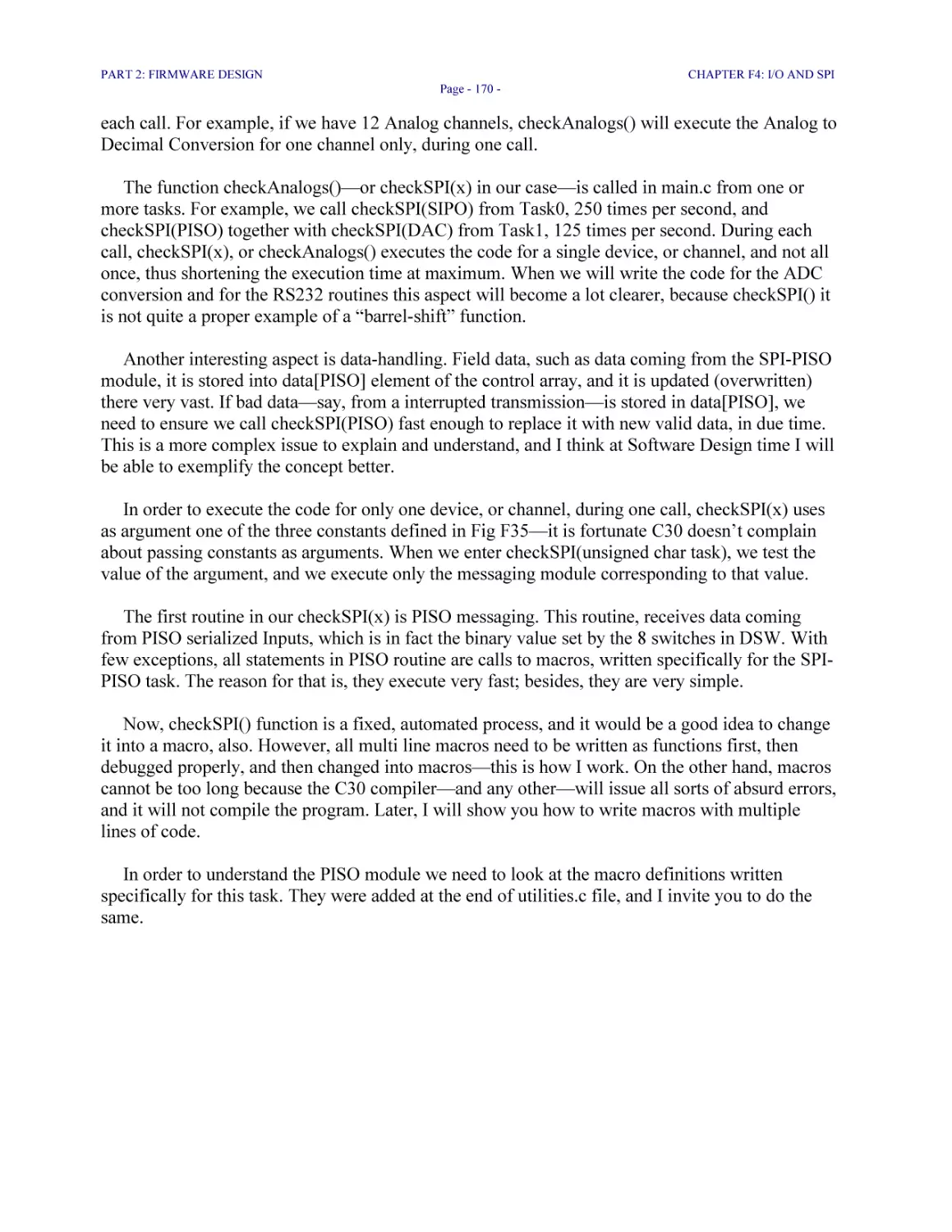
accomplished those tasks sufficiently well or not. Do not worry: I will know your decision.
The second important question which needs to be answered is: “What is this book about
exactly?”
Learn Hardware Firmware and Software Design is structured in three parts, and here
follows a brief summary of their content:
Part 1, Hardware Design, is a practical schematic design: we are going to build together the
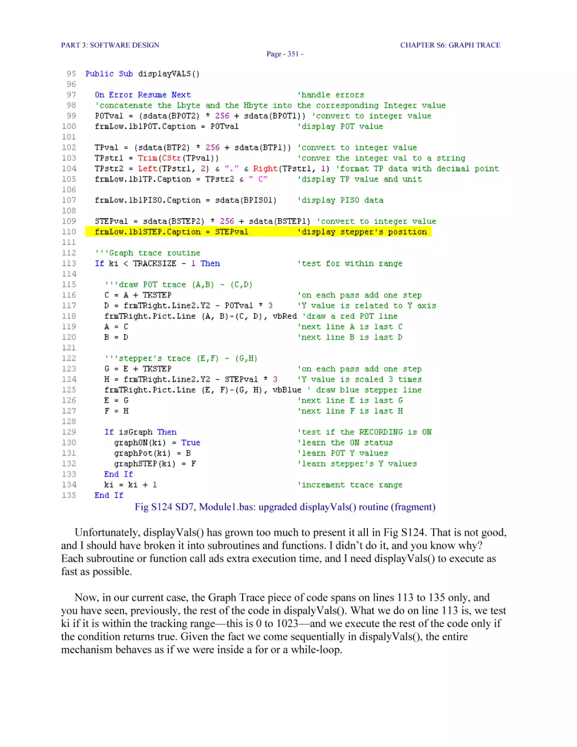
LHFSD-HCK (Hardware Companion Kit). That piece of hardware has a fair degree of complexity,
and my intention is, it will be a useful hardware tool, or instrument, good enough to burn a
dsPIC30F4011—or dsPIC30F3011—microcontroller, to test additional hardware modules, and to
quickly implement new firmware and software test programs.
We will start from a plain, blank page, and we will design the LHFSD-HCK gradually, to
include the following hardware modules:
1. The ICD2 interface needed to program and debug the firmware code;
2. The RS232 interface needed to communicate serially with the software control
applications residing on your PC;
3. One Seven-Segments three figures led display. I used multiplexing to drive those three
figures, which is an interesting hardware and firmware application to learn. In addition, the
seven-segments display is an excellent debugging tool, because it can show the integers’
values inside the hard-to-reach routines—the MPLAB® ICD2 In-Circuit Debugger cannot
see inside all pieces of firmware code, like macros and ISR (Interrupt Service Routines).
The seven-segments module is also an excellent example of working with standard logic
ICs of the “Shift Registers” family.
4. The SPI® Bus (Serial to Peripheral Interface) connected to three devices: serialized
Inputs (PISO), serialized Outputs (SIPO), and to a programmable digital potentiometer
working as Digital to Analog Converter (DAC);
LHFSD
ABOUT THIS BOOK
Page - 6 -
5. Visual and audio testing circuits;
6. One External Interrupt circuit, although many others are possible to implement, based
on the example presented;
7. Two Analog to Decimal Conversion circuits;
8. One Bargraph module using eight comparator Operational Amplifiers;
9. One stepper driver module for both unipolar and bipolar motors;
10. Five microcontroller spare circuits, plus ground, which will allow you to extend the
functionality of the LHFSD-HCK beyond the frame of this book. In this respect, the
LHFSD-HCK could become just one component in a complex, multi-controller design.
At the present time the LHFSD-HCK is built, revised, and tested for endurance. It performs all
functions perfectly well, and I am certain it will be an exciting design experience for you.
Following the LHFSD-HCK example, you could easily design other boards, similar to the one
presented. You could further connect the boards together and experiment with data exchange in a
multi-controller environment—just use the custom SPI Bus example I presented, in order to send
data serially between many controllers.
Part 2, Firmware Design, will reveal many secrets of C firmware programming known to few
programmers. There is no Assembler code in our firmware programs—excepting the classical
embedded NOP operation—and I created a Real-Time Multitasking, multiple files project
structure, with only one source file. That is the best method of working with multiple firmware
files, and it is known to few professionals. It may be things sound rather confusing now, but have
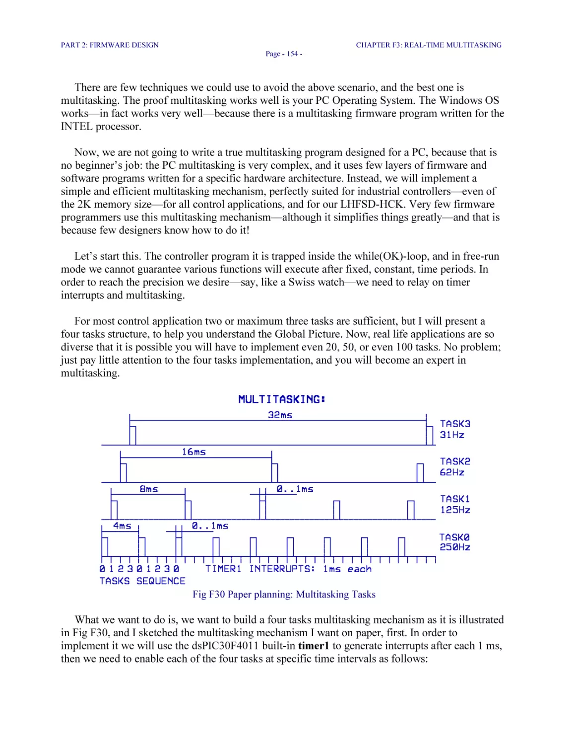
little patience because they will become clear as daylight—do not worry!
All initialization routines I present are useful templates for enabling or disabling various
dsPIC® Digital Signal Controllers system-modules, and you could use them to program all
controllers belonging to the dsPIC family: they are all similar in functionality to dsPIC30F4011!
Since I am well experienced with almost all Microchip® controllers, I can deliver even more good
news: all Microchip controllers—that is in addition to the dsPIC family—work the same, when
using C to develop applications. If you learn the dsPIC30F4011 well, you will be able to work
with any other Microchip controller!
The firmware code we are going to write will be Interrupts Driven Real Time Multitasking,
and it will be implemented in very simple and thoroughly explained ISR. One file is dedicated to
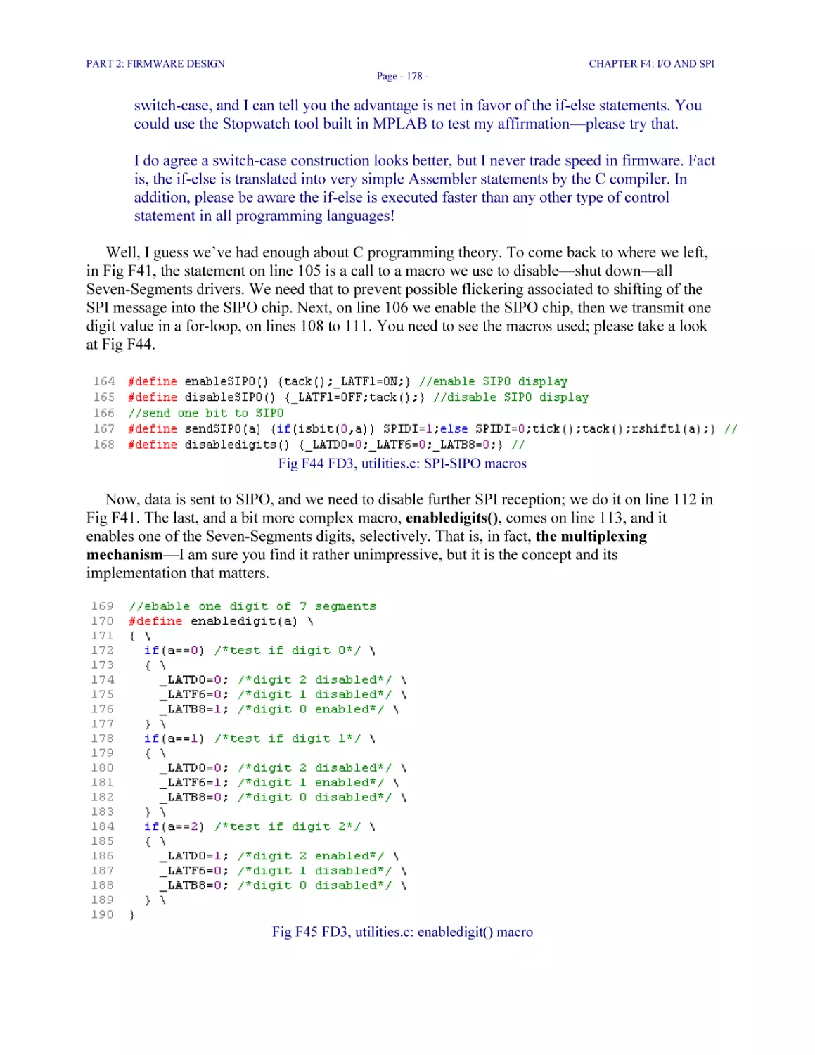
“Utilities Macros”, and you will learn few, simple, and extremely efficient coding shortcuts using
macros—they are precompiled in machine code at compile-time, hence they execute faster than
any other piece of firmware code.
What we want to achieve in Firmware Design is to test all hardware modules we have designed
in Part 1, and to prepare for data exchange with the software applications written in Part 3. Again,
we will start with an empty page, and we will code our way up. You will start loving firmware
LHFSD
ABOUT THIS BOOK
Page - 7 -
programming, and I am convinced you will regret when Part 2 will end. The good news is
Firmware Design is going to continue in Part 3!
Part 3, Software Design, will show you how to use Visual Basic® 6 to build a simple and very
efficient software control interface for hardware and firmware. You could easily use the
knowledge you will gain to control/test in software any other hardware/firmware application, or to
develop your own commercial product. The power of software added to firmware and hardware is
limited by your imagination, only, and this book will help you get a good grip on high-level
technical software programming.
All software applications work perfectly well. However, I would like you to study them more
as programming guidance, so that you will be able to implement similar ones in Visual Basic®
.Net, or even in Visual Basic® 5, depending of the software tool you have. It is the “how to”
lesson I would like you to learn, because in software we can implement specific functions in many
different ways. Only the end-result application or product is what really matters.
As I mentioned, in Part 3 we will continue developing few more firmware programs in parallel,
because both software and firmware start working together. The last software application is
Graph Trace, and at that time you will have all knowledge needed to start building you own
custom oscilloscope. Again, it is the principle that matters, because practical applications are very
many. For example, Graph Trace could be easily used to design medical devices that monitor the
heart-beats and blood pressure; to display the value of a peripheral sensor, as is the vehicle
acceleration vector “a”; to display the output of the automotive oxygen sensor; to display the pH
content of a solution; to . . . Yes, the possibilities are endless!
In Visual Basic 6 we will use built-in Wizards in order to help us code fast and efficient,
without many headaches, but we will correct and add to the code they generate in order to
straighten things up. To add a bit more color, we will implement a custom Internet Browser into
our LHFSD software application, with minimal efforts. It will be perfectly functional, and my
intention is to exemplify the enormous power our little software application has. Part 3 ends with
building an Installation Setup program, which is last step in Software Development.
As you can see we cover all aspects of hardware, firmware, and software design fairly well.
The only fear left, I suspect, is how precise, and easy to assimilate my presentation is going to be.
Well, I will explain everything you need to know in details, to clearly understand what I did,
and I will indicate the best sources for additional information. Even more, each chapter will have
Suggested Tasks, which will help you start working on design by your own. My intention is,
LHFSD will become THE reference book for all your future design work, and it will continue to
be number one for many years to come. This book is unique in the entire World today, because it
explains how hardware, firmware and software can be put to work, interacting and supplementing
each other, in practical applications. No other book has done that before; not even close! LHFSD
is the most you could get in terms of useful knowledge, in any of the mentioned design fields.
Now, I presume that the last unclear issue is: “To whom is this book addressed?”
LHFSD
ABOUT THIS BOOK
Page - 8 -
Of course, LHFSD was designed to help beginners to start on the difficult—although fairly
rewarding—path of hardware, firmware, and software design. They are the ones who will benefit
mostly of the knowledge inserted in following pages.
Another category of readers is the average person willing to gain more knowledge on the
subjects, without stressing too much with technical aspects. My belief is, that is also possible,
because I will try explaining everything using the simplest technical terms. In fact, the true quality
of this book is, it explains and implements advanced technical concepts, based on elementary
hardware modules, on the simplest firmware routines, and on the most basic software procedures.
To me, this is the true, professional secret: no matter how complex the design work is, it is
always possible to break it into very simple (sometimes even disappointingly simple)
hardware or software component modules; this affirmation is true even for the spaceship or
nuclear research technology.
In fact, what I would like you to learn in this book is to deal with any hardware, firmware,
and software project. I want you to understand the Design Method I use, because that is
the most important lesson. Implementing particular functions is simple and easy, but
learning how to start and finish a new design project is a skill which will open for you real,
benefic perspectives.
Many readers would like to start designing as a hobby, off-hours, in their basement or in some
other cozy place, in order to build themselves a nice, useful commercial product. This is how very
many existing commercial products came into existence, and how some extremely successful
businesses have been started. I say, this is the book you need, and I will try helping you even
beyond its pages—just trust me with this one.
For intermediate level designers Learn Hardware Firmware and Software Design is a
priceless gift, because it is easier to understand. They will learn many secrets of improving their
designing and programming efficiency, and they could quickly implement all Suggested Tasks
exercises.
Lastly, this book is an excellent reference for advanced level designers. It happens, by the
time someone reaches top levels of professional development, a lot of simple, but necessary, basic
knowledge is forgotten. It did, and it still happens to me, and I always welcome a good reference
book on subjects I mastered fairly well sometime ago.
Now, you will notice I inserted few Experience Tips which I discovered the hard way, during
many years of design work. They are still very helpful to me, and I hope they relate properly to the
topics explained. For example:
LHFSD
ABOUT THIS BOOK
Page - 9 -
Experience Tip #1
Some time ago I needed to implement a Cyclic Redundancy Check (CRC) algorithm for
the OBDII (On Board Diagnostic version two) automotive protocol. I started searching the
Internet for a sample algorithm and, after four exhausting days each of 12 long hours in
length, I reached the conclusion I will never find what I needed.
There was plenty of theory about CRC on the Internet, and there were few example of
algorithms based on table-search, but I wanted the software implementation of the 8 bits
CRC check formula—that was: x8+x4+x3+x2+1—because the table-search method was
taking too much of my processor memory.
As I mentioned, after four long days I decided to abandon my Internet search, and to write
the algorithms myself. It took me exactly 20 minutes and one single page of routines to
implement a quick, command line testing program in C. It worked like magic! I was very
happy, and amazed of my own work. Later, I analyzed the entire process in order to draw
some valuable conclusions from that experience.
During the four days I lost searching for something that didn’t exist—almost certain, that
piece of algorithm was way too valuable to post it as freeware on the Internet—I studied
the CRC theory very well. Once the theory was crystal clear in my mind, implementing it
in software was just as easy as eating a good piece of cake at breakfast time.
Further from that day it became my routine to take little time to understand the theory,
first, and then to jump on designing. Since then, my work has improved substantially.
In this book I will help you understand and believe in that experience I had. Once you will
know very well what you need to do, and how, you will become not only able of doing it, but you
will also be amazed of how easy it actually is to make things work—what I mean is, work very
well! What you are going to discover in the following pages are secrets of hardware, firmware and
software design work developed by few specialists, with the intention to simplify and make the
designing process fast and more efficient. Those secrets are never told, because they make design
Gurus be Gurus. You are also going to become a hardware, firmware, and software Guru, after
studying methodically this book.
The hidden truth about hardware, firmware, and software design work is, if you know how to
do it, the entire process is incredibly simple and straightforward. However, in order to reach that
level of knowledge it could take you few good years of microcontrollers hardware design; then
few years of firmware design with microcontroller specific Assembler and C; then few more years
of software development with Java®, Delphi®, C++, Visual Basic . . . Overall, there are rather
many “few years”, but cheer up: it can be done a lot faster, and you will experience it right here, in
this book!
If you intend to become a good hardware, firmware, and software designer, please be aware
you are struggling to succeed in a time race. Each day the Hi-Tech domain develops new and more
complex techniques, and it becomes harder and harder to catch up. In the same time, it is more and
LHFSD
ABOUT THIS BOOK
Page - 10 -
more difficult to find information about concepts and techniques developed in 1960s and 1970s,
and that is very bad. Almost all advanced programming concepts and techniques we use today
were designed in that period of time. Take for example Object Oriented Programming: it was
designed theoretically in the 1960s. Today, we have implemented in C++ only a part, not all of the
OOP concepts initially designed. The reality is, many incredible, powerful programming routines
are forgotten with each passing day, because they are embedded into objects, in precompiled
binary code, and in DLL files.
What you will discover in this book is information you will never find in any other book—at
least not grouped together as it is presented here. All design examples presented in this book are
unique, original and personal creations, and they are based on many years of professional
experience. Excepting the basic information contained in Data Sheets and in the online Help, I
used no reference sources to write this book. However, you will discover the quality of useful
design information presented here it is way better than anywhere else.
In addition, the structure of this book it is just an unbelievable opportunity: nobody ever
troubled to explain how things work, globally and in minute details, starting with hardware design,
then using firmware to control hardware, and ending with software taking control of firmware and
hardware. All in just one book! You are very fortunate, my friend, to buy this book and start
studying it very, very seriously, as soon as possible.
What you will learn here is a new technology: designing with microcontrollers. That is entirely
different from writing applications for PC, because the firmware and software applications we use
need to be the most basic, the simplest, the fastest, and also the most efficient ones possible. Of
course, once you learn how to master microcontrollers, you could improve your skills to any level
of complexity; you could even write your own BIOS (Basic Input Output System)—that is not
very difficult. In the particular case of working with the dsPIC30F4011 controller, you will learn
to control Microchip Digital Signal Controllers, which will open for you the gates to the great DSP
domain! Overall, this book teaches you how to control and embed into practical applications any
Microchip controller.
Lastly, I suspect you are wondering about who am I. My name is O G Popa, and I am
Professional Engineer in the Province of British Columbia, Canada. I have 24 years of incredibly
rich engineering experience, combined with permanent, profound study.
***
REQUIREMENTS
My recommendation is, you should first read this book as a relaxed lecture. There are no
additional requirements to understand it—excepting your power of logic, naturally. If you have an
advanced level of hardware, firmware, and software design, you do not necessarily need to
experiment with the firmware and software routines presented, and you could use this book only
as reference for your future design work. However, if it is your intention to study seriously and to
experiment with all schematics and programs presented here, then you do need to prepare first.
Please be aware hardware, firmware, and software design work could be quite expensive to deal
with, and you should expect to invest something into acquiring the knowledge.
This book is based on Microchip controllers, because that is still the cheapest and simplest
technology available to start professional hardware and firmware design. For software design,
Visual Basic 6 compiler is also one of the cheapest and most efficient software tools available. Of
course, we are limited to the Windows® PC environment, but that is over 80% of the existing
market. We need to consider that aspect very well. On the other hand, those particular limitations
refer only to the tools and technologies we use, because designing skills you will learn work on all
Operating Systems and on other microcontrollers as well.
Now, after a first, relaxed lecture of this book it should be perfectly clear to you what to do
next. If you decide to build yourself the LHFSD-HCK (Hardware Companion Kit), to test all
firmware routines and software programs, you need to procure few electronic components, and
then the software compilers. Let’s see what it takes to bring into factual reality all designs in this
book.
For Hardware Design you need, first of all, a Schematic and PCB Editor, and there are
many interesting options for that. If you already have one, then use the one you are most familiar
with; if you do not have any, then you need to go on the Internet and start with a search for “free
PCB software”. Have no fears, you will find your tool.
The good thing is, PCB-CAD software design tools are much needed these days, and there are
many companies striving to offer their products. Now, the interesting aspect is, while some
Schematic and PCB editors are priced in the range of 500 to 10000 USD, others are totally free!
Well, not quite totally free, as you will discover—good things are never free—but they are a very
cheap alternative. I dare say, in the near future the price of the PCB-CAD tools is going to drop
dramatically. Even more, if any of the readers will feel the call for Visual Basic software
development, I encourage them to try building a Schematic and PCB-CAD editor—again, that is
not very difficult.
Now, one way or another you will get your software tools for hardware design, but the tragedy
comes when building the LHFSD-HKC. Although your board will work just fine, it is going to be
rather expensive for a learning aid. We will calculate its approximate costs when studying the
BOM (Bill of Materials). Fact is, LHFSD-HCK is mandatory to experiment with all firmware and
software programs presented. Sure, as I mentioned, if you do have some experience or a very
LHFSD
REQUIREMENTS
Page - 12 -
strong logic, you do not necessarily need to experiment with the firmware and software routines I
present: in that case you will understand them logically. However, little hands-on experience is
mandatory when working with microcontrollers, so . . .
Anyway, in order to help you reduce development costs I will try contracting the LHFSD-HCK
kit with a local manufacturer, which should cut its price in half, or less, not to mention time
saving. That is my intention, but I haven’t done anything yet, because the first step for me is
finishing this book. The good news is, I always manage to implement my intentions, somehow.
Please visit http://www.corollarytheorems.com where I will build few pages dedicated to the
LHFSD book. You will find there software updates for all source code in this book, and
information regarding the future, possible, LHFSD-HCK kit. Now, even if you are going to buy
your LHFSD-HCK from Corollary Theorems, you still need to study hardware design very well,
because hardware and firmware are strongly related together.
Firmware Design requires that you buy the MPLAB ICD2 tool from Microchip. ICD2 is a
very good investment, because you will have a Debugger and a Programmer in a single tool, for a
wide range of Flash microcontrollers. Please buy the complete kit, with RS232 serial and USB
cables, and with the AC/DC power adaptor included, because we will need them all.
Microchip offers their MPLAB® IDE (Integrated Development Editor) for free download,
which is quite encouraging. Unfortunately, you also need the C30® ANSI C compiler to write
firmware, and it is not cheap. You have to decide yourself if you will buy C30 or not. The good
news is, Microchip allows for 60 days free trial period of a fully functional C30 compiler (a
student version). You should download yours when you feel you are ready, and you have the
necessary time. All firmware programs in this book have been developed during the 60 days trial
period—together with many other tasks—and that means it is possible.
On the other hand, the firmware programs presented in this book may be easily ported to any
other C compiler which handles Microchip dsPIC family of controllers, because they were written
in ANSI C. All you need is, translate the header file and the ISR definitions to the new
environment.
Software Design is implemented with Visual Basic 6 compiler and you do need that
excellent software tool. Although modestly expensive, Visual Basic 6 is one of the cheapest
compilers available, of the professional type. Used efficiently, it can help you write beneficial,
commercial products. As an example, the first four SDx (Software Development) applications in
Part 3 are everything you need to know in order to start developing a commercial product, similar
to the HyperTerminal® one—even better.
Now, I let it to your appreciation if you want to work in Part 3 with Visual Basic 6 or with
Visual Basic .Net. I suspect a program developed in Visual Basic 6 is perfectly portable to Visual
Basic .Net without major modifications, but I haven’t experienced that. However, everybody
knows Microsoft® strives to make all their older programs compatible with newer, improved
versions, which is very nice of them.
LHFSD
REQUIREMENTS
Page - 13 -
If some readers have already Visual Basic 5, I encourage them to try implementing software
applications using the code in this book as guidance. It should work, if you have the ActiveX
controls I used; otherwise, try finding similar controls.
You will need a second PC, in order to work with ICD2 Debugger and Visual Basic 6 in the
same time. However, you could try a little harder and use both tools alternatively, on a single PC.
An important issue is, you do need to have both the serial interface DB9 and the USB ports on
your PC machine. The best case is to use one PC with RS232 serial interface—using the serial
DB9 connector—for Visual Basic and HyperTerminal, and a second one with an USB port for
MPLAB ICD2. The OS of your PC could be anything from Windows® 95 to WindowsXP® 2005,
as long as it supports the software tools we are going to use. Again, the most important is to
understand the Design Method I present, because practical implementations could be easily
adapted to any Windows platform, and even on other Operating Systems.
Lastly, regarding your personal skills you should know something about basic notions of
electronics, and you should have at least some idea about C and Visual Basic programming. It is
advisable to keep few good C and Visual Basic programming reference books close to your hand,
if necessary, while working with this book.
As for the future, you do not have to worry: if you do understand and like what you read in this
book, you will learn advanced electronics, ANSI C, and Visual Basic programming by yourself, in
no time!
***
CREDITS
I want to express my gratitude to Microchip Technology Inc.® for helping me write this book.
They sent to me one MPLAB ICD2 Kit, three dsPIC30F4011-IP201 controllers, few sample ICs,
and they designated a Consultant Specialist for technical support.
Unfortunately, due to the fact I had only sixty C30 compiler working days, I simply had no
time to benefit from Microchip’s technical assistance while writing Learn Hardware Firmware and
Software Design.
Nevertheless, the help was offered, which is very nice of Microchip.
Thank you,
O G Popa
***
TABLE OF CONTENTS
ABOUT THIS BOOK 4
REQUIREMENTS 11
CREDITS 14
TABLE OF CONTENTS 15
TABLE OF FIGURES 19
PART 1 HARDWARE DESIGN 25
CHAPTER H1: MICROCONTROLLERS 26
H1.1 General Presentation 26
H1.2 Microcontroller’s Pins 31
H1.3 Application Notes 35
H1.4 Prices and Footprints Considerations 36
CHAPTER H2: OSCILLATOR CIRCUITS 38
H2.1 Oscillator Circuits 38
H2.2 Crystal Oscillator Circuit 39
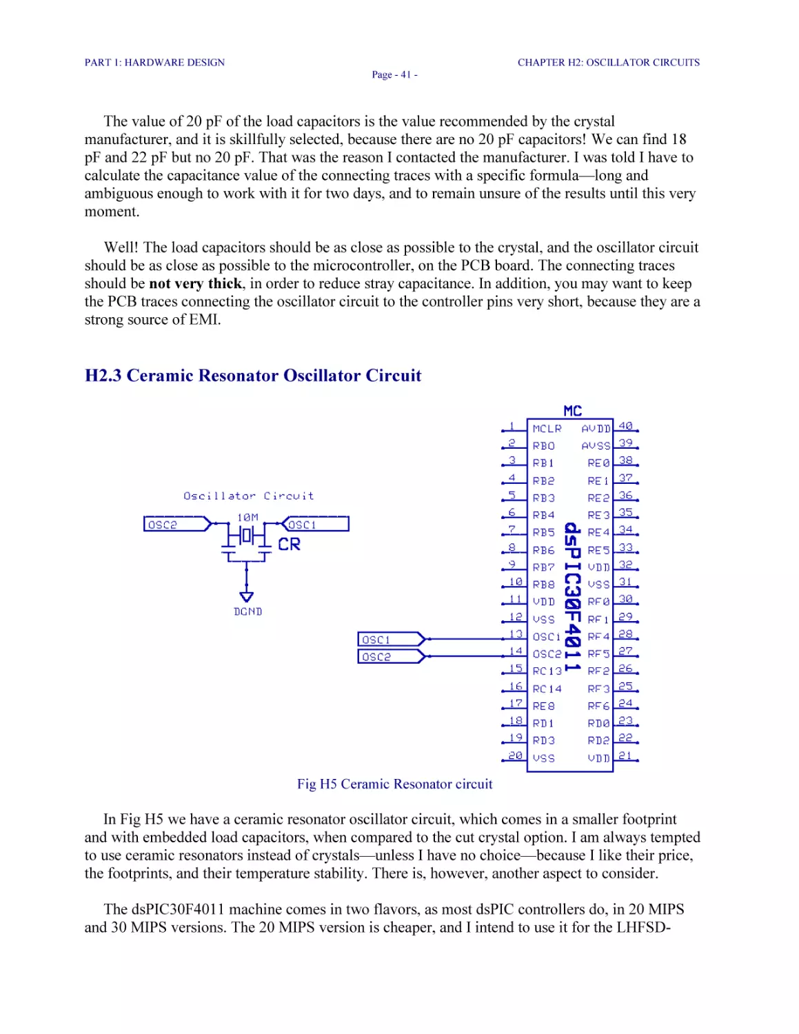
H2.3 Ceramic Resonator Oscillator Circuit 41
CHAPTER H3: POWER SUPPLY 44
H3.1 Voltage Regulators 44
H3.2 The power supply circuit 45
CHAPTER H4: MPLAB® ICD2 INTERFACE 49
H4.1 The MPLAB® ICD2 Interface 49
CHAPTER H5: THE RS232 INTERFACE 54
H5.1 The RS232 Standard 54
H5.2 The RS232 Standard IC Driver Interface 56
H5.3 Custom RS232 Interface 58
CHAPTER H6: SERIAL TO PERIPHERAL INTERFACE – SPI® 62
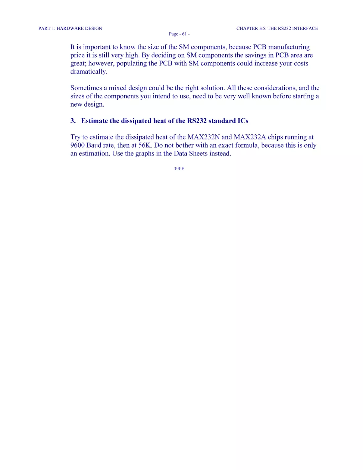
H6.1 The SPI® Bus 62
H6.2 The Custom SPI Bus 63
CHAPTER H7: DIGITAL INPUTS AND OUTPUTS 66
H7.1 Discrete Digital Inputs and External Interrupt function 67
H7.2 Serialized Digital Inputs 69
H7.3 Discrete Digital Outputs 72
H7.4 Serialized Digital Outputs 73
CHAPTER H8: ANALOG INPUTS 77
LHFSD
TABLE OF CONTENTS
Page - 16 -
H8.1 Analog to Decimal Conversion - ADC 77
H8.2 Analog Inputs 80
CHAPTER H9: THE BARGRAPH AND THE SEVEN-SEGMENTS DISPLAY
MODULES 84
H9.1 The Bargraph Module 85
H9.2 The Seven-Segments Led Display Module 89
CHAPTER H10: STEPPER MOTORS DRIVER MODULE 93
10.1 Stepper Motors 93
10.2 Stepper Driver Module 94
CHAPTER H11: PCB DESIGN 99
H11.1 PCB Design 99
H11.2 The Bill of Materials - BOM 102
CHAPTER H12: HARDWARE DESIGN 106
H12.1 Things You Need to Know 106
H12.2 General Facts About Testing Hardware 107
PART 2: FIRMWARE DESIGN 110
CHAPTER F1: THE FIRST FIRMWARE PROJECT 111
F1.1 Firmware Environment Setup 111
F1.2 Suggested Documentation 127
CHAPTER F2: MUTIPLE C FILES PROJECT WITH ONE SOURCE FILE – PROJECT
FD1 129
F2.1 Project FD1 129
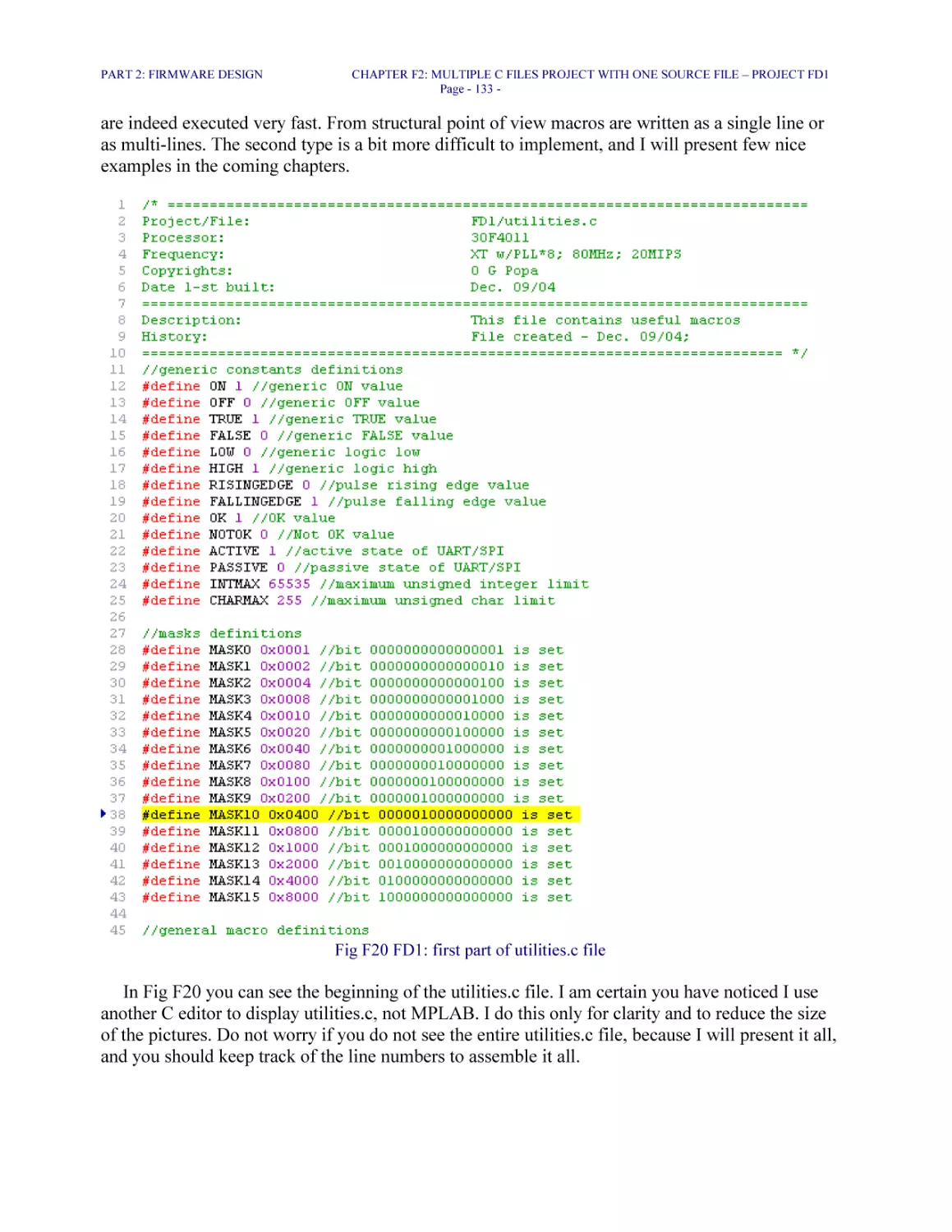
F2.2 File utilities.c 132
F2.3 File data.c 138
F2.4 File main.c 142
F2.5 MPLAB ICD2 useful settings tips 145
F2.6 Testing FD1 149
F2.7 Considerations about C Firmware programming 150
CHAPTER F3: REAL-TIME MULTITASKING 153
F3.1 Processor Time Management 153
F3.2 Programming with Interrupts 155
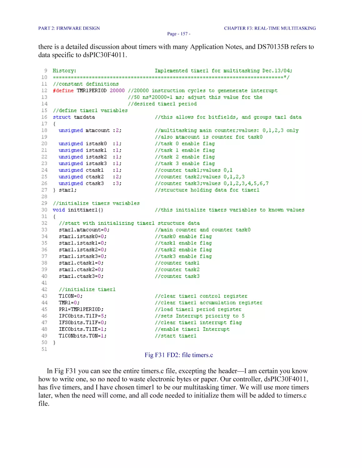
F3.3 File timers.c 156
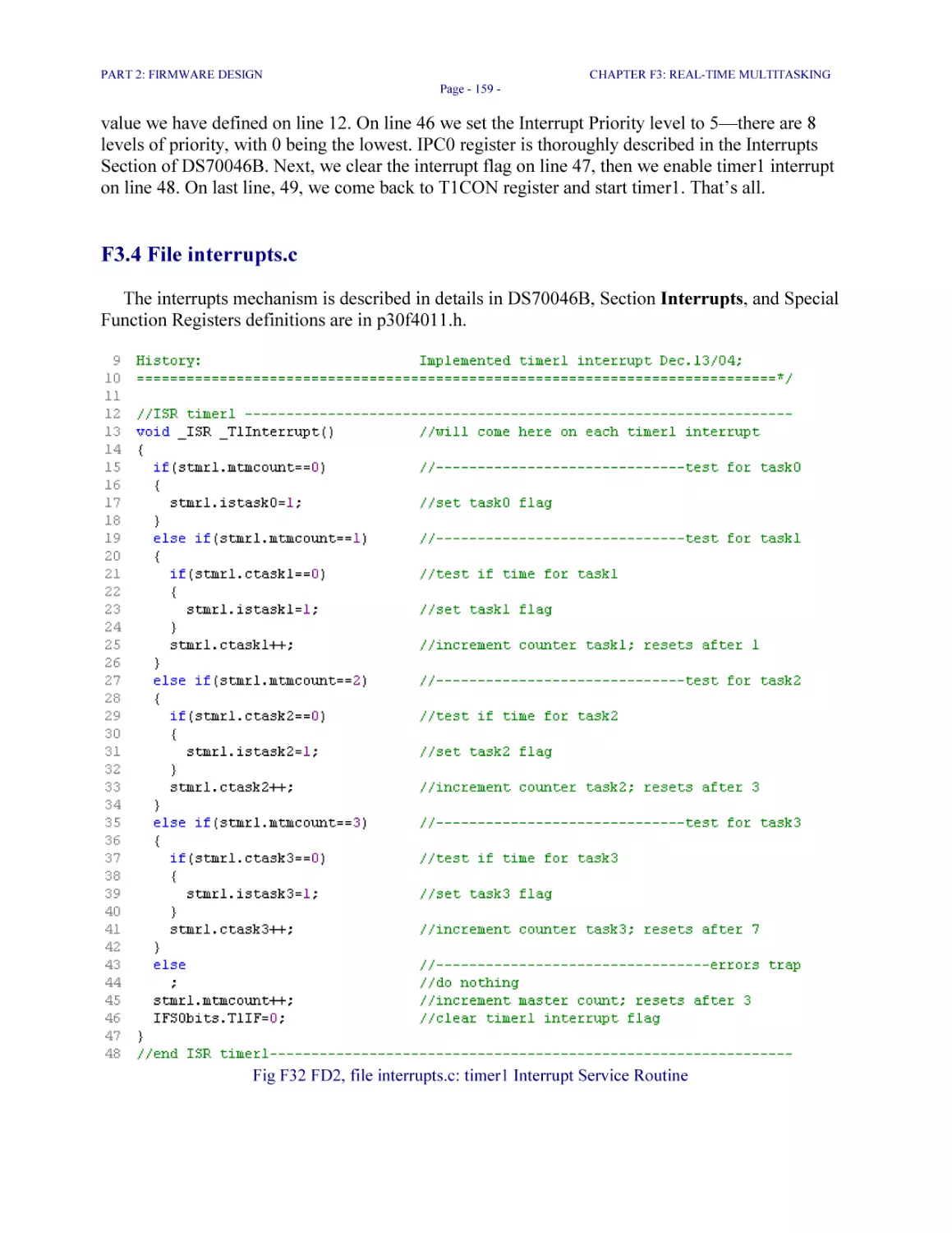
F3.4 File interrupts.c 159
F3.5 File main.c 161
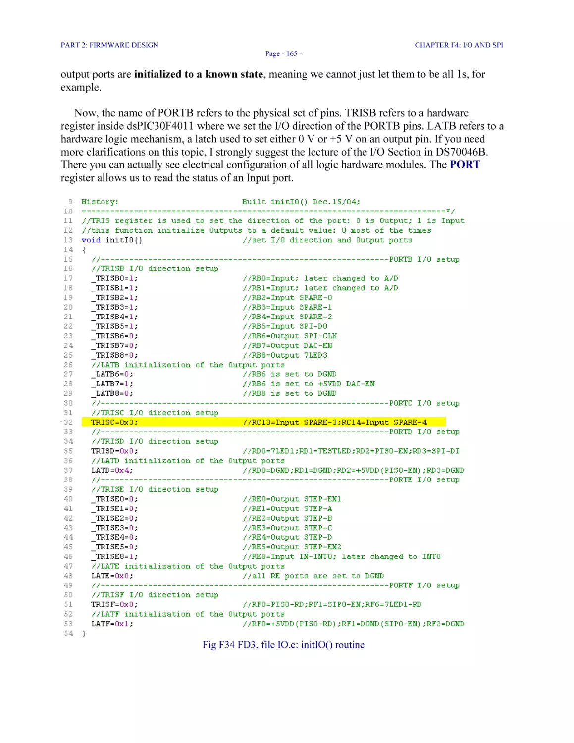
CHAPTER F4: I/O AND SPI 164
F4.1 File IO.c 164
LHFSD
TABLE OF CONTENTS
Page - 17 -
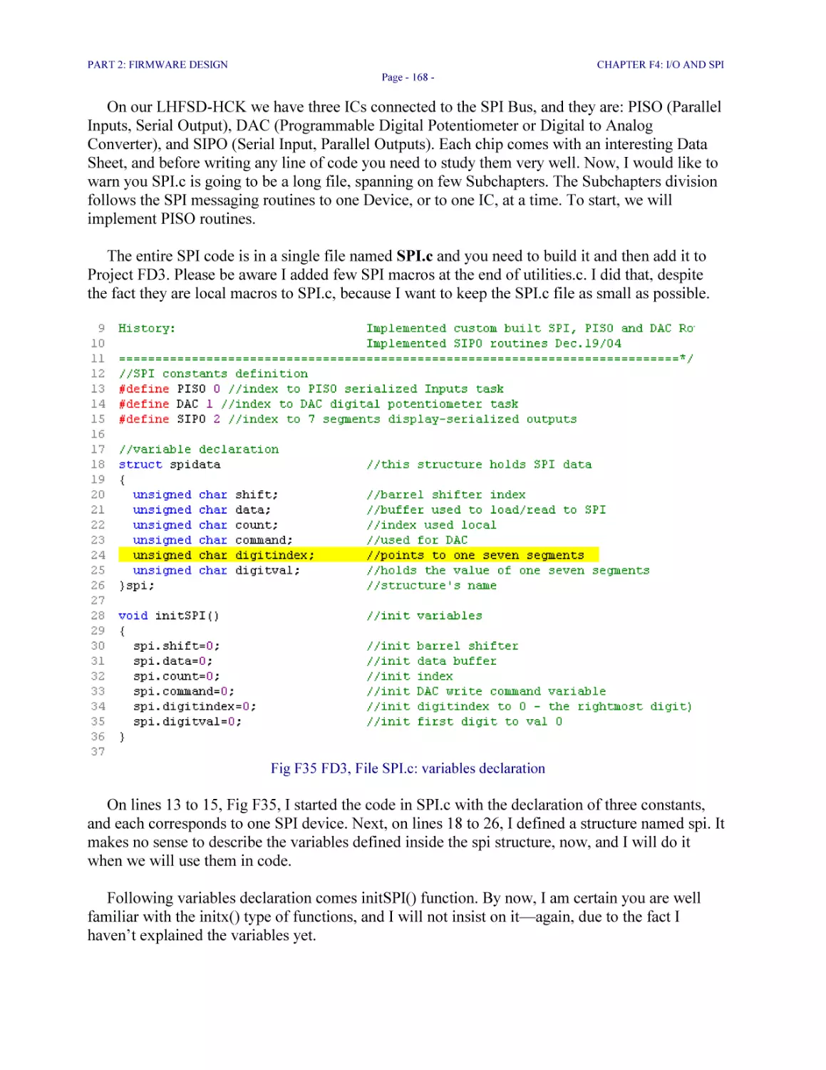
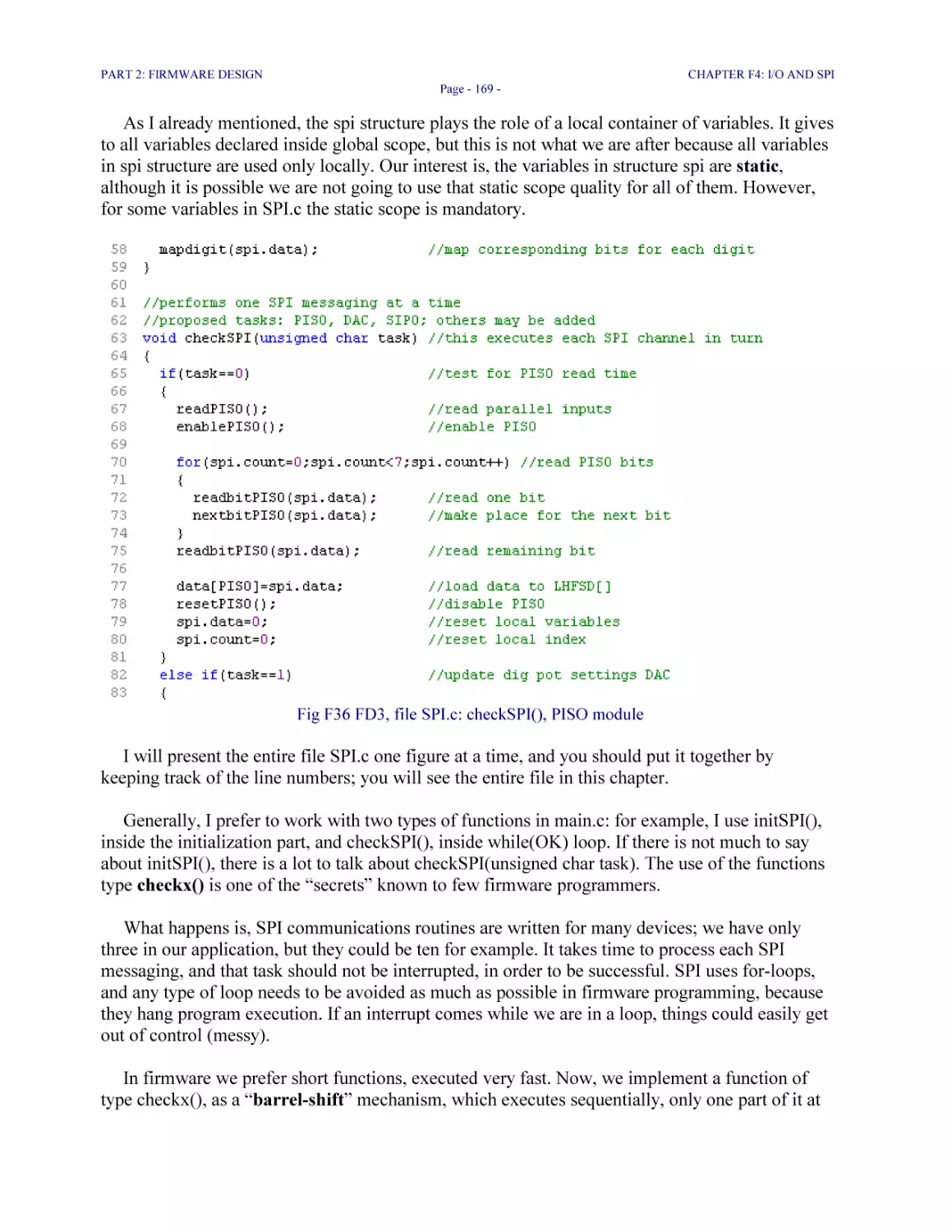
F4.2 File SPI.c: PISO routines 167
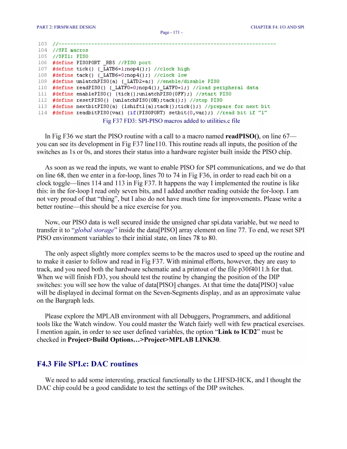
F4.3 File SPI.c: DAC routines 171
F4.4 File SPI.c: SIPO Routines 174
CHAPTER F5: ANALOG INPUTS AND EXTERNAL INTERRUPTS 182
F5.1 File ad.c 182
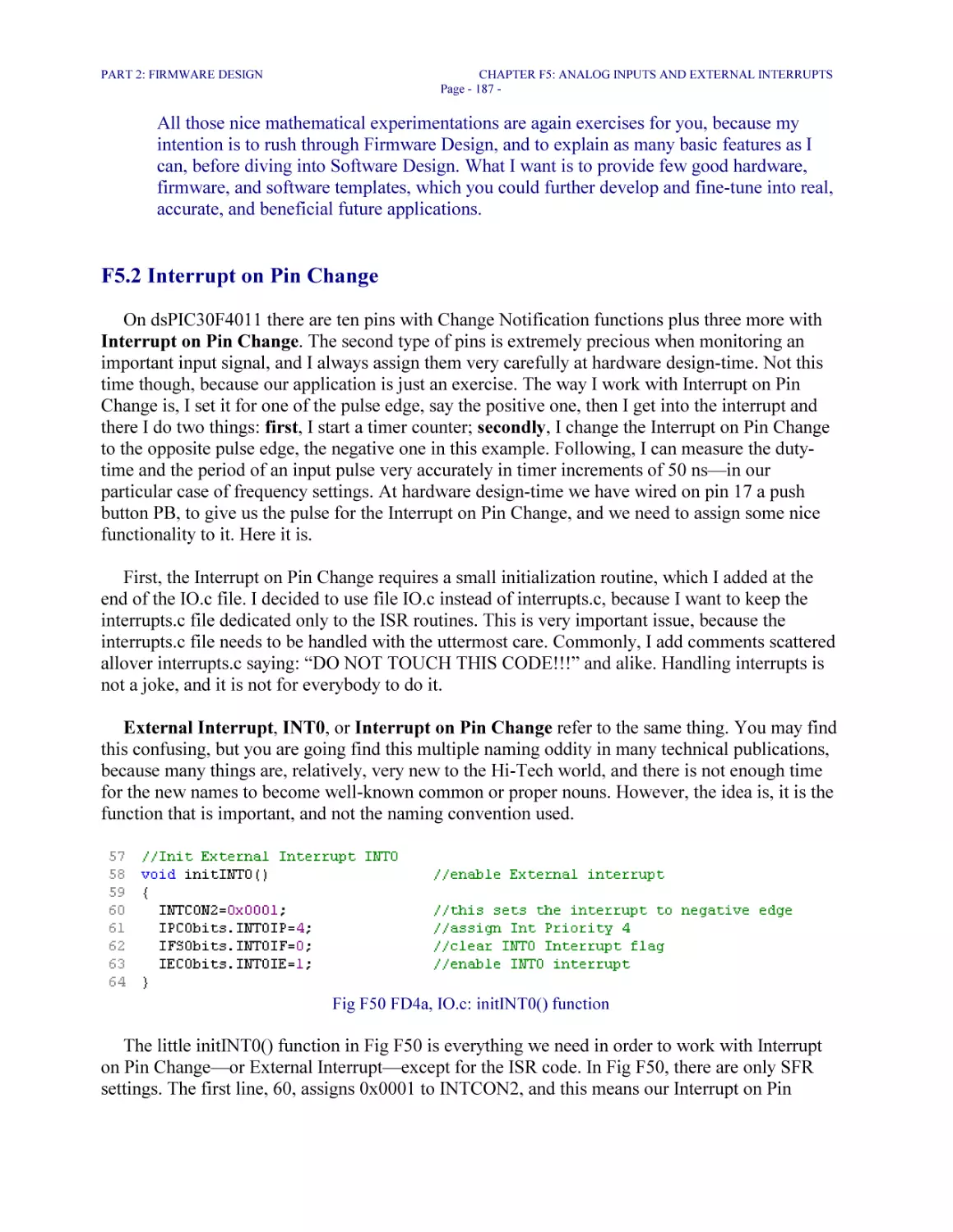
F5.2 Interrupt on Pin Change 187
F5.3 Working with timers 2 and 3 in Timer Mode; file various.c 188
F5.4 Working with pulses and with timer4 in Counter Mode 197
CHAPTER F6: RS232 ROUTINES 203
F6.1 RS232 Firmware Protocol; ASCII and Binary Data Formats 203
F6.2 HyperTerminal® Setup 205
F6.3 File RS232.c 209
CHAPTER F7: DRIVING STEPPER MOTORS 214
F7.1 Unipolar and Bipolar Stepper Motors driving sequences 214
F7.2 File step.c 215
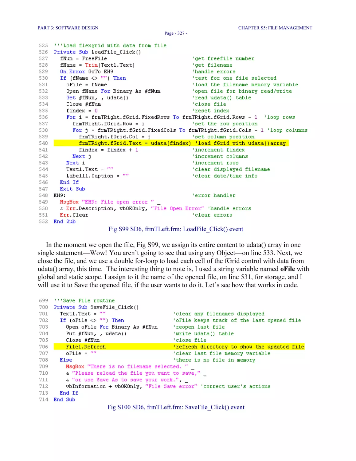
F7.3 End of Part 2 FIRMWARE DESIGN 222
PART 3: SOFTWARE DESIGN 223
CHAPTER S1: THE FIRST SOFTWARE APPLICATION 224
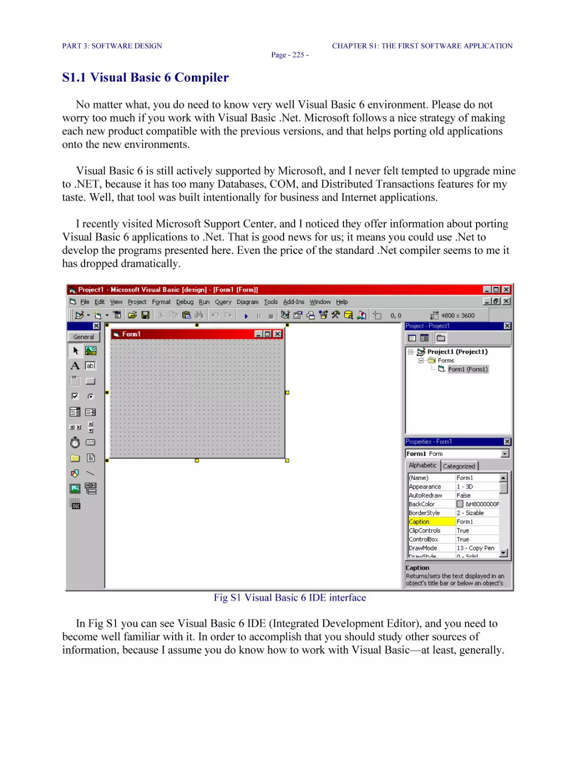
S1.1 Visual Basic 6 Compiler 225
S1.2 Building an MDI Interface 229
S1.3 Customizing the MDI Interface 233
CHAPTER S2: SERIAL COMMUNICATIONS – RS232 243
S2.1 The MSComm Object 243
S2.2 SD2: the Software RS232 Interface 244
S2.3 Custom Continuous Loop RS232 Messaging Protocol - Project FD7 255
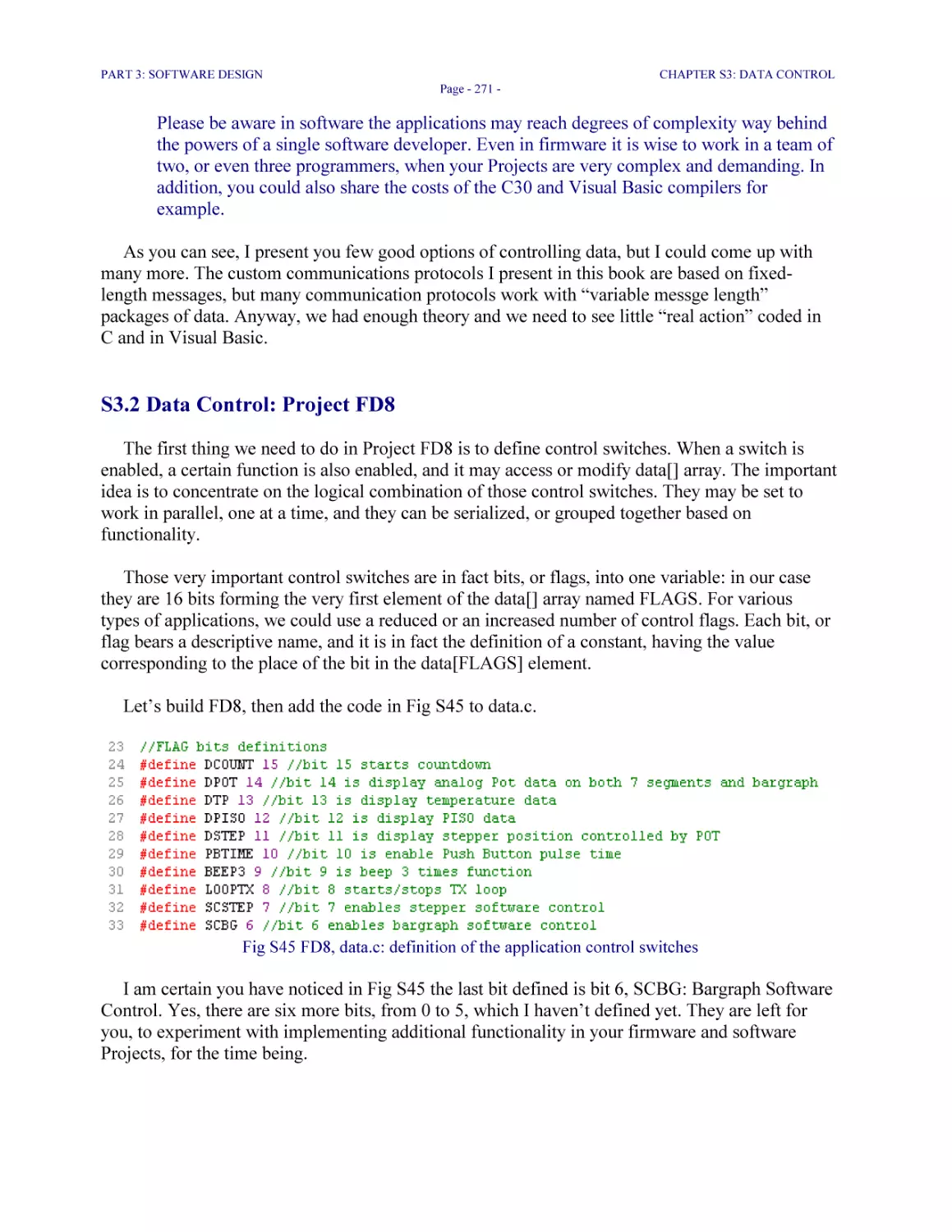
S2.4 Custom Continuous Loop RS232 Messaging Protocol - SD3 application 262
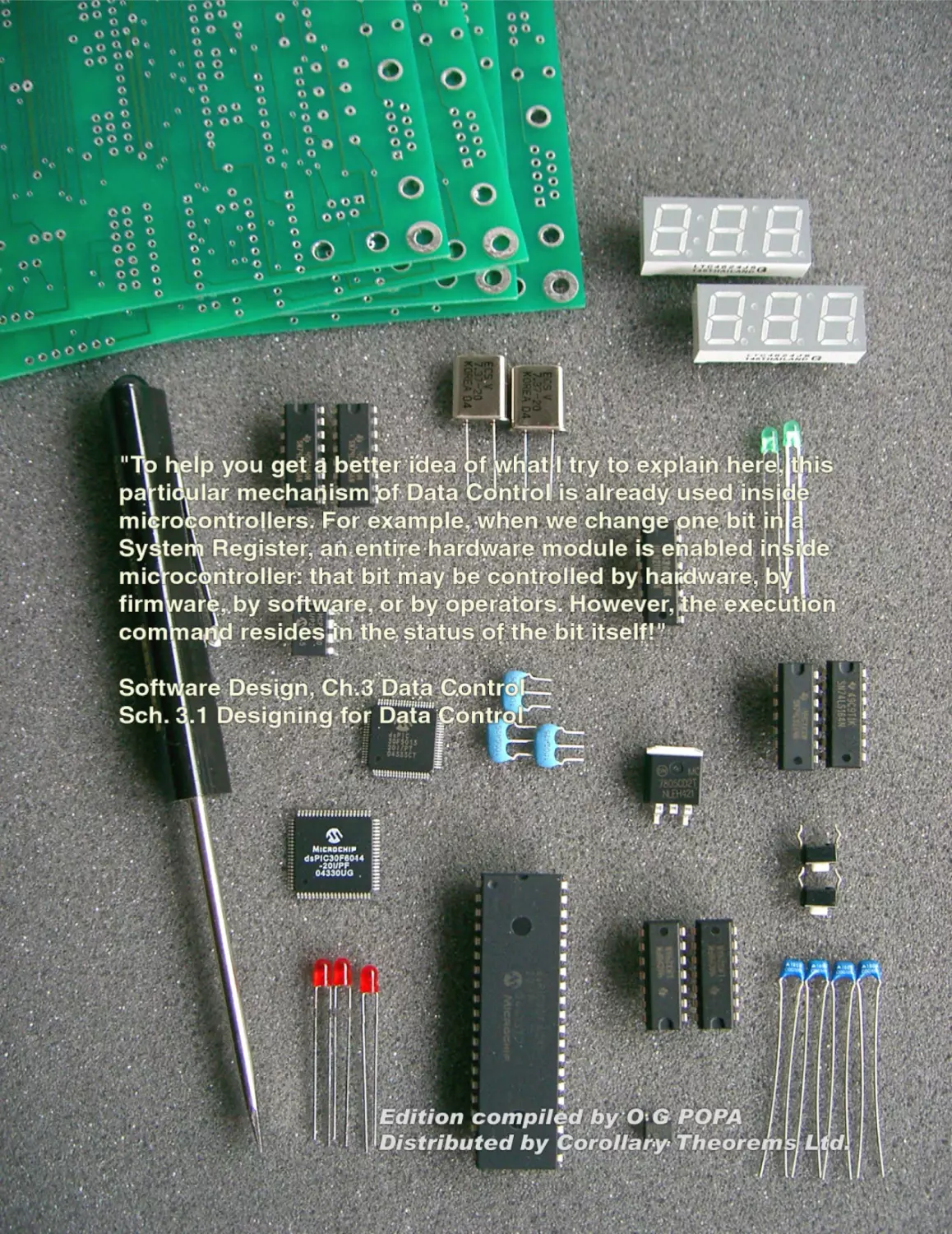
CHAPTER S3: DATA CONTROL 268
S3.1 Designing for Data Control 268
S3.2 Data Control: Project FD8 271
S3.3 Project FD8: processing software commands 276
S3.4 Project SD4: implementing 4 bytes commands 279
CHAPTER S4: DATA DISPLAY 292
S4.1 Visual Basic 6 Graphic Controls 293
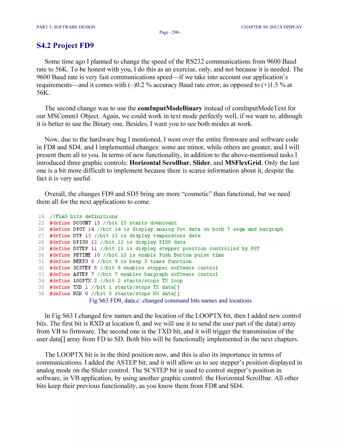
S4.2 Project FD9 296
S4.3 The SD5 application 300
S4.4 MSFlexGrid Control 312
LHFSD
TABLE OF CONTENTS
Page - 18 -
CHAPTER S5: FILE MANAGEMENT 319
S5.1 Generating PC Files in SD6 320
S5.2 Sending a File from SD6 to FD10 328
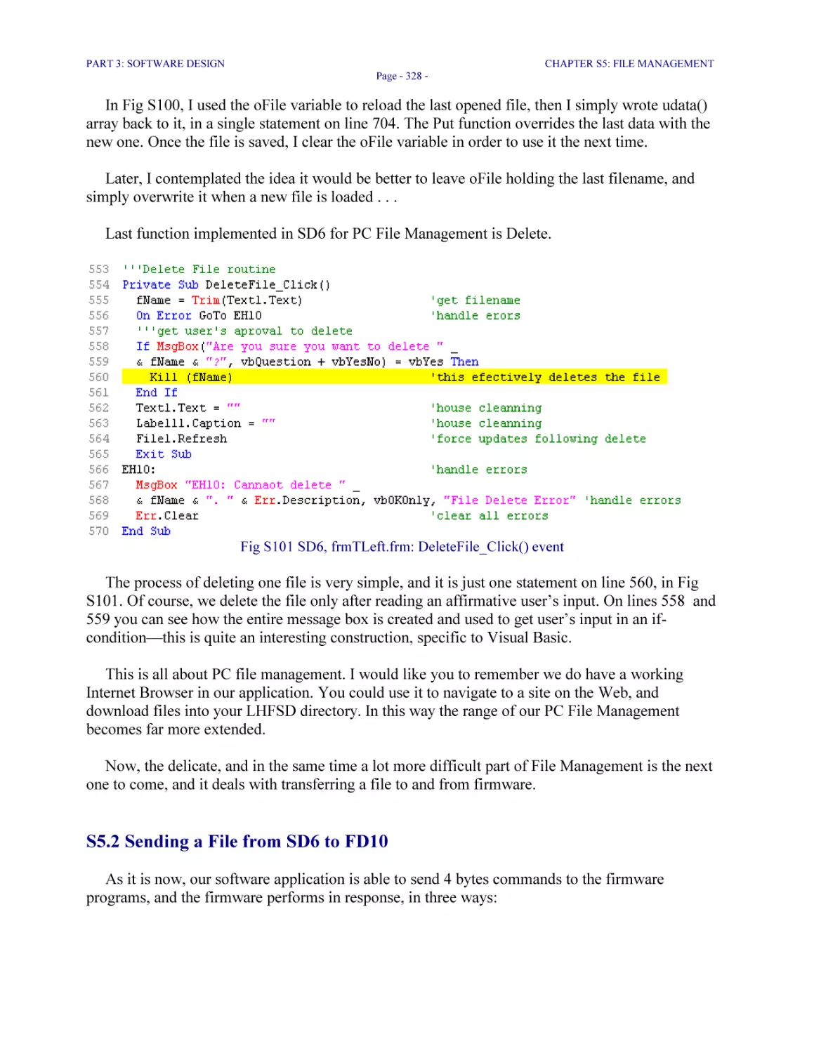
S5.3 Sending a Data File from FD10 to SD6 340
CHAPTER S6: GRAPH TRACE 347
S6.1 Graph Trace - SD7 application 347
CHAPTER S7: THE LFHDS.EXE 358
S7.1 Visual Basic 6 Package and Deployment Wizard 359
S7.2 Software Development Considerations 367
S7.3 Final Word 368
***
TABLE OF FIGURES
PART 1: HARDWARE DESIGN
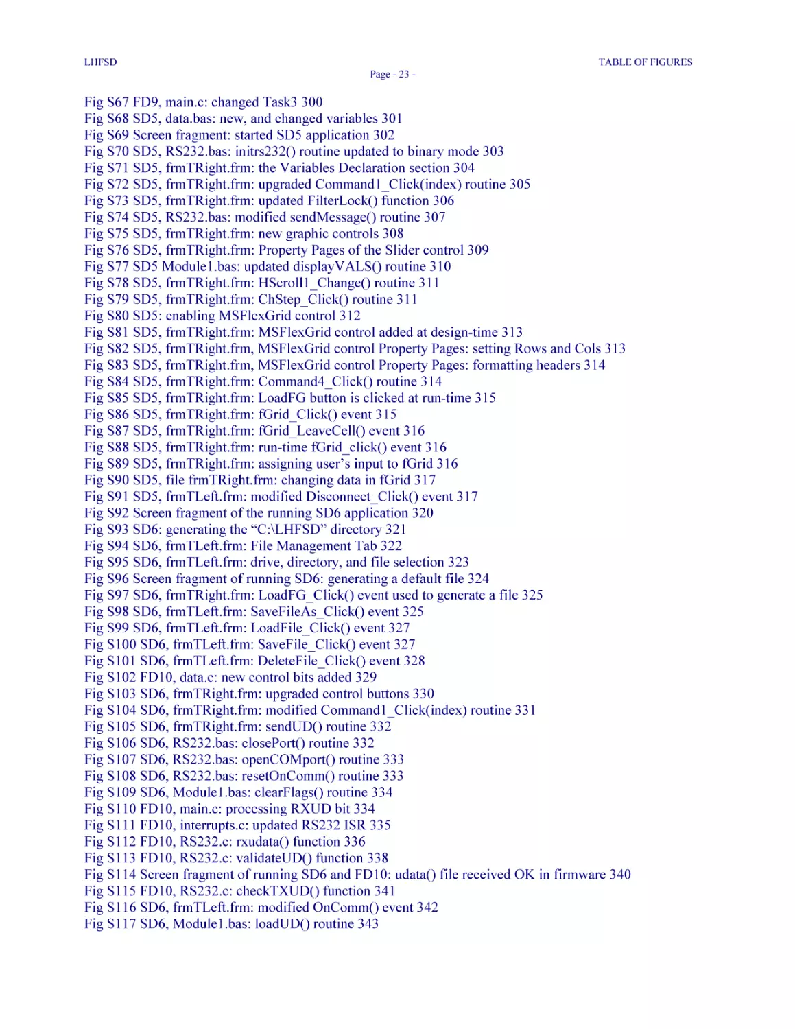
Fig H1 Microcontroller’s work cycle 26
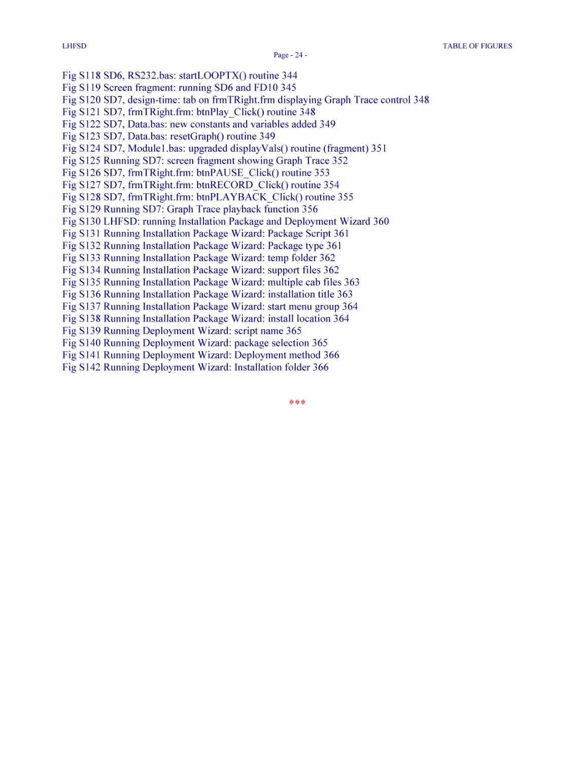
Fig H2 Electrical representation of one firmware byte of data 28
Fig H3 The dsPIC30F4011 controller in a PDIP 40 package 32
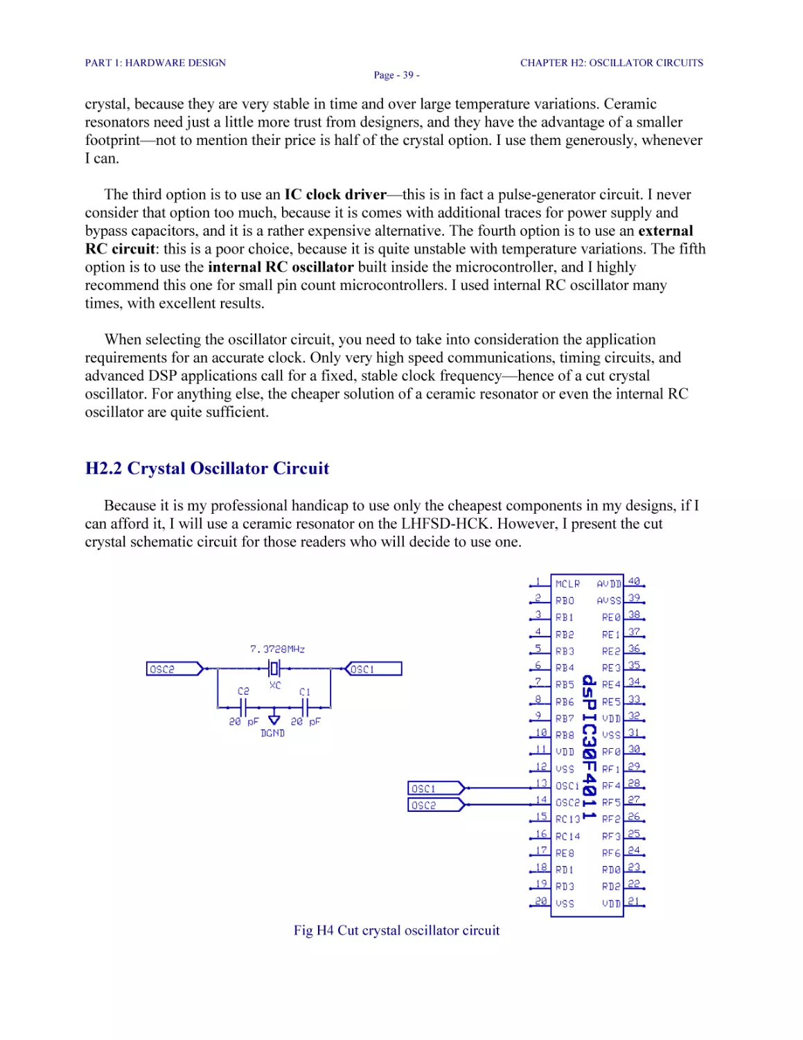
Fig H4 Cut crystal oscillator circuit 39
Fig H5 Ceramic Resonator circuit 41
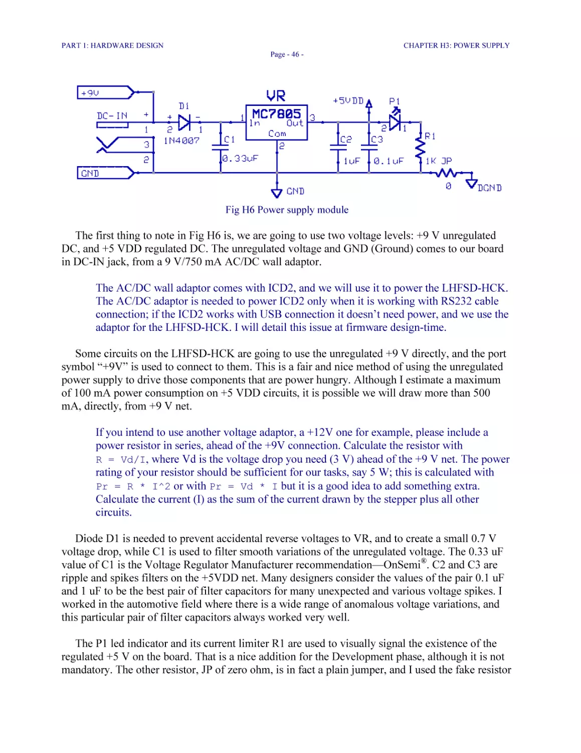
Fig H6 Power supply module 46
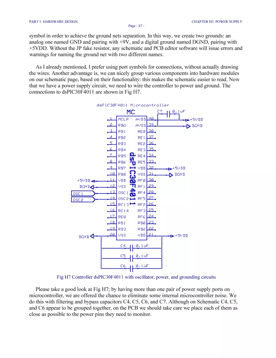
Fig H7 Controller dsPIC30F4011 with oscillator, power, and grounding circuits 47
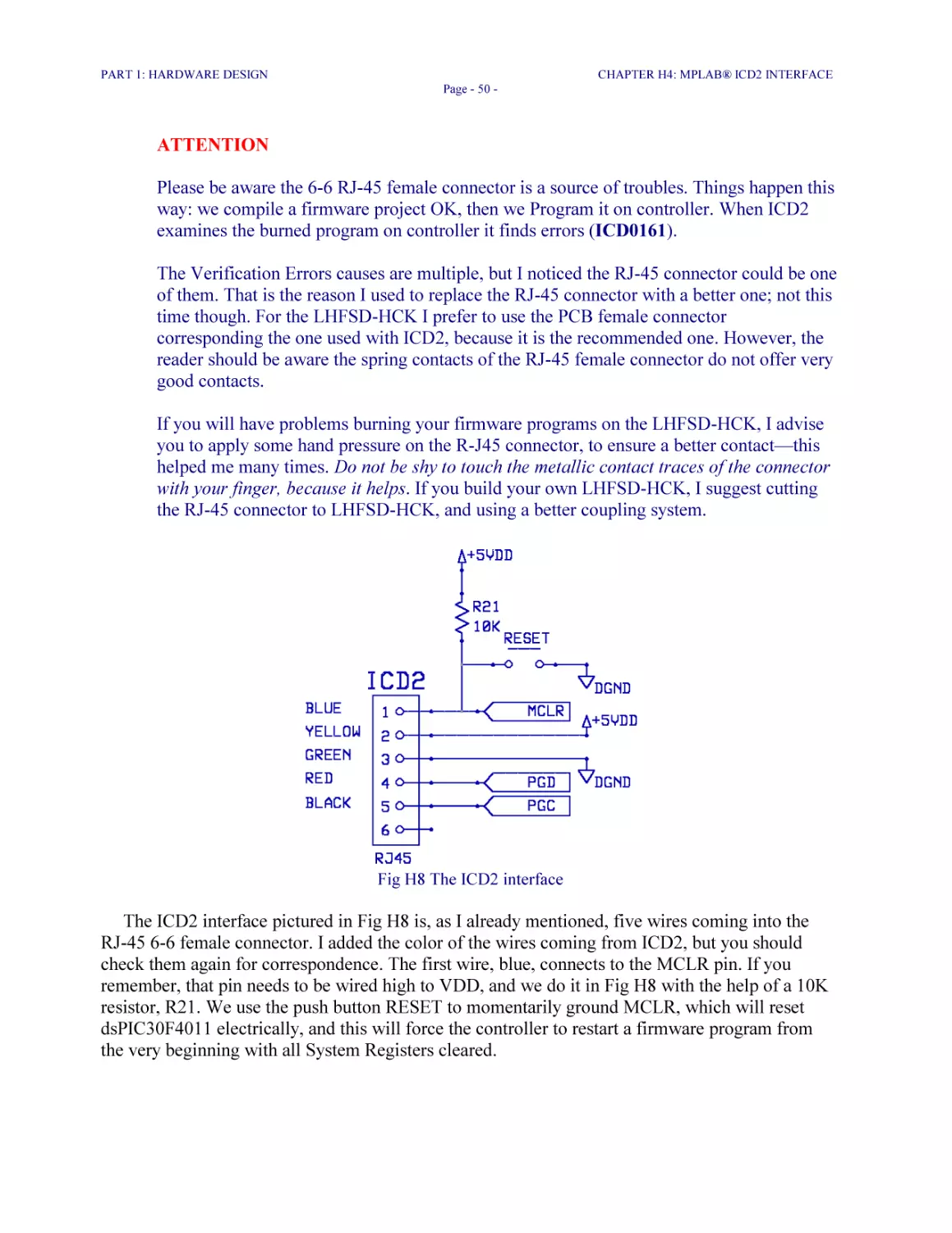
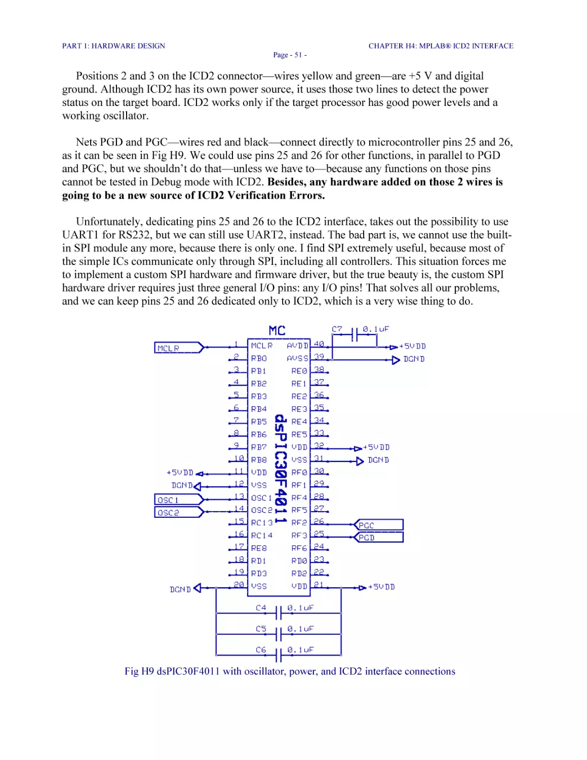
Fig H8 The ICD2 interface 50
Fig H9 dsPIC30F4011 with oscillator, power, and ICD2 interface connections 51
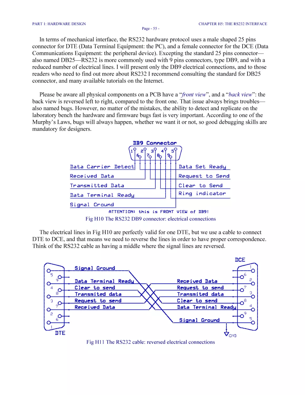
Fig H10 The RS232 DB9 connector: electrical connections 55
Fig H11 The RS232 cable: reversed electrical connections 55
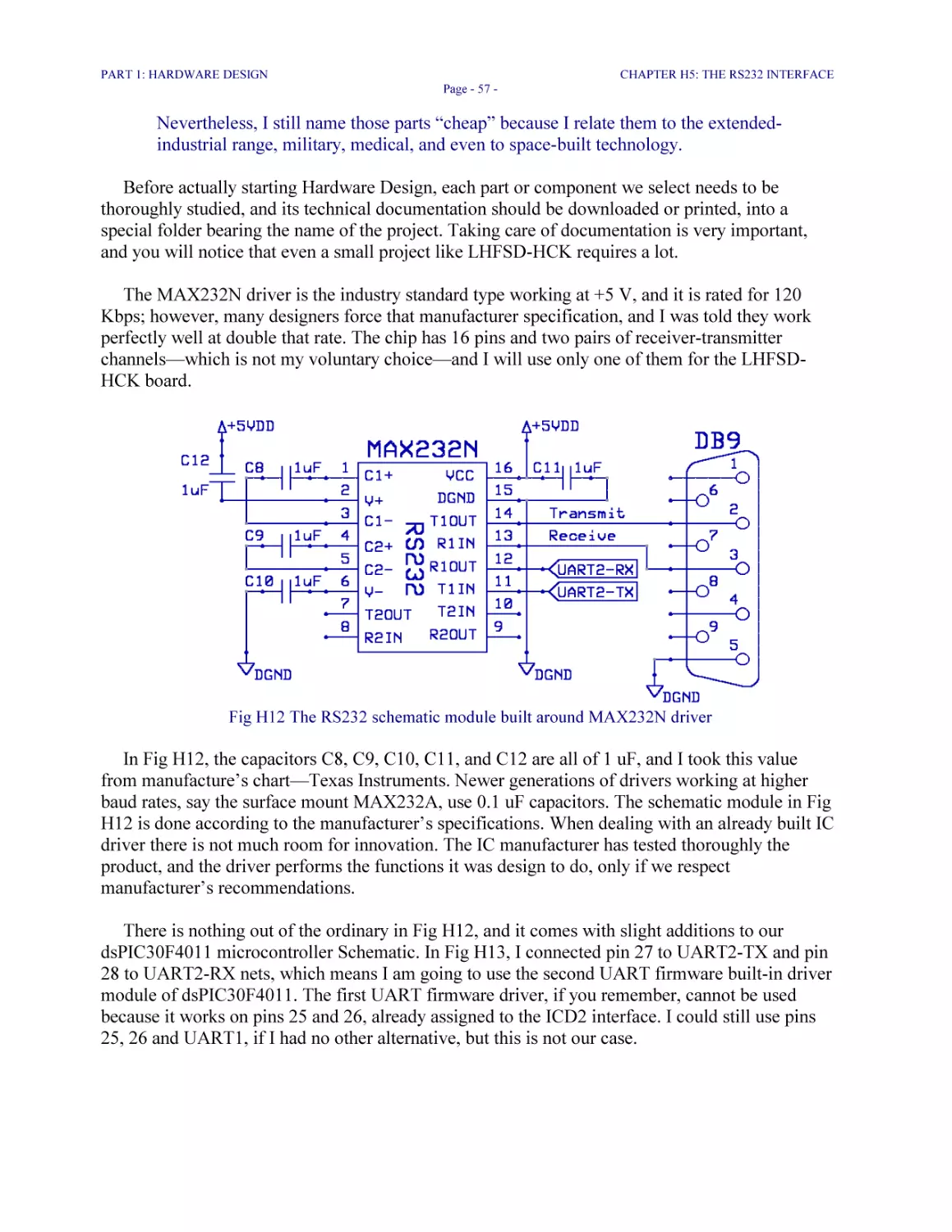
Fig H12 The RS232 Schematic module built with MAX232N 16 pins driver 57
Fig H15 The SPI Bus 62
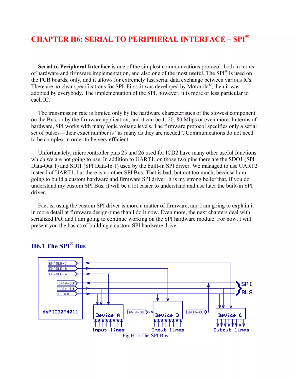
Fig H16 dsPIC30F4011 with the custom SPI Bus wired 64
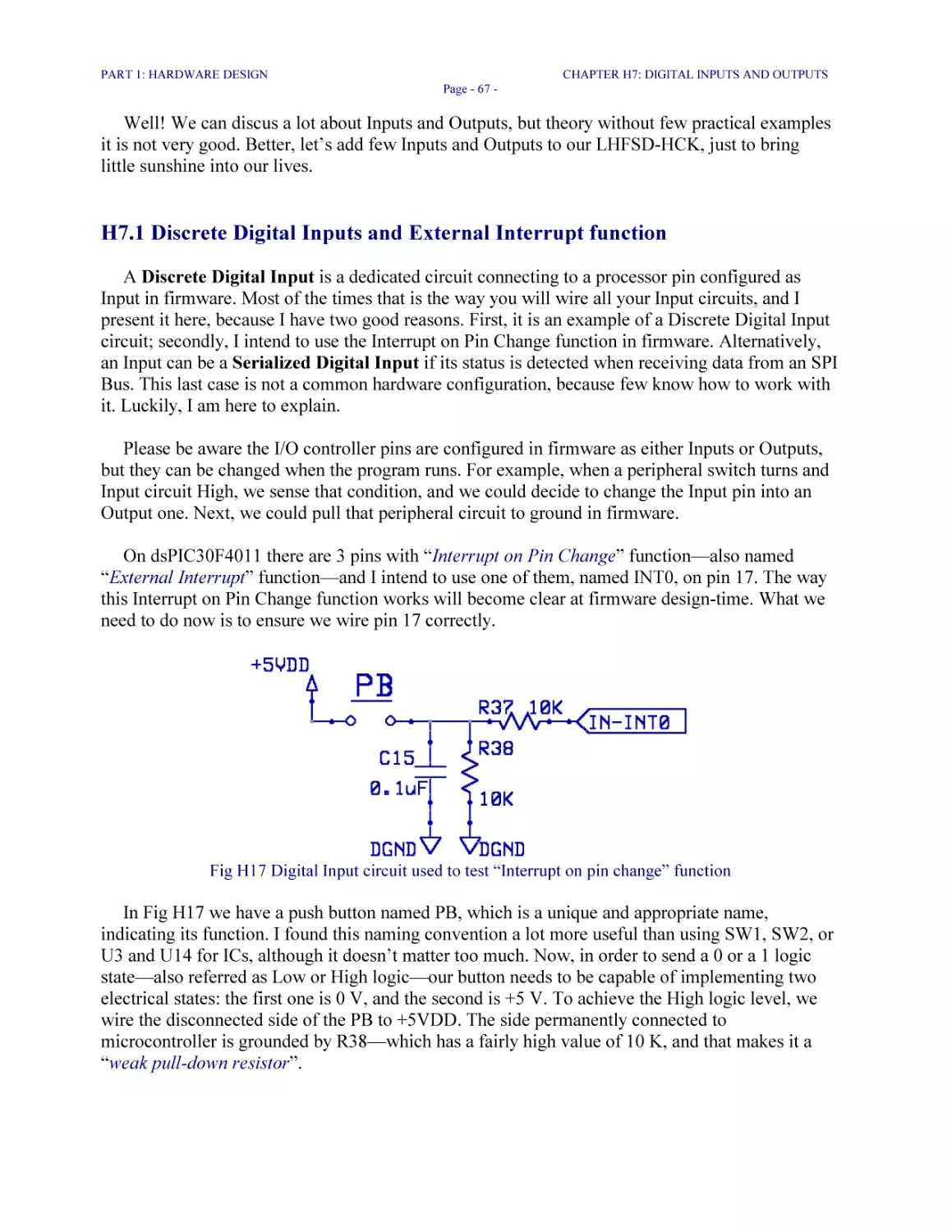
Fig H17 Digital Input circuit used to test “Interrupt on pin change” function 67
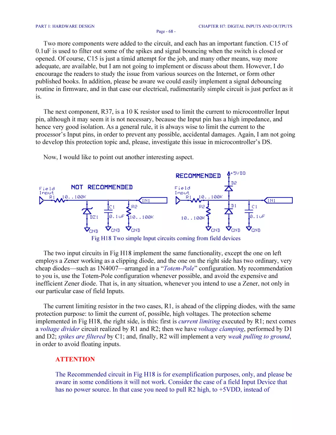
Fig H18 Two simple Input circuits coming from field devices 68
Fig H19 Serialized Digital Input circuits 69
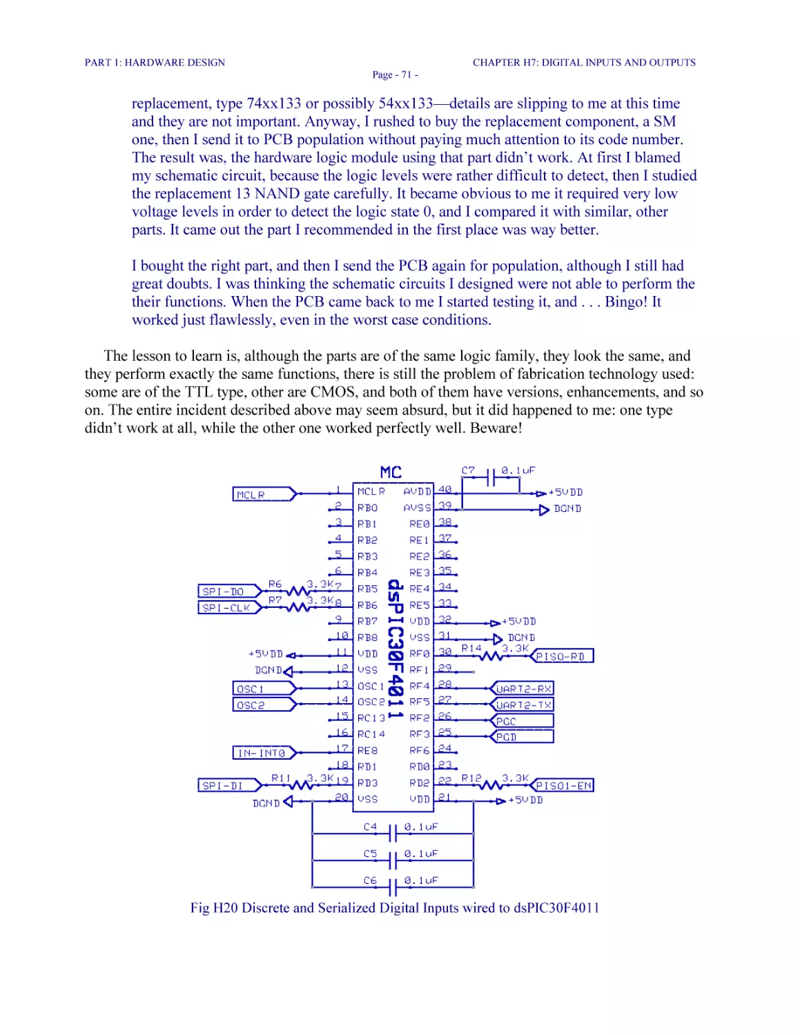
Fig H20 Discrete and Serialized Digital Inputs wired to dsPIC30F4011 71
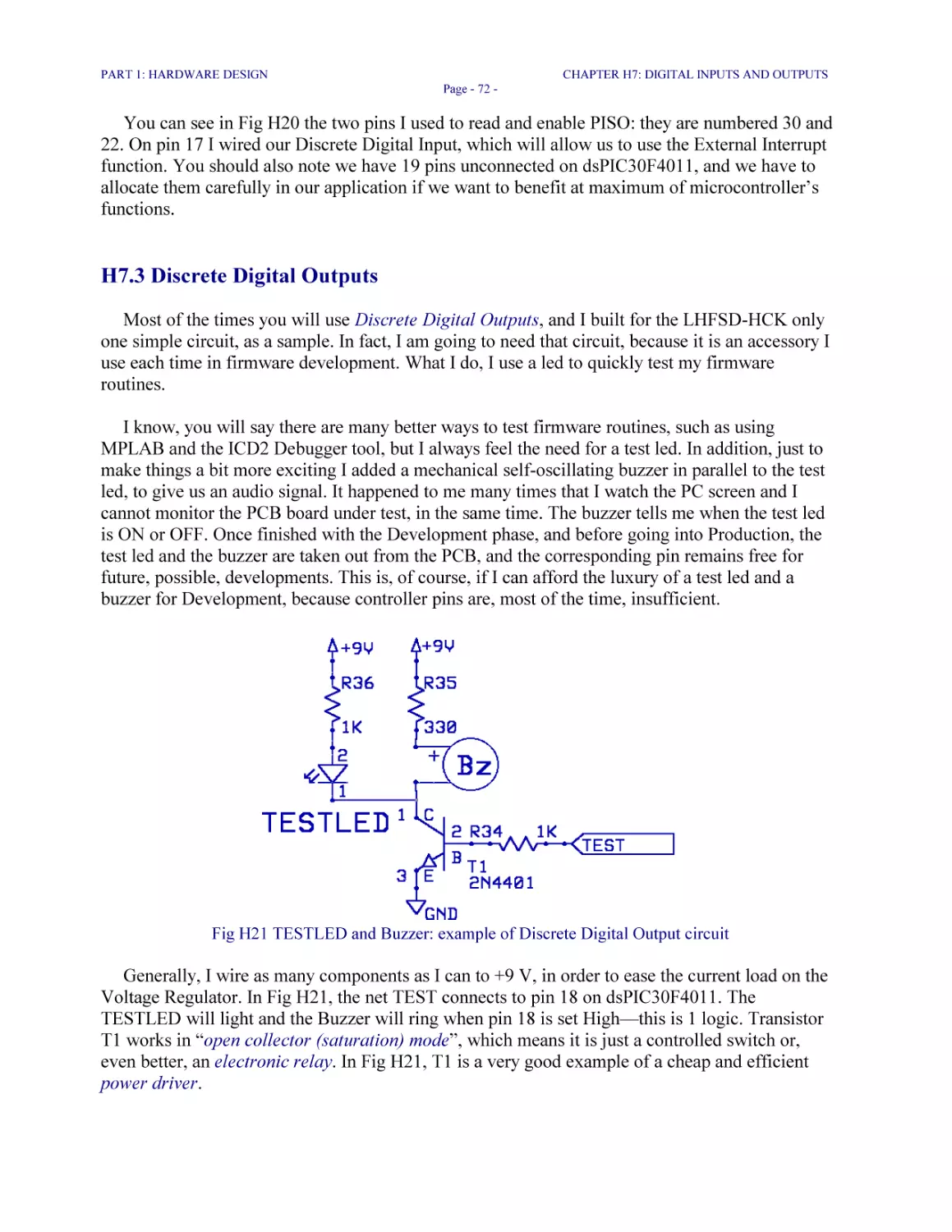
Fig H21 TESTLED and Buzzer: example of Discrete Digital Output circuit 72
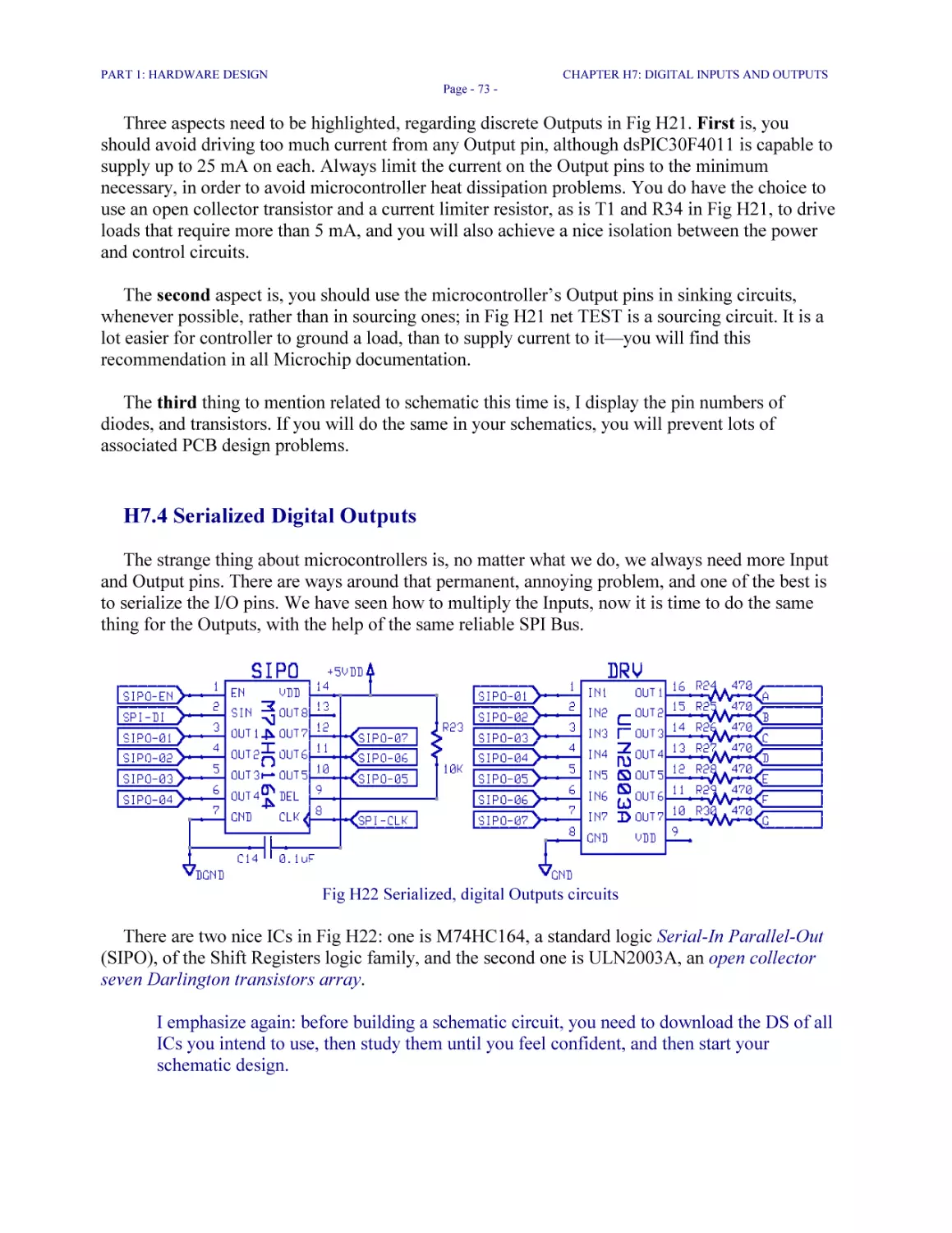
Fig H22 Serialized, digital Outputs circuits 73
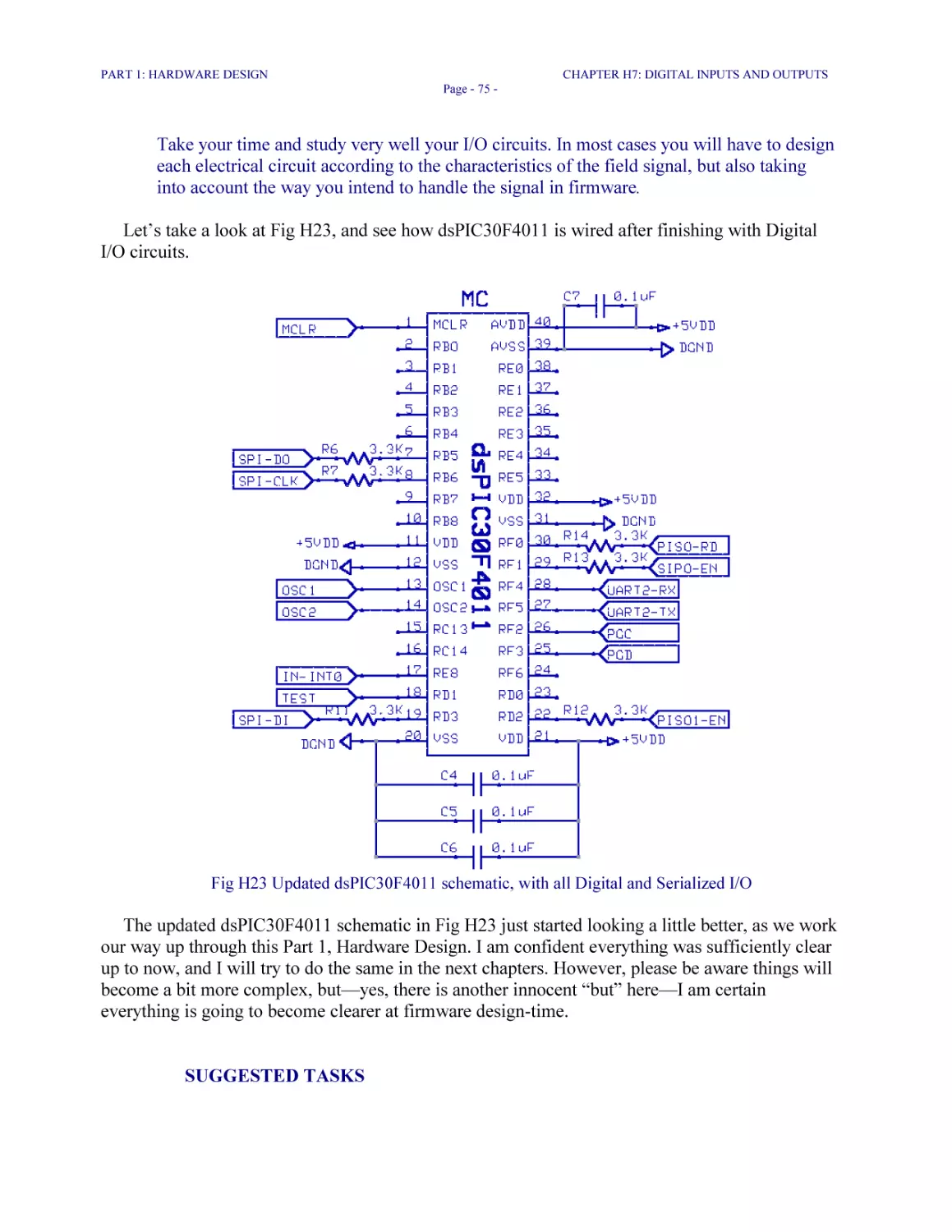
Fig H23 Updated dsPIC30F4011 Schematic, with all Digital and Serialized I/O 75
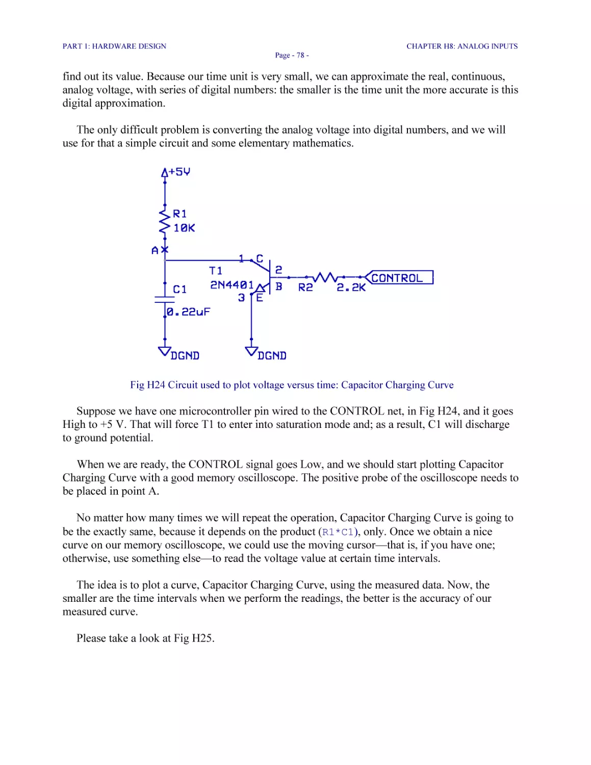
Fig H24 Circuit used to plot voltage versus time: Capacitor Charging Curve 78
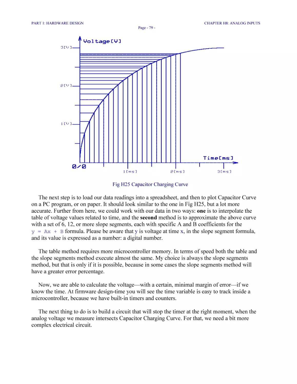
Fig H25 Capacitor Charging Curve 79
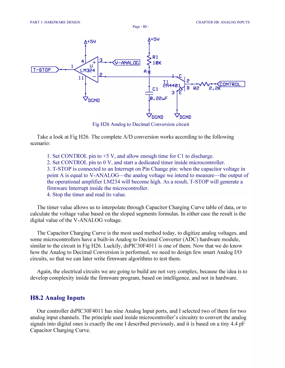
Fig H26 Analog to Decimal Conversion circuit 80
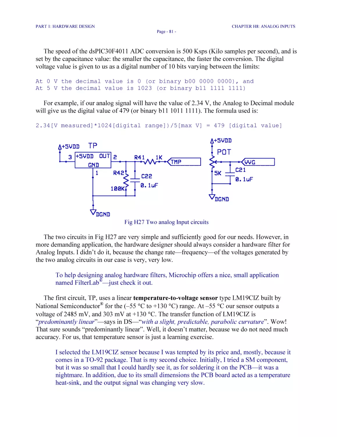
Fig H27 Two analog Input circuits 81
Fig H28 The Bargraph Module 86
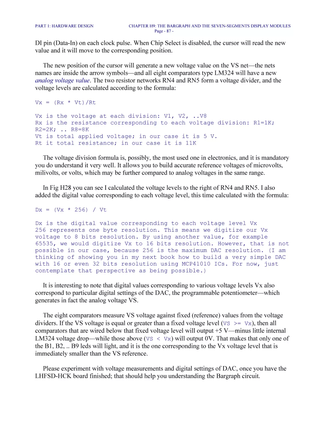
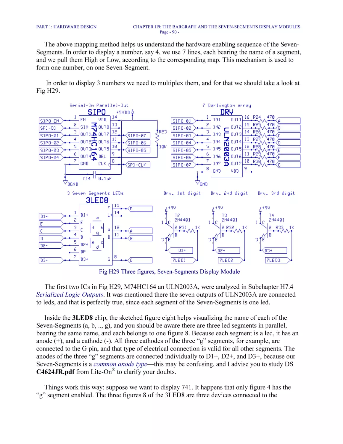
Fig H29 Three figures, Seven-Segments Display Module 90
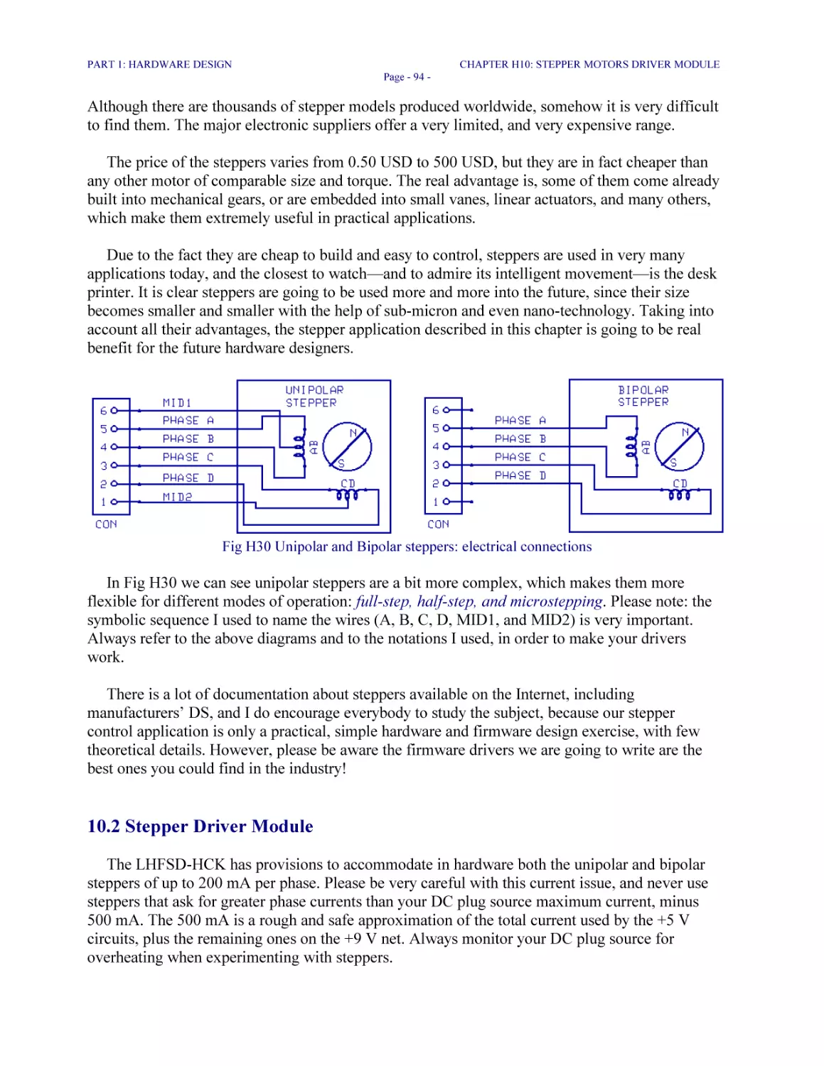
Fig H30 Unipolar and Bipolar steppers: electrical connections 94
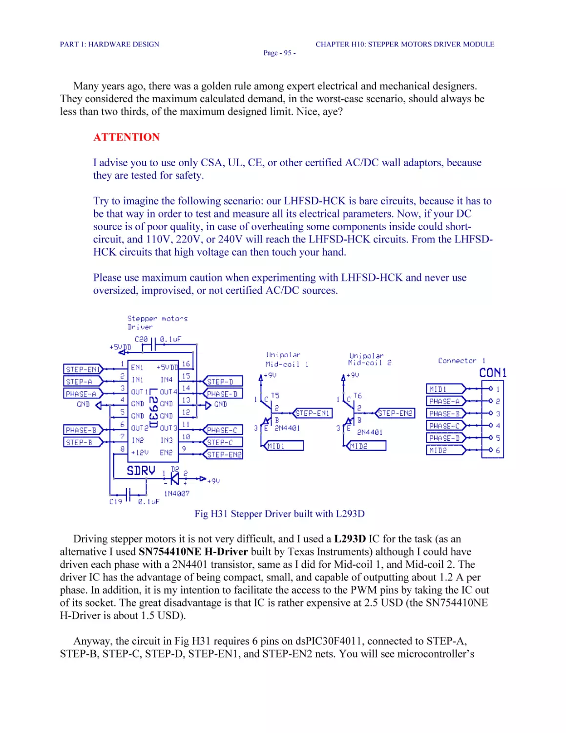
Fig H31 Stepper Driver built with L293D 95
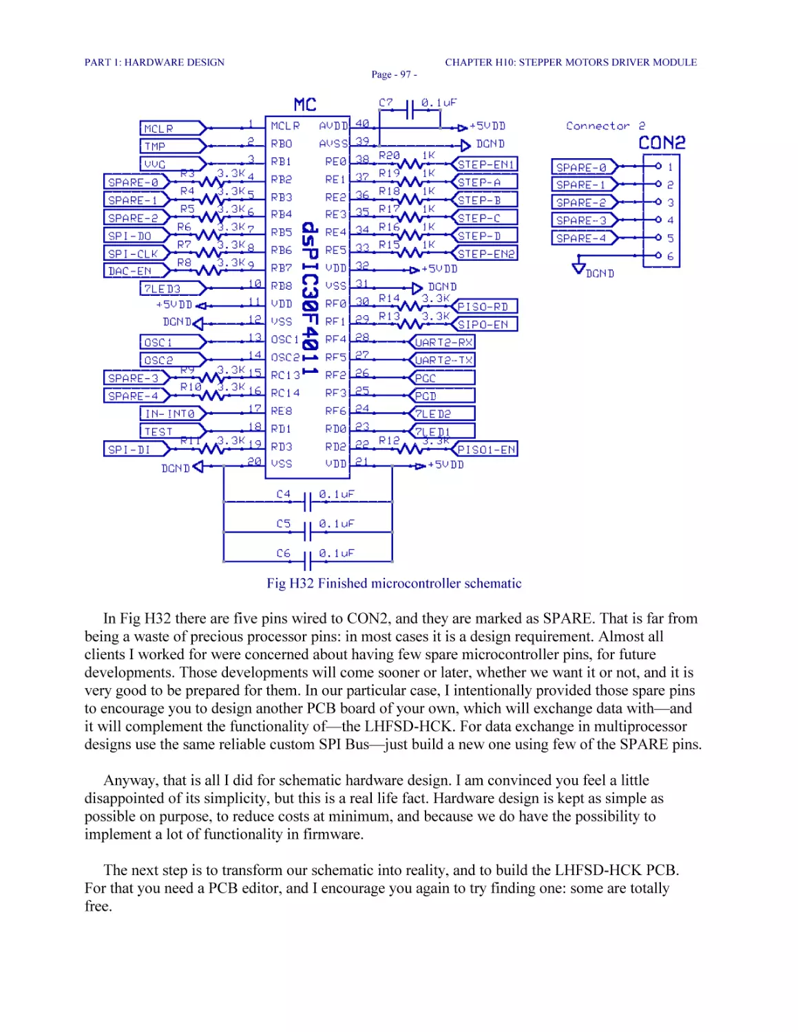
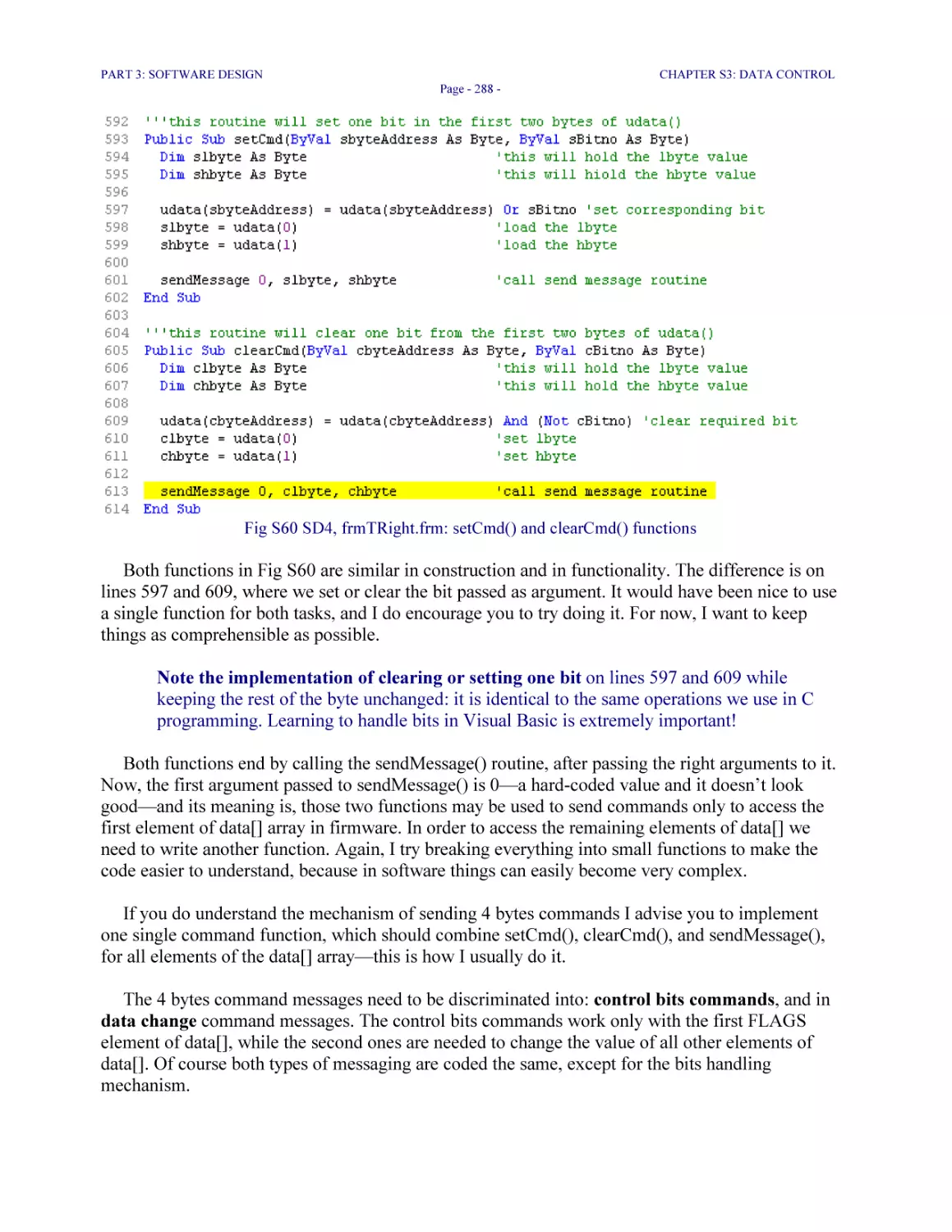
Fig H32 Finished microcontroller Schematic 97
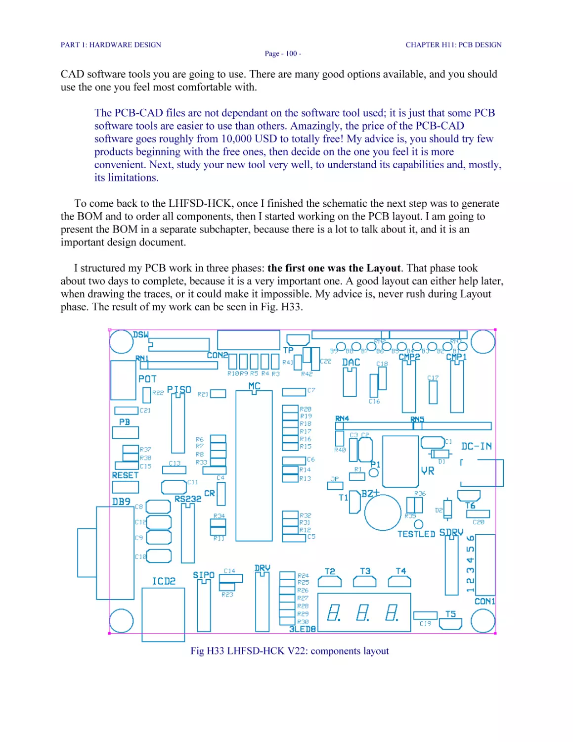
Fig H33 LHFSD-HCK V22: components layout 100
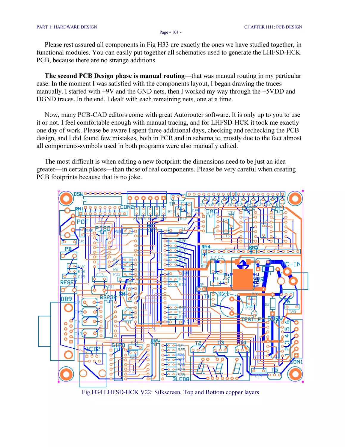
Fig H34 LHFSD-HCK V22: Silkscreen, Top, and Bottom copper layers 101
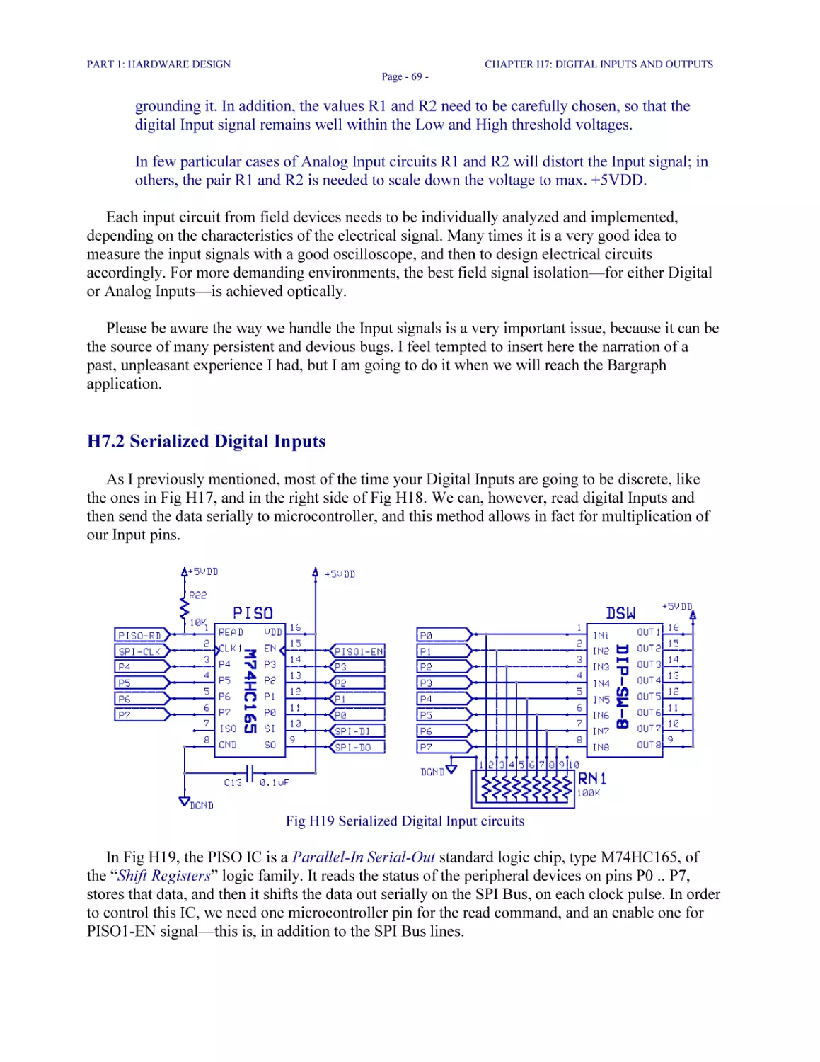
PART 2: FIRMWARE DESIGN
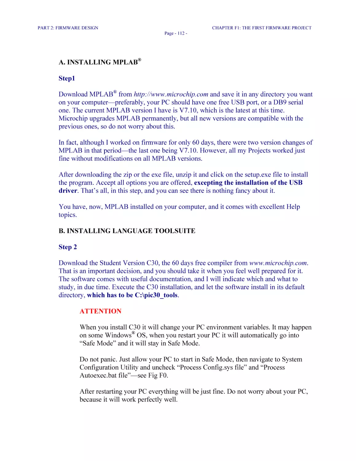
Fig F0 System Configuration Utility: selective startup 113
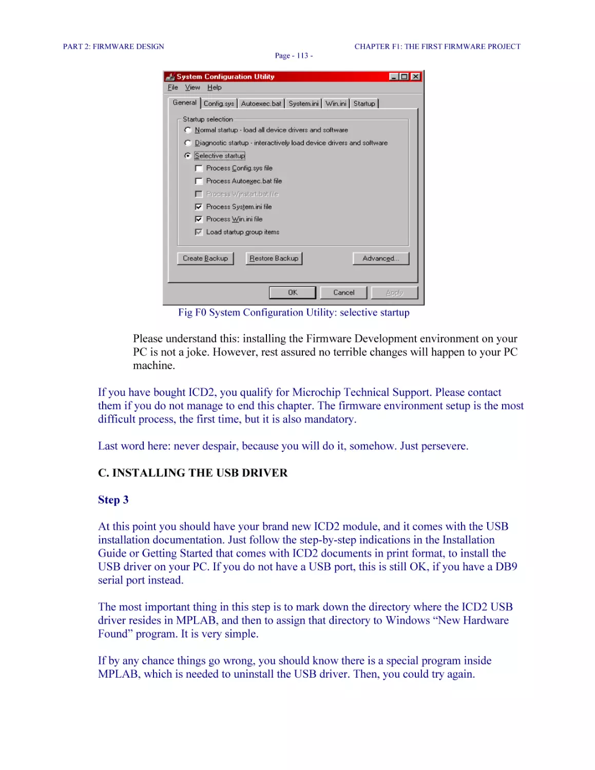
Fig F1 Firmware Development Bench setup 114
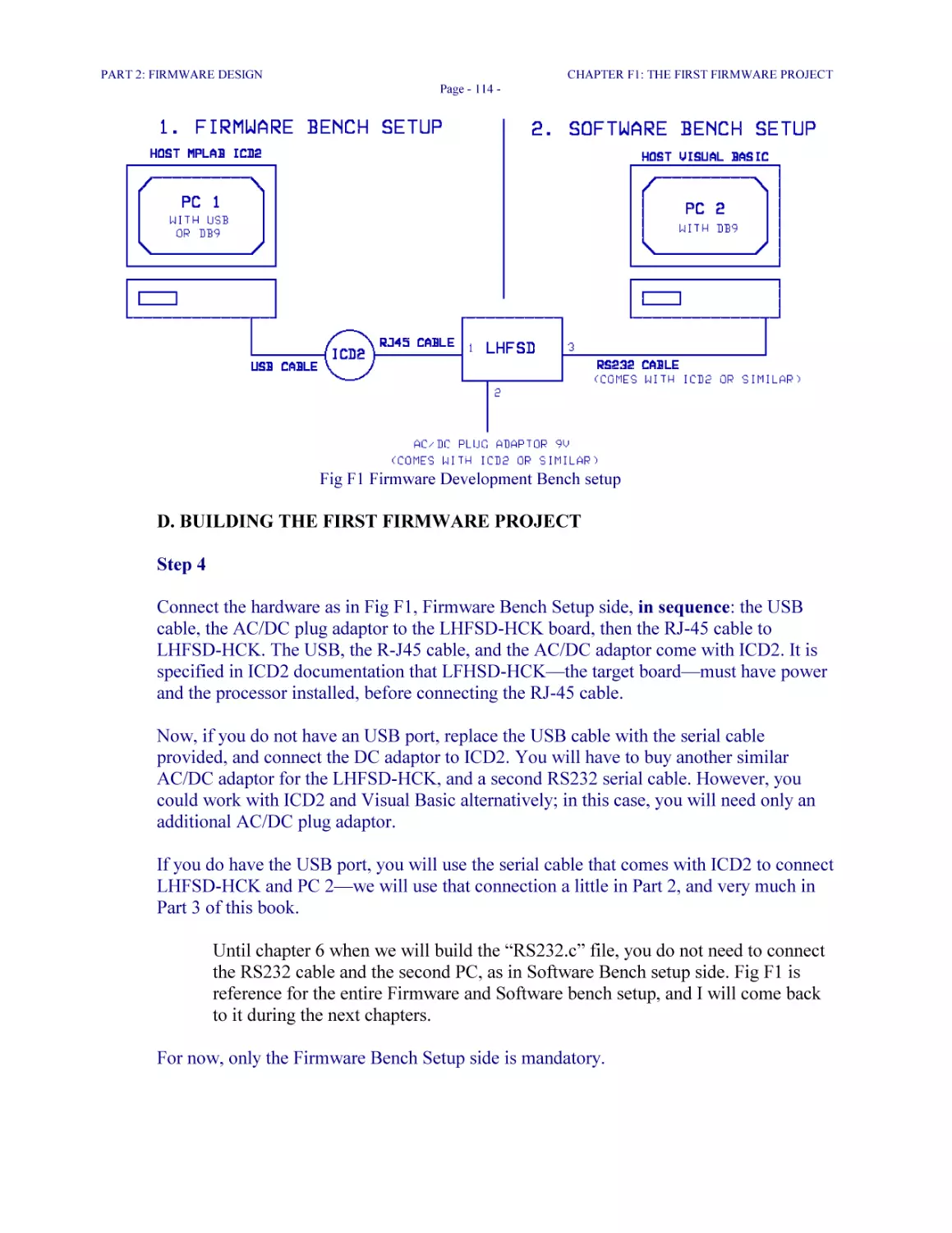
Fig F2 MPLAB screen fragment: enabling Debugger Tool 115
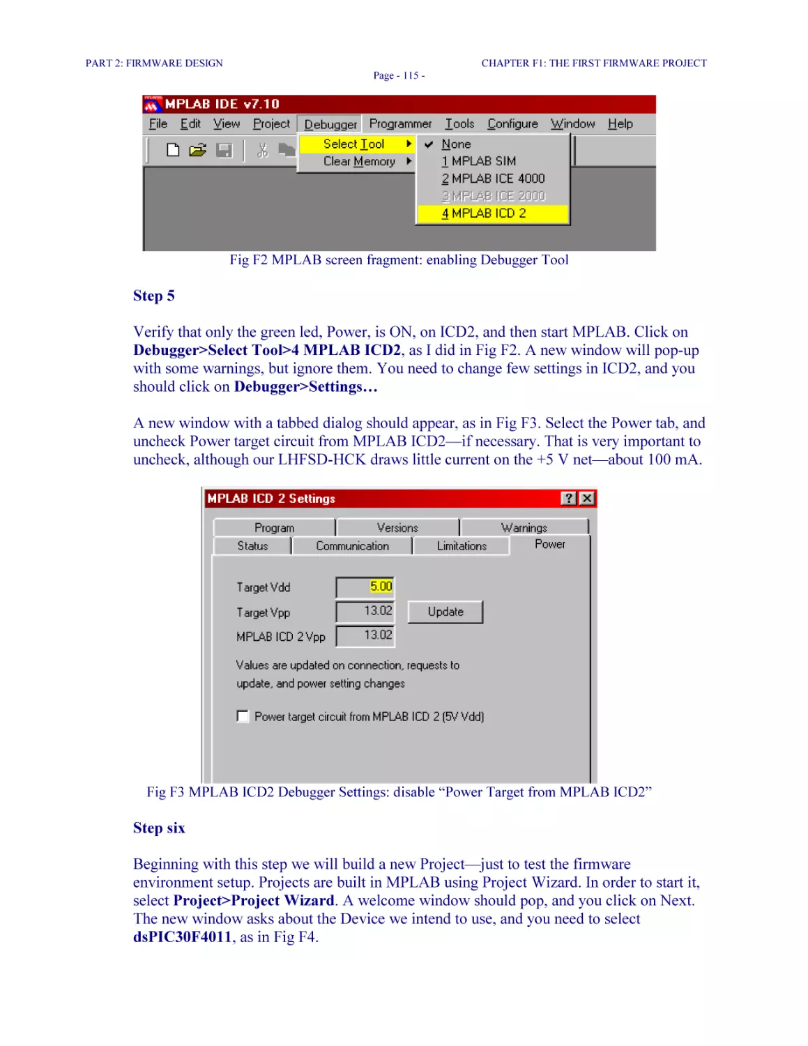
Fig F3 MPLAB ICD2 Debugger Settings: disable power target from MPLAB ICD2 115
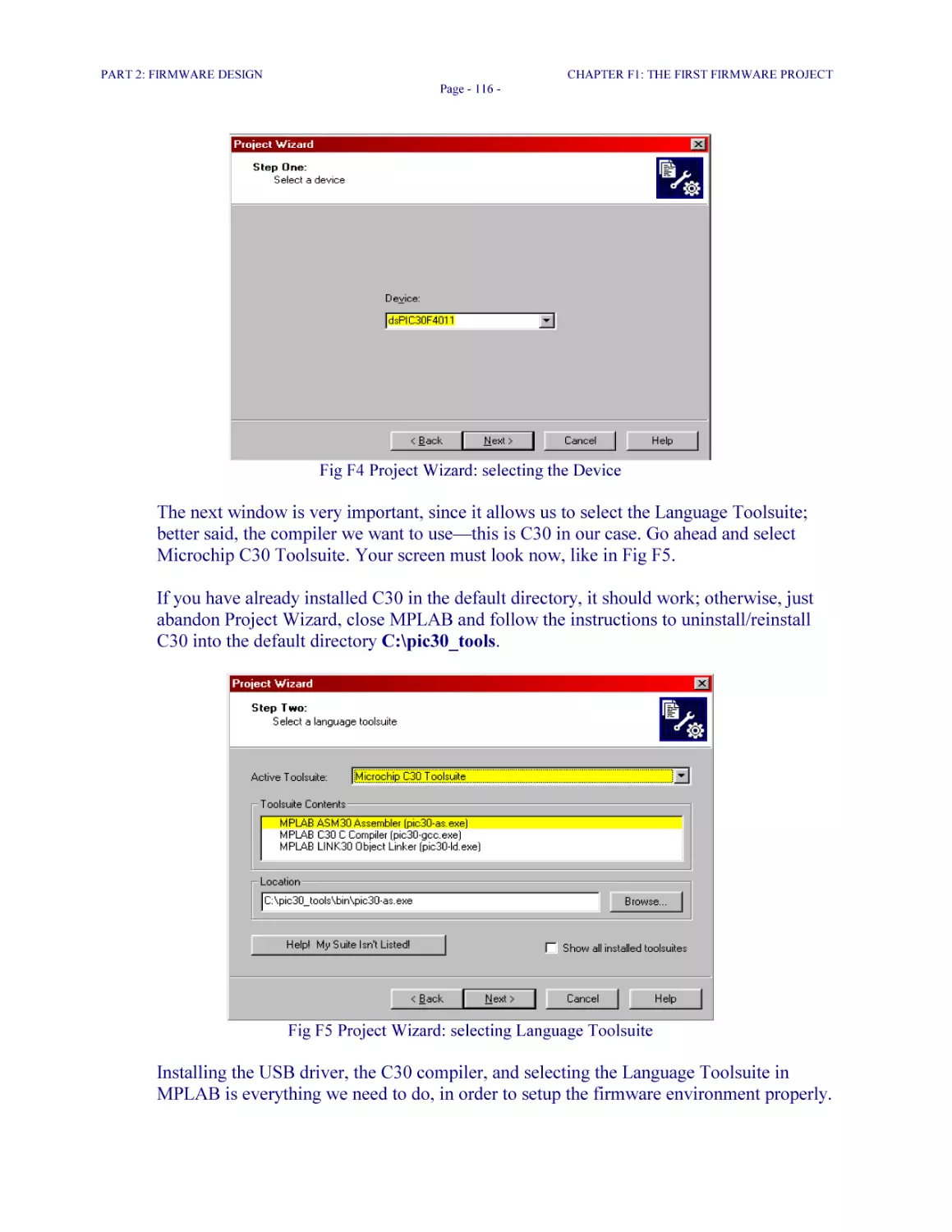
Fig F4 Project Wizard: selecting the Device 116
LHFSD
TABLE OF FIGURES
Page - 20 -
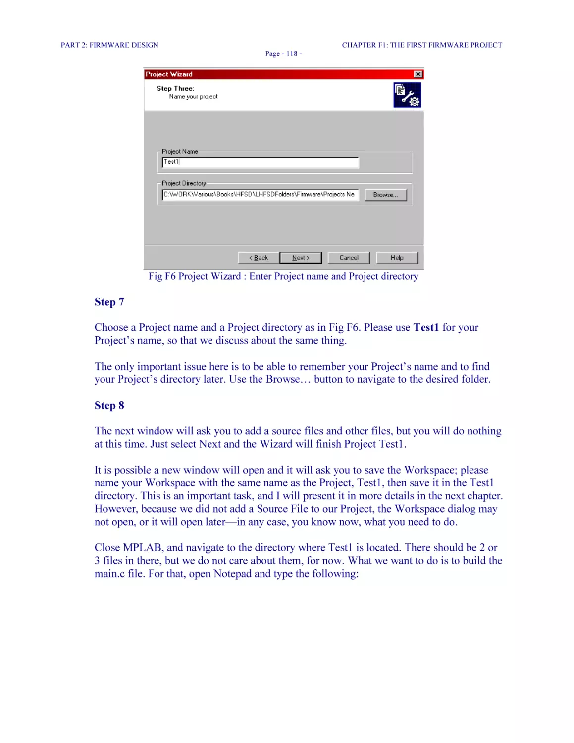
Fig F5 Project Wizard: selecting Language Toolsuite 116
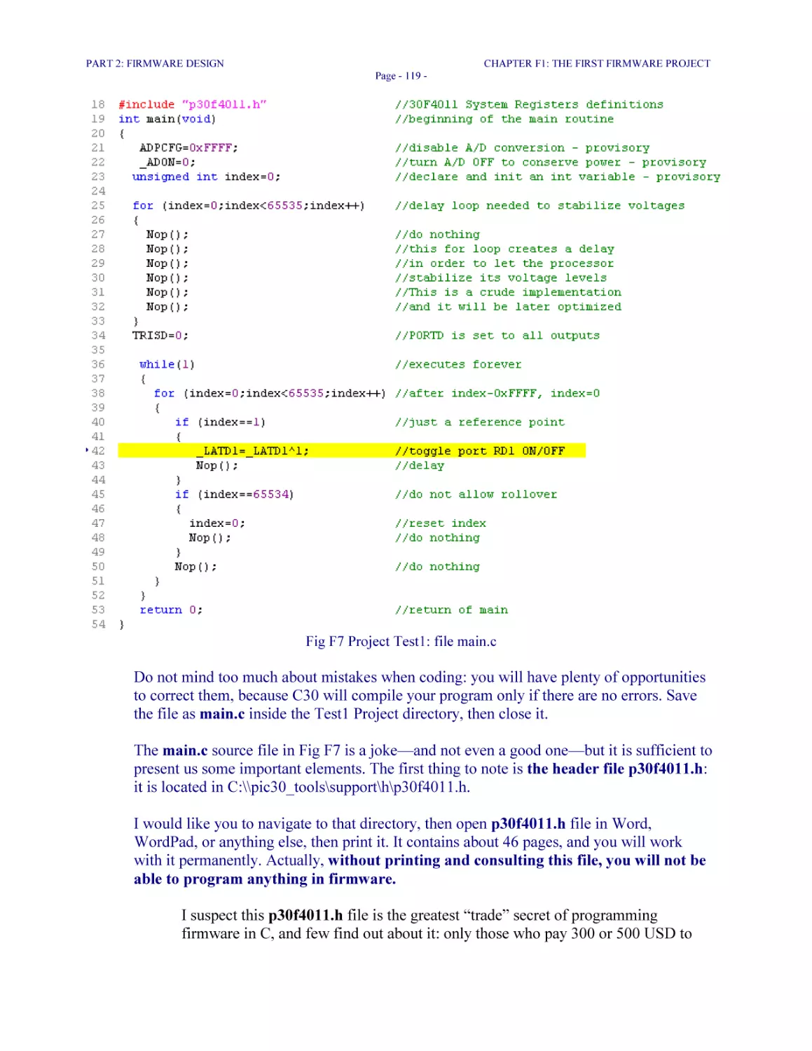
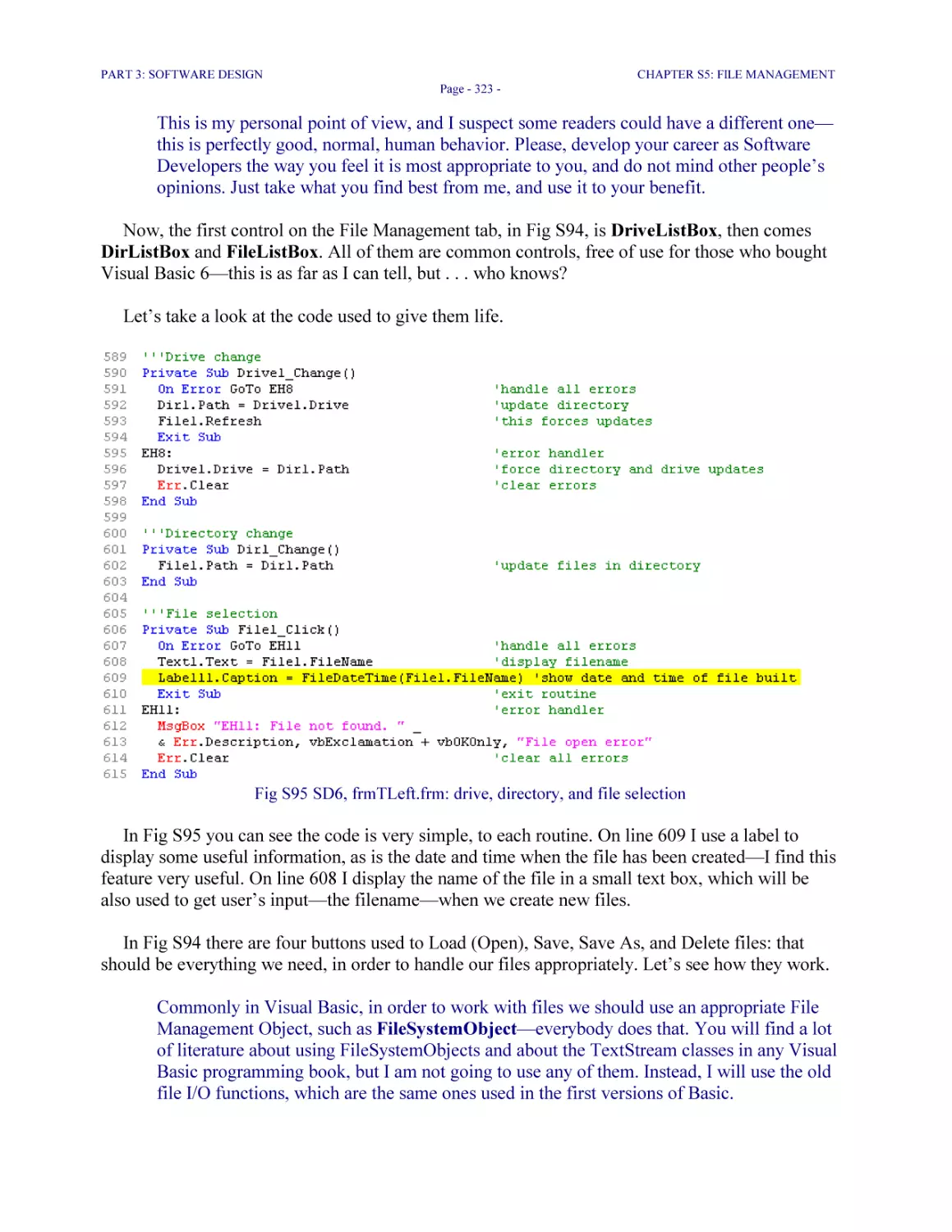
Fig F6 Project Wizard : Enter Project name and Project directory 118
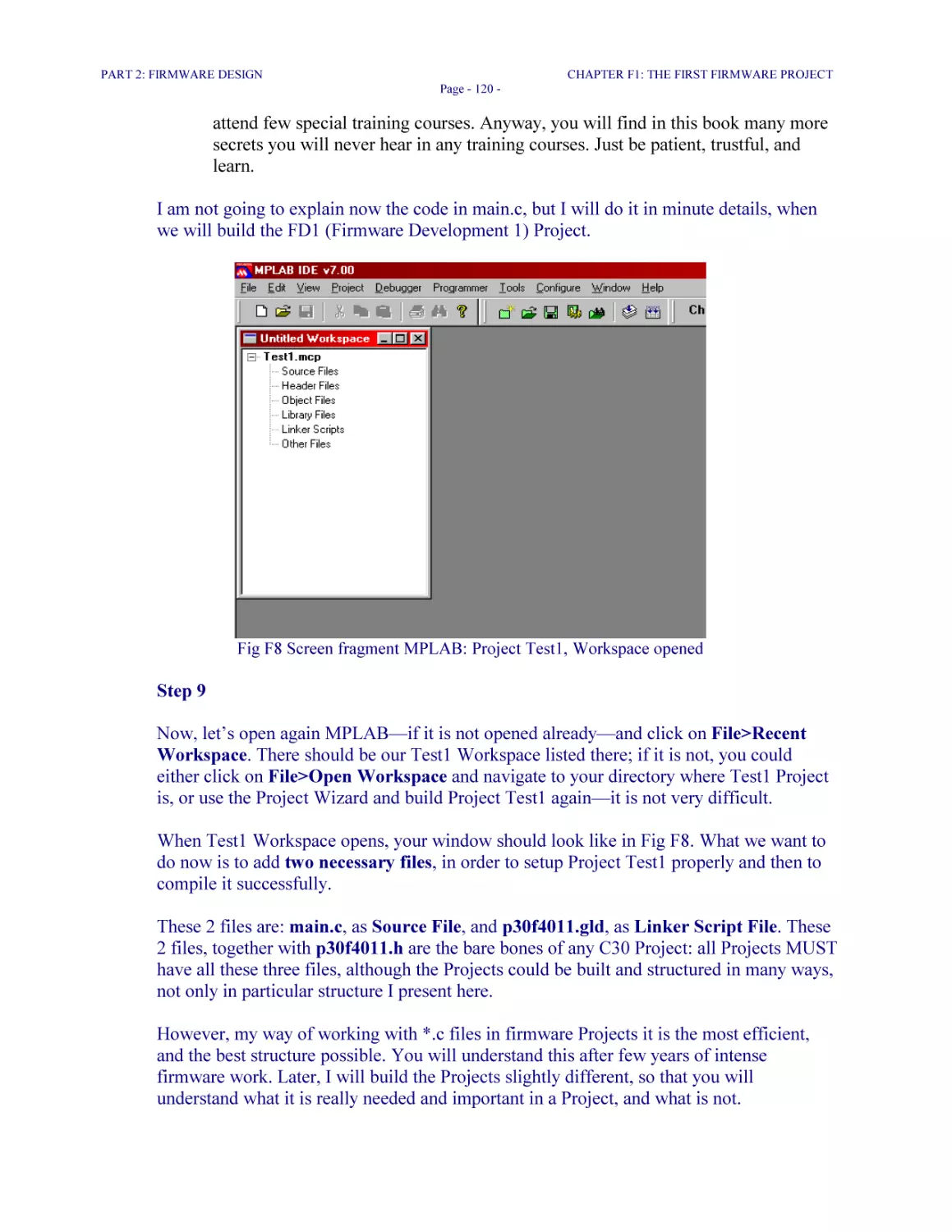
Fig F7 Project Test1: file main.c 119
Fig F8 Screen fragment MPLAB: Project Test1, Workspace opened 120
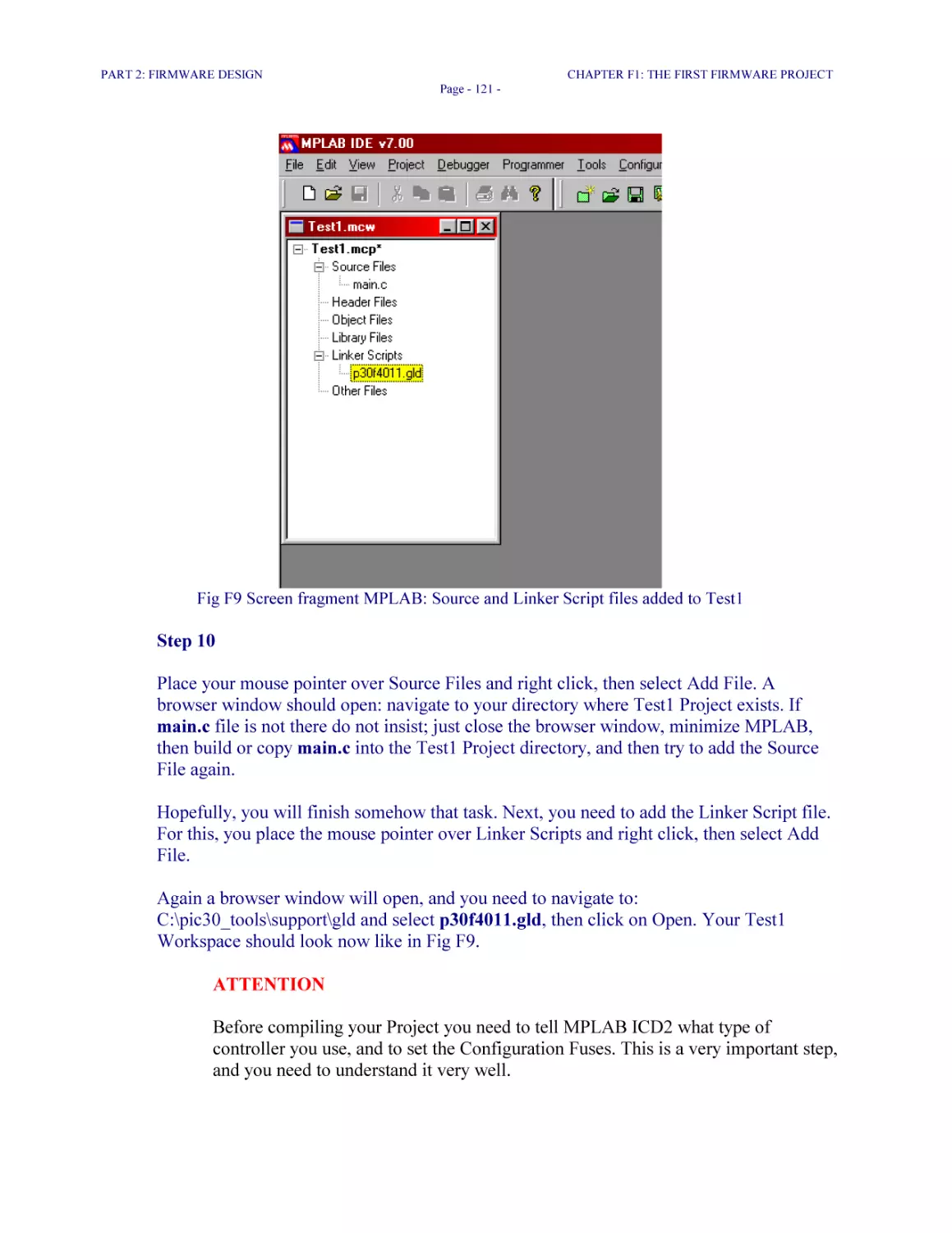
Fig F9 Screen fragment MPLAB: Source and Linker Script files added to Test1 121
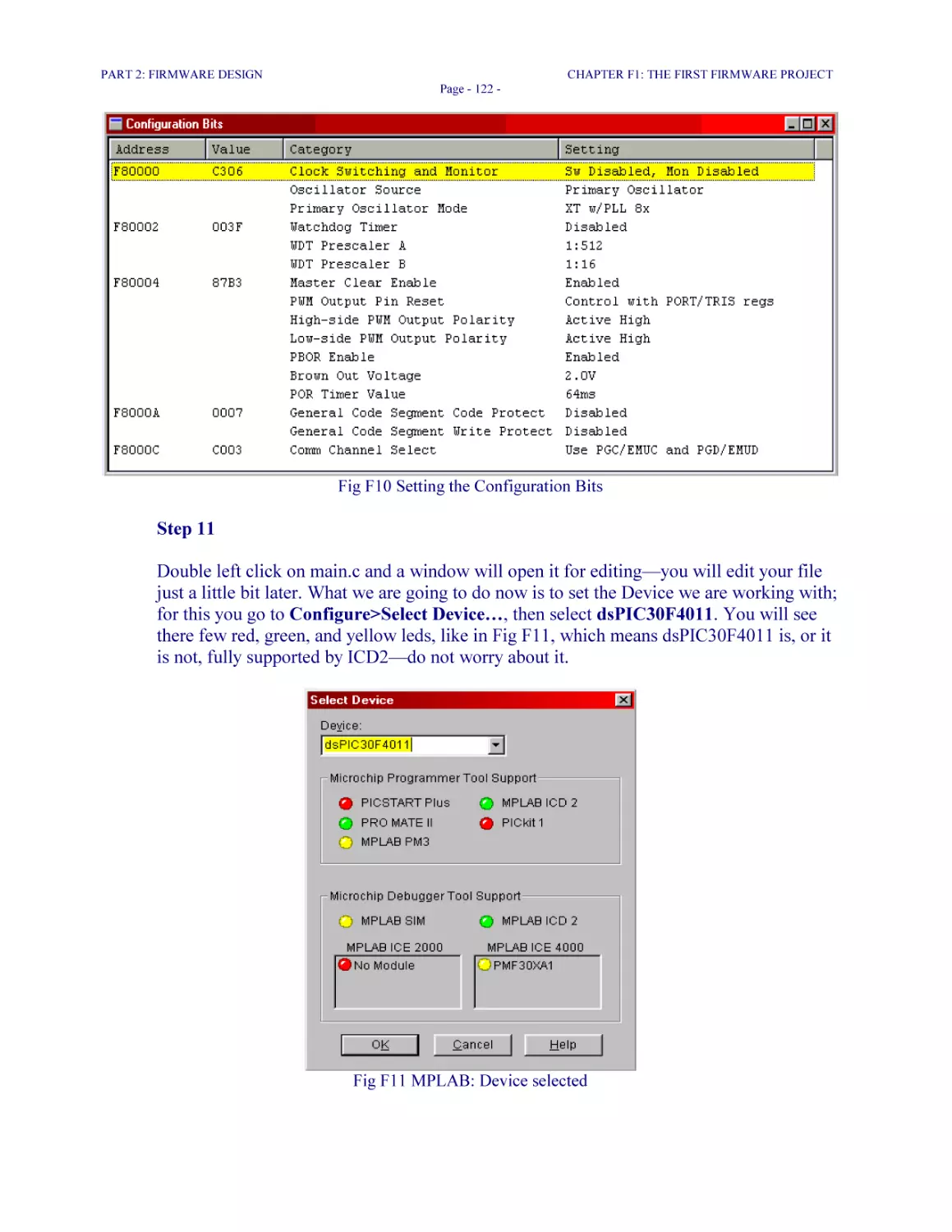
Fig F10 Setting the Configuration Bits 122
Fig F11 MPLAB: Device selected 122
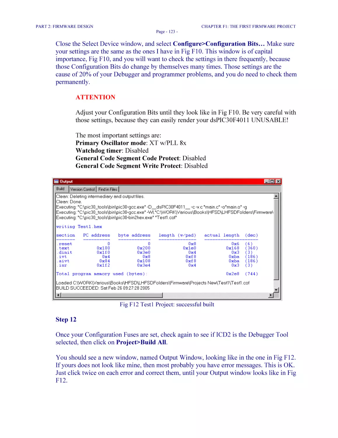
Fig F12 Test1 Project: successful built 123
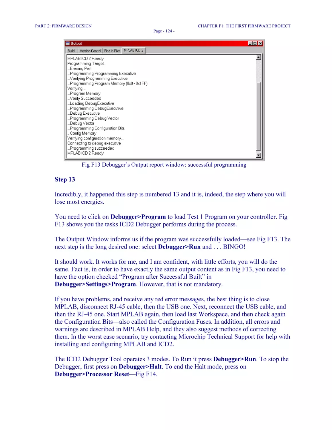
Fig F13 Debugger’s Output report window: successful programming 124
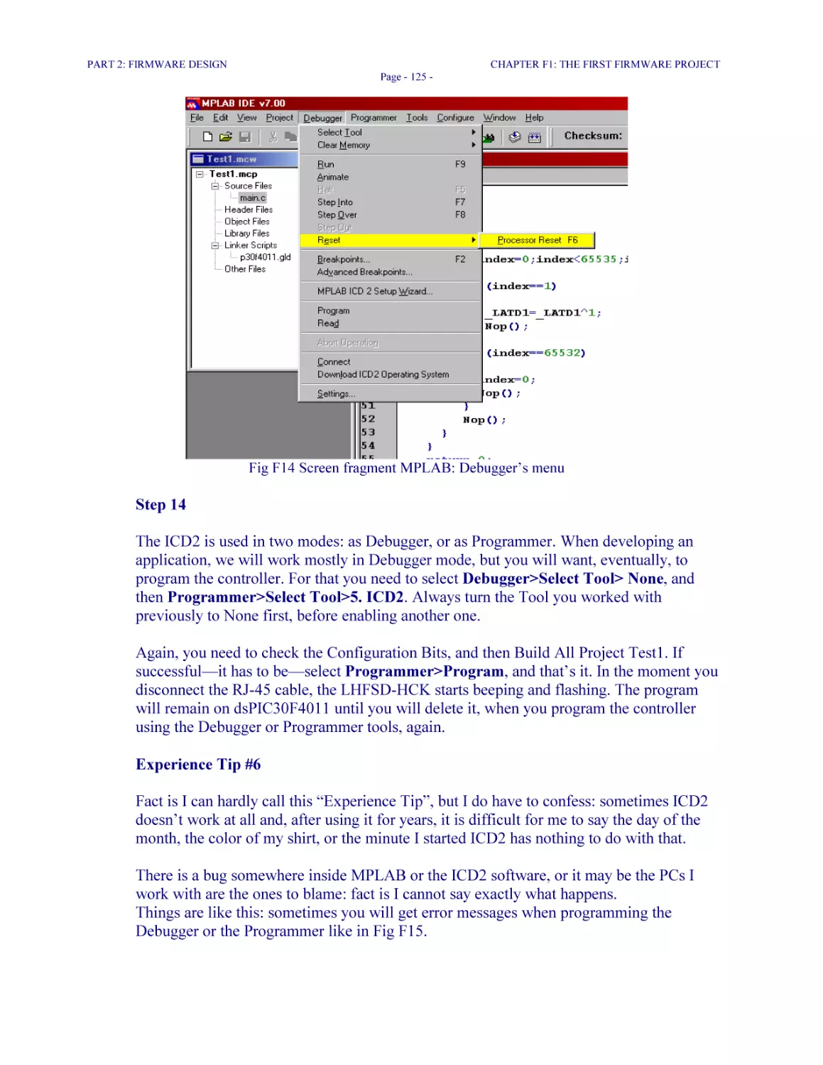
Fig F14 Screen fragment MPLAB: Debugger’s menu 125
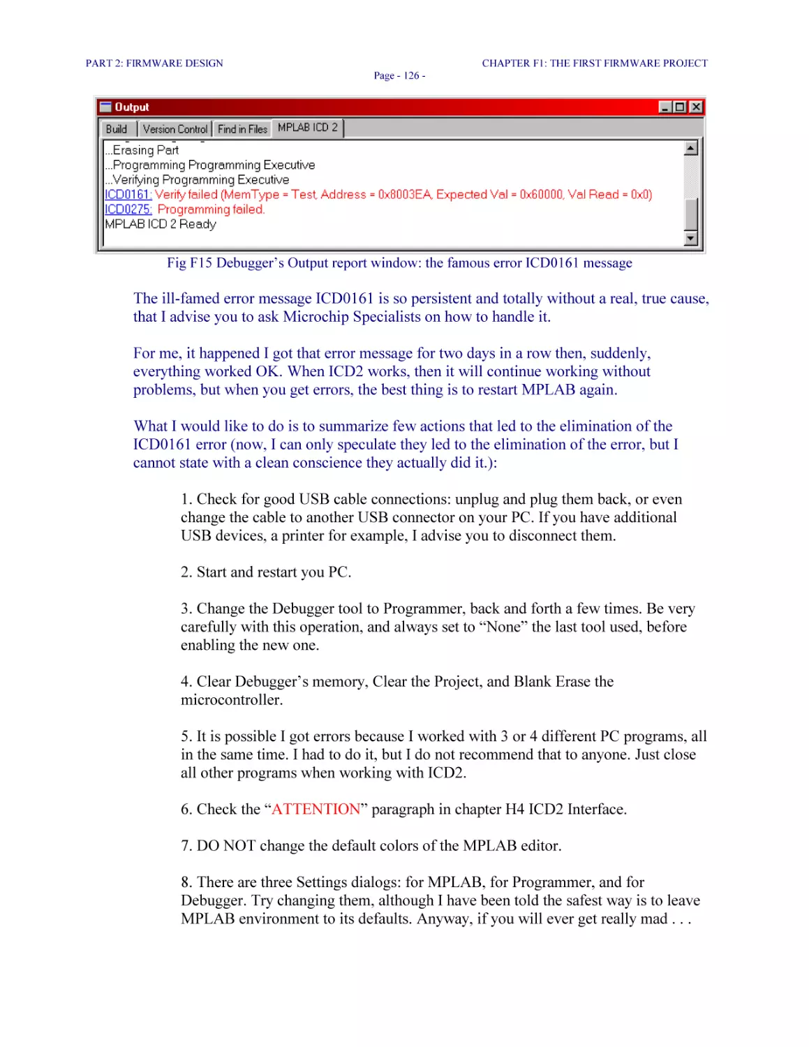
Fig F15 Debugger’s Output report window: the famous error ICD0161 message 126
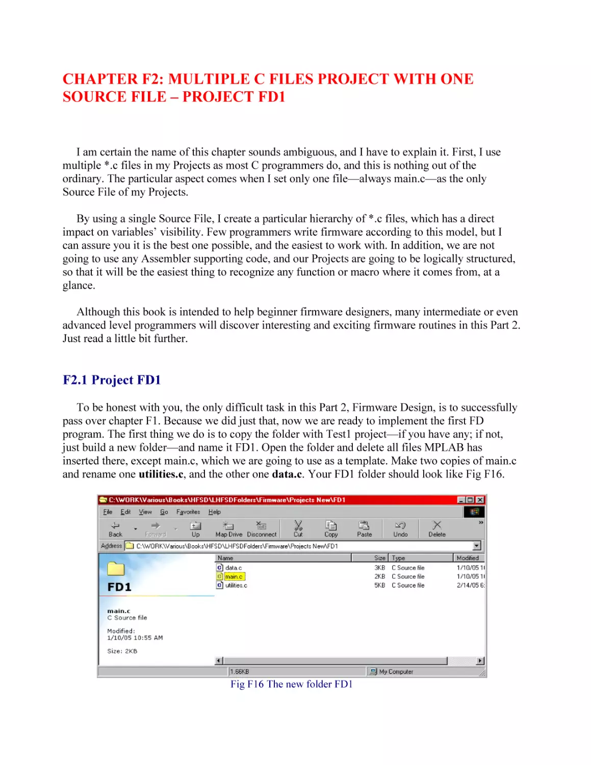
Fig F16 The new folder FD1 129
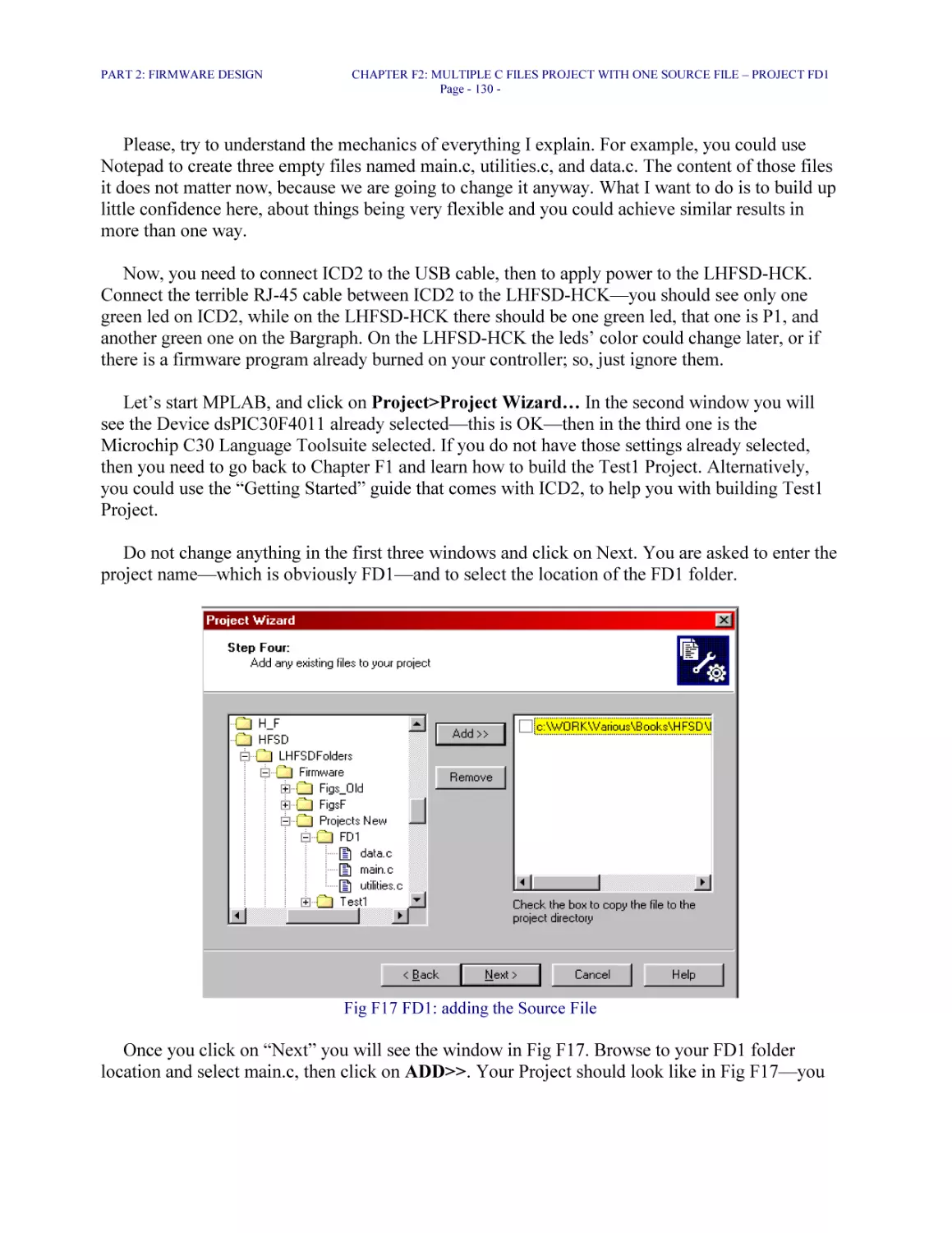
Fig F17 FD1: adding the Source File 130
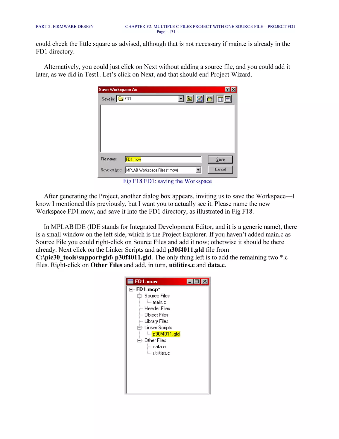
Fig F18 FD1: saving the Workspace 131
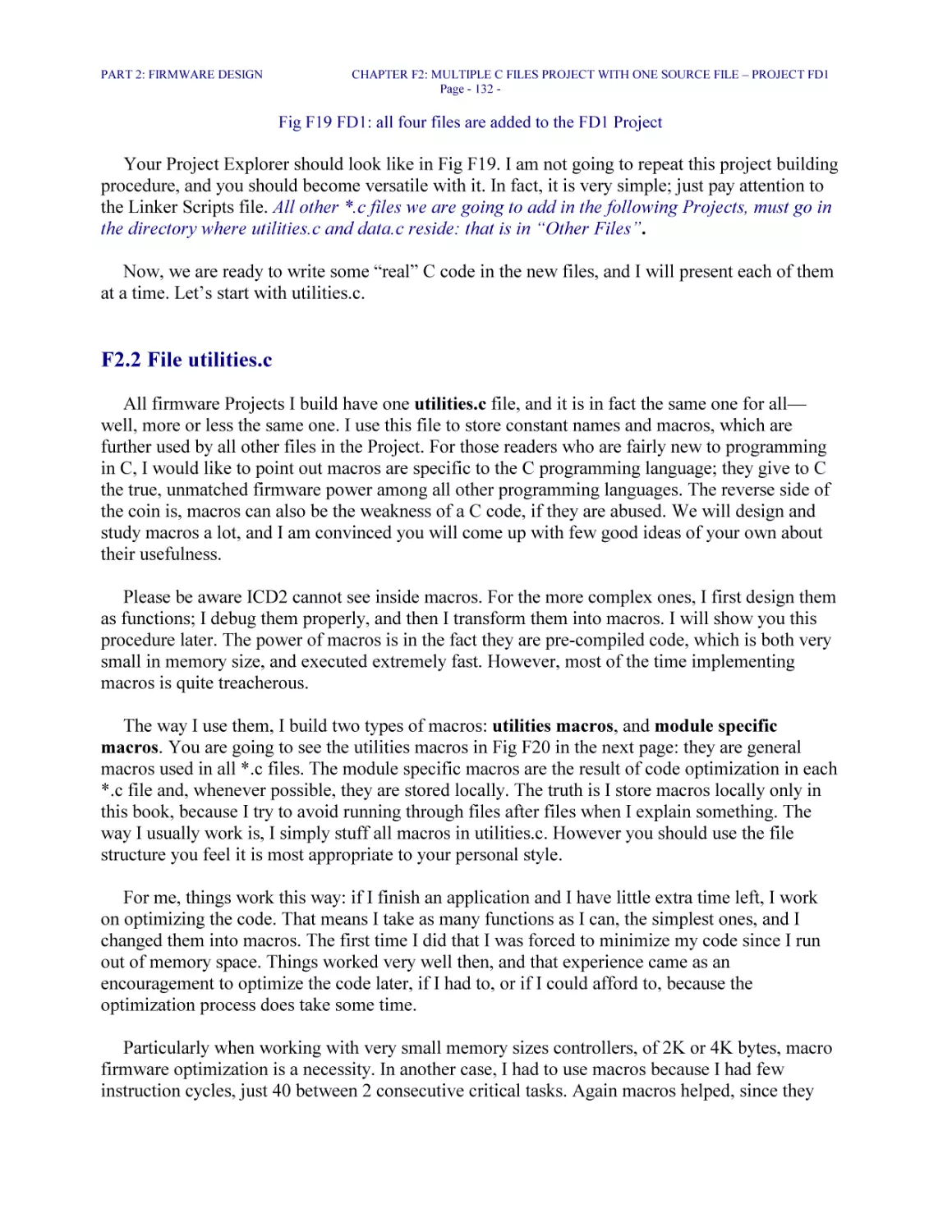
Fig F19 FD1: all four files are added to the FD1 Project 132
Fig F20 FD1: first part of utilities.c file 133
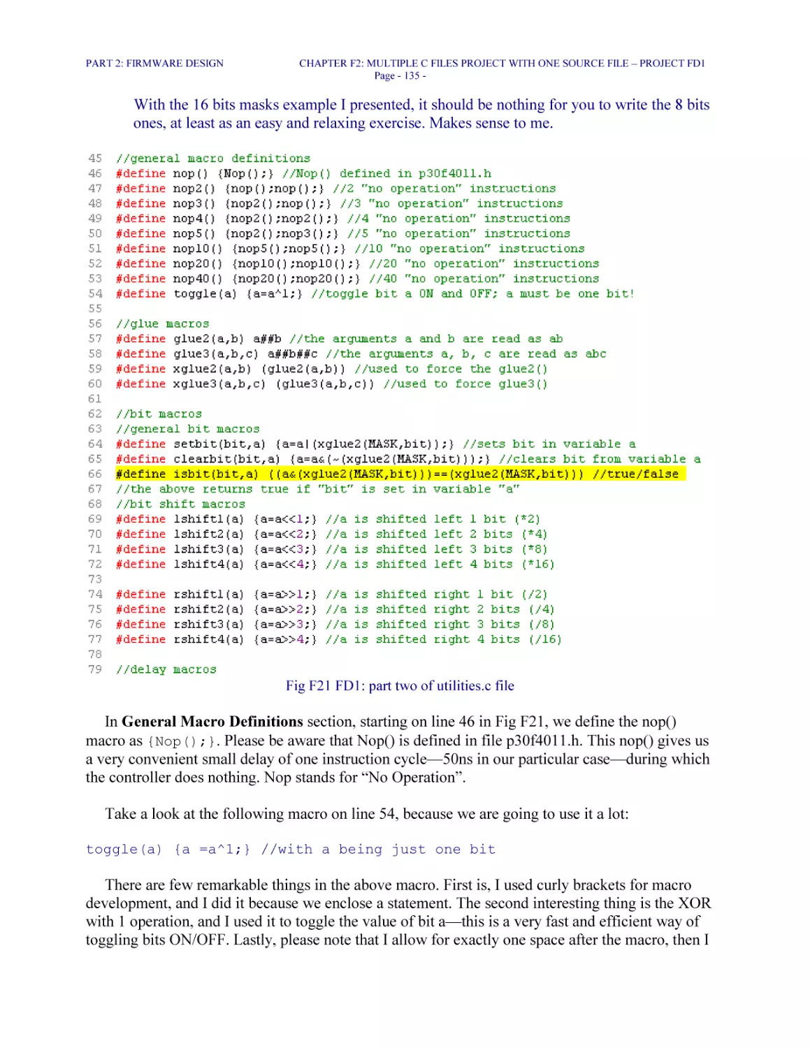
Fig F21 FD1: part two of utilities.c file 135
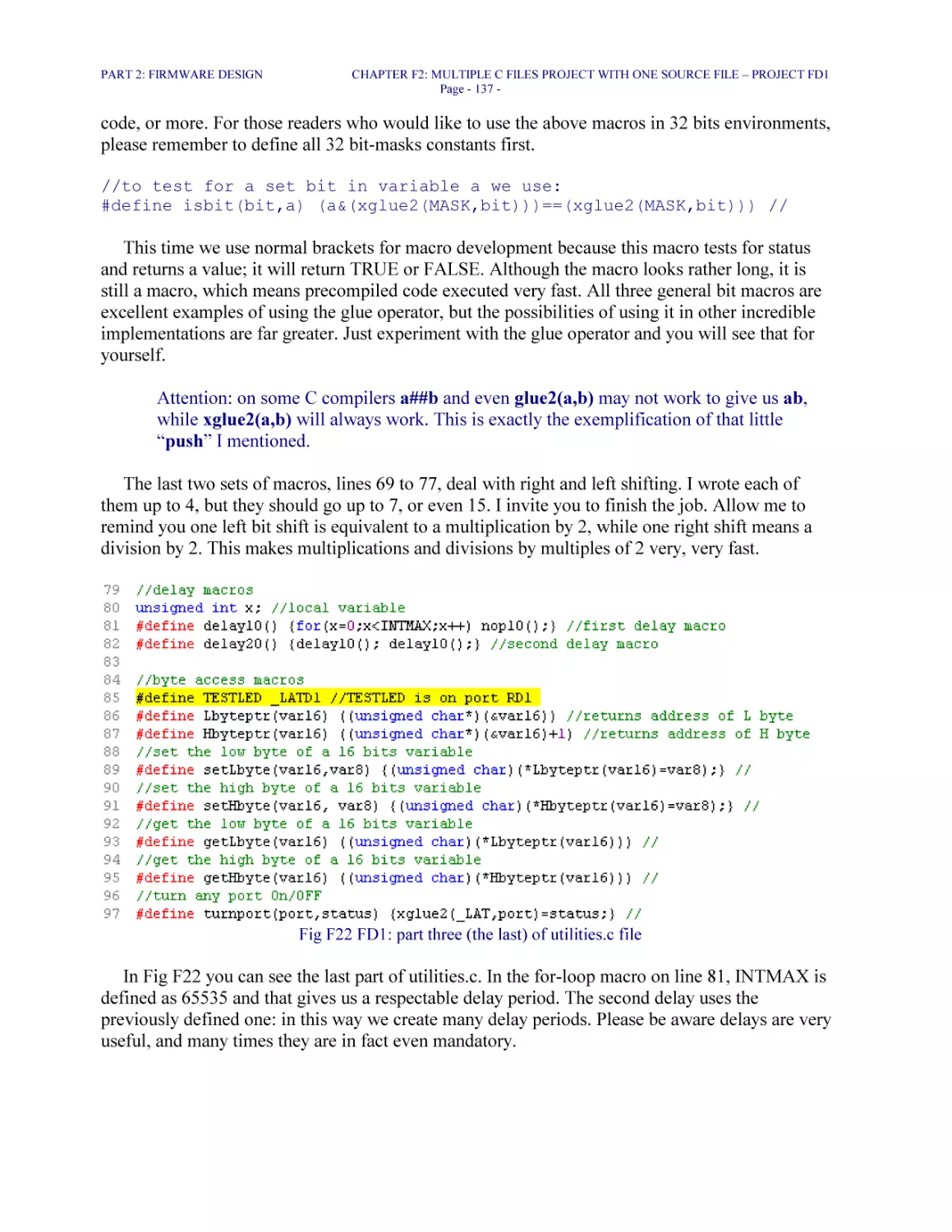
Fig F22 FD1: part three (the last) of utilities.c file 137
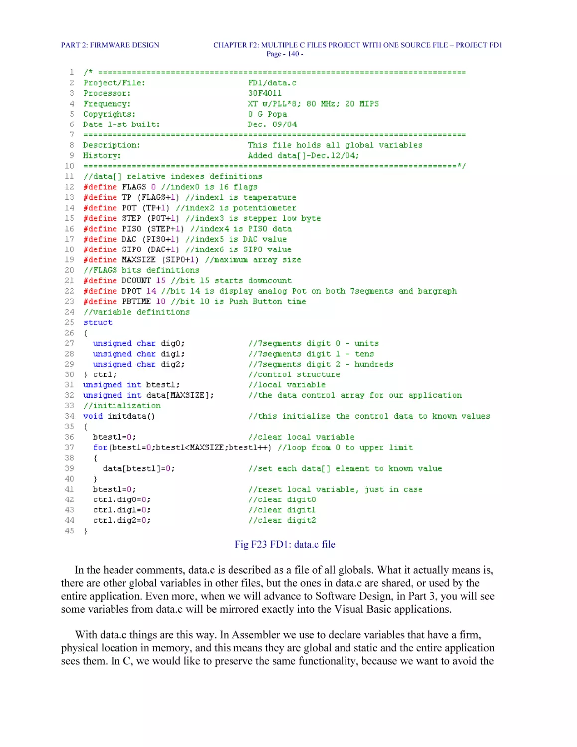
Fig F23 FD1: data.c file 140
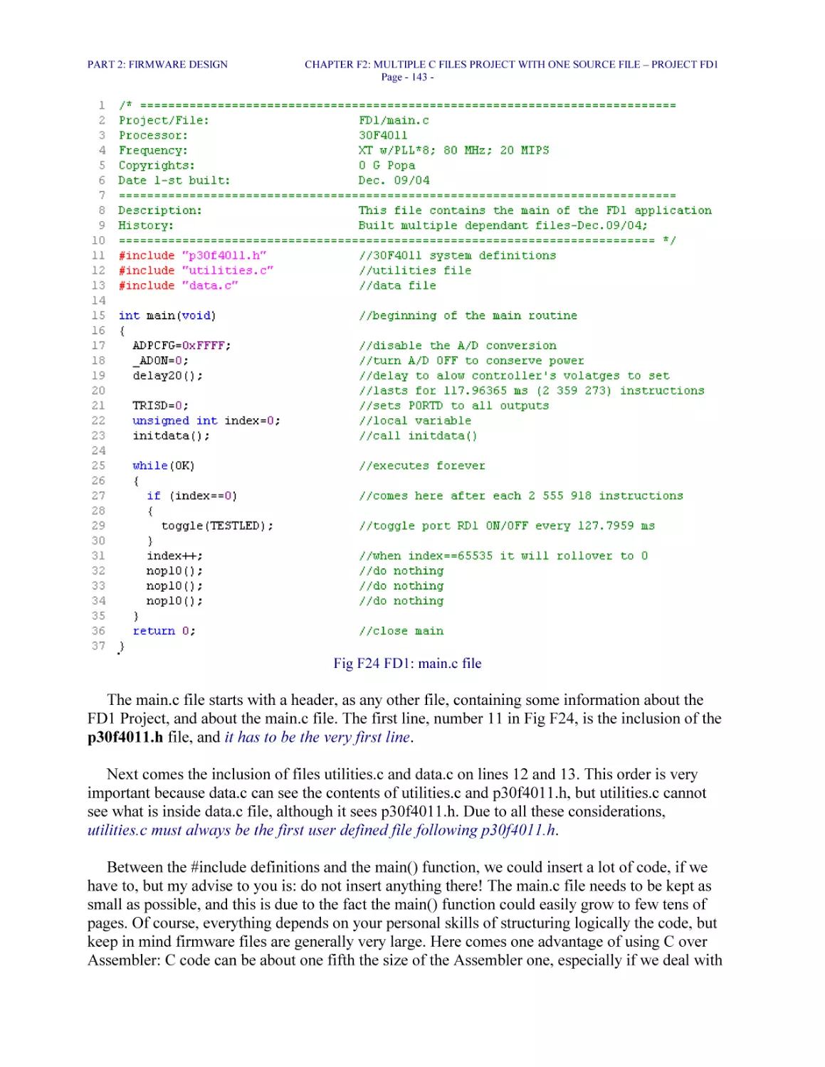
Fig F24 FD1: main.c file 143
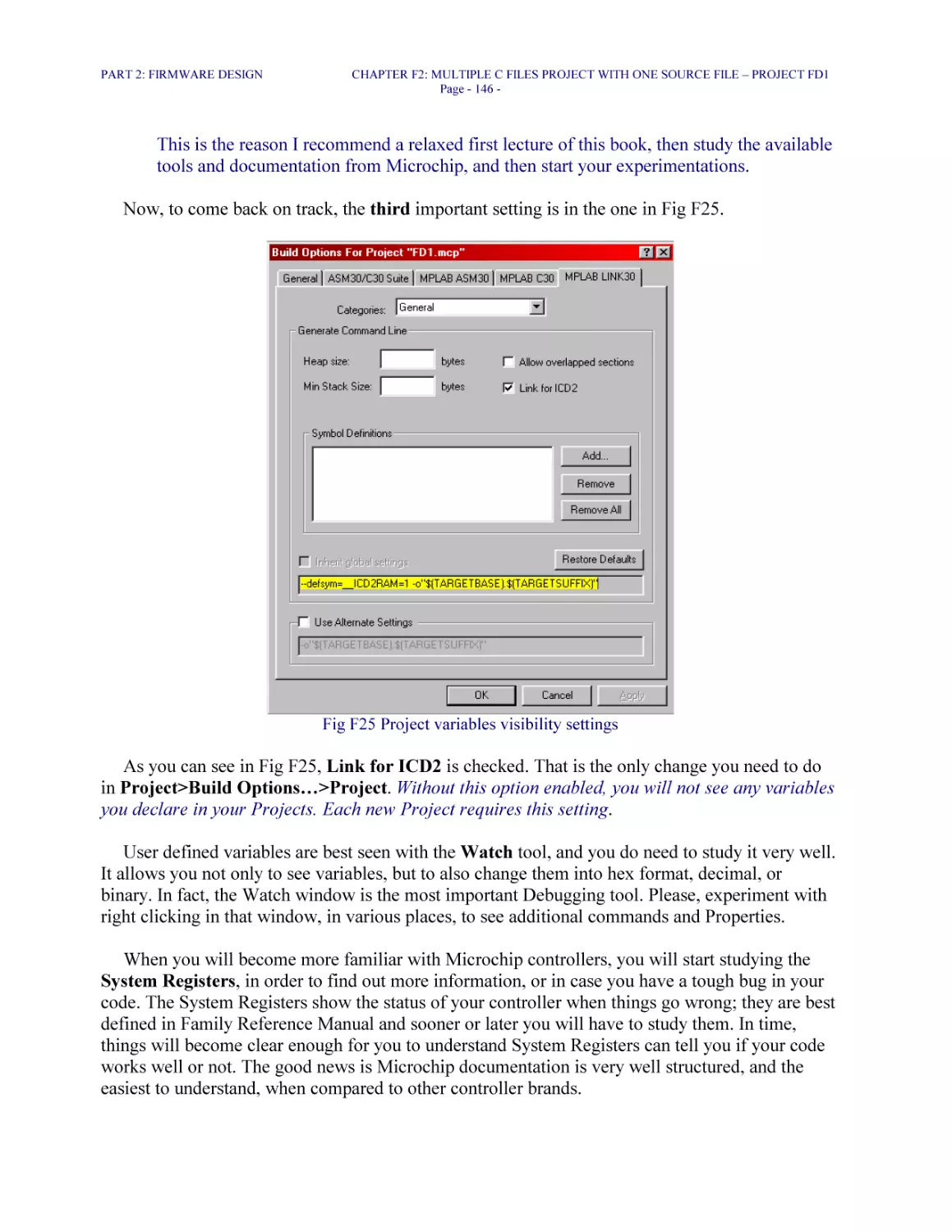
Fig F25 Project variables visibility settings 146
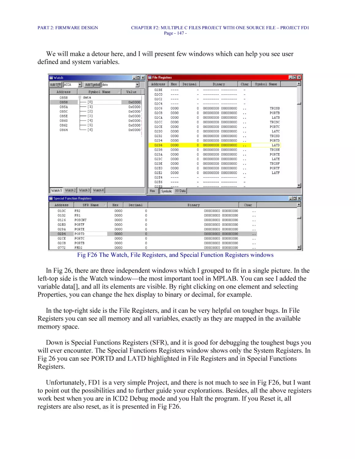
Fig F26 The Watch, File Registers, and Special Function Registers windows 147
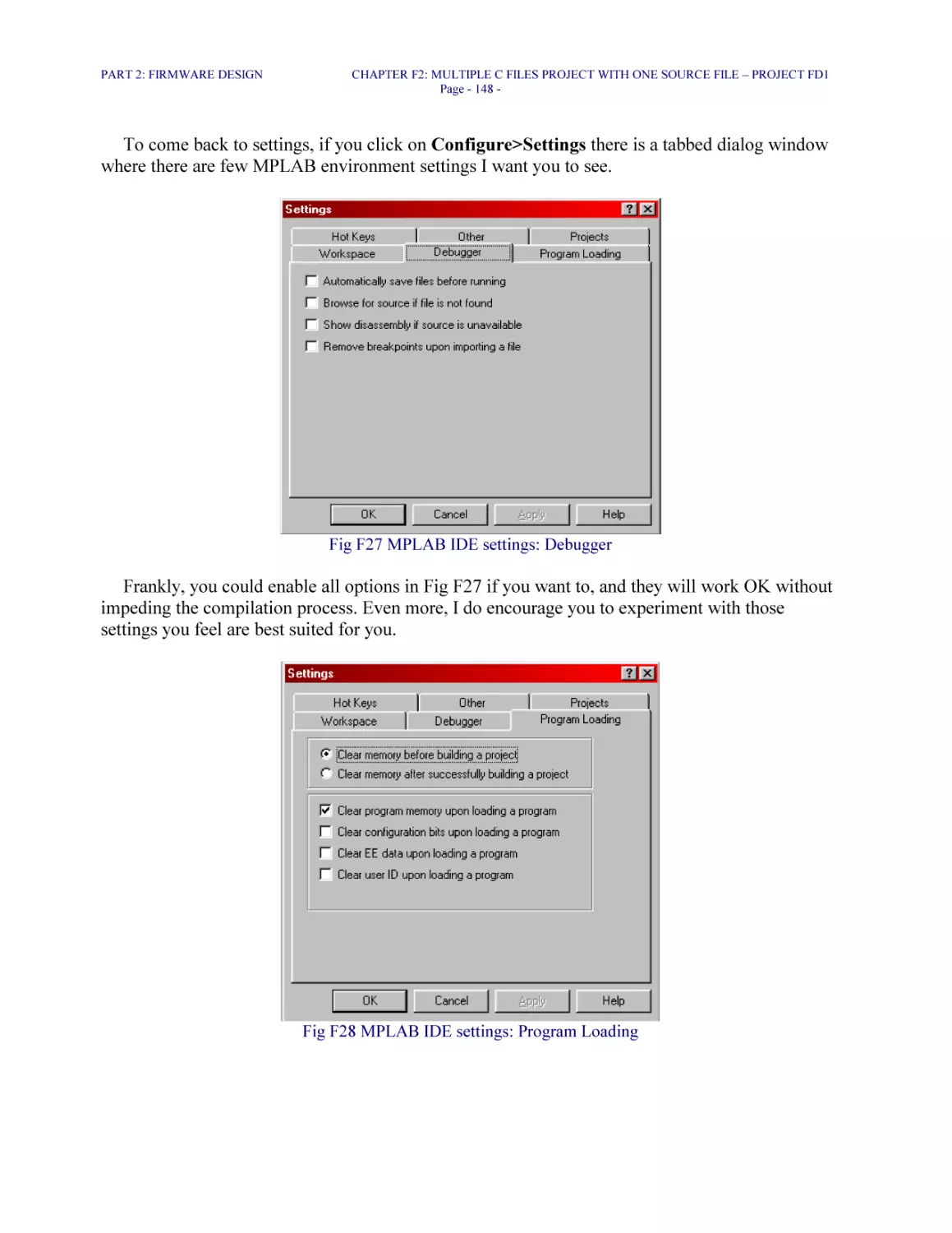
Fig F27 MPLAB IDE settings: Debugger 148
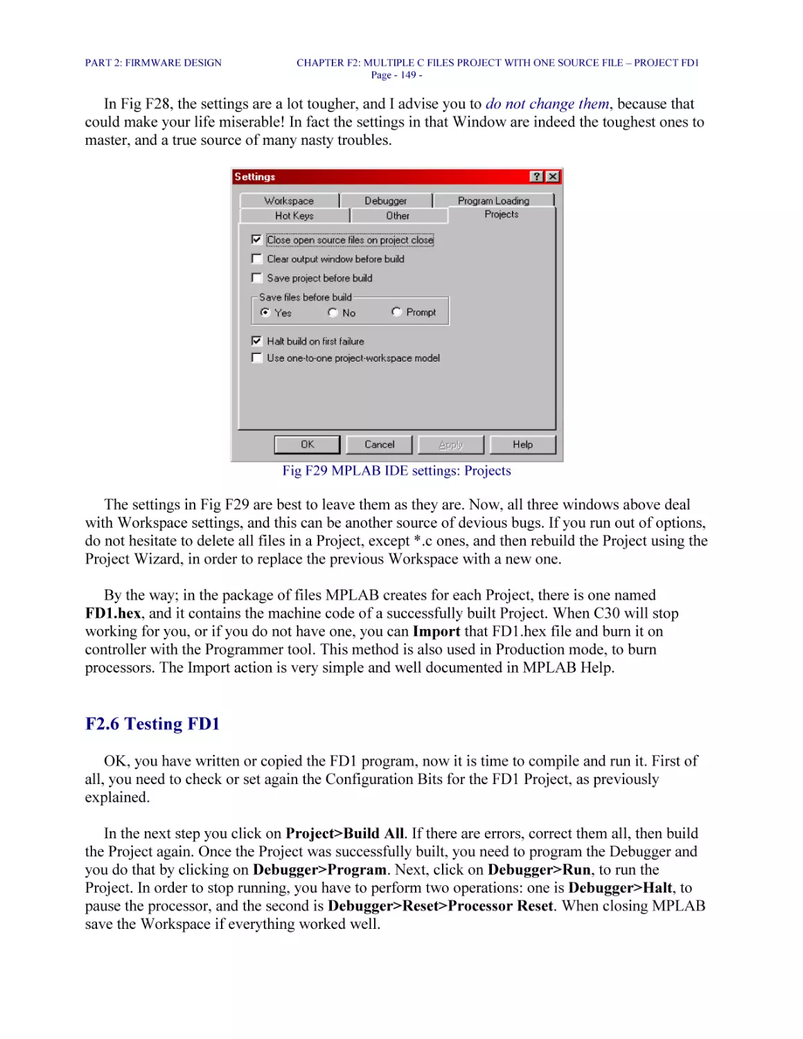
Fig F28 MPLAB IDE settings: Program Loading 148
Fig F29 MPLAB IDE settings: Projects 149
Fig F30 Paper planning: Multitasking Tasks 154
Fig F31 FD2: file timers.c 157
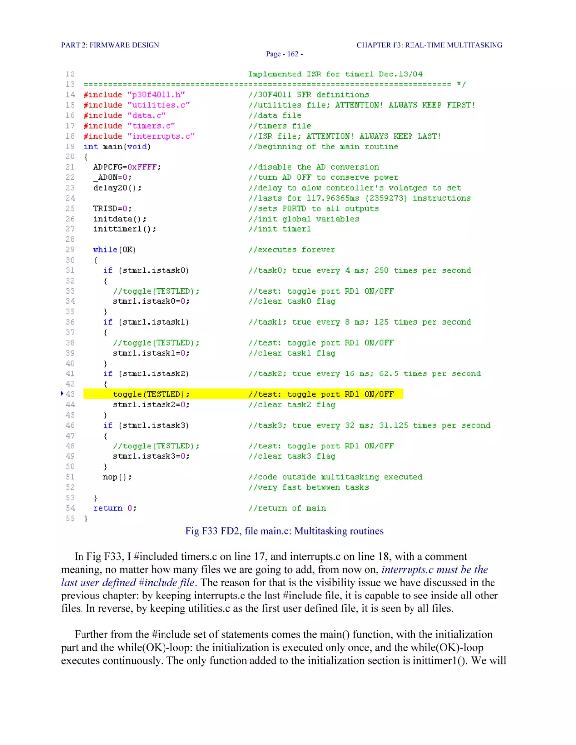
Fig F32 FD2, file interrupts.c: timer1 Interrupt Service Routine 159
Fig F33 FD2, file main.c: Multitasking routines 162
Fig F34 FD3, file IO.c: initIO() routine 165
Fig F35 FD3, File SPI.c: variables declaration 168
Fig F36 FD3, file SPI.c: checkSPI(), PISO module 169
Fig F37 FD3: SPI-PISO macros added to utilities.c file 171
Fig F38 FD3, SPIc: SPI-DAC routine 172
Fig F39 FD3: SPI-DAC macros added to utilities.c file 172
Fig F40 FD3, SPI.c: calculation of the SIPO digits from data[PISO] 175
Fig F41 FD3, SPI.c: SPI-SIPO routine 175
Fig F42 FD3, SPI.c: setdigit() function 176
Fig F43 FD3, utilities.c: multi-line mapdigit(a) macro with comments 177
Fig F44 FD3, utilities.c: SPI-SIPO macros 178
Fig F45 FD3, utilities.c: enabledigit() macro 178
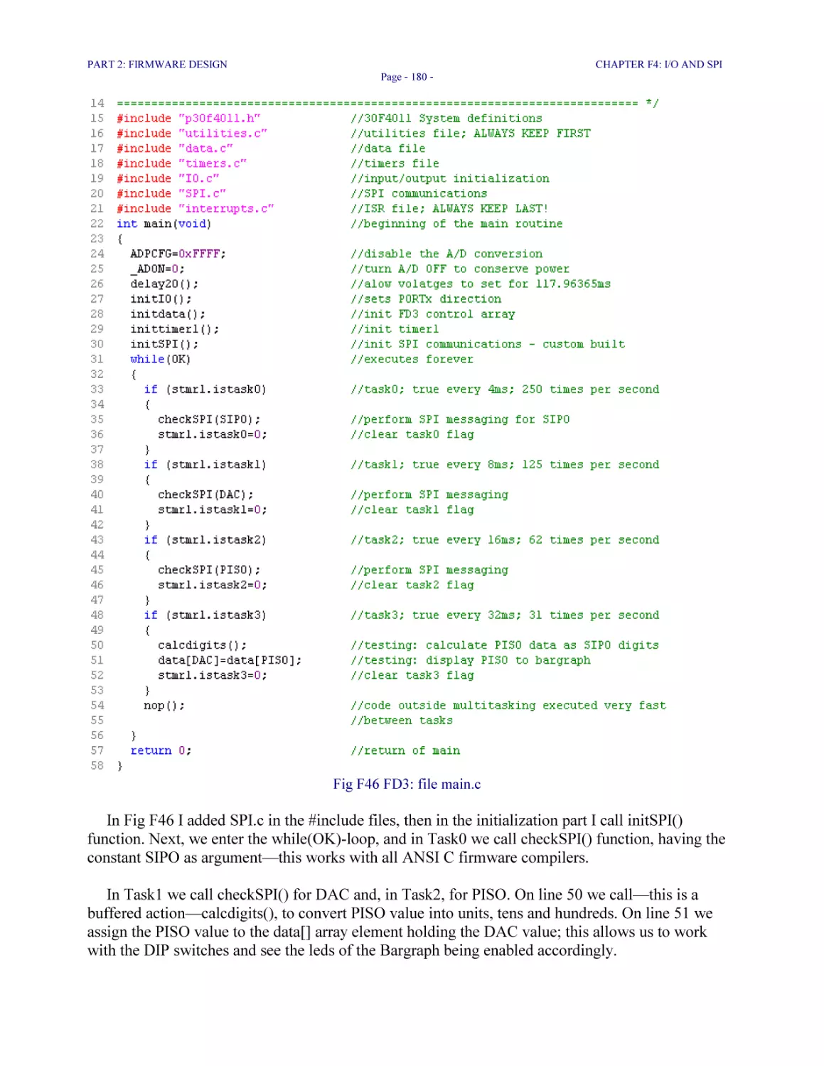
Fig F46 FD3: file main.c 180
Fig F47 FD4a: file ad.c 183
Fig F48 FD4a, ad.c: checkad() function 184
Fig F49 FD4a, ad.c: readad() function 186
Fig F50 FD4a, IO.c: initINT0() function 187
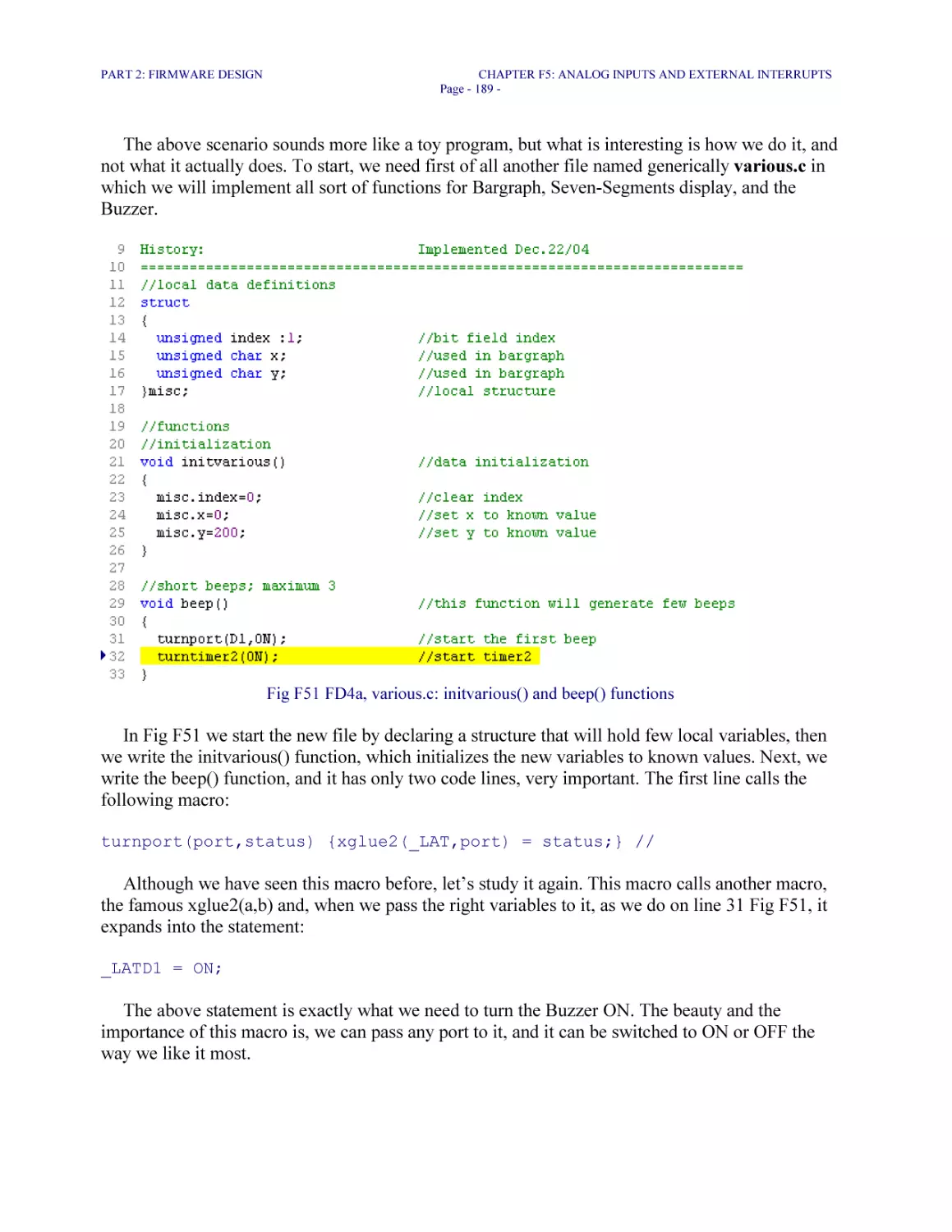
Fig F51 FD4a, various.c: initvarious() and beep() functions 189
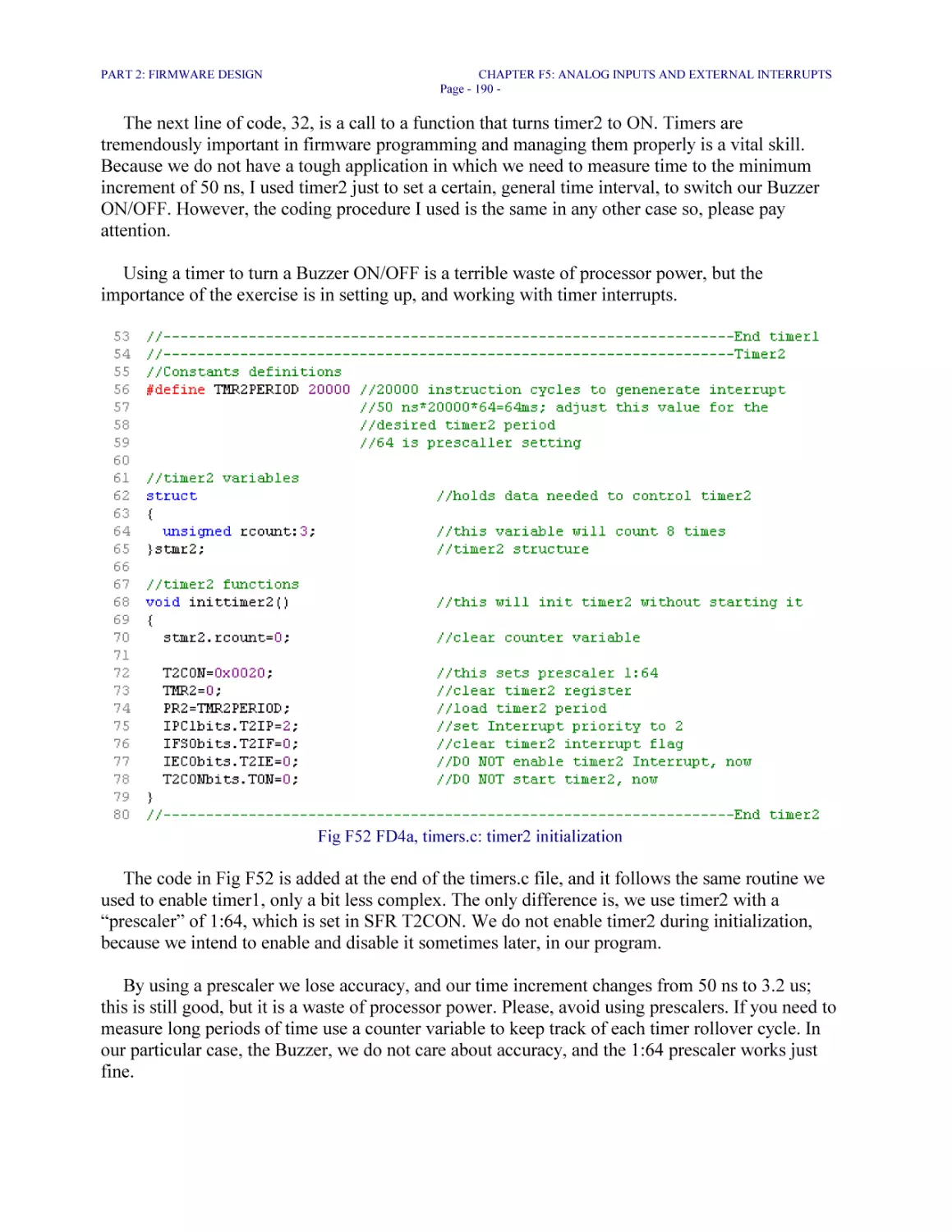
Fig F52 FD4a, timers.c: timer2 initialization 190
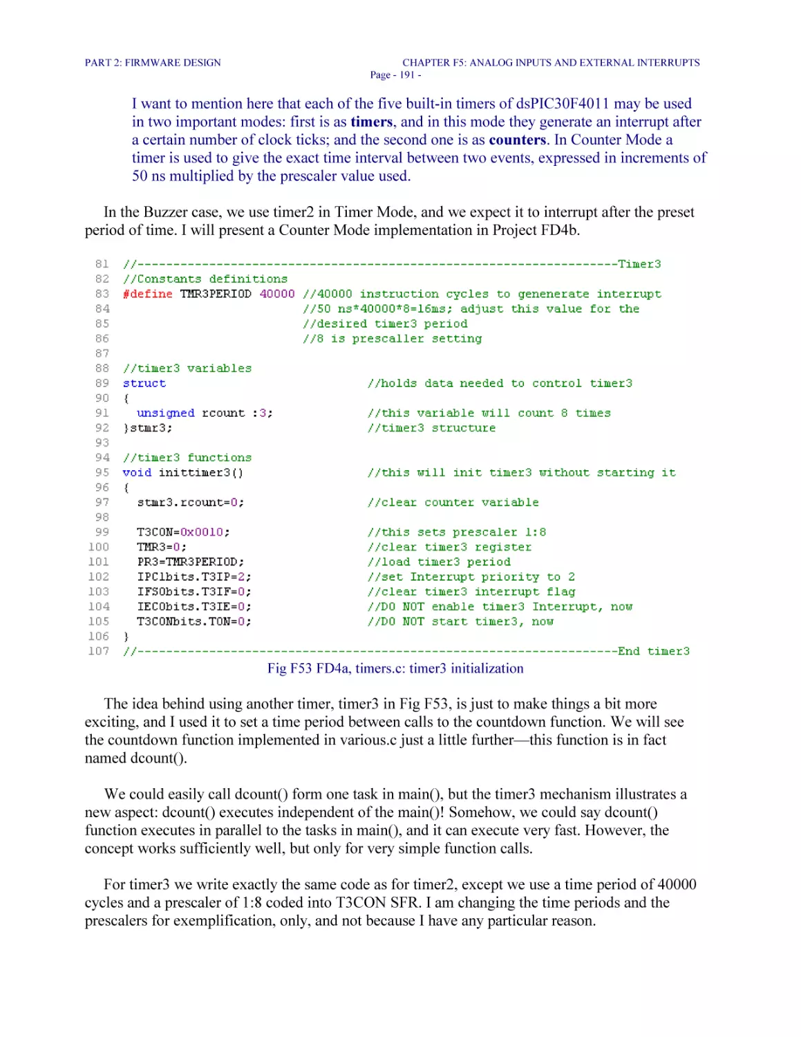
Fig F53 FD4a, timers.c: timer3 initialization 191
Fig F54 FD4a, timers.c: starting and stopping timers 2 and 3 192
Fig F55 FD4, interrupts.c: INT0 ISR 192
LHFSD
TABLE OF FIGURES
Page - 21 -
Fig F56 FD4a, various.c: dcount() function 193
Fig F57 FD4a, interrupts.c: timer3 ISR 194
Fig F58 FD4a, various.c: toggleBG() function 194
Fig F59 FD4a, main.c: while(OK) loop 195
Fig F60 FD4a, interrupts.c: timer2 ISR 196
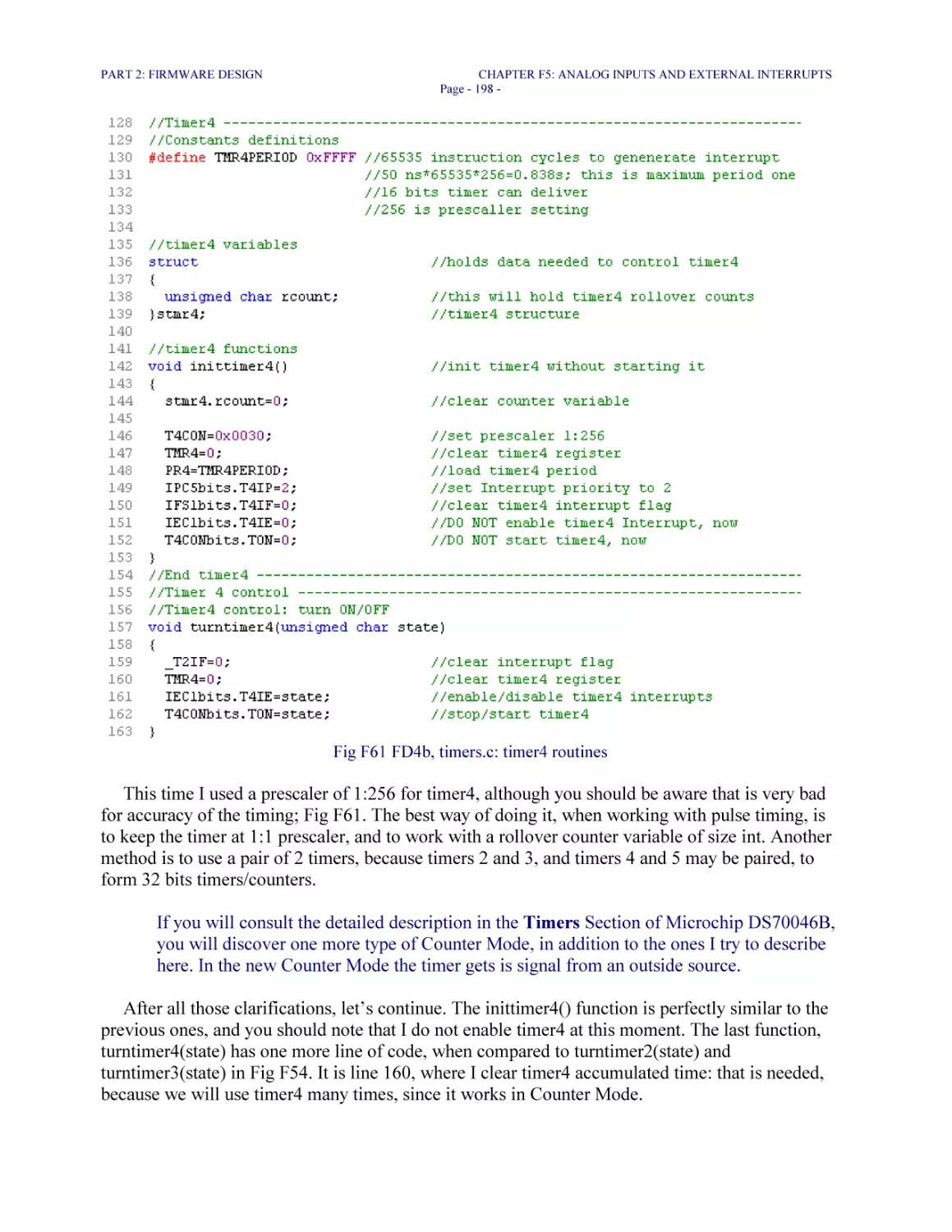
Fig F61 FD4b, timers.c: timer4 routines 198
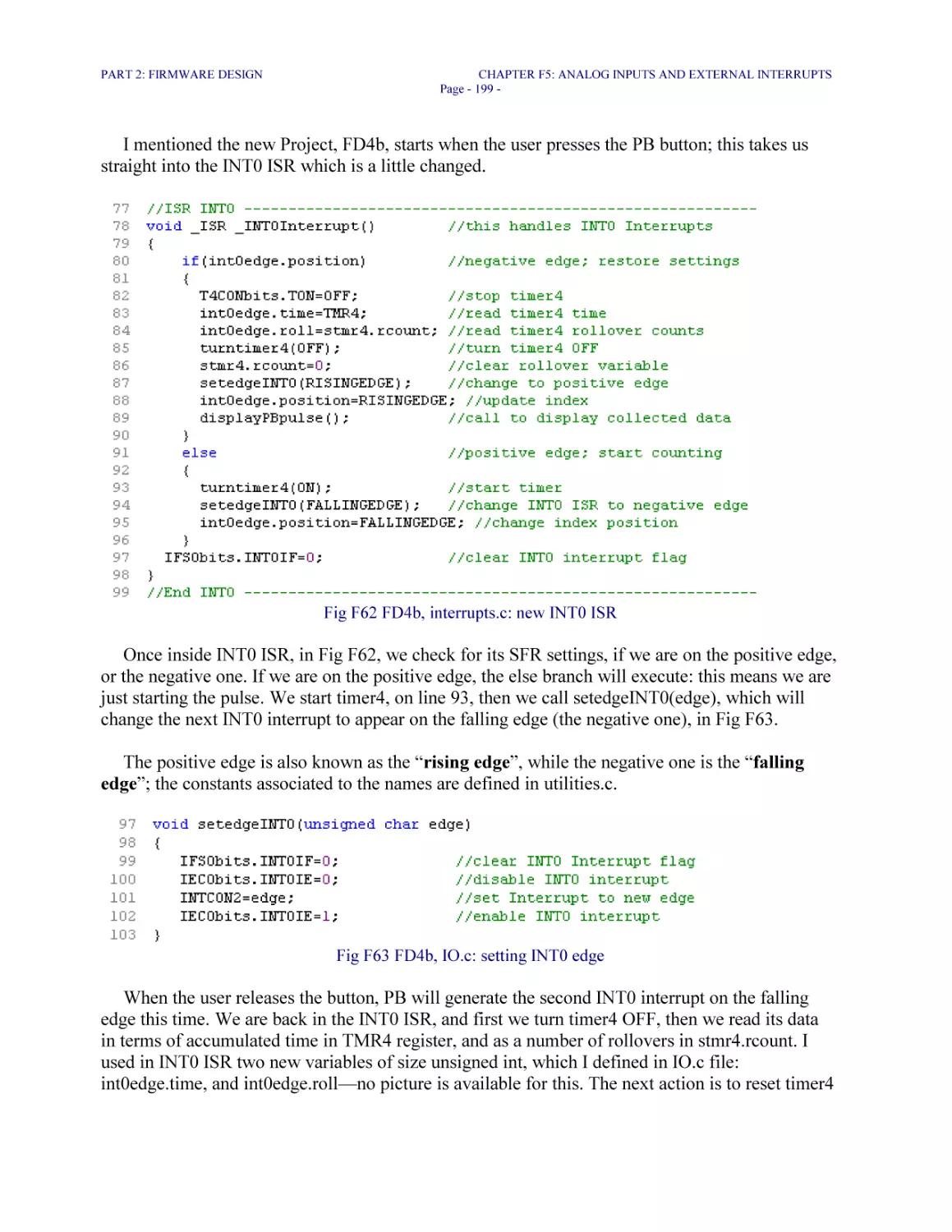
Fig F62 FD4b, interrupts.c: new INT0 ISR 199
Fig F63 FD4b, IO.c: setting INT0 edge 199
Fig F64 FD4b, various.c: displayPBpulse() function 200
Fig F65 FD4b, main.c: task3 201
Fig F66 FD4b, various.c: the new dcount() function 201
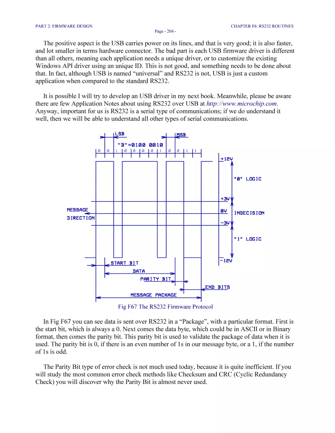
Fig F67 The RS232 Firmware Protocol 204
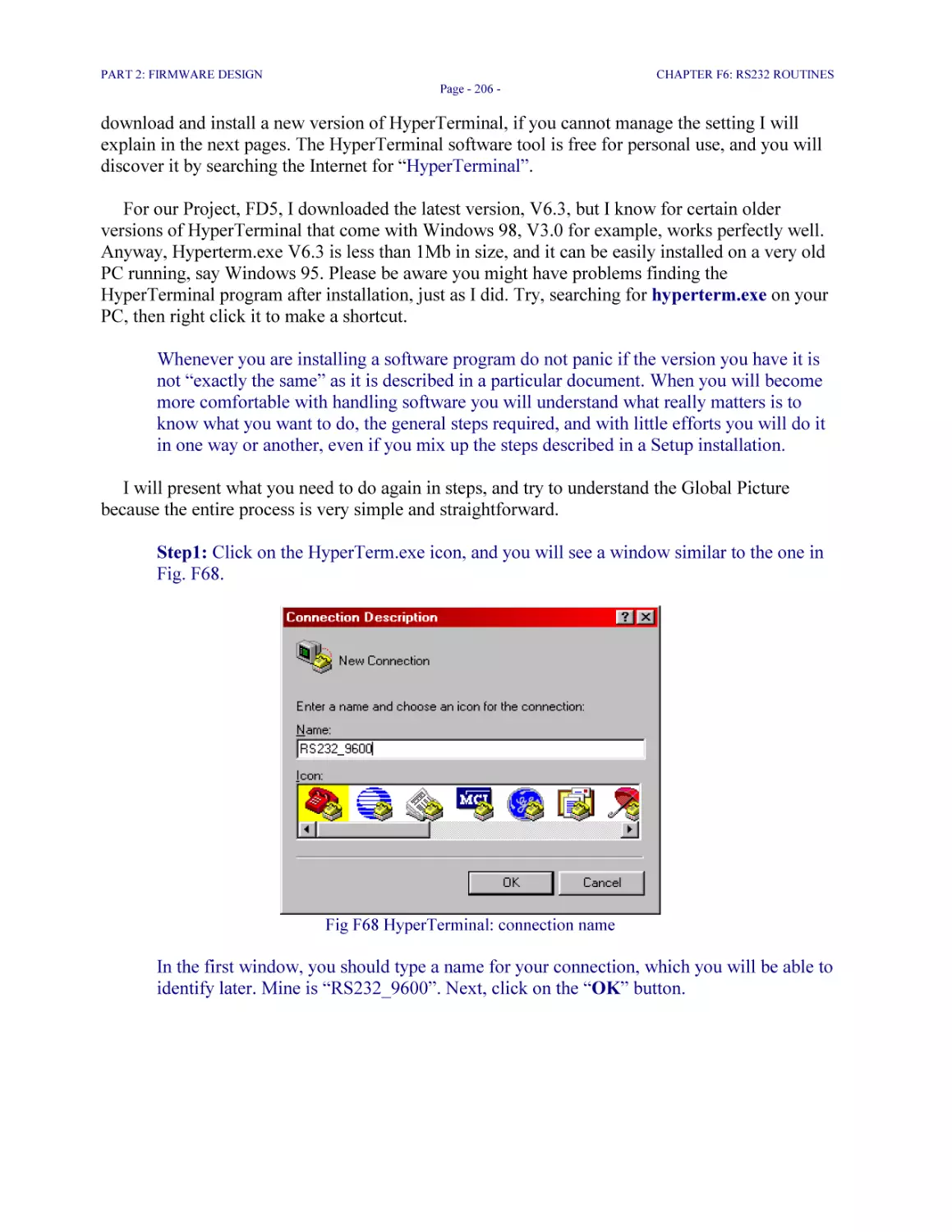
Fig F68 HyperTerminal: connection name 206
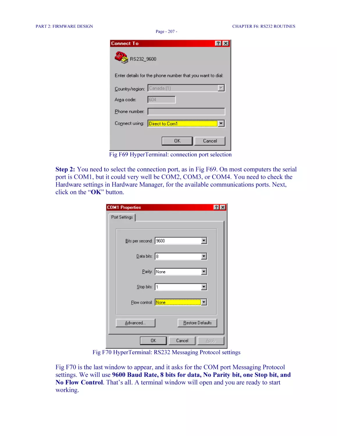
Fig F69 HyperTerminal: connection port selection 207
Fig F70 HyperTerminal: RS232 Messaging Protocol settings 207
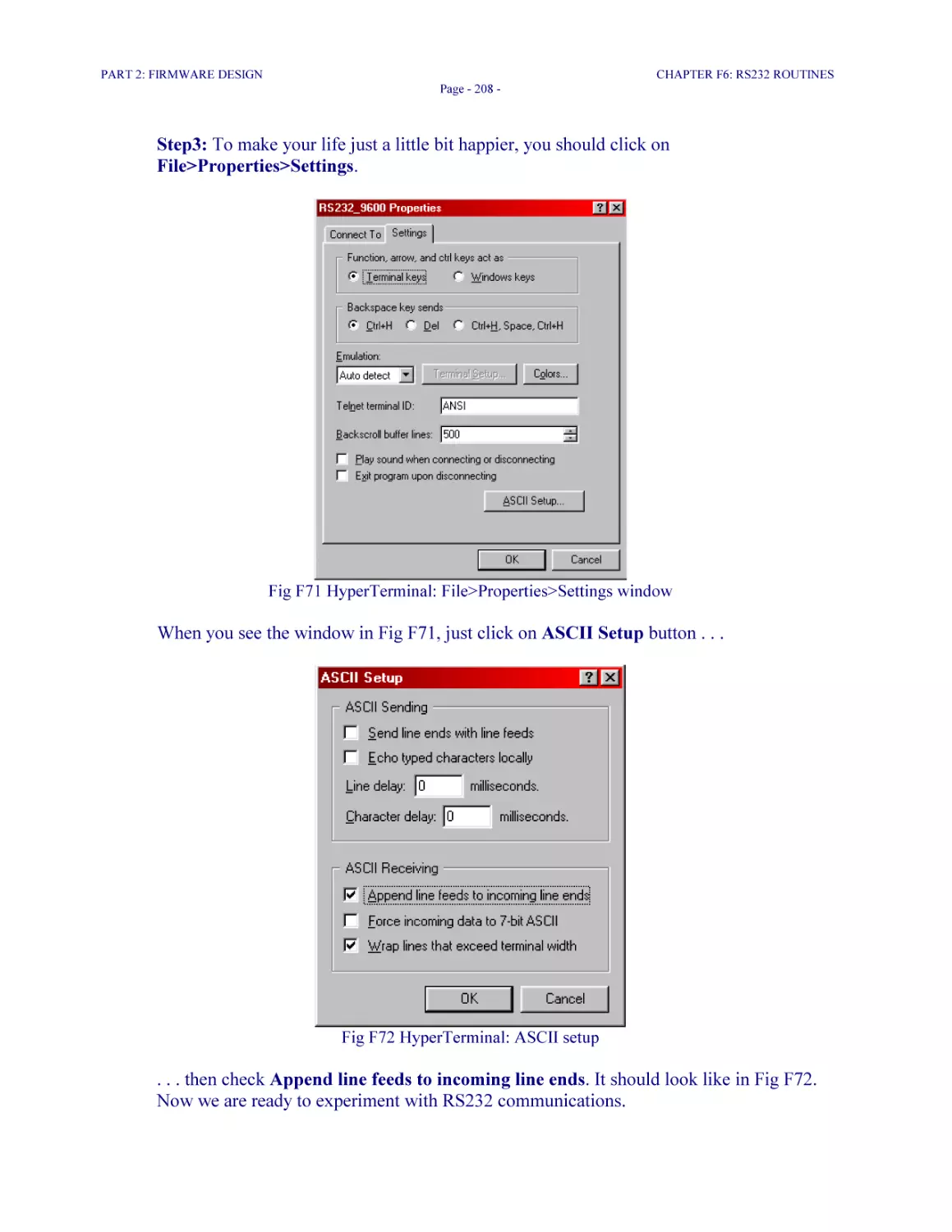
Fig F71 HyperTerminal: File>Properties>Settings window 208
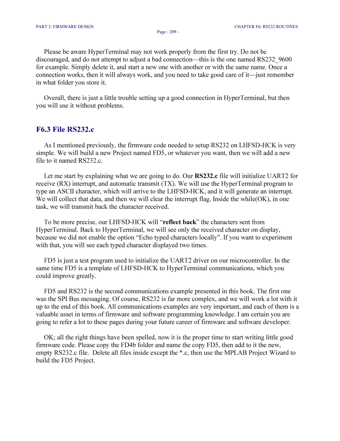
Fig F72 HyperTerminal: ASCII setup 208
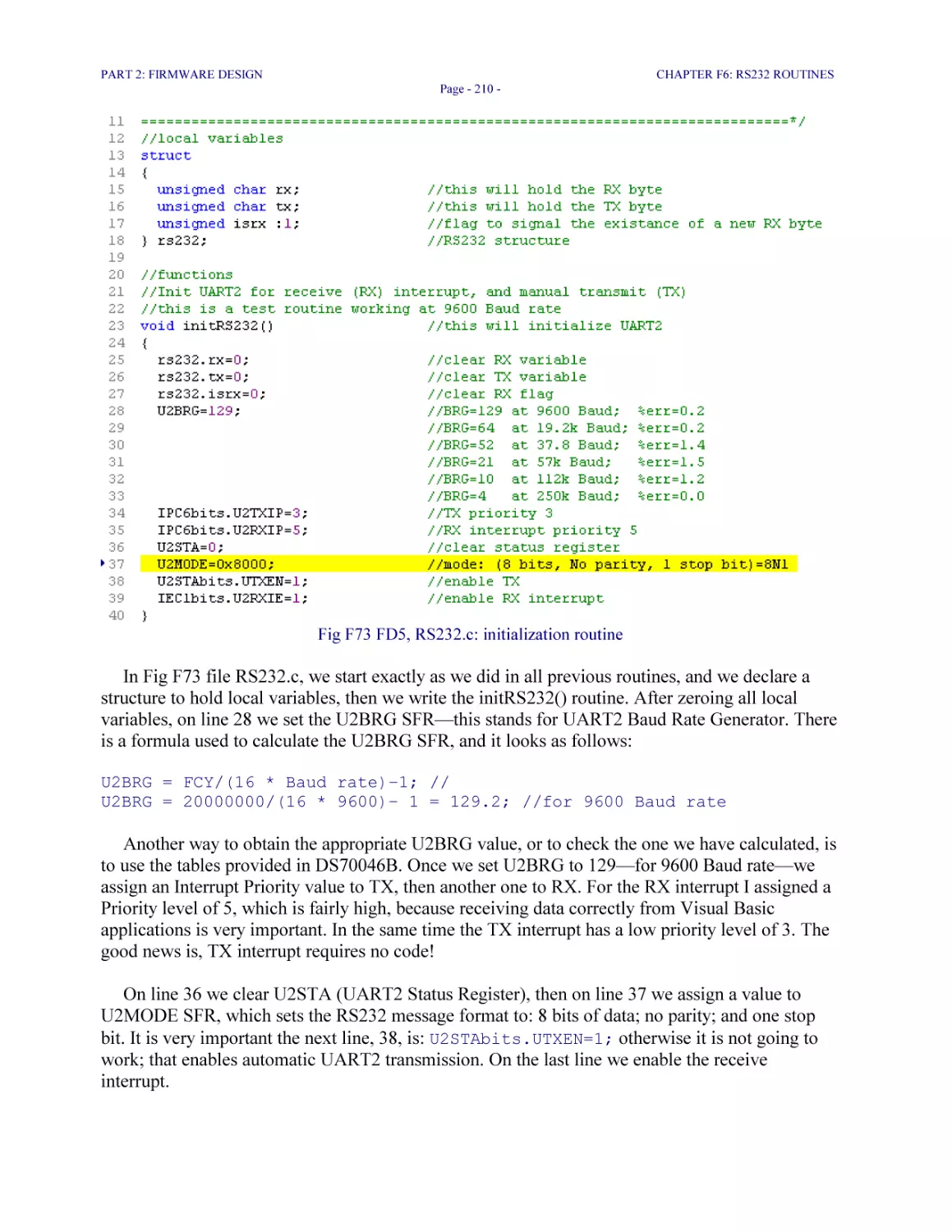
Fig F73 FD5, RS232.c: initialization routine 210
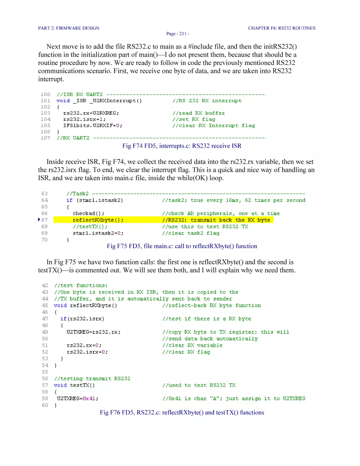
Fig F74 FD5, interrupts.c: RS232 receive ISR 211
Fig F75 FD5, file main.c: call to reflectRXbyte() function 211
Fig F76 FD5, RS232.c: reflectRXbyte() and testTX() functions 211
Fig F77 HyperTerminal window: Project FD5 running 212
Fig F78 Stepping sequences valid for all steppers 215
Fig F79 FD6, step.c: variable definition, macros, and initstep() function 216
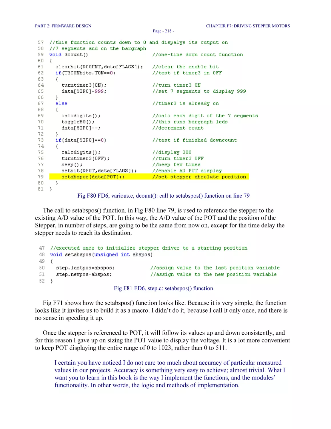
Fig F80 FD6, various.c, dcount(): call to setabspos() function on line 79 218
Fig F81 FD6, step.c: setabspos() function 218
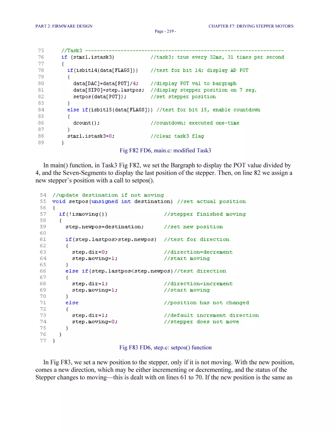
Fig F82 FD6, main.c: modified Task3 219
Fig F83 FD6, step.c: setpos() function 219
Fig F84 FD6, main.c: call to checkstep() function 220
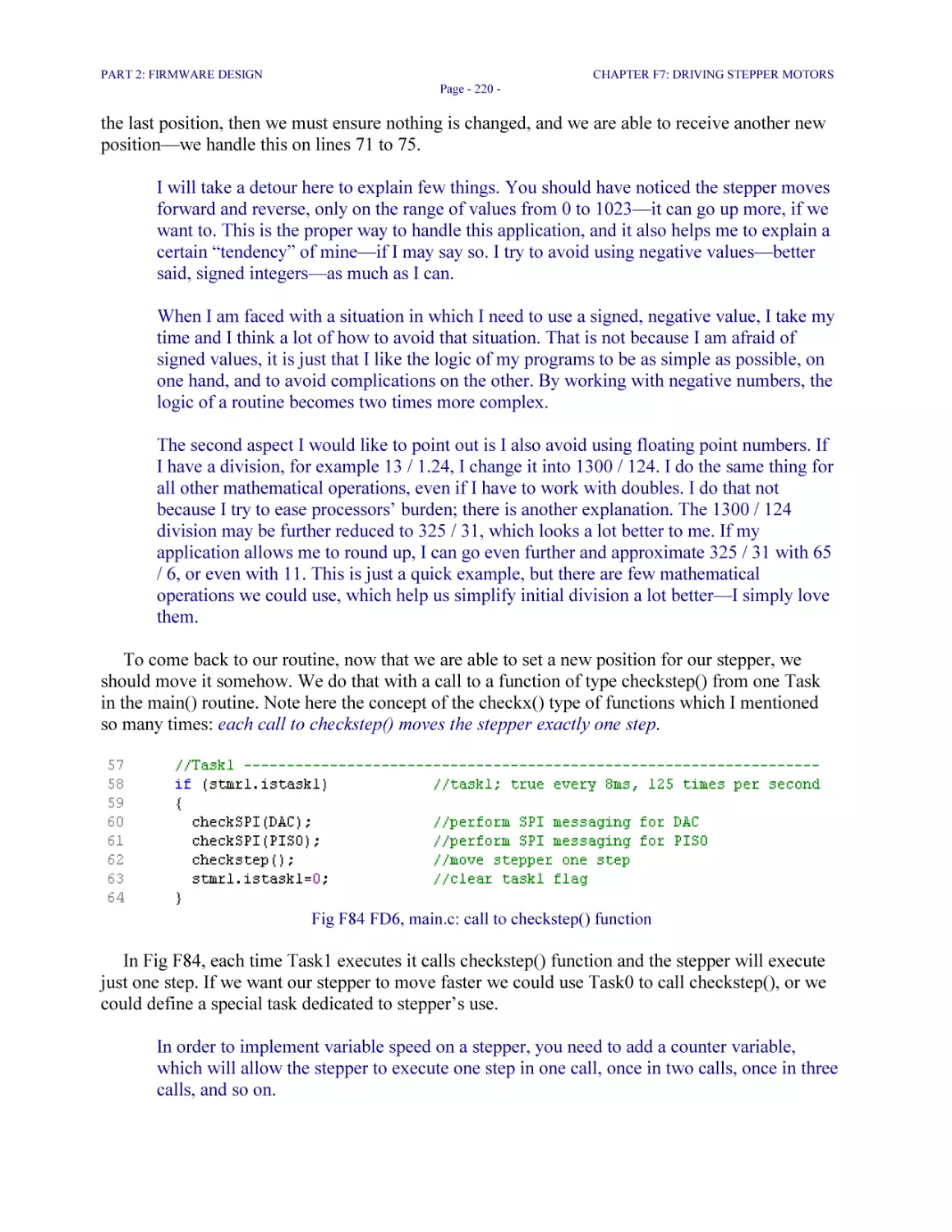
Fig F85 FD6, step.c: checkstep() function 221
PART 3: SOFTWARE DESIGN
Fig S1 Visual Basic 6 IDE interface 225
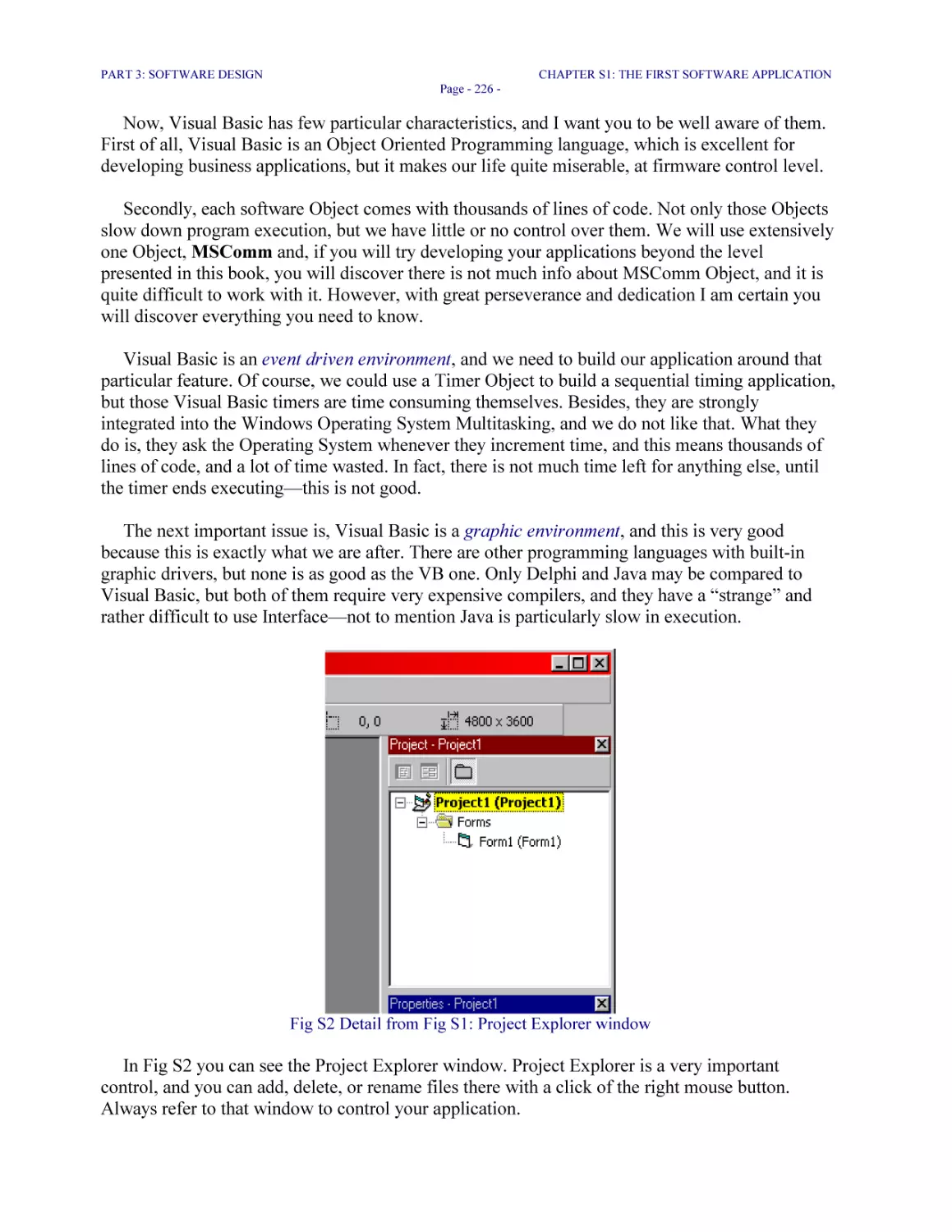
Fig S2 Detail from Fig S1: Project Explorer window 226
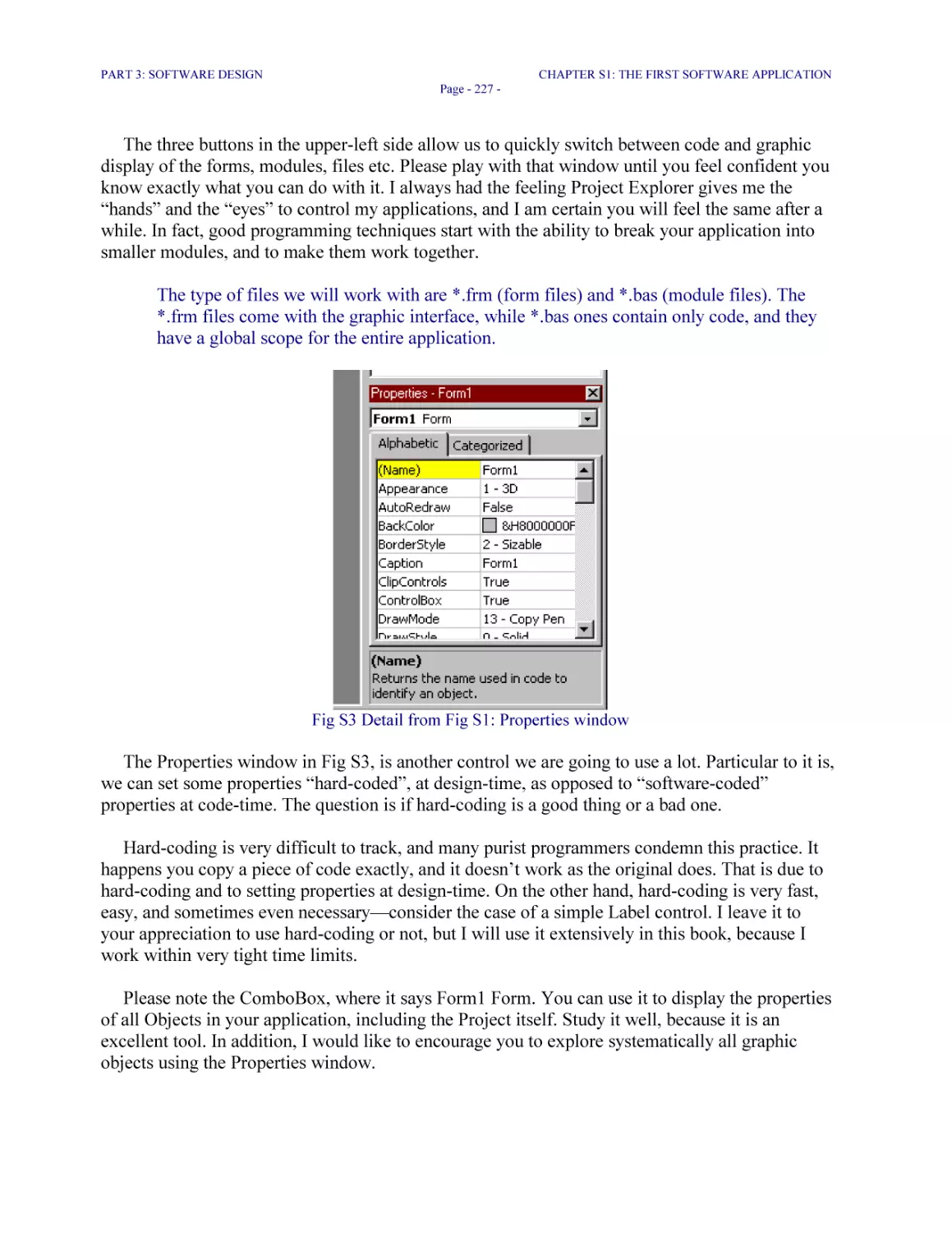
Fig S3 Detail from Fig S1: Properties window 227
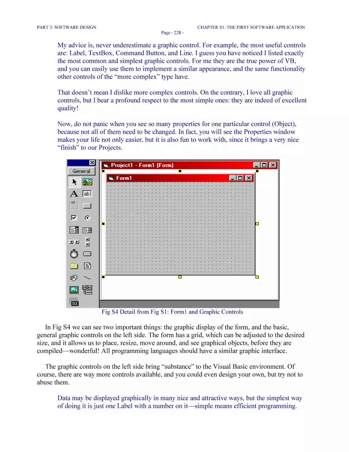
Fig S4 Detail from Fig S1: Form1 and Graphic Controls 228
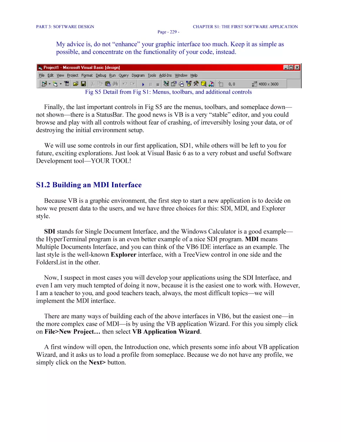
Fig S5 Detail from Fig S1: Menus, toolbars, and additional controls 229
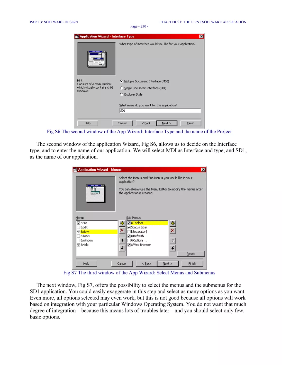
Fig S6 The second window of the App Wizard: Interface Type and the name of the Project 230
Fig S7 The third window of the App Wizard: Select Menus and Submenus 230
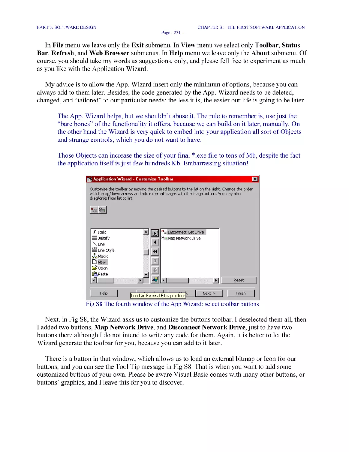
Fig S8 The fourth window of the App Wizard: select toolbar buttons 231
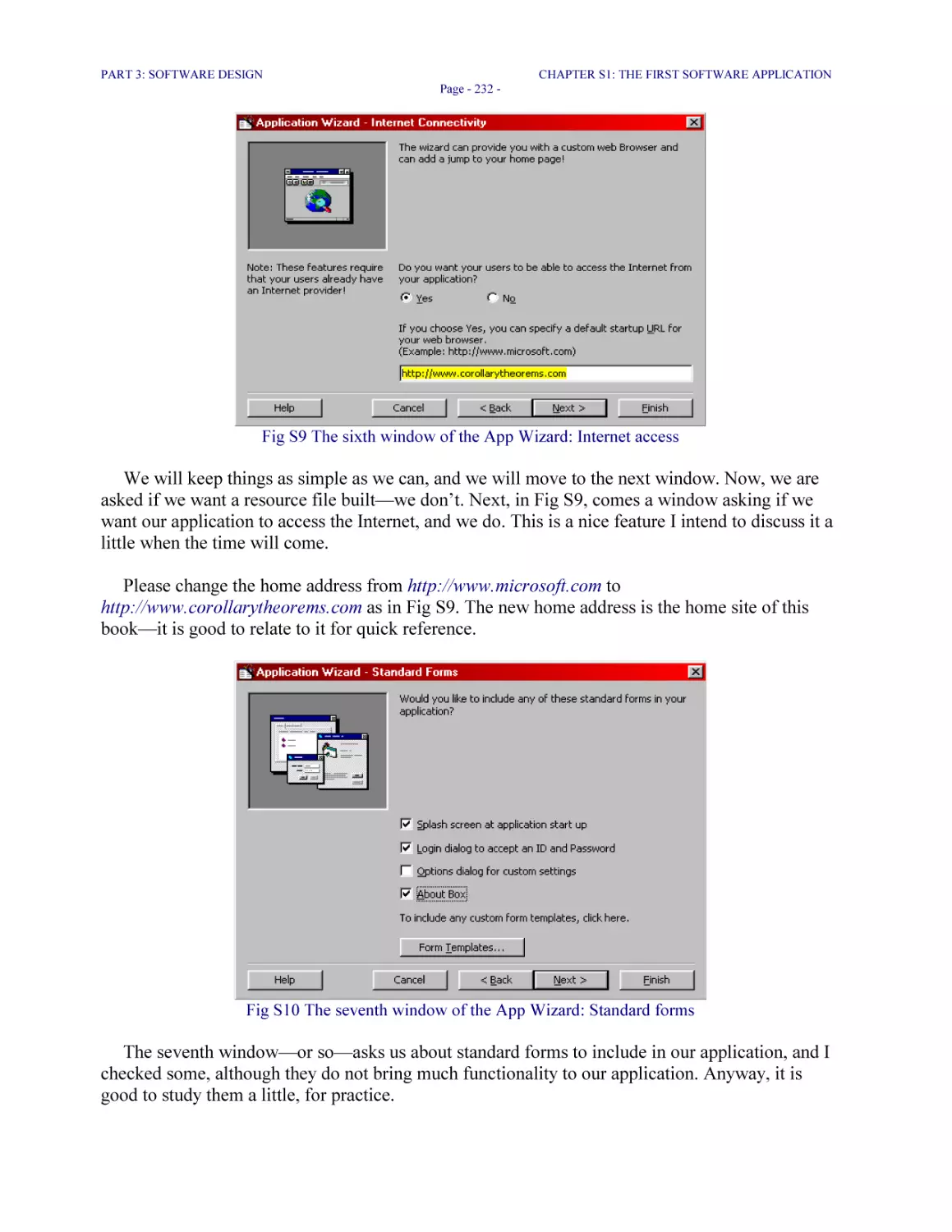
Fig S9 The sixth window of the App Wizard: Internet access 232
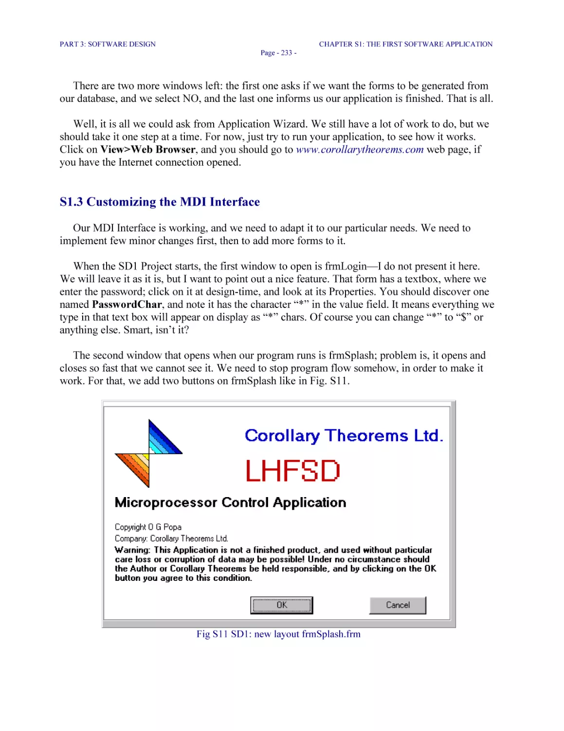
Fig S10 The seventh window of the App Wizard: Standard forms 232
Fig S11 SD1: new layout frmSplash.frm 233
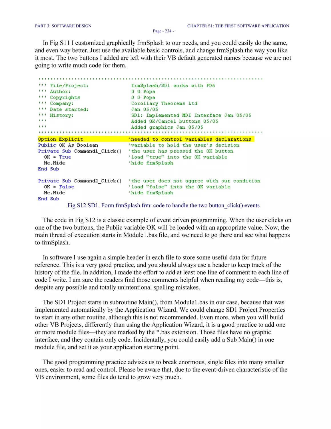
Fig S12 SD1, Form frmSplash.frm: code to handle the two button_click() events 234
Fig S13 SD1, Project Explorer: form files added 235
Fig S14 SD1, Module1.bas: Sub Main() 236
Fig S15 SD1, frmMain.frm: MDIForm_Load() 237
LHFSD
TABLE OF FIGURES
Page - 22 -
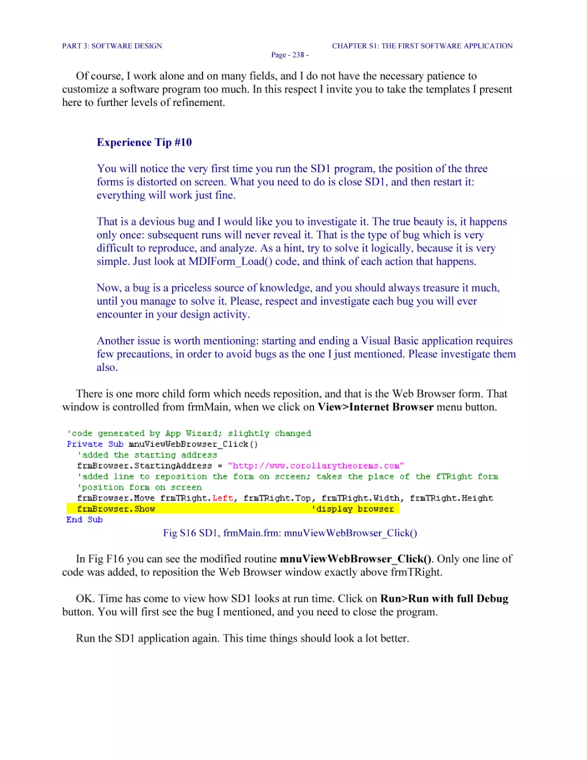
Fig S16 SD1, frmMain.frm: mnuViewWebBrowser_Click() 238
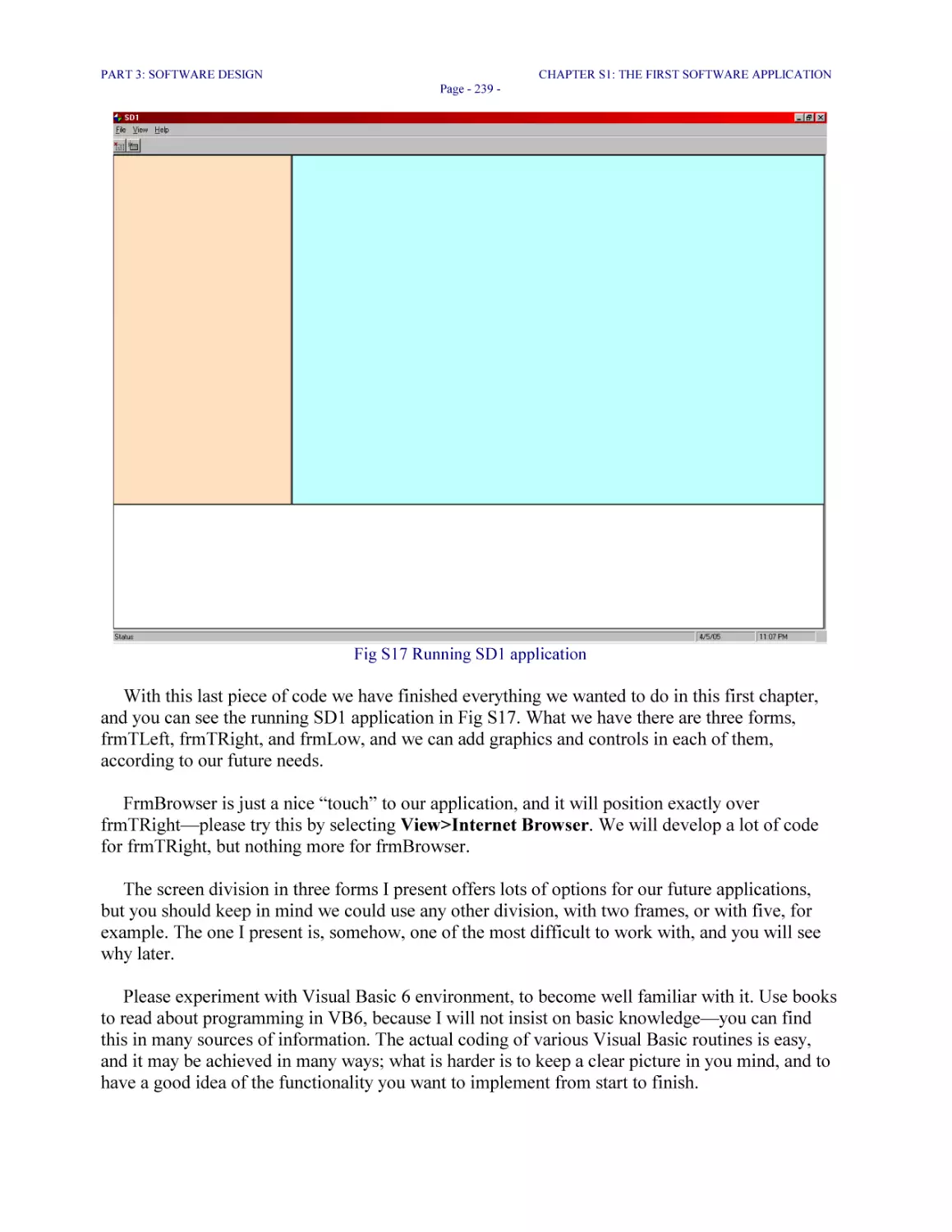
Fig S17 Running SD1 application 239
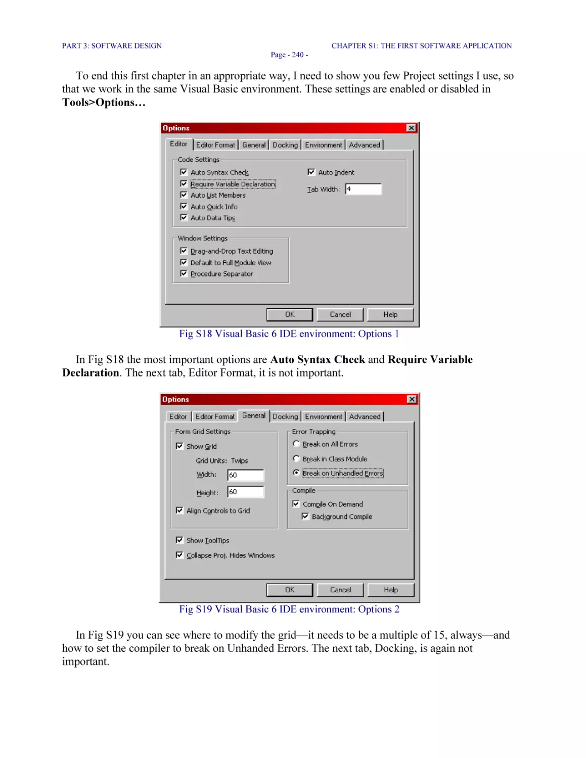
Fig S18 Visual Basic 6 IDE environment: Options 1 240
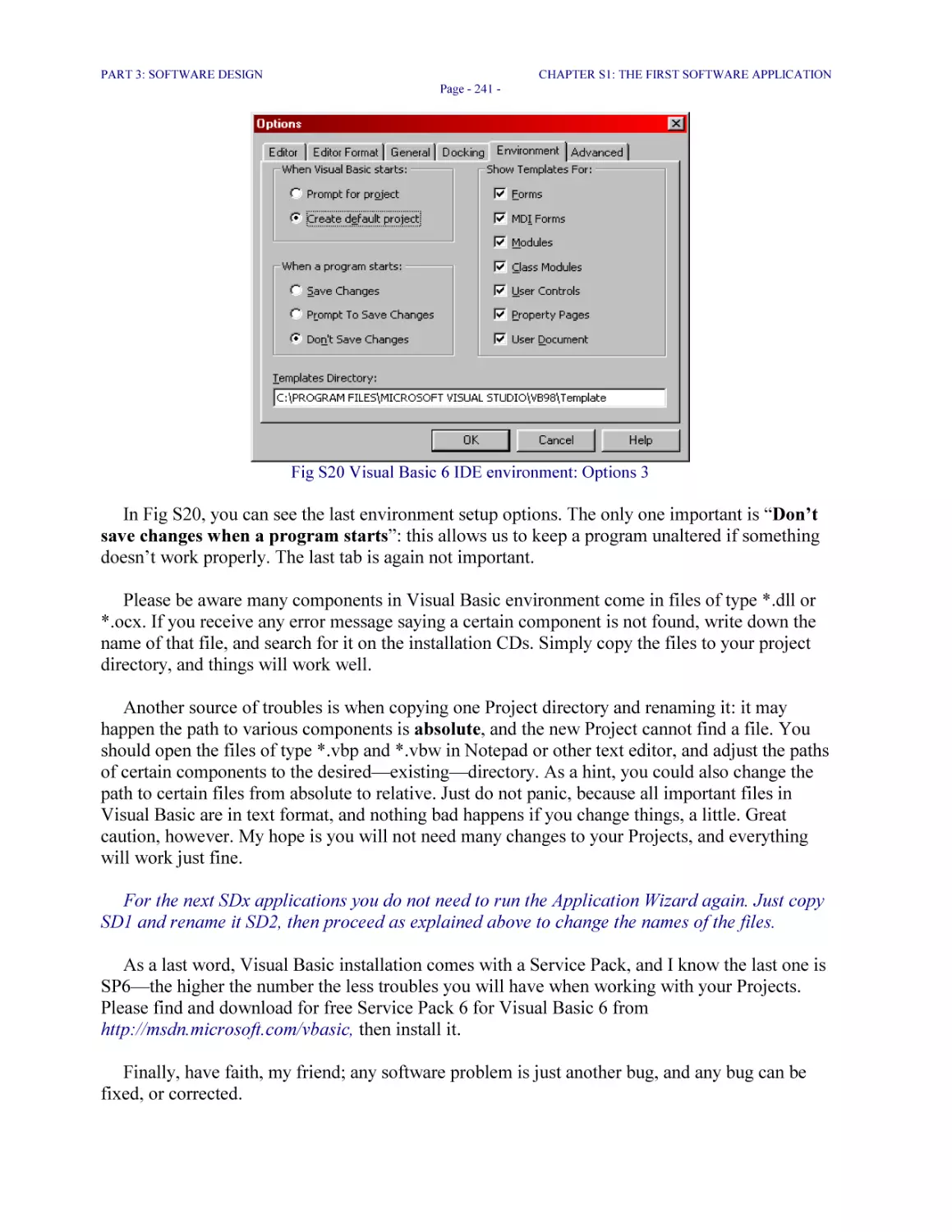
Fig S19 Visual Basic 6 IDE environment: Options 2 240
Fig S20 Visual Basic 6 IDE environment: Options 3 241
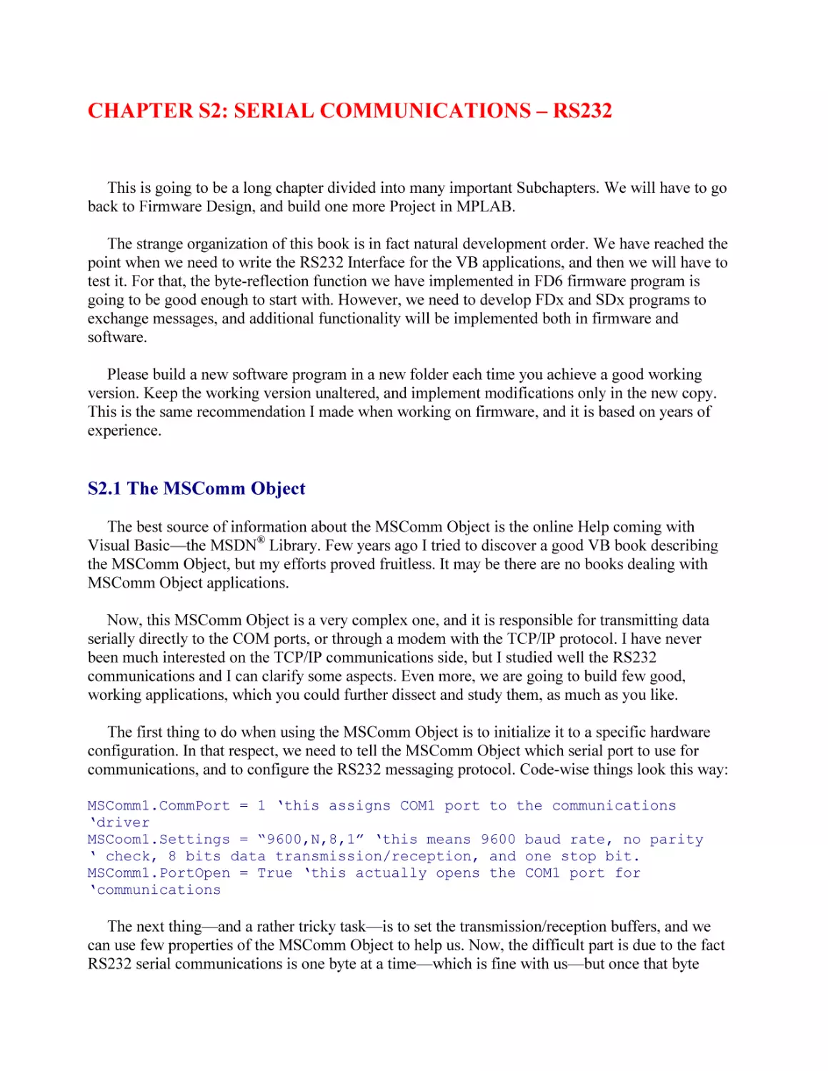
Fig S21 Project SD2: graphic layout 245
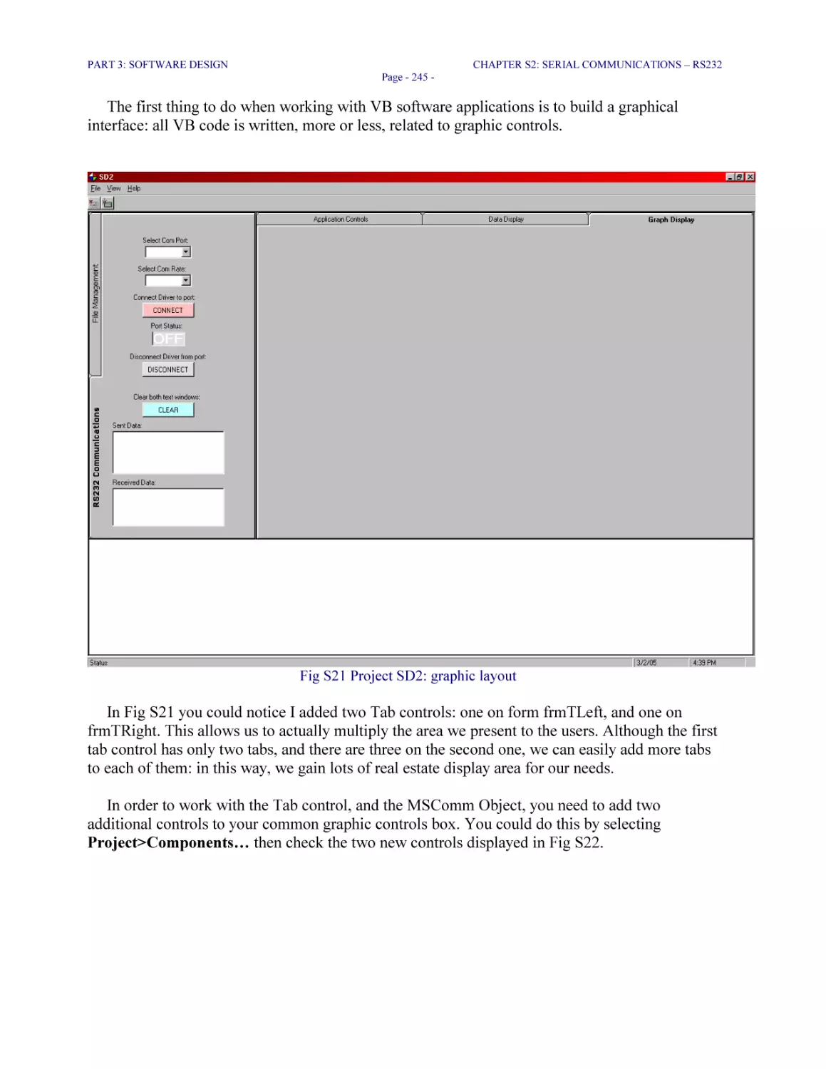
Fig S22 Project SD2: adding Tabbed Dialog control 246
Fig S23 Project SD2: view of the Control Box, with the new controls added 246
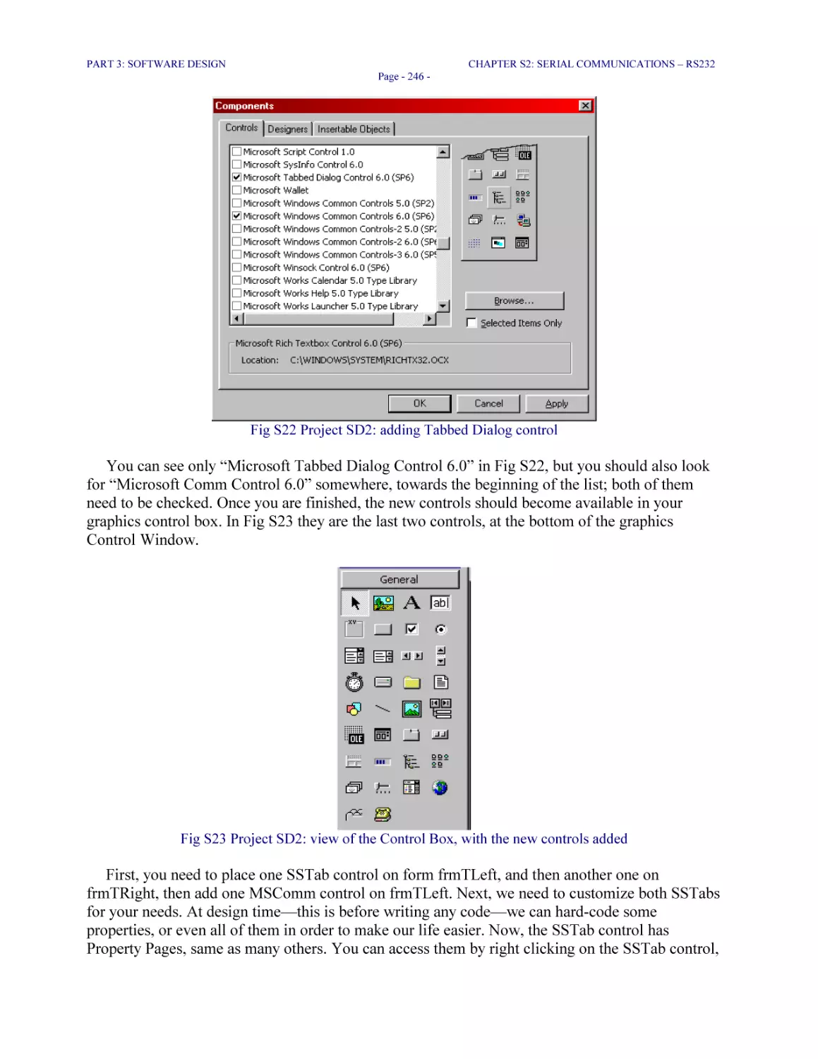
Fig S24 Project SD2: Property Pages opened for the SSTab control placed on frmTLeft.frm 247
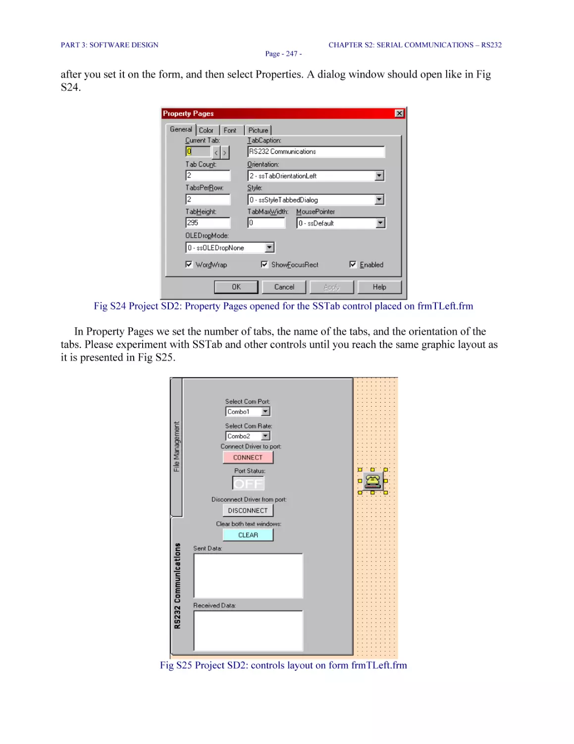
Fig S25 Project SD2: controls layout on form frmTLeft.frm 247
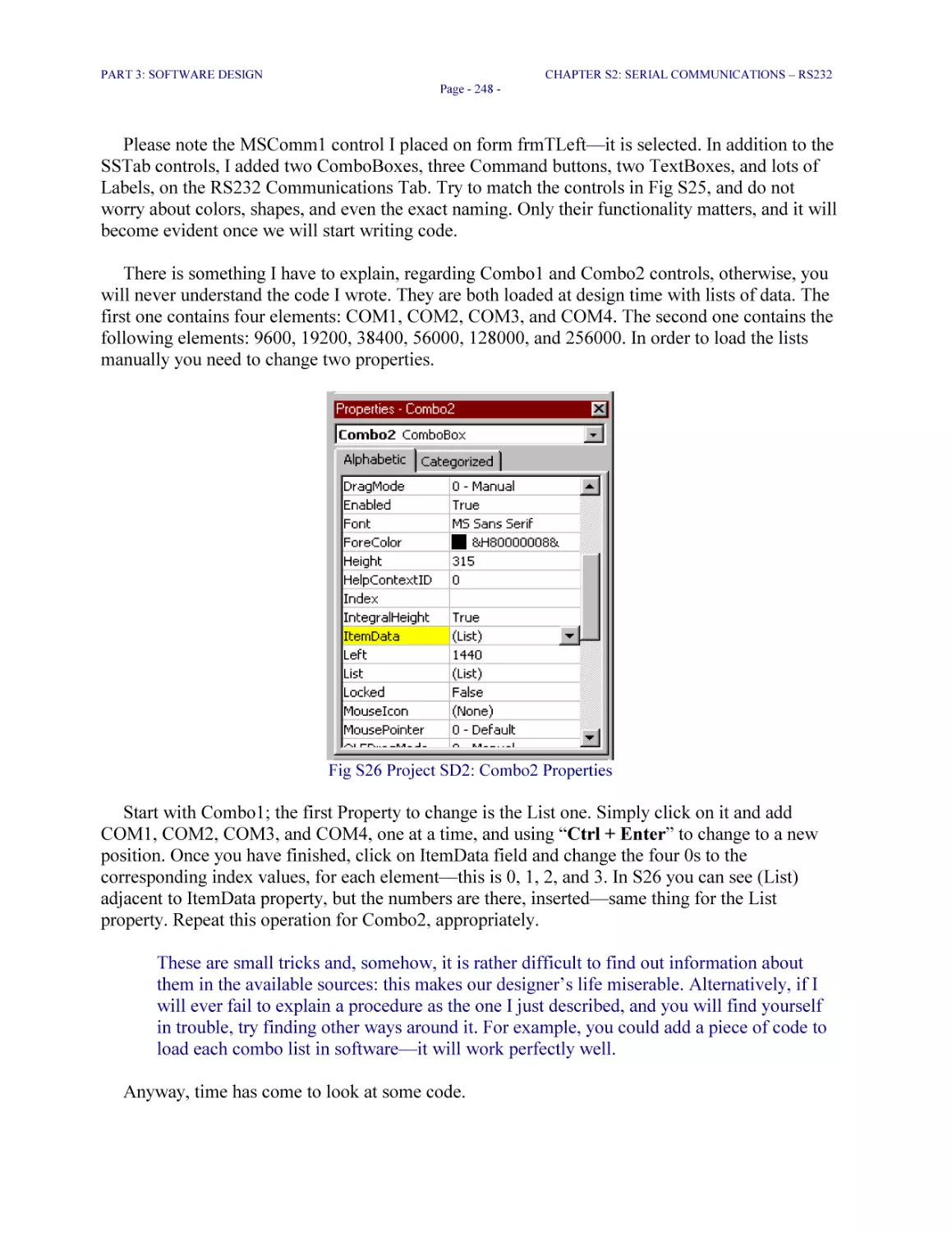
Fig S26 Project SD2: Combo2 Properties 248
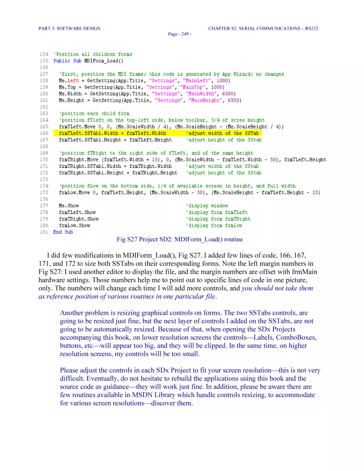
Fig S27 Project SD2: MDIForm_Load() routine 249
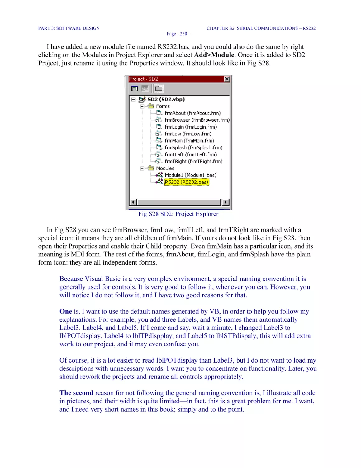
Fig S28 SD2: Project Explorer 250
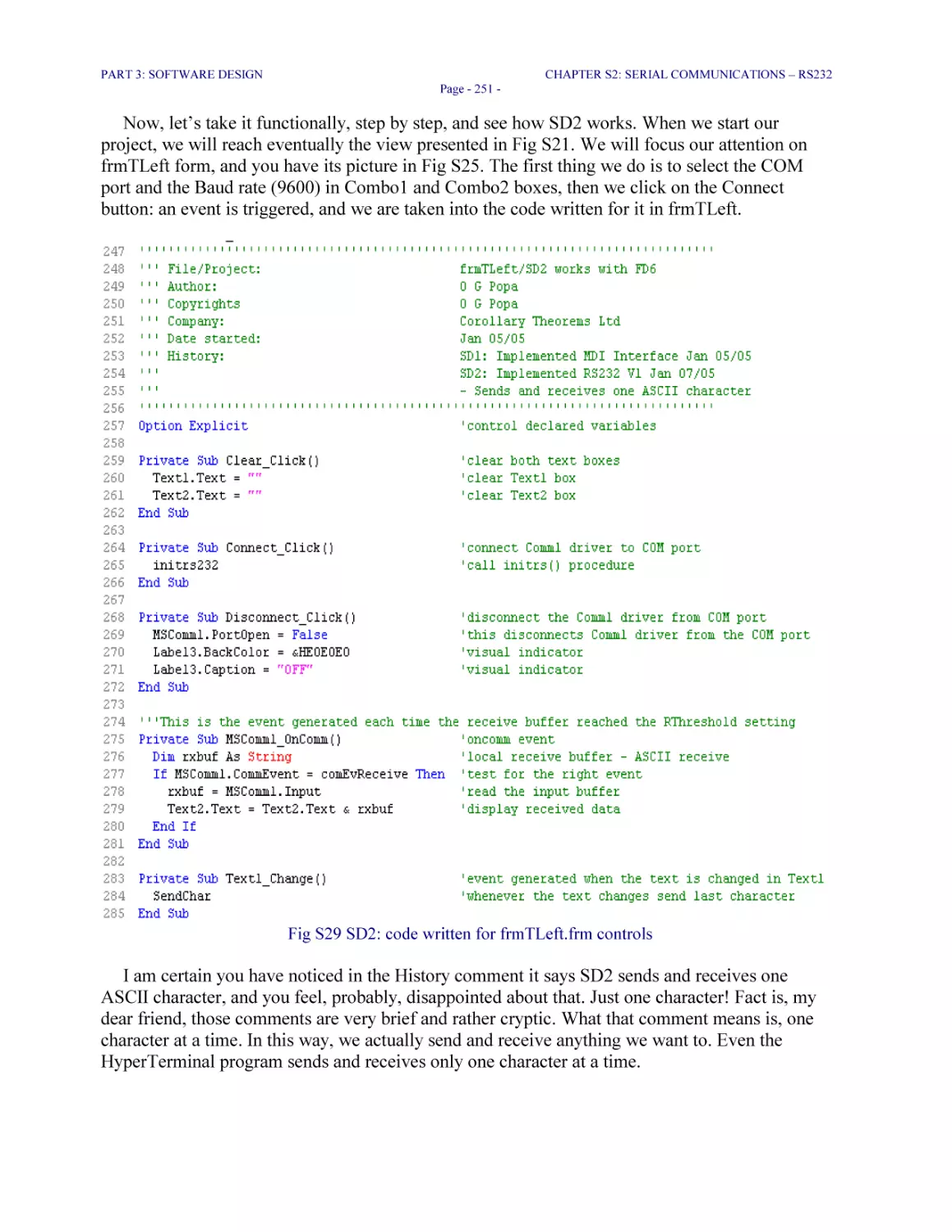
Fig S29 SD2: code written for frmTLeft.frm controls 251
Fig S30 SD2, RS232.bas: initrs232() procedure 252
Fig S31 SD2, RS232.bas: SendChar() procedure 254
Fig S32 Running SD2 application 255
Fig S33 Custom RS232 messaging protocol: continuous LOOPTX 256
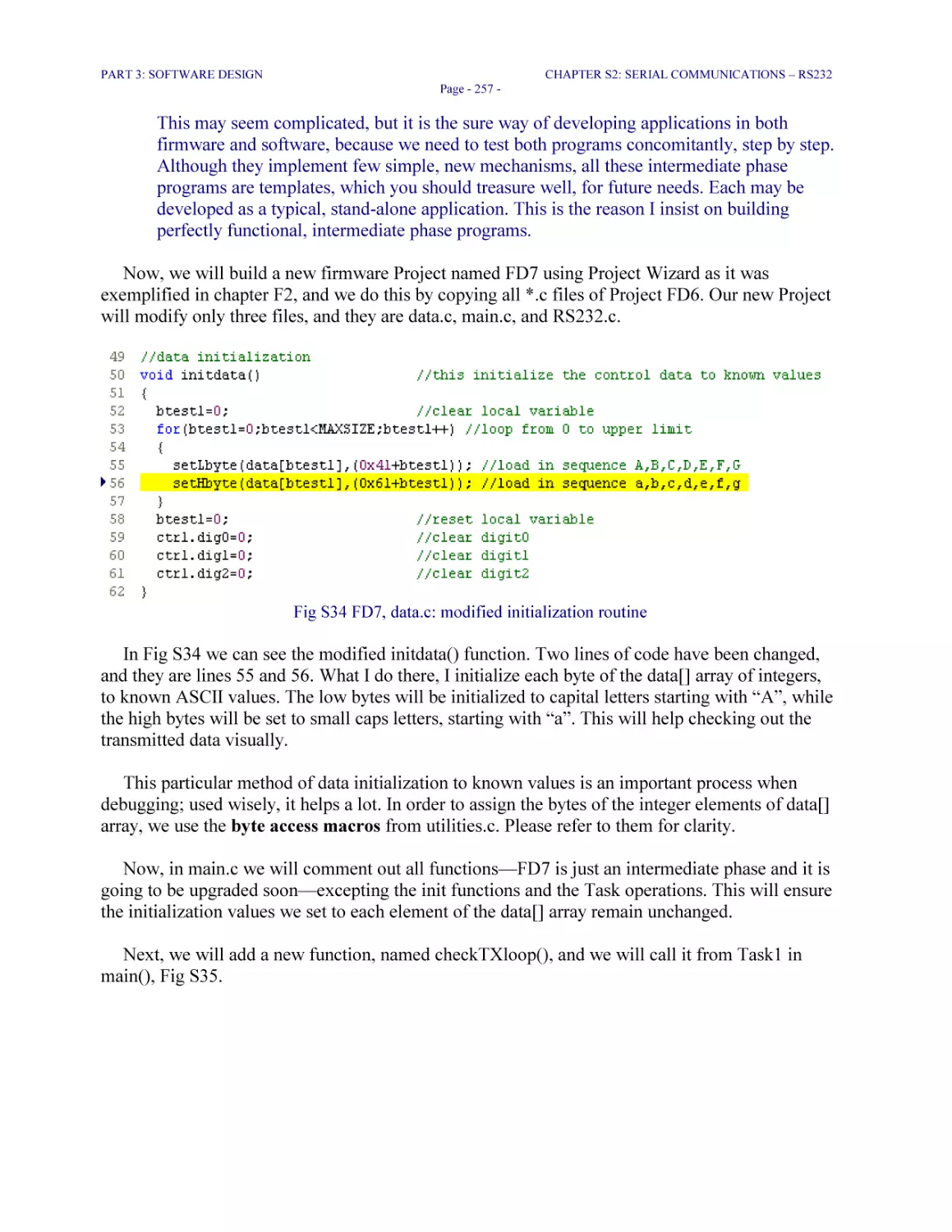
Fig S34 FD7, data.c: modified initialization routine 257
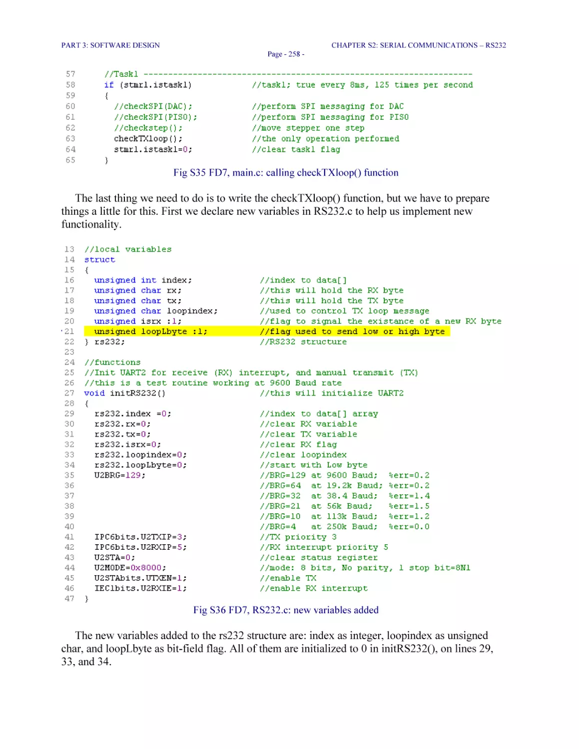
Fig S35 FD7, main.c: calling checkTXloop() function 258
Fig S36 FD7, RS232.c: new variables added 258
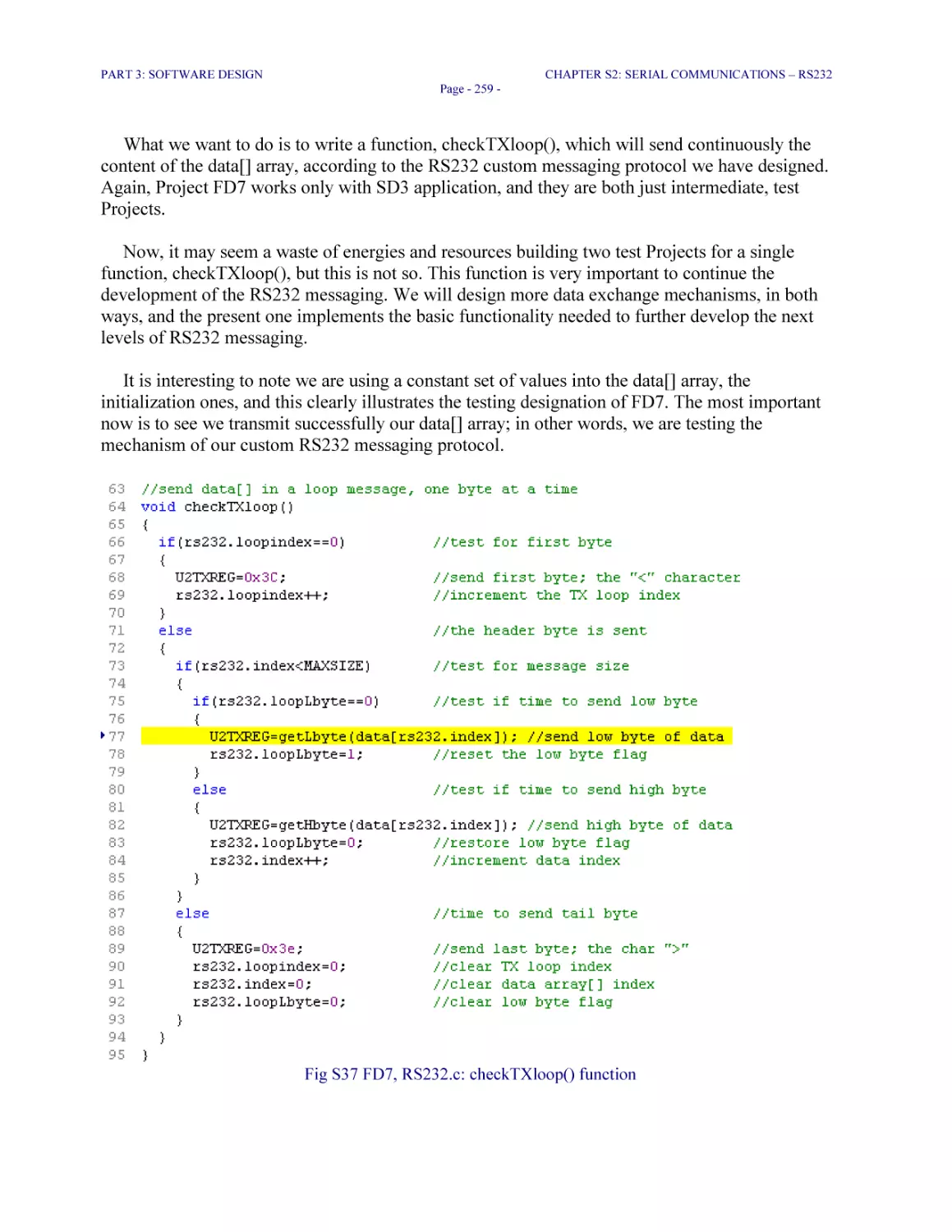
Fig S37 FD7, RS232.c: checkTXloop() function 259
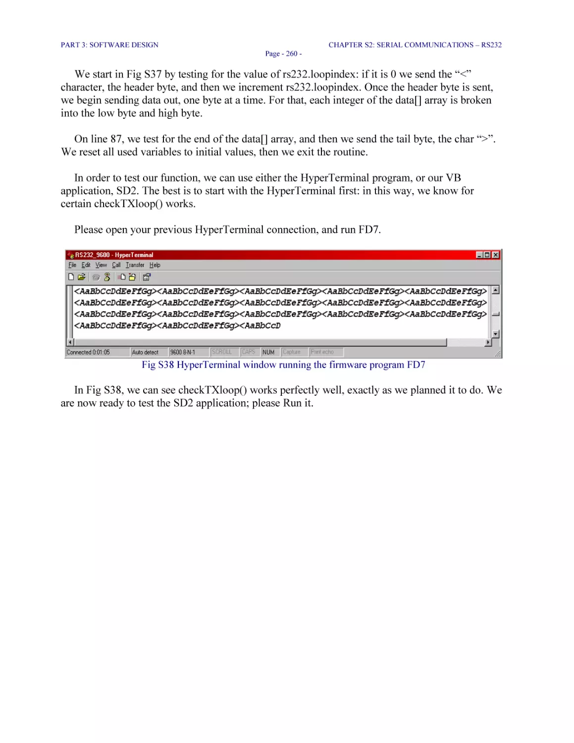
Fig S38 HyperTerminal window running the firmware program FD7 260
Fig S39 Running SD2 and FD7 261
Fig S40 SD3, Data.bas: declarations of global variables 262
Fig S41 SD3, Module1.bas: global variables initialization 263
Fig S42 SD3, frmTLeft.frm: the upgraded OnComm() event 264
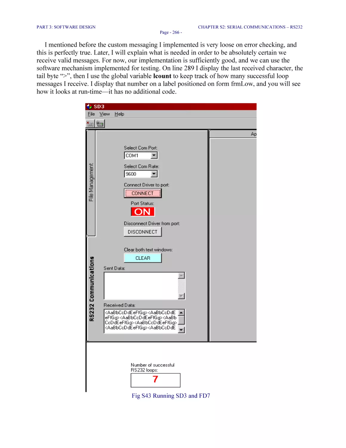
Fig S43 Running SD3 and FD7 266
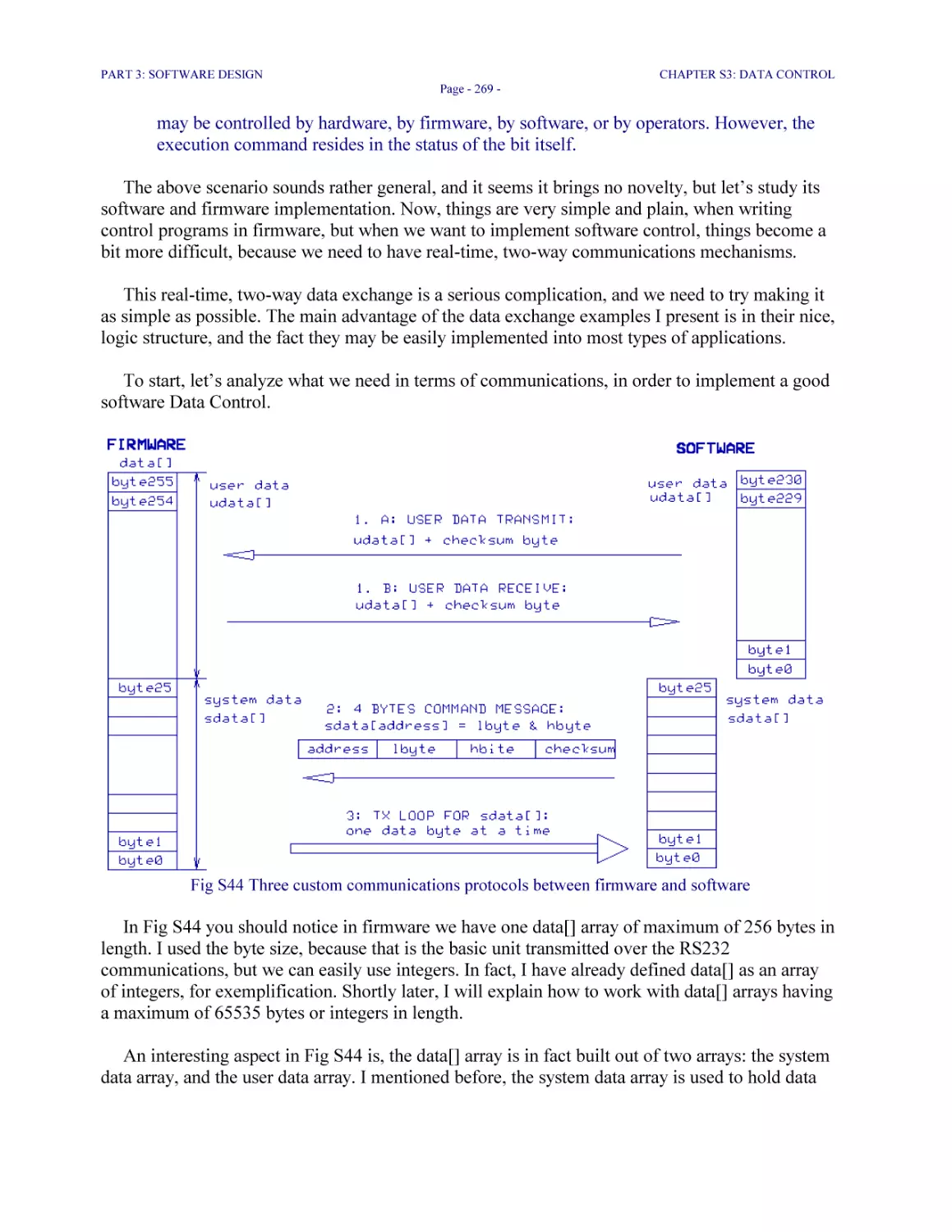
Fig S44 Three custom communications protocols between firmware and software 269
Fig S45 FD8, data.c: definition of the application control switches 271
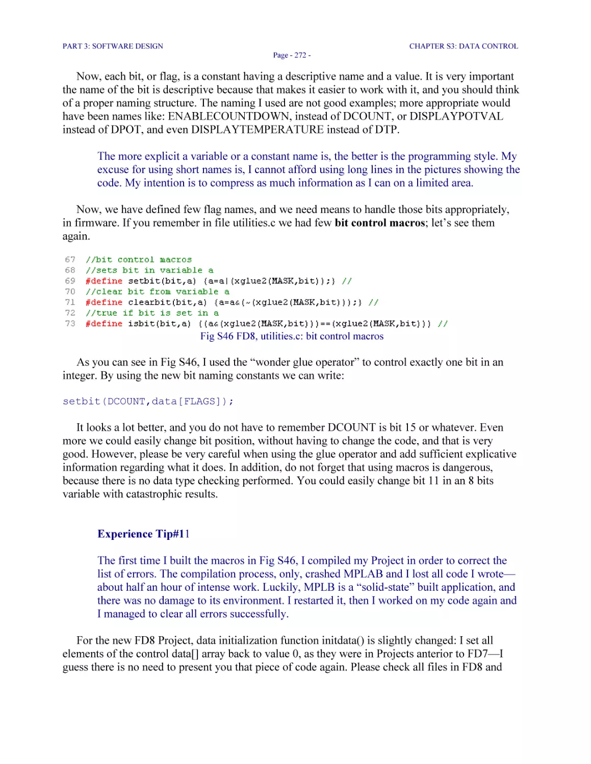
Fig S46 FD8, utilities.c: bit control macros 272
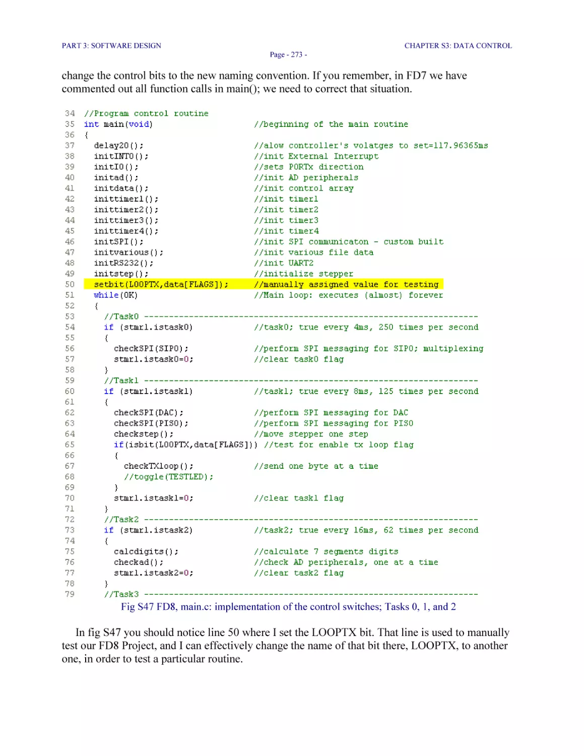
Fig S47 FD8, main.c: implementation of the control switches; Tasks 0, 1, and 2 273
Fig S48 FD8, main.c: implementation of the control switches in Task3 275
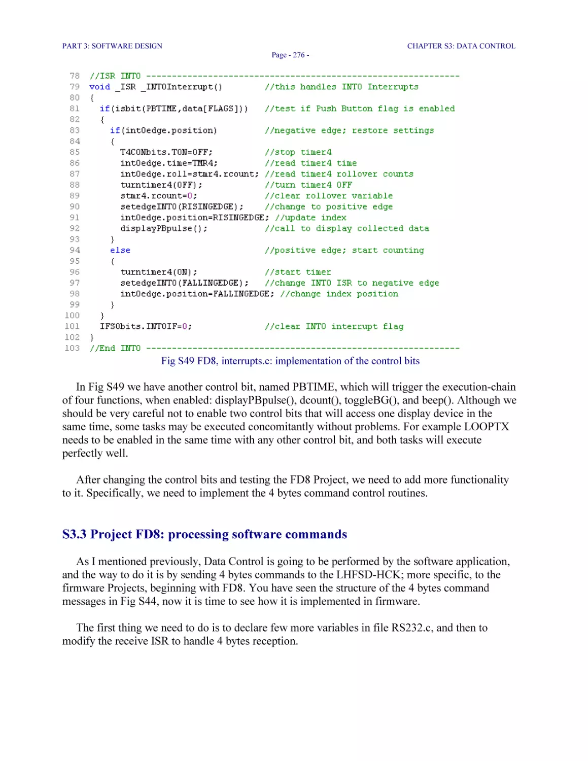
Fig S49 FD8, interrupts.c: implementation of the control bits 276
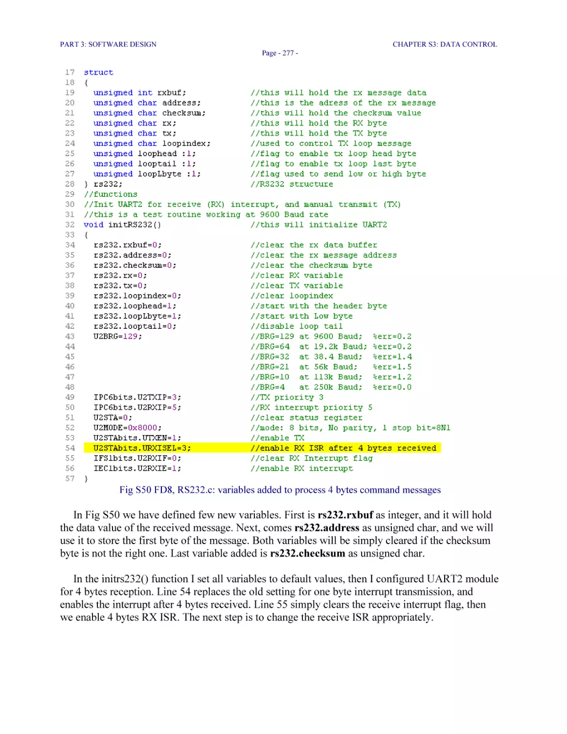
Fig S50 FD8, RS232.c: variables added to process 4 bytes command messages 277
Fig S51 FD8, interrupts.c: new receive ISR routine 278
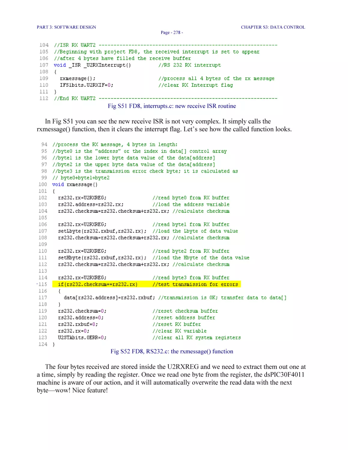
Fig S52 FD8, RS232.c: the rxmessage() function 278
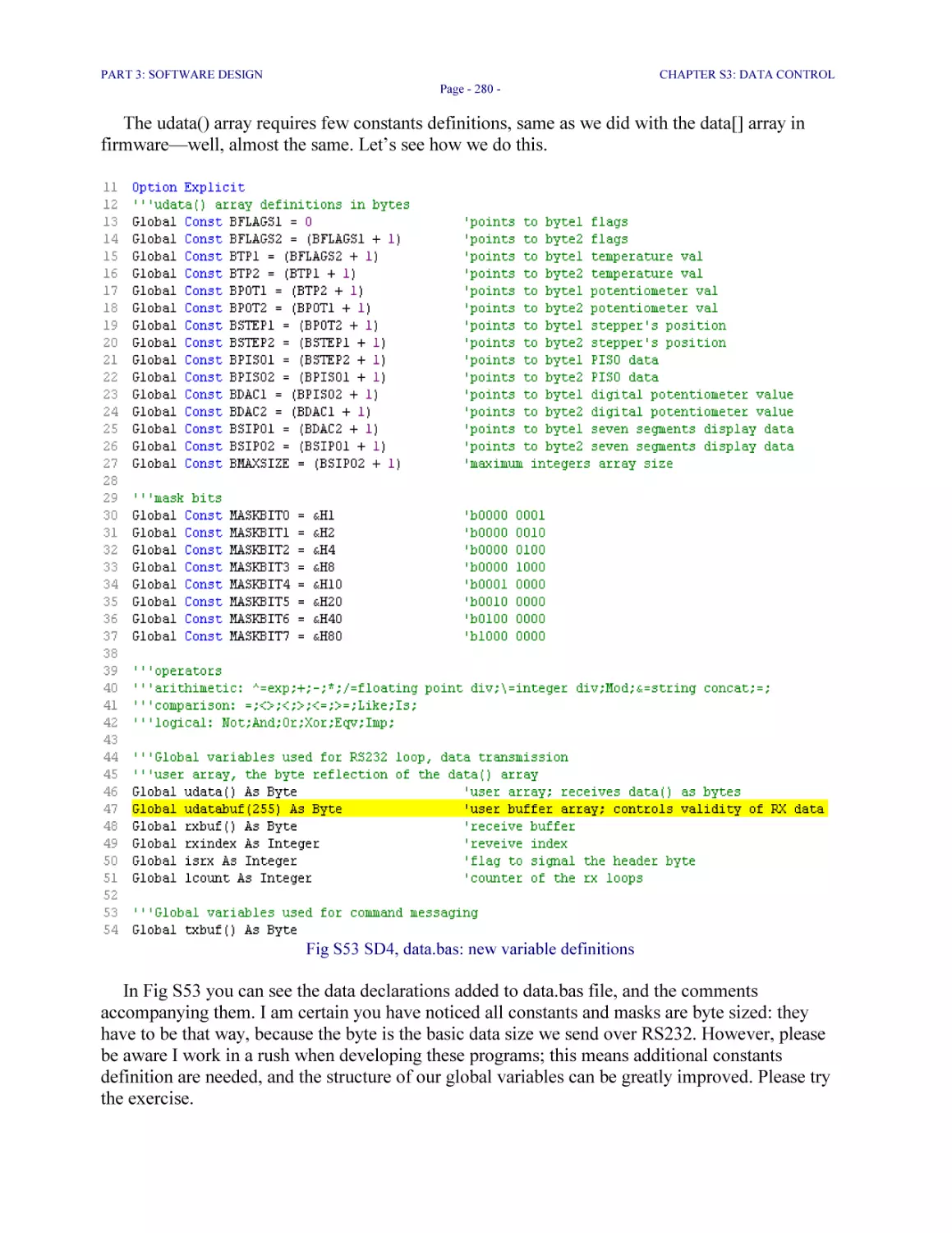
Fig S53 SD4, data.bas: new variable definitions 280
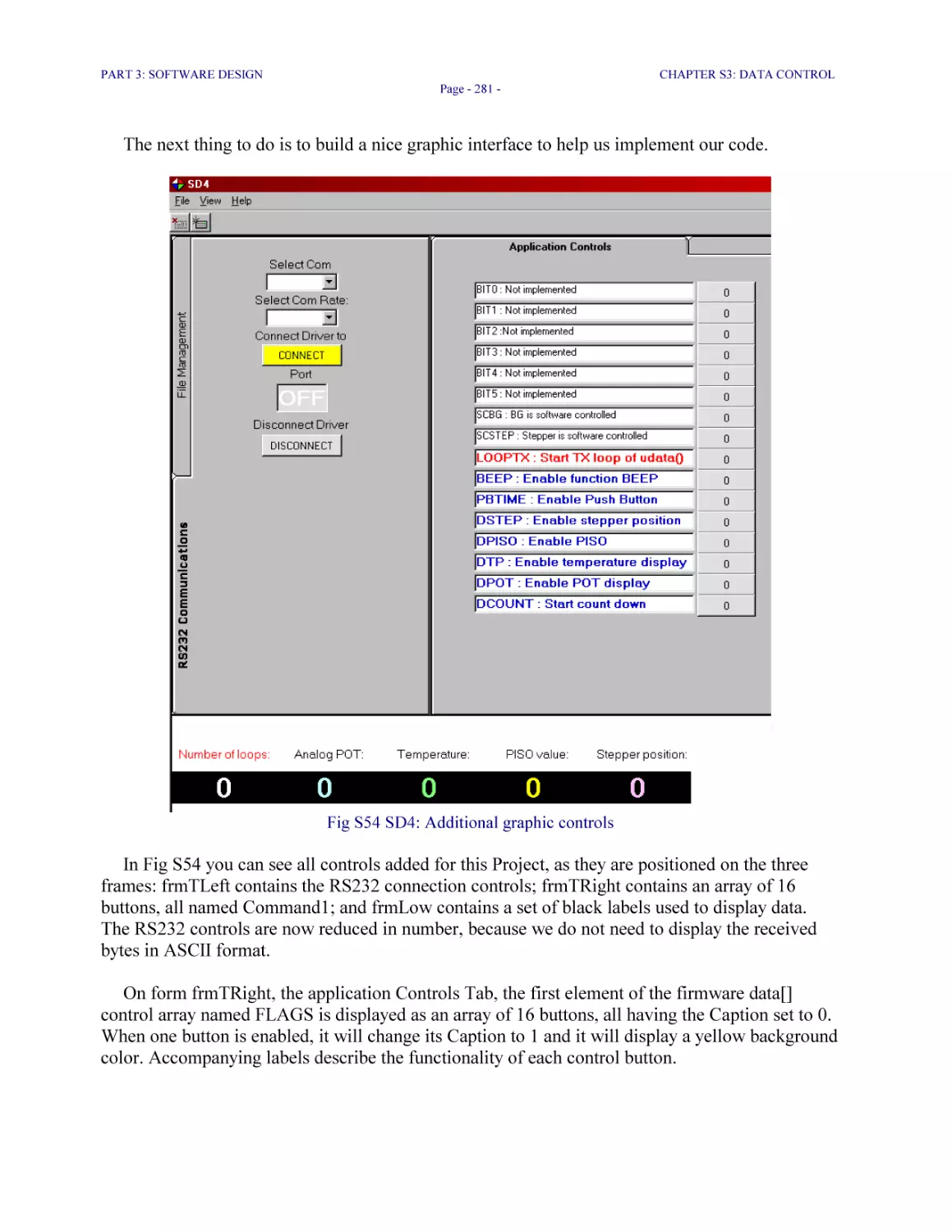
Fig S54 SD4: Additional graphic controls 281
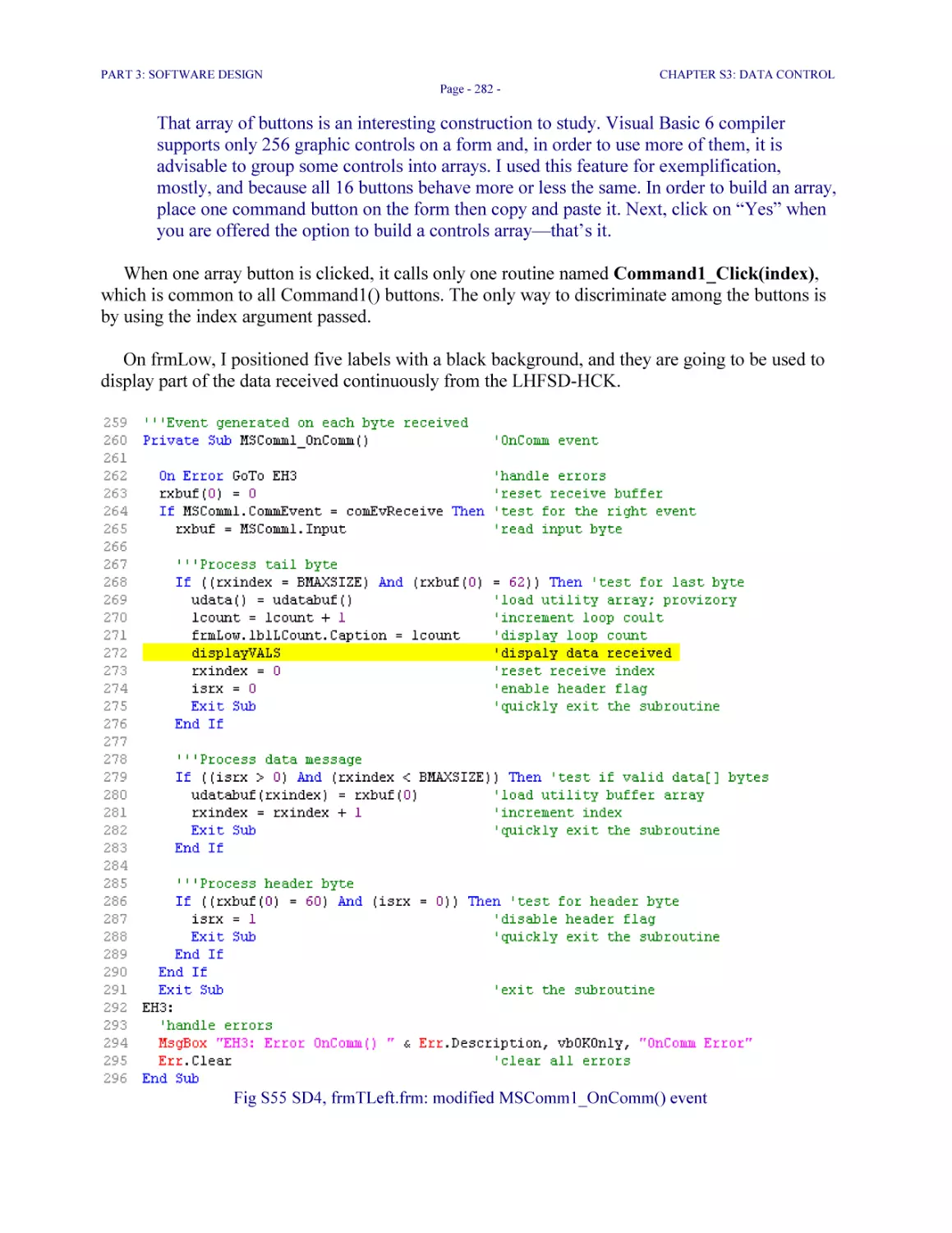
Fig S55 SD4, frmTLeft.frm: modified MSComm1_OnComm() event 282
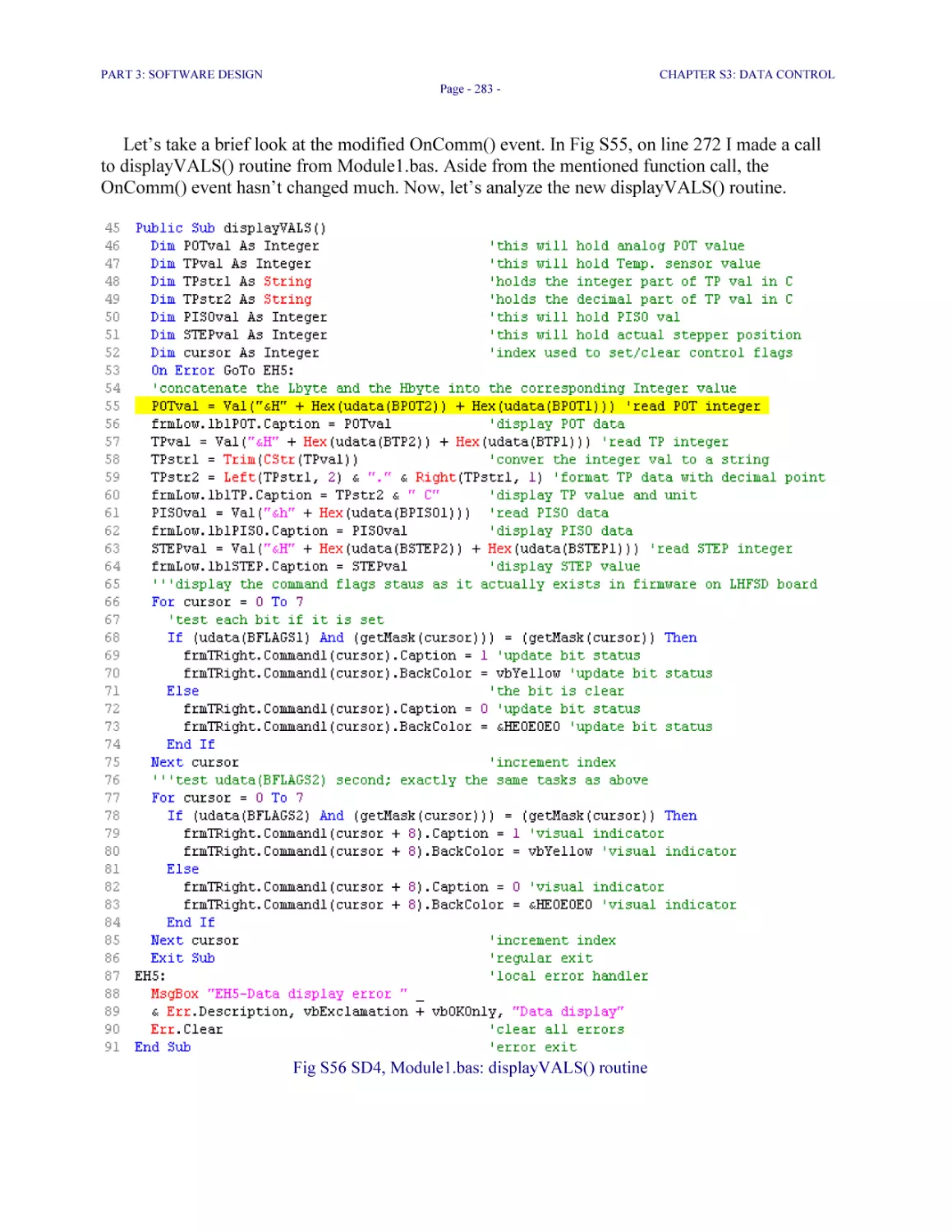
Fig S56 SD4, Module1.bas: displayVALS() routine 283
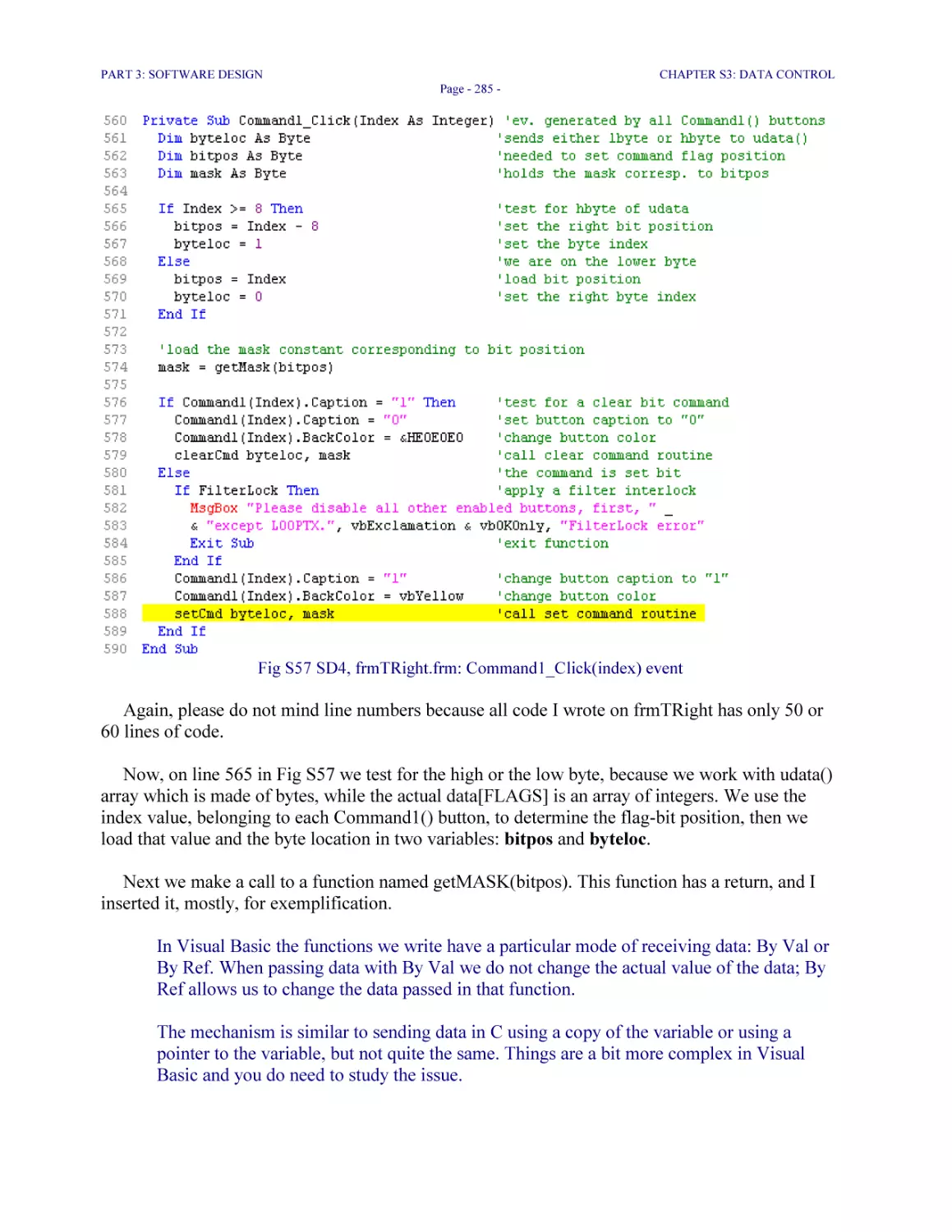
Fig S57 SD4, frmTRight.frm: Command1_Click(index) event 285
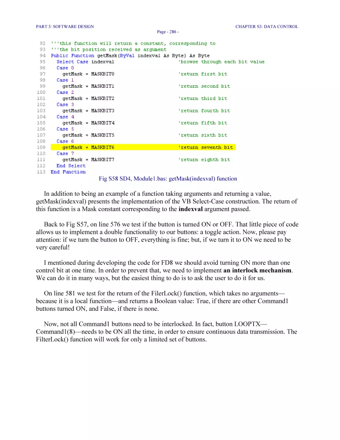
Fig S58 SD4, Module1.bas: getMask(indexval) function 286
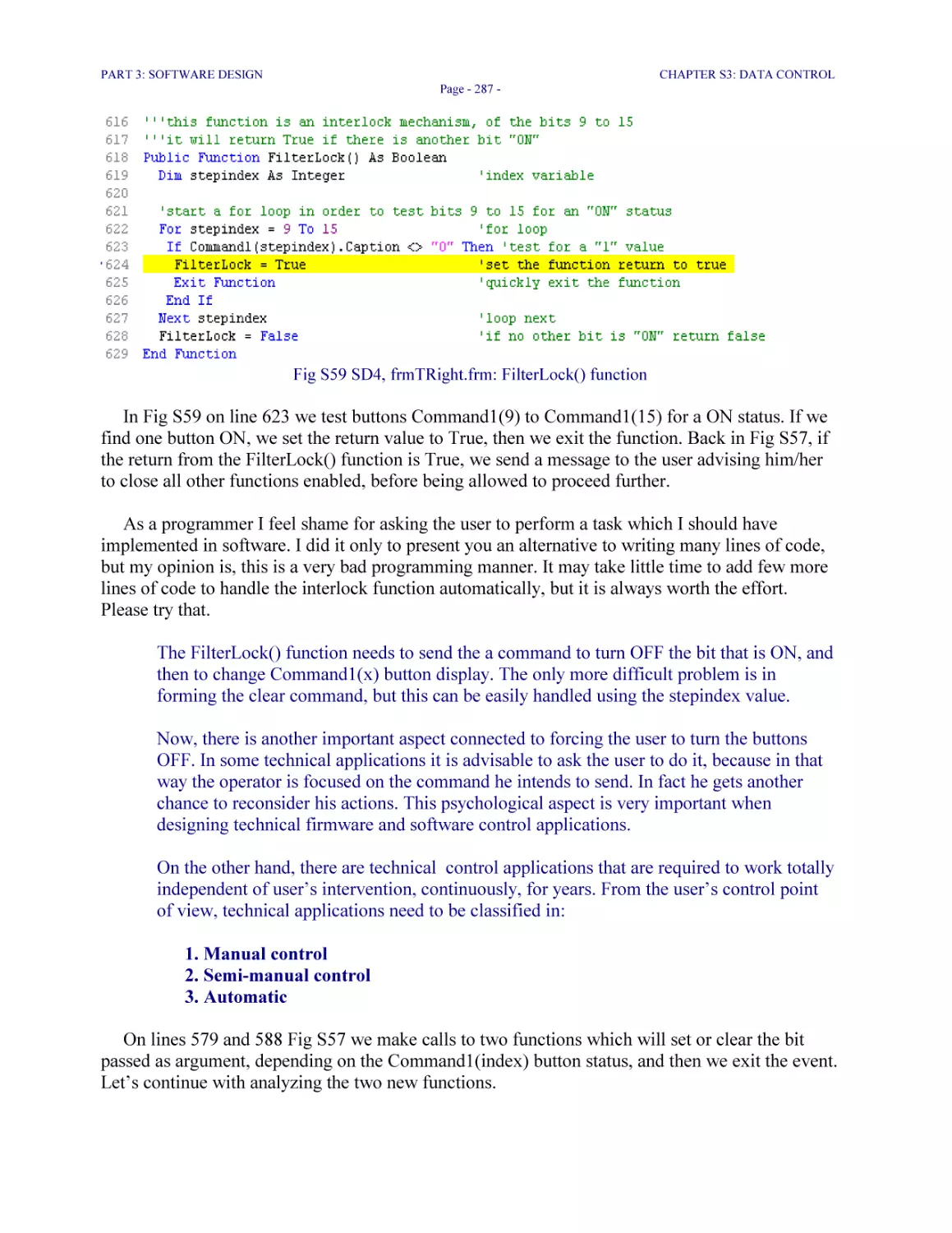
Fig S59 SD4, frmTRight.frm: FilterLock() function 287
Fig S60 SD4, frmTRight.frm: setCmd() and clearCmd() functions 288
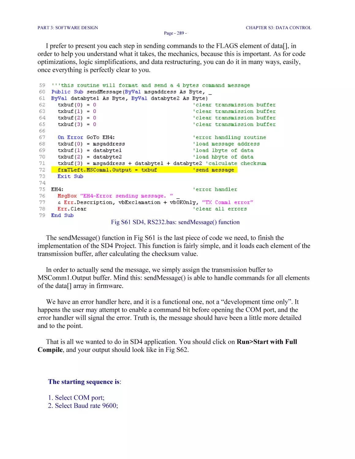
Fig S61 SD4, RS232.bas: sendMessage() function 289
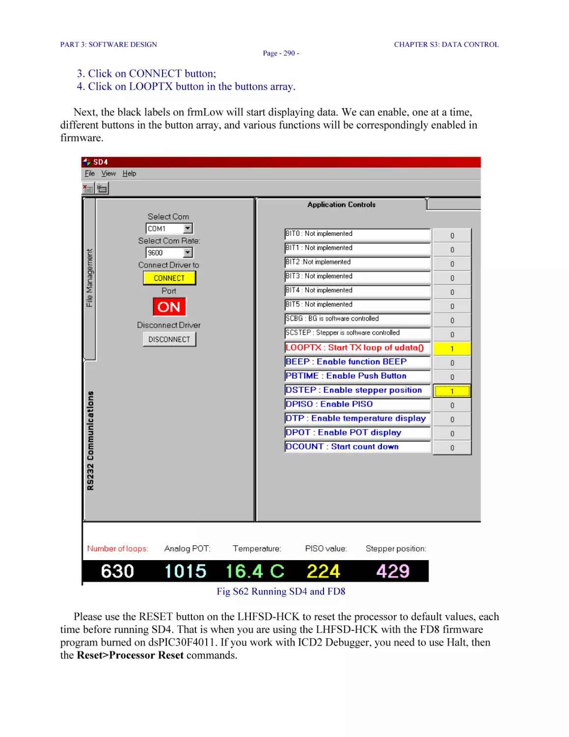
Fig S62 Running SD4 and FD8 290
Fig S63 FD9, data.c: changed command bits names and locations 296
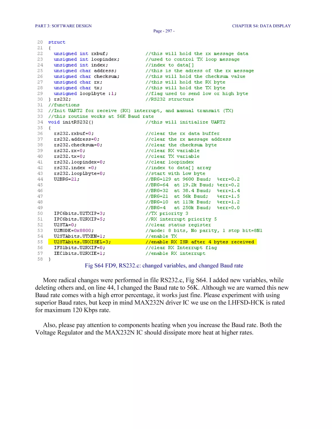
Fig S64 FD9, RS232.c: changed variables, and changed Baud rate 297
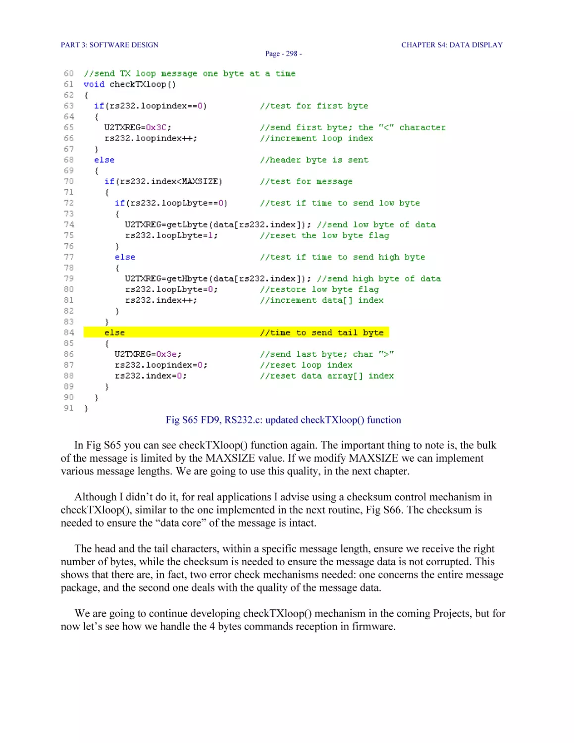
Fig S65 FD9, RS232.c: updated checkTXloop() function 298
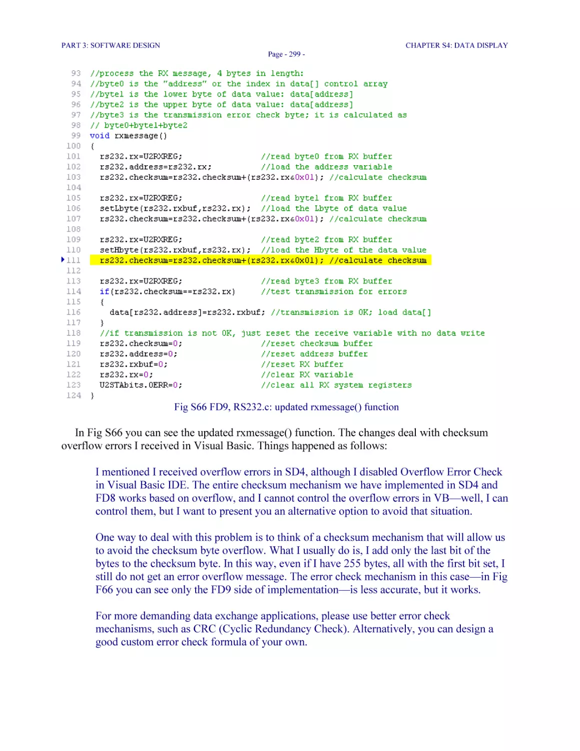
Fig S66 FD9, RS232.c: updated rxmessage() function 299
LHFSD
TABLE OF FIGURES
Page - 23 -
Fig S67 FD9, main.c: changed Task3 300
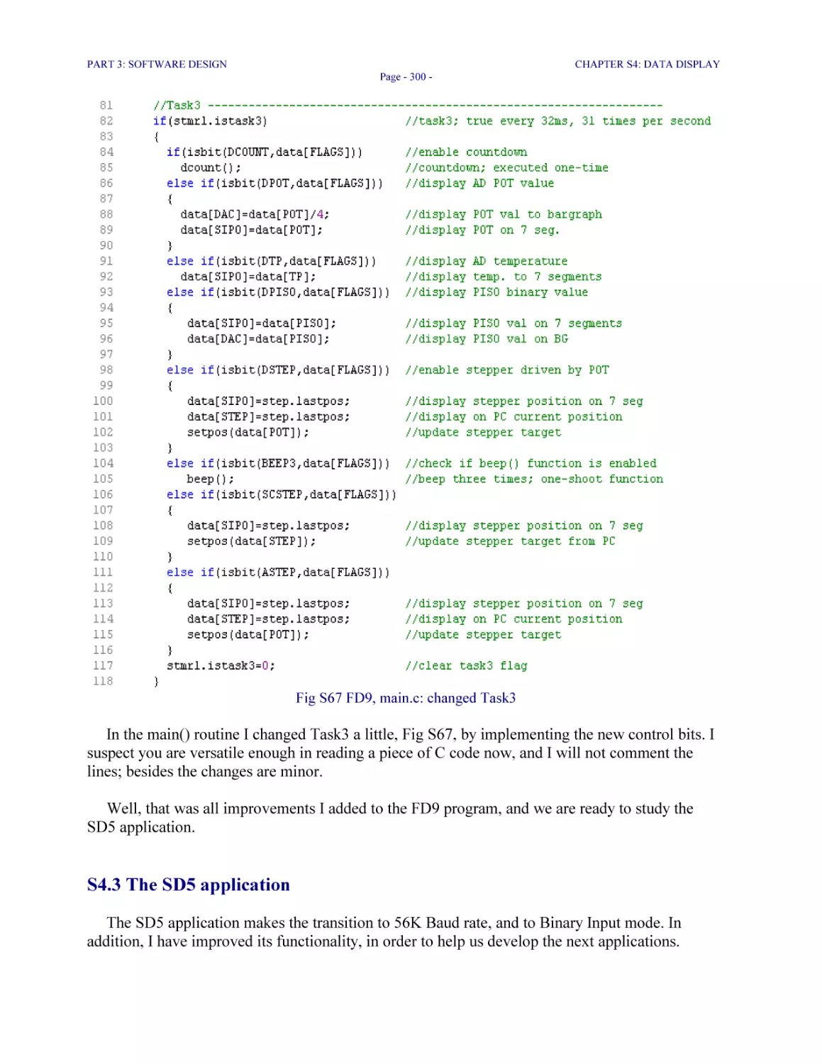
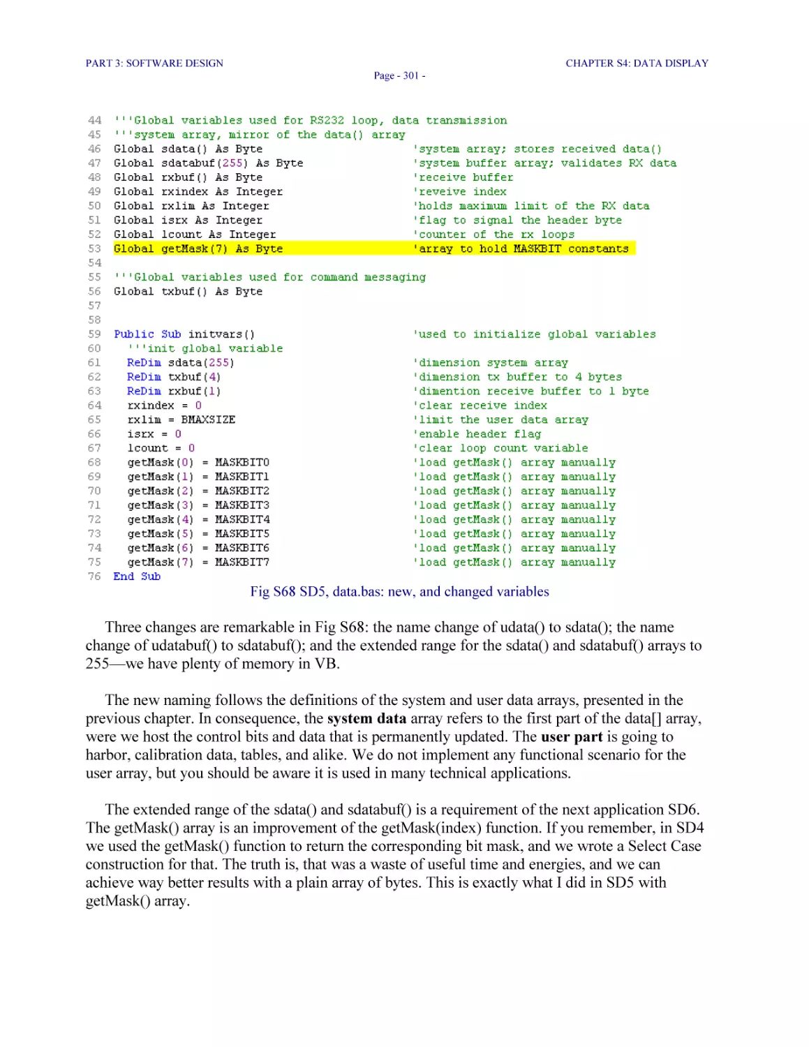
Fig S68 SD5, data.bas: new, and changed variables 301
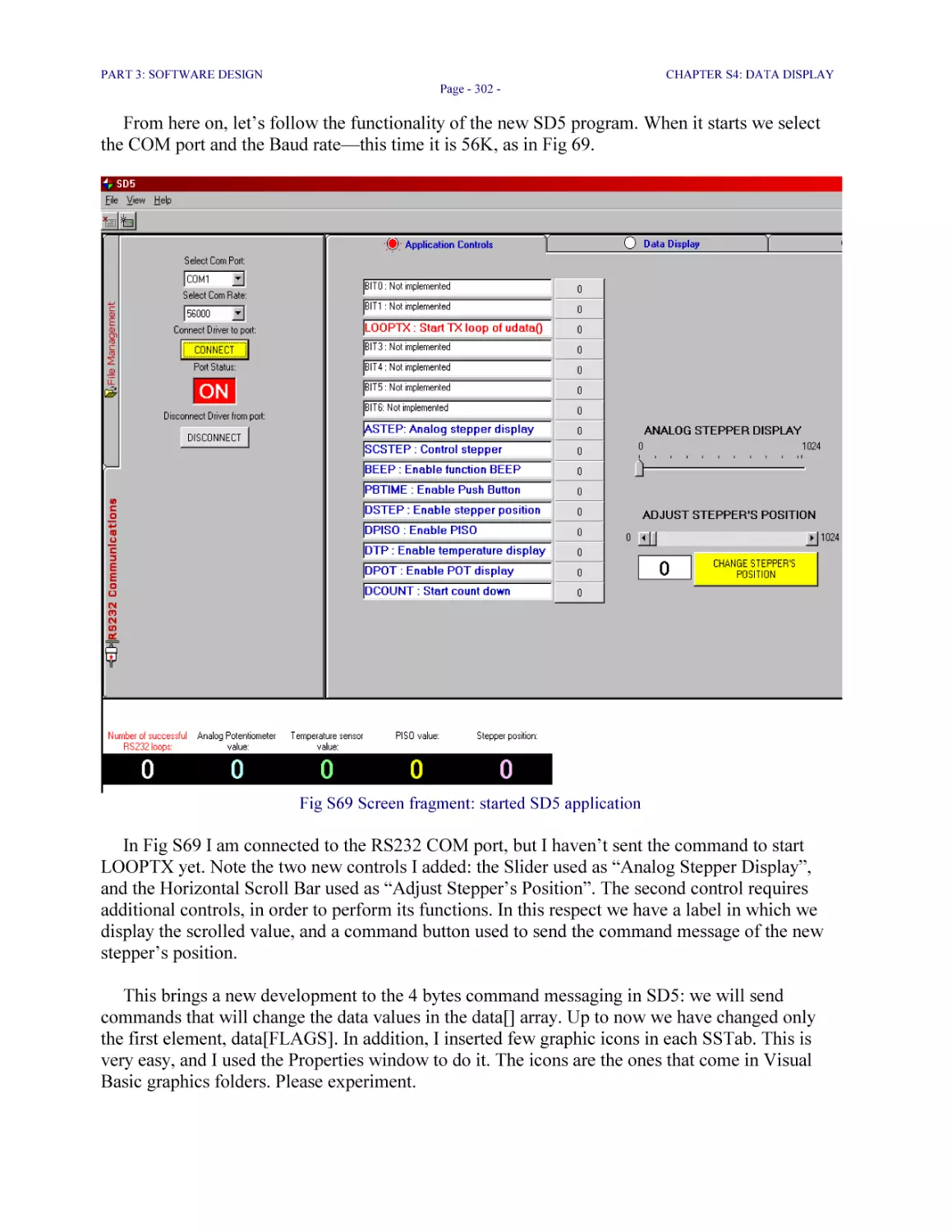
Fig S69 Screen fragment: started SD5 application 302
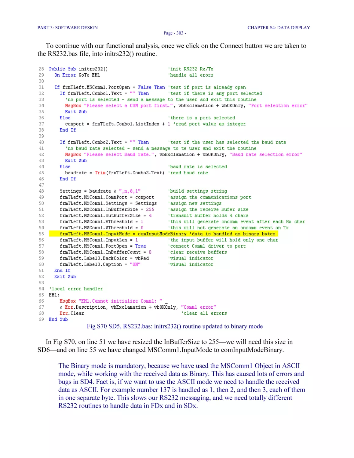
Fig S70 SD5, RS232.bas: initrs232() routine updated to binary mode 303
Fig S71 SD5, frmTRight.frm: the Variables Declaration section 304
Fig S72 SD5, frmTRight.frm: upgraded Command1_Click(index) routine 305
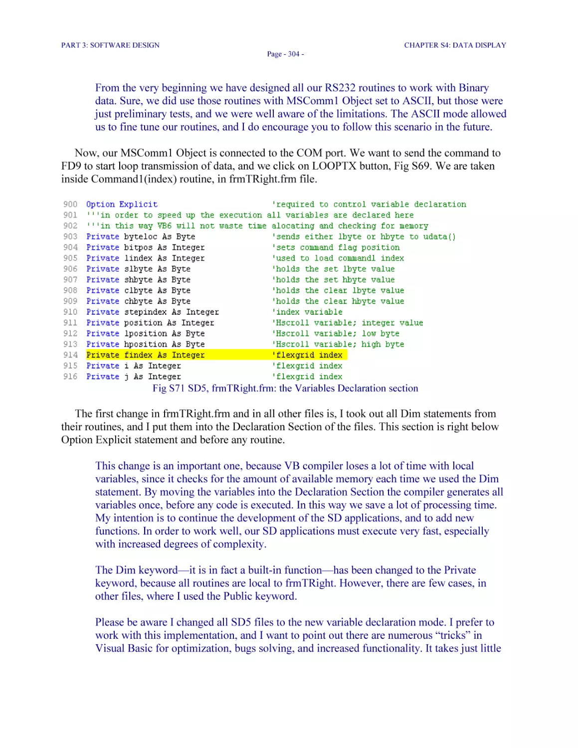
Fig S73 SD5, frmTRight.frm: updated FilterLock() function 306
Fig S74 SD5, RS232.bas: modified sendMessage() routine 307
Fig S75 SD5, frmTRight.frm: new graphic controls 308
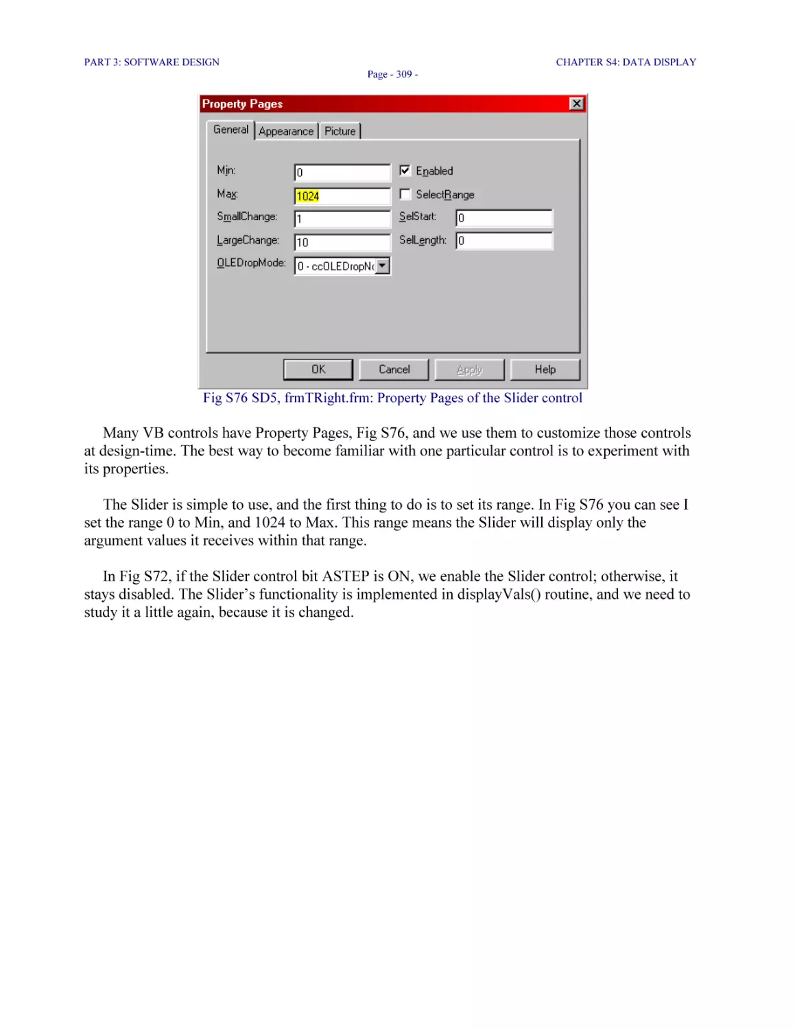
Fig S76 SD5, frmTRight.frm: Property Pages of the Slider control 309
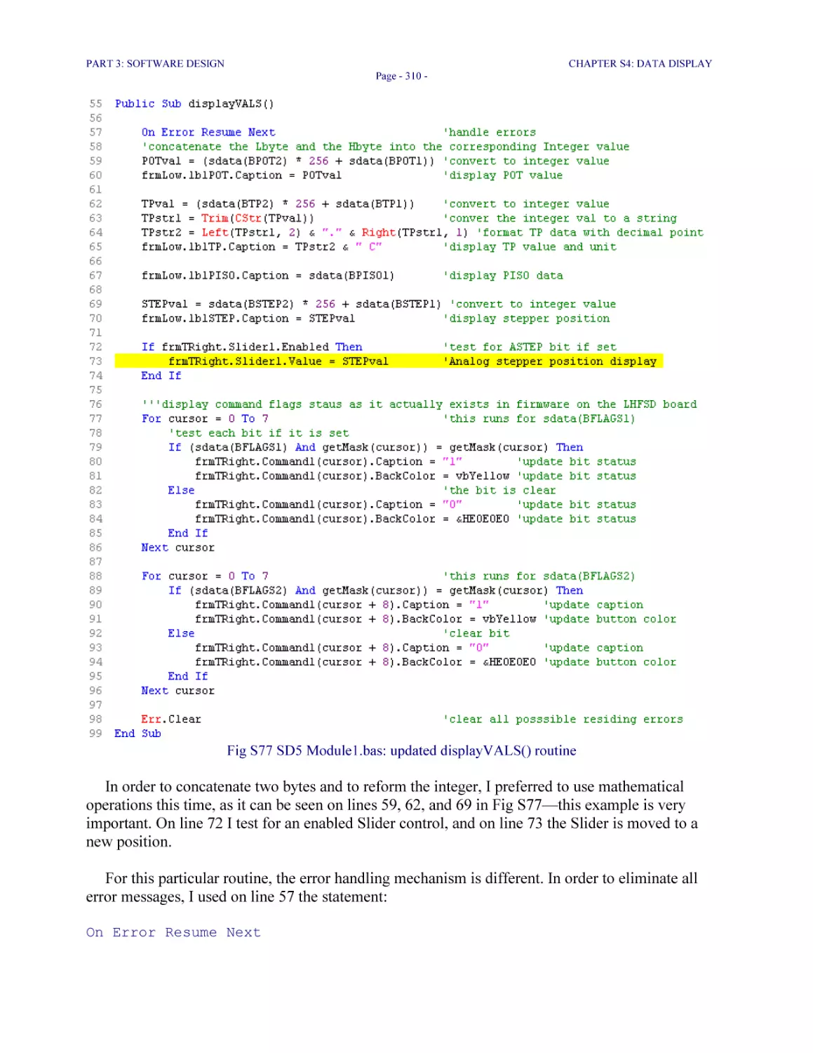
Fig S77 SD5 Module1.bas: updated displayVALS() routine 310
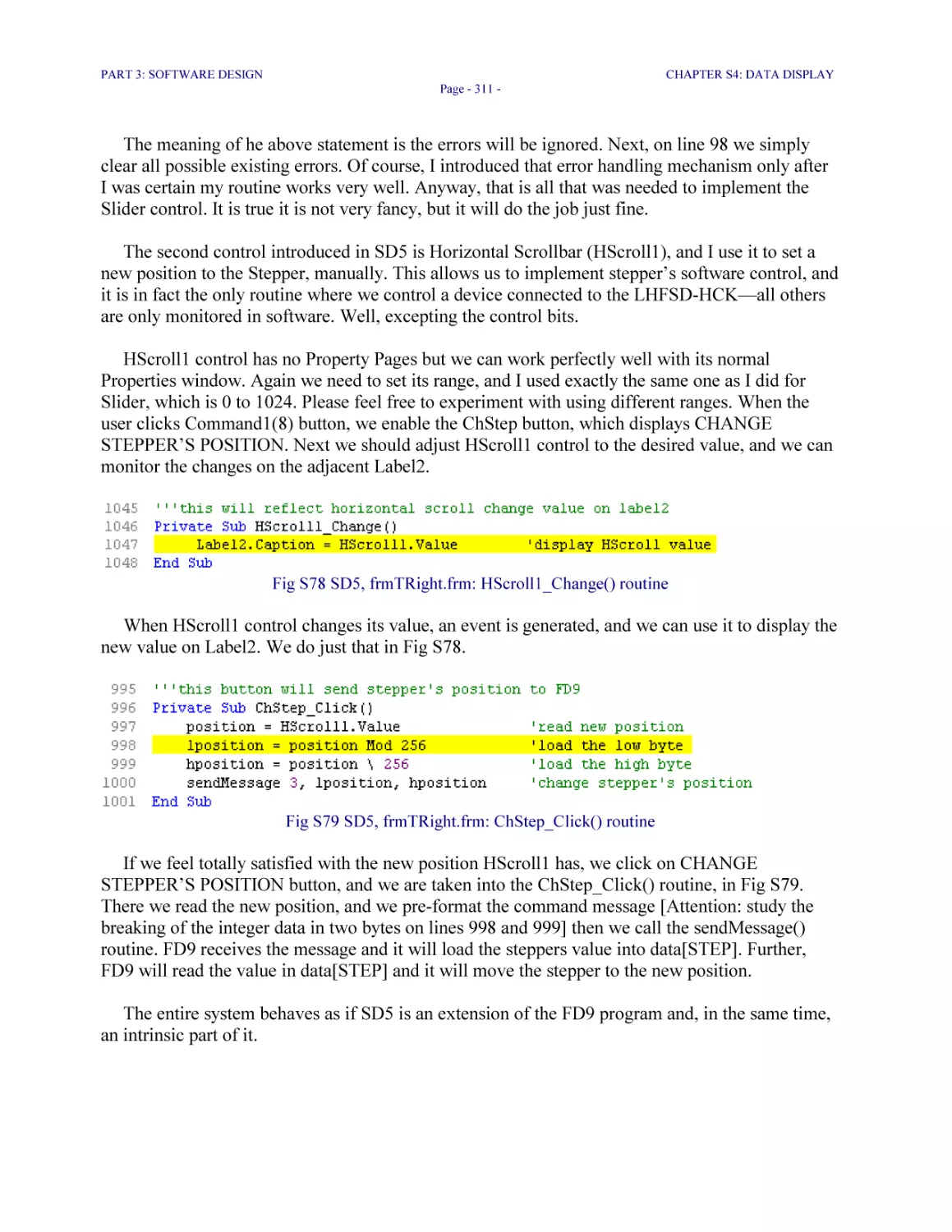
Fig S78 SD5, frmTRight.frm: HScroll1_Change() routine 311
Fig S79 SD5, frmTRight.frm: ChStep_Click() routine 311
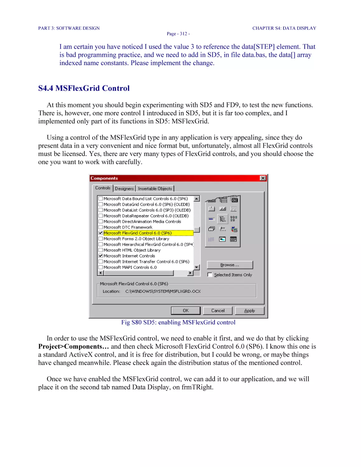
Fig S80 SD5: enabling MSFlexGrid control 312
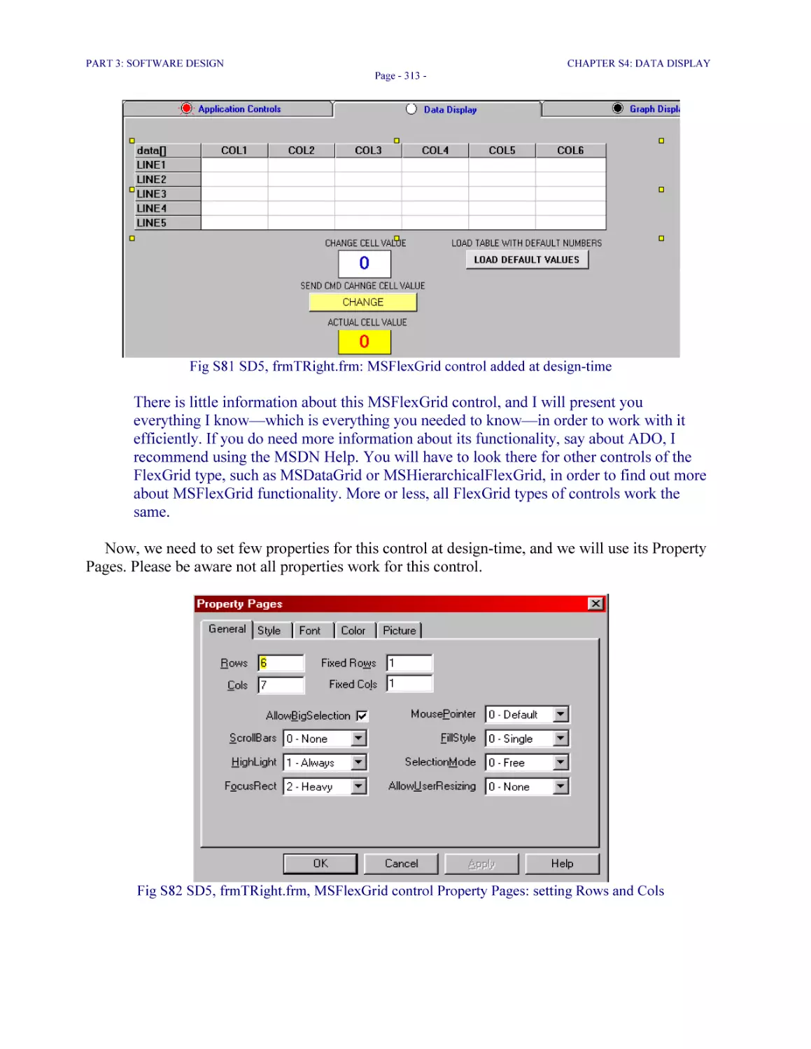
Fig S81 SD5, frmTRight.frm: MSFlexGrid control added at design-time 313
Fig S82 SD5, frmTRight.frm, MSFlexGrid control Property Pages: setting Rows and Cols 313
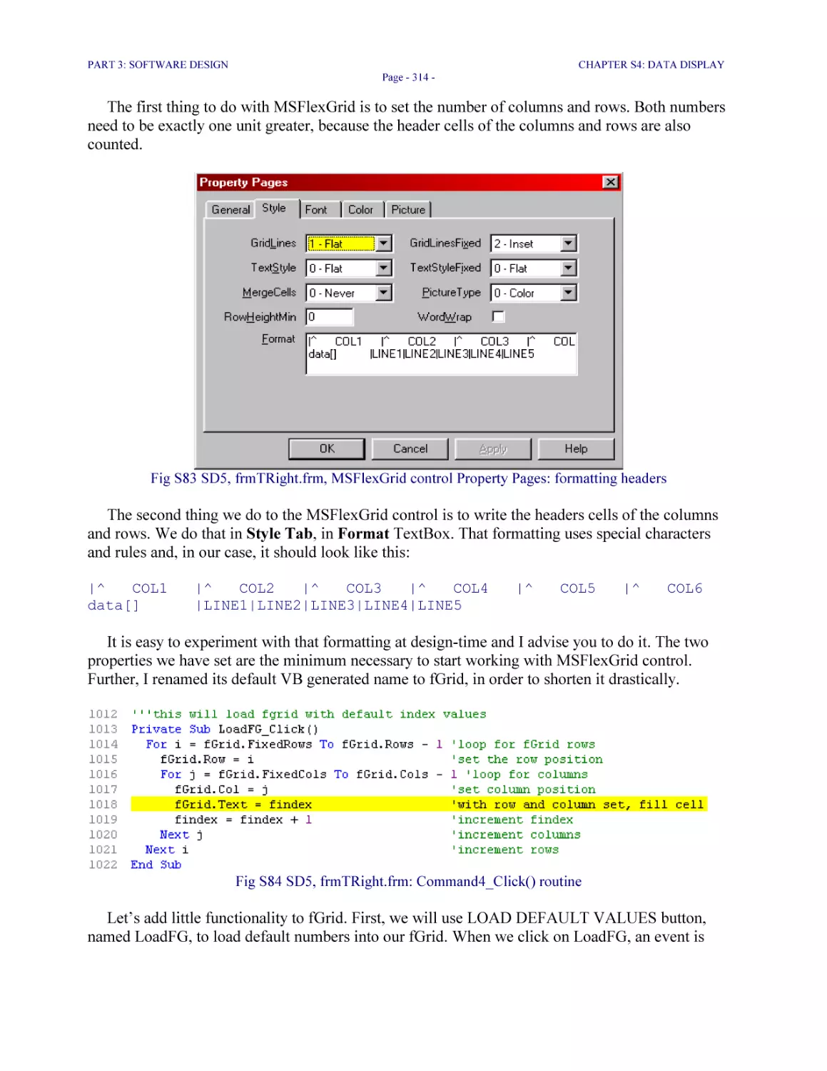
Fig S83 SD5, frmTRight.frm, MSFlexGrid control Property Pages: formatting headers 314
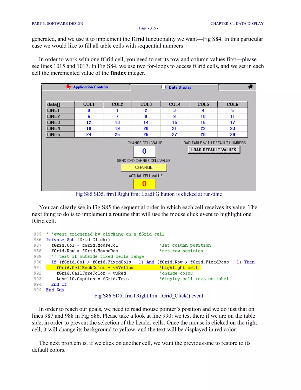
Fig S84 SD5, frmTRight.frm: Command4_Click() routine 314
Fig S85 SD5, frmTRight.frm: LoadFG button is clicked at run-time 315
Fig S86 SD5, frmTRight.frm: fGrid_Click() event 315
Fig S87 SD5, frmTRight.frm: fGrid_LeaveCell() event 316
Fig S88 SD5, frmTRight.frm: run-time fGrid_click() event 316
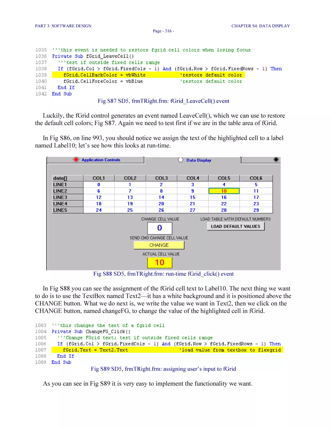
Fig S89 SD5, frmTRight.frm: assigning user’s input to fGrid 316
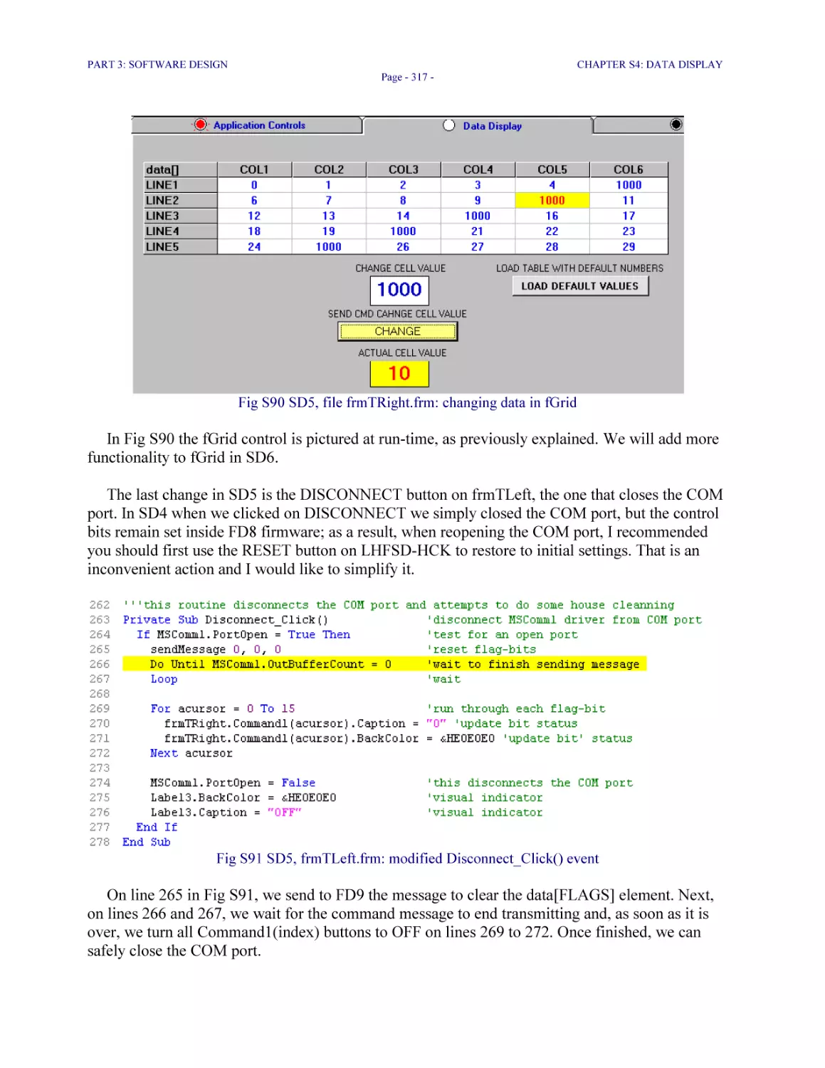
Fig S90 SD5, file frmTRight.frm: changing data in fGrid 317
Fig S91 SD5, frmTLeft.frm: modified Disconnect_Click() event 317
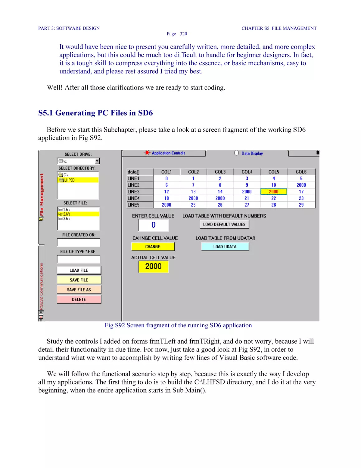
Fig S92 Screen fragment of the running SD6 application 320
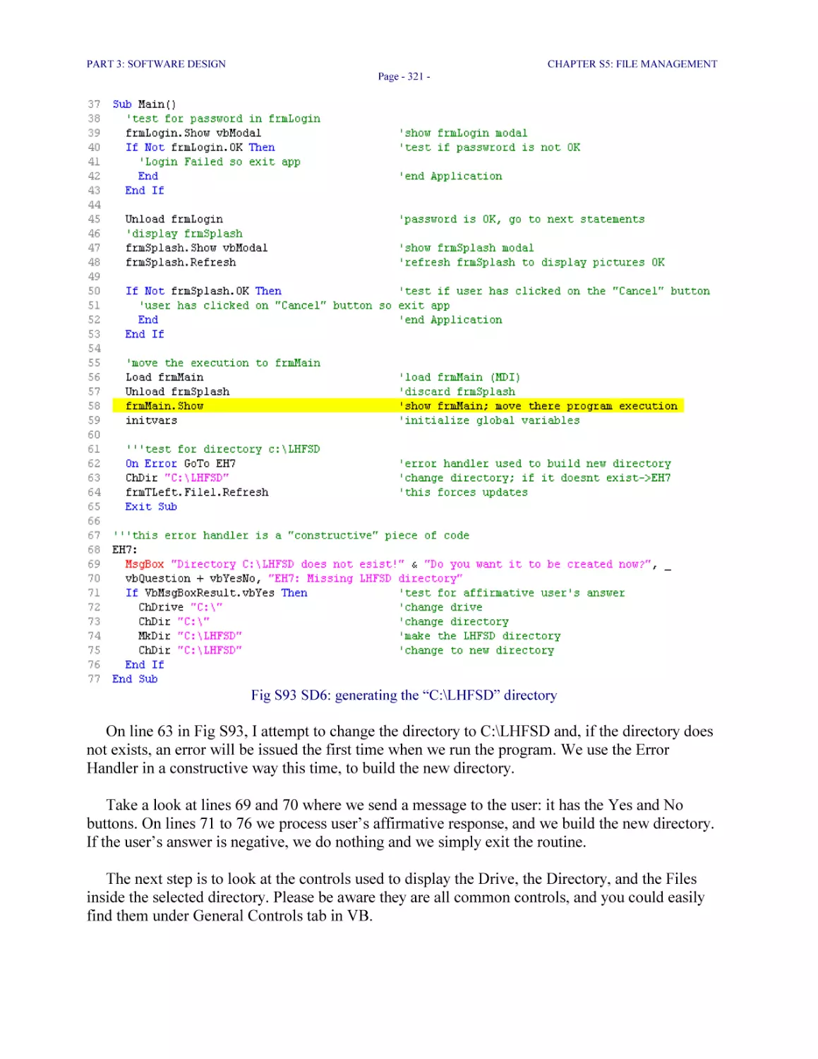
Fig S93 SD6: generating the “C:\LHFSD” directory 321
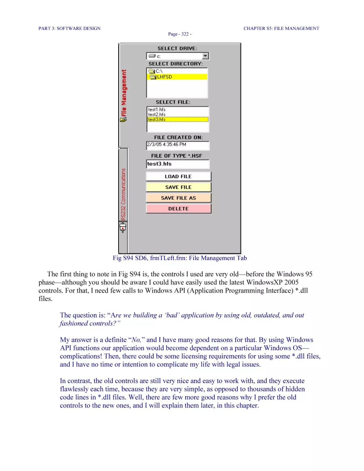
Fig S94 SD6, frmTLeft.frm: File Management Tab 322
Fig S95 SD6, frmTLeft.frm: drive, directory, and file selection 323
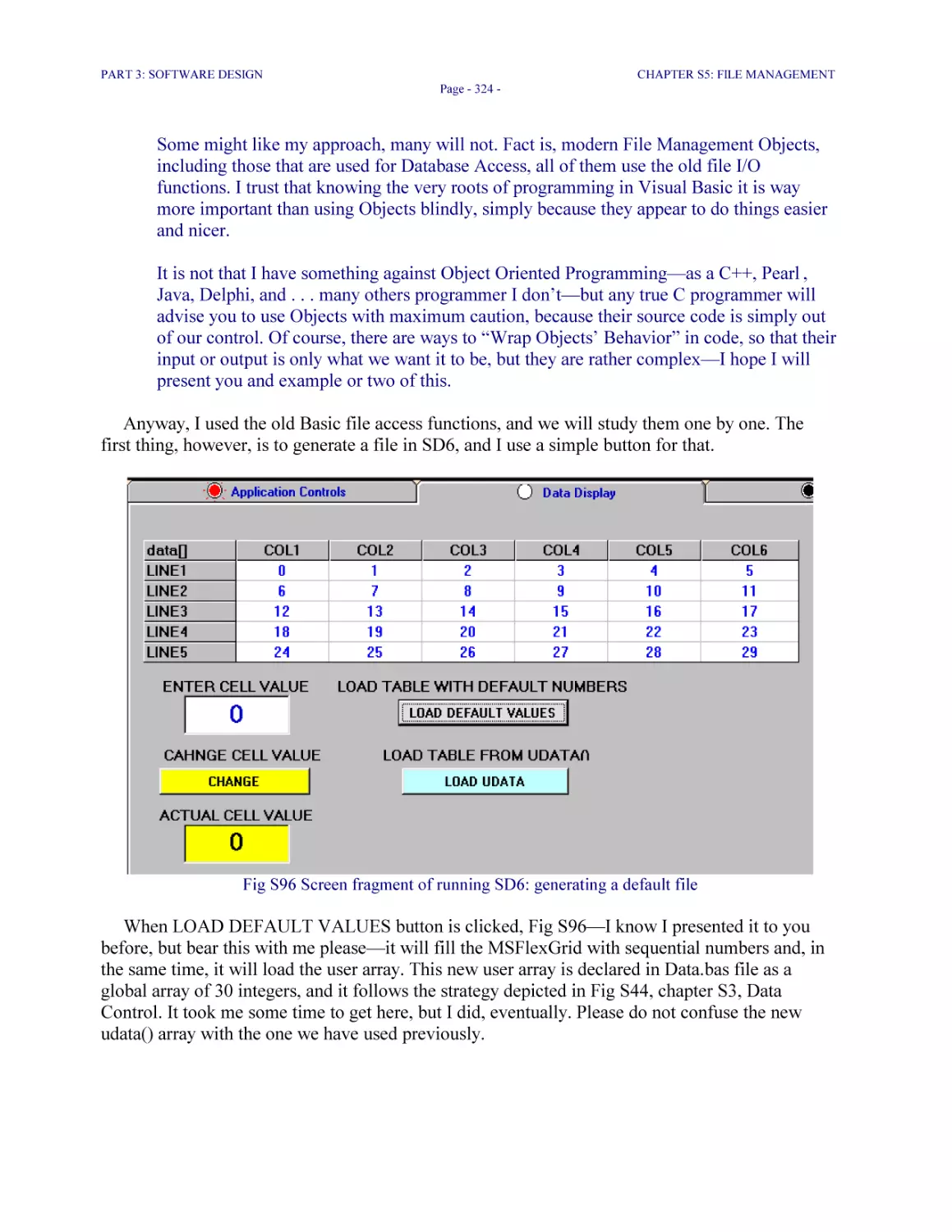
Fig S96 Screen fragment of running SD6: generating a default file 324
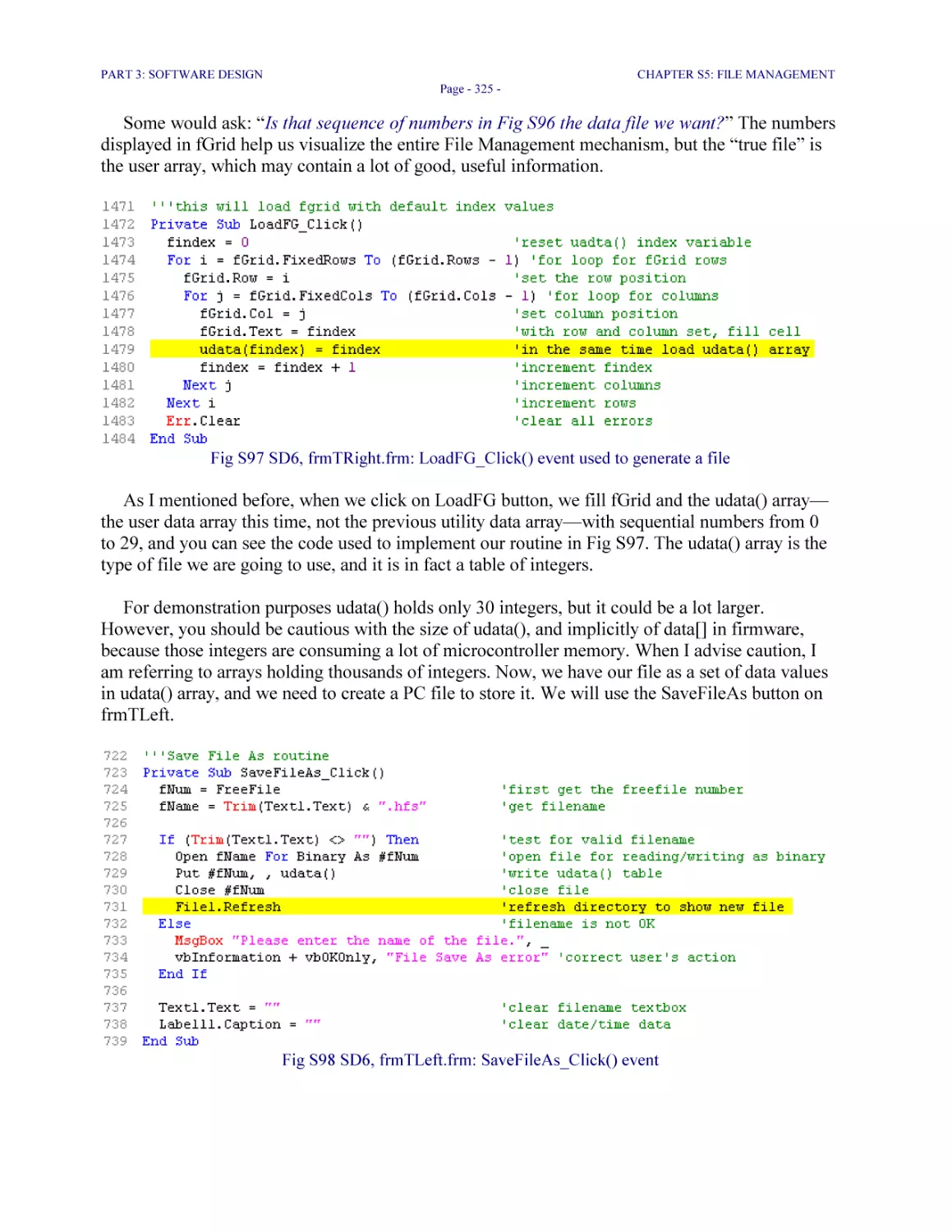
Fig S97 SD6, frmTRight.frm: LoadFG_Click() event used to generate a file 325
Fig S98 SD6, frmTLeft.frm: SaveFileAs_Click() event 325
Fig S99 SD6, frmTLeft.frm: LoadFile_Click() event 327
Fig S100 SD6, frmTLeft.frm: SaveFile_Click() event 327
Fig S101 SD6, frmTLeft.frm: DeleteFile_Click() event 328
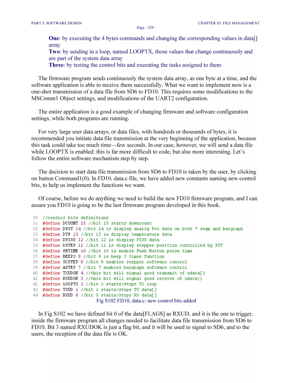
Fig S102 FD10, data.c: new control bits added 329
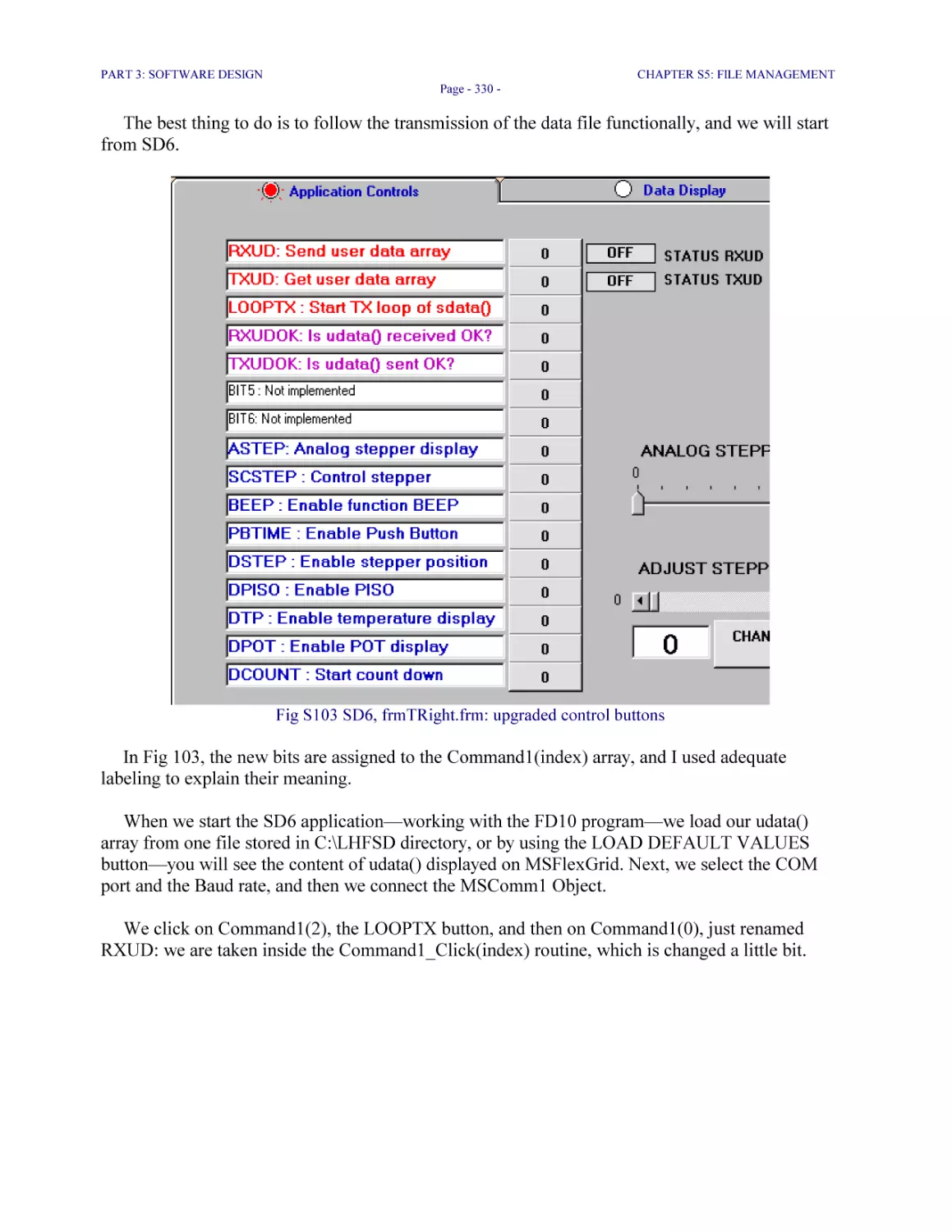
Fig S103 SD6, frmTRight.frm: upgraded control buttons 330
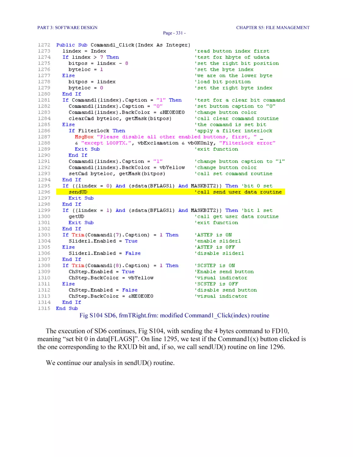
Fig S104 SD6, frmTRight.frm: modified Command1_Click(index) routine 331
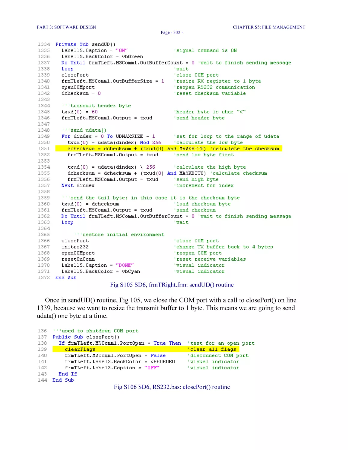
Fig S105 SD6, frmTRight.frm: sendUD() routine 332
Fig S106 SD6, RS232.bas: closePort() routine 332
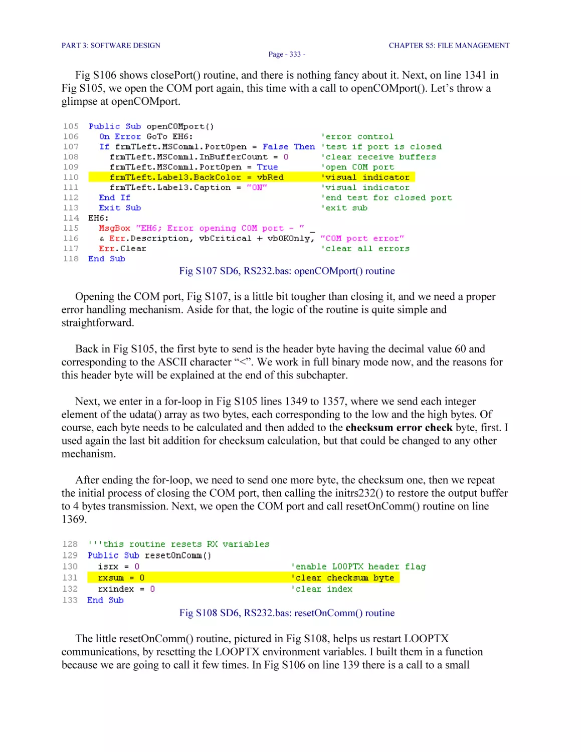
Fig S107 SD6, RS232.bas: openCOMport() routine 333
Fig S108 SD6, RS232.bas: resetOnComm() routine 333
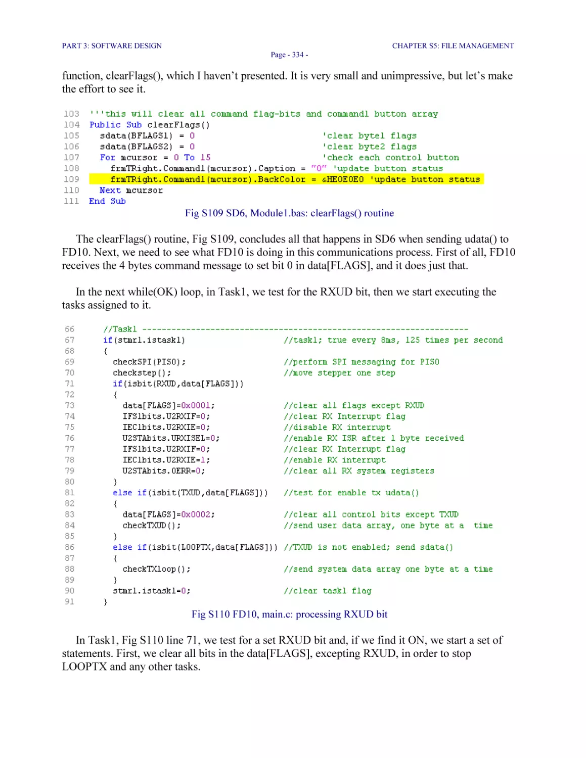
Fig S109 SD6, Module1.bas: clearFlags() routine 334
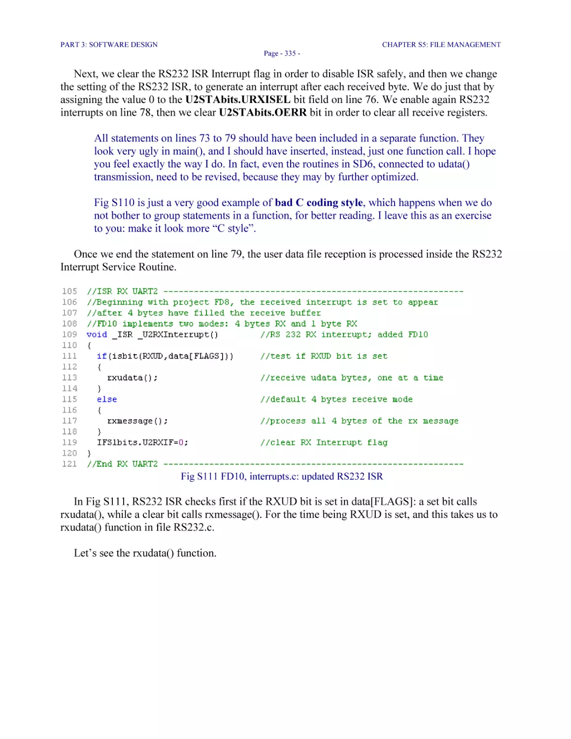
Fig S110 FD10, main.c: processing RXUD bit 334
Fig S111 FD10, interrupts.c: updated RS232 ISR 335
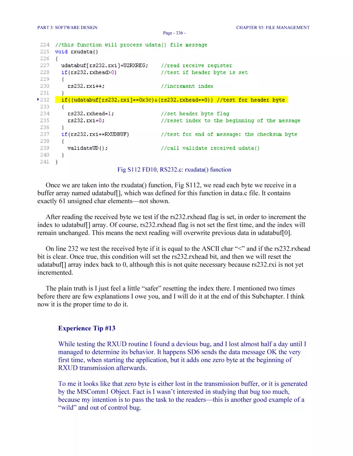
Fig S112 FD10, RS232.c: rxudata() function 336
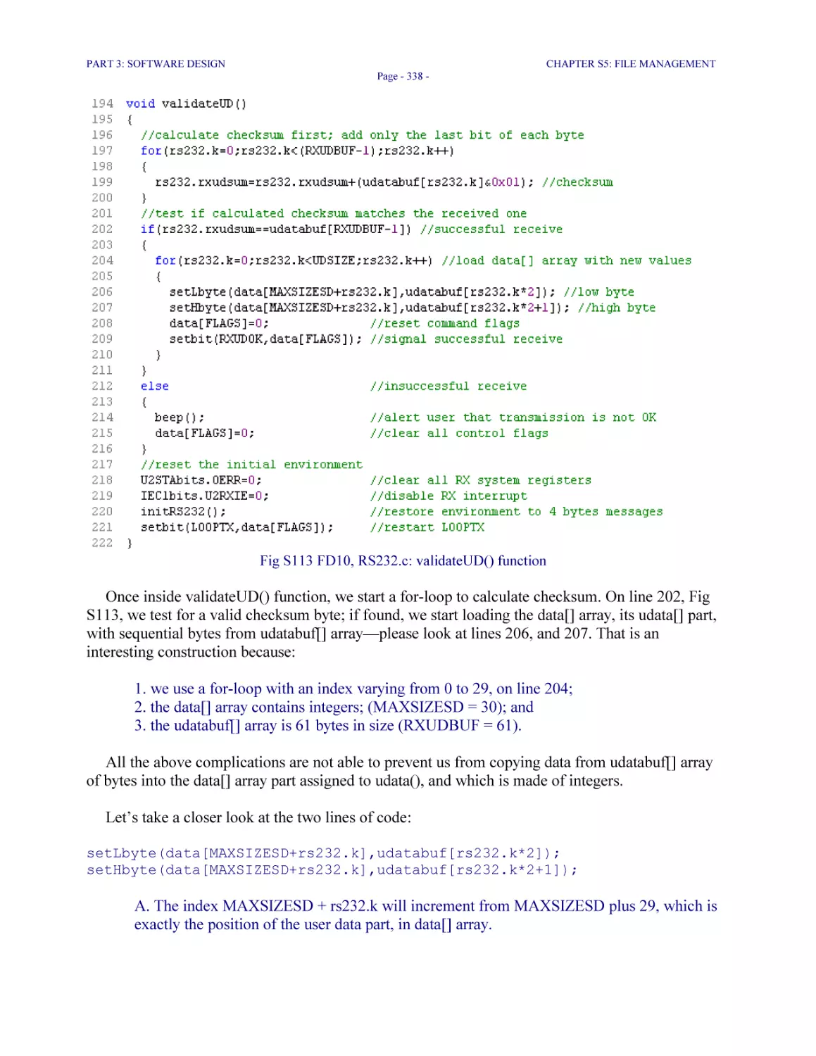
Fig S113 FD10, RS232.c: validateUD() function 338
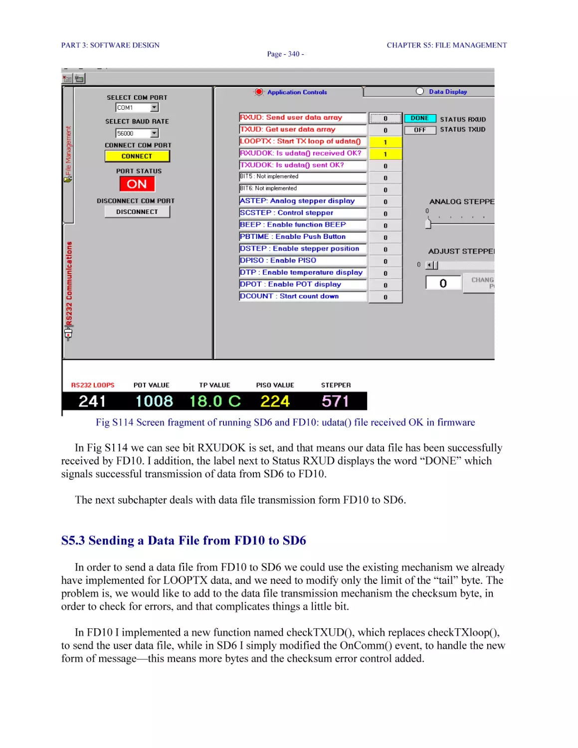
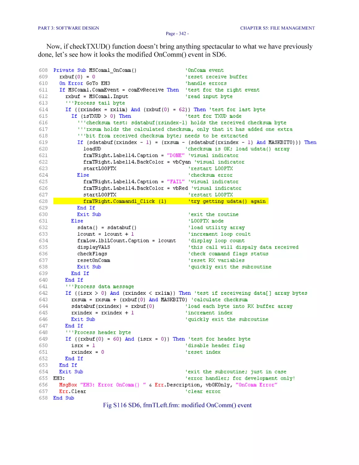
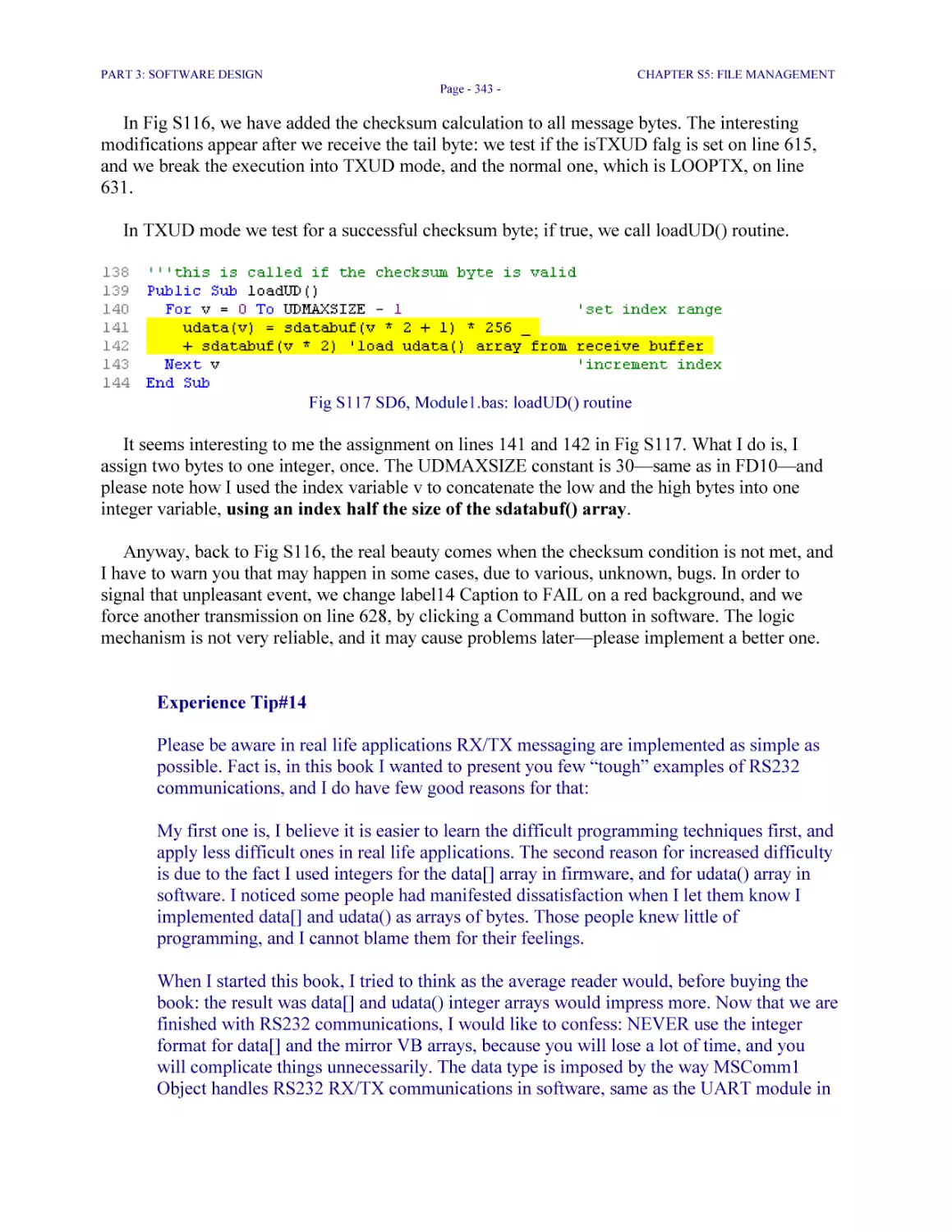
Fig S114 Screen fragment of running SD6 and FD10: udata() file received OK in firmware 340
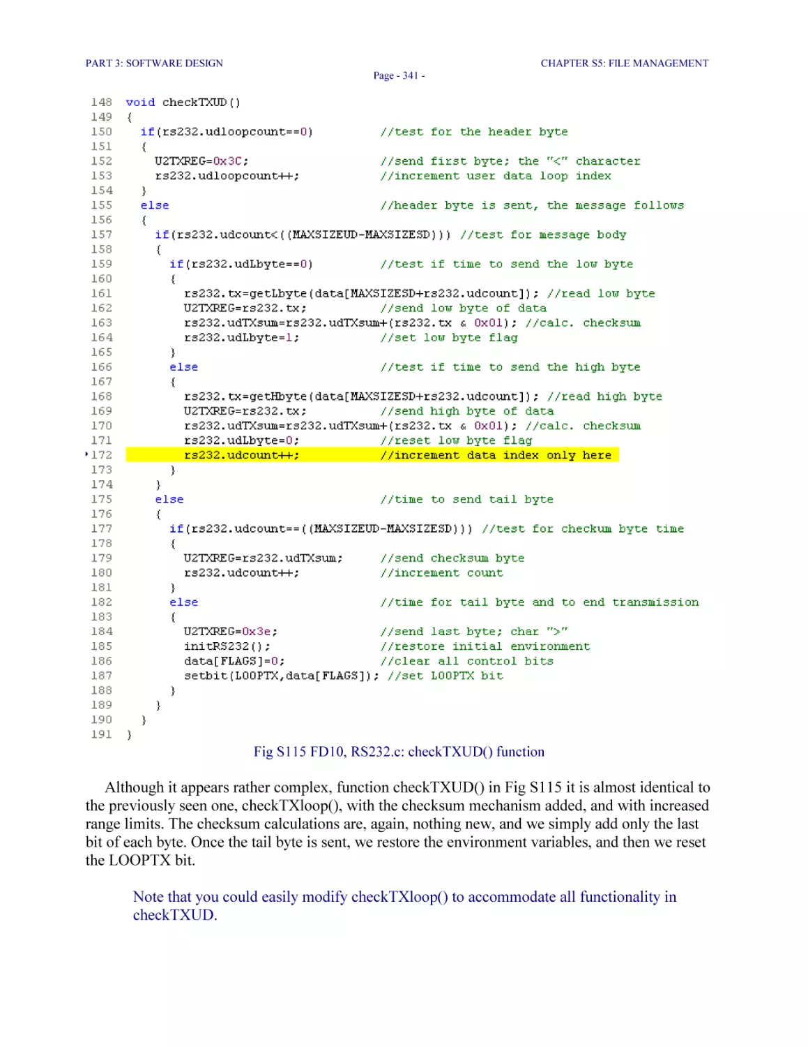
Fig S115 FD10, RS232.c: checkTXUD() function 341
Fig S116 SD6, frmTLeft.frm: modified OnComm() event 342
Fig S117 SD6, Module1.bas: loadUD() routine 343
LHFSD
TABLE OF FIGURES
Page - 24 -
Fig S118 SD6, RS232.bas: startLOOPTX() routine 344
Fig S119 Screen fragment: running SD6 and FD10 345
Fig S120 SD7, design-time: tab on frmTRight.frm displaying Graph Trace control 348
Fig S121 SD7, frmTRight.frm: btnPlay_Click() routine 348
Fig S122 SD7, Data.bas: new constants and variables added 349
Fig S123 SD7, Data.bas: resetGraph() routine 349
Fig S124 SD7, Module1.bas: upgraded displayVals() routine (fragment) 351
Fig S125 Running SD7: screen fragment showing Graph Trace 352
Fig S126 SD7, frmTRight.frm: btnPAUSE_Click() routine 353
Fig S127 SD7, frmTRight.frm: btnRECORD_Click() routine 354
Fig S128 SD7, frmTRight.frm: btnPLAYBACK_Click() routine 355
Fig S129 Running SD7: Graph Trace playback function 356
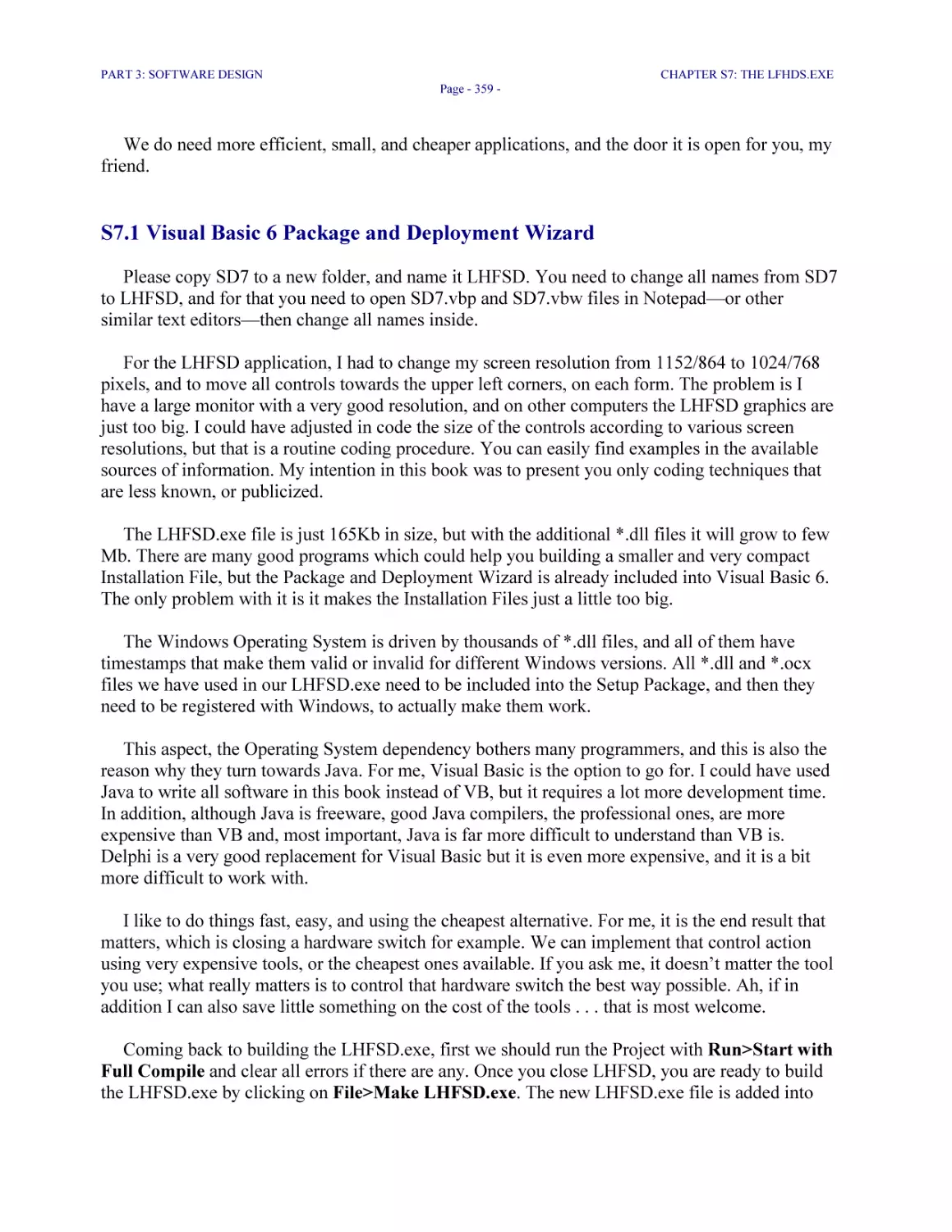
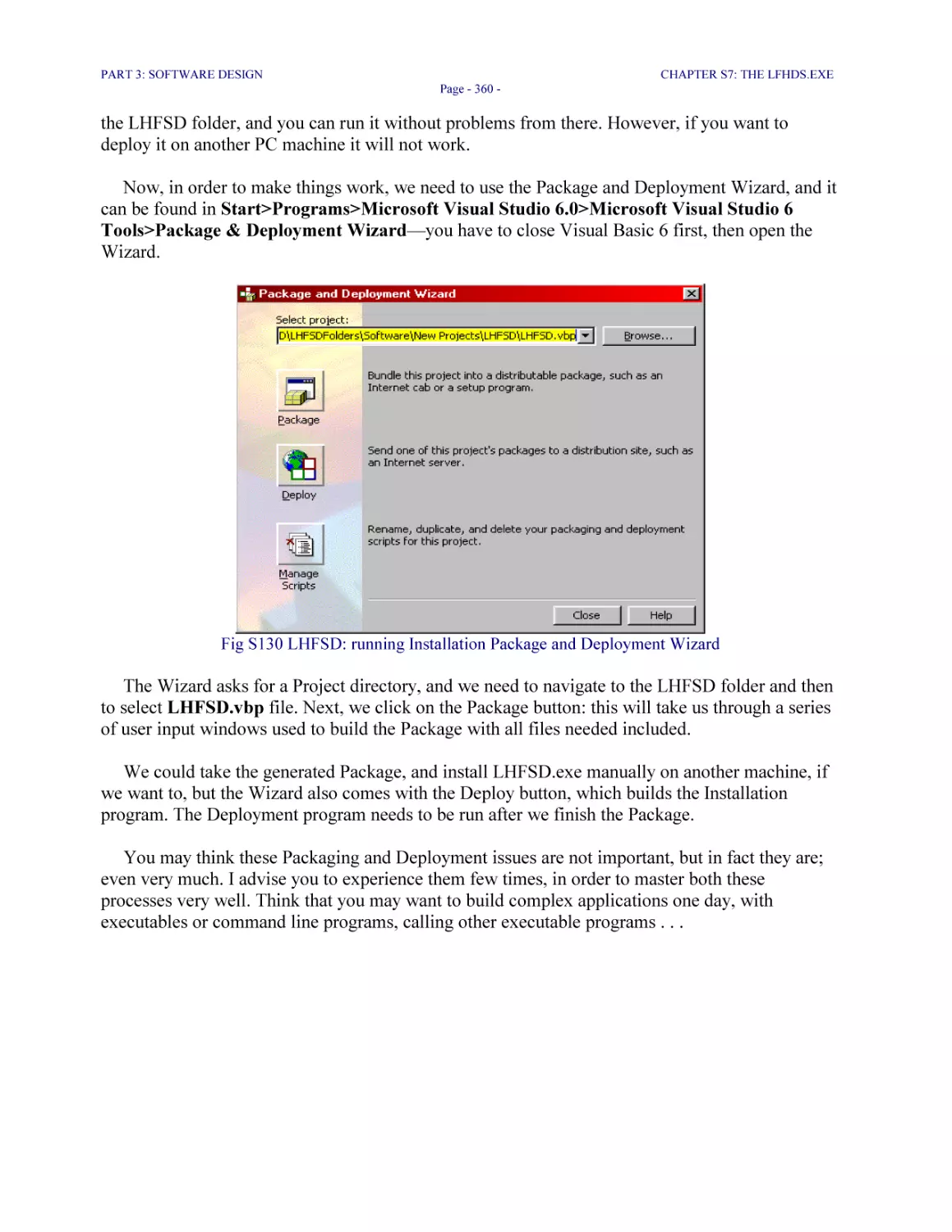
Fig S130 LHFSD: running Installation Package and Deployment Wizard 360
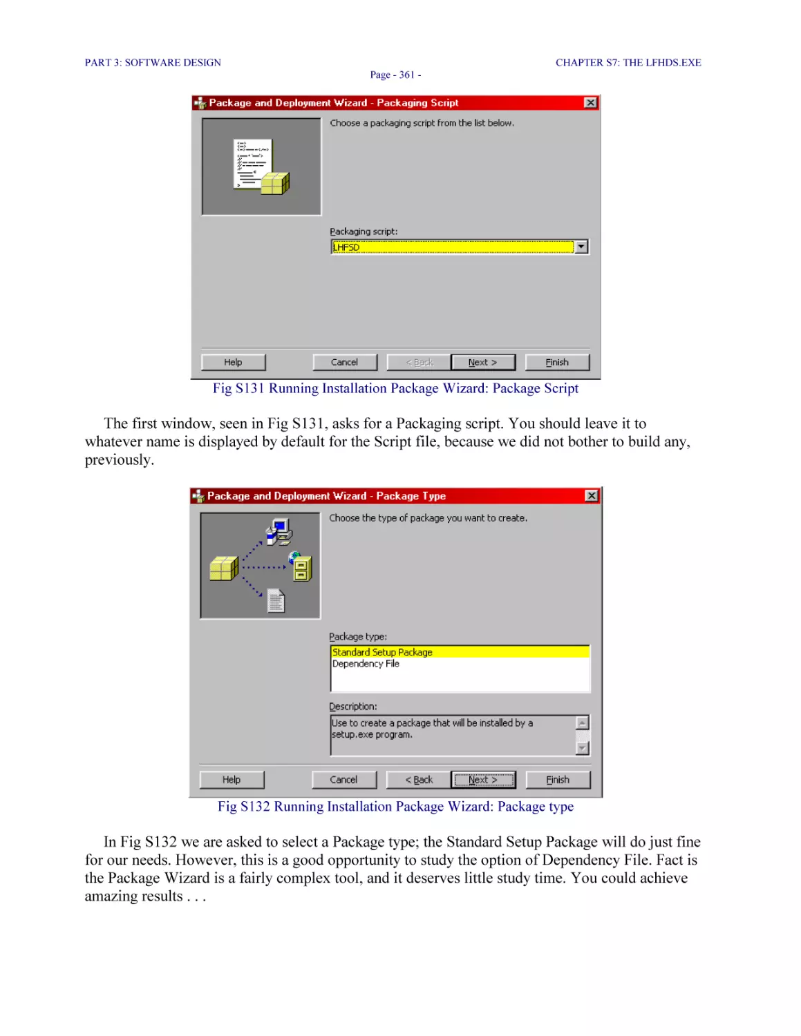
Fig S131 Running Installation Package Wizard: Package Script 361
Fig S132 Running Installation Package Wizard: Package type 361
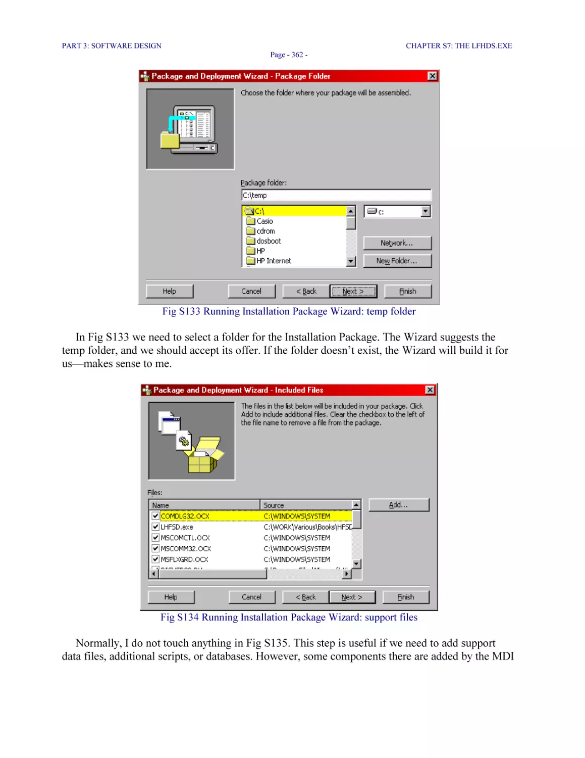
Fig S133 Running Installation Package Wizard: temp folder 362
Fig S134 Running Installation Package Wizard: support files 362
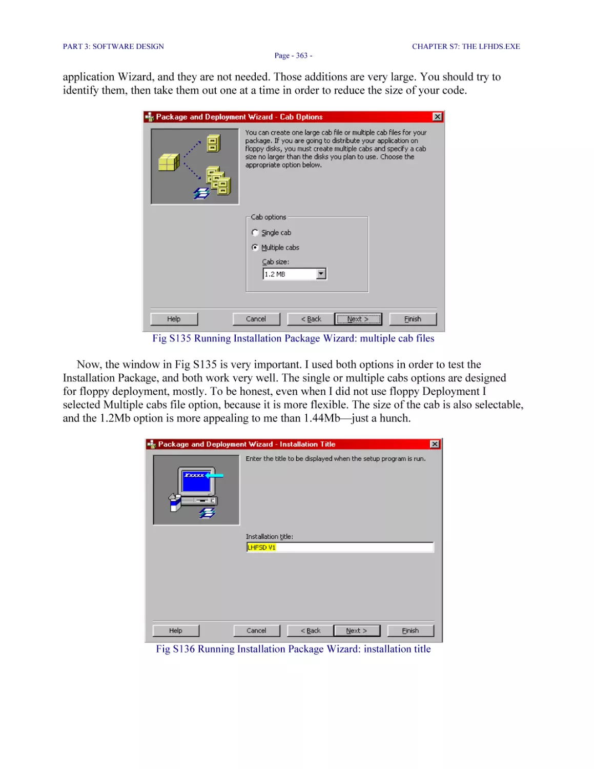
Fig S135 Running Installation Package Wizard: multiple cab files 363
Fig S136 Running Installation Package Wizard: installation title 363
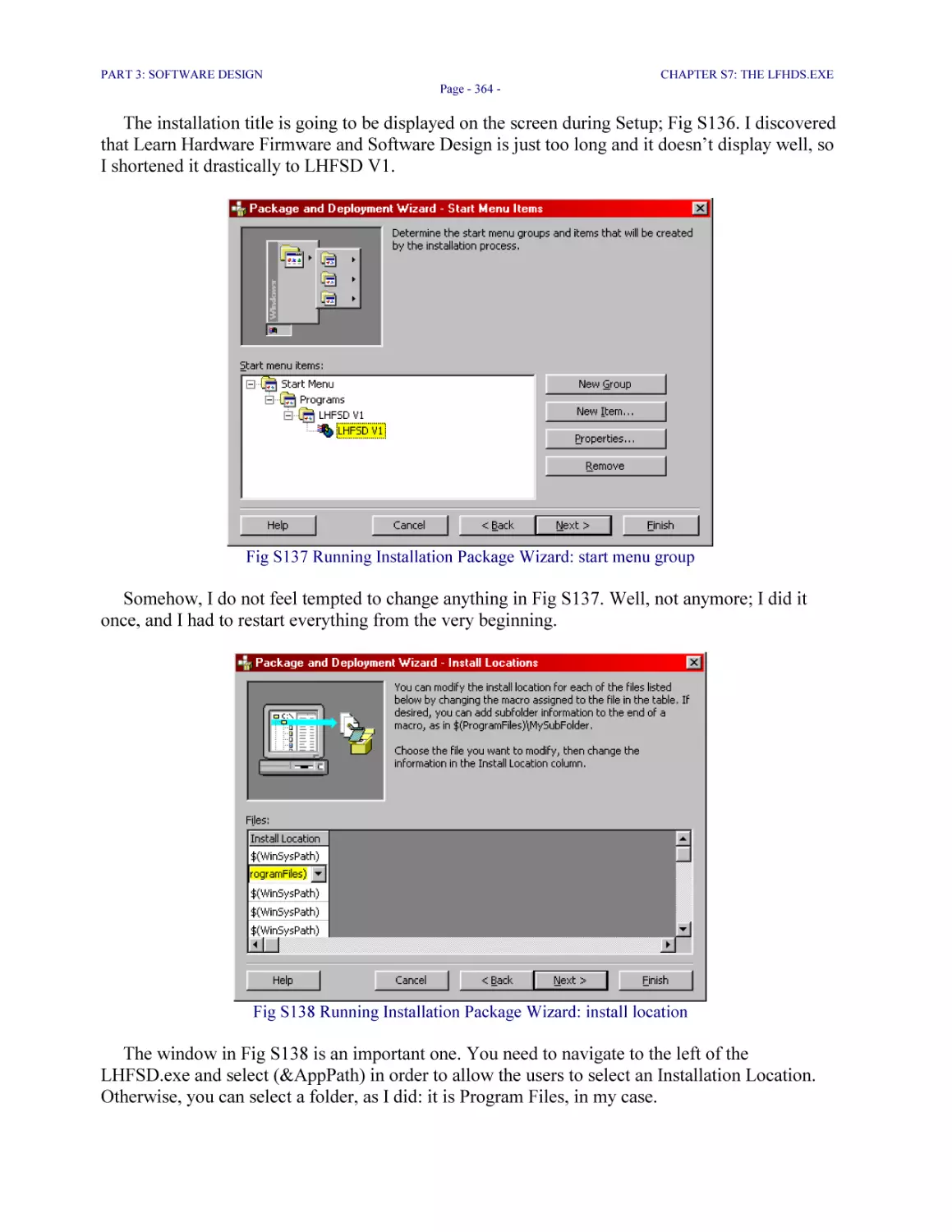
Fig S137 Running Installation Package Wizard: start menu group 364
Fig S138 Running Installation Package Wizard: install location 364
Fig S139 Running Deployment Wizard: script name 365
Fig S140 Running Deployment Wizard: package selection 365
Fig S141 Running Deployment Wizard: Deployment method 366
Fig S142 Running Deployment Wizard: Installation folder 366
***
PART 1: HARDWARE DESIGN
Project: Designing the LHFSD-HCK
CHAPTER H1: MICROCONTROLLERS
So, here we are: we have an empty Schematic page in front of us, and we are ready to start
designing hardware. That is excellent, except . . . we should not rush too much.
In fact, throughout this chapter we will leave the Schematic page just as it is, empty, and we
will study our microcontroller machine: dsPIC30F4011. I am sorry for not providing a
microcontroller picture for you, but there is absolutely nothing impressive about it, in exterior. Our
controller looks just like any other ordinary DIP 40 IC (Through-Hole DIP package, 40 pins,
Integrated Circuit). The inside of the dsPIC30F4011, however, is a totally different story, because
it is a fantastic machine with millions of tiny electrical circuits. Those electrical circuits are
designed to transform our intelligence, the firmware program, into millions of enabled or disabled
electrical paths.
H1.1 General Presentation
A microcontroller is a digital electronic machine, which can execute tasks based on a clock
pulse, and a firmware program. The terms “microcontroller” and “microprocessor” refer to the
same thing. The difference between the two is, a microcontroller is—generally, and not
necessarily—a simpler microprocessor, usually built with 8 or 16 bits data registers and Data Bus
width, and it has lower CPU speeds. CPU stands for Central Processing Unit and it is the
electronic, digital core of the microcontroller.
Microprocessors have 16, 32, 64 bits registers and Data Bus width, and they could be very
complex; sometimes they have embedded an additional math coprocessor. They are used for more
advanced applications, such as Multitasking PC and color graphics display.
Fig H1 Microcontroller’s work cycle
PART 1: HARDWARE DESIGN
CHAPTER H1: MICROCONTROLLERS
Page - 27 -
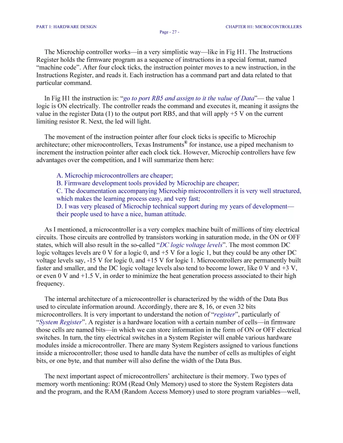
The Microchip controller works—in a very simplistic way—like in Fig H1. The Instructions
Register holds the firmware program as a sequence of instructions in a special format, named
“machine code”. After four clock ticks, the instruction pointer moves to a new instruction, in the
Instructions Register, and reads it. Each instruction has a command part and data related to that
particular command.
In Fig H1 the instruction is: “go to port RB5 and assign to it the value of Data”— the value 1
logic is ON electrically. The controller reads the command and executes it, meaning it assigns the
value in the register Data (1) to the output port RB5, and that will apply +5 V on the current
limiting resistor R. Next, the led will light.
The movement of the instruction pointer after four clock ticks is specific to Microchip
architecture; other microcontrollers, Texas Instruments® for instance, use a piped mechanism to
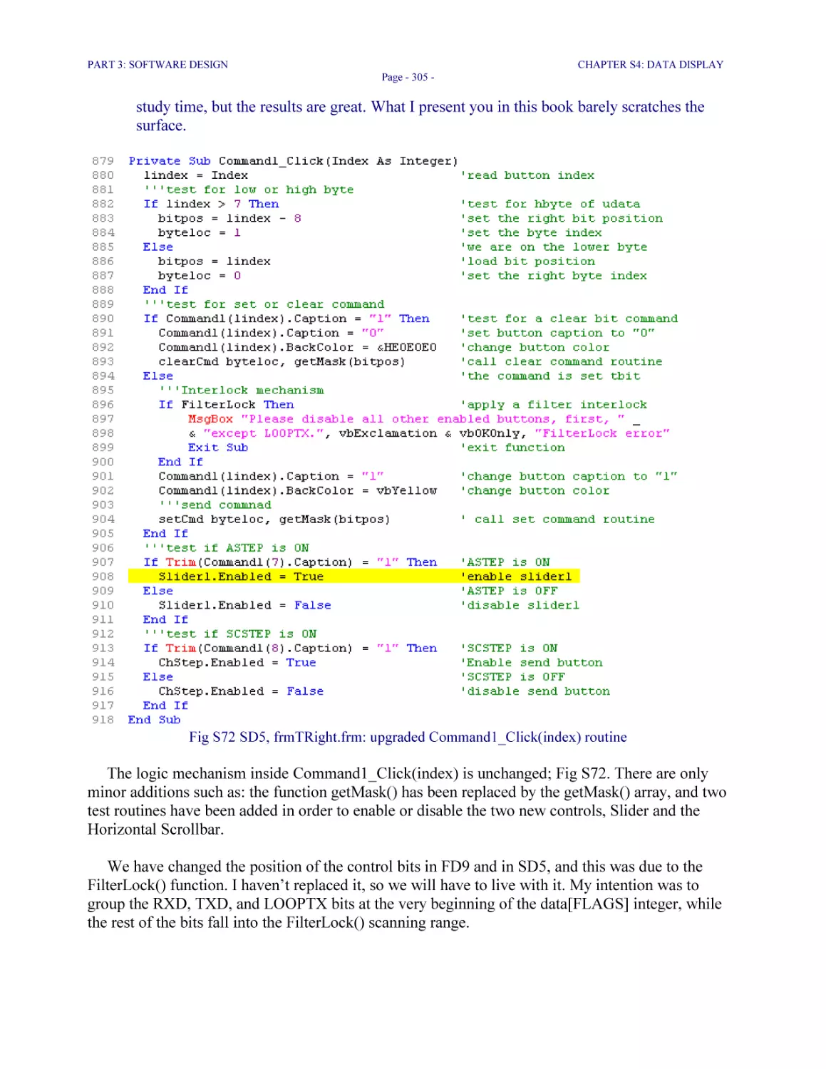
increment the instruction pointer after each clock tick. However, Microchip controllers have few
advantages over the competition, and I will summarize them here:
A. Microchip microcontrollers are cheaper;
B. Firmware development tools provided by Microchip are cheaper;
C. The documentation accompanying Microchip microcontrollers it is very well structured,
which makes the learning process easy, and very fast;
D. I was very pleased of Microchip technical support during my years of development—
their people used to have a nice, human attitude.
As I mentioned, a microcontroller is a very complex machine built of millions of tiny electrical
circuits. Those circuits are controlled by transistors working in saturation mode, in the ON or OFF
states, which will also result in the so-called “DC logic voltage levels”. The most common DC
logic voltages levels are 0 V for a logic 0, and +5 V for a logic 1, but they could be any other DC
voltage levels say, -15 V for logic 0, and +15 V for logic 1. Microcontrollers are permanently built
faster and smaller, and the DC logic voltage levels also tend to become lower, like 0 V and +3 V,
or even 0 V and +1.5 V, in order to minimize the heat generation process associated to their high
frequency.
The internal architecture of a microcontroller is characterized by the width of the Data Bus
used to circulate information around. Accordingly, there are 8, 16, or even 32 bits
microcontrollers. It is very important to understand the notion of “register”, particularly of
“System Register”. A register is a hardware location with a certain number of cells—in firmware
those cells are named bits—in which we can store information in the form of ON or OFF electrical
switches. In turn, the tiny electrical switches in a System Register will enable various hardware
modules inside a microcontroller. There are many System Registers assigned to various functions
inside a microcontroller; those used to handle data have the number of cells as multiples of eight
bits, or one byte, and that number will also define the width of the Data Bus.
The next important aspect of microcontrollers’ architecture is their memory. Two types of
memory worth mentioning: ROM (Read Only Memory) used to store the System Registers data
and the program, and the RAM (Random Access Memory) used to store program variables—well,
PART 1: HARDWARE DESIGN
CHAPTER H1: MICROCONTROLLERS
Page - 28 -
mostly. Do not worry; I have no intention to detail the memory topic because it could become
incredibly difficult to understand.
However, I do have to mention that memory can be permanent or volatile, and the first case is
the important one. Permanent memory may be of type EEPROM (Electrically Erasable
Permanent Memory), and we have 1024 bytes of EEPROM on our dsPIC30F4011 machine. If you
want to use EEPROM you need to build a firmware driver to read and write to it. Another type of
permanent memory is the one named FLASH, which allows us to burn or to erase our firmware
program about ten thousand times while using the ICD2 Debugger or Programmer tools.
I need to specify the term “burn” because it is much used by designers, with different
meanings. In hardware, burning a controller means it was damaged; in firmware, however,
burning a program on a controller means the program has been successfully loaded into
controller’s memory.
Please be aware hardware, firmware, and software designers use an incredible variety of
colorful expressions.
There are many System Registers inside a microcontroller, and those firmware programmers
who use Assembler must study them and the “Memory Allocation Structure” carefully, because
they actually load manually those Registers, and then they move data around step by step, on each
line of code. That is very difficult, and some programmers used to joke saying, “Assembler
separates men from boys!” Quite true, sometime ago, but not anymore. C firmware programmers
do not necessarily need to know everything inside a controller, except when they program a
critical task. When that exceptional event happens, C firmware programmers go down to the
basics; they study the problem very well, and then they insert few lines of Assembler code into a C
firmware module. The result is, a C program can be exactly as fast and efficient as a pure
Assembler one. However, you will learn later a program in C is way more flexible and powerful!
Fig H2 Electrical representation of one firmware byte of data
PART 1: HARDWARE DESIGN
CHAPTER H1: MICROCONTROLLERS
Page - 29 -
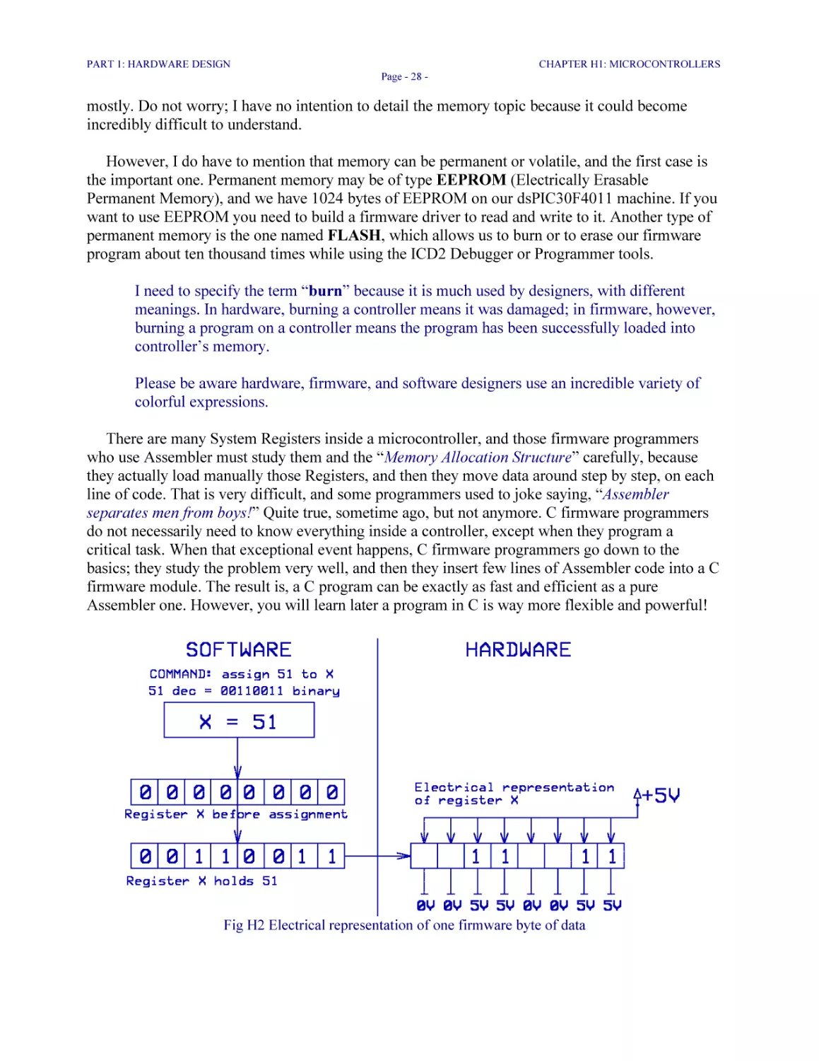
Let’s take a look at Fig H2, because it explains a very important concept: the relation between
firmware and the electrical hardware register. One line of firmware code, say x = 51, is an
instruction with a command part, and a Data value. The command says: load the register
named x with the value of Data (Data has the value 51 in this case). In 8 bits binary format, 51
decimal is represented as 00110011. Suppose register x held no data previously, and each cell
had a zero value inside. After assignment, the binary number will be stored into the 8 cells, as a
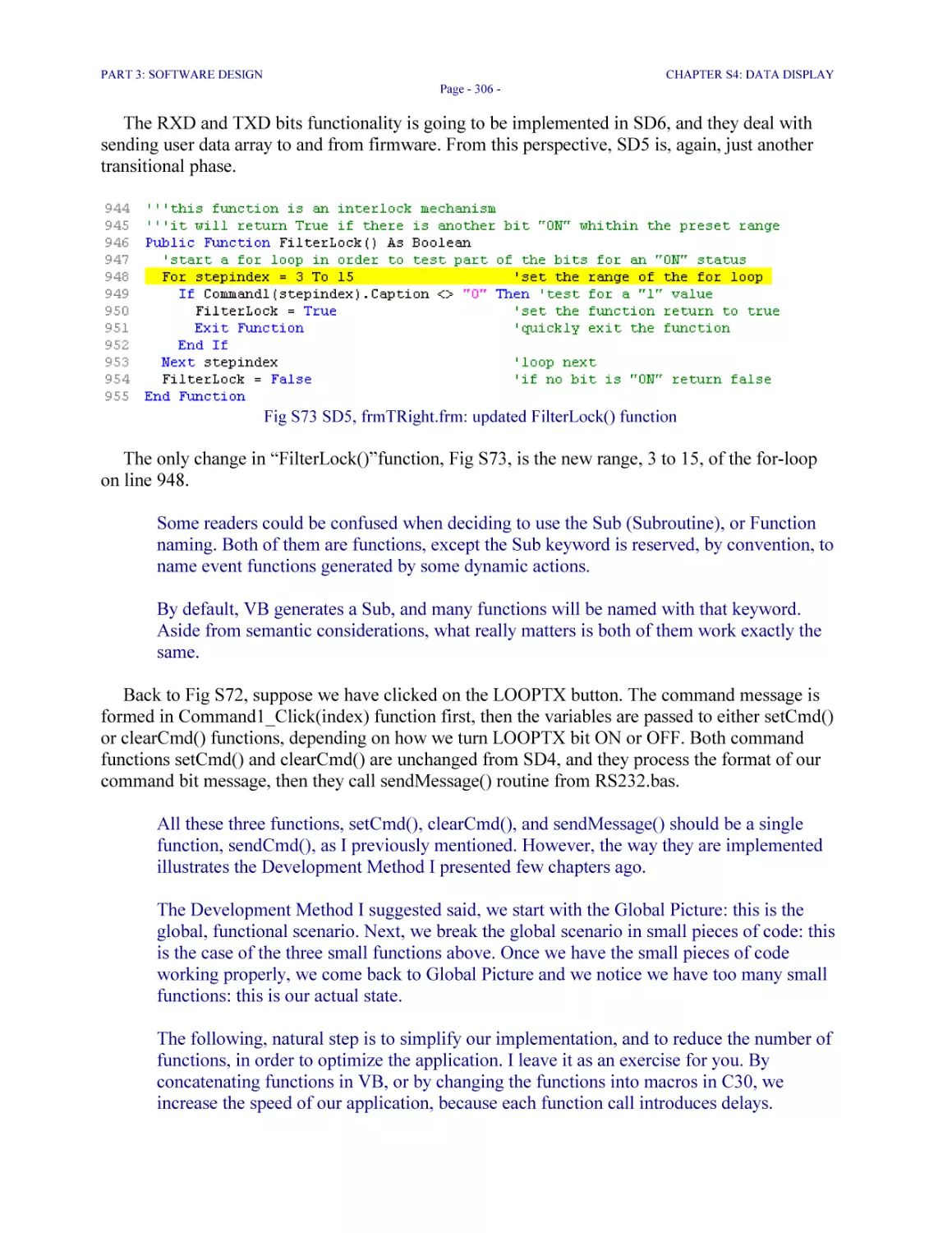
specific sequence of 0s and 1s. I used the 8 bits register for exemplification only, but it could be
16, or 32 bits as well.
Now, take a look at what one 1 and one 0 actually mean for each electrical cell of register x.
Physically, a 1 is a closed electrical path, while a 0 is an opened circuit. That means, a word of
data we write in our program, the decimal 51, takes the physical form of eight electrical switches,
some opened and others closed, in a physical register, somewhere inside the microcontroller.
Those opened or closed switches will enable or disable other electrical circuits by applying to
them a voltage of +5 V for 1 logic, or 0 V for 0 logic.
The idea I would like you to remember is, the words we write in firmware, or in software, are
in fact configurations of ON and OFF physical switches. In a firmware program written in C we
build thousands or millions of switches, which also form thousands or millions of electrical
configurations inside the microcontroller.
Now, there is a lot of data specific to each controller machine, regarding memory allocation,
System Registers—also named “Special Function Registers” (SFR)—and many other parameters,
which it is mandatory to be very well known if you intend to write firmware in Assembler.
However, C firmware programmers need to know a lot less, in order to successfully perform their
job—“Victory!”
In C, we strive to consider the microcontroller a Black Box. All we need to know is, if we set a
SFR to a certain value, we enable a certain hardware module inside microcontroller. As for
Memory Allocation Structure, we simply do not care—except in some limit situations—because
the C30 compiler does the job for us.
The best starting point is always to download from http://www.microchip.com the latest DS
(Data Sheet) specific to the microcontroller machine used: that is dsPIC30F4011 microcontroller,
in our case. For Hardware Design we need only the Microchip document named “DS70135B”.
Please download that file and study it a little. You will need it whenever starting a design of your
own with dsPIC30F4011 controller, and I will refer to specific Sections in DS70135B, in order to
help you find your way around.
From DS70135B (this is 70135b.pdf at the present time) we find out the specifications of the
dsPIC30F4011 controller, and I will point to some of the most important. Now, the first thing I
want you to note is, dsPIC30F4011 controller is pin and function compatible with dsPIC30F3011.
The difference is, dsPIC30F4011 has two times more memory and a CAN (Controller Area
Network) driver. For us, dsPIC30F3011 is a perfect replacement on the future LHFSD-HCK—
and it is almost 1.5 USD cheaper—although there is still a long waiting period to get them from
Microchip for the time being.
PART 1: HARDWARE DESIGN
CHAPTER H1: MICROCONTROLLERS
Page - 30 -
Please be aware the dsPIC family of microcontrollers are the latest, and the most advanced
products developed by Microchip. In fact, not all controllers of the dsPIC family are fully
integrated in production, at this time, November 2004.
General presentation of the dsPIC30F4011 enhanced Flash 16-bits controller:
1. dsPIC30F4011 has a processing speed of maximum 30 MIPS (Mega Instructions Per
Second), which means the internal clock runs at 120 MHz. The hardware architecture is a
modified Harvard one, and it requires four clock ticks to increment the Instruction pointer.
Please note: all dsPIC controllers come in two versions: working at 30 MIPS and at 20
MIPS, and they are marked correspondingly with 301 or with 201 on the package. The
price of the controllers is different in each case;
2. The Instructions Register is 24 bits wide with 16 bits holding the data, and 8 bits
allocated for commands. The hardware word is 16 bits wide, or two bytes, same as the
Data Bus. That defines dsPIC30F4011 as a 16 bits machine;
3. There are 30 interrupt sources, and we will discuss more about them at firmware
design-time;
4. The supply voltage could be anywhere from 2.5 V up to 5 V regulated voltage;
5. There are 30 I/O (General Input Output) pins capable of sourcing or sinking up to 25
mA each. Now, please be very careful and never use the processor to drive power loads,
although it is perfectly capable of doing it. Even more, our dsPIC30F4011 is capable of
dissipating up to 1 W of power, which is enormous; still, you should never use it to drive
power loads. The reason is, dsPIC30F4011 is an intelligent part in any circuit, and it must
continue performing its functions the best way possible, even in critical conditions. In
addition, it is the most expensive electronic component, and its life needs to be protected
and extended as much as possible. The simplest power driver takes only one transistor and
one resistor—maximum ten cents US—to drive a load of up to 600 mA. We will
implement few power drivers on the LHFSD-HCK;
6. There are five 16 bits timers—very important—and they may be paired into 32 bits
timers. We are going to work with few of those timers in firmware;
7. For communications, we can use two UART (Universal Asynchronous Receiver
Transmitter), one built-in SPI (Serial to Peripheral Interface), one I2C® (Inter Integrated
Circuit), and one CAN (Controller Area Network). Unfortunately, we will implement only
UART2 of the built-in communications modules, and we will have to build a custom SPI
driver. We cannot use the SPI built-in hardware module because some of its pins are going
to be dedicated to ICD2 control;
8. Six pins are PWM (Pulse Width Modulation) Outputs;
PART 1: HARDWARE DESIGN
CHAPTER H1: MICROCONTROLLERS
Page - 31 -
9. Nine pins are connected to the 10 bits Analog-to-Digital Converter module, working
at 500 Ksps (Kilo samples per second);
10. Because dsPIC30F4011 is a dsPIC Digital Signal Controller, it is capable of very
fast mathematical operations, and that is very good news for us;
11. To end, dsPIC30F4011 has 48 Kbytes Flash Memory, and 1 Kbytes EEPROM.
H1.2 Microcontroller’s Pins
It is clear our microcontroller has many built-in attractive functions, and the first thing to do is
to identify to which pin they are assigned. Next, we will design the hardware circuits connected to
particular pins, and that design is going to be implemented forever on the PCB board. That is the
reason why, although Hardware Design it is an easy and relatively relaxing task, it is also very
demanding because there is no margin for errors. In firmware and software things may be changed
in no time, at any time, but a hardware circuit is there to stay! If we misjudge at hardware designtime, it will costs us money, and a lot of time to fix errors.
The footprint of a microcontroller plays an important role in deciding on implementing a
particular controller in a new application. To exemplify, my intention was to write this
book based on the top product built by Microchip, which is dsPIC30F6014. I worked with
that controller for few months, and I felt quite comfortable with it. However, because
dsPIC30F6014 comes in 80 pins TQFP (Thin Quad Flat Pack) package, and it is a SM
(Surface Mount) component, I decided to use the closest controller that comes in a DIP
package: it happened to be dsPIC30F4011.
I had few good reasons for my decision, and I will point them out for you. An 80 pins
TQFP processor requires SM technology to work with, and that is way beyond the
resources of beginner designers—not to mention it is also more expensive. Replacing a SM
controller soldered on the PCB is very difficult, and it requires sophisticated and
specialized equipment. We could overcome that problem at design-time, in part, but the
corrective actions are also expensive. In contrast, I used a standard socked to mount our
DIP 40 dsPIC30F4011 controller, which means we can quickly change it in case of
damage.
The Through-Hole technology and the DIP sockets should always be used during the
Project Development phase, whenever possible.
For me, dsPIC30F4011 was a new controller when I started this book, but the beauty is, all
Microchip machines—this “machine” term is frequently used to name controllers or processors—
are almost the same: if you know one well, you know them all. I suspect that aspect is particularly
encouraging to beginner designers. Now, my belief is, it is easier to start learning on a controller
of the most advanced range, because you will have no problems later, when working on any lower
ranking one.
PART 1: HARDWARE DESIGN
CHAPTER H1: MICROCONTROLLERS
Page - 32 -
The remarkable difference of the new dsPIC family of microcontrollers is, they work at 16 bits
word and Data Bus size, while the rest of the Microchip controllers work at 8 bits—well, the vast
majority of them. That means the default firmware variable is the integer for the dsPIC family,
and char for the 8 bits controllers. Of course, and increased Data Bus size will also count as
increased processing speed of mathematical operations. In terms of communications, only the
parallel type is able to benefit of the increased Data Bus size, because the serial ones still deliver
the information one bit at a time—that means an increased Data Bus size brings little or no
improvement to serial communications speed.
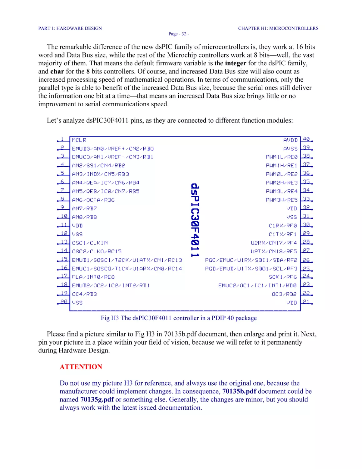
Let’s analyze dsPIC30F4011 pins, as they are connected to different function modules:
Fig H3 The dsPIC30F4011 controller in a PDIP 40 package
Please find a picture similar to Fig H3 in 70135b.pdf document, then enlarge and print it. Next,
pin your picture in a place within your field of vision, because we will refer to it permanently
during Hardware Design.
ATTENTION
Do not use my picture H3 for reference, and always use the original one, because the
manufacturer could implement changes. In consequence, 70135b.pdf document could be
named 70135g.pdf or something else. Generally, the changes are minor, but you should
always work with the latest issued documentation.
PART 1: HARDWARE DESIGN
CHAPTER H1: MICROCONTROLLERS
Page - 33 -
Note this please: each pin has a number and some code letters, which describe its functions. For
example, pin number 10 has two functions: as Analog Input, named AN8, and as a general I/O pin,
named RB8. When a pin has multiple functions, you need to enable those functions you want to
work with, in order to disable other functions of higher priority. As general rule, the right-most
functions have greater priority.
You can find detailed information about pins and their functions in 70135b.pdf, and you do
need to study that document, especially the parts I am pointing at. Please look again at Fig H3, and
let’s go together over the coding of the most important functions:
1. MCLR with a bar line above—you cannot see it in my picture—is Master Clear Reset
pin. The bar means that pin needs to be wired high, to VDD (+5 V). Pin number 1 is used
as “controller hardware reset”, and that is a function which we are going to use a lot,
during firmware and software development;
2. AN0 to AN8 are Analog Input channels connected to the 10 bits Analog to Decimal
Converter (ADC) built-in module. We are going to work with ADC;
3. CN0 to CN7, CN17 and CN18 pins have Input Change Notification capability. Each
of those pins generates an Interrupt if its state—the DC voltage level—is changed. In order
to facilitate Input Change Notification, there are programmable weak pull-ups circuits built
inside the microcontroller;
4. EMUD and EMUC (Emulator Data and Clock) are auxiliary circuits used for
programming and Debugging. They are designed to work with MPLAB® ICE 4000 InCircuit Emulator, and we are not going to use them;
5. INT0 to INT2 are three External Interrupt pins. Those pins work similar to the CN
ones, but they are a bit more complex since they can detect, selectively, pin’s status change
on either the rising or the falling edge. In addition, they are used to “wake-up” the
microcontroller from “sleep” mode. The INTx function is excellent for monitoring external
pulses. We will analyze INTx function in details at firmware design-time;
6. PWM1L, PWM1H to PWM3L, PWM3H are Pulse Width Modulation Outputs. The
dsPIC30F4011 machine is particularly designed for motor control applications, and those
pins are connected to complex, built-in PWM hardware driver modules. We are going to
wire all those pins to a stepper driver IC, then to a connector. If someone intends to use
another driver, say for a brushless DC, simply pull the stepper driver IC out of its socket,
then add few smart jumpers to reconfigure the circuits. Alternatively, a small PCB board
may be designed to replace the jumpers;
7. OSC1 and OSC2 are external oscillator clock inputs;
8. PGD and PGC (Programming Data and Clock) are used by ICD2;
PART 1: HARDWARE DESIGN
CHAPTER H1: MICROCONTROLLERS
Page - 34 -
9. RB0 to RB8 are Port B digital I/O pins; RC13 to RC15 are Port C digital I/O pins; RD0
to RD3 are Port D digital I/O pins; RE0 to RE5 plus RE8 are Port E digital I/O pins; and
RF0 to RF5 plus RF8 are Port F digital I/O pins. Altogether, there are 30 digital, general
I/O ports. The I/O notation stands for Input or Output. Each I/O port may be configured as
either Input or Output, and we can change that configuration during run-time;
10. SCK1, SDI1, SDO1, and SS1 are: Clock, Data In, Data Out, and Slave
Synchronization pins of the built-in SPI module. For our controller 30F4011, SDO1 and
SDI1 pins are shared with PGD and PGC pins. Because ICD2 is going to be connected to
those two pins, we cannot use the built-in SPI driver. The good news is, we are going to
build a custom SPI driver on other pins, and we will implement all SPI functions just as
well.
11. U1RX, U2RX and U1TX, U2TX are UART1 and UART2 Receive and Transmit
RS232 pins. We will use UART2 pins to wire the RS232 serial driver. You should note
UARTx modules are capable of implementing additional serial communications protocols,
such as RS488 for example.
12. VDD and VSS are Positive and Ground supply for the DC logic voltage. VREF+
and VREF- are Analog Positive and Negative Voltage Reference, and we are not going
to use them. The Analog Voltage supply is AVDD and AVSS. Because we have only few
analog Inputs, the AVDD and AVSS pins are simply connected to VDD and VSS, in our
case. However, it is recommended to connect a second, independent power supply to
AVDD and AVSS, in order to keep the Analog Reference Voltage to its superior limit. In
addition, please be aware the Analog to Decimal Conversion built-in module it is a powerhungry one.
There are few more functions implemented on dsPIC30F4011, but they are outside the scope of
the LHFSD book. In consequence, I save them for your individual study.
Before starting a new design, you need to analyze few types of controllers, based on their
functions, in order to select the best one. Of course that experience could play a major role when
selecting a new controller, but experience alone is always shadowed by knowledge. Knowledge is
gained after serious, good quality study.
In fact, Hardware Design is based on designer’s ability to memorize technical data, and on
his power of logic. When I start a new application, the first thing I do is to gather as much
information as I can: technical Data Sheets, software help files, and few good books if
there are any. For example, although I worked for years with Visual Basic, and I have
many good reference books, I always buy few more when starting a new Project, and I
study the MSDN® (Microsoft Foundation Library) very well.
Knowledge it is never enough or sufficient, and we should strive to improve it
permanently.
PART 1: HARDWARE DESIGN
CHAPTER H1: MICROCONTROLLERS
Page - 35 -
Please do not bother too much if you do not understand all those new microcontroller functions
now, or if they may seem too complex, because everything will become clear as daylight at
firmware design-time. In fact, this is the major draw back when starting working with
microprocessors: the beginner designer is simply overwhelmed by the amount of strange, new,
technical documentation. My advice is: “Do not panic!” Just be patient and read this book, and
you will see things will start making sense, without major efforts.
As for assimilating huge amounts of knowledge when studying a new processor, that is going
to become a routine task, and not even a difficult one, in time. It is the beginning that matters, and
you need to reach the level of trust that what you do will work well, no matter what.
H1.3 Application Notes
Microchip has on their website hundreds of Application Notes, suggestions, and even products
designed for a specific purpose such as KeeLoq® Secure Data Products, or rfPIC® Radio
Frequency Controllers. Many controllers have built-in hardware and software drivers for direct
connection to TCP/IP, and you could program them to automatically send and read *.html or
*.xml files over the Internet.
One important field of applications is the Automotive one, because Microchip controllers have
built-in CAN and LIN communications modules. That allows for data exchange with the OnBoard Vehicle Computer. Further, we could use that data for many useful purposes, for display or
calculations, or we could even modify it in some benefic ways, and then send it back to the
Vehicle Computer—much caution with this last one, please.
Many industrial, laboratory, medical, or even personal instruments may be designed or
improved using Microchip controllers, and you could use some advanced features such as USB,
infrared, DSP, and even speech recognition for that. There are in high demand these days SMPS
(Switched Mode Power Supply) battery chargers, and Voltage Bandgap circuits, for example.
Of course, there are lots of ICs built by many companies—they are named ASIC (Application
Specific Integrated Circuits)—with built-in hardware modules performing all previously
mentioned applications, but they could be easily replaced by the firmware intelligence of a 1 USD
Microchip controller, and made even better. For example, using a microcontroller to drive a
Battery Charger is way more efficient than buying a specially designed IC performing that
function, despite the costs associated to controller’s development tools. The reason for that is, the
microcontroller version may be improved to adapt to many ranges of battery chargers, and it
allows for many additional, intelligent functions. The end result could be a totally new product,
better than all other products existing on the market!
To finish, the creativity power depends on your imagination only, but you do need to master the
design tools you work with, and to know microcontrollers. Here comes this book: prepare yourself
to become a GURU in microcontroller design!
PART 1: HARDWARE DESIGN
CHAPTER H1: MICROCONTROLLERS
Page - 36 -
H1.4 Prices and Footprints Considerations
Microchip Flash controllers come in various sizes, and their number of pins is ranging from 6
to 80. That is a good thing, because the price is relatively proportional to the number of pins. The
cheapest microcontroller, PIC10F200 with 6 pins, is about 0.65 USD. Those small, 6 and 8 pins
controllers are real technological monsters and, when you will start working with them, you will
be amazed of the amount of intelligence they can handle.
For volume production orders you could get a lot better prices on controllers. The most
expensive is dsPIC30F6014 at roughly 20 USD, but it comes with the DCI (Data Converter
Interface) included, used for advanced DSP applications. If you do not intend to use DCI, you
could select a cheaper controller, for example dsPIC30F6013 at 18 USD. Please be aware those
two controllers have an enormous amount of memory and processor power at 16 bits. The first
Windows OS versions were written for 16 bits Intel® machines.
The real beauty comes when you look at the prices other microcontroller brands have, and at
the costs associated to their development tools. Overall, Microchip is still the cheapest alternative
available to start hardware and firmware design, and that explains their explosive development
during the last ten years.
The footprint of the controller is an important factor when deciding on a new design, because
Surface Mount technology is more expensive to deal with, although it will save you precious real
estate on the PCB. That is no joke, because the PCB itself is one the most expensive component.
For Development however, it is better to work with DIP (Through-Hole) microcontroller
footprints and use appropriate IC sockets, because controllers could be easily destroyed while
testing and they need to be replaced fast.
About one year ago I designed a PCB using dsPIC30F6014—it comes as an 80 pin TQFP
SM component only—and I was bold enough to consider I would never burn it. Vanity! I
managed to burn that controller—well, it was a pre-production model—and I had lots of
troubles replacing it on the PCB.
Anyway, the point to note is, surface mount components should be considered for Production;
for Development, Through-Hole components are way better. That is, of course, if it is possible
because, unfortunately, many components today are supplied only in SM, or in Through-Hole
footprints.
Microcontrollers with small pin count could be very cheap, and they should be used for
intelligent, local drivers, because the price of the electronic components must be reduced as much
as possible, while gaining in board intelligence. Always consider designing multi-controller PCBs,
because that is a solution which could save you lots of money, in the long run. Now, if you do
design a multi-controller PCB, try using small controllers of the 6 and 8 pins type to handle local
drivers.
That money saving consideration is almost an obsession for hardware designers, because a low
product price means both higher benefits and increased competitiveness. The real power when
PART 1: HARDWARE DESIGN
CHAPTER H1: MICROCONTROLLERS
Page - 37 -
designing hardware logic with microcontrollers resides in their firmware, which can be easily
changed and upgraded for the Flash family, using the ICD2 module. The main design rule you
need to remember is, implement more functionality in firmware, which you can change whenever
it is needed, while designing the simplest and cheapest hardware circuits possible.
In the coming chapters we will develop gradually the LHFSD-HCK. Each new chapter will
deal with one function, or hardware module, at a time.
SUGGESTED TASKS
1. Build yourself a Technical Library
For this task, start with building a folder on your PC named Technical Library, TLib,
or something appropriate. Inside that folder add few directories, like Controllers,
Voltage Regulators, Resonators, Sensors, Transistors, etc. Next, download the
DS70135B document from Microchip and store it in your
TLib>Controllers>Microchip>dsPIC30F4011 folder.
Now, you have added your first Data Sheet to your Technical Library. Over the years it
will be stuffed with useful documentation, and it will become an excellent, valuable
reference.
Save your Technical Library regularly on a dedicated CD-RW.
***
CHAPTER H2: OSCILLATOR CIRCUITS
My way of starting a new design is this: I build again almost each schematic symbol and PCB
footprint I need. I do it because I started many designs with new processors, which did not exist
into the schematic components libraries, at that time. In addition, I noticed the available library
components look different than real things do: they are stylized, or the power pins are missing
because they are wired automatically. I prefer my schematic components to look exactly as they
are in reality, and I want to see all pins and all wires in my schematics. Of course, it is time
consuming to design a processor schematic component and its PCB footprint, but it is a lot safer.
Experience Tip #2
Most processors start the pin count from the marked corner, and that is in fact the standard
way of numbering the pins on ICs. It happened I needed a 14x14 mm, 80 pins TQFP PCB
footprint for Protel®, and I was very happy when I found a standard one. I inserted that
footprint into my PCB design, after checking the overall physical dimensions, only. The
problem was, I had to zoom-in two more times in Protel, to actually see the numbers of the
pins properly, and I didn’t do it. I simply assumed pin number one was the standard one, at
the marked corner.
Because I was working in a rush—as always—I built the PCB with Autorouter, and then I
sent it to be populated. When the board came back to me, I measured the isolation to
ground, then I applied power to test it, and . . . nothing worked! I had no oscillator clock
pulses. I checked again the controller traces on the PCB, and everything looked fine, until I
noticed my mistake. The standard footprint I inserted in my PCB was starting the pin count
from the middle of one side, although it had the standard marked corner!
It took me two weeks of hard work—with no pay—to repair that mistake. Since that
experience, I never complain about losing two or three hours building my own schematic
and PCB footprints for the components I use.
H2.1 Oscillator Circuits
The first things we do when starting a new schematic are to insert the microcontroller
component, and then to wire the oscillator circuit. Many designers consider the oscillator circuit
the first, most important one.
There are at least five options we could use as clock pulse generator for dsPIC30F4011, and
same options are valid for many other Microchip controllers. The most common option is to use a
cut crystal oscillator and two load capacitors. Another one is to use a ceramic resonator, since it
has very good temperature stability, and the load capacitors are embedded. Excepting for the base
frequency itself—which may vary, slightly—a ceramic resonator is a very good replacement for a
PART 1: HARDWARE DESIGN
CHAPTER H2: OSCILLATOR CIRCUITS
Page - 39 -
crystal, because they are very stable in time and over large temperature variations. Ceramic
resonators need just a little more trust from designers, and they have the advantage of a smaller
footprint—not to mention their price is half of the crystal option. I use them generously, whenever
I can.
The third option is to use an IC clock driver—this is in fact a pulse-generator circuit. I never
consider that option too much, because it is comes with additional traces for power supply and
bypass capacitors, and it is a rather expensive alternative. The fourth option is to use an external
RC circuit: this is a poor choice, because it is quite unstable with temperature variations. The fifth
option is to use the internal RC oscillator built inside the microcontroller, and I highly
recommend this one for small pin count microcontrollers. I used internal RC oscillator many
times, with excellent results.
When selecting the oscillator circuit, you need to take into consideration the application
requirements for an accurate clock. Only very high speed communications, timing circuits, and
advanced DSP applications call for a fixed, stable clock frequency—hence of a cut crystal
oscillator. For anything else, the cheaper solution of a ceramic resonator or even the internal RC
oscillator are quite sufficient.
H2.2 Crystal Oscillator Circuit
Because it is my professional handicap to use only the cheapest components in my designs, if I
can afford it, I will use a ceramic resonator on the LHFSD-HCK. However, I present the cut
crystal schematic circuit for those readers who will decide to use one.
Fig H4 Cut crystal oscillator circuit
PART 1: HARDWARE DESIGN
CHAPTER H2: OSCILLATOR CIRCUITS
Page - 40 -
In Fig H4 you can see the schematic component I built for dsPIC30F4011—there is no
dsPIC30F4011 in the schematic library I use—and a crystal oscillator circuit running at 7.3728
MHz. I recommend this value, because dsPIC30F4011 has 4, 8, and 16 times internal hardware
PLL (Phase Lock Loop). More precise, 16 times PLL in this particular case means:
16 * 7.3728 MHz = 117.9648 MHz
By using the setting of 16 times PLL in configuration fuses, in firmware, the internal clock
frequency of 117.9648 MHz is equal to 16 times crystal oscillator frequency. Now:
(1s/(117.9648 * 106)) * 4 = 33.90842 ns
One instruction cycle lasts for exactly 33.90842 ns, and it is 4 clock ticks in length. The 117
MHz frequency is very close to the maximum internal frequency of 120 MHz, the dsPIC30F4011
controller is rated for, and 33.9 ns is the time it takes to execute one instruction cycle. The real
beauty is, 7.3728 MHz may also be used with 8 times internal PLL for a clock frequency of
58.9424 MHz, or with 4 times PLL at 29.4912 MHz.
Please note the ground symbol I used: it has the net name of DGND (Digital Ground). That is a
good practice to separate the digital ground—which is very noisy—from the smooth analog
ground. Of course, both grounds are going to be connected together, in one single point on the
PCB board. In consequence, we are going to use a dedicated analog ground, GND, and it is going
to be the ground of the unregulated +9 V power supply, and the DGND for the +5 V regulated
voltage circuits.
For those readers who intend to become professional hardware designers, I suggest
studying carefully the complicated rules of implementing the analog and digital power and
ground planes, and of designing multilayer PCBs—the employers are rather severe about
those issues. On the other hand the employers are also quite right, because the power and
ground planes, together with multilayer PCBs, are some of the most important weapons of
fighting the devious EMI (Electro-Magnetic Interference).
The second thing I would like you to note is, I used port symbols instead of wires. In Fig H4
the nets take the names of the port symbols I used, and they are not assigned default values. That
is the best method of wiring the schematic, and it also allows for a cleaner design, and easier to
trace wiring errors.
Please be very careful when changing the cut crystal oscillator to another value. I noticed the
crystals manufacturing companies and Microchip specialists have a slightly different opinion
about the value of the load capacitors C1 and C2. The rule is ALWAYS manufacturer’s
specifications take precedence over any other regulations and rules, even if those rules are official,
regulatory ones.
In our particular case, however, things are bit more complex, because Microchip is also a
manufacturer, and their specifications are even more important, since the microcontroller is the
most important component on the PCB.
PART 1: HARDWARE DESIGN
CHAPTER H2: OSCILLATOR CIRCUITS
Page - 41 -
The value of 20 pF of the load capacitors is the value recommended by the crystal
manufacturer, and it is skillfully selected, because there are no 20 pF capacitors! We can find 18
pF and 22 pF but no 20 pF. That was the reason I contacted the manufacturer. I was told I have to
calculate the capacitance value of the connecting traces with a specific formula—long and
ambiguous enough to work with it for two days, and to remain unsure of the results until this very
moment.
Well! The load capacitors should be as close as possible to the crystal, and the oscillator circuit
should be as close as possible to the microcontroller, on the PCB board. The connecting traces
should be not very thick, in order to reduce stray capacitance. In addition, you may want to keep
the PCB traces connecting the oscillator circuit to the controller pins very short, because they are a
strong source of EMI.
H2.3 Ceramic Resonator Oscillator Circuit
Fig H5 Ceramic Resonator circuit
In Fig H5 we have a ceramic resonator oscillator circuit, which comes in a smaller footprint
and with embedded load capacitors, when compared to the cut crystal option. I am always tempted
to use ceramic resonators instead of crystals—unless I have no choice—because I like their price,
the footprints, and their temperature stability. There is, however, another aspect to consider.
The dsPIC30F4011 machine comes in two flavors, as most dsPIC controllers do, in 20 MIPS
and 30 MIPS versions. The 20 MIPS version is cheaper, and I intend to use it for the LHFSD-
PART 1: HARDWARE DESIGN
CHAPTER H2: OSCILLATOR CIRCUITS
Page - 42 -
HCK. Now, I am thinking some readers would like to use a 30 MIPS machine: because we will
provide a DIP socket on the PCB board, it is going to be very easy to replace the microcontroller.
Now comes the oscillator problem: a Through-Hole ceramic resonator is not too difficult to
replace, but for the crystal oscillator circuit things are a lot more difficult, since the load capacitors
also need to be replaced with new, precise values.
The design requirements of the LHFSD-HCK are not very tough. I am going to use a ceramic
resonator type ZTT 10M, and I will select 8 times PLL configuration fuses settings in firmware, in
order to work at 80 MHZ or 20 MIPS. That will make our instruction cycle last for exactly 50 ns,
which is a nice, round value. If some readers intend to use a 30 MIPS machine, there are few
options available, like ZTT 30M, 15M, or 7.5M resonators—or something very close to those
values— and 4, 8, and 16 times PLL settings. Just unsolder the 10M resonator, and solder the 15M
one back, for example. That is all!
You have noticed, probably, ceramic resonators are build to cover the entire range of the
cut crystals, since they are designed, in fact, to replace them. In this respect, ZTT 7.37M is
the replacement for a cut crystal of 7.3728 MHz, but the strange thing is, it is very difficult
to procure ceramic resonators.
For some unnatural reasons the electronic components distributors offer a limited range of
ceramic resonators, while the cut crystals offer is simply overwhelming. Even worse, I
contacted a ceramic resonator manufacturer and I tried to obtain the 7.37 MHz ceramic
resonator. I was told I could get them only if I buy a minimum of 10000 pieces, and wait
for about two months of production time.
That is a perplexing situation, because ceramic resonators are a lot easier and cheaper to
manufacture; still, the manufacturers prefer building the expensive and demanding cut
crystals instead. Well, this is real world!
One more thing to note here is the high internal frequency the dsPIC microcontrollers have,
because they work at 4 times, 8 times, or 16 times oscillator frequency. That high internal
frequency comes with many problems associated, among which heat dissipation is one of the most
important.
About one year ago I noticed the dsPIC30F6014 microcontroller I was working with
becomes rather hot at 117 MHz and 5 VDC, and I contacted Microchip technical support.
They told me that, indeed, at maximum frequency dsPIC30F6014 becomes fairly hot, and
they advised me to use a heat sink. That little piece of hardware solved my problem, but it
came with additional costs—the heat sink I used was about 1.7 USD.
The heat dissipation problem comes as a natural development, because the dsPIC30Fxxxx
family of microcontrollers works at 120 MHz and at 5 V DC. It is the 5 V DC logic level that
creates problems, because at 120 MHz a 3 V DC logic level heat dissipation is cut in half.
However, the fact the dsPIC30Fxxxx controllers work with 5 V is appealing to many designers—
and to me—since it allows for larger ranges of the DC logic voltages levels, and hence they can be
PART 1: HARDWARE DESIGN
CHAPTER H2: OSCILLATOR CIRCUITS
Page - 43 -
easier detected. Besides, many logic ICs work only with 5 V DC logic, since it is the (old)
standard value. The trend today is to implement 3 V, and even 1.5 V DC logic voltage levels.
Our LHFSD-HCK is going to work with 0 V and +5 V DC logic voltages, but I do encourage
the readers to try designing it at 0 V and +3 V DC, for the sake of the experiment. As for heating
problems, we will have none, because we work at only 80 MHz internal frequency, and then the
DIP 40 package is bulky enough to act as a perfect heat sink.
The two parts in Fig H5 are the first components we add to our schematic page, and to the
LHFSD-HCK Project. Now, we do have the clock oscillator connected to our controller, but
nothing works because our controller has no power.
The next, natural step of Development is designing the power supply, and this is exactly what
we are going to do in the coming chapter.
SUGGESTED TASKS
1. Compare crystals oscillators and ceramic resonators
Find and download the DS of a 10 MHz cut crystal, and of a similar ceramic resonator.
Store both DS in your Technical Library, each in a separate folder, then study and
compare electrical specifications of the two components.
I am certain you will feel rather confused about the incompatibility of the technical
data. Fact is, manufacturers give us, intentionally, technical data particular to their
company and to their products, only. In consequence, it is almost impossible to
compare technical characteristics of two similar parts, built by different companies.
The next step is to go on the Internet and find few articles about resonators versus
crystals. That should clear all your doubts about using ceramic resonators to replace
crystals.
***
CHAPTER H3: POWER SUPPLY
The second circuit a processor needs in order to work is regulated voltage, power supply. At
this moment, I am certain some readers would ask: “Why do we need regulated voltage?”
Although the microcontroller machine is a robust enough component to stand voltage variations
from +2.5 V to +5 V, without major problems, it is mandatory to supply it with constant, regulated
power. The controller is, in fact, a very delicate component, and for best performances its DC
logic levels need to be constant.
The Analog to Decimal Conversion module is a sufficiently good reason for constant power
levels, but you should also think of other modules inside. For example: when one module starts
working it will draw additional power in a very short time interval, and that could create a voltage
sag if the power is unregulated; in turn, that voltage sag will surely perturb neighboring circuits.
The rule is, controller’s power must be of good quality and plenty of it.
H3.1 Voltage Regulators
The most common power delivery method is to come to the LHFSD-HCK with unregulated
voltage of 7 V up to 34 V DC from an external DC source, then to regulate the voltage down to 5
V (or to 3 V) and we will do exactly the same.
Voltage Regulators are small ICs, usually with three pins, and they are hiding inside fairly
complex circuitry. Generally, they are grouped into “Linear Voltage Regulators”, and “SwitchMode Voltage Regulators”. The regulators belonging to the last group are more expensive, and I
will let them for you to study. Linear Voltage Regulators come again in few flavors: positive or
negative—yes, we could have (–5 V) and (0 V) DC logic voltage levels—standard, or LDO (Low
Voltage Dropout).
Because we do not have special requirements for LHFSD-HCK power supply, I decided on a 5
V, positive, linear, standard Voltage Regulator.
When designing power supplies you need to consider carefully Voltage Regulator heat
dissipation. Our Voltage Regulator has about 2.2 V internal voltage dropout, which means it needs
a minimum of +7.2 V in order to output constant, regulated +5 V. Now, if we multiply that 2.2 V
internal voltage dropout by the maximum current of 1A, the result is an enormous quantity of 2.2
W of power: this is pure heat, and it has to be dissipated somehow.
The good news is, we are not going to use 1 A of current, and I estimate now we will use even
less than 100 mA on the +5 V circuits. When the board will be assembled and working, I will
measure the average current consumption.
PART 1: HARDWARE DESIGN
CHAPTER H3: POWER SUPPLY
Page - 45 -
You probably ask why the average and not the exact value of the current. Well, current
consumption is dependent on various functioning modes the controller has: in some modes it will
draw more current than in others. I will try to measure the current consumption in the worst-case
firmware scenario, but even that one will be relative, because we do have the possibility to add
more firmware routines anytime we want, which will influence current consumption.
To come back to our Voltage Regulator, I decided on a D2PAK footprint, because it will allow
me to use the PCB board itself to dissipate some heat. To be honest, I am not totally satisfied with
that solution, because the D2PAK footprint is a surface mount component. Another option is to
use a TO-220 footprint, which is a through-hole component, and I could lay the regulator on the
PCB in order to dissipate the heat. But—there is always a small “but” somewhere, somehow,
which ruins everything—the D2PAK footprint uses a smaller area on the PCB, and it doesn’t need
fixing in place with a screw, so . . . it is still the best solution.
Anyway, the part I am going to use is MC7805 and it is capable of delivering up to 1 A at +5
V. Of course that amount of current is way more than our needs are, but I would feel even better if
our Voltage Regulator would deliver 3 A, as some TO-220 components do.
“Why that waste?” some would ask. In fact, there is no waste because the Voltage Regulators
have almost all the same price. On the other hand, the more current a Regulator is capable to
deliver, the more constant the regulated voltage will be when switching various circuits ON and
OFF. Generally, those Voltage Regulators that are capable to deliver more current are built to
withstand more heat dissipation without damage, when working for long periods of time at high
temperatures.
Overall, selecting a standard, linear Voltage Regulator is just a matter of deciding on one of the
many options available, with various technical specifications and having almost all the same price.
H3.2 The power supply circuit
If you take a good look at the microcontroller Schematic in Fig H4 or Fig H5 you will notice
many pins are connected to VDD, VSS, AVDD, and AVSS: that is because microcontroller
designers intended to isolate as many noisy circuits inside as possible. The Analog to Decimal
Conversion module requires its own power supply, although this is not mandatory. We will use
only one power supply for all circuits, and we will simply connect AVDD and AVSS to VDD and
VSS.
Please be aware, for those applications that make intense use of the analog function it is a good
idea to use a second power supply circuit, dedicated only to the Analog module, and identical to
the main one. In that case, you could build another ground, say AGND (Analog Ground), and it
needs to be connected to GND and DGND: again, all in one single point.
We will build a basic power supply circuit, as simple as possible, but perfectly suited for our
needs. My way of designing hardware is, I try to avoid complicating Schematics, unless there is a
good reason for that.
PART 1: HARDWARE DESIGN
CHAPTER H3: POWER SUPPLY
Page - 46 -
Fig H6 Power supply module
The first thing to note in Fig H6 is, we are going to use two voltage levels: +9 V unregulated
DC, and +5 VDD regulated DC. The unregulated voltage and GND (Ground) comes to our board
in DC-IN jack, from a 9 V/750 mA AC/DC wall adaptor.
The AC/DC wall adaptor comes with ICD2, and we will use it to power the LHFSD-HCK.
The AC/DC adaptor is needed to power ICD2 only when it is working with RS232 cable
connection; if the ICD2 works with USB connection it doesn’t need power, and we use the
adaptor for the LHFSD-HCK. I will detail this issue at firmware design-time.
Some circuits on the LHFSD-HCK are going to use the unregulated +9 V directly, and the port
symbol “+9V” is used to connect to them. This is a fair and nice method of using the unregulated
power supply to drive those components that are power hungry. Although I estimate a maximum
of 100 mA power consumption on +5 VDD circuits, it is possible we will draw more than 500
mA, directly, from +9 V net.
If you intend to use another voltage adaptor, a +12V one for example, please include a
power resistor in series, ahead of the +9V connection. Calculate the resistor with
R = Vd/I, where Vd is the voltage drop you need (3 V) ahead of the +9 V net. The power
rating of your resistor should be sufficient for our tasks, say 5 W; this is calculated with
Pr = R * I^2 or with Pr = Vd * I but it is a good idea to add something extra.
Calculate the current (I) as the sum of the current drawn by the stepper plus all other
circuits.
Diode D1 is needed to prevent accidental reverse voltages to VR, and to create a small 0.7 V
voltage drop, while C1 is used to filter smooth variations of the unregulated voltage. The 0.33 uF
value of C1 is the Voltage Regulator Manufacturer recommendation—OnSemi®. C2 and C3 are
ripple and spikes filters on the +5VDD net. Many designers consider the values of the pair 0.1 uF
and 1 uF to be the best pair of filter capacitors for many unexpected and various voltage spikes. I
worked in the automotive field where there is a wide range of anomalous voltage variations, and
this particular pair of filter capacitors always worked very well.
The P1 led indicator and its current limiter R1 are used to visually signal the existence of the
regulated +5 V on the board. That is a nice addition for the Development phase, although it is not
mandatory. The other resistor, JP of zero ohm, is in fact a plain jumper, and I used the fake resistor
PART 1: HARDWARE DESIGN
CHAPTER H3: POWER SUPPLY
Page - 47 -
symbol in order to achieve the ground nets separation. In this way, we create two grounds: an
analog one named GND and pairing with +9V, and a digital ground named DGND, pairing with
+5VDD. Without the JP fake resistor, any schematic and PCB editor software will issue errors and
warnings for naming the ground net with two different names.
As I already mentioned, I prefer using port symbols for connections, without actually drawing
the wires. Another advantage is, we can nicely group various components into hardware modules
on our schematic page, based on their functionality: this makes the schematic easier to read. Now
that we have a power supply circuit, we need to wire the controller to power and ground. The
connections to dsPIC30F4011 are shown in Fig H7.
Fig H7 Controller dsPIC30F4011 with oscillator, power, and grounding circuits
Please take a good look at Fig H7; by having more than one pair of power supply ports on
microcontroller, we are offered the chance to eliminate some internal microcontroller noise. We
do this with filtering and bypass capacitors C4, C5, C6, and C7. Although on Schematic C4, C5,
and C6 appear to be grouped together, on the PCB we should take care we place each of them as
close as possible to the power pins they need to monitor.
PART 1: HARDWARE DESIGN
CHAPTER H3: POWER SUPPLY
Page - 48 -
The simple power circuit in Fig H6 and the oscillator one in Fig H5 are sufficient to make our
microcontroller machine run, although it does absolutely nothing, except for running. We need to
add few nice, useful peripheral circuits, and we will begin doing it in the next chapters. To start,
the first, most important circuit is the ICD2 interface, because it allows us to take control of the
microcontroller.
SUGGESTED TASKS
1. Voltage Regulator footprints
Study for the most common Voltage Regulator footprints. Try finding one in a TO220F package (or footprint), which allows you to use the grounded metallic enclosure
(the box of your PCBs) as a heat sink for Voltage Regulators. Also, find out the
maximum current a TO-92 footprint Voltage Regulator could deliver.
2. Measure the output of the 9 V, AC/DC wall adaptor, and of the Voltage
Regulator
Measure the output of the 9 V AC/DC wall adaptor. Although we name it “unregulated
power supply” the wall adaptor has its own circuitry working to deliver constant,
filtered voltage. Note down the measured values, because you will need them for
precise analog calculations. When the LHFSD-HCK is finished, unplug the power jack
and measure the resistance to ground of the +9V circuits, and of the +5VDD ones. Use
the Voltage Regulator pins for that operation, and try reasoning about results.
3. Electrical Specifications of dsPIC30F4011
In DS70135B—again, this is in fact 70135b.pdf at this moment—there is one Section
dedicated to Electrical Specifications of dsPIC30F4011. Try finding a diagram that will
show the maximum current consumption related to internal frequency. There is a lot
more interesting data in that Section, including few topics about oscillator circuits
options—please study them.
4. Voltage and current sensing devices
We can measure many of the electrical characteristics of a running circuit using
resistors; for example: voltage, current, and current direction. Use the Internet to
discover the most common schematics used in each case.
***
CHAPTER H4: MPLAB® ICD2 INTERFACE
The first interface a Flash microcontroller needs is the programming one. There are few good
options to interface with Microchip controllers, but the cheapest is MPLAB ICD2 In-Circuit
Debugger. That simple Programming and Debugging tool is not the most efficient one possible,
but it is to be preferred to the alternative, which is ICE 2000® or ICE 4000® In-Circuit
Emulators—that is, if you will check their sky-high prices.
I started working with ICE 2000 emulator, and that little tool helped me a lot to understand how
Microchip controllers work. When I switched to ICD2, I noticed few limitations but, at that time, I
was expert enough to overcome them all. I am going to explain some techniques I use at firmware
design-time.
H4.1 The MPLAB® ICD2 Interface
The MPLAB ICD2 tool works in two modes: as Debugger or as Programmer. In Debugger
mode, ICD2 monitors the variables inside dsPIC30F4011, and it can Start, Halt, Restart, and
Reset the microcontroller. Most important, when Halted in Debugger mode, ICD2 can present us
the existing values in the System Registers: that information is mandatory in case of hard, difficult
to find bugs.
In Programmer mode ICD2 burns the firmware program on dsPIC30F4011, and then it must be
disconnected from the target board. Once ICD2 is disconnected, the controller starts executing the
firmware program immediately, and you can use the RESET button, pictured in Fig H8, to reset
the controller in hardware. If something goes wrong, you should hold the RESET button pushed,
until you reconnect ICD2. Programmer mode is useful when you have only one PC to control both
the ICD2 and the Visual Basic compiler: you can do it alternatively.
The ICD2 interface is the first, most important one, because it allows us to communicate with
our controller. Practically, without the ICD2 interface we would be forced to “burn” the processor
on a Programmer tool, and then use it as it is. Most of the time that is the option we use in
Production. In contrast, the ICD2 interface allows us to change the firmware program whenever
we want, which is the true Development mode. In some particular situations, however, it may be
we want to keep the ICD2 interface even in Production phase, in order to implement possible,
firmware upgrades. Because I worked on mostly prototype projects, I always keep the ICD2
interface on my PCBs.
Now, the ICD2 interface is very simple and it requires only a 5 pins connector, which needs to
couple with the ICD2 male cable connector ended in a 6-6 RJ-45 (Registered Jack type 45, with 6in, 6-out active contacts). That means we need the female connector on the LHFSD-HCK.
Sometimes I use to cut that RJ-45 male connector, and to replace it with a better connector, more
appropriate for my needs, but for our LHFSD-HCK Project I will leave the default connector
exactly as it is, and we will provide a female 6-6 RJ-45 coupling on our board.
PART 1: HARDWARE DESIGN
CHAPTER H4: MPLAB® ICD2 INTERFACE
Page - 50 -
ATTENTION
Please be aware the 6-6 RJ-45 female connector is a source of troubles. Things happen this
way: we compile a firmware project OK, then we Program it on controller. When ICD2
examines the burned program on controller it finds errors (ICD0161).
The Verification Errors causes are multiple, but I noticed the RJ-45 connector could be one
of them. That is the reason I used to replace the RJ-45 connector with a better one; not this
time though. For the LHFSD-HCK I prefer to use the PCB female connector
corresponding the one used with ICD2, because it is the recommended one. However, the
reader should be aware the spring contacts of the RJ-45 female connector do not offer very
good contacts.
If you will have problems burning your firmware programs on the LHFSD-HCK, I advise
you to apply some hand pressure on the R-J45 connector, to ensure a better contact—this
helped me many times. Do not be shy to touch the metallic contact traces of the connector
with your finger, because it helps. If you build your own LHFSD-HCK, I suggest cutting
the RJ-45 connector to LHFSD-HCK, and using a better coupling system.
Fig H8 The ICD2 interface
The ICD2 interface pictured in Fig H8 is, as I already mentioned, five wires coming into the
RJ-45 6-6 female connector. I added the color of the wires coming from ICD2, but you should
check them again for correspondence. The first wire, blue, connects to the MCLR pin. If you
remember, that pin needs to be wired high to VDD, and we do it in Fig H8 with the help of a 10K
resistor, R21. We use the push button RESET to momentarily ground MCLR, which will reset
dsPIC30F4011 electrically, and this will force the controller to restart a firmware program from
the very beginning with all System Registers cleared.
PART 1: HARDWARE DESIGN
CHAPTER H4: MPLAB® ICD2 INTERFACE
Page - 51 -
Positions 2 and 3 on the ICD2 connector—wires yellow and green—are +5 V and digital
ground. Although ICD2 has its own power source, it uses those two lines to detect the power
status on the target board. ICD2 works only if the target processor has good power levels and a
working oscillator.
Nets PGD and PGC—wires red and black—connect directly to microcontroller pins 25 and 26,
as it can be seen in Fig H9. We could use pins 25 and 26 for other functions, in parallel to PGD
and PGC, but we shouldn’t do that—unless we have to—because any functions on those pins
cannot be tested in Debug mode with ICD2. Besides, any hardware added on those 2 wires is
going to be a new source of ICD2 Verification Errors.
Unfortunately, dedicating pins 25 and 26 to the ICD2 interface, takes out the possibility to use
UART1 for RS232, but we can still use UART2, instead. The bad part is, we cannot use the builtin SPI module any more, because there is only one. I find SPI extremely useful, because most of
the simple ICs communicate only through SPI, including all controllers. This situation forces me
to implement a custom SPI hardware and firmware driver, but the true beauty is, the custom SPI
hardware driver requires just three general I/O pins: any I/O pins! That solves all our problems,
and we can keep pins 25 and 26 dedicated only to ICD2, which is a very wise thing to do.
Fig H9 dsPIC30F4011 with oscillator, power, and ICD2 interface connections
PART 1: HARDWARE DESIGN
CHAPTER H4: MPLAB® ICD2 INTERFACE
Page - 52 -
The way it is now, our Schematic has everything a Microchip Programmer tool needs, in order
to program dsPIC30F4011 or dsPIC30F3011 microcontrollers. At this stage we are able to write a
firmware program on our microcontroller, and to debug it using MPLAB ICD2 Debugger tool.
The only bad thing is, our program cannot implement any interesting function, because we have
no Input or Output circuits.
We need to start implementing few hardware modules based on functionality, and I would like
to point out the Design Method I use. For example, let’s take the oscillator and the power circuits
modules we have already designed: they are very simple and I am certain some readers feel rather
disappointed. They may have the feeling I do not reveal everything about those particular circuits,
and I cannot deny that: indeed, there is more to say about each previously presented circuit.
What you will learn in this book, in terms of hardware design, is the minimum necessary for
our LHFSD-HCK to work—this is to work very well. You will learn a method of hardware
design, which is one functional module at a time, and I will advise you on where to look for
additional information. Later, you will see that everything we design works very well, and true
complexity is added in firmware, and software—in fact, it must be added there.
If you need to work with another microcontroller, say with C18F458, you are aware now it has
to have a DS which describes, perfectly, everything you need to know; same thing for the
oscillator, or the power circuits. The information in the Data Sheets is the best source of
information you could find about a particular IC and about the schematic circuits it uses, in order
to implement them in your designs.
I have no intention to repeat the information you can find in technical Data Sheets, or in other
books about hardware design. Everything I write in this book comes from my personal knowledge
and experience, as professional. Just follow the way I work, and the reasons behind my actions.
My personal opinion is, hardware design does not need to be complex in order to work very well.
Coming back to our schematic, we have plenty of free pins left on dsPIC30F4011 and we
should use them the best we can. I am convinced there was nothing difficult up to this step, and
you will discover the same simple schematic modules during the next chapters.
SUGGESTED TASKS
1. Use the DS70135B document and study the dsPIC30F4011 sequence of
operations in case of controller reset
This information may be found in Electrical Specifications Section.
2. Find out what “Brown Out Reset” and “Watchdog” means
Use the same DS and discover the function, and the implementation mechanism of the
built-in Watchdog module. Study the Brown Out Reset sequences of operation.
PART 1: HARDWARE DESIGN
CHAPTER H4: MPLAB® ICD2 INTERFACE
Page - 53 -
3. Study the Configuration Fuses
Now that you know what Watchdog and Brown Out Reset mean, find references about
Configuration Fuses (also known as Configuration Bits). Study the available
Configuration Fuses options for dsPIC30F4011.
***
CHAPTER H5: THE RS232 INTERFACE
The RS232 is the first peripheral hardware module we implement on our LHFSD-HCK,
because it is very important. That interface is mandatory for us, since it is our intention to write a
Visual Basic software control application, and we need a simple, efficient way to send data
between firmware and software.
The RS232 interface could be implemented on the LHFSD-HCK in two ways:
1. Using a standard RS232 IC driver
2. Building a custom RS232 driver interface
H5.1 The RS232 Standard
We will see both of the above mentioned schematics but, first of all, we need to explain few
things about the RS232 standard. The name RS232 stands for “Recommended Standard 232”,
and it was introduced in 1962 with great skepticism. It is still in use today, successfully, and it will
continue to be used for quite sometime.
Almost all PCs have one or more dedicated serial ports named COMx and each of them can be
used for RS232. According to the standard, RS232 can work at maximum 256 Kbps (Kilo bits per
second) with line lengths of up to 15 m. However, standard specifications are largely overrun at
speeds of up to 10 Mbps (Mega bits per second) and way longer transmission lines, due to
technological improvements.
The only downsize the RS232 serial communications has is, it doesn’t carry power on the
communications lines, as the new USB protocol does. A “protocol” is a generic name, commonly
used instead of standard. All communications standards are divided into the hardware, and the
software protocols, and we need to take a closer look—although rather brief—at the RS232
hardware implementation protocol.
The RS232 hardware protocol uses two ranges of DC voltages to form the 0 and 1 logic levels:
(+3 V to +12 V) for a logic 0, and (–3 V to –12 V) for the logic 1. The voltage range between (–3
V and +3 V) is considered to be the indecision region.
The RS232 software protocol is a two-way type of communications— also named full
duplex—and it can be synchronous (in the same time) or asynchronous (one at a time). RS232
implements the notion of Baud (Baud rate per second), which refers to how fast a line could
change its polarity—it is similar to bps (bits per second), but not quite the same. The term Baud
honors the name of Jean Maurice Emile Baudot, an officer in the French Telegraph service at
the end of the 19th century, because he was the one to implement the Latin alphabet into a five-bits
code. Later, his work was extended into the ASCII code we use today.
PART 1: HARDWARE DESIGN
CHAPTER H5: THE RS232 INTERFACE
Page - 55 -
In terms of mechanical interface, the RS232 hardware protocol uses a male shaped 25 pins
connector for DTE (Data Terminal Equipment: the PC), and a female connector for the DCE (Data
Communications Equipment: the peripheral device). Excepting the standard 25 pins connector—
also named DB25—RS232 is more commonly used with 9 pins connectors, type DB9, and with a
reduced number of electrical lines. I will present only the DB9 electrical connections, and to those
readers who need to find out more about RS232 I recommend consulting the standard for DB25
connector, and many available tutorials on the Internet.
Please be aware all physical components on a PCB have a “front view”, and a “back view”: the
back view is reversed left to right, compared to the front one. That issue always brings troubles—
also named bugs. However, no matter of the mistakes, the ability to detect and replicate on the
laboratory bench the hardware and firmware bugs fast is very important. According to one of the
Murphy’s Laws, bugs will always happen, whether we want it or not, so good debugging skills are
mandatory for designers.
Fig H10 The RS232 DB9 connector: electrical connections
The electrical lines in Fig H10 are perfectly valid for one DTE, but we use a cable to connect
DTE to DCE, and that means we need to reverse the lines in order to have proper correspondence.
Think of the RS232 cable as having a middle where the signal lines are reversed.
Fig H11 The RS232 cable: reversed electrical connections
PART 1: HARDWARE DESIGN
CHAPTER H5: THE RS232 INTERFACE
Page - 56 -
I am certain you have noticed in Fig H11 I haven’t used all electrical lines to show cable
reversal. The reason for that is, in order to implement a good RS232 interface on our LHFSDHCK board—and on any other—three RS232 lines are quite sufficient. Those three, necessary
lines are: Transmitted Data, Received Data, and Signal Ground. In fact, most applications use only
those three lines.
H5.2 The RS232 Standard IC Driver Interface
There are few more important issues you need to know about RS232 which I haven’t
mentioned, but they are related to the firmware protocol and I am going to discuss them at
firmware design-time. With the minimum knowledge we have now, we can start designing our
RS232 driver module.
The first thing to do is to choose a good RS232 standard, hardware IC driver: it is MAX232N, a
16 pins DIP IC. Some might ask: “Why a 16 pins chip and not a 14 pins, or even an 8 pins one?”
Well, that is a perfectly valid question, and the answer is simply “Digi-Key®”. The standard
chip MAX232N with 16 pins DIP is the cheapest of all RS232 transceivers (transceiver means
transmitter-receiver) chips at 0.78 USD, and it has two channels of transmit/receive—one more
than what we actually need.
That is an important lesson hardware designers need to learn: unless you have a strong
budget for your Project, you will start your new designs by finding the cheapest
components, and then you implement your schematic around them.
Unfortunately, that also comes with many long hours spent on the Internet looking for
cheaper parts—sometimes hopelessly—but there is no way around it. If you do have a
strong budget, then you could look for the best and most expensive components that will
fit your schematic; say, of the extended industrial range, or even of military construction.
I do not have a strong budget and my means are quite limited, same as, I suspect, the vast
majority of the readers. I will apply the general hardware design rule, which says our product must
be build out of the cheapest components possible. Again I emphasize we should try implementing
more functionality in firmware and software, than in hardware.
When I refer to using the cheapest components it doesn’t mean our LHFSD-HCK is going
to be just some junk piece of hardware. When I say cheap components, I refer to cheaper
alternative parts, but take into account these parts are built according to the standards by
the best manufacturers in the World. Their electrical characteristics are checked and
rechecked for quality, and they are, in fact, the best components in their category.
The Digi-Key distributor I use, mostly, is well known for relatively high prices, because all
parts they sale are certified for quality—the best quality possible for their type.
PART 1: HARDWARE DESIGN
CHAPTER H5: THE RS232 INTERFACE
Page - 57 -
Nevertheless, I still name those parts “cheap” because I relate them to the extendedindustrial range, military, medical, and even to space-built technology.
Before actually starting Hardware Design, each part or component we select needs to be
thoroughly studied, and its technical documentation should be downloaded or printed, into a
special folder bearing the name of the project. Taking care of documentation is very important,
and you will notice that even a small project like LHFSD-HCK requires a lot.
The MAX232N driver is the industry standard type working at +5 V, and it is rated for 120
Kbps; however, many designers force that manufacturer specification, and I was told they work
perfectly well at double that rate. The chip has 16 pins and two pairs of receiver-transmitter
channels—which is not my voluntary choice—and I will use only one of them for the LHFSDHCK board.
Fig H12 The RS232 schematic module built around MAX232N driver
In Fig H12, the capacitors C8, C9, C10, C11, and C12 are all of 1 uF, and I took this value
from manufacture’s chart—Texas Instruments. Newer generations of drivers working at higher
baud rates, say the surface mount MAX232A, use 0.1 uF capacitors. The schematic module in Fig
H12 is done according to the manufacturer’s specifications. When dealing with an already built IC
driver there is not much room for innovation. The IC manufacturer has tested thoroughly the
product, and the driver performs the functions it was design to do, only if we respect
manufacturer’s recommendations.
There is nothing out of the ordinary in Fig H12, and it comes with slight additions to our
dsPIC30F4011 microcontroller Schematic. In Fig H13, I connected pin 27 to UART2-TX and pin
28 to UART2-RX nets, which means I am going to use the second UART firmware built-in driver
module of dsPIC30F4011. The first UART firmware driver, if you remember, cannot be used
because it works on pins 25 and 26, already assigned to the ICD2 interface. I could still use pins
25, 26 and UART1, if I had no other alternative, but this is not our case.
PART 1: HARDWARE DESIGN
CHAPTER H5: THE RS232 INTERFACE
Page - 58 -
Fig H13 Controller dsPIC30F4011 wired for RS232
I am certain you have noticed the RS232 interface implementation is quite simple when using
an RS232 IC driver. For those readers who want to experiment further, I will insert the Schematic
of a custom driver, built out of discrete components.
H5.3 Custom RS232 Interface
The great problem when dealing with the RS232 interface is the negative logic voltage level:
for a logic 1 we need a voltage between (–3 V to –12 V). We could build a power supply circuit to
generate –5 V, if we use two Voltage Regulators, one positive, and one negative, and if our
unregulated power supply covers the regulated voltage range plus the two internal voltage drops:
2 * 5[V] + 2 * 2.2[V] = 14.4[V] as a minimum. (15 V is a safe value)
However, it doesn’t make much sense to complicate our power supply circuit for one IC, which
will draw only few mA of power. On the other hand, the negative voltage exists on the
communications lines, as they come from PC. That aspect has determined many designers to build
RS232 circuits that “steal” negative voltage from the communications lines.
PART 1: HARDWARE DESIGN
CHAPTER H5: THE RS232 INTERFACE
Page - 59 -
The “stealing” circuit employs a polarized capacitor and a diode in order to properly perform
the job. Please be aware you cannot use the custom circuit, unless you communicate to a DTE that
is generating negative voltages.
Fig H14 Custom-built RS232 hardware driver
Note: in Fig H14 the circuit requires inverted logic signals in the firmware driver—in fact, this
is rather difficult to see on schematic, so just take my word for it. The way it works is this: the
C1capacitor steals and stores negative voltage from the transmit line helped by D1 diode, and that
makes the entire circuit work with standard RS232 logic voltage levels.
The stealing technique of the negative voltage it is nothing unusual, and there are even
standard ICs built exactly as our custom RS232 circuit. Some time ago the circuit in Fig
H14 was very cheap, when compared to the existing RS232 standard ICs—they were about
2.5 USD one, at that time. Today the RS232 ICs price went down to approximately 0.5
USD, so . . . Besides, ICs are standard components and they need fewer PCB traces.
Another interesting thing to note in Fig H14 are the two transistors NPN 2N4401 and PNP
2N4403. Both are able to handle collector currents of up to 600 mA, which is a lot for a TO-92
PART 1: HARDWARE DESIGN
CHAPTER H5: THE RS232 INTERFACE
Page - 60 -
package. Because they also have very nice switching characteristics, I prefer using these types of
transistors for almost all types of driver applications.
It is possible some readers will say: “Wait a minute, Gino. Why do you waste our time with
outdated, hand-made stuff? We want to see the latest achievements in Hardware Design.”
Thing are like this, my dear friends. It may happen to you, as it did to me, to waste few
good weeks looking for a particular IC driver, and never find it. I was led into persisting on
my search by some Data Sheets describing two excellent drivers I needed, but I couldn’t
find the actual parts. In one case, the initial IC manufacturer had sold part of the company
to another manufacturer, who decided, in the end, not to build any more the IC driver I
wanted.
That is a relatively common situation, and you are going to discover that roughly five
percent of the existing Data Sheets on the Internet refer to parts that do not exist anymore,
or are obsolete. Even worse: that rough estimation of mine is going to increase in the
coming years.
If you will find yourself in a similar situation never hesitate to build your own drivers, because
this is in fact very easy. The RS232 example is one of the toughest implementation, technically,
due to those particular negative logic voltage levels, but it can be done. In fact, over ninety percent
of all standard electronic circuits today have been developed as custom applications first, and the
trend continues. It is very important to be able to build your own drivers, and I advise you to
always study a standard IC driver, and to investigate how you could replicate it with discrete
components.
As for the latest achievements in Hardware Design, they are waiting to be discovered,
someplace inside your minds, my dear readers.
SUGGESTED TASKS
1. Find the families of transistors capable of delivering the most current in a TO220 package
Use the Internet and try to discover the TO-220 package transistors capable of
delivering the most current. Then, try finding a similar part of type TO-220F, with
isolated collector.
Are there any transistors among the ones you have found that have the metallic plate
connected to the pin that needs to be grounded?
2. Try to see the difference in size of a through-hole RS232 IC driver and a
surface mount one
PART 1: HARDWARE DESIGN
CHAPTER H5: THE RS232 INTERFACE
Page - 61 -
It is important to know the size of the SM components, because PCB manufacturing
price it is still very high. By deciding on SM components the savings in PCB area are
great; however, populating the PCB with SM components could increase your costs
dramatically.
Sometimes a mixed design could be the right solution. All these considerations, and the
sizes of the components you intend to use, need to be very well known before starting a
new design.
3. Estimate the dissipated heat of the RS232 standard ICs
Try to estimate the dissipated heat of the MAX232N and MAX232A chips running at
9600 Baud rate, then at 56K. Do not bother with an exact formula, because this is only
an estimation. Use the graphs in the Data Sheets instead.
***
CHAPTER H6: SERIAL TO PERIPHERAL INTERFACE – SPI®
Serial to Peripheral Interface is one of the simplest communications protocol, both in terms
of hardware and firmware implementation, and also one of the most useful. The SPI® is used on
the PCB boards, only, and it allows for extremely fast serial data exchange between various ICs.
There are no clear specifications for SPI. First, it was developed by Motorola®, then it was
adopted by everybody. The implementation of the SPI, however, it is more or less particular to
each IC.
The transmission rate is limited only by the hardware characteristics of the slowest component
on the Bus, or by the firmware application, and it can be 1, 20, 80 Mbps or even more. In terms of
hardware, SPI works with many logic voltage levels. The firmware protocol specifies only a serial
set of pulses—their exact number is “as many as they are needed”. Communications do not need
to be complex in order to be very efficient.
Unfortunately, microcontroller pins 25 and 26 used for ICD2 have many other useful functions
which we are not going to use. In addition to UART1, on those two pins there are the SDO1 (SPI
Data-Out 1) and SDI1 (SPI Data-In 1) used by the built-in SPI driver. We managed to use UART2
instead of UART1, but there is no other SPI Bus. That is bad, but not too much, because I am
going to build a custom hardware and firmware SPI driver. It is my strong belief that, if you do
understand my custom SPI Bus, it will be a lot easier to understand and use later the built-in SPI
driver.
Fact is, using the custom SPI driver is more a matter of firmware, and I am going to explain it
in more detail at firmware design-time than I do it now. Even more, the next chapters deal with
serialized I/O, and I am going to continue working on the SPI hardware module. For now, I will
present you the basics of building a custom SPI hardware driver.
H6.1 The SPI® Bus
Fig H15 The SPI Bus
PART 1: HARDWARE DESIGN
CHAPTER H6: SERIAL TO PERIPHERAL INTERFACE – SPI®
Page - 63 -
The SPI Bus has three lines: Clock, Data-In, and Data-Out. Very many peripheral devices
could be connected to the SPI Bus, but not all of them need to have connections to all three Bus
lines. In Fig H15, each peripheral Device is an example of a particular case. Device A has direct
connections to Clock and Data-In lines; its Data-Out pin is connected serially to Device B as a
Data-In line. Device B has connection to the Clock line, and takes its Data-In line from Device A.
Furthermore, Device B sends Data-Out directly to the Data-Out Bus line.
Device C has direct connections to Clock and Data-In lines, and it has no connections to DataOut. The peripheral Devices of types A and B are Input Devices, while Device C is an Output one.
You should note that there are many other configurations possible, based on the examples
illustrated. For example, one output device of type C may enable/disable eight independent
devices connected to the Bus lines.
Things work this way: we send signals on the SPI Bus for all peripheral Devices, one at a time,
and each of the three Devices, or more, needs a dedicated, enable signal line in order to receive the
message; otherwise, it cannot do it. When we send a message for Device C, we make Enable-C
line high, then we send the message addressed specifically to Device C. In the same time, Device
A and Device B do exactly nothing, because they are not enabled.
The beauty is, we have only three common Bus lines, plus one enable for each device, and this
is excellent news if you take into account one peripheral Device could have eight I/O drive lines,
or even more. In Fig H15, six controller pins are able to control sixteen Inputs and eight Outputs.
This means, in fact, a multiplication of microcontroller’s pins. We will use this SPI Bus in the next
chapters.
I am certain you have noticed the pseudo-improper naming used in Fig H15. The Data-In line is
used to output data from microcontroller, but it is a true Data-In line for peripheral Devices. In our
case, the naming used has as spatial reference field Devices. The same logic is valid for the DataOut line. Of course, the naming I used are just plain tags, and I could change them to reference the
microcontroller, if I want to—this is not important. However, please be very careful with those
subtle nuances because they do create confusion.
H6.2 The Custom SPI Bus
I am sorry to disappoint you again, but actual hardware implementation of the custom SPI Bus
means just assigning three pins on controller, and adding a current limiter resistor to each. That’s
all!
Please do not forget what I said about minimizing hardware implementation, and enhancing the
firmware one. In the end, our SPI Bus will look similar to the one in Fig H15, and it will work like
magic, but you need little patience until we reach that moment.
Now, we need to assign few controller pins to SPI Bus, and this is not an easy choice,
particularly because we are at the very beginning of assigning pins. It may be we will later
discover we need one pin already assigned for something else, and my advice to you is: never
PART 1: HARDWARE DESIGN
CHAPTER H6: SERIAL TO PERIPHERAL INTERFACE – SPI®
Page - 64 -
hesitate to change your schematic! Always remember that once the PCB is done, it is there to stay
for a good while, or even forever.
Fig H16 dsPIC30F4011 with the custom SPI Bus wired
In Fig H16 the SPI Bus is three ports on dsPIC30F4011: pins 7, 8, and 19. The Clock, Data-In,
and Data-Out lines are each wired to a current limiting resistor of 3.3 K, which is a (relatively)
random choice. Things work perfectly well with a current limiting resistor having a value
anywhere in the range 500 ohms to 10 K. That is all the SPI Bus needs, in terms of hardware
implementation, and you can see there is not much to it. However, the Bus is not complete, and we
have to add few peripheral devices to it, and then to assign the enable lines to each. We are going
to do just that in the following chapters.
Few final words: although we are not going to implement it, the SPI Bus is commonly used to
exchange information between controllers, in a multiprocessor PCB board design, commonly in a
master-slave architecture. The built-in SPI driver has a fourth line, an enable slave one, which is
used to signal when the master initiates the dialog. In addition, we can work with both
Synchronous and Asynchronous modes of communications on the SPI Bus.
PART 1: HARDWARE DESIGN
CHAPTER H6: SERIAL TO PERIPHERAL INTERFACE – SPI®
Page - 65 -
I mentioned the SPI is not used outside the PCB, but nothing prevents us from doing it,
excepting its speed. The main advantages the SPI Bus has are its speed and simplicity, but very
high speed it is not always desired, especially if it is used outside the PCB. The high pulse rate is a
strong source of EMI, and shielding that radiation is no joke. In addition, if the SPI Bus is too
long, it will become impossible to operate, due to the increased reactance of the Bus lines.
SUGGESTED TASKS
1. Resistors’ functions in electrical circuits
Resistors could be used as: current limiters; voltage dividers; to set the time constant in
RC circuits; and as components in simple, passive, frequency filters. Try finding on the
Internet examples of schematic implementation and calculations for each case.
2. How do we measure large currents?
Resistors are extremely useful electronic components and they can be used to monitor
large currents in power circuits, and their direct or reverse current flow direction: try to
find out how.
As a hint, the current needs to be changed into its corresponding voltage value
according to: V = I*R. The voltage ahead of the resistor V1is always different than
the voltage after V2. Accordingly, we calculate in firmware the current, and the current
flow direction. Use the formula: ∆V = V1 – V2 = I*R.
Look for the price of the 0.05 ohms/5 W current sense resistors at Digi-Key, or at any
other electronic components distributor.
***
CHAPTER H7: DIGITAL INPUTS AND OUTPUTS
The term “digital” refers to values expressed in numbers—typically, binary numbers.
Consequently, a Digital Input port can be either 0, if it is marked by the presence of the ground
voltage, or 1, when the port is pulled to VDD—in our case VDD is +5 V. The same logic it is also
valid for Digital Output ports. In contrast, some controller ports could be Analog Inputs, and this
means they could have any voltage value between 0 V and +5 V.
Connected to digital ports are digital peripherals, such as switches, leds, relays and many
others. Of course, the more digital ports we have, the easier it is to populate our board with
switches and leds—that is, providing we do assign any useful functionality to them. There is
nothing fancy in connecting a switch or a led to a port, and the only problem is to have sufficient,
free microcontroller pins. In general, the more pins a microcontroller has, the more expensive it is,
and our hidden wish is to build our PCBs as cheap as possible—if you remember. So; what can we
do if our controller has only few I/O ports?
Here comes the interesting part. We can multiply our Input or Output ports, with digital
Devices, as we have seen in Fig. H15, if we use the SPI Bus. For example, we could use a digital
Device of type C connected to the SPI Bus. Now, taking into account we use three controller pins
to control eight I/O ports, this means great savings in terms of controller pins. Things look even
better, because if we add two, or more Devices of type C, we need only one more microcontroller
pin for each. Even better, if you use one Device of type C to enable/disable eight other Devices
connected to the bus, you have 9 devices, each having 8 I/O, and they are controlled by 4
controller pins only!
Now, the problem is, digital Devices connected to the SPI Bus work only after sending data
serially, to or from microcontroller, and this comes with some time lagging. To be a little more
specific, time lagging comes from firmware, and it is generated by the time it takes to poll the SPI
messaging function—the time it takes the SPI firmware driver to send or receive the data message
serially is insignificant.
Suppose for our LHFSD-HCK board we have tougher requirements for some Input ports,
which need careful consideration. For example, we might have a push button that will change the
DC voltage state of an Input port (or Input pin) when pressed, and we would like to sense that
action as fast as possible. In that case, we want a special Input pin which has an Interrupt on Pin
Change function assigned to it. The good news is, we do have plenty of spare pins, because we
use the SPI Bus for all less demanding digital peripherals.
Now, many times the SPI Bus is very good, but sometimes it is not, because particular Input
signals need to be unaltered in any possible way. In the same time, other Inputs may require that
we processed their signals as fast as possible. There are many issues to consider when you want to
respond in real time to an Input signal, beginning with application requirements, microcontroller’s
speed, and with the firmware techniques you intend to use to process the input signal.
PART 1: HARDWARE DESIGN
CHAPTER H7: DIGITAL INPUTS AND OUTPUTS
Page - 67 -
Well! We can discus a lot about Inputs and Outputs, but theory without few practical examples
it is not very good. Better, let’s add few Inputs and Outputs to our LHFSD-HCK, just to bring
little sunshine into our lives.
H7.1 Discrete Digital Inputs and External Interrupt function
A Discrete Digital Input is a dedicated circuit connecting to a processor pin configured as
Input in firmware. Most of the times that is the way you will wire all your Input circuits, and I
present it here, because I have two good reasons. First, it is an example of a Discrete Digital Input
circuit; secondly, I intend to use the Interrupt on Pin Change function in firmware. Alternatively,
an Input can be a Serialized Digital Input if its status is detected when receiving data from an SPI
Bus. This last case is not a common hardware configuration, because few know how to work with
it. Luckily, I am here to explain.
Please be aware the I/O controller pins are configured in firmware as either Inputs or Outputs,
but they can be changed when the program runs. For example, when a peripheral switch turns and
Input circuit High, we sense that condition, and we could decide to change the Input pin into an
Output one. Next, we could pull that peripheral circuit to ground in firmware.
On dsPIC30F4011 there are 3 pins with “Interrupt on Pin Change” function—also named
“External Interrupt” function—and I intend to use one of them, named INT0, on pin 17. The way
this Interrupt on Pin Change function works will become clear at firmware design-time. What we
need to do now is to ensure we wire pin 17 correctly.
Fig H17 Digital Input circuit used to test “Interrupt on pin change” function
In Fig H17 we have a push button named PB, which is a unique and appropriate name,
indicating its function. I found this naming convention a lot more useful than using SW1, SW2, or
U3 and U14 for ICs, although it doesn’t matter too much. Now, in order to send a 0 or a 1 logic
state—also referred as Low or High logic—our button needs to be capable of implementing two
electrical states: the first one is 0 V, and the second is +5 V. To achieve the High logic level, we
wire the disconnected side of the PB to +5VDD. The side permanently connected to
microcontroller is grounded by R38—which has a fairly high value of 10 K, and that makes it a
“weak pull-down resistor”.
PART 1: HARDWARE DESIGN
CHAPTER H7: DIGITAL INPUTS AND OUTPUTS
Page - 68 -
Two more components were added to the circuit, and each has an important function. C15 of
0.1uF is used to filter out some of the spikes and signal bouncing when the switch is closed or
opened. Of course, C15 is just a timid attempt for the job, and many other means, way more
adequate, are available, but I am not going to implement or discuss about them. However, I do
encourage the readers to study the issue from various sources on the Internet, or form other
published books. In addition, please be aware we could easily implement a signal debouncing
routine in firmware, and in that case our electrical, rudimentarily simple circuit is just perfect as it
is.
The next component, R37, is a 10 K resistor used to limit the current to microcontroller Input
pin, although it may seem it is not necessary, because the Input pin has a high impedance, and
hence very good isolation. As a general rule, it is always wise to limit the current to the
processor’s Input pins, in order to prevent any possible, accidental damages. Again, I am not going
to develop this protection topic and, please, investigate this issue in microcontroller’s DS.
Now, I would like to point out another interesting aspect.
Fig H18 Two simple Input circuits coming from field devices
The two input circuits in Fig H18 implement the same functionality, except the one on left
employs a Zener working as a clipping diode, and the one on the right side has two ordinary, very
cheap diodes—such as 1N4007—arranged in a “Totem-Pole” configuration. My recommendation
to you is, use the Totem-Pole configuration whenever possible, and avoid the expensive and
inefficient Zener diode. That is, in any situation, whenever you intend to use a Zener, not only in
our particular case of field Inputs.
The current limiting resistor in the two cases, R1, is ahead of the clipping diodes, with the same
protection purpose: to limit the current of, possible, high voltages. The protection scheme
implemented in Fig H18, the right side, is this: first is current limiting executed by R1; next comes
a voltage divider circuit realized by R1 and R2; then we have voltage clamping, performed by D1
and D2; spikes are filtered by C1; and, finally, R2 will implement a very weak pulling to ground,
in order to avoid floating inputs.
ATTENTION
The Recommended circuit in Fig H18 is for exemplification purposes, only, and please be
aware in some conditions it will not work. Consider the case of a field Input Device that
has no power source. In that case you need to pull R2 high, to +5VDD, instead of
PART 1: HARDWARE DESIGN
CHAPTER H7: DIGITAL INPUTS AND OUTPUTS
Page - 69 -
grounding it. In addition, the values R1 and R2 need to be carefully chosen, so that the
digital Input signal remains well within the Low and High threshold voltages.
In few particular cases of Analog Input circuits R1 and R2 will distort the Input signal; in
others, the pair R1 and R2 is needed to scale down the voltage to max. +5VDD.
Each input circuit from field devices needs to be individually analyzed and implemented,
depending on the characteristics of the electrical signal. Many times it is a very good idea to
measure the input signals with a good oscilloscope, and then to design electrical circuits
accordingly. For more demanding environments, the best field signal isolation—for either Digital
or Analog Inputs—is achieved optically.
Please be aware the way we handle the Input signals is a very important issue, because it can be
the source of many persistent and devious bugs. I feel tempted to insert here the narration of a
past, unpleasant experience I had, but I am going to do it when we will reach the Bargraph
application.
H7.2 Serialized Digital Inputs
As I previously mentioned, most of the time your Digital Inputs are going to be discrete, like
the ones in Fig H17, and in the right side of Fig H18. We can, however, read digital Inputs and
then send the data serially to microcontroller, and this method allows in fact for multiplication of
our Input pins.
Fig H19 Serialized Digital Input circuits
In Fig H19, the PISO IC is a Parallel-In Serial-Out standard logic chip, type M74HC165, of
the “Shift Registers” logic family. It reads the status of the peripheral devices on pins P0 .. P7,
stores that data, and then it shifts the data out serially on the SPI Bus, on each clock pulse. In order
to control this IC, we need one microcontroller pin for the read command, and an enable one for
PISO1-EN signal—this is, in addition to the SPI Bus lines.
PART 1: HARDWARE DESIGN
CHAPTER H7: DIGITAL INPUTS AND OUTPUTS
Page - 70 -
Please study carefully the Data Sheet of each IC you intend to work with, and select only
those components that are best documented, because not all of them are. Whenever
possible, there are to be preferred the standard ICs built by many manufactures, rather than
the expensive ones, built by a single manufacturer.
The circuit in Fig H19 works like this: when the read signal becomes low, PISO reads all inputs
P0 .. P7, and stores the data into a hardware register. Next, we enable PISO, and we use the SPI
Clock, Data-In, and Data-Out lines to shift the contents of the register out. This requires that we
send a sequence of pulses on the Data-In line, which will push the contents of the PISO hardware
register out on the Data-Out line. The microcontroller reads each bit on the Data-Out line, on each
clock pulse, and we further use the collected information the way it pleases us most—makes sense
to me.
The DSW (DIP Switch) is an array of eight switches in a DIP 16 package, which allows us to
simulate serialized Inputs. When the switches are open, the P0 .. P7 lines are pulled to ground by
the resistors-network RN1 of 100K network resistors; if the switches are closed, the lines are
pulled high to +5VDD. Note the value of 100K of each networked resistor: by using 8 resistors in
parallel, their equivalent parallel resistance is a lot smaller. All eight switches could be considered
in firmware discrete Inputs; taken together, they could form an 8 bits register with maximum 256
states, or digital values. The DIP switches are commonly used in hardware design to set a
particular firmware configurations. For example, a DIP switch with 3 switches may command 8
different firmware configurations. We will play more with that DIP switch at firmware designtime.
To come back to the PISO IC, it has some particularities, and I want to point out two of them.
The first one is the EN pin: it is in fact a second Input clock and, in order to make it work as an
Enable pin there is a particular sequence of events we need to implement in firmware. The second
important aspect is the minimum clock pulse width M74HC165 is capable to handle: it must be
slightly shorter then the firmware SPI clock pulse time.
In fact, there is one more very important issue I think should highlight. Our PISO IC is of the
HC type, which means High Speed CMOS (Complementary Metal-Oxide Semiconductor).
However, there are other ICs, of the same logic family and performing the same function, but they
use another fabrication technology, say TTL (Transistor to Transistor Logic) or other types of FET
(Field Effect Transistors). Of course, their code number will be changed, in order to show the
fabrication technology used, for example: SN74LS165. The thing to remember is, although they
are all the same type of IC and performing exactly the same function, the electrical and timing
characteristics are different for different fabrication technologies. The result is, some components
will work well in your Schematics, while other may not work at all, although they are in fact the
same chip!
Experience Tip #3
For one Project I needed a 13 Inputs NAND gate IC, type 74HC133. It happened I
couldn’t find the exact part I specified in BOM (Bill of Materials), but I found a cheaper
PART 1: HARDWARE DESIGN
CHAPTER H7: DIGITAL INPUTS AND OUTPUTS
Page - 71 -
replacement, type 74xx133 or possibly 54xx133—details are slipping to me at this time
and they are not important. Anyway, I rushed to buy the replacement component, a SM
one, then I send it to PCB population without paying much attention to its code number.
The result was, the hardware logic module using that part didn’t work. At first I blamed
my schematic circuit, because the logic levels were rather difficult to detect, then I studied
the replacement 13 NAND gate carefully. It became obvious to me it required very low
voltage levels in order to detect the logic state 0, and I compared it with similar, other
parts. It came out the part I recommended in the first place was way better.
I bought the right part, and then I send the PCB again for population, although I still had
great doubts. I was thinking the schematic circuits I designed were not able to perform the
their functions. When the PCB came back to me I started testing it, and . . . Bingo! It
worked just flawlessly, even in the worst case conditions.
The lesson to learn is, although the parts are of the same logic family, they look the same, and
they perform exactly the same functions, there is still the problem of fabrication technology used:
some are of the TTL type, other are CMOS, and both of them have versions, enhancements, and so
on. The entire incident described above may seem absurd, but it did happened to me: one type
didn’t work at all, while the other one worked perfectly well. Beware!
Fig H20 Discrete and Serialized Digital Inputs wired to dsPIC30F4011
PART 1: HARDWARE DESIGN
CHAPTER H7: DIGITAL INPUTS AND OUTPUTS
Page - 72 -
You can see in Fig H20 the two pins I used to read and enable PISO: they are numbered 30 and
22. On pin 17 I wired our Discrete Digital Input, which will allow us to use the External Interrupt
function. You should also note we have 19 pins unconnected on dsPIC30F4011, and we have to
allocate them carefully in our application if we want to benefit at maximum of microcontroller’s
functions.
H7.3 Discrete Digital Outputs
Most of the times you will use Discrete Digital Outputs, and I built for the LHFSD-HCK only
one simple circuit, as a sample. In fact, I am going to need that circuit, because it is an accessory I
use each time in firmware development. What I do, I use a led to quickly test my firmware
routines.
I know, you will say there are many better ways to test firmware routines, such as using
MPLAB and the ICD2 Debugger tool, but I always feel the need for a test led. In addition, just to
make things a bit more exciting I added a mechanical self-oscillating buzzer in parallel to the test
led, to give us an audio signal. It happened to me many times that I watch the PC screen and I
cannot monitor the PCB board under test, in the same time. The buzzer tells me when the test led
is ON or OFF. Once finished with the Development phase, and before going into Production, the
test led and the buzzer are taken out from the PCB, and the corresponding pin remains free for
future, possible, developments. This is, of course, if I can afford the luxury of a test led and a
buzzer for Development, because controller pins are, most of the time, insufficient.
Fig H21 TESTLED and Buzzer: example of Discrete Digital Output circuit
Generally, I wire as many components as I can to +9 V, in order to ease the current load on the
Voltage Regulator. In Fig H21, the net TEST connects to pin 18 on dsPIC30F4011. The
TESTLED will light and the Buzzer will ring when pin 18 is set High—this is 1 logic. Transistor
T1 works in “open collector (saturation) mode”, which means it is just a controlled switch or,
even better, an electronic relay. In Fig H21, T1 is a very good example of a cheap and efficient
power driver.
PART 1: HARDWARE DESIGN
CHAPTER H7: DIGITAL INPUTS AND OUTPUTS
Page - 73 -
Three aspects need to be highlighted, regarding discrete Outputs in Fig H21. First is, you
should avoid driving too much current from any Output pin, although dsPIC30F4011 is capable to
supply up to 25 mA on each. Always limit the current on the Output pins to the minimum
necessary, in order to avoid microcontroller heat dissipation problems. You do have the choice to
use an open collector transistor and a current limiter resistor, as is T1 and R34 in Fig H21, to drive
loads that require more than 5 mA, and you will also achieve a nice isolation between the power
and control circuits.
The second aspect is, you should use the microcontroller’s Output pins in sinking circuits,
whenever possible, rather than in sourcing ones; in Fig H21 net TEST is a sourcing circuit. It is a
lot easier for controller to ground a load, than to supply current to it—you will find this
recommendation in all Microchip documentation.
The third thing to mention related to schematic this time is, I display the pin numbers of
diodes, and transistors. If you will do the same in your schematics, you will prevent lots of
associated PCB design problems.
H7.4 Serialized Digital Outputs
The strange thing about microcontrollers is, no matter what we do, we always need more Input
and Output pins. There are ways around that permanent, annoying problem, and one of the best is
to serialize the I/O pins. We have seen how to multiply the Inputs, now it is time to do the same
thing for the Outputs, with the help of the same reliable SPI Bus.
Fig H22 Serialized, digital Outputs circuits
There are two nice ICs in Fig H22: one is M74HC164, a standard logic Serial-In Parallel-Out
(SIPO), of the Shift Registers logic family, and the second one is ULN2003A, an open collector
seven Darlington transistors array.
I emphasize again: before building a schematic circuit, you need to download the DS of all
ICs you intend to use, then study them until you feel confident, and then start your
schematic design.
PART 1: HARDWARE DESIGN
CHAPTER H7: DIGITAL INPUTS AND OUTPUTS
Page - 74 -
It happens M74HC164 has few special features, and that means particular design requirements.
First, it requires two of the SPI Bus lines: Clock and Data-In. In addition, there is an ENABLE pin
that needs to be controlled by dsPIC30F4011, so that M74HC164 will do only what we tell it to
do. Another interesting feature is the DEL pin, used to clear al outputs. I do not intend to use it,
and I tied it up to +5VDD with R23, to be out of the way. Except for power and grounding, the
chip has eight parallel output pins.
Unfortunately, ULN2003A has only seven Darlington pairs of transistors—eight would have
been a lot better. Of course, there are other ICs with eight pairs or even more, but they are also 5 to
10 times more expensive. The ULN2003A seven Darlington transistors are capable of driving up
to 500 mA each, and that is fairly close to our needs. I wired only leds—well, some special type of
leds—to the seven open collector circuits named A to G, because leds offer the possibility to
actually see how things behave with serialized Outputs.
The hardware module in Fig H22 is not complete, because it is in fact a bit more complex. It
performs one more function, in addition to serializing the Outputs, and I will present the entire
module in Chapter 9.
Another important thing to mention when dealing with I/O serialization is, both M74HC165
and M74HC164 work in two modes. The first one is as they are already wired on the LHFDSHCK board, and similar to Device C in Fig H15: that is named parallel connection to the SPI Bus.
The second mode of connection is like Device A and B, in Fig H15, and that is named serial
connection. Things work this way: the output from one M74HC165 may be connected to the DataIn pin of the second MC74HC165, which has his Output pin connected to the Data-Out Bus line.
This last mode allows for enhanced multiplication of microcontroller’s pins: the enable line is
common to both ICs, and the data sent out on the Data-Out Bus line has, in this case, a 16 bits
format. Using serialization, we could easily build 24, 32, 64 or even more I/Os, and they are all
controlled by only 3 or 4 pins.
Of course, the tough issue is when and how we are reading/writing the serialized data, but I am
going to discuss this issue at firmware design-time. The messaging speed of the SPI it is not quite
a source of concern, because we will develop few nice “barrel-shift” functions to speed up SPI
messaging. For now, it is important we implement sufficient functionality and protections in our
hardware modules, to make the LHFSD-HCK work nice and smoothly at firmware design-time.
When dealing with Digital I/Os, we need to discriminate them according to their importance.
For example, the less important Input pins may be serialized on an SPI Bus, while the important
ones should be connected individually to those microcontroller pins that generate an Interrupt. If
we organize the time inside our controller in a proper manner, the SPI Bus could be way more
efficient than the classic method of pooling the Input port pins.
As a note, I never use poling of the Input port pins because I do not like it. What I do, I
either connect the Input circuits to an Interrupt on Pin Change port (INTx), or to a Change
Notification one (CNx), or I simply read them when I need to. The serialized I/O ports,
however, is a different type of I/O application, and it needs to be handled in a specific way.
PART 1: HARDWARE DESIGN
CHAPTER H7: DIGITAL INPUTS AND OUTPUTS
Page - 75 -
Take your time and study very well your I/O circuits. In most cases you will have to design
each electrical circuit according to the characteristics of the field signal, but also taking
into account the way you intend to handle the signal in firmware.
Let’s take a look at Fig H23, and see how dsPIC30F4011 is wired after finishing with Digital
I/O circuits.
Fig H23 Updated dsPIC30F4011 schematic, with all Digital and Serialized I/O
The updated dsPIC30F4011 schematic in Fig H23 just started looking a little better, as we work
our way up through this Part 1, Hardware Design. I am confident everything was sufficiently clear
up to now, and I will try to do the same in the next chapters. However, please be aware things will
become a bit more complex, but—yes, there is another innocent “but” here—I am certain
everything is going to become clearer at firmware design-time.
SUGGESTED TASKS
PART 1: HARDWARE DESIGN
CHAPTER H7: DIGITAL INPUTS AND OUTPUTS
Page - 76 -
1. Study the difference between various types of 74xx164, 74xx165 ICs
Download the datasheets of at least three versions of each chip. Study them, and then
mark all differences you can find on a piece of paper.
2. Study the standard logic family of ICs
Navigate to the sites of three major electronic components manufacturers. Find their
libraries, and download classifications of the standard logic family ICs they
manufacture. Study those classifications.
***
CHAPTER H8: ANALOG INPUTS
A digital signal may have only two logic values, 0 or 1, expressed as 0 V and +5 V, while an
analog signal has any value within the (0 V to +5 V) range. Allow me to remind you the values I
have chosen for the Low and High logic voltage levels, 0 V and +5 V, are just arbitrary, and any
other values could be used instead. For example, we could have a Low logic at –12 V and a High
one at +12 V, while the analog signal could take any value in between. The actual value of the
Low and High logic DC voltages is only a relative reference, and it is not important.
Working with digital signals is a lot easier than with analog ones. For instance, a transistor can
function as a digital switch, and pushing it into saturation mode is not much trouble, as opposed to
the analog amplification mode. A set—or a register—of 8 transistors with 0 or 1 digital states
gives us mathematical values ranging from 0 to 255, while larger registers allow for even greater
values. That set of 8 transistors may approximate an analog voltage in 256 increments.
For hardware electronics Digital Logic came as a Technical Revolution, and that is the reason
we do have PCs today. Practically, the notion of an Analog processor is impossible. Analog
circuits need careful tuning and very complex calculations for their components, in order to work,
and that is only within limited voltages and frequencies ranges. Designing analog electronics it is
far tougher.
In real life we have many continuous, analog signals, and we want to convert those analog
signals into digital values or, better said, into mathematical numbers. There is nothing easier,
because any analog signal may be expressed in digital format with a certain degree of accuracy.
The interesting aspect to point out is, digital hardware and firmware programming means
almost the same thing, because both of them work with the same mathematical model: the Base 2
Numbering System, commonly known as the “Binary Code”. Everything we do in firmware can
be done in digital hardware, and vice versa. In fact, it is advisable to think of firmware or software
as of digital hardware electronics.
H8.1 Analog to Decimal Conversion - ADC
Let’s see a practical way of converting an analog voltage value into a digital number. The
problem is this: we have an analog signal with values anywhere between 0 V and +5 V, and it
varies continuously. We would like to know, at fixed time intervals, the exact numeric value of the
analog signal, because that allows us to approximate the analog signal with sets of digital
numbers.
The first thing we need to do is to digitize the time variable. That means we “chop” our
continuous time into sequential, short time intervals—named one time unit—in order to transform
the continuous time domain into a discrete one. Now, when each time unit starts—think of this
time unit as being one millisecond in length—we are able to measure the Analog voltage, and to
PART 1: HARDWARE DESIGN
CHAPTER H8: ANALOG INPUTS
Page - 78 -
find out its value. Because our time unit is very small, we can approximate the real, continuous,
analog voltage, with series of digital numbers: the smaller is the time unit the more accurate is this
digital approximation.
The only difficult problem is converting the analog voltage into digital numbers, and we will
use for that a simple circuit and some elementary mathematics.
Fig H24 Circuit used to plot voltage versus time: Capacitor Charging Curve
Suppose we have one microcontroller pin wired to the CONTROL net, in Fig H24, and it goes
High to +5 V. That will force T1 to enter into saturation mode and; as a result, C1 will discharge
to ground potential.
When we are ready, the CONTROL signal goes Low, and we should start plotting Capacitor
Charging Curve with a good memory oscilloscope. The positive probe of the oscilloscope needs to
be placed in point A.
No matter how many times we will repeat the operation, Capacitor Charging Curve is going to
be the exactly same, because it depends on the product (R1*C1), only. Once we obtain a nice
curve on our memory oscilloscope, we could use the moving cursor—that is, if you have one;
otherwise, use something else—to read the voltage value at certain time intervals.
The idea is to plot a curve, Capacitor Charging Curve, using the measured data. Now, the
smaller are the time intervals when we perform the readings, the better is the accuracy of our
measured curve.
Please take a look at Fig H25.
PART 1: HARDWARE DESIGN
CHAPTER H8: ANALOG INPUTS
Page - 79 -
Fig H25 Capacitor Charging Curve
The next step is to load our data readings into a spreadsheet, and then to plot Capacitor Curve
on a PC program, or on paper. It should look similar to the one in Fig H25, but a lot more
accurate. Further from here, we could work with our data in two ways: one is to interpolate the
table of voltage values related to time, and the second method is to approximate the above curve
with a set of 6, 12, or more slope segments, each with specific A and B coefficients for the
y = Ax + B formula. Please be aware that y is voltage at time x, in the slope segment formula,
and its value is expressed as a number: a digital number.
The table method requires more microcontroller memory. In terms of speed both the table and
the slope segments method execute almost the same. My choice is always the slope segments
method, but that is only if it is possible, because in some cases the slope segments method will
have a greater error percentage.
Now, we are able to calculate the voltage—with a certain, minimal margin of error—if we
know the time. At firmware design-time you will see the time variable is easy to track inside a
microcontroller, because we have built-in timers and counters.
The next thing to do is to build a circuit that will stop the timer at the right moment, when the
analog voltage we measure intersects Capacitor Charging Curve. For that, we need a bit more
complex electrical circuit.
PART 1: HARDWARE DESIGN
CHAPTER H8: ANALOG INPUTS
Page - 80 -
Fig H26 Analog to Decimal Conversion circuit
Take a look at Fig H26. The complete A/D conversion works according to the following
scenario:
1. Set CONTROL pin to +5 V, and allow enough time for C1 to discharge.
2. Set CONTROL pin to 0 V, and start a dedicated timer inside microcontroller.
3. T-STOP is connected to an Interrupt on Pin Change pin: when the capacitor voltage in
point A is equal to V-ANALOG—the analog voltage we intend to measure—the output of
the operational amplifier LM234 will become high. As a result, T-STOP will generate a
firmware Interrupt inside the microcontroller.
4. Stop the timer and read its value.
The timer value allows us to interpolate through Capacitor Charging Curve table of data, or to
calculate the voltage value based on the sloped segments formulas. In either case the result is the
digital value of the V-ANALOG voltage.
The Capacitor Charging Curve is the most used method today, to digitize analog voltages, and
some microcontrollers have a built-in Analog to Decimal Converter (ADC) hardware module,
similar to the circuit in Fig H26. Luckily, dsPIC30F4011 is one of them. Now that we do know
how the Analog to Decimal Conversion is performed, we need to design few smart Analog I/O
circuits, so that we can later write firmware algorithms to test them.
Again, the electrical circuits we are going to build are not very complex, because the idea is to
develop complexity inside the firmware program, based on intelligence, and not in hardware.
H8.2 Analog Inputs
Our controller dsPIC30F4011 has nine Analog Input ports, and I selected two of them for two
analog input channels. The principle used inside microcontroller’s circuitry to convert the analog
signals into digital ones is exactly the one I described previously, and it is based on a tiny 4.4 pF
Capacitor Charging Curve.
PART 1: HARDWARE DESIGN
CHAPTER H8: ANALOG INPUTS
Page - 81 -
The speed of the dsPIC30F4011 ADC conversion is 500 Ksps (Kilo samples per second), and is
set by the capacitance value: the smaller the capacitance, the faster the conversion. The digital
voltage value is given to us as a digital number of 10 bits varying between the limits:
At 0 V the decimal value is 0 (or binary b00 0000 0000), and
At 5 V the decimal value is 1023 (or binary b11 1111 1111)
For example, if our analog signal will have the value of 2.34 V, the Analog to Decimal module
will give us the digital value of 479 (or binary b11 1011 1111). The formula used is:
2.34[V measured]*1024[digital range])/5[max V] = 479 [digital value]
Fig H27 Two analog Input circuits
The two circuits in Fig H27 are very simple and sufficiently good for our needs. However, in
more demanding application, the hardware designer should always consider a hardware filter for
Analog Inputs. I didn’t do it, because the change rate—frequency—of the voltages generated by
the two analog circuits in our case is very, very low.
To help designing analog hardware filters, Microchip offers a nice, small application
named FilterLab®—just check it out.
The first circuit, TP, uses a linear temperature-to-voltage sensor type LM19CIZ built by
National Semiconductor® for the (–55 °C to +130 °C) range. At –55 °C our sensor outputs a
voltage of 2485 mV, and 303 mV at +130 °C. The transfer function of LM19CIZ is
“predominantly linear”—says in DS—“with a slight, predictable, parabolic curvature”. Wow!
That sure sounds “predominantly linear”. Well, it doesn’t matter, because we do not need much
accuracy. For us, that temperature sensor is just a learning exercise.
I selected the LM19CIZ sensor because I was tempted by its price and, mostly, because it
comes in a TO-92 package. That is my second choice. Initially, I tried a SM component,
but it was so small that I could hardly see it, as for soldering it on the PCB—it was a
nightmare. In addition, due to its small dimensions the PCB board acted as a temperature
heat-sink, and the output signal was changing very slow.
PART 1: HARDWARE DESIGN
CHAPTER H8: ANALOG INPUTS
Page - 82 -
Now, two things are very important in Fig H27 the temperature sensor circuit: the first one is in
connection to the two resistors, R41 and R42, and the second refers to the C22 capacitor. I am not
going to use R42 or R41, but I inserted them in schematic, because other types of temperature
sensors could need them.
That is a common hardware design practice, and it is an example of “Alternative, Optional
Circuits” design. If I—or you—will find a cheaper temperature sensor later, I would like to
change LM19CIZ, but it is possible the new sensor will require R42 or R41. I placed both resistors
on the PCB and, if they are not used, this is just fine. I will use an ordinary wire jumper to short
R41. However, if I do need any of them, then I am very fortunate to have their footprints on the
PCB.
C22 and C21 have both the same functionality, and I will discus the C21 case, because it is
easier to understand. In theory, C21 is not needed, because POT has a value of 5K. Microchip
warns us, if an analog device has an impedance of 10K or higher, then C21—or C22—must be
there, in order to load the sample capacitor inside dsPIC30F4011 very fast with the analog voltage.
At 5K POT value, as I said C21 is not needed, but I do use one, because it helps the Analog to
Decimal Conversion module. In fact, the A/D conversion works faster and better with C21 and
C22 in place. Please study the ADC Section in DS70135B.
The second circuit, named POT, is a linear potentiometer, and we will use it to manually
generate variable voltages which will be converted into integers values. Further from there, we
could use the digital VVG signal to reference the motion of a stepper motor, for example, by
programming a proportional relation between its digital value and the stepper’s number of steps.
Another possibility is to change the digital value of VVG into an analog value, again. We can
do that with a Digital to Analog Converter—DAC. Even more, we could use the new analog
voltage to reference a custom Bargraph module presented in Chapter 9.
Our analog Inputs are very simple schematics, because true complexity is, again, going to be
implemented in firmware and in software. However, please be aware the Analog to Digital
Conversion is the first and the most important step into the great, very complex, hardware,
firmware, and software domain: DSP (Digital Signal Processing).
I am not going to present you details about DSP in this book, but do not worry because there
are enough interesting design avenues left to explore. My intention is to help you take control over
dsPIC controllers; once you are able to master you dsPIC, you could use it for true DSP
applications as much as you like.
In the next chapters we will start building few nice, useful hardware modules.
PART 1: HARDWARE DESIGN
CHAPTER H8: ANALOG INPUTS
Page - 83 -
SUGGESTED TASKS
1. Study Operational Amplifiers
Find some good tutorials on the Internet about Operational Amplifiers. Download and
study the DS of LM324.
2. Study the temperature sensor LM19CIZ
Find and download in your Technical Library the DS of LM19CIZ. Study its negative
output curve.
3. Study the dsPIC30F4011 10 bits, 500 Ksps, Analog to Digital Converter
module
In DS70135B find the Section dedicated to ADC. Although that Section contains
information we will use at firmware design-time, it is good to navigate a little through
its pages, just to get a sense of orientation.
***
CHAPTER H9: THE BARGRAPH AND THE SEVEN-SEGMENTS
DISPLAY MODULES
I hope you have noticed I use the term “module” when I refer to grouped hardware
components. Specific to hardware, a module implements a function, or a functionality—a
functionality may be achieved using a group of functions. By using modules in hardware design,
we structure the schematic work into tasks, and we execute each of them, one at a time: this is
both efficient, and easy to accomplish.
Commonly, the module term is used as a generic notion, and its meaning is exactly the same in
hardware, firmware or in software. Working with modules is a form of “unifying” the design
work, so that hardware, firmware, and software lose their particular meanings, and they become
just sequences, or execution steps of the General Design. My intention in this book is to exemplify
a Design Method, which could be applied in any particular case. This will help increasing your
design productivity.
Suppose you have a very complex design, and you simply do not know how to start it. The first
thing to do is, take few white sheets of paper and work with them for few hours. What you need to
do is, draw in a stylized mode the main, or global modules of your design, based on major
functions: in this way, you create a first, general structure. Next, you should deal with each global
module, and break it down into smaller modules, each implementing simpler functions: your
structure will become a little more complex, but you are closer to details.
The process continues few times—believe me, not very many times—and you will narrow your
complex design to many, elementary, very simple, function-based modules. However, you still do
not know how to implement many of the elementary modules, but this is just fine and you do not
have to worry, for now.
The next step is, take each of those elementary modules you have no idea how to deal with, and
make little research on how to build them. Use all sources of information you have at your
disposition, and keep in mind there are always more than one way of doing what you want to do.
Investigate at least three different options of implementation for critical modules. Slowly, you will
solve all your design problems, and you will be ready to start actual design work.
The initial process is the most difficult part of designing, because you sail in unknown waters,
but it is also the most important. What you will achieve is, you will build, first of all, a structure
for your design: a structure of functional modules. Those particular solutions you have found,
when you started the process, for various, small, elementary-function modules are not much
important, because you will discover, later, many more better ways of dealing with them.
Always be flexible and allow for modifications of your Project, no matter in what Design or
Production phase you are in. Modifications should always be welcomed, because they ensure your
design and its implementation lead to a better, safer, and more competitive product. It is very good
to come up with improvement ideas, and it is tragic not to have any.
PART 1: HARDWARE DESIGN
CHAPTER H9: THE BARGRAPH AND THE SEVEN-SEGMENTS DISPLAY MODULES
Page - 85 -
To finish, the entire process works like this: you start with Global Picture and go down to
details; then, you come back to the Global Picture—a lot clearer this time—and then you start
again narrowing your design to elementary modules. After few iterations you are done with it. The
entire process asks only for thinking and paper planning. Take your time and build the entire
Project in your mind. Once the structure of your design is sufficiently clear, you should commence
to implement it, one step at a time.
My intention in this book is to build gradual confidence into the future hardware designers, and
the message is, the most difficult applications are, in fact, built of few, very simple circuits. First,
and specific to hardware design this time, it is very important to understand your application and
the tools you have at disposition to deal with it. Secondly, physical implementation has to be
broken into small, simple circuits, or modules, then each component of each module needs to be
studied carefully for functionality.
The next step is to build a functional, although rudimentary model, which will be tested and
improved, gradually, until you achieve significant, outstanding performances. Many times the
initial, rough hardware model is good enough even for the most advanced applications, because
firmware takes over hardware functionality and improves it dramatically.
This is a Design Method of dealing with any designs. In time, you can make it work incredibly
well. Just trust me with this one.
H9.1 The Bargraph Module
Microcontrollers are used intensely to display information in an attractive and useful graphic
format. The Bargraph and the Seven-Segments display modules are some of the simplest
applications, but they are very good learning exercises, before you start implementing, by
yourself, the more complex ones, such as LCD characters or graphic display.
This chapter should have better been an Analog Outputs one, but I do not want to create
confusion: there are no built-in Analog Outputs inside dsPIC30F4011. In order to achieve Decimal
to Analog Conversion we need a DAC module—which could be very complex and also
expensive.
For our HFSD board I used a programmable digital potentiometer, instead of a true DAC
module, to convert digital data into analog resistance and, implicitly, into analog voltage. The
programmable digital potentiometer is a relatively recent hardware component, which allows for
many useful applications. One quick example that comes into my mind is “automatic adjustment
of the input signal voltage level”.
It is very good to start working with programmable digital potentiometer and to understand
it very well, because you will refer to it many times from now on in your future work.
PART 1: HARDWARE DESIGN
CHAPTER H9: THE BARGRAPH AND THE SEVEN-SEGMENTS DISPLAY MODULES
Page - 86 -
Fig H28 The Bargraph Module
The circuit in Fig H28 may seem difficult and complex, but this is only because we have many
circuits in parallel, performing the same function. We have two types of ICs in this module: one is
a programmable potentiometer, MCP41010, and the second are the two quad Operational
Amplifier Comparators type LM324.
MCP41010 is the programmable digital potentiometer I mentioned, and I used it as a DAC
module. The digital potentiometer is connected to the SPI Bus, and it has an enable pin, named
Chip Select on pin 1. PW0 is potentiometer’s cursor, and it is capable of 256 increments over the
10K range. That 256 value is exactly one byte, or eight bits, and it is a rather poor resolution for a
true DAC. However, for us it is more important to understand the DAC function and, in the same
time, the programmable digital potentiometer.
Functionally, things work like this: the potentiometer is connected to the SPI Bus and it does
nothing until Chip Select is enabled—in fact, we enable Chip Select only when we want to change
the settings of the potentiometer. Once enabled, the new position-value is shifted into DAC, on the
PART 1: HARDWARE DESIGN
CHAPTER H9: THE BARGRAPH AND THE SEVEN-SEGMENTS DISPLAY MODULES
Page - 87 -
DI pin (Data-In) on each clock pulse. When Chip Select is disabled, the cursor will read the new
value and it will move to the corresponding position.
The new position of the cursor will generate a new voltage value on the VS net—the nets
names are inside the arrow symbols—and all eight comparators type LM324 will have a new
analog voltage value. The two resistor networks RN4 and RN5 form a voltage divider, and the
voltage levels are calculated according to the formula:
Vx = (Rx * Vt)/Rt
Vx is the voltage at each division: V1, V2, ..V8
Rx is the resistance corresponding to each voltage division: R1=1K;
R2=2K; .. R8=8K
Vt is total applied voltage; in our case it is 5 V.
Rt it total resistance; in our case it is 11K
The voltage division formula is, possibly, the most used one in electronics, and it is mandatory
you do understand it very well. It allows you to build accurate reference voltages of microvolts,
milivolts, or volts, which may be further compared to analog voltages in the same range.
In Fig H28 you can see I calculated the voltage levels to the right of RN4 and RN5. I also
added the digital value corresponding to each voltage level, this time calculated with the formula:
Dx = (Vx * 256) / Vt
Dx is the digital value corresponding to each voltage level Vx
256 represents one byte resolution. This means we digitize our Vx
voltage to 8 bits resolution. By using another value, for example
65535, we would digitize Vx to 16 bits resolution. However, that is not
possible in our case, because 256 is the maximum DAC resolution. (I am
thinking of showing you in my next book how to build a very simple DAC
with 16 or even 32 bits resolution using MCP41010 ICs. For now, just
contemplate that perspective as being possible.)
It is interesting to note that digital values corresponding to various voltage levels Vx also
correspond to particular digital settings of the DAC, the programmable potentiometer—which
generates in fact the analog voltage VS.
The eight comparators measure VS voltage against fixed (reference) values from the voltage
dividers. If the VS voltage is equal or greater than a fixed voltage level (VS >= Vx), then all
comparators that are wired below that fixed voltage level will output +5 V—minus little internal
LM324 voltage drop—while those above (VS < Vx) will output 0V. That makes that only one of
the B1, B2, .. B9 leds will light, and it is the one corresponding to the Vx voltage level that is
immediately smaller than the VS reference.
Please experiment with voltage measurements and digital settings of DAC, once you have the
LHFSD-HCK board finished; that should help you understanding the Bargraph circuit.
PART 1: HARDWARE DESIGN
CHAPTER H9: THE BARGRAPH AND THE SEVEN-SEGMENTS DISPLAY MODULES
Page - 88 -
I promised to describe a related experience I had, regarding noise filtering of the input signals,
and here it is:
Experience Tip #4
Few years ago I designed a hand-held instrument having a circuit similar to the one in Fig
28, except VS voltage was coming from an automotive oxygen sensor—VS was varying
continuously between 0 and 1.2 V. That instrument needed to be very cheap, and I simply
took off C17 and C18 capacitors, because I worked previously with that oxygen sensor
signal, and I was certain its signal was a “clean” one. I built the hardware, then I wrote the
firmware, and I tested the instrument on the lab bench: it worked just fine!
After the lab tests I began testing the instrument on vehicles, and I noticed I had a bug.
From time to time, my Seven-Segments display—you will see its schematic in the next
Subchapter—froze, and the only way to restore it to normal-function was to restart the
microcontroller.
That microcontroller I used was a very cheap and small 8 pins one—it was doing a lot
more than the Bargraph and the Seven-Segments applications—with limited protection
functions. I had no idea what was causing the bug, because on the lab bench my hand-held
instrument worked perfectly well. Time was running out and, after three weeks of useless
field trials, I still couldn’t find the bug, although I had a very good idea about what was
happening.
As I mentioned, there are only two logic states, 0 and 1, which are translated in two DC
voltages of 0 V and +5 V inside the electronic digital circuitry. However, digital electronic
hardware may exist in a third state, named “High-Impedance”, which is neither 0 nor 1
logic. In normal-function mode, that High-Impedance state cannot, and should not exist,
but in anomalous conditions . . . Well, everything is possible!
The bug was generated by the oxygen sensor signal, which should have been a clean 0 V ..
+1.2 V. Instead, it had tiny negative spikes, from time to time, which I suspect they were
coming from the coils of the vehicle. That caused the comparators to generate a strong
spike on the power line, strong enough to reset the microcontroller. Those spikes were
particularly swift (fast), and the microcontroller was pushed too fast back into the
initialization phase—but not completely—and one of the I/O pins went right into the HighImpedance state I mentioned.
To conclude, I had no time and no more money to add the filtering capacitors on the PCB,
since the instrument was already in Production, and I corrected that problem in firmware. I
will explain how in Firmware Design, Part 2.
Another thing I want to mention here is, designing skills are great for hardware and firmware
designers, but good debugging skills are even more important. Bugs could be very costly, and
detecting and solving them in due time, with minimal costs, it is a skill achieved after long years
PART 1: HARDWARE DESIGN
CHAPTER H9: THE BARGRAPH AND THE SEVEN-SEGMENTS DISPLAY MODULES
Page - 89 -
of study and experience, and after paying much attention to thousands of small, apparently
insignificant, details.
H9.2 The Seven-Segments Led Display Module
The Seven-Segments led display is, somehow, a thing of the past, due to the new, cheap LCD
graphic display modules, although it still has great appeal to the users. More important is, the
Seven-Segments module works based on multiplexing, and you have the opportunity to study
practical implementation of that important function.
As the name suggests, Seven-Segments is the figure 8 built out of seven led segments, and that
arrangement allows for displaying of all decimal figures. Each of those led segments needs to be
enabled individually, and if we have 3 figures 8, we need 21 lines to make them work. We cannot
afford using that many dedicated lines—and implicitly microcontroller pins—and the solution is
to use the SPI Bus and multiplexing.
Multiplexing means dividing the working time of many devices connected to a line, or Bus, so
that only one device is working at one time, while the other devices are inactive, waiting for their
sequential turn to work. If we make time divisions very short and the looping very fast, the periods
of inactivity become unnoticeable, and all devices connected on that line or Bus appear to work in
the same time. The same multiplexing principle is used on a single copper or fiber optic wire to
transport many audio or video signals, in the same time. By using multiplexing, we work with
only 7 individual lines at a time, instead of 21; by adding the SPI Bus, those 7 individual lines are
replaced by data sent serially from microcontroller on the SPI Bus; in other words with 3 lines.
Overall, the entire mechanism transforms 21 lines into 3—well, for the entire Seven-Segments
module they are in fact 6 lines, and you will see why next.
In our specific case of Seven-Segments display, things come with a small inconvenient. It
happens leds are power hungry devices, and they can easily draw 20 mA in continuous DC
functioning mode. That is a lot of power, especially if we have 10 or 20 leds on our board. Things
are even worse when we use multiplexing, because each led is able to draw up to 100 mA in this
particular mode: they are subjected to a only small fraction of time to power, and their brightness
needs to be strong enough to compensate for the inactivity periods.
Now, despite all power problems it creates, the Seven-Segments display remains tempting as
application, because it is cheap and sufficiently simple to implement. Besides, it looks pleasingly
and it is easily noticeable by users.
Each led segment in figure 8 has a particular name: in our case I assigned to them small capitals
letters from “a” to “g”. In order to form a particular figure, we have to “map” the segments first.
What I do is, I assign all letter-names to one 8 bits firmware register, for example “0gfedcba”. Of
course, the names of a, b, .., g are used only symbolically, in order to keep track of the variables.
Now, number 4 it is expressed as the binary number b01100110, or symbolically “0gf00cb0”, and
that represents the mapping of number 4.
PART 1: HARDWARE DESIGN
CHAPTER H9: THE BARGRAPH AND THE SEVEN-SEGMENTS DISPLAY MODULES
Page - 90 -
The above mapping method helps us understand the hardware enabling sequence of the SevenSegments. In order to display a number, say 4, we use 7 lines, each bearing the name of a segment,
and we pull them High or Low, according to the corresponding map. This mechanism is used to
form one number, on one Seven-Segment.
In order to display 3 numbers we need to multiplex them, and for that we should take a look at
Fig H29.
Fig H29 Three figures, Seven-Segments Display Module
The first two ICs in Fig H29, M74HC164 an ULN2003A, were analyzed in Subchapter H7.4
Serialized Logic Outputs. It was mentioned there the seven outputs of ULN2003A are connected
to leds, and that is perfectly true, since each segment of the Seven-Segments is one led.
Inside the 3LED8 chip, the sketched figure eight helps visualizing the name of each of the
Seven-Segments (a, b, .., g), and you should be aware there are three led segments in parallel,
bearing the same name, and each belongs to one figure 8. Because each segment is a led, it has an
anode (+), and a cathode (-). All three cathodes of the three “g” segments, for example, are
connected to the G pin, and that type of electrical connection is valid for all other segments. The
anodes of the three “g” segments are connected individually to D1+, D2+, and D3+, because our
Seven-Segments is a common anode type—this may be confusing, and I advise you to study DS
C4624JR.pdf from Lite-On® to clarify your doubts.
Things work this way: suppose we want to display 741. It happens that only figure 4 has the
“g” segment enabled. The three figures 8 of the 3LED8 are three devices connected to the
PART 1: HARDWARE DESIGN
CHAPTER H9: THE BARGRAPH AND THE SEVEN-SEGMENTS DISPLAY MODULES
Page - 91 -
Multiplexing Bus, as I mentioned previously. Unfortunately, the Multiplexing Bus is built-in,
inside the 3LED8 component, and you need your imagination to understand how it works, or to
see its picture in DS. Now, let’s assume the ON time of each number is just one millisecond. For
example; each “g” segment is going to be enabled by D1+, D2+, or D3+ for one millisecond, and
it will be OFF for the next two milliseconds—that is, if it must be ON, in order to form a number,
otherwise it will be OFF all the time. Because the ON time comes back in a loop very fast, 333
times per second, to us it appears the “g” segment belonging to 4 in 741 is ON all the time.
Exactly the same thing happens to all other segments.
The enabling of each number—multiplexing—is done by the three transistors: T2, T3, and T4.
Once one Seven-Segment has its anode connected to +9V, each led in that figure may be turned
ON by grounding it: this is done inside ULN2003A. If things may seem a little confusing, please
keep in mind the multiplexing mechanism is controlled in firmware, because there is where we
send commands for each Seven-Segment, and for each number.
The Seven-Segments I used is type LTC-4624JR built by Lite-On®. In terms of power
requirements, the DS specifies a maximum value of 90 mA per led segment, which results in
maximum 630 mA per one Seven-Segments. Because only one Seven-Segments is ON at a time,
600 mA approximation of maximum total power consumption should be sufficient for the entire
display (the 3LED8 chip). However, the maximum of 90 mA value is for a 1 ms pulse with 0.1 ms
duty cycle, and I do not intend to push the leds to that maximum value. My intention is to supply
the leds with a lot less current, and the firmware multiplexing routines will help adjusting to the
current values I want. The common-anode enabling transistors are each capable of 600 mA
continuous DC current. In addition, the Seven-Segments are supplied directly from unregulated +9
V net.
Now, please note the seven current limiter resistors R24 .. R30. I want to point out their values
are very high at 470 ohms. Normally, I should have used 330 ohms, 220 ohms, or even smaller
resistors, but I have a very good reason to increase their value. The 470 ohms resistors limit
continuous DC current to 19 mA, on each led segment, while the 220 values would allow 40 mA;
it is evident the 220 ohms values work better in multiplexing mode, but there is another
functioning mode to consider now, at hardware design-time.
When we use the MPLAB ICD2 Debugger tool we work with the following commands: Run,
Halt, and Processor Reset. Suppose we Run the Seven-Segments display and then we Halt it; in
that mode, multiplexing is frozen, and continuous DC current is applied on each led segment. The
time to remain in that Halt mode could be very long, because at firmware design-time we do not
care about hardware anymore—the hardware must work very well, without any problems.
Should we use the 220 ohms values for the R24 .. R30 resistors we will burn the SevenSegments display in no time in Halt mode. By limiting the current to 19 mA, we ensure our SevenSegments display will function well, especially in the dangerous Halt mode. Of course, we will
lose little nice brightness, but it is a lot more important for us to benefit for many years of the
LHFSD-HCK. In practical applications there is no Halt mode, and the 330 ohms, 270 ohms, 220
ohms, or even smaller resistor values may be safely used.
PART 1: HARDWARE DESIGN
CHAPTER H9: THE BARGRAPH AND THE SEVEN-SEGMENTS DISPLAY MODULES
Page - 92 -
Our Seven-Segments display module requires three more pins on dsPIC30F4011, in addition to
the SPI Bus, for 7LED1, 7LED2, and 7LED3 nets, and they are 23, 24, and 10. We will take a
closer look at dsPIC30F4011 after the stepper module in the next chapter.
SUGGESTED TASKS
1.
Build yourself a Digital Oscilloscope
A digital oscilloscope reads an analog channel, transforms its data into digital values,
then it displays the digital data specially formatted for graphic display. Try thinking of
the hardware modules structure needed for this Project. Please be aware Firmware and
Software Design, Parts 2 and 3 in this book, will help you clarify many details
connected to this particular application.
2.
Self adjustable Input voltage levels
The Input channels of a digital oscilloscope need to adjust themselves automatically to
various voltage levels. Try building the schematic of self-adjusting input voltage
module, using the voltage divider formula and programmable digital potentiometers.
3.
Build yourself a digital multimeter
Because we have analog Input channels and a three figures Seven-Segments display on
the LHFSD-HCK, we could easily build a multimeter. Try designing the schematic of
the simplest multimeter possible, which will measure volts and resistor values. Later,
think of what it would take to measure currents.
***
CHAPTER H10: STEPPER MOTORS DRIVER MODULE
In Fig H3 pins 33 to 38 are dedicated to the PWM hardware module built-in dsPIC30F4011. In
fact, our controller machine is built specifically to drive many types of electrical motors, and I do
encourage you to read the Pulse Width Modulation Section in DS70135B.
My intention is to uses all PWM ports as general I/Os in order to drive a stepper motor, but I
wanted the readers could still use some of those PWM pins. What I did is, I used a socket to
mount the stepper’s driver IC. That means the driver IC may be taken out, and you could use
jumpers to bypass some circuits, and to connect the controller PWM ports directly to the stepper’s
connector. Things will become more clear, when we will finish the LHFSD-HCK board, but I
would like you to consider my suggestion until then.
Once you have access to the PWM ports, you could build a custom power driver to help you
implement, say a brushless DC motor control application. Please be aware the current on each
PWM pin is limited to 5 mA by a set of 1K resistors. For now, just think about the proposed
application, and let’s see how we drive stepper motors.
10.1 Stepper Motors
Stepper motors come in two flavors, mostly: unipolar and bipolar. Because they are digital
motors, it is particularly tempting to embed them into mechanical hardware applications. Some
advantages the steppers have over many other types of electrical motors are:
1. Total digital control: both the Process and the Control Variables in a closed loop
control circuit are digital. That makes it easier to use them in PID or Fuzzy-Logic control
algorithms. Steppers are perfect, simple, and cheap closed loop control solutions. For the
controls purists, some steppers come with built-in step encoders, which allow for total,
closed loop control, thus eliminating the misstep problems.
2. High torque in very small size. In fact steppers are little monsters, in terms of power,
among other electrical motors similar to their size. Because they are very simple to build,
there are incredibly powerful tiny steppers built on ICs, with sub-micron technology.
3. The steppers electrical machines are the cheapest ones to build; due to this, they come
in an incredible variety of sizes.
4. Steppers are, most of the time, already embedded into diverse mechanical gears, easy
to integrate in many control applications.
The steppers are the most used electrical machines today, and it is mandatory that future
designers know how to embed them into hardware designs and to control them in firmware.
PART 1: HARDWARE DESIGN
CHAPTER H10: STEPPER MOTORS DRIVER MODULE
Page - 94 -
Although there are thousands of stepper models produced worldwide, somehow it is very difficult
to find them. The major electronic suppliers offer a very limited, and very expensive range.
The price of the steppers varies from 0.50 USD to 500 USD, but they are in fact cheaper than
any other motor of comparable size and torque. The real advantage is, some of them come already
built into mechanical gears, or are embedded into small vanes, linear actuators, and many others,
which make them extremely useful in practical applications.
Due to the fact they are cheap to build and easy to control, steppers are used in very many
applications today, and the closest to watch—and to admire its intelligent movement—is the desk
printer. It is clear steppers are going to be used more and more into the future, since their size
becomes smaller and smaller with the help of sub-micron and even nano-technology. Taking into
account all their advantages, the stepper application described in this chapter is going to be real
benefit for the future hardware designers.
Fig H30 Unipolar and Bipolar steppers: electrical connections
In Fig H30 we can see unipolar steppers are a bit more complex, which makes them more
flexible for different modes of operation: full-step, half-step, and microstepping. Please note: the
symbolic sequence I used to name the wires (A, B, C, D, MID1, and MID2) is very important.
Always refer to the above diagrams and to the notations I used, in order to make your drivers
work.
There is a lot of documentation about steppers available on the Internet, including
manufacturers’ DS, and I do encourage everybody to study the subject, because our stepper
control application is only a practical, simple hardware and firmware design exercise, with few
theoretical details. However, please be aware the firmware drivers we are going to write are the
best ones you could find in the industry!
10.2 Stepper Driver Module
The LHFSD-HCK has provisions to accommodate in hardware both the unipolar and bipolar
steppers of up to 200 mA per phase. Please be very careful with this current issue, and never use
steppers that ask for greater phase currents than your DC plug source maximum current, minus
500 mA. The 500 mA is a rough and safe approximation of the total current used by the +5 V
circuits, plus the remaining ones on the +9 V net. Always monitor your DC plug source for
overheating when experimenting with steppers.
PART 1: HARDWARE DESIGN
CHAPTER H10: STEPPER MOTORS DRIVER MODULE
Page - 95 -
Many years ago, there was a golden rule among expert electrical and mechanical designers.
They considered the maximum calculated demand, in the worst-case scenario, should always be
less than two thirds, of the maximum designed limit. Nice, aye?
ATTENTION
I advise you to use only CSA, UL, CE, or other certified AC/DC wall adaptors, because
they are tested for safety.
Try to imagine the following scenario: our LHFSD-HCK is bare circuits, because it has to
be that way in order to test and measure all its electrical parameters. Now, if your DC
source is of poor quality, in case of overheating some components inside could shortcircuit, and 110V, 220V, or 240V will reach the LHFSD-HCK circuits. From the LHFSDHCK circuits that high voltage can then touch your hand.
Please use maximum caution when experimenting with LHFSD-HCK and never use
oversized, improvised, or not certified AC/DC sources.
Fig H31 Stepper Driver built with L293D
Driving stepper motors it is not very difficult, and I used a L293D IC for the task (as an
alternative I used SN754410NE H-Driver built by Texas Instruments) although I could have
driven each phase with a 2N4401 transistor, same as I did for Mid-coil 1, and Mid-coil 2. The
driver IC has the advantage of being compact, small, and capable of outputting about 1.2 A per
phase. In addition, it is my intention to facilitate the access to the PWM pins by taking the IC out
of its socket. The great disadvantage is that IC is rather expensive at 2.5 USD (the SN754410NE
H-Driver is about 1.5 USD).
Anyway, the circuit in Fig H31 requires 6 pins on dsPIC30F4011, connected to STEP-A,
STEP-B, STEP-C, STEP-D, STEP-EN1, and STEP-EN2 nets. You will see microcontroller’s
PART 1: HARDWARE DESIGN
CHAPTER H10: STEPPER MOTORS DRIVER MODULE
Page - 96 -
picture in Fig H32. The Stepper driver L293D outputs four phases, A, B, C, and D, which are
simply wired to a connector, CON1. That allows for various types of steppers to be connected and
tested for compliance with LHFSD-HCK hardware and firmware modules.
T5 and T6 are needed for unipolar steppers only, but they work all the time, because our
hardware and firmware drivers have no provisions to know when we use unipolar or bipolar
steppers. Please remember this: MID1 and MID2 connectors have power ON all the time!
WARNING
Do not use stepper motors that draw more than 200 mA per phase. When testing hardware
and firmware drivers, it is only the control functionality that matters, not the power
performances. Please read carefully Chapter 12 Hardware Design, and apply all good
hardware testing rules whenever experimenting with LHFSD-HCK—or any other.
Remember that the main hardware testing rule is, we are never too cautious. In addition, it
is designer’s duty to think of any possible scenario of danger, and to design for safety.
In our particular case, the difficult aspect is, a hardware board designed for training needs
to have access to all its components, in order to actually learn anything from it. Even more,
the way LHFSD-HCK is built it allows for hardware modifications, in order to explore
more functions of the microcontroller. Specifically, I built it with Through-Hole
technology and that makes it easy to alter its circuits.
Please be aware the currents used on the LHFSD-HCK PCB are relatively high, and great
caution must be exercised during and after experimentations. Always unplug the DC-In
power jack when the LHFSD-HCK remains unsupervised.
With the Stepper Driver module, the hardware schematic of LHFSD-HCK is finished, and it is
a good moment to take a long look at our microcontroller.
PART 1: HARDWARE DESIGN
CHAPTER H10: STEPPER MOTORS DRIVER MODULE
Page - 97 -
Fig H32 Finished microcontroller schematic
In Fig H32 there are five pins wired to CON2, and they are marked as SPARE. That is far from
being a waste of precious processor pins: in most cases it is a design requirement. Almost all
clients I worked for were concerned about having few spare microcontroller pins, for future
developments. Those developments will come sooner or later, whether we want it or not, and it is
very good to be prepared for them. In our particular case, I intentionally provided those spare pins
to encourage you to design another PCB board of your own, which will exchange data with—and
it will complement the functionality of—the LHFSD-HCK. For data exchange in multiprocessor
designs use the same reliable custom SPI Bus—just build a new one using few of the SPARE pins.
Anyway, that is all I did for schematic hardware design. I am convinced you feel a little
disappointed of its simplicity, but this is a real life fact. Hardware design is kept as simple as
possible on purpose, to reduce costs at minimum, and because we do have the possibility to
implement a lot of functionality in firmware.
The next step is to transform our schematic into reality, and to build the LHFSD-HCK PCB.
For that you need a PCB editor, and I encourage you again to try finding one: some are totally
free.
PART 1: HARDWARE DESIGN
CHAPTER H10: STEPPER MOTORS DRIVER MODULE
Page - 98 -
SUGGESTED TASKS
1. Build a stepper driver with discrete components
Download DS and study the H-drivers L293D and SN754410NE schematics. Try
building an IC replacement stepper driver module using NPN transistors type 2N4401.
Study a possible way to test your new hardware driver module using the LHFSD-HCK.
2. PWM drivers
Navigate to http://www.microchip.com and search for Application Notes related to the
dsPIC30F4011 controller. Most of them deal with various electrical motor drives.
Study and save those documents in your technical library, for future reference.
3. PWM connections
Study Fig H31. Imagine L293D IC is in a socket, and figure out what jumpers you
need in order to connect some PWM pins directly to CON1. Try to figure out what
kind of additional electrical motors driver applications you could implement using the
existing LHFSD-HCK board electrical circuits.
***
CHAPTER H11: PCB DESIGN
Time has come to build the LHFSD-HCK PCB. During my entire career as hardware designer,
I always built two PCB versions, one after the other. In our particular case things happened this
way: I built the first LHFSD-HCK prototype version, V1.1, in order to test the schematic.
Everything worked perfectly well, and I further used the first version to build all firmware and
software programs in this book. However, I was not satisfied with the temperature sensor, and of
the dimensions of my PBC board, since it was taking too much area—it was 4”x6”.
The second prototype, V2.1, looks a lot better—it is 4”x5” in size—and it is perfectly
functional, although I had to change the layout and to rebuild, manually, the entire PCB in two
days. During the first rough revision of this book, however, I felt the need to add one more ground
trace to CON2.
As it is now, the LHFSD-HCK board V2.2 is ready to enter in Production—this is if I will ever
reach that moment. I am satisfied with board’s behavior regarding power consumption, heating,
and performance. The schematics in this book are exactly the ones used to generate the “now
ready” Production version V2.2.
The reason for all those PCB adjustments is, although the schematic worked very well for the
first PCB version, it is the components and the PCB area that will always generate few minor
adjustments. Always plan ahead your development time for two PCBs prototypes before
Production, and never be afraid to implement changes. The goal is to build a safe and very good
PCB, and we should dedicate some time and little efforts for that.
In real life, designers could face a conflicting situation: some employers consider it is a waste
of time and money to build two prototype versions. They want only one and very good prototype
from the very beginning. Even worse, some employers want the first prototype to be also the
Production version. It happened to me, and I am convinced it will happen to you.
My advice is, hold your ground, and never abandon the two prototype trial method, because
that will give you the possibility to test your design, and to make corrections if they are needed.
Our first duty, as designers, is to protect the customers the best way possible, and if the employers
do not like the way we work, then let them find someone else to do the work they like.
In addition, never give up on safety for the sake of saving money. I once lost a very good job
because I asked for a 1 USD protection fuse to be added to a PCB board. I needed that job badly at
that time, but I never regretted my actions . . . Well, not very much.
H11.1 PCB Design
Unfortunately, I am not going to explain in details how I built the LHFSD-HCK PCB, and I
have a good excuse for that. As I mentioned before, I leave it to your appreciation which PCB-
PART 1: HARDWARE DESIGN
CHAPTER H11: PCB DESIGN
Page - 100 -
CAD software tools you are going to use. There are many good options available, and you should
use the one you feel most comfortable with.
The PCB-CAD files are not dependant on the software tool used; it is just that some PCB
software tools are easier to use than others. Amazingly, the price of the PCB-CAD
software goes roughly from 10,000 USD to totally free! My advice is, you should try few
products beginning with the free ones, then decide on the one you feel it is more
convenient. Next, study your new tool very well, to understand its capabilities and, mostly,
its limitations.
To come back to the LHFSD-HCK, once I finished the schematic the next step was to generate
the BOM and to order all components, then I started working on the PCB layout. I am going to
present the BOM in a separate subchapter, because there is a lot to talk about it, and it is an
important design document.
I structured my PCB work in three phases: the first one was the Layout. That phase took
about two days to complete, because it is a very important one. A good layout can either help later,
when drawing the traces, or it could make it impossible. My advice is, never rush during Layout
phase. The result of my work can be seen in Fig. H33.
Fig H33 LHFSD-HCK V22: components layout
PART 1: HARDWARE DESIGN
CHAPTER H11: PCB DESIGN
Page - 101 -
Please rest assured all components in Fig H33 are exactly the ones we have studied together, in
functional modules. You can easily put together all schematics used to generate the LHFSD-HCK
PCB, because there are no strange additions.
The second PCB Design phase is manual routing—that was manual routing in my particular
case. In the moment I was satisfied with the components layout, I began drawing the traces
manually. I started with +9V and the GND nets, then I worked my way through the +5VDD and
DGND traces. In the end, I dealt with each remaining nets, one at a time.
Now, many PCB-CAD editors come with great Autorouter software. It is only up to you to use
it or not. I feel comfortable enough with manual tracing, and for LHFSD-HCK it took me exactly
one day of work. Please be aware I spent three additional days, checking and rechecking the PCB
design, and I did found few mistakes, both in PCB and in schematic, mostly due to the fact almost
all components-symbols used in both programs were also manually edited.
The most difficult is when editing a new footprint: the dimensions need to be just an idea
greater—in certain places—than those of real components. Please be very careful when creating
PCB footprints because that is no joke.
Fig H34 LHFSD-HCK V22: Silkscreen, Top and Bottom copper layers
PART 1: HARDWARE DESIGN
CHAPTER H11: PCB DESIGN
Page - 102 -
I am not very proud of my work in Fig H34, and it is not an example of good practice PCB
design. As you can see I used many square corners, and there are no ground planes. It happens I
am not the personification of patience—I worked all PCB traces in one 14 hrs workday—and the
truth is I do not enjoy much repetitive work. Please find better PCB design examples than mine.
My interest in Fig H34 was to build a functional board without mistakes. In that respect, the
Top Copper layer was drawn with horizontal traces only, and the Bottom one with vertical ones.
That method of manual trace layout has resulted in very many vias, and I had to bend my
horizontal and vertical rules a little, and take out as many vias as I was able to.
The last part of PCB Design is testing. That was the most important design phase, and I
allocated three full working days for it. As I mentioned before, I discovered few mistakes, not only
on PCB but also in schematic. Unfortunately, this is another sad reality: when we become too
confident in our professional level we work leisurely, without paying much attention to small
details, because we know we are able to repair later any mistakes. That is, of course, not very
good, and some laborious testing time is always necessary.
The LHFSD PCB is finished, but there are still few more aspects related to the hardware design
work which we need to cover. One of the most important is the BOM.
H11.2 The Bill of Materials - BOM
BOM is a very important document generated at the end of the Schematic Design phase, and
before actually building the PCB. In most cases, the Schematic Editors have some capability to
generate a BOM, but that is just a basic sketch, and we need to work a lot with it in order to make
it look like a real BOM. However, the sad and brutal reality is, the hardware designer starts
working on BOM even before he begins the schematic work—I will present you the reasons for
that in chapter H12.
Following is a reduced version of the BOM generated for the LHFSD-HCK, and you should be
aware the BOM needs to be as detailed as possible, a lot more than I describe it here. BOM should
contain information about footprints, manufacturer’s part number, documentation, supplier and
manufacturer’s contact data, and any reference to other documentation, as they are necessary.
The BOM is the document used later in the Production, to continuously research for cheaper
alternative parts. In addition, it is required to be handed to a subcontractor if you will ever need
one.
Please excuse me: due to the Trademark and Copyright Legislations I prefer to avoid using
manufacturers and suppliers’ names. The BOM I present here is just the rudiment of the “true”
one.
PART 1: HARDWARE DESIGN
CHAPTER H11: PCB DESIGN
Page - 103 -
#
1
2
3
4
5
6
COMPONENT
3LED8
B1..B9,
P1,TESTLED
BZ
C1
C2,C8..C12
C3..C7,
C13.. C22
7
CMP1,CMP2
8
9
10
11
12
13
14
CON1,CON2
D1,D2
DAC
DB9
DC-IN
DRV
DSW
15
ICD2
16
MC
17
18
19
23
24
25
26
27
28
29
30
31
32
33
PB,RESET
PISO
POT
R1,R15..R20,
R31..R34,R36,
R41,R42
R3..R14
R21..R23,
R37,R38
R35
R24..R30
R42
RN1
RN2,RN3
RN4,RN5
RS232
SDRV
SIPO1
T1..T6
TP
34
VR
35
CR
20
21
22
DESCRIPTION
Seven-Segments,3 in
one,s. red/orange
LED T1,3mm,diffused,RD/
YW/GN
Buzzer, self oscillant
Cap Poly,5%,50V,0.33uF
Cap Poly,5%,50V,1uF
Cap Poly,5%,50V,0.1uF
QTY
1
PART #
P/U
[USD]
160-1542-5
2.16
11
1402/1397/1396
0.15
1
1
6
102-1123
478-2049
478-2047
1.65
0.12
0.24
15
478-2244
0.07
2
296-9542-5
0.48
2
2
1
1
1
1
1
ED1518
1N4007-GICT
MCP41010-I/P
182-09F
CP-002B
296-1979-5
CT1948MST
1.20
0.04
1.68
1.91
0.38
0.64
0.95
1
A9031
0.77
LM324, Quad OpAmp
Comparator,DIP14
Terminal block,6pins
1N4007,Rectifier
MCP41010,Digital Pot,DIP8
DB9,PCB,90,Female
DC Jack,2.5/6.5,Male
ULN2003A,DIP16
Switch 8, Tin
JR45,6-6 pins, Female,
PCB,90
dsPIC30F4011,40pins,
20MIPS
Switch tact,6/3.5/5mm
M74HC165,DIP16
Vertical Pot,5K
1
dsPIC30F4011
2
1
1
EG2512
296-14885-5
CT2265
0.36
0.50
1.51
Rez Carbon,1/4W,5%,1K
13
P1.0KBACT
0.09
Rez Carbon,1/4W,5%,3.3K
12
P3.3KBACT
0.09
Rez Carbon,1/4W,5%,10K
5
P10KBACT
0.09
Rez Carbon,1/4W,5%,330
Rez Carbon,1/4W,5%,470
Rez Carbon,1/4W,5%,100K
Net Bus, 100K
Net independent, 5x330
Net independent, 5x1K
MAX232,DIP16
L293D,DIP16
M74HC164,DIP14
2N4401,TO92
Temperature Sensor,TO92
Voltage regulator, MC7805
1A/5V,D2PAK
Ceramic Resonator,
10Mhz,ZTT10M
1
7
1
1
2
2
1
1
1
6
1
P330BACT
P470BACT
P100KBACT
Q91540
Q6331
Q6152
296-1402-5
296-9618-5
296-1647-5
TC1046VNBTRCT
LM19CIZ
0.09
0.09
0.09
0.42
0.42
0.42
0.78
2.13
0.56
0.16
0.86
1
7805CD2TR4OSCT
0.60
1
490-1213
0.41
TOTAL 1 =
16.10
48.67
Table 1 Bill Of Materials, Part 1
The above BOM is calculated according to the parts count resulted from schematic. There are,
however, few more parts the LHFSD-HCK needs, and they are not enclosed in schematic, hence in
the first part of BOM. We need to add them separately, as follows:
PART 1: HARDWARE DESIGN
CHAPTER H11: PCB DESIGN
Page - 104 -
#
1
2
3
4
5
6
7
COMPONENT
-
DESCRIPTION
QTY
Socket DIP8
Socket DIP14
Socket DIP16
Socket DIP40
Hex, Aluminum, Spacers
Screws
Stepper Bipolar
1
3
4
1
4
4
1
SUPPLIER’S PART #
P/U
[USD]
ED3108
ED3114
ED3116
ED3740
1808K
H346
403-1004
0.32
0.57
0.65
1.62
0.29
0.02
16.20
TOTAL 2
=
23.69
Table 2 Bill Of Materials, Part 2
Adding the first and the second parts of the BOM rounds up our total to (appx.) 72.36 USD, but
I have bad news for you: that is not all. We need to add the following:
1. PCB manufacturing development price = 69.97 USD
2. Board population, soldering and testing; approximate value = 15 USD
3. Shipping, handling, and taxes; approximate value = 35 USD
Now our final total is roughly 190 USD, but I want to point out this is Development price. For
Production, we should expect about one third less, around 125USD.
For those readers who intend to build the LHFSD-HCK, I would like to warn them that it is
impossible to buy some parts in the exact quantities I mentioned in BOM. For example, the cost of
one PCB board for development is 69.97 USD in my calculations, but the manufacturer will build
minimum two boards for a total cost of 139.95 USD plus taxes and shipping. The same situation is
valid for many other components.
I am sorry to disappoint you but, fact is, the components, shipping, and the labor are very
expensive today in N. America, and that is the reason why many manufacturers go offshore, where
the components and the labor are both very cheap. That may sound great for businesses, except not
everybody can afford to offshore their products: the minimum order is 5000 pieces once!
Anyway, as I mentioned, I will try contracting the LHFSD-HCK with a local company, and I
will keep the readers informed about Production developments in few pages dedicated to LHFSD
in my site http://www.corollarytheorems.com/
SUGGESTED TASKS
1. PCB Design Rules
There are many tutorials on the Internet about PCB Design Rules. Try to find out the
conventional rules used when designing the power and ground planes, and multilayer
PCBs.
PART 1: HARDWARE DESIGN
CHAPTER H11: PCB DESIGN
Page - 105 -
2. PCB manufacturing
The hardware designer needs to know something about PCB manufacturing. For
example, the copper thickness is expressed in a specific way; then, there are few
particular, PCB manufacturing layers, as is Soldermask. Please investigate those issues.
3. Tracing and spacing
Many PCB manufactures offer excellent information about PCB design standards, such
as the maximum current a certain trace width may safely conduct, or the minimum
spacing related to voltage. Find and download that information.
***
CHAPTER H12: HARDWARE DESIGN
Well, we have reached the end of Hardware Design, and I am certain many readers feel it was
too easy. The truth is, my dear friends, this is how things happen in reality, and most of the times
the hardware modules used are indeed very simple.
Now, if you look at many PCBs of various electronic products, you could notice some circuits
are built a lot more complex than they should be. I noticed that myself, and for a good while
during my early years I wondered why. Later, I reached the conclusion, as long as those circuits do
work, who cares? Sometimes designers feel tempted to make a circuit intentionally more complex,
in order to hide something: a principle, a physical phenomenon, or just to confuse possible
reverse-engineering attempts. To be totally honest, I did it myself few times.
Anyway, do not let the hardware simplicity deceive you, because the true power these days is
in intelligence; in firmware and software programs. Hardware Design is the equivalent of the
wonderful, innocent, childhood years; in contrast, Firmware and Software Design represent the
end of childhood . . .
H12.1 Things You Need to Know
Designing microprocessors hardware is not pleasing all the time. In fact, you will spend only
ten percent of your time working in peace and tranquility on schematic and PCB. The rest ninety
percents you will study DS, you will search the Internet for a better or cheaper component, and
you will think permanently about improving your design. There is a continuous struggle to ensure
your design is safe, first of all, then to make it competitively cheap and, of course, to follow its
performance on the markets.
The most difficult part is finding the right components. Most of the times, the PCB needs to be
protected in a box and have suitable connectors. That is the weak link: it is almost impossible to
find a good box and proper connectors. As a result, many electronic manufacturers are building
their own boxes; as for connectors, everybody does the best they can manage, although that is far
from being a nice walk in the park.
Experience Tip #5
Some time ago I designed an automotive controller, and I needed a reliable, automotive
sealed enclosure, and an automotive connector. I discovered the extruded aluminum
profiles for enclosures, and I liked them very much, because they look really nice.
However, the price of those enclosures was enormous. To be more exact, the lids and the
gaskets of those extruded aluminum boxes were prohibitively expensive.
PART 1: HARDWARE DESIGN
CHAPTER H12: HARDWARE DESIGN
Page - 107 -
As a designer I felt a lot of sorrow, because the extruded aluminum boxes are products
with a fantastic appeal. If someone would try to design them specifically for hardware
electronics, the benefits could be very nice. Unfortunately, it seems nobody cares too much
about benefits in the extruded aluminum boxes business.
Another sad thing is the electronic enclosures are not the only “untouchable” products. I
discovered on the Internet the picture of a 90 pins automotive connector built by one of the
greatest company in the World, and I tried buying it, or to get samples. I know you will not
believe this, but it took me five months of fruitless attempts until I finally gave up all
hopes of getting that connector.
I have a rather stubborn nature and I find illogical facts or situations fairly hard to
assimilate, but there was no way to include that excellent, automotive, 90 pins connector in
my designs. I had to give up, and to decide on two 60 pins automotive connectors, about
two times more expensive, built by another manufacturer.
Some might say I gave up too easy, after five months, and after discussing with few top
executives of that International, world-famous company—they are building way more
products, besides automotive connectors. Fact is, the people who wanted to help weren’t
able to provide not even technical drawings of that connector, although they manufactured
and sold it in hundreds of thousands pieces each year. Yes, a couple of nice Managers
wanted to help me, and I am convinced they tried really hard, but they were so far high
from the “actual execution level” that all their efforts went in vain.
That is not an isolated incident. I mentioned before that steppers are built in a large variety
but it is very difficult to just simply buy them—this is perfectly true. If someone would
dare building a database with all types of steppers built in the entire world, with their
accompanying mechanisms, gear, vanes, and others, and with their prices, then the
hardware designers would be simply stunned of the variety, low prices, and of the
available quantities. Just try to investigate this aspect for yourself, and please be aware that
only 1/3 of the stepper motors manufacturers display their products on the Web.
Anyway, the catch is, if you would like to buy most of the steppers available, you will
soon discover you cannot do it, unless you are prepared to buy 10000 pieces once!
I have no intention to speculate about the reasons behind the existing situation, and the only
thing important to me is, things are going to be even worse in the future. However, it is our duty as
designers to persevere, to come up with intelligent solutions, and to bypass all troubles. We can do
all those, because there is nothing more powerful than intelligence is.
H12.2 General facts about testing hardware
When testing the analog part of hardware you will have to deal with a large variety of voltage
levels. If you will ever work with dangerous voltages of over 600V, you have to be supervised by
a trained, licensed technician, ready to offer technical and medical assistance if something goes
PART 1: HARDWARE DESIGN
CHAPTER H12: HARDWARE DESIGN
Page - 108 -
wrong. I know this was a regulatory requirement some time ago, but it is possible rules are looser
today, in some places in the World.
Now, with or without regulations the hardware designer should always think of safety first, for
clients, for other people, and for himself. This is the most important aspect of our work, because
true designers are people with conscience and with a strong moral attitude; they are creators of
good, useful things. Just trust your intelligence, and try to design the best way possible, and invent
or improve things for everybody’s benefit.
The designer’s world is ruled by standards and regulations, but do not consider them as limits
to reach. You should consider regulatory standards only a low average, and your designs
should be of higher quality. You will reach those skills—do not worry—in time, and after much,
serious study.
The digital part of hardware works with very low voltages of 1 V, 3 V, 5 V, 12 V or even 24 V,
but the currents could be very high. Those currents are still dangerous, because they could create
heat or tiny sparks, sufficient enough to ignite fires. Never let your laboratory bench powered and
unsupervised. I worked with prototypes that required about one hour to set-up, but I always
disconnected them completely, when I had to depart for longer periods of time. It is a very good
idea to leave notes warning people not to turn the power ON, and to even block, somehow, the
power ON switches.
Please be particularly careful with children, and do not let them come near electric power no
matter of the voltage or current levels. It is our responsibility to protect children: this is any child,
anywhere, and from any injury.
Water, in any pleasing or exciting mixtures, must be kept away from the laboratory bench, and
from the hardware prototypes under tests. Always ensure you work in a well ventilated room, and
please be aware solder contains poisonous lead!
Always keep your workbench clear, and have plenty of unobstructed space around. Before
applying power to any board, use a continuity tester to check the isolation to ground of all power
circuits. Then, after applying power, monitor the PCB board carefully for components heating
during the next one hour, or two. If all components remain within working temperature conditions,
things are good. However, some components like Voltage Regulators, processors, transistors, and
diodes work rather hot, and it is necessary to provide some means to dissipate that heat.
Eventually, do not hesitate to change your designs, to allow for better heat dissipation.
The last question left to answer in this Part1is: “Am I a hardware designer now?”
The honest answer is, “Yes, and no,” and I will explain why.
You are a beginner hardware designer, because you have gained much experience after reading
the Hardware Design Part 1, and you know now the basic notions of how to do it. You have a
method of hardware design; you know where to look for documentation; and you know where to
find technical support. Now, you are familiar enough with Microchip controllers, and I have no
PART 1: HARDWARE DESIGN
CHAPTER H12: HARDWARE DESIGN
Page - 109 -
doubts you are able to build a hardware design of your own, with a fair degree of complexity. Of
course, there is much more to learn, but if you feel “the call” for Hardware Design, just go ahead
and study hardware only. The results are going to amaze you.
On the other hand, you are not quite a hardware designer, because hardware works hand in
hand with firmware. All hardware designers are capable of designing firmware, and vice versa—
well, most of them. You must continue studying firmware, because firmware and hardware are
strongly interrelated: one without the other makes no sense.
Now, the tough reality is, Hardware Design is losing ground in importance to firmware.
Firmware Design is more complex, more demanding, and also way more powerful. In fact, it is the
firmware that drives the hardware.
The good news is, you have just started this book, and there are lots of wonders left to learn.
Amazingly, you will discover in the next Part, Firmware Design, things are just a bit more
complex at first, during the Firmware Environment Setup Chapter, but then it will be as simple as
the Hardware Design Part—trust me with this (another) one.
***************
PART 2: FIRMWARE DESIGN
Bringing life to Hardware
CHAPTER F1: THE FIRST FIRMWARE PROJECT
The first firmware Project is very important, despite its perplexing simplicity, and I estimate
about 80% of the enthusiast beginners give up on pursuing a specific firmware environment, due
to the hard time they have during the setup phase. For our Firmware Design, Part 2, things are not
very easy, although I will try explaining everything as transparent as possible.
As I mentioned at the beginning of this book, it may be wise to read the entire book carefully
first, and then commit to designing/buying the LFHSD-HCK board, the ICD2, and to download
your 60 days of free trial period with Microchip C30 compiler. Hardware, firmware, and software
design are not quite a joke, and you do need to be very serious and diligent in pursuing your goals.
Please be aware we will need to work on two PCs later, when we will reach the RS232
routines. I intend to use one PC for ICD2, and another one for testing the Visual Basic applications
and the RS232 interface. The PC that hosts ICD2 needs to have one USB connector, while the
second PC must have a DB9 serial port. If you do not have two PCs you could use only one, if it
has both the DB9 and the USB connectors: in that case you will have to program your
dsPIC30F4011, and use the PC sequentially, for ICD2 programmer, for HyperTerminal, or for
Visual Basic applications. However, please be aware that alternative is more difficult to work
with.
Please pay particular attention during building the first firmware Project, and try to understand
the mechanics of the setup process, and not specific mouse clicks, options to check/uncheck, or
even special file naming. I will indicate from where you can get help at each step.
F1.1 Firmware Environment Setup
I will structure the setup process into tasks and steps you need to accomplish. Do not panic if
something goes wrong, because, in fact, the firmware environment is easy to setup, and you could
do it in many ways. If you want to stop between steps, this is just fine; you will restart later, at
your own convenience.
What we need to do in this chapter is:
First task: Install Mplab
Second task: Install Language Toolsuite—this is the C30 compiler
Third task: Install the USB driver
Fourth task: Build the first firmware Project
I will present one way you could achieve the above tasks, but please keep in mind you could do
it differently, as the Getting Started guides accompanying each product from Microchip suggest. I
advise you to study them in any case. Just be flexible and keep an open perspective, because it will
have to work, one way or another.
PART 2: FIRMWARE DESIGN
CHAPTER F1: THE FIRST FIRMWARE PROJECT
Page - 112 -
A. INSTALLING MPLAB®
Step1
Download MPLAB® from http://www.microchip.com and save it in any directory you want
on your computer—preferably, your PC should have one free USB port, or a DB9 serial
one. The current MPLAB version I have is V7.10, which is the latest at this time.
Microchip upgrades MPLAB permanently, but all new versions are compatible with the
previous ones, so do not worry about this.
In fact, although I worked on firmware for only 60 days, there were two version changes of
MPLAB in that period—the last one being V7.10. However, all my Projects worked just
fine without modifications on all MPLAB versions.
After downloading the zip or the exe file, unzip it and click on the setup.exe file to install
the program. Accept all options you are offered, excepting the installation of the USB
driver. That’s all, in this step, and you can see there is nothing fancy about it.
You have, now, MPLAB installed on your computer, and it comes with excellent Help
topics.
B. INSTALLING LANGUAGE TOOLSUITE
Step 2
Download the Student Version C30, the 60 days free compiler from www.microchip.com.
That is an important decision, and you should take it when you feel well prepared for it.
The software comes with useful documentation, and I will indicate which and what to
study, in due time. Execute the C30 installation, and let the software install in its default
directory, which has to be C:\pic30_tools.
ATTENTION
When you install C30 it will change your PC environment variables. It may happen
on some Windows® OS, when you restart your PC it will automatically go into
“Safe Mode” and it will stay in Safe Mode.
Do not panic. Just allow your PC to start in Safe Mode, then navigate to System
Configuration Utility and uncheck “Process Config.sys file” and “Process
Autoexec.bat file”—see Fig F0.
After restarting your PC everything will be just fine. Do not worry about your PC,
because it will work perfectly well.
PART 2: FIRMWARE DESIGN
CHAPTER F1: THE FIRST FIRMWARE PROJECT
Page - 113 -
Fig F0 System Configuration Utility: selective startup
Please understand this: installing the Firmware Development environment on your
PC is not a joke. However, rest assured no terrible changes will happen to your PC
machine.
If you have bought ICD2, you qualify for Microchip Technical Support. Please contact
them if you do not manage to end this chapter. The firmware environment setup is the most
difficult process, the first time, but it is also mandatory.
Last word here: never despair, because you will do it, somehow. Just persevere.
C. INSTALLING THE USB DRIVER
Step 3
At this point you should have your brand new ICD2 module, and it comes with the USB
installation documentation. Just follow the step-by-step indications in the Installation
Guide or Getting Started that comes with ICD2 documents in print format, to install the
USB driver on your PC. If you do not have a USB port, this is still OK, if you have a DB9
serial port instead.
The most important thing in this step is to mark down the directory where the ICD2 USB
driver resides in MPLAB, and then to assign that directory to Windows “New Hardware
Found” program. It is very simple.
If by any chance things go wrong, you should know there is a special program inside
MPLAB, which is needed to uninstall the USB driver. Then, you could try again.
PART 2: FIRMWARE DESIGN
CHAPTER F1: THE FIRST FIRMWARE PROJECT
Page - 114 -
Fig F1 Firmware Development Bench setup
D. BUILDING THE FIRST FIRMWARE PROJECT
Step 4
Connect the hardware as in Fig F1, Firmware Bench Setup side, in sequence: the USB
cable, the AC/DC plug adaptor to the LHFSD-HCK board, then the RJ-45 cable to
LHFSD-HCK. The USB, the R-J45 cable, and the AC/DC adaptor come with ICD2. It is
specified in ICD2 documentation that LFHSD-HCK—the target board—must have power
and the processor installed, before connecting the RJ-45 cable.
Now, if you do not have an USB port, replace the USB cable with the serial cable
provided, and connect the DC adaptor to ICD2. You will have to buy another similar
AC/DC adaptor for the LHFSD-HCK, and a second RS232 serial cable. However, you
could work with ICD2 and Visual Basic alternatively; in this case, you will need only an
additional AC/DC plug adaptor.
If you do have the USB port, you will use the serial cable that comes with ICD2 to connect
LHFSD-HCK and PC 2—we will use that connection a little in Part 2, and very much in
Part 3 of this book.
Until chapter 6 when we will build the “RS232.c” file, you do not need to connect
the RS232 cable and the second PC, as in Software Bench setup side. Fig F1 is
reference for the entire Firmware and Software bench setup, and I will come back
to it during the next chapters.
For now, only the Firmware Bench Setup side is mandatory.
PART 2: FIRMWARE DESIGN
CHAPTER F1: THE FIRST FIRMWARE PROJECT
Page - 115 -
Fig F2 MPLAB screen fragment: enabling Debugger Tool
Step 5
Verify that only the green led, Power, is ON, on ICD2, and then start MPLAB. Click on
Debugger>Select Tool>4 MPLAB ICD2, as I did in Fig F2. A new window will pop-up
with some warnings, but ignore them. You need to change few settings in ICD2, and you
should click on Debugger>Settings…
A new window with a tabbed dialog should appear, as in Fig F3. Select the Power tab, and
uncheck Power target circuit from MPLAB ICD2—if necessary. That is very important to
uncheck, although our LHFSD-HCK draws little current on the +5 V net—about 100 mA.
Fig F3 MPLAB ICD2 Debugger Settings: disable “Power Target from MPLAB ICD2”
Step six
Beginning with this step we will build a new Project—just to test the firmware
environment setup. Projects are built in MPLAB using Project Wizard. In order to start it,
select Project>Project Wizard. A welcome window should pop, and you click on Next.
The new window asks about the Device we intend to use, and you need to select
dsPIC30F4011, as in Fig F4.
PART 2: FIRMWARE DESIGN
CHAPTER F1: THE FIRST FIRMWARE PROJECT
Page - 116 -
Fig F4 Project Wizard: selecting the Device
The next window is very important, since it allows us to select the Language Toolsuite;
better said, the compiler we want to use—this is C30 in our case. Go ahead and select
Microchip C30 Toolsuite. Your screen must look now, like in Fig F5.
If you have already installed C30 in the default directory, it should work; otherwise, just
abandon Project Wizard, close MPLAB and follow the instructions to uninstall/reinstall
C30 into the default directory C:\pic30_tools.
Fig F5 Project Wizard: selecting Language Toolsuite
Installing the USB driver, the C30 compiler, and selecting the Language Toolsuite in
MPLAB is everything we need to do, in order to setup the firmware environment properly.
PART 2: FIRMWARE DESIGN
CHAPTER F1: THE FIRST FIRMWARE PROJECT
Page - 117 -
In case something goes wrong, you can uninstall C30 and MPLAB then reinstall them
again.
Only the USB driver is a little more difficult to uninstall, because you need a special
program to do that, and it comes with MPLAB. Follow Microchip’s instructions to the
letter when you install/uninstall the USB driver.
If you find my explanations insufficient, there are two Quick Start Guides: one
comes with MPLAB, and the other one comes with ICD2 in print format. Study
them and follow their instructions, except for building the first Project. Once
everything is installed properly, just come back here to restart step six.
ATTENTION
You will receive MPLAB ICD2 Kit with an installation CD, containing an old
version of MPLAB. Do not use it. When you download MPLAB from
www.microchip.com, it comes with the ICD2 software included, and it is the latest
edition. The ICD2 program resides embedded into MPLAB and all you need to do
is, select the ICD2 Debugger Tool—or ICD2 Programmer—as it is illustrated in
Fig F2. That’s all.
The way this firmware setup and the Project Wizard work is, you could Cancel your job at
any time and do it again. What I do here with these numbered steps is to help you find your
way around the first time, but you will become an expert after building few Projects.
It may be a good idea to download MPLAB ahead and study its accompanying
documentation, in order to become familiar. Look for “Getting Started” PDF files, as they
are of real help. The point to note is, you can achieve similar results in many ways, during
setup.
All right; let’s suppose you have managed to reach the window in Fig F5, somehow, and it
looks identical: from here on, everything is going to work.
Click on the “Next” button, and you will see a new window looking like the one in Fig F6.
PART 2: FIRMWARE DESIGN
CHAPTER F1: THE FIRST FIRMWARE PROJECT
Page - 118 -
Fig F6 Project Wizard : Enter Project name and Project directory
Step 7
Choose a Project name and a Project directory as in Fig F6. Please use Test1 for your
Project’s name, so that we discuss about the same thing.
The only important issue here is to be able to remember your Project’s name and to find
your Project’s directory later. Use the Browse… button to navigate to the desired folder.
Step 8
The next window will ask you to add a source files and other files, but you will do nothing
at this time. Just select Next and the Wizard will finish Project Test1.
It is possible a new window will open and it will ask you to save the Workspace; please
name your Workspace with the same name as the Project, Test1, then save it in the Test1
directory. This is an important task, and I will present it in more details in the next chapter.
However, because we did not add a Source File to our Project, the Workspace dialog may
not open, or it will open later—in any case, you know now, what you need to do.
Close MPLAB, and navigate to the directory where Test1 is located. There should be 2 or
3 files in there, but we do not care about them, for now. What we want to do is to build the
main.c file. For that, open Notepad and type the following:
PART 2: FIRMWARE DESIGN
CHAPTER F1: THE FIRST FIRMWARE PROJECT
Page - 119 -
Fig F7 Project Test1: file main.c
Do not mind too much about mistakes when coding: you will have plenty of opportunities
to correct them, because C30 will compile your program only if there are no errors. Save
the file as main.c inside the Test1 Project directory, then close it.
The main.c source file in Fig F7 is a joke—and not even a good one—but it is sufficient to
present us some important elements. The first thing to note is the header file p30f4011.h:
it is located in C:\\pic30_tools\support\h\p30f4011.h.
I would like you to navigate to that directory, then open p30f4011.h file in Word,
WordPad, or anything else, then print it. It contains about 46 pages, and you will work
with it permanently. Actually, without printing and consulting this file, you will not be
able to program anything in firmware.
I suspect this p30f4011.h file is the greatest “trade” secret of programming
firmware in C, and few find out about it: only those who pay 300 or 500 USD to
PART 2: FIRMWARE DESIGN
CHAPTER F1: THE FIRST FIRMWARE PROJECT
Page - 120 -
attend few special training courses. Anyway, you will find in this book many more
secrets you will never hear in any training courses. Just be patient, trustful, and
learn.
I am not going to explain now the code in main.c, but I will do it in minute details, when
we will build the FD1 (Firmware Development 1) Project.
Fig F8 Screen fragment MPLAB: Project Test1, Workspace opened
Step 9
Now, let’s open again MPLAB—if it is not opened already—and click on File>Recent
Workspace. There should be our Test1 Workspace listed there; if it is not, you could
either click on File>Open Workspace and navigate to your directory where Test1 Project
is, or use the Project Wizard and build Project Test1 again—it is not very difficult.
When Test1 Workspace opens, your window should look like in Fig F8. What we want to
do now is to add two necessary files, in order to setup Project Test1 properly and then to
compile it successfully.
These 2 files are: main.c, as Source File, and p30f4011.gld, as Linker Script File. These
2 files, together with p30f4011.h are the bare bones of any C30 Project: all Projects MUST
have all these three files, although the Projects could be built and structured in many ways,
not only in particular structure I present here.
However, my way of working with *.c files in firmware Projects it is the most efficient,
and the best structure possible. You will understand this after few years of intense
firmware work. Later, I will build the Projects slightly different, so that you will
understand what it is really needed and important in a Project, and what is not.
PART 2: FIRMWARE DESIGN
CHAPTER F1: THE FIRST FIRMWARE PROJECT
Page - 121 -
Fig F9 Screen fragment MPLAB: Source and Linker Script files added to Test1
Step 10
Place your mouse pointer over Source Files and right click, then select Add File. A
browser window should open: navigate to your directory where Test1 Project exists. If
main.c file is not there do not insist; just close the browser window, minimize MPLAB,
then build or copy main.c into the Test1 Project directory, and then try to add the Source
File again.
Hopefully, you will finish somehow that task. Next, you need to add the Linker Script file.
For this, you place the mouse pointer over Linker Scripts and right click, then select Add
File.
Again a browser window will open, and you need to navigate to:
C:\pic30_tools\support\gld and select p30f4011.gld, then click on Open. Your Test1
Workspace should look now like in Fig F9.
ATTENTION
Before compiling your Project you need to tell MPLAB ICD2 what type of
controller you use, and to set the Configuration Fuses. This is a very important step,
and you need to understand it very well.
PART 2: FIRMWARE DESIGN
CHAPTER F1: THE FIRST FIRMWARE PROJECT
Page - 122 -
Fig F10 Setting the Configuration Bits
Step 11
Double left click on main.c and a window will open it for editing—you will edit your file
just a little bit later. What we are going to do now is to set the Device we are working with;
for this you go to Configure>Select Device…, then select dsPIC30F4011. You will see
there few red, green, and yellow leds, like in Fig F11, which means dsPIC30F4011 is, or it
is not, fully supported by ICD2—do not worry about it.
Fig F11 MPLAB: Device selected
PART 2: FIRMWARE DESIGN
CHAPTER F1: THE FIRST FIRMWARE PROJECT
Page - 123 -
Close the Select Device window, and select Configure>Configuration Bits… Make sure
your settings are the same as the ones I have in Fig F10. This window is of capital
importance, Fig F10, and you will want to check the settings in there frequently, because
those Configuration Bits do change by themselves many times. Those settings are the
cause of 20% of your Debugger and programmer problems, and you do need to check them
permanently.
ATTENTION
Adjust your Configuration Bits until they look like in Fig F10. Be very careful with
those settings, because they can easily render your dsPIC30F4011 UNUSABLE!
The most important settings are:
Primary Oscillator mode: XT w/PLL 8x
Watchdog timer: Disabled
General Code Segment Code Protect: Disabled
General Code Segment Write Protect: Disabled
Fig F12 Test1 Project: successful built
Step 12
Once your Configuration Fuses are set, check again to see if ICD2 is the Debugger Tool
selected, then click on Project>Build All.
You should see a new window, named Output Window, looking like in the one in Fig F12.
If yours does not look like mine, then most probably you have error messages. This is OK.
Just click twice on each error and correct them, until your Output window looks like in Fig
F12.
PART 2: FIRMWARE DESIGN
CHAPTER F1: THE FIRST FIRMWARE PROJECT
Page - 124 -
Fig F13 Debugger’s Output report window: successful programming
Step 13
Incredibly, it happened this step is numbered 13 and it is, indeed, the step where you will
lose most energies.
You need to click on Debugger>Program to load Test 1 Program on your controller. Fig
F13 shows you the tasks ICD2 Debugger performs during the process.
The Output Window informs us if the program was successfully loaded—see Fig F13. The
next step is the long desired one: select Debugger>Run and . . . BINGO!
It should work. It works for me, and I am confident, with little efforts, you will do the
same. Fact is, in order to have exactly the same output content as in Fig F13, you need to
have the option checked “Program after Successful Built” in
Debugger>Settings>Program. However, that is not mandatory.
If you have problems, and receive any red error messages, the best thing is to close
MPLAB, disconnect RJ-45 cable, then the USB one. Next, reconnect the USB cable, and
then the RJ-45 one. Start MPLAB again, then load last Workspace, and then check again
the Configuration Bits—also called the Configuration Fuses. In addition, all errors and
warnings are described in MPLAB Help, and they also suggest methods of correcting
them. In the worst case scenario, try contacting Microchip Technical Support for help with
installing and configuring MPLAB and ICD2.
The ICD2 Debugger Tool operates 3 modes. To Run it press Debugger>Run. To stop the
Debugger, first press on Debugger>Halt. To end the Halt mode, press on
Debugger>Processor Reset—Fig F14.
PART 2: FIRMWARE DESIGN
CHAPTER F1: THE FIRST FIRMWARE PROJECT
Page - 125 -
Fig F14 Screen fragment MPLAB: Debugger’s menu
Step 14
The ICD2 is used in two modes: as Debugger, or as Programmer. When developing an
application, we will work mostly in Debugger mode, but you will want, eventually, to
program the controller. For that you need to select Debugger>Select Tool> None, and
then Programmer>Select Tool>5. ICD2. Always turn the Tool you worked with
previously to None first, before enabling another one.
Again, you need to check the Configuration Bits, and then Build All Project Test1. If
successful—it has to be—select Programmer>Program, and that’s it. In the moment you
disconnect the RJ-45 cable, the LHFSD-HCK starts beeping and flashing. The program
will remain on dsPIC30F4011 until you will delete it, when you program the controller
using the Debugger or Programmer tools, again.
Experience Tip #6
Fact is I can hardly call this “Experience Tip”, but I do have to confess: sometimes ICD2
doesn’t work at all and, after using it for years, it is difficult for me to say the day of the
month, the color of my shirt, or the minute I started ICD2 has nothing to do with that.
There is a bug somewhere inside MPLAB or the ICD2 software, or it may be the PCs I
work with are the ones to blame: fact is I cannot say exactly what happens.
Things are like this: sometimes you will get error messages when programming the
Debugger or the Programmer like in Fig F15.
PART 2: FIRMWARE DESIGN
CHAPTER F1: THE FIRST FIRMWARE PROJECT
Page - 126 -
Fig F15 Debugger’s Output report window: the famous error ICD0161 message
The ill-famed error message ICD0161 is so persistent and totally without a real, true cause,
that I advise you to ask Microchip Specialists on how to handle it.
For me, it happened I got that error message for two days in a row then, suddenly,
everything worked OK. When ICD2 works, then it will continue working without
problems, but when you get errors, the best thing is to restart MPLAB again.
What I would like to do is to summarize few actions that led to the elimination of the
ICD0161 error (now, I can only speculate they led to the elimination of the error, but I
cannot state with a clean conscience they actually did it.):
1. Check for good USB cable connections: unplug and plug them back, or even
change the cable to another USB connector on your PC. If you have additional
USB devices, a printer for example, I advise you to disconnect them.
2. Start and restart you PC.
3. Change the Debugger tool to Programmer, back and forth a few times. Be very
carefully with this operation, and always set to “None” the last tool used, before
enabling the new one.
4. Clear Debugger’s memory, Clear the Project, and Blank Erase the
microcontroller.
5. It is possible I got errors because I worked with 3 or 4 different PC programs, all
in the same time. I had to do it, but I do not recommend that to anyone. Just close
all other programs when working with ICD2.
6. Check the “ATTENTION” paragraph in chapter H4 ICD2 Interface.
7. DO NOT change the default colors of the MPLAB editor.
8. There are three Settings dialogs: for MPLAB, for Programmer, and for
Debugger. Try changing them, although I have been told the safest way is to leave
MPLAB environment to its defaults. Anyway, if you will ever get really mad . . .
PART 2: FIRMWARE DESIGN
CHAPTER F1: THE FIRST FIRMWARE PROJECT
Page - 127 -
The list could go on and on, and I hope you got the picture. Try talking to Technical
Support at Microchip and get their advice, although I suggest you should not expect for too
much. Three times I was perfectly positive I burned my dsPIC30F4011 processors, and I
bought additional ones—they are very expensive when buying two or three only, because
of the shipping charges. However, two days later, all controllers worked just fine.
I suspect some flags remain blocked in software, although there are options to
disable/enable them. Try enabling/disabling few less dangerous settings, in order to force
their flags to set/reset—just another wild guess of mine.
Now, if you will be able to draw any valid, useful conclusions from those unpleasant
experiences I had, I will be very happy. As for me, I know that sooner or later ICD2 WILL
WORK . . . somehow.
Please do not misunderstand me: ICD2 is one of the best tools available, of the professional
type. For its price is works fantastically well, because the next tool available, ICE 4000, is priced
well over 5000 USD. It is just a matter of knowing and handling ICD2 properly and,
unfortunately, I am not a good example of patience.
F1.2 Suggested Documentation
There are few Getting Started guides, for ICD2 and MPLAB. It is a good idea to go over them,
to get more experience and to become familiar with your MPLAB ICD2 tool.
In Part 2, Firmware Design, we will work with three documents, only, and they are:
1. DS70046B: dsPIC30Fxxxx Family Reference Manual
2. DS70135B: dsPIC30F4011/4012 Data Sheet
3. DS70082G: Motor Control and Power Conversion Family
The first document has about 750 pages, but it is a very good lecture. Actually, it is the
complete reference you need when programming Microchip dsPIC controllers. You do not
necessarily have to read it all, but do download it in a safe place for future reference. That Manual
contains detailed information for programming all microcontrollers belonging to the dsPIC family,
and I will later indicate the Sections of interest to us.
The second document is the same one we have used during Hardware Design, and it contains
information specific to our microcontroller, dsPIC30F4011. We will used both documents to
develop the future FDx (Firmware Development) programs. The last document should be
consulted for particular references to Motor Control Family dsPIC machines. I do not think we are
going to refer to it in this book, but I would like you to be aware of its existence, in case of need.
There are many Application Notes on Microchip’s web site, which you could be used for
reference, and I do encourage you to browse them. The bad news is, most of them are written in
Assembler, but—good news—I was told the people at Microchip are working towards rewriting
PART 2: FIRMWARE DESIGN
CHAPTER F1: THE FIRST FIRMWARE PROJECT
Page - 128 -
all applications is C. However, once you will finish this Part 2, you will have enough C
programming code reference for all your future needs.
SUGGESTED TASKS
1. Learn and experiment with MPLAB
MPLAB is an excellent tool, far better than many existing ones, of other controller
brands that are available for sale. MPLAB is user friendly and very easy to use. Please
consult its accompanying documentation, and learn well all functions it performs.
***
CHAPTER F2: MULTIPLE C FILES PROJECT WITH ONE
SOURCE FILE – PROJECT FD1
I am certain the name of this chapter sounds ambiguous, and I have to explain it. First, I use
multiple *.c files in my Projects as most C programmers do, and this is nothing out of the
ordinary. The particular aspect comes when I set only one file—always main.c—as the only
Source File of my Projects.
By using a single Source File, I create a particular hierarchy of *.c files, which has a direct
impact on variables’ visibility. Few programmers write firmware according to this model, but I
can assure you it is the best one possible, and the easiest to work with. In addition, we are not
going to use any Assembler supporting code, and our Projects are going to be logically structured,
so that it will be the easiest thing to recognize any function or macro where it comes from, at a
glance.
Although this book is intended to help beginner firmware designers, many intermediate or even
advanced level programmers will discover interesting and exciting firmware routines in this Part 2.
Just read a little bit further.
F2.1 Project FD1
To be honest with you, the only difficult task in this Part 2, Firmware Design, is to successfully
pass over chapter F1. Because we did just that, now we are ready to implement the first FD
program. The first thing we do is to copy the folder with Test1 project—if you have any; if not,
just build a new folder—and name it FD1. Open the folder and delete all files MPLAB has
inserted there, except main.c, which we are going to use as a template. Make two copies of main.c
and rename one utilities.c, and the other one data.c. Your FD1 folder should look like Fig F16.
Fig F16 The new folder FD1
PART 2: FIRMWARE DESIGN
CHAPTER F2: MULTIPLE C FILES PROJECT WITH ONE SOURCE FILE – PROJECT FD1
Page - 130 -
Please, try to understand the mechanics of everything I explain. For example, you could use
Notepad to create three empty files named main.c, utilities.c, and data.c. The content of those files
it does not matter now, because we are going to change it anyway. What I want to do is to build up
little confidence here, about things being very flexible and you could achieve similar results in
more than one way.
Now, you need to connect ICD2 to the USB cable, then to apply power to the LHFSD-HCK.
Connect the terrible RJ-45 cable between ICD2 to the LHFSD-HCK—you should see only one
green led on ICD2, while on the LHFSD-HCK there should be one green led, that one is P1, and
another green one on the Bargraph. On the LHFSD-HCK the leds’ color could change later, or if
there is a firmware program already burned on your controller; so, just ignore them.
Let’s start MPLAB, and click on Project>Project Wizard… In the second window you will
see the Device dsPIC30F4011 already selected—this is OK—then in the third one is the
Microchip C30 Language Toolsuite selected. If you do not have those settings already selected,
then you need to go back to Chapter F1 and learn how to build the Test1 Project. Alternatively,
you could use the “Getting Started” guide that comes with ICD2, to help you with building Test1
Project.
Do not change anything in the first three windows and click on Next. You are asked to enter the
project name—which is obviously FD1—and to select the location of the FD1 folder.
Fig F17 FD1: adding the Source File
Once you click on “Next” you will see the window in Fig F17. Browse to your FD1 folder
location and select main.c, then click on ADD>>. Your Project should look like in Fig F17—you
PART 2: FIRMWARE DESIGN
CHAPTER F2: MULTIPLE C FILES PROJECT WITH ONE SOURCE FILE – PROJECT FD1
Page - 131 -
could check the little square as advised, although that is not necessary if main.c is already in the
FD1 directory.
Alternatively, you could just click on Next without adding a source file, and you could add it
later, as we did in Test1. Let’s click on Next, and that should end Project Wizard.
Fig F18 FD1: saving the Workspace
After generating the Project, another dialog box appears, inviting us to save the Workspace—I
know I mentioned this previously, but I want you to actually see it. Please name the new
Workspace FD1.mcw, and save it into the FD1 directory, as illustrated in Fig F18.
In MPLAB IDE (IDE stands for Integrated Development Editor, and it is a generic name), there
is a small window on the left side, which is the Project Explorer. If you haven’t added main.c as
Source File you could right-click on Source Files and add it now; otherwise it should be there
already. Next click on the Linker Scripts and add p30f4011.gld file from
C:\pic30_tools\support\gld\ p30f4011.gld. The only thing left is to add the remaining two *.c
files. Right-click on Other Files and add, in turn, utilities.c and data.c.
PART 2: FIRMWARE DESIGN
CHAPTER F2: MULTIPLE C FILES PROJECT WITH ONE SOURCE FILE – PROJECT FD1
Page - 132 -
Fig F19 FD1: all four files are added to the FD1 Project
Your Project Explorer should look like in Fig F19. I am not going to repeat this project building
procedure, and you should become versatile with it. In fact, it is very simple; just pay attention to
the Linker Scripts file. All other *.c files we are going to add in the following Projects, must go in
the directory where utilities.c and data.c reside: that is in “Other Files”.
Now, we are ready to write some “real” C code in the new files, and I will present each of them
at a time. Let’s start with utilities.c.
F2.2 File utilities.c
All firmware Projects I build have one utilities.c file, and it is in fact the same one for all—
well, more or less the same one. I use this file to store constant names and macros, which are
further used by all other files in the Project. For those readers who are fairly new to programming
in C, I would like to point out macros are specific to the C programming language; they give to C
the true, unmatched firmware power among all other programming languages. The reverse side of
the coin is, macros can also be the weakness of a C code, if they are abused. We will design and
study macros a lot, and I am convinced you will come up with few good ideas of your own about
their usefulness.
Please be aware ICD2 cannot see inside macros. For the more complex ones, I first design them
as functions; I debug them properly, and then I transform them into macros. I will show you this
procedure later. The power of macros is in the fact they are pre-compiled code, which is both very
small in memory size, and executed extremely fast. However, most of the time implementing
macros is quite treacherous.
The way I use them, I build two types of macros: utilities macros, and module specific
macros. You are going to see the utilities macros in Fig F20 in the next page: they are general
macros used in all *.c files. The module specific macros are the result of code optimization in each
*.c file and, whenever possible, they are stored locally. The truth is I store macros locally only in
this book, because I try to avoid running through files after files when I explain something. The
way I usually work is, I simply stuff all macros in utilities.c. However you should use the file
structure you feel it is most appropriate to your personal style.
For me, things work this way: if I finish an application and I have little extra time left, I work
on optimizing the code. That means I take as many functions as I can, the simplest ones, and I
changed them into macros. The first time I did that I was forced to minimize my code since I run
out of memory space. Things worked very well then, and that experience came as an
encouragement to optimize the code later, if I had to, or if I could afford to, because the
optimization process does take some time.
Particularly when working with very small memory sizes controllers, of 2K or 4K bytes, macro
firmware optimization is a necessity. In another case, I had to use macros because I had few
instruction cycles, just 40 between 2 consecutive critical tasks. Again macros helped, since they
PART 2: FIRMWARE DESIGN
CHAPTER F2: MULTIPLE C FILES PROJECT WITH ONE SOURCE FILE – PROJECT FD1
Page - 133 -
are indeed executed very fast. From structural point of view macros are written as a single line or
as multi-lines. The second type is a bit more difficult to implement, and I will present few nice
examples in the coming chapters.
Fig F20 FD1: first part of utilities.c file
In Fig F20 you can see the beginning of the utilities.c file. I am certain you have noticed I use
another C editor to display utilities.c, not MPLAB. I do this only for clarity and to reduce the size
of the pictures. Do not worry if you do not see the entire utilities.c file, because I will present it all,
and you should keep track of the line numbers to assemble it all.
PART 2: FIRMWARE DESIGN
CHAPTER F2: MULTIPLE C FILES PROJECT WITH ONE SOURCE FILE – PROJECT FD1
Page - 134 -
Let’s analyze utilities.c a little. At the top you can see few comment lines, which are the header
of the file. The header contains the minimum necessary information about the file, and you should
become familiar with implementing one in all you future files—those few comments could be
incredibly useful later.
Next come few constants definitions, and you should note I added a comment to each line of
code, although most of them are rather boring and repetitive. This is one of my firmware/software
coding rule: each line of code should have at least one comment, even if many times it may not be
necessary. I would be very glad if you do the same in all files you will ever create. Besides, that is
going to help you enormously.
The first group of constants definitions, on lines 12 to 25, is needed to make our code easier to
read, because we use C and our code should look like C, not like Assembler. My words alone are
not sufficient to help you understand now, the need and the beauty of coloring C code with selfexplanatory names, but you will get the idea later.
The next group of definitions is bit masks, on lines 28 to 43. As a firmware programmer you
will work a lot with bits, and those masks are of real help, although—I guess I am repeating
myself too much but this is the way I do it—you can do everything differently, without any mask.
There are always more than one way of doing something in firmware, and you will learn them all,
in time. My intention in this book is to present you the easiest ways possible.
The bit masks definitions allow us to set one bit, to clear it, or to test for its status. The masks I
defined in Fig F20 are for integer size variables, but you should make the effort to write a similar
set of macros for the char size variables.
Now, when you use masks for both 16 bits and for 8 bits in your code, you need to name them
appropriately, so that you differentiate them without making mistakes. In this respect, the ones I
wrote should be renamed form MASK14 to 16MASK14 or INTMASK14 for example. In the
same time, masks defined for the char size should be named appropriately, say 8MASK5 or
CHARMASK5.
This naming style is almost a mandatory requirement, because macros do not check for
variables size they work with. Failing to send the proper variable size to a macro may result in
erratic behavior of the firmware program, or even in the destruction of the microcontroller. The
true, real dangerous situation in those two cases is the erratic behavior of the firmware program,
because it may be the cause for accidents or misinformation to the users; the destruction of the
microcontroller is just a small inconvenient.
You probably ask why I didn’t write the 8 bits masks to better exemplify my explanations.
My intention is to present you the entire code I use in pictures, and I cannot afford to insert
too many of them. Besides, there is a lot of code and programming work I have to
accomplish in this book and it is my intention to show you only the minimum amount of
code needed, simply because I cannot explain everything—it is just too much information.
PART 2: FIRMWARE DESIGN
CHAPTER F2: MULTIPLE C FILES PROJECT WITH ONE SOURCE FILE – PROJECT FD1
Page - 135 -
With the 16 bits masks example I presented, it should be nothing for you to write the 8 bits
ones, at least as an easy and relaxing exercise. Makes sense to me.
Fig F21 FD1: part two of utilities.c file
In General Macro Definitions section, starting on line 46 in Fig F21, we define the nop()
macro as {Nop();}. Please be aware that Nop() is defined in file p30f4011.h. This nop() gives us
a very convenient small delay of one instruction cycle—50ns in our particular case—during which
the controller does nothing. Nop stands for “No Operation”.
Take a look at the following macro on line 54, because we are going to use it a lot:
toggle(a) {a =a^1;} //with a being just one bit
There are few remarkable things in the above macro. First is, I used curly brackets for macro
development, and I did it because we enclose a statement. The second interesting thing is the XOR
with 1 operation, and I used it to toggle the value of bit a—this is a very fast and efficient way of
toggling bits ON/OFF. Lastly, please note that I allow for exactly one space after the macro, then I
PART 2: FIRMWARE DESIGN
CHAPTER F2: MULTIPLE C FILES PROJECT WITH ONE SOURCE FILE – PROJECT FD1
Page - 136 -
use C++ style of “begin comments” forward slashes. Always remember, when building macros,
uncontrolled empty spaces will force any C compiler to issue absurd errors, instead of compiling
the Project. Those errors are so unrelated that I advise you to build your program before and after
you write each macro in order to pinpoint the troubles exactly. Use white spaces in macros with
great caution. In fact, you will see later more specific examples about using just one empty space
in multi-lines macros.
All that theory about white spaces refers to ANSI C compilers, which should ignore white
spaces. Still, none of them will work if you do not respect the one space only, rule in
macros.
Now, the next set of macros, lines 57 to 60, is taking advantage of the famous “glue” operator:
##. To be honest with you it is very tricky to use the ## operator (the glue operator), because its
implementation is, more or less, limited by compiler’s capabilities.
Almost all C compilers are said they are “fully ANSI compliant” and I have no doubts
that is perfectly true. However, each compiler has some “extras”, small particularities,
which cannot be noticed, unless you actually “push” that compiler a little. The use of the
glue operator is exactly that particular type of push I am referring to. Few firmware
designers know how to use the glue operator, because that is another well-guarded secret.
The glue operator allows us to replace tens of lines of complex code, with one percompiled macro. Fact is, the glue operator is the true “Fast Code Wizard” in C, and you
will be amazed of what it can do—just bear with me please.
The next set of bit macros, named general bit macros, contains three lines, 64 to 66, and each
line replaces 16 lines of code, or even more, due to the incredible glue operator. Let’s study their
syntax:
//in order to set bit named “bit” in variable “a” of sixteen bits
//size we use:
#define setbit(bit,a) {a = a|(xglue2(MASK,bit));} //
The xglue2() macro unites MASK and the bit names like magic, and this results into new
constant names, for example MASK3, or MASK15. Next, we OR our resultant mask integer with
variable “a” to set a specific bit, 3 or 15 for example, to value 1.
ATTENTION
I use the word “set” for changing the bit to 1 and “clear” for changing it to 0. In addition I
use the word “isbit” for macros that test for bit status. For example: isbit(bit,var),
isbitset(bit,var), or isbitclear(bit,var).
//in order to clear bit in variable a we use:
#define clearbit(bit,a) {a = a&(~(xglue2(MASK,bit)));} //
If you are unclear about the above bit operations, like setting, toggling, and clearing bits, just
consult a C primer book; these are common issues. Again, the above macro replaces 16 lines of
PART 2: FIRMWARE DESIGN
CHAPTER F2: MULTIPLE C FILES PROJECT WITH ONE SOURCE FILE – PROJECT FD1
Page - 137 -
code, or more. For those readers who would like to use the above macros in 32 bits environments,
please remember to define all 32 bit-masks constants first.
//to test for a set bit in variable a we use:
#define isbit(bit,a) (a&(xglue2(MASK,bit)))==(xglue2(MASK,bit))) //
This time we use normal brackets for macro development because this macro tests for status
and returns a value; it will return TRUE or FALSE. Although the macro looks rather long, it is
still a macro, which means precompiled code executed very fast. All three general bit macros are
excellent examples of using the glue operator, but the possibilities of using it in other incredible
implementations are far greater. Just experiment with the glue operator and you will see that for
yourself.
Attention: on some C compilers a##b and even glue2(a,b) may not work to give us ab,
while xglue2(a,b) will always work. This is exactly the exemplification of that little
“push” I mentioned.
The last two sets of macros, lines 69 to 77, deal with right and left shifting. I wrote each of
them up to 4, but they should go up to 7, or even 15. I invite you to finish the job. Allow me to
remind you one left bit shift is equivalent to a multiplication by 2, while one right shift means a
division by 2. This makes multiplications and divisions by multiples of 2 very, very fast.
Fig F22 FD1: part three (the last) of utilities.c file
In Fig F22 you can see the last part of utilities.c. In the for-loop macro on line 81, INTMAX is
defined as 65535 and that gives us a respectable delay period. The second delay uses the
previously defined one: in this way we create many delay periods. Please be aware delays are very
useful, and many times they are in fact even mandatory.
PART 2: FIRMWARE DESIGN
CHAPTER F2: MULTIPLE C FILES PROJECT WITH ONE SOURCE FILE – PROJECT FD1
Page - 138 -
In order to find out the exact time a specific delay takes, please discover and use the
Stopwatch tool in MPLAB. For that, you need to select Simulator as Debugger Tool, then
the Stopwatch will be enabled.
The following group of macros on lines 86 to 95 is extremely useful in firmware programming,
because it allows us to set (write) the values of the Low and High bytes of an integer. Conversely,
we can get (read) the mentioned bytes.
Lastly, please note the definition of the TESTLED as _LATD1, on line 85, and of the turnport()
macro on line 97. The name of _LATD1 port is defined in the p30f4011.gld and in p30f4011.h. I
would like to mention again you have to print and study p30f4011.h file, in order to become able
of writing a decent line of firmware code. You do not need to study the Linker Script file, but
p30f4011.h contains the definitions of the microcontroller ports, and of all Special Function
Registers (SFR).
The turnport(port,status) macro allows us to easily set one controller port to either ON
or OFF, while hiding the _LAT name. In fact, this is another good reason of using macros: many
names used in p30f4011.h have difficult to remember names. By using a descriptive name such as
SPI, bargraph, or POT we increase the development speed. It is a lot easier to write
turnport(POT,ON) than looking each time in p30f4011.h for the definition of the analog
potentiometer port, which is _LATB2.
You are thinking, probably, the macros you have seen should, or could, be more of them, and
you are perfectly right. This utilities.c file never ends. Whenever you feel the need to reduce the
amount of coding, you could add a simple macro to the utilities.c file. Only those macros used are
compiled, the rest of them do not exist in the compiled machine code. The utilities.c file I
currently use in my programs has about 16 pages of general utility macros written in Courier New
size 8, and it is still open.
F2.3 File data.c
As with all other files, we only start data.c in this chapter, and we will continue developing it
throughout this book. Even more, I will show you few C firmware programming techniques I
learned “the hard way”, but I intend to leave plenty of room for improvements and for additional
firmware experimentations, which the readers should implement by themselves.
Please do not be shy to experiment because nothing irreplaceable will break. It is possible
you will burn few microcontrollers, but this is not a tragedy. Just buy a couple more,
because their price is simply nothing when compared to the knowledge you will gain.
To come back to data.c, I always considered the true power of a programming firmware or
software language is the possibility to declare and assign variables. I know, you will say that is the
most basic functionality of all programming languages, but I want to emphasize its importance.
The plain unsigned int index = 0; in any programming language is the most important of
all operations, despite its simplicity. Things do not need to be complex in order to work very
PART 2: FIRMWARE DESIGN
CHAPTER F2: MULTIPLE C FILES PROJECT WITH ONE SOURCE FILE – PROJECT FD1
Page - 139 -
well—I am a little cryptic in this paragraph, but you will understand what I want to say in the
following pages.
Please remember these words: whenever you will find yourself involved in a tough, logic,
programming problem, think of implementing a new variable—one or few more. I bet this
will solve your problems in 99% cases.
Now, why do we need a data.c file with global variables? All books dedicated to C
programming teach us to keep as much as possible the variables automatic and local, and to avoid
the use of globals because they are very dangerous. Well, that is perfectly true, except in firmware
design. During hardware design I emphasized the most important rule is to keep the schematic
simple, in order to lower the costs. The new, main rule in firmware design—a little more
elaborated this time because firmware itself is more complex—is to make your code simple, small
in memory size, efficient logically, and as fast as possible (SSEF if I may say so).
Taking into consideration the above rule, let’s take a look at firmware programming,
specifically, C programming. First, most of the time there is going to be one single
designer/programmer, and he is the only one to control all variables in his firmware application;
hence there is no danger of tampering with globals. Secondly, instead of declaring local variables
and losing precious instruction cycles while checking for the available memory, we prefer to use
globals, because they are declared only once.
Thirdly, firmware programming uses macros extensively, to the detriment of functions, and this
is another concept contrary to the good C programming style. We were taught in C macros should
be avoided as much as possible, because they do not check for data type. True again, but not in
firmware. A macro is a lot faster than a function and it pre-compiles, thus minimizing the code
size drastically.
Fourthly . . . please believe me, I could bring tens of reasons for departing from the “good C
programming style”, but it will take way too much time to explain them all. I will present more
good reasons for using globals, once we will reach a nice piece of code example.
Firmware designers understand my reasons after working for few years with various
controllers, with various processors’ speeds, and with limited amounts of memory, for
example of 2 KBytes. To help you get an idea, on a 2 KBytes memory controller I can
“stuff” about 20 pages of Courier New size 8 of active C code. That is a lot of intelligence
for a tiny, surface mount, eight pins microcontroller.
However, if some readers feel offended, somehow, by my programming style, I do
apologize and I advise them to just look at how I work, and then to implement any
techniques they want. More or less, each programmer will develop a personal
programming style, and my advice is to only try making is simple, small in memory size,
efficient, and very fast.
Now, let’s take a look at data.c file in Fig F23.
PART 2: FIRMWARE DESIGN
CHAPTER F2: MULTIPLE C FILES PROJECT WITH ONE SOURCE FILE – PROJECT FD1
Page - 140 -
Fig F23 FD1: data.c file
In the header comments, data.c is described as a file of all globals. What it actually means is,
there are other global variables in other files, but the ones in data.c are shared, or used by the
entire application. Even more, when we will advance to Software Design, in Part 3, you will see
some variables from data.c will be mirrored exactly into the Visual Basic applications.
With data.c things are this way. In Assembler we use to declare variables that have a firm,
physical location in memory, and this means they are global and static and the entire application
sees them. In C, we would like to preserve the same functionality, because we want to avoid the
PART 2: FIRMWARE DESIGN
CHAPTER F2: MULTIPLE C FILES PROJECT WITH ONE SOURCE FILE – PROJECT FD1
Page - 141 -
complex mechanism of memory checks and allocation for local variables. Even more, most of the
time firmware variables need to be static, in order to preserve their value between function calls.
The best way to do that is by using structures and arrays, which give automatic global visibility
and static character to variables, by default. In addition, they pack all variables together into a
single location in memory. Some globals are used in one *.c file, only, while others are used by all
*.c files; the last type of variables are grouped into data.c. Of course, data.c may contain additional
global variables used locally.
The data.c file starts on line 12 with a set of definitions—in fact they are constants
definitions—and they are relative indexes to an array of integers named data[]. The array itself is
declared further down, on line 32. Those relative indexes allow for referencing various array
elements by using descriptive names—and this is very good C firmware programming style. For
example: POT stands for “Analog Potentiometer” and it is the third element of data[]. It looks a lot
better to name the element data[POT] instead of data[2].
The second advantage is, if my application will need in the future another flag byte, I will
simply insert it as FLAGS1 or NEWFLAG and I will update two constants only. In this way, the
entire application will still use data[POT] element upgraded to position 4 in data[] array, without
additional modifications—this is named “relative addressing”. Relative addressing is one
excellent example of how important is declaring and using variables. In data.c POT becomes a
pseudo-constant variable. All indexes are in fact positions relative to the first index element,
named FLAGS, which is the only one truly constant and having the value 0.
Another interesting aspect in data.c is the FLAGS element. By using the FLAGS integer
element we can manipulate 16 independent flag-bits, in order to control various functions in our
application. This is a lot of good control flags, but if we need more we could easily add another
FLAGS element to data[]. The true beauty is 16 control flags take only two bytes of memory and
that is very good. When we will began coding the SDx (Software Development) applications, you
will see it is very important to keep the “system data array” part of data[] as small as possible.
Following the relative indexes, on lines 21 to 23 come the declarations of few control flag bits
of the data[FLAGS] element, which we are going to use in the next programs. The ones I present
here, now, are for exemplification purposes only, and we will declare more control flags in due
time, because we do have 16 of them. Please be aware I am going to change the names of those
flag bits, because each firmware program presented in this book is a stand alone working
application with specific requirements. Besides, I want you to see how things evolve, and are
developed in real life designs.
On lines 25 to 30 we implement a structure which holds three unsigned char size variables.
Again, we are going to use those variables in the coming programs. For now, just study that
structure implementation. Structures are particularly useful because they allow us to declare and
address bit-field size variables. For example, if we need a counter that will count only up to eight,
we declare a variable of only three bits in size. This allows us to just increment that variable, and it
will automatically reset to 0 after it reaches the value 7. I will present you few nice examples of
this.
PART 2: FIRMWARE DESIGN
CHAPTER F2: MULTIPLE C FILES PROJECT WITH ONE SOURCE FILE – PROJECT FD1
Page - 142 -
Many firmware designers use to declare a local structure in each *.c file, in order to “protect”
and “store” local variables in a proper way. More or less we are going to do the same, because
that is, indeed, a very good technique. Accordingly, the structure “ctrl” in data.c is a local variable.
You should note, on line 31, the byte size variable has a “b” at the beginning of its name. This
is a good idea to mark the byte size variables in a distinctive way, with a b or with 8 while
making—voluntarily—the integer the default variable size. Of course, for the C30 compiler and
dsPIC30F4011 DSC (Digital Signal Controller) the integer size IS the default value, but nothing
prevents us from building custom applications with default byte size variables if we want to. You
will see later in some particular cases that is highly desirable. Never forget we can do almost
anything we want in firmware programming.
Next, on line 32, comes the declaration of the data[] as an array of unsigned integers. In C
programming the array is a “pointer in disguise” construction and, vice versa, the pointer works
like the index in an array. Now, the array is one of the most useful data construction in C, and my
advise to you is to prefer using it to pointers whenever possible. One reason for that is an array can
be easily mirrored in other programming languages, like Visual Basic for instance, and this will
facilitate data exchange. You will see few working examples later.
Lastly, on lines 34 to 45, we have the declaration of a function named initdata(), and we use it
to initialize the data[] array to known values. We will talk more about the initx() type of functions,
because they have a particular behavior.
That’s all about file data.c, and I am certain nothing in there seems out of the ordinary to you.
Both files, utilities.c and data.c, are used just to structure our C program into easier to control
chunks of code, and this is a simple, logic, and natural division to follow. However, during my
activity as designer I had to work with files that were spanning on 80 pages of Assembler, and
they were a true nightmare.
By breaking our code into smaller files, we facilitate the entire design process. However, there
are few more things we need to do, for that multiple files structure to work. Let’s see main.c file.
F2.4 File main.c
File main.c is the only Source File in our Project, and this means all other *.c files are called
from within main.c. Particular to firmware design, the structure I present facilitates the
compilation process, because the compiler sees only main.c, and it considers all other files are part
of main.c. This file structure works with any C compiler.
In fact, this is the normal way in which multiple *.c files should relate to the main.c file. In
contrast, if we declare multiple source files, then the variables need to be “exported” and
“imported” to one another, and the compilation process becomes way more complex.
PART 2: FIRMWARE DESIGN
CHAPTER F2: MULTIPLE C FILES PROJECT WITH ONE SOURCE FILE – PROJECT FD1
Page - 143 -
Fig F24 FD1: main.c file
The main.c file starts with a header, as any other file, containing some information about the
FD1 Project, and about the main.c file. The first line, number 11 in Fig F24, is the inclusion of the
p30f4011.h file, and it has to be the very first line.
Next comes the inclusion of files utilities.c and data.c on lines 12 and 13. This order is very
important because data.c can see the contents of utilities.c and p30f4011.h, but utilities.c cannot
see what is inside data.c file, although it sees p30f4011.h. Due to all these considerations,
utilities.c must always be the first user defined file following p30f4011.h.
Between the #include definitions and the main() function, we could insert a lot of code, if we
have to, but my advise to you is: do not insert anything there! The main.c file needs to be kept as
small as possible, and this is due to the fact the main() function could easily grow to few tens of
pages. Of course, everything depends on your personal skills of structuring logically the code, but
keep in mind firmware files are generally very large. Here comes one advantage of using C over
Assembler: C code can be about one fifth the size of the Assembler one, especially if we deal with
PART 2: FIRMWARE DESIGN
CHAPTER F2: MULTIPLE C FILES PROJECT WITH ONE SOURCE FILE – PROJECT FD1
Page - 144 -
mathematical operations. Particularly, each C compiler comes with a library of functions, and they
are easy to #include, right below p30f4011.h and ahead of utilities.c. The math.h library, for
example, contains code written in Assembler for various mathematical operations, which was
tested an optimized for peak performance. If we would like to write the same functions in
Assembler, it would take us few good years of hard work.
Well! The main() function is divided in two important sections: the first one is from beginning
up to the while(OK), and it is called “the initialization part”, and the second one is the
while(OK) loop, also named “processor loop”.
In the initialization part we insert code that initializes the controller to a specific configuration,
and it is executed only once when the program starts. For now, the first two lines, 17 and 18,
disable the Analog to Decimal Conversion, because there are few warnings in Microchip
documentation about the ADC module drawing a lot of current if it is not controlled.
Next, on line 19, comes a macro delay defined in utilities.c, and I prefer to discuss about it at a
later time. It is interesting to note I know exactly the timing and the number of instruction cycles
that delay lasts. I used the Simulator Debugger, which comes with MPLAB, and the Stopwatch, a
tool accompanying the Simulator Debugger.
This Simulator is a very nice feature, and it allows everybody to compile and test a
program without an ICD2 hardware module. In order to access the Simulator Debugger
and the Stopwatch you click on Debugger>Select Tool>1. MPLAB SIM. Next, your
menus will change to the new tool environment. MPLAB Simulator has many interesting
features and I do encourage you to explore them systematically.
Further in main(), on line 21, we set the entire PORTD to Outputs, by zeroing the TRISD
System Register. I will explain this line of code later, when I will present file IO.c. Next, we
declare a local variable, and then we call the initdata() function. Now, almost all code I inserted
into the initialization part is just a piece of junk code, and you shouldn’t bother too much
understanding it. In the next FDx Projects we are going to clean up that part, gradually, and I will
explain the new code I am going to add in details.
On line 25 we start the while(OK)-loop, which will last “forever” because its condition is
always true: OK is 1. The controller remains in the while-loop and it does what it was designed to
do: processing. On line 27 we test if the local variable index is zero, then on line 29 we toggle
TESTLED. To clear things up, _LATD1 corresponding to TESTLED—please look into file
utilities.c—is defined in p30f4011.h and it is the latch of the port D1.
When reading ports, we read port RD1 directly, but when writing to RD1, it is highly
recommended to write to its latch instead—writing directly to the port doesn’t work in all
conditions, while writing to its latch works each time. If you remember, on port RD1 are
wired the TESTLED and the Buzzer.
PART 2: FIRMWARE DESIGN
CHAPTER F2: MULTIPLE C FILES PROJECT WITH ONE SOURCE FILE – PROJECT FD1
Page - 145 -
In order to clear any possible confusion, the port latch is an internal hardware logic
mechanism, which Microchip microcontrollers use to set the status of an Output port.
Please study Section I/O in DS70046B.
On line 31 we increment the index variable, and you should note it will increment in a circular
way, meaning when index will reach the value of 65535, the next increment will take it to 0—this
is named sometimes rollover or, more common, overflow. On lines 32, 33, and 34 we implement
few delays without any additional functional meaning, and on line 36 is the return of the main()
function, which never executes in normal conditions, but it has to be there.
Again, I used the Simulator and the Stopwatch to measure how long it takes the controller to
come back to line 29 where we toggle TESTLED. The Simulator considers the theoretical value of
50 ns as being the period of an instruction cycle. In reality, the actual instruction cycle value will
be somewhere very close to 50 ns, but not quite exactly, and that is no matter if we use a ceramic
resonator or a crystal one. You need an oscilloscope to measure the exact time interval for precise
applications. For our learning project, however, the Stopwatch will do just fine. However, if you
do have a good oscilloscope, you could measure the margin of error—it should be very, very
small.
F2.5 MPLAB ICD2 useful settings tips
Generally, it is best to keep MPLB within its default settings. However, few settings make our
life easier, and at least three of them are absolutely necessary.
The first important setting is in Debugger>Settings… then click on the Power tab. If there is a
checkmark on “Power the target board from MPLAB ICD2” you must take it out. I know I
mentioned this before, but I want to emphasize its importance.
The second important setting are the Configuration Bits. They could change whenever you
build a new Project, and possibly when you change the tools, like the Debugger ICD2, Debugger
SIM, or Programmer ICD2. Always make sure the Configuration Bits are properly set. Again, I
know I repeat myself, but my wish is all your Projects will work just fine, as they do for me.
Now, to be honest with you, the Configuration Bits may be also hard-coded, but I do that when
I end an application for good. It is quite dangerous to handle the Configuration bits in code, and I
trust you will learn more about them if you use the graphic settings in MPLAB.
Anyway, if you feel confident, please study the last part of p30f4011.h: you will discover there
few tens of various configuration settings, already defined. Just insert the configurations you like
most in the main.c file, right after #include p30f4011.h. Please be aware I do not advise firmware
coding of the Configuration Fuses—at least, not for beginners.
The truth is firmware programming is not quite a joke, although I try to make your life as
nice as possible. There are few hundreds of small details in many barely related processor
and environment settings, which you need to control or to keep track of.
PART 2: FIRMWARE DESIGN
CHAPTER F2: MULTIPLE C FILES PROJECT WITH ONE SOURCE FILE – PROJECT FD1
Page - 146 -
This is the reason I recommend a relaxed first lecture of this book, then study the available
tools and documentation from Microchip, and then start your experimentations.
Now, to come back on track, the third important setting is in the one in Fig F25.
Fig F25 Project variables visibility settings
As you can see in Fig F25, Link for ICD2 is checked. That is the only change you need to do
in Project>Build Options…>Project. Without this option enabled, you will not see any variables
you declare in your Projects. Each new Project requires this setting.
User defined variables are best seen with the Watch tool, and you do need to study it very well.
It allows you not only to see variables, but to also change them into hex format, decimal, or
binary. In fact, the Watch window is the most important Debugging tool. Please, experiment with
right clicking in that window, in various places, to see additional commands and Properties.
When you will become more familiar with Microchip controllers, you will start studying the
System Registers, in order to find out more information, or in case you have a tough bug in your
code. The System Registers show the status of your controller when things go wrong; they are best
defined in Family Reference Manual and sooner or later you will have to study them. In time,
things will become clear enough for you to understand System Registers can tell you if your code
works well or not. The good news is Microchip documentation is very well structured, and the
easiest to understand, when compared to other controller brands.
PART 2: FIRMWARE DESIGN
CHAPTER F2: MULTIPLE C FILES PROJECT WITH ONE SOURCE FILE – PROJECT FD1
Page - 147 -
We will make a detour here, and I will present few windows which can help you see user
defined and system variables.
Fig F26 The Watch, File Registers, and Special Function Registers windows
In Fig 26, there are three independent windows which I grouped to fit in a single picture. In the
left-top side is the Watch window—the most important tool in MPLAB. You can see I added the
variable data[], and all its elements are visible. By right clicking on one element and selecting
Properties, you can change the hex display to binary or decimal, for example.
In the top-right side is the File Registers, and it can be very helpful on tougher bugs. In File
Registers you can see all memory and all variables, exactly as they are mapped in the available
memory space.
Down is Special Functions Registers (SFR), and it is good for debugging the toughest bugs you
will ever encounter. The Special Functions Registers window shows only the System Registers. In
Fig 26 you can see PORTD and LATD highlighted in File Registers and in Special Functions
Registers.
Unfortunately, FD1 is a very simple Project, and there is not much to see in Fig F26, but I want
to point out the possibilities and to further guide your explorations. Besides, all the above registers
work best when you are in ICD2 Debug mode and you Halt the program. If you Reset it, all
registers are also reset, as it is presented in Fig F26.
PART 2: FIRMWARE DESIGN
CHAPTER F2: MULTIPLE C FILES PROJECT WITH ONE SOURCE FILE – PROJECT FD1
Page - 148 -
To come back to settings, if you click on Configure>Settings there is a tabbed dialog window
where there are few MPLAB environment settings I want you to see.
Fig F27 MPLAB IDE settings: Debugger
Frankly, you could enable all options in Fig F27 if you want to, and they will work OK without
impeding the compilation process. Even more, I do encourage you to experiment with those
settings you feel are best suited for you.
Fig F28 MPLAB IDE settings: Program Loading
PART 2: FIRMWARE DESIGN
CHAPTER F2: MULTIPLE C FILES PROJECT WITH ONE SOURCE FILE – PROJECT FD1
Page - 149 -
In Fig F28, the settings are a lot tougher, and I advise you to do not change them, because that
could make your life miserable! In fact the settings in that Window are indeed the toughest ones to
master, and a true source of many nasty troubles.
Fig F29 MPLAB IDE settings: Projects
The settings in Fig F29 are best to leave them as they are. Now, all three windows above deal
with Workspace settings, and this can be another source of devious bugs. If you run out of options,
do not hesitate to delete all files in a Project, except *.c ones, and then rebuild the Project using the
Project Wizard, in order to replace the previous Workspace with a new one.
By the way; in the package of files MPLAB creates for each Project, there is one named
FD1.hex, and it contains the machine code of a successfully built Project. When C30 will stop
working for you, or if you do not have one, you can Import that FD1.hex file and burn it on
controller with the Programmer tool. This method is also used in Production mode, to burn
processors. The Import action is very simple and well documented in MPLAB Help.
F2.6 Testing FD1
OK, you have written or copied the FD1 program, now it is time to compile and run it. First of
all, you need to check or set again the Configuration Bits for the FD1 Project, as previously
explained.
In the next step you click on Project>Build All. If there are errors, correct them all, then build
the Project again. Once the Project was successfully built, you need to program the Debugger and
you do that by clicking on Debugger>Program. Next, click on Debugger>Run, to run the
Project. In order to stop running, you have to perform two operations: one is Debugger>Halt, to
pause the processor, and the second is Debugger>Reset>Processor Reset. When closing MPLAB
save the Workspace if everything worked well.
PART 2: FIRMWARE DESIGN
CHAPTER F2: MULTIPLE C FILES PROJECT WITH ONE SOURCE FILE – PROJECT FD1
Page - 150 -
I trust there was nothing difficult up to now, and this chapter is also one of the most important
steps in Firmware Design. From here on, things are going to be a bit more complex, code-wise,
but a lot easier to implement.
F2.7 Considerations about C firmware programming
I do feel the need to talk a little about firmware programming, in order to emphasize the basic
rule: SSEF. With few minor exceptions, each firmware program is a custom application dependant
on a particular controller and hardware architecture. As always, there is more than one way to
write firmware, and the alternative to C is Assembler.
C30 is an expensive compiler at around 900 USD, while Assembler is free for all Microchip
controllers. The question is: “Why pay money, when we could work in Assembler for free?”
Experience Tip #7
Few years ago I was asked to collaborate to a Project that required to rewrite Assembler
code into C. Thing were like this: there was an Automotive program written in Assembler
of about 6000 lines of code, which needed to be changed, in order to improve that
application.
The designer of the Assembler firmware code stated he simply didn’t dare touching
anything more in his code, because it was incredibly difficult to implement additional
changes. That enormous piece of code had been developed during six years of intense
work and field tests.
Together with a colleague of mine we worked for three months to rewrite the code in C.
After three more months of field testing, the hardware performances were significantly
better.
Now, when I say “rewrite” it doesn’t mean we have “translated” the Assembler code into
C. We simply wrote the entire application again, from ground zero, based on the existing
hardware modules, and on the controller’s functionality given in requirements. Practically,
it took us six months of C programming, to match, and to improve greatly six years of
Assembler work.
The difference in development time it takes to implement an application in Assembler and in C
is obvious. For small applications, writing programs in C is approximately five times faster, but
for larger applications things look way better. The second important criteria is, making changes in
C is child’s play when compared to Assembler, and if time is related to the Manufacturing and
Production processes, this translates into lots of benefits.
PART 2: FIRMWARE DESIGN
CHAPTER F2: MULTIPLE C FILES PROJECT WITH ONE SOURCE FILE – PROJECT FD1
Page - 151 -
In terms of coding, C is lot easier to learn and work with, and designers need to know a
minimum amount of information about microcontroller’s internal architecture. This means easier
switching from one microcontroller type to another, hence more applications and a larger diversity
in Products.
In fact, those applications that use complex mathematical functions, like the DSP ones, simply
cannot be written in Assembler, and this is no matter how good programmer you are. The
development trend is clearly in favor of the C programming language, since most controllers
become faster and more sophisticated with each passing day.
Some Assembler enthusiasts will argue saying Assembler is faster—vanity! At any time we can
insert Assembler instructions into C, to speed up those time critical functions, on one hand; on the
other, it all depends of how good the C compiler is. All compilers translate the C code into
Assembler, and if the compiler optimization is good, the result is just the same as of a manually
written Assembler code, but written, say, ten times faster.
Besides, never forget about 90 percent of controller’s time is lost doing absolutely nothing, and
this is because there is simply nothing to do. You have seen between toggling TESTLED in FD1 it
takes about 2.5 million instructions. Who on Earth is going to write, say 1 million lines of
effective code for the dsPIC30F4011 processor? Even 50 000 effective lines of code is no joke to
write, for us, although dsPIC30F4011 is capable of handling easily twenty, or even thirty millions
instructions if we “push” it at 120Mhz.
When I say effective lines of code I am referring to those lines that actually do something
inside the controller. You have seen I waste a lot of paper space with comments and blank lines,
with opening and closing braces, and so on. Those symbols are more or less necessary, but it is
good to have them there, to make the code easier to read: just like a well-written book.
Right! Please, Run and experiment with FD1, and prepare yourself spiritually to work in the
next chapter with Real Time Multitasking.
SUGGESTED TASKS
1. Study file p30f4011.h
It is very important to study p30f4011.h file before beginning to code firmware.
Without knowing your way around in that file you cannot even understand the
firmware code I wrote. The header file comes with C30 compiler, and by this time you
should have it in print format.
2. Study the documentation accompanying C30® compiler
C30 is an ANSI C compiler and you are not going to find in its documentation basic C
programming information—for this you should get a good C Primer book. However
PART 2: FIRMWARE DESIGN
CHAPTER F2: MULTIPLE C FILES PROJECT WITH ONE SOURCE FILE – PROJECT FD1
Page - 152 -
there is important information you need to know in
MPLAB_C30_Users_Guide_51284b.pdf, which can be found in C:\pic30_tools\docs.
3. Practice building Projects in MPLAB
Navigate to the last Project we have built, and copy the entire folder FD1, then rename
the new folder FD11. Open FD11 and delete all files inside except *.c ones. Open
MPLAB and build a new Project named FD11. Compile and Run program FD11 on
ICD2 Debugger first, then as stand alone Program on dsPIC30F4011 using the
Programmer tool.
Repeat the exercise and practice adding few additional *.c files, even if they contain no
C code.
***
CHAPTER F3: REAL-TIME MULTITASKING
Generally, microcontrollers can be used in two modes of operation: free-run and multitasking.
In free-run mode the processor executes the while(OK)-loop continuously, with no restrains.
Inside the while(OK)-loop we generally add few routines, and the loop will finish each cycle at
various, different moments.
In multitasking mode the controller returns to one, two, three, or more tasks at precise,
calculated moments, to execute the firmware routines. Multitasking requires the code is structured
and broken into small fragments, which are executed in particular Tasks.
The first mode of operation it is appropriate for applications that implement only few functions,
one or two, which require maximum controller speed. For example, if you intend to build a digital
oscilloscope, the free-run mode will be a good choice because it executes very fast. In free-run
mode, in order to control the program all events need to be interrupt driven. The FD1 Project is the
basic structure you need, to work in free-run mode.
Now, most of the time a controller executes many functions, which do not need to be executed
very fast. For example, if all functions, or modules, need to be executed at maximum 10000 times
per second the multitasking mode it is still a good choice. Multitasking is more complex than freerun mode, and we will use it for our projects. In order to implement free-run mode you need only
to handle the interrupts in a proper manner; for multitasking, we will use both the interrupts and
the multitasking mechanism.
Now, if you do understand multitasking and the interrupts, then implementing free-run mode is
just like a nice, morning walk in the park.
F3.1 Processor Time Management
Sooner or later you will discover it for yourself: writing firmware means processor-time
management. Because we work at 80 MHz internal frequency, the instructions are execute at 20
Mhz for our dsPIC30F4011. That means one instruction executes in 50 ns.
In 1 us (one microsecond) dsPIC30F4011 executes 20 instruction cycles; in 1 ms (one
millisecond) it performs 20,000; and in one second a staggering 20,000,000 instructions are
executed. Amazingly, although there is plenty of time for everything, most programs do not work
very well because of timing collisions between various functions and interrupts.
Things work like this: suppose we want to read an integer value in two bytes. If we are not
careful, things could happen like in the following scenario. First, we read the low byte of that
integer. Then, before reading the high byte an interrupt appears and it modifies our integer. When
the interrupt will end, our program will continue with reading the high byte, but our data is
corrupted.
PART 2: FIRMWARE DESIGN
CHAPTER F3: REAL-TIME MULTITASKING
Page - 154 -
There are few techniques we could use to avoid the above scenario, and the best one is
multitasking. The proof multitasking works well is your PC Operating System. The Windows OS
works—in fact works very well—because there is a multitasking firmware program written for the
INTEL processor.
Now, we are not going to write a true multitasking program designed for a PC, because that is
no beginner’s job: the PC multitasking is very complex, and it uses few layers of firmware and
software programs written for a specific hardware architecture. Instead, we will implement a
simple and efficient multitasking mechanism, perfectly suited for industrial controllers—even of
the 2K memory size—for all control applications, and for our LHFSD-HCK. Very few firmware
programmers use this multitasking mechanism—although it simplifies things greatly—and that is
because few designers know how to do it!
Let’s start this. The controller program it is trapped inside the while(OK)-loop, and in free-run
mode we cannot guarantee various functions will execute after fixed, constant, time periods. In
order to reach the precision we desire—say, like a Swiss watch—we need to relay on timer
interrupts and multitasking.
For most control application two or maximum three tasks are sufficient, but I will present a
four tasks structure, to help you understand the Global Picture. Now, real life applications are so
diverse that it is possible you will have to implement even 20, 50, or even 100 tasks. No problem;
just pay little attention to the four tasks implementation, and you will become an expert in
multitasking.
Fig F30 Paper planning: Multitasking Tasks
What we want to do is, we want to build a four tasks multitasking mechanism as it is illustrated
in Fig F30, and I sketched the multitasking mechanism I want on paper, first. In order to
implement it we will use the dsPIC30F4011 built-in timer1 to generate interrupts after each 1 ms,
then we need to enable each of the four tasks at specific time intervals as follows:
PART 2: FIRMWARE DESIGN
CHAPTER F3: REAL-TIME MULTITASKING
Page - 155 -
Task0 will execute after 4ms, at a rate of 250 times per second
Task1 will execute after 8 ms, at a rate of 125 times per second
Task2 will execute after 16ms, at a rate of 62.5 times per second
Task3 will execute after 32ms, at a rate of 31.25 times per second
I am certain you have noticed I use the programming notation, which starts counting from 0, as
the first number. Now, the timing for each task is for exemplification purposes only, but you
should also note we could design all tasks to execute 250 times per second, or whatever else.
As I just mentioned, our application is going to use the 16 bits timer1, as multitasking timer,
and it will generate interrupts every 1 ms—after 20,000 counts, or 20,000 instruction cycles. In
Fig F30 you can see each task is executed at a specific time, independent of the other tasks. In that
way, each task has about 1 ms execution time to perform all assigned functions. Of course, we
could easily increase or decrease the execution time if we want to.
Our future tasks will have various execution frequencies, and we need to discriminate the
functions we will implement, then to assign them to one task or the other, appropriately. For
example, Task0 may be used by SPI and the Seven-Segments display, while Task1 should be
dedicated to RS232 serial communications with the Visual Basic applications. Task2 is a good
candidate for Analog to Decimal Conversion, and Task3 is perfect for updating and checking the
application control flags.
Again, the time division presented in this book is for exemplification only, and the readers
could implement a lot better time management, with fewer or more tasks, customized for their
specific applications.
In order to adjust the execution speed we need to adjust the interrupt interval of timer1. By
reducing the interrupt period from 1 ms to 0.5 ms, Task0 will execute at 500 Hz, Task1 at 250 Hz,
Task2 at 125 Hz and Task3 at 62.5 Hz. However, it is better to start developing your applications
at slower speeds, and then try accelerating the tasks.
Now that things are clear, theoretically, implementing them in software is going to be just as
easy as drinking a cup of good coffee in the morning. There are, however, few more small and
troublesome details, and we will study them one at a time.
F3.2 Programming with Interrupts
For many firmware programmers the interrupts are a nightmare just to think of. For me, if there
were no controller built-in interrupts I would have to design them, somehow. You will further see,
when they are properly explained and structured, the interrupts make your life not only easier, but
they are the very definition of firmware programming.
PART 2: FIRMWARE DESIGN
CHAPTER F3: REAL-TIME MULTITASKING
Page - 156 -
The curious thing about interrupts is, you cannot understand them theoretically, and you do
need a good coding example. We are going to do just that, and I will start with summarizing few
generalities about interrupts.
The dsPIC30F4011 has 30 interrupt sources plus 4 software programmable traps, and that is
good news—the more they are, the easier is our life as firmware designers. The bad part is, I am
going to present only few ISR (Interrupt Service Routines), and you will have to develop the rest
of them by yourself—this is, if you will ever need more than the ones I present here. Do not
worry, because once you will understand the ISR mechanism things are really nice and easy.
There are some coding style requirements for interrupts, and it may be good to explain them
now. First of all, the code inside the ISR must be as short or as small as possible. I guess this is
good news for beginner designers but, unfortunately, it is not always possible to reduce the
amount of necessary code. Anyway, we do need to make the effort.
The second aspect is related to the dsPIC30F4011 controller: because it is an advanced
processor, it has priority levels for interrupts, and it is capable to even nest the interrupts. I do like
the priority scheme, but I do not like nesting the interrupts: to me, that is not a good idea, because
of the variables alteration process I just described. My advice is, never use nesting interrupts,
unless you have an application that “asks” for that.
Lastly, always decide to handle hardware events in interrupts, but do not abuse them. Interrupts
do make our life easier, but they could also be the source of many nasty bugs. Whenever you use
an interrupt, think of implementing a “flags mechanism” to handle the ISR—this is a little cryptic
now, but you will see the flags mechanism at work right here, in this multitasking chapter.
Overall, please remember the interrupts are making our firmware code behave like a
mechanical device: precise and smooth. That is exactly how firmware code is required to work,
and it is also what we are going to do in the next pages.
F3.3 File timers.c
For multitasking I built a new Project named FD2, exactly like in the previous chapter. I copied
FD1 and I used all previous *.c files, then I added 2 more: timers.c, and interrupts.c. The idea is,
each new Project will be built on the previously done one, and we will implement new routines, or
modify the old ones, as it is required at each new chapter. Accordingly, our new main.c has
changed a little and I need to present it again.
Starting with this chapter it is a good idea to begin consulting Microchip documentation, more
specifically DS70046B and DS70135B. Those two documents complement each other, and in both
of them there is a Section entitled Timers where you can find excellent information.
Whenever you feel my explanations are unclear, please consult the mentioned documentation,
or even print those Sections we work with, and keep them close for quick reference. In DS70046B
PART 2: FIRMWARE DESIGN
CHAPTER F3: REAL-TIME MULTITASKING
Page - 157 -
there is a detailed discussion about timers with many Application Notes, and DS70135B refers to
data specific to dsPIC30F4011.
Fig F31 FD2: file timers.c
In Fig F31 you can see the entire timers.c file, excepting the header—I am certain you know
how to write one, so no need to waste electronic bytes or paper. Our controller, dsPIC30F4011,
has five timers, and I have chosen timer1 to be our multitasking timer. We will use more timers
later, when the need will come, and all code needed to initialize them will be added to timers.c
file.
PART 2: FIRMWARE DESIGN
CHAPTER F3: REAL-TIME MULTITASKING
Page - 158 -
Line 12 is the first line of code, in timers.c, and we define there TMR1PERIOD (this is timer1
period) as a constant value 20000. This means timer1 will count up to 20000 and then it will set
the interrupt flag. Next thing, after clearing the interrupt flag timer1 will reset automatically to
zero and restart counting. Each count of timer1 is performed in one instruction cycle (Fosc/4),
and we know one instruction cycle lasts for 50 ns. If we multiply 50 ns by 20000 counts, we find
out timer1 will generate an interrupt after 1 ms: that was exactly our intention expressed in Fig
F30.
Next comes the definition of stmr1 structure, on lines 16 to 27, and we use it to define few bit
field variables. The beauty with these bit field variables is, we can increment them in code, and
they will rollover to 0 automatically when they reach their maximum value. That makes our code a
lot faster, because we do not use an if() construction to test their value, and then to reset them.
Let’s take the first bit field variable named mtmcount (this is multitasking main counter)
and it is defined as 2 bits, on line 18. It will increment like this: 0,1,2,3,0,1,2,3,0 .. and so
on. Those bit field counters are used to build circular buffers and many other useful
firmware constructions, but their main quality is fast execution speed. Unfortunately, bit
fields cannot be declared independently, in C30: they need to be declared inside a structure
data type. In our case, stmr1 is a good example of a C type structure declaration.
Following mtmcount definition, come four one bit variables, on lines 20 to 23, and each
variable is a task flag. On lines 24 to 26 we define three more counters assigned to the tasks 1, 2,
and 3, because we want our tasks to perform exactly as we have planned in Fig 30. Task0 has as
counter mtmcount, when it will reach the 0 value. Next, on lines 30 to 50, comes a function named
inittimer1().
This is the second function of the initx() type, and I have to explain it a little. These initx()
functions execute only once in the initialization part of main(), and they are used to enable or
disable various hardware modules inside dsPIC30F4011 in order to configure the controller
machine. In our case, we initialize timer1 to work as timer and to generate interrupts. Another
important role of the initx() type of functions is to initialize variables to known values.
We could have easily built inittimer1() function as a macro, but the gain in speed it is not
needed for this type of functions. All initx() functions are executed outside the while(OK)loop—although there are few exceptions—and in that section of the program, the
initialization part, there is no need for speed.
Our inittimer1() function starts by zeroing all variables from stmr1 structure. This is
always a wise thing to do and, when not used, all variables should be set to well known
values—zero for instance.
Line 43 reads T1CON = 0; (Timer1 Control Register). You can find the detailed description of
the T1CON register in DS70046B, and its definition is in p30f4011.h. By zeroing that 16 bits
SFR, we set timer1 to Timer Mode, which will generate interrupts. On line 44 we clear TMR1,
another 16 bits SFR, this time holding the accumulated clock counts. We clear it just to wash away
any possible garbage data. On line 45 we load PR1 (Period Register of Timer1) with the constant
PART 2: FIRMWARE DESIGN
CHAPTER F3: REAL-TIME MULTITASKING
Page - 159 -
value we have defined on line 12. On line 46 we set the Interrupt Priority level to 5—there are 8
levels of priority, with 0 being the lowest. IPC0 register is thoroughly described in the Interrupts
Section of DS70046B. Next, we clear the interrupt flag on line 47, then we enable timer1 interrupt
on line 48. On last line, 49, we come back to T1CON register and start timer1. That’s all.
F3.4 File interrupts.c
The interrupts mechanism is described in details in DS70046B, Section Interrupts, and Special
Function Registers definitions are in p30f4011.h.
Fig F32 FD2, file interrupts.c: timer1 Interrupt Service Routine
PART 2: FIRMWARE DESIGN
CHAPTER F3: REAL-TIME MULTITASKING
Page - 160 -
As you probably remember, timer1 is enabled and, when it will end the programmed number of
counts, it will generate an interrupt. An interrupt stops program execution until the interrupt flag is
cleared.
In Fig F32 how I wrote the ISR function:
void _ISR _T1Interrupt() { ; }
ATTENTION
_ISR is a macro substitution defined in p30f4011.h, and _T1Interrupt() is a C30 compiler
definition. All interrupts belonging to the dsPIC30Fxxxx family can be found in
MPLAB_C30_Users_Guide_51284b.pdf. They are listed on two pages, and I always
print them for reference, because their naming must be exactly as they are defined there.
The way I handle timer1 Interrupt Service Routine is, I set a flag for one of the four tasks, then
I quickly clear the interrupt flag. We can see in Fig F32 a number of counters at work—they are
defined in timers.c to help us implement the multitasking routines. The first counter,
stmr1.mtmcount, is capable of counting up to 3, after which it will reset automatically to 0. When
we enter the interrupt, line 15 in Fig F32, we test for stmr1.mtmcount value in an if-else control
statement, and we execute the corresponding piece of code to each value, which also corresponds
to one of the four tasks: Task0, Task1, Task2, and Task3.
Task0 executes each time stmr1.mtmcount has the value 0, and we do not need another
dedicated task counter. We set the flag stmr1.istask0 flag to 1, then we exit the if-else statement.
This is the flags mechanism I mentioned some time ago: inside the ISR, we simply set a flag and
then we clear the interrupt flag in order to end the ISR break as soon as possible. That flags
mechanisms results in very little time wasted inside the ISR, which is exactly what we are after.
Unfortunately, we cannot always use the flags mechanism, as you will further see.
Task1 executes after two counts of stmr1.ctask1 counter, and this happy event happens only
when stmr1.mtmcount has the value 1. We also set the stmr1.istask1 flag to 1, then we increment
the task counter and we exit the if-else statement. For Task2 and Task3 the code is similar to the
one used in Task1.
The empty else branch on line 43 is a manifestation of my firmware paranoia. Fact is,
programming with flags is no joke. I lost so many hours debugging simple firmware if-else
statements—and I am convinced I am going to waste even more in the future—that I do not dare
to include Task3 in the last else statement. I want Task3 to execute only if stmr1.mtmcount has the
value 3. If by any chance the else branch will ever execute, then I know I have a problem.
Unfortunately, ICD2 is not capable to see inside the ISR, and debugging them could be
particularly difficult. If you remember, when we have selected dsPIC30F4011 Device in
MPLAB Configure>Select Device, we were warned there dsPIC30F4011 is not totally
supported by ICD2. The same thing is valid for the entire dsPIC30Fxxxx family, but cheer
up, there is hope. Microchip improves MPLAB constantly, and almost each yearly quarter
they come up with a new version.
PART 2: FIRMWARE DESIGN
CHAPTER F3: REAL-TIME MULTITASKING
Page - 161 -
Anyway, I implemented the empty else statement; if I want to test it, I write a line of code there
to toggle TESTLED: if I hear any sound when running the program, then I know something is
wrong. The TESTLED as debugging tool works flawlessly in any piece of code, including ISR
and macros.
Note the curly brackets I used for each task: I could have not used them, for one single line
expression, and the code would have looked a lot shorter, but I want them there, again due to my
firmware paranoia. For example, if I have a bug and I want to test for a task in a specific way, I
need to insert a line of code in that if statement: by having the brackets already in place, it makes
my life a lot easier when I work under stress. Fact is, I simply hate typing. I suspect all veteran
programmers hate typing, and when we do bother typing something, please be confident it is
mandatory. Anyway, I added a minimum of one comment line to each line of my code, and this is
THE most important rule in programming.
Well, this is all with timer1 ISR, and it looks good enough to me. It should take 12 to 30
instruction cycles to execute, which is not much at 50ns each. Of course, if our application
requires we could do it a lot faster.
F3.5 File main.c
Now it is time to use our timer1 ISR in a useful manner, and we will implement the
multitasking code into main.c file. To start, I feel the need to highlight the advantages of using
multitasking:
1. Precision in execution. In fact each Task behaves like a timer, and we can use that
quality for timing other routines. In addition, because each Task starts at fixed, precise
time intervals, it helps us to continue working with controller time-management at
function level.
2. Calling particular functions in free-run mode would be just a useless burden for
processor, because not all routines need to be executed 1000 times per second or more.
3. Multitasking implements a specific, logic structure in our application, and that
improves the quality of our programs.
4. Multitasking allows us to implement the “barrel-shift” type of functions, the checkx()
ones, which work with sequential, precise time periods required by some hardware
functions: for example, when stepping steppers.
5. To end, multitasking allows us to export the firmware clocking mechanism to
software—you will understand this when we will reach Software Design.
PART 2: FIRMWARE DESIGN
CHAPTER F3: REAL-TIME MULTITASKING
Page - 162 -
Fig F33 FD2, file main.c: Multitasking routines
In Fig F33, I #included timers.c on line 17, and interrupts.c on line 18, with a comment
meaning, no matter how many files we are going to add, from now on, interrupts.c must be the
last user defined #include file. The reason for that is the visibility issue we have discussed in the
previous chapter: by keeping interrupts.c the last #include file, it is capable to see inside all other
files. In reverse, by keeping utilities.c as the first user defined file, it is seen by all files.
Further from the #include set of statements comes the main() function, with the initialization
part and the while(OK)-loop: the initialization is executed only once, and the while(OK)-loop
executes continuously. The only function added to the initialization section is inittimer1(). We will
PART 2: FIRMWARE DESIGN
CHAPTER F3: REAL-TIME MULTITASKING
Page - 163 -
work on straightening things up in that initialization part—I promised you this, and I do not like it
at all the way it looks—in the next chapter.
In while(OK) we have four if-conditions and each contains one Task. We test for the status of
the stmr1.istaskx flag, and if it is True, the Taskx is executed. At the end of each Taskx we clear
the stmr1.istaskx flag. The code in each Task is going to be inserted where toggle(TESTLED)
statements exist. I inserted those toggle(TESTLED) statements, because they turn the TESTLED
and the Buzzer ON/OFF, and we can easily test our multitasking routines. On the other hand, you
can use the Stopwatch to measure the exact time each task takes to execute.
In order to test FD2, simply uncomment toggle(TESTLED) to each Task, one at a time: you
should hear and see the effects of multitasking. Alternatively, you could use an oscilloscope on
dsPIC30F4011 pin 18, to measure the period of the toggling pulse. You can easily calculate the
frequency of the toggling, which is half the frequency of the corresponding task. You should note
I used only if-statements and not if-else, because it is possible to have 2 task flags ON in the same
time, and they should be processed in the same loop pass. However, rest assured most of the times
no task will be enabled, and I inserted a nop() statement, to mark the place where we can execute
code very fast, outside multitasking.
Please, select as Debugger tool ICD2; check the Configuration Fuses, then build Project FD2,
and Run it. Experiment with various tasks, then try selecting ICD2 as Programmer; program your
controller, and then Run it disconnected from the RJ45 cable. It will work. This is a good
opportunity to also test the RESET push button.
SUGGESTED TASKS
1. Study the Timers Section in 70046b.pdf
This exercise is needed to help you find your way around in 70046b.pdf file. You have
seen practical implementation of timer1, and that will help you understand the Timers
Section in 70046b.pdf.
2. Study the Interrupts Section in 70046b.pdf
Same as above; practical implementation of the ISR will help understanding the
Interrupts Section in 70046b.pdf file. When you will become familiar with using
70046b.pdf, 70135b.pdf, and p30f4011.h files, you should start writing firmware
routines on your own—this will come right after the next chapter.
***
CHAPTER F4: I/O AND SPI
If you remember, in Hardware Design we have discriminated general inputs and iutputs, into
discrete and serialized. I mentioned there that in most cases your I/Os are going to be discrete (or
dedicated/independent circuits) and it is very easy to implement them, both in hardware and in
firmware.
Serialized I/Os are just a bit more difficult to implement, but it is very good to know how. In
this chapter we will develop code for both types of I/Os, and we will build a custom SPI Bus
driver.
F4.1 File IO.c
Each I/O pin—also named a port—may be programmed as either input or output. Sometimes
our application could ask the I/O pins will change their status many times from inputs to outputs
and back, during run-time, and there is nothing difficult in doing just that. As you know, there are
many functions on one pin, and many times those functions take over the general I/O ones; this
means we need to enable the pins we need to work with as I/O.
The I/O status of the controller pins is set with the help of the TRIS registers, and we need to
set or clear one corresponding bit in order to enable that pin as input or output. I already
mentioned previously, for the output pins it is highly recommended to work with LAT register,
instead of the output port directly. For inputs, we simply read the status of the actual port. Details
about general I/O ports can be found in the I/O Sections of DS70046B and DS70135B.
The first thing to do is to build a new Project named FD3 and to add a new file named IO.c,
which we will use to initialize our I/O ports. Remember, each new *.c file is added only to the
Other Files folder, and they must be #included into the source file, main.c.
In order to control the I/O ports we work with three Special Function Registers:
1. TRIS
2. LAT
3. PORT
The TRIS register sets the direction of a port, which is either input or output. As I mentioned,
we can change TRIS settings at run-time, but we should do that only if our hardware configuration
allows it. A pin is configured as an input port if its corresponding TRIS bit is set to 1; it is an
output if the TRIS bit is 0.
We work with the LAT registers when we want to turn an output port ON or OFF. We could
turn a port ON or OFF by writing to the PORT register directly, except that is not guaranteed to
work. In contrast, writing to the LAT register works in any situation. Now, it is very important the
PART 2: FIRMWARE DESIGN
CHAPTER F4: I/O AND SPI
Page - 165 -
output ports are initialized to a known state, meaning we cannot just let them to be all 1s, for
example.
Now, the name of PORTB refers to the physical set of pins. TRISB refers to a hardware
register inside dsPIC30F4011 where we set the I/O direction of the PORTB pins. LATB refers to a
hardware logic mechanism, a latch used to set either 0 V or +5 V on an output pin. If you need
more clarifications on this topic, I strongly suggest the lecture of the I/O Section in DS70046B.
There you can actually see electrical configuration of all logic hardware modules. The PORT
register allows us to read the status of an Input port.
Fig F34 FD3, file IO.c: initIO() routine
PART 2: FIRMWARE DESIGN
CHAPTER F4: I/O AND SPI
Page - 166 -
Things are a little mixed up in firmware, and we cannot follow the nice, clear division of
functional modules implemented in Part1, Hardware Design. For example, we have the push
button, PB, as digital input, and TESTLED, as digital output, and both should have some code in
file IO.c, but they don’t have any. Well, not much and not yet.
We have used TESTLED from the very beginning of Firmware Design, because it is in fact a
tool—later you will discover yourself TESTLED is the most important tool in firmware
programming. As for PB, if you remember, it is wired on pin 17, which also has the function INT0
(External Interrupt 0). Almost all PB code is going to be implemented in interrupts.c, and we will
add later little initialization code into IO.c file. The way I work in firmware is, each new function I
implement needs to be verified and tested. For now I am not thinking of testing PB, but we do
need to test IO.c file, at least partly, because we cannot write code to test all ports, for now.
As you can see in Fig F33, IO.c contains a single function named initIO(). Again, all functions
of type initx() are placed before the while(OK)-loop in the initialization section of main(). That
type of functions initializes variables to certain, known values, and configures our microcontroller
machine to work with specific modules. In our case, we use initIO() to set the direction of the I/O
ports to either Inputs or Outputs. In Fig F34, you can see each port (or controller pin) has its
corresponding _TRISx bit set to either 0 = output, or 1 = input. On each line of code, the adjacent
comment explains the port (or ports) designation.
Lines 17 to 25 set the direction of the PORTB, and I used the extended way of doing it,
meaning one port on one line of statement. Lines 27 and 29 set the output ports from PORTB to
either 0 V or +5 V, also in extended code style.
I noticed my explanations could be a little confusing: PORTB (read it “port b”) refers to
the sum of all ports B. In the same time, one pin, say RB3, is also named port (RB3 in this
case), but it refers to a single pin. This is the conventional naming used, and I cannot
change it, nor do I want to. Just take it as it is.
On line 32 we set the entire PORTC as inputs in a single statement, to save on typing energies,
for example, but we do add a detailed explaining comment. Because PORTC has all ports as
inputs, we do not work with its LATC register. In contrast, on line 35 PORTD has all ports as
outputs, and we do set their latch registers on line 37. This time, we assign a certain value to
LATD, which is 0x4 in hex format. Please change 0x4 to binary, in comments, to find out exactly
which RDx port is High or Low (ON or OFF). On the next lines of code, I believe things are
sufficiently clear for PORTE and PORTF.
Unfortunately, C30 does not allow binary values, as many C compilers do; this would have
saved us lots of extra work. For example Hitech® PICC™ allows for the following statement:
TRISB = b1101101011011010;
It looks a lot better than _TRISB = 0xDADA; because we can actually see which port is Input
(1) or Output (0). However, that is just a minor inconvenient, and working with hex numbers or
even with decimal ones is all the same. The firmware designer needs to work a lot with binary-
PART 2: FIRMWARE DESIGN
CHAPTER F4: I/O AND SPI
Page - 167 -
hex-decimal conversions, and the Windows Calculator® it is a priceless tool for that. Please enable
the scientific mode for conversions.
File IO.c is all I implemented in terms of I/O initialization, and we do not need to add more
functionality to it, for the time being. Just add #include IO.c, and insert the new initIO() function
in main() to replace the statement TRISD = 0;. Now, when you compile and run FD3, you should
notice an interesting thing.
Up to FD3 the Voltage Regulator was working rather hot, because some I/O pins were in
output mode, and their corresponding LHFSD hardware circuits were draining unnecessary
current. By setting the proper direction to all I/O pins, to inputs or outputs, and by setting the
output pins to either low or high voltage, as is the case for each hardware circuit, the current
consumption sets to normal parameters and VR becomes sufficiently cold—this is until we will
start RS232 communications and the A/D conversions.
That was the reason I said I didn’t like at all the previous piece of code in the initialization
section of the main() routine. It was indeed a piece of junk code but, up to now, I had no way of
explaining things properly to you.
There is another thing I have to clarify, and I should better do it now, because I delayed it
for too long. In Chapter H9, Experience Tip #4, I mentioned I corrected a hardware
mistake in firmware. To summarize, the problem was strong and very fast voltage spikes
were resetting the controller, and one I/O pin didn’t have enough time to initialize properly
as I/O, and it went straight into “High Impedance” mode.
In order to correct that hardware problem, I introduce a delay() period, and you have seen
it in the initialization part of the main()—you will see it again later in this chapter. That
delay() function is used to postpone the initialization of the initx() functions—
particularly of the initIO()—for a certain period of time, until the voltages inside the
controller reach a level, high enough to initialize properly the I/O pins.
The delay() function worked very well in that particular case, and it is a nice example of
solving hardware bugs in firmware. Following that experience I use the delay() function in
all programs I write—just in case, to be on the safe side.
F4.2 File SPI.c: PISO routines
Time has come to build the custom SPI Bus, which we are going to use for serialized I/O and
for programmable digital potentiometer (DAC) routines. We have seen what it takes in hardware
to implement custom SPI Bus, now it is time to build the firmware driver. In principle, the
firmware SPI Bus works like this: on each clock pulse, one bit of data is pushed Out or In on the
Data-In or Data-Out lines. That’s all. Well, almost all, because each chip capable of SPI has its
particular way of implementing SPI, sometimes quite different from all others.
PART 2: FIRMWARE DESIGN
CHAPTER F4: I/O AND SPI
Page - 168 -
On our LHFSD-HCK we have three ICs connected to the SPI Bus, and they are: PISO (Parallel
Inputs, Serial Output), DAC (Programmable Digital Potentiometer or Digital to Analog
Converter), and SIPO (Serial Input, Parallel Outputs). Each chip comes with an interesting Data
Sheet, and before writing any line of code you need to study them very well. Now, I would like to
warn you SPI.c is going to be a long file, spanning on few Subchapters. The Subchapters division
follows the SPI messaging routines to one Device, or to one IC, at a time. To start, we will
implement PISO routines.
The entire SPI code is in a single file named SPI.c and you need to build it and then add it to
Project FD3. Please be aware I added few SPI macros at the end of utilities.c. I did that, despite
the fact they are local macros to SPI.c, because I want to keep the SPI.c file as small as possible.
Fig F35 FD3, File SPI.c: variables declaration
On lines 13 to 15, Fig F35, I started the code in SPI.c with the declaration of three constants,
and each corresponds to one SPI device. Next, on lines 18 to 26, I defined a structure named spi. It
makes no sense to describe the variables defined inside the spi structure, now, and I will do it
when we will use them in code.
Following variables declaration comes initSPI() function. By now, I am certain you are well
familiar with the initx() type of functions, and I will not insist on it—again, due to the fact I
haven’t explained the variables yet.
PART 2: FIRMWARE DESIGN
CHAPTER F4: I/O AND SPI
Page - 169 -
As I already mentioned, the spi structure plays the role of a local container of variables. It gives
to all variables declared inside global scope, but this is not what we are after because all variables
in spi structure are used only locally. Our interest is, the variables in structure spi are static,
although it is possible we are not going to use that static scope quality for all of them. However,
for some variables in SPI.c the static scope is mandatory.
Fig F36 FD3, file SPI.c: checkSPI(), PISO module
I will present the entire file SPI.c one figure at a time, and you should put it together by
keeping track of the line numbers; you will see the entire file in this chapter.
Generally, I prefer to work with two types of functions in main.c: for example, I use initSPI(),
inside the initialization part, and checkSPI(), inside while(OK) loop. If there is not much to say
about initSPI(), there is a lot to talk about checkSPI(unsigned char task). The use of the functions
type checkx() is one of the “secrets” known to few firmware programmers.
What happens is, SPI communications routines are written for many devices; we have only
three in our application, but they could be ten for example. It takes time to process each SPI
messaging, and that task should not be interrupted, in order to be successful. SPI uses for-loops,
and any type of loop needs to be avoided as much as possible in firmware programming, because
they hang program execution. If an interrupt comes while we are in a loop, things could easily get
out of control (messy).
In firmware we prefer short functions, executed very fast. Now, we implement a function of
type checkx(), as a “barrel-shift” mechanism, which executes sequentially, only one part of it at
PART 2: FIRMWARE DESIGN
CHAPTER F4: I/O AND SPI
Page - 170 -
each call. For example, if we have 12 Analog channels, checkAnalogs() will execute the Analog to
Decimal Conversion for one channel only, during one call.
The function checkAnalogs()—or checkSPI(x) in our case—is called in main.c from one or
more tasks. For example, we call checkSPI(SIPO) from Task0, 250 times per second, and
checkSPI(PISO) together with checkSPI(DAC) from Task1, 125 times per second. During each
call, checkSPI(x), or checkAnalogs() executes the code for a single device, or channel, and not all
once, thus shortening the execution time at maximum. When we will write the code for the ADC
conversion and for the RS232 routines this aspect will become a lot clearer, because checkSPI() it
is not quite a proper example of a “barrel-shift” function.
Another interesting aspect is data-handling. Field data, such as data coming from the SPI-PISO
module, it is stored into data[PISO] element of the control array, and it is updated (overwritten)
there very vast. If bad data—say, from a interrupted transmission—is stored in data[PISO], we
need to ensure we call checkSPI(PISO) fast enough to replace it with new valid data, in due time.
This is a more complex issue to explain and understand, and I think at Software Design time I will
be able to exemplify the concept better.
In order to execute the code for only one device, or channel, during one call, checkSPI(x) uses
as argument one of the three constants defined in Fig F35—it is fortunate C30 doesn’t complain
about passing constants as arguments. When we enter checkSPI(unsigned char task), we test the
value of the argument, and we execute only the messaging module corresponding to that value.
The first routine in our checkSPI(x) is PISO messaging. This routine, receives data coming
from PISO serialized Inputs, which is in fact the binary value set by the 8 switches in DSW. With
few exceptions, all statements in PISO routine are calls to macros, written specifically for the SPIPISO task. The reason for that is, they execute very fast; besides, they are very simple.
Now, checkSPI() function is a fixed, automated process, and it would be a good idea to change
it into a macro, also. However, all multi line macros need to be written as functions first, then
debugged properly, and then changed into macros—this is how I work. On the other hand, macros
cannot be too long because the C30 compiler—and any other—will issue all sorts of absurd errors,
and it will not compile the program. Later, I will show you how to write macros with multiple
lines of code.
In order to understand the PISO module we need to look at the macro definitions written
specifically for this task. They were added at the end of utilities.c file, and I invite you to do the
same.
PART 2: FIRMWARE DESIGN
CHAPTER F4: I/O AND SPI
Page - 171 -
Fig F37 FD3: SPI-PISO macros added to utilities.c file
In Fig F36 we start the PISO routine with a call to a macro named readPISO(), on line 67—
you can see its development in Fig F37 line110. This routine reads all inputs, the position of the
switches as 1s or 0s, and stores their status into a hardware register built inside the PISO chip.
As soon as we read the inputs, we want to enable PISO for SPI communications, and we do that
on line 68, then we enter in a for-loop, lines 70 to 74 in Fig F36, in order to read each bit on a
clock toggle—lines 114 and 113 in Fig F37. It happens the way I implemented the routine is like
this: in the for-loop I read only seven bits, and I added another reading outside the for-loop. I am
not very proud of that “thing”, but I also do not have much time for improvements. Please write a
better routine—this should be a nice exercise for you.
Now, our PISO data is well secured inside the unsigned char spi.data variable, but we need to
transfer it to “global storage” inside the data[PISO] array element on line 77. To end, we reset SPI
PISO environment variables to their initial state, on lines 78 to 80.
The only aspect slightly more complex seems to be the macros used to speed up the routine and
to make it easier to follow and read in Fig F37. With minimal efforts, however, they are easy to
track, and you need both the hardware schematic and a printout of the file p30f4011.h for that.
When we will finish FD3, you should test the routine by changing the position of the DIP
switches: you will see how the value of data[PISO] changes. At that time the data[PISO] value
will be displayed in decimal format on the Seven-Segments display, and as an approximate value
on the Bargraph leds.
Please explore the MPLAB environment with all Debuggers, Programmers, and additional
tools like the Watch window. You could master the Watch fairly well with few practical exercises.
I mention again, in order to see user defined variables, the option “Link to ICD2” must be
checked in Project>Build Options…>Project>MPLAB LINK30.
F4.3 File SPI.c: DAC routines
We need to add some interesting, practical functionally to the LHFSD-HCK, and I thought the
DAC chip could be a good candidate to test the settings of the DIP switches.
PART 2: FIRMWARE DESIGN
CHAPTER F4: I/O AND SPI
Page - 172 -
Things work like this: the positions of the DIP switches correspond to the positions of the bits
in one byte; hence they are automatically transformed into one of 256 possible binary numbers.
Next, we can send that number to the digital potentiometer, which will adjust its cursor
accordingly. The position of the cursor will determine a certain voltage signal for the 8
comparators type LM324, and they will light in a particular mode the array of nine leds B1 to B9.
Each of the DIP switches is 2 times the value of its predecessor in binary number, and they
represent the following sequence: 1, 2, 4, 8, 16, 32, 64, 128. Only the last 4 switches will make
significant changes to the Bargraph leds, although each decimal value between 0 to 255 may be set
as DIP switches equivalent of the binary numbers.
Fig F38 FD3, SPIc: SPI-DAC routine
Fig F39 FD3: SPI-DAC macros added to utilities.c file
In order to analyze the SPI-DAC routine seen in Fig F38 we need an extract from utilities.c file
Fig F39, with the macros I wrote for DAC. Now, the first thing to do when starting the DAC
routine is to study the DS of MCP41010 our programmable digital potentiometer. It says there we
need to send two bytes to DAC: one is the command byte, and the other one is the digital value
PART 2: FIRMWARE DESIGN
CHAPTER F4: I/O AND SPI
Page - 173 -
of the new cursor position—this is the reason we have two for-loops in Fig F38. The command
byte structure is explained in comments on lines 117, 118, and 119 Fig F39, and in DS.
The first line, 84 in Fig F38, reads the value stored in data[DAC] element, and that is going to
be the new position of the DAC potentiometer. Now, I am sure you ask where is that data coming
from, and you couldn’t be more right. Fact is, the current Project we are working on, FD3, is
designed specifically to test SPI, PISO, DAC and the SIPO hardware. The current Project is not
compatible with the next Projects, or with the previous one.
Now, I want to test the DAC routine, and inside main.c in the while(OK)-loop I am going to
insert the statement:
data[DAC] = data[PISO];
We can assign other values to data[DAC], not necessarily data[PISO], and that is exactly what
we are after. The Bargraph needs to be an instrument that will display the corresponding analog
voltage value of any digital number. The next Project, FD4, will modify the above line, and will
build other functionality for the DAC chip. For now, let’s take it as it is, and I will present main.c
at the end of this chapter.
The next statement, on line 85, reads the DAC command byte into the spi.command variable
then, on line 86, we enable the DAC chip. We are ready now to send the command and the new
position of the cursor, and we do that with two for-loops, each executed eight times; lines 88 to 91,
and 93 to 96. Following, on lines 98 to 100, we simply disable SPI-DAC, and we reset the
environment to its initial state—it just couldn’t be clearer than this.
All statements and macros in SPI-DAC routine are straightforward and simple, with good
sequential logic. However, please be aware the programmable digital potentiometer DAC offers
fantastic possibilities. Just try to imagine what you could achieve with a programmable voltage
reference.
Please download and study DS of the Microchip MCP41xxx/42xxx. In addition, there are many
other manufactures building programmable digital potentiometers and you should investigate this
issue.
Experience Tip #8
I was working once with a fairly complex IC driver working in “peak-and-hold” mode,
which required a sense resistor of 0.07 ohms 5W to monitor the current through the
primary power circuit. These sense resistors are both incredibly expensive and very
difficult to procure, and I was running out of design time.
I decided to replace the 0.07ohms current resistor with 1ohm and the appropriate wattage
(far cheaper), and I used a programmable digital potentiometer to divide the output voltage
to the necessary value. I worked perfectly well! (I should better say, amazingly well.)
PART 2: FIRMWARE DESIGN
CHAPTER F4: I/O AND SPI
Page - 174 -
Even more, by using programmable digital potentiometers I was able to adjust my PCB to
many settings of the primary power circuit, with only few software changes, which was a
significant improvement of the project requirements.
However, please be aware I implemented the digital potentiometer circuit only after
discussing with the IC driver manufacturer, and after getting their assurance the chip was
sensing the voltage levels, only, and its input impedance was high enough.
Because I had ten sense resistors on my board, working in parallel circuits, I managed to
make a significant reduction of costs for the entire Project, while adding more intelligent
functionality.
F4.4 File SPI.c: SIPO Routines
Honestly, I had a hard time deciding to introduce the SPI-SIPO routines in this chapter because
the changes are too radical. My intention was to present them in the last two chapters of Part 2.
The SPI SIPO routines come with the Seven-Segments led display, and with the multiplexing
routines. However, we do need the Seven-Segments display to present in a nice manner next
chapter, Analog Inputs, and I decided to try implementing SPI-SIPO routines at this moment.
Now, things are like this: multiplexing requires that Task0 execution frequency would be
divided by 3, because we have three Seven-Segments digits: 250 Hz divided by three is 83.3 Hz,
and that is sufficient to hide any possible flickering. If you want to lower the multiplexing
frequency and use Task1 at 125 Hz, the multiplexing frequency becomes 41 Hz, which is not good
enough—the digits will flicker. That means we have no choice but to use Task0 for SPI-SIPO.
Generally, the minimal optical frequency needed to hide Multitasking flicker is 50 Hz per
displayed digit. In our case, with the multiplexing frequency set to 83.3 Hz per displayed digit the
Seven-Segments work impeccably, and I am ready to present you the firmware routines it requires.
First of all, please remember in data.c file we have three bytes of unsigned char type, and each
is intended to hold the value of one seven segment digit: they are named ctrl.dig0, ctrl.dig1, and
ctrl.dig2. Now, ctrl.dig0 will hold the units figure, and it is the rightmost digit on the SevenSegments display; ctrl.dig1 will hold the tens number, and ctrl.dig2, the leftmost digit, will hold
the hundreds value.
For Project FD3 only, we insert a function named calcdigits(), which will calculate—hardcoded, for exemplification—each Seven-Segment digit from data[PISO] value. In the coming
Projects we will implement the calculation of each Seven-Segment from data passed as argument
to calcdigits().
PART 2: FIRMWARE DESIGN
CHAPTER F4: I/O AND SPI
Page - 175 -
Fig F40 FD3, SPI.c: calculation of the SIPO digits from data[PISO]
In Fig F40, we need to extract the units, the tens, and the hundreds from data[PISO] value, then
each result is assigned to one variable corresponding to one figure on the Seven Segment. Those
variables are in fact static containers, and they will keep (buffered) their values during multiple
calls of the SPI-SIPO messaging. That “buffering” mechanism is not absolutely needed, in our
particular case, but it is good to see its implementation. The way it works is, we call calcdigits()
from anywhere in our program and the value is buffered between calls; alternatively, it could be
embedded into the SPI-SIPO and executed each time one digit is updated (no time buffer).
The first calculation, line 42, extracts the units value by assigning to ctrl.dig0 the result of
data[PISO] modulus 10. The second digit, ctrl.dig1, extracts the tens, on line 43, if there are any,
and we do that by dividing the result of the data[PISO] modulus 100, to 10. In order to calculate
the hundreds, things are very easy, as we simply divide data[PISO] by 100 and we assign the value
to ctrl.dig2 on line 44. Now that we have calculated the three digits, we are ready to implement
SPI-SIPO messaging. However, you should be aware we need to insert two more routines: the
multiplexing mechanism, and the mapping of the numbers on each Seven Segment.
Fig F41 FD3, SPI.c: SPI-SIPO routine
PART 2: FIRMWARE DESIGN
CHAPTER F4: I/O AND SPI
Page - 176 -
When we enter the SPI-SIPO, in Fig F41, we call a small function named
setdigit(spi.digitindex), on line 104. That function is used to set the current digit to be displayed by
the multiplexing mechanism, and to map the digit on the corresponding Seven Segment.
Fig F42 FD3, SPI.c: setdigit() function
In Fig F42, what we want to do is, we load the calculated digit value in Fig F40, one digit at a
time, into a variable used for SPI-SIPO transmission named spi.data. In order to achieve our goal,
we use the spi.digitindex static variable to relate to the right digit: the units digit is related to the 0
value of spi.digitindex; the tens digit is related to 1; and the hundreds digit is related to 2.
Once we finish loading the appropriate digit value, we need to transform the decimal value into
the representation of digit in terms of led segments—this is named mapping the digit on the
Seven-Segments. In consequence, we first define a set of 10 constants in utilities.c, then we call a
macro named mapdigit(spi.data), on line 58.
Please take a good look at Fig F43, because you are not going to see many examples of the
code illustrated there. It is not the functionality I am referring to, it is the implementation.
Designers are using Seven-Segments display for a long time, and there is nothing new in that, but I
would like you to analyze the way I implemented the functionality. To be more exact, I would like
you study very well mapdigit(a) macro, from C programming point of view, and not for what it
does.
We could have used a plain function instead of the mapdigit(a), but the idea is mapdigit(a) is an
example of a multi-line macro—an excellent one!
PART 2: FIRMWARE DESIGN
CHAPTER F4: I/O AND SPI
Page - 177 -
Fig F43 FD3, utilities.c: multi-line mapdigit(a) macro with comments
The macro mapdigit(a) is an example of a multi-line macro with comments, and I would like to
point out again, white spaces inside a macro are very important. In fact, they are so important that
a tab instead of one white space may be a source of errors, and the macro will not compile. Even
worse, because ICD2 cannot see inside macros, the compiler will issue ridiculous error messages.
What I did is, I built mapdigit(a) macro as a function first, I debugged it thoroughly, and then I
transformed it into a macro. Please pay attention to the backslash: it is the line terminating
character, and it allows for exactly one white space ahead. The comments I inserted respect the
one white space rule, and they must be of C style, only, not of C++.
I presented the multi line macro above in order to offer you an example, which you could use
as guidance in the future, when transforming other functions into macros. Please believe me: it is
extremely useful. It allows you to increase the execution speed of your functions two, three, or
more times. That is in addition to reducing the amount of microcontroller memory used.
You will probably notice I used a very long if-else construction in mapdigit() instead of a
switch-case. Long time ago I was interested in the execution speed of the if-else versus the
PART 2: FIRMWARE DESIGN
CHAPTER F4: I/O AND SPI
Page - 178 -
switch-case, and I can tell you the advantage is net in favor of the if-else statements. You
could use the Stopwatch tool built in MPLAB to test my affirmation—please try that.
I do agree a switch-case construction looks better, but I never trade speed in firmware. Fact
is, the if-else is translated into very simple Assembler statements by the C compiler. In
addition, please be aware the if-else is executed faster than any other type of control
statement in all programming languages!
Well, I guess we’ve had enough about C programming theory. To come back to where we left,
in Fig F41, the statement on line 105 is a call to a macro we use to disable—shut down—all
Seven-Segments drivers. We need that to prevent possible flickering associated to shifting of the
SPI message into the SIPO chip. Next, on line 106 we enable the SIPO chip, then we transmit one
digit value in a for-loop, on lines 108 to 111. You need to see the macros used; please take a look
at Fig F44.
Fig F44 FD3, utilities.c: SPI-SIPO macros
Now, data is sent to SIPO, and we need to disable further SPI reception; we do it on line 112 in
Fig F41. The last, and a bit more complex macro, enabledigits(), comes on line 113, and it
enables one of the Seven-Segments digits, selectively. That is, in fact, the multiplexing
mechanism—I am sure you find it rather unimpressive, but it is the concept and its
implementation that matters.
Fig F45 FD3, utilities.c: enabledigit() macro
PART 2: FIRMWARE DESIGN
CHAPTER F4: I/O AND SPI
Page - 179 -
ATTENTION
When you will test FD3 Project you will discover the hundreds and the tens digits do not
become blank, if there are no hundreds or tens; instead, they will display the 0 value. You
could change that situation by modifying the code in Fig F45, and it shouldn’t be too
difficult.
In addition, there is another limitation. When the number to be displayed is greater than
999, say 1024, it will display as 924—it should look 024, or something else. It is easy to
correct that bug, and I will leave it again as an exercise for you.
To help with few hints, you need a flags mechanism—global and static flags—set in
calcdigits(), which will signal when the tens or the hundreds numbers are missing. When
we come to enabledigit(a), we test the second and the third digits if the flags are cleared
first. That means the tens or the hundreds are missing, and we do not display that figure;
otherwise, the existing logic in enabledigit(a) should do the job.
For values greater than 999 it should display 024 when we have 1024. This is in fact a
logic bug coming from mapdigit(a), Fig F43, and I let it “live” there intentionally, in order
to explain my previous words about firmware paranoia.
It is very important to note I allowed the test for a value of 9 into the else-branch, and that
also handles values of 10 and greater. Normally, we should test for an exact value of 9 in
an else-if branch, and then handle the values of 10 or greater into the else one. This logic
implies we also need to handle the case of values greater than 999 appropriately—only the
hundreds digit needs changes in calcdigits().
The suggested exercise above is very easy to implement, and it is a nice, practical
application. This is the best method to start learning firmware programming, by
implementing small changes to an already working program, which could have noticeable,
or even spectacular, effects. I hope you will enjoy executing the required modifications.
The last thing to see is how main.c handles the new routines, and we can do that by throwing a
glimpse at Fig F46.
PART 2: FIRMWARE DESIGN
CHAPTER F4: I/O AND SPI
Page - 180 -
Fig F46 FD3: file main.c
In Fig F46 I added SPI.c in the #include files, then in the initialization part I call initSPI()
function. Next, we enter the while(OK)-loop, and in Task0 we call checkSPI() function, having the
constant SIPO as argument—this works with all ANSI C firmware compilers.
In Task1 we call checkSPI() for DAC and, in Task2, for PISO. On line 50 we call—this is a
buffered action—calcdigits(), to convert PISO value into units, tens and hundreds. On line 51 we
assign the PISO value to the data[] array element holding the DAC value; this allows us to work
with the DIP switches and see the leds of the Bargraph being enabled accordingly.
PART 2: FIRMWARE DESIGN
CHAPTER F4: I/O AND SPI
Page - 181 -
Please remember we have hard-coded the Seven-Segments display to present the digital value
of the PISO switches. We need to change that situation in the next Project FD4.
Compile and test Project FD3. Use the Watch and the TESTLED tools to penetrate and see
inside the macro routines we wrote. For that, you need to declare new test variables, and to write
additional test code. Please be aware ICD2 supports the dsPIC30F4011 machine only partially—at
this time. That means there are limited possibilities to set breakpoints. In time, things will
improve, for certain.
SUGGESTED TASKS
1. Modify the enabledigit() macro to display a figure only if it exists
As mentioned previously, number 7 is displayed as 007. Try modifying the
enabledigit(x) macro—or any other functions and macros—to correct that situation.
Remember, 707 number requires the 0 value of the tens figure to be displayed.
2. Correct the 999+x logic bug situation
Please discover the right places in our code where you need to work, in order to apply
modifications as explained in this chapter. Change the code and test all possible cases.
***
CHAPTER F5: ANALOG INPUTS AND EXTERNAL
INTERRUPTS
At hardware design-time I mentioned electrical signals we work with are either analog or
digital. Analog signals need to be converted into digital numbers, in order to further process them
the way we want. Electrical digital signals have only one of the two electrical states: ON or OFF.
The Analog to Digital Conversion is the first step towards the great DSP domain, and it is also
the most important one. Our dsPIC30F4011 controller is capable of DSP, and the C30 compiler
includes libraries of DSP functions. It takes just some time to study and little experimentation on
your side, to become an expert in DSP. Even more, I connected three analog ports, SPARE-0,
SPARE-1, and SPARE-2 to CON2, plus I grounded pin 6 of CON2 to DGND on LHFSD-HCK, to
encourage you to further use the LHFSD-HCK as a tool for developing further Analog
applications, beyond the frame of this book.
The remaining two SPARE ports have both CN functions—besides others—and they can be
used to implement additional External Interrupts functions. In fact, because LHFSD-HCK is built
with Through-Hole components and I used sockets to mount all ICs, it can be easily modified to
accommodate other hardware configurations. In this way, LHFSD-HCK becomes a Development
Tool for your Firmware Design needs, and you will discover it is very helpful, for years, and years
to come.
Now, let’s see some of the wonders we can do with it.
F5.1 File ad.c
Our microcontroller, dsPIC30F4011, has nine Analog ports, AN0 to AN8, and it is capable of
10 bits conversion of the analog signal at 0.5 MSPS (Mega Samples Per Second) conversion rate.
Ten bits give us a resolution of 1024 increments of the maximum 5V range, which means we can
measure 204 increments of a 1V signal. In other words, the minimum increment measured is
roughly 5 mV. That is not very bad, but other processors from the DSC family have 12 bits
resolution, which means 4096 discrete values, or 1.5 mV increments.
For higher accuracy of 16, 22, or even 24 bits we need to use peripheral ICs or even ADC
hardware modules, to perform the A/D conversion, and they are becoming cheaper with each
passing day. Of course, for even tougher applications we could use specialized, programmable
hardware modules that have their own processors and very complex filtering circuitry.
As I mentioned in Part 1, Analog to Digital Conversion is a very important function in Digital
Design, and we do need to study and master it according to its importance. Now, because the ADC
function is integrated into the dsPIC controllers, it makes our life a lot easier.
PART 2: FIRMWARE DESIGN
CHAPTER F5: ANALOG INPUTS AND EXTERNAL INTERRUPTS
Page - 183 -
The dsPIC30F4011 controller has many settings for its built-in Analog to Digital Conversion
module, and I would like to emphasize again that during Firmware Design we work with three
documents: DS70046B, the dsPIC30Fxxxx Family Reference Manual; DS70135B, the
dsPIC30F4011 Data Sheet; and p30f4011.h C30 header file. In addition, you need to consult the
hardware schematic, because our firmware needs to be written for the specific configuration of the
LHFSD-HCK. After consulting the Analog to Decimal Conversion Sections in Microchip DS the
readers could feel rather confused by the abundance of information. A practical, simple, and
explained application model should help understanding the ADC firmware implementation.
By now, I suspect you have noticed I present a particular sequence of tasks, when I
implement a new firmware module. First, I build a new Project, say FD4a, then I add *.c
files—if needed—and then I implement the new routines. Next, I write some code to test
the new functions. Each previous Project is a good working model, and if things go wrong
during the new Project, you can go back and open the previous one to test MPLAB or
ICD2 for proper functionality.
Even the process of implementing new firmware routines works in few, general steps.
First, we build a new file, dedicated to that particular routine or function, then we declare
constants and local variables. Next, we write the initx() function in order to set the
variables to known values, then we write the checkx() if our function is going to be called
from within while(OK)-loop, and possibly few additional functions and macros. Once
finished, we need to connect our new file to main.c and, possibly, to interrupts.c then,
lastly, we need to add little testing code.
We will follow exactly the two scenarios summarized above, and we will start a new Project
named FD4a, then we will add the ad.c file with a descriptive, although summary, header. Next,
we need to declare few variables as in Fig F47.
Fig F47 FD4a: file ad.c
In the initad() function, Fig F47, you can see the statement:
PART 2: FIRMWARE DESIGN
CHAPTER F5: ANALOG INPUTS AND EXTERNAL INTERRUPTS
Page - 184 -
ADPCFG = 0xFFFC;
This could be rather confusing. The ADPCFG is the name of a Special Function Register built
inside the microcontroller, and it is used to set the A/D pins as analog inputs. For example, the
statement says, all RBx pins are going to be used as digital I/O, except for RB0 and RB1, which
are going to be analog inputs. Each built-in function of the controller requires the setting of those
Special Functions Registers in order to enable/disable it. Some settings are simple, others are very
complex. Luckily, the ADC function is a simple one.
Please find the Section referring to 10 bits Analog to Decimal Conversion inside DS70046B
and keep it handy for quick reference. To continue, in Fig F47 everything is clear enough,
especially if you read the comments to each line of code.
Fig F48 FD4a, ad.c: checkad() function
The checkad() function is going to be called from main.c, in the while(OK) loop, from one of
the tasks, and it will perform the A/D conversion for two devices: the Variable Voltage
Generator—this is the analog potentiometer named POT—and for the temperature sensor TP.
Each time checkad() is called, it performs the A/D conversion for only one device, sequentially.
Should we have, say nine analog devices, the checkad() would convert only one device at a time,
sequentially. This is in fact the entire philosophy behind the functions of type checkx(): they break
the tasks they are required to perform into a sequence of tasks, as in a barrel-shift mechanism.
On line 51, Fig F48, the first SFR register we need to set is ADCON1; in our particular case, it
configures the A/D conversion to “manual sampling start with automatic conversion”. That is only
one of many A/D conversion modes described in DS. Next, on line 52, we test which device
should be used for A/D conversion, with the help of a one bit-field static variable named ad.index.
Because ad.index can have only two values, 0 or 1, we arbitrarily assign the value 1 to POT and 0
to the temperature sensor TP, with the help of the ADCHS (A/D Channel Select) register.
Now the A/D conversion built-in module knows which pin to scan for data. On line 56 we
implement additional settings, we clear ADCSSL (Analog to Decimal Conversion Input Scan
Select Register) then, on line 57, we assign the hex value 0x0107 to ADCON3 (ADC Control
PART 2: FIRMWARE DESIGN
CHAPTER F5: ANALOG INPUTS AND EXTERNAL INTERRUPTS
Page - 185 -
Register 3). This one is a complex register, and it takes a lot of study time, to work with it
appropiately. It sets the A/D timer to use system clock for conversion, then it requires a manual
calculation of the conversion time ADCS (Analog to Decimal Conversion Settings).
There are many examples for that calculation in DS70046B and in DS70135B, and it is a good
idea to take a brief look at them. The truth is, more or less you can use a rather wide range of
values for ADCS, and I do encourage you to modify (increase) the ADCS I came up—it is 7—and
experiment for yourself. My conclusion is, an ADCS of 6 still works, but it crashed my MPLAB,
as for a greater ADCS, I am not interested, because my intention is to keep the sample and
conversion time as small as possible.
TAD (Time of Analog To Decimal Conversion) and ADCS (Analog to Decimal Conversion
Setting) calculations:
ADCS = 2*(TAD/FIC)–1 = 2*(154 ns/50 ns)–1 = 5.16
First we round up 5.16 result to 6, then we can increase the ADCS value a little to 7.
TAD = 154 ns is the minimum time given in dsPIC30F4011 Electrical Specifications—please find
this in DS70135B. With the new value of 7—my choice—we calculate TAD:
TAD = (FIC/2)*(ADCS+1) = (50/2)*(7+1) = 200 us (micro seconds)
Once finished with this terrible ADCON3 SFR, we need to set two more flags: one is “turn the
A/D function ON”, and the other is “start the sample-conversion process”: we do it on lines 58 and
59. Please consult p30f4011.h for details on these flags. At this point, we have two choices: one is
to enable the A/D Interrupt and let it handle the A/D conversion; and the second one is to use a
while-loop and wait for the conversion to finish. Although I am an enthusiast of working with
interrupts, in this case I have chosen the second method, because I have few good reasons.
First, working with interrupts in this case means at least one extra function, hence additional
lines of code. Secondly, the sampling and conversion time is approximately 200 us, and using an
interrupt for this tiny time interval doesn’t make much sense to me. Thirdly, our application is not
a “tough” one with stringent requirements, and we can afford to let it a little “looser”. Fourthly,
you do need to see a good example of wasting precious controller time. Lastly, I am going to let
the interrupts implementation as an exercise for you—do not worry, you will see more ISR
handling by then.
In conclusion, we will go for the while-loop on line 60, where we wait and do nothing . . . but,
when it is over, we quickly call the readad() function on line 61, and then we increment ad.index
to end adcheck() on line 62.
PART 2: FIRMWARE DESIGN
CHAPTER F5: ANALOG INPUTS AND EXTERNAL INTERRUPTS
Page - 186 -
Fig F49 FD4a, ad.c: readad() function
The result of the A/D conversion is stored inside a SFR named ADCBUF0 of 16 bits, and we
need to collect that data, then to store it in a safe place, which is the control array. Again we use
the ad.index static bit-field variable to properly identify the right A/D device we are currently
using, on lines 32 and 40 in Fig F49. On lines 34 and 45 the conditions are similar, and I used the
values of 10 and 5 to “dejitter” the converted data: this is a “quick and dirty” way of solving
things, but efficient. However, please be aware there are many better methods to dejitter the input
data, as is the “running-average” of 2, 3, or 4 values. It is possible the jitter it is caused by my
small ADCS value—try experimenting with an ADCS value of 8. However, I know there will be
some jitter there, no matter what. Sorry, I do not have much time to experiment and make this
application bulletproof—nor do I want to—so please experiment for yourself, because this is the
best way of learning.
Note the reduced formula I used to convert the temperature digital value into Celsius degrees,
on line 44: that is just a rude approximation, and I am not very proud of it. Normally, instead of
that anemic line of code I should have called a decent function with lots of nice mathematical
calculations—well, I do not have much time for this one either, and I will leave all the fun for you
to experiment. Please excuse me for being so abrupt, but I do have to finish this book before my
C30 compiler stops working and this is far from being just a morning walk in the park.
Anyway, now we do have the raw analog converted data, and we need to use it in a beneficial
way. The Bargraph DAC takes only one byte of data while the result of our conversion is 10
bits—a good and quick fix is to divide data[POT] by 4, or to shift it right twice. For the SevenSegments display, we need to transform POT data range of (0 to 1024) into (0V to +5V), and into
Celsius or Fahrenheit degrees for TP.
PART 2: FIRMWARE DESIGN
CHAPTER F5: ANALOG INPUTS AND EXTERNAL INTERRUPTS
Page - 187 -
All those nice mathematical experimentations are again exercises for you, because my
intention is to rush through Firmware Design, and to explain as many basic features as I
can, before diving into Software Design. What I want is to provide few good hardware,
firmware, and software templates, which you could further develop and fine-tune into real,
accurate, and beneficial future applications.
F5.2 Interrupt on Pin Change
On dsPIC30F4011 there are ten pins with Change Notification functions plus three more with
Interrupt on Pin Change. The second type of pins is extremely precious when monitoring an
important input signal, and I always assign them very carefully at hardware design-time. Not this
time though, because our application is just an exercise. The way I work with Interrupt on Pin
Change is, I set it for one of the pulse edge, say the positive one, then I get into the interrupt and
there I do two things: first, I start a timer counter; secondly, I change the Interrupt on Pin Change
to the opposite pulse edge, the negative one in this example. Following, I can measure the dutytime and the period of an input pulse very accurately in timer increments of 50 ns—in our
particular case of frequency settings. At hardware design-time we have wired on pin 17 a push
button PB, to give us the pulse for the Interrupt on Pin Change, and we need to assign some nice
functionality to it. Here it is.
First, the Interrupt on Pin Change requires a small initialization routine, which I added at the
end of the IO.c file. I decided to use file IO.c instead of interrupts.c, because I want to keep the
interrupts.c file dedicated only to the ISR routines. This is very important issue, because the
interrupts.c file needs to be handled with the uttermost care. Commonly, I add comments scattered
allover interrupts.c saying: “DO NOT TOUCH THIS CODE!!!” and alike. Handling interrupts is
not a joke, and it is not for everybody to do it.
External Interrupt, INT0, or Interrupt on Pin Change refer to the same thing. You may find
this confusing, but you are going find this multiple naming oddity in many technical publications,
because many things are, relatively, very new to the Hi-Tech world, and there is not enough time
for the new names to become well-known common or proper nouns. However, the idea is, it is the
function that is important, and not the naming convention used.
Fig F50 FD4a, IO.c: initINT0() function
The little initINT0() function in Fig F50 is everything we need in order to work with Interrupt
on Pin Change—or External Interrupt—except for the ISR code. In Fig F50, there are only SFR
settings. The first line, 60, assigns 0x0001 to INTCON2, and this means our Interrupt on Pin
PART 2: FIRMWARE DESIGN
CHAPTER F5: ANALOG INPUTS AND EXTERNAL INTERRUPTS
Page - 188 -
Change will be generated on the negative edge, which is the one coming down from +5VDD to
DGND. If the assignment was INTCON2 = 0x0000; the interrupt would be triggered by the
positive edge. Please find and study External Interrupts in DS70046B.
The next line, 61, sets a level 4 Interrupt Priority, which is in fact a bit too high for our PB
function. The next two lines clear the interrupt flag, and enable the interrupt. This is important: I
clear the interrupt flag before enabling the interrupt, and I do this to prevent an interrupt to appear
as soon as the enable bit is set. Always be particularly circumspect about the position of various
lines of code, because they are the cause of many tricky bugs.
OK. The Interrupt on Pin Change is set. Now we need to add little code inside the ISR to
handle it. We will do that after just few more pages, because there is an important issue we need to
discus first: the control of our application.
F5.3 Working with timers 2 and 3 in Timer Mode; file various.c
So; we write functions and routines in our program, but who or what it is going to control
them? The plain truth is, there is not much to control in our program, because we simply enable
few routines and test them one at a time. Still, it doesn’t look right.
In real life, things happen like this: we have an application running on a stopped vehicle,
for example. The program is in idle mode, doing nothing, until the owner of the vehicle
comes in and turns the engine to ON. Our firmware senses the new state of the switch, and
comes out of idle to perform its programmed tasks.
This is how most applications are written: there is a main if-condition, and when it
becomes true, the great bulk of the program gets executed. Makes sense to me.
To demonstrate the concept we will work in a similar way—although not quite the same—and
we will use the bits in the data[FALGS] element as switches needed to enable various pieces of
code in our program. The data[FLAGS] element is an integer of 16 bits, and we can use each bit as
a control switch.
We have seen inside utilities.c few lines of code which allows us to set one bit in an integer, to
clear it, or to test for its state, and that is everything we need when working with control bit
switches. To start, let’s rename bit 15 of data[FLAGS], DCOUNT meaning “display countdown”,
and bit 14, DPOT meaning “display analog potentiometer value”. We are going to use the names
later, to help us refer to particular functions in our application.
What we want to do is this. If bit DCOUNT is enabled, our controller should start doing
something, say count down from 999 to zero, and we are going to see the numbers on the SevenSegments display. When the count reaches zero we will hear three beeps, then the program should
automatically switch bit DCOUNT to OFF, and then turn ON bit DPOT which will display the
A/D converted data from the analog potentiometer on the Seven-Segments. In the same time, the
Bargraph should do something appropriately.
PART 2: FIRMWARE DESIGN
CHAPTER F5: ANALOG INPUTS AND EXTERNAL INTERRUPTS
Page - 189 -
The above scenario sounds more like a toy program, but what is interesting is how we do it, and
not what it actually does. To start, we need first of all another file named generically various.c in
which we will implement all sort of functions for Bargraph, Seven-Segments display, and the
Buzzer.
Fig F51 FD4a, various.c: initvarious() and beep() functions
In Fig F51 we start the new file by declaring a structure that will hold few local variables, then
we write the initvarious() function, which initializes the new variables to known values. Next, we
write the beep() function, and it has only two code lines, very important. The first line calls the
following macro:
turnport(port,status) {xglue2(_LAT,port) = status;} //
Although we have seen this macro before, let’s study it again. This macro calls another macro,
the famous xglue2(a,b) and, when we pass the right variables to it, as we do on line 31 Fig F51, it
expands into the statement:
_LATD1 = ON;
The above statement is exactly what we need to turn the Buzzer ON. The beauty and the
importance of this macro is, we can pass any port to it, and it can be switched to ON or OFF the
way we like it most.
PART 2: FIRMWARE DESIGN
CHAPTER F5: ANALOG INPUTS AND EXTERNAL INTERRUPTS
Page - 190 -
The next line of code, 32, is a call to a function that turns timer2 to ON. Timers are
tremendously important in firmware programming and managing them properly is a vital skill.
Because we do not have a tough application in which we need to measure time to the minimum
increment of 50 ns, I used timer2 just to set a certain, general time interval, to switch our Buzzer
ON/OFF. However, the coding procedure I used is the same in any other case so, please pay
attention.
Using a timer to turn a Buzzer ON/OFF is a terrible waste of processor power, but the
importance of the exercise is in setting up, and working with timer interrupts.
Fig F52 FD4a, timers.c: timer2 initialization
The code in Fig F52 is added at the end of the timers.c file, and it follows the same routine we
used to enable timer1, only a bit less complex. The only difference is, we use timer2 with a
“prescaler” of 1:64, which is set in SFR T2CON. We do not enable timer2 during initialization,
because we intend to enable and disable it sometimes later, in our program.
By using a prescaler we lose accuracy, and our time increment changes from 50 ns to 3.2 us;
this is still good, but it is a waste of processor power. Please, avoid using prescalers. If you need to
measure long periods of time use a counter variable to keep track of each timer rollover cycle. In
our particular case, the Buzzer, we do not care about accuracy, and the 1:64 prescaler works just
fine.
PART 2: FIRMWARE DESIGN
CHAPTER F5: ANALOG INPUTS AND EXTERNAL INTERRUPTS
Page - 191 -
I want to mention here that each of the five built-in timers of dsPIC30F4011 may be used
in two important modes: first is as timers, and in this mode they generate an interrupt after
a certain number of clock ticks; and the second one is as counters. In Counter Mode a
timer is used to give the exact time interval between two events, expressed in increments of
50 ns multiplied by the prescaler value used.
In the Buzzer case, we use timer2 in Timer Mode, and we expect it to interrupt after the preset
period of time. I will present a Counter Mode implementation in Project FD4b.
Fig F53 FD4a, timers.c: timer3 initialization
The idea behind using another timer, timer3 in Fig F53, is just to make things a bit more
exciting, and I used it to set a time period between calls to the countdown function. We will see
the countdown function implemented in various.c just a little further—this function is in fact
named dcount().
We could easily call dcount() form one task in main(), but the timer3 mechanism illustrates a
new aspect: dcount() executes independent of the main()! Somehow, we could say dcount()
function executes in parallel to the tasks in main(), and it can execute very fast. However, the
concept works sufficiently well, but only for very simple function calls.
For timer3 we write exactly the same code as for timer2, except we use a time period of 40000
cycles and a prescaler of 1:8 coded into T3CON SFR. I am changing the time periods and the
prescalers for exemplification, only, and not because I have any particular reason.
PART 2: FIRMWARE DESIGN
CHAPTER F5: ANALOG INPUTS AND EXTERNAL INTERRUPTS
Page - 192 -
Fig F54 FD4a, timers.c: starting and stopping timers 2 and 3
Both timers are turned ON/OFF with similar functions in Fig F54—please change them into
macros—and each will give us an Interrupt at the end of its programmed number of ticks. We need
to add their ISR code, but we are still analyzing file various.c if you remember. I will present
timer2 and timer3 ISR in due time.
Now, let’s detail what we want to do. First step: we apply power to the LHFSD-HCK and
nothing bad happens—which is very good! The Seven-Segments displays 000, and we have to
press the push button PB to make it start counting down from 999. When the negative edge of the
PB appears, we are taken to the INT0 ISR Fig F55.
Fig F55 FD4, interrupts.c: INT0 ISR
Inside INT0 ISR, the program clears bit 14 of data[FLAGS] if it is set, then it sets bit 15, on
lines 73 and 74 Fig F55. Bits 15 and 14 are introduced in FD4a in order to build the control
switches needed to turn ON/OFF various functions. They are not fully implemented, and we are
going to change their functionality, so do not mind too much about them, for now.
Please excuse me for using the value of the bits instead of their names; truth is, I am not ready
to implement those bits yet, and I will do it a little later.
Next, on line 75 in INT0 ISR I call function dcount() from file various.c, then I clear the
interrupt flag.
PART 2: FIRMWARE DESIGN
CHAPTER F5: ANALOG INPUTS AND EXTERNAL INTERRUPTS
Page - 193 -
ATTENTION
In all this book I clear the ISR interrupt flag at the end of the ISR, but some firmware
designers use to clear it right at the beginning.
It is correct in both ways, depending on particular circumstances, and you need to weight
those circumstances carefully before clearing the interrupt flag at the beginning of ISR, or
at the end. There are way too many aspects to consider, and I simply cannot account for all
of them.
You will have to decide yourself.
Fig F56 FD4a, various.c: dcount() function
Once in dcount() we check if bit 15 of data[FLAGS] is set, otherwise we do nothing. We test if
timer3 is ON, and if it is not we start it with a call to function turntimer3(ON), line 63 in Fig. F56.
Next, we send the starting value of 999 to data[SIPO], then we exit dcount() function.
Now, timer3 is started and it will soon generate an interrupt. We need to see how we handle its
ISR.
PART 2: FIRMWARE DESIGN
CHAPTER F5: ANALOG INPUTS AND EXTERNAL INTERRUPTS
Page - 194 -
Fig F57 FD4a, interrupts.c: timer3 ISR
When timer3 interrupts, Fig F57, it will make just one call to dcount(). I introduced this timer3
ISR because we need a delay period, in order to see the countdown on the Seven-Segments
display; otherwise, it will end up in a flash.
Back to dcount() Fig F56, because timer3 is still ON the else branch will be executed, and we
calculate each Seven-Segments digit for display on line 68. Next, we make a call to toggleBG()
function, then we decrement the displayed value on the Seven-Segments, and then we exit the first
if-else construction. Let’s see how toggleBG() function looks.
Fig F58 FD4a, various.c: toggleBG() function
The function in Fig F58 uses misc.index, misc.x, and misc.y variables declared and initialized
in file various.c, Fig F51. The misc.index is one (static) bit-field and it takes two values only: it
toggles to 0 and 1. Whenever the if or the else branch is true we turn ON one led corresponding to
the digital value misc.x or misc.y has, and we do this by sending those values to data[PISO]. The
control of the program is going to be passed back to the dcount() function eventually, but we still
have something to do inside toggleBG(). There is a second if-control which tests for misc.x
reaching the limit of 200—arbitrarily chosen—where we reset the variables to their initial values.
The lights-playing function I implemented in toggleBG() is also based on the multiplexing
principle. When the program runs it appears two leds are ON and moving in the same time.
In reality there is only one. With some mathematical efforts you could create four running
PART 2: FIRMWARE DESIGN
CHAPTER F5: ANALOG INPUTS AND EXTERNAL INTERRUPTS
Page - 195 -
leds, or even all of them could light in an interesting way. Truth is, I was—and I still am—
fascinated by colored lights’ play.
With the help of “serialized outputs” and with multiplexing you could easily create
interesting lighting billboards with hundreds of leds, or bulbs—you need only an 8 pins
controller for that. It is just a matter of rich imagination, now that you know how to do it.
Another interesting aspect you need to observe is the execution speed of DAC, the digital
potentiometer: it is very fast! To better understand its limits, you should study its DS for timing
requirements. Anyway, the dcount() function will end, eventually, and we need to see how things
look inside main(). Please study the concept of dcount() function working in parallel to main(), I
mentioned.
Fig F59 FD4a, main.c: while(OK) loop
PART 2: FIRMWARE DESIGN
CHAPTER F5: ANALOG INPUTS AND EXTERNAL INTERRUPTS
Page - 196 -
Inside the while(OK), the multitasking tasks are performed as usual; Fig F59. For now, the only
tasks in which we execute any code are Task0 and Task1. In Task0 we put the Seven-Segments
display to work, while in Task1 we take care the SPI-DAC and SPI-PISO messaging are also
working. As a note, we do not use PISO for the time being.
Now, I hope the entire picture is crystal clear. When the countdown reaches 0, Fig F56, we
execute a set of operations. First we call again calcdigits() to display the 000 value on the SevenSegments—I am thinking of integrating this function somehow—then we stop timer3 because we
do not need it any more. Next, we call the beep() function, and then we clear bit 15 and set bit 14
of data[FLAGS]—this sets the Seven-Segments and the Bargraph to display the data[POT] value.
We have seen in Fig F51 how the beep() function looks, but we haven’t seen timer2 ISR yet.
Let’s look at Fig F60.
Fig F60 FD4a, interrupts.c: timer2 ISR
Timer2 ISR is used only to toggle the Buzzer ON/OFF few times, and the code is self
explanatory; Fig F60. By adjusting the TMR2PERIOD constant—defined in timers.c—you can set
longer or shorter Buzzer pulses. Timer2 ISR shuts itself down after the Buzzer rings three times.
That’s all. The above scenario needs to be first planed on paper, using plain words, then it
needs to be broken into firmware modules. Each firmware module is written and tested
individually, using the Watch tool, TESTLED, Breakpoints, and the Stopwatch, then we test the
entire application for proper functionality.
When dcount() finishes, bit 14 of data[FLAGS] is set—Fig F56, line 78—and in main.c file
Task3 routines began executing, Fig F59. There we send the data[POT] value to SIPO and DAC
for display. You should notice I divided the POT data by 2—this is a rude scaling down of the
data[POT]. Accordingly, on the Seven-Segments we read an approximation of the POT voltage,
without the decimal point. For example 374 means 3.74 V—please use a multimeter and check the
digital value compared to the real one, then determine the error.
An observation regarding the Bargraph display: I simply divide the 10 bit data[POT] value
to 4, in order to make it fit in an 8 bit variable. Please think of, and experiment with, better
routines.
PART 2: FIRMWARE DESIGN
CHAPTER F5: ANALOG INPUTS AND EXTERNAL INTERRUPTS
Page - 197 -
F5.4 Working with pulses and with timer4 in Counter Mode
We have seen timers working in Timer Mode, but we haven’t seen them working in Counter
Mode. For that, I built the FD4b Project in which I modified things a bit, and I invite you to do the
same.
Normally, I should have built a new Project named FD5, but this FD4b is so close related to
FD4a that I couldn’t resist to the temptation. If this naming, FD4a and FD4b, bothers you, because
it breaks natural sequence, just consider them both an extension of FD4. The plain truth is, the
effort to present you a logic and coherent structure in this book is considerable. The entire book is
one unit, built as a sequence of linked and interdependent steps, from one cover to the other.
The new scenario works like this. First, we apply power to the LHFSD-HCK. Next, we need to
press PB (down and up), and this will generate one pulse. The Seven-Segments will display a
rough approximation of the pulse time in ms—I use the “pulse” word, but correct is “duty cycle”.
The duty cycle of a pulse is the time it takes between the positive edge and the negative
one; the time between two positive edges is the period of the pulse.
Next, if the PB pulse has a certain duty cycle length, we start the countdown function. Once the
three beeps are ended, we display the POT value on the Seven-Segments, and we will enable again
PB for action. Let’s see how we do that.
The first things we do is to initialize and enable timer4 to do the counting we want, in timers.c
file, then we need to change INT0 ISR for the new scenario. In Fig F61 we declare a local
variable, stmr4.rcount, of unsigned char size, which will count how many times timer4 will
rollover.
I am going to use timer4 in Counter Mode only as an example, and the entire routine is far
from being tuned to precise timing. The reason for that is, again, I do not intend to do it. In
addition, the pulse generated by PB is a “dirty” one, because there is a lot of undesired
bouncing of the signal.
Please feel free to improve these routines as much as you like, because you can remove
signal bouncing in firmware—actually, this is the most accurate way of doing it. My goal
now is to only present you how to set-up and work with timer4 in Counter Mode.
Now, we write the inittimer4() function, as is the custom, and we need to setup specific SFR of
timer4. Again, their names are defined in p30f4011.h, and their detailed description can be found
in the two Data Sheets I mentioned previously.
PART 2: FIRMWARE DESIGN
CHAPTER F5: ANALOG INPUTS AND EXTERNAL INTERRUPTS
Page - 198 -
Fig F61 FD4b, timers.c: timer4 routines
This time I used a prescaler of 1:256 for timer4, although you should be aware that is very bad
for accuracy of the timing; Fig F61. The best way of doing it, when working with pulse timing, is
to keep the timer at 1:1 prescaler, and to work with a rollover counter variable of size int. Another
method is to use a pair of 2 timers, because timers 2 and 3, and timers 4 and 5 may be paired, to
form 32 bits timers/counters.
If you will consult the detailed description in the Timers Section of Microchip DS70046B,
you will discover one more type of Counter Mode, in addition to the ones I try to describe
here. In the new Counter Mode the timer gets is signal from an outside source.
After all those clarifications, let’s continue. The inittimer4() function is perfectly similar to the
previous ones, and you should note that I do not enable timer4 at this moment. The last function,
turntimer4(state) has one more line of code, when compared to turntimer2(state) and
turntimer3(state) in Fig F54. It is line 160, where I clear timer4 accumulated time: that is needed,
because we will use timer4 many times, since it works in Counter Mode.
PART 2: FIRMWARE DESIGN
CHAPTER F5: ANALOG INPUTS AND EXTERNAL INTERRUPTS
Page - 199 -
I mentioned the new Project, FD4b, starts when the user presses the PB button; this takes us
straight into the INT0 ISR which is a little changed.
Fig F62 FD4b, interrupts.c: new INT0 ISR
Once inside INT0 ISR, in Fig F62, we check for its SFR settings, if we are on the positive edge,
or the negative one. If we are on the positive edge, the else branch will execute: this means we are
just starting the pulse. We start timer4, on line 93, then we call setedgeINT0(edge), which will
change the next INT0 interrupt to appear on the falling edge (the negative one), in Fig F63.
The positive edge is also known as the “rising edge”, while the negative one is the “falling
edge”; the constants associated to the names are defined in utilities.c.
Fig F63 FD4b, IO.c: setting INT0 edge
When the user releases the button, PB will generate the second INT0 interrupt on the falling
edge this time. We are back in the INT0 ISR, and first we turn timer4 OFF, then we read its data
in terms of accumulated time in TMR4 register, and as a number of rollovers in stmr4.rcount. I
used in INT0 ISR two new variables of size unsigned int, which I defined in IO.c file:
int0edge.time, and int0edge.roll—no picture is available for this. The next action is to reset timer4
PART 2: FIRMWARE DESIGN
CHAPTER F5: ANALOG INPUTS AND EXTERNAL INTERRUPTS
Page - 200 -
and all its variables to the initial state. After we reset INT0 to the rising edge—also called the
positive one—we call displayPBpulse() function defined in file various.c.
Fig F64 FD4b, various.c: displayPBpulse() function
This new function displayPBpulse() in Fig F64 works like this. It will display the PB pulse time
on the Seven-Segments, and it will continue to do so until the user is “lucky”, and the pulse has a
duty cycle between 140 and 150 ms. When that happy event occurs, we set bit 15 of the
data[FLAGS]. The enabled flag is sensed into the main(), in Fig F65, and we will go there just a
little bit later.
Now, when we enter the displayPBpulse() routine we check if there was a rollover, on line 85;
if that is true, I didn’t complicate things and I simply display 999 with three beeps, warning the
“push” was too long. In “true” applications we would treasure that rollover count very much, and
we would rush to convert it into precise time units, but . . . Well! For the time being the case we
like is if there is no timer4 rollover, and we copy int0edge.time data into misc.PBpulse—an
integer variable newly added to various.c expressly for this function.
Now comes the “ugly” statement: I simply divide the pulse time value to 78, in order to
approximate its value in milliseconds—please remember the “quick and dirty but efficient” remark
I made few pages ago. I reached the dumb value of 78 after few measurements and many generous
approximations. However, that coarse approximation is good enough, and we send it to
data[SIPO]. Next comes the test for a “lucky” timing range on line 94: if successful, we start
dcount(). In the end, we need to call calcdigits() function, then we reset the variables to their initial
state. Now, it is the right time to take a good look at what happens inside the while(OK)-loop, in
Task3, Fig F65.
PART 2: FIRMWARE DESIGN
CHAPTER F5: ANALOG INPUTS AND EXTERNAL INTERRUPTS
Page - 201 -
Fig F65 FD4b, main.c: task3
The only place in main() where I implemented changes is in Task3, Fig F65. In addition, I
inserted a line of code in the initialization part, where we set bit 14 of data[FLAGS]—not shown
at this time, and please help me with your power of logic and imagination here.
Things work this way. First: bit 14 is set by default in the initialization part. The user is going
to work with PB until he or she will manage a “lucky push”. Secondly: displayPBpulse() will set
bit 15, and this calls dcount(), on line 78, Fig F65. I changed dcount() a little, Fig F66, by clearing
bit 15 as soon as we enter there. At the end of the dcount(), bit 14 is set; the main() function will
immediately sense that embarrassing situation, and it will change the displayed data accordingly.
The entire process is left just ready to be repeated.
Fig F66 FD4b, various.c: the new dcount() function
PART 2: FIRMWARE DESIGN
CHAPTER F5: ANALOG INPUTS AND EXTERNAL INTERRUPTS
Page - 202 -
Well, we will stop here, in this chapter, and I hope everything was clear as day light. If not, try
reading this chapter again, with lots of printed documentation around—this should help.
Timers are very important and they are never sufficient. Usually, I have to assign 2, 3, and even
4 different functions to a single timer. Practically, timers and the ISR mechanism are the most
important built-in functions the controllers have.
SUGGESTED TASKS
1. Try implementing the ADC ISR
Implement the Analog to Decimal Conversion ISR. The only code inside should be one
function call which will read the converted data, and it could be the function we
already have. Of course, checkad() needs to be modified a little bit, in order to make
things work.
2. Implement an accurate ADC conversion for TP
There are two practical methods of designing an accurate ADC conversion function for
the temperature sensor. One is to work with the recommended formula in the Data
Sheet for LM19 temperature sensor—mine is called LM19.pdf, and it was issued by
National Semiconductor®.
The second method requires you make field measurements, using a good multimeter,
and a laser or infrared thermometer. This last method is harder to work with, but it is a
lot more accurate, because I suspect the PCB traces and the solder welding lower the
TP generated voltage. Alternatively, just determine the solder and traces resistance, and
use it as an adjusting constant in the formula method.
I know things are particularly difficult with that temperature sensor, LM19. Other
sensors are nicely linear, with a positive ramp and a wonderful voltage output. For our
learning exercise, however, LM19 it is just perfect!
3. Try implementing at least two additional beep() functions
Using the model I presented, please implement two more, different beep functions. The
purpose of this exercise is to familiarize yourself with using timers.
4. Implement new Bargraph display functions
There are many nice, and interesting ways of lighting the Bargraph leds. Just think of
some, and try implementing them.
***
CHAPTER F6: RS232 ROUTINES
Communications is a great perspective for firmware designers, which offers many satisfactions.
Particularly interesting and beneficial today are wireless applications and, of course, the Internet.
However, there is another domain that is developing at an explosive rate: IC level, hardware and
firmware communications.
The important thing is, at IC level communications means nothing else but working with pulses
and frequencies, with bits and bytes, and with hardware and firmware protocols. The most
common type of communications is the serial one, but that is at macro hardware level only,
because inside processors, memories, and motherboards, the parallel communications is, and it
will forever be the best, simply because it is faster.
Anyway, no matter how old a communications protocol is, as long as it is universal—this
means it is implemented on almost all communications devices—it has to be used for
Development. RS232 is the universal communications protocol that has proven itself over, and
over again. We are going to study RS232, and please be aware it is just a first, small step into the
great Communications Domain, but it is the right, and the necessary one.
After studying this book, everything you will work on, in terms of serial communications, will
appear to you easy and simple.
F6.1 RS232 Firmware Protocol; ASCII and Binary Data Formats
Time has come to use the second computer, which will later host the development of the Visual
Basic applications. For the time being, this chapter is just a preamble, because we still have few
small steps to follow until we get to Part 3, Software Design. What we want now is to test the
RS232 hardware module we have designed, and to build a simple RS232 firmware interface,
which is mandatory to continue with Part 3. Good news: the drivers and the test programs
developed in this chapter are both simple and very small in size!
To start, let’s discuss briefly about RS232 Messaging Protocol. Particular to RS232 is, it is a
“serial” type of communications, and this means each bit, or pulse, is sent one at a time. The
second aspect is, it is “Asynchronous”: this means two devices can exchange data one at a time. I
remember I mentioned in Hardware Design RS232 can also be Synchronous, but we are not going
to use it that way. In fact, I suspect extremely few applications use Synchronous RS232, if any.
Another important characteristic of RS232 is, it is “universal”, meaning all PC-s have the
RS232 serial port. Well, RS232 is universal, but not all PC manufacturers consider that lately, and
the “new” trend is to replace the DB9 connectors with many USB (Universal Serial Bus) ones.
This trend comes, mostly, because PCs are becoming smaller and the USB connectors are a lot
smaller in size than the DB9 ones. Generally, this trend is both good and bad.
PART 2: FIRMWARE DESIGN
CHAPTER F6: RS232 ROUTINES
Page - 204 -
The positive aspect is the USB carries power on its lines, and that is very good; it is also faster,
and lot smaller in terms hardware connector. The bad part is each USB firmware driver is different
than all others, meaning each application needs a unique driver, or to customize the existing
Windows API driver using an unique ID. This is not good, and something needs to be done about
that. In fact, although USB is named “universal” and RS232 is not, USB is just a custom
application when compared to the standard RS232.
It is possible I will try to develop an USB driver in my next book. Meanwhile, please be aware
there are few Application Notes about using RS232 over USB at http://www.microchip.com.
Anyway, important for us is RS232 is a serial type of communications; if we do understand it
well, then we will be able to understand all other types of serial communications.
Fig F67 The RS232 Firmware Protocol
In Fig F67 you can see data is sent over RS232 in a “Package”, with a particular format. First is
the start bit, which is always a 0. Next comes the data byte, which could be in ASCII or in Binary
format, then comes the parity bit. This parity bit is used to validate the package of data when it is
used. The parity bit is 0, if there is an even number of 1s in our message byte, or a 1, if the number
of 1s is odd.
The Parity Bit type of error check is not much used today, because it is quite inefficient. If you
will study the most common error check methods like Checksum and CRC (Cyclic Redundancy
Check) you will discover why the Parity Bit is almost never used.
PART 2: FIRMWARE DESIGN
CHAPTER F6: RS232 ROUTINES
Page - 205 -
After the parity bit comes one or two stop bits—marked as End Bits in Fig F67—and they are
always 1s, just to be in opposition to the start bit. That is all about the RS232 Messaging Protocol,
and I am certain it is not difficult to understand. As you can see in Fig F67, the transmission pulses
need to have specific voltage levels, in order to form the 0 and 1 DC logic levels: they are handled
by the hardware driver, in our case MAX232N.
The format of the message Package is handled by the built-in UART driver, inside
microcontroller. All we have to do is to configure the UART driver correctly, and then to send the
message.
Now, data itself comes in two “flavors”: as ASCII, or as Binary format. ASCII is a convention
used to translate most common literal characters, while Binary format is just binary data. To
exemplify, number 214 in ASCII is expressed as three bytes: one for 2, one for 1 and one for 4. In
Binary format, 214 is simply b11010110, in other words one byte. It is clear now that, when
dealing with numbers, the Binary format is a lot more efficient. The beauty is both the ASCII and
Binary data formats are in fact pure binary bytes; the difference between the two comes only in
our firmware or software drivers, in the way we want to write and read data.
Fact is, sometimes we do need the ASCII format, but not very much when we deal with
microcontroller data exchange. In our particular case, LHFSD-HCK, we will use the RS232
Protocol for both data formats. We are going to start with ASCII then, when everything will work
fine, we will switch to sweet, juicy, pure Binary format!
For now, we need to prepare our LHFSD-HCK for RS232 communications. In order to do that,
please connect the cables as it is illustrated in Fig F1, the Software Bench Setup side. Next, we
need to setup the HyperTerminal program to “talk” to LHFSD-HCK.
F6.2 HyperTerminal® Setup
In Fig F1, PC2 is the host of the Visual Basic application, and it can be any PC running
Windows 95, Windows 98, Windows 2000, Windows ME, or Windows XP, and having the serial
DB9 connector. First of all, please ensure the Operating System used supports Visual Basic 6. I
know Visual Basic can run on all the above OS, but you still need to check on that.
The best thing would be to get an older tower, laptop, or desktop PC with RS232 ports—this is
serial DB9 connectors. You could find a second-hand one for fifty dollars, I suppose, or even for
free if you try harder. Of course, you can find DB9 connectors even on the latest models of PCs,
but I try suggesting here the cheapest alternative solutions.
Please, never underestimate a PC with an old Operating System, because it is still a
valuable tool with a fantastic processing power. It is only up to us to squeeze out the
maximum efficiency we can get from a good, sturdy, old PC.
Now, I presume you do have the second PC and it is connected like in Fig F1; if not, just use
the PC you have alternatively, between HyperTerminal and MPLAB ICD2. Next, you need to
PART 2: FIRMWARE DESIGN
CHAPTER F6: RS232 ROUTINES
Page - 206 -
download and install a new version of HyperTerminal, if you cannot manage the setting I will
explain in the next pages. The HyperTerminal software tool is free for personal use, and you will
discover it by searching the Internet for “HyperTerminal”.
For our Project, FD5, I downloaded the latest version, V6.3, but I know for certain older
versions of HyperTerminal that come with Windows 98, V3.0 for example, works perfectly well.
Anyway, Hyperterm.exe V6.3 is less than 1Mb in size, and it can be easily installed on a very old
PC running, say Windows 95. Please be aware you might have problems finding the
HyperTerminal program after installation, just as I did. Try, searching for hyperterm.exe on your
PC, then right click it to make a shortcut.
Whenever you are installing a software program do not panic if the version you have it is
not “exactly the same” as it is described in a particular document. When you will become
more comfortable with handling software you will understand what really matters is to
know what you want to do, the general steps required, and with little efforts you will do it
in one way or another, even if you mix up the steps described in a Setup installation.
I will present what you need to do again in steps, and try to understand the Global Picture
because the entire process is very simple and straightforward.
Step1: Click on the HyperTerm.exe icon, and you will see a window similar to the one in
Fig. F68.
Fig F68 HyperTerminal: connection name
In the first window, you should type a name for your connection, which you will be able to
identify later. Mine is “RS232_9600”. Next, click on the “OK” button.
PART 2: FIRMWARE DESIGN
CHAPTER F6: RS232 ROUTINES
Page - 207 -
Fig F69 HyperTerminal: connection port selection
Step 2: You need to select the connection port, as in Fig F69. On most computers the serial
port is COM1, but it could very well be COM2, COM3, or COM4. You need to check the
Hardware settings in Hardware Manager, for the available communications ports. Next,
click on the “OK” button.
Fig F70 HyperTerminal: RS232 Messaging Protocol settings
Fig F70 is the last window to appear, and it asks for the COM port Messaging Protocol
settings. We will use 9600 Baud Rate, 8 bits for data, No Parity bit, one Stop bit, and
No Flow Control. That’s all. A terminal window will open and you are ready to start
working.
PART 2: FIRMWARE DESIGN
CHAPTER F6: RS232 ROUTINES
Page - 208 -
Step3: To make your life just a little bit happier, you should click on
File>Properties>Settings.
Fig F71 HyperTerminal: File>Properties>Settings window
When you see the window in Fig F71, just click on ASCII Setup button . . .
Fig F72 HyperTerminal: ASCII setup
. . . then check Append line feeds to incoming line ends. It should look like in Fig F72.
Now we are ready to experiment with RS232 communications.
PART 2: FIRMWARE DESIGN
CHAPTER F6: RS232 ROUTINES
Page - 209 -
Please be aware HyperTerminal may not work properly from the first try. Do not be
discouraged, and do not attempt to adjust a bad connection—this is the one named RS232_9600
for example. Simply delete it, and start a new one with another or with the same name. Once a
connection works, then it will always work, and you need to take good care of it—just remember
in what folder you store it.
Overall, there is just a little trouble setting up a good connection in HyperTerminal, but then
you will use it without problems.
F6.3 File RS232.c
As I mentioned previously, the firmware code needed to setup RS232 on LHFSD-HCK is very
simple. We will build a new Project named FD5, or whatever you want, then we will add a new
file to it named RS232.c.
Let me start by explaining what we are going to do. Our RS232.c file will initialize UART2 for
receive (RX) interrupt, and automatic transmit (TX). We will use the HyperTerminal program to
type an ASCII character, which will arrive to the LHFSD-HCK, and it will generate an interrupt.
We will collect that data, and then we will clear the interrupt flag. Inside the while(OK), in one
task, we will transmit back the character received.
To be more precise, our LHFSD-HCK will “reflect back” the characters sent from
HyperTerminal. Back to HyperTerminal, we will see only the received character on display,
because we did not enable the option “Echo typed characters locally”. If you want to experiment
with that, you will see each typed character displayed two times.
FD5 is just a test program used to initialize the UART2 driver on our microcontroller. In the
same time FD5 is a template of LHFSD-HCK to HyperTerminal communications, which you
could improve greatly.
FD5 and RS232 is the second communications example presented in this book. The first one
was the SPI Bus messaging. Of course, RS232 is far more complex, and we will work a lot with it
up to the end of this book. All communications examples are very important, and each of them is a
valuable asset in terms of firmware and software programming knowledge. I am certain you are
going to refer a lot to these pages during your future career of firmware and software developer.
OK; all the right things have been spelled, now it is the proper time to start writing little good
firmware code. Please copy the FD4b folder and name the copy FD5, then add to it the new,
empty RS232.c file. Delete all files inside except the *.c, then use the MPLAB Project Wizard to
build the FD5 Project.
PART 2: FIRMWARE DESIGN
CHAPTER F6: RS232 ROUTINES
Page - 210 -
Fig F73 FD5, RS232.c: initialization routine
In Fig F73 file RS232.c, we start exactly as we did in all previous routines, and we declare a
structure to hold local variables, then we write the initRS232() routine. After zeroing all local
variables, on line 28 we set the U2BRG SFR—this stands for UART2 Baud Rate Generator. There
is a formula used to calculate the U2BRG SFR, and it looks as follows:
U2BRG = FCY/(16 * Baud rate)–1; //
U2BRG = 20000000/(16 * 9600)– 1 = 129.2; //for 9600 Baud rate
Another way to obtain the appropriate U2BRG value, or to check the one we have calculated, is
to use the tables provided in DS70046B. Once we set U2BRG to 129—for 9600 Baud rate—we
assign an Interrupt Priority value to TX, then another one to RX. For the RX interrupt I assigned a
Priority level of 5, which is fairly high, because receiving data correctly from Visual Basic
applications is very important. In the same time the TX interrupt has a low priority level of 3. The
good news is, TX interrupt requires no code!
On line 36 we clear U2STA (UART2 Status Register), then on line 37 we assign a value to
U2MODE SFR, which sets the RS232 message format to: 8 bits of data; no parity; and one stop
bit. It is very important the next line, 38, is: U2STAbits.UTXEN=1; otherwise it is not going to
work; that enables automatic UART2 transmission. On the last line we enable the receive
interrupt.
PART 2: FIRMWARE DESIGN
CHAPTER F6: RS232 ROUTINES
Page - 211 -
Next move is to add the file RS232.c to main as a #include file, and then the initRS232()
function in the initialization part of main()—I do not present them, because that should be a
routine procedure by now. We are ready to follow in code the previously mentioned RS232
communications scenario. First, we receive one byte of data, and we are taken into RS232
interrupt.
Fig F74 FD5, interrupts.c: RS232 receive ISR
Inside receive ISR, Fig F74, we collect the received data into the rs232.rx variable, then we set
the rs232.isrx flag. To end, we clear the interrupt flag. This is a quick and nice way of handling an
ISR, and we are taken into main.c file, inside the while(OK) loop.
Fig F75 FD5, file main.c: call to reflectRXbyte() function
In Fig F75 we have two function calls: the first one is reflectRXbyte() and the second is
testTX()—is commented out. We will see them both, and I will explain why we need them.
Fig F76 FD5, RS232.c: reflectRXbyte() and testTX() functions
PART 2: FIRMWARE DESIGN
CHAPTER F6: RS232 ROUTINES
Page - 212 -
In Fig F76, function reflectRXbyte() tests for the existence of a received byte, then it simply
assigns that byte to U2TXREG which will send the received byte, automatically, back to
HyperTerminal. Next, we reset the environment variables to their initial state.
I think I have to clarify this: when I use the words “we reset environment variables to their
initial state”, I refer to variables used locally, in a function or in a firmware module. I know
very well there are other meanings for those “environment variables” words, but . . . that is
the way I use them.
Now, despite the improper naming used, it is very important you understand the action of
resetting the variables we work with, once we are done using them.
The function testTX() is even simpler, and I used it before writing the RX ISR, just to test if I
wrote the initRS232() function correctly, and if the hardware RS232 connection works. It sends
letter “A” continuously. Once everything checked OK, I do not need it anymore, but it is good to
present you how things are done: testing at each step!
I am convinced many readers suspect there is a lot more behind that presumed “terrible” RS232
firmware Protocol. Well, there are few extra things you could do, such as “Automatic Baud
Detection” but I always want to keep things as simple as possible. What we have right now, allows
us to receive data, to store and to process it, and to send other data back. That is everything you
need, in order to work successfully with RS232.
Later, we will have to format controller’s data for messaging, then we will change the Baud
rate from 9600 to 57K, but all these are just “routine” coding procedures. Please compile and run
FD5 Project. You should see on your terminal window something like in Fig. F77.
Fig F77 HyperTerminal window: Project FD5 running
Hey! Our LHFSD-HCK “talks” now to the PC! It is a crude conversation, but it promises a lot.
In fact, many companies have developed HyperTerminal programs to control hardware boards,
and they work just fine.
PART 2: FIRMWARE DESIGN
CHAPTER F6: RS232 ROUTINES
Page - 213 -
To us, the HyperTerminal interface it is not sufficient, and we are going to develop our own
“HyperTerminal-like” application, and a lot more. We are close to finishing Part 2, Firmware
Design, and then we will dive into software programming . . . Wow!
SUGGESTED TASKS
1. Implement HyperTerminal control over LHFSD-HCK
Many companies have implemented HyperTerminal control over firmware. Try
building an application in which you send simple commands from HyperTerminal, for
example “A1”.
Your firmware program should collect the A1 command, and it should test to identify
it. Once the command is found valid, a certain function should be enabled: say, the
beep() one.
2. Two-way HyperTerminal communications
Develop your program to handle three commands: A1, B2, and C3 for example, which
should implement the push button function, countdown, and beep(). Next, once a
function ends executing, your program should answer back, in ASCII, something like
DONE A1.
Please be aware ASCII allows the transmission of all typing characters and you could
easily draw a table on the HyperTerminal window, and fill it with data. In order to
simplify your work, you could use some C30 file I/O functions defined is string.h, or
you could build a putchr() function yourself—this is very easy in firmware. Please
check C30 compiler documentation for details.
Try drawing the next table on your HyperTerminal screen, with data coming only from
the LHFSD-HCK.
+----------------+-------------+-------------+
|
Data
|
Value
|
Type
|
+----------------+-------------+-------------+
| Rx
| 23
| chars
|
+----------------+-------------+-------------+
| Tx
| 1285
| bytes
|
+----------------+-------------+-------------+
***
CHAPTER F7: DRIVING STEPPER MOTORS
The beauty in firmware is, very complex tasks are broken into small, simple routines, and then
we implement them one at a time. Once everything is finished and tested OK, we can easily
assemble all routines together: the amazing result is our very complex tasks work like magic
together! Later, we come with even better ideas of improving things. Nothing can be easier than
implementing modifications, because we change just words in electronic files.
The overall picture is, when you deal with very difficult programs, just keep on going by
implementing small and simple functions one at a time. Discover modalities of testing each
function you write. When everything works fine, assemble them together and . . . BINGO!
That is how we make things work.
F7.1 Unipolar and Bipolar Stepper Motors driving sequences
Stepper motors are perfect digital electrical motors. Please, never think for a moment they are
just another type of motor suitable for a fan—I mention this here because I heard someone saying
they are good enough for a fan and I felt deeply revolted.
Steppers require a firmware driver to move them intelligently, and not many people are able to
write one. Unfortunately, file step.c is just a simple implementation intended to present you the
basics, but I strongly recommend you study steppers and stepper drivers very well. To get an idea
of why I say steppers are very important, think they are working in “closed loop” mode. Just take
a look at the closed loop control theory, and you will understand how important that is. In fact, the
closed loop control theory is essential for all automatic and robotic processes.
Anyway, steppers come, mainly, in two hardware forms: unipolar, and bipolar. Generally, the
unipolar ones are more versatile. Regarding the firmware driver, steppers can work in full-step,
half-step, and microstepping modes. I noticed some people are greatly impressed by the
microstepping mode, although they have no idea of what is good for.
As a general rule, the best way of functioning for a stepper is the one in which it is more
efficient. For example, microstepping means thousands of steps per revolution. However, that is
most of the times unnecessary, because steppers come with special mechanical reduction gears,
which could make a full-stepping one to work at thousands of steps per gear revolution just as
well. Besides, in full step mode the torque is way higher, as is the execution precision of each step.
Full-step and half-step modes are both implemented with the same hardware and firmware
drivers, while microstepping requires expensive hardware drivers, first of all, and then even
tougher firmware drivers. Our file step.c works in full-step mode, and I tested it with two
Portescap steppers: bipolar type 44M100D2B, 12 V DC, 170 mA, 3.6 deg/step; and unipolar type
26M048B2U, 12 V DC, 110 mA, 7.5 deg/step. Both of them work like Swiss watches.
PART 2: FIRMWARE DESIGN
CHAPTER F7: DRIVING STEPPER MOTORS
Page - 215 -
Fig F78 Stepping sequences valid for all steppers
All steppers are designed to work according to the two sequences presented in Fig F78.
Although, not all steppers support half-stepping, they all support full-stepping. Both tables have
the MID1 and MID2 columns, but they are valid for unipolar steppers, only. When working with
bipolar ones, just ignore them.
If you will watch carefully, you will discover the full-step sequence inside the half-stepping
ones: S1 is same as HS2; S2 is same as HS4; and so on. For clockwise rotation you need to follow
natural sequence: you move forward with S1, S2, S3, S4; to reverse the stepper you need to
reverse the sequence, S4, S3, S2, S1. The major source of troubles is always identifying the right
wires: MID1, A, B, C, D, and MID2 presented in Fig H30. Of course, they are named in many
other ways, but try to keep it simple. Each manufacturer uses specific color codes for wires, and
you do need their DS to identify them accordingly; this is not very good, but we have to live with
it.
One word of advice: please do not use steppers drawing more than 200 mA per phase. The way
we have designed the LHFSD-HCK is, we source 5 mA driver currents from dsPIC30F4011, and
the L293D H-Driver uses unregulated power, +9 V, to supply the coils. The DC wall plug adaptors
are capable of providing fairly small amounts of currents, while the L293D may draw up to 1.2 A
per coil. Please check the label of your power source, and never use more than one third of its
current rating for driving steppers.
F7.2 File step.c
Now that we feel quite comfortable with steppers’ theory—well, it is not much, but it is
everything we need for what we want to do—we can start coding. Please, build a new Folder and a
new Project, using Project Wizard, and name it FD6—or something appropriate. Add a new file
named step.c, and then open it to start firmware coding.
PART 2: FIRMWARE DESIGN
CHAPTER F7: DRIVING STEPPER MOTORS
Page - 216 -
What we want to do is, we want to write a stepper driver, so that our stepper motor will follow
the movements of the analog potentiometer POT. In most applications, the movement of the
stepper motor executes between fixed hardware or software limits, and our POT device is
providing the software limits we need. They are 0 for the lower limit, and 1023 for the high one.
Hardware limits are a lot better, because they provide a fixed “homing” position. The main
worry when driving steppers is the possibility of “losing steps”, and a hardware limit
provides an excellent reference for resetting the home position. Because we do not have
one, we need to be extra cautious.
Our method of implementing a new *.c file is, we write the header comments, then we define
variables, and then we write the initstep() function. We will do the same in this case, with few
additions because step.c is just a bit more complex.
Fig F79 FD6, step.c: variable definition, macros, and initstep() function
PART 2: FIRMWARE DESIGN
CHAPTER F7: DRIVING STEPPER MOTORS
Page - 217 -
Please pay particular attention to the definition of the first four constants, STEP0 to STEP3,
and read their comments carefully: they are the implementation of the four sequences pictured in
Fig F78, the full-step side.
I mentioned before that C30 does not allow for binary numbers written as b10011011. That
is unfortunate, and you have to make little efforts to translate the hex numbers I used into
binary ones. In most cases I add on each line a comment with the binary form, and I
explain its meaning.
To come back to the STEPx definitions, there must be a strict correlation between the bit
corresponding to wire A, and the physical wire. The STEP0 sequence is 1 0101 1 and it
corresponds to: MID2, D, C, B, A, and MID1—it looks like an apparent inversion of the data
signals here. Do not mind about the rest of the bits, since they are just 0s filling the 16 bits
numbers.
The STEPOFF constant is used to cut power to stepper coils, and thus to reduce power
consumption. However, please be very careful when using it, because there are some specific
timing requirements of the H-Driver IC and of the stepper itself. At very high speeds it is a good
idea to keep the coils permanently energized.
Following the constants definition we declare a structure to hold stepper’s variables, lines 19 to
26. Particularly interesting is step.phase, which is defined as a 2 bits variable: it is used to
increment or decrement the stepper’s sequence. If you want to use the stepper in half-step mode,
you will have to define step.phase as a 3 bits variable.
Next, on line 29, comes the definition of an array to hold the stepper’s sequences. It has both
static and global scope, same as the structure data type. Note how I declare and initialize the array
in the same time.
The macros that follow are meant to accelerate our application, and to simplify the code. The
only one interesting is:
#define onestep(phase) {LATE = sarr[phase];} //
LATE is defined as a 16 bits SFR although it has only seven ports. The sarr[phase] assignment
it is safe enough, because the RE8 port (pin 17) is configured as Input—that is our PB circuit;
changing its latch status does exactly nothing.
Last is the initstep() function where we initialize the variables to default values. We need to add
file step.c into the #include section of main.c, and initstep() function in the initialization part.
Now, we should start by examining how to integrate stepper’s functionality into our application.
Our program starts with waiting for the user to achieve a “lucky push” on the push-button, then
it will countdown. When it will finish, we take off POT display from Seven-Segments, and we
will display stepper’s position instead—which should be the same as the data[POT] value, a
position between 0 to 1023.
PART 2: FIRMWARE DESIGN
CHAPTER F7: DRIVING STEPPER MOTORS
Page - 218 -
Fig F80 FD6, various.c, dcount(): call to setabspos() function on line 79
The call to setabspos() function, in Fig F80 line 79, is used to reference the stepper to the
existing A/D value of the POT. In this way, the A/D value of the POT and the position of the
Stepper, in number of steps, are going to be the same from now on, except for the time delay the
stepper needs to reach its destination.
Fig F81 FD6, step.c: setabspos() function
Fig F71 shows how the setabspos() function looks like. Because it is very simple, the function
looks like it invites us to build it as a macro. I didn’t do it, because I call it only once, and there is
no sense in speeding it up.
Once the stepper is referenced to POT, it will follow its values up and down consistently, and
for this reason I gave up on sizing the POT value to display the voltage. It is a lot more convenient
to keep POT displaying the entire range of 0 to 1023, rather than 0 to 511.
I certain you have noticed I do not care too much about accuracy of particular measured
values in our projects. Accuracy is something very easy to achieve; almost trivial. What I
want you to learn in this book is the way I implement the functions, and the modules’
functionality. In other words, the logic and methods of implementation.
PART 2: FIRMWARE DESIGN
CHAPTER F7: DRIVING STEPPER MOTORS
Page - 219 -
Fig F82 FD6, main.c: modified Task3
In main() function, in Task3 Fig F82, we set the Bargraph to display the POT value divided by
4, and the Seven-Segments to display the last position of the stepper. Then, on line 82 we assign a
new stepper’s position with a call to setpos().
Fig F83 FD6, step.c: setpos() function
In Fig F83, we set a new position to the stepper, only if it is not moving. With the new position,
comes a new direction, which may be either incrementing or decrementing, and the status of the
Stepper changes to moving—this is dealt with on lines 61 to 70. If the new position is the same as
PART 2: FIRMWARE DESIGN
CHAPTER F7: DRIVING STEPPER MOTORS
Page - 220 -
the last position, then we must ensure nothing is changed, and we are able to receive another new
position—we handle this on lines 71 to 75.
I will take a detour here to explain few things. You should have noticed the stepper moves
forward and reverse, only on the range of values from 0 to 1023—it can go up more, if we
want to. This is the proper way to handle this application, and it also helps me to explain a
certain “tendency” of mine—if I may say so. I try to avoid using negative values—better
said, signed integers—as much as I can.
When I am faced with a situation in which I need to use a signed, negative value, I take my
time and I think a lot of how to avoid that situation. That is not because I am afraid of
signed values, it is just that I like the logic of my programs to be as simple as possible, on
one hand, and to avoid complications on the other. By working with negative numbers, the
logic of a routine becomes two times more complex.
The second aspect I would like to point out is I also avoid using floating point numbers. If
I have a division, for example 13 / 1.24, I change it into 1300 / 124. I do the same thing for
all other mathematical operations, even if I have to work with doubles. I do that not
because I try to ease processors’ burden; there is another explanation. The 1300 / 124
division may be further reduced to 325 / 31, which looks a lot better to me. If my
application allows me to round up, I can go even further and approximate 325 / 31 with 65
/ 6, or even with 11. This is just a quick example, but there are few mathematical
operations we could use, which help us simplify initial division a lot better—I simply love
them.
To come back to our routine, now that we are able to set a new position for our stepper, we
should move it somehow. We do that with a call to a function of type checkstep() from one Task
in the main() routine. Note here the concept of the checkx() type of functions which I mentioned
so many times: each call to checkstep() moves the stepper exactly one step.
Fig F84 FD6, main.c: call to checkstep() function
In Fig F84, each time Task1 executes it calls checkstep() function and the stepper will execute
just one step. If we want our stepper to move faster we could use Task0 to call checkstep(), or we
could define a special task dedicated to stepper’s use.
In order to implement variable speed on a stepper, you need to add a counter variable,
which will allow the stepper to execute one step in one call, once in two calls, once in three
calls, and so on.
PART 2: FIRMWARE DESIGN
CHAPTER F7: DRIVING STEPPER MOTORS
Page - 221 -
Fact is, in a real life situation all timings involved in a program needs to be carefully
analyzed from the very beginning. This means, when designing the Multitasking Tasks, we
should have considered the maximum speed the stepper is rated for, and we should have
implemented one dedicated task accordingly. We didn’t do it, but we do learn from our
mistakes; right?
Fig F85 FD6, step.c: checkstep() function
The implementation of the checkstep() function in Fig F85 it is quite straightforward, but you
should be aware the innocent, little, checkstep() function is the “true engine” that drives the
stepper motor.
First we enter an if-else construction, where we check if the stepper has reached its destination.
If it doesn’t, we check if the stepper is still moving on line 84—this second if-condition it is not
quite necessary, because as long as the stepper has not reached its destination it is still moving. I
inserted it as a “double check” during Development, but it can be safely deleted. You should note
the mechanism of double-checking I used for some critical tasks during Development.
Next, we check the direction of the Stepper: if it is increment—forward—then we increment
the sequence and the last position; for decrement—reverse—everything is also reversed. Once we
are finished with all preparations, we are ready to call onestep() macro, Fig F79 line 96, to actually
execute the step. If the stepper has reached its destination, we reset the step.moving flag, and we
shut the power down to stepper’s coils. That is all. Please compile the FD6 Project and run it.
PART 2: FIRMWARE DESIGN
CHAPTER F7: DRIVING STEPPER MOTORS
Page - 222 -
I used a piece of wire coiled on the stepper’s shaft, and I fixed it in place with nail-polish—not
mine—to actually see the position of the stepper. After multiple tests I was well satisfied with the
fact it doesn’t lose steps, and it always returns to the same 0 position.
F7.3 End of Part 2 FIRMWARE DESIGN
The stepper module ends Part 2, Firmware Design, but—you will not believe this—we are not
quite done with Firmware Design. As it happens in real life, things are far from being perfect, and
our last Project FD6 is not sufficient for our future needs. I estimate we will have to build at least
three more firmware Projects, in order to integrate our firmware programs with the Visual Basic
applications. I am certain you are curious if Software Design is going to be as smooth and
straightforward as firmware was, and I can assure you it is going to be just like that.
Please keep alive the message I try to transmit: understand the “mechanics” of a software
program; identify the critical places in a piece of code and deal with them one at a time. Do some
research into DS and other reference books if you are faced with problems, and then learn very
well the few, basic programming techniques I present. All these should help you past the scope of
this book, and well further into the future.
Somewhere in my web site I wrote: “Complexity is in fact deceiving simplicity”. This makes a
lot of sense to me.
SUGGESTED TASKS
1. Try implementing half-stepping
Using the full-step implementation presented, try changing it to half-stepping mode.
Please be aware not all steppers support half stepping, and you do need to look for their
DS, and then study it for that information.
***************
PART 3: SOFTWARE DESIGN
Building a PC Software Interface to take control over LHFSD-HCK
CHAPTER S1: THE FIRST SOFTWARE APPLICATION
Visual Basic is one of the most important high-level programming languages, and it is the
offspring of the world-famous Basic®. It is quite possible Visual Basic is the most complex
Development Environment existing today, since it comes in many flavors, like VB, VBA, ASP,
VB Script, etc.
The power of Visual Basic is limited by our imagination, only, and we can do anything we
want with it. Even this book is a perfect example: we use it in technical applications! On the other
hand, due to its complexity it may seem a little difficult to master Visual Basic properly.
Whenever I start a new application, I always buy few more books about Visual Basic
programming, and I use them as reference in my designs—that is always, except for this book. In
Learn Hardware Firmware and Software Design I try presenting few original application, which
you will never find in any other previously published book.
Experience Tip #9
I worked with roughly twenty programming languages, but I cannot say I know one of
them best. Fact is, high-level programming languages like C++, Visual Basic, Java, or
Delphi are both complex and live organisms in the same time, because they change with
each new issue of a new version compiler.
When I build a new application I never bother to remember the programming language I
use, not even its basics, and I always rely on printed books and on the online help for
guidance. I start by studying the programming language I intend to use for few days—two
or three are sufficient—then I remember everything I need to know. That is an easy
process for me, because I always try to avoid using complex programming techniques. For
example, it is nice to work for few days on building an Object, but the question is: is that
Object absolutely necessary? Is the new Object going to simplify my code?
In some situations I have no choice, as is the case when I use Java for example. Java is a
fully integrated OOP (Object Oriented Programming) language and I have to work with
Objects. However, in most cases OOP will just complicate things unnecessarily; in
addition, it takes more programming efforts and that needs to be avoided at all costs.
Amazingly, I noticed that no book is able to completely cover a programming language in
a decent manner, and I need way more than only one, in order to just “touch” few
particular, thorny issues. Besides, many aspects of a high-level OOP language remain
hidden, and there is not much information about certain, important Objects. We will see
later few practical examples, about that.
PART 3: SOFTWARE DESIGN
CHAPTER S1: THE FIRST SOFTWARE APPLICATION
Page - 225 -
S1.1 Visual Basic 6 Compiler
No matter what, you do need to know very well Visual Basic 6 environment. Please do not
worry too much if you work with Visual Basic .Net. Microsoft follows a nice strategy of making
each new product compatible with the previous versions, and that helps porting old applications
onto the new environments.
Visual Basic 6 is still actively supported by Microsoft, and I never felt tempted to upgrade mine
to .NET, because it has too many Databases, COM, and Distributed Transactions features for my
taste. Well, that tool was built intentionally for business and Internet applications.
I recently visited Microsoft Support Center, and I noticed they offer information about porting
Visual Basic 6 applications to .Net. That is good news for us; it means you could use .Net to
develop the programs presented here. Even the price of the standard .Net compiler seems to me it
has dropped dramatically.
Fig S1 Visual Basic 6 IDE interface
In Fig S1 you can see Visual Basic 6 IDE (Integrated Development Editor), and you need to
become well familiar with it. In order to accomplish that you should study other sources of
information, because I assume you do know how to work with Visual Basic—at least, generally.
PART 3: SOFTWARE DESIGN
CHAPTER S1: THE FIRST SOFTWARE APPLICATION
Page - 226 -
Now, Visual Basic has few particular characteristics, and I want you to be well aware of them.
First of all, Visual Basic is an Object Oriented Programming language, which is excellent for
developing business applications, but it makes our life quite miserable, at firmware control level.
Secondly, each software Object comes with thousands of lines of code. Not only those Objects
slow down program execution, but we have little or no control over them. We will use extensively
one Object, MSComm and, if you will try developing your applications beyond the level
presented in this book, you will discover there is not much info about MSComm Object, and it is
quite difficult to work with it. However, with great perseverance and dedication I am certain you
will discover everything you need to know.
Visual Basic is an event driven environment, and we need to build our application around that
particular feature. Of course, we could use a Timer Object to build a sequential timing application,
but those Visual Basic timers are time consuming themselves. Besides, they are strongly
integrated into the Windows Operating System Multitasking, and we do not like that. What they
do is, they ask the Operating System whenever they increment time, and this means thousands of
lines of code, and a lot of time wasted. In fact, there is not much time left for anything else, until
the timer ends executing—this is not good.
The next important issue is, Visual Basic is a graphic environment, and this is very good
because this is exactly what we are after. There are other programming languages with built-in
graphic drivers, but none is as good as the VB one. Only Delphi and Java may be compared to
Visual Basic, but both of them require very expensive compilers, and they have a “strange” and
rather difficult to use Interface—not to mention Java is particularly slow in execution.
Fig S2 Detail from Fig S1: Project Explorer window
In Fig S2 you can see the Project Explorer window. Project Explorer is a very important
control, and you can add, delete, or rename files there with a click of the right mouse button.
Always refer to that window to control your application.
PART 3: SOFTWARE DESIGN
CHAPTER S1: THE FIRST SOFTWARE APPLICATION
Page - 227 -
The three buttons in the upper-left side allow us to quickly switch between code and graphic
display of the forms, modules, files etc. Please play with that window until you feel confident you
know exactly what you can do with it. I always had the feeling Project Explorer gives me the
“hands” and the “eyes” to control my applications, and I am certain you will feel the same after a
while. In fact, good programming techniques start with the ability to break your application into
smaller modules, and to make them work together.
The type of files we will work with are *.frm (form files) and *.bas (module files). The
*.frm files come with the graphic interface, while *.bas ones contain only code, and they
have a global scope for the entire application.
Fig S3 Detail from Fig S1: Properties window
The Properties window in Fig S3, is another control we are going to use a lot. Particular to it is,
we can set some properties “hard-coded”, at design-time, as opposed to “software-coded”
properties at code-time. The question is if hard-coding is a good thing or a bad one.
Hard-coding is very difficult to track, and many purist programmers condemn this practice. It
happens you copy a piece of code exactly, and it doesn’t work as the original does. That is due to
hard-coding and to setting properties at design-time. On the other hand, hard-coding is very fast,
easy, and sometimes even necessary—consider the case of a simple Label control. I leave it to
your appreciation to use hard-coding or not, but I will use it extensively in this book, because I
work within very tight time limits.
Please note the ComboBox, where it says Form1 Form. You can use it to display the properties
of all Objects in your application, including the Project itself. Study it well, because it is an
excellent tool. In addition, I would like to encourage you to explore systematically all graphic
objects using the Properties window.
PART 3: SOFTWARE DESIGN
CHAPTER S1: THE FIRST SOFTWARE APPLICATION
Page - 228 -
My advice is, never underestimate a graphic control. For example, the most useful controls
are: Label, TextBox, Command Button, and Line. I guess you have noticed I listed exactly
the most common and simplest graphic controls. For me they are the true power of VB,
and you can easily use them to implement a similar appearance, and the same functionality
other controls of the “more complex” type have.
That doesn’t mean I dislike more complex controls. On the contrary, I love all graphic
controls, but I bear a profound respect to the most simple ones: they are indeed of excellent
quality!
Now, do not panic when you see so many properties for one particular control (Object),
because not all of them need to be changed. In fact, you will see the Properties window
makes your life not only easier, but it is also fun to work with, since it brings a very nice
“finish” to our Projects.
Fig S4 Detail from Fig S1: Form1 and Graphic Controls
In Fig S4 we can see two important things: the graphic display of the form, and the basic,
general graphic controls on the left side. The form has a grid, which can be adjusted to the desired
size, and it allows us to place, resize, move around, and see graphical objects, before they are
compiled—wonderful! All programming languages should have a similar graphic interface.
The graphic controls on the left side bring “substance” to the Visual Basic environment. Of
course, there are way more controls available, and you could even design your own, but try not to
abuse them.
Data may be displayed graphically in many nice and attractive ways, but the simplest way
of doing it is just one Label with a number on it—simple means efficient programming.
PART 3: SOFTWARE DESIGN
CHAPTER S1: THE FIRST SOFTWARE APPLICATION
Page - 229 -
My advice is, do not “enhance” your graphic interface too much. Keep it as simple as
possible, and concentrate on the functionality of your code, instead.
Fig S5 Detail from Fig S1: Menus, toolbars, and additional controls
Finally, the last important controls in Fig S5 are the menus, toolbars, and someplace down—
not shown—there is a StatusBar. The good news is VB is a very “stable” editor, and you could
browse and play with all controls without fear of crashing, of irreversibly losing your data, or of
destroying the initial environment setup.
We will use some controls in our first application, SD1, while others will be left to you for
future, exciting explorations. Just look at Visual Basic 6 as to a very robust and useful Software
Development tool—YOUR TOOL!
S1.2 Building an MDI Interface
Because VB is a graphic environment, the first step to start a new application is to decide on
how we present data to the users, and we have three choices for this: SDI, MDI, and Explorer
style.
SDI stands for Single Document Interface, and the Windows Calculator is a good example—
the HyperTerminal program is an even better example of a nice SDI program. MDI means
Multiple Documents Interface, and you can think of the VB6 IDE interface as an example. The
last style is the well-known Explorer interface, with a TreeView control in one side and the
FoldersList in the other.
Now, I suspect in most cases you will develop your applications using the SDI Interface, and
even I am very much tempted of doing it now, because it is the easiest one to work with. However,
I am a teacher to you, and good teachers teach, always, the most difficult topics—we will
implement the MDI interface.
There are many ways of building each of the above interfaces in VB6, but the easiest one—in
the more complex case of MDI—is by using the VB application Wizard. For this you simply click
on File>New Project… then select VB Application Wizard.
A first window will open, the Introduction one, which presents some info about VB application
Wizard, and it asks us to load a profile from someplace. Because we do not have any profile, we
simply click on the Next> button.
PART 3: SOFTWARE DESIGN
CHAPTER S1: THE FIRST SOFTWARE APPLICATION
Page - 230 -
Fig S6 The second window of the App Wizard: Interface Type and the name of the Project
The second window of the application Wizard, Fig S6, allows us to decide on the Interface
type, and to enter the name of our application. We will select MDI as Interface and type, and SD1,
as the name of our application.
Fig S7 The third window of the App Wizard: Select Menus and Submenus
The next window, Fig S7, offers the possibility to select the menus and the submenus for the
SD1 application. You could easily exaggerate in this step and select as many options as you want.
Even more, all options selected may even work, but this is not good because all options will work
based on integration with your particular Windows Operating System. You do not want that much
degree of integration—because this means lots of troubles later—and you should select only few,
basic options.
PART 3: SOFTWARE DESIGN
CHAPTER S1: THE FIRST SOFTWARE APPLICATION
Page - 231 -
In File menu we leave only the Exit submenu. In View menu we select only Toolbar, Status
Bar, Refresh, and Web Browser submenus. In Help menu we leave only the About submenu. Of
course, you should take my words as suggestions, only, and please fell free to experiment as much
as you like with the Application Wizard.
My advice is to allow the App. Wizard insert only the minimum of options, because you can
always add to them later. Besides, the code generated by the App. Wizard needs to be deleted,
changed, and “tailored” to our particular needs: the less it is, the easier our life is going to be later.
The App. Wizard helps, but we shouldn’t abuse it. The rule to remember is, use just the
“bare bones” of the functionality it offers, because we can build on it later, manually. On
the other hand the Wizard is very quick to embed into your application all sort of Objects
and strange controls, which you do not want to have.
Those Objects can increase the size of your final *.exe file to tens of Mb, despite the fact
the application itself is just few hundreds Kb. Embarrassing situation!
Fig S8 The fourth window of the App Wizard: select toolbar buttons
Next, in Fig S8, the Wizard asks us to customize the buttons toolbar. I deselected them all, then
I added two buttons, Map Network Drive, and Disconnect Network Drive, just to have two
buttons there although I do not intend to write any code for them. Again, it is better to let the
Wizard generate the toolbar for you, because you can add to it later.
There is a button in that window, which allows us to load an external bitmap or Icon for our
buttons, and you can see the Tool Tip message in Fig S8. That is when you want to add some
customized buttons of your own. Please be aware Visual Basic comes with many other buttons, or
buttons’ graphics, and I leave this for you to discover.
PART 3: SOFTWARE DESIGN
CHAPTER S1: THE FIRST SOFTWARE APPLICATION
Page - 232 -
Fig S9 The sixth window of the App Wizard: Internet access
We will keep things as simple as we can, and we will move to the next window. Now, we are
asked if we want a resource file built—we don’t. Next, in Fig S9, comes a window asking if we
want our application to access the Internet, and we do. This is a nice feature I intend to discuss it a
little when the time will come.
Please change the home address from http://www.microsoft.com to
http://www.corollarytheorems.com as in Fig S9. The new home address is the home site of this
book—it is good to relate to it for quick reference.
Fig S10 The seventh window of the App Wizard: Standard forms
The seventh window—or so—asks us about standard forms to include in our application, and I
checked some, although they do not bring much functionality to our application. Anyway, it is
good to study them a little, for practice.
PART 3: SOFTWARE DESIGN
CHAPTER S1: THE FIRST SOFTWARE APPLICATION
Page - 233 -
There are two more windows left: the first one asks if we want the forms to be generated from
our database, and we select NO, and the last one informs us our application is finished. That is all.
Well, it is all we could ask from Application Wizard. We still have a lot of work to do, but we
should take it one step at a time. For now, just try to run your application, to see how it works.
Click on View>Web Browser, and you should go to www.corollarytheorems.com web page, if
you have the Internet connection opened.
S1.3 Customizing the MDI Interface
Our MDI Interface is working, and we need to adapt it to our particular needs. We need to
implement few minor changes first, then to add more forms to it.
When the SD1 Project starts, the first window to open is frmLogin—I do not present it here.
We will leave it as it is, but I want to point out a nice feature. That form has a textbox, where we
enter the password; click on it at design-time, and look at its Properties. You should discover one
named PasswordChar, and note it has the character “*” in the value field. It means everything we
type in that text box will appear on display as “*” chars. Of course you can change “*” to “$” or
anything else. Smart, isn’t it?
The second window that opens when our program runs is frmSplash; problem is, it opens and
closes so fast that we cannot see it. We need to stop program flow somehow, in order to make it
work. For that, we add two buttons on frmSplash like in Fig. S11.
Fig S11 SD1: new layout frmSplash.frm
PART 3: SOFTWARE DESIGN
CHAPTER S1: THE FIRST SOFTWARE APPLICATION
Page - 234 -
In Fig S11 I customized graphically frmSplash to our needs, and you could easily do the same,
and even way better. Just use the available basic controls, and change frmSplash the way you like
it most. The two buttons I added are left with their VB default generated names because we are not
going to write much code for them.
Fig S12 SD1, Form frmSplash.frm: code to handle the two button_click() events
The code in Fig S12 is a classic example of event driven programming. When the user clicks on
one of the two buttons, the Public variable OK will be loaded with an appropriate value. Now, the
main thread of execution starts in Module1.bas file, and we need to go there and see what happens
to frmSplash.
In software I use again a simple header in each file to store some useful data for future
reference. This is a very good practice, and you should always use a header to keep track of the
history of the file. In addition, I made the effort to add at least one line of comment to each line of
code I write. I am sure the readers find those comments helpful when reading my code—this is,
despite any possible and totally unintentional spelling mistakes.
The SD1 Project starts in subroutine Main(), from Module1.bas in our case, because that was
implemented automatically by the Application Wizard. We could change SD1 Project Properties
to start in any other routine, although this is not recommended. Even more, when you will build
other VB Projects, differently than using the Application Wizard, it is a good practice to add one
or more module files—they are marked by the *.bas extension. Those files have no graphic
interface, and they contain only code. Incidentally, you could easily add a Sub Main() in one
module file, and set it as your application starting point.
The good programming practice advises us to break enormous, single files into many smaller
ones, easier to read and control. Please be aware that, due to the event-driven characteristic of the
VB environment, some files do tend to grow very much.
PART 3: SOFTWARE DESIGN
CHAPTER S1: THE FIRST SOFTWARE APPLICATION
Page - 235 -
Now, before we look at Module1, we need to add three form files to our Project. For this you
simply right click on the SD1 name in Project Explorer and select Add Files. The new form files
are named automatically, but you should change their names to: frmTRight, frmTLeft, and
frmLow.
The next thing is to change some properties to each form file in turn. Those properties are:
BorderStyle – change to Fixed Single; Caption – delete everything in the data field; ControlBox
– change to none; and MDIChild – change to True.
The reasons behind those changes are: BorderStyle is changed to Fixed Single, because we do
not want our forms to be moved or resized; Caption is kept clear, because I do not want a top
margin to each form. Control Box is false, and this means each form will not have the minimize,
maximize, and the close-window controls; their functionality is taken, partially, by the MDI parent
form. The MDIChild property is needed, in order to load all forms once, together with the parent
MDI; besides, they work from within MDI.
It is very important to understand what we want to do, the functionality of our application,
because actual execution or code implementation is the easy part. As always, particular
functionality may be implemented in many ways, especially in firmware and software.
The idea is to forget for a moment about VB—consider it a Black-Box—and think of a
good, functional scenario. Once you are well satisfied with your scenario, return to VB and
research the easiest methods of implementation. This is how I do it.
Fig S13 SD1, Project Explorer: form files added
PART 3: SOFTWARE DESIGN
CHAPTER S1: THE FIRST SOFTWARE APPLICATION
Page - 236 -
In Fig S13 I removed file frmDocument from Project SD1; its place is taken by the three form
files I added: frmLow, frmTLeft, and frmTRight. These three files, together with frmBrowser are
the “children” of the MDI file, frmMain.frm.
Fig S14 SD1, Module1.bas: Sub Main()
I am certain you have noticed in your SD1 the App. Wizard has introduced instances of the
form Objects. That is due to the fact the Wizzard generates code for business and office
applications, where it is custom to have two instances or more of the program running in the same
time.
In our case, SD1, we cannot allow that behavior; only one SD1 program must work at one time,
to control the communications channels. This is the reason I changed all instances of the form
Objects, with the forms themselves. Please do the same as I did in Fig S14, then click on Run>
Start with full Debugging. If you will get any errors, correct them to the new naming used, until
successful Run.
As you can see in Sub Main(), Fig S14 line 14, we display frmLogin in vbModal mode: this
makes the execution of the program to pause, until we get user’s input. If the user’s input is the
right one, the program will continue, otherwise we will end the application. The same mechanism
is used to control frmSplash display.
PART 3: SOFTWARE DESIGN
CHAPTER S1: THE FIRST SOFTWARE APPLICATION
Page - 237 -
Once finished with frmLogin and frmSplash, we pass the execution of the program to frmMain,
by loading it, then and by calling the Show property.
Fig S15 SD1, frmMain.frm: MDIForm_Load()
When frmMain loads, it will automatically trigger the MDIForm_Load() event, and we will
benefit of this occasion to position all children forms within frmMain. The frmX.Move function
takes four arguments: Left position, Top position, Width, and Height. To each child form the
arguments are set relative to the available screen area, within frmMain.
Please experiment with the arguments I used in order to obtain different screen divisions. The
good news is the above screen division will work on any screen resolution of any size. My default
screen settings are 1152/864 pixels, on a Windows 98 SE platform. I already tested this screen
division on Windows 95, Windows Me, and Windows 2000P, at various screen resolutions, and it
always worked very well. However, the screen resolution affects other graphic Objects we will
insert in each form, and I will have to come back to this topic.
PART 3: SOFTWARE DESIGN
CHAPTER S1: THE FIRST SOFTWARE APPLICATION
Page - 238 -
Of course, I work alone and on many fields, and I do not have the necessary patience to
customize a software program too much. In this respect I invite you to take the templates I present
here to further levels of refinement.
Experience Tip #10
You will notice the very first time you run the SD1 program, the position of the three
forms is distorted on screen. What you need to do is close SD1, and then restart it:
everything will work just fine.
That is a devious bug and I would like you to investigate it. The true beauty is, it happens
only once: subsequent runs will never reveal it. That is the type of bug which is very
difficult to reproduce, and analyze. As a hint, try to solve it logically, because it is very
simple. Just look at MDIForm_Load() code, and think of each action that happens.
Now, a bug is a priceless source of knowledge, and you should always treasure it much,
until you manage to solve it. Please, respect and investigate each bug you will ever
encounter in your design activity.
Another issue is worth mentioning: starting and ending a Visual Basic application requires
few precautions, in order to avoid bugs as the one I just mentioned. Please investigate them
also.
There is one more child form which needs reposition, and that is the Web Browser form. That
window is controlled from frmMain, when we click on View>Internet Browser menu button.
Fig S16 SD1, frmMain.frm: mnuViewWebBrowser_Click()
In Fig F16 you can see the modified routine mnuViewWebBrowser_Click(). Only one line of
code was added, to reposition the Web Browser window exactly above frmTRight.
OK. Time has come to view how SD1 looks at run time. Click on Run>Run with full Debug
button. You will first see the bug I mentioned, and you need to close the program.
Run the SD1 application again. This time things should look a lot better.
PART 3: SOFTWARE DESIGN
CHAPTER S1: THE FIRST SOFTWARE APPLICATION
Page - 239 -
Fig S17 Running SD1 application
With this last piece of code we have finished everything we wanted to do in this first chapter,
and you can see the running SD1 application in Fig S17. What we have there are three forms,
frmTLeft, frmTRight, and frmLow, and we can add graphics and controls in each of them,
according to our future needs.
FrmBrowser is just a nice “touch” to our application, and it will position exactly over
frmTRight—please try this by selecting View>Internet Browser. We will develop a lot of code
for frmTRight, but nothing more for frmBrowser.
The screen division in three forms I present offers lots of options for our future applications,
but you should keep in mind we could use any other division, with two frames, or with five, for
example. The one I present is, somehow, one of the most difficult to work with, and you will see
why later.
Please experiment with Visual Basic 6 environment, to become well familiar with it. Use books
to read about programming in VB6, because I will not insist on basic knowledge—you can find
this in many sources of information. The actual coding of various Visual Basic routines is easy,
and it may be achieved in many ways; what is harder is to keep a clear picture in you mind, and to
have a good idea of the functionality you want to implement from start to finish.
PART 3: SOFTWARE DESIGN
CHAPTER S1: THE FIRST SOFTWARE APPLICATION
Page - 240 -
To end this first chapter in an appropriate way, I need to show you few Project settings I use, so
that we work in the same Visual Basic environment. These settings are enabled or disabled in
Tools>Options…
Fig S18 Visual Basic 6 IDE environment: Options 1
In Fig S18 the most important options are Auto Syntax Check and Require Variable
Declaration. The next tab, Editor Format, it is not important.
Fig S19 Visual Basic 6 IDE environment: Options 2
In Fig S19 you can see where to modify the grid—it needs to be a multiple of 15, always—and
how to set the compiler to break on Unhanded Errors. The next tab, Docking, is again not
important.
PART 3: SOFTWARE DESIGN
CHAPTER S1: THE FIRST SOFTWARE APPLICATION
Page - 241 -
Fig S20 Visual Basic 6 IDE environment: Options 3
In Fig S20, you can see the last environment setup options. The only one important is “Don’t
save changes when a program starts”: this allows us to keep a program unaltered if something
doesn’t work properly. The last tab is again not important.
Please be aware many components in Visual Basic environment come in files of type *.dll or
*.ocx. If you receive any error message saying a certain component is not found, write down the
name of that file, and search for it on the installation CDs. Simply copy the files to your project
directory, and things will work well.
Another source of troubles is when copying one Project directory and renaming it: it may
happen the path to various components is absolute, and the new Project cannot find a file. You
should open the files of type *.vbp and *.vbw in Notepad or other text editor, and adjust the paths
of certain components to the desired—existing—directory. As a hint, you could also change the
path to certain files from absolute to relative. Just do not panic, because all important files in
Visual Basic are in text format, and nothing bad happens if you change things, a little. Great
caution, however. My hope is you will not need many changes to your Projects, and everything
will work just fine.
For the next SDx applications you do not need to run the Application Wizard again. Just copy
SD1 and rename it SD2, then proceed as explained above to change the names of the files.
As a last word, Visual Basic installation comes with a Service Pack, and I know the last one is
SP6—the higher the number the less troubles you will have when working with your Projects.
Please find and download for free Service Pack 6 for Visual Basic 6 from
http://msdn.microsoft.com/vbasic, then install it.
Finally, have faith, my friend; any software problem is just another bug, and any bug can be
fixed, or corrected.
PART 3: SOFTWARE DESIGN
CHAPTER S1: THE FIRST SOFTWARE APPLICATION
Page - 242 -
SUGGESTED TASKS
1. Plan a HyperTerminal-like interface
Use a piece of paper and try shaping a HyperTerminal-like interface of a program
written in Visual Basic. Think of special features you would like to see implemented.
The coming chapters will show you “how”, but it is good to think in advance about
“what”.
***
CHAPTER S2: SERIAL COMMUNICATIONS – RS232
This is going to be a long chapter divided into many important Subchapters. We will have to go
back to Firmware Design, and build one more Project in MPLAB.
The strange organization of this book is in fact natural development order. We have reached the
point when we need to write the RS232 Interface for the VB applications, and then we will have to
test it. For that, the byte-reflection function we have implemented in FD6 firmware program is
going to be good enough to start with. However, we need to develop FDx and SDx programs to
exchange messages, and additional functionality will be implemented both in firmware and
software.
Please build a new software program in a new folder each time you achieve a good working
version. Keep the working version unaltered, and implement modifications only in the new copy.
This is the same recommendation I made when working on firmware, and it is based on years of
experience.
S2.1 The MSComm Object
The best source of information about the MSComm Object is the online Help coming with
Visual Basic—the MSDN® Library. Few years ago I tried to discover a good VB book describing
the MSComm Object, but my efforts proved fruitless. It may be there are no books dealing with
MSComm Object applications.
Now, this MSComm Object is a very complex one, and it is responsible for transmitting data
serially directly to the COM ports, or through a modem with the TCP/IP protocol. I have never
been much interested on the TCP/IP communications side, but I studied well the RS232
communications and I can clarify some aspects. Even more, we are going to build few good,
working applications, which you could further dissect and study them, as much as you like.
The first thing to do when using the MSComm Object is to initialize it to a specific hardware
configuration. In that respect, we need to tell the MSComm Object which serial port to use for
communications, and to configure the RS232 messaging protocol. Code-wise things look this way:
MSComm1.CommPort = 1 ‘this assigns COM1 port to the communications
‘driver
MSCoom1.Settings = “9600,N,8,1” ‘this means 9600 baud rate, no parity
‘ check, 8 bits data transmission/reception, and one stop bit.
MSComm1.PortOpen = True ‘this actually opens the COM1 port for
‘communications
The next thing—and a rather tricky task—is to set the transmission/reception buffers, and we
can use few properties of the MSComm Object to help us. Now, the difficult part is due to the fact
RS232 serial communications is one byte at a time—which is fine with us—but once that byte
PART 3: SOFTWARE DESIGN
CHAPTER S2: SERIAL COMMUNICATIONS – RS232
Page - 244 -
enters the VB environment things can easily get messy. It happens Visual Basic is a very complex
environment capable of working with extended ASCII code, which is two bytes for one character:
this covers all characters in existence, including the Mandarin, Japanese, and Persian ones.
Sometimes, VB will convert the received ASCII characters automatically to the extended ASCII!
Anyway, there are many other delicate issues, and we need to be very careful.
In order to control the number of bytes in the receive/transmit buffers, we must set the
RThreshold and SThreshhold (R stands for receive and S for send) properties. If each is set to 1,
an event named “OnComm” will be fired each time one byte is received/sent to the buffers.
Another disturbing issue is the InputLen property of the MSComm Object: when it is set to 0
the entire receive buffer will be read; if it has a value, that number of bytes will be read. It takes a
lot of practice to set the receive and transmit buffers correctly, but the good news is, once we do it
properly, it will work flawlessly, forever! Well, in theory . . .
Now, with RS232 we can send data as ASCII characters or as Binary data—this is binary
numbers—and we control that by setting the transmit/receive mode, and by loading the transmit
buffer with a string data type, or with bytes data values. To start, we will use the ASCII code to
fine-tune the RS232 messaging, then we will switch to Binary data type transmission/reception.
The last important step is to write some appropriate code for the OnComm() event: this will
handle the received data, only, because we do not need an OnComm() event to be generated when
we transmit data.
Practically, the issues presented here are all that is required for good serial RS232
communications. However, please be aware the MSComm Object is a lot more complex, and you
should study it thoroughly, if you intend to use it a lot.
S2.2 SD2: the Software RS232 Interface
Our application SD2 is a timid approach to RS232 communications, since it will only test the
settings of our MSComm1 Object. If you remember, the last version of our firmware program FD6
was capable to reflect one received byte, and we will use that quality to implement SD2
accordingly.
Now, you need to build the SD2 software Project, and the easiest way of doing it is to copy the
entire directory SD1 and rename the copy folder SD2. Inside SD2 you should manually rename
SD1.vbp and SD1.vbw to SD2.vbp and SD2.vbw. Should there be other file naming issues, they
can be easily changed manually inside Visual Basic IDE. We are going to repeat this operation
frequently, and you should learn the process very well.
Right! The SD2 Project will handle our first version of communications software application,
meaning we will build all required drivers, and we will test them using the LHFSD-HCK running
the FD6 firmware program. This makes a lot of sense to me as long as everything works OK.
PART 3: SOFTWARE DESIGN
CHAPTER S2: SERIAL COMMUNICATIONS – RS232
Page - 245 -
The first thing to do when working with VB software applications is to build a graphical
interface: all VB code is written, more or less, related to graphic controls.
Fig S21 Project SD2: graphic layout
In Fig S21 you could notice I added two Tab controls: one on form frmTLeft, and one on
frmTRight. This allows us to actually multiply the area we present to the users. Although the first
tab control has only two tabs, and there are three on the second one, we can easily add more tabs
to each of them: in this way, we gain lots of real estate display area for our needs.
In order to work with the Tab control, and the MSComm Object, you need to add two
additional controls to your common graphic controls box. You could do this by selecting
Project>Components… then check the two new controls displayed in Fig S22.
PART 3: SOFTWARE DESIGN
CHAPTER S2: SERIAL COMMUNICATIONS – RS232
Page - 246 -
Fig S22 Project SD2: adding Tabbed Dialog control
You can see only “Microsoft Tabbed Dialog Control 6.0” in Fig S22, but you should also look
for “Microsoft Comm Control 6.0” somewhere, towards the beginning of the list; both of them
need to be checked. Once you are finished, the new controls should become available in your
graphics control box. In Fig S23 they are the last two controls, at the bottom of the graphics
Control Window.
Fig S23 Project SD2: view of the Control Box, with the new controls added
First, you need to place one SSTab control on form frmTLeft, and then another one on
frmTRight, then add one MSComm control on frmTLeft. Next, we need to customize both SSTabs
for your needs. At design time—this is before writing any code—we can hard-code some
properties, or even all of them in order to make our life easier. Now, the SSTab control has
Property Pages, same as many others. You can access them by right clicking on the SSTab control,
PART 3: SOFTWARE DESIGN
CHAPTER S2: SERIAL COMMUNICATIONS – RS232
Page - 247 -
after you set it on the form, and then select Properties. A dialog window should open like in Fig
S24.
Fig S24 Project SD2: Property Pages opened for the SSTab control placed on frmTLeft.frm
In Property Pages we set the number of tabs, the name of the tabs, and the orientation of the
tabs. Please experiment with SSTab and other controls until you reach the same graphic layout as
it is presented in Fig S25.
Fig S25 Project SD2: controls layout on form frmTLeft.frm
PART 3: SOFTWARE DESIGN
CHAPTER S2: SERIAL COMMUNICATIONS – RS232
Page - 248 -
Please note the MSComm1 control I placed on form frmTLeft—it is selected. In addition to the
SSTab controls, I added two ComboBoxes, three Command buttons, two TextBoxes, and lots of
Labels, on the RS232 Communications Tab. Try to match the controls in Fig S25, and do not
worry about colors, shapes, and even the exact naming. Only their functionality matters, and it will
become evident once we will start writing code.
There is something I have to explain, regarding Combo1 and Combo2 controls, otherwise, you
will never understand the code I wrote. They are both loaded at design time with lists of data. The
first one contains four elements: COM1, COM2, COM3, and COM4. The second one contains the
following elements: 9600, 19200, 38400, 56000, 128000, and 256000. In order to load the lists
manually you need to change two properties.
Fig S26 Project SD2: Combo2 Properties
Start with Combo1; the first Property to change is the List one. Simply click on it and add
COM1, COM2, COM3, and COM4, one at a time, and using “Ctrl + Enter” to change to a new
position. Once you have finished, click on ItemData field and change the four 0s to the
corresponding index values, for each element—this is 0, 1, 2, and 3. In S26 you can see (List)
adjacent to ItemData property, but the numbers are there, inserted—same thing for the List
property. Repeat this operation for Combo2, appropriately.
These are small tricks and, somehow, it is rather difficult to find out information about
them in the available sources: this makes our designer’s life miserable. Alternatively, if I
will ever fail to explain a procedure as the one I just described, and you will find yourself
in trouble, try finding other ways around it. For example, you could add a piece of code to
load each combo list in software—it will work perfectly well.
Anyway, time has come to look at some code.
PART 3: SOFTWARE DESIGN
CHAPTER S2: SERIAL COMMUNICATIONS – RS232
Page - 249 -
Fig S27 Project SD2: MDIForm_Load() routine
I did few modifications in MDIForm_Load(), Fig S27. I added few lines of code, 166, 167,
171, and 172 to size both SSTabs on their corresponding forms. Note the left margin numbers in
Fig S27: I used another editor to display the file, and the margin numbers are offset with frmMain
hardware settings. Those numbers help me to point out to specific lines of code in one picture,
only. The numbers will change each time I will add more controls, and you should not take them
as reference position of various routines in one particular file.
Another problem is resizing graphical controls on forms. The two SSTabs controls, are
going to be resized just fine, but the next layer of controls I added on the SSTabs, are not
going to be automatically resized. Because of that, when opening the SDx Projects
accompanying this book, on lower resolution screens the controls—Labels, ComboBoxes,
buttons, etc—will appear too big, and they will be clipped. In the same time, on higher
resolution screens, my controls will be too small.
Please adjust the controls in each SDx Project to fit your screen resolution—this is not very
difficult. Eventually, do not hesitate to rebuild the applications using this book and the
source code as guidance—they will work just fine. In addition, please be aware there are
few routines available in MSDN Library which handle controls resizing, to accommodate
for various screen resolutions—discover them.
PART 3: SOFTWARE DESIGN
CHAPTER S2: SERIAL COMMUNICATIONS – RS232
Page - 250 -
I have added a new module file named RS232.bas, and you could also do the same by right
clicking on the Modules in Project Explorer and select Add>Module. Once it is added to SD2
Project, just rename it using the Properties window. It should look like in Fig S28.
Fig S28 SD2: Project Explorer
In Fig S28 you can see frmBrowser, frmLow, frmTLeft, and frmTRight are marked with a
special icon: it means they are all children of frmMain. If yours do not look like in Fig S28, then
open their Properties and enable their Child property. Even frmMain has a particular icon, and its
meaning is MDI form. The rest of the forms, frmAbout, frmLogin, and frmSplash have the plain
form icon: they are all independent forms.
Because Visual Basic is a very complex environment, a special naming convention it is
generally used for controls. It is very good to follow it, whenever you can. However, you
will notice I do not follow it, and I have two good reasons for that.
One is, I want to use the default names generated by VB, in order to help you follow my
explanations. For example, you add three Labels, and VB names them automatically
Label3. Label4, and Label5. If I come and say, wait a minute, I changed Label3 to
lblPOTdisplay, Label4 to lblTPdispplay, and Label5 to lblSTPdispaly, this will add extra
work to our project, and it may even confuse you.
Of course, it is a lot easier to read lblPOTdisplay than Label3, but I do not want to load my
descriptions with unnecessary words. I want you to concentrate on functionality. Later, you
should rework the projects and rename all controls appropriately.
The second reason for not following the general naming convention is, I illustrate all code
in pictures, and their width is quite limited—in fact, this is a great problem for me. I want,
and I need very short names in this book; simply and to the point.
PART 3: SOFTWARE DESIGN
CHAPTER S2: SERIAL COMMUNICATIONS – RS232
Page - 251 -
Now, let’s take it functionally, step by step, and see how SD2 works. When we start our
project, we will reach eventually the view presented in Fig S21. We will focus our attention on
frmTLeft form, and you have its picture in Fig S25. The first thing we do is to select the COM
port and the Baud rate (9600) in Combo1 and Combo2 boxes, then we click on the Connect
button: an event is triggered, and we are taken into the code written for it in frmTLeft.
Fig S29 SD2: code written for frmTLeft.frm controls
I am certain you have noticed in the History comment it says SD2 sends and receives one
ASCII character, and you feel, probably, disappointed about that. Just one character! Fact is, my
dear friend, those comments are very brief and rather cryptic. What that comment means is, one
character at a time. In this way, we actually send and receive anything we want to. Even the
HyperTerminal program sends and receives only one character at a time.
PART 3: SOFTWARE DESIGN
CHAPTER S2: SERIAL COMMUNICATIONS – RS232
Page - 252 -
In Fig S29 you can see all code written for the controls positioned on form frmTLeft. We are
interested now on the procedure named Connect_Click(), on lines 264 to 266. What it does, it calls
another procedure, initrs232, which is coded inside the RS232.bas module we have just added.
Fig S30 SD2, RS232.bas: initrs232() procedure
Please follow me, while I present the code in initrs232(), Fig S30. We start by declaring three
local variables to help us handle data, and the accompanying comments added to each line are
sufficient to help you understand their purposes. Next, on line 19, comes a statement which helps
us handle errors:
On Error GoTo EH1
PART 3: SOFTWARE DESIGN
CHAPTER S2: SERIAL COMMUNICATIONS – RS232
Page - 253 -
The error handling code needs to be present into all procedures suspected to generate an error.
Even more, error handling in VB is very important, and I hope I will find little time to discuss
about various techniques. For now, please watch how it is implemented in this procedure.
On line 20 I try to determine if the MSComm1.PortOpen is False. This is needed, because we
cannot implement changes to the MSComm1 Object while it is connected to the port.
Following are two if-else constructions, and they handle the cases in which the user forgets to
select the COM port or the Baud rate. They work just fine, and they are both nice examples of
local error handling code. The attached comments explain the behavior of each line of code. The
purpose is to handle errors, and in the same time to load user’s selected data into our local
variables: we do just that on lines 26 and 34.
I force things a little on line 26 by relating the COM port number to the Combo1ItemData list,
because it must be an integer number—it works. This is another good example of the “quick and
dirty but efficient” coding. Please try finding better ways of extracting the COM port number from
the Combo1 List property—this is the x from COMx.
On line 37 we build the settings string then, beginning with line 38 and ending on 45, we set
the properties of the MSComm1 Object. Please study them, and be aware they are particular to the
functionality of the SD2 application. In this case, we intend to transmit one ASCII character, and
to receive it back. Subsequent Projects will modify those settings, to implement enhanced
functionality.
On lines 47 and 48 we change the state of Label3 to display a visual indication the MSComm1
object is initialized and the COMx port is open. If there are no errors, we exit the routine on line
50. If there are errors, then the error handler EH1 on line 53 will handle them, and it works as
follows.
If one line of statements between the definition of the error handler on line 19 up to the end of
the routine on line 50 generates an error, the execution of the program is immediately stopped, and
it will jump to line 53. There, the next statement is executed, which is the error message to the
user, then the error is cleared and we exit the procedure. The error message needs to be well
detailed, and please study its structure well. Use the Object Browser tool in View>Object
Browser to see the entire definition of the MsgBox. In fact, you should use Object Browser each
time you want to find a definition in VB, for constants, conversion functions, Objects’ properties,
and many others.
Well, we are finished with initrs232(), and our port is opened for RS232 communications, as it
can be seen on Label3 (Port Status) on frmTLeft. Now, we can use Text1, TextBox, to write
something, and the reflected data will be displayed in Text2, TextBox. However, before
connecting the MSComm1 Object, our SD2 application needs to be connected with an RS232
cable to the LHFSD-HCK, and the dsPIC30F4011 processor needs to have the FD6 firmware
program on it, either run by the ICD2 Debugger, or simply programmed by the ICD2
Programmer—I use it as programmed, for the time being.
PART 3: SOFTWARE DESIGN
CHAPTER S2: SERIAL COMMUNICATIONS – RS232
Page - 254 -
We need to take a look back at Fig S29, to see what happens in SD2. We have an event
procedure named Text1_Change() which calls the SendChar() procedure, defined again in RS232
module. Let’s see it.
Fig S31 SD2, RS232.bas: SendChar() procedure
The SendChar() procedure is very simple: it reads the last character displayed on Text1—this is
the rightmost one—and then it assigns that data to the MSComm1.Output buffer. The character is
automatically sent to the LHFSD-HCK.
We also use another error handler here, and you should ask yourself by now why I do not use a
single, general procedure to handle all errors, globally. There are many good reasons for using a
single, general error handler procedure, and I should develop one, some day. For now I do not
have one, nor the time to think of one. Besides, the error handling has a particularity: it is needed,
mostly, during development-time.
The error handling routines of the finished software products should be different, meaning
they should only handle the errors with a lot less description, because the user doesn’t need
to know programming details. As I mentioned, proper error handling it is no joke, and I
prefer to deal with each of them one at a time, for the time being.
Now, we sent our char to the LHFSD-HCK, and the FD6 firmware program will reflect it back
to us. In Fig S29 there is another event named MSComm1.OnComm() which is triggered each
time one char (byte) is received into the receive buffer—believe me: this event is going to be
famous, one day.
First, we define a string variable, rxbuf, on line 276, Fig S29, to read the MSComm1.Input
buffer, then we test if the generated event is the one we want: CommEvReceive—use the Object
Browser to see the definition of this constant. This is an important test because there are very
many events that trigger the OnComm(), and we could go there and find nothing inside the
MSComm1.Input buffer. By using the test for CommEvReceive we are certain we will find
something good inside MSComm1.Input buffer. Next, on line 279 we display the new data on
Text2 TextBox. That is all about RS232 communications, for now.
PART 3: SOFTWARE DESIGN
CHAPTER S2: SERIAL COMMUNICATIONS – RS232
Page - 255 -
We do have two more buttons, Disconnect and Clear, and you can see the code attached to
them in Fig S29. Both pieces of code are very simple, and it is very easy to understand their
functionality.
Fig S32 Running SD2 application
In Fig S32 you can see our SD2 application running. It is quite stable, and you could use it as a
template to develop a custom HyperTerminal-like application. It can “talk” to another PC using
HyperTerminal at the other end, or even with another SD2 application running on another PC, if
you build or find the appropriate RS232 cable.
Of course, there is a lot of room left for improvements in SD2, and we are going to do just that
in the next pages.
S2.3 Custom Continuous Loop RS232 Messaging Protocol - Project FD7
PART 3: SOFTWARE DESIGN
CHAPTER S2: SERIAL COMMUNICATIONS – RS232
Page - 256 -
Time has come to move forward and enhance the firmware Project FD6 for RS232 messaging.
As I already mentioned, this Firmware Development is inserted here, into Software Design Part3,
because this is natural course of Development. In fact, the new firmware Project FD7 is not the
last one, and we will develop at least two more versions.
What we want to do is to send data from the LHFSD-HCK continuously, to the LHFSD VB
application. For this we will design a custom communications protocol.
Fig S33 Custom RS232 messaging protocol: continuous LOOPTX
As you can see in Fig S33 we send first a header byte, used to identify the beginning of the data
message. The header byte is the character “<” in ASCII data format or 0x3C in hex format. Next
come data values from our control data[] array, and each integer is broken into the Low Byte and
High Byte. In order to signal the end of the message, we use a tail byte, the ASCII char “>”, or
0x3E in hex.
Each byte of our message is sent form FD7 according to the “barrel-shift” mechanism, one at a
time, in Task1, executed 125 times per second. Because we have 7 integers in our control data[]
array, and adding the header and the tail bytes, this gives us a total of 16 bytes per message, and it
means the entire message will be sent 7.8 times in one second. This is not very bad, and we do
have the option to use Task0, executed 250 times per second, or to even change Task1 to execute
250 times per second. Please feel confident our firmware routines are very flexible, and it is easy
to modify and implement enhanced functionality.
There is no checking mechanism on the data integrity in our custom protocol, and I have no
intention of implementing one—at least not yet. Data corruption may happen, from time to time,
and an entire message will be discharged, in this case, due to the header/tail characters. This
“message length” error checking is very poor, and it should be applied only to data displayed
visually, without much importance. Because we change the entire set of data 7.8 times per second,
one bad set of numbers it is not big deal, and it is going to be quickly replaced.
We will continue developing this continuous loop data exchange mechanism, and I will
indicate ways of improving our custom messaging protocol during the next applications. A quick
fix could be to add before the tail byte a rollover checksum byte, or even a last-bit checksum
byte—this is another custom error-control mechanism of mine. We will see both of them at work
later.
In order to accomplish our goals, we need to write two programs, FD7 in firmware and SD3 in
software, which will implement the above messaging protocol using ASCII data format. Once
both programs will function OK in ASCII, we will have to write two more programs, again one in
firmware and the other one in software, to switch to Binary data format.
PART 3: SOFTWARE DESIGN
CHAPTER S2: SERIAL COMMUNICATIONS – RS232
Page - 257 -
This may seem complicated, but it is the sure way of developing applications in both
firmware and software, because we need to test both programs concomitantly, step by step.
Although they implement few simple, new mechanisms, all these intermediate phase
programs are templates, which you should treasure well, for future needs. Each may be
developed as a typical, stand-alone application. This is the reason I insist on building
perfectly functional, intermediate phase programs.
Now, we will build a new firmware Project named FD7 using Project Wizard as it was
exemplified in chapter F2, and we do this by copying all *.c files of Project FD6. Our new Project
will modify only three files, and they are data.c, main.c, and RS232.c.
Fig S34 FD7, data.c: modified initialization routine
In Fig S34 we can see the modified initdata() function. Two lines of code have been changed,
and they are lines 55 and 56. What I do there, I initialize each byte of the data[] array of integers,
to known ASCII values. The low bytes will be initialized to capital letters starting with “A”, while
the high bytes will be set to small caps letters, starting with “a”. This will help checking out the
transmitted data visually.
This particular method of data initialization to known values is an important process when
debugging; used wisely, it helps a lot. In order to assign the bytes of the integer elements of data[]
array, we use the byte access macros from utilities.c. Please refer to them for clarity.
Now, in main.c we will comment out all functions—FD7 is just an intermediate phase and it is
going to be upgraded soon—excepting the init functions and the Task operations. This will ensure
the initialization values we set to each element of the data[] array remain unchanged.
Next, we will add a new function, named checkTXloop(), and we will call it from Task1 in
main(), Fig S35.
PART 3: SOFTWARE DESIGN
CHAPTER S2: SERIAL COMMUNICATIONS – RS232
Page - 258 -
Fig S35 FD7, main.c: calling checkTXloop() function
The last thing we need to do is to write the checkTXloop() function, but we have to prepare
things a little for this. First we declare new variables in RS232.c to help us implement new
functionality.
Fig S36 FD7, RS232.c: new variables added
The new variables added to the rs232 structure are: index as integer, loopindex as unsigned
char, and loopLbyte as bit-field flag. All of them are initialized to 0 in initRS232(), on lines 29,
33, and 34.
PART 3: SOFTWARE DESIGN
CHAPTER S2: SERIAL COMMUNICATIONS – RS232
Page - 259 -
What we want to do is to write a function, checkTXloop(), which will send continuously the
content of the data[] array, according to the RS232 custom messaging protocol we have designed.
Again, Project FD7 works only with SD3 application, and they are both just intermediate, test
Projects.
Now, it may seem a waste of energies and resources building two test Projects for a single
function, checkTXloop(), but this is not so. This function is very important to continue the
development of the RS232 messaging. We will design more data exchange mechanisms, in both
ways, and the present one implements the basic functionality needed to further develop the next
levels of RS232 messaging.
It is interesting to note we are using a constant set of values into the data[] array, the
initialization ones, and this clearly illustrates the testing designation of FD7. The most important
now is to see we transmit successfully our data[] array; in other words, we are testing the
mechanism of our custom RS232 messaging protocol.
Fig S37 FD7, RS232.c: checkTXloop() function
PART 3: SOFTWARE DESIGN
CHAPTER S2: SERIAL COMMUNICATIONS – RS232
Page - 260 -
We start in Fig S37 by testing for the value of rs232.loopindex: if it is 0 we send the “<”
character, the header byte, and then we increment rs232.loopindex. Once the header byte is sent,
we begin sending data out, one byte at a time. For that, each integer of the data[] array is broken
into the low byte and high byte.
On line 87, we test for the end of the data[] array, and then we send the tail byte, the char “>”.
We reset all used variables to initial values, then we exit the routine.
In order to test our function, we can use either the HyperTerminal program, or our VB
application, SD2. The best is to start with the HyperTerminal first: in this way, we know for
certain checkTXloop() works.
Please open your previous HyperTerminal connection, and run FD7.
Fig S38 HyperTerminal window running the firmware program FD7
In Fig S38, we can see checkTXloop() works perfectly well, exactly as we planned it to do. We
are now ready to test the SD2 application; please Run it.
PART 3: SOFTWARE DESIGN
CHAPTER S2: SERIAL COMMUNICATIONS – RS232
Page - 261 -
Fig S39 Running SD2 and FD7
I am certain you feel rather confused, because I mentioned we need to write a new program,
SD3, in VB, in order to implement the new custom transmission Protocol, yet you can see in Fig
S39 our SD2 VB program handles FD7 program just fine.
Well, what happens is SD2 handles our custom message as one byte at a time, and it has no
idea when the message starts, or when it ends, in order to load the received data into appropriate
variables. SD2 is a “blind” program, without any intelligence, and we have to correct that
situation. For now, we send everything we wanted, in the way we wanted. This means the
firmware program FD7 works fine, and we should move on developing the SD3, Visual Basic
application.
PART 3: SOFTWARE DESIGN
CHAPTER S2: SERIAL COMMUNICATIONS – RS232
Page - 262 -
S2.4 Custom Continuous Loop RS232 Messaging Protocol - SD3 application
Let’s build SD3 Visual Basic application, by copying the SD2 folder and changing all names to
SD3. We will use the new application to later develop a real program. If something is going to
look “strange” to you in SD3, just have little patience and we will fix things in due time.
To start, we need to add a new module called Data.bas. This module will hold all global and
static variables we are going to define in SD3.
I must admit I prefer working with globals in this book, although this is a practice
condemned by many purist programmers. For me this comes with code simplifications,
timesaving, and it is a bad habit inherited from firmware programming.
Please feel free to adopt the programming style you feel more comfortable with, and
disregard all bad examples I present.
Inside the Data module we are going to define few global variables, which also have automatic
static scope. Some of these new variables are used only as transitional variables, until we will
define the true ones, in the following SD applications.
Fig S40 SD3, Data.bas: declarations of global variables
In Fig S40 you can see global variables declarations. Again, some of them are just provisory
“quick-fixes”.
Now that we have declared the global variables we need, we have to initialize them someplace,
and we do this in Module1, Sub Main()—for the time being only.
PART 3: SOFTWARE DESIGN
CHAPTER S2: SERIAL COMMUNICATIONS – RS232
Page - 263 -
Fig S41 SD3, Module1.bas: global variables initialization
Only one line of code was added to Sub Main(), 37, where we call the initvars() private routine.
Inside initvars() we set the dimensions of our new arrays, and then we initialize the variables to
start-up values.
The last changes we are going to implement are in frmTLeft, and the first thing to do there is to
delete the Text1.change() subroutine. Next, delete all code in the MSComm1_OnComm() event,
because we are going to change its implementation.
By using Module files we could write parts of the code associated to one control on a form,
inside one Module. This means we keep the events in the form file, where they are
generated, and then we call a public function in a Module file. This helps structuring our
VB applications.
PART 3: SOFTWARE DESIGN
CHAPTER S2: SERIAL COMMUNICATIONS – RS232
Page - 264 -
Fig S42 SD3, frmTLeft.frm: the upgraded OnComm() event
In Fig S42 you can see the “mechanics” of the way I handle the new OnComm() event. Only
the logic mechanism is important because this is a test program and we are going to change it in
the next chapters.
First, I implement the error handling routine on line 280, then I clear the receive buffer. Well, I
need to add few clarifications about this receive buffer.
I am certain you feel rather confused of the way I declare and handle some arrays—
particularly about the ReDim part. I want to apologize for being so cryptic, but things are
cryptic themselves in VB.
PART 3: SOFTWARE DESIGN
CHAPTER S2: SERIAL COMMUNICATIONS – RS232
Page - 265 -
As I mentioned, VB6 is an Object Oriented programming Language—not quite totally
integrated but very close—and it works with Objects. One of those Objects is our
MSComm1, and it has, probably, few thousands of lines of code of which I have no idea
about. This Object requires particular types of data and, in order to satisfy its requirements,
I have to do the entire circus of declaring arrays without dimensions and assigning one
afterwards.
It works for me, although I am convinced there are other ways, a lot better, to handle this
issue. One is to work with variant data type, but I intend to let this for you, as an
optimization exercise.
On line 282 I test for the proper receive event, same as in SD2, and then I enter the main ifcontrol statement. First thing to do there is to read the data from the MSComm1.Input buffer and
to load it into rxbuf: it may be our data is valid, or maybe it is not, and we need to find out exactly.
Following are three independent if-constructions, each assigned to one part of our custom
message: first is the header byte, second comes the control data[] array, and the last is the tail byte.
However, the order to check on them it is reversed, in my code. When I wrote them, I did it
following natural, logic order, and I will explain them the same way.
First, on line 307, we test if the header byte is our hex value of 0x3c—actually, I test for the
decimal value of 60; it is the same thing, and it doesn’t matter if we work with hex, decimal, or
binary representation of a particular number. The testing condition is supplemented by checking if
the isrx flag has a value of 0. All these means we enter this if-control statement, only when the isrx
is 0 and the received byte is the “<” ASCII char. This double condition helps a lot to prevent
errors.
Once inside the if-branch, we change isrx to the value 1, then we display the received char on
Text2, TextBox. I inserted a warning comment there, and the user should be very careful when
using that line of code. I will explain why at run-time. By the way; we use the following naming:
design-time, code-time, and run-time. I am certain you can easily figure out their particular
meanings.
On line 311, I exit the routine prematurely, and you can see I do the same on lines 294 and 303.
That is half “programming paranoia” and the other half is due to the fact that, once I tested and
processed the right byte, I want to exit the routine as fast as possible—VB allows me to do it, and
I take advantage. On line 298 I test for the “core” of the message and I have again a double
condition there. This time the received byte is a character which I am going to use, possibly, and I
need to load it in a provisory buffer array named udatabuf(). If data is going to prove valid I will
used it, otherwise I will simply discard it by overwriting.
Data is validated on line 286, by another double condition. If the last byte “passes” that
condition, I assume I have a full, good message and I load it into another array, udata(), then I
reset the environment variables to their initial condition. Note the assignment of one array to
another on line 287—nice, aye?
PART 3: SOFTWARE DESIGN
CHAPTER S2: SERIAL COMMUNICATIONS – RS232
Page - 266 -
I mentioned before the custom messaging I implemented is very loose on error checking, and
this is perfectly true. Later, I will explain what is needed in order to be absolutely certain we
receive valid messages. For now, our implementation is sufficiently good, and we can use the
software mechanism implemented for testing. On line 289 I display the last received character, the
tail byte “>”, then I use the global variable lcount to keep track of how many successful loop
messages I receive. I display that number on a label positioned on form frmLow, and you will see
how it looks at run-time—it has no additional code.
Fig S43 Running SD3 and FD7
PART 3: SOFTWARE DESIGN
CHAPTER S2: SERIAL COMMUNICATIONS – RS232
Page - 267 -
You should notice in Fig S43 that I disconnected the COM port right after 7 loops. I did that
because the Text2 TextBox has a limited memory capacity, and it is going to “freeze” the program
when it is filled—it takes only 40 to 50 loops to fill all its memory on my PC.
What you need to do is, press the RESET button on LHFSD-HCK very fast, as I did.
Otherwise, you will have to end the task using Ctrl+Alt+Del, and you will loose all lines of your
code, if you haven’t saved them previously.
The text in Text2 TextBox, displaying the received data, is needed only to check that we do
receive all and the right characters. Once tested, simply go back into frmTLeft and comment out
lines 289, 301, and 310, in Fig S42. You will not see the chars displayed on Text2, but at this point
we do not care anymore about that. Important is our routine works well, and we are able to store
the entire message. Even more, you should watch the speed of the messages reception, as it is
displayed on the new label added to frmLow.
This was the last Test program, and from here on, we will start developing “real” programs—
well, more or less. Please do not take everything I say and code as absolute. I present to you only
options, and I intentionally use many “strange” or “custom” software constructs, so that you will
understand my message: there are many ways of implementing particular functionality in
software. It is very important to figure out how you want things to work; as for actually
implementing them, do not worry; you will manage it, somehow.
SUGGESTED TASKS
1. Check Text2 TextBox memory size
For this exercise you need to be prepared to shut down SD3 with CTRL+ALT+DEL.
This means no other application or program on your PC should run concomitantly. I
suspect SD3 will freeze your PC after 40 or maybe 60 runs, depending on your version
of VB. It is possible it will continue running after 60 loops—although I doubt that very
much—and there is no need to test it for more than 100 loops.
Once you have tested the memory limits of your Text2 TextBox control, go to its
Properties and change the Multiline property to False. Run the program again, and try
reasoning about what happens.
***
CHAPTER S3: DATA CONTROL
The essence of hardware, firmware, and software design is Data Control, and this idea needs to
be permanently present when building any application. This is the “Global Picture” of the entire
hardware, firmware, and software design work, and keeping it permanently “alive” in our brains
helps us to simplify and better structure many hardware, firmware, or software modules. All our
efforts are targeted twards achieving control over data, in raw and processed formats.
In hardware, Data Control means some circuits have higher priority or additional functionality
than others. The hardware work is focused on handling data unaltered, or tailored to our needs. In
firmware, it is the data-flow that governs the development of the entire application. Our little,
intelligent microcontroller offers many possibilities to handle, process, and refine our data, and it
is only up to us to design smooth and precise Data Control mechanisms. Lastly, we use software
programs to increase hardware and firmware functionality, and to achieve even better Data
Control.
That control issue is what determines the architecture of a program, and the interesting thing
about it is, it can be implemented in many different ways: some are faster, others are more
complex, while others could be easier to work with.
S3.1 Designing for Data Control
I am going to present you one method of Data Control, specifically designed to take advantage
of Real Time Multitasking microcontroller programming. Things work like this: during one loop
in main(), some functions are enabled by control switches, and then various elements of the data[]
array are processed individually by those functions. The result is stored back into data[], the
control array, where it may be accessed, or seen, by all functions and routines, including the
software application.
The data[] array has two parts: system data, and user data. The system data contains the
control switches and data updated continuously from field inputs, while the user data contains
application specific constants and variables. The hardware is driven by the data-system, and the
data-sytem is controlled by firmware, or by software—in our particular case.
The true control resides in the status of the control switches in the data[] control array. The
control switches are controlled by operators, by firmware, or by software, depending on how we
want it, and on how we allow it. Now, in terms of physical implementation of Data Control, we
need means to access the data[] control array: communications.
To help you get a better idea of what I try to explain here, this particular mechanism of
Data Control is already used inside microcontrollers. For example, when we change one bit
in a System Register, an entire hardware module is enabled inside microcontroller: that bit
PART 3: SOFTWARE DESIGN
CHAPTER S3: DATA CONTROL
Page - 269 -
may be controlled by hardware, by firmware, by software, or by operators. However, the
execution command resides in the status of the bit itself.
The above scenario sounds rather general, and it seems it brings no novelty, but let’s study its
software and firmware implementation. Now, things are very simple and plain, when writing
control programs in firmware, but when we want to implement software control, things become a
bit more difficult, because we need to have real-time, two-way communications mechanisms.
This real-time, two-way data exchange is a serious complication, and we need to try making it
as simple as possible. The main advantage of the data exchange examples I present is in their nice,
logic structure, and the fact they may be easily implemented into most types of applications.
To start, let’s analyze what we need in terms of communications, in order to implement a good
software Data Control.
Fig S44 Three custom communications protocols between firmware and software
In Fig S44 you should notice in firmware we have one data[] array of maximum of 256 bytes in
length. I used the byte size, because that is the basic unit transmitted over the RS232
communications, but we can easily use integers. In fact, I have already defined data[] as an array
of integers, for exemplification. Shortly later, I will explain how to work with data[] arrays having
a maximum of 65535 bytes or integers in length.
An interesting aspect in Fig S44 is, the data[] array is in fact built out of two arrays: the system
data array, and the user data array. I mentioned before, the system data array is used to hold data
PART 3: SOFTWARE DESIGN
CHAPTER S3: DATA CONTROL
Page - 270 -
that is continuously updated, and it controls the functionality of the entire application. The system
data arry is sent in a loop, continuously, from firmware to software.
Three types of communications protocols are presented in Fig S44. The first one is the
continuous loop transmit we have already implemented—well, almost implemented. The second
type is the command protocol and it uses 4 bytes for commands. The third communications mode
sends the user data array, udata[], both ways. In our case, we have chosen to implement Data
Control in software, on PC. The control itself is achieved by sending 4 bytes commands from our
SD applications to data[] array in firmware, with the following structure:
1. The first byte, holds the address of the command-message. Is in fact an index to data[]
array. Because the address is one byte in size it may address only 256 bytes, or integers—
for now.
2. The second byte is the Low byte of data value, because I implemented data[] as an
array of integers.
3. The third byte is the High byte of the data value.
4. The last byte is the checksum byte, and it is used for transmission errors checking.
Now, some readers may object to this custom 4 bytes command messaging Protocol presented,
motivating the 256 integers of the data[] array are not sufficient for their particular applications,
and they are perfectly right. The 256 elements—bytes, or integers—maximum size, are limited by
the address byte, because the message used to send commands from software to firmware is only 4
bytes in length, and the command message needs to be able to modify all elements of data[].
The 4 bytes maximum command messaging length is a limitation of all microcontrollers
belonging to the dsPIC30Fxxxx family: the UART receive buffer can hold maximum 4 bytes of
data, but . . . Yes, there is a but here! Another solution could be to use 2 bytes for addressing, one
for data, and one for checksum or CRC. In this case we could have a data[] array of maximum
65535 bytes in length, which is more than we can handle.
On the other hand, it is possible to send command messages of 5 bytes in length. That would
allow us to use 2 bytes for addressing—and this means 65535 distinct positions—then we can use
2 bytes for data, and one byte for checksum or CRC. This 5 bytes messaging is a special mode in
which the fifth byte is held in the “receive shift-register buffer” inside the microcontroller, and it
requires a particular method of processing it. I am not going to exemplify the 5 bytes command
messaging so, please, try it yourself because things are not that difficult. To end this, in addition to
the continuous system data loop transmission, and to the 4 bytes command messages, we need one
more communications mechanism, the third one, to help us send the entire udata() array from
software to firmware and backwards.
I will present the last type of data control in the next chapters, when we will build the udata[]
array. Of course the udata() array in software needs to have exactly the same elements as its
firmware correspondent part in data[]; in other words, it needs to mirror the user part of the data[]
array. Because the udata() could be very big (thousands of integers), sending it from software to
firmware and backwards may take several seconds, and we need to handle this issue appropriately.
PART 3: SOFTWARE DESIGN
CHAPTER S3: DATA CONTROL
Page - 271 -
Please be aware in software the applications may reach degrees of complexity way behind
the powers of a single software developer. Even in firmware it is wise to work in a team of
two, or even three programmers, when your Projects are very complex and demanding. In
addition, you could also share the costs of the C30 and Visual Basic compilers for
example.
As you can see, I present you few good options of controlling data, but I could come up with
many more. The custom communications protocols I present in this book are based on fixedlength messages, but many communication protocols work with “variable messge length”
packages of data. Anyway, we had enough theory and we need to see little “real action” coded in
C and in Visual Basic.
S3.2 Data Control: Project FD8
The first thing we need to do in Project FD8 is to define control switches. When a switch is
enabled, a certain function is also enabled, and it may access or modify data[] array. The important
idea is to concentrate on the logical combination of those control switches. They may be set to
work in parallel, one at a time, and they can be serialized, or grouped together based on
functionality.
Those very important control switches are in fact bits, or flags, into one variable: in our case
they are 16 bits forming the very first element of the data[] array named FLAGS. For various
types of applications, we could use a reduced or an increased number of control flags. Each bit, or
flag bears a descriptive name, and it is in fact the definition of a constant, having the value
corresponding to the place of the bit in the data[FLAGS] element.
Let’s build FD8, then add the code in Fig S45 to data.c.
Fig S45 FD8, data.c: definition of the application control switches
I am certain you have noticed in Fig S45 the last bit defined is bit 6, SCBG: Bargraph Software
Control. Yes, there are six more bits, from 0 to 5, which I haven’t defined yet. They are left for
you, to experiment with implementing additional functionality in your firmware and software
Projects, for the time being.
PART 3: SOFTWARE DESIGN
CHAPTER S3: DATA CONTROL
Page - 272 -
Now, each bit, or flag, is a constant having a descriptive name and a value. It is very important
the name of the bit is descriptive because that makes it easier to work with it, and you should think
of a proper naming structure. The naming I used are not good examples; more appropriate would
have been names like: ENABLECOUNTDOWN, instead of DCOUNT, or DISPLAYPOTVAL
instead of DPOT, and even DISPLAYTEMPERATURE instead of DTP.
The more explicit a variable or a constant name is, the better is the programming style. My
excuse for using short names is, I cannot afford using long lines in the pictures showing the
code. My intention is to compress as much information as I can on a limited area.
Now, we have defined few flag names, and we need means to handle those bits appropriately,
in firmware. If you remember in file utilities.c we had few bit control macros; let’s see them
again.
Fig S46 FD8, utilities.c: bit control macros
As you can see in Fig S46, I used the “wonder glue operator” to control exactly one bit in an
integer. By using the new bit naming constants we can write:
setbit(DCOUNT,data[FLAGS]);
It looks a lot better, and you do not have to remember DCOUNT is bit 15 or whatever. Even
more we could easily change bit position, without having to change the code, and that is very
good. However, please be very careful when using the glue operator and add sufficient explicative
information regarding what it does. In addition, do not forget that using macros is dangerous,
because there is no data type checking performed. You could easily change bit 11 in an 8 bits
variable with catastrophic results.
Experience Tip#11
The first time I built the macros in Fig S46, I compiled my Project in order to correct the
list of errors. The compilation process, only, crashed MPLAB and I lost all code I wrote—
about half an hour of intense work. Luckily, MPLB is a “solid-state” built application, and
there was no damage to its environment. I restarted it, then I worked on my code again and
I managed to clear all errors successfully.
For the new FD8 Project, data initialization function initdata() is slightly changed: I set all
elements of the control data[] array back to value 0, as they were in Projects anterior to FD7—I
guess there is no need to present you that piece of code again. Please check all files in FD8 and
PART 3: SOFTWARE DESIGN
CHAPTER S3: DATA CONTROL
Page - 273 -
change the control bits to the new naming convention. If you remember, in FD7 we have
commented out all function calls in main(); we need to correct that situation.
Fig S47 FD8, main.c: implementation of the control switches; Tasks 0, 1, and 2
In fig S47 you should notice line 50 where I set the LOOPTX bit. That line is used to manually
test our FD8 Project, and I can effectively change the name of that bit there, LOOPTX, to another
one, in order to test a particular routine.
PART 3: SOFTWARE DESIGN
CHAPTER S3: DATA CONTROL
Page - 274 -
In real life conditions we have Inputs coming from field devices working as switches, and the
control bits are assigned to them; for a better picture, think of the PISO switches. Each of those
switches could simulate one control bit coming from a field device. When they are mechanically
switched to ON or OFF, they enable or disable various functions or pieces of code in our
application.
I didn’t use the PISO switches as field devices because I do not want to complicate things too
much for you, on one hand; secondly, I intend to use the software application to manually switch
the control switches.
However, in many real life situations, the control switches are enabled by field devices, and
they are only monitored for status in software. Because I do not have any field devices I will use
the software application to manually control those switches, and to monitor them in the same time.
Using the PISO switches to simulate field inputs it is a very nice exercise, and I would like
to encourage you to try that. Two modes of implementation are possible. One is to use
each switch as an independent field device, and in that case you have 8 active switches.
Just assign to them the functions we already have, and design few more if you need to.
The second mode of implementation is to use all 8 switches as a hardware register. In this
last case you have 256 different configurations to set for your routines, which are a little
too many. You could get a Buzzer without a self-oscillator circuit, and you could use one
of the PWM pins to generate frequencies, with 256 increments.
Now, the firmware program must be tested independently, before we write the software control
program, and that line 50 allows me to simulate the closing of one control switch at a time. When I
am finished with it, I simply comment it out, but I will leave that code line in place for future
debugging needs.
On line 65 we test the status of the LOOPTX bit, and if it is ON—this means it has the value
1—we start the transmission of the loop messaging. By controlling the LOOPTX bit we start and
stop continuous loop transmit messaging, whenever we want. For other functions we work in a
similar way.
PART 3: SOFTWARE DESIGN
CHAPTER S3: DATA CONTROL
Page - 275 -
Fig S48 FD8, main.c: implementation of the control switches in Task3
In Fig S48, you can see the remaining of the while(OK)-loop. I selected Task3, executed 31
times per second, to implement most of the control bits. Please use line 50 in Fig S47 to change
the bit name when you want to test various pieces of code, manually.
On our LHFSD-HCK we have four devices capable of sending their data to the SevenSegments display. They are: the variable voltage generator potentiometer POT; the temperature
sensor TP; PISO switches; and the stepper. We need to make sure we do not enable two control
switches at one time, because we will read garbage on the Seven-Segments display.
In firmware, we are able to turn ON manually only one switch at a time by using line 50 in Fig
S47, and there are no problems. However, we should keep in mind the issue when developing the
software control application SD4.
PART 3: SOFTWARE DESIGN
CHAPTER S3: DATA CONTROL
Page - 276 -
Fig S49 FD8, interrupts.c: implementation of the control bits
In Fig S49 we have another control bit, named PBTIME, which will trigger the execution-chain
of four functions, when enabled: displayPBpulse(), dcount(), toggleBG(), and beep(). Although we
should be very careful not to enable two control bits that will access one display device in the
same time, some tasks may be executed concomitantly without problems. For example LOOPTX
needs to be enabled in the same time with any other control bit, and both tasks will execute
perfectly well.
After changing the control bits and testing the FD8 Project, we need to add more functionality
to it. Specifically, we need to implement the 4 bytes command control routines.
S3.3 Project FD8: processing software commands
As I mentioned previously, Data Control is going to be performed by the software application,
and the way to do it is by sending 4 bytes commands to the LHFSD-HCK; more specific, to the
firmware Projects, beginning with FD8. You have seen the structure of the 4 bytes command
messages in Fig S44, now it is time to see how it is implemented in firmware.
The first thing we need to do is to declare few more variables in file RS232.c, and then to
modify the receive ISR to handle 4 bytes reception.
PART 3: SOFTWARE DESIGN
CHAPTER S3: DATA CONTROL
Page - 277 -
Fig S50 FD8, RS232.c: variables added to process 4 bytes command messages
In Fig S50 we have defined few new variables. First is rs232.rxbuf as integer, and it will hold
the data value of the received message. Next, comes rs232.address as unsigned char, and we will
use it to store the first byte of the message. Both variables will be simply cleared if the checksum
byte is not the right one. Last variable added is rs232.checksum as unsigned char.
In the initrs232() function I set all variables to default values, then I configured UART2 module
for 4 bytes reception. Line 54 replaces the old setting for one byte interrupt transmission, and
enables the interrupt after 4 bytes received. Line 55 simply clears the receive interrupt flag, then
we enable 4 bytes RX ISR. The next step is to change the receive ISR appropriately.
PART 3: SOFTWARE DESIGN
CHAPTER S3: DATA CONTROL
Page - 278 -
Fig S51 FD8, interrupts.c: new receive ISR routine
In Fig S51 you can see the new receive ISR is not very complex. It simply calls the
rxmessage() function, then it clears the interrupt flag. Let’s see how the called function looks.
Fig S52 FD8, RS232.c: the rxmessage() function
The four bytes received are stored inside the U2RXREG and we need to extract them out one at
a time, simply by reading the register. Once we read one byte from the register, the dsPIC30F4011
machine is aware of our action, and it will automatically overwrite the read data with the next
byte—wow! Nice feature!
PART 3: SOFTWARE DESIGN
CHAPTER S3: DATA CONTROL
Page - 279 -
The first reading is performed on line 102, Fig S52, and we store the read data into the
rs232.address variable. Next, we add the value of the first byte to rs232.checksum. On line 106 we
perform the second reading, and the new byte is used to set the low byte of the rs232.rxbuf integer.
Next, we add the second byte to rs232.checksum. We perform the third reading of the receive
buffer on line 110, and its value is stored into the high byte of rs232.rxbuf, then we add it to
rs232.checksum.
The last read byte is the received checksum byte calculated in software, and on line 115 we
compare its value to the rs232.checksum we calculate in firmware. If they match, then our data is
valid and we write it into data[] array. We write both data bytes once on line 117, because they are
now part of the integer variable rs232.rxbuf. The checksum mechanism is very simple, and it may
be easily implemented into our continuous loop transmit of system data. Please perform this
exercise.
For now, we are finished with all modifications needed in FD8, and we should start developing
SD4, in order to test our data command mechanism.
S3.4 Project SD4: implementing 4 bytes commands
In SD4 we are going to use for continuous receive loop the previously named udata() array of
bytes, instead of the sdata() array of integers, as it should be. Even when we will implement
sdata() array, it will still be an array of bytes, because this is how we receive data from firmware:
one byte at a time.
Please do not be upset about using bytes instead of integers, because they are in fact the
same thing. Better said they are used to hold the same data, and it doesn’t matter how is
that data expressed, as long as it is all of it. Even more, the transformations I present from
integers to bytes, and backwards, both in software and in firmware are very important
pieces of code. You should be aware one of the most important programming skills is to
become able to handle the bits and the bytes in any way you need/want, and in any
programming language.
Now that I presented the system and user arrays, it is obvious I should rush to change the
udata() array name because we use it, in fact, to receive the system array. Please have little
patience and try to understand what we do here, and not the names we use to do things. The
naming problems are going to be solved, but this is going to take some time. My intention is to
implement changes very slow, to avoid confusing you. I have some more good reasons for
continuing to use the udata() name, but I cannot explain them now. Just pay attention to what I do,
not to the names I use.
If you find any mistakes in my code, mark them down, and then send them to me at
www.corollarytheorems.com. Next, I will either explain my motivations, or I will apologize. The
most important thing, however, is that you do understand what I do here.
PART 3: SOFTWARE DESIGN
CHAPTER S3: DATA CONTROL
Page - 280 -
The udata() array requires few constants definitions, same as we did with the data[] array in
firmware—well, almost the same. Let’s see how we do this.
Fig S53 SD4, data.bas: new variable definitions
In Fig S53 you can see the data declarations added to data.bas file, and the comments
accompanying them. I am certain you have noticed all constants and masks are byte sized: they
have to be that way, because the byte is the basic data size we send over RS232. However, please
be aware I work in a rush when developing these programs; this means additional constants
definition are needed, and the structure of our global variables can be greatly improved. Please try
the exercise.
PART 3: SOFTWARE DESIGN
CHAPTER S3: DATA CONTROL
Page - 281 -
The next thing to do is to build a nice graphic interface to help us implement our code.
Fig S54 SD4: Additional graphic controls
In Fig S54 you can see all controls added for this Project, as they are positioned on the three
frames: frmTLeft contains the RS232 connection controls; frmTRight contains an array of 16
buttons, all named Command1; and frmLow contains a set of black labels used to display data.
The RS232 controls are now reduced in number, because we do not need to display the received
bytes in ASCII format.
On form frmTRight, the application Controls Tab, the first element of the firmware data[]
control array named FLAGS is displayed as an array of 16 buttons, all having the Caption set to 0.
When one button is enabled, it will change its Caption to 1 and it will display a yellow background
color. Accompanying labels describe the functionality of each control button.
PART 3: SOFTWARE DESIGN
CHAPTER S3: DATA CONTROL
Page - 282 -
That array of buttons is an interesting construction to study. Visual Basic 6 compiler
supports only 256 graphic controls on a form and, in order to use more of them, it is
advisable to group some controls into arrays. I used this feature for exemplification,
mostly, and because all 16 buttons behave more or less the same. In order to build an array,
place one command button on the form then copy and paste it. Next, click on “Yes” when
you are offered the option to build a controls array—that’s it.
When one array button is clicked, it calls only one routine named Command1_Click(index),
which is common to all Command1() buttons. The only way to discriminate among the buttons is
by using the index argument passed.
On frmLow, I positioned five labels with a black background, and they are going to be used to
display part of the data received continuously from the LHFSD-HCK.
Fig S55 SD4, frmTLeft.frm: modified MSComm1_OnComm() event
PART 3: SOFTWARE DESIGN
CHAPTER S3: DATA CONTROL
Page - 283 -
Let’s take a brief look at the modified OnComm() event. In Fig S55, on line 272 I made a call
to displayVALS() routine from Module1.bas. Aside from the mentioned function call, the
OnComm() event hasn’t changed much. Now, let’s analyze the new displayVALS() routine.
Fig S56 SD4, Module1.bas: displayVALS() routine
PART 3: SOFTWARE DESIGN
CHAPTER S3: DATA CONTROL
Page - 284 -
The first interesting Juju in Fig S56 is on lines 55, 57, and 63, where we concatenate the
received bytes to form integer values. I used the VB built-in Val() function for that, and I think it
is an interesting one to study.
Things are like this: in C we can use pointers to quickly concatenate bytes or to break integers,
but there are no pointers is VB. However, by using mathematical operations we can do anything
we want in VB. In addition, with a little effort we could find few VB built-in functions, like the
Val() one, which help us to do in VB6 what we do by using pointers in C.
The lack of pointers in Visual Basic is not such a tragic limitation, because there are always
many ways to go around it. Now that we are able to quickly combine two bytes back into an
integer value, it is easy to display that value, or to store it someplace safe. For SD4 I haven’t
declared the “mirror” data() array yet, and I will continue to work with udata().
In Fig S56, we display the following data: the value of the analog potentiometer POT; the value
of the temperature sensor TP in Celsius degrees; the PISO value as a decimal number; and the
stepper’s position on frmTLow, in number of steps related to the 0 home position. The last data to
be displayed is the first integer element of the firmware data[] array named FLAGS, and we
display it as 0s or 1s Button Captions on frmTRight.Command1(index) array of buttons.
Here comes the second interesting aspect. When one Command1() button is clicked, it will
change its Caption and color in Command1_Click(index) event. That is a forced action on our
side, because we change the color and Caption of the button based on the manual action we
perform, but it is possible the bit corresponding to that button will not change in firmware—due to
transmission/reception errors, software bugs, an so on.
In order to work properly, our Command1(index) buttons must reflect the existing state of the
command bits, and we do this on lines 66 to 85. In fact, we override there previous settings in
Command1_Click() event. On the other hand, changing the Caption and the button’s color in
Command1_Click() event is necessary due to other reasons.
We will see why, next.
PART 3: SOFTWARE DESIGN
CHAPTER S3: DATA CONTROL
Page - 285 -
Fig S57 SD4, frmTRight.frm: Command1_Click(index) event
Again, please do not mind line numbers because all code I wrote on frmTRight has only 50 or
60 lines of code.
Now, on line 565 in Fig S57 we test for the high or the low byte, because we work with udata()
array which is made of bytes, while the actual data[FLAGS] is an array of integers. We use the
index value, belonging to each Command1() button, to determine the flag-bit position, then we
load that value and the byte location in two variables: bitpos and byteloc.
Next we make a call to a function named getMASK(bitpos). This function has a return, and I
inserted it, mostly, for exemplification.
In Visual Basic the functions we write have a particular mode of receiving data: By Val or
By Ref. When passing data with By Val we do not change the actual value of the data; By
Ref allows us to change the data passed in that function.
The mechanism is similar to sending data in C using a copy of the variable or using a
pointer to the variable, but not quite the same. Things are a bit more complex in Visual
Basic and you do need to study the issue.
PART 3: SOFTWARE DESIGN
CHAPTER S3: DATA CONTROL
Page - 286 -
Fig S58 SD4, Module1.bas: getMask(indexval) function
In addition to being an example of a function taking arguments and returning a value,
getMask(indexval) presents the implementation of the VB Select-Case construction. The return of
this function is a Mask constant corresponding to the indexval argument passed.
Back to Fig S57, on line 576 we test if the button is turned ON or OFF. That little piece of code
allows us to implement a double functionality to our buttons: a toggle action. Now, please pay
attention: if we turn the button to OFF, everything is fine; but, if we turn it to ON we need to be
very careful!
I mentioned during developing the code for FD8 we should avoid turning ON more than one
control bit at one time. In order to prevent that, we need to implement an interlock mechanism.
We can do it in many ways, but the easiest thing to do is to ask the user to do it for us.
On line 581 we test for the return of the FilerLock() function, which takes no arguments—
because it is a local function—and returns a Boolean value: True, if there are other Command1
buttons turned ON, and False, if there is none.
Now, not all Command1 buttons need to be interlocked. In fact, button LOOPTX—
Command1(8)—needs to be ON all the time, in order to ensure continuous data transmission. The
FilterLock() function will work for only a limited set of buttons.
PART 3: SOFTWARE DESIGN
CHAPTER S3: DATA CONTROL
Page - 287 -
Fig S59 SD4, frmTRight.frm: FilterLock() function
In Fig S59 on line 623 we test buttons Command1(9) to Command1(15) for a ON status. If we
find one button ON, we set the return value to True, then we exit the function. Back in Fig S57, if
the return from the FilterLock() function is True, we send a message to the user advising him/her
to close all other functions enabled, before being allowed to proceed further.
As a programmer I feel shame for asking the user to perform a task which I should have
implemented in software. I did it only to present you an alternative to writing many lines of code,
but my opinion is, this is a very bad programming manner. It may take little time to add few more
lines of code to handle the interlock function automatically, but it is always worth the effort.
Please try that.
The FilterLock() function needs to send the a command to turn OFF the bit that is ON, and
then to change Command1(x) button display. The only more difficult problem is in
forming the clear command, but this can be easily handled using the stepindex value.
Now, there is another important aspect connected to forcing the user to turn the buttons
OFF. In some technical applications it is advisable to ask the user to do it, because in that
way the operator is focused on the command he intends to send. In fact he gets another
chance to reconsider his actions. This psychological aspect is very important when
designing technical firmware and software control applications.
On the other hand, there are technical control applications that are required to work totally
independent of user’s intervention, continuously, for years. From the user’s control point
of view, technical applications need to be classified in:
1. Manual control
2. Semi-manual control
3. Automatic
On lines 579 and 588 Fig S57 we make calls to two functions which will set or clear the bit
passed as argument, depending on the Command1(index) button status, and then we exit the event.
Let’s continue with analyzing the two new functions.
PART 3: SOFTWARE DESIGN
CHAPTER S3: DATA CONTROL
Page - 288 -
Fig S60 SD4, frmTRight.frm: setCmd() and clearCmd() functions
Both functions in Fig S60 are similar in construction and in functionality. The difference is on
lines 597 and 609, where we set or clear the bit passed as argument. It would have been nice to use
a single function for both tasks, and I do encourage you to try doing it. For now, I want to keep
things as comprehensible as possible.
Note the implementation of clearing or setting one bit on lines 597 and 609 while
keeping the rest of the byte unchanged: it is identical to the same operations we use in C
programming. Learning to handle bits in Visual Basic is extremely important!
Both functions end by calling the sendMessage() routine, after passing the right arguments to it.
Now, the first argument passed to sendMessage() is 0—a hard-coded value and it doesn’t look
good—and its meaning is, those two functions may be used to send commands only to access the
first element of data[] array in firmware. In order to access the remaining elements of data[] we
need to write another function. Again, I try breaking everything into small functions to make the
code easier to understand, because in software things can easily become very complex.
If you do understand the mechanism of sending 4 bytes commands I advise you to implement
one single command function, which should combine setCmd(), clearCmd(), and sendMessage(),
for all elements of the data[] array—this is how I usually do it.
The 4 bytes command messages need to be discriminated into: control bits commands, and in
data change command messages. The control bits commands work only with the first FLAGS
element of data[], while the second ones are needed to change the value of all other elements of
data[]. Of course both types of messaging are coded the same, except for the bits handling
mechanism.
PART 3: SOFTWARE DESIGN
CHAPTER S3: DATA CONTROL
Page - 289 -
I prefer to present you each step in sending commands to the FLAGS element of data[], in
order to help you understand what it takes, the mechanics, because this is important. As for code
optimizations, logic simplifications, and data restructuring, you can do it in many ways, easily,
once everything is perfectly clear to you.
Fig S61 SD4, RS232.bas: sendMessage() function
The sendMessage() function in Fig S61 is the last piece of code we need, to finish the
implementation of the SD4 Project. This function is fairly simple, and it loads each element of the
transmission buffer, after calculating the checksum value.
In order to actually send the message, we simply assign the transmission buffer to
MSComm1.Output buffer. Mind this: sendMessage() is able to handle commands for all elements
of the data[] array in firmware.
We have an error handler here, and it is a functional one, not a “development time only”. It
happens the user may attempt to enable a command bit before opening the COM port, and the
error handler will signal the error. Truth is, the message should have been a little more detailed
and to the point.
That is all we wanted to do in SD4 application. You should click on Run>Start with Full
Compile, and your output should look like in Fig S62.
The starting sequence is:
1. Select COM port;
2. Select Baud rate 9600;
PART 3: SOFTWARE DESIGN
CHAPTER S3: DATA CONTROL
Page - 290 -
3. Click on CONNECT button;
4. Click on LOOPTX button in the buttons array.
Next, the black labels on frmLow will start displaying data. We can enable, one at a time,
different buttons in the button array, and various functions will be correspondingly enabled in
firmware.
Fig S62 Running SD4 and FD8
Please use the RESET button on the LHFSD-HCK to reset the processor to default values, each
time before running SD4. That is when you are using the LHFSD-HCK with the FD8 firmware
program burned on dsPIC30F4011. If you work with ICD2 Debugger, you need to use Halt, then
the Reset>Processor Reset commands.
PART 3: SOFTWARE DESIGN
CHAPTER S3: DATA CONTROL
Page - 291 -
Both FD8 and SD4 are nice applications with a lot of new functionality. Please experiment with
them and try to understand the code behind each function. Do not forget you can easily implement
new, and better functions in each program.
SUGGESTED TASKS
1. Try implementing the checksum byte into checkTXloop() messaging Protocol
Hint: the checksum byte is one extra byte to the existing message length.
2. Find a better solution for Filterlock() function
Try implementing a routine to automatically disconnect previously set Command1
buttons.
3. Combine both functions setCmd() and clearCmd() into a single one
This should be fun and easy to implement. Please do not change the address bit, 0,
because those are bit functions, and only the first element of data[FLAGS] works
with bit operations.
***
CHAPTER S4: DATA DISPLAY
Project SD4 runs fairly well for Development, although it has a huge cluster of bugs. It would
be easy for me to clean them away, but discovering, studying, and eliminating bugs is, amazingly,
the most reliable method of learning—trust me with this one. In the next project, SD5, we will
implement many changes, and I will comment a little on the limitations SD4 has.
In Visual Basic 6, as in many other programming IDEs, there are debugging tools available,
most of them very efficient, and it is very good to master them well. Strangely, after years of
software development I discovered that, when I need to debug something, I do not relay on
MPLAB or on Visual Basic 6 debugging tools. What I prefer to do is, I implement a quick routine
for testing, written by me “on-the-spot”, and tailored to each specific case.
For example, the LHFSD-HCK has two very efficient visual indicators: the TESTLED and the
Seven-Segments display. They allow me to easily display data and to test for events, with the help
of one or two lines of code. I trust them more than any other debugging tool.
In Visual Basic 6 things are way easier because we have a multitude of useful controls. When I
debug a routine I insert quickly a TexBox or a Label control. Sure, I can use Debug Print or the
Stop commands whenever I need them, but the TextBox is the best tool possible. It allows me to
study few hundreds, or thousands, of bytes received dynamically, in real world, during a
communications session.
The graphic features represent the coronation of a programming language. They are both
appealing visually, and useful tools, or controls. Now, when we talk about visual controls, Visual
Basic has no rival. Sure, there is Visual C++ using Windows API, but working with it is
“unnaturally” difficult. Then, we could use Java, since it is a “platform independent” programming
language, but you will see that working with its graphic controls will consume far too much
amount of your time. Same thing is valid for many other programming languages.
The only “true” rival Quick Basic® and Visual Basic ever had were Pascal® and Delphi. I really
liked Pascal and I do like Delphi but, unfortunately, they were rather shadowed in time by C, C++,
Java, and Visual Basic. Besides, Delphi compilers are too expensive.
Yes, I mentioned Quick Basic, and I did it intentionally. Basic®, and Quick Basic are the first
“versions” of what later became Visual Basic. I have no intention to write a history of the Visual
Basic compiler, but my previous phrase contains a very important message: within Visual Basic
there is a full Quick Basic compiler!
You may not know this: Basic was, and it still is, a high level language used intensely to
interface with firmware. The good news is, Basic was, and it still is, the easiest programming
language to learn; ever! Even more, the real beauty is, once you master Basic, the little step
towards Visual Basic is just child’s play. Then, you will have a fantastic software tool for all your
PART 3: SOFTWARE DESIGN
CHAPTER S4: DATA DISPLAY
Page - 293 -
needs, ranging from firmware interface, to office, business applications, and to Internet
programming.
I am far from being a patient person, as I have the feeling time is the most precious thing during
our short lives, and I prefer the “quick way” of solving problems. This is the reason I like Visual
Basic so much.
S4.1 Visual Basic 6 Graphic Controls
There are many graphic controls available in Visual Basic 6, but you should be aware not all of
them are free for use, in commercial applications. In fact, most of the graphic controls require
purchasing of a License, and this is a legal process, long and complex enough to discourage any
software developer. I always avoid them.
Few years ago I fiddled with the idea of developing graphic controls myself, because the Shape
control—this is circles, and rectangles—plus the Line allow for the development of thousands of
nice, custom controls. I gave up that idea, because I reached the conclusion elaborate graphic
controls are a terrible waste of time.
You see, it is nice to have an analog dial control in our application, but a simple Label
displaying data in digital format takes only few seconds to implement, and it is far more efficient.
In fact this is the (new) message I intend to highlight: use only the simplest, license free, and the
most efficient graphic controls in Visual Basic, so that you will have more time available to
develop functionality in your application. The idea is to present the information graphically, in the
most efficient way possible. The users could be impressed by the movement of a nice, analog dial
control but, after the euphoria of the first few moments passes, they will be more concerned about
the accuracy and functionality of your software routines.
Now, the best way to learn about Visual Basic graphic controls is to experiment with them. If
you will ever have problems regarding some of their properties and methods, the MSDN Help
Library contains thousands of nice examples. There are many useful books about learning Visual
Basic, and I do encourage you to buy the best ones, when you find them.
Which are the best Visual Basic books? This depends on the needs of your application. I
searched for years for books describing the use of the MSComm Object and I never found any.
Later, I needed information about the MSFlexGrid control, and again I never discovered a good
book to help me out. The problem is, most books about Visual Basic describe office applications,
databases, and Internet programming, and there is scarce information about firmware/hardware
interface, or about technical, or scientific use.
My intention is to present you few good, working software templates of using Visual Basic,
targeted towards our specific needs. In this respect, the present book comes as an addition to other
Visual Basic programming documentation. I will show you “how to do it” and you will have to do
what I do: this means I always keep few Visual Basic programming reference books around me,
and I use a lot the MSDN online Help for guidance.
PART 3: SOFTWARE DESIGN
CHAPTER S4: DATA DISPLAY
Page - 294 -
Last word: although my explanations are summary, and the Projects we develop do contain
bugs—they are not final products—please be aware they are very important Development steps. I
present you how things are done “in real world” and each word in this book is the essence of years
of hard work. We develop here very useful software templates, and even I am going to use this
book as reference, in my future applications.
Now, there are few “Caution” issues, when using graphic controls in Visual Basic 6. One is
about the number of controls that may be placed on a form: it is limited to 256. That is bad news,
but there are ways around. Simply group your controls in arrays, and you could use thousands of
them. However, control arrays could increase, greatly, the complexity of your code, because it is
not easy to “handle” them.
Another issue is when using elaborate graphic controls: they take time to be updated—
repainted—by the Windows OS. If your application works with many graphics and mathematical
functions, try to limit your controls to “bare bones”, and avoid changing colors and positions as
much as possible.
Always use the simplest controls available, in order to avoid any “licensing” issues. Our
intention as designers is, we build something totally new, and we do not use other people’s
products. This is very important because the Copyright Legislation is the toughest one existing
today, at International level.
OK! The main problem in SD4 is, we use the OnComm Object in comInputModeText which
is a great source of troubles. I did it because it is possible to develop applications in that mode, by
using ASCII characters instead of Binary data. On the other hand, we could still use Binary data in
comInputModeText, with better built-in functions like Asc() and AscB(), instead of Val().
Now, the true problem with Visual Basic built-in functions is, they can be time consuming,
more than by using mathematical operations. Even the innocent Dim statement used to declare
local variables takes a lot of time to execute, because it checks for the available memory first.
Another issue is, we have no idea how those built-in functions are coded, and in some particular
conditions we could experience “strange” behavior—more bugs!
Firmware programming needs to work with the precision of a perfect mechanism, and we
cannot afford using pieces of code that could get out of our control—unless we have to. For
example, we use the MSComm1 Object because we have no better alternative, but you should be
aware it will work in most cases. While testing SD4 you will notice, sometimes, the MSComm1
Object will simply not start working, and there is nothing we can do, except for closing the
application and restarting it.
For all SDx applications I enabled “Disable overflow error check” in Project>SDx
Properties…>Compile>Advanced Options… but that is not good enough. Overflow errors are
still issued by Objects in VB, and they are outside the VB environment control. I will present in
SD5 a way to deal with those errors.
PART 3: SOFTWARE DESIGN
CHAPTER S4: DATA DISPLAY
Page - 295 -
ATTENTION
While experimenting with SD4 you could get into an “Error Message Loop” meaning, on
each received character you will also receive an error message. You have to close the error
window but, as soon as you do it, another message will pop up back again: you cannot
even close the program!
In those situations, please use the RESET button on the LHFSD-HCK and keep it pressed:
the error messages will end, and you will be able to close the application, normally.
Another alternative is to use the famous Ctrl+Alt+Delete, but this is the hard solution, and
you could lose precious data.
Experience Tip #12
While developing SD5 I discovered a devious bug. I checked the VB application, then the
firmware program FD9 and I found many sources of troubles, but none solved that bug.
Between the code I wrote in FD9 and SD5 there is the MSComm1 Object, and I
investigated it for a good while for proper behavior, but the bug was still there.
When I exhausted all possible software sources of bugs, I turned towards hardware, and—
BINGO!—I found the bug. The LHFSD-HCK I use—Version 1.1—has seen better days
when I first built it, but it is fairly abused by now. One pin of the microcontroller was bent
out of the socket, and it broke away when I tried to straighten it up. This may happen to
anyone, and it is useful to know what to do in this kind of delicate situations.
The dsPIC30F4011 processor is a very expensive part—with all shipping charges included
I paid about 25 USD for that little jewel—and, as long as it is still working, I simply felt I
couldn’t throw away a perfectly good piece of hardware, because it had one, or few more,
broken pins. What I did, I soldered a piece of resistor lead to the remaining part of the
broken pin, then I cut it to the appropriate size.
I used that excellent controller, number 4, to write the SD5 application, and I intend to
finish the entire book using it—it works like a Swiss watch!
Well, this concludes our general, theoretical discussion about Visual Basic Graphic Controls,
and we should start looking at analyzing some code. For this chapter I developed the firmware
program FD9 and the software application SD5. In terms of graphic controls, I will present only
three new ones, but do not be disappointed: we will work with many more during the next SD
applications.
The idea is to only get the “feeling” and the “touch” of using Visual Basic graphic controls.
PART 3: SOFTWARE DESIGN
CHAPTER S4: DATA DISPLAY
Page - 296 -
S4.2 Project FD9
Some time ago I planned to change the speed of the RS232 communications from 9600 Baud
rate to 56K. To be honest with you, I do this as an exercise, only, and not because it is needed. The
9600 Baud rate is very fast communications speed—if we take into account our application’s
requirements—and it comes with (–)0.2 % accuracy Baud rate error, as opposed to (+)1.5 % at
56K.
The second change was to use the comInputModeBinary instead of comInputModeText for
our MSComm1 Object. Again, we could work in text mode perfectly well, if we want to, although
it is better to use the Binary one. Besides, I want you to see both modes at work.
Now, due to the hardware bug I mentioned, I went over the entire firmware and software code
in FD8 and SD4, and I implemented changes: some are minor, while others are greater, and I will
present them all to you. In terms of new functionality, in addition to the above-mentioned tasks I
introduced three graphic controls: Horizontal Scrollbar, Slider, and MSFlexGrid. Only the last
one is a bit more difficult to implement because there is scarce information about it, despite the
fact it is very useful.
Overall, the changes FD9 and SD5 bring are more “cosmetic” than functional, but we need
them all for the next applications to come.
Fig S63 FD9, data.c: changed command bits names and locations
In Fig S63 I changed few names and the location of the LOOPTX bit, then I added new control
bits. The first bit is RXD at location 0, and we will use it to send the user part of the data() array
from VB to firmware. The second one is the TXD bit, and it will trigger the transmission of the
user data[] array from FD to SD. Both bits will be functionally implemented in the next chapters.
The LOOPTX bit is in the third position now, and this is also its importance in terms of
communications. I added the ASTEP bit, and it will allow us to see stepper’s position displayed in
analog mode on the Slider control. The SCSTEP bit is used to control stepper’s position in
software, in VB application, by using another graphic control: the Horizontal Scrollbar. All other
bits keep their previous functionality, as you know them from FD8 and SD4.
PART 3: SOFTWARE DESIGN
CHAPTER S4: DATA DISPLAY
Page - 297 -
Fig S64 FD9, RS232.c: changed variables, and changed Baud rate
More radical changes were performed in file RS232.c, Fig S64. I added new variables, while
deleting others and, on line 44, I changed the Baud rate to 56K. Although we are warned this new
Baud rate comes with a high error percentage, it works just fine. Please experiment with using
superior Baud rates, but keep in mind MAX232N driver IC we use on the LHFSD-HCK is rated
for maximum 120 Kbps rate.
Also, please pay attention to components heating when you increase the Baud rate. Both the
Voltage Regulator and the MAX232N IC should dissipate more heat at higher rates.
PART 3: SOFTWARE DESIGN
CHAPTER S4: DATA DISPLAY
Page - 298 -
Fig S65 FD9, RS232.c: updated checkTXloop() function
In Fig S65 you can see checkTXloop() function again. The important thing to note is, the bulk
of the message is limited by the MAXSIZE value. If we modify MAXSIZE we can implement
various message lengths. We are going to use this quality, in the next chapter.
Although I didn’t do it, for real applications I advise using a checksum control mechanism in
checkTXloop(), similar to the one implemented in the next routine, Fig S66. The checksum is
needed to ensure the “data core” of the message is intact.
The head and the tail characters, within a specific message length, ensure we receive the right
number of bytes, while the checksum is needed to ensure the message data is not corrupted. This
shows that there are, in fact, two error check mechanisms needed: one concerns the entire message
package, and the second one deals with the quality of the message data.
We are going to continue developing checkTXloop() mechanism in the coming Projects, but for
now let’s see how we handle the 4 bytes commands reception in firmware.
PART 3: SOFTWARE DESIGN
CHAPTER S4: DATA DISPLAY
Page - 299 -
Fig S66 FD9, RS232.c: updated rxmessage() function
In Fig S66 you can see the updated rxmessage() function. The changes deal with checksum
overflow errors I received in Visual Basic. Things happened as follows:
I mentioned I received overflow errors in SD4, although I disabled Overflow Error Check
in Visual Basic IDE. The entire checksum mechanism we have implemented in SD4 and
FD8 works based on overflow, and I cannot control the overflow errors in VB—well, I can
control them, but I want to present you an alternative option to avoid that situation.
One way to deal with this problem is to think of a checksum mechanism that will allow us
to avoid the checksum byte overflow. What I usually do is, I add only the last bit of the
bytes to the checksum byte. In this way, even if I have 255 bytes, all with the first bit set, I
still do not get an error overflow message. The error check mechanism in this case—in Fig
F66 you can see only the FD9 side of implementation—is less accurate, but it works.
For more demanding data exchange applications, please use better error check
mechanisms, such as CRC (Cyclic Redundancy Check). Alternatively, you can design a
good custom error check formula of your own.
PART 3: SOFTWARE DESIGN
CHAPTER S4: DATA DISPLAY
Page - 300 -
Fig S67 FD9, main.c: changed Task3
In the main() routine I changed Task3 a little, Fig S67, by implementing the new control bits. I
suspect you are versatile enough in reading a piece of C code now, and I will not comment the
lines; besides the changes are minor.
Well, that was all improvements I added to the FD9 program, and we are ready to study the
SD5 application.
S4.3 The SD5 application
The SD5 application makes the transition to 56K Baud rate, and to Binary Input mode. In
addition, I have improved its functionality, in order to help us develop the next applications.
PART 3: SOFTWARE DESIGN
CHAPTER S4: DATA DISPLAY
Page - 301 -
Fig S68 SD5, data.bas: new, and changed variables
Three changes are remarkable in Fig S68: the name change of udata() to sdata(); the name
change of udatabuf() to sdatabuf(); and the extended range for the sdata() and sdatabuf() arrays to
255—we have plenty of memory in VB.
The new naming follows the definitions of the system and user data arrays, presented in the
previous chapter. In consequence, the system data array refers to the first part of the data[] array,
were we host the control bits and data that is permanently updated. The user part is going to
harbor, calibration data, tables, and alike. We do not implement any functional scenario for the
user array, but you should be aware it is used in many technical applications.
The extended range of the sdata() and sdatabuf() is a requirement of the next application SD6.
The getMask() array is an improvement of the getMask(index) function. If you remember, in SD4
we used the getMask() function to return the corresponding bit mask, and we wrote a Select Case
construction for that. The truth is, that was a waste of useful time and energies, and we can
achieve way better results with a plain array of bytes. This is exactly what I did in SD5 with
getMask() array.
PART 3: SOFTWARE DESIGN
CHAPTER S4: DATA DISPLAY
Page - 302 -
From here on, let’s follow the functionality of the new SD5 program. When it starts we select
the COM port and the Baud rate—this time it is 56K, as in Fig 69.
Fig S69 Screen fragment: started SD5 application
In Fig S69 I am connected to the RS232 COM port, but I haven’t sent the command to start
LOOPTX yet. Note the two new controls I added: the Slider used as “Analog Stepper Display”,
and the Horizontal Scroll Bar used as “Adjust Stepper’s Position”. The second control requires
additional controls, in order to perform its functions. In this respect we have a label in which we
display the scrolled value, and a command button used to send the command message of the new
stepper’s position.
This brings a new development to the 4 bytes command messaging in SD5: we will send
commands that will change the data values in the data[] array. Up to now we have changed only
the first element, data[FLAGS]. In addition, I inserted few graphic icons in each SSTab. This is
very easy, and I used the Properties window to do it. The icons are the ones that come in Visual
Basic graphics folders. Please experiment.
PART 3: SOFTWARE DESIGN
CHAPTER S4: DATA DISPLAY
Page - 303 -
To continue with our functional analysis, once we click on the Connect button we are taken to
the RS232.bas file, into initrs232() routine.
Fig S70 SD5, RS232.bas: initrs232() routine updated to binary mode
In Fig S70, on line 51 we have resized the InBufferSize to 255—we will need this size in
SD6—and on line 55 we have changed MSComm1.InputMode to comInputModeBinary.
The Binary mode is mandatory, because we have used the MSComm1 Object in ASCII
mode, while working with the received data as Binary. This has caused lots of errors and
bugs in SD4. Fact is, if we want to use the ASCII mode we need to handle the received
data as ASCII. For example number 137 is handled as 1, then 2, and then 3, each of them
in one separate byte. This slows our RS232 messaging, and we need totally different
RS232 routines to handle data in FDx and in SDx.
PART 3: SOFTWARE DESIGN
CHAPTER S4: DATA DISPLAY
Page - 304 -
From the very beginning we have designed all our RS232 routines to work with Binary
data. Sure, we did use those routines with MSComm1 Object set to ASCII, but those were
just preliminary tests, and we were well aware of the limitations. The ASCII mode allowed
us to fine tune our routines, and I do encourage you to follow this scenario in the future.
Now, our MSComm1 Object is connected to the COM port. We want to send the command to
FD9 to start loop transmission of data, and we click on LOOPTX button, Fig S69. We are taken
inside Command1(index) routine, in frmTRight.frm file.
Fig S71 SD5, frmTRight.frm: the Variables Declaration section
The first change in frmTRight.frm and in all other files is, I took out all Dim statements from
their routines, and I put them into the Declaration Section of the files. This section is right below
Option Explicit statement and before any routine.
This change is an important one, because VB compiler loses a lot of time with local
variables, since it checks for the amount of available memory each time we used the Dim
statement. By moving the variables into the Declaration Section the compiler generates all
variables once, before any code is executed. In this way we save a lot of processing time.
My intention is to continue the development of the SD applications, and to add new
functions. In order to work well, our SD applications must execute very fast, especially
with increased degrees of complexity.
The Dim keyword—it is in fact a built-in function—has been changed to the Private
keyword, because all routines are local to frmTRight. However, there are few cases, in
other files, where I used the Public keyword.
Please be aware I changed all SD5 files to the new variable declaration mode. I prefer to
work with this implementation, and I want to point out there are numerous “tricks” in
Visual Basic for optimization, bugs solving, and increased functionality. It takes just little
PART 3: SOFTWARE DESIGN
CHAPTER S4: DATA DISPLAY
Page - 305 -
study time, but the results are great. What I present you in this book barely scratches the
surface.
Fig S72 SD5, frmTRight.frm: upgraded Command1_Click(index) routine
The logic mechanism inside Command1_Click(index) is unchanged; Fig S72. There are only
minor additions such as: the function getMask() has been replaced by the getMask() array, and two
test routines have been added in order to enable or disable the two new controls, Slider and the
Horizontal Scrollbar.
We have changed the position of the control bits in FD9 and in SD5, and this was due to the
FilterLock() function. I haven’t replaced it, so we will have to live with it. My intention was to
group the RXD, TXD, and LOOPTX bits at the very beginning of the data[FLAGS] integer, while
the rest of the bits fall into the FilterLock() scanning range.
PART 3: SOFTWARE DESIGN
CHAPTER S4: DATA DISPLAY
Page - 306 -
The RXD and TXD bits functionality is going to be implemented in SD6, and they deal with
sending user data array to and from firmware. From this perspective, SD5 is, again, just another
transitional phase.
Fig S73 SD5, frmTRight.frm: updated FilterLock() function
The only change in “FilterLock()”function, Fig S73, is the new range, 3 to 15, of the for-loop
on line 948.
Some readers could be confused when deciding to use the Sub (Subroutine), or Function
naming. Both of them are functions, except the Sub keyword is reserved, by convention, to
name event functions generated by some dynamic actions.
By default, VB generates a Sub, and many functions will be named with that keyword.
Aside from semantic considerations, what really matters is both of them work exactly the
same.
Back to Fig S72, suppose we have clicked on the LOOPTX button. The command message is
formed in Command1_Click(index) function first, then the variables are passed to either setCmd()
or clearCmd() functions, depending on how we turn LOOPTX bit ON or OFF. Both command
functions setCmd() and clearCmd() are unchanged from SD4, and they process the format of our
command bit message, then they call sendMessage() routine from RS232.bas.
All these three functions, setCmd(), clearCmd(), and sendMessage() should be a single
function, sendCmd(), as I previously mentioned. However, the way they are implemented
illustrates the Development Method I presented few chapters ago.
The Development Method I suggested said, we start with the Global Picture: this is the
global, functional scenario. Next, we break the global scenario in small pieces of code: this
is the case of the three small functions above. Once we have the small pieces of code
working properly, we come back to Global Picture and we notice we have too many small
functions: this is our actual state.
The following, natural step is to simplify our implementation, and to reduce the number of
functions, in order to optimize the application. I leave it as an exercise for you. By
concatenating functions in VB, or by changing the functions into macros in C30, we
increase the speed of our application, because each function call introduces delays.
PART 3: SOFTWARE DESIGN
CHAPTER S4: DATA DISPLAY
Page - 307 -
Of course, there are many more other ways to optimize our code, including logic
simplification and, after two or three optimization iterations like the one presented above,
you could have a perfect application. This is one method of dealing with Project
Development in a fast and efficient manner. Without a Development Method—in fact, any
Method is better than none—things can, and they will drag away for long periods of time.
Unfortunately, this happens a lot in software development today.
In FD9, if you remember, we have changed the implementation of the checksum mechanism,
and we need to do the same in SD5.
Fig S74 SD5, RS232.bas: modified sendMessage() routine
On line 80 Fig S74 you can see the new checksum mechanism: we simply add to the checksum
byte only the last bit of the first three bytes.
I emphasize again that my custom checksum error control is poor error checking and, for more
demanding applications, you should look for better error check implementations. I used the above
custom checksum only as an example of error check implementation, but the reader should be
aware there is a lot of interesting documentation available on the Internet, regarding errorchecking algorithms.
Please study the bit handling mechanism because, as I mentioned, learning to handle bits
and bytes in VB is very important. Think only you can easily implement valuable old
programs previously written in C or in Fortran, into Visual Basic, using its exceptional
graphic interface.
PART 3: SOFTWARE DESIGN
CHAPTER S4: DATA DISPLAY
Page - 308 -
At this moment our LOOPTX has started, and we can see the data values on the labels
positioned on frmLow. Two new control bits have been specifically defined for SD5, and each has
new functionality: ASTEP, and SCSTEP. Let’s analyze them, one at a time.
In Fig S75, the new graphic controls I added could have been positioned vertically. Even more,
the Slider could be easily replaced by a colored, thick Line running alongside scaling marks.
Eventually, you could use the “dotted” property of the Line control for additional effects.
Fig S75 SD5, frmTRight.frm: new graphic controls
The first new control in Fig S75 is a Slider, and it is controlled by the ASTEP bit (Analog
Stepper Display). This slider allows for analog display of stepper’s position, and it is an example
of a nice analog control, already build in VB and readily available for use without license.
Similar to the Slider control is the ProgressBar control or, as suggested, a colored Line or a
Rectangle Shape control will generate the same functionality without many headaches.
The Slider control has Property Pages, in addition to its properties, and you can access them by
right clicking on it at design-time and by selecting Properties.
PART 3: SOFTWARE DESIGN
CHAPTER S4: DATA DISPLAY
Page - 309 -
Fig S76 SD5, frmTRight.frm: Property Pages of the Slider control
Many VB controls have Property Pages, Fig S76, and we use them to customize those controls
at design-time. The best way to become familiar with one particular control is to experiment with
its properties.
The Slider is simple to use, and the first thing to do is to set its range. In Fig S76 you can see I
set the range 0 to Min, and 1024 to Max. This range means the Slider will display only the
argument values it receives within that range.
In Fig S72, if the Slider control bit ASTEP is ON, we enable the Slider control; otherwise, it
stays disabled. The Slider’s functionality is implemented in displayVals() routine, and we need to
study it a little again, because it is changed.
PART 3: SOFTWARE DESIGN
CHAPTER S4: DATA DISPLAY
Page - 310 -
Fig S77 SD5 Module1.bas: updated displayVALS() routine
In order to concatenate two bytes and to reform the integer, I preferred to use mathematical
operations this time, as it can be seen on lines 59, 62, and 69 in Fig S77—this example is very
important. On line 72 I test for an enabled Slider control, and on line 73 the Slider is moved to a
new position.
For this particular routine, the error handling mechanism is different. In order to eliminate all
error messages, I used on line 57 the statement:
On Error Resume Next
PART 3: SOFTWARE DESIGN
CHAPTER S4: DATA DISPLAY
Page - 311 -
The meaning of he above statement is the errors will be ignored. Next, on line 98 we simply
clear all possible existing errors. Of course, I introduced that error handling mechanism only after
I was certain my routine works very well. Anyway, that is all that was needed to implement the
Slider control. It is true it is not very fancy, but it will do the job just fine.
The second control introduced in SD5 is Horizontal Scrollbar (HScroll1), and I use it to set a
new position to the Stepper, manually. This allows us to implement stepper’s software control, and
it is in fact the only routine where we control a device connected to the LHFSD-HCK—all others
are only monitored in software. Well, excepting the control bits.
HScroll1 control has no Property Pages but we can work perfectly well with its normal
Properties window. Again we need to set its range, and I used exactly the same one as I did for
Slider, which is 0 to 1024. Please feel free to experiment with using different ranges. When the
user clicks Command1(8) button, we enable the ChStep button, which displays CHANGE
STEPPER’S POSITION. Next we should adjust HScroll1 control to the desired value, and we can
monitor the changes on the adjacent Label2.
Fig S78 SD5, frmTRight.frm: HScroll1_Change() routine
When HScroll1 control changes its value, an event is generated, and we can use it to display the
new value on Label2. We do just that in Fig S78.
Fig S79 SD5, frmTRight.frm: ChStep_Click() routine
If we feel totally satisfied with the new position HScroll1 has, we click on CHANGE
STEPPER’S POSITION button, and we are taken into the ChStep_Click() routine, in Fig S79.
There we read the new position, and we pre-format the command message [Attention: study the
breaking of the integer data in two bytes on lines 998 and 999] then we call the sendMessage()
routine. FD9 receives the message and it will load the steppers value into data[STEP]. Further,
FD9 will read the value in data[STEP] and it will move the stepper to the new position.
The entire system behaves as if SD5 is an extension of the FD9 program and, in the same time,
an intrinsic part of it.
PART 3: SOFTWARE DESIGN
CHAPTER S4: DATA DISPLAY
Page - 312 -
I am certain you have noticed I used the value 3 to reference the data[STEP] element. That
is bad programming practice, and we need to add in SD5, in file data.bas, the data[] array
indexed name constants. Please implement the change.
S4.4 MSFlexGrid Control
At this moment you should begin experimenting with SD5 and FD9, to test the new functions.
There is, however, one more control I introduced in SD5, but it is far too complex, and I
implemented only part of its functions in SD5: MSFlexGrid.
Using a control of the MSFlexGrid type in any application is very appealing, since they do
present data in a very convenient and nice format but, unfortunately, almost all FlexGrid controls
must be licensed. Yes, there are very many types of FlexGrid controls, and you should choose the
one you want to work with carefully.
Fig S80 SD5: enabling MSFlexGrid control
In order to use the MSFlexGrid control, we need to enable it first, and we do that by clicking
Project>Components… and then check Microsoft FlexGrid Control 6.0 (SP6). I know this one is
a standard ActiveX control, and it is free for distribution, but I could be wrong, or maybe things
have changed meanwhile. Please check again the distribution status of the mentioned control.
Once we have enabled the MSFlexGrid control, we can add it to our application, and we will
place it on the second tab named Data Display, on frmTRight.
PART 3: SOFTWARE DESIGN
CHAPTER S4: DATA DISPLAY
Page - 313 -
Fig S81 SD5, frmTRight.frm: MSFlexGrid control added at design-time
There is little information about this MSFlexGrid control, and I will present you
everything I know—which is everything you needed to know—in order to work with it
efficiently. If you do need more information about its functionality, say about ADO, I
recommend using the MSDN Help. You will have to look there for other controls of the
FlexGrid type, such as MSDataGrid or MSHierarchicalFlexGrid, in order to find out more
about MSFlexGrid functionality. More or less, all FlexGrid types of controls work the
same.
Now, we need to set few properties for this control at design-time, and we will use its Property
Pages. Please be aware not all properties work for this control.
Fig S82 SD5, frmTRight.frm, MSFlexGrid control Property Pages: setting Rows and Cols
PART 3: SOFTWARE DESIGN
CHAPTER S4: DATA DISPLAY
Page - 314 -
The first thing to do with MSFlexGrid is to set the number of columns and rows. Both numbers
need to be exactly one unit greater, because the header cells of the columns and rows are also
counted.
Fig S83 SD5, frmTRight.frm, MSFlexGrid control Property Pages: formatting headers
The second thing we do to the MSFlexGrid control is to write the headers cells of the columns
and rows. We do that in Style Tab, in Format TextBox. That formatting uses special characters
and rules and, in our case, it should look like this:
|^
COL1
data[]
|^
COL2
|^
COL3
|^
COL4
|LINE1|LINE2|LINE3|LINE4|LINE5
|^
COL5
|^
COL6
It is easy to experiment with that formatting at design-time and I advise you to do it. The two
properties we have set are the minimum necessary to start working with MSFlexGrid control.
Further, I renamed its default VB generated name to fGrid, in order to shorten it drastically.
Fig S84 SD5, frmTRight.frm: Command4_Click() routine
Let’s add little functionality to fGrid. First, we will use LOAD DEFAULT VALUES button,
named LoadFG, to load default numbers into our fGrid. When we click on LoadFG, an event is
PART 3: SOFTWARE DESIGN
CHAPTER S4: DATA DISPLAY
Page - 315 -
generated, and we use it to implement the fGrid functionality we want—Fig S84. In this particular
case we would like to fill all table cells with sequential numbers
In order to work with one fGrid cell, you need to set its row and column values first—please
see lines 1015 and 1017. In Fig S84, we use two for-loops to access fGrid cells, and we set in each
cell the incremented value of the findex integer.
Fig S85 SD5, frmTRight.frm: LoadFG button is clicked at run-time
You can clearly see in Fig S85 the sequential order in which each cell receives its value. The
next thing to do is to implement a routine that will use the mouse click event to highlight one
fGrid cell.
Fig S86 SD5, frmTRight.frm: fGrid_Click() event
In order to reach our goals, we need to read mouse pointer’s position and we do just that on
lines 987 and 988 in Fig S86. Please take a look at line 990: we test there if we are on the table
side, in order to prevent the selection of the header cells. Once the mouse is clicked on the right
cell, it will change its background to yellow, and the text will be displayed in red color.
The next problem is, if we click on another cell, we want the previous one to restore to its
default colors.
PART 3: SOFTWARE DESIGN
CHAPTER S4: DATA DISPLAY
Page - 316 -
Fig S87 SD5, frmTRight.frm: fGrid_LeaveCell() event
Luckily, the fGrid control generates an event named LeaveCell(), which we can use to restore
the default cell colors; Fig S87. Again we need to test first if we are in the table area of fGrid.
In Fig S86, on line 993, you should notice we assign the text of the highlighted cell to a label
named Label10; let’s see how this looks at run-time.
Fig S88 SD5, frmTRight.frm: run-time fGrid_click() event
In Fig S88 you can see the assignment of the fGrid cell text to Label10. The next thing we want
to do is to use the TextBox named Text2—it has a white background and it is positioned above the
CHANGE button. What we do next is, we write the value we want in Text2, then we click on the
CHANGE button, named changeFG, to change the value of the highlighted cell in fGrid.
Fig S89 SD5, frmTRight.frm: assigning user’s input to fGrid
As you can see in Fig S89 it is very easy to implement the functionality we want.
PART 3: SOFTWARE DESIGN
CHAPTER S4: DATA DISPLAY
Page - 317 -
Fig S90 SD5, file frmTRight.frm: changing data in fGrid
In Fig S90 the fGrid control is pictured at run-time, as previously explained. We will add more
functionality to fGrid in SD6.
The last change in SD5 is the DISCONNECT button on frmTLeft, the one that closes the COM
port. In SD4 when we clicked on DISCONNECT we simply closed the COM port, but the control
bits remain set inside FD8 firmware; as a result, when reopening the COM port, I recommended
you should first use the RESET button on LHFSD-HCK to restore to initial settings. That is an
inconvenient action and I would like to simplify it.
Fig S91 SD5, frmTLeft.frm: modified Disconnect_Click() event
On line 265 in Fig S91, we send to FD9 the message to clear the data[FLAGS] element. Next,
on lines 266 and 267, we wait for the command message to end transmitting and, as soon as it is
over, we turn all Command1(index) buttons to OFF on lines 269 to 272. Once finished, we can
safely close the COM port.
PART 3: SOFTWARE DESIGN
CHAPTER S4: DATA DISPLAY
Page - 318 -
The delay loop introduced on lines 266, 267 is needed, in this case, to prevent the closure on
the COM port before the entire message is sent. Later, we will use this particular delay loop to
send two commands, one after the other.
SD5 ends here, and please experiment with it and FD9. The main reason for SD5 and FD9
implementation is, they prepare the grounds for SD6 and FD10, and I wanted to ease the burden of
drastic changes coming in the next chapter.
SUGGESTED TASKS
1. Use basic graphic controls to design few custom graphic controls
Hint: use the Line and the Shape controls to design few custom, simple, analog,
graphic controls.
2. Experiment with using the ProgressBar control
Find the ProgressBar control and use it to display stepper’s position.
3. Compare MSFlexGrid, MSDataGrid, and MSHierarchicalFlexGrid
Use the MSDN library and try to figure out the advantages and disadvantages of
using MSFlexGrid over MSDataGrid and MSHierarchicalFlexGrid.
***
CHAPTER S5: FILE MANAGEMENT
Handling data files is very important, both at software and firmware level, and the entire
mechanism is intrinsic part of the Data Control. A file is a safe storage location, usually on PC,
and it may contain as a minimum just one bit of data, or even nothing—an empty file. The
important thing is the file exists, and we could read or write to it if we want to.
The notion of “file” refers to data, and data may exist in many formats, out of which the most
important one seems to be the “table”—the basic form of any database. Each database can be
totally replaced by a good, plain File Management system. Even more, Databases are built out of
File Systems enriched with few special functions for encryption, easy access, for enhanced search,
and for data sorting.
Adding File Management power to a firmware program, hence to a simple PCB, is very good,
because in this way we can store on PC mega and giga bytes of field data. That is, of course, if we
need to. Fact is, in most cases we do, because once we have the field data well secured inside a PC
file we can easily process it further, say for some advanced statistical or DSP analysis using other
PC software programs. In reverse data flow, we can store on PC calibration data for field devices,
or even new firmware programs.
What we want to build in this chapter, is the software application SD6 and the firmware Project
FD10 with the following requirements:
1. Build files in SD6 VB application
2. Save the files in the C:\LHFSD directory on PC
3. Access the files from C:\LHFSD directory to read, write, copy, and delete them
4. Send a file form SD6 to FD10
5. Receive a file from FD10 to SD6
The first three tasks will be implemented in SD6 only, while the last two require programming
both the FD10 and SD6 applications. Please be aware this chapter will be long and rather difficult
to assimilate, although I will try explaining everything as clear as possible.
The only problem I have is, I would like you to understand this special characteristic of
software Development: it takes a lot of time and efforts. Unfortunately, I do not have the
luxury of spending too much time for this book, and I am sorry I have to present you only
the bare bones of these software/firmware applications.
The readers may notice better ways of coding the routines than I did, of improving them,
and of making them simpler and more logic. That is very good, and please do not hesitate
to do so. The most important aspect of learning is to learn from past mistakes, and to reach
the level at which you are able to improve things.
PART 3: SOFTWARE DESIGN
CHAPTER S5: FILE MANAGEMENT
Page - 320 -
It would have been nice to present you carefully written, more detailed, and more complex
applications, but this could be much too difficult to handle for beginner designers. In fact,
it is a tough skill to compress everything into the essence, or basic mechanisms, easy to
understand, and please rest assured I tried my best.
Well! After all those clarifications we are ready to start coding.
S5.1 Generating PC Files in SD6
Before we start this Subchapter, please take a look at a screen fragment of the working SD6
application in Fig S92.
Fig S92 Screen fragment of the running SD6 application
Study the controls I added on forms frmTLeft and frmTRight, and do not worry, because I will
detail their functionality in due time. For now, just take a good look at Fig S92, in order to
understand what we want to accomplish by writing few lines of Visual Basic software code.
We will follow the functional scenario step by step, because this is exactly the way I develop
all my applications. The first thing to do is to build the C:\LHFSD directory, and I do it at the very
beginning, when the entire application starts in Sub Main().
PART 3: SOFTWARE DESIGN
CHAPTER S5: FILE MANAGEMENT
Page - 321 -
Fig S93 SD6: generating the “C:\LHFSD” directory
On line 63 in Fig S93, I attempt to change the directory to C:\LHFSD and, if the directory does
not exists, an error will be issued the first time when we run the program. We use the Error
Handler in a constructive way this time, to build the new directory.
Take a look at lines 69 and 70 where we send a message to the user: it has the Yes and No
buttons. On lines 71 to 76 we process user’s affirmative response, and we build the new directory.
If the user’s answer is negative, we do nothing and we simply exit the routine.
The next step is to look at the controls used to display the Drive, the Directory, and the Files
inside the selected directory. Please be aware they are all common controls, and you could easily
find them under General Controls tab in VB.
PART 3: SOFTWARE DESIGN
CHAPTER S5: FILE MANAGEMENT
Page - 322 -
Fig S94 SD6, frmTLeft.frm: File Management Tab
The first thing to note in Fig S94 is, the controls I used are very old—before the Windows 95
phase—although you should be aware I could have easily used the latest WindowsXP 2005
controls. For that, I need few calls to Windows API (Application Programming Interface) *.dll
files.
The question is: “Are we building a ‘bad’ application by using old, outdated, and out
fashioned controls?”
My answer is a definite “No,” and I have many good reasons for that. By using Windows
API functions our application would become dependent on a particular Windows OS—
complications! Then, there could be some licensing requirements for using some *.dll files,
and I have no time or intention to complicate my life with legal issues.
In contrast, the old controls are still very nice and easy to work with, and they execute
flawlessly each time, because they are very simple, as opposed to thousands of hidden
code lines in *.dll files. Well, there are few more good reasons why I prefer the old
controls to the new ones, and I will explain them later, in this chapter.
PART 3: SOFTWARE DESIGN
CHAPTER S5: FILE MANAGEMENT
Page - 323 -
This is my personal point of view, and I suspect some readers could have a different one—
this is perfectly good, normal, human behavior. Please, develop your career as Software
Developers the way you feel it is most appropriate to you, and do not mind other people’s
opinions. Just take what you find best from me, and use it to your benefit.
Now, the first control on the File Management tab, in Fig S94, is DriveListBox, then comes
DirListBox and FileListBox. All of them are common controls, free of use for those who bought
Visual Basic 6—this is as far as I can tell, but . . . who knows?
Let’s take a look at the code used to give them life.
Fig S95 SD6, frmTLeft.frm: drive, directory, and file selection
In Fig S95 you can see the code is very simple, to each routine. On line 609 I use a label to
display some useful information, as is the date and time when the file has been created—I find this
feature very useful. On line 608 I display the name of the file in a small text box, which will be
also used to get user’s input—the filename—when we create new files.
In Fig S94 there are four buttons used to Load (Open), Save, Save As, and Delete files: that
should be everything we need, in order to handle our files appropriately. Let’s see how they work.
Commonly in Visual Basic, in order to work with files we should use an appropriate File
Management Object, such as FileSystemObject—everybody does that. You will find a lot
of literature about using FileSystemObjects and about the TextStream classes in any Visual
Basic programming book, but I am not going to use any of them. Instead, I will use the old
file I/O functions, which are the same ones used in the first versions of Basic.
PART 3: SOFTWARE DESIGN
CHAPTER S5: FILE MANAGEMENT
Page - 324 -
Some might like my approach, many will not. Fact is, modern File Management Objects,
including those that are used for Database Access, all of them use the old file I/O
functions. I trust that knowing the very roots of programming in Visual Basic it is way
more important than using Objects blindly, simply because they appear to do things easier
and nicer.
It is not that I have something against Object Oriented Programming—as a C++, Pearl ,
Java, Delphi, and . . . many others programmer I don’t—but any true C programmer will
advise you to use Objects with maximum caution, because their source code is simply out
of our control. Of course, there are ways to “Wrap Objects’ Behavior” in code, so that their
input or output is only what we want it to be, but they are rather complex—I hope I will
present you and example or two of this.
Anyway, I used the old Basic file access functions, and we will study them one by one. The
first thing, however, is to generate a file in SD6, and I use a simple button for that.
Fig S96 Screen fragment of running SD6: generating a default file
When LOAD DEFAULT VALUES button is clicked, Fig S96—I know I presented it to you
before, but bear this with me please—it will fill the MSFlexGrid with sequential numbers and, in
the same time, it will load the user array. This new user array is declared in Data.bas file as a
global array of 30 integers, and it follows the strategy depicted in Fig S44, chapter S3, Data
Control. It took me some time to get here, but I did, eventually. Please do not confuse the new
udata() array with the one we have used previously.
PART 3: SOFTWARE DESIGN
CHAPTER S5: FILE MANAGEMENT
Page - 325 -
Some would ask: “Is that sequence of numbers in Fig S96 the data file we want?” The numbers
displayed in fGrid help us visualize the entire File Management mechanism, but the “true file” is
the user array, which may contain a lot of good, useful information.
Fig S97 SD6, frmTRight.frm: LoadFG_Click() event used to generate a file
As I mentioned before, when we click on LoadFG button, we fill fGrid and the udata() array—
the user data array this time, not the previous utility data array—with sequential numbers from 0
to 29, and you can see the code used to implement our routine in Fig S97. The udata() array is the
type of file we are going to use, and it is in fact a table of integers.
For demonstration purposes udata() holds only 30 integers, but it could be a lot larger.
However, you should be cautious with the size of udata(), and implicitly of data[] in firmware,
because those integers are consuming a lot of microcontroller memory. When I advise caution, I
am referring to arrays holding thousands of integers. Now, we have our file as a set of data values
in udata() array, and we need to create a PC file to store it. We will use the SaveFileAs button on
frmTLeft.
Fig S98 SD6, frmTLeft.frm: SaveFileAs_Click() event
PART 3: SOFTWARE DESIGN
CHAPTER S5: FILE MANAGEMENT
Page - 326 -
In Fig S98 we can see the code used to “Save File As”—the most basic one. We need to create
the file, and for that we first call the FreeFile function and we load the number it returns in the
fNum integer variable. Next, we attempt to read the file name the user has entered. If the user
didn’t enter a filename, we output a message box inviting the user to write the name of the file,
otherwise we proceed to creating the file.
For our purposes, the most convenient type of file is the Binary one—most Databases work
with exactly this type of file—and we create it on line 728. You have noticed probably that I use
the following statement:
Open fName For Binary As #fNum
The above statement opens a file, if it exists; if the file does not exist, then it will create it.
Once our file becomes an electronic reality, we write our udata() array in a single statement on line
729—this is the beauty of using Binary files! On line 730 we close the new file then, on line 731,
we call the File1.Refresh function, which will redraw FileListBox to show the newly added file—
it just couldn’t be simpler than that!
Please remember: ASCII characters are also Binary data, and it is entirely up to us if we
write/read the Binary data as Binary or ASCII—this time without using the built-in Visual
Basic ASCII functions or drivers. However the beauty of using the Binary format is, it
hides our data: the files we create cannot be—easily—read for reverse engineering, for
example.
Those who are able to read our Binary data know, for sure, more programming than we do,
and they do not care about our little, smart routines. On the other hand, we could easily
implement an encryption mechanism using a custom CRC formula combined with few
simple, but brain-shattering mathematical operations, just to keep things known to our lone
souls, only. In addition, please be aware Binary data means any other type of data, from
ASCII to sounds and pictures.
Back on frmTRight we use the CHANGE button to manually modify various cells in fGrid,
then we should save few more files in the LHFSD directory. We will use them later, to test udata()
file transmit/receive routines.
Now, we have few files and we would like to open and read them. Because our files are in
Binary format, we need to “load” them in fGrid, in order to actually see what it is inside them.
In many of my previous applications I used ASCII file format and that feature helped much
tuning my applications. However, the Binary format is a lot more powerful then ASCII,
and I do recommend it.
The good news is, changing between the two formats is as easy as eating a tasty, fresh
cake. Just try it, and you will not be disappointed.
PART 3: SOFTWARE DESIGN
CHAPTER S5: FILE MANAGEMENT
Page - 327 -
Fig S99 SD6, frmTLeft.frm: LoadFile_Click() event
In the moment we open the file, Fig S99, we assign its entire content to udata() array in one
single statement—Wow! You aren’t going to see that using any Object—on line 533. Next, we
close the file, and we use a double for-loop to load each cell of the fGrid control with data from
udata() array, this time. The interesting thing to note is, I used a string variable named oFile with
global and static scope. I assign to it the name of the opened file, on line 531, for storage, and I
will use it to Save the opened file, if the user wants to do it. Let’s see how that works in code.
Fig S100 SD6, frmTLeft.frm: SaveFile_Click() event
PART 3: SOFTWARE DESIGN
CHAPTER S5: FILE MANAGEMENT
Page - 328 -
In Fig S100, I used the oFile variable to reload the last opened file, then I simply wrote udata()
array back to it, in a single statement on line 704. The Put function overrides the last data with the
new one. Once the file is saved, I clear the oFile variable in order to use it the next time.
Later, I contemplated the idea it would be better to leave oFile holding the last filename, and
simply overwrite it when a new file is loaded . . .
Last function implemented in SD6 for PC File Management is Delete.
Fig S101 SD6, frmTLeft.frm: DeleteFile_Click() event
The process of deleting one file is very simple, and it is just one statement on line 560, in Fig
S101. Of course, we delete the file only after reading an affirmative user’s input. On lines 558 and
559 you can see how the entire message box is created and used to get user’s input in an ifcondition—this is quite an interesting construction, specific to Visual Basic.
This is all about PC file management. I would like you to remember we do have a working
Internet Browser in our application. You could use it to navigate to a site on the Web, and
download files into your LHFSD directory. In this way the range of our PC File Management
becomes far more extended.
Now, the delicate, and in the same time a lot more difficult part of File Management is the next
one to come, and it deals with transferring a file to and from firmware.
S5.2 Sending a File from SD6 to FD10
As it is now, our software application is able to send 4 bytes commands to the firmware
programs, and the firmware performs in response, in three ways:
PART 3: SOFTWARE DESIGN
CHAPTER S5: FILE MANAGEMENT
Page - 329 -
One: by executing the 4 bytes commands and changing the corresponding values in data[]
array
Two: by sending in a loop, named LOOPTX, those values that change continuously and
are part of the system data array
Three: by testing the control bits and executing the tasks assigned to them
The firmware program sends continuously the system data array, as one byte at a time, and the
software application is able to receive them successfully. What we want to implement now is a
one-shot transmission of a data file from SD6 to FD10. This requires some modifications to the
MSComm1 Object settings, and modifications of the UART2 configuration.
The entire application is a good example of changing firmware and software configuration
settings, while both programs are running.
For very large user data arrays, or data files, with hundreds or thousands of bytes, it is
recommended you initiate data file transmission at the very beginning of the application, because
this task could take too much time—few seconds. In our case, however, we will send a data file
while LOOPTX is enabled: this is far more difficult to code, but also more interesting. Let’s
follow the entire software mechanism step by step.
The decision to start data file transmission from SD6 to FD10 is taken by the user, by clicking
on button Command1(0). In FD10, data.c file, we have added new constants naming new control
bits, to help us implement the functions we want.
Of course, before we do anything we need to build the new FD10 firmware program, and I can
assure you FD10 is going to be the last firmware program developed in this book.
Fig S102 FD10, data.c: new control bits added
In Fig S102 we have defined bit 0 of the data[FLAGS] as RXUD, and it is the one to trigger,
inside the firmware program all changes needed to facilitate data file transmission from SD6 to
FD10. Bit 3 named RXUDOK is just a flag bit, and it will be used to signal to SD6, and to the
users, the reception of the data file is OK.
PART 3: SOFTWARE DESIGN
CHAPTER S5: FILE MANAGEMENT
Page - 330 -
The best thing to do is to follow the transmission of the data file functionally, and we will start
from SD6.
Fig S103 SD6, frmTRight.frm: upgraded control buttons
In Fig 103, the new bits are assigned to the Command1(index) array, and I used adequate
labeling to explain their meaning.
When we start the SD6 application—working with the FD10 program—we load our udata()
array from one file stored in C:\LHFSD directory, or by using the LOAD DEFAULT VALUES
button—you will see the content of udata() displayed on MSFlexGrid. Next, we select the COM
port and the Baud rate, and then we connect the MSComm1 Object.
We click on Command1(2), the LOOPTX button, and then on Command1(0), just renamed
RXUD: we are taken inside the Command1_Click(index) routine, which is changed a little bit.
PART 3: SOFTWARE DESIGN
CHAPTER S5: FILE MANAGEMENT
Page - 331 -
Fig S104 SD6, frmTRight.frm: modified Command1_Click(index) routine
The execution of SD6 continues, Fig S104, with sending the 4 bytes command to FD10,
meaning “set bit 0 in data[FLAGS]”. On line 1295, we test if the Command1(x) button clicked is
the one corresponding to the RXUD bit and, if so, we call sendUD() routine on line 1296.
We continue our analysis in sendUD() routine.
PART 3: SOFTWARE DESIGN
CHAPTER S5: FILE MANAGEMENT
Page - 332 -
Fig S105 SD6, frmTRight.frm: sendUD() routine
Once in sendUD() routine, Fig 105, we close the COM port with a call to closePort() on line
1339, because we want to resize the transmit buffer to 1 byte. This means we are going to send
udata() one byte at a time.
Fig S106 SD6, RS232.bas: closePort() routine
PART 3: SOFTWARE DESIGN
CHAPTER S5: FILE MANAGEMENT
Page - 333 -
Fig S106 shows closePort() routine, and there is nothing fancy about it. Next, on line 1341 in
Fig S105, we open the COM port again, this time with a call to openCOMport(). Let’s throw a
glimpse at openCOMport.
Fig S107 SD6, RS232.bas: openCOMport() routine
Opening the COM port, Fig S107, is a little bit tougher than closing it, and we need a proper
error handling mechanism. Aside for that, the logic of the routine is quite simple and
straightforward.
Back in Fig S105, the first byte to send is the header byte having the decimal value 60 and
corresponding to the ASCII character “<”. We work in full binary mode now, and the reasons for
this header byte will be explained at the end of this subchapter.
Next, we enter in a for-loop in Fig S105 lines 1349 to 1357, where we send each integer
element of the udata() array as two bytes, each corresponding to the low and the high bytes. Of
course, each byte needs to be calculated and then added to the checksum error check byte, first. I
used again the last bit addition for checksum calculation, but that could be changed to any other
mechanism.
After ending the for-loop, we need to send one more byte, the checksum one, then we repeat
the initial process of closing the COM port, then calling the initrs232() to restore the output buffer
to 4 bytes transmission. Next, we open the COM port and call resetOnComm() routine on line
1369.
Fig S108 SD6, RS232.bas: resetOnComm() routine
The little resetOnComm() routine, pictured in Fig S108, helps us restart LOOPTX
communications, by resetting the LOOPTX environment variables. I built them in a function
because we are going to call it few times. In Fig S106 on line 139 there is a call to a small
PART 3: SOFTWARE DESIGN
CHAPTER S5: FILE MANAGEMENT
Page - 334 -
function, clearFlags(), which I haven’t presented. It is very small and unimpressive, but let’s make
the effort to see it.
Fig S109 SD6, Module1.bas: clearFlags() routine
The clearFlags() routine, Fig S109, concludes all that happens in SD6 when sending udata() to
FD10. Next, we need to see what FD10 is doing in this communications process. First of all, FD10
receives the 4 bytes command message to set bit 0 in data[FLAGS], and it does just that.
In the next while(OK) loop, in Task1, we test for the RXUD bit, then we start executing the
tasks assigned to it.
Fig S110 FD10, main.c: processing RXUD bit
In Task1, Fig S110 line 71, we test for a set RXUD bit and, if we find it ON, we start a set of
statements. First, we clear all bits in the data[FLAGS], excepting RXUD, in order to stop
LOOPTX and any other tasks.
PART 3: SOFTWARE DESIGN
CHAPTER S5: FILE MANAGEMENT
Page - 335 -
Next, we clear the RS232 ISR Interrupt flag in order to disable ISR safely, and then we change
the setting of the RS232 ISR, to generate an interrupt after each received byte. We do just that by
assigning the value 0 to the U2STAbits.URXISEL bit field on line 76. We enable again RS232
interrupts on line 78, then we clear U2STAbits.OERR bit in order to clear all receive registers.
All statements on lines 73 to 79 should have been included in a separate function. They
look very ugly in main(), and I should have inserted, instead, just one function call. I hope
you feel exactly the way I do. In fact, even the routines in SD6, connected to udata()
transmission, need to be revised, because they may by further optimized.
Fig S110 is just a very good example of bad C coding style, which happens when we do
not bother to group statements in a function, for better reading. I leave this as an exercise
to you: make it look more “C style”.
Once we end the statement on line 79, the user data file reception is processed inside the RS232
Interrupt Service Routine.
Fig S111 FD10, interrupts.c: updated RS232 ISR
In Fig S111, RS232 ISR checks first if the RXUD bit is set in data[FLAGS]: a set bit calls
rxudata(), while a clear bit calls rxmessage(). For the time being RXUD is set, and this takes us to
rxudata() function in file RS232.c.
Let’s see the rxudata() function.
PART 3: SOFTWARE DESIGN
CHAPTER S5: FILE MANAGEMENT
Page - 336 -
Fig S112 FD10, RS232.c: rxudata() function
Once we are taken into the rxudata() function, Fig S112, we read each byte we receive in a
buffer array named udatabuf[], which was defined for this function in data.c file. It contains
exactly 61 unsigned char elements—not shown.
After reading the received byte we test if the rs232.rxhead flag is set, in order to increment the
index to udatabuf[] array. Of course, rs232.rxhead flag is not set the first time, and the index will
remain unchanged. This means the next reading will overwrite previous data in udatabuf[0].
On line 232 we test the received byte if it is equal to the ASCII char “<” and if the rs232.rxhead
bit is clear. Once true, this condition will set the rs232.rxhead bit, and then we will reset the
udatabuf[] array index back to 0, although this is not quite necessary because rs232.rxi is not yet
incremented.
The plain truth is I just feel a little “safer” resetting the index there. I mentioned two times
before there are few explanations I owe you, and I will do it at the end of this Subchapter. I think
now it is the proper time to do it.
Experience Tip #13
While testing the RXUD routine I found a devious bug, and I lost almost half a day until I
managed to determine its behavior. It happens SD6 sends the data message OK the very
first time, when starting the application, but it adds one zero byte at the beginning of
RXUD transmission afterwards.
To me it looks like that zero byte is either lost in the transmission buffer, or it is generated
by the MSComm1 Object. Fact is I wasn’t interested in studying that bug too much,
because my intention is to pass the task to the readers—this is another good example of a
“wild” and out of control bug.
PART 3: SOFTWARE DESIGN
CHAPTER S5: FILE MANAGEMENT
Page - 337 -
Again, my suspicion is the bug is generated by the MSComm1 Object, but this is just a
foggy guess. I have no intention to investigate it further, and I have two good reasons for
that:
The first one is, I would like to raise your level of curiosity in discovering the source of
that “crazy” bug; this will help you a lot to understand the MSComm Object. The second
reason is, I can exemplify the principle of “Wrapping Objects’ Behavior” so that we will
have only good inputs and outputs.
Now, I am not totally convinced the bug is generated by the MSComm1 Object, but it
doesn’t matter, because the entire data file sending mechanism behaves fairly similar to
using an Object. Even more, we could easily build a software Object to implement RXUD
data file transmission if we want to.
For now, just imagine we have an Object that generates that strange zero byte, exactly the
way things happen. I could use a global flag variable to handle the first time transmission,
but it looks illogic to me. I will never write a word of illogic code—I hope.
My intention is to present you the Wrapping Objects’ Behavior Method, which I
mentioned few chapters ago. That Method says, Objects are out of our control, and they
may experience atypical execution—bugs. In those situations, we need to write some code
to wrap the Objects’ input or output, and to select only the good part we need.
In our particular case, function rxudata(), the wrapping mechanism is implemented with
the help of the “<” character we send at the beginning of the message, and with the last
byte—checksum—in position 61 in udatabu[] array: these two bytes wrap our message
within fixed limits. No matter how many zero bytes—or anything else—are added, or not,
ahead of the data file message or after, we take only 61 bytes, the “core” of the message we
need—or the quantity of the data. In addition, the checksum byte is used to verify the
quality of the data.
Well, I hope my explanation is sufficiently clear, and good enough to exemplify the
Wrapping Objects’ Behavior principle; it is more like “defensive programming” if I may
say so.
Now, on line 237 in Fig S112, we test for the position of checksum byte: if the test returns
True, then we call validateUD() function.
PART 3: SOFTWARE DESIGN
CHAPTER S5: FILE MANAGEMENT
Page - 338 -
Fig S113 FD10, RS232.c: validateUD() function
Once inside validateUD() function, we start a for-loop to calculate checksum. On line 202, Fig
S113, we test for a valid checksum byte; if found, we start loading the data[] array, its udata[] part,
with sequential bytes from udatabuf[] array—please look at lines 206, and 207. That is an
interesting construction because:
1. we use a for-loop with an index varying from 0 to 29, on line 204;
2. the data[] array contains integers; (MAXSIZESD = 30); and
3. the udatabuf[] array is 61 bytes in size (RXUDBUF = 61).
All the above complications are not able to prevent us from copying data from udatabuf[] array
of bytes into the data[] array part assigned to udata(), and which is made of integers.
Let’s take a closer look at the two lines of code:
setLbyte(data[MAXSIZESD+rs232.k],udatabuf[rs232.k*2]);
setHbyte(data[MAXSIZESD+rs232.k],udatabuf[rs232.k*2+1]);
A. The index MAXSIZESD + rs232.k will increment from MAXSIZESD plus 29, which is
exactly the position of the user data part, in data[] array.
PART 3: SOFTWARE DESIGN
CHAPTER S5: FILE MANAGEMENT
Page - 339 -
B. The index (rs232.k * 2) transforms k range from (0 to 29), into (0 to 58) even
numbers—in this case 0 is included in those even numbers.
C. The index (rs232.k * 2 + 1) transforms k range from (0 to 29), into (1 to 59) odd
numbers.
The above indexes mechanisms are very useful logic constructions, and I hope you enjoy them.
Sooner or later, you will need a similar type of indexing mechanism, and it is good to be prepared
for it.
Of course, I could have easily broken the data[] array in two arrays, sdata[] and udata[], as
I did in software, and things could have been a lot simpler. However, do not forget the
purpose of this book is to present you few exceptional coding techniques, logic
mechanisms, and methods of Firmware and Software Design.
All our firmware programs and software applications are exercises, to help you understand
this firmware and software design work. If things may look a bit difficult, sometimes, this
is because I want to exemplify specific, atypical examples—the tough ones!
It is my intention to encourage you to use the programs in this book, to work on
simplifying, and debugging them, because in that way you will gain valuable, practical
programming experience. Later, in real-life applications, you will design better and more
efficient logic mechanisms than the ones I present, and for certain a lot simpler.
Now, after we finish the second for-loop, we clear the data[FLAGS] element, then we set the
RXUDOK bit, in order to signal to SD6 we have received the udata() file OK. If condition on line
202 is not met, it means we do not have a valid checksum and we enter the else branch where we
send a “failed receive” audio signal to the user—incidentally, that could become very annoying
during development—then we clear data[FLAGS].
At the end of the validateUD() function, we reset the environment variables, then we restart
LOOPTX. That is all it takes to receive data files from SD6 to FD10. Of course, things can be
done a lot better than I did it, and I invite you to do just that.
This is a good moment to pause our coding, and to take a good look at the running SD6 and
FD10 programs.
PART 3: SOFTWARE DESIGN
CHAPTER S5: FILE MANAGEMENT
Page - 340 -
Fig S114 Screen fragment of running SD6 and FD10: udata() file received OK in firmware
In Fig S114 we can see bit RXUDOK is set, and that means our data file has been successfully
received by FD10. I addition, the label next to Status RXUD displays the word “DONE” which
signals successful transmission of data from SD6 to FD10.
The next subchapter deals with data file transmission form FD10 to SD6.
S5.3 Sending a Data File from FD10 to SD6
In order to send a data file from FD10 to SD6 we could use the existing mechanism we already
have implemented for LOOPTX data, and we need to modify only the limit of the “tail” byte. The
problem is, we would like to add to the data file transmission mechanism the checksum byte, in
order to check for errors, and that complicates things a little bit.
In FD10 I implemented a new function named checkTXUD(), which replaces checkTXloop(),
to send the user data file, while in SD6 I simply modified the OnComm() event, to handle the new
form of message—this means more bytes and the checksum error control added.
PART 3: SOFTWARE DESIGN
CHAPTER S5: FILE MANAGEMENT
Page - 341 -
Fig S115 FD10, RS232.c: checkTXUD() function
Although it appears rather complex, function checkTXUD() in Fig S115 it is almost identical to
the previously seen one, checkTXloop(), with the checksum mechanism added, and with increased
range limits. The checksum calculations are, again, nothing new, and we simply add only the last
bit of each byte. Once the tail byte is sent, we restore the environment variables, and then we reset
the LOOPTX bit.
Note that you could easily modify checkTXloop() to accommodate all functionality in
checkTXUD.
PART 3: SOFTWARE DESIGN
CHAPTER S5: FILE MANAGEMENT
Page - 342 -
Now, if checkTXUD() function doesn’t bring anything spectacular to what we have previously
done, let’s see how it looks the modified OnComm() event in SD6.
Fig S116 SD6, frmTLeft.frm: modified OnComm() event
PART 3: SOFTWARE DESIGN
CHAPTER S5: FILE MANAGEMENT
Page - 343 -
In Fig S116, we have added the checksum calculation to all message bytes. The interesting
modifications appear after we receive the tail byte: we test if the isTXUD falg is set on line 615,
and we break the execution into TXUD mode, and the normal one, which is LOOPTX, on line
631.
In TXUD mode we test for a successful checksum byte; if true, we call loadUD() routine.
Fig S117 SD6, Module1.bas: loadUD() routine
It seems interesting to me the assignment on lines 141 and 142 in Fig S117. What I do is, I
assign two bytes to one integer, once. The UDMAXSIZE constant is 30—same as in FD10—and
please note how I used the index variable v to concatenate the low and the high bytes into one
integer variable, using an index half the size of the sdatabuf() array.
Anyway, back to Fig S116, the real beauty comes when the checksum condition is not met, and
I have to warn you that may happen in some cases, due to various, unknown, bugs. In order to
signal that unpleasant event, we change label14 Caption to FAIL on a red background, and we
force another transmission on line 628, by clicking a Command button in software. The logic
mechanism is not very reliable, and it may cause problems later—please implement a better one.
Experience Tip#14
Please be aware in real life applications RX/TX messaging are implemented as simple as
possible. Fact is, in this book I wanted to present you few “tough” examples of RS232
communications, and I do have few good reasons for that:
My first one is, I believe it is easier to learn the difficult programming techniques first, and
apply less difficult ones in real life applications. The second reason for increased difficulty
is due to the fact I used integers for the data[] array in firmware, and for udata() array in
software. I noticed some people had manifested dissatisfaction when I let them know I
implemented data[] and udata() as arrays of bytes. Those people knew little of
programming, and I cannot blame them for their feelings.
When I started this book, I tried to think as the average reader would, before buying the
book: the result was data[] and udata() integer arrays would impress more. Now that we are
finished with RS232 communications, I would like to confess: NEVER use the integer
format for data[] and the mirror VB arrays, because you will lose a lot of time, and you
will complicate things unnecessarily. The data type is imposed by the way MSComm1
Object handles RS232 RX/TX communications in software, same as the UART module in
PART 3: SOFTWARE DESIGN
CHAPTER S5: FILE MANAGEMENT
Page - 344 -
firmware: both of them send and receive data one byte at a time. That one byte should be
the building brick of all your data constructs. Of course, inside the arrays of bytes, data
may exist as binary bytes, ASCII characters, integers, doubles, or whatever you want.
The third reason of “difficult” implementation is the fact I presented different
communications modes, with different sizes of messages. The way I use RS232 in
professional applications is—as seen from the firmware UART side—I receive in RX ISR
one byte at a time, and the size of each message is dealt with according to the control flags
previously set—variable message length. For transmission, I use exactly the reverse
mechanism of reception. Again, my intention in this book is to present you few difficult
cases, and more than one example of RX/TX messaging. Each of the examples presented
here may be improved and made “bullet proof”, because there are simply no limits to what
we can do in firmware and software. If you study well the examples presented, you could
easily implement a custom RX/TX messaging protocol of your own.
The last reason of increased difficulty is the Command1(index) buttons array: I do not
recommend it to anybody. The button array is excellent to exemplify the use of the control
bits, but you should never use it, because it brings tremendous complications. Besides, the
users do not need to have access to (all) control bits.
The best thing is to restrict users’ access to few control bits, while the rest of them will be
controlled by software. The use of independent buttons will eliminate many problems in
your future applications. However, as I mentioned, the array of buttons exemplifies things
nicely, and it may be, again, greatly improved. To end, the TXUD mode of transmission
from firmware to software is the best one, and the RXUD reception may be used for all
cases of SD to FD messaging. In addition, use only bytes for sdata[] and udata[] arrays,
even if it takes thousands of them—your application will be way faster, and simpler to
code.
There is one more routine in Fig 116, called on lines 619 and 623, which I haven’t presented
yet: startLOOPTX().
Fig S118 SD6, RS232.bas: startLOOPTX() routine
In Fig S118, startLOOPTX() routine starts with a call to clearFlags(). Next, we set
MSComm1.InBufferCount to 0, in order to clear any residual bytes, then we reset the environment
variables for LOOPTX reception. On line 154 I click again a Command button in software.
PART 3: SOFTWARE DESIGN
CHAPTER S5: FILE MANAGEMENT
Page - 345 -
Fig S119 Screen fragment: running SD6 and FD10
In Fig S119, after TXUD is executed RXUDOK flag is cleared, and a label displays the word
DONE near Status TXUD. After clearing RXUDOK flag, I should have set the TXUDOK flag,
somewhere in SD6, because there is the right place to set it—please, do this for me. Our fGrid
control will display the file received from FD10, and that helps a lot when testing.
The picture with the running SD6 and FD10 ends File Management chapter, and I trust my
description was sufficiently interesting and clear. Please run SD6 and FD10, and test them
thoroughly.
PART 3: SOFTWARE DESIGN
CHAPTER S5: FILE MANAGEMENT
Page - 346 -
SUGGESTED TASKS
1. Implement a “fail safe” routine in SD6 for TXUD mode
The logic bug with a failed TXUD in MSComm1_OnComm() was too beautiful, and
too tempting, and I let it “live” for you. You have to investigate its source, its behavior,
and ways to solve it. As a hint, you have to “wrap” it, according to the Method I
described.
2. Combine checkTXloop() and checkTXUD() functions into a single one
As I mentioned, with the exception of the checksum calculations and the tail byte
limits, both functions are identical. Try building a single function for both transmission
modes in FD10, using flags to discriminate each case.
3. Experiment with the memory variable oFile
Implement better functionality for the memory variable oFile used in SaveFile_Click()
routine.
***
CHAPTER S6: GRAPH TRACE
Graph Trace is the last application we are going to develop together in this book, and it may
be—I’m almost certain—the most exciting one. However, please remember we needed all
previous steps in order to reach this moment.
Graph Tracing is very important, because with a trace we can monitor an analog signal, and in
the same time we can see its past evolution, and its behavior trend. Practically, tracing is the most
detailed form of analog display. In addition to giving us the maximum amount of information
about a signal—or variable—Graph Trace represents the most important reason for developing
software applications on PC when working with hardware and firmware.
The control functions can be easily handled by hardware and firmware, with buttons, leds, led
displays, and many others. For statistics, detailed graphics and analog analysis, however, the
software programs on PC bring unmatched power to our little LHFSD-HCK, or to any other PCB.
Now, let’s define what we want to do in SD7. Our intention is to display a fragment of the
analog potentiometer POT real-time value, as one graphic channel, and of the stepper’s position,
as the second graphic channel. We also want few command buttons which will allow us to Start or
Stop Graph Trace, to Pause, and to Record a fragment—or the entire domain—of the displayed
traces.
That should be sufficient for our learning needs, and we need to focus on how to do it.
S6.1 Graph Trace - SD7 application
In order to implement our custom control we need to select, first of all, a graphic container. My
choice is PictureBox control, although Microsoft warns us a certain company has licensing rights
on it. Frankly, I was greatly intrigued, because PictureBox is a common, general control. I
contacted that company and I received an email saying there are no more licensing issues on the
PictureBox control. Consequently, I used it.
Please be aware PictureBox could be replaced by the Form object, and with little extra
efforts I could have used a form for my presentation. I could have used the Image control,
or even the Frame control, instead of PictureBox. In fact, I could have used any control
that can display a line. The implementation would have been a little different, but the end
result would have been the same—just trust me with this one.
For now, PictureBox is good enough, and it is a common control in Visual Basic 6. Besides, we
are using it to draw lines only, and not to display fancy graphics. To start, let’s see how it looks.
PART 3: SOFTWARE DESIGN
CHAPTER S6: GRAPH TRACE
Page - 348 -
Fig S120 SD7, design-time: tab on frmTRight.frm displaying Graph Trace control
At design-time we draw the X and Y axes and a basic grid, then we add a legend to explain the
meaning of the Graph. At the bottom you can see the four buttons I mentioned: they help us
implement the basic functionality we want. Of course, the Graph Trace application could be
improved into a lot more sophisticated and “appealing” one, or it may be easily transformed into
an ActiveX control but, for learning, it is better to study only the most basic functions.
Let’s imagine we have started our application, and we are connected to the COM port. Next,
we need to start LOOPTX, in order to receive any data, then we should click on
Command1(DSTEP) button, to enable stepper’s position display. Now, we click on the PLAY
button seen in Fig S120, and we are taken into the event it generates.
Fig S121 SD7, frmTRight.frm: btnPlay_Click() routine
Note the code on lines 1682 and 1688 in Fig S121: with that single line statement we clear the
PictureBox area, but we clear only what was dynamically drawn at run-time, and not the axes we
have drawn at design-time. Interesting enough, the lines drawn at design-time on the PictureBox
control—I named it simply Pict—are positioned, in fact, directly on frmTRight, and they cannot
PART 3: SOFTWARE DESIGN
CHAPTER S6: GRAPH TRACE
Page - 349 -
be cleared by the Pict.Cls command. Next, I called the resetGraph() routine, and we need to pause
our btnPlay_Click() analysis right here, and start again from the very beginning, with variable
declaration.
Fig S122 SD7, Data.bas: new constants and variables added
I will not explain the variables in Fig S122 now, because their purpose will become obvious,
when we analyze the code. Just use Fig S122 for quick reference about variables type.
Fig S123 SD7, Data.bas: resetGraph() routine
We will return to Fig S121 in a minute. More interesting, in Fig S123 we set the line variables
we work with, to known values—or positions. Now, a line drawn at run-time by the Line method
is generated according to the following statement:
Object.Line[Step(X1,Y1)]–[Step(X2,Y2)],Color,Fill
PART 3: SOFTWARE DESIGN
CHAPTER S6: GRAPH TRACE
Page - 350 -
The Step, Color, and Fill keywords are all optional. In our case, I used capital letters instead of
X and Y variables as follows:
Pict.Line(A,B)–(C,D),vbRed ‘will generate analog potentiometer trace
Pict.Line(E,F)–(G,H),vbBlue ‘will generate stepper’s position trace
In Fig S123, Line1 is the name of the Y axis drawn at design-time inside PictureBox, and Line2
is the X axis. I used them both to reference the A and B points at the very beginning of our graph
work area. The other end of the line, the points C and D, are set to 0, simply because it doesn’t
matter what values they have. We will calculate and change those values anyway. I worked
exactly the same with the E, F, G, and H points.
On line 148 we set the ki variable—I run out of imagination in naming variables—to 10000.
This ki is an important variable since it plays the role of a flag which will start or stop tracking.
However, in addition to acting as a flag, the integer ki is also a counter of the X axis trace domain.
Now this flag function the ki integer has may be intriguing. It works this way. The integer ki is
tested for value: if the value is greater then 1024, the Graph Trace function is ended. Assigning to
ki the value of 10000—or any value greater than 1024—stops Graph Trace immediately.
Back to Fig S121, on line 1684 we set the ki variable to STARTTRACK, which is in fact 0.
That value will effectively start tracking, as you will further see in the coming piece of code. The
else branch stops track display, and it is similar in logic to the if branch, with the notable
exception it assigns STOPTRACK to the ki variable.
Now, btnPLAY toggles the ki variable to 0 and 10000 in order to start or stop tracking, and we
need to investigate how it does that. We know each time we receive a good LOOPTX message we
call displayVals() routine. This function call works like a clock, because FD10 sends data at fixed
time intervals, due to the intelligent multitasking mechanism we have implemented in firmware. If
you remember, I mentioned that Multitasking allows us to “export” controller timing to software,
and dispalyVals() is practical implementation of that concept.
Should we not have the LOOPTX “clock”, we would need a timer to give us equal time
intervals, in order to make the Graph Trace module work. Fortunately, we do not need one,
because I am not very enthusiastic about the VB built-in timers.
So, it is the displayVals() routine where all the fun actually happens. Let’s see it.
PART 3: SOFTWARE DESIGN
CHAPTER S6: GRAPH TRACE
Page - 351 -
Fig S124 SD7, Module1.bas: upgraded displayVals() routine (fragment)
Unfortunately, displayVals() has grown too much to present it all in Fig S124. That is not good,
and I should have broken it into subroutines and functions. I didn’t do it, and you know why?
Each subroutine or function call ads extra execution time, and I need displayVals() to execute as
fast as possible.
Now, in our current case, the Graph Trace piece of code spans on lines 113 to 135 only, and
you have seen, previously, the rest of the code in dispalyVals(). What we do on line 113 is, we test
ki if it is within the tracking range—this is 0 to 1023—and we execute the rest of the code only if
the condition returns true. Given the fact we come sequentially in dispalyVals(), the entire
mechanism behaves as if we were inside a for or a while-loop.
PART 3: SOFTWARE DESIGN
CHAPTER S6: GRAPH TRACE
Page - 352 -
Lines 116 to 118 draw the trace for POT. To set things properly, on lines 119 and 120 we
connect the beginning of each trace to the end of the previous ones; in this way, we ensure the next
trace will start exactly where the previous one ends. The mechanism—or logic if you prefer—it is
identical for the stepper’s trace.
The starting points of the traces, or lines, are the ones we set in resetGraph(), Fig S123. On
each call to dispalyVals() routine, we draw a new line segment, which is 8 points advanced on the
X axis—the value of the constant TKSTEP is set to 8.
The position of the line segment on the Y axis needs to be calculated, and you should notice the
Y/X origin (0/0) is in the upper left point of the PictureBox. The offset value of Line2.Y2—the X
axis—is 4500, and in our case it represents the relative offset of the Y origin. I multiplied POTval
by 3—same for STEPval—in order to scale their values appropriately on the Graph Trace work
area of the Picture Box. In consequence, the interval of 0 to 1024 digital value on Y axis is
extended to (0 to 3072) in PictureBox display area.
That is all it takes to display both traces, and we could add even more traces if we want to: each
new trace works exactly like the POT one. The last if-construction on line 129 is related to another
Graph Trace function, the Record one, and we will analyze it just a little bit later.
Fig S125 Running SD7: screen fragment showing Graph Trace
In fig S125, you can see Graph Trace running, and it does that using only the part of the code
we have analyzed. The red POT trace is the voltage varying from 0 to +5V, and I changed it
manually using the analog potentiometer. In fact, the POT trace is similar to an oscilloscope one.
This sure opens new perspectives, doesn’t it?
A nice feature to our Graph Trace would have been to draw the X and Y axes and the grid
at run-time. That would allow to change the scale to accommodate for 0 to 5V units
display and, eventually, to zoom-in.
PART 3: SOFTWARE DESIGN
CHAPTER S6: GRAPH TRACE
Page - 353 -
In addition, if we implement a hardware Voltage Input Scaling module—with the help of a
digital potentiometer—we could also scale our Graph display for other values, such as 0 to
10V, 0 to 25V, or 0 to 1V. Another nice feature would be to increase the Graph area, and
to display each trace in a separate band. That is a lot easier to do, and we do not need any
hardware additions. Even more, you could easily add cursors to Graph Trace!
The simple mechanism of drawing the value of an Analog signal as a trace is an interesting
application, which can be greatly improved. The process may be easily tailored for many
useful applications, particularly because it is in fact very simple. At the end of the Graph
Trace application I am certain you will discover many, possible, beneficial
implementations for it. Just have little patience, and try to understand the code I strive to
make it as simple and basic as I can, in order to help you most.
The blue Stepper’s Position trace follows the POT one, and it has a particular time delay, which
is the time it takes the stepper to reach its destination set by the POT digital value. Please
experiment with adding TP and PISO traces.
Now, we can declare ourselves sufficiently pleased of the traces displayed. You should note in
Fig S125 the second functionality of the PLAY button: when the Trace is running, it displays
STOP, and we can click on it to stop tracing. In addition, this action clears PictureBox area, and
we are left just ready to start tracing again.
The next button we need to implement some code for is the one displaying PAUSE, and it does
just that: it will pause tracing display. This function seemed interesting enough to me, particularly
because it is very simple to implement.
Fig S126 SD7, frmTRight.frm: btnPAUSE_Click() routine
In Fig S126, the Pause function works this way: when the button is clicked, we test for its
status: if it is PAUSE then we load the value of the ki integer into a variable named hg. In this way
hg becomes a memory variable, because it stores the value ki had, previously. Next we assign the
STOPTRACK value to ki, and this freezes tracing.
PART 3: SOFTWARE DESIGN
CHAPTER S6: GRAPH TRACE
Page - 354 -
To resume tracing, we click on the button again, because it displays now CONTINUE. We
reload into ki the previous value it had, and everything returns to normal. Couldn’t be simpler than
that.
Please excuse me for the names of the last variables. They do not look right at all, and you
should use better names. My reason is, I want to present you both the good and the bad
styles of programming. Hence, you should draw some conclusions of your own.
The next button to write code for is RECORD, and it implements a function which is almost as
simple as the PAUSE one. What we want is to record both traces for a period of time, which may
be 0 to full trace length.
Please take a look at Fig S122, and study the variables declared for Graph Trace. You can see
there three arrays, each of 1024 elements: we will use them to store both traces. The first two,
graphPot() and graphStep(), store the Y values of each line segment, and the third one,
graphON() will load the exact interval when the RECORD button was enabled.
Fig S127 SD7, frmTRight.frm: btnRECORD_Click() routine
In Fig S127, in order to start or stop Recording it is sufficient to set the flag variable isGraph
to ON or OFF. Further from here, things are clarified inside displayVals() routine. Please look
back at Fig S124 lines 129 to 133. First, we test if the isGraph flag is set, then we simply load each
of the mentioned arrays with the corresponding variables.
To be more specific, the graphON() array records the enabled record period and, as a double
function, it also holds the entire span of the X axis. The graphPot() array records POT Y values,
for the time RECORD function is ON—this is everything we need in order to recreate the trace,
because the values on the X axis are recorded in the graphON() array. The graphStep() array is
used exactly like the graphPot() one, this time working for the benefit of the Y stepper’s position.
Of course, recording the traces it is not big deal, and the problems come when we want to play
the recording back. For that we click the last button, which displays the PLAYBACK word.
PART 3: SOFTWARE DESIGN
CHAPTER S6: GRAPH TRACE
Page - 355 -
Fig S128 SD7, frmTRight.frm: btnPLAYBACK_Click() routine
Once inside btnPLATBACK_Click() routine, Fig S128, the first thing to do is to stop Graph
Trace, then to reset it. We clear the PictureBox, then we start displaying the records of both traces.
Now please pay attention. If the recorded period is somewhere in the middle of the X axis, the first
Y axis values of both traces start from zero; the same thing happens to Y values at the end of the
traces.
On line 1745 we test for the time the recording started, then we test if the D values are greater
than zero—line 1746. The first test, D > 0, is meant to discard the first value of zero, so that the
beginning of the recording will not have a line coming from the top-left corner of the PictureBox.
The second test, H > 0, does exactly the same thing, this time for the end of the recording. To
better understand this logic construction, please delete in turn each condition, then Run the
program. You will see what I try to explain in words, and you will understand better.
The last thing we do is to unite the ends of the line segments to the beginnings of the next ones,
on lines 1752 to 1755. That is all it takes for the PLAYBACK function, and it seems simple
enough to me.
PART 3: SOFTWARE DESIGN
CHAPTER S6: GRAPH TRACE
Page - 356 -
Fig S129 Running SD7: Graph Trace playback function
The result of running the playback function can be seen in Fig S129, and you should note the
PLAYBACK button displays END PLAYBACK. If clicked, it clears the screen and resets all
variables for a new trace.
You should also notice the PLAYBACK function executes very fast, and this is very important.
In fact, in an Oscilloscope type application you will most likely use the PLAYBACK type of
function—just think of it.
This ends this chapter, and all code implementations for SD7. Now, it is true we haven’t build
Graph Trace as an ActiveX control, but the truth is I never intended to. When I refer to a custom
control in VB I mean a template that may be used to implement similar functions, and not of a
standard “thing” good in any situation.
For me, it is important how to do it, how to implement specific functions in VB, not to just take
a control and use it, because in real life situations things are so different and so specific that, no
matter what, each time we build something new. Besides, the most important aspect of
Development is that we learn from each previous application, and we do things better next time;
sometimes even dramatically better.
SUGGESTED TASKS
1. Study and experiment with SD7 and FD10
PART 3: SOFTWARE DESIGN
CHAPTER S6: GRAPH TRACE
Page - 357 -
Both projects, SD7 and FD10 are the “final product” of our Development work. The
other intermediate projects are just natural and necessary development steps. Each of
my professional project looks—well, almost—as the entire collection of projects, from
Test1 to FD10, and SD1 to SD7.
What I presented in this book is “how things are done in real life” and what it takes to
start from an empty page, until we reach the state of a “final product”—or close enough
to it.
Of course, both SD7 and FD10 are far from being real “final products”, but . . .
Anyway, I would like you to study each project very well, and then experiment with
improving each routine or function—sometimes this is named “cleaning the code”. I
know it is a time consuming task, but it will worth the effort. You will learn a lot by
commenting out lines or even entire pieces of code, and by adding additional
functionality.
Try to make SD7 and FD10 work better, and please be aware there are few, little,
innocent bugs in there left for you—just in case.
2. Code Optimization
While experimenting with SD7 and FD10 you could notice sometimes the traces do not
look right. Even more, it may happen the POT signal comes to SD7 as if it is buffered,
for one second or even more.
There is nothing wrong with SD7 or FD10; it is the Windows OS Multitasking. What
you can do is, make sure no other PC program works in the same time, then stop and
restart SD7, or even your PC. Next, search MSDN Library for code Optimization
topics; try implementing few.
A nice and quick addition to Graph Trace is mobile cursors. Insert 2 cursors, one for
each Trace. Use the mouse-click properties, and the select property of the cursor-lines
to change their positions. The intersection of the cursor and the Trace should be
displayed as a number, someplace nearby, and appropriately scaled in each case.
***
CHAPTER S7: THE LFHDS.EXE
Truth is, we are not ready to build the LHFSD.exe file, but we also do not have the time to
foolproof SD7. Besides, developing good error handing code takes, most of the times, much
longer than developing the Project itself.
As a general rule it takes about three times more time to debug a software application than to
write it. Even worse; after being released, a software program must be monitored for “proper
behavior” for at least one year of use. It is no joke to write and release a software program.
Well, let’s build the executable and deployment package, because it is fairly easy, and a good
lesson for you to know what it takes. The first thing to do before building the executable is to
debug all bugs, then to implement a strong error handling mechanism for all possible situations.
There is a lot of good information about various error handling techniques in MSDN, and it is
worth studying it thoroughly.
Our SD7 program is rather packed with routines, including the web browser window, and it
may easily become unstable. The best way to restore it to peak performance is always to stop and
restart it. Please do not run other programs together with SD7—or with LHFSD.exe.
In fact, when you will design a “real” application, try to make it as simple as possible. Try to
avoid excessive graphic use—as I did, for example when changing buttons’ color—and limit your
graphic functionality. A faster solution would be to use the SDI type of Interface, with a single
form. With little work, you can group all controls we have designed on that single form.
I built the SD programs as MDI because that is the most difficult type of Interface, but in most
cases the SDI one is a lot better choice, easier to program, and it executes way faster. Now, you do
not have to worry: if you can handle the MDI interface, you will see that SDI is just “breakfast” in
comparison.
Further from here, Visual Basic is a very large and complex design environment. If your
software application is more difficult, it is a very good idea to work in a team of two or three
designers. The results are going to be great.
If you will take a closer look at some of the small programs you can find on the Internet—of
course, I am referring to the really good ones—you will see that an application of only few mega
bites in size sells for about 100 USD. They are the result of one, two, or three years of intense
work, for one or few more designers, but then you have a commercial Product—possibly, even an
excellent one!
This is the actual trend of our days: small programs developed by a small team of designers are
challenging very large, complex and incredibly expensive applications, developed by tens or
hundreds of professional programmers. As far as I can tell, the small programs win this
competition and, amazingly, they are far better.
PART 3: SOFTWARE DESIGN
CHAPTER S7: THE LFHDS.EXE
Page - 359 -
We do need more efficient, small, and cheaper applications, and the door it is open for you, my
friend.
S7.1 Visual Basic 6 Package and Deployment Wizard
Please copy SD7 to a new folder, and name it LHFSD. You need to change all names from SD7
to LHFSD, and for that you need to open SD7.vbp and SD7.vbw files in Notepad—or other
similar text editors—then change all names inside.
For the LHFSD application, I had to change my screen resolution from 1152/864 to 1024/768
pixels, and to move all controls towards the upper left corners, on each form. The problem is I
have a large monitor with a very good resolution, and on other computers the LHFSD graphics are
just too big. I could have adjusted in code the size of the controls according to various screen
resolutions, but that is a routine coding procedure. You can easily find examples in the available
sources of information. My intention in this book was to present you only coding techniques that
are less known, or publicized.
The LHFSD.exe file is just 165Kb in size, but with the additional *.dll files it will grow to few
Mb. There are many good programs which could help you building a smaller and very compact
Installation File, but the Package and Deployment Wizard is already included into Visual Basic 6.
The only problem with it is it makes the Installation Files just a little too big.
The Windows Operating System is driven by thousands of *.dll files, and all of them have
timestamps that make them valid or invalid for different Windows versions. All *.dll and *.ocx
files we have used in our LHFSD.exe need to be included into the Setup Package, and then they
need to be registered with Windows, to actually make them work.
This aspect, the Operating System dependency bothers many programmers, and this is also the
reason why they turn towards Java. For me, Visual Basic is the option to go for. I could have used
Java to write all software in this book instead of VB, but it requires a lot more development time.
In addition, although Java is freeware, good Java compilers, the professional ones, are more
expensive than VB and, most important, Java is far more difficult to understand than VB is.
Delphi is a very good replacement for Visual Basic but it is even more expensive, and it is a bit
more difficult to work with.
I like to do things fast, easy, and using the cheapest alternative. For me, it is the end result that
matters, which is closing a hardware switch for example. We can implement that control action
using very expensive tools, or the cheapest ones available. If you ask me, it doesn’t matter the tool
you use; what really matters is to control that hardware switch the best way possible. Ah, if in
addition I can also save little something on the cost of the tools . . . that is most welcome.
Coming back to building the LHFSD.exe, first we should run the Project with Run>Start with
Full Compile and clear all errors if there are any. Once you close LHFSD, you are ready to build
the LHFSD.exe by clicking on File>Make LHFSD.exe. The new LHFSD.exe file is added into
PART 3: SOFTWARE DESIGN
CHAPTER S7: THE LFHDS.EXE
Page - 360 -
the LHFSD folder, and you can run it without problems from there. However, if you want to
deploy it on another PC machine it will not work.
Now, in order to make things work, we need to use the Package and Deployment Wizard, and it
can be found in Start>Programs>Microsoft Visual Studio 6.0>Microsoft Visual Studio 6
Tools>Package & Deployment Wizard—you have to close Visual Basic 6 first, then open the
Wizard.
Fig S130 LHFSD: running Installation Package and Deployment Wizard
The Wizard asks for a Project directory, and we need to navigate to the LHFSD folder and then
to select LHFSD.vbp file. Next, we click on the Package button: this will take us through a series
of user input windows used to build the Package with all files needed included.
We could take the generated Package, and install LHFSD.exe manually on another machine, if
we want to, but the Wizard also comes with the Deploy button, which builds the Installation
program. The Deployment program needs to be run after we finish the Package.
You may think these Packaging and Deployment issues are not important, but in fact they are;
even very much. I advise you to experience them few times, in order to master both these
processes very well. Think that you may want to build complex applications one day, with
executables or command line programs, calling other executable programs . . .
PART 3: SOFTWARE DESIGN
CHAPTER S7: THE LFHDS.EXE
Page - 361 -
Fig S131 Running Installation Package Wizard: Package Script
The first window, seen in Fig S131, asks for a Packaging script. You should leave it to
whatever name is displayed by default for the Script file, because we did not bother to build any,
previously.
Fig S132 Running Installation Package Wizard: Package type
In Fig S132 we are asked to select a Package type; the Standard Setup Package will do just fine
for our needs. However, this is a good opportunity to study the option of Dependency File. Fact is
the Package Wizard is a fairly complex tool, and it deserves little study time. You could achieve
amazing results . . .
PART 3: SOFTWARE DESIGN
CHAPTER S7: THE LFHDS.EXE
Page - 362 -
Fig S133 Running Installation Package Wizard: temp folder
In Fig S133 we need to select a folder for the Installation Package. The Wizard suggests the
temp folder, and we should accept its offer. If the folder doesn’t exist, the Wizard will build it for
us—makes sense to me.
Fig S134 Running Installation Package Wizard: support files
Normally, I do not touch anything in Fig S135. This step is useful if we need to add support
data files, additional scripts, or databases. However, some components there are added by the MDI
PART 3: SOFTWARE DESIGN
CHAPTER S7: THE LFHDS.EXE
Page - 363 -
application Wizard, and they are not needed. Those additions are very large. You should try to
identify them, then take them out one at a time in order to reduce the size of your code.
Fig S135 Running Installation Package Wizard: multiple cab files
Now, the window in Fig S135 is very important. I used both options in order to test the
Installation Package, and both work very well. The single or multiple cabs options are designed
for floppy deployment, mostly. To be honest, even when I did not use floppy Deployment I
selected Multiple cabs file option, because it is more flexible. The size of the cab is also selectable,
and the 1.2Mb option is more appealing to me than 1.44Mb—just a hunch.
Fig S136 Running Installation Package Wizard: installation title
PART 3: SOFTWARE DESIGN
CHAPTER S7: THE LFHDS.EXE
Page - 364 -
The installation title is going to be displayed on the screen during Setup; Fig S136. I discovered
that Learn Hardware Firmware and Software Design is just too long and it doesn’t display well, so
I shortened it drastically to LHFSD V1.
Fig S137 Running Installation Package Wizard: start menu group
Somehow, I do not feel tempted to change anything in Fig S137. Well, not anymore; I did it
once, and I had to restart everything from the very beginning.
Fig S138 Running Installation Package Wizard: install location
The window in Fig S138 is an important one. You need to navigate to the left of the
LHFSD.exe and select (&AppPath) in order to allow the users to select an Installation Location.
Otherwise, you can select a folder, as I did: it is Program Files, in my case.
PART 3: SOFTWARE DESIGN
CHAPTER S7: THE LFHDS.EXE
Page - 365 -
The next window asks if we want our application to be a shared component, and we have to
answer yes or no: it is NO for me. Lastly, the Wizard announces it can build the Package.
After generating the files, we are presented with a report, then we need to start the Wizard
again, this time for the Deployment options. We click on the Deploy button in Fig S130, and the
window in Fig S139 pops up.
Fig S139 Running Deployment Wizard: script name
I have no reasons to change the selection in Fig S139, because it looks just right to me.
Fig S140 Running Deployment Wizard: package selection
The default selected Package name in Fig S140 it is also perfect.
PART 3: SOFTWARE DESIGN
CHAPTER S7: THE LFHDS.EXE
Page - 366 -
Fig S141 Running Deployment Wizard: Deployment method
I tried only the first two options in Fig S141, and both work OK, but I prefer to go for the
Folder option, because it allows me to zip the files. Next, I am able to move them around on PCs,
or on the Internet, the way I like it most.
Fig S142 Running Deployment Wizard: Installation folder
Amazingly, the Deployment Wizard does not like the C:\temp directory where I already have
the Installation Package; Fig 142. You need to create a new, empty one. Next comes the well
known Finish window, and that is all.
PART 3: SOFTWARE DESIGN
CHAPTER S7: THE LFHDS.EXE
Page - 367 -
We have now, two Packages to work with: one is the Installation Package, and we could use it
to install our application manually, and the other one is the elegant Installation Setup program.
The last option allows for Windows Uninstall, and for registering the *.dll files, which is great.
S7.2 Software Development Considerations
Software Development is another Universe in itself. There are many compiler tools available;
some are better than others, while most of them are very difficult to use, due to their incredible
complexity—you need to dedicate considerable time to study each of them. If you intend to start
on a career in Software Development you are looking at minimum three good years of intense
learning.
As always, the easiest and the best learning method is by example, although the example itself
needs to be something attractive and interesting, in order to keep you focused for a longer period
of time. My advice is, think very well first, and try to imagine a hardware, firmware, or software
product important enough for you, and for other people. Find and study well few small programs
available for sale on the Internet, and think of possible ways you could handle their
implementation. I always start with building a crude software mechanism first—like SD7—which
allows me to test all basic functionality I need. Further, I work on improving the application
patiently, until it becomes competitive enough for my clients. To be honest with you, I am driven
in my work more by the pleasure of creating new, good, exciting products, rather than professional
dedication. However, designing as a hobby is very, very good, but if you can improve your
designs to become competitive, professional commercial products, then everything is just perfect!
There are so many programmers these days, and the competition is so fierce that you may ask
yourself if you will ever be capable of any significant results. Well, it doesn’t matter how good or
knowledgeable other programmers are; the only thing that matters is your personal, managerial
skills, when working on a project. You need to have the global vision, the intuition, and the
required logic when working on an application, but never forget the capital importance of handling
small details. As everything in life, it is more important to have a strong intellect—the basic
requirement for good managerial skills—than some particular, say programming experience. If
you can imagine a good, competitive software product, then go for it, regardless of your firmware
or software programming level. Programming is something you can and will learn, with little
efforts, but if you do not have what it takes to make your dreams come true, then there is nothing
to do—better, look for something else . . .
Hardware, Firmware, and Software Design are all extremely stimulating and also quite
rewarding. They will take you on a path of personal development where you will never get bored,
or fed up, or even too relaxed. They will always bring new and more exciting perspectives in your
life, and you will discover the most complete feeling: the satisfaction of CREATION!
PART 3: SOFTWARE DESIGN
CHAPTER S7: THE LFHDS.EXE
Page - 368 -
S7.3 Final Word
The entire project named LHFSD took me exactly three months of hard work, starting form the
very first, blank page, and ending before the first Revision. I scheduled my work to last just one
month for each Part of this book. Overall, I built the Schematics, the PCBs, and I bought all parts.
I built two versions of HCK: I used the first one to develop the entire LHFSD project, and the
second one during the first Revision. I wrote all firmware programs for Part 2 in three weeks, and I
used the same amount of time to write all SD applications and the last FD programs.
Of course, everything happened while actually writing about 400 pages of manuscript format,
this book, and that was an almost infernal task. It is particularly difficult to find the right words,
the right sentence syntax, to handle grammar and the punctuation marks, and then to assemble
them into a satisfactory, logic structure. Above all, I had to build 260 colored pictures, and each of
them was rebuilt 4 or 5 times. The first set of pictures was in black and white. The job was not
finished, because I needed four more editing Revisions, one more Revision for pictures, and one
for programs. In the end, I had to prepare everything for electronic publishing . . .
My advice to you is: work methodically and print each chapter of this book, one at a time, then
study them thoroughly. I rushed through developing the firmware and software programs, and they
are the essence of simplicity, but you should try to understand each line of code I wrote, because
they were all dictated by “the need”. Use the LHFSD-HCK and the 60 days of free C30 compiler
intensively, and modify, develop, and improve each firmware program as much as you can. Work
with Visual Basic and develop each application in this book, until it will become a good, solid,
stand-alone application. Logic is perfect, and it helps a lot, but practical, hands-on experience is
going to build a lot of confidence for you.
This books teaches you how to build your own hardware PCB to interface with I/O field data;
to control your hardware using C programming language, and this makes the entire firmware
development process extremely easy; to control hardware and firmware using Visual Basic, which
is the easiest software programming language to work with, but also one of the most powerful; and
to transfer data both ways from PCB to PC. Once you have your field data secured inside a PC
file, you can further process it in many useful ways. The Graph Trace is just a nice, little example,
but you could easily use your field data to interact with other software applications, of the
professional type. You are the only one who sets the limits to what you can do from now on, my
dear friend.
Well! Time has come that we part on separate ways, and I would like to thank you for sharing
your time and your thoughts with me. I will try meeting with you again, in other books.
Thank you,
O G Popa
***************