/


Автор: Wu J. Magyari-Koepe B.
Теги: mathematical modeling semiconductors
ISBN: 978-1-6654-0685-7
Год: 2021

Текст
Advances in atomistic modeling for predictive TCAD
applications
J. Wu1 and B. Magyari-Köpe2
1
TSMC, Hsinchu, TW, email: zqwu@tsmc.com
TSMC, San Jose, CA, USA, email: blankamk@tsmc.com
2
Abstract— Atomistic simulations are rapidly becoming
critical building blocks for predictive TCAD, and are
increasingly utilized in the expanding coverage of applications
way beyond the original TCAD scope. This paper aims to give
an overview on some of the key aspects of material engineering
and physical process optimizations. The continuous evolution in
methodology for more accurate and realistic atomistic modeling,
as well as improvements in computational efficiency such as
automation to deal with large amount of data generation and
analysis, are covered. An overall comprehensive hierarchical
approach to move TCAD toward true virtual fab is also
proposed.
Keywords—Atomistic, predictive TCAD, material optimization,
ferroelectric, hierarchical simulations, virtual fab, chemical etching
I. INTRODUCTION
Semiconductor technology scaling has overcome many
anticipated brick-walls, thanks to multi-fronted innovations [1].
Along the way, TCAD has also evolved and expanded toward
the function of a true virtual fab [2-4], which can be used to
study numerous architectures, device and process options, to
identify root-causes of issues and to provide improvement
suggestions during various R&D stages. Realizing values of
such functions depends critically on TCAD’s predictive-ness,
which could be boosted by incorporation of ab initio atomistic
simulations. Atomistic modeling has seen early adoption in
advanced device simulations [5,6] and has also been employed
in a few limited process modeling cases [7-9]. Since material
and physical process engineering is being increasingly included
in the TCAD virtual fab flow, it is pertinently needed to advance
the methodology to enable seamless integration. Progress in this
aspect is showcased in sections A and B. Bridging atomistic
simulations to feature scale, another piece of the virtual fab
puzzle, has only been partially addressed in previously reported
works mainly limited to electrical simulations [10], or material
modeling up to nanoscale [11]. Finally, from a forward looking
perspective, a systematic approach to address the integration of
atomistic modeling into the virtual fab flow is proposed.
II. ENGINEERING MATERIAL PROPERTIES
Inclusion of engineered materials to serve specific functions is
among the many innovations driving continued technology
scaling. Some of the functions, such as high-k/low-k dielectrics,
etch-resistant materials, used as integration building blocks, are
governed predominantly by bulk properties. On the other hand,
many functions, such as advanced interconnects, contacts,
magnetic or ferroelectric (FE) components, rely on operation
properties such as contact resistance, magnetization or
polarizations, which are additionally influenced heavily by
non-bulk, e.g. grain formations [12], surface or interfacial
properties. These important aspects will be discussed in the
context of rigorous atomistic model frameworks employing a
combination of ab initio simulation tools [13-17].
It is especially noted that these types of simulations, particularly
tailored to identify major bottlenecks in material engineering
and to reveal improvement pathways, comprising high degree
of automation combined with data mining, can be well suited to
integrate into the TCAD virtual fab workflow.
1. Optimizing BN as low-k dielectric
Recently published experimental research raised the potential
applications of amorphous BN [18-20] as low-k dielectric
Figure 1. Multilevel atomistic modeling framework for
material growth showing crystalline-amorphous BN
complex formation with pores & residual hydrogens and
their contributions to dielectric constant.
material. However, up to date detailed understanding on the
governing physical mechanisms is still lacking. To study
978-1-6654-0685-7/21/$31.00 ©2021 IEEE
intrinsic k-value effects, a comprehensive atomistic level model
is required to simultaneously consider multiple effects. Shown
in Figure 1 is a case of such systematic approach to address
dielectric property engineering aspects of BN. Starting with
detailed material growth simulation to identify the key
enhancing factors of desired properties, a structure-property
map is generated. Such a comprehensive atomistic workflow is
comprised of the following elements: 1) growth of BN
nanocrystals embedded in amorphous matrices; 2) formation of
pores and their size dependencies; 3) characterization of the
combined effects of pores and strain. As illustrated in Figure 1,
the prediction by atomistic simulations of the pores formation
and equilibrium pore sizes serve as a first level approach in the
conquest of identifying and engineering viable pathways to
achieve desired k-values. The impact of H impurities is also
addressed within the same framework and is shown to further
affect the calculated dielectric properties.
next level engineering beyond material bulk property. In
addition, defect engineering also needs to be considered to
further account for possible interfacial inter-diffusion
processes. In the following, interfacial engineering to enhance
charge screening at electrode interfaces for better performance
of ferroelectric based devices, is illustrated in the context of abinitio simulations. Particular interfacial interactions with metals
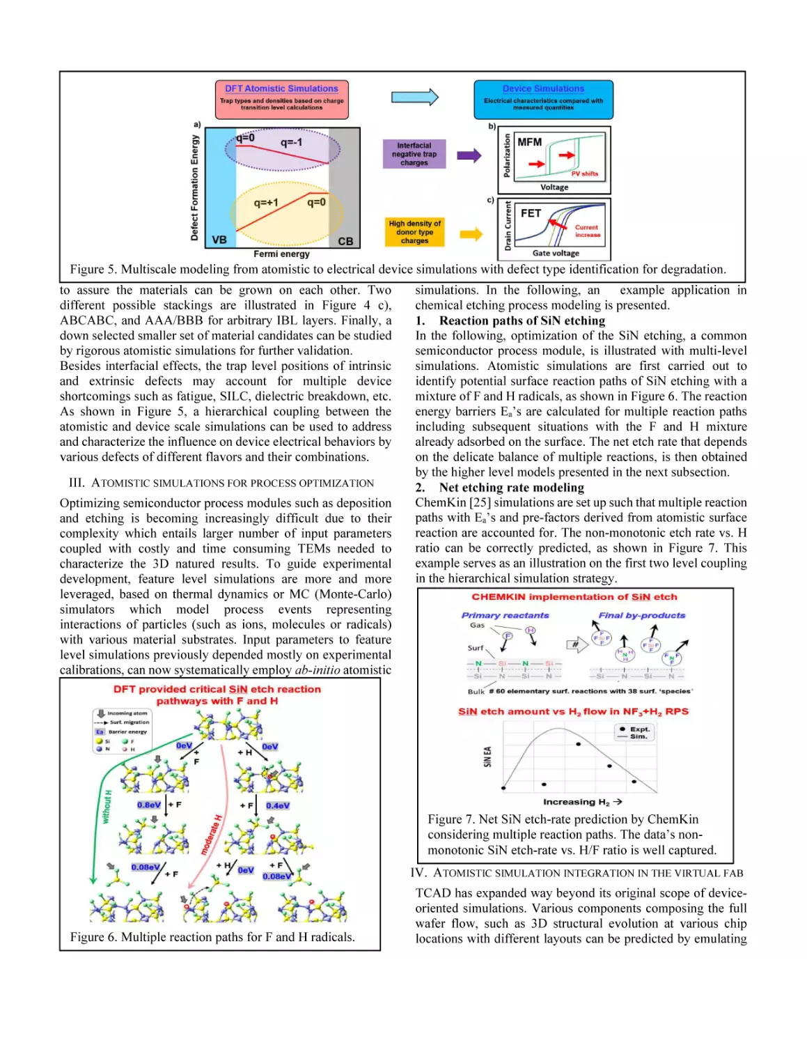
including dead layer considerations are depicted in Figure 2.
Such studies need to allow for multiple interfacial coordination
conditions to develop a realistic description of their impact and
proper comparison with experimental polarization data.
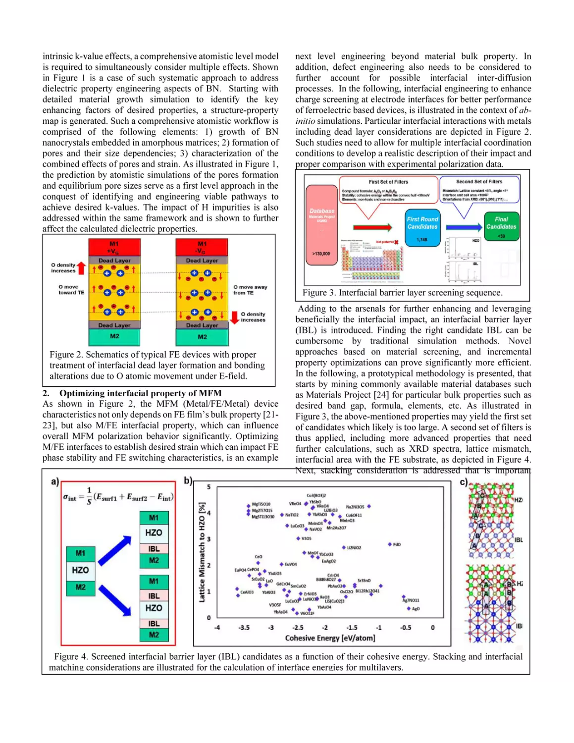
Figure 3. Interfacial barrier layer screening sequence.
Figure 2. Schematics of typical FE devices with proper
treatment of interfacial dead layer formation and bonding
alterations due to O atomic movement under E-field.
2. Optimizing interfacial property of MFM
As shown in Figure 2, the MFM (Metal/FE/Metal) device
characteristics not only depends on FE film’s bulk property [2123], but also M/FE interfacial property, which can influence
overall MFM polarization behavior significantly. Optimizing
M/FE interfaces to establish desired strain which can impact FE
phase stability and FE switching characteristics, is an example
Adding to the arsenals for further enhancing and leveraging
beneficially the interfacial impact, an interfacial barrier layer
(IBL) is introduced. Finding the right candidate IBL can be
cumbersome by traditional simulation methods. Novel
approaches based on material screening, and incremental
property optimizations can prove significantly more efficient.
In the following, a prototypical methodology is presented, that
starts by mining commonly available material databases such
as Materials Project [24] for particular bulk properties such as
desired band gap, formula, elements, etc. As illustrated in
Figure 3, the above-mentioned properties may yield the first set
of candidates which likely is too large. A second set of filters is
thus applied, including more advanced properties that need
further calculations, such as XRD spectra, lattice mismatch,
interfacial area with the FE substrate, as depicted in Figure 4.
Next, stacking consideration is addressed that is important
Figure 4. Screened interfacial barrier layer (IBL) candidates as a function of their cohesive energy. Stacking and interfacial
matching considerations are illustrated for the calculation of interface energies for multilayers.
Figure 5. Multiscale modeling from atomistic to electrical device simulations with defect type identification for degradation.
to assure the materials can be grown on each other. Two
different possible stackings are illustrated in Figure 4 c),
ABCABC, and AAA/BBB for arbitrary IBL layers. Finally, a
down selected smaller set of material candidates can be studied
by rigorous atomistic simulations for further validation.
Besides interfacial effects, the trap level positions of intrinsic
and extrinsic defects may account for multiple device
shortcomings such as fatigue, SILC, dielectric breakdown, etc.
As shown in Figure 5, a hierarchical coupling between the
atomistic and device scale simulations can be used to address
and characterize the influence on device electrical behaviors by
various defects of different flavors and their combinations.
III. ATOMISTIC SIMULATIONS FOR PROCESS OPTIMIZATION
Optimizing semiconductor process modules such as deposition
and etching is becoming increasingly difficult due to their
complexity which entails larger number of input parameters
coupled with costly and time consuming TEMs needed to
characterize the 3D natured results. To guide experimental
development, feature level simulations are more and more
leveraged, based on thermal dynamics or MC (Monte-Carlo)
simulators which model process events representing
interactions of particles (such as ions, molecules or radicals)
with various material substrates. Input parameters to feature
level simulations previously depended mostly on experimental
calibrations, can now systematically employ ab-initio atomistic
simulations. In the following, an
example application in
chemical etching process modeling is presented.
1. Reaction paths of SiN etching
In the following, optimization of the SiN etching, a common
semiconductor process module, is illustrated with multi-level
simulations. Atomistic simulations are first carried out to
identify potential surface reaction paths of SiN etching with a
mixture of F and H radicals, as shown in Figure 6. The reaction
energy barriers Ea’s are calculated for multiple reaction paths
including subsequent situations with the F and H mixture
already adsorbed on the surface. The net etch rate that depends
on the delicate balance of multiple reactions, is then obtained
by the higher level models presented in the next subsection.
2. Net etching rate modeling
ChemKin [25] simulations are set up such that multiple reaction
paths with Ea’s and pre-factors derived from atomistic surface
reaction are accounted for. The non-monotonic etch rate vs. H
ratio can be correctly predicted, as shown in Figure 7. This
example serves as an illustration on the first two level coupling
in the hierarchical simulation strategy.
Figure 7. Net SiN etch-rate prediction by ChemKin
considering multiple reaction paths. The data’s nonmonotonic SiN etch-rate vs. H/F ratio is well captured.
IV. ATOMISTIC SIMULATION INTEGRATION IN THE VIRTUAL FAB
Figure 6. Multiple reaction paths for F and H radicals.
TCAD has expanded way beyond its original scope of deviceoriented simulations. Various components composing the full
wafer flow, such as 3D structural evolution at various chip
locations with different layouts can be predicted by emulating
Figure 8. Atomistic simulations as building blocks to achieve predictive TCAD simulations and enable the virtual fab concept.
the step-by-step process flow. The output of TCAD simulations
can include not only transistors or electrical devices, but also
any 3D structures covering interconnections at middle or back
end of lines, full cell layout, and etc. The modeled steps
composing the process flow are no longer limited to dopant
diffusion, but expanded to cover deposition, etch and other
structural modification processes. The comprehensive coverage
of TCAD flow is only one of the foundations, predictive-ness
is the other important basis for TCAD to enable the true virtual
fab. As illustrated in Figure 8, atomistic simulations can be
integrally employed to afford predictive-ness to various
simulation components linking starting wafer to final chip’s
structural, yield and electrical performances.
ACKNOWLEDGMENT
The authors are grateful to the following colleagues for their
assistance with manuscript preparation: Ying-Chih Chen, YuChien Chiu, Po-Ching Hsu, Jhih-Rong Huang, Ashwathi Iyer,
Steven Nien, Bharath Pulicherla, Raghunath Putikam, TzerMin
Shen, Qing Shi, Aslan Wei.
REFERENCES
[1]
[2]
[3]
[4]
[5]
[6]
[7]
[8]
M. Liu, "Unleashing the Future of Innovation," 2021 IEEE International
Solid- State Circuits Conference (ISSCC), 2021, pp. 9-16
J. Wu and C. H. Diaz, "Expanding role of predictive TCAD in advanced
technology development," 2013 International Conference on Simulation
of Semiconductor Processes and Devices (SISPAD), 2013, pp. 167-171
Keun-Ho Lee, "Challenges and responses for virtual silicon," 2015
International Conference on Simulation of Semiconductor Processes and
Devices (SISPAD), 2015, pp. 80-83
M. Stettler et al., "State-of-the-art TCAD: 25 years ago and today," 2019
IEEE International Electron Devices Meeting (IEDM), pp. 39.1.1-39.1.4
G. Klimeck, F. Oyafuso, T. Boykin et al., "Development of a
nanoelectronic 3-D (NEMO 3-D) simulator for multimillion atom
simulations and application to alloyed quantum dots", CMES, 2002
A. Afzalian, G. Doornbos, T. Shen, M. Passlack and J. Wu, "A HighPerformance InAs/GaSb Core-Shell Nanowire Line-Tunneling TFET: An
Atomistic Mode-Space NEGF Study," in IEEE Journal of the Electron
Devices Society, vol. 7, pp. 88-99, 2019
T.M. Shen et al, “Molecular Dynamic simulation study of stress
memorization in Si dislocations,” 2012 IEEE International Electron
Devices Meeting (IEDM), pp. 30.1.1-30.1.4, 2012
R. Chen, W. Choi, A. Schmidt et al., "A New Kinetic Lattice Monte Carlo
Modeling Framework for the Srouce-Drain Selective Epitaxial Growth
Process", 2013 International Conference on Simulation of Semiconductor
Processes and Devices (SISPAD), 2013
[9]
[10]
[11]
[12]
[13]
[14]
[15]
[16]
[17]
[18]
[19]
[20]
[21]
[22]
[23]
[24]
[25]
Y. Park et al., "Dopant diffusion in Si, SiGe and Ge : TCAD model
parameters determined with density functional theory," 2017 IEEE
International Electron Devices Meeting (IEDM), pp. 35.3.1-35.3.4, 2017
M. Karner, Z. Stanojević, C. Kernstock, H. W. Cheng-Karner and O.
Baumgartner, "Hierarchical TCAD device simulation of FinFETs," 2015
International Conference on Simulation of Semiconductor Processes and
Devices (SISPAD), pp. 258-261, 2015
S.T. Dunham, P. Fastenko, Z. Qin and M. Diebel “The Process modeling
hierarchy: connecting atomistic calculations to nanoscale behavior”,
IEICE Trans. Electron. E86-C, 276, 2003
S.J. Aboud, J. Huang, J. Cobb et al. “Ab initio for design-technology cooptimization”, Proceedings Volume 11614, Design-Process-Technology
Co-optimization XV; 116140S, 2021
P. Giannozzi, O. Baseggio, P. Bonfà et al. "Quantum ESPRESSO toward
the exascale", The Journal of Chemical Physics 152, 154105, 2020
G. Kresse and J. Furthmüller, “Efficient iterative schemes for ab initio
total-energy calculations using a plane-wave basis set”., Phys. Rev. B 47,
558, 1993
G. Kresse and D. Joubert, “From ultrasoft pseudopotentials to the
projector augmented-wave method”,Phys. Rev. B 59, 1758, 1999
S. Smidstrup, T. Markussen, P. Vancraeyveld et al., “QuantumAtk: an
integrated platform of electronic and atomic-scale modelling tools“, J.
Phys.: Condens. Matter 32 015901, 2020
T. D. Kühne, M. Iannuzzi, M. Del Ben et al.,"CP2K: An electronic
structure and molecular dynamics software package - Quickstep: Efficient
and accurate electronic structure calculations", The Journal of Chemical
Physics 152, 194103, 2020, https://doi.org/10.1063/5.0007045
S. Hong, C.S. Lee, M.H. Lee et al. “Ultralow-dielectric-constant
amorphous boron nitride”, Nature 582, 511–514, 2020. “Reply to: On the
measured dielectric constant of amorphous boron nitride”, Nature 590,
E8–E10, 2021. https://doi.org/10.1038/s41586-020-03163-x
L. Li and X.M. Chen, On the measured dielectric constant of amorphous
boron nitride. Nature 590, E6–E7, 2021
J. Liu, K. P. Loh, M. Lin et al, “Plasma deposition of low dielectric
constant (k=2.2∼2.4)(k=2.2∼2.4) Boron Nitride on methylsilsesquioxanebased nanoporous films", J. Appl. Phys. 96, 6679-6684, 2004
T. Maeda, B. Magyari-Köpe, and Y. Nishi “Identifying ferroelectric
switching pathways in HfO2: first principles calculations under electric
fields”, 1-4. 10.1109 IMW, 2017
S. Clima, B. J O’Sullivan; N. Ronchi et al., "Ferroelectric switching in
FEFET: physics of the atomic mechanism and switching dynamics in
HfZrOx, HfO2 with oxygen vacancies and Si dopants", 2020 IEEE
International Electron Devices Meeting IEDM, 4.2.1, 2020
H.-J. Lee, M. Lee, K. Lee et al., “Scale-free ferroelectricity induced by
flat phonon bands in HfO2”, Science 10.1126/science.aba0067, 2020
A. Jain, S.P. Ong, G. Hautier et al., “The Materials Project: A materials
genome approach to accelerating materials innovation”
APL Materials, 1, 011002, 2013, doi:10.1063/1.4812323
Chemkin-Pro 18.1, ANSYS, Inc.: San Diego, 2017.