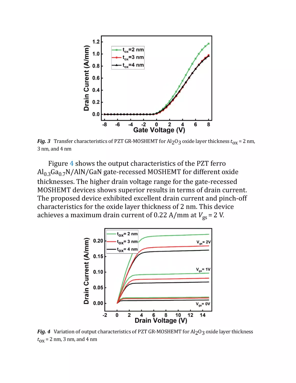
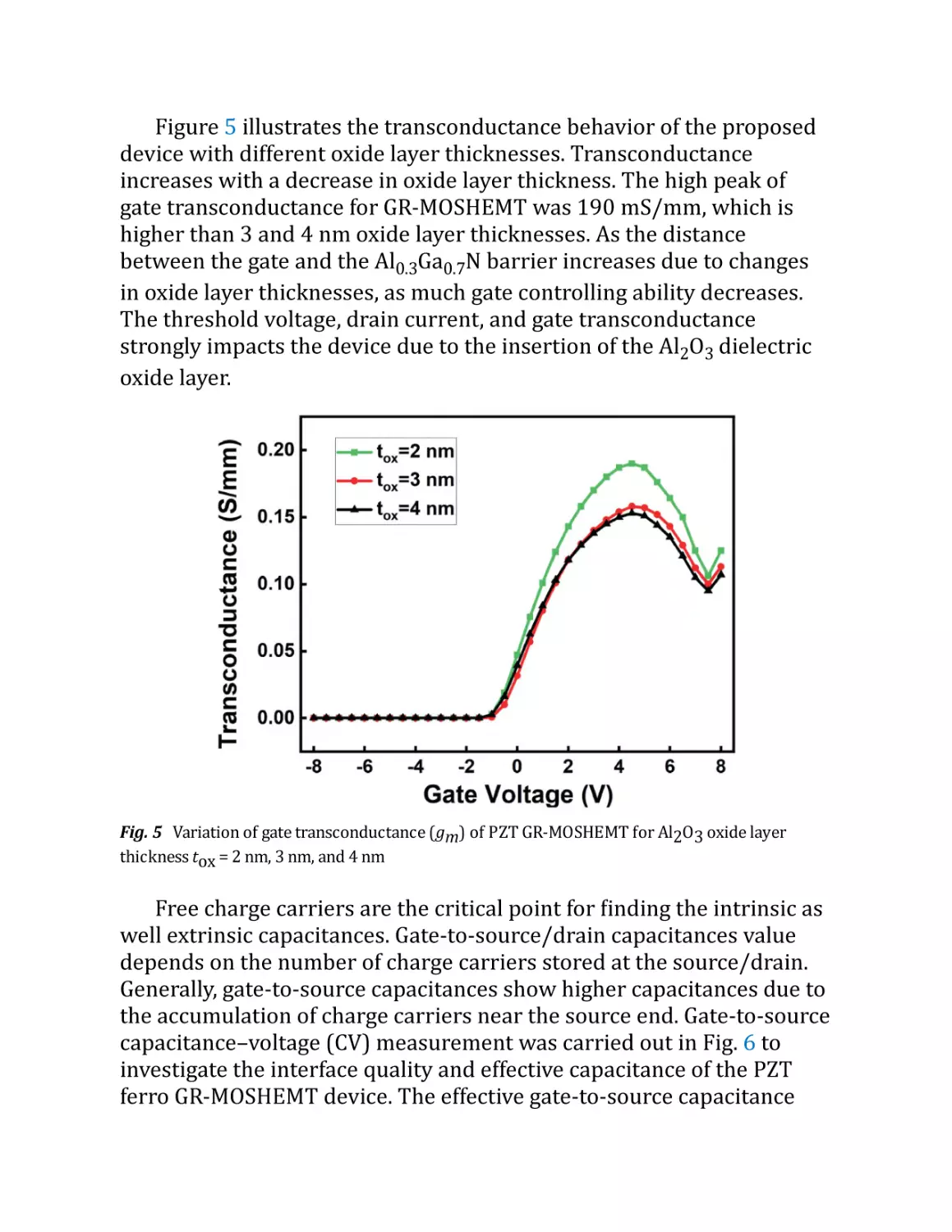
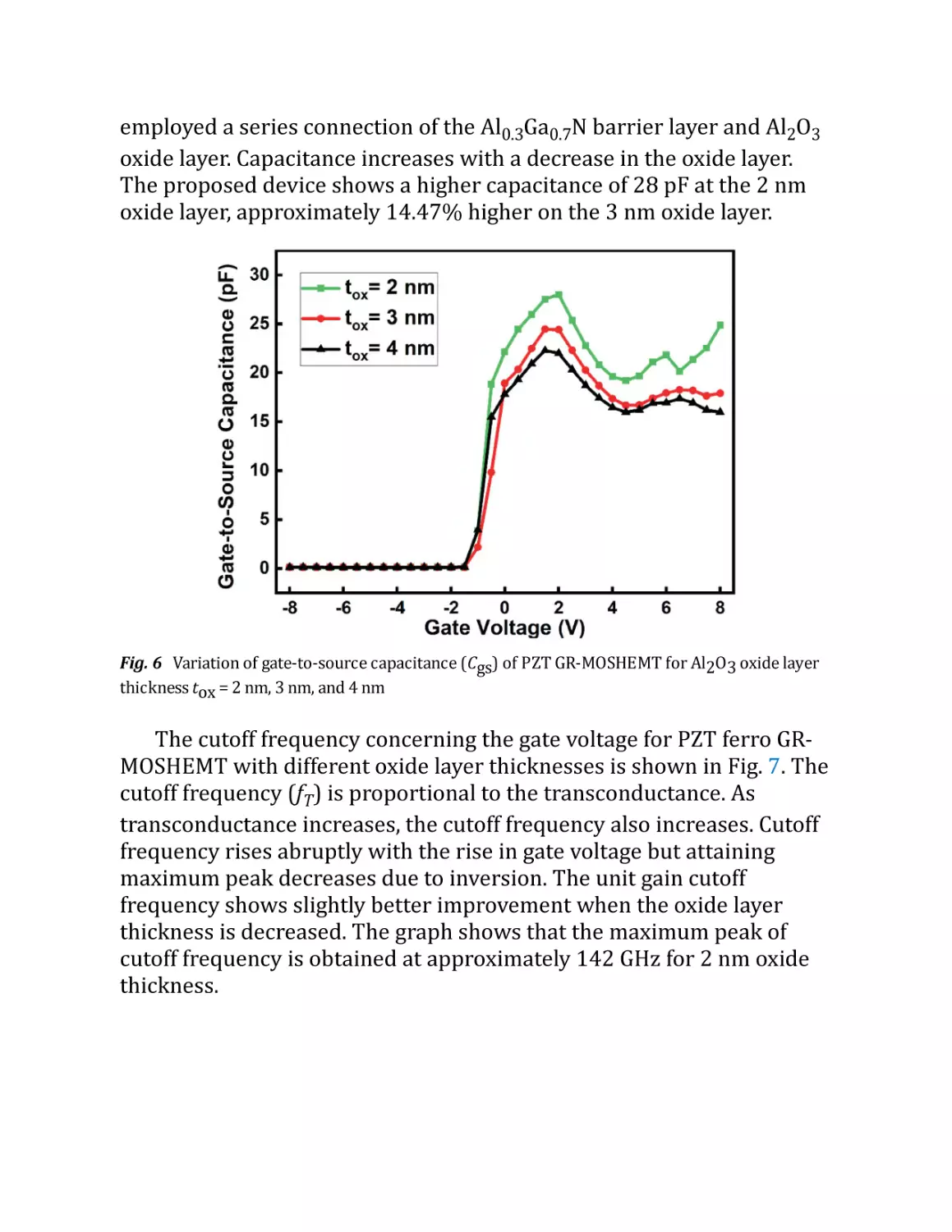
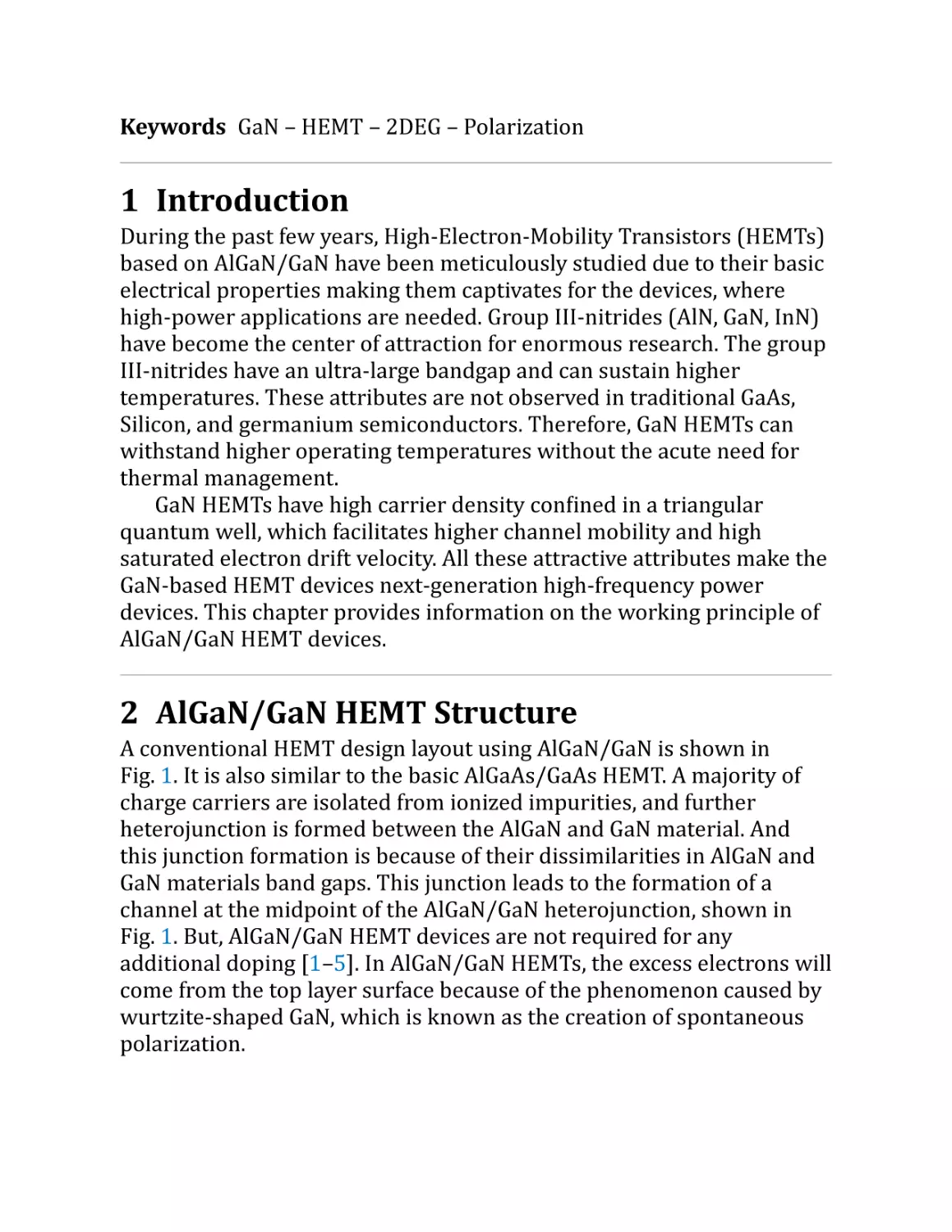
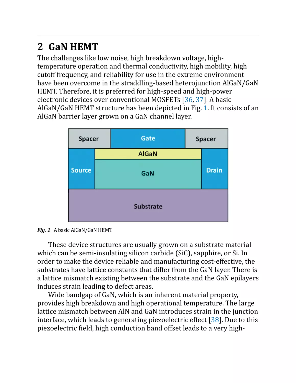
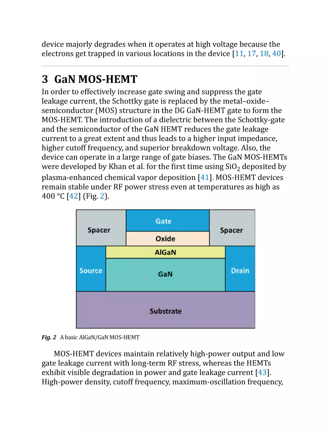
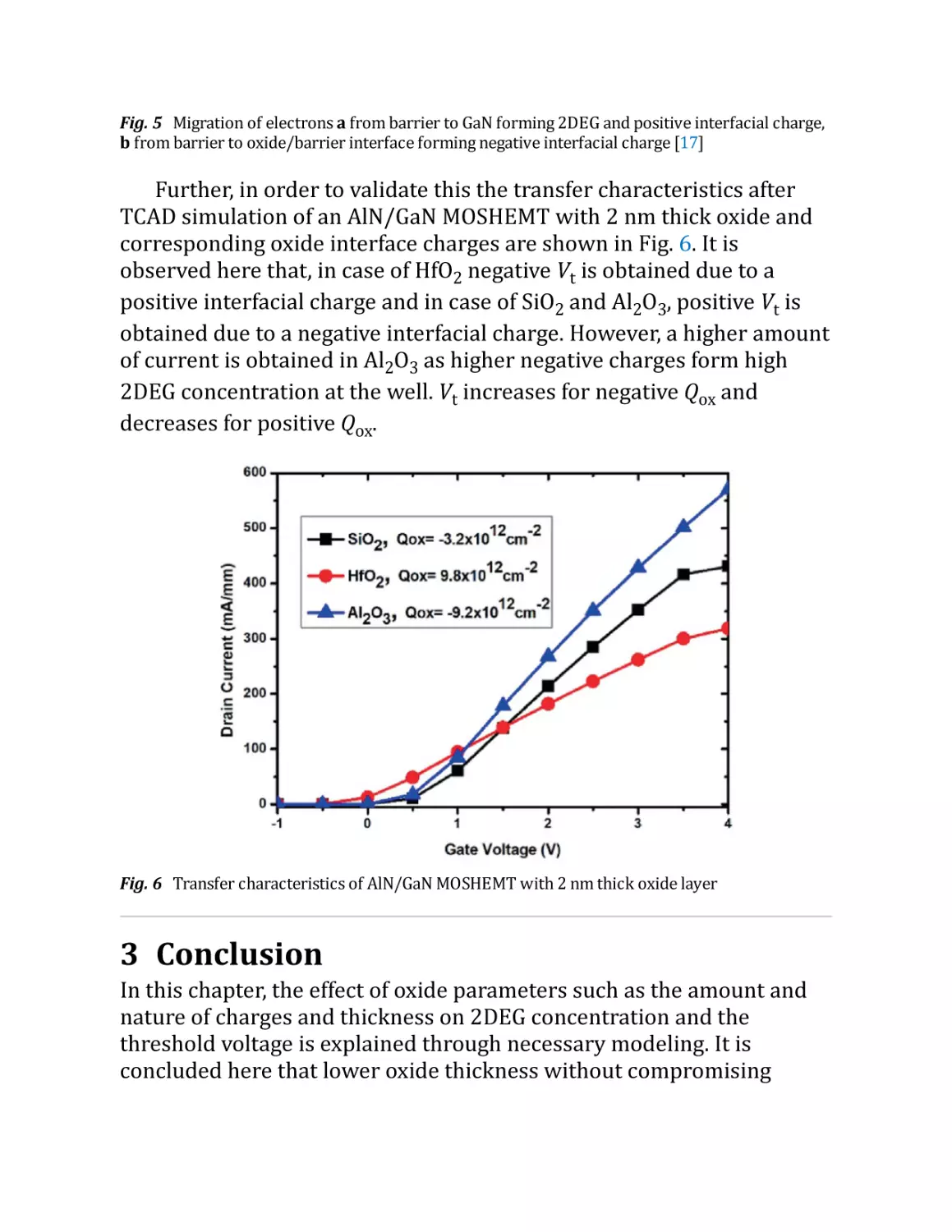
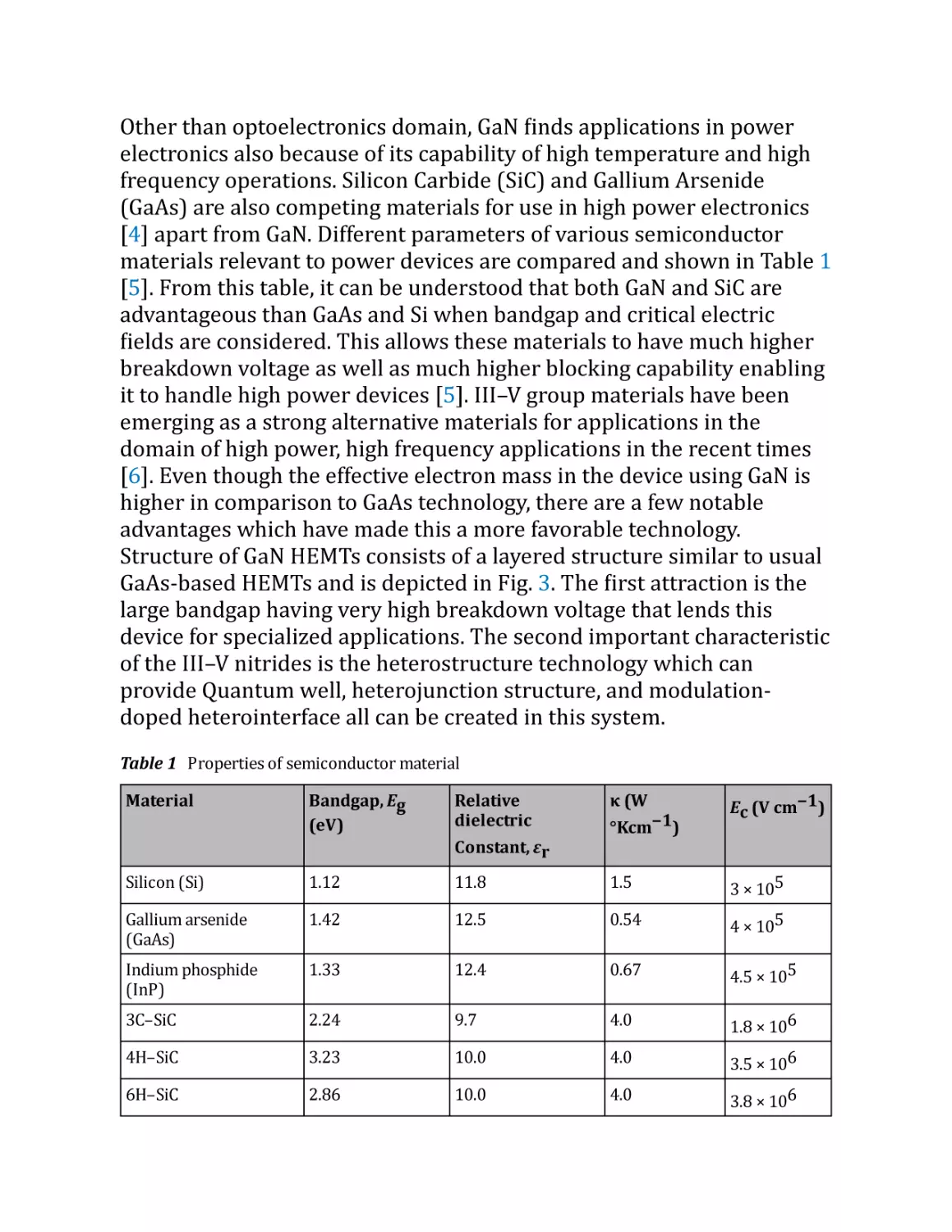
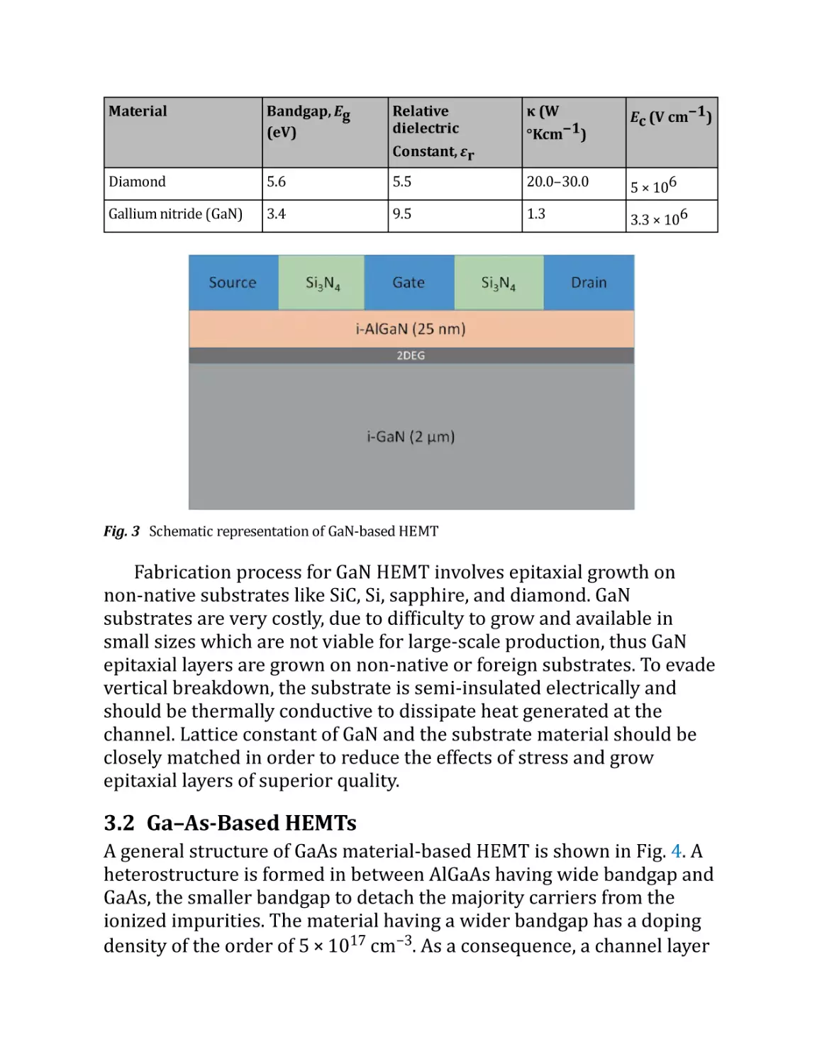
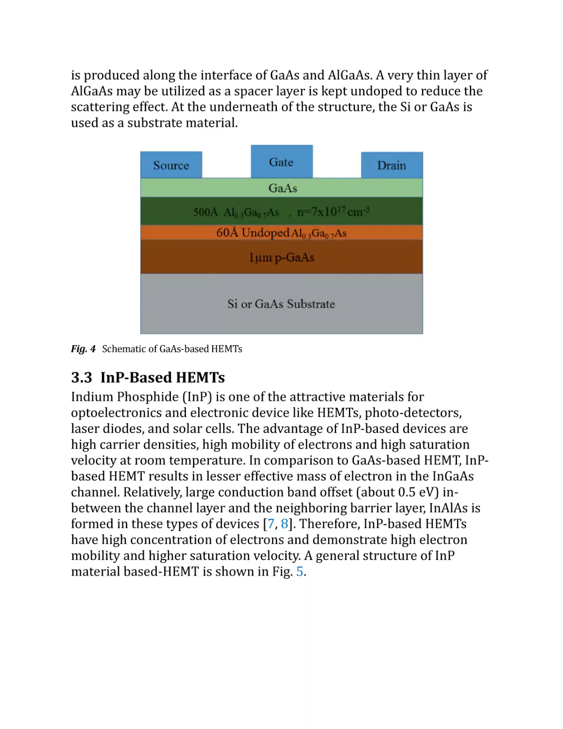
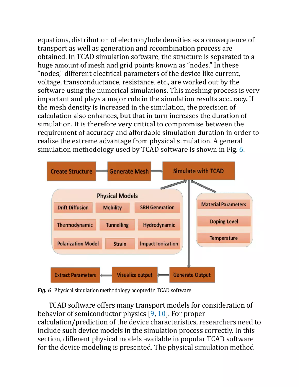
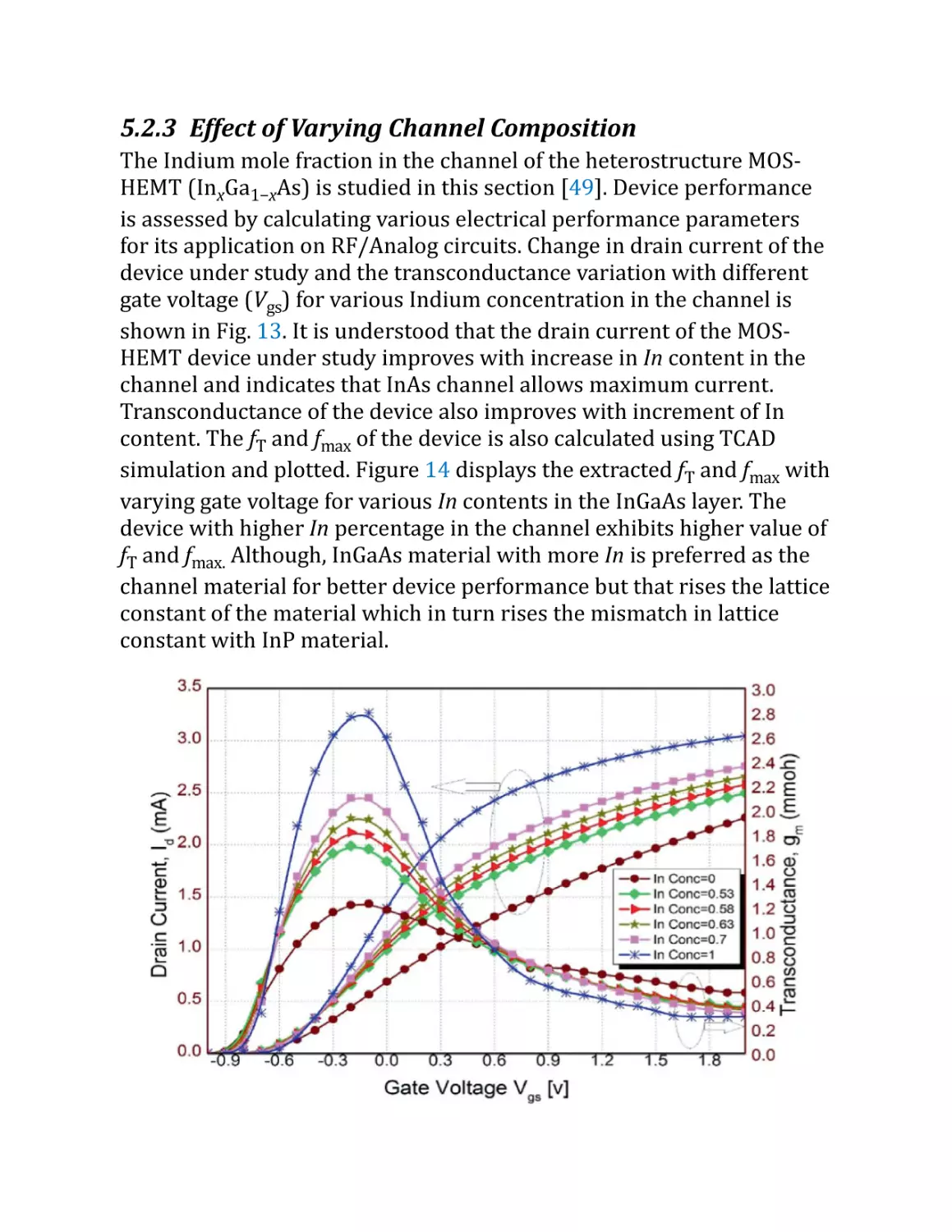
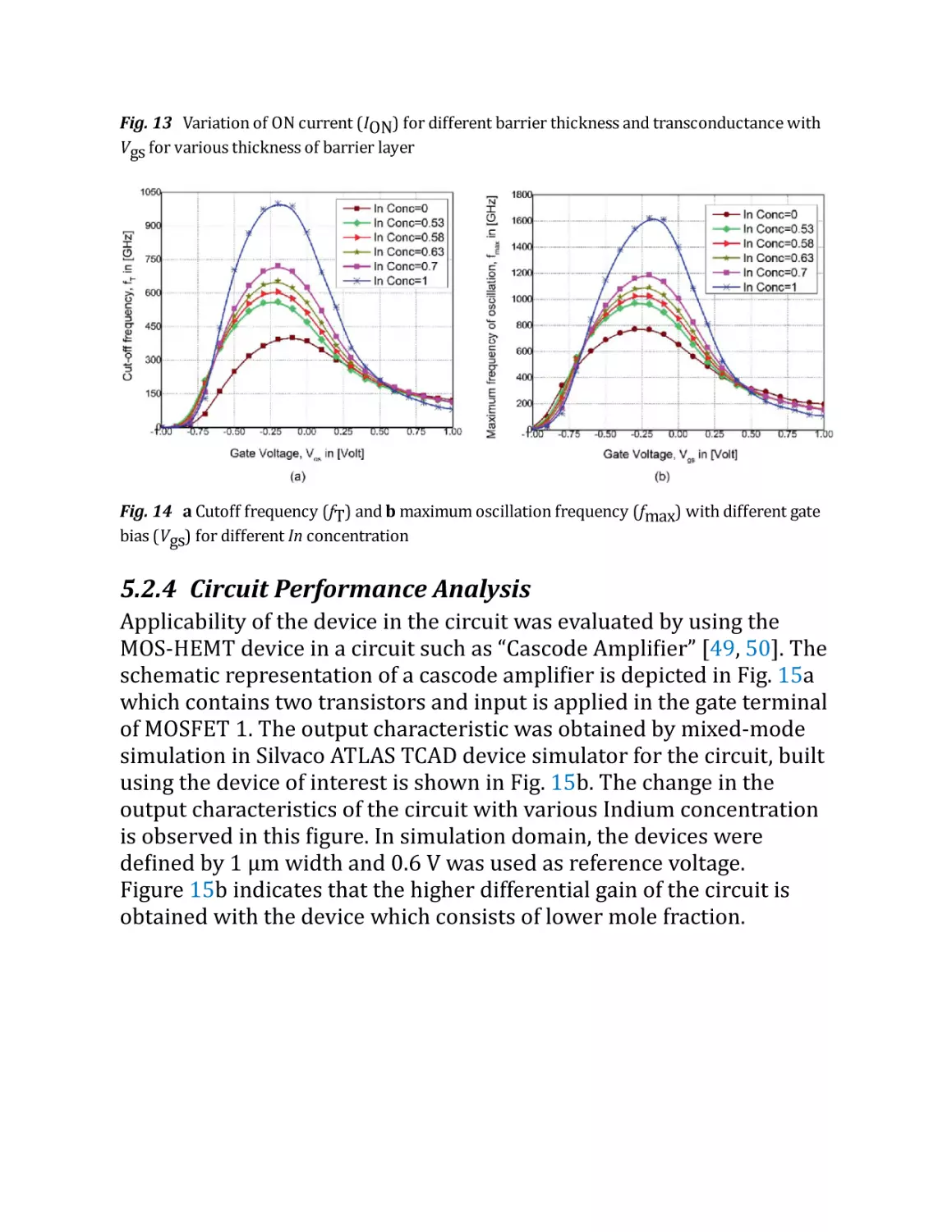
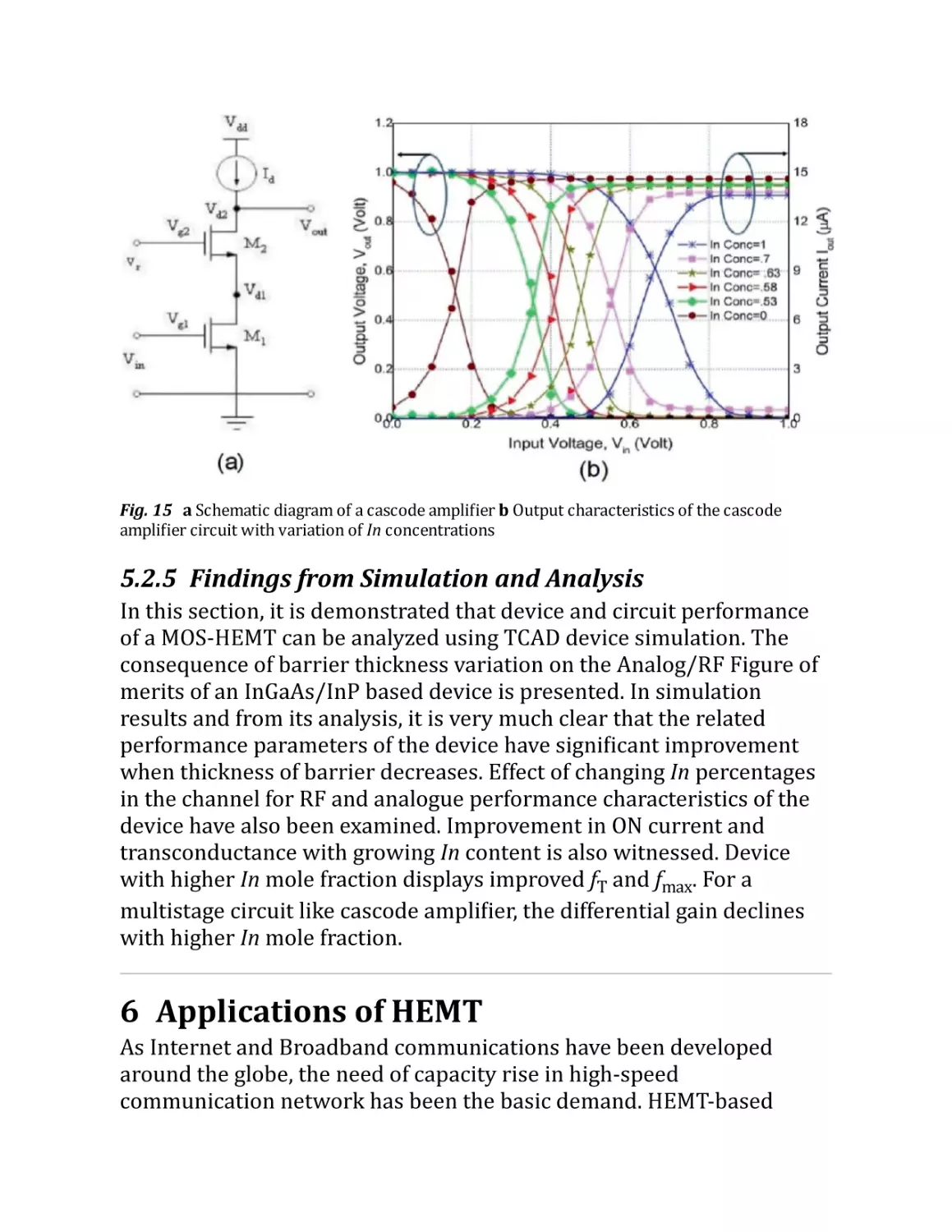
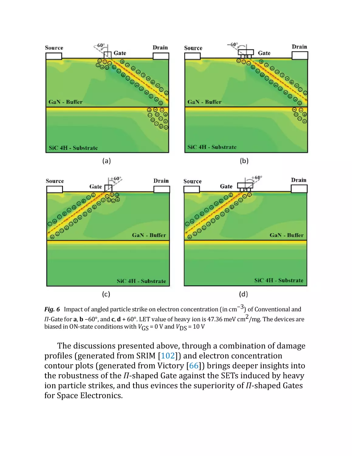
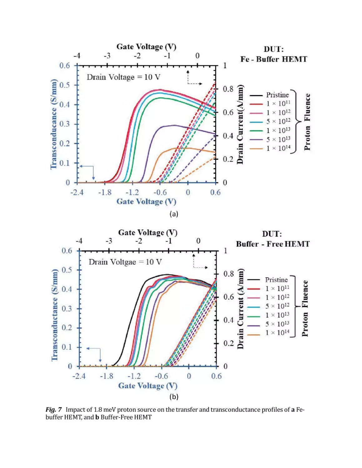
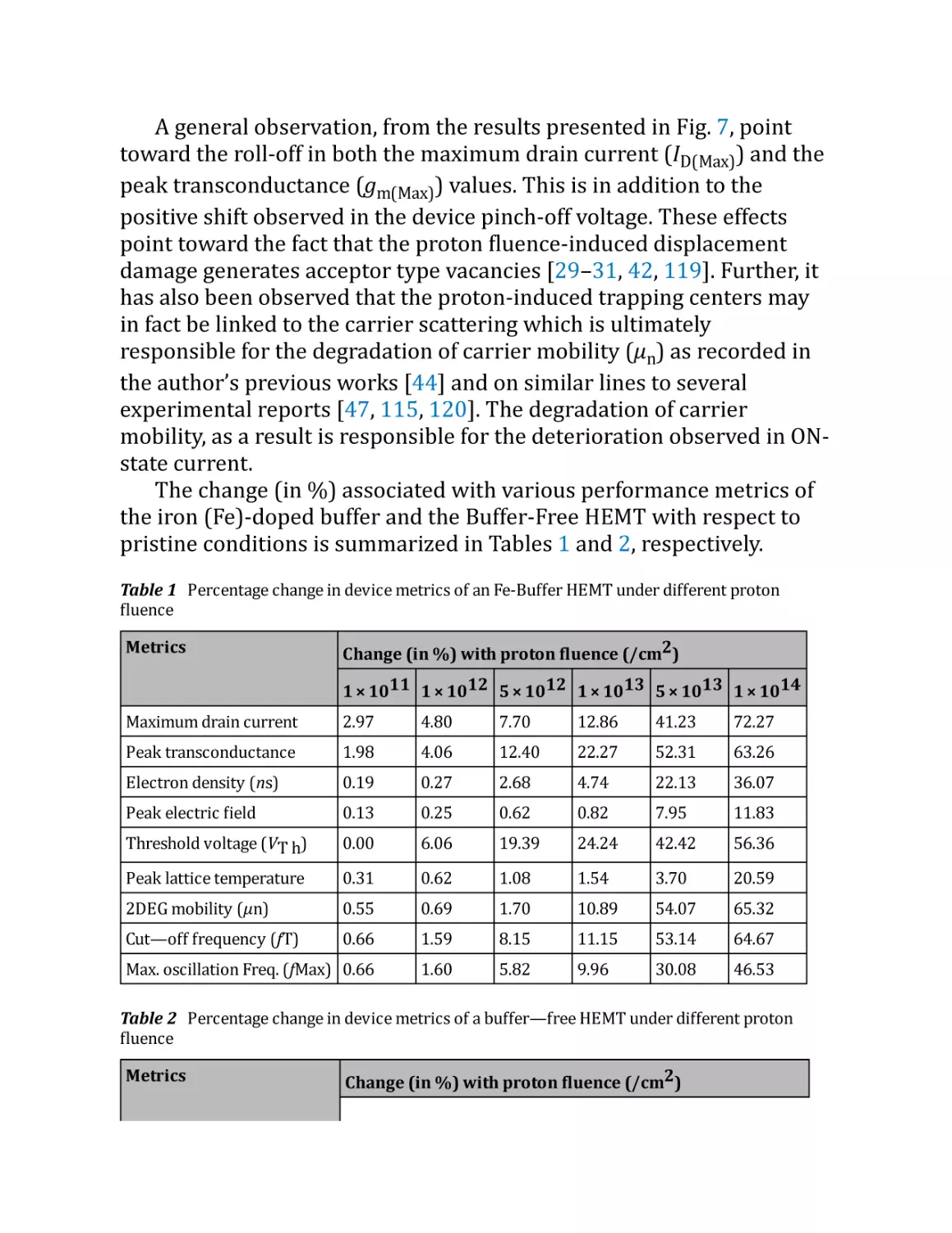
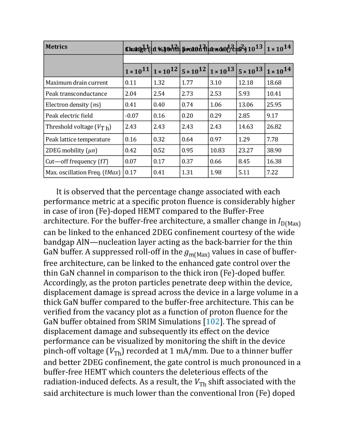
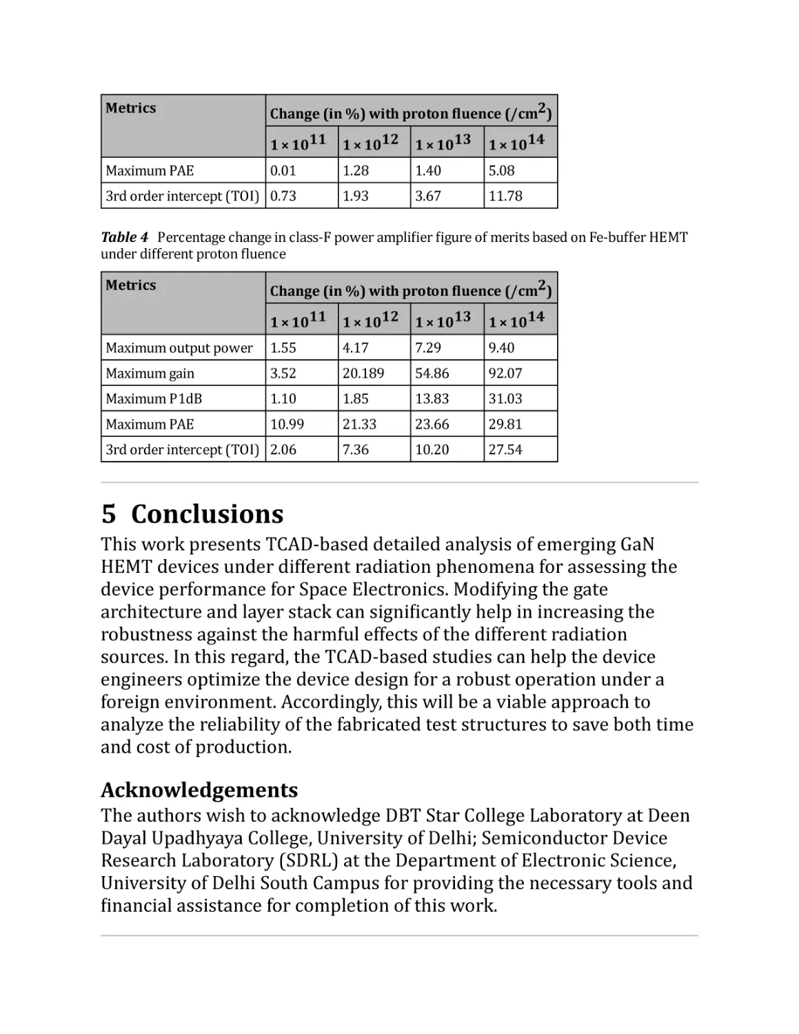
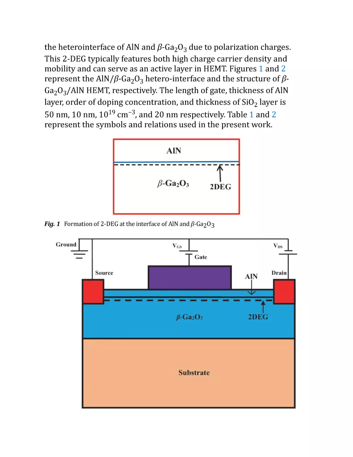
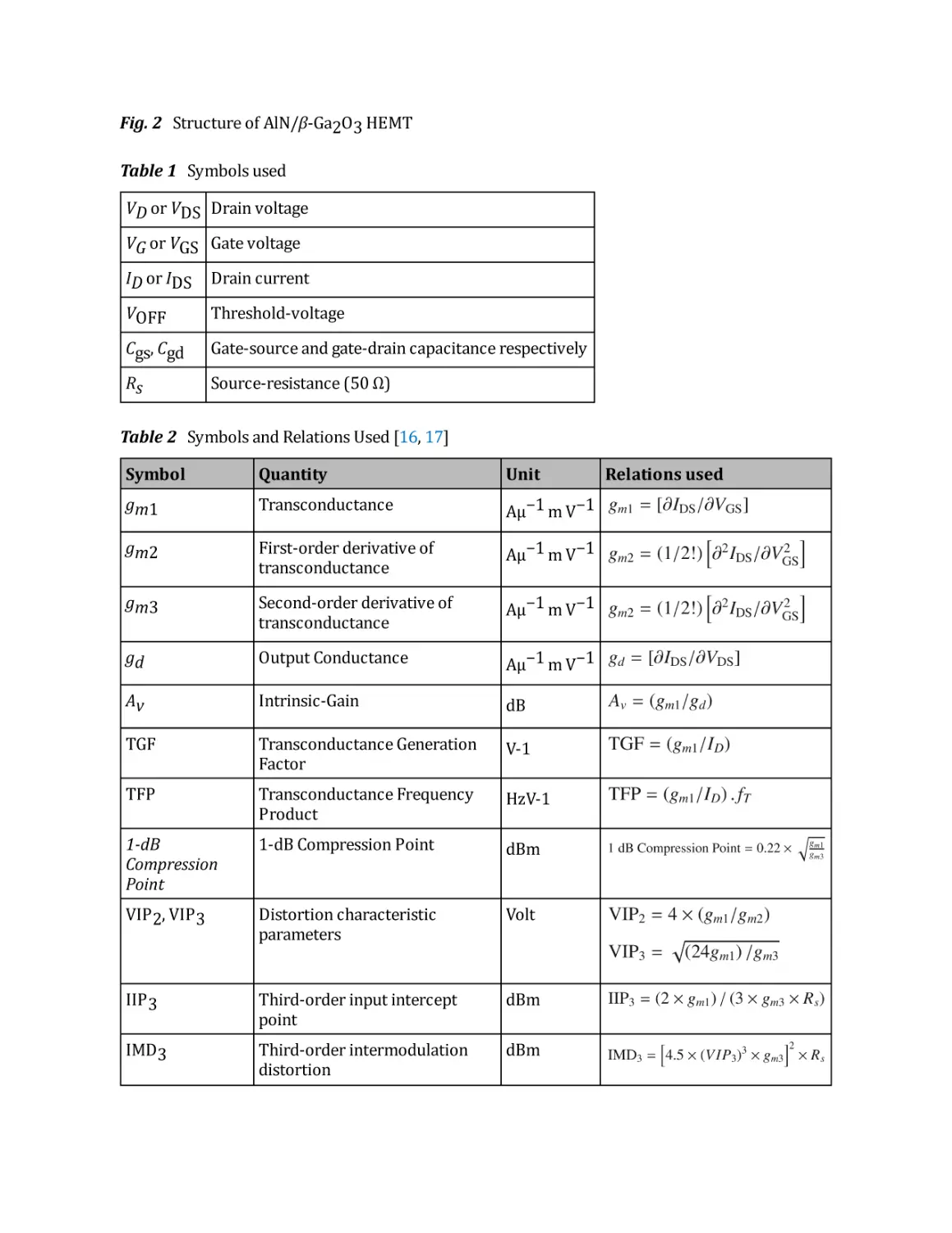
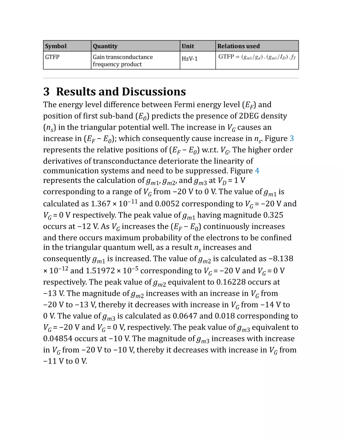
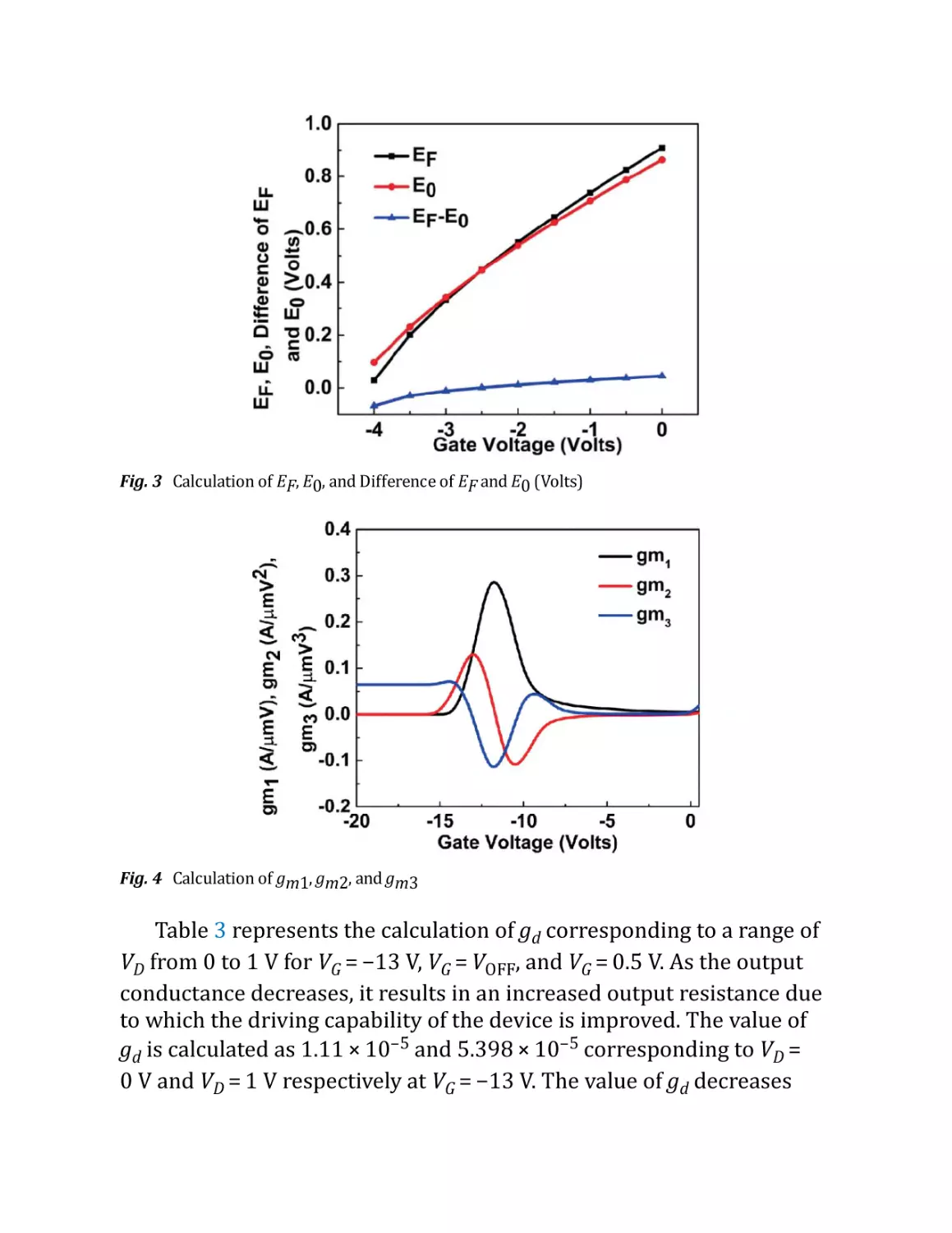
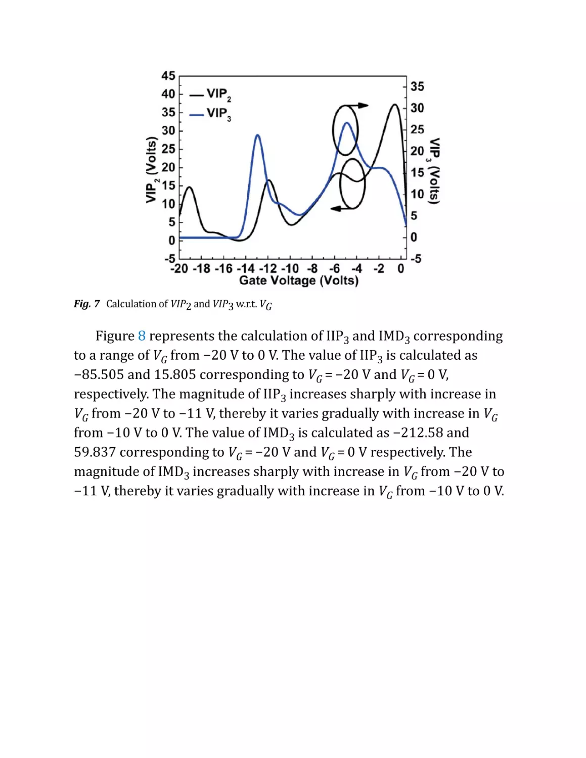
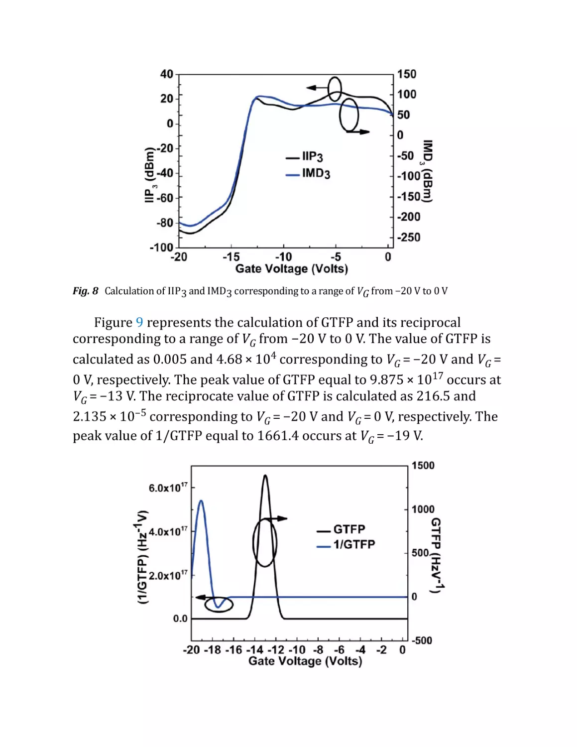
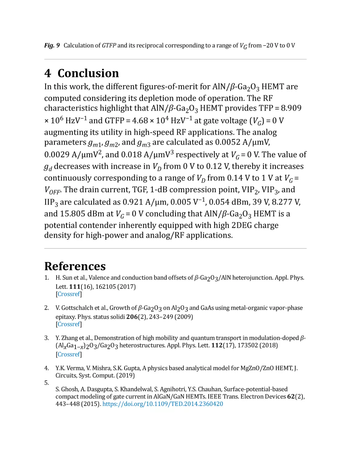
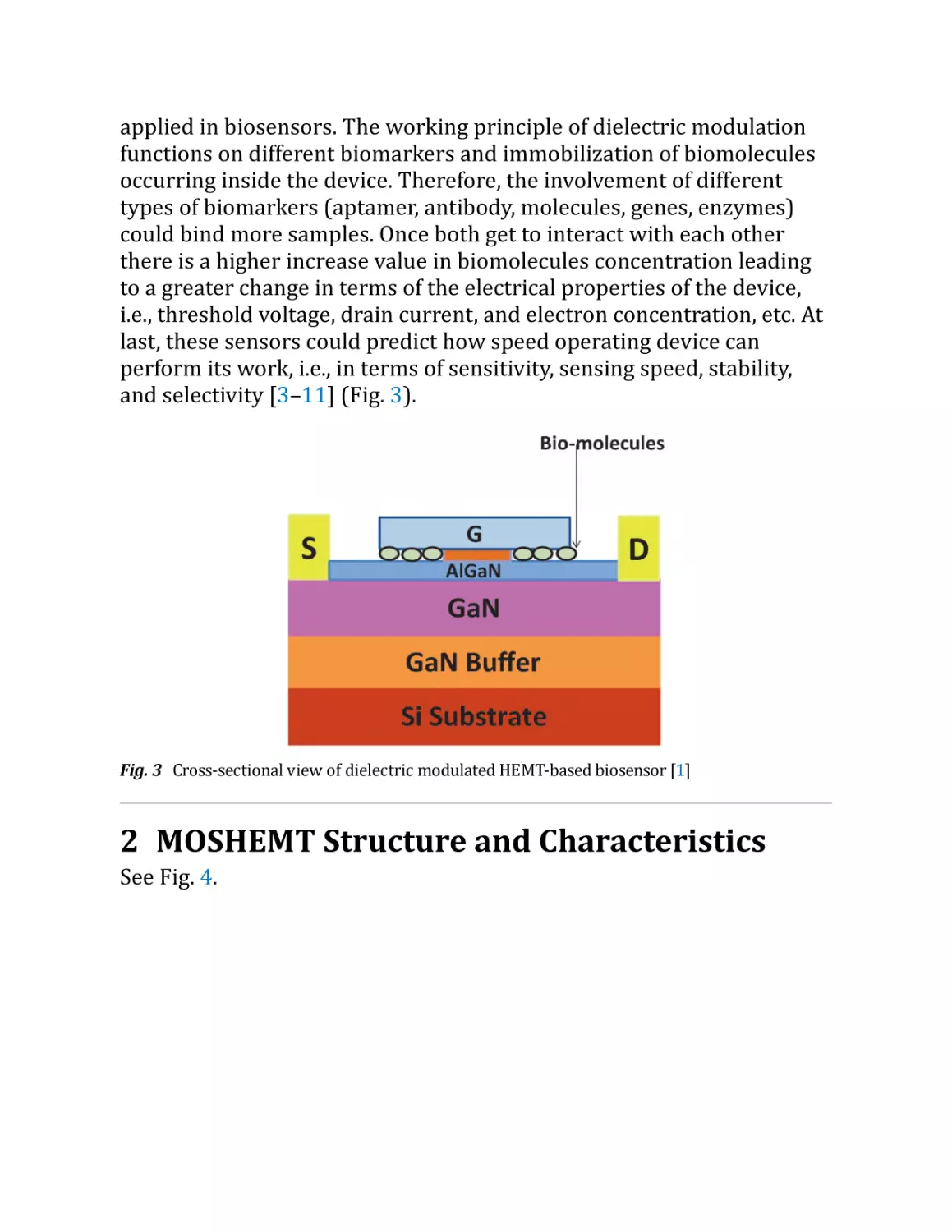
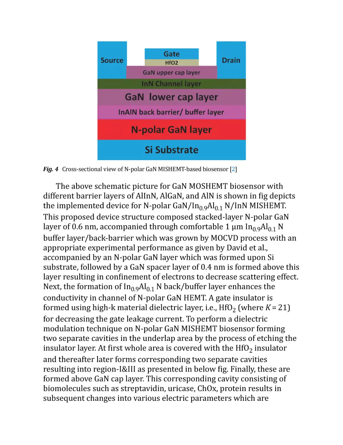
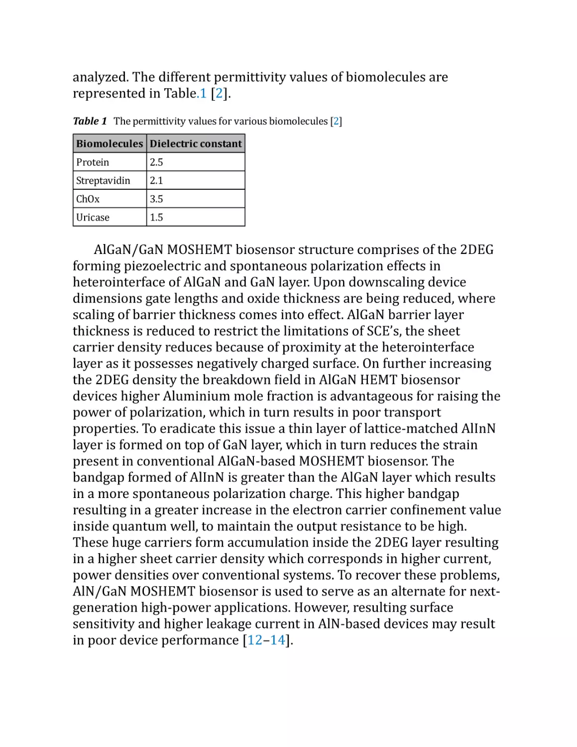
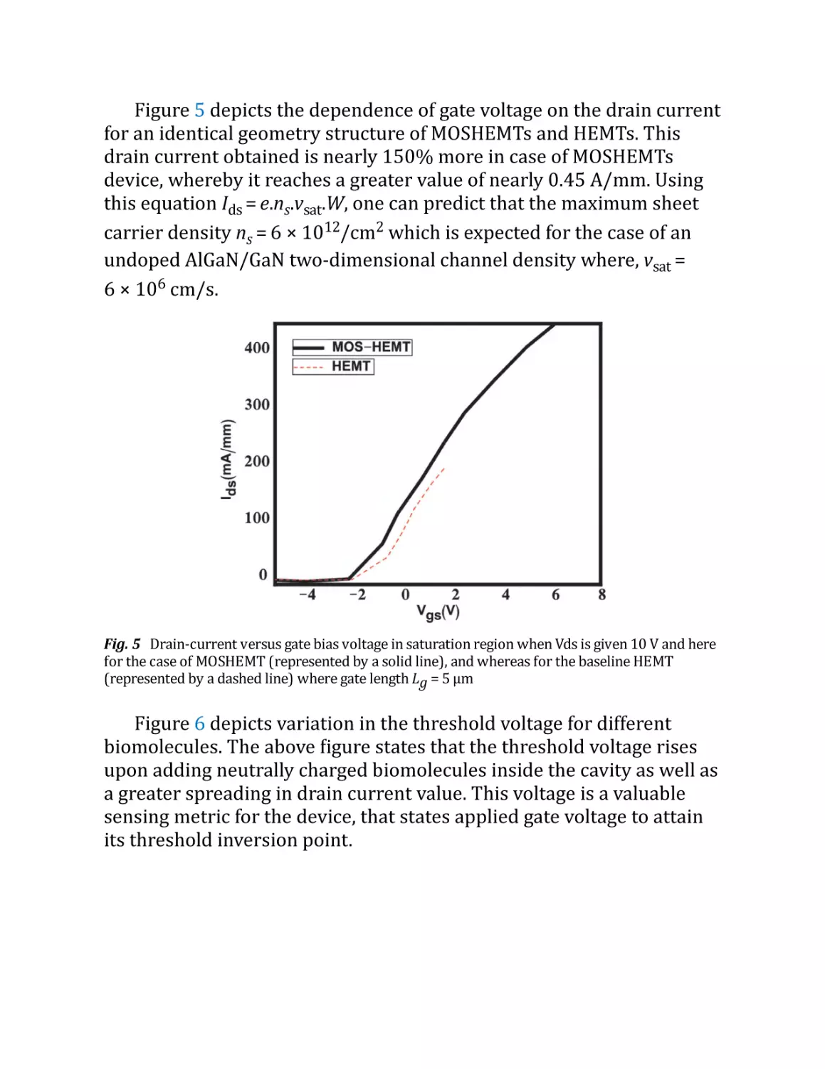
/


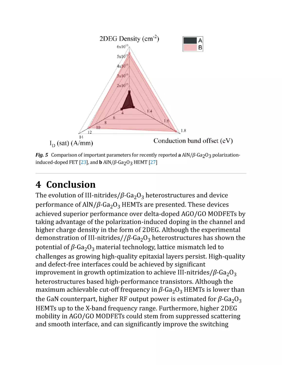

Автор: Kaushik Brajesh Kumar
Теги: electrical engineering electronics computer engineering
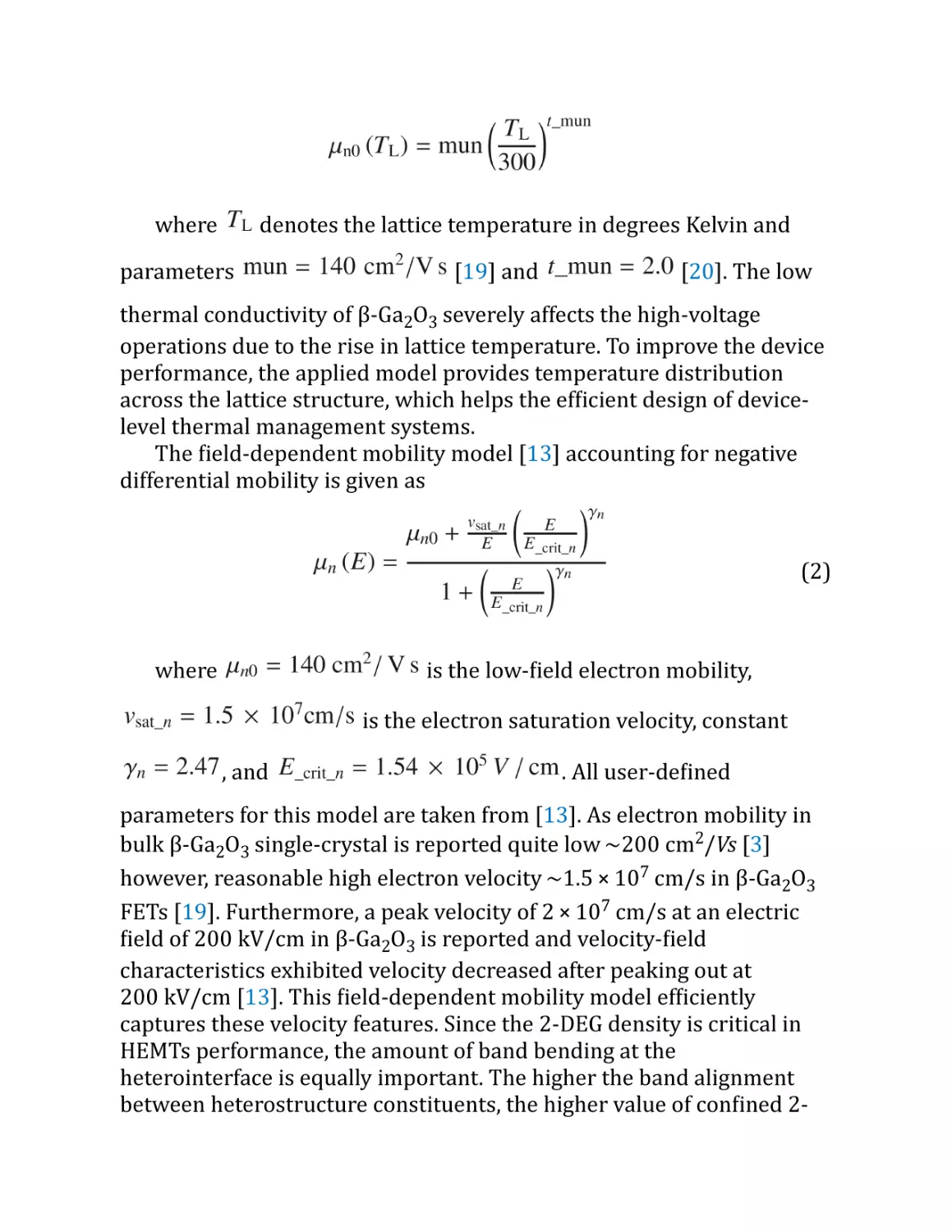
ISBN: 978-981-19-2164-3
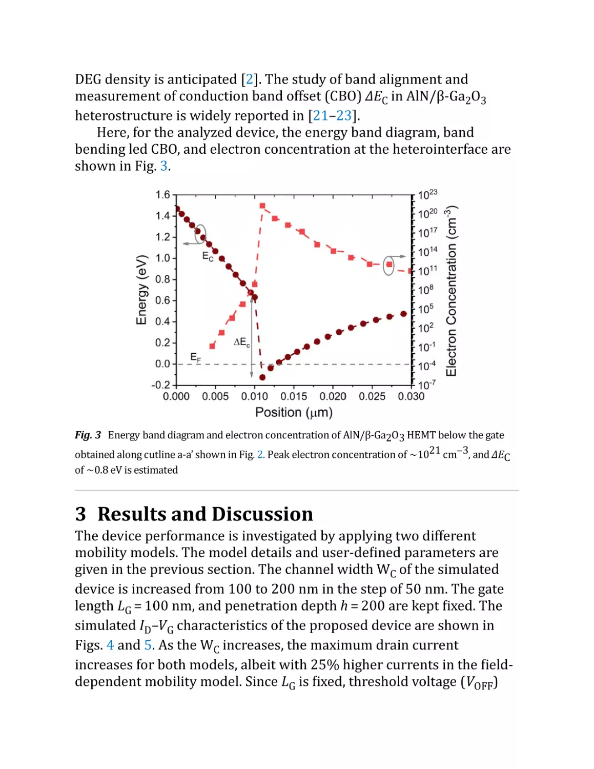
Год: 2023


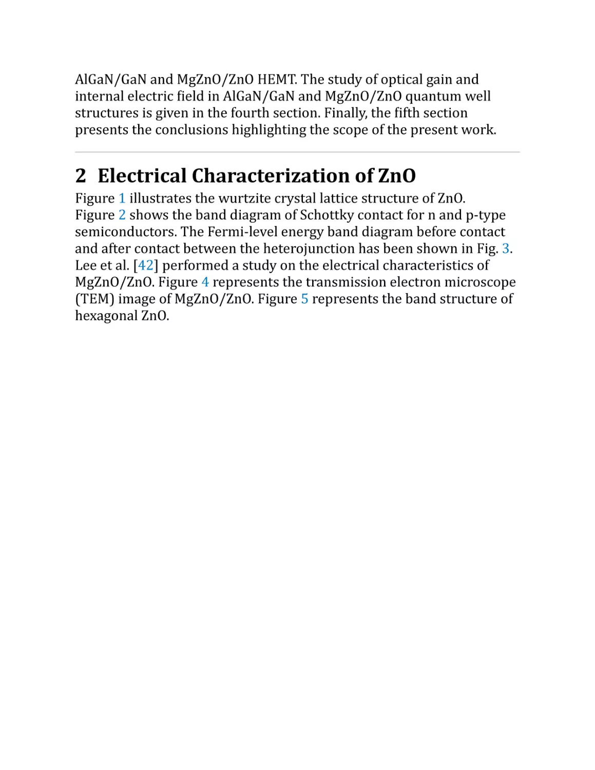
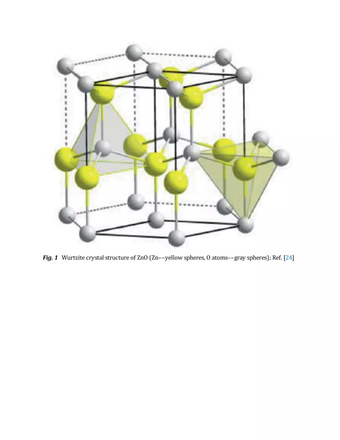
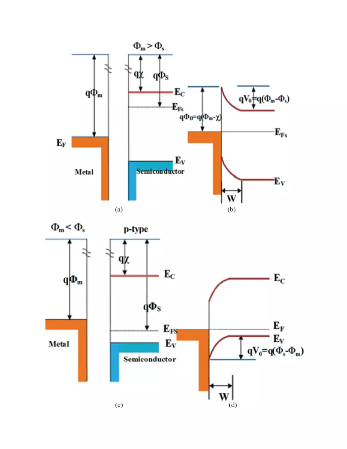
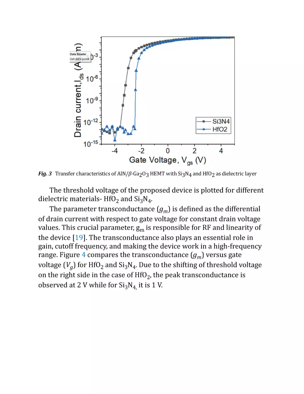
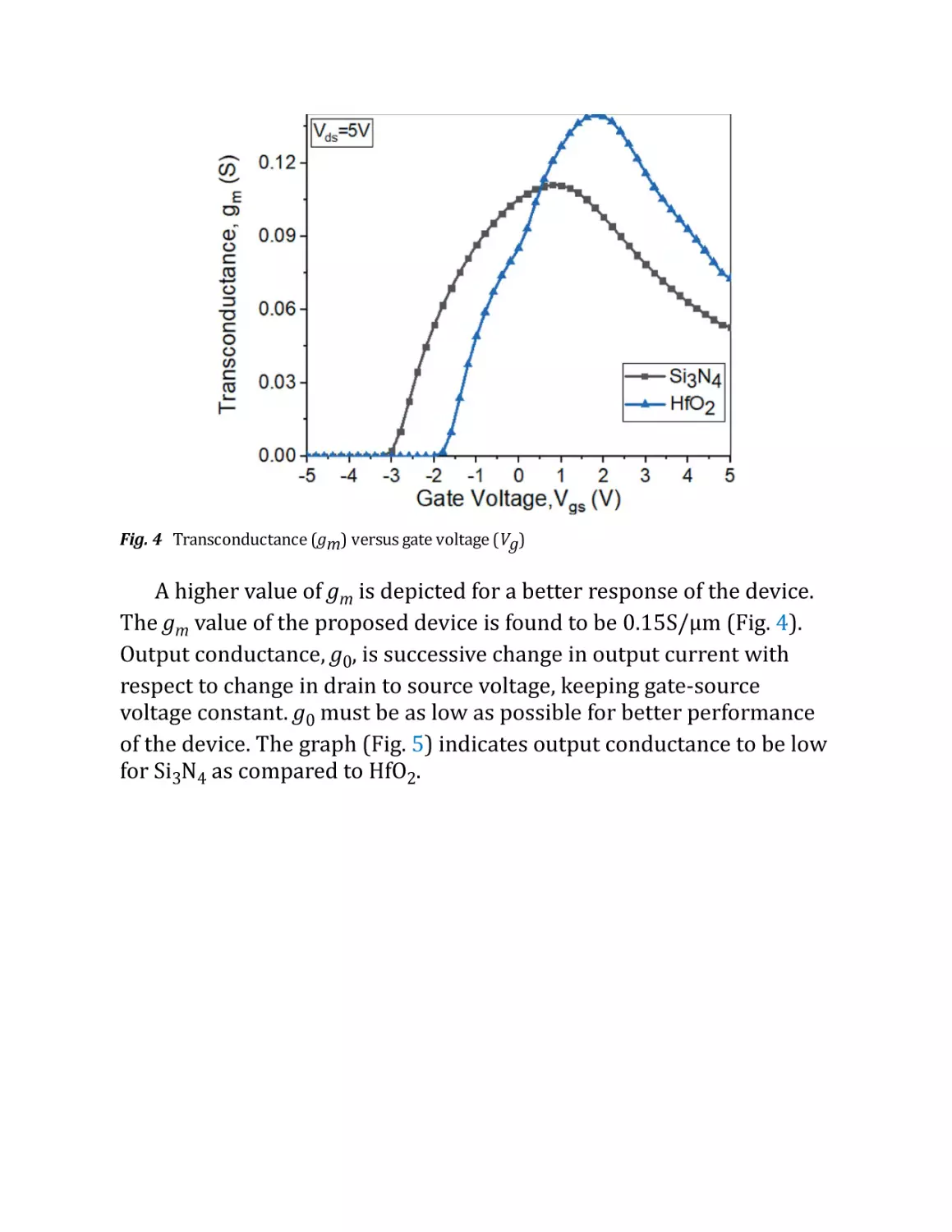
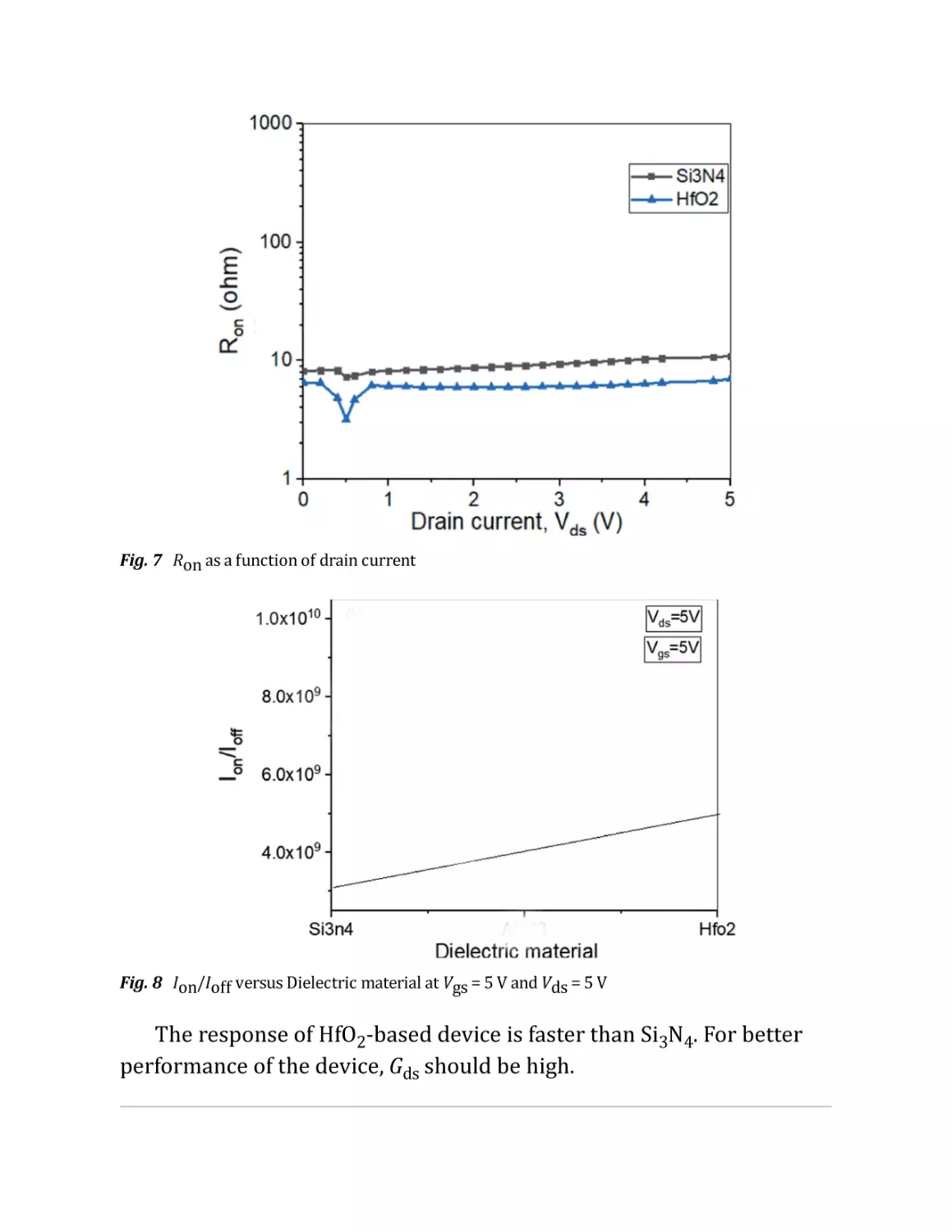
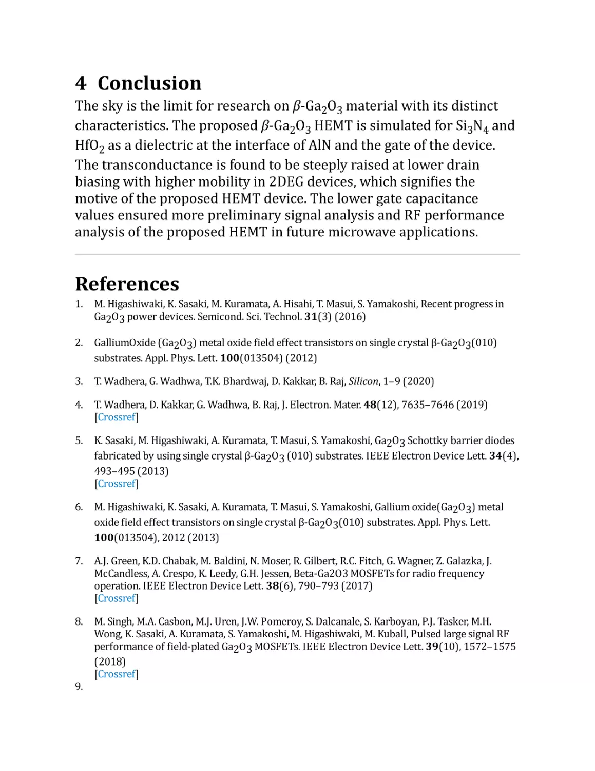
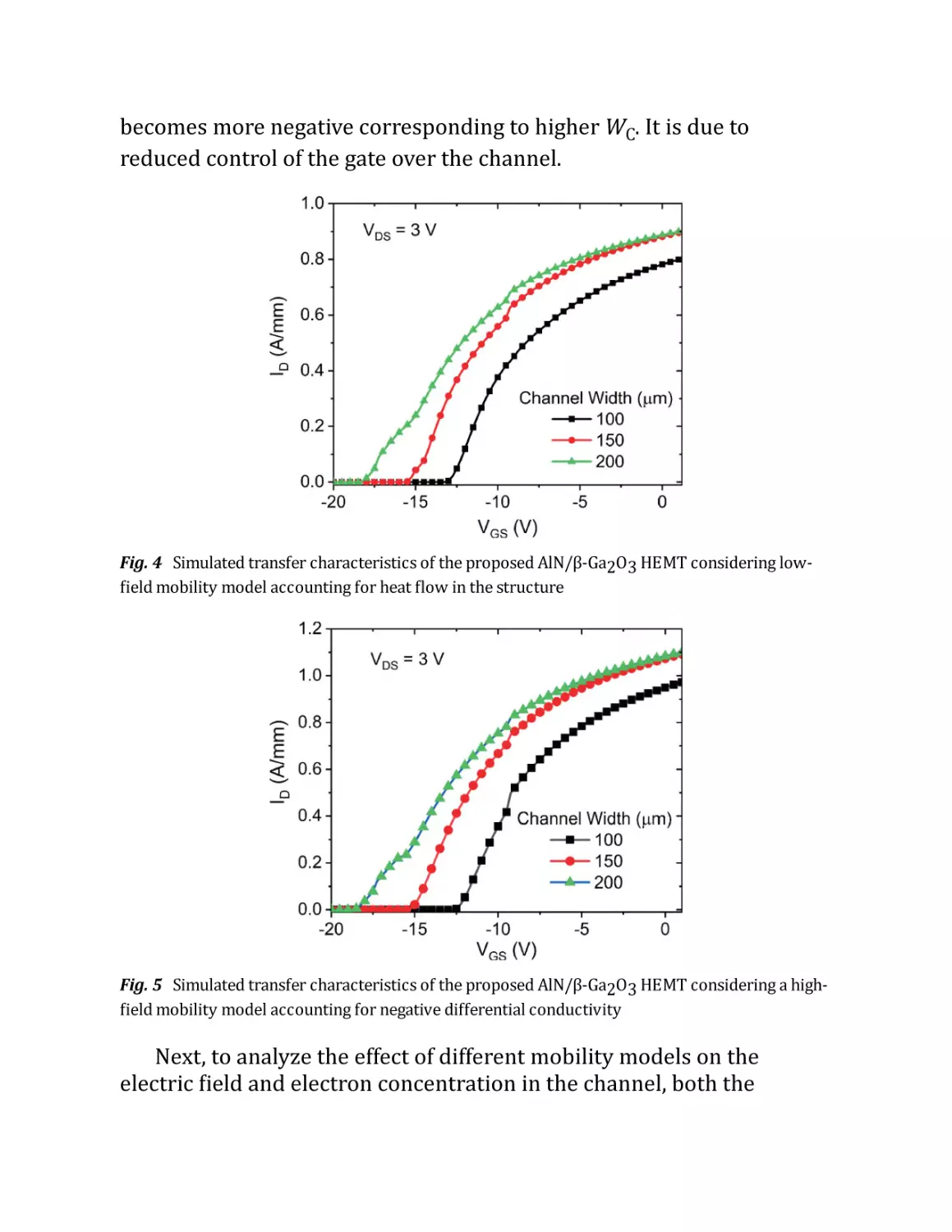
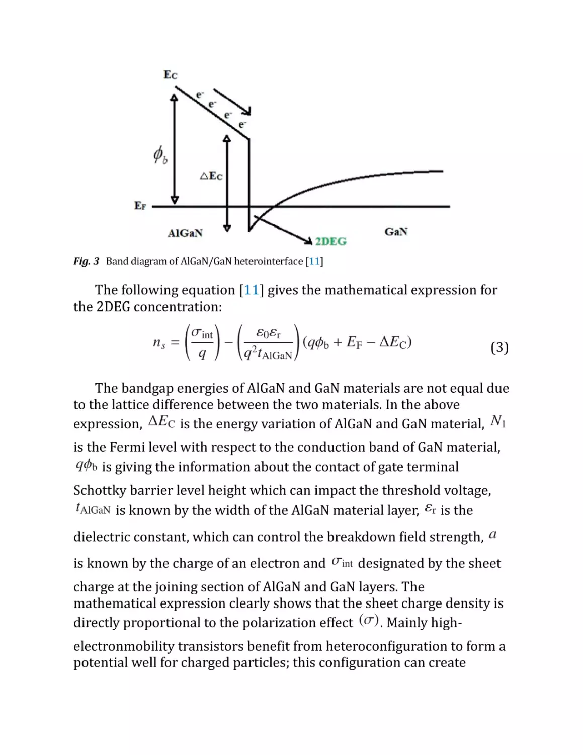
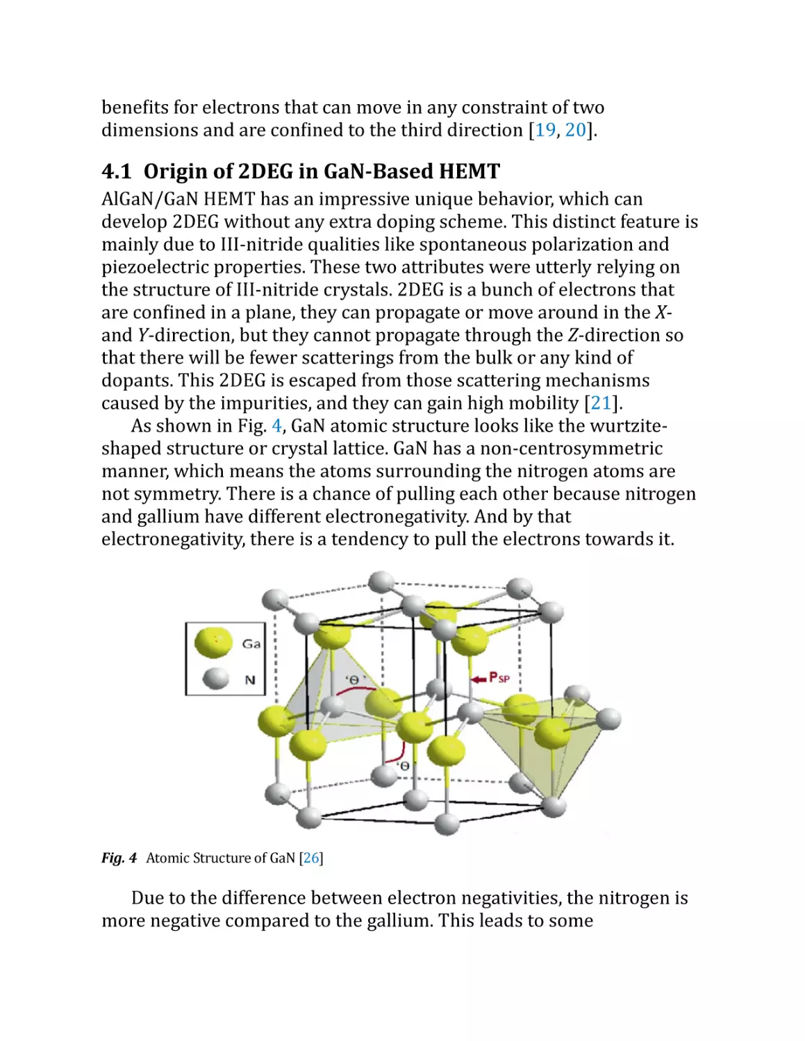
Текст
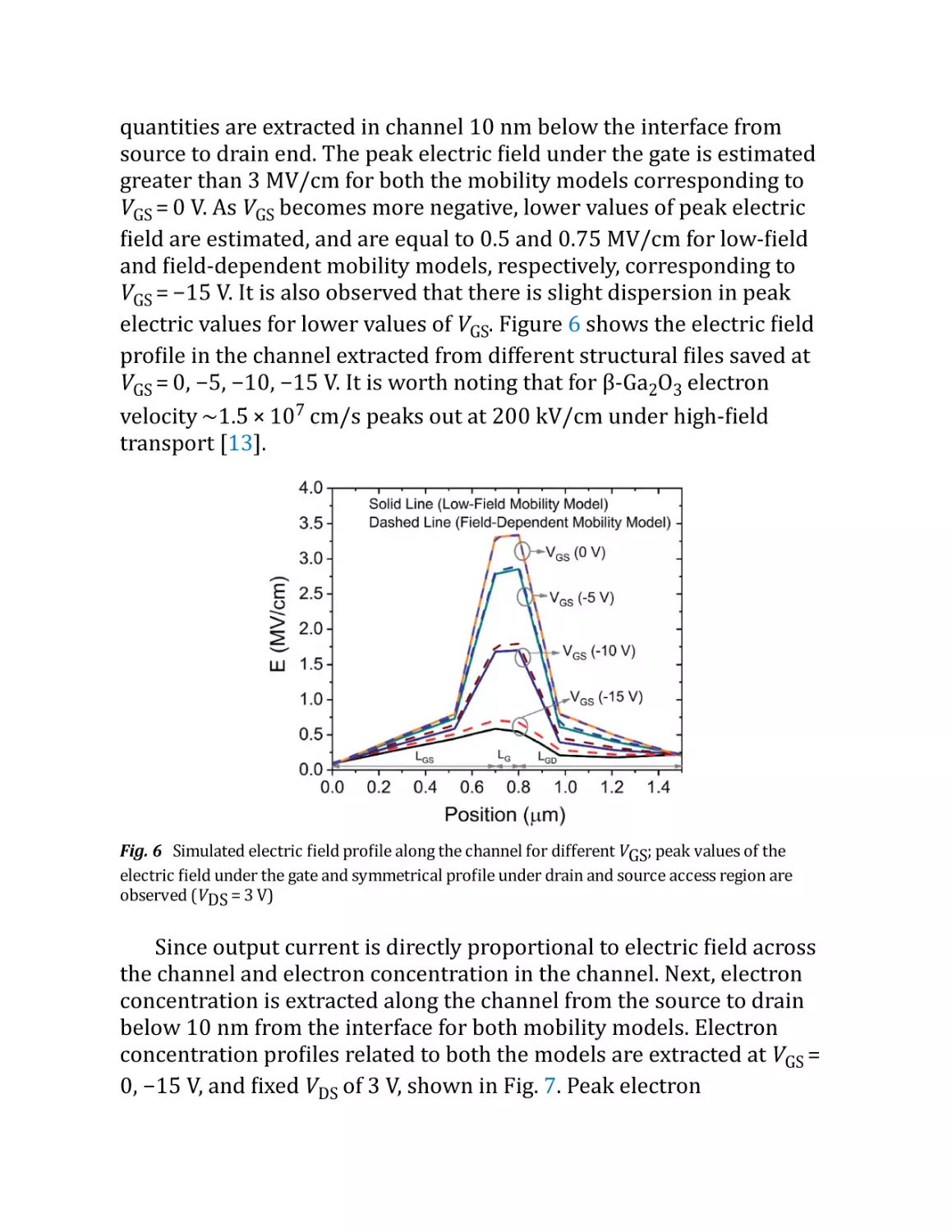
Springer Tracts in Electrical and
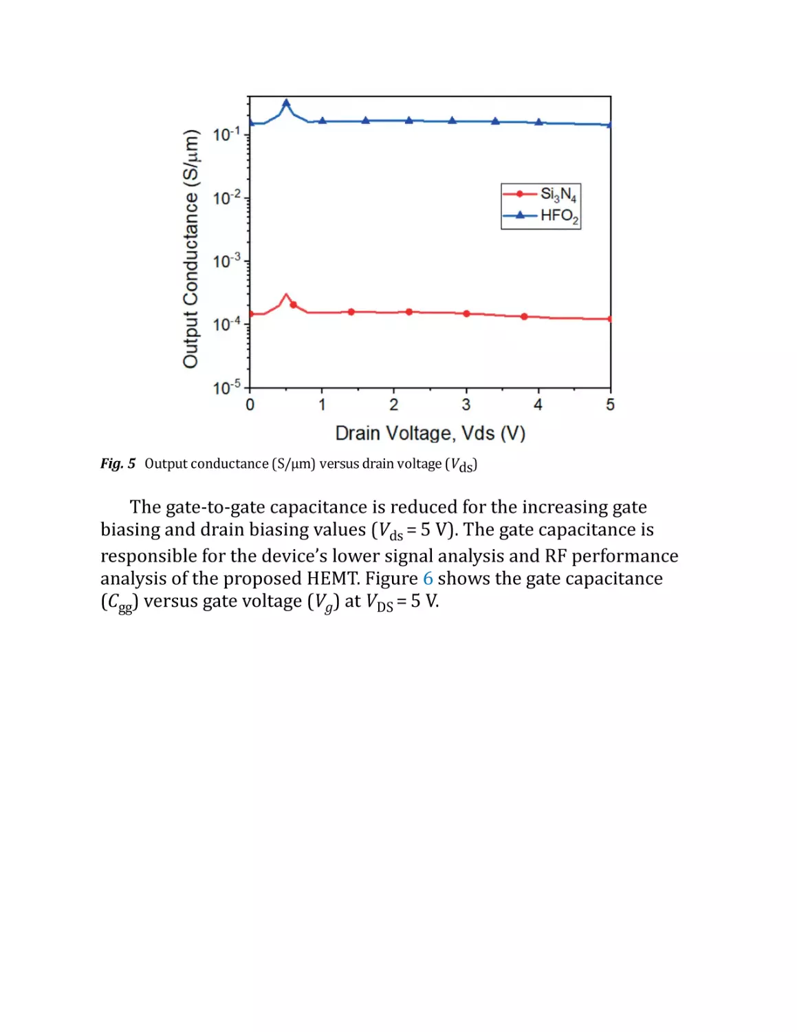
Electronics Engineering
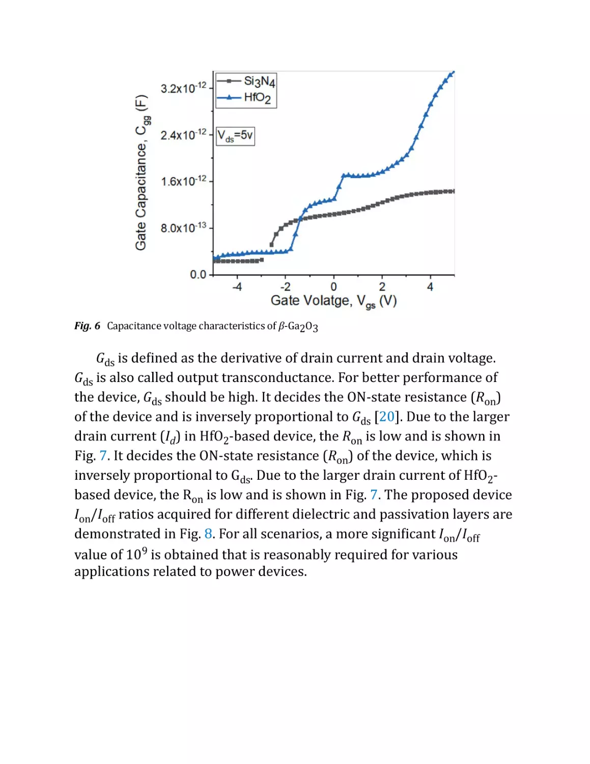
Series Editors
Brajesh Kumar Kaushik
Department of Electronics and Communication Engineering, Indian
Institute of Technology Roorkee, Roorkee, Uttarakhand, India
Mohan Lal Kolhe
Department of Engineering & Science, University of Agder, Kristiansand,
Norway
Springer Tracts in Electrical and Electronics Engineering (STEEE)
publishes the latest developments in Electrical and Electronics
Engineering - quickly, informally and with high quality. The intent is to
cover all the main branches of electrical and electronics engineering,
both theoretical and applied, including:
Signal, Speech and Image Processing
Speech and Audio Processing
Image Processing
Human-Machine Interfaces
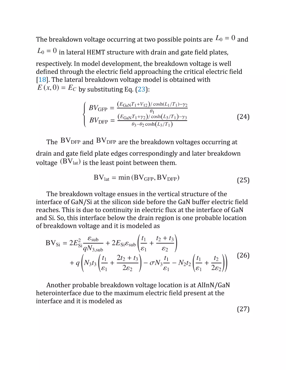
Digital and Analog Signal Processing
Microwaves, RF Engineering and Optical Communications
Electronics and Microelectronics, Instrumentation
Electronic Circuits and Systems
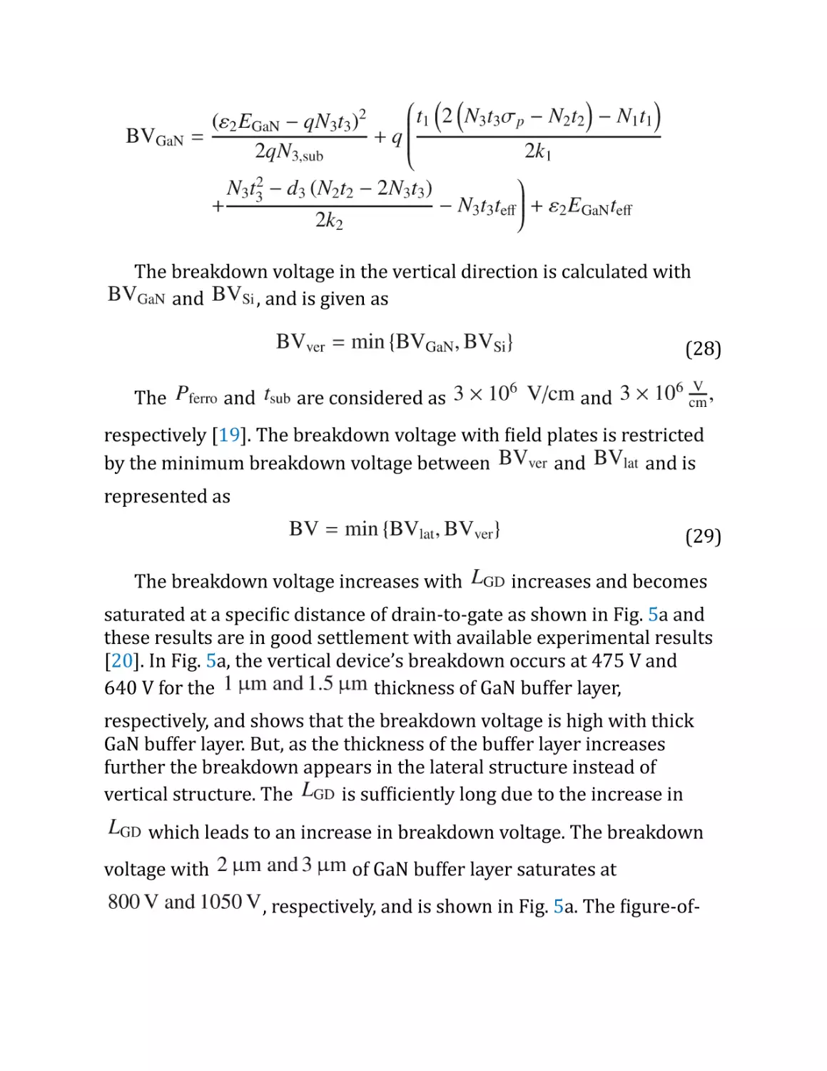
Embedded Systems
Electronics Design and Verification
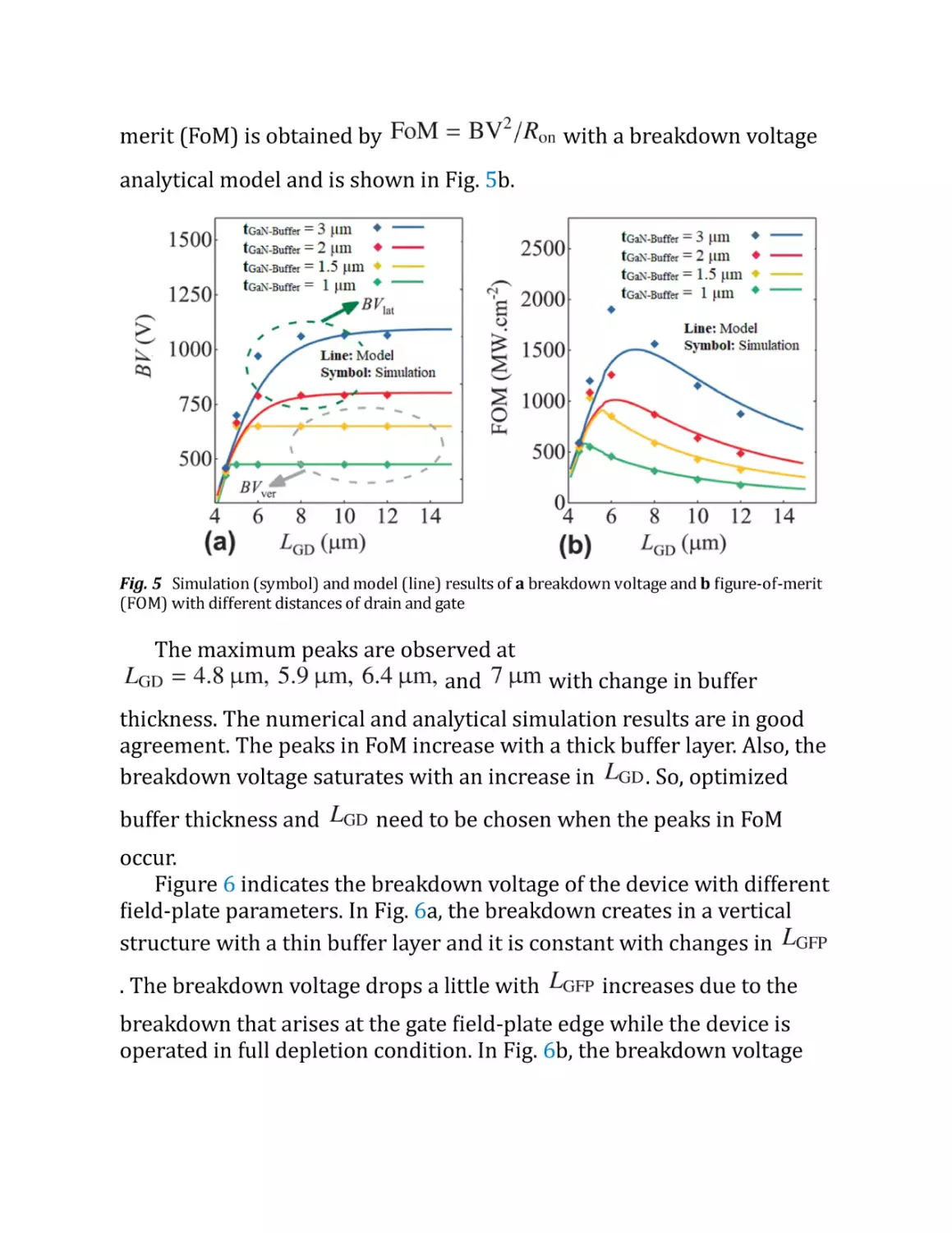
Cyber-Physical Systems
Electrical Power Engineering
Power Electronics
Photovoltaics
Energy Grids and Networks
Electrical Machines
Control, Robotics, Automation
Robotic Engineering
Mechatronics
Control and Systems Theory
Automation
Communications Engineering, Networks
Wireless and Mobile Communication
Internet of Things
Computer Networks
Within the scope of the series are monographs, professional books
or graduate textbooks, edited volumes as well as outstanding PhD
theses and books purposely devoted to support education in electrical
and electronics engineering at graduate and post-graduate levels.
Review Process
The proposal for each volume is reviewed by the main editor and/or
the advisory board. The books of this series are reviewed in a single
blind peer review process.
Ethics Statement for this series can be found in the Springer
standard guidelines here https://www.springer.com/us/authorseditors/journal-author/journal-author-helpdesk/before-you-start/
before-you-start/1330#c14214
More information about this series at https://link.springer.com/
bookseries/16799
Editors
Trupti Ranjan Lenka and Hieu Pham Trung Nguyen
HEMT Technology and Applications
Editors
Trupti Ranjan Lenka
Department of Electronics and Communication Engineering, National
Institute of Technology Silchar, Silchar, Assam, India
Hieu Pham Trung Nguyen
Department of Electrical and Computer Engineering, New Jersey
Institute of Technology, Newark, New Jersey, USA
ISSN 2731-4200
e-ISSN 2731-4219
Springer Tracts in Electrical and Electronics Engineering
ISBN 978-981-19-2164-3
e-ISBN 978-981-19-2165-0
https://doi.org/10.1007/978-981-19-2165-0
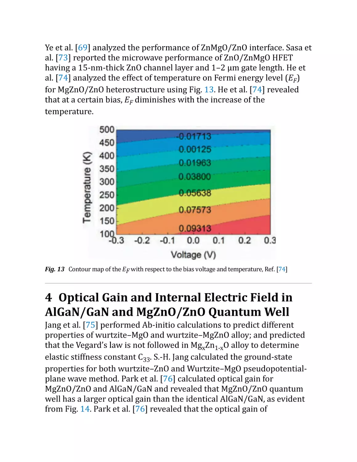
© The Editor(s) (if applicable) and The Author(s), under exclusive
license to Springer Nature Singapore Pte Ltd. 2023
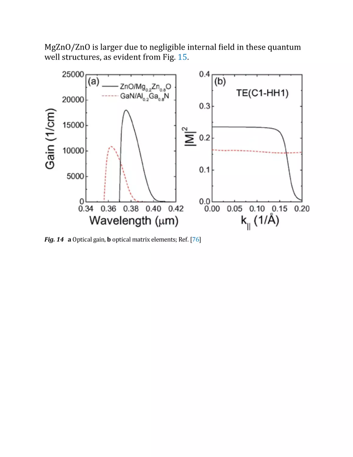
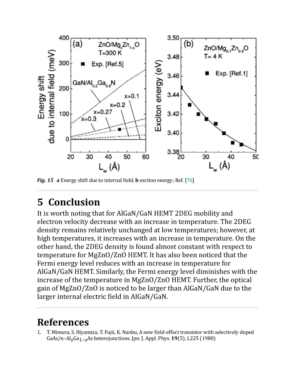
This work is subject to copyright. All rights are solely and exclusively
licensed by the Publisher, whether the whole or part of the material is
concerned, specifically the rights of translation, reprinting, reuse of
illustrations, recitation, broadcasting, reproduction on microfilms or in
any other physical way, and transmission or information storage and
retrieval, electronic adaptation, computer software, or by similar or
dissimilar methodology now known or hereafter developed.
The use of general descriptive names, registered names, trademarks,
service marks, etc. in this publication does not imply, even in the
absence of a specific statement, that such names are exempt from the
relevant protective laws and regulations and therefore free for general
use.
The publisher, the authors, and the editors are safe to assume that the
advice and information in this book are believed to be true and accurate
at the date of publication. Neither the publisher nor the authors or the
editors give a warranty, expressed or implied, with respect to the
material contained herein or for any errors or omissions that may have
been made. The publisher remains neutral with regard to jurisdictional
claims in published maps and institutional affiliations.
This Springer imprint is published by the registered company Springer
Nature Singapore Pte Ltd.
The registered company address is: 152 Beach Road, #21-01/04
Gateway East, Singapore 189721, Singapore
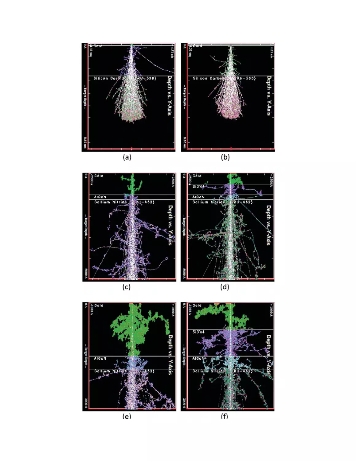
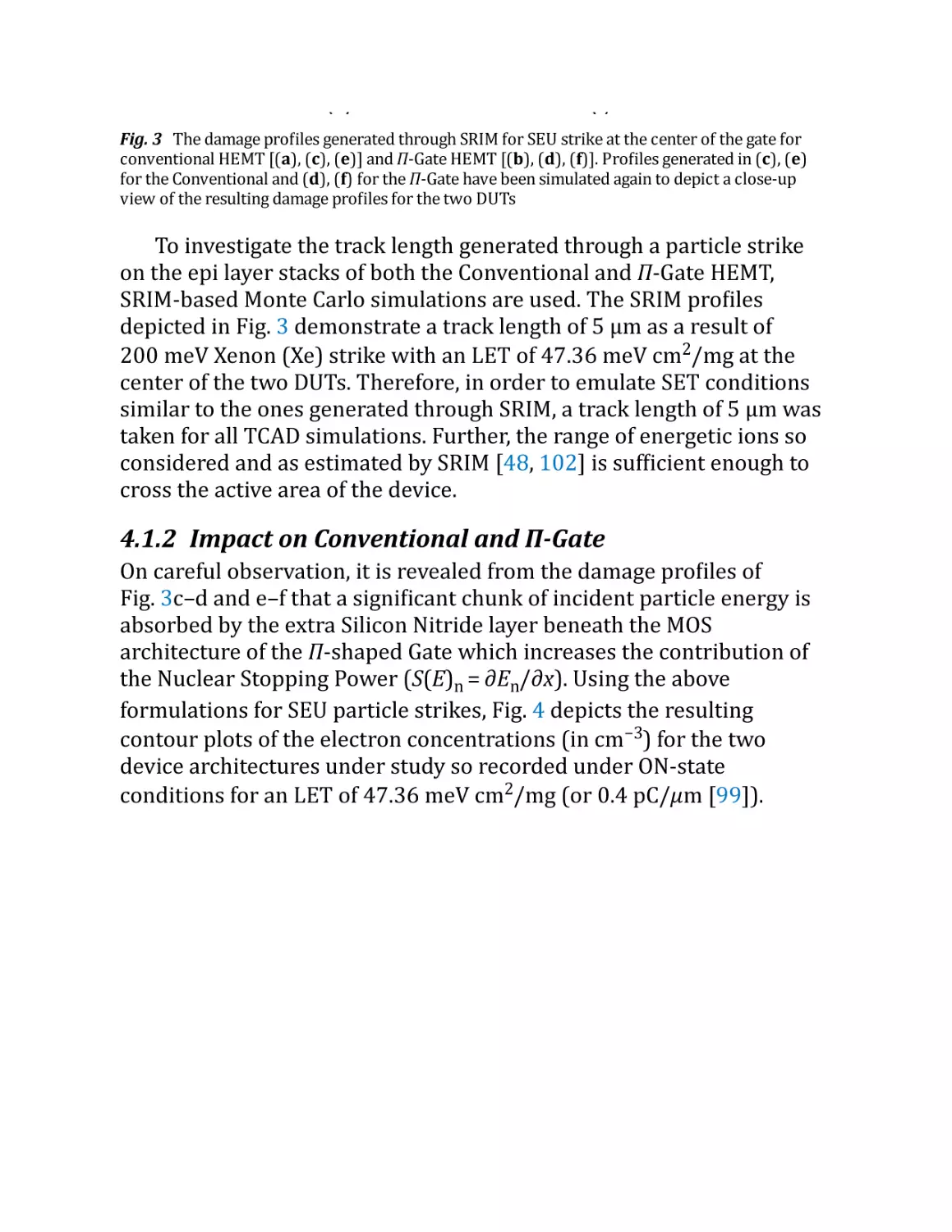
Contents
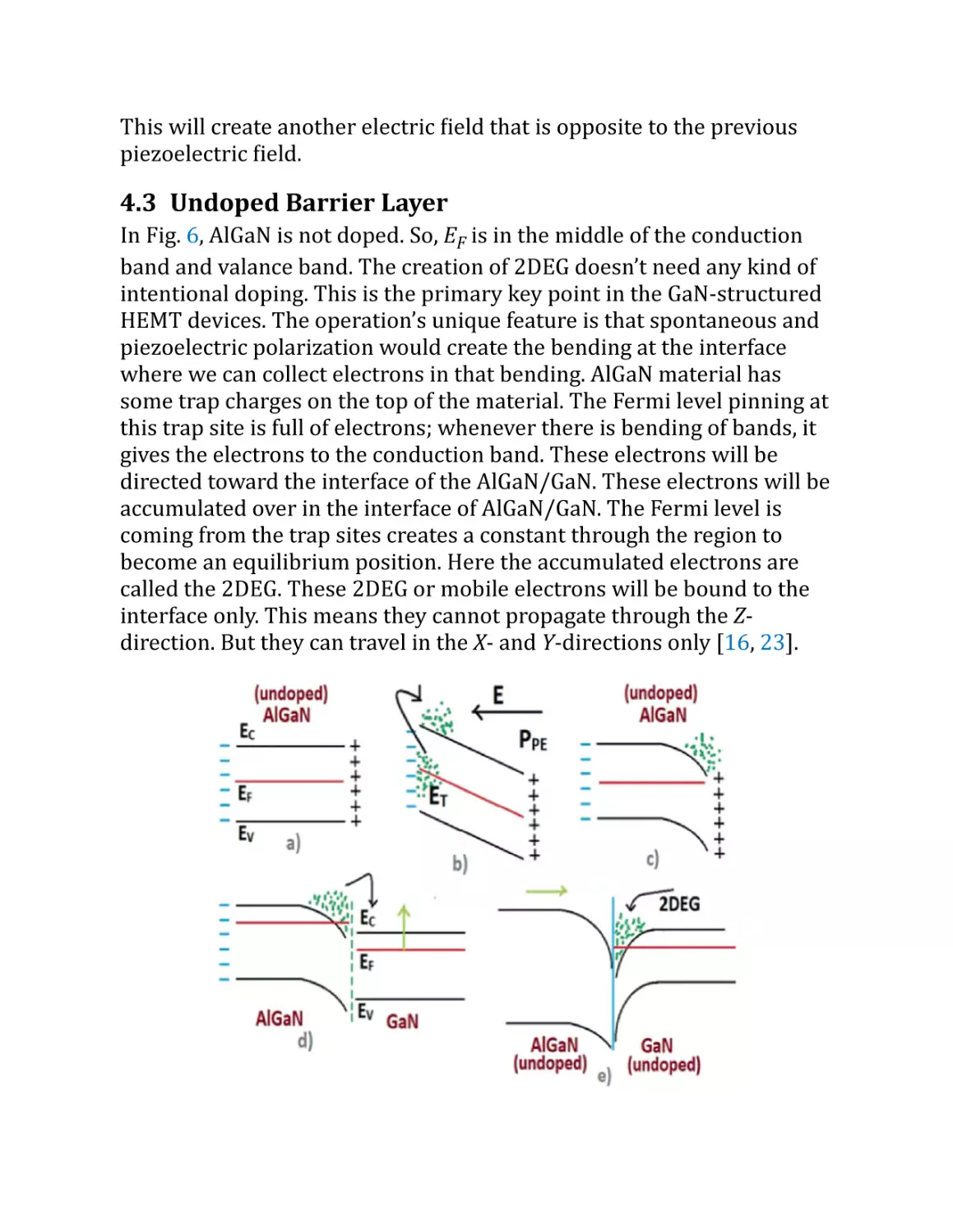
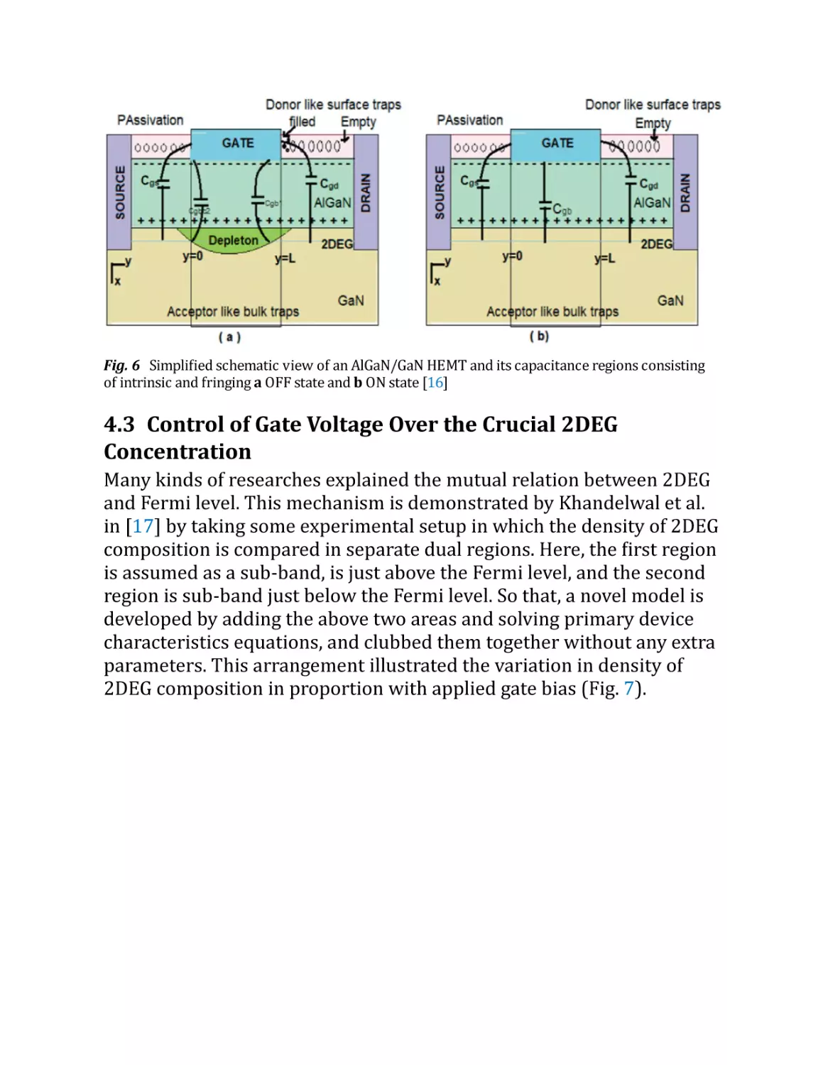
Ultrawide Bandgap AlGaN-Channel-Based HEMTs for NextGeneration Electronics
P. Murugapandiyan, N. Ramkumar and S. Ravi
Breakdown Mechanisms and Scaling Technologies of AlGaN/GaN
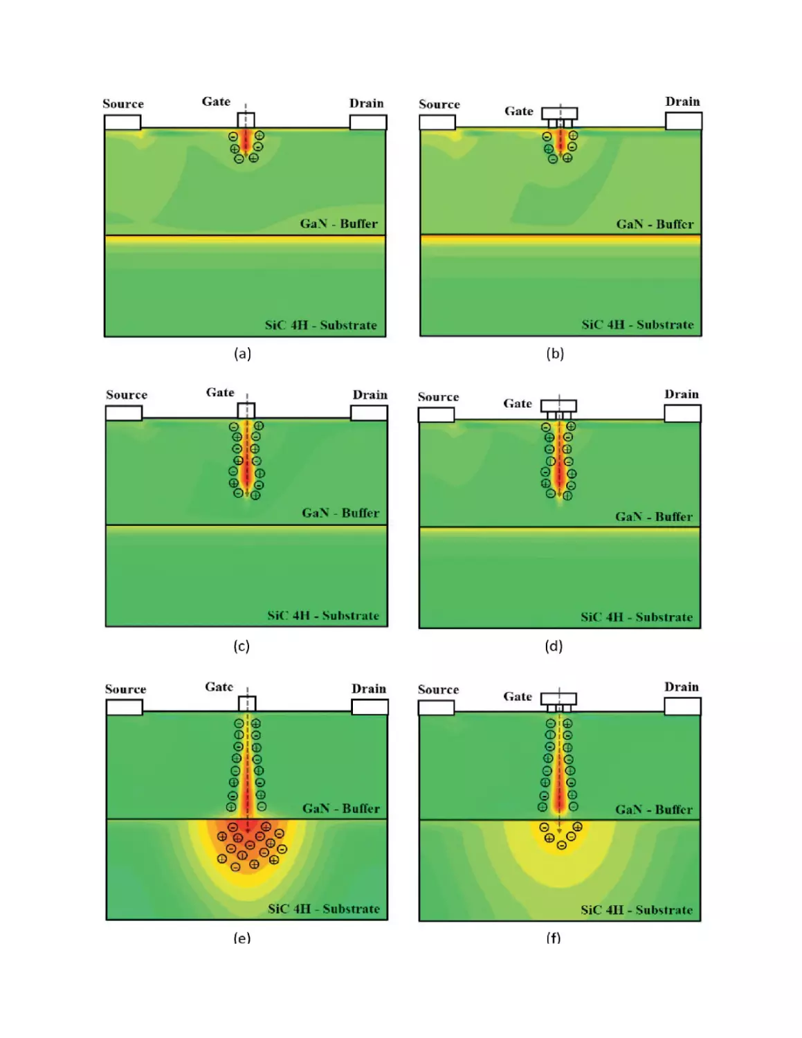
HEMTs
Sneha Kabra and Mridula Gupta
Influence of Al2O3Oxide Layer Thickness Variation on PZT
Ferroelectric Al0.3Ga0.7N/AlN/GaN E-Mode GR-MOSHEMT
Abdul Naim Khan, S. N. Mishra, Meenakshi Chauhan,
Kanjalochan Jena and G. Chatterjee
Study of Different Transport Properties of MgZnO/ZnO and AlGaN/
GaN High Electron Mobility Transistors:A Review
Yogesh Kumar Verma, Varun Mishra, Lucky Agarwal, Laxman Singh
and Santosh Kumar Gupta
Analytical Modeling of Electric Field and Breakdown Voltage
Characteristics of AlInN/GaN HEMT with Field Plates
G. Amarnath, Manisha Guduri and M. C. Chinnaiah
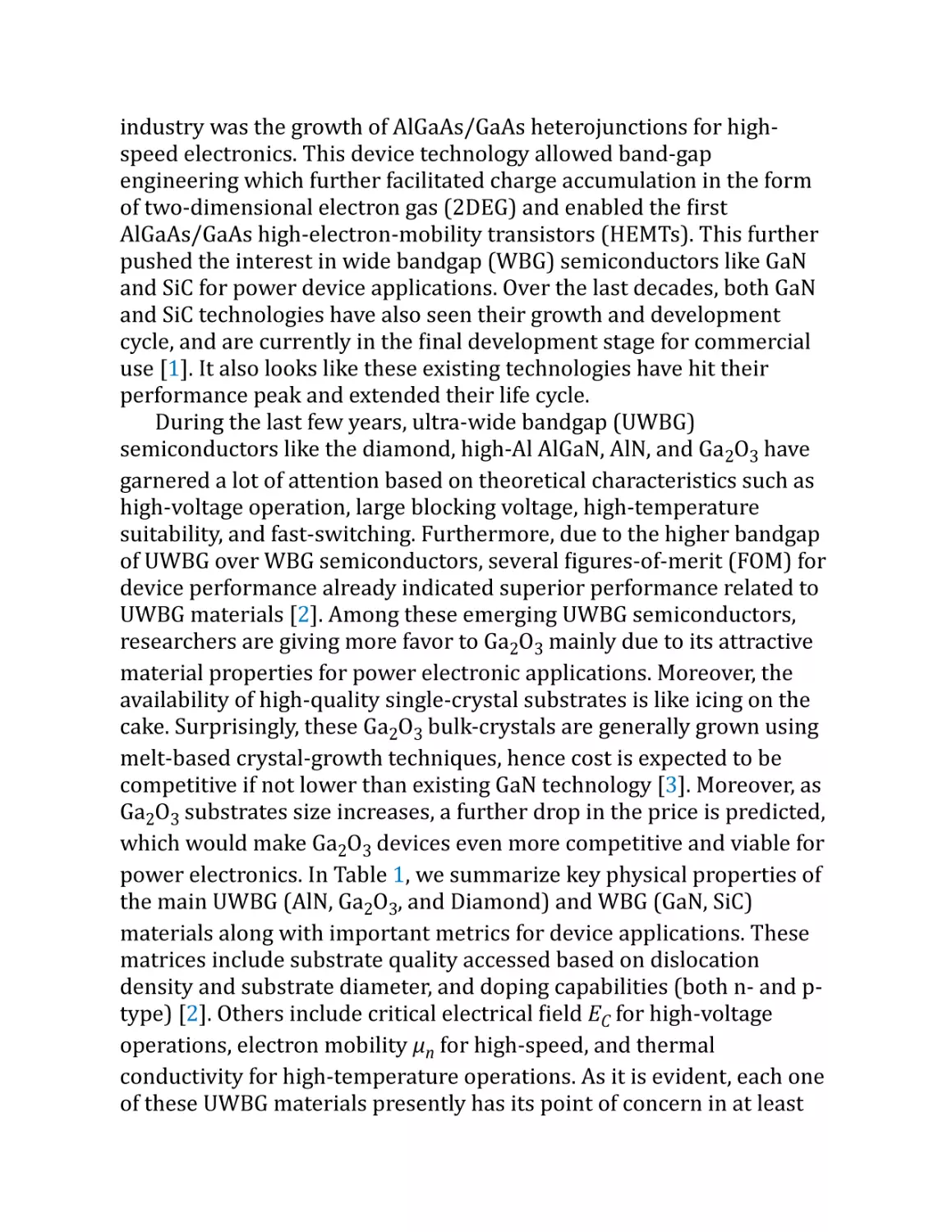
Performance Analysis of HfO2 and Si3N4 Dielectrics in β-Ga2O3
HEMT
Meenakshi Chauhan, Abdul Naim Khan, Raghuvir Tomar and
Kanjalochan Jena
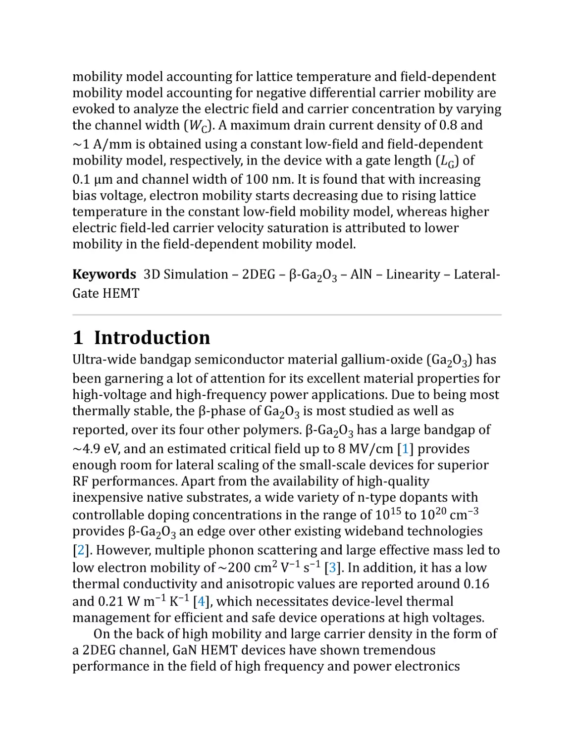
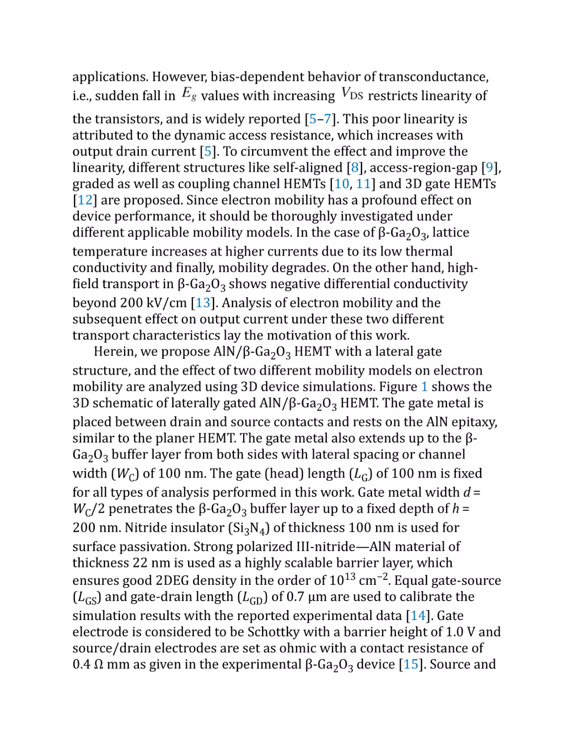
3D Simulation Study of Laterally Gated AlN/β-Ga2O3HEMT
Technology for RF and High-Power Nanoelectronics
Rajan Singh, Trupti Ranjan Lenka and Hieu Pham Trung Nguyen
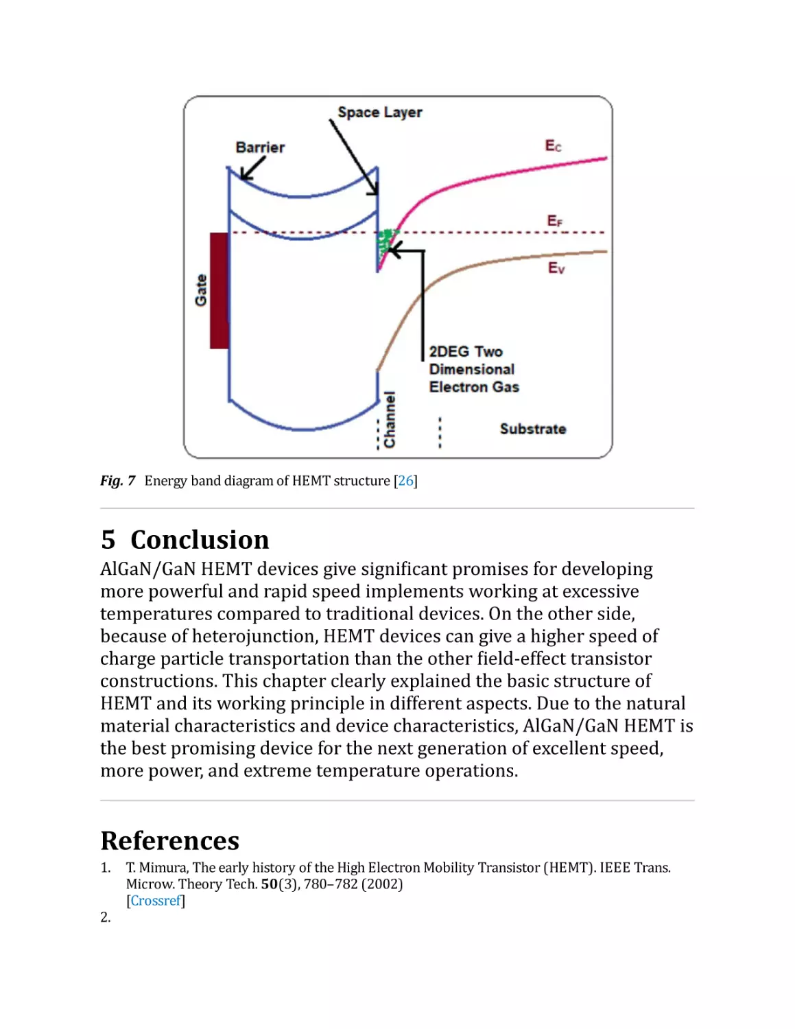
Operation Principle of AlGaN/GaN HEMT
G. Purnachandra Rao, Rajan Singh and Trupti Ranjan Lenka
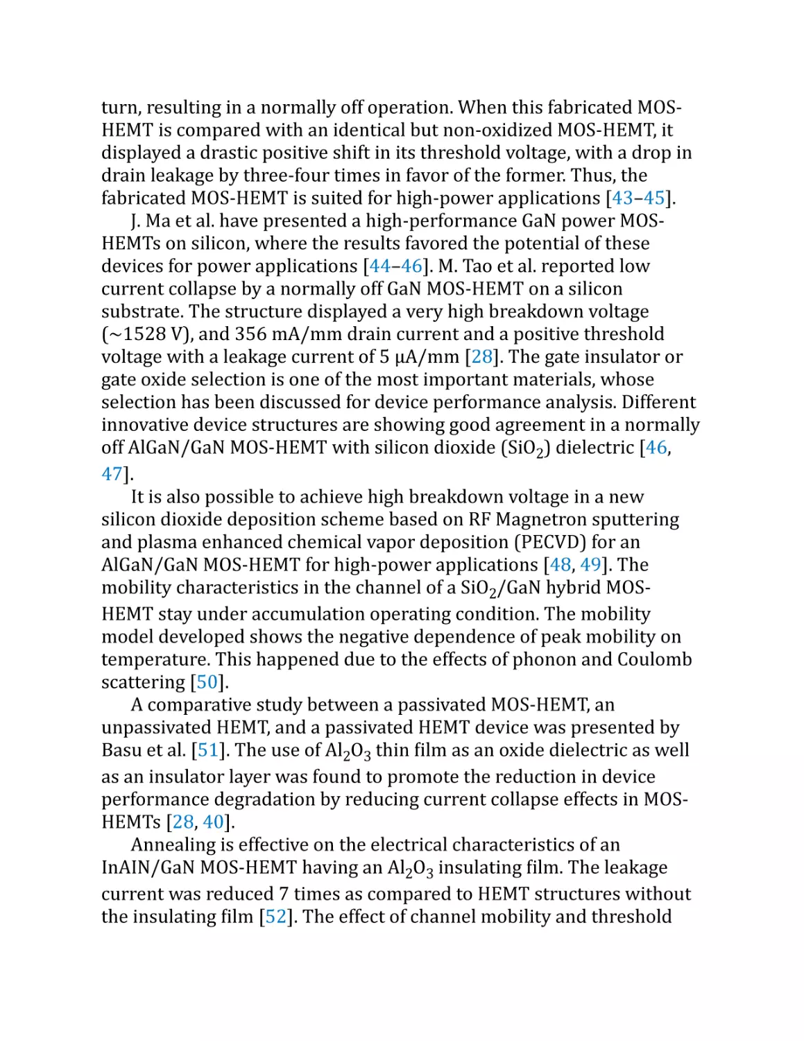
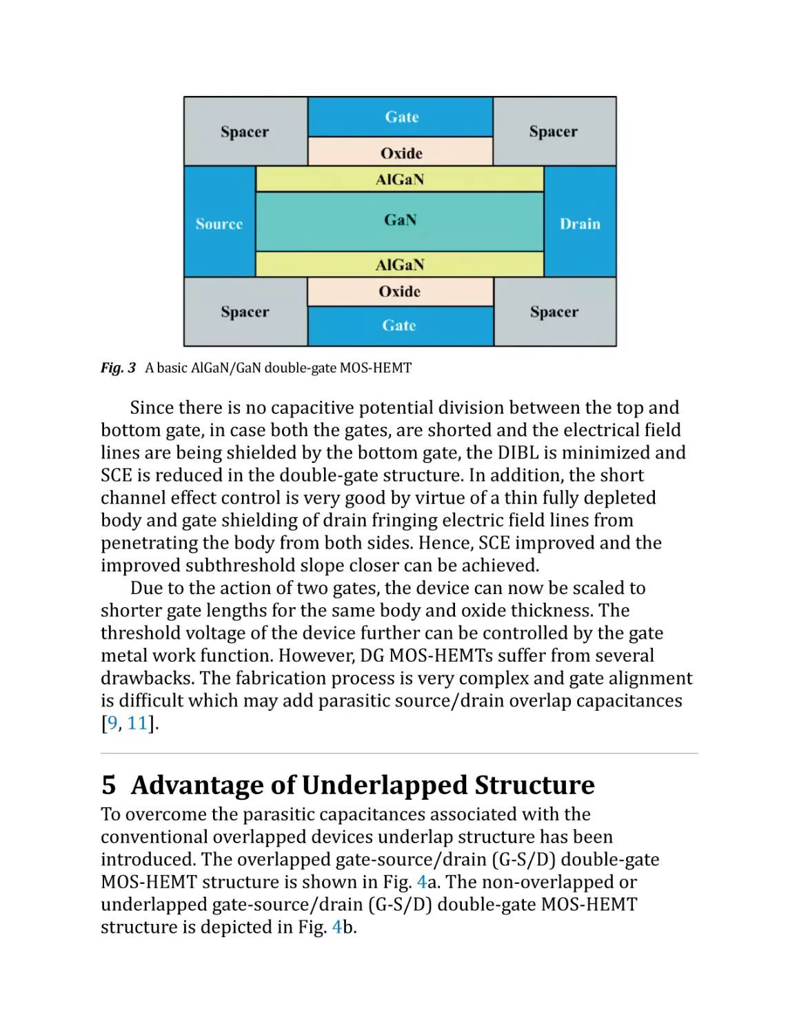
Multigate MOS-HEMT
Atanu Kundu and Mousiki Kar
Enhancement-Mode MOSHEMT
Raghunandan Swain and Trupti Ranjan Lenka
Performance Analysis of AlGaN/GaN HEMT for RF and Microwave
Nanoelectronics Applications
G. Purnachandra Rao, Rajan Singh and Trupti Ranjan Lenka
High Electron Mobility Transistor:Physics-Based TCAD Simulation
and Performance Analysis
Kalyan Biswas, Rachita Ghoshhajra and Angsuman Sarkar
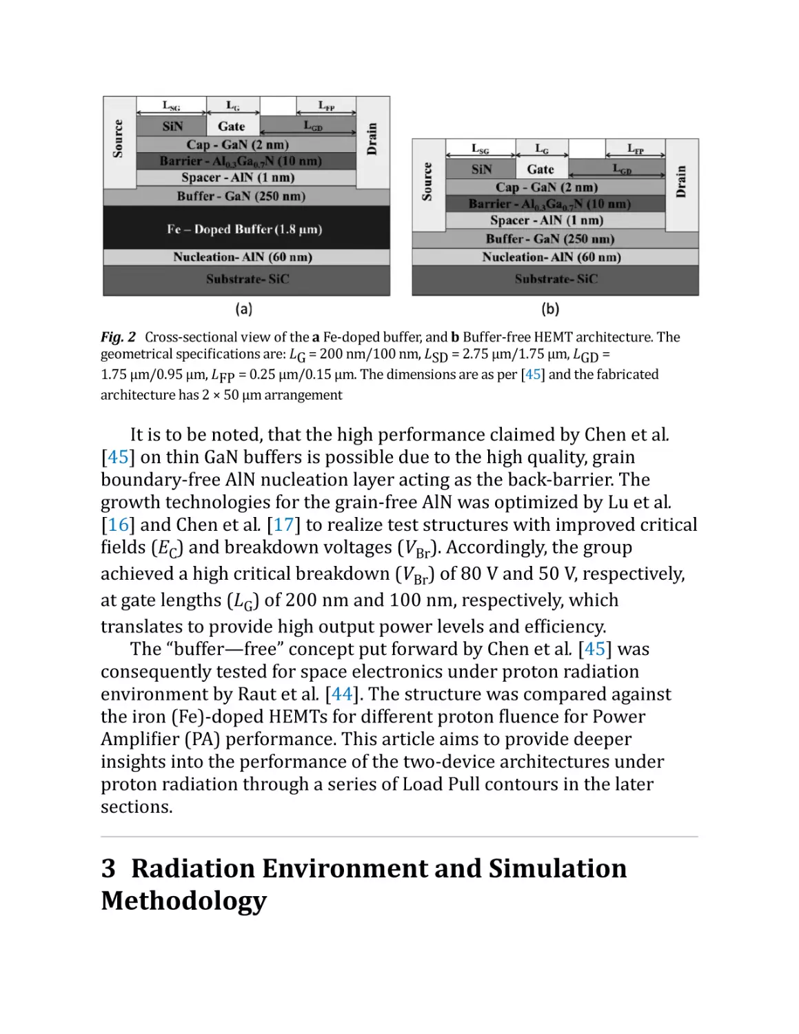
Emerging Device Architectures for Space Electronics
Khushwant Sehra, Samriddhi Raut, D. S. Rawal and Manoj Saxena
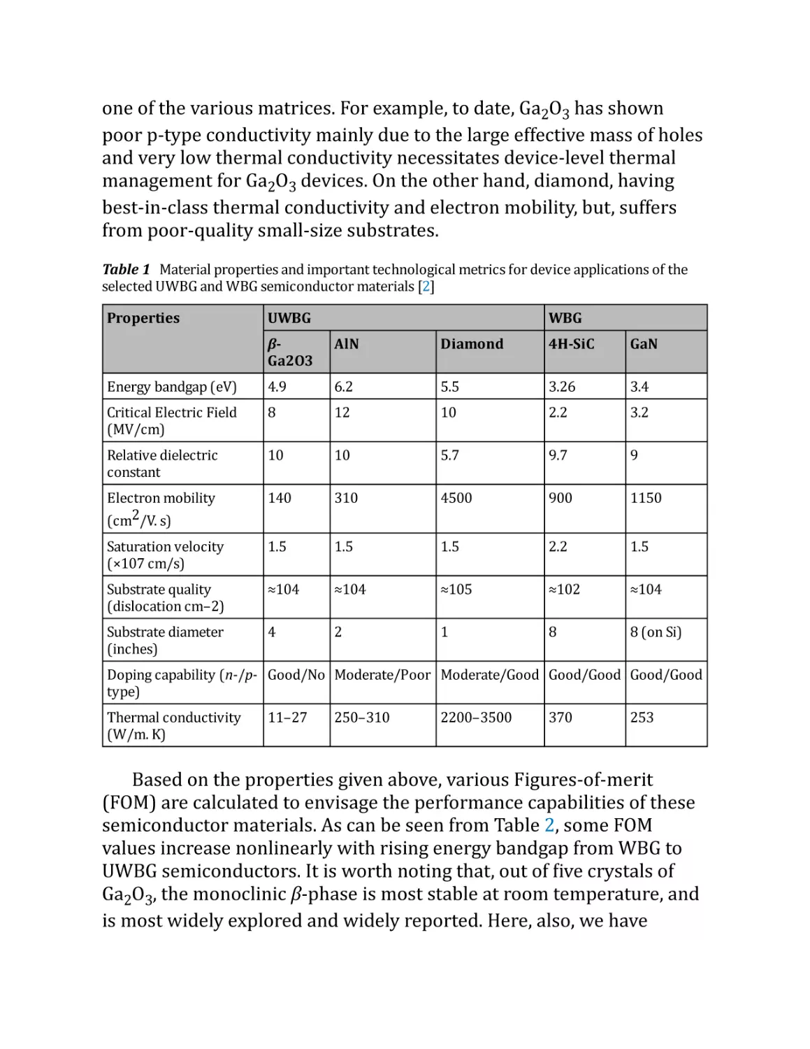
Evolution and Present State-of-Art Gallium Oxide HEMTs–The Key
Takeaways
Rajan Singh, Trupti Ranjan Lenka and Hieu Pham Trung Nguyen
Linearity Analysis of AlN/β-Ga2O3HEMT for RFIC Design
Yogesh Kumar Verma, Varun Mishra, Rajan Singh,
Trupti Ranjan Lenka and Santosh Kumar Gupta
HEMT for Biosensing Applications
Deepak Kumar Panda and Trupti Ranjan Lenka
Editors and Contributors
About the Editors
Trupti Ranjan Lenka is an Assistant Professor in the Department of
Electronics and Communication Engineering, National Institute of
Technology Silchar, India. He received a B.E. degree in Electronics and
Communication Engineering from Berhampur University, Odisha, in
2000, M.Tech. degree in VLSI Design from Dr. A. P. J. Abdul Kalam
Technical University, Lucknow, in 2007 and a Ph.D. degree in
Microelectronics Engineering from Sambalpur University, Odisha, in
2012. He was a Visiting Researcher at Helen and John C. Hartmann
Department of Electrical and Computer Engineering, New Jersey
Institute of Technology (NJIT), Newark, New Jersey, the USA, in 2019,
and Solar Energy Research Institute of Singapore (SERIS), National
University of Singapore (NUS), Singapore, in 2018. He received
Distinguished Faculty Award by NIT Silchar in 2019. He has supervised
12 Ph.D. and 23 M.Tech. students under his guidance. He has published
105 journal research papers, 17 book chapters, and 58 conference
papers to his credit and delivered 21 invited talks. His research
interests include nanoelectronics: III-nitride heterojunction devices
(HEMT, NW LED), solar photovoltaics, energy harvesting using MEMS,
and nanotechnology.
Hieu Pham Trung Nguyen received his Ph.D. degree in Electrical
Engineering from McGill University, Canada, in 2012. He joined the New
Jersey Institute of Technology in 2014 and currently is an Associate
Professor in the Department of Electrical and Computer Engineering.
He is a recipient of the 2020 NSF CAREER Award, the 2019 Saul K
Fenster Innovation in Engineering Education Ward, the SPIE
Scholarship in Optics and Photonics 2012 (for his potential long-range
contributions to the field of optics, photonics, or related field), the Best
Student Paper Award 2011 (Second Place) at the IEEE Photonics
Conference 2011, and the Outstanding Student Paper Award at the 28th
North American Molecular Beam Epitaxy Conference, 2011. He is
serving as a reviewer for over 70 journals. His research areas are
electronic and photonic devices.
Contributors
Lucky Agarwal
School of Electronics Engineering, Vellore Institute of Technology,
Chennai, Tamil Nadu, India
G. Amarnath
Department of ECE, Marri Laxman Reddy Institute of Technology and
Management, Hyderabad, India
Kalyan Biswas
ECE Department, MCKV Institute of Engineering, Liluah, Howrah, WB,
India
G. Chatterjee
Department of Electronics and Communication Engineering, The LNM
Institute of Information Technology, Jaipur, Rajasthan, India
Meenakshi Chauhan
Department of Electronics and Communication Engineering, The LNM
Institute of Information Technology, Jaipur, Rajasthan, India
M. C. Chinnaiah
Department of ECE, B.V. Raju Institute of Technology, Narsapur, India
Rachita Ghoshhajra
CSE Department, MCKV Institute of Engineering, Liluah, Howrah, WB,
India
Manisha Guduri
Department of ECE, KG Reddy College of Engineering and Technology,
Hyderabad, India
Mridula Gupta
Senior Professor and Head, Department of Electronic Science,
University of Delhi South Campus, New Delhi, India
Santosh Kumar Gupta
Department of Electronics and Communication Engineering, Motilal
Nehru National Institute of Technology, Allahabad, Uttar Pradesh, India
Kanjalochan Jena
Department of Electronics and Communication Engineering, The LNM
Institute of Information Technology, Jaipur, Rajasthan, India
Sneha Kabra
Associate Professor, Department of Instrumentation, Shaheed Rajguru
College of Applied Sciences for Women, University of Delhi, New Delhi,
India
Mousiki Kar
Department of Electronics and Communication Engineering, Heritage
Institute of Technology, Kolkata, India
Abdul Naim Khan
Department of Electronics and Communication Engineering, The LNM
Institute of Information Technology, Jaipur, Rajasthan, India
Atanu Kundu
Department of Electronics and Communication Engineering, Heritage
Institute of Technology, Kolkata, India
Trupti Ranjan Lenka
Microelectronics and VLSI Design Group, Department of Electronics
and Communication Engineering, National Institute of Technology
Silchar, Silchar, Assam, India
S. N. Mishra
School of Electronics Engineering, KIIT (Deemed to be University),
Bhubaneswar, Odisha, India
Varun Mishra
Department of Electronics and Electrical Engineering, Graphic Era
(Deemed to be University), Dehradun, Uttarakhand, India
P. Murugapandiyan
Department of Electronics and Communication Engineering, Anil
Neerukonda Institute of Technology & Sciences, Visakhapatnam,
Andhra Pradesh, India
Hieu Pham Trung Nguyen
Department of Electrical and Computer Engineering, New Jersey
Institute of Technology, Newark, New Jersey, USA
Deepak Kumar Panda
Microelectronics and VLSI Design Group, School of Electronics, VIT-AP
University, Amaravati, Andhra Pradesh, India
G. Purnachandra Rao
Department of Electronics and Communication Engineering, National
Institute of Technology Silchar, Silchar, Assam, India
N. Ramkumar
Department of Electronics and Communication Engineering, Anil
Neerukonda Institute of Technology & Sciences, Visakhapatnam,
Andhra Pradesh, India
Samriddhi Raut
Department of ECE, Maharaja Surajmal Institute of Technology, Guru
Gobind Singh Indraprastha University, New Delhi, India
S. Ravi
Department of Electronics and Communication Engineering, Seshadri
Rao Gudlavalleru Engineering College, Gudlavalleru, Andhra Pradesh,
India
D. S. Rawal
MMIC Fabrication Division, Solid State Physics Laboratory, Defence
Research & Development Organization, New Delhi, India
Angsuman Sarkar
ECE Department, Kalyani Government Engineering College, Kalyani,
Nadia, WB, India
Manoj Saxena
Department of Electronics, Deen Dayal Upadhyaya College, University of
Delhi, New Delhi, India
Khushwant Sehra
Department of Electronic Science, University of Delhi South Campus,
New Delhi, India
Laxman Singh
Department of Electronics and Communication Engineering, Noida
Institute of Engineering and Technology, Greater Noida, India
Rajan Singh
Microelectronics and VLSI Design Group, Department of Electronics
and Communication Engineering, National Institute of Technology
Silchar, Silchar, Assam, India
Raghunandan Swain
Department of Electronics and Telecommunication Engineering, Parala
Maharaja Engineering College, Berhampur, Odisha, India
Raghuvir Tomar
Department of Electronics and Communication Engineering, The LNM
Institute of Information Technology, Jaipur, Rajasthan, India
Yogesh Kumar Verma
School of Electronics and Electrical Engineering, Lovely Professional
University, Jalandhar, Punjab, India
© The Author(s), under exclusive license to Springer Nature Singapore Pte Ltd. 2023
T. R. Lenka, H. P. T. Nguyen (eds.), HEMT Technology and Applications, Springer Tracts in Electrical
and Electronics Engineering
https://doi.org/10.1007/978-981-19-2165-0_1
Ultrawide Bandgap AlGaN-ChannelBased HEMTs for Next-Generation
Electronics
P. Murugapandiyan1 , N. Ramkumar1 and S. Ravi2
(1) Department of Electronics and Communication Engineering, Anil
Neerukonda Institute of Technology & Sciences, Visakhapatnam,
Andhra Pradesh, 531162, India
(2) Department of Electronics and Communication Engineering,
Seshadri Rao Gudlavalleru Engineering College, Gudlavalleru,
Andhra Pradesh, 521356, India
P. Murugapandiyan
Email: murugavlsi@gmail.com
Abstract
This chapter reviews the recent progress in ultrawide bandgap AlGaNchannel-based high electron mobility transistors. AlGaN channel is the
alternate substitute for the conventional GaN channel. In order to
enhance the power handling capability of III-nitride-based
heterostructure devices, improving the breakdown performance of the
device without reduction in the current density is one of the simplest
techniques. AlGaN-channel-based HEMTs favorably increase the critical
electric field of the device. For the next-generation RF application,
further improving the power handling capabilities of RF modules,
AlGaN channel HEMT is the most optimistic applicant and it delivers
four times larger GaN HEMT’s power performance and thus becoming
the possible substitute to the GaN channel for the next generation
power as well as RF devices and circuits. This chapter describes the
polarization details of AlxGa1−xN/AlyGa1−yN heterostructure, and
various device structure of AlGaN channel HEMTs and their static and
dynamic characteristics.
Keywords GaN – HEMT – Heterostructure – Polarizations – RF – Ultrawide Bandgap
1 Introduction
Since the III-nitride semiconductor materials offer a wide range of
bandgap spectrum, III-nitride-based devices are widely used in
optoelectronics, RF, and power electronics applications. Due to the
existence of stronger polarization, high critical breakdown field, and
higher carrier velocity, the GaN-channel-based HEMTs are used in highpower RF amplification and switching. Because of the existence of
polarization effects, the AlGaN/GaN heterostructure interface has a
high density of electron density with high carrier mobility and many
researchers demonstrated the potential of AlGaN/GaN HEMTs. Several
GaN-channel-based commercial HEMTs are developed and available in
the market for high-power microwave applications, low-noise RF circuit
design, DC–DC converters, electric vehicles, motor drivers, etc.
Further increasing the power density of the III-nitride devices for
next-generation electronics and enhancing the breakdown voltage of
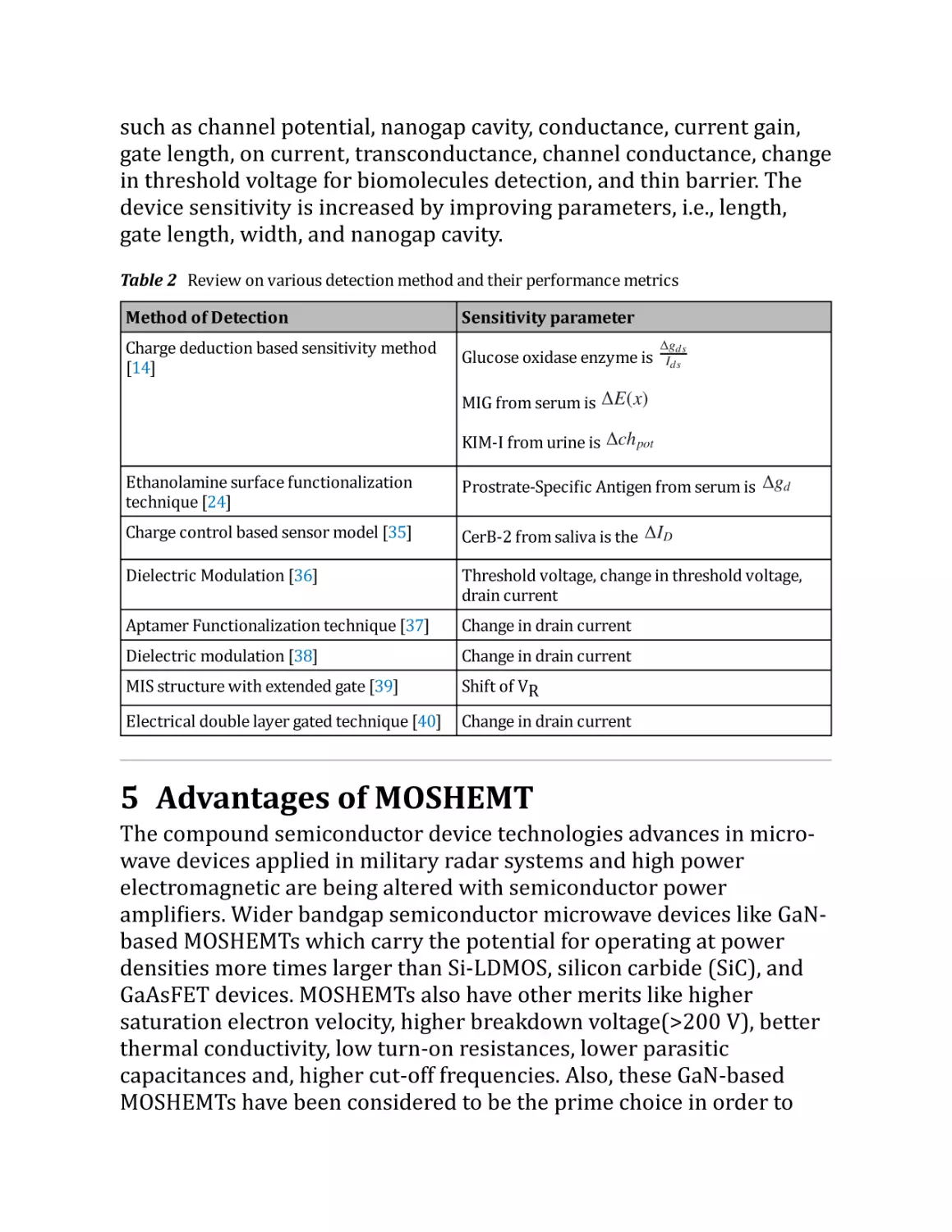
the HEMTs are most important. Table 1 shows the compound
semiconductor material properties. The AlN material properties
dominate the GaN in terms of 2 × bandgap, 4 × breakdown field, high
Johnson figure of merit (JFoM), good thermal conductance, and high
Baliga figure of merit (BFoM). Due to these outstanding properties,
AlxGa1-xN ultrawide bandgap ternary material is used as the channel
instead of a conventional GaN channel for improving the breakdown
field of the HEMTs. Therefore, high Al composition AlGaN-channelbased HEMTs are expected to exhibit extremely large blocking voltage
and high-temperature operation in modern power electronics era.
Aside from power electronics applications, AlGaN channel HEMTs are
promising candidates for millimeter-wave applications because of their
high Johnson figure of merit (
) and expected to
deliver high RF power density at millimeter wave. In evaluating AlGaN
channel HEMT technologies for millimeter-wave high-power
applications, the cutoff frequencies (FT, and FMAX) of the HEMTs are
important device parameters in addition to breakdown voltage and
high drain current density. The improvement in the device cutoff
frequency was achieved through scaling techniques.
Table 1 Semiconductor material properties
Si
GaAs SiC
GaN AlN
Bandgap (eV)
1.12 1.42
3.26 3.40 6.20
Breakdown field (MV/cm)
0.3
3.0
Electron mobility (cm2/Vs)
1500 8500 1000 2000 1090
Electron saturation velocity (cm/s) × 107 1
0.4
2
3.3
12
2
2.5
2.2
Dielectric constant
11.9 12.9
10
8.9
8.5
JFoM
1
7
400
760
7800
BFoM
1
9
11
39
67
2 Spontaneous and Piezoelectric Polarization
of AlxGa1−xN/AlyGa1−yN Heterostructure
The III-nitride-based heterostructure-based devices are widely used in
various electronic applications including high power switching, high
power microwave, and optoelectronics. The asymmetry of wurtzite
crystal structure induces spontaneous polarization (SP) and
piezoelectric polarization (PZ) effect in III-nitride semiconductorsbased heterostructure devices. Due to the polarization difference
between a wide bandgap and a narrow bandgap semiconductor, a high
density of 2DEG is existing at the interface. The spontaneous
polarization difference between the materials and strain-induced
piezoelectric polarization is the major source of creation of 2DEG [1].
This property of III-nitride heterostructure devices is attractive for
power electronics and microwave applications. The
AlxGa1−xN/AlyGa1−yN heterostructure polarization details are illustrated
in Fig. 1 for Ga-face crystal structure by considering relaxed, and tensile
strain.
Fig. 1 Spontaneous and piezoelectric polarization details of AlxGa1−xN/AlyGa1−yN
heterostructure
The polarization sheet charge density was obtained from the
following equation:
(1)
The polarization induced charges depend on Al composition and
surface roughness. As shown in Fig. 1a and b, to neutralize the
polarization induced positive charges (
), the free electrons from
donor-like surface trap states come and occupy the quantum well when
the AlxGa1−xN/AlyGa1−yN band offset is reasonably high. Assume the
heterostructure was grown in pseudomorphic (Fig. 1b), the tensile
strain AlxGa1−xN piezoelectric polarization will improve the PAlxGa1−xN–
PAlyGa1−yN polarization difference. In the absence of stain-induced PZ
also, electrons are accumulated in the quantum well due to the SP
difference of AlxGa1−xN/AlyGa1−yN. The PZ of wurtzite III-nitride
materials are described as follows:
(2)
where
and
, and
are elastic constants,
is lattice constant, and
are elastic coefficient. The elastic coefficient parameter, elastic
constant, and lattice constant of
ternary alloy are as
follows:
(3)
(4)
(5)
(6)
(7)
The spontaneous polarization of
calculated from the following equation:
ternary alloys is
(8)
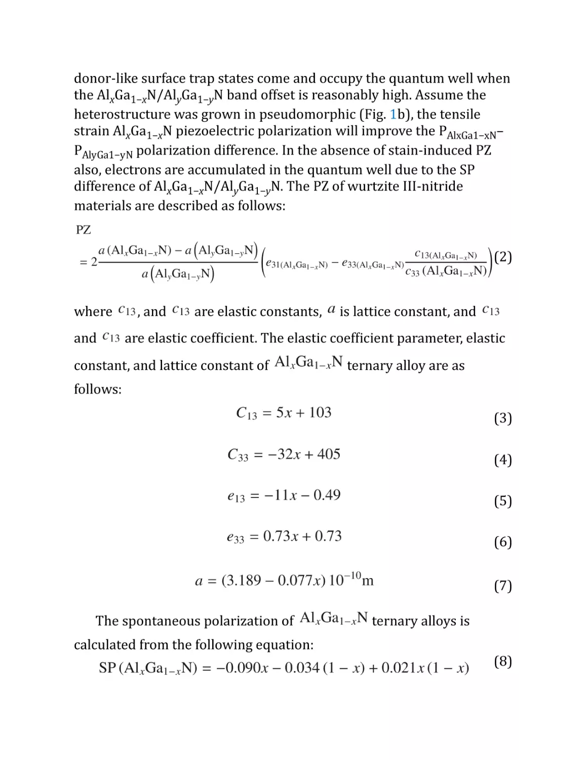
The total carrier density in the 2DEG region for undoped device
configuration is as follows;
(9)
The carrier density in the channel depends on the relative dielectric
constant
, thickness of the barrier layer
, Schottky
barrier
, Fermi energy level
, and conduction band offset
. Therefore, the sheet charge density can be controlled by Al
composition in the AlGaN barrier and the thickness of the barrier. The
bandgap of AlGaN ternary material and conduction band offset is
calculated from the following:
(10)
(11)
(12)
(13)
(14)
(15)
3 AlGaN-Channel-Based HEMTs for HighFrequency Electronics Application
In recent years, ultrawide bandgap semiconductors (AlGaN, Ga2O3, and
diamond) have attracted enormous research interest as key
components for high-power switching applications [1–10]. Particularly,
AlxGa1−xN-channel-based HEMTs are optimistic devices for future
electronics because of their wide bandgap relative to the GaN channel (
), strong polarization, high saturation velocity,
ultrahigh breakdown field. The Monte Carlo simulation showed the Alrich AlGaN material is favorable for high-power RF performance
because the saturation velocity is on par with GaN [11]. Recently, Alrich AlxGa1−xN/AlyGa1−yN-based HEMTs have proven their potential,
which is exceeded the AlxGa1−xN /GaN-based HEMTs performances
[12–15]. And therefore, AlxGa1−xN/AlyGa1−yN-based HEMTs are suitable
for realizing solid-state power amplifiers (PAs) with high power, wide
operational bandwidth, and high efficiency for 5G and 6G wireless
communications. The maximum RF power delivered to a load of a basic
amplifier circuit is as follows:
(16)
The high RF current (
), and breakdown voltage (
) of the
transistor will improve the output power density of a solid-state power
amplifier. Due to the virtue of high critical electric field ( ), large
breakdown field, and a high Johnson figure of merit (
),
the AlGaN channel HEMTs are highly desirable for high-power RF
electronics. Further, the
enhanced by Al-rich AlxGa1−xN/AlyGa1−yN
(x > y) heterostructures. High output current density (IDS) and high VBR
are the important factors for improving the power density of solid-state
power amplifier. The AlyGa1−yN channel HEMT with high Al
composition enables the critical field ~4 × higher than GaN-channelbased devices. The low carrier mobility (µ) and alloy scattering degrade
the on-state current (
) for long AlGaN channel devices.
However, at a high electric field, the saturation velocity of AlGaN
channel HEMTs is on par with GaN-channel devices [11]. Therefore, the
current density (
) of Al-rich AlGaN channel HEMTs majorly
depends on 2DEG electron density (
).
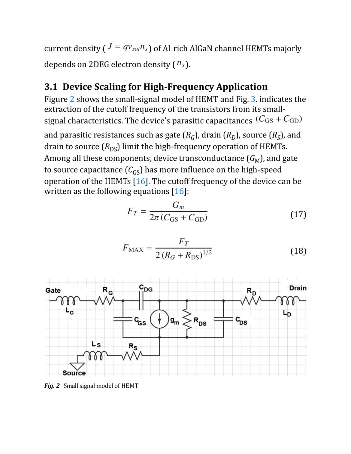
3.1 Device Scaling for High-Frequency Application
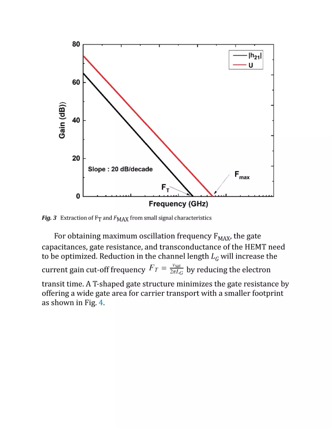
Figure 2 shows the small-signal model of HEMT and Fig. 3. indicates the
extraction of the cutoff frequency of the transistors from its smallsignal characteristics. The device’s parasitic capacitances
and parasitic resistances such as gate (RG), drain (RD), source (RS), and
drain to source (RDS) limit the high-frequency operation of HEMTs.
Among all these components, device transconductance (GM), and gate
to source capacitance (CGS) has more influence on the high-speed
operation of the HEMTs [16]. The cutoff frequency of the device can be
written as the following equations [16]:
(17)
(18)
Fig. 2 Small signal model of HEMT
Fig. 3 Extraction of FT and FMAX from small signal characteristics
For obtaining maximum oscillation frequency FMAX, the gate
capacitances, gate resistance, and transconductance of the HEMT need
to be optimized. Reduction in the channel length LG will increase the
current gain cut-off frequency
by reducing the electron
transit time. A T-shaped gate structure minimizes the gate resistance by
offering a wide gate area for carrier transport with a smaller footprint
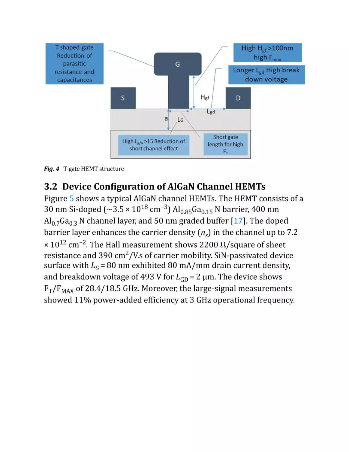
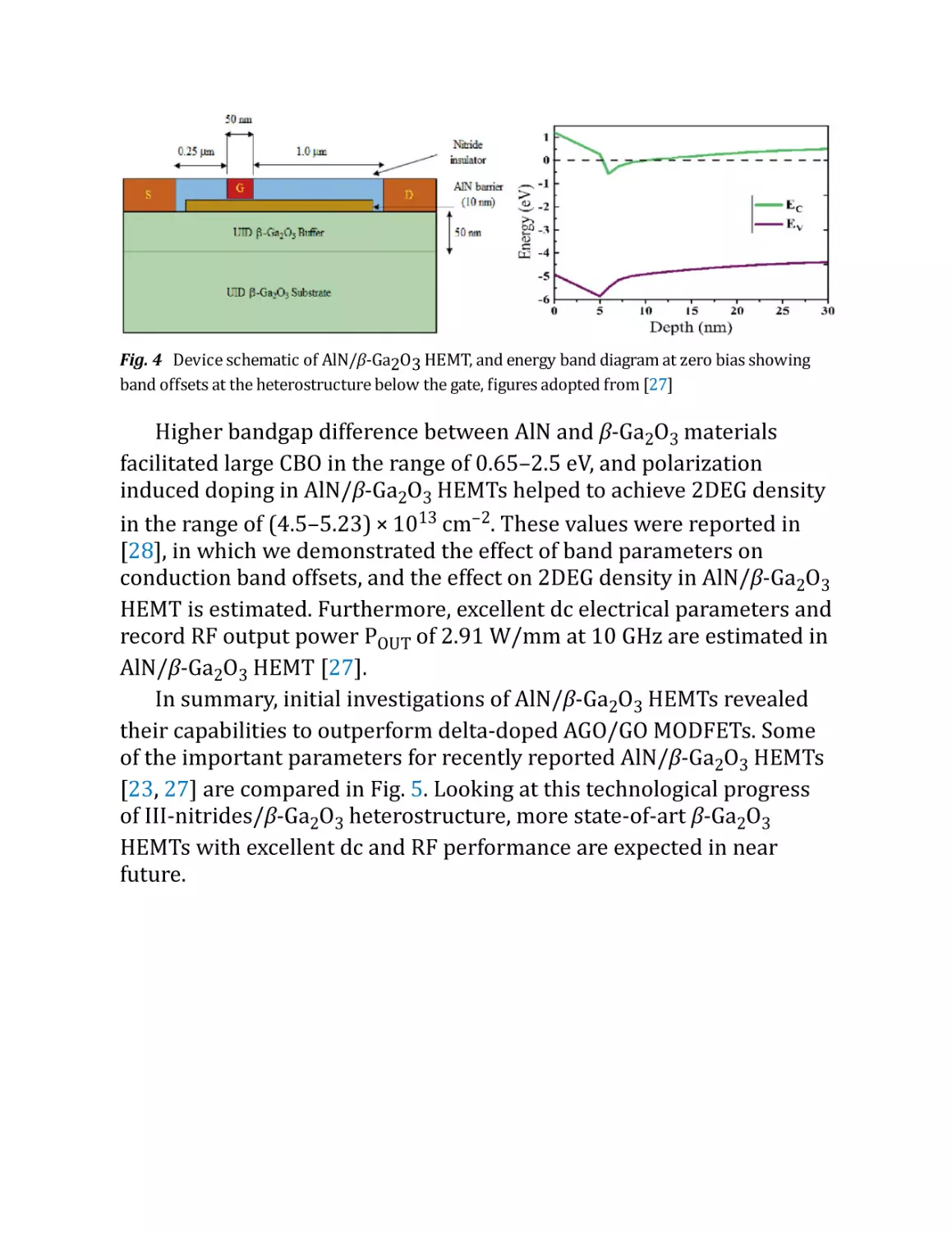
as shown in Fig. 4.
Fig. 4 T-gate HEMT structure
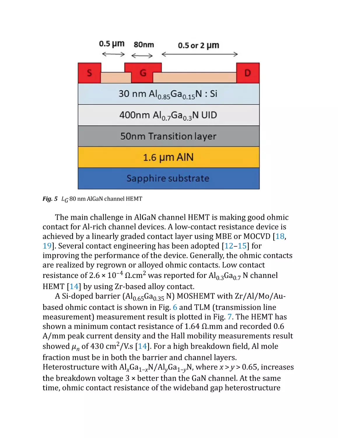
3.2 Device Configuration of AlGaN Channel HEMTs
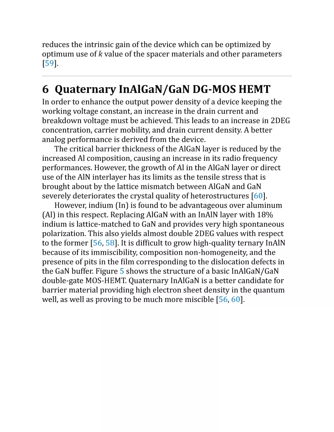
Figure 5 shows a typical AlGaN channel HEMTs. The HEMT consists of a
30 nm Si-doped (~3.5 × 1018 cm−3) Al0.85Ga0.15 N barrier, 400 nm
Al0.7Ga0.3 N channel layer, and 50 nm graded buffer [17]. The doped
barrier layer enhances the carrier density (ns) in the channel up to 7.2
× 1012 cm−2. The Hall measurement shows 2200 Ω/square of sheet
resistance and 390 cm2/V.s of carrier mobility. SiN-passivated device
surface with LG = 80 nm exhibited 80 mA/mm drain current density,
and breakdown voltage of 493 V for LGD = 2 µm. The device shows
FT/FMAX of 28.4/18.5 GHz. Moreover, the large-signal measurements
showed 11% power-added efficiency at 3 GHz operational frequency.
Fig. 5 LG 80 nm AlGaN channel HEMT
The main challenge in AlGaN channel HEMT is making good ohmic
contact for Al-rich channel devices. A low-contact resistance device is
achieved by a linearly graded contact layer using MBE or MOCVD [18,
19]. Several contact engineering has been adopted [12–15] for
improving the performance of the device. Generally, the ohmic contacts
are realized by regrown or alloyed ohmic contacts. Low contact
resistance of 2.6 × 10⁻⁴ Ω.cm2 was reported for Al0.3Ga0.7 N channel
HEMT [14] by using Zr-based alloy contact.
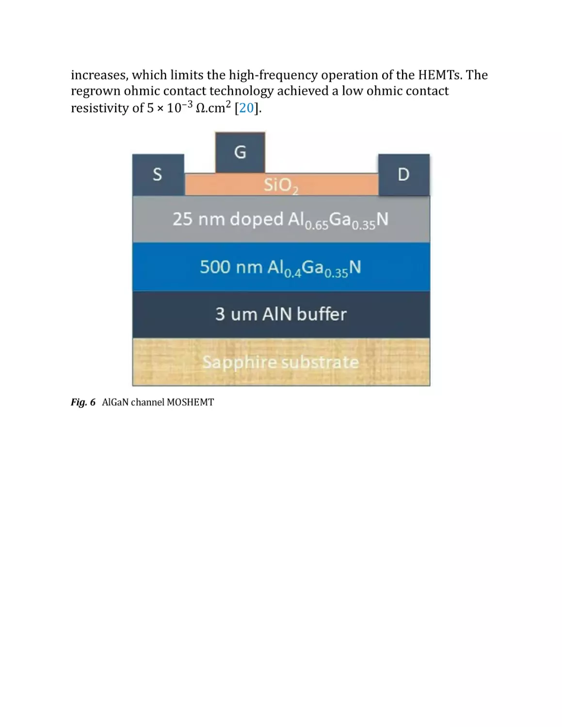
A Si-doped barrier (Al0.65Ga0.35 N) MOSHEMT with Zr/Al/Mo/Aubased ohmic contact is shown in Fig. 6 and TLM (transmission line
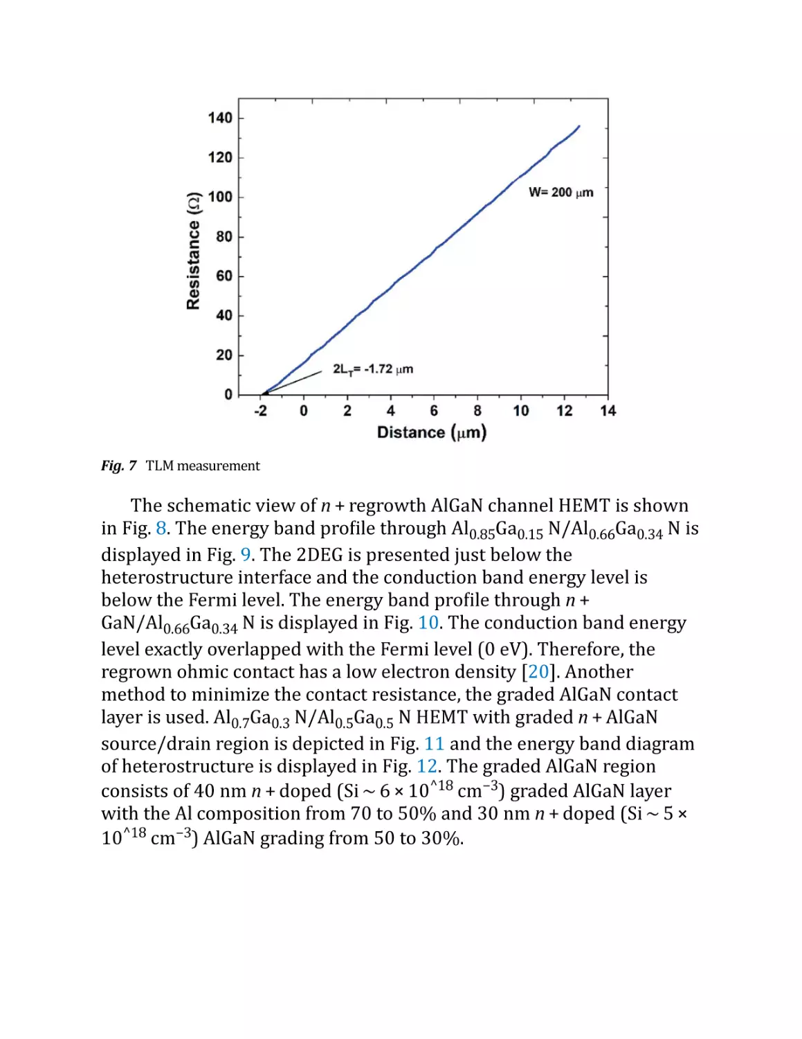
measurement) measurement result is plotted in Fig. 7. The HEMT has
shown a minimum contact resistance of 1.64 Ω.mm and recorded 0.6
A/mm peak current density and the Hall mobility measurements result
showed µn of 430 cm2/V.s [14]. For a high breakdown field, Al mole
fraction must be in both the barrier and channel layers.
Heterostructure with AlxGa1−xN/AlyGa1−yN, where x > y > 0.65, increases
the breakdown voltage 3 × better than the GaN channel. At the same
time, ohmic contact resistance of the wideband gap heterostructure
increases, which limits the high-frequency operation of the HEMTs. The
regrown ohmic contact technology achieved a low ohmic contact
resistivity of 5 × 10⁻³ Ω.cm2 [20].
Fig. 6 AlGaN channel MOSHEMT
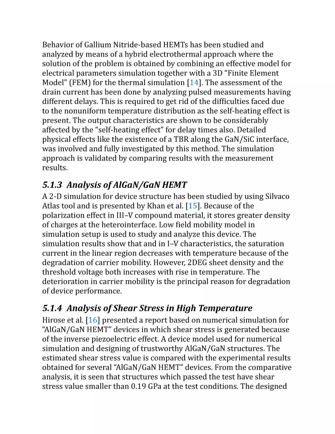
Fig. 7 TLM measurement
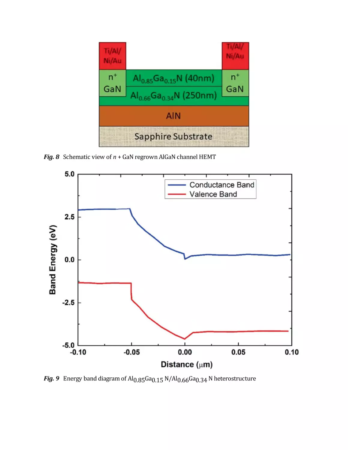
The schematic view of n + regrowth AlGaN channel HEMT is shown
in Fig. 8. The energy band profile through Al0.85Ga0.15 N/Al0.66Ga0.34 N is
displayed in Fig. 9. The 2DEG is presented just below the
heterostructure interface and the conduction band energy level is
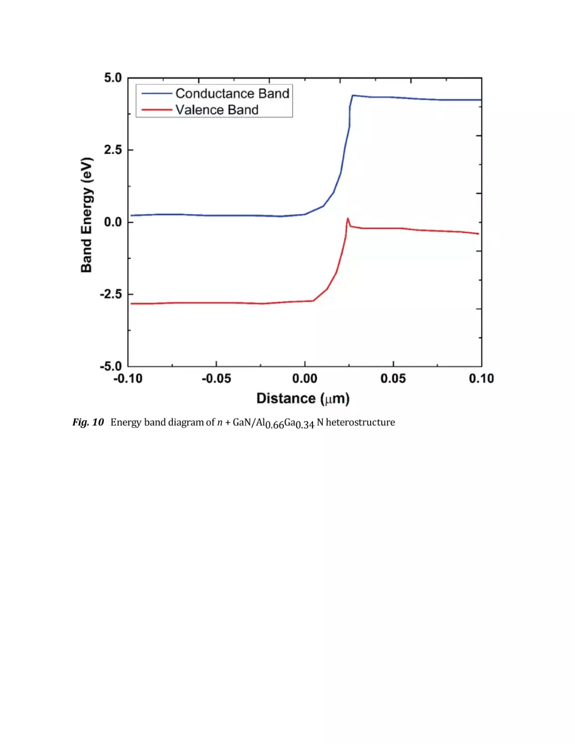
below the Fermi level. The energy band profile through n +
GaN/Al0.66Ga0.34 N is displayed in Fig. 10. The conduction band energy
level exactly overlapped with the Fermi level (0 eV). Therefore, the
regrown ohmic contact has a low electron density [20]. Another
method to minimize the contact resistance, the graded AlGaN contact
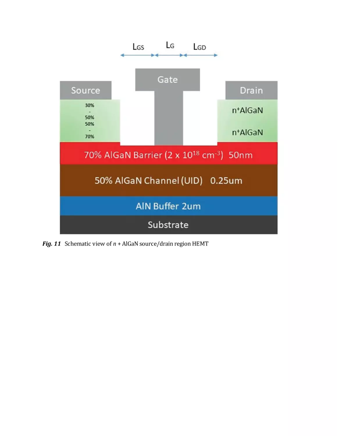
layer is used. Al0.7Ga0.3 N/Al0.5Ga0.5 N HEMT with graded n + AlGaN
source/drain region is depicted in Fig. 11 and the energy band diagram
of heterostructure is displayed in Fig. 12. The graded AlGaN region
consists of 40 nm n + doped (Si ~ 6 × 10^18 cm−3) graded AlGaN layer
with the Al composition from 70 to 50% and 30 nm n + doped (Si ~ 5 ×
10^18 cm−3) AlGaN grading from 50 to 30%.
Fig. 8 Schematic view of n + GaN regrown AlGaN channel HEMT
Fig. 9 Energy band diagram of Al0.85Ga0.15 N/Al0.66Ga0.34 N heterostructure
Fig. 10 Energy band diagram of n + GaN/Al0.66Ga0.34 N heterostructure
Fig. 11 Schematic view of n + AlGaN source/drain region HEMT
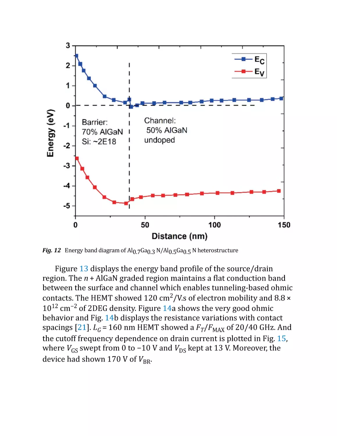
Fig. 12 Energy band diagram of Al0.7Ga0.3 N/Al0.5Ga0.5 N heterostructure
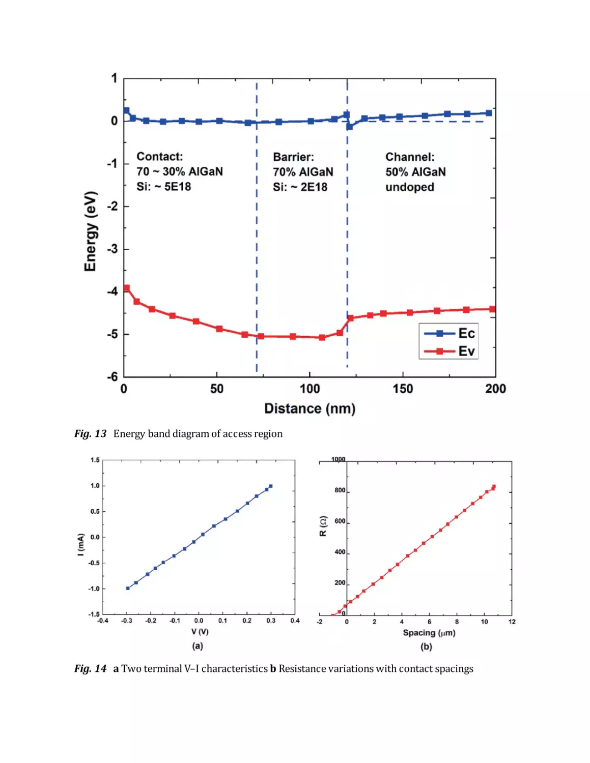
Figure 13 displays the energy band profile of the source/drain
region. The n + AlGaN graded region maintains a flat conduction band
between the surface and channel which enables tunneling-based ohmic
contacts. The HEMT showed 120 cm2/V.s of electron mobility and 8.8 ×
1012 cm−2 of 2DEG density. Figure 14a shows the very good ohmic
behavior and Fig. 14b displays the resistance variations with contact
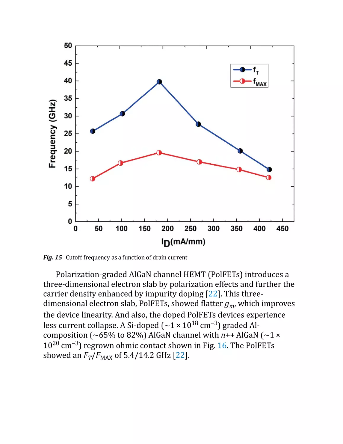
spacings [21]. LG = 160 nm HEMT showed a FT/FMAX of 20/40 GHz. And
the cutoff frequency dependence on drain current is plotted in Fig. 15,
where VGS swept from 0 to −10 V and VDS kept at 13 V. Moreover, the
device had shown 170 V of VBR.
Fig. 13 Energy band diagram of access region
Fig. 14 a Two terminal V–I characteristics b Resistance variations with contact spacings
Fig. 15 Cutoff frequency as a function of drain current
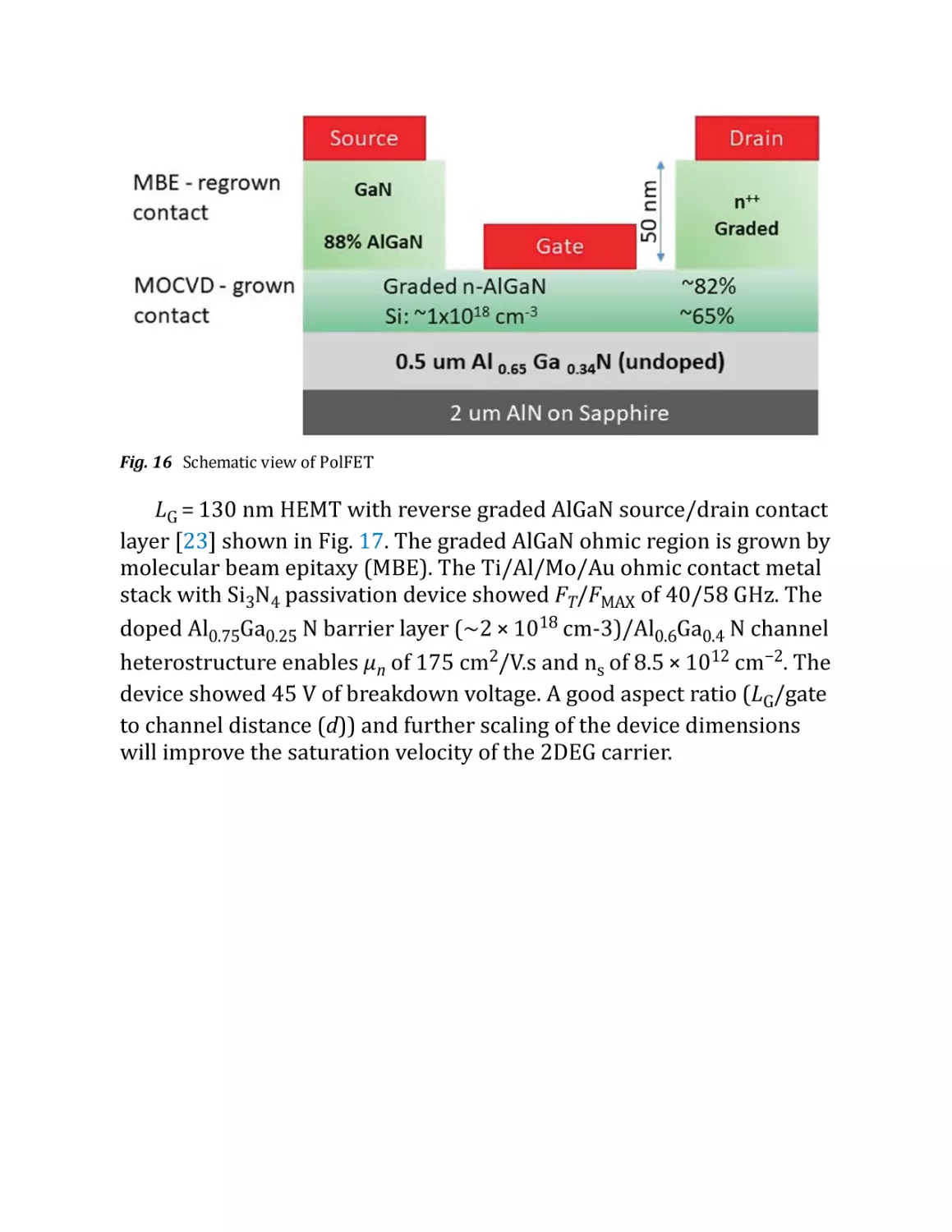
Polarization-graded AlGaN channel HEMT (PolFETs) introduces a
three-dimensional electron slab by polarization effects and further the
carrier density enhanced by impurity doping [22]. This threedimensional electron slab, PolFETs, showed flatter gm, which improves
the device linearity. And also, the doped PolFETs devices experience
less current collapse. A Si-doped (~1 × 1018 cm−3) graded Alcomposition (~65% to 82%) AlGaN channel with n++ AlGaN (~1 ×
1020 cm−3) regrown ohmic contact shown in Fig. 16. The PolFETs
showed an FT/FMAX of 5.4/14.2 GHz [22].
Fig. 16 Schematic view of PolFET
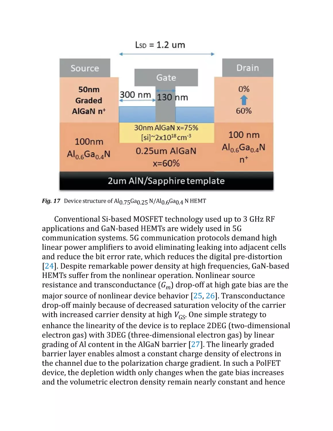
LG = 130 nm HEMT with reverse graded AlGaN source/drain contact
layer [23] shown in Fig. 17. The graded AlGaN ohmic region is grown by
molecular beam epitaxy (MBE). The Ti/Al/Mo/Au ohmic contact metal
stack with Si3N4 passivation device showed FT/FMAX of 40/58 GHz. The
doped Al0.75Ga0.25 N barrier layer (~2 × 1018 cm-3)/Al0.6Ga0.4 N channel
heterostructure enables µn of 175 cm2/V.s and ns of 8.5 × 1012 cm−2. The
device showed 45 V of breakdown voltage. A good aspect ratio (LG/gate
to channel distance (d)) and further scaling of the device dimensions
will improve the saturation velocity of the 2DEG carrier.
Fig. 17 Device structure of Al0.75Ga0.25 N/Al0.6Ga0.4 N HEMT
Conventional Si-based MOSFET technology used up to 3 GHz RF
applications and GaN-based HEMTs are widely used in 5G
communication systems. 5G communication protocols demand high
linear power amplifiers to avoid eliminating leaking into adjacent cells
and reduce the bit error rate, which reduces the digital pre-distortion
[24]. Despite remarkable power density at high frequencies, GaN-based
HEMTs suffer from the nonlinear operation. Nonlinear source
resistance and transconductance (Gm) drop-off at high gate bias are the
major source of nonlinear device behavior [25, 26]. Transconductance
drop-off mainly because of decreased saturation velocity of the carrier
with increased carrier density at high VGS. One simple strategy to
enhance the linearity of the device is to replace 2DEG (two-dimensional
electron gas) with 3DEG (three-dimensional electron gas) by linear
grading of Al content in the AlGaN barrier [27]. The linearly graded
barrier layer enables almost a constant charge density of electrons in
the channel due to the polarization charge gradient. In such a PolFET
device, the depletion width only changes when the gate bias increases
and the volumetric electron density remain nearly constant and hence
there is no significant change in saturation velocity of electrons in the
channel leading to flatter transconductance (Gm). The flat Gm is highly
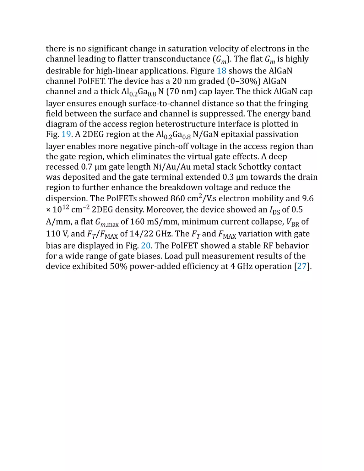
desirable for high-linear applications. Figure 18 shows the AlGaN
channel PolFET. The device has a 20 nm graded (0–30%) AlGaN
channel and a thick Al0.2Ga0.8 N (70 nm) cap layer. The thick AlGaN cap
layer ensures enough surface-to-channel distance so that the fringing
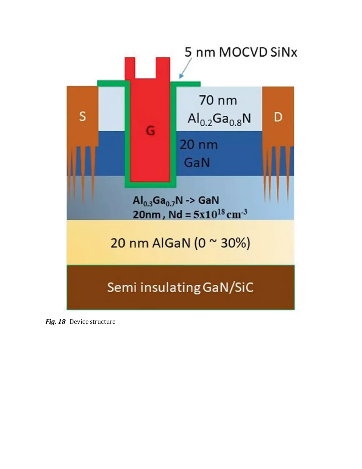
field between the surface and channel is suppressed. The energy band
diagram of the access region heterostructure interface is plotted in
Fig. 19. A 2DEG region at the Al0.2Ga0.8 N/GaN epitaxial passivation
layer enables more negative pinch-off voltage in the access region than
the gate region, which eliminates the virtual gate effects. A deep
recessed 0.7 µm gate length Ni/Au/Au metal stack Schottky contact
was deposited and the gate terminal extended 0.3 µm towards the drain
region to further enhance the breakdown voltage and reduce the
dispersion. The PolFETs showed 860 cm2/V.s electron mobility and 9.6
× 1012 cm−2 2DEG density. Moreover, the device showed an IDS of 0.5
A/mm, a flat Gm,max of 160 mS/mm, minimum current collapse, VBR of
110 V, and FT/FMAX of 14/22 GHz. The FT and FMAX variation with gate
bias are displayed in Fig. 20. The PolFET showed a stable RF behavior
for a wide range of gate biases. Load pull measurement results of the
device exhibited 50% power-added efficiency at 4 GHz operation [27].
Fig. 18 Device structure
Fig. 19 Band diagram
Fig. 20 FT/FMAX dependence on VGS
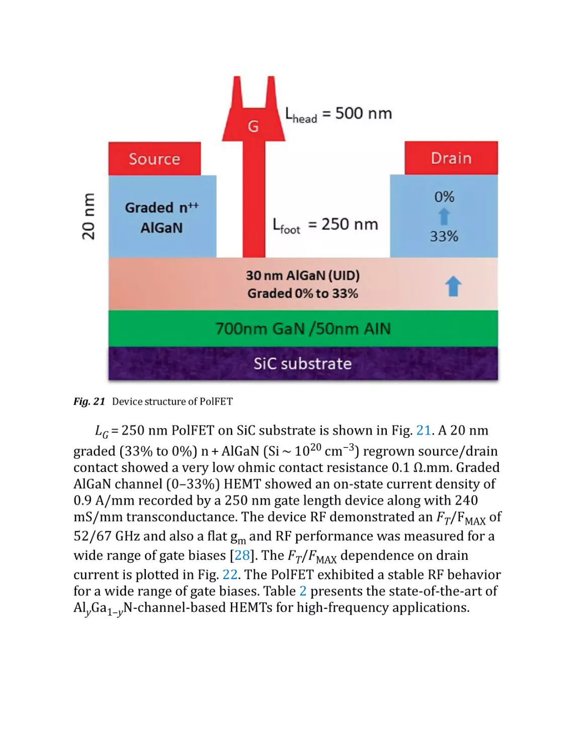
Fig. 21 Device structure of PolFET
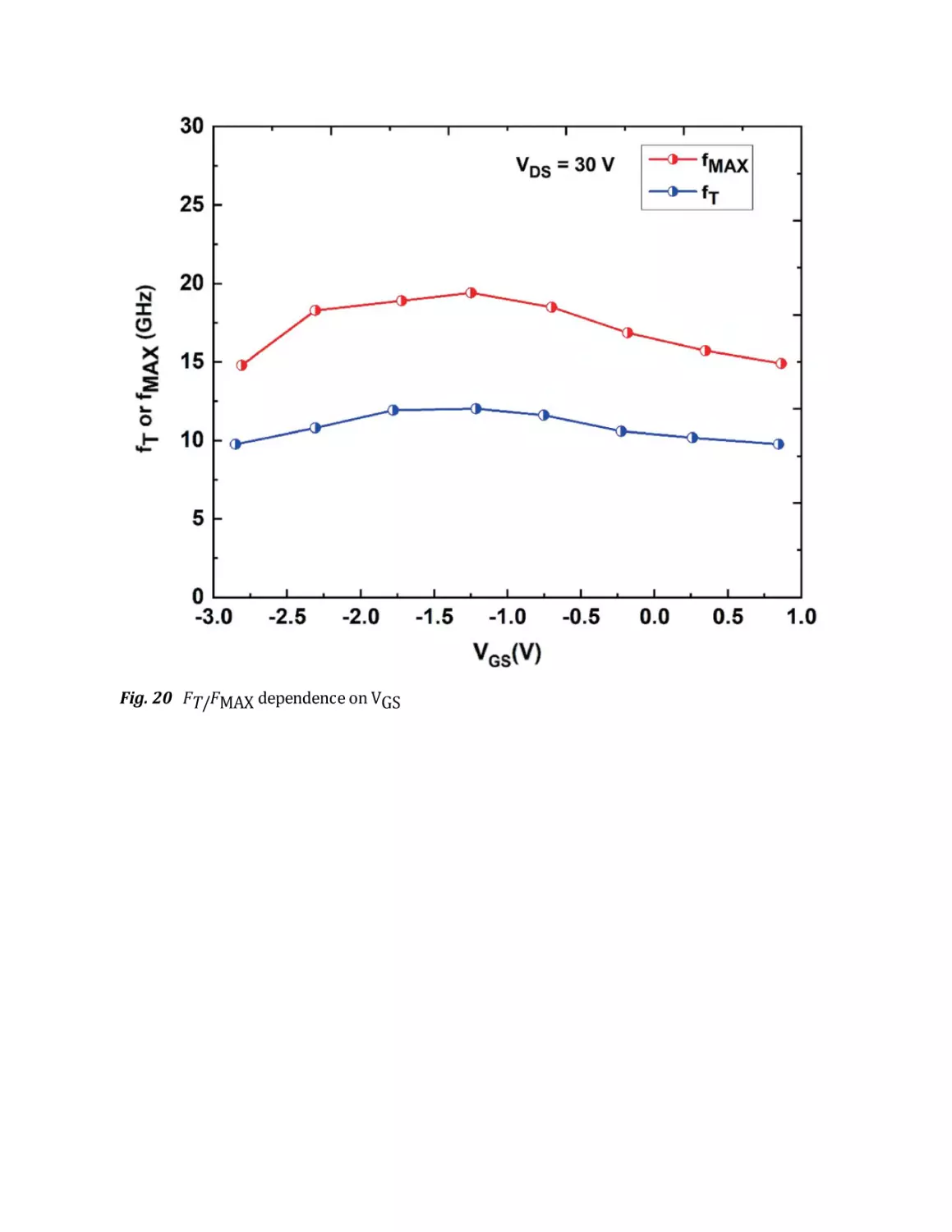
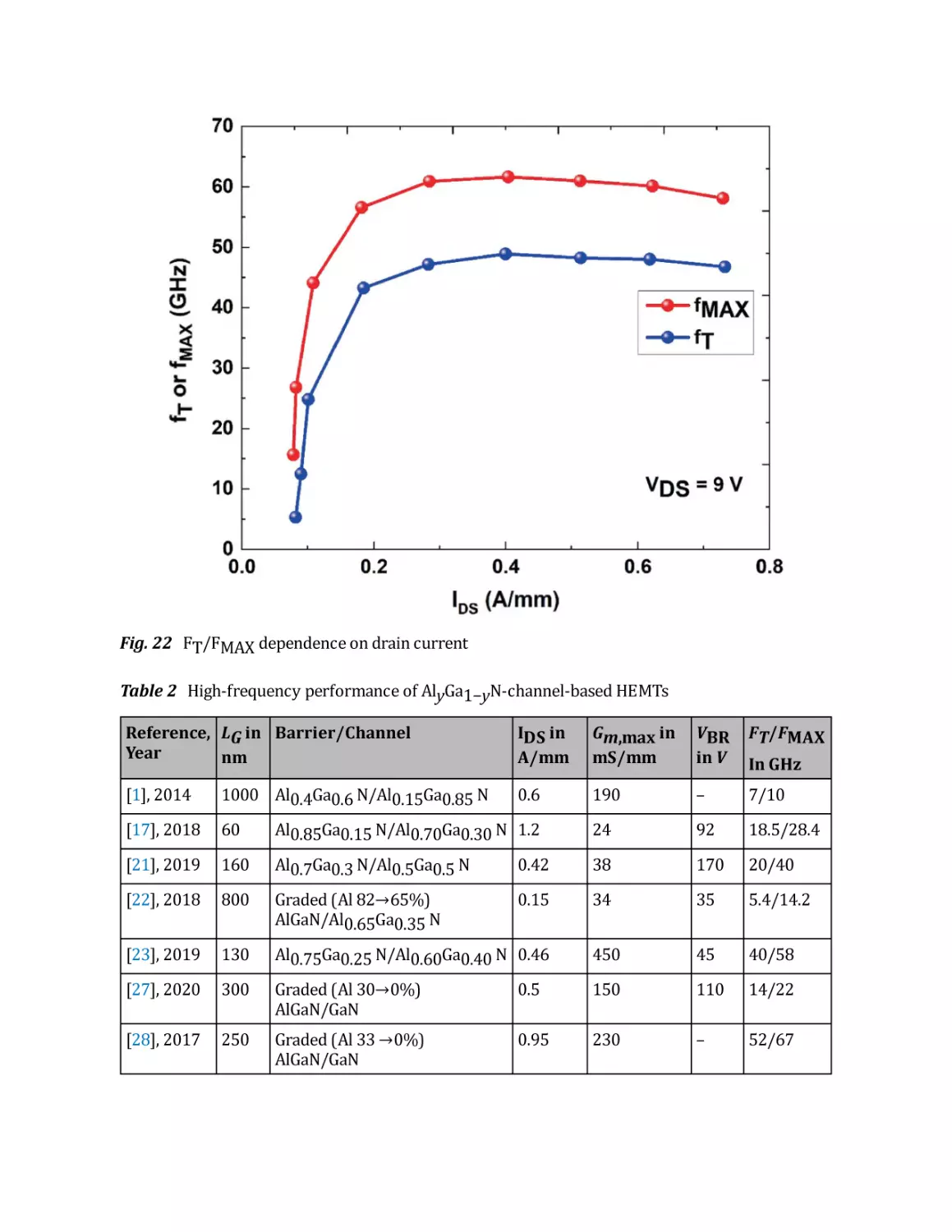
LG = 250 nm PolFET on SiC substrate is shown in Fig. 21. A 20 nm
graded (33% to 0%) n + AlGaN (Si ~ 1020 cm−3) regrown source/drain
contact showed a very low ohmic contact resistance 0.1 Ω.mm. Graded
AlGaN channel (0–33%) HEMT showed an on-state current density of
0.9 A/mm recorded by a 250 nm gate length device along with 240
mS/mm transconductance. The device RF demonstrated an FT/FMAX of
52/67 GHz and also a flat gm and RF performance was measured for a
wide range of gate biases [28]. The FT/FMAX dependence on drain
current is plotted in Fig. 22. The PolFET exhibited a stable RF behavior
for a wide range of gate biases. Table 2 presents the state-of-the-art of
AlyGa1–yN-channel-based HEMTs for high-frequency applications.
Fig. 22 FT/FMAX dependence on drain current
Table 2 High-frequency performance of AlyGa1−yN-channel-based HEMTs
Reference, LG in Barrier/Channel
Year
nm
IDS in
A/mm
Gm,max in
mS/mm
VBR
in V
FT/FMAX
[1], 2014
1000 Al0.4Ga0.6 N/Al0.15Ga0.85 N
0.6
190
–
7/10
[17], 2018
60
Al0.85Ga0.15 N/Al0.70Ga0.30 N 1.2
24
92
18.5/28.4
[21], 2019
160
Al0.7Ga0.3 N/Al0.5Ga0.5 N
0.42
38
170
20/40
[22], 2018
800
Graded (Al 82→65%)
AlGaN/Al0.65Ga0.35 N
0.15
34
35
5.4/14.2
[23], 2019
130
Al0.75Ga0.25 N/Al0.60Ga0.40 N 0.46
450
45
40/58
[27], 2020
300
Graded (Al 30→0%)
AlGaN/GaN
0.5
150
110
14/22
[28], 2017
250
Graded (Al 33 →0%)
AlGaN/GaN
0.95
230
–
52/67
In GHz
4 AlGaN Channel HEMTs in Power Switching
Applications
Despite the high breakdown performance of the ultrawide bandgap
AlGaN channel, due to significant lattice and thermal mismatches
between the Al-rich AlGaN channel and buffer heterostructure, the
crystalline quality is very poor [29, 30]. Therefore, the Al-rich AlGaN
channel HEMT cannot meet the theoretical electric field strength. A
simple approach to improve the breakdown voltage of high-quality
crystalline Al0.1Ga0.9 N channel HEMT is hybrid ohmic/Schottky drain
contacts [31] without modifying the conventional device fabrication
steps. The hybrid ohmic/Schottky drain contact
Al0.3Ga0.7 N/Al0.1Ga0.9 N HEMT fabricated structure is shown in Fig. 23.
The device shows 9.2 × 1012 cm−2 of sheet charge density and 2070
cm2V−1 s−1 of carrier mobility due to improved polarization and the
alloy disorder scattering mechanism is majorly reduced by the low Almole fraction AlGaN device. LG = 3 µm, and WG = 50 µm device exhibited
a remarkable breakdown voltage of 2200 V for LGD = 22 µm. This hybrid
technology anticipated uniform breakdown characteristics due to
improved surface metal morphology.
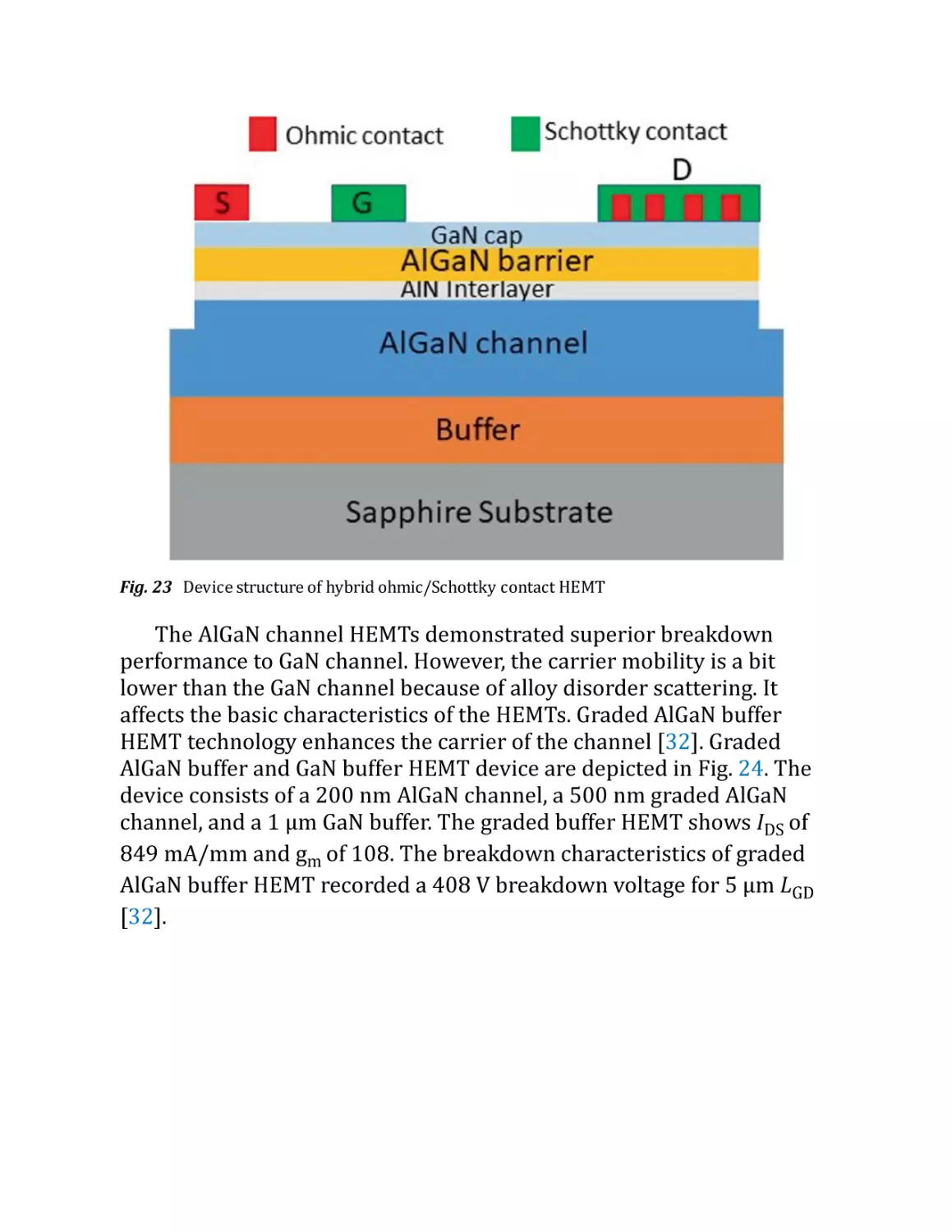
Fig. 23 Device structure of hybrid ohmic/Schottky contact HEMT
The AlGaN channel HEMTs demonstrated superior breakdown
performance to GaN channel. However, the carrier mobility is a bit
lower than the GaN channel because of alloy disorder scattering. It
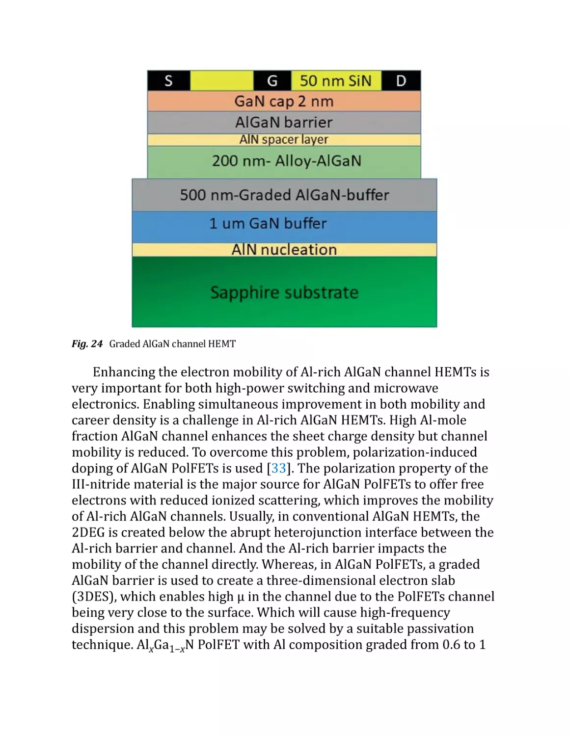
affects the basic characteristics of the HEMTs. Graded AlGaN buffer
HEMT technology enhances the carrier of the channel [32]. Graded
AlGaN buffer and GaN buffer HEMT device are depicted in Fig. 24. The
device consists of a 200 nm AlGaN channel, a 500 nm graded AlGaN
channel, and a 1 µm GaN buffer. The graded buffer HEMT shows IDS of
849 mA/mm and gm of 108. The breakdown characteristics of graded
AlGaN buffer HEMT recorded a 408 V breakdown voltage for 5 µm LGD
[32].
Fig. 24 Graded AlGaN channel HEMT
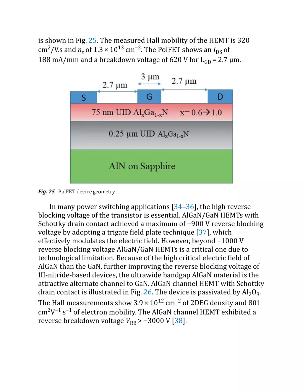
Enhancing the electron mobility of Al-rich AlGaN channel HEMTs is
very important for both high-power switching and microwave
electronics. Enabling simultaneous improvement in both mobility and
career density is a challenge in Al-rich AlGaN HEMTs. High Al-mole
fraction AlGaN channel enhances the sheet charge density but channel
mobility is reduced. To overcome this problem, polarization-induced
doping of AlGaN PolFETs is used [33]. The polarization property of the
III-nitride material is the major source for AlGaN PolFETs to offer free
electrons with reduced ionized scattering, which improves the mobility
of Al-rich AlGaN channels. Usually, in conventional AlGaN HEMTs, the
2DEG is created below the abrupt heterojunction interface between the
Al-rich barrier and channel. And the Al-rich barrier impacts the
mobility of the channel directly. Whereas, in AlGaN PolFETs, a graded
AlGaN barrier is used to create a three-dimensional electron slab
(3DES), which enables high µ in the channel due to the PolFETs channel
being very close to the surface. Which will cause high-frequency
dispersion and this problem may be solved by a suitable passivation
technique. AlxGa1−xN PolFET with Al composition graded from 0.6 to 1
is shown in Fig. 25. The measured Hall mobility of the HEMT is 320
cm2/V.s and ns of 1.3 × 1013 cm−2. The PolFET shows an IDS of
188 mA/mm and a breakdown voltage of 620 V for LGD = 2.7 µm.
Fig. 25 PolFET device geometry
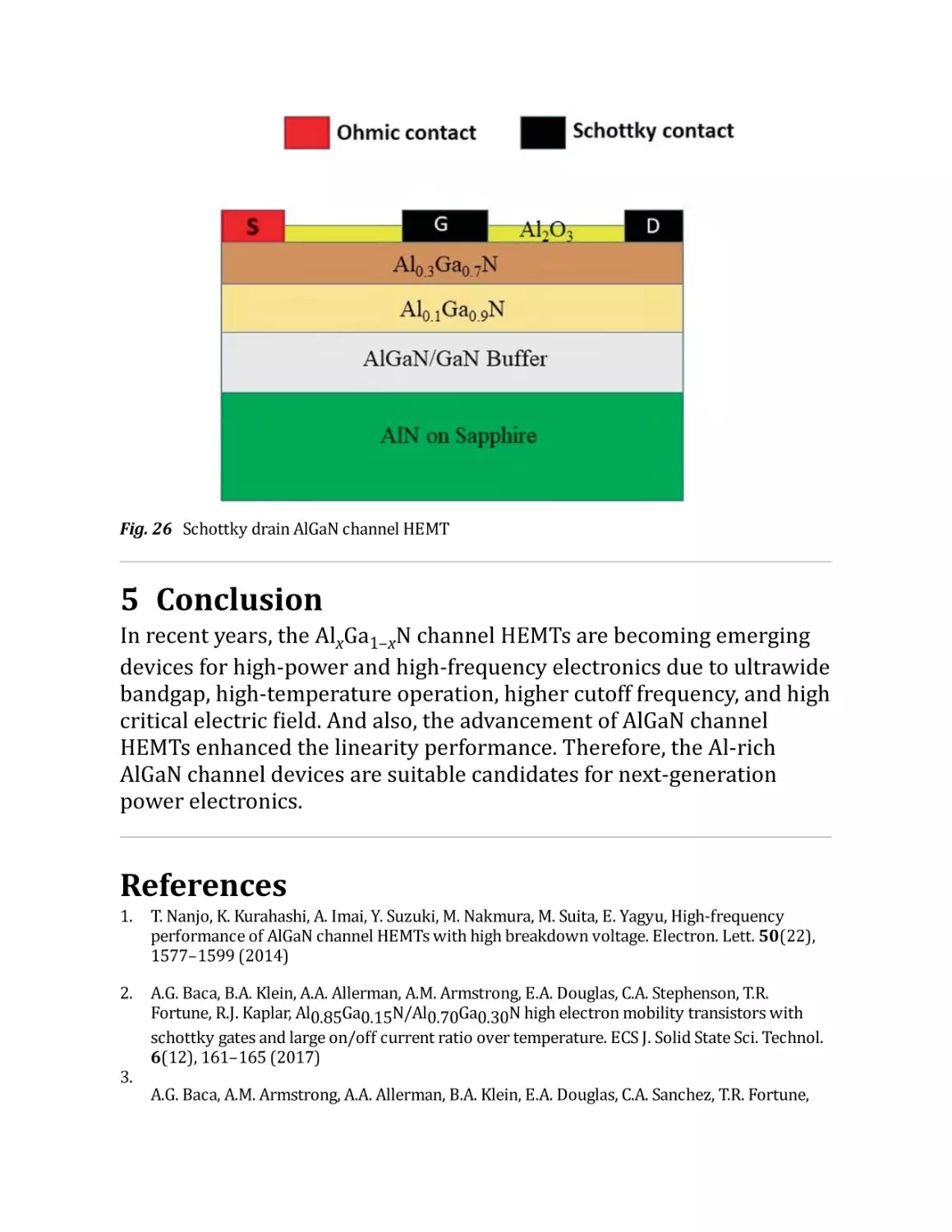
In many power switching applications [34–36], the high reverse
blocking voltage of the transistor is essential. AlGaN/GaN HEMTs with
Schottky drain contact achieved a maximum of −900 V reverse blocking
voltage by adopting a trigate field plate technique [37], which
effectively modulates the electric field. However, beyond −1000 V
reverse blocking voltage AlGaN/GaN HEMTs is a critical one due to
technological limitation. Because of the high critical electric field of
AlGaN than the GaN, further improving the reverse blocking voltage of
III-nitride-based devices, the ultrawide bandgap AlGaN material is the
attractive alternate channel to GaN. AlGaN channel HEMT with Schottky
drain contact is illustrated in Fig. 26. The device is passivated by Al2O3.
The Hall measurements show 3.9 × 1012 cm−2 of 2DEG density and 801
cm2V−1 s−1 of electron mobility. The AlGaN channel HEMT exhibited a
reverse breakdown voltage VRB > −3000 V [38].
Fig. 26 Schottky drain AlGaN channel HEMT
5 Conclusion
In recent years, the AlxGa1–xN channel HEMTs are becoming emerging
devices for high-power and high-frequency electronics due to ultrawide
bandgap, high-temperature operation, higher cutoff frequency, and high
critical electric field. And also, the advancement of AlGaN channel
HEMTs enhanced the linearity performance. Therefore, the Al-rich
AlGaN channel devices are suitable candidates for next-generation
power electronics.
References
1.
T. Nanjo, K. Kurahashi, A. Imai, Y. Suzuki, M. Nakmura, M. Suita, E. Yagyu, High-frequency
performance of AlGaN channel HEMTs with high breakdown voltage. Electron. Lett. 50(22),
1577–1599 (2014)
2.
A.G. Baca, B.A. Klein, A.A. Allerman, A.M. Armstrong, E.A. Douglas, C.A. Stephenson, T.R.
Fortune, R.J. Kaplar, Al0.85Ga0.15N/Al0.70Ga0.30N high electron mobility transistors with
schottky gates and large on/off current ratio over temperature. ECS J. Solid State Sci. Technol.
6(12), 161–165 (2017)
3.
A.G. Baca, A.M. Armstrong, A.A. Allerman, B.A. Klein, E.A. Douglas, C.A. Sanchez, T.R. Fortune,
High temperature operation of Al0.45Ga0.55N/Al0.30Ga0.70N high electron mobility
transistors. ECS J. Solid State Sci. Technol. 6(11) S3010-S3013 (2017)
4.
S.J. Pearton, J. Yang, P.H. Cary IV, F. Ren, J. Kim, MJ. Tadjer, M.A. Mastro, A review of Ga2O3
materials, processing, and devices. Appl. Phys. Rev. 5, 011301 (2018)
5.
T. Oishi, Y. Koga, K. Harada, M. Kasu, High-mobility β-Ga2O3( 01) single crystals grown by
edge-defined film-fed growth method and their Schottky barrier diodes with Ni contact. Appl.
Phys. Express 8, 031101 (2015)
[Crossref]
6.
Z. Xia, C. Joishi, S. Krishnamoorthy, S. Bajaj, Y. Zhang, M. Brenner, S. Lodha, S. Rajan, Delta doped
β-Ga2O3 field effect transistors with regrown ohmic contacts. IEEE Electron Device Lett.
39(4), 568–571 (2018)
[Crossref]
7.
Y. Zhang, C. Joishi, Z. Xia, M. Brenner, S. Lodha, S. Rajan, Demonstration of β-(AlxGa1x)2O3/Ga2O3 double heterostructure field effect transistors. Appl. Phys. Lett. 112, 233503–
233505 (2018)
[Crossref]
8.
A.J. Green et al., β -Ga2O3 MOSFETs for radio frequency operation. IEEE Electron Device Lett.
38(6), 790–793 (2017). https://doi.org/10.1109/LED.2017.2694805
[Crossref]
9.
K. Ueda, M. Kasu, Y. Yamauchi, T. Makimoto, M. Schwitters, D.J. Twitchen, G.A. Scarsbrook, S.E.
Coe, Diamond FET using high-quality polycrystallinediamond with f T of 45 GHz and f max of
120 GHz, IEEE Electron Device Lett. 27(7), 570–572 (2006)
10. M. Kasu, K. Ueda, H. Ye, Y. Yamauchi, S. Sasaki, T. Makimoto, 2 W = mm output power density at
1 GHz fordiamond FETs, Electron. Lett. 41(22), 1249–1250 (2005)
11. M. Farahmand, C. Garetto, E. Bellotti, K.F. Brennan, M. Goano, E. Ghillino, G. Ghione, J.D.
Albrecht, P. Paul Ruden, Monte Carlo simulation of electron transport in Theiii-nitride
Wurtzite phase materials system: Binariesand ternaries. IEEE Trans. Electron Device 48(3),
535–542 (2001)
12. H. Tokuda, M. Hatano, N. Yafune, S. Hashimoto, K. Akita, Y. Yamamoto, M. Kuzuhara, High Al
composition AlGaN-channel high-electron-mobility transistor on AlN substrate. Appl. Phys.
Express 3, 121003, 1–3 (2010)
13. T. Nanjo, A. Imai, Y. Suzuki, Y. Abe, T. Oishi, M. Suita, E. Yagyu, Y. Tokuda, AlGaN Channel HEMT
With Extremely High Breakdown Voltage. IEEE Trans. Electron Device 60(3), 1046–1053
(2013)
14. X. Hu, S. Hwang, K. Hussain, R. Floyd, S. Mollah, F. Asif, G. Simin, A. Khan, Doped Barrier
Al0.65Ga0.35N/Al0.40Ga0.60N MOSHFETwith SiO2 Gate-insulator and Zr-based ohmic
contacts.IEEE Electron Device Letters. 39(10):1–4 (2018)
15.
E.A. Douglas, S. Reza, C. Sanchez, D. Koleske, A. Allerman, B. Klein, A.M. Armstrong, R.J. Kaplar,
A.G. Baca, Ohmic contacts to Al-rich AlGaNheterostructures.Phys. Status Solidi A 214(8),
1600842, 1–7 (2017)
16. K. Harrouche, F. Medjdoub, GaN-Based HEMTs for millimeter-wave applications. Wiley Online
Library, Chapter 3(Book Chapter), 99–135 (2020)
17. A.G. Baca, B.A. Klein, J.R. Wendt, S.M. Lepkowski, C.D. Nordquist, A.M. Armstrong, A.A.
Allerman, E.A. Douglas, R.J. Kaplar, RF Performance of Al0.85Ga0.15N/Al0.70Ga0.30N high
electron mobility transistors with 80 nm gates. IEEE Electron Device Lett. 40(1), 17–20
(2019)
18. S. Bajaj, F. Akyol, S. Krishnamoorthy, Y. Zhang, S. Rajan, AlGaN channel field effect transistors
with graded heterostructure ohmic contacts. Appl. Phys. Lett. 109(13), 133508 (2016)
19. T. Razzak, S. Hwang, A. Coleman, H. Xue, S.H. Sohel, S. Bajaj, Y. Zhang, W. Lu, A. Khan, S. Rajan,
Design of compositionally graded contact layers for MOCVD grown high Al-content AlGaN
transistors. Appl. Phys. Lett. 115(4), 043502 (2019)
20. E.A. Douglas, S. Reza, C. Sanchez, D. Koleske, A. Allerman, B. Klein, A.M. Armstrong, R.J. Kaplar,
A.G. Baca, Ohmic contacts to Al-rich AlGaN heterostructures. Phys. Status Solidi A 214(8),
1600842, 1–7 (2017)
21. H. Xue, S. Hwang, T. Razzak, C. Lee, G. C. Ortiz, Z. Xia, S.H. Sohel, J. Hwang, S. Rajan, A. Khan, Wu
Lu, All MOCVD grown Al0.7Ga0.3N/Al0.5Ga0.5N HFET: An approach to makeohmic contacts
to Al-Rich AlGaN channel transistors. 164, 30534–30539 (2020)
22. T. Razzak, S. Hwang, A. Coleman, S. Bajaj, H. Xue, Y. Zhang, Z. Jamal-Eddine, S. H. Sohel, W. Lu, A.
Khan, S. Rajan, RF operation in graded AlxGa1-xN (x=0.65 to 0.82) Channel Transistors. IET—
Inst. Eng. Technol. 54(23), 1351–1353 (2018)
23. H. Xue, C.H. Lee, K. Hussian, T. Razzak, M. Abdullah, Z. Xia, S.H. Sohel, A. Khan, S. Rajan, W. Lu,
Al0.75Ga0.25N/Al0.6Ga0.4N heterojunction field effect transistor with fT of 40 GHz. Appl.
Phys. Express 12(6), 066502 (2019)
24. P. Choi, U. Radhakrishna, C.C. Boon, L.-S. Peh, D. Antoniadis, Linearity enhancement of a fully
integrated 6-GHz GaN power amplifier. IEEE Microwave Wireless Compon. Lett. 27(10), 927–
929 (2017)
25. S. Bajaj, Z. Yang, F. Akyol, P.S. Park, Y. Zhang, A.L. Price, S. Krishnamoorthy, D.J. Meyer, S. Rajan,
Graded AlGaN Channel Transistors for Improved Current and Power Gain Linearity. IEEE
Trans. Electron Devices 64(8), 3114–3119 (2017)
26. J.B. Khurgin, S. Bajaj, S. Rajan, Amplified spontaneous emission of phonons as a likely
mechanism for density-dependent velocity saturation in GaN transistors. Appl. Phys. Express
9, 094101 (2016)
27. S.H. Sohel, A. Xie, E. Beam, H. Xue, T. Razzak, S. Bajaj, S. Campbell, D. White, K. Will, Y. Cao, W.
Lu, S. Rajan, Improved DC-RF dispersion with epitaxial passivation for high linearity graded
AlGaN channel field effect transistors. Appl. Phys. Express 13, 036502 (2020)
28.
V. Sandeep, J. Charles Pravin, Influence of Graded AlGaN sub-channel over the DC and
breakdown characteristics of a T-gated AlGaN/GaN/AlInN MOS-HEMT, superlattices and
microstructures, vol. 156 (2021). https://doi.org/10.1016/j.spmi.2021.106954
29. A.G. Baca, A.M. Armstrong, A.A. Allerman, E.A. Douglas, C.A. Sanchez, M.P. King, M.E. Coltrin,
T.R. Fortune, R.J. Kaplar, An AlN/Al0.85Ga0.15N high electron mobility transistor, Appl. Phys.
Lett. 109, 033509 (2016)
30. S. Muhtadi, S. Mo Hwang, A. Coleman, F. Asif, G. Simin, M.V.S. Chandrashekhar, A. Khan, High
electron mobility transistors with Al0.65Ga0.35N channel layers on thick AlN/sapphire
templates. IEEE Electron Device Lett. 38(7), 914–917 (2017)
31. W. Zhang, J. Zhang, M. Xiao, L. Zhang, Y. Hao, High breakdown-voltage (>2200 V) AlGaNchannel HEMTs with Ohmic/Schottky hybrid drains. IEEE J. Electron Devices Soc. 6, 931–935
(2018)
[Crossref]
32. M. Xiao, J. Zhang, X. Duan, W. Zhang, H. Shan, J. Ning, Y. Hao, High performance Al0.10Ga0.90N
channel HEMTs. IEEE Electron Device Lett. 39(8), 1149–1151 (2018)
33. A.M. Armstrong, B.A. Klein, A.G. Baca, A.A. Allerman, E.A. Douglas, A. Colon, V.M. Abate, T.R.
Fortune, AlGaN polarization-doped field effect transistor with compositionally graded
channel from Al0.6Ga0.4N to AlN, Appl. Phys. Lett. 114 052103 (2019)
34. J.-K. Kang, H. Hara, A.M. Hava, E. Yamamoto, E. Watanabe, T. Kume, The matrix converter drive
performance under abnormal input voltage conditions. IEEE Trans. Power Electron. 17(5),
721–730 (2002)
[Crossref]
35. P.W. Wheeler, J. Rodriguez, J.C. Clare, L. Empringham, A. Weinstein, Matrix converters: A
technology review. IEEE Trans. Ind. Electron. 49(2), 276–288 (2002)
[Crossref]
36. T. Morita, S. Tamura, Y. Anda, M. Ishida, Y. Uemoto, T. Ueda, T. Tanaka, D. Ueda, 99.3% Efficiency
of Three-Phase Inverter for Motor Drive Using GaN-Based Gate Injection Transistors.
Conference Proceedings -Annual IEEE Applied Power Electronics Conference and Exposition
(APEC), pp. 481–484 (2011)
37. J. Ma, M. Zhu, E. Matioli, 900 V reverse-blocking GaN-on-Si MOSHEMTs with a hybrid trianode Schottky drain. IEEE Electron Device Lett. 38(12), 1704–1707 (2017)
[Crossref]
38. Y. Wu et al., More Than 3000 V reverse blocking Schottky-drain AlGaN-channel HEMTs with
>230 MW/cm2 power figure-of-merit. IEEE Electron Device Lett. 40(11), 1724–1727 (2019)
[Crossref]
© The Author(s), under exclusive license to Springer Nature Singapore Pte Ltd. 2023
T. R. Lenka, H. P. T. Nguyen (eds.), HEMT Technology and Applications, Springer Tracts in Electrical
and Electronics Engineering
https://doi.org/10.1007/978-981-19-2165-0_2
Breakdown Mechanisms and Scaling
Technologies of AlGaN/GaN HEMTs
Sneha Kabra1 and Mridula Gupta2
(1) Associate Professor, Department of Instrumentation, Shaheed
Rajguru College of Applied Sciences for Women, University of
Delhi, Vasundhara Enclave, New Delhi, 110096, India
(2) Senior Professor and Head, Department of Electronic Science,
University of Delhi South Campus, Benito Juarez Road, New Delhi,
110021, India
Sneha Kabra (Corresponding author)
Email: sneha.kabra@rajguru.du.ac.in
Email: snehakabra@ieee.org
Mridula Gupta
Email: mridula@south.du.ac.in
Abstract
Breakdown mechanisms play a significant role in determining the
performance of AlGaN/GaN HEMTs in high-power circuit applications.
This chapter presents a brief overview of various factors, which cause
an early breakdown in AlGaN/GaN HEMT at high drain voltage. The
chapter also covers technological advancements proposed so far by
various research groups to enhance the breakdown voltage of the
device. Further, scaling technologies are discussed to improve the highfrequency performance of the device.
Keywords Breakdown mechanisms – Field plates – Double-channel
HEMT – Scaling technologies
1 Introduction
AlGaN/GaN HEMTs are primarily used in high-power, high-frequency
switching applications because of the low on-resistance, high drain
current density, and high breakdown voltage offered by these devices
[1]. Breakdown voltage for GaN device is defined as the voltage level at
which drain current of the pinched off transistor exceeds a normalized
value of 1 mA/mm of device width. It is also defined as a nonlinear
increase of subthreshold drain current with an increase in drain
voltage. Vertical leakage current from GaN to silicon limits the
maximum breakdown voltage in AlGaN/GaN HEMTs grown on silicon.
Breakdown also depends on the specific epitaxial design of the buffer
layer along with its material quality, lateral geometrical design of the
device, and passivation technique [2]. The physical properties of
various materials used for designing HEMTs are listed in Table 1. A
large bandgap of GaN ensures a high breakdown field. The critical
electric field of GaN is almost ten times higher than Si, thus making
GaN, a suitable choice for making high-power devices. The breakdown
voltage of AlGaN/GaN HEMT grown on silicon is lesser than those
grown on SiC substrate. Different figures of merit have been proposed
for quantifying the high power handling capability of material used for
fabricating HEMT. These include Johnson’s figure of merit for
microwave performance, Baliga’s figure of merit for a low frequency
that reflects resistive losses, and Baliga’s high-frequency figure of merit,
which signifies switching losses.
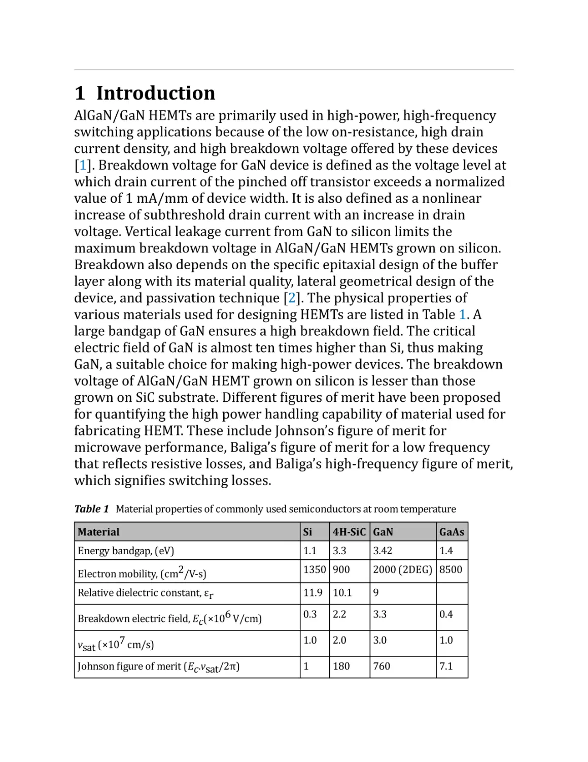
Table 1 Material properties of commonly used semiconductors at room temperature
Material
Si
4H-SiC GaN
GaAs
Energy bandgap, (eV)
1.1
3.3
1.4
Electron mobility, (cm2/V-s)
1350 900
2000 (2DEG) 8500
Relative dielectric constant, εr
11.9 10.1
9
Breakdown electric field, Ec(×106 V/cm)
0.3
2.2
3.3
0.4
vsat (×107 cm/s)
1.0
2.0
3.0
1.0
Johnson figure of merit (Ec.vsat/2π)
1
180
760
7.1
3.42
Material
Si
4H-SiC GaN
GaAs
Baliga’s figure of merit for low frequency
1
130
650
15.6
Baliga’s figure of merit for high frequency (μEc2) 1
22.9
77.8
10.8
(εμEc3)
The aim of this chapter is to present a brief overview of various
physical and technological factors responsible for breakdown in
AlGaN/GaN HEMTs and different methods which have been proposed
by various research groups to enhance the breakdown voltage of these
devices for high-power applications. Section 2 of this chapter describes
the causes of breakdown in AlGaN /GaN HEMTs. Breakdown strength
and commonly used methods for improvement of breakdown voltage
reported to date are explained in detail in Sects. 3 and 4, respectively.
Finally, scaling technologies that are currently being explored for highfrequency applications of HEMTs are discussed in Sect. 5.
2 Causes of Breakdown in AlGaN/GaN HEMTs
At high drain bias, the electric field increases at the drain edge of the
gate, which accelerates the breakdown. In order to have a high current
density and large breakdown voltage, it is essential to confine electrons
in 2DEG formed at the interface of AlGaN/GaN by maintaining sufficient
potential height. There are many mechanisms that limit the high
voltage capability of AlGaN/GaN HEMT. These include.
1.2.1
Leakage currents originating from the gate structure
1.2.2
Punch-through effect
1.2.3
Breakdown along the channel region
1.2.4
Breakdown through the buffer layer
1.2.5
Breakdown due to impact ionization.
2.1 Leakage Currents Originating from the Gate Structure
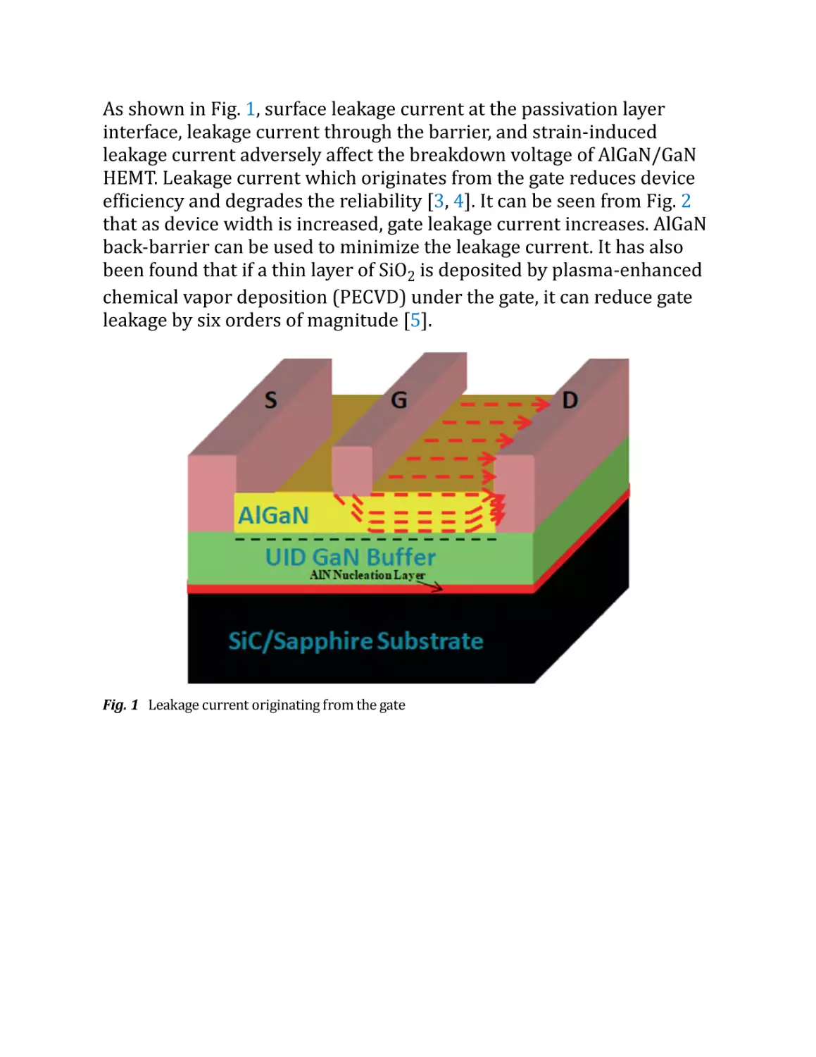
As shown in Fig. 1, surface leakage current at the passivation layer
interface, leakage current through the barrier, and strain-induced
leakage current adversely affect the breakdown voltage of AlGaN/GaN
HEMT. Leakage current which originates from the gate reduces device
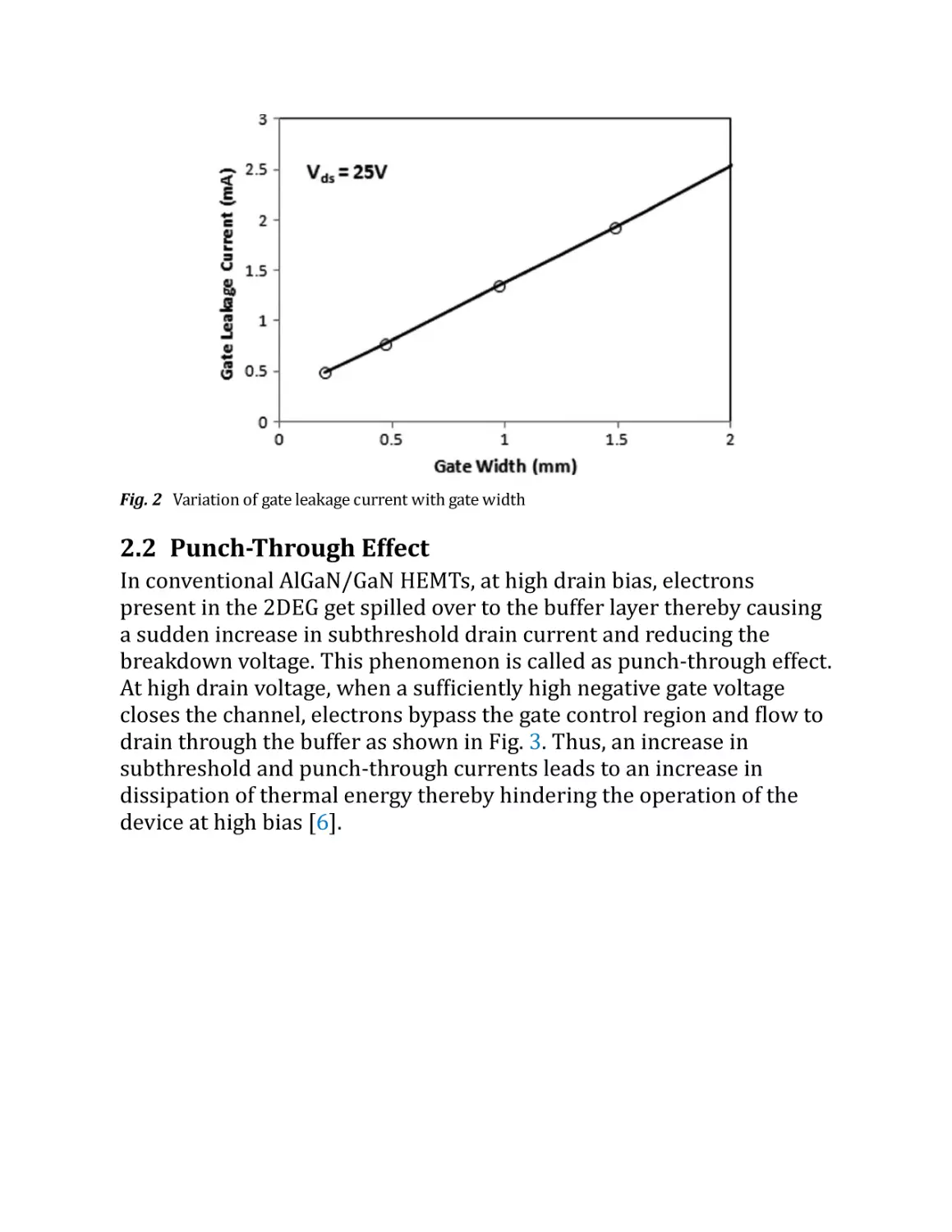
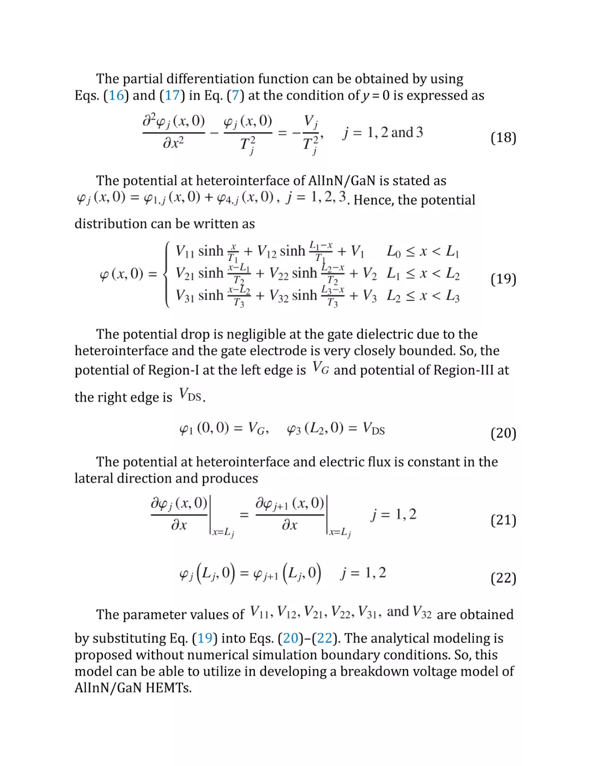
efficiency and degrades the reliability [3, 4]. It can be seen from Fig. 2
that as device width is increased, gate leakage current increases. AlGaN
back-barrier can be used to minimize the leakage current. It has also
been found that if a thin layer of SiO2 is deposited by plasma-enhanced
chemical vapor deposition (PECVD) under the gate, it can reduce gate
leakage by six orders of magnitude [5].
Fig. 1 Leakage current originating from the gate
Fig. 2 Variation of gate leakage current with gate width
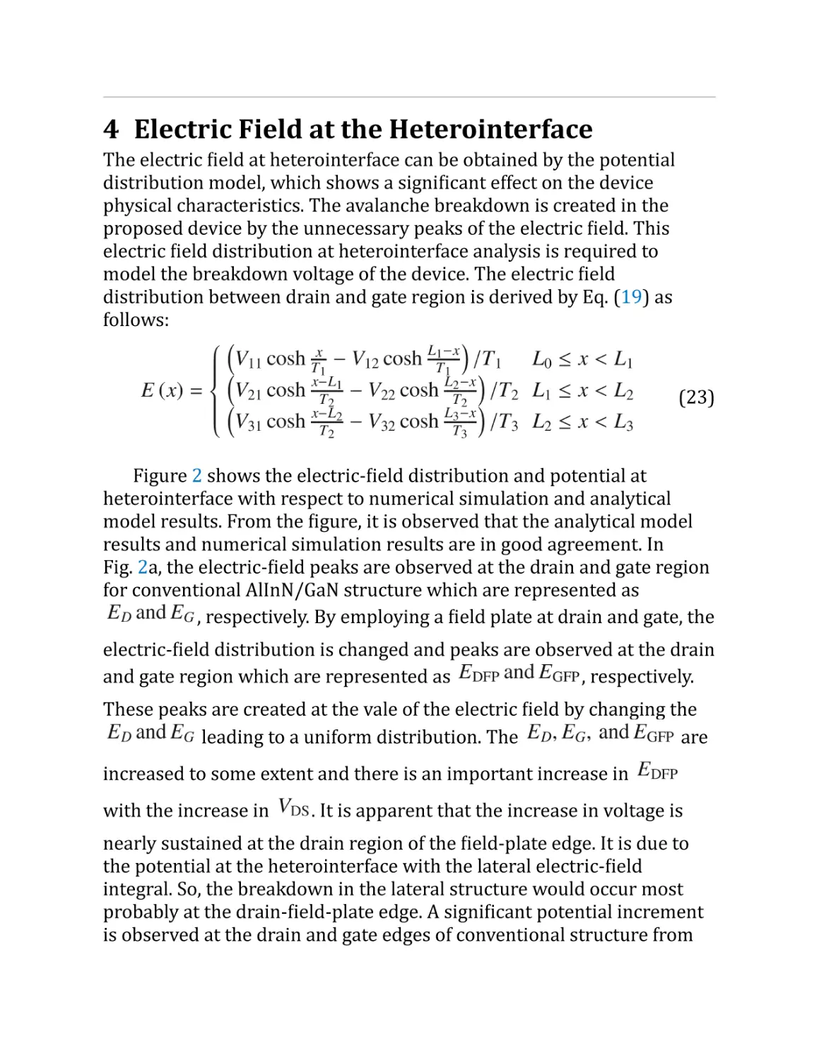
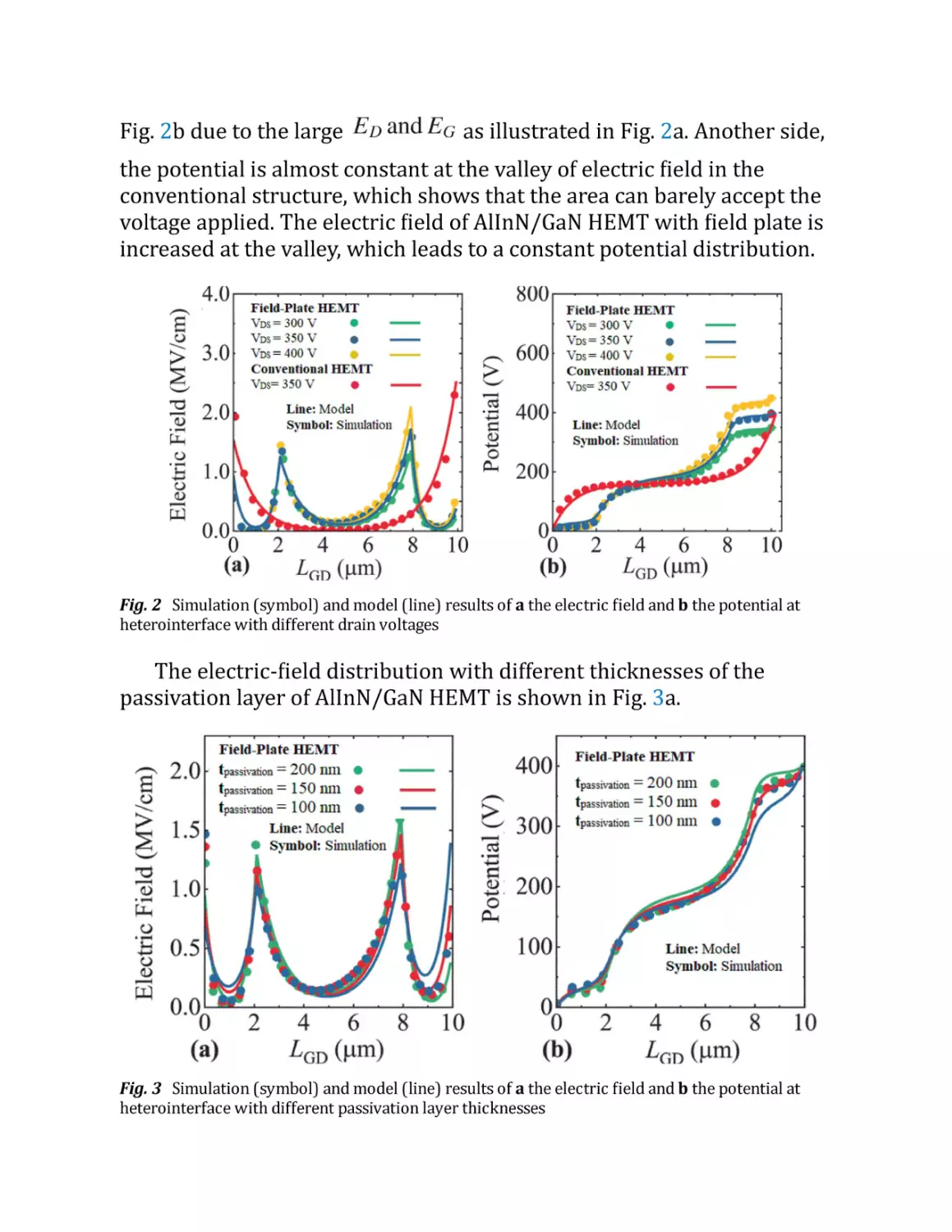
2.2 Punch-Through Effect
In conventional AlGaN/GaN HEMTs, at high drain bias, electrons
present in the 2DEG get spilled over to the buffer layer thereby causing
a sudden increase in subthreshold drain current and reducing the
breakdown voltage. This phenomenon is called as punch-through effect.
At high drain voltage, when a sufficiently high negative gate voltage
closes the channel, electrons bypass the gate control region and flow to
drain through the buffer as shown in Fig. 3. Thus, an increase in
subthreshold and punch-through currents leads to an increase in
dissipation of thermal energy thereby hindering the operation of the
device at high bias [6].
Fig. 3 Punch through in AlGaN/GaN HEMT on SiC or sapphire substrate
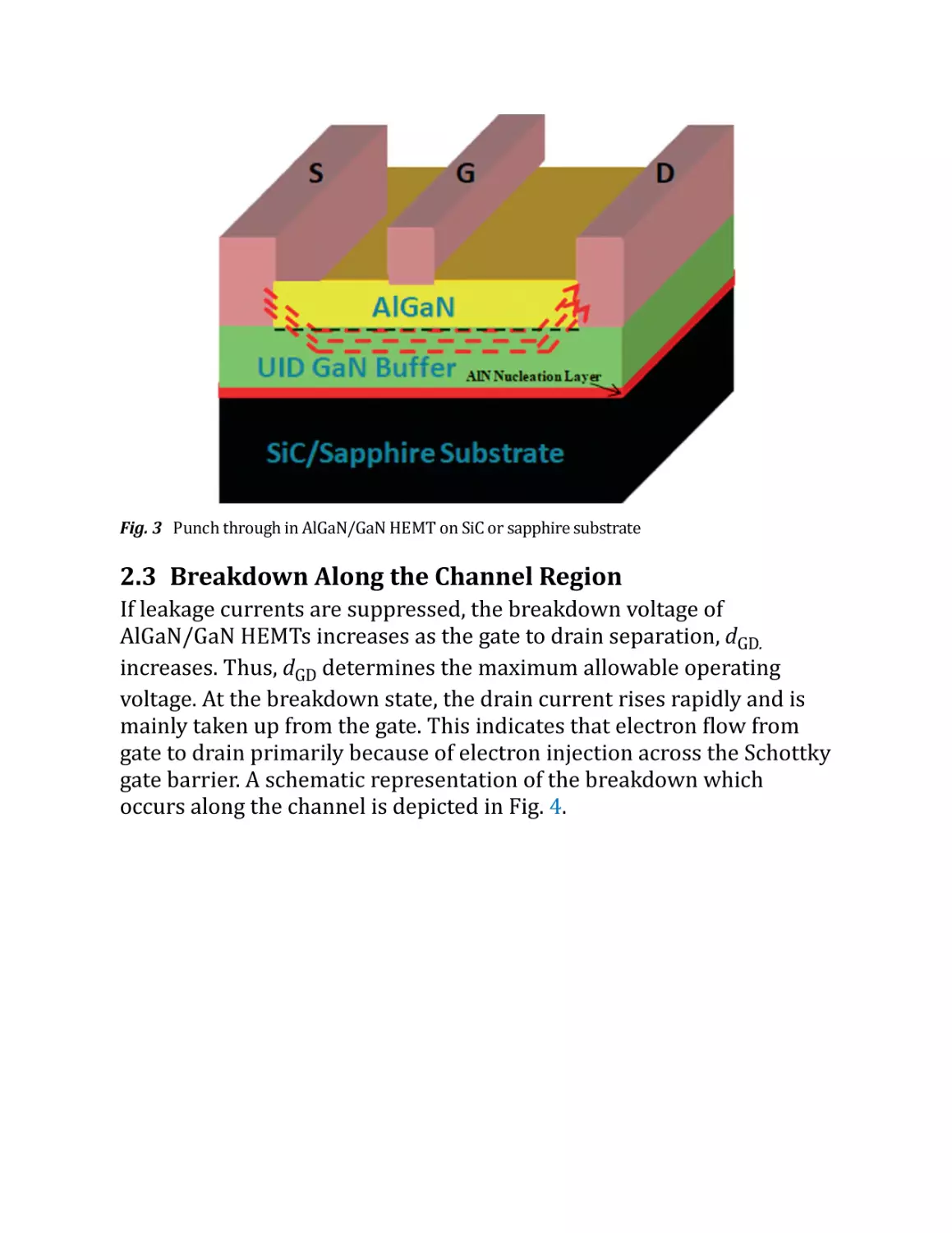
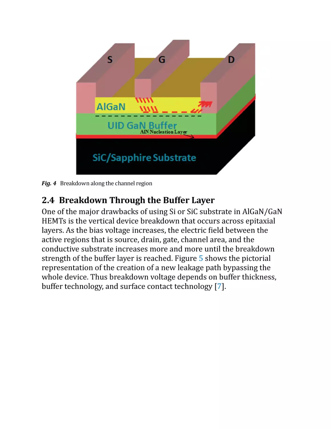
2.3 Breakdown Along the Channel Region
If leakage currents are suppressed, the breakdown voltage of
AlGaN/GaN HEMTs increases as the gate to drain separation, dGD.
increases. Thus, dGD determines the maximum allowable operating
voltage. At the breakdown state, the drain current rises rapidly and is
mainly taken up from the gate. This indicates that electron flow from
gate to drain primarily because of electron injection across the Schottky
gate barrier. A schematic representation of the breakdown which
occurs along the channel is depicted in Fig. 4.
Fig. 4 Breakdown along the channel region
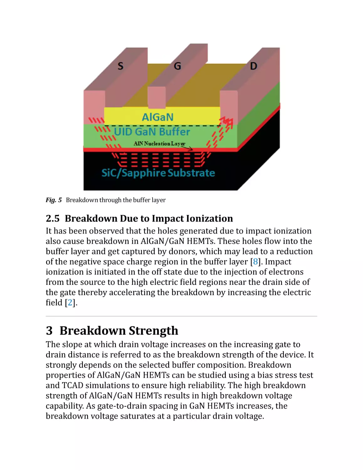
2.4 Breakdown Through the Buffer Layer
One of the major drawbacks of using Si or SiC substrate in AlGaN/GaN
HEMTs is the vertical device breakdown that occurs across epitaxial
layers. As the bias voltage increases, the electric field between the
active regions that is source, drain, gate, channel area, and the
conductive substrate increases more and more until the breakdown
strength of the buffer layer is reached. Figure 5 shows the pictorial
representation of the creation of a new leakage path bypassing the
whole device. Thus breakdown voltage depends on buffer thickness,
buffer technology, and surface contact technology [7].
Fig. 5 Breakdown through the buffer layer
2.5 Breakdown Due to Impact Ionization
It has been observed that the holes generated due to impact ionization
also cause breakdown in AlGaN/GaN HEMTs. These holes flow into the
buffer layer and get captured by donors, which may lead to a reduction
of the negative space charge region in the buffer layer [8]. Impact
ionization is initiated in the off state due to the injection of electrons
from the source to the high electric field regions near the drain side of
the gate thereby accelerating the breakdown by increasing the electric
field [2].
3 Breakdown Strength
The slope at which drain voltage increases on the increasing gate to
drain distance is referred to as the breakdown strength of the device. It
strongly depends on the selected buffer composition. Breakdown
properties of AlGaN/GaN HEMTs can be studied using a bias stress test
and TCAD simulations to ensure high reliability. The high breakdown
strength of AlGaN/GaN HEMTs results in high breakdown voltage
capability. As gate-to-drain spacing in GaN HEMTs increases, the
breakdown voltage saturates at a particular drain voltage.
4 Methods of Increasing the Breakdown
Voltage
In order to improve the breakdown voltage of AlGaN/GaN HEMTS,
often a compromise is made in its cut-off frequency and resistance.
Thus, it is imperative to use the appropriate device configuration and
device engineering techniques to enhance breakdown voltage, power
density, and cut-off frequency for high-frequency and high-power
applications. The electric field in the vicinity of the gate should be
reduced to delay premature breakdown and reduce dispersion effects.
Some of the methods used for this purpose are as follows.
1.4.1.
Field-plate Approach
1.4.2.
Designing of potential barriers in the epitaxial buffer layer to
confine electrons in the channel
1.4.3.
Epitaxial layer engineering: Pre-Epitaxy Implantation (Increase
of vertical breakdown)
1.4.4.
Schottky source/drain contact HEMT
1.4.5.
Use of high K dielectric passivation layer in HEMT
1.4.6.
Use of electron blocking layer
1.4.7.
Optimization of the gate to drain spacing
1.4.8.
Modulation of electric field using partial GaN cap layer
1.4.9.
Double-channel AlGaN HEMT.
4.1 Field-Plate Approach
Field plate approach reduces the electric fields inside critical regions of
the device, which is useful for S-band high-power FETs. Crowding of the
electric field near the drain side of gate edge results in a reduction in
breakdown voltage of AlGaN/GaN HEMTs. Therefore, different fieldplate approaches have been proposed to mitigate drain field crowding
to enhance breakdown voltage and reduce dispersive effects [9]. It
consists of an asymmetric gate with an extension of the gate-to-drain
edge.
It has been observed that the electric field is maximum near the
gate in AlGaN/GaN HEMTs. It has to be reduced to reduce the
probability of electrons spilling from the gate into the AlGaN layer or
into the passivation to prevent premature breakdown. Field plates near
the gate or drain have been extensively used to solve this issue.
Dimensions of the field plates and thickness of passivation and
metallization layers may be optimized to effectively smoothen the
electric field near the gate. Some of the field-plate designs which have
been reported so far are as follows:
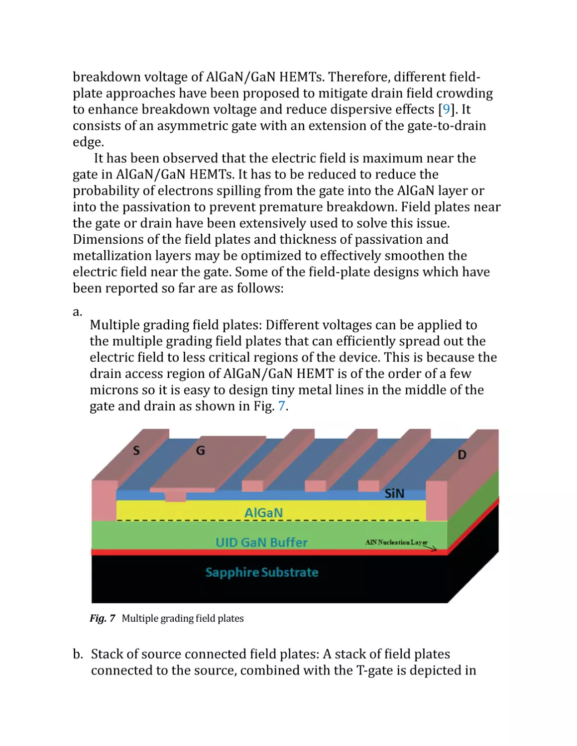
a.
Multiple grading field plates: Different voltages can be applied to
the multiple grading field plates that can efficiently spread out the
electric field to less critical regions of the device. This is because the
drain access region of AlGaN/GaN HEMT is of the order of a few
microns so it is easy to design tiny metal lines in the middle of the
gate and drain as shown in Fig. 7.
Fig. 7 Multiple grading field plates
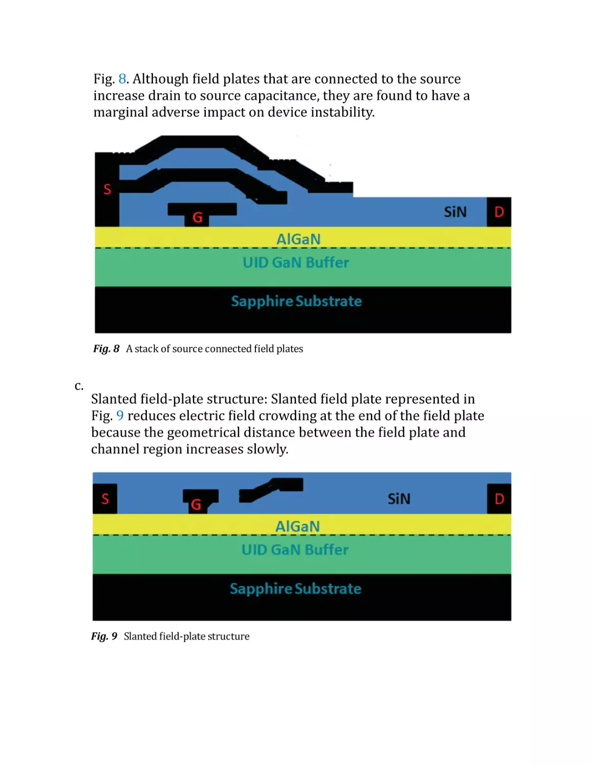
b. Stack of source connected field plates: A stack of field plates
connected to the source, combined with the T-gate is depicted in
Fig. 8. Although field plates that are connected to the source
increase drain to source capacitance, they are found to have a
marginal adverse impact on device instability.
Fig. 8 A stack of source connected field plates
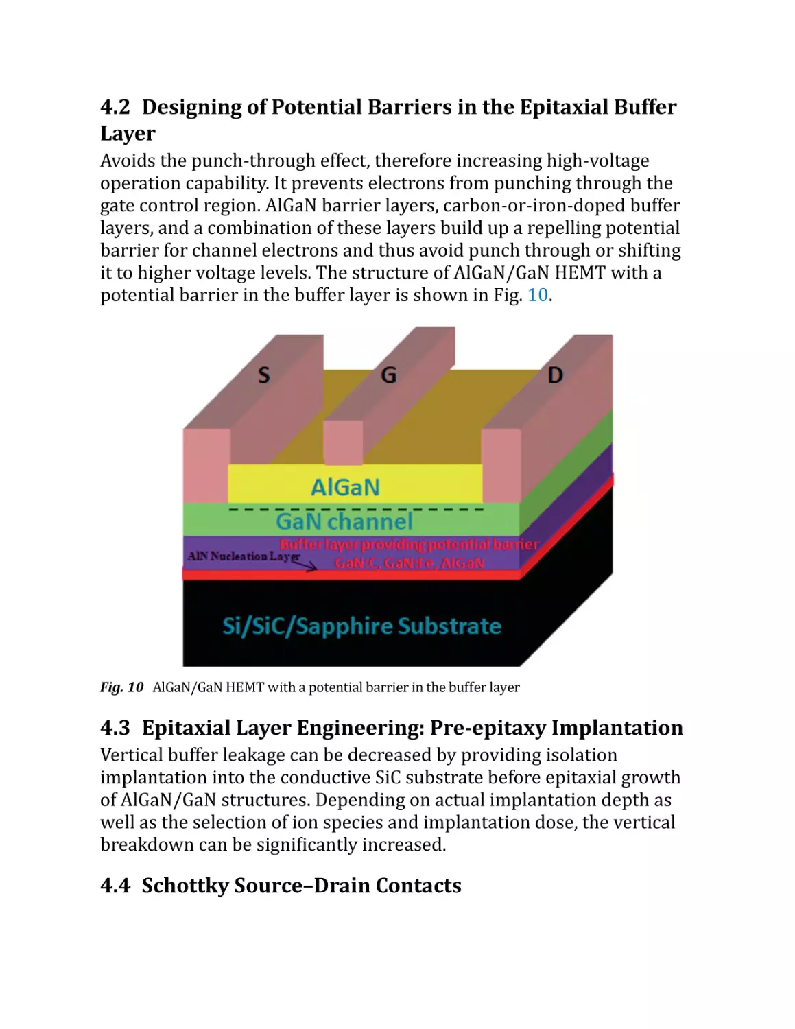
c.
Slanted field-plate structure: Slanted field plate represented in
Fig. 9 reduces electric field crowding at the end of the field plate
because the geometrical distance between the field plate and
channel region increases slowly.
Fig. 9 Slanted field-plate structure
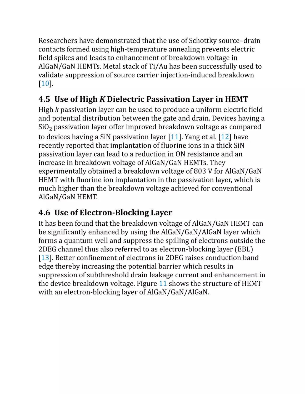
4.2 Designing of Potential Barriers in the Epitaxial Buffer
Layer
Avoids the punch-through effect, therefore increasing high-voltage
operation capability. It prevents electrons from punching through the
gate control region. AlGaN barrier layers, carbon-or-iron-doped buffer
layers, and a combination of these layers build up a repelling potential
barrier for channel electrons and thus avoid punch through or shifting
it to higher voltage levels. The structure of AlGaN/GaN HEMT with a
potential barrier in the buffer layer is shown in Fig. 10.
Fig. 10 AlGaN/GaN HEMT with a potential barrier in the buffer layer
4.3 Epitaxial Layer Engineering: Pre-epitaxy Implantation
Vertical buffer leakage can be decreased by providing isolation
implantation into the conductive SiC substrate before epitaxial growth
of AlGaN/GaN structures. Depending on actual implantation depth as
well as the selection of ion species and implantation dose, the vertical
breakdown can be significantly increased.
4.4 Schottky Source–Drain Contacts
Researchers have demonstrated that the use of Schottky source–drain
contacts formed using high-temperature annealing prevents electric
field spikes and leads to enhancement of breakdown voltage in
AlGaN/GaN HEMTs. Metal stack of Ti/Au has been successfully used to
validate suppression of source carrier injection-induced breakdown
[10].
4.5 Use of High K Dielectric Passivation Layer in HEMT
High k passivation layer can be used to produce a uniform electric field
and potential distribution between the gate and drain. Devices having a
SiO2 passivation layer offer improved breakdown voltage as compared
to devices having a SiN passivation layer [11]. Yang et al. [12] have
recently reported that implantation of fluorine ions in a thick SiN
passivation layer can lead to a reduction in ON resistance and an
increase in breakdown voltage of AlGaN/GaN HEMTs. They
experimentally obtained a breakdown voltage of 803 V for AlGaN/GaN
HEMT with fluorine ion implantation in the passivation layer, which is
much higher than the breakdown voltage achieved for conventional
AlGaN/GaN HEMT.
4.6 Use of Electron-Blocking Layer
It has been found that the breakdown voltage of AlGaN/GaN HEMT can
be significantly enhanced by using the AlGaN/GaN/AlGaN layer which
forms a quantum well and suppress the spilling of electrons outside the
2DEG channel thus also referred to as electron-blocking layer (EBL)
[13]. Better confinement of electrons in 2DEG raises conduction band
edge thereby increasing the potential barrier which results in
suppression of subthreshold drain leakage current and enhancement in
the device breakdown voltage. Figure 11 shows the structure of HEMT
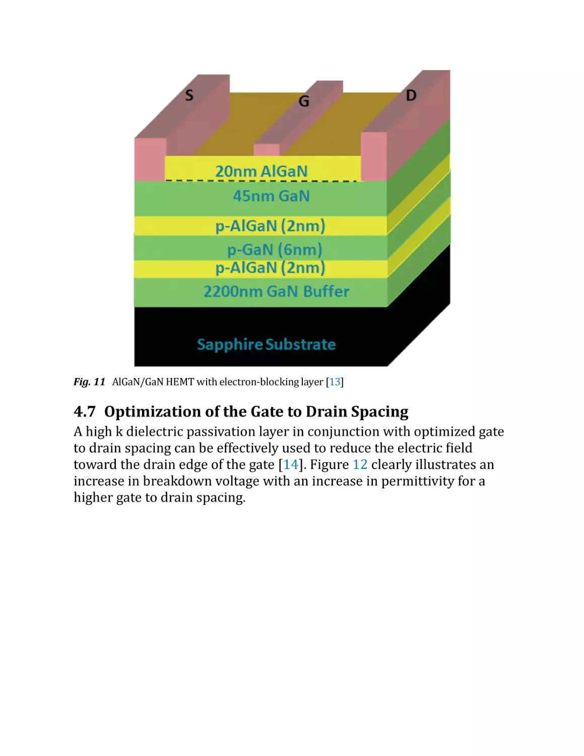
with an electron-blocking layer of AlGaN/GaN/AlGaN.
Fig. 11 AlGaN/GaN HEMT with electron-blocking layer [13]
4.7 Optimization of the Gate to Drain Spacing
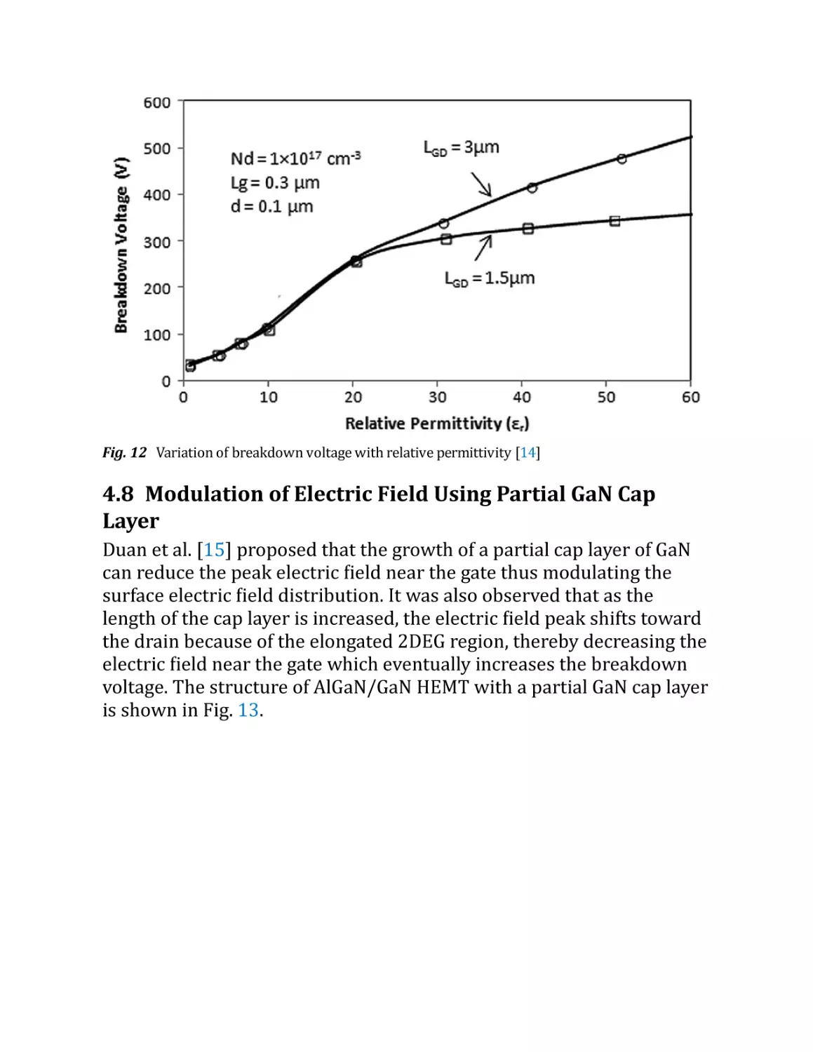
A high k dielectric passivation layer in conjunction with optimized gate
to drain spacing can be effectively used to reduce the electric field
toward the drain edge of the gate [14]. Figure 12 clearly illustrates an
increase in breakdown voltage with an increase in permittivity for a
higher gate to drain spacing.
Fig. 12 Variation of breakdown voltage with relative permittivity [14]
4.8 Modulation of Electric Field Using Partial GaN Cap
Layer
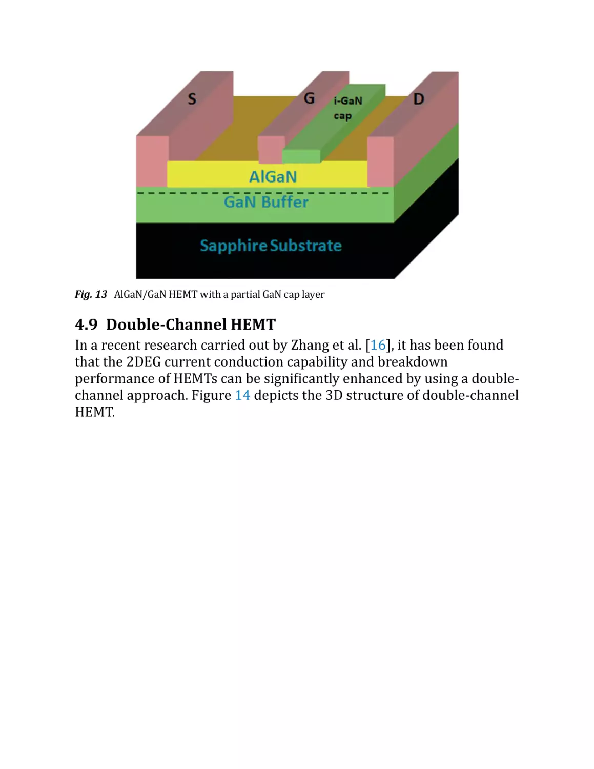
Duan et al. [15] proposed that the growth of a partial cap layer of GaN
can reduce the peak electric field near the gate thus modulating the
surface electric field distribution. It was also observed that as the
length of the cap layer is increased, the electric field peak shifts toward
the drain because of the elongated 2DEG region, thereby decreasing the
electric field near the gate which eventually increases the breakdown
voltage. The structure of AlGaN/GaN HEMT with a partial GaN cap layer
is shown in Fig. 13.
Fig. 13 AlGaN/GaN HEMT with a partial GaN cap layer
4.9 Double-Channel HEMT
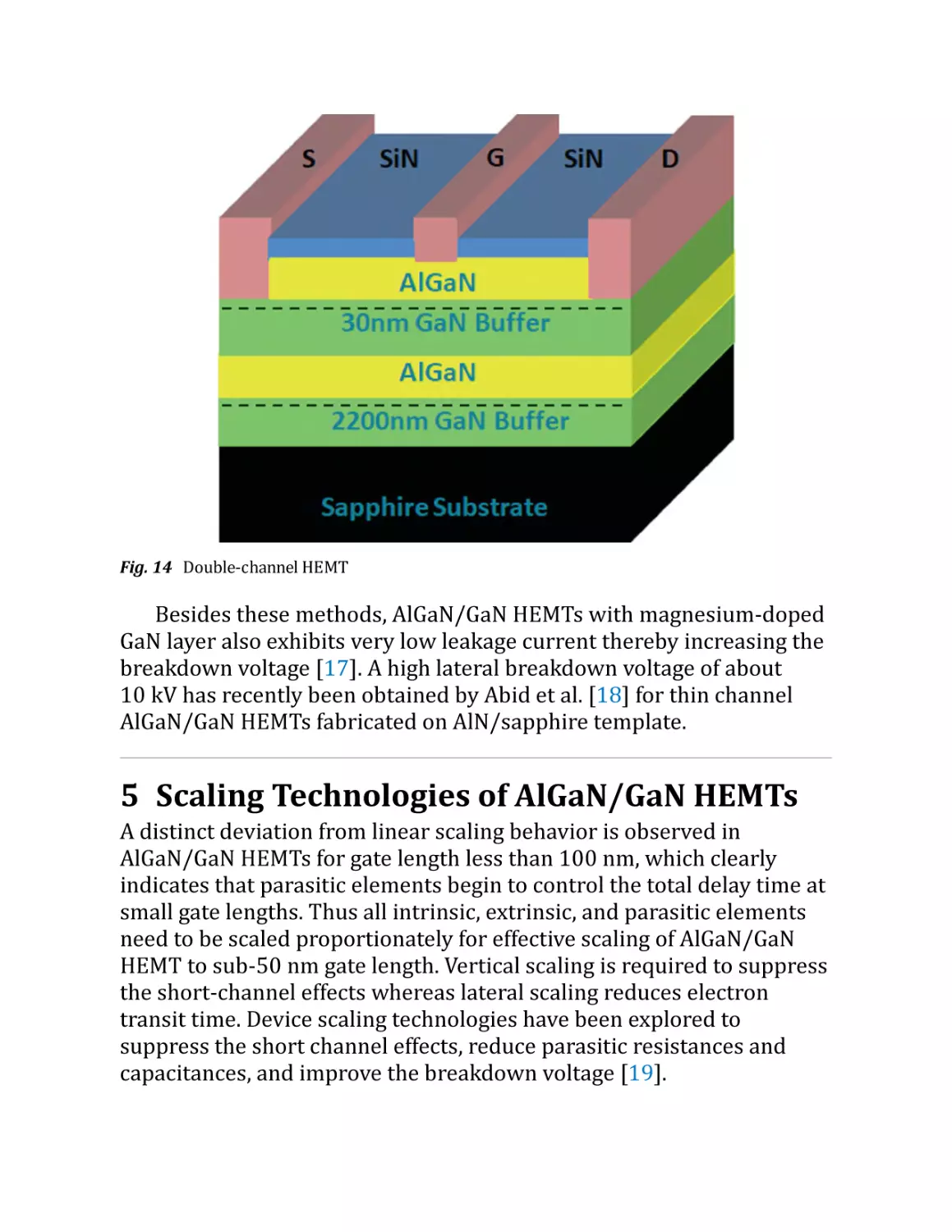
In a recent research carried out by Zhang et al. [16], it has been found
that the 2DEG current conduction capability and breakdown
performance of HEMTs can be significantly enhanced by using a doublechannel approach. Figure 14 depicts the 3D structure of double-channel
HEMT.
Fig. 14 Double-channel HEMT
Besides these methods, AlGaN/GaN HEMTs with magnesium-doped
GaN layer also exhibits very low leakage current thereby increasing the
breakdown voltage [17]. A high lateral breakdown voltage of about
10 kV has recently been obtained by Abid et al. [18] for thin channel
AlGaN/GaN HEMTs fabricated on AlN/sapphire template.
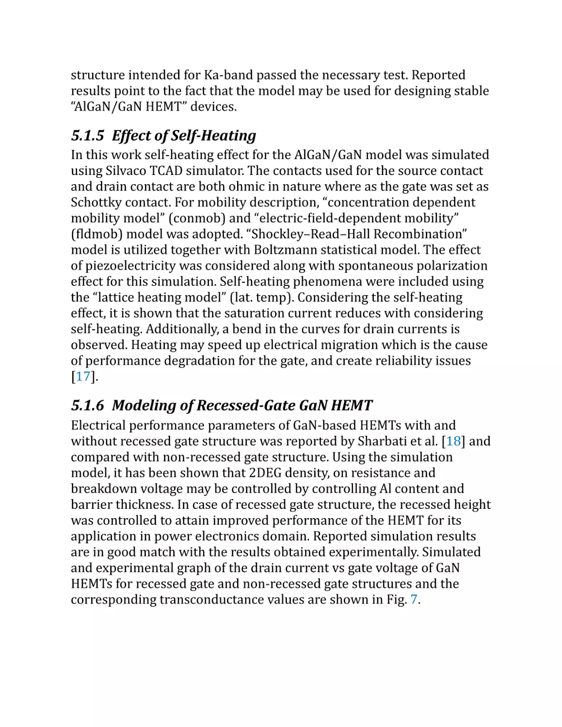
5 Scaling Technologies of AlGaN/GaN HEMTs
A distinct deviation from linear scaling behavior is observed in
AlGaN/GaN HEMTs for gate length less than 100 nm, which clearly
indicates that parasitic elements begin to control the total delay time at
small gate lengths. Thus all intrinsic, extrinsic, and parasitic elements
need to be scaled proportionately for effective scaling of AlGaN/GaN
HEMT to sub-50 nm gate length. Vertical scaling is required to suppress
the short-channel effects whereas lateral scaling reduces electron
transit time. Device scaling technologies have been explored to
suppress the short channel effects, reduce parasitic resistances and
capacitances, and improve the breakdown voltage [19].
Self-aligned-gate double-heterojunction AlGaN/GaN HEMT with
heavily doped regrown n+-GaN ohmic contacts offer low RON, high
maximum drain current, high transconductance, and high linearity with
a broad transconductance curve [20]. Highly doped source/drain can
drastically enhance the performance of the device by increasing
electron concentration in the source region [21]. Regrown n+ -GaN
ohmic contacts have also proved to decrease parasitic access
resistances [22]. In order to obtain a high cutoff frequency, aggressive
dimensional scaling (Lg and Lsd) is required, maintaining high
breakdown voltage.
Lateral scaling using self-aligned gate (SAG) technology can be
explored to reduce parasitic capacitance in highly scaled devices [23].
When gate length is reduced to a sub-50 nm range and becomes smaller
than the source to drain distance (Lds), cutoff frequency and maximum
frequency of oscillation of HEMT are restricted by an extrinsic delay
related to depletion of the 2DEG channel at the drain edge of the gate.
This is referred to as drain delay and is directly related to the transit
time of electrons through the depleted region. Therefore, it can be
minimized by reducing gate to drain distance (Lgd), which can be
achieved by developing a self-aligned gate process, through which
precise dimension control along with high device yield and uniformity
can be obtained.
References
1.
F. Zeng et al., A comprehensive review of recent progress on GaN high electron mobility
transistors: Devices, fabrication and reliability, Electron. 7, (12) (2018). https://doi.org/10.
3390/electronics7120377
2.
G. Meneghesso, M. Meneghini, E. Zanoni, Breakdown mechanisms in AlGaN/GaN HEMTs: An
overview, Jpn J. Appl. Phys. 53(10). Japan Soc. Appl. Phys. (2014). https://doi.org/10.7567/
JJAP.53.100211
3.
A. Goswami, R.J. Trew, G.L. Bilbro, Modeling of the gate leakage current in AlGaN/GaN HFETs.
IEEE Trans. Electron Devices 61(4), 1014–1021 (2014). https://doi.org/10.1109/TED.2014.
2302797
[Crossref]
4.
A. Wang, L. Zeng, W. Wang, Simulation of gate leakage current of AlGaN/GaN HEMTs: Effects of
the gate edges and self-heating. ECS J. Solid State Sci. Technol. 6(11), S3025–S3029 (2017).
https://doi.org/10.1149/2.0031711jss
[Crossref]
5.
R. Chu et al., 1200-V normally off GaN-on-Si field-effect transistors with low dynamic on resistance. IEEE Electron Device Lett. 32(5), 632–634 (2011). https://doi.org/10.1109/LED.
2011.2118190
[Crossref]
6.
M. Baeumler et al., Investigation of leakage current of AlGaN/GaN HEMTs under pinch-off
condition by electroluminescence microscopy. J. Electron. Mater. 39(6), 756–760 (2010).
https://doi.org/10.1007/s11664-010-1120-9
[Crossref]
7.
B. Lu, E. L. Piner, T. Palacios, Breakdown Mechanism in AlGaN/GaN HEMTs on Si Substrate, in
Device Research Conference—Conference Digest, DRC, pp. 193–194 (2010). https://doi.org/
10.1109/DRC.2010.5551907
8.
W. Saito, T. Suwa, T. Uchihara, T. Naka, T. Kobayashi, Breakdown behaviour of high-voltage
GaN-HEMTs. Microelectron. Reliab. 55(9–10), 1682–1686 (2015). https://doi.org/10.1016/j.
microrel.2015.06.126
[Crossref]
9.
T. Asano, N. Yamada, T. Saito, H. Tokuda, M. Kuzuhara, Breakdown Characteristics in
AlGaN/GaN HEMTs with Multi-field-plate Structure, in IMFEDK 2012—2012 International
Meeting for Future of Electron Devices, Kansai, pp. 100–101 (2012). https://doi.org/10.
1109/IMFEDK.2012.6218601
10. Q. Zhou et al., Schottky-contact technology in InAlN/GaN HEMTs for breakdown voltage
improvement. IEEE Trans. Electron Devices 60(3), 1075–1081 (2013). https://doi.org/10.
1109/TED.2013.2241439
[Crossref]
11. S. Chander, S. Gupta, Ajay, M. Gupta, Enhancement of breakdown voltage in AlGaN/GaN HEMT
using passivation technique for microwave application, Superlattices Microstruct. 120, 217–
222 (2018). https://doi.org/10.1016/j.spmi.2018.05.039
12. C. Yang et al., High breakdown voltage and low dynamic ON-resistance AlGaN/GaN HEMT
with fluorine ion implantation in SiNx passivation layer, Nanoscale Res. Lett. 14 (2019).
https://doi.org/10.1186/s11671-019-3025-8
13. Y.J. Lee et al., High breakdown voltage in AlGaN/GaN HEMTs using AlGaN/GaN/AlGaN
quantum-well electron-blocking layers. Nanoscale Res. Lett. 9(1), 1–9 (2014). https://doi.
org/10.1186/1556-276X-9-433
[Crossref]
14. R. Tomita, S. Ueda, T. Kawada, H. Mitsuzono, K. Horio, Analysis of dependence of breakdown
voltage on gate-drain distance in AlGaN/GaN HEMTs with high-k passivation layer. IEEE
Trans. Electron Devices 68(4), 1550–1556 (2021). https://doi.org/10.1109/TED.2021.
3060353
[Crossref]
15.
B. Duan, L. Yang, Y. Wang, Y. Yang, Experimental results for AlGaN/GaN HEMTs improving
breakdown voltage and output current by electric field modulation. IEEE Trans. Electron
Devices 68(5), 2240–2245 (2021). https://doi.org/10.1109/TED.2021.3067865
[Crossref]
16. Y. Zhang et al., High-performance AlGaN double channel HEMTs with improved drain current
density and high breakdown voltage, Nanoscale Res. Lett. 15(1) (2020). https://doi.org/10.
1186/s11671-020-03345-6
17. T. Liu et al., Suppression of the regrowth interface leakage current in AlGaN/GaN HEMTs by
unactivated Mg doped GaN layer, Appl. Phys. Lett. 118(7) (2021). https://doi.org/10.1063/5.
0034584
18. I. Abid et al., High lateral breakdown voltage in thin channel AlGaN/GaN high electron mobility
transistors on AlN/Sapphire Templates, Micromachines 10(10) (2019). https://doi.org/10.
3390/mi10100690
19. Y. Dai, J. Zhou, J. Chen, M. Han, Scaling technologies for millimeter-wave GaN-HEMTs, in 2012
IEEE MTT-S International Microwave Workshop Series on Millimeter Wave Wireless
Technology and Applications, 2012, pp. 1–3,https://doi.org/10.1109/IMWS2.2012.6338180
20. K. Shinohara et al., Scaling of gan hemts and schottky diodes for submillimeter-wave mmic
applications. IEEE Trans. Electron Devices 60(10), 2982–2996 (2013). https://doi.org/10.
1109/TED.2013.2268160
[Crossref]
21. K.C. Sahoo, C.-I. Kuo, Y. Li, E.Y. Chang, Novel metamorphic HEMTs with highly doped InGaAs
source/drain regions for high frequency applications. IEEE Trans. Electron Devices 57(10),
2594–2598 (2010). https://doi.org/10.1109/TED.2010.2062521
[Crossref]
22. A.G. Baca et al., An AlN/Al<inf>0.85</inf>Ga<inf>0.15</inf>N High Electron Mobility
Transistor with a Regrown Ohmic Contact, in 2016 74th Annual Device Research Conference
(DRC), Jun. 2016, pp. 1–2. https://doi.org/10.1109/DRC.2016.7548395
23. N.S. Garigapati, F. Lindelö w, L. Sö dergren, E. Lind, Capacitance scaling in In0.71Ga0.29As/InP
MOSFETs with self-aligned a: Si spacers. IEEE Trans. Electron Devices 68(8), 3762–3767
(2021). https://doi.org/10.1109/TED.2021.3092299
[Crossref]
© The Author(s), under exclusive license to Springer Nature Singapore Pte Ltd. 2023
T. R. Lenka, H. P. T. Nguyen (eds.), HEMT Technology and Applications, Springer Tracts in Electrical
and Electronics Engineering
https://doi.org/10.1007/978-981-19-2165-0_3
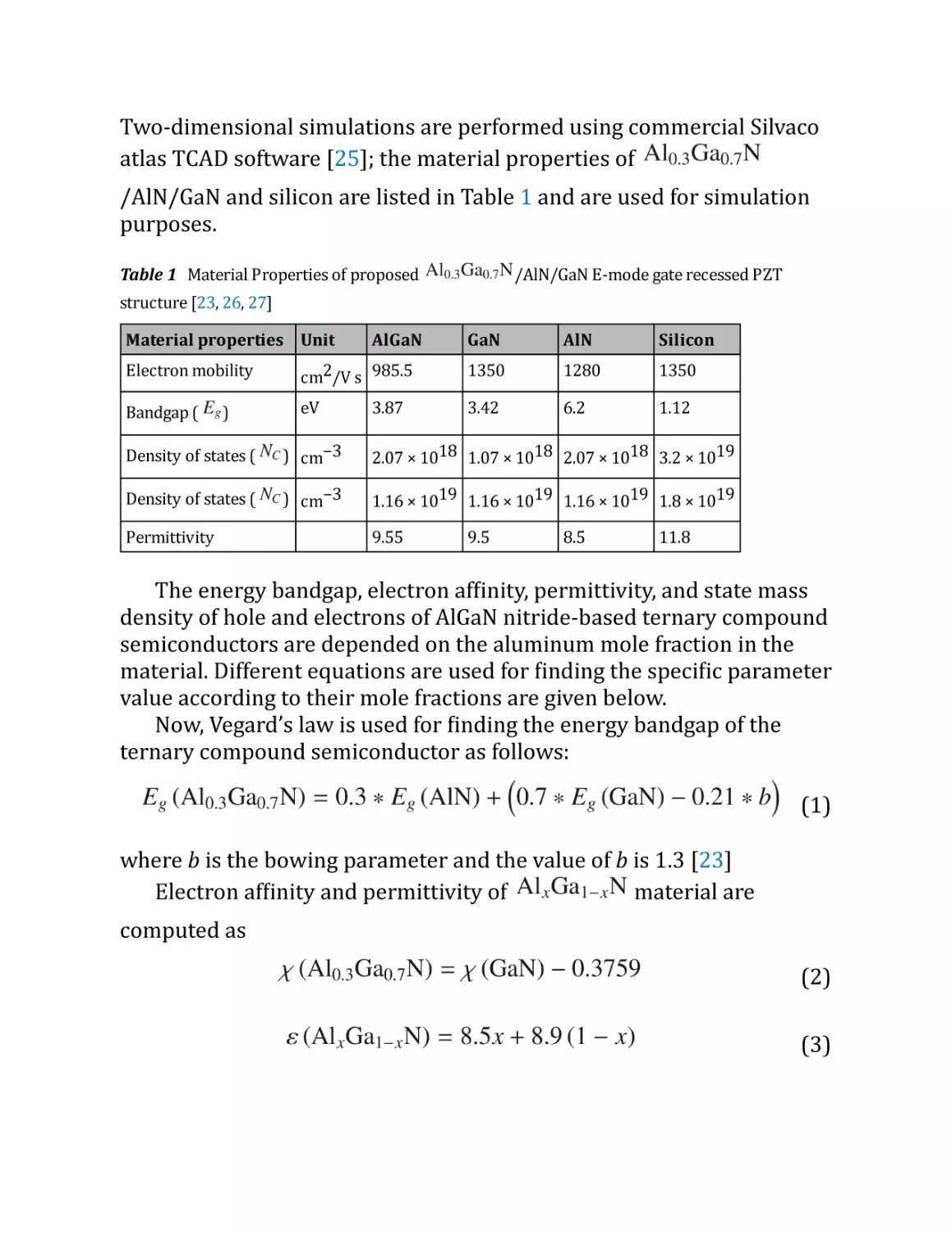
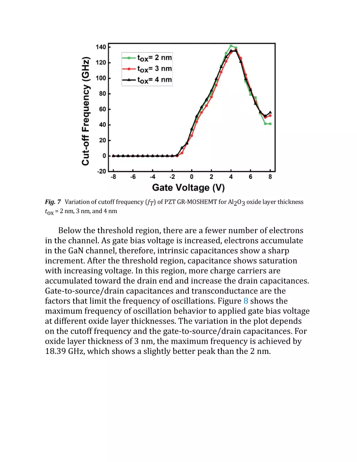
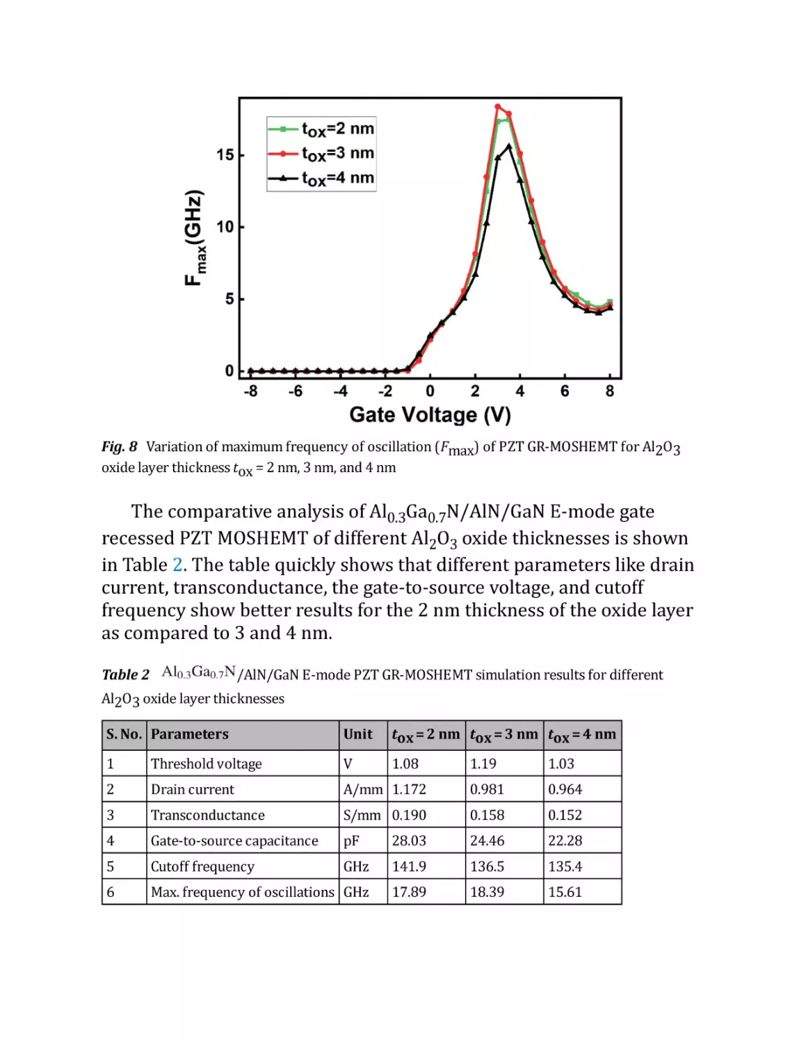
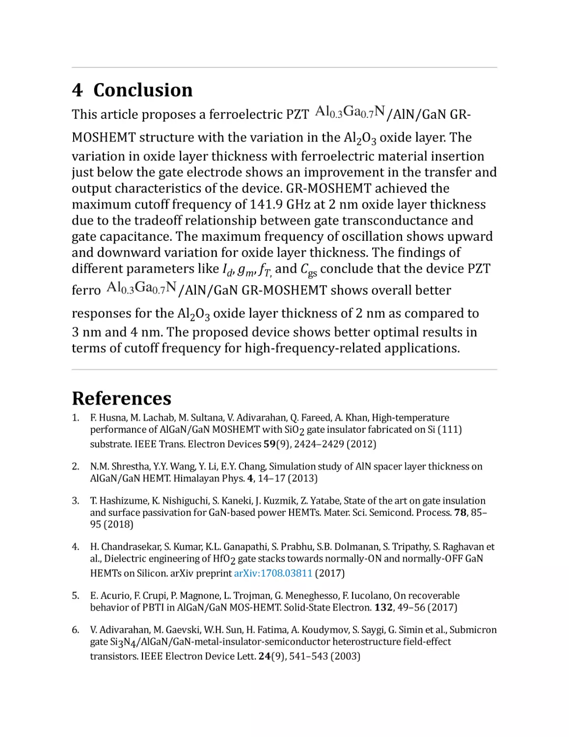
Influence of Al2O3 Oxide Layer
Thickness Variation on PZT
Ferroelectric Al0.3Ga0.7N/AlN/GaN EMode GR-MOSHEMT
Abdul Naim Khan1 , S. N. Mishra2, Meenakshi Chauhan1 ,
Kanjalochan Jena1 and G. Chatterjee1
(1) Department of Electronics and Communication Engineering, The
LNM Institute of Information Technology, Jaipur, Rajasthan,
302031, India
(2) School of Electronics Engineering, KIIT (Deemed to be University),
Bhubaneswar, Odisha, 751024, India
Abdul Naim Khan (Corresponding author)
Email: abdulnaimkhan.y19@lnmiit.ac.in
Meenakshi Chauhan
Email: 20pec006@lnmiit.ac.in
Kanjalochan Jena
Email: kanjalochan.jena@lnmiit.ac.in
G. Chatterjee
Email: gaurav.chatterjee@lnmiit.ac.in
Abstract
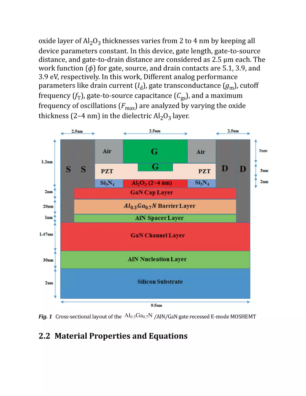
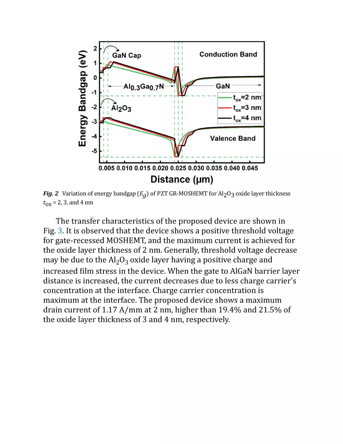
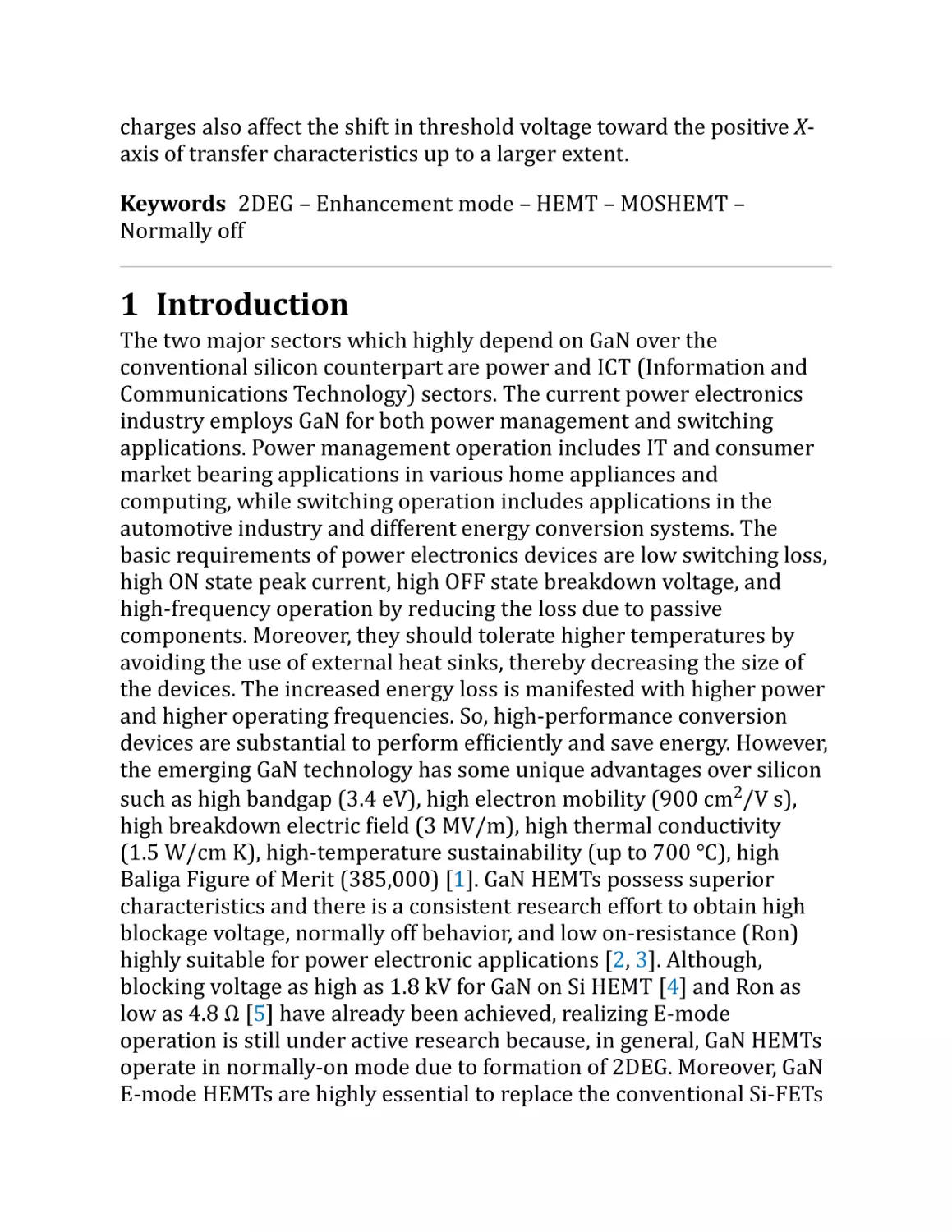
The dielectric oxide Al2O3 induced gate recessed PZT ferroelectric
Al0.3Ga0.7N/AlN/GaN MOSHEMT device behavior with different oxide
thicknesses is analyzed in this work. The stack of different layers
Al2O3/Al0.3Ga0.7N/AlN/GaN is grown on a silicon (Si) substrate. Gate
recessed technique is used for achieving the normally off operation in
the MOSHEMT. Normally off devices provide better control in gate
leakage current and stability of threshold voltage (Vth). The
ferroelectric material of lead zirconate titanate Pb(Zr,Ti)O3 (PZT) is
induced between the gate and oxide layer to obtain the enhancement
type (E-Mode) operation to improve the device performance due to the
strong polarization effect. The AlN spacer layer is introduced between
the Al0.3Ga0.7N barrier and GaN Channel to increase mobility and 2-DEG
confinement. For controlling the GaN channel layer, the AlN nucleation
layer is inserted between GaN/Si–substrate interfaces by producing
better surface morphology. Furthermore, silicon-based substrates are
used to achieve excellent thermal characteristics. Due to the
polarization effect, a two-dimensional electron gas (2-DEG) is created
at the Al0.3Ga0.7N/GaN interface. The analog performance parameters
like drain current (Id), output characteristics (Id − Vd),
transconductance (gm), cutoff frequency (fT), and gate-to-source
capacitance (Cgs) except maximum frequency of oscillation (Fmax) show
an improvement for 3 nm oxide layer thickness of Al2O3. The results of
the proposed device Al0.3Ga0.7N/AlN/GaN PZT GR-MOSHEMT shows an
impact on high power and RF-based devices. All the simulations are
done by the commercial Silvaco Atlas Technology Computer-Aided
Design (TCAD) tool.
Keywords
/AlN/GaN – Al2O3 – 2-DEG – PZT – GR-
MOSHEMT – E-Mode – TCAD
1 Introduction
Recently, gallium nitride-based devices are favorable ones over the
GaAs and Si-based devices due to their superior material properties
such as large bandgap [1], high breakdown field [2], and high
breakdown voltage [3]. AlGaN/GaN-based HEMT devices show better
trade-off ON-Resistance (RON) and high breakdown voltage enabling the
work device at higher frequencies. But GaN-based HEMTs provide
negative threshold voltage due to work in normally on mode. For
converting the normally on to normally off operation [4], a stack of
metal oxide is needed with some modification in the gate electrode.
MOS-HEMT-based devices show switch-off current at zero bias gate
voltage [5]. Gate recessed-MOSHEMT (GR-MOSHEMT) provides low
leakage gate current [6, 7], higher breakdown voltage [8, 9], and
positive threshold voltage[10] as compared to HEMT-based devices,
which show more impact in the system-based high-frequency
applications [11]. Ferroelectric materials have been used as oxide gate
dielectrics to perform E-mode [12] operations due to the impact of
polarization to achieve two-dimensional electron gas (2-DEG) and
generate the positive cutoff voltage. Different types of insulators are
used for AlGaN/GaN MOSHEMTs such as Al2O3 [13], SiO2 [14], SiNx
[15], HfO2 [16], etc. The major drawback of MOSHEMT-based devices is
that they provide low transconductance compared to HEMT-based
devices due to an increase in the AlGaN barrier layer thickness [17, 18],
which limits the high RF performance [19]. The improvement in the
gate transconductance [20, 21] is done by using a recessed gate
methodology with a thin oxide layer. To operate the device in DC and
high-frequency microwave application [22], AlN spacer layer is inserted
between the barrier and the channel layer. The spacer layer increases
the charge concentration and mobility near the interface, which is
helpful in generating 2-DEG. The AlN nucleation layer was introduced
to reduce the tensile stress and the lattice mismatch [23] between GaN
and silicon substrate. Also, it provides better surface properties [24] for
the deposition of nitride-based material on AlN. Silicon substrate
provides better thermal properties to the proposed device structure.
To overcome the issues related to low transconductance, gate
leakage, and negative threshold voltage, this work makes the following
contributions:
The proposed device structure suggests a ferroelectric dielectric
oxide layer insertion between the gate and the Al2O3 oxide layer to
improve the 2-DEG.
The AlN spacer layer inclusion helps to improve the AlGaN layer
quality as well as remove the strain.
This work searches Al2O3 oxide layer optimal thickness at which the
proposed device shows better drain current, gate transconductance,
and cutoff frequency. Investigation findings show that oxide layer
thickness is an essential parameter for the realization of the device in
DC and high-power applications.
In this work, we demonstrated the performance of the dielectric
Al2O3 oxide layer by varying the thickness for ferroelectric
Al0.3Ga0.7N/AlN/GaN GR-MOSHEMT to investigate the different figures
of merit. Section 2 represents the behavior of the ferroelectric
Al0.3Ga0.7N/AlN/GaN PZT GR-MOSHEMT device structure with device
material properties. The simulated results are generated with the help
of Silvaco atlas TCAD in Sect. 3. At last, the conclusion is drawn in
Sect. 4.
2 Device Model Description and Material
Properties
2.1 Device Structure
The proposed device structure for
/AlN/GaN gate recessed
E-mode MOSHEMT is shown in Fig. 1. A stack of epitaxial layers
consists of a GaN cap layer, Al0.3Ga0.7N barrier layer, AlN spacer layer,
GaN channel layer, AlN nucleation layer, and silicon as a substrate layer
from top to down approach with a thickness of 2 nm, 20 nm, 1 nm,
1.47 µm, 30 nm, and 20 nm, respectively. The AlGaN barrier layer is
doped with a charge concentration of 1e17 cm−3 to increase the charge
carriers at the Al0.3Ga0.7N/GaN interface to make 2-DEG rich in terms of
electron concentration. The AlN spacer layer is used to increase
electron mobility and make 2-DEG more confined. The nucleation layer
is used between GaN and substrate to reduce lattice mismatch and
provide smooth surface morphology to the device. The ferroelectric
PZT with 3 nm layer thickness is used in this simulation. The dielectric
oxide layer of Al2O3 thicknesses varies from 2 to 4 nm by keeping all
device parameters constant. In this device, gate length, gate-to-source
distance, and gate-to-drain distance are considered as 2.5 µm each. The
work function (ϕ) for gate, source, and drain contacts are 5.1, 3.9, and
3.9 eV, respectively. In this work, Different analog performance
parameters like drain current (Id), gate transconductance (gm), cutoff
frequency (fT), gate-to-source capacitance (Cgs), and a maximum
frequency of oscillations (Fmax) are analyzed by varying the oxide
thickness (2–4 nm) in the dielectric Al2O3 layer.
Fig. 1 Cross-sectional layout of the
/AlN/GaN gate recessed E-mode MOSHEMT
2.2 Material Properties and Equations
Two-dimensional simulations are performed using commercial Silvaco
atlas TCAD software [25]; the material properties of
/AlN/GaN and silicon are listed in Table 1 and are used for simulation
purposes.
Table 1 Material Properties of proposed
/AlN/GaN E-mode gate recessed PZT
structure [23, 26, 27]
Material properties Unit
AlGaN
GaN
AlN
Silicon
Electron mobility
cm2/V s 985.5
1350
1280
1350
Bandgap (
eV
3.42
6.2
1.12
)
3.87
Density of states (
) cm−3
2.07 × 10¹⁸ 1.07 × 10¹⁸ 2.07 × 10¹⁸ 3.2 × 10¹⁹
Density of states (
) cm−3
1.16 × 10¹⁹ 1.16 × 10¹⁹ 1.16 × 10¹⁹ 1.8 × 10¹⁹
Permittivity
9.55
9.5
8.5
11.8
The energy bandgap, electron affinity, permittivity, and state mass
density of hole and electrons of AlGaN nitride-based ternary compound
semiconductors are depended on the aluminum mole fraction in the
material. Different equations are used for finding the specific parameter
value according to their mole fractions are given below.
Now, Vegard’s law is used for finding the energy bandgap of the
ternary compound semiconductor as follows:
(1)
where b is the bowing parameter and the value of b is 1.3 [23]
Electron affinity and permittivity of
material are
computed as
(2)
(3)
The electron and hole mass density of
ternary
compound material can be calculated by linear interpolations [28]:
(4)
(5)
where me and mh are the electron and hole mass density of
material and x is the mole fraction of
.
For achieving the maximum gain in the high linearity, devices
transconductance should be high. Generally, AlGaN HEMT and
MOSHEMT-based devices generate bell-shaped transconductance due
to thermal effects and nonlinearity effects of source and drain
resistances. The gate-to-source/drain capacitances are a function of
gate charge variation concerning gate-to-source and drain-to-source
voltages. The amount of net charge to apply voltage to gate bias is
denoted by gate charge. The following equations can calculate
transconductance, gate-to-source, and gate-to-drain capacitances [29]:
(6)
(7)
(8)
where gm, Cgs, and Cgd are denoted gate transconductance, gate-tosource capacitance, and gate-to-drain capacitance, respectively.
Generally, AlGaN/GaN-based MOSHEMT characterized its dynamics
for high-frequency-related devices in two crucial parameters––cutoff
frequency (fT) and the maximum frequency of oscillations (Fmax). These
parameters are depended on the gate and output transconductance as
well as gate-to-source/drain capacitances. Expression for cutoff
frequency and frequency of oscillations is given as [27, 30]
(9)
where Cgg is the summation of gate-to-source and gate-to-drain
capacitances.
(10)
(11)
The ferroelectric model should be used in the simulation for setting
the ferro material parameters. The permittivity for the ferroelectric
material is given by the following Eqs. (12)–(13) [31]:
(12)
where E is the electric field,
spontaneous polarization,
is the coercive field,
is the
is the Remnant polarization, and
is the permittivity of the ferroelectric material.
(13)
Ferroelectric material parameters like
and
,
,
can be specified in an atlas during simulation. The
polarization effect is generated at the boundary of the ferroelectric
,
material and
/GaN interface. Ferroelectric polarization
related to dielectric constant and electric field is given by Eq. (14) [32]:
(14)
where
: Linear dielectric constant of the semiconductor
: Linear dielectric constant of ferroelectric material
and
: Electric field in semiconductor and ferroelectric material
layer
: Total Polarization of the device
: Polarization of the ferroelectric material.
3 Simulation Results and Discussions
The ferroelectric
/AlN/GaN PZT GR-MOSHEMT is
simulated in TCAD by variation in Al2O3 oxide layer thickness from 2 to
4 nm with a step size of 1 nm. The electrical behavior of the proposed
E-mode GR-MOSHEMT device with its energy bandgap at different
oxide layer thicknesses is demonstrated in Fig. 2. The energy band
diagram shows that the energy bandgap level shifts upward due to
reducing the oxide layer thickness. Al0.3Ga0.7N, AlN, and GaN conduction
and valence band energies are constant but show a positional shift for
distance due to increment in the oxide layer thickness.
Fig. 2 Variation of energy bandgap (Eg) of PZT GR-MOSHEMT for Al2O3 oxide layer thickness
tox = 2, 3, and 4 nm
The transfer characteristics of the proposed device are shown in
Fig. 3. It is observed that the device shows a positive threshold voltage
for gate-recessed MOSHEMT, and the maximum current is achieved for
the oxide layer thickness of 2 nm. Generally, threshold voltage decrease
may be due to the Al2O3 oxide layer having a positive charge and
increased film stress in the device. When the gate to AlGaN barrier layer
distance is increased, the current decreases due to less charge carrier’s
concentration at the interface. Charge carrier concentration is
maximum at the interface. The proposed device shows a maximum
drain current of 1.17 A/mm at 2 nm, higher than 19.4% and 21.5% of
the oxide layer thickness of 3 and 4 nm, respectively.
Fig. 3 Transfer characteristics of PZT GR-MOSHEMT for Al2O3 oxide layer thickness tox = 2 nm,
3 nm, and 4 nm
Figure 4 shows the output characteristics of the PZT ferro
Al0.3Ga0.7N/AlN/GaN gate-recessed MOSHEMT for different oxide
thicknesses. The higher drain voltage range for the gate-recessed
MOSHEMT devices shows superior results in terms of drain current.
The proposed device exhibited excellent drain current and pinch-off
characteristics for the oxide layer thickness of 2 nm. This device
achieves a maximum drain current of 0.22 A/mm at Vgs = 2 V.
Fig. 4 Variation of output characteristics of PZT GR-MOSHEMT for Al2O3 oxide layer thickness
tox = 2 nm, 3 nm, and 4 nm
Figure 5 illustrates the transconductance behavior of the proposed
device with different oxide layer thicknesses. Transconductance
increases with a decrease in oxide layer thickness. The high peak of
gate transconductance for GR-MOSHEMT was 190 mS/mm, which is
higher than 3 and 4 nm oxide layer thicknesses. As the distance
between the gate and the Al0.3Ga0.7N barrier increases due to changes
in oxide layer thicknesses, as much gate controlling ability decreases.
The threshold voltage, drain current, and gate transconductance
strongly impacts the device due to the insertion of the Al2O3 dielectric
oxide layer.
Fig. 5 Variation of gate transconductance (gm) of PZT GR-MOSHEMT for Al2O3 oxide layer
thickness tox = 2 nm, 3 nm, and 4 nm
Free charge carriers are the critical point for finding the intrinsic as
well extrinsic capacitances. Gate-to-source/drain capacitances value
depends on the number of charge carriers stored at the source/drain.
Generally, gate-to-source capacitances show higher capacitances due to
the accumulation of charge carriers near the source end. Gate-to-source
capacitance–voltage (CV) measurement was carried out in Fig. 6 to
investigate the interface quality and effective capacitance of the PZT
ferro GR-MOSHEMT device. The effective gate-to-source capacitance
employed a series connection of the Al0.3Ga0.7N barrier layer and Al2O3
oxide layer. Capacitance increases with a decrease in the oxide layer.
The proposed device shows a higher capacitance of 28 pF at the 2 nm
oxide layer, approximately 14.47% higher on the 3 nm oxide layer.
Fig. 6 Variation of gate-to-source capacitance (Cgs) of PZT GR-MOSHEMT for Al2O3 oxide layer
thickness tox = 2 nm, 3 nm, and 4 nm
The cutoff frequency concerning the gate voltage for PZT ferro GRMOSHEMT with different oxide layer thicknesses is shown in Fig. 7. The
cutoff frequency (fT) is proportional to the transconductance. As
transconductance increases, the cutoff frequency also increases. Cutoff
frequency rises abruptly with the rise in gate voltage but attaining
maximum peak decreases due to inversion. The unit gain cutoff
frequency shows slightly better improvement when the oxide layer
thickness is decreased. The graph shows that the maximum peak of
cutoff frequency is obtained at approximately 142 GHz for 2 nm oxide
thickness.
Fig. 7 Variation of cutoff frequency (fT) of PZT GR-MOSHEMT for Al2O3 oxide layer thickness
tox = 2 nm, 3 nm, and 4 nm
Below the threshold region, there are a fewer number of electrons
in the channel. As gate bias voltage is increased, electrons accumulate
in the GaN channel, therefore, intrinsic capacitances show a sharp
increment. After the threshold region, capacitance shows saturation
with increasing voltage. In this region, more charge carriers are
accumulated toward the drain end and increase the drain capacitances.
Gate-to-source/drain capacitances and transconductance are the
factors that limit the frequency of oscillations. Figure 8 shows the
maximum frequency of oscillation behavior to applied gate bias voltage
at different oxide layer thicknesses. The variation in the plot depends
on the cutoff frequency and the gate-to-source/drain capacitances. For
oxide layer thickness of 3 nm, the maximum frequency is achieved by
18.39 GHz, which shows a slightly better peak than the 2 nm.
Fig. 8 Variation of maximum frequency of oscillation (Fmax) of PZT GR-MOSHEMT for Al2O3
oxide layer thickness tox = 2 nm, 3 nm, and 4 nm
The comparative analysis of Al0.3Ga0.7N/AlN/GaN E-mode gate
recessed PZT MOSHEMT of different Al2O3 oxide thicknesses is shown
in Table 2. The table quickly shows that different parameters like drain
current, transconductance, the gate-to-source voltage, and cutoff
frequency show better results for the 2 nm thickness of the oxide layer
as compared to 3 and 4 nm.
Table 2
/AlN/GaN E-mode PZT GR-MOSHEMT simulation results for different
Al2O3 oxide layer thicknesses
S. No. Parameters
Unit
tox = 2 nm tox = 3 nm tox = 4 nm
1
Threshold voltage
V
1.08
2
Drain current
3
1.19
1.03
A/mm 1.172
0.981
0.964
Transconductance
S/mm 0.190
0.158
0.152
4
Gate-to-source capacitance
pF
28.03
24.46
22.28
5
Cutoff frequency
GHz
141.9
136.5
135.4
6
Max. frequency of oscillations GHz
17.89
18.39
15.61
4 Conclusion
This article proposes a ferroelectric PZT
/AlN/GaN GR-
MOSHEMT structure with the variation in the Al2O3 oxide layer. The
variation in oxide layer thickness with ferroelectric material insertion
just below the gate electrode shows an improvement in the transfer and
output characteristics of the device. GR-MOSHEMT achieved the
maximum cutoff frequency of 141.9 GHz at 2 nm oxide layer thickness
due to the tradeoff relationship between gate transconductance and
gate capacitance. The maximum frequency of oscillation shows upward
and downward variation for oxide layer thickness. The findings of
different parameters like Id, gm, fT, and Cgs conclude that the device PZT
ferro
/AlN/GaN GR-MOSHEMT shows overall better
responses for the Al2O3 oxide layer thickness of 2 nm as compared to
3 nm and 4 nm. The proposed device shows better optimal results in
terms of cutoff frequency for high-frequency-related applications.
References
1.
F. Husna, M. Lachab, M. Sultana, V. Adivarahan, Q. Fareed, A. Khan, High-temperature
performance of AlGaN/GaN MOSHEMT with SiO2 gate insulator fabricated on Si (111)
substrate. IEEE Trans. Electron Devices 59(9), 2424–2429 (2012)
2.
N.M. Shrestha, Y.Y. Wang, Y. Li, E.Y. Chang, Simulation study of AlN spacer layer thickness on
AlGaN/GaN HEMT. Himalayan Phys. 4, 14–17 (2013)
3.
T. Hashizume, K. Nishiguchi, S. Kaneki, J. Kuzmik, Z. Yatabe, State of the art on gate insulation
and surface passivation for GaN-based power HEMTs. Mater. Sci. Semicond. Process. 78, 85–
95 (2018)
4.
H. Chandrasekar, S. Kumar, K.L. Ganapathi, S. Prabhu, S.B. Dolmanan, S. Tripathy, S. Raghavan et
al., Dielectric engineering of HfO2 gate stacks towards normally-ON and normally-OFF GaN
HEMTs on Silicon. arXiv preprint arXiv:1708.03811 (2017)
5.
E. Acurio, F. Crupi, P. Magnone, L. Trojman, G. Meneghesso, F. Iucolano, On recoverable
behavior of PBTI in AlGaN/GaN MOS-HEMT. Solid-State Electron. 132, 49–56 (2017)
6.
V. Adivarahan, M. Gaevski, W.H. Sun, H. Fatima, A. Koudymov, S. Saygi, G. Simin et al., Submicron
gate Si3N4/AlGaN/GaN-metal-insulator-semiconductor heterostructure field-effect
transistors. IEEE Electron Device Lett. 24(9), 541–543 (2003)
7.
D. Kikuta, J.P. Ao, Y. Ohno, Gate leakage and electrical performance of AlGaN/GaN MIS-type
HFET with evaporated silicon oxide layer. Solid-State Electron. 50(3), 316–321 (2006)
8.
S. Yagi, M. Shimizu, M. Inada, Y. Yamamoto, G. Piao, H. Okumura, Y. Yano, N. Akutsu, H. Ohashi,
High breakdown voltage AlGaN/GaN MIS–HEMT with SiN and TiO2 gate insulator. Solid-State
Electron. 50(6), 1057–1061 (2006)
9.
J. LaRoche, W. Hoke, D. Altman, J. McClymonds, P. Alcorn, K. Smith, E. Chumbes, J. Letaw, T.
Kazior, Performance and reliability of GaN MISHEMTs and MMICs fabricated from GaN grown
on high resistance <111> Si substrates by molecular beam epitaxy, in Digest of the 2013
International Conference on Compound Semiconductor Manufacturing Technology (2013 CS
MANTECH) (2013)
10. M. Ťapajna, L. Válik, F. Gucmann, D. Gregušová, K. Frö hlich, Š. Haščík, E. Dobročka, L. Tó th, B.
Pécz, J. Kuzmík, Low-temperature atomic layer deposition-grown Al2O3 gate dielectric for
GaN/AlGaN/GaN MOS HEMTs: impact of deposition conditions on interface state density. J.
Vac. Sci. Technol. B Nanotechnol. Microelectron. Mater. Process. Meas. Phenom. 35(1),
01A107 (2017)
11. S.-H. Yi, D.-B. Ruan, S. Di, X. Liu, Y.H. Wu, A. Chin, High performance metal-gate/high-κ GaN
MOSFET with good reliability for both logic and power applications. IEEE J. Electron Devices
Soc. 4(5), 246–252 (2016)
12. D.K. Panda, T.R. Lenka, Linearity improvement in E-mode ferroelectric GaN MOS-HEMT using
dual gate technology. Micro Nano Lett. 14(6), 618–622 (2019)
13. T. Hashizume, S. Ootomo, H. Hasegawa, Al2O3‐based surface passivation and insulated gate
structure for AlGaN/GaN HFETs. Phys. Status Solidi (C) 7, 2380–2384 (2003)
14. M.A. Khan, X. Hu, A. Tarakji, G. Simin, J. Yang, R. Gaska, M.S. Shur, AlGaN/GaN metal–oxide–
semiconductor heterostructure field-effect transistors on SiC substrates. Appl. Phys. Lett.
77(9), 1339–1341 (2000)
15. X. Hu, A. Koudymov, G. Simin, J. Yang, M.A. Khan, A. Tarakji, M.S. Shur, R. Gaska,
Si3N4/AlGaN/GaN–metal–insulator–semiconductor heterostructure field–effect transistors.
Appl. Phys. Lett. 79(17), 2832–2834 (2001)
16. A. Kawano, S. Kishimoto, Y. Ohno, K. Maezawa, Takashi Mizutani, H. Ueno, T. Ueda, T. Tanaka,
AlGaN/GaN MIS‐HEMTs with HfO2 gate insulator. Phys. Status Solidi C 4(7), 2700–2703
(2007)
17. K.-Y. Park, H.-I. Cho, H.-C. Choi, Y.-H. Bae, C.-S. Lee, J.-L. Lee, J.-H. Lee, Device characteristics of
AlGaN/GaN MIS-HFET using Al2O3–HfO2 laminated high-k dielectric. Jpn. J. Appl. Phys.
43(11A), L1433 (2004)
18. M.A. Khan, X. Hu, G. Sumin, A. Lunev, J. Yang, R. Gaska, M.S. Shur, AlGaN/GaN metal oxide
semiconductor heterostructure field effect transistor. IEEE Electron Device Lett. 21(2), 63–
65 (2000)
19.
M. Marso, G. Heidelberger, K.M. Indlekofer, J. Bernát, A. Fox, P. Kordos, H. Luth, Origin of
improved RF performance of AlGaN/GaN MOSHFETs compared to HFETs. IEEE Trans.
Electron Devices 53(7), 1517–1523 (2006)
20. D.P. Nguyen, X.-T. Tran, N.L.K. Nguyen, P.T. Nguyen, A.-V. Pham, A wideband high efficiency Kaband MMIC power amplifier for 5G wireless communications, in 2019 IEEE International
Symposium on Circuits and Systems (ISCAS) (IEEE, 2019), pp. 1–5
21. S. Maroldt, C. Haupt, W. Pletschen, S. Mü ller, R. Quay, O. Ambacher, C. Schippel, F. Schwierz,
Gate-recessed AlGaN/GaN based enhancement-mode high electron mobility transistors for
high frequency operation. Jpn. J. Appl. Phys. 48(4S), 04C083 (2009)
22. K. Jena, T.R. Lenka, Effect of AlN spacer thickness on device characteristics of AlInN/AlN/GaN
MOSHEMT, in 2016 IEEE Region 10 Conference (TENCON) (IEEE, 2016), pp. 3253–3256
23. T. Zine-Eddine, H. Zahra, M. Zitouni, Design and analysis of 10 nm T-gate enhancement-mode
MOS-HEMT for high power microwave applications. J. Sci. Adv. Mater. Devices 4(1), 180–187
(2019)
24. J.J. Freedsman, A. Watanabe, Y. Yamaoka, T. Kubo, T. Egawa, Influence of AlN nucleation layer
on vertical breakdown characteristics for GaN‐on‐Si. Phys. Status Solidi (A) 213(2), 424–428
(2016)
25. Silvaco: ATLAS user’s manual: device simulation software (Silvaco, Santa Clara, CA, USA, 2013)
26. M. Verma, A. Nandi, DC analysis of GaN-capped AlGaN/GaN HEMT for different gate-drain
spacing, in 2018 2nd International Conference on Inventive Systems and Control (ICISC)
(IEEE, 2018), pp. 1337–1340
27. N. Braga, R. Mickevicius, R. Gaska, X. Hu, M. S. Shur, M.A. Khan, G. Simin, J. Yang, Simulation of
hot electron and quantum effects in AlGaN/GaN heterostructure field effect transistors. J.
Appl. Phys. 95(11), 6409–6413 (2004)
28. I. Vurgaftman, J.R. Meyer, L.R. Ram-Mohan, Band parameters for III–V compound
semiconductors and their alloys. J. Appl. Phys. 89(11), 5815–5875 (2001)
29. K. Jena, R. Swain, T.R. Lenka, Effect of thin gate dielectrics on DC, radio frequency and linearity
characteristics of lattice-matched AlInN/AlN/GaN metal–oxide–semiconductor high electron
mobility transistor. IET Circuits, Devices Syst. 10(5), 423–432 (2016)
30. M. Farahmand, C. Garetto, E. Bellotti, K.F. Brennan, M. Goano, E. Ghillino, G. Ghione, J.D.
Albrecht, P.P. Ruden, Monte Carlo simulation of electron transport in the III-nitride Wurtzite
phase materials system: binaries and ternaries. IEEE Trans. Electron Devices 48(3), 535–542
(2001)
31. M.H. Sani, A.A. Shakeri, Design and Analysis of High-Power Device Based on PZT/AlGaN/GaN
by Ferroelectric-Gate Heterojunction (2020)
32. Y.C. Kong, F.S. Xue, J.J. Zhou, L. Li, C. Chen, Y.R. Li, Ferroelectric polarization-controlled twodimensional electron gas in ferroelectric/AlGaN/GaN heterostructure. Appl. Phys. A 95(3),
703–706 (2009)
© The Author(s), under exclusive license to Springer Nature Singapore Pte Ltd. 2023
T. R. Lenka, H. P. T. Nguyen (eds.), HEMT Technology and Applications, Springer Tracts in Electrical
and Electronics Engineering
https://doi.org/10.1007/978-981-19-2165-0_4
Study of Different Transport Properties
of MgZnO/ZnO and AlGaN/GaN High
Electron Mobility Transistors: A Review
Yogesh Kumar Verma1 , Varun Mishra2 , Lucky Agarwal3 ,
Laxman Singh4 and Santosh Kumar Gupta5
(1) School of Electronics and Electrical Engineering, Lovely
Professional University, Jalandhar, Punjab, 144411, India
(2) Department of Electronics and Electrical Engineering, Graphic Era
(Deemed to be University), Dehradun, Uttarakhand, 248002, India
(3) School of Electronics Engineering, Vellore Institute of Technology,
Chennai, Tamil Nadu, 600127, India
(4) Department of Electronics and Communication Engineering, Noida
Institute of Engineering and Technology, Greater Noida, 201310,
India
(5) Department of Electronics and Communication Engineering,
Motilal Nehru National Institute of Technology, Allahabad, Uttar
Pradesh, 211004, India
Yogesh Kumar Verma (Corresponding author)
Email: yogesh.25263@lpu.co.in
Varun Mishra
Email: varunmishra.ece@geu.ac.in
Lucky Agarwal
Email: rel1408@mnnit.ac.in
Santosh Kumar Gupta
Email: skg@mnnit.ac.in
Abstract
ZnO material exhibits superior properties required for several
electronic applications. It has been noticed that the different
temperature-based models of conventional AlGaN/GaN HEMTs have
been widely studied; however, physics-based analytical models
including the effect of temperature for MgZnO/ZnO HEMT are not
sufficiently explored much as of now in the literature. Accordingly, in
this brief, the different transport properties and Fermi energy levels of
AlGaN/GaN and MgZnO/ZnO HEMT are studied with respect to
different temperatures. Further, we have also comparatively reviewed
the important transport properties including 2DEG density, internal
electric field, and optical gain of AlGaN/GaN and MgZnO/ZnO quantum
well structures having identical dimensions.
Keywords Temperature – 2DEG density – Fermi energy level – HEMT –
Quantum well
1 Introduction
The study of the 2-DEG region at the heterojunction conferred the
researchers with a new idea to fabricate heterostructure-based fieldeffect transistor [1–5]. Morkoc et al. [6] revealed that the modulation
doping technique adopted in HFET reduces the ionized donor
scattering. Anderson et al. [7] reported the presence of an inversion or
accumulation layer of charge carriers (electrons) at the heterointerface
of certain materials caused due to the electrons originating from the
dopant impurities in wider bandgap material. These electrons turn out
to accumulate in the lower bandgap region from the material of the
wider bandgap and form 2 DEG at the heterointerface [8, 9]. Mimura et
al. [1] reported the fabrication of GaAs/n-AlGaAs HEMT for the first
time, with improved electrical performance. T. Mimura revealed the
high-speed performance of the GaAs/n-AlGaAs HEMT to be three times
superior to that of the MESFET at the temperature of 77 Hiyamizu et al.
[10] reported enhanced mobility of the 2DEG at low temperatures in
MBE-grown GaAs/n-AlGaAs heterojunction, and Witkowski et al. [11]
reported high electron mobilities in AlGaAs–GaAs modulation-doped
heterojunction. Wang et al. [12] reported the growth of GaAs–AlGaAs
modulation-doped multilayer structures using MBE with very high
electron mobilities at 77 K. Delagebeaudeuf et al. [13] revealed that
heterojunction 2-DEG Metal–Semiconductor Field-Effect Transistor
(MESFET) is a promising candidate as low noise Field-Effect Transistor
(FET). Drummond et al. [14] proposed a model describing electrical
characteristics of modulation-doped FET. Lee et al. [15] developed a
model describing current–voltage characteristics of HEMT. Weiler et al.
[16] developed a model for DC I–V characteristics of the AlGaAs/GaAs
HEMT. Sadwick et al. [17] presented a model for electrical
characteristics of AlGaAs/GaAs HEMT using the quantum mechanical
triangular potential well model. Majewski et al. [18] introduced a novel
analytical model for MODFET to predict its electrical performance.
Salmer et al. [19] discussed the properties of 2DEG. Shey et al. [20, 21]
developed an analytical model for AlGaAs/GaAs HEMT.
ZnO is one of the ideal semiconductors having many attractive
properties that would make it suitable for fabricating electronic and
optoelectronic devices [22]. ZnO inherits n-type conductivity and
transparent nature in its pure form [23–25]. Over the previous decades,
worldwide researchers explored the possibility of ZnO as a supplement
or other option to GaN for optoelectronics [26–30]. Thus, attempts have
been concentrated on exploring the semiconductor properties of ZnO.
Further, emphasis has been on obtaining p-type conductivity by
controlling unintentional n-type conductivity in ZnO [31, 32].
Regardless of several attempts, stable p-nature in ZnO is still a
challenge. Undoped ZnO shows n-type conductivity due to
unintentional hydrogen incorporation and native point defects [33–37].
In nature, ZnO can exist in three types of crystal structure: wurtzite,
zinc-blend, and cubic rock salt [38, 39]. The stable zinc blend phase
exists only when ZnO is grown over the cubic substrate [40]. The huge
difference in the electronegativity values of Zn2+ (1.65) and O2− ion
(3.44) results in stronger ionic bonding between Zn and O [41].
The work in this chapter is presented in five sections. The first
section represents the introduction. The second section presents the
review of electrical characterization of ZnO. The third section explains
the effect of temperature on 2DEG density and the Fermi energy level of
AlGaN/GaN and MgZnO/ZnO HEMT. The study of optical gain and
internal electric field in AlGaN/GaN and MgZnO/ZnO quantum well
structures is given in the fourth section. Finally, the fifth section
presents the conclusions highlighting the scope of the present work.
2 Electrical Characterization of ZnO
Figure 1 illustrates the wurtzite crystal lattice structure of ZnO.
Figure 2 shows the band diagram of Schottky contact for n and p-type
semiconductors. The Fermi-level energy band diagram before contact
and after contact between the heterojunction has been shown in Fig. 3.
Lee et al. [42] performed a study on the electrical characteristics of
MgZnO/ZnO. Figure 4 represents the transmission electron microscope
(TEM) image of MgZnO/ZnO. Figure 5 represents the band structure of
hexagonal ZnO.
Fig. 1 Wurtzite crystal structure of ZnO (Zn––yellow spheres, O atoms––gray spheres); Ref. [24]
Fig. 2 Schottky contact a n-type semiconductor and isolated metal, b metal/n-type
semiconductor junction at equilibrium, c p-type semiconductor and isolated metal, d metal/p-type
semiconductor junction at equilibrium; Ref. [43]
Fig. 3 Band diagram of the heterojunction a before contact, b after contact at equilibrium; Ref.
[31]
Fig. 4 a TEM image, b SAED pattern, c high-angle annular dark field TEM image and EDX-line
scan, d EDX-spot spectrum of MgZnO/ZnO (12 nm); Ref. [42]
Fig. 5 Band structure of hexagonal ZnO; Ref. [44]
3 Effect of Temperature on 2DEG Density (ns)
and Fermi Energy Level (EF) of AlGaN/GaN and
MgZnO/ZnO HEMT
(a)
Effect of Temperature on 2DEG Density for AlGaN/GaN HEMT
Khan et al. [45] performed the analysis of the GaN/AlGaN
heterostructure-based system and attributed the increased electron
mobility in the 2DEG region. Shur et al. [46] calculated electron
mobility for GaAs and GaN with respect to different values of
temperature, as represented in Fig. 6.
Fig. 6 Electron mobility with respect to Temperature (K) with and without accounting for
impurity scattering [46]. a GaAs. b GaN
Khan et al. [47] fabricated AlGaN HFET and calculated its different
performance parameters. Khan et al. [48] reported the DC
characteristics and microwave performance of AlGaN/GaN HFET in the
temperature range from 25 to 300 °C. Redwing et al. [49] fabricated
high-quality Al0.15Ga0.85 N/GaN heterostructures on 6H-SiC and
Sapphire substrates by metal–organic vapor phase epitaxy (MOVPE).
Redwing et al. [49] confirmed the presence of 2DEG. Binari et al. [50]
described the fabrication of 1 μm gate length AlGaN/GaN HEMT grown
on SiC substrate and calculated transconductance, gate breakdown
voltage, and pinch-off voltage [46]. Tan et al. [51] and Daumiller et al.
[52] demonstrated in Fig. 7 that the 2DEG density remains relatively
unchanged from 25 to 250 °C. Smorchkova et al. [53] revealed that
2DEG density is almost constant at low temperatures, however, it
increases with an increase in temperature (i.e., at high temperature).
Arulkumaran et al. [54] revealed that the 2DEG mobility and electron
velocity decreases with increase in temperature. It is also revealed
using Fig. 8 that 2DEG density increases with temperature (i.e., at high
temperature).
Fig. 7 Effect of temperature on 2DEG density; Ref. [52]
Fig. 8 Effect of temperature on 2DEG density; Ref. [54]
Maeda et al. [55] calculated the electron occupation ratio with
respect to temperature, followed by the Fermi distribution function to
account for the effect of temperature as represented in Fig. 9.
Fig. 9 a Potential and electron density with respect to position, b occupation ratio with respect
to temperature; Ref. [55]
(b)
Effect of Temperature on Fermi Energy Level for AlGaN/GaN
HEMT
Shur et al. [46] calculated the 2DEG density at the AlGaN/GaN
heterointerface. Wu et al. [56] proposed the use of a high Al-content in
the AlGaN/GaN MODFET structure for better device performance.
Zhang et al. [57] developed a charge control model and a mobility
model for AlGaN/GaN HEMT. Agrawal et al. [58] developed a model of
AlGaN/GaN MODFET and reported the superiority of GaN-based
devices over AlGaAs devices. Wu et al. [59] reported better electrical
performance of GaN HEMTs over GaAs, similar to [60]. In addition to it,
AlGaN/GaN HFET does not require modulation doping which is
mandatory in AlGaAs/GaAs HFET to create 2DEG at the heterointerface
[61]. Wu et al. [62] calculated the effect of temperature on EF for
AlGaN/GaN HEMT and revealed its magnitude as 0.092 eV and 0.052 eV
at 300 K and 500 K, respectively, at a 2DEG concentration of 1.8 ×
1012 cm−2. Accordingly, EF reduces with an increase in temperature for
AlGaN/GaN HFET. Figure 10 represents the calculation of EF as a
function of ns for different temperatures, as revealed by Wu et al. [62].
Fig. 10 EF as a function of ns for different temperatures, Ref. [62]
(c)
Effect of Temperature on 2DEG Density for MgZnO/ZnO HEMT
The II–VI group oxide semiconductor ZnO possesses several merits
over GaN including higher exciton binding energy (60 meV for ZnO and
21–25 meV for GaN) and a wide energy bandgap (3.37 eV for ZnO and
3.36 eV for ZnO) [63]. Edahiro et al. [64] revealed the formation of
2DEG at the heterointerface of zinc–magnesium oxide (ZnMnO) and
zinc–oxide (ZnO). Koike et al. [65] revealed the formation of 2DEG
density in ZnO/Zn0.6Mg0.4. Koike et al. [66] performed the
characterization of a Zn0.7Mg0.3O/ZnO HFET and examined the I–V
characteristics. Tampo et al. [67] revealed the formation of 2DEG
density at the heterointerface of Zn polar MgZnO/ZnO. Nause et al. [63]
analyzed the electrical performance of MgZnO/ZnO HEMT. Tampo et al.
[68] revealed the importance of determining and controlling the Mg
composition in ZnMgO.
Tampo et al. [70] investigated the electrical properties of 2DEG for
ZnMgO/ZnO heterostructure and revealed that the origin of 2DEG is the
surface of the ZnMgO layer. Brandt et al. [71] compared the properties
of ZnO/MgZnO heterostructures. Brandt revealed the formation of
2DEG in these heterostructures by temperature-dependent Hall effect
measurements. Chin et al. [72] computed the 2DEG density with
respect to different thicknesses of MgZnO. Tampo et al. [69] revealed in
Fig. 11 that ns remains almost constant for different values of
temperature. Similarly, Chin et al. [72] reported almost constant sheet
carrier concentration with respect to temperature using Fig. 12.
Fig. 11 Temperature-dependent Hall measurement for ZnMgO/ZnO heterostructure, Ref. [69]
Fig. 12 Hall mobility and ns of MgZnO/ZnO heterostructure; Ref. [72]
(d)
Effect of Temperature on Fermi Energy Level for MgZnO/ZnO
HEMT
Ye et al. [69] analyzed the performance of ZnMgO/ZnO interface. Sasa et
al. [73] reported the microwave performance of ZnO/ZnMgO HFET
having a 15-nm-thick ZnO channel layer and 1–2 μm gate length. He et
al. [74] analyzed the effect of temperature on Fermi energy level (EF)
for MgZnO/ZnO heterostructure using Fig. 13. He et al. [74] revealed
that at a certain bias, EF diminishes with the increase of the
temperature.
Fig. 13 Contour map of the EF with respect to the bias voltage and temperature, Ref. [74]
4 Optical Gain and Internal Electric Field in
AlGaN/GaN and MgZnO/ZnO Quantum Well
Jang et al. [75] performed Ab-initio calculations to predict different
properties of wurtzite–MgO and wurtzite–MgZnO alloy; and predicted
that the Vegard’s law is not followed in MgxZn1-xO alloy to determine
elastic stiffness constant C33. S.-H. Jang calculated the ground-state
properties for both wurtzite–ZnO and Wurtzite–MgO pseudopotentialplane wave method. Park et al. [76] calculated optical gain for
MgZnO/ZnO and AlGaN/GaN and revealed that MgZnO/ZnO quantum
well has a larger optical gain than the identical AlGaN/GaN, as evident
from Fig. 14. Park et al. [76] revealed that the optical gain of
MgZnO/ZnO is larger due to negligible internal field in these quantum
well structures, as evident from Fig. 15.
Fig. 14 a Optical gain, b optical matrix elements; Ref. [76]
Fig. 15 a Energy shift due to internal field, b exciton energy; Ref. [76]
5 Conclusion
It is worth noting that for AlGaN/GaN HEMT 2DEG mobility and
electron velocity decrease with an increase in temperature. The 2DEG
density remains relatively unchanged at low temperatures; however, at
high temperatures, it increases with an increase in temperature. On the
other hand, the 2DEG density is found almost constant with respect to
temperature for MgZnO/ZnO HEMT. It has also been noticed that the
Fermi energy level reduces with an increase in temperature for
AlGaN/GaN HEMT. Similarly, the Fermi energy level diminishes with the
increase of the temperature in MgZnO/ZnO HEMT. Further, the optical
gain of MgZnO/ZnO is noticed to be larger than AlGaN/GaN due to the
larger internal electric field in AlGaN/GaN.
References
1.
T. Mimura, S. Hiyamizu, T. Fujii, K. Nanbu, A new field-effect transistor with selectively doped
GaAs/n–AlxGa1−xAs heterojunctions. Jpn. J. Appl. Phys. 19(5), L225 (1980)
2.
Y.-F. Wu et al., Very high breakdown voltage and large transconductance realized on GaN
heterojunction field effect transistors. Appl. Phys. Lett. 69(10), 1438–1440 (1996)
3.
M.A. Khan et al., AlGaN/GaN metal oxide semiconductor heterostructure field effect transistor.
IEEE Electron Device Lett. 21(2), 63–65 (2000)
4.
P.M. Solomon, H. Morkoc, Modulation-doped GaAs/AlGaAs heterojunction field-effect
transistors (MODFET’s), ultrahigh-speed device for supercomputers. IEEE Trans. Electron
Devices 31(8), 1015–1027 (1984)
5.
K. Lee, M.S. Shur, T.J. Drummond, H. Morkoc, Parasitic MESFET in (Al, Ga) As/GaAs modulation
doped FET’s and MODFET characterization. IEEE Trans. Electron Devices 31(1), 29–35
(1984)
6.
H. Morkoc, P.M. Solomon, The hemt: A superfast transistor: an experimental GaAs–AlGaAs
device switches in picoseconds and generates little heat. This is just what supercomputers
need. IEEE Spectr. 21(2), 28–35 (1984)
7.
R.L. Anderson, Germanium-gallium arsenide heterojunctions. IBM J. Res. Dev. 4(3), 283–287
(1960)
8.
L. Esaki, R. Tsu, Superlattice and negative conductivity in semiconductors. IBM Res. Note RC
2418 (1969)
9.
R. Dingle, H.L. Stö rmer, A.C. Gossard, W. Wiegmann, Electron mobilities in modulation-doped
semiconductor heterojunction superlattices. Appl. Phys. Lett. 33(7), 665–667 (1978)
10. S. Hiyamizu, T. Mimura, T. Fujii, K. Nanb, High mobility of two-dimensional electrons at the
GaAs/n-AlGaAs heterojunction interface. Appl. Phys. Lett. 37(9), 805–807 (1980)
11. L.C. Witkowski, T.J. Drummond, C.M. Stanchak, H. Morkoc, High mobilities in AlxGa1−xAs–
GaAs heterojuntions. Appl. Phys. Lett. 37(11), 1033–1035 (1980)
12. W.I. Wang, C.E.C. Wood, L.F. Eastman, Extremely high electron mobilities in modulation-doped
GaAs–AlxGa1−xAs heterojunction superlattices. Electron. Lett. 17(1), 36–37 (1981)
13. D. Delagebeaudeuf, N.T. Linh, Metal-(n) AlGaAs–GaAs two-dimensional electron gas FET. IEEE
Trans. Electron Devices 29(6), 955–960 (1982)
14. T.J. Drummond, H. Morkoç, K. Lee, M. Shur, Model for modulation doped field effect transistor.
IEEE Electron Device Lett. 3(11), 338–341 (1982)
15. K. Lee, M.S. Shur, T.J. Drummond, H. Morkoc, Current-voltage and capacitance-Voltage
characteristics of modulation-doped field-effect transistors. IEEE Trans. Electron Devices
30(3), 207–212 (1983)
16. M.H. Weiler, Y. Ayasli, DC and microwave modeis for AIxGa1−xAs/GaAs high electron mobility
transistors. IEEE Trans. Electron Devices 31(12), 1854–1861 (1984)
17. L.P. Sadwick, K.L. Wang, A treatise on the capacitance voltage relation of high electron
mobility transistors. IEEE Trans. Electron Devices 33(5), 651–656 (1986)
18. M.L. Majewski, An analytical DC model for the modulation-doped field-effect transistor. IEEE
Trans. Electron Devices 34(9), 1902–1910 (1987)
19. G. Salmer, J. Zimmermann, R. Fauquembergue, Modeling of MODFETs. IEEE Trans. Microw.
Theory Tech. 36(7), 1124–1140 (1988)
20. A.J. Shey, W.H. Ku, On the charge control of the two-dimensional electron gas for analytic
modeling of HEMT’s. IEEE Electron Device Lett. 9(12), 624–626 (1988)
21. A.-J. Shey, W.H. Ku, An analytical current-voltage characteristics model for high electron
mobility transistors based on nonlinear charge-control formulation. IEEE Trans. Electron
Devices 36(10), 2299–2306 (1989)
22. S.S. Shinde, P.S. Shinde, C.H. Bhosale, K.Y. Rajpure, Optoelectronic properties of sprayed
transparent and conducting indium doped zinc oxide thin films. J. Phys. D. Appl. Phys. 41(10)
(2008)
23. Y.K. Verma, V. Mishra, S.K. Gupta, A physics based analytical model for MgZnO/ZnO HEMT. J.
Circ. Syst. Comput. 29(1), 2050009-1 (2020)
24. Ü . Ö zgü r et al., A comprehensive review of ZnO materials and devices. J. Appl. Phys. 98(4), 11
(2005)
25. P. Wang et al., Monte Carlo investigation of high-field electron transport characteristics in
ZnMgO/ZnO heterostructures. IEEE Trans. Electron Devices 63(1), 517–523 (2016)
26. Y.K. Verma, V. Mishra, P.K. Verma, S.K. Gupta, Analytical modelling and electrical
characterisation of ZnO based HEMTs. Int. J. Electron. 106(5), 707–720 (2019)
27. M. Rouchdi, E. Salmani, B. Fares, N. Hassanain, A. Mzerd, Synthesis and characteristics of Mg
doped ZnO thin films: experimental and ab-initio study. Results Phys. 7, 620–627 (2017)
28. M. Caglar, Y. Caglar, S. Ilican, Investigation of the effect of Mg doping for improvements of
optical and electrical properties. Phys. B Condens. Matter 485, 6–13 (2016)
29. S.S. Shinde, A.P. Korade, C.H. Bhosale, K.Y. Rajpure, Influence of tin doping onto structural,
morphological, optoelectronic and impedance properties of sprayed ZnO thin films. J. Alloys
Compd. 551, 688–693 (2013)
30. S.S. Shinde, C.H. Bhosale, K.Y. Rajpure, Size dependent electron-phonon coupling in N, Li, In, Ga,
F and Ag doped ZnO thin films. Spectrochim. Acta Part A Mol. Biomol. Spectrosc. 98, 453–456
(2012)
31. L. Agarwal, B.K. Singh, S. Tripathi, P. Chakrabarti, Fabrication and characterization of Pd/cu
doped ZnO/Si and Ni/cu doped ZnO/Si Schottky diodes. Thin Solid Films 612, 259–266
(2016)
32. B.K. Singh, S. Tripathi, pn homojunction based on Bi doped p-type ZnO and undoped n-type
ZnO for optoelectronic application in yellow–red region of visible spectrum. J. Lumin. 198,
427–432 (2018)
33.
Z.R. Dai, Z.W. Pan, Z.L. Wang, Novel nanostructures of functional oxides synthesized by
thermal evaporation. Adv. Funct. Mater. 13(1), 9–24 (2003)
34. Y.K. Verma, V. Mishra, S.K. Gupta, Analog/RF and linearity distortion analysis of MgZnO/CdZnO
quadruple-gate field effect transistor (QG-FET). Silicon, 1–17 (2020). https://doi.org/10.
1007/s12633-020-00406-4
35. J.H. Campbell et al., NIF optical materials and fabrication technologies: an overview, in Optical
Engineering at the Lawrence Livermore National Laboratory II: The National Ignition
Facility, vol. 5341 (2004), pp. 84–101
36. S.S. Shinde, P.S. Shinde, S.M. Pawar, A.V. Moholkar, C.H. Bhosale, K.Y. Rajpure, Physical
properties of transparent and conducting sprayed fluorine doped zinc oxide thin films. Solid
State Sci. 10(9), 1209–1214 (2008)
37. M.A. Khan et al., Enhanced sheet charge density in DIBS grown CdO alloyed ZnO buffer based
heterostructure. IEEE Electron Device Lett. 39(6), 827–830 (2018)
38. F. Benharrats, K. Zitouni, A. Kadri, B. Gil, Determination of piezoelectric and spontaneous
polarization fields in CdxZn1−xO/ZnO quantum wells grown along the polar 〈0001〉
direction. Superlattices Microstruct. 47(5), 592–596 (2010)
39. A. Ashrafi, C. Jagadish, Review of zincblende ZnO: stability of metastable ZnO phases. J. Appl.
Phys. 102(7), 4 (2007)
40. V. Bilgin, S. Kose, F. Atay, I. Akyuz, The effect of substrate temperature on the structural and
some physical properties of ultrasonically sprayed CdS films. Mater. Chem. Phys. 94(1), 103–
108 (2005)
41. K. Li, D. Xue, Estimation of electronegativity values of elements in different valence states. J.
Phys. Chem. A 110(39), 11332–11337 (2006)
42. J.H. Lee et al., A study of electrical enhancement of polycrystalline MgZnO/ZnO bi-layer thin
film transistors dependence on the thickness of ZnO layer. Curr. Appl. Phys. 15(9), 1010–1014
(2015)
43. B.K. Singh, S. Tripathi, Fabrication and characterization of Au/p-ZnO Schottky contacts.
Superlattices Microstruct. 85, 697–706 (2015)
44. B.K. Meyer et al., Bound exciton and donor-acceptor pair recombinations in ZnO. Phys. Status
Solidi Basic Res. (2004). https://doi.org/10.1002/pssb.200301962
[Crossref]
45. M.A. Khan, J.M. Van Hove, J.N. Kuznia, D.T. Olson, High electron mobility GaN/AlxGa1−xN
heterostructures grown by low-pressure metalorganic chemical vapor deposition. Appl. Phys.
Lett. 58(21), 2408–2410 (1991)
46. M.S. Shur, GaN based transistors for high power applications. Solid. State. Electron. 42(12),
2131–2138 (1998)
47.
M.A. Khan, J.N. Kuznia, D.T. Olson, W.J. Schaff, J.W. Burm, M.S. Shur, Microwave performance of
a 0.25 μm gate AlGaN/GaN heterostructure field effect transistor. Appl. Phys. Lett. 65(9),
1121–1123 (1994)
48. M.A. Khan, M.S. Shur, J.N. Kuznia, Q. Chen, J. Burm, W. Schaff, Temperature activated
conductance in GaN/AlGaN heterostructure field effect transistors operating at temperatures
up to 300 °C. Appl. Phys. Lett. 66(9), 1083–1085 (1995)
49. J.M. Redwing et al., Two-dimensional electron gas properties of AlGaN/GaN heterostructures
grown on 6H–SiC and sapphire substrates. Appl. Phys. Lett. 69(7), 963–965 (1996)
50. S.C. Binari, J.M. Redwing, G. Kelner, W. Kruppa, AlGaN/GaN HEMTs grown on SiC substrates.
Electron. Lett. 33(3), 242–243 (1997)
51. W.S. Tan, M.J. Uren, P.W. Fry, P.A. Houston, R.S. Balmer, T. Martin, High temperature
performance of AlGaN/GaN HEMTs on Si substrates. Solid. State. Electron. 50(3), 511–513
(2006)
52. I. Daumiller, C. Kirchner, M. Kamp, K.J. Ebeling, E. Kohn, Evaluation of the temperature stability
of AlGaN/GaN heterostructure FETs. IEEE Electron Device Lett. 20(9), 448–450 (1999)
53. I.P. Smorchkova et al., Polarization-induced charge and electron mobility in AlGaN/GaN
heterostructures grown by plasma-assisted molecular-beam epitaxy. J. Appl. Phys. 86(8),
4520–4526 (1999)
54. S. Arulkumaran, T. Egawa, H. Ishikawa, T. Jimbo, High-temperature effects of AlGaN/GaN highelectron-mobility transistors on sapphire and semi-insulating SiC substrates. Appl. Phys. Lett.
80(12), 2186–2188 (2002)
55. N. Maeda, K. Tsubaki, T. Saitoh, N. Kobayashi, High-temperature electron transport properties
in AlGaN/GaN heterostructures. Appl. Phys. Lett. 79(11), 1634–1636 (2001)
56. Y.-F. Wu et al., High Al-content AlGaN/GaN MODFETs for ultrahigh performance. IEEE
Electron Device Lett. 19(2), 50–53 (1998)
57. Y. Zhang, J. Singh, Charge control and mobility studies for an AlGaN/GaN high electron
mobility transistor. J. Appl. Phys. 85(1), 587–594 (1999)
58. A. Agrawal, S. Sen, S. Haldar, R.S. Gupta, Analytical model for dc characteristics and small-signal
parameters of AIGaN/GaN modulation-doped field-effect transistor for microwave circuit
applications. Microw. Opt. Technol. Lett. 27(6), 413–419 (2000)
59. Y.-F. Wu, D. Kapolnek, J.P. Ibbetson, P. Parikh, B.P. Keller, U.K. Mishra, Very-high power density
AlGaN/GaN HEMTs. IEEE Trans. Electron Devices 48(3), 586–590 (2001)
60. A. Kranti, S. Haldar, R.S. Gupta, An accurate charge control model for spontaneous and
piezoelectric polarization dependent two-dimensional electron gas sheet charge density of
lattice-mismatched AlGaN/GaN HEMTs. Solid State Electron. 46, 621–630 (2002)
61. F.A. Marino, P. Menegoli, High performance multigate transistor. Google Patents (2015)
62. S. Wu, R.T. Webster, A.F.M. Anwar, Physics-based intrinsic model for AlGaN/GaN HEMTs. Mater.
Res. Soc. Internet J. Nitride Semicond. Res. 4, 775–780 (1999)
63.
J. Nause, S. Ganesan, High-electron mobility transistor with zinc oxide. Google Patents (2006)
64. T. Edahiro, N. Fujimura, T. Ito, Formation of two-dimensional electron gas and the
magnetotransport behavior of ZnMnO/ZnO heterostructure. J. Appl. Phys. 93(10), 7673–7675
(2003)
65. K. Koike et al., Piezoelectric carrier confinement by lattice mismatch at ZnO/Zn0.6Mg0.4O
heterointerface. Jpn. J. Appl. Phys. 43, L1372 (2004)
66. K. Koike, I. Nakashima, K. Hashimoto, S. Sasa, M. Inoue, M. Yano, Characteristics of a
Zn0.7Mg0.3O/ZnO heterostructure field-effect transistor grown on sapphire substrate by
molecular-beam epitaxy. Appl. Phys. Lett. 87(11), 7–10 (2005)
67. H. Tampo et al., Two-dimensional electron gas in Zn polar ZnMgO/ZnO heterostructures
grown by radical source molecular beam epitaxy. Appl. Phys. Lett. 89(13), 67–70 (2006)
68. H. Tampo et al., Strong excitonic transition of Zn1−x MgxO alloy. Appl. Phys. Lett. 91(26),
261907 (2007)
69. J.D. Ye et al., Two-dimensional electron gas in Zn-polar ZnMgO/ZnO heterostructure grown by
metal-organic vapor phase epitaxy. Appl. Phys. Lett. 97(11), 2010–2012 (2010)
70. H. Tampo et al., Polarization-induced two-dimensional electron gases in ZnMgO/ZnO
heterostructures. Appl. Phys. Lett. 93(20), 11–14 (2008)
71. M. Brandt, H. von Wenckstern, G. Benndorf, H. Hochmuth, M. Lorenz, M. Grundmann,
Formation of a two-dimensional electron gas in ZnO/MgZnO single heterostructures and
quantum wells. Thin Solid Films 518(4), 1048–1052 (2009)
72. H.A. Chin et al., Two dimensional electron gases in polycrystalline MgZnO/ZnO
heterostructures grown by RF-sputtering process. J. Appl. Phys. 108(5), 2–5 (2010)
73. S. Sasa et al., Microwave performance of ZnO/ZnMgO heterostructure field effect transistors.
Phys. Status Solidi 208(2), 449–452 (2011)
74. J. He, P. Wang, H. Chen, X. Guo, L. Guo, Y. Yang, Study on temperature effect on properties of
ZnO/MgZnO based quantum cascade detector in mid-infrared region. Appl. Phys. Express
10(1), 11101 (2016)
75. S.-H. Jang, S.F. Chichibu, Structural, elastic, and polarization parameters and band structures of
wurtzite ZnO and MgO. J. Appl. Phys. 112(7), 73503 (2012)
76. S.-H. Park, D. Ahn, Spontaneous and piezoelectric polarization effects in wurtzite ZnO/MgZnO
quantum well lasers. Appl. Phys. Lett. 87(25), 253509 (2005)
© The Author(s), under exclusive license to Springer Nature Singapore Pte Ltd. 2023
T. R. Lenka, H. P. T. Nguyen (eds.), HEMT Technology and Applications, Springer Tracts in Electrical
and Electronics Engineering
https://doi.org/10.1007/978-981-19-2165-0_5
Analytical Modeling of Electric Field and
Breakdown Voltage Characteristics of
AlInN/GaN HEMT with Field Plates
G. Amarnath1 , Manisha Guduri2 and M. C. Chinnaiah3
(1) Department of ECE, Marri Laxman Reddy Institute of Technology
and Management, Hyderabad, India
(2) Department of ECE, KG Reddy College of Engineering and
Technology, Hyderabad, India
(3) Department of ECE, B.V. Raju Institute of Technology, Narsapur,
India
G. Amarnath
Email: amarnath.nits@gmail.com
Abstract
An analytical modeling of electric field and breakdown voltage
characteristics of AlInN/GaN HEMT with field plate at drain and gate
regions is presented. In the model development, GaN buffer and Si
substrate regions are treated as depletion regions. The developed model
gives a deep physical understanding of the electric field and breakdown
voltage characteristics of AlInN/GaN HEMT devices. The avalanche
breakdown of a device appears in the vertical interface or edges of
lateral field-plate structures. The relationship between vertical and
lateral breakdown with respect to analytical modeling is presented. The
breakdown characteristics are analyzed with device parameters
including the thickness of regions, the length of field plate, and the
distance between gate and drain. These analytical model characteristics
are verified by matching with numerical simulations and are found in
good agreement. The developed model can be used as an effective
direction for the optimization of the device to accomplish better
performance.
Keywords GaN – HEMT – Field plate – Electric field – Breakdown
voltage
1 Introduction
III–V wide bandgap GaN material is achieving consideration for its
routine in high-power and high-frequency applications owing to its
greater material properties [1–3]. The two-dimensional electron gas
(2DEG) is created at the interface of AlInN and GaN due to the
polarization present in the materials. The high 2DEG density and
mobility give the high routine of AlInN/GaN High Electron Mobility
Transistors (HEMTs) [4]. An analytical model of these HEMT devices is
required to give physical understanding with easy approaches and
effective results. The analytical model for heterostructure with GaN was
introduced in [5], and electric-field dependent on drain voltage was
explored in [6]. These analytical models are utilized for the optimization
of the device.
Even though these models are related to numerical simulation curve
fitting instead of analytical Poisson's solutions. With this method,
modeling critical devices are becoming challenging, and needs
simulation results to be acquired before analytical modeling. The
analytical models are proposed by using Poisson’s expressions for
AlInN/GaN HEMTs [7–9]. The electric field and channel potential are
calculated by taking boundary conditions at the surface of the
passivation layer. An analytical model was proposed with partial silicon
doping in [10]. With this model, compromised analytical and simulation
results are obtained. AlInN/GaN HEMT device is suitable for high-power
application due to its high breakdown voltage capacity and it is
considered for the analysis. These models are obtained by electric field
and potential at the heterointerface. There are some critical challenges
in analyzing the breakdown voltage with their model limitations. An
analytical model was present by taking the potential at the surface of the
passivation layer to calculate the breakdown voltage in [11]. However,
the breakdown voltage in the vertical field is not incorporated. So, a two-
dimensional analytical model of AlInN/GaN with drain and gate field
plates is proposed by considering substrate and buffer regions as
depletion regions to analyze electric field and breakdown voltage
characteristics.
2 Device Structure
The cross-sectional schematic view of AlInN/GaN HEMT with gate and
drain field plates is given in Fig. 1. The AlInN barrier is recessed below
the gate region to operate the device in an enhancement mode. Si3N4
material is used as the passivation and gate dielectric layer [12]. This
Metal–Insulator–Semiconductor structure is considered to accomplish
less gate leakage current in HEMT structures [12]. It is commonly
identified that the electric field at drain or gate edges becomes high and
it causes significant avalanche breakdown in the device. To overcome
this effect, field plate technology is employed at the drain and gate
regions [13] and is used for this structure. The actual maximum electric
field at the drain and gate edges becomes less and another maximum
electric field appears at the drain field plate and gate field plate, leading
to a uniform electric field and potential distribution. The drain-fieldplate structure has not been generally utilized in commercial GaN
HEMTs, it leads to improved performance in high-power applications
[14] consequently worthy of further investigation.
Fig. 1 Cross-sectional schematic view of AlInN/GaN HEMT with gate and drain field plates
3 Model Development
The substrate (SiC), buffer (GaN), channel (GaN), and barrier (AlInN)
layers are depleted with the device’s off-state biased condition
The GaN-buffer layer is considered
as a p-type material due to the presence of the acceptor traps [15]. The
depletion region of the potential distribution can be calculated by
solving two-dimensional Poisson’s equations in nine depletion regions.
In the structure, the x-direction shows the lateral distance in relation to
gate region’s right edge and the y-direction shows the vertical distance
in relation to AlInN/GaN hetero-interface. In addition, the
heterointerface point at the right edge of the gate region is set to zero.
The depletion region contains Si-substrate, GaN-buffer, GaN-channel,
and AlGaN-barrier layers. These layers are categorized into three
sections in lateral-distance x-direction due to the presence of gate-drain
field plates. The limits are designated as
, respectively,
with
and
. The passivation layer
thickness is
represented as
. The AlInN-barrier, GaN-channel, and GaN-buffer layer
thickness are represented as
respectively. The substrate
depletion region thickness is represented as
. The
is derived
from a general analytical modeling method by considering Eq. (1):
(1)
where
,
.
is background intrinsic carrier
concentration of AlInN,
is background intrinsic carrier concentration
of GaN-channel,
are dielectric constants of the barrier- and
and
channel-layer. The GaN-buffer-layer’s charge density is considered to be
invariant in model development and assumed to be
.
Parameter is the GaN buffer-layer equivalent concentration and is
expressed as
.
and
are the dielectric constant and
doping concentration of the substrate.
is the charge density of
polarization and it depends on the thickness and Al composition of the
barrier material. In the simulation analysis, current continuity, drift–
diffusion, and Poisson’s equation physical models are used. These
parameter models include the impact-ionization model for generation,
the Shockley–Read–Hall model for recombination, carrier-statistic
model, polarization- and mobility-model. The two-dimensional potential
function is represented as
all 9 regions with
. Since the fact that the device current is very small and can be negligible
before occurring the breakdown. The charges are the fixed ionized
charges which are presented in the depletion region of each layer [16].
The two-dimensional potential functions are obtained by calculating the
Poisson’s equations as
(2)
(3)
(4)
The depletion region charges are separated in two parts to make the
modeling simpler. The depletion region denoted as top and bottom
regions are specified above and below AlInN/GaN heterointerface. By
applying the equivalent potential method, depletion region charges are
corresponding to the passivation layer of the surface potential and
substrate boundaries [16]. So, the top and bottom regions of the charges
are corresponding to the passivation layer of the surface potential and
substrate, represented as
respectively.
(5)
(6)
The depletion layer is equivalent to a neutral semiconductor with
respect to the mathematical equivalent potential method. So, Laplace
equations are given as
(7)
The channel and buffer layer are considered as a combined layer due
to the same GaN semiconductor material for easiness. The combined
GaN layer of the potential function represented as
(8)
and it can be expressed as Eq. (9).
(9)
The boundary conditions are applied to solve Laplace expressions in
the model development. These boundary conditions give with respect to
continuity electric flux at passivation interface of AlInN/Si3N4 in the
vertical direction as
(10)
where
. The
electric field in the vertical direction is evaluated to zero when
. The electric flux and potential at the heterointerface of
AlInN/GaN are constant in the vertical field and is represented as
(11)
(12)
Equation (13) can be calculated at the heterointerface by employing
an equivalent potential method.
(13)
Equation (14) can be calculated with respect to the continuity of
electric flux at the buffer and substrate interface as
(14)
The potential-function
is simplified with Taylor’s
expansion as a parabolic function and can be modeled as
(15)
Boundary conditions in the vertical direction are obtained using
Eqs. (10)–(14) and substituted in Eq. (15) to calculate the relation
between
as
(16)
Here,
is a modification factor to consider the edge-effect due to
Region III and Region I being near the drain and gate electrode edges
[17].
is the device thickness is determined through
structural parameters and is stated as Eq. (17).
(17)
The partial differentiation function can be obtained by using
Eqs. (16) and (17) in Eq. (7) at the condition of y = 0 is expressed as
(18)
The potential at heterointerface of AlInN/GaN is stated as
. Hence, the potential
distribution can be written as
(19)
The potential drop is negligible at the gate dielectric due to the
heterointerface and the gate electrode is very closely bounded. So, the
potential of Region-I at the left edge is
and potential of Region-III at
the right edge is
.
(20)
The potential at heterointerface and electric flux is constant in the
lateral direction and produces
(21)
(22)
The parameter values of
are obtained
by substituting Eq. (19) into Eqs. (20)–(22). The analytical modeling is
proposed without numerical simulation boundary conditions. So, this
model can be able to utilize in developing a breakdown voltage model of
AlInN/GaN HEMTs.
4 Electric Field at the Heterointerface
The electric field at heterointerface can be obtained by the potential
distribution model, which shows a significant effect on the device
physical characteristics. The avalanche breakdown is created in the
proposed device by the unnecessary peaks of the electric field. This
electric field distribution at heterointerface analysis is required to
model the breakdown voltage of the device. The electric field
distribution between drain and gate region is derived by Eq. (19) as
follows:
(23)
Figure 2 shows the electric-field distribution and potential at
heterointerface with respect to numerical simulation and analytical
model results. From the figure, it is observed that the analytical model
results and numerical simulation results are in good agreement. In
Fig. 2a, the electric-field peaks are observed at the drain and gate region
for conventional AlInN/GaN structure which are represented as
, respectively. By employing a field plate at drain and gate, the
electric-field distribution is changed and peaks are observed at the drain
and gate region which are represented as
, respectively.
These peaks are created at the vale of the electric field by changing the
leading to a uniform distribution. The
are
increased to some extent and there is an important increase in
with the increase in
. It is apparent that the increase in voltage is
nearly sustained at the drain region of the field-plate edge. It is due to
the potential at the heterointerface with the lateral electric-field
integral. So, the breakdown in the lateral structure would occur most
probably at the drain-field-plate edge. A significant potential increment
is observed at the drain and gate edges of conventional structure from
Fig. 2b due to the large
as illustrated in Fig. 2a. Another side,
the potential is almost constant at the valley of electric field in the
conventional structure, which shows that the area can barely accept the
voltage applied. The electric field of AlInN/GaN HEMT with field plate is
increased at the valley, which leads to a constant potential distribution.
Fig. 2 Simulation (symbol) and model (line) results of a the electric field and b the potential at
heterointerface with different drain voltages
The electric-field distribution with different thicknesses of the
passivation layer of AlInN/GaN HEMT is shown in Fig. 3a.
Fig. 3 Simulation (symbol) and model (line) results of a the electric field and b the potential at
heterointerface with different passivation layer thicknesses
It is observed that the
slightly decreases and
significantly increase when the thickness of passivation
layer decreases. This is due to decreasing the space with a thin
passivation layer between heterointerface and field plates of the drain
and gate. So, the field-plate technique gives a significant effect on
electric-filed distribution. The potential distribution with different
thicknesses of the passivation layer of AlInN/GaN HEMT is shown in
Fig. 3b. It is observed that the analytical model results are well-matched
with the numerical-simulation results. The potential distribution and
electric field with drain and gate field plate are shown in Fig. 4. The
positions of the
varies with different drain and gate field
plates is shown in Fig. 4a. The applied voltage considered at the drain
and gate field plates are shown in Fig. 4b. It is observed that the field
plates need to be enhanced to achieve better performance.
Fig. 4 Simulation (symbol) and model (line) results of a the electric-field and b the potential at
heterointerface with different lengths of drain and gate field plates
5 Breakdown Voltage
The breakdown voltage occurring at two possible points are
and
in lateral HEMT structure with drain and gate field plates,
respectively. In model development, the breakdown voltage is well
defined through the electric field approaching the critical electric field
[18]. The lateral breakdown voltage model is obtained with
by substituting Eq. (23):
(24)
The
and
are the breakdown voltages occurring at
drain and gate field plate edges correspondingly and later breakdown
voltage
is the least point between them.
(25)
The breakdown voltage ensues in the vertical structure of the
interface of GaN/Si at the silicon side before the GaN buffer electric field
reaches. This is due to continuity in electric flux at the interface of GaN
and Si. So, this interface below the drain region is one probable location
of breakdown voltage and it is modeled as
(26)
Another probable breakdown voltage location is at AlInN/GaN
heterointerface due to the maximum electric field present at the
interface and it is modeled as
(27)
The breakdown voltage in the vertical direction is calculated with
and
, and is given as
(28)
The
and
are considered as
and
respectively [19]. The breakdown voltage with field plates is restricted
by the minimum breakdown voltage between
and
and is
represented as
(29)
The breakdown voltage increases with
increases and becomes
saturated at a specific distance of drain-to-gate as shown in Fig. 5a and
these results are in good settlement with available experimental results
[20]. In Fig. 5a, the vertical device’s breakdown occurs at 475 V and
640 V for the
thickness of GaN buffer layer,
respectively, and shows that the breakdown voltage is high with thick
GaN buffer layer. But, as the thickness of the buffer layer increases
further the breakdown appears in the lateral structure instead of
vertical structure. The
is sufficiently long due to the increase in
which leads to an increase in breakdown voltage. The breakdown
voltage with
of GaN buffer layer saturates at
, respectively, and is shown in Fig. 5a. The figure-of-
merit (FoM) is obtained by
with a breakdown voltage
analytical model and is shown in Fig. 5b.
Fig. 5 Simulation (symbol) and model (line) results of a breakdown voltage and b figure-of-merit
(FOM) with different distances of drain and gate
The maximum peaks are observed at
and
with change in buffer
thickness. The numerical and analytical simulation results are in good
agreement. The peaks in FoM increase with a thick buffer layer. Also, the
breakdown voltage saturates with an increase in
. So, optimized
buffer thickness and
need to be chosen when the peaks in FoM
occur.
Figure 6 indicates the breakdown voltage of the device with different
field-plate parameters. In Fig. 6a, the breakdown creates in a vertical
structure with a thin buffer layer and it is constant with changes in
. The breakdown voltage drops a little with
increases due to the
breakdown that arises at the gate field-plate edge while the device is
operated in full depletion condition. In Fig. 6b, the breakdown voltage
increases significantly with
increases when the thickness of the
buffer layer increases.
Fig. 6 Simulation (symbol) and model (line) results of breakdown voltage at a drain field plate of
0 µm and b gate field plate of 0 µm
This shows that the drain field plate is a more possible place for the
breakdown to occur in lateral structure when the device is in a fulldepletion region. The
is moderated and electric-field distribution is
uniform with drain field plate leading to large breakdown voltage and it
reduces significantly with
increases further. From this, the high
breakdown voltage is achieved by optimizing the drain field plate with
respect to GaN-buffer thickness.
6 Conclusion
An analytical model for the electric field, potential distribution, and
breakdown voltage of AlInN/GaN HEMT with drain and gate field plates
is presented. The analytical model is developed with the Laplace
equation solution. For the justification, the analytical model results are
compared with numerical simulation results and available experimental
results, and are found to be in good agreement. A more accurate
analytical model is developed by considering GaN buffer-layer and Si-
substrate material. The breakdown voltage analytical model gives a
more physical understanding of the breakdown characteristics of the
device, which are calculated by the simultaneous vertical and lateral
breakdown. The breakdown voltage occurs in the vertical device when
the GaN-buffer layer is sufficiently thin. Also, the breakdown voltage is
constant when the gate-to-drain distance is increasing. So, achieving a
large breakdown voltage is critical with a thin buffer layer. This vertical
breakdown is difficult to occur with a thick buffer layer and
consequences in lateral breakdown occur. To accomplish good
performance, an optimized buffer thickness, field-plate thickness, and
gate-to-drain distance are used.
References
1.
S.H. Sohel et al., Polarization engineering of AlGaN/GaN HEMT with graded InGaN sub-channel
for high-linearity X-band applications. IEEE Electron Device Lett. 40(4), 522–525 (2019)
2.
M. Alshahed et al., Low-dispersion, high-voltage, low leakage GaN HEMTs on native GaN
substrates. IEEE Trans. Elect. Dev. 65(7), 2939–2947 (2018)
[Crossref]
3.
B. Kim, H. Fark, S. Eom, Kaband MMIC using AlGaN/GaN-on-Siwith recessed high-k dual MISstructure. IEEE Electron Device Lett. 39(7), 995–998 (2018)
[Crossref]
4.
G. Amarnath, D.K. Panda, T.R. Lenka, Modeling and simulation of DC and microwave
characteristics in AlInN(AlGaN)/AlN/GaN MOSHEMTs with different gate length. Int. J. Numer.
Model. Electron. Netw. Dev. Fields 32(1), e2456 (2019)
5.
A. Rawat, V.K. Surana, M. Meer, N. Bhardwaj, S. Ganguly, D. Saha, Gate current reduction and
improved DC/RF characteristics in GaN-based MOS-HEMTs using thermally grown TiO2 as a
dielectric. IEEE Trans. Electron Devices 66(6), 2557–2562 (2019)
[Crossref]
6.
S. Karmalkar, M.S. Shur, G. Simin, M.A. Khan, Fieldplate engineering for HFETs. IEEE Trans.
Electron Devices 52(12), 2534–2540 (2005)
[Crossref]
7.
J.P. Ibbetson, P.T. Fini, K.D. Ness, S.P. DenBaars, J.S. Speck, U.K. Mishra, Polarization effects,
surface states and the source of electrons in AlGaN/GaN heterostructure field-effect
transistors. Appl. Phys. Lett. 77(2), 250–252 (2000)
[Crossref]
8.
Nao, W., et al.: A two-dimensional fullyanalytical model with polarizationeffect for off-state
channel potential and electricfield distributions of GaN-based field-plated high
electronmobility transistor. Chin. Phys. B 23(8) (2014)
9.
S. Karmalkar, N. Soudabi, A closed-form model of the drain voltage dependence of the off-state
channel electric field in a HEMT with a field plate. IEEE Trans. Electron Devices 53(10), 2430–
2437 (2006)
[Crossref]
10. G. Amarnath, D. Sudha, D. Krishna, S. Ghanate, S. Karthik, A. Vinod, Analytical model
development for channel potential in junction-less double-gate FETs, in 2020 IEEE
International Conference on Advent Trends in Multidisciplinary Research and Innovation
(ICATMRI) (2020), pp. 1–5
11. L. Tang, B. Buan, Y. Wang, Analytical models or the electric-field and potential of AlGaN/GaN
HEMT with partialsilicon doping. Superlattices Microstruct. 128, 349–357 (2019)
[Crossref]
12. K. Nourad, A. Pelia, A. Toltani, Analytical modeling analysis of AlmGa1−mN/GaN HEMTs
employing fieldplate and high-k dielectric stack high-voltage-operation. J. Comput. Electron.
12(3), 501–510 (2013)
[Crossref]
13. J. Jiu et al., Analytical model for the potential and electric field distributions of AlGaN/GaN
HEMTs with gate-connected FP based on equivalent potential method. Superlattices
Microstruct. 138 (2019)
14. G. Amarnath, T.R. Lenka, Analytical model development for unified 2D electron gas sheet charge
density of AlInN/GaN MOSHEMT. Int. J. Electron. Telecommun. 63(4), 363–368 (2017)
[Crossref]
15. Y. Shi et al., Normally off GaN-on-Si MIS-HEMTs fabricated with LPCVD-SiNx passivation and
high-temperature gate recess. IEEE Trans. Electron Devices 63(2), 614–619 (2016)
[Crossref]
16. G. Amarnath, D.K. Panda, T.R. Lenka, Microwave frequency small-signal equivalent circuit
parameter extraction for AlInN/GaN MOSHEMT. Int. J. RF Microwave Comput. Aided Eng.
28(2), e21179 (2018)
[Crossref]
17. A. Soni, M. Shrivastava, Novel drain-connected field plate GaN HEMT designs for improved
VBD–RON tradeoff and RF PA performance. IEEE Trans. Electron Devices 67(4), 1718–1725
(2020)
[Crossref]
18. B. Jiao, Q. Jhou, J. Kin, Simulation of AlGaN/GaN HEMTs’ breakdownvoltage enhancement using
gate-field-plate, source-field-plate and drain-field plate. Electronics 8(4), 1–11 (2019)
19. G. Amarnath, R. Swain, T.R. Lenka, Modeling and simulation of 2DEG density and intrinsic
capacitances in AlInN/GaN MOSHEMT. Int. J. Numer. Model. Electron. Networks Devices Fields
31(1), e2268 (2018)
[Crossref]
20. T. Jabemura, S. Veda, Y. Kawada, “Enhancement of breakdown-voltage in AlGaN/GaN HEMTs:
Fieldplate plus high-k passivationlayer and high acceptor density buffer layer. IEEE Trans.
Electron Devices 65(9), 3848–3854 (2018)
© The Author(s), under exclusive license to Springer Nature Singapore Pte Ltd. 2023
T. R. Lenka, H. P. T. Nguyen (eds.), HEMT Technology and Applications, Springer Tracts in Electrical
and Electronics Engineering
https://doi.org/10.1007/978-981-19-2165-0_6
Performance Analysis of HfO2 and
Si3N4 Dielectrics in β-Ga2O3 HEMT
Meenakshi Chauhan1 , Abdul Naim Khan1 , Raghuvir Tomar1 and
Kanjalochan Jena1
(1) Department of Electronics and Communication Engineering, The
LNM Institute of Information Technology, Jaipur, Rajasthan,
302031, India
Meenakshi Chauhan (Corresponding author)
Email: 20pec006@lnmiit.ac.in
Abdul Naim Khan
Email: 19pec001@lnmiit.ac.in
Raghuvir Tomar
Email: rtomar@lnmiit.ac.in
Kanjalochan Jena
Email: kanjalochan.jena@lnmiit.ac.in
Abstract
β-Ga2O3 HEMT with 10 nm AlN as a barrier layer is designed in this
paper. The dielectric layer of Si3N4 and HfO2 is introduced beneath the
gate as a passivation layer. HfO2 shows high thermal stability and high
reliability while Si3N4 shows good interface attribute. The double gate
of 0.2 µm and 0.5 µm with a gap of 50 nm aids in enhancing the 2DEG.
The relation between dielectric constant and bandgap shows the
interdependence on diametric size of the material. The passivation
layer controls the gate leakage current and improves the pinch-off
characteristics of the device. The transfer characteristic,
transconductance, and output conductance demonstrate the device
tunability for application in power radio frequency and microwave.
Keywords Dielectric – AlN – β-Ga2O3 – Passivation – Bandgap
1 Introduction
The dawn of semiconductors initiated by Si, grew up to III–V group
elements such as AlGaN/GaN, InGaAs/GaAs, AlGaN/GaN, and now
Ga2O3 is paving the way to the pinnacle. Comparing the properties of
GaN with the contemporary Ga2O3, the breakdown voltage for GaN is
3.3 MV/cm and for Ga2O3 is 8 MV/cm; the bandgap for GaN is 3.4 eV
while for Ga2O3 lies between 4.5 and 4.9 eV; mobility for GaN is
reported to be 1200 cm2Vs−1 as compared to 300 cm2Vs−1 for Ga2O3 [1].
β-Ga2O3 shows the potential to grow a large single crystal that is better,
both quality-wise and economically. Due to some distinct properties, βGa2O3 has an edge over its counter compounds of III–V semiconductors
and promises to find unparallel applications in power electronics. The
researchers have great zeal in exhibiting monoclinic β-Ga2O3 as an
efficient and reliable material for HEMT [2–4]. The β-Ga2O3HEMT can
be fabricated on single crystal and large diameter wafers can be
produced using Float Zone and edge-defined field-fed growth
techniques. The material is cheap and easily available, also the
techniques are low cost and low energy consumption [5]. The β-Ga2O3
HEMT is finding application in high-voltage and high power RF and DC
power switching applications [6, 7]. Scaling also plays an important
role in enhancing RF characteristics and power added efficiency (PAE)
[8, 9]. Gate scaling improves the DC and RF performance and frequency
of the device [10]. Proper parameters help in improving the
device sensitivity, gate leakage current and short channel effects, hence
the device finds application as biosensor [11, 12]. Table 1 shows the
standard value for material properties of β-Ga2O3 [13].
Table 1 Material properties OF β-Ga2O3
Parameters
β-Ga2O3
Bandgap (eV)
4.8–4.9
Electron mobility, µn (cm2/Vs) 300
Relative dielectric constant, ε
10
Electron affinity, χ (eV)
4.0
Breakdown field, Eb (MV/cm)
8
The dielectric layer is employed beneath the gate to reduce gate
leakage effects in HEMT. The dielectric plays a vital role in reducing
gate leakage current and reducing power dissipation. Hence, the
implementation of dielectric improves the performance of HEMT by
enhancing gain and output resistance [14]. Various dielectric materials
like Al2O3, HfO2, and ZrO2 have been implemented in HEMT but the
percentage of reduction in gate leakage current and adherence are
taken into consideration. In this paper, HfO2 and Si3N4 are implemented
as a dielectric layer in β-Ga2O3 HEMT. HfO2 shows high thermal stability
and high reliability while Si3N4 shows good interface attributes [15].
2 Device Architecture and Simulation
The substrate is taken to be unintentional doped Ga2O3, with uniform
doping in depth but it reduces towards edge of the device [5]. The
detailed device structure is shown in Fig. 1. The β-Ga2O3 substrate has a
buffer layer, 50 nm of the same material with unintentional doping. The
2DEG channel is formed between the buffer and barrier layer of 10 nm.
The AlN of 10 nm acts as a barrier layer. The oxide (HfO2) or nitride
layers (Si3N4) provide a surface passivation layer with the double gate
of the same material. The dielectric constant for Si3N4 lies between 9.5
and 10.5, and for HfO2 it lies between 20 and 25 [16]. The distance
between source and gate LSG is 0.2 µm, the distance between source and
drain LSD is 1.2 µm, and the distance between the gate and drain LGD is
0.5 µm. The source and drain contact (Ti/Au/Ni) have fixed the work
function, Фm = 5.1 eV. The gate length is 0.2 µm and 0.5 µm, which
reduces short channel effects and provides better electrostatic control
in the channel region [17].
Fig. 1 Cross-section of dual-gate AlN/β-Ga2O3 HEMT
The dielectric material is used to reduce the gate leakage current
and improve the efficiency and pinch-off characteristics of the device.
The dielectric constant at room temperature is directly proportional to
the bandgap of material as shown in Eq. (1). The relation between
dielectric constant and susceptibility is given in [18].
(1)
where χ(D) is electrical susceptibility, Eg(D) is the bandgap for
nanomaterials.
The dielectric constant is related to the movement of electrons from
the conduction band to the valence band. Therefore, the dielectric
constant is a consequence of bandgap and the phenomenon of motion
of electrons from the ground state to the excited state [18].
(2)
where
and
are dielectric constants for nano and bulk
materials, and D denotes the diametric size of the material.
Equation (2) shows the relation between the dielectric constant and
bandgap of material, with dependence on the size of the crystal. This
paper compares the performance of two dielectric materials, Si3N4 and
HfO2 implemented as passivation layers separately in β-Ga2O3 HEMT.
The parameters of dielectric material Si3N4 and HfO2 enacted in the
device are being compared in Table 2 [16].
Table 2 Comparison of parameters FOR Si3N4 and HfO2
Parameter
Si3N4
HfO2
Dielectric Constant (K) 7
25
Bandgap (eV)
5.3
5.8
CB offset (eV)
2.4
1.4
Permittivity (F/m)
9.5–10.5 20–25
3 Results and Discussion
The Id − Vd graph specifies the output characteristics for dielectric Si3N4
and HfO2 at gate voltage Vg = 5 V as shown in Fig. 2. The Ids is observed
to be slightly higher for HfO2 than Si3N4. The abrupt increase with
lower drain biasing indicates the rise in the mobility of the 2DEG
device. Thus, the significance of the proposed HEMT device is
successful.
Fig. 2 Output characteristics of AlN/β-Ga2O3 HEMT
The transfer characteristics are analyzed using Ids − Vgs at Vd = 5 V
for the dielectric Si3N4 and HfO2. As shown in Fig. 3, the β-Ga2O3 HEMT
with HfO2 turns off at a higher gate bias than Si3N4. This is the
consequence of the high permittivity of HfO2, resulting in reduced
charge carrier concentration and hence decreasing the Voff.
Fig. 3 Transfer characteristics of AlN/β-Ga2O3 HEMT with Si3N4 and HfO2 as dielectric layer
The threshold voltage of the proposed device is plotted for different
dielectric materials- HfO2 and Si3N4.
The parameter transconductance (gm) is defined as the differential
of drain current with respect to gate voltage for constant drain voltage
values. This crucial parameter, gm is responsible for RF and linearity of
the device [19]. The transconductance also plays an essential role in
gain, cutoff frequency, and making the device work in a high-frequency
range. Figure 4 compares the transconductance (gm) versus gate
voltage (Vg) for HfO2 and Si3N4. Due to the shifting of threshold voltage
on the right side in the case of HfO2, the peak transconductance is
observed at 2 V while for Si3N4, it is 1 V.
Fig. 4 Transconductance (gm) versus gate voltage (Vg)
A higher value of gm is depicted for a better response of the device.
The gm value of the proposed device is found to be 0.15S/µm (Fig. 4).
Output conductance, g0, is successive change in output current with
respect to change in drain to source voltage, keeping gate-source
voltage constant. g0 must be as low as possible for better performance
of the device. The graph (Fig. 5) indicates output conductance to be low
for Si3N4 as compared to HfO2.
Fig. 5 Output conductance (S/µm) versus drain voltage (Vds)
The gate-to-gate capacitance is reduced for the increasing gate
biasing and drain biasing values (Vds = 5 V). The gate capacitance is
responsible for the device’s lower signal analysis and RF performance
analysis of the proposed HEMT. Figure 6 shows the gate capacitance
(Cgg) versus gate voltage (Vg) at VDS = 5 V.
Fig. 6 Capacitance voltage characteristics of β-Ga2O3
Gds is defined as the derivative of drain current and drain voltage.
Gds is also called output transconductance. For better performance of
the device, Gds should be high. It decides the ON-state resistance (Ron)
of the device and is inversely proportional to Gds [20]. Due to the larger
drain current (Id) in HfO2-based device, the Ron is low and is shown in
Fig. 7. It decides the ON-state resistance (Ron) of the device, which is
inversely proportional to Gds. Due to the larger drain current of HfO2based device, the Ron is low and is shown in Fig. 7. The proposed device
Ion/Ioff ratios acquired for different dielectric and passivation layers are
demonstrated in Fig. 8. For all scenarios, a more significant Ion/Ioff
value of 109 is obtained that is reasonably required for various
applications related to power devices.
Fig. 7 Ron as a function of drain current
Fig. 8 Ion/Ioff versus Dielectric material at Vgs = 5 V and Vds = 5 V
The response of HfO2-based device is faster than Si3N4. For better
performance of the device, Gds should be high.
4 Conclusion
The sky is the limit for research on β-Ga2O3 material with its distinct
characteristics. The proposed β-Ga2O3 HEMT is simulated for Si3N4 and
HfO2 as a dielectric at the interface of AlN and the gate of the device.
The transconductance is found to be steeply raised at lower drain
biasing with higher mobility in 2DEG devices, which signifies the
motive of the proposed HEMT device. The lower gate capacitance
values ensured more preliminary signal analysis and RF performance
analysis of the proposed HEMT in future microwave applications.
References
1.
M. Higashiwaki, K. Sasaki, M. Kuramata, A. Hisahi, T. Masui, S. Yamakoshi, Recent progress in
Ga2O3 power devices. Semicond. Sci. Technol. 31(3) (2016)
2.
GalliumOxide (Ga2O3) metal oxide field effect transistors on single crystal β-Ga2O3(010)
substrates. Appl. Phys. Lett. 100(013504) (2012)
3.
T. Wadhera, G. Wadhwa, T.K. Bhardwaj, D. Kakkar, B. Raj, Silicon, 1–9 (2020)
4.
T. Wadhera, D. Kakkar, G. Wadhwa, B. Raj, J. Electron. Mater. 48(12), 7635–7646 (2019)
[Crossref]
5.
K. Sasaki, M. Higashiwaki, A. Kuramata, T. Masui, S. Yamakoshi, Ga2O3 Schottky barrier diodes
fabricated by using single crystal β-Ga2O3 (010) substrates. IEEE Electron Device Lett. 34(4),
493–495 (2013)
[Crossref]
6.
M. Higashiwaki, K. Sasaki, A. Kuramata, T. Masui, S. Yamakoshi, Gallium oxide(Ga2O3) metal
oxide field effect transistors on single crystal β-Ga2O3(010) substrates. Appl. Phys. Lett.
100(013504), 2012 (2013)
7.
A.J. Green, K.D. Chabak, M. Baldini, N. Moser, R. Gilbert, R.C. Fitch, G. Wagner, Z. Galazka, J.
McCandless, A. Crespo, K. Leedy, G.H. Jessen, Beta-Ga2O3 MOSFETs for radio frequency
operation. IEEE Electron Device Lett. 38(6), 790–793 (2017)
[Crossref]
8.
M. Singh, M.A. Casbon, M.J. Uren, J.W. Pomeroy, S. Dalcanale, S. Karboyan, P.J. Tasker, M.H.
Wong, K. Sasaki, A. Kuramata, S. Yamakoshi, M. Higashiwaki, M. Kuball, Pulsed large signal RF
performance of field-plated Ga2O3 MOSFETs. IEEE Electron Device Lett. 39(10), 1572–1575
(2018)
[Crossref]
9.
K. Shinohara et al., Scaling of GaN HEMTs and Schottky diodes for sub millimeter-wave MMIC
applications. IEEE Trans. Electron Devices 60(10), 2982–2996 (2013)
[Crossref]
10. M.J. Kumar, A. Chaudhry, IEEE Trans. Electron Devices 15, 569–574 (2004)
[Crossref]
11. G. Wadhwa, B. Raj, J. Electron. Mater. 47(8), 4683–4693 (2018)
[Crossref]
12. A. Chaudhry, M.J. Kumar, IEEE Trans. Device Mater. Reliab. 4(1), 99–109 (2004)
[Crossref]
13. S. Kumar, R. Soman, A.S. Pratiyush, R. Muralidharan, D.N. Nath, A Performance comparison
between beta-Ga2O3 and GaN HEMTs. IEEE Trans. Electron Devices 66(8), 3310–3317
(2019)
[Crossref]
14. V. Sandeep, J.C. Pravin, J. Nano Electron. Phys. 13(4) (2021)
15. J.C. Pravin, D. Nirmal, P. Prajoon, J. Ajayan, Physica E: Low Dimension Nanostructure 83.95
(2016)
16. J. Robertson, High Dielectric Constant Oxides. Eur. Phys. J. Appl. Phys. 28, 265–291 (2004)
[Crossref]
17. U. Pachauri, P. Joshi, N. Arora, Theoretical Model for size, dimension and shape effect on
behavior of semiconductor materials. Appl. Phys. A 126, 253 (2020)
[Crossref]
18. T. Ishigaki, R. Tsuchiya, Y. Morita, H. Yoshimoto, N. Sugii, T. Iwamatsu, H. Oda, Y. Inoue, T. Ohta,
T. Hiramoto, S. Kimura, Solid-State Electron. 53(7), 717–722 (2009)
[Crossref]
19. A. Mohamed et al., RF performance of Trigate GaN HEMTs. IEEE Trans Electron Dev. 63(11),
4255–4261 (2016)
[Crossref]
20. A.J. Green et al., 3.8-MV/cm breakdown strength of MOVPE-grown Sn-doped β-Ga2O3
MOSFETs. IEEE Electron Device Lett. 37(7), 902–905 (2016)
[Crossref]
© The Author(s), under exclusive license to Springer Nature Singapore Pte Ltd. 2023
T. R. Lenka, H. P. T. Nguyen (eds.), HEMT Technology and Applications, Springer Tracts in Electrical
and Electronics Engineering
https://doi.org/10.1007/978-981-19-2165-0_7
3D Simulation Study of Laterally Gated
AlN/β-Ga2O3 HEMT Technology for RF
and High-Power Nanoelectronics
Rajan Singh1 , Trupti Ranjan Lenka1
and Hieu Pham Trung Nguyen2
(1) Microelectronics and VLSI Design Group, Department of
Electronics and Communication Engineering, National Institute of
Technology Silchar, Silchar, Assam, 788010, India
(2) Department of Electrical and Computer Engineering, New Jersey
Institute of Technology, Newark, New Jersey 07102, USA
Rajan Singh (Corresponding author)
Email: rajan_rs@ece.nits.ac.in
Trupti Ranjan Lenka
Email: trlenka@ieee.org
Hieu Pham Trung Nguyen
Email: hieu.p.nguyen@njit.edu
Abstract
In this work, we present the effect of buried gate dimensions on
electron mobility in a laterally gated AlN/β-Ga2O3 high-electronmobility-transistor (HEMT) using 3D numerical simulations. The
recessed parts of the gate laterally control the two-dimensionalelectron-gas (2DEG) density in the channel as opposed to vertical
control in the conventional planar HEMT. The constant low-field
mobility model accounting for lattice temperature and field-dependent
mobility model accounting for negative differential carrier mobility are
evoked to analyze the electric field and carrier concentration by varying
the channel width (WC). A maximum drain current density of 0.8 and
~1 A/mm is obtained using a constant low-field and field-dependent
mobility model, respectively, in the device with a gate length (LG) of
0.1 µm and channel width of 100 nm. It is found that with increasing
bias voltage, electron mobility starts decreasing due to rising lattice
temperature in the constant low-field mobility model, whereas higher
electric field-led carrier velocity saturation is attributed to lower
mobility in the field-dependent mobility model.
Keywords 3D Simulation – 2DEG – β-Ga2O3 – AlN – Linearity – LateralGate HEMT
1 Introduction
Ultra-wide bandgap semiconductor material gallium-oxide (Ga2O3) has
been garnering a lot of attention for its excellent material properties for
high-voltage and high-frequency power applications. Due to being most
thermally stable, the β-phase of Ga2O3 is most studied as well as
reported, over its four other polymers. β-Ga2O3 has a large bandgap of
~4.9 eV, and an estimated critical field up to 8 MV/cm [1] provides
enough room for lateral scaling of the small-scale devices for superior
RF performances. Apart from the availability of high-quality
inexpensive native substrates, a wide variety of n-type dopants with
controllable doping concentrations in the range of 1015 to 1020 cm−3
provides β-Ga2O3 an edge over other existing wideband technologies
[2]. However, multiple phonon scattering and large effective mass led to
low electron mobility of ~200 cm2 V−1 s−1 [3]. In addition, it has a low
thermal conductivity and anisotropic values are reported around 0.16
and 0.21 W m−1 K−1 [4], which necessitates device-level thermal
management for efficient and safe device operations at high voltages.
On the back of high mobility and large carrier density in the form of
a 2DEG channel, GaN HEMT devices have shown tremendous
performance in the field of high frequency and power electronics
applications. However, bias-dependent behavior of transconductance,
i.e., sudden fall in
values with increasing
restricts linearity of
the transistors, and is widely reported [5–7]. This poor linearity is
attributed to the dynamic access resistance, which increases with
output drain current [5]. To circumvent the effect and improve the
linearity, different structures like self-aligned [8], access-region-gap [9],
graded as well as coupling channel HEMTs [10, 11] and 3D gate HEMTs
[12] are proposed. Since electron mobility has a profound effect on
device performance, it should be thoroughly investigated under
different applicable mobility models. In the case of β-Ga2O3, lattice
temperature increases at higher currents due to its low thermal
conductivity and finally, mobility degrades. On the other hand, highfield transport in β-Ga2O3 shows negative differential conductivity
beyond 200 kV/cm [13]. Analysis of electron mobility and the
subsequent effect on output current under these two different
transport characteristics lay the motivation of this work.
Herein, we propose AlN/β-Ga2O3 HEMT with a lateral gate
structure, and the effect of two different mobility models on electron
mobility are analyzed using 3D device simulations. Figure 1 shows the
3D schematic of laterally gated AlN/β-Ga2O3 HEMT. The gate metal is
placed between drain and source contacts and rests on the AlN epitaxy,
similar to the planer HEMT. The gate metal also extends up to the βGa2O3 buffer layer from both sides with lateral spacing or channel
width (WC) of 100 nm. The gate (head) length (LG) of 100 nm is fixed
for all types of analysis performed in this work. Gate metal width d =
WC/2 penetrates the β-Ga2O3 buffer layer up to a fixed depth of h =
200 nm. Nitride insulator (Si3N4) of thickness 100 nm is used for
surface passivation. Strong polarized III-nitride—AlN material of
thickness 22 nm is used as a highly scalable barrier layer, which
ensures good 2DEG density in the order of 1013 cm−2. Equal gate-source
(LGS) and gate-drain length (LGD) of 0.7 µm are used to calibrate the
simulation results with the reported experimental data [14]. Gate
electrode is considered to be Schottky with a barrier height of 1.0 V and
source/drain electrodes are set as ohmic with a contact resistance of
0.4 Ω mm as given in the experimental β-Ga2O3 device [15]. Source and
drain access regions are doped with n-type dopants having a Gaussian
profile and concentration of 1 × 1019 cm–3. A 2D schematic of the
investigated device is shown in Fig. 2.
Fig. 1 3D schematic of the investigated laterally gated AlN/β-Ga2O3 HEMT
Fig. 2 2D schematic of the investigated device a Y–Z cut plane view with fixed position X =
1.75 µm, b X–Y cut plane view with fixed position Z = 0.1 µm
2 3D Simulation Framework and Mobility
Models
The device structure file is designed as per the material epitaxial
sequence, doping, and electrode specifications mentioned above. The βGa2O3 material is considered a user-defined material in ATLAS [16],
and its different properties are calculated and taken from [17, 18].
Table 1 shows the β-Ga2O3 material property used in the simulations.
The different physics-based models—Shockley–Read–Hall (SRH) for
carrier recombination, Boltzmann statistics for carrier calculations. The
two different mobility models—LAT.TEMP and FLDMOB accounting for
heat flow in the device and negative differential conductivity (NDC),
respectively, are evoked. The mobility models are described next
mentioning all the user-defined model parameters used in simulations.
Table 1 Material property of β-Ga2O3 [17, 18]
Symbol Quantity
Values
Eg
Energy bandgap
4.9 eV
χ
Electron affinity
3.15 eV
me
Electron effective mass
0.25 m0
D
Density of states
1.045 × 10¹⁸ m–2 V–1
NC
Conduction band density 3.13 × 10¹⁸
NV
Valence band density
2.86 × 10¹⁸
εr
Relative permittivity
10
a0
Lattice constant
3.04
µn0
Electron mobility
140 cm2 /Vs
µp0
Hole mobility
50 cm2 /Vs
The default low-field mobility model [16] for electrons that takes
account of heat flow in the investigated device is given as
(1)
where
denotes the lattice temperature in degrees Kelvin and
parameters
[19] and
[20]. The low
thermal conductivity of β-Ga2O3 severely affects the high-voltage
operations due to the rise in lattice temperature. To improve the device
performance, the applied model provides temperature distribution
across the lattice structure, which helps the efficient design of devicelevel thermal management systems.
The field-dependent mobility model [13] accounting for negative
differential mobility is given as
(2)
where
is the low-field electron mobility,
is the electron saturation velocity, constant
, and
. All user-defined
parameters for this model are taken from [13]. As electron mobility in
bulk β-Ga2O3 single-crystal is reported quite low ~200 cm2/Vs [3]
however, reasonable high electron velocity ~1.5 × 107 cm/s in β-Ga2O3
FETs [19]. Furthermore, a peak velocity of 2 × 107 cm/s at an electric
field of 200 kV/cm in β-Ga2O3 is reported and velocity-field
characteristics exhibited velocity decreased after peaking out at
200 kV/cm [13]. This field-dependent mobility model efficiently
captures these velocity features. Since the 2-DEG density is critical in
HEMTs performance, the amount of band bending at the
heterointerface is equally important. The higher the band alignment
between heterostructure constituents, the higher value of confined 2-
DEG density is anticipated [2]. The study of band alignment and
measurement of conduction band offset (CBO) ΔEC in AlN/β-Ga2O3
heterostructure is widely reported in [21–23].
Here, for the analyzed device, the energy band diagram, band
bending led CBO, and electron concentration at the heterointerface are
shown in Fig. 3.
Fig. 3 Energy band diagram and electron concentration of AlN/β-Ga2O3 HEMT below the gate
obtained along cutline a-a’ shown in Fig. 2. Peak electron concentration of ~1021 cm–3, and ΔEC
of ~0.8 eV is estimated
3 Results and Discussion
The device performance is investigated by applying two different
mobility models. The model details and user-defined parameters are
given in the previous section. The channel width WC of the simulated
device is increased from 100 to 200 nm in the step of 50 nm. The gate
length LG = 100 nm, and penetration depth h = 200 are kept fixed. The
simulated ID–V G characteristics of the proposed device are shown in
Figs. 4 and 5. As the WC increases, the maximum drain current
increases for both models, albeit with 25% higher currents in the fielddependent mobility model. Since LG is fixed, threshold voltage (VOFF)
becomes more negative corresponding to higher WC. It is due to
reduced control of the gate over the channel.
Fig. 4 Simulated transfer characteristics of the proposed AlN/β-Ga2O3 HEMT considering lowfield mobility model accounting for heat flow in the structure
Fig. 5 Simulated transfer characteristics of the proposed AlN/β-Ga2O3 HEMT considering a highfield mobility model accounting for negative differential conductivity
Next, to analyze the effect of different mobility models on the
electric field and electron concentration in the channel, both the
quantities are extracted in channel 10 nm below the interface from
source to drain end. The peak electric field under the gate is estimated
greater than 3 MV/cm for both the mobility models corresponding to
VGS = 0 V. As VGS becomes more negative, lower values of peak electric
field are estimated, and are equal to 0.5 and 0.75 MV/cm for low-field
and field-dependent mobility models, respectively, corresponding to
VGS = −15 V. It is also observed that there is slight dispersion in peak
electric values for lower values of VGS. Figure 6 shows the electric field
profile in the channel extracted from different structural files saved at
VGS = 0, −5, −10, −15 V. It is worth noting that for β-Ga2O3 electron
velocity ~1.5 × 107 cm/s peaks out at 200 kV/cm under high-field
transport [13].
Fig. 6 Simulated electric field profile along the channel for different VGS; peak values of the
electric field under the gate and symmetrical profile under drain and source access region are
observed (VDS = 3 V)
Since output current is directly proportional to electric field across
the channel and electron concentration in the channel. Next, electron
concentration is extracted along the channel from the source to drain
below 10 nm from the interface for both mobility models. Electron
concentration profiles related to both the models are extracted at VGS =
0, −15 V, and fixed VDS of 3 V, shown in Fig. 7. Peak electron
concentration of ~1019, ~1018 cm–3 is obtained at the source-, draingate end for both the mobility models. Symmetrical electron
concentration profile about the gate—highest at the source and drain
end and lowest under the gate is observed, however, the respective
values are at least one order higher relating to the field-dependent
mobility model over the low-field mobility model.
Fig. 7 Electron concentration extracted along the channel for VGS = 0 and −15 V under two
different mobility models (VDS = 3 V)
It is worth noting that mobility degrades with increasing gate
voltage for both mobility models, however, the underlying reasons are
different. In the case of field-dependent mobility, average peak velocity
starts decreasing beyond electric field ≥200 kV and hence mobility
degrades [13]. On the other hand, for low-field mobility which accounts
for lattice temperature, mobility decreases with rising lattice
temperature as per relation (1).
The peak lattice temperature is extracted from the simulated
structure files saved at different VGS and are shown in Fig. 8. It can be
seen that peak lattice temperature at VGS = 0 V is the highest among
other recorded values. At lower gate voltages, say VGS = −15 V, there is
almost a 4% drop in maximum temperature is estimated. In this way,
results from (1) got validated from simulation results.
Fig. 8 Lattice temperature contours corresponding to device with LG = 0.1 µm, WC = 150 µm,
extracted at VDS = 3 V, and VGS = 0 V (a), −5 V (b), −10 V (c), −15 V (d)
4 RF Characteristics
The small-signal high-frequency response of the proposed device is
also analyzed, and cutoff frequency (fT) as well as maximum oscillation
frequency (fMAX) are estimated. The device with gate-length LG = 0.1 µm
and channel width WC = 0.1 µm. The drain bias VDS = 3 V is kept fixed,
while gate bias is equal to the corresponding peak transconductance
value. As shown in Fig. 9, with respect to peak transconductance, VGS is
equal to −11, and −12 V for field-dependent and low-field models,
respectively. Transconductance curves for both mobility models exhibit
‘peaky’ behavior, i.e., sudden fall from peak value as gate voltage
increases. This nature of gm versus VGS is responsible for the poor
linearity of HEMT devices, and is widely reported. Several studies
attributed this nonlinearity to dynamic source resistance or source
choking effect.
Fig. 9 Transconductance (gm) versus gate voltage (VGS) for the proposed device with low-field
and field-dependent mobility models, and channel width (WC) = 100 nm
The small-signal high-frequency response for the proposed device is
investigated to estimate the cutoff frequency fT and maximum
frequency of oscillation fMAX and is shown in Figs. 10 and 11
considering the field-dependent and low-field mobility models,
respectively. From the ‘Gain’ versus ‘Frequency’ plots shown above, fT is
found to be 21 and 26 GHz, while fMAX is equal to 40 and 61 GHz,
respectively, for field-dependent and low-field mobility models. The
estimated values here are in good agreement with values reported for
the β-Ga2O3 experimental device [15]. However, these values are
significantly lower than theoretically estimated values ~200 GHz for fT
[24], considering the saturation velocity vsat = 1.5 × 107 cm/s for βGa2O3 devices. Here, for the proposed device design, lateral depletion of
the charge carriers under the gate in the channel reduces the channel
conductance (Fig. 7). Furthermore, as source resistance RS increases
with reduced carrier density ns in the channel, consequently, DC, as
well as RF performances, are affected.
Fig. 10 Current gain (h21) versus frequency (f) plot showing unity-gain cutoff frequency (fT)
and maximum oscillation frequency (fMAX) for a field-dependent model
Fig. 11 Cutoff frequency (fT) and maximum oscillation frequency (fMAX) for the low-field
mobility model
5 Conclusion
In conclusion, we reported DC and RF performance analysis of laterally
gated AlN/β-Ga2O3 high-electron-mobility transistor using 3D
numerical simulations under two different mobility models related to
β-Ga2O3 material. Low-field mobility model accounting for heat flow in
the device and the field-dependent mobility model, which accounts for
negative differential conductivity have been evoked to analyze the
device performance. Transfer characteristics of the proposed device are
analyzed corresponding to duo mobility models evoked individually
under fixed gate length while varying the channel width. As channel
width increases, lateral control of the gate abates and off-voltage of the
transistor rises. Lateral depletion of carriers showed better gate control
near the subthreshold region and led to the improved subthreshold
slope. Related to each mobility model, electron concentration and
electric field values are estimated along the channel by varying the
gate-bias voltage and fixed VDS. Small-signal high-frequency analyses
are performed to estimate the cutoff and maximum oscillation
frequency for the laterally gated AlN/β-Ga2O3 HEMT. It is observed that
β-Ga2O3 poor thermal conductivity caused higher lattice temperature at
increased voltages, and carrier velocity saturation at higher electric
fields affected the device performance. These results would be helpful
to understand the electron mobility in the emerging β-Ga2O3 device
technology.
Acknowledgements
The authors acknowledge the National Institute of Technology Silchar
for providing the necessary facilities to carry out the research with
international collaboration with the New Jersey Institute of Technology,
New Jersey, USA.
References
1.
M. Higashiwaki, K. Sasaki, A. Kuramata, T. Masui, S. Yamakoshi, Gallium oxide (Ga2O3) metalsemiconductor field-effect transistors on single-crystal β-Ga2O3 (010) substrates. Appl. Phys.
Lett. 100(1), 3–6 (2012). https://doi.org/10.1063/1.3674287
[Crossref]
2.
R. Singh et al., The dawn of Ga2O3 HEMTs for high power electronics—a review. Mater. Sci.
Semicond. Process. 119, 105216 (2020). https://doi.org/10.1016/j.mssp.2020.105216
3.
N. Ma et al., Intrinsic electron mobility limits in β-Ga2O3. Appl. Phys. Lett. 109(21), 212101
(2016). https://doi.org/10.1063/1.4968550
[Crossref]
4.
M.D. Santia, N. Tandon, J.D. Albrecht, Lattice thermal conductivity in β-Ga2O3 from first
principles. Appl. Phys. Lett. 107(4) (2015). https://doi.org/10.1063/1.4927742
5.
T. Palacios et al., Influence of the dynamic access resistance in the gm and fT linearity of
AlGaN/GaN HEMTs. IEEE Trans. Electron Devices 52(10), 2117–2122 (2005). https://doi.
org/10.1109/TED.2005.856180
[Crossref]
6.
T. Fang, R. Wang, G. Li, H. Xing, S. Rajan, D. Jena, Effect of optical phonon scattering on the
performance limits of ultrafast GaN transistors. Device Research Conference, vol. 33(5)
(2011), pp. 273–274. https://doi.org/10.1109/DRC.2011.5994529
7.
C.H. Chen et al., The causes of GaN HEMT bell-shaped transconductance degradation. Solid.
State. Electron. 126, 115–124 (2016). https://doi.org/10.1016/j.sse.2016.09.005
[Crossref]
8.
K. Shinohara et al., Self-aligned-gate GaN-HEMTs with heavily-doped n+-GaN ohmic contacts
to 2DEG, in 2012 International Electron Devices Meeting (2012), pp. 27.2.1–27.2.4. https://
doi.org/10.1109/IEDM.2012.6479113
9.
R. Singh, T.R. Lenka, H.P.T. Nguyen, Optimization of dynamic source resistance in a β-Ga2O3
HEMT and Its effect on electrical characteristics. J. Electron. Mater. 49(9), 5266–5271 (2020).
https://doi.org/10.1007/s11664-020-08261-0
[Crossref]
10. S. Bajaj et al., Graded AlGaN channel transistors for improved current and power gain linearity.
IEEE Trans. Electron Devices 64(8), 3114–3119 (2017). https://doi.org/10.1109/TED.2017.
2713784
[Crossref]
11. H. Lu et al., AlN/GaN/InGaN coupling-channel HEMTs for improved g2098 and gain linearity.
IEEE Trans. Electron Devices 1–6 (2021). https://doi.org/10.1109/TED.2021.3082104
12. O. Odabasi et al., AlGaN/GaN-based laterally gated high-electron-mobility transistors with
optimized linearity. IEEE Trans. Electron Devices 68(3), 1016–1023 (2021). https://doi.org/
10.1109/TED.2021.3053221
[Crossref]
13. K. Ghosh, U. Singisetti, Ab initio velocity-field curves in monoclinic β-Ga2O3. J. Appl. Phys.
122(3), 035702 (2017). https://doi.org/10.1063/1.4986174
[Crossref]
14. E. Ture et al., Performance and parasitic analysis of sub-micron scaled tri-gate AlGaN/GaN
HEMT design. Eur. Microw. Week 2015, 97–100 (2015). https://doi.org/10.1109/EuMIC.
2015.7345077
[Crossref]
15. Z. Xia et al., β-Ga 2 O 3 Delta-doped field-effect transistors with current gain cutoff frequency
of 27 GHz. IEEE Electron Device Lett. 40(7), 1052–1055 (2019). https://doi.org/10.1109/
LED.2019.2920366
[Crossref]
16.
Device Simulation Software, ATLAS User’s manual (Silvaco, Santa Clara, CA, USA, 2019)
17. A. Mock et al., Band-to-band transitions, selection rules, effective mass, and excitonic
contributions in monoclinic β-Ga2O3. Phys. Rev. B 96(24), 1–14 (2017). https://doi.org/10.
1103/P hysRevB.96.245205
[Crossref]
18. S. Poncé, F. Giustino, Structural, electronic, elastic, power, and transport properties of β-Ga2O3
from first principles. Phys. Rev. Res. 2(3), 033102 (2020)
[Crossref]
19. Y. Zhang et al., Evaluation of low-temperature saturation velocity in β-(AlxGa1−x)2O3/Ga2O3
modulation-doped field-effect transistors. IEEE Trans. Electron Devices 66(3), 1574–1578
(2019). https://doi.org/10.1109/TED.2018.2889573
[Crossref]
20. S.A.O. Russell et al., Heteroepitaxial Beta-Ga2O3 on 4H-SiC for an FET with reduced self
heating. IEEE J. Electron Devices Soc. 5(4), 256–261 (2017). https://doi.org/10.1109/JEDS.
2017.2706321
[Crossref]
21. H. Sun et al., Valence and conduction band offsets of β-Ga2O3/AlN heterojunction. Appl. Phys.
Lett. 111(16), 162105 (2017). https://doi.org/10.1063/1.5003930
[Crossref]
22. J.-X. Chen et al., Band alignment of AlN/β-Ga 2O3 heterojunction interface measured by x-ray
photoelectron spectroscopy. Appl. Phys. Lett. 112(26), 261602 (2018). https://doi.org/10.
1063/1.5035372
[Crossref]
23. S. Lyu, A. Pasquarello, Band alignment at β-Ga2O3/III-N (III = Al, Ga) interfaces through
hybrid functional calculations. Appl. Phys. Lett. 117(10), 102103 (2020). https://doi.org/10.
1063/5.0020442
[Crossref]
24. S. Kumar, R. Soman, A.S. Pratiyush, R. Muralidharan, D.N. Nath, A Performance Comparison
Between β-Ga2O3 and GaN HEMTs. IEEE Trans. Electron Devices 66(8), 3310–3317 (2019).
https://doi.org/10.1109/TED.2019.2924453
[Crossref]
© The Author(s), under exclusive license to Springer Nature Singapore Pte Ltd. 2023
T. R. Lenka, H. P. T. Nguyen (eds.), HEMT Technology and Applications, Springer Tracts in Electrical
and Electronics Engineering
https://doi.org/10.1007/978-981-19-2165-0_8
Operation Principle of AlGaN/GaN
HEMT
G. Purnachandra Rao1 , Rajan Singh1 and Trupti Ranjan Lenka1
(1) Department of Electronics and Communication Engineering,
National Institute of Technology Silchar, Silchar, Assam, 788010,
India
G. Purnachandra Rao (Corresponding author)
Email: gpurna_rs@ece.nits.ac.in
Rajan Singh
Email: rajan_rs@ece.nits.ac.in
Trupti Ranjan Lenka
Email: trlenka@ieee.org
Abstract
Nowadays, the development of wide bandgap-based devices in power
electronics has become more prominent to ameliorate the energy
capability of devices. Furthermore, it can help reduce the total energy
wastage in the world. Presently, AlGaN/GaN high-electron-mobility
transistors (HEMTs) have shown excellent performance on the back of
their extraordinary attributes like higher carrier density, and higher
channel mobility over traditional wide bandgap devices like
AlGaAs/GaAs. Because of the outstanding characteristics of the GaN
HEMTs and their composited materials, they are becoming promising
devices for the upcoming generation of more power and highest
frequency-based implements. This chapter will provide a complete
overview of the “Operation Principle of AlGaN/GaN HEMT.”
Keywords GaN – HEMT – 2DEG – Polarization
1 Introduction
During the past few years, High-Electron-Mobility Transistors (HEMTs)
based on AlGaN/GaN have been meticulously studied due to their basic
electrical properties making them captivates for the devices, where
high-power applications are needed. Group III-nitrides (AlN, GaN, InN)
have become the center of attraction for enormous research. The group
III-nitrides have an ultra-large bandgap and can sustain higher
temperatures. These attributes are not observed in traditional GaAs,
Silicon, and germanium semiconductors. Therefore, GaN HEMTs can
withstand higher operating temperatures without the acute need for
thermal management.
GaN HEMTs have high carrier density confined in a triangular
quantum well, which facilitates higher channel mobility and high
saturated electron drift velocity. All these attractive attributes make the
GaN-based HEMT devices next-generation high-frequency power
devices. This chapter provides information on the working principle of
AlGaN/GaN HEMT devices.
2 AlGaN/GaN HEMT Structure
A conventional HEMT design layout using AlGaN/GaN is shown in
Fig. 1. It is also similar to the basic AlGaAs/GaAs HEMT. A majority of
charge carriers are isolated from ionized impurities, and further
heterojunction is formed between the AlGaN and GaN material. And
this junction formation is because of their dissimilarities in AlGaN and
GaN materials band gaps. This junction leads to the formation of a
channel at the midpoint of the AlGaN/GaN heterojunction, shown in
Fig. 1. But, AlGaN/GaN HEMT devices are not required for any
additional doping [1–5]. In AlGaN/GaN HEMTs, the excess electrons will
come from the top layer surface because of the phenomenon caused by
wurtzite-shaped GaN, which is known as the creation of spontaneous
polarization.
Fig. 1 Schematic representation of polarization charge of GaN-Based HEMT [6]
In the AlGaN HEMT, the top layer is AlGaN, the bottom is GaN, and
there is the substrate that is the GaN or something else, which is based
on the application of thermal management system [6–8]. The collection
of free carriers creates a channel consisting of 2DEG. Figure 1 shows
traps on the top layer and a positive charge induced by polarization at
the interface of AlGaN/GaN. The 2DEG is confined to the third
dimension and freely moves in two directions only. The creation of
2DEG in AlGaN/GaN HEMT is clearly explained with some suitable
diagrams in the following sections. The 2DEG concentration is
extremely large value of 2.7 × 1013 cm−2, and it is almost 12-fold higher
than the AlGaAs and InP-based HEMT devices [9, 10].
3 Polarization Effects
AlGaN/GaN HEMT has an outstanding feature, which can produce 2DEG
without any additional doping procedure. This special feature is mainly
due to the spontaneous polarization and piezoelectric attributes that
originated in III-nitrides [11]. These distinctive qualities are due to the
natural formation of the III-nitrides crystal arrangement. Because of an
atom’s more propensity nature, this can form a bonding between the III
group elements with nitrogen. The atoms are being connected in the
passion of tetrahedral, which is known by each atom being bonded with
another four atoms. The crystal formation of III-nitrides leads to create
spontaneous polarization (PSP) [12–16]. This is mainly because of the
powerful electronegativity variation among metal atoms and nitrogen,
which impact spontaneous polarization. Epitaxially, GaN flake was
accrued normal to exterior facet and has scantiness of inversion
uniformity. This resulted in the formation of spontaneous polarization
toward the <0001> direction. Figure 2 represents the different
polarization fields in AlGaN/GaN HEMT.
Fig. 2 Spontaneous and piezoelectric polarization fields in the AlGaN/GaN HEMT [11]
The other polarization effect is piezoelectric polarization (PPE),
formed due to the strain in epitaxial layers. This piezoelectric field is
emerging mainly because of the factors of mechanical deformation and
the drawback of regularities. In general, the HEMT is comprised of
AlGaN/GaN; the upper layer (AlGaN) is slender and thin when
compared with the lower layer, which has GaN. It is assumed that the
GaN layer is supposed to be placid sans any other polarization effects.
One kind of stress is formed on the AlGaN flake because of the lattice
mismatch between the upper and lower layers, resulting in one type of
polarization called piezoelectric polarization. The following equation
[11] expresses the mathematical representation for piezoelectric
polarization.
(1)
The above equation gives information about the piezoelectric field
induced due to the stress caused by the mismatch in lattice values of
AlGaN and GaN layers. In the above expression, “ ” is known by the
lattice constant of AlGaN, and
are the piezoelectric constants of
AlGaN and GaN materials. The interface between the barrier (AlGaN
layer) and buffer (GaN layer) will incite hiatuses in the polarization.
The below expression gives the complete polarization outcome due to
the AlGaN and GaN layers. AlGaN manifests positive polarization fields,
whereas GaN shows the negative polarization filed at the joint interface
surface.
(2)
From the above expression [11], it is clearly evident that at the
heterointerface of AlGaN/GaN layers, a constant 2DEG can exist. This is
due to the spontaneous polarization in the upper layer being more
excellent value when compared with the lower material layer.
4 Two-Dimensional Electron Gas (2DEG)
2DEG is an acronym for two-dimensional electron gas, which can move
in two directions and is limited to a third direction. Figure 3 depicts the
band diagram of HEMT-based AlGaN/GaN. Due to its III-nitride intrinsic
character called polarization, it can create a conduction path at the
interface of the upper and lower material layers. As already discussed
in the previous section, the dissimilarity at the joining layers of AlGaN
and GaN will result in a net positive charge. The conduction band was
dragged toward the bottom so that the electrons would move toward
the interface of AlGaN and GaN layers. These electrons are confined and
restricted in the potential well of a triangular shape. So finally
conduction band is pulled upwards, and the polarization will shift the
total negative charges in the plane’s direction. The electrons jammed at
the joining section are called 2DEG, and these charged particles can be
used in the AlGaN/GaN channel [17, 18]. Figure 3 will give the complete
pictorial representation of 2DEG formation.
Fig. 3 Band diagram of AlGaN/GaN heterointerface [11]
The following equation [11] gives the mathematical expression for
the 2DEG concentration:
(3)
The bandgap energies of AlGaN and GaN materials are not equal due
to the lattice difference between the two materials. In the above
expression,
is the energy variation of AlGaN and GaN material,
is the Fermi level with respect to the conduction band of GaN material,
is giving the information about the contact of gate terminal
Schottky barrier level height which can impact the threshold voltage,
is known by the width of the AlGaN material layer, is the
dielectric constant, which can control the breakdown field strength,
is known by the charge of an electron and
designated by the sheet
charge at the joining section of AlGaN and GaN layers. The
mathematical expression clearly shows that the sheet charge density is
directly proportional to the polarization effect
. Mainly highelectronmobility transistors benefit from heteroconfiguration to form a
potential well for charged particles; this configuration can create
benefits for electrons that can move in any constraint of two
dimensions and are confined to the third direction [19, 20].
4.1 Origin of 2DEG in GaN-Based HEMT
AlGaN/GaN HEMT has an impressive unique behavior, which can
develop 2DEG without any extra doping scheme. This distinct feature is
mainly due to III-nitride qualities like spontaneous polarization and
piezoelectric properties. These two attributes were utterly relying on
the structure of III-nitride crystals. 2DEG is a bunch of electrons that
are confined in a plane, they can propagate or move around in the Xand Y-direction, but they cannot propagate through the Z-direction so
that there will be fewer scatterings from the bulk or any kind of
dopants. This 2DEG is escaped from those scattering mechanisms
caused by the impurities, and they can gain high mobility [21].
As shown in Fig. 4, GaN atomic structure looks like the wurtziteshaped structure or crystal lattice. GaN has a non-centrosymmetric
manner, which means the atoms surrounding the nitrogen atoms are
not symmetry. There is a chance of pulling each other because nitrogen
and gallium have different electronegativity. And by that
electronegativity, there is a tendency to pull the electrons towards it.
Fig. 4 Atomic Structure of GaN [26]
Due to the difference between electron negativities, the nitrogen is
more negative compared to the gallium. This leads to some
spontaneous polarization vector created inside the structure. This
polarization remains will be +ve charge and −ve charge. Those charges
will be further apart from each other to the similarity of the dipole. This
means they can’t move around, but they create an electric field inside or
an internal electric field. This is called spontaneous polarization. This is
happening without applying any kind of pressure or mechanical stress
[22].
If we apply some mechanical stress, the angle between those bonds
of Gallium and Nitrogen atoms will change. The angle is denoted by “θ.”
This angle may be increasing or decreasing depending on the tensile
stress or compressive stress. Depending upon the stress, there is
another polarization vector that will be created. This additional
polarization vector is known as the piezoelectric polarization. If the
input is pressure or mechanical stress, the output will be some voltage
or electric field. So, because of this strain, there will be two different
kinds of polarization in GaN. One is piezoelectric, and another is
spontaneous. And this whole process is a natural phenomenon [19].
4.2 Doped Barrier Layer
The energy band diagram of AlGaN is shown in Fig. 5. EC is the
conduction band, EV is the valance band, and EF is the Fermi level. Here
AlGaN is doped with the n-type material to create the n-type heavily
doped material. We can see that the Fermi level is very near the
conduction band. The origin of electrons is from doping [12]. There will
be a bunch of electrons in the conduction band. +ve and −ve charge in
the surface; these charges are bound charges like a dipole.
Fig. 5 Schematic diagram for 2DEG origin in doped GaN
These are created by the polarization vectors and existed in AlGaN,
because AlGaN is placed on the GaN crystal. Their (AlGaN and GaN)
lattice constants are not matched to each other. GaN inserts some kind
of tensile strain on the AlGaN. So that there is some polarization
because of the caused stress, and this leads to some kind of electric
field. This electric field creates band bending at the interface of AlGaN
with GaN as per Poisson’s equation.
AlGaN is n-type doped material which is having high electrons on
the top of the conduction band. These bunch of electrons will propagate
toward the band bending or interface to make the device balanced so
that it creates a −ve charge on the top of AlGaN and +ve charge on the
bottom of the material.
When we grow on AlGaN on the GaN, the Fermi levels on both sides
are not equally matched. But under thermal equilibrium, i.e., under any
extra bias, the two Fermi levels will remain constant throughout the
structure. So, therefore, the accumulated charges are collected at the
interface. These are −ve electrons.
Because of a huge number of electrons coming from the AlGaN, they
will move to the interface and are bent because some +ve charges exist
at the interface. The Fermi levels are constant on both sides to make
equilibrium. This region of electrons is known as 2DEG. This electron
can move in two directions only and be confined to the other directions.
This will create another electric field that is opposite to the previous
piezoelectric field.
4.3 Undoped Barrier Layer
In Fig. 6, AlGaN is not doped. So, EF is in the middle of the conduction
band and valance band. The creation of 2DEG doesn’t need any kind of
intentional doping. This is the primary key point in the GaN-structured
HEMT devices. The operation’s unique feature is that spontaneous and
piezoelectric polarization would create the bending at the interface
where we can collect electrons in that bending. AlGaN material has
some trap charges on the top of the material. The Fermi level pinning at
this trap site is full of electrons; whenever there is bending of bands, it
gives the electrons to the conduction band. These electrons will be
directed toward the interface of the AlGaN/GaN. These electrons will be
accumulated over in the interface of AlGaN/GaN. The Fermi level is
coming from the trap sites creates a constant through the region to
become an equilibrium position. Here the accumulated electrons are
called the 2DEG. These 2DEG or mobile electrons will be bound to the
interface only. This means they cannot propagate through the Zdirection. But they can travel in the X- and Y-directions only [16, 23].
Fig. 6 Schematic diagram for 2DEG origin in undoped GaN
4.4 Energy Band Diagram
HEMTs are mainly using the principle of heterojunctions that are
formed by semiconductors, which are having different band gaps
between them. In the heterojunctions, the conduction band (EC) and the
valance band (EV) at the junction point of the wider and narrowband
should bend to get continuity in the Fermi level. Excess electrons will
have in the upper material because of the heavily doped donor atoms
(but in GAN-based HEMT, it is quite different because of the charge
caused by polarization in the GaN material). The lower material has a
narrow bandgap, lower energy, and no doping or less doping. So, the
electrons will transfer from the high state to the lower state of having
less energy to form the thermal equilibrium. Due to diffusion, an
electric field will be induced between wide bandgap and narrow
bandgap materials [17, 24].
This process will continue until concentration on both sides
becomes equal, making a junction under thermal equilibrium
conditions like in a PN junction. Ultimately, the undoped narrow
bandgap material will get excess electrons at the interface, giving a high
speed. These electrons can get high mobility because accumulated
electrons are free from the scattering effects caused by the donor
atoms, which are not in the undoped material. The dissimilarity at the
interface of two junctions will form a notch at the center, and this notch
can collect electrons from the upper material. The accumulated
electrons can give a high level of current due to increased mobility in
these HEMT devices. Figure 7 represents the band diagram of a
heterojunction in the HEMT’s model [7, 8, 25].
Fig. 7 Energy band diagram of HEMT structure [26]
5 Conclusion
AlGaN/GaN HEMT devices give significant promises for developing
more powerful and rapid speed implements working at excessive
temperatures compared to traditional devices. On the other side,
because of heterojunction, HEMT devices can give a higher speed of
charge particle transportation than the other field-effect transistor
constructions. This chapter clearly explained the basic structure of
HEMT and its working principle in different aspects. Due to the natural
material characteristics and device characteristics, AlGaN/GaN HEMT is
the best promising device for the next generation of excellent speed,
more power, and extreme temperature operations.
References
1.
2.
T. Mimura, The early history of the High Electron Mobility Transistor (HEMT). IEEE Trans.
Microw. Theory Tech. 50(3), 780–782 (2002)
[Crossref]
T. Mimura, A new field-effect transistor with selectively doped GaAs/n-Al Ga As
Heterojunctions. Jpn. J. Appl. Phys. 19(5), 225–227 (1980)
[Crossref]
3.
U.K. Mishra, P. Parikh, Y.-F. Wu, AlGaN/GaN HEMTs—an overview of device operation and
applications. Proc. IEEE 90, 1022–1031 (2002)
[Crossref]
4.
C.G. Van de Walle, C. Stampfl, J. Neugebauer, Theory of doping and defects in III-V nitrides. J.
Cryst. Growth 189(190), 505–510 (1998)
[Crossref]
5.
M. A. Khan, et al., Observation of a two-dimensional electron gas in low pressure metalorganic
chemical vapor deposited GaN/AlGaN heterojunctions. Appl. Phys. Lett. 60, 3027–3029
(1992)
6.
U.K. Mishra, AlGaN/GaN HEMTs—an overview of device operation and applications. Proc.
IEEE 90(6), 1022–1031 (2002)
[Crossref]
7.
J.P. Ibbetson, P.T. Fini, K.D. Ness, S.P. DenBaars, J.S. Speck, U.K. Mishra, Polarization effects,
surface states, and the source of electrons in AlGaN/GaN heterostructure field effect
transistors. Appl. Phys. Lett. 77, 250–252 (2000)
[Crossref]
8.
L. Hsu, W. Walukiewicz, Effect of polarization fields on transport properties in AlGaN/GaN
heterostructures. J. Appl. Phys. 89, 1783–1789 (2001)
[Crossref]
9.
M. Li, Y. Wang, 2D analytical model for current–voltage characteristics and transconductance
of AlGaN/GaN MODFETs. IEEE Trans. Electron Devices 55(1), 261–267 (2008)
[Crossref]
10. A. Zhang, L. Zhang, Z. Tang, X. Cheng, Y. Wang, K.J. Chen, M. Chan, Analytical modeling of
capacitances for GaN HEMTs, including parasitic components. IEEE Trans. Electron Devices
61(3) (2014)
11. A.S.A. Fletcher, D. Nirmal, A survey of gallium nitrate HEMT for RF and high power
applications. Superlattices Microstruct. (2017). https://doi.org/10.1016/j.spmi.2017.05.042
[Crossref]
12. Ambacher, Two dimensional electron gases induced by spontaneous and piezoelectric
polarization in undoped and doped AlGaN/GaN heterostructures. J. Appl. Phys. 87, 334 (2000)
13. O. Ambacher, Growth and applications of group III-nitrides. J. Appl. Phys. 31(20), 2653 (1998)
14. S. Keller, Metal organic chemical vapour deposition of group III nitrides—a discussion of
critical issues. J. Cryst. Growth 248, 479–486 (2003)
[Crossref]
15.
D.A. Neumayer, Growth of group III nitrides. A review of precursors and techniques. J. Chem.
Mater. 8(1), 9–25 (1996)
[Crossref]
16. S.C. Jain, III–nitrides: Growth, characterization, and properties. J. Appl. Phys. 87(3), 965–1006
(2000)
[Crossref]
17. B.K. Jebalin, S. Rekh, Prajoon, N. Mohankumar, D. Nirmal, Unique model of polarization
engineered AlGaN/GaN based HEMTs for high power applications. Superlattices Microstruct.
78, 210–223 (2015)
18. T.R. Lenka, A.K. Panda, Characteristics study of 2DEG transport properties of AlGaN/GaN and
AlGaAs/GaAs-based HEMT. Semiconductors 45(5), 660–665 (2014)
19. Z.H. Feng, Enhanced thermal stability of the two dimensional electron gas in GaN⁄AlGaN⁄GaN
heterostructures by Si3N4 surface passivation induced strain solidification. Appl. Phys.
85(22), 5248–5250 (2004)
20. A. Tyagi, Partial strain relaxation via misfit dislocation generation at hetero interfaces in (Al,
In) GaN epitaxial layers grown on semi polar (112¯ 2) GaN free standing substrates. Appl. Phys.
95(25), 251905 (2009)
21. T.R. Lenka, G.N. Dash, A.K. Panda, 2DEG Transport characteristics by self-consistent subband
calculations of Schrö dinger and Poisson equations in InAlN/GaN HEMT, IEEE Nanotechnology
Materials and Devices Conference (IEEE, Aci Castello, Italy, 2014) pp. 124–127. https://doi.
org/10.1109/NMDC.2014.6997438
22. S. Khandelwal, N. Goyal, T.A. Fjeldly, A physics-based analytical model for 2DEG charge density
in AlGaN/GaN HEMT devices. IEEE Trans. Electron Devices 58(10), 3622–3625 (2011)
[Crossref]
23. Chen, Room-temperature mobility above 2200 cm2/V_s of two-dimensional electron gas in a
sharp-interface AlGaN/GaN heterostructure. Appl. Phys. Lett. 106 (2015)
24. Pengelly, A review of GaN on SiC high electron-mobility power transistors and MMICs. IEEE
Trans. Microw. Theory Tech. 60, 1764 (2012)
25. M.N.A. Aadit, S.G. Kirtania, F Afrin, M.K Alam, Q.D.M. Khosru, High Electron Mobility
Transistors: Performance Analysis, Research Trend and Applications. (Intech open science)
https://doi.org/10.5772/67796
26. https://en.wikipedia.org/
© The Author(s), under exclusive license to Springer Nature Singapore Pte Ltd. 2023
T. R. Lenka, H. P. T. Nguyen (eds.), HEMT Technology and Applications, Springer Tracts in Electrical
and Electronics Engineering
https://doi.org/10.1007/978-981-19-2165-0_9
Multigate MOS-HEMT
Atanu Kundu1 and Mousiki Kar1
(1) Department of Electronics and Communication Engineering,
Heritage Institute of Technology, Kolkata, India
Mousiki Kar (Corresponding author)
Email: mousikikar@gmail.com
Email: mousiki.kar@heritageit.edu
Abstract
Gallium nitride (GaN) based High-Electron-Mobility Transistors
(HEMTs), and in particular, aluminum gallium nitride (AlGaN)/GaN
devices have become a popular choice due to their ability to produce
higher power densities at higher frequencies as compared to their
silicon (Si) and gallium arsenide (GaAs) based counterparts. GaN-based
HEMTs have also proven to be excellent candidates for amplifiers
operating at higher power levels, high temperatures, and in robust
environments. This chapter discusses how the performance of such
GaN-based HEMTs can be enhanced by introducing a gate oxide and an
underlapped structure. The chapter also delves into the advantages of
multigate structures and the use of quaternary indium aluminum
gallium nitride (InAlGaN) compound to deliver higher breakdown
voltage.
Keywords MOS-HEMT – DG GaN HEMT – Underlap structure
1 Introduction
Low power dissipating, high speed, and high-frequency devices having
small dimensions are the fundamental requirements for the Very Large
Scale Integrated (VLSI) circuits [1–4]. Silicon was considered the most
suitable material for CMOS technology, therefore it has been
dominating for the past 50 years in the VLSI industry [5, 6]. Due to the
numerous inherent advantages, viz. reliability, ease of use, and low cost,
silicon has been used for the fabrication of discrete devices and
integrated circuits in the VLSI industry [5, 7, 8].
Conventional MOSFETs have comparatively slower performance due
to impurity scattering, which ultimately causes unwanted heating and
loss [9, 10]. However, as per the current requirements of the
semiconductor industry and applications, silicon has certain limitations
[11, 12]. Silicon being indirect bandgap material, it is difficult to make
optical devices. It is inappropriate for designing terahertz frequency
application devices. It is unsuitable for high-voltage and hightemperature electronics applications [8–12].
Silicon-based devices are not operable where temperature rises
above 200 °C and is not appropriate for cryogenic semiconductor
applications that operate at 4.2 K and below for space instruments [13,
14]. Devices working in a harsh environment should be immune to
water, oxygen, and hydrogen, which can deteriorate and modify the
electrical characteristics with time. III-N materials like gallium nitride
(GaN) show exceptional performance for analog, high-frequency, highpower applications [15, 16]. Therefore, it has a wide range of
applications like space, radio astronomy, military applications,
cryogenic low-noise systems, satellite broadcasting receivers, cellphone handsets, radio telescopes, and entertainment applications in
broadcasting satellite receivers [17, 18]. Besides, GaN-based devices
show good agreement for power conversion and control-based SOC
devices [19, 20].
With innovative device structure, GaN/AlGaN HEMT has been
considered appropriate as solid-state transistors for amplification as
well as low to high (900 V) voltage range operations, which includes a
major share of the consumer electronic market, viz. audio amplifiers,
converters for electric vehicles (EV) inverters for renewable energy and
hybrid electric vehicles (HEV), and power supplies [18–21]. In the highvoltage regime, GaN devices are likely to be better at coexisting with SiC
and act as the backbone for electrical grid systems, converting power
[21, 22].
On account of the high breakdown voltage, GaN transistors can
withstand high drain voltages, high-saturation current densities, and
higher output impedance per watt of RF power [9, 11, 12, 20]. This
causes lower loss matching circuits and lower parasitic capacitances
per watt of output power making GaN transistors an appropriate choice
for high-speed amplifiers. As GaN is ten times faster than silicon, GaNbased transistors can operate in the terahertz frequency regime, which
makes it suitable for 5G technology and wideband applications [23–25].
Novel device processing technology ensures to integrate GaN-based
devices with existing Si technology, where with this heterogeneous
integration both the advantages of Si and GaN can be achieved. RFIC
design requires the integration of an RF circuit by proper choice of
radio architecture, the existing device technology, crosstalk, parasitics,
cost, and time-to-market which can be managed properly by this
heterogeneous integration [26, 27]. The assortment of superior
efficiency, higher power density, lower noise figure, and robustness
gives new potential in the designing of radar transceivers for 5G
wireless communication and space applications [28–30].
GaN has inherent properties like large bandgap, high carrier
mobility, and saturation velocity with a high critical electric field. It
enables high sheet carrier concentration without extrinsic doping, due
to the spontaneous and piezoelectric polarization. The high bandgap
helps to tolerate high voltage and without extrinsic doping nonuniform
dopant distribution and dopant scattering effect can be avoided. These
features help in achieving up to ft/fmax around 500 GHz in the
nanoscaled HEMTs and high-voltage, high-power rectifiers and
transistors capable of handling voltages up to 1500 V [31, 32].
Overall, GaN-based III–V materials show great promise in
electronics circuit applications. The introduction of various innovative
device structures, viz. multigate, double gate (DG), underlap MOSHEMT can work as perfect power amplifiers at microwave frequencies,
amplifiers with gain control, and show good agreement as terahertz
devices. They are also good candidates as a magnetic semiconductor for
spintronics device materials by proper doping with appropriate
transition metal [33–35].
2 GaN HEMT
The challenges like low noise, high breakdown voltage, hightemperature operation and thermal conductivity, high mobility, high
cutoff frequency, and reliability for use in the extreme environment
have been overcome in the straddling-based heterojunction AlGaN/GaN
HEMT. Therefore, it is preferred for high-speed and high-power
electronic devices over conventional MOSFETs [36, 37]. A basic
AlGaN/GaN HEMT structure has been depicted in Fig. 1. It consists of an
AlGaN barrier layer grown on a GaN channel layer.
Fig. 1 A basic AlGaN/GaN HEMT
These device structures are usually grown on a substrate material
which can be semi-insulating silicon carbide (SiC), sapphire, or Si. In
order to make the device reliable and manufacturing cost-effective, the
substrates have lattice constants that differ from the GaN layer. There is
a lattice mismatch existing between the substrate and the GaN epilayers
induces strain leading to defect areas.
Wide bandgap of GaN, which is an inherent material property,
provides high breakdown and high operational temperature. The large
lattice mismatch between AlN and GaN introduces strain in the junction
interface, which leads to generating piezoelectric effect [38]. Due to this
piezoelectric field, high conduction band offset leads to a very high-
density sheet charge, which results in high current and higher carrier
mobility [39].
In AlGaN/GaN structures sapphire is used as the substrate which
gives excellent thermal conductivity, high operating temperature up to
1800 °C, and is naturally the second hardest material which can even
leave a scratch on diamond. When the junction is formed between a
high and low bandgap material, the electron in the conduction band of
high bandgap material diffuses automatically to the conduction band of
low bandgap material so as to acquire minimum energy. This leads to
high electron concentration on GaN side and low electron
concentration on the AlGaN side of the junction. The conduction band
of GaN material near the junction comes closer to the Fermi level and
the AlGaN conduction band distance increases from the Fermi level.
Thus, two-dimensional electron gas (2DEG) is formed in the
quantum well. There exists a difference in electronegativity between
Al–N and Ga-N bonds, which are highly ionic and are strong dipoles in
nature. This feature of the III-nitride materials leads to creating five
times more spontaneous polarization in III–V semiconductors. As
piezoelectric and spontaneous polarizations occur in the AlGaN/GaN
material system of the AlGaN layer, these two different polarization
vectors result in the formation of dipole sheet charges at the
AlGaN/GaN junction [35, 37–39]. Due to the low-loss switching
capability in AlGaN/GaN technology, it is possible to fabricate an entire
transceiver on a single chip.
High-power amplifiers (HPA) require wide bandwidth and high
linearity at low power consumption. GaN HEMTs meet all the
requirements and are considered the best choice. Conventionally for
designing high-power amplifier devices, gallium arsenide HEMT or
LDMOS devices were used, but it has been seen that GaN-based HEMTs
provide higher power-added efficiency (PAE) for high-power amplifiers
(HPAs). Higher PAE saves electrical power usage (OPEX) as well as
lessens the dimension and cost of high-power amplifiers (HPAs). In
case of amplifiers, higher PAE also reduces the launch cost of a satellite
[3, 7, 8, 11]. Adverse effects such as trapping are major drawback for
AlGaN/GaN HEMTs, which cause reliability issues. Due to this, it is
difficult to use GaN-based HEMT transistors for high-voltage, hightemperature, and high-power applications. The performance of the
device majorly degrades when it operates at high voltage because the
electrons get trapped in various locations in the device [11, 17, 18, 40].
3 GaN MOS-HEMT
In order to effectively increase gate swing and suppress the gate
leakage current, the Schottky gate is replaced by the metal–oxide–
semiconductor (MOS) structure in the DG GaN-HEMT gate to form the
MOS-HEMT. The introduction of a dielectric between the Schottky-gate
and the semiconductor of the GaN HEMT reduces the gate leakage
current to a great extent and thus leads to a higher input impedance,
higher cutoff frequency, and superior breakdown voltage. Also, the
device can operate in a large range of gate biases. The GaN MOS-HEMTs
were developed by Khan et al. for the first time using SiO2 deposited by
plasma-enhanced chemical vapor deposition [41]. MOS-HEMT devices
remain stable under RF power stress even at temperatures as high as
400 °C [42] (Fig. 2).
Fig. 2 A basic AlGaN/GaN MOS-HEMT
MOS-HEMT devices maintain relatively high-power output and low
gate leakage current with long-term RF stress, whereas the HEMTs
exhibit visible degradation in power and gate leakage current [43].
High-power density, cutoff frequency, maximum-oscillation frequency,
and low-noise figure are essential factors for high-power/highfrequency microwave devices. This enables compact die sizes and
simple input and output matching networks. Higher power-added
efficiency (PAE) saves electrical power consumption and reduces the
cost and size of HPAs due to the low heat dissipation [41, 43].
MOS-HEMT devices operate at a higher supply voltage similar to the
power feeder voltage range, which is generally used for radar and
satellite communication equipment. GaN-based MOS-HEMTs show
higher impedance than other devices [44]. HPA designers can utilize
the advantages of MOS-HEMTs in order to increase the performance of
HPAs with a wide coverage of frequency bands and higher PAE [41–44].
MOS-HEMTs are preferred over the Schottky-HEMTs because they
have higher gate capacitance, higher input impedance, lower leakage
current, higher drive current capacity, and are better candidates for
high-frequency RF applications. Tremendous improvements in solidstate transistor speed has been achieved. Integrated circuits
demonstrated up to a few terahertz in GaN/AlGaN DG MOS-HEMT IC
amplifiers. DG HEMTs exhibit an evidently superior frequency
performance with an added higher immunity to short-channel effects
due to the reduced parasitic resistances and lower drain conductance
in their extrinsic form. When the gate length reduces below 100 nm in
single-gate HEMT (SG HEMT), it leads to a fall in transconductance (gm),
resulting in a reduction of voltage gain (gm/gd) of the device. Thus, the
maximum frequency of oscillation (fmax) reduces [15, 17, 18, 37].
While fabricating MOS-HEMT, it was found that the choice of
materials ensures good thermal stability. The use of high-κ dielectrics
helps to reduce leakage current, while the inclusion of a nucleation
layer reduces stress and lattice mismatch. The barrier layer thickness is
capable of proper confinement of carriers within the quantum-well at
the heterointerface. The selection of the substrate material is important
for the overall device behavior. One of the highly used substrate
materials is silicon due to its excellent property of high resistivity, low
cost, abundance in nature, and good thermal conductivity.
F. Medjdoub et al. presented a MOS-HEMT that is normally off based
on AIN/GaN on a 0.1 µm silicon substrate [45]. A thermal dry oxidized
AlN (AlON) has been grown that has been reported to be highly
selective toward the silicon nitride layer, which depleted the 2DEG, in
turn, resulting in a normally off operation. When this fabricated MOSHEMT is compared with an identical but non-oxidized MOS-HEMT, it
displayed a drastic positive shift in its threshold voltage, with a drop in
drain leakage by three-four times in favor of the former. Thus, the
fabricated MOS-HEMT is suited for high-power applications [43–45].
J. Ma et al. have presented a high-performance GaN power MOSHEMTs on silicon, where the results favored the potential of these
devices for power applications [44–46]. M. Tao et al. reported low
current collapse by a normally off GaN MOS-HEMT on a silicon
substrate. The structure displayed a very high breakdown voltage
(~1528 V), and 356 mA/mm drain current and a positive threshold
voltage with a leakage current of 5 µA/mm [28]. The gate insulator or
gate oxide selection is one of the most important materials, whose
selection has been discussed for device performance analysis. Different
innovative device structures are showing good agreement in a normally
off AlGaN/GaN MOS-HEMT with silicon dioxide (SiO2) dielectric [46,
47].
It is also possible to achieve high breakdown voltage in a new
silicon dioxide deposition scheme based on RF Magnetron sputtering
and plasma enhanced chemical vapor deposition (PECVD) for an
AlGaN/GaN MOS-HEMT for high-power applications [48, 49]. The
mobility characteristics in the channel of a SiO2/GaN hybrid MOSHEMT stay under accumulation operating condition. The mobility
model developed shows the negative dependence of peak mobility on
temperature. This happened due to the effects of phonon and Coulomb
scattering [50].
A comparative study between a passivated MOS-HEMT, an
unpassivated HEMT, and a passivated HEMT device was presented by
Basu et al. [51]. The use of Al2O3 thin film as an oxide dielectric as well
as an insulator layer was found to promote the reduction in device
performance degradation by reducing current collapse effects in MOSHEMTs [28, 40].
Annealing is effective on the electrical characteristics of an
InAIN/GaN MOS-HEMT having an Al2O3 insulating film. The leakage
current was reduced 7 times as compared to HEMT structures without
the insulating film [52]. The effect of channel mobility and threshold
voltage engineering in an Al2O3/AlGaN interface in GaN MOS-HEMTs for
power switching applications was presented by Bajaj et al. [53].
The outcome of post oxidation annealing (POA) process on the
hydrogen peroxide (H2O2)-based oxide growth layer in an
Al2O3/AlGaN/GaN MOS-HEMT was investigated by Liu et al. [54]. The
traps in the device were reduced, thereby improving its electrical
characteristics [45, 54]. The authors have also presented the fabrication
of an E-mode AlGaN/GaN MOS-HEMT s and it has been reported that
the Cl doped Al2O3 MOS-HEMT exhibited higher gate leakage than with
undoped Al2O3 [55].
4 Multigate GaN MOS-HEMT
The inability of the device to maintain the desired channel aspect ratio
(α) accounts for the reduction in gm with gate length in single-gate
HEMT. Double-gate HEMT (DG-HEMT) overcomes the shortcomings of
SG HEMT by virtue of its double-gate structure. Also, it requires the
same supply voltage to operate and gates can be controlled
independently depending on applications.
On the introduction of a new gate in the MOS-HEMT on the
backside, named as a back gate, the modified device is denoted as
double-gate MOS-HEMT (DG MOS-HEMT) shown in Fig. 3. The extra
gate improves gate control and doubles ON current that can be attained
in the device because of double oxide capacitances [15, 18, 36]. Gate
oxide capacitances improve on current and reduce off current. Thus, it
improves gate controllability.
Fig. 3 A basic AlGaN/GaN double-gate MOS-HEMT
Since there is no capacitive potential division between the top and
bottom gate, in case both the gates, are shorted and the electrical field
lines are being shielded by the bottom gate, the DIBL is minimized and
SCE is reduced in the double-gate structure. In addition, the short
channel effect control is very good by virtue of a thin fully depleted
body and gate shielding of drain fringing electric field lines from
penetrating the body from both sides. Hence, SCE improved and the
improved subthreshold slope closer can be achieved.
Due to the action of two gates, the device can now be scaled to
shorter gate lengths for the same body and oxide thickness. The
threshold voltage of the device further can be controlled by the gate
metal work function. However, DG MOS-HEMTs suffer from several
drawbacks. The fabrication process is very complex and gate alignment
is difficult which may add parasitic source/drain overlap capacitances
[9, 11].
5 Advantage of Underlapped Structure
To overcome the parasitic capacitances associated with the
conventional overlapped devices underlap structure has been
introduced. The overlapped gate-source/drain (G-S/D) double-gate
MOS-HEMT structure is shown in Fig. 4a. The non-overlapped or
underlapped gate-source/drain (G-S/D) double-gate MOS-HEMT
structure is depicted in Fig. 4b.
Fig. 4 Cross-sectional view of a Overlapped double-gate MOS-HEMT. b Underlapped double-gate
MOS-HEMT
The non-overlapped or underlapped gate-source/drain (G-S/D)
structure is used to overcome the problem of SCE and DIBL of the
scaled transistors [15, 18, 36, 37]. The SCEs in conventionally scaled
bulk-Si transistors were predominantly controlled by the high-channel
doping. However, due to the difficulty of nonuniform dopant
distribution, which leads to multiple threshold voltage, the ultra-thin
body (UTB) of the DG FETs is left undoped and the doping is also
avoided in HEMT devices. Thus, it is required to have underlap regions
for acceptable SCE control. The underlap region on the drain side
increases the distance between the channel and drain regions. Thus, the
effect of the induced drain voltage on gate barrier lowering is
minimized. The underlap structure, due to the absence of overlap gatesource/drain capacitance, reduces the gate overlap capacitance.
Although, it reduces the on-state current due to the increased series
resistances added to the device for the underlap regions [56–58].
However, optimum performance can be achieved by optimum
underlap length and the improved device performances have been
achieved by the use of high dielectric constant (k) spacer material. This
effect of increased series resistance is less in case of these power
transistors as they operate at a higher voltage. The use of a high
dielectric constant (k) spacer material increases the on current of the
device as the fringing field density inside the high-k spacer material
improves, which improves the potential barrier reduction in DG MOSHEMTs. Though high-k spacers can improve performance, it also
reduces the intrinsic gain of the device which can be optimized by
optimum use of k value of the spacer materials and other parameters
[59].
6 Quaternary InAlGaN/GaN DG-MOS HEMT
In order to enhance the output power density of a device keeping the
working voltage constant, an increase in the drain current and
breakdown voltage must be achieved. This leads to an increase in 2DEG
concentration, carrier mobility, and drain current density. A better
analog performance is derived from the device.
The critical barrier thickness of the AlGaN layer is reduced by the
increased Al composition, causing an increase in its radio frequency
performances. However, the growth of Al in the AlGaN layer or direct
use of the AlN interlayer has its limits as the tensile stress that is
brought about by the lattice mismatch between AlGaN and GaN
severely deteriorates the crystal quality of heterostructures [60].
However, indium (In) is found to be advantageous over aluminum
(Al) in this respect. Replacing AlGaN with an InAlN layer with 18%
indium is lattice-matched to GaN and provides very high spontaneous
polarization. This also yields almost double 2DEG values with respect
to the former [56, 58]. It is difficult to grow high-quality ternary InAlN
because of its immiscibility, composition non-homogeneity, and the
presence of pits in the film corresponding to the dislocation defects in
the GaN buffer. Figure 5 shows the structure of a basic InAlGaN/GaN
double-gate MOS-HEMT. Quaternary InAlGaN is a better candidate for
barrier material providing high electron sheet density in the quantum
well, as well as proving to be much more miscible [56, 60].
Fig. 5 A basic InAlGaN/GaN double-gate MOS-HEMT
Using quaternary InAlGaN barrier layers in GaN-based HEMTs
allows the realization of depletion mode (d-mode) and enhancement
mode (e-mode) operation. Their composition can be altered leading to
a change in the spontaneous and piezoelectric polarization in a pseudomorphically grown InAlGaN layer, one can control the polarization
difference between the InAlGaN barrier and the GaN buffer [60].
Lattice-matched pure AlInN and tensile strained InAlGaN layers
with high Al contents both contribute high two-dimensional electron
gas (2DEG) densities [61]. However, high In content leads to inferior
crystal quality with limited device performance. Effects such as
relaxation and In pulling, are exhibited by barrier layers under high
compressive strain which degrade device characteristics [62].
Quaternary InAlGaN having a considerably higher bandgap than
ternary AlGaN can deliver higher breakdown voltage, further allowing
its application in the high-frequency, high-power electronics domain.
After careful evaluation of their analog, RF and power performances
InAlGaN/GaN has been established as a better choice than the
conventional AlGaN/GaN in MOS-HEMT devices. When the quaternary
barrier width increases, the 2DEG values are also enhanced due to an
increase in both its spontaneous and piezoelectric polarization charge,
thus improving the device’s drain current density. When the barrier
thickness is reduced, control of the gate over the channel is
strengthened making the device highly sensitive. This leads to a rise in
the high-frequency input power swing as it turns ON.
References
1.
S.K. Saha, FinFET Devices for VLSI Circuits and Systems (CRC Press, 2020)
2.
C. Bhargava, G.M. Khanal, Advanced VLSI Technology Technical Questions and Solutions (River
Publishers, 2020)
3.
R. Qu, W. Zhang, Q. Lv, M. Zhang, Research on security evaluation of space used very large scale
integration (VLSI), in The 2nd International Conference on Computing and Data Science
(2021), pp. 1–5
4.
V.K. Sharma, Design and simulation of FinFET circuits at different technologies, in 2021 6th
International Conference on Inventive Computation Technologies (ICICT) (IEEE, 2021), pp. 1–
6
5.
T. Mikolajick, U. Schroeder, S. Slesazeck, The past, the present, and the future of ferroelectric
memories. IEEE Trans. Electron Devices 67(4), 1434–1443 (2020)
[Crossref]
6.
D. Xie, E. Simoen, H. Chen, H. Arimura, N. Horiguchi, Impact of dummy gate removal and a
silicon cap on the low-frequency noise performance of Germanium nFinFETs. IEEE Trans.
Electron Devices 67(11), 4713–4719 (2020)
[Crossref]
7.
F.U. Ahmed, Z.T. Sandhie, L. Ali, M.H. Chowdhury, A brief overview of on-chip voltage
regulation in high-performance and high-density integrated circuits. IEEE Access (2020)
8.
A. Amirsoleimani, F. Alibart, V. Yon, J. Xu, M.R. Pazhouhandeh, S. Ecoffey, Y. Beilliard, R. Genov,
D. Drouin, Memory vector‐matrix multiplication in monolithic complementary metal–oxide–
semiconductor‐memristor integrated circuits: design choices, challenges, and perspectives.
Adv. Intell. Syst. 2(11), 2000115 (2020)
9.
H. Mukherjee, R. Dasgupta, M. Kar, A. Kundu, A comparative analysis of analog performances of
underlapped dual gate AlGaN/GaN based MOS-HEMT and Schottky-HEMT, in 2020 IEEE
Calcutta Conference (CALCON) (IEEE, 2020), pp. 412–416
10. A. Lavasani, D. Bulmash, S.D. Sarma, Wiedemann-Franz law and Fermi liquids. Phys. Rev. B
99(8), 085104 (2019)
11. B. Syamal, A. Kundu, AlGaN/GaN HEMT modeling and simulation, in Handbook for III–V High
Electron Mobility Transistor Technologies (CRC Press, 2019), pp. 251–273
12. A. Kundu, S. Roy, C.K. Ghosh, C.K. Sarkar, Micro/nanoelectromechanical systems, in
Nanotechnology (CRC Press, 2017), pp. 297–318
13. R. Chen, F.F. Wang, SiC and GaN devices with cryogenic cooling. IEEE Open J. Power Electron.
2, 315–326 (2021)
[Crossref]
14.
S.M. Abd El-Azeem, S.M. El-Ghanam, Comparative study of gallium nitride and silicon carbide
MOSFETs as power switching applications under cryogenic conditions. Cryogenics 107,
103071 (2020)
15. A. Mondal, A. Roy, R. Mitra, A. Kundu, Comparative study of variations in gate oxide material of
a novel underlap DG MOS-HEMT for analog/RF and high power applications. Silicon 12(9),
2251–2257 (2020)
[Crossref]
16. R. Sun, J. Lai, W. Chen, B. Zhang, GaN power integration for high frequency and high efficiency
power applications: a review. IEEE Access 8, 15529–15542 (2020)
17. M.A. Khan, X. Hu, G. Sumin, A. Lunev, J. Yang, R. Gaska, M.S. Shur, AlGaN/GaN metal oxide
semiconductor heterostructure field effect transistor. IEEE Electron Device Lett. 21(2), 63–
65 (2000)
[Crossref]
18. R. Mitra, A. Roy, A. Mondal, A. Kundu, Influence of symmetric underlap on analog, RF and
power applications for DG AlGaN/GaN MOS-HEMT. Silicon, 1–8 (2021)
19. M.A. Khan, G. Simin, J. Yang, J. Zhang, A. Koudymov, M.S. Shur, R. Gaska, X. Hu, A. Tarakji,
Insulating gate III–N heterostructure field-effect transistors for high-power microwave and
switching applications. IEEE Trans. Microw. Theory Tech. 51(2), 624–633 (2003)
20. P. Kordoš, D. Gregušová, R. Stoklas, K. Čičo, J. Novák, Improved transport properties of
Al2O3/AlGaN/GaN metal-oxide-semiconductor heterostructure field-effect transistor. Appl.
Phys. Lett. 90(12), 123513 (2007)
[Crossref]
21. X. Ding, Y. Zhou, J. Cheng, A review of gallium nitride power device and its applications in
motor drive. CES Trans. Electr. Mach. Syst. 3(1), 54–64 (2019)
[Crossref]
22. A. Avila, M. Lucu, A. Garcia-Bediaga, U. Ibarguren, I. Gandiaga, A. Rujas, Hybrid energy storage
system based on Li-Ion and Li-S battery modules and GaN-based DC–DC converter. IEEE
Access 9, 132342–132353 (2021)
[Crossref]
23. A. Acharyya, Gallium nitride-based solid-state devices for terahertz applications. Adv. Mater.
Future Terahertz Devices Circuits Syst. 727, 9 (2021)
[Crossref]
24. R.K. Kaneriya, G. Rastogi, P.K. Basu, R.B. Upadhyay, A.N. Bhattacharya, Intersubband device
modeling of gallium nitride high electron mobility transistor for terahertz applications. Radio
Sci. 54(12), 1172–1180 (2019)
25. A.S.A. Fletcher, D. Nirmal, A survey of gallium nitride HEMT for RF and high power
applications. Superlattices Microstruct. 109, 519–537 (2017)
26. L.-H. Hsu, Y.-Y. Lai, P.-T. Tu, C. Langpoklakpam, Y.-T. Chang, Y.-W. Huang, W.-C. Lee et al.,
Development of GaN HEMTs fabricated on silicon, silicon-on-insulator, and engineered
substrates and the heterogeneous integration. Micromachines 12(10), 1159 (2021)
27. F. Meng, D. Disney, B. Liu, Y.B. Volkan, A. Zhou, Z. Liang, X. Yi et al., Heterogeneous integration
of GaN and BCD technologies and its applications to high conversion-ratio DC–DC boost
converter IC. IEEE Trans. Power Electron. 34(3), 1993–1996 (2018)
28. A. Chini et al., Experimental and numerical correlation between current-collapse and Fedoping profiles in GaN HEMTs, in IEEE International Reliability Physics Symposium
Proceedings (2012), pp. 2–5
29. B. Syamal, X. Zhou, S.B. Chiah, A.M. Jesudas, S. Arulkumaran, G.I. Ng, A comprehensive compact
model for GaN HEMTs, including quasi-steady-state and transient trap-charge effects. IEEE
Trans. Electron Devices 63(4), 1478–1485 (2016)
[Crossref]
30. R. Ma, K.H. Teo, S. Shinjo, K. Yamanaka, P.M. Asbeck, A GaN PA for 4G LTE-advanced and 5G:
meeting the telecommunication needs of various vertical sectors including automobiles,
robotics, health care, factory automation, agriculture, education, and more. IEEE Microw.
Mag. 18(7), 77–85 (2017)
31. C. Jiang, T. Liu, C. Du, X. Huang, M. Liu, Z. Zhao, L. Li et al., Piezotronic effect tuned AlGaN/GaN
high electron mobility transistor. Nanotechnology 28(45), 455203 (2017)
32. W.E. Muhea, F.M. Yigletu, R. Cabre-Rodon, B. Iniguez, Analytical model for Schottky barrier
height and threshold voltage of AlGaN/GaN HEMTs with piezoelectric effect. IEEE Trans.
Electron Devices 65(3), 901–907 (2018)
33. Z. Cui, K. Bai, X. Wang, E. Li, J. Zheng, Electronic, magnetism, and optical properties of
transition metals adsorbed g-GaN. Physica E 118, 113871 (2020)
[Crossref]
34. J. Li, H. Liu, Magnetism investigation of GaN monolayer doped with group VIII B transition
metals. J. Mater. Sci. 53(23), 15986–15994 (2018)
[Crossref]
35. E. Vetter, M. Biliroglu, D. Seyitliyev, P. Reddy, R. Kirste, Z. Sitar, R. Collazo, K. Gundogdu, D. Sun,
Observation of carrier concentration dependent spintronic terahertz emission from nGaN/NiFe heterostructures. Appl. Phys. Lett. 117(9), 093502 (2020)
[Crossref]
36. A. Roy, R. Mitra, A. Mondal, A. Kundu, Analog/RF and power performance analysis of an
underlap DG AlGaN/GaN based high-k dielectric MOS-HEMT. Silicon, 1–8 (2021)
37. R. Mitra, A. Roy, A. Kundu, M. Kar, Impact of AlGaN doping concentration on the analog/RF
performance of a double gate underlap n-AlGaN/GaN MOSHEMT, in 2020 International
Symposium on Devices, Circuits and Systems (ISDCS) (IEEE, 2020), pp. 1–4
38. G. Hansdah, M. Raul, Pyroelectricity with an extra-polarization effect in AlN/GaN
heterostructures. Mater. Today Proc. (2021)
39. M.K. Chattopadhyay, K.T. Upadhyay, Unified analytical model for charge density and plasmonic
waves in the quaternary AlInGaN/AlN/GaN heterostructures, in Microelectronics, Circuits and
Systems (Springer, Singapore, 2021), pp. 167–177
40.
E. Conwell, V.F. Weisskopf, Theory of impurity scattering in semiconductors. Phys. Rev. 77(3),
388–390 (1949). S.A. Sleiman, A. Di Carlo, G. Verzellesi, G. Meneghesso, E. Zanoni, Current
collapse associated with surface states in GaN-based HEMT’s. theoretical/experimental
investigations. Simul. Semicond. Process. Devices, 81–84 (2004)
41. X. Hu, S. Hwang, K. Hussain, R. Floyd, S. Mollah, F. Asif, G. Simin, A. Khan, Doped barrier
Al0.65Ga0.35N/Al0.40Ga0.60N MOSHFET with SiO2 gate-insulator and Zr-based ohmic
contacts. IEEE Electron Device Lett. 39(10), 1568–1571 (2018)
[Crossref]
42. K. Nishiguchi, S. Kaneki, S. Ozaki, T. Hashizume, Current linearity and operation stability in
Al2O3-gate AlGaN/GaN MOS high electron mobility transistors. Jpn. J. Appl. Phys. 56(10),
101001 (2017)
[Crossref]
43. J.D. Albrecht, R.P. Wang, P.P. Ruden, M. Farahmand, K.F. Brennan, Electron transport
characteristics of GaN for high temperature device modeling. J. Appl. Phys. 83(9), 4777
(1998)
[Crossref]
44. R.S. Pengelly, S.M. Wood, J.W. Milligan, S.T. Sheppard, W.L. Pribble, A review of GaN on SiC high
electron-mobility power transistors and MMICs. IEEE Trans. Microw. Theory Tech. 60(6 Part
2), 1764–1783 (2012)
45. S. Kumar, N. Remesh, S.B. Dolmanan, S. Tripathy, S. Raghavan, R. Muralidharan, D.N. Nath,
Interface traps at Al2O3/InAlN/GaN MOS-HEMT-on-200 mm Si. Solid-State Electron. 137,
117–122 (2017)
46. M. Zhu, J. Ma, E. Matioli. Investigation of p-GaN tri-gate normally-off GaN power MOSHEMTs,
in 2020 32nd International Symposium on Power Semiconductor Devices and ICs (ISPSD)
(IEEE, 2020), pp. 345–348
47. Z.-S. Kim, H.-S. Lee, J. Na, S.-B. Bae, E. Nam, J.-W. Lim, Ultra-low rate dry etching conditions for
fabricating normally-off field effect transistors on AlGaN/GaN heterostructures. Solid-State
Electron. 140, 12–17 (2018)
[Crossref]
48. A. Malmros, Advanced III-Nitride Technology for mm-Wave Applications (Chalmers Tekniska
Hogskola, Sweden, 2019)
49. F. Azam, AlGaN/GaN MOSHFETs using ALD dielectrics: a study in performance and reliability.
Ph.D. dissertation. North Carolina State University (2018)
50. P. Fiorenza, G. Greco, F. Iucolano, A. Patti, F. Roccaforte, Channel mobility in GaN hybrid MOSHEMT using SiO2 as gate insulator. IEEE Trans. Electron Devices 64(7), 2893–2899 (2017)
[Crossref]
51.
S. Basu, P.K. Singh, S.-K. Lin, P.-W. Sze, Y.-H. Wang, Effects of short-term DC-bias-induced stress
on n-GaN/AlGaN/GaN MOSHEMTs with liquid-phase-deposited Al2O3 as a gate dielectric.
IEEE Trans. Electron Devices 57(11), 2978–2987 (2010)
[Crossref]
52. Z.H. Liu, G.I. Ng, H. Zhou, S. Arulkumaran, Y.K.T. Maung, Reduced surface leakage current and
trapping effects in AlGaN/GaN high electron mobility transistors on silicon with SiN/Al2O3
passivation. Appl. Phys. Lett. 98(11), 113506 (2011)
[Crossref]
53. S. Bajaj, T.-H. Hung, F. Akyol, D. Nath, S. Rajan, Modeling of high composition AlGaN channel
high electron mobility transistors with large threshold voltage. Appl. Phys. Lett. 105(26),
263503 (2014)
[Crossref]
54. H.-Y. Liu, W.-C. Ou, W.-C. Hsu, Investigation of post oxidation annealing effect on H 2O2-grownAl2O3/AlGaN/GaN MOSHEMTs. IEEE J. Electron Devices Soc. 4(5), 358–364 (2016)
[Crossref]
55. H.-Y. Liu, C.-W. Lin, C.-S. Lee, W.-C. Hsu, Threshold voltage engineering of enhancement-mode
AlGaN/GaN metal-oxide-semiconductor high electron mobility transistors with different
doping concentration of in situ Cl−doped Al2O3. ECS J. Solid State Sci. Technol. 10(7), 075005
(2021)
[Crossref]
56. A. Roy, R. Mitra, A. Kundu, Influence of channel thickness on analog and RF performance
enhancement of an underlap DG AlGaN/GaN based MOS-HEMT device, in 2019 Devices for
Integrated Circuit (DevIC) (IEEE, 2019), pp. 186–190
57. S. Adak, S.K. Swain, Impact of high-K dielectric materials on performance analysis of underlap
In0.17Al0.83N/GaN DG-MOSHEMTs. Nano 14(05), 1950060 (2019)
58. S. Kumar, M. Ali, R. Kumar, R. Mitra, A. Kundu, M. Kar, Impact of source and drain underlap on
analog performance of double-gate AlGaN/GaN MOS-HEMT, in 2020 IEEE Calcutta Conference
(CALCON) (IEEE, 2020), pp. 378–381
59. K. Koley, A. Dutta, B. Syamal, S.K. Saha, C.K. Sarkar, Subthreshold analog/RF performance
enhancement of underlap DG FETs with high-k spacer for low power applications. IEEE
Trans. Electron Devices 60(1), 63–69 (2012)
60. M. Hrit, K. Mousiki, K. Atanu, Enhancement in Analog/RF and power performance of
underlapped dual gate GaN based MOSHEMTs with quaternary InAlGaN barrier of varying
widths. J. Electron. Mater. (2021). https://doi.org/10.1007/s11664-021-09324-6
[Crossref]
61. B. Reuters, A. Wille, N. Ketteniss, H. Hahn, B. Holländer, M. Heuken, H. Kalisch, A. Vescan,
Polarization-engineered enhancement-mode high-electron-mobility transistors using
quaternary AlInGaN barrier layers. J. Electron. Mater. 42(5), 826–832 (2013)
62. S. Turuvekere, N. Karumuri, A.A. Rahman, A. Bhattacharya, A.D. Gupta, N.D. Gupta, Gate leakage
mechanisms in AlGaN/GaN and AlInN/GaN HEMTs: comparison and modeling. IEEE Trans.
Electron Devices 60(10), 3157–3165 (2013)
© The Author(s), under exclusive license to Springer Nature Singapore Pte Ltd. 2023
T. R. Lenka, H. P. T. Nguyen (eds.), HEMT Technology and Applications, Springer Tracts in Electrical
and Electronics Engineering
https://doi.org/10.1007/978-981-19-2165-0_10
Enhancement-Mode MOSHEMT
Raghunandan Swain1 and Trupti Ranjan Lenka2
(1) Department of Electronics and Telecommunication Engineering,
Parala Maharaja Engineering College, Berhampur, Odisha, 761003,
India
(2) Department of Electronics and Communication Engineering,
National Institute of Technology, Silchar, Assam, 788010, India
Raghunandan Swain (Corresponding author)
Email: raghu.etc@pmec.ac.in
Trupti Ranjan Lenka
Email: trlenka@ieee.org
Abstract
The enhancement-mode (E-mode) High-Electron-Mobility Transistors
(HEMTs) and Metal–Oxide Semiconductor High-Electron-Mobility
Transistors (MOSHEMTs) play a major role in power electronic
applications for fail-safe operation. However, due to the formation of
two-dimensional electron gas (2DEG), these devices operate in
depletion mode and the realization of normally off MOSHEMT has
become a challenge among the researchers. In this chapter, first
attempt is made to investigate the effect of oxide layer parameters such
as thickness and dielectric constant through analytical modeling of
oxide-dependent 2DEG and threshold voltage. It is also verified through
mathematical modeling that the inclusion of oxide/barrier interface
density of states (DOS) into the existing HEMT models and considering
thin subcritical barrier thickness can satisfy the modeling challenges of
the DC characteristics of this device. Moreover, oxide barrier interface
charges also affect the shift in threshold voltage toward the positive Xaxis of transfer characteristics up to a larger extent.
Keywords 2DEG – Enhancement mode – HEMT – MOSHEMT –
Normally off
1 Introduction
The two major sectors which highly depend on GaN over the
conventional silicon counterpart are power and ICT (Information and
Communications Technology) sectors. The current power electronics
industry employs GaN for both power management and switching
applications. Power management operation includes IT and consumer
market bearing applications in various home appliances and
computing, while switching operation includes applications in the
automotive industry and different energy conversion systems. The
basic requirements of power electronics devices are low switching loss,
high ON state peak current, high OFF state breakdown voltage, and
high-frequency operation by reducing the loss due to passive
components. Moreover, they should tolerate higher temperatures by
avoiding the use of external heat sinks, thereby decreasing the size of
the devices. The increased energy loss is manifested with higher power
and higher operating frequencies. So, high-performance conversion
devices are substantial to perform efficiently and save energy. However,
the emerging GaN technology has some unique advantages over silicon
such as high bandgap (3.4 eV), high electron mobility (900 cm2/V s),
high breakdown electric field (3 MV/m), high thermal conductivity
(1.5 W/cm K), high-temperature sustainability (up to 700 ℃), high
Baliga Figure of Merit (385,000) [1]. GaN HEMTs possess superior
characteristics and there is a consistent research effort to obtain high
blockage voltage, normally off behavior, and low on-resistance (Ron)
highly suitable for power electronic applications [2, 3]. Although,
blocking voltage as high as 1.8 kV for GaN on Si HEMT [4] and Ron as
low as 4.8 Ω [5] have already been achieved, realizing E-mode
operation is still under active research because, in general, GaN HEMTs
operate in normally-on mode due to formation of 2DEG. Moreover, GaN
E-mode HEMTs are highly essential to replace the conventional Si-FETs
used in power electronics circuits [6]. Therefore, in this chapter, the
primary focus is on realizing normally off operation in MOSHEMTs
through the most convenient methods and verifying it through compact
modeling and TCAD (technology computer-aided design) simulations.
2 Model Development and Simulation
2.1 Effect of Oxide Layer on 2DEG
One of the approaches to realize electric field (Ewell) in the triangular
well region across the barrier/GaN junction is to obtain and use the
2DEG concentration (ns) while solving Poisson’s equation. Another
approach is to measure potential at barrier/GaN junction and then
obtain ns and Ewell from it. The second method is used here due to its
less complexity.
Fig. 1 Energy band bending in MOSHEMT showing the formation of quantum well
The energy band bending compensates the difference in work
function between metal to semiconductor and applied gate voltage.
Potential is dropped at GaN surface due to 2DEG, in barrier layer due to
piezoelectric and spontaneous polarization charges and in oxide layer
due to fabrication process lead unintentional charges. The potential
drop equation on both sides of the oxide layer can be written as (Fig. 1)
(1)
(2)
where
is metal to GaN work function difference,
is the
discontinuity in conduction band at quantum well, e is the electronic
charge,
is Fermi potential in GaN,
is the electron affinity of
barrier,
and
are the voltage drop at the oxide and barrier
layer respectively due to application of gate voltage
potential at GaN surface,
,
is the
is the barrier between metal and oxide.
The potential at the GaN surface is
(3)
The voltage drop in the oxide layer is given by
(4)
where Cox is capacitance due to oxide dielectric per unit area,
and
are the charges present in the oxide layer and oxide/barrier
interface, respectively.
These charges occupy interface energy levels having a central
charge neutrality level (ECNL). Acceptor levels are present above ECNL
and donor levels are present below it [7]. Negative and positive charges
are formed due to ionized acceptor and donor states, respectively, at
equilibrium depending on the position of Fermi level (EF0) above (in
Al2O3, SiO2) [7] and below (in HfO2) [8] ECNL as shown in Fig. 2.
Fig. 2 Fermi energy level position-dependent on positive and negative charges at Vgs = 0 V
Now Qit is given by
(5)
where
is the oxide/barrier interface charge at
Vgs = 0 V.
Vbarrier is given by
(6)
is the net polarisation charge,
and
are the
electrical permittivity and thickness of barrier layer.
The expression for surface potential can be found by putting
Eqs. (4), (5) and (6) in Eq. (3) as follows:
(7)
The inversion layer width (d) at GaN surface at Vgs = 0 V can be
expressed as [9]:
(8)
where
is electrical permittivity of GaN,
doping in GaN [6]. At moderate inversion i.e.
is unintentional
and Vgs = 0 V,
Ewell can be expressed as
(9)
Here, the quantum well is approximated in a triangular shape as the
slope of the potential function is constant. Electrons are quantized at
specific energy levels when confined in a quantum well. The expression
of quantized energy level can be written as follows [10]:
(10)
where
is the effective mass of electron in GaN,
Plank’s constant, and
is modified
can be 0, 1, 2, 3, 4 …
The 2DEG concentration can be obtained by using three energy
subbands in the triangular quantum well, 2D density of states function
D, and Fermi–Dirac probability distribution function [11].
(11)
It is assumed here that the Fermi level is constant inside the
quantum well and the 2DEG is analyzed at zero gate bias [12].
Equation (11) upon solving and neglecting higher-order energy
terms can be written as
(12)
At low temperature, the above equation reduces to
(13)
According to the developed model, the 2DEG concentration is
dependent on the thickness and charge of the oxide layer. The variation
of 2DEG concentration with oxide thickness for an AlGaN/GaN
MOSHEMT is plotted in Fig. 3. The 2DEG concentration increases with
oxide thickness in case of HfO2 and decreases with oxide thickness in
case of SiO2 and Al2O3. For negative oxide/barrier interface charge
(SiO2 and Al2O3), Ewell increases with oxide thickness and so as the
Eigen energy values. This reduces the difference between the Eigen
energy and Fermi energy and hence ns. The reverse phenomenon
happens in case of HfO2 due to the presence of positive interface
charges.
Fig. 3 Variation of ns with the thickness of three different oxides (Al2O3, HfO2, and SiO2) [12]
2.2 Oxide Interfacial Charge Effect on the Threshold
Voltage
The conduction band profile and charges formed at different interfaces
across the MOSHEMT structure are shown in Fig. 4. The total charge at
the oxide/barrier interface is due to barrier surface donor trap charges
(Qd), barrier polarization charges (σpol) due to σ1 and σ2, fixed
oxide/barrier interfacial charge (Qox) and gate bias dependent variable
oxide/barrier interface charge (Qit) [13, 14]. Among all, Qd is always
positive due to empty donor traps present at the surface of the barrier
and becomes a source of electrons inside the 2DEG [15]. Qox is positive
for HfO2 and negative for SiO2 and Al2O3 [16]. A minor amount of
charges present at the bulk of oxide can be ignored.
Fig. 4 Charge distribution along AlGaN/GaN MOSHEMT
So the VT expression for this structure can be written as
(14)
Equation (14) signifies that threshold voltage is a function of oxide
interfacial charge and it can be rewritten as
(15)
(16)
Equation (15) represents inverse proportionality of VT with respect
to Qox at constant tox. Further for very small tox, the last term of Eq. (15)
can be neglected and VT becomes independent of Qox. Moreover, VT
decreases with an increase in tox at constant Qox. If tox is less, VT moves
toward positive for positive Qox and vice versa.
The formation of positive/negative interfacial charges and 2DEG
can be represented by demonstrating the movement of barrier surface
electrons as shown in Fig. 5. In case of HfO2, the barrier surface donors
provide electrons to GaN surface quantum well, hence empty donors
found below ECNL form positive charges. Similarly, in SiO2 and Al2O3
barrier surface donors provide electrons to the acceptor states present
above ECNL forming negative charges.
Fig. 5 Migration of electrons a from barrier to GaN forming 2DEG and positive interfacial charge,
b from barrier to oxide/barrier interface forming negative interfacial charge [17]
Further, in order to validate this the transfer characteristics after
TCAD simulation of an AlN/GaN MOSHEMT with 2 nm thick oxide and
corresponding oxide interface charges are shown in Fig. 6. It is
observed here that, in case of HfO2 negative Vt is obtained due to a
positive interfacial charge and in case of SiO2 and Al2O3, positive Vt is
obtained due to a negative interfacial charge. However, a higher amount
of current is obtained in Al2O3 as higher negative charges form high
2DEG concentration at the well. Vt increases for negative Qox and
decreases for positive Qox.
Fig. 6 Transfer characteristics of AlN/GaN MOSHEMT with 2 nm thick oxide layer
3 Conclusion
In this chapter, the effect of oxide parameters such as the amount and
nature of charges and thickness on 2DEG concentration and the
threshold voltage is explained through necessary modeling. It is
concluded here that lower oxide thickness without compromising
leakage current and negative oxide/barrier interfacial charge can be an
option to realize enhancement mode operation in MOSHEMTs.
References
1.
T. Imada, M. Kanamura, T. Kikkawa, Enhancement-mode GaN MISHEMTs for power supplies.
IEEE Power Electron. Conf. 1027–1033 (2010)
2.
S.L. Zhao, B. Hou, W.W. Chen, M.H. Mi, J.X. Zheng, J.C. Zhang, X.H. Ma, Y. Hao, Analysis of the
breakdown characterization method in GaN-based HEMTs. IEEE Trans. Power Electron. 31,
1517–1527 (2016)
[Crossref]
3.
H. Hahn et al., Threshold voltage engineering in GaN-based HFETs: A systematic study with the
threshold voltage reaching more than 2V. IEEE Trans. Electron Devices 62(2), 538–545
(2015)
[Crossref]
4.
N. Ikeda, S. Kaya, J. Li, Y. Sato, S. Kato, S. Yoshida, High power AlGaN/GaN HFET with a high
breakdown voltage of over 1.8 kV on 4 inch Si substrates and the suppression of current
collapse, in 20th International Symposium Power Semiconductor Devices IC’s (2008), pp. 287–
290
5.
Y. Suzuki, K. Tone, J.T. Asubar, H. Tokuda, M. Kuzuhara, High drain current and low onresistance in AlGaN/GaN HEMTs with Au-plated ohmic electrodes. IEEE Int. Meet. Future
Electron Devices (2015)
6.
P. Parikh, Y. Wu, L. Shen, Commercialization of High 600V GaN-on-silicon power HEMTs and
diodes. Mater. Sci. Forum 1174–1179 (2013)
7.
M. Tapajna, J. Kuzmík, A comprehensive analytical model for threshold voltage calculation in
GaN based metal-oxide-semiconductor high-electron-mobility transistors. Appl. Phys. Lett.
100, 113509 (2012)
[Crossref]
8.
Y. Hayashi, S. Sugiura, S. Kishimoto, T. Mizutani, AlGaN/GaN MOSHFETs with HfO2 gate oxide:
A simulation study. Solid-State Electron. 54, 1367–1371 (2010)
[Crossref]
9.
Y. Tsividis, Operation and Modeling of the MOS Transistor, 2nd ed. (Oxford University Press,
2010)
10. F. Stengel, S. Noor Mohammad, H. Morkoc, Theoretical investigation of electrical
characteristics of AlGaN/GaN modulation doped field-effect transistors. J. Appl. Phys. 80,
3031–3042 (1996)
11. D. Delagebeaudeuf, N.T. Linh, Metal-(n) AIGaAs-GaAs two-dimensional electron gas FET. IEEE
Trans. Electron Devices 29, 955–960 (1982)
[Crossref]
12.
S.S. Li, Semiconductor Physical Electronics, 1st ed. (Plenum Press, 1993)
13. R. Swain, J. panda, K. Jena, T.R. Lenka, Modeling and simulation of oxide dependent 2DEG sheet
charge density in AlGaN/GaN MOSHEMT. J. Comput. Electron. 14 (03), 754–761 (2015)
14. X. Qin et al., A comparative study of atomic layer deposition of Al2O3 and HfO2 on
AlGaN/GaN. J. Mater. Sci. Mater. Electron. 26, 4638–4643 (2015)
15. J.P. Ibbetson, P.T. Fini, K.D. Ness, S.P. DenBaars, J.S. Speck, U.K. Mishra, Polarization effects,
surface states, and the source of electrons in AlGaN/GaN heterostructure field effect
transistors. Appl. Phys. Lett. 77(2), 250–252 (2000)
[Crossref]
16. M. Tapajna, J. Kuzmık, Control of threshold voltage in GaN based metal–oxide–semiconductor
high-electron mobility transistors towards the normally-off operation. Jpn. J. Appl. Phy. 52,
08JN08 (2013)
17. R. Swain, K. Jena, T.R. Lenka, Oxide interfacial charge engineering towards normally-off
AlN/GaN MOSHEMT. Mater. Sci. Semicond. Process. 53, 66–71 (2016)
[Crossref]
© The Author(s), under exclusive license to Springer Nature Singapore Pte Ltd. 2023
T. R. Lenka, H. P. T. Nguyen (eds.), HEMT Technology and Applications, Springer Tracts in Electrical
and Electronics Engineering
https://doi.org/10.1007/978-981-19-2165-0_11
Performance Analysis of AlGaN/GaN
HEMT for RF and Microwave
Nanoelectronics Applications
G. Purnachandra Rao1 , Rajan Singh1 and Trupti Ranjan Lenka1
(1) Department of Electronics and Communication Engineering,
National Institute of Technology Silchar, Assam, 788010, India
G. Purnachandra Rao (Corresponding author)
Email: gpurna_rs@ece.nits.ac.in
Rajan Singh
Email: rajan_rs@ece.nits.ac.in
Trupti Ranjan Lenka
Email: trlenka@ieee.org
Abstract
In recent days, wide bandgap semiconductor materials constructed
with GaN are exhibiting incredible performances in developing devices
that are handling applications like high power, high frequency, high
reliability in switching speeds, etc. This device became most promising
due to its matchless properties over the conventional technologies
which use Si-based materials, specifically with their impressive
electrical management features demonstrating in HEMT (High Electron
Mobility Transistor) based on GaN material. This review reports the
detailed study on performance analysis of GaN-based HEMTs,
preferably in RF and Microwave Nanoelectronics applications, along
with various aspects of the issues related to the device function.
Keywords GaN – HEMT – 2DEG – Polarization – Traps – Current
collapse
1 Introduction
The day-by-day improved technology devices are not matching their
performance with the use of Si. This leads to the replacement of current
devices with more reliable and sophisticated improvements. Which are
also to be expected to exhibit veracity and accuracy, and more sensible
to electrical energy. Therefore, all these requirements are preceded
forward to find the new technology christened HEMT (high electron
mobility transistor).
AlGaN/GaN HEMTs are highly recommended for RF and Microwave
applications owing to their extraordinary feature of the wide bandgap.
A higher bandgap of GaN gives the improved drain current and
substantial breakdown voltage, which in turn the GaN to be a promising
device for monolithic microwave integrated circuits (MMICs) and RF
amplifiers. The movement of free electrons in HEMTs was explored in
the year of 1969. But the primary RF model came to accessible in the
mid of 1980. In the initial days, the cost associated with a RF model is
very high, resulting in limited usage of HEMT. Now the device price is
moderately reduced and frequently used in RF applications, in cellular
communications, satellite communication and radio astronomy. The
AlGaN/GaN HEMT is preferable for RF applications, that needs less
noise, broad bandwidth range and workable in more power range. In
the initial days, HEMTs are produced in individual transistors, but now
it is developing compactly. These Compact Integrated circuits are
MMIC’s, generally employed in the burgeoning of RF models where
remarkable performance is necessitated. HEMTs are widely becoming
outstanding devices for an upcoming generation where the applications
involving in high power. The scientist named E. J. Lum demonstrated
the superior advantage of HEMT, presenting three folds of more power
density as compared with MESFET, which leads to reduction in chip
size. The HEMTs based on GaAs and InP were achieved in improved
corner frequencies, but these HEMTs offer small breakdown fields.
Therefore, these kinds of devices based on GaAs and InP are preferred
for small voltages.
But in contrast, HEMT based on GaN provides remarkable RF
performance against traditional HEMTs based on GaAs and InP
materials. The distinctive feature of GaN material with a larger bandgap
resulting in high breakdown voltage with excessive handling
temperature. GaN material has one more stupendous advantage of
spontaneous polarization, which carries a cloud of 2DEG solidity (ns) of
6 × 1013 cm−2. This beneficial feature of HEMT based on AlGaN/GaN is
drawing the attention of aspirational researchers in the direction of
GaN material over AlGaAs/GaAs devices. Several improved mechanisms
are adopted to ameliorate the device performance. The field plate
mechanism can enhance the device characteristics by decreasing
unwanted spikes that emerged in the gate area. Hence, the breakdown
voltage strength of the device could be increased. One more way to
enhance the device performance is by placing a slender AlN barrier
flake between the interface of AlGaN and GaN channel. This
arrangement gives an improved carrier charge thickness and
diminishes the compound scattering dislocations and finally yields
increased mobility. Additionally, it improves the device’s operating
frequency, and dual heterojunction formation can offer increased 2DEG
concentration.
In this report, it reviews the developments and withstanding of
AlGaN/GaN from the initial stage to recent days covering the following
sections. First, the basic idea behind HEMT and operation with
structure will be discussed. Then performance analysis is carried out
with some available literature followed by different factors influencing
the performance of the device.
2 Motivation Towards HEMT
In the present day, the requirement for the high switching speed
demanded in various fields like RF and Microwave communications
technologies urged transistors to expand with the help of improved
electron mobility and preferred transport features. The devices with
high-speed electron mobility devices are invented by T. Mimura, who
had conducted profound research work in the domain of mixed
semiconductors of III-V materials at Fujitsu Laboratories Ltd, Kobe,
Japan [1].
Conventional MOSFET devices and MESFET devices designed with
the scaled channel lengths can lead to a scattering mechanism resulting
in mobility decrement [2]. The conventional transistors are not only
facing mobility problems but also suffering with many other factors
such as, short channel effects, current leakage and power dissipation at
the gate terminal, ionizing impurities, lattice and impurity scattering,
threshold voltage shift in the negative direction, larger subthreshold
slope, etc. These effects can degrade the device performance drastically.
But fortunately, there is a preventive solution to ameliorate the device
performance with the help of increment in doping concentration levels.
However, some mentioned issues were solved with the rise in doping,
but increased doping concentration is not a perfect choice for
improving mobility. Some of the problems with raised doping levels are
discussed as follows [3].
Figure 1 gives the effect of increment in doping concentration. From
this Fig. 1, we can notice that if the doping is hiked, then the mobility
will decrease. In this case, columbic scatterings will dominate the
electron mobility so that it will lead to lesser speed. This is an untoward
action, so the rise in doping option is not a good choice for this
situation. Then, what is the alternative to overcome all these effects.
Fig. 1 Mobility variation with Average transverse field [4]
To get high mobility, one solution is known by a device based on
HEMT. The HEMT contains heterojunction between two distinct
bandgap materials where charged electrons are confined in the
quantum well and free from scatterings caused by impurity atoms.
Therefore, the classical MOSFET limitations may be overcomed by this
heterojunction principle.
The junction between two different materials having different
bandgaps is known as a heterojunction. But there is one requirement to
form the heterojunctions; when we grow one material on another, there
should be a lattice match between those two materials. In this sense,
the lattice constant must be comparable. If we want to grow silicon on
germanium, there is a problem because the lattice constant is quite
different in silicon and germanium. Where Si has 5.43 and Ge is having
5.65. But on the other hand, if we want to grow GaAs on Ge, there is no
difficulty because the lattice constant matches [4, 5].
Now a days, the AlGaN/GaN HEMT became a splendid device that
can work in a very high range of frequencies with high breakdown
voltage ability and possess high electron speed in saturation. GaN
exhibits extreme piezoelectric polarization, which supports the
collection of huge charge carriers at the interface of AlGaN/GaN. So,
therefore without extra doping in the AlGaN material, it can give the
cloud of electrons to the interface. Therefore, AlGaN type devices giving
more freedom in designing them. In this report, we review the GaN and
its affiliate compositions with clear and in-depth explanations.
It is very clear from Table 1, where GaN has a high bandgap, high
breakdown field and more saturation velocity among all the listed
semiconductors. These features will give that GaN can be operated in
high frequencies and higher voltage levels. Figure 2 provides a relation
between cut-off frequency and break down voltage [6, 7].
Table 1 Physical parameters of different compound semiconductors [6]
Parameter
Si
4HSiC InP (InGaAs) GaAs GaN
Bandgap (eV)
1.11 3.02
1.35
1.43
3.29
Saturation velocity of electron (×107 cm/s)
1.0
2.5
2.0
2.7
Mobility of electron (cm2/V s) @27 ℃
1500 700
15,000
8500 900
Breakdown field ((×105 V/cm)
3.0
@27 ℃
2.7
(InGaAs)
25
7.5
6.5
33
Parameter
Si
Thermal management conductivity (W/cm K) 1.5
4HSiC InP (InGaAs) GaAs GaN
4.9
0.68
0.54 1.3
Fig. 2 Relationship between cutoff frequency and breakdown voltage [6]
Khan [8] was the first person who demonstrated the functional
behaviour and the existence of 2DEG at the interface junction of
AlGaN/GaN HEMT. The channel quality will be improved by reducing
the defects in the manufacturing process. SiN passivation and charge
controlling at the surface are going to diminish the effect of parasitic
inconsistencies.
Figure 3 explains the relation between the operating voltage and
power density on the output side. From Fig. 3, we can notice power
density of GaN is four–six folds higher than the GaAs FET and SiC
MESFET, and GaN has a high impedance. This unique feature leads to
identify the GaN as the most promising material for communications.
Fig. 3 Operation voltage versus output power density [6]
3 AlGaN/GaN HEMT Structure
Figure 4 depicts the HEMT based on AlGaN/GaN device, which is
constructed on a silicon substrate. It has a huge concentration of 2DEG
density due to its intrinsic properties like spontaneous polarization and
piezoelectric effects. The concentration is almost equal to 2.7 ×
1013 cm−2, which is twelve folds higher than HEMTs based on
AlGaAs/GaAs materials.
Fig. 4 Structure of AlGaN/GaN HEMT [43]
The mobility of the 2DEG at the intersection of AlGaN and GaN
layers is very high, and its value is almost equal to 2000 cm2/vs. The
primary key to achieve this mobility is the existence of the concept of a
2DEG sheet charge at the junction point. This particular character
makes the AlGaN/GaN-based HEMT as the most suitable device for RF
and microwave applications [9–13].
4 Performance Analysis of AlGaN/GaN HEMT
AlGaN/GaN HEMT devices are becoming more and more popular for
their unique nature in providing less noise, high breakdown voltage
and promised speed. So, many aspirational researchers and companies
are looking towards HEMT; this leads to more inspection and research
on HEMT designs. Here, some of the existing literature reports of GaN
HEMTs are discussed.
4.1 The Control of Charge Employed with 2D Distributive
Design for I–V Characteristics
Mario [14] successfully developed a traditional charge control model in
which elucidation of well-known one dimensional Schrö dinger
equation utilized with Robin boundary constraints in the short
horizontal field and velocity saturation key unravelled for 2D Poisson’s
expression. Feasible eigenvalues are introduced in expanding the
solution of given Poisson’s equations. Additionally, it acquired a more
polarization effect by employing a doped 22 nm AlGaN flake on the top
of the undoped AlGaN layer. Furthermore, they proposed an altered
mobility prototype named Polyakov-Schwierz. Figure 5 depicts the
relation of drain current (mA) and VDS (V) with distinct voltages
applied at the gate terminals.
Fig. 5 Voltage–current characteristics for AlGaN (Al:15% and Ga: 85%)/GaN HEMT at distinct
gate bias [16]
4.2 Surface Charge Relying on Parasitic Components
In [15], it mainly focused on the stability of congenital charges and
capacitance parameters by expounding a solution for charged sheet
solidity inside the movement of change particles. As a result, the
outcome of modified HEMT is acquainted with parasitic modules.
Therefore, surface potential is depending on latent parasitic elements
formed by terminal charges. Figure 6 is clearly illustrated with donor
traps and acceptor traps in HIGH and LOW positions of the device with
the developed model [16]. This arrangement is finally constituted with
tri terminal charges accompanied by several trans capacitances.
Fig. 6 Simplified schematic view of an AlGaN/GaN HEMT and its capacitance regions consisting
of intrinsic and fringing a OFF state and b ON state [16]
4.3 Control of Gate Voltage Over the Crucial 2DEG
Concentration
Many kinds of researches explained the mutual relation between 2DEG
and Fermi level. This mechanism is demonstrated by Khandelwal et al.
in [17] by taking some experimental setup in which the density of 2DEG
composition is compared in separate dual regions. Here, the first region
is assumed as a sub-band, is just above the Fermi level, and the second
region is sub-band just below the Fermi level. So that, a novel model is
developed by adding the above two areas and solving primary device
characteristics equations, and clubbed them together without any extra
parameters. This arrangement illustrated the variation in density of
2DEG composition in proportion with applied gate bias (Fig. 7).
Fig. 7 Comparison of novel model and regions with gate bias [15]
4.4 Dual Gate AlGaN/GaN HEMT
In the year of 2013, Guohao offered a new kind of HEMT structure. This
construction is constituted of two gates. The secondary gate electrode
could enclose the primary gate and stretch towards the source and
drain electrodes by the protrusion. The complete schematic of the novel
dual-gate HEMT picture is shown in Fig. 8 [18, 19].
Fig. 8 Representation of an AlGaN/GaN double gate HEMT structure [16]
If we observe, the structure of dual Gate HEMT is almost equal to
single gate HEMT except for the buffer layer, which is situated on the
top and bottom sides. Dual Gate HEMT provides excellent benefits over
traditional single gate HEMT devices. Dual gate devices prevent
intrusion of charge carriers to buffer side and provide enhanced pinchoff characteristics and amplified gm.
4.5 Role of Temperature
It is also one of the crucial factors which affect the HEMT device. For
higher temperatures, the device can’t stick to its promises. It couldn’t
deliver the optimal performance in such incidents. Therefore, a thermal
design model is needed for understanding device performance status in
high temperatures. Bangall et al. [20] introduced one such design which
can handle thermal effects very efficiently. The configuration developed
by Bangall is shown in Fig. 9. The proposed design comprises of heat
sinks placed within several layers. Several mathematical models are
applied to solve the setup with the help of the Fourier series and
proclaimed with well-known spectra.
Fig. 9 a HEMT design based on (b) Distribution of temperature index. Heat
source arrangement [20] in AlGaN/GaN HEMT [20]
5 Factors Affecting the Performance of GaN
HEMT
5.1 Trapping Effects
The primary cause of effects is the production of nearby active energy
states within the semiconductor energy—gap, which emanates from
the direction of the channel and gate terminal as a consequence of traps
that will be formed. It leads to a powerful jolt on the device’s static and
dynamic performances. Trapping effects are mainly due to the
formation of parasitic elements. Generally, parasitic effects are
developed in GaN HEMT due to asymmetry in crystal and impurities
within the device layer due to atom dislocations [21]. The device’s
performance weakened due to engulfed trapping phenomena. Applying
viable and feasible electric fields can eradicate the above said unwanted
occurrence. Two main dominant causes of trapping effects are the
current collapse in output current and the kink effect [22]. Let us see
how the kink effect is forming; it is the abrupt change of drain current
because of the demure trapping effect on lesser drain bias. The kink
effect is thrived on lower drain voltage (Vds) and disappeared on the
higher electric field, which concomitant to an unpredicted increase in
current at drain due to higher negative in a pinch-off voltage.
Consequently, ON resistance along with transconductance (gm) is also
affected [23].
Traps that are being occupied on the top region of the energy
bandgap are known by acceptors, and those existed on the bottom
place of bands are known as donors, will dominate the performance of
the device. Traps are scrambled at the AlGaN barrier because the Fermi
level is placed above the surface trap index. The AlGaN barrier used is
very thin; hence traps are easily moved to the channel on account of the
unique polarization process in AlGaN [24]. Arrhenius [25] proposed
and developed an equation for emission rate at the trap level. Which is
given by
(1)
(2)
(3)
The barrier ( ) is diminishing with the changes in the electric field
(F). Here
is the ionization energy of a function, and the symbols
are their usual meanings. Therefore, traps formed at AlGaN surface
proximity can influence the channel reduction and plummet in drain
current [26].
5.2 Surface Passivation
The unwanted interaction of outside signals and chemical responses is
detached from transistor devices with the help of situating an oxide
layer above the HEMT. This arrangement stabilizes the electrical
performance, refines breakdown voltage, reduces the undesired
leakage current and improves power consumption [27]. The compound
material Si3N4 can curtail the impact of trap states. In earlier developed
devices, silicon dioxide is widely used to fulfil the desired activity. It
demonstrated in [28], silicon dioxide passivation exhibited an excellent
result of lowering in leakage current (0.009 A) when passivation is
inspected with silicon nitride (Si3N4) on the identical and same wafer.
But, Silicon Nitride exhibits considerable output current by 700 mA and
a subtle increase in leakage current. Bruce [29] reported that high
voltage transitions with Si3N4 passivation could give the outstanding
minimization of on resistance value.
In another research by Chu [30] exhibited passivation by Si3N4, ALD
and including filed around 1200 V, augmentation in drain current,
decrease in Cgd to 3 pF accompanied by diminishing in trap effects. If
La2O3, including Si3N4, used in passivation could develop a drastic
increase in the breakdown voltage of HEMT. Surprisingly, Nicolas
Herbecq [31] reported a matchless increased withstand voltage of
3000 V by passivation with MOCVD SiN formed on AlGaN/GaN HEMT
besides extinguishing substrate parasitic conduction.
A Slender ALN film is passivated on the surface with the help of
PEALD could result in the pruning of ON resistance value in the region
of high-stress electric fields. Huang [32] examined passivation by AlN
PEALD gives nominal leakage current but allows output current to
350 mA. Generally, the solidness of the passivation layer should
maintain in the range of 50–100 nm with encompassing manifold field
plates. CF Lo developed a distinct HEMT [33] of having mobility
1900 cm2/Vs and an impressive output current of 1.25 A by
incorporating the passivation with AlN with the help of ozone gate
advance technology.
5.3 Field Plate Arrangement
Many types of researches and experiments were noticed that the
optimized performance characteristics of GaN HEMT with the aid of
field plates. Brannick [34] suggested the attachment of field plates
around gate and source points can deliver improved power attributes
of the device, and extending the length of the field plate can reduce the
degradation of the device positively. It is distinctly deciphered that the
trap effect decreased by aligning lengthy field plates in some research.
Here, one main difference in arrangement can give the best results,
i.e. field plate at gate terminal bestows good and acceptable breakdown
voltage escorted by subjugating current collapse. But field plates in the
source terminal’s proximity can quickly introduce more unwanted
traps into the gate region. Multiple field plate layer structures are taken
into consideration in the analysis of boosting device performance. It
yields remarkable performance by eliminating lag at the drain,
dwindling in current collapse. Double field gates can exhibit dealing in
sharing applied voltage in an identical manner, which is not observed in
the devices having a single field plate connection.
In [35], the author proved the magnified performance of the device
by examining 0.6 μm and 0.5 μm lengths of gate and field late,
respectively. Ahmet Toprak [35] stated GAN could give five folds better
power handling capacity (33%) at the drain terminal against the same
setup with GaAs. One more advantage also identified in some more
research papers is handling self-hotness, one of the essential factors for
managing power gadgets. We know that if the device’s temperature
increases, it will affect the working and gives unaccepted results. But
this kind of complication issue related to self-heat is also curtailed with
the service of field plates. This improvement is explained by Š odan
[36]; in this paper, some experimental setup is made to compare two
devices with the same properties with different field plate
configurations. It has shown that reduced thermal resistance was
achieved in field plate arrangement.
But some kinds of limitations are restricted to the length of the
plates; otherwise, some disturbance would cause in breakdown voltage
of the device. The remedy for improving breakdown voltage is
improving the dimension over drain and gate node described in [35]; it
also achieved appreciable mobility of the value 1310 cm2 V−1 s−1. So
from all these works of literature [34–38], different lengths of field
plates have almost the same breakdown voltage, reduced current
collapse and vanish the traps at the gate surface. But the difference is
clearly visible in ON resistance, i.e. stretched field plates can diminish
ON resistance value.
5.4 Dominance Caused by the Back-Barrier Layer
There is one more primary factor that affects the performance of GaN
HEMT is known as the back barrier. It is possible to procure high speed
by decreasing gate length; consequently, meticulous pinch-off voltage
features eluding from the upper part of the barrier in the presence of
more drain voltage. This will leads to short channel effects raised in the
device. Therefore curtailing gate length has some limitations. In [39], it
has instigated the pivotal concept of back barrier with AlGaN in GaN
HEMT with suitable gate length. The setup with the back barrier is
successfully enclosing the 2DEG in the allotted channel. Mobility of the
transistor increased thoroughly sans touching pinch-off characteristics.
Whilst, astonishing polarization sequel also rose drastically.
Here, one point should be remembered for polarization, which also
escalates when Al’s content is increased but leads to degradation of the
device by forming traps with stretching Al content. As we discussed
earlier, the kink effect known by an abrupt spike in current at meagre
source voltage will come into the picture [40]. At more VDS, hot
electrons are performing detrapping effects with the help of included
back barrier. So in the process of controlling electrons in the top region,
the barrier lost its control over electron blocking in the lower barrier
layer.
So, to conquer the situation, an additional substitution of the
hindmost barrier layer within the device. Now device performance is
remarkable with augmented breakdown voltage, amplified 2DEG
concentration, reduction of current collapse, and interestingly DIBL
subjugated. With some experimental setup by Chunjiang [41]
demonstrated the largest output current 1. 3 A, and acceptable
breakdown voltage accompanied with the back-barrier layer. In [42], it
is developed with a twin barrier layer in the bottom side with few
changes in gate length, exhibited a truncated ON resistance followed by
the fabulous breakdown voltage of 2200 V.
So, from all these results and discussions, the bottom barrier layer
in GAN HEMT plays a vital role in enhancing the performance
characteristics (2DEG, current collapse, trap removal, pinch-off voltage)
of the device.
6 Conclusion
This report shows a detailed review of the performance analysis of
AlGaN/GaN-based HEMT. These devices are an excellent choice for
applications involved in RF and Microwave Nanoelectronics due to their
distinctive character of wide bandgap, extensive frequency range and
high breakdown voltage of operation. The review started with a brief
acquaints with the fundamental need of HEMT devices and explained
basic working principles with primary structure. Mainly, it furnished
the several factors which can impact the performance of the AlGaN/
GaN HEMT device in an understandable fashion. This paper
demonstrated various primary issues, and key remedies for GaN-based
HEMT’s are discussed with the existed literature of several research
papers. This review work presents a direction in the future
advancement of HEMT to aspirant researchers of a similar domain.
References
1.
T. Mimura, The early history of the high electron mobility transistor (HEMT). IEEE Trans.
Microwave Theory Tech. 50(3), 780–782 (2002)
[Crossref]
2.
T. Mimura, A new field-effect transistor with selectively doped GaAs/n-Al Ga As
heterojunctions. Jpn. J. Appl. Phys. 19(5), 225–227 (1980)
[Crossref]
3.
U.K. Mishra, P. Parikh, Y.-F. Wu, AlGaN/GaN HEMTs—An overview of device operation and
applications. Proc. IEEE 90, 1022–1031 (2002)
[Crossref]
4.
C.G. Van de Walle, C. Stampfl, J. Neugebauer, Theory of doping and defects in III–V nitrides. J.
Cryst. Growth 189(190), 505–510 (1998)
[Crossref]
5.
G. Snider, 1D Poisson Band Diagram Calculator (University of Notre Dame Press, South Bend,
IN)
6.
S. Nakajima, Compound Semiconductor IC’s. 0-7803-889-17/05/$20.0002 005 lEEE
7.
E.O. Johnson, RCA Rev. 26, 163 (1965)
8.
M.A. Khan, et al., Observation of a two-dimensional electron gas in low pressure metalorganic
chemical vapour deposited GaN/AlGaN heterojunctions. Appl. Phvs. Lett. 60, 3027–3029
(1992)
9.
U.K. Mishra, AlGaN/GaN HEMTs an overview of device operation and applications. Proc. IEEE
90(6), 1022–1031 (2002)
[Crossref]
10. Wang, Maximizing the performance of 650-V p-GaN gate HEMTs: Dynamic RON degradation
and circuit design considerations. IEEE Trans. Power Electron 32 (7), 5539–5549 (2016)
11. J.P. Ibbetson, P.T. Fini, K.D. Ness, S.P. DenBaars, J.S. Speck, U.K. Mishra, Polarization effects,
surface states, and the source of electrons in AlGaN/GaN heterostructure field effect
transistors. Appl. Phys. Lett 77, 250–252 (2000)
[Crossref]
12. L. Hsu, W. Walukiewicz, Effect of polarization fields on transport properties in AlGaN/GaN
heterostructures. J. Appl. Phys 89, 1783–1789 (2001)
[Crossref]
13. T.R. Lenka, A.K. Panda, Characteristics study of 2DEG transport properties of AlGaN/GaN and
AlGaAs/GaAs-based HEMT. Semiconductors 45 (5), 660–665 (2011). (Springer) [IF: 0.739
(2014), JCR-Thomson Reuters, SCI]
14. M. Li, Y. Wang, 2D analytical model for current–voltage characteristics and transconductance
of AlGaN/GaN MODFETs. IEEE Trans. Electron Devices 55(1), 261–267 (2008)
[Crossref]
15. A. Zhang, L. Zhang, Z. Tang, X. Cheng, Y. Wang, K.J. Chen, M. Chan, “Analytical modeling of
capacitances for GaN HEMTs,” including parasitic components. IEEE Trans. Electron Devices
61 (3) (Mar 2014)
16. J. Shanthi, P. Vimala, High electron mobility transistor: A review on analytical models. IJIRST
Int. J. Innov. Res. Sci. Technol. 3 (05) (Oct 2016) ISSN (online): 2349-6010
17.
S. Khandelwal, N. Goyal, T.A. Fjeldly, A physics-based analytical model for 2DEG charge density
in AlGaN/GaN HEMT devices. IEEE Trans. Electron Devices 58(10), 3622–3625 (2011)
[Crossref]
18. G. Yu, Y. Wang, Y. Cai, Z. Dong, C. Zeng, B.Zhang, Dynamic “characterizations of AlGaN/GaN
HEMTs with field plates using a double-gate structure. IEEE Electron Device Lett. 34 (2) (Feb
2013)
19. S. Zafar* (a, b), A. Kashifa, S. Hussain (b), N. Akhtar (a), N. Bhatti (a), M. Imran (a), Designing of
double gate HEMT in TCAD for THz applications. In: Proceedings of 2013 10th International
Bhurban Conference on Applied Sciences & Technology (IBCAST), Islamabad, Pakistan (15th–
19th January, 2013)
20. K.R. Bagnall, O.I. Saadat, T. Palacios, E.N. Wang, Analytical thermal model for HEMTs with
complex epitaxial structures. In: 2014 IEEE Intersociety Conference on Thermal and
Thermomechanical Phenomena in Electronic Systems (ITherm), Orlando, FL, USA. IEEE (27–
30 May 2014), pp. 947–958
21. Zanoni, Trapping mechanisms in GaN-based MIS-HEMTs grown on silicon substrate. Phys.
Status Solidi Appl. Mater. 212, 1122–1129 (2015)
22. G. Meneghesso, Anomalous Kink effect in GaN high electron mobility transistors. IEEE
Electron Device Lett. 30(2), 100–102 (2009)
[Crossref]
23. Meneghesso, Reliability and parasitic issues in GaN-based power HEMTs: A review. Semicond.
Sci. Technol. 31, 093004 (2016)
24. J.B. Shealy, 0.9 W/mm, 76% P.A.E. (7 GHz) GaInAs/InP composite channel HEMTs. In:
International Conference on Indium Phosphide and Related Materials (1997), pp. 20–23
25. J.L. Jimenez, Recent advances on the understanding of the physics of failure of GaN on SiC FET
technology. In: Proceedings of IEEE International Reliability Physics Symposium, Phoenix,
USA, pp. 429–435 (2008)
26. A.S.A. Fletchera, D. Nirmalb, A survey of gallium nitrate HEMT for RF and high power
applications. Superlattices Microstruct. https://doi.org/10.1016/j.spmi.2017.05.042
27. T.R. Lenka, A.K. Panda, AlGaN/GaN-based HEMT on SiC-substrate for microwave
characteristics using different passivation layers. Pramana J. Phys. 79 (1), 151–163 (2012)
(Springer) [IF: 0.649 (2014), JCR-Thomson Reuters]
28. N. Kumar, Characterization of parasitic resistances of AlN/GaN/AlGaN HEMTs through TCADbased device simulations and on-wafer measurements. IEEE Trans. Microwave Theor. 64(5),
1351–1358 (2016)
[Crossref]
29. B.M. Green, The effect of surface passivation on the microwave characteristics of undoped
AlGaN/GaN HEMTs. IEEE Electron Device Lett. 21(6), 268–270 (2000)
[Crossref]
30. R. Chu, 1200-V normally off GaN-on-Si field-effect transistors with low dynamic onresistance.
IEEE Electron Device Lett. 32(5), 632–634 (2011)
[Crossref]
31.
N. Herbecq, Above 2000V breakdown voltage at 600 K GaN-on-silicon high electron mobility
transistors. Phys. Status Solidi A 213 (4), 873–877 (2016)
32. S. Huang, Effective passivation of AlGaN/GaN HEMTs by ALD-grown AlN thin film. IEEE
Electron Device Lett. 33(4), 516–518 (2012)
[Crossref]
33. C.F. Lo, Passivation of AlN/GaN high electron mobility transistor using ozone treatment. J. Vac.
Sci. Technol. B: Nanotechnol. Microelectron. Mater. Process. Meas. Phenom. 28, 52 (2010)
[Crossref]
34. A. Brannick, Influence of field plate on the transient operation of the AlGaN/GaN HEMT. IEEE
Electron Device Lett. 30, 436–438 (2009)
[Crossref]
35. A. Toprak, Structural field plate length optimization for high power applications. In:
Proceedings of the 9th European Microwave Integrated Circuits Conference (2014)
36. V. Šodan, Influence of field-plate configuration on power dissipation and temperature profiles
in AlGaN/GaN on silicon HEMTs. IEEE Trans. Electron Devices 62 (8) (2015)
37. T. Horii, High-breakdown-voltage GaN vertical Schottky barrier diodes with field plate
structure. Mater. Sci. Forum 615–617, 963–966 (2009)
[Crossref]
38. H. Xing, High breakdown voltage AlGaN–GaN HEMTs achieved by multiple field plates. IEEE
Electron Device Lett. 25 (4) (2004)
39. M. Micovic, GaN double heterojunction field effect transistor for microwave and millimeter
wave power applications. Int. Electron Device Meet. 4, 807 (2004)
40. M. Xiao-Hua, Kink effect in current–voltage characteristics of a GaN-based high electron
mobility transistor with an AlGaN back barrier. China. Phys. B 23 (2) (2014)
41. R. Chunjiang, GaN HEMT with AlGaN back barrier for high power MMIC switch application. J.
Semicond. 36 (1) (2015)
42. A. Tzou, An investigation of carbon-doping-induced current collapse in GaN-on-Si high
electron mobility transistors. Electronics 2 (5) (2016)
43. https://en.wikipedia.org/
© The Author(s), under exclusive license to Springer Nature Singapore Pte Ltd. 2023
T. R. Lenka, H. P. T. Nguyen (eds.), HEMT Technology and Applications, Springer Tracts in Electrical
and Electronics Engineering
https://doi.org/10.1007/978-981-19-2165-0_12
High Electron Mobility Transistor:
Physics-Based TCAD Simulation and
Performance Analysis
Kalyan Biswas1 , Rachita Ghoshhajra2 and Angsuman Sarkar3
(1) ECE Department, MCKV Institute of Engineering, Liluah, Howrah,
WB, India
(2) CSE Department, MCKV Institute of Engineering, Liluah, Howrah,
WB, India
(3) ECE Department, Kalyani Government Engineering College,
Kalyani, Nadia, WB, India
Kalyan Biswas (Corresponding author)
Email: kalyan.b.2006@ieee.org
Angsuman Sarkar
Email: angsumansarkar@ieee.org
Abstract
High Electron Mobility Transistor (HEMT) attained great interest
because of its superior electron transport making it suitable for
applications in high-speed circuits and high power requirements. These
devices are finding special interest to replace conventional field-effect
transistors having outstanding performance in the domain of highfrequency applications. In HEMT, the high mobility of electrons and
highly confined characteristics of the two-dimensional electron gas
made sure that modulation doping could be utilized to have high-speed
field-effect transistors having brilliant “Short Channel Effects” (SCEs)
and excessive scope of scaling. However, lack of existing experimental
results of such a device, designers require a dependable tool for
simulation and analysis of the device characteristics in less time and
low cost before device is fabricated for commercial use. Therefore,
physics-based device simulator for design and performance prediction
of the semiconductor device are very important. This book chapter
describes an overview of the HEMT device and its physics-based
simulation for performance analysis.
Keywords HEMT – Heterojunction – 2DEG – GaN – InGaAs/InP – TCAD
simulation
1 Introduction
The growing demand of higher switching speed which is the basic
requirement in the microwave communications field and RF
technology, made it crucial for transistors to go forward with high
electron mobility and greater transport characteristics. In order to
cater the necessity of high power, high frequency, and low noise
applications, traditional MOSFETs and related devices have
requirement of a very short length of channel so that most of the
carriers experience the least impurity scattering which causes
degradation of performance. HEMT device was first developed and
presented by Mimura and his team at Fujitsu Labs of Japan in the year
1980 [1]. Many composite materials have a much higher mobility than
silicon, that is why devices are made using composite semiconductors
and those devices show better performance in high-frequency
operation. Modulation doping is one of the most significant
developments that really augmented the importance of compound
semiconductors. Modulation doping offers an important benefit of the
free carrier concentration within the semiconductor layer. “High
Electron Mobility Transistor” (HEMT) is a special type of FET based on
this principle, which has a junction of two materials having different
bandgaps (known as heterojunction) and acts as a channel as a
substitute for a doped region (modulation doping). Heterojunction
along with modulation doping rise the channel mobility in the HEMT
device.
In microwave circuit applications HEMTs device are considerably
important. With the advancement in HEMT device technology, many
areas are found for its application, especially at millimeter and
submillimeter wave frequencies. However, a substantial challenge for
low-visibility, medical imaging, and security in addition to
telecommunications applications still exists. The first generation most
common materials used AlGaAs/GaAs lattice-matched HEMTs, later on,
many material systems have been considered for the fabrication of
HEMT device. In recent years, because of the technology generation
below 22-nm, a lot of hypotheses have been created at the end line of
the silicon device roadmap. A lot of attempts are being made on
different materials having high channel mobility, among them HEMTlike structures are the most probable candidate.
“High Electron Mobility Transistor” is also recognized as
“modulation-doped-FET” (MODFET) or heterostructure FET (HFET).
There are lots of HEMT structures reported in literature. The
fundamental principle of HEMT devices is the formation of
heterostructure which consists of a doped wide bandgap energy
material (barrier) and an undoped narrow energy bandgap material
(channel) which form heterojunction [2].
This chapter begins with a brief discussion on working principle of
HEMT devices. Then different common structures and material
combinations used to realize HEMT devices are presented in Sect. 2.
TCAD device simulation methodology along with different physicsbased models are also introduced in Sect. 3. Basics of TCAD
simulation methodology are presented in Sect. 4. Performance analysis
of HEMT and MOS-HEMT devices are explained in Sect. 5. In Sect. 6,
some of the applications of HEMT in communication, space
applications, and biomedical sensor field is highlighted. Finally, a
conclusion is made in Sect. 7.
2 Basic Principles
In HEMTs, heterojunctions are created by different semiconductors
having a difference in bandgaps which requires the conduction band
(CB) and valence band (VB) right through the material to bend to have
a continuous level. In the formation of heterostructure with a material
having a wide bandgap and a narrow bandgap, the alignment of the
bandgap energies is very essential. Based on the alignments of the
bandgap, there may be different types of structure that exists
depending on material combinations. Different possible bandgap
alignments are shown in Fig. 1, namely, Straddling (a), Staggered (b),
and Broken (c). Heterojunctions can also be classified based on the
conductivity of materials forming heterojunction. There are two types
of heterojunctions based on conductivity, one is isotype and another
one is anisotype heterojunction. Isotype heterojunctions are those
which are formed between the semiconductor having the same
conductivity (N–n or p–P), where the capital letter represents the
larger bandgap materials and small letter represents the low bandgap
materials. However, anisotype heterojunctions formed between the
semiconductor materials having different conductivity (N–p or n–P).
Fig. 1 Different possible bandgap alignments
The Straddling type heterojunction is the most important for the
creation of the high mobility of electron in the channel of HEMT. The
conduction band offset formed depends on the electron affinity
difference of the semiconductors used.
When forming a heterojunction, the bending of band is necessary to
have a continuous level. Excess electrons of doped wide bandgap
materials diffuse toward the adjacent lower bandgap materials
containing lower energy states. Thus, potential difference will be
caused because of the movement of electrons which in turn produce an
electric field between the two materials. Drift in electrons is caused by
this electric field to bring back to the conduction band (CB) of the
larger bandgap material. These processes of drift/diffusion will be
continued till they stabilize each other and create a junction at the
equilibrium. It’s worth mentioning that the smaller bandgap material
which is undoped has an excess of majority carriers. As the material
with lower bandgap is undoped, it has no donor atoms to create
scattering as a result having high mobility. In HEMT, the most
interesting aspect is the band discontinuities at the valance and
conduction band which can be adjusted to control the flow of careers to
and from the device. Because of this diffusion of the carriers, an
electron accumulation is created inside the narrow bandgap material
along the boundary of the two regions. A very large current in these
devices can be generated because of the accumulation of electrons. The
region of high electron density is generated as a result of accumulated
electrons and is also known as 2D electron gas (2DEG). Figure 2
presents the schematic representation of a general band diagram
shaped at the heterojunction for usual HEMTs [3].
Fig. 2 Schematic band diagram of HEMTs
3 Different HEMT Structures
3.1 GaN‐Based HEMTs
Other than optoelectronics domain, GaN finds applications in power
electronics also because of its capability of high temperature and high
frequency operations. Silicon Carbide (SiC) and Gallium Arsenide
(GaAs) are also competing materials for use in high power electronics
[4] apart from GaN. Different parameters of various semiconductor
materials relevant to power devices are compared and shown in Table 1
[5]. From this table, it can be understood that both GaN and SiC are
advantageous than GaAs and Si when bandgap and critical electric
fields are considered. This allows these materials to have much higher
breakdown voltage as well as much higher blocking capability enabling
it to handle high power devices [5]. III–V group materials have been
emerging as a strong alternative materials for applications in the
domain of high power, high frequency applications in the recent times
[6]. Even though the effective electron mass in the device using GaN is
higher in comparison to GaAs technology, there are a few notable
advantages which have made this a more favorable technology.
Structure of GaN HEMTs consists of a layered structure similar to usual
GaAs‐based HEMTs and is depicted in Fig. 3. The first attraction is the
large bandgap having very high breakdown voltage that lends this
device for specialized applications. The second important characteristic
of the III–V nitrides is the heterostructure technology which can
provide Quantum well, heterojunction structure, and modulationdoped heterointerface all can be created in this system.
Table 1 Properties of semiconductor material
Material
Bandgap, Eg
(eV)
Relative
dielectric
Constant, εr
κ (W
Ec (V cm−1)
°Kcm−1)
Silicon (Si)
1.12
11.8
1.5
3 × 10⁵
Gallium arsenide
(GaAs)
1.42
12.5
0.54
4 × 10⁵
Indium phosphide
(InP)
1.33
12.4
0.67
4.5 × 10⁵
3C–SiC
2.24
9.7
4.0
1.8 × 10⁶
4H–SiC
3.23
10.0
4.0
3.5 × 10⁶
6H–SiC
2.86
10.0
4.0
3.8 × 10⁶
Material
Bandgap, Eg
(eV)
Relative
dielectric
Constant, εr
κ (W
Ec (V cm−1)
°Kcm−1)
Diamond
5.6
5.5
20.0–30.0
5 × 10⁶
Gallium nitride (GaN)
3.4
9.5
1.3
3.3 × 10⁶
Fig. 3 Schematic representation of GaN-based HEMT
Fabrication process for GaN HEMT involves epitaxial growth on
non-native substrates like SiC, Si, sapphire, and diamond. GaN
substrates are very costly, due to difficulty to grow and available in
small sizes which are not viable for large-scale production, thus GaN
epitaxial layers are grown on non-native or foreign substrates. To evade
vertical breakdown, the substrate is semi-insulated electrically and
should be thermally conductive to dissipate heat generated at the
channel. Lattice constant of GaN and the substrate material should be
closely matched in order to reduce the effects of stress and grow
epitaxial layers of superior quality.
3.2 Ga–As‐Based HEMTs
A general structure of GaAs material-based HEMT is shown in Fig. 4. A
heterostructure is formed in between AlGaAs having wide bandgap and
GaAs, the smaller bandgap to detach the majority carriers from the
ionized impurities. The material having a wider bandgap has a doping
density of the order of 5 × 1017 cm−3. As a consequence, a channel layer
is produced along the interface of GaAs and AlGaAs. A very thin layer of
AlGaAs may be utilized as a spacer layer is kept undoped to reduce the
scattering effect. At the underneath of the structure, the Si or GaAs is
used as a substrate material.
Fig. 4 Schematic of GaAs‐based HEMTs
3.3 InP‐Based HEMTs
Indium Phosphide (InP) is one of the attractive materials for
optoelectronics and electronic device like HEMTs, photo-detectors,
laser diodes, and solar cells. The advantage of InP-based devices are
high carrier densities, high mobility of electrons and high saturation
velocity at room temperature. In comparison to GaAs-based HEMT, InPbased HEMT results in lesser effective mass of electron in the InGaAs
channel. Relatively, large conduction band offset (about 0.5 eV) inbetween the channel layer and the neighboring barrier layer, InAlAs is
formed in these types of devices [7, 8]. Therefore, InP‐based HEMTs
have high concentration of electrons and demonstrate high electron
mobility and higher saturation velocity. A general structure of InP
material based-HEMT is shown in Fig. 5.
Fig. 5 Schematic of InP based HEMT
4 TCAD Simulations
With the increasing demand of HEMT technology for its acceptance in
the areas of high frequency and high power applications, researchers
show lots of interest in these devices in recent times. Because of the
lack of exiting experimental results of such a device designers want a
trustworthy tool to predict performance of the device in advance within
little time and less cost before it is fabricated for commercial use.
Therefore, physics-based device simulators for design and performance
prediction of the semiconductor device are very important. Though
many analytical models are already reported in the literature by the
researchers to study and analyze the characteristics of HEMTS and to
enhance device performance, TCAD device simulators are much more
convenient to use for rapid developments [9]. Physics-based models are
developed by considering the specific material properties focused on
energy band diagram, polarization effect, piezoelectricity, etc. The
specific models are developed consisting of a set of primary equations,
which connect the carrier densities as well as the electrostatic potential
using some simulation domain. Those fundamental equations need to
be obtained from Maxwell’s equation consisting of Poisson’s equation,
transport equations, continuity equations, etc. By solving those
equations, distribution of electron/hole densities as a consequence of
transport as well as generation and recombination process are
obtained. In TCAD simulation software, the structure is separated to a
huge amount of mesh and grid points known as “nodes.” In these
“nodes,” different electrical parameters of the device like current,
voltage, transconductance, resistance, etc., are worked out by the
software using the numerical simulations. This meshing process is very
important and plays a major role in the simulation results accuracy. If
the mesh density is increased in the simulation, the precision of
calculation also enhances, but that in turn increases the duration of
simulation. It is therefore very critical to compromise between the
requirement of accuracy and affordable simulation duration in order to
realize the extreme advantage from physical simulation. A general
simulation methodology used by TCAD software is shown in Fig. 6.
Fig. 6 Physical simulation methodology adopted in TCAD software
TCAD software offers many transport models for consideration of
behavior of semiconductor physics [9, 10]. For proper
calculation/prediction of the device characteristics, researchers need to
include such device models in the simulation process correctly. In this
section, different physical models available in popular TCAD software
for the device modeling is presented. The physical simulation method
of a typical TCAD software is highlighted in Fig. 6. Different physical
models offered by TCAD software are briefly described here.
4.1 Transport Model
Poisons equations describe the movement of carrier charges in
semiconductor materials and used to solve the electrostatic potential
from the continuity equations of carriers and electro and hole
concentrations [9, 10]. Attainment of solution of the Poison’s equation
is needed for calculation of current densities from charge
concentrations and electrostatic potential. That can obtained by using
transport models.
4.2 “Drift–Diffusion” Transport Model
The “drift–diffusion” current relations are obtained by using conditions
of charge carriers which are in thermal equilibrium and can be used for
most of the device simulations in submicron regime. Current densities
can be obtained through derivations using Boltzmann’s theory. Drift–
diffusion (DD) model integrated in TCAD software solves “Poisson’s
equations” as well as the “current continuity equation” numerically and
gets electron concentrations, hole concentrations, electrostatic
potentials, etc., at all the nodes which are defined during meshing. The
current caused owing to the drift of carriers because of external electric
field applied is known as Drift current whereas the current associated
with diffusion of carriers is known as Diffusion current.
4.3 Thermodynamic Model
By using thermodynamic model self-heating effect of the device may be
simulated by consideration of the equations related to lattice heat flow
along with current continuity. This enables to calculate the effect of
temperature gradient on current densities for the lattice temperature of
the device. For GaN, InGaAs-based HEMT, this simulation model is very
important as lots of heat is generated inside the device due its
operating conditions.
4.4 Hydrodynamic Model
The hydrodynamic model is important for the simulation and analysis
of semiconductor devices. This model can provide their average energy
and average energy flux along with the carrier concentration and
current density. Continuity equation, energy balance equations, and the
self-consistent Poisson’s equations are solved by using this model for
charge carriers and the lattice. Hydrodynamic model is more precise
compared to drift–diffusion model though hydrodynamic model
requires more computing resources that faces difficulty in convergence.
4.5 Generation-Recombination Process
Generation of Carrier is a method where pairs of “electron” and “hole”
are produced by stimulating an “electron” in the valence band and
transferring it to the conduction band leaving a “hole” there. On the
other hand, when electrons and holes recombine and are annihilated
known as recombination process. This eventually causes the
disappearance of both carriers in this process. In semiconductor,
several Generation-Recombination Process exists such as “Shockley–
Read–Hall (SRH) generation/recombination,” “Auger
generation/recombination,” or three-particle transitions, along with
“impact ionization” process. The model for SRH [11] describes the
electrons and holes recombination by the trapping process.
The Auger recombination model determines a recombination of
hole and electron for a transition from band to band. The energy as a
result of this mechanism is transported to another electron or hole and,
consequently, the implication of the third particle impacts the
recombination rate. In TCAD, standard models are available to choose
proper description of the Generation-Recombination Process.
4.6 High-Field Saturation Model
With the application of high electric fields, a condition appears when
the electron velocity due to drift in the channel is no longer
proportional to the electric field in the channel. This results in the
velocity to saturate to a finite speed vsat. The high-field mobility model
is obtained based on the low-field mobility with additional extensions
to consider the high-field phenomenon. Three different models such as
the “actual mobility model,” “driving force model,” and “velocity
saturation model” are available. These models may be incorporated
with few constraints.
4.7 Density Gradient Model
The wave nature of charge carriers need to be considered for MOSFET
and GaN-based HEMT when their channel length and thickness of oxide
are of quantum–mechanical scales. Moreover, for AlGaN/GaN materialsbased HEMT devices, the discontinuity in bandgap at the interface
results in a 2D electron gas (2DEG) to confine the electrons. This causes
the quantization of energy levels inside a 2DEG channel. Hence, it is
crucial to take account of this model for the simulation process to
calculate the electron distribution accurately inside the channel.
5 Performance Analysis Using TCAD-Based
Simulations: Some Recent Studies
5.1 Performance Analysis of AlGaN/GaN HEMT
Numerical studies based on inherent device physics of HEMTs have
been done to analyze the influence of material combinations and other
device parameters [12–18] in the recent past. Some common numerical
simulation models reviewed from available literatures are summarized
here.
5.1.1 GaN/AlGaN Heterojunction HEMT
One of the most interesting device structures developed in the recent
years is the AlGaN/GaN-based HEMT. In this system, modulation doping
was first used and demonstrated in 1992 and a working transistor was
first reported in 1993 [13]. The wide bandgap of GaN makes a high
breakdown voltage enabling the device to be used in high voltage
operation. Another advantage is the higher saturation velocity of
electrons in GaN in comparison to its Si counterpart which enables the
device for high-frequency applications. Also, HEMT structure ensures a
high concentration of electron induced at the AlGaN/GaN interface
resulting high current. All these important factors together helps in
these devices with exceptional power amplification characteristics at
frequencies up to the millimeter wave regime.
5.1.2 Hybrid Electrothermal Model
Behavior of Gallium Nitride-based HEMTs has been studied and
analyzed by means of a hybrid electrothermal approach where the
solution of the problem is obtained by combining an effective model for
electrical parameters simulation together with a 3D “Finite Element
Model” (FEM) for the thermal simulation [14]. The assessment of the
drain current has been done by analyzing pulsed measurements having
different delays. This is required to get rid of the difficulties faced due
to the nonuniform temperature distribution as the self-heating effect is
present. The output characteristics are shown to be considerably
affected by the “self-heating effect” for delay times also. Detailed
physical effects like the existence of a TBR along the GaN/SiC interface,
was involved and fully investigated by this method. The simulation
approach is validated by comparing results with the measurement
results.
5.1.3 Analysis of AlGaN/GaN HEMT
A 2-D simulation for device structure has been studied by using Silvaco
Atlas tool and is presented by Khan et al. [15]. Because of the
polarization effect in III–V compound material, it stores greater density
of charges at the heterointerface. Low field mobility model in
simulation setup is used to study and analyze this device. The
simulation results show that and in I–V characteristics, the saturation
current in the linear region decreases with temperature because of the
degradation of carrier mobility. However, 2DEG sheet density and the
threshold voltage both increases with rise in temperature. The
deterioration in carrier mobility is the principal reason for degradation
of device performance.
5.1.4 Analysis of Shear Stress in High Temperature
Hirose et al. [16] presented a report based on numerical simulation for
“AlGaN/GaN HEMT” devices in which shear stress is generated because
of the inverse piezoelectric effect. A device model used for numerical
simulation and designing of trustworthy AlGaN/GaN structures. The
estimated shear stress value is compared with the experimental results
obtained for several “AlGaN/GaN HEMT” devices. From the comparative
analysis, it is seen that structures which passed the test have shear
stress value smaller than 0.19 GPa at the test conditions. The designed
structure intended for Ka-band passed the necessary test. Reported
results point to the fact that the model may be used for designing stable
“AlGaN/GaN HEMT” devices.
5.1.5 Effect of Self-Heating
In this work self-heating effect for the AlGaN/GaN model was simulated
using Silvaco TCAD simulator. The contacts used for the source contact
and drain contact are both ohmic in nature where as the gate was set as
Schottky contact. For mobility description, “concentration dependent
mobility model” (conmob) and “electric-field-dependent mobility”
(fldmob) model was adopted. “Shockley–Read–Hall Recombination”
model is utilized together with Boltzmann statistical model. The effect
of piezoelectricity was considered along with spontaneous polarization
effect for this simulation. Self-heating phenomena were included using
the “lattice heating model” (lat. temp). Considering the self-heating
effect, it is shown that the saturation current reduces with considering
self-heating. Additionally, a bend in the curves for drain currents is
observed. Heating may speed up electrical migration which is the cause
of performance degradation for the gate, and create reliability issues
[17].
5.1.6 Modeling of Recessed-Gate GaN HEMT
Electrical performance parameters of GaN-based HEMTs with and
without recessed gate structure was reported by Sharbati et al. [18] and
compared with non-recessed gate structure. Using the simulation
model, it has been shown that 2DEG density, on resistance and
breakdown voltage may be controlled by controlling Al content and
barrier thickness. In case of recessed gate structure, the recessed height
was controlled to attain improved performance of the HEMT for its
application in power electronics domain. Reported simulation results
are in good match with the results obtained experimentally. Simulated
and experimental graph of the drain current vs gate voltage of GaN
HEMTs for recessed gate and non-recessed gate structures and the
corresponding transconductance values are shown in Fig. 7.
Fig. 7 Transfer characteristics plot of a non-recessed and b 3-nm recessed-gate GaN HEMT [18]
5.2 Performance Analysis of Nanoscale DG
Heterostructure MOS-HEMT
HEMT gates consisted of a Schottky barrier which is not exceptionally
effective at suppressing gate leakage, especially as devices are scaleddown. Therefore in recent years, research has gone into adding an
additional insulating layer in between the metal gate contact and the
semiconductor material layers. In most cases, the insulators used are
oxides, creating a “metal–oxide–semiconductor HEMT (MOS-HEMT)”
structure. A typical cross-sectional representation of the MOS-HEMT
model is presented in Fig. 8. Al2O3 [19, 20] is a frequently chosen oxide
used in MOS-HEMT devices because of its large bandgap, high
breakdown voltage, high thermal and chemical stability, and ease of
deposition, although others have been and continue to be explored.
Excellent performance is demonstrated by researchers utilizing TiO2
[21], HfO2 [22], SiO2 [23] and Pr2O3 [24] as the gate dielectric. There
are many works based on TCAD simulation of MOS-HEMT devices
available in literature [25–29].
Fig. 8 Cross-section of Al2O3/AlGaN/GaN MOS-HEMT
5.2.1 Structure of Device and Simulation Setup
The schematic illustration of an InGaAs/InP-based Double Gate
nanoscale MOSFET device is depicted in Fig. 9. Among III–V group
compound semiconductors, “Indium-Gallium-Arsenide (InGaAs)” has
been extensively studied as a prospective material for high mobility
channel n-MOSFETs of future generation due to its enhanced channel
mobility [30]. In literature, many works have been reported by
researchers for its applications in digital, RF, and analog circuits [31–
40]. The device structure composed of an InGaAs channel sandwiched
between two InP barrier layers. The channel length is considered as
12 nm and the Source/Drain region length is fixed at 2 nm. Thickness of
the channel (tch) is considered as 2 nm. To study the effect of barrier
thickness, InP barrier layer thickness is varied in a range of 1–4 nm.
High-k gate dielectric material HfO2 having “Equivalent-OxideThickness” (EOT) of 1.2 nm is used in order to accomplish robust
vertical confinement vital to have higher transconductance and suitably
low “drain-induced barrier lowering (DIBL).” The use of high-k gate
dielectric helps to reduce gate leakage current. Highly doped source
region and drain region of the device are n-type having doping density
of the order of 1020 cm−3. Channel region is lightly p-type doped having
density of doping 1016/cm3. As channel, In0.53Ga0.47As material is
considered as it offers superb electron mobility.
Fig. 9 Schematic diagram of the InGaAs/InP based DG MOS-HEMT
The structure of the device as shown in Fig. 9 has been considered
and simulated using the TCAD software SILVACO ATLAS [41]. 2-D
numerical simulations using drift–diffusion carrier transport model
have been performed in detail. In “drift–diffusion” mechanism, the
fundamental equations comprise of carrier continuity equations and
Poisson equation and, where the current is generated by either “drift”
or from “diffusion” process. “Newton” numerical method is utilized for
simulation in the model and 300 K has been set as temperature value.
Field-dependent mobility model (fldmob) is incorporated in the
simulation setup. For recombination, the “Shockley–Read–Hall (SRH)”
model is engaged to deliberate effects essential for calculating the
carrier mobility [42]. Density of mesh in the device design is chosen
properly for the precise simulation results and also improves the
computational efficiency. The simulation model has been initially
calibrated with the results available in literature. The calibrated model
is then used to calculate different electric parameters of the device for
its performance evaluation.
5.2.2 Investigation of Device Performance for Different
Barrier Thickness
In this segment, the different parameters important for analog
performance analysis like transconductance (gm), output resistance Ro,
and intrinsic gain (gmRo) are calculated [43]. The importance of barrier
layer thickness for the analog performance is examined primarily by
TCAD simulation. Sheet carrier density and electron mobility are the
significant parameters of the heterostructure device. The separation
between gate and channel has an impact on the gate control of the
conduction layers and is a real way to command the basic physics
governing the confinement of electrons inside the channel. This helps
to reduce “Short Channel Effects” (SCEs). A better carrier modulation
by the gate bias under high drain voltage occurs due to higher carrier
confinement results a greater control of drain current. Thus,
transconductance (gm), gate capacitances, and frequency parameters of
the device is directly influenced by the change in barrier layer thickness
[44]. The thickness of barrier layer decides the space between the gates
and the 2DEG [45]. Increase of 2DEG density with an increase in
thickness of the barrier matches well with earlier reported results [46].
The thickness of the barrier is varied from 1 to 4 nm while channel
width is 12 nm. The drain current variation with different values of
barrier thickness is depicted in Fig. 10a.
Fig. 10 Variation of on current (ION) for different barrier thickness and transconductance with
Vgs for different values of barrier thickness
Figure 10b, shows the change in transconductance with gate voltage
(Vgs) for various barrier thickness. Figure 10b exposes that a significant
enhancement in gm is witnessed for a device having a reduced barrier
thickness.
The output resistance (Ro) obtained from the simulation and
corresponding intrinsic gain (gmRo) of the device are presented in
Fig. 11a and b, respectively.
Fig. 11 Plot of a output resistance (Ro) for different barrier thickness and b intrinsic gain gmRo
for different barrier thickness
From Fig. 11a, it seems that a thin layer of barrier consequences a
higher value of output resistance. The channel region moves far away
from the interface of insulator–semiconductor for a thicker barrier and
carriers inside the channel face less surface-roughness scattering,
which in turn results in an improvement in its mobility to make a
reduction in output resistance. In contrast, a reduction of barrier
thickness results a reduction of charge density because of induced
greater electric fields acting upon the barrier which causes superior
depletion of the 2DEG. That’s why lower value of current and higher
value of sheet resistance as well as output resistance is observed with
thinner barrier layer.
The two most significant parameters evaluated to identify the
applicability of the device for RF circuits are the cut-off frequency (fT)
and the maximum oscillation frequency (fmax). The fT represents the
frequency for which the unity current gain is attained, whereas fmax
stands for the frequency corresponding to the unity power gain of the
device. fT and fmax can be calculated as follows [36, 40]:
(1)
where gm denotes the transconductance, Cgs, and Cgd represents the
capacitances for gate-source and gate-drain region, respectively.
(2)
where Rg, is the gate resistance, Rs, source resistance, and Ri is the
intrinsic channel resistances. gds denotes the output conductance.
The plot of extracted values of fT and fmax for different barrier
thickness is illustrated in Fig. 12a and b, respectively. In Fig. 12, it is
indicated that RF performances may be enhanced by reducing the
thickness of the barrier, which is in agreement with the results
published earlier [47, 48]. Value of fmax which indicates the power gain
cut-off frequency is a more sensible measure for high-frequency
characteristics of the device. To improve the value of fT and fmax of the
device the parameters in the denominator of Eq. (2) should be
diminished.
Fig. 12 Comparison of the a cutoff frequency (fT) and b maximum frequency of oscillation
(fmax) as a function of the gate bias (Vgs) for different barrier thickness
5.2.3 Effect of Varying Channel Composition
The Indium mole fraction in the channel of the heterostructure MOSHEMT (InxGa1−xAs) is studied in this section [49]. Device performance
is assessed by calculating various electrical performance parameters
for its application on RF/Analog circuits. Change in drain current of the
device under study and the transconductance variation with different
gate voltage (Vgs) for various Indium concentration in the channel is
shown in Fig. 13. It is understood that the drain current of the MOSHEMT device under study improves with increase in In content in the
channel and indicates that InAs channel allows maximum current.
Transconductance of the device also improves with increment of In
content. The fT and fmax of the device is also calculated using TCAD
simulation and plotted. Figure 14 displays the extracted fT and fmax with
varying gate voltage for various In contents in the InGaAs layer. The
device with higher In percentage in the channel exhibits higher value of
fT and fmax. Although, InGaAs material with more In is preferred as the
channel material for better device performance but that rises the lattice
constant of the material which in turn rises the mismatch in lattice
constant with InP material.
Fig. 13 Variation of ON current (ION) for different barrier thickness and transconductance with
Vgs for various thickness of barrier layer
Fig. 14 a Cutoff frequency (fT) and b maximum oscillation frequency (fmax) with different gate
bias (Vgs) for different In concentration
5.2.4 Circuit Performance Analysis
Applicability of the device in the circuit was evaluated by using the
MOS-HEMT device in a circuit such as “Cascode Amplifier” [49, 50]. The
schematic representation of a cascode amplifier is depicted in Fig. 15a
which contains two transistors and input is applied in the gate terminal
of MOSFET 1. The output characteristic was obtained by mixed-mode
simulation in Silvaco ATLAS TCAD device simulator for the circuit, built
using the device of interest is shown in Fig. 15b. The change in the
output characteristics of the circuit with various Indium concentration
is observed in this figure. In simulation domain, the devices were
defined by 1 μm width and 0.6 V was used as reference voltage.
Figure 15b indicates that the higher differential gain of the circuit is
obtained with the device which consists of lower mole fraction.
Fig. 15 a Schematic diagram of a cascode amplifier b Output characteristics of the cascode
amplifier circuit with variation of In concentrations
5.2.5 Findings from Simulation and Analysis
In this section, it is demonstrated that device and circuit performance
of a MOS-HEMT can be analyzed using TCAD device simulation. The
consequence of barrier thickness variation on the Analog/RF Figure of
merits of an InGaAs/InP based device is presented. In simulation
results and from its analysis, it is very much clear that the related
performance parameters of the device have significant improvement
when thickness of barrier decreases. Effect of changing In percentages
in the channel for RF and analogue performance characteristics of the
device have also been examined. Improvement in ON current and
transconductance with growing In content is also witnessed. Device
with higher In mole fraction displays improved fT and fmax. For a
multistage circuit like cascode amplifier, the differential gain declines
with higher In mole fraction.
6 Applications of HEMT
As Internet and Broadband communications have been developed
around the globe, the need of capacity rise in high-speed
communication network has been the basic demand. HEMT-based
devices attract the most interests from researchers for cracking the
required limit of speed, having high gain as well as low noise
mechanism. As many new areas of applications are suggested in recent
times, many new companies are developing and offering HEMT-based
solutions. Some of the attractive areas of applications are highlighted
below.
6.1 Cellular Communication
HEMT devices finds major area of applications in Cellular
Communications. The growing demands in bandwidth for a fixed level
of power is very crucial. Linearity may also be improved with the same
power level. AlGaN/GaN-based HEMT replacing Si-based devices for
power amplifier and power switching applications. Filters that are
capable of tuning electrically or reconfigurable filters utilizing RFMEMS were developed by Pelliccia et al. [51]. In that work, quality
factors of approximately 1000 and frequency tunability of
approximately 5% are claimed by the researchers. An RF-MEMS tuned
cavity oscillator for the application in X-band was reported by Horberg
et al. [52]. GaN-HEMT MMIC technology was used to implement the
active part of the oscillator.
6.2 Satellite Communication
Microwave equipment normally used in satellite communication is
relatively costly as these devices require extra care for protection and
proven reliability records from harsh environment in space for survival.
A very efficient and having large output power amplifier using GaN for
L-band space application is reported by Chi et al. [53]. It is revealed that
GaN may be exploited to fabricate transistors for different purposes
such as high-voltage converters [54]. A high-gain and high power
amplifier and module were developed and reported by Quay et al. [55]
for 90 GHz frequency having up to 400 mW of output power.
Another high efficiency and high power GaN-based HEMT which are
compatible to be applied for navigation satellite or communication
satellite are developed recently. The level of power of 200 W under CW
conditions was reported [56]. These devices passed a space
qualification test (SQT) on the GaN HEMT in accordance with the
standard space qualification procedures based on MIL-PRF-19500, a
global standard.
6.3 Power Amplifiers
GaN HEMT is a preferred choice for application in radar components
because of its availability in high gain and very low noise amplifiers.
Recently, a power amplifier using GaN HEMT for X‐band is developed
and described with a detailed analysis of performance parameters [57].
An output power range of 47.5–48.7dBm can be achieved using this
amplifier. This type of amplifier may be used to build electronic systems
that need satellite transmitters or airborne phased radar array.
Broadband gallium nitride (GaN-HEMT) power amplifier with push–
pull technique and shunt-feedback is presented by Kim et al. [58].
6.4 Various Sensors
HEMT devices find applications in miniaturized sensors such as
chemical and gas sensors which are proficient for operation in harsh
environments. Fabrication methodology and testing results of an
AlGaN/GaN HEMT device were reported recently [59]. Very good
sensing characteristics were shown for H2S, NO2 gas.
AnotherAlGaN/GaN-based nitrogen dioxide (NO2) sensor using a
tungsten trioxide (WO3) film adapted as a gate was reported [60]. Ionic
pollutants in solution was also detected by “differential extended gate
(DEG)-AlGaN/GaN HEMT” [61]. These devices may be used for
environmental monitoring. Recently, a pH sensor system based on
AlGaN/GaN MOS-HEMT utilizing the “resistive coupling effect” is
reported to overcome the Nernst limit [62]. This pH sensor is likely to
be freely included in circuits with large transmission bandwidth, high
power, and high temperature in a biosensor design with very high
sensitivity. Another “extended-gate (EG) AlGaN/GaN HEMT” based pH
sensor was reported recently [63]. The EG is implemented to develop
the device as a disposable biosensor. The EG which acts as a sensing
membrane, may be destroyed after it is contaminated and can be
reused. 57.6 mV/pH sensitivity level was achieved by the device which
is near to the Nernst limit, and a very good linearity of 98.93%. It was
also reported that AlGaN/GaN HEMTs display great potential for the
making of sensor systems for pharmaceutical, bio-molecular and
medical applications. “AlGaN/GaN HEMT” based DNA hybridization
sensor was also available in literature [64]. Biosensor based on GaN
MOS-HEMT is also reported recently for finding biomolecules like
protein, streptavidin, and Uricase [65].
7 Conclusion
In this chapter, HEMT device characteristics and TCAD-based
simulation and analysis have been discussed. These devices are finding
special interest to replace conventional field-effect transistors having
outstanding performance. After a brief outline, different device
structures and basic principle is also presented. Basic simulation
methodology along with different physical models appropriate for
HEMT devices and commonly offered by the TCAD simulation software
are presented in detail. Some noticeable analytical modeling and
numerical research works on HEMTs device have also been presented
in this chapter. Applications based on different HEMT structures in the
areas of broadband communications, radar communications, satellite
communication, and sensor are also introduced. This chapter is
intended to provide researchers with various avenues to continue their
research using TCAD-based simulation and analysis in a direction of
further development of HEMT devices with potential applications.
References
1.
T. Mimura, S. Hiyamizu, T. Fujii, K. Nanbu, A new field-effect transistor with selectively doped
GaAs/n-AlxGa1-xAs heterojunctions. Jpn. J. Appl. Phys. 19(5), 225–227 (1980)
[Crossref]
2.
D.A. Neamen, Semiconductor Physics and Devices: Basic Principles (Mcgraw-Hill, 2003)
3.
M.N.A. Aadit, S. Kirtania, F. Afrin, M.K. Alam, Q.D.M. Khosru, High electron mobility transistors:
Performance analysis, research trend and applications, in Different Types of Field-Effect
Transistors-Theory and Applications (Chap. 3) (InTech, 2017). https://doi.org/10.5772/
67796
4.
R. Szweda, Gallium Nitride and Related Bandgap Materials and Devices (Elsevier Science,
2000)
5.
R.J. Trew, M.W. Shin, V. Gatto, High power applications for GaN-based devices. Solid State
Electron. 41(10), 1561–1567 (1997)
[Crossref]
6.
S.R. Bahl, J. Joh, L. Fu, A. Sasikumar, T. Chatterjee, S. Pendharkar, Application reliability
validation of GaN power devices, in Proceedings of the International Electron Devices Meeting
(IEDM), San Francisco, CA, USA, 3–7 Dec 2016, pp. 20.5.1–20.5.4.
7.
K. Shinohara, T. Matsui, Y. Yamashita, A. Endoh, K. Hikosaka, T. Mimura, S. Hiyamizu, Simple and
high-precision asymmetric gate-recess process for ultrafast InP-based high electron mobility
transistors. J. Vac. Sci. Technol. B Microelectron. Nanometer Struct. 20, 2096–2100 (2002).
https://doi.org/10.1116/1.1510527
[Crossref]
8.
K. Shinohara, T. Matsui, Nano-gate transistor-world’s fastest InP-HEMT. J. Natl. Inst. Inf.
Commun. Technol. 51, 95–102 (2004)
9.
C.K. Sarkar, Technology Computer Aided Design: Simulation for VLSI MOSFET (CRC Press,
2016)
10. C.K. Maiti, Computer Aided Design of Micro- and Nanoelectronic Devices (WorldScientific,
2016)
11. W. Shockley, W.T. Read, Statistics of the recombinations of holes and electrons. Phys. Rev.
87(5), 835–842 (1952)
[Crossref]
12. N. Chand, S.K. Swain, S.M. Biswal, A. Sarkar, S. Adak, Comparative study on analog and RF
parameter of InAlN/AlN/GaN normally off HEMTs with and without AlGaN back barrier.
Devices Integr. Circ. (DevIC) 2021, 616–620 (2021). https://doi.org/10.1109/DevIC50843.
2021.9455877
[Crossref]
13. M. Asif Khan, A. Bhattarai, J.N. Kuznia, D.T. Olson, High electron mobility transistor based on a
GaN‐AlxGa1−xN heterojunction. Appl. Phys. Lett. 63, 1214 (1993). https://doi.org/10.1063/1.
109775
14. A. Valletta et al., Hybrid electrothermal simulations of GaN HEMT devices based on selfheating free virtual electrical characteristics. IEEE Trans. Electron Devices 68(8), 3740–3747
(2021). https://doi.org/10.1109/TED.2021.3084547
[Crossref]
15. A.B. Khan, M. Sharma, M.J. Siddiqui et al., Performance analysis of AC and DC characteristics of
AlGaN/GaN HEMT at various temperatures. Trans. Electr. Electron. Mater. 19, 90–95 (2018).
https://doi.org/10.1007/s42341-018-0018-8
[Crossref]
16. M. Hirose, K. Matsushita, K. Takagi, K. Tsuda, Numerical device model for reliable AlGaN/GaN
HEMT structure design based on shear stress. IEEE Compound Semicond. Integr. Circ. Symp.
(CSICS) 2013, 1–4 (2013). https://doi.org/10.1109/CSICS.2013.6659242
[Crossref]
17.
Z. Fang, The study of self-heating effect of AlGaN/GaN high electron mobility transistors based
on TCAD. J. Phys. Conf. Ser. 1699 (1) (Article ID 012006) (Nov 2020)
18. S. Sharbati, I. Gharibshahian, T. Ebel et al., Analytical model for two-dimensional electron gas
charge density in recessed-gate GaN high-electron-mobility transistors. J. Elec. Materi. 50,
3923–3929 (2021). https://doi.org/10.1007/s11664-021-08842-7
[Crossref]
19. H. Liu, B. Chou, W. Hsu, C. Lee, J. Sheu, C. Ho, Enhanced AlGaN/GaN MOS-HEMT performance
by using hydrogen peroxide oxidation technique. IEEE Trans. Electron Devices 60(1), 213–
220 (2013)
[Crossref]
20. Y. Hori1, Z. Yatabe1, T. Hashizume, Characterization of interface states in Al2O3/AlGaN/GaN
structures for improved performance of high-electron-mobility transistors. J. Appl. Phys. 114,
244503 (2013)
21. Z. Dong, J. Wang, C.P. Wen, D. Gong, Y. Li, M. Yu et al., High breakdown AlGaN/GaN MOSHEMT
with thermal oxidized Ni/Ti as gate insulator. Solid State Electron. 54, 1339–1342 (2010)
[Crossref]
22. C.-S. Lee, Y.-H. Liao, B.-Y. Chou, H.-Y. Liu, W.-C. Hsu, Composite HfO 2/Al2O3-dielectric
AlGaAs/InGaAs MOS-HEMTs by using RF sputtering/ozone water oxidation. Superlattice.
Microst. 72, 194–203 (2014)
23. C.-H. Hsu, W.-C. Shih, Y.-C. Lin, H.-T. Hsu, H.-H. Hsu, Y.-X. Huang, et al., Improved linearity and
reliability in GaN metal–oxide–semiconductor high-electron-mobility transistors using
nanolaminate La2O3/SiO2 gate dielectric. Jpn. J. Appl. Phys. 55, 04EG04 (2016)
24. H.-C. Chiu, C.-W. Yang, Y.-H. Lin, R.-M. Lin, L.-B. Chang, K.-Y. Horng, Device characteristics of
AlGaN/GaN MOS-HEMTs using high-praseodymium oxide layer. IEEE Trans. Electron. Dev. 55,
3305–3309 (2008)
25. S. Mondal, S. Paul, A. Sarkar, Investigation of the effect of barrier layer engineering on DC and
RF performance of gate-recessed AlGaN/GaN HEMT, in Methodologies and Application Issues
of Contemporary Computing Framework ed. by J. Mandal, S. Mukhopadhyay, P. Dutta, K.
Dasgupta (Springer, Singapore, 2018). https://doi.org/10.1007/978-981-13-2345-4_14
26. S. Paul, S. Mondal, A. Sarkar, Characterization and analysis of low-noise GaN-HEMT based
inverter circuits. Microsyst. Technol. 27, 3957–3965 (2021)
[Crossref]
27. S. Adak, N. Chand, S.K. Swain, A. Sarkar, Effect of AlGaN back barrier on InAlN/AlN/GaN Emode HEMTs. Devices Integr. Circ. (DevIC) 2019, 156–160 (2019). https://doi.org/10.1109/
DEVIC.2019.8783383
[Crossref]
28. K. Biswas, A. Sarkar, C.K. Sarkar, Assessment of dielectrics and channel doping impact in
nanoscale double gate III–V MOSFET with heavily doped source/drain region. ASP Mater.
Focus 6(2), 116–120 (2017)
[Crossref]
29.
A. Roy, R. Mitra, A. Mondal, A. Kundu, Analog/RF and power performance analysis of an
underlap DG AlGaN/GaN based high-K dielectric MOS-HEMT. Silicon, 1–8 (2021). https://doi.
org/10.1007/s12633-021-01020-8
30. Y. Xuan, Y.Q. Wu, P.D. Ye, High-performance inversion-type enhancement-mode InGaAs
MOSFET with maximum drain current exceeding 1 A/mm. IEEE Electron Device Lett. 29(4),
294–296 (2008)
[Crossref]
31. P.H. Woerlee, M.J. Knitel, R. van Langevelde, Member, IEEE, D.B. Klaassen, L.F. Tiemeijer, A.J.
Scholten, A.T. Zegers-van Duijnhoven, RF-CMOS performance trends. IEEE Trans Electron
Devices 48 (8), 1776–1782 (Aug, 2001)
32. A. Nandi, A.K. Saxena, S. Dasgupta, Impact of dual-k spacer on analog performance of underlap
FinFET. Microelectron. J. 43, 883–887 (2012)
33. B. Murmann, P. Nikaeen, D.J. Connelly, R.W. Dutton, Impact of scaling on analog performance
and associated modelling needs. IEEE Trans. Electron Devices 53 (9), 2160–2167 (Sept 2006)
34. A. Sarkar, R. Jana, The influence of gate underlap on analog and RF performance of III-V
heterostructure double gate MOSFET. Superlattices Microstruct. (2014). https://doi.org/10.
1016/j.spmi.2014.05.038
[Crossref]
35. L. Morassi, G. Verzellesi, H. Zhao, J.C. Lee, D. Veksler, G. Bersuker, Errors limiting split-CV
mobility extraction accuracy in buried-channel InGaAs MOSFETs. IEEE Trans. Electron
Devices 59 (4), 1068–1075 (Apr 2012)
36. N. Mohankumar, B. Syamal, C.K. Sarkar, Influence of Channel and Gate Engineering on the
Analog and RF Performance of DG MOSFETs. IEEE Trans. Electron Devices 57 (4), 820–826
(Apr 2010)
37. H. Pardeshi, S.K. Pati, G. Raj, N. Mohankumar, C.K. Sarkar, Investigation of asymmetric effects
due to gate misalignment, gate bias and underlap length in III–V heterostructure underlap
DGMOSFET. Physica E 46, 61–67 (2012)
[Crossref]
38. S. Tewari, A. Biswas, A. Mallik, Study of InGaAs-channel MOSFETs for analog/mixed-signal
system-on-chip applications. IEEE Electron Device Lett. 33 (3), 372–374 (Mar 2012)
39. K.P. Pradhan, S.K. Mohapatra, P.K. Sahu, D.K. Behera, Impact of high-k gate dielectric on analog
and RF performance of nanoscale DG-MOSFET. Microelectron. J. 45, 144–151 (2014)
[Crossref]
40. A. Sarkar, A.K. Das, S. De, C.K. Sarkar, Effect of gate engineering in double-gate MOSFETs for
analog/RF applications. Microelectron. J. 43, 873–882 (2012)
[Crossref]
41. Device simulator ATLAS User manual. Silvaco Int., Santa Clara, CA, May 2011 [Online].
Available: http://www.silvaco.com
42.
S.K. Pati, H. Pardeshi, G. Raj, N. Mohan Kumar, C.K. Sarkar, Impact of gate length and barrier
thickness on performance of InP/InGaAs based double gate metal–oxide-semiconductor
heterostructure field-effect transistor (DG MOS-HFET). Superlattices Microstruct. 55, 8–15
(2013)
43. K. Biswas, A. Sarkar, C.K. Sarkar, Impact of barrier thickness on analog, RF and linearity
performance of nanoscale DG heterostructure MOSFET. Superlattices Microstruct. 86, 95–104
(2015). ISSN 0749-6036. https://doi.org/10.1016/j.spmi.2015.06.047
44. L. Yang, A. Asenov, J.R. Watling, M. Boriçi, J.R. Barker, S. Roy, K. Elgaid, I. Thayne, T. Hackbarth,
Impact of device geometry and doping strategy on linearity and RF performance in Si/SiGe
MODFETs. Microelectron. Reliab. 44 (7), 1101–1107 (2004)
45. B.R. Bennett, R. Magno, J.B. Boos, W. Kruppa, M.G. Ancona, Antimonide-based compound
semiconductors for electronic devices: A review. Solid-State Electron. 49(12), 1875–1895
(2005)
[Crossref]
46. A. Adikimenakis, K.E. Aretouli, E. Iliopoulos, A. Kostopoulos, K. Tsagaraki, G. Konstantinidis, A.
Georgakilas, High electron mobility transistors based on the AlN/GaN heterojunction.
Microelectron. Eng. 86(4–6), 1071–1073 (2009)
[Crossref]
47. G. Gu, Y. Cai, Z. Feng, B. Liu, C. Zeng, G. Yu, Z. Dong, B. Zhang, Enhancement-mode InAlN/GaN
MISHEMT with low gate leakage current. J. Semicond. 33, 064004-1-064004–3 (2012)
48. D.S. Lee, J.W. Chung, H. Wang, 245-GHz InAlN/GaN HEMTs with oxygen plasma treatment.
IEEE Electron Device Lett. 32, 755–757 (2011)
[Crossref]
49. K. Biswas, A. Sarkar, C.K. Sarkar, Effect of varying indium concentration of InGaAs channel on
device and circuit performance of nanoscale double gate heterostructure MOSFET. Micro
Nano Lett. 13 (5) (Feb 2018). https://doi.org/10.1049/mnl.2017.0884
50. S. Paul, S. Mondal, A. Sarkar, A novel GaN-HEMT based inverter and cascode amplifier. IEEE
Electron Devices Kolkata Conf. (EDKCON) 2018, 465–469 (2018). https://doi.org/10.1109/
EDKCON.2018.8770510
[Crossref]
51. L. Pelliccia, F. Cacciamani, P. Farinelli, R. Sorrentino, High-Q tunable waveguide filters using
ohmic RF MEMS switches. IEEE Trans. Microw. Theory Tech. 63(10), 3381–3390 (2015).
https://doi.org/10.1109/TMTT.2015.2459689
[Crossref]
52. M. Hö rberg, T. Emanuelsson, P. Ligander, S. Lai, H. Zirath, D. Kuylenstierna, RF-MEMS tuned
GaN HEMT based cavity oscillator for X-band. IEEE Microwave Wirel. Compon. Lett. 27(1),
46–48 (2017). https://doi.org/10.1109/LMWC.2016.2629973
[Crossref]
53. C. Chi, C. Jun, W. Lei, L-band high efficiency GaN HEMT power amplifier for space application.
IET Conf. Proc. 0687–0687 (2013). https://doi.org/10.1049/cp.2013.0455 IET Digit. Libr.
https://digitallibrary.theiet.org/content/conferences/10.1049/cp.2013.0455
54.
P. Waltereit, W. Bronner, R. Quay, M. Dammann, M. Cäsar, S. Mü ller, R. Reiner, P. Brü ckner, R.
Kiefer, F. Raay, J. Kü hn, M. Musser, C. Haupt, M. Mikulla, O. Ambacher, GaN HEMTs and MMICs
for space applications. Semicond. Sci. Technol. 28, 074010 (2013). https://doi.org/10.1088/
0268-1242/28/7/074010
55. R. Quay et al., Submicron-AlGaN/GaN MMICs for space applications. IEEE MTT-S Int.
Microwave Symp. Digest (MTT) 2013, 1–4 (2013). https://doi.org/10.1109/MWSYM.2013.
6697533
[Crossref]
56. T. Satoh, K. Osawa, A. Nitta, GaN HEMT for space applications, in 2018 IEEE BiCMOS and
Compound Semiconductor Integrated Circuits and Technology Symposium (BCICTS), pp. 136–
139 (2018). https://doi.org/10.1109/BCICTS.2018.8551070
57. H. Tao, W. Hong, B. Zhang, X. Yu, A compact 60W X-band GaN HEMT power amplifier MMIC.
IEEE Microwave Wirel. Compon. Lett. 27(1), 73–75 (2017). https://doi.org/10.1109/LMWC.
2016.2630926
[Crossref]
58. J. Kim et al., A 20-W wide bandwidth GaN HEMT power amplifier for VHF/UHF applications.
IEEE Trans. Industr. Electron. 67(12), 10905–10910 (2020). https://doi.org/10.1109/TIE.
2019.2960749
[Crossref]
59. R. Sokolovskij, J. Zhang, Y. Jiang, G. Chen, G.Q. Zhang, H. Yu, AlGaN/GaN HEMT micro-sensor
technology for gas sensing applications, in 2018 14th IEEE International Conference on SolidState and Integrated Circuit Technology (ICSICT), pp. 1–4 (2018). https://doi.org/10.1109/
ICSICT.2018.8564904
60. J. Sun, R. Sokolovskij, E. Iervolino, Z. Liu, P.M. Sarro, G.Q. Zhang, Suspended AlGaN/GaN HEMT
NO2 gas sensor integrated with micro-heater. J. Microelectromech. Syst. 1–8 (2019). https://
doi.org/10.1109/JMEMS.2019.2943403
61. L. Zhao, X. Liu, B. Miao, Z. Gu, J. Wang, H. Peng, B. Zeng, J. Zhang, J. Li, Differential extended
gate-AlGaN/GaN HEMT sensor for real-time detection of ion pollutants. Anal. Methods 11
(2019). https://doi.org/10.1039/C9AY01019J
62. S.-K. Cho, W.-J. Cho, High-sensitivity pH sensor based on coplanar gate AlGaN/GaN metaloxide-semiconductor high electron mobility transistor. Chemosensors 9 (3), 42 (2021).
https://doi.org/10.3390/chemosensors903004
63. J.-Y. Pyo, J.-H. Jeon, Y. Koh, C. Cho, H.-H. Park, K.-H. Park, S.W. Lee, W.-J. Cho, AlGaN/GaN highelectron-mobility transistor pH sensor with extended gate platform. AIP Adv. 8, 085106
(2018) https://doi.org/10.1063/1.5041847
64. S. Schwarz, S. Linkohr, P. Lorenz, S. Krischok, T. Nakamura, V. Cimalla, C. Nebel, O. Ambacher,
DNA-sensor based on AlGaN/GaN high electron mobility transistor. Phys. Status Solidi (a).
208 (2011). https://doi.org/10.1002/pssa.201001041
65.
Shaveta, H.M. Ahmed, R. Chaujar, Rapid detection of biomolecules in a dielectric modulated
GaN MOSHEMT. J. Mater. Sci. Mater. Electron 31, 16609–16615 (2020). https://doi.org/10.
1007/s10854-020-04216-7
© The Author(s), under exclusive license to Springer Nature Singapore Pte Ltd. 2023
T. R. Lenka, H. P. T. Nguyen (eds.), HEMT Technology and Applications, Springer Tracts in Electrical
and Electronics Engineering
https://doi.org/10.1007/978-981-19-2165-0_13
Emerging Device Architectures for
Space Electronics
Khushwant Sehra1 , Samriddhi Raut2 , D. S. Rawal3 and
Manoj Saxena4
(1) Department of Electronic Science, University of Delhi South
Campus, New Delhi, India
(2) Department of ECE, Maharaja Surajmal Institute of Technology,
Guru Gobind Singh Indraprastha University, New Delhi, India
(3) MMIC Fabrication Division, Solid State Physics Laboratory, Defence
Research & Development Organization, New Delhi, India
(4) Department of Electronics, Deen Dayal Upadhyaya College,
University of Delhi, New Delhi, India
Khushwant Sehra
Email: ksehra@electronics.du.ac.in
Samriddhi Raut
Email: samriddhiraut@ieee.org
D. S. Rawal
Email: ds-rawal.sspl@gov.in
Manoj Saxena (Corresponding author)
Email: msaxena@ddu.du.ac.in
Abstract
Gallium Nitride HEMT technology has been in focus for several decades
due to its exemplary intrinsic properties. It provides a viable solution
for the RF and high power Applications. The strong bonding nature of
such III–V binary and ternary compounds ensures robustness to
ionizing radiations for Space Electronics. In this regard, GaN has
established itself as the dominating material for fulfilling the needs of
future RF and high power applications. This article brings a brief
overview of the current technology trends in HEMTs for nextgeneration Space Electronics with a deliberate focus toward TCADbased studies.
Keywords HEMT – 2DEG – Single event transients – Proton fluence
1 Introduction
Gallium Nitride has seen unprecedented development ever since it was
proposed by Khan et al. [1] as a possible candidate for high frequency
and high power applications over the traditional AlGaAs/GaAs systems
discovered by Mimura et al. [2]. GaN devices have since evolved into a
dominating technology which have captured the world interest for
various defense applications [3–5]. Their superior device quality and
unique intrinsic properties [6, 7] make it possible for the devices to
deliver high power and exhibit low noise characteristics [8–10].
Accordingly, in an attempt to target mm-wave applications, GaN HEMTs
have experienced significant changes to the epi-layer stacks [11–15],
which have matured their growth technology over the years [16–19]. In
this regard, the GaN devices, which were earlier realized on a SiC
substrate, have now been reported to offer exceptional performance on
low-cost Silicon substrates [15, 20–23]. This has consequently laid
down the pathway for the integration of GaN on Si MMICs with Siliconbased CMOS circuits [24, 25].
GaN is a polar crystal with a wide bandgap and a high melting point
which makes it possible for operating the devices at high temperatures
[26–28]. In addition to this, the ternary alloy AlGaN with its binary
counterpart GaN forming a heterostructure system is robust enough to
withstand the harsh conditions experienced in space environments [27,
29–31]. This is possible due to their strong bonding nature [32–34].
These properties, make GaN-based devices desirable for space
electronics. Accordingly, there have been numerous attempts to make
both qualitative and quantitative assessments of different radiation
sources and their impact on the device performance [27, 29–31].
Several research groups have also ventured into the reliability aspects
of the material systems post-irradiation [35–40] in order to investigate
the changes in the base material. This consequently helps in identifying
the sensitive areas of the device and opens up the avenues for
improving the robustness of the device for space electronics. In one
instance, Zhang et al. [41] have proposed the utilization of an AlGaN
interlayer in limiting the Electron Hole Pair (EHP) generation in
AlGaN/GaN HEMTs post heavy ion particle strike. The structure as
reported, has a high Single Event Burnout (SEB) threshold in
comparison to the conventional HEMT architecture. A similar concept
has also been demonstrated by Zhang et al. [42] in terms of a composite
channel to improve the robustness of the InP HEMTs against the
incident proton fluence. In yet another work, a p-GaN HEMT has been
identified to provide a robust operation against the ionizing X-Rays
[43], thus qualifying the structure for possible space applications.
Apart from the material and device level studies pertaining to the
robustness of the GaN HEMT devices under different radiation sources,
it is imperative to investigate the performance of the device for actual
circuit-level applications. In this regard, several research groups have
made an effort to explore the robustness claimed in GaN devices for
circuit-level applications. In one such instance, Raut et al. [44] have
explored the robustness of the buffer- free architecture proposed by
Chen et al. [45] under proton radiation environment. The architecture
was subsequently explored by realizing Power Amplifiers, and
investigating the performance under different fluence levels. In yet
another attempt, Tang et al. [46] demonstrate a wireless power system
based on an enhancement mode p-GaN HEMT, and subsequently
explored the system performance using a 100 kGy irradiated device.
As pointed out in the above discussions, there is a need to bridge
the gap between the experimental reports and their possible
applications. However, carrying out such studies is often difficult since
the radiation facilities and test structures are not available readily, as
pointed out by Sehra et al. [32]. Further, most of the radiation species
result in a permanent damage to the device [27, 29, 30, 37] which
makes it unviable to fabricate and optimize devices in an iterative
fashion. Accordingly, this calls for a low-cost solution involving
preliminary studies through the TCAD tools as demonstrated through
author’s previous works [32, 40, 44, 47, 48]. This article aims to expand
on the above knowledge by providing supplementary information
regarding the two robust device architectures explored by the author
for possible space applications. The focus has been kept toward the
TCAD simulations in line with the above discussions. The device
architectures are explained briefly in Sect. 2. The simulation
methodology for carrying out such analysis through TCAD is presented
in Sect. 3. Additional supplementary information for gaining deeper
insights into the robustness of the device architectures under test is
given in Sect. 4, and finally, the article is summarized in Sect. 5.
2 Device Architectures Under Consideration
This section of the article aims to give a comprehensive view of the two
emerging device architectures and gives a detailed insight to the issues
that led to the development of the Π-shaped Gate and a Buffer-Free
architecture for GaN HEMTs.
2.1 A Π-Shaped AlGaN/GaN HEMT
The GaN HEMTs have evolved ever since the field effect concept was
demonstrated on the AlGaAs/GaAs system by Mimura et al. [2] and
adopted for an AlGaN/GaN system by Khan et al. [49]. Accordingly, the
reliability issues and the failure mechanisms observed for AlGaAs/GaAs
systems were also observed in the AlGaN/GaN systems [50, 51] since
their development was stemmed from the experiments performed by
Mimura et al. [2]. In this regard, hot electron-induced device aging
becomes a serious issue for GaN HEMTs [52], primarily due to their
operating capabilities at high voltages. Further, in an attempt to push
the device operation for mm-wave applications, the gate geometries
have been continuously scaled down in submicrometer regimes [52–
57]. The aggressive scaling of the gate geometries in submicrometer
regimes reaching below 0.1 µm node, and coupled with high electric
fields arising due to the high voltage operation results in the departure
from the expected performance. Accordingly, several studies have been
performed to study, identify, and mitigate the hot-electron degradation
in GaN HEMTs through a combination of DC-Stress Tests and
Electroluminescence (EL) Characterizations [52, 58–65]. It has also
been identified that gate engineering could help mitigate such
reliability issues by minimizing the peak electric fields at the gate edge
near the drain side of the terminal [61].
Consequently, a Π-shaped Gate architecture was proposed by Rey et
al. [67] to minimize the hot-electron-induced degradation in GaN
HEMTs. The idea behind such a gate architecture was to modify the
electric field profiles at the heterointerface, in order to limit the kinetic
energy of the energetic carriers by accelerating them through a stepped
profile [67]. The proposed device, as reported exhibits modest tradeoffs to the device RF performance. The authors also demonstrate an
asymmetric Π-Gate to optimize the scattering rates to further reduce
the kinetic energy. The proposed gate architecture was further studied
for low noise applications by Sehra et al. [10, 68, 69] where the
improved scattering rates of an asymmetric Π-Gate were exploited to
achieve a lower noise figure by reducing the contribution from thermal
noise [70, 71].
The abovementioned advantages proposed by Rey et al. [67] and
further extended by Sehra et al. [10, 68, 69] evince the superior
capabilities of the Π-shaped Gate for Space Applications. In this regard,
Sehra et al. [48] further extended the study to investigate the
performance of the said architecture for Single Event Transients (SETs)
under the influence of heavy ion particle strike. The authors, also
propose and validate for the first time the process recipe for the
fabrication of Π-shaped Gate. The tool used for validation is Victory
Process provided by Silvaco [66].
The process recipe at each major step realized through Silvaco’s
Victory Process is shown in Fig. 1. Initially, the desired epi-layer stack is
grown on a six- inch substrate of semi-insulating SiC-4H through Metal
Organic Chemical Vapor Deposition (MOCVD) technique. For the
present case, the epi-layer stack was prepared in accordance with the
experimental stack of a Conventional HEMT involving Al0.23Ga0.77 N
barrier of 24 nm and a GaN buffer of 2.4 µm thickness [48]. Poststandard wafer cleaning procedure, the Ohmic contacts are defined
with the help of photolithography technique for marking the Source
and Drain windows and with e-beam evaporated
Titanium(Ti)/Aluminum(Al)/Nickel(Ni)/Gold(Au) stack with thickness
of (300/1500/400/1000) ˚A. This is followed up by standard lift-off
procedures and Rapid Thermal Annealing (RTA) at 830 ℃ for 1 min in
Nitrogen (N2) ambient for Alloying. This is illustrated in Fig. 1a. The
samples are then passivated by the dielectric deposition of Silicon
Nitride (SiNx) through Plasma Enhanced Chemical Vapor Deposition
(PECVD) at 300 ℃ as shown in Fig. 1b. To realize the Π-shaped Gate, a
two-step electron–beam lithography technique is used [48, 72]. This
first involves the definition of the Π.
Fig. 1 Describes the major steps for the fabrication of Π-Gate HEMT through Silvaco’s process
simulation [66]
Gate legs through Electron Beam Lithography (EBL) and followed by
the etching of the deposited SiNx dielectric through dry etching using
BCl3/Cl2-based Inductively Coupled Plasma–Reactive Ion Etching (ICP–
RIE). The steps are again repeated to define the head of the Π-structure
through a different set of masks followed by partial etching of the SiNx
dielectric layer. The contact window etched out for the Π-structure is
depicted in Fig. 1 c–d.
The schottky gate contact is then realized by depositing e-beam
evaporated Nickel(Ni)/Gold(Au) stack with thickness of (400/2000) Å
and standard lift-off procedures as shown in Fig. 1e. In the end, the SiNx
dielectric at the Drain/Source terminals is etched out to get the metallic
contacts (Fig. 1f). The virtually fabricated Π-Gate is then compared with
its Conventional counterpart to test the robustness against the heavy
ion particle strikes. This article aims to provide deeper insights in the
Π-architecture through a series of electron concentration contour plots
in the later sections.
2.2 Buffer-Free AlGaN/GaN HEMTs
The wide bandgap semiconductors belonging to group III-nitrides, have
been observed to exhibit trap-related dispersive effects that lead to the
departure from the expected RF performance [1]. The electron trapping
in the buffer and barrier regions or at the surface states on AlGaN
barrier results in a collapse of the output current density and hence a
compression of the output power density [73–75]. Accordingly, several
techniques have been demonstrated to mitigate the trap-related
dispersive effects through passivation techniques [76], employing field
plate technology [77], or by modifying the gate architectures [75] to
suppress the virtual gate formation. In this regard, it has been observed
that a highly resistive (HR) GaN buffer would limit the buffer leakage
and suppress the short channel effects to a large extent, thereby
improving the overall breakdown characteristics of the device [78, 79].
This is expected to improve the overall PA performance of the device
and can be achieved by various methods including deliberately
introducing intrinsic growth defects at the cost of crystal quality [80].
An alternative method, however, is by introducing dopants in GaN
buffer during growth, where the commonly used dopants are iron (Fe)
[81–84] and carbon (C) [74, 85–87]. These dopants, however, have
other implications on the device performance such as the memory
effects in iron (Fe) [88], or the floating buffer-induced channel pinch-off
[88] in the case of carbon (C) doping. Further, there are several tradeoffs in the performance metrics and these require critical design
guidelines [85, 89–92] which causes a concern regarding the reliability
issues.
One of the best alternatives to the above-stated issues is to adopt
thin GaN buffers. These, however, have issues regarding the 2DEG
confinement and are usually used along with back barriers such as the
AlN. Previous reports on such a system resulted in high dislocations
density (threading dislocation density) and poor carrier mobility (µn)
at the quantum well [93–95]. In this regard, Chen et al. [45] redefined
the concept of “buffer-free” by demonstrating AlGaN/GaN HEMTs using
a 250 nm GaN buffer supported by a 60 nm thick AlN nucleation layer
acting as the back-barrier for the 2DEG confinement. The device
schematic is shown in Fig. 2. The structure as reported, demonstrates
exceptionally good 2DEG properties reported for the first time on a thin
GaN buffer (virtually buffer-free) along with an AlN back-barrier. The
fabricated structure exhibits high carrier mobility (µn) of 2030 cm2/Vs
along with a high sheet carrier density (ns) of 1.16 × 1013 cm−2 [45].
Further, the fabricated structures demonstrate a lower dispersion than
their iron (Fe)-doped counterparts at gate lengths (LG) of 200 and
100 nm. In addition to this, the group reports competitive RF and
Power Amplifier (PA) performance of the buffer-free HEMT compared
to their iron (Fe)-doped counterparts [45].
Fig. 2 Cross-sectional view of the a Fe-doped buffer, and b Buffer-free HEMT architecture. The
geometrical specifications are: LG = 200 nm/100 nm, LSD = 2.75 µm/1.75 µm, LGD =
1.75 µm/0.95 µm, LFP = 0.25 µm/0.15 µm. The dimensions are as per [45] and the fabricated
architecture has 2 × 50 µm arrangement
It is to be noted, that the high performance claimed by Chen et al.
[45] on thin GaN buffers is possible due to the high quality, grain
boundary-free AlN nucleation layer acting as the back-barrier. The
growth technologies for the grain-free AlN was optimized by Lu et al.
[16] and Chen et al. [17] to realize test structures with improved critical
fields (EC) and breakdown voltages (VBr). Accordingly, the group
achieved a high critical breakdown (VBr) of 80 V and 50 V, respectively,
at gate lengths (LG) of 200 nm and 100 nm, respectively, which
translates to provide high output power levels and efficiency.
The “buffer—free” concept put forward by Chen et al. [45] was
consequently tested for space electronics under proton radiation
environment by Raut et al. [44]. The structure was compared against
the iron (Fe)-doped HEMTs for different proton fluence for Power
Amplifier (PA) performance. This article aims to provide deeper
insights into the performance of the two-device architectures under
proton radiation through a series of Load Pull contours in the later
sections.
3 Radiation Environment and Simulation
Methodology
In order to emulate the radiation environment and thus investigate the
impact of foreign environment on the performance metrics, Silvaco’s
Victory TCAD suite [66] was used. This section gives a brief overview of
the simulation methodology adopted to carry out the analysis for Space
Electronics.
3.1 Single Event Transients
To study the Single Event Transients post heavy ion particles strike, the
Single Event Upset (SEU) model of Silvaco’s Victory TCAD Suite is used
[66]. Silvaco models the charge generation along the track length post
heavy ion particle strike-through both spatial and time dependence.
The spatial generation of the electron–hole pairs (EHP) along the track
length can be specified by the Entry Point and Exit Point parameters of
the SEU model. The model also has provisions to capture the recoils
post-collision events through both Axial and Radial parameters [66].
The time dependence of the EHP generation along the track is modeled
through parameters T0 and TC [40, 41, 66]. These parameters together
define the instant charge generation that takes place (T0) and the width
of the Gaussian function that dictates the peak charge generation (TC).
Accordingly, it is possible to replicate the damage profiles through
the TCAD tools and thus investigate the performance of the device. The
heavy ion particle strikes are commonly characterized through a Linear
Energy Transfer (LET) value which is an estimate of the energy lost by
the energetic particle as it undergoes several collisions within the
lattice post penetration. It can also be defined as the energy deposited
by the energetic particle per unit path length along its track [96]. In this
regard, the LET value is commonly specified in units of MeV cm2/mg.
The SEU model in Silvaco’s Victory TCAD Suite works on a Linear
Charge Deposition (LCD) value in line with several experimental
studies [41, 97, 98] and is specified in units of pc/µm. Accordingly, one
may utilize the formulations given by Weatherford et al. [99] for
interconversion between pc/µm and MeV cm2/mg.
3.2 Proton Radiation Effects
To study the impact of proton radiation on the device performance, the
Radiation Effects Module (REM) of Silvaco’s Victory TCAD Suite is used
[66]. The energy transfer from the energetic protons to the crystal
lattice on collision may result in displacement damage [29–31, 100].
The displacement damage is often characterized by the interaction of
the energetic species with the nucleus, which results in lattice defects
[29, 30]. Such an interaction does not ionize the atom but instead, the
energy from collision displaces it from its original lattice position,
thereby creating vacancies. Accordingly, the displacement damage
caused is characterized by that component of Stopping Power (S(E) =
∂E/∂x) that is disjoint from ionizing interactions [30]. It is generally
called as Non-Ionizing Energy Loss (NIEL) and specified in units of
MeV cm2/(gram of particle). The displaced atom may acquire sufficient
energy to cause subsequent displacement to form clusters [101] or may
occupy an interstitial site as depicted by Sehra et al. [47]. The vacancies
evolved as a result of interaction of proton fluence with the device
architecture, acts as trapping centers and degrades the device
performance.
Silvaco’s Radiation Module captures the degradation caused by such
displacements by calculating the density of defect states. Consequently,
the density is a function of several parameters including the damage
factor ( D), the NIEL Component (EL), and the Particle Fluence (no. of
species/cm2) of the interacting species [66]. Additionally, one may
provide additional details to describe the defect states acting as the
trapping centers by specifying the density and tail-state parameters
(capture cross-sections) [66] to accurately capture the carrier
interactions with the evolved defect states.
4 Results and Discussions
This section aims to give additional physical insights into the operation
of the two device architectures under radiation environment to qualify
devices for Space Electronics. In this regard, supplementary results
from the author’s previous works [44, 48] have been used for further
analysis.
4.1 Robustness Against Heavy Ion Particle Stikes
The proposal for a Π-shaped Gate for the AlGaN/GaN HEMT against the
Conventional architecture as discussed in Sect. 2.1 was to improve the
hot electron reliability of the resulting device architectures by
modifying the electric field profiles to improve the scattering rates.
Since, the device as proposed by Rey et al. [67] and further extended by
Sehra et al. [10] is capable to provide competitive performance for both
Power and Low Noise applications, it is imperative to test the device
architectures for the robustness against radiation under foreign
environments. This section gives an insight into the robustness of the
said device architectures against the Single Event Effects (SEEs) postHeavy Ion Particle Strikes.
4.1.1 TCAD Setup for Heavy Ion Particle Damage Using SRIM
To investigate the device architectures for robustness against the heavy
ion species, Silvaco’s Single Event Upset (SEU) model [64] is invoked as
described in Sect. 3.1. Author’s previous work gives the details
regarding the formulations of different parameters so considered for
analysis [48]. A well-calibrated simulation deck of Conventional
AlGaN/GaN HEMT calibrated against the in-house fabricated test
structures is used for realizing the Π-Gate HEMT. Initial analysis is
carried out through the open-source tool SRIM [102] to estimate the
beam radius and the LET values required to model the SET effect. The
SRIM Tool [102] is based on a Monte Carlo approach and is capable of
accurately capturing the particle interactions. Accordingly, it has been
used excessively to investigate the damage profiles in GaN HEMTs [30,
31, 48, 98, 103, 104] for various applications.
The SET model setup by Sehra et al. [48] relies on a beam radius of
0.07 µm as identified through the damage profiles generated through
SRIM [102], in contrast to the 0.05 µm value used by Zerarka et al. [97,
98]. A comparison of the damage profiles generated by SRIM for the
two device architectures at different magnification scales considering a
200 meV Xenon (Xe) source is shown in Fig. 3a–f The choice for heavy
ion and its corresponding energy source has been taken to align with
earlier experimental reports [41, 97, 98, 104–108]. Further, the T0 and
TC values taken are in accordance with the longer SET experiments
performed by Rostewitz et al. [105].
Fig. 3 The damage profiles generated through SRIM for SEU strike at the center of the gate for
conventional HEMT [(a), (c), (e)] and Π-Gate HEMT [(b), (d), (f)]. Profiles generated in (c), (e)
for the Conventional and (d), (f) for the Π-Gate have been simulated again to depict a close-up
view of the resulting damage profiles for the two DUTs
To investigate the track length generated through a particle strike
on the epi layer stacks of both the Conventional and Π-Gate HEMT,
SRIM-based Monte Carlo simulations are used. The SRIM profiles
depicted in Fig. 3 demonstrate a track length of 5 µm as a result of
200 meV Xenon (Xe) strike with an LET of 47.36 meV cm2/mg at the
center of the two DUTs. Therefore, in order to emulate SET conditions
similar to the ones generated through SRIM, a track length of 5 µm was
taken for all TCAD simulations. Further, the range of energetic ions so
considered and as estimated by SRIM [48, 102] is sufficient enough to
cross the active area of the device.
4.1.2 Impact on Conventional and Π-Gate
On careful observation, it is revealed from the damage profiles of
Fig. 3c–d and e–f that a significant chunk of incident particle energy is
absorbed by the extra Silicon Nitride layer beneath the MOS
architecture of the Π-shaped Gate which increases the contribution of
the Nuclear Stopping Power (S(E)n = ∂En/∂x). Using the above
formulations for SEU particle strikes, Fig. 4 depicts the resulting
contour plots of the electron concentrations (in cm−3) for the two
device architectures under study so recorded under ON-state
conditions for an LET of 47.36 meV cm2/mg (or 0.4 pC/µm [99]).
Fig. 4 Evolution of electron concentration (in cm−3) contour plots of Conventional and Π-Gate as
heavy ion passes through GaN buffer at a depth of a, b 0.5 µm, c, d 1.5 µm, and e, f 2.5 µm. LET
value of Heavy Ion is 47.36 meV cm2/mg. The devices are biased in ON-state conditions with VGS
= 0 V and VDS = 10 V
It is evident from the contour plots of Fig. 4, the Π-Gate architecture
is resistant toward such particle strikes due to the presence of MOS
architecture that increases the contribution of nuclear stopping power
(S(E)n = ∂En/∂x). This is validated through the plots of collision events
for both the device architectures as given in Fig. 5. It is evident that the
total number of vacancies generated in both the AlGaN barrier and GaN
buffer is lower in Π-Gate (Fig. 5b) compared to its conventional
counterpart (Fig. 5a). Further, the EHP generation is also depicted in
Fig. 4 alongside the electron concentration to demonstrate the
difference in charge generation (or EHP) for the two devices along the
SEU track (depicted by ).
Fig. 5 Summary of collision events for a Conventional, and b Π-Gate AlGaN/GaN HEMT as a result
of SEU particle strike corresponding to an LET of 47.36 meV cm2/mg
When the device is radiated with heavy ion particle strikes, the
incident particles start colliding with the lattice atoms of the epi-layer
stack present in AlGaN/GaN HEMTs. In course of their action, the
particles transfer their energy to lattice sites through which they pass,
causing them to shift from their initial position and create vacancies.
This is accompanied by energy loss of the incident particle and such
collisions may result them to deviate from their initial path as depicted
in Fig. 3. Generally, a particle collides multiple times with several lattice
sites before coming to complete rest, and in this process, several
vacancies are generated until the energy of the incident particle is less
than the binding energy of the lattice with which it is interacting. This
phenomenon is depicted for the two DUTs in Fig. 5. Further, the elastic
collisions that occur due to such particle strikes may result in such
events, wherein the displaced lattice atoms acquire sufficient energy to
collide with other lattice atoms to create secondary vacancies. This is
depicted in damage profiles presented in Fig. 3. The tracks associated
with white color in Fig. 3, correspond to the incident particle strike,
while that of green color correspond to the displaced atoms from gate
electrode, purple color tracks refer to the atoms displaced from GaN
layer (for Conventional HEMT) and nitride layer (for Π-Gate HEMT), sky
blue colored tracks are associated with the displacements in AlGaN
barrier layers, and dark green color is associated with the
displacements in GaN layer for the Π-Gate architecture. It is evident
from both Figs. 3 and 5 that the Π-Gate architecture is resistant toward
vacancy generation and lattice displacements as the damage profiles
(Fig. 3b, d, f) are mainly crowded due to the tracks generated through
the incident particle strikes. This is again validated through the abrupt
change in collision events depicted in Fig. 5 for the Conventional HEMT
at GaN/SiC interface which is also observed in the electron
concentration contour plots depicted in Fig. 4.
It is worthwhile to mention that the EHP generated along the track
length as depicted in Fig. 4 gets redistributed due to the electric field
set up in the AlGaN/GaN system as a result of the applied bias.
Accordingly, the redistribution may include majority of electrons to be
accumulated near the drain electrode, which sets off specific events for
the activation of the parasitic bipolar transistor. There is also a
possibility of the holes being accumulated below the Gate region, which
consequently sets off peculiar environment for the back-channel effects.
These effects have been widely reported in many experimental reports
[109–111] and a visual representation of the same is provided by Sehra
et al. [48].
These effects are more pronounced at specific conditions and can be
individually visualized by considering the impact of angled strike at the
Gate electrode. Two strike conditions are considered, where the
incident particle strikes the Gate electrode at an angle of − 60° and +
60°. The resulting electron concentration contour plots for the two
device architectures is depicted in Fig. 6. It is observed from Fig. 6a–b,
that the impact of ion strike is closer to the drain electrode. Accordingly,
the redistribution of EHP under the applied bias results in holes to
traverse a longer distance towards the source, which consequently
lowers the barrier potential at the Gate region, for enhanced electron
injection from the Source terminal. These events constitute the backchannel effects. The resulting Single Event Transients (SETs) recorded
by Sehra et al. [48] demonstrate robustness of Π-shaped gate to such
events due to the presence of an MOS architecture. This can also be
visualized from the contour plots of Fig. 6a–b. The parasitic bipolar
effect can be visualized from the particle strike at an angle of + 60° as
shown in Fig. 6c–d. Under these conditions, the impact is near the
Source electrode, and the excessive hole accumulation kicks off the
bipolar effects. The change in current associated with these effects is
thus small as demonstrated by Sehra et al. [48].
Fig. 6 Impact of angled particle strike on electron concentration (in cm−3) of Conventional and
Π-Gate for a, b −60°, and c, d + 60°. LET value of heavy ion is 47.36 meV cm2/mg. The devices are
biased in ON-state conditions with VGS = 0 V and VDS = 10 V
The discussions presented above, through a combination of damage
profiles (generated from SRIM [102]) and electron concentration
contour plots (generated from Victory [66]) brings deeper insights into
the robustness of the Π-shaped Gate against the SETs induced by heavy
ion particle strikes, and thus evinces the superiority of Π-shaped Gates
for Space Electronics.
4.2 Proton Irradiation Effects on Buffer-Free HEMT
The buffer-free architecture for the AlGaN/GaN HEMT was proposed
and optimized by Chen et al. [45] to suppress the trap-related buffer
dispersion and improve the Large Signal Performance, as discussed in
Sect. 2.2. This was achieved by optimizing the growth technology of a
thin GaN buffer with a high -quality grain boundary-free AlN nucleation
layer acting as the back-barrier [16, 17]. The device, as reported,
exhibits a lower buffer dispersion and similar RF performance
compared to its Iron (Fe) doped counterpart. Accordingly, proposed
device design was further investigated by Raut et al. [44] to test the
robustness of the buffer-free architecture under proton radiation
environment. The authors also present a detailed description of the
proton irradiation effects on the PA performance for both Buffer-Free
and Iron (Fe) doped architecture. This section gives additional insights
into the robustness of the said architectures.
4.2.1 Impact on DC Characteristics
To investigate the proton irradiation effects on the device architectures
under test, Silvaco’s Radiation Effects Module (REM) [66] was invoked
as described in Sect. 3.2. Author’s previous work [44] gives details
regarding the formulations of the fluence model used for investigating
the effects.
Authors make use of the well-calibrated simulation decks of bufferfree and iron (Fe)-doped architectures in order to mimic the actual
behavior of the device. The experimental data and the device
geometries were adapted from Chen et al. [45].
Initial analysis for this work also involved preliminary investigation
using the SRIM Simulations [102]. The epi-layer stack of the device was
defined and investigated under a 1.8 meV Proton source. The choice for
the energy is in accordance with the Bragg’s curve for producing
maximum damage in the device [30, 112, 113]. In this regard, the
corresponding NIEL values obtained from the SRIM Simulations were
given as input (EL) to the fluence model. Further, it is evident from the
damage profiles that the trajectories of the incident protons post
penetration are high enough to penetrate the SiC substrate [47, 112,
113]. Accordingly, the incident protons can easily interact with the
active area of the device. The proton fluence considered in the
investigation ranges from 1 × 10¹¹ protons/cm2 to 1 × 10¹⁴
protons/cm2 with a decade change in the particle fluence. This aligns
with several experimental reports on similar radiation species [114–
116]. The value of damage factor ( D) was determined by calculating
the total number of vacancies generated in the epi layer stack from the
SRIM Simulations [102] for each fluence in accordance with the
methodology presented by Pearton et al. [30]. The number of vacancies
increases linearly with the proton fluence suggesting that the
displacement damage is proportional to the particle’s NIEL as also
summarized in various experimental reports [30, 117, 118].
The DC characteristics of the two device architectures were
compared under the proton environment using the fluence model as
described above. The impact on transfer and transconductance profiles
is depicted in Fig. 7a and b, respectively. A superficial look at the
profiles depicted in Fig. 7 demonstrates a higher degradation in Iron
(Fe) doped architecture in comparison to the Buffer-Free HEMT.
Fig. 7 Impact of 1.8 meV proton source on the transfer and transconductance profiles of a Febuffer HEMT, and b Buffer-Free HEMT
A general observation, from the results presented in Fig. 7, point
toward the roll-off in both the maximum drain current (ID(Max)) and the
peak transconductance (gm(Max)) values. This is in addition to the
positive shift observed in the device pinch-off voltage. These effects
point toward the fact that the proton fluence-induced displacement
damage generates acceptor type vacancies [29–31, 42, 119]. Further, it
has also been observed that the proton-induced trapping centers may
in fact be linked to the carrier scattering which is ultimately
responsible for the degradation of carrier mobility (µn) as recorded in
the author’s previous works [44] and on similar lines to several
experimental reports [47, 115, 120]. The degradation of carrier
mobility, as a result is responsible for the deterioration observed in ONstate current.
The change (in %) associated with various performance metrics of
the iron (Fe)-doped buffer and the Buffer-Free HEMT with respect to
pristine conditions is summarized in Tables 1 and 2, respectively.
Table 1 Percentage change in device metrics of an Fe-Buffer HEMT under different proton
fluence
Metrics
Change (in %) with proton fluence (/cm2)
1 × 10¹¹ 1 × 10¹² 5 × 10¹² 1 × 10¹³ 5 × 10¹³ 1 × 10¹⁴
Maximum drain current
2.97
4.80
7.70
12.86
41.23
72.27
Peak transconductance
1.98
4.06
12.40
22.27
52.31
63.26
Electron density (ns)
0.19
0.27
2.68
4.74
22.13
36.07
Peak electric field
0.13
0.25
0.62
0.82
7.95
11.83
Threshold voltage (VT h)
0.00
6.06
19.39
24.24
42.42
56.36
Peak lattice temperature
0.31
0.62
1.08
1.54
3.70
20.59
2DEG mobility (µn)
0.55
0.69
1.70
10.89
54.07
65.32
Cut—off frequency (fT)
0.66
1.59
8.15
11.15
53.14
64.67
Max. oscillation Freq. (fMax) 0.66
1.60
5.82
9.96
30.08
46.53
Table 2 Percentage change in device metrics of a buffer—free HEMT under different proton
fluence
Metrics
Change (in %) with proton fluence (/cm2)
Metrics
12 5
13 52×) 1013 1 × 10¹⁴
Change
1
× 1011(in1 %)
× 10with
proton
× 1012fluence
1 × 10(/cm
1 × 10¹¹ 1 × 10¹² 5 × 10¹² 1 × 10¹³ 5 × 10¹³ 1 × 10¹⁴
Maximum drain current
0.11
1.32
1.77
3.10
12.18
18.68
Peak transconductance
2.04
2.54
2.73
2.53
5.93
10.41
Electron density (ns)
0.41
0.40
0.74
1.06
13.06
25.95
Peak electric field
-0.07
0.16
0.20
0.29
2.85
9.17
Threshold voltage (VT h)
2.43
2.43
2.43
2.43
14.63
26.82
Peak lattice temperature
0.16
0.32
0.64
0.97
1.29
7.78
2DEG mobility (µn)
0.42
0.52
0.95
10.83
23.27
38.90
Cut—off frequency (fT)
0.07
0.17
0.37
0.66
8.45
16.38
Max. oscillation Freq. (fMax) 0.17
0.41
1.31
1.98
5.11
7.22
It is observed that the percentage change associated with each
performance metric at a specific proton fluence is considerably higher
in case of iron (Fe)-doped HEMT compared to the Buffer-Free
architecture. For the buffer-free architecture, a smaller change in ID(Max)
can be linked to the enhanced 2DEG confinement courtesy of the wide
bandgap AlN—nucleation layer acting as the back-barrier for the thin
GaN buffer. A suppressed roll-off in the gm(Max) values in case of bufferfree architecture, can be linked to the enhanced gate control over the
thin GaN channel in comparison to the thick iron (Fe)-doped buffer.
Accordingly, as the proton particles penetrate deep within the device,
displacement damage is spread across the device in a large volume in a
thick GaN buffer compared to the buffer-free architecture. This can be
verified from the vacancy plot as a function of proton fluence for the
GaN buffer obtained from SRIM Simulations [102]. The spread of
displacement damage and subsequently its effect on the device
performance can be visualized by monitoring the shift in the device
pinch-off voltage (VTh) recorded at 1 mA/mm. Due to a thinner buffer
and better 2DEG confinement, the gate control is much pronounced in a
buffer-free HEMT which counters the deleterious effects of the
radiation-induced defects. As a result, the VTh shift associated with the
said architecture is much lower than the conventional Iron (Fe) doped
buffer. Also, there is a considerable difference in the number of
vacancies generated for an iron (Fe)-doped buffer compared to the
Buffer-Free architecture, which consequently gets reflected in the
percentage change of ns for the two devices. The number of vacancies
generated also has a direct consequence in degrading the carrier
mobility (µn) at the 2DEG channel which is significantly lower for a
buffer-free HEMT.
The discussions presented above for the results compiled in Tables
1 and 2, point toward the fact that the RF performance of the bufferfree architecture will be tolerant against the ill-effects of the radiationinduced traps. This is in conjunction to the small degradation recorded
in gm(Max) for the buffer-free HEMT in comparison to the iron (Fe)doped buffer, which consequently limits the deterioration in the
Current Gain and the Unilateral Power Gain metrics along with fT and
fMax.
4.2.2 RF Performance Under Proton Radiation
This section presents the RF performance comparison of the BufferFree and iron (Fe)-doped HEMT to test the applicability under space
environment. The devices were calibrated with transfer characteristics
and S—parameters in Keysight ADS [121] suite using ASM HEMT model
card [122]. The calibrated models were then used to design a Class F
Power Amplifier for X-band application (8–12 GHz). The author’s
previous work [44] was based on 3 GHz and an extension for
Microwave X–band is presented in this article.
Harmonic balance simulation setup was employed for the Class F
Power Amplifier analysis. At first, a suitable bias point of interest is
determined and system’ stability is constantly monitored. This is
followed by designing of output matching network (OMN) and input
matching networks (IMN) through iterative process of load
optimization in load-pull and source pull simulations respectively.
During load/source pull simulation, given constant input power,
output/input load is varied to have maximum power-added efficiency
(PAE), optimum power delivered (PDEL), gain, and linearity. Figure 8
shows the output of load-pull simulation where an optimum load is
determined at the point where optimum output power and maximum
PAE are delivered. From PDEL and PAE contours, the maximum PDEL of
22 dBm and PAE of 73.08% is obtained after three iterations.
Fig. 8 Load pull simulation result after three iterations for Fe–buffer HEMT under pristine
condition
The complete methodology for load optimization and PA design is
adapted from the author’s previous works [44].
Buffer-Free structure despite of lacking highly doped buffer layer
shows competitive RF performance. When exposed to high energy
proton radiation, rate of performance deterioration in iron (Fe)-doped
buffer HEMT is significantly higher than Buffer-Free structure which
directs higher radiation sensitivity in buffered configuration. Figure 9a
and b illustrate the Output Power (POUT), Power Added Efficiency (PAE),
and Gain obtained through the Harmonic Balance Simulation at 10 GHz
for system biased at VGS = −1 V and VDS = 10 V. The change (in %) on the
various figure of metrics of Power Amplifier for the Iron (Fe) doped
buffer and Buffer-Free HEMT with respect to pristine conditions is
summarized in Tables 3 and 4, respectively. As discussed in previous
section, the impact of radiation is not so pronounced at lower fluence
values. However, at higher fluences, due to larger number of vacancies
and defect sites generated in Iron (Fe) doped buffer compared to
Buffer-Free structure, higher amount of dispersion effects, higher 2DEG
degradation, and hence, reduced gate control overcharge carriers is
observed in case of buffered configuration. This has consequent impact
on power extraction capability which can be referred from reduced
power delivered and gain. Moreover, lower distortion and better
linearity in case of Buffer-free HEMT can be concluded from trend of
P1dB and third-order intercept (TOI). This is in conjunction to the DC
results presented in Sect. 4.2.1. To conclude, Buffer-Free HEMT tends to
have much higher resistance to radiation hence directs better
suitability in high-power and space applications.
Fig. 9 Power amplifier key figure of metrics under pristine condition: Output power, gain, and
power added efficiency (PAE) for a Fe-buffer HEMT, and b Buffer- free HEMT
Table 3 Percentage change in class-F power amplifier figure of merits based on buffer-free HEMT
under different proton fluence
Metrics
Change (in %) with proton fluence (/cm2)
1 × 10¹¹
1 × 10¹²
1 × 10¹³
1 × 10¹⁴
Maximum output power
1.08
1.84
5.46
8.56
Maximum gain
1.26
3.09
6.82
50.86
Maximum P1dB
1.59
2.14
7.36
12.99
Metrics
Change (in %) with proton fluence (/cm2)
1 × 10¹¹
1 × 10¹²
1 × 10¹³
1 × 10¹⁴
0.01
1.28
1.40
5.08
3rd order intercept (TOI) 0.73
1.93
3.67
11.78
Maximum PAE
Table 4 Percentage change in class-F power amplifier figure of merits based on Fe-buffer HEMT
under different proton fluence
Metrics
Change (in %) with proton fluence (/cm2)
1 × 10¹¹
1 × 10¹²
1 × 10¹³
1 × 10¹⁴
Maximum output power
1.55
4.17
7.29
9.40
Maximum gain
3.52
20.189
54.86
92.07
Maximum P1dB
1.10
1.85
13.83
31.03
Maximum PAE
10.99
21.33
23.66
29.81
7.36
10.20
27.54
3rd order intercept (TOI) 2.06
5 Conclusions
This work presents TCAD-based detailed analysis of emerging GaN
HEMT devices under different radiation phenomena for assessing the
device performance for Space Electronics. Modifying the gate
architecture and layer stack can significantly help in increasing the
robustness against the harmful effects of the different radiation
sources. In this regard, the TCAD-based studies can help the device
engineers optimize the device design for a robust operation under a
foreign environment. Accordingly, this will be a viable approach to
analyze the reliability of the fabricated test structures to save both time
and cost of production.
Acknowledgements
The authors wish to acknowledge DBT Star College Laboratory at Deen
Dayal Upadhyaya College, University of Delhi; Semiconductor Device
Research Laboratory (SDRL) at the Department of Electronic Science,
University of Delhi South Campus for providing the necessary tools and
financial assistance for completion of this work.
References
1.
M.A. Khan, M.S. Shur, Q. Chen, J. Kuznia, Current/voltage characteristic collapse in AlGaN/GaN
heterostructure insulated gate field effect transistors at high drain bias. Electron. Lett.
30(25), 2175–2176 (1994)
2.
T. Mimura, S. Hiyamizu, T. Fujii, K. Nanbu, A new field-effect transistor with selectively doped
GaAs/n-AlxGa1−xAs heterojunctions. Jpn. J. Appl. Phys. 19(5), L225 (1980)
3.
G. Gauthier, F. Reptin, KORRIGAN: development of GaN HEMT technology in Europe. CS
Mantech Conf. 49–51 (Citeseer, 2006)
4.
M.J. Rosker, J.D. Albrecht, E. Cohen, J. Hodiak, T.H. Chang, DARPA’s GaN technology thrust, in
2010 IEEE MTT-S International Microwave Symposium (IEEE, 2010), pp. 1214–1217
5.
D.S. Green, C.L. Dohrman, J. Demmin, Y. Zheng, T.H. Chang, A revolution on the horizon from
DARPA: Heterogeneous integration for revolutionary microwave/millimeter-wave circuits
at DARPA: Progress and future directions. IEEE Microwave Mag. 18(2), 44–59 (2017)
6.
O. Ambacher, J. Smart, J. Shealy, N. Weimann, K. Chu, M. Murphy, W. Schaff, L. Eastman, R.
Dimitrov, L. Wittmer et al., Two-dimensional electron gases induced by spontaneous and
piezoelectric polarization charges in N-and Ga-face AlGaN/GaN heterostructures. J. Appl.
Phys. 85(6), 3222–3233 (1999)
7.
O. Ambacher, B. Foutz, J. Smart, J. Shealy, N. Weimann, K. Chu, M. Murphy, A. Sierakowski, W.
Schaff, L. Eastman et al., Two dimensional electron gases induced by spontaneous and
piezoelectric polarization in undoped and doped AlGaN/GaN heterostructures. J. Appl. Phys.
87(1), 334–344 (2000)
8.
M. Su, C. Chen, S. Rajan, Prospects for the application of GaN power devices in hybrid electric
vehicle drive systems. Semicond. Sci. Technol. 28(7), 074012 (2013)
9.
R.S. Pengelly, S.M. Wood, J.W. Milligan, S.T. Sheppard, W.L. Pribble, A review of GaN on SiC
high electron-mobility power transistors and MMICs. IEEE Trans. Microw. Theory Tech.
60(6), 1764–1783 (2012)
10.
K. Sehra, V. Kumari, M. Gupta, M. Mishra, D. Rawal, M. Saxena, Optimization of π–gate
AlGaN/AlN/GaN HEMTs for low noise and high gain applications. Silicon 1–12 (2020)
11.
S. Dhakad, N. Sharma, C. Periasamy, N. Chaturvedi, Optimization of ohmic contacts on thick
and thin AlGaN/GaN HEMTs structures. Superlattices Microstruct. 111, 922–926 (2017)
12.
N. Remesh, H. Chandrasekar, A. Venugopalrao, S. Raghavan, M. Rangarajan, D.N. Nath, Reengineering transition layers in AlGaN/GaN HEMT on Si for high voltage applications. J. Appl.
Phys. 130(7), 075702 (2021)
13.
A.K. Visvkarma, K. Sehra, R. Laishram, D. Rawal, M. Saxena, Advances in DC/RF performance
of AlGaN/GaN MIS-HEMT by incorporating dual metal gate architecture. IETE Tech. Rev. 1–9
(2020)
14.
F. Heinz, F. Thome, A. Leuther, O. Ambacher, A 50-nm gate-length metamorphic HEMT
technology optimized for cryogenic ultra-low-noise operation. IEEE Trans. Microwave
Theory Tech. (2021)
15.
Y. Wu, W. Zhang, J. Zhang, S. Zhao, J. Luo, X. Tan, W. Mao, C. Zhang, Y. Zhang, K. Cheng, et al.,
Au-free Al0.4Ga0.6N/Al0.1G0.9N HEMTs on silicon substrate with high reverse blocking
voltage of 2 kv. IEEE Trans. Electron Devices 68(9), 4543–4549 (2021)
16.
J. Lu, J.T. Chen, M. Dahlqvist, R. Kabouche, F. Medjdoub, J. Rosen, O. Kordina, L. Hultman,
Transmorphic epitaxial growth of AlN nucleation layers on SiC substrates for highbreakdown thin GaN transistors. Appl. Phys. Lett. 115(22), 221601 (2019)
17.
J.T. Chen, J. Bergsten, J. Lu, E. Janz´en, M. Thorsell, L. Hultman, N. Rorsman, O. Kordina, A GaN–
SiC hybrid material for high-frequency and power electronics. Appl. Phys. Lett. 113 (4),
041605 (2018)
18.
J.H. Lee, K.S. Im, Growth of high quality GaN on Si (111) substrate by using two-step growth
method for vertical power devices application. Curr. Comput. Aided Drug Des. 11(3), 234
(2021)
19.
Y. Feng, H. Sun, X. Yang, K. Liu, J. Zhang, J. Shen, D. Liu, Z. Cai, F. Xu, N. Tang et al., High quality
GaN-on-SiC with low thermal boundary resistance by employing an ultrathin AlGaN buffer
layer. Appl. Phys. Lett. 118(5), 052104 (2021)
20.
A. Dadgar, F. Schulze, M. Wienecke, A. Gadanecz, J. Bl¨asing, P. Veit, T. Hempel, A. Diez, J.
Christen, A. Krost, Epitaxy of GaN on silicon—impact of symmetry and surface
reconstruction. New J. Phys. 9 (10), 389 (2007)
21.
A. Dadgar, T. Hempel, J. Bl¨asing, O. Schulz, S. Fritze, J. Christen, A. Krost, Improving GaN-onsilicon properties for GaN device epitaxy. Phys. Status Solidi C 8 (5), 1503–1508 (2011)
22.
J. Jeong, Y. Jang, J. Kim, S. Kim, W. Kim, Design of W-band GaN-on-silicon power amplifier
using low impedance lines. Appl. Sci. 11(19), 9017 (2021)
23.
Y. Wang, X. Lin, A high power X-band GaN solid-state power amplifier with 55% PAE, in 2021
9th International Symposium on Next Generation Electronics (ISNE). IEEE (2021), pp. 1–3
24.
H. Xie, Z. Liu, Y. Gao, K.E. Lee, G.I. Ng, 100 nm T-gate GaN-on-Si HEMTs fabricated with CMOScompatible metallization for microwave and mm-wave applications, in 2021 5th IEEE
Electron Devices Technology & Manufacturing Conference (EDTM), IEEE (2021), pp. 1–3
25.
S. Warnock, C.L. Chen, J. Knechtl, R. Molnar, et al., InAlN/GaN-on-Si HEMT with 4.5 W/mm in
a 200-mm CMOS-compatible MMIC process for 3D integration, in 2020 IEEE/MTT-S
International Microwave Symposium (IMS). IEEE (2020), pp. 1–4
26.
Z. Xu, W. Zhang, F. Xu, F. Wang, L.M. Tolbert, B.J. Blalock, Investigation of 600 V GaN HEMTs
for high efficiency and high temperature applications, in 2014 IEEE Applied Power
Electronics Conference and Exposition-APEC 2014. IEEE (2014), pp. 131–136
27.
S. Pearton, F. Ren, A. Zhang, G. Dang, X. Cao, K. Lee, H. Cho, B. Gila, J. Johnson, C. Monier et al.,
GaN electronics for high power, high temperature applications. Mater. Sci. Eng. B 82(1–3),
227–231 (2001)
28.
P. Palacios, T. Zweipfennig, A. Ottaviani, M. Saeed, C. Beckmann, M. Alomari, G. Lukens, H.
Kalisch, J. Burghartz, A. Vescan, et al., 3D Integrated 300 ℃ tunable RF oscillator exploiting
AlGaN/GaN HEMT for high temperature applications, in 2021 IEEE MTT-S International
Microwave Symposium (IMS). IEEE (2021), pp. 519–522
29.
S.J. Pearton, R. Deist, F. Ren, L. Liu, A.Y. Polyakov, J. Kim, Review of radiation damage in GaNbased materials and devices. J. Vac. Sci. Technol. A Vac. Surf. Films 31(5), 050801 (2013)
30.
S. Pearton, F. Ren, E. Patrick, M. Law, A.Y. Polyakov, Ionizing radiation damage effects on GaN
devices. ECS J. Solid State Sci. Technol. 5(2), Q35 (2015)
31.
S. Pearton, A. Aitkaliyeva, M. Xian, F. Ren, A. Khachatrian, A. Ildefonso, Z. Islam, M.A.J. Rasel, A.
Haque, A. Polyakov et al., Radiation damage in wide and ultra-wide bandgap semiconductors.
ECS J. Solid State Sci. Technol. 10(5), 055008 (2021)
32.
K. Sehra, V. Kumari, M. Gupta, M. Mishra, D.S. Rawal, M. Saxena, TCAD investigation of total
ionizing dose (TID) effects on gallium nitride HEMTs. Silvaco’s simulation standard, Silvaco
Inc. 31 (1) (2021). Available at: https://silvaco.com/simulation-standard/tcadinvestigation-of-total-ionizing-dose-tid-effects-on-gallium-nitride-hemts/
33.
A.I. Nedelcescu, C. Carlone, A. Houdayer, H.V. Bardeleben, J.L. Cantin, S. Raymond, Radiation
hardness of gallium nitride. IEEE Trans. Nucl. Sci. 49(6), 2733–2738 (2002)
34.
A.Y. Polyakov, S.J. Pearton, P. Frenzer, F. Ren, L. Liu, J. Kim, Radiation effects in GaN materials
and devices. J. Mater. Chem. C 1(5), 877–887 (2012)
35.
C. Sharma, A.K. Visvkarma, R. Laishram, A. Malik, K. Narang, S. Vinayak, R. Singh, Cumulative
dose γ-irradiation effects on material properties of AlGaN/GaN hetero-structures and
electrical properties of HEMT devices. Semicond. Sci. Technol. 34(6), 065024 (2019)
36.
A.K. Visvkarma, C. Sharma, C. Saraswat, D. Rawal, S. Vinayak, M. Saxena, Improvement in
Schottky barrier inhomogeneities of Ni/AlGaN/GaN Schottky diodes after cumulative γ-ray
irradiation. Semicond. Sci. Technol. 36(6), 065012 (2021)
37.
S. Pearton, A. Haque, A. Khachatrian, A. Ildefonso, L. Chernyak, F. Ren, Opportunities in single
event effects in radiation-exposed SiC and GaN power electronics. ECS J. Solid State Sci.
Technol. 10(7), 075004 (2021)
38.
D.S. Kim, J.G. Kim, J.H. Lee, Y.S. Hwang, Y.J. Yoon, J.S. Lee, Y. Bae, J.H. Lee, Mechanism of
proton-induced electrical degradation of AlGaN/GaN high electron mobility transistors.
Solid-State Electron. 175, 107957 (2021)
39.
A. Khachatrian, A. Ildefonso, Z. Islam, M.A.J. Rasel, A. Haque, J. Kim, F. Ren, M. Xian, S.J.
Pearton, Total dose effects and single event upsets during radiation damage of GaN and SiC.
ECS Trans. 104(7), 13 (2021)
40.
S. Das, V. Kumari, K. Sehra, M. Gupta, M. Saxena, TCAD based investigation of single event
transient effect in double channel AlGaN/GaN HEMT. IEEE Trans. Device Mater. Reliab.
21(3), 416–423 (2021)
41.
F. Zhang, Y. Wang, X. Wu, F. Cao, An SEB hardened AlGaN/GaN HEMT with barrier interlayer.
IEEE Access 8, 12445–12451 (2020)
42.
Zhang, J.J., Ding, P., Jin, Y.N., Meng, S.H., Zhao, X.Q., Hu, Y.F., Zhong, Y.H., Jin, Z.: A comparative
study on radiation reliability of composite channel InP high electron mobility transistors.
Chinese Physics B (2021)
43.
Q. Yongle, W. Denggui, Z. Jianjun, K. Zhang, K. Yuechan, W. Suzhen, T. Chen, Effect of X-ray
irradiation on threshold voltage of AlGaN/GaN HEMTs with p-GaN and MIS gates.
Nanotechnol. Precis. Eng. 3(241), 241–243 (2020)
44.
S. Raut, K. Sehra, M. Mishra, D. Rawal, M. Gupta, M. Saxena, Proton irradiation effects on
buffer-free gallium nitride on silicon carbide high electron mobility transistor-based radio
frequency power amplifier. Semicond. Sci. Technol. 36(4), 045019 (2021)
45.
D.Y. Chen, A. Malmros, M. Thorsell, H. Hjelmgren, O. Kordina, J.T. Chen, N. Rorsman,
Microwave performance of ‘buffer-free’GaN-on-SiC high electron mobility transistors. IEEE
Electron Device Lett. 41(6), 828–831 (2020)
46.
S.W. Tang, P.Y. Yao, D.S. Chao, T.L. Wu, H.M. Hsu, Stability of wireless power transfer using
gamma-ray irradiated GaN power HEMTs. Microelectron. Reliab. 114425 (2021)
47.
K. Sehra, V. Kumari, M. Gupta, M. Mishra, D. Rawal, M. Saxena, Degradation mechanisms in a
proton irradiated HEMT with 3DEG conduction and 3DHG as a back barrier, in 2021 IEEE
21st International Conference on Nanotechnology (NANO). IEEE (2021), pp. 173–176
48.
K. Sehra, V. Kumari, M. Gupta, M. Mishra, D. Rawal, M. Saxena, Impact of heavy ion particle
strike induced single event transients on conventional and π-gate AlGaN/GaN HEMTs.
Semicond. Sci. Technol. 36(3), 035009 (2021)
49.
M. Asif Khan, A. Bhattarai, J. Kuznia, D. Olson, High electron mobility transistor based on a
GaN-AlxGa1−xN heterojunction. Appl. Phys. Lett. 63(9), 1214–1215 (1993)
50.
A. Watanabe, K. Fujimoto, M. Oda, T. Nakatsuka, A. Tamura, Rapid degradation of WSi selfaligned gate GaAs MESFET by hot carrier effect, in 30th Annual Proceedings Reliability
Physics 1992. IEEE (1992), pp. 127–130
51.
C. Tedesco, C. Canali, F. Magistrali, A. Paccagnella, E. Zanoni, Hot-electron induced
degradation in AlGaAs/GaAs HEMTs. Microelectron. Eng. 19(1–4), 405–408 (1992)
52.
G. Meneghesso, G. Verzellesi, F. Danesin, F. Rampazzo, F. Zanon, A. Tazzoli, M. Meneghini, E.
Zanoni, Reliability of GaN high-electron-mobility transistors: State of the art and
perspectives. IEEE Trans. Device Mater. Reliab. 8(2), 332–343 (2008)
53.
M. Micovic, D. Brown, D. Regan, J. Wong, Y. Tang, F. Herrault, D. Santos, S. Burnham, J. Tai, E.
Prophet, et al., High frequency GaN HEMTs for RF MMIC applications, in 2016 IEEE
International Electron Devices Meeting (IEDM). IEEE (2016), pp. 3–3
54.
A. Hassan, M. Ali, A. Trigui, Y. Savaria, M. Sawan, A GaN-based wireless monitoring system for
high-temperature applications. Sensors 19(8), 1785 (2019)
55.
H.B. Jo, S.W. Yun, J.G. Kim, D.Y. Yun, I.G. Lee, D.H. Kim, T.W. Kim, S.K. Kim, J. Yun, T. Kim, et al.,
Lg = 19 nm In0.8Ga0.2As composite-channel HEMTs with fT = 738 GHz and fmax= 492 GHz,
in 2020 IEEE International Electron Devices Meeting (IEDM). IEEE (2020), pp. 8–4
56.
J.S. Moon, B. Grabar, J. Wong, D. Chuong, E. Arkun, D.V. Morales, P. Chen, C. Malek, D. Fanning,
N. Venkatesan et al., Power scaling of graded-channel GaN HEMTs with mini-field-plate Tgate and 156 GHz fT. IEEE Electron Device Lett. 42(6), 796–799 (2021)
57.
T. Iwamoto, S. Akiyama, K. Horio, Passivation-layer thickness and field-plate optimization to
obtain high breakdown voltage in AlGaN/GaN HEMTs with short gate-to-drain distance.
Microelectron. Reliab. 121, 114153 (2021)
58.
E. Zanoni, M. Meneghini, G. Meneghesso, F. Rampazzo, D. Marcon, V.G. Zhan, F. Chiocchetta, A.
Graff, F. Altmann, M. Simon-Najasek, et al., Reliability physics of GaN HEMT microwave
devices: The age of scaling, in 2020 IEEE International Reliability Physics Symposium (IRPS).
IEEE (2020), pp. 1–10
59.
A. Minetto, N. Modolo, M. Meneghini, E. Zanoni, L. Sayadi, S. Sicre, B. Deutschmann, O.
Haberlen, Hot electron effects in AlGaN/GaN HEMTs during hard-switching events.
Microelectron. Reliabil. 114208 (2021)
60.
M. Meneghini, N. Ronchi, A. Stocco, G. Meneghesso, U.K. Mishra, Y. Pei, E. Zanoni, Investigation
of trapping and hot-electron effects in GaN HEMTs by means of a combined electrooptical
method. IEEE Trans. Electron Devices 58(9), 2996–3003 (2011)
61.
J.A. del Alamo, J. Joh, GaN HEMT reliability. Microelectron. Reliabil. 49(9–11), 1200–1206
(2009)
62.
M. Ruzzarin, M. Meneghini, I. Rossetto, M. Van Hove, S. Stoffels, T.L. Wu, S. Decoutere, G.
Meneghesso, E. Zanoni, Evidence of hot-electron degradation in GaN-based MIS-HEMTs
submitted to high temperature constant source current stress. IEEE Electron Device Lett.
37(11), 1415–1417 (2016)
63.
G. Meneghesso, M. Meneghini, A. Stocco, D. Bisi, C. De Santi, I. Rossetto, A. Zanandrea, F.
Rampazzo, E. Zanoni, Degradation of AlGaN/GaN HEMT devices: Role of reverse-bias and
hot electron stress. Microelectron. Eng. 109, 257–261 (2013)
64.
Y. Puzyrev, T. Roy, M. Beck, B. Tuttle, R. Schrimpf, D. Fleetwood, S. Pantelides,
Dehydrogenation of defects and hot-electron degradation in GaN high-electron-mobility
transistors. J. Appl. Phys. 109(3), 034501 (2011)
65.
Y. Puzyrev, S. Mukherjee, J. Chen, T. Roy, M. Silvestri, R.D. Schrimpf, D.M. Fleetwood, J. Singh,
J.M. Hinckley, A. Paccagnella et al., Gate bias dependence of defect-mediated hot-carrier
degradation in GaN HEMTs. IEEE Trans. Electron Devices 61(5), 1316–1320 (2014)
66.
Silvaco Victory TCAD Tool Ver. 1.12.1.R. Available at: https://www.silvaco.com
67.
A.D.L. Rey, J.D. Albrecht, M. Saraniti, A Π—shaped gate design for reducing hot-electron
generation in GaN HEMTs. IEEE Trans. Electron Devices 65(10), 4263–4270 (2018)
68.
K. Sehra, V. Kumari, V. Nath, M. Gupta, D. Rawal, M. Saxena, Comparison of linearity and
intermodulation distortion metrics for T-and Pi-gate HEMT, in 2019 International
Conference on Electrical, Electronics and Computer Engineering (UPCON). IEEE (2019), pp.
1–6
69.
K. Sehra, V. Kumari, V. Nath, M. Gupta, M. Saxena, Optimization of asymmetric π gate HEMT
for improved reliability and frequency applications, in 2019 IEEE 9th International
Nanoelectronics Conferences (INEC). IEEE (2019), pp. 1–4
70.
A. Van der Ziel, E. Wu, Thermal noise in high electron mobility transistors. Solid-State
Electron. 26(5), 383–384 (1983)
71.
A. Dasgupta, S. Khandelwal, Y.S. Chauhan, Surface potential based modeling of thermal noise
for HEMT circuit simulation. IEEE Microwave Wirel. Compon. Lett. 25(6), 376–378 (2015)
72.
Y. Chen, K. Peng, Z. Cui, Fabrication of ultra-short T gates by a two—step electron beam
lithography process. Microelectron. Eng. 73, 662–665 (2004)
73.
J.M. Tirado, J.L. Sanchez-Rojas, J.I. Izpura, Trapping effects in the transient response of
AlGaN/GaN HEMT devices. IEEE Trans. Electron Devices 54(3), 410–417 (2007)
74.
S. Gustafsson, J.T. Chen, J. Bergsten, U. Forsberg, M. Thorsell, E. Janz´en, N. Rorsman,
Dispersive effects in microwave AlGaN/AlN/GaN HEMTs with carbon-doped buffer. IEEE
Trans. Electron Devices 62 (7), 2162–2169 (2015)
75.
K. Sehra, V. Kumari, M. Gupta, M. Mishra, D. Rawal, M. Saxena, TCAD investigation of gate-lag
measurements on conventional and π-gate AlGaN/GaN HEMTs, in 2020 IEEE 20th
International Conference on Nanotechnology (IEEE- NANO). IEEE (2020), pp. 128–133
76.
B.M. Green, K.K. Chu, E.M. Chumbes, J.A. Smart, J.R. Shealy, L.F. Eastman, The effect of surface
passivation on the microwave characteristics of undoped AlGaN/GaN HEMTs. IEEE Electron
Device Lett. 21(6), 268–270 (2000)
77.
Y.F. Wu, A. Saxler, M. Moore, R. Smith, S. Sheppard, P. Chavarkar, T. Wisleder, U. Mishra, P.
Parikh, 30-W/mm GaN HEMTs by field plate optimization. IEEE Electron Device Lett. 25(3),
117–119 (2004)
78.
M.J. Uren, D. Hayes, R. Balmer, D. Wallis, K. Hilton, J. Maclean, T. Martin, C. Roff, P. McGovern, J.
Benedikt, et al., Control of short-channel effects in GaN/AlGaN HFETs, in 2006 European
Microwave Integrated Circuits Conference. IEEE (2006), pp. 65–68
79.
M. Uren, K. Nash, R.S. Balmer, T. Martin, E. Morvan, N. Caillas, S.L. Delage, D. Ducatteau, B.
Grimbert, J.C. De Jaeger, Punch-through in short—channel AlGaN/GaN HFETs. IEEE Trans.
Electron Devices 53(2), 395–398 (2006)
80.
P. Klein, J. Freitas Jr., S. Binari, A. Wickenden, Observation of deep traps responsible for
current collapse in GaN metal–semiconductor field-effect transistors. Appl. Phys. Lett.
75(25), 4016–4018 (1999)
81.
S. Heikman, S. Keller, T. Mates, S. DenBaars, U. Mishra, Growth and characteristics of Fe-doped
GaN. J. Cryst. Growth 248, 513–517 (2003)
82.
Z. Bougrioua, M. Azize, P. Lorenzini, M. Lau¨gt, H. Haas, Some benefits of Fe doped less
dislocated GaN templates for AlGaN/GaN HEMTs grown by MOVPE. Physica Status Solidi (a)
202 (4), 536–544 (2005)
83.
A. Corrion, F. Wu, T. Mates, C. Gallinat, C. Poblenz, J. Speck, Growth of Fe-doped GaN by RF
plasma-assisted molecular beam epitaxy. J. Cryst. Growth 289(2), 587–595 (2006)
84.
W. Lee, J.H. Ryou, D. Yoo, J. Limb, R. Dupuis, D. Hanser, E. Preble, N. Williams, K. Evans,
Optimization of Fe doping at the regrowth interface of GaN for applications to III-nitridebased heterostructure field-effect transistors. Appl. Phys. Lett. 90(9), 093509 (2007)
85.
C. Poblenz, P. Waltereit, S. Rajan, S. Heikman, U. Mishra, J. Speck, Effect of carbon doping on
buffer leakage in AlGaN/GaN high electron mobility transistors. J. Vac. Sci. Technol. B:
Microelectron. Nanometer Struct. Process. Measur. Phenom. 22(3), 1145–1149 (2004)
86.
S. Haffouz, H. Tang, J. Bardwell, E. Hsu, J. Webb, S. Rolfe, AlGaN/GaN field effect transistors
with C-doped GaN buffer layer as an electrical isolation template grown by molecular beam
epitaxy. Solid-State Electron. 49(5), 802–807 (2005)
87.
J. Bergsten, M. Thorsell, D. Adolph, J.T. Chen, O. Kordina, E.Ö . Sveinbjö rnsson, N. Rorsman,
Electron trapping in extended defects in microwave AlGaN/GaN HEMTs with carbon-doped
buffers. IEEE Trans. Electron Devices 65 (6), 2446–2453 (2018)
88.
S. Heikman, S. Keller, S.P. DenBaars, U.K. Mishra, Growth of Fe doped semi-insulating GaN by
metalorganic chemical vapor deposition. Appl. Phys. Lett. 81(3), 439–441 (2002)
89.
E. Bahat-Treidel, F. Brunner, O. Hilt, E. Cho, J. Wurfl, G. Trankle, AlGaN/GaN/GaN: C backbarrier HFETs with breakdown voltage of over 1 kV and low RON × A. IEEE Trans. Electron
Devices 57(11), 3050–3058 (2010)
90.
V. Desmaris, M. Rudzinski, N. Rorsman, P. Hageman, P. Larsen, H. Zirath, T. Rodle, H. Jos,
Comparison of the DC and microwave performance of AlGaN/GaN HEMTs grown on SiC by
MOCVD with Fe-doped or unintentionally doped GaN buffer layers. IEEE Trans. Electron
Devices 53(9), 2413–2417 (2006)
91.
M. Meneghini, I. Rossetto, D. Bisi, A. Stocco, A. Cester, G. Meneghesso, E. Zanoni, A. Chini, A.
Pantellini, C. Lanzieri, Role of buffer doping and pre-existing trap states in the current
collapse and degradation of AlGaN/GaN HEMTs, in 2014 IEEE International Reliability
Physics Symposium. IEEE (2014), pp. 6C–6
92.
S. Rajan, A. Chakraborty, U.K. Mishra, C. Poblenz, P. Waltereit, J.S. Speck, MBE-grown
AIGaN/GaN HEMTs on SiC, in High Performance Devices (World Scientific, 2005), pp. 108–
113
93.
S. Mathis, A. Romanov, L. Chen, G. Beltz, W. Pompe, J. Speck, Modeling of threading dislocation
reduction in growing GaN layers. J. Cryst. Growth 231(3), 371–390 (2001)
94.
J.P. Ao, T. Wang, D. Kikuta, Y.H. Liu, S. Sakai, Y. Ohno, AlGaN/GaN high electron mobility
transistor with thin buffer layers. Jpn. J. Appl. Phys. 42(4R), 1588 (2003)
95.
P. Herfurth, D. Maier, L. Lugani, J.F. Carlin, R. Rosch, Y. Men, N. Grandjean, E. Kohn, Ultrathin
body InAlN/GaN HEMTs for high-temperature (600 ℃) electronics. IEEE Electron Device
Lett. 34(4), 496–498 (2013)
96.
V. Zajic, P. Thieberger, Heavy ion linear energy transfer measurements during single event
upset testing of electronic devices. IEEE Trans. Nucl. Sci. 46(1), 59–69 (1999)
97.
M. Zerarka, P. Austin, A. Bensoussan, F. Morancho, A. Durier, TCAD simulation of the single
event effects in normally-OFF GaN transistors after heavy ion radiation. IEEE Trans. Nucl.
Sci. 64(8), 2242–2249 (2017)
98.
M. Zerarka, O. Crepel, Radiation robustness of normally-off GaN/HEMT power transistors
(COTS). Microelectron. Reliab. 88, 984–991 (2018)
99.
T.R. Weatherford, Radiation effects in high speed III–V integrated circuits. Int. J. High Speed
Electron. Syst. 13(01), 277–292 (2003)
100. A.Y. Polyakov, S. Pearton, P. Frenzer, F. Ren, L. Liu, J. Kim, Radiation effects in GaN materials
and devices. J. Mater. Chem. C 1(5), 877–887 (2013)
101. B. Chatterjee, D. Shoemaker, Y. Song, T. Shi, H.L. Huang, D. Keum, A. Krishnan, B.M. Foley, I.
Jovanovic, J. Hwang et al., Cumulative impacts of proton irradiation on the self-heating of
AlGaN/GaN HEMTs. ACS Appl. Electron. Mater. 2(4), 980–991 (2020)
102. J.F. Ziegler, M.D. Ziegler, J.P. Biersack, SRIM–The stopping and range of ions in matter (2010).
Nucl. Instrum. Methods Phys. Res. Sect. B 268(11–12), 1818–1823 (2010)
103. H. Sasaki, T. Hisaka, K. Kadoiwa, T. Oku, S. Onoda, T. Ohshima, E. Taguchi, H. Yasuda, Ultrahigh voltage electron microscopy investigation of irradiation induced displacement defects
on AlGaN/GaN HEMTs. Microelectron. Reliab. 81, 312–319 (2018)
104. S. Mateos-Angulo, R. Rodr´ıguez, J. Del Pino, B. Gonz´alez, S. Khemchandani, Single event
effects analysis and charge collection mechanisms on AlGaN/GaN HEMTs. Semicond. Sci.
Technol. 34 (3), 035029 (2019)
105. M. Rostewitz, K. Hirche, J. L¨atti, E. Jutzi, Single event effect analysis on DC and RF operated
AlGaN/GaN HEMTs. IEEE Trans. Nuclear Sci. 60 (4), 2525–2529 (2013)
106. A. Bensoussan, R. Marec, J. Muraro, L. Portal, P. Calvel, C. Barillot, M. Perichaud, L. Marchand,
G. Vignon, GaAs P-HEMT MMIC processes behavior under multiple heavy ion radiation stress
conditions combined with DC and RF biasing. Microelectron. Reliab. 53(9–11), 1466–1470
(2013)
107. S. Kuboyama, A. Maru, H. Shindou, N. Ikeda, T. Hirao, H. Abe, T. Tamura, Single-event damages
caused by heavy ions observed in AlGaN/GaN HEMTs. IEEE Trans. Nucl. Sci. 58(6), 2734–
2738 (2011)
108. B.D. Olson, J.D. Ingalls, C.H. Rice, C.C. Hedge, P.L. Cole, A.R. Duncan, S.E. Armstrong, Leakage
current degradation of gallium nitride transistors due to heavy ion tests, in 2015 IEEE
Radiation Effects Data Workshop (REDW). IEEE (2015), pp. 1–10
109. S. Onoda, A. Hasuike, Y. Nabeshima, H. Sasaki, K. Yajima, S. Sato, T. Ohshima, Enhanced charge
collection by single ion strike in AlGaN/GaN HEMTs. IEEE Trans. Nuclear Sci. 60 (6), 4446–
4450 (2013)
110. D. McMorrow, A.R. Knudson, J.B. Boos, D. Park, J.S. Melinger, Ionization—induced carrier
transport in InAlAs/InGaAs high electron mobility transistors. IEEE Trans. Nucl. Sci. 51(5),
2857–2864 (2004)
111.
D. McMorrow, J.S. Melinger, A.R. Knudson, S. Buchner, L.H. Tran, A. Campbell, W. Curtice,
Charge-enhancement mechanisms of GaAs field-effect transistors: Experiment and
simulation, in RADECS 97. Fourth European Conference on Radiation and its Effects on
Components and Systems (Cat. No. 97TH8294). IEEE (1997), pp. 346–352
112. X. Hu, A.P. Karmarkar, B. Jun, D.M. Fleetwood, R.D. Schrimpf, R.D. Geil, R.A. Weller, B.D. White,
M. Bataiev, L.J. Brillson et al., Proton-irradiation effects on AlGaN/AlN/GaN high electron
mobility transistors. IEEE Trans. Nucl. Sci. 50(6), 1791–1796 (2003)
113. J.M. Osheroff, J.M. Lauenstein, R.L. Ladbury, LET and range characteristics of proton recoil
ions in gallium nitride (GaN). IEEE Trans. Nucl. Sci. 68(5), 597–602 (2021)
114. D.M. Keum, H.Y. Cha, H. Kim, Proton bombardment effects on normally—off AlGaN/GaN-onSi recessed MIS heterostructure FETs. IEEE Trans. Nucl. Sci. 62(6), 3362–3368 (2015)
115. S. Yue, Z. Lei, C. Peng, X. Zhong, J. Wang, Z. Zhang, Y. En, Y. Wang, L. Hu, High-fluence protoninduced degradation on AlGaN/GaN high-electron—Mobility transistors. IEEE Trans. Nucl.
Sci. 67(7), 1339–1344 (2020)
116. N.E. Ives, J. Chen, A.F. Witulski, R.D. Schrimpf, D.M. Fleetwood, R.W. Bruce, M.W. McCurdy,
E.X. Zhang, L.W. Massengill, Effects of proton—Induced displacement damage on gallium
nitride HEMTs in RF power amplifier applications. IEEE Trans. Nucl. Sci. 62(6), 2417–2422
(2015)
117. S.R. Messenger, E.A. Burke, M.A. Xapsos, G.P. Summers, R.J. Walters, I. Jun, T. Jordan, NIEL for
heavy ions: An analytical approach. IEEE Trans. Nucl. Sci. 50(6), 1919–1923 (2003)
118. J. Srour, J. Palko, A framework for understanding displacement damage mechanisms in
irradiated silicon devices. IEEE Trans. Nucl. Sci. 53(6), 3610–3620 (2006)
119. X. Hu, B.K. Choi, H.J. Barnaby, D.M. Fleetwood, R.D. Schrimpf, S. Lee, S. Shojah-Ardalan, R.
Wilkins, U.K. Mishra, R.W. Dettmer, The energy dependence of proton-induced degradation in
AlGaN/GaN high electron mobility transistors. IEEE Trans. Nucl. Sci. 51(2), 293–297 (2004)
120. A.P. Karmarkar, B. Jun, D.M. Fleetwood, R.D. Schrimpf, R.A. Weller, B.D. White, L.J. Brillson,
U.K. Mishra, Proton irradiation effects on GaN-based high electron-mobility transistors with
Si-doped Al/sub x/Ga/sub 1–x/N and thick GaN cap layers. IEEE Trans. Nucl. Sci. 51(6),
3801–3806 (2004)
121. Keysight ADS (2021). Available at: www.keysight.com
122. S. Khandelwal, Y.S. Chauhan, T.A. Fjeldly, S. Ghosh, A. Pampori, D. Mahajan, R. Dangi, S.A.
Ahsan, ASM GaN: Industry standard model for GaN RF and power devices—Part 1: DC, CV,
and RF model. IEEE Trans. Electron Devices 66(1), 80–86 (2018)
© The Author(s), under exclusive license to Springer Nature Singapore Pte Ltd. 2023
T. R. Lenka, H. P. T. Nguyen (eds.), HEMT Technology and Applications, Springer Tracts in Electrical
and Electronics Engineering
https://doi.org/10.1007/978-981-19-2165-0_14
Evolution and Present State-of-Art
Gallium Oxide HEMTs–The Key
Takeaways
Rajan Singh1 , Trupti Ranjan Lenka1
and Hieu Pham Trung Nguyen2
(1) Microelectronics and VLSI Design Group, Department of
Electronics and Communication Engineering, National Institute of
Technology Silchar, Silchar, Assam, 788010, India
(2) Department of Electrical and Computer Engineering, New Jersey
Institute of Technology, Newark, New Jersey 07102, USA
Rajan Singh (Corresponding author)
Email: rajan_rs@ece.nits.ac.in
Trupti Ranjan Lenka
Email: trlenka@ieee.org
Hieu Pham Trung Nguyen
Email: hieu.p.nguyen@njit.edu
Abstract
On the back of the large energy bandgap, ultrawide bandgap (UWBG)
materials have shown superior figures of merit for device performance
in high-power and high-frequency applications. Among emerging
UWBG semiconductors of interest, gallium oxide (Ga2O3) has a
distinctive advantage over its peers mainly due to the availability of
high-quality bulk crystals grown using cost-effective melt-based
techniques. Furthermore, bandgap energy of ~5 eV makes Ga2O3 highly
suitable for high-voltage devices. Related to high-speed device
technologies, high-electron-mobility-transistors (HEMTs) have shown
capabilities beyond existing lightly doped metal–oxide–semiconductor
(LDMOS) for high-power applications, and GaN-based power devices
~600 V are currently commercially available. However, emerging areas
like charging stations for electric vehicles (EVs) and electric power
trains demand ultra-high-power switching >1 kW. Going by what Ga2O3
promises, it can be considered as a viable candidate for these emerging
as well as existing power electronics areas. Large bandgap-led high
critical field of β-Ga2O3 ensures superior performance in high voltage
rectifiers and E-mode MOSFETs over GaN and SiC. Furthermore, βGa2O3 HEMTs also outperform GaN HEMTs in terms of X-band RF
output power. However, low electron mobility coupled with poor
thermal conductivity of β-Ga2O3 limits its dc power switching
performance and demand device level thermal management. In this
paper, we present the evolution of β-Ga2O3 HEMTs and overview the
high power RF and dc switching performance of the latest reported β(AlxGa1−x)2O3/β-Ga2O3 MODFETs and AlN/β-Ga2O3 HEMTs. These
results have been discussed to gauge the capabilities of β-Ga2O3
technology and potential applications in RF and high power electronics
applications.
Keywords Gallium oxide (Ga2O3) – β-(AlxGa1−x)2O3/β-Ga2O3 MODFETs
– AlN/β-Ga2O3 HEMTs – High-power – Heterostructure – Power switch
– Ultrawide bandgap (UWBG) semiconductors
1 Introduction
The lifecycle of a particular semiconductor material technology
generally goes through key phases: evolution, growth, and maturity.
Since the invention of the Si- and Ge-based transistors in 1947, the
latter half of the twentieth century in the microelectronics industry was
focused on Si material technology. Going forward through the
development and growth phases, material physical limits finally
overweigh over the devices’ performance, especially for high-voltage
and high-power applications. Another breakthrough in the electronics
industry was the growth of AlGaAs/GaAs heterojunctions for highspeed electronics. This device technology allowed band-gap
engineering which further facilitated charge accumulation in the form
of two-dimensional electron gas (2DEG) and enabled the first
AlGaAs/GaAs high-electron-mobility transistors (HEMTs). This further
pushed the interest in wide bandgap (WBG) semiconductors like GaN
and SiC for power device applications. Over the last decades, both GaN
and SiC technologies have also seen their growth and development
cycle, and are currently in the final development stage for commercial
use [1]. It also looks like these existing technologies have hit their
performance peak and extended their life cycle.
During the last few years, ultra-wide bandgap (UWBG)
semiconductors like the diamond, high-Al AlGaN, AlN, and Ga2O3 have
garnered a lot of attention based on theoretical characteristics such as
high-voltage operation, large blocking voltage, high-temperature
suitability, and fast-switching. Furthermore, due to the higher bandgap
of UWBG over WBG semiconductors, several figures-of-merit (FOM) for
device performance already indicated superior performance related to
UWBG materials [2]. Among these emerging UWBG semiconductors,
researchers are giving more favor to Ga2O3 mainly due to its attractive
material properties for power electronic applications. Moreover, the
availability of high-quality single-crystal substrates is like icing on the
cake. Surprisingly, these Ga2O3 bulk-crystals are generally grown using
melt-based crystal-growth techniques, hence cost is expected to be
competitive if not lower than existing GaN technology [3]. Moreover, as
Ga2O3 substrates size increases, a further drop in the price is predicted,
which would make Ga2O3 devices even more competitive and viable for
power electronics. In Table 1, we summarize key physical properties of
the main UWBG (AlN, Ga2O3, and Diamond) and WBG (GaN, SiC)
materials along with important metrics for device applications. These
matrices include substrate quality accessed based on dislocation
density and substrate diameter, and doping capabilities (both n- and ptype) [2]. Others include critical electrical field EC for high-voltage
operations, electron mobility μn for high-speed, and thermal
conductivity for high-temperature operations. As it is evident, each one
of these UWBG materials presently has its point of concern in at least
one of the various matrices. For example, to date, Ga2O3 has shown
poor p-type conductivity mainly due to the large effective mass of holes
and very low thermal conductivity necessitates device-level thermal
management for Ga2O3 devices. On the other hand, diamond, having
best-in-class thermal conductivity and electron mobility, but, suffers
from poor-quality small-size substrates.
Table 1 Material properties and important technological metrics for device applications of the
selected UWBG and WBG semiconductor materials [2]
Properties
UWBG
WBG
βGa2O3
AlN
Diamond
4H-SiC
GaN
Energy bandgap (eV)
4.9
6.2
5.5
3.26
3.4
Critical Electric Field
(MV/cm)
8
12
10
2.2
3.2
Relative dielectric
constant
10
10
5.7
9.7
9
Electron mobility
(cm2/V. s)
140
310
4500
900
1150
Saturation velocity
(×107 cm/s)
1.5
1.5
1.5
2.2
1.5
Substrate quality
(dislocation cm–2)
≈104
≈104
≈105
≈102
≈104
Substrate diameter
(inches)
4
2
1
8
8 (on Si)
Doping capability (n-/p- Good/No Moderate/Poor Moderate/Good Good/Good Good/Good
type)
Thermal conductivity
(W/m. K)
11–27
250–310
2200–3500
370
253
Based on the properties given above, various Figures-of-merit
(FOM) are calculated to envisage the performance capabilities of these
semiconductor materials. As can be seen from Table 2, some FOM
values increase nonlinearly with rising energy bandgap from WBG to
UWBG semiconductors. It is worth noting that, out of five crystals of
Ga2O3, the monoclinic β-phase is most stable at room temperature, and
is most widely explored and widely reported. Here, also, we have
focused on β-Ga2O3 polymorph, its material properties, and β-Ga2O3based devices especially HEMTs.
Table 2 Different FOMs for power device applications based on β-Ga2O3, GaN, and 4H-SiC
material technology at room temperature (300 K)
Figures-of-merit
Si 4H-SiC GaN
β-Ga2O3
Baliga’s FOM (µn.εr. Ec3)
1 216
649
1665
Johnson’s FOM (Ec.vs/2π)
1 7
6.9
17.3
Baliga High Frequency’s FOM (µ. Ec2) 1 36
97.3
74
Keyes’ FOM (λ.c.vs/4π.εr)
0.709 0.009
1 4.63
FOM values are normalized with those for Silicon. Note: For Si material,
Eg = 1.12 eV, µn = 1350 cm2/Vs, εr = 11.7, vs = 2.3 × 107 cm/s, EC = 0.3
MV/cm, and λ = 1.48 W/cmK resulted to BFOM = 4305 × 1017 V2/cm.s,
JFOM = 1.1 × 10¹² V/s, BHFFOM = 121 V/cm.s, KFOM = 1.17 ×
1015 W/deg.s
So, as per various FOMs: Baliga’s FOM predicting DC conduction
losses and Johnson’s FOM (JFOM) showing suitability for RF
amplification, it can be said that β-Ga2O3 has enough potential for highvoltage, as well as, for low power switching in a high-frequency regime.
On the other hand, FOM which takes thermal conductivity in its
calculation shows poor performance of β-Ga2O3 devices, as shown by
Keyes’ FOM. Additionally, being an emerging material technology,
various known as well as unknown challenges exist for Ga2O3 also, and
would need required interest from potential organizations like defense
and military institutions for enormous research and sustained funding.
Here, we will give an outlook on the evolution of Ga2O3 HEMTs in the
context of its suitability for existing power-electronic applications
which are currently inaccessible with existing GaN/SiC technologies,
and for emerging areas like electric vehicles (EVs) and associated
infrastructure, robotics, and sensors.
As far as β-Ga2O3 devices are concerned, various power devices like
Schottky diodes [4–7], FETs, MESFETs, MOSFETs (both enhancementand depletion-mode) [8–13], and MODFETs/HEMTs [14–18] with
superior DC and RF performance have been already reported.
Regarding β-Ga2O3 HEMTs, the majority of the work reported to date
focused on the development of growing ternary alloys to make β(AlxGa1−x)2O3/β-Ga2O3 heterostructures. While these heterostructures
showed good DC and RF performance, looking at the β-Ga2O3 material
properties and indications of different FOMs, further improvement
could be possible. Also, these results do not match with the existing
although, rather a mature GaN technology. Some of the key issues in the
β-(AlxGa1−x)2O3/Ga2O3 heterostructures like small band bending led
small band offsets and parasitic channel in the β-(AlxGa1−x)2O3 barrier
layer are already identified [19]. Furthermore, in absence of any
polarization properties in β-Ga2O3, two-dimensional electron gas (2DEG) density is also one order less than GaN HEMT counterparts.
Nevertheless, like an effective and efficient use of III-nitrides (GaN, AlN,
InN) in GaN technology, the same can also be explored for β-Ga2O3, as
successful growth of III-N (III = Al, Ga)/β-Ga2O3 heterostructures are
already reported.
In the following section, we discuss briefly the achievements and
issues of the β-(AlxGa1−x)2/Ga2O3 heterostructures reported to date.
The next section reviews the major developments reported for the
evolution of the III-nitrides (AlN, GaN, InN)/β-Ga2O3 heterostructures
focusing on the growing technology and band offset measurements.
Then, the performance of the latest (AlN, GaN)/β-Ga2O3 HEMTs is
discussed, followed by conclusions.
2 β-(AlxGa1−x)2O3/β-Ga2O3
Heterostructures
In the year 2009, successful demonstration of molecular beam epitaxy
(MBE) technology for the growth of homoepitaxial β-Ga2O3 films
facilitated the growth of ternary alloys β-(Al, Ga)2O3 and β-(In, Ga)2O3
and bandgap engineering in resulting heterostructures. This was the
major technological breakthrough and opened new potential
applications for β-Ga2O3. Subsequently, β-(AlxGa1–x)2O3/Ga2O3 or β-
(AGO/GO) MODFETs were developed which resembled characteristics
like band offset led charge confinement in the form of 2-DEG density,
similar to the GaN HEMTs.
Figure 1 shows key technological breakthroughs in the process of
growth of β-(AlxGa1–x)2O3/Ga2O3 heterostructures. Earlier efforts to
grow ternary alloys β-(Al, Ga)2O3 or β-(In, Ga)2O3 faced major
challenges like solubility limit of β-Ga2O3 and surface morphology
between binary and ternary β-Ga2O3 materials. Oshima et al. [20]
demonstrated the first-time growth of β-(AlGa)2O3 thin films on a (010)
β-Ga2O3 substrate using plasma-assisted MBE (PA-MBE). This type of
development helped the growth of future β-(AGO/GO)
heterostructures. Subsequent developments involved carrier
confinement at the interface of β-(AGO/GO) heterostructures and
growth of the first β-(AlxGa1−x)2O3/Ga2O3 (AGO/GO) heterostructure by
Kaun et al. [21]. However, poor available technology-led interface
abruptness hampered carrier confinement at the interface. Validation
of carrier confinement in heterojunction FETs (HFETs or MODFETs)
was another big achievement, and demonstrated by two author groups
[14, 22]. While Wong et al. [22] attributed it to the Si unintentional
dopants accumulated during melt-growth of β-Ga2O3 substrates,
Ahmadi et al. [14] used intentional doping of Ge in the AGO barrier to
achieving carrier confinement at the heterointerface. In other means to
achieve higher 2-DEG density, Si-delta doping was used in the β-AGO
barrier, and high mobility of 180 cm2/Vs in β-(AlxGa1−x)2O3/Ga2O3
MODFET [16]. Recently, Tadjer et al. [18] demonstrated first-time use of
ozone-MBE in the growth of β-(AlxGa1−x)2O3/Ga2O3 HFETs and showed
breakdown voltage of 900 V. Figure 2 shows schematics of the main β(AlxGa1−x)2O3/Ga2O3 HFETs/MODFETs demonstrated recently.
Fig. 1 Major experimental developments during realization of β-AGO/GO MODFETs/HEMTs
Fig. 2 Schematic epitaxial layers of Si delta-doped β-(AGO)/GO heterostructures a MODFET
structure grown using PA-MBE method and having highly doped S/D contact regions with contact
resistance as low as 4.9 Ω mm [16], b HFET structure grown using ozone-MBE technique [18]
In summary, β-(AlxGa1−x)2O3/Ga2O3 HFETs/MODFETs achieved
superior DC and RF performance. However, 2DEG density was limited
to ~1012 cm–2 mainly due to small conduction band offset (CBO) ~0.4–
0.6 eV due to the small bandgap difference between AGO and GO
materials. Key parameters of two different delta-doped β-
(AlxGa1−x)2O3/Ga2O3 heterostructure grown using plasma-assisted
molecular beam epitaxy (PA-MBE) and ozone-assisted MBE (O-MBE)
are shown in Fig. 3. The later device achieved higher 2DEG density on
the back of more advanced MBE process technology. However, higher
contact resistances limit the maximum achievable output current. It is
worth noting that, these devices suffer from secondary channels
formed in the barrier layer. Nevertheless, the development of AlN, GaN/
β-Ga2O3 heterostructures has made possible bandgap engineering and
higher band offsets, and higher 2DEG density is anticipated. Next, the
evolution of III-nitrides/β-Ga2O3 heterostructure and recently reported
β-Ga2O3-based HEMTs are discussed.
Fig. 3 Comparison of key parameters for delta-doped β-(AlxGa1−x)2O3/Ga2O3 MODFETs grown
using a plasma-assisted MBE, and b ozone-assisted MBE.
3 III-N (III = Ga, Al, In)/β-Ga2O3
Heterojunction
Large band offsets and higher charge density were the key motivations
for developing III-nitride/β-Ga2O3 heterostructure. Low lattice
mismatch and advanced process technology led to realize a high-quality
epitaxial layer of AlN, GaN on β-Ga2O3 or vice versa [23]. Since band
offsets have a large impact on transport properties in heterojunction,
several experimental and computational studies measuring band
offsets in AlN, GaN/β-Ga2O3 heterostructures have been presented.
Band alignments between AlN and β-Ga2O3 are found as type I
(straddling) and type II (staggered), and conduction band offset (CBO),
ΔEC in the range of 0.58–1.9 eV was reported. This variation in
measurement values is attributed to different measurement
methodologies and depositions techniques. Various attributes of AlN/βGa2O3 band offset measurements reported are given in Table 3.
Table 3 Band alignment values, type of alignment, and methodology to grow in AlN/β-Ga2O3
heterojunctions
Interfaces
CBO (eV)/type of
alignment
Deposition
method
Methodology References
βGa2O3/AlN
1.75/type-II
MOCVD
Experimental
2.43/type-II
–
Computational [25]
AlN/βGa2O3
1.90/type-II
–
[25]
1.39/type-I
PEALD
0.58/type-II
T-ALD
Experimental
[24]
[26]
[26]
The development of AlN/β-Ga2O3 heterostructure and band offsets
measurement facilitated bandgap engineering and modulation doping
in potential β-Ga2O3 power devices. This breakthrough in β-Ga2O3
device technology-led various state-of-art β-Ga2O3 power devices
including AlN/β-Ga2O3 HEMT and E-mode β-Ga2O3 MOSFET. In one of
our previous works, we demonstrated novel AlN/β-Ga2O3 HEMT and
estimated record RF output power of 2.91 W/mm in X-band [27].
Recently, Song et al. [23] demonstrated the use of p-GAN to achieve Emode operation in AlN/β-Ga2O3 HEMT. The device schematic and
energy band diagram at thermal equilibrium for AlN/β-Ga2O3 HEMT
[27] are shown in Fig. 4.
Fig. 4 Device schematic of AlN/β-Ga2O3 HEMT, and energy band diagram at zero bias showing
band offsets at the heterostructure below the gate, figures adopted from [27]
Higher bandgap difference between AlN and β-Ga2O3 materials
facilitated large CBO in the range of 0.65–2.5 eV, and polarization
induced doping in AlN/β-Ga2O3 HEMTs helped to achieve 2DEG density
in the range of (4.5–5.23) × 1013 cm–2. These values were reported in
[28], in which we demonstrated the effect of band parameters on
conduction band offsets, and the effect on 2DEG density in AlN/β-Ga2O3
HEMT is estimated. Furthermore, excellent dc electrical parameters and
record RF output power POUT of 2.91 W/mm at 10 GHz are estimated in
AlN/β-Ga2O3 HEMT [27].
In summary, initial investigations of AlN/β-Ga2O3 HEMTs revealed
their capabilities to outperform delta-doped AGO/GO MODFETs. Some
of the important parameters for recently reported AlN/β-Ga2O3 HEMTs
[23, 27] are compared in Fig. 5. Looking at this technological progress
of III-nitrides/β-Ga2O3 heterostructure, more state-of-art β-Ga2O3
HEMTs with excellent dc and RF performance are expected in near
future.
Fig. 5 Comparison of important parameters for recently reported a AlN/β-Ga2O3 polarizationinduced-doped FET [23], and b AlN/β-Ga2O3 HEMT [27]
4 Conclusion
The evolution of III-nitrides/β-Ga2O3 heterostructures and device
performance of AlN/β-Ga2O3 HEMTs are presented. These devices
achieved superior performance over delta-doped AGO/GO MODFETs by
taking advantage of the polarization-induced doping in the channel and
higher charge density in the form of 2DEG. Although the experimental
demonstration of III-nitrides//β-Ga2O3 heterostructures has shown the
potential of β-Ga2O3 material technology, lattice mismatch led to
challenges as growing high-quality epitaxial layers persist. High-quality
and defect-free interfaces could be achieved by significant
improvement in growth optimization to achieve III-nitrides/β-Ga2O3
heterostructures based high-performance transistors. Although the
maximum achievable cut-off frequency in β-Ga2O3 HEMTs is lower than
the GaN counterpart, higher RF output power is estimated for β-Ga2O3
HEMTs up to the X-band frequency range. Furthermore, higher 2DEG
mobility in AGO/GO MODFETs could stem from suppressed scattering
and smooth interface, and can significantly improve the switching
speed of β-Ga2O3 power devices. However, the low thermal conductivity
of β-Ga2O3 will demand device-level and integrated thermal
management for effective heat removal to avoid performance
degradation. Looking at the all-around progress of the process,
processing, and device technology of β-Ga2O3 material, it has shown
enough pieces of evidence to cater to emerging power electronics
applications apart from supplementing existing technologies.
Acknowledgements
The authors acknowledge the National Institute of Technology Silchar
for providing necessary facilities to carry out the research with
international collaboration with New Jersey Institute of Technology,
New Jersey, USA.
References
1.
E. Ahmadi, Y. Oshima, Materials issues and devices of α- And β-Ga2O3, J. Appl. Phys. 126(16)
(2019). https://doi.org/10.1063/1.5123213
2.
J.Y. Tsao et al., Ultrawide-Bandgap semiconductors: research opportunities and challenges,
Adv. Electron. Mater. 4(1) (2018). https://doi.org/10.1002/aelm.201600501
3.
S.J. Pearton, F. Ren, M. Tadjer, J. Kim, Perspective: Ga2O3 for ultra-high power rectifiers and
MOSFETS, J. Appl. Phys. 124(22) (2018). https://doi.org/10.1063/1.5062841
4.
M. Mohamed, K. Irmscher, C. Janowitz, Z. Galazka, R. Manzke, R. Fornari, Schottky barrier
height of Au on the transparent semiconducting oxide β-Ga2O3. Appl. Phys. Lett. 101(13), 3–8
(2012). https://doi.org/10.1063/1.4755770
[Crossref]
5.
J. Yang, F. Ren, M. Tadjer, S.J. Pearton, A. Kuramata, Ga2O3 Schottky rectifiers with 1 ampere
forward current, 650 v reverse breakdown and 26.5 MW.cm-2 figure-of-merit, AIP Adv. 8(5)
(2018). https://doi.org/10.1063/1.5034444
6.
X. Lu, X. Zhang, H. Jiang, X. Zou, K.M. Lau, G. Wang, Vertical β-Ga2O3 Schottky Barrier diodes
with enhanced breakdown voltage and high switching performance. Phys. Status Solidi Appl.
Mater. Sci. 217(3), 3–7 (2020). https://doi.org/10.1002/pssa.201900497
[Crossref]
7.
Y. Wei et al., Experimental study on static and dynamic characteristics of Ga2O3 Schottky
barrier diodes with compound termination. IEEE Trans. Power Electron. 36(10), 10976–
10980 (2021). https://doi.org/10.1109/TPEL.2021.3069918
[Crossref]
8.
9.
M. Higashiwaki et al., Depletion-mode Ga2O3 metal-oxide-semiconductor field-effect
transistors on β-Ga2O3 (010) substrates and temperature dependence of their device
characteristics. Appl. Phys. Lett. 103(12), 1–5 (2013). https://doi.org/10.1063/1.4821858
[Crossref]
A.J. Green et al., 3.8-MV/cm breakdown strength of MOVPE-grown Sn-Doped β-Ga2O3
MOSFETs. IEEE Electron Device Lett. 37(7), 902–905 (2016). https://doi.org/10.1109/LED.
2016.2568139
[Crossref]
10. M.H. Wong, Y. Nakata, A. Kuramata, S. Yamakoshi, and M. Higashiwaki, Enhancement-mode
Ga2O3 MOSFETs with Si-ion-implanted source and drain, Appl. Phys. Express 10(4) (2017).
https://doi.org/10.7567/APEX.10.041101
11. S. Krishnamoorthy, Z. Xia, S. Bajaj, M. Brenner, S. Rajan, Delta-doped β-gallium oxide fieldeffect transistor. Appl. Phys. Express 10(5), 051102 (2017). https://doi.org/10.7567/APEX.
10.051102
[Crossref]
12. J.K. Mun, K. Cho, W. Chang, H.-W. Jung, J. Do, Editors’ choice—2.32 kV breakdown voltage
lateral β-Ga2O3 MOSFETs with source-connected field plate. ECS J. Solid State Sci. Technol.
8(7), Q3079–Q3082 (2019). https://doi.org/10.1149/2.0151907jss
[Crossref]
13. Z. Feng et al., Design and fabrication of field-plated normally off β-Ga2O3MOSFET with
laminated-ferroelectric charge storage gate for high power application. Appl. Phys. Lett.
116(24), 1–6 (2020). https://doi.org/10.1063/5.0010561
[Crossref]
14. E. Ahmadi et al., Demonstration of β-(AlxGa1–x) 2O3/β-Ga2O3 modulation doped field-effect
transistors with Ge as dopant grown via plasma-assisted molecular beam epitaxy. Appl. Phys.
Express 10(7), 071101 (2017). https://doi.org/10.7567/APEX.10.071101
[Crossref]
15. S. Krishnamoorthy et al., Modulation-doped β-(Al 0.2 Ga 0.8)2O3/Ga2O3 field-effect
transistor, Appl. Phys. Lett. 111(2), 023502 (2017). https://doi.org/10.1063/1.4993569
16. Y. Zhang et al., Demonstration of high mobility and quantum transport in modulation-doped β(AlxGa1-x)2O3/Ga2O3 heterostructures. Appl. Phys. Lett. 112(17), 1–6 (2018). https://doi.
org/10.1063/1.5025704
[Crossref]
17. M.A. Mastro, M.J. Tadjer, J. Kim, F. Ren, S.J. Pearton, Design of Ga2O3 modulation doped field
effect transistors. J. Vac. Sci. Technol. A 39(2), 023412 (2021). https://doi.org/10.1116/6.
0000825
[Crossref]
18.
M.J. Tadjer et al., Delta-doped β-(AlxGa1–x)2O3/Ga2O3 heterostructure field-effect
transistors by ozone molecular beam epitaxy. J. Vac. Sci. Technol. A 39(3), 033402 (2021).
https://doi.org/10.1116/6.0000932
[Crossref]
19. R. Singh et al., The dawn of Ga2O3 HEMTs for high power electronics—A review, Mater. Sci.
Semicond. Process. 119(September) (2019), 105216 (2020). https://doi.org/10.1016/j.mssp.
2020.105216
20. T. Oshima, T. Okuno, N. Arai, Y. Kobayashi, S. Fujita, β-Al2xGa2-2xO3 thin film growth by
molecular beam epitaxy, Jpn. J. Appl. Phys. 48(7) PART 1, 7–10 (2009). https://doi.org/10.
1143/JJAP.48.070202
21. S.W. Kaun, F. Wu, J.S. Speck, β -(AlxGa1−x)2O3/Ga2O3 (010) heterostructures grown on βGa2O3 (010) substrates by plasma-assisted molecular beam epitaxy, J. Vac. Sci. Technol. A
Vacuum, Surfaces, Film. 33(4), 041508, (2015). https://doi.org/10.1116/1.4922340
22. M.H. Wong, K. Sasaki, A. Kuramata, S. Yamakoshi, M. Higashiwaki, Electron channel mobility in
silicon-doped Ga2O3 MOSFETs with a resistive buffer layer, Jpn. J. Appl. Phys. 55(12) (2016).
https://doi.org/10.7567/JJAP.55.1202B9
23. K. Song, H. Zhang, H. Fu, C. Yang, R. Singh, Normally-off AlN/β -Ga2O3 field-effect transistors
using polarization-induced (2020)
24. H. Sun et al., Valence and conduction band offsets of β-Ga2O3/AlN heterojunction. Appl. Phys.
Lett. 111(16), 162105 (2017). https://doi.org/10.1063/1.5003930
[Crossref]
25. S. Lyu, A. Pasquarello, Band alignment at β-Ga2O3/III-N (III = Al, Ga) interfaces through
hybrid functional calculations. Appl. Phys. Lett. 117(10), 102103 (2020). https://doi.org/10.
1063/5.0020442
[Crossref]
26. J.-X. Chen et al., Band alignment of AlN/ β-Ga 2O3 heterojunction interface measured by x-ray
photoelectron spectroscopy. Appl. Phys. Lett. 112(26), 261602 (2018). https://doi.org/10.
1063/1.5035372
[Crossref]
27. R. Singh, T.R. Lenka, R.T. Velpula, B. Jain, H.Q.T. Bui, H.P.T. Nguyen, A novel β-Ga2O3 HEMT with
fT of 166 GHz and X-band POUT of 2.91 W/mm, Int. J. Numer. Model. Electron. Networks,
Devices Fields 34(1), 1–11 (2021). https://doi.org/10.1002/jnm.2794
28. R. Singh, T.R. Lenka, H. Pham, T. Nguyen, Analytical study of effect of energy band parameters
and lattice temperature on conduction band offset in AlN/Ga2O3 HEMT, Electronics and
Energetics 34(3), 323–332 (2021). https://doi.org/10.2298/FUEE2103323S
© The Author(s), under exclusive license to Springer Nature Singapore Pte Ltd. 2023
T. R. Lenka, H. P. T. Nguyen (eds.), HEMT Technology and Applications, Springer Tracts in Electrical
and Electronics Engineering
https://doi.org/10.1007/978-981-19-2165-0_15
Linearity Analysis of AlN/β-Ga2O3
HEMT for RFIC Design
Yogesh Kumar Verma1 , Varun Mishra2 , Rajan Singh3 ,
Trupti Ranjan Lenka3 and Santosh Kumar Gupta4
(1) School of Electronics and Electrical Engineering, Lovely
Professional University, Jalandhar, Punjab, 144411, India
(2) Department of Electronics and Electrical Engineering, Graphic Era
(Deemed to be University), Dehradun, Uttarakhand, 248002, India
(3) Microelectronics and VLSI Design Group, Department of
Electronics and Communication Engineering, National Institute of
Technology Silchar, Silchar, Assam, 788010, India
(4) Department of Electronics and Communication Engineering,
Motilal Nehru National Institute of Technology, Allahabad, Uttar
Pradesh, 211004, India
Yogesh Kumar Verma (Corresponding author)
Email: yogesh.25263@lpu.co.in
Varun Mishra
Email: varunmishra.ece@geu.ac.in
Rajan Singh
Email: rajan_rs@ece.nits.ac.in
Trupti Ranjan Lenka
Email: trlenka@ieee.org
Santosh Kumar Gupta
Email: skg@mnnit.ac.in
Abstract
In this work, the different figures-of-merit for AlN/β-Ga2O3 High
Electron Mobility Transistor (HEMT) are computed using TCAD. The
first and second-order derivatives of transconductance, outputconductance (gd), intrinsic-gain (dB), gate-source capacitance (Cgs),
gate-drain capacitance (Cgd), transconductance-generation factor (TGF),
transconductance-frequency product (TFP), 1-dB compression-point,
extrapolated input voltages (VIP2 and VIP3), third-order input intercept
point (IIP3), third-order intermodulation distortion (IMD3), and gaintransconductance frequency product (GTFP) are computed to predict
the linearity performance and minimize intermodulation distortion.
The present analysis is beneficial for optimizing the device bias point
required for RFIC design.
Keywords AlN – β-Ga2O3 – HEMT – 2DEG – TCAD
1 Introduction
The (N)-polar AlN on β-Ga2O3 form the two-dimensional electron gas
(2-DEG) concentration of a much larger magnitude than conventional
metal-polar AlN/GaN hetero-interface [1]. The β-Ga2O3 epilayers have
been grown by several research groups on different substrates [2].
These advanced growth techniques offer versatile hetero-structures
with precise control over the interface. Zhang et al. [3] revealed the
formation of 2-DEG at the interface of β-(AlxGa1−x)2O3 and Ga2O3
analogues to the formation of 2-DEG in MgZnO/ZnO, AlGaN/GaN, and
AlGaAs/GaAs heterostructures [4–10]. However, β-Ga2O3/AlN
heterojunction induces higher 2-DEG density in comparison to
conventional β-(AlxGa1−x)2O3/Ga2O3 heterostructures. There exist
better transport properties as mobility greater than 200 cm2/V.sec,
saturation velocity of 2 × 107 cm/sec, large energy bandgap of 4.7 eV,
and breakdown field of 8 MV/cm in β-Ga2O3 material [3]. Sun et al. [1]
calculated the valence band offset and conduction band offset of β-
Ga2O3/AlN heterojunction as −0.55 eV and −1.75 eV respectively using
HR-X-ray photoemission spectroscopy. The combination of wide energy
bandgap and ability to control the conductivity by doping in Ga2O3
material finds application to high power MESFETs and MOSFETs [1, 11–
14].
It is essential to characterize device linearity in order to minimize
linearizer design complexity of communication systems [15]. The
linearity is defined as the property of a device where output of the
device is directly proportional to the input. The devices are typically
linear only over a certain input power range. The operation of a device
in the non-linear region can create distortion in the form of harmonics
and intermodulation products. The harmonics are copies of a signal
appearing at integer multiples of the fundamental signal. The
amplitude of a harmonic usually decreases as the harmonic order
increases. Intermodulation occurs when two (or more) signals mix in a
non-linear device. The mixing produces new signals at the sum and
difference of their two frequencies. The order of harmonics and
intermodulation is the sum of their (unsigned) coefficients. The
harmonic and intermodulation products are undesired signals due to
the creation of leakage into adjacent channels, noise or distortion, etc.
The undesired intermodulation is often referred to as intermodulation
distortion. The higher order harmonics have very low amplitudes and
can usually be ignored. The third-order intermodulation products
present an additional complication; where for every 1 dB increase in
the fundamental (useful) signal, the third-order (unwanted)
intermodulation products increase in level by 3 dB. The
intermodulation distortion occurs basically due to the mixing of
multiple input signals inside the receiver often due to non-linearity in
the receiver. The third-order intermodulation distortion (IMD3) lies
close to fundamental frequencies thereby causing in-band problems.
2 Device Structure and Its Physics
The Ga and O atoms in β-Ga2O3 and the Al and N atoms in AlN are both
arranged in a hexagonal pattern but with slightly different sizes of
hexagons [1]. The two-dimensional electron gas (2DEG) is formed at
the heterointerface of AlN and β-Ga2O3 due to polarization charges.
This 2-DEG typically features both high charge carrier density and
mobility and can serve as an active layer in HEMT. Figures 1 and 2
represent the AlN/β-Ga2O3 hetero-interface and the structure of βGa2O3/AlN HEMT, respectively. The length of gate, thickness of AlN
layer, order of doping concentration, and thickness of SiO2 layer is
50 nm, 10 nm, 1019 cm−3, and 20 nm respectively. Table 1 and 2
represent the symbols and relations used in the present work.
Fig. 1 Formation of 2-DEG at the interface of AlN and β-Ga2O3
Fig. 2 Structure of AlN/β-Ga2O3 HEMT
Table 1 Symbols used
VD or VDS Drain voltage
VG or VGS Gate voltage
ID or IDS
Drain current
VOFF
Threshold-voltage
Cgs, Cgd
Gate-source and gate-drain capacitance respectively
Rs
Source-resistance (50 Ω)
Table 2 Symbols and Relations Used [16, 17]
Symbol
Quantity
Unit
gm1
Transconductance
Aμ−1 m V−1
gm2
First-order derivative of
transconductance
Aμ−1 m V−1
gm3
Second-order derivative of
transconductance
Aμ−1 m V−1
gd
Output Conductance
Aμ−1 m V−1
Av
Intrinsic-Gain
dB
TGF
Transconductance Generation
Factor
V-1
TFP
Transconductance Frequency
Product
HzV-1
1-dB
Compression
Point
1-dB Compression Point
dBm
VIP 2, VIP 3
Distortion characteristic
parameters
Volt
IIP 3
Third-order input intercept
point
dBm
IMD3
Third-order intermodulation
distortion
dBm
Relations used
Symbol
Quantity
Unit
GTFP
Gain transconductance
frequency product
HzV-1
Relations used
3 Results and Discussions
The energy level difference between Fermi energy level (EF) and
position of first sub-band (E0) predicts the presence of 2DEG density
(ns) in the triangular potential well. The increase in VG causes an
increase in (EF − E0); which consequently cause increase in ns. Figure 3
represents the relative positions of (EF − E0) w.r.t. VG. The higher order
derivatives of transconductance deteriorate the linearity of
communication systems and need to be suppressed. Figure 4
represents the calculation of gm1, gm2, and gm3 at VD = 1 V
corresponding to a range of VG from −20 V to 0 V. The value of gm1 is
calculated as 1.367 × 10⁻¹¹ and 0.0052 corresponding to VG = −20 V and
VG = 0 V respectively. The peak value of gm1 having magnitude 0.325
occurs at −12 V. As VG increases the (EF − E0) continuously increases
and there occurs maximum probability of the electrons to be confined
in the triangular quantum well, as a result ns increases and
consequently gm1 is increased. The value of gm2 is calculated as −8.138
× 10–12 and 1.51972 × 10⁻⁵ corresponding to VG = −20 V and VG = 0 V
respectively. The peak value of gm2 equivalent to 0.16228 occurs at
−13 V. The magnitude of gm2 increases with an increase in VG from
−20 V to −13 V, thereby it decreases with increase in VG from −14 V to
0 V. The value of gm3 is calculated as 0.0647 and 0.018 corresponding to
VG = −20 V and VG = 0 V, respectively. The peak value of gm3 equivalent to
0.04854 occurs at −10 V. The magnitude of gm3 increases with increase
in VG from −20 V to −10 V, thereby it decreases with increase in VG from
−11 V to 0 V.
Fig. 3 Calculation of EF, E0, and Difference of EF and E0 (Volts)
Fig. 4 Calculation of gm1, gm2, and gm3
Table 3 represents the calculation of gd corresponding to a range of
VD from 0 to 1 V for VG = −13 V, VG = VOFF, and VG = 0.5 V. As the output
conductance decreases, it results in an increased output resistance due
to which the driving capability of the device is improved. The value of
gd is calculated as 1.11 × 10⁻⁵ and 5.398 × 10⁻⁵ corresponding to VD =
0 V and VD = 1 V respectively at VG = −13 V. The value of gd decreases
continuously with increase in VD from 0 V to 0.1 V, thereby it increases
corresponding to a range of VD from 0.2 V to 1 V at VG = −13 V. The value
of gd is calculated as 0.015 and 0.024 corresponding to VD = 0 V and VD
= 1 V, respectively at VG = VOFF. The value of gd decreases continuously
with increase in VD from 0 V to 0.1 V, thereby it increases corresponding
to a range of VD from 0.2 V to 1 V at VG = VOFF. The value of gd is
calculated as 0.923 and 0.936 corresponding to VD = 0 V and VD = 1 V,
respectively, at VG = 0.5 V. The value of gd decreases continuously with
increase in VD from 0 V to 0.3 V, thereby it increases corresponding to a
range of VD from 0.4 V to 1 V at VG = 0.5 V.
Table 3 Calculation of gd (Aµ−1 m−1 V−1) w.r.t. VD
VD (Volts) VG = −13 V VG = VOFF VG = 0.5 V
0
1.11E-5
0.015
0.923
0.1
5.777E-6
0.008
0.920
0.2
6.944E-6
0.009
0.918
0.3
9.168E-6
0.011
0.917
0.4
1.213E-5
0.013
0.917
0.5
1.594E-5
0.015
0.919
0.6
2.072E-5
0.017
0.925
0.7
2.674E-5
0.019
0.927
0.8
3.431E-5
0.021
0.929
0.9
4.372E-5
0.0229
0.933
1
5.398E-5
0.024
0.936
The gate voltage acts as the source of pulling energy required to pull
up the ground state toward Fermi energy level. The higher the
magnitude of (EF − E0), higher will be the operable gate voltage and
consequently higher will be the linear operable region of the transistor.
The derivative of (EF − E0) with respect to VG gives the measurement of
linearity. Figure 5 represents the calculation of gd and intrinsic gain
with respect to VG at VDS = 1 V. The magnitude of (EF − E0) increases
with increase in VG and consequently, gd is increased. The value of gd is
calculated as 1.563 × 10⁻⁹ and 0.933 corresponding to VG = −20 V and
VG = 0 V respectively. The magnitude of gd increases continuously with
increase in VG from −20 V to 0 V. The peak value of gd equal to 0.933
occurs at VG = 0 V. The value of intrinsic gain is calculated as 20.582 and
22.79 corresponding to VG = −20 V and VG = 0 V respectively. The peak
value of gain equal to 34.133 occurs at VG = −14 V.
Fig. 5 Calculation of gd and intrinsic gain with respect to VG at VDS = 1 V
Figure 6 represents the calculation of Cgs and Cgd corresponding to a
range of VG from −20 V to 0 V. The value of Cgs is calculated as 1.096 ×
10–13 and 3.528 × 10⁻¹³ corresponding to VG = −20 V and VG = 0 V,
respectively. The magnitude of Cgs increases continuously with increase
in VG from −20 V to 0 V. The value of Cgd is calculated as 1.098 × 10⁻¹³
and 1.147 × 10⁻¹³ corresponding to VG = −20 V and VG = 0 V, respectively.
The peak value of Cgd equal to 1.457 × 10⁻¹³ occurs at VG = −11 V. The
magnitude of Cgd increases with increase in VG from −20 V to −11 V,
thereby it decreases with increase in VG from −10 V to 0 V.
Fig. 6 Calculation of Cgs and Cgd with respect to VG
Table 4 represents the calculation of TFP and 1 dB compression
point corresponding to a range of VG from −20 V to 0 V. The value of TFP
is calculated as 0.529 and 8.909 × 10⁶ corresponding to VG = −20 V and
VG = 0 V, respectively. The peak magnitude of TFP equal to 4.116 × 10¹⁴
occurs at −13 V. The value of 1 dB compression point is calculated as
1.499 × 10⁻⁶ and 0.054 corresponding to VG = −20 V and VG = 0 V,
respectively. The two peak values of 1 dB compression point equal to
0.709 and 0.647 occur at VG = −13 V and VG = −5 V, respectively. 1-dB
compression point predicts the upper limit of linear operation.
Table 4 Calculation of TFP and 1 dB Compression Point w.r.t. VG
VG (Volts) TFP
1 dB Comp. point
−20
0.529
1.4993E-6
−19
0.08072
9.5397E-7
−18
0.31651
1.3713E-6
−17
8.9367
3.262E-6
−16
61.725
5.7396E-6
−15
1076.9
1.3651E-5
−14
2.2092E10 0.00116
−13
4.1159E14 0.70957
VG (Volts) TFP
1 dB Comp. point
−12
1.4625E11 0.15558
−11
3.2072E10 0.17987
−10
2.7476E9
0.13082
−9
6.8114E8
0.09572
−8
2.6808E8
0.16229
−7
1.32E8
0.22144
−6
8.3356E7
0.33076
−5
5.643E7
0.64729
−4
3.2783E7
0.43744
−3
1.9822E7
0.33021
−2
1.3606E7
0.34776
−1
1.0168E7
0.33435
0
8.9086E6
0.17435
Figure 7 represents VIP2 and VIP3 corresponding to a range of VG
from −20 V to 0 V. The value of VIP2 is calculated as 6.721 and 39
corresponding to VG = −20 V and VG = 0 V, respectively. The three peak
values of VIP2 equal to 19.803, 21.894, and 37.298 occurs at VG = −19 V,
VG = −12 V, and VG = −1 V, respectively. The value of VIP3 is calculated as
7.118 × 10⁻⁵ and 8.277 corresponding to VG = −20 V and VG = 0 V,
respectively. The two peak values of VIP3 equal to 33.687 and 30.731
occurs at VG = −13 V and VG = −5 V, respectively.
Fig. 7 Calculation of VIP2 and VIP3 w.r.t. VG
Figure 8 represents the calculation of IIP3 and IMD3 corresponding
to a range of VG from −20 V to 0 V. The value of IIP3 is calculated as
−85.505 and 15.805 corresponding to VG = −20 V and VG = 0 V,
respectively. The magnitude of IIP3 increases sharply with increase in
VG from −20 V to −11 V, thereby it varies gradually with increase in VG
from −10 V to 0 V. The value of IMD3 is calculated as −212.58 and
59.837 corresponding to VG = −20 V and VG = 0 V respectively. The
magnitude of IMD3 increases sharply with increase in VG from −20 V to
−11 V, thereby it varies gradually with increase in VG from −10 V to 0 V.
Fig. 8 Calculation of IIP 3 and IMD3 corresponding to a range of VG from −20 V to 0 V
Figure 9 represents the calculation of GTFP and its reciprocal
corresponding to a range of VG from −20 V to 0 V. The value of GTFP is
calculated as 0.005 and 4.68 × 10⁴ corresponding to VG = −20 V and VG =
0 V, respectively. The peak value of GTFP equal to 9.875 × 10¹⁷ occurs at
VG = −13 V. The reciprocate value of GTFP is calculated as 216.5 and
2.135 × 10⁻⁵ corresponding to VG = −20 V and VG = 0 V, respectively. The
peak value of 1/GTFP equal to 1661.4 occurs at VG = −19 V.
Fig. 9 Calculation of GTFP and its reciprocal corresponding to a range of VG from −20 V to 0 V
4 Conclusion
In this work, the different figures-of-merit for AlN/β-Ga2O3 HEMT are
computed considering its depletion mode of operation. The RF
characteristics highlight that AlN/β-Ga2O3 HEMT provides TFP = 8.909
× 106 HzV−1 and GTFP = 4.68 × 10⁴ HzV−1 at gate voltage (VG) = 0 V
augmenting its utility in high-speed RF applications. The analog
parameters gm1, gm2, and gm3 are calculated as 0.0052 A/µmV,
0.0029 A/µmV2, and 0.018 A/µmV3 respectively at VG = 0 V. The value of
gd decreases with increase in VD from 0 V to 0.12 V, thereby it increases
continuously corresponding to a range of VD from 0.14 V to 1 V at VG =
VOFF. The drain current, TGF, 1-dB compression point, VIP2, VIP3, and
IIP3 are calculated as 0.921 A/µm, 0.005 V−1, 0.054 dBm, 39 V, 8.277 V,
and 15.805 dBm at VG = 0 V concluding that AlN/β-Ga2O3 HEMT is a
potential contender inherently equipped with high 2DEG charge
density for high-power and analog/RF applications.
References
1.
H. Sun et al., Valence and conduction band offsets of β-Ga2O3/AlN heterojunction. Appl. Phys.
Lett. 111(16), 162105 (2017)
[Crossref]
2.
V. Gottschalch et al., Growth of β-Ga2O3 on Al2O3 and GaAs using metal-organic vapor-phase
epitaxy. Phys. status solidi 206(2), 243–249 (2009)
[Crossref]
3.
Y. Zhang et al., Demonstration of high mobility and quantum transport in modulation-doped β(AlxGa1−x)2O3/Ga2O3 heterostructures. Appl. Phys. Lett. 112(17), 173502 (2018)
[Crossref]
4.
Y.K. Verma, V. Mishra, S.K. Gupta, A physics based analytical model for MgZnO/ZnO HEMT, J.
Circuits, Syst. Comput. (2019)
5.
S. Ghosh, A. Dasgupta, S. Khandelwal, S. Agnihotri, Y.S. Chauhan, Surface-potential-based
compact modeling of gate current in AlGaN/GaN HEMTs. IEEE Trans. Electron Devices 62(2),
443–448 (2015). https://doi.org/10.1109/TED.2014.2360420
[Crossref]
6.
S. Khandelwal, Y.S. Chauhan, T.A. Fjeldly, Analytical modeling of surface-potential and intrinsic
charges in AlGaN/GaN HEMT devices. IEEE Trans. Electron Devices 59(10), 2856–2860
(2012). https://doi.org/10.1109/TED.2012.2209654
[Crossref]
7.
Y.K. Verma, V. Mishra, P.K. Verma, S.K. Gupta, Analytical modelling and electrical
characterisation of ZnO based HEMTs, Int. J. Electron. 106(5), 707–720 (2019)https://doi.
org/10.1080/00207217.2018.1545931
8.
S. Krishnamoorthy, Z. Xia, S. Bajaj, M. Brenner, S. Rajan, Delta-doped β-gallium oxide fieldeffect transistor. Appl. Phys. Express 10(5), 51102 (2017)
[Crossref]
9.
J. Zhang, B. Syamal, X. Zhou, S. Arulkumaran, G.I. Ng, A compact model for generic Mis-hemts
based on the unified 2deg density expression. IEEE Trans. Electron Devices 61(2), 314–323
(2014). https://doi.org/10.1109/TED.2013.2295400
[Crossref]
10. S. Krishnamoorthy et al., Modulation-doped β-(Al0.2Ga0.8)2O3/Ga2O3 field-effect transistor,
Appl. Phys. Lett. 111(2), 23502 (2017)
11. B.W. Krueger, C.S. Dandeneau, E.M. Nelson, S.T. Dunham, F.S. Ohuchi, M.A. Olmstead, Variation
of Band Gap and Lattice Parameters of β-(AlxGa1− x)2O3 powder produced by solution
combustion synthesis. J. Am. Ceram. Soc. 99(7), 2467–2473 (2016)
[Crossref]
12. Z. Hu et al., Enhancement-mode Ga2O3 vertical transistors with breakdown voltage >1 kV.
IEEE Electron Device Lett. 39(6), 869–872 (2018)
[Crossref]
13. Z. Xia et al., β-Ga2O3 delta-doped field-effect transistors with current gain cutoff frequency of
27 GHz. IEEE Electron Device Lett. 40(7), 1052–1055 (2019)
[Crossref]
14. S.W. Kaun, F. Wu, J.S. Speck, β-(AlxGa1− x)2O3/Ga2O3 (010) heterostructures grown on βGa2O3 (010) substrates by plasma-assisted molecular beam epitaxy, J. Vac. Sci. Technol. A
Vacuum, Surfaces, Film. 33(4), 41508 (2015)
15. S. Kumar, R. Soman, A.S. Pratiyush, R. Muralidharan, D.N. Nath, A performance comparison
between beta-Ga2O3 and GaN HEMTs. IEEE Trans. Electron Devices 66(8), 3310–3317
(2019)
[Crossref]
16. Y.K. Verma, S.K. Gupta, Center potential based analysis of Si and III-V gate all around field effect
transistors (GAA-FETs), Silicon, 1–17 (2020)
17.
S.K. Gupta, A.S. Rawat, Y.K. Verma, V. Mishra, Linearity distortion analysis of junctionless
quadruple gate MOSFETs for analog applications, Silicon, 1–9 (2018). https://doi.org/10.
1007/s12633-018-9850-z
© The Author(s), under exclusive license to Springer Nature Singapore Pte Ltd. 2023
T. R. Lenka, H. P. T. Nguyen (eds.), HEMT Technology and Applications, Springer Tracts in Electrical
and Electronics Engineering
https://doi.org/10.1007/978-981-19-2165-0_16
HEMT for Biosensing Applications
Deepak Kumar Panda1 and Trupti Ranjan Lenka2
(1) Microelectronics and VLSI Design Group, School of Electronics,
VIT-AP University, Amaravati, Andhra Pradesh, 522237, India
(2) Microelectronics and VLSI Design Group, Department of
Electronics & Communication Engineering, National Institute of
Technology Silchar, Silchar, Assam, 788010, India
Deepak Kumar Panda (Corresponding author)
Email: deepak.panda@vitap.ac.in
Trupti Ranjan Lenka
Email: trlenka@ieee.org
Abstract
Among various types of biological sensors, the semiconductor
biosensors gathered attraction due to their superior advantage in the
process of integration, multifunction, and miniaturization. ISFET’s
based sensor has been processed for the very same as they deliver
faster response, higher sensitivity, higher resolution, and label-free
detection. The major drawback of these types of sensors it lacks
because of its material degradation of the gate insulators and longerterm drift performance which possess instability in solution. FieldEffect Transistors (FET) based biosensors provide easy signal read-out
capabilities, lower detection limit, and higher sensitivity. At the same
time, the occurrence of Debye or Charge screening when exposed in
high salt concentration suchlike as physiological fluids restrict in
ground of clinical applications as assay requirements that includes
expansive sample pre-treatment process steps, this technology suffer
from noise signals which restrict their detection limit. Upon the
introduction of a few external change around surface conditions, i.e.,
linking of biomolecules in the underlap area of gate region results in
significant variation in the piezoelectric-induced carrier density inside
channel region of the device results in variation in drain current.
Henceforth, comparatively HEMT-based biosensor facilitates higher
sensitivity upon immobilization of biomolecules. Therefore these
demerits could be overcome by implementation of GaN HEMT
biosensor that bears the built-in properties like stability in aqueous
solutions, biocompatibility, and are more sensitive to surrounding
surface charge as the 2DEG channel concentration at the
heterointerface layer which changes due to its existing surface charge
variations by capacitive coupling.
Keywords 2DEG – Biosensor – Dielectrics – GaN HEMT – MOSHEMT –
Sensitivity
1 Introduction
A major advantage of third-generation semiconductor material
depicted by wide-bandgap GaN delivers stable material properties,
higher thermal and chemical stability in solution, superior
biocompatibility, higher sensitivity toward surface charge modifies the
2DEG channel which moves closer toward surface, the resulting higher
bond strength of GaN-based semiconductor materials restricts chemical
attack, used for transduction as its highly sensitive, thermally stable,
have good chemical resistivity, high-temperature tolerance, and
excellent electrical properties, allows the detection of a wide range of
molecules, higher bandgap, sensitivity, lower power consumption, and
faster responses. In addition, the use of GaN HEMT-based biosensor
devices permits single microcircuits to operate a whole diagnostic
laboratory, radio-frequency system for delivering data to a stationary
computer [1].
The key factors which limit the performance degradation and
reliability performance of AlGaN/GaN high electron mobility
transistors (HEMT) biosensors in field of high-power radio-frequency
(RF) applications is its greater gate leakage current. To eradicate this
problem, the Metal-Insulator-Semiconductor (MIS) structure is
introduced to the GaN HEMT gate region to form the MIS-HEMT. The
previous review literature focuses on a wide category of insulation
dielectrics for semiconductor devices that includes oxides that are
insulated in the form of the metal oxide semiconductor (MOS)
structure, i.e., MOSHEMT [2]. This chapter deals with different types of
HEMTs consisting of oxide and biomolecules forming cavity underlap
gate area are referred to as MOSHEMTs biosensor, with MISHEMTs as a
designation of insulated gate HEMTs biosensors. A list of experiments
conducted predicts that N-polar GaN MOSHEMT biosensor devices can
improve on current, reduce off current, improve sensitivity. A brief
introduction focusing on HEMT as a biosensor with different structures,
different materials, and different characteristics is focused on in this
manuscript.
1.1 Characteristic of Biosensor
Sensitivity: The minimal amount of analyte which could be recognized
by a biosensor determines its detection limit (Figs. 1 and 2).
Fig. 1 Detection limit for different AlGaN-based HEMT
Fig. 2 Sensitivity parameter value variation upon exposure to various biomolecules are
immobilized inside the cavity
Selectivity: It’s stated as a limit to which the method could be used
to analyze particular analytes in a matrix or mixture without its
interference from any other components which are of similar behavior.
Specificity: It’s defined as capability to examine unequivocally the
analyte presence consisting components which are expected to come
out. Generally the aforementioned include matrix, degradants,
impurities, etc.
Linearity: It’s the attribute that proves the accuracy of the
concerned measured response (for a given set of measurements with
various analyte concentrations) to a given straight line.
1.2 Working Principle of HEMT as Biosensor
Dielectric modulation is used to engrave/etch a part of the gate oxide
under the gate electrode forming a nanocavity region, which is then
filled up with many types of biomolecules. The biomolecules
permittivity inside the cavity change (i.e., different biomolecules having
various permittivity values) the electrical characteristics of the device
which gets reflected in the values of transfer curve and sensitivity. Due
to its less cost and easy operation, dielectric modulation is mostly
applied in biosensors. The working principle of dielectric modulation
functions on different biomarkers and immobilization of biomolecules
occurring inside the device. Therefore, the involvement of different
types of biomarkers (aptamer, antibody, molecules, genes, enzymes)
could bind more samples. Once both get to interact with each other
there is a higher increase value in biomolecules concentration leading
to a greater change in terms of the electrical properties of the device,
i.e., threshold voltage, drain current, and electron concentration, etc. At
last, these sensors could predict how speed operating device can
perform its work, i.e., in terms of sensitivity, sensing speed, stability,
and selectivity [3–11] (Fig. 3).
Fig. 3 Cross-sectional view of dielectric modulated HEMT-based biosensor [1]
2 MOSHEMT Structure and Characteristics
See Fig. 4.
Fig. 4 Cross-sectional view of N-polar GaN MISHEMT-based biosensor [2]
The above schematic picture for GaN MOSHEMT biosensor with
different barrier layers of AlInN, AlGaN, and AlN is shown in fig depicts
the implemented device for N-polar GaN/In0.9Al0.1 N/InN MISHEMT.
This proposed device structure composed stacked-layer N-polar GaN
layer of 0.6 nm, accompanied through comfortable 1 μm In0.9Al0.1 N
buffer layer/back-barrier which was grown by MOCVD process with an
appropriate experimental performance as given by David et al.,
accompanied by an N-polar GaN layer which was formed upon Si
substrate, followed by a GaN spacer layer of 0.4 nm is formed above this
layer resulting in confinement of electrons to decrease scattering effect.
Next, the formation of In0.9Al0.1 N back/buffer layer enhances the
conductivity in channel of N-polar GaN HEMT. A gate insulator is
formed using high-k material dielectric layer, i.e., HfO2 (where K = 21)
for decreasing the gate leakage current. To perform a dielectric
modulation technique on N-polar GaN MISHEMT biosensor forming
two separate cavities in the underlap area by the process of etching the
insulator layer. At first whole area is covered with the HfO2 insulator
and thereafter later forms corresponding two separate cavities
resulting into region-I&III as presented in below fig. Finally, these are
formed above GaN cap layer. This corresponding cavity consisting of
biomolecules such as streptavidin, uricase, ChOx, protein results in
subsequent changes into various electric parameters which are
analyzed. The different permittivity values of biomolecules are
represented in Table.1 [2].
Table 1 The permittivity values for various biomolecules [2]
Biomolecules Dielectric constant
Protein
2.5
Streptavidin
2.1
ChOx
3.5
Uricase
1.5
AlGaN/GaN MOSHEMT biosensor structure comprises of the 2DEG
forming piezoelectric and spontaneous polarization effects in
heterointerface of AlGaN and GaN layer. Upon downscaling device
dimensions gate lengths and oxide thickness are being reduced, where
scaling of barrier thickness comes into effect. AlGaN barrier layer
thickness is reduced to restrict the limitations of SCE’s, the sheet
carrier density reduces because of proximity at the heterointerface
layer as it possesses negatively charged surface. On further increasing
the 2DEG density the breakdown field in AlGaN HEMT biosensor
devices higher Aluminium mole fraction is advantageous for raising the
power of polarization, which in turn results in poor transport
properties. To eradicate this issue a thin layer of lattice-matched AlInN
layer is formed on top of GaN layer, which in turn reduces the strain
present in conventional AlGaN-based MOSHEMT biosensor. The
bandgap formed of AlInN is greater than the AlGaN layer which results
in a more spontaneous polarization charge. This higher bandgap
resulting in a greater increase in the electron carrier confinement value
inside quantum well, to maintain the output resistance to be high.
These huge carriers form accumulation inside the 2DEG layer resulting
in a higher sheet carrier density which corresponds in higher current,
power densities over conventional systems. To recover these problems,
AlN/GaN MOSHEMT biosensor is used to serve as an alternate for nextgeneration high-power applications. However, resulting surface
sensitivity and higher leakage current in AlN-based devices may result
in poor device performance [12–14].
Figure 5 depicts the dependence of gate voltage on the drain current
for an identical geometry structure of MOSHEMTs and HEMTs. This
drain current obtained is nearly 150% more in case of MOSHEMTs
device, whereby it reaches a greater value of nearly 0.45 A/mm. Using
this equation Ids = e.ns.vsat.W, one can predict that the maximum sheet
carrier density ns = 6 × 10¹²/cm2 which is expected for the case of an
undoped AlGaN/GaN two-dimensional channel density where, vsat =
6 × 106 cm/s.
Fig. 5 Drain-current versus gate bias voltage in saturation region when Vds is given 10 V and here
for the case of MOSHEMT (represented by a solid line), and whereas for the baseline HEMT
(represented by a dashed line) where gate length Lg = 5 µm
Figure 6 depicts variation in the threshold voltage for different
biomolecules. The above figure states that the threshold voltage rises
upon adding neutrally charged biomolecules inside the cavity as well as
a greater spreading in drain current value. This voltage is a valuable
sensing metric for the device, that states applied gate voltage to attain
its threshold inversion point.
Fig. 6 Variation in Threshold voltage parameter upon immobilization of biomolecules inside the
cavity
Figure 7 depicts shifting in change in threshold voltage is taken as
one of the good sensing parameters in the identification and
optimization of biomolecules inside the device. There are two key
factors that is taken to be considered in change of ΔVt is permittivity.
Greater variation in threshold voltage leads in sensitivity enhancement.
Fig. 7 Change in threshold voltage parameter upon introducing biomolecules inside the cavity
3 State-Of-Art Research of GaN MOSHEMT
with Different Material Systems
By introducing a dielectric between the Schottky-gate and the
semiconductor of the GaN HEMT forming an MIS-HEMT which in turn
reduces the gate leakage current, thus resulting in a higher breakdown
voltage and a larger range of gate bias within which the device can
operate. Both the positive as well as negative gate voltage swing of the
MIS-HEMT increases, owing to the negative shift in the threshold
voltage value induced by increasing gate-to-channel spacing and gate
forward turn-on voltage with the introduction of the gate dielectric.
Although there is a decrease in transconductance peak value, it remains
relatively comparing the larger range of gate voltage with greater
improved linearity, behind there as on for which MIS-HEMTs enjoy
good linearity in microwave power applications. The layer of gate
dielectric could act as the layer of surface passivation to stabilize
surface states of the semiconductor material, thus resulting in
suppression of current collapse, improvement of the microwave power
properties, and long-term reliability of the device [2].
First GaN MOSHEMTs were developed by Khan et al. using SiO2
deposited by the method of plasma-enhanced chemical vapor
deposition. The higher gate dielectric constant value can increase the
value of gate capacitance, thereby resulting in both as better control of
the channel charge and a lesser deleterious effect of the gate dielectric
value introduction on transconductance as well as a noticeable
advantage in device scaling [18].
In recent years, there have been ongoing studies on the application
of the MIS structure in N-polar GaNHEMTs. N-polar GaN
heterostructures possess lower ohmic contact resistance and better
quantum confinement but suffer from substantial point defects in GaN
resulting in a larger gate leakage current value; therefore, the
introduction of the MIS structure can greatly enhance the device
properties. MIS-HEMTs have become one of the important categories of
nitride semiconductor electronic devices. But in comparison to Gapolar devices, N-polar based devices offers meritious effects in the field
of better electron confinement in the channel, the increased gate-
channel capacitance value, lower access and contact (source and
drain)resistance, offers enhancement mode of operation, advantages of
reverse polarization direction, and decrease in short channel
effects(SCS’s) due to its back-barrier structure. Also, these devices have
proven an increased RF, noise performance, and DC in comparison
aforementioned Ga polar devices. We can obtain a highly scaled
enhancement mode device by using this n-polar technology with better
properties such as cut-off frequency and transconductance [15–19].
Eickhoff et al. firstly performed an AlGaN/GaN high electron
mobility transistor (HEMT) biosensor for detection of pH wherein GaN
oxidized surface serves as sensing membrane which contacts available
hydrogen ions. The author Fan et al. utilized gold material for gate
region of AlGaN/GaN HEMT based biosensor that has widened
detection area relating to AlGaN/GaN HEMT based biosensors, which
realized successfully for the detection of ions, DNA, and protein.
Furthermore, these are further implemented for different inorganic
materials which serve as sensing membranes that broadened the range
of application for AlGaN/GaN HEMT biosensors improving its
sensitivity value. Although, higher-energy Au deposition progress, some
inorganic materials activate native oxide which results in lowering
instability of the device decreasing performance response [33].
For prostate-specific antigen detection an AlGaN/GaN HEMTs
biosensor formed using gold-coated gates thioglycolic acid-modified
was implemented. Although, gold deposited layer not only increases
processing cost but also reduces the sensitive detection of the sensors.
In comparison to Au-gated AlGaN/GaN HEMT biosensors, these devices
attain a better lower detection limit. Millimeter-graded biomoleculegate AlGaN/GaN HEMT acts as a transducer that offers two main
benefits which include both a lesser number of steps for the fabrication
process of the sensor as well as potentially attained a lesser detection
limit where the target biomarker moves closer to the 2DEG [20, 21].
To recover these problems, here we have implemented molecular
gated-AlGaN/GaN HEMT-based biosensor tests potentiality in pH
detection, prostate-specific antigen, Hg2+, and TNT. Although it offers
better performance, relatively low sensitivity limited its application in
real detection. Zhiqi et al. have also demonstrated a more effective
surface changing strategy based on HEMT devices, where ethanolamine
(EA) is applied over GaN surface which gave amphoteric amine groups
for the case of immobilization of probe molecular for applying in
bioassay. Another surface modification strategy using ethanolamine
was used to solve the lower sensitivity problem faced by moleculargated AlGaN/GaN HEMT biosensors. Although clinical applications gets
limited due to the nature of these sensors that can get easily
contaminated in the biological environment. Therefore to recover this
problem Gate-pulsed AlGaN/GaN HEMT structure was implemented,
but their design makes it more complicated due to the subsequent
modification. The biggest advantage of this device is sensing structures
comprising a different sensitive membrane, which overcomes demerit
for being contaminated around the surrounding biochemical
environment [22].
ZnO nanostructures offer better merits in the field of biotechnology,
i.e., electrochemical activity, chemical stability, higher specific surface
area, biocompatibility, and featuring communication of electron. In
addition to that, these materials act as an absolute choice for adsorbing
organic molecules as they possessess a relatively higher isoelectric
point (IEP) value 9.5. The use of Zinc oxide (ZnO) nanostructures in the
HEMT gate areas is the path for the process of biosensors fabrication.
The process of adsorbing enzyme and transfer function, i.e., vary in
electrochemical properties in gate region of the surface, these materials
possessing transport property, higher compatibility are in greater need
[23–31].
The inclusion of doped Silicon GaAs cap layer on AlGaAs layer
improves both the chemical stability of the gate as well as carrier
transport property in cap layer. Additionally, these electrons inside
AlGaAs/GaAs HEMTs could be overactivated easily over AlGaN/GaN
HEMTs due to its lesser energy bandgap of GaAs(=1.42 eV) than
GaN(=3.44 eV). Finally, we have opted for GaAs substrate for the
construction of the HEMT device to increase the sensor sensitivity as
well as also for achieving a lower detection limit [32–34].
4 List of Sensitivity Parameters
Table 2 represents the important parameters metrics and methods for
detection used which affects the sensitivity parameter of the device
such as channel potential, nanogap cavity, conductance, current gain,
gate length, on current, transconductance, channel conductance, change
in threshold voltage for biomolecules detection, and thin barrier. The
device sensitivity is increased by improving parameters, i.e., length,
gate length, width, and nanogap cavity.
Table 2 Review on various detection method and their performance metrics
Method of Detection
Sensitivity parameter
Charge deduction based sensitivity method
[14]
Glucose oxidase enzyme is
MIG from serum is
KIM-I from urine is
Ethanolamine surface functionalization
technique [24]
Prostrate-Specific Antigen from serum is
Charge control based sensor model [35]
CerB-2 from saliva is the
Dielectric Modulation [36]
Threshold voltage, change in threshold voltage,
drain current
Aptamer Functionalization technique [37]
Change in drain current
Dielectric modulation [38]
Change in drain current
MIS structure with extended gate [39]
Shift of VR
Electrical double layer gated technique [40]
Change in drain current
5 Advantages of MOSHEMT
The compound semiconductor device technologies advances in microwave devices applied in military radar systems and high power
electromagnetic are being altered with semiconductor power
amplifiers. Wider bandgap semiconductor microwave devices like GaNbased MOSHEMTs which carry the potential for operating at power
densities more times larger than Si-LDMOS, silicon carbide (SiC), and
GaAsFET devices. MOSHEMTs also have other merits like higher
saturation electron velocity, higher breakdown voltage(>200 V), better
thermal conductivity, low turn-on resistances, lower parasitic
capacitances and, higher cut-off frequencies. Also, these GaN-based
MOSHEMTs have been considered to be the prime choice in order to
realize superior performance in high power amplifiers (HPAs) designs.
Recently, these HPAs have become essential for wider bandwidth
operation and high linearity operations at lower power consumption.
While LDMOS or HEMT have initially been broadly used as high-power
amplifier devices, MOSHEMT provides the following advantages. First,
higher power-added efficiency (PAE), which saves electrical power
consumption and reduces the cost and size of HPAs due to the small
amount of heat dissipation. Next, high operating voltage, MOSHEMT
operates at higher supply voltage similar to power feeder voltage range
which is generally used for radar and satellite communication
equipment. Generally, the design of the amplifier becomes more critical
as the low device impedances. GaN-based MOSHEMTs show higher
impedance than different devices. Thus, the HPA designers can utilize
the advantages of MOSHEMTs to increase the performance of HPAs with
a wide coverage of frequency bands and higher PAE with respect to the
required HPA performance. In comparison with HEMT, GaN MOSHEMT
devices offer better advantages of higher electron mobility in both
lower as well as higher transverse field, high breakdown voltage, and
reduced gate leakage current density.
6 Conclusion
This chapter deals with many varieties of biosensors focused on
various heterostructures, i.e., AlGaAs/GaAs, AlGaN/GaN, InGaAs,
AlInN/AlN, ZnO based high electron mobility transistors (HEMTs). Also,
the choice of these corresponding materials has gained immense
potential in different fields because of their widespread properties such
as good selectivity, higher sensitivity, reliability, specificity, good
repeatability, chemical and thermal stability, stability, linearity, small
device size, and high electron mobility. This technology offers lesser
cost, easier for integrating into portable systems, time-effective, and
depicts signs for excellence in future in case of point-of-care
diagnostics.
References
1.
V. Hemaja, D.K. Panda, A comprehensive review on high electron mobility transistor (HEMT)
based biosensors: Recent advances and future prospects and its comparison with si-based
biosensor. Silicon (2021). https://doi.org/10.1007/s12633-020-00937-w
[Crossref]
2.
V. Hemaja, D.K. Panda, Dielectric modulated enhancement mode N-polar GaN MIS-HEMT
biosensor for label free detection. ECS J. Solid State Sci. Technol. (2021). https://doi.org/10.
1149/2162-8777/abea5c
[Crossref]
3.
A.G. Gudkov, S.V. Agaseiva, V.G. Tikhomirov, V.V. Zherdeva, D.V. Klinov, V.D. Sasurin, Perspective
in the development of biosensors based on AlGaN/GaN HEMT. Biomed. Eng. 53(3), 196–200
(2019)
[Crossref]
4.
R. Narang, K.V.Sashidhar Reddy, M. Saxena, R.S. Gupta, M. Gupta, A dielectric modulated tunnelFET-based biosensor for label-free detection: Analytical modeling study and sensitivity
analysis, IEEE Electron Dev. Lett. 59(10), 2809–2817 (2012)
5.
R. Narang, M. Saxena, R.S. Gupta, M. Gupta, Dielectric modulated tunnel-field-effect-transistorA biomolecule sensor. IEEE Electron Dev. Lett. 33(2), 266–268 (2012)
6.
R. Narang, M. Saxena, M. Gupta, Drain current model of a four-gate dielectric modulated
MOSFET for application as a biosensor. IEEE Electron Dev. Lett. 62, 2636–2644 (2015)
[Crossref]
7.
Ajay, R. Narang, M. Saxena, M. Gupta, Investigation of dielectric modulated (DM) double gate
(DG) junctionless MOSFETs for application as biosensor. Superlattices Microstruct. 85, 557–
572, (2015)
8.
R.K. Paswan, D.K. Panda, T.R. Lenka, Dielectric modulated AlGaAs/GaAs HEMT for label-free
detection of biomolecules. International Workshop on the Physics of Semiconductor and
Devices, pp. 709–715 (2017)
9.
E. Rahman, A. Sadman, Q.D.M. Khosru, Effect of biomolecule position and fill in factor on the
sensitivity of a dielectric modulated double gate junctionless MOSFET biosensor. Sens. BioSensing Res. 13, 49–54 (2017)
10. Shaveta, H.M. Maali Ahmed, R. Chaujar, Rapid detection of biomolecules in a dielectric
modulated GaN MOSHEMT, J Mater Sci. Mater Electron (2020)
11. S. Kalra, M. Jagdesh Kumar, A. Dhawan, Dielectric modulated filed effect transistors for DNA
detection: Impact of DNA orientation, IEEE Electron Dev. Lett. 37(11), 1485–1488 (2016)
12. E. Rahman, A. Sadman, Q.D.M. Khosru, Effect of biomolecule position and fill in factor on
sensitivity of a dielectric modulated double gate junctionless MOSFET biosensor, Sens. Biosensing Res. 13, 49–54 (2017)
13. P. Pal, Y. Pratap, M. Gupta, S. Kabra, Modeling and simulation of AlGaN/GaN MOSHEMT for
biosensor applications, 1–7 (2018)
14.
A. Varghese, C. Periasamy, L. Bhargava, Fabrication and charge deduction based sensitivity
analysis of GaN MOSHEMT device for glucose, MIG, C-erbB-2, KIM-1, and PSA detection. IEEE
Trans. Nanotechnol. 18, 747–755 (2019)
[Crossref]
15. P. Pal, Y. Pratap, M. Gupta, S. Kabra, Modeling and simulation of AlGaN/GaN MOSHEMT for
biosensor application. IEEE Sensors 1–7 (2018)
16. D.K. Panda, T.R. Lenka, Analytical model development of channel potential, electric field,
threshold voltage and drain current for gate workfunction engineered short channel E-mode
N-polar GaN MOSHEMT. Microsyst. Technol. 1–8 (2019)
17. D.K. Panda, G. Amarnath, T.R. Lenka, Small signal parameter extraction of E-mode N-polar GaN
MOSHEMT using optimization algorithms and its comparison. J. Semconductors 39(7),
074001 (1–9) (2018)
18. A. Rakoski, S. Diez, H. Li, S. Keller, E. Ahmedi, C. Kurdak, Electron transport in N-Polar GaNbased heterostructures. Appl. Phys. Lett. 114, 162102 (2019)
19. D.K. Panda, T.R. Lenka, Compact thermal noise model for enhancement mode N-polar GaN
MOSHEMT including 2DEG density solution with two sub-bands, IET Circuits Devices and
Systems, 1–7 (2018)
20. D.K. Panda, T.R. Lenka, Analytical model development of channel potential, electric field,
threshold voltage and drain current for gate workfunction engineered short channel E-mode
N polar GaN MOSHEMT. Microsyst. Technol. 1–8 (2019)
21. B.S. Kang, H.T. Wang, T.P. Lele, Y. Tseng, F. Ren, S.J. Pearton, J.W. Johnson, P. Rajagopal, J.C.
Roberts, E.L. Piner, K.J. Linthcum, Prostate specific antigen detection using AlGaN/GaN high
electron mobility transistors. Appl. Phys. Lett. 91, 112106 (2007)
[Crossref]
22. J.D. Li, J.-J. Chang, B. Miao, X.-W. Wei, J. Xie, J.C. Zhang, Z.-Q. Zhang, H.-W. Li, D.M. Wu, Label free
electrical detection of prostrate specific antigen with millimeter grade biomolecule-gated
AlGaN/GaN high electron mobility transistor (Springer, 2014)
23. J.-D. Li, J.-J. Chang, B. Miao, X.-W. Wei, J. Xie, J.-C. Zhang, Z.-Q. Zhang, D.-M. Wu, Detection of
prostrate specific antigen with biomolecule-gated AlGaN/GaN high electron mobility
transistors, J. Micromech. Microeng. 24, 075023 (2014)
24. Z. Gu, J. Wang, B. Miao, L. Zhao, X. Liu, D. Wu, J. Li, Highly sensitive AlGaN/GaN HEMT
biosensors using an ethanolamine modification strategy for bioassay applications. RSC Adv.
9,15341(2019)
25. Md A. Khan, P. Kumar, G. Siddharth, M. Das, S. Mukherjee, Analysis of drain current in
polycrystalline MgZnO/ZnO and MgZnO/CdZnO HFET, IEEE Trans. Electron Dev. 66(12),
5097–5102 (2019)
26. Y.K. Verma, V. Mishra, S.K. Gupta, A physics based analytical model for MgZnO/ZnO HEMT. J.
Circuits, Syst. Comput. (2019)
27. S.-H. Park, W.-P. Hong, J.-J. Kim, Theoretical Studies on the two dimensional electron gas
properties of MgZnO/MgO/ ZnO heterostructures. J. Korean Phys. Soc. 69(1), 96–98 (2016)
[Crossref]
28.
B.H. Chu, B.S. Kang, H.T. Wang, C.Y. Chang, T. Lele, Y. Tseng, A. Goh, A. Sciullo, W.S. Wu, J.N. Lin,
B.P. Gila, S.J. Pearton, J.W. Johnson, E.L. Piner, K.J. Linthicum, F. Ren, AlGaN/GaN HEMT and
ZnO nanorod-based sensor for chemical and bio-applications 7216, 72162A1-10 (2009)
29. Y. Song, Y. Lie, X. Yan, Y. Zhang, Y. Liu, Biosensors of ZnO nanotetrapods and HEMT for
detecting uric acid, IEEE, pp. 345–346 (2012)
30. S. Ma, Q. Liao, H. Liu, Y. song, P. Li, Y. Huang, Y. Zhang, An excellent enzymatic lactic acid
biosensor with ZnO nanowires-gated AlGaAs/GaAs high electron mobility transistor. Royal
Soc. Chem 6415–6418 (2012)
31. R. Singh, Md.A. Khan, S. Mukherjee, A. Kranti, Analytical model for 2DEG density in graded
MgZnO/ZnO Heterostructures with cap layer. IEEE Trans. Electron Devices 64(9), 3661–
3667 (2017)
32. K. Ding, C. Wang, B. Zhang, Y. Zhang, M. Guan, L. Cui, Y. Zhang, Y. Zeng, Z. Lin, F. Huang, Specific
detection of alpha-fetoprotein using algaas/gaas high electron mobility transistors, IEEE
Electron Device Lett. 35(3) (2014)
33. X.-M. Zhan, M.-L. Hao, Q. Wang, W. Li, H.-L. Xiao, C. Feng, L.-J. Jiang, C.-M. Wang, X.-L. Wang, Z.G. Wang, Highly sensitive detection of deoxyribonucleic acid hybridization using Au-gated
AlInN/GaN high electron mobility transistor-based sensors, Chin. Phys. Lett 34(4),
047301(2017)
34. Y. Song, X. Zhang, X. Yan, Q. Liao, Z. Wang, Y. Zhang, An enzymatic biosensor based on threedimensional ZnO nanotetrapods spatial net modified AlGaAs/GaAs high electron mobility
transistors. Appl. Phys. Lett 105, 213703 (2014)
35. A. Varghese, C. Periasamy, L. Bhargava, Analytical modeling and simulation-based investigation
of AlGaN/AlN/GaN Bio-HEMT Sensor for C-erbB-2 Detection. IEEE Sens. J. 18(23), 9595–
9603 (2018)
[Crossref]
36. S.N. Mishra, K. Jena, A dielectric-modulated normally-Off AlGaN / GaN MOSHEMT for biosensing application: Analytical modeling study and sensitivity analysis74(4) (2019)
37. T.Y. Tai, A. Sinha, I. Sarangadharan, A.K. Pulikkathodi, S.L. Wang, S.C. Shiesh, Y.L. Wang,
Aptamer-functionalized AlGaN/GaN high-electron-mobility transistor for rapid diagnosis of
fibrinogen in human plasma, Sens. Mater. (2018)
38. B.H. Chu, B.S. Kang, C.Y. Chang, F. Ren, A. Goh, A. Sciullo, K.J. Linthicum, AlGaN/GaN high
electron mobility transistors integrated into wireless detection system for glucose and pH in
exhaled breath condensate. ECS Trans. 19(3), 85–97 (2019)
[Crossref]
39. J.Y. Pyo, J.H. Jeon, Y. Koh, C.Y. Cho, H.H. Park, K.H. Park, W.J. Cho, AlGaN/GaN high-electronmobility transistor pH sensor with extended gate platform. AIP Adv. 8(8), 1–6 (2018)
40. I. Sarangadharan, A. Regmi, Y.W. Chen, C.P. Hsu, P.C. Chen, W.H. Chang, Y. L. Wang, High
sensitivity cardiac troponinI detection in physiological environment using AlGaN/GaN High
Electron Mobility Transistor (HEMT) biosensors. Biosens Bioelectron (2018)