/


Автор: Tohidian M. Madadi I. Bozorg A. Staszewski R.B.
Теги: electrical engineering electronics
ISBN: 978-1-107-19470-0
Год: 2022


Текст
Wireless Discrete-Time Receivers
This book is the first comprehensive guide to discrete-time (DT) receivers (RX),
discussing the fundamental concepts and implications of the technology. It will serve
as an essential reference, covering the necessary building blocks of this field, such as
low-noise transconductance amplifiers, current-driven mixers, DT band-pass filters,
and DT low-pass filters. As well as addressing the basics, the authors present the most
recent state-of-the-art techniques applied to the DT RX blocks. A step-by-step style
is used to allow readers to develop the required skills to design the DT receivers at
the architectural level while providing in-depth knowledge of the details. Written by
leading experts in the fields of academia, research, and industry, this book provides an
excellent reference to the subject for a wide audience, from postgraduate students to
experienced researchers and professionals working with RF circuits.
Massoud Tohidian is currently Chief Technology Officer and a managing partner at
Qualinx BV, a high-tech fabless semiconductor company using digital RF techniques.
He has been involved in developing low-power CMOS wireless chips for the company.
Dr. Tohidian has a PhD from Delft University of Technology in electrical engineering.
Iman Madadi is CEO and cofounder of Qualinx BV, a high-tech fabless semiconductor
company using digital RF techniques. Dr. Madadi holds a PhD from Delft University
of Technology in electrical engineering.
Amir Bozorg is currently a postdoctoral research scientist at University College Dublin
and at Equal1 Labs. Dr. Bozorg holds a PhD from University College Dublin in
electrical engineering and has authored several IEEE journal papers and holds four
issued US patents in the field of RF-CMOS design.
Robert Bogdan Staszewski is a full professor of electronic circuits at University
College Dublin and a guest professor at Delft University of Technology. Professor
Staszewski is an IEEE Fellow and a recipient of the 2012 IEEE Circuits and Systems
Industrial Pioneer Award. He is also a cofounder of Equal1 Labs. He spent 14 years at
Texas Instruments designing wireless transceivers based on the presented technology.
Wireless Discrete-Time
Receivers
MASSOUD TOHIDIAN
Qualinx BV, Delft
IMAN MADADI
Qualinx BV, Delft
AMIR BOZORG
University College Dublin
R O B E RT B O G D A N S TA S Z E W S K I
University College Dublin
University Printing House, Cambridge CB2 8BS, United Kingdom
One Liberty Plaza, 20th Floor, New York, NY 10006, USA
477 Williamstown Road, Port Melbourne, VIC 3207, Australia
314–321, 3rd Floor, Plot 3, Splendor Forum, Jasola District Centre, New Delhi – 110025, India
103 Penang Road, #05–06/07, Visioncrest Commercial, Singapore 238467
Cambridge University Press is part of the University of Cambridge.
It furthers the University’s mission by disseminating knowledge in the pursuit of
education, learning, and research at the highest international levels of excellence.
www.cambridge.org
Information on this title: www.cambridge.org/9781107194700
DOI: 10.1017/9781108163620
© Cambridge University Press 2022
This publication is in copyright. Subject to statutory exception
and to the provisions of relevant collective licensing agreements,
no reproduction of any part may take place without the written
permission of Cambridge University Press.
First published 2022
A catalogue record for this publication is available from the British Library.
Library of Congress Cataloging-in-Publication Data
Names: Tohidian, Massoud, 1985– author.
Title: Wireless discrete-time receivers : monograph / Massoud Tohidian, Qualinx B.V., Delft,
CTO and Co-founder, Iman Madadi, Qualinx B.V., Delft, CTO and Co-founder,
Amir Bozorg, University College Dublin, School of Electrical and Electronic Engineering,
Robert Bogdan Staszewski, University College Dublin, School of Electrical and
Electronic Engineering.
Other titles: Discrete-time receivers
Description: New York, NY : Cambridge University Press, 2022. |
Includes bibliographical references and index.
Identifiers: LCCN 2021056116 (print) | LCCN 2021056117 (ebook) |
ISBN 9781107194700 (hardback) | ISBN 9781108163620 (epub)
Subjects: LCSH: Radio–Transmitter-receivers–Design and construction. |
Wireless communication systems–Equipment and supplies–Design and construction. |
Timing circuits–Design and construction. | Discrete-time systems.
Classification: LCC TK6564.3 .T64 2022 (print) | LCC TK6564.3 (ebook) |
DDC 621.384–dc23/eng/20220113
LC record available at https://lccn.loc.gov/2021056116
LC ebook record available at https://lccn.loc.gov/2021056117
ISBN 978-1-107-19470-0 Hardback
Cambridge University Press has no responsibility for the persistence or accuracy
of URLs for external or third-party internet websites referred to in this publication
and does not guarantee that any content on such websites is, or will remain,
accurate or appropriate.
To my parents
— Amir Bozorg
To my parents: Kazimierz and Irena.
To Sunisa, Alexander, and Erik.
— Robert Bogdan Staszewski
Contents
Preface
page xi
1
Fundamentals of Discrete-Time RF Receivers
1.1 Why Discrete Time?
1.2 Overview of Wireless Receiver Architectures
1.3 Discrete-Time Concepts
1.3.1 Direct-Sampling Mixer
1.3.2 Temporal Moving Average
1.3.3 High-Rate IIR Filtering
1.3.4 Additional Spatial MA Filtering Zeros
1.3.5 Lower-Rate IIR Filtering
1.3.6 Cascaded MTDSM Filtering
1.3.7 Near-Frequency Interferer Attenuation
1.3.8 Signal Processing Example
1.3.9 MTDSM Feedback Path
1.4 DT ZIF Receiver: 1× and 2× Sampling
1.4.1 1× Sampling in Zero-IF
1.4.2 2× Sampling in Zero-IF
1.5 4× Sampling for DT High-IF Receiver
1.5.1 2× Sampling in Superheterodyne
1.5.2 4× Sampling Signal Processing Technique
1.6 Conclusion
1
1
2
4
4
5
7
8
10
11
12
12
14
15
17
18
19
19
21
22
2
First Stage: Low-Noise Transconductance Amplifier
2.1 Introduction
2.2 Overview of Noise-Cancelation and -Reduction Techniques
2.2.1 Conventional Noise-Cancelation Technique
2.2.2 Noise-Reduction Technique
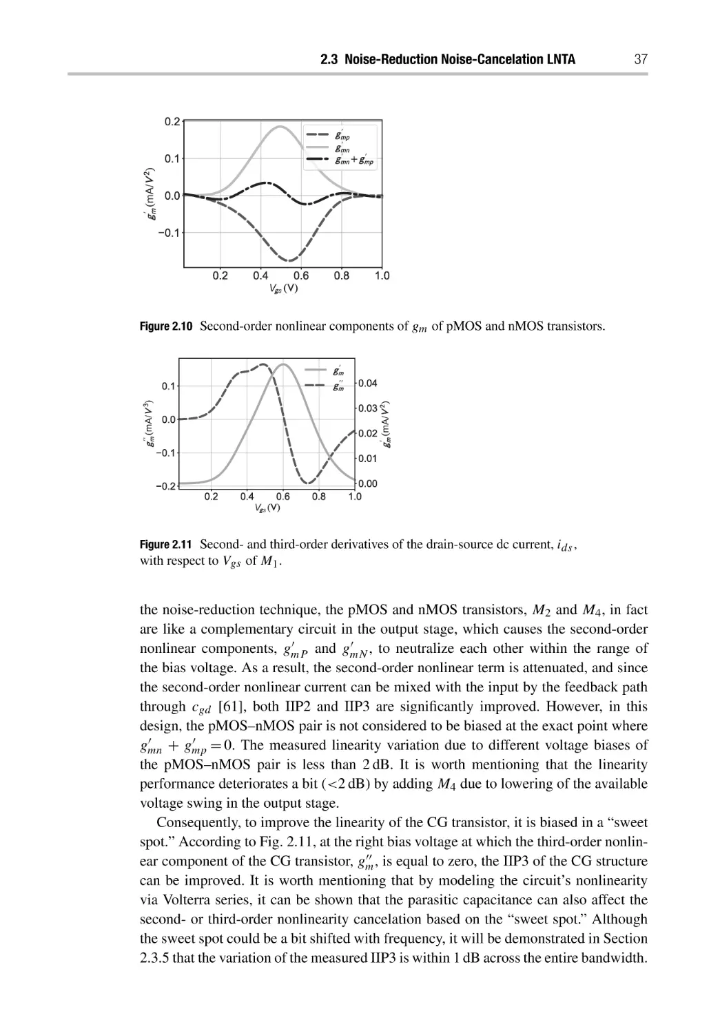
2.3 Noise-Reduction Noise-Cancelation LNTA
2.3.1 Input Matching
2.3.2 Gain Analysis
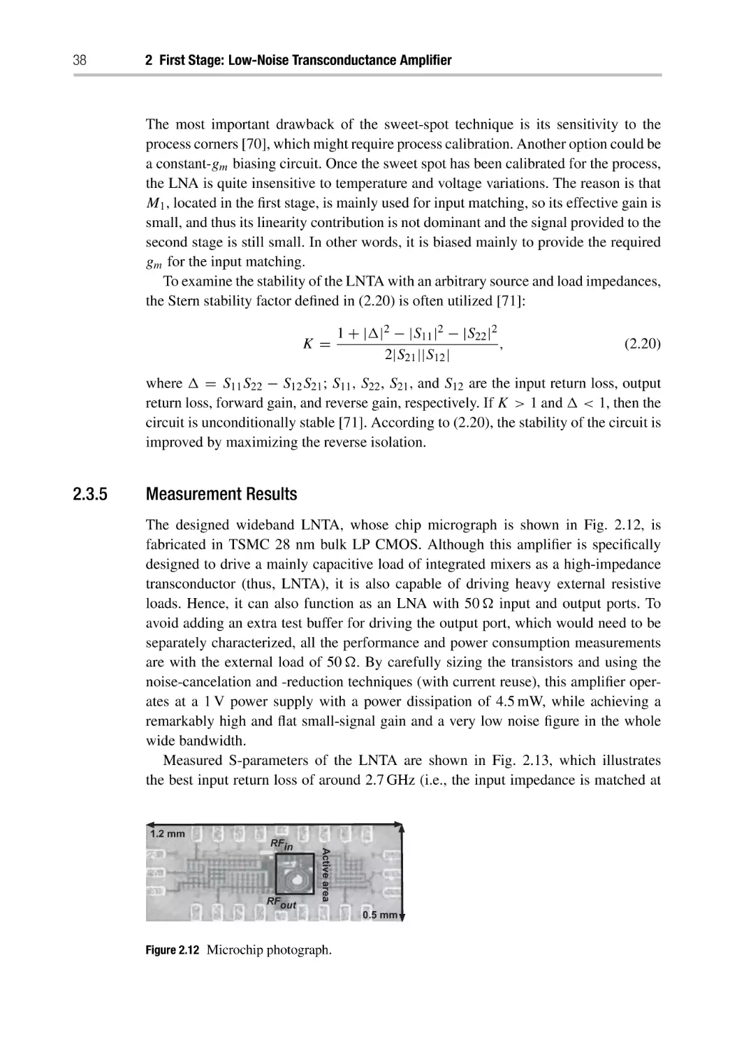
2.3.3 Noise Analysis
2.3.4 Linearity and Stability
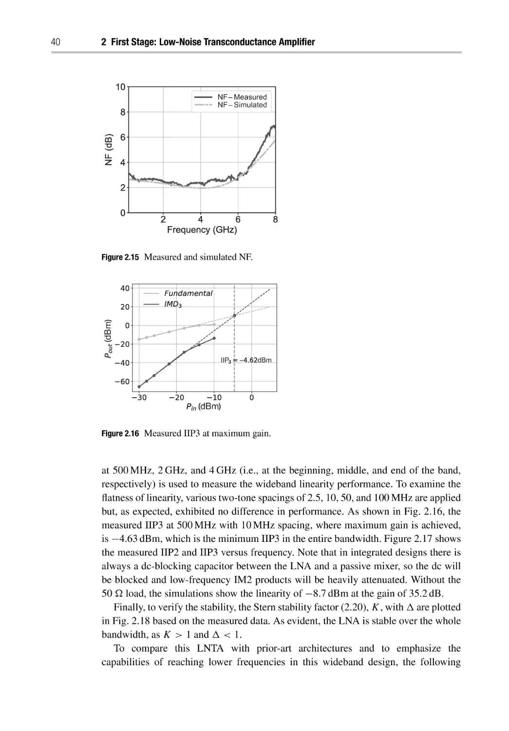
2.3.5 Measurement Results
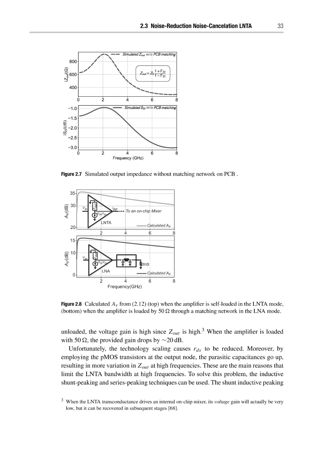
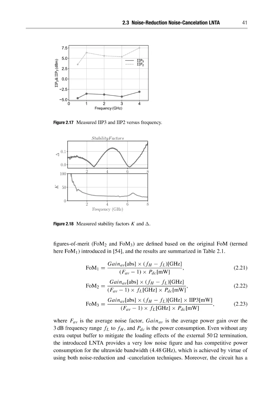
23
23
25
25
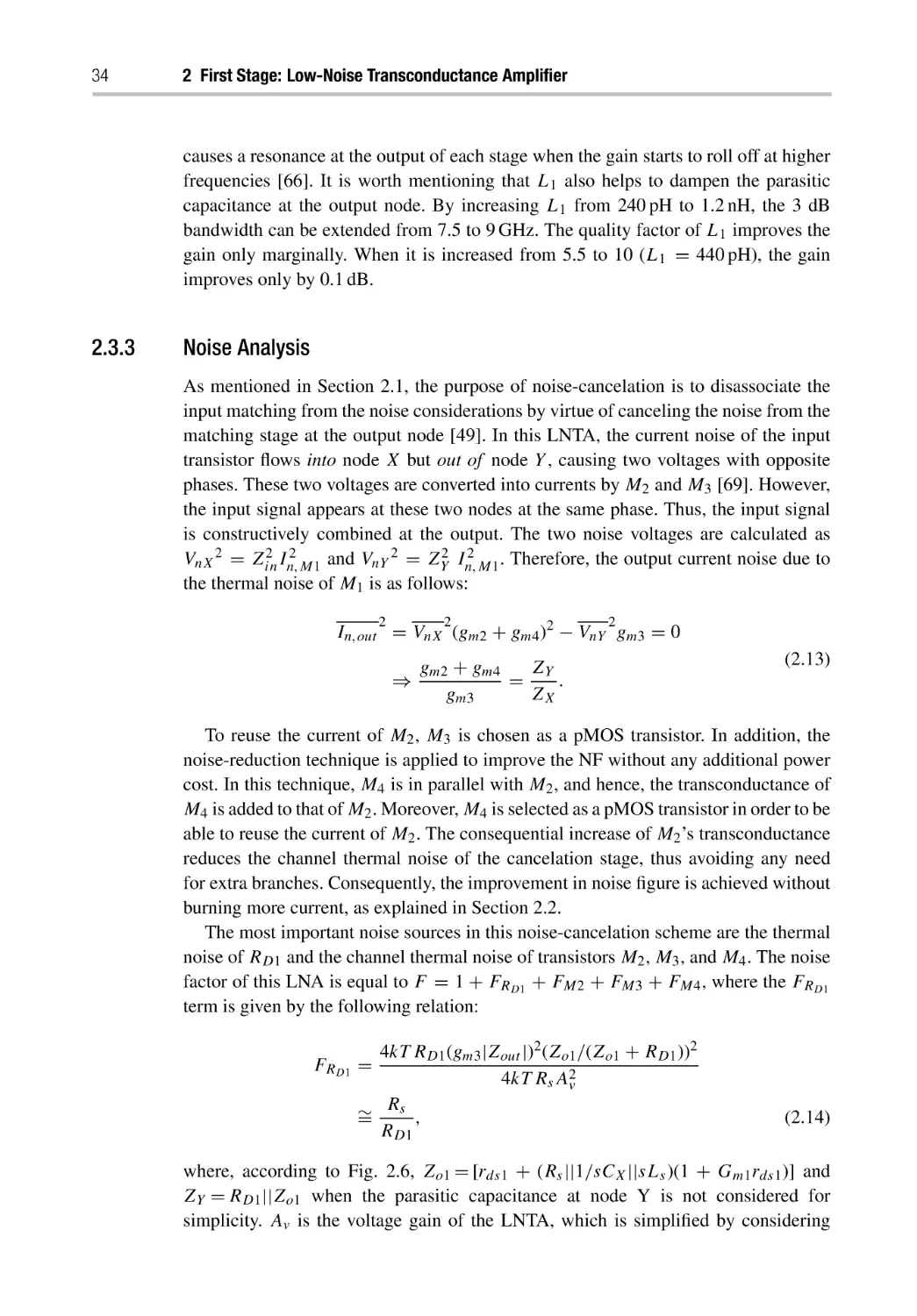
26
30
31
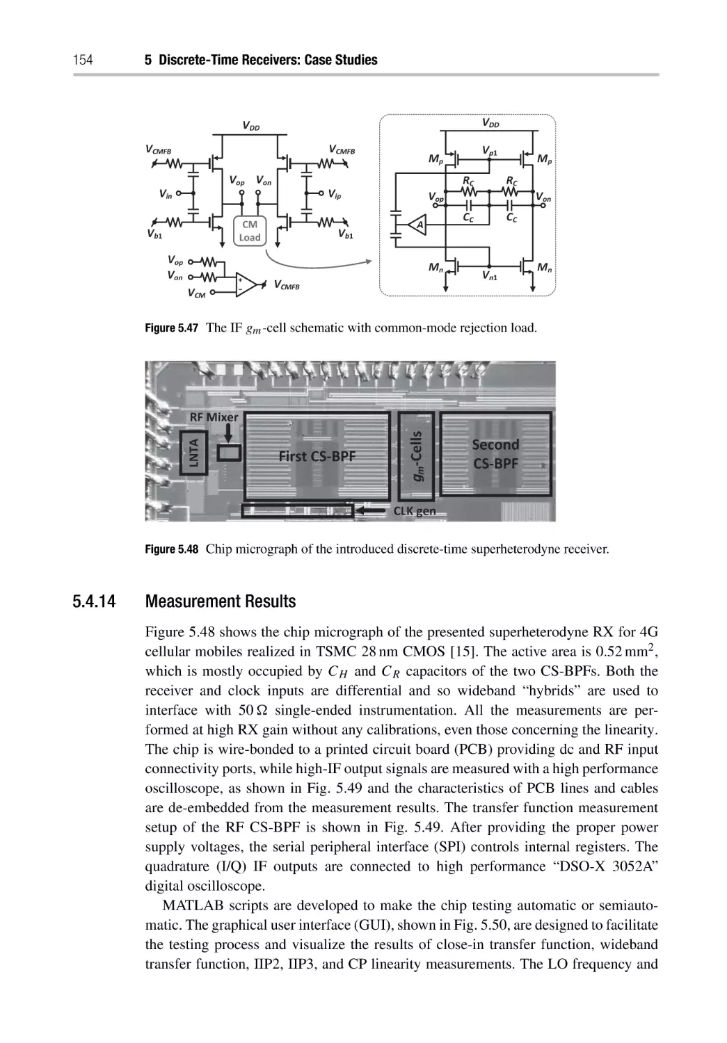
32
34
36
38
viii
Contents
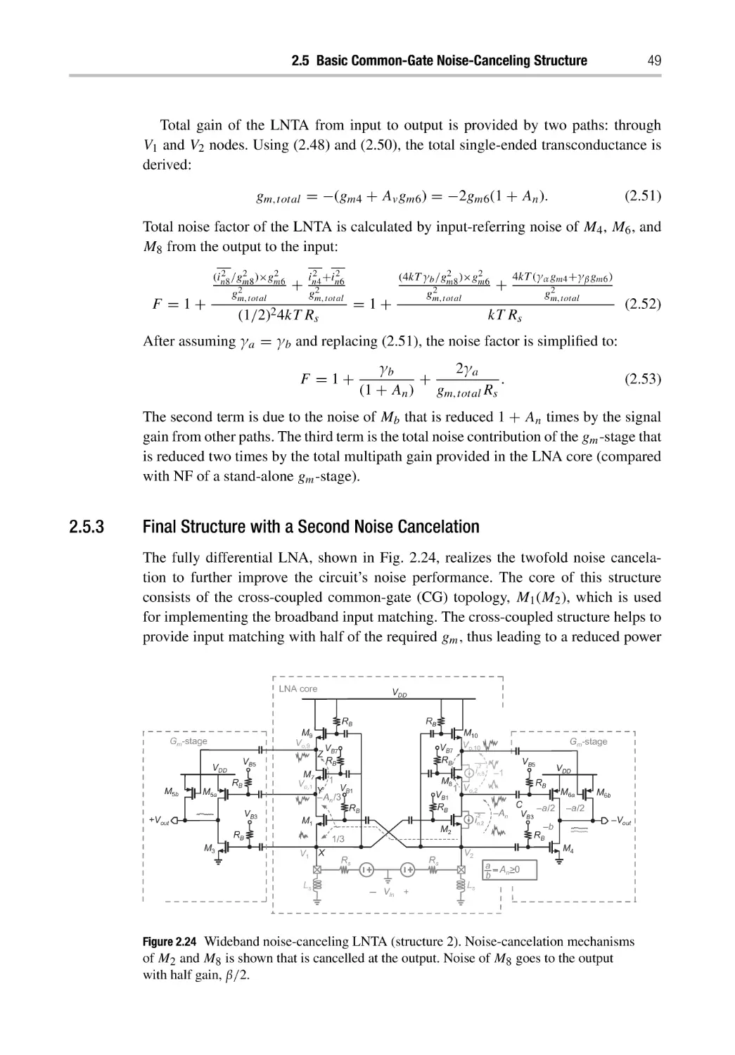
2.4 TwoFold Cross-Coupled Wideband LNTA architecture
2.4.1 Cross-Coupled Common-Gate LNA
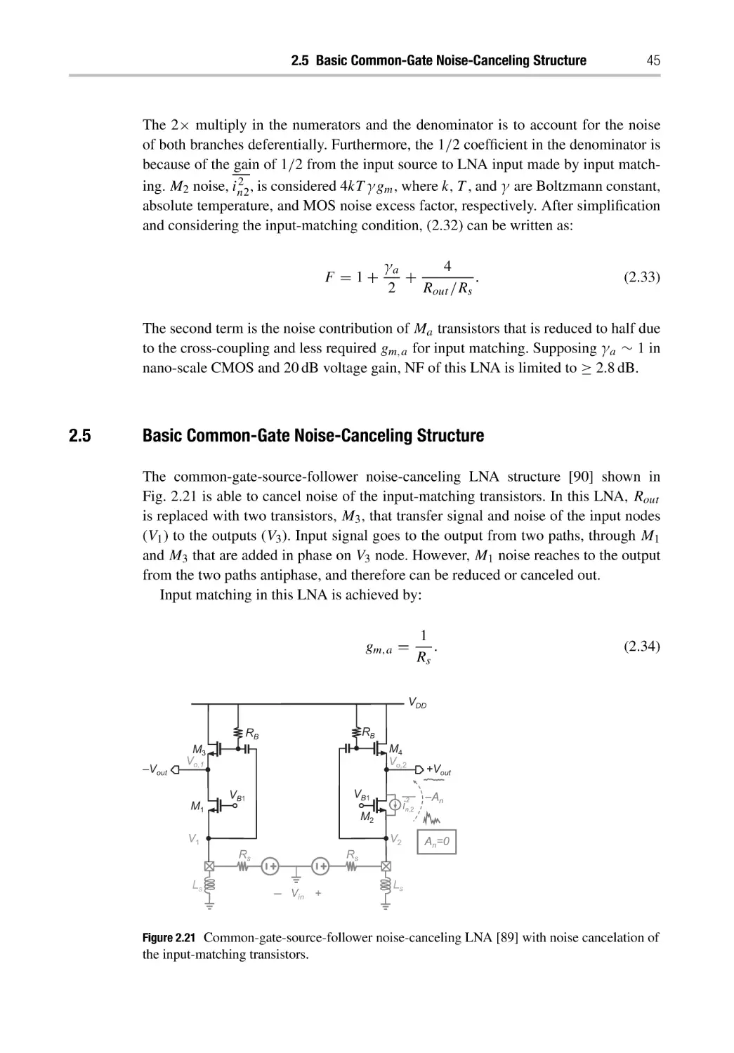
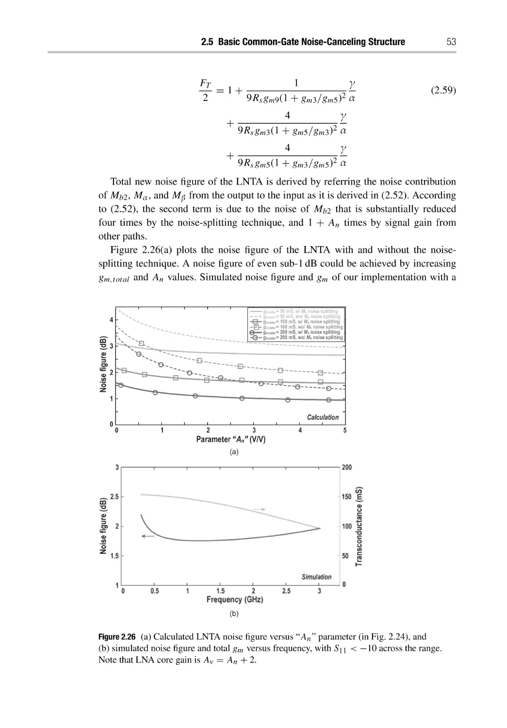
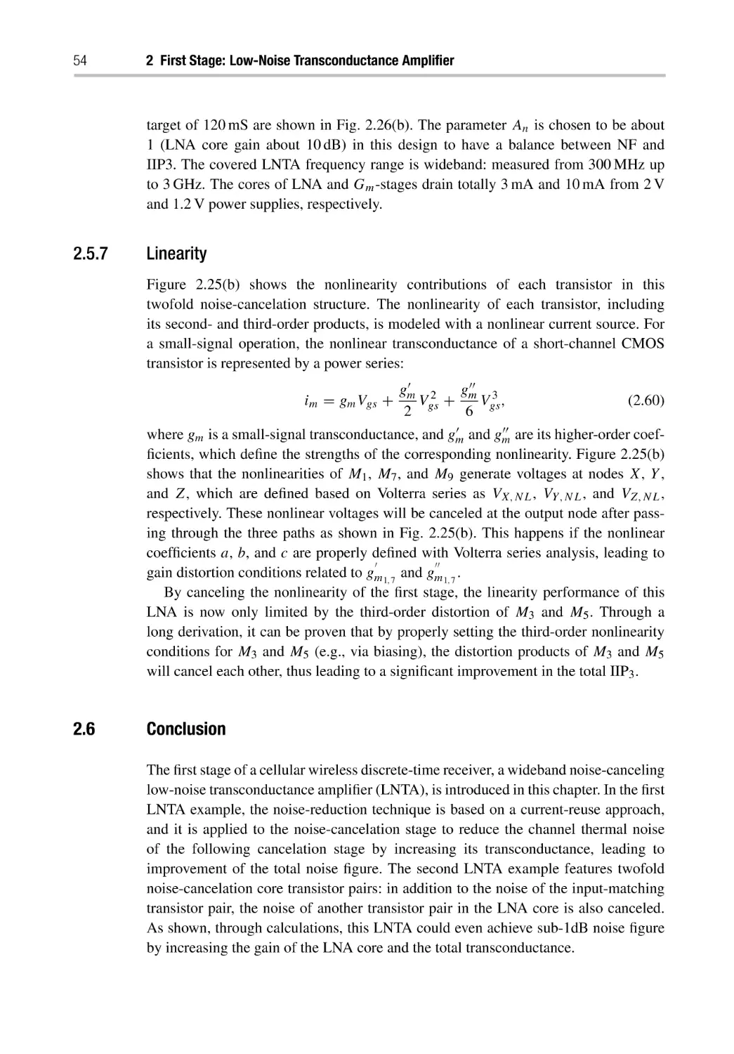
2.5 Basic Common-Gate Noise-Canceling Structure
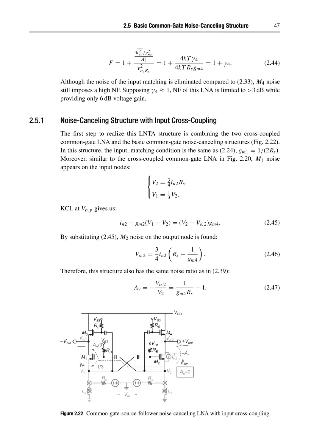
2.5.1 Noise-Canceling Structure with Input Cross-Coupling
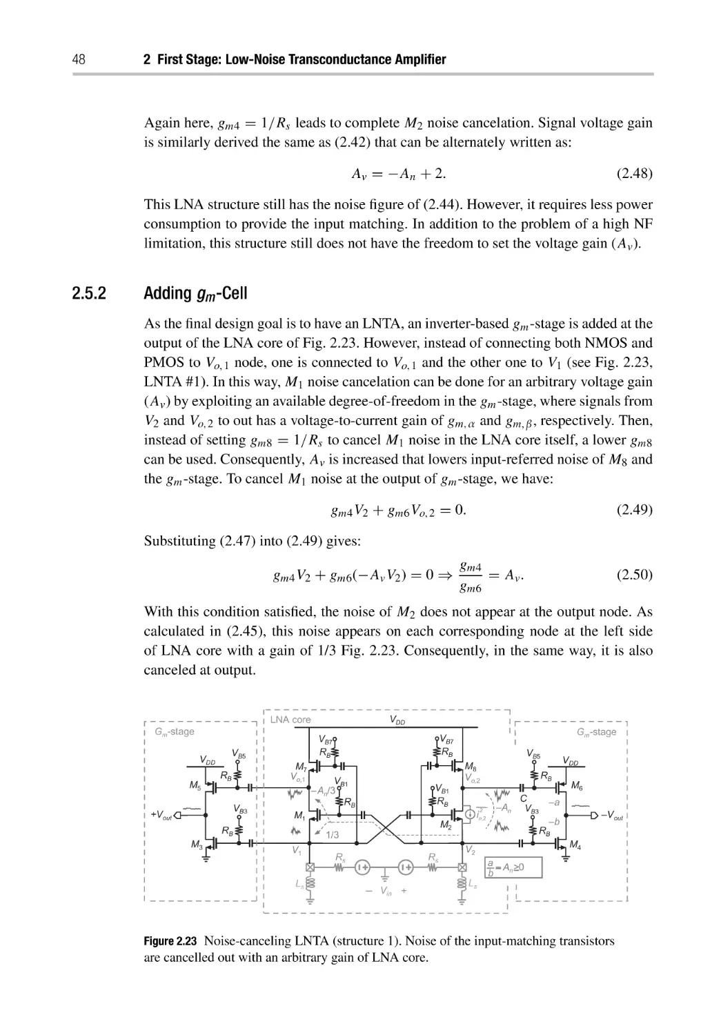
2.5.2 Adding gm -Cell
2.5.3 Final Structure with a Second Noise Cancelation
2.5.4 Input Matching
2.5.5 Gain Analysis
2.5.6 Noise Analysis
2.5.7 Linearity
2.6 Conclusion
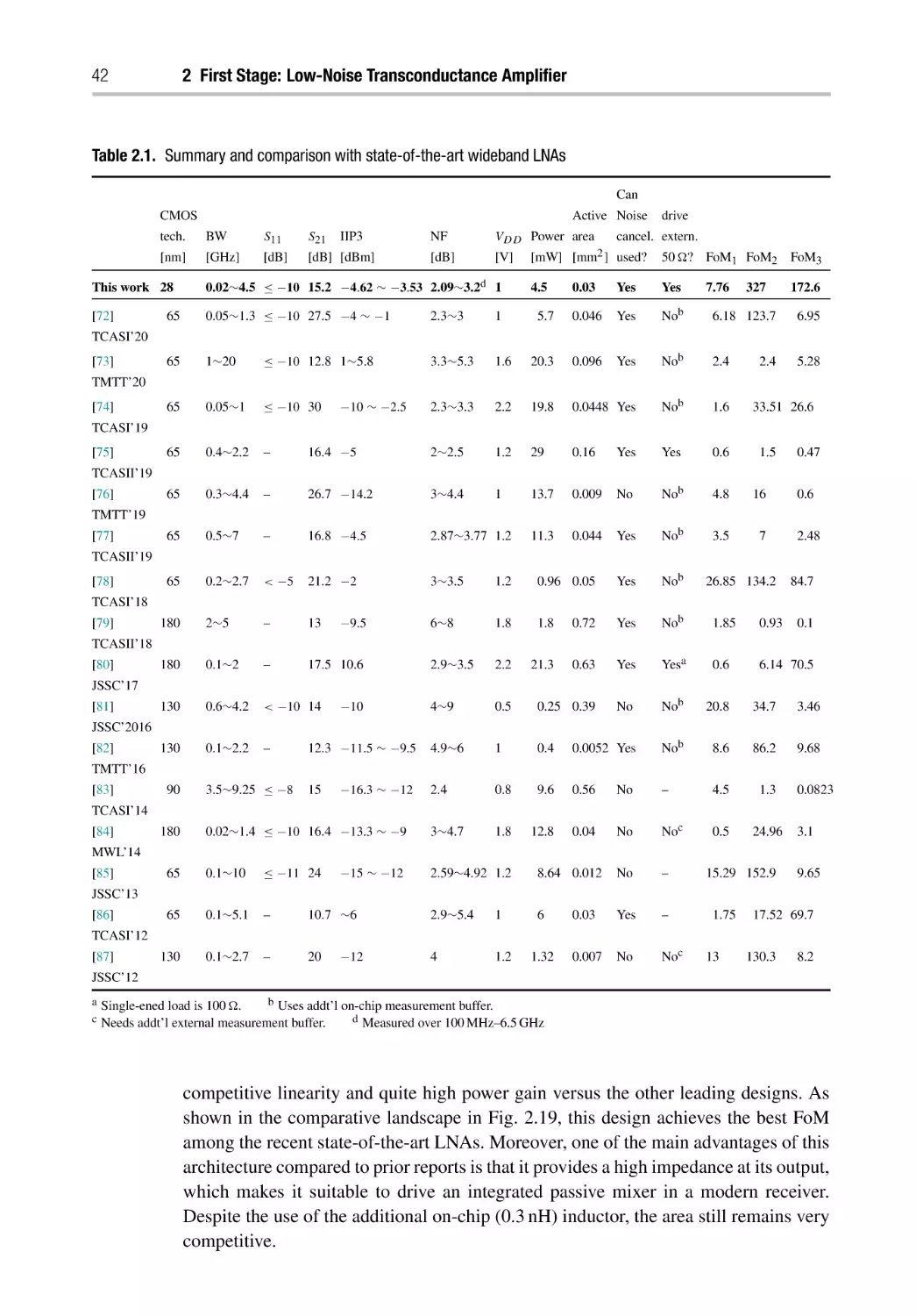
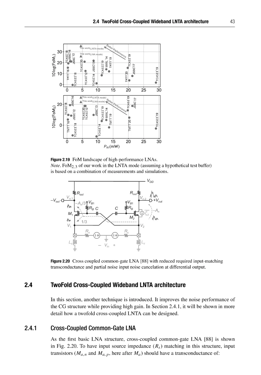
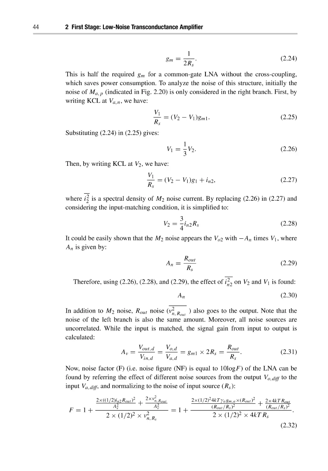
43
43
45
47
48
49
50
50
51
54
54
3
Discrete-Time High-Order Low-Pass Filter
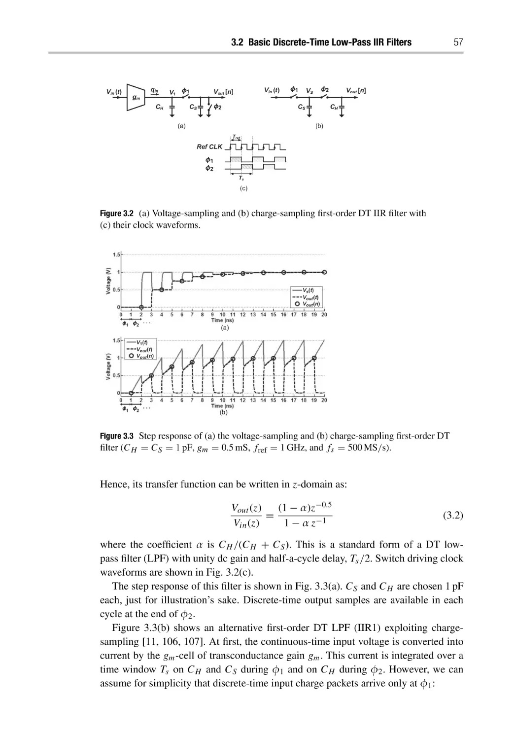
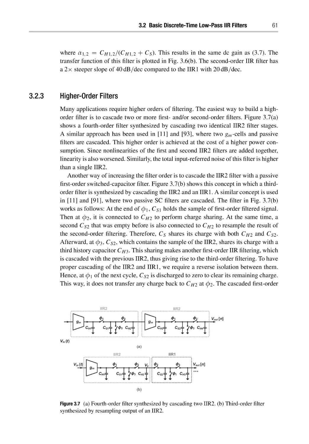
3.1 LPF Structure
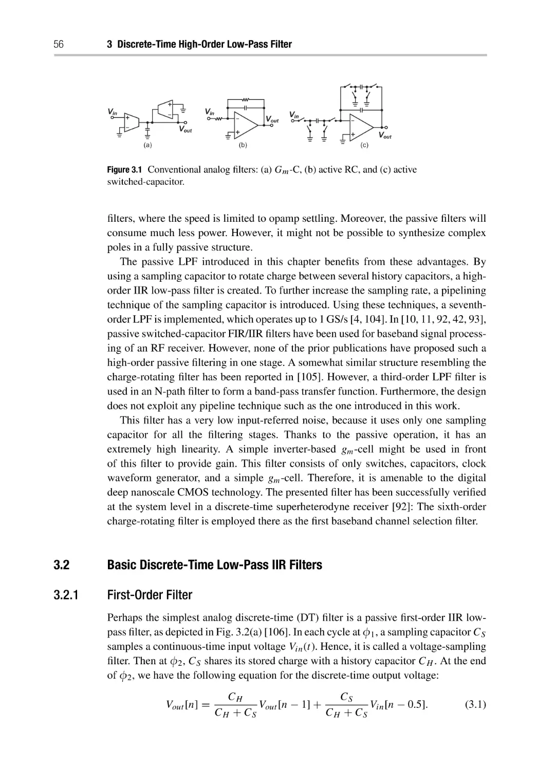
3.2 Basic Discrete-Time Low-Pass IIR Filters
3.2.1 First-Order Filter
3.2.2 Second-Order Filter
3.2.3 Higher-Order Filters
3.3 Novel High-Order DT IIR Low-Pass Filter
3.3.1 Charge-Rotating DT Filter
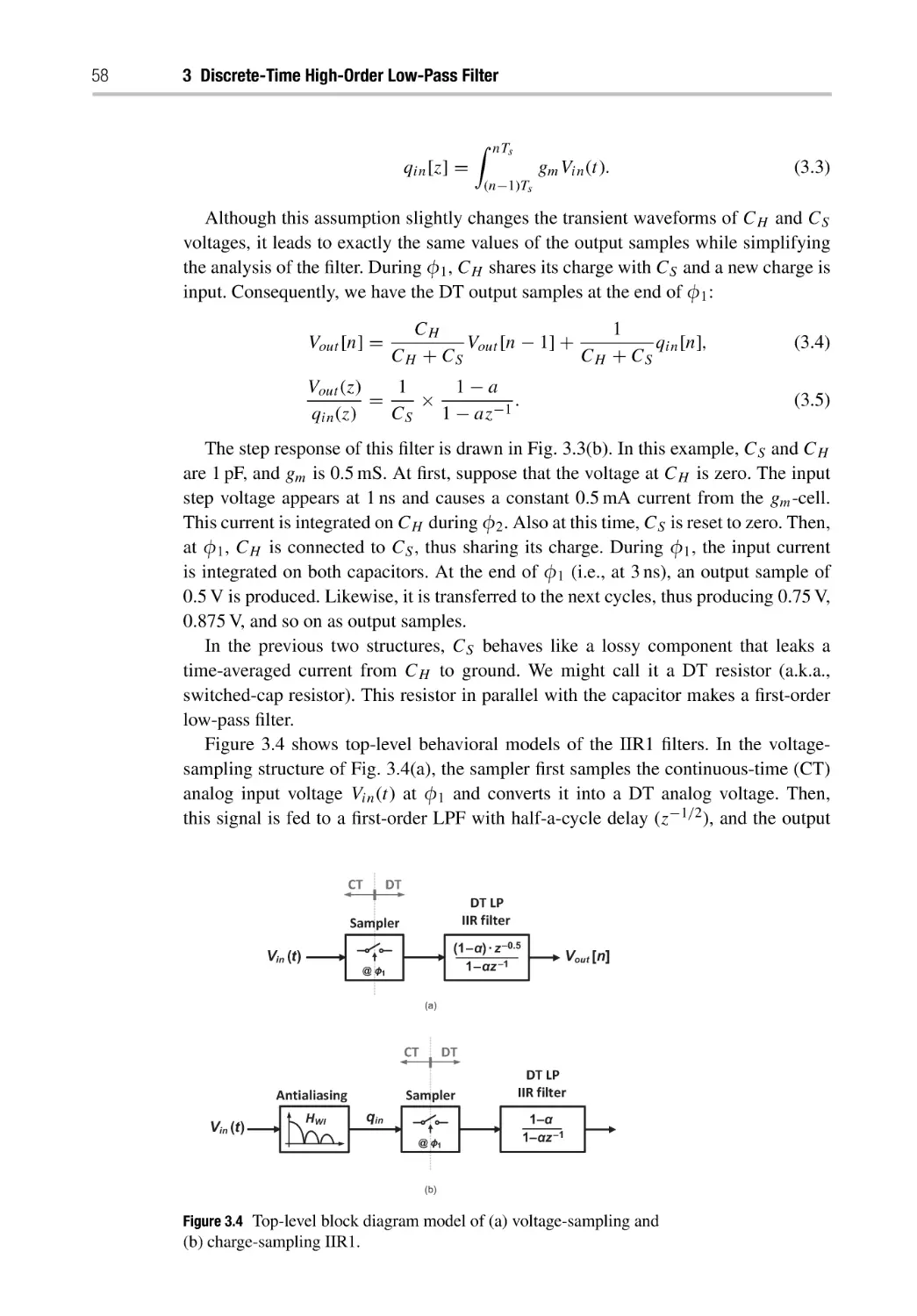
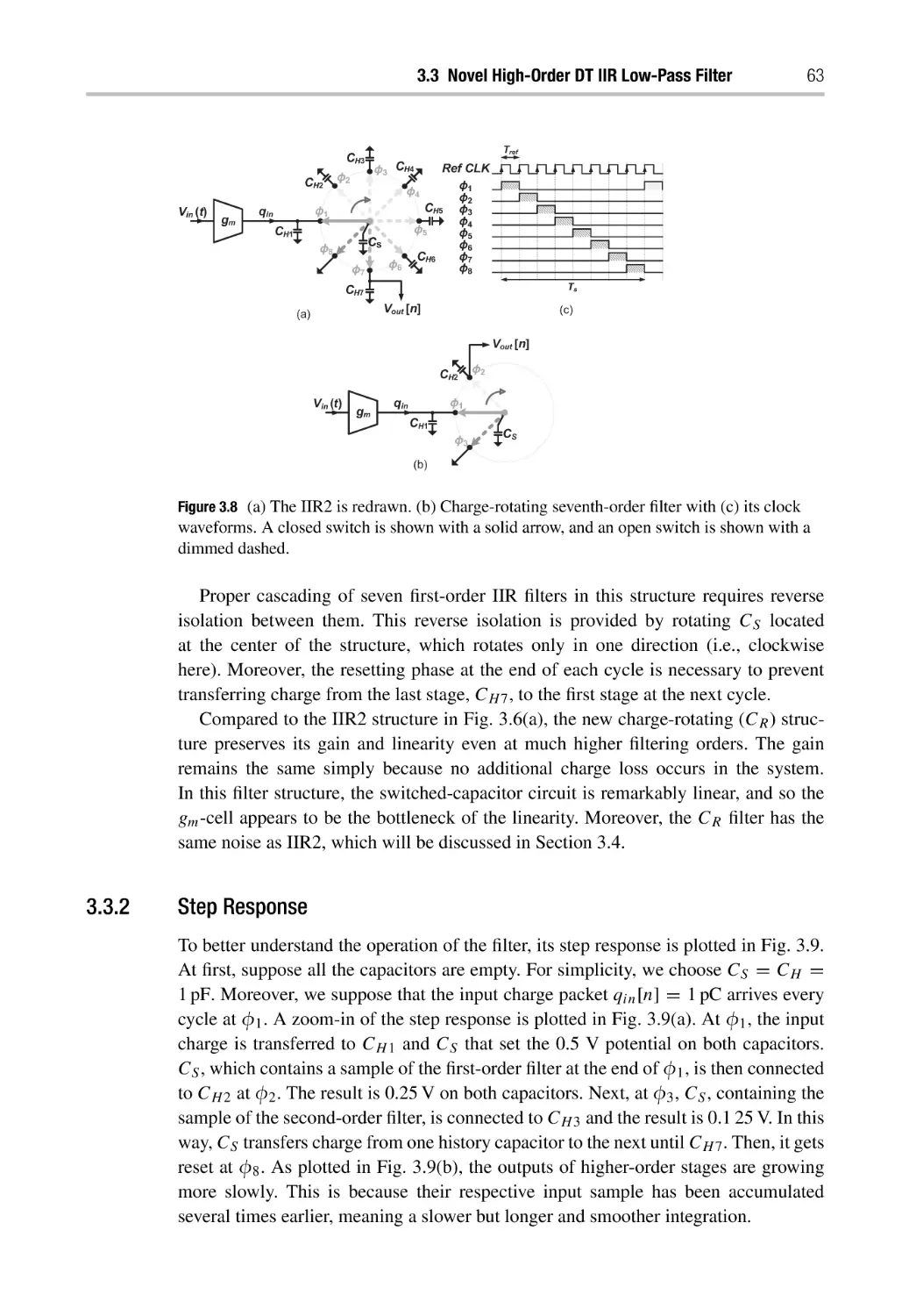
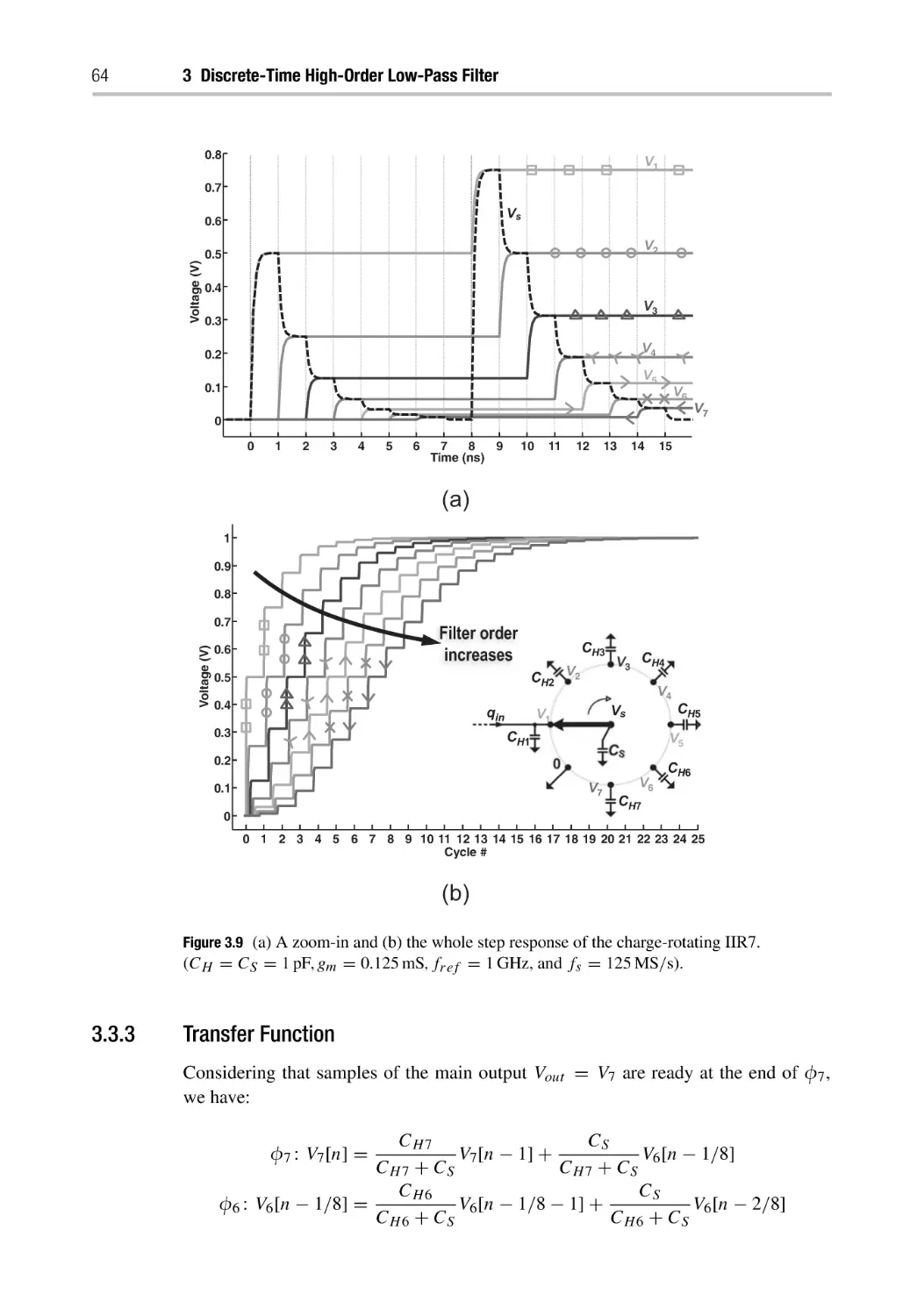
3.3.2 Step Response
3.3.3 Transfer Function
3.3.4 Equalization of the Transfer Function
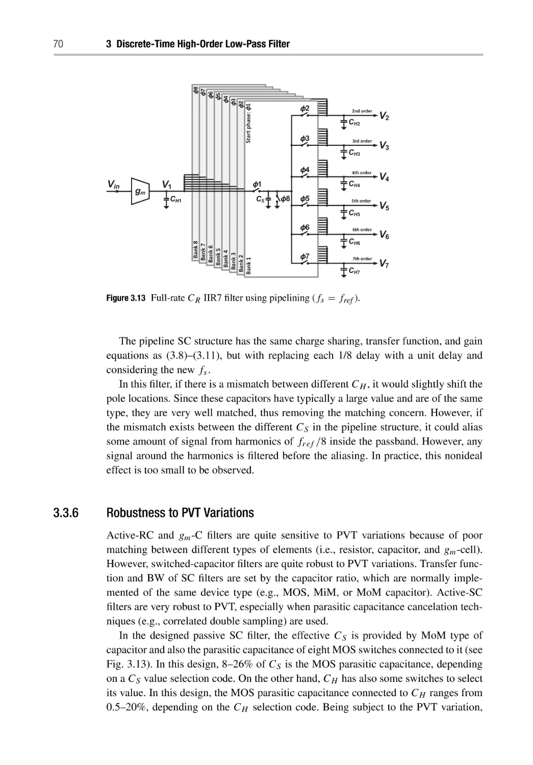
3.3.5 Sampling Rate Increase
3.3.6 Robustness to PVT Variations
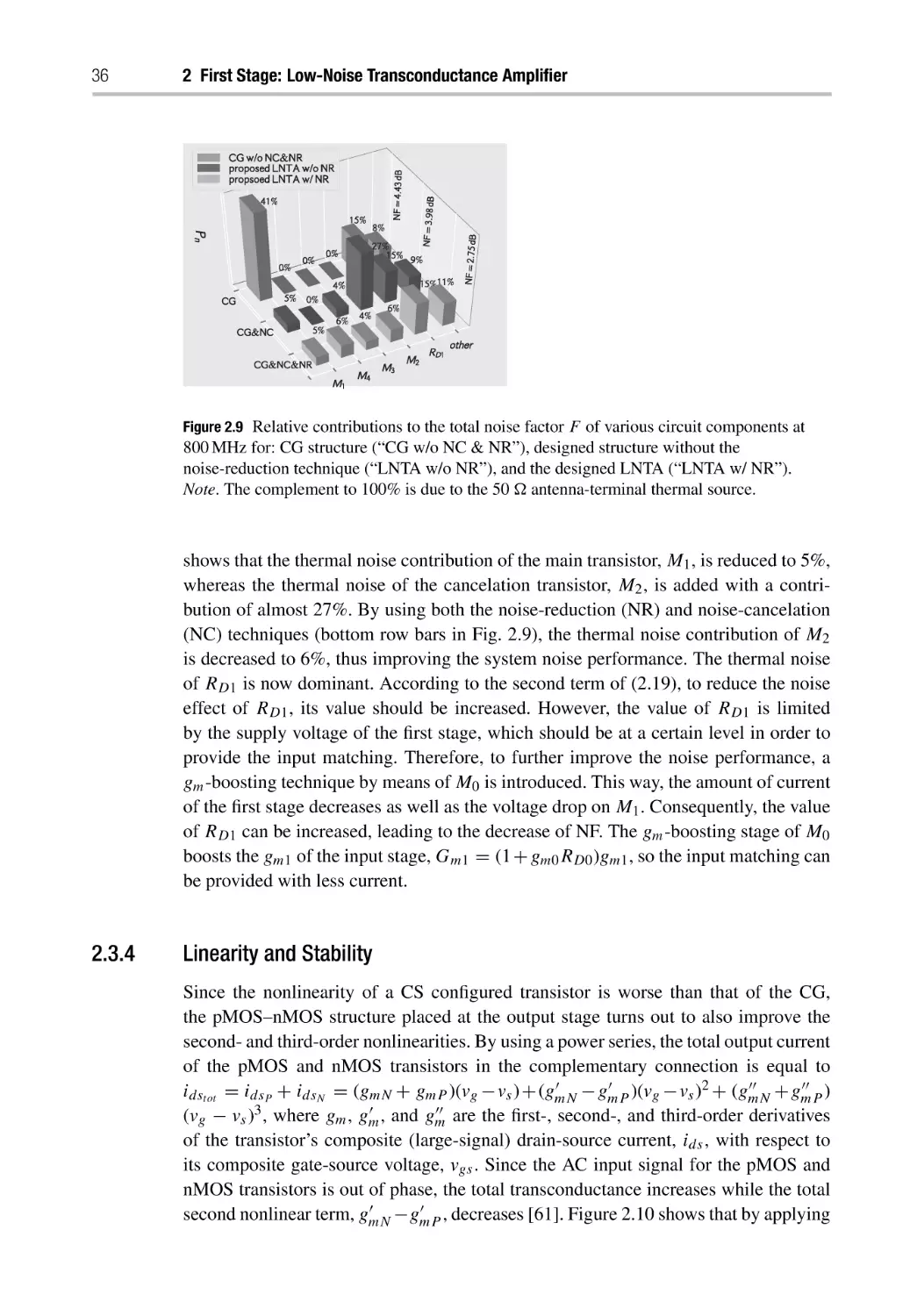
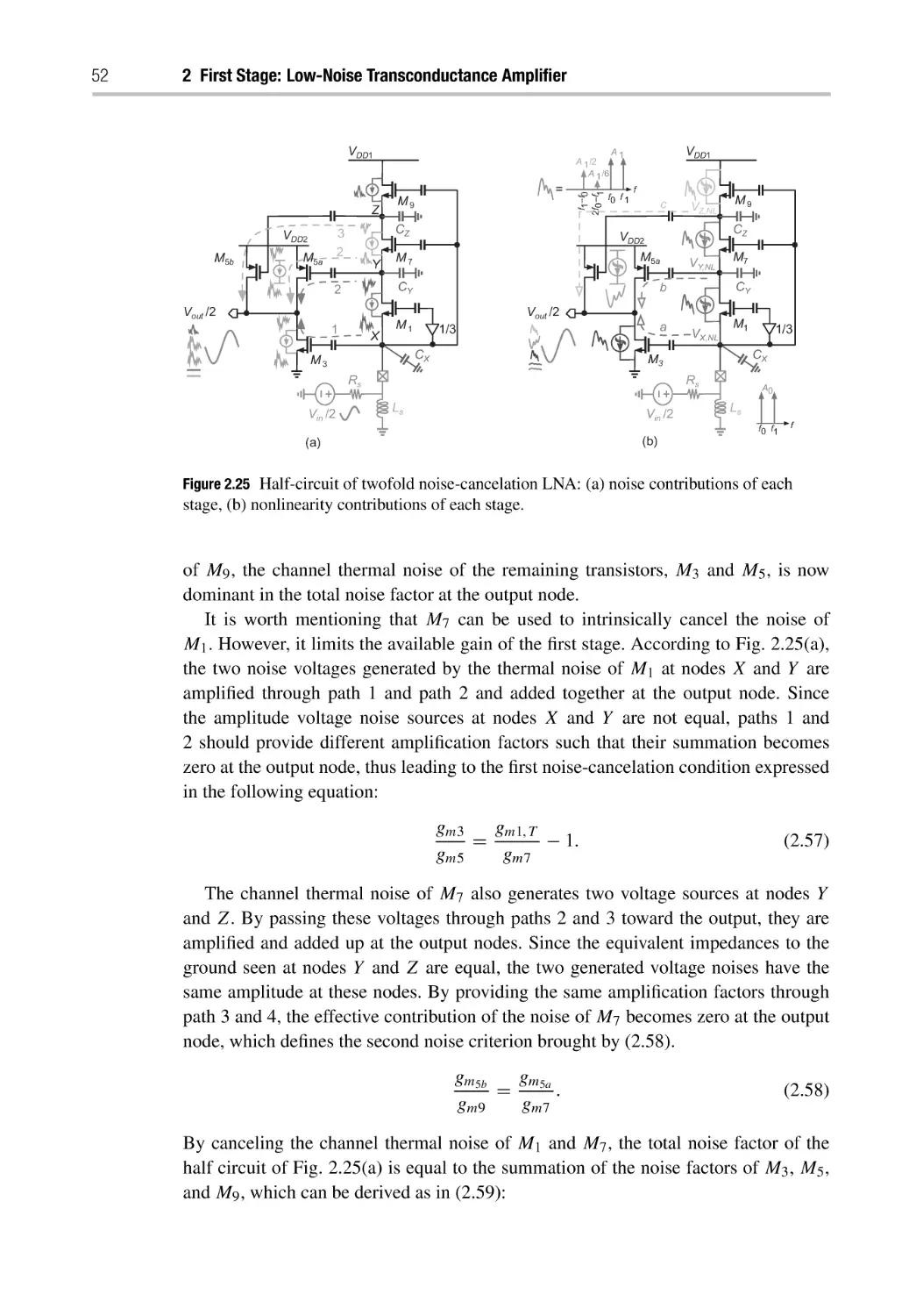
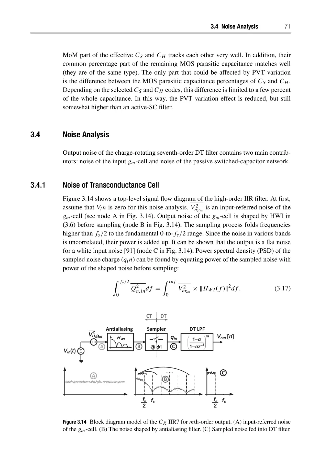
3.4 Noise Analysis
3.4.1 Noise of Transconductance Cell
3.4.2 Noise of Switched-Capacitor Network
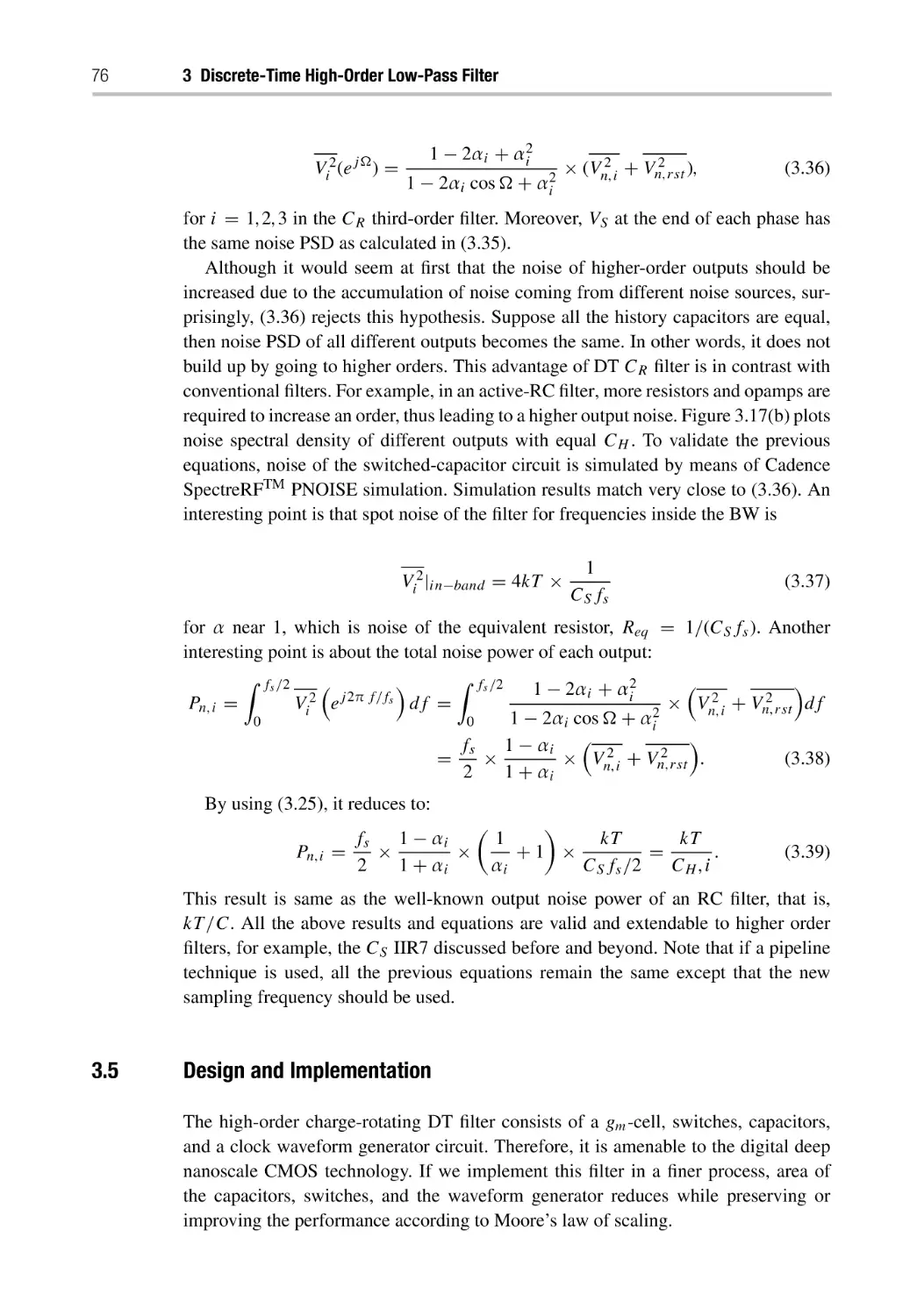
3.5 Design and Implementation
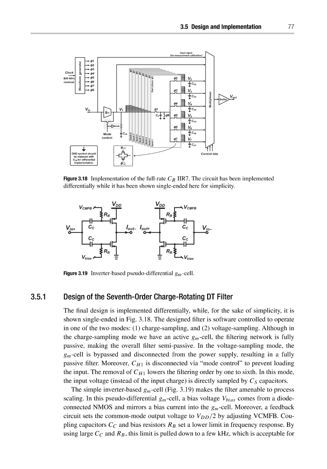
3.5.1 Design of the Seventh-Order Charge-Rotating DT Filter
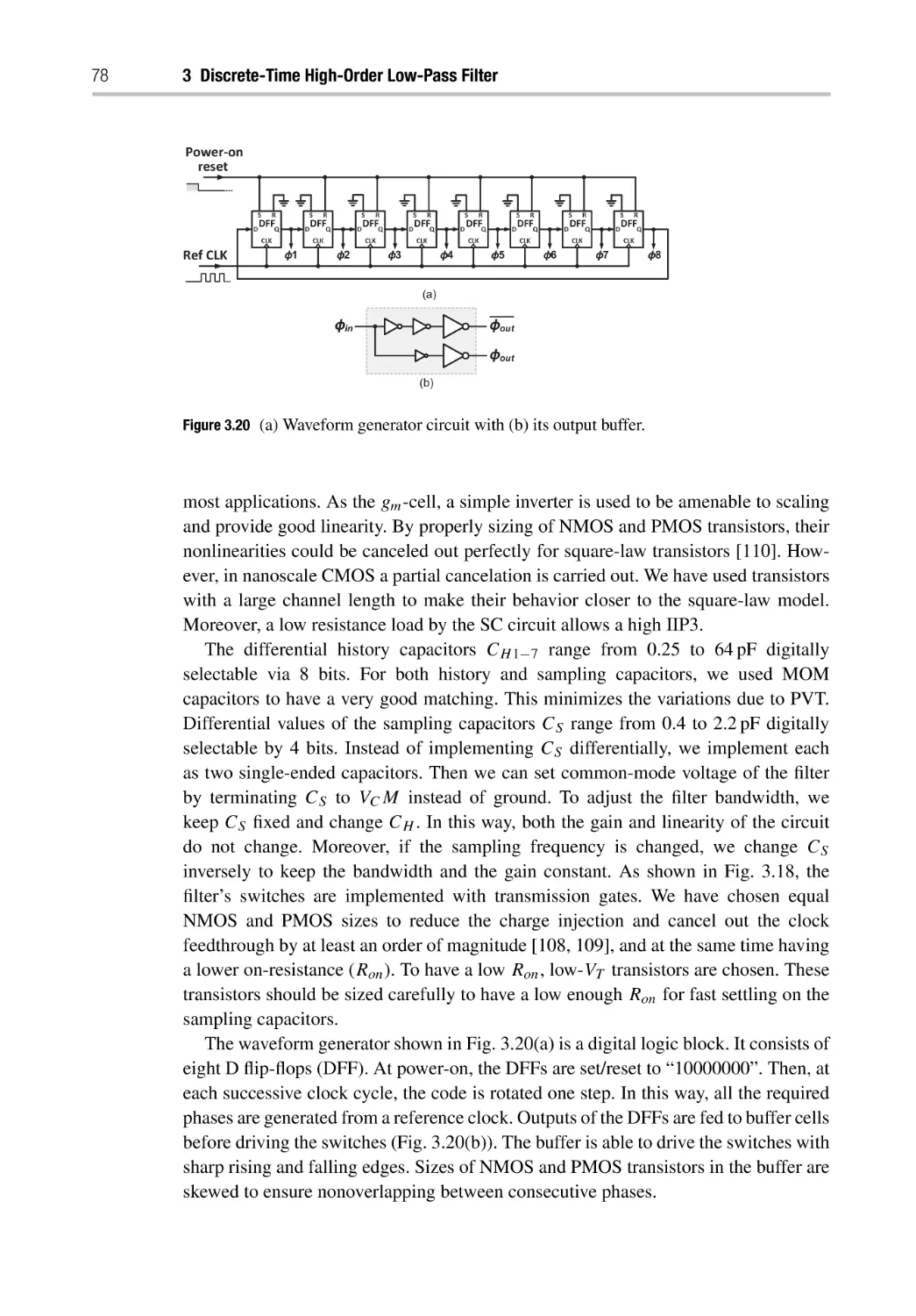
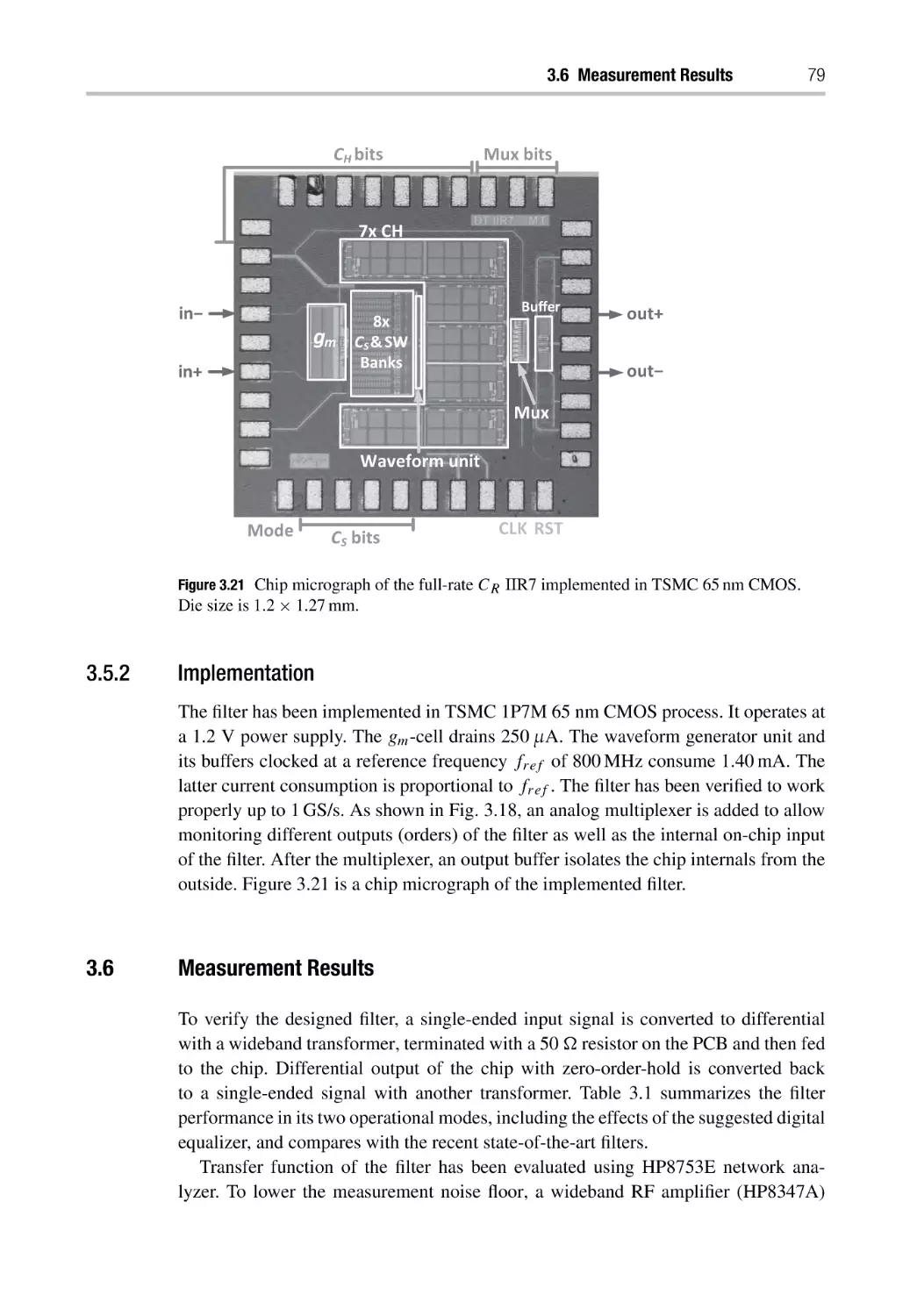
3.5.2 Implementation
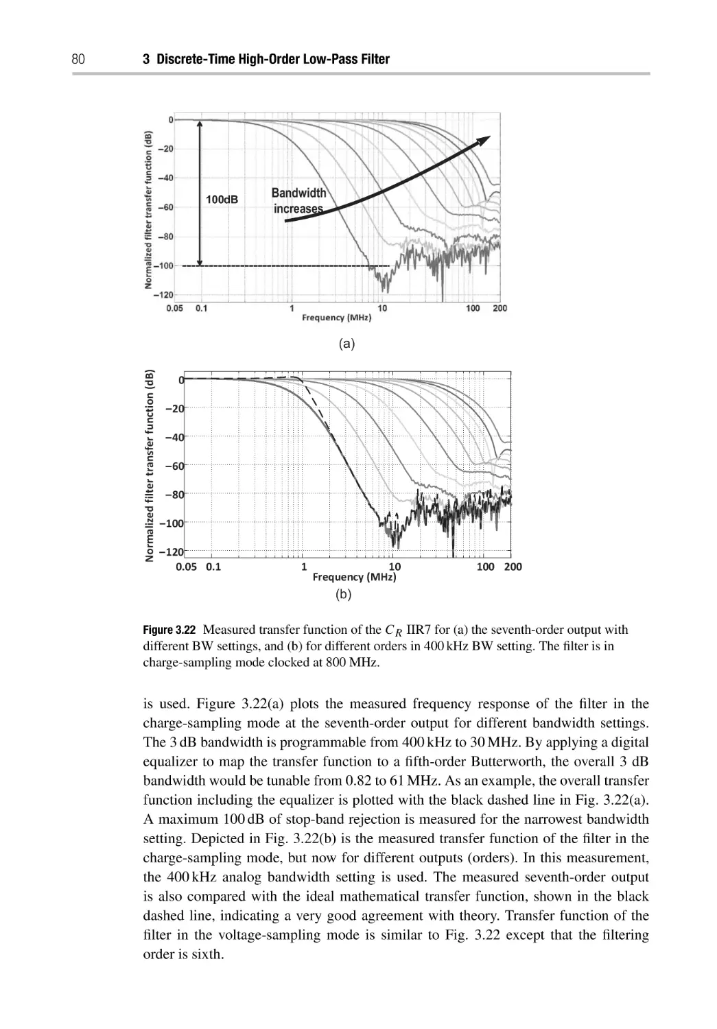
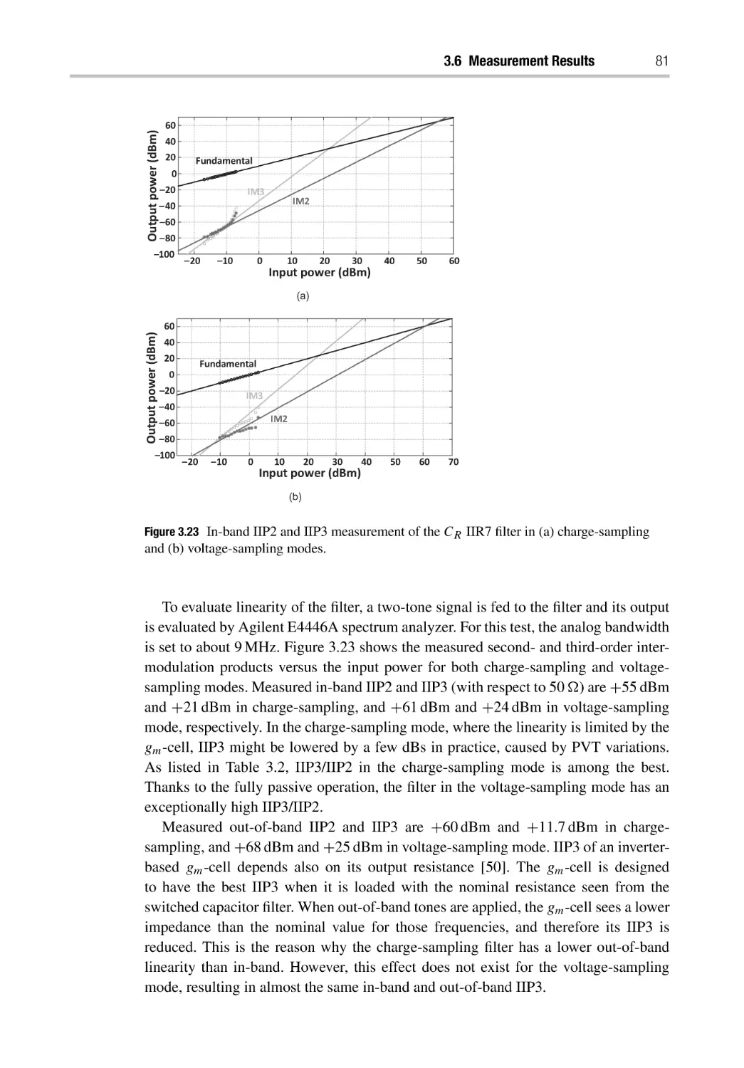
3.6 Measurement Results
3.7 Conclusion
55
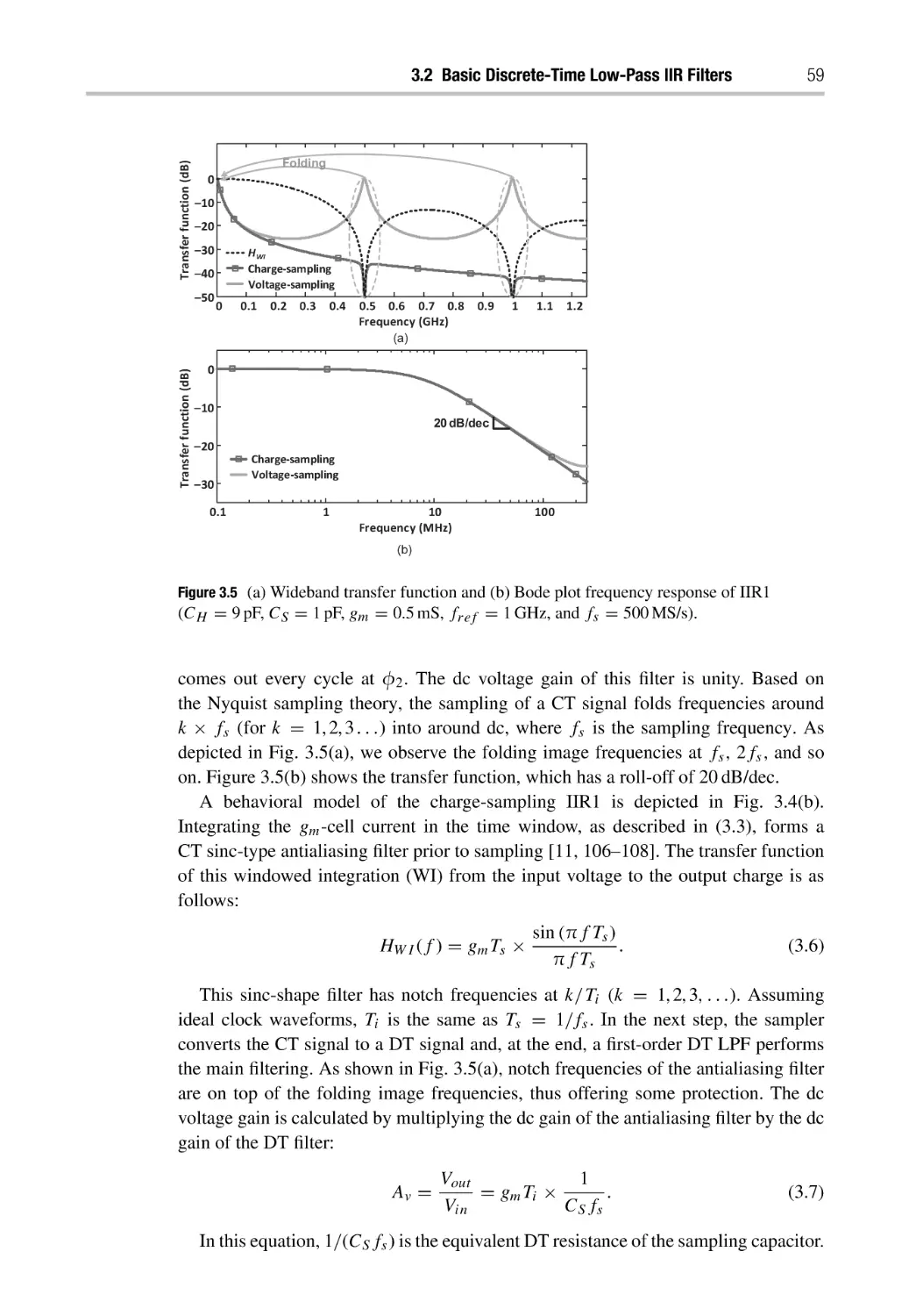
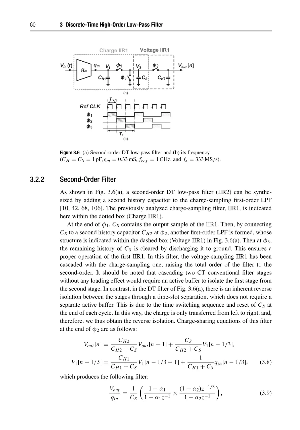
55
56
56
60
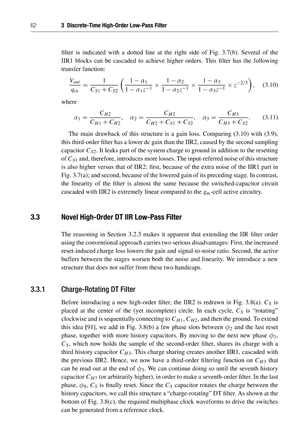
61
62
62
63
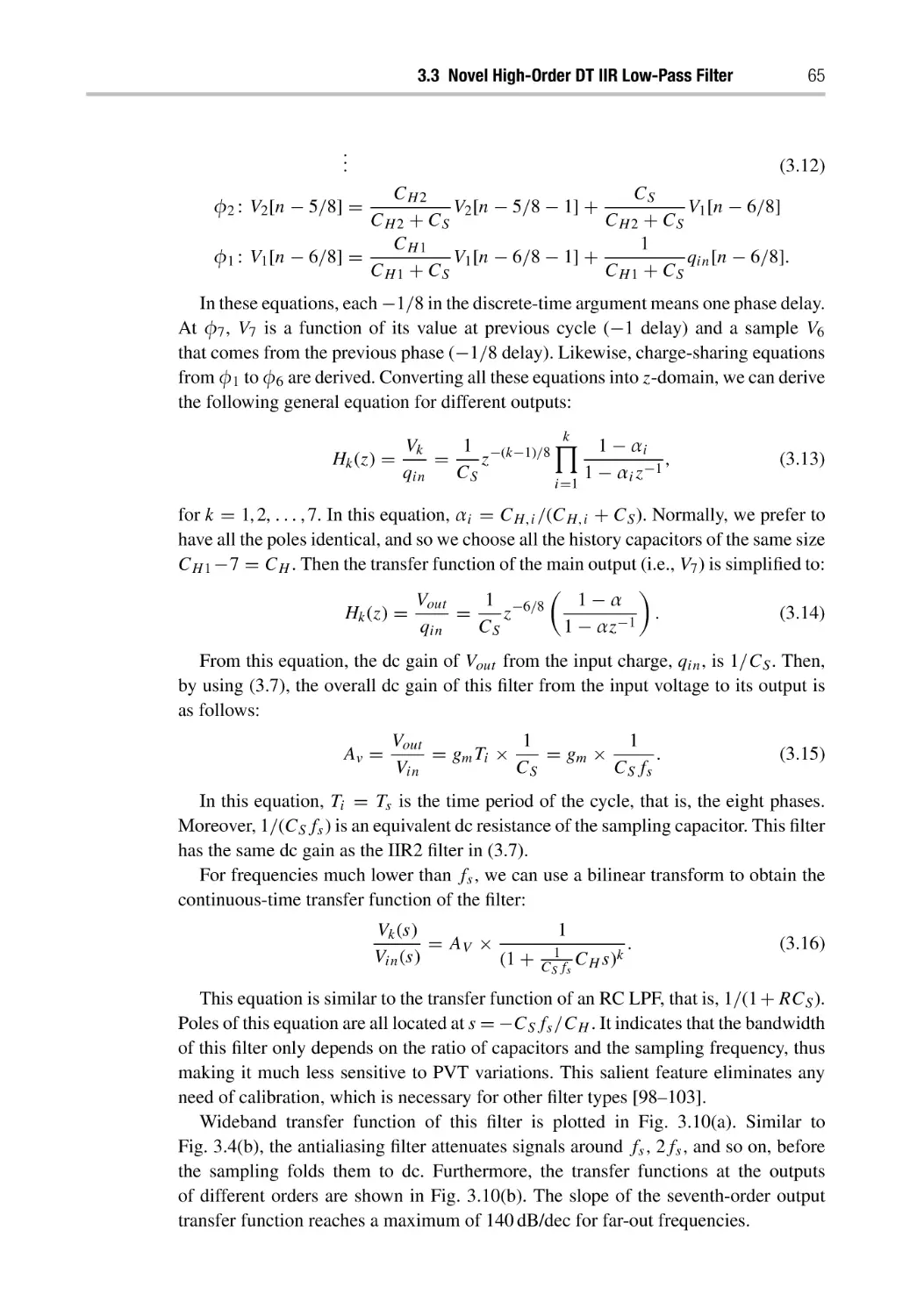
64
66
69
70
71
71
72
76
77
79
79
85
4
Discrete-Time Band-Pass Filter
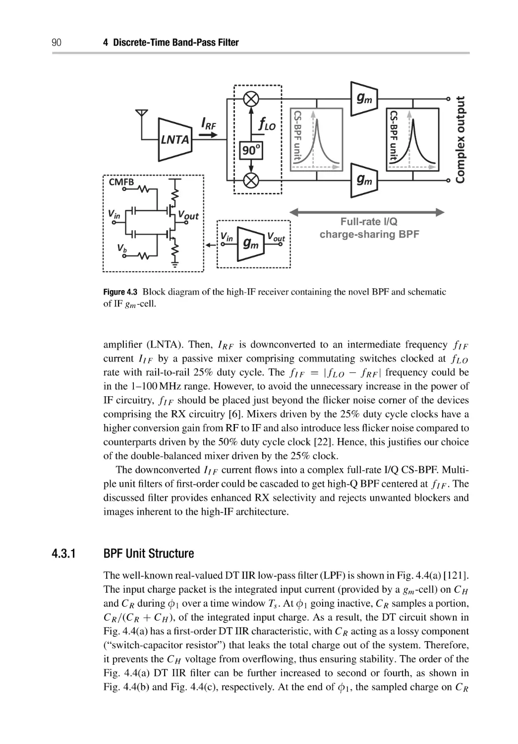
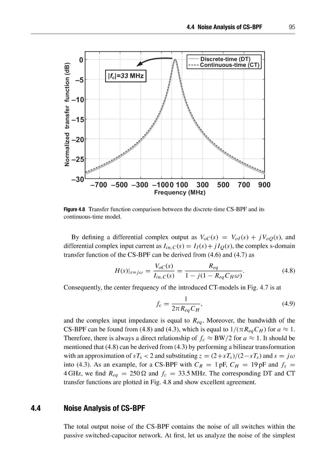
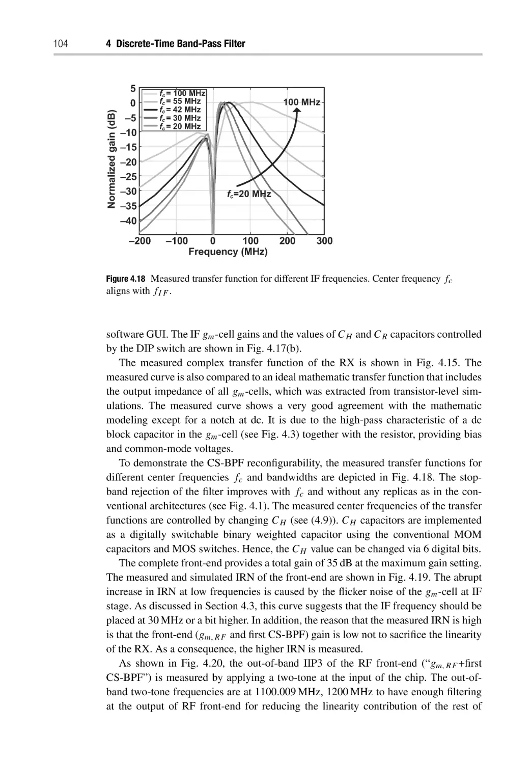
4.1 Introduction
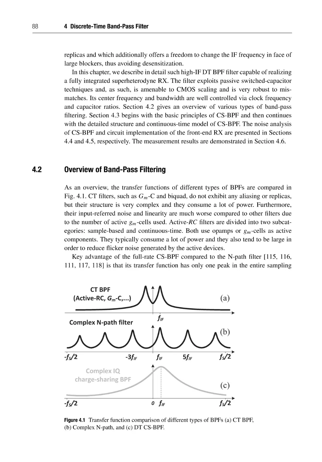
4.2 Overview of Band-Pass Filtering
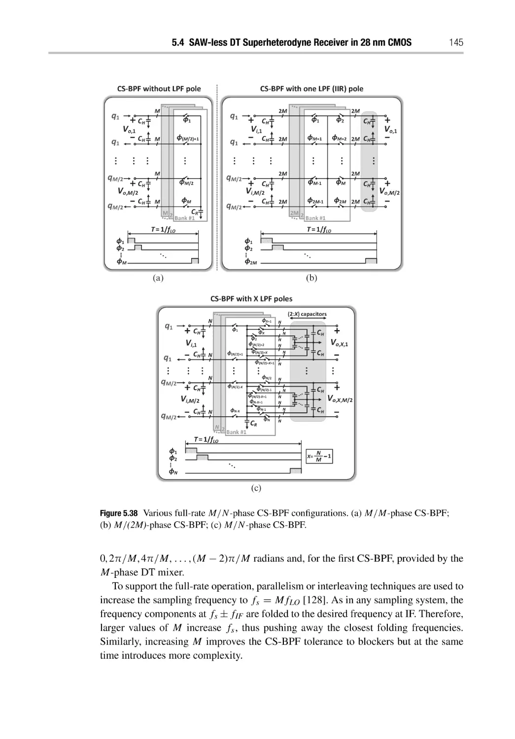
4.3 Charge-Sharing Band-pass Filter (CS-BPF)
4.3.1 BPF Unit Structure
4.3.2 CS-BPF Continuous-Time Model
4.4 Noise Analysis of CS-BPF
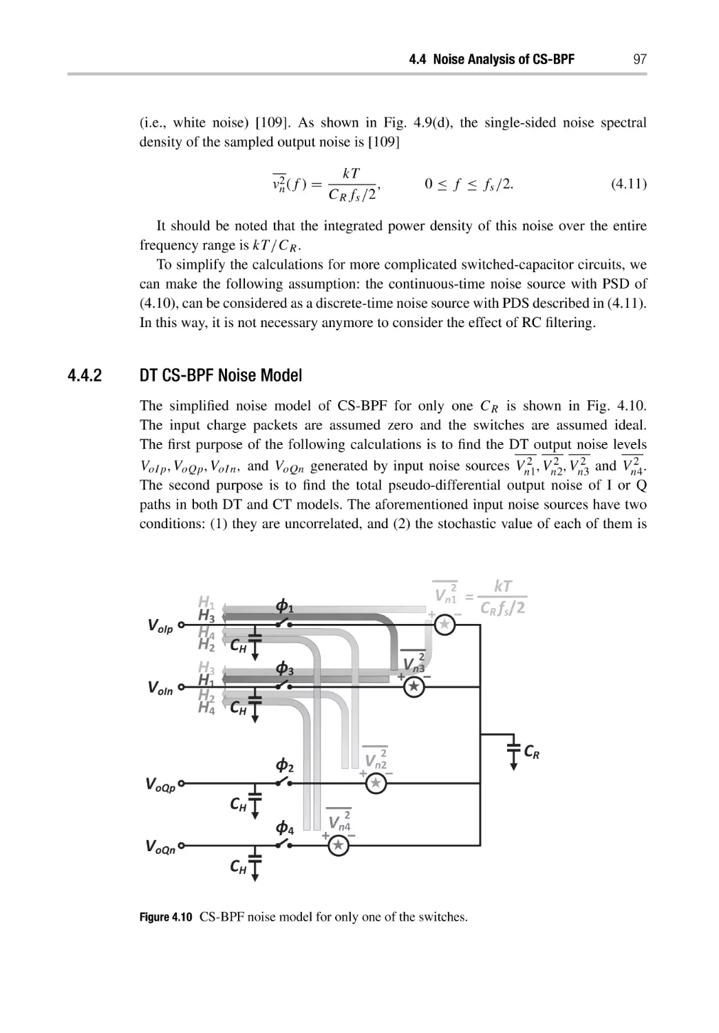
4.4.1 Voltage Sampler Output Noise
4.4.2 DT CS-BPF Noise Model
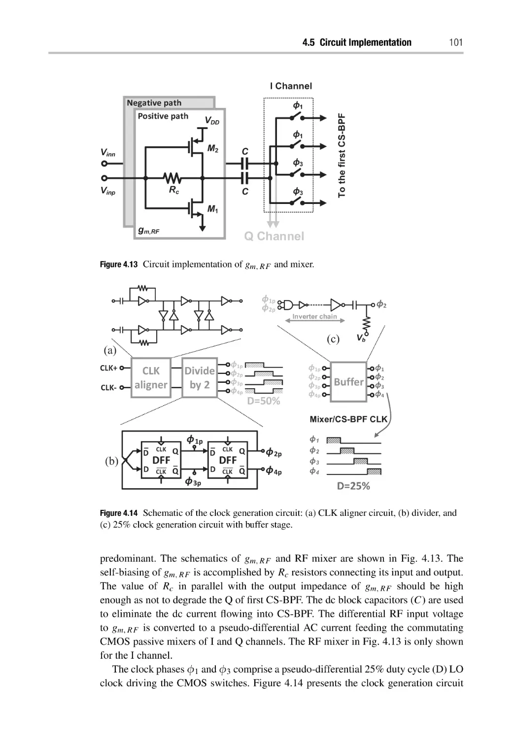
4.5 Circuit Implementation
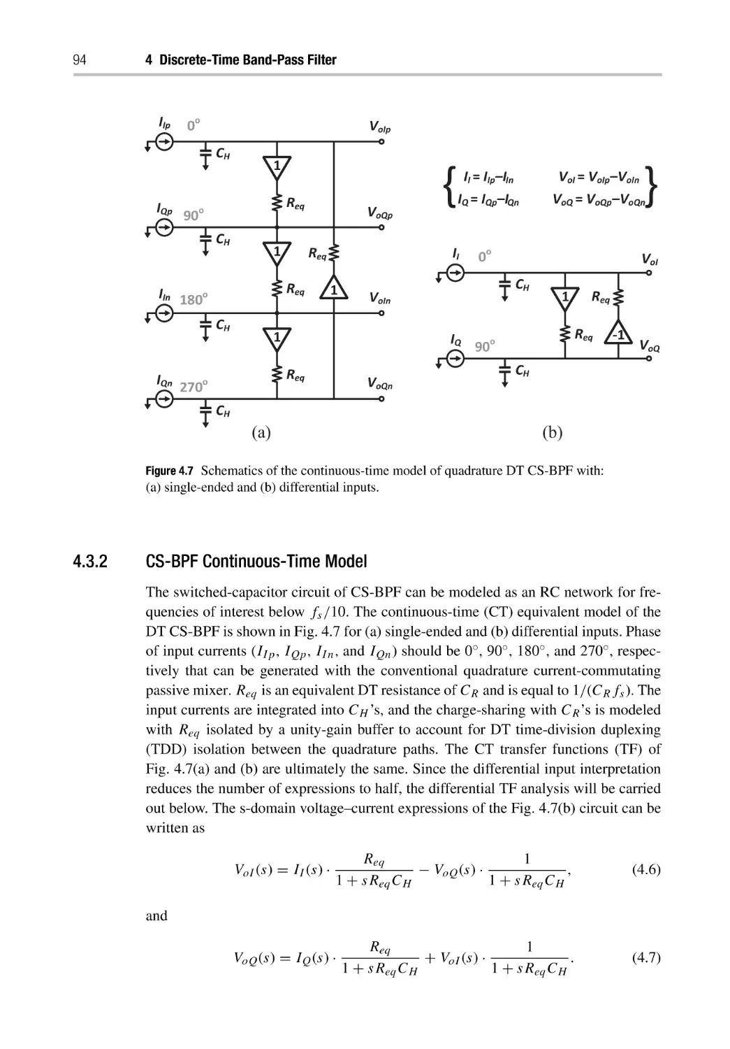
87
87
88
89
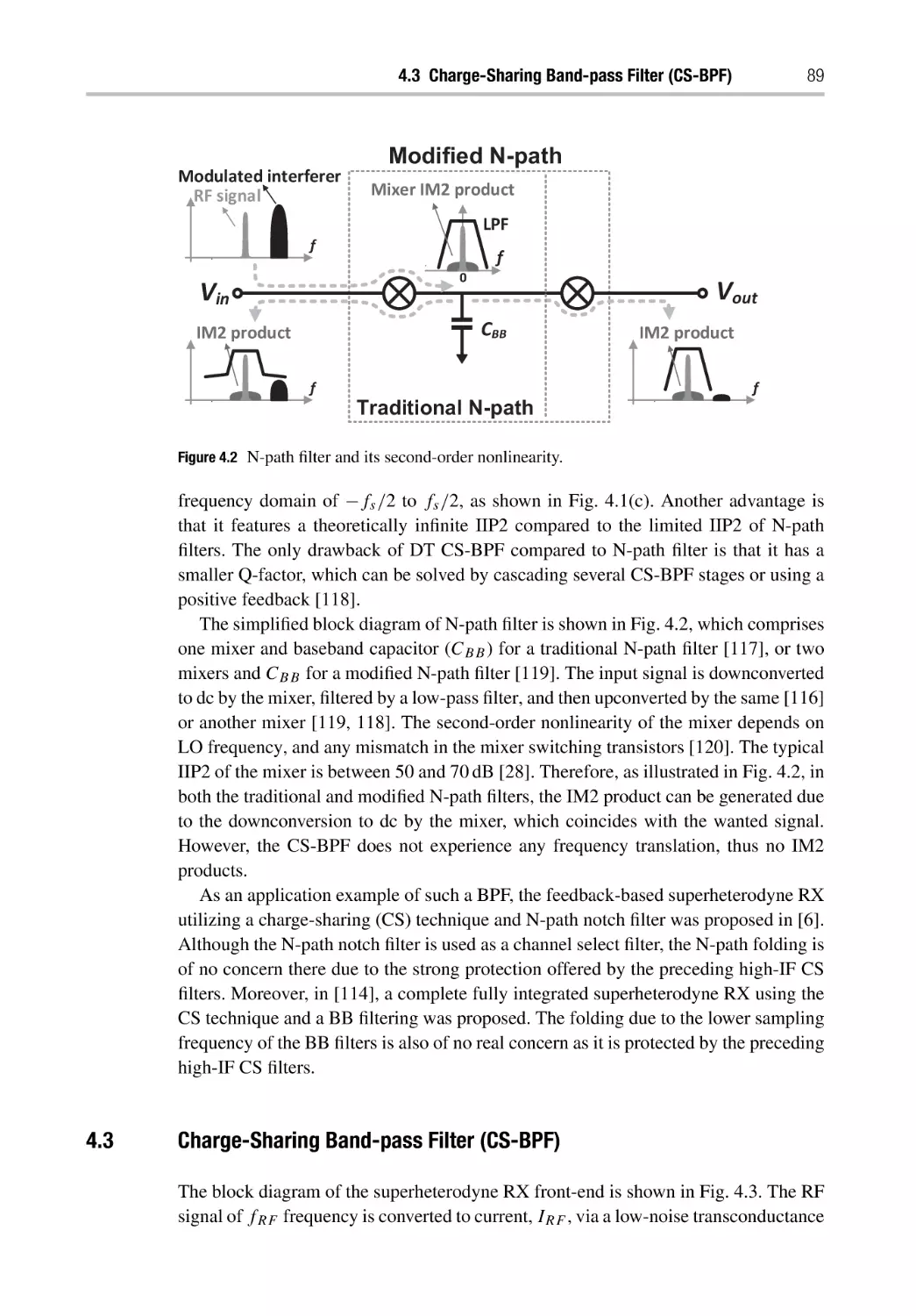
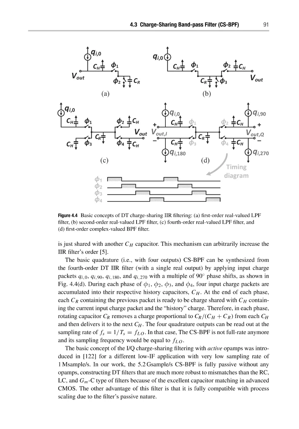
90
94
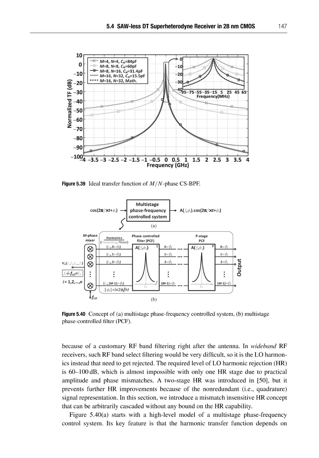
95
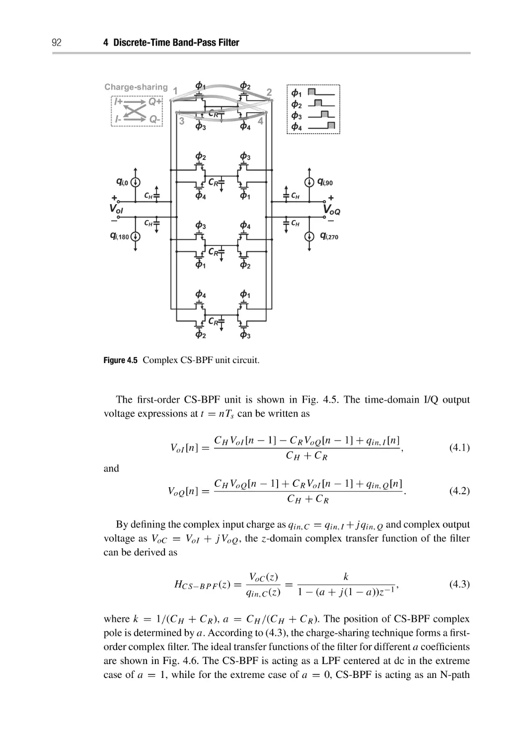
96
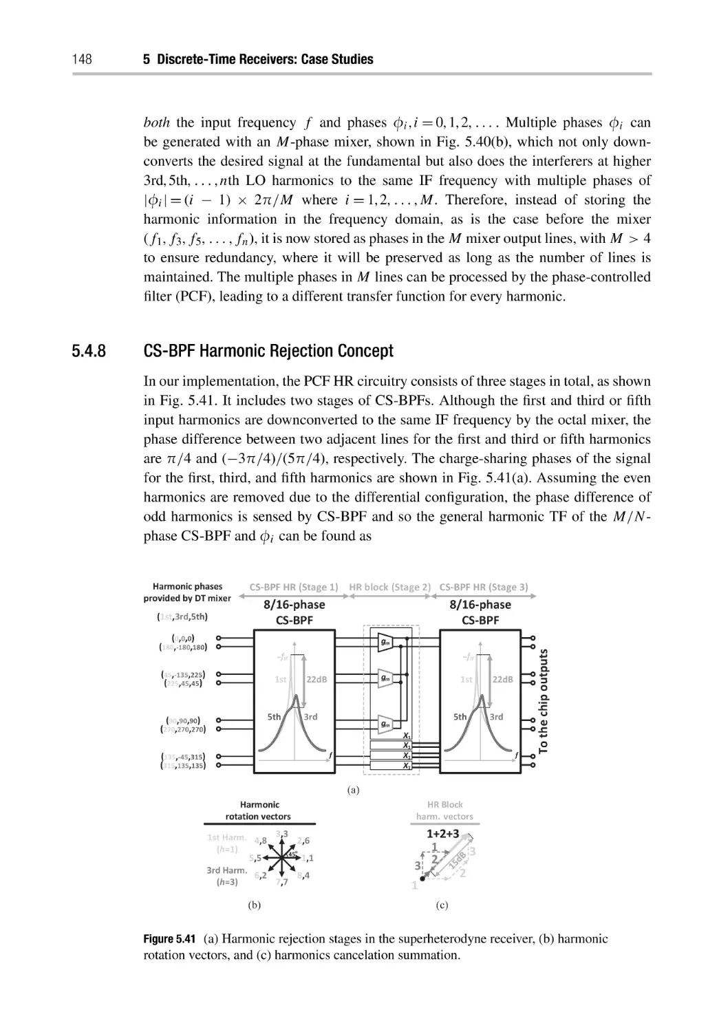
97
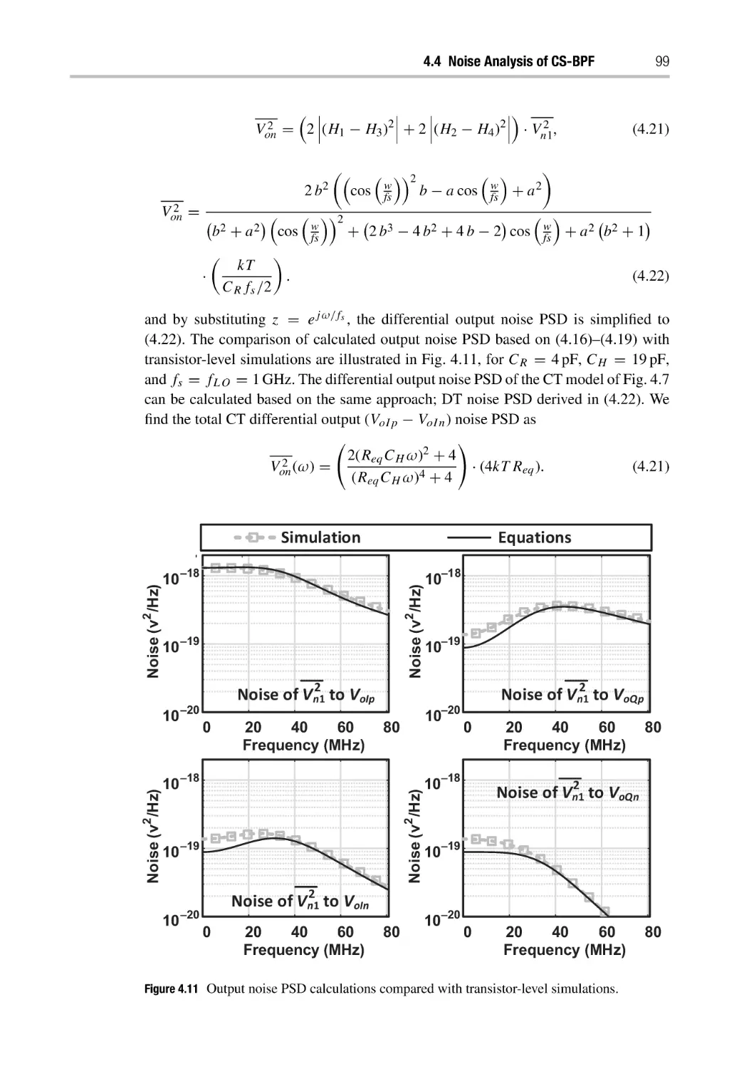
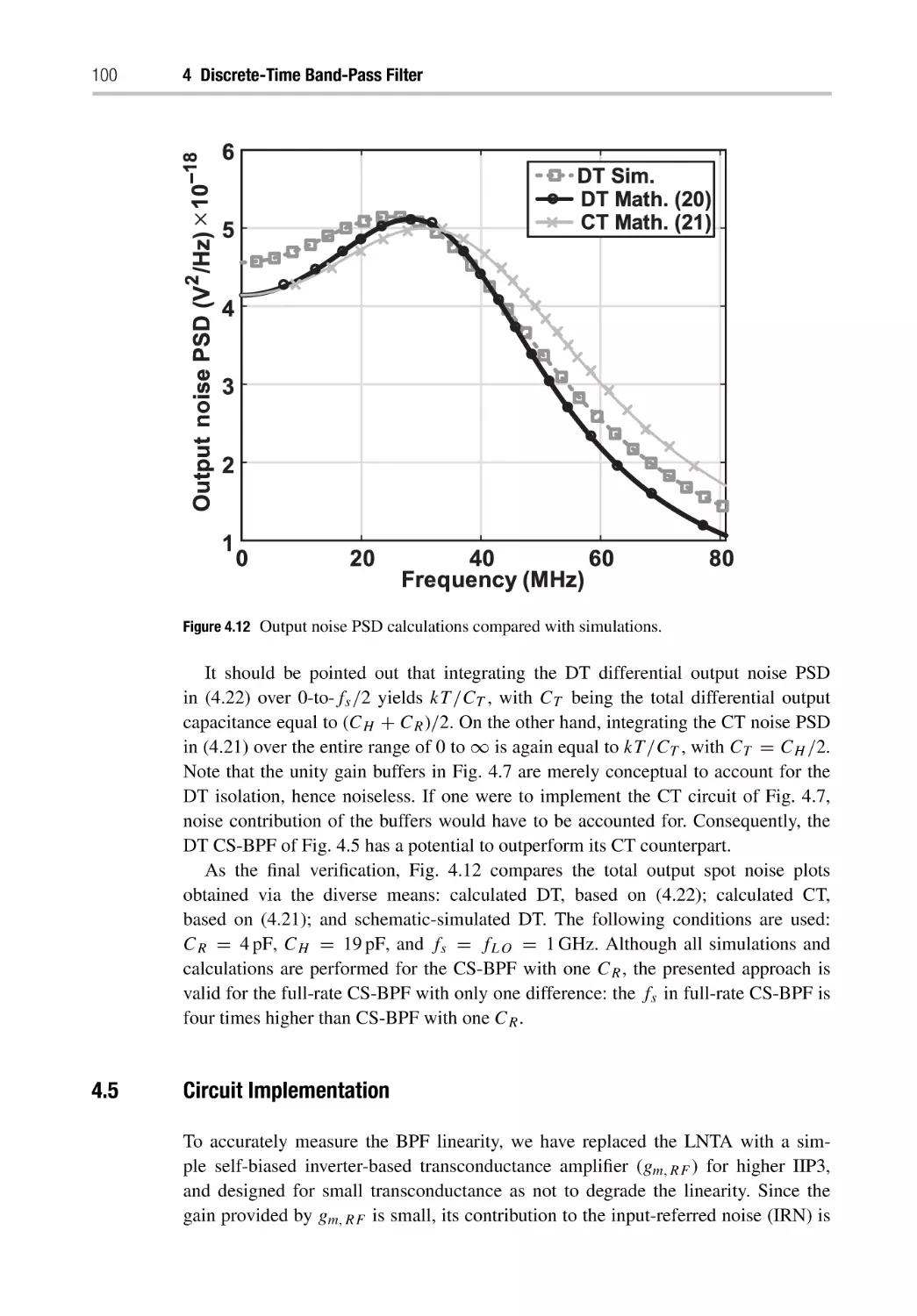
100
Contents
5
ix
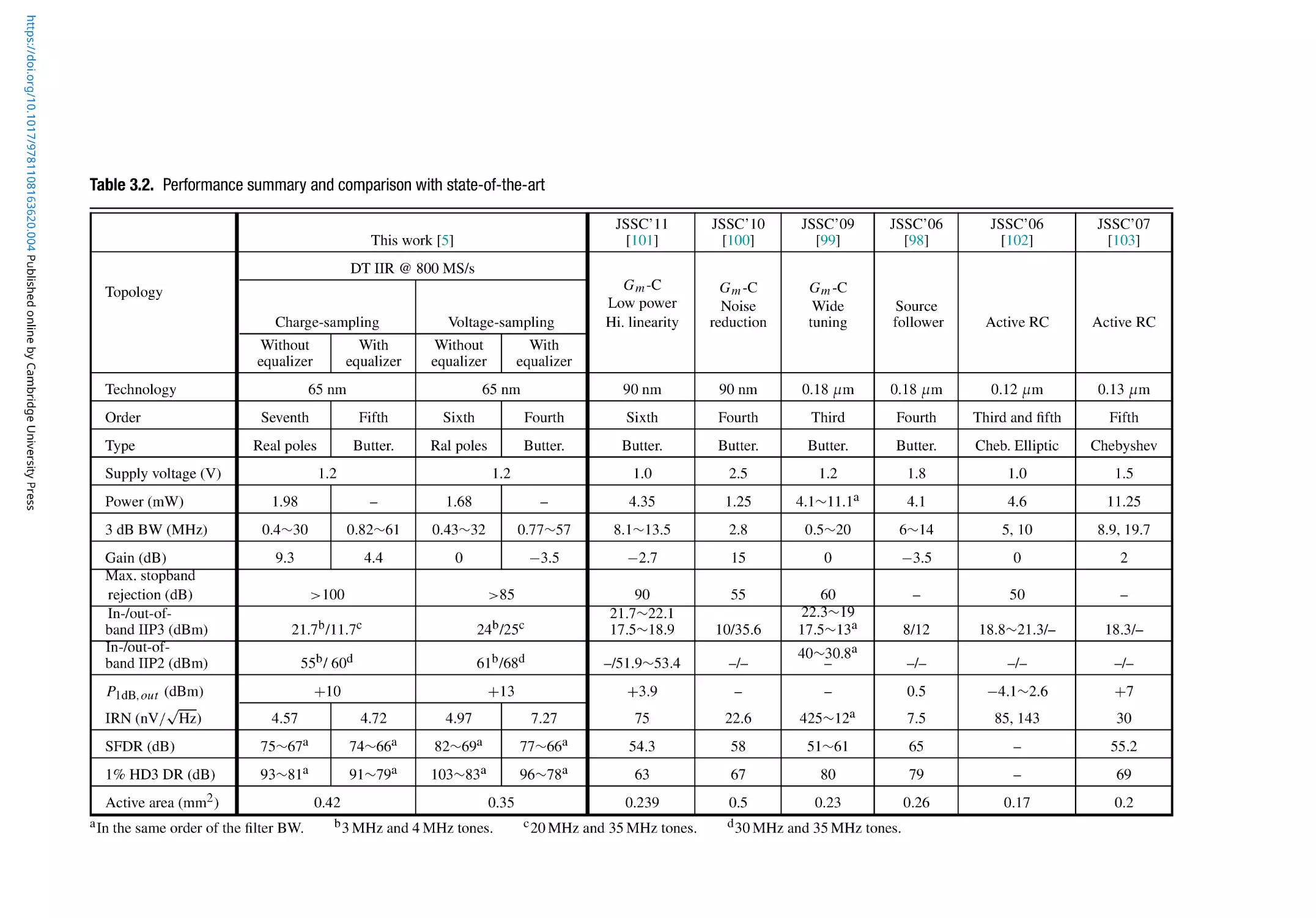
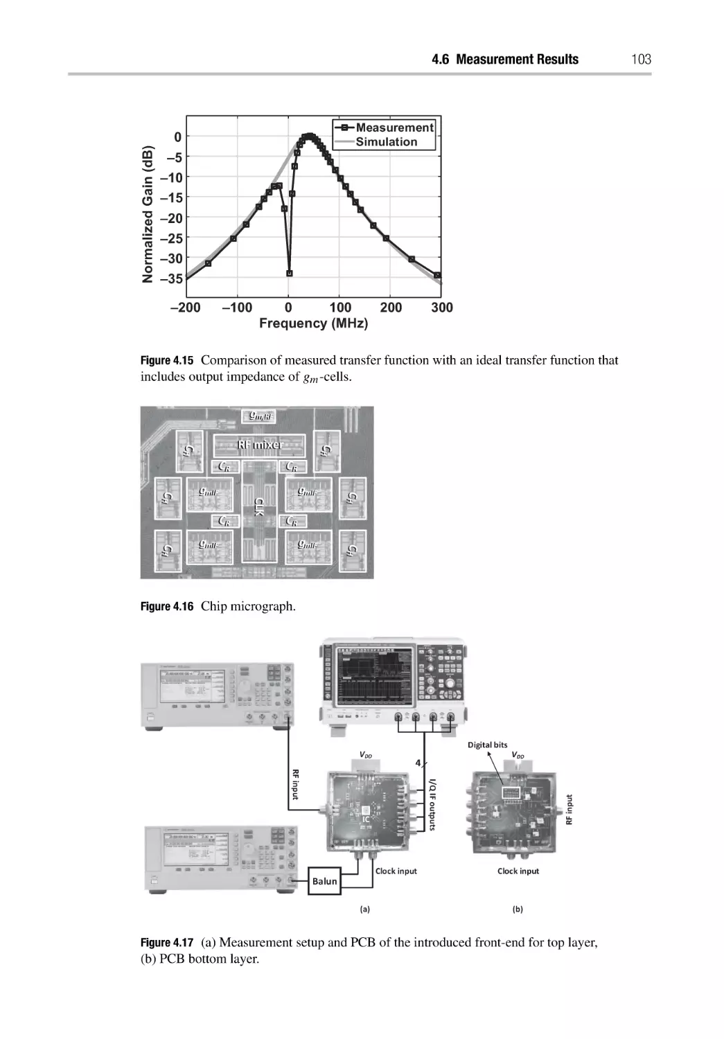
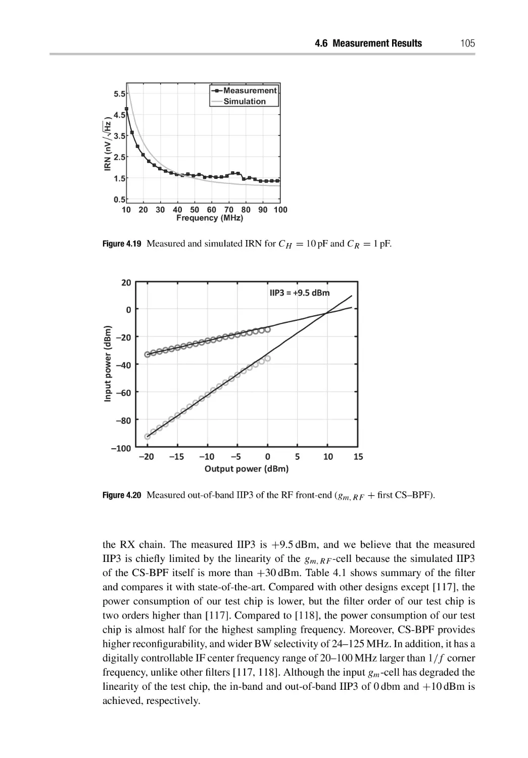
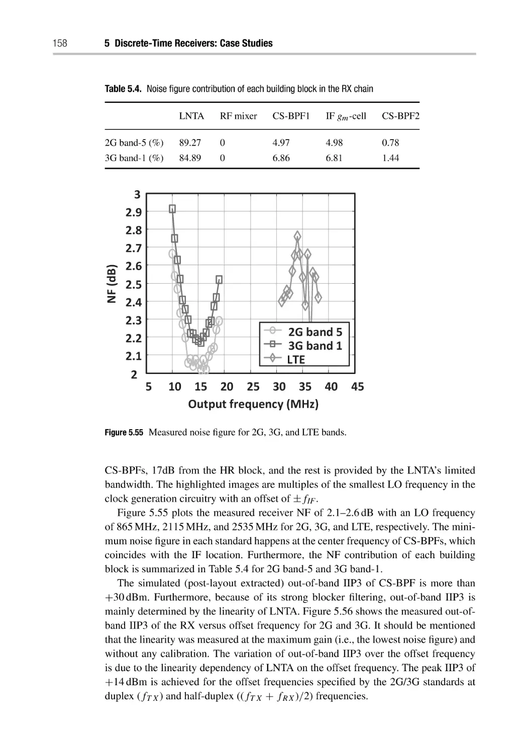
4.6 Measurement Results
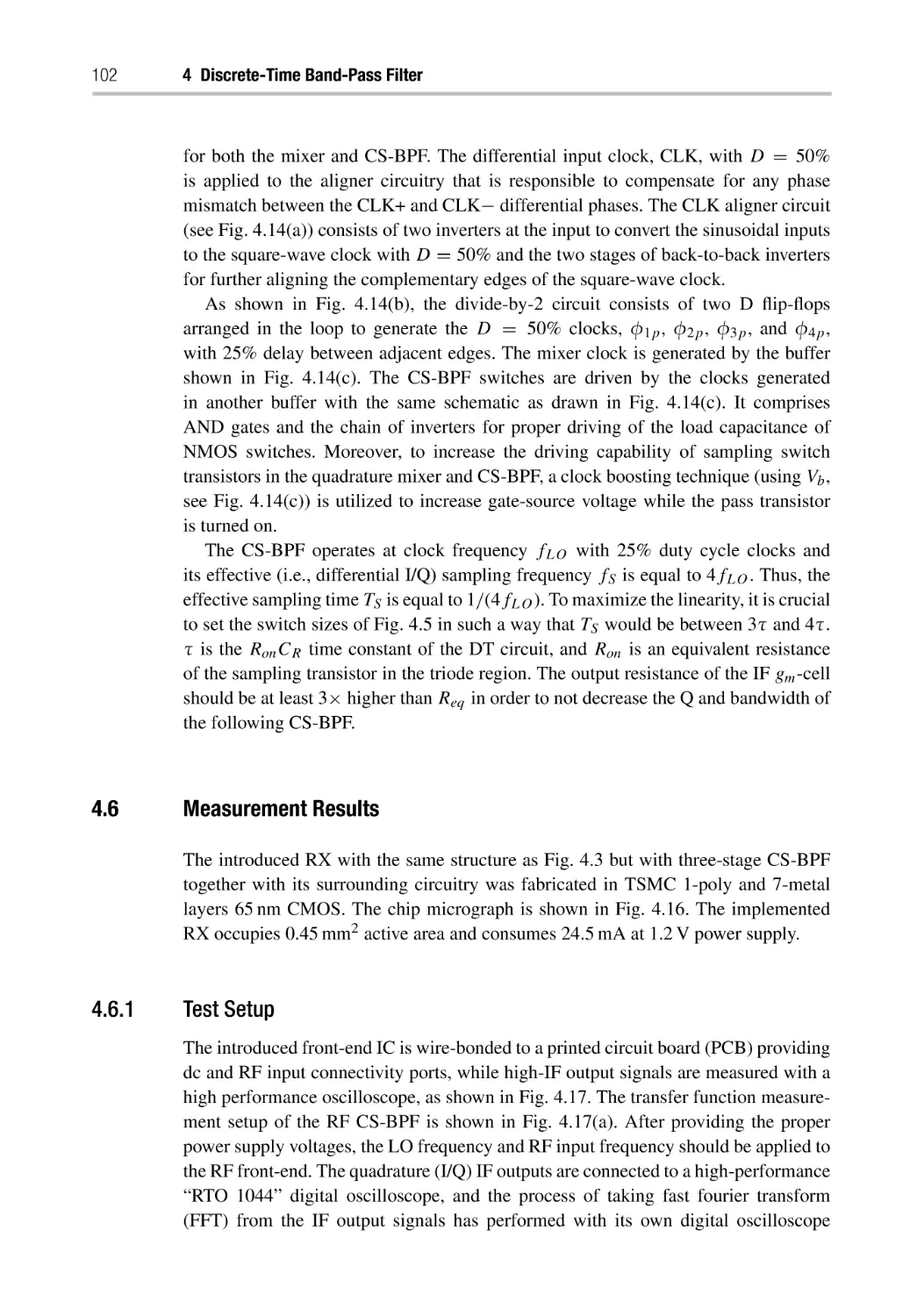
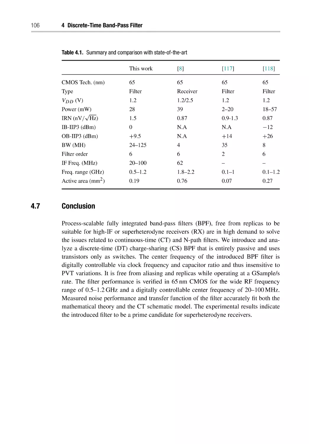
4.6.1 Test Setup
4.7 Conclusion
102
102
106
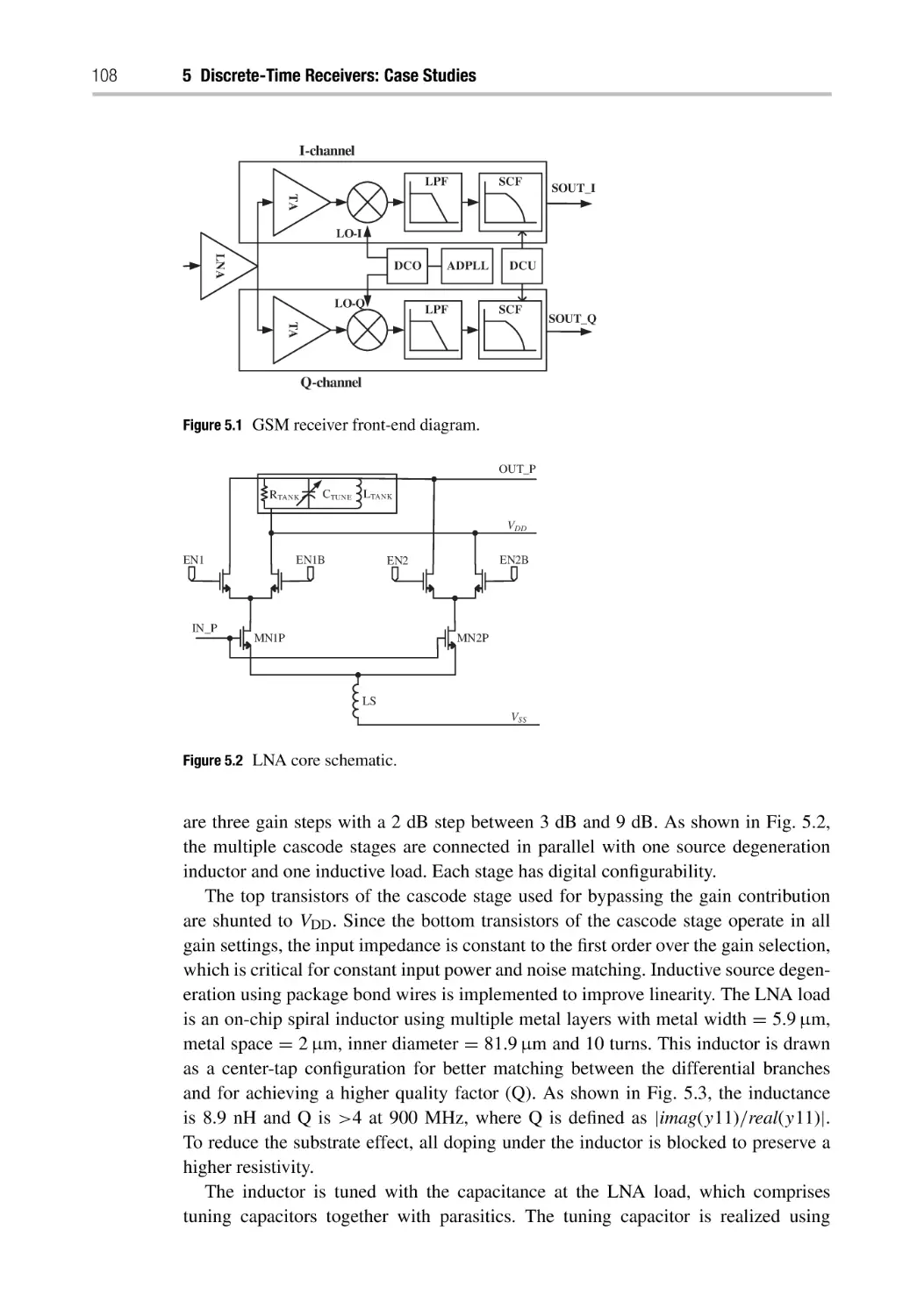
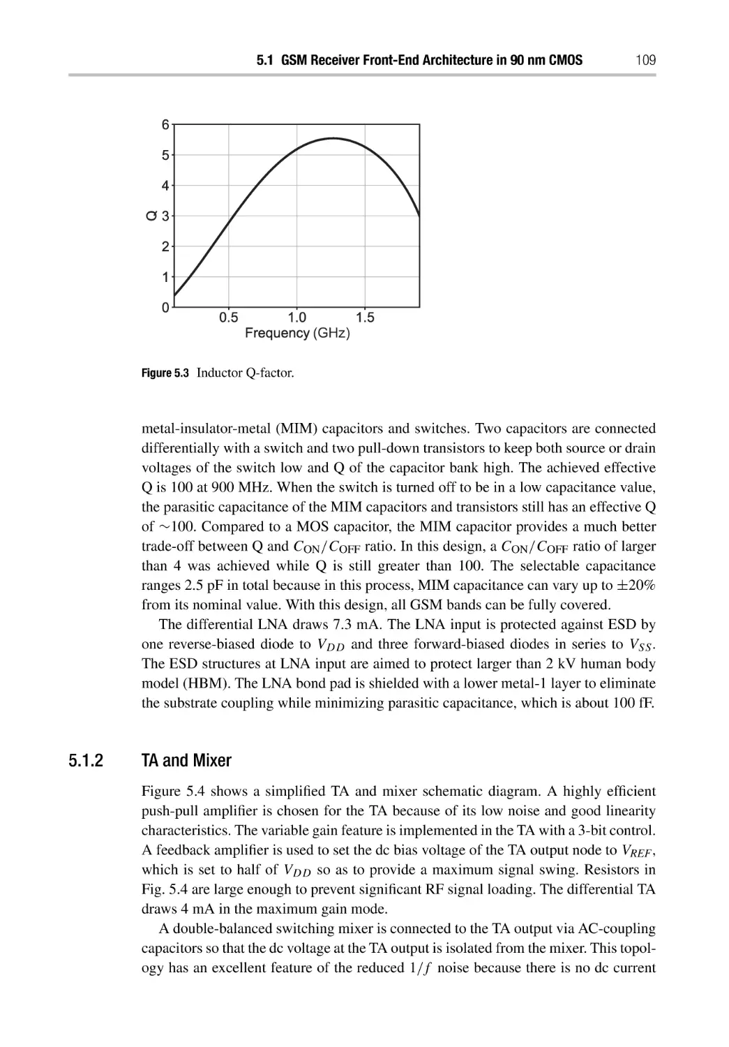
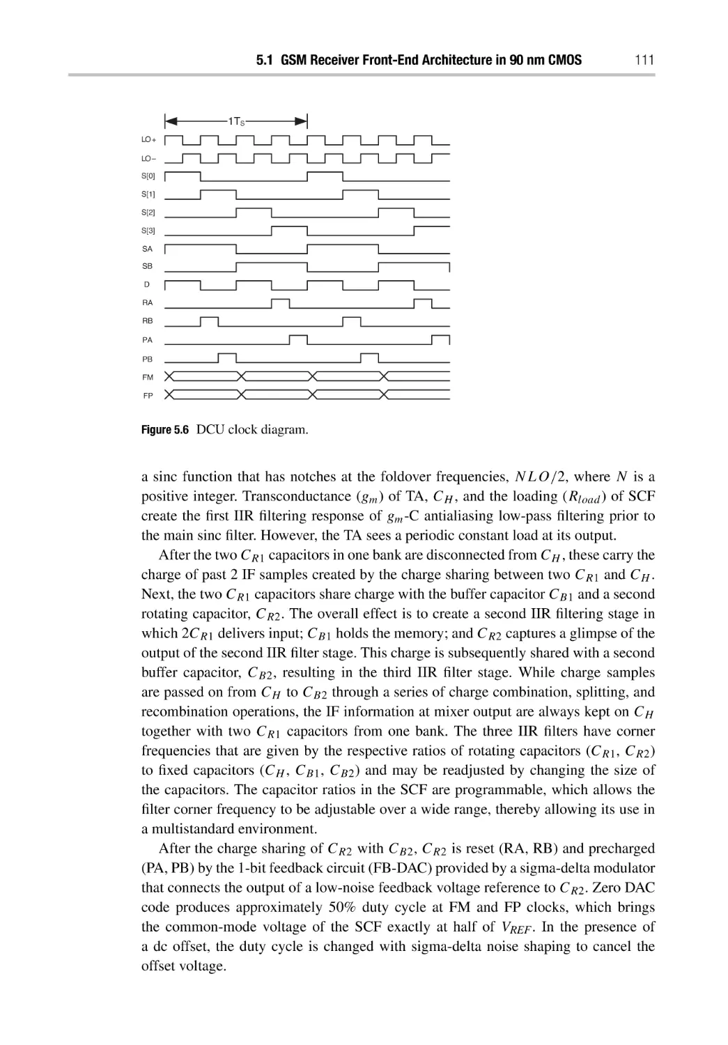
Discrete-Time Receivers: Case Studies
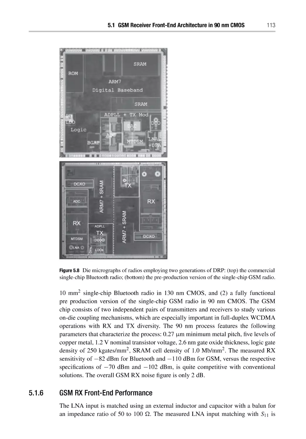
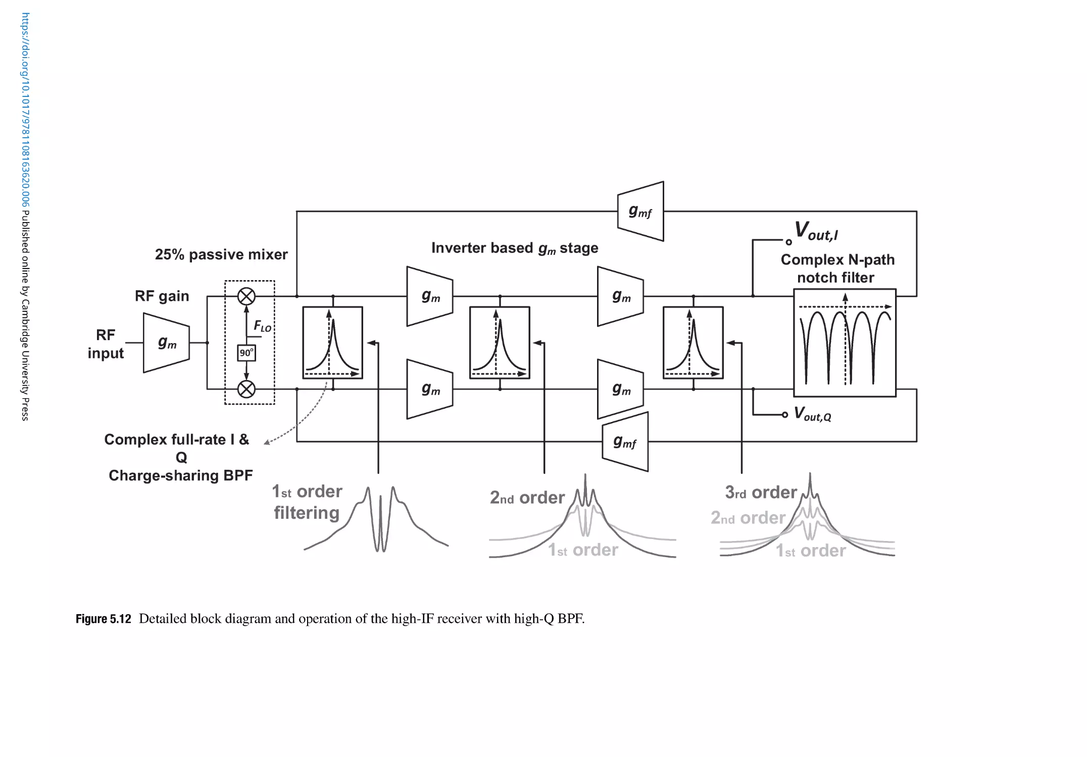
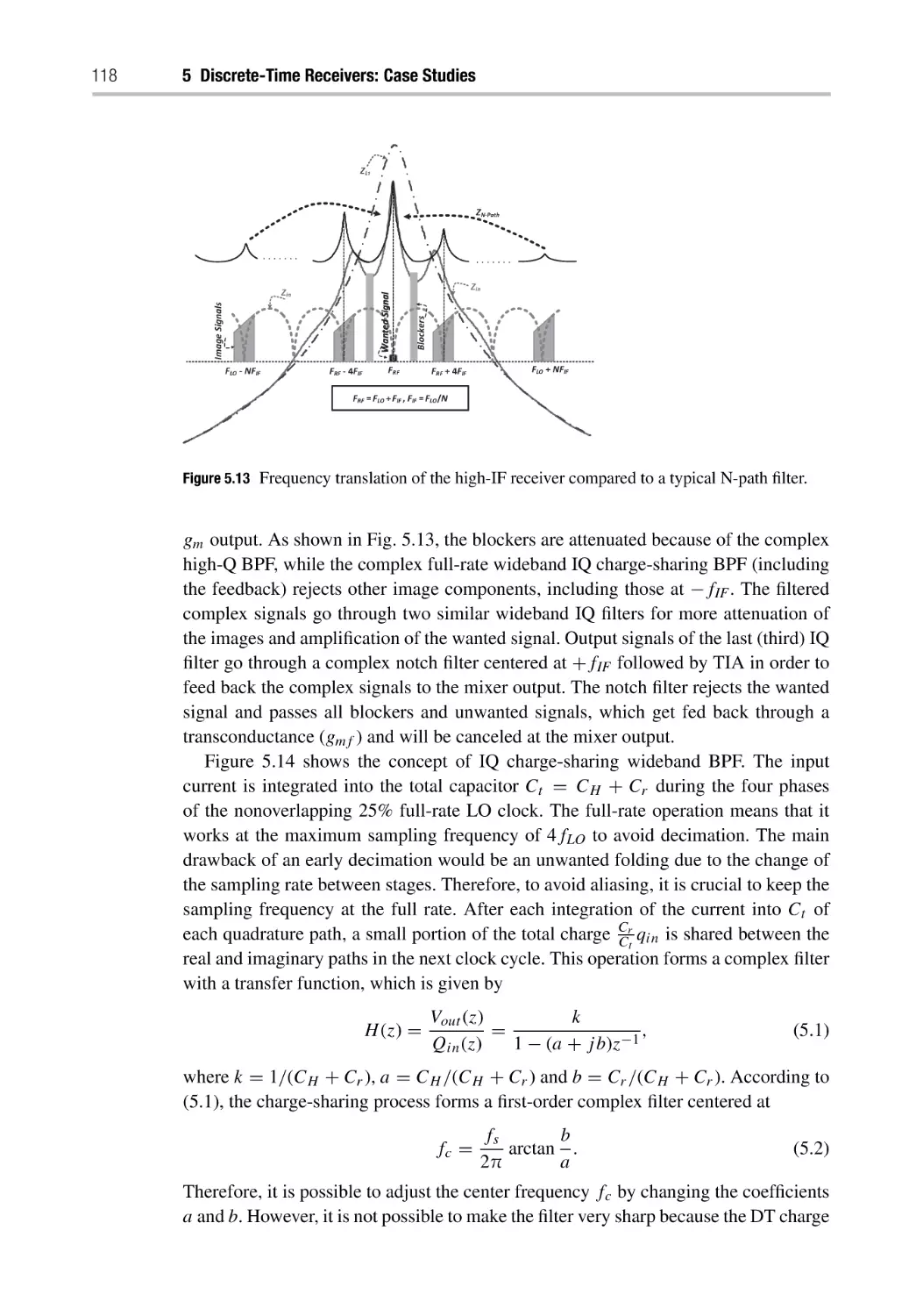
5.1 GSM Receiver Front-End Architecture in 90 nm CMOS
5.1.1 Low-Noise Amplifier
5.1.2 TA and Mixer
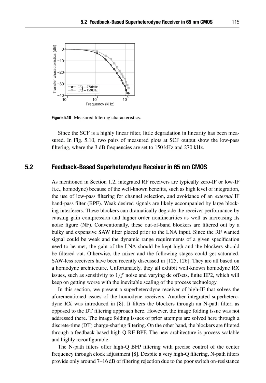
5.1.3 Switched-Capacitor Filter (SCF)
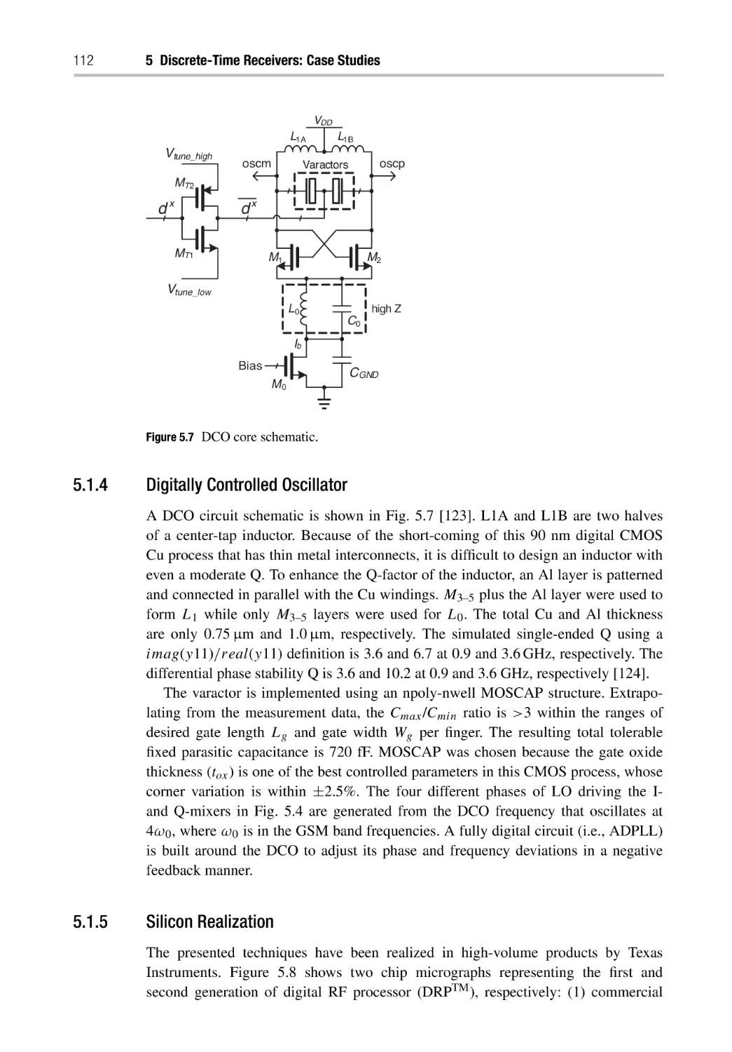
5.1.4 Digitally Controlled Oscillator
5.1.5 Silicon Realization
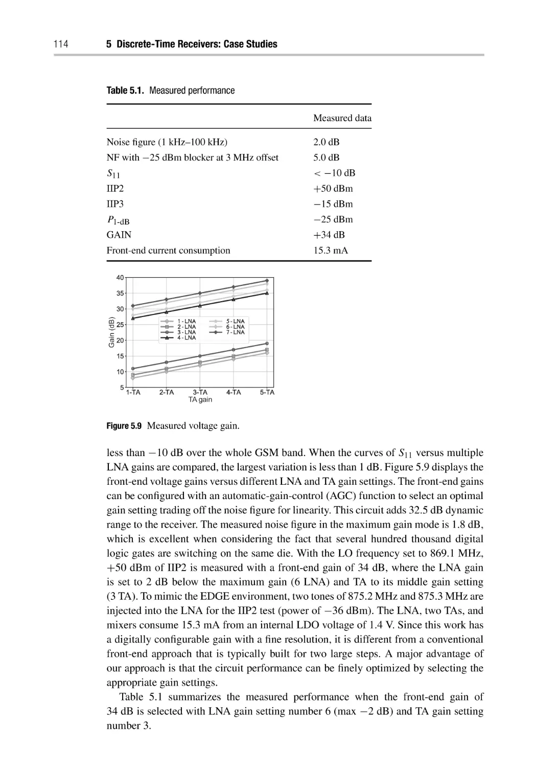
5.1.6 GSM RX Front-End Performance
5.2 Feedback-Based Superheterodyne Receiver in 65 nm CMOS
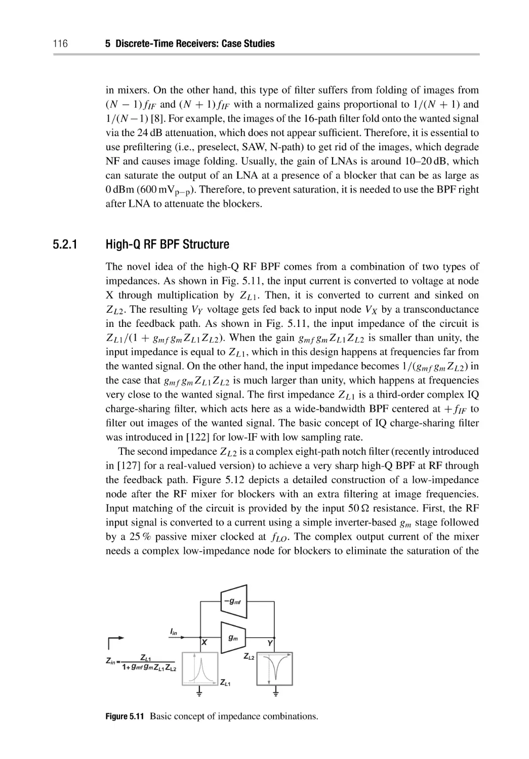
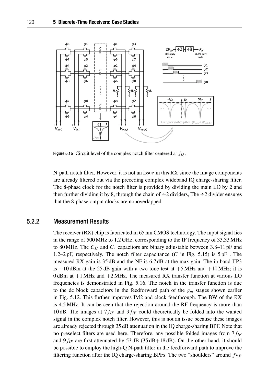
5.2.1 High-Q RF BPF Structure
5.2.2 Measurement Results
5.3 DT Superheterodyne Receiver in 65 nm CMOS
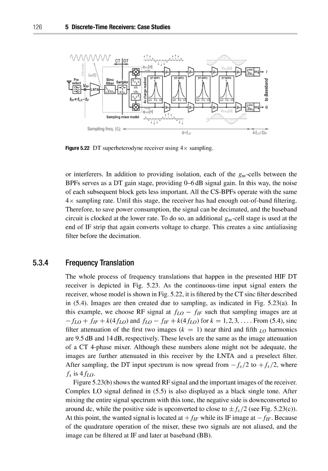
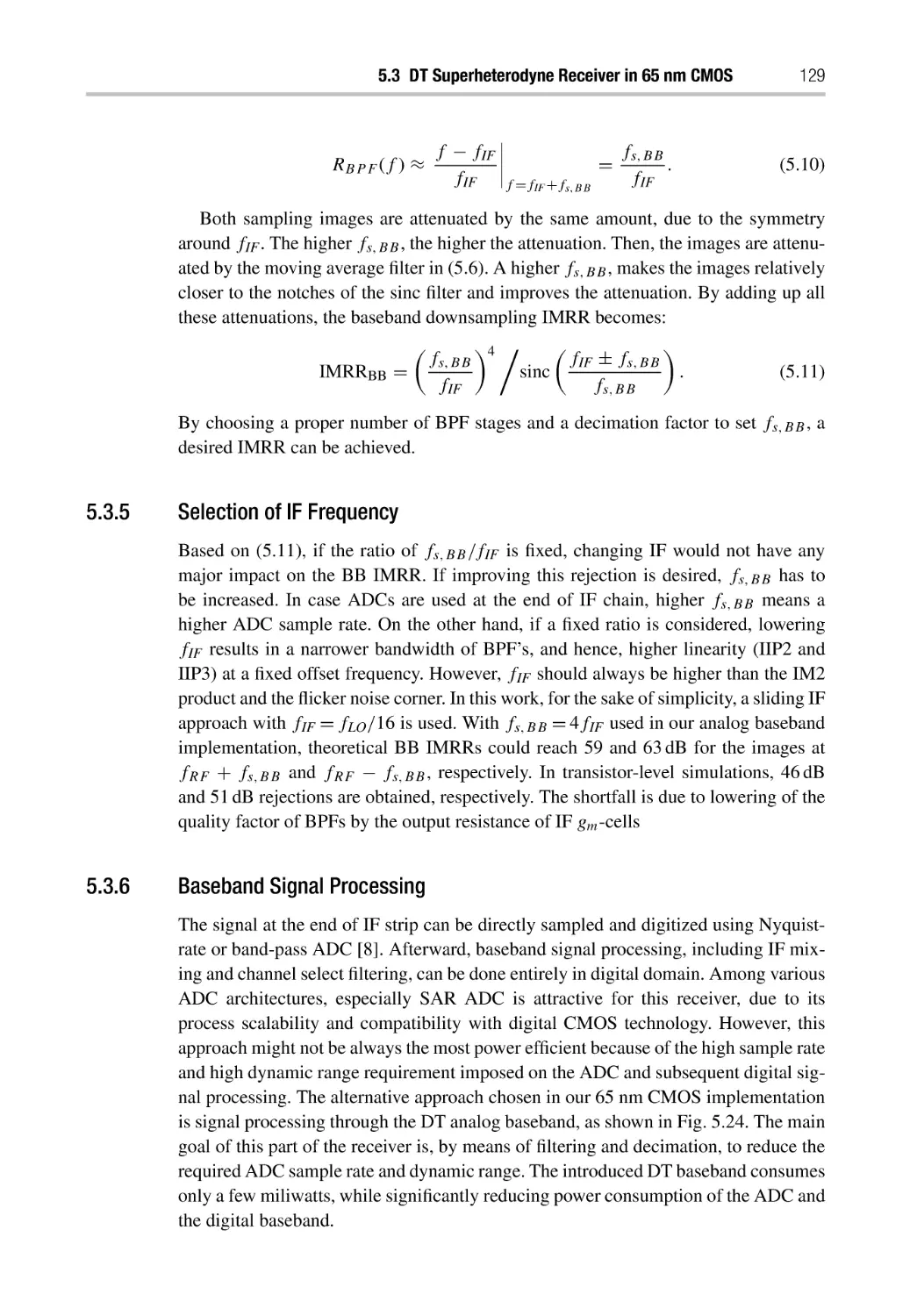
5.3.1 Structure
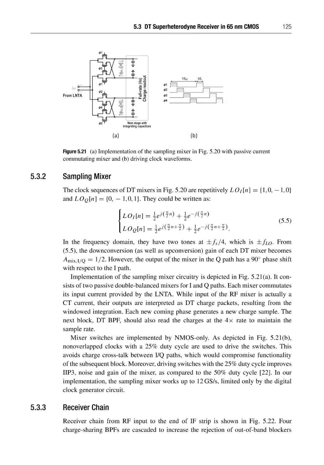
5.3.2 Sampling Mixer
5.3.3 Receiver Chain
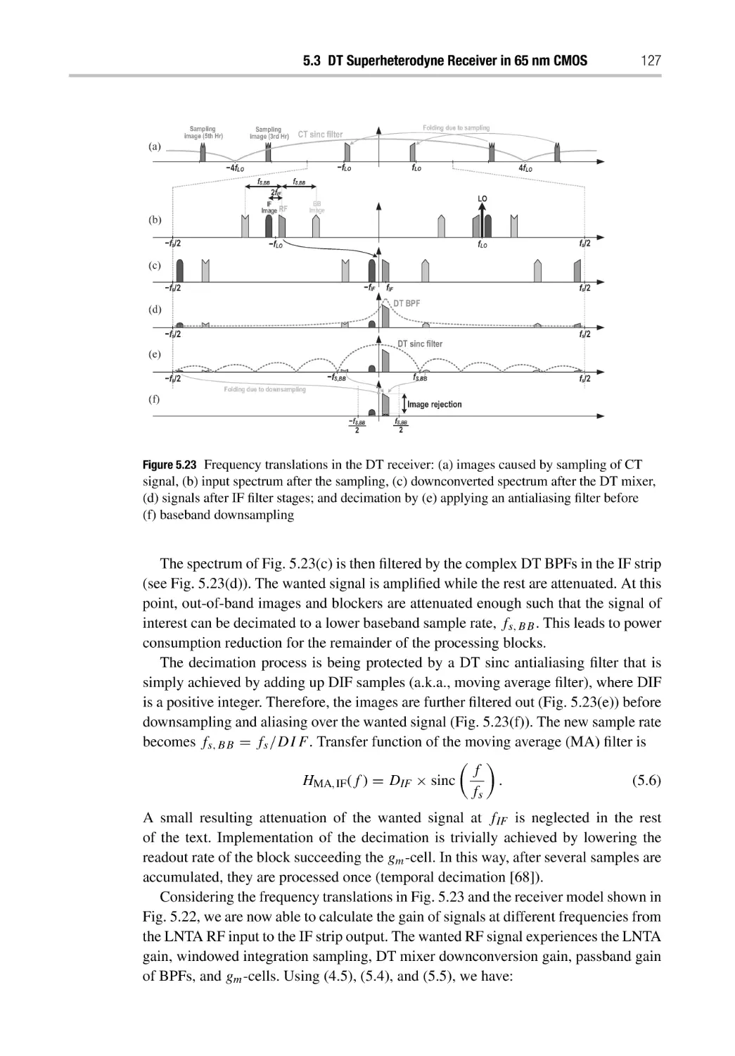
5.3.4 Frequency Translation
5.3.5 Selection of IF Frequency
5.3.6 Baseband Signal Processing
5.3.7 Digital Equalization
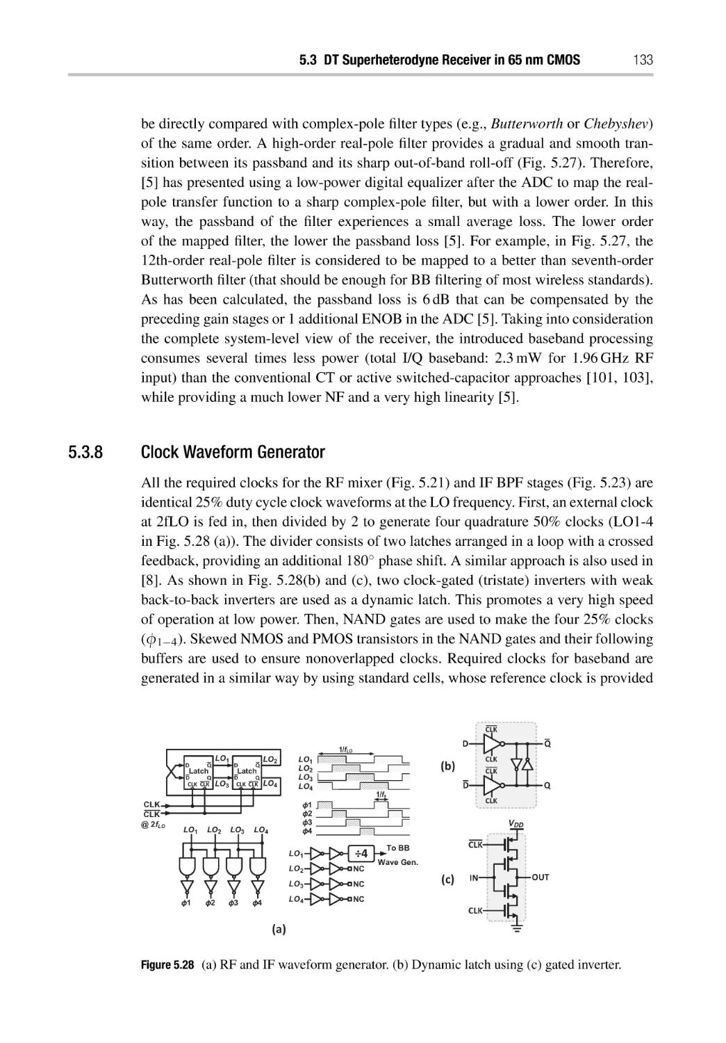
5.3.8 Clock Waveform Generator
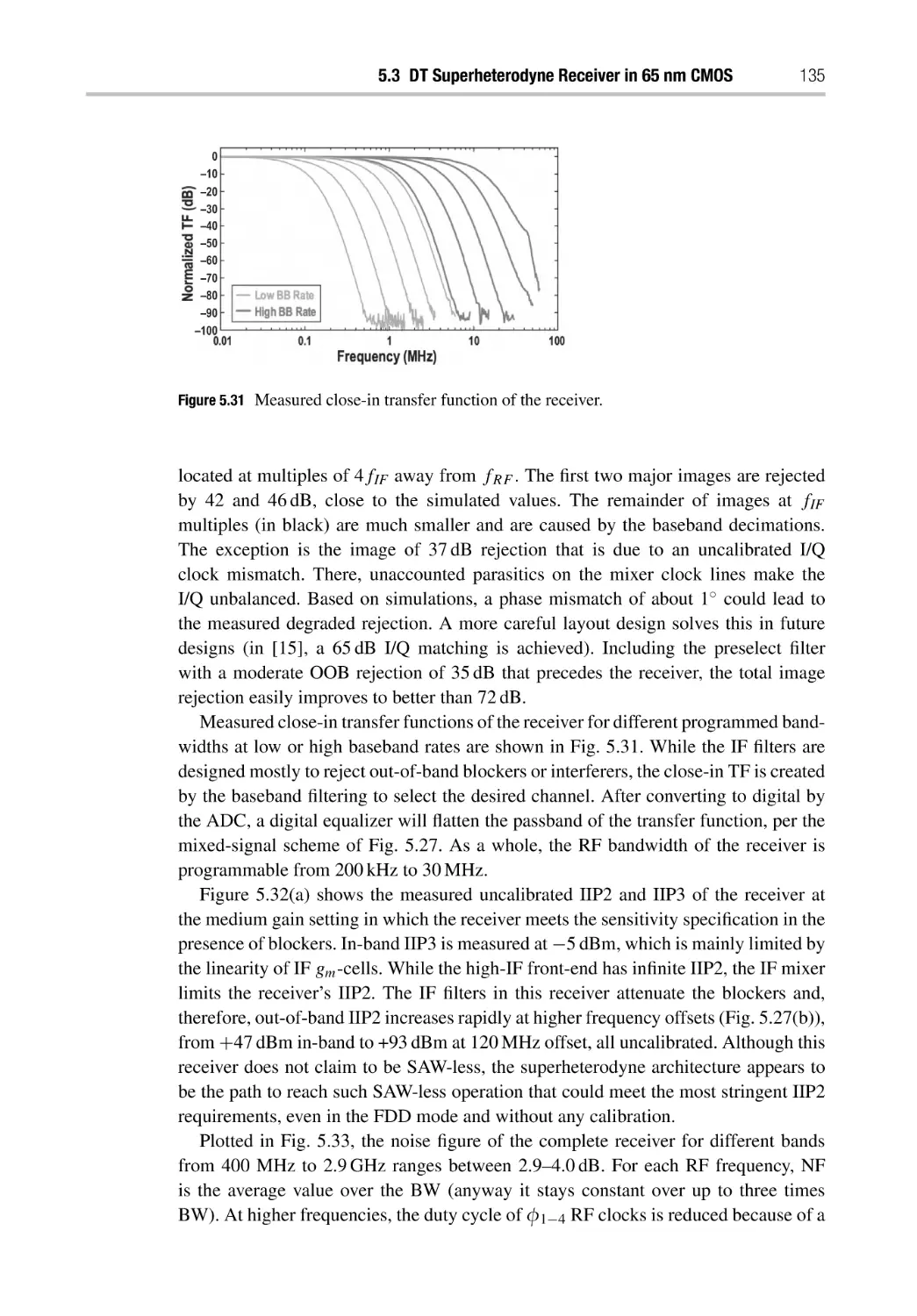
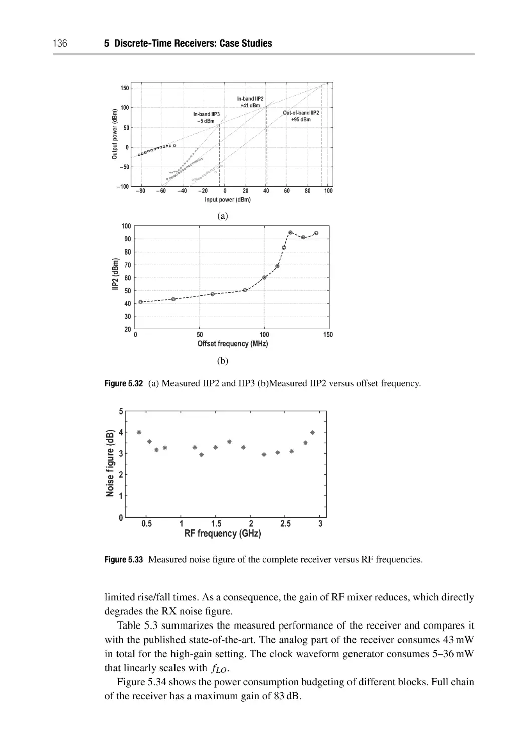
5.3.9 Measurement Results
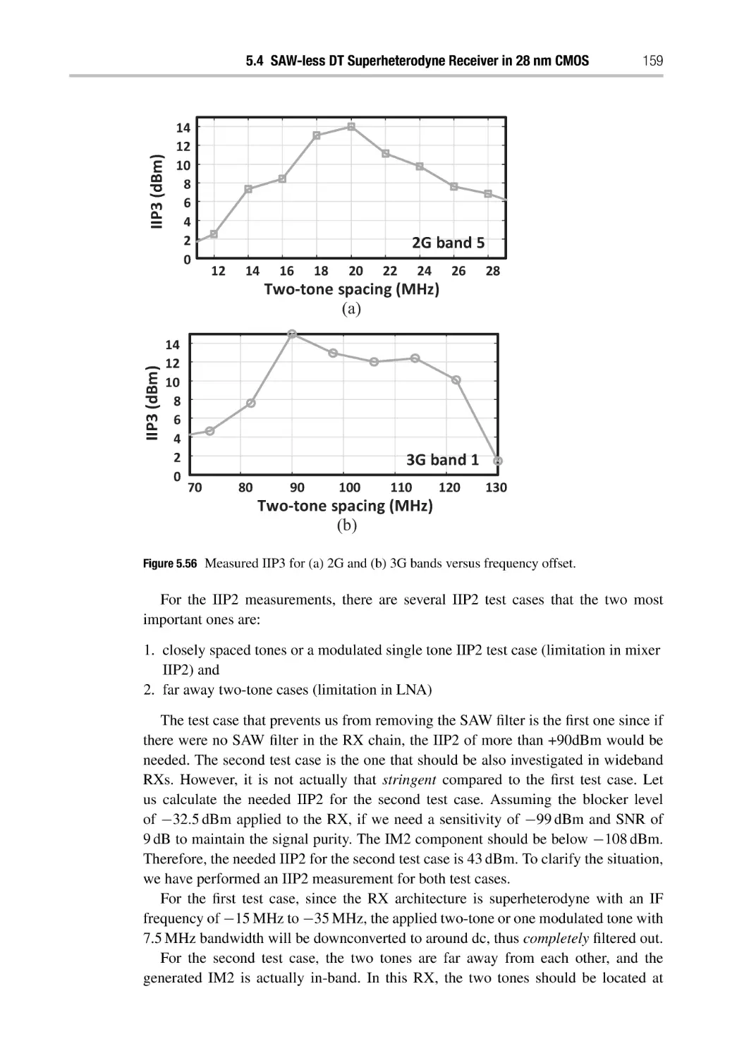
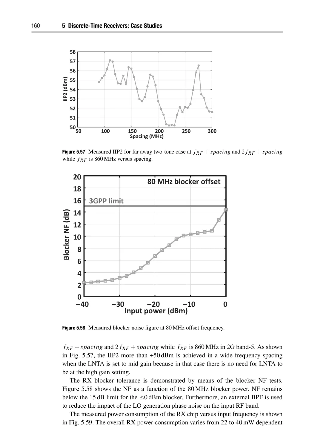
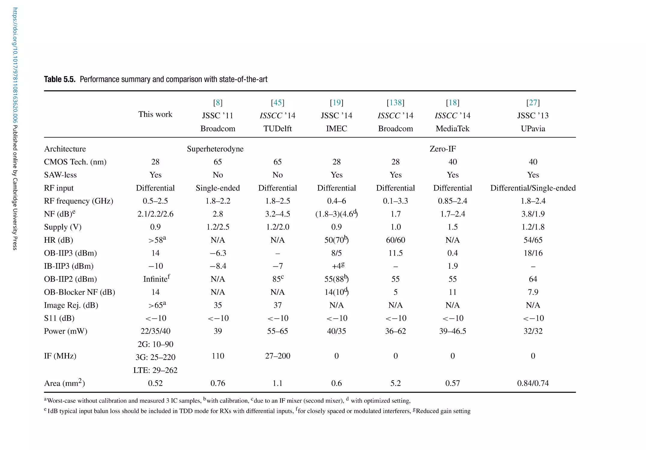
5.4 SAW-less DT Superheterodyne Receiver in 28 nm CMOS
5.4.1 New SAW-less Superheterodyne Receiver
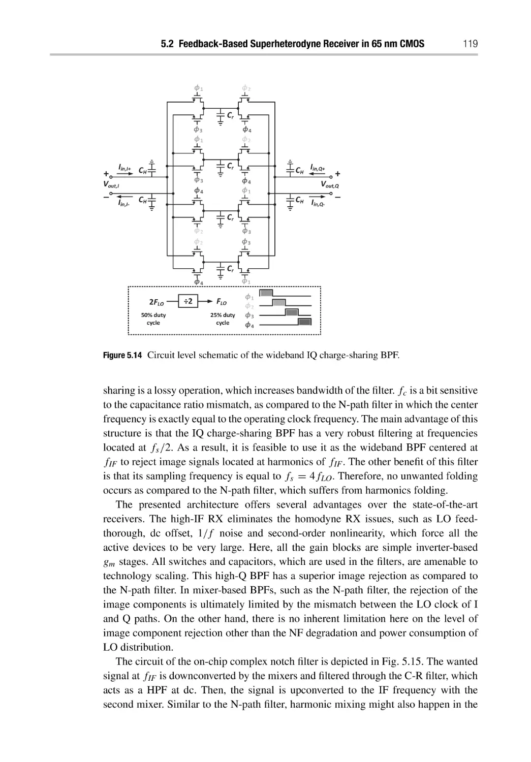
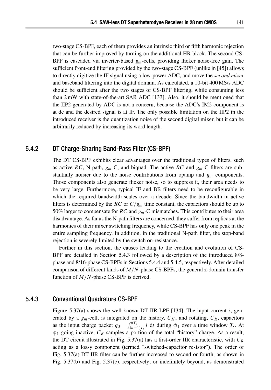
5.4.2 DT Charge-Sharing Band-Pass Filter (CS-BPF)
5.4.3 Conventional Quadrature CS-BPF
5.4.4 8/8-Phase CS-BPF
5.4.5 8/16-Phase CS-BPF
5.4.6 General M/N-Phase CS-BPF
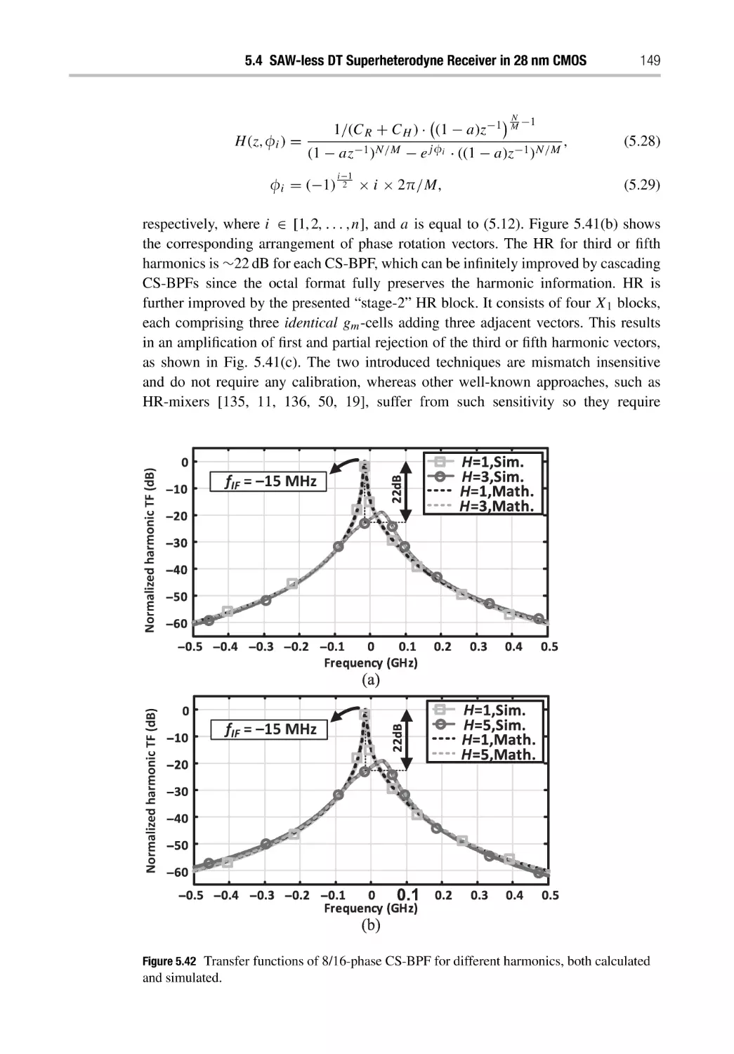
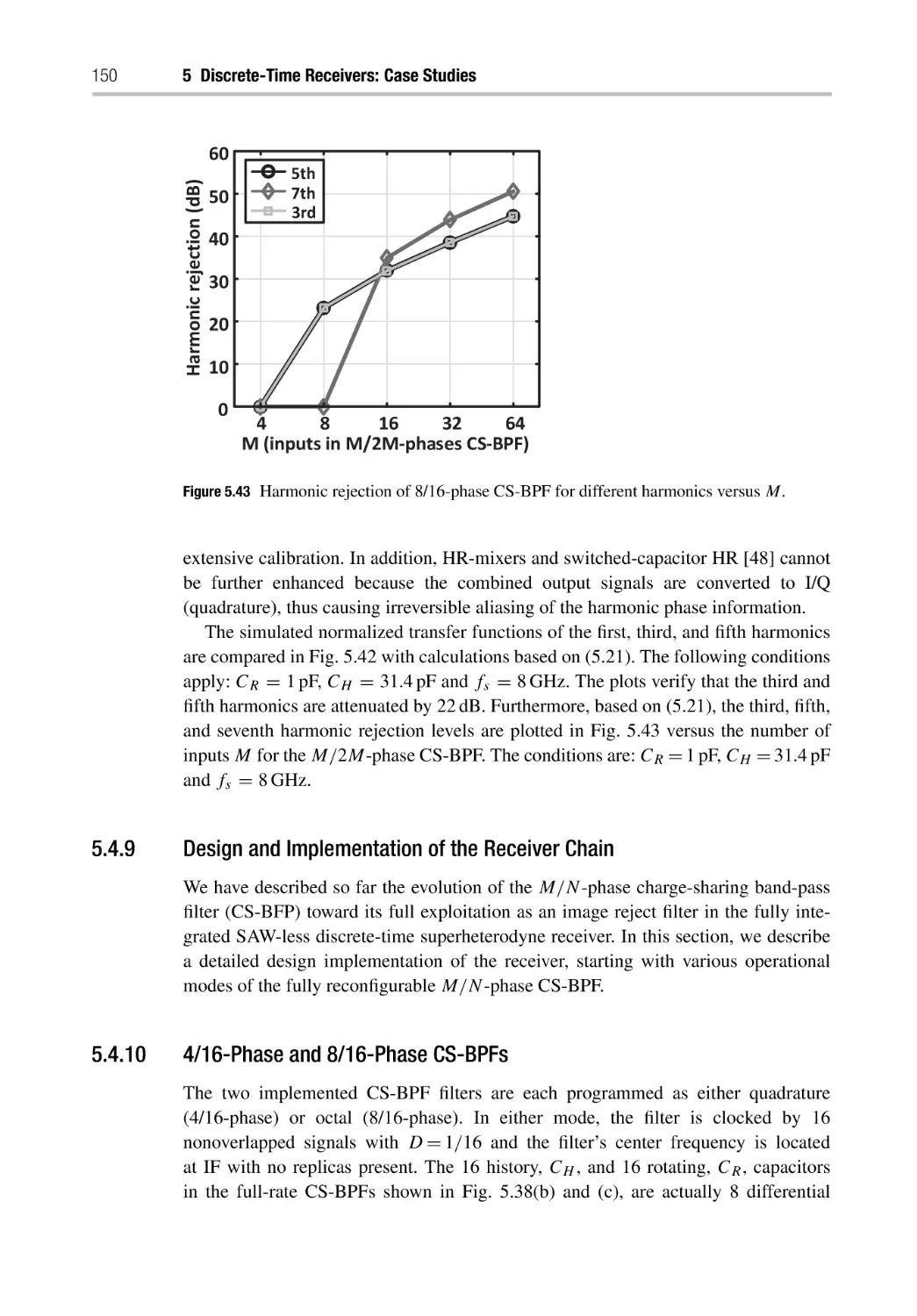
5.4.7 Harmonic Rejection
5.4.8 CS-BPF Harmonic Rejection Concept
5.4.9 Design and Implementation of the Receiver Chain
5.4.10 4/16-Phase and 8/16-Phase CS-BPFs
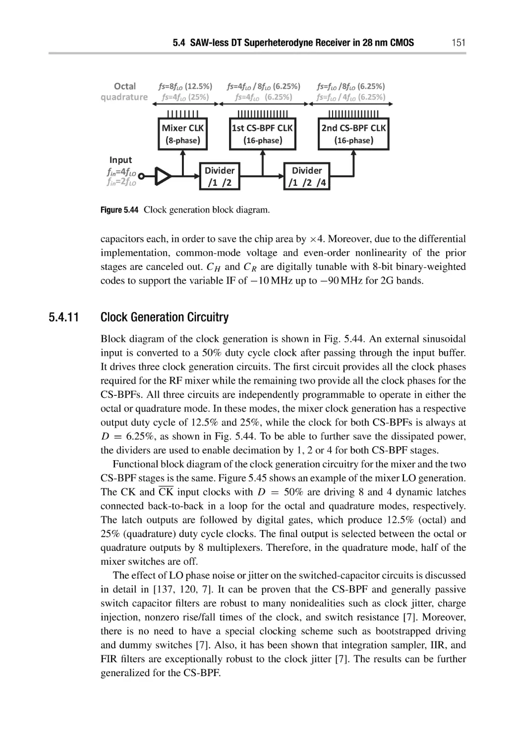
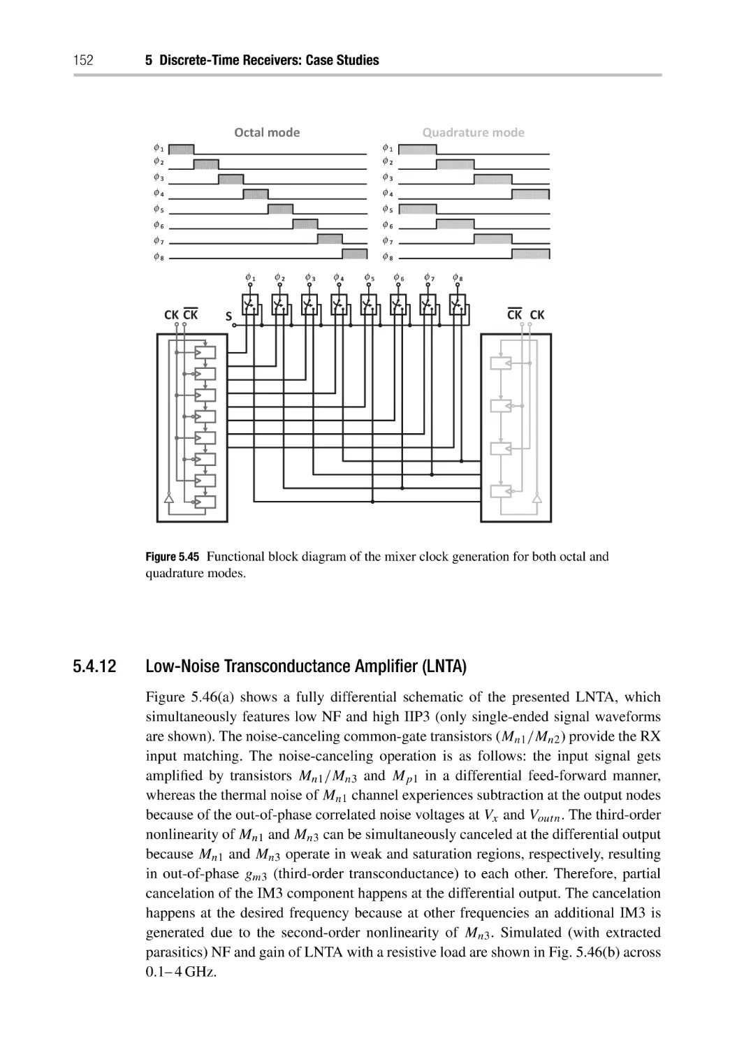
5.4.11 Clock Generation Circuitry
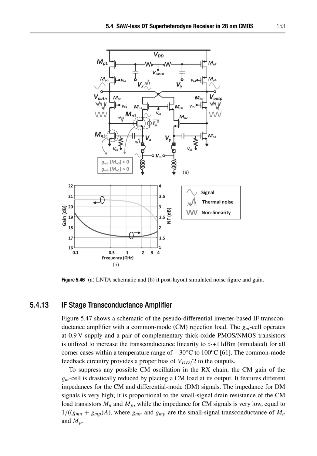
5.4.12 Low-Noise Transconductance Amplifier (LNTA)
5.4.13 IF Stage Transconductance Amplifier
5.4.14 Measurement Results
5.5 Conclusion
107
107
107
109
110
112
112
113
115
116
120
122
123
125
125
126
129
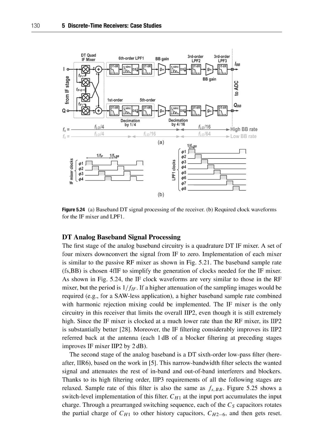
129
132
133
134
138
140
141
141
143
143
144
146
148
150
150
151
152
153
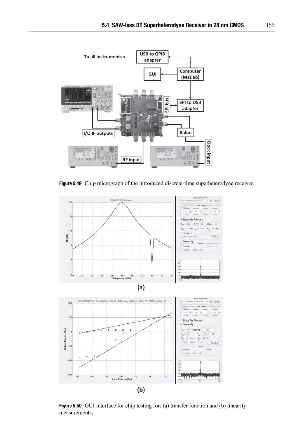
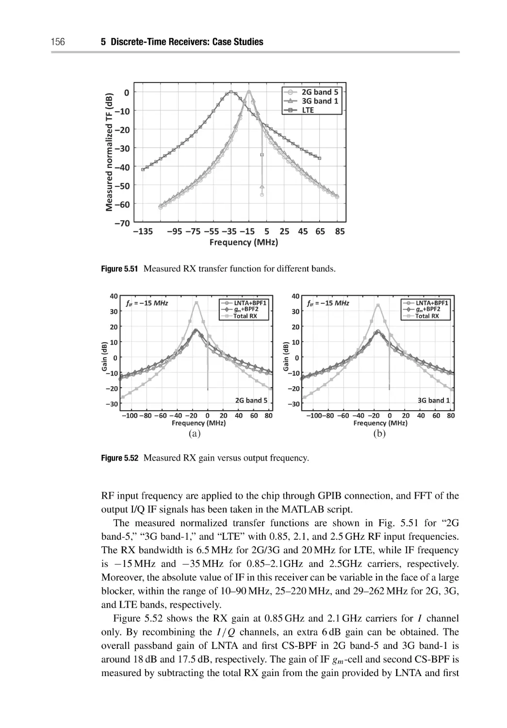
154
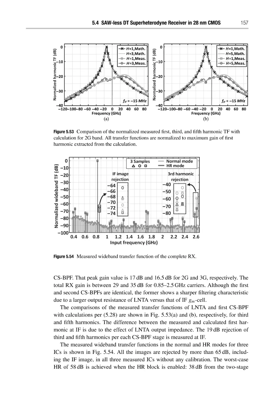
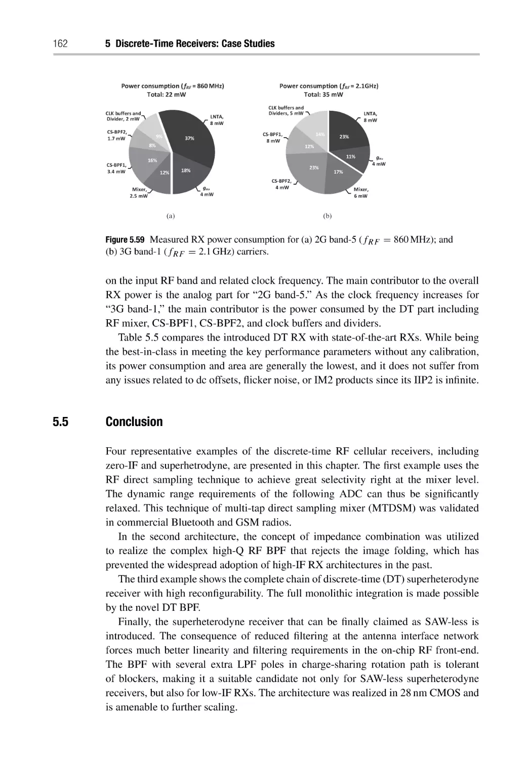
162
References
Index
163
172
Preface
The ideas described in this book go back to the year 2000, when, together with my
Texas Instruments (TI) colleague and research collaborator, Dr. Khurram Muhammad,
and inspired by our luminary physicist colleague, Dr. Dirk Leipold, with the tacit
approval of our managers, Ken Maggio and Dr. Bill Krenik (TI’s motto back then was
“Do not ask for permission, ask for forgiveness”), we conceived an idea of realizing
the RF reception functionality using discrete-time (DT) charge packets that can be
processed using mostly passive switched-capacitor circuitry. This was motivated by
the fact that TI was then the unquestionable leader in CMOS process development for
low-leakage (i.e., mobile) digital processors, but with an almost nonexistent market
presence in RF transceivers. To leapfrog the formidable competitors, such as Infineon
and ST Microelectronics, and to secure continued business with Nokia, we had to
come up with a distinctly different approach from the conventional continuous-time
analog-intensive implementations, something that would exploit TI’s leadership in
digital CMOS technology. Our invention was the DT receiver (RX) front end that
was amenable to the purely digital CMOS process that would not require any analog
extensions. The DT RX was quickly put into high-volume production for Bluetooth
and GSM single-chip radios. Later on, we had discovered to our surprise that Professor. Abidi’s group at the University of California–Los Angeles was working in parallel
on a similar research.
This new field was generating lots of exciting ideas. Not unexpectedly, the business
product environment is known to not always be terribly welcoming of new ideas,
especially when the original DT RX ideas were just “good enough” to secure new
products and markets. In that environment, I left TI and moved to Europe to accept
a fully tenured faculty position at Delft University of Technology in the Netherlands,
where I joined Professor John Long’s team. While there, I was finally free to realize
the many ideas that were just begging to be explored. After 20 years in industry,
I soon realized that the grass on the other (i.e., academia) side was actually not that
much greener. All ideas would require funding to pay for the high cost of research.
I was lucky to quickly find a sponsor: Mr. Zhuobiao He from the HiSilicon group of
Huawei in Shanghai. This allowed me to hire two young, bright-eyed PhD students,
Massoud Tohidian and Iman Madadi, who did a fantastic job of realizing the world’s
first discrete-time superheterodyne radio for wireless cellular applications. The effort
was further continued in collaboration with Dr. Patrick Vandenameele from the M4S
group of Huawei in Leuven, Belgium, to build commercial 4G/5G radios.
xii
Preface
While Tohidian and Madadi were busy writing their PhD dissertations and getting
ready to start their own company, Qualinx b.v. where they tried to produce receiver
for satellite navigation, a visiting PhD student from Brazil, Dr. Sandro BinsfeldFerreira, took it upon himself to realize these DT superheterodyne RX ideas in
ultra-low-power applications. Together with our research collaborator from TSMC in
Hsin-Chu, Taiwan, Dr. Feng-Wei Kuo, who later became my part-time PhD student,
they developed the most power-efficient Bluetooth low-energy receiver for Internetof-Things (IoT) applications.
In 2014, I moved to University College Dublin in Ireland, where I hired another
bright-eyed PhD student, Amir Bozorg, to continue developing ideas along the lines
of DT RX. Some of the developed circuits and architectures are included in this book,
but I believe the best is yet to come. So, stay tuned . . . .
This book consists of five chapters. Chapter 1 describes the fundamentals of the
DT RF receiver architectures and how the sampling phenomenon affects their performance. Moreover, it explains the key concepts of DT filtering.
Chapter 2 deals with the low-noise transconductance amplifier (LNTA), giving
an overview on wideband LNTA and noise cancelation techniques, noise and gain
analysis.
Chapters 3 and 4 address high-order, low-pass infinite-impulse response (IIR) and
band-pass complex charge-sharing filter architectures, respectively. The main goal is
to show that high-order low-noise filters can be developed by applying the switchcapacitor circuitry.
Finally, Chapter 5 takes the reader through case studies of different types of DT
receivers that exemplify the DT approach taken in the actual RF receivers.
I would also like to thank the staff at Cambridge University Press, particularly Sara
Strange and Julia Ford, for their support and patience.
—Robert Bogdan Staszewski (on behalf of co-authors)
1
Fundamentals of Discrete-Time
RF Receivers
We start the book with the basics. In this chapter, we first present the motivation
and fundamentals of discrete-time (DT) radio-frequency (RF) signal processing, and
an overview of zero/low intermediate-frequency (IF) and superheterodyne receiver
architectures. Then, different sampling schemes present in the state-of-the-art zero-IF
DT receivers are studied using a simplified DT receiver. At the end, a 4×-sampling
concept is introduced for use in DT high-IF receivers [1].
1.1
Why Discrete Time?
While the main motivations of CMOS scaling have been to reduce transistor cost
and to improve digital performance, conventional RF/analog designs have not benefited significantly. A finer process node produces shorter digital gate delays while a
lowered supply voltage and gate capacitance reduce power consumption. As shown
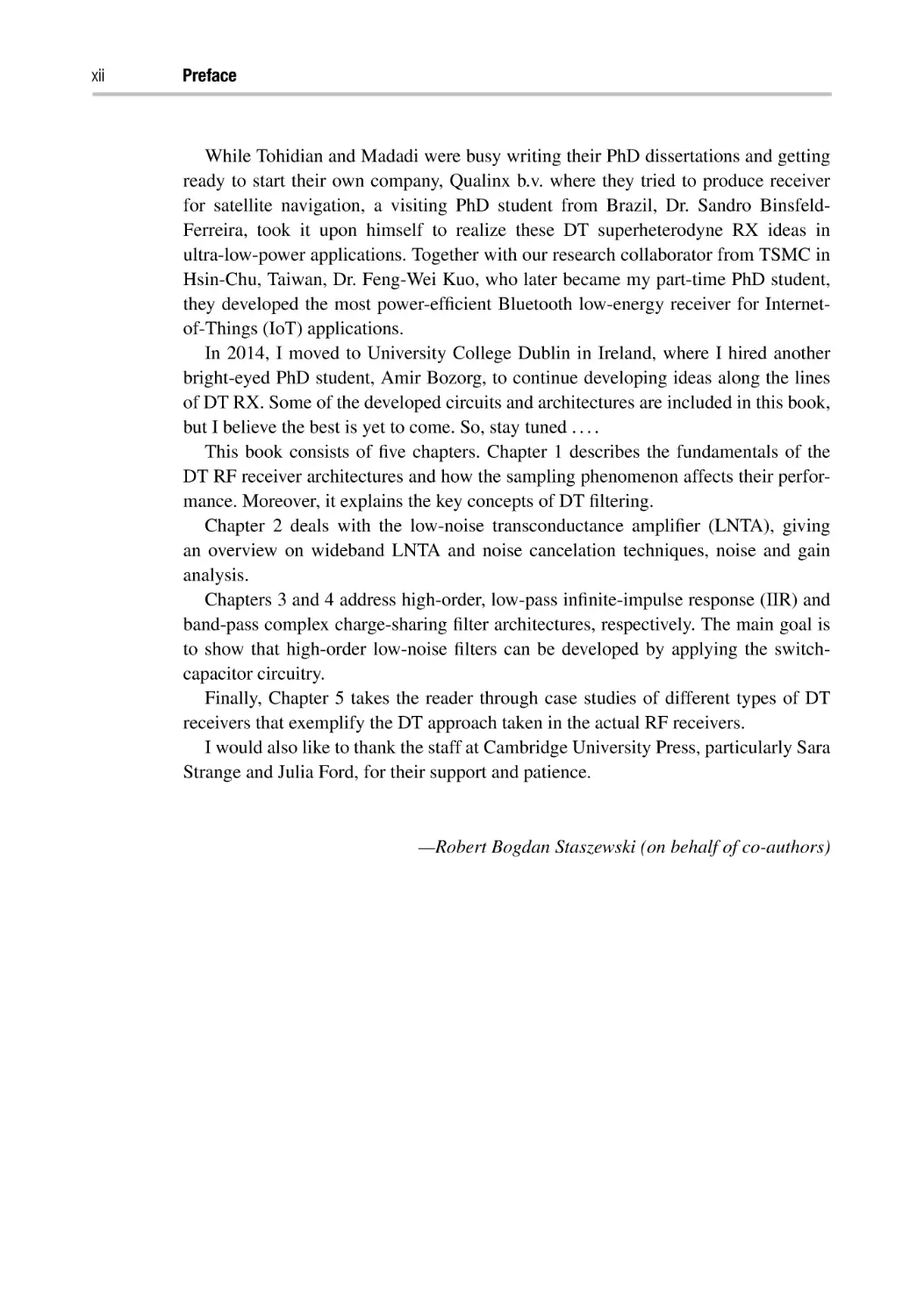
in Fig. 1.1, from 180 to 28 nm CMOS, the VDD supply is reduced more than 30%
while the MOS threshold voltage (Vth ) has not changed considerably. Therefore, the
precious available voltage headroom for RF/analog design is now reduced dramatically [2]. Considering also the reduced MOS intrinsic gain [2] and its saturation
linearity in scaled CMOS [3], continuous-time (CT) RF/analog design is becoming
generally more difficult. In this way, the power consumption and area of the traditional
RF/analog designs are not directly process scalable.
On the other hand, the majority of cellular and wireless standard frequency bands
are allocated from 400 MHz to 6 GHz, and have not significantly changed for many
years. Meanwhile, the transistor cutoff frequency (fT ) has improved dramatically with
scaling, as shown in Fig. 1.1. For example, the period from 1999 to 2011 has seen fT
increasing from 20 GHz in 0.35 μm to more than 400 GHz in 28 nm process. This
suggests that conventional CT techniques that were optimized for the older technology
do not effectively use the ultrahigh speed of transistors of scaled CMOS to improve
the performance of RF/analog designs.
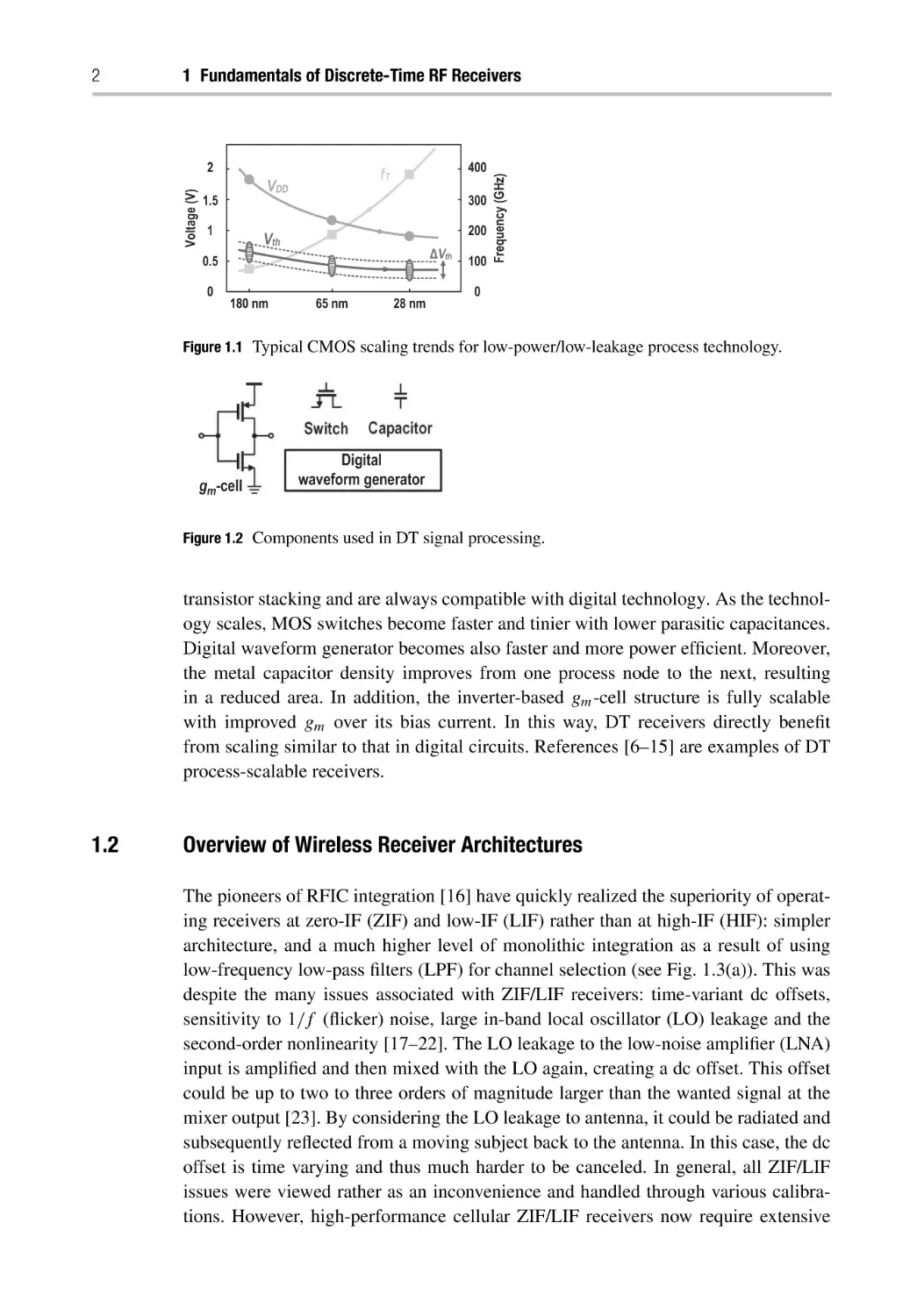
In contrast, the newly introduced discrete-time (DT) RF/analog blocks (Fig. 1.2)
avoid using complicated traditional analog components such as opamps, and most
of signal processing and filtering are done using passive switched-capacitor circuits
[4, 5]. Waveforms required for driving the switches are also generated using digital
logic. To provide signal gain, DT techniques use inverter-based gm -cells that avoid
1 Fundamentals of Discrete-Time RF Receivers
Voltage (V)
2
400
fT
VDD
1.5
300
1
200
Vth
ΔVth
0.5
0
180 nm
65 nm
28 nm
100
Frequency (GHz)
2
0
Figure 1.1 Typical CMOS scaling trends for low-power/low-leakage process technology.
gm-cell
Digital
waveform generator
Figure 1.2 Components used in DT signal processing.
transistor stacking and are always compatible with digital technology. As the technology scales, MOS switches become faster and tinier with lower parasitic capacitances.
Digital waveform generator becomes also faster and more power efficient. Moreover,
the metal capacitor density improves from one process node to the next, resulting
in a reduced area. In addition, the inverter-based gm -cell structure is fully scalable
with improved gm over its bias current. In this way, DT receivers directly benefit
from scaling similar to that in digital circuits. References [6–15] are examples of DT
process-scalable receivers.
1.2
Overview of Wireless Receiver Architectures
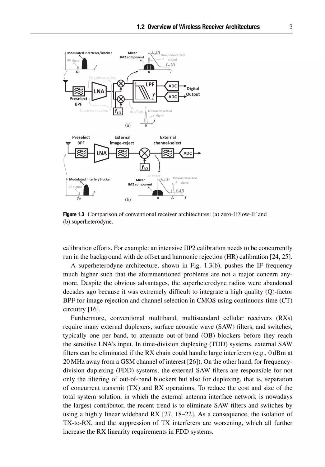
The pioneers of RFIC integration [16] have quickly realized the superiority of operating receivers at zero-IF (ZIF) and low-IF (LIF) rather than at high-IF (HIF): simpler
architecture, and a much higher level of monolithic integration as a result of using
low-frequency low-pass filters (LPF) for channel selection (see Fig. 1.3(a)). This was
despite the many issues associated with ZIF/LIF receivers: time-variant dc offsets,
sensitivity to 1/f (flicker) noise, large in-band local oscillator (LO) leakage and the
second-order nonlinearity [17–22]. The LO leakage to the low-noise amplifier (LNA)
input is amplified and then mixed with the LO again, creating a dc offset. This offset
could be up to two to three orders of magnitude larger than the wanted signal at the
mixer output [23]. By considering the LO leakage to antenna, it could be radiated and
subsequently reflected from a moving subject back to the antenna. In this case, the dc
offset is time varying and thus much harder to be canceled. In general, all ZIF/LIF
issues were viewed rather as an inconvenience and handled through various calibrations. However, high-performance cellular ZIF/LIF receivers now require extensive
1.2 Overview of Wireless Receiver Architectures
S1/f( f )
Mixer
IM2 component
Modulated interferer/Blocker
RF signal
f
fRF
3
Downconverted
signal
S Th ( f )
f
0
Parasitic coupling
LPF
ADC
f
ADC
LNA
Preselect
BPF
Substrate coupling
fLO
Digital
Output
Downconverted
signal
dc offset
f
(a)
Preselect
BPF
0
External
image-reject
External
channel-select
LNA
ADC
fLO
Modulated interfer/Blocker
RF signal
dc offset
S1/f ( f ) Downconverted
Mixer
signal
IM2 component
STh( f )
f
fRF
(b)
0
fIF
f
Figure 1.3 Comparison of conventional receiver architectures: (a) zero-IF/low-IF and
(b) superheterodyne.
calibration efforts. For example: an intensive IIP2 calibration needs to be concurrently
run in the background with dc offset and harmonic rejection (HR) calibration [24, 25].
A superheterodyne architecture, shown in Fig. 1.3(b), pushes the IF frequency
much higher such that the aforementioned problems are not a major concern anymore. Despite the obvious advantages, the superheterodyne radios were abandoned
decades ago because it was extremely difficult to integrate a high quality (Q)-factor
BPF for image rejection and channel selection in CMOS using continuous-time (CT)
circuitry [16].
Furthermore, conventional multiband, multistandard cellular receivers (RXs)
require many external duplexers, surface acoustic wave (SAW) filters, and switches,
typically one per band, to attenuate out-of-band (OB) blockers before they reach
the sensitive LNA’s input. In time-division duplexing (TDD) systems, external SAW
filters can be eliminated if the RX chain could handle large interferers (e.g., 0 dBm at
20 MHz away from a GSM channel of interest [26]). On the other hand, for frequencydivision duplexing (FDD) systems, the external SAW filters are responsible for not
only the filtering of out-of-band blockers but also for duplexing, that is, separation
of concurrent transmit (TX) and RX operations. To reduce the cost and size of the
total system solution, in which the external antenna interface network is nowadays
the largest contributor, the recent trend is to eliminate SAW filters and switches by
using a highly linear wideband RX [27, 18–22]. As a consequence, the isolation of
TX-to-RX, and the suppression of TX interferers are worsening, which all further
increase the RX linearity requirements in FDD systems.
4
1 Fundamentals of Discrete-Time RF Receivers
The resulting reduction in out-of-band filtering implies tough IIP2 requirements
(e.g., 90 dBm [25, 22]) for ZIF and LIF receivers. The IIP2 performance of such
receivers depends mainly on the second-order nonlinearity of LNA and RF mixer in
the receiver chain, as shown in Fig. 1.3(a). Since the typical IIP2 of an RF mixer is
between 50 and 70 dB [28], ZIF/LIF receivers require highly sophisticated calibration
algorithms [29–33, 22, 34] to be frequently executed to account for variations in, VDD ,
[19, 35, 36, 24, 37, 38], process corner [38], temperature [39], mixer transistor’s gate
bias [35], RF blocker frequency [33, 36–38], LO frequency [36–38], LO power [38],
and channel frequency [39]. Also, the IIP2 calibration time is rather very slow to find
optimum setting for the mixer, and it needs to be run repeatedly due to environmental
and operational changes [35].
Most of the filtering and amplification in a zero-IF receiver are done after the
mixer, at low frequency. In CMOS implementations, the flicker noise of devices at
low frequencies corrupts the wanted signal, leading to a higher noise figure (NF)
of the receiver. In contrast, filtering and amplification in a superheterodyne are done
normally at higher frequencies than the device’s flicker corner.
Superheterodyne or HIF architectures, on the other hand, can have a theoretically
infinite IIP2. As shown in Fig. 1.3(b), the desired signal and modulated blocker at the
RF input will be downconverted to a higher IF and dc, respectively; thus the modulated
blocker can be completely filtered out by a band-pass filter (BPF) [40, 41]. For this
reason, there is an increasing interest in uncalibrated high-IIP2 SAW-less superheterodyne RXs with integrated blocker-tolerant BPFs that are amenable to CMOS scaling.
1.3
Discrete-Time Concepts
1.3.1
Direct-Sampling Mixer
The basic idea of the current-mode direct-sampling mixer [42, 43] is illustrated in
Fig. 1.4(a). The low-noise transconductance amplifier (LNTA) converts the received
RF voltage vRF into iRF in current domain through the transconductance gain gm .
The current iRF gets switched by the half-cycle of the local oscillator (LO) and
gm
gm
iRF
iRF
LO+
LO
LO
LO+
LO-
LOCs +
Cs
(a )
Cs -
(b )
Figure 1.4 Temporal MA operation at RF rate: (a) single-ended and (b) pseudo-differential
configurations.
1.3 Discrete-Time Concepts
5
integrated into the sampling capacitor Cs . Since it is difficult to switch the current at
RF rate, it could be merely redirected to an identical sampler that is operating on the
opposite half-cycle of the LO clock, as shown in Fig. 1.4(b) for a pseudo-differential
configuration.
If the LO oscillating at f0 frequency is synchronous and in phase with the sinusoidal
RF waveform, the voltage gain of a single RF half-cycle is
1 1 gm
·
,
·
π f0 Cs
Gv,RF =
(1.1)
and the accumulated charge on the sampling capacitor is
Gq,RF =
1 1
· gm .
·
π f0
(1.2)
In (1.1) and (1.2), the π1 factor is contributed by the half-cycle sinusoidal integration.
As an example, if gm = 30 mS, Cs = 15.925 pF, and f0 = 2.4 GHz, then Gv,RF = 0.25.
1.3.2
Temporal Moving Average
Continuously accumulating the charge as shown in Fig. 1.4 is not very practical if it
cannot be read out. In addition, a mechanism to prevent the charge overflow is needed.
Both of these operations are accomplished by fixing the integration window length
followed by a charge readout phase that will also discharge the sampling capacitor
such that the next period of integration would start from the same zero condition. The
RF sampling and readout operations are cyclically rotated on both Cs capacitors as
shown in Fig. 1.5. When LOA rectifies N RF cycles that are being integrated on the
first sampling capacitor, LOB is off and the second sampling capacitor charge is being
read out. On the following N RF cycles, the operation is reversed. This way, the charge
integration and readout occur at the same time and no RF cycles are missed.
The sampling capacitor integrates the half-rectified RF current over N cycles. The
charge accumulated on the sampling capacitor and the resulting voltage (V = Q/Cs )
increases with the integration window, thus giving rise to a discrete signal processing
gain of N .
gm
N
LOA
iRF
LOA
LOB
LOB
Cs
Cs
Figure 1.5 Temporal MA operation at RF rate with cyclic charge readout.
1 Fundamentals of Discrete-Time RF Receivers
Frequency response of the temporal MA filters
20
MA7 @RF
MA8 @RF
MA9 @RF
10
Voltage gain (dB)
6
0
−10
−20
−30
−40
0
200
400
600
800
Frequency (MHz)
1000
1200
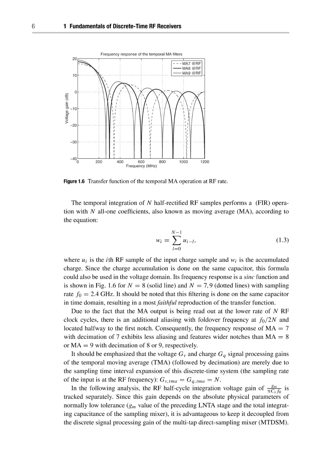
Figure 1.6 Transfer function of the temporal MA operation at RF rate.
The temporal integration of N half-rectified RF samples performs a (FIR) operation with N all-one coefficients, also known as moving average (MA), according to
the equation:
wi =
N−1
ui−l ,
(1.3)
l=0
where ui is the ith RF sample of the input charge sample and wi is the accumulated
charge. Since the charge accumulation is done on the same capacitor, this formula
could also be used in the voltage domain. Its frequency response is a sinc function and
is shown in Fig. 1.6 for N = 8 (solid line) and N = 7,9 (dotted lines) with sampling
rate f0 = 2.4 GHz. It should be noted that this filtering is done on the same capacitor
in time domain, resulting in a most faithful reproduction of the transfer function.
Due to the fact that the MA output is being read out at the lower rate of N RF
clock cycles, there is an additional aliasing with foldover frequency at f0 /2N and
located halfway to the first notch. Consequently, the frequency response of MA = 7
with decimation of 7 exhibits less aliasing and features wider notches than MA = 8
or MA = 9 with decimation of 8 or 9, respectively.
It should be emphasized that the voltage Gv and charge Gq signal processing gains
of the temporal moving average (TMA) (followed by decimation) are merely due to
the sampling time interval expansion of this discrete-time system (the sampling rate
of the input is at the RF frequency): Gv,tma = Gq,tma = N .
In the following analysis, the RF half-cycle integration voltage gain of πCgms f0 is
tracked separately. Since this gain depends on the absolute physical parameters of
normally low tolerance (gm value of the preceding LNTA stage and the total integrating capacitance of the sampling mixer), it is advantageous to keep it decoupled from
the discrete signal processing gain of the multi-tap direct-sampling mixer (MTDSM).
1.3 Discrete-Time Concepts
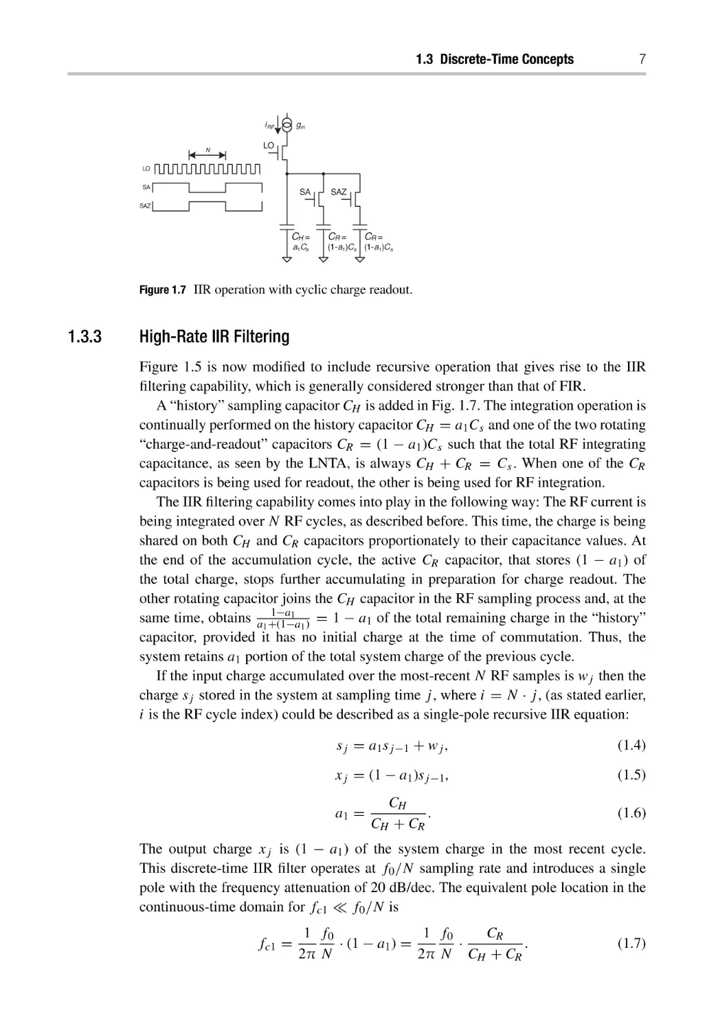
gm
i RF
N
7
LO
LO
SA
SA
SAZ
SAZ
CH =
a1Cs
CR =
CR =
(1-a1)Cs (1-a1)Cs
Figure 1.7 IIR operation with cyclic charge readout.
1.3.3
High-Rate IIR Filtering
Figure 1.5 is now modified to include recursive operation that gives rise to the IIR
filtering capability, which is generally considered stronger than that of FIR.
A “history” sampling capacitor CH is added in Fig. 1.7. The integration operation is
continually performed on the history capacitor CH = a1 Cs and one of the two rotating
“charge-and-readout” capacitors CR = (1 − a1 )Cs such that the total RF integrating
capacitance, as seen by the LNTA, is always CH + CR = Cs . When one of the CR
capacitors is being used for readout, the other is being used for RF integration.
The IIR filtering capability comes into play in the following way: The RF current is
being integrated over N RF cycles, as described before. This time, the charge is being
shared on both CH and CR capacitors proportionately to their capacitance values. At
the end of the accumulation cycle, the active CR capacitor, that stores (1 − a1 ) of
the total charge, stops further accumulating in preparation for charge readout. The
other rotating capacitor joins the CH capacitor in the RF sampling process and, at the
1−a1
= 1 − a1 of the total remaining charge in the “history”
same time, obtains a1 +(1−a
1)
capacitor, provided it has no initial charge at the time of commutation. Thus, the
system retains a1 portion of the total system charge of the previous cycle.
If the input charge accumulated over the most-recent N RF samples is wj then the
charge sj stored in the system at sampling time j , where i = N · j , (as stated earlier,
i is the RF cycle index) could be described as a single-pole recursive IIR equation:
sj = a1 sj −1 + wj ,
(1.4)
xj = (1 − a1 )sj −1,
(1.5)
a1 =
CH
.
CH + CR
(1.6)
The output charge xj is (1 − a1 ) of the system charge in the most recent cycle.
This discrete-time IIR filter operates at f0 /N sampling rate and introduces a single
pole with the frequency attenuation of 20 dB/dec. The equivalent pole location in the
continuous-time domain for fc1 f0 /N is
fc1 =
1 f0
1 f0
CR
.
· (1 − a1 ) =
·
2π N
2π N CH + CR
(1.7)
8
1 Fundamentals of Discrete-Time RF Receivers
Since there is no sampling time expansion for the IIR operation, the discrete signal
processing charge gain is one. In other words, due to the charge conservation principle,
the input charge per sample interval is on average the same as the output charge. For
the voltage gain, however, there is an impedance transformation of Cinput = Cs and
Coutput = (1 − a1 )Cs , thus resulting in a gain.
Gq,iir1 = 1,
(1.8)
1
CH + CR
=
.
1 − a1
CR
Gv,iir1 =
(1.9)
As an example, the IIR filtering with a single coefficient of a1 = 0.9686, placing the
pole at fc1 = 1.5 MHz (CR = 0.5 pF, CH = 15.425 pF) is performed at f0 /N =
2.4 GHz / 8 = 300 MHz sampling rate, and it follows the FIR MA = 8 filtering of
the input at f0 RF sampling rate. The voltage gain of the high-rate IIR filter is 31.85
(30.06 dB).
1.3.4
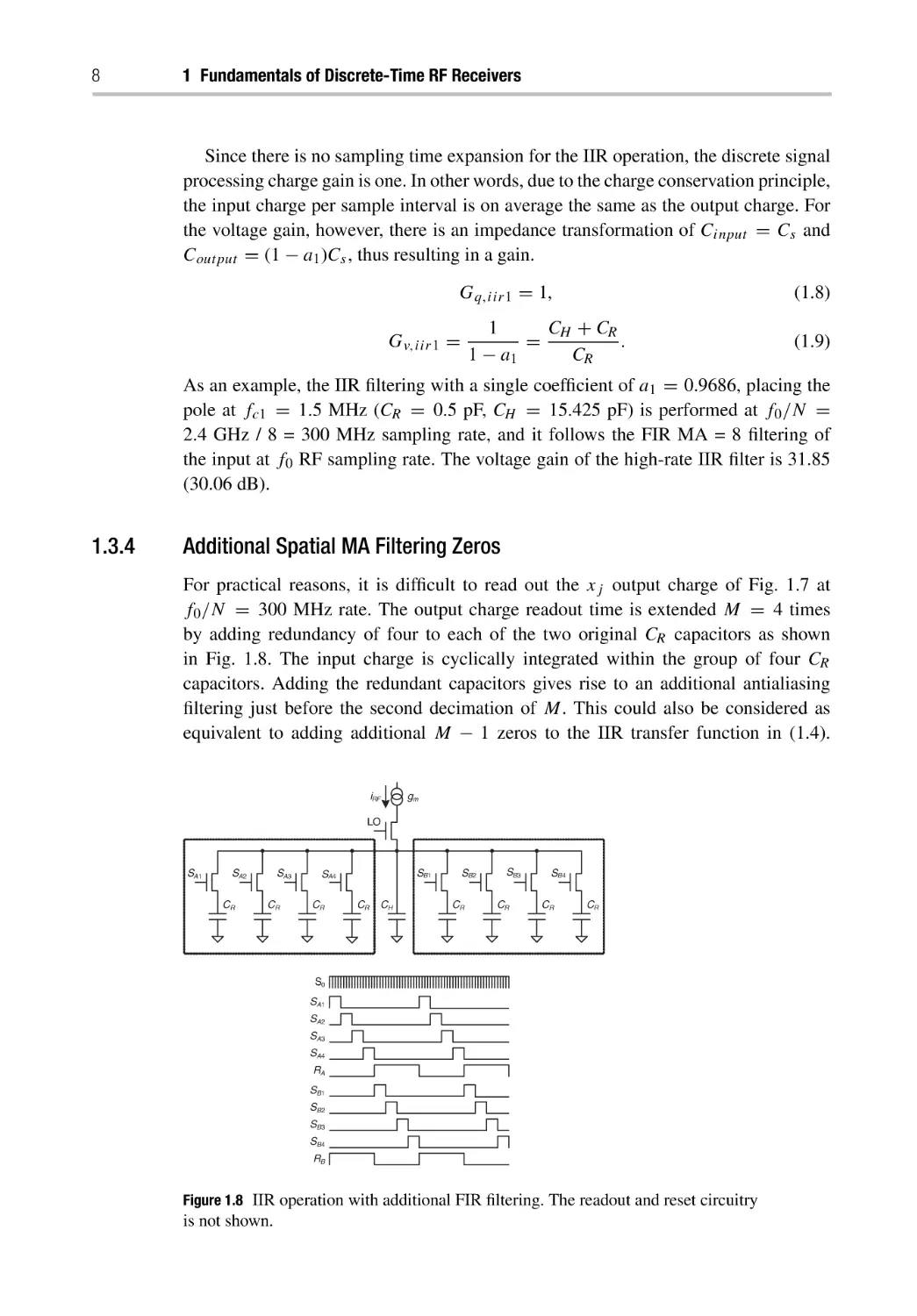
Additional Spatial MA Filtering Zeros
For practical reasons, it is difficult to read out the xj output charge of Fig. 1.7 at
f0 /N = 300 MHz rate. The output charge readout time is extended M = 4 times
by adding redundancy of four to each of the two original CR capacitors as shown
in Fig. 1.8. The input charge is cyclically integrated within the group of four CR
capacitors. Adding the redundant capacitors gives rise to an additional antialiasing
filtering just before the second decimation of M. This could also be considered as
equivalent to adding additional M − 1 zeros to the IIR transfer function in (1.4).
iRF
gm
LO
SA1
SA2
CR
SA3
CR
SB1
SA4
CR
CR
CH
SB2
CR
SB3
CR
SB4
CR
CR
S0
SA1
SA2
SA3
SA4
RA
SB1
SB2
SB3
SB4
RB
Figure 1.8 IIR operation with additional FIR filtering. The readout and reset circuitry
is not shown.
1.3 Discrete-Time Concepts
9
After the first bank of four capacitors gets charged (SA1 − SA4 in Fig. 1.8), the
second bank (SB1 − SB4 ) is in the process of being charged and the charge on the
first bank of capacitors is summed and read out (R1 ). Physically connecting together
the four capacitors performs an FIR filtering described as the spatial moving average
of M = 4:
yk =
M−1
(1.10)
xk−l ,
l=0
where yk is the output charge and sampling time index j = M · k. RA and RB in
Fig. 1.8 are the readout/reset cycles during which the output charge on the four nonsampling capacitors is transferred out, and the remnant charge is reset before the
capacitors are put back into the sampling operation. It should be noted that after the
reset phase, but before the sampling phase, the capacitors are unobtrusively precharged
[44] in order to implement a dc-offset cancelation or to accomplish a feedback summation for the loop operation.
Since the charge of four capacitors is added, there is a charge gain of M = 4 and a
voltage gain of 1. Again, as explained before, the charge gain is due to the sampling
interval expansion: Gq,sma = M and Gv,sma = 1.
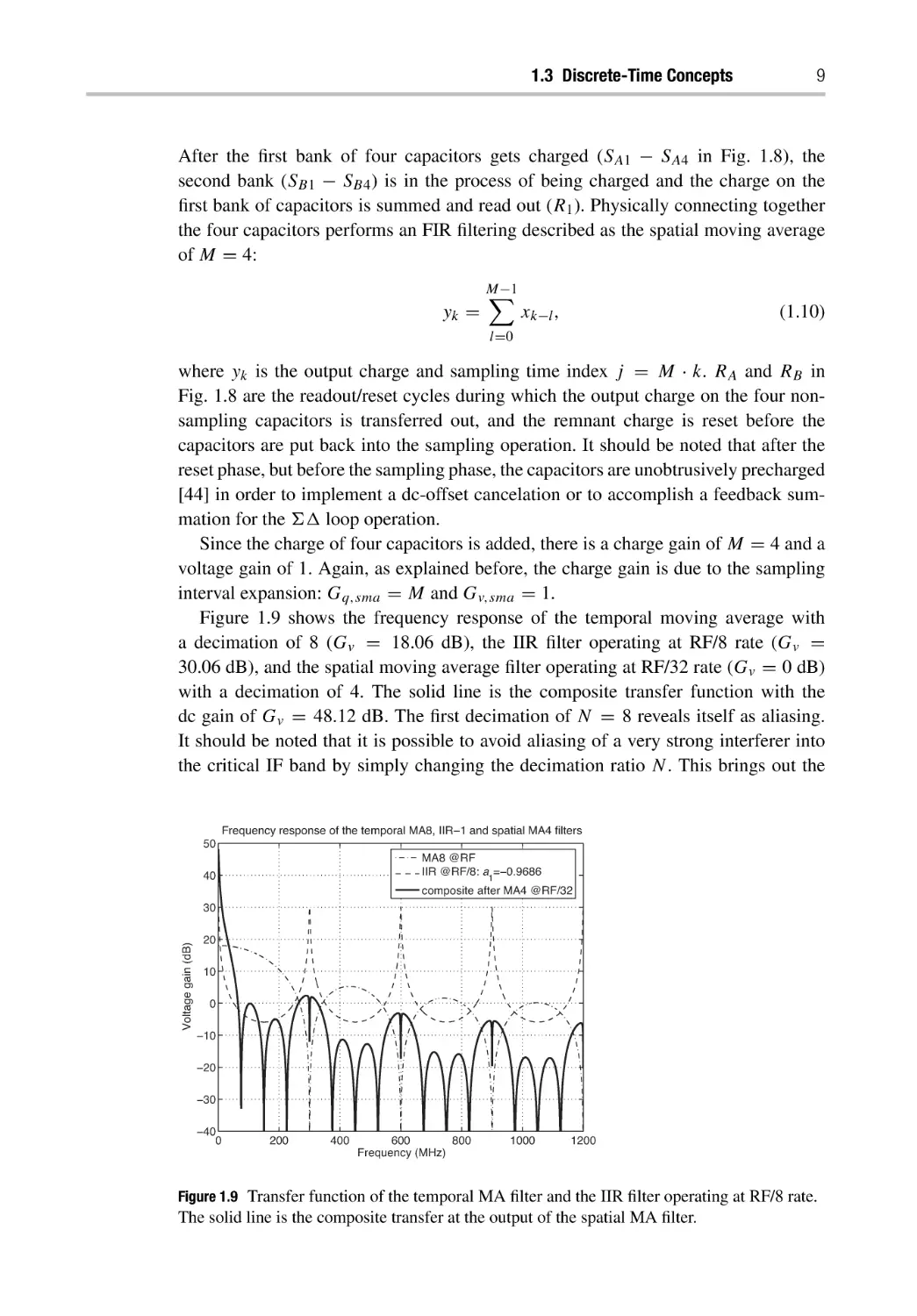
Figure 1.9 shows the frequency response of the temporal moving average with
a decimation of 8 (Gv = 18.06 dB), the IIR filter operating at RF/8 rate (Gv =
30.06 dB), and the spatial moving average filter operating at RF/32 rate (Gv = 0 dB)
with a decimation of 4. The solid line is the composite transfer function with the
dc gain of Gv = 48.12 dB. The first decimation of N = 8 reveals itself as aliasing.
It should be noted that it is possible to avoid aliasing of a very strong interferer into
the critical IF band by simply changing the decimation ratio N . This brings out the
Frequency response of the temporal MA8, IIR−1 and spatial MA4 filters
50
MA8 @RF
IIR @RF/8: a =−0.9686
40
1
composite after MA4 @RF/32
Voltage gain (dB)
30
20
10
0
−10
−20
−30
−40
0
200
400
800
600
Frequency (MHz)
1000
1200
Figure 1.9 Transfer function of the temporal MA filter and the IIR filter operating at RF/8 rate.
The solid line is the composite transfer at the output of the spatial MA filter.
10
1 Fundamentals of Discrete-Time RF Receivers
Q output
-
D
+
Qinput
M *C R
MTDSM
Output
CB
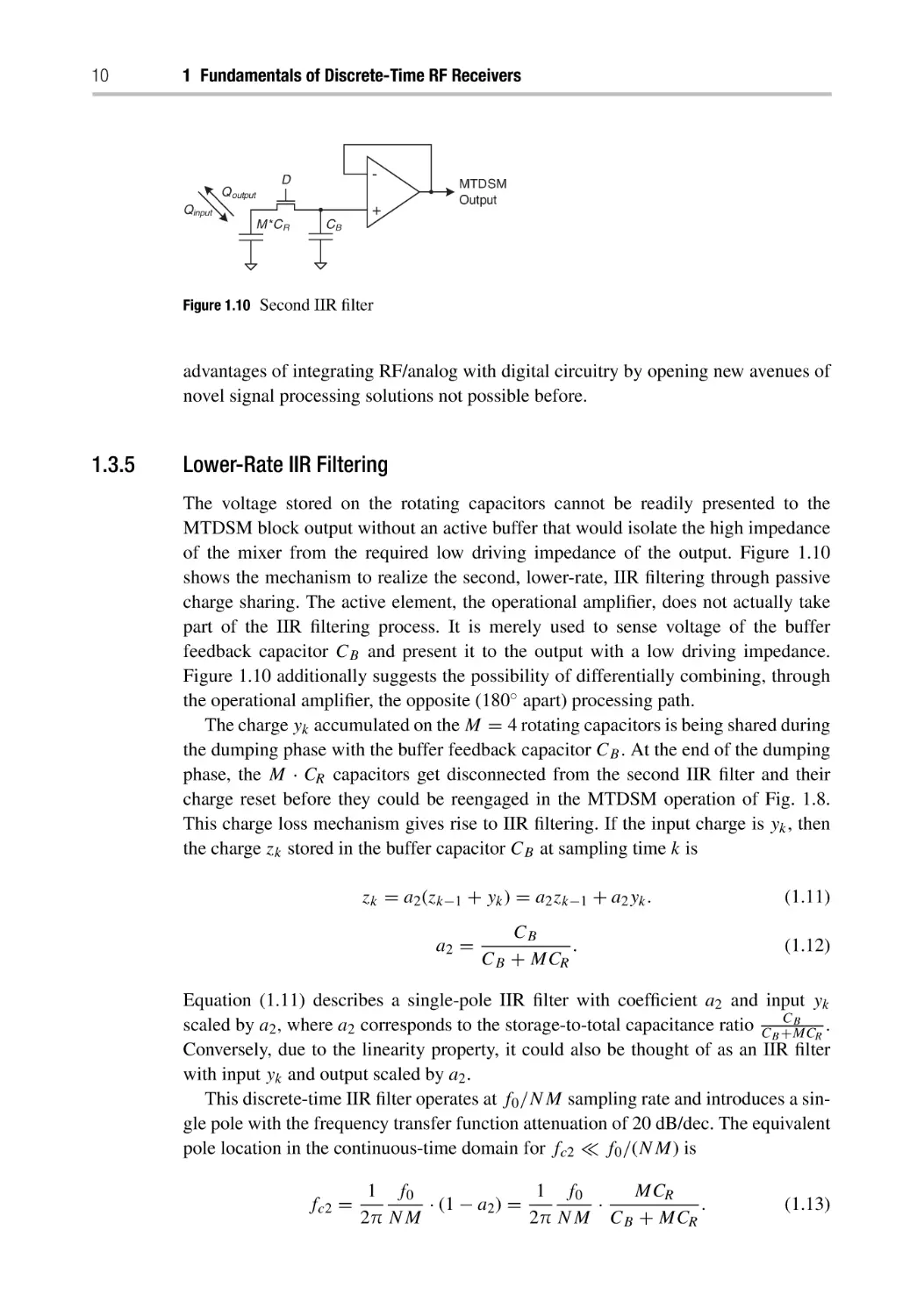
Figure 1.10 Second IIR filter
advantages of integrating RF/analog with digital circuitry by opening new avenues of
novel signal processing solutions not possible before.
1.3.5
Lower-Rate IIR Filtering
The voltage stored on the rotating capacitors cannot be readily presented to the
MTDSM block output without an active buffer that would isolate the high impedance
of the mixer from the required low driving impedance of the output. Figure 1.10
shows the mechanism to realize the second, lower-rate, IIR filtering through passive
charge sharing. The active element, the operational amplifier, does not actually take
part of the IIR filtering process. It is merely used to sense voltage of the buffer
feedback capacitor CB and present it to the output with a low driving impedance.
Figure 1.10 additionally suggests the possibility of differentially combining, through
the operational amplifier, the opposite (180◦ apart) processing path.
The charge yk accumulated on the M = 4 rotating capacitors is being shared during
the dumping phase with the buffer feedback capacitor CB . At the end of the dumping
phase, the M · CR capacitors get disconnected from the second IIR filter and their
charge reset before they could be reengaged in the MTDSM operation of Fig. 1.8.
This charge loss mechanism gives rise to IIR filtering. If the input charge is yk , then
the charge zk stored in the buffer capacitor CB at sampling time k is
zk = a2 (zk−1 + yk ) = a2 zk−1 + a2 yk .
a2 =
CB
.
CB + MCR
(1.11)
(1.12)
Equation (1.11) describes a single-pole IIR filter with coefficient a2 and input yk
CB
scaled by a2 , where a2 corresponds to the storage-to-total capacitance ratio CB +MC
.
R
Conversely, due to the linearity property, it could also be thought of as an IIR filter
with input yk and output scaled by a2 .
This discrete-time IIR filter operates at f0 /NM sampling rate and introduces a single pole with the frequency transfer function attenuation of 20 dB/dec. The equivalent
pole location in the continuous-time domain for fc2 f0 /(N M) is
fc2 =
1 f0
1 f0
MCR
.
· (1 − a2 ) =
·
2π N M
2π N M CB + MCR
(1.13)
1.3 Discrete-Time Concepts
11
The actual MTDSM output is the voltage sensed on the buffer feedback capacitor
zk /CB . The previously used charge stream model cannot be directly applied here
because the “output” charge zk is not the one that leaves the system.
The charge “lost” or reflected back into the M · CR capacitor for subsequent reset
is (1 − a2 )(zk−1 + yk ). Due to the charge conservation principle, the time-averaged
values of charge input, yk , and charge leaked out, (1 − a2 )(zk−1 + yk ), should be
equal. As stated before, the leak-out charge is not the output from the signal processing
standpoint. It should be noted that the amplifier does not contribute to the net charge
change of the system and, consequently, the only path of the charge loss is through the
same M · CR capacitors being reset after the dumping phase.
The output charge zk stops at the IIR-2 stage and does not further propagate;
therefore, it is of less importance for signal processing analysis. The charge discrete
signal processing gain of the second IIR stage is
Gq,iir2 =
a2
CB
=
.
1 − a2
MCR
The input/output impedance transformation is
IIR-2 is unity.
MCR
CB . Consequently,
Gv,iir2 = 1.
1.3.6
(1.14)
the voltage gain of
(1.15)
Cascaded MTDSM Filtering
The cascaded discrete signal processing gain equations of the MTDSM mixer are
Gq,dsp = Gq,tma · Gq,iir1 · Gq,sma · Gq,iir2
CB
=N ·1·M ·
MCR
N CB
.
=
CR
Gv,dsp = Gv,tma · Gv,iir1 · Gv,sma · Gv,iir2
CH + CR
·1·1
=N·
CR
N(CH + CR )
.
=
CR
(1.16)
(1.17)
(1.18)
(1.19)
(1.20)
(1.21)
Including the RF half-cycle integration (1.1 and 1.2) the total single-ended gain is
Gq,tot = Gq,RF · Gq,dsp
1
1
= ·
· gm
π f0 /N
(1.22)
Gv,tot = Gv,RF · Gv,dsp
1
1
gm
= ·
.
·
π f0 /N CR
(1.24)
(1.23)
(1.25)
12
1 Fundamentals of Discrete-Time RF Receivers
Note the similarity between (1.25) and (1.1). In both cases, the term Rsc = fs1Cs is
an equivalent resistance of a switched-capacitor Cs sampling at rate fs . For example,
if fs = 300 MHz and CR = 0.5 pF, then the equivalent resistance is Rsc = 6.7 k.
Since the MTDSM output is differential, the gain values in (1.23)–(1.25) are actually
doubled.
The dc-frequency gain Gv,tot in (1.25) requires further elaboration. The gain
depends only on the gm of the LNTA stage, rotating capacitor value, and the rotation
frequency. Amazingly, it does not depend on the other capacitor values, which
contribute only to the filtering transfer function at higher frequencies.
1.3.7
Near-Frequency Interferer Attenuation
Most of the lower-frequency filtering could be realistically done only with the first and
second IIR filters. The two FIR filters do not have appreciable filtering capability at
low frequencies and are mainly used for antialiasing.
It should be noted that the best filtering could be accomplished by making 3 dB
corner frequency of both IIR filters the same and placing them as close to the higher
end of the signal band as possible.
fc1 = fc2 .
(1.26)
CB = CH − (M − 1)CR .
(1.27)
This gives the following constraint:
1.3.8
Signal Processing Example
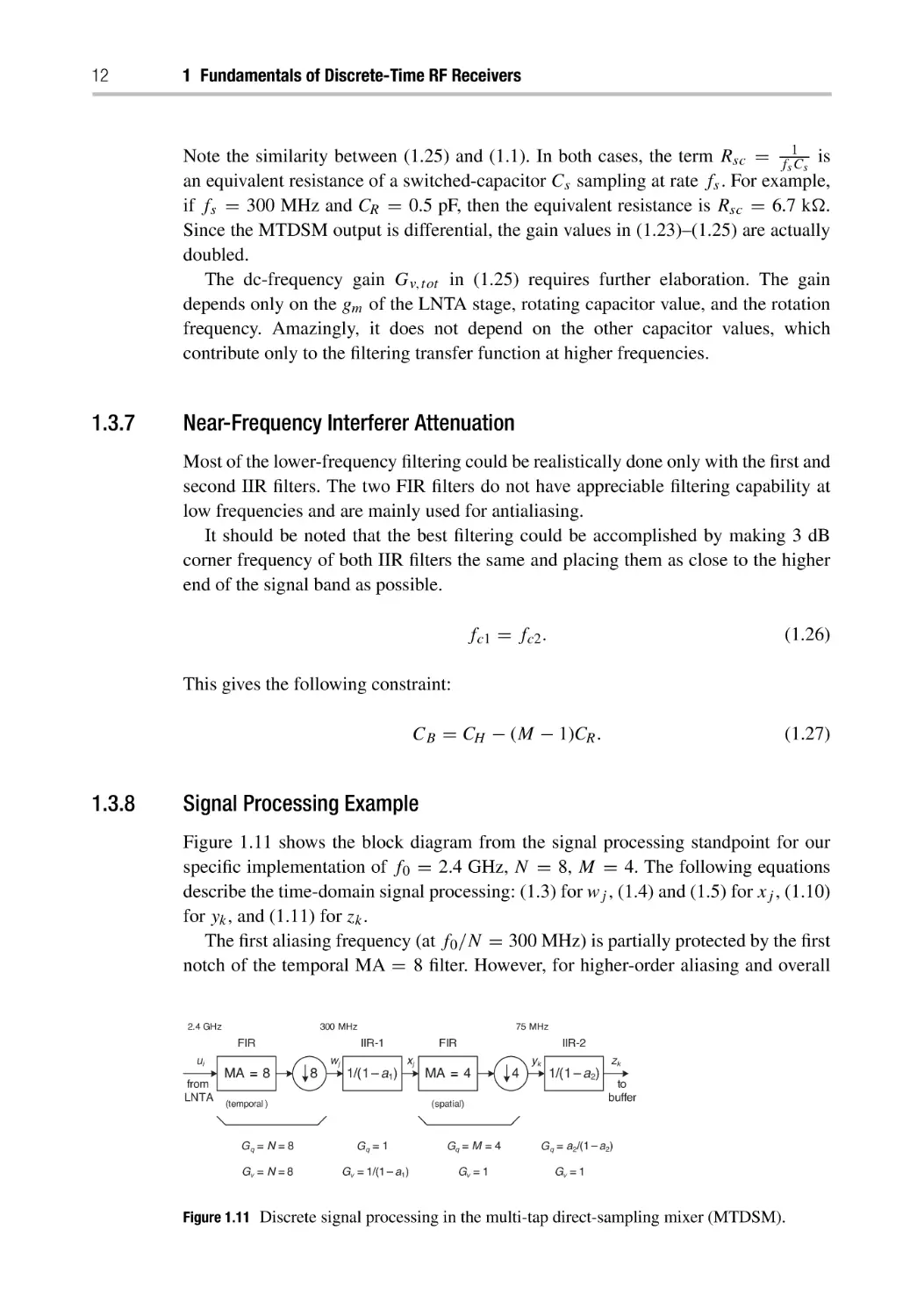
Figure 1.11 shows the block diagram from the signal processing standpoint for our
specific implementation of f0 = 2.4 GHz, N = 8, M = 4. The following equations
describe the time-domain signal processing: (1.3) for wj , (1.4) and (1.5) for xj , (1.10)
for yk , and (1.11) for zk .
The first aliasing frequency (at f0 /N = 300 MHz) is partially protected by the first
notch of the temporal MA = 8 filter. However, for higher-order aliasing and overall
2.4 GH z
300 MH z
FIR
ui
from
LNTA
75 MH z
IIR-1
wj
MA = 8
8
FIR
IIR-2
xj
1/(1 – a1)
(temporal )
yk
MA = 4
4
zk
1/(1 – a2)
(spatial)
Gq = N = 8
Gq = 1
Gq = M = 4
Gv = N = 8
Gv = 1/(1 – a1)
Gv = 1
to
buffer
Gq = a2/(1 – a2)
Gv = 1
Figure 1.11 Discrete signal processing in the multi-tap direct-sampling mixer (MTDSM).
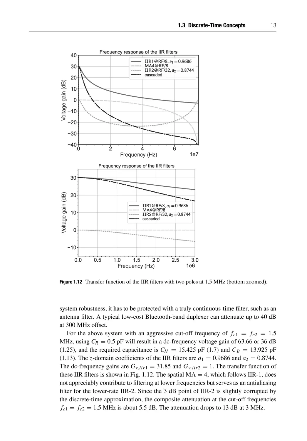
13
Voltage gain (dB)
1.3 Discrete-Time Concepts
Voltage gain (dB)
Frequency (Hz)
Frequency (Hz)
Figure 1.12 Transfer function of the IIR filters with two poles at 1.5 MHz (bottom zoomed).
system robustness, it has to be protected with a truly continuous-time filter, such as an
antenna filter. A typical low-cost Bluetooth-band duplexer can attenuate up to 40 dB
at 300 MHz offset.
For the above system with an aggressive cut-off frequency of fc1 = fc2 = 1.5
MHz, using CR = 0.5 pF will result in a dc-frequency voltage gain of 63.66 or 36 dB
(1.25), and the required capacitance is CH = 15.425 pF (1.7) and CB = 13.925 pF
(1.13). The z-domain coefficients of the IIR filters are a1 = 0.9686 and a2 = 0.8744.
The dc-frequency gains are Gv,iir1 = 31.85 and Gv,iir2 = 1. The transfer function of
these IIR filters is shown in Fig. 1.12. The spatial MA = 4, which follows IIR-1, does
not appreciably contribute to filtering at lower frequencies but serves as an antialiasing
filter for the lower-rate IIR-2. Since the 3 dB point of IIR-2 is slightly corrupted by
the discrete-time approximation, the composite attenuation at the cut-off frequencies
fc1 = fc2 = 1.5 MHz is about 5.5 dB. The attenuation drops to 13 dB at 3 MHz.
1 Fundamentals of Discrete-Time RF Receivers
Phase (rad)
14
Frequency (Hz)
Figure 1.13 Phase response the IIR filters with two poles at 1.5 MHz.
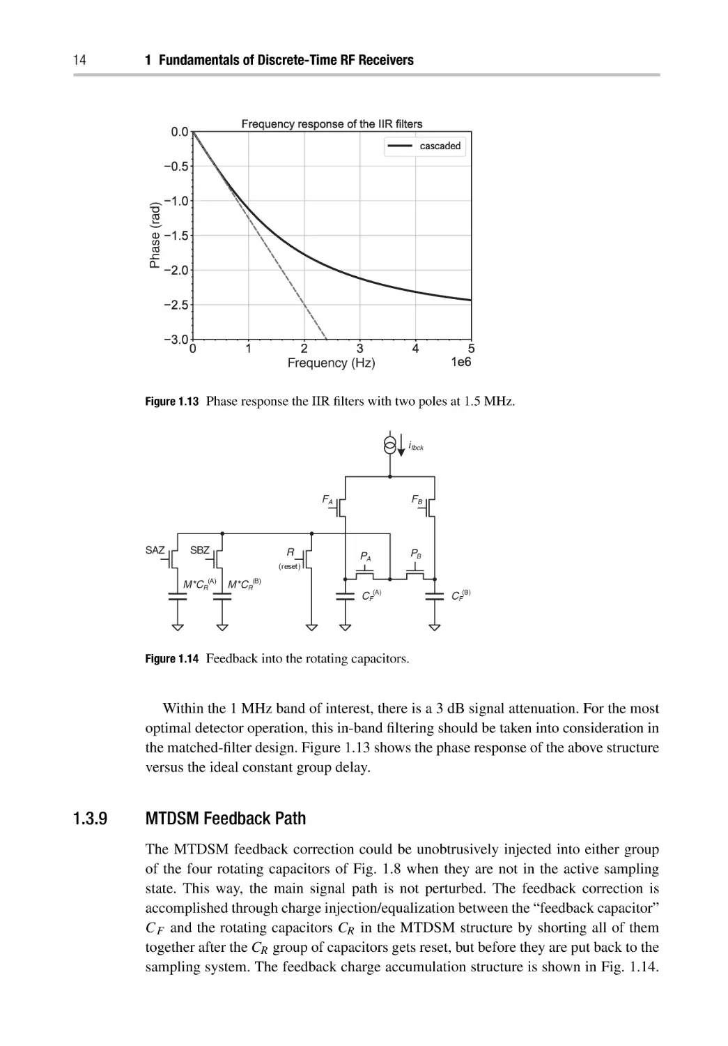
i fbck
FA
SAZ
SBZ
R
FB
PA
PB
(reset)
M *CR(A)
M *CR(B)
CF(A)
CF(B)
Figure 1.14 Feedback into the rotating capacitors.
Within the 1 MHz band of interest, there is a 3 dB signal attenuation. For the most
optimal detector operation, this in-band filtering should be taken into consideration in
the matched-filter design. Figure 1.13 shows the phase response of the above structure
versus the ideal constant group delay.
1.3.9
MTDSM Feedback Path
The MTDSM feedback correction could be unobtrusively injected into either group
of the four rotating capacitors of Fig. 1.8 when they are not in the active sampling
state. This way, the main signal path is not perturbed. The feedback correction is
accomplished through charge injection/equalization between the “feedback capacitor”
CF and the rotating capacitors CR in the MTDSM structure by shorting all of them
together after the CR group of capacitors gets reset, but before they are put back to the
sampling system. The feedback charge accumulation structure is shown in Fig. 1.14.
1.4 DT ZIF Receiver: 1× and 2× Sampling
15
Each feedback capacitor CF is associated with one of the two rotating capacitor of
group “A” and “B.” The two groups commutate the charging process.
Voltage on the feedback capacitor can be calculated as follows. Charging the feedback capacitor CF with the current if bck for the duration of T will result in incremental accumulation of Qin = if bck · T charge. This charge gets added to the total
charge QF (k) of the feedback capacitor at the kth time instance.
QF (k) = QF (k − 1) + Qin = QF (k − 1) + if bck · T .
(1.28)
During the charge distribution moment, the feedback capacitor gets connected with
the previously reset group of rotating capacitors M · CR . The charge depleted from CF
is dependent on the relative capacitor values.
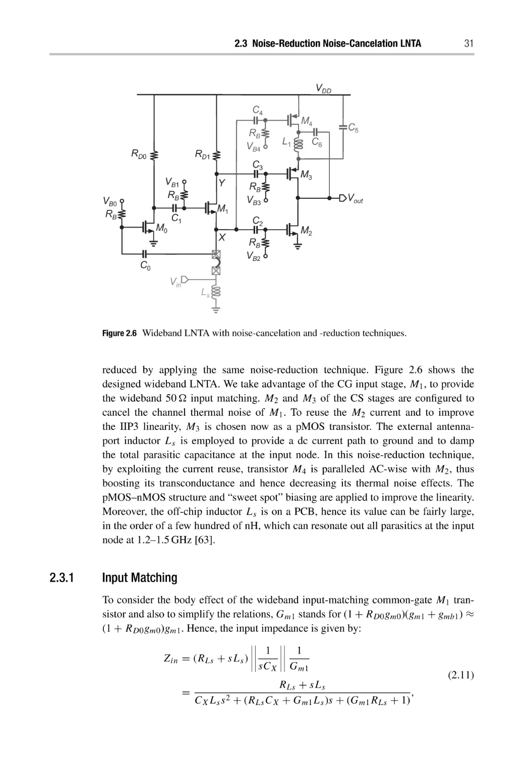
Qout (k) =
MCR
QF (k).
CF + MCR
(1.29)
The charge transferred to the rotating capacitors is proportional to the total accumulated charge QF or voltage on the feedback capacitor VF = QF /CF . At first, the
accumulated charge is small, so the outgoing charge is small. Since the incoming
charge is constant, the QF charge will continue accumulating until the net charge
intake becomes zero. Equilibrium is reached when Qin (k) = Qout (k).
if bck · T =
MCR
QF (k).
CF + MCR
(1.30)
Transformation of (1.28), (1.29), and (1.30) gives the equilibrium voltage.
VF,eq = if bck · T ·
CF + MCR
.
CF · MCR
(1.31)
The Qout,eq charge transfer into the rotating capacitors at equilibrium will create
voltage on the bank of rotating capacitors.
VR =
if bck · T
.
MCR
(1.32)
As shown in Section 1.3.5, the voltage transfer function from the rotating capacitors
to the history capacitor is unity. Therefore, the bias voltage developed on CH is
VH =
1.4
if bck · T
.
MCR
(1.33)
DT ZIF Receiver: 1× and 2× Sampling
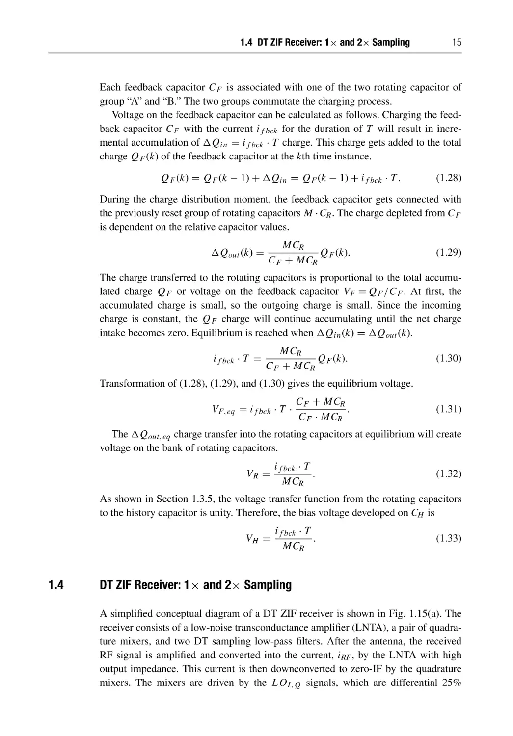
A simplified conceptual diagram of a DT ZIF receiver is shown in Fig. 1.15(a). The
receiver consists of a low-noise transconductance amplifier (LNTA), a pair of quadrature mixers, and two DT sampling low-pass filters. After the antenna, the received
RF signal is amplified and converted into the current, iRF , by the LNTA with high
output impedance. This current is then downconverted to zero-IF by the quadrature
mixers. The mixers are driven by the LOI,Q signals, which are differential 25%
16
1 Fundamentals of Discrete-Time RF Receivers
ϕ
ϕ
ϕ
ϕ
ϕ
ϕ
Windowed integration,
Sampling and low-pass filter
(a)
1/fLO
1/fs
Ti
(b)
Figure 1.15 (a) A simple DT receiver with passive LPF; and (b) its waveforms at various nodes.
duty-cycle clocks with a 90 phase shift. Considering a narrow-band modulated RF
signal, Fig. 1.15(b) shows the signal waveforms at various stages. The current leaving the mixers is integrated over a time window Ti and sampled in the form of DT
charge packets [45], qI,Q [n]. This DT data is then low-pass filtered by a passive
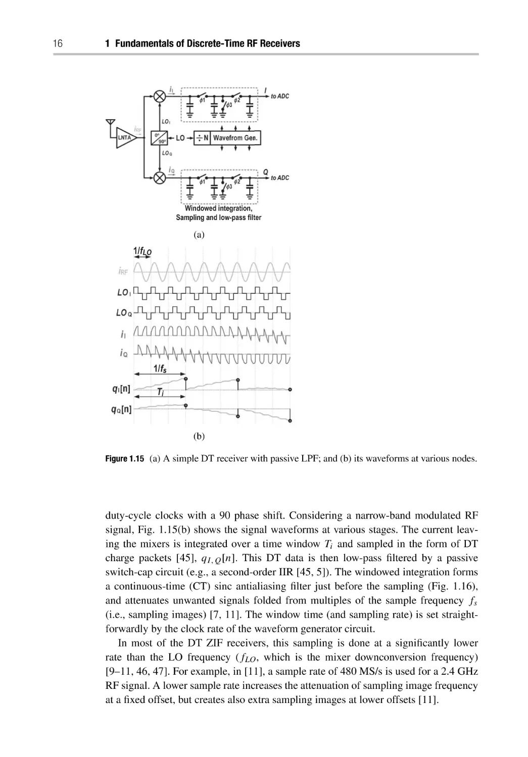
switch-cap circuit (e.g., a second-order IIR [45, 5]). The windowed integration forms
a continuous-time (CT) sinc antialiasing filter just before the sampling (Fig. 1.16),
and attenuates unwanted signals folded from multiples of the sample frequency fs
(i.e., sampling images) [7, 11]. The window time (and sampling rate) is set straightforwardly by the clock rate of the waveform generator circuit.
In most of the DT ZIF receivers, this sampling is done at a significantly lower
rate than the LO frequency (fLO , which is the mixer downconversion frequency)
[9–11, 46, 47]. For example, in [11], a sample rate of 480 MS/s is used for a 2.4 GHz
RF signal. A lower sample rate increases the attenuation of sampling image frequency
at a fixed offset, but creates also extra sampling images at lower offsets [11].
Impulse
response
1.4 DT ZIF Receiver: 1× and 2× Sampling
17
Freq
response
Ti =1/fs
fs
2fs
3fs
Figure 1.16 Impulse and frequency response of windowed integration.
Windowed integration
& charge sampling
Figure 1.17 Signal sampling in a DT receiver.
1.4.1
1× Sampling in Zero-IF
For the time being, the signal sampling in a DT receiver with the simplified structure of
Fig. 1.17 is our focus. Consider the case of a ZIF reception where the signal is sampled
at the same rate as the LO frequency [10], hereafter called 1× sampling. Drawn in
Fig. 1.18(a), the narrow-band modulated current signal iRF is downconverted as iI
and iQ baseband quadrature currents, windowed integrated (WI), and then sampled in
the form of charge packets, qI n and qQn , at the end of each LO cycle.
A ZIF architecture with 1× sampling has image frequencies at multiples of LO
frequency. Figure 1.18(b) shows the frequency translation. The wanted RF signal is
downconverted to dc by mixing with the quadrature LO (black tone). At the same time,
the frequency bands near zero and 2fLO are translated to ±fLO . The windowed integration of iI Q and sampling forms a continuous-time (CT) antialiasing filter (shown
in green), with its notches coinciding with the sampling images. The narrower the
required bandwidth, the stronger the image attenuation [11]. After the sampling, the
attenuated images at multiples of ±fs are folded over the wanted signal at baseband.
18
1 Fundamentals of Discrete-Time RF Receivers
1/fLO
1/fS
qI[n]
qQ[n]
(a)
LO
RF
Input
spectrum
Windowed
integration
Downconverted
Image
Image
Folding
due to sampling
Good image rejection
for narrow-band ZIF
Sampling
2 fs
fs
fLO
Downconversion
fs/2
fs/2
fs
2 fs
(b)
Figure 1.18 (a) Time-domain signal waveforms and (b) frequency translation in a 1× sampling
zero-IF DT receiver: input spectrum is shifted to right (RF downconversion) and after
windowed integration is sampled.
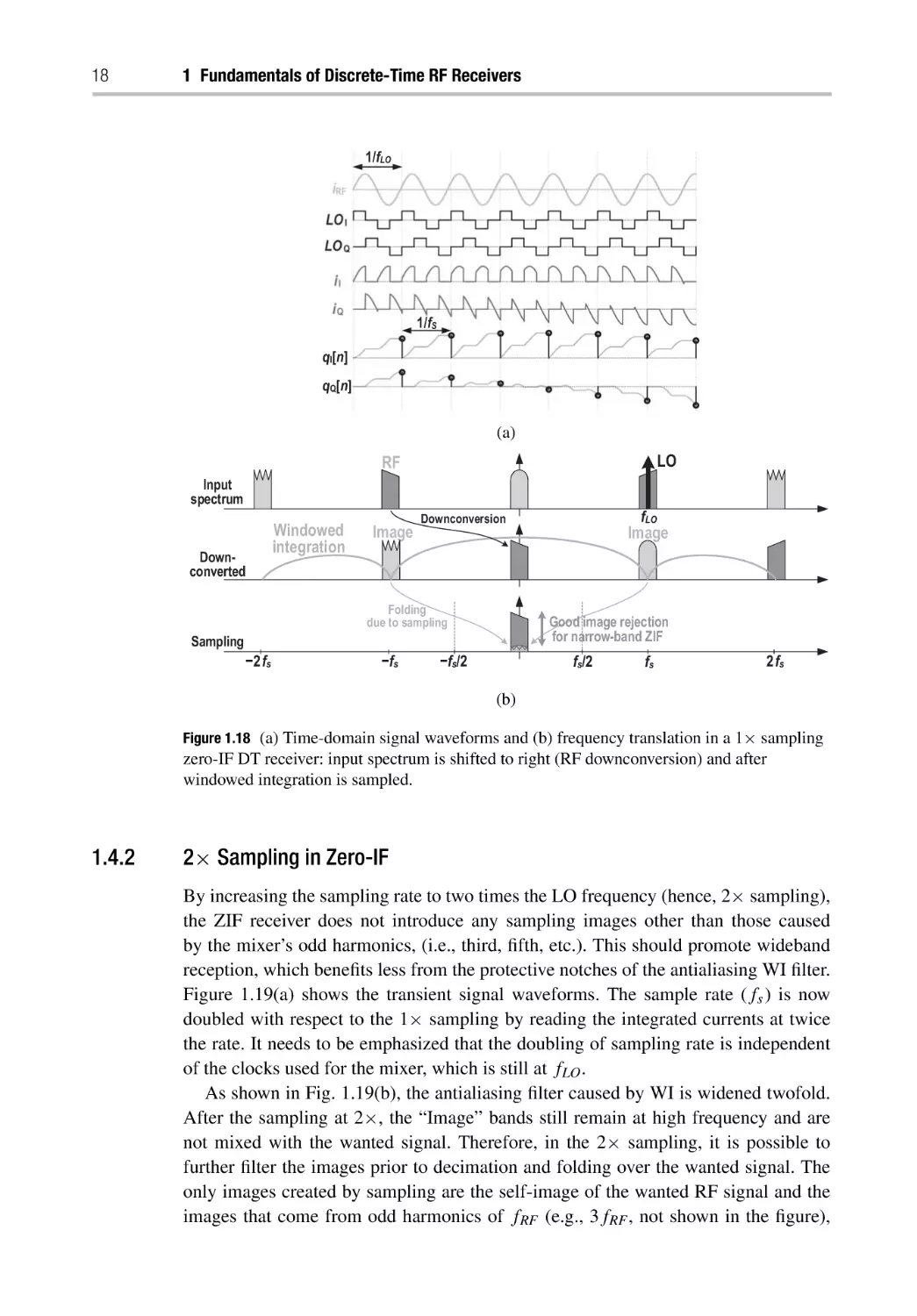
1.4.2
2× Sampling in Zero-IF
By increasing the sampling rate to two times the LO frequency (hence, 2× sampling),
the ZIF receiver does not introduce any sampling images other than those caused
by the mixer’s odd harmonics, (i.e., third, fifth, etc.). This should promote wideband
reception, which benefits less from the protective notches of the antialiasing WI filter.
Figure 1.19(a) shows the transient signal waveforms. The sample rate (fs ) is now
doubled with respect to the 1× sampling by reading the integrated currents at twice
the rate. It needs to be emphasized that the doubling of sampling rate is independent
of the clocks used for the mixer, which is still at fLO .
As shown in Fig. 1.19(b), the antialiasing filter caused by WI is widened twofold.
After the sampling at 2×, the “Image” bands still remain at high frequency and are
not mixed with the wanted signal. Therefore, in the 2× sampling, it is possible to
further filter the images prior to decimation and folding over the wanted signal. The
only images created by sampling are the self-image of the wanted RF signal and the
images that come from odd harmonics of fRF (e.g., 3fRF , not shown in the figure),
1.5 4× Sampling for DT High-IF Receiver
19
1/fLO
1/fS
qI[n]
qQ[n]
(a)
LO
RF
Input
spectrum
fLO
Downconversion
Windowed
integration
Downconverted
LPF
Self-image
folding
Sampling
fs
fs/2
fs/2
fs
(b)
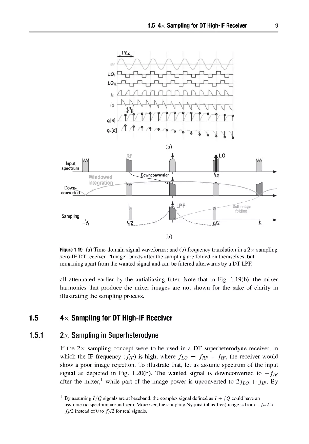
Figure 1.19 (a) Time-domain signal waveforms; and (b) frequency translation in a 2× sampling
zero-IF DT receiver. “Image” bands after the sampling are folded on themselves, but
remaining apart from the wanted signal and can be filtered afterwards by a DT LPF.
all attenuated earlier by the antialiasing filter. Note that in Fig. 1.19(b), the mixer
harmonics that produce the mixer images are not shown for the sake of clarity in
illustrating the sampling process.
1.5
4× Sampling for DT High-IF Receiver
1.5.1
2× Sampling in Superheterodyne
If the 2× sampling concept were to be used in a DT superheterodyne receiver, in
which the IF frequency (fIF ) is high, where fLO = fRF + fIF , the receiver would
show a poor image rejection. To illustrate that, let us assume spectrum of the input
signal as depicted in Fig. 1.20(b). The wanted signal is downconverted to +fIF
after the mixer,1 while part of the image power is upconverted to 2fLO + fIF . By
1 By assuming I /Q signals are at baseband, the complex signal defined as I + j Q could have an
asymmetric spectrum around zero. Moreover, the sampling Nyquist (alias-free) range is from −fs /2 to
fs /2 instead of 0 to fs /2 for real signals.
20
1 Fundamentals of Discrete-Time RF Receivers
1/fLO
qI[n]
qQ[n]
(a)
LO
RF
Input
spectrum
fRF fLO
Downconversion
Windowed
integration
Image
Downconverted
fIF
fIF
Poor
Image Rejection
Sampling
fs
fs/2
fIF
fIF
fs/2
Folding
due to sampling
fs
(b)
Figure 1.20 (a) Time-domain signal waveforms and (b) frequency translation in a 2× sampling
DT superheterodyne receiver. After the sampling, image is aliased on the wanted signal
without enough attenuation.
sampling this signal at the 2× rate, this image (whose absolute frequency is higher
than the Nyquist rate, fs /2) folds over the wanted signal at +fIF . In addition, note
that in the superheterodyne the notch of the windowed integration is not aligned
(unlike in ZIF) with the image (it is separated by fIF ). Therefore, the image signal
is not effectively filtered out, and this leads to an unacceptable image rejection of
the receiver.
To get further insight, let us inspect the time-domain signals of this structure in
Fig. 1.20(a). As expected, the RF signal after downconversion and sampling is centered at a high IF and the two sampled signals (qIn and qQn ) have quadrature sinusoidal
waveforms. Looking more closely, the phase shift between I and Q is not exactly
90◦ , as normally expected for quadrature signals. There is an error of half a cycle of
sampling that creates θerr = (Ts /2) × 2πfIF [48]. This limits the image rejection of
this structure.
1.5 4× Sampling for DT High-IF Receiver
21
1/fLO
qI[n]
qQ[n]
(a)
LO
RF
Input
spectrum
Windowed integration
fRF fLO
Downconversion
Downconverted
fIF
fIF
BPF
Folding
due to sampling
Sampling
fs/2
fIF
fIF
fs/2
(b)
Figure 1.21 (a) Time-domain signal waveforms and (b) frequency translations in a 4× sampling
DT superheterodyne receiver. Since fs is increased to 4fLO , IF image is completely distinct
from the wanted signal and can be filtered afterward by a DT BPF.
1.5.2
4× Sampling Signal Processing Technique
To solve the problem of the DT superheterodyne image introduced by sampling,
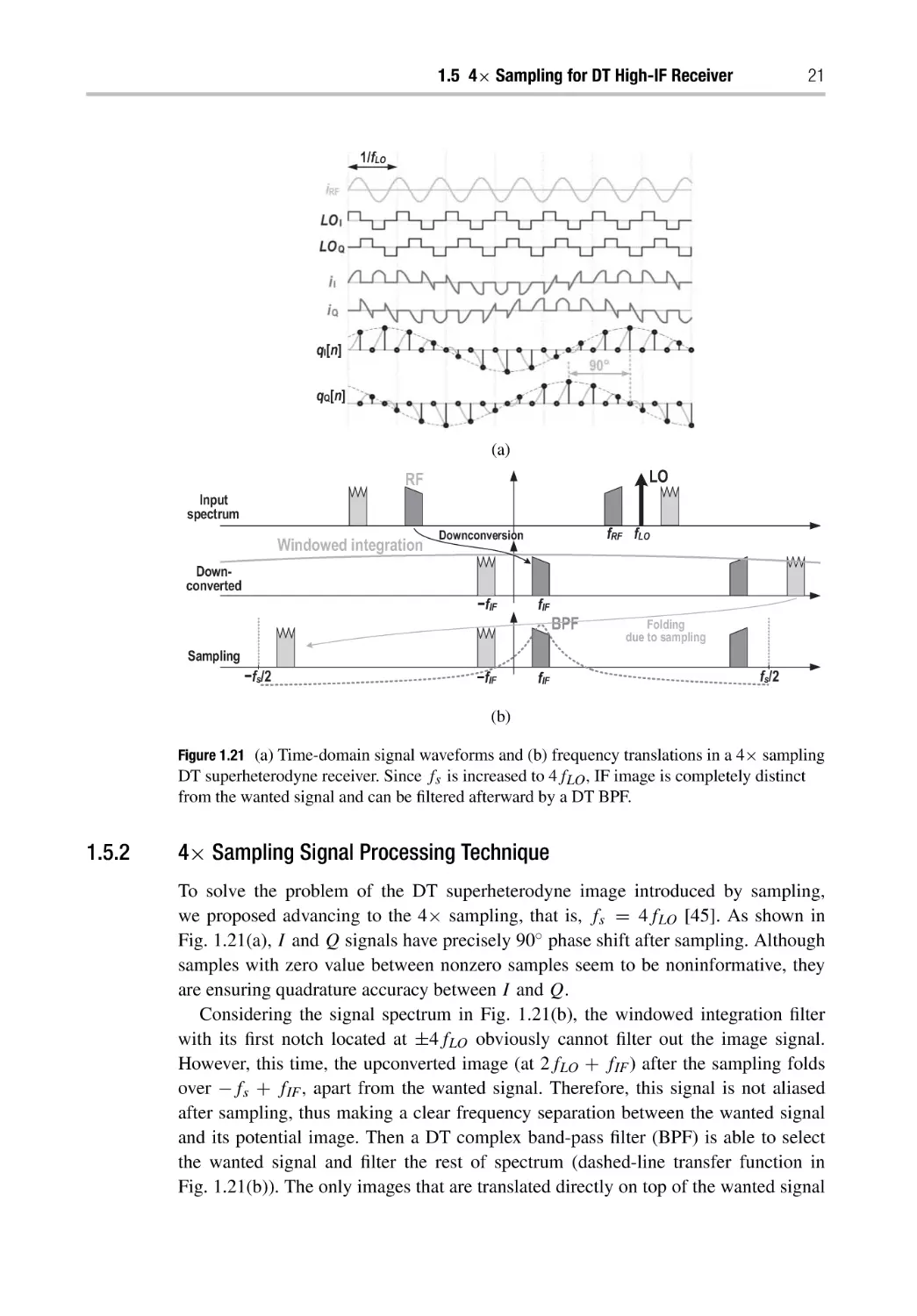
we proposed advancing to the 4× sampling, that is, fs = 4fLO [45]. As shown in
Fig. 1.21(a), I and Q signals have precisely 90◦ phase shift after sampling. Although
samples with zero value between nonzero samples seem to be noninformative, they
are ensuring quadrature accuracy between I and Q.
Considering the signal spectrum in Fig. 1.21(b), the windowed integration filter
with its first notch located at ±4fLO obviously cannot filter out the image signal.
However, this time, the upconverted image (at 2fLO + fIF ) after the sampling folds
over −fs + fIF , apart from the wanted signal. Therefore, this signal is not aliased
after sampling, thus making a clear frequency separation between the wanted signal
and its potential image. Then a DT complex band-pass filter (BPF) is able to select
the wanted signal and filter the rest of spectrum (dashed-line transfer function in
Fig. 1.21(b)). The only images that are translated directly on top of the wanted signal
22
1 Fundamentals of Discrete-Time RF Receivers
are the mixer’s odd harmonics images. In this respect, further increasing the sample
rate (e.g., to 8×) without using a harmonic rejection mixer would not be beneficial.
In [48], an 8× sampling DT mixing architecture was proposed that also implements
harmonic rejection.
To summarize, the 4×-sampling concept offers discrete-time signal processing
without introducing any unwanted images other than LO odd harmonics. This imagefree sampling will later be used in DT receiver examples in Chapter 5.
1.6
Conclusion
The discrete-time manner of RF signal processing is an attractive approach for
realizing receivers in an advanced CMOS process technology. It opens up new
architectural possibilities, not previously possible with the traditional analog-intensive
implementations. Considering the advantages and disadvantages of a superheterodyne
architecture compared to zero-IF, and accounting for the recent advancements in the
CMOS process technology, it appears that it is now the time to return to the historical
superheterodyne for high-performance applications and/or low-power operations. The
main remaining challenge is the full CMOS integration of the IF filter, which will be
discussed in Chapter 4.
2
First Stage: Low-Noise
Transconductance Amplifier
To be able to amplify an RF signal located at any of the supported cellular frequency
bands, a wideband noise-canceling low-noise amplifier (LNA) [49] appears to be a
good choice. As the receivers, later introduced in Chapter 5, are based on sampling the
input charge, the RF amplifier needs to provide current rather than voltage, thus acting
as a transconductance amplifier (TA) exhibiting a high output impedance compared to
the input load of its subsequent stage. An LNTA (i.e., LNA+TA) could trivially be
constructed by cascading LNA and TA (gm ) stages [9–12]. However, to improve noise
and linearity, both of these circuits should be codesigned and tightly coupled [13, 50].
This chapter presents examples of state-of-the-art wideband noise-canceling LNTAs.
2.1
Introduction
The usage of various wireless standards, such as Bluetooth, Wi-Fi, GPS, and
2G/3G/4G/5G cellular, has been continually increasing. To utilize the frequency bands
efficiently and to support more communication standards with lower power consumption, with lower occupied volume, and at reduced costs, multimode transceivers,
software-defined radios (SDR), cognitive radios, and so on have been actively
investigated [51].
Broadband behavior of a wireless receiver is typically defined by its front-end
low-noise amplifier (LNA), whose design must consider trade-offs between input
matching, noise figure (NF), gain, bandwidth, linearity, and voltage headroom in a
given process technology. There are several wideband LNA design topologies and
techniques, including filter-type amplifiers [52], gm -enhancement technique [53],
common-gate (CG) amplifiers [54], resistive shunt-feedback amplifiers [55–57], and
distributed amplifiers [58].
A very wide bandwidth LNA can be constructed using a common-source (CS)
amplifier topology with several bandpass filters for providing wideband input matching. In [52], a three-section bandpass Chebyshev filter is used to resonate the reactive
part of the input impedance to provide wideband input matching over the whole band
from 3.1 to 10.6 GHz. However, several of the associated bulky inductors there occupy
a large chip area, which makes this technique unsuitable for wideband applications
below 3 GHz [58]. Moreover, although the CS configuration typically ensures better noise performance than in a CG structure, a low quality factor (Q) of on-chip
24
2 First Stage: Low-Noise Transconductance Amplifier
VDD
VDD
RD
RD
Vout
VB
RF
M1
Vin
Ls
Vout
Rs
Rs
M1
Vin
(a)
(b)
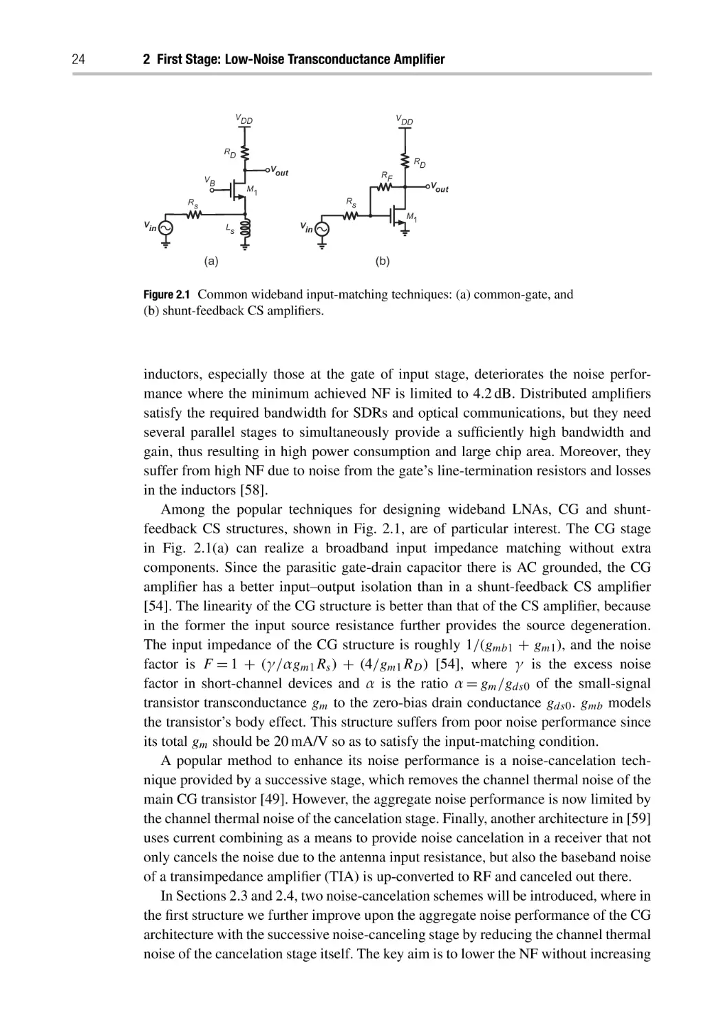
Figure 2.1 Common wideband input-matching techniques: (a) common-gate, and
(b) shunt-feedback CS amplifiers.
inductors, especially those at the gate of input stage, deteriorates the noise performance where the minimum achieved NF is limited to 4.2 dB. Distributed amplifiers
satisfy the required bandwidth for SDRs and optical communications, but they need
several parallel stages to simultaneously provide a sufficiently high bandwidth and
gain, thus resulting in high power consumption and large chip area. Moreover, they
suffer from high NF due to noise from the gate’s line-termination resistors and losses
in the inductors [58].
Among the popular techniques for designing wideband LNAs, CG and shuntfeedback CS structures, shown in Fig. 2.1, are of particular interest. The CG stage
in Fig. 2.1(a) can realize a broadband input impedance matching without extra
components. Since the parasitic gate-drain capacitor there is AC grounded, the CG
amplifier has a better input–output isolation than in a shunt-feedback CS amplifier
[54]. The linearity of the CG structure is better than that of the CS amplifier, because
in the former the input source resistance further provides the source degeneration.
The input impedance of the CG structure is roughly 1/(gmb1 + gm1 ), and the noise
factor is F = 1 + (γ/αgm1 Rs ) + (4/gm1 RD ) [54], where γ is the excess noise
factor in short-channel devices and α is the ratio α = gm /gds0 of the small-signal
transistor transconductance gm to the zero-bias drain conductance gds0 . gmb models
the transistor’s body effect. This structure suffers from poor noise performance since
its total gm should be 20 mA/V so as to satisfy the input-matching condition.
A popular method to enhance its noise performance is a noise-cancelation technique provided by a successive stage, which removes the channel thermal noise of the
main CG transistor [49]. However, the aggregate noise performance is now limited by
the channel thermal noise of the cancelation stage. Finally, another architecture in [59]
uses current combining as a means to provide noise cancelation in a receiver that not
only cancels the noise due to the antenna input resistance, but also the baseband noise
of a transimpedance amplifier (TIA) is up-converted to RF and canceled out there.
In Sections 2.3 and 2.4, two noise-cancelation schemes will be introduced, where in
the first structure we further improve upon the aggregate noise performance of the CG
architecture with the successive noise-canceling stage by reducing the channel thermal
noise of the cancelation stage itself. The key aim is to lower the NF without increasing
2.2 Overview of Noise-Cancelation and -Reduction Techniques
25
the consumed power, which is mainly achieved by employing a current-reuse technique. Then, in the second architecture, twofold noise cancelation is introduced, which
shows how the noise performance of the CG architecture can be improved while
simultaneously providing high gain.
2.2
Overview of Noise-Cancelation and -Reduction Techniques
In this section, we first describe the basic idea of a noise-cancelation scheme. Then,
based on that, we introduce a new noise-reduction technique. Finally, these two
techniques are combined in a manner that saves power.
2.2.1
Conventional Noise-Cancelation Technique
The most important noise source in CMOS LNAs is the channel thermal noise of MOS
transistors. This noise is modeled as a shunt current source across the transistor’s
drain and source terminals. The designer’s goal is to minimize the generation and
propagation of this noise. Among various publications introducing noise-cancelation
techniques in LNAs, [49, 60–62] are noteworthy.
The conventional noise-cancelation scheme in the CS shunt-feedback topology is
shown in Fig. 2.2. The noise current of the main, that is, input-matching, transistor,
M1 , flows through the feedback resistor, RF , toward the M1 gate and creates two noise
voltages at nodes X and Y with the same phase but different amplitudes. On the other
hand, the signal voltage at these nodes has opposite polarities and different amplitudes
due to the inverting operation of the M1 amplifier. The signal and noise polarities being
opposite at nodes X and Y make it possible to cancel the noise originating from the
input-matching transistor while adding the signal contributions constructively. The
noise voltage at node X, VnX , is amplified and inverted by M2 , while the noise voltage
at node Y , VnY , is passed across M3 barely changed. At the output node, the two
voltages with opposite phases are canceled. Ultimately, the channel thermal noise
VDD
RD
RF
Rs
Vin
X
Y
M3
Vout
M1
M2
Figure 2.2 Conventional noise cancelation of M1 configured as a CS shunt-feedback amplifier
(biasing not shown).
26
2 First Stage: Low-Noise Transconductance Amplifier
of M1 will be greatly attenuated or altogether canceled, provided that the following
condition is satisfied:
rds2
gm2
Vn,out = VnY
− vnX
=0
rds2 + 1/gm3
gm3
(2.1)
gm2
RF + Rs
=
,
Rs
gm3
where gm rds 1 was assumed.
As mentioned, this kind of noise cancelation is commonly used in LNA structures
with the CS input stage. The main drawback here is the need for an extra stage in order
to amplify and invert the voltage noise at node X and add it with the voltage noise at
the output. According to (2.1), since the feedback resistor is much larger than the input
source resistor, RF Rs , the transconductance of M2 , gm2 , must be large enough
to satisfy the noise-cancelation condition, but at a cost of higher power consumption.
In Section 2.2.2, we offer a new technique that can be used as either a noisecancelation or noise-reduction technique without substantially increasing the power
consumption [63].
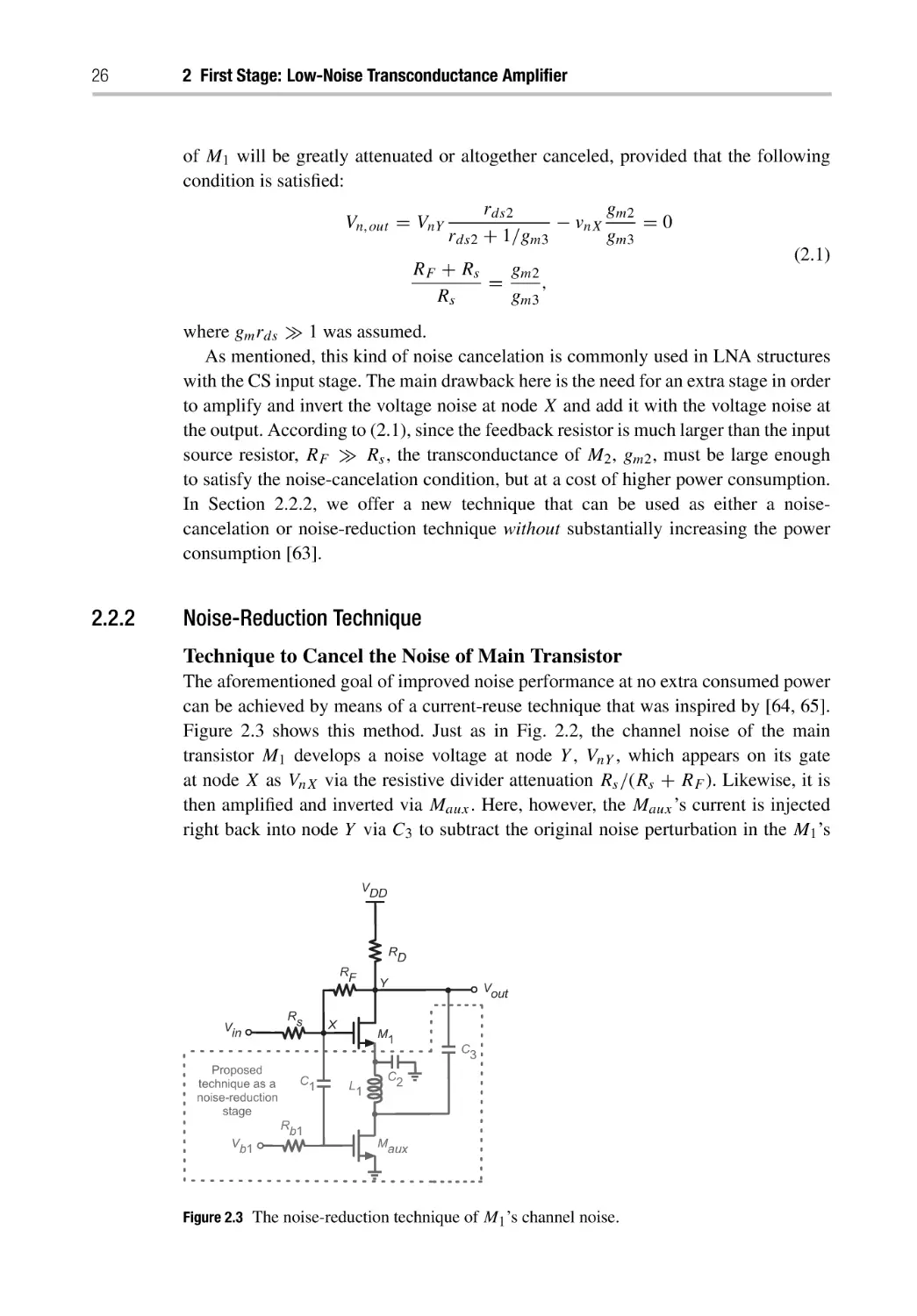
2.2.2
Noise-Reduction Technique
Technique to Cancel the Noise of Main Transistor
The aforementioned goal of improved noise performance at no extra consumed power
can be achieved by means of a current-reuse technique that was inspired by [64, 65].
Figure 2.3 shows this method. Just as in Fig. 2.2, the channel noise of the main
transistor M1 develops a noise voltage at node Y , VnY , which appears on its gate
at node X as VnX via the resistive divider attenuation Rs /(Rs + RF ). Likewise, it is
then amplified and inverted via Maux . Here, however, the Maux ’s current is injected
right back into node Y via C3 to subtract the original noise perturbation in the M1 ’s
VDD
RD
RF
Vin
Proposed
technique as a
noise-reduction
stage
Vb1
Rs
C1
Rb1
X
Y
M1
L1
Vout
C3
C2
Maux
Figure 2.3 The noise-reduction technique of M1 ’s channel noise.
2.2 Overview of Noise-Cancelation and -Reduction Techniques
27
channel. This way, there is no need for an extra branch M3 used in the conventional
noise cancelation of Fig. 2.2. Furthermore, the source of M1 is connected to the ground
via C2 . Inductor L1 provides some AC isolation between the source of M1 and drain of
M2 . By stacking M1 on top of M2 dc-wise, the dc current is reused, and M2 is biased
by the main transistor current. However, AC-wise, Maux is paralleled with the main
transistor M1 by means of C1 and C3 , but completes the negative feedback around
M1 for its noise. For the aforementioned technique to cancel the noise of M1 , the
following condition should be met:
Vn,out = VnY − vnX gmaux RD = 0
RF + Rs
= gmaux RD .
Rs
(2.2)
Equation (2.2) suggests that the full noise-cancelation of M1 is rather expensive in
terms of consumed power, since the ratio of RF /RD and gmaux need to be very high.1
However, this technique could be beneficially used at low expended power for a partial
noise cancelation, that is, noise reduction, of M1 .
Current-Reuse Technique as Noise Reduction
Noise factor excess, FM1 , contributed by the M1 transistor of the shunt-feedback CS
amplifier shown in Fig. 2.1(b) is calculated as:
2
2
V
I
n,M1 /Av
n,M1 Zout
FM1 =
=
Vn,Rs
Vn,Rs Av
(2.3)
4kT gm1 |Zout |2 γ
4 γ
=
=
,
2 |Z |2 α
Rs gm1 α
kT Rs gm1
out
where Zout is the output impedance of the amplifier as seen by the unloaded out2
put node. In addition, I n,M1 = 4kT gm1 γ is the channel thermal noise of M1 , and
|Av | gm1 Zout · Zin /(Zin + Rs ) is the voltage gain of M1 , where Zin = RF /(1 +
gm1 RD )||1/sCin , and Cin is due to parasitics at the gate of M1 , for the sake of simplicity Zin is considered equal to Rs . Hence, the noise factor of the shunt-feedback
amplifier shown in Fig. 2.1(b) is approximately equal to [56]:
F(Fig. 2.1b) 1 +
4 γ
.
Rs gm1 α
(2.4)
According to (2.4), the noise factor has a reverse relationship with the transconductance. It means that by increasing the transconductance of the main transistor, the
circuit’s relative noise contribution is decreased. However, this results in a higher
power dissipation.
1 The input matching of the shunt-feedback CS amplifier is defined by R and is approximately equal to
F
RF /(1 + gm1 RD ); for providing the noise-cancelation condition, gmaux should be much larger than
gm1 , that is, gmaux (2 + gm1 RD )/RD .
28
2 First Stage: Low-Noise Transconductance Amplifier
By using the discussed current-reuse technique of Fig. 2.3, the noise factor is
roughly equal to F(Fig. 2.3) = 1 + FM1 + FMaux , where FM1 and FMaux are expressed by:
γ
4kT gm1 |Zout |2
kT Rs (gm1 + gmaux )2 |Zout |2 α
γ
4gm1
=
.
Rs (gm1 + gmaux )2 α
(2.5)
γ
4kT gmaux |Zout |2
kT Rs (gm1 + gmaux )2 |Zout |2 α
γ
4gmaux
=
.
2
Rs (gm1 + gmaux ) α
(2.6)
FM1 =
FMaux =
Finally, the total noise factor of the presented structure, without considering the thermal noise of RD , is approximately given by:
F(Fig. 2.3) ≥ 1 +
4γ
4
+
.
α(gm1 + gmaux )Rs
Rs RD (gm1 + gmaux )2
(2.7)
From the standpoint of the received signal, Maux is paralleled with the main transistor M1 , and hence, according to (2.7), their transconductances are summed up.
This boost in transconductance reduces the noise figure without increasing the bias
current. Without the current-reuse technique, Maux would be paralleled with M1 in a
conventional way as in Fig. 2.2, and the structure would consume twice the power in
order to achieve the same NF. Nonetheless, the main drawback of the new technique
is the reduced voltage headroom leading to some deterioration of linearity.
To demonstrate the benefit of the noise-reduction technique introduced in Fig. 2.3,
we now apply it into the CS noise-canceling LNA of Fig. 2.2 for the purpose of
reducing the noise of the latter’s second stage (i.e., M2 ). To have a better comparison
between Figs. 2.2 and 2.5, their respective simplified noise factors, F(Figs. 2.2) and
F(Fig. 2.5) , are calculated as follows:
F(Fig. 2.2) ≥ 1 +
F(Fig. 2.5) ≥ 1 +
γ
αgm2 Rs
+
2
γgm3 + αRD gm3
2
αRs gm2
.
2
γgm3 + αRD gm3
γ
+
.
α(gm2 + gmaux )Rs
αRs (gm2 + gmaux )2
(2.8)
(2.9)
By comparing (2.8) and (2.9), it can be seen that for the same value of gm2 and gm3 in
both structures (Figs. 2.2 and 2.5), the noise performance in Fig. 2.5 has improved.
The efficacy of this noise-reduction technique of Fig. 2.3 is illustrated by the NF
circuit simulation plots in Fig. 2.4 with superimposed analytical plots to verify the
derived noise equations.2 It is compared with the basic shunt-feedback amplifier of
2 We extend (2.4) and (2.7) by further considering the thermal noise of R , that is,
D1
2 (g +kg )2 (R +
F 1+[RD (RF (1+(gm1 +kgm1 )RD ))2 /Rs (ZD +RF (1+(gm1 +kgm1 )RD ))2 ZD
F
m1
m1
2
RF Zin Cin s +gm1 RD Zin +Zin ) ]+[γ/4(Rs (gm1 +kgm1 )(Rs /(Rs (1+Rs Cin s)+Rs )2 )]+(4Rs /RF ),
2.2 Overview of Noise-Cancelation and -Reduction Techniques
gm
gm
gm
29
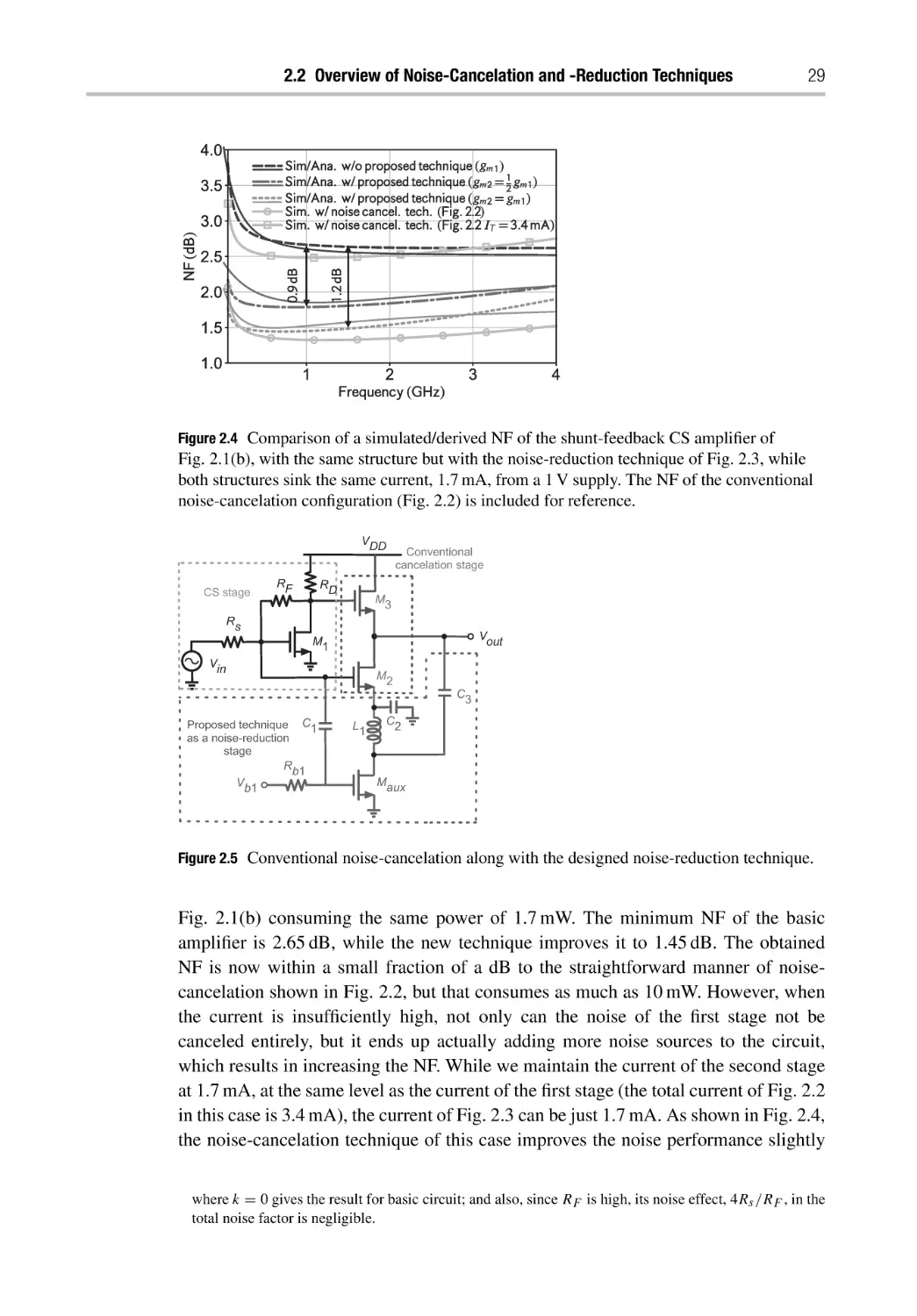
gm
gm
IT
Figure 2.4 Comparison of a simulated/derived NF of the shunt-feedback CS amplifier of
Fig. 2.1(b), with the same structure but with the noise-reduction technique of Fig. 2.3, while
both structures sink the same current, 1.7 mA, from a 1 V supply. The NF of the conventional
noise-cancelation configuration (Fig. 2.2) is included for reference.
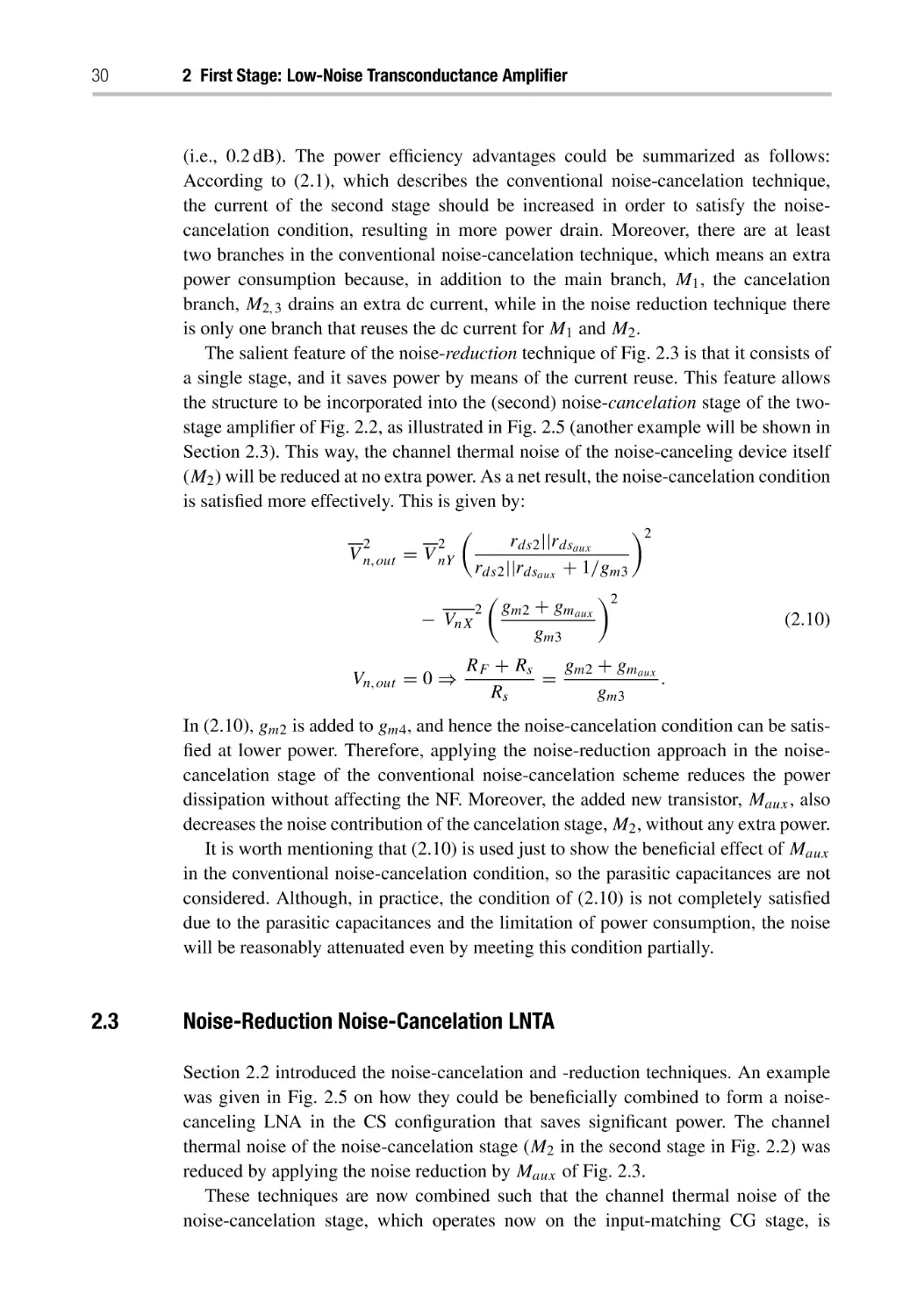
VDD
CS stage
RF
RD
Conventional
cancelation stage
M3
Rs
Vout
M1
Vin
M2
C3
Proposed technique C1
as a noise-reduction
stage
Rb1
Vb1
L1
C2
Maux
Figure 2.5 Conventional noise-cancelation along with the designed noise-reduction technique.
Fig. 2.1(b) consuming the same power of 1.7 mW. The minimum NF of the basic
amplifier is 2.65 dB, while the new technique improves it to 1.45 dB. The obtained
NF is now within a small fraction of a dB to the straightforward manner of noisecancelation shown in Fig. 2.2, but that consumes as much as 10 mW. However, when
the current is insufficiently high, not only can the noise of the first stage not be
canceled entirely, but it ends up actually adding more noise sources to the circuit,
which results in increasing the NF. While we maintain the current of the second stage
at 1.7 mA, at the same level as the current of the first stage (the total current of Fig. 2.2
in this case is 3.4 mA), the current of Fig. 2.3 can be just 1.7 mA. As shown in Fig. 2.4,
the noise-cancelation technique of this case improves the noise performance slightly
where k = 0 gives the result for basic circuit; and also, since RF is high, its noise effect, 4Rs /RF , in the
total noise factor is negligible.
30
2 First Stage: Low-Noise Transconductance Amplifier
(i.e., 0.2 dB). The power efficiency advantages could be summarized as follows:
According to (2.1), which describes the conventional noise-cancelation technique,
the current of the second stage should be increased in order to satisfy the noisecancelation condition, resulting in more power drain. Moreover, there are at least
two branches in the conventional noise-cancelation technique, which means an extra
power consumption because, in addition to the main branch, M1 , the cancelation
branch, M2,3 drains an extra dc current, while in the noise reduction technique there
is only one branch that reuses the dc current for M1 and M2 .
The salient feature of the noise-reduction technique of Fig. 2.3 is that it consists of
a single stage, and it saves power by means of the current reuse. This feature allows
the structure to be incorporated into the (second) noise-cancelation stage of the twostage amplifier of Fig. 2.2, as illustrated in Fig. 2.5 (another example will be shown in
Section 2.3). This way, the channel thermal noise of the noise-canceling device itself
(M2 ) will be reduced at no extra power. As a net result, the noise-cancelation condition
is satisfied more effectively. This is given by:
2
rds2 ||rdsaux
2
2
V n,out = V nY
rds2 ||rdsaux + 1/gm3
2
2 gm2 + gmaux
− VnX
(2.10)
gm3
Vn,out = 0 ⇒
RF + Rs
gm2 + gmaux
=
.
Rs
gm3
In (2.10), gm2 is added to gm4 , and hence the noise-cancelation condition can be satisfied at lower power. Therefore, applying the noise-reduction approach in the noisecancelation stage of the conventional noise-cancelation scheme reduces the power
dissipation without affecting the NF. Moreover, the added new transistor, Maux , also
decreases the noise contribution of the cancelation stage, M2 , without any extra power.
It is worth mentioning that (2.10) is used just to show the beneficial effect of Maux
in the conventional noise-cancelation condition, so the parasitic capacitances are not
considered. Although, in practice, the condition of (2.10) is not completely satisfied
due to the parasitic capacitances and the limitation of power consumption, the noise
will be reasonably attenuated even by meeting this condition partially.
2.3
Noise-Reduction Noise-Cancelation LNTA
Section 2.2 introduced the noise-cancelation and -reduction techniques. An example
was given in Fig. 2.5 on how they could be beneficially combined to form a noisecanceling LNA in the CS configuration that saves significant power. The channel
thermal noise of the noise-cancelation stage (M2 in the second stage in Fig. 2.2) was
reduced by applying the noise reduction by Maux of Fig. 2.3.
These techniques are now combined such that the channel thermal noise of the
noise-cancelation stage, which operates now on the input-matching CG stage, is
2.3 Noise-Reduction Noise-Cancelation LNTA
31
VDD
C4
RD0
RD1
VB1
RB
VB0
RB
RB
VB4
M0
C3
Y
M1
C1
C0
Vin
L1
C5
C6
M3
RB
VB3
C2
X
M4
Vout
M2
RB
VB2
Ls
Figure 2.6 Wideband LNTA with noise-cancelation and -reduction techniques.
reduced by applying the same noise-reduction technique. Figure 2.6 shows the
designed wideband LNTA. We take advantage of the CG input stage, M1 , to provide
the wideband 50 input matching. M2 and M3 of the CS stages are configured to
cancel the channel thermal noise of M1 . To reuse the M2 current and to improve
the IIP3 linearity, M3 is chosen now as a pMOS transistor. The external antennaport inductor Ls is employed to provide a dc current path to ground and to damp
the total parasitic capacitance at the input node. In this noise-reduction technique,
by exploiting the current reuse, transistor M4 is paralleled AC-wise with M2 , thus
boosting its transconductance and hence decreasing its thermal noise effects. The
pMOS–nMOS structure and “sweet spot” biasing are applied to improve the linearity.
Moreover, the off-chip inductor Ls is on a PCB, hence its value can be fairly large,
in the order of a few hundred of nH, which can resonate out all parasitics at the input
node at 1.2–1.5 GHz [63].
2.3.1
Input Matching
To consider the body effect of the wideband input-matching common-gate M1 transistor and also to simplify the relations, Gm1 stands for (1 + RD0 gm0 )(gm1 + gmb1 ) ≈
(1 + RD0 gm0 )gm1 . Hence, the input impedance is given by:
1 1
Zin = (RLs + sLs )
sCX Gm1
(2.11)
RLs + sLs
,
=
CX Ls s 2 + (RLs CX + Gm1 Ls )s + (Gm1 RLs + 1)
32
2 First Stage: Low-Noise Transconductance Amplifier
where CX lumps the total parasitic capacitance at node X, which is damped by Ls .
Since Ls is external and connected to the antenna pin, thus not consuming any extra
pads on the chip, it can be fairly large (150 nH); therefore (2.11) can be simplified to
Zin = 1/(sCX + Gm1 ). This shows that the input matching is mainly defined by M0
and M1 . In this case, if the size of Ls changes, for instance, from 150 to 200 nH, there
will be just a barely noticeable effect on S11 . However, the lower limit of bandwidth
(fL ) will be improved. On the other hand, if the size of Ls is decreased, its series
resistance, RLs , will go down (to as low as 5 ) due to the limited Q-factor of Ls . This
resistance is paralleled with 1/Gm1 and so it lowers the equivalent input impedance.
Although a new technique was described in [66] to extend the bandwidth at lower
frequencies without increasing the size of Ls , here an off-chip inductor in parallel
with the IC antenna input pin is used to realize Ls in order to save the silicon die area.
Although the gm -boost transistor, M0 , adds a bit more parasitics to the input node, it
is of small size, so it does not affect the bandwidth substantially. By increasing its size
from W = 10 μm to 20 μm, the simulated upper cutoff frequency lowers by 450 MHz,
from 7.78 to 7.33 GHz.
2.3.2
Gain Analysis
The equivalent impedance seen from the drain of M1 toward the ground is termed
ZY and is equal to RD1 ||[rds1 + (1/sCX ||sLs )(1 + Gm1 rds1 )]||1/sCY , where RD1 is
the load resistance of M1 , and CY is the total parasitic capacitance at node Y . Zout
determines the output impedance, which is calculated as rds2 ||rds3 ||rds4 ||1/sCout ,
where Cout is the total output parasitic capacitance seen by Vout . Therefore, the voltage
gain of this LNTA is given by:
Av = −
1/Gm1
(Gm1 gm3 |ZY | + gm2 + gm4 )|Zout |.
1/Gm1 + Rs
(2.12)
The design can be used either as an LNTA in an integrated current-mode RX or
as a stand-alone LNA if it is externally loaded by a 50 termination. In the latter, the amplifier must properly handle the intermediate network of wire-bonding
inductance, pad capacitance, package parasitics, and PCB transmission lines (TLs)
and components. Figure 2.7 shows the simulated output impedance of the designed
LNTA, which confirms that it is suitable for the current-mode application where its
output impedance is at least eight times larger than the 50 load impedance [67].
In this matching network, the pad capacitance is in parallel with Zout , where the
equivalent impedance is in series with the wire-bond inductance. The rest of the
matching network is provided on the PCB by using SMD capacitors and TLs that
makes the equivalent output impedance compatible with 50 .
To examine the effect of the 50 load impedance of the external test equipment
on the gain of this structure, (2.12) for Av is plotted in Fig. 2.8. As expected, when
2.3 Noise-Reduction Noise-Cancelation LNTA
33
w/o
dB
w/o
Figure 2.7 Simulated output impedance without matching network on PCB .
30
Vin
Zout
Av (dB)
35
IRF
GmVin
To an on-chip Mixer
LNTA
Calculated Av
20
4
2
6
8
10
Vin
0
Zout
Av (dB)
15
GmVin
50
LNA
2
4
Frequency(GHz)
Calculated Av
6
8
Figure 2.8 Calculated Av from (2.12) (top) when the amplifier is self-loaded in the LNTA mode,
(bottom) when the amplifier is loaded by 50 through a matching network in the LNA mode.
unloaded, the voltage gain is high since Zout is high.3 When the amplifier is loaded
with 50 , the provided gain drops by ∼20 dB.
Unfortunately, the technology scaling causes rds to be reduced. Moreover, by
employing the pMOS transistors at the output node, the parasitic capacitances go up,
resulting in more variation in Zout at high frequencies. These are the main reasons that
limit the LNTA bandwidth at high frequencies. To solve this problem, the inductive
shunt-peaking and series-peaking techniques can be used. The shunt inductive peaking
3 When the LNTA transconductance drives an internal on-chip mixer, its voltage gain will actually be very
low, but it can be recovered in subsequent stages [68].
34
2 First Stage: Low-Noise Transconductance Amplifier
causes a resonance at the output of each stage when the gain starts to roll off at higher
frequencies [66]. It is worth mentioning that L1 also helps to dampen the parasitic
capacitance at the output node. By increasing L1 from 240 pH to 1.2 nH, the 3 dB
bandwidth can be extended from 7.5 to 9 GHz. The quality factor of L1 improves the
gain only marginally. When it is increased from 5.5 to 10 (L1 = 440 pH), the gain
improves only by 0.1 dB.
2.3.3
Noise Analysis
As mentioned in Section 2.1, the purpose of noise-cancelation is to disassociate the
input matching from the noise considerations by virtue of canceling the noise from the
matching stage at the output node [49]. In this LNTA, the current noise of the input
transistor flows into node X but out of node Y , causing two voltages with opposite
phases. These two voltages are converted into currents by M2 and M3 [69]. However,
the input signal appears at these two nodes at the same phase. Thus, the input signal
is constructively combined at the output. The two noise voltages are calculated as
2
2 I2
2 2
VnX 2 = Zin
n,M1 and VnY = ZY In,M1 . Therefore, the output current noise due to
the thermal noise of M1 is as follows:
2
2
2
In,out = VnX (gm2 + gm4 )2 − VnY gm3 = 0
⇒
gm2 + gm4
ZY
=
.
gm3
ZX
(2.13)
To reuse the current of M2 , M3 is chosen as a pMOS transistor. In addition, the
noise-reduction technique is applied to improve the NF without any additional power
cost. In this technique, M4 is in parallel with M2 , and hence, the transconductance of
M4 is added to that of M2 . Moreover, M4 is selected as a pMOS transistor in order to be
able to reuse the current of M2 . The consequential increase of M2 ’s transconductance
reduces the channel thermal noise of the cancelation stage, thus avoiding any need
for extra branches. Consequently, the improvement in noise figure is achieved without
burning more current, as explained in Section 2.2.
The most important noise sources in this noise-cancelation scheme are the thermal
noise of RD1 and the channel thermal noise of transistors M2 , M3 , and M4 . The noise
factor of this LNA is equal to F = 1 + FRD1 + FM2 + FM3 + FM4 , where the FRD1
term is given by the following relation:
4kT RD1 (gm3 |Zout |)2 (Zo1 /(Zo1 + RD1 ))2
4kT Rs A2v
Rs
∼
,
=
RD1
FRD1 =
(2.14)
where, according to Fig. 2.6, Zo1 = [rds1 + (Rs ||1/sCX ||sLs )(1 + Gm1 rds1 )] and
ZY = RD1 ||Zo1 when the parasitic capacitance at node Y is not considered for
simplicity. Av is the voltage gain of the LNTA, which is simplified by considering
2.3 Noise-Reduction Noise-Cancelation LNTA
35
the noise-cancelation and input-matching conditions, (gm2 + gm4 )Rs = gm3 RD1 and
Zin = Rs = 1/Gm1 , respectively. The other constituting terms of the noise factor F are
γ
4kT gm2 |Zout |2 γ
4gm2
=
2
2
4kT Rs Av α
Rs (ZY Gm1 gm3 +gm2 +gm4 ) α
gm2
γ
∼
,
=
Rs (gm2 + gm4 )2 α
(2.15)
γ
4kT gm3 |Zout |2 γ
4gm3
=
4kT Rs A2v α
Rs (ZY Gm1 gm3 +gm2 +gm4 )2 α
γ
Rs
∼
,
=
|ZY |2 gm3 α
(2.16)
γ
4kT gm4 |Zout |2 γ
4gm4
=
2
2
4kT Rs Av α
Rs (ZY Gm1 gm3 +gm2 +gm4 ) α
g
γ
m4
∼
.
=
Rs (gm2 + gm4 )2 α
(2.17)
FM2 =
FM3 =
FM4 =
By considering the noise-cancelation condition, (2.16) can be simplified as:
γRs
γRs
∼
=
2
RD1 (gm2 + gm4 )Rs α
α|ZY | gm3
γ
∼
.
=
αRD1 (gm2 + gm4 )
FM3 =
(2.18)
Finally, the total noise factor of the LNTA is approximately given by:
Rs
γ
γ
F ∼
+
+
,
=1+
RD1
αRD1 (gm2 + gm4 ) αRs (gm2 + gm4 )
(2.19)
where the fourth component is the total noise factor due to M2 and M4 transistors.
According to (2.19), to reduce the noise contribution of RD1 , its value should be
increased, but this is limited by the voltage drop on RD1 . In addition, the channel
thermal noise of M3 can be decreased by enhancing gm2 . As suggested by (2.19), the
noise factor of M2 is decreased since gm4 is added to gm2 without any power penalty.
The simulated relative contributions of noise sources to the total noise factor, F ,
at 800 MHz are shown in Fig. 2.9. The designed LNTA is compared with two other
designs: (1) the CG topology shown in Fig. 2.20(a) without any noise-cancelation and
-reduction techniques, and (2) the designed structure but without M4 , that is, without
the noise-reduction technique. In this comparison, the LNTA with and without M4
consumes 4.5 mW with the same-sized transistors. The size of the transistor in the CG
structure is the same as the size of the CG transistor in the designed LNTA, and also
its power consumption is exactly like the power consumption of the first stage in this
structure, which is about 1.5 mW.
As revealed in Fig. 2.9, the CG structure (top row bars) suffers from high noise. The
channel thermal noise of the main transistor, M1 , is 41% of the total noise factor. By
canceling its noise, the next highest contributor is M2 . The second row (CG and NC)
36
2 First Stage: Low-Noise Transconductance Amplifier
Figure 2.9 Relative contributions to the total noise factor F of various circuit components at
800 MHz for: CG structure (“CG w/o NC & NR”), designed structure without the
noise-reduction technique (“LNTA w/o NR”), and the designed LNTA (“LNTA w/ NR”).
Note. The complement to 100% is due to the 50 antenna-terminal thermal source.
shows that the thermal noise contribution of the main transistor, M1 , is reduced to 5%,
whereas the thermal noise of the cancelation transistor, M2 , is added with a contribution of almost 27%. By using both the noise-reduction (NR) and noise-cancelation
(NC) techniques (bottom row bars in Fig. 2.9), the thermal noise contribution of M2
is decreased to 6%, thus improving the system noise performance. The thermal noise
of RD1 is now dominant. According to the second term of (2.19), to reduce the noise
effect of RD1 , its value should be increased. However, the value of RD1 is limited
by the supply voltage of the first stage, which should be at a certain level in order to
provide the input matching. Therefore, to further improve the noise performance, a
gm -boosting technique by means of M0 is introduced. This way, the amount of current
of the first stage decreases as well as the voltage drop on M1 . Consequently, the value
of RD1 can be increased, leading to the decrease of NF. The gm -boosting stage of M0
boosts the gm1 of the input stage, Gm1 = (1 + gm0 RD0 )gm1 , so the input matching can
be provided with less current.
2.3.4
Linearity and Stability
Since the nonlinearity of a CS configured transistor is worse than that of the CG,
the pMOS–nMOS structure placed at the output stage turns out to also improve the
second- and third-order nonlinearities. By using a power series, the total output current
of the pMOS and nMOS transistors in the complementary connection is equal to
idstot = idsP + idsN = (gmN + gmP )(vg − vs ) + (gmN − gmP )(vg − vs )2 + (gmN + gmP )
(vg − vs )3 , where gm , gm , and gm are the first-, second-, and third-order derivatives
of the transistor’s composite (large-signal) drain-source current, ids , with respect to
its composite gate-source voltage, vgs . Since the AC input signal for the pMOS and
nMOS transistors is out of phase, the total transconductance increases while the total
second nonlinear term, gmN −gmP , decreases [61]. Figure 2.10 shows that by applying
37
mA/
2.3 Noise-Reduction Noise-Cancelation LNTA
Vs
mA/
mA/
Figure 2.10 Second-order nonlinear components of gm of pMOS and nMOS transistors.
Vs
Figure 2.11 Second- and third-order derivatives of the drain-source dc current, ids ,
with respect to Vgs of M1 .
the noise-reduction technique, the pMOS and nMOS transistors, M2 and M4 , in fact
are like a complementary circuit in the output stage, which causes the second-order
nonlinear components, gmP and gmN , to neutralize each other within the range of
the bias voltage. As a result, the second-order nonlinear term is attenuated, and since
the second-order nonlinear current can be mixed with the input by the feedback path
through cgd [61], both IIP2 and IIP3 are significantly improved. However, in this
design, the pMOS–nMOS pair is not considered to be biased at the exact point where
gmn + gmp = 0. The measured linearity variation due to different voltage biases of
the pMOS–nMOS pair is less than 2 dB. It is worth mentioning that the linearity
performance deteriorates a bit (<2 dB) by adding M4 due to lowering of the available
voltage swing in the output stage.
Consequently, to improve the linearity of the CG transistor, it is biased in a “sweet
spot.” According to Fig. 2.11, at the right bias voltage at which the third-order nonlinear component of the CG transistor, gm , is equal to zero, the IIP3 of the CG structure
can be improved. It is worth mentioning that by modeling the circuit’s nonlinearity
via Volterra series, it can be shown that the parasitic capacitance can also affect the
second- or third-order nonlinearity cancelation based on the “sweet spot.” Although
the sweet spot could be a bit shifted with frequency, it will be demonstrated in Section
2.3.5 that the variation of the measured IIP3 is within 1 dB across the entire bandwidth.
38
2 First Stage: Low-Noise Transconductance Amplifier
The most important drawback of the sweet-spot technique is its sensitivity to the
process corners [70], which might require process calibration. Another option could be
a constant-gm biasing circuit. Once the sweet spot has been calibrated for the process,
the LNA is quite insensitive to temperature and voltage variations. The reason is that
M1 , located in the first stage, is mainly used for input matching, so its effective gain is
small, and thus its linearity contribution is not dominant and the signal provided to the
second stage is still small. In other words, it is biased mainly to provide the required
gm for the input matching.
To examine the stability of the LNTA with an arbitrary source and load impedances,
the Stern stability factor defined in (2.20) is often utilized [71]:
K=
1 + ||2 − |S11 |2 − |S22 |2
,
2|S21 ||S12 |
(2.20)
where = S11 S22 − S12 S21 ; S11 , S22 , S21 , and S12 are the input return loss, output
return loss, forward gain, and reverse gain, respectively. If K > 1 and < 1, then the
circuit is unconditionally stable [71]. According to (2.20), the stability of the circuit is
improved by maximizing the reverse isolation.
2.3.5
Measurement Results
The designed wideband LNTA, whose chip micrograph is shown in Fig. 2.12, is
fabricated in TSMC 28 nm bulk LP CMOS. Although this amplifier is specifically
designed to drive a mainly capacitive load of integrated mixers as a high-impedance
transconductor (thus, LNTA), it is also capable of driving heavy external resistive
loads. Hence, it can also function as an LNA with 50 input and output ports. To
avoid adding an extra test buffer for driving the output port, which would need to be
separately characterized, all the performance and power consumption measurements
are with the external load of 50 . By carefully sizing the transistors and using the
noise-cancelation and -reduction techniques (with current reuse), this amplifier operates at a 1 V power supply with a power dissipation of 4.5 mW, while achieving a
remarkably high and flat small-signal gain and a very low noise figure in the whole
wide bandwidth.
Measured S-parameters of the LNTA are shown in Fig. 2.13, which illustrates
the best input return loss of around 2.7 GHz (i.e., the input impedance is matched at
1.2 mm
RFout
Active area
RFin
0.5 mm
Figure 2.12 Microchip photograph.
2.3 Noise-Reduction Noise-Cancelation LNTA
39
0
|Sij | (dB)
−10
−20
|S11| − M easured
|S22| − M easured
|S11| − Simulated
|S22| − Simulated
−30
−40
2
4
6
Frequency (GHz)
8
Figure 2.13 Measured and simulated input/output return loss.
20
|Sij | (dB)
0
−20
|S12| −
|S12| −
|S21| −
|S21| −
−40
−60
2
M easured
Simulated
M easured
Simulated
4
6
Frequency (GHz)
8
Figure 2.14 Measured and simulated gain and isolation.
this frequency). Although the input return loss gets worse away from this point, the
wideband input-matching feature is well controlled as S11 < −10 dB in the whole
bandwidth. The measurement results are well matched with the simulations.
Figure 2.14 shows the power gain that varies between 12 and 15.2 dB in the range of
20 MHz to 4.5 GHz. By adding transistor M4 , the second-stage transconductance in
the presented LNA increases, resulting in more power gain, which is also expected
from (2.12). Since the drains of three transistors, M2 , M3 , M4 , are connected to
the output node, the total parasitic capacitance at this node increases. Hence, the
−3dB bandwidth of the LNTA is partially decreased. However, L1 helps to dampen
the parasitic capacitance at the output node and compensate for the reduction in
bandwidth. Unfortunately, the measurement results of the bandwidth fall short mainly
because of the larger wire-bonding inductance and parasitic capacitance of the pad
and PCB traces affecting the dominant pole at the external output port. It is worth
mentioning that this issue is irrelevant in integrated receivers or if the LNA is followed
by an integrated mixer on the same die.
The measured NF of the LNTA is superimposed on the simulated NF in Fig. 2.15.
It varies from 2.09 dB to 3.2 dB in the 4.4 GHz bandwidth. A two-tone RF signal
2 First Stage: Low-Noise Transconductance Amplifier
NF– Measured
NF– Simulated
Figure 2.15 Measured and simulated NF.
dBm
40
IIP
dBm
dBm
Figure 2.16 Measured IIP3 at maximum gain.
at 500 MHz, 2 GHz, and 4 GHz (i.e., at the beginning, middle, and end of the band,
respectively) is used to measure the wideband linearity performance. To examine the
flatness of linearity, various two-tone spacings of 2.5, 10, 50, and 100 MHz are applied
but, as expected, exhibited no difference in performance. As shown in Fig. 2.16, the
measured IIP3 at 500 MHz with 10 MHz spacing, where maximum gain is achieved,
is −4.63 dBm, which is the minimum IIP3 in the entire bandwidth. Figure 2.17 shows
the measured IIP2 and IIP3 versus frequency. Note that in integrated designs there is
always a dc-blocking capacitor between the LNA and a passive mixer, so the dc will
be blocked and low-frequency IM2 products will be heavily attenuated. Without the
50 load, the simulations show the linearity of −8.7 dBm at the gain of 35.2 dB.
Finally, to verify the stability, the Stern stability factor (2.20), K, with are plotted
in Fig. 2.18 based on the measured data. As evident, the LNA is stable over the whole
bandwidth, as K > 1 and < 1.
To compare this LNTA with prior-art architectures and to emphasize the
capabilities of reaching lower frequencies in this wideband design, the following
2.3 Noise-Reduction Noise-Cancelation LNTA
41
Figure 2.17 Measured IIP3 and IIP2 versus frequency.
Δ
StabilityF actors
0.1
0.0
K
100
2
4
6
8
4
6
Frequency (GHz)
8
50
0
2
Figure 2.18 Measured stability factors K and .
figures-of-merit (FoM2 and FoM3 ) are defined based on the original FoM (termed
here FoM1 ) introduced in [54], and the results are summarized in Table 2.1.
FoM1 =
Gainav [abs] × (fH − fL )[GHz]
,
(Fav − 1) × Pdc [mW]
(2.21)
FoM2 =
Gainav [abs] × (fH − fL )[GHz]
,
(Fav − 1) × fL [GHz] × Pdc [mW]
(2.22)
FoM3 =
Gainav [abs] × (fH − fL )[GHz] × IIP3[mW]
,
(Fav − 1) × fL [GHz] × Pdc [mW]
(2.23)
where Fav is the average noise factor, Gainav is the average power gain over the
3 dB frequency range fL to fH , and Pdc is the power consumption. Even without any
extra output buffer to mitigate the loading effects of the external 50 termination,
the introduced LNTA provides a very low noise figure and has competitive power
consumption for the ultrawide bandwidth (4.48 GHz), which is achieved by virtue of
using both noise-reduction and -cancelation techniques. Moreover, the circuit has a
42
2 First Stage: Low-Noise Transconductance Amplifier
Table 2.1. Summary and comparison with state-of-the-art wideband LNAs
Can
CMOS
IIP3
tech.
BW
S11
S21
[nm]
[GHz]
[dB]
[dB] [dBm]
This work 28
[72]
Active Noise
NF
VDD Power area
[dB]
[V]
0.02∼4.5 ≤ −10 15.2 −4.62 ∼ −3.53 2.09∼3.2d 1
drive
cancel. extern.
[mW] [mm2 ] used?
50 ? FoM1 FoM2 FoM3
4.5
Yes
Yes
6.18 123.7
6.95
5.28
0.03
7.76
327
172.6
5.7
0.046
Yes
Nob
1.6
20.3
0.096
Yes
Nob
2.4
2.3∼3.3
2.2
19.8
0.0448 Yes
Nob
1.6
16.4 −5
2∼2.5
1.2
29
0.16
Yes
Yes
0.6
–
26.7 −14.2
3∼4.4
1
13.7
0.009
No
Nob
4.8
16
0.6
0.5∼7
–
16.8 −4.5
2.87∼3.77 1.2
11.3
0.044
Yes
Nob
3.5
7
2.48
0.2∼2.7
< −5
21.2 −2
3∼3.5
1.2
0.96 0.05
Yes
Nob
180
2∼5
–
13
6∼8
1.8
1.8
0.72
Yes
Nob
1.85
0.93
180
0.1∼2
–
17.5 10.6
2.9∼3.5
2.2
21.3
0.63
Yes
Yesa
0.6
6.14 70.5
130
0.6∼4.2
< −10 14
4∼9
0.5
0.25 0.39
No
Nob
20.8
34.7
3.46
130
0.1∼2.2
–
4.9∼6
1
0.4
0.0052 Yes
Nob
8.6
86.2
9.68
2.4
0.8
9.6
0.56
No
–
4.5
1.3
0.02∼1.4 ≤ −10 16.4 −13.3 ∼ −9
3∼4.7
1.8
12.8
0.04
No
Noc
0.5
24.96
65
0.1∼10
≤ −11 24
2.59∼4.92 1.2
8.64 0.012
No
–
65
0.1∼5.1
–
10.7 ∼6
2.9∼5.4
1
6
0.03
Yes
–
130
0.1∼2.7
–
20
4
1.2
1.32
0.007
No
Noc
65
0.05∼1.3 ≤ −10 27.5 −4 ∼ −1
2.3∼3
1
65
1∼20
≤ −10 12.8 1∼5.8
3.3∼5.3
65
0.05∼1
≤ −10 30
65
0.4∼2.2
–
65
0.3∼4.4
65
65
TCASI’20
[73]
2.4
TMTT’20
[74]
−10 ∼ −2.5
33.51 26.6
TCASI’19
[75]
1.5
0.47
TCASII’19
[76]
TMTT’19
[77]
TCASII’19
[78]
26.85 134.2
84.7
TCASI’18
[79]
−9.5
0.1
TCASII’18
[80]
JSSC’17
[81]
−10
JSSC’2016
[82]
12.3 −11.5 ∼ −9.5
TMTT’16
[83]
90
3.5∼9.25 ≤ −8
15
−16.3 ∼ −12
0.0823
TCASI’14
[84]
180
3.1
MWL’14
[85]
−15 ∼ −12
15.29 152.9
9.65
JSSC’13
[86]
1.75
17.52 69.7
TCASI’12
[87]
−12
13
130.3
8.2
JSSC’12
a Single-ened load is 100 .
b Uses addt’l on-chip measurement buffer.
c Needs addt’l external measurement buffer.
d Measured over 100 MHz–6.5 GHz
competitive linearity and quite high power gain versus the other leading designs. As
shown in the comparative landscape in Fig. 2.19, this design achieves the best FoM
among the recent state-of-the-art LNAs. Moreover, one of the main advantages of this
architecture compared to prior reports is that it provides a high impedance at its output,
which makes it suitable to drive an integrated passive mixer in a modern receiver.
Despite the use of the additional on-chip (0.3 nH) inductor, the area still remains very
competitive.
2.4 TwoFold Cross-Coupled Wideband LNTA architecture
This work(LNTA mode)
Be
rm
an
TCASI
TCASII
JSSC
TMTT
TCASI
tte
rP
erf
o
TCASII
TCASII
MWL
TMTT
ce
TCASI
JSSC
TCASI
TCASI
TCASII
Be
TMTT
JSSC
This work(LNA mode)
JSSC
TCASI
JSSC
TCASII
MWL
TMTT
JSSC
TCASI
TCASI
TCASII
ce
This work(LNTA mode)
TMTT
an
TCASI
JSSC
TCASI
JSSC
TMTT
log
tte
rP
erf
o
rm
This work(LNA mode)
log
43
Pdc
Figure 2.19 FoM landscape of high-performance LNAs.
Note. FoM2,3 of our work in the LNTA mode (assuming a hypothetical test buffer)
is based on a combination of measurements and simulations.
VDD
–Vout
Vo,1
Rout
Rout
–An /3 VB1
RB C
C
VB1
RB
M1
V1
2
in,2
M2
1/3
+Vout
–An
V2
Rs
Ls
Vo,2
Rs
– Vin +
Ls
Figure 2.20 Cross coupled common-gate LNA [88] with reduced required input-matching
transconductance and partial noise input noise cancelation at differential output.
2.4
TwoFold Cross-Coupled Wideband LNTA architecture
In this section, another technique is introduced. It improves the noise performance of
the CG structure while providing high gain. In Section 2.4.1, it will be shown in more
detail how a twofold cross-coupled LNTA can be designed.
2.4.1
Cross-Coupled Common-Gate LNA
As the first basic LNA structure, cross-coupled common-gate LNA [88] is shown
in Fig. 2.20. To have input source impedance (Rs ) matching in this structure, input
transistors (Ma,n and Ma,p , here after Ma ) should have a transconductance of:
44
2 First Stage: Low-Noise Transconductance Amplifier
gm =
1
.
2Rs
(2.24)
This is half the required gm for a common-gate LNA without the cross-coupling,
which saves power consumption. To analyze the noise of this structure, initially the
noise of Ma,p (indicated in Fig. 2.20) is only considered in the right branch. First, by
writing KCL at Va,n , we have:
V1
= (V2 − V1 )gm1 .
Rs
(2.25)
Substituting (2.24) in (2.25) gives:
V1 =
1
V2 .
3
(2.26)
Then, by writing KCL at V2 , we have:
V1
= (V2 − V1 )g1 + in2,
Rs
(2.27)
where i22 is a spectral density of M2 noise current. By replacing (2.26) in (2.27) and
considering the input-matching condition, it is simplified to:
3
(2.28)
in2 Rs
4
It could be easily shown that the M2 noise appears the Vo2 with −An times V1 , where
An is given by:
V2 =
An =
Rout
Rs
(2.29)
2 on V and V is found:
Therefore, using (2.26), (2.28), and (2.29), the effect of in2
2
1
An
(2.30)
In addition to M2 noise, Rout noise (v2n,Rout ) also goes to the output. Note that the
noise of the left branch is also the same amount. Moreover, all noise sources are
uncorrelated. While the input is matched, the signal gain from input to output is
calculated:
Vout,d
Vo,d
Rout
=
= gm1 × 2Rs =
.
(2.31)
Av =
Vin,d
Va,d
Rs
Now, noise factor (F) (i.e. noise figure (NF) is equal to 10logF ) of the LNA can be
found by referring the effect of different noise sources from the output Vo,diff to the
input Va,diff , and normalizing to the noise of input source (Rs ):
F =1+
2×((1/2)in2 Rout )2
A2v
2 × (1/2)2
+
2×v2n,Rout
A2v
× v2n,Rs
=1+
2×(1/2)2 4kT γa gm,a ×(Rout )2
Rout
+ 2×4kT
(Rout /Rs )2
(Rout /Rs )2
2 × (1/2)2 × 4kT Rs
.
(2.32)
2.5 Basic Common-Gate Noise-Canceling Structure
45
The 2× multiply in the numerators and the denominator is to account for the noise
of both branches deferentially. Furthermore, the 1/2 coefficient in the denominator is
because of the gain of 1/2 from the input source to LNA input made by input match2 , is considered 4kT γg , where k, T , and γ are Boltzmann constant,
ing. M2 noise, in2
m
absolute temperature, and MOS noise excess factor, respectively. After simplification
and considering the input-matching condition, (2.32) can be written as:
F =1+
γa
4
.
+
2
Rout /Rs
(2.33)
The second term is the noise contribution of Ma transistors that is reduced to half due
to the cross-coupling and less required gm,a for input matching. Supposing γa ∼ 1 in
nano-scale CMOS and 20 dB voltage gain, NF of this LNA is limited to ≥ 2.8 dB.
2.5
Basic Common-Gate Noise-Canceling Structure
The common-gate-source-follower noise-canceling LNA structure [90] shown in
Fig. 2.21 is able to cancel noise of the input-matching transistors. In this LNA, Rout
is replaced with two transistors, M3 , that transfer signal and noise of the input nodes
(V1 ) to the outputs (V3 ). Input signal goes to the output from two paths, through M1
and M3 that are added in phase on V3 node. However, M1 noise reaches to the output
from the two paths antiphase, and therefore can be reduced or canceled out.
Input matching in this LNA is achieved by:
gm,a =
1
.
Rs
(2.34)
VDD
RB
RB
–Vout
M4
Vo,2
M3
Vo,1
M1
VB1
VB1
V1
V2
Rs
Rs
Ls
2
in,2
M2
– Vin +
+Vout
–An
An=0
Ls
Figure 2.21 Common-gate-source-follower noise-canceling LNA [89] with noise cancelation of
the input-matching transistors.
46
2 First Stage: Low-Noise Transconductance Amplifier
Substituting (2.33) in (2.34) gives: First, the noise of M2 is only considered in the
right branch. By writing KCL at V2 , we have:
V2
= −V2 gm2 + in2 .
Rs
(2.35)
Substituting (2.34) in (2.35) gives:
1
V2 = − Rs in2 .
2
(2.36)
in2 − V2 gm2 = (V2 − V4 )gm4 .
(2.37)
Then, KCL at V4 node gives:
By replacing (2.34) in (2.36) gives:
1
1
.
V2 = in2 Rs −
2
gm4
(2.38)
Here M2 noise transfer ration (An ) from V2 to V4 is found from (2.36) and (2.38):
An = −
V4
1
=
− 1.
V2
gm4 Rs
(2.39)
To have a perfect noise cancelation of M2 , An should become zero. Hence we have:
An = 0 ⇒ gm4 =
1
.
Rs
(2.40)
With this condition, the amount of M2 noise current that directly goes to the output
(Vo,2 ) is the same amount transferred from M4 , but with the opposite direction. In
this way, only M4 noise is left in the right branch so that its output noise voltage is
trivially:
v2n4 =
2
in4
2
gm4
.
(2.41)
Considering the input-matching (2.34) condition, the signal voltage gain from the two
paths is derived:
Av =
Vout
gm,z
a
=
+ 1,
=
Vin
gm4 + 1
gm4 Rs
(2.42)
where the first and second terms are paths through M2 and M4 , respectively. Note
that the signal gain (Av ) in (2.42) is different than the M2 noise ratio (An ) in (2.39).
Moreover, accounting for M2 noise-cancelation (2.40) condition, (2.32) is reduced to:
An = 0 ⇒ Av + 2.
(2.43)
Therefore, the noise-cancelation condition forces a fixed voltage gain in this LNA.
Noise factor of this LNA is found by considering the only remaining noise source
in (2.41):
2.5 Basic Common-Gate Noise-Canceling Structure
F =1+
2 /g 2
4in4
m4
A2v
v2n,Rs
4kT γ4
= 1 + γ4 .
4kT Rs gm4
=1+
47
(2.44)
Although the noise of the input matching is eliminated compared to (2.33), M4 noise
still imposes a high NF. Supposing γ4 ≈ 1, NF of this LNA is limited to >3 dB while
providing only 6 dB voltage gain.
2.5.1
Noise-Canceling Structure with Input Cross-Coupling
The first step to realize this LNTA structure is combining the two cross-coupled
common-gate LNA and the basic common-gate noise-canceling structures (Fig. 2.22).
In this structure, the input, matching condition is the same as (2.24), gm1 = 1/(2Rs ).
Moreover, similar to the cross-coupled common-gate LNA in Fig. 2.20, M1 noise
appears on the input nodes:
⎧
⎨V = 3 i R ,
2
4 n2 s
⎩
V1 = 13 V2,
KCL at Vb,p gives us:
in2 + gm2 (V1 − V2 ) = (V2 − Vo,2 )gm4 .
By substituting (2.45), M2 noise on the output node is found:
3
1
Vo,2 = in2 Rs −
.
4
gm4
(2.45)
(2.46)
Therefore, this structure also has the same noise ratio as in (2.39):
Av = −
Vo,2
1
=
− 1.
V2
gm4 Rs
(2.47)
VDD
VB3
RB
VB3
RB
–V out
M3
Vo,1
VB1
–An /3
RB
VB1
RB
M1
V1
2
in,2
M2
1/3
V2
+Vout
–An
An=0
Rs
Rs
Ls
M4
Vo,2
– Vin +
Ls
Figure 2.22 Common-gate-source-follower noise-canceling LNA with input cross-coupling.
48
2 First Stage: Low-Noise Transconductance Amplifier
Again here, gm4 = 1/Rs leads to complete M2 noise cancelation. Signal voltage gain
is similarly derived the same as (2.42) that can be alternately written as:
Av = −An + 2.
(2.48)
This LNA structure still has the noise figure of (2.44). However, it requires less power
consumption to provide the input matching. In addition to the problem of a high NF
limitation, this structure still does not have the freedom to set the voltage gain (Av ).
2.5.2
Adding gm -Cell
As the final design goal is to have an LNTA, an inverter-based gm -stage is added at the
output of the LNA core of Fig. 2.23. However, instead of connecting both NMOS and
PMOS to Vo,1 node, one is connected to Vo,1 and the other one to V1 (see Fig. 2.23,
LNTA #1). In this way, M1 noise cancelation can be done for an arbitrary voltage gain
(Av ) by exploiting an available degree-of-freedom in the gm -stage, where signals from
V2 and Vo,2 to out has a voltage-to-current gain of gm,α and gm,β , respectively. Then,
instead of setting gm8 = 1/Rs to cancel M1 noise in the LNA core itself, a lower gm8
can be used. Consequently, Av is increased that lowers input-referred noise of M8 and
the gm -stage. To cancel M1 noise at the output of gm -stage, we have:
gm4 V2 + gm6 Vo,2 = 0.
(2.49)
Substituting (2.47) into (2.49) gives:
gm4 V2 + gm6 (−Av V2 ) = 0 ⇒
gm4
= Av .
gm6
(2.50)
With this condition satisfied, the noise of M2 does not appear at the output node. As
calculated in (2.45), this noise appears on each corresponding node at the left side
of LNA core with a gain of 1/3 Fig. 2.23. Consequently, in the same way, it is also
canceled at output.
VDD
LNA core
Gm-stage
VDD
M5
VB5
M7
Vo,1
RB
VB3
+Vout
M3
VB1
–An/3
RB
VB1
RB
M1
RB
Ls
VB5
M8
Vo,2
2
in,2
M2
1/3
V1
Gm-stage
VB7
RB
VB7
RB
Rs
Rs
– Vin +
–An
C
VB3
M6
–a
–V out
–b
RB
M4
V2
Ls
VDD
RB
a A >0
n
b
Figure 2.23 Noise-canceling LNTA (structure 1). Noise of the input-matching transistors
are cancelled out with an arbitrary gain of LNA core.
2.5 Basic Common-Gate Noise-Canceling Structure
49
Total gain of the LNTA from input to output is provided by two paths: through
V1 and V2 nodes. Using (2.48) and (2.50), the total single-ended transconductance is
derived:
gm,total = −(gm4 + Av gm6 ) = −2gm6 (1 + An ).
(2.51)
Total noise factor of the LNTA is calculated by input-referring noise of M4 , M6 , and
M8 from the output to the input:
F =1+
2 /g 2 )×g 2
(in8
m8
m6
2
gm,total
+
2 +i 2
in4
n6
2
gm,total
(1/2)2 4kT Rs
=1+
2 )×g 2
(4kT γb /gm8
m6
2
gm,total
+
4kT (γα gm4 +γβ gm6 )
2
gm,total
kT Rs
(2.52)
After assuming γa = γb and replacing (2.51), the noise factor is simplified to:
F =1+
2γa
γb
.
+
(1 + An ) gm,total Rs
(2.53)
The second term is due to the noise of Mb that is reduced 1 + An times by the signal
gain from other paths. The third term is the total noise contribution of the gm -stage that
is reduced two times by the total multipath gain provided in the LNA core (compared
with NF of a stand-alone gm -stage).
2.5.3
Final Structure with a Second Noise Cancelation
The fully differential LNA, shown in Fig. 2.24, realizes the twofold noise cancelation to further improve the circuit’s noise performance. The core of this structure
consists of the cross-coupled common-gate (CG) topology, M1 (M2 ), which is used
for implementing the broadband input matching. The cross-coupled structure helps to
provide input matching with half of the required gm , thus leading to a reduced power
LNA core
VDD
RB
Vo,9
VDD
M5b
RB
M9
Gm-stage
M5a
VB5
M7
Vo,1
RB
VB3
+Vout
VB1
Y
–An /3
RB
M1
1/3
V1
Ls
X
M10
Vo,10
2
n,8
i
M8
1 Vo,2
VB1
RB
2
in,2
M2
1
RB
M3
VB7
RB
V
Z B7
RB
Rs
Rs
– Vin +
Gm-stage
VB5
–1
RB
–An
C
–a/2
VB3
–b
RB
M6a
M6b
–a/2
–Vout
M4
V2
Ls
VDD
a A >0
n
b
Figure 2.24 Wideband noise-canceling LNTA (structure 2). Noise-cancelation mechanisms
of M2 and M8 is shown that is cancelled at the output. Noise of M8 goes to the output
with half gain, β/2.
50
2 First Stage: Low-Noise Transconductance Amplifier
consumption. The source-follower transistors, M7 and M9 (M8 , M10 ), complete the
core of the twofolded noise cancelations. The common-source (CS) transistors, M5a
and M3 (M6a ,M4 ), cancel the channel thermal noise of M1 (M2 ). The second noisecancelation stage helps to cancel the channel thermal noise of M7 (M8 ) by using M5a
and M5b (M6a , M6b ).
As was derived in (2.53), the noise of gm -stage can be reduced by increasing the
total gm . Moreover, M2 noise can be lowered by increasing the voltage gain of the
LNA core. However, to reach a very low NF in the range of 1 − 2 dB, excess increase
of voltage gain degrades linearity of the gm -stage.
To achieve this with a reasonable LNA core gain, M4 noise in Fig. 2.23 is also
reduced substantially, in addition to complete cancelation of M2 noise. Instead of
using only one M4 on each side of the LNA core, two identical transistors M8 and M10
are stacked (see Fig. 2.24, LNTA [1]). Although the amplified input signal appears in
phase with the same gain, noise of M8 , (shown in Fig. 2.24), appears antiphase on
Vo,2 and Vo,10 . Then, splitting M6,n into two half transistors (M6,a and M6,b ) cancels
noise of Mb1,p at the output via the introduced noise splitting technique. This way,
only noise of M10 contributes to the output but with a reduced gain of gm6 /2 instead
of previously gm6 in (2.52). The noise splitting technique can be further utilized to
cancel noise of M10 at the cost of a higher LNA core supply voltage.
2.5.4
Input Matching
In the twofold noise-canceling architecture, the common-gate (CG) stage is used to
provide wideband input matching, which is roughly equal to Zin = 1/gm1 at low
frequencies. Since this architecture is fully differential, the gates of the input transistors, M1 and M2 , are cross-coupled to save power consumption. In doing so, the total
gm needed to provide the 50 input matching is cut in half, that is, to 10 mS. The
equivalent input impedance seen at the input node, X, is calculated as:
1
1
Zin = (RLs + sLs )
sCX 2(gm1 + gmb1 )
= CX Ls s 2 + (RLs CX + 2(gm1 + gmb1 )Ls )s
+ (2(gm1 + gmb1 )RLs + 1/2)
−1
× RLs + sLs
(2.54)
where gmb1 represents the body effect of transistor M1 , RLs is a series resistance of
the off-chip inductor Ls due to its finite quality factor, and CX is the lumped parasitic
capacitances at the input node X.
2.5.5
Gain Analysis
As indicated in Fig. 2.24, the input signal reaches the output node via four parallel
paths. In the main path, path 1, the input signal is amplified by M1 and M5a to get
2.5 Basic Common-Gate Noise-Canceling Structure
51
to the output node. Paths 3 and 4 use M7 , M5a and M9 , M5b , respectively, to provide
the boosted input signal at the output. Finally, the output voltage provided by path 2 is
amplified by M3 .
As shown in Section 2.5.4, Zin is expressed by (2.54). ZY and ZZare total
impedances
at nodes Y and Z, and defined as rds1 (sCY )−1 (gm7 )−1
to ground
seen −1
−1
(gm9 ) , respectively, where CY and CZ are total parasitic
and rds7 (sCZ )
capacitances to ground at nodes Y and
Z. Finally,
Zout is a total impedance seen at
the output node and is equal to rds3 (sCout )−1 rds5 where Cout is the total parasitic
capacitance at the output. Then, the LNA gain, by considering the effects of all
parasitic capacitances, is equal to:
Av =
Zin
(2gm1 gm5 ZY + gm5a + gm5b
Zin + Rs
+ gm3 + gm1 gm5b gm7 ZZ ZY )Zout .
(2.55)
According to (2.55), by increasing the transconductances gm1 , gm3 , and gm5 , higher
gain can be achieved, but the total power consumption will be increased. Moreover,
by increasing the size of M3 and M5 for the sake of increasing the gain, the total
parasitic capacitance at the output node increases, thus leading to reduction in the
−3 dB bandwidth of the designed architecture.
To consider the body effect of M1 and also to simplify the formulation, in all
following equations gm1 stands for gm1 + gmb1 . To simplify (2.55), it is considered
ZY = 1/gm7 , ZZ = 1/gm9 , and gm5a = gm5b . By applying constraints from the
calculated noise-cancelation equations in Section 2.5.6, that is, (2.3) and (2.10), the
gain of the circuit can be simplified to:
Av =
3
(gm5 + gm3 )Zout .
2
(2.56)
As explained previously, the second-stage transistors, M3 and M5 , are the key contributions to the total gain of the circuit. Now, the total gain of LNTA from input to
output is provided by three paths: through Va ,Vb1 , and Vb2 nodes. However, the same
equation in (2.51) is still valid here (the signal voltage gain from Vb1 to Vb2 is 1).
2.5.6
Noise Analysis
The half-circuit of the LNA, shown in Fig. 2.25(a), is examined for its noise performance. All parasitic capacitances, including CX , CY , and CZ associated with nodes
X, Y , and Z, are considered for bandwidth limitations. The channel thermal noise of
M1 and M7 generates two antiphase noise voltages at their respective drain and source
ports. By utilizing the double noise-cancelation technique, their effects are canceled at
the output node, ultimately leading to the enhancement of the LNA noise performance.
Moreover, the channel thermal noise of M9 is also partially canceled through the
noise-cancelation mechanism. This further reduces its contribution in the total output
noise. As shown in Fig. 2.25(a), by canceling the noise of M1,7 and reducing the noise
2 First Stage: Low-Noise Transconductance Amplifier
VDD1
Z
M5b
M5a
Y
2
Vout /2
=
M9
CZ
3
2
VDD2
A 1 /2
A 1 /6
f1–f0
2f0 –f
1
52
VDD1
A1
f0 f 1
f
c
M5a
M7
X
1/3
a
VX,NL
M1
Rs
Ls
Vin /2
(b)
(a)
1/3
CX
M3
Rs
Vin /2
M7
CY
Vout /2
CX
M3
VY,NL
b
M1
M9
CZ
VDD2
CY
1
VZ,NL
A0
Ls
f0 f1
f
Figure 2.25 Half-circuit of twofold noise-cancelation LNA: (a) noise contributions of each
stage, (b) nonlinearity contributions of each stage.
of M9 , the channel thermal noise of the remaining transistors, M3 and M5 , is now
dominant in the total noise factor at the output node.
It is worth mentioning that M7 can be used to intrinsically cancel the noise of
M1 . However, it limits the available gain of the first stage. According to Fig. 2.25(a),
the two noise voltages generated by the thermal noise of M1 at nodes X and Y are
amplified through path 1 and path 2 and added together at the output node. Since
the amplitude voltage noise sources at nodes X and Y are not equal, paths 1 and
2 should provide different amplification factors such that their summation becomes
zero at the output node, thus leading to the first noise-cancelation condition expressed
in the following equation:
gm1,T
gm3
=
− 1.
gm5
gm7
(2.57)
The channel thermal noise of M7 also generates two voltage sources at nodes Y
and Z. By passing these voltages through paths 2 and 3 toward the output, they are
amplified and added up at the output nodes. Since the equivalent impedances to the
ground seen at nodes Y and Z are equal, the two generated voltage noises have the
same amplitude at these nodes. By providing the same amplification factors through
path 3 and 4, the effective contribution of the noise of M7 becomes zero at the output
node, which defines the second noise criterion brought by (2.58).
gm5a
gm5b
=
.
gm9
gm7
(2.58)
By canceling the channel thermal noise of M1 and M7 , the total noise factor of the
half circuit of Fig. 2.25(a) is equal to the summation of the noise factors of M3 , M5 ,
and M9 , which can be derived as in (2.59):
2.5 Basic Common-Gate Noise-Canceling Structure
FT
γ
1
=1+
2
9Rs gm9 (1 + gm3 /gm5 )2 α
+
γ
4
9Rs gm3 (1 + gm5 /gm3 )2 α
+
γ
4
2
9Rs gm5 (1 + gm3 /gm5 ) α
53
(2.59)
Total new noise figure of the LNTA is derived by referring the noise contribution
of Mb2 , Mα , and Mβ from the output to the input as it is derived in (2.52). According
to (2.52), the second term is due to the noise of Mb2 that is substantially reduced
four times by the noise-splitting technique, and 1 + An times by signal gain from
other paths.
Figure 2.26(a) plots the noise figure of the LNTA with and without the noisesplitting technique. A noise figure of even sub-1 dB could be achieved by increasing
gm,total and An values. Simulated noise figure and gm of our implementation with a
!
gm,total = 50 mS, w/ Mb noise splitting
gm,total = 50 mS, wo/ Mb noise splitting
gm,total = 100 mS, w/ Mb noise splitting
gm,total = 100 mS, wo/ Mb noise splitting
gm,total = 200 mS, w/ Mb noise splitting
gm,total = 200 mS, wo/ Mb noise splitting
Noise figure (dB)
4
3
2
1
Calculation
0
0
1
3
2
4
5
Parameter An (V/V)
Noise figure (dB)
(a)
(b)
Figure 2.26 (a) Calculated LNTA noise figure versus “An ” parameter (in Fig. 2.24), and
(b) simulated noise figure and total gm versus frequency, with S11 < −10 across the range.
Note that LNA core gain is Av = An + 2.
54
2 First Stage: Low-Noise Transconductance Amplifier
target of 120 mS are shown in Fig. 2.26(b). The parameter An is chosen to be about
1 (LNA core gain about 10 dB) in this design to have a balance between NF and
IIP3. The covered LNTA frequency range is wideband: measured from 300 MHz up
to 3 GHz. The cores of LNA and Gm -stages drain totally 3 mA and 10 mA from 2 V
and 1.2 V power supplies, respectively.
2.5.7
Linearity
Figure 2.25(b) shows the nonlinearity contributions of each transistor in this
twofold noise-cancelation structure. The nonlinearity of each transistor, including
its second- and third-order products, is modeled with a nonlinear current source. For
a small-signal operation, the nonlinear transconductance of a short-channel CMOS
transistor is represented by a power series:
im = gm Vgs +
gm 2
g
3
,
Vgs + m Vgs
2
6
(2.60)
where gm is a small-signal transconductance, and gm and gm are its higher-order coefficients, which define the strengths of the corresponding nonlinearity. Figure 2.25(b)
shows that the nonlinearities of M1 , M7 , and M9 generate voltages at nodes X, Y ,
and Z, which are defined based on Volterra series as VX,NL , VY,N L , and VZ,NL ,
respectively. These nonlinear voltages will be canceled at the output node after passing through the three paths as shown in Fig. 2.25(b). This happens if the nonlinear
coefficients a, b, and c are properly defined with Volterra series analysis, leading to
gain distortion conditions related to gm1,7 and gm1,7 .
By canceling the nonlinearity of the first stage, the linearity performance of this
LNA is now only limited by the third-order distortion of M3 and M5 . Through a
long derivation, it can be proven that by properly setting the third-order nonlinearity
conditions for M3 and M5 (e.g., via biasing), the distortion products of M3 and M5
will cancel each other, thus leading to a significant improvement in the total IIP3 .
2.6
Conclusion
The first stage of a cellular wireless discrete-time receiver, a wideband noise-canceling
low-noise transconductance amplifier (LNTA), is introduced in this chapter. In the first
LNTA example, the noise-reduction technique is based on a current-reuse approach,
and it is applied to the noise-cancelation stage to reduce the channel thermal noise
of the following cancelation stage by increasing its transconductance, leading to
improvement of the total noise figure. The second LNTA example features twofold
noise-cancelation core transistor pairs: in addition to the noise of the input-matching
transistor pair, the noise of another transistor pair in the LNA core is also canceled.
As shown, through calculations, this LNTA could even achieve sub-1dB noise figure
by increasing the gain of the LNA core and the total transconductance.
3
Discrete-Time High-Order
Low-Pass Filter
One of the main building blocks in a receiver is a low-pass filter (LPF) used at the baseband. This block is responsible for selecting the desired channel. In zero-IF receivers,
this block is placed directly after the radio frequency (RF) downconversion mixer.
In a high-IF receiver, the LPF is required after a second downconversion from the
IF to baseband. In addition to wireless communication applications [10, 11, 93, 68],
integrated LPFs are the key building blocks in various other types of applications, such
as hard disk drive read channels [94, 95], video signal processing [96], smoothing
filtering in a DAC [97], and antialiasing filtering before a sampling system. The Noise
of these filters is one of the key system-level concerns. This noise can be usually traded
off with the total filter capacitance and, consequently, total power and area. Therefore,
for a given system-level noise budget, a filter with a lower noise coefficient reduces
the area and power consumption. On the other hand, the linearity of the filter should
be high enough to maintain the fidelity of the wanted signal.
In this chapter, after a short comparison of different LPF structures, an overview
of a basic DT passive LPF is presented. Next, the designed high-order DT filter [5] is
described, accompanied by the design and implementation of its test chip. At the end,
measurement results of the test chip are explained.
3.1
LPF Structure
As shown is Fig. 3.1, three types of commonly used analog filters are Gm -C, active
RC, and active switched-capacitor (SC) filters [98–103]. In Gm -C and active RC
filters, pole/zero locations are set by gm value, capacitance (C), and resistance (R).
Due to the poor matching of Gm -C and R/C values, the process–voltage–temperature
(PVT) variations have a considerable impact on the filter transfer function. Therefore,
many applications require component (i.e., gm , R, and C) calibration/tuning [102,
103]. However, the pole/zero locations of active SC filters are accurately set by the
capacitor ratio, thus minimizing the effect of PVT variations.
Implementation of such filters in deep nanoscale CMOS is getting increasingly
difficult, especially due to the design challenges of high-quality opamps and high
linearity gm -cells. In contrast, the switching performance of MOS transistors is getting
improved due to the technology scaling. Consequently, passive switched-capacitor
filters are expected to work at much higher sampling rates than do the active SC
56
3 Discrete-Time High-Order Low-Pass Filter
Vin
Vin
–
–
Vout
Vin
–
Vout
–
(a)
Vout
(b)
(c)
Figure 3.1 Conventional analog filters: (a) Gm -C, (b) active RC, and (c) active
switched-capacitor.
filters, where the speed is limited to opamp settling. Moreover, the passive filters will
consume much less power. However, it might not be possible to synthesize complex
poles in a fully passive structure.
The passive LPF introduced in this chapter benefits from these advantages. By
using a sampling capacitor to rotate charge between several history capacitors, a highorder IIR low-pass filter is created. To further increase the sampling rate, a pipelining
technique of the sampling capacitor is introduced. Using these techniques, a seventhorder LPF is implemented, which operates up to 1 GS/s [4, 104]. In [10, 11, 92, 42, 93],
passive switched-capacitor FIR/IIR filters have been used for baseband signal processing of an RF receiver. However, none of the prior publications have proposed such a
high-order passive filtering in one stage. A somewhat similar structure resembling the
charge-rotating filter has been reported in [105]. However, a third-order LPF filter is
used in an N-path filter to form a band-pass transfer function. Furthermore, the design
does not exploit any pipeline technique such as the one introduced in this work.
This filter has a very low input-referred noise, because it uses only one sampling
capacitor for all the filtering stages. Thanks to the passive operation, it has an
extremely high linearity. A simple inverter-based gm -cell might be used in front
of this filter to provide gain. This filter consists of only switches, capacitors, clock
waveform generator, and a simple gm -cell. Therefore, it is amenable to the digital
deep nanoscale CMOS technology. The presented filter has been successfully verified
at the system level in a discrete-time superheterodyne receiver [92]: The sixth-order
charge-rotating filter is employed there as the first baseband channel selection filter.
3.2
Basic Discrete-Time Low-Pass IIR Filters
3.2.1
First-Order Filter
Perhaps the simplest analog discrete-time (DT) filter is a passive first-order IIR lowpass filter, as depicted in Fig. 3.2(a) [106]. In each cycle at φ1 , a sampling capacitor CS
samples a continuous-time input voltage Vin (t). Hence, it is called a voltage-sampling
filter. Then at φ2 , CS shares its stored charge with a history capacitor CH . At the end
of φ2 , we have the following equation for the discrete-time output voltage:
Vout [n] =
CH
CS
Vout [n − 1] +
Vin [n − 0.5].
C H + CS
C H + CS
(3.1)
3.2 Basic Discrete-Time Low-Pass IIR Filters
Vin (t)
gm
qin
V1 ϕ1
CH
Vin (t)
Vout [n]
ϕ2
CS
ϕ1
ϕ2
VS
CS
(a)
57
Vout [n]
CH
(b)
Tref
Ref CLK
ϕ1
ϕ2
Ts
(c)
Figure 3.2 (a) Voltage-sampling and (b) charge-sampling first-order DT IIR filter with
(c) their clock waveforms.
Vs(t)
Vout (t)
Vout (n)
ϕ1 ϕ2 . . .
(a)
V1(t)
Vout (t)
Vout (n)
ϕ1 ϕ2 . . .
(b)
Figure 3.3 Step response of (a) the voltage-sampling and (b) charge-sampling first-order DT
filter (CH = CS = 1 pF, gm = 0.5 mS, fref = 1 GHz, and fs = 500 MS/s).
Hence, its transfer function can be written in z-domain as:
(1 − α)z−0.5
Vout (z)
=
Vin (z)
1 − α z−1
(3.2)
where the coefficient α is CH /(CH + CS ). This is a standard form of a DT lowpass filter (LPF) with unity dc gain and half-a-cycle delay, Ts /2. Switch driving clock
waveforms are shown in Fig. 3.2(c).
The step response of this filter is shown in Fig. 3.3(a). CS and CH are chosen 1 pF
each, just for illustration’s sake. Discrete-time output samples are available in each
cycle at the end of φ2 .
Figure 3.3(b) shows an alternative first-order DT LPF (IIR1) exploiting chargesampling [11, 106, 107]. At first, the continuous-time input voltage is converted into
current by the gm -cell of transconductance gain gm . This current is integrated over a
time window Ts on CH and CS during φ1 and on CH during φ2 . However, we can
assume for simplicity that discrete-time input charge packets arrive only at φ1 :
58
3 Discrete-Time High-Order Low-Pass Filter
qin [z] =
nTs
gm Vin (t).
(3.3)
(n−1)Ts
Although this assumption slightly changes the transient waveforms of CH and CS
voltages, it leads to exactly the same values of the output samples while simplifying
the analysis of the filter. During φ1 , CH shares its charge with CS and a new charge is
input. Consequently, we have the DT output samples at the end of φ1 :
CH
1
Vout [n − 1] +
qin [n],
CH + CS
C H + CS
Vout [n] =
1−a
1
Vout (z)
×
.
=
qin (z)
CS
1 − az−1
(3.4)
(3.5)
The step response of this filter is drawn in Fig. 3.3(b). In this example, CS and CH
are 1 pF, and gm is 0.5 mS. At first, suppose that the voltage at CH is zero. The input
step voltage appears at 1 ns and causes a constant 0.5 mA current from the gm -cell.
This current is integrated on CH during φ2 . Also at this time, CS is reset to zero. Then,
at φ1 , CH is connected to CS , thus sharing its charge. During φ1 , the input current
is integrated on both capacitors. At the end of φ1 (i.e., at 3 ns), an output sample of
0.5 V is produced. Likewise, it is transferred to the next cycles, thus producing 0.75 V,
0.875 V, and so on as output samples.
In the previous two structures, CS behaves like a lossy component that leaks a
time-averaged current from CH to ground. We might call it a DT resistor (a.k.a.,
switched-cap resistor). This resistor in parallel with the capacitor makes a first-order
low-pass filter.
Figure 3.4 shows top-level behavioral models of the IIR1 filters. In the voltagesampling structure of Fig. 3.4(a), the sampler first samples the continuous-time (CT)
analog input voltage Vin (t) at φ1 and converts it into a DT analog voltage. Then,
this signal is fed to a first-order LPF with half-a-cycle delay (z−1/2 ), and the output
CT
DT
Sampler
DT LP
IIR filter
@ ϕ1
(1–α) ∙ z –0.5
1–αz –1
Vin (t)
Vout [n]
(a)
CT
Sampler
Antialiasing
Vin (t)
HWI
DT
qin
@ ϕ1
DT LP
IIR filter
1–α
1–αz –1
(b)
Figure 3.4 Top-level block diagram model of (a) voltage-sampling and
(b) charge-sampling IIR1.
Tra ns fer f unction (dB)
3.2 Basic Discrete-Time Low-Pass IIR Filters
Folding
0
–10
–20
H WI
Charge-sampling
Voltage-sampling
–30
–40
–50
Tra ns fer f unction (dB)
59
0
0.1
0.2 0.3
0.4
0.5 0.6 0.7 0.8
Frequency (GHz)
(a)
0.9
1
1.1
1.2
0
–10
20 dB/dec
–20
–30
0.1
Charge-sampling
Voltage-sampling
1
10
Frequency (MHz)
100
(b)
Figure 3.5 (a) Wideband transfer function and (b) Bode plot frequency response of IIR1
(CH = 9 pF, CS = 1 pF, gm = 0.5 mS, fref = 1 GHz, and fs = 500 MS/s).
comes out every cycle at φ2 . The dc voltage gain of this filter is unity. Based on
the Nyquist sampling theory, the sampling of a CT signal folds frequencies around
k × fs (for k = 1,2,3 . . .) into around dc, where fs is the sampling frequency. As
depicted in Fig. 3.5(a), we observe the folding image frequencies at fs , 2fs , and so
on. Figure 3.5(b) shows the transfer function, which has a roll-off of 20 dB/dec.
A behavioral model of the charge-sampling IIR1 is depicted in Fig. 3.4(b).
Integrating the gm -cell current in the time window, as described in (3.3), forms a
CT sinc-type antialiasing filter prior to sampling [11, 106–108]. The transfer function
of this windowed integration (WI) from the input voltage to the output charge is as
follows:
HW I (f ) = gm Ts ×
sin (πf Ts )
.
πf Ts
(3.6)
This sinc-shape filter has notch frequencies at k/Ti (k = 1,2,3, . . .). Assuming
ideal clock waveforms, Ti is the same as Ts = 1/fs . In the next step, the sampler
converts the CT signal to a DT signal and, at the end, a first-order DT LPF performs
the main filtering. As shown in Fig. 3.5(a), notch frequencies of the antialiasing filter
are on top of the folding image frequencies, thus offering some protection. The dc
voltage gain is calculated by multiplying the dc gain of the antialiasing filter by the dc
gain of the DT filter:
Av =
Vout
1
= gm Ti ×
.
Vin
CS fs
(3.7)
In this equation, 1/(CS fs ) is the equivalent DT resistance of the sampling capacitor.
60
3 Discrete-Time High-Order Low-Pass Filter
Charge IIR1
Vin (t)
gm
qin
V1
ϕ1
ϕ2
VS
ϕ3
CH1
Voltage IIR1
CS
Vout [n]
CH2
(a)
Tref
Ref CLK
ϕ1
ϕ2
ϕ3
Ts
(b)
Figure 3.6 (a) Second-order DT low-pass filter and (b) its frequency
(CH = CS = 1 pF,gm = 0.33 mS,fref = 1 GHz, and fs = 333 MS/s).
3.2.2
Second-Order Filter
As shown in Fig. 3.6(a), a second-order DT low-pass filter (IIR2) can be synthesized by adding a second history capacitor to the charge-sampling first-order LPF
[10, 42, 68, 106]. The previously analyzed charge-sampling filter, IIR1, is indicated
here within the dotted box (Charge IIR1).
At the end of φ1 , CS contains the output sample of the IIR1. Then, by connecting
CS to a second history capacitor CH 2 at φ2 , another first-order LPF is formed, whose
structure is indicated within the dashed box (Voltage IIR1) in Fig. 3.6(a). Then at φ3 ,
the remaining history of CS is cleared by discharging it to ground. This ensures a
proper operation of the first IIR1. In this filter, the voltage-sampling IIR1 has been
cascaded with the charge-sampling one, raising the total order of the filter to the
second-order. It should be noted that cascading two CT conventional filter stages
without any loading effect would require an active buffer to isolate the first stage from
the second stage. In contrast, in the DT filter of Fig. 3.6(a), there is an inherent reverse
isolation between the stages through a time-slot separation, which does not require a
separate active buffer. This is due to the time switching sequence and reset of CS at
the end of each cycle. In this way, the charge is only transferred from left to right, and,
therefore, we thus obtain the reverse isolation. Charge-sharing equations of this filter
at the end of φ2 are as follows:
CH 2
CS
Vout [n − 1] +
V1 [n − 1/3],
C H 2 + CS
C H 2 + CS
CH 1
1
V1 [n − 1/3] =
V1 [n − 1/3 − 1] +
qin [n − 1/3],
C H 1 + CS
C H 1 + CS
Vout [n] =
which produces the following filter:
Vout
1
(1 − α2 )z−1/3
1 − α1
=
×
,
qin
CS 1 − α1 z−1
1 − α2 z−1
(3.8)
(3.9)
3.2 Basic Discrete-Time Low-Pass IIR Filters
61
where α1,2 = CH 1,2 /(CH 1,2 + CS ). This results in the same dc gain as (3.7). The
transfer function of this filter is plotted in Fig. 3.6(b). The second-order IIR filter has
a 2× steeper slope of 40 dB/dec compared to the IIR1 with 20 dB/dec.
3.2.3
Higher-Order Filters
Many applications require higher orders of filtering. The easiest way to build a highorder filter is to cascade two or more first- and/or second-order filters. Figure 3.7(a)
shows a fourth-order filter synthesized by cascading two identical IIR2 filter stages.
A similar approach has been used in [11] and [93], where two gm -cells and passive
filters are cascaded. This higher order is achieved at the cost of a higher power consumption. Since nonlinearities of the first and second IIR2 filters are added together,
linearity is also worsened. Similarly, the total input-referred noise of this filter is higher
than a single IIR2.
Another way of increasing the filter order is to cascade the IIR2 filter with a passive
first-order switched-capacitor filter. Figure 3.7(b) shows this concept in which a thirdorder filter is synthesized by cascading the IIR2 and an IIR1. A similar concept is used
in [11] and [91], where two passive SC filters are cascaded. The filter in Fig. 3.7(b)
works as follows: At the end of φ1 , CS1 holds the sample of first-order filtered signal.
Then at φ2 , it is connected to CH 2 to perform charge sharing. At the same time, a
second CS2 that was empty before is also connected to CH 2 to resample the result of
the second-order filtering. Therefore, CS shares its charge with both CH 2 and CS2 .
Afterward, at φ3 , CS2 , which contains the sample of the IIR2, shares its charge with a
third history capacitor CH 3 . This sharing makes another first-order IIR filtering, which
is cascaded with the previous IIR2, thus giving rise to the third-order filtering. To have
proper cascading of the IIR2 and IIR1, we require a reverse isolation between them.
Hence, at φ1 of the next cycle, CS2 is discharged to zero to clear its remaining charge.
This way, it does not transfer any charge back to CH 2 at φ2 . The cascaded first-order
IIR2
IIR2
ϕ2
ϕ1
gm
CH1
CS1
ϕ2
ϕ1
gm
ϕ3 CH2
CH3
CS2
Vout [n]
ϕ3 CH4
Vin (t)
(a)
IIR1
IIR2
Vin (t)
ϕ1
gm
CH1
CS1
ϕ2
ϕ3 CH2
V2
ϕ2
CS2
ϕ3
Vout [n]
ϕ1 CH3
(b)
Figure 3.7 (a) Fourth-order filter synthesized by cascading two IIR2. (b) Third-order filter
synthesized by resampling output of an IIR2.
62
3 Discrete-Time High-Order Low-Pass Filter
filter is indicated with a dotted line at the right side of Fig. 3.7(b). Several of the
IIR1 blocks can be cascaded to achieve higher orders. This filter has the following
transfer function:
Vout
1
1 − α2
1 − α3
1 − α1
−2/3
=
×
×
×
z
, (3.10)
qin
CS1 + CS2 1 − α1 z−1
1 − α2 z−1
1 − α3 z−1
where
α1 =
CH 2
,
CH 1 + CH 2
α2 =
CH 2
,
CH 2 + CS1 + CS2
α3 =
CH 3
.
CH 3 + CS2
(3.11)
The main drawback of this structure is a gain loss. Comparing (3.10) with (3.9),
this third-order filter has a lower dc gain than the IIR2, caused by the second sampling
capacitor CS2 . It leaks part of the system charge to ground in addition to the resetting
of CS1 and, therefore, introduces more losses. The input-referred noise of this structure
is also higher versus that of IIR2: first, because of the extra noise of the IIR1 part in
Fig. 3.7(a); and second, because of the lowered gain of its preceding stage. In contrast,
the linearity of the filter is almost the same because the switched-capacitor circuit
cascaded with IIR2 is extremely linear compared to the gm -cell active circuitry.
3.3
Novel High-Order DT IIR Low-Pass Filter
The reasoning in Section 3.2.3 makes it apparent that extending the IIR filter order
using the conventional approach carries two serious disadvantages: First, the increased
reset-induced charge loss lowers the gain and signal-to-noise ratio. Second, the active
buffers between the stages worsen both the noise and linearity. We introduce a new
structure that does not suffer from these two handicaps.
3.3.1
Charge-Rotating DT Filter
Before introducing a new high-order filter, the IIR2 is redrawn in Fig. 3.8(a). CS is
placed at the center of the (yet incomplete) circle. In each cycle, CS is “rotating”
clockwise and is sequentially connecting to CH 1 , CH 2 , and then the ground. To extend
this idea [91], we add in Fig. 3.8(b) a few phase slots between φ2 and the last reset
phase, together with more history capacitors. By moving to the next new phase φ3 ,
CS , which now holds the sample of the second-order filter, shares its charge with a
third history capacitor CH 3 . This charge sharing creates another IIR1, cascaded with
the previous IIR2. Hence, we now have a third-order filtering function on CH 3 that
can be read out at the end of φ3 . We can continue doing so until the seventh history
capacitor CH 7 (or arbitrarily higher), in order to make a seventh-order filter. In the last
phase, φ8 , CS is finally reset. Since the CS capacitor rotates the charge between the
history capacitors, we call this structure a “charge-rotating” DT filter. As shown at the
bottom of Fig. 3.8(c), the required multiphase clock waveforms to drive the switches
can be generated from a reference clock.
3.3 Novel High-Order DT IIR Low-Pass Filter
CH3
CH2
Vin (t)
gm
ϕ2
ϕ1
qin
CH1
ϕ8
63
Tref
ϕ3 CH4
Ref CLK
ϕ1
ϕ4
ϕ2
CH5 ϕ3
ϕ4
ϕ5
ϕ5
CS
ϕ6
ϕ7
CH6
ϕ6
ϕ8
ϕ7
Ts
CH7
Vout [n]
(a)
(c)
Vout [n]
CH2
Vin (t)
gm
ϕ2
ϕ1
qin
CH1
ϕ3
CS
(b)
Figure 3.8 (a) The IIR2 is redrawn. (b) Charge-rotating seventh-order filter with (c) its clock
waveforms. A closed switch is shown with a solid arrow, and an open switch is shown with a
dimmed dashed.
Proper cascading of seven first-order IIR filters in this structure requires reverse
isolation between them. This reverse isolation is provided by rotating CS located
at the center of the structure, which rotates only in one direction (i.e., clockwise
here). Moreover, the resetting phase at the end of each cycle is necessary to prevent
transferring charge from the last stage, CH 7 , to the first stage at the next cycle.
Compared to the IIR2 structure in Fig. 3.6(a), the new charge-rotating (CR ) structure preserves its gain and linearity even at much higher filtering orders. The gain
remains the same simply because no additional charge loss occurs in the system.
In this filter structure, the switched-capacitor circuit is remarkably linear, and so the
gm -cell appears to be the bottleneck of the linearity. Moreover, the CR filter has the
same noise as IIR2, which will be discussed in Section 3.4.
3.3.2
Step Response
To better understand the operation of the filter, its step response is plotted in Fig. 3.9.
At first, suppose all the capacitors are empty. For simplicity, we choose CS = CH =
1 pF. Moreover, we suppose that the input charge packet qin [n] = 1 pC arrives every
cycle at φ1 . A zoom-in of the step response is plotted in Fig. 3.9(a). At φ1 , the input
charge is transferred to CH 1 and CS that set the 0.5 V potential on both capacitors.
CS , which contains a sample of the first-order filter at the end of φ1 , is then connected
to CH 2 at φ2 . The result is 0.25 V on both capacitors. Next, at φ3 , CS , containing the
sample of the second-order filter, is connected to CH 3 and the result is 0.1 25 V. In this
way, CS transfers charge from one history capacitor to the next until CH 7 . Then, it gets
reset at φ8 . As plotted in Fig. 3.9(b), the outputs of higher-order stages are growing
more slowly. This is because their respective input sample has been accumulated
several times earlier, meaning a slower but longer and smoother integration.
64
3 Discrete-Time High-Order Low-Pass Filter
0.8
V1
0.7
V
Voltage (V)
0.6
V2
0.5
0.4
V3
0.3
V4
0.2
V5
0.1
V6
0
0
1
2
3
4
5
6
7
8
9
Time
(ns)
Sample
#
10
11
12
13
14
V7
15
(a)
1
0.9
0.8
Voltage (V)
0.7
Filter order
increases
0.6
CH3
CH2
0.5
0.4
qin
V2
V3 CH4
V4
Vs
V1
CH1
0.3
V5
0.2
V7
0.1
CH5
V6
CH6
CH7
0
0 1 2 3 4 5 6 7 8 9 10 11 12 13 14 15 16 17 18 19 20 21 22 23 24 25
Cycle #
(b)
Figure 3.9 (a) A zoom-in and (b) the whole step response of the charge-rotating IIR7.
(CH = CS = 1 pF,gm = 0.125 mS,fref = 1 GHz, and fs = 125 MS/s).
3.3.3
Transfer Function
Considering that samples of the main output Vout = V7 are ready at the end of φ7 ,
we have:
CH 7
CS
V7 [n − 1] +
V6 [n − 1/8]
C H 7 + CS
C H 7 + CS
CH 6
CS
V6 [n − 1/8 − 1] +
V6 [n − 2/8]
φ6 : V6 [n − 1/8] =
C H 6 + CS
C H 6 + CS
φ7 : V7 [n] =
3.3 Novel High-Order DT IIR Low-Pass Filter
..
.
65
(3.12)
CH 2
CS
V2 [n − 5/8 − 1] +
V1 [n − 6/8]
CH 2 + CS
C H 2 + CS
CH 1
1
V1 [n − 6/8 − 1] +
qin [n − 6/8].
φ1 : V1 [n − 6/8] =
CH 1 + CS
C H 1 + CS
φ2 : V2 [n − 5/8] =
In these equations, each −1/8 in the discrete-time argument means one phase delay.
At φ7 , V7 is a function of its value at previous cycle (−1 delay) and a sample V6
that comes from the previous phase (−1/8 delay). Likewise, charge-sharing equations
from φ1 to φ6 are derived. Converting all these equations into z-domain, we can derive
the following general equation for different outputs:
Vk
1 −(k−1)/8
=
z
Hk (z) =
qin
CS
k
i=1
1 − αi
,
1 − αi z−1
(3.13)
for k = 1,2, . . . ,7. In this equation, αi = CH,i /(CH,i + CS ). Normally, we prefer to
have all the poles identical, and so we choose all the history capacitors of the same size
CH 1 −7 = CH . Then the transfer function of the main output (i.e., V7 ) is simplified to:
Vout
1 −6/8
1−α
=
z
.
(3.14)
Hk (z) =
qin
CS
1 − αz−1
From this equation, the dc gain of Vout from the input charge, qin , is 1/CS . Then,
by using (3.7), the overall dc gain of this filter from the input voltage to its output is
as follows:
Av =
Vout
1
1
= gm Ti ×
= gm ×
.
Vin
CS
CS fs
(3.15)
In this equation, Ti = Ts is the time period of the cycle, that is, the eight phases.
Moreover, 1/(CS fs ) is an equivalent dc resistance of the sampling capacitor. This filter
has the same dc gain as the IIR2 filter in (3.7).
For frequencies much lower than fs , we can use a bilinear transform to obtain the
continuous-time transfer function of the filter:
Vk (s)
= AV ×
Vin (s)
(1 +
1
1
k
CS fs CH s)
.
(3.16)
This equation is similar to the transfer function of an RC LPF, that is, 1/(1 + RCS ).
Poles of this equation are all located at s = −CS fs /CH . It indicates that the bandwidth
of this filter only depends on the ratio of capacitors and the sampling frequency, thus
making it much less sensitive to PVT variations. This salient feature eliminates any
need of calibration, which is necessary for other filter types [98–103].
Wideband transfer function of this filter is plotted in Fig. 3.10(a). Similar to
Fig. 3.4(b), the antialiasing filter attenuates signals around fs , 2fs , and so on, before
the sampling folds them to dc. Furthermore, the transfer functions at the outputs
of different orders are shown in Fig. 3.10(b). The slope of the seventh-order output
transfer function reaches a maximum of 140 dB/dec for far-out frequencies.
3 Discrete-Time High-Order Low-Pass Filter
Transfer function (dB)
66
0
Folding
–50
–100
–150
–200
0
0.1
0.2
Frequency (GHz)
0.3
Transfer function (dB)
(a)
0
First-order
–50
Second-order
–100
Fourth-order
Seventh-order
–150
0.1
1
Frequency (MHz)
10
(b)
Figure 3.10 Bode plot frequency response of the CR IIR7.
(CH = 9 pF,CS = 1 pF,gm = 0.125 mS,fref = 1 GHz, and fs = 125 MS/s).
3.3.4
Equalization of the Transfer Function
In many applications, the wanted signal could be accompanied by a strong interferer. Analog-intensive receivers traditionally use continuous-time (CT) Butterworth
or Chebyshev type of filters with complex conjugate poles to select the wanted channel
out of adjacent channels while filtering out interferers and blockers. In this way,
most of the filtering is done in the CT analog domain, and a low dynamic range
ADC can be used afterward. However, digitally intensive DT receivers distribute the
channel select filtering between the pre-ADC analog filter and post-ADC digital filter.
In [10, 11, 91, 92, 42, 93, 68], second/third/sixth-order real-pole analog filters are
used before the ADC, and the rest of filtering is done in digital domain with minimum
power consumption. Considering a 3 dB BW, the transfer function of real-pole filters
exhibits a gradual and smooth transition region between the flat passband into the
sharp roll-off (see Fig. 3.11(b)). Therefore, the real-pole filters are used mostly to filter
far-out interferers/blockers, while they have a moderate selectivity between wanted
and adjacent channels.
The proposed DT CR filter could be converted at the system level to a sharp high
selectivity filter (e.g., Butterworth) with digital assistance in the form of post-emphasis
equalizer. The idea is to “pull in” the 3 dB cutoff frequency transition region of the
analog filter to well within the channel and digitally compensate for the extra droop at
3.3 Novel High-Order DT IIR Low-Pass Filter
Real-pole
analog filter
Discrete-time
analog
in(t)
Discrete-time
digital
Digital
equalizer
out[n]
ADC
Normalized transfer function (dB)
67
(a)
20
0
–20
Alias due to ADC
sample rate
Passband
–40
–60
Seventh-order analog filter
–80
–100
–120
Digital equalizer
Overall filter
Fifth-order butterworth
5
10
6
10
Frequency (Hz)
7
10
(b)
Figure 3.11 (a) Novel system for digital equalization of the filter transfer function. (b) An
example of equalizing transfer function of a seventh-order real-poles DT CR filter and
comparison with a fifth-order Butterworth.
the channel edges. The gradual roll-off region of the analog filter is masked by flattening it out in the digital domain such that only the sharp roll-off remains. Figure 3.11(a)
shows the concept. The digital equalizer can be an all-pass IIR filter with 0 dB gain
and a small peaking at a certain frequency, thus of insignificant incremental area and
power penalty, especially in scaled CMOS. The transfer function of this filter is easily
calculated by dividing the targeted total transfer function by the transfer function of
the analog CR filter. In practice, its transfer function is merged with the existing digital
part of the channel select filtering, sample-rate decimation, VGA, offset cancelation,
I/Q mismatch compensation, and demodulation [10, 42, 68].
An example is shown in Fig. 3.11(b). The equalizer is designed to map the seventhorder real-pole transfer function of the CR filter to a fifth-order Butterworth filter.
The goal of this mapping is to flatten the passband of the overall transfer function,
while keeping it unchanged or better for far-out frequencies. To maximally reduce
power consumption, the digital equalizer operates in this example at a decimated rate
of 10 MS/s while the analog CR filter runs at 800 MS/s. Note that the CR filter also
serves as an effective antialiasing filter for the decimation.
The overall transfer function (including the analog filter and the digital equalizer) has a higher 3 dB bandwidth (BWoverall ) than the real-pole analog filter itself
(BWanalog ). Consequently, the input signal undergoes some attenuation by the analog
filter inside the overall passband, which is compensated by the small peaking of the
digital equalizer. While the signal experiences an overall flat transfer function within
the passband, the peaking increases noise at the transition region frequencies of both
the analog filter and the ADC to some extent. To be able to compare the overall filter
with a stand-alone CT analog filter, we consider that the overall filter transfer function
68
3 Discrete-Time High-Order Low-Pass Filter
Table 3.1. Mapping of the seventh-order real-pole IIR filter to the overall (i.e., analog and digital)
fifth- to seventh-order Butterworth filter of 1 MHz 3 dB bandwidth (BWoverall )
Order of mapped Butterworth (1 MHz BW)
Fifth
Sixth
Seventh
3 dB BW of analog filter (seventh-order, real-pole)
490 KHz
415 KHz
340 KHz
Gain loss (RMS averaged within 1 MHz BW)
4.9 dB
7.2 dB
11.2 dB
Attenuation of analog filter at 2/4 MHz
31/64 dB
37/75 dB
43/85 dB
is lumped before the ADC, but with a gain loss caused by the analog filter. This loss
is equal to the RMS averaged value of the transfer function of the digital equalizer
within BWoverall .
Table 3.1 summarizes the analog gain losses for three different digital equalizers
that map the seventh-order real-pole IIR filter to the fifth- to seventh-order Butterworth
filters with a target 3 dB BWoverall of 1 MHz. Due to the large over-sampling ratio
(800 MS/s compared to the filter BW), the reported gain losses remain almost the same
in case BWanalog and BWoverall are scaled proportionally. In equalization into fifthorder Butterworth, for example, a 490 kHz BWanalog is used to reach 1 MHz BWoverall ,
while 4.9 MHz BWanalog can be used for 10 MHz BWoverall . Since in both cases the
filtering profile is similar, the passband gain loss remains almost the same 4.9 dB (from
Table 3.1). Depending on the application, the order of the analog filter and the mapped
transfer function should be chosen in a way that provides enough analog stopband
attenuation and that minimizes the gain loss.
As this filter has passband loss for specific spot frequencies, it increases inputreferred noise of the ADC at such spot frequencies. Therefore, a straightforward
suggestion (i.e., rule of thumb) is to compensate this effect by increasing gain of the
frond-end (before the filter) or the filter itself by the same amount. This suggestion
holds very well for reasonably small droop values and when decreasing the filter order
(e.g., going from seventh-order real-pole to fifth-order Butterworth).
However, in a communication channel one needs to consider interferers/blockers.
There, not only the channel noise of the ADC is considered, but also its dynamic range
(DR) in order to absorb the residual blockers. As shown in Fig. 3.11(b), “absolute”
out-of-band blocker attenuation of the real-pole filter is the same (or better) than the
mapped Butterworth filter. However, the real-pole filter has an average passband gain
loss. Therefore, its “relative” blocker attenuation is lowered by this loss. Figure 3.12
compares the required ADC dynamic range for two cases of a baseband filter without
and with passband loss (i.e., Butterworth and real-pole filters, respectively). When the
filter has a passband loss, the dynamic range of the blockers at its output is increased
by the same amount (see Fig. 3.12). Therefore, the ADC full-scale remains the same.
However, the required ADC channel noise is reduced. Thus, the ADC needs an extra
dynamic range equal to the amount of average passband gain loss. If one uses a higher
front-end gain to return the ADC channel noise to its original value, it increases the
ADC full-scale level by the same amount. Hence, in this case, the ADC requires
3.3 Novel High-Order DT IIR Low-Pass Filter
ADC full-scale
ADC full-scale
Headroom
(I/Q comp., AGC error, etc.)
ADC dynamic range
Required SNR
Headroom
(I/Q comp., AGC error, etc.)
ADC dynamic range
Residual DR of blockers
BB filter
gain
69
Residual DR of blockers
Passband
loss
BB filter
gain
Required SNR
ADC noise margin
ADC noise margin
ADC channel noise
Front-end
gain
Front-end
gain
Input signal level
(a)
ADC channel noise
Input signal level
(b)
Figure 3.12 ADC dynamic range calculation considering a baseband filter (a) without, and
(b) with passband loss.
the same amount of extra dynamic range. Therefore, the ADC could require 0.8–1.8
extra ENOB (1 bit per 6 dB loss) when the transfer function is mapped to the fifthto seventh-order Butterworth, respectively. However, under certain circumstances in
which the equalized TF has a higher attenuation than the desired one (e.g., far-out
blockers and when decreasing the filter order from seventh-order real-pole to fifthorder Butterworth; for example, for frequencies higher than 4 MHz in Fig. 3.11(b)),
the DR loss can be prevented altogether.
3.3.5
Sampling Rate Increase
Sampling rate of the CR filter in Fig. 3.8(b) is one sample per cycle, with each cycle
comprising eight phases. Therefore, the sampling frequency fs is fref /8. By increasing the sampling rate, the frequency folding would be pushed higher, thus making it
less of a concern. Moreover, the filter can achieve a wider bandwidth.
Operation of the CR IIR7 filter as shown in Fig. 3.8(b) can be considered as eight
different stages in series. As new data arrives at φ1 , it is sequentially processed at
each stage until φ8 . Only then the next data sample arrives. In this way, we have not
used the full capacity (data rate) of each stage. For example, while the data is being
processed at φ7 on CH 7 , other capacitors, CH 1 to CH 6 , are unused awaiting a new
sample. As history capacitors CH 1−7 are holding the data between different stages,
we are able to readily increase the data rate by pipelining.
Suppose that instead of only one CS , we now have eight sampling capacitors, each
of them connected to one of the “history” nodes. Then, by going to the next phase, all
of them are moving to the next node in the clockwise direction. At each new phase of
this pipeline structure, a new data (qin [n]) comes into CH 1 , a new data is transferred
from CH 1 to CH 2 , from CH 2 to CH 3 , and so on until CH 7 , and one sampling capacitor
is reset to ground. Therefore, new data comes in and new data comes out at each phase
(instead of each cycle). In this way, functionality of the filter has not changed while its
sampling rate has increased by eight times (fs = fref ). Schematic of this full-rate CR
IIR7 filter is shown in Fig. 3.13. For each sampling capacitor and its rotation network,
a separate switch bank is used.
3 Discrete-Time High-Order Low-Pass Filter
ϕ8
ϕ7
ϕ6
ϕ5
ϕ4
ϕ3
ϕ2
Start phase: ϕ1
70
2
3
4
1
Vin
gm
V1
CH1
1
CS
1
CS
1
CS
1
8
CS
1
8
CS
1
8
2
2
3
Bank 8
Bank 7
Bank 6
Bank 5
Bank 4
Bank 3
Bank 2
Bank 1
7
7
3
8
4
2
ϕ2
2nd order
3
3
ϕ3
3rd order
8
6
7
4
4
4
ϕ4
4th order
CH4
5
CS
6
3
4
CS
6
2
CH3
4
ϕ1
CS
2
CH2
3
5
5
8
2
5
8
5
ϕ8
5
5
ϕ5
5th order
CH5
6
6
6
6
ϕ6
6th order
CH6
7
7
7
7
ϕ7
7th order
CH7
V2
V3
V4
V5
V6
V7
Figure 3.13 Full-rate CR IIR7 filter using pipelining (fs = fref ).
The pipeline SC structure has the same charge sharing, transfer function, and gain
equations as (3.8)–(3.11), but with replacing each 1/8 delay with a unit delay and
considering the new fs .
In this filter, if there is a mismatch between different CH , it would slightly shift the
pole locations. Since these capacitors have typically a large value and are of the same
type, they are very well matched, thus removing the matching concern. However, if
the mismatch exists between the different CS in the pipeline structure, it could alias
some amount of signal from harmonics of fref /8 inside the passband. However, any
signal around the harmonics is filtered before the aliasing. In practice, this nonideal
effect is too small to be observed.
3.3.6
Robustness to PVT Variations
Active-RC and gm -C filters are quite sensitive to PVT variations because of poor
matching between different types of elements (i.e., resistor, capacitor, and gm -cell).
However, switched-capacitor filters are quite robust to PVT variations. Transfer function and BW of SC filters are set by the capacitor ratio, which are normally implemented of the same device type (e.g., MOS, MiM, or MoM capacitor). Active-SC
filters are very robust to PVT, especially when parasitic capacitance cancelation techniques (e.g., correlated double sampling) are used.
In the designed passive SC filter, the effective CS is provided by MoM type of
capacitor and also the parasitic capacitance of eight MOS switches connected to it (see
Fig. 3.13). In this design, 8–26% of CS is the MOS parasitic capacitance, depending
on a CS value selection code. On the other hand, CH has also some switches to select
its value. In this design, the MOS parasitic capacitance connected to CH ranges from
0.5–20%, depending on the CH selection code. Being subject to the PVT variation,
3.4 Noise Analysis
71
MoM part of the effective CS and CH tracks each other very well. In addition, their
common percentage part of the remaining MOS parasitic capacitance matches well
(they are of the same type). The only part that could be affected by PVT variation
is the difference between the MOS parasitic capacitance percentages of CS and CH .
Depending on the selected CS and CH codes, this difference is limited to a few percent
of the whole capacitance. In this way, the PVT variation effect is reduced, but still
somewhat higher than an active-SC filter.
3.4
Noise Analysis
Output noise of the charge-rotating seventh-order DT filter contains two main contributors: noise of the input gm -cell and noise of the passive switched-capacitor network.
3.4.1
Noise of Transconductance Cell
Figure 3.14 shows a top-level signal flow diagram of the high-order IIR filter. At first,
2 is an input-referred noise of the
assume that Vi n is zero for this noise analysis. Vng
m
gm -cell (see node A in Fig. 3.14). Output noise of the gm -cell is shaped by HWI in
(3.6) before sampling (node B in Fig. 3.14). The sampling process folds frequencies
higher than fs /2 to the fundamental 0-to-fs /2 range. Since the noise in various bands
is uncorrelated, their power is added up. It can be shown that the output is a flat noise
for a white input noise [91] (node C in Fig. 3.14). Power spectral density (PSD) of the
sampled noise charge (qi n) can be found by equating power of the sampled noise with
power of the shaped noise before sampling:
fs /2
0
CT
2
Vn,gm
A
Vin(t)
inf
Q2n,in df =
Antialiasing
0
(3.17)
DT
Sampler
DT LPF
qin
HWI
B
2
2 × H
Vng
W I (f ) df .
m
@ ϕ1
Vout [n]
C
C
A
B
fs f s
2
fs fs
2
Figure 3.14 Block diagram model of the CR IIR7 for mth-order output. (A) input-referred noise
of the gm -cell. (B) The noise shaped by antialiasing filter. (C) Sampled noise fed into DT filter.
72
3 Discrete-Time High-Order Low-Pass Filter
By substituting (3.6) into (3.17) and considering Ti = 1/fs in our case, the noise
PSD of the sampled input charge simplifies to.
Q2n,in =
2
gm
V2 ,
fs2 ngm
(3.18)
The above noise is fed to the switched-capacitor filter and is shaped by its transfer
function:
2
Vn,out
= |H (z)|2 × Q2n,in .
(3.19)
For example, the output voltage noise PSD of the CS IIR7 can be calculated by
substituting (3.14) and z = ej = ej 2πf/fs into (3.19):
2
Vn,out
7 2
2
1−α
gm
1 −j 6
=
.e 8 .
×
V2
cS
1 − α e−j
fs2 n,gm
7
1 − 2 α + α2
gm 2 2
=
×
Vn,gm ,
CS fs
1 − 2α cos + α2
(3.20)
where gm /(CS fs ) is the voltage gain of the filter calculated also in (3.15).
3.4.2
Noise of Switched-Capacitor Network
The second key noise contributor of the filter is from the switched-capacitor network.
Before calculating this noise, we first discuss the noise of a voltage-sampling process.
In Fig. 3.15(a), a voltage sampler that includes the noise of its switch is drawn. In
this circuit, assume that Vin is zero. When the switch is on, it has a finite resistance
(Ron ). A series voltage source models the resistor’s thermal noise with a constant PSD,
as shown in Fig. 3.15(b):
SR (f ) = 4kT Ron
f ≥ 0,
(3.21)
where k is Boltzmann’s constant and T is the absolute temperature. When the switch
is on, the noise of the resistor is shaped by the RC filter with a time constant of
τ = Ron CS and then appears at the output. At the moment the switch is disconnected,
2
ϕ Ron Vn
Vin
VS
CS
(a)
(b)
fs
2
fs
(c)
(d)
fs
2
fs
Figure 3.15 (a) Noise circuit model of a voltage-sampling process. (b) Noise of switch.
3.4 Noise Analysis
73
V2
CH2
2
Vn,2
ϕ2
V1
qin
2
Vn,1
ϕ1̀
ϕ3
VS
2
Vn,3
V3
CH3
CH1
ϕ4
CS
ϕ1
ϕ2
ϕ3
ϕ4
2
Vn,rst
Figure 3.16 Noise model of a charge-rotating third-order filter.
the output noise is sampled and held on CS . The sampling causes noise folding from
frequencies higher than fs /2, to the 0-to-fs /2 range and they are added up, as shown
in Fig. 3.15(c). If the time constant τ is much lower than “on” duration of the switch,
it can be shown that the summation of all folded noise will be flat (i.e., white noise)
[109]. As shown in Fig. 3.15(d), single-sided noise spectral density of the sampled
noise at the output is [109]:
v2n (f ) =
kT
CS fs /2
0 ≤ f ≤ fs /2.
(3.22)
If we integrate this noise over the entire frequency range, its power is kT /CS . To
simplify the problem for more complicated switched-capacitor circuits, we can use the
following assumption: the continuous-time noise source Vn2 with PSD of (3.21), can be
considered as a discrete-time noise source with PDS described in (3.22). In this way,
it is not anymore necessary to consider the effect of RC filter in switched-capacitor
noise analysis.
To calculate the output noise of the CS IIR7, we first start with a lower order for
simplicity, and then extend it to the seventh order. Figure 3.16 shows a charge-rotating
third-order filter. In this filter, the input current signal is considered zero. The aim of
the following calculation is to find the DT output noise at different outputs, that is, V1 ,
2
2 , V 2 , and V 2 . To simplify the
V2 , and V3 , generated by noise sources Vn,rst
, Vn,1
n,2
n,3
equations, for the rest of the calculation, we define:
α1−3 =
CH,1−3
.
CH,1−3 + CS
(3.23)
2
is
As defined in (3.22), PSD of Vn,rst
v2n,rst (f ) =
kT
.
CR fs /2
(3.24)
74
3 Discrete-Time High-Order Low-Pass Filter
However, other noise sources are differently calculated. Since from φ1 to φ3 , CS is
in series with CH 1 to CH 3 , the total capacitance at each phase should be taken into
account for noise PSD:
v2n,1−3 (f ) =
kT
CH,1−2 CS
CH,1−3 +CS fs /2
=
v2n,rst
kT
.
=
α 1 − 3 CS fs /2
α 1−3
(3.25)
Sampling frequency, fs , in (3.24) and (3.25) is the repetition frequency of each phase,
equal to fref /4 in this case. At φ4 , CS is reset. In other words, the effects of noise
sources at other phases on CS are all cleared. At the end of this phase, it samples noise
2
of the reset switch Vn,rst
:
@φ4 : vs [n] = vn,rst [n].
(3.26)
Then, CS is connected to CH 1 at φ1 . Charge-sharing equations at this phase are:
@φ1 : v1 [n] =
CH 1
CS
CH 1
v1 [n − 1] +
vn,1 [n] +
vS [n − 1/4],
CH 1 + CS
CH 1 + CS
C H 1 + CS
(3.27)
where v1 [n − 1] is the previous history of CH 1 , vS [n − 1/4] is a voltage sample of
VS from the previous phase (i.e., α4 ), and vn,1 [n] is noise of switch at α 1 . Combining
(3.26) and (3.27) and (3.23), we obtain:
@φ1 : v1 [n] = α1 v1 [n − 1] + (1 − α1 )v1 [n − 1]vn,1 [n]
+ (1 − α1 )vn,rst [n − 1][n − 1/4].
(3.28)
Now, we can calculate the noise transfer function to output V1 by using a
z-transform:
1
1 − α1
(1 − α1 )z− 4
V1 =
V
+
Vn,rst .
n,1
1 − α1 z−1
1 − α1 Z −1
(3.29)
To see PSD of V1 , we substitute z = ej and it follows that:
V12 (ej )
1 − α1
=
1 − α1 e−j
1
2
V12
(1 − α1 )e− 4 j
+
1 − α1 e−j
2
2
Vn,rst
.
(3.30)
Then, it reduces to:
V12 (ej ) =
1 − 2α 1 + α21
1 − 2α 1 cos + α21
2 +V2
× (Vn1
n,rst ).
(3.31)
Before going to the next phase, we need to calculate the remaining noise on CS at
the time it is disconnecting from CH 1 :
@φ1 : vs [n] = v1 [n] − vn,1 [n].
(3.32)
3.4 Noise Analysis
75
By using (3.29), its noise transfer function on VS at the end of φ1 is
1
α 1 (1 − z−1 )
(1 − α1 )z− 4
@φ1 : VS = −
V
+
Vn,rst .
n,1
1 − α1 z−1
1 − α1 z−1
(3.33)
Then, its noise PSD is simplified to
VS2 (ej )
α1 (2 − 2 cos )
=
1 − 2α 1 cos + α21
2
Vn1
+
1 − 2α 1 + α21
1 − 2α 1 cos +
2
Vn,rst
α21
.
(3.34)
Substituting (3.25) in this equation, it reduces to:
1 − 2α 1 + α21
α1 (2 − 2 cos )
1
j
2
2
VS (e ) =
×
+
× Vn,rst
2
2
α1
1 − 2α 1 cos + α1
1 − 2α 1 cos + α1
2
= 1 × Vn,rst
(3.35)
This appears to be a very interesting and important result. It suggests that the noise
PSD of VS at φ1 is exactly the same as its PSD at previous phase, φ4 , which is the
2
reset phase. It can be explained as follows: at the end of φ4 , VS has a PSD of Vn,rst
,
which is a flat noise. Next, when CS is connected to CH 1 at φ1 , this noise is low-pass
filtered (the second term of (3.34)). However, at this phase, a high-pass filtered noise
2 is added to V (the first term of (3.34)). These two noise contrioriginated from Vn,1
S
butions are shown in Fig. 3.17(a). The latter noise compensates for the attenuated part
of the former noise in a way that the total PSD remains constant and is equal to the
2
. This result is independent of the history capacitor value.
original one, Vn,rst
Similar to what was described for φ1 , the same set of equations, (3.27) and (3.35),
are valid for other phases executing before the reset phase (φ4 in this case). Therefore,
in general we have:
10
Vs total
Vn,1 contribution
Vn,rst contribution
–10
1
10
Frequency (MHz)
(a)
100
Noise spectral density (V/ Hz)
Noise spectral density (V/ Hz)
–9
10
10
Calculated
Simulated
–8
–8
10
–9
10
–10
10
1
10
Frequency (MHz)
100
(b)
Figure 3.17 (a) Calculated noise spectral density of VS at the end of φ1 and (b) noise spectral
density of V1 (CH = 9 pF, CS = 1 pF, gm = 0.125 mS, fref = 1 GHz, and fs = 125 MS/s).
76
3 Discrete-Time High-Order Low-Pass Filter
Vi2 (ej ) =
1 − 2α i + α2i
1 − 2α i cos + α2i
2 +V2
× (Vn,i
n,rst ),
(3.36)
for i = 1,2,3 in the CR third-order filter. Moreover, VS at the end of each phase has
the same noise PSD as calculated in (3.35).
Although it would seem at first that the noise of higher-order outputs should be
increased due to the accumulation of noise coming from different noise sources, surprisingly, (3.36) rejects this hypothesis. Suppose all the history capacitors are equal,
then noise PSD of all different outputs becomes the same. In other words, it does not
build up by going to higher orders. This advantage of DT CR filter is in contrast with
conventional filters. For example, in an active-RC filter, more resistors and opamps are
required to increase an order, thus leading to a higher output noise. Figure 3.17(b) plots
noise spectral density of different outputs with equal CH . To validate the previous
equations, noise of the switched-capacitor circuit is simulated by means of Cadence
SpectreRFTM PNOISE simulation. Simulation results match very close to (3.36). An
interesting point is that spot noise of the filter for frequencies inside the BW is
Vi2 |in−band = 4kT ×
1
CS fs
(3.37)
for α near 1, which is noise of the equivalent resistor, Req = 1/(CS fs ). Another
interesting point is about the total noise power of each output:
fs /2
Pn,i =
0
Vi2 ej 2π f/fs df =
fs /2
1 − 2α i + α2i
2 +V2
× Vn,i
n,rst df
1 − 2α i cos + α2i
1 − αi 2
fs
2
× Vn,i + Vn,rst
×
.
=
2
1 + αi
0
By using (3.25), it reduces to:
Pn,i =
fs
1 − αi
×
×
2
1 + αi
1
kT
kT
+1 ×
=
.
αi
CS fs /2
CH ,i
(3.38)
(3.39)
This result is same as the well-known output noise power of an RC filter, that is,
kT /C. All the above results and equations are valid and extendable to higher order
filters, for example, the CS IIR7 discussed before and beyond. Note that if a pipeline
technique is used, all the previous equations remain the same except that the new
sampling frequency should be used.
3.5
Design and Implementation
The high-order charge-rotating DT filter consists of a gm -cell, switches, capacitors,
and a clock waveform generator circuit. Therefore, it is amenable to the digital deep
nanoscale CMOS technology. If we implement this filter in a finer process, area of
the capacitors, switches, and the waveform generator reduces while preserving or
improving the performance according to Moore’s law of scaling.
3.5 Design and Implementation
77
Input signal
(for measurement calibraon)
2
3
4
1
Vin
V1
gm
1
CS
1
CS
1
CS
1
8
CS
1
8
CS
1
8
CS
ϕ1-8
GND symbol should
be replaced with
VCM for differential
implementation
Bank 8
Bank 7
Bank 6
Bank 5
Bank 4
Bank 3
Bank 2
Bank 1
CH1
2
3
8
7
3
4
2
2
ϕ2
V2
3
3
ϕ3
V3
8
6
7
4
4
4
ϕ4
V4
5
ϕ5
V5
6
ϕ6
V6
7
ϕ7
V7
CH4
5
CS
7
3
4
CS
6
2
CH3
4
8
2
CH2
3
ϕ5 15
6
Mode
control
2
5
8
5
ϕ8
5
Multiplexer
ϕ8
ϕ7
ϕ6
ϕ5
ϕ4
ϕ3
ϕ2
Start phase: ϕ1
Waveform generator
Clock
800 MHz
nominal
ϕ1
ϕ2
ϕ3
ϕ4
ϕ5
ϕ6
ϕ7
ϕ8
Buffer
Vout
CH5
6
6
6
CH6
7
7
7
CH7
Control bits
ϕ1-8
Figure 3.18 Implementation of the full-rate CR IIR7. The circuit has been implemented
differentially while it has been shown single-ended here for simplicity.
VDD
VCMFB
VDD
RB
Vin+
VCMFB
RB
Iout– Iout+
CC
CC
CC
Vbias
Vin–
CC
RB
RB
Vbias
Figure 3.19 Inverter-based pseudo-differential gm -cell.
3.5.1
Design of the Seventh-Order Charge-Rotating DT Filter
The final design is implemented differentially, while, for the sake of simplicity, it is
shown single-ended in Fig. 3.18. The designed filter is software controlled to operate
in one of the two modes: (1) charge-sampling, and (2) voltage-sampling. Although in
the charge-sampling mode we have an active gm -cell, the filtering network is fully
passive, making the overall filter semi-passive. In the voltage-sampling mode, the
gm -cell is bypassed and disconnected from the power supply, resulting in a fully
passive filter. Moreover, CH 1 is disconnected via “mode control” to prevent loading
the input. The removal of CH 1 lowers the filtering order by one to sixth. In this mode,
the input voltage (instead of the input charge) is directly sampled by CS capacitors.
The simple inverter-based gm -cell (Fig. 3.19) makes the filter amenable to process
scaling. In this pseudo-differential gm -cell, a bias voltage Vbias comes from a diodeconnected NMOS and mirrors a bias current into the gm -cell. Moreover, a feedback
circuit sets the common-mode output voltage to VDD /2 by adjusting VCMFB. Coupling capacitors CC and bias resistors RB set a lower limit in frequency response. By
using large CC and RB , this limit is pulled down to a few kHz, which is acceptable for
78
3 Discrete-Time High-Order Low-Pass Filter
Power-on
reset
S
D
R
S
DFFQ
D
CLK
Ref CLK
R
S
DFFQ
D
CLK
ϕ1
R
S
DFFQ
D
CLK
ϕ2
R
S
DFFQ
D
CLK
ϕ3
R
S
DFFQ
D
CLK
ϕ4
R
S
DFFQ
D
CLK
ϕ5
R
S
DFFQ
D
CLK
ϕ6
R
DFFQ
CLK
ϕ7
ϕ8
(a)
ϕin
ϕout
ϕout
(b)
Figure 3.20 (a) Waveform generator circuit with (b) its output buffer.
most applications. As the gm -cell, a simple inverter is used to be amenable to scaling
and provide good linearity. By properly sizing of NMOS and PMOS transistors, their
nonlinearities could be canceled out perfectly for square-law transistors [110]. However, in nanoscale CMOS a partial cancelation is carried out. We have used transistors
with a large channel length to make their behavior closer to the square-law model.
Moreover, a low resistance load by the SC circuit allows a high IIP3.
The differential history capacitors CH 1−7 range from 0.25 to 64 pF digitally
selectable via 8 bits. For both history and sampling capacitors, we used MOM
capacitors to have a very good matching. This minimizes the variations due to PVT.
Differential values of the sampling capacitors CS range from 0.4 to 2.2 pF digitally
selectable by 4 bits. Instead of implementing CS differentially, we implement each
as two single-ended capacitors. Then we can set common-mode voltage of the filter
by terminating CS to VC M instead of ground. To adjust the filter bandwidth, we
keep CS fixed and change CH . In this way, both the gain and linearity of the circuit
do not change. Moreover, if the sampling frequency is changed, we change CS
inversely to keep the bandwidth and the gain constant. As shown in Fig. 3.18, the
filter’s switches are implemented with transmission gates. We have chosen equal
NMOS and PMOS sizes to reduce the charge injection and cancel out the clock
feedthrough by at least an order of magnitude [108, 109], and at the same time having
a lower on-resistance (Ron ). To have a low Ron , low-VT transistors are chosen. These
transistors should be sized carefully to have a low enough Ron for fast settling on the
sampling capacitors.
The waveform generator shown in Fig. 3.20(a) is a digital logic block. It consists of
eight D flip-flops (DFF). At power-on, the DFFs are set/reset to “10000000”. Then, at
each successive clock cycle, the code is rotated one step. In this way, all the required
phases are generated from a reference clock. Outputs of the DFFs are fed to buffer cells
before driving the switches (Fig. 3.20(b)). The buffer is able to drive the switches with
sharp rising and falling edges. Sizes of NMOS and PMOS transistors in the buffer are
skewed to ensure nonoverlapping between consecutive phases.
3.6 Measurement Results
CH bits
79
Mux bits
7x CH
Buffer
in−
gm
in+
8x
CS & SW
Banks
out+
out−
Mux
Waveform unit
Mode
CS bits
CLK RST
Figure 3.21 Chip micrograph of the full-rate CR IIR7 implemented in TSMC 65 nm CMOS.
Die size is 1.2 × 1.27 mm.
3.5.2
Implementation
The filter has been implemented in TSMC 1P7M 65 nm CMOS process. It operates at
a 1.2 V power supply. The gm -cell drains 250 μA. The waveform generator unit and
its buffers clocked at a reference frequency fref of 800 MHz consume 1.40 mA. The
latter current consumption is proportional to fref . The filter has been verified to work
properly up to 1 GS/s. As shown in Fig. 3.18, an analog multiplexer is added to allow
monitoring different outputs (orders) of the filter as well as the internal on-chip input
of the filter. After the multiplexer, an output buffer isolates the chip internals from the
outside. Figure 3.21 is a chip micrograph of the implemented filter.
3.6
Measurement Results
To verify the designed filter, a single-ended input signal is converted to differential
with a wideband transformer, terminated with a 50 resistor on the PCB and then fed
to the chip. Differential output of the chip with zero-order-hold is converted back
to a single-ended signal with another transformer. Table 3.1 summarizes the filter
performance in its two operational modes, including the effects of the suggested digital
equalizer, and compares with the recent state-of-the-art filters.
Transfer function of the filter has been evaluated using HP8753E network analyzer. To lower the measurement noise floor, a wideband RF amplifier (HP8347A)
3 Discrete-Time High-Order Low-Pass Filter
100dB
Bandwidth
increases
(a)
Normalized filter transfer f unction (dB)
80
0
–20
–40
–60
–80
–100
–120
0.05 0.1
1
10
Frequency (MHz)
100 200
(b)
Figure 3.22 Measured transfer function of the CR IIR7 for (a) the seventh-order output with
different BW settings, and (b) for different orders in 400 kHz BW setting. The filter is in
charge-sampling mode clocked at 800 MHz.
is used. Figure 3.22(a) plots the measured frequency response of the filter in the
charge-sampling mode at the seventh-order output for different bandwidth settings.
The 3 dB bandwidth is programmable from 400 kHz to 30 MHz. By applying a digital
equalizer to map the transfer function to a fifth-order Butterworth, the overall 3 dB
bandwidth would be tunable from 0.82 to 61 MHz. As an example, the overall transfer
function including the equalizer is plotted with the black dashed line in Fig. 3.22(a).
A maximum 100 dB of stop-band rejection is measured for the narrowest bandwidth
setting. Depicted in Fig. 3.22(b) is the measured transfer function of the filter in the
charge-sampling mode, but now for different outputs (orders). In this measurement,
the 400 kHz analog bandwidth setting is used. The measured seventh-order output
is also compared with the ideal mathematical transfer function, shown in the black
dashed line, indicating a very good agreement with theory. Transfer function of the
filter in the voltage-sampling mode is similar to Fig. 3.22 except that the filtering
order is sixth.
Output power (dBm)
3.6 Measurement Results
81
60
40
20
Fundamental
0
–20
IM3
IM2
–40
–60
–80
–100
–20
–10
0
10
20
30
40
50
60
60
70
Input power (dBm)
(a)
Output power (dBm)
60
40
20
Fundamental
0
–20
IM3
–40
IM2
–60
–80
–100
–20
–10
0
10
20
30
40
50
Input power (dBm)
(b)
Figure 3.23 In-band IIP2 and IIP3 measurement of the CR IIR7 filter in (a) charge-sampling
and (b) voltage-sampling modes.
To evaluate linearity of the filter, a two-tone signal is fed to the filter and its output
is evaluated by Agilent E4446A spectrum analyzer. For this test, the analog bandwidth
is set to about 9 MHz. Figure 3.23 shows the measured second- and third-order intermodulation products versus the input power for both charge-sampling and voltagesampling modes. Measured in-band IIP2 and IIP3 (with respect to 50 ) are +55 dBm
and +21 dBm in charge-sampling, and +61 dBm and +24 dBm in voltage-sampling
mode, respectively. In the charge-sampling mode, where the linearity is limited by the
gm -cell, IIP3 might be lowered by a few dBs in practice, caused by PVT variations.
As listed in Table 3.2, IIP3/IIP2 in the charge-sampling mode is among the best.
Thanks to the fully passive operation, the filter in the voltage-sampling mode has an
exceptionally high IIP3/IIP2.
Measured out-of-band IIP2 and IIP3 are +60 dBm and +11.7 dBm in chargesampling, and +68 dBm and +25 dBm in voltage-sampling mode. IIP3 of an inverterbased gm -cell depends also on its output resistance [50]. The gm -cell is designed
to have the best IIP3 when it is loaded with the nominal resistance seen from the
switched capacitor filter. When out-of-band tones are applied, the gm -cell sees a lower
impedance than the nominal value for those frequencies, and therefore its IIP3 is
reduced. This is the reason why the charge-sampling filter has a lower out-of-band
linearity than in-band. However, this effect does not exist for the voltage-sampling
mode, resulting in almost the same in-band and out-of-band IIP3.
https://doi.org/10.1017/9781108163620.004 Published online by Cambridge University Press
Table 3.2. Performance summary and comparison with state-of-the-art
JSSC’11
[101]
JSSC’10
[100]
JSSC’09
[99]
JSSC’06
[98]
JSSC’06
[102]
JSSC’07
[103]
Gm -C
Low power
Hi. linearity
Gm -C
Noise
reduction
Gm -C
Wide
tuning
Source
follower
Active RC
Active RC
90 nm
90 nm
0.18 μm
0.18 μm
0.12 μm
0.13 μm
Fourth
Sixth
Fourth
Third
Fourth
Third and fifth
Fifth
Butter.
Butter.
Butter.
Butter.
Butter.
Cheb. Elliptic
Chebyshev
1.0
2.5
1.2
1.8
1.0
1.5
4.1
4.6
11.25
This work [5]
DT IIR @ 800 MS/s
Topology
Charge-sampling
Without
equalizer
Technology
With
equalizer
Voltage-sampling
Without
equalizer
65 nm
Order
Seventh
Type
Real poles
Supply voltage (V)
With
equalizer
65 nm
Fifth
Sixth
Butter.
Ral poles
1.2
1.2
1.98
–
1.68
–
4.35
1.25
4.1∼11.1a
3 dB BW (MHz)
0.4∼30
0.82∼61
0.43∼32
0.77∼57
8.1∼13.5
2.8
0.5∼20
6∼14
5, 10
8.9, 19.7
Gain (dB)
Max. stopband
rejection (dB)
In-/out-ofband IIP3 (dBm)
In-/out-ofband IIP2 (dBm)
9.3
4.4
0
−3.5
−2.7
15
0
−3.5
0
2
90
21.7∼22.1
17.5∼18.9
55
–
50
–
10/35.6
60
22.3∼19
17.5∼13a
8/12
18.8∼21.3/–
18.3/–
–/–
40∼30.8a
–
–/–
–/–
–/–
Power (mW)
>100
>85
21.7b /11.7c
24b /25c
55b / 60d
61b /68d
+3.9
–
–
0.5
−4.1∼2.6
+7
4.57
4.72
4.97
7.27
75
22.6
425∼12a
7.5
85, 143
30
SFDR (dB)
75∼67a
74∼66a
82∼69a
77∼66a
54.3
58
51∼61
65
–
55.2
1% HD3 DR (dB)
93∼81a
91∼79a
103∼83a
96∼78a
P1dB,out (dBm)
√
IRN (nV/ Hz)
+10
–/51.9∼53.4
Active area (mm2 )
a In the same order of the filter BW.
0.42
+13
0.35
b 3 MHz and 4 MHz tones.
63
67
80
79
–
69
0.239
0.5
0.23
0.26
0.17
0.2
c 20 MHz and 35 MHz tones.
d 30 MHz and 35 MHz tones.
3.6 Measurement Results
83
Figure 3.24 Measured P1dB (a) in charge-sampling and (b) voltage-sampling modes.
Comparing in-band IIP3 of charge- and voltage-sampling modes, it seems that
IIP3 of voltage-sampling should be higher than what reported (due to lower gain
than charge sampling). However, the lower IIP3 than expected is caused by the extra
switch that shorts the gm -cell in voltage-sampling mode (Fig. 3.18). This switch, in
series with the voltage-sampling filter, degrades the original linearity of the filter. To
be able to fairly compare the 1 dB compression point of our filter in its two operational
modes to other filters with various gains, we compare the output compression point
P1dB,out = P1dB,in + Gain −1. The measured output compression point of the filter
in the charge-sampling mode is +10 dBm, while in the voltage-sampling mode, this
value goes to +13 dBm (Fig. 3.24). These are outstanding values compared to other
works listed in Table 3.2.
In charge-sampling mode, P1dB of the gm -cell is limited by its output saturation
between near 0 and VDD . The P1dB,out of +10 dBm is translated to 1 V peak-topeak swing for each of the gm -cells, while VDD is 1.2 V. Therefore, in this case,
P1dB is not only set by third-order nonlinearity, but also with higher orders caused
3 Discrete-Time High-Order Low-Pass Filter
Input referred noise (nV/√Hz)
by output clipping of gm -cell between ∼0.1 V and ∼1.1 V. In voltage-sampling mode,
P1dB,out of +13 dBm is equal to ∼1.4 V peak-to-peak single-ended swing that barely
exceeds the supply limit. This happens, thanks to the fully passive structure made
of only switches and capacitors. After this point, bulk diodes of the transistors are
starting leaking current and compressing signal. Furthermore, P1dB,in = +14 dBm in
this mode is also very close to typical prediction of P1dB,in = IIP3–10.
Noise of the filter is evaluated by the spectrum analyzer. For this measurement,
input of the filter is grounded. A two-step experiment is carried out: (1) measuring
the total output noise (including noise of the filter and output buffer), (2) disabling the
filter and measuring the noise of only the output buffer. Then, since the noise of the
buffer and the filter are uncorrelated, the filter noise is calculated by subtracting the
total noise PSD and the buffer noise PSD.
Figure 3.25(a) shows the measured input-referred noise (IRN) spectral density of
the filter in the charge-sampling mode for the 9 MHz BWanalog setting (CS = 0.75 pF,
CH = 2.35 pF). The slope below 1 MHz is due to the flicker and bias noise of
the gm -cell. The noise between 1 MHz and 20 MHz is mainly the thermal noise
of the gm -cell shaped by the filter transfer function, and the rest is dominantly the
noise of the√switched-capacitor circuit. The averaged spot noise over the bandwidth
is 4.57 nV/ Hz. Integrated noise, PN, from 50 kHz to 9 MHz is 13.6 μVrms,
which increases to 16.4 μVrms for the entire frequency range. This gives a 71 dB
4.72nV/√Hz
Averaged over
BWoverall = 18 MHz
10
4.57nV/√Hz
Averaged over
BWanalog = 9 MHz
1
Analog filter
Equalized filter
0.1
0.05
0.1
1
Frequency (MHz)
10
(a)
Input referred noise (nV/√Hz)
84
7.27nV/√Hz
Averaged over
BWoverall = 5.4 MHz
10
4.97nV/√Hz
Averaged over
BWanalog = 3.1 MHz
1
Analog filter
Equalized filter
0.1
0.05 0.1
1
Frequency (MHz)
(b)
10
Figure 3.25 Measured input-referred noise of the filter in (a) charge-sampling and
(b) voltage-sampling mode.
3.7 Conclusion
85
spurious-free dynamic range (SFDR) as defined in [71]. As measured by a single-tone
test, a −3.5 dBm input signal (422 mV peak-to-peak differential) creates −40 dB
third-harmonic distortion (HD3) at the output, giving an 81 dB dynamic range (1%
HD3 DR). By applying the digital equalizer to map the analog transfer function
to a fifth-order
Butterworth, the equivalent IRN of the total filter increases to
√
4.72 nV/ Hz, resulting in 68 dB SFDR for 18 MHz BWoverall .
Measured input-referred noise of the filter in the voltage-sampling mode for the
3.1 MHz BWanalog (CS = 0.75 pF, CH = 8.25 pF) is illustrated in Fig. 3.25(b). In
this mode, the whole noise spectrum is due to the√switched-capacitor network. The
spot IRN averaged over the bandwidth is 4.97 nV/ Hz. The integrated IRN over the
bandwidth is 8.6 μVrms and rises to 22.2 μVrms for the entire frequency range. This
results in 75 dB SFDR. As measured, a single-tone input signal as large as 8.8 dBm
(1.75 V peak-to-peak differential) creates 1% HD3 in this mode. This results in 97 dB
dynamic range. By mapping the sixth-order real-pole transfer function of this filter to
a fourth-order
Butterworth using the equalizer, the overall IRN of the filter rises to
√
7.27 nV/ Hz giving 71 dB SFDR for 5.4 MHz BWoverall .
Based on a hand calculation in (3.37), in-band spot noise is 4kT /(CS fs ) for the
switch √
capacitor circuit itself. In the voltage-sampling mode, this value is about
5.2 nV/ Hz, for the used CS = 750 f F in√the filter. As shown in Fig. 3.25(b), the
measured in-band spot noise is about 5 nV/ Hz, in good agreement with the handcalculated value. Using a gm -cell before the SC circuit with a gain of 9.3 dB, reduces
the input referred noise of the SC circuit in charge-sampling mode. However, the
gm -cell itself adds some extra noise, increasing the total input-referred noise.
Considering input-referred noise of gm -cell as 4kT γ/gm , we have
I RN =
√
4kT
1
4kT γ
kT
× 2 +
= 3.6 nV/ Hz =
,
CS fs
gm
CH,i
AV
(3.40)
where AV = 9.3 dB, gm = 1.7 mS, and γ = 1. This is the expected value for an
ideal gm -cell. However, RC bias used in the gm -cell further increases the noise at
low frequencies (see Fig. 3.25(a)).
As measured, the average spot noise in the charge√
sampling mode is 4.57 nV/ Hz, aligned with the above hand calculation.
Figure 3.25 shows the measured input-referred noise in both charge-sampling and
voltage-sampling modes. Measured clock feedthrough at the output of this filter is less
than −110 dBm at fref /8 = 100 MHz. This very low value avoids any noise and spur
problems caused by the clock signal.
3.7
Conclusion
In this chapter, a high-order discrete-time (DT) charge-rotating (CR ) IIR filter structure is described. It is a necessary building block of a DT superheterodyne receiver.
Implementation of the seventh-order charge-sampling sixth-order voltage-sampling
DT filter is elaborated in detail. The order of this filter is easily extendable to even
86
3 Discrete-Time High-Order Low-Pass Filter
higher orders. Using a pipelining technique, the sample rate of the filter is increased up
to 1 GS/s. The CR filter is process scalable according to the Moore’s law and friendly
to digital nanoscale CMOS technology. The transfer function of this filter is precise
and robust to PVT variations. Even though the CR filter features real poles, modern
system applications, such as wireless receivers, could expend digital post-processing
to equalize the droop at the passband edge of the transfer function. Its state-of-the-art
performance includes very low power consumption, the lowest input-referred noise,
very wide tuning range, and excellent linearity.
4
Discrete-Time Band-Pass Filter
A complex quadrature charge-sharing (CS) technique is utilized to implement a
discrete-time band-pass filter with a programmable bandwidth of 20–100 MHz. The
BPF is a natural part of a cellular superheterodyne receiver and completely determines
the receiver frequency selectivity. It operates at the full sampling rate (4×) (described
in Chapter 2) of up to 5.2 GHz corresponding to the 1.2 GHz RF input frequency, thus
making it free from any aliasing or replicas in its transfer function. Furthermore, the
advantages of CS-BPF over other band-pass filters such as N-path, active-RC, Gm -C,
and biquad are described. A mathematical noise analysis of the CS-BPF and the
comparison of simulations and calculations are presented. The entire 65 nm CMOS
receiver, which does not include
√ a front-end LNTA for test reasons, achieves a total
gain of 35 dB, IRN of 1.5 nV/ Hz, out-of-band IIP3 of +10 dBm. It consumes 24 mA
at 1.2 V power supply.
4.1
Introduction
Monolithic RF receivers (RX) have conventionally used a zero/low intermediate frequency (IF) due to straightforward silicon integration of low-pass channel-select filtering and avoidance of images (when zero-IF) or their easy baseband filtering (when
low-IF) [22, 111, 48, 17, 112, 113]. However, their drawbacks (such as poor secondorder nonlinearity, sensitivity to 1/f (flicker) noise, and time-variant dc offsets) are
all getting ever more severe with CMOS scaling. These problems could be solved
by increasing the IF frequency, as was the norm in the pre-IC era with superheterodyne radios. However, to avoid interferers and blockers at IF images, a high quality
(Q)-factor band-pass filtering (BPF) is required, which is extremely difficult to implement in CMOS using continuous-time circuitry.
The integration problem of high-IF BPF was solved in [8, 6, 114]. A high-Q
complex frequency translation (“N-path”) filtering at the high-IF stage was used in [8]
as an alternative to the conventional CT BPF. However, that filter cannot reject images
defined as interferers at odd harmonics of the IF frequency because the N-path filter
inherently features replicas there. Therefore, there is an increased demand for highly
integrated BPFs that would be free from any of those replicas and still compatible
with CMOS scaling suitable for superheterodyne RX. In [6, 114], we have introduced
a full-rate charge-sharing (CS) discrete-time (DT) operation that is largely free from
88
4 Discrete-Time Band-Pass Filter
replicas and which additionally offers a freedom to change the IF frequency in face of
large blockers, thus avoiding desensitization.
In this chapter, we describe in detail such high-IF DT BPF filter capable of realizing
a fully integrated superheterodyne RX. The filter exploits passive switched-capacitor
techniques and, as such, is amenable to CMOS scaling and is very robust to mismatches. Its center frequency and bandwidth are well controlled via clock frequency
and capacitor ratios. Section 4.2 gives an overview of various types of band-pass
filtering. Section 4.3 begins with the basic principles of CS-BPF and then continues
with the detailed structure and continuous-time model of CS-BPF. The noise analysis
of CS-BPF and circuit implementation of the front-end RX are presented in Sections
4.4 and 4.5, respectively. The measurement results are demonstrated in Section 4.6.
4.2
Overview of Band-Pass Filtering
As an overview, the transfer functions of different types of BPFs are compared in
Fig. 4.1. CT filters, such as Gm -C and biquad, do not exhibit any aliasing or replicas,
but their structure is very complex and they consume a lot of power. Furthermore,
their input-referred noise and linearity are much worse compared to other filters due
to the number of active gm -cells used. Active-RC filters are divided into two subcategories: sample-based and continuous-time. Both use opamps or gm -cells as active
components. They typically consume a lot of power and they also tend to be large in
order to reduce flicker noise generated by the active devices.
Key advantage of the full-rate CS-BPF compared to the N-path filter [115, 116,
111, 117, 118] is that its transfer function has only one peak in the entire sampling
CT BPF
(Active-RC, Gm-C,...)
(a)
fIF
Complex N-path filter
(b)
-fS/2
fIF
-3fIF
Complex IQ
charge-sharing BPF
-fS/2
5fIF
fS/2
(c)
0
fIF
fS/2
Figure 4.1 Transfer function comparison of different types of BPFs (a) CT BPF,
(b) Complex N-path, and (c) DT CS-BPF.
4.3 Charge-Sharing Band-pass Filter (CS-BPF)
89
Modified N-path
Modulated interferer
RF signal
Mixer IM2 product
LPF
f
f
0
Vin
Vout
CBB
IM2 product
IM2 product
f
f
Traditional N-path
Figure 4.2 N-path filter and its second-order nonlinearity.
frequency domain of −fs /2 to fs /2, as shown in Fig. 4.1(c). Another advantage is
that it features a theoretically infinite IIP2 compared to the limited IIP2 of N-path
filters. The only drawback of DT CS-BPF compared to N-path filter is that it has a
smaller Q-factor, which can be solved by cascading several CS-BPF stages or using a
positive feedback [118].
The simplified block diagram of N-path filter is shown in Fig. 4.2, which comprises
one mixer and baseband capacitor (CBB ) for a traditional N-path filter [117], or two
mixers and CBB for a modified N-path filter [119]. The input signal is downconverted
to dc by the mixer, filtered by a low-pass filter, and then upconverted by the same [116]
or another mixer [119, 118]. The second-order nonlinearity of the mixer depends on
LO frequency, and any mismatch in the mixer switching transistors [120]. The typical
IIP2 of the mixer is between 50 and 70 dB [28]. Therefore, as illustrated in Fig. 4.2, in
both the traditional and modified N-path filters, the IM2 product can be generated due
to the downconversion to dc by the mixer, which coincides with the wanted signal.
However, the CS-BPF does not experience any frequency translation, thus no IM2
products.
As an application example of such a BPF, the feedback-based superheterodyne RX
utilizing a charge-sharing (CS) technique and N-path notch filter was proposed in [6].
Although the N-path notch filter is used as a channel select filter, the N-path folding is
of no concern there due to the strong protection offered by the preceding high-IF CS
filters. Moreover, in [114], a complete fully integrated superheterodyne RX using the
CS technique and a BB filtering was proposed. The folding due to the lower sampling
frequency of the BB filters is also of no real concern as it is protected by the preceding
high-IF CS filters.
4.3
Charge-Sharing Band-pass Filter (CS-BPF)
The block diagram of the superheterodyne RX front-end is shown in Fig. 4.3. The RF
signal of fRF frequency is converted to current, IRF , via a low-noise transconductance
4 Discrete-Time Band-Pass Filter
gm
90o
gm
CMFB
Vin
CS-BPF unit
fLO
CS-BPF unit
LNTA
IRF
Vout
Vb
Vin
gm
Vout
Complex output
90
Full-rate I/Q
charge-sharing BPF
Figure 4.3 Block diagram of the high-IF receiver containing the novel BPF and schematic
of IF gm -cell.
amplifier (LNTA). Then, IRF is downconverted to an intermediate frequency fI F
current II F by a passive mixer comprising commutating switches clocked at fLO
rate with rail-to-rail 25% duty cycle. The fI F = |fLO − fRF | frequency could be
in the 1–100 MHz range. However, to avoid the unnecessary increase in the power of
IF circuitry, fI F should be placed just beyond the flicker noise corner of the devices
comprising the RX circuitry [6]. Mixers driven by the 25% duty cycle clocks have a
higher conversion gain from RF to IF and also introduce less flicker noise compared to
counterparts driven by the 50% duty cycle clock [22]. Hence, this justifies our choice
of the double-balanced mixer driven by the 25% clock.
The downconverted II F current flows into a complex full-rate I/Q CS-BPF. Multiple unit filters of first-order could be cascaded to get high-Q BPF centered at fI F . The
discussed filter provides enhanced RX selectivity and rejects unwanted blockers and
images inherent to the high-IF architecture.
4.3.1
BPF Unit Structure
The well-known real-valued DT IIR low-pass filter (LPF) is shown in Fig. 4.4(a) [121].
The input charge packet is the integrated input current (provided by a gm -cell) on CH
and CR during φ1 over a time window Ts . At φ1 going inactive, CR samples a portion,
CR /(CR + CH ), of the integrated input charge. As a result, the DT circuit shown in
Fig. 4.4(a) has a first-order DT IIR characteristic, with CR acting as a lossy component
(“switch-capacitor resistor”) that leaks the total charge out of the system. Therefore,
it prevents the CH voltage from overflowing, thus ensuring stability. The order of the
Fig. 4.4(a) DT IIR filter can be further increased to second or fourth, as shown in
Fig. 4.4(b) and Fig. 4.4(c), respectively. At the end of φ1 , the sampled charge on CR
4.3 Charge-Sharing Band-pass Filter (CS-BPF)
qi,0
CH
Vout
qi,0
1
2
CH
1
CR
CR
(a)
CH
1
3
2
CR
(c)
1
2
3
4
CH
Vout
3
(b)
qi,0
CH
2
91
CH
qi,0
+
Vout Vout,I
4
CH
_
CH
CH
qi,180
qi,90
1
3
2
CR
(d)
CH
+
Vout,Q
4
CH
_
qi,270
Timing
diagram
Figure 4.4 Basic concepts of DT charge-sharing IIR filtering: (a) first-order real-valued LPF
filter, (b) second-order real-valued LPF filter, (c) fourth-order real-valued LPF filter, and
(d) first-order complex-valued BPF filter.
is just shared with another CH capacitor. This mechanism can arbitrarily increase the
IIR filter’s order [5].
The basic quadrature (i.e., with four outputs) CS-BPF can be synthesized from
the fourth-order DT IIR filter (with a single real output) by applying input charge
packets qi,0 , qi,90 , qi,180 , and qi,270 with a multiple of 90◦ phase shifts, as shown in
Fig. 4.4(d). During each phase of φ1 , φ2 , φ3 , and φ4 , four input charge packets are
accumulated into their respective history capacitors, CH . At the end of each phase,
each CR containing the previous packet is ready to be charge shared with CH containing the current input charge packet and the “history” charge. Therefore, in each phase,
rotating capacitor CR removes a charge proportional to CR /(CH + CR ) from each CH
and then delivers it to the next CH . The four quadrature outputs can be read out at the
sampling rate of fs = 1/Ts = fLO . In that case, The CS-BPF is not full-rate anymore
and its sampling frequency would be equal to fLO .
The basic concept of the I/Q charge-sharing filtering with active opamps was introduced in [122] for a different low-IF application with very low sampling rate of
1 Msample/s. In our work, the 5.2 Gsample/s CS-BPF is fully passive without any
opamps, constructing DT filters that are much more robust to mismatches than the RC,
LC, and Gm -C type of filters because of the excellent capacitor matching in advanced
CMOS. The other advantage of this filter is that it is fully compatible with process
scaling due to the filter’s passive nature.
92
4 Discrete-Time Band-Pass Filter
Charge-sharing
I+
Q+
I-
Q-
1
1
3
CR
3
4 4
2
3
qi,0
+
2
2
1
2
3
4
qi,90
CR
CH
4
1
CH
VoI
_
qi,180
+
VoQ
CH
3
4
CH
_
qi,270
CR
1
2
4
1
CR
2
3
Figure 4.5 Complex CS-BPF unit circuit.
The first-order CS-BPF unit is shown in Fig. 4.5. The time-domain I/Q output
voltage expressions at t = nTs can be written as
VoI [n] =
CH VoI [n − 1] − CR VoQ [n − 1] + qin,I [n]
,
C H + CR
(4.1)
VoQ [n] =
CH VoQ [n − 1] + CR VoI [n − 1] + qin,Q [n]
.
C H + CR
(4.2)
and
By defining the complex input charge as qin,C = qin,I +j qin,Q and complex output
voltage as VoC = VoI + j VoQ , the z-domain complex transfer function of the filter
can be derived as
HCS−BP F (z) =
VoC (z)
k
,
=
qin,C (z)
1 − (a + j (1 − a))z−1
(4.3)
where k = 1/(CH + CR ), a = CH /(CH + CR ). The position of CS-BPF complex
pole is determined by a. According to (4.3), the charge-sharing technique forms a firstorder complex filter. The ideal transfer functions of the filter for different a coefficients
are shown in Fig. 4.6. The CS-BPF is acting as a LPF centered at dc in the extreme
case of a = 1, while for the extreme case of a = 0, CS-BPF is acting as an N-path
4.3 Charge-Sharing Band-pass Filter (CS-BPF)
93
a
a
a
a
a
–
c
–
–
–
–
–
–
Figure 4.6 Ideal CS-BPF transfer function.
filter centered at fs /4. Moreover, the filter bandwidth increases when a < 0.5, and
decreases when a > 0.5, with the increase of the center frequency fc .
As CH increases, the center frequency (fc ) of the transfer function moves toward
zero where the BPF becomes more of a low-pass filter (LPF), similar to that in [10].
By increasing CR , charge sharing between I & Q increases and shifts fc away from
zero toward fs /4. In addition, it reduces the passband gain. In the case where CH is
zero, the BPF turns to a complex N-path filter (N = 4) with center frequency at fs /4
(i.e., same as fLO ), similar to the one in [116]. The center frequency could be flipped
to negative by reversing the sequence of clock signals (φ4−1 ). As also calculated in
[122], fc derived from (4.3) is
fs
CR
arctan
.
(4.4)
fc =
2π
CH
This shows that the transfer function of this filter is set only by the sampling frequency
and CR /CH capacitor ratio. Therefore, it has little sensitivity to process, voltage, and
temperature (PVT) variations. Passband gain of this filter is calculated by replacing
z = ej 2πf Ts in (4.3) at the center frequency (4.4):
ABPF =
CR + CH
1
1
≈
for CR CH .
C
R
1 − 1 + (CR /CH )2
(4.5)
As in practical applications, fs is in the GS/s range while IF (and so fc ) is around
tens of MHz; the assumption that CR is much smaller than CH is reasonable. The unit
of (4.5) is volt/coulomb.
94
4 Discrete-Time Band-Pass Filter
IIp
VoIp
0o
CH
IQp
90
1
Req
o
CH
Req
CH
IQn
Req
1
IIn 180o
VoQp
1
VoI = VoIp–VoIn
IQ = IQp–IQn
VoQ = VoQp–VoQn
0o
VoQn
VoI
CH
VoIn
IQ
Req
}
II = IIp–IIn
II
1
270o
{
1
Req
Req
90o
-1
VoQ
CH
CH
(b)
(a)
Figure 4.7 Schematics of the continuous-time model of quadrature DT CS-BPF with:
(a) single-ended and (b) differential inputs.
4.3.2
CS-BPF Continuous-Time Model
The switched-capacitor circuit of CS-BPF can be modeled as an RC network for frequencies of interest below fs /10. The continuous-time (CT) equivalent model of the
DT CS-BPF is shown in Fig. 4.7 for (a) single-ended and (b) differential inputs. Phase
of input currents (IIp , IQp , II n , and IQn ) should be 0◦ , 90◦ , 180◦ , and 270◦ , respectively that can be generated with the conventional quadrature current-commutating
passive mixer. Req is an equivalent DT resistance of CR and is equal to 1/(CR fs ). The
input currents are integrated into CH ’s, and the charge-sharing with CR ’s is modeled
with Req isolated by a unity-gain buffer to account for DT time-division duplexing
(TDD) isolation between the quadrature paths. The CT transfer functions (TF) of
Fig. 4.7(a) and (b) are ultimately the same. Since the differential input interpretation
reduces the number of expressions to half, the differential TF analysis will be carried
out below. The s-domain voltage–current expressions of the Fig. 4.7(b) circuit can be
written as
VoI (s) = II (s) ·
Req
1
− VoQ (s) ·
,
1 + sReq CH
1 + sReq CH
(4.6)
Req
1
+ VoI (s) ·
.
1 + sReq CH
1 + sReq CH
(4.7)
and
VoQ (s) = IQ (s) ·
Normalized transfer function (dB)
4.4 Noise Analysis of CS-BPF
Discrete-time (DT)
Continuous-time (CT)
0
–5
95
|fc|=33 MHz
–10
–15
–20
–25
–30
–700 –500 –300 –1000 100
300
500
700
900
Frequency (MHz)
Figure 4.8 Transfer function comparison between the discrete-time CS-BPF and its
continuous-time model.
By defining a differential complex output as VoC (s) = VoI (s) + j VoQ (s), and
differential complex input current as Iin,C (s) = II (s) + j IQ (s), the complex s-domain
transfer function of the CS-BPF can be derived from (4.6) and (4.7) as
H (s)|s=j ω =
Req
VoC (s)
=
.
Iin,C (s)
1 − j (1 − Req CH ω)
(4.8)
Consequently, the center frequency of the introduced CT-models in Fig. 4.7 is at
fc =
1
,
2πReq CH
(4.9)
and the complex input impedance is equal to Req . Moreover, the bandwidth of the
CS-BPF can be found from (4.8) and (4.3), which is equal to 1/(πReq CH ) for a ≈ 1.
Therefore, there is always a direct relationship of fc ≈ BW/2 for a ≈ 1. It should be
mentioned that (4.8) can be derived from (4.3) by performing a bilinear transformation
with an approximation of sTs < 2 and substituting z = (2+sTs )/(2−sTs ) and s = j ω
into (4.3). As an example, for a CS-BPF with CR = 1 pF, CH = 19 pF and fs =
4 GHz, we find Req = 250 and fc = 33.5 MHz. The corresponding DT and CT
transfer functions are plotted in Fig. 4.8 and show excellent agreement.
4.4
Noise Analysis of CS-BPF
The total output noise of the CS-BPF contains the noise of all switches within the
passive switched-capacitor network. At first, let us analyze the noise of the simplest
96
4 Discrete-Time Band-Pass Filter
switched-capacitor circuit in Section 4.4.1. Afterward, the detailed noise analysis of
the CS-BPF will be described for DT/CT model in Section 4.4.2.
4.4.1
Voltage Sampler Output Noise
A voltage sampler that includes the noise of its switch is drawn in Fig. 4.9(a). Let
us assume that Vin is zero. When the switch is turned on, it has a finite resistance
Ron . A series voltage source models the resistor’s thermal noise with a constant power
spectral density (PSD), as shown in Fig. 4.9(b).
SR (f ) = 4kT Ron
f ≥ 0,
(4.10)
where k is Boltzmann constant and T is the absolute temperature. When the switch is
on, noise of the resistor is shaped by the RC filter with a time constant of τ = Ron CR
and then appears at the output. At the moment the switch is disconnected, the output
noise is sampled and held on CR . The periodical sampling at fs causes noise folding
from frequencies higher than fs /2, to the 0-to-fs /2 range, where they add up, as
shown in Fig. 4.9(c). If the time constant τ is much shorter than the turn-on time
of the switch, it can be shown that the summation of all folded noise will be flat
Ron
2
Vn
Vout
CR
Vin
(a)
S R( f )
fs f s
2
(b)
(c)
fs fs
2
(d)
Figure 4.9 (a) Noise circuit model of a voltage-sampling process, (b) noise of a switch
resistance, (c) noise shaped by RC filter, and (d) sampled noise.
4.4 Noise Analysis of CS-BPF
97
(i.e., white noise) [109]. As shown in Fig. 4.9(d), the single-sided noise spectral
density of the sampled output noise is [109]
v2n (f ) =
kT
,
CR fs /2
0 ≤ f ≤ fs /2.
(4.11)
It should be noted that the integrated power density of this noise over the entire
frequency range is kT /CR .
To simplify the calculations for more complicated switched-capacitor circuits, we
can make the following assumption: the continuous-time noise source with PSD of
(4.10), can be considered as a discrete-time noise source with PDS described in (4.11).
In this way, it is not necessary anymore to consider the effect of RC filtering.
4.4.2
DT CS-BPF Noise Model
The simplified noise model of CS-BPF for only one CR is shown in Fig. 4.10.
The input charge packets are assumed zero and the switches are assumed ideal.
The first purpose of the following calculations is to find the DT output noise levels
2 ,V 2 ,V 2 and V 2 .
VoIp,VoQp,VoI n, and VoQn generated by input noise sources Vn1
n2 n3
n4
The second purpose is to find the total pseudo-differential output noise of I or Q
paths in both DT and CT models. The aforementioned input noise sources have two
conditions: (1) they are uncorrelated, and (2) the stochastic value of each of them is
VoIp
VoIn
VoQp
VoQn
H1
H3
H4
H2 CH
H3
H1
H2
H4 CH
2
Vn1 =
1
2
Vn3
3
2
Vn2
2
CH
4
kT
CR fs/2
2
Vn4
CH
Figure 4.10 CS-BPF noise model for only one of the switches.
CR
98
4 Discrete-Time Band-Pass Filter
2 ,V 2 , and V 2 are zero to calculate the noise
equal to (4.11). We first assume that Vn2
n3
n4
√ 2
transfer function only from vn = Vn1 to all outputs. The time-domain noise outputs
at t = nTs with respect to the input noise source vn [n] can be written as
VoIp [n] = aVoIp [n − 1] + bVoQn [n − 1] + bvn [n],
(4.12)
VoQp [n] = aVoQp [n − 1] + bVoIp [n − 1] − bvn [n − 1],
(4.13)
VoI n [n] = aVoI n [n − 1] + bVoQp [n − 1],
(4.14)
VoQn [n] = aVoQn [n − 1] + bVoI n [n − 1].
(4.15)
and
where a = CH /(CH + CR ), and b = 1 − a are the same as before. By converting the
time-domain expressions to z-domain, we find DT noise transfer functions as,
H1 =
VoIp
b(1 − az−1 )3 − b3 z−4
= − 4 −4
,
vn
b z − (1 − az−1 )4
(4.16)
VoQp
a(1 − az−1 )3 (1 − z−1 )
bz−1
= 4 −4
·
,
vn
b z − (1 − az−1 )4
1 − az−1
2
VoI n
a(1 − az−1 )3 (1 − z−1 )
bz−1
= 4 −4
·
,
H3 =
vn
b z − (1 − az−1 )4
1 − az−1
H2 =
and
VoQn
a(1 − az−1 )3 (1 − z−1 )
H4 =
= 4 −4
·
vn
b z − (1 − az−1 )4
bz−1
1 − az−1
(4.17)
(4.18)
3
.
(4.19)
2 ,V 2 , and V 2 being
The above expressions are derived based on the assumption of Vn2
n3
n4
zero. It should be mentioned that, since the circuit is symmetric for all four input
noise sources in Fig. 4.10, the noise TF of other DT input noise sources to the output
combinations are exactly the same as (4.16)–(4.19). The only difference is that the
outputs in the expressions should be changed according to the DT input noise sources;
√ 2
to VoI n is the same as (4.16). The detailed noise
for instance, the noise TF of Vn3
TF for each DT input noise is also illustrated in Fig. 4.10. To calculate a differential
DT output noise (Von = VoIp − VoI n ) with respect to all four input noise sources,
we should consider that the differential DT output noise is composed of a sum of
four uncorrelated noise contributions, as shown in Fig. 4.10. Moreover, each of them
has two correlated noise contributions in the differential output. The correlated noises
are shown with the same color (see Fig. 4.10). Therefore, we find the DT differential
output noise PSD as
2 = (H − H )2 V 2 + (H − H )2 V 2 + (H − H )2 V 2 + (H −H )2 V 2 .
Von
1
3
4
2
3
1
2
4
n1
n2
n3
n4
(4.20)
Since the absolute values of the four input sources are the same, (4.20) can be
simplified as
4.4 Noise Analysis of CS-BPF
2 = 2 (H − H )2 + 2 (H − H )2 · V 2 ,
Von
1
3
2
4
n1
2 b2
2 =
Von
cos
2
w
fs
b − a cos
w
fs
99
(4.21)
+ a2
2
3 − 4 b2 + 4 b − 2 cos w + a 2 b2 + 1
b2 + a 2 cos w
+
2
b
fs
fs
kT
.
(4.22)
·
CR fs /2
and by substituting z = ej ω/fs , the differential output noise PSD is simplified to
(4.22). The comparison of calculated output noise PSD based on (4.16)–(4.19) with
transistor-level simulations are illustrated in Fig. 4.11, for CR = 4 pF, CH = 19 pF,
and fs = fLO = 1 GHz. The differential output noise PSD of the CT model of Fig. 4.7
can be calculated based on the same approach; DT noise PSD derived in (4.22). We
find the total CT differential output (VoIp − VoI n ) noise PSD as
2+4
2(R
C
ω)
eq
H
2 (ω) =
Von
(4.21)
· (4kT Req ).
(Req CH ω)4 + 4
Equations
10 –18
Noise (v2 /Hz)
Noise (v2 /Hz)
Simulation
10 –19
10–18
10–19
2
Noise of Vn1
to VoIp
0
20
40
60
Frequency (MHz)
10 –18
10 –19
10
10–20
80
Noise (v2 /Hz)
Noise (v2 /Hz)
10 –20
2
Noise of Vn1
to VoQp
2
Noise of Vn1
to VoIn
–20
0
20
40
60
Frequency (MHz)
80
0
10–18
20
40
60
Frequency (MHz)
80
2
Noise of Vn1
to VoQn
10–19
10–20
0
20
40
60
Frequency (MHz)
Figure 4.11 Output noise PSD calculations compared with transistor-level simulations.
80
4 Discrete-Time Band-Pass Filter
no
100
Figure 4.12 Output noise PSD calculations compared with simulations.
It should be pointed out that integrating the DT differential output noise PSD
in (4.22) over 0-to-fs /2 yields kT /CT , with CT being the total differential output
capacitance equal to (CH + CR )/2. On the other hand, integrating the CT noise PSD
in (4.21) over the entire range of 0 to ∞ is again equal to kT /CT , with CT = CH /2.
Note that the unity gain buffers in Fig. 4.7 are merely conceptual to account for the
DT isolation, hence noiseless. If one were to implement the CT circuit of Fig. 4.7,
noise contribution of the buffers would have to be accounted for. Consequently, the
DT CS-BPF of Fig. 4.5 has a potential to outperform its CT counterpart.
As the final verification, Fig. 4.12 compares the total output spot noise plots
obtained via the diverse means: calculated DT, based on (4.22); calculated CT,
based on (4.21); and schematic-simulated DT. The following conditions are used:
CR = 4 pF, CH = 19 pF, and fs = fLO = 1 GHz. Although all simulations and
calculations are performed for the CS-BPF with one CR , the presented approach is
valid for the full-rate CS-BPF with only one difference: the fs in full-rate CS-BPF is
four times higher than CS-BPF with one CR .
4.5
Circuit Implementation
To accurately measure the BPF linearity, we have replaced the LNTA with a simple self-biased inverter-based transconductance amplifier (gm,RF ) for higher IIP3,
and designed for small transconductance as not to degrade the linearity. Since the
gain provided by gm,RF is small, its contribution to the input-referred noise (IRN) is
4.5 Circuit Implementation
101
I Channel
1
To the first CS-BPF
Negative path
Positive path
VDD
1
M2
Vinn
C
Rc
Vinp
3
3
C
M1
gm,RF
Q Channel
Figure 4.13 Circuit implementation of gm,RF and mixer.
1p
2p
2
Inverter chain
(c)
(a)
CLK+
CLK-
CLK
aligner
Divide
by 2
1p
2p
3p
4p
D=50%
1p
2p
3p
4p
Vb
Buffer
1
2
3
4
Mixer/CS-BPF CLK
(b)
_
D
CLK
Q
DFF
___ _
D CLK Q
1p _
3p
CLK
Q
DFF
___ _
D CLK Q
D
2p
4p
1
2
3
4
D=25%
Figure 4.14 Schematic of the clock generation circuit: (a) CLK aligner circuit, (b) divider, and
(c) 25% clock generation circuit with buffer stage.
predominant. The schematics of gm,RF and RF mixer are shown in Fig. 4.13. The
self-biasing of gm,RF is accomplished by Rc resistors connecting its input and output.
The value of Rc in parallel with the output impedance of gm,RF should be high
enough as not to degrade the Q of first CS-BPF. The dc block capacitors (C) are used
to eliminate the dc current flowing into CS-BPF. The differential RF input voltage
to gm,RF is converted to a pseudo-differential AC current feeding the commutating
CMOS passive mixers of I and Q channels. The RF mixer in Fig. 4.13 is only shown
for the I channel.
The clock phases φ1 and φ3 comprise a pseudo-differential 25% duty cycle (D) LO
clock driving the CMOS switches. Figure 4.14 presents the clock generation circuit
102
4 Discrete-Time Band-Pass Filter
for both the mixer and CS-BPF. The differential input clock, CLK, with D = 50%
is applied to the aligner circuitry that is responsible to compensate for any phase
mismatch between the CLK+ and CLK− differential phases. The CLK aligner circuit
(see Fig. 4.14(a)) consists of two inverters at the input to convert the sinusoidal inputs
to the square-wave clock with D = 50% and the two stages of back-to-back inverters
for further aligning the complementary edges of the square-wave clock.
As shown in Fig. 4.14(b), the divide-by-2 circuit consists of two D flip-flops
arranged in the loop to generate the D = 50% clocks, φ1p , φ2p , φ3p , and φ4p ,
with 25% delay between adjacent edges. The mixer clock is generated by the buffer
shown in Fig. 4.14(c). The CS-BPF switches are driven by the clocks generated
in another buffer with the same schematic as drawn in Fig. 4.14(c). It comprises
AND gates and the chain of inverters for proper driving of the load capacitance of
NMOS switches. Moreover, to increase the driving capability of sampling switch
transistors in the quadrature mixer and CS-BPF, a clock boosting technique (using Vb ,
see Fig. 4.14(c)) is utilized to increase gate-source voltage while the pass transistor
is turned on.
The CS-BPF operates at clock frequency fLO with 25% duty cycle clocks and
its effective (i.e., differential I/Q) sampling frequency fS is equal to 4fLO . Thus, the
effective sampling time TS is equal to 1/(4fLO ). To maximize the linearity, it is crucial
to set the switch sizes of Fig. 4.5 in such a way that TS would be between 3τ and 4τ.
τ is the Ron CR time constant of the DT circuit, and Ron is an equivalent resistance
of the sampling transistor in the triode region. The output resistance of the IF gm -cell
should be at least 3× higher than Req in order to not decrease the Q and bandwidth of
the following CS-BPF.
4.6
Measurement Results
The introduced RX with the same structure as Fig. 4.3 but with three-stage CS-BPF
together with its surrounding circuitry was fabricated in TSMC 1-poly and 7-metal
layers 65 nm CMOS. The chip micrograph is shown in Fig. 4.16. The implemented
RX occupies 0.45 mm2 active area and consumes 24.5 mA at 1.2 V power supply.
4.6.1
Test Setup
The introduced front-end IC is wire-bonded to a printed circuit board (PCB) providing
dc and RF input connectivity ports, while high-IF output signals are measured with a
high performance oscilloscope, as shown in Fig. 4.17. The transfer function measurement setup of the RF CS-BPF is shown in Fig. 4.17(a). After providing the proper
power supply voltages, the LO frequency and RF input frequency should be applied to
the RF front-end. The quadrature (I/Q) IF outputs are connected to a high-performance
“RTO 1044” digital oscilloscope, and the process of taking fast fourier transform
(FFT) from the IF output signals has performed with its own digital oscilloscope
4.6 Measurement Results
Measurement
Simulation
Normalized Gain (dB)
0
–5
–10
–15
–20
–25
–30
–35
–200
–100
0
100
200
Frequency (MHz)
300
Figure 4.15 Comparison of measured transfer function with an ideal transfer function that
includes output impedance of gm -cells.
gm,RF
m,RF
CRR
CH
CH
RF mixer
CRR
CH
CRR
gmIF
mIF
CLK
CH
gmIF
mIF
CRR
gmIF
mIF
CH
CH
gmIF
mIF
Figure 4.16 Chip micrograph.
Digital bits
4
VDD
I/Q IF outputs
RF input
IC
Clock input
RF input
VDD
Clock input
Balun
(a)
(b)
Figure 4.17 (a) Measurement setup and PCB of the introduced front-end for top layer,
(b) PCB bottom layer.
103
4 Discrete-Time Band-Pass Filter
5
0
Normalized gain (dB)
104
–5
–10
–15
fc = 100 MHz
fc = 55 MHz
fc = 42 MHz
fc = 30 MHz
fc = 20 MHz
–20
–25
–30
–35
100 MHz
fc=20 MHz
–40
–200
–100
0
100
Frequency (MHz)
200
300
Figure 4.18 Measured transfer function for different IF frequencies. Center frequency fc
aligns with fI F .
software GUI. The IF gm -cell gains and the values of CH and CR capacitors controlled
by the DIP switch are shown in Fig. 4.17(b).
The measured complex transfer function of the RX is shown in Fig. 4.15. The
measured curve is also compared to an ideal mathematic transfer function that includes
the output impedance of all gm -cells, which was extracted from transistor-level simulations. The measured curve shows a very good agreement with the mathematic
modeling except for a notch at dc. It is due to the high-pass characteristic of a dc
block capacitor in the gm -cell (see Fig. 4.3) together with the resistor, providing bias
and common-mode voltages.
To demonstrate the CS-BPF reconfigurability, the measured transfer functions for
different center frequencies fc and bandwidths are depicted in Fig. 4.18. The stopband rejection of the filter improves with fc and without any replicas as in the conventional architectures (see Fig. 4.1). The measured center frequencies of the transfer
functions are controlled by changing CH (see (4.9)). CH capacitors are implemented
as a digitally switchable binary weighted capacitor using the conventional MOM
capacitors and MOS switches. Hence, the CH value can be changed via 6 digital bits.
The complete front-end provides a total gain of 35 dB at the maximum gain setting.
The measured and simulated IRN of the front-end are shown in Fig. 4.19. The abrupt
increase in IRN at low frequencies is caused by the flicker noise of the gm -cell at IF
stage. As discussed in Section 4.3, this curve suggests that the IF frequency should be
placed at 30 MHz or a bit higher. In addition, the reason that the measured IRN is high
is that the front-end (gm,RF and first CS-BPF) gain is low not to sacrifice the linearity
of the RX. As a consequence, the higher IRN is measured.
As shown in Fig. 4.20, the out-of-band IIP3 of the RF front-end (“gm,RF +first
CS-BPF”) is measured by applying a two-tone at the input of the chip. The out-ofband two-tone frequencies are at 1100.009 MHz, 1200 MHz to have enough filtering
at the output of RF front-end for reducing the linearity contribution of the rest of
4.6 Measurement Results
Measurement
Simulation
5.5
Hz )
105
4.5
IRN (nV
3.5
2.5
1.5
0.5
10 20 30 40 50 60 70 80 90 100
Frequency (MHz)
Figure 4.19 Measured and simulated IRN for CH = 10 pF and CR = 1 pF.
20
IIP3 = +9.5 dBm
Input power (dBm)
0
–20
–40
–60
–80
–100
–20
–15
–10
0
5
–5
Output power (dBm)
10
15
Figure 4.20 Measured out-of-band IIP3 of the RF front-end (gm,RF + first CS–BPF).
the RX chain. The measured IIP3 is +9.5 dBm, and we believe that the measured
IIP3 is chiefly limited by the linearity of the gm,RF -cell because the simulated IIP3
of the CS-BPF itself is more than +30 dBm. Table 4.1 shows summary of the filter
and compares it with state-of-the-art. Compared with other designs except [117], the
power consumption of our test chip is lower, but the filter order of our test chip is
two orders higher than [117]. Compared to [118], the power consumption of our test
chip is almost half for the highest sampling frequency. Moreover, CS-BPF provides
higher reconfigurability, and wider BW selectivity of 24–125 MHz. In addition, it has a
digitally controllable IF center frequency range of 20–100 MHz larger than 1/f corner
frequency, unlike other filters [117, 118]. Although the input gm -cell has degraded the
linearity of the test chip, the in-band and out-of-band IIP3 of 0 dbm and +10 dBm is
achieved, respectively.
106
4 Discrete-Time Band-Pass Filter
Table 4.1. Summary and comparison with state-of-the-art
CMOS Tech. (nm)
4.7
This work
[8]
[117]
[118]
65
65
65
65
Type
Filter
Receiver
Filter
Filter
VDD (V)
1.2
1.2/2.5
1.2
1.2
Power (mW)
√
IRN (nV/ Hz)
28
39
2–20
18–57
1.5
0.87
0.9-1.3
0.87
IB-IIP3 (dBm)
0
N.A
N.A
−12
OB-IIP3 (dBm)
+9.5
N.A
+14
+26
BW (MH)
24–125
4
35
8
Filter order
6
6
2
6
IF Freq. (MHz)
20–100
62
–
–
Freq. range (GHz)
0.5–1.2
1.8–2.2
0.1–1
0.1–1.2
Active area (mm2 )
0.19
0.76
0.07
0.27
Conclusion
Process-scalable fully integrated band-pass filters (BPF), free from replicas to be
suitable for high-IF or superheterodyne receivers (RX) are in high demand to solve
the issues related to continuous-time (CT) and N-path filters. We introduce and analyze a discrete-time (DT) charge-sharing (CS) BPF that is entirely passive and uses
transistors only as switches. The center frequency of the introduced BPF filter is
digitally controllable via clock frequency and capacitor ratio and thus insensitive to
PVT variations. It is free from aliasing and replicas while operating at a GSample/s
rate. The filter performance is verified in 65 nm CMOS for the wide RF frequency
range of 0.5–1.2 GHz and a digitally controllable center frequency of 20–100 MHz.
Measured noise performance and transfer function of the filter accurately fit both the
mathematical theory and the CT schematic model. The experimental results indicate
the introduced filter to be a prime candidate for superheterodyne receivers.
5
Discrete-Time Receivers:
Case Studies
In this chapter, we describe four realized examples of discrete-time receivers that are
largely based on the architecture and circuitry introduced in Chapters 3 and 4. We
start with a commercial DT receiver designed for GSM single-chip radios, which
introduces the novel low-pass IIR filter, then continue with three highly reconfigurable
superheterodyne receivers that employ the complex IQ charge-sharing band-pass filter
(BPF) for image rejection.
5.1
GSM Receiver Front-End Architecture in 90 nm CMOS
The first-ever DT receiver front-end for wireless cellular radios is shown in Fig. 5.1.
It was mass-produced by Texas Instruments. The RX consists of an LNA followed by
two transconductance amplifiers (TA) and two passive mixers. The RF input signal is
amplified by the LNA and splits into I/Q paths where it is further amplified by the
TA. It is then downconverted to a low intermediate frequency (IF) that is fully programmable (but defaults to 100 kHz) by the following mixers driven by an integrated
local oscillator (LO). The IF signal is sampled and low-pass filtered by passing through
the switched-capacitor-filter (SCF). The LO signals are generated using an all-digital
PLL (ADPLL) [123] that incorporates a digitally controlled oscillator (DCO). The
digital control unit (DCU) provides all the clocks for the SCF operation.
Although the front-end circuit requires two TAs, two mixers, and quadrature LO
signals, the receiver has an excellent sensitivity and good linearity at a low supply
voltage (VDD ) of 1.4 V, thus offering excellent performance that satisfies the GSM
requirements. The power is supplied by an integrated low-dropout (LDO) regulator.
5.1.1
Low-Noise Amplifier
A differential LNA is implemented to improve the noise figure from substrate coupling
originated from DBB since the impact of the switching noise of more than a million
digital gates on the same silicon die could not have been known precisely. Figure 5.2
shows a simplified schematic diagram of the LNA. A variable gain feature with seven
digitally configurable steps is implemented. In the high gain mode, four voltage gains
are realized with a 2 dB step between 21 dB and 29 dB. In the low-gain mode, there
108
5 Discrete-Time Receivers: Case Studies
I-channel
LPF
SCF
TA
SOUT_I
LO-I
LNA
DCO
LO-Q
ADPLL
DCU
SCF
LPF
TA
SOUT_Q
Q-channel
Figure 5.1 GSM receiver front-end diagram.
OUT_P
RTANK
CTUNE LTANK
VDD
EN1B
EN1
IN_P
EN2B
EN2
MN1P
MN2P
LS
VSS
Figure 5.2 LNA core schematic.
are three gain steps with a 2 dB step between 3 dB and 9 dB. As shown in Fig. 5.2,
the multiple cascode stages are connected in parallel with one source degeneration
inductor and one inductive load. Each stage has digital configurability.
The top transistors of the cascode stage used for bypassing the gain contribution
are shunted to VDD . Since the bottom transistors of the cascode stage operate in all
gain settings, the input impedance is constant to the first order over the gain selection,
which is critical for constant input power and noise matching. Inductive source degeneration using package bond wires is implemented to improve linearity. The LNA load
is an on-chip spiral inductor using multiple metal layers with metal width = 5.9 μm,
metal space = 2 μm, inner diameter = 81.9 μm and 10 turns. This inductor is drawn
as a center-tap configuration for better matching between the differential branches
and for achieving a higher quality factor (Q). As shown in Fig. 5.3, the inductance
is 8.9 nH and Q is >4 at 900 MHz, where Q is defined as |imag(y11)/real(y11)|.
To reduce the substrate effect, all doping under the inductor is blocked to preserve a
higher resistivity.
The inductor is tuned with the capacitance at the LNA load, which comprises
tuning capacitors together with parasitics. The tuning capacitor is realized using
5.1 GSM Receiver Front-End Architecture in 90 nm CMOS
109
(GHz)
Figure 5.3 Inductor Q-factor.
metal-insulator-metal (MIM) capacitors and switches. Two capacitors are connected
differentially with a switch and two pull-down transistors to keep both source or drain
voltages of the switch low and Q of the capacitor bank high. The achieved effective
Q is 100 at 900 MHz. When the switch is turned off to be in a low capacitance value,
the parasitic capacitance of the MIM capacitors and transistors still has an effective Q
of ∼100. Compared to a MOS capacitor, the MIM capacitor provides a much better
trade-off between Q and CON /COFF ratio. In this design, a CON /COFF ratio of larger
than 4 was achieved while Q is still greater than 100. The selectable capacitance
ranges 2.5 pF in total because in this process, MIM capacitance can vary up to ±20%
from its nominal value. With this design, all GSM bands can be fully covered.
The differential LNA draws 7.3 mA. The LNA input is protected against ESD by
one reverse-biased diode to VDD and three forward-biased diodes in series to VSS .
The ESD structures at LNA input are aimed to protect larger than 2 kV human body
model (HBM). The LNA bond pad is shielded with a lower metal-1 layer to eliminate
the substrate coupling while minimizing parasitic capacitance, which is about 100 fF.
5.1.2
TA and Mixer
Figure 5.4 shows a simplified TA and mixer schematic diagram. A highly efficient
push-pull amplifier is chosen for the TA because of its low noise and good linearity
characteristics. The variable gain feature is implemented in the TA with a 3-bit control.
A feedback amplifier is used to set the dc bias voltage of the TA output node to VREF ,
which is set to half of VDD so as to provide a maximum signal swing. Resistors in
Fig. 5.4 are large enough to prevent significant RF signal loading. The differential TA
draws 4 mA in the maximum gain mode.
A double-balanced switching mixer is connected to the TA output via AC-coupling
capacitors so that the dc voltage at the TA output is isolated from the mixer. This topology has an excellent feature of the reduced 1/f noise because there is no dc current
110
5 Discrete-Time Receivers: Case Studies
Mixer
Transconductance amplifier
V DD
LO+
VFB
VFB
CH
R LOAD
IF+
LO–
VCM
IF–
CH
Vgs
Vgs
LO+
VSS
RF–
RF+
Figure 5.4 TA and mixer core schematic.
SB
SA
IF+
SA
S[0]
D
CR 1
CR2
S[3]
CR 1
CR2
CR 1
SB
RB PB
CR2
SB
FP
RB PB
CR2
SDM
FM
CR 2
SB
D
CB2
SA
FB-DAC
CB1
SOUT+
SA
VREF
SB
SB
IF–
CR2
CR 1
SA
SB
S[2]
RA PA
SB
SA
SA
S[1]
CR2
D
SB
SA
RA PA
SA
CR 2
SA
SB
CB2
D
SOUT–
Figure 5.5 SCF core schematic.
flowing through, making it suitable for direct-conversion or near-zero IF receivers. By
adding a capacitive load (CH , history capacitor) to the mixer output, low-pass filtering
can be obtained to reduce large interferers. In this mixer, two switches are toggled
by one of the complementary LO signals (LO+, LO−) from a digitally controlled
oscillator (DCO). Since the mixer is connected to the switched-capacitor filter (SCF),
its loading effect can be represented as Rload which is about 4.5 k.
5.1.3
Switched-Capacitor Filter (SCF)
The schematic diagram of the switched-capacitor filter block (SCF) is shown in
Fig. 5.5. The switches are controlled by the digital control unit (DCU) that generates
the timing waveforms shown in Fig. 5.6. For one LO cycle, the RF signal of the mixer
output is integrated into a history capacitor (CH ) and a rotating capacitor (CR1 ).
Since the four rotating capacitors sequentially connect to CH in a fixed order, the
charge transfer via CR1 is a direct sampling of the IF signal. It is also clear that a
charge loss on CH through CR1 creates the loading (Rload ) on the mixer output. For
two LO cycles, two rotating capacitors in the first bank sample the IF signal on CH
while the rotating capacitors in the second bank and CB1 share charge. Because of
the half-sampling rate from the mixer output to CB1 , the decimation operation creates
5.1 GSM Receiver Front-End Architecture in 90 nm CMOS
111
1TS
LO+
LO–
S[0]
S[1]
S[2]
S[3]
SA
SB
D
RA
RB
PA
PB
FM
FP
Figure 5.6 DCU clock diagram.
a sinc function that has notches at the foldover frequencies, N LO/2, where N is a
positive integer. Transconductance (gm ) of TA, CH , and the loading (Rload ) of SCF
create the first IIR filtering response of gm -C antialiasing low-pass filtering prior to
the main sinc filter. However, the TA sees a periodic constant load at its output.
After the two CR1 capacitors in one bank are disconnected from CH , these carry the
charge of past 2 IF samples created by the charge sharing between two CR1 and CH .
Next, the two CR1 capacitors share charge with the buffer capacitor CB1 and a second
rotating capacitor, CR2 . The overall effect is to create a second IIR filtering stage in
which 2CR1 delivers input; CB1 holds the memory; and CR2 captures a glimpse of the
output of the second IIR filter stage. This charge is subsequently shared with a second
buffer capacitor, CB2 , resulting in the third IIR filter stage. While charge samples
are passed on from CH to CB2 through a series of charge combination, splitting, and
recombination operations, the IF information at mixer output are always kept on CH
together with two CR1 capacitors from one bank. The three IIR filters have corner
frequencies that are given by the respective ratios of rotating capacitors (CR1 , CR2 )
to fixed capacitors (CH , CB1 , CB2 ) and may be readjusted by changing the size of
the capacitors. The capacitor ratios in the SCF are programmable, which allows the
filter corner frequency to be adjustable over a wide range, thereby allowing its use in
a multistandard environment.
After the charge sharing of CR2 with CB2 , CR2 is reset (RA, RB) and precharged
(PA, PB) by the 1-bit feedback circuit (FB-DAC) provided by a sigma-delta modulator
that connects the output of a low-noise feedback voltage reference to CR2 . Zero DAC
code produces approximately 50% duty cycle at FM and FP clocks, which brings
the common-mode voltage of the SCF exactly at half of VREF . In the presence of
a dc offset, the duty cycle is changed with sigma-delta noise shaping to cancel the
offset voltage.
112
5 Discrete-Time Receivers: Case Studies
VDD
L1A
Vtune_high
oscm
L1B
oscp
Varactors
MT2
dx
dx
MT1
M1
M2
Vtune_low
L0
high Z
C0
Ib
Bias
M0
CGND
Figure 5.7 DCO core schematic.
5.1.4
Digitally Controlled Oscillator
A DCO circuit schematic is shown in Fig. 5.7 [123]. L1A and L1B are two halves
of a center-tap inductor. Because of the short-coming of this 90 nm digital CMOS
Cu process that has thin metal interconnects, it is difficult to design an inductor with
even a moderate Q. To enhance the Q-factor of the inductor, an Al layer is patterned
and connected in parallel with the Cu windings. M3–5 plus the Al layer were used to
form L1 while only M3–5 layers were used for L0 . The total Cu and Al thickness
are only 0.75 μm and 1.0 μm, respectively. The simulated single-ended Q using a
imag(y11)/real(y11) definition is 3.6 and 6.7 at 0.9 and 3.6 GHz, respectively. The
differential phase stability Q is 3.6 and 10.2 at 0.9 and 3.6 GHz, respectively [124].
The varactor is implemented using an npoly-nwell MOSCAP structure. Extrapolating from the measurement data, the Cmax /Cmin ratio is >3 within the ranges of
desired gate length Lg and gate width Wg per finger. The resulting total tolerable
fixed parasitic capacitance is 720 fF. MOSCAP was chosen because the gate oxide
thickness (tox ) is one of the best controlled parameters in this CMOS process, whose
corner variation is within ±2.5%. The four different phases of LO driving the Iand Q-mixers in Fig. 5.4 are generated from the DCO frequency that oscillates at
4ω0 , where ω0 is in the GSM band frequencies. A fully digital circuit (i.e., ADPLL)
is built around the DCO to adjust its phase and frequency deviations in a negative
feedback manner.
5.1.5
Silicon Realization
The presented techniques have been realized in high-volume products by Texas
Instruments. Figure 5.8 shows two chip micrographs representing the first and
second generation of digital RF processor (DRPTM ), respectively: (1) commercial
5.1 GSM Receiver Front-End Architecture in 90 nm CMOS
113
Figure 5.8 Die micrographs of radios employing two generations of DRP: (top) the commercial
single-chip Bluetooth radio; (bottom) the pre-production version of the single-chip GSM radio.
10 mm2 single-chip Bluetooth radio in 130 nm CMOS, and (2) a fully functional
pre production version of the single-chip GSM radio in 90 nm CMOS. The GSM
chip consists of two independent pairs of transmitters and receivers to study various
on-die coupling mechanisms, which are especially important in full-duplex WCDMA
operations with RX and TX diversity. The 90 nm process features the following
parameters that characterize the process: 0.27 μm minimum metal pitch, five levels of
copper metal, 1.2 V nominal transistor voltage, 2.6 nm gate oxide thickness, logic gate
density of 250 kgates/mm2 , SRAM cell density of 1.0 Mb/mm2 . The measured RX
sensitivity of −82 dBm for Bluetooth and −110 dBm for GSM, versus the respective
specifications of −70 dBm and −102 dBm, is quite competitive with conventional
solutions. The overall GSM RX noise figure is only 2 dB.
5.1.6
GSM RX Front-End Performance
The LNA input is matched using an external inductor and capacitor with a balun for
an impedance ratio of 50 to 100 . The measured LNA input matching with S11 is
5 Discrete-Time Receivers: Case Studies
Table 5.1. Measured performance
Measured data
Noise figure (1 kHz–100 kHz)
2.0 dB
NF with −25 dBm blocker at 3 MHz offset
5.0 dB
S11
< −10 dB
IIP2
+50 dBm
IIP3
−15 dBm
P1-dB
−25 dBm
GAIN
+34 dB
Front-end current consumption
15.3 mA
Gain (dB)
114
TA gain
Figure 5.9 Measured voltage gain.
less than −10 dB over the whole GSM band. When the curves of S11 versus multiple
LNA gains are compared, the largest variation is less than 1 dB. Figure 5.9 displays the
front-end voltage gains versus different LNA and TA gain settings. The front-end gains
can be configured with an automatic-gain-control (AGC) function to select an optimal
gain setting trading off the noise figure for linearity. This circuit adds 32.5 dB dynamic
range to the receiver. The measured noise figure in the maximum gain mode is 1.8 dB,
which is excellent when considering the fact that several hundred thousand digital
logic gates are switching on the same die. With the LO frequency set to 869.1 MHz,
+50 dBm of IIP2 is measured with a front-end gain of 34 dB, where the LNA gain
is set to 2 dB below the maximum gain (6 LNA) and TA to its middle gain setting
(3 TA). To mimic the EDGE environment, two tones of 875.2 MHz and 875.3 MHz are
injected into the LNA for the IIP2 test (power of −36 dBm). The LNA, two TAs, and
mixers consume 15.3 mA from an internal LDO voltage of 1.4 V. Since this work has
a digitally configurable gain with a fine resolution, it is different from a conventional
front-end approach that is typically built for two large steps. A major advantage of
our approach is that the circuit performance can be finely optimized by selecting the
appropriate gain settings.
Table 5.1 summarizes the measured performance when the front-end gain of
34 dB is selected with LNA gain setting number 6 (max −2 dB) and TA gain setting
number 3.
115
Transfer characteristics (dB)
5.2 Feedback-Based Superheterodyne Receiver in 65 nm CMOS
Frequency (kHz)
Figure 5.10 Measured filtering characteristics.
Since the SCF is a highly linear filter, little degradation in linearity has been measured. In Fig. 5.10, two pairs of measured plots at SCF output show the low-pass
filtering, where the 3 dB frequencies are set to 150 kHz and 270 kHz.
5.2
Feedback-Based Superheterodyne Receiver in 65 nm CMOS
As mentioned in Section 1.2, integrated RF receivers are typically zero-IF or low-IF
(i.e., homodyne) because of the well-known benefits, such as high level of integration,
the use of low-pass filtering for channel selection, and avoidance of an external IF
band-pass filter (BPF). Weak desired signals are likely accompanied by large blocking interferers. These blockers can dramatically degrade the receiver performance by
causing gain compression and higher-order nonlinearities as well as increasing its
noise figure (NF). Conventionally, these out-of-band blockers are filtered out by a
bulky and expensive SAW filter placed prior to the LNA input. Since the RF wanted
signal could be weak and the dynamic range requirements of a given specification
need to be met, the gain of the LNA should be kept high and the blockers should
be filtered out. Otherwise, the mixer and the following stages could get saturated.
SAW-less receivers have been recently discussed in [125, 126]. They are all based on
a homodyne architecture. Unfortunately, they all exhibit well-known homodyne RX
issues, such as sensitivity to 1/f noise and varying dc offsets, finite IIP2, which will
keep on getting worse with the inevitable scaling of the process technology.
In this section, we present a superheterodyne receiver of high-IF that solves the
aforementioned issues of the homodyne receivers. Another integrated superheterodyne RX was introduced in [8]. It filters the blockers through an N-path filter, as
opposed to the DT filtering approach here. However, the image folding issue was not
addressed there. The image folding issues of prior attempts are solved here through a
discrete-time (DT) charge-sharing filtering. On the other hand, the blockers are filtered
through a feedback-based high-Q RF BPF. The new architecture is process scalable
and highly reconfigurable.
The N-path filters offer high-Q BFP filtering with precise control of the center
frequency through clock adjustment [8]. Despite a very high-Q filtering, N-path filters
provide only around 7–16 dB of filtering rejection due to the poor switch on-resistance
116
5 Discrete-Time Receivers: Case Studies
in mixers. On the other hand, this type of filter suffers from folding of images from
(N − 1)fIF and (N + 1)fIF with a normalized gains proportional to 1/(N + 1) and
1/(N −1) [8]. For example, the images of the 16-path filter fold onto the wanted signal
via the 24 dB attenuation, which does not appear sufficient. Therefore, it is essential to
use prefiltering (i.e., preselect, SAW, N-path) to get rid of the images, which degrade
NF and causes image folding. Usually, the gain of LNAs is around 10–20 dB, which
can saturate the output of an LNA at a presence of a blocker that can be as large as
0 dBm (600 mVp−p ). Therefore, to prevent saturation, it is needed to use the BPF right
after LNA to attenuate the blockers.
5.2.1
High-Q RF BPF Structure
The novel idea of the high-Q RF BPF comes from a combination of two types of
impedances. As shown in Fig. 5.11, the input current is converted to voltage at node
X through multiplication by ZL1 . Then, it is converted to current and sinked on
ZL2 . The resulting VY voltage gets fed back to input node VX by a transconductance
in the feedback path. As shown in Fig. 5.11, the input impedance of the circuit is
ZL1 /(1 + gmf gm ZL1 ZL2 ). When the gain gmf gm ZL1 ZL2 is smaller than unity, the
input impedance is equal to ZL1 , which in this design happens at frequencies far from
the wanted signal. On the other hand, the input impedance becomes 1/(gmf gm ZL2 ) in
the case that gmf gm ZL1 ZL2 is much larger than unity, which happens at frequencies
very close to the wanted signal. The first impedance ZL1 is a third-order complex IQ
charge-sharing filter, which acts here as a wide-bandwidth BPF centered at +fIF to
filter out images of the wanted signal. The basic concept of IQ charge-sharing filter
was introduced in [122] for low-IF with low sampling rate.
The second impedance ZL2 is a complex eight-path notch filter (recently introduced
in [127] for a real-valued version) to achieve a very sharp high-Q BPF at RF through
the feedback path. Figure 5.12 depicts a detailed construction of a low-impedance
node after the RF mixer for blockers with an extra filtering at image frequencies.
Input matching of the circuit is provided by the input 50 resistance. First, the RF
input signal is converted to a current using a simple inverter-based gm stage followed
by a 25 % passive mixer clocked at fLO . The complex output current of the mixer
needs a complex low-impedance node for blockers to eliminate the saturation of the
–gmf
Iin
X
Zin
ggmm
Y
ZL2
ZL1
1 gmf gm ZL1 ZL2
ZL1
Figure 5.11 Basic concept of impedance combinations.
https://doi.org/10.1017/9781108163620.006 Published online by Cambridge University Press
gmf
25% passive mixer
RF gain
RF
input
gm
Inverter based gm stage
gm
gm
gm
gm
Vout,I
Complex N-path
notch filter
FLO
o
90
Vout,Q
gmf
Complex full-rate I &
Q
Charge-sharing BPF
1st order
filtering
2nd order
1st order
Figure 5.12 Detailed block diagram and operation of the high-IF receiver with high-Q BPF.
3rd order
2nd order
1st order
5 Discrete-Time Receivers: Case Studies
ZL1
ZN-Path
Zin
Zin
Blockers
Image Signals
118
FLO - NFIF
FRF - 4FIF
FRF
FRF + 4FIF
FLO + NFIF
FRF = FLO + FIF , FIF = FLO/N
Figure 5.13 Frequency translation of the high-IF receiver compared to a typical N-path filter.
gm output. As shown in Fig. 5.13, the blockers are attenuated because of the complex
high-Q BPF, while the complex full-rate wideband IQ charge-sharing BPF (including
the feedback) rejects other image components, including those at −fIF . The filtered
complex signals go through two similar wideband IQ filters for more attenuation of
the images and amplification of the wanted signal. Output signals of the last (third) IQ
filter go through a complex notch filter centered at +fIF followed by TIA in order to
feed back the complex signals to the mixer output. The notch filter rejects the wanted
signal and passes all blockers and unwanted signals, which get fed back through a
transconductance (gmf ) and will be canceled at the mixer output.
Figure 5.14 shows the concept of IQ charge-sharing wideband BPF. The input
current is integrated into the total capacitor Ct = CH + Cr during the four phases
of the nonoverlapping 25% full-rate LO clock. The full-rate operation means that it
works at the maximum sampling frequency of 4fLO to avoid decimation. The main
drawback of an early decimation would be an unwanted folding due to the change of
the sampling rate between stages. Therefore, to avoid aliasing, it is crucial to keep the
sampling frequency at the full rate. After each integration of the current into Ct of
each quadrature path, a small portion of the total charge CCrt qin is shared between the
real and imaginary paths in the next clock cycle. This operation forms a complex filter
with a transfer function, which is given by
H (z) =
Vout (z)
k
,
=
Qin (z)
1 − (a + j b)z−1
(5.1)
where k = 1/(CH + Cr ), a = CH /(CH + Cr ) and b = Cr /(CH + Cr ). According to
(5.1), the charge-sharing process forms a first-order complex filter centered at
fc =
fs
b
arctan .
2π
a
(5.2)
Therefore, it is possible to adjust the center frequency fc by changing the coefficients
a and b. However, it is not possible to make the filter very sharp because the DT charge
5.2 Feedback-Based Superheterodyne Receiver in 65 nm CMOS
1
119
2
Cr
3
1
+
Cr
Iin,I+ C
H
3
4
Vout,I
_
Iin,I-
4
2
CH
4
1
CH Iin,Q+
+
Vout,Q
CH Iin,Q-
_
Cr
2
2
3
3
Cr
1
4
2FLO
50% duty
cycle
÷2
FLO
25% duty
cycle
1
2
3
4
Figure 5.14 Circuit level schematic of the wideband IQ charge-sharing BPF.
sharing is a lossy operation, which increases bandwidth of the filter. fc is a bit sensitive
to the capacitance ratio mismatch, as compared to the N-path filter in which the center
frequency is exactly equal to the operating clock frequency. The main advantage of this
structure is that the IQ charge-sharing BPF has a very robust filtering at frequencies
located at fs /2. As a result, it is feasible to use it as the wideband BPF centered at
fIF to reject image signals located at harmonics of fIF . The other benefit of this filter
is that its sampling frequency is equal to fs = 4fLO . Therefore, no unwanted folding
occurs as compared to the N-path filter, which suffers from harmonics folding.
The presented architecture offers several advantages over the state-of-the-art
receivers. The high-IF RX eliminates the homodyne RX issues, such as LO feedthorough, dc offset, 1/f noise and second-order nonlinearity, which force all the
active devices to be very large. Here, all the gain blocks are simple inverter-based
gm stages. All switches and capacitors, which are used in the filters, are amenable to
technology scaling. This high-Q BPF has a superior image rejection as compared to
the N-path filter. In mixer-based BPFs, such as the N-path filter, the rejection of the
image components is ultimately limited by the mismatch between the LO clock of I
and Q paths. On the other hand, there is no inherent limitation here on the level of
image component rejection other than the NF degradation and power consumption of
LO distribution.
The circuit of the on-chip complex notch filter is depicted in Fig. 5.15. The wanted
signal at fIF is downconverted by the mixers and filtered through the C-R filter, which
acts as a HPF at dc. Then, the signal is upconverted to the IF frequency with the
second mixer. Similar to the N-path filter, harmonic mixing might also happen in the
120
5 Discrete-Time Receivers: Case Studies
1
3
1
3
2FLO ÷2
C
÷8
50% duty
cycle
FIF
12.5% duty
cycle
7
5
5
7
4
2
2
4
1
2
3
6
8
8
RL
RL
8
2
4
6
C
6
8
8
2
RL
-3fIF
fIF
5fIF
f
C
4
6
+
-
Vin,Q
+
Vin,I
-
0
f
-
+
Vout,I
-
+
Complex notch filter (Vout,I +jVout,Q )
Vout,Q
HPF
Figure 5.15 Circuit level of the complex notch filter centered at fIF .
N-path notch filter. However, it is not an issue in this RX since the image components
are already filtered out via the preceding complex wideband IQ charge-sharing filter.
The 8-phase clock for the notch filter is provided by dividing the main LO by 2 and
then further dividing it by 8, through the chain of ÷2 dividers, The ÷2 divider ensures
that the 8-phase output clocks are nonoverlapped.
5.2.2
Measurement Results
The receiver (RX) chip is fabricated in 65 nm CMOS technology. The input signal lies
in the range of 500 MHz to 1.2 GHz, corresponding to the IF frequency of 33.33 MHz
to 80 MHz. The CH and Cr capacitors are binary adjustable between 3.8–11 pF and
1.2–2 pF, respectively. The notch filter capacitance (C in Fig. 5.15) is 5 pF . The
measured RX gain is 35 dB and the NF is 6.7 dB at the max gain. The in-band IIP3
is +10 dBm at the 25 dB gain with a two-tone test at +5 MHz and +10 MHz; it is
0 dBm at +1 MHz and +2 MHz. The measured RX transfer function at various LO
frequencies is demonstrated in Fig. 5.16. The notch in the transfer function is due
to the dc block capacitors in the feedforward path of the gm stages shown earlier
in Fig. 5.12. This further improves IM2 and clock feedthrough. The BW of the RX
is 4.5 MHz. It can be seen that the rejection around the RF frequency is more than
10 dB. The images at 7fIF and 9fIF could theoretically be folded into the wanted
signal in the complex notch filter. However, this is not an issue because these images
are already rejected through 35 dB attenuation in the IQ charge-sharing BPF. Note that
no preselect filters are used here. Therefore, any possible folded images from 7fIF
and 9fIF are first attenuated by 53 dB (35 dB+18 dB). On the other hand, it should
be possible to employ the high-Q N-path filter in the feedforward path to improve the
filtering function after the IQ charge-sharing BPFs. The two “shoulders” around fRF
5.2 Feedback-Based Superheterodyne Receiver in 65 nm CMOS
0
Normalized TF (dB)
–5
fin =0.8 GHz
fin =0.94 GHz
fin =1.1GHz
121
11dB
–10
– 15
35dB
–20
– 25
–30
– 35
–40
0.4
0.6
0.8
1
1.2
1.4
1.6
Frequency (GHz)
0
Fit NF
NF
Gain
–2
14
13
–4
12
–6
11
–8
10
–10
9
–12
8
–14
7
–16
–40 –30 –20 –10
0
10
20
30
40
NF (dB)
Normalized close-in TF (dB)
Figure 5.16 Measured transfer function of the receiver.
6
Frequency offset (MHz)
Figure 5.17 Measured transfer function and NF around desired RF frequency versus
frequency offset.
in Fig. 5.16 are due to the transition from the filtering function of the sharp high-Q RF
BPF to the IQ charge-sharing BPF. The measured close-in transfer function and NF
are depicted in Fig. 5.17.
The Q-factor of the BPF is 208 and the total power consumption of the RX is
24.5 mA. The performance of the RX is summarized and compared in Table 5.2
with the only other published high-IF RX [8]. A clock generation circuit consumes
6 mA at 1.2 V. The active area of RX including the clock generation is 0.45 mm2 ,
as shown in Fig. 5.18. The presented high-IF RX with high-Q complex BPF offers
superior filtering at RF frequencies in addition to the strong filtering of the image
components, while achieving low power consumption in a very small chip area. It
should be emphasized that the LNA was not implemented in this chip in order to
better characterize the linearity and noise. Hence, the NF given in Table 5.2 is high,
just as expected, due to the low gain of the RX front-end (i.e., gm and mixer) stage,
which is about 6 dB.
122
5 Discrete-Time Receivers: Case Studies
Table 5.2. Summary and comparison with state-of-the-art
This work
[8]
CMOS technology
65 nm
65 nm
Active area
0.45 mm2
0.76 mm2
Power consumption
24.5 mA
21 mA
Rejection @ fLO − 7fIF , fLO + 9fIF
<−53 dB
<−18 dB
NF (dB)
7.5
2.8
IIP3 (dBm) @ 1M, 2M
0
–
IIP3 (dBm) @ 5M, 10M
+10
–
IIP3 (dBm) @ 10M, 20M
+2
–
BW (MHz)
4.5
4
RX frequency (GHz)
0.5–1.2
1.8–2.2
Cr
1072µm
RF mixer
Notch
filter
gm stage
Buffer
1056µm
CH
Figure 5.18 Chip micrograph.
5.3
DT Superheterodyne Receiver in 65 nm CMOS
This section presents a fully integrated DT superheterodyne receiver. The receiver
uses the concepts and blocks introduced in Chapters 3 and 4. After discussing this
structure and its DT model, the internal frequency translations as well as image rejection mechanisms are explained. Then, baseband signal processing using an ultralow
5.3 DT Superheterodyne Receiver in 65 nm CMOS
Windowed Integration
and charge sampling
123
1 / fLO
iI
I
iRF
LO I
LO Q
LO I
iRF
0º
90º
LNTA
LO
iI
iQ
Wave Gen.
LO Q
q I [n]
90°
iQ
Q q Q [n]
(a)
(b)
Mixer Hr
Image
LO (1st Hr)
RF
LO (3rd Hr)
Input
spectrum
−4fLO
−3fLO
Down
converted
−4fLO =−fs
−2fLO
fRF fLO
−fLO
1st Hr
1st Hr
3rd Hr
2fLO
3fLO
1st Hr
4fLO
1st Hr
Win. Integ.
3rd Hr
3rd Hr
3rd Hr
−3fLO
−2fLO
−fLO
−fIF
fIF
fLO
2fLO
3fLO
4fLO=fs
Folding
Folding
Sampling
(DT spectrum)
BPF
−fs /2
−fIF
fIF
fs /2
(c)
Figure 5.19 (a) Signal sampling after the mixer in a DT receiver with (b) its time-domain signal
waveforms (c) Frequency translation considering CT mixing and then sampling. Although
only the main and third harmonics of mixer are shown, it still make a rather complicated
frequency translations.
power implementation is discussed. Afterward, the measurement results of the implemented test chip in CMOS 65 nm are presented and compared with other state-of-theart receivers.
5.3.1
Structure
Figure 5.19(a) shows the simplified DT receiver. In this RX, signals at the mixer
outputs are still continuous-time (CT). In addition to the main harmonic of the mixer
clocks, LOI /Q , they also possess odd harmonics (i.e. +3rd, −5th, +7th, etc.) due
to their square-like waveforms (see Fig. 5.19(b)). These harmonics not only downconvert high-frequency images on top of the wanted signal, but also upconvert the
input spectrum to high frequencies around the harmonics. In reality, the windowed
current integration, sampling, and DT processing of samples happen in the subsequent
switched-capacitor block. As mentioned earlier, the sampling folds the spectrum of the
signal that is outside of the Nyquist range into the −fs /2 to +fs /2 range. Since both
mixing and sampling processes translate frequencies with respect to the LO harmonics
5 Discrete-Time Receivers: Case Studies
CT DT
qin,I [n]
Pre
select
Sinc
filter
LNTA
4x charge readout
124
+1
0
Sampler
4×fLO
0
-1
fLO -I
fLO -Q
+1
0
0
-1
fRF = fLO − fIF
Discrete-time
band-pass filter
-fs/2
0 fIF
fs/2
I
Q
qin,Q[n]
Sampling mixer model
Figure 5.20 DT superheterodyne receiver model using 4× sampling.
and sampling rate, respectively, they make a rather complicated matrix to calculate
the total frequency translations from RF input to the sampled output of the receiver
(see Fig. 5.19(c)).
The top-level diagram, shown in Fig. 5.20, provides a straightforward yet accurate
model for the DT receiver, illustrating its functionality and the scheme of frequency
translations. Since the accumulated charge is read out by the switched-capacitor filter
at the 4× rate, and also the states of mixer clocks are changing with the same rate (i.e.,
four times in each cycle), these operations are mutually commutative, so it would make
no difference if we consider the WI and sampling executed ahead of the mixing. In
this way, the rest of signal processing after the sampling is done in the discrete-time
domain . Therefore, the DT mixers interpret their input signals as DT input sequences
instead of the CT square waveform. Moreover, the outputs of DT mixers become
sampled-charge data rather than the CT iI and iQ waveforms of Fig. 5.19(b). This
model will be later used to calculate the gain and to illustrate the frequency translations
of the DT receiver. Moreover, this model can also be used for other IF sample rates
(e.g., 1 × /2×) by placing a DT decimation block after the DT mixer in Fig. 5.20.
Discrete-time charge packets after windowed integration and sampling are described
with the following equation [5, 11, 7, 46]:
qin [n] =
nTs
iRF dt,
(5.3)
(n−1)Ts
where iRF is the result of a voltage at LNTA input (VRF ) multiplied by the transconductance gm of LNTA. This WI creates a continuous-time sinc-type filter prior to the
sampler in Fig. 5.20:
sin(πf Ts )
f
= Ts × sinc
.
HWI (f ) = Ts ×
πf Ts
fs
This filter has notches at multiples of fs .
(5.4)
5.3 DT Superheterodyne Receiver in 65 nm CMOS
125
iRF
ϕ1
ϕ2
ϕ4
qin,Q[n]
From LNTA
ϕ2
Full-rate (4x)
Charge readout
ϕ3
qin, I [n]
ϕ1
1/fLO
1/fs
ϕ1
ϕ2
ϕ3
ϕ4
Next stage with
integrating capacitors
(a)
(b)
Figure 5.21 (a) Implementation of the sampling mixer in Fig. 5.20 with passive current
commutating mixer and (b) driving clock waveforms.
5.3.2
Sampling Mixer
The clock sequences of DT mixers in Fig. 5.20 are repetitively LOI [n] = {1,0, − 1,0}
and LOQ [n] = {0, − 1,0,1}. They could be written as:
⎧
⎨LO [n] = 1 ej ( π2 n) + 1 e−j ( π2 n)
I
2
2
(5.5)
π
π
⎩
1 j ( π2 n+ π2 )
+ 12 e−j ( 2 n+ 2 ) .
LOQ [n] = 2 e
In the frequency domain, they have two tones at ±fs /4, which is ±fLO . From
(5.5), the downconversion (as well as upconversion) gain of each DT mixer becomes
Amix,I/Q = 1/2. However, the output of the mixer in the Q path has a 90◦ phase shift
with respect to the I path.
Implementation of the sampling mixer circuitry is depicted in Fig. 5.21(a). It consists of two passive double-balanced mixers for I and Q paths. Each mixer commutates
its input current provided by the LNTA. While input of the RF mixer is actually a
CT current, their outputs are interpreted as DT charge packets, resulting from the
windowed integration. Each new coming phase generates a new charge sample. The
next block, DT BPF, should also read the charges at the 4× rate to maintain the
sample rate.
Mixer switches are implemented by NMOS-only. As depicted in Fig. 5.21(b),
nonoverlapped clocks with a 25% duty cycle are used to drive the switches. This
avoids charge cross-talk between I/Q paths, which would compromise functionality
of the subsequent block. Moreover, driving switches with the 25% duty cycle improves
IIP3, noise and gain of the mixer, as compared to the 50% duty cycle [22]. In our
implementation, the sampling mixer works up to 12 GS/s, limited only by the digital
clock generator circuit.
5.3.3
Receiver Chain
Receiver chain from RF input to the end of IF strip is shown in Fig. 5.22. Four
charge-sharing BPFs are cascaded to increase the rejection of out-of-band blockers
5 Discrete-Time Receivers: Case Studies
qin,I [n]
gm
iRF(t)
VRF
Sinc
filter Sampler
LNTA
+1
0
0
-1
LO I
LOQ
4×fLO
+1
0
0
fRF = fLO −fIF
-1
DT BPF1
gm
DT BPF2
-fs/2 0 fIF fs/2
DT BPF3
-fs/2 0 fIF fs/2
gm
gm
gm
sinc
DS
DT BPF4
-fs/2 0 fIF fs/2
gm
VIF4,I[n]
-fs/2 0 fIF fs/2
gm
I
to Baseband
Pre
select
CT DT
4x charge readout
Chip border
126
gm
sinc
DS
Q
VIF4,Q[n]
qin,Q[n]
Sampling mixer model
Sampling freq. (fs):
4×fLO
4fLO /DIF
Figure 5.22 DT superheterodyne receiver using 4× sampling.
or interferers. In addition to providing isolation, each of the gm -cells between the
BPFs serves as a DT gain stage, providing 0–6 dB signal gain. In this way, the noise
of each subsequent block gets less important. All the CS-BPFs operate with the same
4× sampling rate. Until this stage, the receiver has had enough out-of-band filtering.
Therefore, to save power consumption, the signal can be decimated, and the baseband
circuit is clocked at the lower rate. To do so, an additional gm -cell stage is used at the
end of IF strip that again converts voltage to charge. This creates a sinc antialiasing
filter before the decimation.
5.3.4
Frequency Translation
The whole process of frequency translations that happen in the presented HIF DT
receiver is depicted in Fig. 5.23. As the continuous-time input signal enters the
receiver, whose model is shown in Fig. 5.22, it is filtered by the CT sinc filter described
in (5.4). Images are then created due to sampling, as indicated in Fig. 5.23(a). In
this example, we choose RF signal at fLO − fIF such that sampling images are at
−fLO + fIF + k(4fLO ) and fLO − fIF + k(4fLO ) for k = 1,2,3, . . . . From (5.4), sinc
filter attenuation of the first two images (k = 1) near third and fifth LO harmonics
are 9.5 dB and 14 dB, respectively. These levels are the same as the image attenuation
of a CT 4-phase mixer. Although these numbers alone might not be adequate, the
images are further attenuated in this receiver by the LNTA and a preselect filter.
After sampling, the DT input spectrum is now spread from −fs /2 to +fs /2, where
fs is 4fLO .
Figure 5.23(b) shows the wanted RF signal and the important images of the receiver.
Complex LO signal defined in (5.5) is also displayed as a black single tone. After
mixing the entire signal spectrum with this tone, the negative side is downconverted to
around dc, while the positive side is upconverted to close to ±fs /2 (see Fig. 5.23(c)).
At this point, the wanted signal is located at +fIF while its IF image at −fIF . Because
of the quadrature operation of the mixer, these two signals are not aliased, and the
image can be filtered at IF and later at baseband (BB).
5.3 DT Superheterodyne Receiver in 65 nm CMOS
Sampling
image (5th Hr)
Sampling
image (3rd Hr)
127
Folding due to sampling
CT sinc filter
(a)
−fLO
−4fLO
fS,BB
fLO
4fLO
fS,BB
2fIF
IF
Image RF
LO
BB
Image
(b)
−fs/2
fLO
−fLO
fs/2
(c)
−fIF
−fs/2
fIF
fs/2
DT BPF
(d)
−fs/2
fs/2
DT sinc filter
(e)
−fS,BB
−fs/2
fS,BB
fs/2
Folding due to downsampling
(f)
Image rejection
−fS,BB
2
fS,BB
2
Figure 5.23 Frequency translations in the DT receiver: (a) images caused by sampling of CT
signal, (b) input spectrum after the sampling, (c) downconverted spectrum after the DT mixer,
(d) signals after IF filter stages; and decimation by (e) applying an antialiasing filter before
(f) baseband downsampling
The spectrum of Fig. 5.23(c) is then filtered by the complex DT BPFs in the IF strip
(see Fig. 5.23(d)). The wanted signal is amplified while the rest are attenuated. At this
point, out-of-band images and blockers are attenuated enough such that the signal of
interest can be decimated to a lower baseband sample rate, fs,BB . This leads to power
consumption reduction for the remainder of the processing blocks.
The decimation process is being protected by a DT sinc antialiasing filter that is
simply achieved by adding up DIF samples (a.k.a., moving average filter), where DIF
is a positive integer. Therefore, the images are further filtered out (Fig. 5.23(e)) before
downsampling and aliasing over the wanted signal (Fig. 5.23(f)). The new sample rate
becomes fs,BB = fs /DI F . Transfer function of the moving average (MA) filter is
f
HMA,IF (f ) = DIF × sinc
.
(5.6)
fs
A small resulting attenuation of the wanted signal at fIF is neglected in the rest
of the text. Implementation of the decimation is trivially achieved by lowering the
readout rate of the block succeeding the gm -cell. In this way, after several samples are
accumulated, they are processed once (temporal decimation [68]).
Considering the frequency translations in Fig. 5.23 and the receiver model shown in
Fig. 5.22, we are now able to calculate the gain of signals at different frequencies from
the LNTA RF input to the IF strip output. The wanted RF signal experiences the LNTA
gain, windowed integration sampling, DT mixer downconversion gain, passband gain
of BPFs, and gm -cells. Using (4.5), (5.4), and (5.5), we have:
128
5 Discrete-Time Receivers: Case Studies
VIF4,I/Q
= [gmLNTA HW I (fLO − fIF )Amix ABP F )] × [AgmIF · ABP F ]3
VRF
1
1
1
gmIF 3
≈ gmLNTA sinc
,
(5.7)
× ×
×
4
2 fs CR
CR fs
Gwanted =
where (AgmIF ABPF ) is defined as:
AgmIF ABPF = gm Ts ×
1
1
= gm
.
CR
CR fs
(5.8)
In (5.7), the two terms are the gain of the stages until the first BPF, and the second to
fourth BPFs, respectively. In the approximation, fIF fLO is considered. The closest
image that could fold onto the wanted RF signal is the IF image at fLO + fIF . As
shown in Fig. 5.23(e), part of the IF image energy after mixing and attenuation resides
at −fs /2 + fIF . This signal is folded over the wanted signal after downsampling,
assuming an even decimation factor, DIF. By neglecting a small gain difference due to
the CT sinc filter (HWI), IF image rejection is calculated by adding the attenuations
of the BPFs and DT moving average filter. Using (4.3), gain of BPF at −fs /2 + fIF
can be very well approximated by 1/(2CH ) for CR lCH . Therefore, the attenuation
of BPF with respect to its passband gain in (4.5) is 2CH /CR , for each of the four
stages. Therefore, by adding the effect of the moving average filter from (5.6), IF
image rejection ratio (IMRR) is
IMRRIF =
sinc
2CH
CR
4
−fs /2+fIF
fs,BB
(5.9)
Considering fIF = fLO /16 in our implementation, (4.4) suggests CH /CR to be
about 10. Consequently, with the DIF decimation factor of 16, the total IMRRIF
reaches more than 135 dB. Note that this value assumes perfectly quadrature LO
signals driving the mixers without any mismatch. However, the quadrature inaccuracy
of the practical LO signals also aliases a tiny part of IF image right after the mixers,
from fLO + fIF to +fIF in Fig. 5.23(b) and (c). The latter effect is predominant and
limits IMRRIF to 40–80 dB, depending on the quadrature accuracy, layout, and mixer
mismatch.
The second important class of images are baseband downsampling images. Translated back to the RF input, they are located at fRF ± kfs,BB . The first two of them
(for k = 1) are shown in Fig. 5.23(b). After mixing down (Fig. 5.23(c)) and passing
through the BPFs (Fig. 5.23(d)), they are attenuated by the DT moving average filter
(Fig. 5.23(e)), and then folded over the wanted signal via downsampling (Fig. 5.23(f)).
By means of (4.3), the exact attenuation of BPF can be calculated. As a first-order
approximation of (4.3) for mid-range frequencies (fIF f fs /2), Bode plot of
a first-order low-pass filter with a 3 dB bandwidth of fIF is being considered that is
shifted to be centered at fIF . Therefore, BPF rejection at s,BB offset from the passband
is approximated as:
5.3 DT Superheterodyne Receiver in 65 nm CMOS
f − fIF
fs,BB
RBP F (f ) ≈
=
.
fIF f =fIF +fs,BB
fIF
129
(5.10)
Both sampling images are attenuated by the same amount, due to the symmetry
around fIF . The higher fs,BB , the higher the attenuation. Then, the images are attenuated by the moving average filter in (5.6). A higher fs,BB , makes the images relatively
closer to the notches of the sinc filter and improves the attenuation. By adding up all
these attenuations, the baseband downsampling IMRR becomes:
fs,BB 4
fIF ± fs,BB
sinc
.
(5.11)
IMRRBB =
fIF
fs,BB
By choosing a proper number of BPF stages and a decimation factor to set fs,BB , a
desired IMRR can be achieved.
5.3.5
Selection of IF Frequency
Based on (5.11), if the ratio of fs,BB /fIF is fixed, changing IF would not have any
major impact on the BB IMRR. If improving this rejection is desired, fs,BB has to
be increased. In case ADCs are used at the end of IF chain, higher fs,BB means a
higher ADC sample rate. On the other hand, if a fixed ratio is considered, lowering
fIF results in a narrower bandwidth of BPF’s, and hence, higher linearity (IIP2 and
IIP3) at a fixed offset frequency. However, fIF should always be higher than the IM2
product and the flicker noise corner. In this work, for the sake of simplicity, a sliding IF
approach with fIF = fLO /16 is used. With fs,BB = 4fIF used in our analog baseband
implementation, theoretical BB IMRRs could reach 59 and 63 dB for the images at
fRF + fs,BB and fRF − fs,BB , respectively. In transistor-level simulations, 46 dB
and 51 dB rejections are obtained, respectively. The shortfall is due to lowering of the
quality factor of BPFs by the output resistance of IF gm -cells
5.3.6
Baseband Signal Processing
The signal at the end of IF strip can be directly sampled and digitized using Nyquistrate or band-pass ADC [8]. Afterward, baseband signal processing, including IF mixing and channel select filtering, can be done entirely in digital domain. Among various
ADC architectures, especially SAR ADC is attractive for this receiver, due to its
process scalability and compatibility with digital CMOS technology. However, this
approach might not be always the most power efficient because of the high sample rate
and high dynamic range requirement imposed on the ADC and subsequent digital signal processing. The alternative approach chosen in our 65 nm CMOS implementation
is signal processing through the DT analog baseband, as shown in Fig. 5.24. The main
goal of this part of the receiver is, by means of filtering and decimation, to reduce the
required ADC sample rate and dynamic range. The introduced DT baseband consumes
only a few miliwatts, while significantly reducing power consumption of the ADC and
the digital baseband.
5 Discrete-Time Receivers: Case Studies
DT Quad
IF Mixer
6th-order LPF1
DT-IIR
sinc
3rd-order
LPF2
BB gain
DT-IIR
DS
gm
sinc
DT-IIR
DS
fIF-I
3rd-order
LPF3
gm
DT-IIR
IBB
DT-IIR
QBB
BB gain
to ADC
from IF stage
I
fIF-Q
1st-order
fIF-I
DT-IIR
Q
5th-order
sinc
DT-IIR
DS
gm
sinc
DT-IIR
DS
Decimation
by 4 / 16
Decimation
by 1 / 4
fLO /4
fLO /4
fs =
fs =
fLO /16
(a)
1/fs,BB
ϕ1
ϕ2
ϕ3
ϕ4
gm
fLO /16
fLO /64
High BB rate
Low BB rate
1/fs,BB
LPF1 clocks
1/fIF
IF mixer clocks
130
ϕ1
ϕ2
ϕ3
ϕ4
ϕ5
ϕ6
ϕ7
ϕ8
(b)
Figure 5.24 (a) Baseband DT signal processing of the receiver. (b) Required clock waveforms
for the IF mixer and LPF1.
DT Analog Baseband Signal Processing
The first stage of the analog baseband circuitry is a quadrature DT IF mixer. A set of
four mixers downconvert the signal from IF to zero. Implementation of each mixer
is similar to the passive RF mixer as shown in Fig. 5.21. The baseband sample rate
(fs,BB) is chosen 4fIF to simplify the generation of clocks needed for the IF mixer.
As shown in Fig. 5.24, the IF clock waveforms are very similar to those in the RF
mixer, but the period is 1/fIF . If a higher attenuation of the sampling images would be
required (e.g., for a SAW-less application), a higher baseband sample rate combined
with harmonic rejection mixing could be implemented. The IF mixer is the only
circuitry in this receiver that limits the overall IIP2, even though it is still extremely
high. Since the IF mixer is clocked at a much lower rate than the RF mixer, its IIP2
is substantially better [28]. Moreover, the IF filtering considerably improves its IIP2
referred back at the antenna (each 1 dB of a blocker filtering at preceding stages
improves IF mixer IIP2 by 2 dB).
The second stage of the analog baseband is a DT sixth-order low-pass filter (hereafter, IIR6), based on the work in [5]. This narrow-bandwidth filter selects the wanted
signal and attenuates the rest of in-band and out-of-band interferers and blockers.
Thanks to its high filtering order, IIP3 requirements of all the following stages are
relaxed. Sample rate of this filter is also the same as fs,BB . Figure 5.25 shows a
switch-level implementation of this filter. CH 1 at the input port accumulates the input
charge. Through a prearranged switching sequence, each of the CS capacitors rotates
the partial charge of CH 1 to other history capacitors, CH 2−6 , and then gets reset.
5.3 DT Superheterodyne Receiver in 65 nm CMOS
in
High rate (wo/ decimation):
ϕ –ϕ
n
Low rate (w/ decimation):
ϕ ϕ
ϕ –ϕ
ϕ –ϕ
ϕ
ϕ
ϕ
ϕ
ϕ
ϕ
ϕ
ϕ
ϕ
ϕ
ϕ
ϕ
ϕ
ϕ
ϕ
ϕ
ϕ
ϕ
ϕ
ϕ
ϕ
ϕ
ϕ
ϕ
ϕ
ϕ
ϕ
ϕ
ϕ
ϕ
ϕ
ϕ
ϕ
ϕ
ϕ
out
ϕ
ϕ
ϕ
ϕ
H
ϕ
ϕ
ϕ
ϕ
ϕ
ϕ
ϕ
ϕ
ϕ
ϕ
ϕ
ϕ
ϕ
ϕ
ϕ
ϕ
ϕ
ϕ
H
ϕ
ϕ
H
ϕ
H
ϕ
H
ϕ
131
n
ϕ
ϕ
ϕ
ϕ
ϕ
Figure 5.25 Implementation of the DT sixth-order IIR low-pass filter with selectable
decimation by 4.
Each charge-sharing operation within the cycle adds one order of filtering. Using eight
sampling capacitors, each with a delay of one phase, increases the filter’s sampling rate
eight times while using the same clock signals (parallelized operation). More details
and analysis of this filter are described in [5]. In the normal high sample rate mode,
φi and φiH , i = 1, . . . ,8 are clocked and the filter works as described. This mode
is used for high bandwidth signals up to about 30 MHz (e.g., for the LTE standard).
For narrowband signals (e.g., 200 kHz in GSM standard), the sample rate of 4fIF
(several 100 s of MS/s) would be much higher than necessary. Further decimation
should therefore be done to save power consumption. In this low sampling rate mode,
only switches with clock phases as φi and φiL , i = 1, . . . ,8 are engaged and switches
with clock phases as φiH , i = 1, . . . ,8 are disengaged to save power. After a set of
four succeeding CS ’s are charge-shared with CH 1 , they are shorted together to make
a spatial decimation by 4 [68]. Charge sharing of the four CS ’s makes a 4-tap moving
average (sinc antialiasing filter) prior to the subsequent decimation. Then one of them
continues charge sharing with CH 2−6 . This also reduces the required CH value to
support the narrow bandwidth. In this mode, the input sample rate of this filter is 4fIF
while its output rate is reduced to fIF . Clock waveforms required for driving this filter
are shown in Fig. 5.24.
The receiver path up to the end of IIR6 already enjoys high gain and high order of
filtering. Hence, noise and IIP3 of the remaining stages would be less of a concern.
Due to this reason, the following stages can be implemented at an ultralow power
consumption. After IIR6, two filter stages are cascaded with two gm -cells. Figure 5.26
shows the implementation of the baseband gm -cells in which a fully differential
132
5 Discrete-Time Receivers: Case Studies
VDD
VCMFB
Vin+
Vin−
− Iout +
Vbias
20
0
–20
Blocker rejection
Normalized transfer function (dB)
Figure 5.26 Implementation of baseband gm -cells.
Passband Avg Loss: 6 dB
–40
–60
–80
–100
–120
12th-order real-pole analog filter
Digital equalizer
Overall equalized filter
Ideal 7th-order butterworth
1
10
Frequency (MHz)
50
ADC fs
Figure 5.27 Digital equalization of 12th-order real-pole transfer function to better than a
7th-order Butterworth filter. The ADC and digital equalizer are clocked at 50 MHz.
inverter-based structure is used. Note that the baseband gm -cells are dc-coupled to
pass the whole signal spectrum. Although putting tail current sources in the gm -cell
reduces IIP3, the cell still features good enough linearity (IIP3 = 0 dBm) considering
the filtering beforehand. Both stages of the third-order IIR LPFs (IIR3) are identical
and use the same structure as in Fig. 5.25, though without spatial decimation [5]. To
further save power in these filters, their clocks are reduced by 4× with respect to the
IIR6 output rate. This creates a temporal decimation after the first baseband gm -cell.
The two baseband gain stages together with LPF2 and LPF3 in I and Q paths totally
consume only 100–700 μW, depending on the gain and bandwidth setting.
At the bottom of Fig. 5.24 (a), the sample rate of each block from IF to the end of
the baseband is displayed. Due to the high total order of filtering (up to the 12th-order
in this design), ADC sample rate could be reduced to below the receiver output sample
rate without any other antialiasing filter.
5.3.7
Digital Equalization
The analog baseband part of the receiver features the total of 12th-order of filtering.
However, despite this very high order, only real poles are used, and so this filter cannot
5.3 DT Superheterodyne Receiver in 65 nm CMOS
133
be directly compared with complex-pole filter types (e.g., Butterworth or Chebyshev)
of the same order. A high-order real-pole filter provides a gradual and smooth transition between its passband and its sharp out-of-band roll-off (Fig. 5.27). Therefore,
[5] has presented using a low-power digital equalizer after the ADC to map the realpole transfer function to a sharp complex-pole filter, but with a lower order. In this
way, the passband of the filter experiences a small average loss. The lower order
of the mapped filter, the lower the passband loss [5]. For example, in Fig. 5.27, the
12th-order real-pole filter is considered to be mapped to a better than seventh-order
Butterworth filter (that should be enough for BB filtering of most wireless standards).
As has been calculated, the passband loss is 6 dB that can be compensated by the
preceding gain stages or 1 additional ENOB in the ADC [5]. Taking into consideration
the complete system-level view of the receiver, the introduced baseband processing
consumes several times less power (total I/Q baseband: 2.3 mW for 1.96 GHz RF
input) than the conventional CT or active switched-capacitor approaches [101, 103],
while providing a much lower NF and a very high linearity [5].
5.3.8
Clock Waveform Generator
All the required clocks for the RF mixer (Fig. 5.21) and IF BPF stages (Fig. 5.23) are
identical 25% duty cycle clock waveforms at the LO frequency. First, an external clock
at 2fLO is fed in, then divided by 2 to generate four quadrature 50% clocks (LO1-4
in Fig. 5.28 (a)). The divider consists of two latches arranged in a loop with a crossed
feedback, providing an additional 180◦ phase shift. A similar approach is also used in
[8]. As shown in Fig. 5.28(b) and (c), two clock-gated (tristate) inverters with weak
back-to-back inverters are used as a dynamic latch. This promotes a very high speed
of operation at low power. Then, NAND gates are used to make the four 25% clocks
(φ1−4 ). Skewed NMOS and PMOS transistors in the NAND gates and their following
buffers are used to ensure nonoverlapped clocks. Required clocks for baseband are
generated in a similar way by using standard cells, whose reference clock is provided
CLK
D
Q
LO1
CLK
CLK
@ 2fLO
LO1
D
Q
D
Q
LO2
Latch
Latch
D
Q
CLK CLK
LO3 CLK CLK LO4
LO2
LO3
LO1
LO2
LO3
LO4
ϕ2
ϕ3
Q
CLK
(b)
CLK
D
Q
1/fs
CLK
ϕ1
ϕ2
ϕ3
ϕ4
LO4
LO 1
ϕ1
D
1/fLO
ϕ4
VDD
÷4
LO 2
NC
LO 3
NC
LO 4
NC
CLK
To BB
Wave Gen.
(c)
IN
OUT
CLK
(a)
Figure 5.28 (a) RF and IF waveform generator. (b) Dynamic latch using (c) gated inverter.
134
5 Discrete-Time Receivers: Case Studies
Figure 5.29 Receiver’s chip micrograph occupying 1.9×2.4 mm2 .
1.96GHz RF
Wideban d TF (dB)
0
Image due to
I/Q mismatch
Preselect filtering to be added
Major images
@ × 4fIF
–50
–100
0
0.5
1
1.5
2
2.5
3
3.5
Frequency (GHz)
Figure 5.30 Measured wideband transfer function.
via a divide-by-4 of LO1 clock. To keep the phases balanced, two levels of dummy
buffers are used for LO2−4 . Transistors in the clock generator circuit are sized based
on the phase noise requirement and load capacitance.
5.3.9
Measurement Results
The receiver is implemented in standard TSMC 1P7M 65 nm CMOS and occupies an
active area of 1.1 mm2 (Fig. 5.29). It consists mostly of MOS switches, capacitors, and
inverter-based gm -cells, making it process scalable and amenable to digital nanoscale
CMOS. Majority of the chip area is occupied by capacitors used for baseband filtering
that supports cutoff frequencies down to 100 kHz. Most of the capacitors are of metaloxide-metal (MOM) type implemented differentially. Therefore, the chip area scales
very well with the CMOS technology advancements.
Measured wideband transfer function of the complete receiver is plotted in
Fig. 5.30. There are only a discrete number of frequency points that can fold into
the received band of interest. As analyzed in Section 5.3.4, the major images are
5.3 DT Superheterodyne Receiver in 65 nm CMOS
135
0
–10
–20
–30
–40
–50
–60
–70
–80
–90
–100
Figure 5.31 Measured close-in transfer function of the receiver.
located at multiples of 4fIF away from fRF . The first two major images are rejected
by 42 and 46 dB, close to the simulated values. The remainder of images at fIF
multiples (in black) are much smaller and are caused by the baseband decimations.
The exception is the image of 37 dB rejection that is due to an uncalibrated I/Q
clock mismatch. There, unaccounted parasitics on the mixer clock lines make the
I/Q unbalanced. Based on simulations, a phase mismatch of about 1◦ could lead to
the measured degraded rejection. A more careful layout design solves this in future
designs (in [15], a 65 dB I/Q matching is achieved). Including the preselect filter
with a moderate OOB rejection of 35 dB that precedes the receiver, the total image
rejection easily improves to better than 72 dB.
Measured close-in transfer functions of the receiver for different programmed bandwidths at low or high baseband rates are shown in Fig. 5.31. While the IF filters are
designed mostly to reject out-of-band blockers or interferers, the close-in TF is created
by the baseband filtering to select the desired channel. After converting to digital by
the ADC, a digital equalizer will flatten the passband of the transfer function, per the
mixed-signal scheme of Fig. 5.27. As a whole, the RF bandwidth of the receiver is
programmable from 200 kHz to 30 MHz.
Figure 5.32(a) shows the measured uncalibrated IIP2 and IIP3 of the receiver at
the medium gain setting in which the receiver meets the sensitivity specification in the
presence of blockers. In-band IIP3 is measured at −5 dBm, which is mainly limited by
the linearity of IF gm -cells. While the high-IF front-end has infinite IIP2, the IF mixer
limits the receiver’s IIP2. The IF filters in this receiver attenuate the blockers and,
therefore, out-of-band IIP2 increases rapidly at higher frequency offsets (Fig. 5.27(b)),
from +47 dBm in-band to +93 dBm at 120 MHz offset, all uncalibrated. Although this
receiver does not claim to be SAW-less, the superheterodyne architecture appears to
be the path to reach such SAW-less operation that could meet the most stringent IIP2
requirements, even in the FDD mode and without any calibration.
Plotted in Fig. 5.33, the noise figure of the complete receiver for different bands
from 400 MHz to 2.9 GHz ranges between 2.9–4.0 dB. For each RF frequency, NF
is the average value over the BW (anyway it stays constant over up to three times
BW). At higher frequencies, the duty cycle of φ1−4 RF clocks is reduced because of a
5 Discrete-Time Receivers: Case Studies
150
In-band IIP2
+41 dBm
Output power (dBm)
100
Out-of-band IIP2
+95 dBm
In-band IIP3
–5 dBm
50
0
– 50
– 100
– 80
– 60
– 40
– 20
0
20
Input power (dBm)
40
60
80
100
(a)
100
90
IIP2 (dBm)
80
70
60
50
40
30
20
0
50
100
150
Offset frequency (MHz)
(b)
Figure 5.32 (a) Measured IIP2 and IIP3 (b)Measured IIP2 versus offset frequency.
5
Noise f igure (dB)
136
4
3
2
1
0
0.5
1
1.5
2
2.5
3
RF frequency (GHz)
Figure 5.33 Measured noise figure of the complete receiver versus RF frequencies.
limited rise/fall times. As a consequence, the gain of RF mixer reduces, which directly
degrades the RX noise figure.
Table 5.3 summarizes the measured performance of the receiver and compares it
with the published state-of-the-art. The analog part of the receiver consumes 43 mW
in total for the high-gain setting. The clock waveform generator consumes 5–36 mW
that linearly scales with fLO .
Figure 5.34 shows the power consumption budgeting of different blocks. Full chain
of the receiver has a maximum gain of 83 dB.
https://doi.org/10.1017/9781108163620.006 Published online by Cambridge University Press
Table 5.3. Performance summary and comparison with state-of-the-art receivers
This work
[6]
RFIC’13
[8]
JSSC’11
[91]
JSSC’10
[11]
JSSC’06
[13]
JSSC’14
[19]
JSSC’14
[22]
JSSC’9
Technology
65 nm
65 nm
65 nm
90 nm
90 nm
65 nm
28 nm
90 nm
Architecture
Superhet.
Superhet.
Superhet.
Zero-IF
Zero-IF
Zero-IF
Zero-IF
Zero-IF
Description
Full DT
DT/N-path
N-path
Full DT
CT/DT
DT/CT
Full CT
Full CT
Analog BB/Order
Yes/7tha
No
No
Yes/2ndb
Yes/3rdb
Yes/2ndb
Yes/2ndc
Yes/2ndc
RF frequency (GHz)
0.4∼2.9
0.5∼1.2
1.8∼2.2
0.5∼3.8
0.8∼6
0.5∼3
0.4∼6
0.8∼2.2
1.2/2
1.2
1.2/2.5
1.2
1.0/2.5
1.2/2.5
0.9
1.5
35∼40
19.5∼22.6
1.8∼3.1
2.2∼3.2
Supply voltage (V)
Power (mW)d
48∼79
25.4
39
67∼115
45.5∼65.5
210∼540e
NF (dB)
2.9∼4
7.5
2.8
5.3∼6
5∼5.5
5.5∼8.8
Max. gain (dB)
83
35
55
58/64
>47
35
70
61.5
In-band IIP3 (dBm)
Out-of-band IIP3 (dBm)
calibration
−5
+93
No
+10
−8.5
–
–
+1/+2.5
+38∼+52
No
−35
+60
No
>−12.5
>+46
No
+4
+80
Yes
–
+90
Yes
Channel BWf (MHz)
Area
a
f
0.2∼30
4.5
4
0.2∼20
0.2∼20
26
1∼100
0.2∼3.8
1.1
0.45
0.76
0.5
3.8g
1.85e
0.6
–
12th-order real pole mapped to a 7th-order Butterworth.
g
Two times BB bandwidth.
Including synthesizer.
b
Real-pole.
c
Biquad.
d
At highest gain setting.
e
Synthesizer and bias are excluded.
138
5 Discrete-Time Receivers: Case Studies
Analog power consumption (mW)
Digital clock power consumption (mW)
BPF1-4, 18.0
IF gm1-3, 23.0
LNTA, 18.7
BB gm1-2, 0.08
RF Mixer, 4.5
LPF2-3, 0.04
IF gm4, 0.83
IF Mixer, 0.23
LPF1, 1.4
Figure 5.34 Power consumption budget of various blocks for maximum gain setting at
1.96 GHz RF input.
IF gain
N-path
LO
LOIF
IF gain
fRF
N-path
LO
LNA
LOIF
-3fIF fIF +5fIF
N-path
LOIF
-3fIF fIF +5fIF
Buffer
ADC
Preselect
BPF
(a)
fIF
IF gain
CS-BPF
fIF
IF gain
CS-BPF
LO
fIF
IF gain
CS-BPF
LNTA
CS-BPF
IF gain
High-order LPF
f
ADC
f
ADC
fIF
LOIF
Preselect
BPF
(b)
Figure 5.35 State-of-the-art superheterodyne receivers: (a) with N-path filter. (b) With complex
BP IIR filter.
5.4
SAW-less DT Superheterodyne Receiver in 28 nm CMOS
The integration problem of high-IF BPF was addressed in [8] (see Fig. 5.35(a))
utilizing an N-path filtering technique [115, 116, 111, 117, 119, 118]; and in [45, 1]
(see Fig. 5.35(b)), [6] using a discrete-time (DT) quadrature charge-sharing (CS) BPF
[128, 122]. The N-path filter cannot reject images defined as blockers/interferers at
harmonics of the IF frequency because it inherently features replicas there [8]. On
the contrary, the transfer function of the DT CS-BPF has only one peak in the entire
sampling frequency domain of −fs /2 to fs /2, which makes it a proper candidate
as an integrated BPF for superheterodyne receivers [128]. The center frequency and
bandwidth of the full-rate DT CS-BPF in [45, 6] are precisely controlled via fs and
the capacitor ratios. In addition, that filter comprises only transistors as switches
and capacitors, which occupy a small area and follow the process scaling very well.
Unfortunately, CS-BPF in [45, 6] has insufficient blocker rejection to support the
SAW-less operation.
We introduce the superheterodyne architecture shown in Fig. 5.36 that utilizes
a novel charge-sharing BPF based on an M/N-phase signaling and an extra pole
to improve filtering. Combined with the presented highly linear wideband LNTA
and cascaded harmonic rejection (HR) stages, the first-ever SAW-less high-IF
+1
-1
o
Sinc
– fIF
o
(45 ,225 )
+1
-1
+1
-1
LNTA
(90o,270o)
+1
-1
8fLO
RF
Sinc
Sinc
Sinc
0
o
o
4fLO
Decimation
by 2
fS = 4fLO
(135 ,315 )
fS
IF gain with HR
f
gm
2nd CS-BPF
I
Sinc
– fIF
Sinc
NC
gm
Sinc
Q
gm
Sinc
gm
Decimation
by (1:2)
4fLO
Normal mode HR mode
0
f
NC
fS
2fLO
Intermediate frequency (IF)
Figure 5.36 Superheterodyne receiver architecture including two stages of CS-BPF filtering and three stages of harmonic rejection.
To ADC
(0o,180o)
1st CS-BPF
Harmonic Rejection (HR)
(3rd /5th Harm.)
From TX
Duplexer
https://doi.org/10.1017/9781108163620.006 Published online by Cambridge University Press
DT octal/quad
RF sampling mixer
140
5 Discrete-Time Receivers: Case Studies
(superheterodyne) RX is thus demonstrated. By exploiting two stages of the M/Nphase CS-BPF, the desired signal is amplified while the images and in-band/out-ofband blockers are progressively filtered out thoroughout the receiver chain.
As stated before, this architecture has several key advantages compared to stateof-the-art LIF RXs. First, since its IF is high, the issues associated with LIF RXs
are eliminated, especially IIP2 and the need for dc offset calibration. Also, 1/f noise
is not a concern anymore, so the active IF amplifiers use minimum length transistors. Second, two stages of DT CS-BPF consist of only capacitors as information
charge storage devices, and transistors as switches. All of this makes the structure fully
compatible with the technology scaling. Moreover, the presented RX offers the same
level of monolithic integration as LIF RXs without using any calibration. Furthermore,
this RX exhibits clear advantages over the traditional superheterodyne RXs. First, it
includes two stages of integrated blocker-tolerant complex image-reject CS-BPFs and
three stages of harmonic rejection circuitry. Second, since the center frequency (i.e.,
coinciding with the chosen IF) of the M/N-phase DT CS-BPF is well controlled by
the clock frequency and ratio of capacitors, the IF frequency could be changed, thus
avoiding RX desensitization in face of extremely large blockers. Finally, the second
mixer and baseband filters have moved to the digital domain after the ADC (external
in this work), hence they are ideal.
5.4.1
New SAW-less Superheterodyne Receiver
Digital circuits benefit from process scaling in both speed and energy due to, respectively, the increase in transistor transit frequency, fT , and lowering of its dimensions
with every finer process technology node. However, the analog/RF circuitry is getting
worse, except for LNAs,1 because the threshold voltage, Vth , remains almost constant
while the supply voltage, VDD , decreases. Moreover, the intrinsic gain and signal
swing are reduced. All of those make analog/RF circuitry not amenable to CMOS
scaling [129–132, 3].
On the other hand, the DT approach is fundamentally based on building blocks
that scale very well: transistors acting as switches, switched capacitors, inverter-based
gm -cells, and digital clock generation circuitry. Hence, the RF performance improves
with newer CMOS technology [9, 45]. These reasons motivate us to exploit the DT
approach in this SAW-less superheterodyne RX shown in Fig. 5.36.
The input voltage at the antenna is converted to current by LNTA and downconverted to high-IF by DT sampling RF mixer, as shown in Fig. 5.36. The octal
(i.e., 8-phase) mixer can be reconfigured to operate in the quadrature (i.e., 4-phase)
mode if the detected reception conditions are not demanding. After the mixer, the
sampled downconverted signal is fed to the DT CS-BPF to attenuate images and outof-band blockers. To reduce the power consumption of the first CS-BPF even further,
the decimation by 2 can be performed by integrating two samples, thus giving rise
to the antialiasing sinc-type transfer function. In addition to all advantages of the
1 LNA noise figure improves when f increases.
T
5.4 SAW-less DT Superheterodyne Receiver in 28 nm CMOS
141
two-stage CS-BPF, each of them provides an intrinsic third or fifth harmonic rejection
that can be further improved by turning on the additional HR block. The second CSBPF is cascaded via inverter-based gm -cells, providing flicker noise-free gain. The
sufficient front-end filtering provided by the two-stage CS-BPF (unlike in [45]) allows
to directly digitize the IF signal using a low-power ADC, and move the second mixer
and baseband filtering into the digital domain. As calculated, a 10-bit 400 MS/s ADC
should be sufficient after the two stages of CS-BPF filtering, while consuming less
than 2 mW with state-of-the-art SAR ADC [133]. Also, it should be mentioned that
the IIP2 generated by ADC is not a concern, because the ADC’s IM2 component is
at dc and the desired signal is at IF. The only possible limitation on the IIP2 in the
introduced receiver is the quantization noise of the second digital mixer, but it can be
arbitrarily reduced by increasing its word length.
5.4.2
DT Charge-Sharing Band-Pass Filter (CS-BPF)
The DT CS-BPF exhibits clear advantages over the traditional types of filters, such
as active-RC, N-path, gm -C, and biquad. The active-RC and gm -C filters are substantially noisier due to the noise contributions from opamp and gm components.
Those components also generate flicker noise, so to suppress it, their area needs to
be very large. Furthermore, typical IF and BB filters need to be reconfigurable in
which the required bandwidth scales over a decade. Since the bandwidth in active
filters is determined by the RC or C/gm time constant, the capacitors should be up to
50% larger to compensate for RC and gm -C mismatches. This contributes to their area
disadvantage. As far as the N-path filters are concerned, they suffer from replicas at the
harmonics of their mixer switching frequency, while CS-BPF has only one peak in the
entire sampling frequency. In addition, in the traditional N-path filter, the stop-band
rejection is severely limited by the switch on-resistance.
Further in this section, the causes leading to the creation and evolution of CSBPF are detailed in Section 5.4.3 followed by a description of the introduced 8/8phase and 8/16-phase CS-BPFs in Sections 5.4.4 and 5.4.5, respectively. After detailed
comparison of different kinds of M/N -phase CS-BPFs, the general z-domain transfer
function of M/N -phase CS-BPF is derived.
5.4.3
Conventional Quadrature CS-BPF
Figure 5.37(a) shows the well-known DT IIR LPF [134]. The input current i, generated by a gm -cell, is integrated on the history, CH , and rotating, CR , capacitors
nTs
i dt during φ1 over a time window Ts . At
as the input charge packet q0 = (n−1)T
s
φ1 going inactive, CR samples a portion of the total “history” charge. As a result,
the DT circuit illustrated in Fig. 5.37(a) has a first-order IIR characteristic, with CR
acting as a lossy component (termed “switched-capacitor resistor”). The order of
Fig. 5.37(a) DT IIR filter can be further increased to second or fourth, as shown in
Fig. 5.37(b) and Fig. 5.37(c), respectively; or indefinitely beyond, as demonstrated
5 Discrete-Time Receivers: Case Studies
q0 CH
1
Vout
2 CR
q0 CH
1
Vout CH
2
2nd -order
IIR LPF
q0 CH
1
CH
3
CH
2
4th -order CH
IIR LPF V
4
3 CR
Apply other q0
q180
Inputs
CR 5
q90
q270
+
CH
1
–
CH
3
+
CH
2
–
CH
4
VoI
VoQ
CR
out
(a)
(b)
(c)
(d) Quadrature CS-BPF
Adding 1 LPF pole
Increasingg number of Inputs
to octal
p
142
q1
+
Vo,1
q1
q2
CH 1
0o
q3
q4
Vi,1
1
2
CH
C
q1 – H
9
10
CH
45o
CH 2
3
4
CH
– 225
6
q2 + C
H
Vi,2
11
12
+
o
+
90o
Vo,3
q3
Timing diagram
+ CH
– 180o CH 5
Vo,2
q2
q1
CH
CH 3
– 270o CH 7
o
+ 135 CH 4
Vo,4
– 315o CH 8
CR
8/8-phase CS-BPF
q4
q2
q3
– CH
CH
Vo,1
Ts
–
Ts = 1/fs
1
2
3
+
16
Vo,2
V
|H|= q o
in
–
1/(CR + CH) . (1-a)z-1
+ CH
5
q3 – CH
13
14
CH
+ CH
7
8
CH
C
q4 – H
15
Vi,3
q4
T = 1/fLO
+
Vi,4
6
16
CH
CH
CR
(e)
+
2
(1-az-1) - e jp /4((1-a)z-1)
2
Vo,3
–
fS = 16fLO
f
+
fIF
-fS/2
Vo,4
fIF »
–
CR fs sin(p/8)
´
2p
CH
fS/2
a=
CH
CH + CR
8/16-phase CS-BPF
(f)
Figure 5.37 Evolution toward (f) M/N -phase CS-BPF (M = 8,N = 16), starting from (a) the
simplest first order IIR LPF, then through (b) second order IIR LPF, through (c) fourth order
IIR LPF, through (d) conventional CS-BPF, and finally through (e) 8/8-phase CS-BPF.
in [5]. The conventional quadrature CS-BPF with a single real-valued output can be
synthesized from the fourth-order DT IIR filter by applying input charge packets q0 ,
q90 , q180 , and q270 with a multiple of 90◦ phase shifts, as shown in Fig. 5.37(d) [128].
By defining the complex-valued input constructed from two differential signals having
the quadrature relationship, qI = q0 − q180 and qQ = q90 − q270 , the complex transfer
function of a conventional quadrature CS-BPF is derived as:
H (z) =
k
VoI (z) + j VoQ (z)
,
=
qI (z) + j qQ (z)
1 − (a + j · (1 − a))z−1
(5.12)
where
k = 1/(CH + CR ),
(5.13)
a = CH /(CH + CR ).
(5.14)
This transfer function has a first-order complex BPF characteristic with its peak
located at:
fs
1−a
fIF =
arctan
.
(5.15)
2π
a
5.4 SAW-less DT Superheterodyne Receiver in 28 nm CMOS
143
The filter comprises only capacitors and switching transistors. Its center frequency
fIF only depends on the sampling frequency fs and capacitor ratios. Hence, it is fully
amenable to process scaling.
5.4.4
8/8-Phase CS-BPF
The filtering characteristic and tolerance to out-of-band blockers of the conventional
quadrature CS-BPF can be significantly enhanced by increasing the number of inputs,
corresponding history capacitors, and digital clock phases to 8 (i.e., octal) or more.
As an example of such a filter, the schematic of a 8/8-phase CS-BPF is introduced
in Fig. 5.37(e), where it features 8 inputs/outputs, 8 history capacitors, and 8 digital
clock phases. The inputs, which are generated by the DT mixer for the first filter, are
differential integrated charge packets q1,q2,q3,q4 that are phase shifted by 0, 45◦ , 90◦ ,
135◦ . As in the traditional CS-BPF, CR shares the charge between various CH ’s. By
defining the complex output voltage as
VoC = Vo,1 + ej π/4 Vo,2 + ej π/2 Vo,3 + ej 3π/4 Vo,4,
(5.16)
and complex input charge as
qiC = q1 + ej π/4 q2 + ej π/2 q3 + ej 3π/4 q4,
(5.17)
and following the same approach as presented in [128], we find the complex transfer
function of the 8/8-phase CS-BPF, driven by ideal input charge packets, as
H8/8 (z) =
VoC (z)
k
,
=
−1
qiC (z)
(1 − az ) − ej π/4 (1 − a)z−1
(5.18)
where k and a are the same as in (5.12) and (5.13). The peak of the transfer function
lies at
fs
(1 − a) sin(π/4)
fIF =
arctan
.
(5.19)
2π
a + (1 − a) cos(π/4)
The 8/8-phase CS-BPF has a first-order BPF characteristic centered at fIF . In addition
to the filtering improvement over its conventional counterpart, this filter is capable of
filtering images and out-of-band blockers at third or fifth LO harmonics. It should be
noted that this filter still maintains the full compatibility with the technology scaling
due to its DT passive nature.
5.4.5
8/16-Phase CS-BPF
To further improve the filtering order and characteristics of the 8/8-phase CS-BPF,
an IIR LPF (of single or multiple poles) is added during the charge-sharing process
in-between every two adjacent inputs. As an example of such a filter, one LPF pole is
added between each pair of adjacent input history capacitors, CH , in Fig. 5.37(f) to
give rise to an 8/16-phase CS-BPF. This filter has 8 inputs, 8 outputs, 16 CH ’s (8 of
them are input CH ’s), and 16 nonoverlapped clock phases with a duty cycle of 1/16.
The input is interpreted as four differential charge packets (q1,q2,q3 , and q4 ) with
144
5 Discrete-Time Receivers: Case Studies
multiples of 45◦ phase shifts provided by the DT mixer. The eight individual singleended input charge packets are accumulated into their respective input CH ’s . At the
end of each odd-numbered phase φ1,φ3, . . . ,φ15 , the rotating capacitor CR samples a
charge from the active CH . In the following even-numbered phase of φ2,φ4, . . . ,φ16 ,
CR containing the previous packet is charge shared with a newly introduced history
capacitor, termed “output CH ,” which contains the intermediate (i.e., additionally
LPF filtered) version of the “history” charge. Therefore, in each phase, CR removes
a charge proportional to CR /(CH + CR ) from each CH (whether input or output)
and then delivers it to the next CH . The newly introduced output history capacitors
add significant extra filtering, thus improving blocker resilience. They also provide
convenient pick-up nodes for the dedicated output port that is now physically separate
from the input.
5.4.6
General M/N-Phase CS-BPF
In the above case, the 8/16-phase CS-BPF does not operate at the full rate and so all
eight outputs can be read out at the maximum sampling rate of fs = 1/Ts = fLO . By
defining VoC and qiC the same as (5.12) and (5.12), the filtering transfer function of
the filter driven by ideal charge packets, as shown in Fig. 5.37(f), can be proven to be
H8/16 (z) =
VoC (z)
k · (1 − a)z−1
,
=
2
qiC (z)
(1 − az−1 )2 − ej π/4 (1 − a)z−1
(5.20)
where k and a are the same as (5.12) and (5.13), respectively. We find the center
frequency of the filter to be
fs
(1 − a) sin(π/8)
fIF =
arctan
.
(5.21)
2π
a + (1 − a) cos(π/8)
To summarize, the blocker-resilient 8/16-phase CS-BPF features a sharp and highly
linear transfer function (TF) in order to filter images and out-of-band blockers even
at third or fifth harmonics of LO. The out-of-band filtering of blockers is improved
significantly compared to [45, 128] by increasing the number of input phases of
CS-BPF and adding the LPF pole between each pair of adjacent input history
capacitors. The center frequency of the filter is fully controllable by the capacitance
ratios and sampling frequency, thus making it insensitive to PVT.
Figure 5.38 presents various configurations of the single-stage full-rate CS-BPF: (a)
without the additional LPF poles; (b) with one LPF pole; and (c) with X = (N/M −1)
LPF poles between the adjacent history capacitors. For extending the CS-BPF to a
general form, we use the notation of “M/N -phase CS-BPF,” where it has M inputs,
M outputs, N history capacitors, N nonoverlapped clock phases with a duty cycle
of D = 1/N, and X LPF poles in the charge-sharing loop. Inputs of the filter are
interpreted as differential charge packets, q1,q2, . . . ,qM/2 , that are phase shifted by
5.4 SAW-less DT Superheterodyne Receiver in 28 nm CMOS
CS-BPF without LPF pole
q1
Vo,1
q1 – CH
qM/2
+ CH
Vo,M/2
– CH
q
M/2
CS-BPF with one LPF (IIR) pole
M
(M/2)+1
M
qM/2
M/2
M
M
M2
+ CH
Vi,1
– CH
q1
M
qM/2
CR
2M
2M
q1
1
+ CH
145
2
1
M+2 2M CH
M+1
2M
+
Vo,1
–
2M
2M
+ CH
Vi,M/2
– CH
CH
2M
M-1
M
2M-1
2M 2M CH
CH
+
Vo,M/2
–
2M 2
CR
Bank #1
Bank #1
T = 1/fLO
T = 1/fLO
1
2
1
2
M
2M
(a)
(b)
CS-BPF with X LPF poles
q1
q1
qM/2
qM/2
X+1
N
+ CH
Vi,1
– CH
1
(N/2)+1
N
X
2
(N/2)+2
(N/2)+X
N
CH
N
CH
N
CH
N
CH
N
N
(N/2)+X+1 N
N/2
N
+ CH
Vi,M/2
– CH
(2:X) capacitors
N
(N/2)-X
N-X
N
N 2
Bank #1
N
(N/2)-1
(N/2)-X+1
N-X+1
N-1
CR
N
+
Vo,X,1
–
N
N
+
Vo,X,M/2
–
N
T = 1/fLO
1
2
X=
N
–1
M
N
(c)
Figure 5.38 Various full-rate M/N -phase CS-BPF configurations. (a) M/M-phase CS-BPF;
(b) M/(2M)-phase CS-BPF; (c) M/N -phase CS-BPF.
0,2π/M,4π/M, . . . ,(M − 2)π/M radians and, for the first CS-BPF, provided by the
M-phase DT mixer.
To support the full-rate operation, parallelism or interleaving techniques are used to
increase the sampling frequency to fs = MfLO [128]. As in any sampling system, the
frequency components at fs ± fIF are folded to the desired frequency at IF. Therefore,
larger values of M increase fs , thus pushing away the closest folding frequencies.
Similarly, increasing M improves the CS-BPF tolerance to blockers but at the same
time introduces more complexity.
146
5 Discrete-Time Receivers: Case Studies
To investigate the transfer function of full-rate M/N -phase CS-BPF, the timedomain output voltage expressions at t = nTs , where Ts = 1/fs , can be derived as
Vi,1 [n] =
CH Vi,1 [n − 1] + CR Vo,X,M/2 [n − 1] + 2q1 [n]
,
C H + CR
(5.22)
Vi,h [n] =
CH Vi,1 [n − 1] + CR Vo,X,h−1 [n − 1] + 2qh [n]
,
C H + CR
(5.23)
Vo,2,j [n] =
CH Vo,2,j [n − 1] + CR Vi,j [n − 1]
,
CH + CR
(5.24)
Vo,l,j [n] =
CH Vo,l,j [n − 1] + CR Vo,l−1,j [n − 1]
,
CH + CR
(5.25)
where i ∈ [1,M/2],j ∈ [1,M/2],h ∈ [2,M/2], and l ∈ [3,X]. By performing a conversion from time-domain to z-domain, the general transfer function and center frequency
can be derived as
M/2
HM/N (z) =
(Vo,X,l (z))ej (2l−2)π/M
l=1
M/2
(ql (z))ej (2l−2)π/M
l=1
=
and
fIF
k · (1 − a)z−1
N
M −1
(1 − az−1 )N/M − ej 2π/M (1 − a)z−1
fs
(1 − a) sin(2π/N )
≈
arctan
,
2π
a + (1 − a) cos(2π/N )
N/M
,
(5.26)
(5.27)
where k and a are the same as (5.13) and (5.13), respectively. The simulated and
calculated normalized complex transfer functions are plotted in Fig. 5.39 for the conventional (i.e., 4/4-phase), 8/8-, 8/16-, and 16/32-phase CS-BPF with the following
conditions: CR = 1 pF and fs = 8 GHz, and the same IF frequency (fIF = 15 MHz).
The switch resistance is assumed to be sufficiently small. Most notably, the filtering
characteristic of the M/N-phase filter is improved substantially for higher M. Filter’s
rejection for far-out frequencies depends on its order. Since both 8/16- and 16/32phase CS-BPFs have a second-order characteristic, they have the same rejection at
far-out frequencies. Nevertheless, the close-in rejection of the 16/32-phase filter is
higher than that of 8/16-phase. Moreover, the calculated transfer function based on
(5.12) agrees well with simulations.
5.4.7
Harmonic Rejection
The differential mixer driven by a square-wave clock is a linear time-variant circuit
that downconverts the desired signal together with undesired interferers at higher
LO harmonics. In narrowband receivers, those interferers are not of a major concern
5.4 SAW-less DT Superheterodyne Receiver in 28 nm CMOS
147
M=4, N=4, CH=84pF
M=8, N=8, CH=60pF
M=8, N=16, CH=31.4pF
M=16, N=32, CH=15.5pF
M=16, N=32, Math.
Figure 5.39 Ideal transfer function of M/N -phase CS-BPF.
cos(2π f ×t+f i)
Multistage
phase-frequency
controlled system
A( f,f i).cos(2π f ×t+f i)
(a)
(fIF 0´ f i)
Vin( f1, f3, f5,…, fn)
A( f,f i)
1
P-stage
PCF
0´ f i
A( f,f i)
P
0´ f i
(fIF 1´ f i)
1´ f i
1´ f i
(fIF 2´ f i)
2´f i
2´f i
fi-i´fLO=fIF
i = 1,2,…,n
(fIF (M-1)´ f i)
|f i|=i´2π/M
fLO
f
fIF
(M-1)´f i
fIF
Output
M-phase
Phase controlled
Harmonics
mixer (Frequency, Phase)
filter (PCF)
(M-1)´f i
(b)
Figure 5.40 Concept of (a) multistage phase-frequency controlled system, (b) multistage
phase-controlled filter (PCF).
because of a customary RF band filtering right after the antenna. In wideband RF
receivers, such RF band select filtering would be very difficult, so it is the LO harmonics instead that need to get rejected. The required level of LO harmonic rejection (HR)
is 60–100 dB, which is almost impossible with only one HR stage due to practical
amplitude and phase mismatches. A two-stage HR was introduced in [50], but it
prevents further HR improvements because of the nonredundant (i.e., quadrature)
signal representation. In this section, we introduce a mismatch insensitive HR concept
that can be arbitrarily cascaded without any bound on the HR capability.
Figure 5.40(a) starts with a high-level model of a multistage phase-frequency
control system. Its key feature is that the harmonic transfer function depends on
148
5 Discrete-Time Receivers: Case Studies
both the input frequency f and phases φi ,i = 0,1,2, . . . . Multiple phases φi can
be generated with an M-phase mixer, shown in Fig. 5.40(b), which not only downconverts the desired signal at the fundamental but also does the interferers at higher
3rd,5th, . . . ,nth LO harmonics to the same IF frequency with multiple phases of
|φi | = (i − 1) × 2π/M where i = 1,2, . . . ,M. Therefore, instead of storing the
harmonic information in the frequency domain, as is the case before the mixer
(f1,f3,f5, . . . ,fn ), it is now stored as phases in the M mixer output lines, with M > 4
to ensure redundancy, where it will be preserved as long as the number of lines is
maintained. The multiple phases in M lines can be processed by the phase-controlled
filter (PCF), leading to a different transfer function for every harmonic.
CS-BPF Harmonic Rejection Concept
In our implementation, the PCF HR circuitry consists of three stages in total, as shown
in Fig. 5.41. It includes two stages of CS-BPFs. Although the first and third or fifth
input harmonics are downconverted to the same IF frequency by the octal mixer, the
phase difference between two adjacent lines for the first and third or fifth harmonics
are π/4 and (−3π/4)/(5π/4), respectively. The charge-sharing phases of the signal
for the first, third, and fifth harmonics are shown in Fig. 5.41(a). Assuming the even
harmonics are removed due to the differential configuration, the phase difference of
odd harmonics is sensed by CS-BPF and so the general harmonic TF of the M/Nphase CS-BPF and φi can be found as
Harmonic phases
provided by DT mixer
CS-BPF HR (Stage 1) HR block (Stage 2) CS-BPF HR (Stage 3)
8/16-phase
CS-BPF
(1st,3rd,5th)
(0,0,0)
(180,-180,180)
8/16-phase
CS-BPF
gm
– fIF
(45,-135,225)
(225,45,45)
1st
5th
(90,90,90)
(270,270,270)
– fIF
gm
22dB
3rd
5th
gm
X1
X1
X1
X1
f
(135,-45,315)
(315,135,135)
1st
22dB
3rd
f
To the chip outputs
5.4.8
(a)
Harmonic
rotation vectors
HR Block
harm. vectors
1st Harm. 4,8 3,3 2,6
(h=1)
45o
5,5
1,1
3rd Harm.
8,4
6,2
7,7
(h=3)
1+2+3
1
3
3 2
2
1
(b)
(c)
Figure 5.41 (a) Harmonic rejection stages in the superheterodyne receiver, (b) harmonic
rotation vectors, and (c) harmonics cancelation summation.
5.4 SAW-less DT Superheterodyne Receiver in 28 nm CMOS
H (z,φi ) =
1/(CR + CH ) · (1 − a)z−1
N
M −1
(1 − az−1 )N/M − ej φi · ((1 − a)z−1 )N/M
φi = (−1)
i−1
2
× i × 2π/M,
149
,
(5.28)
(5.29)
Normalized harmonic TF (dB)
Normalized harmonic TF (dB)
respectively, where i ∈ [1,2, . . . ,n], and a is equal to (5.12). Figure 5.41(b) shows
the corresponding arrangement of phase rotation vectors. The HR for third or fifth
harmonics is ∼22 dB for each CS-BPF, which can be infinitely improved by cascading
CS-BPFs since the octal format fully preserves the harmonic information. HR is
further improved by the presented “stage-2” HR block. It consists of four X1 blocks,
each comprising three identical gm -cells adding three adjacent vectors. This results
in an amplification of first and partial rejection of the third or fifth harmonic vectors,
as shown in Fig. 5.41(c). The two introduced techniques are mismatch insensitive
and do not require any calibration, whereas other well-known approaches, such as
HR-mixers [135, 11, 136, 50, 19], suffer from such sensitivity so they require
fIF = –15 MHz
H
H
H
H
fIF = –15 MHz
H
H
H
H
Figure 5.42 Transfer functions of 8/16-phase CS-BPF for different harmonics, both calculated
and simulated.
150
5 Discrete-Time Receivers: Case Studies
Harmonic rejection (dB)
60
50
5th
7th
3rd
40
30
20
10
0
4
8
16
32
64
M (inputs in M/2M-phases CS-BPF)
Figure 5.43 Harmonic rejection of 8/16-phase CS-BPF for different harmonics versus M.
extensive calibration. In addition, HR-mixers and switched-capacitor HR [48] cannot
be further enhanced because the combined output signals are converted to I/Q
(quadrature), thus causing irreversible aliasing of the harmonic phase information.
The simulated normalized transfer functions of the first, third, and fifth harmonics
are compared in Fig. 5.42 with calculations based on (5.21). The following conditions
apply: CR = 1 pF, CH = 31.4 pF and fs = 8 GHz. The plots verify that the third and
fifth harmonics are attenuated by 22 dB. Furthermore, based on (5.21), the third, fifth,
and seventh harmonic rejection levels are plotted in Fig. 5.43 versus the number of
inputs M for the M/2M-phase CS-BPF. The conditions are: CR = 1 pF, CH = 31.4 pF
and fs = 8 GHz.
5.4.9
Design and Implementation of the Receiver Chain
We have described so far the evolution of the M/N-phase charge-sharing band-pass
filter (CS-BFP) toward its full exploitation as an image reject filter in the fully integrated SAW-less discrete-time superheterodyne receiver. In this section, we describe
a detailed design implementation of the receiver, starting with various operational
modes of the fully reconfigurable M/N-phase CS-BPF.
5.4.10
4/16-Phase and 8/16-Phase CS-BPFs
The two implemented CS-BPF filters are each programmed as either quadrature
(4/16-phase) or octal (8/16-phase). In either mode, the filter is clocked by 16
nonoverlapped signals with D = 1/16 and the filter’s center frequency is located
at IF with no replicas present. The 16 history, CH , and 16 rotating, CR , capacitors
in the full-rate CS-BPFs shown in Fig. 5.38(b) and (c), are actually 8 differential
5.4 SAW-less DT Superheterodyne Receiver in 28 nm CMOS
Octal
quadrature
fs=8fLO (12.5%)
fs=4fLO (25%)
fs=4fLO / 8fLO (6.25%)
fs=4fLO (6.25%)
fs=fLO /8fLO (6.25%)
fs=fLO / 4fLO (6.25%)
1st CS-BPF CLK
(16-phase)
2nd CS-BPF CLK
(16-phase)
Mixer CLK
(8-phase)
Input
fin=4fLO
fin=2fLO
Divider
/1 /2
151
Divider
/1 /2 /4
Figure 5.44 Clock generation block diagram.
capacitors each, in order to save the chip area by ×4. Moreover, due to the differential
implementation, common-mode voltage and even-order nonlinearity of the prior
stages are canceled out. CH and CR are digitally tunable with 8-bit binary-weighted
codes to support the variable IF of −10 MHz up to −90 MHz for 2G bands.
5.4.11
Clock Generation Circuitry
Block diagram of the clock generation is shown in Fig. 5.44. An external sinusoidal
input is converted to a 50% duty cycle clock after passing through the input buffer.
It drives three clock generation circuits. The first circuit provides all the clock phases
required for the RF mixer while the remaining two provide all the clock phases for the
CS-BPFs. All three circuits are independently programmable to operate in either the
octal or quadrature mode. In these modes, the mixer clock generation has a respective
output duty cycle of 12.5% and 25%, while the clock for both CS-BPFs is always at
D = 6.25%, as shown in Fig. 5.44. To be able to further save the dissipated power,
the dividers are used to enable decimation by 1, 2 or 4 for both CS-BPF stages.
Functional block diagram of the clock generation circuitry for the mixer and the two
CS-BPF stages is the same. Figure 5.45 shows an example of the mixer LO generation.
The CK and CK input clocks with D = 50% are driving 8 and 4 dynamic latches
connected back-to-back in a loop for the octal and quadrature modes, respectively.
The latch outputs are followed by digital gates, which produce 12.5% (octal) and
25% (quadrature) duty cycle clocks. The final output is selected between the octal or
quadrature outputs by 8 multiplexers. Therefore, in the quadrature mode, half of the
mixer switches are off.
The effect of LO phase noise or jitter on the switched-capacitor circuits is discussed
in detail in [137, 120, 7]. It can be proven that the CS-BPF and generally passive
switch capacitor filters are robust to many nonidealities such as clock jitter, charge
injection, nonzero rise/fall times of the clock, and switch resistance [7]. Moreover,
there is no need to have a special clocking scheme such as bootstrapped driving
and dummy switches [7]. Also, it has been shown that integration sampler, IIR, and
FIR filters are exceptionally robust to the clock jitter [7]. The results can be further
generalized for the CS-BPF.
152
5 Discrete-Time Receivers: Case Studies
Octal mode
Quadrature mode
f1
f2
f1
f2
f3
f3
f4
f4
f5
f5
f6
f6
f7
f7
f8
f8
f1
CK CK
f2
f3
f4
f5
f6
f7
f8
S
CK CK
Figure 5.45 Functional block diagram of the mixer clock generation for both octal and
quadrature modes.
5.4.12
Low-Noise Transconductance Amplifier (LNTA)
Figure 5.46(a) shows a fully differential schematic of the presented LNTA, which
simultaneously features low NF and high IIP3 (only single-ended signal waveforms
are shown). The noise-canceling common-gate transistors (Mn1 /Mn2 ) provide the RX
input matching. The noise-canceling operation is as follows: the input signal gets
amplified by transistors Mn1 /Mn3 and Mp1 in a differential feed-forward manner,
whereas the thermal noise of Mn1 channel experiences subtraction at the output nodes
because of the out-of-phase correlated noise voltages at Vx and Voutn . The third-order
nonlinearity of Mn1 and Mn3 can be simultaneously canceled at the differential output
because Mn1 and Mn3 operate in weak and saturation regions, respectively, resulting
in out-of-phase gm3 (third-order transconductance) to each other. Therefore, partial
cancelation of the IM3 component happens at the differential output. The cancelation
happens at the desired frequency because at other frequencies an additional IM3 is
generated due to the second-order nonlinearity of Mn3 . Simulated (with extracted
parasitics) NF and gain of LNTA with a resistive load are shown in Fig. 5.46(b) across
0.1– 4 GHz.
5.4 SAW-less DT Superheterodyne Receiver in 28 nm CMOS
VDD
Mp1
Mp2
VCMFB
Mp3
Voutn
Vb4
Vy
Mn7
Mn8
Mn6
Mn1
Mn3
Vb2
Vb1
Vin
gm3 (Mn3) < 0
gm3 (Mn1) > 0
(a)
4
21
3.5
20
3
19
2.5
18
2
17
1.5
2
Signal
Thermal noise
NF (dB)
22
0.5
1
Frequency (GHz)
Mn4
Vy
Vx
Voutp
Vb3
Mn2
Vb1
Gain (dB)
Mp4
Vb4
Vx
Mn5
Vb3
16
0.1
153
Non-linearity
1
3 4
(b)
Figure 5.46 (a) LNTA schematic and (b) it post-layout simulated noise figure and gain.
5.4.13
IF Stage Transconductance Amplifier
Figure 5.47 shows a schematic of the pseudo-differential inverter-based IF transconductance amplifier with a common-mode (CM) rejection load. The gm -cell operates
at 0.9 V supply and a pair of complementary thick-oxide PMOS/NMOS transistors
is utilized to increase the transconductance linearity to >+11dBm (simulated) for all
corner cases within a temperature range of −30o C to 100o C [61]. The common-mode
feedback circuitry provides a proper bias of VDD /2 to the outputs.
To suppress any possible CM oscillation in the RX chain, the CM gain of the
gm -cell is drastically reduced by placing a CM load at its output. It features different
impedances for the CM and differential-mode (DM) signals. The impedance for DM
signals is very high; it is proportional to the small-signal drain resistance of the CM
load transistors Mn and Mp , while the impedance for CM signals is very low, equal to
1/((gmn + gmp )A), where gmn and gmp are the small-signal transconductance of Mn
and Mp .
154
5 Discrete-Time Receivers: Case Studies
VDD
VDD
VCMFB
VCMFB
Vop Von
Vin
Vip
CM
Load
Vb1
Vop
Von
Vb1
Mp
RC
RC
CC
CC
Vop
A
Mn
VCM
Vp1
Mp
VCMFB
Von
Vn1
Mn
Figure 5.47 The IF gm -cell schematic with common-mode rejection load.
First CS-BPF
gm-Cells
LNTA
RF Mixer
Second
CS-BPF
CLK gen
Figure 5.48 Chip micrograph of the introduced discrete-time superheterodyne receiver.
5.4.14
Measurement Results
Figure 5.48 shows the chip micrograph of the presented superheterodyne RX for 4G
cellular mobiles realized in TSMC 28 nm CMOS [15]. The active area is 0.52 mm2 ,
which is mostly occupied by CH and CR capacitors of the two CS-BPFs. Both the
receiver and clock inputs are differential and so wideband “hybrids” are used to
interface with 50 single-ended instrumentation. All the measurements are performed at high RX gain without any calibrations, even those concerning the linearity.
The chip is wire-bonded to a printed circuit board (PCB) providing dc and RF input
connectivity ports, while high-IF output signals are measured with a high performance
oscilloscope, as shown in Fig. 5.49 and the characteristics of PCB lines and cables
are de-embedded from the measurement results. The transfer function measurement
setup of the RF CS-BPF is shown in Fig. 5.49. After providing the proper power
supply voltages, the serial peripheral interface (SPI) controls internal registers. The
quadrature (I/Q) IF outputs are connected to high performance “DSO-X 3052A”
digital oscilloscope.
MATLAB scripts are developed to make the chip testing automatic or semiautomatic. The graphical user interface (GUI), shown in Fig. 5.50, are designed to facilitate
the testing process and visualize the results of close-in transfer function, wideband
transfer function, IIP2, IIP3, and CP linearity measurements. The LO frequency and
5.4 SAW-less DT Superheterodyne Receiver in 28 nm CMOS
USB to GPIB
adapter
To all instruments
Computer
(Matlab)
Bias, VDD
SPI bus
GUI
SPI to USB
adapter
IC
Balun
I/Q IF outputs
Clock input
RF input
Figure 5.49 Chip micrograph of the introduced discrete-time superheterodyne receiver.
(a)
(b)
Figure 5.50 GUI interface for chip testing for: (a) transfer function and (b) linearity
measurements.
155
Measured normalized TF (dB)
5 Discrete-Time Receivers: Case Studies
2G band 5
3G band 1
LTE
0
–10
–20
–30
–40
–50
–60
–70
–135
–95 –75 –55 –35 –15 5 25 45 65
Frequency (MHz)
85
Figure 5.51 Measured RX transfer function for different bands.
40
40
fIF = –15 MHz
LNTA+BPF1
gm+BPF2
Total RX
30
20
20
10
10
0
fIF = –15 MHz
LNTA+BPF1
gm+BPF2
Total RX
30
Gain (dB)
Gain (dB)
156
0
–10
–10
–20
–20
2G band 5
–30
–100 –80 –60 – 40 –20 0 20 40 60 80
Frequency (MHz)
3G band 1
–30
–100 –80 –60 –40 –20 0 20 40 60 80
Frequency (MHz)
(a)
(b)
Figure 5.52 Measured RX gain versus output frequency.
RF input frequency are applied to the chip through GPIB connection, and FFT of the
output I/Q IF signals has been taken in the MATLAB script.
The measured normalized transfer functions are shown in Fig. 5.51 for “2G
band-5,” “3G band-1,” and “LTE” with 0.85, 2.1, and 2.5 GHz RF input frequencies.
The RX bandwidth is 6.5 MHz for 2G/3G and 20 MHz for LTE, while IF frequency
is −15 MHz and −35 MHz for 0.85–2.1GHz and 2.5GHz carriers, respectively.
Moreover, the absolute value of IF in this receiver can be variable in the face of a large
blocker, within the range of 10–90 MHz, 25–220 MHz, and 29–262 MHz for 2G, 3G,
and LTE bands, respectively.
Figure 5.52 shows the RX gain at 0.85 GHz and 2.1 GHz carriers for I channel
only. By recombining the I /Q channels, an extra 6 dB gain can be obtained. The
overall passband gain of LNTA and first CS-BPF in 2G band-5 and 3G band-1 is
around 18 dB and 17.5 dB, respectively. The gain of IF gm -cell and second CS-BPF is
measured by subtracting the total RX gain from the gain provided by LNTA and first
5.4 SAW-less DT Superheterodyne Receiver in 28 nm CMOS
H
H
H
H
Normalized harmonic TF (dB)
Normalized harmonic TF (dB)
H
H
H
H
IF
157
IF
Figure 5.53 Comparison of the normalized measured first, third, and fifth harmonic TF with
calculation for 2G band. All transfer functions are normalized to maximum gain of first
harmonic extracted from the calculation.
Normal mode
HR mode
3 Samples
Normalized wideband TF (dB)
0
–10
–20
–30
–40
–50
–60
–70
–80
–90
–100
IF image
rejection
–64
–66
–68
–70
–72
–74
0.4 0.6 0.8
1
3rd harmonic
rejection
–40
–50
–60
–70
–80
1.2 1.4 1.6 1.8 2
Input frequency (GHz)
2.2 2.4 2.6
Figure 5.54 Measured wideband transfer function of the complete RX.
CS-BPF. That peak gain value is 17 dB and 16.5 dB for 2G and 3G, respectively. The
total RX gain is between 29 and 35 dB for 0.85–2.5 GHz carriers. Although the first
and second CS-BPFs are identical, the former shows a sharper filtering characteristic
due to a larger output resistance of LNTA versus that of IF gm -cell.
The comparisons of the measured transfer functions of LNTA and first CS-BPF
with calculations per (5.28) are shown in Fig. 5.53(a) and (b), respectively, for third
and fifth harmonics. The difference between the measured and calculated first harmonic at IF is due to the effect of LNTA output impedance. The 19 dB rejection of
third and fifth harmonics per each CS-BPF stage is measured at IF.
The measured wideband transfer functions in the normal and HR modes for three
ICs is shown in Fig. 5.54. All the images are rejected by more than 65 dB, including the IF image, in all three measured ICs without any calibration. The worst-case
HR of 58 dB is achieved when the HR block is enabled: 38 dB from the two-stage
5 Discrete-Time Receivers: Case Studies
Table 5.4. Noise figure contribution of each building block in the RX chain
LNTA
RF mixer
CS-BPF1
IF gm -cell
CS-BPF2
2G band-5 (%)
89.27
0
4.97
4.98
0.78
3G band-1 (%)
84.89
0
6.86
6.81
1.44
NF (dB)
158
3
2.9
2.8
2.7
2.6
2.5
2.4
2.3
2.2
2.1
2
2G band 5
3G band 1
LTE
5
10
15 20 25 30 35 40
Output frequency (MHz)
45
Figure 5.55 Measured noise figure for 2G, 3G, and LTE bands.
CS-BPFs, 17dB from the HR block, and the rest is provided by the LNTA’s limited
bandwidth. The highlighted images are multiples of the smallest LO frequency in the
clock generation circuitry with an offset of ±fIF .
Figure 5.55 plots the measured receiver NF of 2.1–2.6 dB with an LO frequency
of 865 MHz, 2115 MHz, and 2535 MHz for 2G, 3G, and LTE, respectively. The minimum noise figure in each standard happens at the center frequency of CS-BPFs, which
coincides with the IF location. Furthermore, the NF contribution of each building
block is summarized in Table 5.4 for 2G band-5 and 3G band-1.
The simulated (post-layout extracted) out-of-band IIP3 of CS-BPF is more than
+30 dBm. Furthermore, because of its strong blocker filtering, out-of-band IIP3 is
mainly determined by the linearity of LNTA. Figure 5.56 shows the measured out-ofband IIP3 of the RX versus offset frequency for 2G and 3G. It should be mentioned
that the linearity was measured at the maximum gain (i.e., the lowest noise figure) and
without any calibration. The variation of out-of-band IIP3 over the offset frequency
is due to the linearity dependency of LNTA on the offset frequency. The peak IIP3 of
+14 dBm is achieved for the offset frequencies specified by the 2G/3G standards at
duplex (fT X ) and half-duplex ((fT X + fRX )/2) frequencies.
IIP3 (dBm)
IIP3 (dBm)
5.4 SAW-less DT Superheterodyne Receiver in 28 nm CMOS
14
12
10
8
6
4
2
0
14
12
10
8
6
4
2
0
159
2G band 5
12
14
16
18
20
22
24
Two-tone spacing (MHz)
(a)
26
28
3G band 1
70
80
90
100
110
Two-tone spacing (MHz)
(b)
120
130
Figure 5.56 Measured IIP3 for (a) 2G and (b) 3G bands versus frequency offset.
For the IIP2 measurements, there are several IIP2 test cases that the two most
important ones are:
1. closely spaced tones or a modulated single tone IIP2 test case (limitation in mixer
IIP2) and
2. far away two-tone cases (limitation in LNA)
The test case that prevents us from removing the SAW filter is the first one since if
there were no SAW filter in the RX chain, the IIP2 of more than +90dBm would be
needed. The second test case is the one that should be also investigated in wideband
RXs. However, it is not actually that stringent compared to the first test case. Let
us calculate the needed IIP2 for the second test case. Assuming the blocker level
of −32.5 dBm applied to the RX, if we need a sensitivity of −99 dBm and SNR of
9 dB to maintain the signal purity. The IM2 component should be below −108 dBm.
Therefore, the needed IIP2 for the second test case is 43 dBm. To clarify the situation,
we have performed an IIP2 measurement for both test cases.
For the first test case, since the RX architecture is superheterodyne with an IF
frequency of −15 MHz to −35 MHz, the applied two-tone or one modulated tone with
7.5 MHz bandwidth will be downconverted to around dc, thus completely filtered out.
For the second test case, the two tones are far away from each other, and the
generated IM2 is actually in-band. In this RX, the two tones should be located at
5 Discrete-Time Receivers: Case Studies
58
57
IIP2 (dBm)
56
55
54
53
52
51
50
50
100
150
200
Spacing (MHz)
250
300
Figure 5.57 Measured IIP2 for far away two-tone case at fRF + spacing and 2fRF + spacing
while fRF is 860 MHz versus spacing.
20
18
16 3GPP limit
Blocker NF (dB)
160
80 MHz blocker offset
14
12
10
8
6
4
2
0
–40
–30
–20
–10
Input power (dBm)
0
Figure 5.58 Measured blocker noise figure at 80 MHz offset frequency.
fRF + spacing and 2fRF + spacing while fRF is 860 MHz in 2G band-5. As shown
in Fig. 5.57, the IIP2 more than +50 dBm is achieved in a wide frequency spacing
when the LNTA is set to mid gain because in that case there is no need for LNTA to
be at the high gain setting.
The RX blocker tolerance is demonstrated by means of the blocker NF tests.
Figure 5.58 shows the NF as a function of the 80 MHz blocker power. NF remains
below the 15 dB limit for the ≤0 dBm blocker. Furthermore, an external BPF is used
to reduce the impact of the LO generation phase noise on the input RF band.
The measured power consumption of the RX chip versus input frequency is shown
in Fig. 5.59. The overall RX power consumption varies from 22 to 40 mW dependent
https://doi.org/10.1017/9781108163620.006 Published online by Cambridge University Press
Table 5.5. Performance summary and comparison with state-of-the-art
This work
Architecture
[8]
[45]
[19]
[138]
[18]
[27]
JSSC ’11
ISSCC ’14
JSSC ’14
ISSCC ’14
ISSCC ’14
JSSC ’13
Broadcom
TUDelft
IMEC
Broadcom
MediaTek
UPavia
Superheterodyne
Zero-IF
CMOS Tech. (nm)
28
65
65
28
28
40
40
SAW-less
Yes
No
No
Yes
Yes
Yes
Yes
RF input
Differential
Single-ended
Differential
Differential
Differential
Differential
Differential/Single-ended
0.5–2.5
1.8–2.2
1.8–2.5
0.4–6
0.1–3.3
0.85–2.4
1.8–2.4
2.1/2.2/2.6
2.8
3.2–4.5
(1.8–3)(4.6d)
1.7
1.7–2.4
3.8/1.9
Supply (V)
0.9
1.2/2.5
1.2/2.0
0.9
1.0
1.5
1.2/1.8
HR (dB)
>58a
N/A
N/A
50(70b)
60/60
N/A
54/65
RF frequency (GHz)
NF (dB)e
OB-IIP3 (dBm)
14
−6.3
–
8/5
11.5
0.4
18/16
IB-IIP3 (dBm)
−10
−8.4
−7
+4g
–
1.9
–
OB-IIP2 (dBm)
Infinitef
N/A
85c
55(88b)
55
55
64
14
N/A
N/A
14(10d)
5
11
7.9
OB-Blocker NF (dB)
Image Rej. (dB)
S11 (dB)
Power (mW)
>65a
35
37
N/A
N/A
N/A
N/A
<−10
<−10
<−10
<−10
<−10
<−10
<−10
22/35/40
39
55–65
40/35
36–62
39–46.5
32/32
110
27–200
0
0
0
0
0.76
1.1
0.6
5.2
0.57
0.84/0.74
2G: 10–90
IF (MHz)
3G: 25–220
LTE: 29–262
Area (mm2 )
0.52
a Worst-case without calibration and measured 3 IC samples, b with calibration, c due to an IF mixer (second mixer), d with optimized setting,
e 1dB typical input balun loss should be included in TDD mode for RXs with differential inputs, f for closely spaced or modulated interferers, g Reduced gain setting
162
5 Discrete-Time Receivers: Case Studies
Power consumption ( fRF = 2.1GHz)
Total: 35 mW
Power consumption ( fRF = 860 MHz)
Total: 22 mW
CLK buffers and
Divider, 2 mW
LNTA,
8 mW
CS-BPF2,
1.7 mW
9%
CLK buffers and
Dividers, 5 mW
LNTA,
8 mW
14%
CS-BPF1,
8 mW
37%
8%
23%
12%
11%
16%
CS-BPF1,
3.4 mW
12%
23%
18%
gm,
4 mW
Mixer,
2.5 mW
(a)
gm,
4 mW
17%
CS-BPF2,
4 mW
Mixer,
6 mW
(b)
Figure 5.59 Measured RX power consumption for (a) 2G band-5 (fRF = 860 MHz); and
(b) 3G band-1 (fRF = 2.1 GHz) carriers.
on the input RF band and related clock frequency. The main contributor to the overall
RX power is the analog part for “2G band-5.” As the clock frequency increases for
“3G band-1,” the main contributor is the power consumed by the DT part including
RF mixer, CS-BPF1, CS-BPF2, and clock buffers and dividers.
Table 5.5 compares the introduced DT RX with state-of-the-art RXs. While being
the best-in-class in meeting the key performance parameters without any calibration,
its power consumption and area are generally the lowest, and it does not suffer from
any issues related to dc offsets, flicker noise, or IM2 products since its IIP2 is infinite.
5.5
Conclusion
Four representative examples of the discrete-time RF cellular receivers, including
zero-IF and superhetrodyne, are presented in this chapter. The first example uses the
RF direct sampling technique to achieve great selectivity right at the mixer level.
The dynamic range requirements of the following ADC can thus be significantly
relaxed. This technique of multi-tap direct sampling mixer (MTDSM) was validated
in commercial Bluetooth and GSM radios.
In the second architecture, the concept of impedance combination was utilized
to realize the complex high-Q RF BPF that rejects the image folding, which has
prevented the widespread adoption of high-IF RX architectures in the past.
The third example shows the complete chain of discrete-time (DT) superheterodyne
receiver with high reconfigurability. The full monolithic integration is made possible
by the novel DT BPF.
Finally, the superheterodyne receiver that can be finally claimed as SAW-less is
introduced. The consequence of reduced filtering at the antenna interface network
forces much better linearity and filtering requirements in the on-chip RF front-end.
The BPF with several extra LPF poles in charge-sharing rotation path is tolerant
of blockers, making it a suitable candidate not only for SAW-less superheterodyne
receivers, but also for low-IF RXs. The architecture was realized in 28 nm CMOS and
is amenable to further scaling.
References
[1] M. Tohidian, I. Madadi, and R. B. Staszewski. A fully integrated discrete-time superheterodyne receiver with +90 dBm uncalibrated IIP2. In Proceedings of the IEEE
International Solid-State Circuits Conference, 2015.
[2] C. P. Yue and S. S. Wong. Scalability of RF CMOS. In Proceedings of the 2005 IEEE
Radio Frequency Integrated Circuits (RFIC) Symposium – Digest of Papers, pages 53–
56, 2005.
[3] C. H. Diaz, D. D. Tang, and J. Y. C. Sun. CMOS technology for MS/RF SoC. IEEE
Transactions on Electron Devices, 50(3):557–566, 2003.
[4] M. Tohidian, I. Madadi, and R. Bogdan Staszewski. A 2mW 800MS/s 7th-order discretetime IIR filter with 400kHz-to-30MHz BW and 100dB stop-band rejection in 65nm
CMOS. In Proceedings of the IEEE International Solid-State Circuits Conference –
Digest of Technical Papers, volume 56, pages 174–175, 2013.
[5] M. Tohidian, I. Madadi, and R. B. Staszewski. Analysis and design of a high-order
discrete-time passive IIR low-pass filter. IEEE Journal of Solid-State Circuits, 49(11):
2575–2587, 2014.
[6] I. Madadi, M. Tohidian, and R. B. Staszewski. A 65nm CMOS high-IF superheterodyne
receiver with a High-Q complex BPF. In Proceedings of the 2013 IEEE Radio Frequency
Integrated Circuits (RFIC) Symposium, pages 323–326, 2013.
[7] A. Mirzaei, S. Chehrazi, R. Bagheri, and A. A. Abidi. Analysis of first-order anti-aliasing
integration sampler. IEEE Transactions on Circuits and Systems I, 55(10):2994–3005,
2008.
[8] A. Mirzaei, H. Darabi, and D. Murphy. A low-power process-scalable superheterodyne receiver with integrated high-Q filters. IEEE Journal of Solid-State Circuits,
46(12):2920–2932, 2011.
[9] R. B. Staszewski, K. Muhammad, D. Leipold et al. All-digital TX frequency synthesizer
and discrete-time receiver for Bluetooth radio in 130-nm CMOS. IEEE Journal of SolidState Circuits, 39(12):2278–2291, 2004.
[10] K. Muhammad, Y. Ho, T. L. Mayhugh et al. The first fully integrated quad-band
GSM/GPRS receiver in a 90-nm digital CMOS process. IEEE Journal of Solid-State
Circuits, 41(8):1772–1783, 2006.
[11] R. Bagheri, A. Mirzaei, S. Chehrazi et al. An 800-MHz-6-GHz software-defined wireless
receiver in 90-nm CMOS. IEEE Journal of Solid-State Circuits, 41(12):2860–2875,
2006.
[12] A. Geis, J. Ryckaert, L. Bos et al. A 0.5 mm2 power-scalable 0.5–3.8-GHz CMOS
DT-SDR receiver with second-order RF band-pass sampler. IEEE Journal of Solid-State
Circuits, 45(11):2375–2387, 2010.
164
References
[13] R. Chen and H. Hashemi. A 0.5-to-3 GHz software-defined radio receiver using discretetime RF signal processing. IEEE Journal of Solid-State Circuits, 49(5):1097–1111, 2014.
[14] I. Madadi, M.Tohidian, and R. B. Staszewski. In Press A high IIP2 SAW-less superheterodyne receiver with multi-stage harmonic rejection. IEEE Journal of Solid-State
Circuits, 51:332–347, 2016.
[15] I. Madadi, M.Tohidian, and R. B. Staszewski. A TDD/FDD SAW-less superheterodyne
receiver with blocker-resilient band-pass filter and multi-stage HR in 28nm CMOS.
In 2015 IEEE Symposium on VLSI Circuits – Digest of Technical Papers, pages 1–2,
2015.
[16] T. H. Lee. The Design of CMOS Radio Frequency Integrated Circuits, 2nd ed.,
Cambridge University Press, 2004.
[17] I. Fabiano, M. Sosio, A. Liscidini, et al. SAW-Less analog front-end receivers for TDD
and FDD. IEEE Journal of Solid-State Circuits, 48(12):3067–3079, 2013.
[18] M. D. Tsai, C. F. Liao, C. Y. Wang et al. A multi-band inductor-less SAW-less 2G/3GTD-SCDMA cellular receiver in 40nm CMOS. In Proceedings of the IEEE International
Solid-State Circuits Conference – Digest of Technical Papers, volume 57, pages 354–
355, 2014.
[19] B. van Liempd, J. Borremans, E. Martens et al. A 0.9 V 0.4–6 GHz harmonic
recombination SDR receiver in 28 nm CMOS with HR3/HR5 and IIP2 calibration. IEEE
Journal of Solid-State Circuits, 49(8):1815–1826, 2014.
[20] D. Murphy, A. Mirzaei, H. Darabi et al. An LTV analysis of the frequency translational
noise-cancelling receiver. IEEE Transactions on Circuits and Systems I, 61(1):266–279,
2014.
[21] D. Murphy, H. Darabi, A. Abidi et al. A blocker-tolerant, noise-cancelling receiver
suitable for wideband wireless applications. IEEE Journal of Solid-State Circuits,
47(12):2943–2963, 2012.
[22] D. Kaczman, M. Shah, M. Alam et al. A single-chip 10-band WCDMA/HSDPA 4-band
GSM/EDGE SAW-less CMOS receiver with DigRF 3G interface and +90 dBm IIP2.
IEEE Journal of Solid-State Circuits, 44(3):718–739, 2009.
[23] B. Razavi. Fundamentals of Microelectronics, 2nd ed. Wiley, 2013
[24] B. van Liempd, J. Borremans, S. Cha, E. Martens, H. Suys, and J. Craninckx. IIP2 and
HR calibration for an 8-phase harmonic recombination receiver in 28nm. In Proceedings
of IEEE Custom Integrated Circuits Conference, pages 2–5, 2013.
[25] B. Debaillie, P. van Wesemael, G. Vandersteen et al. Calibration of direct-conversion
transceivers. IEEE Journal of Selected Topics in Signal Processing, 3(3):488–498, 2009.
[26] Digital cellular telecommunications system (Phase 2+); Radio transmission and reception. ETSI TS 100 910 V8.6.0 (2000-09), 2013.
[27] I. Fabiano, M. Sosio, A. Liscidini, and R. Castello. SAW-less analog front-end receivers
for TDD and FDD. IEEE Journal of Solid-State Circuits, 48(12):3067–3079, 2013.
[28] S. Chehrazi, A. Mirzaei, and A. A. Abidi. Second-order intermodulation in currentcommutating passive FET mixers. IEEE Transactions on Circuits and Systems I,
56(12):2556–2568, 2009.
[29] E. E. Bautista, B. Bastani, and J. Heck. High IIP2 downconversion mixer using dynamic
matching. IEEE Journal of Solid-State Circuits, 35(12):1934–1941, 2000.
[30] M. Brandolini, P. Rossi, D. Sanzogni, and F. Svelto. A +78 dBm IIP2 CMOS direct
downconversion mixer for fully integrated UMTS receivers. IEEE Journal of Solid-State
Circuits, 41(3):552–559, 2006.
References
165
[31] H. Darabi, H. J. Kim Hea Joung Kim, J. Chiu, B. Ibrahim, and L. Serrano. An IP2
improvement technique for zero-IF down-converters. In Proceedings of the 2006 IEEE
International Solid-State Circuits Conference – Digest of Technical Papers, volume 38,
pages 171–174, 2006.
[32] I. Elahi and K. Muhammad. IIP2 calibration by injecting DC offset at the mixer in a
wireless receiver. IEEE Transactions on Circuits and Systems II, 54(12):1135–1139,
2007.
[33] K. Dufrene and R. Weigel. A novel IP2 calibration method for low-voltage downconversion mixers. In Proceedings of the 2006 IEEE Radio Frequency Integrated Circuits
(RFIC) Symposium, 2006.
[34] Q. Huang, J. Rogin, X. Chen et al. A tri-band SAW-less WCDMA/HSPA RF CMOS
transceiver with on-chip DC-DC converter connectable to battery. In Proceedings of
the IEEE International Solid-State Circuits Conference – Digest of Technical Papers,
volume 53, pages 60–61, 2010.
[35] Y. Feng, G. Takemura, S. Kawaguchi, N. Itoh, and P. Kinget. A low-power low-noise
direct-conversion front-end with digitally assisted IIP2 background self calibration. In
Proceedings of the IEEE International Solid-State Circuits Conference – Digest of
Technical Papers, volume 53, pages 70–71, 2010.
[36] K. Dufrêne, Z. Boos, and R. Weigel. A 0.13μm 1.5V CMOS I/Q downconverter with
digital adaptive IIP2 calibration. In Proceedings of the IEEE International Solid-State
Circuits Conference – Digest of Technical Papers, volume 2, pages 80–82, 2007.
[37] K. Dufrêne, Z. Boos, and R. Weigel. Digital adaptive IIP2 calibration scheme for CMOS
downconversion mixers. IEEE Journal of Solid-State Circuits, 43(11):2434–2445, 2008.
[38] Y. Feng, G. Takemura, S. Kawaguchi, N. Itoh, and P. R. Kinget. Digitally assisted IIP2
calibration for CMOS direct-conversion receivers. IEEE Journal of Solid-State Circuits,
46(10):2253–2267, 2011.
[39] M. Chen, Y. Wu, and M. F. Chang. Active 2nd-order intermodulation calibration
for direct-conversion receivers. In Proceedings of the IEEE International Solid-State
Circuits Conference – Digest of Technical Papers, volume 38(6), pages 171–174, 2006.
[40] L. Longo, R. Halim, B.-R. Horng et al. A cellular analog front end with a 98 dB IF
receiver. In Proceedings of the 1994 IEEE International Solid-State Circuits Conference,
pages 226–227, 1994.
[41] A. Hairapetian. An 81-MHz IF receiver in CMOS. IEEE Journal of Solid-State Circuits,
31(12):1981–1986, 1996.
[42] B. Staszewski, K.Muhammad, and D. Leipold. A discrete-time Bluetooth receiver in a
0.13μm digital CMOS process. In Proceedings of the IEEE International Solid-State
Circuits Conference, pages 268–269, Feb 2004.
[43] K. Muhammad and R. B. Staszewski. Direct RF sampling mixer with recursive filtering
in charge domain. Proceedings of the 2004 IEEE International Symposium on Circuits
and Systems, pages 577–580, May 2004.
[44] R. B. Staszewski and K. Muhammad. Joint common mode voltage and differential
offset voltage control scheme in a low-IF receiver. Proceedings of the 2004 IEEE Radio
Frequency Integrated Circuits (RFIC) Symposium, pages 405–408, June 2004.
[45] M. Tohidian, I. Madadi, and R. B. Staszewski. A fully integrated highly reconfigurable
discrete-time superheterodyne receiver. In Proceedings of the 2014 IEEE International
Solid-State Circuits Conference, pages 72–74, 2014.
166
References
[46] S. Karvonen, T. A. D. Riley, and J. Kostamovaara. A CMOS quadrature charge-domain
sampling circuit with 66-dB SFDR up to 100 MHz. IEEE Transactions on Circuits and
Systems I, 52(2):292–304, 2005.
[47] S. Karvonen. Charge-domain sampling of high-frequency signals with embedded filtering. PhD thesis, University of Oulu, 2006.
[48] Z. Ru, E. A. M. Klumperink, and B. Nauta. Discrete-time mixing receiver architecture for
RF-sampling software-defined radio. IEEE Journal of Solid-State Circuits, 45(9):1732–
1745, 2010.
[49] F. Bruccoleri, E. A. M. Klumperink, and B. Nauta. Wide-band CMOS low-noise
amplifier exploiting thermal noise canceling. IEEE Journal of Solid-State Circuits,
39(2):275–282, February 2004.
[50] Z. Ru, N. A. Moseley, E. A. M. Klumperink, and B. Nauta. Digitally enhanced softwaredefined radio receiver robust to out-of-band interference. IEEE Journal of Solid-State
Circuits, 44(12):3359–3375, 2009.
[51] X. Wang, J. Sturm, N. Yan, X. Tan, and H. Min. 0.6–3-GHz wideband receiver RF frontend with a feedforward noise and distortion cancellation resistive-feedback LNA. IEEE
Transactions on Microwave Theory and Techniques, 60(2):387–392, 2012.
[52] A. Bevilacqua and A. M. Niknejad. An ultrawideband CMOS low-noise amplifier for
3.1–10.6-GHz wireless receivers. IEEE Journal of Solid-State Circuits, 39(12):2259–
2268, 2004.
[53] Z. Li, L. Chen, Z. Wang, et al. Low-noise and high-gain wideband LNA with
gm -boosting technique. Electronics Letters, 49(18):1126–1128, 2013.
[54] H. Zhang, X. Fan, and E. S. Sinencio. A low-power, linearized, ultra-wideband LNA
design technique. IEEE Journal of Solid-State Circuits, 44(2):320–330, 2009.
[55] K. C. He, M. T. Li, C. M. Li, and J. H. Tarng. Parallel-RC feedback low-noise amplifier
for UWB applications. IEEE Transactions on Circuits and Systems II: Express Briefs,
57(8):582–586, 2010.
[56] S. B. T. Wang, A. M. Niknejad, and R. W. Brodersen. Design of a sub-mW 960-MHz
UWB CMOS LNA. IEEE Journal of Solid-State Circuits, 41(11):2449–2456, 2006.
[57] M. Moezzi and M. Sharif Bakhtiar. Wideband LNA using active inductor with multiple
feed-forward noise reduction paths. IEEE Transactions on Microwave Theory and
Techniques, 60(4):1069–1078, 2012.
[58] F. Zhang and P. R. Kinget. Low-power programmable gain CMOS distributed LNA.
IEEE Journal of Solid-State Circuits, 41(6):1333–1343, 2006.
[59] D. Murphy, A. Hafez, A. Mirzaei, M. Mikhhemar, H. Darabi, M. Chang, and A. Abidi.
A blocker-tolerant wideband noise-canceling receiver with a 2-dB noise figure. In
Proceedings of the IEEE International Solid-State Circuits Conference (ISSCC), pages
74–76, 2012.
[60] S. C. Blaakmeer, E. A. M. Klumperink, D. M. W. Leenaerts, and B. Nauta. Wideband balun-LNA with simultaneous output balancing, noise-canceling and distortioncanceling. IEEE Journal of Solid-State Circuits, 43(6):1341–1350, 2008.
[61] H. Zhang and E. Sanchez-Sinencio. Linearization techniques for CMOS low noise
amplifiers: A tutorial. IEEE Transactions on Circuits and Systems I: Regular Papers,
58(1):22–36, 2011.
[62] P. Simitsakis, Y. Papananos, and E. S. Kytonaki. Design of a low voltage-low power
3.1–10.6 GHz UWB RF front-end in a CMOS 65 nm technology. IEEE Transactions on
Circuits and Systems II: Express Briefs, 57(11):833–837, 2011.
References
167
[63] A. Bozorg and R. B. Staszewski. A 0.02–4.5-GHz LN(T)A in 28-nm CMOS for 5G
exploiting noise reduction and current reuse. IEEE Journal of Solid-State Circuits,
55:404–415 2021.
[64] Y. J. Lin, S. S. H. Hsu, J. D. Jin, and C. Y. Chan. A 3.1–10.6 GHz ultra-wideband
CMOS low noise amplifier with current-reused technique. IEEE Microwave and Wireless
Components Letters, 17(3):232–234, 2007.
[65] R. M. Weng, C. Y. Liu, and P. C. Lin. A low-power full-band low-noise amplifier for
ultra-wideband receivers. IEEE Transactions on Microwave Theory and Techniques,
58(8):2077–2083, 2010.
[66] A. Ansari and M. Yavari. A very wideband low noise amplifier for cognitive radios. In
2011 18th IEEE International Conference on Electronics, Circuits, and Systems, pages
623–626, 2012.
[67] I. Madadi, M. Tohidian, K. Cornelissens, P. Vandenameele, and R. B. Staszewski.
A high IIP2 SAW-less superheterodyne receiver with multistage harmonic rejection.
IEEE Journal of Solid-State Circuits, 51(2):332–347, 2016.
[68] Y.-C. Ho, R. B. Staszewski, K. Muhammad, C.-M. Hung, D. Leipold, and K. Maggio.
Charge-domain signal processing of direct RF sampling mixer with discrete-time filters
in Bluetooth and GSM receivers. EURASIP Journal on Wireless Communications and
Networking, 2006(1):1–14, 2006.
[69] C. F. Liao and S. I. Liu. A broadband noise-canceling CMOS LNA for 3.1–10.6-GHz
UWB receivers. IEEE Journal of Solid-State Circuits, 42(2):329–339, 2007.
[70] B. Toole, C. Plett, and M. Cloutier. RF circuit implications of moderate inversion
enhanced linear region in MOSFETs. IEEE Transactions on Circuits and Systems I:
Regular Papers, 51(2):319–328, 2004.
[71] B. Razavi. RF Microelectronics, 2nd edition. Prentice Hall Press, 2011.
[72] S. Kim and K. Kwon. Broadband balun-LNA employing local feedback gm -boosting
technique and balanced loads for low-power low-voltage applications. IEEE Transactions on Circuits and Systems I: Regular Papers, pages 1–10, 2020.
[73] H. Yu, Y. Chen, C. C. Boon, P.-I. Mak, and R. P. Martins. A 0.096-mm2 1–20-GHz triplepath noise-canceling common-gate common-source LNA with dual complementary
pMOS–nMOS configuration. IEEE Transactions on Microwave Theory and Techniques,
68(1):144–159, 2020.
[74] S. Kim and K. Kwon. A 50 MHz – 1 GHz 2.3-dB NF noise-cancelling balun-LNA
employing a modified current-bleeding technique and balanced loads. IEEE Transactions
on Circuits and Systems I, 66(2):546–554, 2019.
[75] S. S. Regulagadda, B. D. Sahoo, A. Dutta, K. Y. Varma, and V. S. Rao. A packaged
noise-canceling high-gain wideband low noise amplifier. IEEE Transactions on Circuits
and Systems II: Express Briefs, 66(1):11–15, 2019.
[76] J. Jang, H. Kim, G. Lee, and T. W. Kim. Two-stage compact wideband flat gain lownoise amplifier using high-frequency feedforward active inductor. IEEE Transactions
on Microwave Theory and Techniques, pages 1–9, 2019.
[77] H. Yu, Y. Chen, C. C. Boon, C. Li, P.-I. Mak, and R. P. Martins. A 0.044-mm2 0.5to-7-GHz resistor-plus-source-follower-feedback noise-cancelling LNA achieving a flat
NF of 3.3–0.45 dB. IEEE Transactions on Circuits and Systems II: Express Briefs,
66(1):71–75, 2019.
168
References
[78] Z. Pan, C. Qin, Z. Ye, Y. Wang, and Z. Yu. Wideband inductorless low-power LNAs with
gm enhancement and noise-cancellation. IEEE Transactions on Circuits and Systems I,
65(1):26–38, 2018.
[79] A. R. Aravinth Kumar, B. D. Sahoo, and A. Dutta. A wideband 2–5 GHz noise
canceling subthreshold low noise amplifier. IEEE Transactions on Circuits and Systems
II, 65(7):834–838, 2018.
[80] B. Guo, J. Chen, L. Li, H. Jin, and G. Yang. A wideband noise-canceling CMOS LNA
with enhanced linearity by using complementary nMOS and pMOS configurations. IEEE
Journal of Solid-State Circuits, 52(5):1331–1344, 2017.
[81] M. Parvizi, K. Allidina, and M. N. El-Gamal. Short channel output conductance
enhancement through forward body biasing to realize a 0.5 v 250 μW 0.6–4.2 GHz
current-reuse CMOS LNA. IEEE Journal of Solid-State Circuits, 51(3):574–586, 2016.
[82] M. Parvizi, K. Allidina, and M. N. El-Gamal. An ultra-low-power wideband inductorless
CMOS LNA with tunable active shunt-feedback. IEEE Transactions on Microwave
Theory and Techniques, 64(6):1843–1853, 2016.
[83] S. Bagga, A. L. Mansano, W. A. Serdijn, J. R. Long, K. van Hartingsveldt, and K. Philips.
A frequency-selective broadband low-noise amplifier with double-loop transformer
feedback. IEEE Transactions on Circuits and Systems I: Regular Papers, 61(6):1883–
1891, 2014.
[84] J. Y.-C. Liu, J.-S. Chen, C. Hsia, P.-Y. Yin, and C.-W. Lu. A wideband inductorless
single-to-differential LNA in 0.18 ¯m CMOS technology for digital TV receivers. IEEE
Microwave and Wireless Components Letters, 24(7):472–474, 2014.
[85] J. W. Park and B. Razavi. A harmonic-rejecting CMOS LNA for broadband radios. IEEE
Journal of Solid-State Circuits, 48(4):1072–1084, 2013.
[86] K. H. Chen and S. I. Liu. Inductorless wideband CMOS low-noise amplifiers using noise
cancelling technique. IEEE Transactions on Circuits and Systems I, 59(59):305–315,
2012.
[87] F. Belmas, F. Hameau, and J.-M. Fournier. A low power inductorless LNA with double
Gm enhancement in 130 nm CMOS. IEEE Journal of Solid-State Circuits, 47(5):1094–
1103, 2012.
[88] W. Zhuo, X. Li, S. Shekhar, S. H K Embabi, J. Pineda de Gyvez, D. J. Allstot, and
E. Sanchez-Sinencio. A capacitor cross-coupled common-gate low-noise amplifier. IEEE
Transactions on Circuits and Systems II, 52(12):875–879, 2005.
[89] F. Bruccoleri, E.A.M. Klumperink, and B. Nauta. Generating all two-MOS-transistor
amplifiers leads to new wide-band LNAs. IEEE Journal of Solid-State Circuits,
36(7):1032–1040, 2001.
[90] F. Bruccoleri, E. A. M. Klumperink, and B. Nauta. Generating all two-MOS-transistor
amplifiers leads to new wide-band LNAs. IEEE Journal of Solid-State Circuits,
36(7):1032–1040, 2001.
[91] A. Geis, J. Ryckaert, L. Bos, G. Vandersteen, Y. Rolain, and J. Craninckx. A 0.5 mm2
power-scalable 0.5–3.8-GHz CMOS DT-SDR receiver with second-order RF band-pass
sampler. IEEE Journal of Solid-State Circuits, 45(11):2375–2387, 2010.
[92] M. Tohidian, I. Madadi, and R. B. Staszewski. A fully integrated highly reconfigurable
discrete-time superheterodyne receiver. In Proceedings of the 2014 IEEE International
Solid-State Circuits Conference – Digest of Technical Papers, pages 1–3, 2014.
[93] A. Geis, J. Ryckaert, J. Borremans, G. Vandersteen, Y. Rolain, and J. Craninckx.
A compact low power SDR receiver with 0.5–20MHz baseband sampled filter. In
References
[94]
[95]
[96]
[97]
[98]
[99]
[100]
[101]
[102]
[103]
[104]
[105]
[106]
[107]
[108]
[109]
[110]
169
Proceedings of the 2009 IEEE Radio Frequency Integrated Circuits Symposium, pages
285–288, 2009.
S. Kiriaki, T. L. Viswanathan, G. Feygin, et al. A 160-MHz analog equalizer for magnetic
disk read channels. IEEE Journal of Solid-State Circuits, 32(11):1839–1850, 1997.
G. T. Uehara and P. R. Gray. A 100 MHz A/D interface for PRML magnetic disk read
channels. IEEE Journal of Solid-State Circuits, 29(12):1606–1613, 1994.
S.-S. Lee and C. A. Laber. A BiCMOS continuous-time filter for video signal processing
applications. IEEE Journal of Solid-State Circuits, 33(9):1373–1382, 1998.
F. Yang and C. C. Enz. A low-distortion BiCMOS seventh-order Bessel filter operating
at 2.5 V supply. IEEE Journal of Solid-State Circuits, 31(3):321–330, 1996.
S. D’Amico, M. Conta, and A. Baschirotto. A 4.1-mW 10-MHz fourth-order sourcefollower-based continuous-time filter with 79-dB DR. IEEE Journal of Solid-State
Circuits, 41(12):2713–2719, 2006.
T. Y. Lo, C. C. Hung, and M. Ismail. A wide tuning range Grm m -C filter for multimode CMOS direct-conversion wireless receivers. IEEE Journal of Solid-State Circuits,
44(9):2515–2524, 2009.
A. Pirola, A. Liscidini, and R. Castello. Current-mode, WCDMA channel filter with
in-band noise shaping. IEEE Journal of Solid-State Circuits, 45(9):1770–1780, 2010.
M. S. Savadi Oskooei, N. Masoumi, M. Kamarei, and H. Sjoland. A CMOS 4.35-mW
+22-dBm IIP3 continuously tunable channel select filter for WLAN/WiMAX Receivers.
IEEE Journal of Solid-State Circuits, 46(6):1382–1391, 2011.
A. Vasilopoulos, G. Vitzilaios, G. Theodoratos, and Y. Papananos. A low-power wideband reconfigurable integrated active-RC filter with 73 dB SFDR. IEEE Journal of SolidState Circuits, 41(9):1997–2008, 2006.
S. Kousai, M. Hamada, R. Ito, and T. Itakura. A 19.7 MHz, fifth-order active-RC
Chebyshev LPF for draft IEEE802.11n with automatic quality-factor tuning scheme.
IEEE Journal of Solid-State Circuits, 42(11):2326–2337, 2007.
M. Tohidian, I. Madadi, and R. B. Staszewski. A 2mw 800ms/s 7th-order discrete-time
IIR filter with 400khz-to-30mhz BW and 100db stop-band rejection in 65nm CMOS. In
Proceedings of the 2013 IEEE International Solid-State Circuits Conference – Digest of
Technical Papers, pages 174–175, 2013.
M. Ghaderi, J. Nossek, and G. Temes. Narrow-band switched-capacitor bandpass filters.
IEEE Transactions on Circuits and Systems, 29(8):557–572, 1982.
R. Winoto, G. Hueber B. Nikolic, and R. B. Staszewski. “Discrete time processing of
RF signals.” In Multi-Mode/Multi-Band RF Transceivers for Wireless Communications:
Advanced Techniques, Architectures, and Trends. Wiley-IEEE Press, 29:219–245, 2011.
J. Yuan. A charge sampling mixer with embedded filter function for wireless applications.
In ICMMT 2000. 2000 2nd International Conference on Microwave and Millimeter Wave
Technology Proceedings (Cat. No.00EX364), pages 315–318, 2000.
Y. S. Poberezhskiy and G. Y. Poberezhskiy. Corrections to “Sampling and Signal
Reconstruction Circuits Performing Internal Antialiasing Filtering and Their Influence
on the Design of Digital Receivers and Transmitters.” IEEE Transactions on Circuits
and Systems I: Regular Papers, 51(6):1234–1234, 2004.
R. Gregorian and G. C. Temes. Analog MOS Integrated Circuits for Signal Processing.
Wiley, New York, 1986.
B. Nauta. A CMOS transconductance-C filter technique for very high frequencies. IEEE
Journal of Solid-State Circuits, 27(2):142–153, 1992.
170
References
[111] A. Mirzaei, X. Chen, A. Yazdi, J. Chiu, J. Leete, and H. Darabi. A frequency translation
technique for SAW-Less 3G receivers. In 2009 Symposium on VLSI Circuits, pages 280–
281, 2009.
[112] A. Geis. Discrete-time receiver topologies for SDR. PhD thesis, 2010.
[113] M. Kitsunezuka, T. Tokairin, T. Maeda, and M. Fukaishi. A low-IF/Zero-IF reconfigurable analog baseband IC with an I/Q imbalance cancellation scheme. IEEE Journal of
Solid-State Circuits, 46(3):572–582, 2011.
[114] M. Tohidian, I. Madadi, and R.B. Staszewski. A fully integrated highly reconfigurable
discrete-time superheterodyne receiver. In Proceedings of the 2014 IEEE International
Solid-State Circuits Conference – Digest of Technical Papers, pages 72–73, 2014.
[115] L. E. Franks and I. W. Sandberg. An alternative approach to the realization of network
transfer functions: The N-Path filter. Bell Labs Technical Journal, 39(5):1321–1350,
1960.
[116] A. Mirzaei, H. Darabi, and D. Murphy. Architectural evolution of integrated M-phase
high-Q bandpass filters. IEEE Transactions on Circuits and Systems I, 59(1):52–65,
2012.
[117] A. Ghaffari, E. A. M. Klumperink, M. C. M. Soer, and B. Nauta. Tunable High-Q
N-path band-pass filters: Modeling and verification. IEEE Journal of Solid-State Circuits,
46(5):998–1010, May 2011.
[118] M. Darvishi, R. van der Zee, and B. Nauta. Design of active N-path filters. IEEE Journal
of Solid-State Circuits, 48(12):2962–2976, 2013.
[119] M. Darvishi, R. van der Zee, E. A. M. Klumperink, and B. Nauta. Widely tunable 4th
order switched gm -C band-pass filter based on n-path filters. IEEE Journal of Solid-State
Circuits, 47(12):3105–3119, 2012.
[120] A. Mirzaei and H. Darabi. Analysis of imperfections on performance of 4-phase passivemixer-based high-Q bandpass filters in SAW-Less receivers. IEEE Transactions on
Circuits and Systems, 58(5):879–892, May 2011.
[121] G. Hueber and R. B. Staszewski. “Discrete-time processing of RF signals” in MultiMode/Multi-Band RF Transceivers for Wireless Communications: Advanced Techniques,
Architectures, and Trends, pages 219–245. John Wiley & Sons, Inc., 2011.
[122] S. Karvonen, T. A. D. Riley, S. Kurtti, and J. Kostamovaara. A quadrature charge-domain
sampler with embedded FIR and IIR filtering functions. IEEE Journal of Solid-State
Circuits, 41(2):507–515, 2006.
[123] R. B. Staszewski, J. Wallberg, S. Rezeq, et al. All-digital PLL and GSM/EDGE
transmitter in 90nm CMOS. In Proceedings of the IEEE International Solid-State
Circuits Conference, pages 316–317, 2005.
[124] K. O. Estimation methods for quality factors of inductors fabricated in silicon integrated
circuit process technologies. IEEE Journal of Solid-State Circuits, pages 1249–1252,
1998.
[125] A. Mirzaei, H. Darabi, A. Yazdi, Z. Zhou, E. Chang, and P. Suri. A 65 nm CMOS
quad-band SAW-Less receiver SoC for GSM/GPRS/EDGE. IEEE Journal of Solid-State
Circuits, 46(4):950–964, 2011.
[126] H. Darabi. A blocker filtering technique for SAW-Less wireless receivers. IEEE Journal
of Solid-State Circuits, 42(12):2766–2773, 2007.
[127] A. Ghaffari, E. Klumperink, and B. Nauta. 8-path tunable RF notch filters for blocker
suppression. In Proceedings of the 2012 IEEE International Solid-State Circuits Conference – Digest of Technical Papers, pages 76 –78, 2012.
References
171
[128] I. Madadi, M. Tohidian, and R. B. Staszewski. Analysis and design of I/Q chargesharing band-pass-filter for superheterodyne receivers. IEEE Transactions on Circuits
and Systems I: Regular Papers, 62(8):2114–2121, 2015.
[129] E. Morifuji, H. S. Momose, T. Ohguro, et al. Future perspective and scaling down
roadmap for RF CMOS. 1999 IEEE Symposium on VLSI Technology and Circuits –
Digest of Technical Papers (IEEE Cat. No.99CH36325), pages 163–164, 1999.
[130] K. Lee, I. Nam, I. Kwon, J. Gil, K. Han, S. Park, and B. I. Seo. The impact
of semiconductor technology scaling on CMOS RF and digital circuits for wireless
application. IEEE Transactions on Electron Devices, 52(7):1415–1422, 2005.
[131] L. F. Tiemeijer, R. J. Havens, R. De Kort, et al. Record RF performance of standard
90 nm CMOS technology. IEEE International Electron Devices Meeting 2004 – IEDM
Technical Digest, pages 441–444, 2004.
[132] P. H. Woerlee, M. J. Knitel, R.van Langevelde, et al. RF-CMOS performance trends.
IEEE Transactions on Electron Devices, 48:1776–1782, 2001.
[133] B. Verbruggen, M. Iriguchi, M. de la Guia Solaz, et al. A 2.1 mW 11b 410 MS/s dynamic
pipelined SAR ADC with background calibration in 28nm digital CMOS. In 2013 IEEE
Symposium on VLSI Circuits, pages C268–C269, 2013.
[134] G. Hueber and R. B. Staszewski. Multi-Mode/Multi-Band RF Transceivers for Wireless
Communications: Advanced Techniques, Architectures, and Trends. Wiley, 2011.
[135] J. A. Weldon, J. C. Rudell, R. S. Narayanaswami, M. Otsuka, S. Dedieu, and P. R. Gray.
A 1.75 GHz highly-integrated narrow-band CMOS transmitter with harmonic-rejection
mixers. In Proceedings of the 2001 IEEE International Solid-State Circuits Conference –
Digest of Technical Papers ISSCC (Cat. No.01CH37177), volume 36, pages 160–161,
2003.
[136] T. Forbes, W. G. Ho, and R. Gharpurey. Design and analysis of harmonic rejection mixers
with programmable LO frequency. IEEE Journal of Solid-State Circuits, 48(10):2363–
2374, 2013.
[137] H. Darabi. Highly integrated and tunable RF front-ends for reconfigurable multi-band
transceivers. Cust. Integr. Circuits Conf. (CICC), 2010 IEEE, 2010.
[138] D. Murphy, H. Darabi, and H. Xu. A noise-cancelling receiver with enhanced resilience
to harmonic blockers. In Proceedings of the IEEE International Solid-State Circuits
Conference – Digest of Technical Papers, volume 57, pages 68–69, 2014.
Index
absolute temperature, 72
AC isolation, 27
accumulated charge, 5
active buffer, 10, 60
active switched-capacitor (SC) filters, 55
active-RC filter, 76
ADC, 68
adjacent channel, 66
aliasing frequency, 12
aliasing with foldover frequency, 6
all-digital PLL (ADPLL), 107
amplifier, 11
analog, 1
analog multiplexer, 79
analog-intensive receivers, 66
antenna, 2, 15, 140
antialiasing, 8, 13, 55
antialiasing filter, 16, 132
antiphase, 45
band-pass Chebyshev filter, 23
band-pass filter (BPF), 106
band-pass filters, 23
band-pass transfer function, 56
bandwidth, 23, 32, 38, 51, 78, 88, 135
baseband, 55
baseband quadrature currents, 17
baseband signal processing, 56
BB IMRR, 129
bias current, 2
biquad, 141
blocker, 160
blockers, 66, 68, 140
Bluetooth, 23, 113
body effect, 24
Boltzmann’s constant, 72
Butterworth, 68, 80, 133
calibration algorithms, 4
calibration/tuning, 55
capacitive load, 38, 110
capacitor matching, 91
capacitor ratio, 88
cellular, 1
channel select filtering, 66
channel selection, 3
channel-select, 87
charge accumulated, 7
charge discrete signal processing, 11
charge distribution, 15
charge gain, 9
charge injection, 78
charge integration, 5
charge loss, 11
charge packets, 16, 57, 91, 97, 125, 142
charge readout, 7
charge-rotating, 62
charge rotation, 56
charge transfer, 15
charge-sampling, 57, 59
charge-sharing, 61, 111, 119
charge-sharing (CS) technique, 89
charge-sharing band-pass filter (CS-BFP), 150
Chebyshev filters, 66
chip micrograph, 154
clock cycle, 78
clock feedthrough, 78, 85
clock rate, 16
clock waveform generator, 56, 76
clock waveforms, 57
CMOS, 1
CMOS scaling, 87
cognitive radios, 23
common-gate (CG) amplifiers, 23
common-mode, 77
common-mode (CM) rejection, 153
common-source (CS) amplifier, 23
communication standards, 23
complex conjugate poles, 66
complex IQ charge-sharing band-pass filter
(BPF), 107
complex low-impedance node, 116
complex poles, 56
complex quadrature charge-sharing (CS), 87
consecutive phases, 78
consumed power, 25
Index
continuous-time, 7, 13, 57
continuous-time (CT), 1, 66
cross-coupled common-gate LNA, 43
cross-talk between I/Q paths, 125
CS-BPF filters, 150
current combining, 24
current-mode, 4
current-mode RX, 32
current-reuse technique, 25, 26
cut-off frequency, 13
cutoff frequency, 1
D flip-flops (DFF), 78
DAC, 111
dc gain, 9, 65
dc-frequency gain, 12
dc-offset cancelation, 9
DCO, 112
decimation, 6, 8
digital circuits, 2
digital control unit (DCU), 110
digital domain, 67
digital equalizer, 80, 85
digital logic, 1, 78
digital oscilloscope, 102
digital RF processor, 112
digital technology, 2
Digital waveform generator, 2
digitally controlled oscillator (DCO), 107
digitally intensive DT receivers, 66
diode-connected NMOS, 77
direct-conversion, 110
direct-sampling mixer, 4
discrete signal processing, 5
discrete-time (DT), 1, 56, 138
distributed amplifiers, 23
dividers, 151
double-balanced switching mixer, 109
downconversion, 20
downconversion mixer, 55
downconverted, 90
DT complex bandpass filter (BPF), 21
DT IIR filter, 90
DT output samples, 58
dumping phase, 10
duplexers, 3
duty cycle clock, 151
dynamic latch, 133
dynamic range, 66, 68, 115
ENOB, 69, 133
equalized, 69
feedback capacitor, 15
feedback resistor, 26
feedback-based superheterodyne RX, 89
173
finite-impulse response, 6
FIR, 8
flicker, 2
flicker noise, 4, 88, 162
folding image frequency, 59
fourier transform (FFT), 102
frequency domain, 148
frequency response, 6, 9
frequency selectivity, 87
frequency-division duplexing (FDD), 3
full sampling rate, 87
full-rate, 145
gain, 1, 23, 32, 38, 41, 46, 48, 50, 51
gain loss, 62, 68
gain roll off, 34
gate oxide thickness (tox ), 112
gm -cell, 1
GPS, 23
GSM, 3, 107
harmonic rejection, 140, 150
harmonic rejection (HR), 3
harmonic vector, 149
HIF architectures, 4
high impedance, 10
high output impedance, 15, 23
high-IF, 55, 154
high-IF (HIF), 2
high-IF BPF, 87
high-impedance, 38
high-order IIR low-pass filter, 56
high-quality opamps, 55
history capacitor, 7, 60, 63, 91, 110
history capacitors, 56, 144
homodyne receivers, 115
I/Q charge-sharing, 91
I/Q mismatch compensation, 67
IF, 1
IF frequency, 87
IIP2 calibration, 3
IIP3, 37, 81
IIR filtering, 7
image attenuation, 17
image folding, 115
image rejection, 3, 19, 20, 107
impedance matching, 24
in-band, 2
in-band filtering, 14
in-phase addition, 45
inductive shunt-peaking, 33
inductors, 23
infinite IIP2, 89
input matching, 23, 27, 32, 35, 38, 39, 45, 49
input stage, 24
174
Index
input-output isolation, 24
input-referred noise, 48, 56, 61, 85, 88
integration window, 5
interferer, 66
interferers, 3, 68, 87, 110, 135
intermediate frequency (IF), 107
inverter-based gm-cell, 1
inverter-based gm-cells, 141
isolation, 3
LDO voltage, 114
leak-out charge, 11
LIF, 4
linear time-variant circuit, 146
linearity, 23, 55, 61, 63, 81, 88, 107, 132, 154
LNA, 107
LNA+TA, 23
LNTA, 32, 38, 43, 124, 160
LO cycle, 17
LO frequency, 4, 89
local oscillator (LO), 2, 107
loop operation, 9
low power consumption, 23
low-VT transistors, 78
low-frequency low-pass filters (LPF), 2
low-IF (LIF), 2
low-noise amplifier (LNA), 2, 23
low-noise transconductance amplifier (LNTA),
4, 90
low-pass filter, 89, 90
low-pass filter (LPF), 55
matching network, 32
metal capacitor, 2
MIM capacitors, 109
mismatch, 70, 128
mixer, 2, 89, 151
mixer harmonics, 19
mixer switching transistors, 89
MoM type of capacitor, 70
monolithic integration, 2
MOS parasitic capacitance, 71
MOS switches, 2
moving average, 6
multistage phase-frequency control system, 147
multistandard cellular, 3
multi-tap direct-sampling mixer (MTDSM), 6
multimode transceivers, 23
multiphase clock waveforms, 62
N-path filter, 56, 87, 89, 115, 119
N-path folding, 89
N-path notch filter, 89
nanoscale CMOS, 55
narrowband, 16
noise, 23, 55, 121
noise cancelation, 24, 35, 49
noise factor, 24, 27, 34, 41, 52
noise figure, 41, 48
noise figure (NF), 4, 23, 115
noise floor, 79
noise folding, 73
noise perturbation, 26
noise power, 76
noise reduction, 30
noise spectral density, 76
noise transfer function, 98
noise-canceling, 152
noiseless, 100
nonlinearity, 36, 54, 87, 89
nonoverlapped, 150
nonoverlapping, 78
nonsampling capacitors, 9
nonzero samples, 21
notch filter, 118
notches, 6
npoly-nwell MOSCAP, 112
Nyquist sampling theory, 59
Nyquist-rate, 129
octal and quadrature modes, 151
odd harmonics, 18, 22, 87
offset cancelation, 67
on-chip inductors, 24
operational amplifier, 10
optimal detector operation, 14
out-of-band IIP3, 104, 158
output impedance, 101
package parasitics, 32
pad capacitance, 32
parasitic capacitance, 30, 112
parasitic capacitances, 2
passive charge sharing, 10
passive operation, 56
passive switched-capacitor circuits, 1
passive switched-capacitor techniques, 88
phase noise, 160
phase rotation vector, 149
phase shift, 20
phase-controlled filter (PCF), 148
pipeline technique, 56
post-emphasis equalizer, 66
power consumption, 44
power efficiency, 30
power spectral density (PSD), 71
power supply, 4
pre-filtering, 116
preselect, 116
printed circuit board (PCB), 102, 154
process scaling, 91
process-voltage-temperature (PVT), 55
programmable bandwidth, 87
Index
pseudo-differential, 4, 97, 101, 153
pseudo-differential gm -cell, 77
PVT variations, 65
quadrature charge-sharing (CS) BPF, 138
quadrature current-commutating passive
mixer, 94
quadrature mixers, 15
quadrature sinusoidal waveforms, 20
quality factor (Q), 23
quantization noise, 141
real-pole analog filter, 66
real-pole filter, 68
receiver, 133
reference clock, 62
reset, 60
reset phase, 9
resistance of a switched-capacitor, 12
resistive load, 152
resistive loads, 38
resistive shunt feedback amplifiers, 23
reverse isolation, 60
RF amplifier, 23
RF blocker, 4
RF integration, 7
RF mixer, 4, 101
RF sampling, 5
RF/analog designs, 1
RFIC integration, 2
rising and falling edges, 78
roll-off, 59
rotating capacitor, 91
rotating capacitors, 10
RX desensitization, 140
sample rate, 132
sample-rate decimation, 67
sampling capacitor, 5, 56, 61, 69, 78
sampling frequency, 59, 89
sampling images, 16
sampling Nyquist, 19
sampling rate, 7
sampling rates, 55
sampling time interval, 6
SAW filter, 115, 159
SAW filters, 3
SAW-less superheterodyne RX, 140
scaling, 1
second sampling capacitor, 62
second- and third-order products, 54
second-order DT low-pass filter, 60
second-order nonlinearity, 2
selectivity, 66
self-loaded, 33
semiautomatic, 154
sensitivity, 2, 87, 107
series-peaking, 33
sharp high selectivity filter, 66
sharp roll-off, 66
short-channel devices, 24
shunt-feedback amplifier, 27
sigma-delta modulator, 111
signal, 1
signal processing, 1
signal-to-noise ratio, 62
sinc-shape filter, 59
sinc-type antialiasing filter, 59
single pole, 7
single-ended, 77, 79, 94, 154
single-ended capacitors, 78
single-pole recursive IIR, 7
single-sided noise spectral density, 73
small-signal, 54
software controlled, 77
software defined radio (SDR), 23
software GUI, 104
spatial decimation, 132
spatial moving average, 9
square-law transistors, 78
square-wave clock, 146
stability, 38, 90
step response, 63
Stern stability, 38
stop-band rejection, 80
superheterodyne, 1, 20, 87, 115
surface acoustic wave (SAW), 3
sweet spot, 37
sweet-spot, 38
switch resistance, 146
switch-capacitor resistor, 90
switched-capacitor filter (SCF), 110
switched-capacitor circuit, 97
switched-capacitor circuits, 151
switched-capacitor FIR/IIR, 56
temperature, 4
temporal moving-average, 5
test buffer, 38
Texas Instruments, 107
the sampling transistor, 102
thermal noise, 24, 27, 28, 36, 51
third-order distortion, 54
time constant, 72
time domain, 6
time window, 16, 57
time-averaged values, 11
time-division duplexing (TDD), 3, 94
time-variant dc offset, 87
time-variant dc offsets, 2
transconductance, 28, 34, 39, 43, 54
175
176
Index
transconductance amplifier (TA), 23, 153
transfer function, 12, 59, 66, 80, 88
transient signal waveforms, 18
transient waveforms, 58
transimpedance amplifier (TIA), 24
transistor, 1
transistor stacking, 2
twofold noise-cancelation, 54
two-stage amplifier, 30
two-tone RF signal, 39
ultrahigh speed, 1
ultralow power, 123
ultrawide bandwidth, 41
uncalibrated IIP2 and IIP3, 135
upconverted, 19
varactor, 112
voltage gain, 9
voltage headroom, 23, 28
voltage sample, 74
voltage-sampling, 80
voltage-sampling structure, 58
voltage-to-current gain, 48
Volterra series, 54
wanted channel, 66
wanted signal, 19, 66, 89
waveform generator circuit, 16
Waveforms, 1
white noise, 73
Wi-Fi, 23
wideband, 23, 31, 42, 50, 54
wideband input matching, 23
wideband LNTA, 138
wideband noise-canceling LNA, 23
wideband RX, 3
wideband transformer, 79
windowed integration (WI), 59
wire-bonding inductance, 32
wireless, 1
wireless standards, 23
z-domain, 57, 65
z-transform, 74
zero-bias drain conductance, 24
zero-IF, 4, 15, 87, 115
zero-IF (ZIF), 2
ZIF, 4