/


Автор: Fornel F. de
Теги: physics optics evanescent waves atomic physics
ISBN: 3-540-65845-9
Год: 2001


Текст
Springer Series in
OPTICAL SCIENCES 73
founded by H.K.V. Lotsch
Editor-in-Chief: W. T. Rhodes, Metz
Editorial Board: T. Asakura, Sapporo
K.-H. Brenner, Mannheim
T. W. Héinsch, Garching
F. Krausz, Wien
H. Weber, Berlin
Springer
Berlin
Heidelberg
New York
Barcelona
Hon g Kong
London
Milan
Pam Physics and Astronomy flgflyfl
Singapore
Tokyo http://www.springer.de/phys/
Springer Series in
OPTICAL SCIENCES
The Springer Series in Optical Sciences, under the leadership of Editor-in-Chief William T. Rhodes,
Georgia Institute of Technology, USA, and Georgia Tech Lorraine, France, provides an expanding
selection of research monographs in all major areas of optics: lasers and quantum optics, ultrafast
phenomena, optical spectroscopy techniques, optoelectronics, information optics, applied laser tech-
nology, industrial applications, and other topics of contemporary interest.
With this broad coverage of topics, the series is of use to all research scientists and engineers who need
up-to—date reference books.
The editors encourage prospective authors to correspond with them in advance of submitting a manu-
script. Submission of manuscripts should be made to the Editor-in-Chief or one of the Editors. See also
http://www.spririger.de/phys/books/optical_science/os.htm
Editor-in-Chief ' U NA;g!J%RAL
' ' IBLIOTECA G
William T. Rhodes EROV. A I M t,
Georgia Tech Lorraine
57070 Metz, France FECHA47‘
Phone: +33 387 2o 3922 PRECIOA Z
Fax: +33 387 20 3940 '
E-mail: wrhodes@georgiatech-metz.fr _l_:2 __ __*_____________3,
URL: http://www.georgiatech-metz.fr
http://users.ece.gatech.edu/~wrhodes
Editorial Board
Toshimitsu Asakura Ferenc Krausz
Faculty of Engineering Institut fiir Photonik
Hokkai—Gakuen University Technische Universitéit Wien
1-1, Minami-26, Nishi ii, Chuo-ku Gusshausstrasse 27/387
Sapporo, Hokkaido 064-0926, Japan 1040 Wien. Austria
E-mail: asakura@eli.hokl<ai-s-u.ac.jp Phone! +43 (1) 53301 33711
(Special Editor for Optics in the Pacific Rim) Fax! +43 (1) 53301 33799
E-mail: ferenc.krausz@tuwien.ac.at
Kar1'Heinz Brenner URL: http://info.tuwien.ac.at/photonik/
Chair of Optoelectronics home/Krausz/CV.htm
:3};1’l:€6I'Slt}’ of Mannheim Horst Weber
68131 Mannheim, Germany Optisches Institut
Phone: +49 (621) 292 3004 Technische Universitéit Berlin
Fax: +49 (621) 292 i605 Strasse des 17- 111111 135
E-mail: brenner@rumms.uni-mannheim.de io623 Berlin» G€I'manY
URL: http://www.ti.uni—mannheim.de/~oe Phone: +49 (30) 314 23535
.. Fax: +49 (30) 314 27850
Theodor W‘ Hansch E-mail: weber@physik.tu-berlin.de
MaX-PlanCk-1I1Stit11t 551? Qllafltenoptik URL: http://www.physik.tu-berlin.de/institute/
Hans-Kopfermann-Strasse i OI/Weber/Webhome.htm
85748 Garching, Germany
Phone: +49 (89) 2180 3211 or +49 (89) 32905 702
Fax: +49 (89) 32905 2oo
E-mail: t.w.haensch@physik.uni-muenchen.de
URL: http://www.mpq.mpg.de/~haensch
Frédérique de Fornel
Evanescent Waves
From Newtonian Optics
to Atomic Optics
With 277 Figures
ire‘; Springer
Dr. Frédérique de Fornel
Groupe Optique de Champ Proche
Laboratoire de Physique de1’Université de Bourgogne
9, avenue A. Savary BP4oo
21011 Dijon
France U N .32: R5
E—mail:ffornel@u-bourgogne.fr BIBLI TECA CENTRAL
CLASIF. t *\ ’\ ‘- (J
F ../_‘‘''I‘
m
MATRIZ ‘ 4"}
- r-.
\
Num. ADQ. . g..:::‘;3
1,-
7
Library of Congress Cataloging-in-Publication Data
Fomel, Frédérique de, 1953-
Evanescent waves : from Newtonian optics to atomic optics / F rédérique de Fomel.
p. cm. -- (Springer series in optical sciences, ISSN 0342-4111 ; 73)
Includes bibliographical references and index.
ISBN 3540658459 (alk. paper)
1. Optics. 2. Electromagnetic waves. 3. Integrated optics. 4. Atoms. I. Title. 11.
Springer series in optical sciences ; v. 73.
TAl52O .F67 2000
621 .36--dc2l
00-0221 66
ISSN 0342-4111
ISBN 3-540-65845-9 Springer-Verlag Berlin Heidelberg New York
This work is subject to copyright. All rights are reserved, whether the whole or part of the material is
concerned, specifically the rights of translation, reprinting, reuse of illustrations, recitation, broadcasting,
reproduction on microfilm or in any other way, and storage in data banks. Duplication of this publication or
parts thereof is permitted only under the provisions of the German Copyright Law of September 9, 1965, in its
current version, and permission for use must always be obtained from Springer-Verlag. Violations are liable
for prosecution under the German Copyright Law.
Springer-Verlag Berlin Heidelberg New York
a member of Bertelsmannspringer Science+Business Media GmbH
© Springer-Verlag Berlin Heidelberg 2001
Printed in Germany
The use of general descriptive names, registered names, trademarks, etc. in this publication does not imply,
even in the absence of a specific statement, that such names are exempt from the relevant protective laws and
regulations and therefore free for general use.
Typesetting by the author using a Springer TEX macro package.
Final typesetting and figure processing: LE-TEX Ielonek, Schmidt 8: Vockler GbR, 04229 Leipzig.
Cover concept by eStudio Calamar Steinen using a background picture from The Optics Project. Courtesy of
John T. Foley, Professor, Department of Physics and Astronomy, Mississippi State University, USA.
Cover production: design 6- production GmbH, Heidelberg
Printed on acid-free paper SPIN 10652964 56/3141/mf 5 4 3 2 1 0
To Agnes, Gilles, Pierre and Daniel
Preface
That an object of physical investigations can be described as evanescent might
at first sight seem paradoxical. This is not caused by the ideas of poetry and
mystery which are conveyed by the term evanescent, because examples of op-
tical phenomena to which the same terms are applied can be easily found. But;
evanescent also suggests the idea of something which disappears and fades
away. The strangeness of the phenomena to which the term evanescent has
been applied is directly related to this character, in the sense that, although
something has been generated, it nevertheless escapes direct measurement.
Therefore, the possibility that phenomena described as evanescent could be
quantified and thus could become an ob jet of physical investigations was not
at all obvious.
The decisive and in many respects seminal step was made by Newton when
he recognized that light can transfer through media where nothing seemed to
exist, as, for example, near the surface where total internal reflection occurs.
But the existence of the evanescent waves, which ultimately are involved
in the phenomena observed by Newton, was proven only at the end of the
19th century, when the first quantitative measurements of these waves were
realized, this being true at least for large wavelengths. In spite of this, some
of the distinctive properties of evanescent waves were not discovered before
the middle of the 20th century.
This being said, we would like to briefly elaborate the reasons behind
our interest in these waves, and which have led us to writing this book. Of
course, the number and richness of the different fields where these waves
are involved would have been a suflicient reason for devoting a book to the
description of these waves, to the related experiments and to their analysis
on the basis of the laws of electromagnetic fields. However, such a book is also
justified because of the large variety of realizations where specific properties
of these waves are used. Properties of evanescent waves are used in particular
for designing new components and for characterizing them, especially in the
optics of nanotechnology. The exploitation of evanescent properties has led
to impressive progress in areas as different as atom optics and near-field
microscopy, and subsequently to realizations which might have hardly been
imagined only a few decades earlier. An example of such a realization is
VIII Preface
the guiding of atoms using the evanescent field of the modes generated by
waveguides with certain characteristics.
In microscopy, the use of distinctive properties of evanescent waves has
permitted us to break down the limitation established by Lord Rayleigh on
the resolution of microscopes. Again, the enforcement of the Rayleigh limi-
tation on the resolution is an achievement which would have been previously
unbelievable. To mention just one further example, evanescent waves are
utilized in the realization of optical structures with band gaps, which are
therefore similar in this respect to crystals.
While the examples just mentioned all date from the last 10 years, the
guiding of light through optical fibers, where the evanescent field plays a cru-
cial part, is an area of research which still attracts interest. Until recently, the
phenomena of data transfer, whether at optical or at microwave frequencies,
were in general analyzed in terms of propagative waves. The presence and
the role of evanescent waves remained implicit in the analyses of these phe-
nomena. At the same time, only a few applications of the properties of these
waves to the construction of actual instruments had been implemented, with
the exception of some spectroscopy techniques and dark-field microscopy.
Presently, due to the constant necessity to increase the transfer capabil-
ities of systems and to enhance the resolution of the instruments designed
for characterizing optical devices, it has become necessary to make full use
of the potential of evanescent waves. A deeper understanding of the physics
of optical devices, and hence a better utilization of these devices, requires an
exhaustive analysis of their near-field.
The near-field of an object extends within an area where the distance to
the object remains smaller than the wavelength of the light used for the illu-
mination. The near-field presents both an evanescent part and a propagative
part. The structure of the far-field of the object is to a large extent deter-
mined by the structure of its near-field, and even weak perturbations arising
in the near-field region may have significant effects on the field propagated
far from the object. This is one of the reasons for the increasing amount of
research investigating the near-field of objects, and especially the evanescent
field, which is a part of this field. Further, the development of the techniques
of miniaturization of optical devices has led to the possibility of constructing
devices where the different elements are located within the near-field regions
of each part. This imposes a different analysis of systems consisting of several
such components. Indeed, a system of this type cannot be analyzed as a mere
juxtaposition of n independent elements, but the ensemble chain needs to be
analyzed as a whole.
For these reasons, it has become necessary to understand the physics of
the near-field of an object. The intent of this book is to describe the near-field
associated with different optical systems. I have chosen here to present the
near-field through a description of the role of the evanescent field in different
areas of research. Even if the near-field could also have been described without
Preface IX
so much emphasis on the role of the evanescent field, it seemed to me that the
approach presented here has the advantage of providing a better insight into
the role of the evanescent field. Further, it gives prominence to the intimate
relation which exists between the propagative and evanescent fields. Indeed,
these two fields are not physically separated and independent — only the whole
of the propagative and evanescent fields is a physical reality.
The description of the near-field which is presented here will therefore
begin with a description of evanescent waves. The theoretical study of these
waves, which were first observed during the 17th century, has not really been
addressed until recent decades. The very name ‘evanescent waves’ indicates
the strangeness of these waves, which remain confined in the vicinity of the
object that has generated them.
An analysis of the optical signal emitted by this object does not pro-
vide any direct information on these waves. To obtain such information, the
evanescent waves have to be perturbed so that a part of the evanescent field
can be transformed into a propagative field. This characteristic of evanescent
waves is treated at length within the theoretical section of this book, where
some of the optical systems which generate evanescent waves are examined.
As the evanescent part of the fields plays a significant part in the guiding of
modes, a description of optical waveguides has been included here.
The evanescent field can be perturbed in such a way that a transfer of the
energy contained in the initial field arises. Evanescent-field couplers provide
examples of systems based on the use of a perturbation of this kind. Fiber-
optic couplers, as well as integrated-optical couplers are described in Chaps.
4 and 5, respectively.
Even a slight modification of the object which has generated evanescent
waves can significantly modify the fields emitted by this object. Different
types of sensors are based on this property of evanescent waves. Moreover,
the use of optical fibers permits us to fabricate either localized or delocalized
sensors. Another application of great importance concerns the possibility of
producing spectroscopic measurements by total internal reflection. The spec-
trum of elements present in very small quantities can be measured with the
techniques developed using these principles. These techniques are assembled
under the name ‘internal reflection spectroscopy’.
a distinctive feature of the evanescent field is the fact that it presents
a high spatial pressure gradient. If certain conditions are satisfied, an atom
emerging with a low velocity inside this field will be submitted to a pressure
which can be used to modify the path of this atom, to make it rebound, for
example. This striking property of the evanescent field is being extensively
used in the area of atom optics. In particular, it is the principle behind atom
mirrors.
If the perturbation of the evanescent field has a localized character, one
obtains local information about the object. This phenomenon is used in par-
ticular in near—field microscopy. This property of evanescent waves will be
X Preface
discussed in relation to the description of several local-probe microscopes
which have been developed in the last decade.
The main intent of this book is to provide an insight into the role of
the information contained within the evanescent fields of different types of
objects. As such, the different parts of the book have been conceived in such
a way that each of them can be read independently. In the first three chapters
the reader will find a theoretical analysis of the structure of the near-field
of different optical systems. This description is far from being exhaustive,
but might be useful in the analysis of instruments based on the use of the
evanescent field.
The next two parts are devoted to the utilization of the evanescent field
in different areas. Here the applications based on localized interactions have
been separated from those based on delocalized interactions, following a cri-
terion of lateral misalignment. We consider a phenomenon as localized if it
arises in an area much smaller than the wavelength of the light used for il-
lumination of the system. The application of this criterion allows us to draw
a sharp distinction between the localized measurement of a parameter and
the average measurement with respect to the wavelength used.
As a consequence of the very nature of the evanescent field, the analysis
of this field is at the boundary between different physical approaches. On the
other hand, the properties of the evanescent field a.re being used in a large
variety of areas. Therefore, the choice of the subjects treated in this book
necessarily has an arbitrary character, and several other topics could have
been included here, such as, for example, evanescent-field holography. Like-
wise, the case of the evanescent aspect of solid lasers has not been addressed
here, since cavity modes are similar to optical guided modes.
Acknowledgements. Some years ago, as I was still graduating in physics,
P. Facq explained me that total internal reflection was still actively inves-
tigated and in particular that research was being carried out on the measure-
ment of the Goos—Hanchen shift. I did not know at this time that I would
describe this research in a book devoted to evanescent waves.
I owe a special debt to all those who helped me in acquiring and preserving
a certain curiosity, first to my parents, to my husband and to those with
whom I have worked. Without them, I would perhaps never have been led to
involve myself in research in the field of evanescent waves. My first thanks
are to my children and to my husband, and I dedicate this book to them.
Their confidence and support have been essential in writing this book.
I am greatly indebted to P.N. Favennec for his constant support and for
all the improvements which he suggested. I also want to acknowledge the
referees who read and judged this book, and particularly M. Monerie and
J .P. Pochole for their constructive and pertinent suggestions. I would like
to express my sincere thanks to all the fellow researchers who have kindly
sent me articles dealing with the evanescent field, even if, due to a lack of
Preface XI
space and time, I have not been able to include here all the information which
I received. I am also grateful to all those who took the trouble to send me
their constructive suggestions, and in particular to N. Kallas, H. Lotsch and
L. 'Mathey.
I would like to express my gratitude to my son Pierre de Fornel for his
active participation in the translation of this book. I would also like to thank
H.J . Kolsch for his valuable advice and J. Lenz for her help during the prepa-
ration of this book.
This book, although it is not exactly the result of the 15 years of research
which I spent at the CNRS, is closely linked with them, and I am grateful to
all of those teachers, researchers, technicians and students who trained me
and made me discover different sides of physics. During that time, I had the
pleasure to be part of three different laboratories: the IRCOM directed by
Y. Garault, the Electronics Laboratory of Southampton University directed
by A. Gambling, and the Physics Laboratory of the University of Burgundy
directed by H. Berger. I would like in particular to acknowledge J. Arnaud,
G. Boutinaud, B. Colombeau, P. Dawson, J .P. Dufour, P. Facq, C. Froehly,
A. Hartog, J .D. Love, D. Pagnoux, D.N. Payne, C. Ragdale, A. Rahmani,
M. Remoissenet, L. Salomon, P. Teyssier, M. Vampouille and P. Vernier.
Of course, this enumeration does not intend to be complete, and I would like
to express my gratitude to all those who are not mentioned here.
Dijon, October 2000 Frédérique de Fornel
Contents
Symbols and Definitions of Abbreviations Used . . . . . . . . . . . . . XVIII
Part I. The Evanescent Field
Introduction to Part I . . . . . . . . . . . . . . . . . . . . . . . . . . . . . . . . . . . . . . . . 3
1. Total Internal Reflection . . . . . . . . . . . . . . . . . . . . . . . . . . . . . . . . . . 5
1.1 The Electromagnetic Field at Total Internal Reflection . . . . . . 5
1.1.1 Snell’s Law . . . . . . . . . . . . . . . . . . . . . . . . . . . . . . . . . . . . . . 5
1.1.2 Analysis of Total Internal Reflection on the Basis
of Maxwell’s Equations . . . . . . . . . . . . . . . . . . . . . . . . . . . . 7
1.1.3 Components of the Electric Field in the Second Medium
in the z = 0 Plane . . . . . . . . . . . . . . . . . . . . . . . . . . . . . . . . 8
1.2 Flux of the Poynting Vector Associated
with the Evanescent Field . . . . . . . . . . . . . . . . . . . . . . . . . . . . . . . 11
1.3 Shifts of the Beams at Total Internal Reflection . . . . . . . . . . . . 12
1.4 Frustrated Total Internal Reflection . . . . . . . . . . . . . . . . . . . . . . . 18
1.5 Resonant Tunneling Effect . . . . . . . . . . . . . . . . . . . . . . . . . . . . . . . 22
1.6 Conclusion . . . . . . . . . . . . . . . . . . . . . . . . . . . . . . . . . . . . . . . . . . . . 29
2. Diffraction from an Aperture
and Dipolar Radiation . . . . . . . . . . . . . . . . . . . . . . . . . . . . . . . . . . . . 31
2.1 Analysis of the Propagation of Light Through
an Aperture . . . . . . . . . . . . . . . . . . . . . . . . . . . . . . . . . . . . . . . . . . . 31
2.2 Diffraction of Light from a Circular Aperture . . . . . . . . . . . . . . 34
2.2.1 Diffraction from an Aperture in an Infinitely Thin Plane . 34
2.2.2 Diffraction from a Circular Aperture in a Thick Screen 36
2.3 Coupling Between Several Apertures . . . . . . . . . . . . . . . . . . . . . . 38
2.4 Dipolar Emission . . . . . . . . . . . . . . . . . . . . . . . . . . . . . . . . . . . . . . . 42
2.4.1 Expression of the Dipolar Field . . . . . . . . . . . . . . . . . . . . 43
2.4.2 Energy Emitted by a Dipole . . . . . . . . . . . . . . . . . . . . . . . 44
2.5 Dipolar Emission in the Vicinity of a Surface . . . . . . . . . . . . . . . 46
2.6 Conclusion . . . . . . . . . . . . . . . . . . . . . . . . . . . . . . . . . . . . . . . . . . . . 49
XIV Contents
3. The Evanescent Field in Guided Optics . . . . . . . . . . . . . . . . . . . 51
3.1 The Evanescent Field in Planar Optics . . . . . . . . . . . . . . . . . . . . 51
3.1.1 Analysis of Planar Waveguides . . . . . . . . . . . . . . . . . . . . . 51
3.1.2 Production of Step-Index Planar Waveguides . . . . . . . . 54
3.2 Confined Waveguides . . . . . . . . . . . . . . . . . . . . . . . . . . . . . . . . . . . 56
3.3 Optical Fibers . . . . . . . . . . . . . . . . . . . . . . . . . . . . . . . . . . . . . . . . . 58
3.3.1 Ray-Optical Analysis of the Propagation
in Optical Fibers . . . . . . . . . . . . . . . . . . . . . . . . . . . . . . . . . 58
3.3.2 Modes of Step-Index Fibers . . . . . . . . . . . . . . . . . . . . . . . . 60
3.3.3 Modes of Inner-Cladding Fibers . . . . . . . . . . . . . . . . . . . . 63
3.3.4 Modes of Annular-Core Fibers . . . . . . . . . . . . . . . . . . . . . 67
3.3.5 Modes of Graded-Index Fibers . . . . . . . . . . . . . . . . . . . . . 69
3.3.6 Modes of Polarization-Preserving Fibers . . . . . . . . . . . . . 69
3.4 Whispering-Gallery Modes . . . . . . . . . . . . . . . . . . . . . . . . . . . . . . . 70
3.5 Band—Gap Photonics Waveguides . . . . . . . . . . . . . . . . . . . . . . . . . 72
3.6 Conclusion . . . . . . . . . . . . . . . . . . . . . . . . . . . . . . . . . . . . . . . . . . . . 73
Conclusion of Part I . . . . . . . . . . . . . . . . . . . . . . . . . . . . . . . . . . . . . . . . . . 75
Part II. Delocalized Interaction with the Evanescent Field
Introduction to Part II . . . . . . . . . . . . . . . . . . . . . . . . . . . . . . . . . . . . . . . 79
4. Evanescent-Field Optical-Fiber Couplers . . . . . . . . . . . . . . . . . . 81
4.1 Types of Couplers . . . . . . . . . . . . . . . . . . . . . . . . . . . . . . . . . . . . . . 81
4.2 Fabrication Techniques
of Evanescent-Field Fiber-Optic Couplers . . . . . . . . . . . . . . . . . . 82
4.2.1 Twist-Etched Fiber Couplers . . . . . . . . . . . . . . . . . . . . . . . 82
4.2.2 Mechanically Polished Fiber Couplers . . . . . . . . . . . . . . . 83
4.2.3 Fused-Tapered Fiber Couplers . . . . . . . . . . . . . . . . . . . . . 84
4.2.4 Comparison Between the Different Types of Couplers . 85
4.3 Analysis of the Coupling . . . . . . . . . . . . . . . . . . . . . . . . . . . . . . . . 86
4.3.1 Coupled Power Between Two Parallel Uniform Fibers . 88
4.3.2 Step-Index Fibers . . . . . . . . . . . . . . . . . . . . . . . . . . . . . . . . 89
4.3.3 Inner—Cladding Fibers . . . . . . . . . . . . . . . . . . . . . . . . . . . . . 90
4.3.4 Variable-Diameter Couplers . . . . . . . . . . . . . . . . . . . . . . . . 93
4.4 Spectral Filters and Spectral Multiplexers . . . . . . . . . . . . . . . . . 97
4.5 Polarization Splitters . . . . . . . . . . . . . . . . . . . . . . . . . . . . . . . . . . . 98
4.6 Production of Modal Filters . . . . . . . . . . . . . . . . . . . . . . . . . . . . . 99
4.7 Devices Produced from Evanescent-Field Couplers . . . . . . . . . . 101
4.7.1 Optical-Fiber Gyroscope . . . . . . . . . . . . . . . . . . . . . . . . .. 101
4.7.2 Fiber Lasers . . . . . . . . . . . . . . . . . . . . . . . . . . . . . . . . . . . .. 102
4.8 Conclusion . . . . . . . . . . . . . . . . . . . . . . . . . . . . . . . . . . . . . . . . . . .. 103
Contents XV
Integrated-Optical Evanescent-Field Couplers . . . . . . . . . . . . . 105
5.1 Description of Integrated-Optical Couplers . . . . . . . . . . . . . . . . . 105
5.2 Analysis of the Coupling Between Two VVaveguides . . . . . . . . . 106
5.3 Active Couplers . . . . . . . . . . . . . . . . . . . . . . . . . . . . . . . . . . . . . . . . 106
5.4 Coupling from a Fiber to a Planar Waveguide . . . . . . . . . . . . . . 109
5.5 Integration of a Waveguide and a Photodiode . . . . . . . . . . . . . . 110
5.6 Conclusion . . . . . . . . . . . . . . . . . . . . . . . . . . . . . . . . . . . . . . . . . . . . 111
Evanescent-Field Waveguide Sensors . . . . . . . . . . . . . . . . . . . . . . 113
6.1 General Points on Sensors . . . . . . . . . . . . . . . . . . . . . . . . . . . . . . . 113
6.2 Fiber-Optic Sensors . . . . . . . . . . . . . . . . . . . . . . . . . . . . . . . . . . . . . 114
6.2.1 Monitoring of a Chemical Reaction
by Fluorescence Detection . . . . . . . . . . . . . . . . . . . . . . . . . 120
6.3 Integrated-Optical Sensors . . . . . . . . . . . . . . . . . . . . . . . . . . . . . . . 123
6.3.1 Analysis of the Sensitivity
of Integrated—Optical Sensors . . . . . . . . . . . . . . . . . . . . . . 123
6.3.2 Creating the Sensing Region . . . . . . . . . . . . . . . . . . . . . . . 125
6.3.3 Evanescent-Field Interferometric Sensors . . . . . . . . . . . . 125
6.3.4 Amplification of the Evanescent Field
by a Multilayered System and Applications
to Biosensors . . . . . . . . . . . . . . . . . . . . . . . . . . . . . . . . . . . . 127
6.4 Conclusion . . . . . . . . . . . . . . . . . . . . . . . . . . . . . . . . . . . . . . . . . . .. 129
Internal-Reflection Spectroscopy . . . . . . . . . . . . . . . . . . . . . . . . . . 131
7.1 Effect of Index Variations
on Total Internal Reflection . . . . . . . . . . . . . . . . . . . . . . . . . . . . . . 132
7.1.1 Effective Thickness . . . . . . . . . . . . . . . . . . . . . . . . . . . . . . . 132
7.1.2 Measurement of the Dielectric Constants
in an Arbitrary Medium . . . . . . . . . . . . . . . . . . . . . . . . . . . 135
7.2 Spectroscopy Devices Based
on Total Internal Reflection . . . . . . . . . . . . . . . . . . . . . . . . . . . . . . 136
7.2.1 Description of Different Systems Generating
Total Internal Reflection . . . . . . . . . . . . . . . . . . . . . . . . . . 136
7.2.2 Description of Internal-Reflection Spectroscopes . . . . . . 140
7.2.3 Quality of the Reflective Element . . . . . . . . . . . . . . . . . . . 141
7.2.4 Constraints in the Preparation of the Samples . . . . . . . 142
7.3 Atom Spectroscopy in the Vicinity of Interfaces . . . . . . . . . . . . 143
7.4 Conclusion . . . . . . . . . . . . . . . . . . . . . . . . . . . . . . . . . . . . . . . . . . .. 145
Evanescent-Wave Atom Optics . . . . . . . . . . . . . . . . . . . . . . . . . . . . 147
8.1 Atomic Interferences . . . . . . . . . . . . . . . . . . . . . . . . . . . . . . . . . . . . 147
8.2 Reflection of Atoms . . . . . . . . . . . . . . . . . . . . . . . . . . . . . . . . . . . . . 149
8.3 Deflection of Atoms . . . . . . . . . . . . . . . . . . . . . . . . . . . . . . . . . . . . . 152
8.3.1 Deflection Based on the Use of Evanescent Waves
Generated at Total Internal Reflection . . . . . . . . . . . . . . 153
XVI Contents
8.3.2 Deflection Based on the Use of the Evanescent Field
of Whispering-Gallery Modes of a Sphere . . . . . . . . . . . . 155
8.4 Atom Guiding . . . . . . . . . . . . . . . . . . . . . . . . . . . . . . . . . . . . . . . .. 158
8.5 Conclusion . . . . . . . . . . . . . . . . . . . . . . . . . . . . . . . . . . . . . . . . . . .. 160
9. Dark-Field Microscopy
and Photon Tunneling Microscopy . . . . . . . . . . . . . . . . . . . . . . . . 163
9.1 Dark-Field Microscopy . . . . . . . . . . . . . . . . . . . . . . . . . . . . . . . . . . 163
9.1.1 Basic Principles . . . . . . . . . . . . . . . . . . . . . . . . . . . . . . . . . . 163
9.1.2 Description of the Dark-Field Microscope . . . . . . . . . . . . 165
9.1.3 Comparison between Dark-Field
and Bright-Field Images . . . . . . . . . . . . . . . . . . . . . . . . . . . 167
9.1.4 Dark-Field Microscopy and Fluorescence . . . . . . . . . . . . 169
9.2 Photon Tunneling Microscopy . . . . . . . . . . . . . . . . . . . . . . . . . . . . 170
9.3 Conclusion . . . . . . . . . . . . . . . . . . . . . . . . . . . . . . . . . . . . . . . . . . .. 176
Conclusion of Part II . . . . . . . . . . . . . . . . . . . . . . . . . . . . . . . . . . . . . . . . . 179
Part III. Localized Interaction with the Evanescent Field
Introduction to Part III . . . . . . . . . . . . . . . . . . . . . . . . . . . . . . . . . . . . . . 183
10. Scanning Tunneling Optical Microscopy . . . . . . . . . . . . . . . . . . 185
10.1 Fundamental Principles
of the Scanning Tunneling Optical Microscope . . . . . . . . . . . . . 185
10.2 Detection of the Near-Field in the Vicinity
of a Plane Surface . . . . . . . . . . . . . . . . . . . . . . . . . . . . . . . . . . . . . . 187
10.3 Early Results in Scanning Tunneling Microscopy . . . . . . . . . . . 188
10.4 Near-Field Study of Homogeneous Samples . . . . . . . . . . . . . . . . 193
10.4.1 Effects of the Polarization and Orientation
of the Source . . . . . . . . . . . . . . . . . . . . . . . . . . . . . . . . . . 194
10.4.2 Effect of the Distance Between the Probe
and the Surface . . . . . . . . . . . . . . . . . . . . . . . . . . . . . . . . . . 196
10.4.3 Effect of the Coherence of the Source . . . . . . . . . . . . . . . 197
10.4.4 Effect of the Wavelength . . . . . . . . . . . . . . . . . . . . . . . . . . 199
10.4.5 Effect of the Probe . . . . . . . . . . . . . . . . . . . . . . . . . . . . . . . 199
10.5 Near-Field Study of Non—Homogeneous Samples . . . . . . . . . . . 202
10.6 Near-Field Study of Optical Waveguides . . . . . . . . . . . . . . . . . . . 203
10.6.1 Observation of the Index Variations of a Waveguide. . . 203
10.6.2 Detection of the Evanescent Field of Guided Modes . . . 204
10.6.3 Near-Field Analysis of the Structure of Guided Modes 205
10.7 Local Near-Field Spectroscopies . . . . . . . . . . . . . . . . . . . . . . . . . . 207
10.8 Photon Scanning Tunneling Microscopy
and Fluorescence . . . . . . . . . . . . . . . . . . . . . . . . . . . . . . . . . . . . . . 208
Contents XVII
10.9 Near-Field Study of Surface Plasmons . . . . . . . . . . . . . . . . . . . . 210
10.10 Conclusion . . . . . . . . . . . . . . . . . . . . . . . . . . . . . . . . . . . . . . . . . .. 213
11. Micro-Aperture Microscopy . . . . . . . . . . . . . . . . . . . . . . . . . . . . .. 215
11.1 Fundamental Principles
of the Scanning Near-Field Optical Microscope . . . . . . . . . . . . . 215
11.2 The Breaking of the Rayleigh Limit on Resolution
for Microwave and Optical Frequencies . . . . . . . . . . . . . . . . . . . . 217
11.3 Description of the Scanning Near-Field
Optical Microscope . . . . . . . . . . . . . . . . . . . . . . . . . . . . . . . . . . . . . 220
11.4 Effects of the Physical Parameters
on the Formation of the Images . . . . . . . . . . . . . . . . . . . . . . . . . . 223
11.4.1 Effect of the Polarization . . . . . . . . . . . . . . . . . . . . . . . . . . 223
11.4.2 Effect of the Wavelength . . . . . . . . . . . . . . . . . . . . . . . . . . 225
11.4.3 Effect of the Coherence of the Source . . . . . . . . . . . . . . . 226
11.4.4 Effect of the Distance Between the Probe
and the Surface . . . . . . . . . . . . . . . . . . . . . . . . . . . . . . . . . . 226
11.5 Local Fluorescence Detection . . . . . . . . . . . . . . . . . . . . . . . . . . . . 227
11.6 Near-Field Optics and Photolithography . . . . . . . . . . . . . . . . . . . 230
11.7 Conclusion . . . . . . . . . . . . . . . . . . . . . . . . . . . . . . . . . . . . . . . . . . .. 233
12. Apertureless Microscopies . . . . . . . . . . . . . . . . . . . . . . . . . . . . . . . . 235
12.1 Near-Field Optical Microscope
Based on the Local Perturbation of a Diffraction Spot . . . . . . . 235
12.2 Scanning Interferometric Apertureless Microscope . . . . . . . . . . 238
12.3 Tetrahedral Probe Microscope . . . . . . . . . . . . . . . . . . . . . . . . . . . 241
12.4 Local Probe Microscope Derived from the PSTM . . . . . . . . . . . 242
12.5 Radiation Pressure Scanning Microscope . . . . . . . . . . . . . . . . . . 244
12.6 Conclusion . . . . . . . . . . . . . . . . . . . . . . . . . . . . . . . . . . . . . . . . . . .. 247
Conclusion of Part III . . . . . . . . . . . . . . . . . . . . . . . . . . . . . . . . . . . . . . . . 249
References . . . . . . . . . . . . . . . . . . . . . . . . . . . . . . . . . . . . . . . . . . . . . . . . . . . . 251
Index . . . . . . . . . . . . . . . . . . . . . . . . . . . . . . . . . . . . . . . . . . . . . . . . . . . . . . . . . 265
Symbols and Definitions of Abbreviations Used
AFM atomic force microscope
BPM beam propagation method
FTR frustrated total reflection
LP mode linearly polarized mode
PSTM photon scanning tunneling microscope
PTM photon tunneling microscope
SN OM scanning near field optical microscope
STM scanning tunneling microscope
TE mode transverse electric mode
TIR total internal reflection
TM mode transverse magnetic mode
Part I
The Evanescent Field
Introduction to Part I
These first three chapters have essentially a theoretical character and are
intended to present the basic theory required for analyzing devices based
on the use of properties of the evanescent field. Indeed, before examining
the physics of different instruments where the evanescent field of specific
elements is involved, it is necessary first to analyze some simple systems
which generate evanescent waves. These configurations will be met again in
the description of devices like sensors, power splitters or local probe optical
microscopes. A few examples of optical systems generating evanescent waves
are graphically represented here (Fig. I.1).
c d
Fig. I.1. Some systems generating an evanescent. field (a) total internal reflection
of a plane wave, (b) diffraction of a beam from an aperture, (c) diffraction from
a grating, (d) evanescent field of a guided mode
4 Introduction to Part I
We address in Chap. 1 the phenomenon of total internal reflection. Even
if the discovery of this phenomenon dates back to Newton, it may be useful
to recall here the distribution of the field at total int.ernal reflection. The
different types of shifts arising at total internal reflection are also described.
We then examine the phenomenon of the frustration of a totally reflected
wave. Near the end of the first chapter, a brief analysis of the optical tunr1el—
ing effect is provided, in relation to a description of experimental results on
superlattices.
Chapter 2 is concerned with the diffraction of a plane wave from an aper-
ture. In view of the rise of local-probe microscopies in recent years, it seemed
to me necessary to review here the analysis of the field in the vicinity of
a subwavelength aperture. We first examine the ideal case of an aperture cut
in a perfectly thin plane, and then the case of an aperture in a screen with
nonzero thickness. The coupling of several apertures is also examined in this
chapter.
The physics of a dipole can be regarded as a subject complementary to the
diffraction of a plane wave from an aperture. Since a dipole is never isolated
in space, we have incorporated in this chapter a description of the effect of the
presence of a plane in the vicinity of a dipole. An analysis of the evanescent
and propagative fields generated by this dipole is also presented.
The evanescent field has crucial importance in optoelectronics, and so
this presentation would not have been complete without a description of the
evanescent field of modes of planar waveguides and optical fibers. This is given
in Chap. 3. The propagation of light in waveguides is described on the basis of
Maxwell’s equations and of ray theory. We end this chapter with a description
of waveguides presenting distinctive characteristics, like annular waveguides
or polarization-preserving bow-tie fibers, where the evanescent field plays
an important part. The properties of these waveguides associated with the
evanescent field of their modes have led to their utilization in several different
applications. Some of these applications are described in later chapters.
These three cases are treated in distinct chapters, each of which can be
read separately. The intent of these chapters is to review the basic theory
necessary to the analysis of the physics of the optical systems described in
the following chapters. Nevertheless, the final two parts of this book, devoted
to applications of properties of the evanescent field in different areas, can be
read independently.
1. Total Internal Reflection
The intent of this chapter is first to review t.he conditions of total internal
reflection and to provide a description of the associated electromagnetic field.
VVithin this description, the notion of the penetration depth of the evanescent
field will be introduced.
When a light beam with a limited extent is totally reflected, a displace-
ment of the beam arises in the plane of the interface where it is reflected.
A part of the chapter is therefore devoted to a description and to an analysis
of this displacement, referred to under the name of ‘Goos—Ha.nchen shift’.
Near the end of the chapter, we address in detail the phenomenon of the
frustration of total internal reflection. The frustration of a totally reflected
plane wave from a semiinfinite medium is described and the related experi-
mental facts are displayed. Presently, the structures known as superlattices
have a wide range of applications. When they are illuminated under predeter-
mined conditions, these structures present a resonant tunneling effect, which
is described at the end of the chapter.
1.1 The Electromagnetic Field
at Total Internal Reflection
1.1.1 Snell’s Law
Let us consider two media with refractive indices n1 and 112 respectively.
A plane wave strikes the interface between the two media at an angle of
incidence 61. If the value of the refractive index of the second medium is higher
than that of the refractive index of the first medium, the beam is refracted.
In other words, the beam is partially reflected and partially transmitted in
the form of plane waves. The directions of propagation of these waves are
given by Snell’s law
n1sin01 = ’I'l.2SlI192, (1.1)
where 02 is the angle of the direction of propagation formed by the refracted
beam with the normal to the surface.
6 1. Total Internal Reflection
n,>n,
Fig. 1.1. Refraction of a wave from a denser medium towards a rarer medium
When the light beam associated with the plane wave travels from the
denser medium into the rarer medium, a reduction of the propagative angle
of the beam with respect to the normal to the surface arises (Fig. 1.1).
Let us now examine the inverse case, which is schematized in Fig. 1.2.
If the value of the incidence angle is smaller than 01 = sin'1(n2/n1), the
angle of the refracted ray can be determined from Snell’s law. The value
01 = sin‘1 (72,; /n1) of the incidence angle is referred to either as the ‘boundary
angle of refraction’ or as the ‘critical angle’, and is usually denoted by 66.
If the incidence angle exceeds the value of the critical angle, the light
can no longer propagate within the second medium, and is therefore totally
reflected. In spite of this, as will be seen later, there are still waves present
within the second medium: these waves are referred to as ‘evanescent waves’.
The phenomenon of the total internal reflection of light rays was first
recognized by Newton. He observed that when two dioptres are moved closer
together, and as long as the distance between them remains small, a part
n,<n, n2<n1
n2 "2
Fig. 1.2. Refraction of a wave from a rarer medium into a denser medium (a)
BC > 61, 0c < 01
1.1 The Electromagnetic Field at Total Internal Reflection 7
of the light can penetrate into the rarer medium before contact is made
and travel some distance inside it before re—emerging in the denser medium
[Newton 1952].
Quincke in 1966 and Bose in 1897 carried out more precise experiments
providing evidence for the dependence of the light transfer into the second
medium on the incidence angle as well as on the wavelength of the source
[Quincke 19663., Quincke 1966b, Bose 1897, Hall 1902]. Nevertheless, the full
analysis of this phenomenon requires the use of the formalism of electromag-
netism. The experiment carried out by Newton will be described in Sect. 1.4.
We first examine the phenomenon of total internal reflection as it arises in
the simple case of a two—media system.
1.1.2 Analysis of Total Internal Reflection on the Basis
of Maxwell’s Equations
Let us return to the previous two—media system. In order to analyze this
system within the formalism of electromagnetism, it is convenient to assume
that an electromagnetic wave reaches the interface between these media.
We hereafter use the following coordinate system for discussing this
model: 2 is to be directed from the more refractive medium towards the
less refractive medium, while :1: and y lie on the interface between the two
media (Fig. 1.3). The y = 0 plane is the plane of incidence.
We consider the case of total internal reflection, where the incidence angle
0 is greater than sin—1(n2 / n1). The incident, reflected and transmitted wave
vectors are referred to respectively as Ki, K, and K9,.
‘ X
\\
K A
K.
lv
—--* -,2 +
BK //7H z
_,/
Kl /’//
,/ medium1 medium 2
“1 "2
with n,>n2
Fig. 1.3. Geometry of the system
8 1. Total Internal Reflection
Let us consider an incident plane wave whose electric and magnetic fields
are referred to as E‘ and H‘ respectively
_ ELL H;
E‘ = and Hi = H; . (1.2)
E; H;
Under these conditions, the field is in general represented in terms of two
fields with distinct directions: the p polarized, i.e. parallel to the incidence
plane, and s polarized, i.e. normal (in German senkrecht) to the incidence
plane, electric fields. These fields are expressed as follows
Ep = Exec: + Ezez and E, = Eyeyo (1.3)
The p and s polarizations are also referred to as transverse electric (TE)
and transverse magnetic (TM) polarizations, respectively.
1.1.3 Components of the Electric Field in the Second Medium
in the z = 0 Plane
By applying the continuity equations for the fields at the interface to the
configuration of two semiinfinite distinct media, we obtain an expression of
the field in the case where an incident plane wave is present within the
first medium of amplitudes and El, contained within the z = 0 plane
[Axelrod 1992 In the following equations, we have left out the :1: depen-
dence and the time dependence, which are of the form exp(—j:m1(w/ c) sin 6)
and exp(jwt), respectively withj = (—1)1/2
(2 cos c9)(sin2 0 — n2)1/2
Em 2 (724 cos? 0 + sin2 0 — n2) El) eXp(—j(6p + M2», (1.4)
2 9 . ,
Ey = exp<—.;a.>, (1.5)
2 cos 6 sin‘? 0
(n4 cos2 (9 + sin? 0 — 17.2)
where n = n2/n1, while 6p and 65 are solutions of the equations
(sin2 6 — n2)1/2
n2 cos 6
E2 = E; exp(—j5p), (1.6)
tan 6,, = (1.7)
and
(sin2 9 — n2)1/2
cos 0
As can be seen in Fig. 1.4, the intensity of the electric field at z = 0
depends on the value of the incidence angle. Further, the maximal value for
the intensity is reached at a value of the incidence angle equal to the critical
angle BC.
(1.8)
tan 55 =
1.1 The Electromagnetic Field at Total Internal Refiection 9
5 T I I I I u I I I’ o n u 1' u I T a
Intensity
be
0 lL14LLLLLl'l'lLl'
O 20 40 60 e 80
Incidence angle 9
Fig. 1.4. Electric field intensity at the interface of the media as a function of the
incidence angle 6, in p and s polarizations respectively. n1 = 1.46 and 722 = 1.33
The 2 dependence of the evanescent field can be expressed as
_ i (2 cost?) exp(—z/d )
Ep(z) _ Ep n2 cos6 +j(sin2 9 — nI;)1/2
[—j(sin2 0 — n2)1/2e; + sin 6’e,._,], (1.9)
in p polarization, and as
. 2 _
E.(z) = Egcols ff; _Z,/,‘2l§’.)/2 ey = Ezey. (1.10)
in s polarization. In the equation above, E; corresponds to the transmitted
field in s polarization.
The amplitude of the electric field decreases exponentially as the distance
from the interface increases. The dependence of the amplitude of the field on
the distance is represented graphically in Fig. 1.5.
The parameter denoted by dp is referred to as the penetration depth of the
evanescent field. The value of dp reflects the decrease of the evanescent field
amplitude when the distance to the interface increases. Hence it expresses
the confinement of the evanescent field in the vicinity of the interface. The
penetration depth dp of the evanescent field is related to the refractive indices
of the two media, to the wavelength and to the incidence angle by the equation
dp = A . (1.11)
27r‘/nf sin2 6 — 71.3
The penetration depth dp goes from infinity to /\/27m/nf — 11% as the
incidence angle extends from 19¢ to 7r/ 2. For understanding the confinement
of the evanescent field, a few values of the penetration depth for different
media illuminated at different angles are reported in Table 1.1.
It is apparent from the values reported here that only a limited part of
the second medium actually ‘sees’ the field. We have already seen that the
10 1. Total Internal Reflection
A
.\
\\\\
.\\
E0/e _ - _ -
n \\
l \ Q»
0 d, 2
Fig. 1.5. Variation of the amplitude of the evanescent field in the second medium.
E0 is the amplitude value in the z = 0 plane and dp corresponds to the distance
where the amplitude is divided by e
amplitude of the field could be very important. Hence, the phenomenon of
total internal reflection presents a high sensitivity to the physical state of the
interface between the two media.
The fact may be emphasized that when the incident field is 3 polarized
the evanescent field is purely transverse to the direction of propagation. In
p polarization, the electric field has two nonzero components with a phase
difference equal to 7r/ 2. The extremity of this vector describes an ellipse as
time evolves.
The equations for the magnetic components of the evanescent field can
be determined in exactly in the same way as for the electric fields. We thus
obtain the following equations
_ n1(2 cos 9)(sin2 9 — n2)1/2
H1. _ CW1 _ ml/2 E;exp[—j(5S — 7r/2)], (1.12)
Table 1.1. Values of the penetration depth of the evanescent field in different
configurations.
Wavelength Index Index Critical Incidence dp
of the first of the second angle angle 0
(nm) medium medium (degrees) (degrees) (nm)
1300 Glass : 1.458 Air : 1 43.3 45 825
1300 Silicium : 3.430 Air : 1 16.9 45 94
633 Glass 2 1.458 Air : 1 43.3 45 402
633 Glass : 1.458 Air : 1 43.3 85 96
633 Glass : 1.458 Water : 1.33 65.8 85 173
414 Glass : 1.458 Air : 1 46.3 85 63
1.2 Flux of the Poynting Vector Associated with the Evanescent Field 11
277.1722 cos 6 -
= ' —° — L
Hy c,uo(n4 cos2 9 + sin2 9 — n2)1/2 ED exp[ Jwp W/2)]’ ( 13)
2111 cos6sin6 -
E‘ —'6S . 1.14
In incident p polarization, the magnetic field remains transverse, while the
electric component of the field undergoes an elliptic polarization. Conversely,
in s polarization, the magnetic field is elliptically polarized.
A rectilinear polarized wave can always be decomposed in terms of the
two polarization modes [Imbert 1975, Huard 1997]. The following diagram
(Fig. 1.6) summarizes the situation.
Hz
.0
- R
H \\
299 K:\ /RE \:\n
a b
Fig. 1.6. Polarization of the evanescent field at total internal reflection (a) in TM
polarization, (b) in T E polarization
The characterization of an electromagnetic wave requires that the energy
it conveys has been determined. In fact, as will be seen immediately after, an
evanescent wave does not on average transport any energy into the second
medium if the conditions of total int.ernal reflection are fulfilled.
1.2 Flux of the Poynting Vector Associated
with the Evanescent Field
The expression of the Poynting vector P, where E and H are real values of
the complex fields previously described, is
P=EAH. am)
The expression of the Poynting vector transmitted in the second medium
indicates that the y component is always equal to 0. This means that the
energy flux along this direction is always zero.
12 1. Total Internal Reflection
As an example, we shall examine in detail what happens in TE polariza-
tion
' 1
P; = —£1-E§2 sin 0,; cos2 wt — my sint9 + 65 ,
[L0 C C
P; =< Psty = 0, (1.16)
I
Psfz = —E(sin2 9 — n2)1/QEQ2 cos2 (wt — xml sin0 + 65) .
x #0 C C
Proceeding to the solution of these equations, it turns out that the average
flux through the interface over a period is zero. Over a half-period, the average
flux is also zero. In contrast, over a quarter-period, the average flux (P:z)a
has nonzero values
P‘ - -1- T/4P‘
( SZ)av — 4 S2
0
I
= —E§2;—%(sin2 9 — 72,2)‘/2 cos2 (wt — a:n%J sin6? + 55).
0
(1.17)
At the next quarter-period, the signs in the equation are reversed. Hence,
even if a wave is present in the second medium, the net energy flux through
the interface on average is zero. In contrast, there is actually a nonzero net
energy flux in the 0-11; direction.
From these results, it can be seen that the light intensity associated with
the waves involved in total internal reflection does not completely characterize
evanescent waves. In fact, intrinsic properties of these waves were effectively
measured only during this century. In particular, a distinctive characteristic
of evanescent waves is the shift of the light beam reflected after total internal
reflection.
1.3 Shifts of the Beams at Total Internal Reflection
Let us examine the case of a laterally limited beam totally reflecting at the
interface of two distinct media. In this section, we shall first recall that the
phenomenon of total internal reflection is accompanied by two distinct shifts,
respectively lateral and longitudinal, as illustrated in Fig. 1.7.
The existence of a longitudinal shift had already been predicted by New-
ton. In 1947, F. Goos and H. Hanchen carried out the first experiments
demonstrating the existence of this shift. Since that time, the problem of
the measurement of the Goos- «Hiinclien shift has been extensively studied.
The reader interested by this subject will find detailed accounts of these
studies in the articles of Lotsch and Imbert [Lotsch 1970a, Lotsch 1970b,
1.3 Shifts of the Beams at Total Internal Reflection 13
Lotscli 1971a, Lotsch 1971b, Imbert 1975]. Among the theoretical analy-
ses of this phenomenon, the analyses developed by Artmann and Picht,
based on a stationary-phase argument, and by Renard, based on an energy-
conservation argument, can be mentioned.
The longitudinal shift corresponds to linearly polarized waves, either in
p or in s polarization, or in any combination of these two polarizations. As
demonstrated by Imbert, when the incident wave is circularly polarized, a lat-
eral shift of the reflected beam arises (Fig. 1.7)[Imbert 1972)].
#2
Fig. 1.7. Schematic representation of the two shifts: L3,; is the longitudinal shift,
Ly the transverse shift
The existence of a lateral shift, and the physics underlying this phe-
nomenon, were foreseen by Fedorov as early as 1955 and experimentally
proven by Imbert. The theoretical analysis of the shift can be based on
a stationary-phase argument, on a energy-conservation argument or on a de-
scription of a beam laterally limited by a superposition of plane waves
[Imbert 1975]. Finally, this shift can be viewed as a manifestation of the
inertial effect of the proton spin [Costa de Beauregard 1965].
From the principle of energy conservation, La, and Ly can be written in
the following form [Imbert 1975]
1 ° ,
L3 = F Pxdz,
L — 1 0 Ptd (119)
‘ll — F y Z? '
Z -00
where P’ is the z component of the Poynting vector of the totally reflected
Z
wave, and P; and P; are the :1: and y components of the Poynting vector of
14 1. Total Internal Reflection
the evanescent wave. We thus obtain the following equations
L5 = K{°| E; P and L; = K:|E,_f 12, (1.20)
L, = K2 [E,‘;E;* — E_.'jEf,*] . (1.21)
The experimental arrangement presented in Fig. 1.8 allows a measurement
of the longitudinal shift L1,. The shift is measured by comparing the position
of the beam reflected by the metallized surface with the position of the totally
reflected beam.
\ . "
Fig. 1.8. Experimental arrangement used for the measurement of the Goos—
Héinchen shift
A prism is partially coated with a metallic film m where the reflection
of the beam is, unlike total internal reflection, not accompanied by a shift.
After several successive reflections, the shift between parts a and b of the
beam becomes detectable.
Equations (1.18) and (1.19) express the dependence of the shift on the
polarization. This dependence has been exploited in an experiment reported
by Imbert et al. for realizing polarization splitters.
The image A’ B’ of a metallic wire AB is formed upon a screen E, the
source being an unpolarized laser, as represented in Fig. 1.10. Figure 1.11.
shows that the image of AB appears in the form of two lines A’ HB’ H and
A’ LB’ L, which respectively correspond to the p— and s-polarized beams. In
order to demonstrate this correspondence, an analyzer was placed behind
the plate. The rotation of the plate makes each image alternately disappear,
these disappearances corresponding to the positions of the analyzer parallel
and perpendicular to the incidence plane. Similarly, by polarizing the incident
beam, either of the two images can be produced, depending on the direction
of the incidence field (parallel or perpendicular to the incidence plane).
Since the Ly shift obtained after a single refiection is very small, it is
necessary to amplify it through multiple reflections. The arrangement used
for this purpose is represented in Figs. 1.11 and 1.12.
A x\/ 2 plate placed across a half of the beam reverses the polarization
of the two half-images. By placing a circular light analyzer, consisting of
1.3 Shifts of the Beams at Total Internal Reflection 15
l M M_
laser I] AB
/~ / /\ bi
/ \,~ \/
L
Fig. 1.9. Experimental arrangement, described by Imbert and Levy, used for car-
rying out multiple total internal reflections and observing a large La; shift. A non-
polarized laser beam strikes a wire AB perpendicular to the incidence plane defined
by the laser beam and the plate L. After 31 multiple total int.ernal reflections, the
image of AB is formed upon the screen E [Imbert 1975]
Fig. 1.10. Photograph of the two images displaying the filtering of the rectilinear
polarization states parallel and perpendicular to the incidence plane [Imbert 1975]
P19
P 02 X /2
M1 O‘ X /2
laser
ACB
M2
Fig. 1.11. Experimental arrangement used for observing the Ly shift
16 1. Total Internal Reflection
A' q!
75'
A‘ c'
.... (c)
Fig. 1.12. A A/ 2 plate placed across a half of the beam reverses the polarization of
the two half-images CB’ and C"B". The result is schematized by (c) for a position
of the Pe polarizer
Fig. 1.13. Observation of the Ly shift (a) the photograph of the image on the
screen E corresponds to the case illustrated in Fig. 1.12, (b) this photograph was
obtained by turning the Pe polarizer through an angle of 90° [Imbert 1975]
a quarter-wave plate and of a Pe polarizer, the Ly shift can be directly ob-
served. The results obtained with this arrangement are presented in Fig. 1.13.
The longitudinal shift can be amplified by making the incident beam
reflect on a prism coated with several thin layers. The arrangement used to
this end is illustrated in Fig. 1.14.
1.3 Shifts of the Beams at Total Internal Reflection 17
Ll OI LII
9
Fig. 1.14. Experimental arrangement. used for amplifying the Ly shift [Imbert
1975]
VVe shall not examine in detail here all the measurements reported by
Imbert [1975]. The remarkable images of the shifts obtained show that with
convenient arrangements it is possible to observe shifts of the order of about
ten microns. In his article, Imbert stresses the fact that. the measurement of
one of the shifts prevents the measurement of the other.
Other measurements of the Goos—Héinchen shift have been achieved in
the following years. As an example, we may mention here results pre-
sented by Bretenaker. A prism is inserted within a laser cavity (Fig. 1.15)
[Bretenaker 1992]. For measuring the longitudinal Goos—Héinchen shift, the
optical signal is modulated from the displacements of a knife which acts as
an obstacle, these displacements being controlled from a piezo-electric device.
This induces a modulated signal, which directly depends on the polarization
of the beam. Figure 1.16 shows that these results are consistent with the
values derived from Artmann’s formulas [Huard 1997].
D
F’ E22322:
TE ‘_' TM
“ PZT
I He-Ne
A i
I :—B——> P D1‘
Fig. 1.15. Experimental arrangement used for measuring the difference between
the Goos—Héinchen shifts in TE and TM modes inside a laser cavity [Bretenaker
1992]
18 1. Total Internal Reflection
A (um)
Ir,’
\\-4
. E ,
O 1 .1
45 45,2 45,4
i (degrees)
Fig. 1.16. Difference between the shifts in TE and TM polarizations as a function
of the incidence angle of the Gaussian beam |Bretenaker 1992]
The Goos—Hanchen shift is still an object of researches, directed either
at a theoretical understanding of the physics of this phenomenon or at the
collection of experimental results [Kallas 1997]. The very nature of evanescent
waves renders the determination of their properties difficult. Whereas the
Goos—Héi.nchen shift can be measured without having to perturb total internal
reflection, a more complete understanding of evanescent waves is likely to
require measurements that might modify the system where these waves have
originated. In order to prevent a modification of the nature of the evanescent
waves, the perturbation induced must be as slight as possible. The case of the
interaction of an electron or an atom placed in the vicinity of the interface,
described by Vigoureux, will not be examined here, and we shall content us
with describing the interaction of the evanescent wave with a semiinfinite
medium [Vigoureux 1974, Vigoureux 1975a].
1.4 Frustrated Total Internal Reflection
The average energy transported by the evanescent field is zero. Therefore,
for determining the value of the field at a given time, it is necessary to
perturb the system in such-a way that a part of the evanescent wave will
be transformed into a propagative wave, which, unlike evanescent Waves, can
be detected. This basically was what Newton achieved in the well-known
experiment schematized in Fig. 1.17. This experiment consisted in placing
a prism against a lens with a very large radius of curvature. Newton observed
that the light intensity transferred onto the lens was located on an area of
the lens larger than the point of contact.
1.4 Frustrated Total Internal Reflection 19
MW
ill
Fig. 1.17. Scheme of Newton’s experiment. A prism is illuminated in total internal
reflection and a lens with a large radius of curvature is brought. into contact with
the prism. Along the axis of the incident beam. a luminous area larger than the
point of contact is observed
This experiment suggests that a light transfer can arise from the first
medium into the second medium, even if the surfaces of the lens and of the
prism are not in contact, but provided that the distance between them is very
small, namely far below the value of the l1alf—wavelength of the source.
In order to examine the transfer of light onto the lens, we consider a simple
model, consisting of two semiinfinite media separated by an air gap with
variable thickness. This tl1ree—media model is represented in Fig. 1.18.
° >4
i
medium 2 I medium 3
"2 | "3
Fig. 1.18. Model with three media of refractive indices n1, ng and 713 respectively
In this model, the third medium has the same refractive index as the
first medium. It will be assumed here that the wave re-emerges in the third
medium with the same direction of propagation as the incident wave. The
20 1. Total Internal Reflection
presence of this third medium requires us to express the field within the inter-
mediate region in terms of two exponential functions, respectively increasing
and decreasing [Salomon 1991b].
The equation for the amplitude of the field at the interface of the second
and third media is therefore
E : exp(jn1(w/c)dcosz')
3 coshKd+jsinhKdcot2<,o
The field intensity at the interface between air and the third medium
depends on the wavelength of the incident wave, on the incidence angle 2' and
on the thickness of the intermediate medium. E, here denotes the amplitude
of the incident electric field. Unlike the dependence of the evanescent field on
the distance between the two outer media, the dependence of the intensity
of the field on this distance is not exponential (Fig. 1.19). If this variation
is plotted as a function of the distance between the two media, one obtains
a curve which decreases exponentially only for large distances between the
two media, namely, when the distance between them is greater than the
wavelength. Further, the slope at the origin is zero.
The case where the two media are sufficiently far from each other, and
where the amplitude of the field decreases exponentially, is referred to as the
low-coupling regime. The similarity of the field variation in this case with the
variation of the evanescent field in the absence of a third medium, reflects
the fact that the third medium does not, or at least not much, perturb the
total internal reflection.
(1.22)
Intensity of the field (a. u.)
0
O)
0.2
.LJ_LLLlJJJ-LlJJ_LJ.LLL1JJJ.LLLLLJ.L.LLLlJ.LLLLJ.LLLL1J.JJ.L J_LLLLL
Distance (nm)
Fig. 1.19. Intensity of the field in the third medium as a function of the distance
between the outer media [Salomon 1991]
1.4 Frustrated Total Internal Reflection 21
The observation of the phenomenon of the frustration of evanescent waves
in the field of centimetric waves does not encounter any serious difficulty,
because the necessary displacements of the elements of the experimental ar-
rangement can be mechanically controlled [Albiol 1993]. The first experi1nen—
tal evidence of the frustration of the evanescent wave by a third medium was
achieved by Bose at the end of the nineteenth century. These experiments
were carried out with one of the first available sources of cent.imetric waves
[Bose 1897].
In optics, the displacements of the elements in the experimental arrange-
ment are to be carried out at a micrometric scale. Therefore, experiments on
the frustration of the evanescent wave from a third medium are much more
recent in this field than for centimetric frequencies [Zhu 1986].
Bose demonstrated that the transmitted energy decreases very rapidly
when two prisms are very far from each other. He also recognized the fact
that, from a certain distance, the presence of the second prism does not
perturb the total internal reflection. Further, this distance increases with
the wavelength. These discerning remarks can be easily verified with the
instrumentation presently available.
As an example, we present one of the first curves of the intensity frus-
trated by the second prism, in the case of illumination by a visible source
with wavelength A : 546.1 nm [Zhu 1986]. Zhu et al. report. that, with the
09OTl
080 >
TRANSMISSION
0m + : : .
am 0.20 0.40 0.60 000 III) [N 1.40
d /X
Fig. 1.20. The intensity transmitted in the second medium as a function of the
distance between the two prisms (dotted lines): comparison with a theoretical model
calculated for two incidence angles (represented by the two solid curves) [Zhu 1986]
22 1. Total Internal Reflection
exception of the measurements carried out by Coon in 1966 in the case of
distances between 3.5)‘ and 8A for the mercury line at 546.1 nm, they were
the first to perform a measurement of the variation of the frustrated intensity
in the case of distances between the two prisms comprised between 0.3/\ and
/\ [Zhu 1986].
These experimental curves agree quite well with the theoretical curves
(Fig. 1.20). The slight. difference between the curves may be d11e to contam-
ination on the surfaces of the prisms. For this experiment, the authors have
used Pellin—Broca prisms, as represented in the scheme of the experimental
arrangement (Fig. 1.21).
/
Fig. 1.21. Experimental arrangement used for the measurement of the coupling
ratio between the two prisms
The distance between the two prisms was measured by using an inter-
ferometer for calibrating the vernier of the displacements of the prisms. In
order to determine exactly the distance separating the two prisms, it was
essential to determine in advance the position corresponding to the contact
(d = 0). Depending 011 the distance between the two prisms, any ratio for
the transferred light can be obtained. Such a system can be used as a beam
splitter, as can be seen from Figs. 1.22 and 1.23 [Hecht 1974].
Despite this, the high wavelength sensitivity of these components restricts
the field of their applications.
1.5 Resonant Tunneling Effect
The analysis of frustrated total internal reflection was developed in the fore-
going with a model comprising only three media. In the case of more complex
systems, three-media models may be insufficient and it might be necessary
to introduce models with additional media.
1.5 Resonant Tunneling Effect ‘23
Fig. 1.22. Beam splitter [I-Ie('l1t 1974]
Fig. 1.23. Beam splitter [Melles Griot]
In the description of the phenomenoii of f1‘ustra,tecl total int.e1'11a,l reflec—
tion, we have seen that the quaiitity of light that is frust.1'a.ted from the t.hi1'(l
merlilim dec1'ea.ses in proportion to the distanc-.e between this medium and the
interface where total internal 1'efleet.i0n arises. The introduction of a fourth
inediuin might sig11i[i(:a11t.l_y modify this behavior. As shown by different, au-
L11o1's, the f1'11strated iI1teI1Sit_V is a periodic f11n(+ti01’1 of the thictkiiess of the
second mediuin [Salomon 1992]. We disciiss in detail the case of a f01.1r—1nediai
;s'ysteI1'1 (Fig. 1.24).
24 1. Total Internal Reflection
fl
medium 1 medium 2 medium 3 medium 4
"1 "2 "3 fl.
Fig. 1.24. Four-media model
The transmissivity in the fourth medium satisfies the following relation
U.
T,-= ‘
(P,-sinhz sinz’ +Q,-coshz cosz’ )2 + (R,-sinhz cosz’ + S,;coshz sinz’ )2 ’
(1.23)
where i corresponds either to s or p polarization, while 2 = Bs(d1 — d2), and
z’ = Asdl, with d1 and d2 as defined on the previous schematic. The variables
in the expression of T, are given by the equations
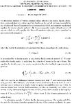
P. _ a,-A,-C, — _ A1‘ +CL7;C'z' _ (QB? - A,-C’,
' 2A,-B, ’ ’ ‘ 2A,- ’ ' ‘ 2A,-B, ’
S_ = av.-A,-+C'¢ a = ng cos92 a :a 77,?
l 2A,- ’ S 7110039,-’ P 353’
A
A, =n2%cos92, AP = Cs =n4%cos04,
C’ w B
0:5 Bs=—2'6—21/2B2‘
p E c(”2Sm 2 7'3) a p Egg
n4cos04 T13
U,.=j. U =U .
'n.1cos0,-' p 553
From these relations, it may be noted that, if the second and fourth media
have the same refractive index, the maximal value of the transmissivity in
the latter medium equals 1. If the intensity frustrated by the fourth medium
is represented as a function of the thickness of air, the form of this function
depends on the thickness of medium 2. A maximal value of transmissivity
does not necessarily correspond to an air gap with a zero thickness.
Transmissivity
1.5 Resonant Tunneling Effect 25
0.10 1 0-40 3
II
-1 n
1 C
4 1
T(d2m) “- . . . .
0.30
_.g 1.
._>. 3
0, , 6=46.79°
0-203 b) d,=10|.1m
E’
to
I: 3
0.10 '1
om l r . I r I . . . . . . I r . . . 1 - T . . . . I I | . . . F
0.00 10.00 2000 30.00
d2m—d1
Adz = d2 —d1 (in mm) Adz = d2 — d1 (in mm)
Fig. 1.25. The transmissivity as a function of the thickness of the air gap, for two
values of the thickness d1 [Salomon 1991a]
Furthermore, the maximal value Tmax of the transmissivity is a periodic
function of the thickness of medium 2. The curve represented in Fig. 1.26
exhibits such a variation, which corresponds to a resonance of the system.
At resonance, the transmissivity reaches 1, and the decrease of the inten-
sity goes on for more than a hundred nanometers, against ten nanometers
only outside the resonance. This very rapid decrease was measured by means
of a scanning tunneling optical microscope.
These results, which suggest the phenomenon of resonance, can be com-
pared with results formerly presented by Yeh on superlattices [Yeh 1985].
A superlattice is a structure obtained by depositing very thin layers, usually
monocrystalline, of materials with alternately high and low indices. Figure
1.27 provides a schematic representation of a superlattice.
GaAs-GaAlAs superlattices are the most extensively studied and have
numerous applications in optics as well as in optoelectronics. The index profile
of a superlattice can be expressed as a function of the thickness, as follows
n(:1:)=n2 if:r<—a,0<:I:<borNA<:I:,
if — a < cc < 0, (1.24)
= n1
where n(:1: + A) = n(:1:) if 0 < :1: < NA.
The different coefficients in the equation are as defined in Fig. 1.27. The
modes propagating in such a structure are of the form
E = exp[j(wt — 132)], (1.25)
26 1. Total Internal Reflection
1.0 -1
1 l
1 Pots
O8 3'
A 3 n1x2.0
3 n2an4=1_:.5a
E - 3 n3=1_O
3‘ 0.‘:
IE 3
.3 *
5 0.».
C O
S .
I-
o.2 ‘
3 L__
-l
0.01 . . .. . . .
0.0 10.0 20.0 30.0
Thickness of the air gap (pm)
Fig. 1.26. Maximal value of the transmissivity within the second medium, as a
function of the thickness of medium 2, with n1 = 2, n2 = n4 = 1.458 and n3 = 1 in
s polarization [Salomon 1991a]
4n(x)
"2
3N c(§.,,1)
(-
du
E, 32, _°_1, 3.;
<— <— <— (-
do be d1 b.
(b: §_(;+1)
"1
>
-a 0 b A (N-1)A NA
Fig. 1.27. Schematic representation of a superlatticc. Refractive indiccs and re-
flection coefficients in the structure
where [3 is the propagation constant associated with the fields propagating
within the structure. The amplitude of the field is given by the equation
' co exp[—jp(r1: + a)] + do exp[jp(a: + a)] if :1: < -0.,
a0 exp(—q:2:) + b0(q:c) if — a. < :1: < 0,
cl exp[—jp(:1: — b)] + d1 exp[jp(:z: — b)] if 0 < :1; < b,
Ea) Z 4 a1 exp[—q(a: — /1)]+ bexp[q(:1: — A)] if b < :1: < /1, (1.26)
(LN exp[—q(:1:—N/l)]+bN exp[q(:1:—N/1)] if N/1—a < .7: < NA,
\ cN+1 exp[—jp($ — NA — b)] if NA < IL‘.
1.5 Resonant Tunneling Effect
27
We consider only fields which present an evanescent behavior in media
with low refractive index and therefore satisfy the equations
1? = [(Tb2w/Clgll/2,
q = W - (7l1w/C)2l1/2-
(1.27)
The transmissivity in such a system can easily be calculated by means of
a matrix method. In 3 polarization, the value of the transmissivity is given
by the equation
[ sin K/1 ]2
cN+1 2 sin[(N + 1)KA]
TN+1 =| C0 l — p q SinKA 7
exp(J';vq)-(- + -) Sinh qa 2 + . 12
[ 2 q p J [s1n[(N + 1)KA]
(1.28)
where K A is given by the relation
cos KA = cosh qa cospb + 1/2(p/q — q/p) sinh qa sinpb. (1.29)
1.0 1 .0
0.0 0.0
1.0 1.4
0.0 0.0
1.0 1.0
0.0 0.0
1.0 1.0
0.0 0.0
1.0 1.0
0.0 0.0
Qa¢¢
3.20 3.25 3.30 3.35 3.40 3.45 3.50 3.20 3.25 3.30 3.35 3.40 3.45 3.50
B/(co/c) B/(«M c)
a b
Fig. 1.28. The transmission as a function of the propagation constant H. The ar-
rows indicate the propagation constant of the guided modes. The structures consist
of layers of GaAs and AlGaAs, with m = 3.2, a = 0.20, ng = 3.5. (a) b = 0.20 and
(b) b = 0.55
28 1. Total Internal Reflection
K is known as the ‘Bloch wave number’. The phenomenon of resonant
optical tunneling arises when
sin[(N + 1)KA] _
sin KA _
If these conditions are fulfilled, the Bloch wave propagates throughout
the whole structure.
Calculating the eigenvalues associated with the modes guided in a struc-
ture bounded by two low-index media. thereby ensuring the guiding, we ob-
tain values close to the values found in the case of the superlattice, as shown
in Fig. 1.28. In the second case, it may be noted that a second band appears
[Yeh 1985].
Superlattices, which are also known under the names of ‘photonic crys-
tals’, by analogy with solid crystals, and ‘band gap photonics’, have potential
applications in the field of light sources [Berger 1996]. Indeed, the produc-
tion of superlattices should permit the fabrication of sources emitting with
very high directivity, as well as the classical realization of filters. Different
groups are presently working on the production of superlattices from semi-
conductors.
We present here a type of superlattice different from those mentioned
above. This superlattice is a fiber obtained by the collective fusion of a bundle
of n capillaries. The illumination of this fiber under special angles reveals the
existence of privileged directions of illumination [Knight 1996]. This fiber is
represented in Fig. 1.29.
0. (1.30)
Fig. 1.29. Image obtained by scanning electronic microscopy of the photonic su-
perlattice fiber [Knight 1996]
1.6 Conclusion 29
Researches on photonic crystals are still going on. for these devices
have potential applications in a number of areas [Joan 1995, Tayeb 1997,
Painter 1999, Broeng 1999, Centeno 1999]. The production of these super-
lattices usually involves high technologies. However, the theoretical models
developed thus far still need to be experimentally confirmed.
1 .6 Conclusion
The phenomenon of the total internal reflection of a plane wave at the in-
terface of two media with different refractive indices has been described in
this chapter. Even if this model is unreal, it presents the advantage of being
rigorously treatable on the basis of Maxwell’s equations. In particular, this
model permits an exhaustive analysis of the field in the vicinity of the in-
terface where total internal reflection arises. This analysis shows that if on
average there is no energy transfer into the second medium, the field near
the interface might have a very high amplitude. The phenomenon of total
internal reflection can therefore be used for achieving an amplification of the
electromagnetic field amplitude, in particular at the interface where it arises.
The amplification of the electromagnetic field depends on different pa-
rameters, such as the wavelength of the source, the indices of the different
media, or the angle of incidence of the incident beam. We shall later see that
a judicious choice of the values of these parameters theoretically enables an
amplification of the field which might reach an order of 104.
When a laterally limited beam is totally reflected, a shift of this beam
occurs. It seemed to us interesting to devote a part of this chapter to this
phenomenon, which was experimentally proven at the beginning of the twen-
tieth century. The fact that this shift can be analyzed on the basis of classical
optics indicates that the evanescent properties of the electromagnetic field are
at the boundary of different physical approaches.
The measurement of the totally reflected beam does not provide any direct
information on the evanescent field itself. Therefore, it is necessary to induce
a perturbation on the system. The simplest way for perturbing the evanescent
field is by introducing a third medium with such a refractive index that
the total internal reflection is partially or totally frustrated. The frustration
of total internal reflection reflects a coupling between the different media.
The coupling depends on the value of the evanescent field between the first
two media. In the case of a weak perturbation, the value of the evanescent
field can be determined directly. Since the coupling involves several different
parameters, like the wavelength, the angle of incidence or the refractive index,
a large range of components are based on it.
2. Diffraction from an Aperture
and Dipolar Radiation
Among the different systems that generate evanescent. waves, the illumination
of an aperture by a plane wave is of particular importance for the recently
developed near-field microscopies. In the present chapter, we shall review
procedures developed by different authors for analyzing the field generated
by the diffraction of a plane wave from an aperture with extent smaller than
the wavelength.
The existence of evanescent waves in the vicinity of apertures was first re-
vealed by researches carried by Toraldo di Francia [Toraldo di Francia 1942a,b].
Experimental results for microwave frequencies were presented a few years later
[Schaffner 1949]. Similar results were obtained for antennas by Woodward in
1948. The latter sub ject can be seen as equivalent to the diffraction of light from
an aperture with finite extent and will not be detailed here |Schaffner 1949,
Toraldo di Francia 1952].
We end this chapter by recalling the description of the field emitted by
a dipole in free space and in the vicinity of an interface. The simplest element
to be described here is the dipole itself. The field generated by the dipole de-
pends on several parameters. In particular, the medium in which the dipole
lies plays an important part. Until recently, fluorescent labels were essen-
tially used by biologists for accurately investigating molecular interactions.
In order to be able to realize components from materials doped with fluores-
cent molecules, for example with erbium, it is essential to have a thorough
understanding of the interaction of the fluorescent element with its environ-
ment, and this can be achieved through the description of the field emitted
by a dipole.
2.1 Analysis of the Propagation of Light
Through an Aperture
Let us consider a plane wave illuminating an aperture. The simplest model,
presented in Fig. 2.1, is the case of a single aperture in an opaque screen.
The limitations of ray optics, where light is described as propagating
along straight lines, first became apparent in the seventeenth century, when
it was recognized by Grimaldi that the light which has propagated through
32 2. Diffraction from an Aperture and Dipolar Radiation
j)
plane wave ) \f transmitted beam
——>
slot in a perfectly
conducting screen
Fig. 2.1. ‘Slot with width larger than the wavelength illuminated by a plane wave
a slot is not entirely confined (Fig. 2.2) [Grimaldi 1665]. From this discovery
of diffraction phenomena therefore arose the necessity of developing a new
approach to optics.
L ML 0 "21:
Fig. 2.2. Diffraction of light from a circular aperture [Grimaldi 1665]
The exhaustive analysis of the diffraction of light from an aperture really
began with Fresnel [Maitte 1981].
Let us consider an electromagnetic wave propagating normally to the
2 plane where the aperture is located. At a distance greater than the half-
wavelength, the field can be expressed in terms of a superposition of elemen-
tary waves
E“”’”"‘") = /’"‘’“”‘’’“y’ (2.1)
x exp[—j(wt — k_.,,:1: — kyy — kz(k,,,, ky)z] dkxdky,
where f * (km, Icy) is the Fourier transform of f (kw, Icy). The integration domain
of this function is interrelated with the dimensions of the aperture by the
equations Aa:Ak,_. 2 27r and AyAIs:y 2 27r. The expression of the field involves
its decomposition into elementary waves. Each wave vector of these waves
satisfies the relation
“)2
—2 = kf, + kg + kg. (2.2)
C
2.1 Analysis of the Propagation of Light Through an Aperture 33
If the width of the slot is much smaller than the wavelength of the source,
Aka; remains small in comparison with kz = 27r. Light propagates without
undergoing any significant deviation, and remains confined within a cone
whose numerical aperture is as large as the size of the aperture is small. The
waves which propagate behind the aperture are propagative waves.
The smaller the extent of the aperture, the larger the aperture of the
emerging beam (Fig. 2.3). If the width of the slot is equal to A / 2, the emerging
beam fills the entire half-space. Elementary waves like kz = 0 and 139:2 +ky2 =
w2/c2 are in this case generated within the half-space.
. __>x _,
incident i} inddeflt
mane wave % plane wave Z.) __.:9 transmitted beam
7
__9 ——> /
screen with a slot screen with a slot
Fig. 2.3. Schematic representation of the diffraction of light from an aperture with
width (1
Let us now assume that the width of the aperture is smaller than )\/ 2.
In this case, elementary wa.ves of wave vectors, like 1:32 + 133,2 > w2/c2, are
diffracted from the slot. The dispersion relation has to be satisfied and re-
stricts kz to be purely imaginary. The field of these waves is thus expressed
as
E = E0 exp(—z/dp) exp(jwt — k,,:c — kyy), (2.3)
where dp is the penetration depth associated with the evanescent waves
2 -1/2
dp = (kg + k3, - (2.4)
These waves do not propagate along the z axis, but remain confined within
the 2: = 0 plane. They are related to high spatial frequencies of the slot
[Wolf 1985].
These direct calculations indicate the existence of evanescent waves in the
vicinity of apertures with dimensions smaller than half the wavelength. Lit.-
tle experimental evidence for the presence of evanescent waves in the vicinity
of subwavelength apertures is presently available. Only in the field of mi-
crowave frequencies have some measurements demonstrated the existence of
evanescent waves in the vicinity of such apertures.
In the following section, we examine in more detail the case of the diffrac-
tion of light from a circular aperture.
34 2. Diffraction from an Aperture and Dipolar Radiation
2.2 Diffraction of Light from a Circular Aperture
The theoretical analysis of the diffraction of light from an aperture with an
extent smaller than the wavelength was developed only in the 1940s, with the
researches carried out by Bethe [1944]. In the next decade, the analysis de-
veloped by Bethe was resumed by Bouwkamp and was developed into a more
complete description of the problem [Bouwkamp 1950b].
Evidently, the field can be determined from numerical simulations. We
base our presentation on works carried out by Leviatan at Cornell University
(New York) [Leviatan 1986].
2.2.1 Diffraction from an Aperture in an Infinitely Thin Plane
Figure 2.4 illustrates the parameters of the aperture and the illumination
conditions. An aperture with a limited extent is cut in an infinitely thin
perfectly conducting plane. The system is analyzed in different stages. The
situation in the initial problem is first divided into two equivalent systems:
in each half-space, the presence of the aperture is assumed to be equivalent
to a system consisting of a screen not containing any aperture. Further, it
is assumed that sources of magnetic current -1)! and M are present at the
location of the aperture, as illustrated in Fig. 2.5.
In Fig 2.5, n stands for the unit vector normal to the aperture. From the
equation of the field emitted by the sources a11d from the continuity conditions
of the fields at the aperture, the form of the field can be determined in relation
to the distance from the aperture. for different values of the radius of the
aperture (Figs. 2.6 and 2.7).
I11 the case of the system of a single aperture, three regions can be distin-
guished, as is illustrated in Figs. 2.6 and 2.7. In the vicinity of the aperture,
the field remains constant (proximity regime); it then very rapidly decreases
circular aperture
\
\
\
\
\
V9950“ 3 region b
pl’ 58 “hr 85
\
\
\
conducting screen
Fig. 2.4. The two regions coupled by the aperture
2.2 Diffraction of Light from a Circular Aperture 35
region a region b
Fae. lkufi ,
-M e M
F!’ fi‘
EH-Ea(-M) El,-,(M)_
—> —> —)
Hi+Ha(-M). Hb(M)
Originalsituation = Equivalence for region a + Equivalence for region b
Fig. 2.5. Decomposition, as described by Leviatan, of the system of an apertured
screen into two distinct systems
A
O
1
Normalized magnetic field (dB)
0.0! 0.10 1.00 10.00 IO0.00 I000 00
Up,
Fig. 2.6. The magnetic component of the field as a function of the distance from
the circular aperture of radius po = A/ 50. Three regions characterizing diffraction
can be observed: proximity regime, near-field regime and far—field regime [Leviatan
1986]
(near-field regime), and finally becomes similar to the field of a dipole at
a great distance (far-field regime).
The dependence of the field on the distance from the dipole is graphically
represented in the curves presented in Figs. 2.6 and 2.7. The field generated
by a dipole will be described near the end of the chapter. As soon as the
far-field is reached, a very good agreement between the two curves can be
observed. At grea.t distance, the aperture behaves like a dipole.
36 2. Diffraction from an Aperture and Dipolar Radiation
Normalized magnetic field (dB)
00: o.io ..¢o uobo uoolco xcccco
Z/po
Fig. 2.7. The magnetic component of the field as a function of the distance from
the circular aperture with radius po = A/ 500 [Leviatan 1986]
The average intensity of the energy flux of the field in the vicinity of
the aperture has also been determined by Leviatan. He thus obtained the
equation
Sz|,~=o = Re{[Eb(M1):1:Hb*]uz |,»} = 0. (2.5)
From Fig. 2.8 it can be noted that the average flux of the Poynting vector
decreases exponentially as the distance from the aperture increases.
Evidently, the model of an infinitely thin plane remains ideal. The problem
of the diffraction from an aperture in a screen with a nonzero thickness has
thus been studied by A. Roberts. These results will be reviewed in the next
subsection.
2.2.2 Diffraction from a Circular Aperture in a Thick Screen
The model we now describe applies to the diffraction of a plane wave
from an aperture in a screen with non-negligible thickness [Roberts 1987,
Roberts 1989]. The field is decomposed outside the aperture on the basis of
plane waves, and inside it on the basis of the modes guided by the aperture.
The geometry of the system is illustrated in Fig. 2.9.
The field outside the aperture can be written in the form
190
R(a1fy7x3y7 z) : "i’ + 7z)i=
2.2 Diffraction of Light from a Circular Aperture 37
1.50
§
125
Average flux of the Poyntmg vector
§ § § '
Average flux of the Poyntmg vector
1 .00
0.75
0.00 050 0.00
025
050 050
2.00
-3
1:?
&/
E
X/pa y/pa
Fig. 2.8. Average flux of the Poynting vector near the aperture, as a function of
the normalized distance z/po from the aperture, with respect to the :1: axis (a) and
y axis (b) respectively [Leviatan 1986]
where a and 7 are real terms and are bound to H by the following equations
x/1-0? -72, ifaa:+fiy+7z S 1,
fl(0t,7)= (2-7)
j a2+7—1, ifa:I;+By+'yz>1.
The equation for the transmitted field is
- k; _
R(a, 7, 2:, y, 2) = % exp[Jko(a:v - By + "/z)l- (2-8)
J
a /
h >
X
Fig. 2.9. Parameters used in the description of the aperture, of the screen and of
the incident field
38 2. Diffraction from an Aperture and Dipolar Radiation
The transverse component of the electric field within the aperture can be
determined from the expression of the modes of the aperture
2 oo oo 2
Et = X Z Z X lasnml Sin(kO1/snmly)
3:1 “:0 m=1 1:1 +b3nm; cos(k0z/)sPsnm;(p, (2.9)
Since the aperture presents an azimuthal symmetry, the eigenmodes of
the aperture can be expressed in terms of Bessel functions. The equations for
the modes !Psnm,(p, 0) and for the related variables asnml, bsnml and vmm;
are quite heavy. The interested reader is referred to the paper by A. Roberts,
where these calculations are presented in full [Roberts 1987]. The solution for
the problem of the diffraction of a plane wave by an aperture is deduced from
the continuity equations of the field at the different interfaces. The solut.ion
of these equations leads to long developments, which can be found in the
article mentioned above.
0.0 1.0 2.0 3.0 4.0 5.0 6.0 7:0 8:0 9:0 10.0 koa
1.5 -1
1.0 -
0.5 4
0-0 v 1 I I I 1 I u I u
0.0 1.0 2.0 3.0 4.0 5.0 6.0 7.0 8.0 9.0 10.0 koa
Fig. 2.10. The transmission coefficient as a function of the koa parameter for two
values of the screen thickness (h = 0 for the solid curve and h = a. for the curve in
dashed lines) (a) normal incidence, (b) the incident beam is 30° from the normal
to the aperture in TE polarization [Roberts 1987. with permission of the Optical
Society of America]
2.2 Diffraction of Light from a Circular Aperture 39
1.54 <50
1.0 4
05 ~
0-0 I I I ] f
o.o ' 1.0 2.0 3.0 4.0 5.0 koa
1.5. (b)
1.0 -
0.5 -
o.o , , , , ,
o.o 1.0 2.0 3.0 4.0 5.0 koa
Fig. 2.11. The transmission coefficient as a function of the koa parameter with
h = 10a (a) normal incidence, (b) the incident beam is 30° from the normal to the
aperture in TM polarization Roberts 1987, with permission of the Optical Society
of America]
The dependence of the transmission coefficient T on the radius of the
aperture, as well as the effect of the incidence angle of the incident wave on
the value of the transmission coefficient, were determined in this way. These
dependences are graphically represented in Figs. 2.10 and 2.11 respectively.
An abrupt fall of the transmitted signal arises when the value of the koa.
parameter becomes smaller than 1.8. Below this value, the modes propa-
gated by the aperture are purely evanescent. Since the screen has a nonzero
thickness, these modes are totally attenuated as they propagate through the
scree11. A value of T higher than 1 reflects the presence of the evanescent
field. If the width of the aperture rises, the coefficient of the evanescent field
falls and T tends towards a value of the order of 1.
The intent of the calculations performed by A. Roberts was primarily
to provide a better evaluation of the resolution power of microscopes where
an aperture with very small extent. is used as a source. Incidentally, the
resolving power of these microscopes does not seem to be enhanced by the
use of a screen with nonzero thickness.
40 2. Diffraction from an Aperture and Dipolar Radiation
2.3 Coupling Between Several Apertures
In practice, actual optical systems, whether they be designed for data trans-
fer or for microscopy, generally include several coupled apertures. In order
to characterize these systems, it is therefore necessary to analyze the phe-
nomenon of coupling between different apertures.
If the diffraction of a plane wave by an aperture generates evanescent
waves, the diffraction of the evanescent waves correspondingly creates prop-
agative waves. Leviatan has investigated the problem of the coupling between
two slots perforated in two separated screens. The parameters of this coupling
are illustrated in Fig. 2.12 [Leviatan 1988].
The space is first divided into different parts. Proceeding in the same
way as in the case of a single aperture, the system is separated into different
equivalent systems.
. A\X . .
region a region b region c
Fla’ 83 H13’ ab p'cI 8c
-> .
E_ conductive screens
/ \
H ‘
z
j - 9:: _ _ _ _ _ ._ _ _ >
52
2w, wide slot -- - —
2w, wide slot
Fig. 2.12. Illustration of the coupling between two apertures in two conductive
screens
The calculations of the field will not be presented in full here. Instead, we
shall discuss some of the results that were obtained with this method.
Leviatan was able to determine the dependence of the transmission coef-
ficient on the distance separating the two screens. Figure 2.13 displays the
variation of the transmission coefficient for different values of the distance.
The curves presented in this figure exhibit resonance peaks corresponding to
values of the distance that are multiples of the half-wavelength. Further, the
rapid decrease which can be observed between 0 and A / 2 reflects the coupling
with the evanescent waves generated by the first aperture.
As illustrated in Fig. 2.14, the transverse shift obviously modifies the value
of the transmission coefficient. For very small distances between the screens,
the value of the transmitted intensity falls very abruptly when the slots are
shifted. In contrast, if the screens are far from each other, the transmitted
energy does not tend to a zero value, but remains constant. This phenomenon
2.3 Coupling Between Several Apertures 41
o.7s~ I
/\
CICO‘ //rm\\¥§\
\
011-0 02/ \
0'0.‘ r I Y T Y
-0.3 -0.2 -0.! 0.0 O.l 0.2 S2/*
Fig. 2.13. Effect of the distance between the slots on the value of the transmission
coefficient [Leviatan 1988, with permission of IEEE]
201
L6 4
! an-0.04
L24
(-
0.0 <
~'i
I I
I
I
3
I
0.4- :
_:
0° 8' T I
-2 -I o I 2
S;/X
Fig. 2.14. Effect of the transverse shift between t.he slots on the transmission
coefficient [Leviatan 1988, with permission of IEEE]
42 2. Diffraction from an Aperture and Dipolar Radiation
Oflj
0.75-*
0.60 -1
,_ o4sJ
0.30 ‘
W votes
0.0
T T I I I f
on 0.: l.O 1.5 2.0 2.: 3.0
d/X
Fig. 2.15. The transmission coefficient as a function of the transverse shift between
the slots and of the distance between the slots [Leviata.n 1988, with permission of
IEEE]
is related to the fact that the light emitted from a small aperture remains
confined only in the vicinity of the near-field of the aperture b11t spreads out
beyond. In this case, irrespective of the value of the distance separating the
slots, a part of the light can be collected by a second slot. as can be see11 in
Fig. 2.15.
2.4 Dipolar Emission
The calculations of the field present in the vicinity of an aperture with a sub-
wavelength extent suggest. that at great distances the variation of the field is
similar to the emission of an oscillating dipole [Bouwkamp 1950b]. We shall
hereafter return in more detail to the case of the emission of a dipole. The
importance of understanding the physics of the field emitted by a dipole is
related with the fact that the development of near-field optics have led to
the proposal of several models for describing the scattering of an electro-
magnetic wa.ve by different structures. An example of an elementary object
often encountered is that of a subwavelength-sized spherical particle. A sim-
ple method for calculating the electromagnetic response of such a sphere
is by considering a dipole with polarisability as given by the Clausi11s-
Mossotti relation. More detail on this subject can be found in recent articles
[Xiao 1996, Nevotny 1997, Chaumet 1998].
2.4 Dipolar Emission 43
2.4.1 Expression of the Dipolar Field
The description presented here will be based on the analysis of the field
present in the vicinity of an aperture which is developed in the book by
Born and Wolf [Born 1959]. Figure 2.16 defines the parameters used in these
calculations. It is assumed that the dipole is located at the origin of the
coordinate system.
Fig. 2.16. Schematic of the dipole with momentum parallel to the z axis
We shall resume in the following the calculations described by Born and
VVolf [Born 1959].
Let us consider a linear dipole vibrating along the unit vector 11. The
electric polarization satisfies the equation
Pe(r, t) = p(t)6(r — r0)n, (2.10)
where 5 is the Dirac distribution and p(t) the polarizability, the latter being
time—dependent.
We skip a few steps in these calculations, which are presented in full in
Born [1959]. The equations for the components of the electromagnetic field
generated by the dipole are
, .
E, = 2 P 7”. ~0,
<3‘ + COb
fl E9 = ($3 + JP; + sine, (2.11)
where 1') and 1')’ denote the first and second derivatives of p(t) versus t.
44 2. Diffraction from an Aperture and Dipolar Radiation
In this form, the expression of the components does not allow us to sep-
arate the terms corresponding to propagative waves and the terms corre-
sponding to evanescent waves. In order to differentiate the evanescent part of
the field, it is necessary to assume that the dipole is surrounded by a closed
surface, and then to determine the flux of the Poynting vector through this
surface.
2.4.2 Energy Emitted by a Dipole
The Poynting vector P can be expressed as follows:
P = E /\ H, (2.12)
P = EgH¢e,. — E,.H¢eg. (2.13)
Proceeding to the integration of e,» - P upon a sphere of radius 7" and
retaining the real terms, we determine the average va.lue of the energy pass-
ing through the surface of the sphere. The power emitted by the dipole in
a medium with dielectric constant e and magnetic constant it is equal to
W4
W: —— 2 2.14
mrux/#6 lpl , ( )
where W is expressed in CGS units.
The smaller the wavelength, the higher the emitted power. It is apparent
that only the 1/7' components present a nonzero contribution, which corre-
sponds to the 1/T2 variation of the energy of a spherical wave. The remaining
1/7'2 and 1 /7'3 components represent the evanescent waves. For very small dis-
tances from the dipole, the amplitude of the evanescent field is very large and
extends largely over the amplitude of the propagative field.
Everything happens as if the energy associated with the evanescent waves
was leaving the so11rce and periodically returning inside it, without being ever
lost by the system. This character of evanescent waves has already been noted
in the preceding chapter.
Evanescent waves can be detected only if they are perturbed and therefore
are partially transformed into radiative waves. A possible approach for achiev-
ing this perturbation is by frustrating the evanescent waves from a semiin-
finite medium. The first demonstration was achieved near the beginning of
the twentieth century by Sélényi [Sélényi 1913].
The experiment carried out by Sélényi basically consisted in illuminating
a fluorescent material placed at the surface of a semicylindrical prism, as
illustrated in the schematic of Fig. 2.17.
The fact that the presence of light can be observed when 0 has a value
higher than the critical angle proves the existence of evanescent waves asso-
ciated with the fluorescence of the material deposited at the surface of the
prism. Indeed, only if evanescent waves are present within the fluorescent
medium can waves with directions of propagation comprised between 0c and
7r/ 2, and between —0c and —7r/ 2 be generated inside the prism.
2.4 Dipolar Emission 45
9>B, e>ec
9<9c
Fig. 2._17. Principle of the Sélényi experiment [Sélényi 1913]
More accurate experiments based on the same principle were carried out
by Carniglia et al. The arrangement used for these experiments is represented
in Fig. 2.18. The experimental results and the theoretical curves are presented
in Fig. 2.19. The calculations on which the latter are based are detailed in
the article by Carniglia [1972].
dyelayer
\
\
\
\Z
monomolecular layers . X
polanzer
%
filter C?
Fig. 2.18. Arrangement used for observing the light emission with respect to the
angle of measurement. The plate is kept fixed while the detector rotates about the
axis of the cylindrical window [Carniglia 1972]
It may be noted that the experimental measurements are quite consistent
with the numerical simulation. This agreement quantitatively demonstrates
the existence of evanescent waves emitted by the dipole.
46 2. Diffraction from an Aperture and Dipolar Radiation
Fluorescence (a.u.)
60' 9,. 7 o ' go’
Angle of observation 6
Fig. 2.19. Experimental results for an incident plane wave. The solid curve is
based on theoretical calculations. The curve in dashed lines takes into account the
effect of the finite size of the aperture [Carniglia 1972]
The authors have demonstrated in the same way, and with a similar ar-
rangement, that if a dipole can generate evanescent waves, it can correspond-
ingly absorb evanescent photons [Carniglia 1972].
We now return i11 det.ail to the effect. of the presence of a second medium
on the dipolar emission.
2.5 Dipolar Emission in the Vicinity of a Surface
The presence of a surface in the vicinity of a dipole modifies the nat11re
of its emission. In 1909, Sommerfeld recognized that the Earth acts on the
evanescent part of the waves emitted by an antenna, and that the energy
emitted by the antenna is absorbed by the Earth. In the presence of a medium
near the dipole, the dipola.r emission has the same form.
In Fig. 2.20 are illustrated the orientations that the dipole may assume
with respect to the interface. It will be assumed hereafter that the dipole
is located within the medium 1 of refractive index n1, and that. it lies at
a distance d from the second medium of refractive index 72,2. The dipole is
denoted by or _L depending if it.s momentum is parallel or perpendicular to
the surface of the second medium.
VVe have seen earlier that in the case where the dipole lies within a ho-
mogeneous isotropic infinite medium. the total power emitted could be ex-
pressed by (2.14). The emitted power corresponds to the propagative waves
emitted by the dipole. If the field generated by the dipole is perturbed by
the presence of the second medium, a part of the evanescent waves ca11 be
2.5 Dipolar Emission in the Vicinity of a Surface 47
region 1
/ region 2
/
”////
Fig. 2.20. Schematic of a dipole in the vicinity of an interface
transformed into propagative waves. This can be demonstrated with a vari-
ety of formalisms. Among the descriptions of this interaction, those devel-
oped by Chance and Lukosz can be mentioned [Kuhn 1970, Chance 19753.,
Chance 1975b, Lukosz 1977, Nha 1996, Lamouche 1999]. In order to show
the role of evanescent waves in the interact.ion of the dipole with the second
medium, we here examine results presented by Lukosz [1977].
Lukosz calculated the energy emitted by the dipole in the presence of
the second medium. The following expression yields the energy emitted by
the dipole with an arbitrary orientation. The emitted energy is normalized
with respect to the energy emitted by the dipole in the presence of a single
medium
W(d)/W = cos2 6[W(d)/W]; + sin2 0[W(d)/W], (2.15)
where
P ' ImlEr(11?o)l
p - Im[E(a:0)] '
Figure 2.21 describes the variation of the emitted power when the second
medium is of higher index than the medium in which the dipole lies. Figure
2.22 describes the inverse case.
Different conclusions can be drawn from the observation of these curves.
Let 11s first consider the case where the dipole is far from the surface (d >
/\ / 2). We can observe here the presence of oscillations with a period of A / 2.
These oscillations are present in particular when the dipole is parallel to
the interface. This phenomenon is due to the dipolar emission which arises
normally to the direction of the dipole [Stratton 1941]. In this case, the light
emitted by the dipole in the form of propagative waves is reflected at the
interface and interferes with the emitted light. Depending on the distance
between the dipole and the surface, these interferences are either constructive
or destructive.
We now turn our attention to the curves obtained in the case where
the surface lies within the near—field of the dipole. If the second medium is
W(d)/W = 1 + (2.16)
48 2. Diffraction from an Aperture and Dipolar Radiation
_J_ //
O . 0.5 1 0 0.5 1
Fig. 2.21. Normalized power emitted by a parallel or perpendicular dipole as
a function of d/A, in the case where n > 1. d is the distance between the dipole and
the interface, /\ is the wavelength and n = 111/112 [Lukosz 1977]
.L //
n = 1/3
n=Z3
0 0.5 1 0 0.5 1
Fig. 2.22. Normalized power emitted by a parallel or perpendicular dipole as
a function of d/A, in the case where n < 1. d is the distance between the dipole a11d
the interface, A is the wavelength and n = n1/n2 [Lukosz 1977]
of higher refractive index than the medium in which the dipole is located,
this medium frustrates the evanescent waves, thus transforming them into
propagative waves. This induces a rise of the radiation of the dipole.
If the index of the second medium is smaller than the index of the medium
containing the dipole, the waves emitted by the dipole can be totally reflected
by the second medium. Evanescent waves are then generated inside the second
medium, while the radiation is reduced.
Another approach is based on the consideration of the lifetime 7' of the
dipolar emission [Drexhage 1970, Drexhage 1974, Lukosz 1977]. The lifetime
is related to the energy emitted in the entire space by the following equation
[Lukosz 1977]
T(d)/T = lW(d)/Wl'1» (2-17)
where 7' is the lifetime associated with the dipole in free space. Hence, the
measurement of the lifetime is equivalent to a measurement of the normalized
power emitted in the entire space of the dipole. We end this section with an
example which has applications in the realization of optical amplifiers.
2.6 Conclusion 49
I-
I l 1
2 3 4 5
d (|O'° cm)
0)]-
Fig. 2.23. Normalized lifetime of Eu3+ ions as a function of the distance to a silver
film. The solid curve corresponds to the measurements. The dipole is assumed to
be parallel to the film with an efliciency of 0.85. m = 1.5, ng = 0.06 :l: 0.02 and
k2 = 4.11 :l: 0.007 [Chance 1974]
Figure 2.23 represents the lifetime of erbium molecules as a function of
the distance separating the Eu3+ ions and a silver film [Chance 1974].
The measurements presented in the Fig. 2.23 were carried out by Drexhage
[1968]. As in the case of a dipole in front of a dielectric, the curve exhibits
oscillations which indicate the existence of interference phenomena. Further,
an important fall of the lifetime can be observed when the metallic film lies
within the near—field of the dipole. This fall expresses a nonradiative transfer
from the Eu3+ ions to the metal.
2.6 Conclusion
For a long time, the diffraction of light from an aperture was analyzed without
taking into account the presence of evanescent waves. However, when the
aperture is of subwavelength extent, the phenomenon of diffraction requires
more complete studies for its analysis. In fact, the rigorous analysis of the field
in the vicinity of subwavelength apertures really started being developed with
the researches carried out by Bethe [1944] and Bouwkamp [1950a, 19501)].
As described by Leviatan, when an aperture with a subwavelength ex-
tent is illuminated by a plane wave, the space beyond the aperture can
be divided into different regions with distinct propagation characteristics
[Bouwkamp 1950a, Bouwkamp 1950b]. Within the first region, referred to
as the proximity region, the field remains constant and confined. The dimen-
sion of this region is very small: a. fraction of the wavelength. The second
region, or region of the near—field of the aperture, extends over a half of the
wavelength. In this region, the field decreases very rapidly. Lastly, within the
third region, or far-field region, the field decreases inversely with respect to
the distance from the aperture. This region extends indefinitely.
50 2. Diffraction from an Aperture and Dipolar Radiation
More realistic calculations, taking into account the thickness of the screen
in which the aperture is located, have vindicated the previous results. Further,
as actual systems usually include several successive slots, it was of interest
to discuss here some results on the coupling between slots. Here again has
appeared the effect of the near-field on the coupling between two slots.
The results of these calculations have several direct applications, related
in particular to ‘near-field microscopy’, both in the case of highly localized
sources and for the analysis of the field diffracted by subwavelength objects.
These applications will be described in the last part of this book.
Evanescent. waves can be generated from the total internal reflection of
plane waves or from the light emission of a dipole. This field remains confined
near the dipole and does not transport any energy at great distances from
the dipole. In order to obtain information about the near-field, it is therefore
imperative to have it perturbed, so as to transform a part of the evanescent
field into a propagative field. This can be achieved by using a semiinfinite,
either dielectric or metallic medium, or else a second dipole.
The light emission of the dipole can be characterized by its probability
of emitting a photon. In other words, the emitted power can be related to
the notion of lifetime. This possibility is being widely used in spectroscopy.
It seemed to us that this needed to be mentioned, even if there are few
applications related to dipolar emission described in this book.
3. The Evanescent Field in Guided Optics
The development of lasers during the 1960s has led to a renewal of interest
in optics. This trend was amplified in the 1970s, when it was recognized
that silica fibers could guide light with losses of the order of dB/km. This
was realized first with the sources available at the time, for example with
lasers, and later with laser diodes, which present the advantage over lasers of
being extremely compact. Another advantage of optical fibers is that the raw
material used in their fabrication is silica, which is found in great quantities on
Earth. It was soon theoretically demonstrated that perceptible enhancements
of the transmission properties of optical fibers could be obtained by modifying
their characteristics. Experimental results rapidly confirmed these theoretical
predictions.
The evanescent field itself is not actively involved in the guiding of the
light. Rather, the evanescent field can be regarded as reflecting the fact that
the light is being guided. This chapter begins by describing the basic theory
of guided modes, which will serve in the analysis of the characteristics of the
evanescent field associated with these modes. We then describe planar and
confined waveguides respectively, and finally treat the case of optical fibers.
3.1 The Evanescent Field in Planar Optics
3.1.1 Analysis of Planar Waveguides
Let us consider two semiinfinite media with refractive indices ng and n3 re-
spectively. It will be assumed that these two media are separated by a medium
of index n1. If the conditions of total internal reflection are satisfied at the
1-2 and 1-3 interfaces, a plane wave will be guided between the second and
third media (Fig. 3.1).
A wave guided between these media satisfies the following conditions
01> sin”1(n2/n1),
(3.1)
Hi > sin—1('n3/n1).
The simplest description of the propagation of light in a waveguide is in
terms of ray-optical arguments. This however requires that the very notion of
52 3. The Evanescent Field in Guided Optics
X
2a
n2
Fig. 3.1. Guiding of light between the two media
‘ray’ has a physical meaning for such a system, namely that the dimensions of
the guiding area, in particular its thickness, are larger than the wavelength.
In the following, it will be assumed that these conditions are satisfied.
Let us consider now a more complicated model: instead of a single layer, as
before, it will be assumed that several layers are inserted between the second
and third media. If the indices of the internal layers are higher than the indices
of the two semiinfinite media, and provided that the previous relations hold
at the two interfaces, the ray is guided by this stratified system (Fig. 3.2). In
this case, the path of the ray is formed by segments of straight lines. If the
number of layers is very high, the path of the rays is a curve which directly
depends on the index profile of the waveguide.
Fig. 3.2. Propagation of rays in a stratified system with parabolic index profile
It may be noted that the guiding, i.e. the fact that the ray returns back
into the center of the core, does not necessarily take place at the last interface.
If the incidence angle at an internal interface is high enough, the guiding
might arise at this interface. In this case, the evanescent field associated with
the different plane waves is present not only within the last medium, but also
within the internal layers.
The representation of the path followed by the rays in Fig. 3.1 is not
entirely exact, for it does not take into account the Goos—Hanchen shift which
arises at each total internal reflection 3.3). As observed by Adams,
the effective propagation of the rays in the waveg11ide is equivalent. to the
propagation inside a waveguide with width 21).
The propagation in these waveguides can be analyzed on the basis of
Maxwell’s equations and of the boundary conditions [Adams 1981].
3.1 The Evanescent Field in Planar Optics 53
V
Fig. 3.3. Effective width of the waveguide resulting from the Goos—Héinchen shift
For TE modes, the solution of Maxwell’s equations yields
Aexp(—7'a:) if :1: Z 0,
Ey = Acos qsc + Bsin qa: if 0 2 :1: 2 —2a, (3.2)
(A cos 2aq — B sin 2aq) exp[p(m + 2a)] if — 2a 2 :13,
and
—A exp(—'r:1:) if :13 Z 0,
Hz = 1- —q(—Asinq:c + Bcosqa:) if 0 Z :1: 2 -2a,
WHO
p(A cos 2aq — Bsin 2aq) exp[p(:z: + 2a)] if — 2a 2 12:, (3 3)
where p, q and 7" are bound to the propagation constant by the equations
2 = ngkz _ 62,
p2 = 52 _ n§k2, (3.4)
7'2 = flz — 713192,
where k = w(,u0e0)1/2. The eigenvalue equation derived from the continuity
conditions is
61(1) + 7‘)
£12 - 10'!“
For TM modes, the components of the fields can correspondingly be writ-
ten
tan(2aq) = (3.5)
C'exp(—m:) if :1: Z 0,
Hy = Ccos qa: + Dsin qzr if 0 2 2: 2 —2a, (3.6)
(C cos 2aq — Dsin 2aq) exp[p(:c -1- 2a)] if — 2a 2 2:,
54 3. The Evanescent Field in Guided Optics
and
’ C
T—2— exp(—7':1:) if :1: 2 0,
"0
E2214 iZ(—C'sinq:z:+Dcosq:c) if02:z:2—2a,
6050 "0
%(C cos 2aq — D sin 2a.q) exp[p(:I: + 2a)] if — 2a 2 3:.
x "0 (3.7)
The eigenvalue equation is thus
(nzp + 7227* n2q
tan(2a.q) = 20 2 ) 1 (3.8)
2 4 '
n2n3q2 — nlpr
The field inside the waveguide is a sine or cosine function. In contrast,
within the cladding, i.e. within the medium of index 17.2 or n3, the variation
of the field is exponential [Ostrowsky 1979, Adams 1981, Hunsperger 1985].
As an infinite field does not have any physical meaning, we restrict ourselves
here to the solution of the case of an exponentially decreasing field. Here
again, the form of the evanescent field turns out to be similar to the form of
the evanescent field generated by the total internal reflection of a plane wave.
3.1.2 Production of Step-Index Planar Waveguides
Step—index planar waveguides are produced by depositing a layer upon a sub-
strate. Different methods are available for the production of the guiding layer.
One of these methods is the technique of epitaxial growth. This technique
imposes several conditions on the preparation of the sample. The structure
has to be effectively guiding, and the materials used must be compatible, in
order to adhere to one another and for ensuring the stability of the resulting
structure.
A more recent method uses the ‘sol—-gel’ technique: a material in the form
of a gel is deposited upon a substrate a11d submitted to an overheating in-
tended to solidify it. Lastly, the guiding layer can be for111ed by the deposit
of a polymer material.
Each material has a specific transmission band and other distinctive prop-
erties. Table 3.1 reproduces the characteristics of step-index planar wave-
guides fabricated with different teclmiques.
The value of the optical losses in these waveguides is intimately related
with the state of the surface. By adding a supplementary layer at the surface
of the waveguide, the losses can be reduced, so that the amplitude of the
evanescent field becomes zero at the interface between the waveguide and
air.
Ion-implanted and diffused waveguides have an index profile which di-
rectly depends on the technique used for their fabrication [Hunsperger 1985,
3.1 The Evanescent Field in Planar Optics 55
Table 3.1. Comparison of different fabrication techniques of planar waveguides.
Material Substrate Transmission Loss Distinctive
band (urn) (dB/cm) characteristics
Semiconductor
Si, SiGe Silicon 1-10 0.1 Si technique,
microelectronic
integration,
heavy
technology
Semiconductor
III-V (binary, GaAs, InP 0.5—1O 0.1 Heavy and
ternary, expensive
quaternary, technique
superlat— adjustable
tice,...) spectral band
.S'ol—gel
Silicon (either Any O.2—1O Some dB /cm Simple and
doped or (immature inexpensive
pure), technique) technique,
BaTiO3, easily achieved
LiNbO3... doping
PZG Glass, CaF2... O.4~2 1 Recently
developed and
relatively
simple
technique
LiNbO3 LiNbO3 0.1 Ion
implantation
Polymer
Pure or doped Any 0.2—10 2 Relatively
organic simple
material technique,
thermal and
time stability‘?
Favennec 1993, Fogret 1994]. As an example of a waveguide with specific
characteristics, we may mention waveguides fabricated by the diffusion of sil-
ver in glass [Zolatov 1978]. The characteristics of these waveguides are surn-
marized in Table 3.2.
Diffusion techniques are not really adapted to the production of buried
waveguides, except in some rather special cases: waveguides produced by
the diffusion of silver in certain glasses under an electric field are but an
example. For the fabrication of buried waveguides, high-energy ion-diffusion
techniques may be used. If the implantation is accompanied with a decrease of
the refractive index, a confinement of the field limited to the non—implanted
56 3. The Evanescent Field in Guided Optics
Table 3.2. Comparison between two fabrication techniques of doped waveguides.
Technique
Ion implantation
Ion diffusion
Implanted elements
Any element in ionized
form
Elements compatible
with the host material
Host material
Any material
Silicium, silica,
ZBLAN, glasses...
Transmission band (pm)
0.2—10 depending on the
bombarded material
().2—10 depending on
the bombarded
material
Loss (dB / cm)
1
0.1
Distinctive characteristics
This method requires
the use of a convenient
implanter. In the case
where the implanted
area is guided, the
thickness of the
waveguide is limited
Simple and rather
inexpensive technique,
which can be
completed with
a diffusion under an
electric field
A Refractive index profile
/ f \ \
V \ . . . .
I \\ Field distribution
/ \ \
T i , ' _
air : implanted region : Depth of implantation
Fig. 3.4. Example of the profile of a lithium niobate plate implanted with a proton
beam
zone can be obtained. In this case, the implanted zone acts as an optical
cladding (Fig. 3.4).
3.2 Confined Waveguides
The field present inside the waveguide actually needs to be laterally con-
fined. Several different techniques can be used for the production of confined
waveguides. Waveguides fabricated with different methods are represented in
Fig. 3.5.
3.2 Confined Waveguides 57
a- guide made by implantation b- guide made by difussion c- "ribbon" guide
Fig. 3.5. Different types of confined waveguides (a) ion-implanted waveguide, (b)
ion-diffused waveguide, (c) strip-loaded waveguide produced by lithography and ion
etching
The production of the first type of waveguides represented in Fig. 3.5
proceeds as illustrated in Fig. 3.6. The fabrication technique for strip-loaded
waveguides is shown in Fig. 3.7.
The determination of the propagation of the modes in confined waveguides
is more complex than in the case described in the preceding paragraph. Fur-
ther, there is not any general analytical solution for this problem. The anal-
ysis of these waveguides can be achieved by using either the finite elements
method [Yeh 1975] or the beam propagation method (BPM), developed by
Feit and Fleck [Feit 1978, Feit 1980]. However, to detail here at length all
the calculations necessary for the analysis of these waveguides would extend
largely beyond the scope of this book.
Beam
W
Ions
/ Resist L l i l
(3) (c)
(b) (d)
Fig. 3.6. Description of the fabrication process of an ion-implanted waveguide (a)
deposit, irradiation and developing of an electroresist or a photoresist, (b) etching
of the unexposed parts for the production of the mask, (c) diffusion or implantation
through the mask, ((1) withdrawal of the mask
58 3. The Evanescent Field in Guided Optics
llllllllll
(8) (0)
Beam
Resist
(b) (d)
Fig. 3.7. Fabrication process of a strip-loaded waveguide (a) deposit by epitaxial
growth of the different layers, (b) deposit of the sensitive resist and local sensitiza-
tion, (c) developing of the resist, (d) selective etching
3.3 Optical Fibers
3.3.1 Ray-Optical Analysis of the Propagation in Optical Fibers
The propagation of light inside an optical fiber can be analyzed in terms of
ray-optical arguments [Arnaud 1976]. The relative variations of indices inside
the fibers are generally smaller than one, and therefore the theory of paraxial
rays can be applied here.
The path followed by the rays is deduced from the following two equations
[Arnaud 1977]
d2:1:/dz2 — —8U(:I:, y)/81:,
(3.9)
dzy/C122 = -5U($,y)/By.
where 3: and y are z dependent. U (a:, y) is related to the index profile by the
equation
U(:1:,y) = 1 — n(:r,y)/no, (3.10)
where no is the refractive index along the axis of the fiber.
Representing in such a way the propagation of light in fibers, the pres-
ence of fluctuations of the diameter of the fiber as well as microbending can
be readily incorporated into the model [Grignand 1980, de Fornel 1983]. Fur-
ther, this method permits us to analyze the propagation of the rays inside
a fiber whatever the index profile of the fiber is.
3.3 Optical Fibers 59
Fig. 3.8. Propagation of a light ray inside an optical fiber
The equations describing the propagation of rays can be easily solved
using Eu1er’s method. The light rays which correspond to the source are
injected in the 2: = 0 plane. The path followed by the rays is then calculated
segment by segment (Fig. 3.8). If a perturbation arises, the only condition
to be satisfied is at the interface between the core and the cladding. If the
angle of the ray and the interface is less than the critical angle, the ray is
not guided any more and the calculation of the propagation of the ray can
be ended.
The amount of the losses resulting from perturbations can therefore be
determined from the number of rays that reach the location 2, by comparing it
with the number of rays that were injected (Fig. 3.9). The time of propagation
of the rays can be determined in the same way. If all rays were injected
at a time to in the form of an impulse, the value of the scattering of this
impulse at the end of a given length of fiber can thus be determined. The
numerically determined value of the steady-state length of different fibers
A
ulse .
roadlng
exit of the first ray
1 1 I >
fiber length
>
Fig. 3.9. Variation of the spreading of a light impulse injected in a. fiber subjected
to microbending. The transition to the equilibrium regime appears distinctly on
the curve
60 3. The Evanescent Field in Guided Optics
subjected to random microbending was found in agreement. with experimental
measurements.
The notion of ‘ray’ does not correspond exactly to an eigenmode of the
fiber and it must therefore be cautiously used. In fact, only a congruence of
rays can be said to be equivalent to an eigenmode of the fiber.
Different authors, see for example Marcuse, Adams. Snyder or Joindot
have given comprehensive descriptions of the propagation of light in wave-
guides [Marcuse 1972, Adams 1981, Snyder 1983, Joindot 1996]. In the fol-
lowing sections, we review the theory of optical waveguides a11d provide an
account _of the basic principles which are necessary for understanding the
physics of devices containing optical fibers. VVe begin with the simplest case:
step-index fibers.
3.3.2 Modes of Step-Index Fibers
A step-index fiber consists simply of a silica cladding and of 3. doped core
with refractive index higher than that of the cladding. This geometry and
the associated optical characteristics permit an analytic treatment. of these
fibers.
We assume here that modes of propagation constant fi and azimuthal or-
der 1/ can propagate inside a structure of this type. [3 is the constant of prop-
agation of the mode in the direction along which the waveguide is uniform,
while 1/ expresses the azimuthal symmetry of the system. The expression of
the field is thus
EU‘, 9, Z, t) = lE-(7')e- + E9(7")€9 + Ez(7‘)ezl expj(wt - V9 - fiz),
H0‘, 9, z,t) = lH1~(7")e- + H0(7")e0 + H.~.(7')ez] expj(wt - V9 - £32)-
From Maxwell’s equations we derive the equations of propagation in the
two media, i.e. in the core and in the cladding respectively
(3.11)
2
d2Ez(r) 1 dEz 1/
T2: + ; Tdgr) ‘l’ (W25/J40 ‘ :82 - Ez(T) = 0:
(3.12)
d2Hz(r) + + 2 _ g2 _ V2 H (7.) _ 0
T9‘ 7' dz “’ “*0 :2 z - -
The expression of the 2 component of the electromagnetic field is given
by the following relations
E,._.(r) = Eo.],,(ur/a) if 0 < 1" < a,
(3.13)
if r > a,
3.3 Optical Fibers 61
with u and w defined by the equations
_ 2 2
u — ax/konl — (32,
w = a‘/fi2 — kgng,
where 121 and 77.2 are the refractive indices of the,core and of the cladding
respectively. Here J,, is the Bessel function pf the first kind of order 1/ and
K, is the modified Bessel function of the first kind [Abramowitz 1964].For
Hz(r), we obtain similar expressions. The other components of the field can
be directly derived from these relations on the basis of Maxwell’s equations.
The part of the field which extends outside the core corresponds to the
evanescent part of the mode. Due to the simple geometry of step—index fibers,
the localization of the evanescent part of the field can be easily achieved.
Figures 3.10, 3.11 and 3.12 indicate respectively the variations of the
E2 and Hz longitudinal components of the TM01, TE02 and EH21 modes.
V denotes the normalized frequency. In the case of a step-index fiber, the
equation for the normalized frequency is
V = (11.2 +w2)1/2 = [%Ta‘/nf — . (3.15)
(3.14)
Ez
Fig. 3.10. Radial dependence of E; (r) for the TMO1 mode of a fiber with normal-
ized frequency V = 7.2
The modes of an optical fiber are sensitive to all the perturbations that
the evanescent part of the field undergoes. It might be instructive to express
the relative ratio of the power propagated in the core 77 as a function of the
normalized frequency of the fiber (Fig. 3.13)
2 2 - 1
PCOFG u
U
= =1—— w2+l21/2+—:—
77 Pcore + Pcladding V2 ( ) U2 _ [2
(3.16)
62 3. The Evanescent Field in Guided Optics
IIfTYITrI
.
-0
Fig. 3.11. Radial dependence of H 2 (7') for the TEO2 mode of a fiber with normalized
frequency V = 7.2
FIIVYY
Fig. 3.12. Radial dependence of Hz (r) for the EH21 mode of a fiber with normalized
frequency V = 7.2
For the fundamental mode (l = 0), we obtain the curve represented in
Fig. 3.13. This curve indicates that the field extends very rapidly inside
the cladding when the normalized frequency decreases and becomes less
than a predetermined value. Below this value, the relative importance of the
evanescent part of the field makes the field very sensitive to any perturbation,
for example to bending or to variations of the refractive index.
It is apparent that when the mode draws nearer to its cutoff frequency,
the energy of the mode is contained within the evanescent part of the field.
In this case, the mode is less guided. The mode is highly sensitive to defects
in the fiber as Well as to bending. For producing fibers where the light will
be effectively guided, it is preferable to proceed 11nder conditions limiting as
much as possible the evanescent part of the field, but preventing the distribu-
tion inside the core from being t.oo confined. This will permit the avoidance
of problems which might arise when components are being connected.
Perturbations induced on the evanescent part. of the mode might cause
a loss of a part of the energy of the mode. Likewise, the modes can also be
excited by coupling the light to the evanescent part of the mode. The first
Optical Fibers 63
711-
0,8
0,6 '
0,4 -
0.2 -
I l I
012 3 4V5
Fig. 3.13. The dependence of the norni-a.lized power guided inside the core on the
total power as a fi111(:t.io11 of the normalized frequency
experirnents in this direction were (:a.1‘1‘ied o1_1t by Stewart and, El. few years
later, by Szczepanek [S7.czepa.nek 1978, Facq 1980].
The experi1nenta,l arraiigeinent. represented in Fig. 3.1-1 was used for ex-
citing and exaniiniiig the modes. Figure 3.15 represents one of t.he modes
excited under these conditions.
Incident beam
Coupling with
a prism
Propagation of
the excited mode
Fig. 3.14. Arrangement used for the exc-itation of the modes
Fig. 3.15. Observation of the ne-ar—field of a mode excited inside a. pambolic graded-
index fiber. The diameter of the core is equal to 80 pm. The orders of the mode are
,u = 0 and 1/ = 5 |Szczepanek 1978]
64 3. The Evanescent Field in Guided Optics
As shown by Stewart, modes of a high order can be excited using this
technique [Facq 1980]. Figure 3.15 corresponds to the excitation of the mode
of orders )1 = 0 and 1/ = 5, obtained by Szczepanek in the case of a fiber with
core of diameter 80 um.
An inherent disadvantage of this technique is that it can be used only
for the excitation of modes of high order (Fig. 3.15). This technique has
therefore been replaced by methods based on the direct excitation of the
modes [Facq 1980, de Fornel 1983, Facq 1984].
3.3.3 Modes of Inner-Cladding Fibers
Enhancement of the guiding properties of step-index fibers can be obtained
by creating an index depression between the core and the cladding. This leads
to the production of fibers with three index levels. The index profiles of two
different fibers of this type are schematized in Fig. 3.16. We shall discuss
hereafter in general terms this class of fibers, referred to as ‘inner-cladding
fibers’.
A R°f"a°“V° ind“ ARefractive index
n1
n2
'1. ——:——- :—-‘_ L;———
> L! e >
Distance to the fiber axis b 3 Distance to the fiber axis
Fig. 3.16. Index profile of raised and depressed inner-cladding fibers
The thorough analysis of structures of this type is quite cumbersome. As
the relative variations of the refractive index between the various parts are
very small (|1—n,;-3 / << 1), Monerie was able to determine the expressions of
the field of the modes of these fibers [l\/Ionerie 1982]. The role of each interface
obviously depends on the characteristics of the guiding (wavelength, modal
order, refractive indices, dimensions, etc.). Depending on the values of these
parameters, the evanescent field will be generated either from the first or
from the second interface.
Under these conditions, the radial dependence of the transversal compo-
nents of guided modes can be expressed in the following simple form
A0JN(u'r/a) if 7' < a,
w(7') = A1JN(u’r/b) + A2YN(u’r/b) if a < 7' < b, (3.17)
A2KN(w7'/b) if b < 7",
3.3 Optical Fibers 65
if kgng < [3 < kong, and
A6JN(u'r/a) if r < a,
v,b(r) = A’1IN(w’r/b) + A§KN(w’r/b) if a < 7‘ < b, (3.18)
A§KN(w1'/b) if b < 7*,
if kong < fl < konl. Here J N and YN are Bessel functions of the first and
second kinds and of order N, and K N and I N are modified Bessel functions
of the first and second kinds.
Recall that N corresponds to the azimuthal order of the mode LPN_L,
where L is the Lth root of the dispersion equation. u, u’ , w and w’ are bound
to the propagation constant by the following relations
u = a ,
u’ =
w = b ,
w’ = a .
The coefficients A,- and Ag deduced from the equations expressing the
continuity of 1p(r) and its derivative at each interface are given by Monerie
[1982l
The eigenvalue equation of the modes can then be deduced from the
continuity equations of the field and its derivative
lj~(u) - YN(U/5)llKN(w) ~ fN(’u')l _ JN+1(u’/5)Yzv+1(u’)
(3.19)
[j1v(u) _ jN(t/s)nr<N(w) _ 1‘/N(u')] “ JN+1(u’)YN+1(u,/S), (320)
if kong, < [3 < kong, and
ljN(U) ‘ KN(w'/5)llf(N(“’) ~ jN(w)l _ IN+1(w,/S)KN+1(w,) (3.21)
l~7N(u) - 1AN(w’/5')llI“<~(w) - KN(w’)l _ IN+1('“')KN+1(“"/3)’
if kong < ,6 < konl. The different terms in these equations are given by the
relation
ZN(£B)
ZNCF) =
The parameters of the mode being determined, it might be instructive to
represent graphically the dependence of the distribution of the field in the
core and the cladding on the different characteristics of the waveguide. For
this purpose, we plotted the ratio 77 of the flux of the Poynting vector inside
the core to the flux of the Poynting vector in a plane normal to the fiber axis.
66 3. The Evanescent Field in Guided Optics
The 2 component of the Poynting vector is
Pz(7") = [E.,.(r)Hg(r) — Eg(r)H,.(r)]/2. (3.22)
Hence the equation for 17 is
77 = —j/(’LPz(T)dr . (3.23)
lo Pz(r)dr
The dependence of 77 on the normalized frequency of these waveguides is
represented in Figs. 3.17 and 3.18, for two sets of values of the parameters S
and R. The normalized frequency is defined by the equation
V = (21ra/A0) 17.512 — (3.24)
.4
0 1 2 3 V
Fig. 3.17. Energy inside the core as a function of the normalized frequency V,
where S = b/a. = 2 and R = (n2 — n3)/(n1 — 11.3) = -0.3
0 1 2 3 V
Fig. 3.18. Energy inside the core as a function of the normalized frequency V,
where S = b/a = 1.084 and R = (n2 — n3)/(n1 — 713) = -0.9
3.3 Optical Fibers 67
The influence of the size of the depression on the guiding of the mode can
also be graphically represented. The curve drawn in Fig. 3.19 corresponds to
a value of the normalized frequency equal to 2.
4 l
1 5 ‘I0 5
Fig. 3.19. Power inside the core as a function of the size of the depression, where
V=2 and R=—O.1
3.3.4 Modes of Annular-Core Fibers
In the waveguides previously described, the evanescent field extended outside
the waveguide and therefore had a delocalized character. By creating a central
index depression in the core of the waveguide, as schematized in Fig. 3.20,
an evanescent field localized inside the fiber ca.n be generated. Therefore, one
obtains a ring-shaped guiding area, which fulfills the same function as the
core in a step-i11dex fiber. This type of guiding is known under the name of
annular waveguiding.
Refractive
index
a b
Fig. 3.20. Index profile of an annular-core fiber
68 3. The E\«'a.nes<s:ent Field in Guided Optics
The transverse dependence of the field of the guided modes of this fiber
on the radial dista.n(:e is given by the equations
A0IN(w17“/0.) if 7" < a.
1,/2(r) = A1JN(u2r/b) + A2YN(u-27“/b) if a < 7" < b, (3.25)
A2KN(w,-37'/b) if b < 7',
where
W1 = b e
u-2 — b 138723 — [32, (3 26)
103 = ax/62 —
Resuming t.l1e procedure 11sed by i.\Ionerie. the eigenvalue equation is de-
termined iii the following form
LIN (U20) — IN(w1)][YN (U.-3) — _ }/,\ *1(1l.-g(.').]N_g,1(’(l.-2)
A A A A : , 0
[ N(u2c) — IN('w1)][JN(u2) — KN(w3)] YN+1(U2)-]N+1(U.2C)
where J = J,’L/Jn and so on.
Ito et al. have excited the fundamental mode of such a struct.ure with
an efficiency of 10% [Ito 1995]. These experiments were primari1_\f carried
o11t with t.he construction of atom waveguides i11 view. The project. of using
the radiation pressure exerted by evanescent fields for constructing atom
waveguides will he treated more extensively in Chap. 8. Figure 3.21 represents
an exainple of a. mode guided inside this structure.
Fig. 3.21. LPO1 mode excited inside an anm1lar—core fiber |Ito 1995]
3.3 Optical Fibers 69
3.3.5 Modes of Graded-Index Fibers
In the case of step-index fibers, the region where the evanescent field is present
can be readily determined, whatever the number of index depressions in the
fiber is. The question which arises then is that of the possibility of localizing
the evanescent field inside a graded-index fiber.
Figure 3.22 represents the paths followed by different rays inside a graded-
index waveguide with parabolic index profile. Consider the optical path of the
first ray: from A0 to A, the ray is just refracted, and then is totally reflected
at point A. A diferent ray will be totally reflected at another value of the
distance to the axis. Therefore the field is not evanescent within a unique
region of the waveguide. Indeed, the field will depend on the entire set of
rays, each of these rays being characterized by a specific direction and optical
path.
Fig. 3.22. Paths followed by rays inside a waveguide with parabolic profile
3.3.6 Modes of Polarization-Preserving Fibers
The perturbation of the evanescent part of a mode can result in a modifica-
tion of the properties of this mode. As an example, the polarization generally
induces a degeneracy of the modes in fibers presenting a symmetry of revo-
lution. This degeneracy can be removed by perturbing the evanescent part of
the mode. This can be achieved either by inducing birefringence in the core
or in the cladding, or by creating variations of the indices, in order to break
the symmetry of revolution of the waveguide.
There are several different types of polarization-preserving fibers: elliptic-
core fibers, panda fibers or bow-tie fibers are a few examples of fibers of
this type [Snyder 1983]. We shall detail hereafter the case of fibers where
the perturbation arises within the evanescent part of the field. Figure 3.23
represents the index profile of a bow-tie fiber. An effect of the presence of
an index depression inside the cladding is that the two normally polarized
modes do not have the same propagation constant.
From the curves presented in Fig. 3.24 it can be seen that the two polarized
modes of a bow-tie fiber both have a nonzero cutoff frequency. Further, these
polarized modes do not have the same cutoff frequency and therefore the
extinction ratio of the fiber can be high (Fig. 3.25).
70 3. The Evanescent Field in Guided Optics
Variation in the refractive
index is equal to 0.001
Fig. 3.23. Index profile of a bow-tie fiber
0.5”
5 i 5 i
Fig. 3.24. Dispersion curves (a) mode of a st.ep-index fiber with no local depression
inside t.he cladding, (b) and (C) polarized modes of_ a bow-tie fiber, ((1) mode of
a depressed inner-cladding fiber with a ring-shaped depression
3.4 Whispering-Gallery Modes
The modes that we examined in the preceding subsect.ions were propagating
within the core of the waveguide. Therefore, these modes remained relatively
well confined. This type of pr()pagatio11 is adapted to applications related to
information transfer.
The modes that will be described in this section are referred to under
the name of Whispering-gallery modes. The concept of wliispering-gallery
mode dates back to the nineteenth century, and was introduced first by Lord
Rayleigh in the study of the propagation of acoustic waves. It is well known
that Whispers in the gallery of the cathedral of St. Paul’s iI1 London can be
3.4 VVhispering-Gallery Modes 71
]'
8 :-
3 go -
7?:
.§ F
t _
Q)
O P
U
C
.9 '-
‘E
m L
in
7'
0 L L A; L L l 1_ 1 L I
6% 7% 8% 900
Wavelength (nm)
Fig. 3.25. Value of the extinction coefficient of a bow-tie fiber as a function of the
wavelength
heard from other places in the gallery without any loss of information. The
term ‘whispering-gallery mode’ refers to this phenomenon, for which Rayleigh
developed a solution in terms of Bessel functions.
From the 1960s, the use of whispering-gallery modes has extended from
acoustics to the study of electromagnetic waves. In 1961, Arnaud suggested
an application of whispering-gallery modes to microwaves [Vedrenne 1982,
Cros 1990b]. As described by Garrett in 1961, whispering-gallery modes can
be applied to laser sources [Garret 1961, Sandoghdar 1998]. As an example,
a CaF2:Sm§ sphere immersed in liquid hydrogen and optically pumped exhib-
ited a tangential stimulated emission inducing the oscillation of a whispering-
gallery mode.
We shall not engage here in an exhaustive description of the wl1ispering—
gallery modes. Figure 3.26 represents the geometrical construction associated
with the whispering-gallery mode, in the case of a circular propagation of the
rays [Lomer 1992].
If the incidence plane is not normal to the axis, the rays propagate he-
licoidally inside the waveguide. The photograph reproduced in Fig. 3.27 is
a lateral view of a silica cylinder where a whispering-gallery mode has been ex-
cited. The helicoidal propagation which is associated with whispering-gallery
modes can be observed in this figure.
The near-field of the extremity of a fiber where a whispering-gallery mode
has propagated is shown in the photograph presented in Fig. 3.28. The ray as-
sociated with the whispering-gallery mode ca11 be distinctly recognized here.
The excitation of the whispering-gallery mode was achieved by using a cou-
pling prism ]Etour11eau 1996].
The structure of the whispering-gallery modes was used for determining
the value of the losses caused by defects present at the surface of a plastic fiber
72 3. The Evanescent Field in Guided Optics
2
Optical
wave
X.r
surface
Fig. 3.26. Geometrical construction associated with the whispering-gallery mode
for a circular propagation of rays
Fig. 3.27. Lateral view of a cylinder where a whispering-gallery mode is excited,
displaying the helicoidal propagation of the rays [Lomer 1992]
[Etourneau 1996]. Researches on Whispering-galery modes of microspheres are
still progressing [Mukaiyama 1999].
3.5 Band-Gap Photonics Waveguides
Before ending this chapter, it might be of interest to mention the exis-
tence of a markedly different type of waveguides [Knight 1996, Broeng 1999,
Centeno 1999]. These waveguides are produced from band-gap photonics
structures. The particular example represented in Fig. 3.29 is fabricated from
3.6 Conclusion 73
Fig. 3.28. Near-field of a plastic fiber where helicoidal rays are propagating
[Etourneau 1996]
default in
the core
Fig. 3.29. Schematic representation of a band—gap photonics waveguide
a bundle of fused-tapered capillaries. The structure thus produced consists of
a set of hexagonally distributed holes, except at the center of the waveguide.
The analysis of these waveguides has demonstrated that they remain
single-mode at all wavelengths. The fabrication of these waveguides is quite
difficult, and the field of applications of these fibers has not been entirely
determined.
3.6 Conclusion
In this chapter we have recalled that light propagates inside a confined
medium only if totally reflected along the entire waveguide. The evanescent
field is a proper part of the mode, and the properties of the mode are in-
timately related to the evanescent. field, a11d depend on all the physical pa-
rameters of the waveguide, namely the geometry of the waveguide and the
index profiles of the cladding and of the core. An example is the possibility
of removing the degeneracy of the mode that results from the polarization,
74 3. The Evanescent Field in Guided Optics
simply by breaking the symmetry of the refractive index, thereby inducing
a perturbation of the evanescent part of the mode. This phenomenon is re-
lated to the fact that modes with distinct polarizations do not have the same
propagation constant.
By abrading the cladding of the waveguide, the evanescent part of a mode
can be easily reached. This leads to the possibility of producing highly sen-
sitive sensors. The sensors developed on these principles are described in
Chap. 6. The applications of hollow-core fibers belong to the field of atom
optics and will be described in the chapter devoted to the utilization of the
evanescent _field in this area.
Conclusion of Part I
These first three chapters are essentially devoted to the description from
a theoretical standpoint of the physics of the evanescent field in different
optical systems. Beginning with the configuration described by Newton, we
first presented the form of the evanescent field generated by the total internal
reflection of a plane wave. Even if this case co11ld at first sight seem simpler
than some of the other systems which generate evanescent waves, researches
on the evanescent field at total internal reflection have continued until recent
years. An example is the Goos-Hanchen shift, which was not completely
analyzed until the 19603.
In the analysis of the field present in the vicinity of a simple dipole, the
separation between the propagative and the evanescent parts of this field has
turned out to be not a trivial matter. Here again, although the study of this
phenomenon dates back quite a long time, researches on fluorescence have
recently led to a renewal of interest in dipola.r resonances.
In the last part of this book. some of the recently developed local-probe
microscopies will be described. For understanding the principles of these mi-
croscopies, it is necessary to recall first the analysis of the evanescent field
generated in the vicinity of subwavelength apertures. For this reason, a chap-
ter has been devoted here to the analysis of this configuration.
Lastly, the description of the evanescent field presented in these three
chapters would have been incomplete if the role of the evanescent field in the
area of integrated optics had not been examined. Therefore we were led to
include here a presentation both of the characteristics of guided modes and of
the importance of the evanescent field associated with these modes, in optics
as well as in the field of microwaves.
The relation between the evanescent field present in some configurations
and the physical parameters of the media involved in these configurations has
been presented in the first three chapters. In the rest of this book, different
types of devices will be described, the developement of which was a conse-
quence of researches on the evanescent field.
The localized or delocalized character of the interaction with the evanes-
cent field will be used as a criterion for separating these applications into two
classes. Part II deals with devices where the interaction with the evanescent
field has a laterally delocalized character, while the devices where this inter-
76 Conclusion of Part I
action is localized are examined in Part III. For some devices, the application
of this criterion might not be self-evident. This will be indicated hereinafter
every time the case arises.
Part II
Delocalized Interaction
with the Evanescent Field
Introduction to Part II
As described in the first three chapters, an evanescent. field can be generated
when a plane wave either reaches an interface where the conditions of total
internal reflection are satisfied or illuminates a structure with subwavelength
extent. The detection and analysis of evanescent waves requires the complete
or partial transformation of the evanescent field into a propagative field. To
this end, it is necessary to induce a perturbation on the evanescent field.
The evanescent field generated by the total internal reflection of a plane
wave and frustrated from a plane presents the same character of lateral delo-
calization as the propagating mode does. In contrast, the diffraction of a plane
wave from an interface with subwavelength dimensions is an extremely local-
ized phenomenon.
The following chapters deal with systems in which the interaction with the
evanescent field has a delocalized character. This means that the interaction
with the evanescent field arises within a lateral domain larger than the squa.re
of the wavelength of the light used.
In Chap. 4 the characteristics of evanescent-field fiber—optic couplers will
be described. A survey of the analysis of the coupling between two wave-
guides is also provided in this chapter. We also describe some applications
of evanescent-field couplers. Chapter 5 is devoted to a different type of
evanescent-field couplers, known as integrated-optical couplers.
Chapter 6 deals with the utilization of the sensitivity of the evanescent
field to physical parameters for the production of fiber-optic and integrated-
optical sensors. These sensors are based on the perturbation exerted by
a given parameter on the evanescent field of guided modes. Some applica-
tions of these sensors are also presented. A related topic is internal-reflection
spectroscopy, which is treated in Chap. 7. Here again, extensions of this tech-
nique will be presented. _
Chapter 8 is rather different in character, and addresses the applications
of the properties of the evanescent field in the area of atom optics. In partic-
ular, we describe experiments on the reflection and deflection of atoms using
evanescent fields. The very recent schemes of atom guiding are also presented.
In Chap. 9 is a description of microscopy systems based on the use of
properties of evanescent waves. We present two different instruments, the
dark-field microscope developed in the nineteenth century and the photon
80 Introduction to Part II
tunneling microscope. The fundamental difference between these microscopes
and the systems described in the three last chapters of the book is that
the latter use a subwavelength probe for the detection of the evanescent
field. A further difference between these systems is that the resolution of the
microscopes described in Chap. 9 is still within the Rayleigh limit.
4. Evanescent-Field Optical-Fiber Couplers
In classical optics, the use of a beam splitter is required to be able to sum and
compare data transported by distinct light waves. Without such an element,
a large range of optical functions cannot be achieved. In guided optics, beam
splitters are replaced by optical-fiber couplers.
The idea of data transfer necessarily implies the possibility not only of
summing signals with distinct origins, but also of selecting a part of the propa-
gating signal. Couplers are precisely those devices which have been developed
in order to fulfill this function. VVe first present evanescent-field couplers re-
alized from optical fibers. Integrated-optical evanescent-field couplers will be
treated in the next chapter.
4.1 Types of Couplers
In the chapters devoted to the description of the evanescent field, we described
the modes of optical fibers. The field of these modes has an evanescent part,
which is generally located within the cladding of the fiber [Adams 1981]. If
two optical fibers are sufiiciently close to each other, a coupling between the
two fibers arises. In other words, the light energy travels from one of the
fibers into the other, and conversely. The coupling between two fibers can be
expressed in a simple form as a function of the overlap integral of the fields
of the fibers.
The couplers based on these principles are referred to as evanescent-field
couplers. A large range of components derive from this type of couplers: some
of them will be presented hereafter. Evanescent-field coupling is also used in
planar optics. The applications in these fields are treated in the next chap-
ter. The fundamental principle of evanescent-field coupling is schematized in
Fig. 4.1.
Before turning to evanescent-field coupling, it may first be recalled that
evanescent-field couplers are not the only type of optical-fiber couplers. In-
deed, the simplest method for summing two information signals coming from
different sources consists in joining two waveguides. Figure 4.2 represents
such an arrangement, known under the name of a Y-branch coupler. The
name refers to the form of the coupler, which consists of two waveguides con-
verging at a branch into a single waveguide. This device can be used either
82 4. Evanescent-Field Optical-Fiber Couplers
guide 1 guide 2
Fig. 4.1. Principle of an evanescent-field coupler (a) if the distance between the two
waveguides is very large, the evanescent fields do not overlap, and the waveguides
are not coupled, (b) if the waveguides are close enough, the fields overlap: a part
of the light energy present in one of the waveguides can transfer into the other
waveguide
as a multiplexer or as a demultiplexer. The Y-branch coupler represented in
Fig. 4.2 in fact works as a divider.
These couplers can be fabricated only from fibers with large diameter.
Further, the distribution of the field of the two fibers is not identical with
the repartition of the field of the fiber where the signals are multiplexed, and
this induces nonnegligible losses. For these reasons, evanescent-field couplers
are generally preferred.
—»o
Fig. 4.2. Y-branch coupler used as a divider. The three fibers are designed in such
a way that the core of the first fiber is in contact with the cores of the other two:
the light beam is divided with nonnegligible loss
4.2 Fabrication Techniques
of Evanescent-Field Fiber-Optic Couplers
4.2.1 'I‘vvist-Etched Fiber Couplers
Early evanescent-field couplers were produced by chemically etching two
fibers at the same time in order to reduce the distance between the cores
4.2 Fabrication Techniques of Evanescent-Field F iber-Optic Couplers 83
of the fibers. This technique was described by Sheem in 1979. Two twisted
optical fibers are immersed in a bottle filled with hydrofluoric acid (Fig. 4.3).
When the desired coupling ratio is reached, the hydrofluoric acid is replaced
by water in order to stop the chemical etching of the silica a11d rinse the
fibers. Finally, the bottle is filled with a resist which, when solidifying, re-
duces the fragility of the coupler [Sheem 1979, Liao 1980, Sheem 1981]. This
technique has been presently abandoned, for the devices thus produced were
lacking stability and durability.
access 3 access 4
detector / d¢;<:mr\
epoxy
hydrofluoric acid
quartz bottle
epoxy
access 2
access 1
Fig. 4.3. Fabrication of a twist-etched coupler [Sheem 1979, with the permission
of the Optical Society of America]
4.2.2 Mechanically Polished Fiber Couplers
The lack of stability and durability of twist-etched fibers that results from
the etching of the fiber by hydrofluoric acid has led to the proposal of other
fabrication techniques. The method that we describe has been developed by
Bergh. The distance between the cores is reduced by moving closer together
two locally polished fibers [Bergh 1980].
As shown in Fig. 4.4, a slot is first cut into two quartz blocks, and a fiber
is bonded in the slot of each of these blocks. The blocks are then mechanically
84 4. Evanescent-Field Optical-Fiber Couplers
access 1 {
quartz block
D
.. """""" .. access 3
'''-...._-;.Z';-.
access 2
..\ quartz block
optical
fiber
access 4
Fig. 4.4. Fabrication of a polished-fiber coupler [Bergh 1980, with the permission
of the IEE]
polished and moved closer to each other. By adjusting the distance between
the fibers, any value of the coupling ratio can be achieved. Refractive-index
matching oil can be inserted between the fibers [Bergh 1980]. The couplers
realized with this technique present low losses, high directivity, and more
generally good characteristics, and accordingly they have become widely
used.
4.2.3 Fused-Tapered Fiber Couplers
The fabrication technique of fused-tapered fiber couplers is schematically
represented in Fig. 4.5. Two optical fibers are twisted together and me-
chanically pulled either under the flame of a burner or inside a furnace
[Kawasaki 1981, Ragdale 1983]. Light is then injected into one of the fibers,
which is pulled until the desired coupling ratio is reached. The implemen-
tation of this technique is simple, but requires good control of the pulling
process if reproducible coupling ratios are wanted.
Fused—tapered fiber couplers differ from the two previously described types
of couplers by the fact that the overlap of the fields is achieved by reducing si-
multaneously the distance between the cores and their diameter, thus causing
a spreading of the evanescent field inside the cladding.
4.2 Fabrication Techniques of Evanescent-Field Fiber-Optic Couplers 85
T4
7‘
Mode stripper
Detector ‘/
Heat
Detector (Oxy'b”ta"e)
Fig. 4.5. Fabrication of a fused-tapered optical-fiber coupler [Ragdale 1983]
4.2.4 Comparison Between the Different Types of Couplers
A coupler, for example a (2 x 2) coupler, can be schematically illustrated in
a simple form as a black box with two inputs and two outputs, as represented
in Fig. 4.6. An (77. x n) coupler has 72 inputs and n outputs.
The characteristics of a coupler with a single input at I1 are determined
by the following set of parameters.
a Excess loss: —10log
1
. . . 02 . 02
C 1 : ———° B — j— .
0 oup mg ratio in %, 01 + 02,111 d , 10log (01 + 02)
o Insertion loss: excess loss + coupling ratio.
o Directivity: 10log
1
Here I1 and I2 are, as illustrated in Fig. 4.6, the values of the intensity
at each input of the coupler, while 01 and 02 are the values of the intensity
at each output.
We end this rapid survey of the techniques of production of couplers with
a comparison of the characteristics of fused-tapered and polished couplers.
._ To
2
Fig. 4.6. Schematic representation of the parameters in a coupler
86 4. Evanescent-Field Optical-Fiber Couplers
Table 4.1 has been set from data indicated by different manufacturers, such
as Gould [1992]. The characteristics indicated in this table correspond to
a standard coupler, and single-mode fiber couplers with lower losses than
the limits reported can be designed. The coupling ratios of the couplers have
not been indicated, for the val11e of the losses remains almost unaffected by
variations of this parameter.
Table 4.1. Comparison of fused-tapered couplers and mechanically polished cou-
plers.
Parameters of the coupler Excess loss Directivity
(dB) (dB)
Fused-tapered single-mode fiber couplers < 0.2 > 55
Polished single-mode fiber couplers < 0.2 > 55
Fused-tapered multimode fiber couplers < 1.5 > 40
The utilization of evanescent-field coupling enables the produc.tion of
single-mode fiber couplers with very low losses. In contrast, multimode fiber
couplers still present residual losses. The theoretical analysis of the coupling
presented in the next section is designed to provide the materials necessary
for understanding the reasons for the difference between the behaviors of
these two couplers.
4.3 Analysis of the Coupling
An evanescent-field coupler consists at least of two waveguides placed in
conditions such that the evanescent parts of the fields of their modes partially
overlap. The system thus produced is a coupled system. If the fields slightly
overlap, the system is defined by the two waveguides where the eigenmodes
of the fields propagate. The first studies on this subject were carried out in
the field of microwaves [Marcuse 1973].
The coupling between the two waveguides is expressed by the value of
the rate of energy transfer from one of the waveguides into the other, which
is approximately in proportion to the overlap integral of the modes of the
two waveguides. This is true only if the presence of each waveguide does
not much perturb the mode propagating inside the other. Otherwise, the
ensemble system of the two waveguides has to be described. This means that
the eigenmodes of the system thus formed have to be taken into a.ccour1t.
VVe shall limit ourselves here to the case of evanescent-field couplers, which
corresponds to low coupling.
The analysis presented hereafter resumes works by Marcuse for microwave
frequencies |Marcuse 1973]. These calculations are based on the assumption
4.3 Analysis of the Coupling 87
that each waveguide is not much perturbed by the presence of the other
waveguide. In other words, the resulting field can be expressed in terms of
the modes of the two waveguides. as in the equations
E(r, 9, z) = A1(z)E1(r,0, z) + A2(z)E2(7',0, z), (4 )
.1
H(73 9, Z) = A1(Z)H1(739, Z) + A2(z)H2(?‘, 9, Z)-
The functions A1(z) and A2(z) yield the relative evolution of the fields in
each waveguide. The resulting fields are interrelated by Maxwell’s equations
rotH(7', 6’, z) = jwe0n2E(r, 9, z),
(4.2)
r0tE(r, 9, Z) = -jw#oH(r, 0, 2),
where the refractive index n is defined in terms of the indices of each wave-
guide
n2 = — + 71.39;, (4.3)
where 77.1 and n2 are the indices of the two fibers. Each of these indices
depends on 7' and 0. n3 is the index of the medium in which the fibers have
been placed. We consider the case where the value of 72.3 is constant.
The functions A1(z) and A2(z), which express the evolution of the field,
are obtained by solving the equation deduced from the previous relations
dA 00 21r
1(3) I / [Ef(ez /\ H1) + Hf(ez /\ E1)]drd9
dz 0 0
(4.4)
00 211'
= A2(z)jweo/ — n§)EfE2drd0,
0 0
where
E1; = E1’; exp [j(wt — 3132)] and E1",2 = E1’; exp [—j(wt — 6132)].
(4.5)
guide1
n2(r,9)
Fig. 4.7. Index profiles of the two waveguides
88 4. Evanescent-Field Optical—Fiber Couplers
The subscripts in the equation indicate the waveguide to be considered.
In the case of a fiber with diameter gradually and adiabetically extending
with z, the eigenmodes of the waveguide can always be locally determined.
The previous equation can also be written in the form
A2(Z)C1(Z) = lfd-41(2)/dZ)€XPl—l(,31 — fi2)l, (4-5)
where c1(z) is given by the equation
oo 211'
f f (71% (7') — n§)E{E2rd7'd6l
0 0
0 00 211' ’
f I ez(E; /\ H1 — E1 /\ H;)rd7"d0
0 0
cl = —we (4.7)
7" being defined with respect to the axis of the first fiber. The equation for
c2(z) is exactly the same as (4.7) except that the subscript 1 is replaced by
the subscript 2. The integration is then carried over the second fiber instead
of the first.
These coefficients characterize the coupling between the modes of two
fibers. In order to determine the coupling between the modes, it is necessary
to measure the transmitted power. VVe first examine the ideal case of two
parallel uniform fibers.
4.3.1 Coupled Power Between 'IVvo Parallel Uniform Fibers
If the two fibers are perfectly uniform and parallel, the value of the coupling
coefficient is constant. In the case of two fibers with the same characteristics,
it is readily seen that functions A1(z) and /12(2) become
A1(z) = [A1(0) cos(cz) + A2(0) sin(cz)] expjfiz, ( )
4.8
A2(z) = [A1(0) sin(cz) + A2(0) cos(cz)] expjfiz.
Assuming that the light power was injected in the first waveguide at z = 0,
the values of the power transferred in the two waveguides are respectively
P1(z) = P0 cos2(cz), (4 9)
P2(z) = P0 sin2(cz), l
where P0 represents the initial power at z = 0.
It is essential to understand the physical meaning of the expression of the
coupling coefiicient. The coupling coefficient is in proportion to the overlap
integral of the fields of the two fibers. 111 the current conditions of fabrication
of couplers, the only terms expressing the coupling are the products between
the evanescent part of the field and the propagative part guided in the core,
or the cross-products of the evanescent parts of the fields. The coupling can
be seen as arising via the evanescent part of the field of the guided mode.
For this reason, these co11plers are in general referred to under the name of
‘evanescent-field couplers’.
4.3 Analysis of the Coupling 89
4.3.2 Step-Index Fibers
The analytical expression of the coupling ratio of two step-index fibers is
[Snyder 1972]
(Hi - n3)u2Ko(wD/<1)
aV3Kf(w) ’
where 721 is the index of the cladding of the fibers, and K0 and K1 are the
modified Bessel functions of the second kind of order 0 and 1 respectively.
u and w -are variables characterizing the propagation of the mode, and V is
the normalized frequency of the fibers. The expression of the normalized
frequency is
V: (27r/).)a.(/n%—n§ = \/'u2+w2. (4.11)
Here u and to represent the solutions to the equation
uK0(w).]1(u) = wK1(w)Jo(u), (4.12)
where JN is the Bessel function of the first kind of order N. Figure 4.8
represents the coupling coefficient C expressed as a function of the normalized
frequency V [Bures 1983].
C’:
(4.10)
2
2
-L
OI
I
a,°= 2.0
U UUIIII
2.5
Y
—L
on
l'\J
3.0
v 1 1111"]
3.5
_.|.
Q
('9
I I VIII]
4.0
—L
C
J:
45
f1YVv[
I 5.0
1 0.0
I 5.5
L g L
Normalized coupling coefficient aC I — n,2 /n
—L
0.
U1
1 2 3
Nomialized frequency V
Fig. 4.8. Theoretical curves of the normalized coupling as a function of the nor-
malized frequency V, with D / a as parameter. D is the distance between the centers
of the two fibers and a is the radius of the core [Bures 1983, with the permission
of the Optical Society of America]
90 4. Evanescent-Field Optical-Fiber Couplers
From observation of these curves, it is appa.rent that the coupling arises
only at values of the normalized frequency contained in a certain interval.
The coupling is non-existent at very high values of V. for the evanescent
fields do not in this case overlap. As the normalized frequency decreases, the
evanescent field extends farther from the core, thereby inducing an excita-
tion of the modes of the other waveguide 4.9). At very low val11es of the
normalized frequency, the modes of the two waveguides merge, and there-
fore the waveguides become undifferentiated. In this case, the model of the
evanescent—field coupling fails to apply.
axes of the fibers
Fig. 4.9. Spreading of the fields as a function of the normalized frequency Vc <
Vb < Va. The amplitudes of the two fields were shifted in order to distinguish them
4.3.3 Inner-Cladding Fibers
Step-index fibers are not the only type of single-mode fibers. In fact, en-
hancement of single-mode fibers as regards to their guiding qualities can be
achieved by creating an intermediate area with variable refractive index be-
tween the core and the optical cladding. The index profile of such a fiber is
schematized in Fig. 4.10. The coupling between fibers of this type, referred
to as ‘inner-cladding fibers’, will be compared with the coupling between
step-index fibers.
The complete analysis of the coupling between these fibers is quite cum-
bersome and we shall hereafter content ourselves with presenting the curves
representing the dependence of the coupling on the various characteristics of
the fibers (Figs. 4.11, 4.12 and 4.13). The coupling between the modes of two
fibers is dependent on the parameters of each fiber, as well as on intrinsic
characteristics of the couplers, for example the value of the refractive index
in the intermediate area or the distance between the two cores.
4.3 Analysis of the Coupling 91
A refractive index fi refractive index
n, n,
n2
:1, ms
"2
I I
! !
4 > n . > .
distance to the fiber axis b 3 distance to the fiber axis
Fig. 4.10. Index profiles of raised and depressed inner-cladding fibers
The dependence of the coupling on the index of the intermediate area
is illustrated in Fig. 4.11. From this curve, it can be seen that, depending
on the value of the refractive index, the intermediate area behaves like an
extension either of the core or of the optical cladding. In the first case, it can
be noted that the fundamental mode of this structure has a nonzero cutoff
frequency. This characteristic has to be taken into account in the production
of couplers.
-3»-C(m'1)
10
I 1: R=oo.21
2: R8-0.01
3: R:-0.05
4: R3-0.1
2-O
Fig. 4.11. The coupling as a function of the normalized frequency V, for different
values of the parameter R, S’ = 5
If the refractive index of the intermediary cladding is very low, the field
is highly confined inside the core. The confinement of the field results in this
case from the great difference between the refractive indices of the core and
92 4. Evanescent-Field Optical-Fiber Couplers
C(m-1)
_ 1
-4
4.10 '-
11S-‘=20
__ 2:3:-10
3:3=5'
2.16‘ - 3
1 . 3 .
O 0.2 0.4 06 08 V
Fig. 4.12. The coupling ratio of two parallel uniform fibers as a function of the
width of the intermediate area, for different values of the parameter S, R = 0.1
of the cladding. Positive values of R correspond to the case of less confined
fields, where the coupling between the modes can arise more easily. The
same remarks can be made concerning Figure 4.12, where curves obtained at
different values of the distance between the cores of the fibers are represented.
These variations of the coupling ratio reveal the importance of the char-
acteristics of the waveguide in the coupling. Nevertheless, it remains difficult
to grasp the physical meaning of the value of the coupling ratio, and it is
therefore preferable to characterize a coupler through the value of the cou-
pling length. The coupling length of a coupler is defined as the distance at
which a transfer of a given power P arises from one waveguide into the other.
The coupling length L is related to the power P in the second waveguide by
the equation
L = (1/C) arcsin \/P/P0. (4.13)
The first complete transfer of the power (P = P0) takes place at the dis-
tance LT, which is equal to 7rC / 2. At values of the coupling length equal to
odd multiples of LT, the power is totally transferred into the second wave-
guide. As can be seen from Fig. 4.13, the value of LT expands from a few
millimeters to some centimeters depending 011 the characteristics of the wave-
guide and on the geometrical parameters of the coupler.
From observation of these curves, it may be noted that the values of the
coupling length of depressed inner-cladding fibers are higher than the values
of the coupling length of raised cladding fibers. This difference is related to
4.3 Analysis of the Coupling 93
L,(mm)
60*’
40'-
zor
0
Fig. 4.13. The coupling length LT as a function of the normalized frequency of
the depressed inner cladding: S’ = 5, D = 4b (a), R = -0.2, (b) R = -0.1,
(c) R = -0.05, (d) R = -0.001, (e) R = 0.21
the greater confinement of the field in the core that results from the index
depression.
4.3.4 Variable-Diameter Couplers
The preceding results were obtained in the ideal case of two perfectly uniform
fibers. Therefore, they apply only approximately to actual couplers where,
irrespective of the technique used for their fabrication, there always remains
an area where the coupling is not uniform.
If the two fibers have characteristics varying with the distance 2, the
coupling coefficient at z = L is defined by the equation
1
C(L) = E fol] c(z)dz. (4.14)
The normalized frequency V is a parameter which frequently appears in
guided optics. In the case of step-index fibers, the equation for V is
27r7'C
Ao
where /\0 is the wavelength of light. in free space, re is the radius of the core
of the fiber, nc is the refractive index of the core of the fiber, and n3 is the
refractive index of the optical cladding.
The coupling coefficient can be rewritten as
V—_—
ng — ng, (4.15)
CL 1 W) V dzdV 416
<>—-_,;/0 c<z<>>d—V. <.>
The local coupling ratio c(z(V)) will be referred to simply as C This
simplification is justified in so fa.r as we specialize to the case where the
function c is monotonic.
94 4. Evanescent-Field Optical-Fiber Couplers
In the case of a coupler where the normalized frequency depends linearly
on the distance, we obtain the equation
1 Vf
C V = / C V dV. 4.17
( 0 Vi _ Vf Vi ( ) , ( )
where V; and Vf' are the values of the normalized frequency at each end of
the coupler.
In the case of an exponential dependence on distance, the last equation
becomes
14 Vi c(v)
C V = —l — ——dV. 4.18
( f) 0% Vf vi V ( )
We shall examine more realistically the two most employed types of
couplers: mechanically polished couplers and fused—tapered couplers
[Digonnet 1983].
fiber core 1
/ fiber core 2
R/
Fig. 4.14. Relative positions of the cores in a polished coupler. A shift normal to
2:, which has not been indicated in the figure, might also arise [Digonnet 1983, with
the permission of the Optical Society of America]
A coupler realized by mechanical polishing is schematically represented
in Fig. 4.14. The two fibers are bent with a radius of curvature R. The
minimum distance between the cores of the two fibers will be denoted by ho.
By using a parabolic approximation, Digonnet et al. have demonstrated that.
the distance between the cores of the fibers is determined by the equation
h(z) = \/(ho + 2 + 3/2, (4.19)
where y is the lateral shift between the fibers. The determination of the
value of the complete coupled power from this equation is, as can be seen
i11 Fig. 4.15, in agreement with the experimental Ineasurements. The experi-
mental curve was obtained by varying the lateral shift between the two fibers.
The parameters involved in the fabrication of a fused—tapered coupler are
in general specific to each coupler (Fig. 4.16). Therefore, the general equation
4.3 Analysis of the Coupling 95
for the form of these couplers cannot be determined as readily as in the case
of mechanically polished couplers. Measurements carried out with isolated
fibers fused and pulled in the flame of a blowlamp have shown that their
diameter varies according to the relation
R(l) = R0 exp [— 0-10)] , (4.20)
2l0
where Z0 is the width of the burner used for fusing the fiber [de Fornel 1984a].
The fact that the fibers were twisted before being fused obviously modifies
the shape of the tapered area of the coupler. In spite of this, the previous
equation can be used as a first approximation.
Further, the shape of the coupler depends also on the temperature of the
heating system and on the system used for lengthening the fiber (by gravita-
tion, or using a linear motor, for example). For this reason. other expressions
for the shape of these couplers have been suggested. As an example, Bures
has advanced the following equation [Bures 1983]
GXDKL — — 1]
L3 '
The coupling obviously depends on the shape of the coupler. As an exam-
ple, we compare a coupler where the diameter depends linearly on the length
of the thinned area with a coupler where the diameter varies exponentially.
The dependence of the coupling ratio on the shape of the thinned area is
represented in Fig. 4.17 for each type of coupler. In this example, it can be
seen that a coupler with an exponential variation of its diameter presents
a coupling ratio higher than a coupler with linearly varying diameter.
In the case of step-index fibers, the above equation for the coupling ratio
is valid provided that the medium surrounding the fibers has the same refrac-
tive index as the cladding of the fibers. If the field at the interface between
R(z) = Ro(1 + 722) where 7 = 4 (4.21)
_ l X =O.6.‘.28_u.m
Coupling ratio
0
1.
I
Lateral shift (um)
Fig. 4.15. Comparison between the experimental curve obtained with a source of
wavelength A = 0.6328 mm (R = 100 cm) and the theoretical curve, ho = 4.40 pm
[Digonnet 1983, with the permission of the Optical Society of America]
96 4. Evanescent-Field Optical-Fiber Couplers
Fig. 4.16. Longitudinal view of a fused-tapered coupler. Dmax is the initial diam-
eter of the fused structure before pulling, D is the diameter of the waist w, lo is
the length of the fused area and L is the total lengthening of the fiber [Bures 1983,
with the permission of the Optical Society of America]
c(m'l)
lfiIIUUTT—YrIUIIIIUUTj
s
0 12 V O 0‘ as V
Fig. 4.17. Comparison between the coupling ratio and the length of complete
transfer of couplers with different shapes: exponential (dotted lines) and linear (solid
lines), as a function of the normalized frequency R = 0.1, S = 5, D = 20a
the cladding and the external medium is zero, this expression remains valid,
irrespective of the value of the refractive index of the medium surrounding
the fibers. The latter case can be seen as equivalent to that of an infinite
optical cladding. If the field is nonzero outside the fiber, it it imperative not
to neglect the effects of the medium in which the fibers are contained. In
the calculations presented in Fig. 4.18, the presence of this medium has been
taken into account |Pagnoux 1987].
These curves show that the model of an infinite cladding is adapted to
high values of the normalized frequency, because the mode is not sensitive to
the external medium in this case. If the value of the normalized frequency is
very small, the field spreads inside tlle cladding and in the external medium,
and so the core does not play any part in the guiding. Hence, the model of
a negligible core can be used for low values of the normalized frequency.
Between these two extrema, the amplitude of the field as well as the coupling
coefficient have to be determined from the complete model [Pagnoux 1987].
4.4 Spectral Filters and Spectral Multiplexers 97
103(0) _
l‘ I _ . . . . . .
O. 1 1 _. I L \"\ J . - ' I ' ' ° ' ' ' ' ' ; ’ ‘ ' ' ' ' 1 - - L I
9] 100 2b in Pm
- S = 28
'10‘ " N1 = 1.466
_ N2 = 1.45605
» N3 = 1.460
_ _ _ _ __ Model of an
infinite cladding
-20. —
_ Model of
a negligible core
F
. ———— Complete model
Fig. 4.18. The coupling ratio as a function of the normalized frequency. Com-
parison with the models of an infinite cladding and of a negligible core [Pagnoux
1987]
The results presented in Fig. 4.18 indicate that the guiding conditions are
modified when the diameter of the fiber is reduced. The field is sensitive to
the characteristics of the external medium. This phenomenon can be used for
the production of sensors, for example temperature or concentration sensors.
Evanescent-field couplers present a very high level of sensitivity to polar-
ization, wavelength and modal order. This high sensitivity would be a disad-
vantage in the case of a device like a beam splitter, but presents great interest
for the production of optical components like polarizers or filters.
4.4 Spectral Filters and Spectral Multiplexers
As seen earlier, the coupling is highly sensitive to the normalized frequency,
the latter being inversely proportional to the wavelength. For a given coupler,
the intensity transferred in each branch depends on the wavelength used. In
order to examine this dependence, we shall here review results presented by
Digonnet et al. These results are represented in Fig. 4.19.
For a 2 pm vertical shift, the signal with wavelength 0.6328 mm is trans-
ferred into the second branch, while the signal with wavelength 1.064 mm is
guided into the other output. The agreement between the numerical simula-
tions and the experimental measurements can be noted.
A multiplexer and a demultiplexer are schematically represented in Fig.
4.20. The insertion losses are indicated for each wavelength. The isolation
between the exits is also specified.
An application of multiplexers lies in the possibility of using them for in-
creasing the transmission capabilities by multiplying the number of channels,
98 4. Evanescent-Field Optical-Fiber Couplers
LO
X = 0.5|45p.rn f ), ;_55.; [um
I
.9 2
C-9 0-’ D
E 9
S’ 25.5
‘:1 E. ,
3 3
o 0 1
O I O \,.
\D
' L ' O Y I I . _‘
0 ea «:2 °l6 +20
Lateral shift (um) Lateral shift (pm)
Fig. 4.19. Values of the coupling ratio calculated and measured for the same
coupler (R = 100 cm) and for two sources with wavelength A = 0.5145 mm and
A = 1.064 mm respectively (R = 100 cm, ho = 4.3 pm) with respect to the vertical
shift |Digonnet 1983, with the permission of the Optical Society of America]
M A ?.1+?.2 ;, at M
i M
Fig. 4.20. (a) Multiplexer, (b) demultiplexer
each channel corresponding to a wavelength. Another application of 1nulti—
plexers can be found in the production of fiber lasers. These devices will be
described near the end of this chapter.
4.5 Polarization Splitters
As seen before, the coupling ratio is dependent on the propagation constant of
the modes. A specific feature of polarization-preserving fibers is that polarized
modes with different propagation constants can propagate inside them. As
the coupling ratio of an evanescent-field coupler depends on the polarization
of the mode, polarization splitters have been produced from couplers of this
type.
The fabrication of fused-tapered couplers present some deficiencies. In
particular, the axes of the twisted fibers can hardly be perfectly aligned.
Further, in the case where inner—cladding fibers, for example bow—tie fibers,
are being used, the reduction of the diameter of the fiber during the pulling
process might bring the modes near their cutoff frequency, thereby inducing
losses.
An advantage of couplers produced from mechanically polished fibers is
that they can be used as polarization splitters. Fig. 4.21 represents a coupler
working as a polarization splitter [Lefevre 1984].
4.6 Production of Modal Filters 99
Y
P +
X $ Px+Py A V y
N fl
12/—. -1
B G) X
Px
Polished block
Cut along the AB axis
Fig. 4.21. Coupler used as a polarization splitter
Table 4.2. Parameters of a polished coupler used as a polarization splitter [Pho-
tonetics 1997a].
Polarization Cross polarization Losses Directivity Fiber type
selectivity coupling (P4 + P3) / P1
P3x/P4x or P3x/P3y or
P4x/P3X P4y/P4x
(dB) (dB) (dB) (dB)
-10 to -13 -16 to -13 < 0.2 < -60 Bow-tie fiber
As an example, we present in Table 4.2 a few characteristics of a polar-
ization splitter.
4.6 Production of Modal Filters
We previously specialized our discussion to the determination of the coupling
between the fundamental modes of two single-mode fibers. In this section, we
extend this description to the modes of higher order of weakly single-mode
step-index fibers. The fibers are assumed to lie within a rnedium of the same
refractive index as the optical cladding. Further, it is assumed that the modes
are far from their cutoff frequency. Under these conditions, the approximation
of linearly polarized modes can be used [Snyder 1969, Adams 1981].
The equation for the transverse component of the field is thus
Eo(r, 6) = —jsP(r) cos n9e¢, (4.22)
for the mode polarized along ex. and
100 4. Evanescent-Field Optical—Fiber Couplers
Eo(1', 0) = Ll’/(7') cos nfley, (4.23)
for the mode polarized along ey.
Iiere
Ll"/(T) = JN(u7'/a) if "r < a,
(4.24)
Ll’/(7') = ANKN('w7'/a) if r > a,
where AN = JN(u) / K N(w). Under these conditions, the coupling ratio can
be expressed in the following form
weo(n8 — vra
C 2 4P0 2Dw 27rIAN exp(—Dw/a), (4.25)
where
2
I = uTfL‘_—1D§[wJN (u)IN+1(w) + uIN(w)JN+1(u)]. (4.26)
Figures 4.22 and 4.23 represent the dependence of the coupling on the
coupling length.
‘ Coupling ratio
3 4 5 v
Fig. 4.22. The coupling of the LPO1, LP11 and LP21 modes between two step-index
fibers as a function of the normalized frequency V, after a coupling length equal to
0.019 m, D = 4Rc, A = 0.633 um [Bennamane 1985]
These calculations, where the assumption was made that the diameter
of the fibers remains constant, apply t.o the case of polished couplers. They
indicate that the modes of step-index fibers can be multiplexed as well as
selected [Bennamane 1985].
4.7 Devices Produced from Evanescent-Field Couplers 101
Coupling; ratio
0.5
‘ ‘.3; L
a
5 V
0.
Fig. 4.23. The coupling of the LPO1 and LP11 modes between two step-index-
fibers as a function of the normalized frequency V, after a coupling length equal to
0.063 In, D = 4Rc, x\ = 0.633 mm
4.7 Devices Produced from Evanescent-Field Couplers
We shall end this chapter by rapidly describing a few systems which are based
on applications of evanescent-field coupling.
4.7.1 Optical-Fiber Gyroscope
An optical-fiber gyroscope is schematically represented in Fig. 4.24.
The light emitted by a laser is separated into two beams by a coupler
[Lefevre 1984]. The two beams propagate in inverse directions before recom-
bining as they return through the coupler. If the system rotates about an
controller . controller
polanzer
<-\
(D \\
couplers
,/
‘_._/
detector . .
fiber COII
reference
modulated signal phase
modulator
rotation signal
Fig. 4.24. Optical-fiber gyroscope
102 4. Evanescent-Field Optical-Fiber Couplers
axis D, the Sagnac effect induces a phase difference between the inversely
propagating beams. The phase difference between the two beams is expressed
by the equation
A45 = N7rw'r2, (4.27)
where N is the number of turns of the Sagnac loop, and 7* the radius of the
loop. The speed of rotation of the system can be accurately determined from
the phase difference thus measured.
4.7.2 Fiber Lasers
Thus far, we have not treated the case of active components, like gas lasers or
solid—state lasers. We shall however make an exception with the description
of fiber lasers. Figure 4.25 represents schematically an arrangement for such
a device.
Pump
laser beam
—~>
::"::::'e°
signal 9
?> ——>
coupler _
optical 9Pt'°a'
Fig. 4.25. Schematic illustration of a fiber laser
A fiber laser includes an amplifying medium generally formed from silica
doped with rare earth elements, like erbium or neodymium. The production
of such a device requires that the wavelength of the pump signal injected
into the amplifying medium is different from the wavelength of the emitted
signal. Table 4.3 summarizes the characteristics of a mechanically polished
fiber-coupler produced with this application in view. The coupler was used
in this arrangement for conveying the pump beam.
It must be borne in mind that the couplers used i11 such an arrangement
have to resist light powers of the order of several hundred 1nW without having
their characteristics changed.
These devices lie within the tendency towards the production of all-optical
components. With a system of this type, a signal can be amplified without
needing to perform successively first an optical-electric conversion and then
an electric-optical conversion.
4.8 Conclusion 103
Table 4.3. Characteristics of a coupler designed for the production of fiber lasers
[Photonetics 1997b].
Spectral band Insertion loss Polarization Isolation
sensitivity
(nm) (dB) (dB) (dB)
Pump Between 1540 and 1560 < 0.1 < 0.05 > 15
Signal 980 < 0.2 < 0.005
4.8 Conclusion
A first application of the properties of the evanescent field associated with the
modes of an optical fiber has been described in this chapter. Eva.nescent-field
coupling enables the realization of optical-fiber couplers with negligible losses
for all values of the coupling ratio. In planar optics, an optica.l-fiber coupler
fulfills the same functions as a separating plate in classical optics. For these
reasons, evanescent-field coupling optical-fiber couplers have become widely
used.
Beside the function of beam splitters, we have seen that these couplers
could be used for example as mode or polarization splitters. A further appli-
cation of these couplers is their use as spectral demultiplexers.
These applications have extensions in the production of more complex
components, like electro-optical switches or amplifiers. It is likely that the
present development of all-optical devices will lead to a more extensive use
of evanescent-field couplers.
5. Integrated-Optical Evanescent—Field Couplers
In recent years, the trend towards the production of all-optical devices has
given integrated optics a greater importance than ever before. The term ‘inte-
grated optics’ assembles the different technologies involved in the production
of active and passive couplers. These technologies are very different from
the fabrication techniques of optical-fiber devices. Indeed, while optical-fiber
devices are produced from already developed fibers, the waveguides used in
integrated-optical components have to be designed at the same time as the
components themselves.
This chapter begins with a description of the fabrication techniques of
integrated-optical couplers. Before examining the applications of these cou-
plers, an analysis of their properties is provided. Examples of applications
of these couplers are then presented. As integrated-optical waveguides are
often coupled with optical fibers, this type of coupling is treated here. Lastly,
the coupling between an integrated-optical waveguide and a photodiode is
presented.
5.1 Description of Integrated-Optical Couplers
An integrated-optical coupler includes at least two waveguides fabricated on
the same substrate (Fig. 5.1). Unlike polished couplers, where any coupling
ratio can be achieved depending on the distance separating the fibers, the
parameters of an integrated-optical coupler comprising only two waveguides
are in general definitively fixed.
Fig. 5.1. Schematic representation of an integrated-optical coupler
106 5. Integrated-Optical Evanescent-Field Couplers
The production of strip-loaded waveguides has been described in Chap. 3.
The fabrication techniques of integrated-optical couplers are basically the
same as the techniques used for fabricating these waveguides. Figure 5.2
illustrates the fabrication process of an ion-implanted coupler. Strip-loaded
couplers are realized according to the method described in Chap. 4.
Beam
\l/ Ions
1 ll ll
(8) (C)
([3) (d)
Fig. 5.2. Fabrication of a coupler by localized implantation (a) deposit of an
electroresist or a photoresist and appropriate irradiation, (b) developing of the
resist, (c) etching of the unexposed areas for producing the mask, (d) diffusion or
implantation through the mask
5.2 Analysis of the Coupling Between Two Waveguides
The coupling between the modes of an integrated-optical waveguide can be
analyzed using the same formalism as in the analysis of the coupling between
optical fibers. Since these calculations have been extensively detailed in the
preceding chapter, it does not seem necessary to repeat them. In what follows,
emphasis will be placed instead on a few distinctive characteristics of these
couplers.
5.3 Active Couplers
One of the reasons behind the interest in integrated optics is the possibility
of realizing active components. As early as 1968, researches inquiring into the
possibility of fabricating active integrated-optical devices were carried out at
Bell Telephone Laboratories [Miller 1969]. The first active components, on
5.3 Active Couplers 107
lithium niobate (LiNbO3) and on gallium arsenide (GaAs), were produced
about 1975. Before examining these two components in technical detail, their
fundamental principle has to be described.
The coupling ratio between the modes of two waveguides depends on
the propagation constants of each of the two modes. If the modes have the
same propagation constant and if the length of the coupler satisfies certain
conditions, i.e. if it is a multiple of LC, the transfer can be total. In contrast, if
the modes have different propagation constants, the coupling between them
remains always partial (Fig. 5.3).
1 A
1.
AB=0
<—— A[3=0
- - - >
0 Lo 2Lc 3Lc
Fig. 5.3. Coupled intensity as a function of the propagation constant of the modes
of each waveguide
The propagation constant of a mode depends on the index profile of the
waveguide. Electro-optical devices are characterized by the fact that the re-
fractive index can vary with respect to the electromagnetic field applied to
them. The variation of the refractive index An is in proportion to the value
of the electric field for the Pockels effect, and to the squa.re of the value of
the field for the Kerr effect. The latt.er effect will not be examined here.
In the case of the simple system represented in Fig. 5.4, the dependence
of the variation of the refractive index on the crystal length traveled by the
beam is given by the equation
n37'VL
2d ’
where V is the voltage applied to the crystal, d is the thickness of the crystal
and L is the distance that the light beam travels inside it. 7* and n are respec-
tively the electro-optical coefficient and the refractive index of the material.
As a consequence of the geometry of the electrodes and of the waveguide,
the equation for the variation of the refractive index in an integrated-optical
coupler is not as simple as in the example above.
An = (5.1)
108 5. Integrated-Optical Evanescent-Field Couplers
d
C
‘C
‘C
‘C
,v
—C
‘C
‘C
.0
‘C
c"‘.
_,.
/7/"' L
——v
Fig. 5.4. Polarization of an electro-optical crystal
\_L_—/_J
Fig. 5.5. Form of the field lines for ribbon electrodes
Let us consider here the simple case where the electrodes are just placed
over each waveguide. As can be seen in Fig. 5.5, the field lines have a form
more complex than previously.
Different schemes of the structure of the electrodes in a directive cou-
pler can be designed. Two examples are represented in Figs. 5.6 and 5.7
[Carenco 1983].
V
1 —\1\\:\\\\\\\\\\1%- ° 1
_/1\\\\\\_\l_\\\\\\‘I\x. 1 0 3
< ' > 2
L
2 4 AB.L/It
Fig. 5.6. Directive coupler with a structure of uniform electrodes and diagram of
electric switching. LC is the transfer length and Afl the induced phase difference.
The latter is in proportion to V
The phase difference is proportional to the voltage applied. In particular,
it can be seen from Fig. 5.6 that a signal can be transferred from one of
the waveguides into the other by simply reversing the polarization of the
electrodes. For returning to the initial conditions, i.e. to a state, the voltage
has to be removed. This difficulty can be prevented by fabricating several
5.4 Coupling from a Fiber to a Planar Waveguide 109
1 —\\\j\\
_J/1A}\\1:1\\%\\\i\L
e >
L
o Va2 Vb4 AB.|J1t
Fig. 5.7. Directive coupler with a structure of alternate electrodes and diagram of
electric switching
successive electrodes. The transition from a state to a J. state can then be
controlled for example by modulating the voltage from Va to Vb.
5.4 Coupling from a Fiber to a Planar Waveguide
Recent. works [Marcuse 1989, Panajotov 1994] have demonstrated the pos-
sibility of coupling a single-mode fiber to a planar waveguide. Transverse
and longitudinal views of this fiber—to-planar waveguide coupler are shown in
Fig. 5.8.
X Planar waveguide Z
n° /'k-—-gal)
Fiber core ————-p
{T
Y Y
a) b) V
Fig. 5.8. Transverse (a) and longitudinal (b) views of a fiber-to-planar waveguide
As in the case of optical-fiber couplers, the field $17 of this coupler can be
expressed in terms of the sum of the field F of the fiber and of the fields 3,,
of the planar waveguide
N5
SP = a(z)Fexp(—jfifz) + Z b,,(z)S,, exp(—jfls,,z). (5.2)
1/=0
110 5. Integrated—Optical Evanescent-Field Couplers
Assuming that the two waveguides do not perturb each other much, the
equation of the field of the coupler is deduced from Maxwell’s equations. This
leads to the following coupled-mode equations
d N‘
'CT: = _.(Qfs + Qfc)a' _.l Z Kfspbu exp[.l(Bf — ,Bsp)Zla
p.=0
dbu . .
dz = _J(Ksu + Kcu)a expl.l(l8su — fif)Z]
N. (5.4)
—.l Zcgsupbp exp[.l(l8su _ Bsp.)Zla
p.=0
where
k2 2 2 2
Qfa: = Tfif (nm - n0)F dzzzdy, (5.5)
and
k2 2 2
K,,,, = Zfi — n0)FS,,da:dy, (5.6)
where at stands either for s or c.
Iiere
'32 2 2
Q3”, = zfi (nf — n0)S,,S,,,d1:dy, (5.7)
kg 2 2 .-
Kfsu = Qfif /(nf — n0)FS,,d:z:dy. (5.8)
From these equations, Panajotov has obtained the numerical results rep-
resented iI1 Fig. 5.9.
The high sensitivity of the coupling to the value of the refractive index of
the waveguide can be emphasized. These curves indicate the potential of this
type of coupling. Indeed, if the planar waveguide is realized from an electro-
optical material, a system of this type can be used as a polarizer, where either
of the two polarizations can be selected from the polarization applied to the
system. Applications to different types of sensors might also be developed.
5.5 Integration of a Waveguide and a Photodiode
Besides the miniaturization of components, the interest in optics is linked
with the possibility of enhancing the capacities of data transfer and data
processing. The utilization of the evanescent—field coupling from a photodi-
ode to a waveguide already permits us to increase the bandpass of these
components [Umbach 1995].
5.6 Conclusion 111
1.0— 10
Pf ‘\ pf Tl
0-8 , 0.3
I
0.6 ‘ Q_5 -
I
0.4 E Q4
1
9
0-2 0.2
a)
0-0 - - T 4 0.0 '
1.460 1.462 1.464 1.466 1.468 1.470 1.470
“s
10 TV 1.0
P 3 \ P W
1 5 1 3
0.3 l 0.3 1
1 1
0.6 : 0.6 l
4 3
0.4 3 I 0.4
0.2g 0.23
3 c) 3
Q0‘ - . . - 0.0 - -- - -.- -
1.460 1.462 1.464 1.466 1.468 1.470 1.470 1-475 1-480 1-485
n5 n5
Fig. 5.9. Power Pf calculated at the end of the fiber for TE (solid lines) and
TM (dashed lines) polarization modes, as a function of the index 11... of the planar
waveguide. The value of the coupling length is 2500 pm (a) so = 3 pm, nc : 1.453,
(b) so = 3 pm, nc = 1.0, (C) so = 2 pm, nc : 1.453, ((1) so = 2 pm, 72.; = 1.0
Umbach et al. have integrated a GaInAsP waveguide and a GaInAs pho-
todiode on InP. The waveguide used was made of a GaInAsP:Fe layer with
a 600 um thickness (AG = 1.06 pm) and of a 40 nm GaInAsP:Fe tape
(Ac = 1.3 pm). The structure of this component is detailed in Fig. 5.10.
Figure 5.11 represents the time response of the photodiode to a 2 ps
impulse.
5.6 Conclusion
Evanescent—field integrated-optical couplers present a number of advantages
over optical-fiber couplers. By using masking techniques, couplers with any
shape can be realized. This allows to reduce the losses arising at the curva-
ture of the waveguide. Further, the fact that couplers can also be realized
from active electro-optical materials leads to the possibility of using them for
a number of optical functions, for example as multiplexers or as switches.
The excitation of the modes of a waveguide generally induces some losses.
By directly exciting the modes from the evanescent field of a fiber, these
112 5. Integrated—Optical Evanescent-Field Couplers
polyimide
p*lnGaAs
nidInGaAs
' ‘ n*lnGaAs =1.3pm
I T I Y T 1 1 T Y T f T f f 1’ V f V
100'
response / a.u.
U1
0
I J_ J A_ 1 9
V
4 1 A A 1 A ; L4’ 1 A_ 1 A 1 A A4 A
0 so 100 150 200
time / ps
1
Fig. 5.11. Response to an impulse of an integrated photodiode with length 10 um
and thickness 6 pm [Umbach 1995]
losses can be reduced. Further, since the coupling arises along a relatively
large length of the waveguide, the adjustment of the fiber can be achieved in
conditions less critical than with a classical excitation.
In the same way, an evanescent field can be used for directly coupling
a source to a waveguide. VVith such a coupling, the rapidity of the response
of the system has been shown to be greatly enhanced in comparison with
current systems.
The few examples presented in this chapter show the ever increasing part
of evanescent-field coupling in the field of integrated optics.
6. Evanescent-Field Waveguide Sensors
The phenomenon of total internal reflection, whether it be generated by
a prism or by a waveguide, is highly sensitive to all the parameters involved,
namely, to the wavelength, to the refractive indices of the different media, to
the roughness, etc. This sensitivity has given rise to the production of several
different types of sensors.
The first sensors developed were designed for spectroscopic measurements
and used the total internal reflection of light inside a prism. An extensive
literature is available on these spectroscopes, which have been developed from
the 1960s. Besides, their widespread use in research as well as in industry
indicates that these devices have reached maturity. These are the reasons for
which a separate chapter has been devoted to internal-reflection spectroscopy
(Chap. 7).
In this chapter, we shall describe sensors where the properties of guided
modes in fibers or in integrated-optical waveguides are utilized. In these sen-
sors, the evanescent field of the guided modes is perturbed by the phenomenon
to be detected. When affected by this perturbation, these modes transfer the
information thus detected. This behavior is evidently of great interest for
measurements in distant, dangerous or hard to reach environments.
The propagation of a. mode can be extremely affected by local modifica-
tions of the conditions of the guiding. Accordingly, the optical properties of
the cladding in which the evanescent field lies can easily be modified. This
characteristic is present in most evanescent-field sensors. The properties of
the evanescent field are also exploited in sensors designed for the detection
of microbending.
6.1 General Points on Sensors
The different types of sensors can be grouped into two classes: intrinsic sen-
sors and extrinsic sensors [Dakin 1988, Ferdinand 1992, Udd 1995]. With an
intrinsic sensor, the value of the physical parameter to be measured is deter-
mined from the effect of this parameter on some intrinsic properties of the
waveguide. In contrast, with a sensor of the second type, the measurement
of the physical parameter is based on extrinsic properties of the waveguide,
that is, on characteristics of the waveguide resulting from some modifications
114 6. Evanescent—Field Waveguide Sensors
this waveguide has been submitted to. The sensors that will be described in
this chapter belong in general to the class of extrinsic sensors.
The characteristics of a guided mode depend on the parameters of the
waveguide. If the waveguide is being locally perturbed, the perturbation in-
duced might cause a modification in the distribution of the mode, a change
in the propagation constant of the mode, a delay, and even losses.
Different methods can be used for perturbing a. mode. The perturbation
can for example be achieved either:
0 by curving the waveguide or by submitting it to microbending, or
0 by modifying the geometrical parameters of the waveguide (thinning of the
waveguide by fusion and pulling, chemical etching of the cladding), or
0 by modifying the refractive index of the cladding of the waveguide, either
by diffusion or by gas adsorption.
The physical parameters that can be detected with a given waveguide
depend on the perturbation induced on the waveguide. Since the ma.in subject
of this book is the evanescent field, we shall specialize to evanescent—wave
sensing. Therefore, the sensors we describe are all based on the use of the
sensitivity of the evanescent field to external perturbations exerted on the
waveguide. We examine separately sensors realized from fibers and sensors
realized from planar or integrated waveguides.
6.2 Fiber-Optic Sensors
The fibers used in telecommunication systems are produced in such a way
that the field is zero at the interface between the external medium (e.g. air)
and the surface of the fiber. To this end, these fibers are fabricated from
materials that do not depend much on the physical conditions, for example
on the ambient temperature, on the index of the external medium or on
the bending of the fiber. A consequence of these characteristics of the raw
materials of fibers is that a fiber cannot be sensitized witho11t first having
been modified.
A technique currently used consists in treating the fiber in such a way that
the evanescent part of the guided modes is nonzero in the medium tested.
Another method is by using fibers with such characteristics that for certain
parameters, for example the temperature or the wavelength, the evanescent
field has a nonzero value at the interface between the core and the cladding.
The perturbation of the evanescent field is generally accompanied by an
increase of the losses. If the losses are distributed along the fiber or at least
along a great length of the fiber, the measurement can be performed using an
optical-fiber reflectometer. The basic principle of this device is represented
in Fig. 6.1.
An impulse is emitted by the source. A small percentage of the injected
energy is reflected at the input side of the fiber. A part of the light is
6.‘). Fiber -Qptic Sensors KY3
................ ...........-
polarization analyzer
................... .........a
computer
Fig. 6.1. Principle of a fiber—optic reflectometer; E is an impulse source, R is
a detector. The latter can be preceded by a polarization analyzer
then backscattered along the entire fiber. This phenomenon results from the
Rayleigh backscattering, from defects inside the fiber, from bending and from
microbending. The shapes of the backscattering curves are schematized in
Fig. 6.2.
; 4‘
r r
a) t b) i
Fig. 6.2. Time-dependence of the intensity I of the backscattered signal (a) case
of a fiber without defects, (b) case of several fibers fused together
The losses caused by some physical parameter result in a perturbation
of the propagation of the mode. Accordingly, a physical parameter whose
variations induce losses can be measured in reflectometry.
The phenomenon of Rayleigh backscattering can be analyzed on the basis
on the model represented in Fig. 6.3. A part of the beams originating in the
scattered field is guided in the fiber along the two directions of propagation.
The losses of the fiber correspond to the beams not totally internally refiected
at the interface between the core and the cladding.
The time dependence of the backscattered signal is expressed by the equa-
tion
PR(t) = 0.5E01/gadB(t) exp[—oz(t)1/gt], (6.1)
where E0 is the initial injected energy, 1/g is the group velocity in the fiber,
B (t) is the ratio of the backscattered energy to the total energy scattered at
the same point, and oz = oza + ad is the loss coefficient of the fiber, where oza
116 6. Evanesce11t—Field Waveguide Sensors
V? /.4 cladding
cladding
Fig. 6.3. Schematic representation of the losses caused by a scattering center. The
beams represented in dashed lines correspond to the losses of the fiber
and ad are respectively the adsorption coefficient and the diffusion coefficient
of the fiber.
The sensitivity of the measurement of the scattered signal depends 011 the
width of the impulse. Two typical values indicated by Ferdinand are reported
in Table 6.1.
Table 6.1. Characteristics of reflectometric measurements for a single-mode fiber
illuminated by a laser diode [Ferdinand 1992].
Width of Spatial Typical range Backscattered level Bandpass
the impulse resolution on initial level
(ns) (In) (dB) (MHZ)
10 1 A few 100 m — 60 > 100
100 10 Some km — 50 > 10
The form of the backscattered signal depends on several parameters. As an
example, we present here two cases reported by Ferdinand. The first of these
concerns the determination of the level of a liquid from the backscattered
signal. For these measurements, Yoshikawa used an eccentrically clad fiber.
An effect of the eccentricity of the core of the fiber is that the evanescent
field spreads outside the core. The fiber was immersed in a liquid with high
index, in order to prevent a part of the light from reflecting at the interface
between the cladding and the external medium, which would have resulted in
an increase of the value of the losses [Yoshikawa 1988]. Figure 6.4 represents
the structure of the fiber, the arrangement used and finally the characteristic
shape of the backscattering curves.
The presence of bending or microbending also causes a leak of the light
beams outside the core of the fiber. This can be seen in the numerical simu-
lation represented in Fig. 6.5.
6.2 Fiber-Optic Sensors 117
b)
monomode fiber
100 m
E »«
reflectometer fiber with
liquid eccentric
A/ cladding
Hf-—>I
60 m
signal 0.0
(dB)
Backscattered signals
-1.0 — 1: without liquid - 2: with liquid
1
enr
2
-4.0 1 1 1
0.20 0.30 0.40 0.50 0-50
distance (km)
Fig. 6.4. Backscattering measurement. of the level of a liquid
W(m) ’
/J
/;
//
/ b
3- I
2..
1_ ”,»~
/
/
W ____
/ ..
8
I I
Fig. 6.5. Spreading of a helicoidal mode (20 is in um) propagating inside a fiber
as a function of the length of the fiber. The fiber was subjected to periodic mi-
crobending with amplitude (a) 1.25 nm, (b) 2.5 nm, (c) 125 nm respectively. The
fiber has either a parabolic index profile (solid curve) or a triangular index profile
(dashed curve)
118 6. Evanescent-Field VVaveguide Sensors
The backscattered signal also reflects the amount of the losses, and so
a variation of the pressure exerted along the fiber can be recognized from the
analysis of the backscattered signal (Fig. 6.6). As can be seen in the exa1n-
ple represented in Fig. 6.7. this property can be used for the time-resolved
monitoring of the evolution of a pressure exerted on a fiber [Ferdinand 1992].
0 Fiber length (rn) 160
Fig. 6.6. Signal backscattered by a fiber partially subjected to mi(-robcnding
Losses (a.u.)
Fig. 6.7. Profile of the perturbations exerted on an optical fiber as a function of
time [Ferdinand 1992]
Recently. a type of sensor based on a different. principle has been suggested
|Brunner 1995]. The technology used for the production of this sensor is de-
scended from the liquid-core fibers which Were developed during the 1970s
[Hartog 1983]. The basic principle of these sensors is the dependence of the
rcflectometric response on the local tempera.ture of the fiber.
The sensor devised by Brunner is based 011 the use of a capillary filled
with a liquid with refractive index smaller than the index of the capillary.
The light is therefore guided by a ring, as represented in Fig. 6.8.
6.2 Fiber-Optic Sensors 119
A/\
L
Afiefractivei index
a
Distance to the guide axis
Fig. 6.8. Annular waveguiding
Only an evanescent part of the guided mode propagates inside the liquid.
The parameters of the guiding of the mode(s) depend on the value of the
refractive index of the liquid. By observing which modes are guided inside the
fiber, an eventual modification of t.he liquid can be detected. The description
of the modes that are sustained by such a structure can be found in the
chapter devoted to evanescent—field atom optics.
The interest-of these backscattering measurements is in the possibility of
thereby measuring phenomena located at a great distance from the source.
The advantage of such measurements is perceptible in the case of measure-
ments practiced in polluted or dangerous environments (e.g. nuclear, mines).
As can be seen from Table 6.1, the high sensitivity of a measurement is ac-
companied by a less accurate localization of the defect. In each particular
case, a compromise between the level of sensitivity of the measurement and
the accuracy of the localization has t.o be found.
In order to measure the effects of the variation of a given physical pa-
rameter, a part of the optical cladding of the fiber can be removed so that
the field can ‘see’ the external medium. The same result can be achieved
using a fiber thinned by fusion and pulling, as represented in Fig. 6.9
[de Fornel 1984b, Golden 1994, Egami 1996].
Fig. 6.10 represents the dependence of the sensitivity of a tapered fiber on
the value of the refractive index of the external medium [de Fornel 1984b].
For understanding the physical meaning of such a curve, it only has to
be recalled that the polarized HE1 1,: and HE11y modes of a bow—tie fiber do
not have the same cutoff frequency. Under these conditions, the evanescent
fields of these modes extend more or less outside the fiber. Hence, the effect
of a given variation of the refractive index of the external medium depends
on the polarization of the modes. If the fiber has been tapered in such a way
that one of the modes is 11ear its cutoff frequency, even a very Weak variation
of the index of the external medium can significantly modify the value of
12O 6. Evanescent-Field V\/aveguide Sensors
daddim "R/«"—'
core
Fig. 6.9. Different techniques used for having a part of the evanescent field pene-
trates into the tested medium (a) non-perturbed fiber, (b) removal of a part of the
cladding, (c) thinning of the fiber by fusion and pulling, (d) bending of the fiber
u
0
I
N)
O
I
3
T
'—:-—-'-1}
Extinction ratio for k=810 nm (dB)
1 1 1 L L 4
-002 -0'01 0 0-01 0'02 003
Refractive index difference between silica and medium
Fig. 6.10. Measurement of the extinction coefficient between the two polarized
modes of a polarization-preserving fiber as a function of the difference between the
refractive indices of the silica fiber and of the medium which contains the tapered
fiber. Comparison with direct calculations of the reflectivity between the two media
the losses. Figure 6.11 summarizes the effects of three different values of the
index difference.
The extreme sensitivity of these measurements can be noted. A variation
of 25 dB was obtained for a 0.001 variation of the refractive index. An inherent
disadvantage of this technique is the lack of durability a11d the fragility of the
device thus produced.
6.2.1 Monitoring of a Chemical Reaction
by Fluorescence Detection
Let us examine the case of an optical fiber where the evanescent field extends
outside the fiber or of a fiber whose cladding contains molecules that can
adsorb fluorescent markers. If the fiber is immersed in a medium where flu-
6.2 Fiber-Optic Sensors 121
I
\
An<O An=O \ An>0
‘ \ ‘\
x \ \
/
I I /,
I /
I /
a b c ,'
Fig. 6.11. The waveguide and the modes for three values of the index difference
(a) the two modes are well-guided, (b) one of the modes is near its cutoff frequency,
(C) the two modes are near their cutoff frequencies
orescent markers released in it have interacted with the molecules present in
this medium, the fluorescent molecules can be excited. Different techniques
have been developed for exciting the molecules and detecting the fluores-
cence emission. As represented in Fig. 6.12, the detection of the fluorescence
emission can be used for the monitoring of a. chemical reaction.
11 M + 72 act _
, sp rosoopnc
3) —> analysis
fluorescent product
b)
M +1.2
4/
Fig. 6.12. Two methods of monitoring a chemical reaction by the measurement of
fluorescence (a) in transmission, (b) in reflection
Figure 6.13 represents a typical arrangement used for measuring the anti-
gen concentration in a liquid. The measurement is based on the detection of
the fluorescence excited by the evanescent field using an optical fiber coated
with antibodies |Bluestein 1990].
Under these conditions, the fiber is placed in the medium to be examined.
As represented in Fig. 6.14, by varying the concentration of a given product,
the optical response can be correlated with the concentration. The high level
of sensitivity of these results is apparent in the curves. Similarly, chemical
122 6. Evanescent-Field VVaveguide Sensors
Excfiafion
ugh: Anfibody
light
Ught
source
Labefled
anfigen
Fig. 6.13. Principle of the measurement of antigen concentration from the detec-
tion of the fluorescence refiected by a fiber coated with antibodies
350‘ ,5O ng/ml
E 280- ,/
E 210. ,” ’.2:': ng/ml
ox -’ ,»-’
§ 140« /’ ..I’
O 1"’
/ ../ 10 I I
> 7o~ /./ .. ---—=:- "9 '“
/ ’ ..-—-2'...‘-‘---""' ~‘”9/ml
0.1+‘-“"' On:/"wl
0.0 ’ 3.'o F efo ' 9.0
1”nme(min)
Fig. 6.14. Fluorescence detection applied to biology: detection of different antigen
concentrations versus time; the response is determined from the voltage measured
in mV [Bluestein 1990]
reactions can be monitored in real time using the arrangement shown in
Fig. 6.13.
All evanescent-field optical-fiber sensor systems have not been com1ner—
cially developed. This results from the fact that most of them were designed
with specific and limited studies in view. The characteristics of some optical-
fiber sensors are summarized in Table 6.2. Researches on optical-fiber sensors
are presently still being carried out. Therefore, the characteristics presented
here are given only for information.
As evanescent-field couplers were described in the preceding chapter, the
case of sensors produced from couplers has not been addressed here. VVe have
seen that evanescent-field optical—fiber sensors are based on the use of either
the interaction between the evanescent-field of the modes of the fiber and the
external medium or the variations in the conditions of total internal reflection
6.3 Integrated-Optical Sensors 123
Table 6.2. Characteristics of optical-fiber sensors based on the use of the evanes-
cent field.
Parameter detected Perturbation type Measurement
Temperature Hollow-core fiber Reflectometry
Temperature Unclad fiber Transmission
Refractive index Unclad fiber, Transmission
pulled fiber, thinned fiber
Refractive index Eccentrically clad fiber Reflectometry
Pressure Fiber submitted Reflectometry,
to pressure transmission
Chemical reaction Unclad fiber, Transmission,
doped cladding reflection
associated with the perturbation. Integrated—optical sensors are based on the
same type of interactions with respect to the specific constraints involved by
their technology.
6.3 Integrated-Optical Sensors
6.3.1 Analysis of the Sensitivity of Integrated-Optical Sensors
The main field of applications of planar waveguides is, as for optical fibers,
information transmission. Nevertheless, they might also be employed as sen-
sors [Zhou 1991, Helmers 1995, Helmers 1996]. Planar waveguides generally
sustain only a few modes and present a simple index profile, which directly
depends on the technique used for their production (diffusion of silver salts,
sol—gel solution, ion implantation, etc.). As in optical fibers, the essential part
of the field is the evanescent part.
Enhancement of the sensitivity of the sensor can be obtained if the ex-
perimental conditions are s11cl1 that the evanescent field reaches its maximal
amplitude and confinement. Under these conditions, a modification arising
at the surface of the waveguide will then have a maximal perturbing effect.
The simplest waveguides to be studied are asymmetrical index—profile
waveguides, that is waveguides presenting only three refractive indices
(Fig. 6.15). As demonstrated by Parriaux, for the different parameters which
characterize these waveguides. the values corresponding to a maximal am-
plitude of the field at the interface between the waveguide and air can be
analytically determined [Parriaux 1994a, Parriaux 1994b].
The square of the amplitude of the TEO mode of this waveguide is
4w,uoP eg — ac
A2:
C
, 6.2
ne(5g—5c) kowe ( )
124 6. Evanescent-Field Waveguide Sensors
external medium
guide w
-__- i "S
n(y)
'1 9
substrate
Fig. 6.15. Step-index planar waveguide. 10 is the width of the waveguide, nc, ng
and nc are the indices of the core, substrate and external medium respectively. The
asymmetry parameter is a = (17.2 — /(71: —
°-" I I I I I m I I I
as -
0.45 - -l
X3
04 » -1
0.35 - -
03 1 I 1 1 1 I 1 I J
I L2 1.4 L6 LI 2 2.2 u 2.5 2.: 3
8
Fig. 6.16. Conditions for a Inaximal field at the interface between the waveguide
and the external medium. 3 = [(58 — E5)/(E: — se)]1/2 = — — n§)]1/2,
and a is as defined in the caption of Fig. 6.15
where P is the total power guided by the mode. Figure 6.16 indicates the con-
ditions for a maximal value of the field at the interface between the waveguide
and the external medium.
The maximal amplitude of the field is given by the equation
1 — 5 /6 1/2
s0 5 8 (6.3)
X [(1 + :L'§0)(arctan 3:30 + arctan {Eco + mvr + acgol + :1:S“01)]‘1.
From this equation, the maximal sensitivity of the evanescent-field sensor
can be determined in the case of materials deposited in the form of thin layers
at the interface between the waveguide and the external medium.
6.3 Integrated-Optical Sensors 125
However, the results of the analysis presented here are valid only as a first
approach in the determination of the sensitivity of one-parameter sensors of
the type described above.
6.3.2 Creating the Sensing Region
An integrated-optical element has t.o fulfill different functions.
0 Receive and guide the optical signal.
0 Be sensitive to local perturbations.
0 Transfer the signal onto the detector.
Different techniques can be used for creating the sensing region of an
integrated-optical element (Fig.6.17). A standard waveguide can be locally
polished, in order to be able to perturb more easily the evanescent field. Wave-
guides with variable depth may also be used |Clauss 1994]. Another method
is by using a waveguide with convenient length, where the perturbation of
the evanescent field from the tested medium will be much higher than the
losses occurring in the guiding region.
?> \/:B J /
/
a) distribution of the field b) distribution of the field
Fig. 6.17. Two different methods for accessing the evanescent field (a) local removal
of the cladding, (b) waveguide with variable depth
6.3.3 Evanescent-Field Interferometric Sensors
The mode whose field extends within the external medium is sensitive to
the parameters of this medium. Thus far, only the losses associated with the
modes have been taken into account. There are however other parameters of
the mode, in particular its velocity, which undergo significant changes.
The basic principle of the sensor developed by Gréco et al. is schematized
in Fig. 6.18. Two types of interferometric sensors have been realized. A recti-
linear waveguide (I) is divided into two arms at a Y-junction (II) where light
is distributed equally between waveguides (III) and (IV). Branch III presents
locally a depression where the waveguide is in contact with a material whose
refractive index varies with the presence of a gas or of an antigen. The ma-
terial may be either a polymer or antibodies grafted on glass [Gréco 1994].
The effective index of the mode in branch III can thus differ from the
index of branch IV. For the same distance traveled inside the waveguide, the
optical paths in each branch will be different. After the second junction at
126 6. Evanescent-Field W'aveguide Sensors
Y(V), the two modes recolnbine. Depending on their phase difference, their
summation has either a constructive or a destructive character. The second
element diverges from the first one by the fact that the junction is followed
by a widened waveguide. This arrangement permits the observation of the
effect. of -the summation of the two modes, which is reflected b_v interference
fringes.
Depression containing DeP"e$5i°“ C°“t3i"'i"9
the sensing n-‘ate.-ja| the sensing material planar
waveguide (VI)
input output input
waveguide (I) waveguide (VI) waveguide (I)
branch 1 (III) E
E
branch 2 (IV)
junction Y (ll) junction Y (V) junction (Ill) taper (V)
T 5 cm ————:> < 5 an ‘P
Fig. 6.18. Evanescent—field extended fields interferometer [Gréco 1994]
The device used comprises an where the width of the waveguide
increases adiabatically, in order to prevent losses as well as a coupling of the
modes. The two waves interfere in this section of the device, thereby causing
interference fringes like those represented i11 Fig. 6.19.
40
20
10
100 200 400 500
Fig. 6.19. Interference fringes observed at the end of the interferometer
The waveguides used in this study were realized from microscope glass
plates using the method of ion exchange Na+-K+, for a 4 hr time of exchange
at 450°. The result.s obtained suggest a high level of sensitivity. The curve
represented in Fig. 6.20 represents the detection of hexane vapors for hexane
concentrations comprised between 1.21% and 0.19%.
6.3 Integrated-Optical Sensors 127
I : ~ ~
15 - ' ' ‘
I I I : § '
it ' 0.890/O ' : I
0 I 3 _ '
t: ‘ I I‘ : I I : I
g 1.0 '- 1 0.72% ' E ' I
9.’ | 7 ' I
Q I I , . I 055% j ,
‘5 ' I I - . '
u , . I
CD I i 2 ' I
g I I ' - . I .
E 0'5 I I 0.19°/o ‘
I I I I I I I
E ! _ l - - = I
I I ' I i I = I
0 I ‘ i ‘ ' 5
‘ 500 1000 1500 2000 T 2500 3000 3500
Time (a.u.)
Fig. 6.20. The phase difference as a function of hexane concentration [Gréco 1994]
A different method of enhancing the sensitivity of a sensor of this type
consists in amplifying the value of the evanescent field in contact with the
substance to be detected.
6.3.4 Amplification of the Evanescent Field
by a Multilayered System and Applications to Biosensors
The evanescent field can be amplified with a system Consisting of a set of
layers with high and low indices. A system of this type ensures a very high
level of sensitivity for the measurements which are to be performed. There-
fore, the application of this method for the measurement or the detection of
biological parameters has led to the production of very efficient biosensors
[Buckle 1993, Davies 1993, Georges 1995, Georges 1999]. The scheme drawn
in Fig. 6.21 represents the technique developed by few companies.
The reader is referred to Chap. 8 for an analysis of the field present in
such a structure. The values of the incidence angle and of the wavelength
are determined in such a way that, for a given set of layers, the amplitude of
the field at the interface between the last layer and the external medium is
maximal. Further, the last. layer has an intrinsic roughness of such a value that
a part of the field is diffused, thereby causing a reduction of the amplitude
of the reflected beam.
A change, due for example t.o the absorption of certain molecules, of the
characteristics of the medium where the evanescent field is present will result
128 6. Evanescent-Field Waveguide Sensors
evanescent field hydrogel
high index
I ' d
100 nm ow In ex resonant
structure
1000 nm
incident reflected
bear“ bean]
Fig. 6.21. Principle of an evanescent-field biosensor
in a decrease of the amplitude of the evanescent field. This in turn causes
a relative increase of the amplitude of the reflected beam. As can be seen in
Fig. 6.22, the experimental parameters of the system can be selected in order
that the resonance corresponds to a particular stage of a chemical reaction.
equilibrium constant
variation of . .
association . . .
resonance dlSSOClatI0n
200 "
- concentration
0
200 -- .
regeneration
400 -- K
I I I 1% 1
200 400 600 800 1000
time (s)
Fig. 6.22. Example of a variation of the resonance with respect to biological pa-
rametcrs
6.4 Conclusion 129
6.4 Conclusion
The light propagating inside a waveguide is highly sensitive to perturbations
affecting the propagation of the modes. VVhile a large variety of sensors are
based on this interaction, we have restricted ourselves to sensors where the
perturbation is exerted on the evanescent part of the modes. For amplifying
the sensitivity of these sensors, we have seen that. the waveguide needs to
be placed under such conditions that the evanescent part of its field spreads
out of the cladding into the medium to be investigated. This can be achieved
either by bending the waveguide or by removing a part of the optical cladding.
The few examples described in this chapter have shown that the sensors thus
produced have a very high sensitivity. Researches are being carried out in
order to determine the optimal production conditions of these sensors.
The advantage of optical-fiber sensors is that they can be used for measur-
ing certain physical parameters in distant or dangerous environments. These
sensors have applications in a variety of different areas, and therefore are
presently being extensively studied. Nevertheless, a normalization of the dif-
ferent types of fiber-optic sensors is still necessary.
The spectral response of a material is one of the physical parameters
from the measurement of which a material can be characterized. The tech-
niques developed for detecting this parameter, which are referred to under
the general term of ‘internal-reflection spectroscopy’, have not been described
in this chapter. Indeed, the technique of internal—reflection spectroscopy has
been rapidly expanding since the 1960s and is at present in a much more ad-
vanced state of development than the techniques presented herein. Therefore,
it seemed to us justified to treat this topic in a separate chapter.
7. Internal-Reflection Spectroscopy
The refractive index and the absorption coefficient of homogenous objects
larger than the wavelength can be readily determined. This does not hold
when the materials to be measured are present in small quantities. In this
case, it is necessary to use cautiously the very notion of refractive index.
Researches have shown that the properties of total internal reflection could
be efiiciently used in the analysis of thin layers. The possibility of using total
internal reflection to this end gave rise during the 1960s to the development of
the technique known as internal-reflection spectroscopy (IRS) [Harrick 1979,
Wilks 1967, Mirabella 1985]. This technique can be based on the use of either
frustrated or non-frustrated total internal reflection.
The principles themselves on which internal-reflection spectroscopy is
based were already known for a long time (Fig. 7.1). In fact, experiments
in this direction had already been carried out much earlier [Taylor 1933a,
1933b, 1933c]. Nevertheless, the potential of internal-reflection spectroscopy
really started to be exploited with the researches conducted by Harrick [1960].
monochromator
|( A)
Fig. 7.1. Principle of a spectroscope using total internal reflection
Before examining the applications of internal—reflection spectroscopy, it is
necessary to recall first that the phenomenon of total internal reflection is sen-
sitive to the refractive indices, and in particular to the absorption coefficients,
of the different elements. We then describe the most significant extensions of
IRS. Lastly, we discuss the possibility of investigating the adsorption and
desorption of molecules at the surface of a prism.
132 7. Internal-Reflection Spectroscopy
7.1 Effect of Index Variations
on Total Internal Reflection
Internal-reflection spectroscopy, whether it employs frustrated or no-frus-
trated total internal reflection, is based on the fa.ct. that the qua.ntity of light
reflected at the interface between the prism and the material depends i11 ei-
ther case on the absorption coefficient of the material where the evanescent
waves have penetrated. As we have seen in the chapter devoted to total in-
ternal reflection, the components of the field inside the medium where the
evanescent field is generated are
_ i (2 cos 6)exp(—z/dp)
Ep(z) _ Ep n2 cos6 +j(sin2 (9 — n2)‘/2
[—j(sin2 6’ — n2)1/2eI + sin Oezl ,
(7.1)
in p polarization. In 3 polarization, the equation for these components is
(2 cos 0) exp(—z/dp)
n2 cos0 +j(sin2 6 — 'n.2)1/2 y’
where 0 is the incidence angle of the plane wave inside the first. medium. 72, is
equal to n2/n1, n1 is the index of the first medium, and n2 is the index of
the second medium, m > n2.
If the medium where the evanescent waves have been generated is ab-
sorbing, the field present in this medium has a more complex expression
[Harrick 1979]. We address the problem of determining this field in the fol-
lowing subsection.
ES(z) = E; (7.2)
7.1.1 Effective Thickness
The field inside an absorbing medium can be determined using analytical
methods. This field does not have a simple form, and it is usually necessary
to proceed to a few calculations for determining it. It will be assumed here
that the experimental conditions are such that the interaction of the evanes-
cent field with the absorbing medium can easily be calculated. This can be
achieved by selecting the values of the experimental parameters in order that
the resulting absorption coefficient does not exceed an order of 10%.
Let us now return to the problem of determining the transmission co-
efficient of a material. Neglecting the losses arising at the reflection, the
transmitted intensity decreases exponentially: I /I0 = e‘°‘d. In the case of
low absorption, that is, if ad is smaller than 1, we have: I / Io % 1 — ad. In
the case of an absorbing medium, the absorption coefficient oz is related t.o
the refractive index by the following equation
a = 47rnI<:/A. (7.3)
Two extreme cases can be examined: a semiinfinite medium and a thin
layer deposited at the surface of a prism [Mirabella 1985]. The losses inside
7.1 Effect of Index Variations on Total Internal Reflection 133
a medium are measured in transmission. In the case of a material illuminated
under total internal reflection, we determine the equivalent layer with thick-
ness de of the same material, illuminated in transmission and undergoing the
same losses.
In the case of a thin film with a thickness far less than the penetration
depth of the field, we consider the effective thickness de of an equivalent
medium with the same absorption coefficient. The effective thickness de of
such a medium can be simply written in the form
n21dE'3
de = C089 . (7.4)
Replacing the expression of the value E0 of the evanescent field at the
interface between the first two media of indices n1 and 722, one obtains an
expression of the effective thickness. For 3 and p polarizations of the incident
wave respectively, the equations for the effective thickness are [Harrick 1966a,
Zolotaryov 1970, Mirabella 1985]
dc; = <76)
31
4 4 - 2 __ 2
de” : n21dcos6[(1 +n32)s1n 6 7131] (7.6)
(1 ‘ '”§1)l(1 ‘l’ 7331) SW2 6 ‘ ngll ,
where n3 is the refractive index of the third medium.
These equations are of interest on several accounts. In particular, the
spectral response of such a system can thus be correlated with the actual
spectral response of the bulk material. Different authors, see for example
Harrick and Mirabella, have stressed the fact that in the vicinity of the critical
angle 0c the measurements of the reflected beam yield a spectral response
with only a few distortions caused by total internal reflection [Mirabella 1985,
Harrick 1966a].
Let us return to a simpler two-media model. If total internal reflection
arises within a second semiinfinite medium with low absorption, the losses
are expressed by the equation
n21aEg
= ———. 7.7
2'y cos0 ( )
The equation for the effective thickness is then
/\ cos6l
de = n21 1 .
i "T(1 - 7131)” ‘ n’g1)(S1n2 9 _ "gill/2
in s polarization, and
- 2 _ 2
den = n21)\1(2s1n 9 n21)cos0 (7.9)
7I(1 ‘ T531)“ " 77»§1)l(1 ‘l’ 7531) Sin2 9 ’ 77/§1l(Sin2 6 ‘ ng1)1/2,
in p polarization.
134 7. Internal—Reflection Spectroscopy
The effective thickness of a material is a very significant physical para1ne-
ter. In particular, this not.io11 is at the basis of any serious comparison between
the values obtained under total internal reflect.ion a.nd the values measured
in transmission. The penetration depth of the evanescent field can actually
be quite different from the value of the effective thickness, as can be seen in
the example given by Harrick (Fig. 7.2).
10.0 F I I I I I I I I '1
5.0-
LO
LO-
0.!
.05
Relative depth of penetration and effective thickness
.02 '
P‘
V‘
.-
'o I 1 1 I 1 I
0 IO 20 30 40 5° 50 7° 30 90
Angle of incidence (degrees)
Fig. 7.2. Comparison between the penetration depth of the evanescent field in
a medium of index n21 = 0.423 and the value of the effective thickness for each
polarization [Harrick 1979]
In this example, it can be noted that in the vicinity of low—angled in-
cidence, the value of the effective thickness goes far below the value of the
penetration depth.
The va.lue of the effective thickness depends on several parameters, such
as the incidence angle, the wavelength or the refractive indices of the differ-
ent media [Harrick 1979, Mirabella 1985]. When analyzing a spectrum, it is
imperative to take into account the fact that the spectrum obtained depends
on all these parameters.
7.1 Effect of Index Variations on Total Internal Reflection 135
As an example, a comparison between two spectra obtained under differ-
ent experimental conditions is displayed in Fig. 7.3. Despite the difference in
the experimental parameters, it can be seen that the two spectra represented
present the same contrast.
Ge, 9 = 23°
(0)
I_. I L I . I . I
2 4 6 8 Io
Wavelength (pm)
Fig. 7.3. Comparison between polypropylene spectra (n2 = 1.5), in the case of
a single reflcction on a prism made of (a) germanium (n1 = 4), for an incidence
angle of 23°, (b) KRS-5 (n1 = 2.4), for an incidence angle of 45° [Harrick 1979]
7.1.2 Measurement of the Dielectric Constants
in an Arbitrary Medium
In the case of an arbitrary medium, the values of the reflected amplitude r
in 3 and p polarizations respectively, for an incident field of amplitude 1, are
given by the following equations [Mirabella 1985]
cos6 — (7531 — sing 9)1/2
= — , 7.10
Ti cos 6 — (7531 + sin2 6)1/2 ( )
732 —sin26 1/2-732 cos9
( 31 ) 21
2
'’'II =
where 7121 = n12(1 +jI~c2).
136 7. Internal-Reflection Spectroscopy
From these relations, the refractive indices of any medium can theoreti-
cally be determined. The determination of the value of the indices can how-
ever be enhanced by varying parameters other than polarization. In fact, this
usually turns out to be imperative when determining the imaginary compo-
nent of the refractive index.
Before discussing the spectra obtained, it may be useful to describe in
more detail some systems of internal-reflection spectroscopy. VVe begin with
a description of the elements where total internal reflection arises.
7.2 Spectroscopy Devices
Based on Total Internal Reflection
7.2.1 Description of Different Systems
Generating Total Internal Reflection
Several configurations of spectroscopes have been developed. As an example,
we may mention the spectroscope realized by Connecticut Instruments. Fig-
ure 7.4 displays the part of the spec.troscope where total internal reflection is
generated [Harrick 1966a, Harrick 1966b, Harrick 1979].
a b
Fig. 7.4. Devices used for varying the incidence angle of the beam (a) single-
reflection system, (b) multiple—reflection system [Harrick 1979]
As can be seen in Fig. 7.4b, the prism illuminated at total internal re-
flection (Fig. 7.4a) has been replaced by an optical device allowing multi-
ple reflections [Harrick 1966b, Harrick 1966c, Harrick 1973]. An effect of this
modification is the amplification of the absorption of the medium whose spec-
trum is desired. Fig. 7.5a represents a double—pass multiple i11ternal reflection
plate. The photograph in Fig. 7.5b shows the set. of multiple reflections arising
Within the plate.
7.2 SpeCI.1‘oscop}' Devices Based 011 Total Int.e1'11-al Reflecétion 137
Fig. 7.5. (a) DQ111110-pass 11111lt.iple i11t.ier1‘121l reflectioli ])18.1.(‘.. (b) photograph of the
light. path inside. the plate [H211'1'i(.'k 1979]
It. is so111et.i111es 11ecessa1'_\;' to sepa1'ate sliglitily tl1e (1i1‘eCti011s of the 1‘efle(-.t,e<l
a,11(l i11(+i(lent. heains. This C21-11 be oht.-ai11e(l I1}-1' m0(lif_\y'i11g the form of the
p1‘evi011s device (Figs. 7.6 and 7.7). As 21.11 example. Fig. 7.6 1‘ep1‘ese11t.s a. device
clesigned for sepa1'at.i11g the incideiit. and 1'eflect.e(l l1>ea.111s. If the incideiice
plane of the le)ea1'11 is not 1101'111-(11 to 11110 surfac-e. the path of the 1‘ays (-.a.11 he
a. b1'0ke11 line. The 111111111101‘ of total i11te1'11-ail 1'efi0(:t,i011s is then inultiplied even
f111‘t.he1'.
4%
Fig. 7.6. Double—pz.1ss m111t.iple int.e1‘11a,1 reflectioii plate. The c1i1‘ect.io11s of the inci-
dent, and reflected beams are almost. icle11t.iCal [IIau'1'ick 1979]
The fa.b1'iCat.i011 of (leviees of this type is not a.lwa._vs easy. As seen i11
the precccliiig pzu'ag1'a.p1‘1s, i11 o1'de1' t.11a.t 1'ep1'o(1uCible ‘di)S()1‘pfi()I1 spectra C2111
he obt.ai11ed. the plate or the prism 011 which the sziinple is placed 11111st
be of a. ve1'y 11ig11 qllality. As the (l0vel()pme11t of ()p1‘.i(:al fibers went. on. it.
was rec-og11ize(.1 that fibers where the ('1addi11g had been either 1'e1110\-‘ed or
138 7. Internal-Reflection Spectroscopy
Fig. 7.7. Folded—path multiple-pass internal reflection plate [Harrick 1979]
Fig. 7.8. Light path inside an optical fiber
reduced could fulfill the same functions as classical optical devices. Figure 7.8
represents the propagation of a ray in such a fiber.
The advantage of fibers is that. their interface is in general of a very high
quality. This is due to the fact that fibers are generally fabricated by fusion
and pulling from a preform with larger diameter. Further, fibers are highly
sensitive to the parameters of the external medium.
Fiber—optic evanescent.-wave spectroscopy allows 11s to obtain spectra in
the visible spectrum using silica fibers well as infrared spectra using AgX
silver halogenure fibers (2 pm < l < 20 um) [Katz 1994]. As an example, un-
clad AgCl0_3Br0_7 fibers with a diameter 900 um were used by Simhi [1996].
By constructing a cell for immersing the fiber, as represented in Fig. 7.9,
reference spectra for a given medium ca11 be obtained. If the physical param-
7.2 Spectroscopy Devices Based on Total Internal Reflection 139
to the
935 vacuum
Input pump
ZnSe
'3'“ manometer
DTGS
Q) detector
»____._.___:__
IR optical fiber
Fig. 7.9. Fiber spectroscope
eters of the medium are changed. the spectral response corresponds to this
modification.
The advantage of using fibers for such purposes is that they permit us to
perform measurements of very small quantities of materials Chiacchiera 1992].
This can be seen in the spectrum represented in Fig. 7.10.
oo293 L
l
00240 -
8 00191 - l ‘'1
C 1
8
§ 00143 -
2 00094 " '
¢ -+/\-"“ .
00045 ' \
r I ‘‘‘J__._ 1*'|fi''+lr !
oooos
3500 3022 2544 2056 1794 1555 1316 1077 836 600
Wavenumber (cm‘ )
Fig. 7.10. Infrared spectrum of 10 ug trypsin on a silver halogenure fiber [Chiac-
chiera 1992]
The multiple internal reflection devices presented in Figs. 7.5, 7.6 and 7.8
can be used for measuring the spectrum of a liquid where the plate is partially
immersed. This requires that a relatively great quantity of the product to be
measured is available. In the case of a material in very small quantity or in
the case of a powder, this disadvantage can be avoided by using an element
iii the form of a rosette. A device of this kind is represented i11 Fig. 7.11.
As described in Fig. 7.11, the light beam injected into the rosette is suc-
cessively reflected several times at the same point |Harrick 1966c]. Spectra
140 7. Internal-Reflection Spectroscopy
Fig. 7.11. Optical device in the form of a rosette for obtaining successive total
internal reflections of a light beam at the same point |Harrick 1966c]
of materials of which only at very small quantity is available can thus be
obtained.
7.2.2 Description of Internal-Reflection Spectroscopes
The element where the single or multiple t.otal internal reflections arise is
generally inserted inside a more complex system which consists of:
0 a slot for injecting the light beams emitted from a monochromator,
0 an optical device for the illumination of the prism under the required con-
ditions,
0 the system where total internal reflection arises,
0 an optical system, comprising a lens, filters and polarizers in order to bring
the light onto the detector,
0 a system for detecting the signal after total internal reflection, and
0 a data processing syst.en1 for the detected information.
For carrying out measurements more accuratly, a double-prism spectro-
scope can be employed (Fig. 7.12). An advantage of using such a device is
that the measurements actually performed can be compared to a reference
spectrum.
The data processing of the spectrum consists in recording the spectrum
and in analyzing it. The emerging light signal reflects the characteristics of the
ensemble arrangement, and not only of the sample under study. In general,
a reference spectrum is first recorded in the absence of the sample. The
absorption spectrum of the sample is determined from the difference between
7.2 Spectroscopy Devices Based on Total Internal Reflection 141
total intcmal
plat:
\’°f3‘i“.°°
Fig. 7.12. Double-prism spectroscope
the spectrum of the sample and this reference spectrum. This procedure is
illustrated in Fig. 7.13.
If the component which is studied needs to be diluted in a specific medium,
in water or in alcohol for example, the reference spectrum has to be obtained
in the presence of the liquid in its pure state. As an example, if the effect of
a given physical parameter (e.g. temperature, pressure) on a given material
is investigated, the spectrum of the material has to be recorded earlier in
a reference state.
In recent years, the use of filtering techniques based on Fourier transforms
has led to an enhancement of the signal-to-noise characteristics of internal-
reflection spectroscopes in comparison with the current filtering methods.
7.2.3 Quality of the Reflective Element
The fabrication of the reflective element must satisfy certain conditions. The
surface must be as even as possible in order that the material to be measured
be in close contact with the surface of the prism. Not all materials can be
prepared in such a way: for infrared measurements, glasses, silica or germa-
nium are examples of materials presenting appropriate characteristics. The
roughness of the internal reflection elements is generally of the order of a few
nanometers.
On the other hand, the element where the tota.l internal reflection arises
must be easily cleaned. Hence, it must be insensitive to a number of solvents,
142 7. Internal-Reflection Spectroscopy
Wavelength (microns)
4.5 4E0 31.0 2.10 1.15 1.0
- (3) F
F .1
- F"
(b)
A (C)
* ‘ M ‘\_ _
J _
1 O-H
C-H
2500 5000 10,000
Wavenumber (cm’1 )
Fig. 7.13. (a) Reference intensity detected in the absence of the sample, (b) inten-
sity detected in the presence of the sample, (C) difference between the two curves
displaying the absorption spectrum of the sample, ((1) the same absorption spec-
trum amplified with a factor 25
and especially, since internal-reflect.ion spectroscopy is extensively used in
biology, to organic solvents.
Fibers generally present a good state of surface and their use as internal-
reflection elements has permitted us to extend the spectrum available a.nd to
enhance the sensitivity of the measurements.
7.2.4 Constraints in the Preparation of the Samples
The samples whose absorption spectrum is desired have to be deposited at the
surface of the reflective element in the form either of a film or of a powder.
7.3 Atom Spectroscopy in the Vicinity of Interfaces 143
The refractive indices of the prism and of the medium to be studied are
determined so that an evanescent wave can be generated at the interface
between the sample and the prism. The choice of a given reflective element
depends on the type of the sample to be analyzed.
7 .3 Atom Spectroscopy in the Vicinity of Interfaces
Illumination under total internal reflection has also been employed for spec-
troscopic measurements different from those previously described [Oria 1989,
Ducloy 1997, Deutschmann 1993]. As an example, measurements based on
illumination in the conditions of total internal reflection of the interface be-
tween a gas and a prism have been carried out. Unlike volume measurements,
these teclmiques can be used for obtaining information on specific effects re-
lated to the presence of the surface, such as, for instance:
a van der VVaals interactions affecting the dipolar momentum of the atom,
thereby inducing a displacement of the atomic resonance. While the range
of these forces is of the order of 1O‘1° m, evanescent waves extend only
between 10"6 In and 10-7 m. Accordingly, the detection of van der Waals
interactions is quite diflicult [Landragin 1996].
Lock-in
Vapor Amplifier
Probe Modulator
Tunable
Laser
Fig. 7.14. Principle of the experiment of absorption saturated with evanescent
waves
144 7. Internal-Reflection Spectroscopy
o modifications of the spontaneous radiation caused by the presence of the
partially reflective interface: inhibition or amplification of the spontaneous
radiation.
0 collision effects with the wall. Experiments on Cs vapor (transition at
6S1 /2-6P3/2, A = 852 nm) have gained evidence for the redistribution
of the velocities after the collision. These measurements have permit-
ted the determination of the time of ‘sticking’ of the molecules with the
surface.
Figure 7.14 illustrates the experimental arrangement used for carrying out
these measurements. Two beams, referred to as ‘pump’ and ‘probe’, gener-
ated by the same laser, propagate along opposite directions until they reach
a prism illuminated under total internal reflection. The pump beam is mod-
ulated with a frequency d, while the probe beam is used for detecting the
modulations induced by the presence of the pump beam.
As an example, Fig. 7.15 represents the attenuation of the total inter-
nal reflection coefficient during an experiment on absorption saturated with
evanescent waves on the Cs vapor around the transitions F:4 ——> F’ : 2,3,4,5
of the ray at 852 nm [Oria 1989]. The modulation frequency was equal to
10 kHz. The peaks corresponding to the transitions appear when the detec-
tion is in phase with the modulation. If the detection is in quadrature with
the modulation, only the effect of the collision response appears. In this case,
the response is out of phase and amplified.
. I
(*4) ''f‘\,-; ‘M:
500 MHz
, 4-5
A R =
10*"
4-4
Vb.
l. -
(a) ‘i3
Fig. 7.15. Attenuation of the total internal reflection coefficient. Frequencies are
represented decreasing from left to right (a) spectrum obtained with detection in
phase with the modulation of the pump beam, (b) spectrum obtained with detection
in quadrature with the modulation [Oria 1989]
7.4 Conclusion 145
7.4 Conclusion
The phenomenon of total internal reflection can be attenuated depending 011
the material deposited at the interface where it arises. This property is used
for obtaining the absorption spectrum of materials. An extremely accurate
determination of the refractive index of a material can be performed from
these measures. Different systems based on the t.otal internal reflection of light
at a plane interface have been described in this chapter. An enhancement of
the sensitivity of these spectroscopes has been obtained by the use of multiple
internal reflections. Fibers can be used for obtaining information of the same
type in a more direct and elegant way.
Internal—reflection spectroscopes present a high sensitivity which can be
enhanced by an additional treatment of the information obtained by means
of Fourier transforms. At present, these systems have apparently reached
maturity, and should not undergo any significant evolution.
In contrast, the spectroscopy of atoms in the vicinity of interfaces is a rela-
tively new technique. Advances in this area in the next few years are probable,
this being related to the possibility of utilizing the evanescent field associated
with plasmons or the evanescent field of guided modes of a fiber.
8. Evanescent-Wave Atom Optics
In recent years, extensive researches on the manipulation of atoms have been
carried out. Besides the fundamental nature of these researches, a large num-
ber of applications should derive from them. As an example, an application
of great interest would be the production of an atomic microscope. Indeed,
since the de Broglie wavelengths associated with atoms have a very small
extent, i.e. far below optical wavelengths, a resolution of the order of the
angstrom could be reached. Applications of the manipulation of atoms also
include high-precision atomic clocks [Aspect 1994] and the use of atom inter-
ferometry in researches on gravitation [Carnal 1992].
An important and far-reaching application of the properties of evanescent
waves in the area of atom optics is the production of atom mirrors. Even if
this subject lies outside the scope of this book, we shall begin this chapter
by briefly presenting atom optics in general terms. This permits us to place
the atom-optical applications of the evanescent field in context.
The advances which have arisen in this field would not have been pos-
sible if experiments dealing with atomic interferences or with the reflection
of atoms had not been carried out before. These experiments will be briefly
described at the beginning of this chapter. VVe first describe results presented
by Mlynek on atomic interferences, and then describe in more detail experi-
ments where the evanescent field is used for manipulating the trajectories of
atoms. Different experiments performed in this field will be described. In par-
ticular, we shall pay attention to experiments dealing with atom reflections
and atom deflections.
Near the end of the chapter we present recent results which lie within the
prospect of fabricating atom waveguides. Since this is a still emerging field
of research, it seemed to us interesting to include a section devoted to this
subject.
8.1 Atomic Interferences
An atomic analog of Young’s double-hole experiment can be carried outwith
atomic de Broglie waves. Such an experiment indicates a similarity between
atom optics and wave optics. The scheme of this experiment is represented
in Fig. 8.1.
148 8. Evanescent-\Vave Atom Optics
A beam of atoms is emitted from an aperture cut in the screen referred
to a.s E. The atoms reaching the screen D have first traveled between the two
apertures located in the screen DF. If the difference between the le11gtl1s of
the two paths is a multiple of the waxelength associated with the atomic wave.
a constructive effect arises. In this case. the intensit_\'. which corresponds to
the number of atoms detected during a given interval of time. reaches its
maximal value.
In Fig. 8.2 values of the intensit__v are reported for different positions of
a convenient grating placed at a distance L from each of the two apertures.
The period of the int.erfere11ces is equal to :17 = LA/ d. where A is the wave-
le11gtl1 of the metastable helium atoms used in the experiment. The de Broglie
wavelength associated with these atoms is of the order of a few angstroms.
atom
source path 1 E
He Ax
path 2 E
Fig. 8.1. Experimental arrangement used for the observation of atomic interfer-
ences [Carnal 1992]
1%
Intensity (counts/5min)
Displacement of the grating
Fig. 8.2. Intensity detected in the screen D by displacing an appropriate grating.
The periodic character of the intensity reflects the presence of interferences [Carnal
1992]
Experiments on atomic interferences are not the only type of experiments
dealing with the wave character of atoms. It was known from the beginning
of the twentieth century that atoms diffracted from a, lattice exhibit a wave
8.2 Reflection of Atoms 149
behavior. Further, in the same way that refractive indices are defined in
classical optics, atom-optical indices for dilute media can be determined from
certain physical parameters ]Vigué 1995].
The radiation pressure exerted by light on atoms can also be used for
manipulating atoms ]Roosen 1972, Durrant 1995, Savage 1995]. Experiments
based on this principle will be described in the following sections.
8.2 Reflection of Atoms
While atomic interferences reflect the wave character of atom optics, the ray-
optical properties of atoms can be encountered in the manipulation of the
trajectories of atoms based on the use of the evanescent field. Evanescent light
fields have been used in particular for reflecting beams of atoms. The first
experiments on the interactions between atoms and an evanescent field with
a high intensity were carried out by Balykin [Balykin 1988, Aminoff 1993,
Aspect 1994].
These experiments will be described at length in Sect. 8.3. VVe first exam-
ine experiments on atom rebounds. The reflection of atoms can be regarded
as a special case of atom deflection, which will be examined in Sect. 8.3. The
principle of these experiments is illustrated in Fig. 8.3.
Fig. 8.3. Reflection of atoms at the surface of a prism illuminated in total internal
reflection
Atoms cooled inside an ‘atom trap’ arrive near the surface with a re-
duced velocity. As they are subjected to the radiation pressure exerted by
the evanescent field, they can be reflected. The evanescent field can be re-
garded here as acting like an ‘atomic trampoline’.
If an atom with an electronic transition of frequency wat is released within
an electric field, it will be subjected to a radiation pressure which can be
expressed by a potential U
150 8. Evanescent-VVave Atom Optics
wlog 1.]. I/Isa‘ 2 2),
2 1 + 4(wL — coat) /I"
where wL is the laser frequency, F is the width of the atomic transition, Isa];
is its saturation intensity and I is the light intensity. The latter is related to
the electric field by the following equation
1
U = n (8.1)
I(7') = §5ocE2(r) (8.2)
at point r, where the electric field is expressed by the equation
E(r, t) = E(r) cos]wL + q5(r)]. (8.3)
The intensity of the evanescent wave I (.2) can be expressed by the function
I(z) = IM exp(—2kz), (8.4)
where k and IM are as defined earlier; k is the inverse of the penetration
depth of the evanescent field in vacuum, while IM is the light intensity in the
z = 0 plane.
If the detuning is positive, i.e. if d = wL — coat > 0, an atom directed
towards the prism—air interface will be subjected to a repulsive potential
barrier. The height of this barrier is determined by the intensity of the field.
As described by Kaiser. laser i11t.ensities are generally too weak for pro-
ducing a potential barrier higher than the thermal intensity of the atoms at
ambient temperature. In the case of rubidium with a transition at 780 nm
(F/27.’ - 6 MHz, Isat : 1.6 mW/cm), a laser inte11sity of 1 mW/cn12 gives
a maximal barrier height too weak for overcoming the effect of thermal move-
ment. It is therefore necessary to produce an amplification of the field.
The amplification of the field in the vicinity of a surface can be achieved
by using a prism coated with several dielectric layers presenting such char-
acteristics that the field will be highly amplified (Fig. 8.4) [Levy 1985,
Salomon 1991b, Seifert 1994]. This configuration has been described by Im-
bert and Lévy in 1975 [I1nbert. 1975]. Recently it was used again for obtaining
local amplifications of the field higher than 300 [Kaiser 1994].
+2
Fig. 8.4. Multilayered system used for the amplification of the evanescent field
8.2 Reflection of Atoms 151
The measurement of the value of the amplitude of the evanescent. field is
not always possible. An estimated value can be derived from the detection of
the field which can be performed by frustrating the evanescent field from the
tapered end of an optical fiber similar to those employed in near-field optical
microscopy. The value of the amplitude of the evanescent field thus obtained
remains approximate, because the fiber induces a perturbation on the evanes-
cent field so that the interaction between the probe and the evanescent field
is not entirely taken into account. Accordingly, the value of the field cannot
be unequivocally determined using this method.
The distance between the tip and the surface is not an experimentally
measurable value. The value of the evanescent field has therefore to be deter-
mined by other means. It is known that the field is amplified if the mode of
the thin layer is excited, and that. the excitation of this mode is highly sen-
sitive. Hence, by measuring the reflectivity of the prism—la.yers system and
by comparing it with a theoretical model, the amplification of the evanescent
field can be estimated. As illustrated in Fig. 8.5, an amplification of a factor
300 can be determined for the layer under consideration, by comparing it
with a numerical simulation [Kaiser 1994]
G)
O
/' \
5 -
8 105 I, .\
U) /1 \\C
9 4 ’-/l\' \\
E 10 /_’/ \_b \
5 \ \\
9 /In '-‘I .\
.3 ‘°° ' '\ \
C ._ \\
.9 \ \
‘E3’ 102 \
’ \
.9 x
1":
«E 10'
<(
500 1 000 1 500 2000
Gap thickness (nm)
Fig. 8.5. Amplification of the field at the air—layer interface [Kaiser 1994]
It is apparent that the quality of the layer determines the maximal am-
plification of the field which can be reached [Landragin 1996]. The more the
amplitude of the field has to be amplified, the higher must be the quality of
the layer. In order to obtain an amplification of a factor 130, the layer was
polished so that the residual roughness was of the order of 0.4 nm.
A different method for achieving the amplification of the field consists in
coating the prism with a thin metallic layer and exciting a surface plasmon
in the Kretschn1ann—geometry [Kretschmann 1968].
152 8. Evanescent-Wave Atom Optics
VV hen the cloud of atoms arrives near the surface, the medium ‘seen’ by
the incident field is somewhat different from the same medium in the absence
of the atoms. A non-destructive measurement. of the reflection of atoms on an
evanescent wave has therefore been suggested recently [Vansteenkist.e 1994,
Aspect 1995]. The principle of this measurement is illustrated in Fig. 8.6.
atom
vacuum
Fig. 8.6. Experimental setup of the polarization interferometer used for detecting
the phase difference due to the reflection of the atoms on the evanescent wave
[Aspect 1995]
The prism is illuminated by the sum of a TE wave and of a TM wave in
such a way that a phenomenon of resonance arises for the TE beam. In these
conditions, the phase difference induced by the total internal reflection is very
important for the s-polarized beam, and negligible for the p-polarized beam.
After the total internal reflection has arisen, the phase difference between
the two polarizations can be measured by classical means. The authors have
demonstrated that in the conditions of these experiments the phase difference
can be measured.
8.3 Deflection of Atoms
Even if the reflection of atoms can be regarded as simply a particular case of
the deflection of atoms, their respective applications are not exactly the same.
In the deflection of atoms, the evanescent field is not used for causing the
atoms to rebound, but only for deflecting them. The role of the evanescent
field here can be regarded as similar to that of a mirror illuminated at an
incidence angle 11ot normal to the surface.
Two different types of experiments have been imagined for deflecting
atoms: the first uses the configuration described earlier, where the evanescent
8.3 Deflection of Atoms 153
field is simply generated by the total internal reflection of a plane wave. The
second, which has not been experimentally implemented thus far, is based on
the use of the evanescent field of the whispering-gallery modes of a dielectric
microsphere.
8.3.1 Deflection Based on the Use of Evanescent Waves
Generated at Total Internal Reflection
The first results concerning the deflection of atoms by an evanescent field
were presented by Balykin et al. in 1988. The principles of this experiment
are schematized in Fig. 8.7.
laser
'12 I t probe
incident-atom beam qua p a e
high POWBT 1353' beam reflected-atom beam
quartz
vacuum
1 /2
E0
Y
Fig. 8.7. Scheme of Balykin’s experiment [Balykin 1988]
A prism is illuminated under total internal reflection. Atoms emerging
inside the evanescent field are subjected to the pressure exerted by this field
and are thus deflected. The atoms reflected by the evanescent field are then
detected and localized from the fluorescence that they emit when illuminated
with an appropriate source.
If the extent of the incident beam of atoms is large enough , the atoms
divide into two distinct beams: while some of the atoms are deflected, the
others continue along their initial direction. This arrangement acts therefore
as an atom splitter, as can be seen in Fig. 8.8.
Experimental results presented by Sigel have demonstrated the depen-
dence of the position of the deflected beam on the incidence angle. These
results are represented in Fig. 8.9.
154 8. Evanescent-Wave Atom Optics
Ar * beam
prism
laser
beam
Fig. 8.8. Splitting of an atomic beam
F
2 l
1 l Omrad
0 .
2
1 » ‘ 0.38 mrad
Q .
2
1 L l 0.70 mrad
0 _ «L
8 2
<3 1 . 1.02 mrad
‘:5 ° 2
8 2
,, 1 L 1.34 mrad
o O _
1'.
2‘ 2 {
‘(TI 1 1.66 mrad
8 0 _ L A—
‘E
" 2
1 l 1.98 mrad
0 _ -l— L-
2
1 l 2.30 mrad
0 * —
2
1 2.94 mrad
0 .
O 1 2 3 4 5 6
Angle of deflecfion (mrad)
Fig. 8.9. Number of detected metastable argon atoms. The peak at 0 corresponds
to the non-deflected atoms. The curves are given for different values of the angle of
incidence [Sigel 1993]
An amplification of the evanescent field can be obtained by exciting a plas-
mon of a silver film placed upon a prism. Figure 8.10 displays the deflection
of atoms obtained under these conditions. In their article, the authors stress
the fact that the size of the intensity peak with respect to the angle depends
on the variations of the thickness of the silver film [Sige1 1993].
8.3 Deflection of Atoms 155
‘F5
0
1- \
E L\
C 50
23
O .
3 I
2:
‘:7:
C
9 0 ‘I.-' ' '
E 0 "£0.55 cl‘. V.II c.—,‘n ‘I’ % I A -V 1
0 2 4 6 8 10 12
Angle of deflection (mrad)
Fig. 8.10. Experimental results displaying the deflection of the atoms by the
evanescent field of a surface plasmon of a silver film with thickness 52 nm [Sigel
1993]
8.3.2 Deflection Based on the Use of the Evanescent Field
of Whispering-Gallery Modes of a Sphere
In this subsection, we shall describe a set of experiments which were primarily
intended for demonstrating the relation between the quantization of the force
exerted by an evanescent field on an atom and the quantization of the number
of photons present within this field. Even if the aim of these experiments has
not been presently attained, the fact that. the evanescent field is involved in
several respects in them has led us to incorporate in this chapter some of the
results obtained with this end in view.
In particular, the preliminary experiments have resulted in a theoretical
and experimental analysis of the whispering-gallery modes of a sphere. These
modes have been mentioned near the end of Chap. 3.
Let us first describe the scheme of these experiments. The interaction force
per photon is inversely proportional to the volume of the field, and therefore
the quantization of the force exerted on atoms by an evanescent field can
be measured only if extremely small cavities are used. The quality factor of
these cavities must be high enough in order that the number of photons be
kept constant. The experiment imagined at the Kastler—Brossel laboratory
of the Ecole Normale Supérieure in Paris [Treussart 1994, Dubreuil 1995b] is
schematized in Fig. 8.11.
From theoretical results, it follows that the quantization of the deviation
of the atoms can be experimentally demonstrated to depend on the number
of photons present within the whispering—gallery mode, as can be seen in
Fig. 8.12 [T‘reussart 1994].
The performing of the experiments corresponding to these calculations re-
quires the fabrication of microspheres with the required characteristics. The
whispering—gallery modes of these spheres are then excited and characterized.
The spheres are produced by fusing the extremity of a silica fiber or cylin-
156 8. Evanescent-Wave Atom Optics
(b)
Fig. 8.11. Principle of the experiment. (a) Atoms released from a magneto—optical
trap arrive between the sphere and a ring: they are deflected by the evanescent field
of the whispering-gallery mode. (b) Path of a11 atom
it
3
3 (a)
Z‘
1 __i
C
Q)
.2
° A
E I
3
<
0 F2.‘ .
(b)
_i
-200m£060I0lCXJl2O
Angle of deflection (mrad)
Fig. 8.12. Distribution of the deflections of atoms for different atomic densities
der. Using this fabrication method. spheres with a radius of a few tens of
micrometers can be obtained (Fig. 8.13).
The modes are excited by coupling them to the evanescent field of a prism
illuminated under total internal reflection or t.o the evanescent field of the
modes of a polished optical fiber (Fig. 8.14).
8.3 Deflection of Atoms 157
Fig. 8.13. Photograph of a microsphere |Treussart 1994]
optical fiber
polished surface Wlspeflng
galery modes
Fig. 8.14. Coupling from a sphere to a fiber
The resulting coupling ratio is of the order of 10%. For carrying out this
experiment, both the sphere, the polishing of the fiber and the adjust.n'1e11t of
the sphere with respect to the fiber had to be controlled. Before returning to
the description of the excitation and co11pling of whispering-gallery modes,
it may be recalled here that, as mentioned in Chap. 1, similar components
have been developed in the case of microwave frequencies. Since dielectric
resonators possess a high quality factor, they can be utilized as multiplexers,
as filters or as active components [Vedrenne 1982, Cros 1990a]. The basic
principle of the excitation of wl1isperi11g-gallery modes in such a resonator is
schematically represented in Fig. 8.15.
Let 11s now return to the whispering-gallery modes of the microsphere. In
order to characterize the modes excited iii the sphere, a near-field detection
was performed [Knight 1995]. To this end, a. si11gle—n1ode optical fiber with
the end thinned by chemical etching was used as a probe a11d brought inside
the near—field of the sphere (Fig. 8.16) [Lefevre-Seguin 1995].
The end of the probe fiber is displaced with respect. t.o a meridian. The
angular dependence of the different whispering-gallery modes guided by the
sphere is indirectly determined from the detected intensity which was found
to be of the order of 0.1 uW. These modes are analytically expressed by the
equation
158 8. Evanescent-Wave Atom Optics
r
Id
% transmission line Z?
Fig. 8.15. Excitation of whispering-gallery modes inside a dielectric resonator
(DR). d is the distance between the resonator a11d the excitation [Cros 1990]
lock-in
amplifier
o o o o u coco oooooooo
semi-coupler
laser
computer
pulled optical fiber
sphere
Fig. 8.16. Principle of the detection of the whispering-gallery modes of a sphere
with use of a. tapered fiber [Lefévre-Seguin 1995]
I;,m(0, qfi) oc |H,_,m|(I1/2 cos9sin'm' 0exp(jmcz5)|, (8.5)
where H ,_|m, is an Hermite polynomial, and 6 and q5 are respectively the polar
angle and the angle in the equatorial plane of the sphere. As can be seen from
Fig. 8.17, the experimental results are consistent with the theoretical values.
The presence of the detecting fiber slightly modifies the excitation fre-
quencies of the whispering-gallery modes. Even if these first results do not
concern directly the deflection of atoms, they prove the necessity of control-
ling both the fabrication and the characterization of every single element of
the system.
8.4 Atom Guiding
The light guided inside an optical waveguide is t.otal1y reflected at the in-
terface between the core and the cladding. This has led to the idea of pro-
ducing atom waveguides where an evanescent field would be used for re-
flecting the atoms. The fundamental principle of such an atom waveguide,
8.4 Atom Guiding 159
m=4-5
m=4-7
\
78 82 86 90 94 98 1 02
Angle (degrees)
Fig. 8.17. Angular dependence of the whispering-gallery modes of a sphere
]Lefevre-Seguin 1995]
evanescent field
core
cladding
Fig. 8.18. Principle of an atom waveguide [Savage 1993]
as it has been imagined by different authors, is represented in Fig. 8.18
[Savage 1993, Jhe 1994, Kawata 1996].
The realization of an experimental arrangement of this type is prevented
practically by a number of technical difficulties. Therefore, a different scheme
based simply on the structure of the field of hollow waveguides has been
proposed [Savage 1993, Ito 1995]. Figure 8.19 represents schematically the
latter system.
The theoretical analysis of these waveguides had been developed during
the 1980s, b11t, as these waveguides do not present. any remarkable charac-
teristics as regards to information transmission, their utilization remained at
160 8. Evanescent-Wave Atom Optics
hole
Fig. 8.19. Schematic of the waveguide used
the time limited. Later, as described in Chap. 6, it was recognized however
that these fibers could be used for the production of sensors.
A distinctive feature of the eigenmodes of hollow waveguides is that the
evanescent field they generate is present both in the center and outside the
guiding region. Therefore, atoms propagating along the axis of the waveguide
would be reflected by the evanescent field present near the cladding of the
waveguide.
The equations for the modes of these waveguides have been given in Chap.
3. Since the expressions of the fields are quite cumbersome, we shall not return
to them here and instead we present some related experimental results.
A prerequisite for the production of atom waveguides based on these prin-
ciples is the control of the optical guiding of the light in hollow waveguides.
The excitation by Ito et al. of the modes of a waveguide of this type with
an efficiency of the order of 10% can be regarded as progress in this direc-
tion (Fig. 8.20). The very first results concerning the guiding of atoms have
recently been published [Ito 1997].
The amplification of the guiding could be achieved with more complex
waveguides sustaining only one mode, in which the atoms would be reflected
evenly along the entire waveguide. Further, by using a waveguide presenting
a convenient profile, a field with intensity higher than that of the wa.veguide
described here could be produced.
8.5 Conclusion
The recent advances which have arisen in the manipulation of atomic tra-
jectories have led to the development of the rapidly expanding field of atom
optics. In classical optics, the behavior of light is modified by devices such
as deflectors, mirrors and lenses. Researches in the field of atom optics are
directed towards the production of atom-optical analogs of such devices. The
respective roles of light and matter are reversed in comparison with classical
optics: light fields are here being used for inducing displacements of atoms.
The evanescent field has been used for the production of mirrors for atoms,
where it serves as an atom ‘trampoline’. A11 important extension is the pos-
sibility of using the phenomenon of deflection of atoms for producing atom-
optical analogs of beam splitters.
8.5 C()11(r111si()11 161
Normalized propagating constant
Fig. 8.20. Dispersion ciirvo of annular wavogiiides and 1'cp1‘oso11ta.tio11 of a few
modes oxcitecl in a wavcgliide of this t._Vpc
A1’10tl1e1' a1)pli(:at.i011 0ft.l10 0va.11e.s‘(te11t field in tlie '(l.l'(’d of atom optics is
the p1'0<l1_1('.ti011 of atom wavegliitles. P1'es01'1t.ly. the 1‘esea1'(°l10s in this direc-
tion are still at their \-'c1'_y l)egi111ii1igs, but this niiglit lead to the possiliilitiy of
p1'0d11ci11g ‘a.t.0n1ic lasms‘. .\*Io1'e ge11e1‘all_\r, and as iiienrionccl near the begin-
ning of this cl1apt.e1'. atoni optics liave a large number of 0xt.1'e111Cl_y proiiiisiiig
a.pplica.tions S11Cl'1 as atomic clocks a.11(l atoiiiic ii1t.01'f01'o111et1'y.
9. Dark-Field Microscopy
and Photon Tunneling Microscopy
From the early 1980s, the parallel advances which had arisen in the fields of
piezoelectric microdisplacements, of feedback systems and of data processing
led to a significant development of local-probe microscopies. The different mi-
croscopies assembled under this name are based on the use of the interactions
arising between a local probe and the surface of a sample: these interactions
can be either electric, as in the scanning tunneling microscope (STM), or re-
sulting from van der Waals forces, as in the atomic force microscope (AFM).
Loca1—probe microscopies have also turned out t.o be useful in the field of op-
tics. The description of these microscopies will be addressed in the last part
of this book.
In the present chapter, we examine two different types of microscopes
based on the use of evanescent waves generated in the vicinity of the sample.
VVe first describe the dark-field microscope developed by N achet in 1847, and
then the photon tunneling microscope devised by Guerra more than a century
later in 1984.
9.1 Dark-Field Microscopy
9.1.1 Basic Principles
Let us first recall that a microscope consists of a generally incoherent light
source, of a condenser equipped with devices like filters or polarizers, of the
sample placed on the stage, a11d finally of the lens and the eyepiece for imaging
the enlarged object. The function of the condenser is to focus light onto
the sample 11nder the conditions required by the type of observation, by the
object to be observed and by the other elements in the system. These different
elements are schematically represented in Fig. 9.1.
There exist two different ways of illuminating the sa.mple to be observed
[Boutry 1946, Wastiaux 1994]. VVith the bright.-field illumination system,
which is the more generally employed, the light beams detected by the lens are
collinear with the beams illuminating the sample. In dark-field microscopy,
the sample is illuminated in such a way that the beams transmitted onto
the lens are not collinear with the beams illuminating the object. This is
164 9. Dark-Field Microscopy and Photon Tunneling Microscopy
ml
t.r*””
'
——«_... ..._.:
Fig. 9.1. Schematic representation of an optical microscope
achieved by illuminating the sample at a high incidence angle or even under
total internal reflection.
Under these conditions, an object with extent larger than the half-
wavelength diffuses light. The diffusion of light indirectly reveals the presence
of the sample, which can thereby be imaged. In contrast, in the case of ob-
jects smaller than the half-Wavelength, an effect of the diffraction phenomena
that arise at their edges is that the apparent shape of a sample on the re-
sulting images differs from its effective geometry. Unlike classical microscopy,
where the samples appear upon a white background, the objects observed
with a dark-field microscope are imaged upon a black background (Fig.9.2).
.‘_
_,. -. _
,9-' ‘ ‘--.
.a ' ’ ‘ ' s.
,.— —
Fig. 9.2. Principles of the bright—field microscope and dark-field microscope re-
spcctivcly
9.1 Dark-Field Microscopy 165
9.1.2 Description of the Dark-Field Microscope
It follows from the very definition of a dark-field microscope that this in-
strument is a microscope where the sample is illuminated either at a high
incidence angle or even in total internal reflection. Figures 9.3 and 9.4 are
designed for a comparison between the two illumination systems: dark—field
illumination and brigl1t—field illumination.
\\\/I
i_.
Fig. 9.3. Condenser used for bright-field illumination
Fig. 9.4. Condenser used for dark-field illumination
With a microscope equipped with a condenser with a small numerical
aperture, the sample appears upon a bright background. The resulting prac-
tical difficulties drastically restrict the possibilities of observing very small
objects with this type of microscope. In contrast. if a dark—field condenser
is used, the lens does not detect directly any light ray, but only the light
diffused by the sample.
Historically, the dark—field microscope was the first microscopy system
based on the use of properties of evanescent waves. The earliest dark—field
illumination system was developed in 1847 by N achet. As can be seen in Fig.
9.5, this device consisted of a glass cone for illuminating the sample at a high
angle of incidence |Nachet 1847]
166 9. Dark-Field Microscopy and Photon Tunneling Microscopy
Fig. 9.5. Principle of the first dark-field microscope
The dark—field microscope could employ only objectives with a small nu-
merical aperture. At the time, this type of microscope was not clearly under-
stood, and the principles of dark-field microscopy were left behind until the
researches conducted by A. Cotton and H. Mouton at the beginning of the
twentieth century [Cotton 1906]. In the system developed by these authors,
a light beam strikes a parallepipedal glass plate at such an incidence angle
that the beam is focused under the conditions of total internal reflection onto
the surface to be observed (Fig. 9.6).
Fig. 9.6. Cotton—Mouton illumination
As these authors had suggested, an illumination system with a symmetry
of revolution was later developed. This instrument, devised by Siedentopf,
is represented in Fig. 9.7. The incident beam is reflected first on the convex
surface, denoted by 1, and then on the concave surface, denoted by 2, each of
the two surfaces being metallized. The reflected beams then reach the surface
to be observed, either in total internal refiection or at such an incidence angle
that the lens does not directly detect them (Fig. 9.7).
9.1 Dark-Field Microscopy 167
Fig. 9.7. Dark-field condenser devised by Siedentopf and referred to as ‘cardioid
condenser’
The utilization of the da.rk-field microscope includes in particular the
observation of samples smaller than the wavelength of the light used for the
illumination. Therefore, this technique has also been referred to under the
name of ultramicroscopy [de Gramont 1945].
Although the history of dark-field microscopy dates back to the nine-
teenth century, it has recently been independently rediscovered and renamed
under the name of total internal reflection microscopy (TIRM) ]Nachet 1979,
Temple 1981].
9.1.3 Comparison between Dark-Field and Bright-Field Images
As an example, the dark—field microscope can be used for determining the
number of elements of subwavelength extent contained in a solution. The
first experiments were carried out with solutions containing metallic parti-
cles [de Gramont 1945]. A direct way for comparing the features of images ob-
tained with dark-field microscopy and bright-field microscopy respectively is
to examine the bright-field and dark—field images of a given sample (Fig. 9.8).
It is apparent from these images that the contrast of the image obtained in
da.rk-field is higher than in the bright-field image. However, the edges of the
object are tainted with modulations which do not directly correspond to the
effective surface of the object. In analyzing dark-field images, it is therefore
necessary to take into account the fact that the intensity detected by the lens
is related to the diffraction of light from the object.
As an example, the dark-field image in Fig. 9.8 exhibits thin lines caused
by the presence of crystals and by the diffraction of light from the edges of
these crystals. This phenomenon was not visible in the bright-field image of
the sample. In the case of a total internal reflection illumination, the presence
of the sample transforms the evanescent waves into propagative waves. As far
168 9. Dark-Field Microscopy and Photon Tunneling Microscopy
Fig. 9.8. Images of the same sample obtained using a bright-field condenser a11d
a dark—field condenser respectively [Nachet 1998]
as we know, there does not exist any exhaustive theoretical analysis of the
formation of images in dark-field microscopy.
Illumination systems where the sample is illuminated with two sources
with markedly different wavelengths have also been proposed (Fig. 9.9).
The use of a do11ble-illumination system permits us t.o illuminate the ob-
ject both in bright-field with one source and in dark-field with the other
[Boutry 1946]. This method combines the advantages of the two illumination
systems, namely the clearness of the images for objects larger than the wave-
length, which characterizes bright-field illumination, and the possibility of
imaging the presence of subwavelength structures or objects, as in dark-field
microscopy. Using this system, the background upon which the samples ob-
served appear depends on the first wavelength. For instance, if the dark-field
illumination system uses blue light, while the bright-field illumination system
uses red light, the sample will appear purple upon a red background.
Fig. 9.9. Double-illumination system (dark-field and bright-field)
9.1 Dark-Field Microscopy 169
9.1.4 Dark-Field Microscopy and Fluorescence
An extension of the dark-field microscope is the illumination of a fluorescent
sample in total internal reflection. This technique is known under the name
of ‘total internal reflection fluorescence’ (TIRF). The first results on the se-
lective excitation of a 1iquid—solid interface were obtained by Hirschfeld in
1965 [Hirschfeld 1965, Harrick 1979, Hirschfeld 1977, Lakowics 1992]. Differ-
ent types of fluorescent. materials can be used, for example adsorbed labels or
grafted molecules. An advantage of this technique is that a section of a sample
can be labeled with different types of markers fixed at different stages in the
preparation of the sample. Further, depending on the value of the incidence
angle, the section or the preparation to be observed can be illuminated along
a variable depth.
The utilization of the dark-field microscope permits us to separate the
illumination beam from the light emitted by the fluorescent materials. Since
the excitation beam can be partially diffused by the object imaged, it may
be useful to add a spectral filter. The arrangement used is represented in
Fig. 9.10.
PM or video
filter block
glass plate
objective
“"5 culture cish
.9
5 platform
E
8 oil
L’
:1 . .
% trapezoidal prism
‘1
L"
30 M
lens
Fig. 9.10. Standard microscope equipped with a TIRF type microscope (enlarged
in the drawing). For observations requiring measurements of a time-dependent pa-
rameter, the sample can be thermostated and subjected to a gas flux
170 9. Dark-Field l\-Iic1'oscop.\f and Photon Tunneling ;\Iicroscop_\'
The images obtained with such a. systein depend on the incidence angle.
and therefore on the way the evanescent field penet.ra.tes into the prepara-
tion. If the a.ngle of incidence has a high value. the penetration depth of t.l1e
evanescent field is limited. In this case. the object is illuminated only along
a thickness corresponding to the value of the penetration depth. By varying
the incidence angle, a varia.ble thickness of t.he sample can he illu1ni11at.ed.
This can be seen in the two images presented in Fig. 9.11 [Axelrod 1992
Fig. 9.11. Images of a sample of l1uma11 skin fibroblast labeled with Dil. The
sample was illuminated at t.wo different values of the incidence angle. and therefore
at two values of the penetration depth d (a) 6 = 74.30. dp : 105 nm and (b)
9 = 67.9°, dp = 406 nm [Axelrod 1992]
The extension of the. use of (1-ark-field 111ic1‘oscopv to researches o11 fluores-
cence indicates the interest. of exploiting the p1'ope1‘ties of evanescent waves.
Evanescent. waves can be transformed into propagative waves by tliffrac-
tion or by fluorescence. The possil)ilit,y of achieving the. t1'a11sfo1'n1atio11 of
evanescent waves into propagative waves by frnst1'ation of a plane wave has
been viewed in the theoret.ical aiialysis presented in Chap. 2. This cl1aracter-
istic of the evanescent waves is the basis of a recentl_v developed microscope,
the photon tunneling rnicroscope.
9.2 Photon Tunneling Microscopy
The microscope that will be examined in this section uses the properties of
the evanescent. field associated with total internal reflect.ion. In the case of
9.2 Photon Tunneling Microscopy 171
the dark-field microscope, the presence of an object smaller than half the
wavelength was detected from the diffusion of light caused by the sample
[de Gramont 1945]. In the microscope described hereinafter, the measure-
ment of very low height variations is based on the optical tunneling effect
[Guerra 1990, Dyer 1993].
The optical tunneling effect refers basically to the same phenomenon as
the frustration of an evanescent wave in classical optics. The term ‘optical
tunneling effect’ was coined in reference to the electronic tunneling effect
[Binning 1982]. Indeed, in optics, the inverse of the refractive indices of the
different media can be regarded as an analog of the potential barrier. The
photons go through the air gap in a way similar to that of the electrons
between two conductors.
T T
photons l , electrons
Fig. 9.12. Schematic representation of the analogy between the optical tunneling
effect and the electronic tunneling effect
Figure 9.12 illustrates the analogy between the optical tunneling effect
and the electronic tunneling effect. In either case, the detected intensity is
equal to
I = I0 exp(—z/2dp). (9.1)
In the case of the electronic tunneling effect, dp is given by
dp = <2m¢)“1/2/2h. (9.2)
where qfi is the height of the potential barrier between the metallic substrate
and the probe.
In the case of the optical tunneling effect, the equation for the penetration
depth dp is
dp = (A/27r)(sin26 — n.2)—1/2, (9.3)
where
n = 112/721. (9.4)
172 9. Dark-Field Microscopy and Photon Tunneling Microscopy
Here n1 and n2 are the refractive indices of air and the prism respectively,
A1 is the wavelengt.h of light iii the first medium and 9 is the angle of incidence.
The relation between the electromagnetic field and the photons can there-
fore be regarded as similar to that of the electrons with the wave function
associated with them. However, the equivalence remains approximate a11d it
might even be misleading in certain cases.
As stated in Chap. 1, the field of the evanescent wave generated at total
internal reflection can be expressed as a function of the distance from the
surface where total internal reflection arises
Eevanescent = E(z) = E; exp (—z/dp), (9.5)
where dp is the penetration depth of the evanescent field. The penetration
depth of the evanescent field corresponds to the distance for which the inten-
sity of the evanescent field is equal to the intensity of the field at the interface
where total reflection arises, divided by e2.
The penetration depth of the evanescent field is related to the wavelength:
when the value of the wavelength increases, the resolving power of the mi-
croscope decreases. Similarly, if the extent of the numerical aperture of the
incident beam rises, the value of the penetration depth decreases and the
resolution of the microscope is enhanced.
If a medium of index n3 is brought near the surface illuminated at total
internal reflection, then the evanescent wave will be frustrated, provided that
the refractive index of this medium is higher than the index of medium 2
and that the distance between this medium and medium 1 is smaller than
the penetration depth. Under these conditions, an important part of the light
energy will transfer into this medium, as illustrated in Fig. 9.13.
An essential element in the photon tunneling microscope is the Koehler
condenser, by means of which the sample can be illuminated at total internal
-5
ll?
(0
d,,_)
Fig. 9.13. Frustration of an evanescent wave from a third medium
9.2 Photon Tunneling Microscopy 173
reflection. Unlike dark-field microscopy, where the measurements are per-
formed in transmission, this microscope works in reflection. The microscope
employs an oil-immersed objective with a large aperture (N .A. > 1), the oil
being deposited upon a transparent. plate called a transducer.
By adjusting the focusing, total int.ernal reflection is produced on the lower
side of the plate. In the absence of a sample, the light is integrally reflected, as
can be seen in Fig. 9.14. The resulting image is therefore uniform. In contrast,
if an object is brought into the vicinity of the internal surface, a part of the
evanescent wave will be collected by the sample. At distances between the
surface of the object and the condenser less than the penetration depth of
the evanescent field, the reflectance is weaker. The camera provides an image
L _ _ _ _ _ _ _ _ _ _ | VIDEO SIGNAL
O$lLLOSCOPE XYZ
/ L
/ 5 - ’
» ' ,¢1oo as
= _ REFLECTIQN
= A
a)
Llght to vidicon
(WWW UV Iuuminatot
photon
Into sarnplo)
D007
Tramdacer
Immersion oil
b)
Fig. 9.14. Photon tunneling microscope (a) overall arrangement, (b) detailed view
of the lens, sample, transducer and objective
174 9. Dark—Field Microscopy and Photon Tunneling Microscopy
of these signal variations corresponding to the variations of the height of the
object.
The source used for the photon tunneling microscope is a white light
source. Enhancement of the resolution of the photon tunneling microscope
can be obtained by employing a filter in order to select short wavelengths. The
illumination at total internal reflection is accompanied by a Goos—Hanchen
shift. However, as the lateral resolution of the microscope is limited by the
Rayleigh limit on resolution, this shift is not perceptible.
Examples of images obtained with the photon tunneling microscope are
presented in Fig. 9.15 [Guerra 1993b]. The selected samples were hon1oge-
neous, so that their shape can be more easily observed.
(b)
Fig. 9.15. Examples of PTM images (a) image of a photoresist layer deposited
at the surface of a silica substrate, (b) Image of a diamond-turned acrylic [Guerra
1993b, with the permission of the Optical Society of America]
In order to determine the actual geometry of the sample, it is necessary
to calibrate the PTM. To this end, a sample whose surface has a calibrated
degree of curvature is used for determining the relation between the measured
optical density and the width of the corresponding gap. This relation thus
defines a calibration function. Evidently, a given such function can be applied
only to a single type of material.
If the sample is a dielectric object, the calibration of the microscope can
be achieved quite easily. Indeed, in this case, the transmitted intensity is
a monotonic function of the distance between the surface and the sample
(Fig. 9.16). This is not the case if the sample is a metallic object, for the
maximal value of the transmission then corresponds to a distance from the
surface of some tens of nanometers. Therefore, the transmitted intensity is
not a monotonic function of the distance [Rather 1976]. A possible solution
consists in placing between the sample and the condenser, and outside the
observation field, a wedge whose thickness corresponds to the position where
the transmission reaches its maximal value (Fig. 9.16). The measured distance
is therefore unequivocally determined.
The basic features reflect the variations of intensity related to the vari-
ations of the height of the sample. In order to obtain a three-dimensional
"7
9.2 Photon Tunneling Microscopy 1:5
density"/‘ ,9/\\ ----‘ h=o
[/1 \\ ]
\\ Uanscijeer ] // \\ l W]
\.T *———»r ; / 1
A. h ]/, ._\ “L
r
calibrated sample mapping function
a b
Fig. 9.16. Determination of the calibration funct.ion: variation of optical density-
variation of height. The curve represented here applies only to dielectric objects
image, the effective variations of height of the object are restored 011 the ba-
sis of the calibration function. As an example, the image of a compact disk
obtained with this method is represe11t.ed in Fig. 9.17 [Guerra 1988].
Fig. 9.17. Restoration of the image of a compact disk (a) PTM image. (b) direct
image. (c) image of the disk calculated from the mapping function [Guerra 1988]
The lateral resolution of the system ca11 be estimated as equal to 0.5 um
[Guerra 1995]. The value of the resolution is related to the numerical aperture
of the condenser (N.A. r 1.25). The vertical resolution._ estimated at 1 nm,
depends on the sensitivity a11d on the noise caused by the optical detector.
The set of images shown in Fig. 9.18 represents the evolution of the s11r-
face of a polystyrene film heated at 165°C during the condensation phase
[Guerra 1993a].
Recently Marchman and Novembre have succeeded in imaging the latent
image of a photoresist layer 9.19). The formation of the latent. image
during the sensitization of the photoresist. corresponds t.o the variations of
the value of the refractive index during this process. The photon tunneling
microscope permits us to observe the transformations that the phot.oresist
undergoes during the formation of the latent lines. This phenornenon is 11ot
detectable with an atomic-for(:e microscope ]Marclnnan 1995].
176 9. Dark—Field Microscopy and Photon Tunneling Microscopy
l<—25 pm-)I
I1-25 |Jfl1-)|
l+-25 pm-vl I4-25 um—+I
l4-25 Um->l Ii-25 pm—>|
Fig. 9.18. Images of a polystyrene film at different stages of condensation (a) 60
s, (b) 456 s, (c) 540 s, (d) 564 s. (e) 864 s, (f) 1200 s. The difference of height.
between the most contrasted regions is of the order of 0.2 pm [Guerra 19933]
9.3 Conclusion
The intent of this chapter was to present two types of microscopes where the
properties of the evanescent field are being used: the dark-field microscope
and the photon tunneling microscope. A common feature of these microscopes
is that, unlike the microscopes which will be presented in the following chap-
ters, their lateral resolution remains within the Rayleigh limit. Nevertheless,
9.3 Conclusion 177
Fig. 9.19. PTM image of the latent features in a photoresist layer [Marchman
1995]
even if these microscopes are based on the use of properties of the evanescent
field, the principles on which they rest are markedly different.
The dark-field microscope is based on the diffusion of light from objects
with subwavelength extent, and uses the propagative waves generated from
the diffraction of the object. As such, this microscope can be employed only
for localizing subwavelength samples or details. An extension of dark-field
microscopy is the total internal reflection fluorescence microscope. As we
have seen, the illumination of a fluorescent material in the conditions of
tot.al internal reflection enables a more effective observation of the fluorescent
regions in the sample. Similarly, by adjusting the incidence of the source
beam, the fluorescence of molecules more or less deeply ‘buried’ inside the
sample can be detected with this microscope.
Historically, the photon tunneling microscope was, after the dark-field
microscope, the second type of microscope based on the use of the evanescent
properties of the field. Like the dark-field microscope, its lateral resolution
is limit.ed by the Rayleigh criterion. The photon tunneling microscope can
be used for obtaining three-dimensional images and for gaining information
about the height of the sample, with resolution as good as 1 nm. The physical
principle which lies behind this microscope is not the diffraction of light from
the sample, but the frustration of the evanescent field born in the vicinity
of the sample from a medium with high index located near the sample. This
requires that the objects to be studied are only slightly rough.
The last decade has seen the development of local-probe microscopies.
These microscopies are based on the use of interactions between the surface
of a sample and a probe, the latter being assumed to be point-like. Examples
of such interactions are:
0 the electronic tunneling effect, i.e. the electronic interaction between
a probe and a metallic surface,
0 the Vail der Waals effect, i.e. the interaction between the extremity of
a flexible cantilever and a surface, and
178 9. Dark—Fie1d Microscopy and Photon Tunneling Microscopy
o the optical tunneling effect, i.e. the photonic interaction between a dielec-
tric probe and a transparent surface.
The microscopies based on interactions of this type are also referred to
as proximity microscopies. The remainder of this book will be essentially
devoted to near-field optical microscopies.
Conclusion of Part II
As described in the preceding chapters, there exist a large range of devices
based on the delocalized use of properties of the evanescent field. The exam-
ples that we presented here show that the instruments based on this principle
have applications in a number of different fields.
Couplers are devices used for separating or summing different signals.
The use of evanescent-field coupling allows us to achieve any coupling or
demultiplexing ratio. The characteristics inherent in this type of coupling lead
to the possibility of separating the light with respect to certain criteria, for
example the polarization, the modal order. or the wavelength. These functions
are defined when the coupler is devised, whether in the case of integrated-
optical devices or in the case of couplers fabricated from optical fibers.
The propagation in waveguides also depends on properties of the exter-
nal medium. This dependence can therefore be used for producing sensors
designed for the detection of a given parameter. The perturbations, whether
they be localized or not, that the variations of a given physical parameter
induce on the evanescent field associated with the guided mode(s) of the
guiding structure can thus be used for measuring this parameter. Because
of the large amplitude of the evanescent field, the level of sensitivity of the
sensors based on this principle can be very high.
A prior application of the sensitivity of the evanescent field to the pa-
rameters of the medium in which it lies is the technique of internal reflection
spectroscopy. Internal refiection spectroscopy systems are based on the fact
that the ratio of the reflected light depends on the nature of the medium
within which the evanescent field propagates. These spectroscopies permit
a spectral analysis of materials deposited in the form of thin layers, and in
particular, of materials present in very small quantity.
The evanescent-field manipulation of atoms is an application which was
hardly thinkable a few years ago. The results we have described here have
shown that the concept of an atom mirror has become a reality and a part of
the instrumentation of atom optics. Recent years have seen the very begin-
nings of the use of hollow dielectric waveguides for the production of atom
waveguides.
As the last part of this book is devoted to local-probe near—field optical
microscopies, it seemed to us of interest to present first the characteristics of
180 Conclusion of Part II
two microscopy systems based on the use of the evanescent field: the dark-
field microscope and the photon tunneling microscope, developed a few years
before the local-probe microscopy systems. The dark-field microscope can be
used for localizing subwavelength structures. The photon tunneling micro-
scope, even if its lateral resolution is limited, presents an axial sensitivity of
the order of a few nanometers.
In the next three chapters we shall describe a class of instruments which
are presently rapidly expanding and still evolving: scanning near-field optical
microscopes.The name ‘scanning near-field microscopy’ refers generally to
local probe or local source microscopes, where the probe or the source is
smaller than the wavelength of the light used for illumination. This new
generation of microscopes forms the main subject of the third part of this
book.
Part III
Localized Interaction
with the Evanescent Field
Introduction to Part III
In the last part of this book, we describe microscopes based on the use of the
local information contained within the near-field of an object to be observed.
By the term ‘local’ we here understand a domain ranging over an area smaller
than the half-wavelength. As described in the first chapters, the near-field
contains information both in the form of propagative and of evanescent waves.
It is well known that the resolution power of classical microscopies, which
are based on the use of propagative waves, either emitted, reflected or trans-
mitted by the objects to be analyzed, is necessarily half the wavelength of
the light used. On the other hand, evanescent waves had not been used in mi-
croscopy except in the case of the dark-field microscope developed in 1830 by
Nachet. This microscope, however, could be used only for localizing objects
with subwavelength extent.
In an article of 1928, E.H. Synge presented what was the principle of a
microscope overcoming the Rayleigh limit on resolution. Nevertheless, the
first experimental results date only from 1956 and were obtained in the field
of microwaves. The development of these techniques for frequencies in the
visible spectrum really began during the 1980s.
The fundamental principle of near-field optical microscopy is the use of
the interaction between a dielectric or metallic tip and a sample, this in-
teraction arising through the near—fields of the tip and the sample. Several
different systems have been developed for generating this interaction. Figure
III.1 represents some more or less classical systems that will be detailed at
length in the last part of this book.
measurement 1 source
I
lr
measurement
a) b) measurement C)
Fig. III.1. Schematic representation of the principles of (a) photon scanning tun-
neling microscopy, (b) scanning near-field optical microscopy, (c) apertureless mi-
croscopy
184 Introduction to Part III
The different systems of near-field microscopy ca.n be divided into differ-
ent classes, each being treated in a separate chapter. VVe first examine the
scanning tunneling optical microscopy, then micro-aperture microscopy and
finally the apertureless microscopies.
10. Scanning Tunneling Optical Microscopy
We begin the description of local probe microscopies with a description of
the scanning tunneling optical microscope. This microscope descends directly
from the tunneling optical microscope. which, as we described in Chap. 9,
is based on the frustration of light from a glass plate parallel to the surface
of the sample. In the scanning tunneling optical microscope, this plate is
replaced by a dielectric probe whose end frustrates locally the evanescent
field born in the vicinity of the sample. The energy transfer arises essentially
at the end of the tip, thereby ensuring the lateral resolution of the system. As
the use of local probes in physics is quite recent. we shall treat these elements
in detail.
An alternative denomination for the scanning tunneling optical micro-
scope is that of ‘photon scanning tunneling microscope’ (PSTM), not to be
confused with the photon tunneling microscope (PTM) developed by Guerra
and described in the preceding chapter.
10.1 Fundamental Principles
of the Scanning Tunneling Optical Microscope
Before turning to the analysis of the scanning tunneling optical microscope,
the principle of this microscope has to be briefly explained. Figure 10.1 rep-
resents schematically the physics underlying this microscope.
etched
optical fiber
sample surface
Fig. 10.1. Principle of the scanning tunneling optical microscope
186 10. Scanning Tunneling Optical Microscopy
As illustrated in Fig. 10.1, the surface of a sample is illuminated at such
an incidence angle that the conditions for total internal reflection are ful-
filled. If the surface is perfectly plane, the field is purely evanescent. and
remains constant within a plane parallel to the scanned surface. If the sur-
face exhibits even a small roughness, or if the sample placed 011 this surface is
small compared with the wavelength, the variat.ions of the electric field cor-
respond approximately to the topography of the scanned surface. Therefore,
if a dielectric probe, for example the extremity of a sharpened optical fiber,
is moved close to the sample. it will detect a part of the light intensity of
the electromagnetic field. Figure 10.2 reproduces the first published decrease
curves [Reddick 1989].
100.00
10-00 r Non-metallized fiber 1
2‘
c 1.00 7*"-—,_,, _ ‘'‘'~\,_ 1
\./ s_-”‘-’ .. ..~_‘
T O .' .3...” ‘. - .
O. 1 O _ Metalhzed fiber _ ' ' '_‘_ _'_'_"' _;
0.01 !
0 200 400 500 1300 1000
AZ (rim)
Fig. 10.2. Value of the current detected by the photomultiplier tube as a function
of the distance between the fiber a11d the surface of a thin quartz plate illuminated
in total internal reflection under an incidence angle of 45 degrees. The source was
a He-Ne laser with power 7 mW [Reddick 1989]
In the presence of a perfectly plane surface, the intensity detected by the
probe is a decreasing exponential function of the distance between the fiber
and the surface. Hence, as the signal detected by the probe is a monotonic
function of the distance, the feedback of the position of the probe can be
achieved relative to the surface of the sample. The imaging principle is the
same as for the electronic tunneling microscope.
The scanning of the sample can be achieved in two different ways. The
two operating modes of the photon scanning tunneling microscope, referred to
respectively as constant-height a11d constant-intensity modes, are illustrated
in Fig. 10.3.
In the constant-height n1ode, the fiber scans the sample along a plane
which in general is parallel to the average plane of the sample. The resulting
image thus restores the variations of the optical signal as they are detected
by the probe during the scanning process.
In the constant intensity mode, the vertical position of the fiber is con-
trolled, while the intensity is kept constant during the sca11. The images
10.2 Detection of the Near-Field in the Vicinity of a Plane Surface 187
straight fine iso-intensity line
Fig. 10.3. Operating modes of the PSTM (a) constant-height mode, (b) constant-
intensity mode
obtained with this mode reproduce the displacements of the probe normal to
the surface of the sample. This mode restores as a first approximation the
form of slightly rough samples. In the case of an object with such charac-
teristics that the signal detected by the fiber presents important variations,
such as those caused by absorption phenomena, the constant-height mode is
more appropriate.
Let us examine more precisely the detection by the probe of the light in
the vicinity of the interface.
10.2 Detection of the Near-Field in the Vicinity
of a Plane Surface
VVe have seen in the first chapter how a semiinfinite medium could be used for
detecting the evanescent field in the vicinity of a surface illuminated under
total internal reflection. The first curves displaying the decrease of the light
intensity collected by an optical fiber were presented by Reddick |1989]. These
curves are reported here with a semi-logarithmic scale in Fig. 10.2. They
indicate that the dependence of the intensity detected by a tip in front of
a surface is roughly exponential.
In fact, further measurements have shown that the curve of the intensity
is not exactly exponential. Indeed, as can be seen from Fig. 10.4, the curve
bends as the distance between the fiber and the surface tends towards zero
[Salomon 1991b].
These experimental results have been analyzed on the basis of a three-
layer model similar to the one described in Fig. 10.5.
Under these conditions, the curves displaying the energy detected by
the third medium representing the fiber were compared to the experimen-
tal curves of the energy detected by the optical fiber. The comparison was
carried by varying the incidence angle (Fig. 10.6).
188 10. Scanning Tunneling Optical Microscopy
1.2
6 = 53°
sj 0.3
L‘;
.§‘
In
C
9.
E
0.4 3
a
o.o . .. . , _
-200 o 200 we sco aco
Distance (nm)
Fig. 10.4. Intensity detected by the optical fiber as a function of the distance
between the fiber and the surface [Salomon 1991b]
02
d
Fig. 10.5. Three—layer system [Salomon 1991a]
Despite the great simplicity of the model where the probe is represented
by a semiinfinite plane, this model allows a description of the effect of the
distance on the frustration of the evanescent field by the probe, as can be
seen in Fig. 10.7.
10.3 Early Results in Scanning Tunneling Microscopy
Several different schemes of the photon scanning tunneling microscope have
been designed ]Reddick 1989, Courjon 1989]. Figure 10.8 represents one of
these arrangements.
10.3 Early Results in Scanning Tunneling Microscopy 189
Intensity (a.u.)
vvrvvvfirr
a 200 460 500' aoo ' miiioo
Distance (nm)
Fig. 10.6. Intensity detected by the probe as a function of the incidence angle of
the beam. A = 1.3 pm. The value of the refractive index of the fiber and of the
prism is equal to 1.447; (a) 0 = 50°, (b) 0 = 60°
1
‘N
LLAAAIAAAAALAIAILALLAAAAAI
1.0
Intensity (a.u.)
I
1
0.4 —;
'4
'1
0 200 4-00 600 800 1000 1200
Distance (nm)
Fig. 10.7. Calculated intensity of the field transinitted in the seiniinfinite medium
representing the tip. These curves are consistent with experimental measurements
(the curves in dashed lines correspond to the case of a prism covered with 50 nm
of water)
The light source can be either a He-Ne laser with wavelength )\:633 nm or
542 nm [Reddick 1989], a laser diode with wavelength A = 670 run or 1300 nm
[J iang 1991, de Fornel 1992], a white source [Adam 1993, Chabrier1994] or an
infrared source [Piednoir 1992, de Fornel 1993, Quartel 1999]. This subject
will be discussed at length in the following section.
190 10. Scanning Tunneling Optical Microscopy
InGaAs
photodiode Feedback
Piezoelectric
tube
Computer
Fig. 10.8. Schematic view of a scanning tunneling optical microscope
The fiber used as probe must be transparent to the excitation wavelength.
For applications extending from the visible spectrum to near infrared, silica
fibers are well suited [J iang 1991, Courjon 1989, de Fornel 1989]. For infrared
observat.ions, it is necessary to use fibers of a different type, such as for
example fluorized or chalcogenure glass fibers [Piednoir 1992].
The fabrication technique of the probe depends evidently on the raw Ina-
terial of the fiber. Examples of techniques used for producing classical silica
fibers are chemical etching of the fiber or simply pulling of the fiber with use
of a C02 laser for fusing the fiber ]Garcia—Parajo 1995]. The fabrication of
fluorized glass fibers is more complex: indeed, these fibers cannot be chemi-
cally etched, and the fusion process is made more difficult by problems related
to low-ternperature re-crystallization effects which render the tip opaque at
the usual wavelengths. Other types of probes have been designed from tips
produced for atomic-force microscopes [van Hulst 1993, Fillard 1996]. The
latter technique allows a simultaneous utilization of this microscope and the
AFM.
Probes fabricated from silica single-mode or multimode fibers with cur-
rent characteristics present, after having been chemically etched, a radius
of curvature of the order of 50 nm. It has been shown that, under cer-
tain conditions, the use of highly-doped single-rnode fibers permits the
production of tips with diameters as small as some tens of nanometers
[Pangaribuan 1992, Ohtsu 1998]. Figure 10.9 represents examples of differ-
ent probes.
The scanning of the probe in front of the sample is generally controlled
from a piezo-electric tube, similar to those a scanning tunneling microscope
is equipped with. The scanned surfaces, which of course are larger than in the
10.3 Early Reslllts in Sc'a1111i11g Tunneling 1\IiC1‘0sCop_\' 191
3Bkx__ lekv 914
Fig. 10.9. 1\iIic1'ograpl1s of probes (a) :30 11111 (liaiiieter tip [Saloniori 1991b],
(b) 10 nm diznnctcr Lip |P2Lnga1'ibnan .1992], (C) pulled tip |Ga1'cia.- Parajo 1994]
Case of 21. STM, 1'ange between a few square lI1i('.I‘()11S and sonie h1n1d1'ed sqna.1‘e
l11iC1'Ol1S. The p1‘0b1eIns that one enc-.0n11t.e1‘s wl1o11 using pie’/.0—electric tubes,
nan1Cly hyste1'esis. 11011—li11ea.1'it.y 01' d1'ift.s. have been exteI1si\*eI_\;' (lescribed iii
the 1itera.t.u1'e devoted to sc-,a11ni11g txuniieling 111ic1'osc0py a.11cl a.t.0111ic force
111i(:1‘0sc0p_y'. In tl1e a1121l_\_«'sis of the iilmges 0bt.ai11e(l with a1'1y 11ea.1°-field 111i-
('.1'0scopy sys1'.e111. the possibility t.l1a.1: some of these p11en0n1e11a, had arisen
must. always be borne iI1 Inind.
192 10. Scanning Tunneling Optical Microscopy
Let us now return to the description of the photon scanning tunneling
microscope. The detector used can be either a photodiode or a pl1oton1ulti-
plier. The light signal is transformed into an electric current recorded by the
computer while the probe scans the surface of the sample along a plane par-
allel to the average plane of the surface. This scanning mode is referred t.o as
constant-height mode. The other type of scanning is performed by controlling
the vertical position of the probe so that. the intensity detected during the
scanning remains constant. The recorded signal corresponds to the variations
of the altitude of the probe relative to its position. This mode is referred to
as constant-intensity mode.
Among the earliest images obtained in 1989, the images due to Reddick
and to Courjon can be mentioned here [Reddick 1989, Courjon 1989]. Figure
10.10 presents the images of a low-amplitude grating (40 nm) with a large
period (1.3 pm).
(3) I (b)
Fig. 10.10. Images of a grating (a) STM image, (b) PSTM image [Reddick 1989]
Figure 10.11 reproduces the image of a step on a mica sample obtained
by Courjon. The step is schematized against the image.
At first sight the correspondence between the near-field image and the ef-
fective surface of the sample may appear to be obvious. However, further
researches have demonstrated that the image obtained does not actually
represent the surface of the sample, but rather the iso—intensity lines, i.e.
the lines along which the light intensity detected by the probe is constant
[de Fornel 1992, van Hulst 1992a].
In reality, the PSTM images of a sample can just be said to represent
the diffraction of the incident electromagnetic field from the surface and the
perturbation induced by the probe. The effects of the respective illumination
systems have been investigated by different authors. Researches carried out
10.4 Near-Field Study of Homogeneous Samples 193
’
San". -_
of I
S |
C -
C I
3 , ..
m_ '
>. %*¢ - .
W
‘
F——‘%§
u_F’\»..____/‘“"\-—--4 :
_ I
x scanning 500 M"
Fig. 10.11. Image of a mica step [Courjon1989]
by van Hulst, Courjon and Ferrell have shown that the distance between
the probe and the sample and the polarization of light plays an essential part
[van Hulst 1992b, Ferrell 1991]. As soon as the probe is at a distance from the
sample of the order of A / 2, there appear huge corrugation phenomena, which
reflect the phase summation of the different propagative signals diffused by
the different parts of the sample. If the fiber is extremely close to the sample,
the part of the evanescent field frustrated by the fiber dominates over all
other parts.
The effect of the shape of the probe on the images has not been en-
tirely analyzed. Using traditional probes, details of the order of 20 nm have
been imaged for wavelengths in the visible spectruln (400 nm, 800 nm)
|Courjon 1991, Salomon 1991a]. Infrared measurements (x\ = 7 um), have
shown a resolution beyond the Rayleigh lin1it [Piednoir 1993].
Nevertheless, the resolution of such a system remains a controversial sub-
ject. Indeed, the information provided by a PSTM image is related not only
to the sample itself, but also to the coupling of the probe and the sample.
Only if the sample is almost even does the PSTM image correspond to the
effective topography of the sample. If this is not the case, a more accurate
analysis of the image is required.
10.4 Near-Field Study of Homogeneous Samples
As mentioned earlier, the images obtained with a photon scanning tunneling
microscope depend on several different parameters. The respective effects of
these parameters will be examined in the following subsections. In classical
optics, the resolution limit of a given system depends on the value of the
194 10. Scanning Tunneling Optical Microscopy
wavelength of the light used for illuminating the sample. The resolution limit
can therefore be determined in each particular case.
In optical near-field microscopy, the resolution limit has still not been
exactly determined. This comes in particular from the fact that the forma-
tion of images depends not only on the characteristics of the incident waves
(wavelength, polarization, coherence, incidence angle) but also on the inter-
actions between the probe and the near-field of the sample. The effect of
some of these parameters on the formation of PSTM images will thereafter
be addressed in detail. We begin with the description of the effects of the
polarization and of the orientation of the source.
10.4.1 Effects of the Polarization and Orientation of the Source
Let us examine the case of a sample with a fairly simple geometry, that is
a single step on a surface (Fig. 10.12).
a b
Fig. 10.12. Images of a geometrical step (a) in p polarization, (b) in s polarization
The results presented in Fig. 10.12 are to be compared with the related
theoretical calculations. As an example, a numerical simulation carried out by
Santenac et al. for the same step is represented in Fig. 10.13. These results
were obtained with two different methods, the finite element method and
perturbation theory. In the case of this example, the values obtained with
the two methods turn out to be identical.
Even if these calculations remain approximate, the effect of polarization is
clearly visible in this simulation. The model used here does not take into ac-
count the presence of the probe. This simplification is justified in the present
case in so far as the probe is located at a distance of several tens of nanome-
ters from the surface and hence has a weakly perturbing effect. The effect of
polarization on the images of a grating was observed and confirmed by van
Hulst [1992a].
The features of the images also depend on the orientation of the sample
relative to the incident wave.
It can be seen from the images reproduced in Fig. 10.14 that the geom-
etry of an object appears in a form which directly depends on the direction
10.4 Near—Field Study of Homogeneous Samples 195
Z
L
E: 1, X
(a)
1 fi .
0.9% 0.0»
on 9.3,
0.7% 0.7 -
0.6? 05>
s..,, 5 .,»
o a» on
Mr 0.1}
02- 0:}-
io .23 . l
(b) (C)
Fig. 10.13. (a) Geometry of the sample, h = 50 nm, L = 20A, (b) iso-intensity
lines in p polarization, (c) iso-intensity lines in s polarization [Santenac 1995]
of illumination. Here again these results are consistent with the numerical
simulations reported in Fig. 10.13. This example is rather ideal, and a real
sample may simultaneously present the different configurations described
above. The shape that a more complex structure assumes on the PSTM
image can therefore be very different from the real geometry of the sample
[Salomon 1991a, Meixner 1994, Santenac 1995].
320 1
J?’
-/\‘\/Y
280 WW
A A 250-,
E E 2
E, C J
.. 240- I.’
.C .: 1
.9’ E) 2004
<0 0) 1
I 200 I i
3 -J\.»
150.
1 \f
0 5000 10000 15000 20000 0 5000 10000 15000 20000
x(nm) x(nm)
(a) (b)
Fig. 10.14. Image of a geometrical step illuminated by a beam normal to its edge
(a) the source is on the left of the step, (b) the source is on the right of the step
.10» V
196 10. Scanning Tunneling Optical Microscopy
10.4.2 Effect of the Distance Between the Probe and the Surface
The effect of the distance on the formation of the images will not be de-
scribed here in detail. A sample observed with the photon scanning tunneling
microscope can be assumed to consist of several multiple radiative secondary
so1u'ces. If the probe is near the surface, only the light. emitted from the sur-
face will be detected. In contrast, if the probe is far from the surface, the
light detected is the sum of the light re-emitted by each secondary source. If
the source is sufficiently coherent, significant. variations of the signal can be
observed. These variations result from the amplitude summation of the light
emitted by the different parts of the surface (Fig. 10.15) [Neviére 1992].
The theoretical results presented in Fig. 10.15 are consistent. with mea-
surements obtained by different authors [Ferrell 1991, van Hulst 1992b]. Fig-
ure 10.16 displays the effect of distance on the experimental PSTM images.
x<um>’ ><(um)'
Fig. 10.15. Numerical simulation of the effect of the distance on the form of the
iso-intensity lines of the field. 6 = 53°, 72, = 1.58, A = 633 nm
703 250;
5° 200-
A 50 ’§ 3
E 5 150-
-0-‘ -0-’
E» 4° 5» 3
G) 0) 100-3
I 30 I 3
50 :
20 3
3
1o rrv .-. r .vvrvrr~v—.v—-v-----rvrv--rr 0 ' e fr+r~» r vv vr v
0 200 400 500 0 200 400 600
Lateral displacement (nm) Lateral displacement (nm)
Fig. 10.16. Effect of the distance on the formation of PSTM images: profile of
the image of a quartz pad corresponding to the numerical simulation shown in Fig.
10.15, d = 20 and d = zo + 500 nm
T/'/f// -27 _/////////// 7/
// Grating / Grating /’ - // /
.0O_ 0. A //Q...,,./// //A
-10 -2 b
-.20 - EL -4
‘g. — 4./"'” 3
._3o '' -6 I_\ /-—-—-——.
‘.40 " -8 ) I
_._50 1 L L L _1_0 1 1 1 1
_oo _1() _2o 30 _4o _5o .00 .10 .20 30 .40 .50
10.4 Near-Field Study of Homogeneous Samples 197
If the probe is located at a distance smaller than half the wavelength from
the surface, the image restores the structure of the 11ear-field of the sample.
If the distance between the probe and the surface is larger than this value,
the probe remains beyond the nea.r-field of the sample. The image provides the
diffraction pattern of the field scattered by the sample, and the information
thus recorded does not depend on the local struct.ure of the sample placed
in front of the probe. In order to retain the local information related to the
sample, the probe has to be located at a very small distance from the sample.
10.4.3 Effect of the Coherence of the Source
The images of a surface with a random roughness exhibit a granular structure
[de Fornel 1994]. This type of structure, when observed in far-field, is referred
as speckle. The same term will be used hereafter for describing similar near-
field structures [Maréchal 1960, Goodman 1972].
If the light used for the illumination of the sample is coherent, the diffrac-
tion pattern of each particular detail of the object presents a specific struc-
ture. As an example, we shall examine here the case of simple spherical par-
ticles deposited upon a plane surface. The image represented in Fig. 10.17
displays the diffraction patterns of latex spheres illuminated with a coherent
source [Ferrell 1991, van Hulst 1992b]. If the particles are observed under
incoherent illumination, the fringes disappear and the effective geometry of
the sample is more effectively restored. Similar results can be obtained with
a dielectric step (Fig. 10.18).
Fig. 10.17. Image of latex spheres with diameter 91 nm under coherent illumina-
tion. Scanning domain: 8 pm X 8 pm [van Hulst 1992b]
These results clearly present us with the problem of defining the effect of
the coherence of the source in near-field microscopy, and, in the particular
case of photon scanning tunneling microscopy, of evaluating this effect for
str11ctures separated by Very small distances.
198 10. Scanning Tunneling Optical Microscopy
Fig. 10.18. Image of a dielectric step under incoherent illumination [de Fornel
1994]
A theoretical study of this problem was carried out by Grelfet. et al. The
effect of the degree of coherence on the formation of PSTM images is apparent
in the numerical simulation presented in Fig. 10.19.
Surface profile With an incoherent source (400nm < A < 800nm)
_ -.J-
_:n
\\L ' '
-Q ‘U
V:
“ ’ ‘-“LE3” .1“
_v\_:—‘ I
Fig. 10.19. Numerical simulation showing the effect of the degree of coherence and
the appearance of speckle—t.ype structures in near-field [Greffct 1995]
Further calculations indicate that if the sample were illuminated from
a source with large numerical aperture a11d low degree of coherence, the re-
sulting images would come very close to the effective shape of the sample
10.4 Near-Field Study of Homogeneous Samples 199
[Greffet 1995, Greffet 1997]. These calculations do not take into account the
specific features of the detection of the near-field by the probe. Indeed, de-
pending on the physical parameters of the probe. the detection of the field in
the vicinity of the sample is not performed under the same conditions. The re-
sponse to the degree of coherence depends also on the physical characteristics
of the probe [Salomon 1997].
10.4.4 Effect of the Wavelength
To this day, the effect of the incident. wavelengt.h on the formation of the
images has not been the subject of any exhaustive analysis. In particular, the
effect of the wavelength of the incident light on the resolution has not been
investigated.
However, the perturbations of the measurenients induced by the mechan-
ical or electronic noise have been related to the value of the wavelength used.
As demonstrated by Adam, the penetration depth of the evanescent field ex-
tends as the value of the incident wavelength rises. Accordingly. the higher the
wavelength, the smaller the value of the gradient of the signal [Adam 1993].
A consequence is the relative increase of the mechanical or electronic noise
compared with the signal detected by the probe. Therefore, under the same
experimental conditions, the images obtained with high wavelengt.hs are more
noisy than the images obtained at short.er wavelengths.
10.4.5 Effect of the Probe
Numerical simulations performed by Carminati suggest the possibility of as-
sociating a transfer function with the photon scanning tunneling microscope
[Carminati 1995]. The experimental system is illustrated in Fig. 10.20, and
the transfer function of the probe is defined in Fig. 10.21.
The effect. of the probe can be analyzed with a different procedure, by
first obtaining an AFM image from a given region of a calibrated sample,
while recording the PSTM image. The transfer function of the probe is then
determined from the image obtained with the photon scannning tunneling
microscope. The PSTM images of a different region are then calculated on
the basis of the transfer function thus determined and of the AFM image of
this region. The resulting photon scanning tunneling microscope images are
in agreement with the numerical simulations [Weeber 1995].
The influence of the probe in the detection of light can also be determined
from the dependence of the intensity detected by the probe on the distance,
for different types of fibers. The intensity detected by single-mode and multi-
mode fibers is represented i11 Fig. 10.22 as a function of the distance for three
angles of incidence.
From observation of these curves, it is apparent that the detection of
the field in the vicinity of the sample depends strongly on the type of fiber
200 10. Scanning Tunneling Optical Microscopy
| z.
' X
T
Fig. 10.20. System of the probe and the sample [Carminati 1995]
10.0 F
:
_9_ 1.0 -
ti
0
:
3
H-
&
3 0.1
U)
C
E
'._ »
0.0
o 1 2 3 4 5
ck/w
Fig. 10.21. Spectrum of the transfer function of the PSTM [Carminati 1995]
50°F . % 20
; x 0.1
6- =45°
400 . ' . 15 b X 0.04
E
3.‘
.5210
§
.5
-’ 6,’ =55)
0 J . . . "’ 91 =60°
0 I 2 3 4 5 5
Z in microns Z in microns
Fig. 10.22. Intensity detected by two fibers, for three different values of the inci-
dence angle (the sample is represented in the insert). The probe is (a) multimode
with a core of diameter 50 um, (b) single—mode with a core of diameter 3 pm
10.4 Near—Field Study of Homogeneous Samples 201
probe. With a multimode fiber, both the evanescent and propagative waves
are detected. This explains the high level of the intensity detected in far-
field. With a single-mode fiber, the intensity detected in far-field is very
low in comparison with the intensity detected at very small distances from
the surface. The difference in the detection of the near-field appears if one
compares the two images represented in Fig. 10.23. The first was obtained
with a probe fabricated from a multimode fiber, while the other was obtained
with a single-mode fiber. It may be mentioned that the PSTM images are in
general obtained with single-mode fibers.
15 O M
O.
10 A,
E O <"/T:/"¢'v"\-_',-‘
3
>-
5 C)
2' I I I T
:0 2.5 5.0 7.5 10.0
HM
°o 5 10 15
X(l-W") (a)
15 O rm
0
10
A O ' “"-“"'f‘=/1‘/\\__-/v/-\ -‘ /V\'/-.7/U"-/‘«'*'v'*."r‘»"
§
3.’
5 o
O I I I '
To 2.5 5.0 7.5 10.0
ms
0
0 5 10 15
x (um) (b)
Fig. 10.23. Image of a 50 nm wide and 15 nm high silica bar (a) the probe is
fabricated from a multimode fiber, (b) the probe is fabricated from a single-mode
fiber
202 10. Scanning Tunneling Optical Microscopy
10.5 Near-Field Study of Non-Homogeneous Samples
The images that the photon scanning tunneling microscope provides are re-
lated to the electromagnetic field present near the sample. Therefore it is not
surprising that an important application of this microscope is the study of
non-homogeneous samples. The PSTM image of a non-homogeneous sample
is determined by the product of the index variations (An) and of the topo-
graphical variations (Ae). The latter can be viewed as the difference between
the refractive index of the sample and the refractive index of air. In general,
a sample does not present only index variations, and the topography of the
sample must be first determined. To this effect, instruments like atomic-force
microscopes or scanning tunneling microscopes can be used as complements
to the photon scanning tunneling microscope.
Figure 10.24 represents the PSTM image of a lithium niobate plate where
protons were locally implanted through the grid of a microscope. Whereas the
implanted regions (20 mm x 20 um) appear in the AF M image with a 5 nm
height, the PSTM image displays 30 nm hollows instead. This essentially
reflects the difference of the dielectric constant in the implanted regions and
in the rest of the sample [Dazzi 1994].
Fig. 10.24. PST)/I image of a lithium niobate plate locally implanted with protons
[Dazzi 1994]
These images demonstrate that the photon scanning tunneling micro-
scope, far from being only a microscope, can be used as an optical analyzer
for detecting localized index variations. This type of measurement is well
adapted to the study of integrated-optical devices, as will be described in the
following.
10.6 Near—Field Study of Optical Waveguides 203
10.6 Near-Field Study of Optical Waveguides
An area where the photon scanning tunneling microscope has become a very
useful instrument is the study of optical waveguides. Three different types of
measurements can be performed using this microscope.
o The observation of index variations.
0 The detection of the evanescent field of a guided mode.
0 The observation of the structure of guided modes.
These subjects will be successively examined in the following subsections.
10.6.1 Observation of the Index Variations of a Waveguide
Planar optical waveguides can be produced either by ion implantation or by
the thermal diffusion of impurities. The PSTM image presented in Fig. 10.25
corresponds to a strip-loaded waveguide fabricated by the local diffusion of
silver salts in glass. The profile of the observed waveguide has a Gaussian
shape, while the index difference between the core and the cladding is equal to
0.01. The width of the waveguide is of the order of 20 um, this being consistent
with the value determined from the PSTM images. It can be noted that the
PSTM images reflect the index variations of the waveguide in all directions,
both laterally and transversely [Bo11rillot 1992, Bourillot 1995].
Fig. 10.25. Image of a waveguide fabricated by the diffusion of silver salts in glass
[Bourillot 1992]
Any waveguide, whether it be fabricated from dielectric devices or from
semiconductors and whatever its dimensions, can be analyzed using a photon
scanning tunneling microscope.
204 10. Scanning Tunneling Optical Microscopy
10.6.2 Detection of the Evanescent Field of Guided Modes
The modes sustained by a strip-loaded waveguide typically present an evanes-
cent. part extending in air. As shown in Fig. 10.26, a part of the evanescent
field of a mode can be detected by bringing a tapered fiber into the near-field
of the waveguide.
\/T-p
/:"::'...i§"::""
Piezoelectric tube
Waveguides Tlp
Objective 20
Fig. 10.26. Arrangement used for detecting the evanescent field of the waveguide
[Tsai 1990]
The fiber brought into the I1ear—field of the waveguide will detect the
evanescent field of the guided mode(s). The decrease curve reported by Tsai
of the intensity detected by the probe indicates that the length of decrease
associated with the guided modes is equal to 26 nm. This value is identical
within about 3 nm with the theoretical predicted value. The PSTM image
of the guided mode is reproduced in Fig. 10.27 [Tsai 1990, Jackson 1991,
Wang 1992].
The photon scanning tunneling microscope can also be used for the char-
acterization of other integrated-optical components. Figure 10.28 represents
a coupler fabricated on a silica substrate [Choo 1994], while Fig. 10.29 dis-
plays the variation of intensity detected by the probe along the coupler.
This example shows that the photon scanning tunneling microscope can
be used for characterizing integrated-optical devices. Further, the analysis
of these components can be carried out Without having to subject them to
metal coating. As a non-destructive technique, it can therefore be used for
testing integrated-optical devices under their actual operating conditions.
10.6 Near—Field Study of Opt.ical \«Vaveguides ‘205
~ Height (nm)
~.. - .2 s-..
‘R: Q ' ‘-0- i‘ '
as e
' - "°'-‘ ~* “*3 -3-.» ., ::
‘ W "‘%~;:'.;~Z$3§g ' ..
2 pm
Fig. 10.27. Image of t.he guided mode |Tsai 1990]
2.4pm 1.6pm* 2.4um
4.5 nm air, n = 1
145 "m I si,N,,, n = 2.02
3.04pm I SiO,, n = 1.46
Si
715nm
“Too
Fig. 10.28. Illustration of a coupler
10.6.3 Near-Field Analysis of the Structure of Guided Modes
The results presented hereafter, if not obtained directly with the photon
scanning tunneling microscope, were based on measureinents performed in
the near—field of the waveguide. Tlierefore, it seemed of interest to present
them in this chapter.
To begin with, we shall resume researches described by Cella [I995].
The waveguide used in these experiinents, whose geornetry is represented in
Fig. 10.30, was made of different layers deposited by MOCVD upon an InP
substrate. The 1 pm thick I11P epitaxial layer was locally chemically etched
using a mask fabricated by photolithography. The width Lmcsa ranges from
2 min to 17 uni.
The Ineasureinents were carried out using a tapered fiber probe fabri-
cated by fusion and pulling with a C02 laser. The sharpened extreinity of
206 10. Scanning Tunneling Optical Microscopy
3‘
:9’,
.42‘
(D
C
2
5
0
500
.1 ooo
Iigfanc
9 al/77) 1500 30
15 m\
2000 0 0,\s\a“c,e K“
Fig. 10.29. Representation of the intensity detected by the probe along the coupler
[Choo 1994]
L mesa
6-:->
thickness 1 m h|CkneS5 nm
InP InGaAsP
thickness 0.8 m thickness 25 nm Y
/
_/
InP InGaAsP x
thickness 0.8 in thickness 25 nm
Z
_/
Substrate InP
Fig. 10.30. Geometry of the waveguide
the fiber presents a radius of curvature of the order of 50 nm. The fiber is
brought to a distance from the output side of the fiber far smaller than the
wavelength. The fiber, whose displacements are being piezo-electrically Con-
trolled, scans a domain parallel to the output side. Figure 10.31 shows the
modal distribution with respect to the ribbon width.
In Fig. 10.31, the variations of the detected intensity were compared with
the theoretical determination of the field of the modes obtained from the
beam propagation method (BPM) [Feit 1978]. The waveguide used here was
single-mode for ribbon widths 11nder 10 pm and 12 pm for TE and TM polar-
izations respectively. The detection of the field of the modes in near-field is
quite consistent for the transverse distribution, but the vertical confinement
of the field is weaker than the predicted value calculated from the character-
istics of the waveguide.
10.7 Local Near-Field Spectroscopies 207
Fig. 10.31. Modal distribution with respect to the ribbon width in p polarization
[Cclla 1995]
This example indicates that a near-field measurement of the modal dis-
tribution of a waveguide allows a control of the modes of the waveguide.
10._7 Local Near-Field Spectroscopies
An advantage of near-field optical microscopy lies iii the possibility of car-
rying out local spectroscopic analyses. The basic principle of these analyses
is fairly simple: the end of the fiber, that is, of the local probe, is placed
within the near-field of the sample. The optical signal detected by the probe
depends on the light emitted or absorbed by the sample. The signal is then
transmitted along the fiber onto a detector where its spectrum is analyzed.
Until the present, relatively few experiments of this type have been carried
out [Moyer 1990, Sharp 1993, Piednoir 1993].
The earliest results on near-field spectroscopy were presented by Moyer in
1990. The excitation laser was a He-Cd laser emitting at wavelength 441.6 nm
and the prism was a chromium Cr3+ doped ruby crystal A1203. A part of the
signal collected by the fiber was used for the feedback of the PSTM, while the
remaining part of the signal was analyzed with a spectrometer. The doublet
detected at /\ = 692.4 nm and /\ = 694.2 nm is d11e to the Cr3+ luminescence.
Later, results on the local luminescence of an organic film deposited at the
surface of a prism were presented by Piednoir (Fig. 10.32).
The film has a very limited thickness, far below the excitation wavelength,
a11d so the signal analyzed corresponds only to the thin organic layer. The
different spectra represented in Fig. 10.32 are designed for a comparison be-
tween spectra obtained under near-field conditions and spectra obtained in
far-field conditions.
The utilization of the PSTM for spectroscopic studies is limited by the
necessity of depositing the materials to be studied in the form of thin layers.
208 10. Scanning Tunneling Optical Microscopy
Wavelength (pm)
5 4.83 4.76 4.55 4.53 4.-'1-'-
3,4 L . . . . . .
, l
E 0
3.2 _. .
2 l‘ ° °
‘U ‘: .r.
"’ - I
m I. on
1:’ 2.8 9'3 ..
E l‘- 4 ° '0 ° 2
- A "0 A
U! I
c A A
E 2.6 :- A
'— I: cCI\L\‘aL‘./‘ ":5
2 4 .’ . . . .
2000 2050 Z l 00 2150 2200 2250
Wavenumber (cm")
Fig. 10.32. Near—field and far-field luminescence spectra of a thin organic film
]Piednoir 1993]
Indeed, if the samples are in a different form. the spectra detected provide
the response of the ensemble sample. In this case, it might then be diflicult
to differentiate the near-field a.11d far-field responses. If a material cannot be
prepared in this way, it is necessary either to locally illuminate the sample or
to modulate the distance between the tip and the surface, in order to separate
the contribution of the evanescent field from the field generated by the whole
sample.
10.8 Photon Scanning Tunneling Microscopy
and Fluorescence
The detection of the fluorescence of materials has important applications in
physics as well as in chemistry and in biology. A11 example is the localization
of fluorescent markers released in a biological material in order to study
molecules or chemical reactions.
The fluorescence of small spheres containing fluorescent markers has been
observed with the PSTM. As an example, Saiki was able to localize from the
detected fluorescence signal fluorescent particles which had been deposited
at the surface of a material (Fig. 10.33) [Saiki 1995].
For imaging fluorescent. particles, the use of a filter is necessary. As an
example, Fig. 10.34 represents an experimental arrangement used for the
observation of such particles.
Images of fluorescent polystyrene spheres, reproduced in Fig. 10.35, have
been obtained at different wavelengths [Rahmani 1996]. The feedback of the
PST“ is performed on the total near—field signal detected by the fiber. The
10.8 Photon Scanning Tunneling Microscopy and Fluorescence 209
l----l
200 nm
Fig. 10.33. Image of fluorescent particles [Saiki 1995]
optical filters \ PM tube
0 ..........
microspheres of pzT Ph0tQnS
110 nm diameter, doped °°””t'"9
with rhodamin dye ‘
\
fluorescence
argon laser image
( X = 488 nm)
Fig. 10.34. Experimental arrangement used for the observation of fluorescent par-
ticles [Saiki 1995]
nea.r—field signal is composed of the pump signal and of the fluorescence signal
if the fluorescence is excited [Rahrnani 1996]. The resulting images show t.hat
the spheres are localized more eflectively if the excitation of the fluorescence
is maximal. Similar results have been obtained using a scanning near—fie1d
optical microscope. Vaez-Iravani has observed the same type of localization
phenomena in the case of a porous silicon sample [Rogers 1995].
These researches on optical near—fielcl fluorescence are necessary for ex-
tending photon scanning tunneling microscopy, for example for applications of
this n1i(:1'()sc<)pe to biology. The analysis of near—field fluorescence phenomena
should be greatly enhanced by employing for the measurements a shear-force
feedback system which allows us to place the fiber at a (.lista11ce of a. few
210 10. Scanning Tllllllellllg Optical Microscopy
a b c
Fig. 10.35. PSTM images of fluorescent particles at different wavelengtlis (a)
A = 612 11111. (b) A = 535 nm. A = 532 nm [Ralmiani 1996]
11a110111et.e1's from the s111‘fa.ce. In these c011dit.i011s. it. will he 11ecessa,1‘_\' to take
into a,cc01i111t the i11te1‘acti()11 between the fiber and the sample.
10.9 Near-Field Study of Surface Plasmons
The present section will be devot.ed to the 11ea1'-field ()bse1*\*a.t,i011 of su1'l'ace
plasmons. These plasm011s had p1‘eviousl_\' been 0hserve(l only in fa1'—field
[Rather 1976]. The plivsics of surface 1)ldS1Il()1lS caimot. be <lesc1'il>e(l here in
detail. Surface plasmons observed with the photon scaiming tmmeling mi-
croscope are exc-.it,e('l in the K1'et.scl1n1a.1'111 co11fig1c1ra.t.i()11 [K1'etscl1ma1m 1968].
A t.hi11 silver film is deposited at the surface of a prism illumi11a.t.ed in the
conditions of total lI1t-(‘.1‘I1a.l 1'eflect.i0n. as illustrat.ed in Fig. 10.36.
Fibcr
Ag film
Fig. 10.36. K1‘etscl‘11na11n co11fig'111'a.ti0n used for the excit,at.io11 ol's11rface pla.s1nons
and detection by the PSTM [l'\'1'etsclm‘1a.11n 1968]
The (lispersion relation of the surface plasinons excited at the air metal
i11t.erfa,ce is
Lu‘
(,
10.9 Near-Field Study of Surface Plasmons 211
where 6p is the excitation angle of the plasmon. 51 the dielectric constant of
the prism, and Icy the component along the y axis of the wave vector asso-
ciated with the plasmon. The excitation of the plasmon brings the intensity
reflected by the prism to a minimal value. The reflectance of a thin silver
layer deposited on a prism reaches a ininimum when the plasmon is excited
at the air—metal interface.
Marti was able to measure the intensity of the field in the vicinity of
a metallic film deposited at the surface of a prism [Marti 1993]. The plasmon
resonance can be recognized in the decrease curves reproduced in Fig. 10.37.
Unfortunately, as the apex of the tip used for the experiment had a radius
of curvature of the order of one micron. the far-field signal and the near-field
signal were mixed in the response of the system.
111 order to correlate the near-field and far-field measurements, the re-
flectance of the film was determined for different values of the incidence angle.
For each value of the incidence angle, the decrease curve of the signal detected
by the optical probe was recorded. The probe used in this experiment had
a radius of curvature of the order of 50 nm.
1.0 * l
l-
Q8 __ 5 P_poIor~i2c:.:on
A -—-----5_po!cr~.:c:ncn
=1
3 1
,3‘ 0.o ~
(f) 2 L:
c .. .
2 ' -~////
5 IDS‘. .‘
0.4 -
6 " "
l 3
02 -
4
:10,‘ l
00 “-— - 1 . I
o 2:13 400 500 am zooo 1200
Distance (nm)
Fig. 10.37. Intensity detected by the probe as a function of the distance between
the silver film and the probe
It can be seen in this figure that the maximal value of the intensity col-
lected by the probe is at the 0p plasmon resonance for fiber surface distances
larger than several hundred nanometers. In contrast, when the probe gets
closer to the sample, the angle corresponding to the maximal value is shifted
a fraction of degree. This shift indicates that the probe becomes active at
small distances. The presence of the probe locally modifies the conditions of
212 10. Scanning Tunneling Optical Microscopy
the resonance of the plasmon [Adam 1993]. The effect of the probe can be
understood using the multilayer model for describing the system.
Other experiments have been conducted on surface plasmons. An example
is the experiment described by Dawson, where a thin film is illuminated with
a light spot with diameter 15 pm and with the beam emitted by a laser
with diameter 2 mm. The latter configuration, described in Fig. 10.38, can
be compared with the illumination of the film by a plane wave. The two
sources have different wavelengths, so that the feedback is carried out over
the intensity detected by the tip in the evanescent field associated with the
plane wave. The variations of the signal detected at other wa.velengths are
simultaneously recorded. This type of measurement is referred t.o under the
name of pilot-wavelength mode.
PZT
Ag film
;"2 (632.8 nm) 7]‘! (543.5 nm)
Fig. 10.38. Experimental arrangement used for the near-field measurement of the
lateral de-excitation of the surface plasmon
If the value of the incidence angle is different from the angle of the plasmon
resonance, the image corresponding to the Gaussian spot reveals a symmet-
rical structure. In contrast, if the incidence angle is within the range of the
plasmon resonance, an asymmetry in the form of the spot can be observed, re-
flecting the lateral propagation of the plasmon [Dawson 1994, Dawson 1999].
The difference between the images of the spot obtained at the resonance and
beyond the resonance can be seen in the images represented in Fig. 10.39.
Thus far, few researches have investigated the physics of surface plasmons
[Bielefeldt 1993, Tsai 1994, Bolzhevolny 1995a, Bolzhevolny 1995b],
[Krenn 1996, Salomon 1999]. Let us mention here results described by Krenn.
Using an aluminum-metallized probe, Krenn was able to adjust the distance
10.10 Conclusion 213
lb)
la)
Fig. 10.39. Images of the spot at the resonance and beyond the resonance. The
scanning range is 40 um X 40 um [Dawson 1994]
between the probe and the surface from the electric intensity of the tunneling
current detected by the probe |Krenn 1996]. He thus demonstrated that the
response of a sample consisting of gold dots with different sizes and shapes
deposited upon a quartz plate depends on the characteristics of the dots.
10. 10 Conclusion
The photon scanning tunneling microscope has shown the capability of resolv-
ing objects with a subwavelength extent. The analysis of the images obtained
with this microscope is quite complex, for the presence of the field diffracted
by the sample and the interaction between the probe and the field have both
t.o be taken into account.
The photon scanning tunneling microscope has turned out to be a com-
plement to the microscopy systems used for obtaining topographical images
of samples. Indeed, the photon scanning tunneling microscope can be used
for obtaining maps of the index va.riations of the objects under consideration.
Further, the photon scanning tunneling microscope can be used for studying
the modes of optical waveguides. An example of application of this micro-
scope in this field is the observation of the coupling between two integrated
waveguides. For these reasons, the photon scanning tunneling microscope has
a large range of applications related to the characterization of integrated-
optical devices.
The use of near—field detection enables one to obtain localized spec-
troscopic information. Among the topics related to local near-field spec-
troscopy, the researches presently carried on near-field fluorescence are di-
rectly connected with the possibility of extending photon scanning tunneling
microscopy, for example to biology. Enhancement of these analyses could be
achieved by coupling the near-field measurement with a shear-force feedback.
214 10. Scanning Tunneling Optical Microscopy
The study of the formation of the optical near-field and of its coupling
with a dielectric probe is an emerging field of research. Further researches a.re
presently in process, addressing the theoretical analysis of these phenomena
as well as the collection of experimental data.
11. Micro-Aperture Microscopy
The principle underlying the scanning near-field optical microscope (SNOM)
is the use of an aperture with subwavelength extent [1928, O’Keefe 1956].
The idea of a microscope based on such a principle was first advanced by
E.H. Synge. He suggested as early as 1928 in a letter to Einstein, and then in
an article, to illuminate a sample with an aperture perforated in an opaque
screen [1928]. He believed that with an aperture with subwavelength extent,
the resolution limit that results from the diffraction of the field could be
broken.
These ideas were vindicated more than ten years later with the analysis
developed by Bethe and Bouwkamp of the field present in the vicinity of an
aperture with a limited extent [1944, Bouwkamp 1950a, Bouwkamp 1950b].
A similar analysis was presented for microwave frequencies by Toraldo di
Francia [1942a, 1942b].
The Gedankenezrperiments which had been described by Synge were effec-
tively performed only during the 1970s, first in the field of centimetric waves,
and then for wavelengths of the visible spectrum.
It may be pointed out that the theoretical analysis of this problem was
addressed before experimental results had been produced. The analysis of
the diffraction of light from an aperture with subwavelength extent has been
presented in Chap. 2.
11.1 Fundamental Principles
of the Scanning Near-Field Optical Microscope
The scanning near-field optical microscope employs an aperture smaller than
the wavelength used for the illumination of the system. Depending on the
arrangement used for the scanning near-field optical microscope, this aper-
ture acts either as a localized source or as a local detector [Pohl 1991]. This
microscope can work either in transmission or in reflection. These two modes
are represented in Figs. 11.1 and 11.2 respectively.
Let us first examine the case of a transmission SNOM. The probe serves
either for the illumination of the sample or for the detection of the opti-
cal signal. In the first system, an incident wave strikes the aperture. Since
216 1 1. Micro—Aperture Microscopy
/l\
(3) (b)
Fig. 11.1. Transmission scanning near-field optical microscope (a) illumination
from the probe, (b) detection by the probe
-------- -’
(8) (b)
Fig. 11.2. Reflection scanning near-field optical microscope (a) illumination and
detection by the probe, (b) external illumination and detection by the probe
the aperture is smaller than the wavelength, it generates an evanescent field
highly confined in the vicinity of the aperture. The aperture is then brought
near the sample, thereby perturbing the evanescent waves generated by the
aperture. The variations of the light intensity of the propagative waves can
thus be detected in far-field. These variations express the near-field coupling
between the sample and the aperture [Massey 1983].
The roughness or inhomogeneities of the surface of the sample can be
regarded as generating an evanescent field. Therefore, with a scanning near-
field optical microscope where the aperture is used as a probe, a part of the
evanescent field is transformed into a propagative field which then propagates
into the detector.
Different arrangements of reflection scanning near-field optical micro-
scopes have been developed. As an example, the aperture can be used si-
multaneously as a source and as a detector. The sample can also be illumi-
nated from an external source while the aperture detects the light reflected
by the object. Here again, the interaction between the object and the sample
is detectable in far-field.
The different systems of scanning near-field optical microscopy, and the
different types of probes used in these arrangements, will be described in
more detail in the following sect.ions.
11.2 The Breaking of the Rayleigli Limit 217
11.2 The Breaking of the Rayleigh Limit on Resolution
for Microwave and Optical Frequencies
As stated earlier, the very’ principle of local probe optical near-field ini-
croscopy dates back to Synge [1928]. The first e.\'peri1nental evidence for a res-
olution going beyond the Rayleigli limit. is much more recent and came froin
experiments where cent.i1netric' Waves (A = 3 cm) were used [Ash 1972]. The
scheme of the first such experiment, where a /\ / 60 resolution was aeliieved,
is present.ed in Fig. 11.3.
Ow —°<—>W
Fig. 11.3. Scheme of Ash‘s experiment. The source is an open resonator with
frequency equal t.o 10 GHZ (/\o = 3 cm) and radius of curvature 10 cm. located at
9.3 cm from the aperture. The sample vibrates at the frequency fm. ()nl_\t' the signal
refleeted by the sample is modulated at the same freqiieiicy fm and restored by an
oscilloscope [Ash 1972]
Figure 11.4 is designed for a comparison between the image obtained
with the syst.em illustrated in Fig. 11.3 and the sainple. The '2 pm high
(A / 15) lett.ers were formed by an aluniinuin deposit 011 glass. The possibility
of reaching a resolution of the order of /\ / 60 has been suggested from other
experiments |Asl1 1972].
Fig. 11.4. Comparison between the sample and it.s near-field image |Ash 1972]
218 11. Micro—Aperture Microscopy
The proposal of a source or of a detector with subwavelength extent l1as
been made at several times. In optics, the problem of the fabrication of such
elements began to be effectively addressed d11rir1g the 1980s with the re-
searches carried at IBM by Pohl. and independently at Cornell University by
Harootunian, Lewis and later Betzig [Lewis 1984]. It might be remembered
here that the diffraction of light from a small aperture had been theoretically
analyzed a few decades earlier by Bethe at Cornell University.
The theory of the diffraction of light from subwavelength apertures has
been developed in the first part of this book, and therefore we shall not return
to the theoretical problems underlying this question. Instead, the present
chapter will be concerned essentially with the experimental results obtained
in this field and the related applications.
Whereas at centimetric frequencies, the production of apertures with ex-
tent far below the wavelength is not prevented by any significant difficulties,
if the wavelength of the light used for illuminating the sample belongs to
the visible spectrum, the size of a subwavelength aperture must be a hun-
dred times smaller than for microwave frequencies. For this reason, different
stages of development were necessary for the perfecting of apertures smaller
than the wavelengths of the visible spectrum.
Several techniques have been proposed by Pohl and Fischer. The earliest
one consisted in coating a crystal with metal, and then in bringing the crystal
in contact with a plane surface. The metal layer was locally pierced during
the contact, and thus an aperture with very small extent was created.
In his 1982 patent, Pohl explains that the key element in the microscope is
the aperture, whose size he estimates to be of the order of 20 nm [Pohl 1982].
8) D) I
In
aux I l E T uartz with
miciosco I ‘L x'Y'z q
P3 metal film
lF:5;
Vii ,1,
\/
;\ laser
/ \ V: R. A /1’
‘s\ I/I
I .|
I II
I u T
laser-___:_—?__7
laser
Fig. 11.5. Microscope developed at IBM Zurich [Pohl 1982] (a) overall arrange-
ment, (b) details of the method used for the fabrication of the aperture
11.2 The Breaking of the Rayleigh Limit 219
The main disadvantage of t.his technique is the lack of stability of the geom-
etry of the aperture thus created. Indeed. the surface tension exerted b_\,' the
metallic film tends t.o widen the size of the aperture. Figure 11.5 illustrates
the principle of this niieroscope.
The first resnlt.s obtained already indicated a resolution of the order of
10 11111, as can be observed in Fig. 11.6 [P0111 1984. P011] 1985].
‘IO
08
0.6
0.4
‘ii"ii'-2_.,.-.__'.'»'_*.‘i'_.i"'-‘iii -_ 0.2
.2 . "7:i"=‘-7*-" '1 _
O ‘t % 3 4 g.‘ film O
0 O2 O4 O6 O8 10 O 02 C4 06 O8 ‘-1
(b) (C)
Fig. 11.6. Images of a ta.nt.alum film containing holes with dia.meter 100 nm (a)
and (b) images obtained in optical nea.r—field in transinission. (C) image obtained
with a scanning electron microscope [Pohl 1985]
At the same time, sin1ila.r experiinents were performed at Cornell U11i—
versity, with the difference that the source apertures used there were formed
from micropipettes. An example of an aperture of this kind is represented in
Fig. 11.7.
VV
1'',’
(3) (b)
Fig. 11.7. Apertures created from niicropipettes (a) SEM image. (b) schematic
View of the tip [Harootunian 1986]
The resolution of the images obtained with such a.pertures was already
very high, as ca.n be seen in Fig. 11.8 [Harootunian 1986].
The technique of scanning near-field optical niicroscopy has rapidly ad-
vanced in the following years. Present.—day systerns will be described i11 the
next sections.
22O 11. Micro—Aperture Microscopy
6 V . 0
2‘
E 4 ‘E
2 ] 1 2 __
E ] n,x-_o.55 E
‘U ‘5
.2 _ ' ‘ 33
«.52 * in
O Q
SEU
0 1 L I 6
-0.2 -0.1 0.0 0.1 0.2
Microns
Fig. 11.8. Comparison of image profiles of the edge of a 50 nm thick chromium
deposit [Harootunian 1986] (a) measurement with a densitometer of a profile of
a SEM image, (b) variation of the optical signal during the displacement of the
source (A = 570 nm), (c) and ((1) responses of a traditional microscope with a 0.55
and 1.4 numerical aperture. The curves are normalized in order that the variation
of the signal for each curve is unitary
11.3 Description of the Scanning Near-Field
Optical Microscope
Several different schemes of scanning near-field optical microscopes ha.ve been
demonstrated in recent years. The microscopes presently used differ from the
early systems in two major respects: the aperture and the scanning process.
We shall describe here a typical, modern scanning near-field optical micro-
scope.
As was already advocated by Pohl, the probes are fabricated from silica
single-mode optical fibers ]Pohl 1982]. For scanning near-field infrared optical
microscopy the probes are fabricated from single-mode chalcogenide fibers
]Schaafsma 1999]. The fiber is strongly pulled in order to obtain a diameter
of the end of the order of a few tens of nanometers. As represented in Fig. 11.9,
the fusion and pulling process is generally performed in the beam of a C02
laser. The fiber is then metallized using a masking technique in order not to
cover its extremity. The aperture of the probe is formed by the non—metallized
region. Under these conditions, we obtain apertures whose diameter can be
of the order of a few tens of nanometers (Fig. 11.9).
The fiber probe must then be brought inside the near-field of a sample at
a distance of a few nanometers from the latter. In order to prevent damage to
the sample during the scan, the vertical position needs to be controlled. The
first. solution to this technical problem consisted in metallizing the sample.
The feedback of the position of the probe was then achieved by keeping
constant the tunneling current between the probe and the sample during
the scan [Fisher 1988]. A few years later, systems for the feedback of the
probe based 011 the use of the contact forces between the probe and the
surface of the sample were at the same time developed by Betzig and Vaez—
11.3 Description of t.l1e Scanning Near-Field ()ptic-al Microscope 221
200 um
Fig. 11.9. (a) Schematic illustration of the fabrication technique of probes from
metallized fused-tapered fibers, (b) and (c) images of two probes fabricated from
pipettes. (c) image of a probe fabricated from a single-mode fiber. The difference
in the guiding parameters between t.l1ese probes can be noted
lravani [Vaez-Iravani 1992, Betzig 1991]. Figure 11.10 represents the system
developed by the latter at Rocliester University.
The probe is mounted upon a piezo-electric element. here a parallel-
epipedal bimorph fabricated fro111 a piezo—elect1'ic material. A piezo—electric
tube vibrating at a frequency tag can also be used in different experiments.
The light emitt.ed by a laser travels through a W'ollaston prism. is refieeted
from the fiber, returns onto the separating slide and is finally detected. By
using synchronous detection, only the modulated signal will be detected. The
frequency ws corresponds to the resonance frequency of the fiber or of the
pipette fixed on the piezo-electric element.
VVhen the fiber is brought. near the surface of the sample. a.n effect. of
the interaction which arises between the probe and the surface is that. the
airiplitude of the oscillation of the probe at the point of Contact with the sur-
face becomes almost zero. During the scan. the distance between the probe
and the surface is controlled so that the amplitude of the vibrations remains
constant. (Fig. 11.11). This feedback system is referred t.o as sliear-force feed-
back. Under these conditions_. the images corresponding to variations of the
distance at each point of the scanning domain reproduce roughly the topog-
raphy of the sample. The image simultaneously 1‘€C'.O1‘(lC(l which restores the
variations of the detected light intensity provides the optical response of the
sample [Betzig 1993b].
111 the descriptions of their experiments, 1110st of the authors employing
shear-force regulation agree on the fact that the probe is moved laterally
222 11. Micro-Aperture Microscopy
x :> X
z Qjfeedback
Y-——.> Y
bimorph
fcantilever __,/
laser F
sampm T‘%‘
J _ E Z 5
Z 3 reference
lock-in
amplifier
Wollaston
AA, -.
l<— laorlfpllller
NSOM
P > ’ AFM
X ‘j’
Y <—
computer
laser feedback toZ 4-—— di5P'aV
Jl SOM
Fig. 11.10. Principle of the feedback system developed at Rochester University
1011 < z < 1oooA
. «J, N
<-—— unpl¢—)
_ IA 1 x. 4 100A
—fi ‘—— Q ~too (air)
' O ~20-50 (water) .
detector dclcctor
IOU-lz < f. c max ‘L
Fig. 11.11. Schematized illustration of the detection of the displacements of the
probe. Two examples (a) by the detection of the image through an aperture, (b)
by the measurement of diffusion [Betzig 1993b]
with an amplitude of a few nanometers. The curves presented in Fig. 11.12
illustrate the effect of the vibration amplitude on the determination of the
distance between the probe and the surface [Moers 1995].
The samples which are typically observed with the SNOM can be grouped
into two classes: metallic or absorbing patterns and fluorescent samples. The
11.4 Effects of the Physical Parameters on the Formation of the Images 223
.. 10
3 azsnrn
U)
8
Cr aJ8nm
T 05 c56nn-
l a:'5nn-I
cflilnrn
0.0
O 1 2 3 4 5 6 7
—" distance[nm]
Fig. 11.12. Effect of the modulation amplitude of the probe on the response mea-
sured with synchronous detection for different values of the distance between the
probe and the surface [Moers 1995]
latter will be treated in more detail near the end of the chapter. As far as
we know, for samples presenting only index variations, the ‘optical’ images
obtained with this microscope have never been analyzed in regard to the
effective variations of the optical index of the sample.
11.4 Efi'ects of the Physical Parameters
on the Formation of the Images
As in scanning tunneling optical microscopy, all the physical parameters play
a part in the formation of the images. Therefore, the images obtained with
a scanning near-field optical microscope depend in particular on the coherence
of the light used for illuminating the sample, on the polarization, and clearly
on the wavelength. Since the orientation of the incident wave does not have
any effect on the images, the number of variable parameters of the system
will be more limited than for photon scanning tunneling microscopy.
In the present section, we shall examine separately the different parame-
ters involved in the formation of the images by considering results presented
by various authors. A difference between the photon scanning tunneling mi-
croscope and the scanning near-field optical microscope is that in the latter
case the respective effects of these parameters have not been theoretically
investigated to the same degree.
11.4.1 Effect of the Polarization
The effect of the polarization of the source has been extensively analyzed
with the experimental results presented by Betzig [I992]. The arrangement
used in these experiments was similar to ordinary scanning near-field optical
224 11. Micro-Aperture Microscopy
. lock-in
oscillator amplifier
\ I I l _
1 oanzer
feedback pinhole —\v— ‘:i:i:‘ P
A H _
.. \ ‘
:7 I 5.1%‘ _‘H’' PMT -
amplifier I \
eyepiece I \\
/, \ dichroic
4 "‘ ~ — beamsplitter
removable " .1
beamsplitter
: ‘O:/" lamp
_ _i _
objective
dither
}ibe
_-;|/
-_ J
l computer
_/r\ I
_\,l/_ _[i {I1
/I\ U fiber
L2 .
laser coupler probe amplu
Fig. 11.13. Experimental arrangement used for determining the effect of polariza-
tion [Betzig 1992]
microscopes. The scheme of the experimental set.up used here is represented
in Fig. 11.13.
The polarization of the light depends on the optical fiber placed between
the source and the sample and is selected from the orientation of a A / 2 slide
and of a )\/4 slide placed at the input of the fiber. Even if the rotation of
polarization is not the same for all fibers, the variations of the polarization
can be effectively determined in each particular case.
The sample that the authors used in these studies was a set of four alu-
minum rings placed upon a. glass plate. The aluminum layer had a thickness
of 20 nm for a diameter of 1 pm. The following images (Fig. 11.14) illustrate
some of the cases that might be encountered.
Fewer studies are presently available for the reflection scanning near-field
optical microscope. Figure 11.15 is designed for a comparison between the
shear-force image and the SNOM image of a sample formed by an aluminum
deposit on glass [Cline 1995].
The absence of a systematic theoretical analysis of the effect of the polar-
ization on the images results in a difficulty of discussing the results presented
11.4 Effects of the Physical Parameters on the Formation of the Images 225
lpm
Fig. 11.14. Images of the rings obtained for different polarizations in transmission
mode: the polarizations of the source and of the detector were (a) vertical, (b)
horizontal [Betzig 1992]
Fig. 11.15. Images obtained in reflection mode and in shear—force mode respec-
tively [Cline 1995]
herein. In fact, the effects of certain parameters, such as for example the ef-
fects induced by the polarization at the very end of the probe, are still not
entirely determined.The studies about effect of the polarization are still in
progress [Higgins 1996].
11.4.2 Effect of the Wavelength
The images obtained with scanning near-field optical microscopes apparently
depend also on the wavelength of the light used for illuminating the sample,
but the exact relation between this parameter and the images remains to be
determined. As far as we know, the effect of the wavelength of the source
on the formation of the images has not been the subject of any exhaustive
analysis.
226 11. Micro-Aperture l\/Iicroscopy
11.4.3 Effect of the Coherence of the Source
In his PhD thesis, E. Betzig presented images that demonstrate the i11flu-
ence of the degree of coherence of the source on the formation of the images
[Bet.zig 1988]. The weaker the coherence of the source. the higher the resolu-
tion of the images (Fig. 11.16). In transmission. the effect of the coherence
of the source is relatively limited. To a large extent. the weak effect of the
col1erence results from the fact that the illumination has a localized charac-
ter. Hence the light. is diffracted only from the elements contained within the
spot, each of these elements acting as a secondary source.
Fig. 11.16. Effect of the coherence on the formation of images (a) image obtained
with an incoherent source, (b) image obtained with a laser [Betzig 1988]
11.4.4 Effect of the Distance Between the Probe and the Surface
The effect of the distance on the formation of images has also be investigated
by Betzig [1992]. The images represented in Fig. 11.17 demonstrate that the
resolving power of the microscope decreases slowly when the probe is more
than some tens of nanometers from the surface of the sample.
The use of shear—force regulation allows us to bring the probe to a few
nanometers from the surface under investigation. The results obtained with
this technique ca11 therefore be reproduced, this being a prerequisite for the
development of any commercial instrument. Up to the present, the resolution
limit of the scanning near-field optical microscope has not been precisely de-
termined. The resulting optical images must be analyzed caut.iously since they
contain not only optical data, but also purely topographical data which are
dependent on the regulation mode, and which therefore are called artefacts
by some authors [Hecht 1997].
1.1.5 Local Fluorescence Detection 227
Fig. 11.17. Images obtained for dilferent values of the distance between the fiber
and the surface of the sample (a) the two are in contact, (b) 5 nm. (e) 10 nm. (d)
25 nm, (e) 100 nm, 400 nm ]Betzig 1992]
11.5 Local Fluorescence Detection
By attaching a shear-force type regulation for restoring the topography of the
sample, complementary optical information can be drawn from the optical
signal. An example is the detection of the fluorescence of the sample, which
has great importance in a number of extensions of scanning near-field optical
microscopy.
In classical microscopy, the measurement of the fluorescence had always
been a complementary instrument of analysis of the observations. The phe-
nomena of near-field fluorescence had been the subject. of researches carried
out by Drexhage ]1968, 1970 and 1974]. At the time when t.l1e first researches
on optical near-field were carried out, images of fluorescent. samples had al-
ready been obtained, bot.h by the Cornell group and by the IBM Zurich group
(Fig. 11.18) ]Ha1'oot.1111ia11 1986].
The early scanning near-field optical inicroscopes lacked an effective feed-
back system, and so the position of the probe relative to the surface of the
sample could not be controlled. The results obtained with these microscopes
were therefore 11ot reproducible. From around 1992, the observation of the
sa.Inple could be carried o11t while simultaneously detecting the local varia-
tions of the fluorescence signal. As an example. we may mention here recent
researches carried out at Twente University in the Netherlands [J alocha 1995].
The possibility of accurat.ely localizing fluorescent. ele111ents is of great
interest not only for biology, but also for physics. for example in the study
of optical fibers doped with rare earth elements. Betzig has been able to
image the field emitted by a single molecule ]Bet.zig 1993a]. Figure 11.20a
reproduces the image of carbocya11ine molecules diluted in a resist of PMMA
2'28 11. l\Iicro-Aperture .\Iicroscopy
P0
0
-1
2."
"E (b)
E 1*‘.
3 1.0 F " ‘ -
E \\
an
( )
E: V: 3*
0.0 *
0.0 1.0 2.0 3.0
Microns
Fig. 11.18. Profiles of different images of a fluorescent sample (a) image obtained
from the fluorescence signal, (b) SEM image [Harootunian 1986]
_ _ . _ 7-; "_- -
. ...‘» xv. -_- —v .
.~ 3:. - -’-.-.—:-.*-+3’-‘1 3.-.
‘ .,. . . ._+_ ‘.1’ - ,.;~n- _
- I ‘ 2 '~‘$:~~
. ~._ - 1 " .. JP
-.
Fig. 11.19. Comparison between (a) the shear-force type image and (b) the fluo-
rescence image of a DPDA film. The scanning range is equal t.o 12 X 12 111112. The
domains are clearly visible in the fluorescence response [Jalocha 1995]
(polymethylmethacrylat.e) type. The apparent. shape of the molecules is not
the same throughout the entire sa.n1ple. Indeed. the shape of tlie image of each
molecule depends on the orientat.ion of its active dipole. Figure 11.201) rep-
resents a numerical simulation where the possible orientations of the dipoles
coherent. with the image reproduced in Fig. 11.‘20a are taken into a(:(:o11nt.
The use of spectroscopy associate(l with near-field opt.ica.l measureinents
enables a thorough study of fluorescent molecules. Following these resea.rcl1es,
local spectroscopic measurements have thus been obtained [Trautman 1994.
Jahncke 1995, Moerner 1999].
As an exalnple, we l1ere-after examine works l)_v Trautinan et al. which
were carried out at AT&T Bell [Trautnian 1994]. 1,1’-dioctadecyl—3,3,3’,3’-
tetraniethylindocarbocyanine (Dil) lnolecules are released in a thin film of
polymethylmethacrylate (P.\vIl\IA). Single molecules are first localized from
11.5 Local Fluorescence Detection 229
Ium
Fig. 11.20. Moleciiles released in P1\I_\1A (a) SNOM image of the molecules, (b)
numerical simulation (‘OI‘I'CSp0I1(l111g to the previous image
z/a ; 0.1 1/3 = 0.2 data 2/: = 0.4 2/3 = Q3
200nm
Fig. 11.21. Model of t.he eleCtroma.g11et.ie field in t.he vicinity of molecules with
distinct o1'ient.ations
the nieasuremeiit. of the fluoreseenc-.e of t.hese 1110l€C11l€S. as rep1'ese1'1t.e(l in
Fig. 11.22. The {luoresCe11ce sigiial is then a.11a1yz-e(l by a speetroseope. The
spe(*t1'a obtained in the vicinit_\r of two 1I1()l€C11l€S are reproduee<l in 11.23.
The phot.ol)1eae11ing of single 111()l(‘.('.11lCS <*.a11 also be observed using near-
Iield seauiiiug optical 111ic'1'()s(:()p_\,' (Fig. 11.24).
A large 11u111l)er ofst.1.1(lies in optical 11ea.1'-lielcl 111icros(rop_\-1' have been con-
Cernetl with ()l)S(‘,l‘\«"cLl110l1S oft he H11()1'es(-.e11c-.e ofsingle molecules [T1'aut.1ua11 1994,
Ambrose 1994]. Fl11o1'esee11t molecules are used as 111a.rkers, for example for the
iuouitoriug Of(‘.l1GI111Ca.l 1'eaet.io11s. Even if these resea,rcl1es ext.e11(1 la.1‘gel.\-' l‘)€?_\fO1'l(l
the scope of this book, the pot..eut:.ial applicatioiis of near—fiel(l opt1i(_'a.l fluores-
ee11Ce(let.ectio11 liave such an i111po1't.a11ee that. it. was 11ec-essa1'y to briefly 111ent..ion
this subject.
230 11. t_\li(-ro-Aperture .\Iicros(-.op_\‘
silica
(‘$13517 C 31-37
N N P.»cvL=.
(b) 1 pm
Fig. 11.22. Schematic View of the probe in front of a fluorescent molecule. Image
of the fluorescence signal displaying a few isolated molecules
150?
1.00
50
Counts min"
0
5.30 600 6.30 700
Wavelength (nm)
Fig. 11.23. Spectra and images of two molecules [Trautinan 1994]
11.6 Near-Field Optics and Photolithography
Frorn the very beginnings of researclles on near—field microscopy. tl1e pos-
sibility of using the co11finen1ent of light by probes for carryi11g out pho-
tolithographies had been apparent t.o all. An a.rrangen1ent used for this pur-
pose is represe11ted in Fig. 11.25. As can be seen i11 tliis figure, it resembles
the a.rrange111e11t of tl1e sc.a11ni11g ne-a.r—field optical microscope.
The authors have compared the photolithographies obtained with a 11011-
metallized fiber and with an a.lun1inu111—coated fiber. Here again, the dif-
ference bet.ween the two is apparent from observation of the result.i11g im-
ages. Figure 11.26 represents the profile of the AFM ilnage of li11es produced
in a photoresist using chen1ica.lly etched fibers of each type [Rugar 1990,
Krausch 1995].
As can be seen from these profiles. the modulation induced in the photore-
sist is close to a. Gaussian curve. The half-width of the modulation is about
254 11111 for the uncox-'ered fiber and 82 11111 for the 111etallized fiber. In the first
11.6 Near-Field Optics and Photolithography 231
5°”?
l 3.
D : ' \
300 I" ‘ll ‘\
L ll\\ r
'-' _ 3'; _ Average or
200 f l‘ "\/“K flrst 17min
2 ' '\
E - M. \
U L [ : ‘il\d,,'“ ‘Ks-““«~a
ol \ .
47 -_ mln
0 r‘~*‘
1
at
550 600 650 700
Wavelength (nm)
20"‘ min
_ «A*A
50 ' _J
Fig. 11.24. Evolution of the fluorescence spectrum of a single molecule. The up-
per spectrum corresponds to the average of seventeen spectra recorded during the
seventeen first minutes. The second spectrum was obtained one minute later and ex-
hibits a 5 nm shift. At the nineteenth minute, the molecule was photobleached. The
authors have determined that during these measurements around 2 x 10⁸ photons
have been emitted by the molecule |Trautman 1994]
PM
me, .................................. _ F
454.5 nm F
coupler
2x2
F
Ps1(— G ——> DP
433 L21
PD LD
sample
PC v _
. pIeZ0
F J——> pIezoC ——>
Fig. 11.25. Experimental arrangement used for carrying out photolithographies
[Krausch 1995]
232 11. Micro—Aperture Microscopy
Height (nm)
3
. I
\J/ 3 =1)
..._° ‘l
.3
Height (nm)
3
“Y’—""
.5 . 1
.20 '1: __l
E 82 nm 1
9° . . . . . 4
2500 aooo 3500 4ooo 4500 5000 5500
Laterale position (nm)
Fig. 11.26. Profiles of AFM images of lines produced in a photoresist. The lines
were engraved with (a) a non-metallized fiber, (b) a fiber coated with 65 nm
aluminum. The solid curve corresponds to an adjustment with a Gaussian curve
[Krausch 1995]
case, the Gaussian shape is consistent with the intensity distribution of the
beam emitted from the fiber. In contrast, for the metallized fiber. one would
have expected a more complicated shape, because of the distribution of the
p—polarized field at the very end of the probe [Novotny 1994]. The fiber used
there was not polarization preserving, and hence it is difficult to determine
exactly the state of polarization near the aperture.
Onm
—10nm
3pm
Fig. 11.27. AFM image of an area of the resist photolithographied with a metallic
tip [Krausch 1995]
1 1.7 Conclusion 233
11 .7 Conclusion
A resolution in near-field microscopy equal to A/ 60 was attained as early as
1972. These early results were obtained in the field of microwave frequen-
cies. From 1982, the interest raised by photon scanning tunneling microscopy
has led to the development of local-probe microscopes where a resolution
of the same order as the value claimed by Ash in 1972 was reached. In the
initial scanning near-field optical microscopes, however, the probe had to be
brought to within a few nanometers of the surface, and this often resulted in
mechanical deterioration of the probe. Therefore, this restricted the imaging
capabilities of this microscope.
These defects were settled when an accurate feedback was associated with
the optical measurements. The feedback of the microscope, based on the use
of the interactions of the probe and the surface, permits us to control precisely
the distance between the probe and the surface of the sample. The topography
of the sample can therefore be imaged with a very high degree of resolution,
while the optical data are simultaneously detected.
Another extension of the scanning near-field optical microscope is in the
field of fluorescence studies. Using this microscope, very effective fluorescence
measurements were performed. An example concerns the detection of single
molecules. Further, the orientation of a molecule can be determined from
the form of the intensity detected by the probe. The spectrum of a single
molecule has also become measurable with this microscope.
There still remain a few unresolved technical problems. Among these are
the control of the size of the aperture at the end of the probe and the re-
duction of the overheating of the extremity of the probe caused by the high
concentration of light.
Finally, certain researches indicate the possibility of using the tunneling
optical effect for carrying out photolithography. The arrangement used in this
case would then be quite similar to the scanning near-field optical microscope.
Resolutions of engraved lines of the order of 80 nm have been obtained.
12. Apertureless Microscopies
There exist several different techniques for detecting the information con-
tained within the evanescent. field of an object. In the two previous chapters
we have described the techniques referred to as photon scanning tunneling
microscopy and scanning near-field optical microscopy. We shall end this
survey of local probe microscopies with the presentation of some other sys-
tems of local probe microscopy. All the systems that will be described here
are presently in an earlier state than photon scanning tunneling microscopy
or scanning near-field microscopy, b11t they nevertheless can be regarded as
promising.
The common feature of the systems that we are t.o examine in this chapter
is that they all are apertureless microscopes. This means that the essential
parameter to be considered in them is the fact that the probe consists of
an opaque element used for inducing a perturbation on the evanescent field
present in the vicinity of the object.
12.1 Near-Field Optical Microscope
Based on the Local Perturbation of a Diffraction Spot
As we have seen in the preceding chapter, a subwavelength aperture can be
used as a local probe. This is actually the principle of the scanning near-field
optical microscope. The scheme of the system developed by Boccara. and
Bachelot can be regarded as symmetrical to the system of a subwavelength
aperture suggested by Synge [I928], provided however that the opaque probe
used in it also has a subwavelength extent. This symmetry can be found in
the other microscopies described in this chapter.
The principle of this microscope can be briefly stated as follows [Gleyzes
1995]: a thin metallic probe is brought within the near-field of a locally illu-
minated sample placed at the focus of an objective. The diffraction spot has
an extent of the order of one micrometer. The presence of the probe inside
the near-field of the sample induces a perturbation of the field in the vicinity
of the sample. Besides, the probe has a periodic motion of low amplitude, i.e.
of the order of 100 nm and vibrates normally to the surface of the sample.
During the oscillation of the probe. and as long as it remains located
at a great distance from the surface. the perturbation induced on the ob-
236 12. Apertureless M icroscopies
diode
laser I
/\
//
¢
fl I OW P855 fill‘
/r ’ filter 5 signal
><‘‘_ \
__/’ | ,,;.,:.;,dc.
K
\
\
\
1 lock-'n , ,
“V amplilficr > SINOM signal
visual
. ,/ obscnmion
z vibration PZT ‘ oscmmor
/—~~~+—_s :
lock-in
3 amplifier
.\ h ” T
L, HV amp
x and y position PZT
Fig. 12.1. Experimental arrangement for the metallic local-probe microscope
ject under study is very weak a11d is therefore not detectable in far-field. In
contrast, as the probe moves closer to the sample, the perturbation induced
on the electromagnetic field in the vicinity the sample becomes important
enough to be measured in far-field.
As demonstrated by the authors, the signal reflected and detected in far-
field has two components: the first term is related to the dimension of the
diffraction spot, while the second term depends on the intrinsic characteristics
of the sample placed near the probe [Bachelot 1995].
The system uses the objective of a microscope with a magnification factor
of 100 and a numerical aperture equal to 0.85, while the source is a laser
diode emitting at wavelength 0.670 pm. The objective is used to focus light
onto the sample and to collect the reflected light, which is then detected
by the photodiode D1. The probe is a tungsten cone with an extremity of
diameter 0.1 pm, bent and attached to a piezoelectric ceramic tube exciting it
at resonance frequency (5 kHz). The amplitude of the oscillation is measured
by a second photodiode D2.
As can be seen in the images represented in Fig. 12.2, the resolution of this
microscope extends beyond the Rayleigh limit. The sample examined here was
12.] Near-Field Optical Microscope 237
a gold layer in which grooves had been cut and coated internally with silicon.
The topographical information of the sample is obtained using atomic force
microscopy detection. The optical parameters are simultaneously measured
with the optical detection system. The images obtained with this system
present quite a high degree of agreement with the geomet.rical characteristics
of the sample.
Au
100
nm
$11
100
nm
(6)
W 4/
nm
1oTn'm
' 300 nm
(0
Fig. 12.2. (a), (d) AFM and (b), (e) optical images of different areas (c), of
the sample
The comparison between the profiles, represented in Fig. 12.3, of images of
a no11-homogeneous plane sample obtained with different types of microscopes
is more instructive. As can be seen in this figure, while the profile of the image
obtained with an atomic-force microscope is planar, the profile of the image
obtained with the near—field optical microscope exhibits a step which reveals
a change in the optical characteristics of the sample. The enhancement of the
resolution is clearly visible when this image is compared with measurements
performed with a traditional optical microscope.
The lateral resolution of this microscope is apparently of the order of
about 15 nm for wavelengths iii the visible spectrum. Similar observations
carried out iii the infrared (x\ = 10.6 um) have shown a resolution of the
order of 20 111n [Lahrech 1996]. Therefore, the resolution obtained for infrared
observations turns out to be of the same order as for observations in the visible
spectrum. This suggests that the resolution is directly related to the size of
the tip. The respective effects of the size of the spot and of polarization on
resolution have been reported by Adam [1998a, 1998b]. The direct effect of
wavelength on resolution still needs to be further inquired into.
238 12. Apertureless Microscopies
I0
.0.
(0
2,6
2,5 . A‘ in
B - ' - - - - - - - - - _' -:_,vW" ' (c)"‘r“-
2,4 ' / W‘
:3 2.3} ___ ..,,.. _.~_‘Z- ,«—«—----—-~
5‘. A ""‘ / (b)
E: 2-2;’ /' 4
‘:7: I ..__ ,.,---r-''
C
9 2,1 .
E I
[ J
I
’
(a) I
2,5 3 3.5 4 4.5 5
pm
-5
an
'‘’r
Fig. 12.3. Image profiles of a non-homogeneous planar sample (the left and right
sides are respectively formed of GaAs and Ga;,,Al1_xAs) obtained with three dif-
ferent microscopy systems (a) atomic-force microscope, (b) classical optical micro-
scope, (c) near-field microscope
12.2 Scanning Interferometric Apertureless Microscope
Recently a different type of apertureless microscope has been devised by
W ickramasinghe et al. The principle of this microscope rests on the interac-
tion between the sample and a metallic tip and on the perturbation of the field
present in the vicinity of the tip and of the sample [Wickramasinghe 1987,
Zenhausern 1994, Wickramasinghe 1995]. The scheme of this microscope, re-
ferred to under the name of scanning interferometric apert.ureless microscope
(SIAM) is represented in Fig. 12.4.
A laser beam focused onto the surface of the sample travels through the
sample. A probe, whose position is controlled from a11 atomic-force micro-
scope, is then brought near the sample. The probe oscillates vertically with
a frequency of the order of 250 kHz and an amplitude comprised between
6 and 10 run, while the spring constant is equal to 20 nN/m. Finally, the
extent of the extremity of the tip can be estimated as 5 11111. As the feedback
of the probe is achieved using an AFM in attractive mode, the position of
the probe with respect to the surface can be controlled within about one or
two nanometers.
The question of the physical significance of the optical signal detected
by the system may be raised. The reflected signal is the sum of E,« and ES,
which respectively denote the signal reflected by the sample surface and the
signal corresponding to the perturbation induced by the vibrating tip on the
evanescent waves born in the vicinity of the sample. The reflected signal is
then added to a reference signal Er. Using such an interferometric arrange-
ment, the phase and amplitude of the reflected signal can be determined.
12.2 Scanning Interferometric Apertureless Microscope 239
llaser
Er-*9 interferometer
——>amp|itude
’ phase
Ef+Es
Es
/f\ oscillating tip
Fig. 12.4. Principle of the scanning interferometric apertureless microscope [Wick-
ramasinghe 1987]
Figure 12.5 displays a comparison between the atomic-force microscope
image and the image corresponding to the variations of the light intensity
diffracted by the probe. Comparing the two images clearly shows the high
sensitivity of the image obtained with the scanning interferometric aperture-
less microscope. We use here the term of sensitivity, rather than that of
resolution, which supposes the existence of a reference sample with a well-
deflned topography. Even if a relative correlation between the AFM images
and the optical images can be observed, the question of the physical origin
of this correlation is presently left unanswered.
The question of the origin of the resolution in the scanning interfero-
metric apertureless microscope is a controversial one. The variations of the
optical signal have sometimes been analyzed as an effect of perturbations, for
example of interferences, affecting the diffraction spot..
We here review the theoretical analysis developed by Wickramasinghe in
the article that he published in Science in 1995 [Zenhausern 1995]. The fact
that the images obtained with this microscope reflect a local perturbation
is explained by Wickramasinghe in the following way: according to him, the
interaction between the tip and the sample can be described in terms of an
interaction between the dipole of the tip and the dipole of the surface of the
sample placed in front of the tip [Zenhausern 1995].
The end of the tip and the section of the sample in front of the tip can be
schematically represented by two spheres with radius a and polarizabilities
at and of respectively, contained within the electric field Ei.
240 12. Apertureless Microseopies
i-—c
2nm
Fig. 12.5. C'o111pariso11 between AFl\[ a11d optical i111ages of oil drops spread o11t. on
a 111ica plate (a) AFM image: the drops appea.r i11 general in the for111 of bumps. but.
a.s a11 effect of elect.rostatie forces. some of them are i111a.ged i11 inverted contrast. (b)
simultaneous ima.ges of tlie variations of tlie optical signal: some details (iiidicated
with a11 arrow) are reversed in co111parison with the AFM image. The smaller details
are of the order of a few na11omet.ers
The coupling between the two spheres induces a variation of their polar-
iz-abilities. This is expressed by the equation
2CY1-laf
‘ (7.2 + a2)3/2‘
In far-field, the amplitude of the wave scattered by a particle of extent.
smaller than 50 11111 is given by the equations
E1
Aa
E.,. = -1;-2 I 12.2
. d a ( )
a11d
AES = %k2Aa. (12.3)
Equation (12.3) expresses the lnodulation of the field indu<:e<1 by the
coupling of the two dipoles. The 1nodulat.io11 of the field is represented i11
Fig. 12.6. From observatioii of these curves. it ca11 be seen that to a la.rge
extent the 111od11latio11 depends on the distance between the tip a11d the sur-
face. A very high degree of agreement. can be observed between the theoretical
model a.11d the experiinental values wl1icl1 in this case were obtained with a
probe placed within the near-field of a planar (‘.l11‘o1ni111n s111‘fa.ce.
This microscope is still in 21.11 early expe1'i111e1'1tal state. and up to the
present the li111its of it.s performances have not been deterinined. Nevertheless,
the autliors believe that an atomic resolution can be reaelied with this system.
If this were the case, the problem of the physical mea11i11g of the optical signal
12.3 Tetrahedral Probe Microscope 241
l
l
L
__ I: Experimental results
\ _; Theoretical curve
Optical signal (a.u.)
I
TlT:F1v|VI'$
0 50 100
Distance (nm)
Fig. 12.6. The detected optical signal as a function of the distance between the
probe and the surface of a chromium film deposited on a glass plate. The theoret-
ical curve is in solid lines and the experimental values are represented by squares
[Wickramasinghe 1987]
would have to be addressed. This in fact implies that further researches are
to be conducted on this subject.
12.3 Tetrahedral Probe Microscope
A microscope based on a different principle has been developed by U. Fisher
at the University of Munster [Koglin 1996, Ferber 1999]. The feedback of
the position of the probe is achieved by using the electric tunneling effect.
A tetrahedron is partially coated with metal, as illustrated in Fig. 12.7. The
metal used is gold, and is deposited by evaporation in the form of a 50 nm
layer.
The light emitted by a laser is focused onto the 11on-metallized side of the
tetrahedron. Then, after it has propagated inside the layer, the light is emitted
by the vertex at A and is detected by the photodiode, as represented in Fig.
12.8. The feedback of the system can be achieved by using the end of this
probe in the same way as in a scanning tunneling microscope arrangement.
From profiles effected through different parts of the scanning near-field
optical microscope image, the resolving power of this microscope has been
estimated to be of the order of a few nanometers. Images of samples ob-
tained with this technique have shown a resolution of the same magnitude
(Fig. 12.9).
The origin of the resolving power of this microscope is still not entirely
understood. It has been suggested that a surface plasmon is excited on the
242 12. Apertureless Microscopies
Ki
Fig. 12.7. Scheme of the tetrahedron used as a probe. The sides S12, S13 and S23,
edges K2 and K3 and the vertex at A are covered with gold, while the edge K1
remains free
photodiode L p PH D 0
Fig. 12.8. Scheme of the coupled system of the near-field optical microscope and
the scanning tunneling electron microscope; C: contact, R: mirror, D: diaphragm,
PH: hole, CE: control electronics, PD: photodiode [Koglin 1996]
metallic side of the tip and perturbed by the sample. Up to now this hypo-
thesis has not been completely confirmed.
As earlier, the question arises whether the optical images are related to
the interaction between the tip and the surface or to a variation of the signal
due to the spot as a whole. To answer this question. further researches a.re
necessary.
12.4 Local Probe Microscope Derived from the PSTM
In this section, we examine another system of optical near-field microscopy.
Here a thin metallic tip is used for perturbing the evanescent field generated
in the vicinity of the structure to be studied, and for partially transforming
12.4 Local Probe Microscope Derived from the PSTM 243
a b
Fig. 12.9. Image of a thin silver film (thickness 0.5 nm). evaporated upon an ITO
substrate. (a) Image of the variations of the optical intensity. (b) STl\-I images
obtained simultaneously [Koglin 1996]
it into a propagative field. Only a few studies on this subject have been
published so far.
Various configurations can be used for generating an evanescent field 11ear
the sample. If the object is transparent. it is possible to use an arrangement
derived from the PSTM. In this case. the sample is illuminated at total in-
ternal reflection. Figure 12.10 represents the rnicroscope developed by Inouye
H994]. The metallic probe is coated with a thin aluminurn oxide (A1203)
layer. The source used here is a 10 n1V\7 laser diode emitting at wavelength
670 run.
2 displacement
Piezoelectrique tube
xyz
Metallic tip
Camera
Laser diode CCD
Fig. 12.10. Scheme of the arrangenient. used
The photograph in Fig. 12.11 shows the extremity of the tip used for
scattering the evanescent field. The distance between the tip and the surface
is within about ten nanorneters.
The measurements of the dependence of the signal 011 the distance between
the probe and the surface have revealed a decrease length of the order of
244 12. Apertureless ;\Iicrosc0pies
(a) (b)
Fig. 12.11. Photograph of the probe in front of the sample (a) tl1e probe is ill11—
minated while the evanescent field is present. (b) the probe is illuminated from a11
external source |Inouye 1994. with permission of O.S.A.]
80-
E 40”: 2 2 """" ":
‘D l I . I I
I -40“: : 2 : :
-80 Y 1 1 1 1%
O 1 2 3 4
Position( pm)
Fig. 12.12. I111age profile of a compact disk. The curve i11 dashed lines corresponds
to the theoretical geon1etr_y of the sample [Inouye 1994. with permission of O.S.A.]
200 11111. These results are ('onsist.e11t with the value of the pe11etra.tio11 (leptl1
of the evanescent field for an angle of i11cide11ce equal to 47°. Figure 12.12
represents the profile of t.he image of a compact disk.
The microscopes described thus far in this cliapter were all based on the
idea of exploiting the far-field effects of a perturbation induced bx) a thin
metallic tip on t.he near-field of the sample.
The microscope that we shall describe hereafter does not belong to this
class of microscopes, and relies o11 an entirely different principle. Its dis-
tinctive feature is the use of radiation forces for displacing a probe inside
a sample.
12.5 Radiation Pressure Scanning Microscope
The last type of microscope that will be described is based on t.l1e use of
the radiation pressure exerted by light beams for displacing a particle, for
example at microspliere [Kawata 1994]. The sphere acts either as a source or
a scattering ce11t.er. The displaceinents of the sphere are achieved with
a. laser beam focused by the objective of a. Inicroscope with a 0.85 11u111erical
12.5 Radiation Pressure Scanning Microscope 245
. ’/. '.
/)’//;//’//;///7/,/ //,x,. / / ////,/,//// 1’///////7///'//L<4///L";
Fig. 12.13. Radiation pressure of a Gaussian light beam focused onto a particle
[Kawata 1994, with permission of J.A.P.]
aperture and a magnification factor 40. The power of the Nd:YAG laser is
equal to 150 mW (Fig. 12.13).
The interest raised by this microscope is linked with the fact that the par-
ticle can be displaced along three directions. In order to scatter the evanescent
field generated in the vicinity of the surface of the sample illuminated at total
internal reflection, a. particle with a small extent was used (Fig. 12.14). The
sample was illuminated with an argon laser at an angle greater than the crit-
ical angle. In order not to perturb the conditions of the trapping, the power
of the illumination laser was 10 000 times weaker than that of the trapping
laser.
The following images were obtained using a polystyrene probe with di-
ameter 1 pm. The probe sphere was lying in a film of water, while the sample
.-__- _. __ .__j
YAG laser
PC
-____;
Fig. 12.14. System where the radiation pressure of a focused photon beam is used
for displacing a particle [Kawata 1994, with permission of J .A.P.]
246 1'2. Aporturoless ;\liCI‘()s('()pies
polystyren
probe polystyren sphere
\ n=1 ,59
. \ \\ . \ \\ \ \ ‘\‘\ \ \ T\‘\_ \\ \\ \\ \\\\x \l(‘:\'\\__
\§\\\ j\\ §~\ \ ;\\\\‘.\:3\: \.;\_\;~~.
‘\ ‘\\\:\\\\_\ \ ‘\\_‘\‘\~\_\\\\ t
\ . \\‘\\ ‘*\‘ \‘~ x C‘ \ \ \\\.>‘.‘~.\\‘\
.\ \\\\> \\\\‘ \\\\\ \\\\ ’(I( \ \ \\\\ \\
\\\\ _‘\\\\\\\\§\\\ ‘x :\'»\\‘\\\\\E \\\\\\ \ ‘
\ \ . . \ \ \ . .
:\ . ;\\\\\ \Q»~tt~:\C:<**\s;¥;:~*?>:\:e
\‘.\\\ \\\:\\\\\\\ \ x. ~ \.\\\~».\.\t\\\- PM MA, 100nm
1 I / / I I I / ; / / / / / I ,1 (I / I
////// ///,7 /,§/fig/‘////o~;¢//,.9O%€*;:»/443
/ / ///I /7 2' w 29' _
7./,1/6/,ie7...’1:’?,i71’/:1:31%/<i~§5?:1.<f/:‘/15:37» 9'a55» “-151
Fig. 12.15. Schematic rep1'cse11t.atio11 of a polyst_\f1'e11e spl1e1‘e in Pl\l.\IA resist
(:o11sist.ed of polysty1‘e11e splieres with dia111et:e1' 100 11111 released inside a layer
of Pl\Il\IA resist (Fig. 12.1-5).
Iiiiages of fluoresceiitr spheres with a resolution of tlie order of 21 few hun-
dred 11a.11o111et.e1's liave also been ohtaiiied (Fig. 12.16).
4
Luli 3°g
4 >
3.2 pm
Fig. 12.16. Iniage of fl11o1'esC.e11t, splieros [Kawata 1994. with periiiissioii of .J.A.P.]
This 111ic1'osc-ope p1'ese11t1_\r has 21 low resolutioii. The CllS])ldC€1l'lC11t of the
sphere is c:a1'1'ie(l out at the s111'f-ace of the sample. The autliors expect tl1a.t
in the next phase of the (1evelop111e11t, of this teclniique. the spl1o1‘e will be
displa.(-.od i11side the sa,111plC itself. This would open pe1'spec-t.i\1'es of a.pplicz1.tio11
of t.l1is 111ic1'os(:opo t.o the ol)se1‘\'a.ti(')11 of biological pl1e11o111e11a.
12.6 Conclusion 247
12.6 Conclusion
This chapter has been devoted to different apertureless microscopy systems
where a non-transparent tip is used for perturbing locally the near-field of the
sample. Evidence of the possibility of reaching a very high resolution with
microscopes using a metallic probe tip has been experimentally obtained
recently.
The purely optical character of the information detected by these mi-
croscopes is still disputed by some authors. According to them, the images
obtained with this microscope would be due at least partially to a correlation
with the feedback system (STM or AFM). The results presented by Wick-
ramasinghe, which have been compared with numerical results, demonstrate
that the detected information is effectively related to the optical near-field of
the sample. On the other hand, the question whether an atomic resolution
can be reached with such a system remains presently unanswered.
The experiments on the possibility of using microspheres as scattering
centers are still in their beginnings. These researches are directed at the
observation of biological elements using the displacements of a probe inside
the sample to be studied. Such a system, where the probe is displaced due
to the radiation pressure exerted by the evanescent field, would have several
applications in biology.
Conclusion of Part III
The presence within evanescent waves of information related to details smaller
than half the wavelength was demonstrated at the beginning of the twentieth
century with the researches carried out in ultramicroscopy. This information,
which is not contained within propagative waves, could be obtained only
through a perturbation of the evanescent waves. In dark-field microscopy,
both the illumination of the sample and the detection had a delocalized char-
acter.
Local-probe microscopies have introduced a localized element, which can
be either the source, as in the scanning near—field optical microscope, or
the probe, as in the photon scanning tunneling microscope. This localized
character has given these microscopies a lateral resolution which goes beyond
the Rayleigh limit on resolution.
The development of local-probe microscopies has benefitted from advances
in different fields. In particular, the progress in the technologies of piezo-
electric microdisplacements, of the fabrication of microstructures and of data
processing were essential in the development of these microscopies.
Local-probe microscopies are based on the exploitation of the information
contained within the near—field of the sample. This has led to the possibility
of observing objects smaller than x\/ 60. The two most representative local-
probe microscopes are the photon scanning tunneling microscope (PSTM)
and the scanning near-field optical microscope (SNOM), where a subwave-
length source is used. More recently, the possibility of achieving a high reso-
lution with apert11reless microscopy systems has been demonstrated.
Further, the combined utilization of several microscopy systems (STM-
PSTM, AFM-SNOM, etc.) allows the simultaneous detection of different
types of information (topography of the sample, local absorption, etc.). This
clearly is one of the advantages of these new microscopies. The use of near-
field measurements also allows the characterization of integrated-optical de-
vices, for example waveguides, from the detection of the evanescent part of
the guided mode(s).
Local-probe microscopes will certainly evolve in the next few years, as
regards both the construction of the probes and the analysis of the coupling
between the sample and the probe.
The physics of the near-field is still a recent field of research, and notwith-
standing dark-field microscopy and internal reflection spectroscopy, has been
250 Conclusion of Part III
investigated only during the last ten years. The concept of near-field will
certainly become more and more employed. The trend towards the miniatur-
ization of integrated-optical components and the researches on microcavities
are but two examples of the extension of the use of the concept of near-field.
References
Abramowitz H., Stegun I. ( 1964): “Handbook of Mathematical Functions”, Nat.
Bur. Stand. U.S., GPO, Washington
Adam P.M., Salomon L., de Fornel F., Goudonnet J .P. (1993): “Determination of
the spatial extension of the surface-plasmon evanescent field of a silver film with
a photon scanning tunneling microscope”, Physical Review B, 48, 4, 2680
Adam P.M., Royer P., Laddada R., Bijeon J.L. (1998a): “Polarization contrast with
an apertureless near—field optical microscope”, Ultramicroscopy, 71, 1-4, 327
Adam P.M., Royer P., Laddada R., Bijeon J .L. (1998b): “Apertureless near-field op-
tical microscopy: influence of the illumination conditions on the image contrast”,
Applied Optics, 37, 1814
Adams M.J. (1981): “An Introduction to Optical Waveguides”, VViley, New-York
Albiol F., N avas S., Andreas M. (1993): “Microwave experiments on electromagnetic
waves and tunneling effect”, Am. J . Phys., 61, 2,165
Ambrose W.P., Goodwin P.M., Martin J .C., Keller R.A. (1994): “Alteration of single
molecule fluorescence lifetimes in near—field optical microscopy”, Science, 265, 364
Aminoff C.G., Steane A.M., Bouyer P., Desbiolles P., Dalibard J ., Cohen-Tannoudji
C. (1993): “Cesium atoms bouncing in a stable gravitational cavity ”, Phys. Rev.
Lett., 71, 3083
Arnaud J . A. (1976): “Beam and Fiber Optics”, Academic Press, New York
Arnaud J . A. (1977): “Applications des techniques hamiltoniennes aux fibres mul-
timodes ”, Ann. Télécom., 32, 135
Ash E. A., Nicholls G. (1972): “Super-resolution aperture scanning microscope”,
Nature, 237, 510
Aspect A., Dalibart J . (1994): “Le refroidissement des atomes par laser”, La
Recherche, 261, 25, 30
Aspect A., Kaiser R., Vansteenkiste N., Vignolo P., Westbrook C.I. (1995): “Non-
destructive detection of atoms bouncing on an evanescent wave”, Phys. Rev. A,
52, 6, 4704
Axelrod D., Hellen E.H, Fullbright R.M. (1992): “Total internal reflection fluores-
cence”, in Topics in Fluorescence Spectroscopy, .].Lakowicz, Plenum Press, New
york, 3, 289
Bachelot R., Gleyzes P., Boccara A.C. (1995): “Near—field optical microscope based
on local perturbation of a diffraction spot”, Optics Lett., 20, 18, 1924
Balykin V.I., Letokhov V.S., Ovchininnikov Yu. B., Sidorov A.I. (1988): “Quantum-
state—se1ective mirror reflection of atoms by laser light”, Phys. Rev. Lett., 60, 21,
2137
Bennamane B. (1985):“Couplage entre deux fibres optiques multimodes”, DEA Re-
port, Limoges, France
Berger V. (1996): “Cristaux photoniques”, La Recherche, 290, 74
Bergh R. A., Koitler G., Shaw H.J. (1980): “Single-mode fibre optic directional
coupler”, Electronics Lett., 16, 7, 260
252 References
Bethe H.A. (1944): “Theory of diffraction by small holes". Physical Rev., 66, 7 and
8, 163
Betzig E., Lewis A., Harootunian A., Isaacson M, Kratschmer E. (1986):
“Near—field scanning optical microscopy (NSOM), development and biophysical
applications”, Biophys. J ., 49, pp.269
Betzig E., Harootunian A., Lewis A., Isaacson M. (1986): “Near-field diffraction by
a slit: implications for superresolution microscopy”, App]. Optics. 25, 12
Betzig E. (1988) PhD, New York
Betzig B., Trautman J.K., Harris T.D., Wetner J.S., Kostelak R.L. (1991):“Breaking
the diffraction barrier: optical microscopy on a nanometric scale”. Science, 251,
1468
Betzig E., Trautman J.K., VVeiner J.S., Harris T.D., VVolfe R. (1992): “Polarization
contrast in near-field scanning optical microscopy”, Applied Optics, 31, 22, 4563
Betzig E., Chichester R.J. (1993): “Single molecules observed by near-field scanning
microscopy”, Science, 262, 1422
Betzig E. (1993): “Principles and applications of near-field scanning optical mi-
croscopy (SNOM)” in Near Field Optics, D. Pohl and D. Courjon, NATO ASI
Series, 7, Kluwer, Dordrecht
Bielefeldt H., Hecht B., Herminghaus S., Mlynek J ., Marti O. (1993): "Direct mea-
surement of the field enhancement caused by surface plasmons with scanning
tunneling optical microscope”, in Near Field Optics, D. Pohl and D. Courjon,
NATO ASI Series, 242, Kluwer, Dordrecht
Binning G., Rohrer H. (1982):“Scanning tunneling microscope”, Helv. Phys. Acta,
55, 726
Bluestein B.I., Walczak I.M., Chen S.-Y. (1990): “Fiber optic evanescent wave im-
munosensors for medical diagnostics”, Tibbtech, 8, 161
Bolzhevolny S.I., Vohnsen B., Smo1yaninovI.I., Zayats A. (1995) “Direct observation
of surface polariton localization caused by surface roughness”. Opt. Comm., 117,
417
Bolzhevolny S.I., Smo1yaninovI.I., Zayats A. (1995) “Near-field microscopy of sur-
face plasmon polaritons: localization and internal interface imaging”, Phys. Rev.
B, 51, 17916
Born M., Wolf E. (1959): “Principles of Optics”, Pergamon Press. London
Bose J .C. (1897): “On the influence of the thickness of air-space on total reflection
of electric radiation”, Proc. R. Soc. London, 62, 300
Bourillot E., de Fornel F., Salomon L., Adam P., Goudonnet JP. (1992): “Obser-
vation de structures guidantes en microscopie a effet tunnel optique”, J . Optics,
(Paris), 23, 57
Bourillot E., Hosain S.I., Goudonnet J .P., Voirin G., Kotrotsios G. (1995): “Deter-
mination of mode cutoff wavelengths and refractive index profile of planar optical
waveguides with a photon scanning tunneling microscope”, Phys. Rev. B, 51, 16,
11 225
Boutry G.A. (1946): “Optique instrumentale”, Masson, Paris
Bouwkamp C.J. (1950): “On Bethe’s theory of diffraction by small holes”, Philips
Recs. Dep., 5, 321
Bouwkamp C.J. (1950): “On the diffraction of electromagnetic waves by small cir-
cular disks and holes”, Philips Recs. Dep., 5, 401
Bretenaker F., Le Floch A., Dutriaux L. (1992): “Direct measurement. of the Goos-
Hanchen effect in lasers”, Phys. Rev. Lett., 68, 7, 931
Broeng J., Mogilevstev, Barkou S.E., Bjarklev A. (1999): “Photonic crystal fibers:
at new class of optical waveguides", Optical Fiber Technology, 5, 3, 305
References 253
Brunner R.., Doupovec J ., Suchy F., Berta M. (1995): “Evanescent wave penetration
depth in capillary optical fibres: challenges for liq11ids sensing”, Acta Physica
Slovaca, 45, 4, 491
Buckle P.E., Davies R.J., Kinning T., Yeung D., Edwards P.R., Pollard-Knight D.,
Lowe C.R. (1993) :“The resonnant mirror: A novel optical biosensor for direct
sensing of biomolecular interactions. Part II: Applications”, Biosens. Bioelectron-
ics, 8, 355
Bures J., Lacroix S., Lapierre J. (1983):“Analyse d’un coupleur bidirectionnel a
fibres optiques monomodes fusionnées”, Appl. Optics, 22, 12, 1918-1922
Carenco A. (1983): “Le coupleur directif optique: un composant universel”, L’Echo
des Recherches, 112, 15
Carminati R., Greffet J .J. (1995): “Two dimensional numerical simulation of the
photon scanning tunneling microscope. Concept of transfer function”, Optics
Comm., 116, 316
Carnal O., Mlynek J . (1992): “L’Optique Atomique”, La Recherche, 247, 23, 1134
Carniglia C.K., Mandel L., Drexhage K.H. (1972): “Absorption and emission of
evanescent photons”, J.O.S.A., 62, 4, 479
Cella R., Mersali B., Barthe F., Licoppe C. (1995): “Etude modale de guides 5.
puits quantiques dilués par la microscopie en champ proche”, XV émes J .N.O.G.,
Palaiseau
Centeno E., Guizal B., Felbacq D. (1999): “Multiplexing and demultiplexing with
photonic crystal”, J. Opt. A: Pure Appl. Opt., 1, L10
Chabrier G., de Fornel F., Bourillot B., Salomon L., Goudonnet J .P. (1994): “A dark
field photon scanning tunneling microscope under incoherent light illumination”,
Optics Comm., 107, 347
Chance R.R., Prock A., Silbey R. (1974): “Lifetime of an excited molecule near a
metal mirror: energy transfer in the Eu3+ silver system”, J . Chem. Phys.. 60, 5,
2184
Chance R.R., Prock A., Silbey R. (1975): “Decay of an emitting dipole between two
parallel mirrors”, J . Chem. Phys., 62, 3, 771
Chance R.R., Prock A., Silbey R. (1975): “Comments on the classical theory of
energie transfer”, .1. Chem. Phys., 62, 6, 2245
Chaumet P., R.ahmani A., de Fornel F., Dufour J .P. (1998): “Evanescent light scat-
tering: the validity of the dipole approximation”, Phys. Rev. B, 58, 4, 2310
Chiacchiera S.M., Kosower E.M. (1992): “Deuterium exchange on micrograms of
proteins by attenuated total reflection Fourier transform infrared spectroscopy
on silver halide fiber”, Anal. Biochem., 201, 43
Choo A.G., Jackson H.E. (1994): “Near field measurement of optical channel wave-
guides and directional couplers”, Appl. Phys. Lett., 65, 8, 947
Clauss G., Kévorkian A., Persegol D., R.ehouma F. (1994): “Guides optiques de
profondeur variable: une nouvelle approche des capteurs a onde évanescente”,
J.N.O.G., Besancon
Cline J .A., Isaacson M. ( 1995): “Pr0be—sample interactions in reflection near-field
scanning optical microscopy” Appl. Phys., 34, 22, 4869
Costa de Beauregard O. (1965):“Translational inertial spin effect with photons”
Phys.Rev.139, 1443-1446
Cotton A., Mouton H. (1906): “Les ultramicroscopes. Les ob jets u1tramicro-
scopiques”, Masson, Paris
Courjon D., Sarayeddine K., Spajer M. (1989): “Scanning tunneling microscopy”,
Opt. Comm., 71, 23
Courjon D., Bainier C., Spajer M.: “Imaging of submicron index variation by scan-
ning optical tunneling”, J . Vac. Sci. Technol. B 10, 6, 2436.
254 References
Cros D., Auxemery P., Jiao X.H., Jarry B.. Guillon P. (1990): “Un combineur de
puissance a résonateur diélectrique dans la bande 75-110 Ghz”, Ann. Télécom-
mun., 45, 5-6, 288
Cros D., Guillon P. (1990): “VVhispering gallery dielectric resonator modes for W-
band devices”, IEEE Trans. M.T.T., 38. 11,1667
Dakin J ., Cushaw B. (1988): “Optical Fibre Sensors: Principles and Components”,
Artech House Inc., USA
Davies R.J., Pollard-Knight D. (1993): “An optical biosensor system for molecular
interaction studies”, Am. Biotechnol. Lab., 11, 52
Dawson P., de Fornel F., Goudonnet J .P. (1994): “Imaging surface plasmon prop-
agation and edge interaction using a photon scanning tunneling microscope”,
Phys. Rev. Lett., 72, 18, 2927
Dawson P., Puygranier B.A.F., Cao VV. , de Fornel F.(1999): “The interaction of
surface plasmon polaritons with a silver film edge”, Journal of Microscopy, 194,
2-3. 578
Dazzi A., Rahmani A., Jullien P., de Fornel F., Moretti P. (1994): “Observation de
structures implantées en microscopie a effet tunnel optique”, XIV émes J.N.O.G.,
Besancon
Deutschmann R., Ertmer W., Wallis H. (1993): “Reflection beam splitter for mul-
tilevel atoms”, Phys. Rev. A, 48, 6, R4023
Digonnet M. and Shaw H. J .(1983): “Wavelength multiplexing in single-mode fiber
couplers”. Appl. Optics, 22, 3
Drexhage K.H., Kuhn H., Schiiffer F.P. (1968): “Wide angle interference and multi-
pole nature of fluorescence and phosphorescence of organic dyes", Ber. Bunsenges.
Phys. Chem., 72, 329
Drexhage K.H. (1970): “Influence of a dielectric interface on fluorescence decay
time”, J . Lumin., 1, 2, 693
Drexhage K.H. (1974): “Interaction of light with monomolecular dye layers”,
Progress in Optics, Wolf ed., vol. XII, North-Holland, Amsterdam, 163
Dubreuil N., Knight J.C., Leventhal D.K., Sandoghdar V., Hare J., Lefévre V.
(1995): “Eroded monomode optical fiber for whispering-gallery mode excitation
in fused-silica microspheres”, Optics Lett., 20, 8813
Ducloy M. (1997): “High-resolution reflection spectroscopy” in Atomic, Molecular
and Cluster Physics, Narosa Publishing House, New Delhi
Durrant A.V., Hill K.E., Hopkins S.A., Usadi E. (1995): “A field-momentum ap-
proach the semiclassical theory of light forces on atoms”, Journal of Modern
Optics, 42, 1, 131
Dyer G. L. ( 1993): “Photon tunnelling microscopy : new instrument for old theory”,
Materials and Design, 14, 2
Egami C., Takeda K., Isai M., Ogita M. (1996): “Evanescent-wave spectroscopic
fiber optic pH sensor”, Optics Comm., 122, 122
Etourneau K. (1996): “Etude de l’interface coeur/gaine des fibres optiques
polyméres par excitation de modes de galerie”, Thesis, Limoges, France
Facq P., Fournet P., Arnaud J . (1980): “Observation of tubular modes in multimode
graded-index optical fibres”, Electronics Lett., 16, 648
Facq P., de Fornel F., Jean F. (1984): “Tunable single mode excitation in multimode
fibres”, Electronics Letters, 20, 15, 613-614
Favennec P.-N. (1993): “L’implantation Ionique, pour la Microélectronique et l’Op-
tique”, Collection Technique et Scientifique des Télécommunications, Masson,
Paris
Feit M.D., Fleck J.A. (1978): “Light propagation in graded—index optical fibers”,
Applied Optics, 17, 3990
References 255
Feit. M.D., Fleck J.A. (1980): “The computation of modes properties in optical
waveguide by a propagation beam method”, Applied Optics, 19, 1154
Ferber J ., Fischer U.C., Hagedorn N., Fuchs H. (1999): “Internal reflection mode
scanning near-field optical microscopy with the tetrahedral tip on metallic sam-
ples”, Appl. Phys. A, 69, 581
Ferdinand P. (1992): “Les capteurs a fibres optiques”, Technique et Documentation,
Lavoisier, Paris.
Ferrell T.L., Goudonnet J .P., Reddick R.C., Sharp S.L. (1991): “Photon scanning
tunneling microscope”, J . Vac. Scien. Technol., B9, 2, 525
Fillard J .P. (1996): “Near Field and Nanoscopy”, World Scientific Publishing, Sin-
gapore
Fisher U.Ch., Diirig U.T., Pohl D.W. (1988): “Near—field optical scanning mi-
croscopy in reflection”, Appl. Phys. Lett., 52, 4, 249
Fogret E., Fonteneau G., Rimet R., Lucas J . (1994): “Guides d’ondes plans confines
sur du verre de fluorures”, J . N. O. G., Besancon, 1994
de Fornel F., Arnaud J . A., Facq P. (1983).: “Microbending effects on monomode
light propagation in multimode fibers”, J . Opt.Soc. Am.A, 73, 5, 661
de Fornel F., Ragdale C., Mears R. (1984): “Analysis of single mode fused tapered
fibre couplers”, I.E.E. Proceedings, 131, 4, 221
de Fornel F., Varnham M., Payne D. (1984): “Finite cladding effects in highly
birefringent fibre taper-polarisers”, Electronics Lett., 20, 10, 398
de Fornel F., Goudonnet J .P., Salomon L., Lesniewska E. (1989): “An evanescent
optical microscope”, SPIE Proceedings, 1139, 77
de Fornel F., Salomon L., Adam P., Bourillot E., Goudonnet J .P., Neviere M. (1992):
“Resolution of the photon scanning tunneling microscope: influence of physical
parameters”, Ultramicroscopy, 42-44, 422
de Fornel F., Lesniewska E., Salomon L., Goudonnet J.P. (1993): “First images
obtained in the near infrared spectrum with the photon scanning tunneling mi-
croscope”, Optics Comm., 102, 1
de Fornel F ., Salomon L., Adam P., Bourillot E., Goudonnet J .P. (1994): “Effect
of the coherence of the source on the images obtained with a photon scanning
tunneling microscope”, Optics Lett., 19, 14
Garcia—Parajo M., Cambril E., Chen Y. (1994): “Simultaneous scanning tunneling
microscope and collection mode scanning near-field optical microscope using gold
Coated optical fiber probes”, Appl. Phys. Lett., 65, 12, 1498
Garret C.G.B., Kaiser W., Blond W.L. (1961): “Stimulated emission into optical
whispering modes of spheres”, Phys. Rev., 124, 6, 1807
Georges A.J.T., French R.R., Glennie M.J. (1995): “Measurement of kinetic binding
constants of a panel of anti-saporin antibodies using a resonant mirror biosensor”,
J . Immunol. Methods, 183, 51
Georges A.J.T. (1999): “Measurement of the kinetics of biomolecular interaction
using the IAsys resonant mirror biosensor”, Current Protocol in Immunology, 33,
18.5.1
Gleyzes P., Boccara A.C., Bachelot R. (1995): “Near field optical microscopy using
a metallic vibrating tip”, Ultramicroscopy, 57, 318
Golden J.P., Anderson G.P., Rabbany S.Y., Ligler F.S. (1994): “An evanescent wave
biosensor - Part II : fluorescent signal acquisition from tapered fiber optic probes”,
IEEE Transactions on Biomedical Engineering, 41, 6
Goodman J.W. (1972): “Introduction :1 l’optique de Fourier et a l’holographie”,
Masson, Paris
Gould (1992): Technical Document, Gould Inc Glen Burie (USA)
de Gramont A. (1945): “Vers l’Infiniment Petit”, Gallimard, Paris
256 References
Gréco P., Hemers H., Rimet R., Kherrat R., Jaffrezic N. (1994): “Capteurs chimiques
en optique intégrée sur verre”, J .N.O.G., Besancon
Greffet J . J ., Santenac A., Carminati R. (1995): “Surface profile reconstruction using
near-field date”, Optics Comm., 116, 20
Greffet J. J ., Carminati R. (1997): “Image formation in near-field optics”, Progress
in Surface Science, 56, 3, 133
Grignand P. (1980): “Solutions of the exact time—dependent microbending equation-
s”, Optics Com., 33, 262
Grimaldi F. (1665): “Physico-mathesis de Lumine, Coloribus et Iridi”, Florence
Guerra J.M. (1988): “Surface Measurements and Characterization”, Proc.SPIE,
1009, 254
Guerra J.M. (1990): “Photon tunneling microscopy”, Applied Optics, 29,26, 3741
Guerra J .M., Srinivasarao M., Stein R. (1993): “Photon Tunneling Microscopy of
Polymeric Surfaces”, Science, 262, 1393
Guerra J .i\/I. (1993b): “Photon tunneling microscopy of diamond-turned surfaces”,
Appl. Optics, 32, 1, 24
Guerra J . ( 1995): “Super resolution through illumination by diffraction-born evanes-
cent waves”, Appl. Phys. Lett., 66, 26, 3555
Hall E.E. (1902): “The penetration of totally reflected light into the rarer medium”,
Phys. Rev., 15, 73,
Harootunian A., Betzig E., Isaacson M., Lewis A. (1986): “Super-resolution fluores-
cence near—field scanning optical microscopy”, Appl. Phys. Lett., 49. 11, 674
Harrick N.J. (1960): “Study of physics and chemistry of surface from frustrated
total internal reflections”, Phys. Rev. Lett., 4, 5, 224
Harrick N.J., du Pré F.K. (1966a): “Effective thickness of bulk materials and of thin
films for internal reflection spectroscopy” , Appl. Opt., 5, 1739
Harrick N .J . (1966b): “Vertical double pass multiple reflection element. for internal
reflection spectroscopy”, Appl. Opt., 5, 1
Harrick l\'.J. (1966c): “The 1'osette- a unioint multiple internal reflection element,
Appl. Opt., 5, 1236
Harrick NJ. and Loeb G.I. (1973): “Multiple internal reflection fluorescence spec-
troscopy”, Anal. Che1n., 45, 687
Harrick N .J . (1979): “Internal Reflection Spectroscopy”, Harrick Scientific Corpora-
tion, New York
Hartog A. (1983): “A distributed temperature sensor based on liquid-core optical
fibers”, J . of Light Techn., LT-1,3
Hecht E. (1974): “Optics” Addison-VVesley Publishing Company, Adelphi University
Hecht B., Bielefeld H., Inouye Y., Pohl D.VV. (1997): “Facts and artefacts in near-
field optical microscopy”, J . Appl. Phys., 81, 6, 2492
Helmers H., Greco P., Rustard R., Kherret R.. Bouvier G., Benech P. (1995): “Per-
formance of a compact, hybrid optical evanescent-wave sensor for chemical and
biological applications”, Appl. Optics, 35, 4, 676
Helmers H., Benech P., Rimet R. (1996): “Integrated optical components employing
slab waveguide for sensor application”, IEEE Photonics Lett., 8, 1
Higgins D.A., Vanden Bout D.A., Kerimo J., Barbara P.F. (1996) “Polarization
modulation near-field scanning optical microscopy of mesostructured materials”,
J. Phys. Chem., 100, 13 794
Hirschfeld T. (1965): “Attenuated total reflection, applications in the UV—visible
region”, Can. Spectrosc., 10, 128
Hirschfeld T. (1977): “Real time measurement and observation of viruses in biolog-
ical fluids”, in R.L. Whitman (ed.), Multidisciplinary Microscopy, Proc. SPIE,
104,16
Huard S. (1997): “Polarization of Light”, Wiley. London
References 257
van Hulst N., Segerink F.B., Bélger B. (1992): “High resolution imaging of dielectric
surfaces with an evanescent field optical microscope”, Opt. Comm. 87, 212
van Hulst N., Segerink F.B., Achten F., Béilger B. (1992): “Evanescent-field opti-
cal microscopy: effect of polarization, tip shape and radiative waves", Ultrami-
croscopy, 42-44, 416
van Hulst N., Moers M.H.P., Noordman O.F.J., Tack R.G., Segerink F.B., B6lger B.
(1993): “Near-field optical microscope using a silicon-nitride probe”, Appl. Phys.
Lett., 62, 461
Hunsperger RC. (1985): “Integrated Optics: Theory and Technology”. Springer-
Verlag, Berlin
Imbert C. (1972): “Calculation and experimental proof of the transverse shift in-
duced by total internal reflection of a circularly polarized light beam”. Phys. rev.
D, 5, 4, 787
Imbert C., Levy Y. (1975): “Déplacement d’un faisceau lumineux par reflexion to-
tale: filtrage des états de polarisation et amplification”, Nouv. Rev. d’Optique,
6, 5, 285
Inouye Y., Kawara S. (1994): “Near-field scanning optical microscope with a metallic
tip”, Optics Lett., 19, 3
Ito H., Sakaki K., Nakata T., Jhe W., Ohtsu l\/I.(1995): “Optical potential for atom
guidance in a cylindrical-core hollow fiber”, Optics Comm., 115, 57
Ito H., Sakaki K., Ohtsu M., Jhe W. (1997): “Evanescent—light guiding of atoms
through hollow optical fiber for optically controlled atomic deposition”, Appl.
Phys. Lett., 70, 19, 2496
Jackson H.E., Boyd J.T. (1991): “Raman and photon scanning tunnelling mi-
croscopy of optical waveguides”, Optical and Quantum Electronics, 23. S901
Jahncke C.L., Paesler M.A., Hallen H.D. (1995): “Raman imaging with near-field
scanning optical microscopy”, Appl. Phys. Lett., 67, 17, 2483
Jalocha A., van Hulst N. ( 1995): “Dielectric and fluorescent samples imaged by
scanning near field optical microscopy in reflection”, Optics Comm., 119, 17
Jhe VV., Othsu M., Hori H., Friberg S.R. ( 1994): “Atomic waveguide using evanes-
cent waves near optical fiber”, Jpn. J . Appl. Phys., 33, L1680
Jiang S., Tomita N ., Ohsava H., Othsu M. (1991): “A photon scanning tunneling
microscope using an AlGaAs Laser”, Jpn. J . Appl. Phys., 30, 9A, 2107
Joannopoulos J.D., Meade J.D., Winn J. (1995): “Photonic Crystal”, Princeton
University Press, Princeton
Joindot I., Joindot M. (1996): “Les Télécommunications par Fibres Optiques ”,
Collection Technique ct Scientifique du CNET, Dunod, Paris
Kaiser R., Levy Y., Vansteenkiste N., Aspect A., Seifert W., Leipold D. and Mlynek
J . (1994): “Resonant enhancement of evanescent waves with a thin dielectric
waveguide”, Optics Comm., 104, 234
Kallas N.C., Kallas RH. (1997): “Déplacements Goos—Hanchen et Imbert a la réfiex-
ion totale sur l’interface séparant deux milieux relativement mobiles normalement
au plan d’incidence”, Can. J . Pl1ys., 75, 677
Katz M., Katzir A., Schnitzer I., Bornstein A. (1994): “Quantitative evaluation of
chalcogenide glass fiber evanescent wave spectroscopy”, Appl. Opt., 33, 5888
Kawasaki B.S., Hill K.O., Lamont R.G. (1981): “Biconical-taper single mode fiber
coupler”, Optics Lett., 6, 327
Kawata S., Inouye Y., Sugiura T. (1994): “Near-field scanning optical microscope
with a laser trapped probe”, Jpn. J . Appl. Phys., 33, L1725
Kawata S., Tani T. (1996): “Optically driven Mie particules in an evanescent field
along a channeled waveguide”, Optics Lett., 21, 21, 1768
O’Keefe J .A. (1956): “Resolving power of visible light”, J . Opt. Soc Am. 46, 359
258 References
Knight J .C., Dubreuil N., Sandoghdar V., Lefévre-Seguin V., Raimond J .M.,
Haroche S. (1995): “Mapping whispering-gallery modes in microspheres with a
near-field probe”, Optics Lett., 20, 14, 1515
Knight J.C., Birks T.A., St. J. Russell P., Atkin D.M. (1996): “All silica single-mode
optical fiber with photonic crystal cladding”, Optics Lett., 21,1547
Koglin J ., Fisher U.C., Fuchs H. (1996): “SNOM and simultaneous STM with the
tetrahedral tip at resolution of 10nm”, in “Optics at the nanometer scale. Imaging
and storing with photonics fields” , M. N ieto-Vesperinas and N. Garcia, NATO
ASI Series E: Applied Sciences, 319, Kluwer, Dordrecht
Krausch G., Wegscheider S., Kirsch A., Bielefeldt H., Meiners J.C., Mlynek J.
(1995): “Near field microscopy and lithography with uncoated fiber tips: a com-
parison”, Optics Comm., 119, 283
Krenn J .R., Gotschy W., Somitsch D., Leitner A., Aussenegg F.R. (1995): “Investi-
gation of localized surface plasmons with photon scanning tunneling microscope”,
Appl. Phys. A, 6, 541
Kretschmann E., Raether H. (1968): “Plasma resonance emission in solids”, Z.
Naturforsch., A23, 2135
Khun H. (1970): “Classical aspects of energy transfer in molecular systems”, J.
Chem. Phys., 53, 1, 101 in “Fluorescence Spectroscopy”, Plenum Press, New York
Lakowics J.R. (1992) “Topics in Fluorescence Spectroscopy”, Plenum Press, New
York
Lahrech A., Bachelot H., Gleyzes P., Boccara A.C. (1996): “Infra-red reflection mode
near-field microscope using an apertureless probe with a resolution of A/600”,
Optics Lett., 21, 17, 1315
Lamouche G., Lavallard P., Gacoin T. (1999): “Optical properties of dye molecules
as a function of the surrounding dielectric medium”, Phys. Rev. A, 59, 6, 4668
Landragin A., Courtois J .Y., Labeyrie G., Henkel C., Vansteenkiste N., Westbrook
C.I., Aspect A. (1996): “Measurement of the van der W'alls forces in an atomic
mirror”, Phys. Rev. Lett., 77, 8, 1464
Landragin A., Labeyrie G., Henkel C., Kaiser R., Vansteenkiste N., V\/estbrook C.I.,
Aspect A. (1996): “Specular versus diffuse reflection of atoms from an evanescent-
wave mirror”, Optics Lett., 21, 19, 1591
Lefévrc H., Simonpiétri P., Graindorge P. (1984): “High selectivity polarization
splitting fiber coupler”, S.P.I.E. Proceedings, 988, 63
Lefevre-Seguin V., Knight J .C., Sandoghdar V., Weiss D.S., Hare J ., Raimond J .M.,
Haroche S. (1995): “Very high whispering-gallery modes in silica microspheres for
cavity-QED experiments”, Advanced Series in Applied Phys. 3, R.K. Chang and
A.J. Campillo Eds.
Leviatan Y. (1986): “Study of near-zone fields of a small aperture”, J. Appl. Phys.,
60, 5
Leviatan Y. (1988): “Electromagnetic coupling between two half-space regions sep-
arated by two perforated parallel conducting screens”, IEEE Transaction on Mi-
crowave Theory and Techniques, 36, 1
Lévy Y., Zhang Y., Loulergue J .C. (1985): “Optical field enhancement comparison
between long range surface plasma—waves indiced by resonant cavity", Optics
Comm., 56, 155
Lewis A., Isaacson l\/1., Harootunian A., Murray A. (1984): “Development of a 500A
spatial resolution light microscope. 1. Light is efficiently transmitted through
A/ 16 diameter aperture”, Ultramicroscopy, 13, 227
Liao F., Boyd J . (1980): “Single—mode fiber coupler”, Appl. Opt., 20, 2731
Lomer M. (1992): “Contribution a l’étude de modes de galerie optiques. Fabrication
de guides optiques non linéaires par diffusion de plomb”, Thesis, Limoges
References 259
Lotsch H.K.V. (1970a): “Beam displacement at total refiection: the Goos—Héi.nchen
effect, I”, Optik, 32, 116
Lotsch H.K.V. (1970b): “Beam displacement at total refiection: the Goos—Héi.nchen
effect, II”, Optik, 32, 189
Lotsch H.K.V. (1971a): “Beam displacement at total reflection: the G00s~Héi.nchen
effect, III”, Optik, 32, 319
Lotsch H.K.V. (1971b): “Beam displacement at total reflection: the Goos—Héinchen
effect, IV”, Optik, 32, 553
Lukosz VV., Kunz R.E. (1977): “Light emission by magnetic and electric dipoles
close to a plane interface. 1. Total radiated power”, J .O.S.A., 67, 12
Maitte B. (1981): “La lumiére”, Editions du Seuil, Paris
Marchman H.M., Novembre A.E. (1995): “Near field latent imaging with the photon
tunneling microscope”, Appl. Phys. Lett., 66, 24, 3269
Marcuse D. (1972): “Light Transmission Optics”, Van Nostrand, New York
Marcuse D. (1973): “Coupled mode theory of round optical fiber”, B.S.T.J., 52, 6,
817
Marcuse D. (1989): “Investigation of coupling between a single—mode fiber and an
infinite slab”., J .Lightwave Technol., 7 122
Maréchal A., Franqon M. (1960): “Diffraction, structure des images, influence de la
cohérence de la lumiére”, Revue d’Optique Théorique et Instrumentale, Paris
l\/Iarti 0., Bielefeldt H., Herminghaus S., Leiderer P., Mlynek J. (1993): “Near-field
optical measurement of the surface plasmon field”, Optics Comm., vol, 225
Massey G.A. (1983): “Microscopy and pattern generation with scanned evanescent
waves”, Appl. Optics, 23, 5, 658
Meixner A., Bopp M., Tarrach G. (1994): “Direct measurement of standing evanes-
cent waves with a photon-scanning tunneling microscope”, Applied Optics, 33,
34, 7995
Miller S.E. (1969): “Integrated optics: an introduction”, Bell Syst. Techn. J., 48,
2059
Mirabella F.M. (1985): “Internal reflection spectroscopy”, Applied Spectroscopy Re-
views, 21, 1 and 2, 45
Moerner W.E., Orrit M. (1999): “Illuminating single molecules in condensed mat-
ter”, Science, 283, 5408, 1670
Moers l\/I., van Hulst N., Ruiter A., Béilger B. ( 1995): “Optical contrast in near field
techniques”, Ultramicroscopy, 57, 298
Monerie M. (1982): “Propagation in doubly clad single-mode fibers”, IEEE Quantum
Eleetron., QE-18, 535
Moyer P.J., J ahncke C.L., Paesler M.A., Reddick R.C., VVarmack R.J. (1990): “Spec-
troscopy in the evanescent field with an analytical photon scanning tunneling
microscope”, Physics letters A, 145, 6-7, 343
Mukaiyama T., Takeda K., Miyazaki H., Jimba Y., Kuwata—Gonokami M. (1999):
“Tight-binding photonic molecule modes of resonant bispheres”, Phys. Rev. Lett.,
82, 23, 4623
Nachet C.S. (1847): “Appareil destiné a permettre l’éclairage par une lumiére
oblique des ob jets que l’on observe au microscope”, Compte Rendu de l’Académie
des Sciences, XXIV, 976
Nachet (1979): “Catalogue de Fonds de 1854 a 1910”, A. Brieux, Paris
Neviére M., Vincent P. (1993): “Diffraction gratings as components for photonscan-
ning tunneling microscope image interpretation”,in Near Field Optics, D. Pohl
and D. Courjon, NATO ASI Series, 242, Kluwer, Dordrecht
Newton I. (1952): “Opticks”, Dover, New York
Nha H., Jhe W. (1996): “Cavity quantum electrodynamics between parallel dielec-
tric surfaces”, Phys. Rev. A, 54, 4
260 References
Novotny L., Pohl D., Regli R. (1994): “Light propagation through nanometer sized
structures: the two dimensional aperture scanning near field microscope”, J. Opt.
Soc. Am. A, 11, 1768
Novotny L., Hecht B, Pohl D.VV. (1997): “Interference of locally excited surface
plasmons”, J. Appl. Phys., 81, 1798
Othsu M. (1998): “Near-Field Nano,/Atom Optics and Technology”, Springer, Tokyo
Oria M., Bloch D., Fichet M., Ducloy M. (1989): “Spectroscopic d’atomes au voisi-
nage d’une interface” Bulletin de la SFP, 73. 18
Ostrowsky D.B. (1979): “Fiber and Integrated Optics”, Plenum Press, New York
Pagnoux D. (1987): “Etude théorique et réalisation de Coupleurs pour fibres op-
tiques: méthode de fusion et étirage. Coupleurs a microoptique”, Thesis, Limoges,
Painter O., Lee R.K., Schere A., Yariv A., O’Brien J.D., Dapkus P.D., Kim I. (1999):
“Two-dimensional photonic band-gap defect mode laser”, Science. 284, 1819
Panajotov K.P. (1994): “Polarization properties of a fiber-to-asymmetric planar
waveguide coupler”, J. Lightwave Technol., 12, 6, 983
Pangaribuan T., Yamada K., Jiang S., Ohsawa H., Ohtsu M. (1992): “Reproducible
fabrication technique of nanometric tip diameter fiber probe for photon scanning
tunneling microscope”, Jpn. J. Appl. Phys., 9A, 1302
Parriaux O., Dierauer P. (1994): “Normalized expressions for the optical sensitivity
of evanescent wave sensors”, Optics Lett., 19, 7, 508
Parriaux O., Dierauer P. (1994): “Normalizd expressions for the optical sensitivity
of evanescent wave sensors erratum”, Optics Lett., 19, 20, 1665
Photonetics (1997): “Polarization splitting fiber couplers”, Application note
Photonetics (1997): “Advanced fiber couplers”, Application note,
Piednoir A., Creuzet F., Licoppe C., de Fornel F. (1992): “First specifications of a
PSTM working in the infrared”, Workshop on Optical Near Field, Arc et Senans,
France
Piednoir A., Creuzet F., Licoppe C., Ortéga J .M. (1993): “Locally resolved infrared
spectroscopy”, Second International Conference on Near Field Optics, Raleigh,
U.S.A
Pohl D.W. (1982): “Optical near-field microscope”, European Patent Application
No 0112401, 27/12/1982- US Patent 4, 604,520, 20/12/1983
Pohl D.W., Denk W., Diirig U.T. (1988): “Optical stethoscopy: image recording
with resolution )\/20’’, Appl. Phys. Lett., 44, 651
Pohl D.W., Denk W., Diirig U.T. (1985): “Optical stethoscopy: image recording
with resolution /\/20”, in Micron and Submicron Integrated Circuit Metrology,
Proc. SOIE, 565, 56
Pohl D.VV. (1991): “Scanning near-field optical microscopy”, in Advances in Optical
and Electron Microscopy, T. Mulvey and C.J.R. Sheppard, eds., Academic Press,
New York, 12, 243
Quartel J .C., Dainty J .C. (1999): “An infrared photon scanning tunneling micro-
scope for investigations of near—field imaging”, J . Opt. A: Pure Appl. Opt., 1,
517
Quincke G. (1866a): “Optische Experimental—Untersuchungen. I Uber das Eindrin-
gen des total reflektierten Lichtes i11 das diinnere Medium”, Ann. Phys.; 127, 1
Quincke G. (1866b): “Optische Experimental—Untersuchungen. II. Uber die elliptis-
che Plarisation des bei totaler Reflexion eingedrungen oder zuriick-geworfenen
Lichtes”, Ann. Phys.; 127, 199
Ragdale O., Payne D., de Fornel F., Mears R. (1983): “Sing1e-mode fused biconical
taper fiber couplers”, O.F.S., London
Rahmani A., de Fornel F. (1996): “Near—field optical probing of fluorescent micro-
spheres using a photon scanning tunneling microscope”, Optics Commun., 131,
253
R eferences 26 1
Rather H. (1976): “Surface Plasmons in Smooth and Rough Surfaces and on Grat-
ings”, vol. 111 of Springer Tracts in Modern Physics, Spinger Verlag, Berlin
Reddick R.C., Warmack R.J., Ferrell T.L. (1989): “New form of scanning optical
microscopy”, Phys. Rev. B, 39, 767
Roberts A. (1987): “Electromagnetic theory of diffraction by a circular aperture in
a thick, perfectly conducting screen”, J.O.S.A. A, 4, 10
Roberts A. (1989): “Near-zone fields behind circular apertures in thick, perfectly
conducting screens”, J . Appl. Phys., 65. 5
Rogers J .K., Seiferth F., Vaez-Iravani M. (1995) “Near field probe microscopy of
porous silicon: observation of spectral shifts in photoluminescence of small par-
ticles”, Appl. Phys. Lett., 66, 3260
Roosen G., lmbert C. (1972): “Etude de la pression de radiation de l’onde évanes-
cente par absorption de lumiére résonnante”, Optics Comm. 18, 3. 247
Rugar D., Hansma P.K. (1990): “Atomic force microscopy”, Physics Today, 23
Saiki T., Mononobe S., Ohtsu M. (1995): “High resolution fluorescence imaging with
enhanced sensitivity due to short range electromagnetic interaction in photon
STM”, Near Field optics-3 EOS Topical Meeting, 8, 127-128
Saleh B.E.A., Teich M.C. (1991): “Fundamentals of Photonics”, John Wiley and
Sons, New York
Salomon L. (1991): “Théorie et mise au point d’un microscope 5. effet t.unnel pho-
tonique ”, Thesis, Dijon
Salomon L., de Fornel F., Goudonnet J .P. (1991): “Sample-tip coupling efficiencies
of the photon scanning tunneling microscope”, J. Opt. Soc. Am. A, 8, 2009
Salomon L. (1992).: “Etude théorique et expérimentale de la profondeur de péné—
tration du champ frustré dans un microscope -.1 effet tunnel optique”, J. of Optics
(Paris), 23, 49
Salomon L., de Fornel F. (1997): “Applications of the near-field optics to the carac-
terization of optoelectronic components” Annales des Télécommun., 52, 11-12,594
Salomon L., de Fornel F., Adam P.M. (1999): “Analysis of the near field and the far
field diffracted by a metallized grating at and beyond the plasmon resonance”, J.
Opt. Soc.Am; A, 16, 11, 2695
Sandoghdar V., Treussart F., Hare J., Lefévre-Seguin V., Raimond J.M., Haroche S.
(1996): “Very low threshold whispering-tgallery-mode microsphere laser”, Phys.
Rev. A, 54, 3, R1777
Santenac A., Greffet J .J. (1995): “Study of the features of PSTM images by means
of a perturbative approach”, Ultramicroscopy, 57, 246
Savage C.M., Markstein S., Zoller P. (1993): “Atomic waveguides and cavities from
hollow optical fibers ” in “Fondamentals of quantum optics III”, Ehlosky, Springer
Verlag, 60
Savage C.M., Gordon D., Ralph T.C. (1995): “Numerical modeling of evanescent-
wave atom optics”, Phys. Rev. A, 52, 6, 4741
Schaafsma D.T., Mossadegh R., Sanghera J .S., Aggarwal I.D., Luce M., Generosi
R., Perfetti P., Cricenti A., Gilligan J.M., Tolk N.H. (1999): “Fabrication of
single-mode chalcogenide fiber probes for scanning near-field infrared optical mi-
croscopy”, Opt. Eng., 38, 8, 1381
Schaffner M., Toraldo di Francia G. (1949): “Microonde evanescenti generate per
diffrazione”, Nuovo Cimento, 6, 2, 125
Sélényi P. (1913): “Sur l’existence et l’observation des ondes lumineuses sphériques
inhomogenes”, Comp. Rend., 157, 1408
Sharp S.L., Warmack R.J., Goudonnet J.P., Lee I., Ferrell T.L. (1993): “Spec-
troscopy and imaging using the Photon Scanning Tunneling Microscope”, Acc.
Chem. Res. 26, 377
262 References
Sheem S.K., Gaillorenzi T. (1979): "Single-mode fiber—optical power divider”, Opt.
Lett., 4, 29
Sheem S.K., Taylor H.F., Moeller R.P., Burns W.K. (1981): “Propagation charac-
teristics of single-mode evanescent field couplers", Appl. Optics, 20. 6, 1056
Seifert VV., Kaiser R., Aspect A., Mlynek J. (1994): "Reflection of atoms from a
dielectric waveguide”, Optics Comm.. 111, 566
Sigel M., Pfau T., Adams C.S., Kurtsiefer C., Seifert W., Heine C., Mlynek J.,
Kaiser R., Aspect A. (1993): “Optical elements for atoms : a beamsplitter and a
mirror ” in “Fundamentals of Quantum Optics III ”, Ehlosky, Springer Verlag, 3
Simhi R., Gotshal Y., Bunimovich D., Sela B.-A., Katzir A. (1996): “Fiber-optic
evanescent wave spectroscopy for fast multicomponent analysis of human blood”,
Appl. Optics, 35, 19, 3421
Snyder A.W. (1969): “Asymptotic expressions for eigenfunctions and eigenvalues of
a dielectric or optical waveguide”, IEEE Trans. Microwaves Theory Tech. MTT-
17, 12, 1130
Snyder A.VV. (1972): “Coupled mode theory”, J. Opt. Soc. Am., 62, 1267
Snyder A.W., Love J.D. (1983): “Optical Waveguide Theory", Chapman and Hall,
London
Stratton J .A. (1941): “Electromagnetic theory”, Mc Graw-Hill Inc., New York
Synge E. (1928): “Suggested method for extending microscopic resolution into the
ultra-microscopic region”, Phil. Mag., 6, 357
Szczepanek P.S., Berthold J (1978): “Side launch excitation of selected modes
in graded-index optical fibers”, Appl. Optics, 17, 20, 3245
Tayeb G., Maystre D. (1997): “Rigorous theoretical study of finite-size two dimen-
sional photonic crystals doped with microcavities”, J . Opt. Soc. Am. A, 14, 3323
Taylor A.M., A.M. Glover (1933a): “Studies in refractive index I and II”, J . Opt.
Soc. Am., 23, 206
Taylor A.M., D.A. Durfee (1933b): “Studies in refractive index III”, J. Opt. Soc.
Am., 23, 263
Taylor A.M., A.King (1933c): “Studies in refractive index IV”, J . Opt. Soc. Am.,
23, 308
Temple P. A. (1981): “Total internal reflection microscopy”, Applied Optics, 20,
2656
Toraldo di Francia G. (1942a): “Alcuni fenomeni di diffrazione trattati mediante il
principio dell’interferenza inversa”, Ottica, 7, 117
Toraldo di Francia G. (1942b): “Le onde evanescenti nella diffrazione”, Ottica, 7,
197
Toraldo di Francia G. (1952): “Super-gain antenna and optical resolving power”,
Supplement al vol. IX del Nuovo Cimento, 3
Trautman J .K., l\/Iacklin J .J ., Brus L.E., Betzig E. (1994): “Near field spectroscopy
of single molecules at room temperature”, Nature , 369, 40
Treussart F., Hare J ., Collot L., Lefévre V., Weiss D. S., Sandoghdar V., Raimond
J .M., S. Haroche (1994): “Quantized atom-field force at the surface of a micro-
sphere”, Optics Lett., 19, 20, 1651
Tsai D.P., Jackson H.E., Reddick R.C., Sharp S.H., Warmack R.J. (1990): “Photon
scanning tunneling microscope study of optical waveguides”, Appl. Phys. Lett.,
56, 16,
Tsai D.P., Kovacs J., Wang Z., Moskovits M., Shalvev V.l\/I., Suh J.S., Botet R.
(1994): “Photon scanning tunneling microscopy images of optical excitations of
fractal metal cilloid clusters”, Phys. Rev. Lett., 72, 4149
Udd E. (1995): “An overview of fiber-optic sensors”, Rev. Sci. Instru1n., 66, 8,4015
References 263
Umbach A., Trommer D., Siefke A., Unterbrsch G. (1995): “50 Ghz operation of
Waveguide Integrated Photodiode at 1.55pm”, Proc. 21st. Eur. Conf. on Opt.
Comm. (ECOC’95), Brussels
Vaez-Iravani M., To1edo—Crow R. (1992): “Amplitude, phase contrast, and polar-
ization imaging in near-field scanning optical microscopy”, VVorkshop on Optical
Near Field, Arc et Senans, France
Vansteenkiste N., Aspect A., Courtois J .-Y., Desbiolles P., Jurczak C., Kaiser R.,
Landragin A., Senstock K., Vognolo P., Von Zanthier J ., Westbrook C. (1994):
“Ondes Bvanescentes Exaltées pour Miroir a Atomes, Détection Non Destructive
de Rebonds d’Atomes”, J .N.O.G., Besangon, France
Vedrenne C., Arnaud J. (1982): “Whispering gallery modes of dielectric resonators”,
Proc. Inst. Elec. Eng., pt. H, 183
Vigoureux J .M., Payen R. (1974): “Interaction matiére-onde évanescente de Fresnel.
I. Radiation spontanée par un électron au voisinage d’un dioptre plan. Effet
Cerenkov”, J . Physique, 35, 617
Vigoureux J . M., Payen R. (1975): “Interaction matiére-onde évanescente de Fresnel.
II. Absorption par un atome au voisinage d’un dioptre plan”, J . Physique, 36,
631
Vigué J . (1995): “Index of refraction of dilute matter in atomic interferometry”,
Phys. Rev. A, 52, 5, 3973
Wang Y., Chudgar M.H., Jackson H.E., Miller J.S., de Brabander G.N., Boyd J.T.
(1992): “Characterization of Si3N4/SiO2 optical channel waveguides by photon
scanning tunneling microscopy”, Proc. SPIE 1793, Integrated Optics and Mi-
crostructure
Wastiaux G.( 1994): “La Microscopie Optique Moderne”, Lavoisier, Paris
Weeber J .C., de Fornel F., Salomon L., Bourillot E., Goudonnet J .P. (1995): “Com-
putation of the field diffracted by a dielectric grating: a comparison with exper-
iments”, Opt. Commun., 119, 23
Wickramasinghe H.K., VVilliams C.C. (1987): U.S. Patent 4 947 034 (28 April 1989);
IBM Disclosure YO887-0949
Wickramashinge H.K. (1995): “Apertureless Near Field Microscope”, Nato ARW on
Near Field Optics, Miraflores, September 11-15
VVilks P.A., Hirschfeld T. (1967): “Internal Reflection Spectroscopy”, Applied Spec-
troscopy Reviews, 1, 1, 99
Wolf E., N ieto-Vesperinas M. (1985): “Analyticalicity of the angular spectrum am-
plitude of scattered fields and some of its consequences”, J . O. S. A. A, 2, 886
Xiao M. (1996): “Cutting off the diffraction: A numerical solution in scanning near-
field optical microscopy”, Appl. Phys. Lett., 69, 3125
Yeh C., Dong S.B., Oliver W. (1975): “Arbitrary shaped inhomogeneous optical
fiber or integrateg optical waveguide”, J . Appl. Phys., 46, 2125
Yeh P. (1985): “Resonant tunneling of electromagnetic radiation in superlattice
structures ”, J. Opt. Soc. Am. A, 2, 4, 568
Yariv A. (1997): “Optical Electronics in Modern Communications”, Oxford Univer-
sity Press, New York
Yoshikawa H., Watanabe M, Ohno Y. (1988): “Distributed oil sensor using eccen-
triclly cladded fiber”, OFS’88, 92, New Orleans
Zenhausern F., O’Boyle M.P., Wikramasinghe H.K. (1994): “Apertureless near-field
optical microscope”, Appl. Phys. Lett., 65, 1623
Zenhausern F., Martin Y., Wikramasinghe H.K. (1995): “Scanning interferometric
apertureless microscopy: optical imaging at 10 angstrom resolution”, Science, 269,
1083
264 References
Zhou Y., Laybourn P.J.R., Magill J.V., De La Rue RM. (1991): “An evanescent flu-
orescence biosensor using ion—exchanged buried waveguides and the enhancement
of peak fluorescence”, Biosensors and Bioelectronics, 6, 595
Zhu S., Yu A.VV., Hawley D., Roy R. (1986): “Frustrated total internal reflection:
a demonstration and review” , Am. J. Pl1ys., 7, 601
Zolatov E.M., Kiselyov V.A., Prokhorov A.M., Sacherbakov E.A. (1978): “Determi-
nation of characteristicsof diffused optical waveguide”, Digest of Technical Papers,
OSA Topical meeting on Integrated Optics, Salt Lake City, UT (16-18, january
1978)
Zolotaryov V.M. (1970): “Perturbed tota.l internal reflection (PTIR) spectroscopy.
Use of polarized light in compensative measurement”, Opt. Spectr., 5, 519
Index
absorption medium, 132
absorbing, 132
— of evanescent photons, 46
— saturated with evanescent waves, 143
amplification of the evanescent field,
150
— using a multilayered system, 127
amplifying medium, 102
annular waveguiding, 119
annular-core fibers, 67
apertureless microscopy, 235-238
apertures created using micropipettes,
219
Ash’s experiment, 217
asymmetrical index-profile waveguide,
123
atom waveguides, 68
atom guiding, 158
atom interferometry, 147
atom mirrors, 147
atom optics, 147
atomic force microscopy (AFM),
230~239
atomic interferences, 147
atomic microscope, 147
backscattered signal, 115
Balykin’s experiment, 153
band-gap photonics waveguides, 72
beam propagation method (BPM), 57,
206
beam splitter, 81
boundary conditions, 52
bow-tie fibers, 70
bright-field microscope, 164
cardioid condenser, 167
collision effect, 144
condenser, 165
confined waveguides, 57
constant-height Inode, 187
constant-intensity mode, 187
Cotton—Mouton illumination, 166
couphng
— between several apertures, 38
— from a photodiode to a waveguide,
110
— from a sphere to a fiber, 157
coupling length, 92
coupling ratio, 84, 85, 88, 107
~ of two step-index fibers, 89
critical angle, 6, 59
cutoff frequency, 62, 69, 119
dark-field condenser, 165
dark-field microscopy, 163, 164
do Broglie wavelength, 147
deflection of atoms, 152
demultiplexer, 97
depressed inner-cladding fiber, 64
depth of penetration, 9, 33
detection of antibody concentration,
122
detection of the evanescent field of
guided modes, 204
detection of the near-field, 187
detuning, 150
dielectric constant, 135
dielectric resonator, 158
diffraction
— using a circular aperture, 32—34
—— in a thick screen, 36
— using a grating, 3
— using an aperture, 3, 31
- using a slot, 33
diffusion, 55
dioptre, 6
dipolar emission, 43
— in the vicinity of a surface, 46
dipolar field, 43
dipole, 43, 239
directive coupler, 108
directivity, 85
266 Index
dispersion relation of the surface
plasmons, 210
divider, 82
doped waveguides, 56
double-pass multiple internal reflection
plate, 137
effect of the coherence of the source,
197,226
effect of the distance between the probe
and the surface, 196
effect of the wavelength, 199, 225
effective thickness, 132
eigenmode of the fiber, 60
eigenvalue equation, 53, 54, 65
electronic transition, 149
electronic tunneling effect, 171
emitted power, 50
energy emitted by a dipole, 44
equilibrium regime, 59
erbium molecules, 49
evanescent waves, 44
— associated with a dipole, 44
evanescent-field
- coupler, 81, 88
— interferometric sensors, 125
— of an eigenmode of a fiber, 61
— sensor, 113
evanescent-wave atom optics, 147
excess loss, 85
excitation of a mode by coupling with
the evanescent part of the mode, 62
extrinsic sensor, 113
far-field regime, 34
fiber laser, 102
fiber spectroscope, 139
fiber-to-planar waveguide coupler, 109
field generated by a dipole, 35, 43
field in the vicinity of an aperture, 215
finite elements method, 57
fluorescence, 169
fluorescence image
of a DPDA film, 228
fluorescent molecules, 228
fluorescent particles, 209
fluorescent spheres, 246
flux of the Poynting vector through an
aperture, 36
free space, 48
frustration, 171
frustration of total internal reflection,
18, 21
fundamental mode, 62
fused-tapered optical-fiber coupler, 84,
85
gallium arsenide, 107
Goos—Héi.nchen shift, 12, 52, 174
graded-index fiber, 69
Grimaldi’s experiment, 32
guided modes, 60
helicoidal rays, 73
hollow waveguides, 159
illumination from the probe, 216
image of a geometrical step, 195
image of latex spheres, 197
implantation, 55, 106
incoherent illumination, 198
infinite cladding model, 96
infrared spectrum, 139
inner-cladding fibers, 63
insertion loss, 85
integrated coupler, 206
integrated optics, 105
integrated-optical coupler, 105
internal—reflection spectroscopy, 131,
140
intrinsic sensor, 113
iso-intensity lines. 195
Koehler condenser, 172
Kretschmann configuration, 151, 210
lateral de-excitation of the surface
plasmon, 212
lateral resolution, 237
lifetime, 50
— of dipolar emission, 48
lithium niobate, 107
local fluorescence detection, 227
local probe microscopy, 185, 235
losses, 54
manipulation of atoms, 147
Maxwell’s equations, 52, 87, 110
metallic probe, 235
metallic tip, 235
microbending, 60, 116
microsphere, 157
microwaves, 33
MOCVD, 205
modal distribution, 207
modal filter, 99
modes of an aperture, 38
modes of step—index fibers, 60
multilayer system, 52
multiple internal reflection plate, 136,
139
multiplexer, 97
Nachet’s microscope, 165
near-field lithography, 230
near-field luminescence spectrum, 208
near-field regime, 34
near-field spectroscopy, 207, 228
negligible core model, 96
Newton’s experiment, 18
non-homogeneous samples , 202
nonradiative transfer, 49
normal incidence, 38
normalized frequency, 62, 66, 93
numerical aperture, 165
observation of the index variations of a
waveguide, 203
optical fiber, 58
optical microscope, 164
optical tunneling effect, 171
optical-fiber
— coupler, 81
— gyroscope, 101
— sensor, 114
p polarization, 8
parallel uniform fibers, 88
path of a ray, 52
penetration depth, 134, 150, 170
perturbation on the evanescent field,
235
photobleaching of single molecules, 229
photon scanning tunneling microscope
(PSTM), 185
probe, 190
photon tunneling microscope (PTM),
170
photonic crystal, 29
pilot-wavelength mode, 212
planar waveguide, 51, 123
plasmon resonance, 213
polarizability, 43, 240
polarization effect, 223
— on image formation, 194
polarization—preserving fibers, 69
polarizer splitter, 98
polished fiber couplers, 83
polished optical fiber, 156
potential barrier, 171
Poynting vector, 11
LE,’
probe, 185
probes fabricated from metallized
fused-tapered fibers, 221
propagation of rays in a fiber, 58
propagative waves, 33, 44
proximity regime, 34
radial dependence of a mode of a fiber.
61, 62
radiation pressure. 1-19. '2-14
radiation pressure scanning microscope.
244
raised inner-cladding fiber, 64
Raman spectroscopy, 228
ray, 52
Rayleigh backscattering, 115
Rayleigh limit breaking, 217
Rayleigh limit on resolution, 174, 236
rays in a waveguide, 52, 58
reflection mode, 225
reflection of atoms, 149
reflectometer, 115
refracted beam, 5
refractive index
— of the cladding, 61
— of the core, 61
- profile, 87
relative ratio of the power inside the
core of a fiber, 61
resolution limit, 215
resonant tunneling effect, 22
role of the probe, 199
rosette, 139
s polarization, 8
Sélényi’s experiment, 44
scanning interferometric apertureless
microscope (SIAM), 238
scanning near-field optical microscope
(SNOM), 215
— image of molecules, 229
— in reflection, 216
— in transmission, 216
scanning tunneling electronic micro-
scope, 242
scanning tunneling optical microscope,
185,190
sensing region, 125
sensor, 113
— sensitivity, 120
shape of the probe, 193
shear—force feedback, 221
Siedentopf’s condenser, 167
268 Index
silver film, 49, 211
single molecule, 231
Snell’s law, 5
spectral filter, 97
spectral response, 133
spectrum, 141
splitting of an atomic beam, 154
spontaneous radiation, 144
step-index fibers, 60
strip-loaded coupler, 106
strip—loaded waveguides, 57
superlattice, 25
surface plasmons, 151, 154, 210, 242
TE modes, 53
tetrahedral probe microscope, 241
thin film, 133
three—layer model, 187
TM modes, 53
total internal reflection, 5, 51, 132
Printing (Computer to Film): Saladruck, Berlin
Binding: Liideritz & Bauer, Berlin
— fluorescence (TIRF), 169
— microscopy (TIRM), 167
transfer function of the PSTM, 200
transmission, 134
— coefficient, 132
— coefficient through an aperture, 38
transmission mode, 225
transverse shift between two apertures,
39
twist-etched fiber coupler, 82
ultramicroscopy, 167
variable—diameter couplers, 93, 95
wave scattered by a particle, 240
whispering-gallery mode (WGM), 70,
155, 158
Y-branch coupler, 81
Springer Series in
OPTICAL SCIENCES
New editions of volumes prior to volume 60
1
14
36
45
Solid-State Laser Engineering
By W. Koechner, 5th revised and updated ed. 1999, 472 figs., 55 tabs., XII, 746 pages
Laser Crystals
Their Physics and Properties
By A. A. Kaminskii, 2nd ed. 1990, 89 figs., 56 tabs., XVI, 456 pages
X-Ray Spectroscopy
An Introduction
By B. K. Agarwal, 2nd ed. 1991, 239 figs., XV, 419 pages
Transmission Electron Microscopy
Physics of Image Formation and Microanalysis
By L. Reimer, 4th ed. 1997, 273 figs. XVI, 584 pages
Scanning Electron Microscopy
Physics of Image Formation and Microanalysis
By L. Reimer, 2nd completely revised and updated ed. 1998,
260 figs., XIV, 527 pages
Published titles since volume 60
6o
61
62
53
55
66
67
68
69
Holographic Interferometry in Experimental Mechanics
By Yu. I. Ostrovsky, V. P. Shchepinov, V. V. Yakovlev, 1991, 167 figs., IX, 248 pages
Millimetre and Submillimetre Wavelength Lasers
A Handbook of cw Measurements
By N. G. Douglas, 1989, 15 figs., IX, 278 pages
Photoacoustic and Photothermal Phenomena II
Proceedings of the 6th International Topical Meeting, Baltimore, Maryland,
Iuly 31 - August 3, 1989
By I. C. Murphy, I. W. Maclachlan Spicer, L. C. Aamodt, B. S. H. Royce (Eds.),
1990, 389 figs., 23 tabs., XXI, 545 pages
Electron Energy Loss Spectrometers
The Technology of High Performance
By H. Ibach, 1991, 103 figs., VIII, 178 pages
Handbook of Nonlinear Optical Crystals
By V. G. Dmitriev, G. G. Gurzadyan, D. N. Nikogosyan,
3rd revised ed. 1999, 39 figs., XVIII, 413 pages
High-Power Dye Lasers
By P. I. Duarte (Ed.), 1991, 93 figs., XIII, 252 pages
Silver-Halide Recording Materials
for Holography and Their Processing
By H. I. Bjelkhagen, 2nd ed. 1995, 64 figs., XX, 440 pages
X-Ray Microscopy III
Proceedings of the Third International Conference, London, September 3-7, 1990
By A. G. Michette, G. R. Morrison, C. 1. Buckley (Eds.), 1992, 359 figs., XVI, 491 pages
Holographic Interferometry
Principles and Methods
By P. K. Rastogi (Ed.), 1994, 178 figs., 3 in color, XIII, 328 pages
Photoacoustic and Photothermal Phenomena III
Proceedings of the 7th International Topical Meeting, Doorwerth, The Netherlands,
August 26-30, 1991
By D. Bicanic (Ed.), 1992, 501 figs., XXVIII, 731 pages
Springer Series in
OPTICAL SCIENCES
70
72
74
76
77
79
Electron Holography
By A. Tonomura, 2nd, enlarged ed. 1999, 127 figs., XII, 162 pages
Energy-Filtering Transmission Electron Microscopy
By L. Reimer (Ed.), 1995, 199 figs., XIV, 424 pages
Nonlinear Optical Effects and Materials
By P. Giinter (Ed.), 2000, 174 figs., 43 tabs., XIV, 540 pages
Evanescent Waves
From Newtonian Optics to Atomic Optics
By F. de Fornel, 2001, 277 figs., XVIII, 268 pages
International Trends in Optics and Photonics
ICO IV
By T. Asakura (Ed.), 1999, 190 figs., 14 tabs., XX, 426 pages
Advanced Optical Imaging Theory
By M. Gu, 2000, 93 figs., XII, 214 pages
Holographic Data Storage
By H.]. Coufal, D. Psaltis, G.T. Sincerbox (Eds.), 2000
228 figs., 64 in color, 12 tabs., XXVI, 486 pages
Solid-State Lasers for Materials Processing
Fundamental Relations and Technical Realizations
By R. Iffléinder, 2001, 230 figs., 72 tabs., XVI, 350 pages
Holography
The First 50 Years
By ].-M. Fournier (Ed.), 2001, 266 figs., XII, 460 pages
Mathematical Methods of Quantum Optics
By R.R. Puri, 2001, 13 figs., XIV, 285 pages