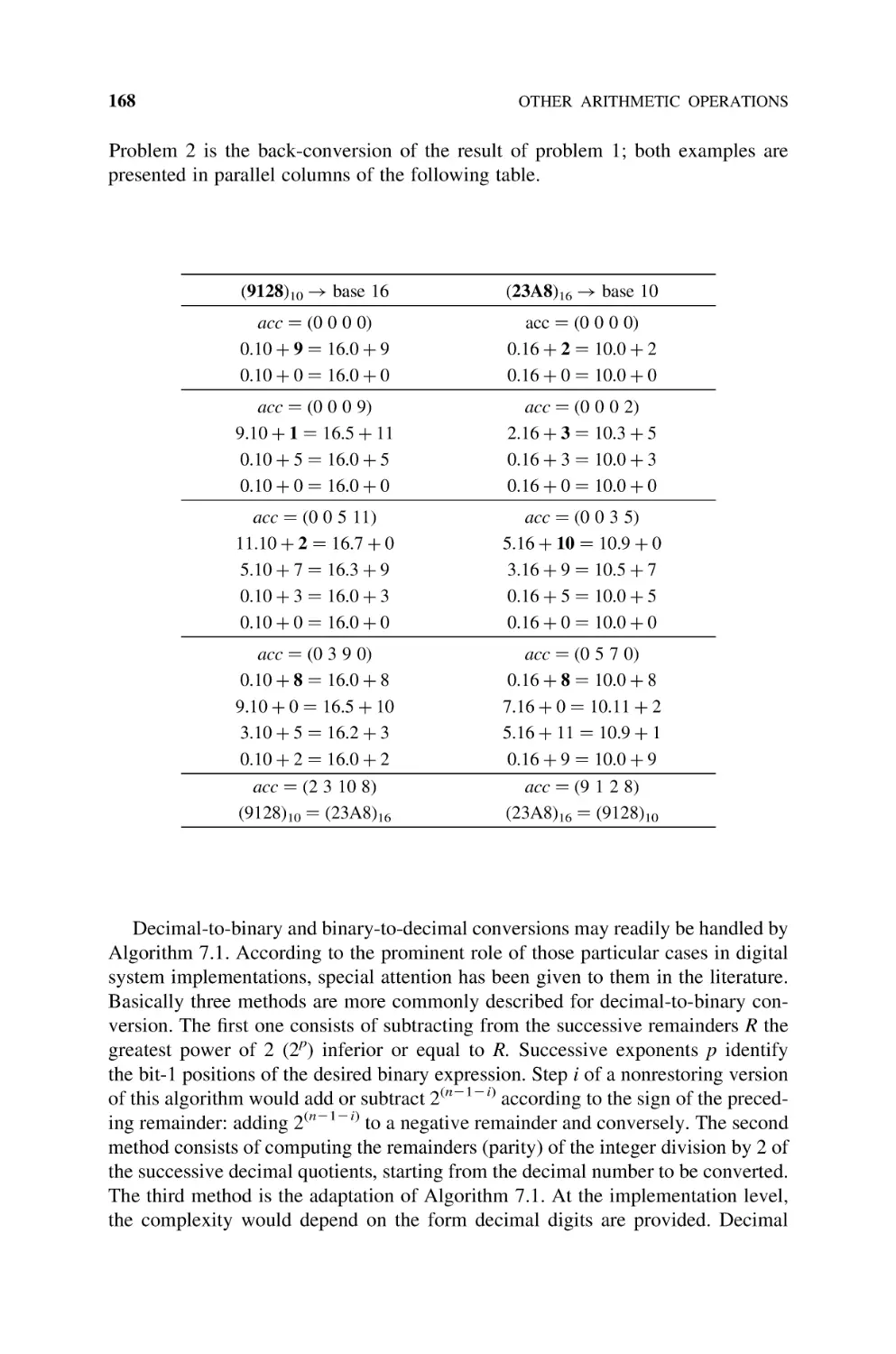
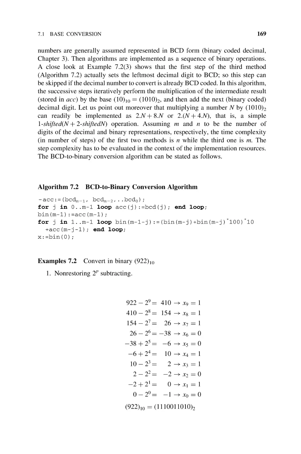
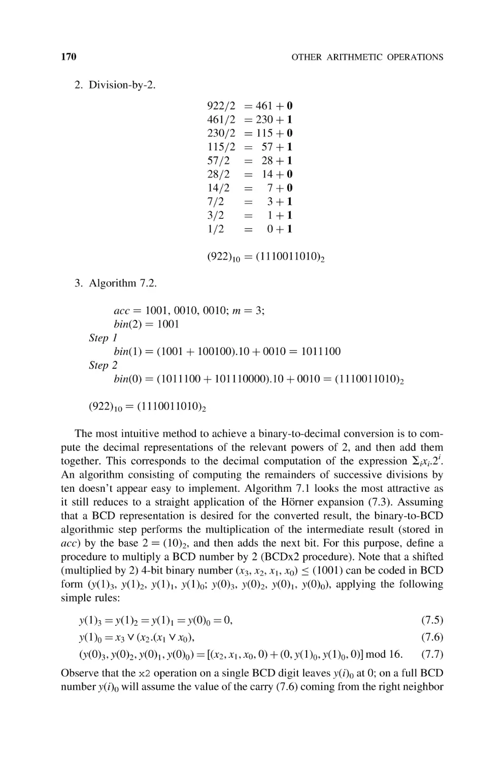
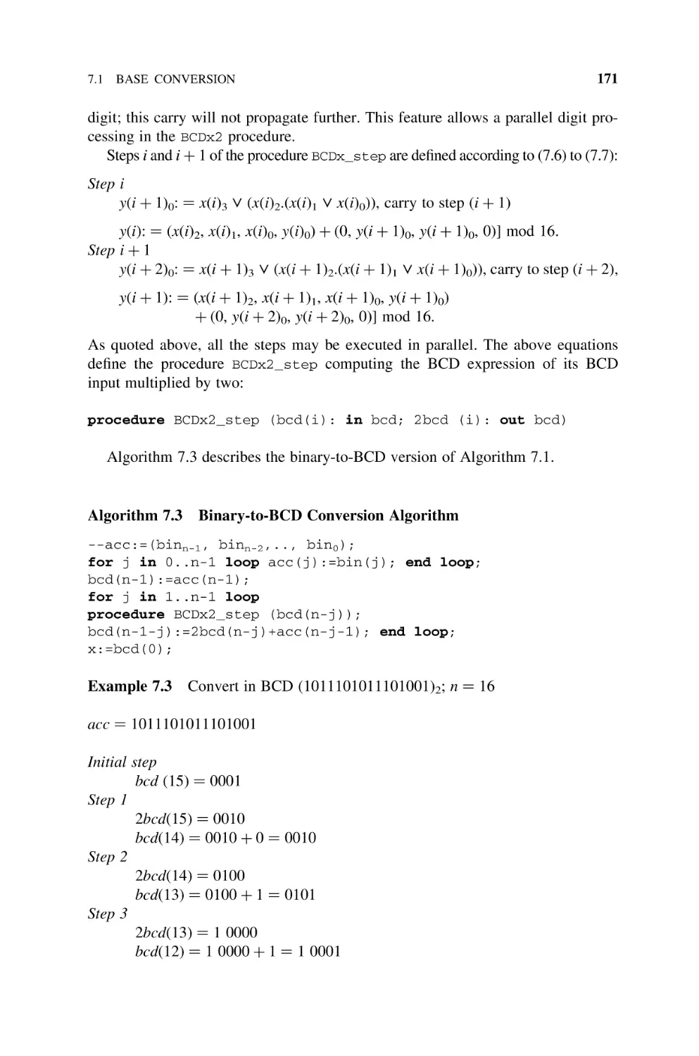
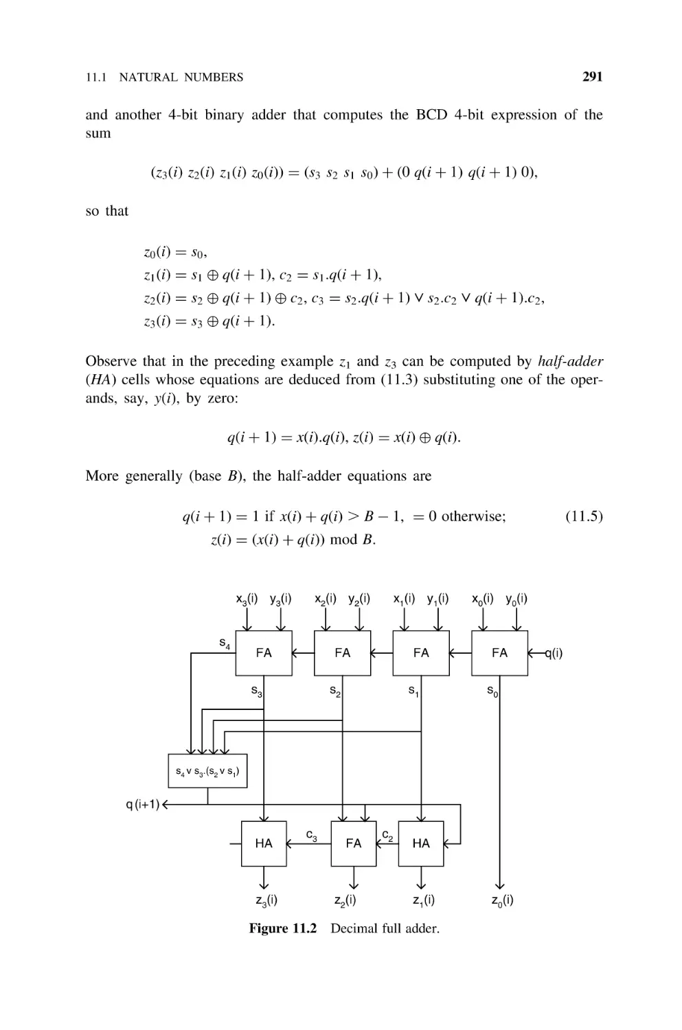
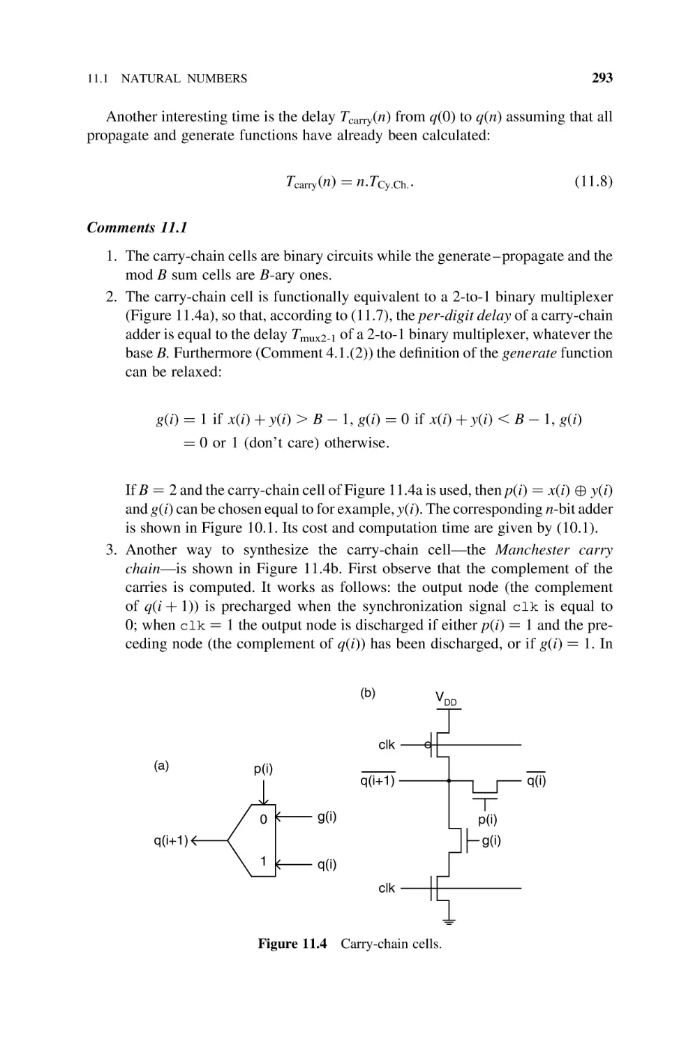
/


Текст
SYNTHESIS OF
ARITHMETIC CIRCUITS
FPGA, ASIC, and Embedded Systems
JEAN-PIERRE DESCHAMPS
University Rovira i Virgili
GÉRY JEAN ANTOINE BIOUL
National University of the Center of the Province of Buenos Aires
GUSTAVO D. SUTTER
University Autonoma of Madrid
A JOHN WILEY & SONS, INC., PUBLICATION
SYNTHESIS OF
ARITHMETIC CIRCUITS
SYNTHESIS OF
ARITHMETIC CIRCUITS
FPGA, ASIC, and Embedded Systems
JEAN-PIERRE DESCHAMPS
University Rovira i Virgili
GÉRY JEAN ANTOINE BIOUL
National University of the Center of the Province of Buenos Aires
GUSTAVO D. SUTTER
University Autonoma of Madrid
A JOHN WILEY & SONS, INC., PUBLICATION
Copyright # 2006 by John Wiley & Sons, Inc. All rights reserved.
Published by John Wiley & Sons, Inc., Hoboken, New Jersey. Published simultaneously in Canada.
No part of this publication may be reproduced, stored in a retrieval system, or transmitted in any
form or by any means, electronic, mechanical, photocopying, recording, scanning, or otherwise,
except as permitted under Section 107 or 108 of the 1976 United States Copyright Act, without
either the prior written permission of the Publisher, or authorization through payment of the
appropriate per-copy fee to the Copyright Clearance Center, Inc., 222 Rosewood Drive, Danvers,
MA 01923, 978-750-8400, fax 978-646-8600, or on the web at www.copyright.com. Requests to
the Publisher for permission should be addressed to the Permissions Department, John Wiley & Sons, Inc.,
111 River Street, Hoboken, NJ 07030, (201) 748-6011, fax (201) 748-6008
or online at http://www.wiley.com/go/permission.
Limit of Liability/Disclaimer of Warranty: While the publisher and author have used their best
efforts in preparing this book, they make no representations or warranties with respect to the
accuracy or completeness of the contents of this book and specifically disclaim any implied
warranties of merchantability or fitness for a particular purpose. No warranty may be created or
extended by sales representatives or written sales materials. The advice and strategies contained
herein may not be suitable for your situation. You should consult with a professional where
appropriate. Neither the publisher nor author shall be liable for any loss of profit or any other
commercial damages, including but not limited to special, incidental, consequential, or other damages.
For general information on our other products and services please contact our Customer Care Department
within the U.S. at 877-762-2974, outside the U.S. at 317-572-3993 or fax 317-572-4002.
Wiley also publishes its books in a variety of electronic formats. Some content that appears in print,
however, may not be available in electronic format.
Library of Congress Cataloging-in-Publication Data:
Deschamps, Jean-Pierre, 1945Synthesis of arithmetic circuits: FPGA, ASIC and embedded systems/Jean-Pierre Deschamps, Gery
Jean Antoine Bioul, Gustavo D. Sutter.
p. cm.
ISBN-13 978-0471-68783-2 (cloth)
ISBN-10 0-471-68783-9 (cloth)
1. Computer arithmetic and logic units. 2. Digital electronics. 3. Embedded computer systems.
I. Bioul, Gery Jean Antoine. II. Sutter, Gustavo D. III. Title.
TK7895.A65D47 2006
621.39’5 - - dc22
2005003237
Printed in the United States of America
10 9 8 7 6
5 4 3
2 1
To Marc
CONTENTS
Preface
xvii
About the Authors
xix
1
Introduction
1.1
Number Representation, 1
1.2
Algorithms, 2
1.3
Hardware Platforms, 2
1.4
Hardware – Software Partitioning, 3
1.5
Software Generation, 3
1.6
Synthesis, 3
1.7
A First Example, 3
1.7.1 Specification, 3
1.7.2 Number Representation, 6
1.7.3 Algorithms, 6
1.7.4 Hardware Platform, 8
1.7.5 Hardware – Software Partitioning, 8
1.7.6 Program Generation, 9
1.7.7 Synthesis, 10
1.7.8 Prototype, 12
1.8
Bibliography, 14
1
vii
CONTENTS
viii
2
3
4
Mathematical Background
2.1
Number Theory, 15
2.1.1 Basic Definitions, 15
2.1.2 Euclidean Algorithms, 17
2.1.3 Congruences, 19
2.2
Algebra, 25
2.2.1 Groups, 25
2.2.2 Rings, 27
2.2.3 Fields, 27
2.2.4 Polynomial Rings, 27
2.2.5 Congruences of Polynomial, 32
2.3
Function Approximation, 35
2.4
Bibliography, 36
Number Representation
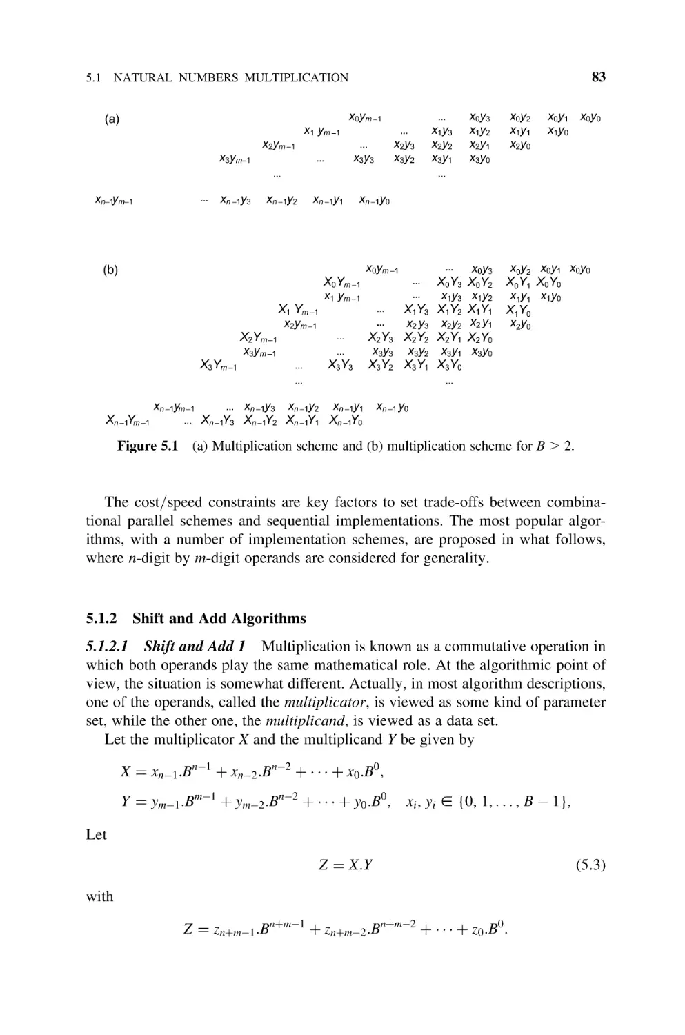
3.1
Natural Numbers, 39
3.1.1 Weighted Systems, 39
3.1.2 Residue Number System, 42
3.2
Integers, 42
3.2.1 Sign-Magnitude Representation, 42
3.2.2 Excess-E Representation, 43
3.2.3 B’s Complement Representation, 44
3.2.4 Booth’s Encoding, 47
3.3
Real Numbers, 51
3.4
Bibliography, 54
Arithmetic Operations: Addition and Subtraction
4.1
Addition of Natural Numbers, 55
4.1.1 Basic Algorithm, 55
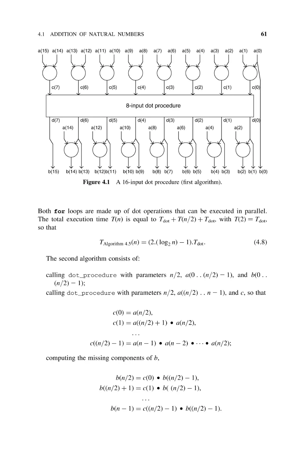
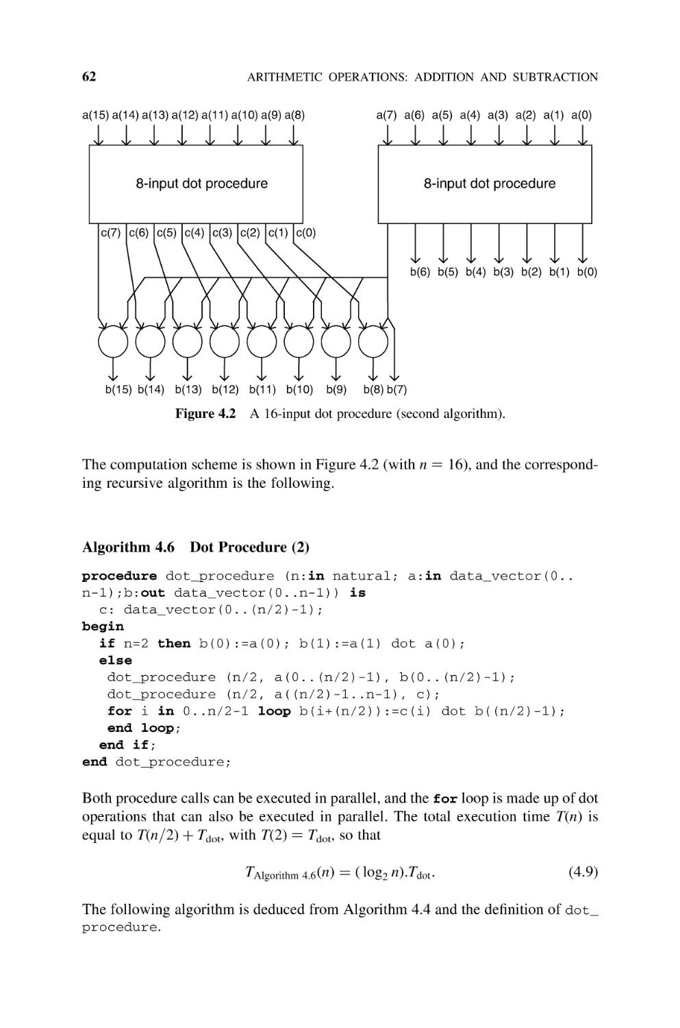
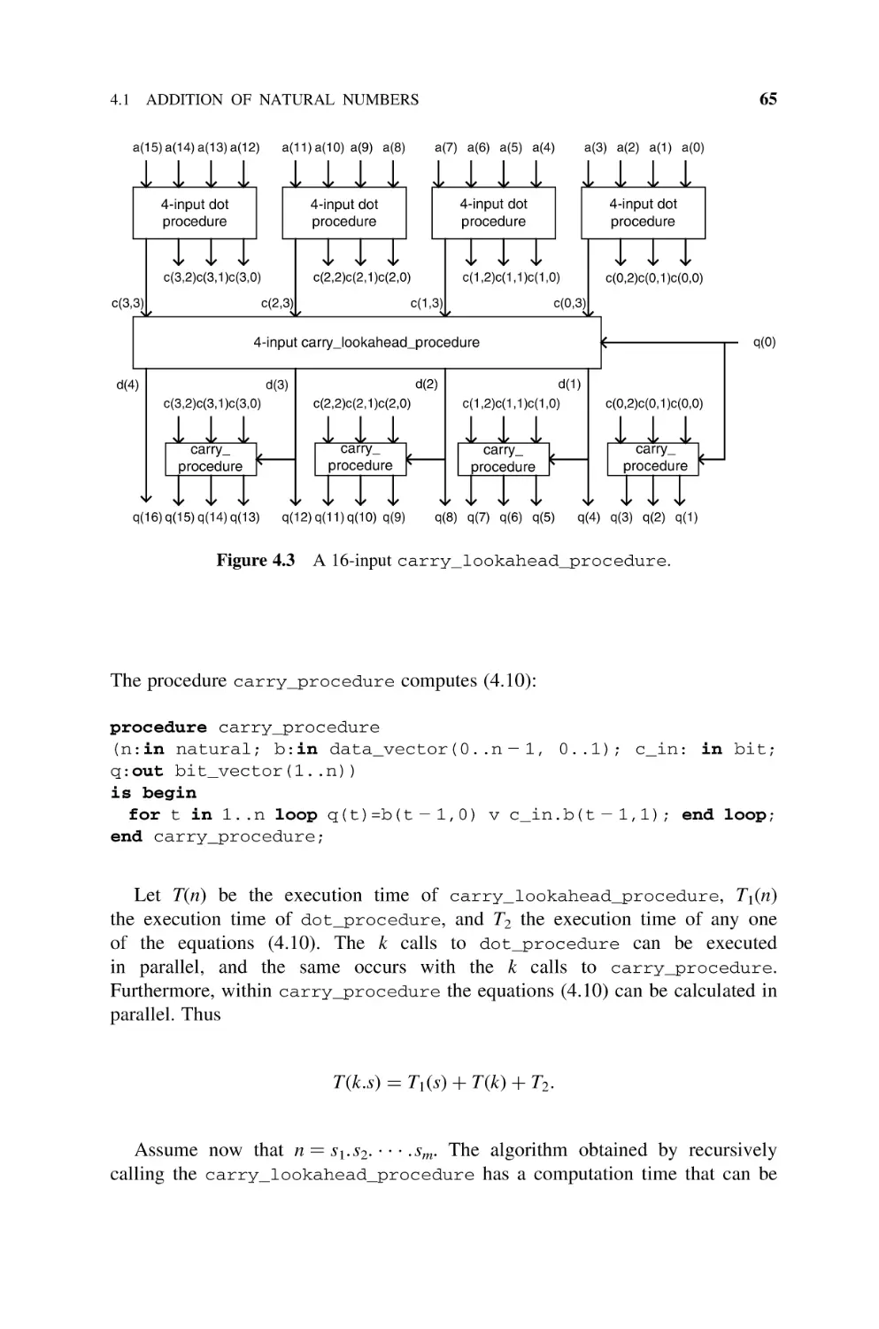
4.1.2 Faster Algorithms, 57
4.1.3 Long-Operand Addition, 66
4.1.4 Multioperand Addition, 67
4.1.5 Long-Multioperand Addition, 70
4.2
Subtraction of Natural Numbers, 71
4.3
Integers, 71
4.3.1 B’s Complement Addition, 71
4.3.2 B’s Complement Sign Change, 72
4.3.3 B’s Complement Subtraction, 74
15
39
55
CONTENTS
ix
4.3.4
4.3.5
4.3.6
4.4
5
6
B’s Complement Overflow Detection, 74
Excess-E Addition and Subtraction, 78
Sign – Magnitude Addition and Subtraction, 79
Bibliography, 80
Arithmetic Operations: Multiplication
5.1
Natural Numbers Multiplication, 82
5.1.1 Introduction, 82
5.1.2 Shift and Add Algorithms, 83
5.1.2.1 Shift and Add 1, 83
5.1.2.2 Shift and Add 2, 84
5.1.2.3 Extended Shift and Add Algorithm:
XY þ C þ D, 86
5.1.2.4 Cellular Shift and Add, 86
5.1.3 Long-Operand Algorithm, 90
5.2
Integers, 91
5.2.1 B’s Complement Multiplication, 91
5.2.1.1 Mod Bnþm B’s Complement Multiplication, 92
5.2.1.2 Signed Shift and Add, 93
5.2.1.3 Postcorrection B’s Complement Multiplication, 93
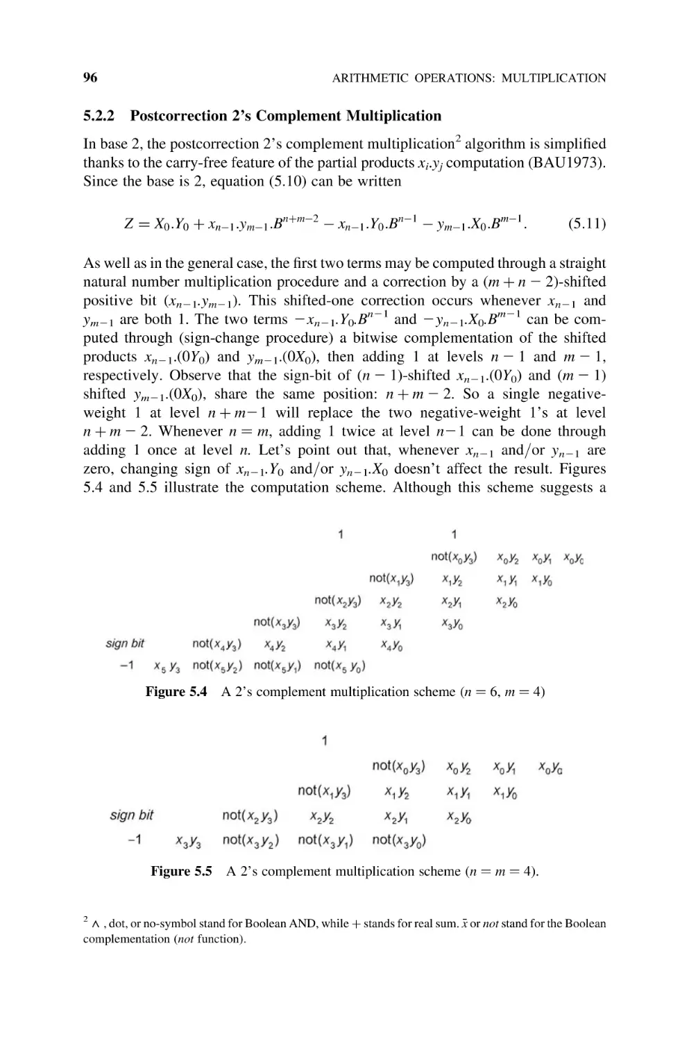
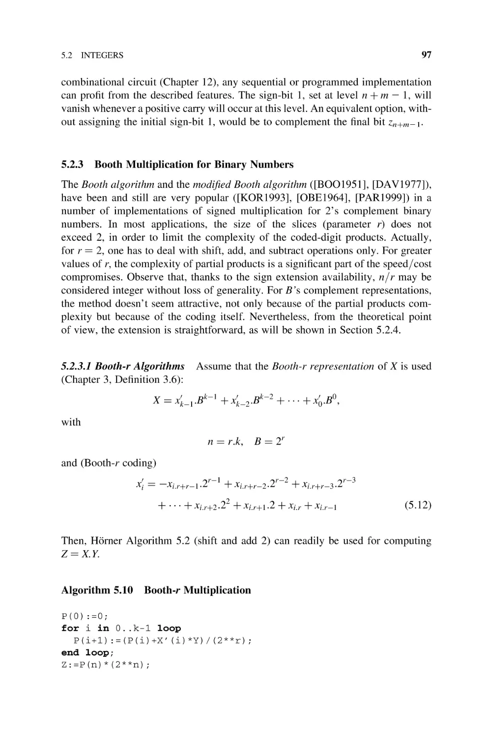
5.2.2 Postcorrection 2’s Complement Multiplication, 96
5.2.3 Booth Multiplication for Binary Numbers, 97
5.2.3.1 Booth-r Algorithms, 97
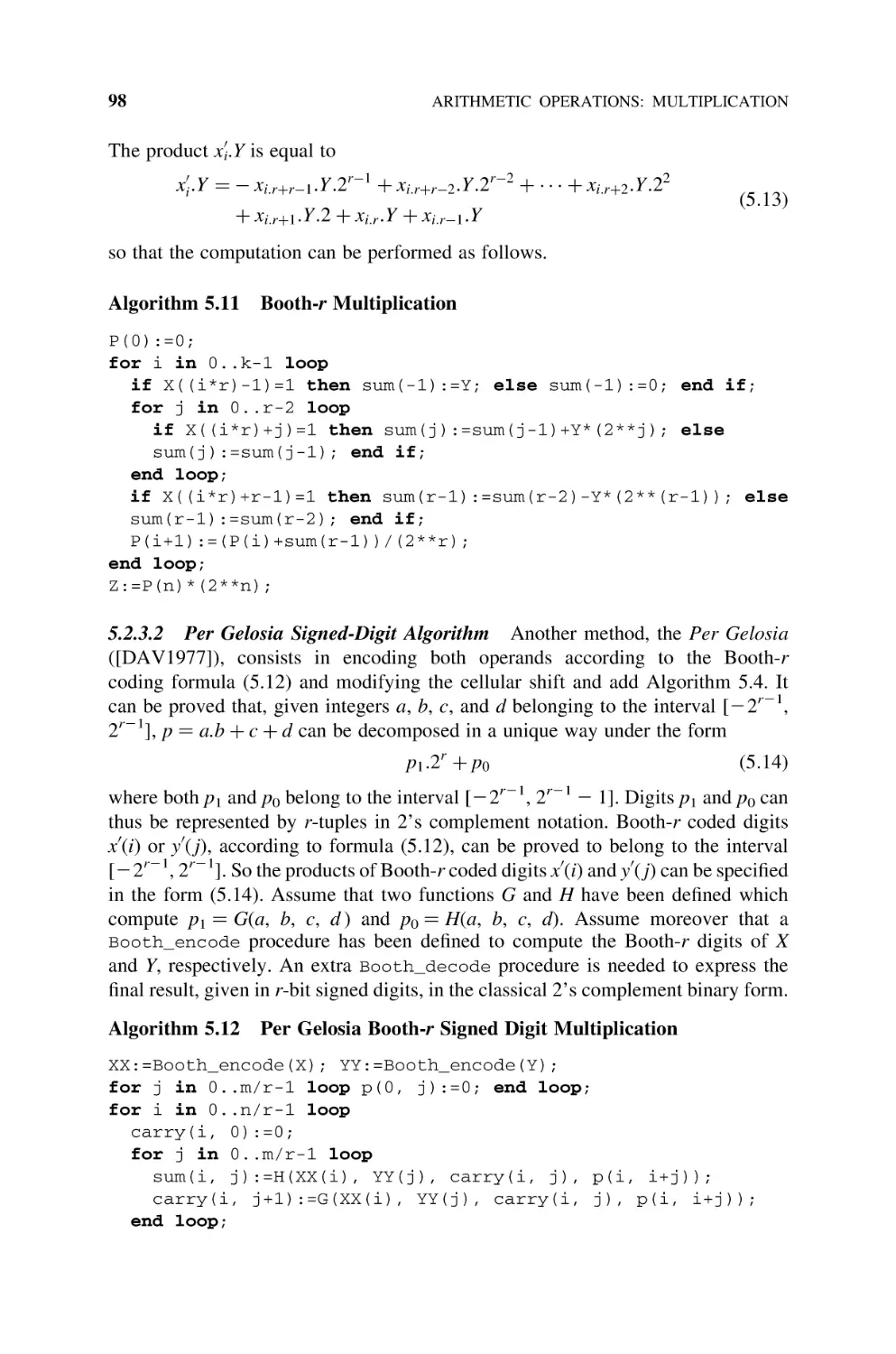
5.2.3.2 Per Gelosia Signed-Digit Algorithm, 98
5.2.4 Booth Multiplication for Base-B Numbers
(Booth-r Algorithm in Base B), 102
5.3
Squaring, 104
5.3.1 Base-B Squaring, 104
5.3.1.1 Cellular Carry –Save Squaring Algorithm, 104
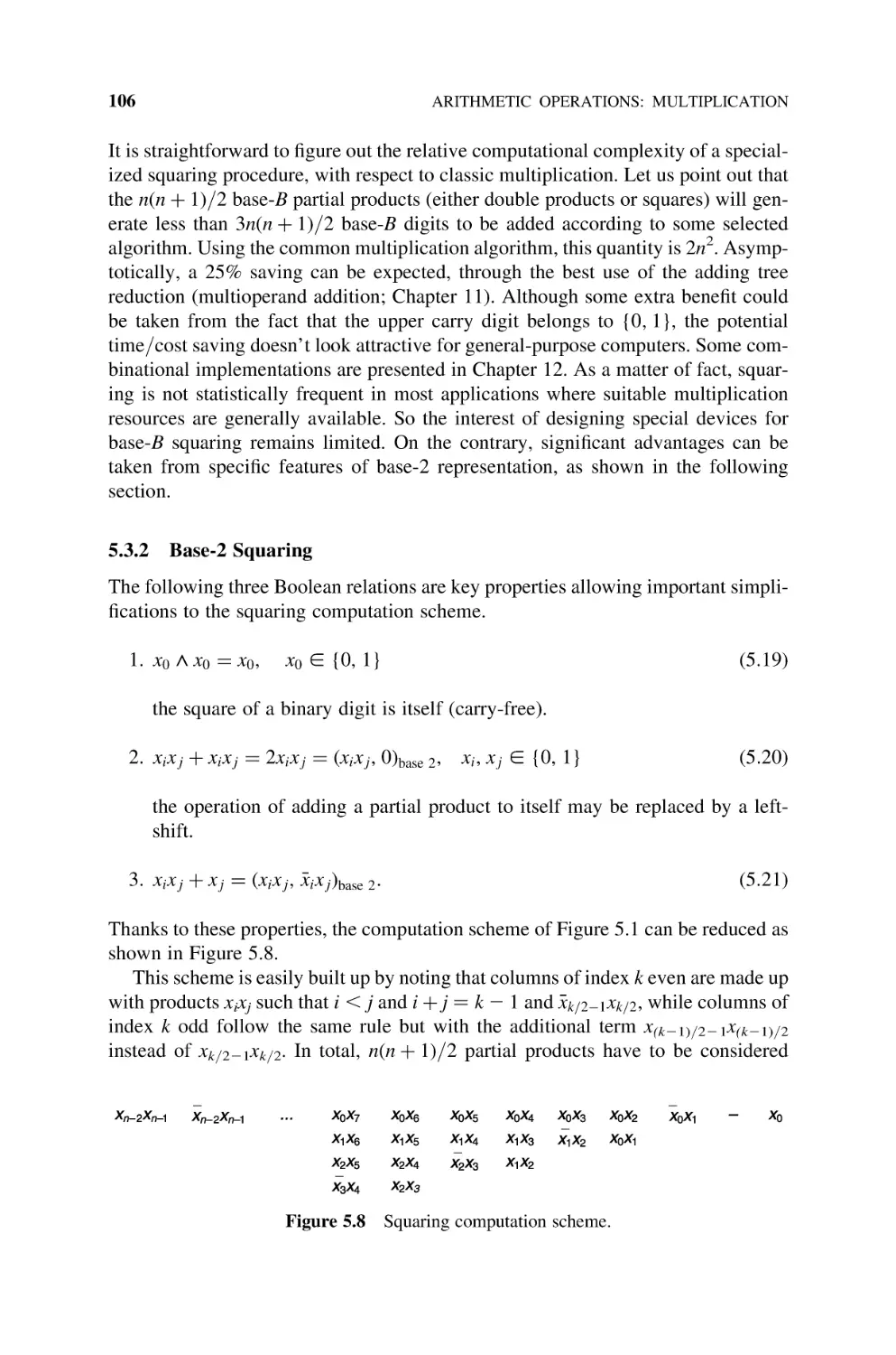
5.3.2 Base-2 Squaring, 106
5.4
Bibliography, 107
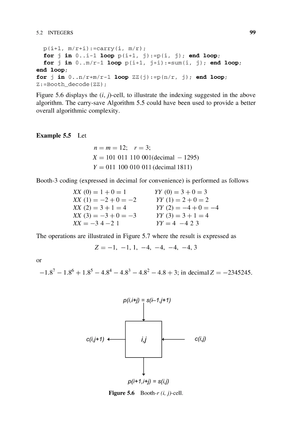
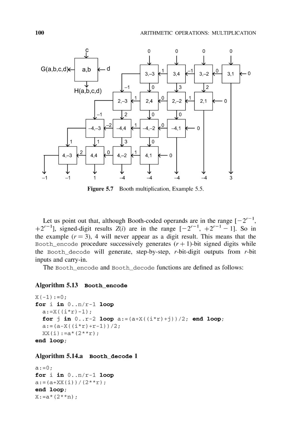
Arithmetic Operations: Division
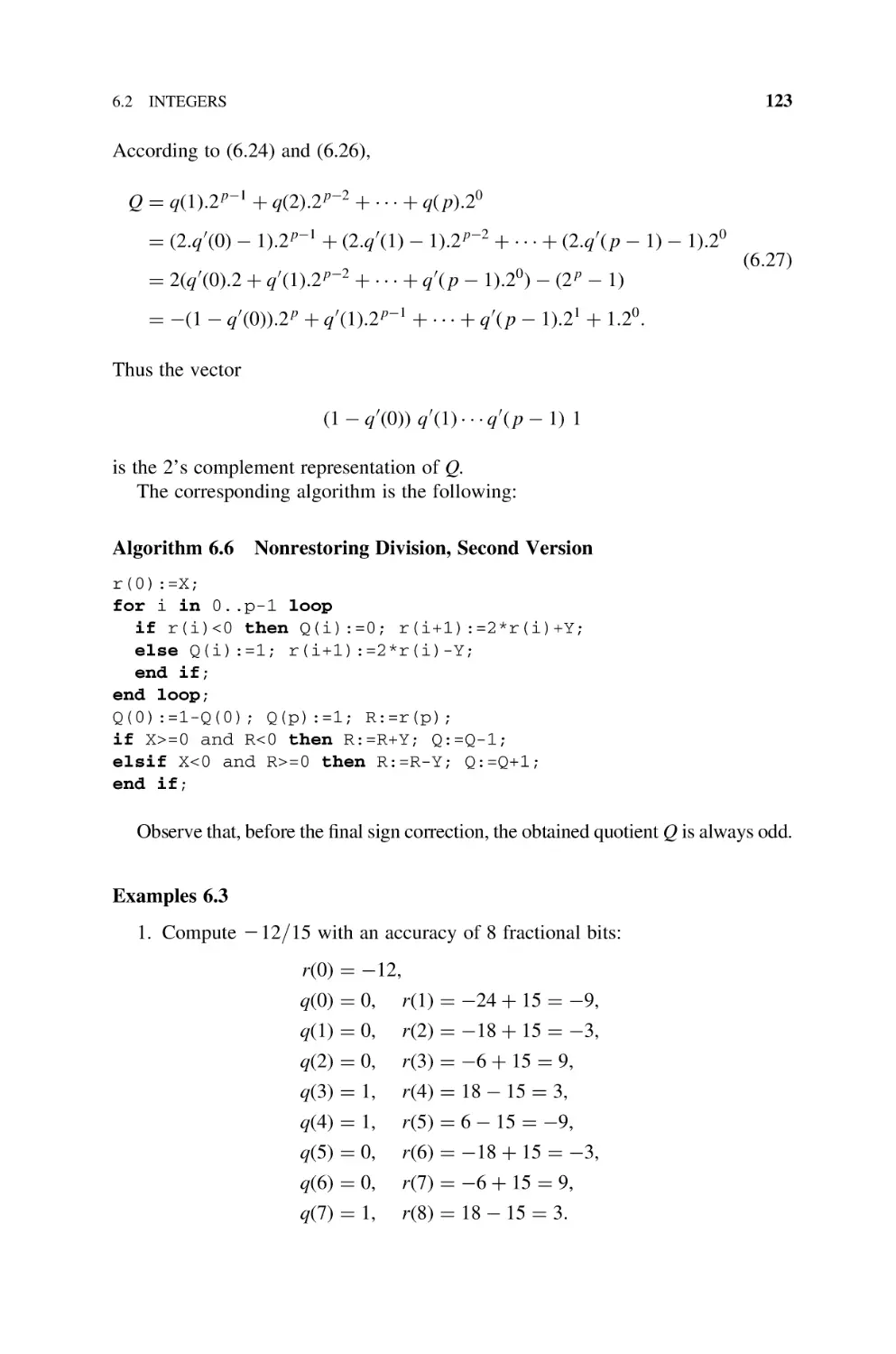
6.1
Natural Numbers, 110
6.2
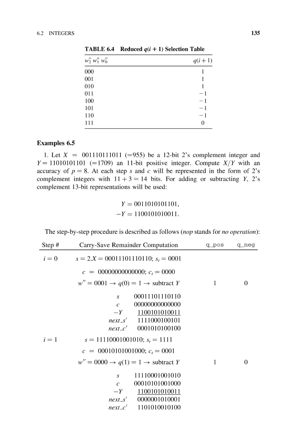
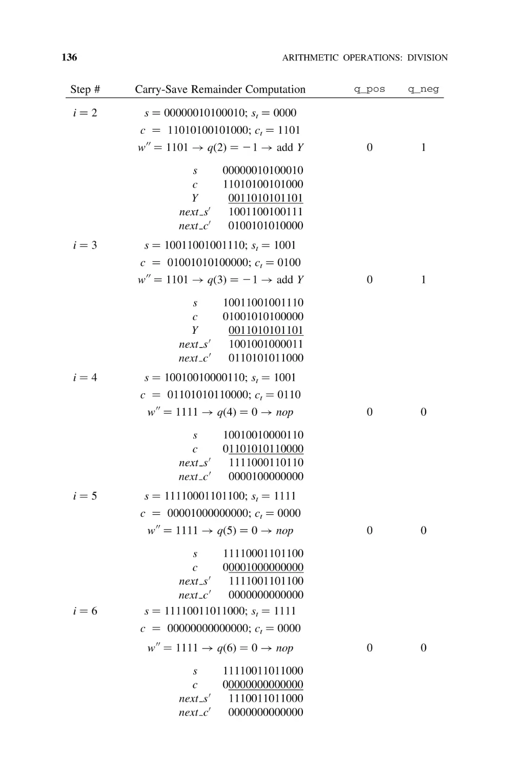
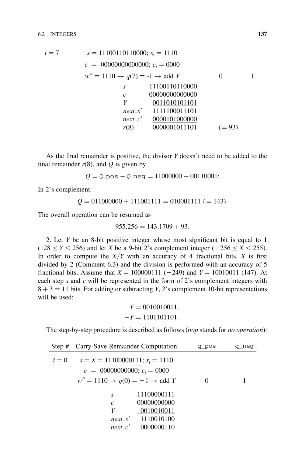
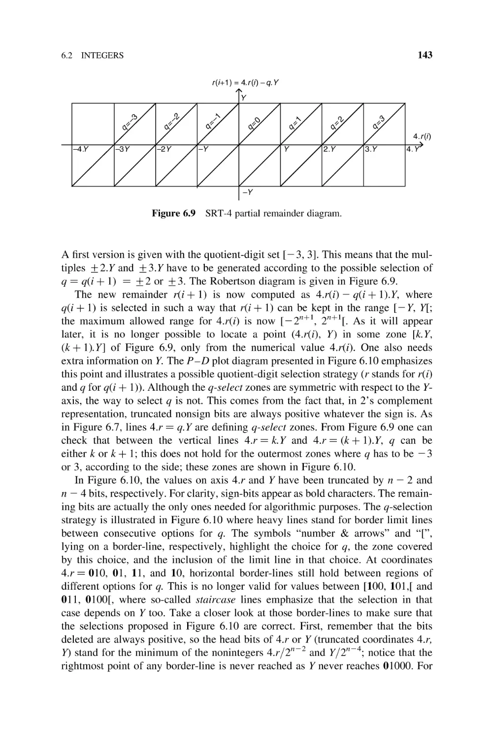
Integers, 117
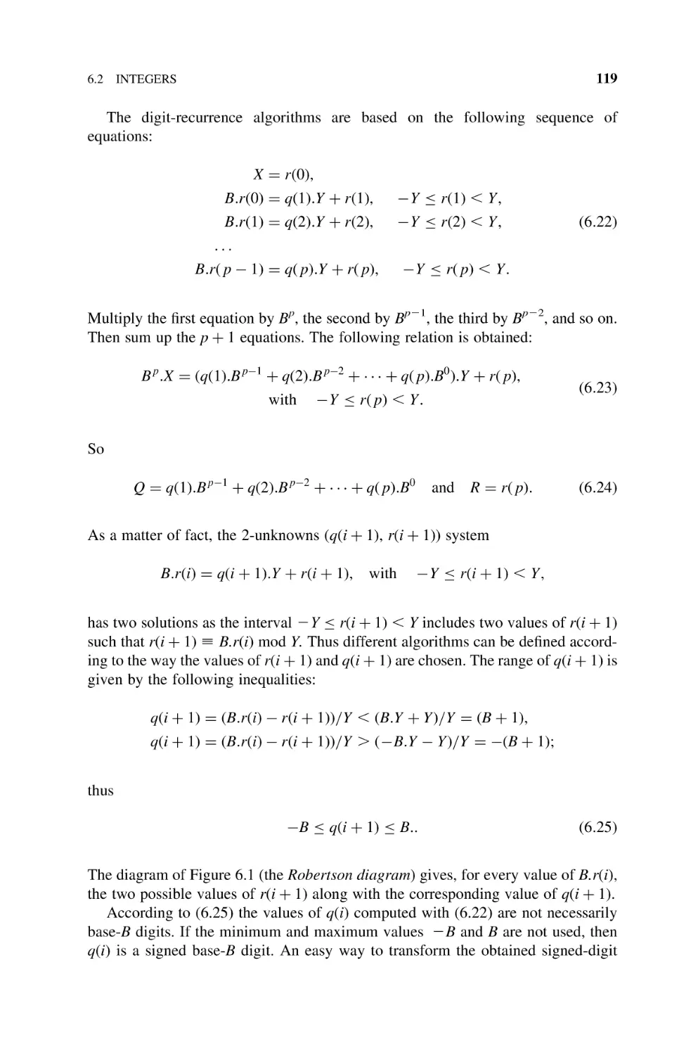
6.2.1 General Algorithm, 117
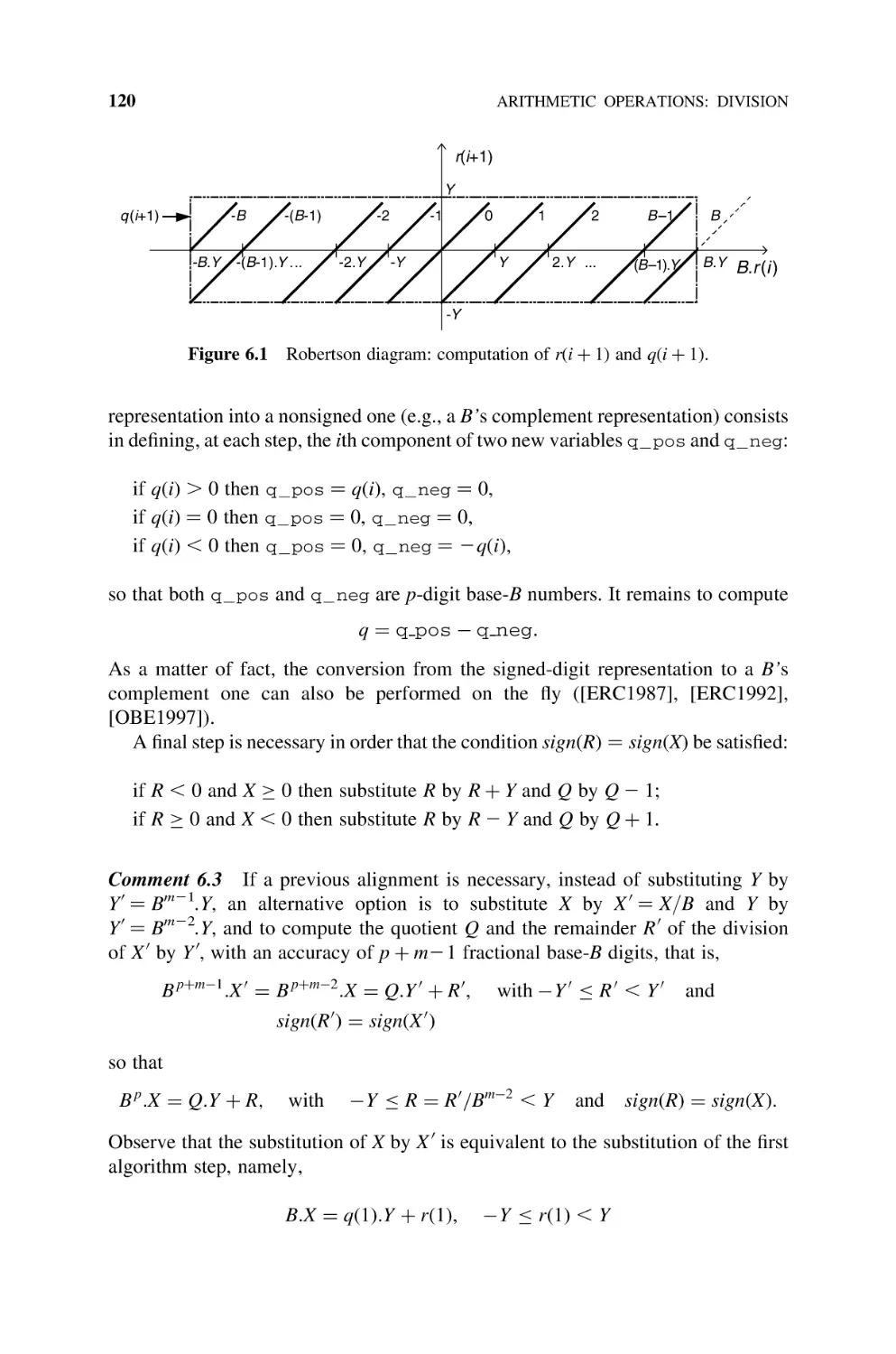
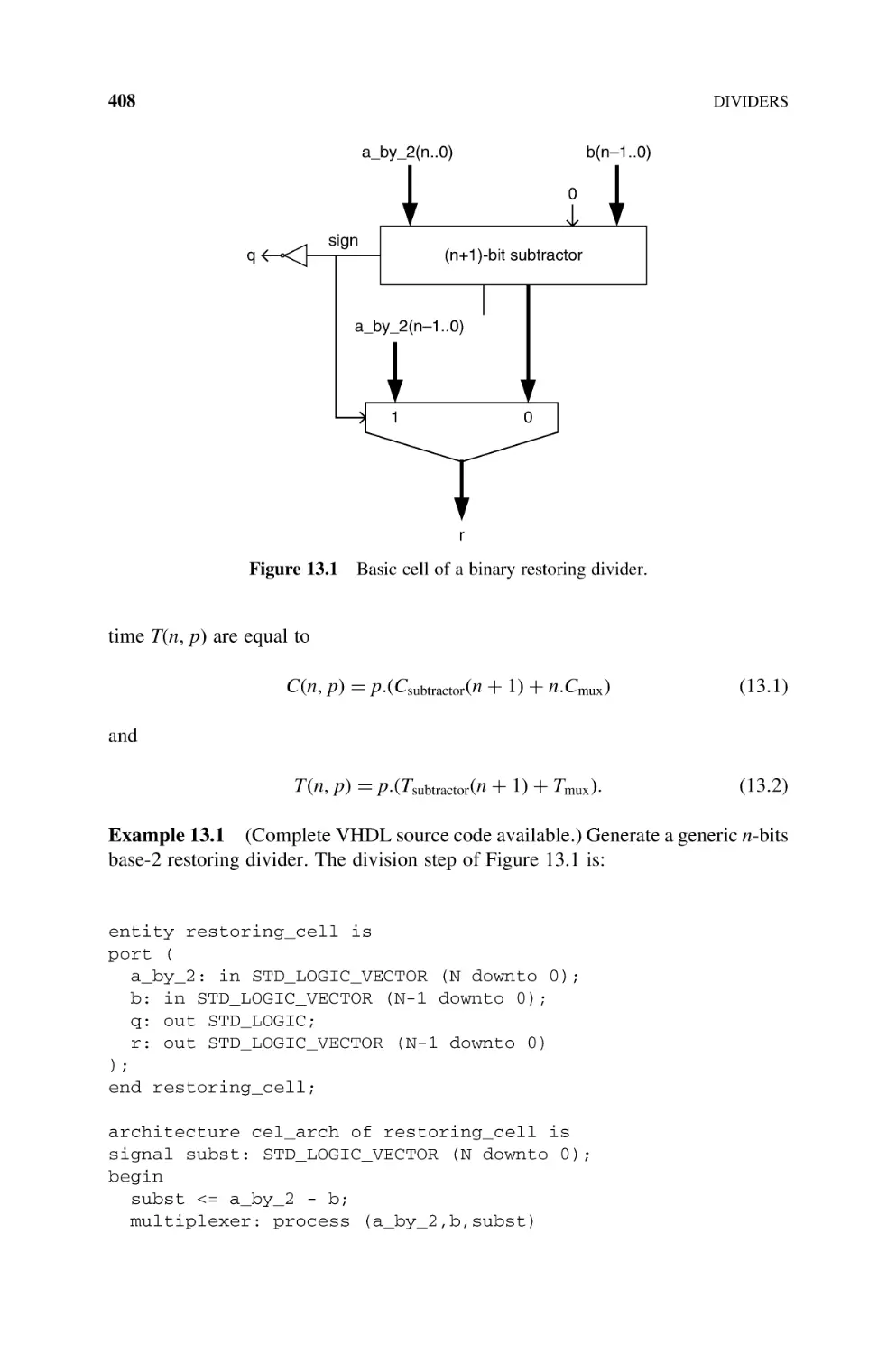
6.2.2 Restoring Division Algorithm, 121
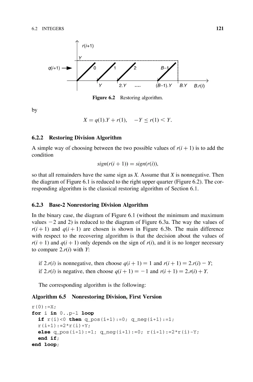
6.2.3 Base-2 Nonrestoring Division Algorithm, 121
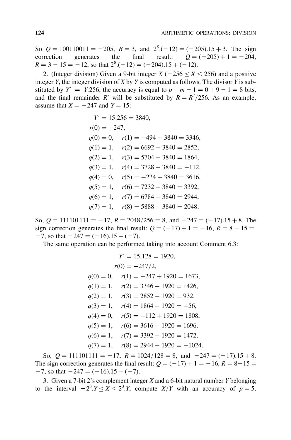
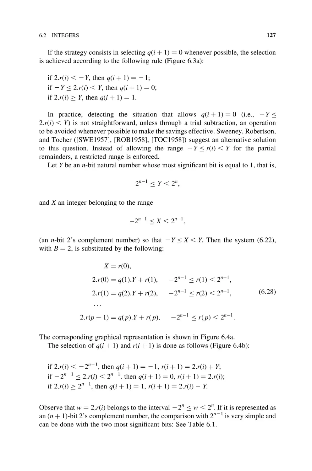
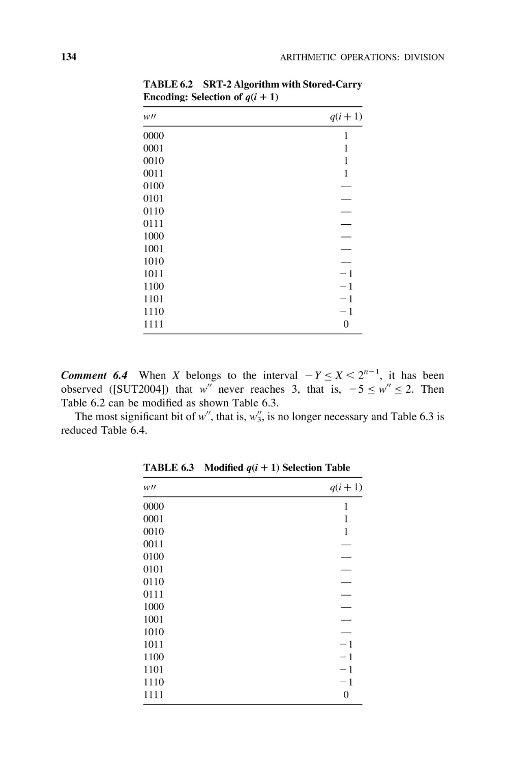
6.2.4 SRT Radix-2 Division, 126
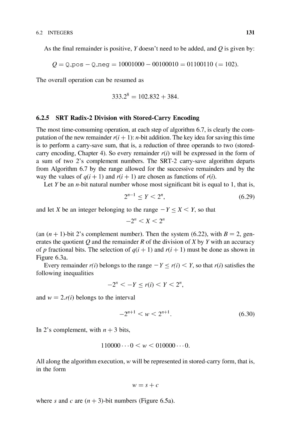
6.2.5 SRT Radix-2 Division with Stored-Carry Encoding, 131
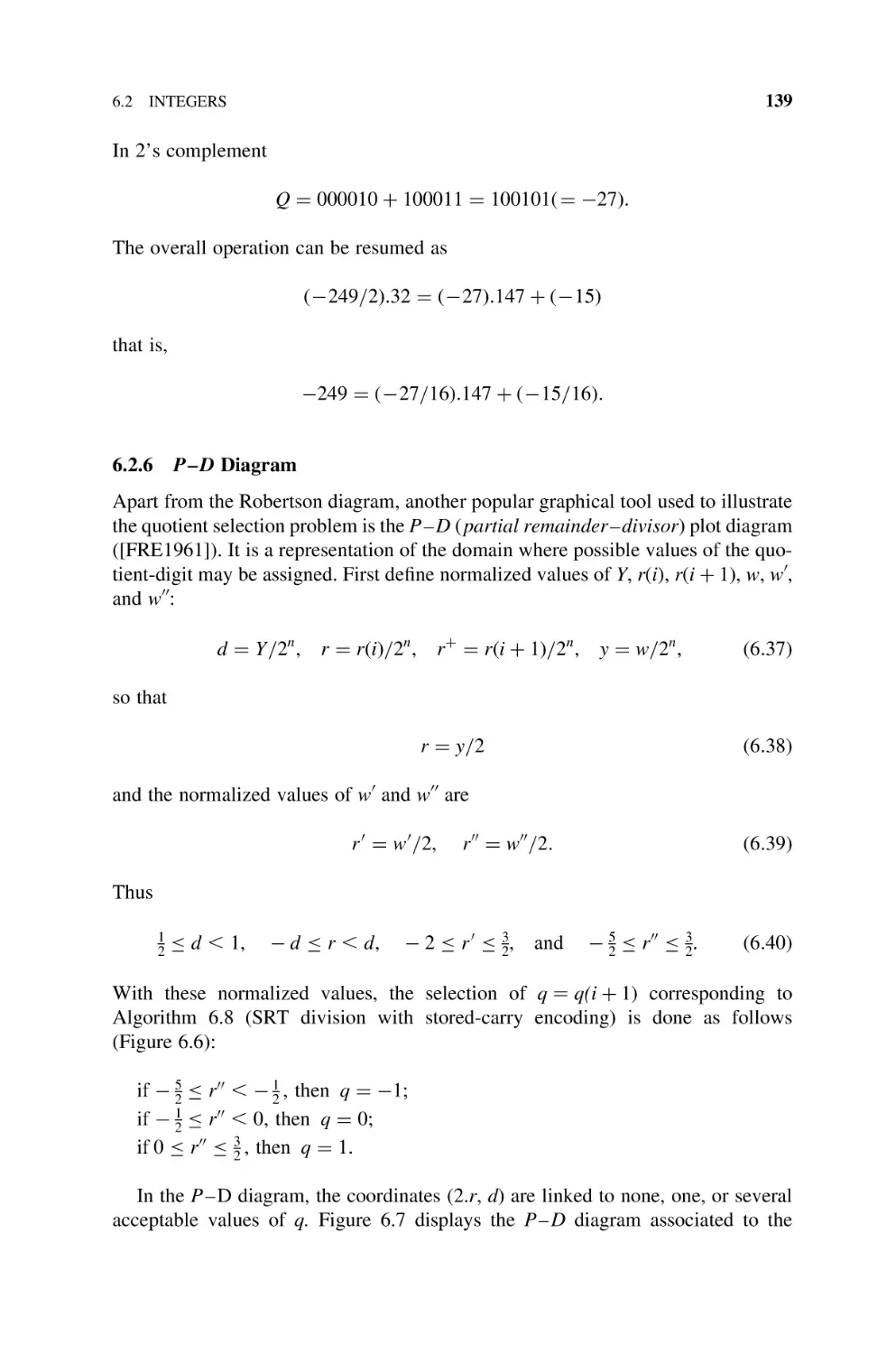
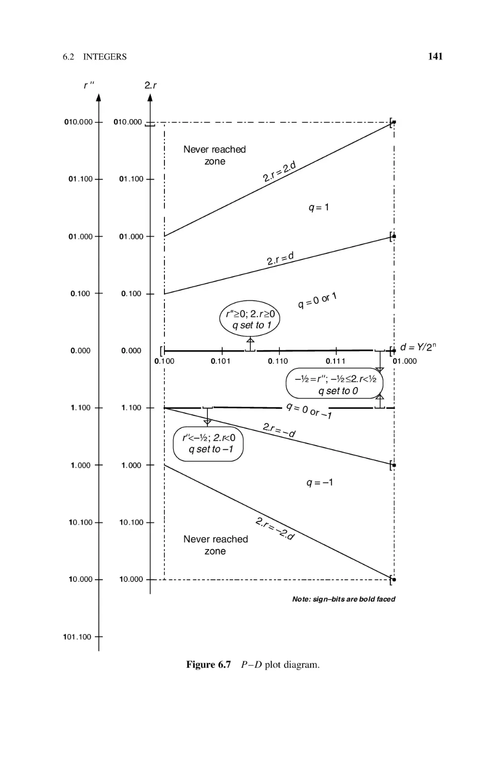
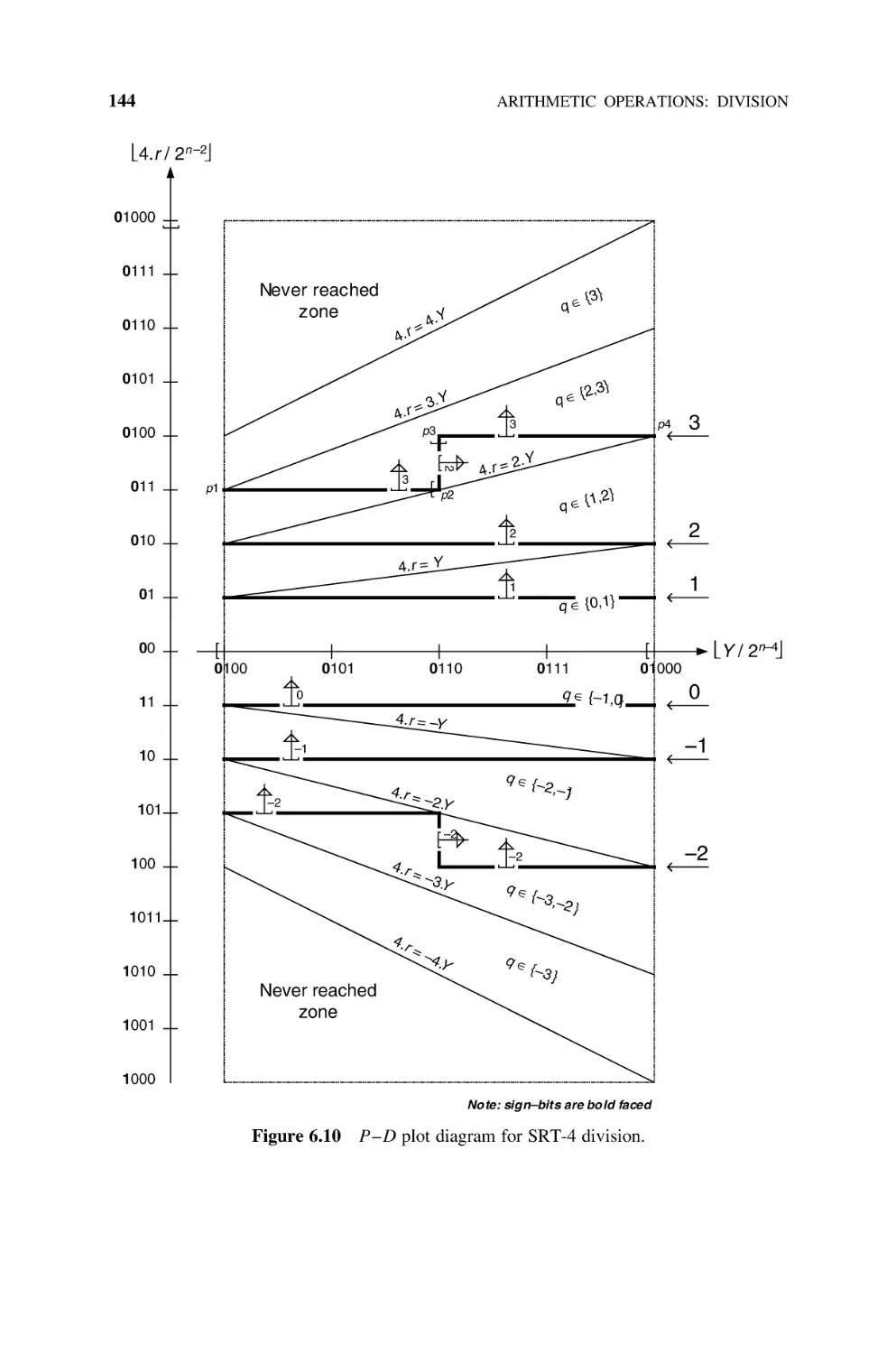
6.2.6 P– D Diagram, 139
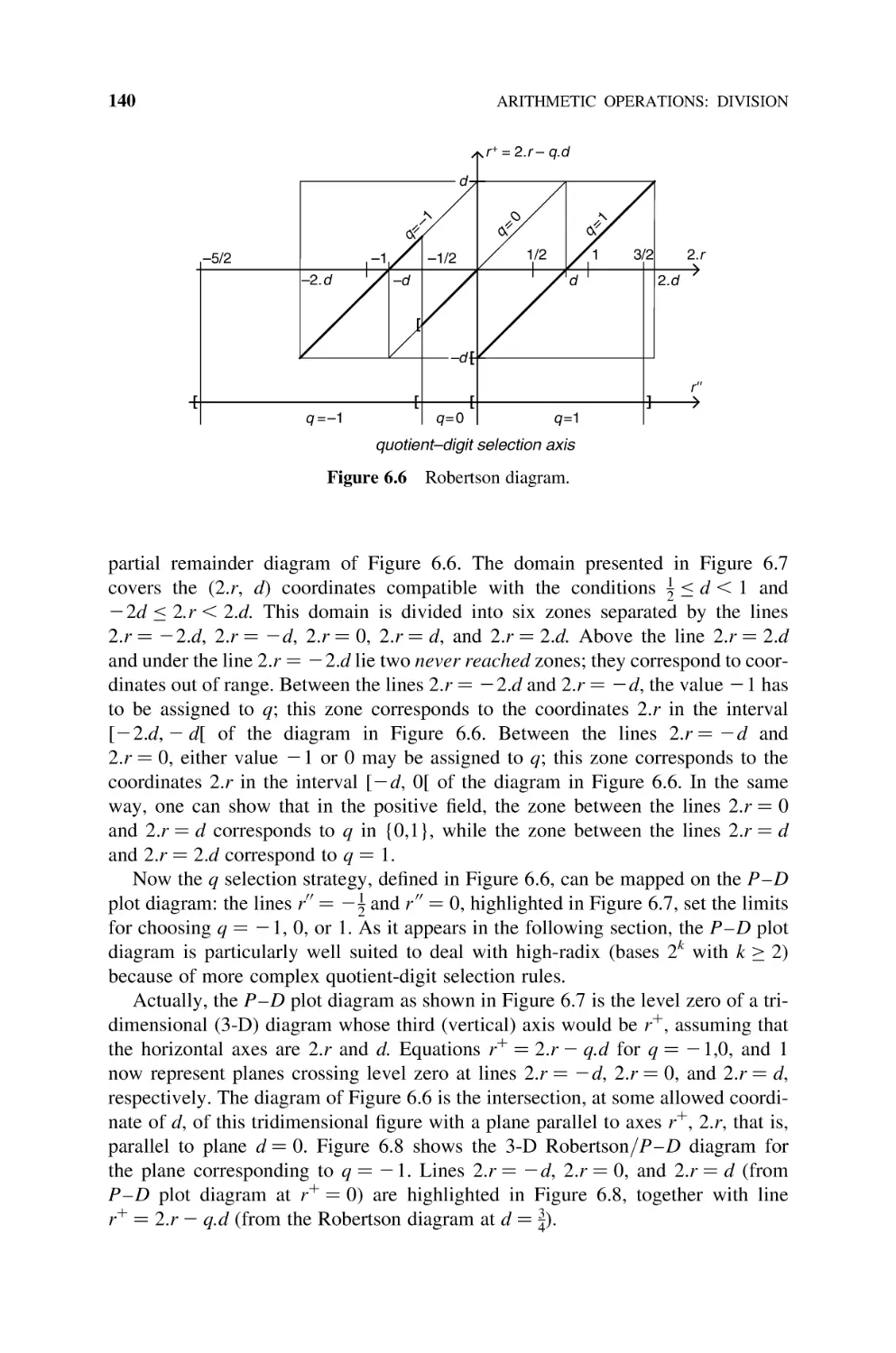
81
109
CONTENTS
x
6.2.7
6.2.8
7
8
SRT-4 Division, 142
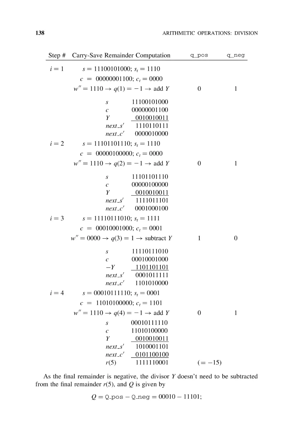
Base-B Nonrestoring Division Algorithm, 148
6.3
Convergence (Functional Iteration) Algorithms, 155
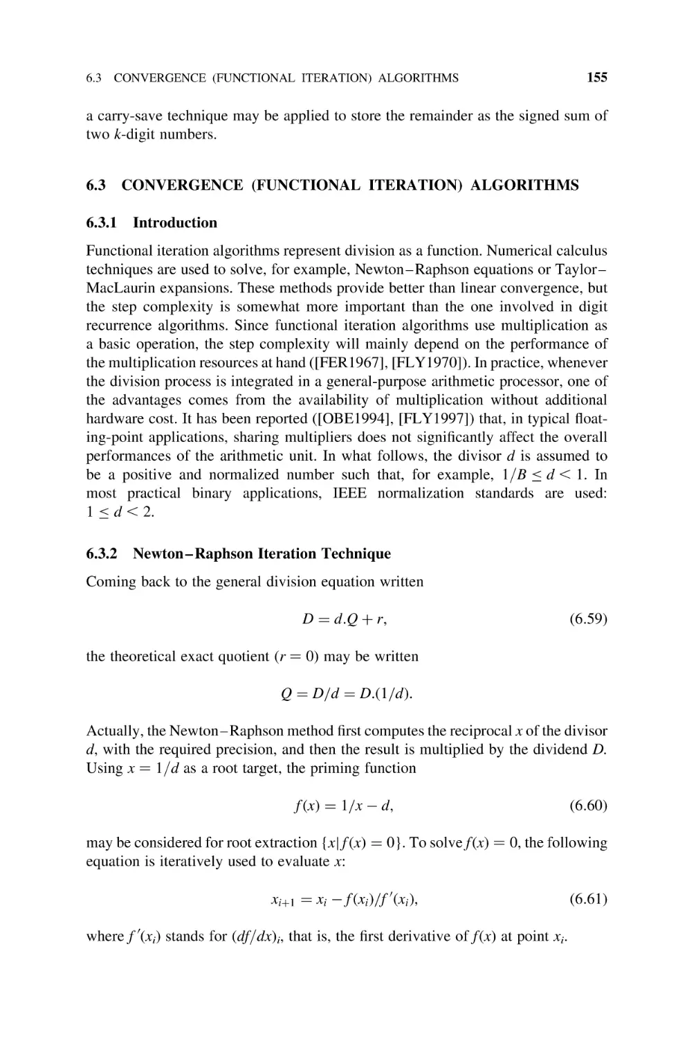
6.3.1 Introduction, 155
6.3.2 Newton –Raphson Iteration Technique, 155
6.3.3 MacLaurin Expansion—Goldschmidt’s Algorithm, 159
6.4
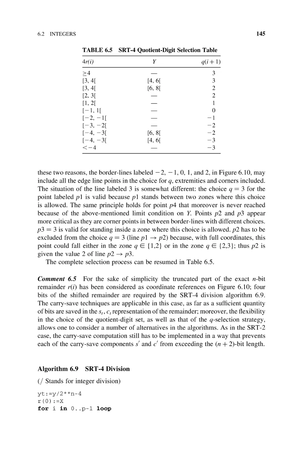
Bibliography, 161
Other Arithmetic Operations
7.1
Base Conversion, 165
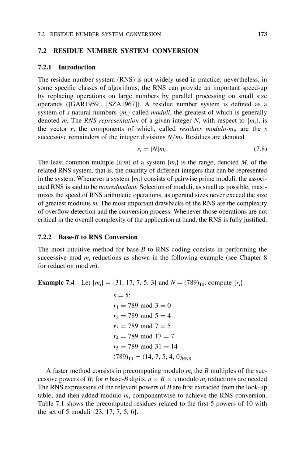
7.2
Residue Number System Conversion, 173
7.2.1 Introduction, 173
7.2.2 Base-B to RNS Conversion, 173
7.2.3 RNS to Base-B Conversion, 177
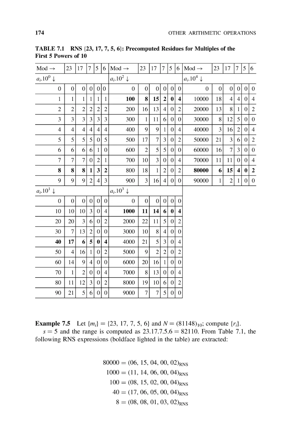
7.3
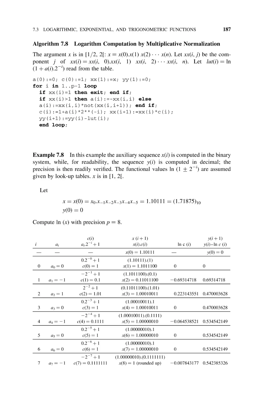
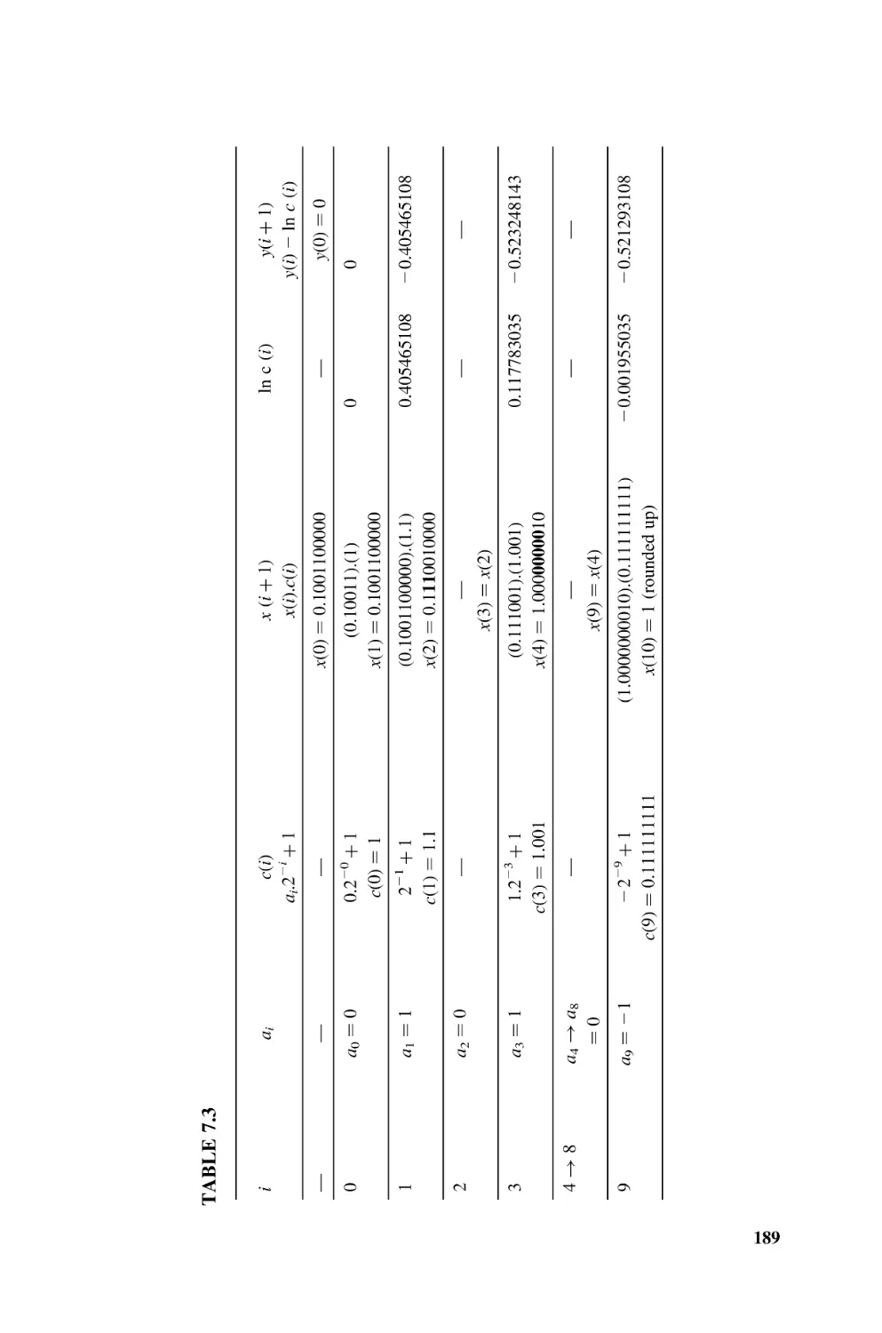
Logarithmic, Exponential, and Trigonometric Functions, 180
7.3.1 Taylor – MacLaurin Series, 181
7.3.2 Polynomial Approximation, 183
7.3.3 Logarithm and Exponential Functions Approximation
by Convergence Methods, 184
7.3.3.1 Logarithm Function Approximation by
Multiplicative Normalization, 184
7.3.3.2 Exponential Function Approximation by
Additive Normalization, 188
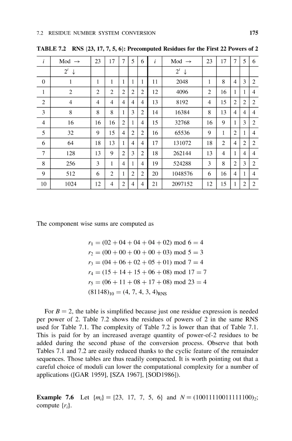
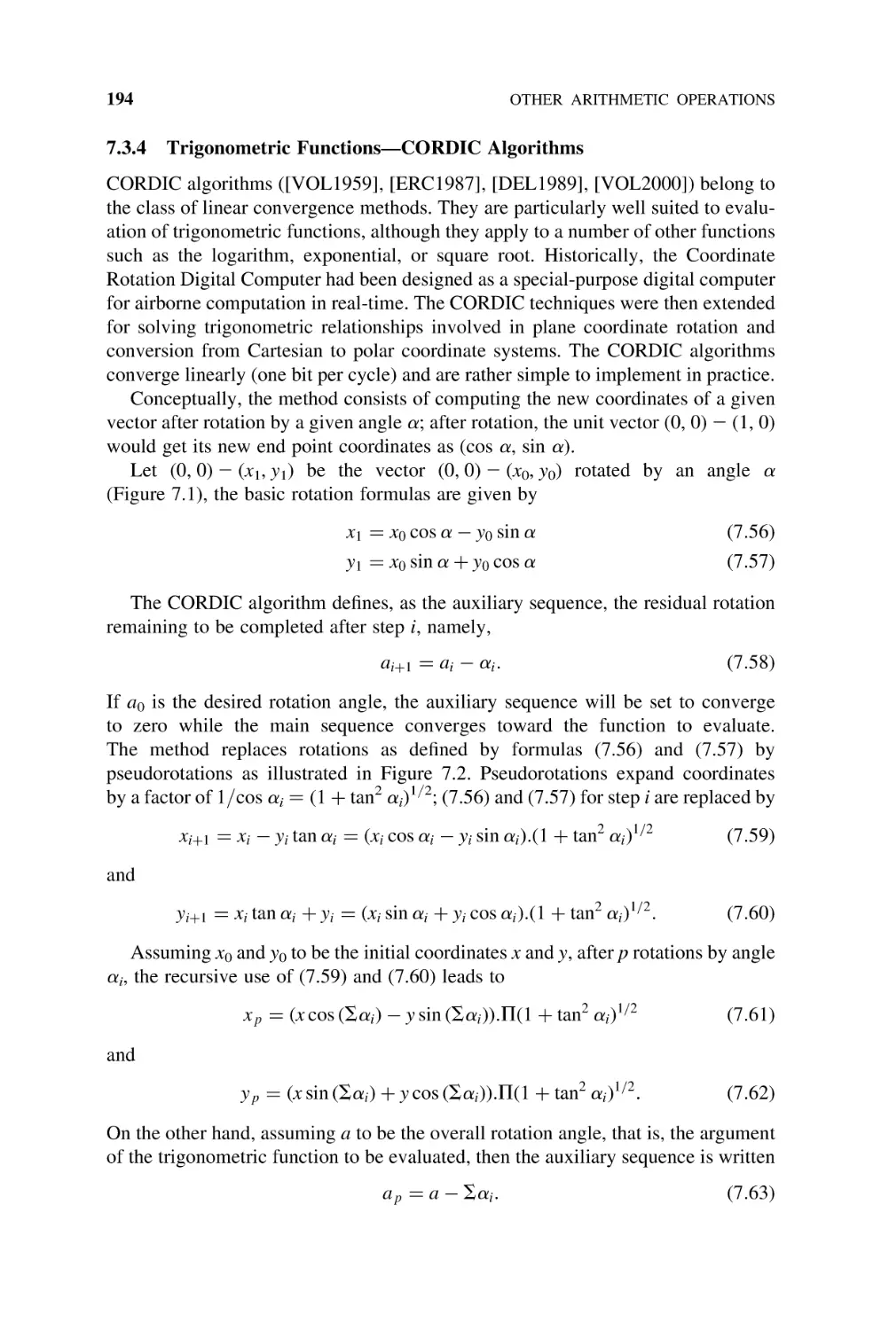
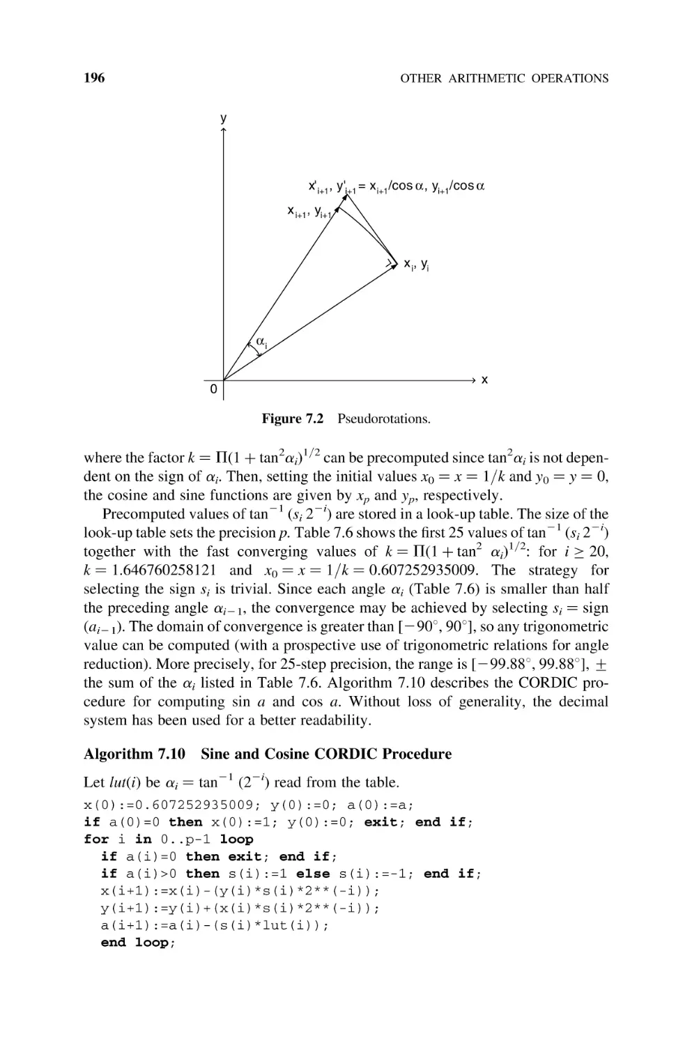
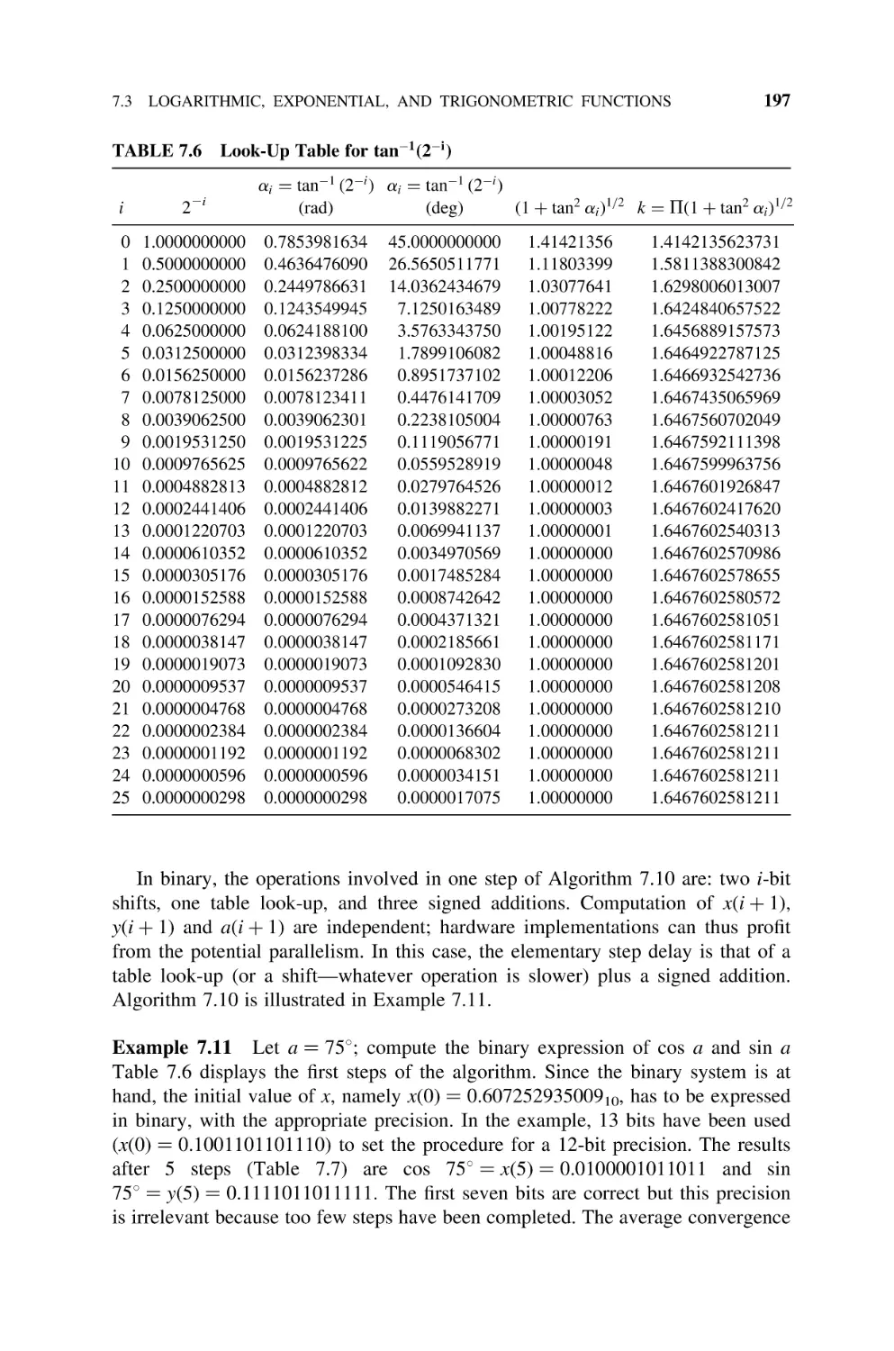
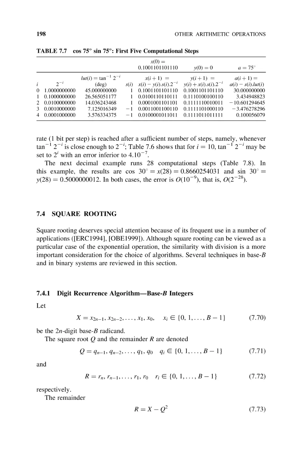
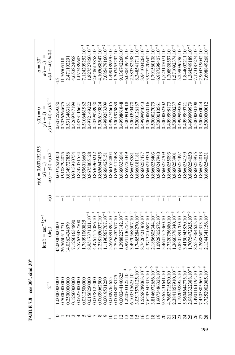
7.3.4 Trigonometric Functions—CORDIC Algorithms, 194
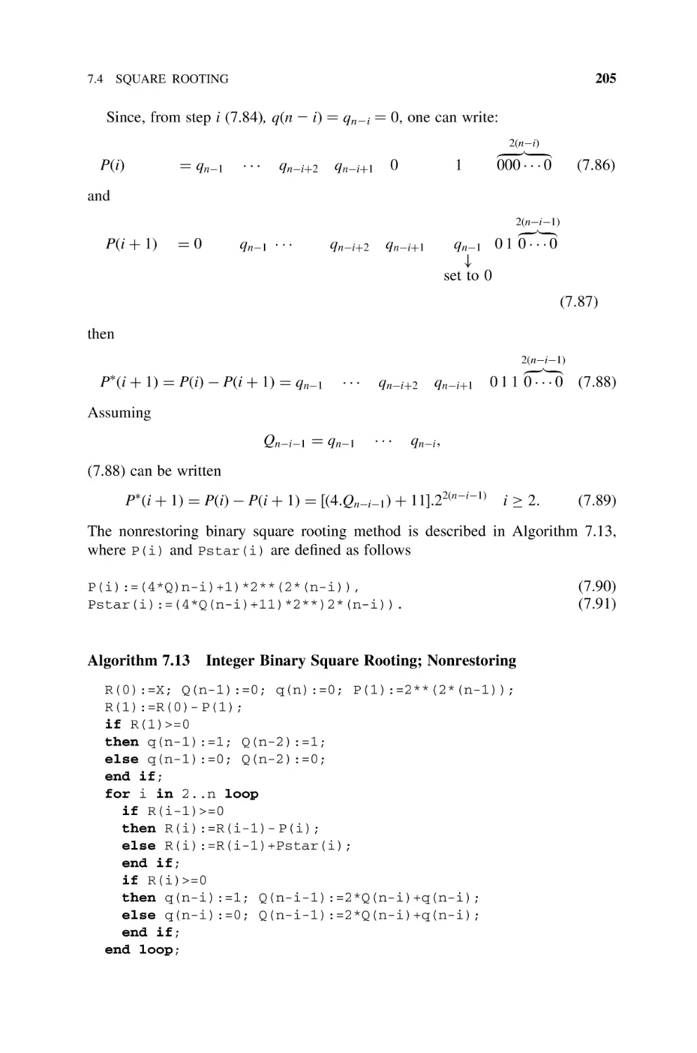
7.4
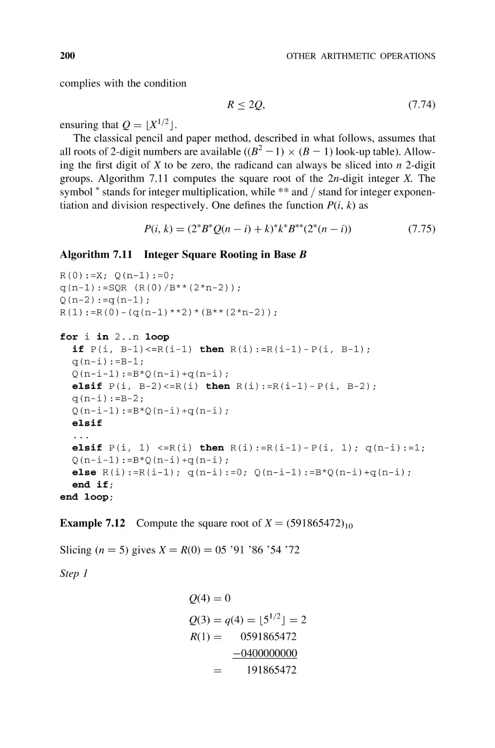
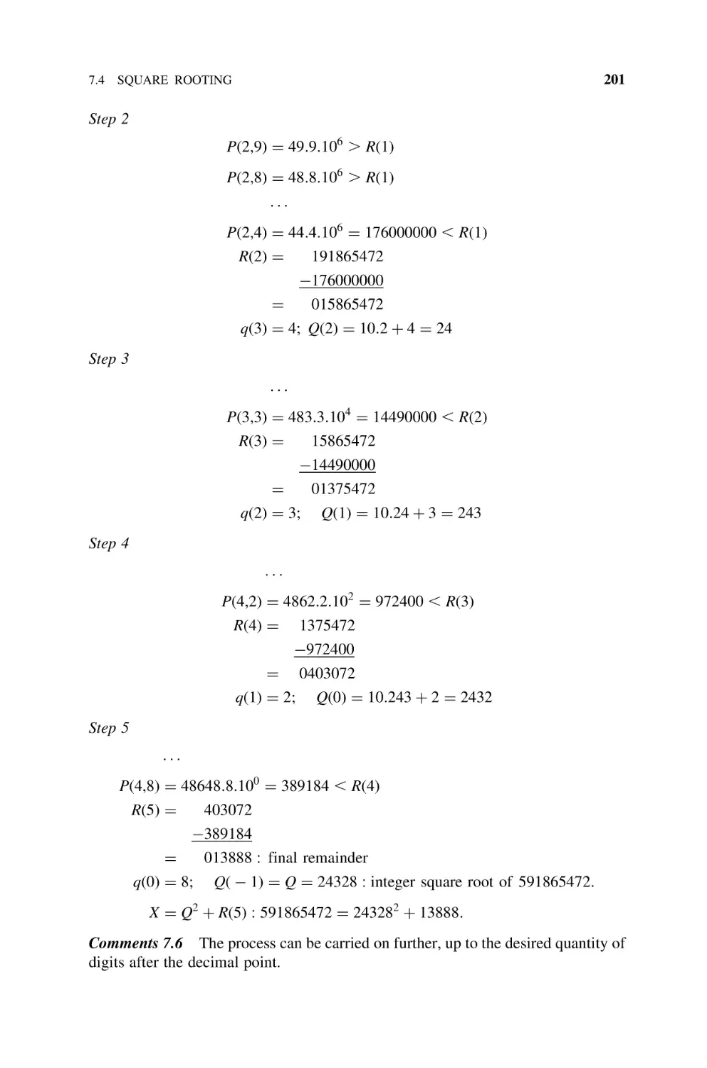
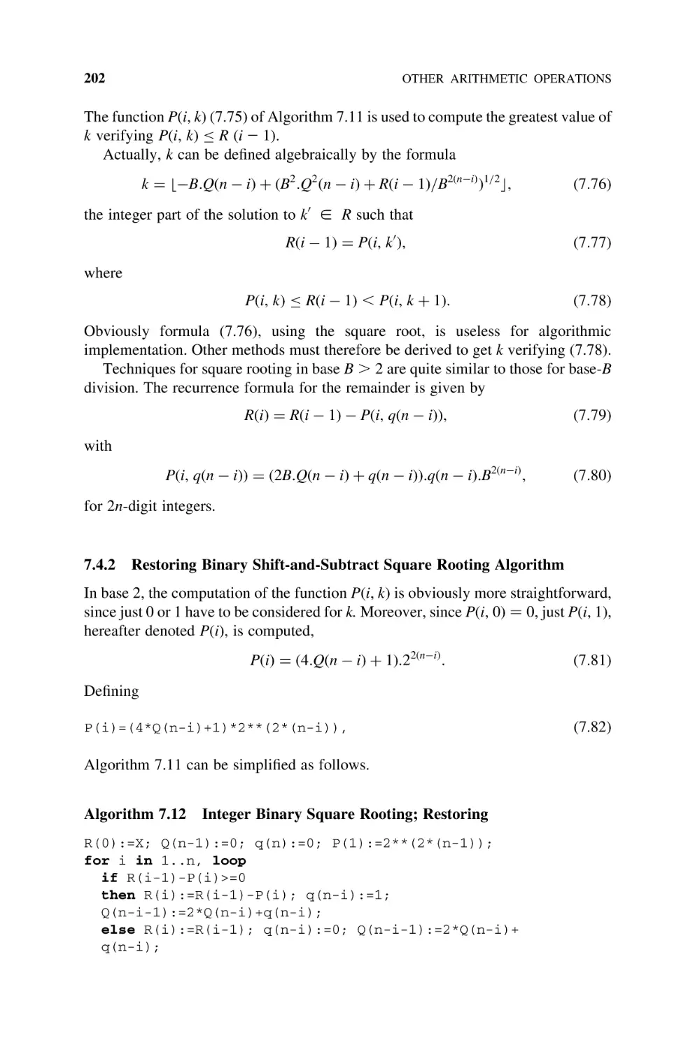
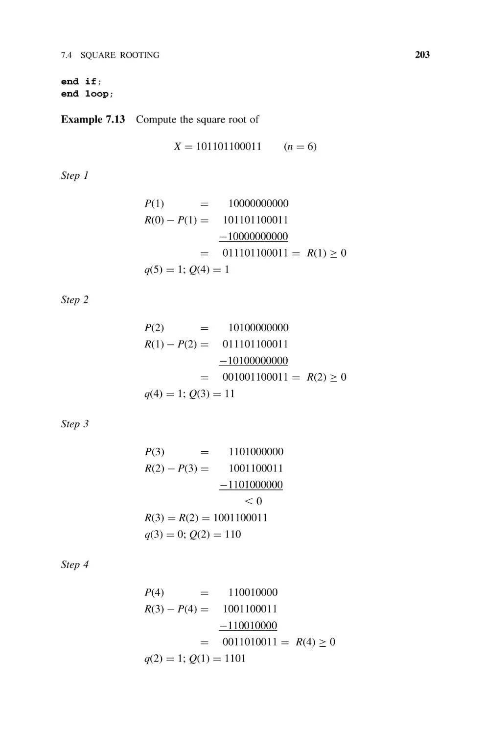
Square Rooting, 198
7.4.1 Digit Recurrence Algorithm—Base-B Integers, 198
7.4.2 Restoring Binary Shift-and-Subtract Square Rooting
Algorithm, 202
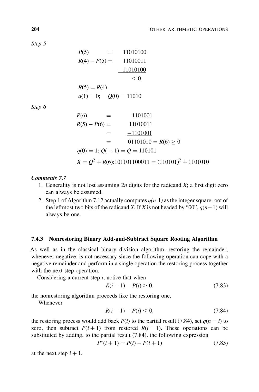
7.4.3 Nonrestoring Binary Add-and-Subtract Square Rooting
Algorithm, 204
7.4.4 Convergence Method—Newton –Raphson, 208
7.5
Bibliography, 208
Finite Field Operations
8.1
Operations in Zm, 211
8.1.1 Addition, 212
8.1.2 Subtraction, 213
8.1.3 Multiplication, 213
8.1.3.1 Multiply and Reduce, 214
8.1.3.2 Modified Shift-and-Add Algorithm, 214
165
211
CONTENTS
xi
8.1.3.3 Montgomery Multiplication, 216
8.1.3.4 Specific Ring, 220
8.1.4 Exponentiation, 221
8.2
Operations in GF(p), 222
8.3
Operations in Zp[x]/f (x), 224
8.3.1 Addition and Subtraction, 224
8.3.2 Multiplication, 225
8.4
Operations in GF(pn), 228
8.5
Bibliography, 236
Appendix 8.1
9
Computation of fki, 236
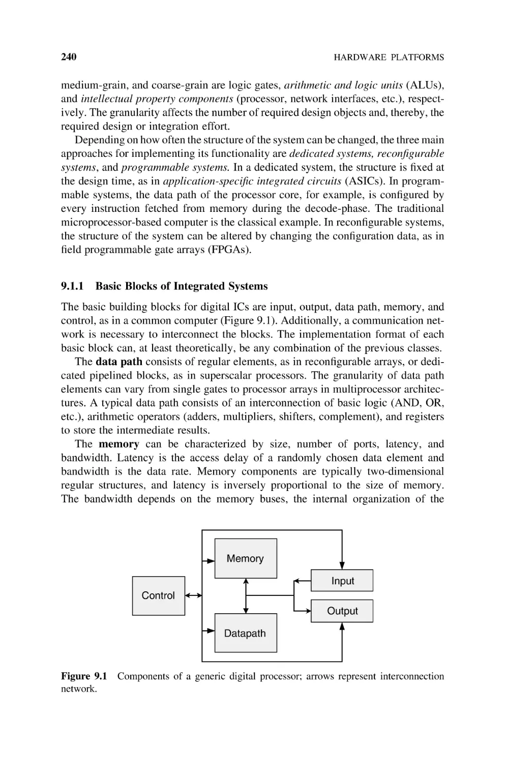
Hardware Platforms
9.1
Design Methods for Electronic Systems, 239
9.1.1 Basic Blocks of Integrated Systems, 240
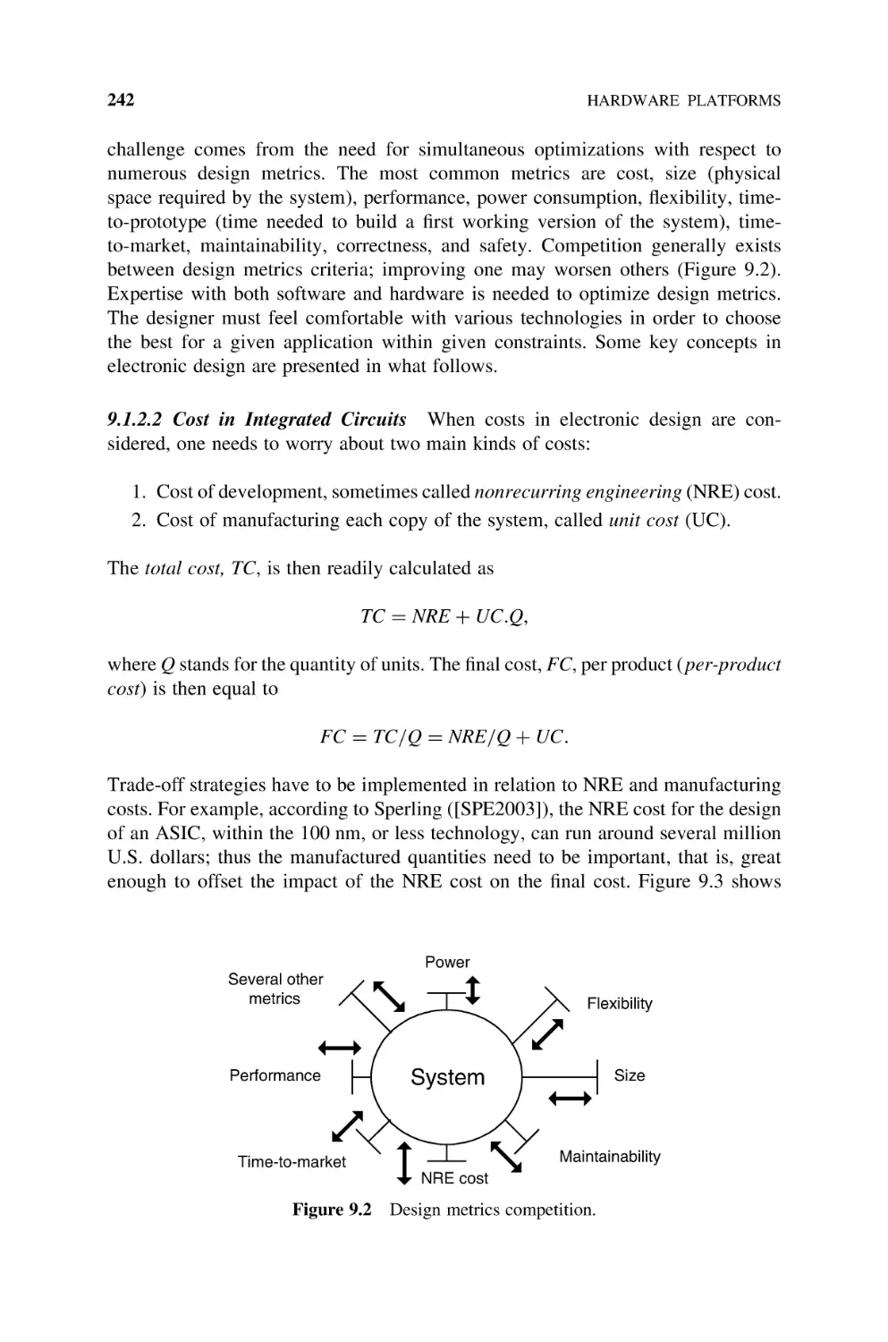
9.1.2 Recurring Topics in Electronic Design, 241
9.1.2.1 Design Challenge: Optimizing
Design Metrics, 241
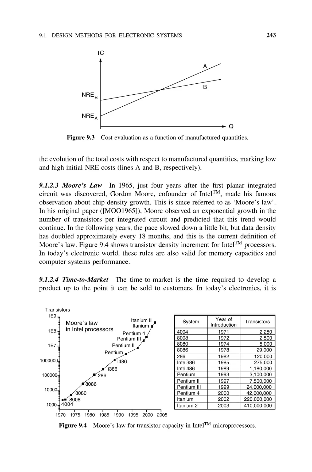
9.1.2.2 Cost in Integrated Circuits, 242
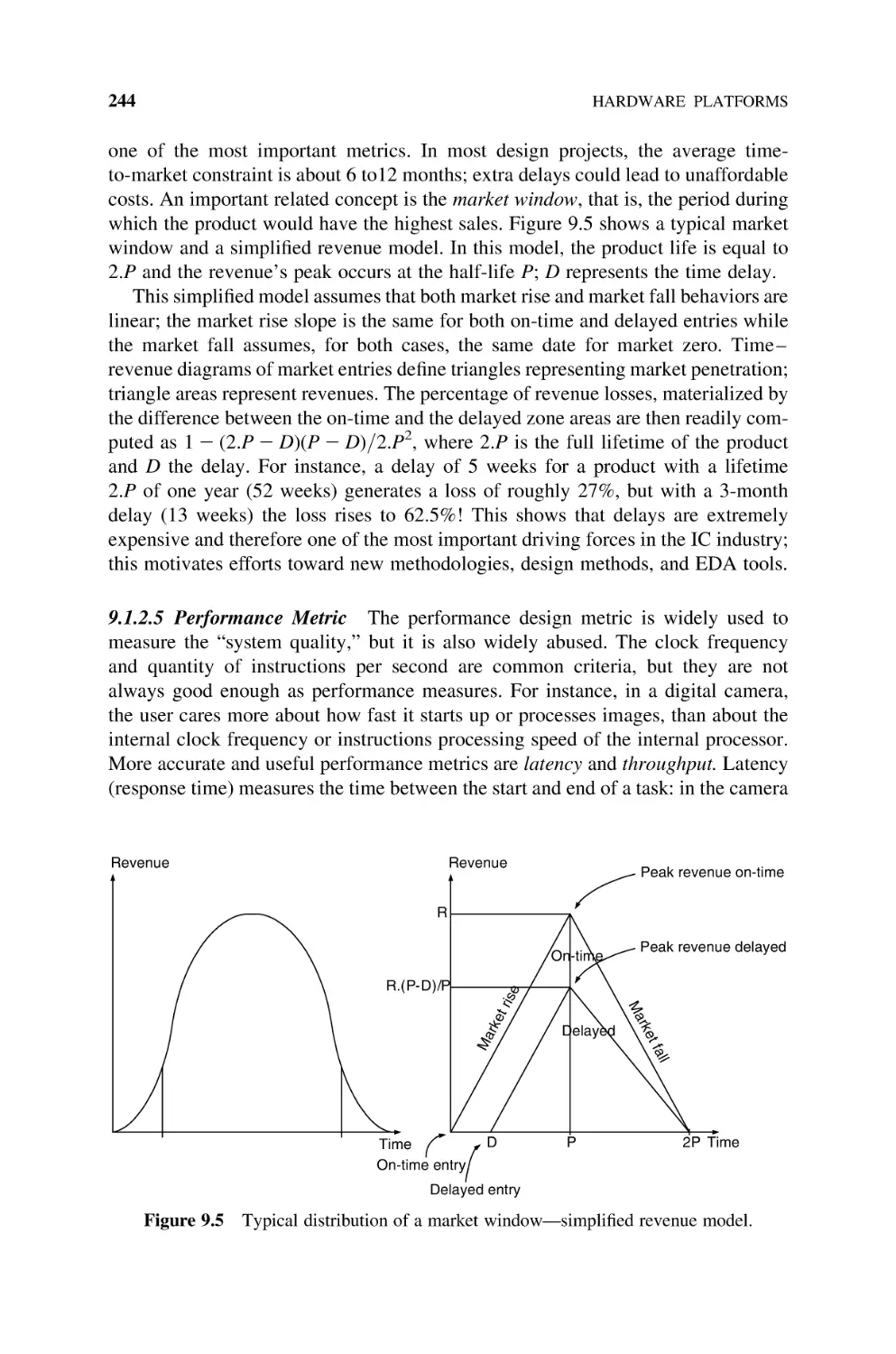
9.1.2.3 Moore’s Law, 243
9.1.2.4 Time-to-Market, 243
9.1.2.5 Performance Metric, 244
9.1.2.6 The Power Dimension, 245
9.2
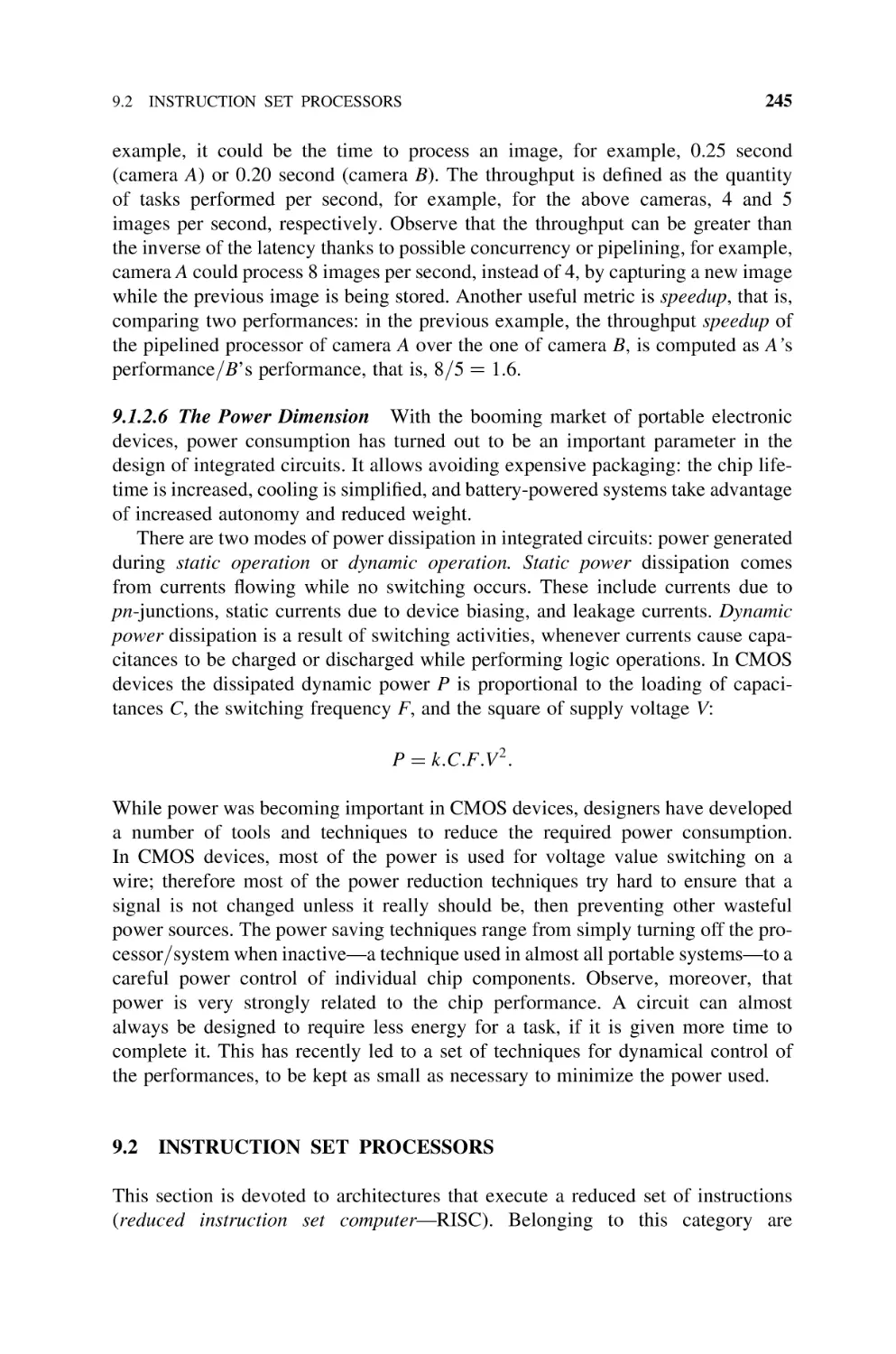
Instruction Set Processors, 245
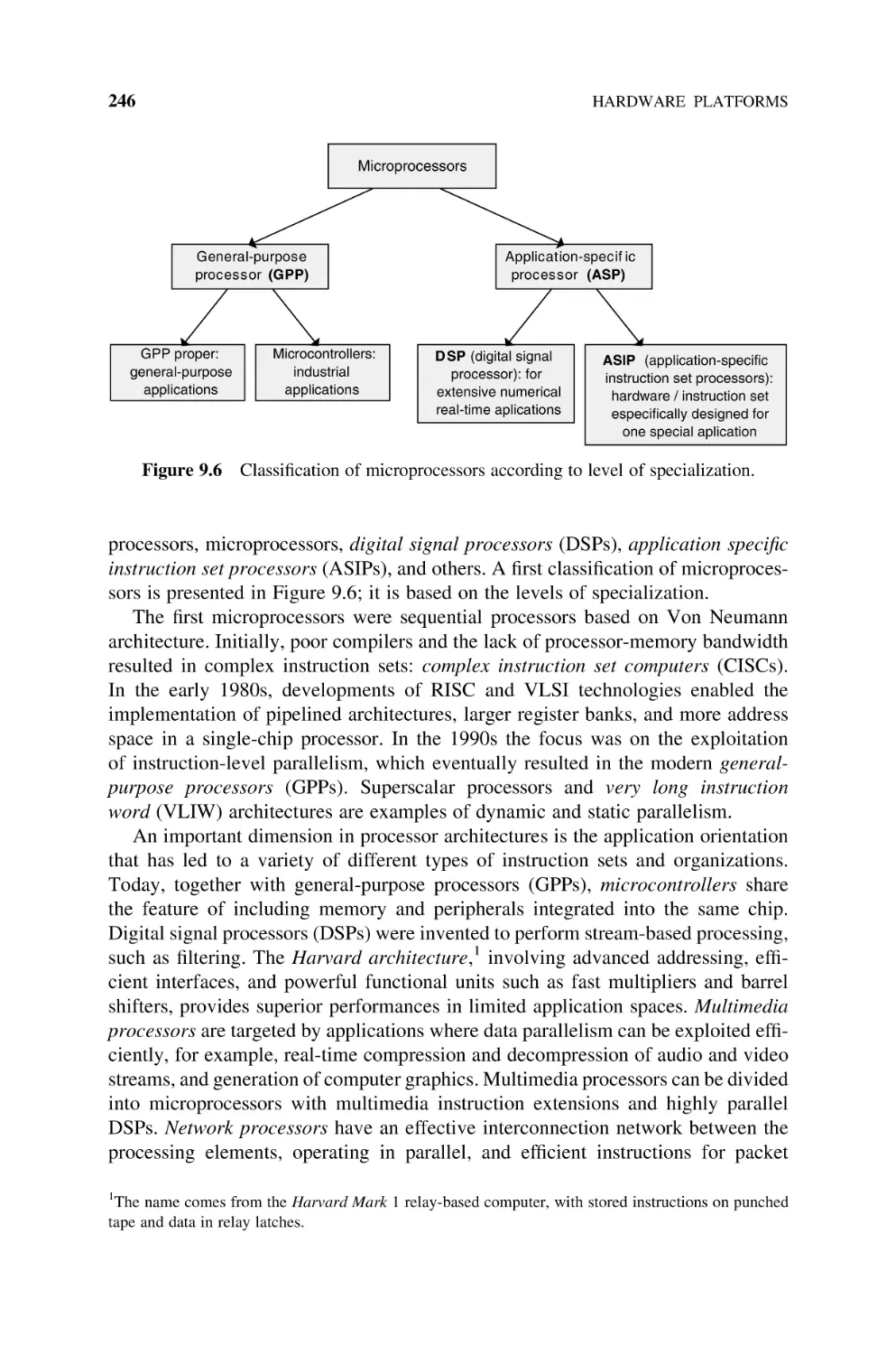
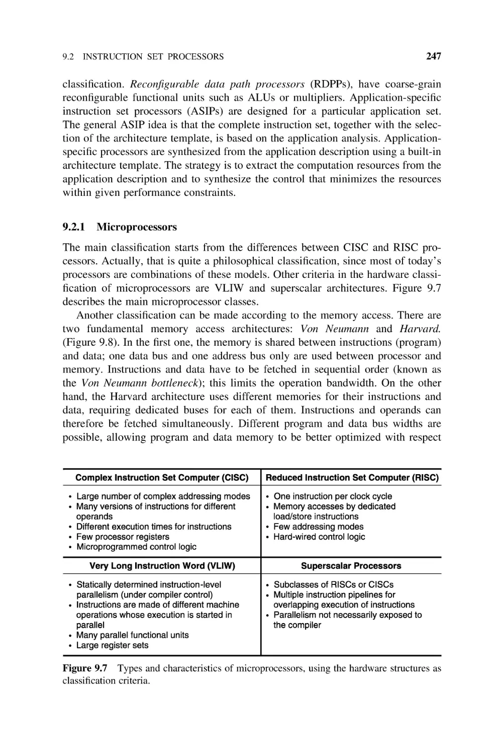
9.2.1 Microprocessors, 247
9.2.2 Microcontrollers, 248
9.2.3 Embedded Processors Everywhere, 248
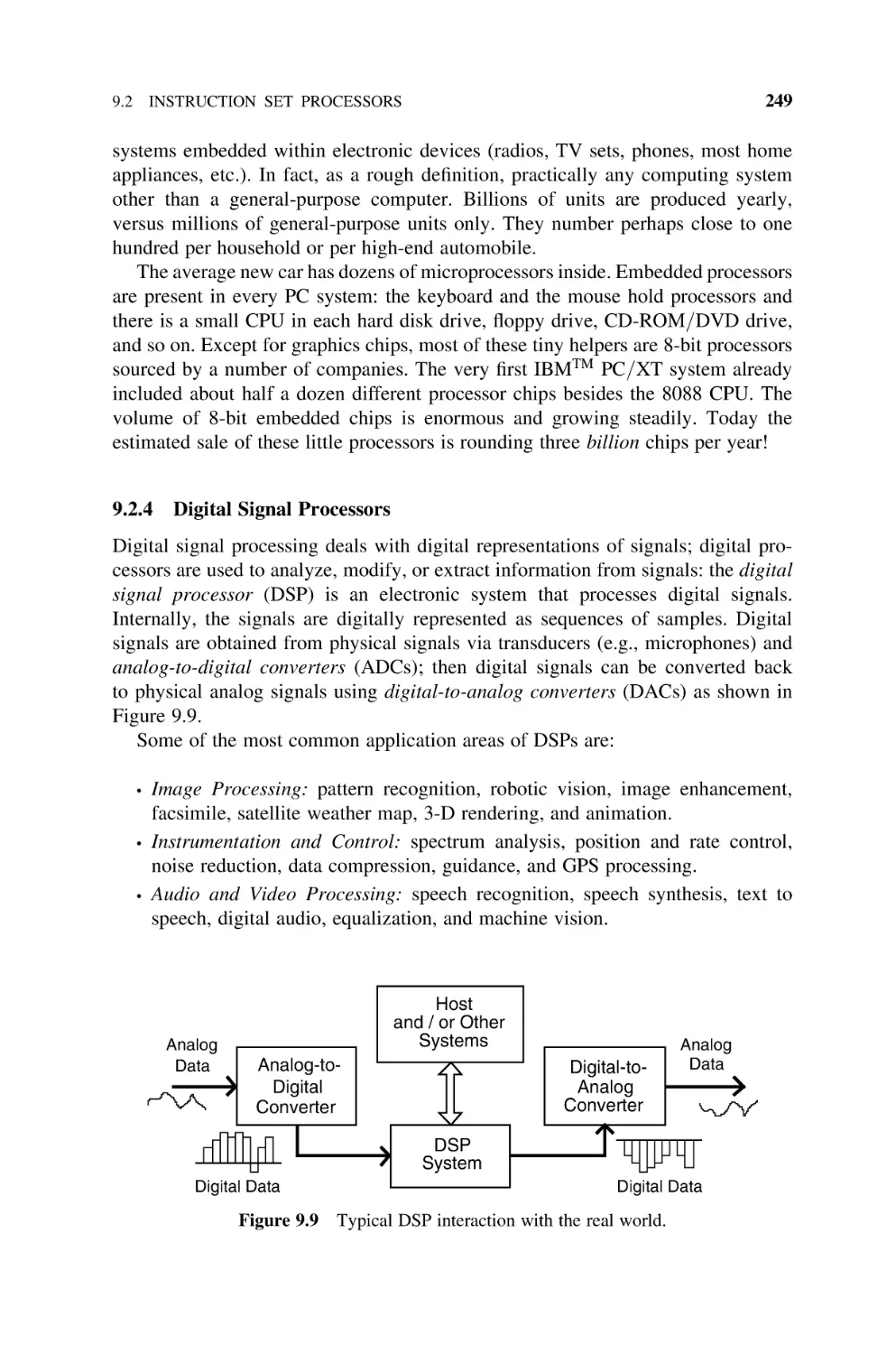
9.2.4 Digital Signal Processors, 249
9.2.5 Application-Specific Instruction Set Processors, 250
9.2.6 Programming Instruction Set Processors, 251
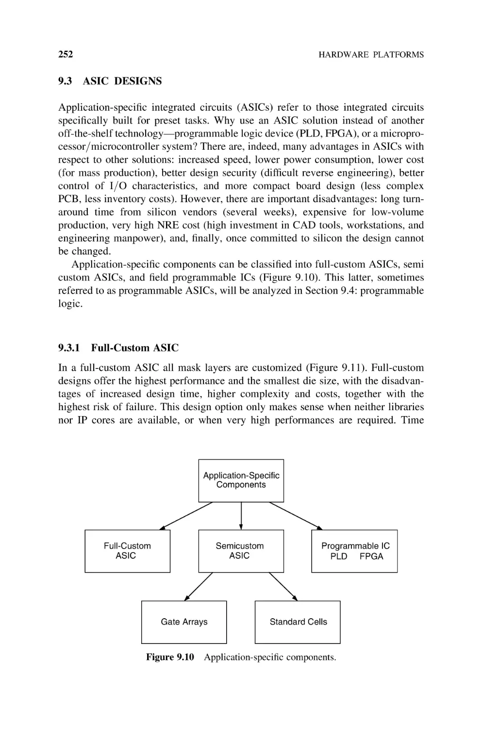
9.3
ASIC Designs, 252
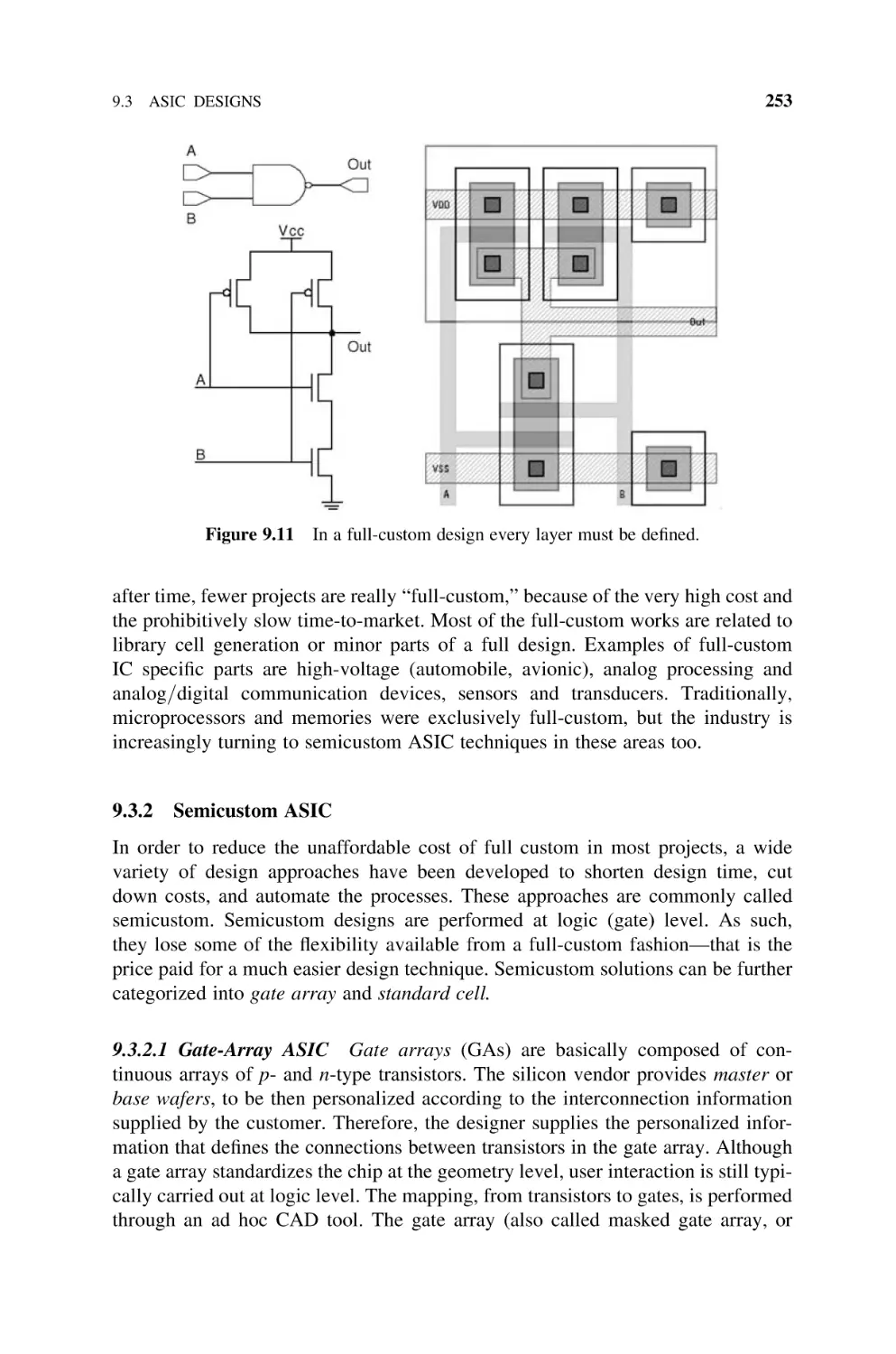
9.3.1 Full-Custom ASIC, 252
9.3.2 Semicustom ASIC, 253
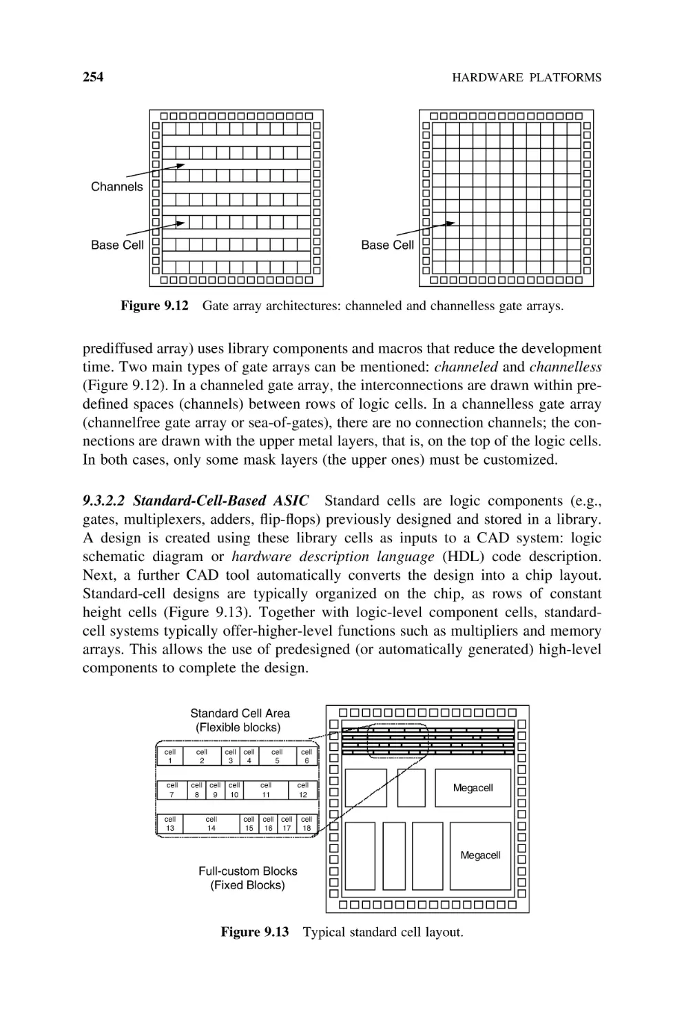
9.3.2.1 Gate-Array ASIC, 253
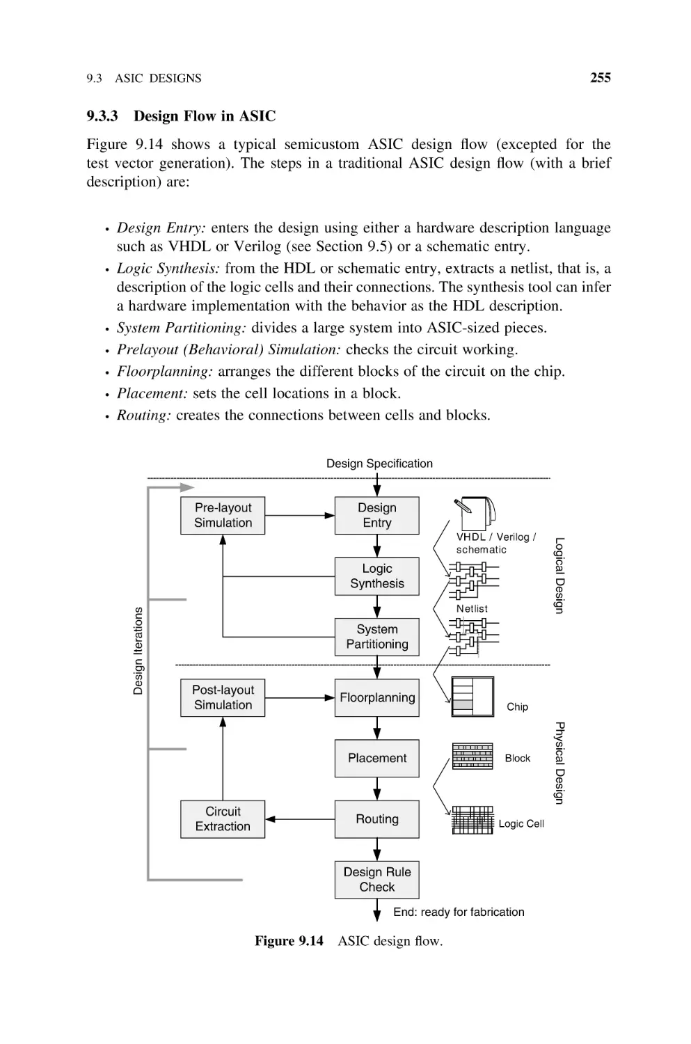
9.3.2.2 Standard-Cell-Based ASIC, 254
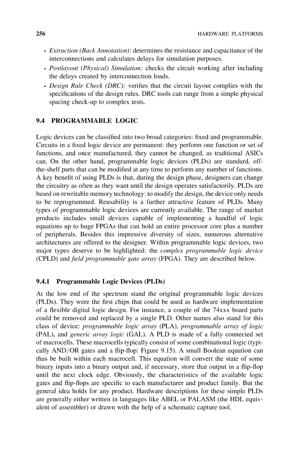
9.3.3 Design Flow in ASIC, 255
9.4
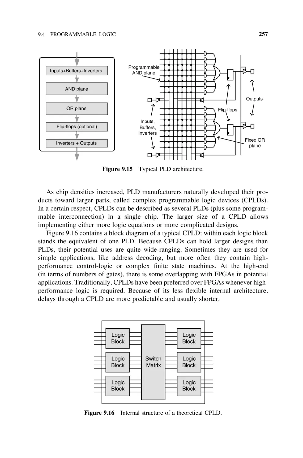
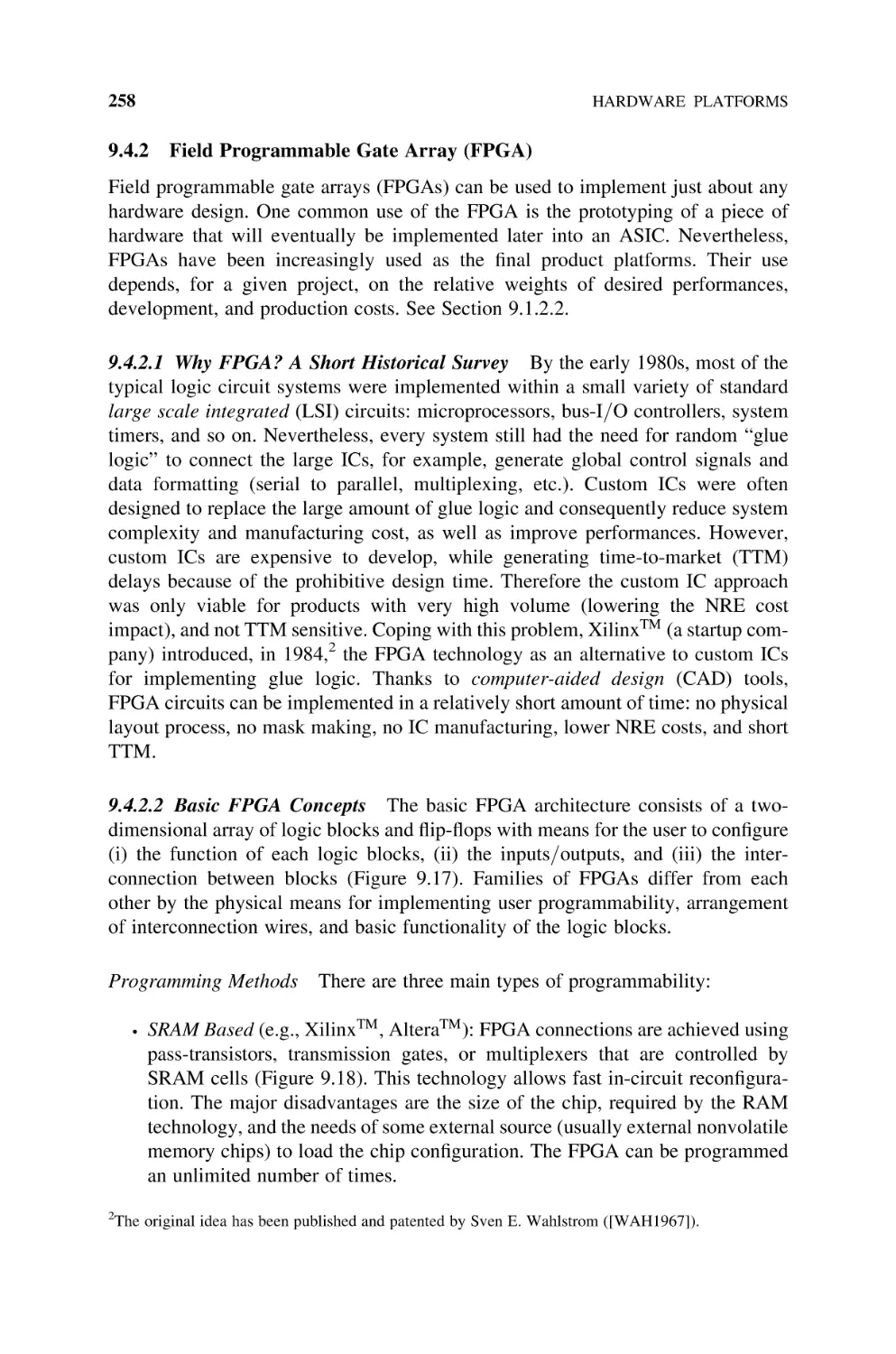
Programmable Logic, 256
9.4.1 Programmable Logic Devices (PLDs), 256
9.4.2 Field Programmable Gate Array (FPGA), 258
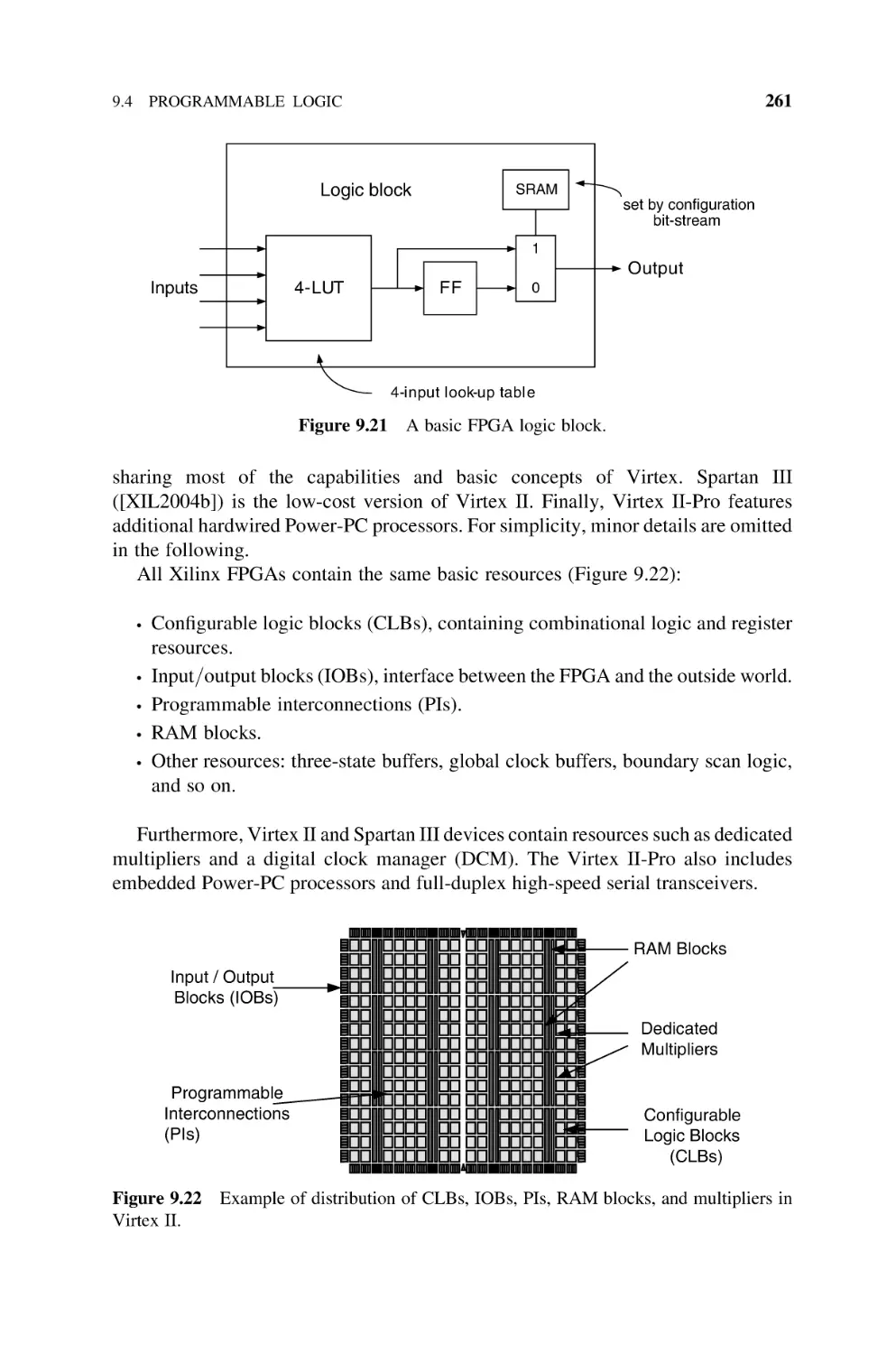
9.4.2.1 Why FPGA? A Short Historical Survey, 258
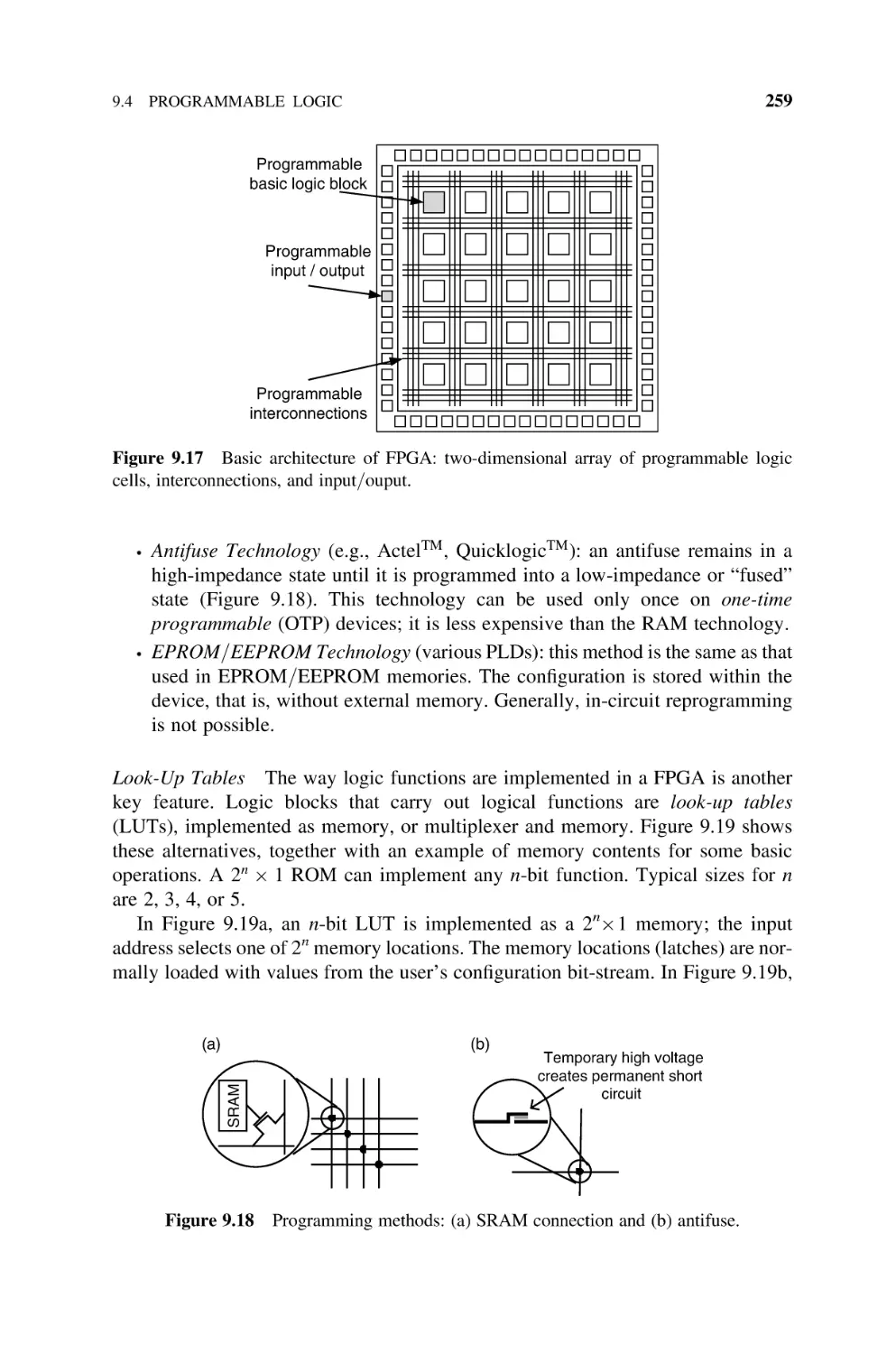
9.4.2.2 Basic FPGA Concepts, 258
239
CONTENTS
xii
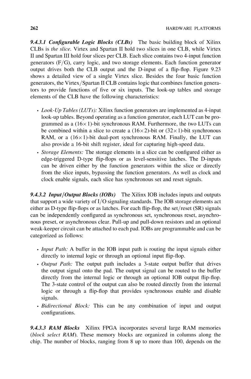
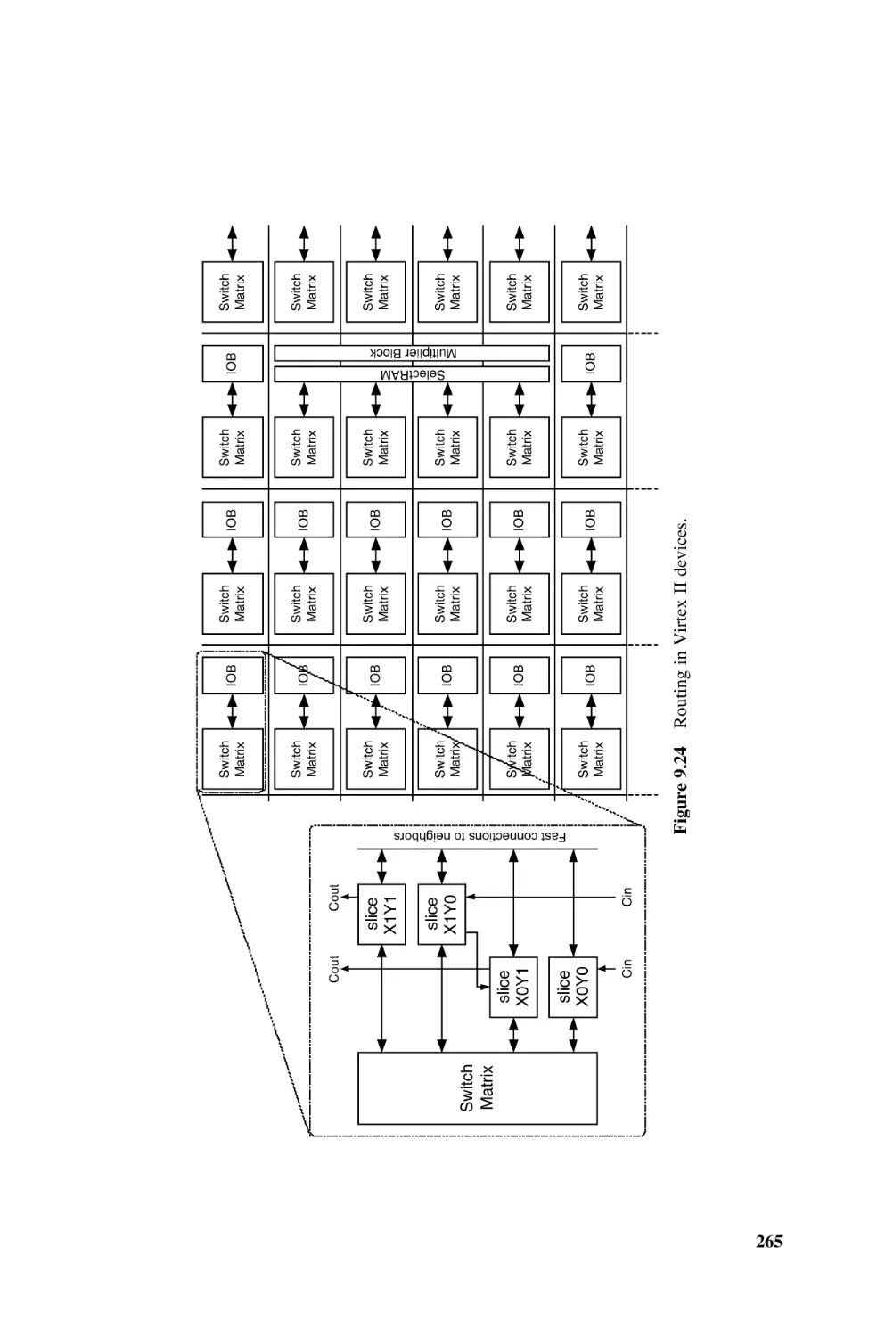
XilinxTM Specifics, 260
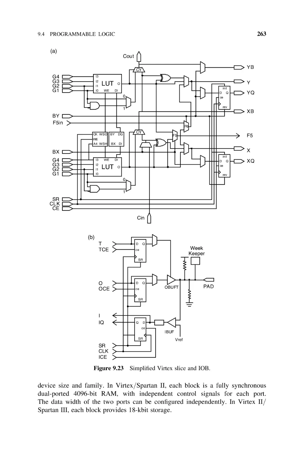
9.4.3.1 Configurable Logic Blocks (CLBs), 262
9.4.3.2 Input/Output Blocks (IOBs), 262
9.4.3.3 RAM Blocks, 262
9.4.3.4 Programmable Routing, 264
9.4.3.5 Arithmetic Resources in Xilinx FPGAs, 264
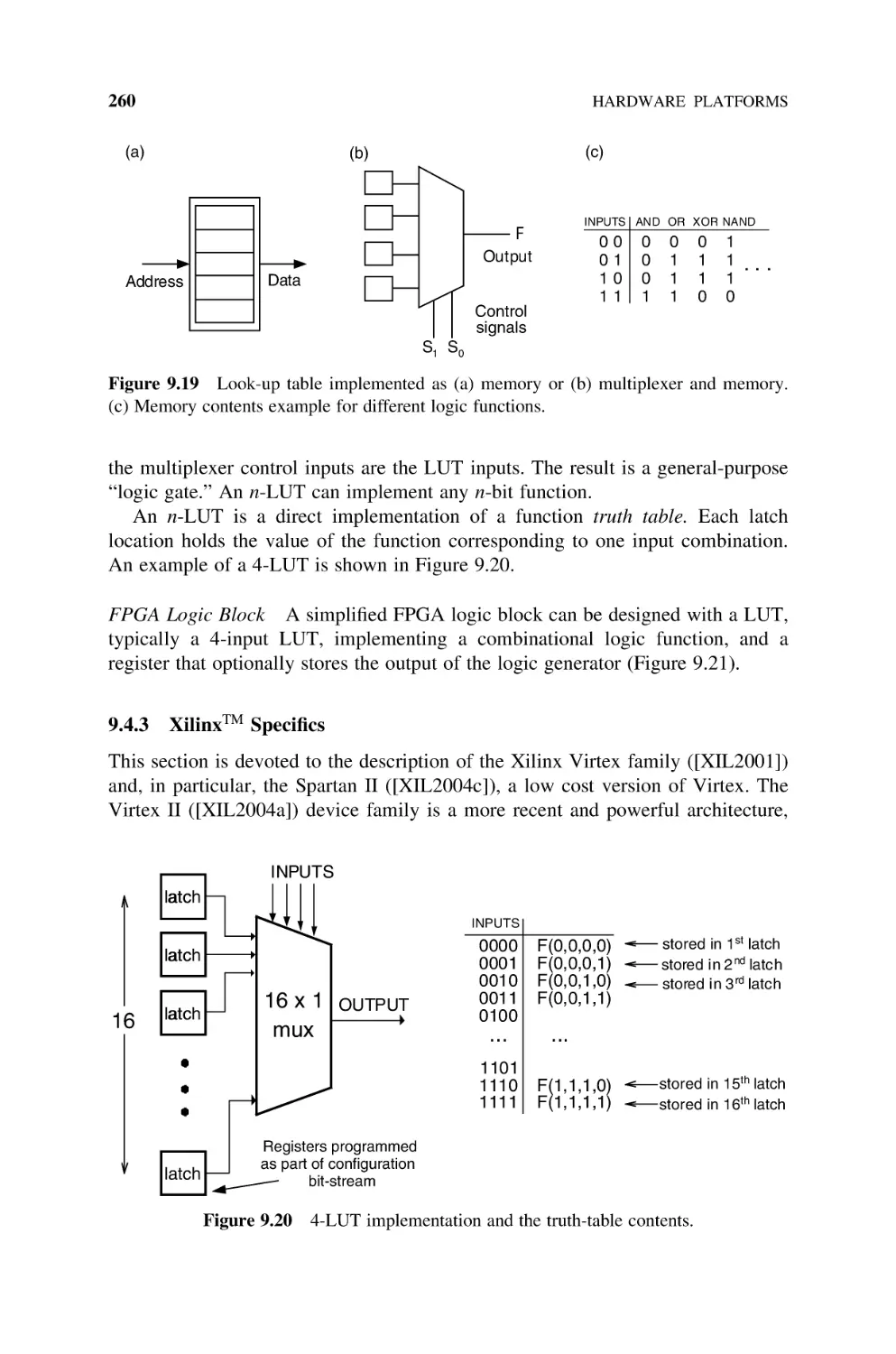
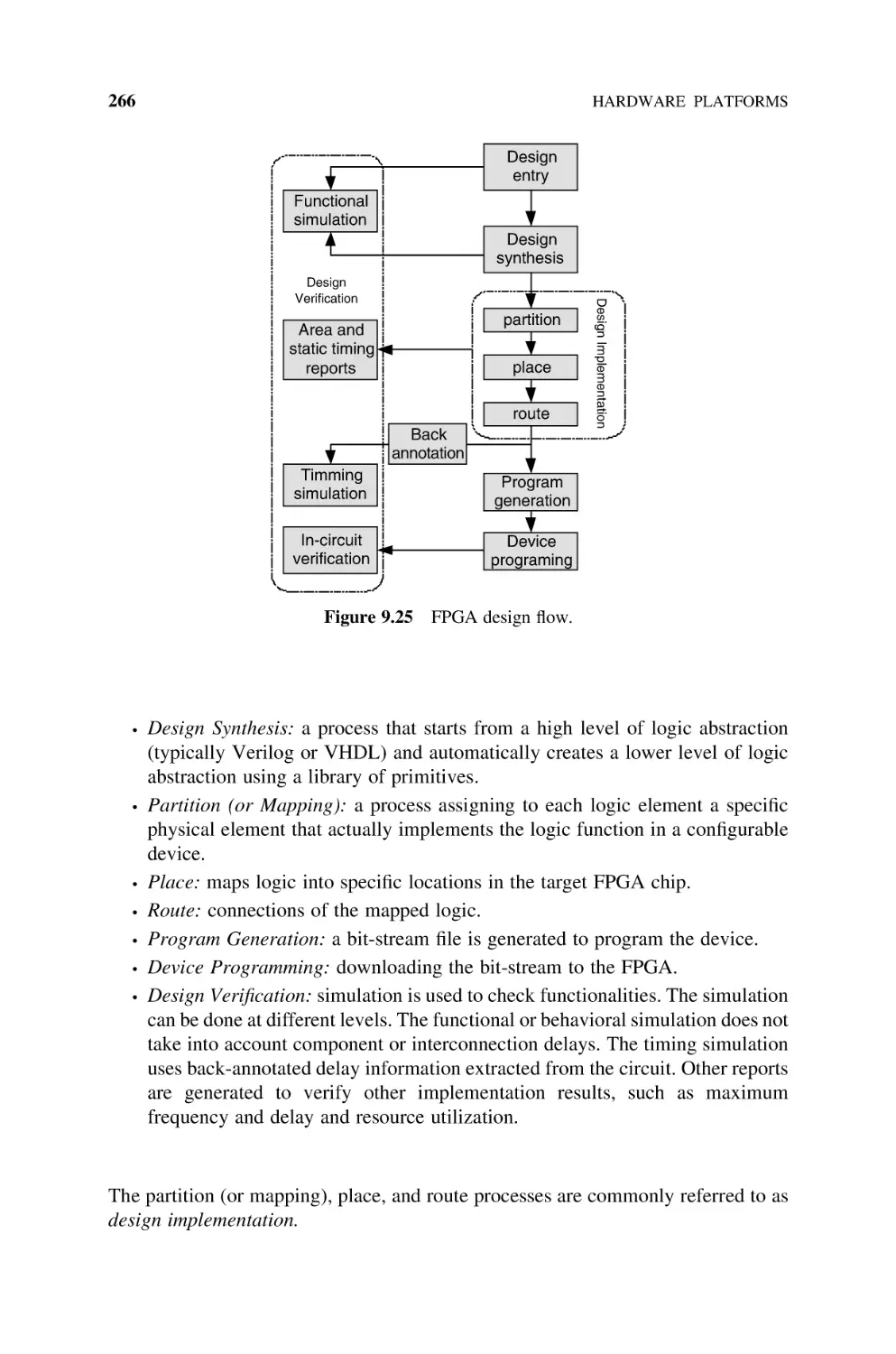
9.4.4 FPGA Generic Design Flow, 264
9.4.3
10
11
9.5
Hardware Description Languages (HDLs), 267
9.5.1 Today’s and Tomorrow’s HDLs, 267
9.6
Further Readings, 268
9.7
Bibliography, 268
Circuit Synthesis: General Principles
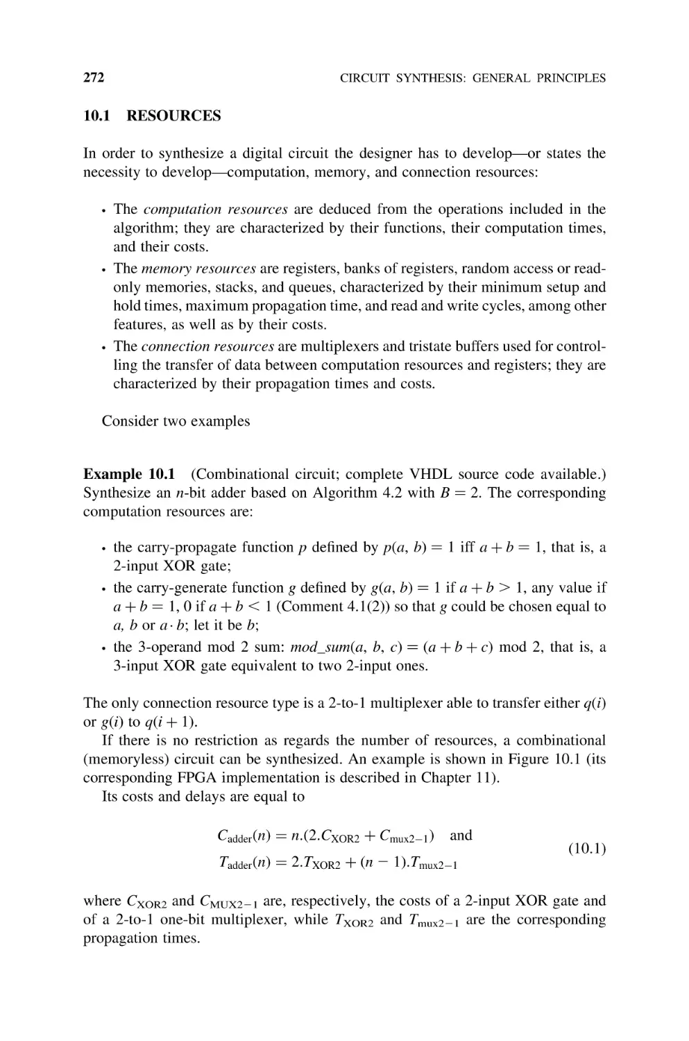
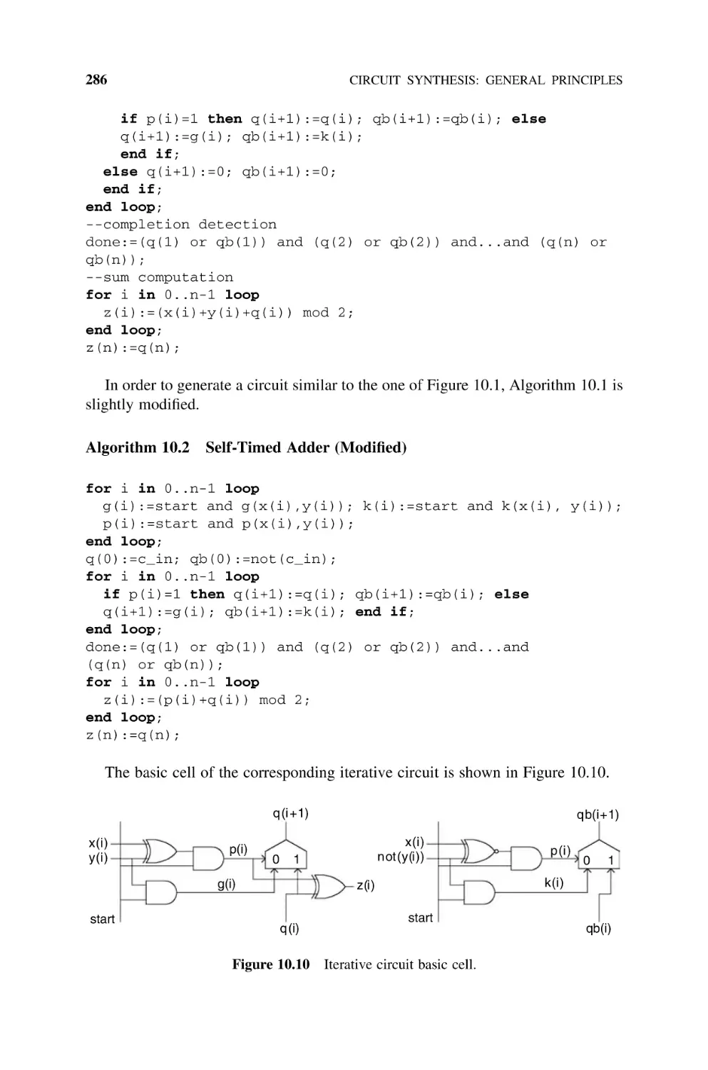
10.1
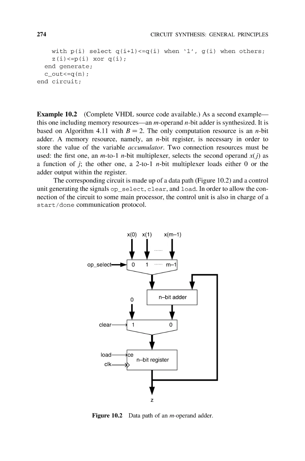
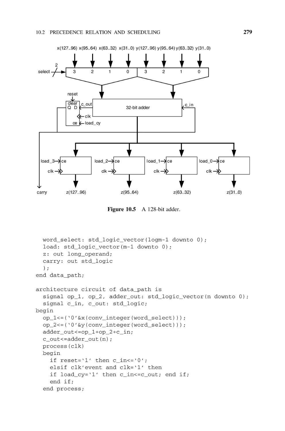
Resources, 272
10.2
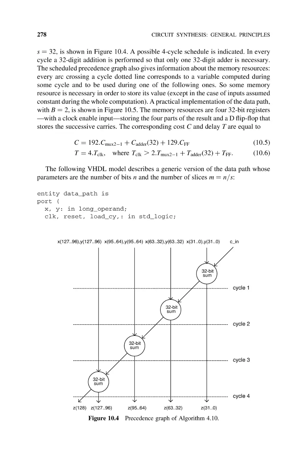
Precedence Relation and Scheduling, 277
10.3
Pipeline, 281
10.4
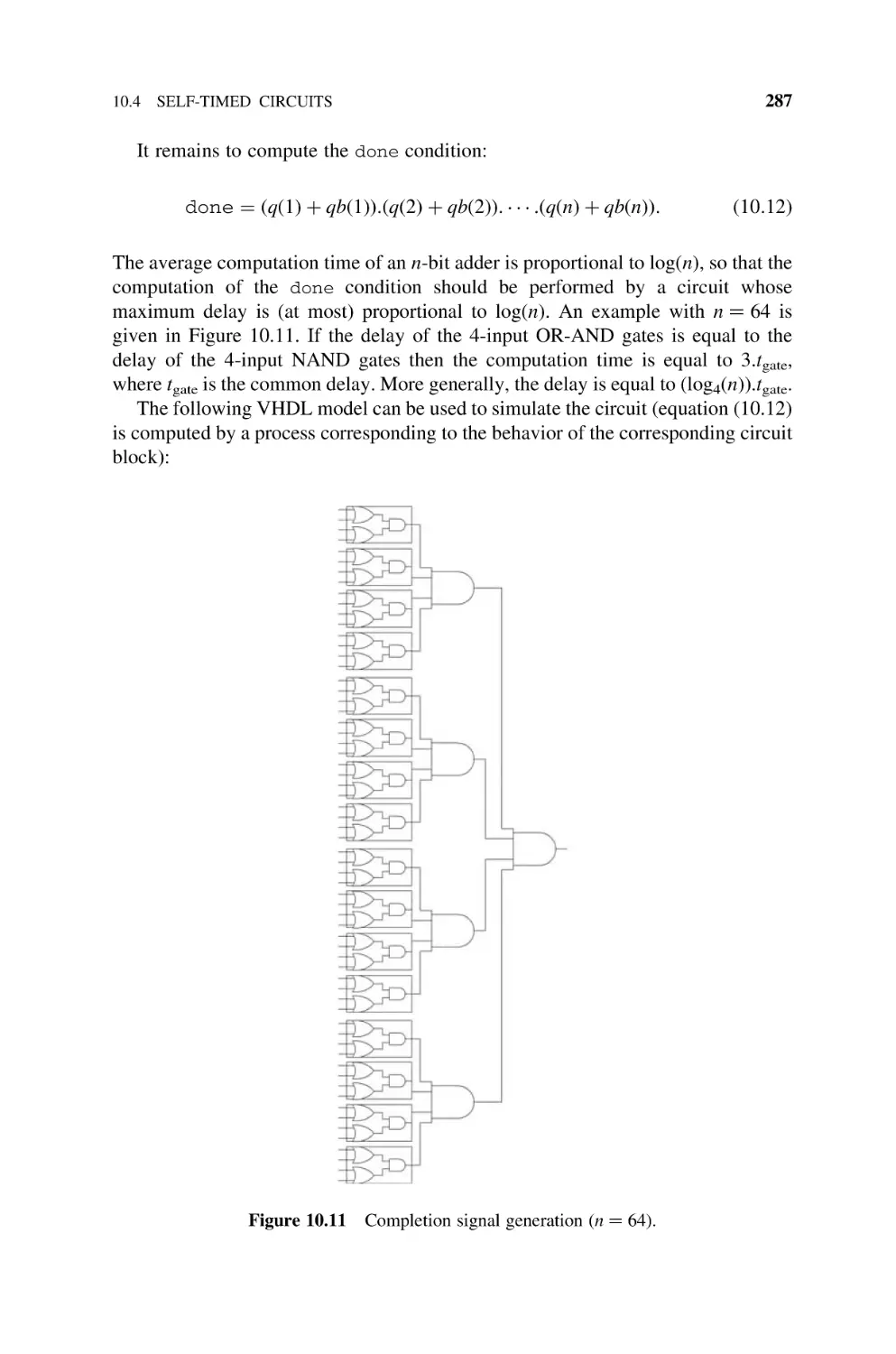
Self-Timed Circuits, 282
10.5
Bibliography, 288
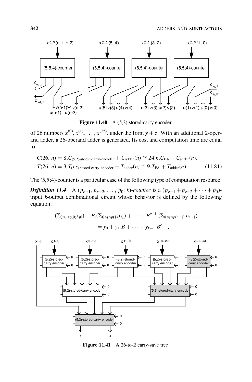
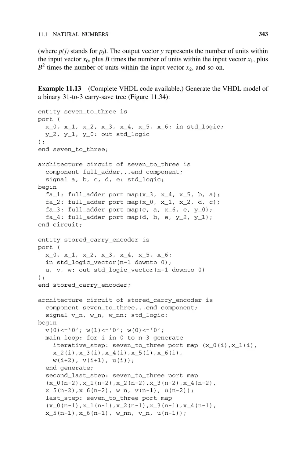
Adders and Subtractors
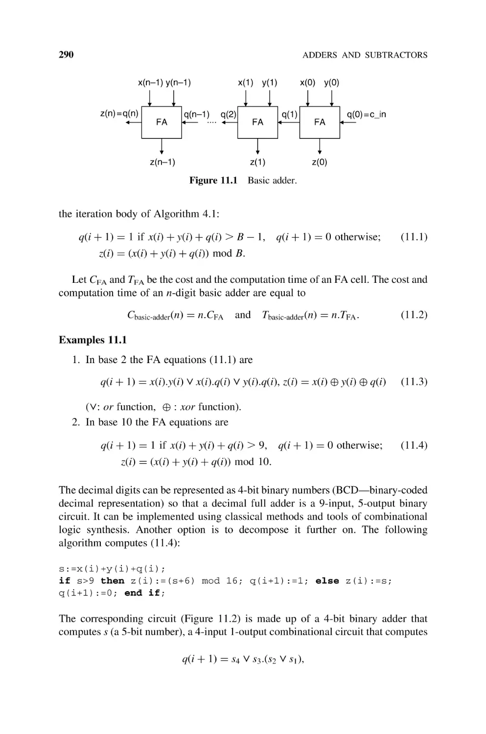
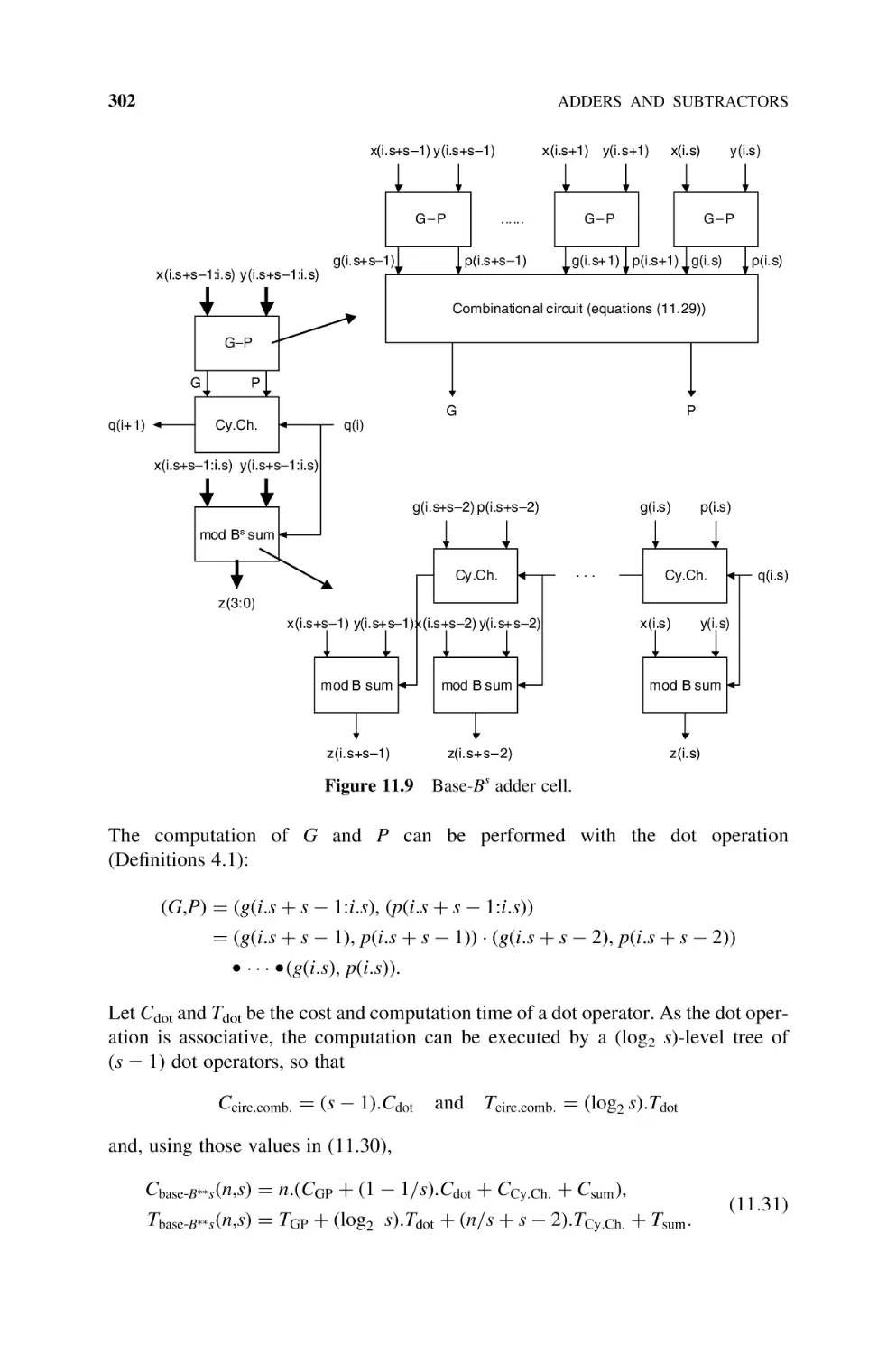
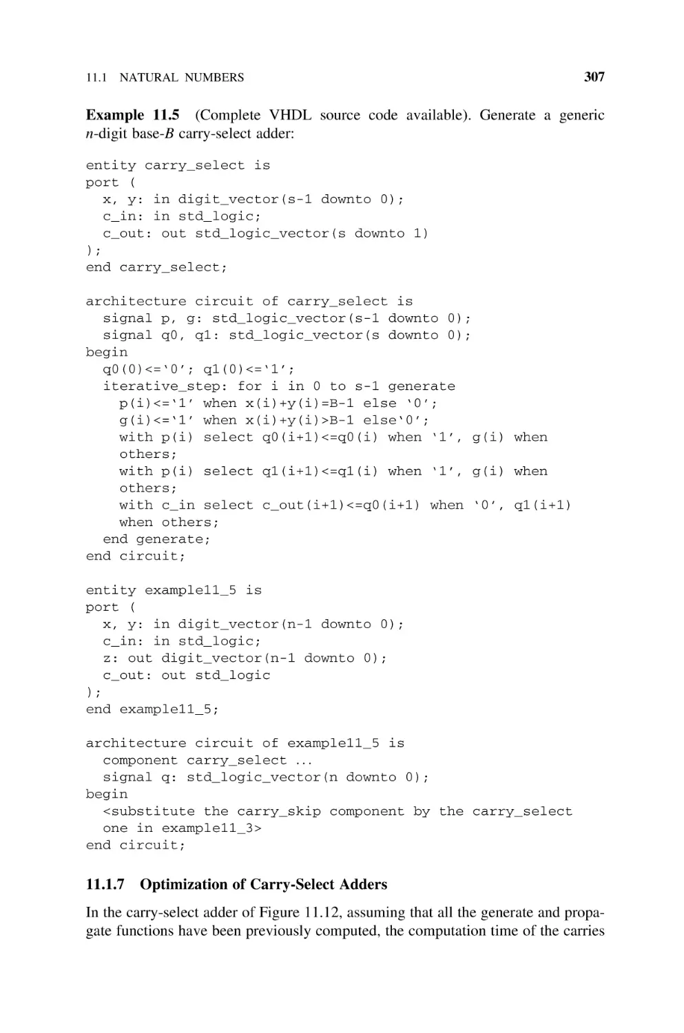
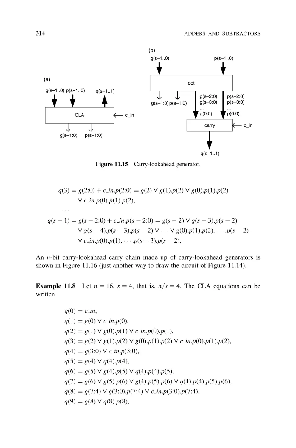
11.1
Natural Numbers, 289
11.1.1
Basic Adder (Ripple-Carry Adder), 289
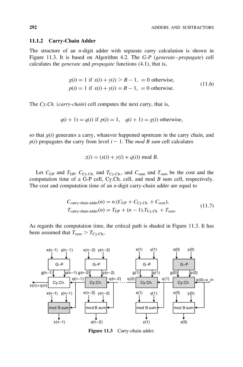
11.1.2
Carry-Chain Adder, 292
11.1.3
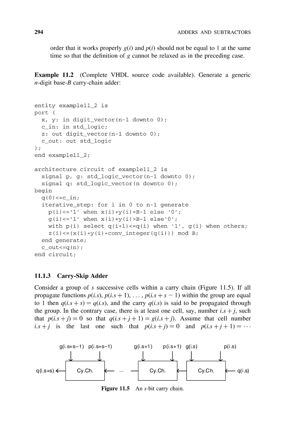
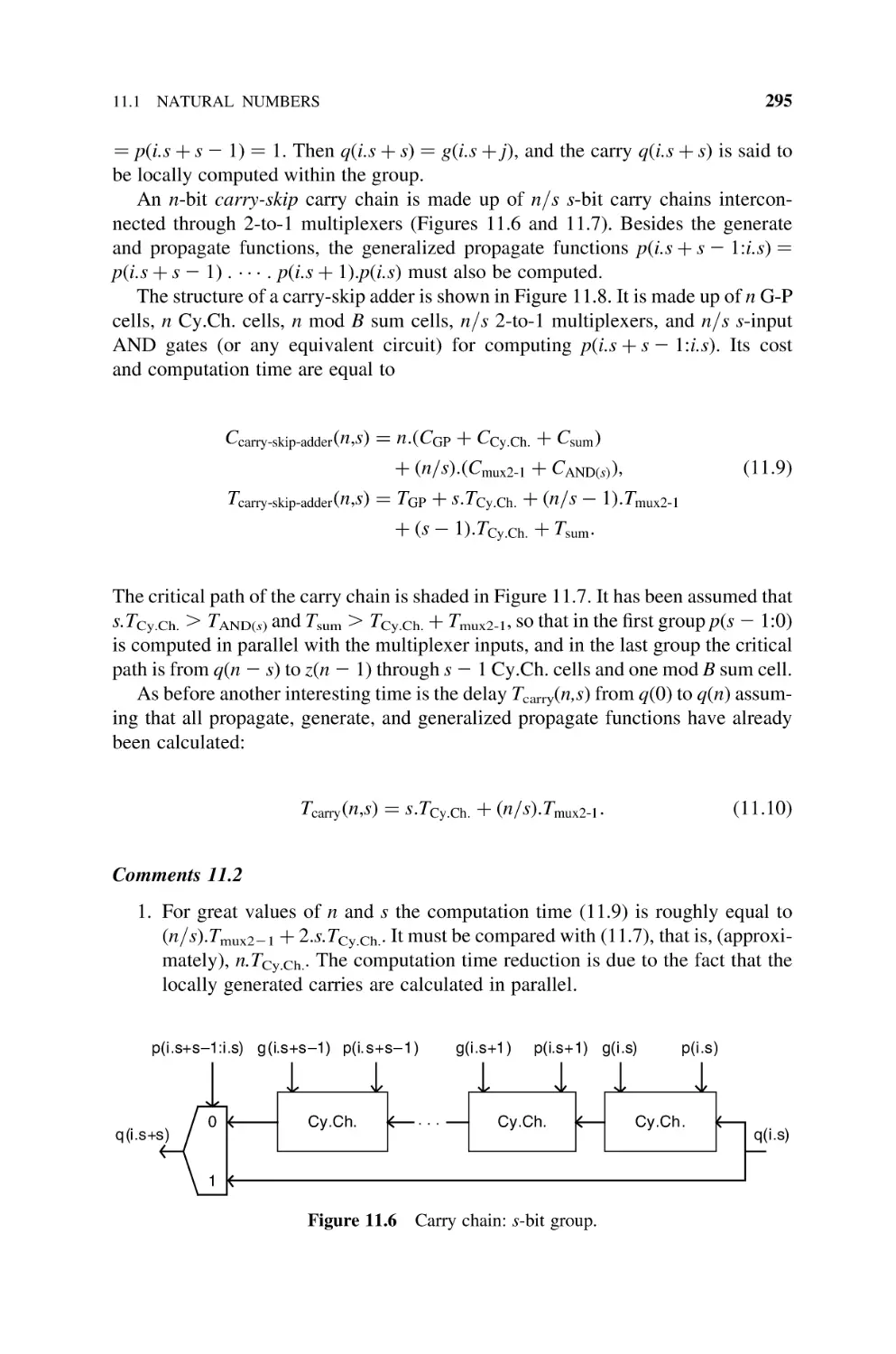
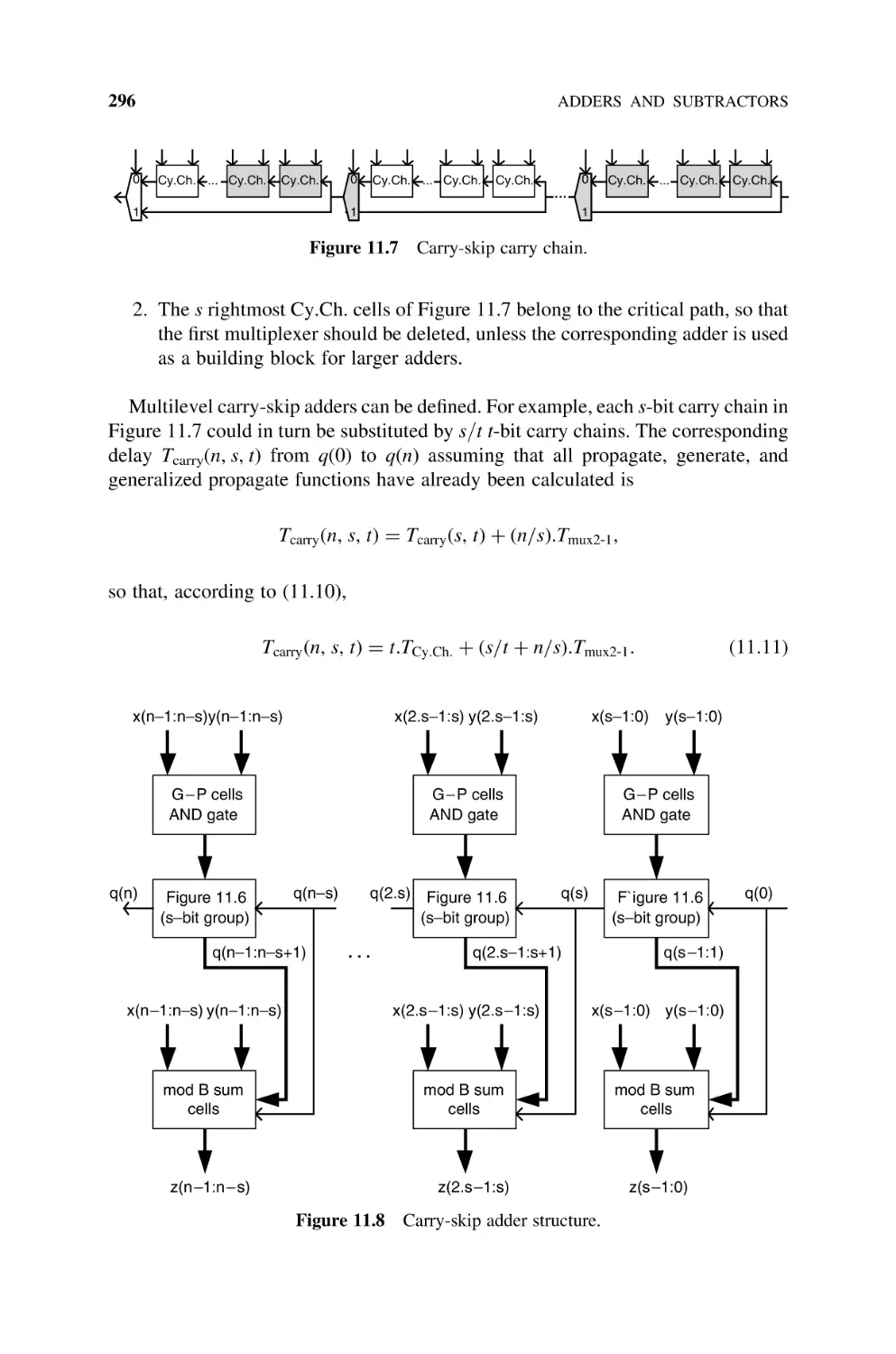
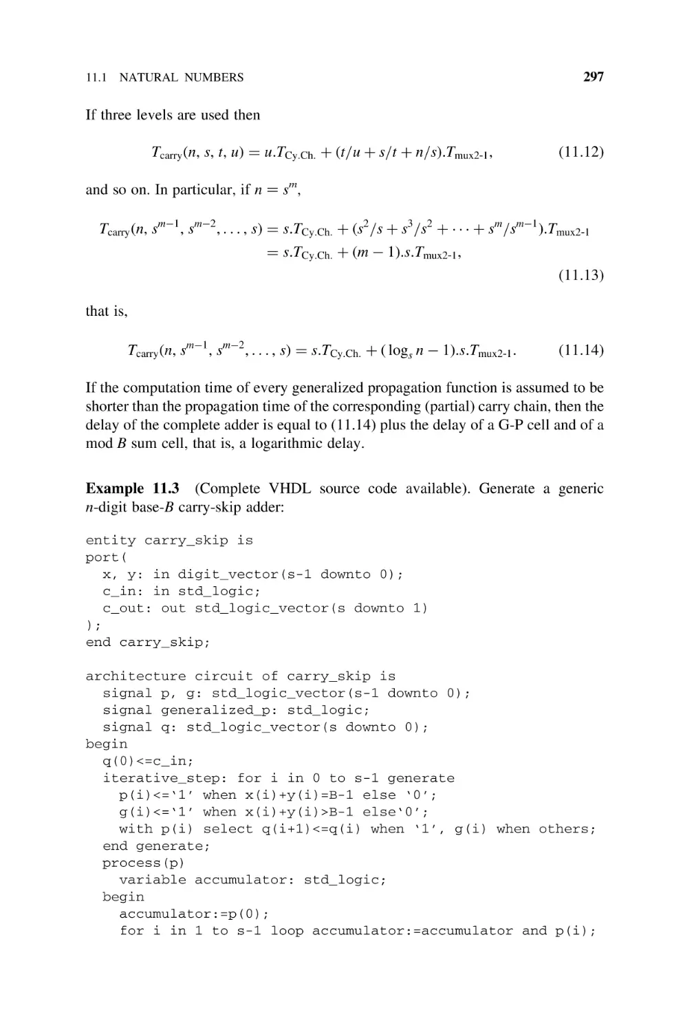
Carry-Skip Adder, 294
11.1.4
Optimization of Carry-Skip Adders, 298
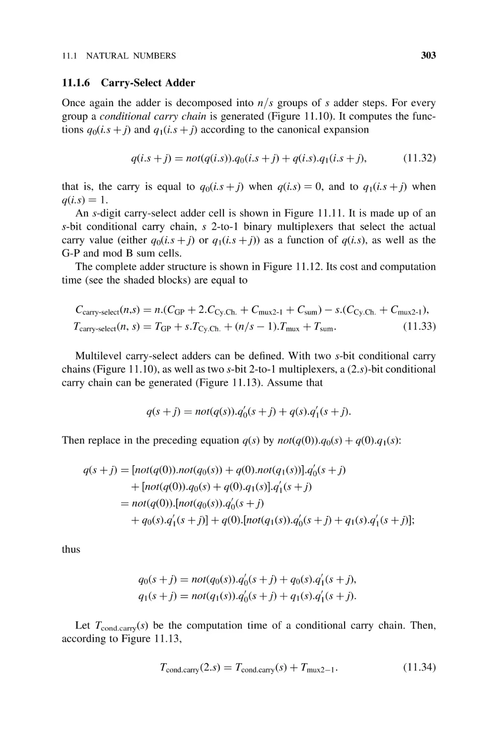
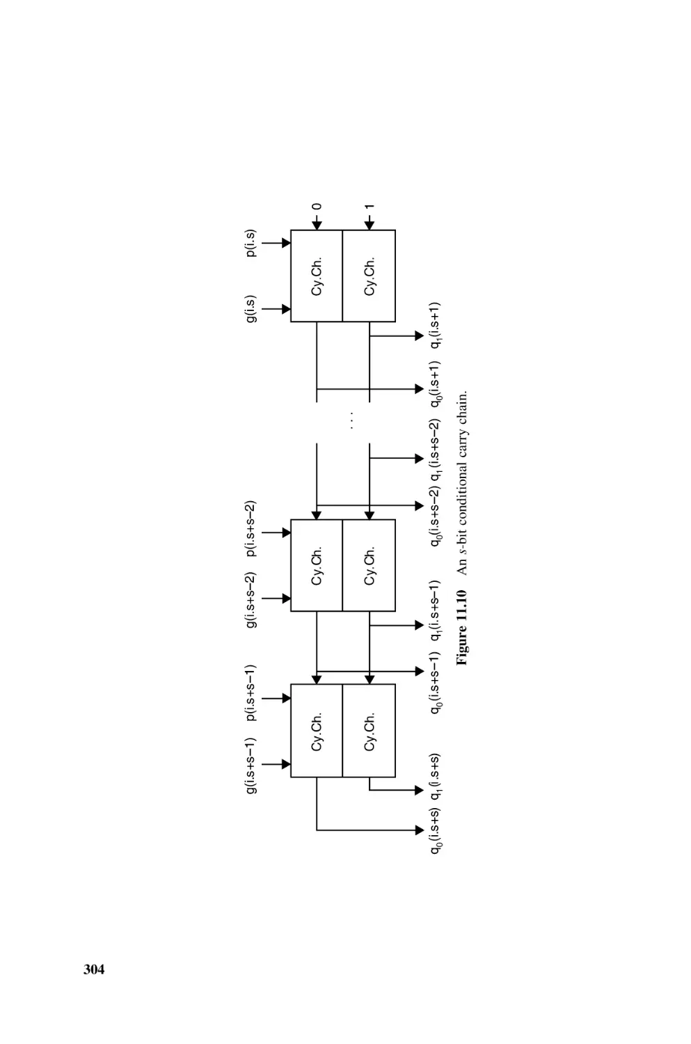
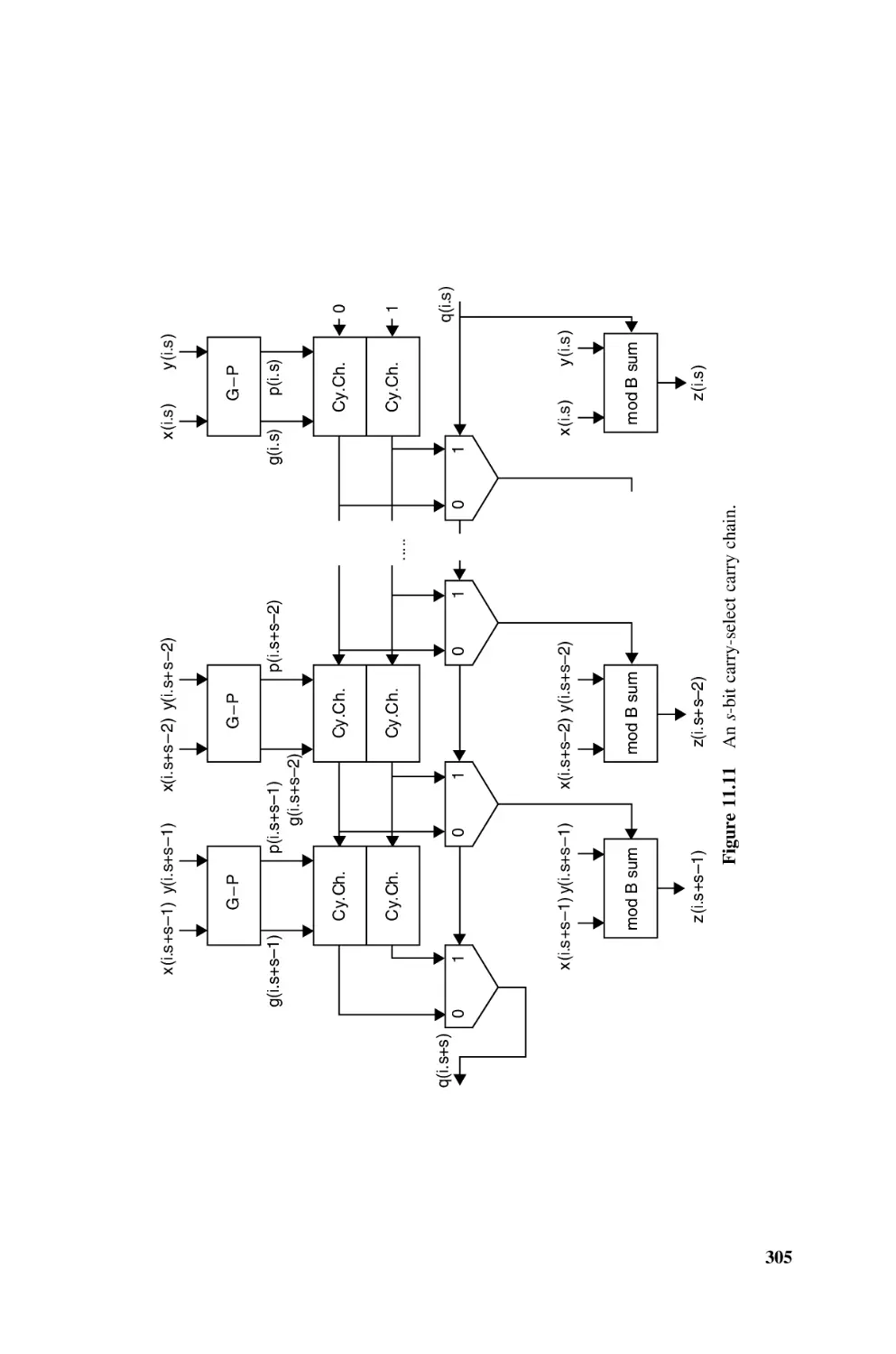
11.1.5
Base-Bs Adder, 301
11.1.6
Carry-Select Adder, 303
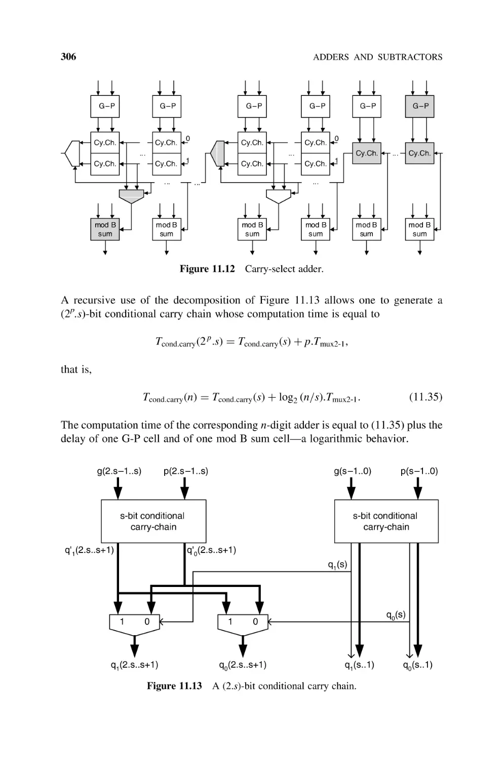
11.1.7
Optimization of Carry-Select Adders, 307
11.1.8
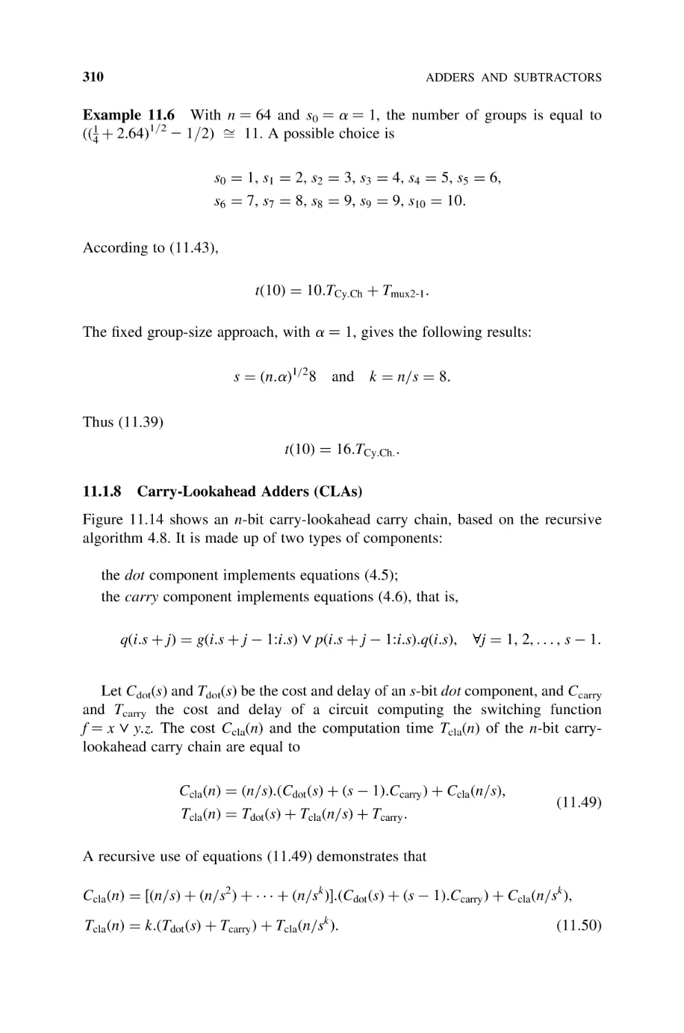
Carry-Lookahead Adders (CLAs), 310
11.1.9
Prefix Adders, 318
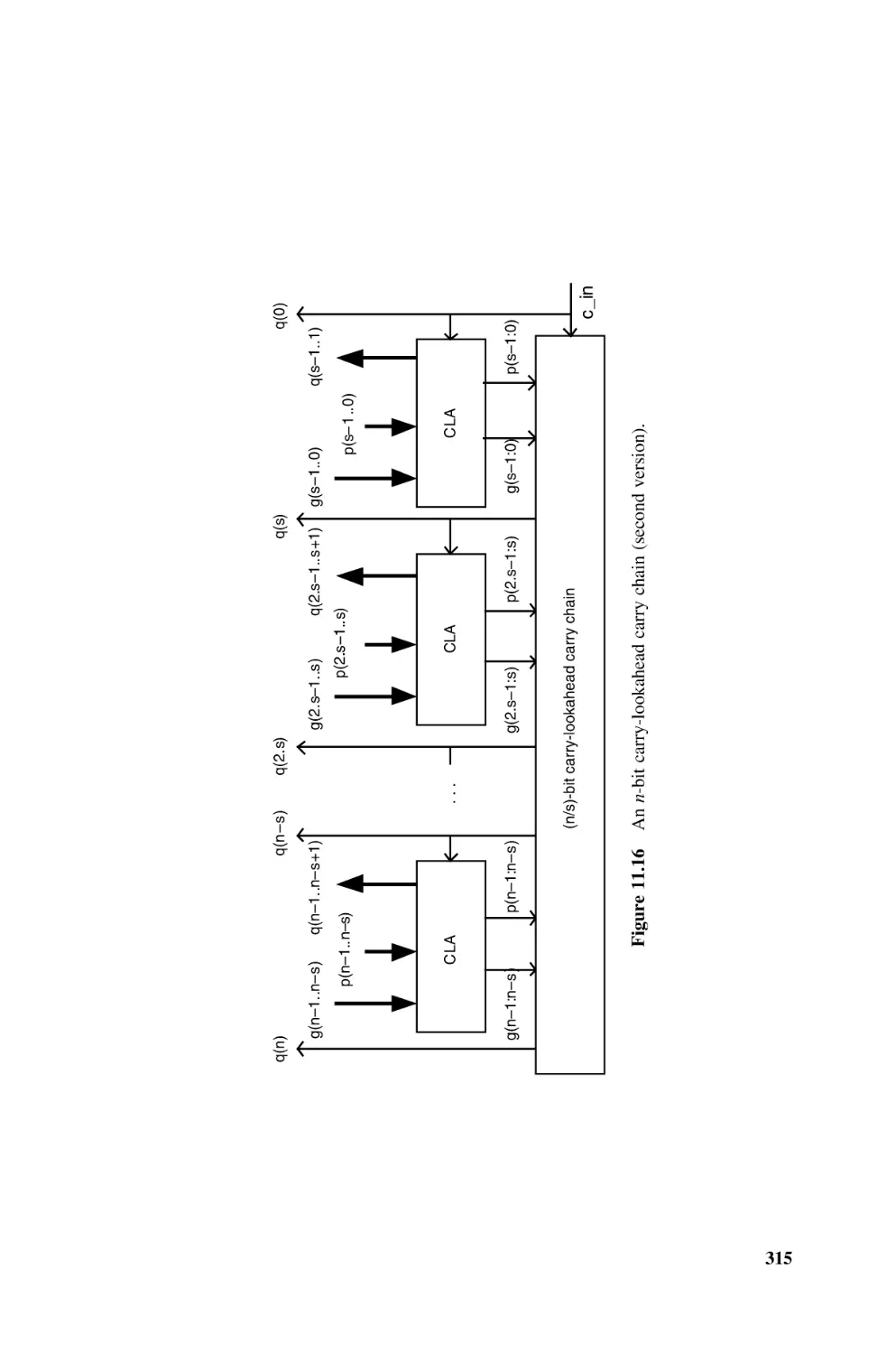
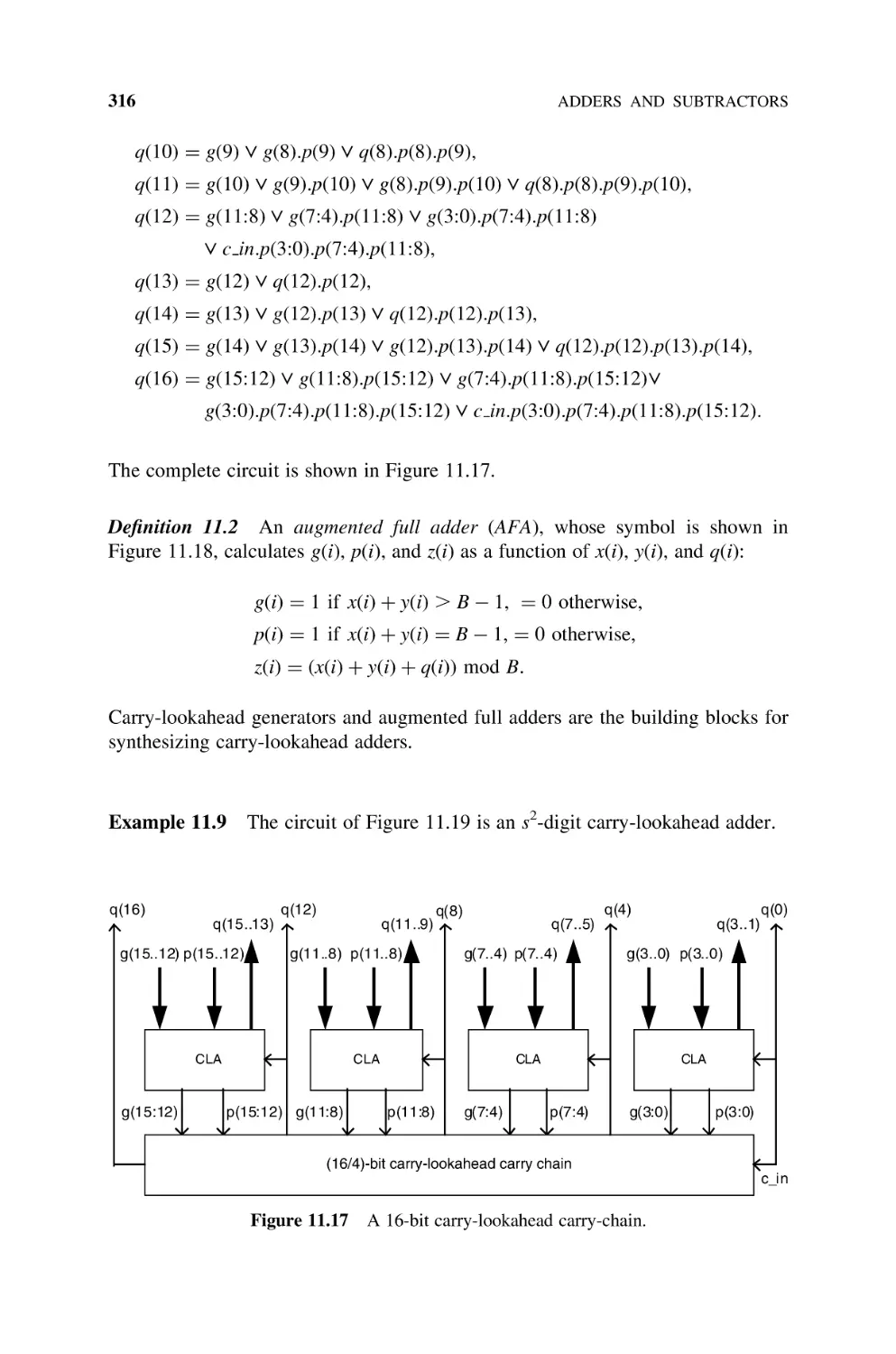
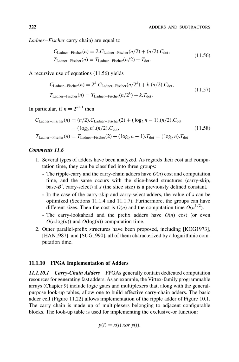
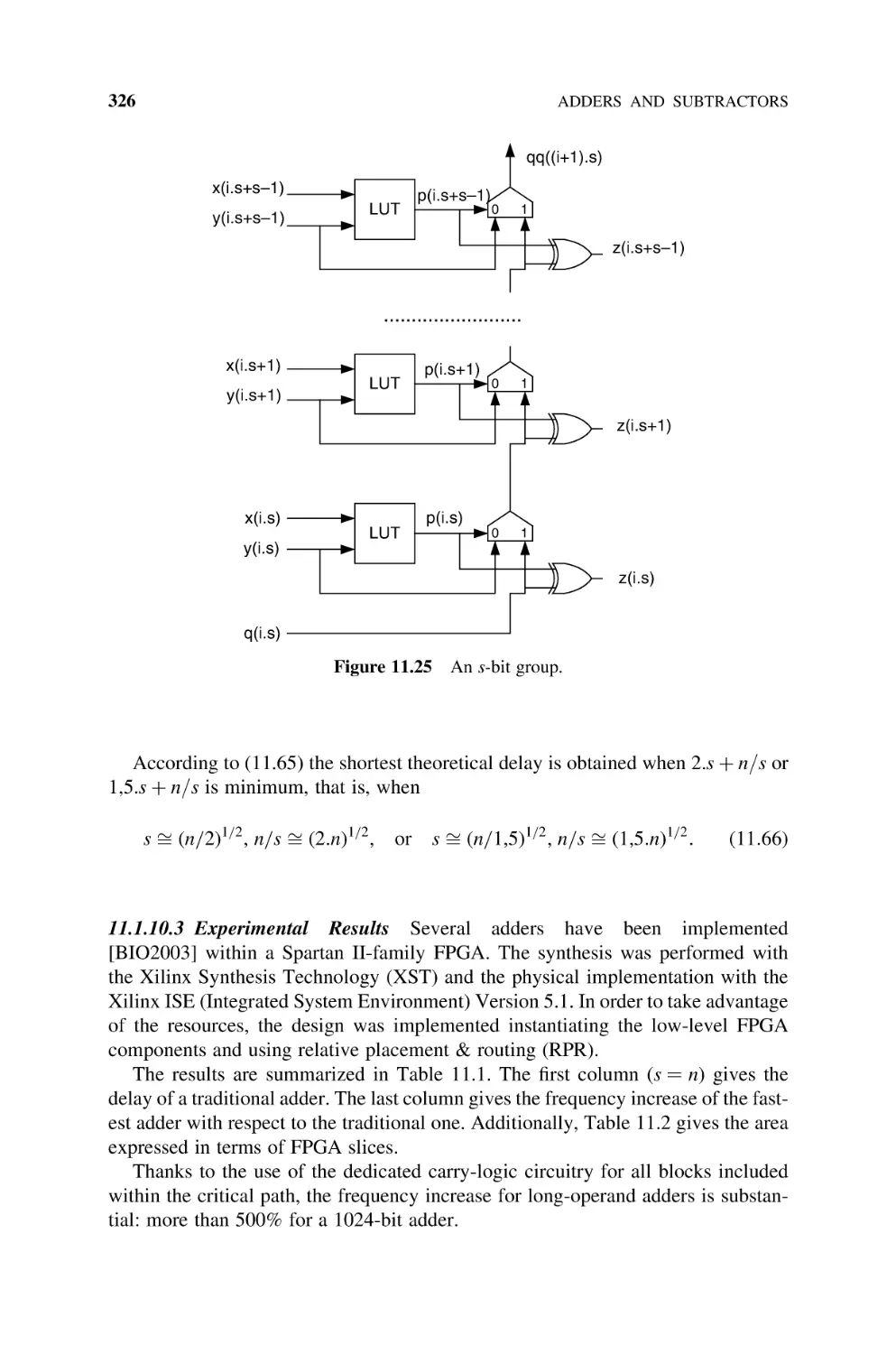
11.1.10 FPGA Implementation of Adders, 322
11.1.10.1 Carry-Chain Adders, 322
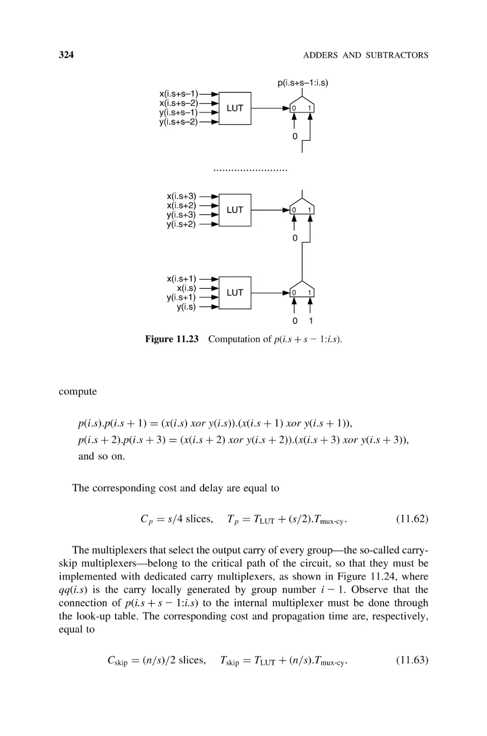
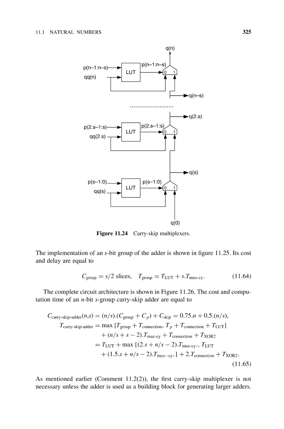
11.1.10.2 Carry-Skip Adders, 323
11.1.10.3 Experimental Results, 326
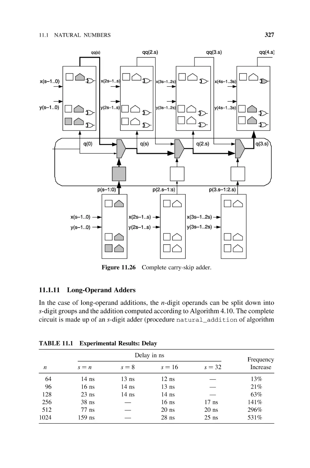
11.1.11 Long-Operand Adders, 327
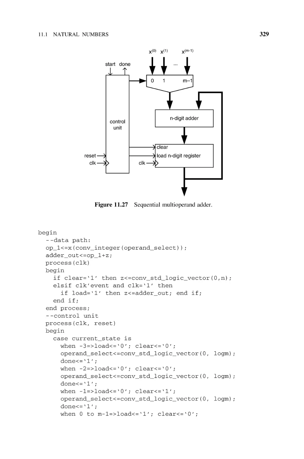
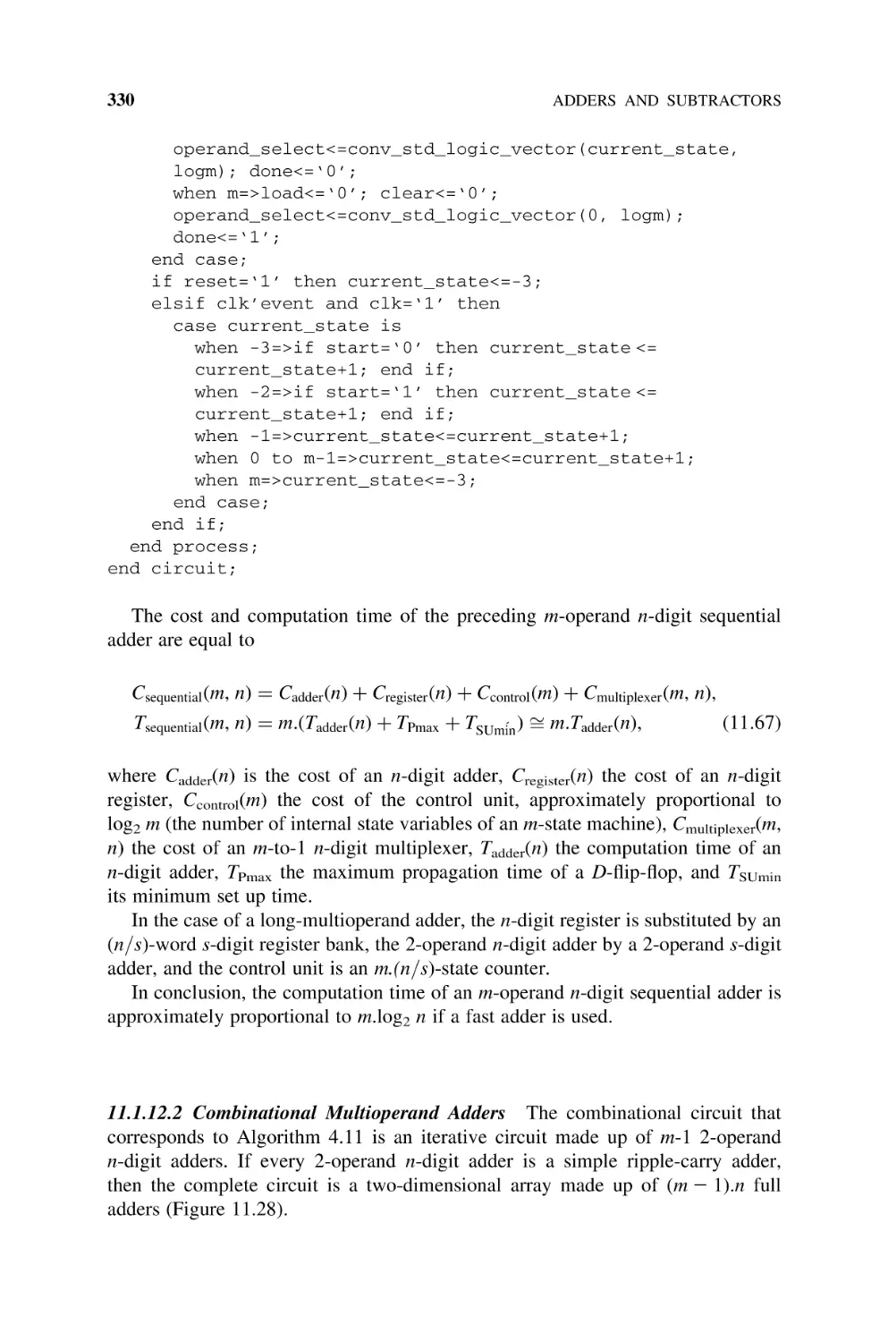
11.1.12 Multioperand Adders, 328
11.1.12.1 Sequential Multioperand Adders, 328
11.1.12.2 Combinational Multioperand Adders, 330
271
289
CONTENTS
xiii
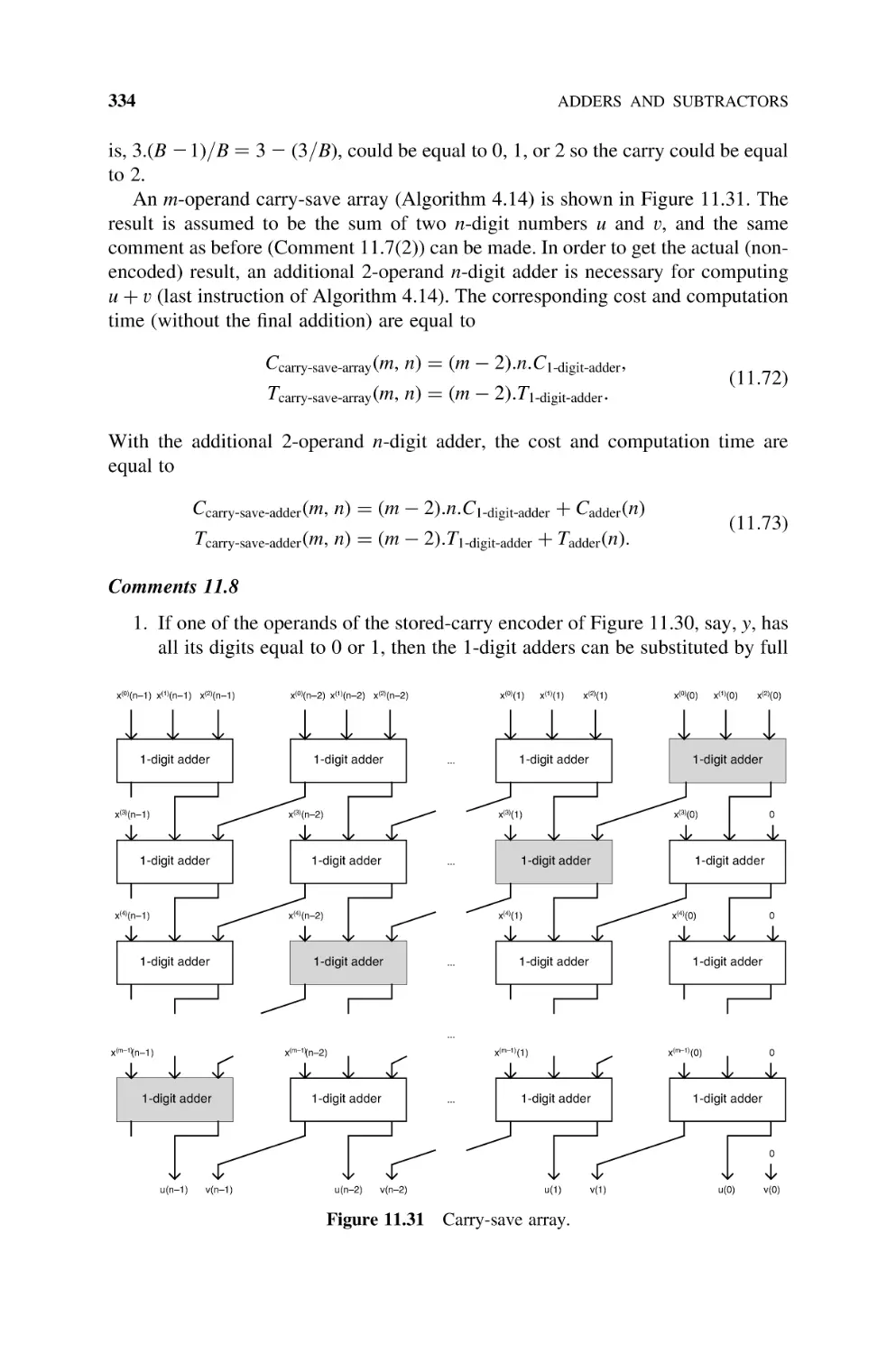
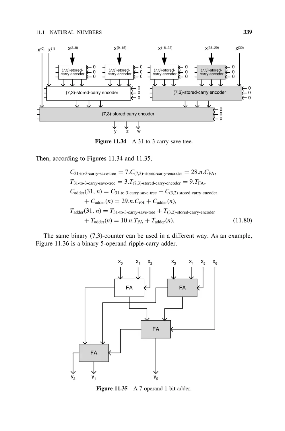
11.1.12.3 Carry-Save Adders, 333
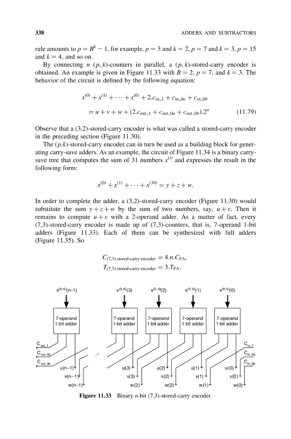
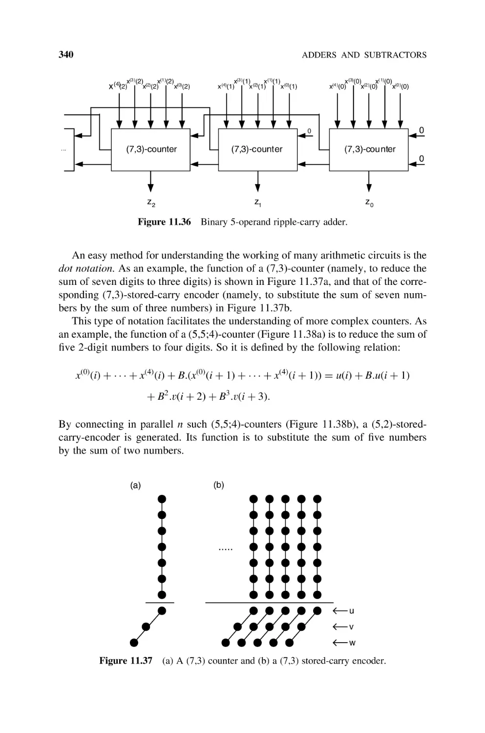
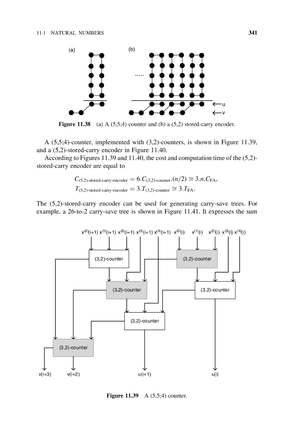
11.1.12.4 Parallel Counters, 337
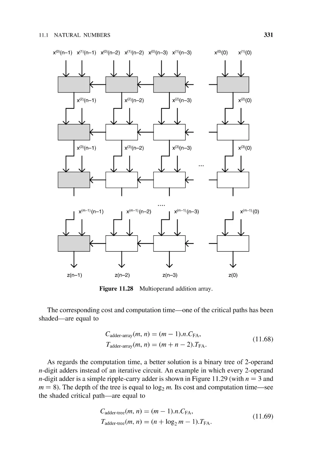
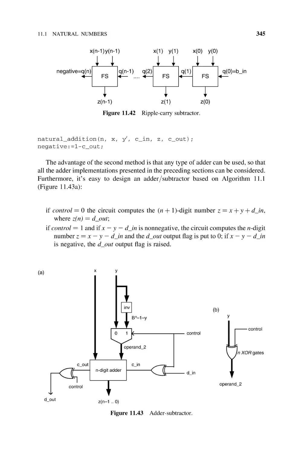
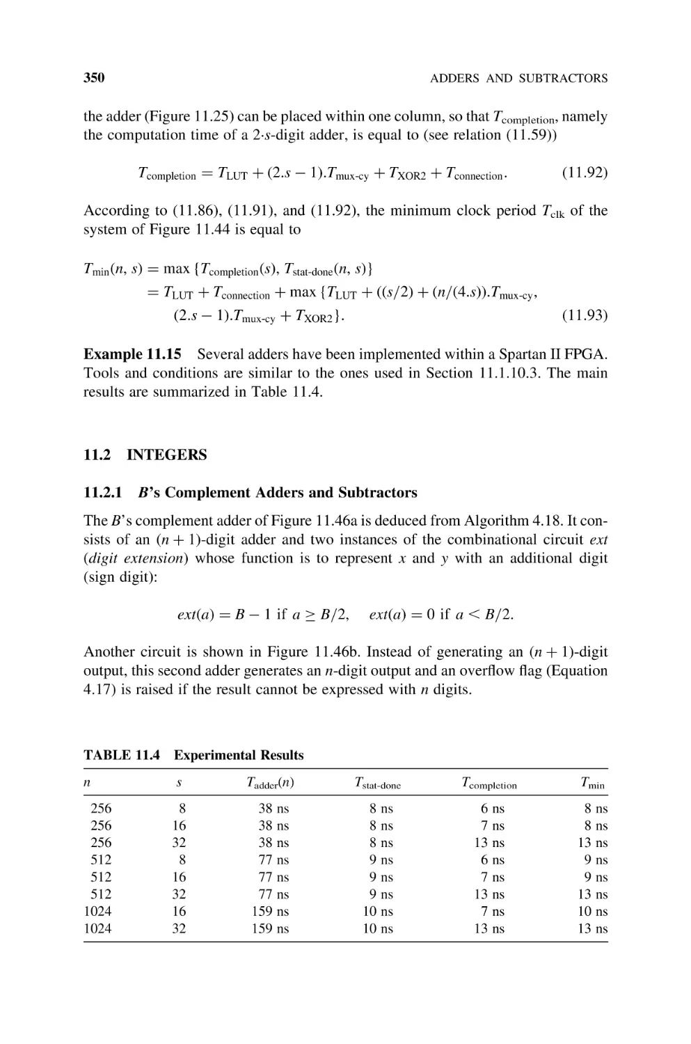
11.1.13 Subtractors and Adder-Subtractors, 344
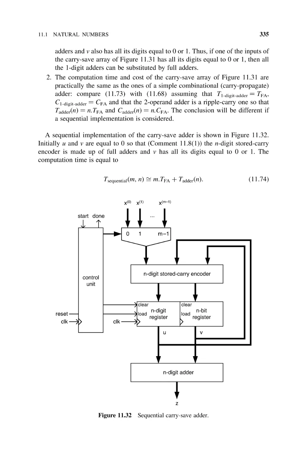
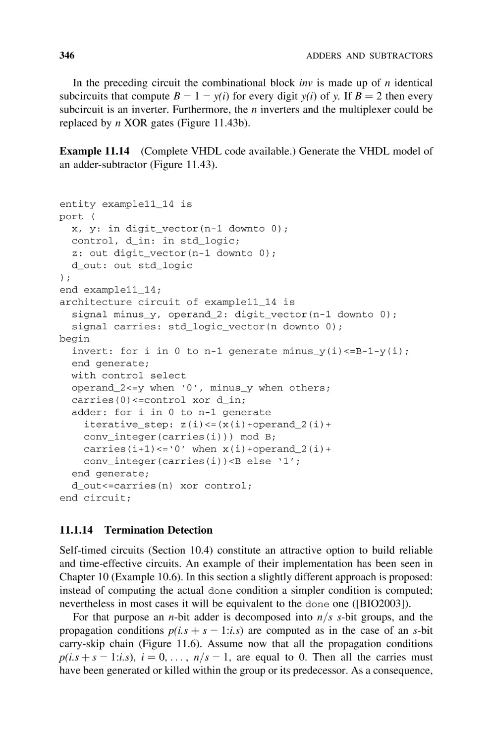
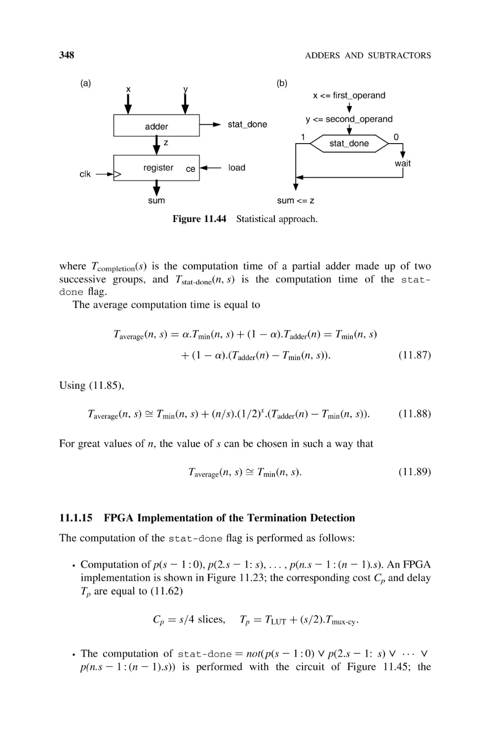
11.1.14 Termination Detection, 346
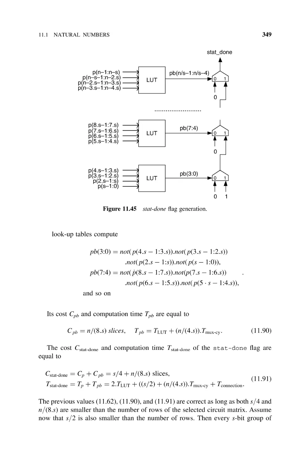
11.1.15 FPGA Implementation of the Termination Detection, 348
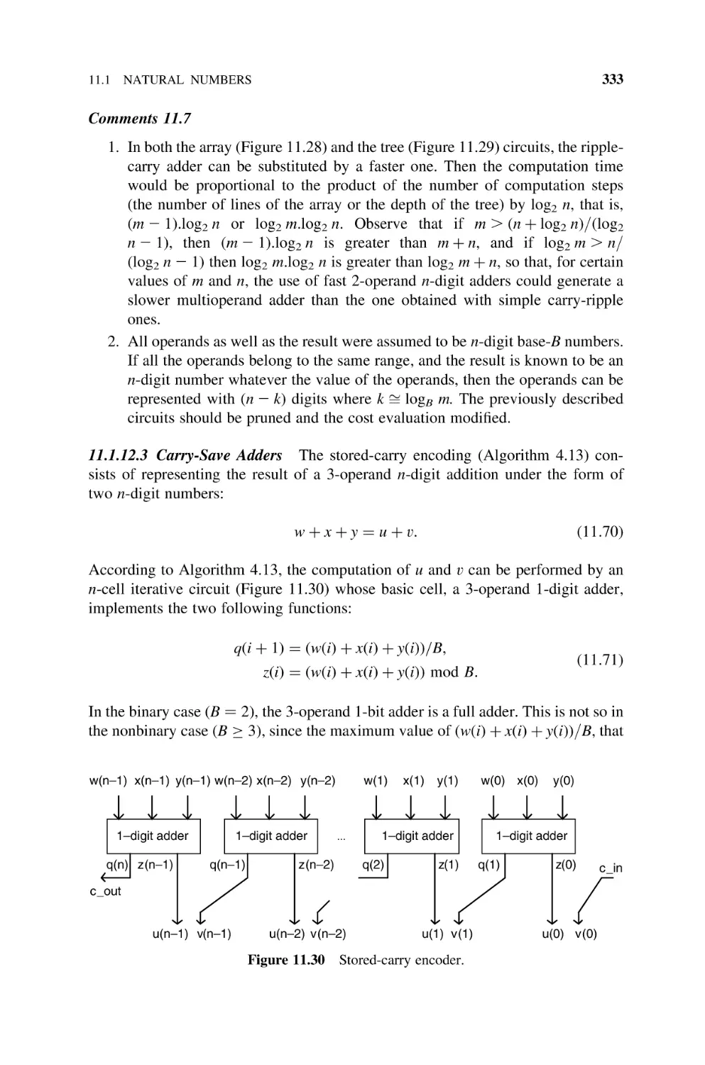
12
11.2
Integers, 350
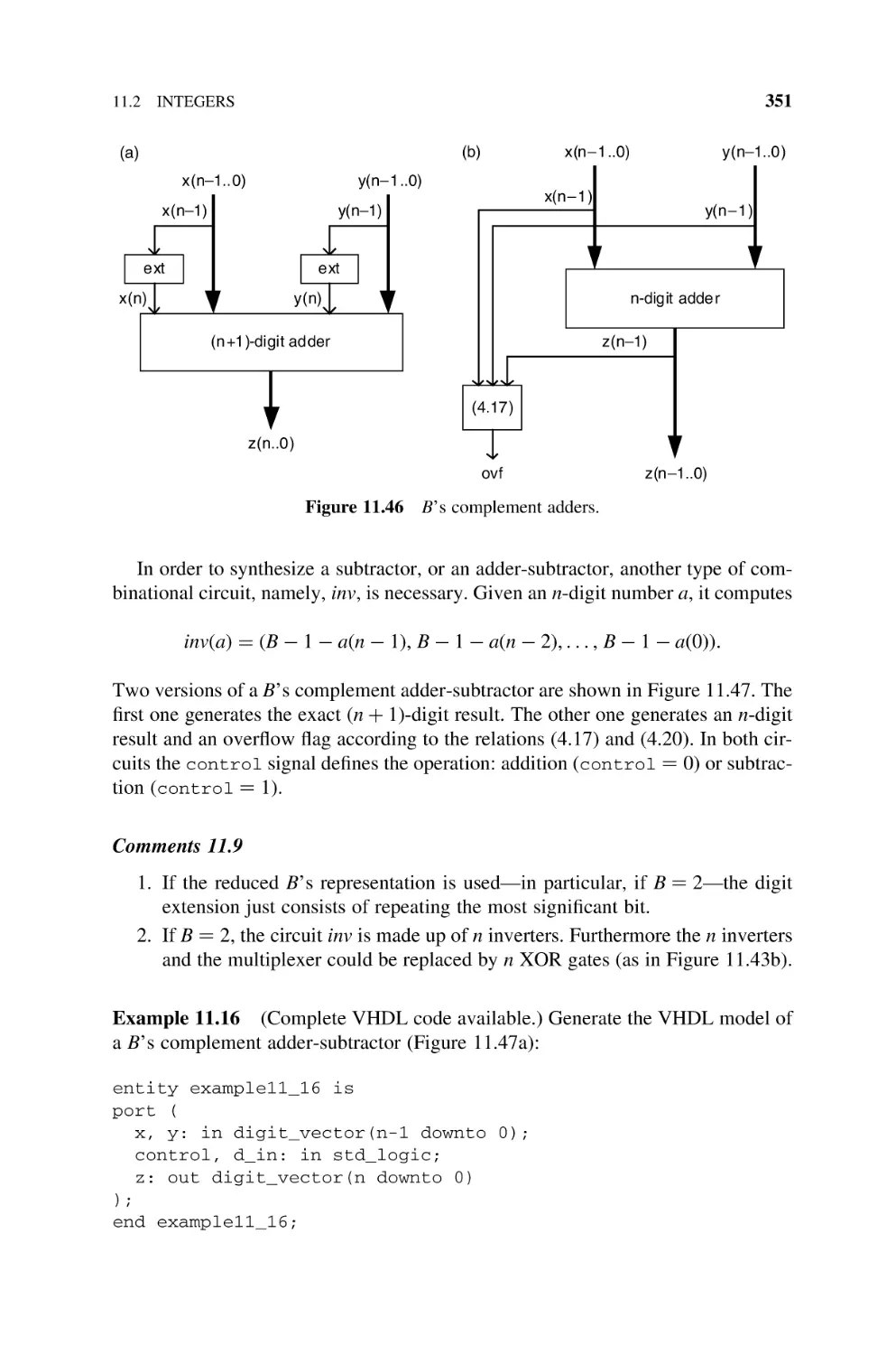
11.2.1 B’s Complement Adders and Subtractors, 350
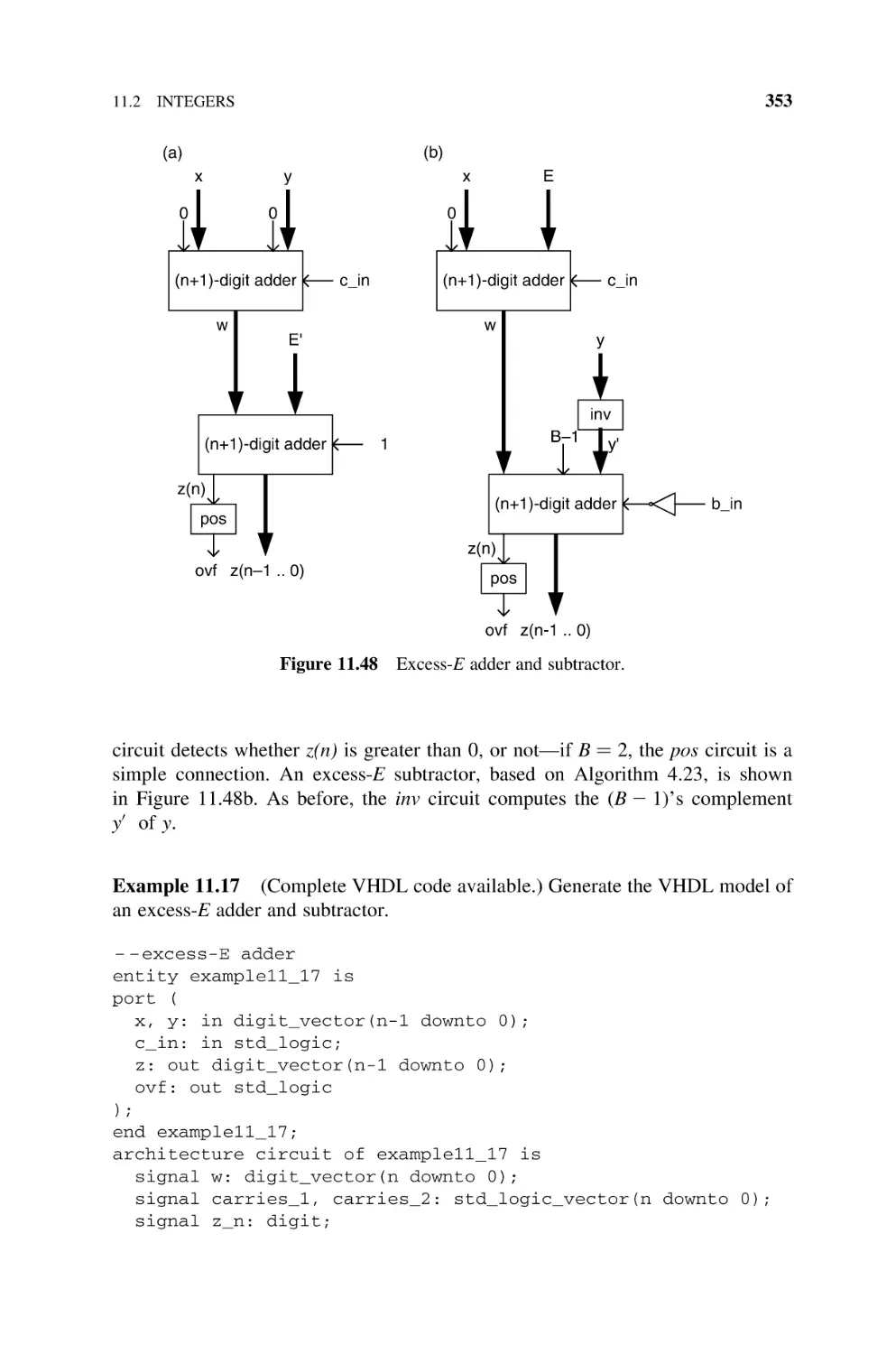
11.2.2 Excess-E Adders and Subtractors, 352
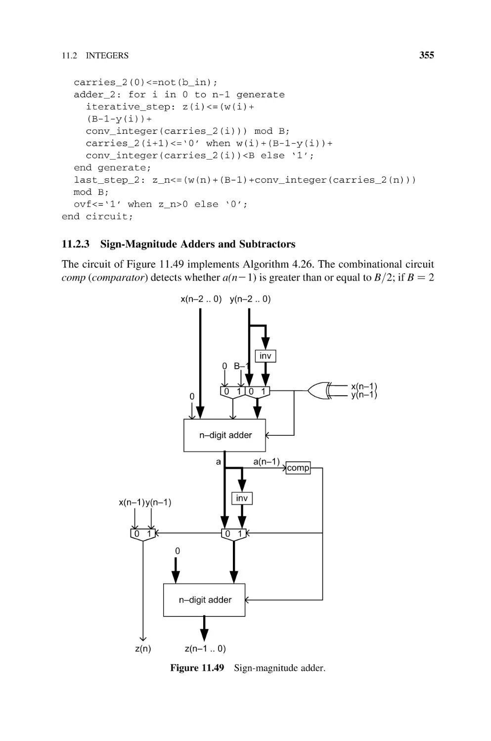
11.2.3 Sign-Magnitude Adders and Subtractors, 355
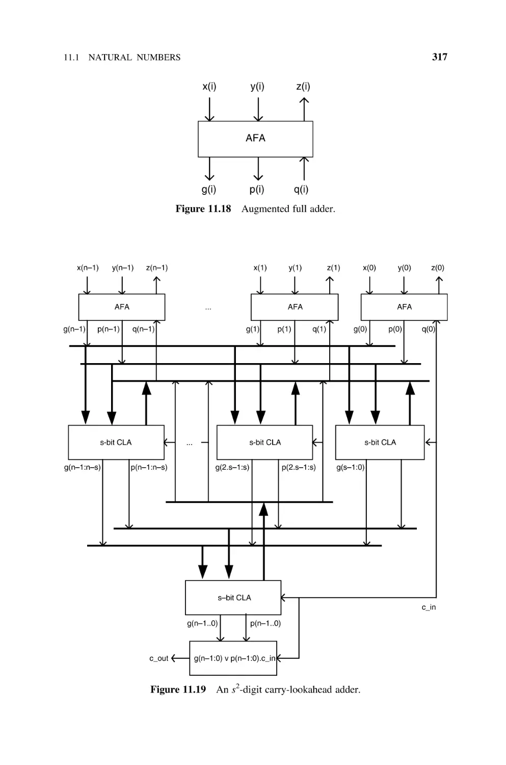
11.3
Bibliography, 357
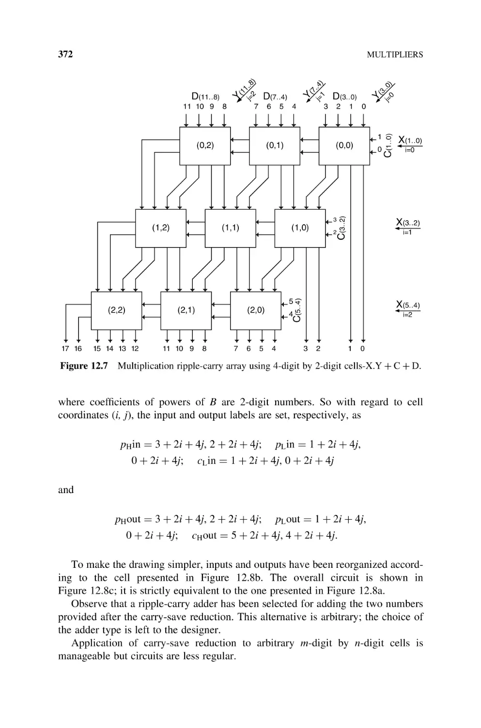
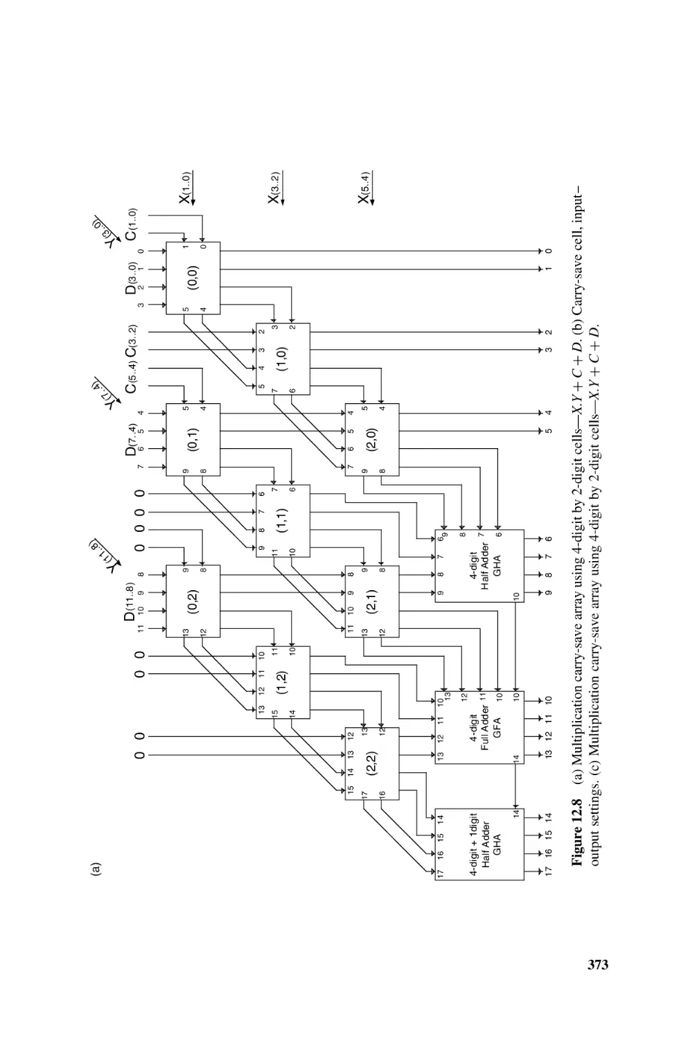
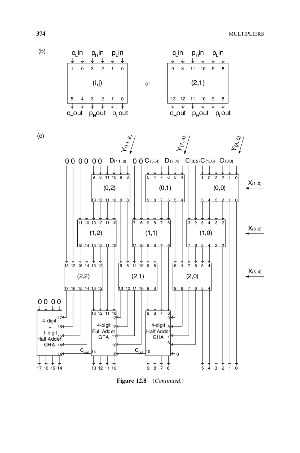
Multipliers
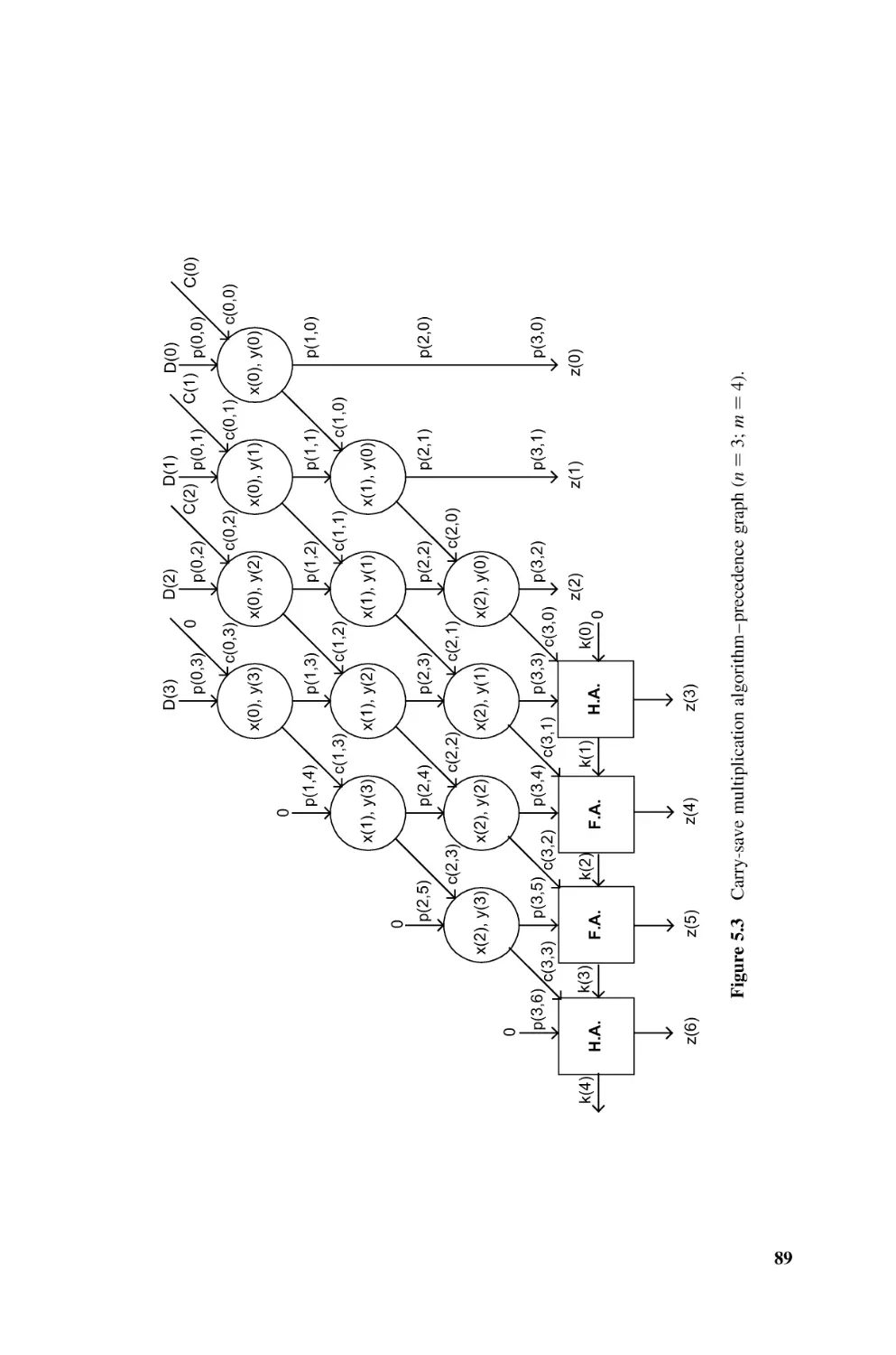
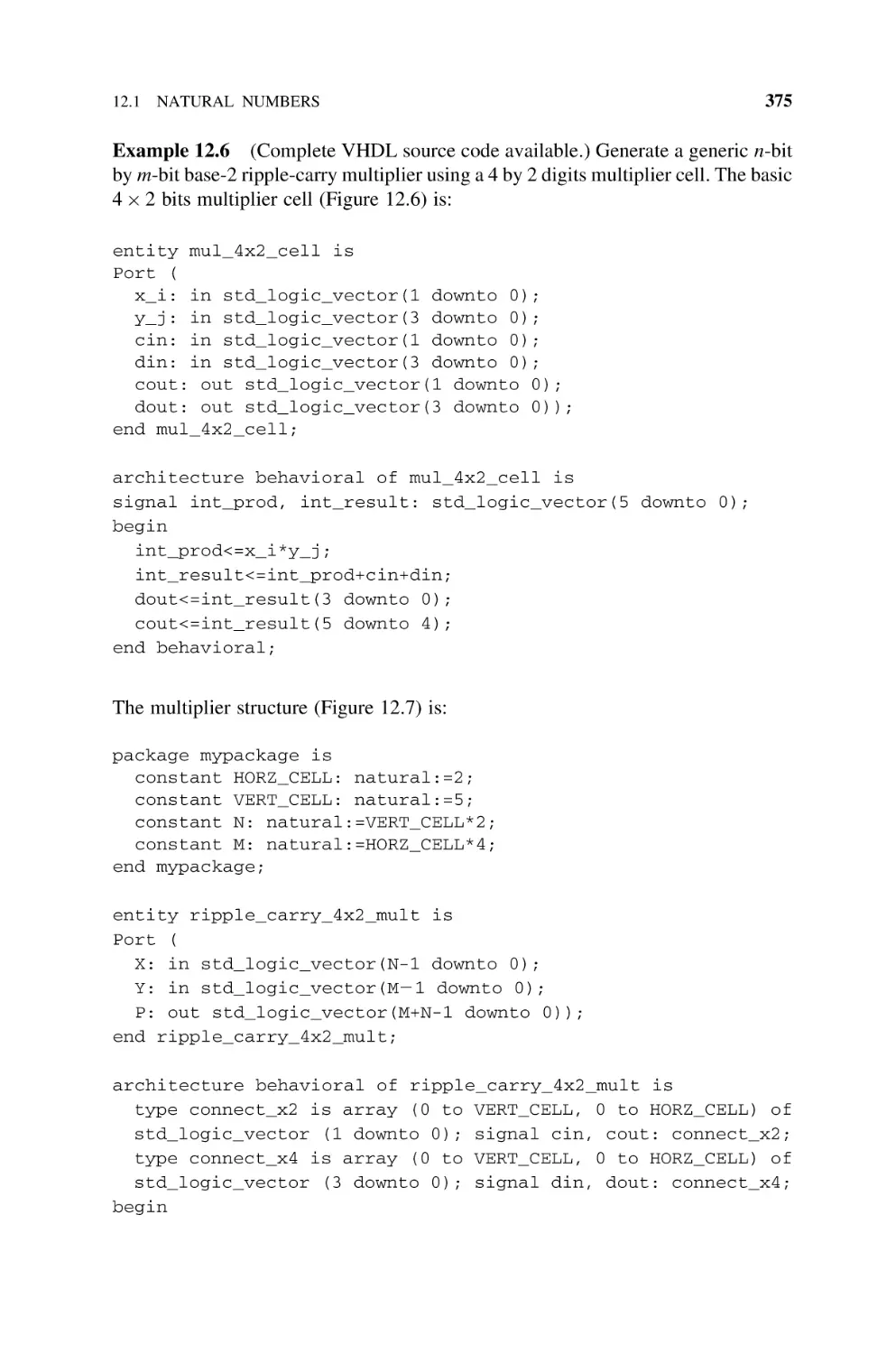
12.1
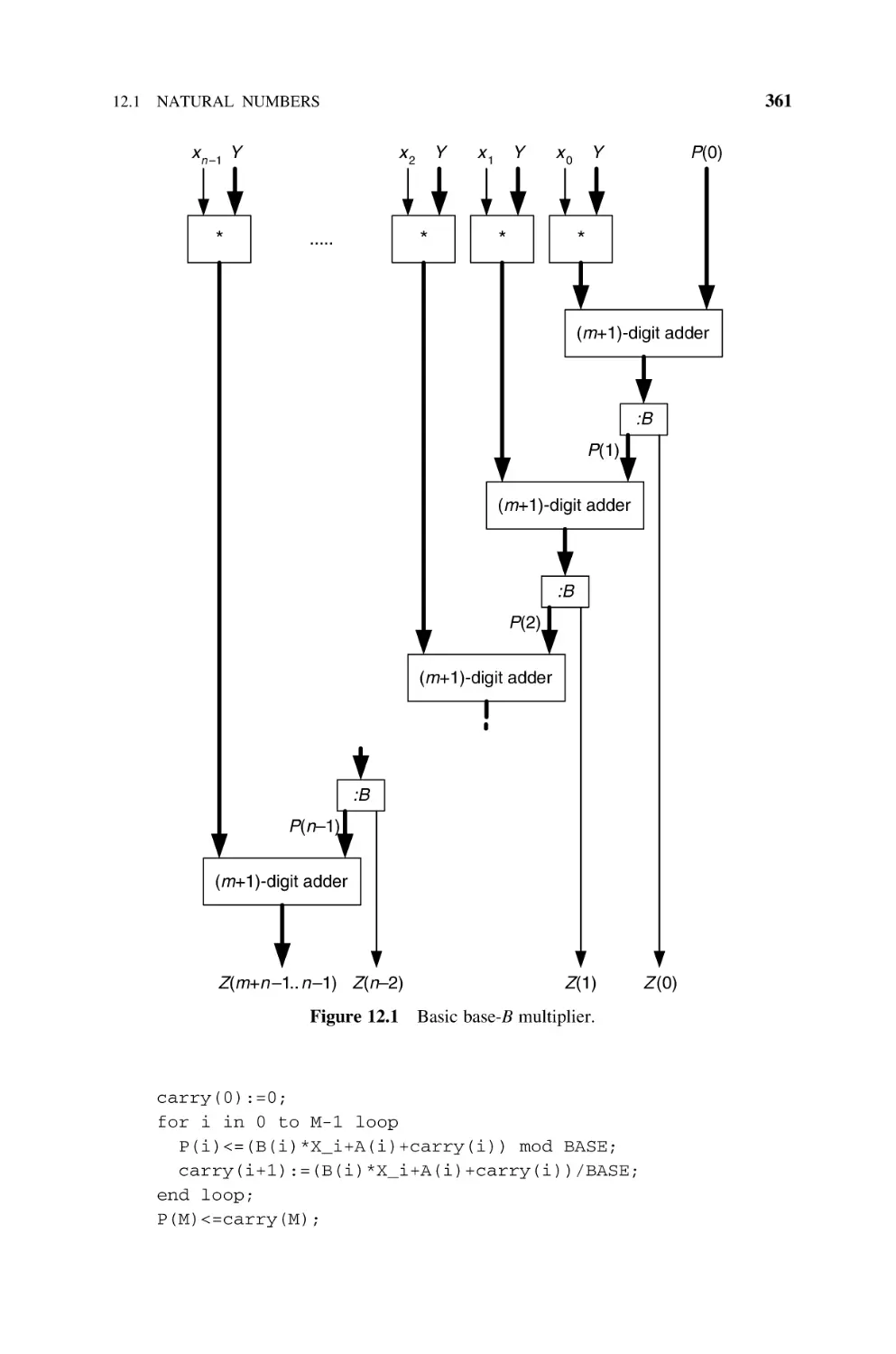
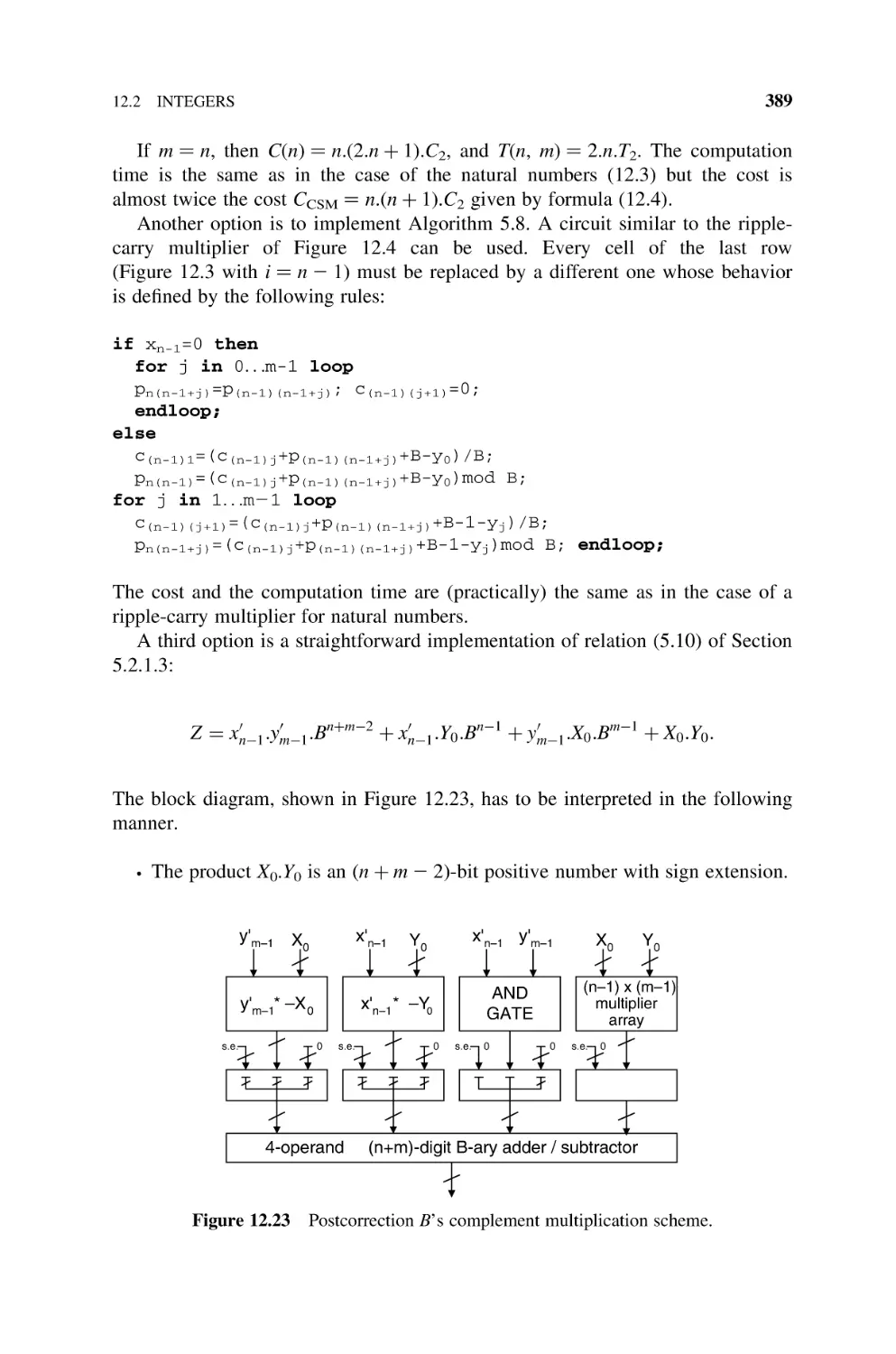
Natural
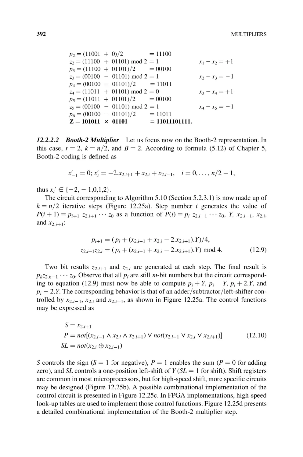
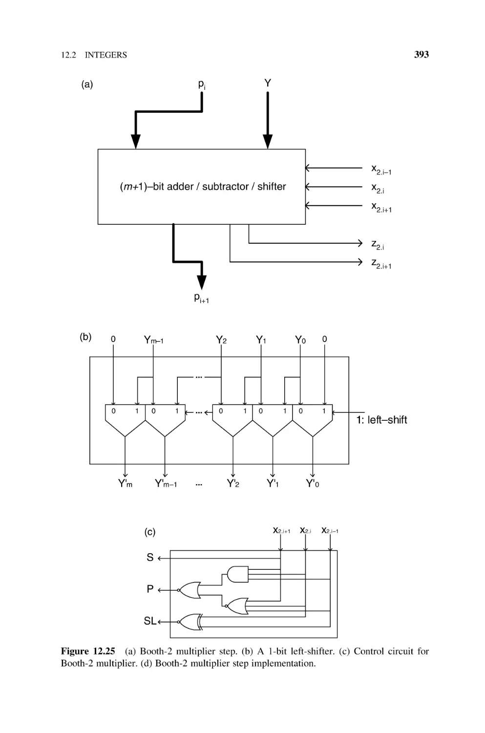
12.1.1
12.1.2
12.1.3
12.1.4
12.1.5
12.1.6
12.1.7
12.2
12.3
13
359
Numbers, 360
Basic Multiplier, 360
Sequential Multipliers, 363
Cellular Multiplier Arrays, 363
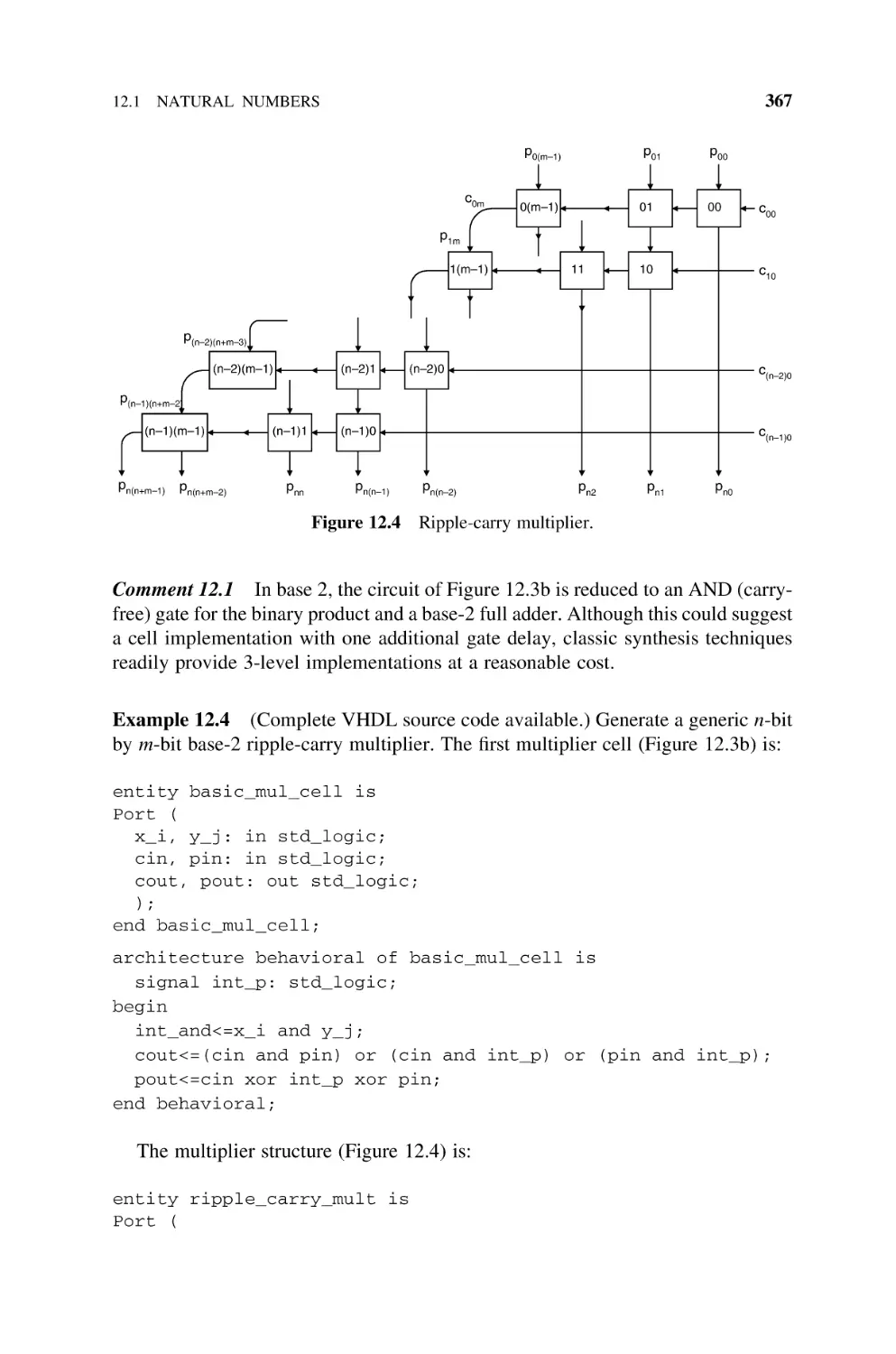
12.1.3.1 Ripple-Carry Multiplier, 365
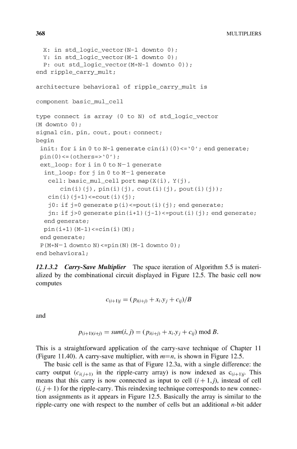
12.1.3.2 Carry-Save Multiplier, 368
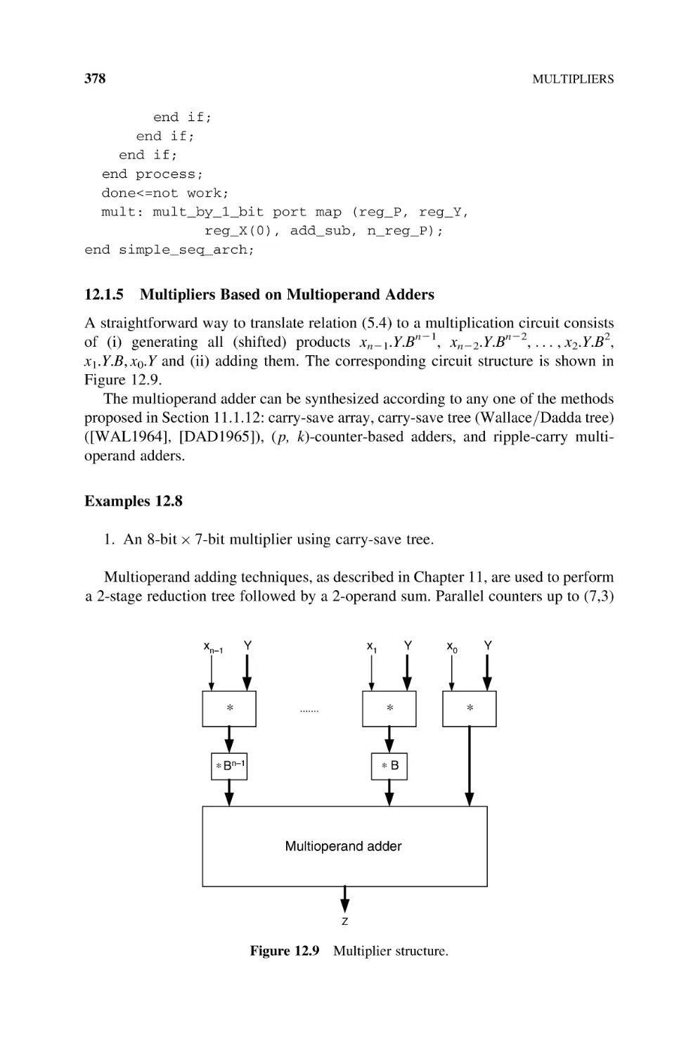
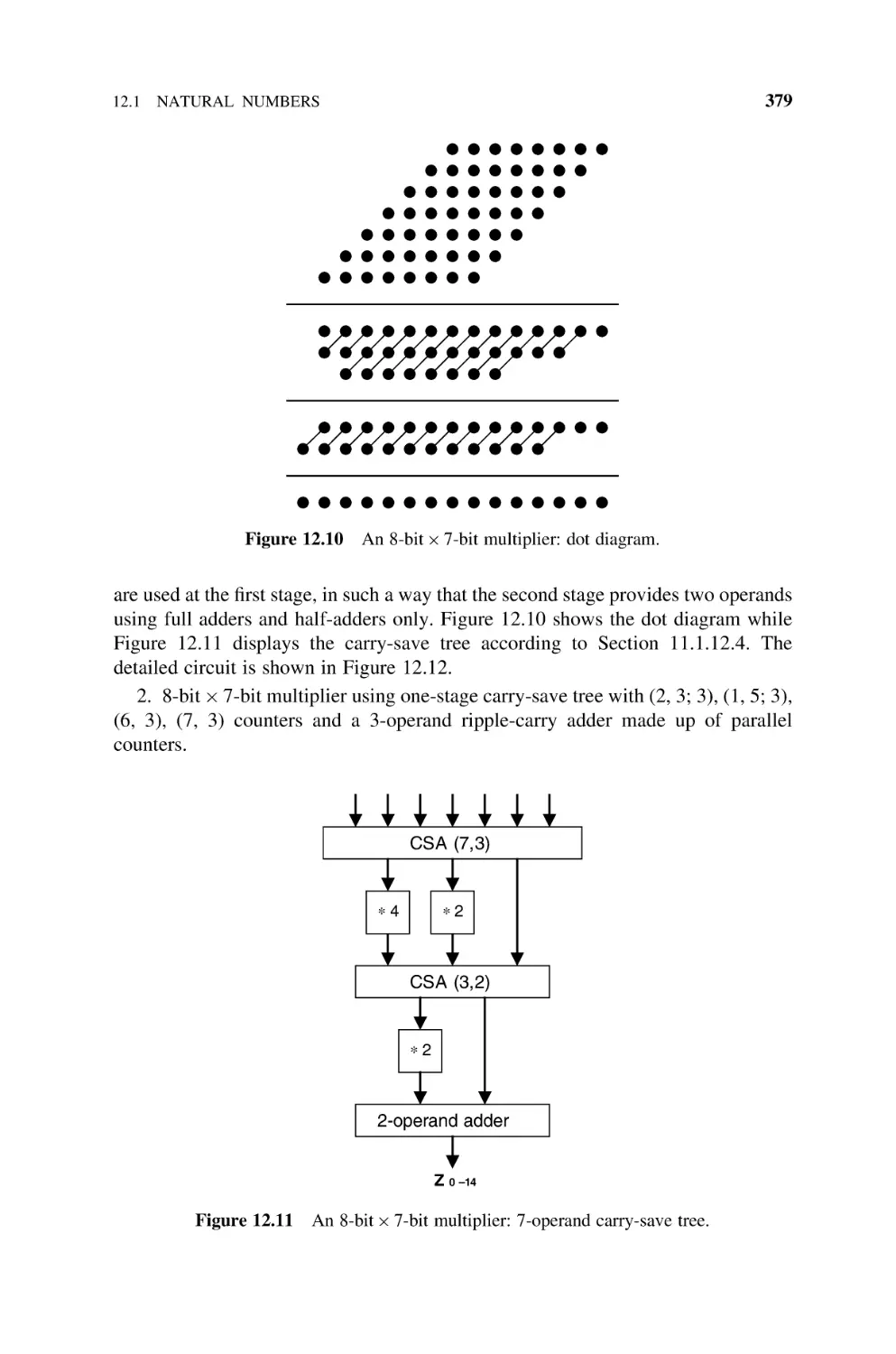
12.1.3.3 Figures of Merit, 370
Multipliers Based on Dissymmetric
Br Bs Cells, 370
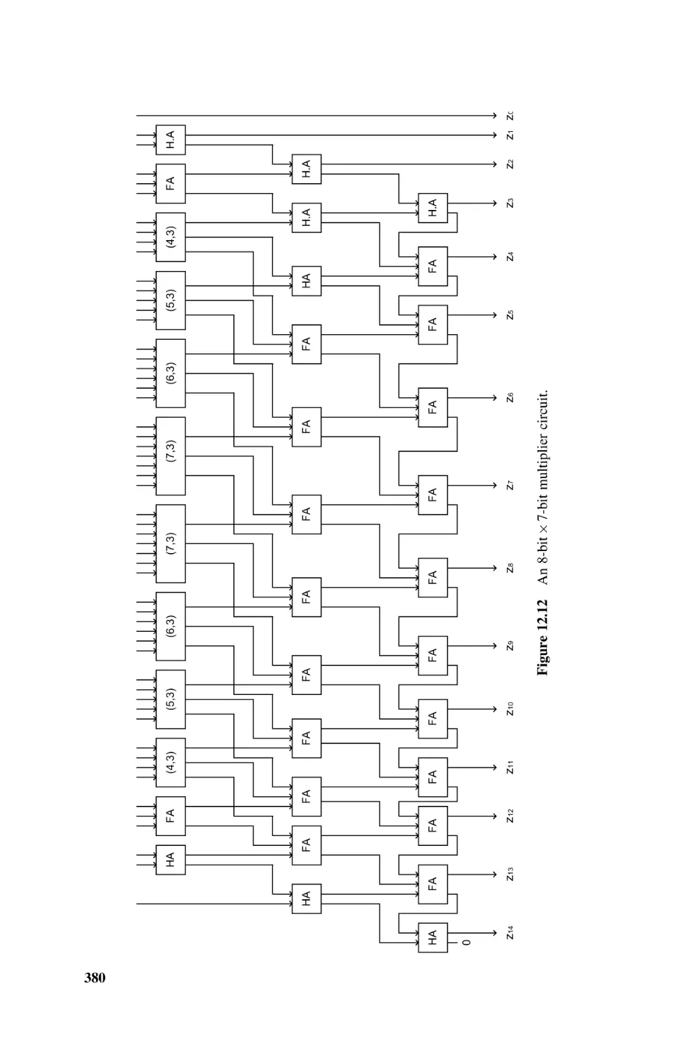
Multipliers Based on Multioperand Adders, 378
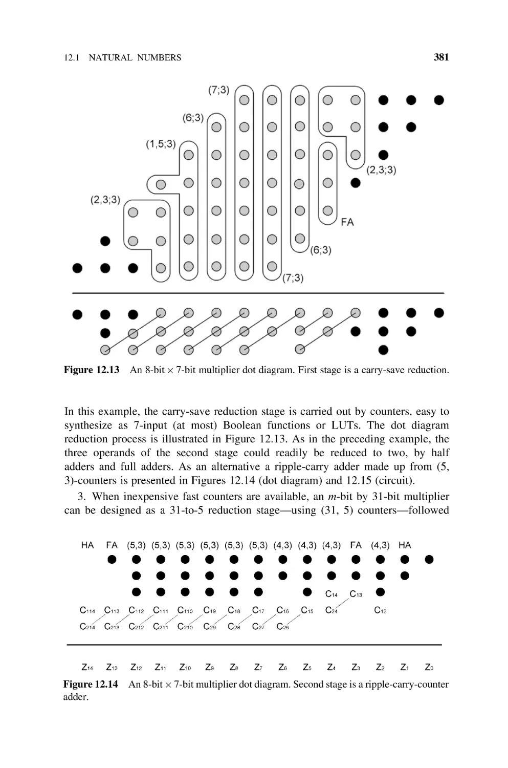
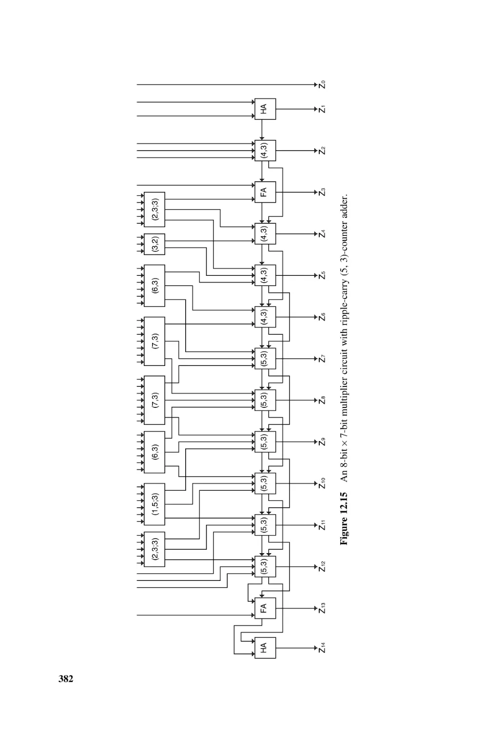
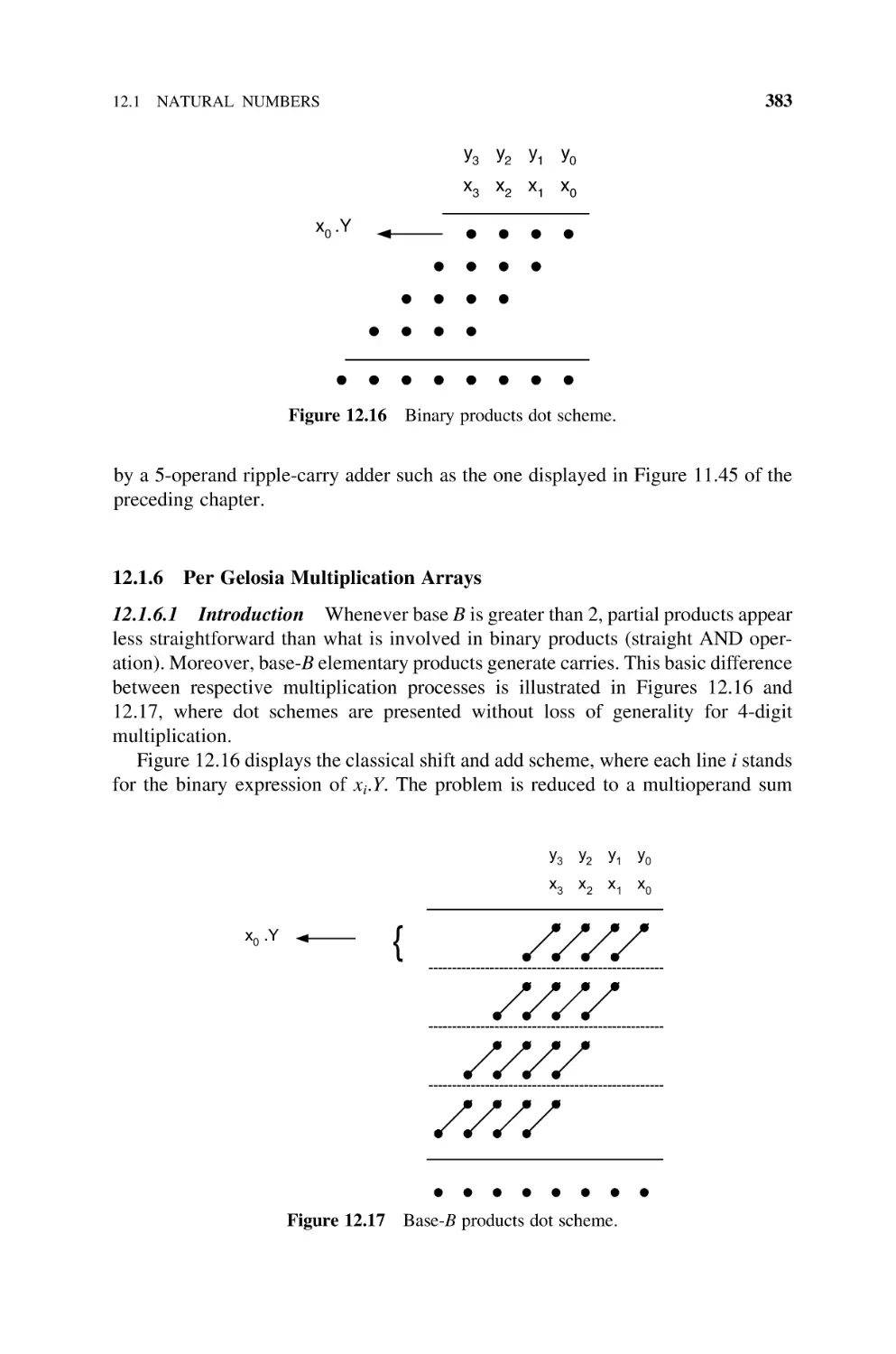
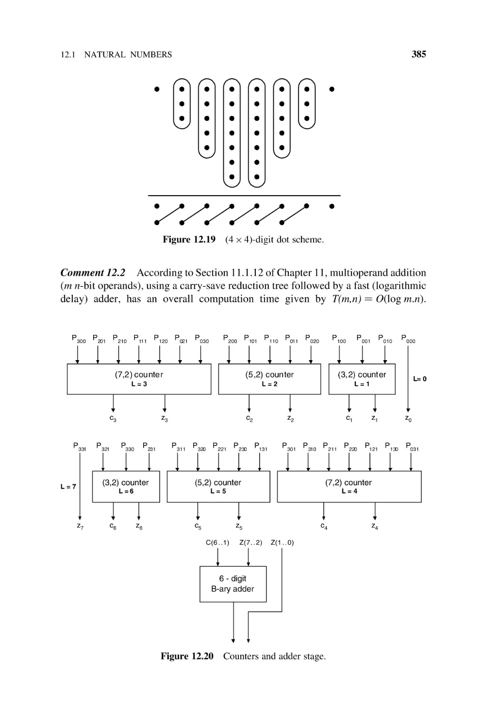
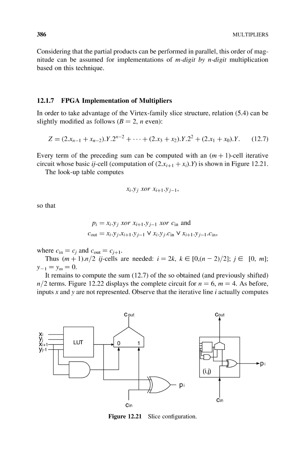
Per Gelosia Multiplication Arrays, 383
12.1.6.1 Introduction, 383
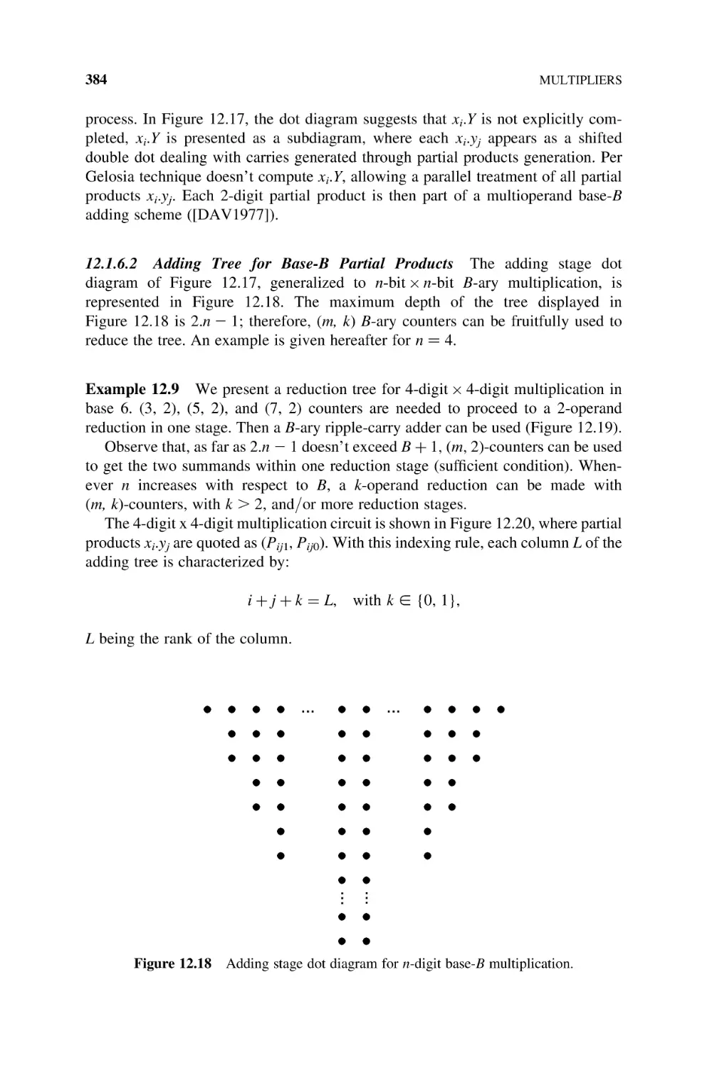
12.1.6.2 Adding Tree for Base-B Partial Products, 384
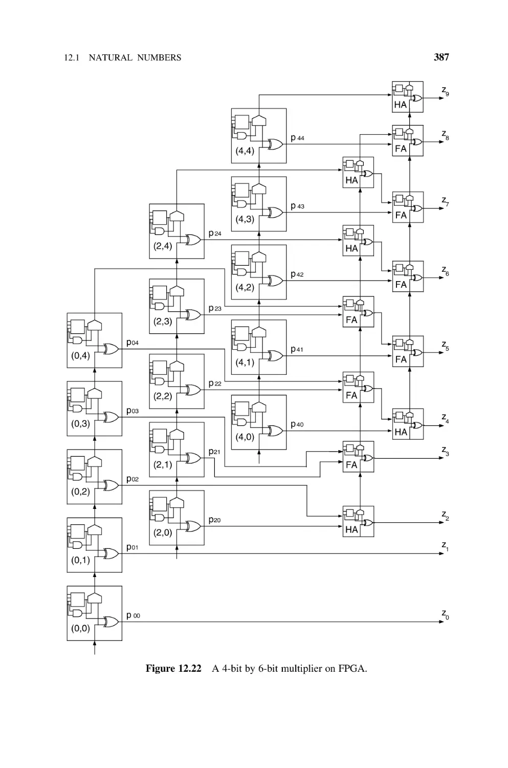
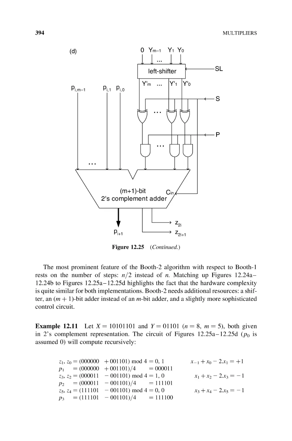
FPGA Implementation of Multipliers, 386
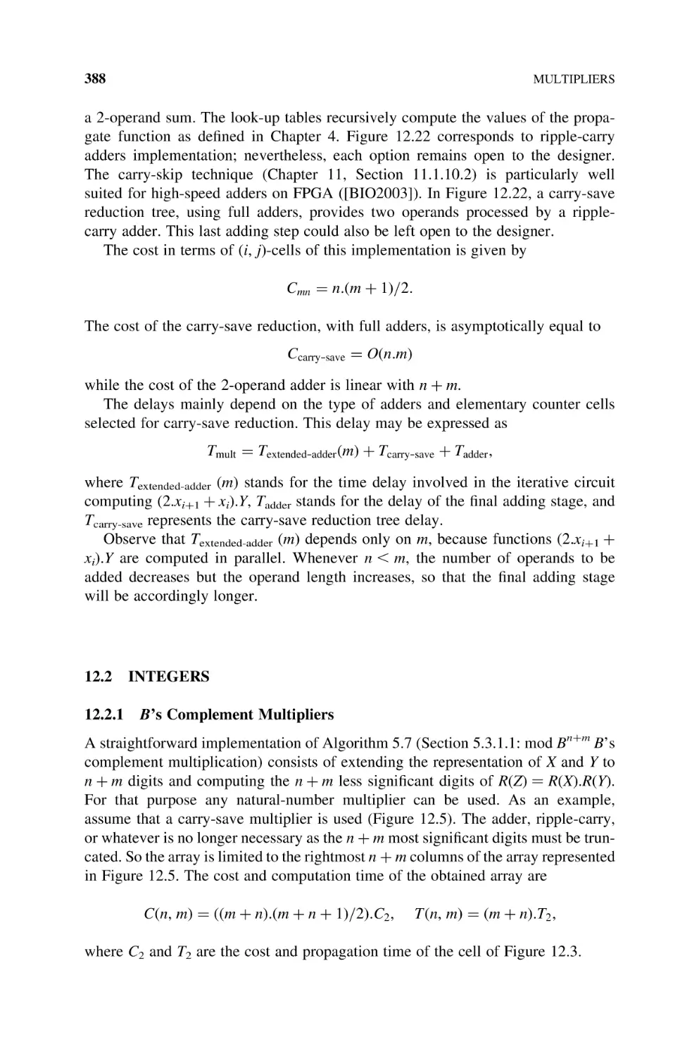
Integers, 388
12.2.1 B’s Complement Multipliers, 388
12.2.2 Booth Multipliers, 390
12.2.2.1 Booth-1 Multiplier, 390
12.2.2.2 Booth-2 Multiplier, 392
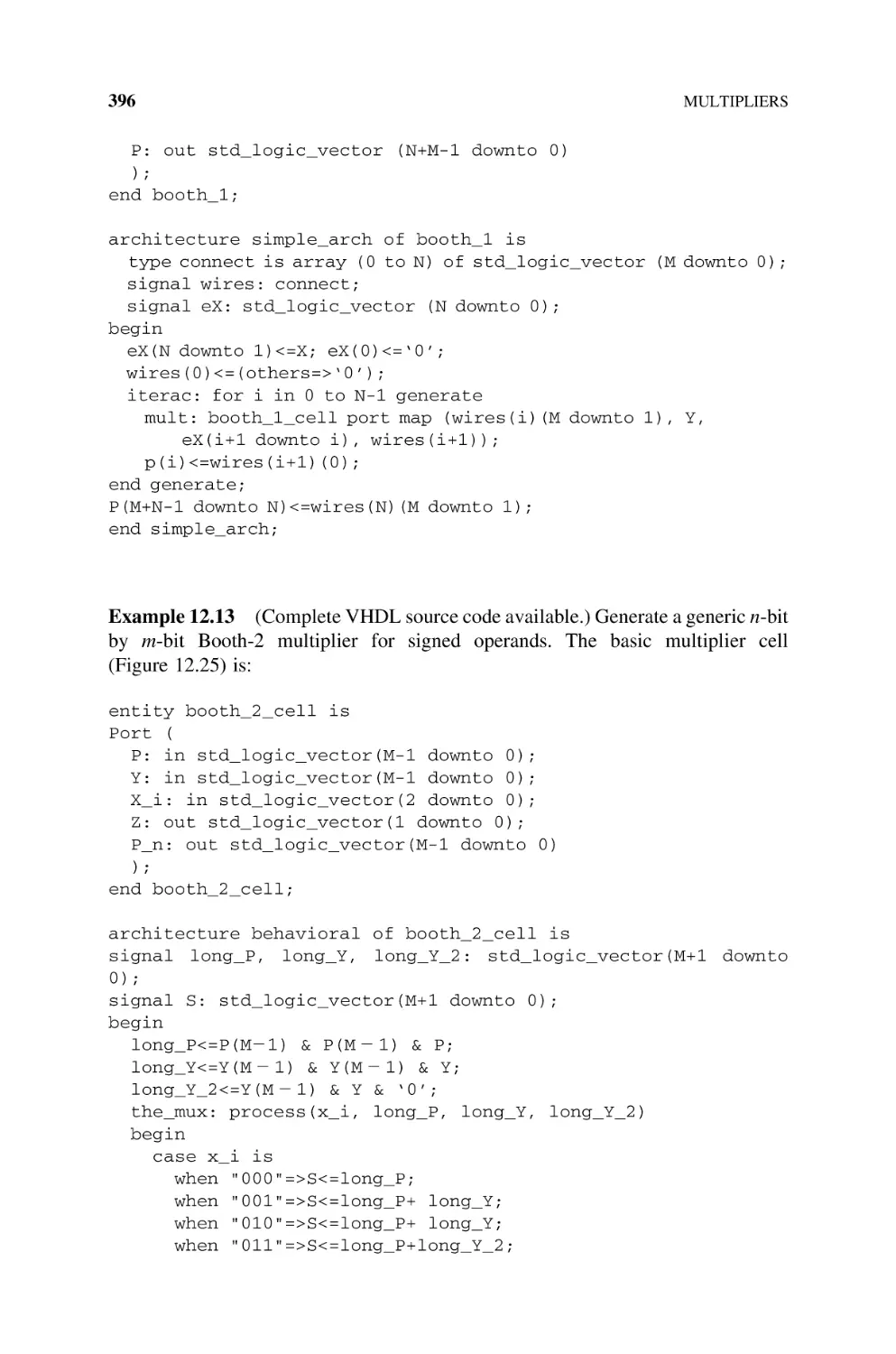
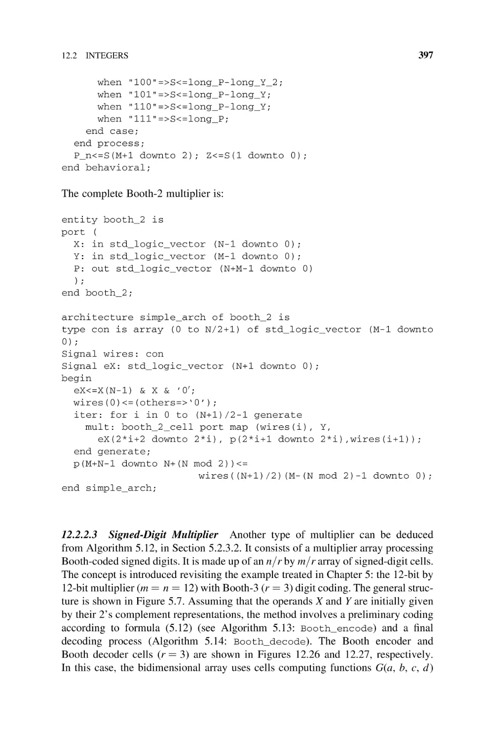
12.2.2.3 Signed-Digit Multiplier, 397
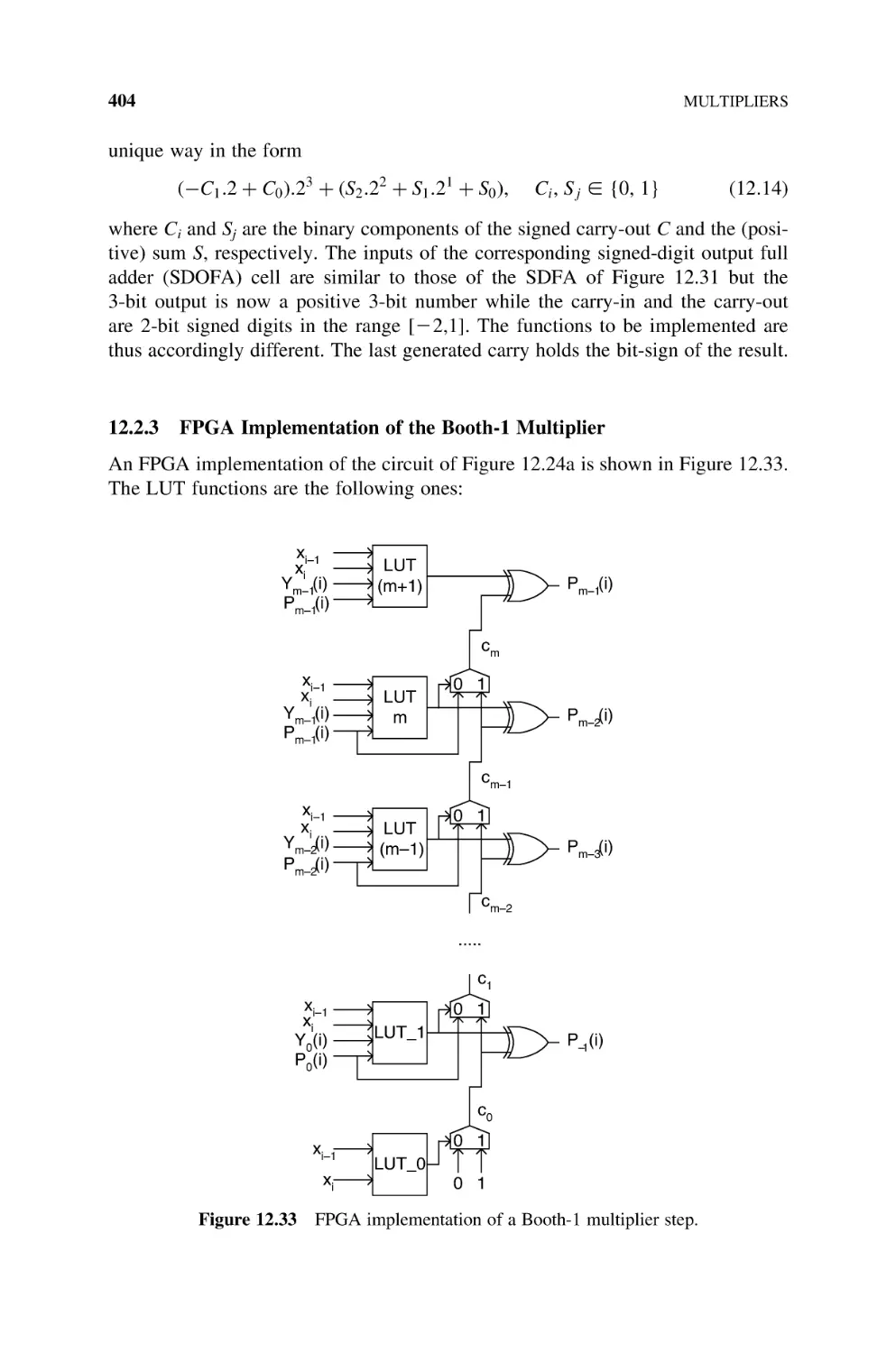
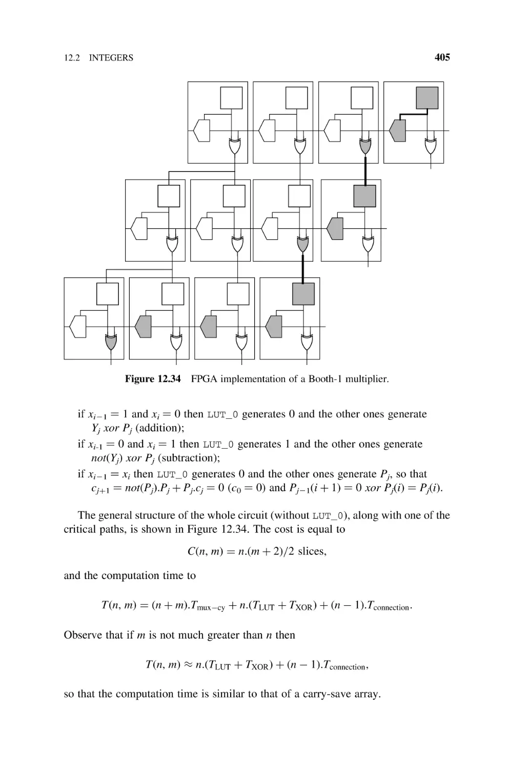
12.2.3 FPGA Implementation of the Booth-1 Multiplier, 404
Bibliography, 406
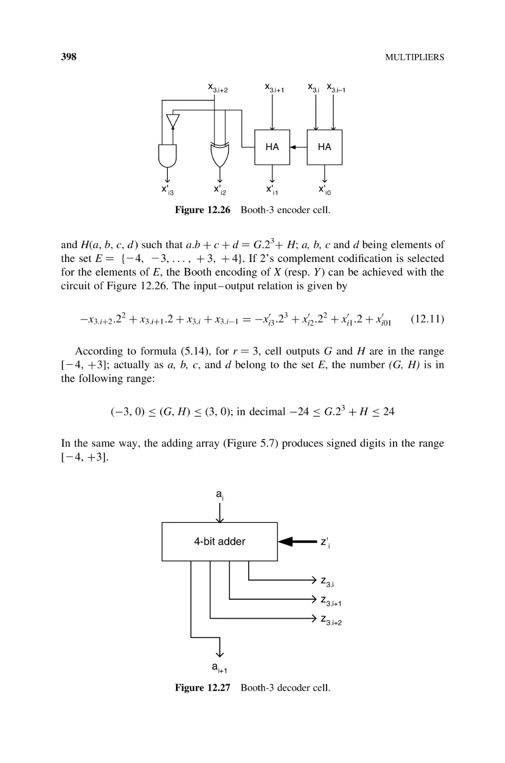
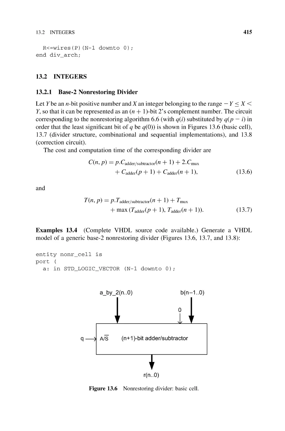
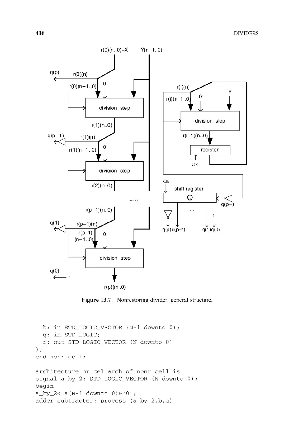
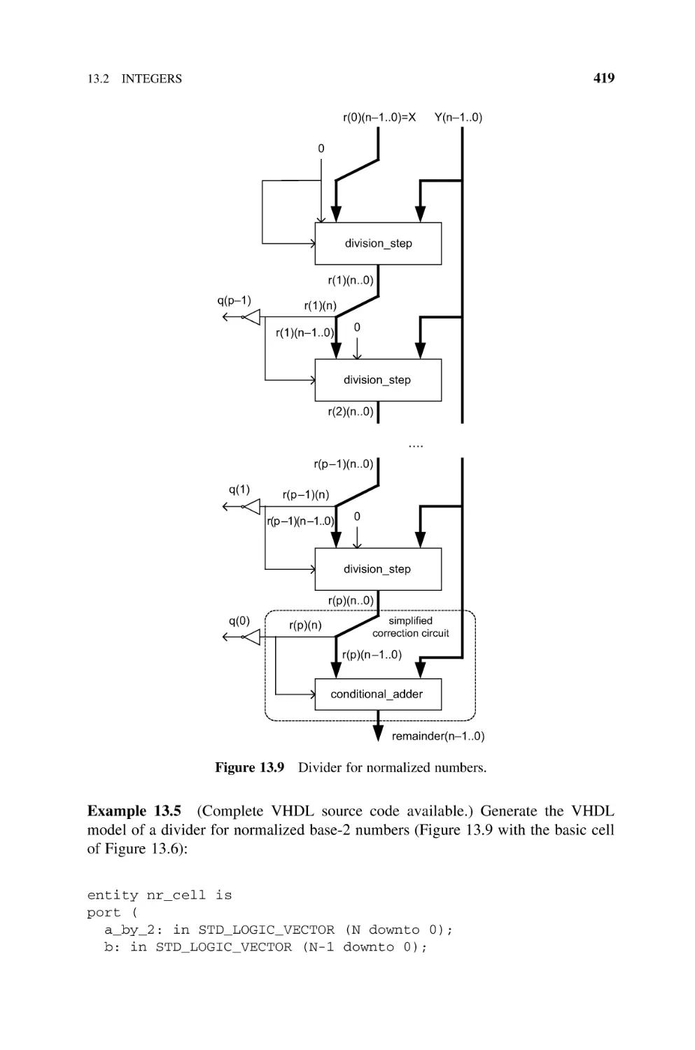
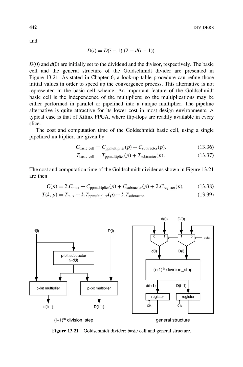
Dividers
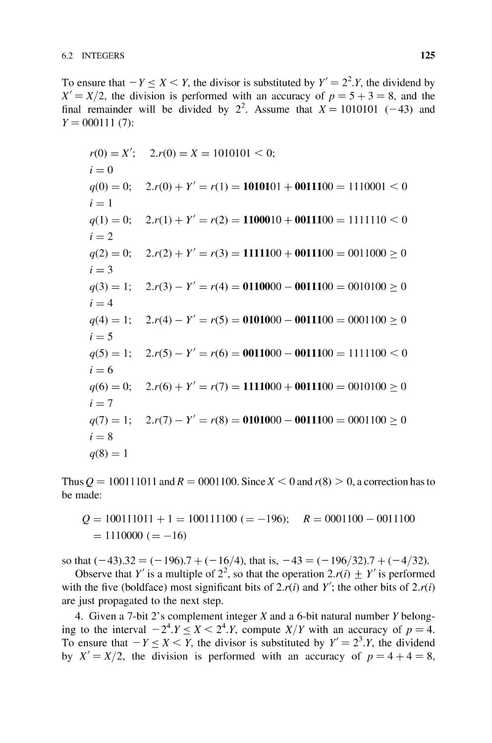
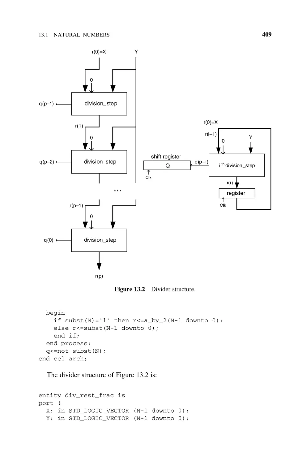
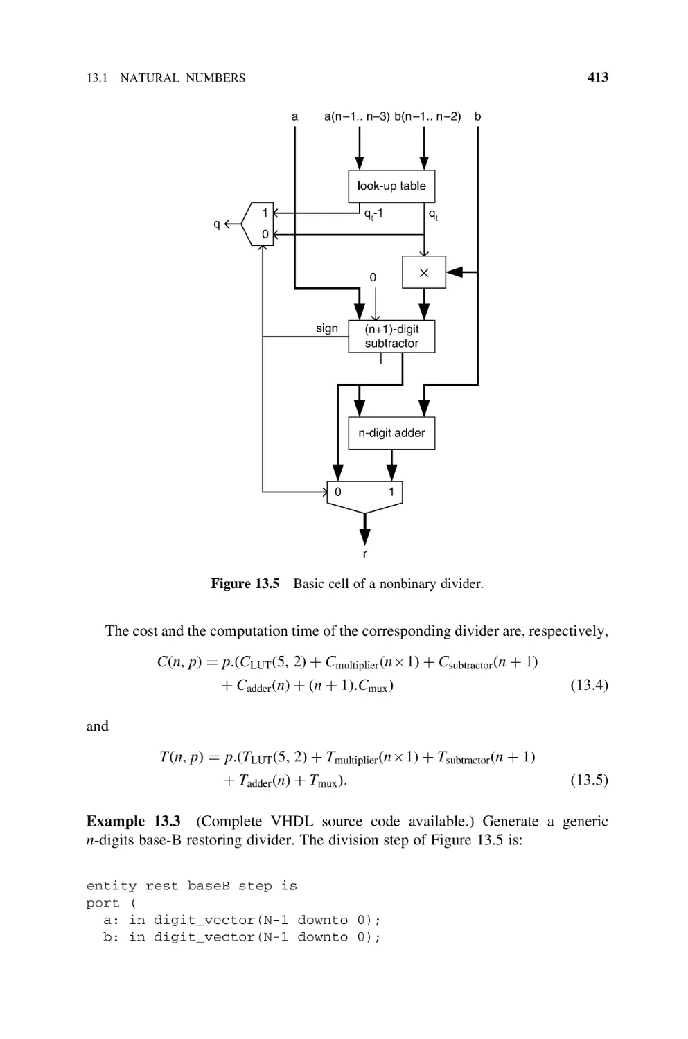
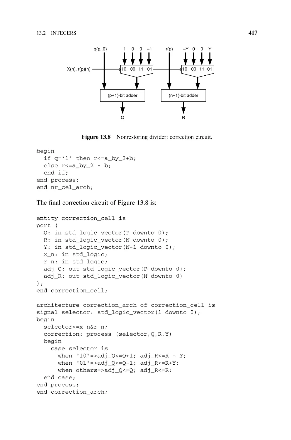
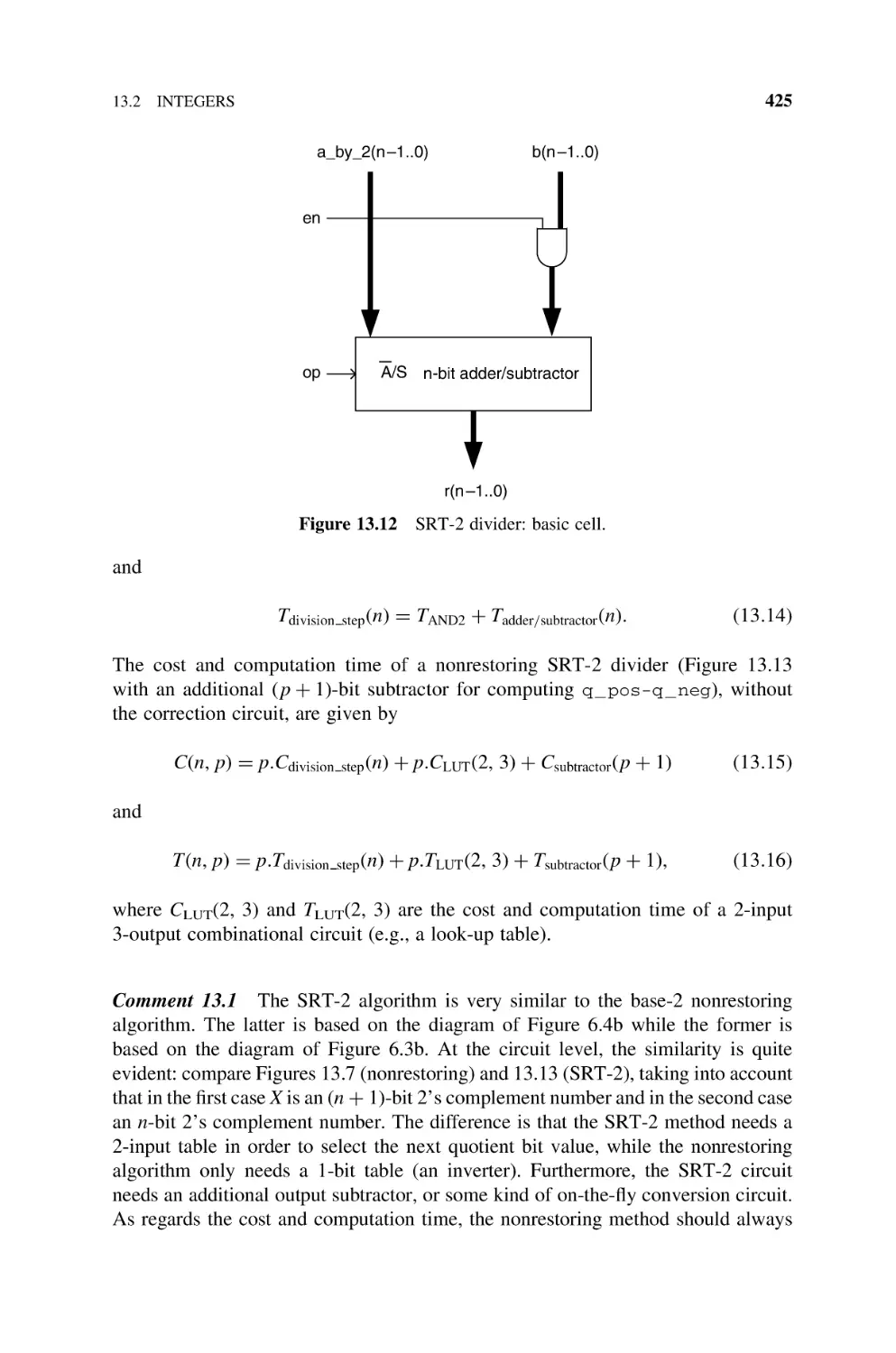
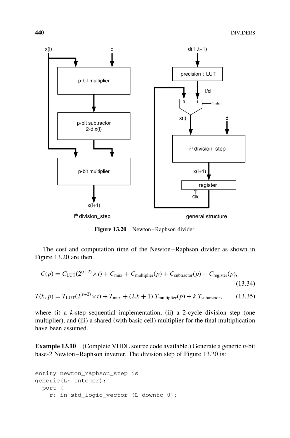
13.1
Natural Numbers, 407
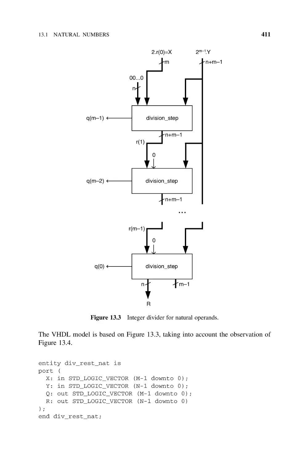
13.2
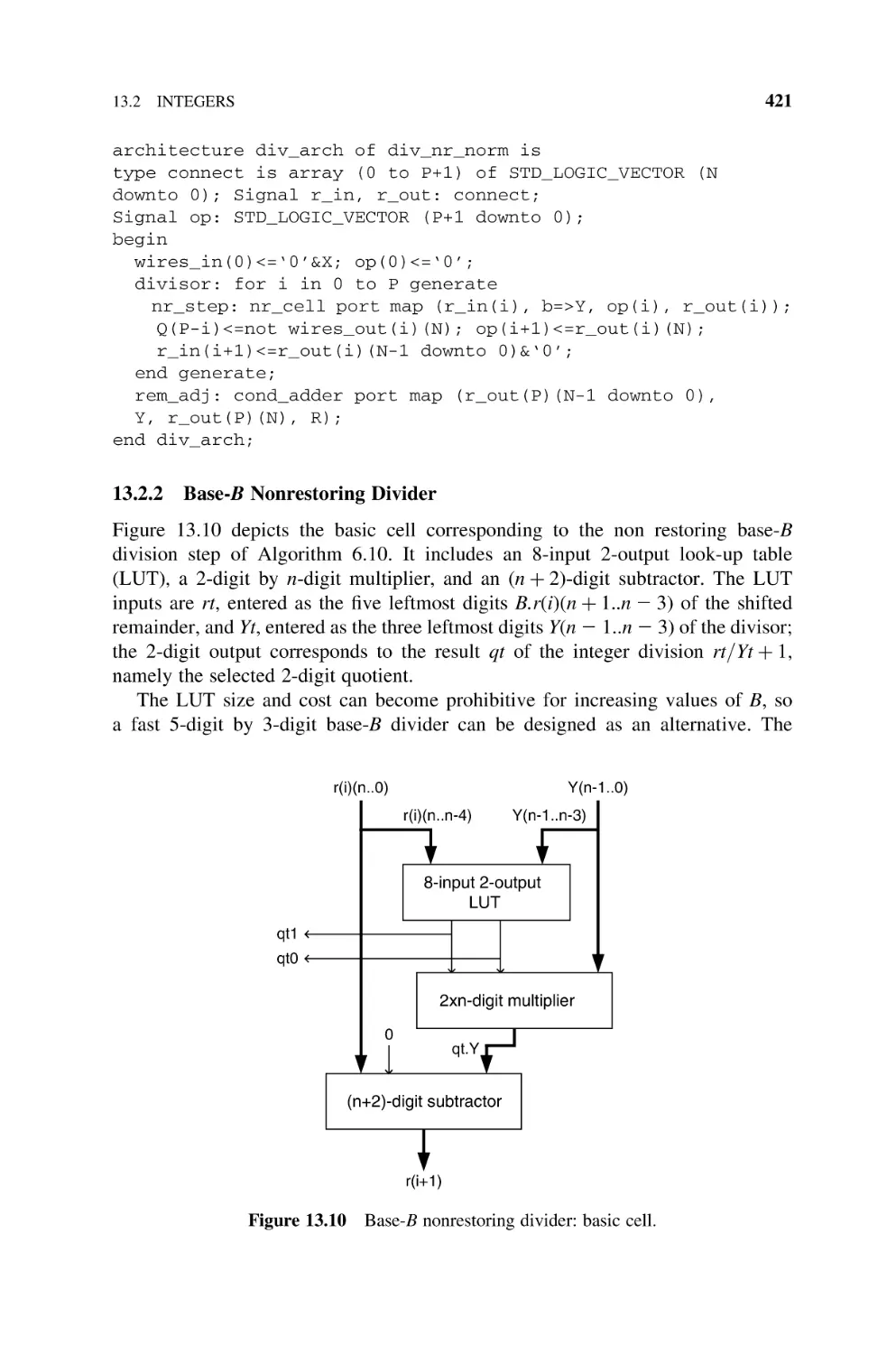
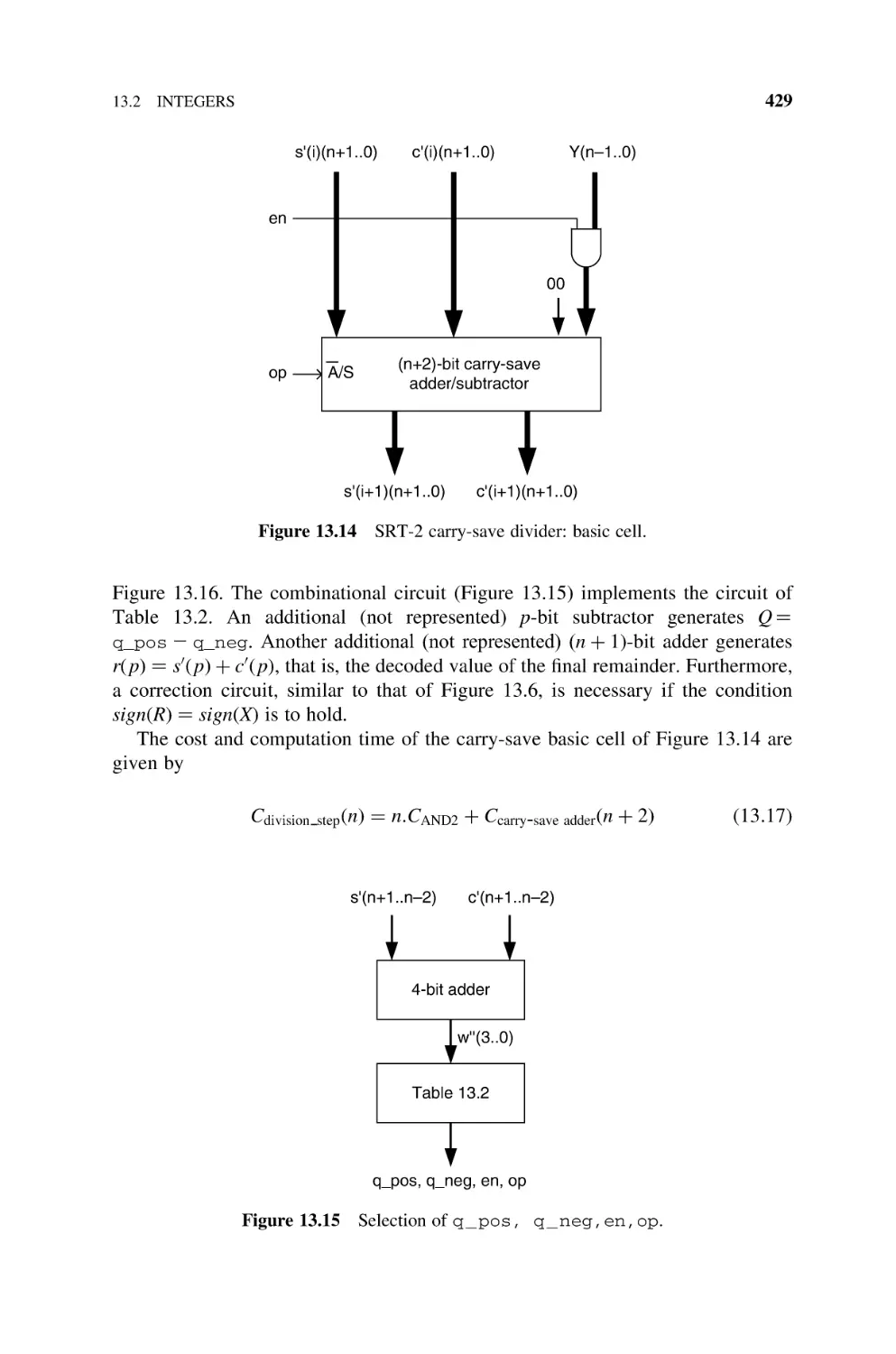
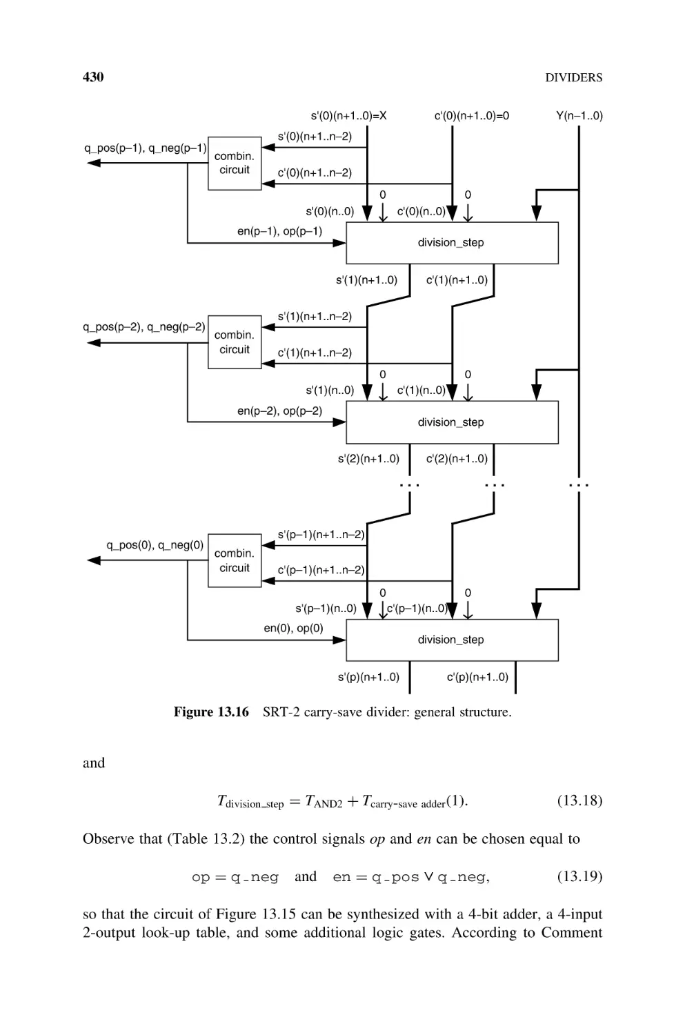
Integers, 415
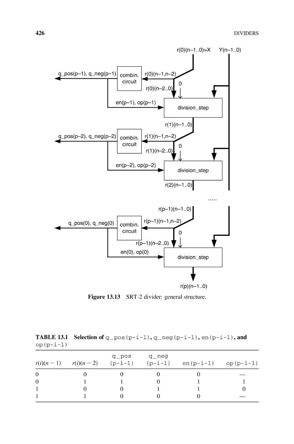
13.2.1 Base-2 Nonrestoring Divider, 415
13.2.2 Base-B Nonrestoring Divider, 421
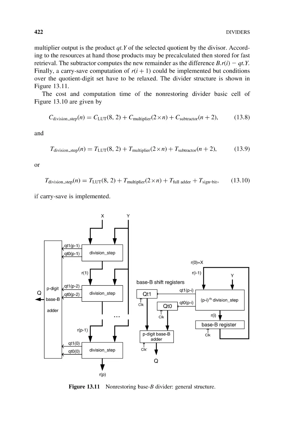
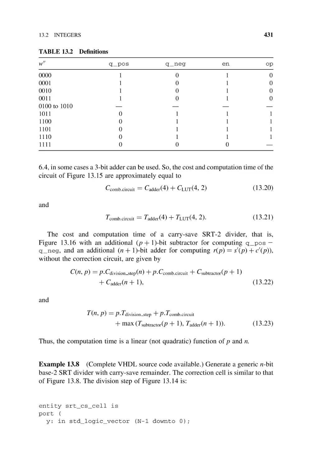
407
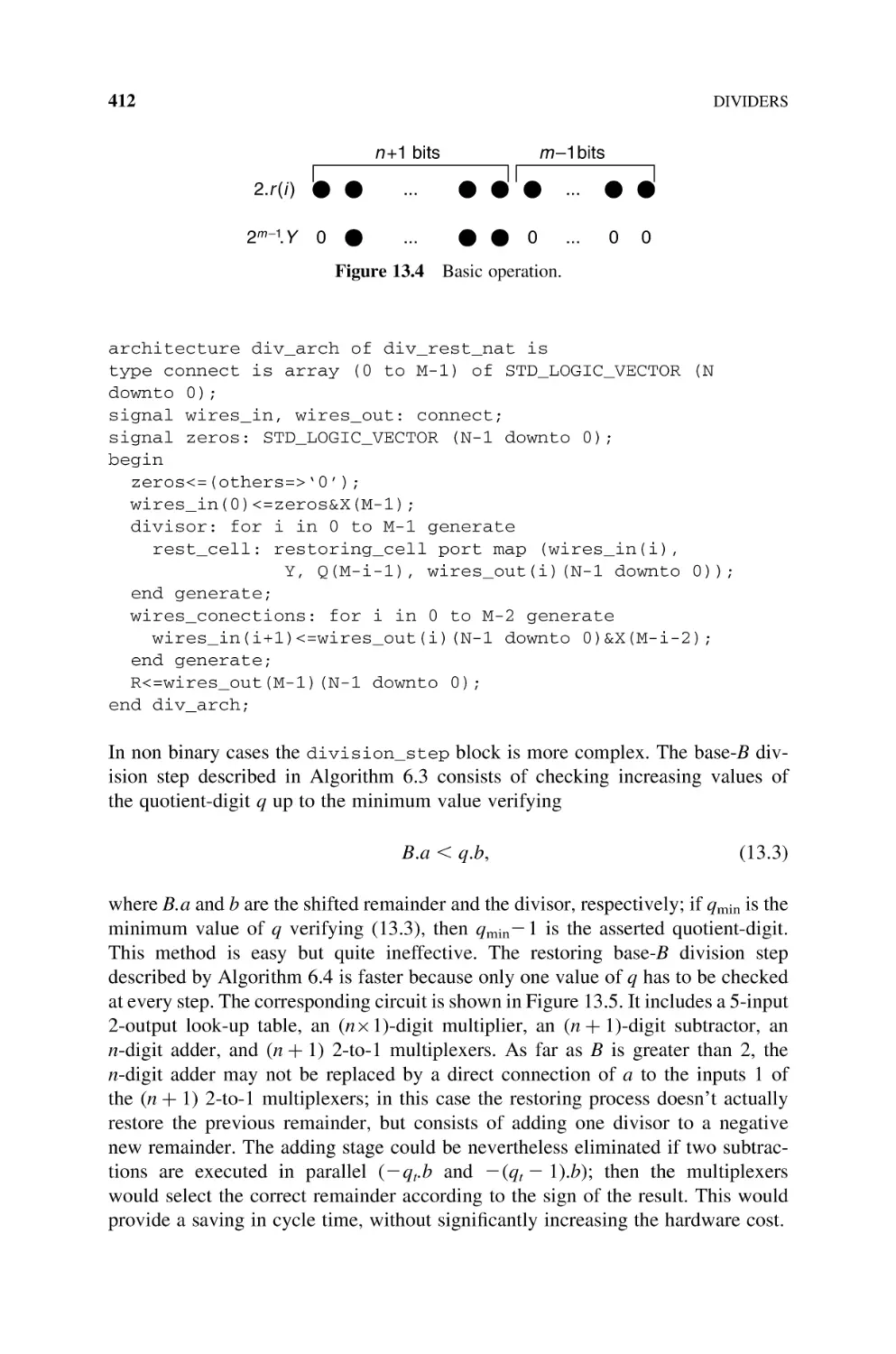
CONTENTS
xiv
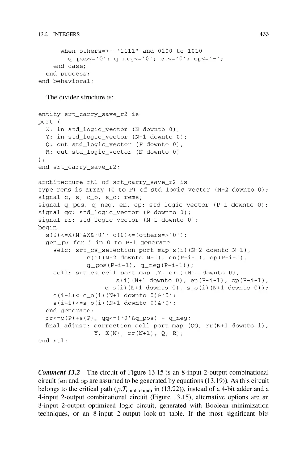
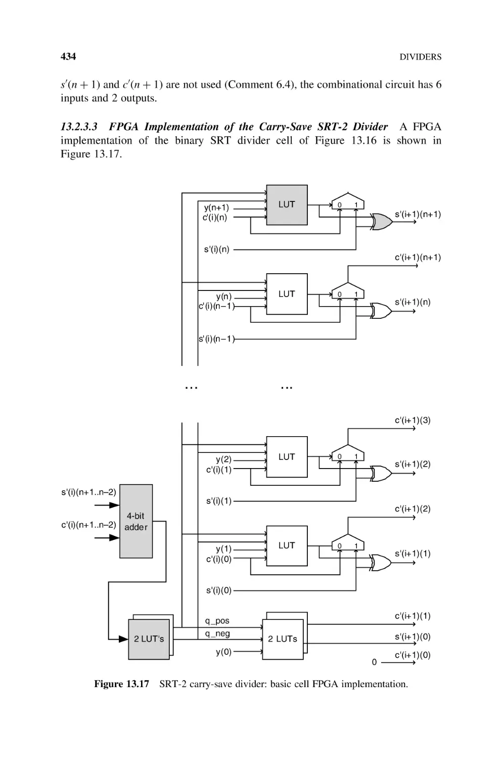
13.2.3
SRT Dividers, 424
13.2.3.1 SRT-2 Divider, 424
13.2.3.2 SRT-2 Divider with Carry-Save Computation
of the Remainder, 428
13.2.3.3 FPGA Implementation of the Carry-Save SRT-2
Divider, 434
13.2.4 SRT-4 Divider, 435
13.2.5 Convergence Dividers, 439
13.2.5.1 Newton– Raphson Divider, 439
13.2.5.2 Goldschmidt Divider, 441
13.2.5.3 Comparative Data Between Newton –Raphson
(NR) and Goldschmidt (G) Implementations, 444
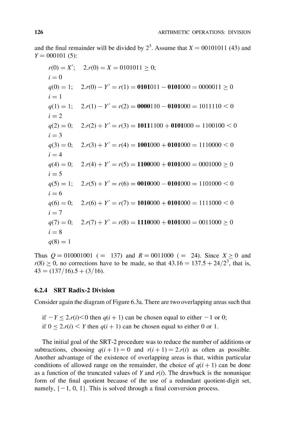
13.3
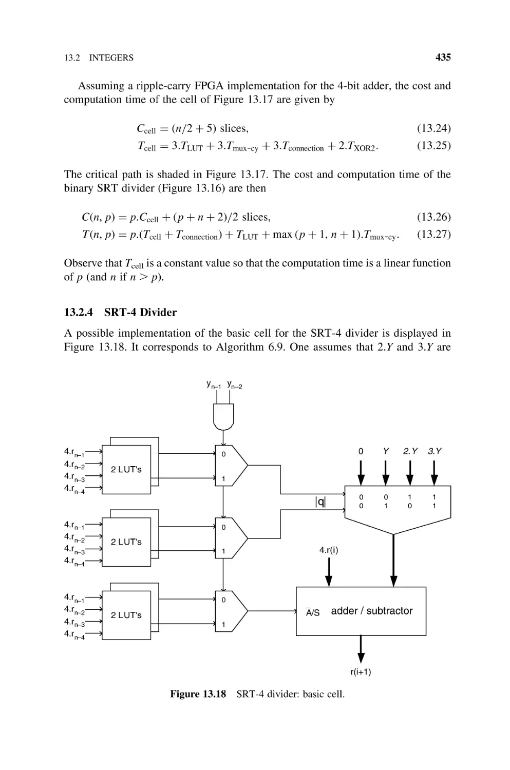
14
15
Bibliography, 444
Other Arithmetic Operators
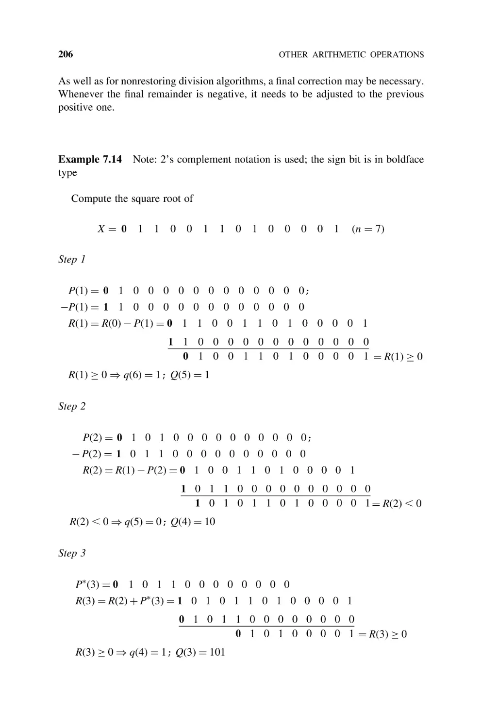
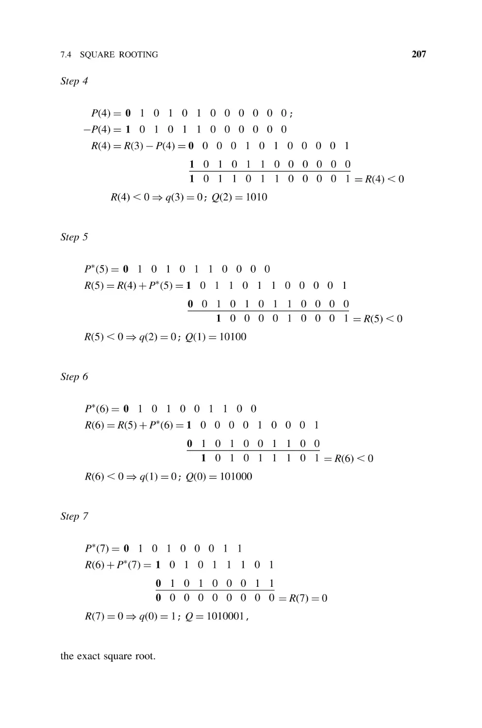
447
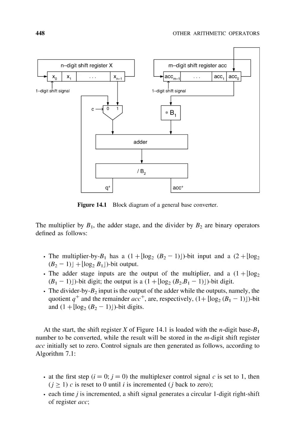
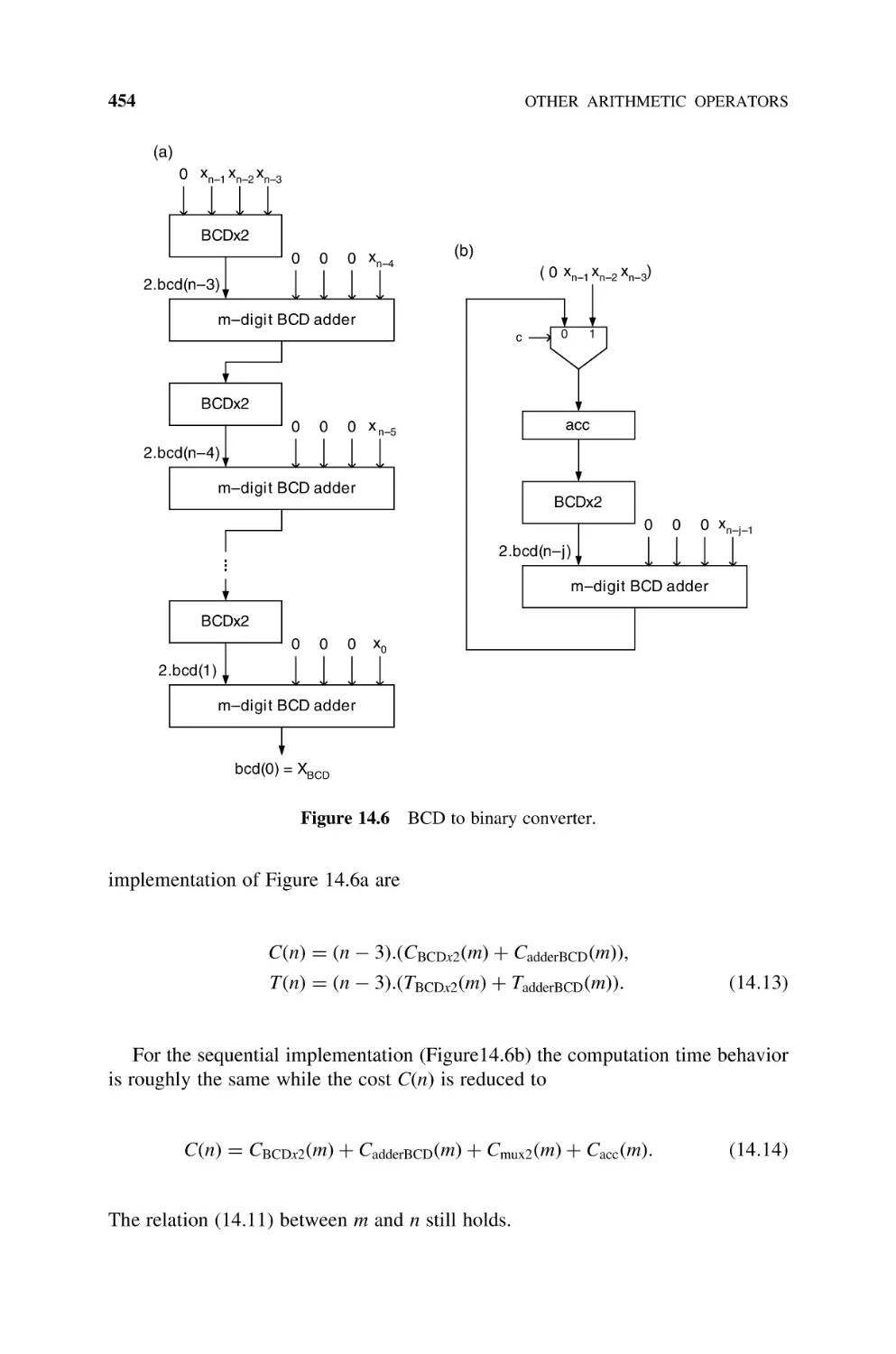
14.1
Base Conversion, 447
14.1.1 General Base Conversion, 447
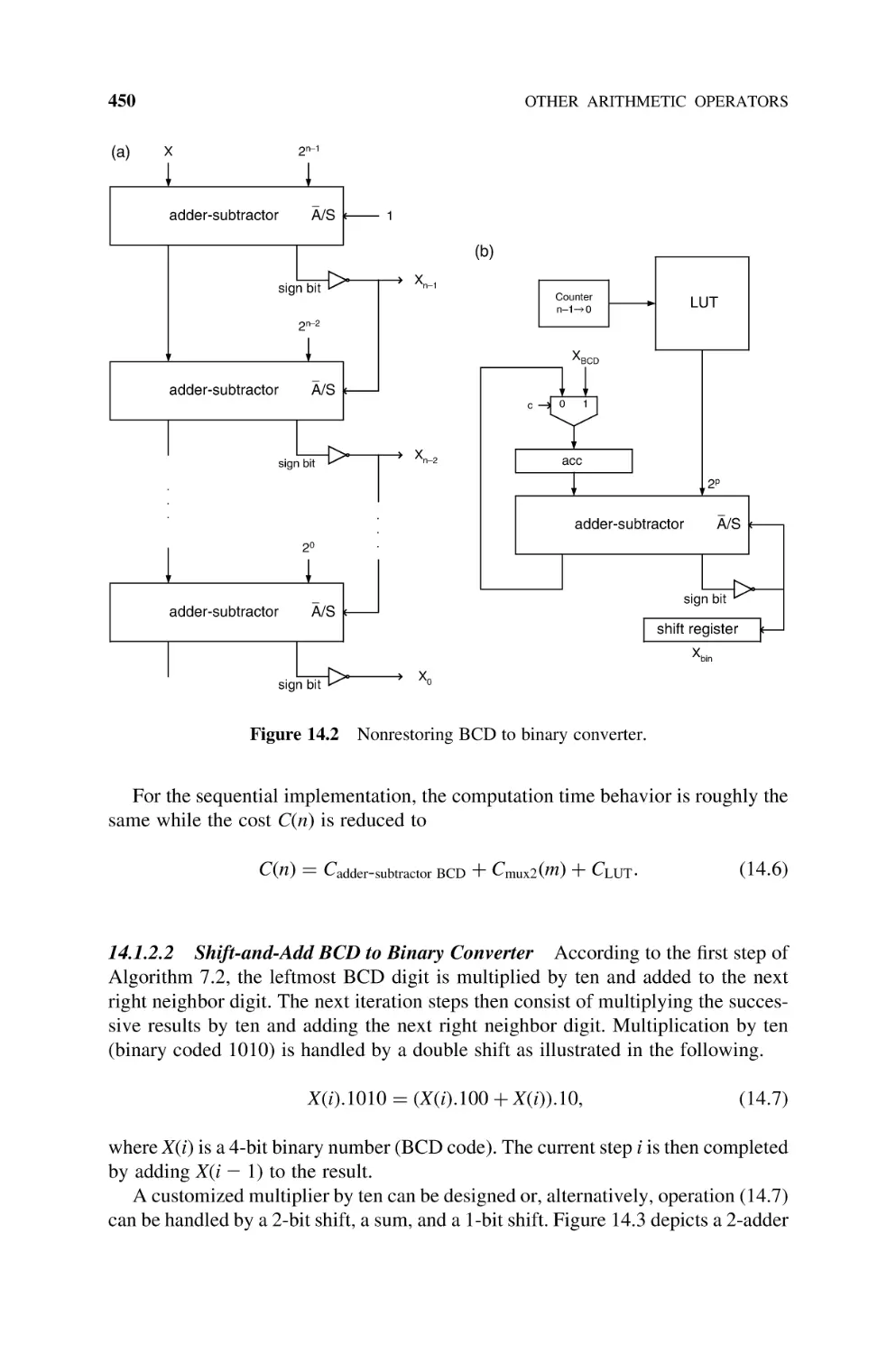
14.1.2 BCD to Binary Converter, 449
14.1.2.1 Nonrestoring 2p Subtracting Implementation, 449
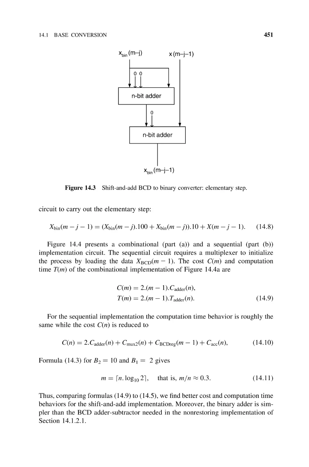
14.1.2.2 Shift-and-Add BCD to Binary Converter, 450
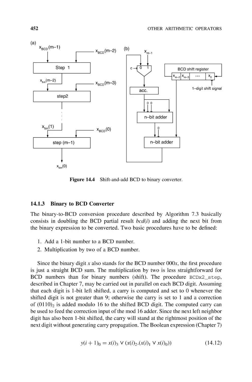
14.1.3 Binary to BCD Converter, 452
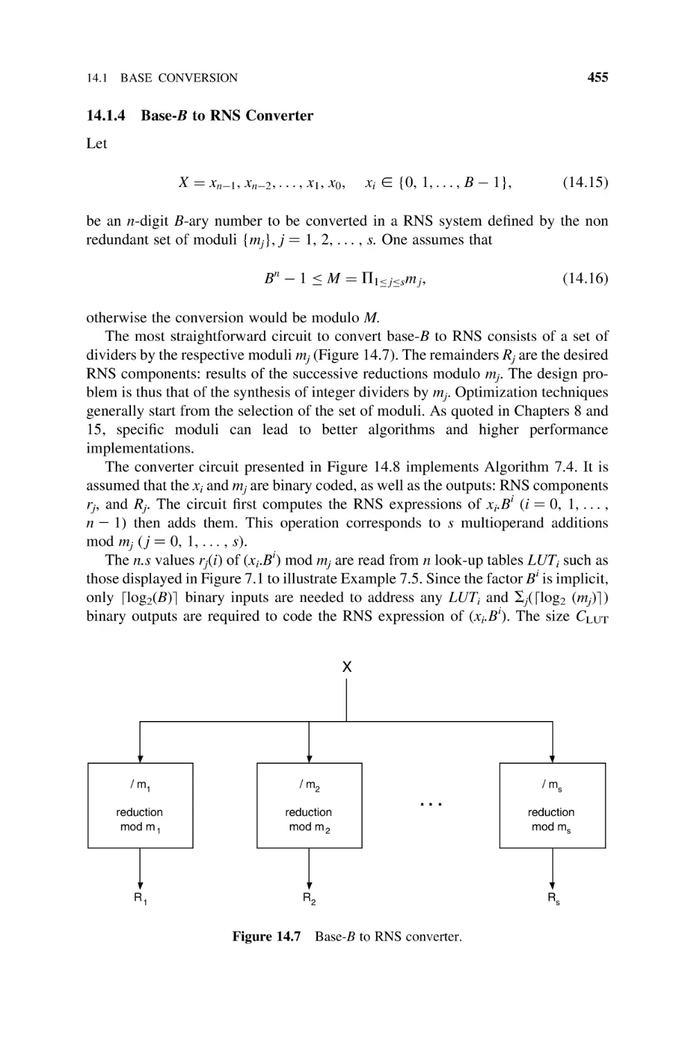
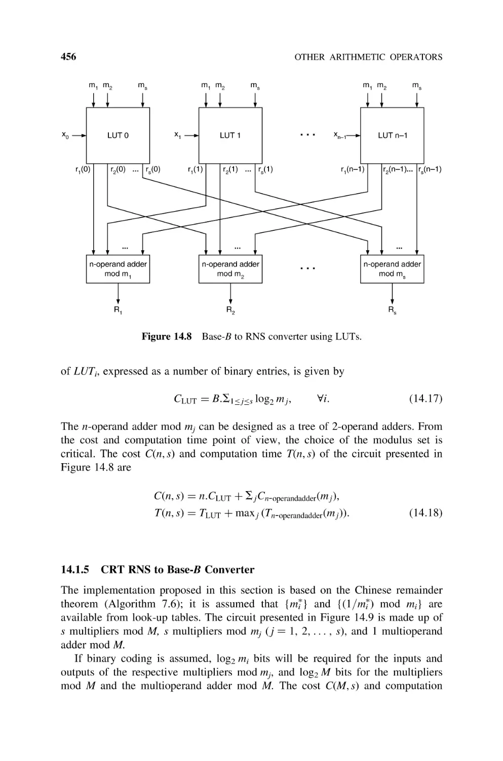
14.1.4 Base-B to RNS Converter, 455
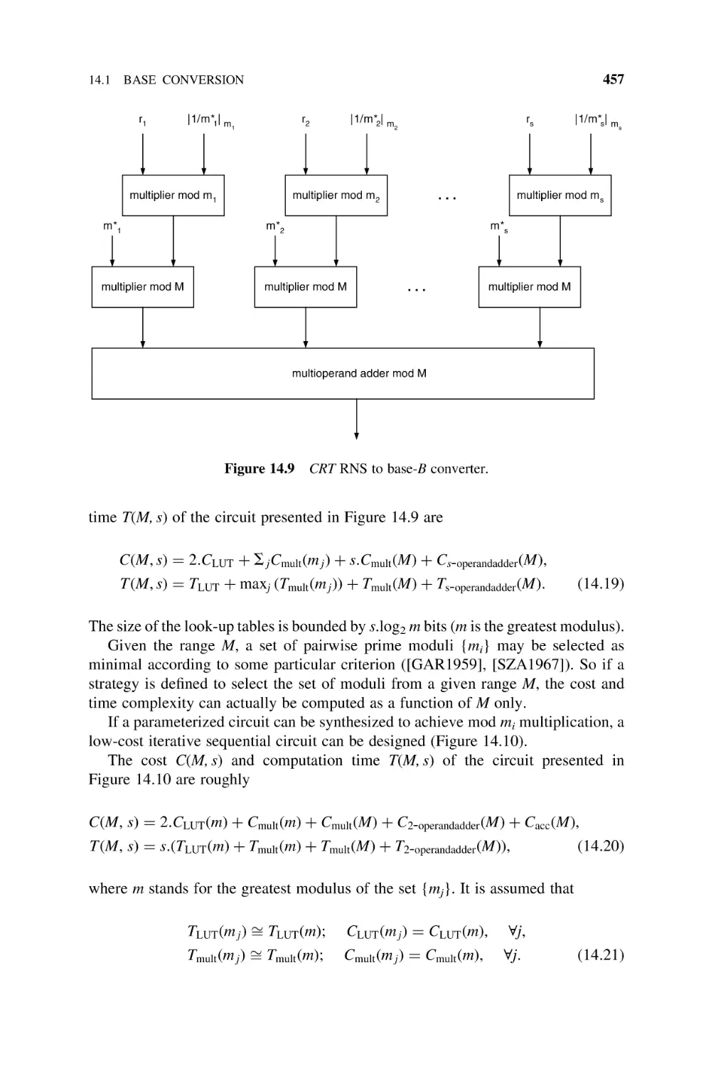
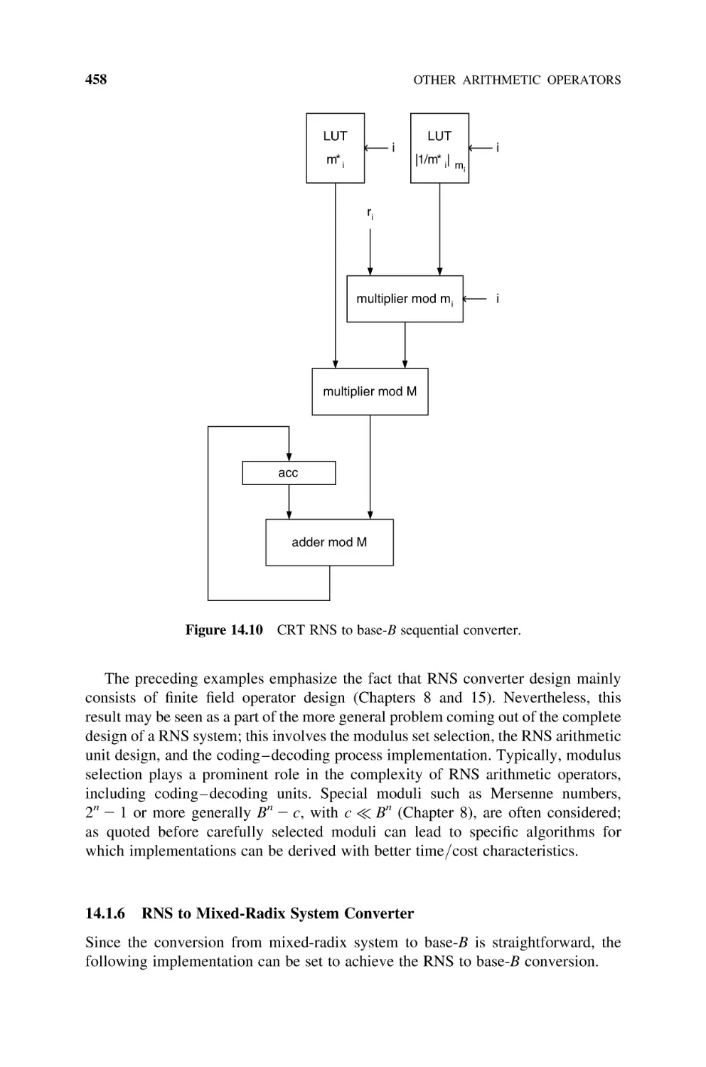
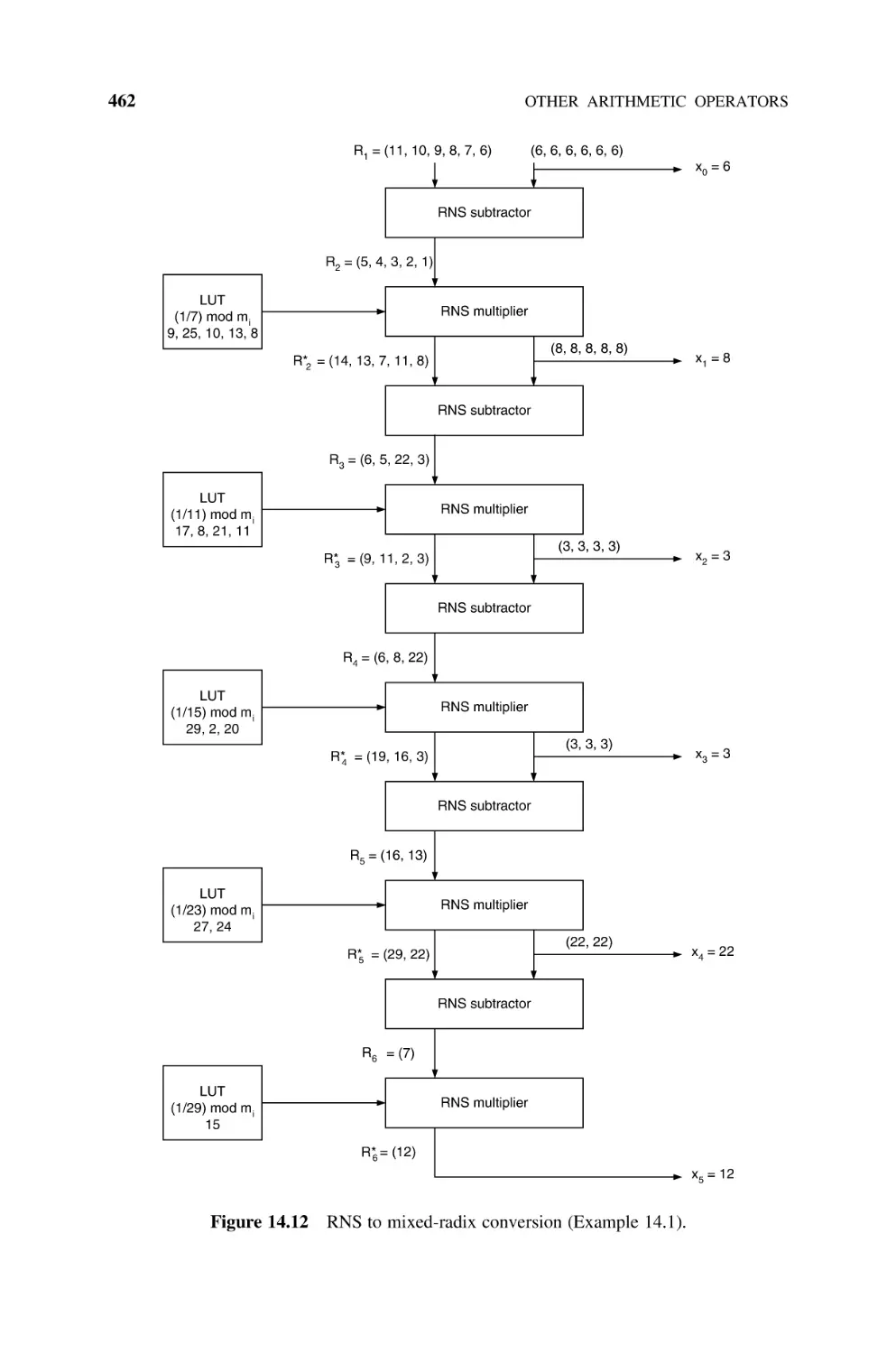
14.1.5 CRT RNS to Base-B Converter, 456
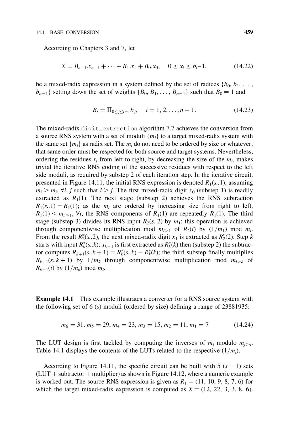
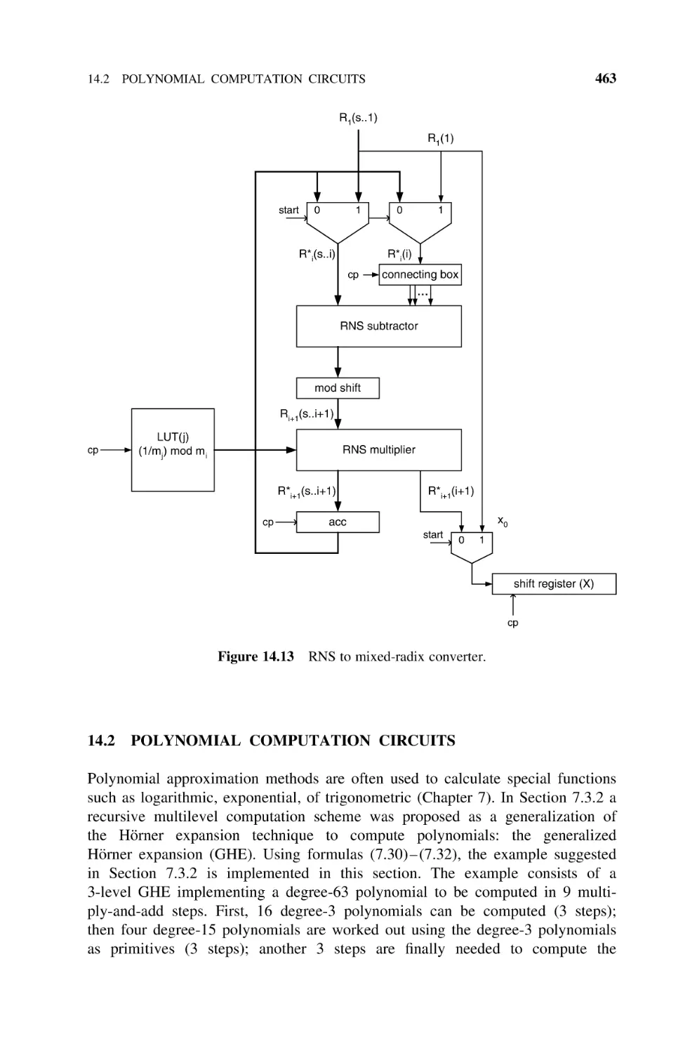
14.1.6 RNS to Mixed-Radix System Converter, 458
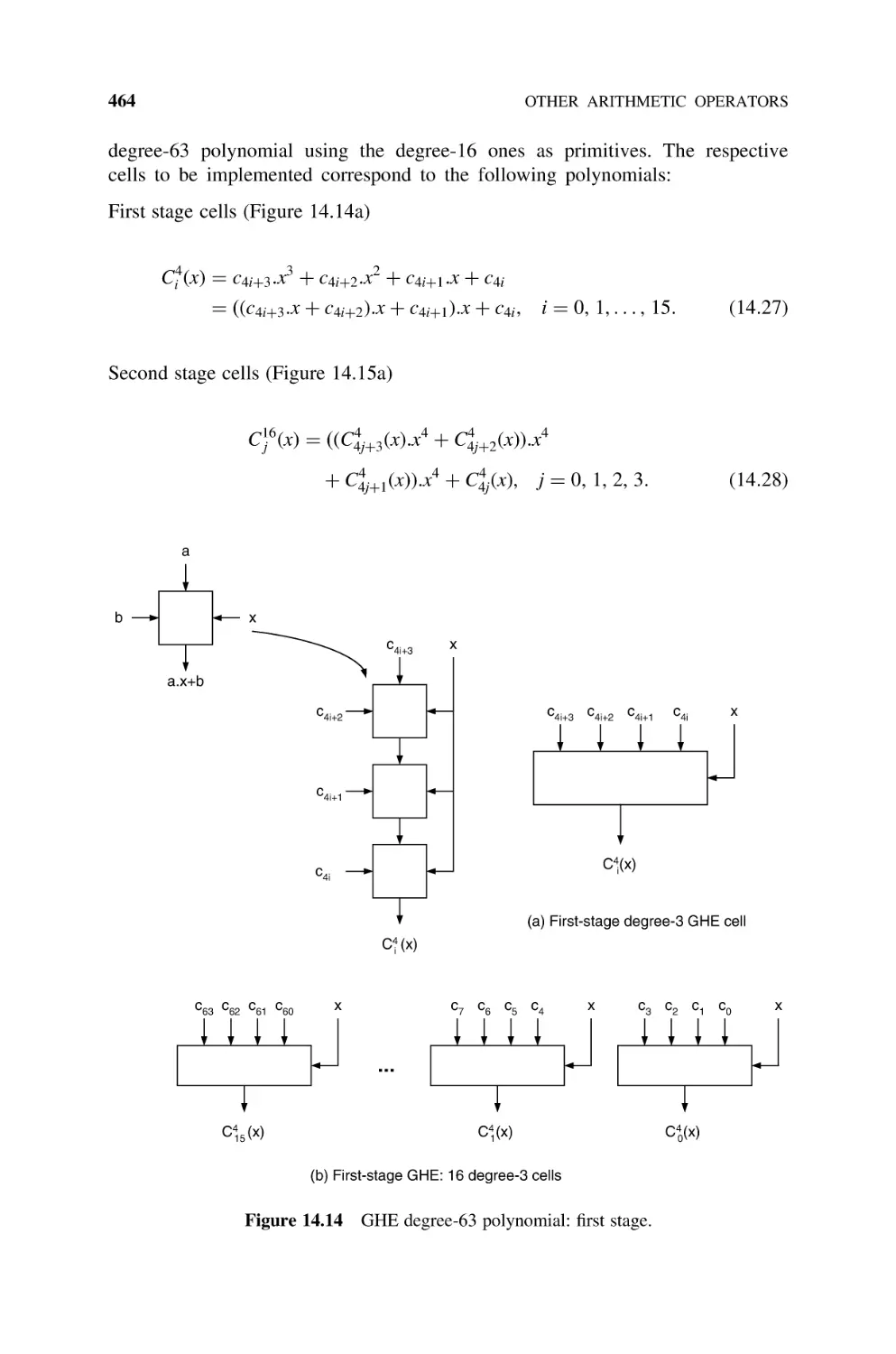
14.2
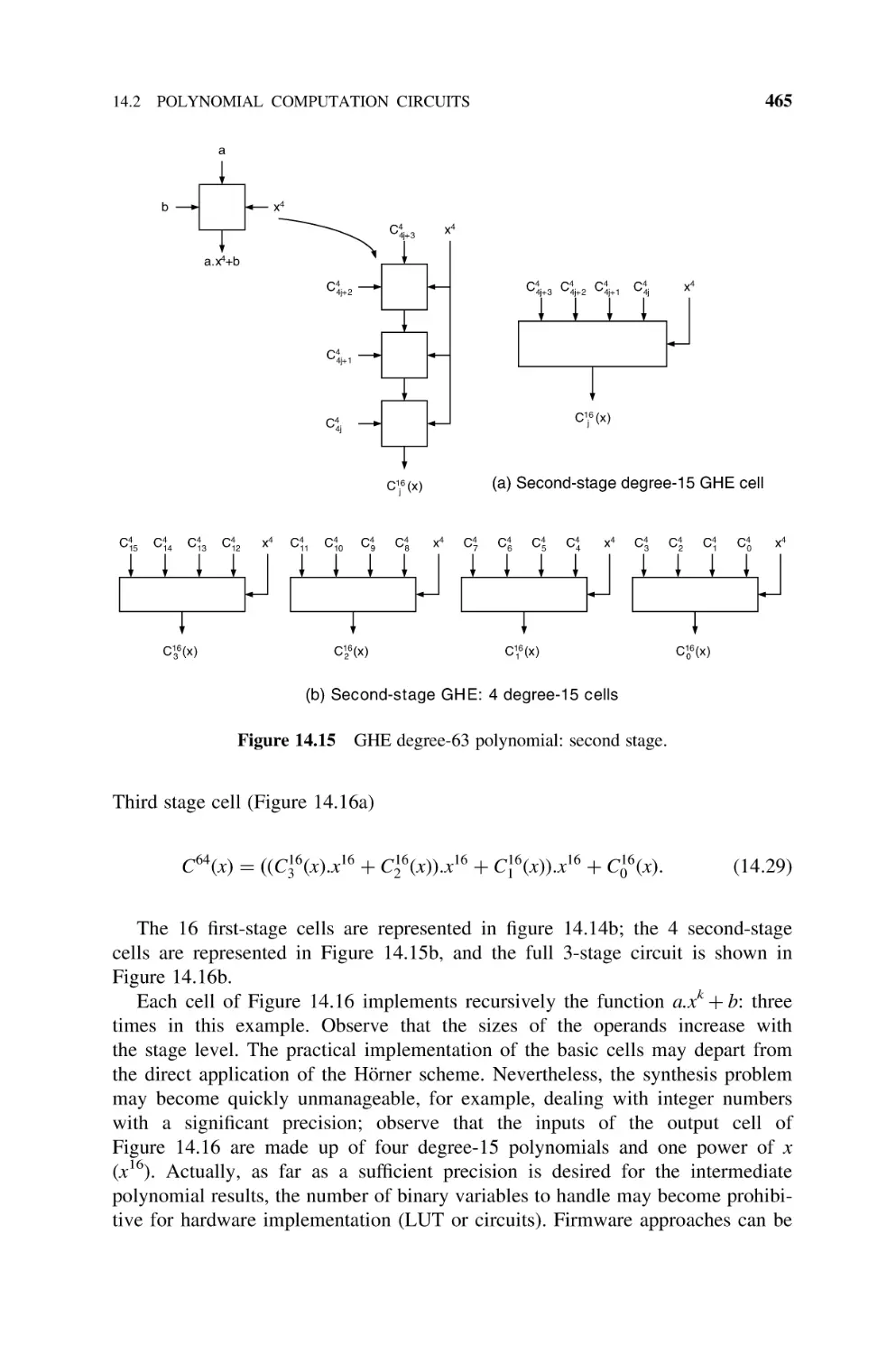
Polynomial Computation Circuits, 463
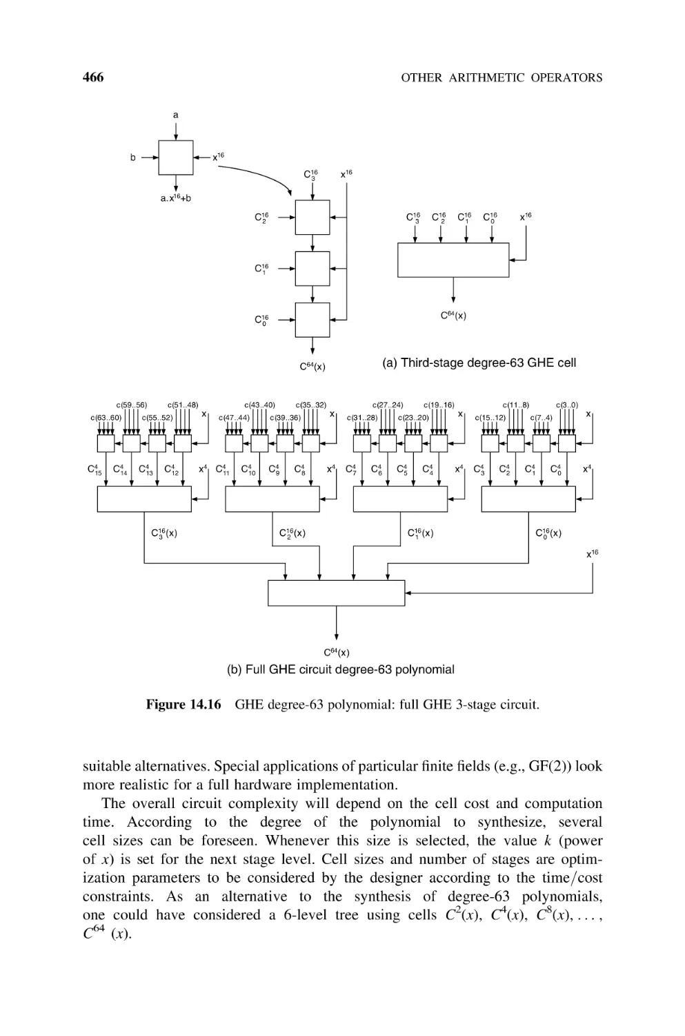
14.3
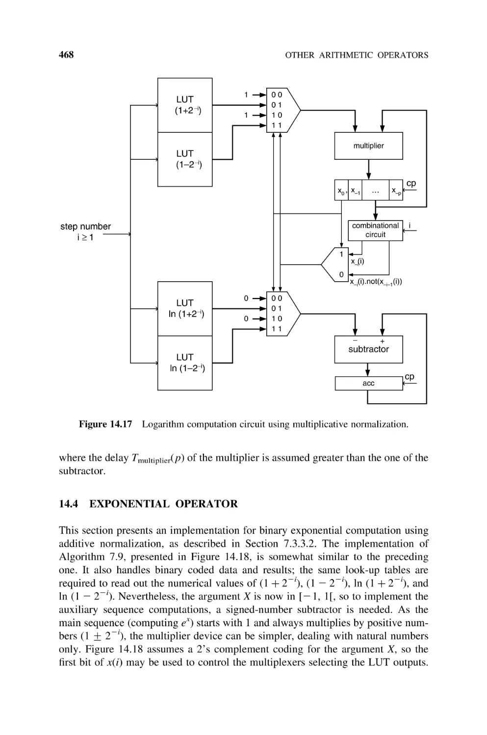
Logarithm Operator, 467
14.4
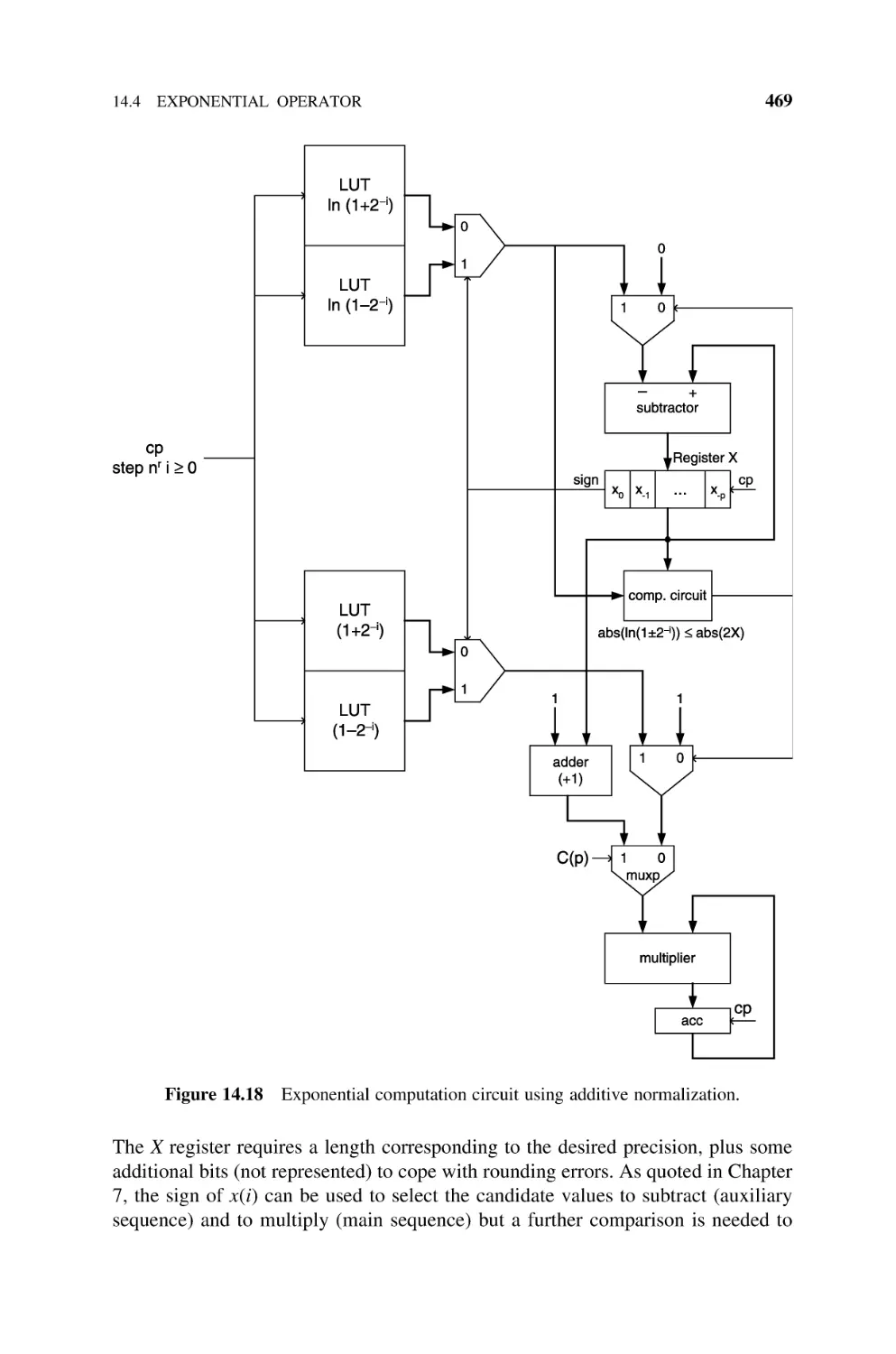
Exponential Operator, 468
14.5
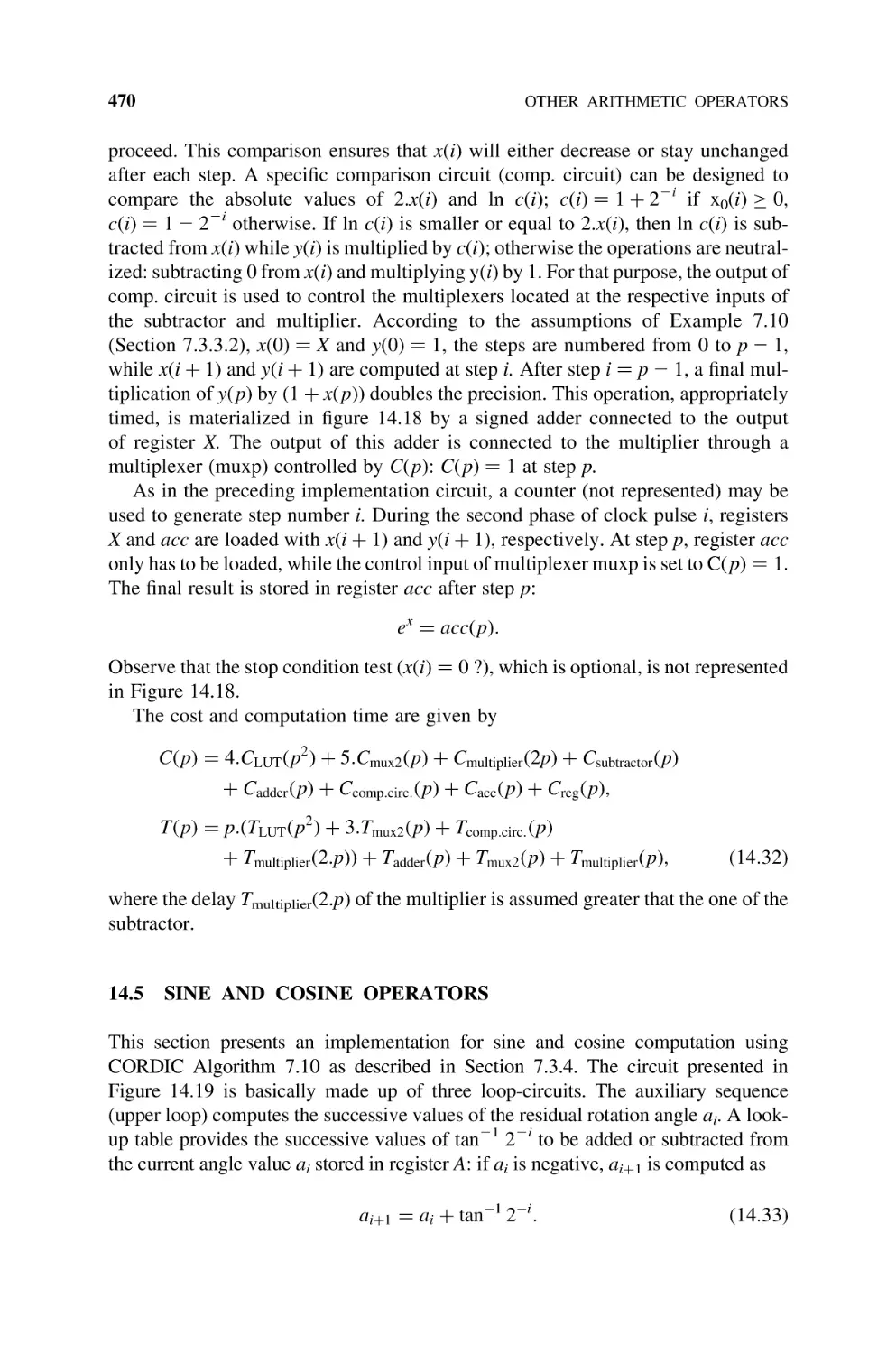
Sine and Cosine Operators, 470
14.6
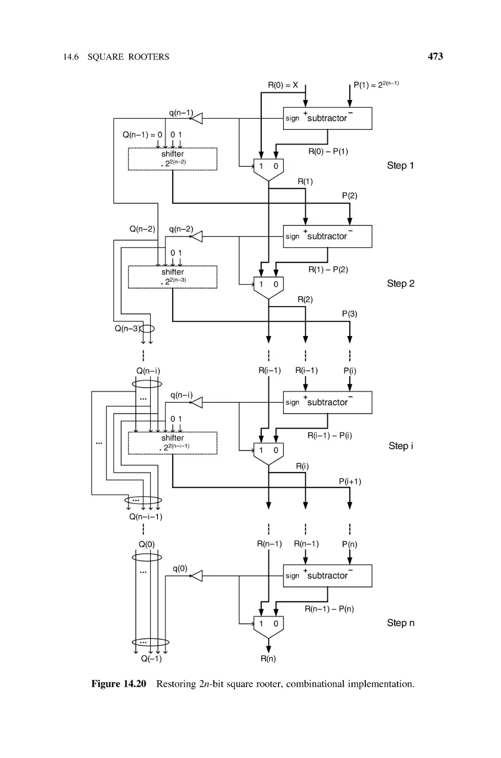
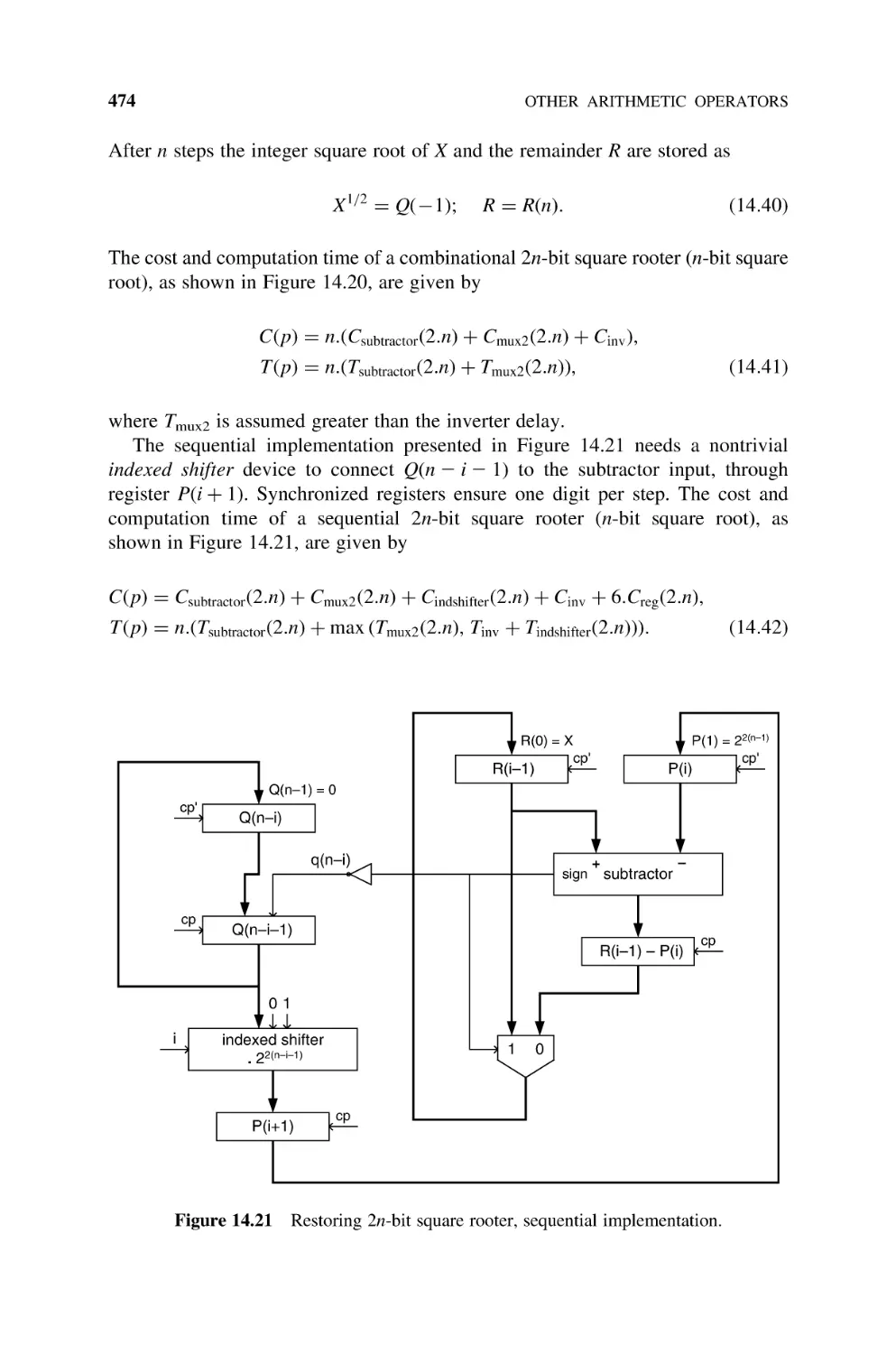
Square Rooters, 472
14.6.1 Restoring Shift-and-Subtract Square Rooter (Naturals), 472
14.6.2 Nonrestoring Shift-and-Subtract Square Rooter
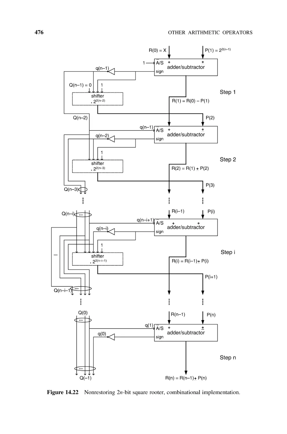
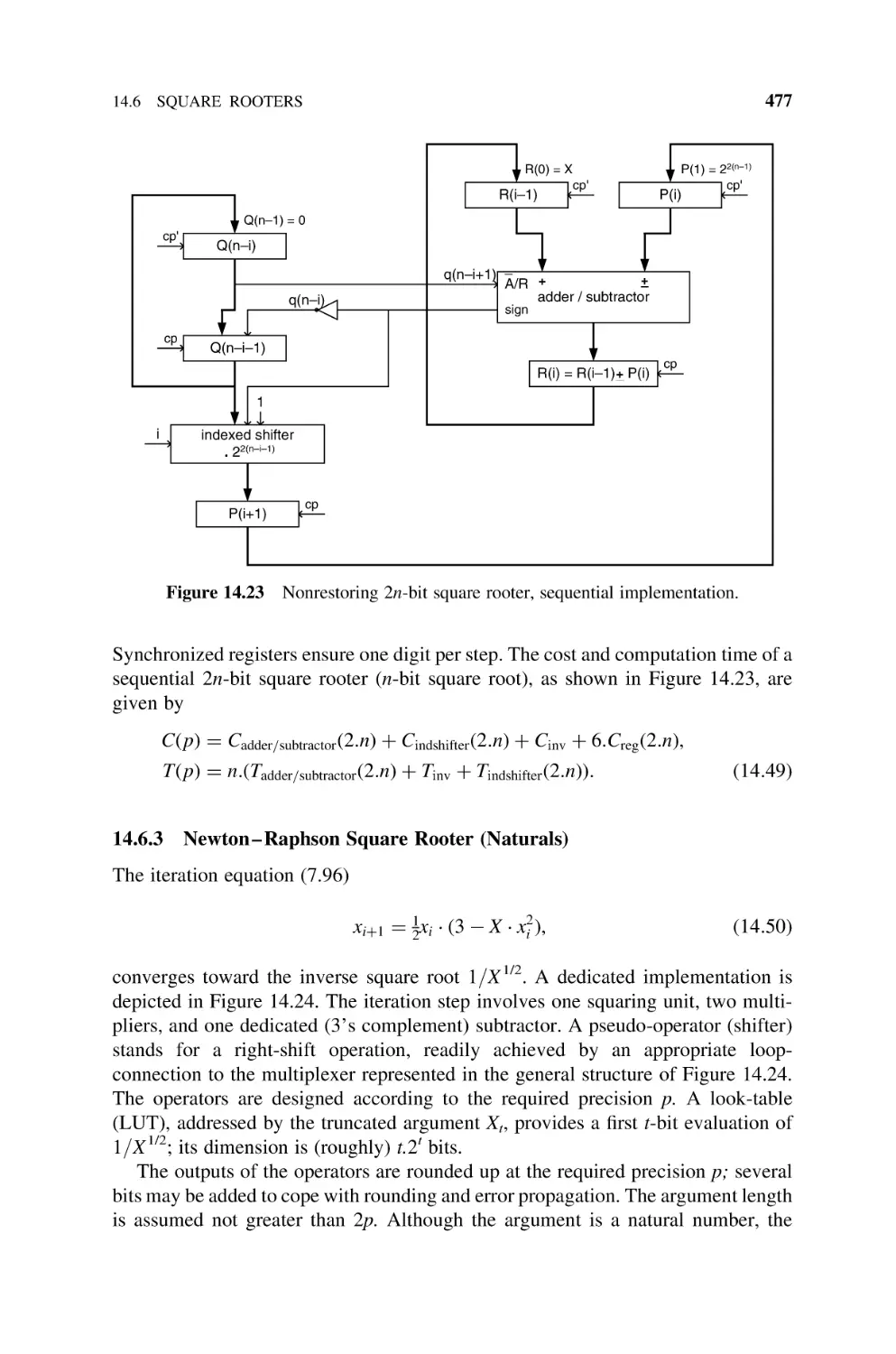
(Naturals), 475
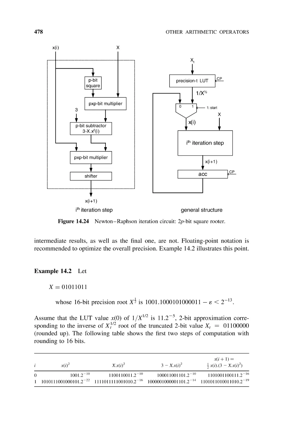
14.6.3 Newton –Raphson Square Rooter (Naturals), 477
14.7
Bibliography, 479
Circuits for Finite Field Operations
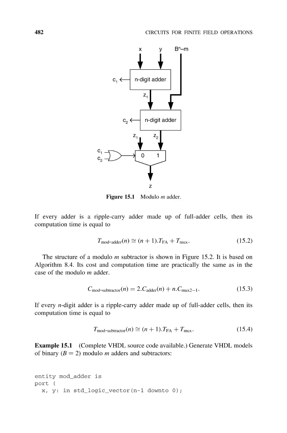
15.1
Operations in Zm , 481
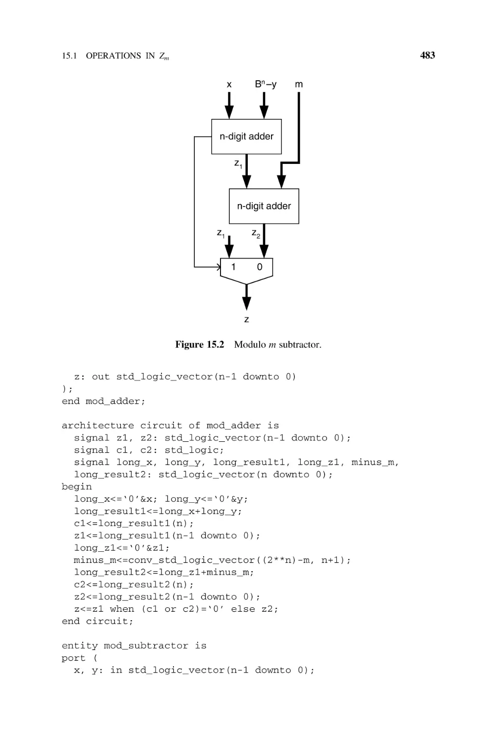
15.1.1 Adders and Subtractors, 481
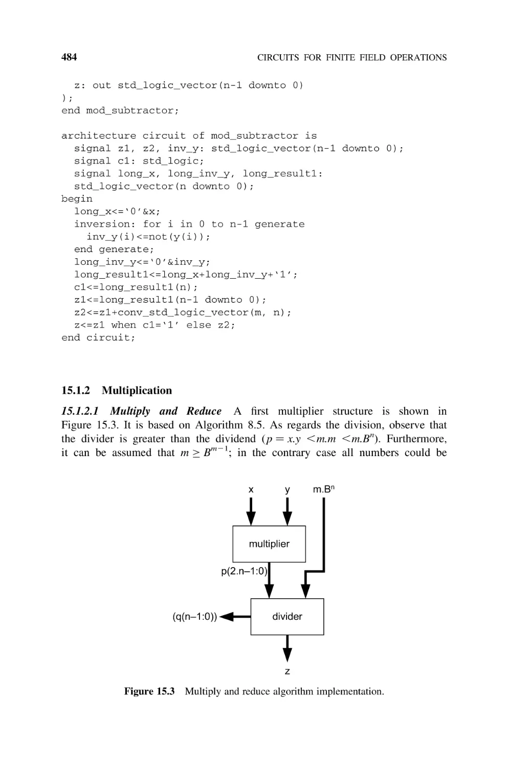
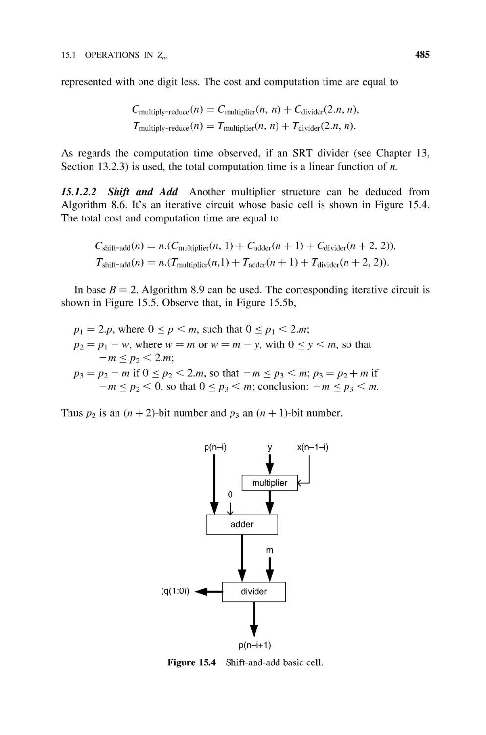
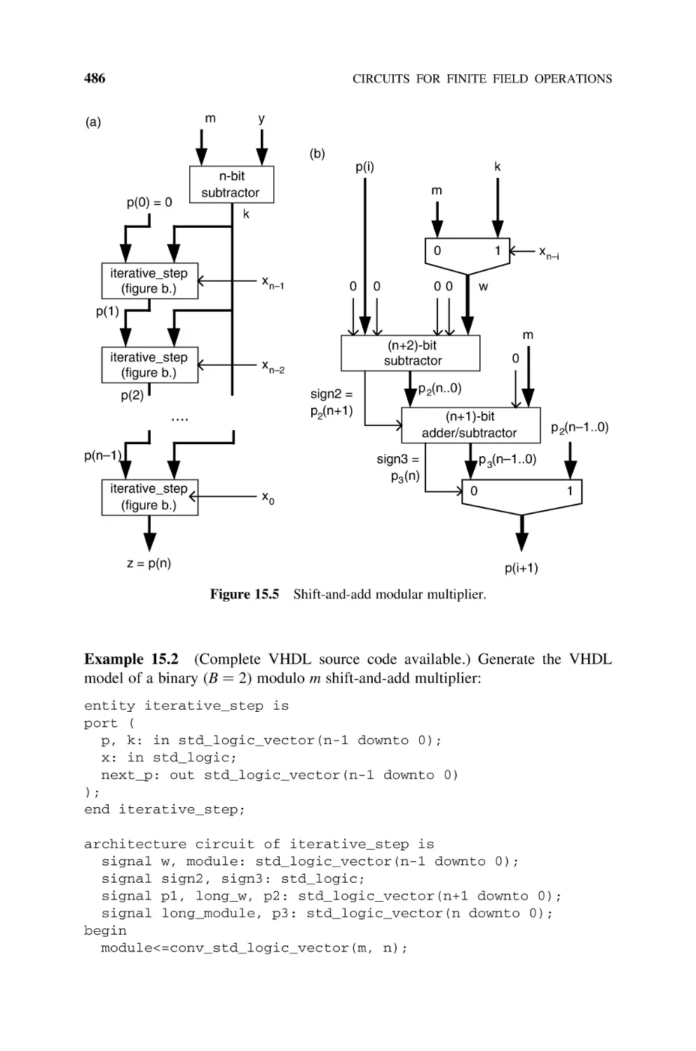
15.1.2 Multiplication, 484
15.1.2.1 Multiply and Reduce, 484
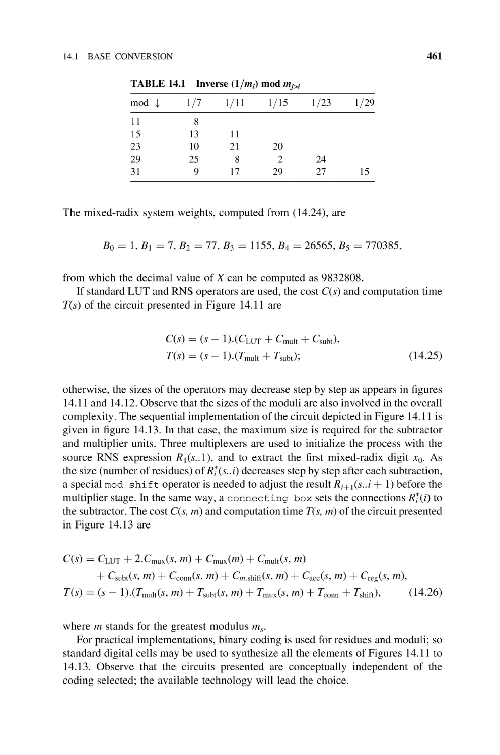
481
CONTENTS
xv
15.1.2.2
15.1.2.3
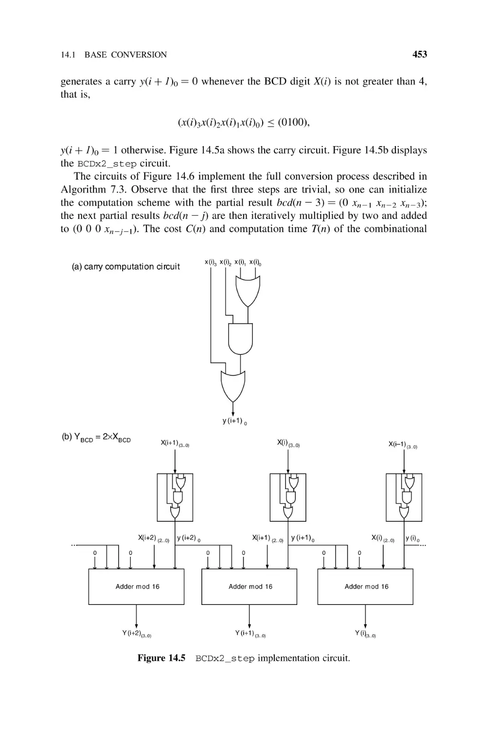
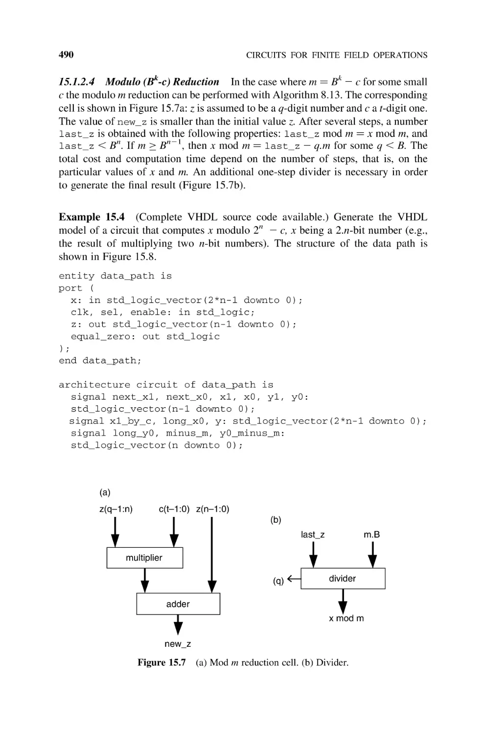
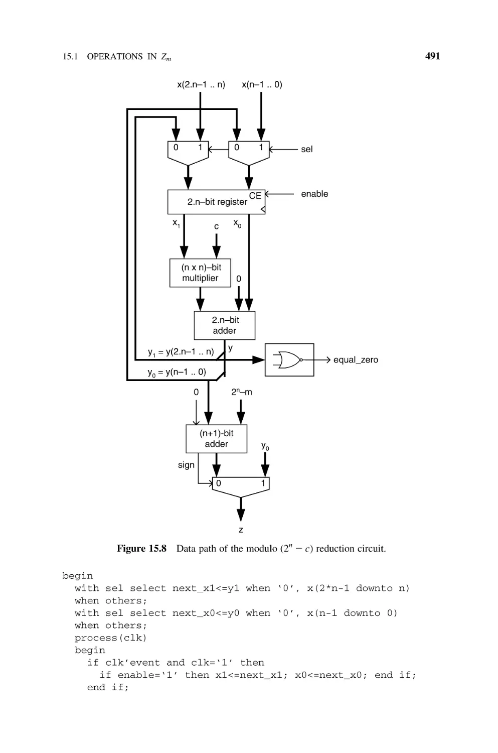
15.1.2.4
15.1.2.5
16
Shift and Add, 485
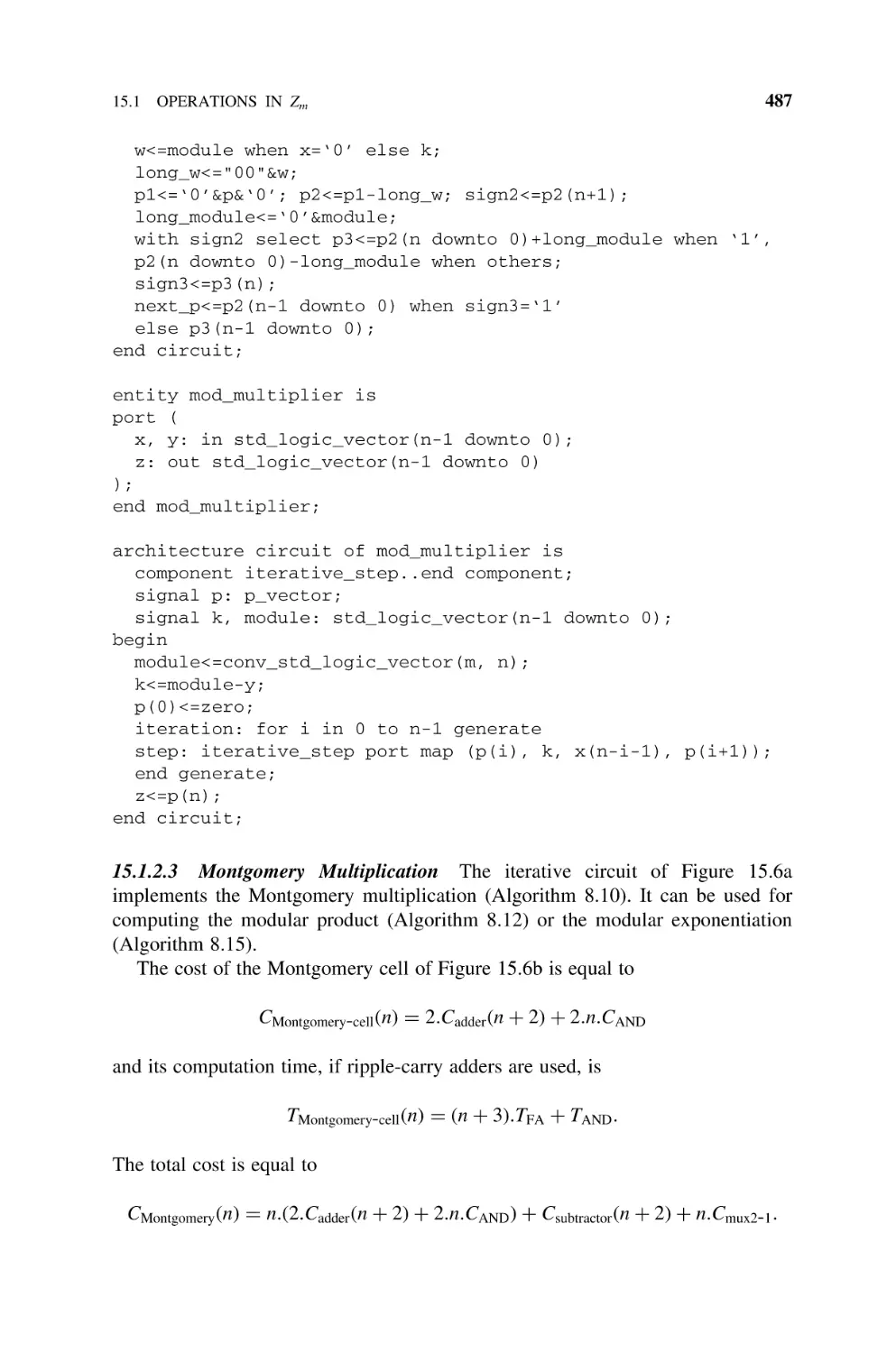
Montgomery Multiplication, 487
Modulo (Bk2c) Reduction, 490
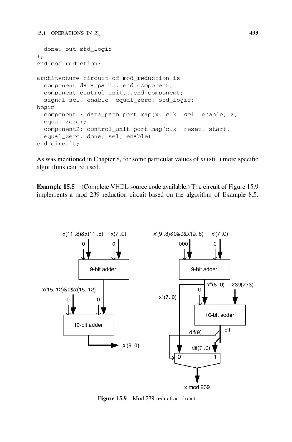
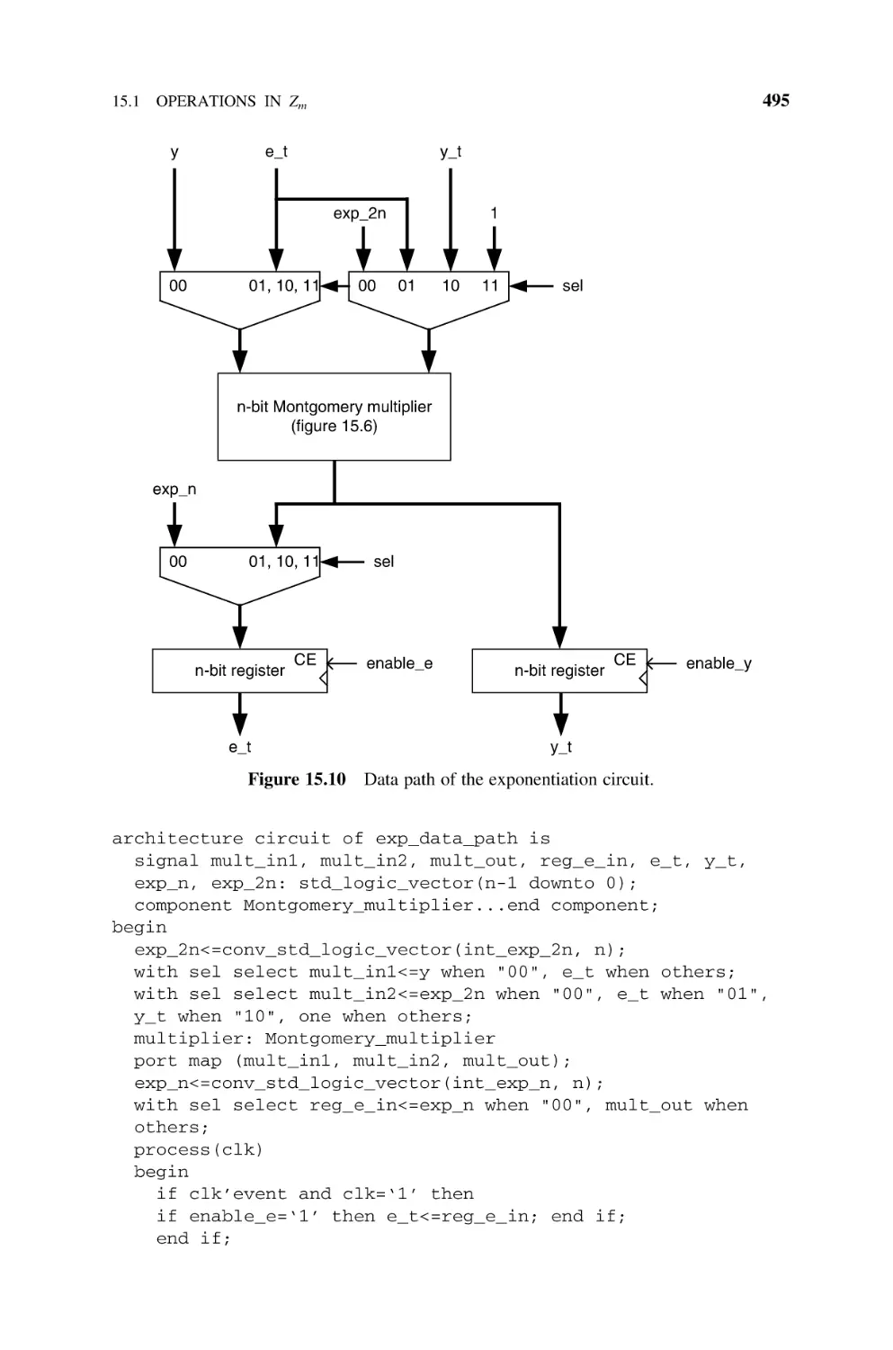
Exponentiation, 494
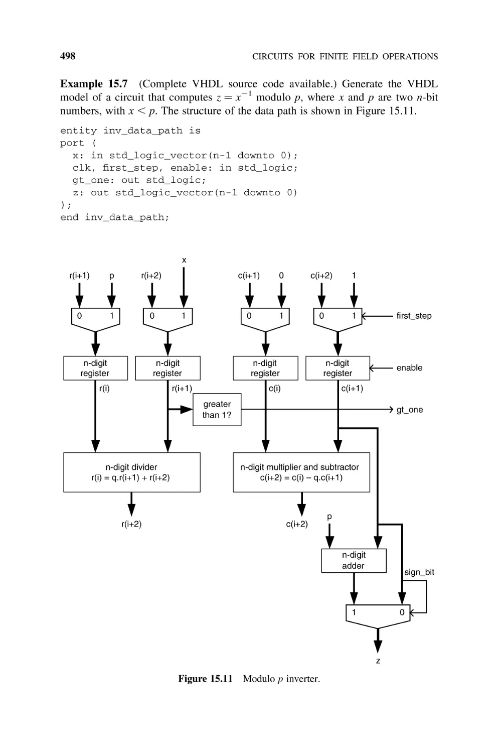
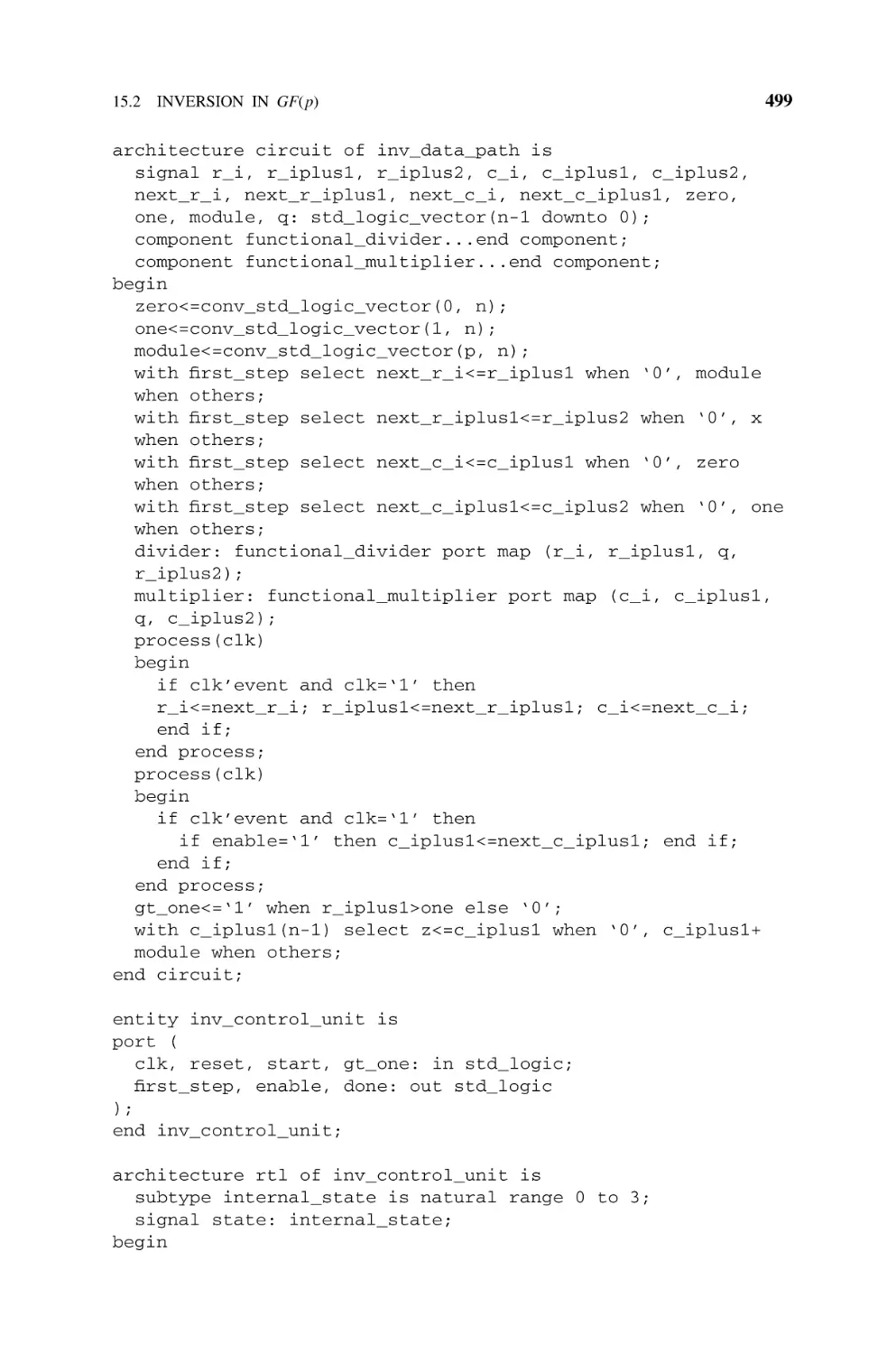
15.2
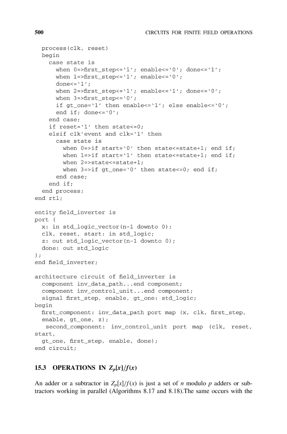
Inversion in GF(p), 497
15.3
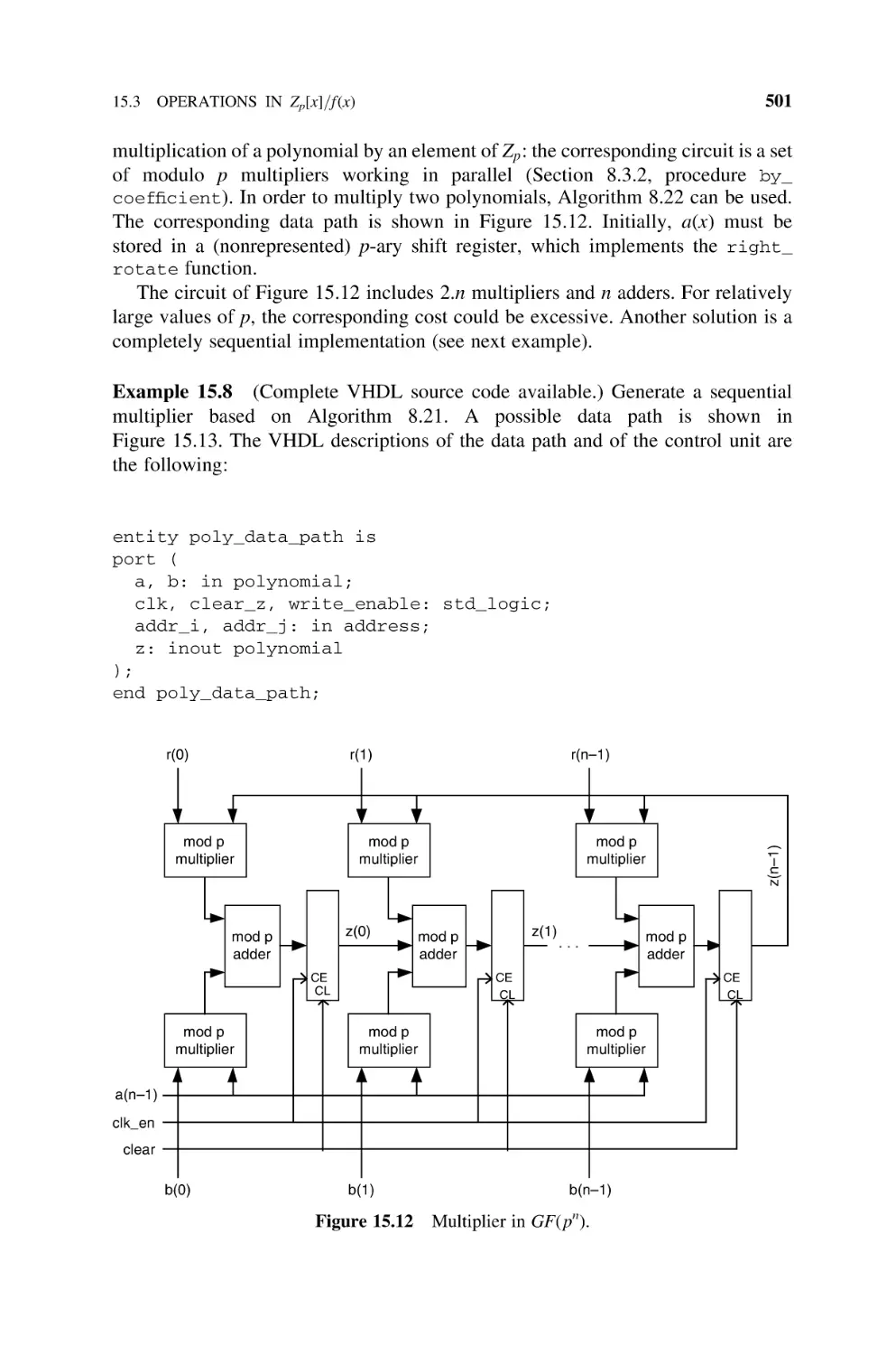
Operations in Zp[x]/f (x), 500
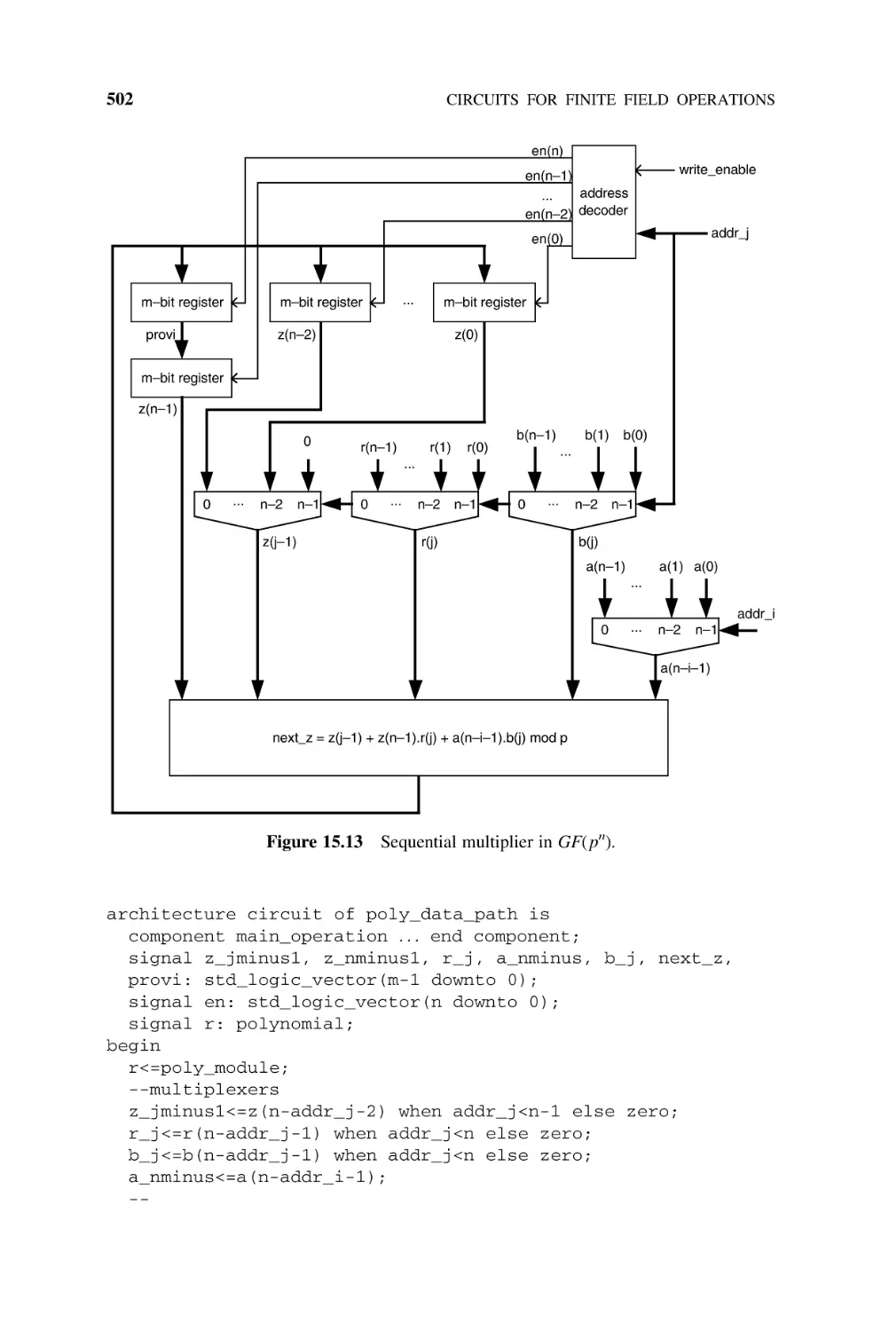
15.4
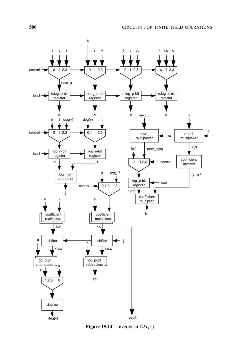
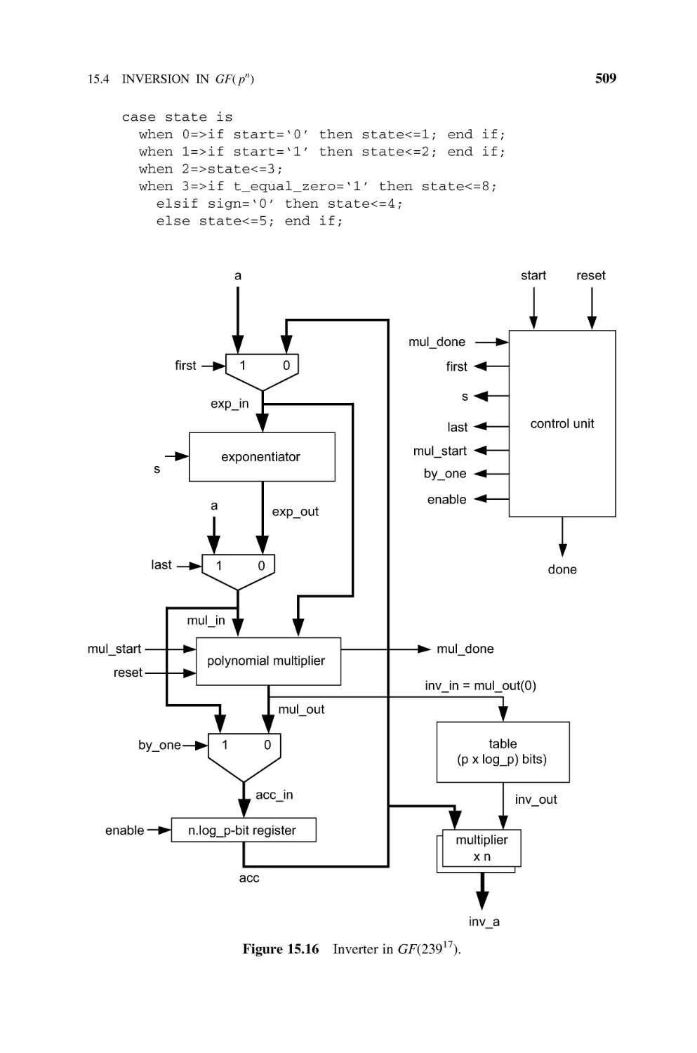
Inversion in GF(pn), 504
15.5
Bibliography, 510
Floating-Point Unit
16.1
Floating-Point System Definition, 513
16.2
Arithmetic Operations, 515
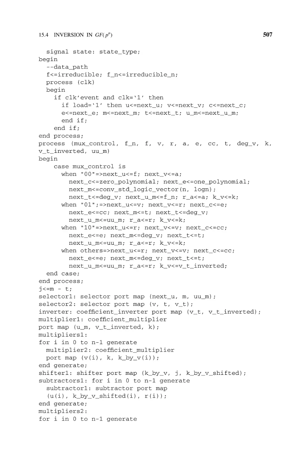
16.2.1 Addition of Positive Numbers, 515
16.2.2 Difference of Positive Numbers, 517
16.2.3 Addition and Subtraction, 518
16.2.4 Multiplication, 520
16.2.5 Division, 521
16.2.6 Square Root, 522
16.3
Rounding Schemes, 524
16.4
Guard Digits, 525
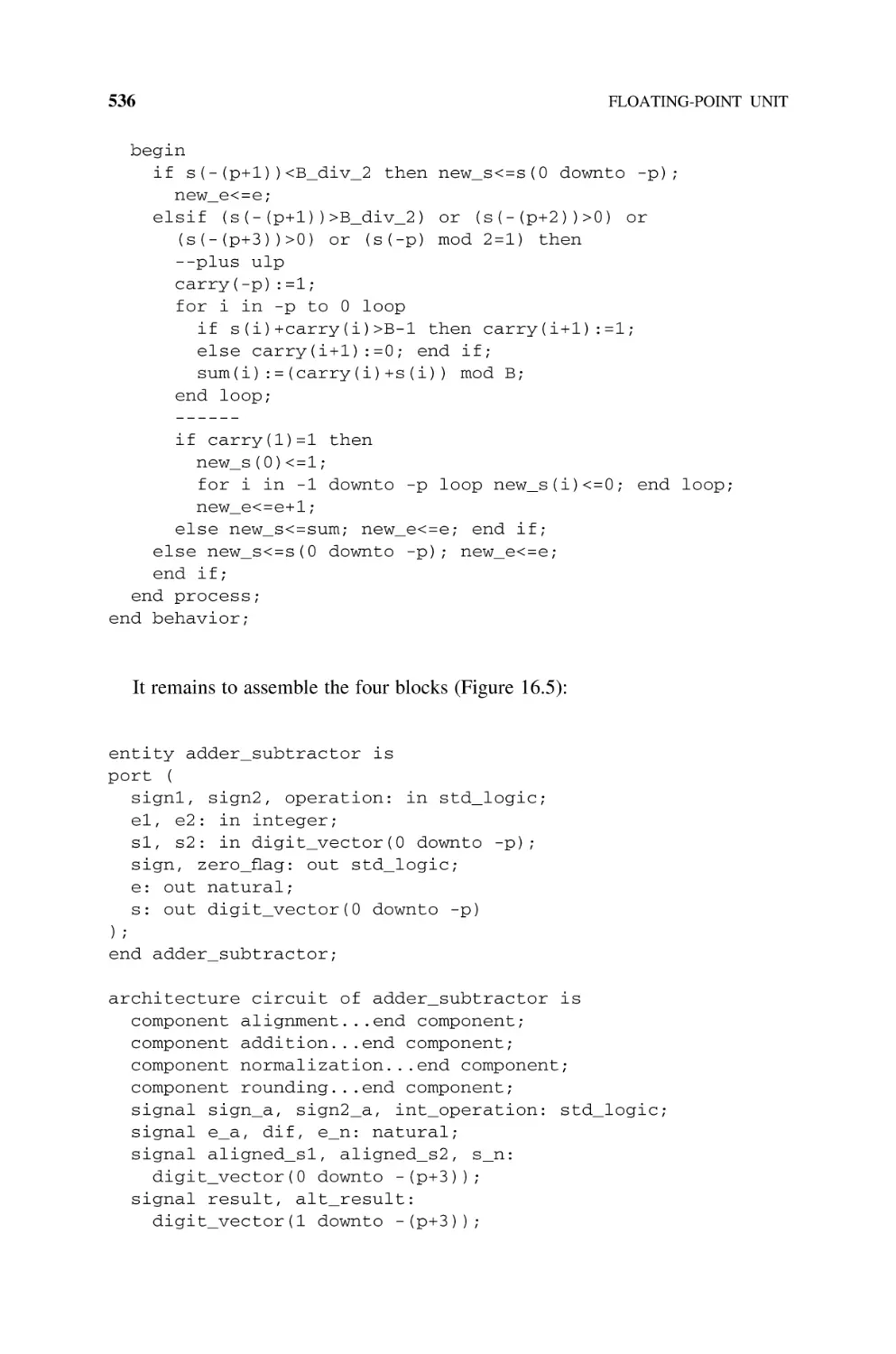
16.5
Adder-Subtractor, 527
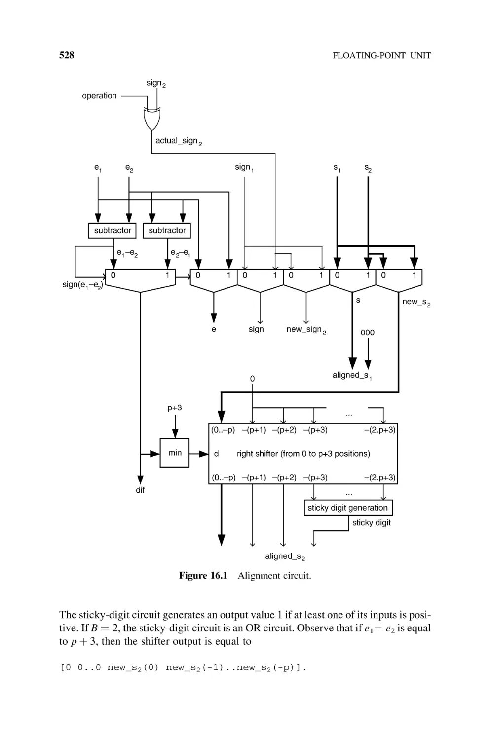
16.5.1 Alignment, 527
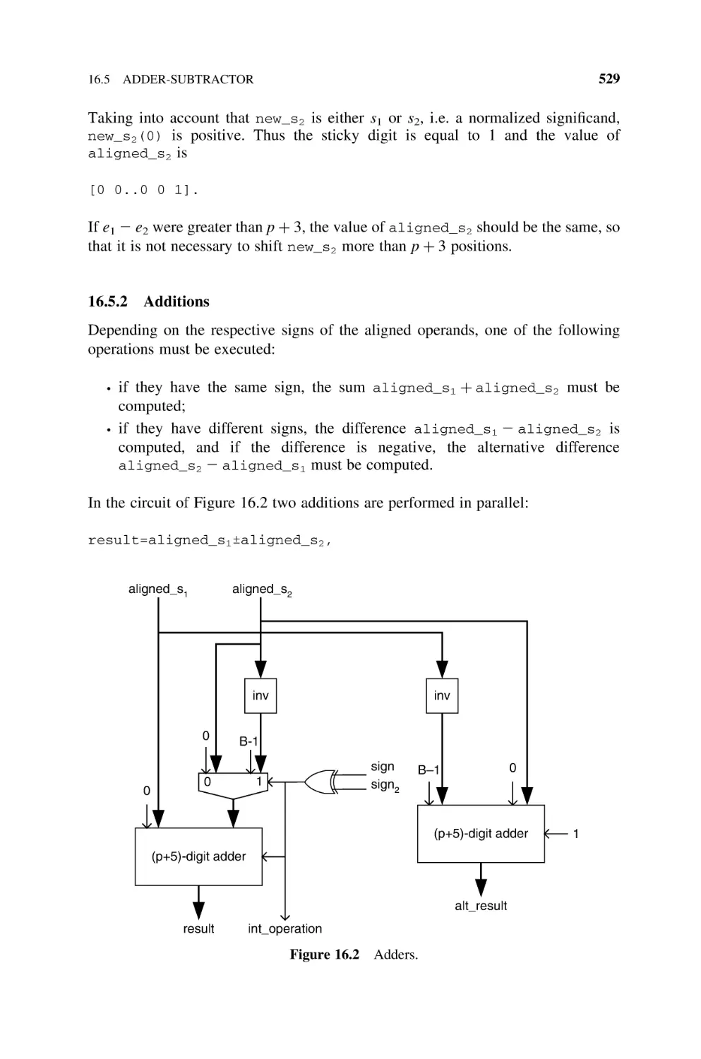
16.5.2 Additions, 529
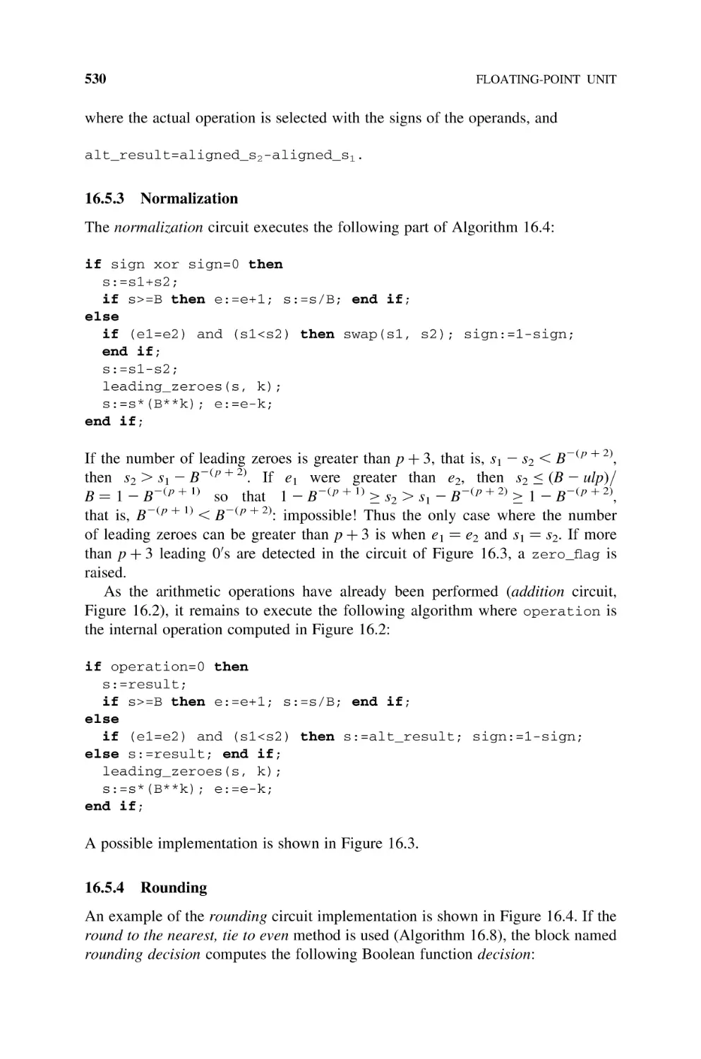
16.5.3 Normalization, 530
16.5.4 Rounding, 530
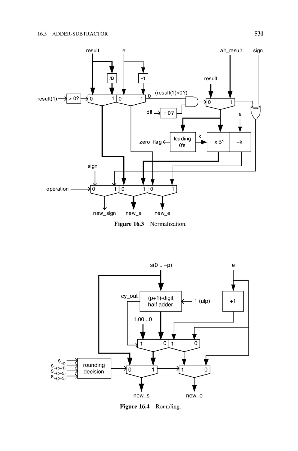
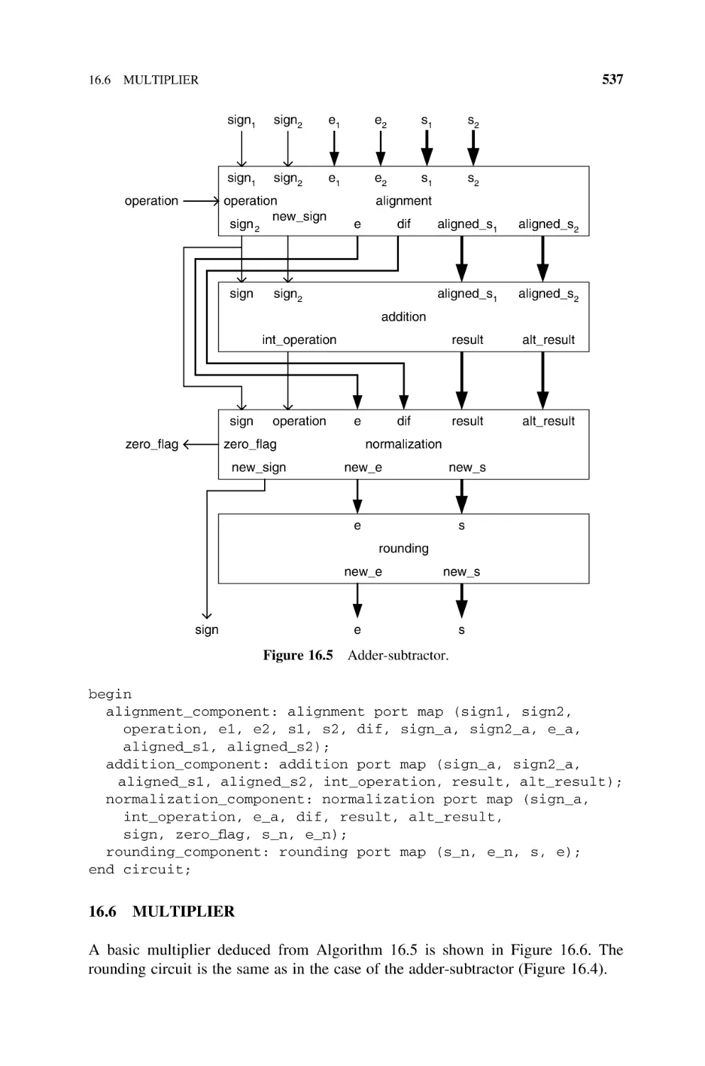
16.6
Multiplier, 537
16.7
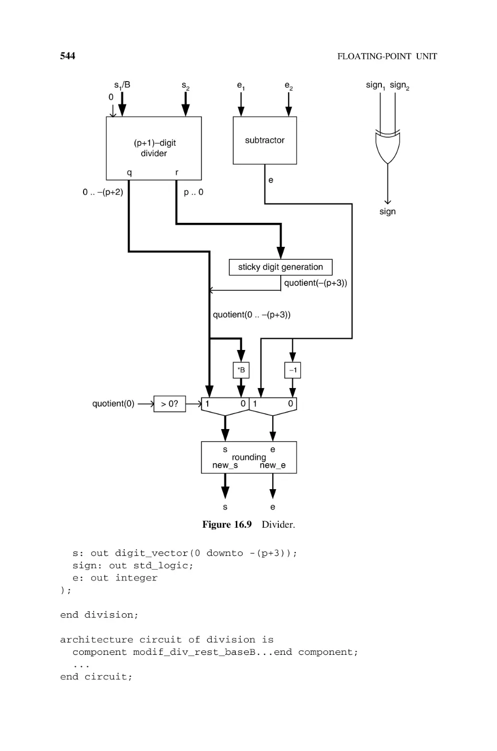
Divider, 542
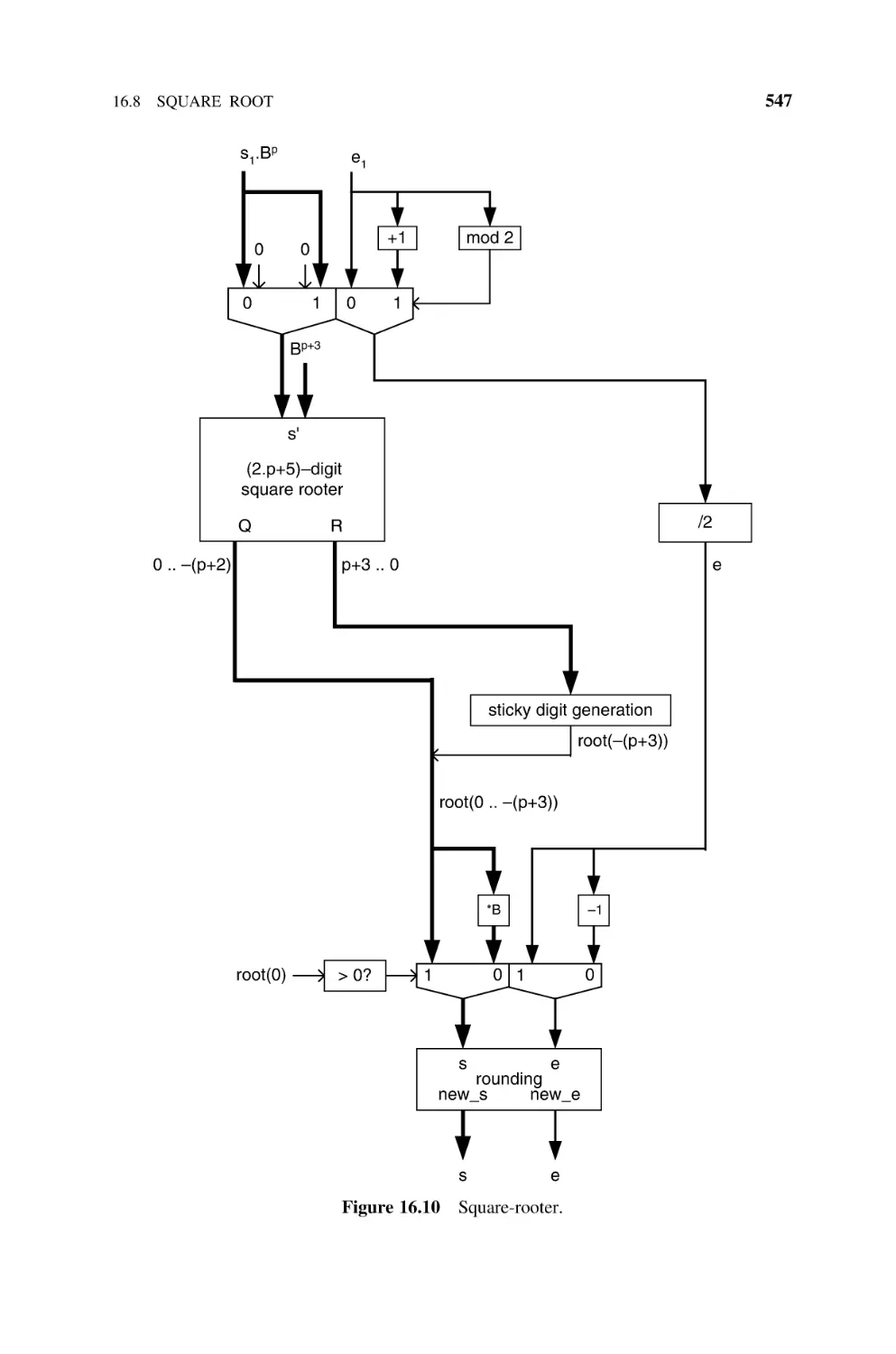
16.8
Square Root, 546
16.9
Comments, 548
16.10
Bibliography, 548
Index
513
549
PREFACE
From the beginnings of digital electronic science, the synthesis of circuits carrying
out arithmetic operations has been a central topic. As a matter of fact, it is an activity
directly related to computer development. From then on, a well-known technical discipline was born: computer arithmetic. Traditionally, the study of arithmetic circuits
has been oriented toward applications to general-purpose computers, which provide
the most important applications of digital circuits. However, the electronic market
share corresponding to specific systems (embedded systems) is significant. It is
important to point out that the huge business volume that corresponds to generalpurpose computers (personal computers, servers, main frames) is distributed
among a relatively reduced number of different models. Therefore the number of
designers involved in general-purpose computer development is not as big as it
might seem and is much less than the number of engineers dedicated to production
and sales. The case of embedded systems is different. Embedded systems are circuits
designed for specific applications (special-purpose devices), so a great diversity of
products exist in the market, and the design effort per fabricated unit can be a lot
bigger than in the case of general-purpose computers. In consequence, the design
of specific computers is an activity in which numerous engineers are involved, in
all type of companies—even small ones—within numerous countries.
In this book methods and examples for synthesis of arithmetic circuits are described
with an emphasis somewhat different from the classic texts on computer arithmetic.
.
.
It is not limited to the description of the arithmetic units of computers.
Descriptions of computation algorithms are presented in a section apart from
the one dedicated to their materialization or implementation by digital circuits.
The development of an embedded system is an operation of hardware– software
codesign for which it is not known beforehand what tasks will be executed by a
microprocessor and what other tasks by specific coprocessors. For this reason, it
xvii
xviii
.
.
PREFACE
appeared useful to describe the algorithms in an independent manner, without
any assumption on subsequent executions by an existent processor (software) or
by a new customized circuit (hardware).
A special, although not exclusive, importance has been given to user programmable devices (field programmable devices such as FPGAs), especially to the
families Spartan II and Virtex. Those devices are very commonly used for the
realization of specific systems, mainly in the case of small series and prototypes. The particular architecture of those components leads the designer to
use synthesis techniques somewhat different from the ones applied for ASICs
(application-specific integrated circuits) for which standard cell libraries exist.
In what concern circuits description, logic schemes are presented, sometimes
with some VHDL models, in such a way that the corresponding circuits can
easily be simulated and synthesized.
After an introductory chapter, the book is divided in two parts. The first one is
dedicated to mathematical aspects and algorithms: mathematical background
(Chapter 2), number representation (Chapter 3), addition and subtraction (Chapter
4), multiplication (Chapter 5), division (Chapter 6), other arithmetic operations
(Chapter 7), and operations in finite fields (Chapter 8). The second part is dedicated
to the central topic—the synthesis of arithmetic circuits: hardware platforms
(Chapter 9), general principles of synthesis (Chapter 10), adders and subtractors
(Chapter 11), multipliers (Chapter 12), dividers (Chapter 13), other arithmetic primitives (Chapter 14), operators for finite fields (Chapter 15), and floating-point unit.
Numerous VHDL models, and other source files, can be downloaded from http://
www.ii.uam.es/gsutter/arithmetic/. This will be indicated in the text (e.g., complete VHDL source code available). As regards the VHDL models, they are of two
types: some of them have been developed for simulation purposes only, so the working of the corresponding circuit can be observed; others are synthesizable models that
have been implemented within commercial programmable components (FPGA’s).
The authors thank the people who have helped them in developing this book,
especially Dr. Tim Bratten, for correcting the text, and Paula Mirón, for the cover
design. They are grateful to the following universities for providing them the
means for carrying this work through to a successful conclusion: University
Rovira i Virgili (Tarragona, Spain), University Rey Juan Carlos (Madrid, Spain),
State University UNCPBA (Tandil, Argentina), University FASTA (Mar del
Plata, Argentina), and Autonomous University of Madrid (Spain).
JEAN -PIERRE DESCHAMPS
University Rovira i Virgili
GÉRY JEAN ANTOINE BIOUL
National University of the Center of the Province of Buenos Aires
GUSTAVO D. SUTTER
University Autonoma of Madrid
ABOUT THE AUTHORS
Jean-Pierre Deschamps received a MS degree in electrical engineering from the
University of Louvain, Belgium, in 1967, a PhD in computer science from the
Autonomous University of Barcelona, Spain, in 1982, and a PhD degree in electrical
engineering from the Polytechnic School of Lausanne, Switzerland, in 1983. He has
worked in several companies and universities. He is currently a professor at the
University Rovira i Virgili, Tarragona, Spain. His research interests include ASIC
and FPGA design, digital arithmetic, and cryptography. He is the author of six
books and about a hundred international papers.
Géry Jean Antoine Bioul received a MS degree in physical aerospace engineering
from the University of Liège, Belgium. He worked in digital systems design with
PHILIPS Belgium and in computer-aided industrial logistics with several Fortune-100 U.S. companies in the United States, and Africa. He has been a professor
of computer architecture in several universities mainly in Africa and South America.
He is currently a professor at the State University UNCPBA of Tandil (Buenos
Aires), Argentina, and a professor consultant at the Saint Thomas University
FASTA of Mar del Plata (Buenos Aires), Argentina. His research interests include
logic design and computer arithmetic algorithms and implementations. He is the
author of about 50 international papers and patents on fast arithmetic units.
Gustavo D. Sutter received a MS degree in Computer Science from the State
University UNCPBA of Tandil (Buenos Aires), Argentina, and a PhD degree
from the Autonomous University of Madrid, Spain. He has been a professor at
the UNCPBA, Argentina and is currently a professor at the University Autonoma
of Madrid, Spain. His research interests include ASIC and FPGA design, digital
arithmetic, and development of embedded systems. He is the author of about 30
international papers and communications.
xix
1
INTRODUCTION
The design of embedded systems, that is, circuits designed for specific applications,
is based on a series of decisions as well as on the use of several types of development
techniques. For example:
.
.
.
.
.
.
.
Selection of the data representation
Generation or selection of algorithms
Selection of hardware platforms
Hardware – software partitioning
Program generation
New hardware synthesis
Cosimulation, coemulation, and prototyping
Some of these activities have a close relationship with the study of arithmetic
algorithms and circuits, especially in the case of systems including a great
amount of data processing (e.g., ciphering and deciphering, image processing,
digital signature, biometry).
1.1
NUMBER REPRESENTATION
When using general-purpose equipment, the designer has few possible choices
concerning the internal representation of data. He must conform to some fixed
Synthesis of Arithmetic Circuits: FPGA, ASIC, and Embedded Systems
By Jean-Pierre Deschamps, Géry J. A. Bioul, and Gustavo D. Sutter
Copyright # 2006 John Wiley & Sons, Inc.
1
2
INTRODUCTION
and predefined data types such as integer, floating-point, double precision, and character. On the contrary, if a specific system is under development, the designer can
choose, for each data, the most convenient type of representation. It is no longer
necessary to choose some standard fixed-point or floating-point numeration
system. Nonstandard specific formats can be used. In Chapter 3 the main number
representation methods will be defined.
1.2
ALGORITHMS
Every complex data processing operation must be decomposed into simpler
operations — the computation primitives — executable either by the main processor or by some specific coprocessor. The way the computation primitives are
used in order to perform the complex operation is what is meant by algorithm.
Obviously, knowledge of algorithms is of fundamental importance for developing
arithmetic procedures (software) and circuits (hardware). It is the topic of
Chapters 4 –8.
1.3
HARDWARE PLATFORMS
The selection of a hardware platform is based on the answer to the following question. How do we get the desired behavior at the lowest cost, while fulfilling some
additional constraints? As a matter of fact, the concept of cost must be carefully
defined in each particular case. It can cover several aspects: for example, the unit
production cost, the nonrecurring engineering costs, and the implicit cost for a
late introduction of the product to the market. Some examples of additional technical
constraints are the size of the system, its power consumption, and its reliability and
maintainability.
For systems requiring little data processing capability, microcontrollers and lowrange microprocessors can be the best choice. If the computation needs are greater,
more powerful microprocessors, or even digital signal processors (DSPs), should be
considered. This type of solution (microprocessors and DSPs) is very flexible as the
development work mainly consists in generating programs.
For getting higher performances, it may be necessary to develop specific circuits.
A first option is to use a programmable device, for example, a field-programmable
gate array (FPGA). It could be an interesting option for prototypes and small series.
For greater series, an application-specific integrated circuit (ASIC) should be
developed. ASIC vendors offer several types of products: for example, gate
arrays, with relatively small prototyping costs, or standard cell libraries, integrating
a complete system-on-chip (SOC) including processors, program memories, data
memories, logic, macrocells, and analog interfaces.
A brief presentation of the most common hardware platforms is given in
Chapter 9.
1.7 A FIRST EXAMPLE
1.4
3
HARDWARE – SOFTWARE PARTITIONING
The hardware –software partitioning consists of deciding which operations will be
executed by the central processing unit (the software) and which ones by specific
coprocessors (the hardware). As a matter of fact, the platform selection and the
hardware –software partitioning are tightly related operations. For systems requiring
little data processing capability, the whole system is implemented in software. If
higher performances are necessary, the noncritical operations, as well as control
of the operation sequence, are executed by the central processing unit, while the
critical ones are implemented within specific coprocessors.
1.5
SOFTWARE GENERATION
The operations belonging to the software block of the chosen partition must be programmed. In Chapters 4 –8 the algorithms are presented in an Ada-like language that
can easily be translated to C or even to the assembly language of the chosen
microprocessor.
1.6
SYNTHESIS
Once the hardware– software partition has been defined, all the tasks assigned to the
specific hardware (FPGA, ASIC) must be translated into circuit descriptions. Some
important synthesis principles and methods are described in Chapter 10. The synthesis of arithmetic circuits, based on the algorithms of Chapters 4 –8, is the topic
of Chapters 11– 15, and an additional chapter (16) is dedicated to the implementation of floating-point arithmetic.
1.7
A FIRST EXAMPLE
Common examples of application fields resorting to embedded solutions are cryptography, access control, smart cards, automotive, avionics, space, entertainment, and
electronic sales outlets. In order to illustrate the main steps of the design process, a
small digital signature system will now be developed (complete assembly language
and VHDL code available).
1.7.1
Specification
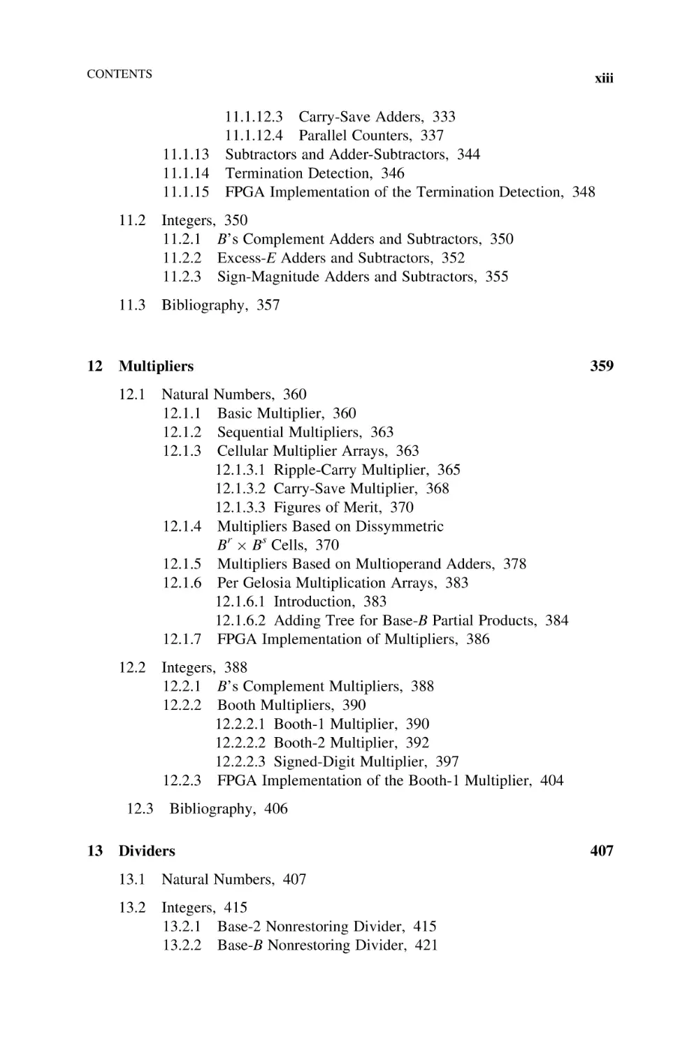
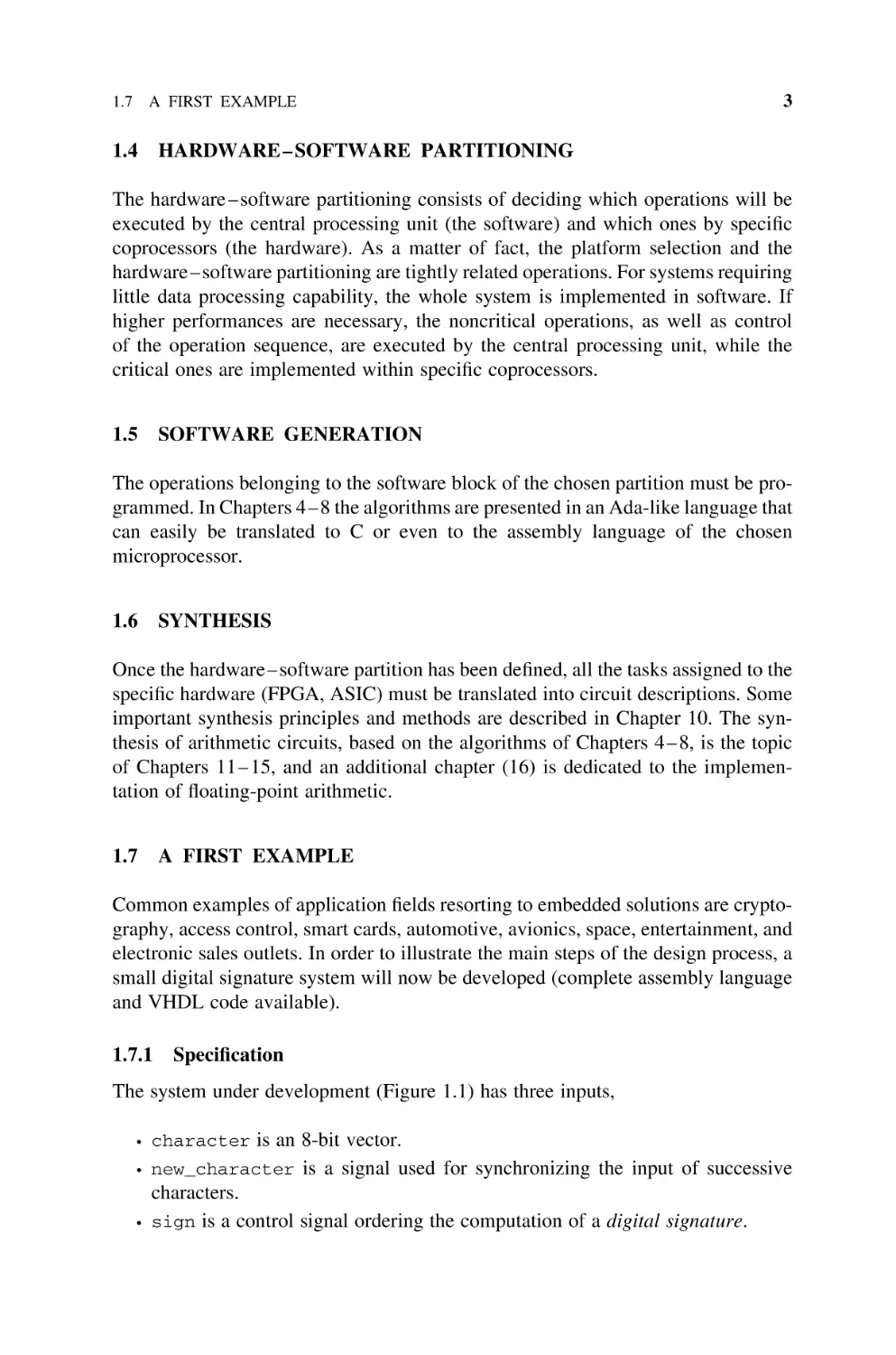
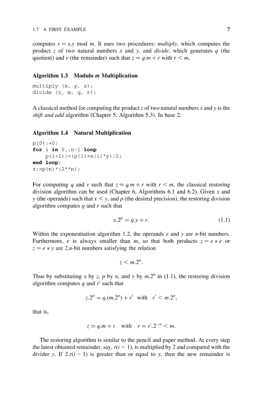
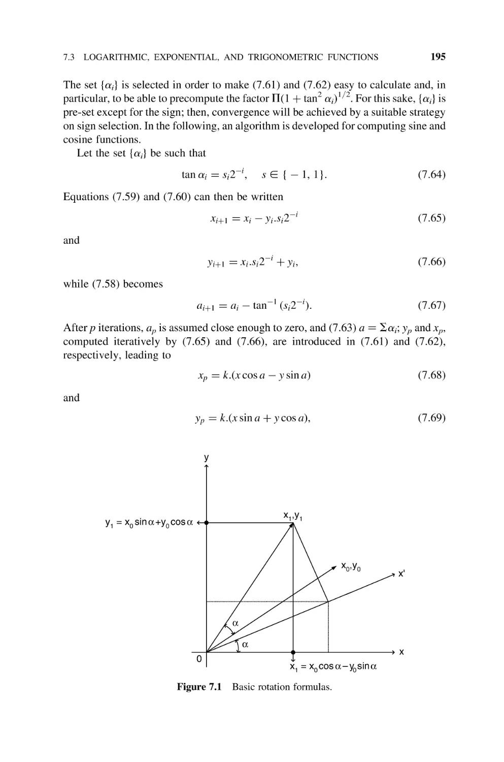
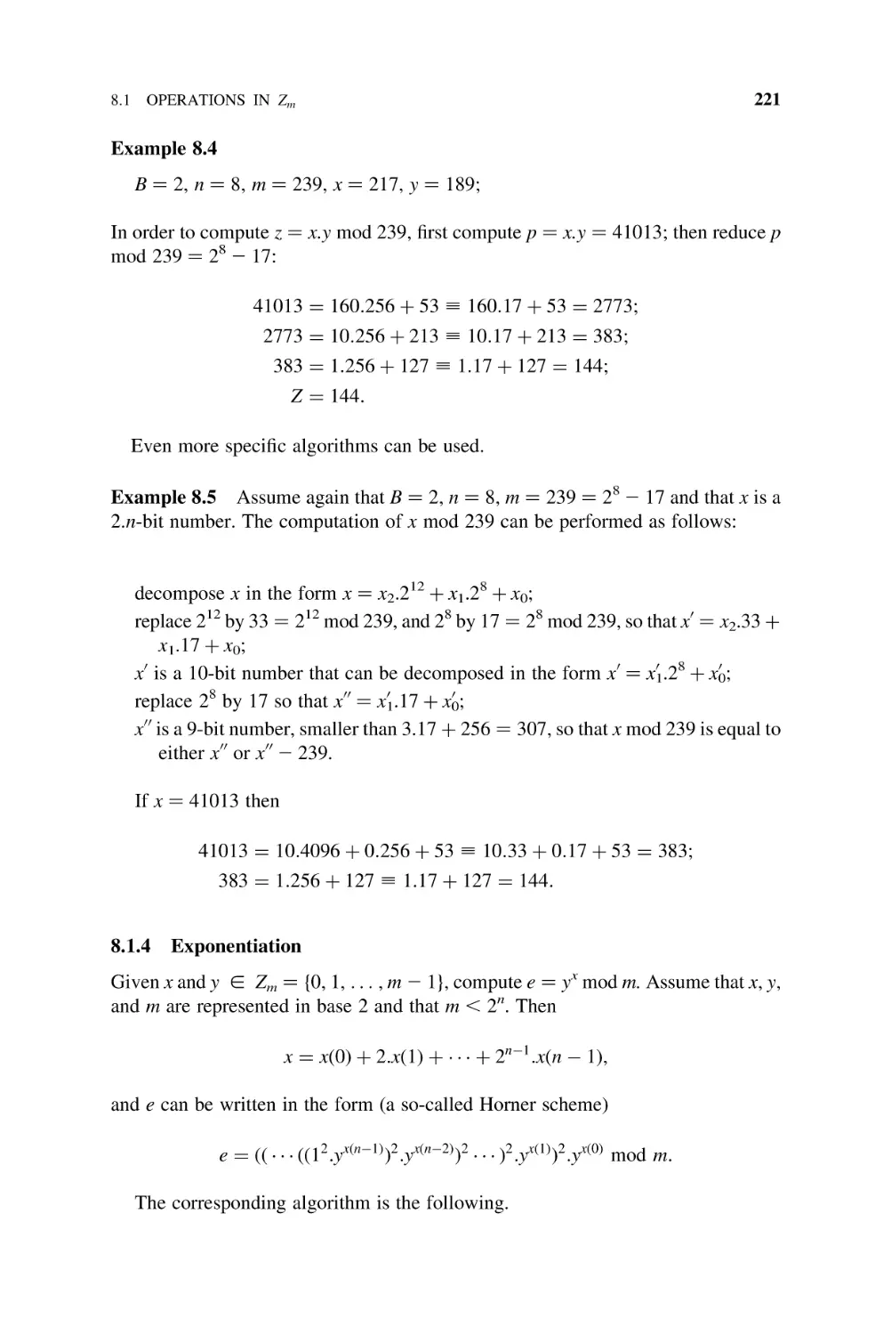
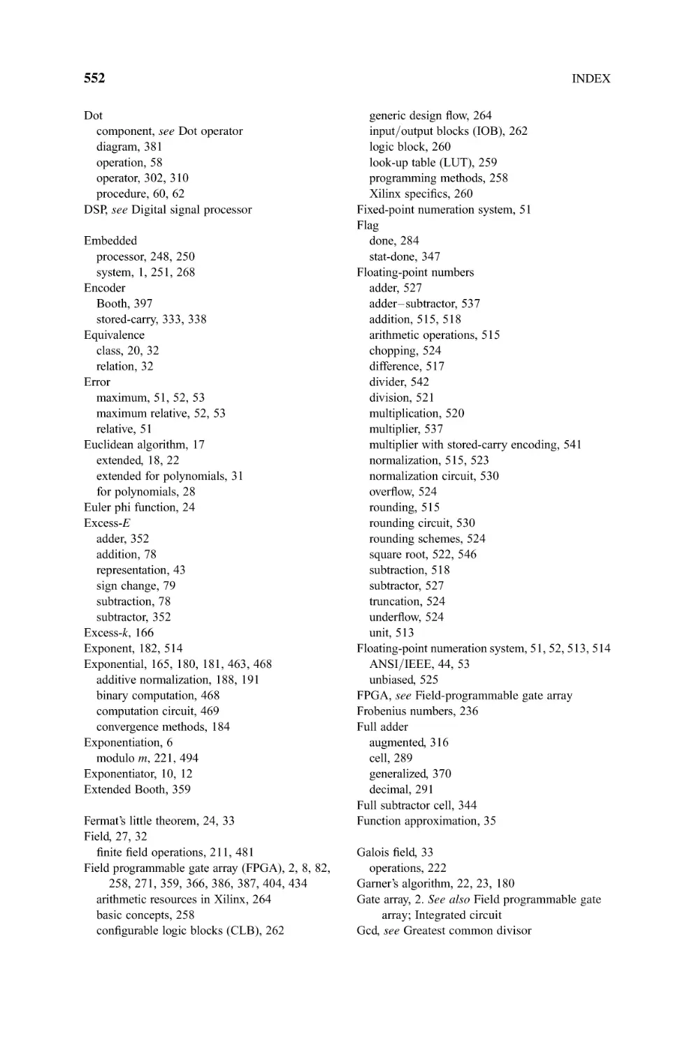
The system under development (Figure 1.1) has three inputs,
.
character is an 8-bit vector.
.
new_character is a signal used for synchronizing the input of successive
.
sign is a control signal ordering the computation of a digital signature.
characters.
4
INTRODUCTION
character
new_character
signature
generator
signature
done
sign
Figure 1.1
System under development.
and two outputs,
.
.
done is a status variable indicating that the signature computation has been
completed,
signature is a 32-bit vector, namely, the signature of the message.
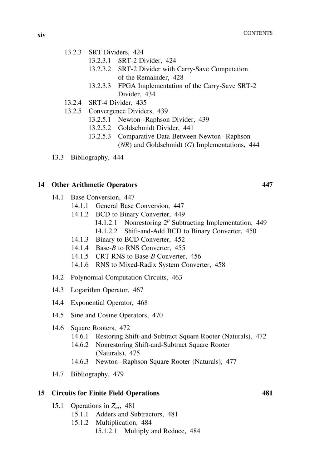
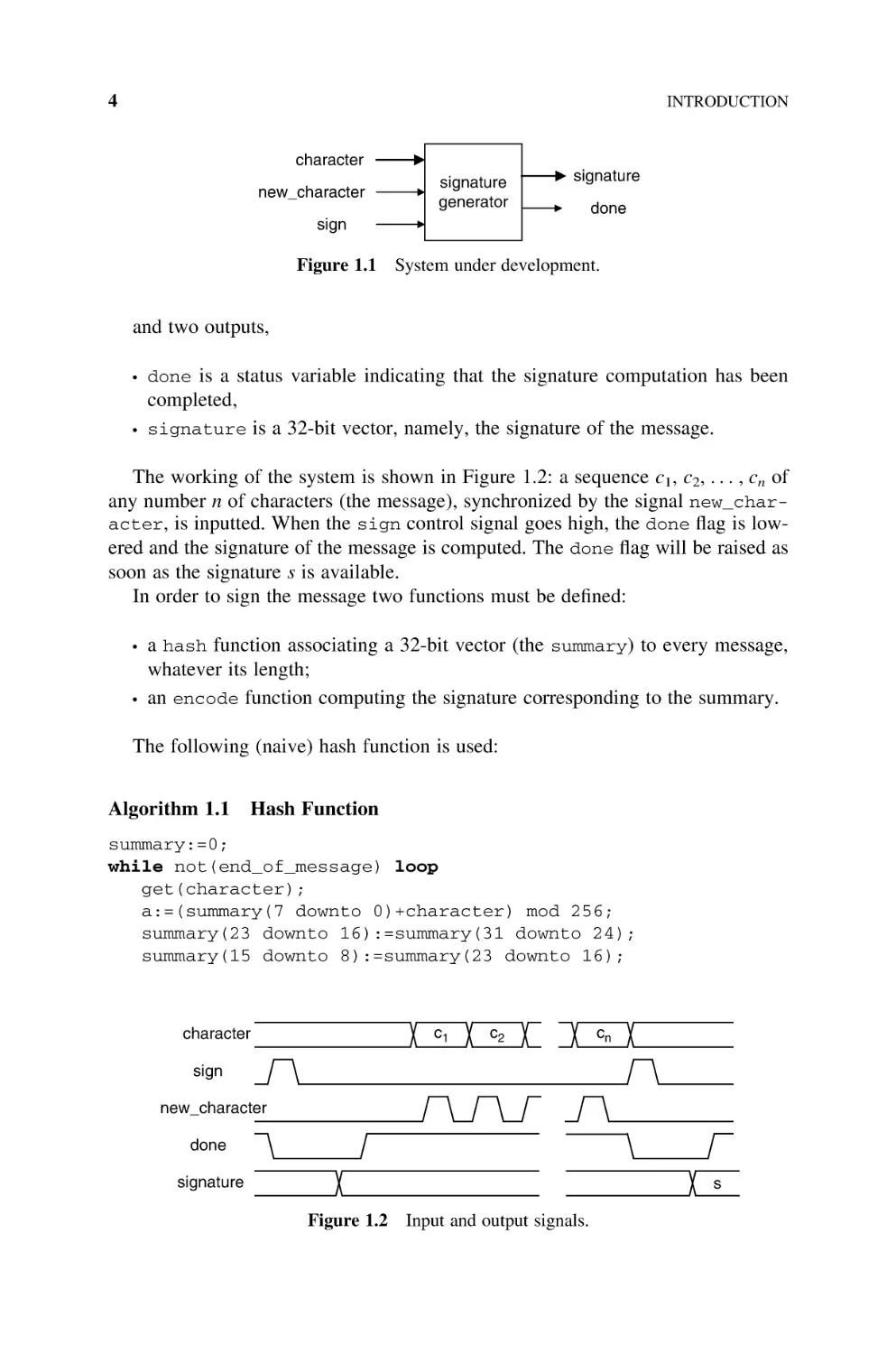
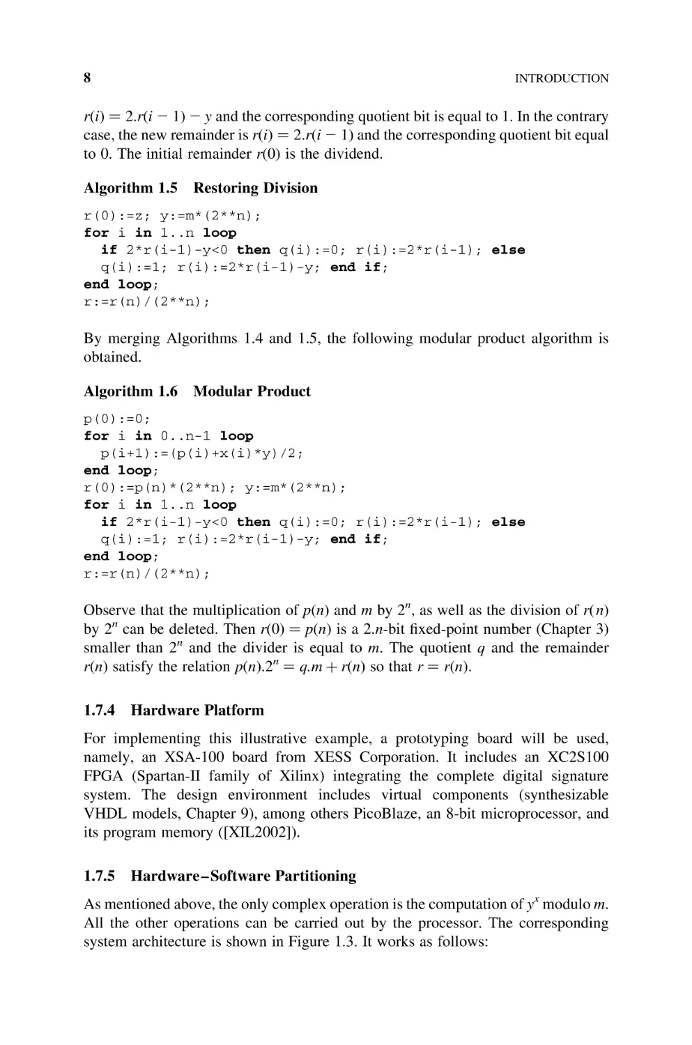
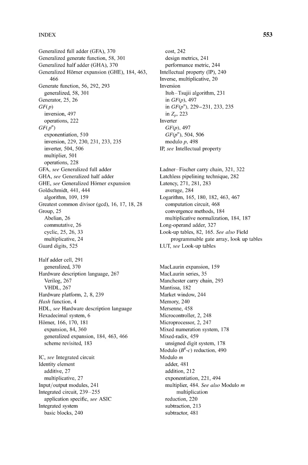
The working of the system is shown in Figure 1.2: a sequence c1, c2, . . . , cn of
any number n of characters (the message), synchronized by the signal new_character, is inputted. When the sign control signal goes high, the done flag is lowered and the signature of the message is computed. The done flag will be raised as
soon as the signature s is available.
In order to sign the message two functions must be defined:
.
.
a hash function associating a 32-bit vector (the summary) to every message,
whatever its length;
an encode function computing the signature corresponding to the summary.
The following (naive) hash function is used:
Algorithm 1.1
Hash Function
summary:=0;
while not(end_of_message) loop
get(character);
a:=(summary(7 downto 0)+character) mod 256;
summary(23 downto 16):=summary(31 downto 24);
summary(15 downto 8):=summary(23 downto 16);
c1
character
c2
cn
sign
new_character
done
signature
s
Figure 1.2
Input and output signals.
5
1.7 A FIRST EXAMPLE
summary(7 downto 0):=summary(15 downto 8);
summary(31 downto 24):=a;
end loop;
As an example, assume that the message is the following (every character can
be equivalently considered as an 8-bit vector or a natural number smaller than
256, i.e. a base-256 digit; see Chapter 3):
12, 45, 216, 1, 107, 55, 10, 9, 34, 72, 215, 114, 13, 13, 229, 18:
The summary is computed as follows:
summary ¼ (0, 0, 0, 0),
summary ¼ (12, 0, 0, 0),
summary ¼ (45, 12, 0, 0),
summary ¼ (216, 45, 12, 0),
summary ¼ (1, 216, 45, 12),
summary ¼ (119, 1, 216, 45),
summary ¼ (100, 119, 1, 216),
summary ¼ (226, 100, 119, 1),
summary ¼ (10, 226, 100, 119),
summary ¼ (153, 10, 226, 100),
summary ¼ (172, 153, 10, 226),
summary ¼ (185, 172, 153, 10),
summary ¼ (124, 185, 172, 153),
summary ¼ (166, 124, 185, 172),
summary ¼ (185, 166, 124, 185),
summary ¼ (158, 185, 166, 124),
summary ¼ (142, 158, 185, 166):
The final result, translated from the base-256 to the decimal representation, is
summary ¼ 142 2563 þ 158 2562 þ 185 256 þ 166 ¼ 2392766886:
The encode function computes
encode(y) ¼ yx mod m
x being some private key, and m a 32-bit number. Assume that
x ¼ 1937757177
and
m ¼ 232 1 ¼ 4294967295:
6
INTRODUCTION
Then the signature of the previous message is
s ¼ (2392766886)1937757177 mod 4294967295 ¼ 37998786:
1.7.2
Number Representation
In this example all the data are either 8-bit vectors (the characters) or 32-bit vectors
(the summary, the key, and the module m). So instead of representing them in the
decimal numeration system, they should be represented in the binary or, equivalently, the hexadecimal system. The message is
0C, 2D, D8, 01, 6B, 37, 0A, 09, 22 48, D7, 72, 0D, 0D, E5, 12:
The summary, the key, the module, and the signature are
summary ¼ 8E9EB9A6,
private key ¼ 737FD3F9,
m ¼ FFFFFFFF,
s ¼ 0243D0C2:
1.7.3
Algorithms
The hash function amounts to a mod-256 addition, that is, a simple 8-bit addition
without output carry. The only complex operation is the mod m exponentiation.
Assume that x, y, and m are n-bit numbers. Then
x ¼ x(0) þ 2:x(1) þ þ 2n1 :x(n 1),
and e can be written in the form
e ¼ (( ((12 :yx(n1) )2 :yx(n2) )2 )2 :yx(1) )2 :yx(0) mod m:
The corresponding algorithm is the following (Chapter 8, Algorithm 8.14).
Algorithm 1.2
Exponentiation
e:=1;
for i in 1..n loop
e:=(e*e) mod m;
if x(n-i)=1 then e:=(e*y) mod m; end if;
end loop;
The only computation primitive is the modulo m product, which, in turn, is
equivalent to a natural multiplication followed by a modulo m reduction, that is,
an integer division by m. The following algorithm (Chapter 8, Algorithm 8.5)
7
1.7 A FIRST EXAMPLE
computes r ¼ x.y mod m. It uses two procedures: multiply, which computes the
product z of two natural numbers x and y, and divide, which generates q (the
quotient) and r (the remainder) such that z ¼ q.m þ r with r , m.
Algorithm 1.3
Modulo m Multiplication
multiply (x, y, z);
divide (z, m, q, r);
A classical method for computing the product z of two natural numbers x and y is the
shift and add algorithm (Chapter 5, Algorithm 5.3). In base 2:
Algorithm 1.4
Natural Multiplication
p(0):=0;
for i in 0..n-1 loop
p(i+1):=(p(i)+x(i)*y)/2;
end loop;
z:=p(n)*(2**n);
For computing q and r such that z ¼ q.m þ r with r , m, the classical restoring
division algorithm can be used (Chapter 6, Algorithms 6.1 and 6.2). Given x and
y (the operands) such that x , y, and p (the desired precision), the restoring division
algorithm computes q and r such that
x:2p ¼ q:y þ r:
(1:1)
Within the exponentiation algorithm 1.2, the operands e and y are n-bit numbers.
Furthermore, e is always smaller than m, so that both products z ¼ e e or
z ¼ e y are 2.n-bit numbers satisfying the relation
z , m:2n :
Thus by substituting x by z, p by n, and y by m.2n in (1.1), the restoring division
algorithm computes q and r0 such that
z:2n ¼ q:(m:2n ) þ r 0 with r 0 , m:2n ,
that is,
z ¼ q:m þ r
with
r ¼ r 0 :2n , m:
The restoring algorithm is similar to the pencil and paper method. At every step
the latest obtained remainder, say, r(i 2 1), is multiplied by 2 and compared with the
divider y. If 2.r(i 2 1) is greater than or equal to y, then the new remainder is
8
INTRODUCTION
r(i) ¼ 2.r(i 2 1) 2 y and the corresponding quotient bit is equal to 1. In the contrary
case, the new remainder is r(i) ¼ 2.r(i 2 1) and the corresponding quotient bit equal
to 0. The initial remainder r(0) is the dividend.
Algorithm 1.5
Restoring Division
r(0):=z; y:=m*(2**n);
for i in 1..n loop
if 2*r(i-1)-y<0 then q(i):=0; r(i):=2*r(i-1); else
q(i):=1; r(i):=2*r(i-1)-y; end if;
end loop;
r:=r(n)/(2**n);
By merging Algorithms 1.4 and 1.5, the following modular product algorithm is
obtained.
Algorithm 1.6
Modular Product
p(0):=0;
for i in 0..n-1 loop
p(i+1):=(p(i)+x(i)*y)/2;
end loop;
r(0):=p(n)*(2**n); y:=m*(2**n);
for i in 1..n loop
if 2*r(i-1)-y<0 then q(i):=0; r(i):=2*r(i-1); else
q(i):=1; r(i):=2*r(i-1)-y; end if;
end loop;
r:=r(n)/(2**n);
Observe that the multiplication of p(n) and m by 2n, as well as the division of r(n)
by 2n can be deleted. Then r(0) ¼ p(n) is a 2.n-bit fixed-point number (Chapter 3)
smaller than 2n and the divider is equal to m. The quotient q and the remainder
r(n) satisfy the relation p(n).2n ¼ q.m þ r(n) so that r ¼ r(n).
1.7.4
Hardware Platform
For implementing this illustrative example, a prototyping board will be used,
namely, an XSA-100 board from XESS Corporation. It includes an XC2S100
FPGA (Spartan-II family of Xilinx) integrating the complete digital signature
system. The design environment includes virtual components (synthesizable
VHDL models, Chapter 9), among others PicoBlaze, an 8-bit microprocessor, and
its program memory ([XIL2002]).
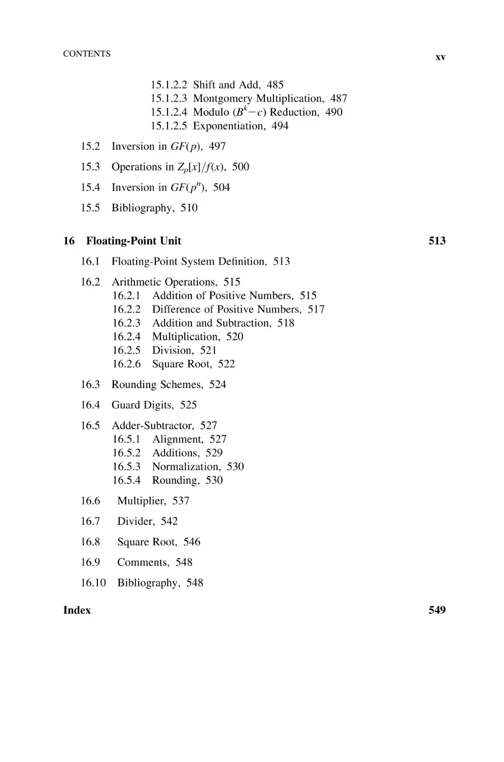
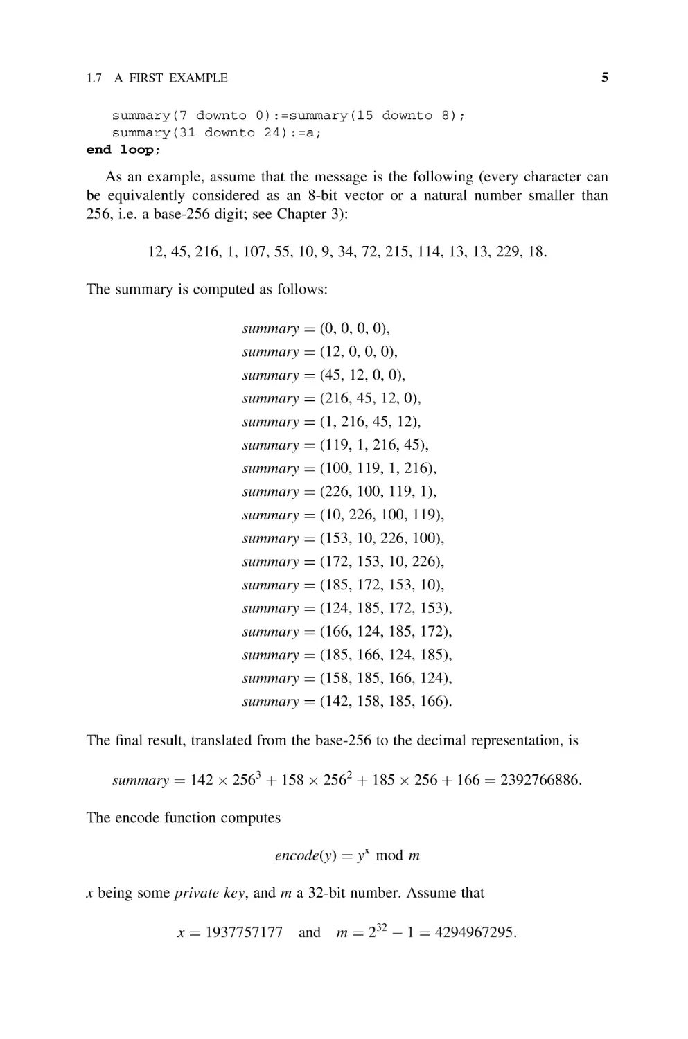
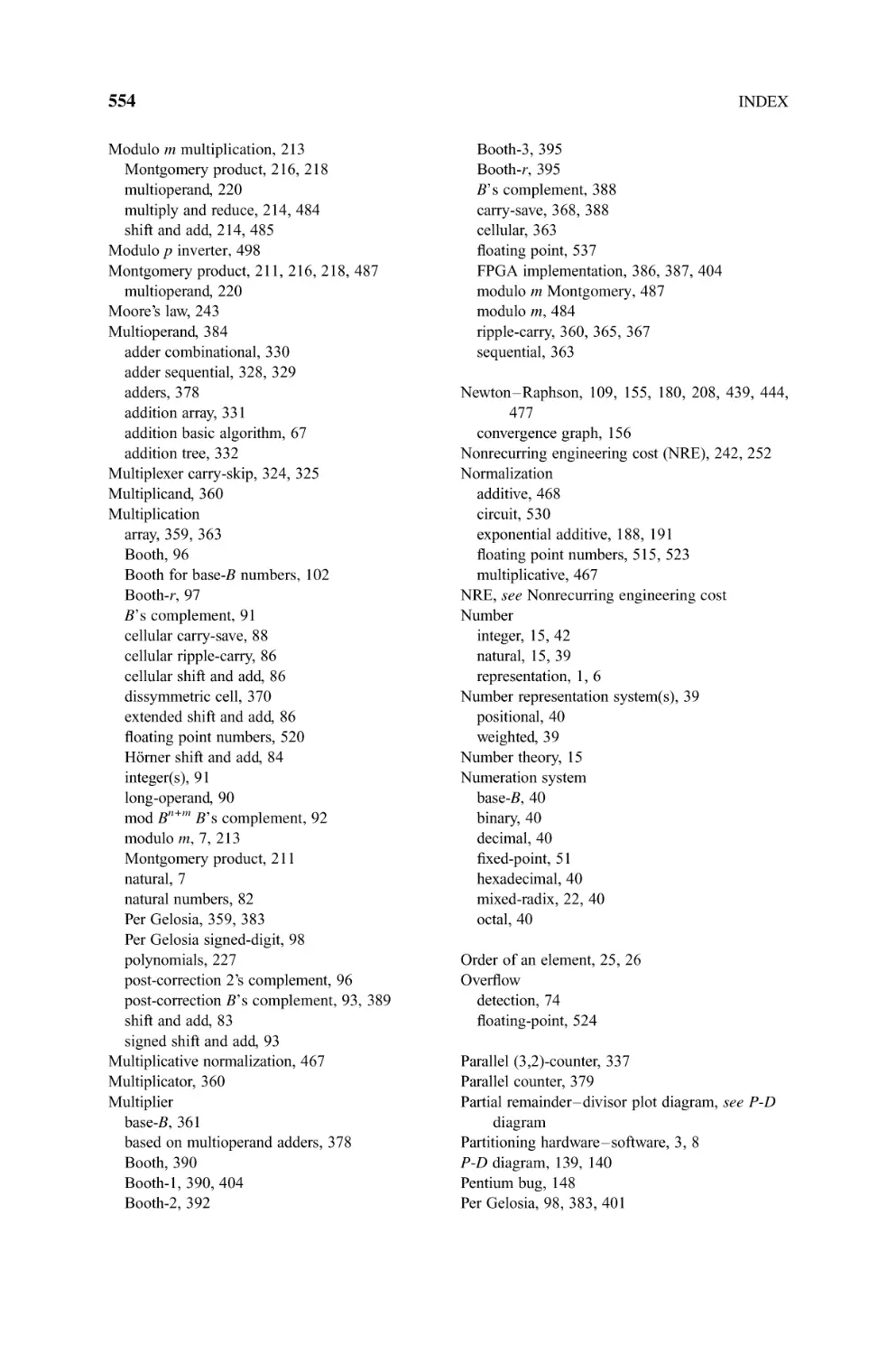
1.7.5
Hardware– Software Partitioning
As mentioned above, the only complex operation is the computation of yx modulo m.
All the other operations can be carried out by the processor. The corresponding
system architecture is shown in Figure 1.3. It works as follows:
9
1.7 A FIRST EXAMPLE
ws and port_id = 3
Y(3)
port_id(0)
character
0
command
1
in_port
PicoBlaze and
program
memory
port_id
out_port
ws
(write_strobe)
ws and port_id = 2
Y(2)
ws and port_id = 1
ws and port_id = 4
signature
exponentiator y
done
done
ws and port_id = 0
Y(3)&Y(2)&Y(1)&Y(0)
x
737FD3F9
m
FFFFFFFF
Figure 1.3
.
out_port(0)
start
z
Y(1)
Y(0)
System architecture.
PicoBlaze reads the character input at address 0 and the command input at
address 1, where
command = 0 0 0 0 0 0 sign new_character.
.
It computes the 32-bit summary and writes it, under the form of four separate
bytes,
summary = Y(3) Y(2) Y(1) Y(0),
.
into four registers whose addresses are 3, 2, 1 and 0, respectively.
A specific coprocessor receives the start signal from PicoBlaze at address 4,
computes
s =(summary)737FD3F9 mod FFFFFFFF,
and generates the done flag.
1.7.6
Program Generation
The program executed by PicoBlaze is made up of three parts (assembly language
code available):
.
.
.
reading of the new_character and sign input signals,
reading of the character input and updating of the summary,
writing of the summary and of the start command within the interface
registers:
10
INTRODUCTION
summary:=(0, 0, 0, 0);
start:=0;
loop
--wait for command=0
while command>0 loop null; end loop;
--wait for command=1 (new_character) or 2 (sign)
while command=0 loop null; end loop;
if command=1 then
a:=(summary(0)+character) mod 256;
summary(0):=summary(1);
summary(1):=summary(2);
summary(2):=summary(3);
summary(3):=a;
elsif command=2 then
Y(3):=summary(3);
Y(2):=summary(2);
Y(1):=summary(1);
Y(0):=summary(0);
start:=1;
summary:=(0, 0, 0, 0);
start:=0;
end if;
end loop;
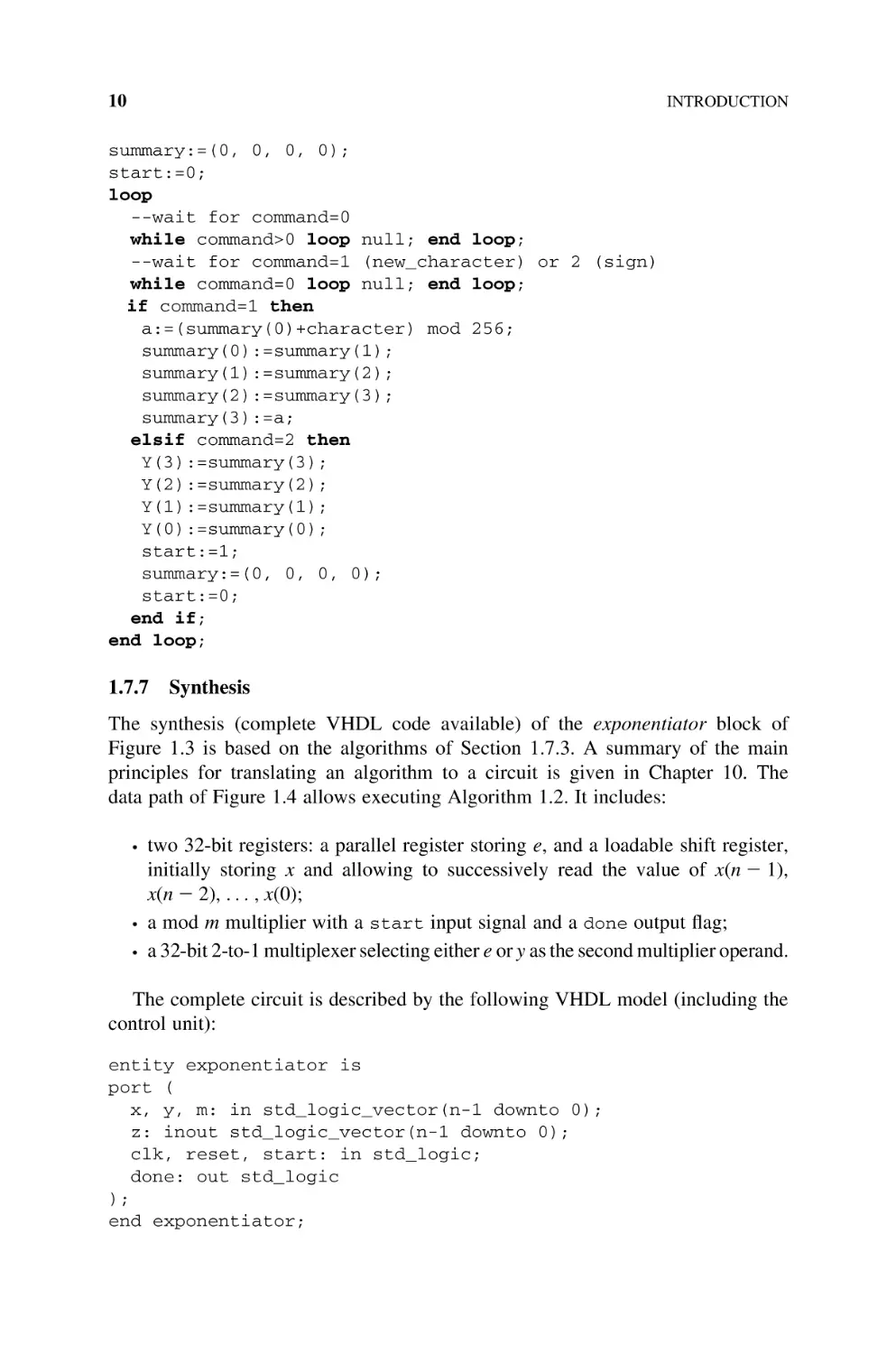
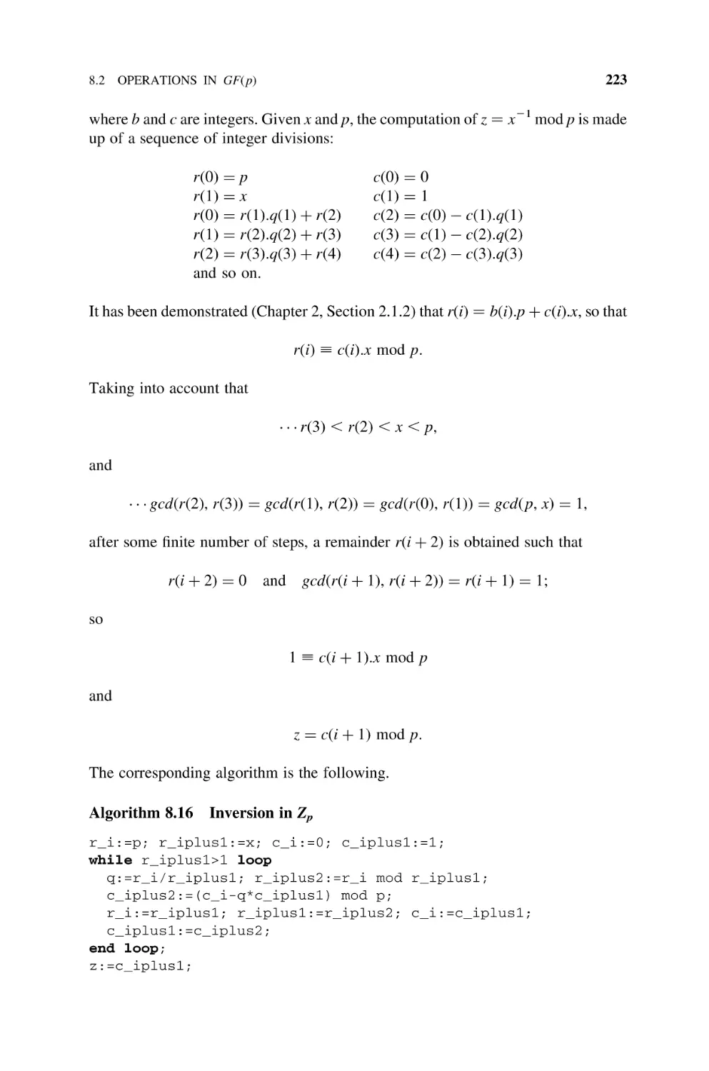
1.7.7
Synthesis
The synthesis (complete VHDL code available) of the exponentiator block of
Figure 1.3 is based on the algorithms of Section 1.7.3. A summary of the main
principles for translating an algorithm to a circuit is given in Chapter 10. The
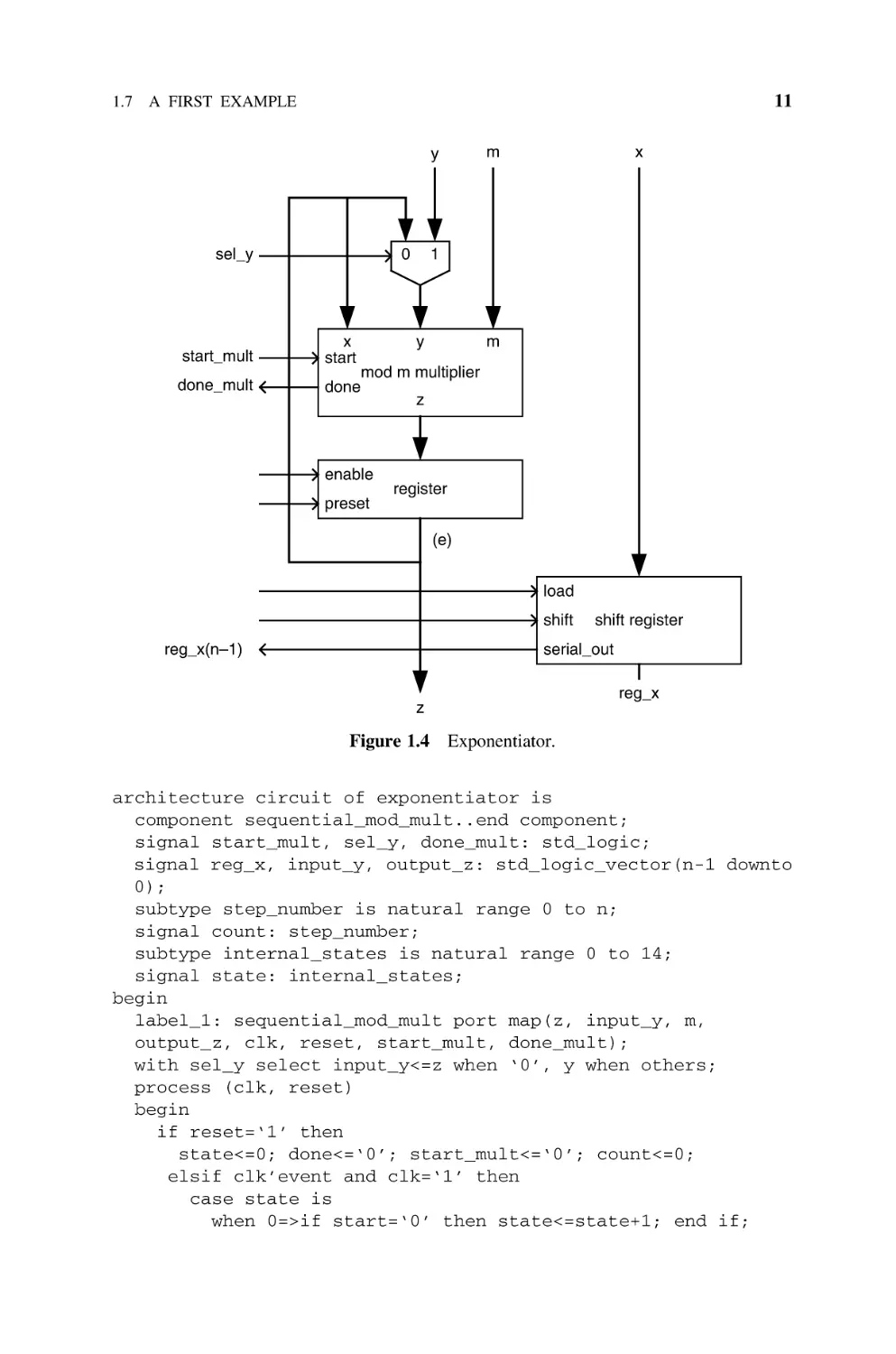
data path of Figure 1.4 allows executing Algorithm 1.2. It includes:
.
.
.
two 32-bit registers: a parallel register storing e, and a loadable shift register,
initially storing x and allowing to successively read the value of x(n 2 1),
x(n 2 2), . . . , x(0);
a mod m multiplier with a start input signal and a done output flag;
a 32-bit 2-to-1 multiplexer selecting either e or y as the second multiplier operand.
The complete circuit is described by the following VHDL model (including the
control unit):
entity exponentiator is
port (
x, y, m: in std_logic_vector(n-1 downto 0);
z: inout std_logic_vector(n-1 downto 0);
clk, reset, start: in std_logic;
done: out std_logic
);
end exponentiator;
11
1.7 A FIRST EXAMPLE
0
sel_y
start_mult
done_mult
x
start
x
m
y
1
m
y
mod m multiplier
done
z
enable
preset
register
(e)
load
shift
reg_x(n–1)
shift register
serial_out
reg_x
z
Figure 1.4
Exponentiator.
architecture circuit of exponentiator is
component sequential_mod_mult..end component;
signal start_mult, sel_y, done_mult: std_logic;
signal reg_x, input_y, output_z: std_logic_vector(n-1 downto
0);
subtype step_number is natural range 0 to n;
signal count: step_number;
subtype internal_states is natural range 0 to 14;
signal state: internal_states;
begin
label_1: sequential_mod_mult port map(z, input_y, m,
output_z, clk, reset, start_mult, done_mult);
with sel_y select input_y<=z when ‘0’, y when others;
process (clk, reset)
begin
if reset=‘1’ then
state<=0; done<=‘0’; start_mult<=‘0’; count<=0;
elsif clk’event and clk=‘1’ then
case state is
when 0=>if start=‘0’ then state<=state+1; end if;
12
INTRODUCTION
when 1=>if start=‘1’ then state<=state+1; end if;
when 2=>z<=conv_std_logic_vector(1, n);
reg_x<=x; count<=0; done<=‘0’; state<=state+1;
when 3=>
sel_y<=‘0’; start_mult<=‘1’; state<=state+1;
when 4=>state<=state+1;
when 5=>start_mult<=‘0’; state<=state+1;
when 6=>
if done_mult=‘1’ then state<=state+1; end if;
when 7=>z<=output_z;
if reg_x(n-1)=‘1’ then state<=state+1;
else state<=13; end if;
when 8=>
sel_y<=‘1’; start_mult<=‘1’; state<=state+1;
when 9=>state<=state+1;
when 10=>start_mult<=‘0’; state<=state+1;
when 11=>
if done_mult=‘1’ then state<=state+1; end if;
when 12=>z<=output_z; state<=state+1;
when 13=>reg_x(0)<=reg_x(n-1);
for i in 1 to n-1 loop reg_x(i)<=reg_x(i-1);
end loop;
count<=count+1; state<=state+1;
when 14=>
if count>=n then done<=‘1’; state<=0;
else state<=3; end if;
end case;
end if;
end process;
end circuit;
1.7.8
Prototype
All the files (complete source files available) necessary for programming an XSA100 board are included in the file section1_7.zip:
.
exponentiator.vhd is the complete description of the exponentiation circuit
.
signatu.psm is the assembly language program;
.
kpcsm.vhd is the PicoBlaze model;
.
signatu.vhd is the program memory model generated from the assembly
language program with kcpsm.exe (the PicoBlaze assembler released by
(including the modular multiplier model);
Xilinx [XIL2002]).
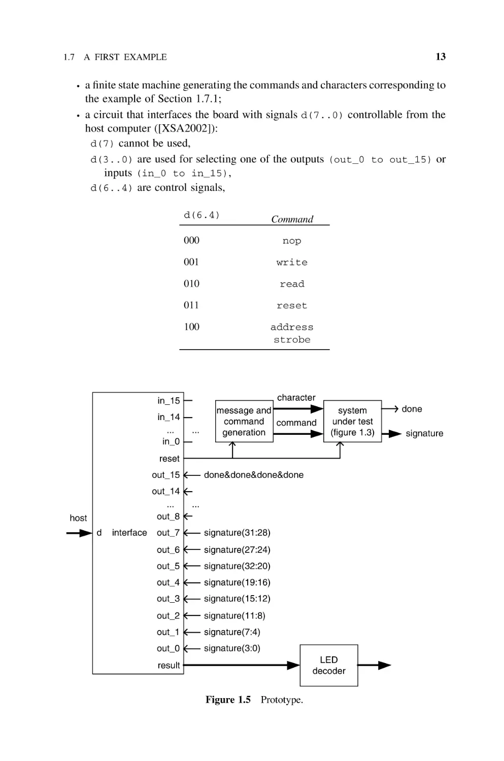
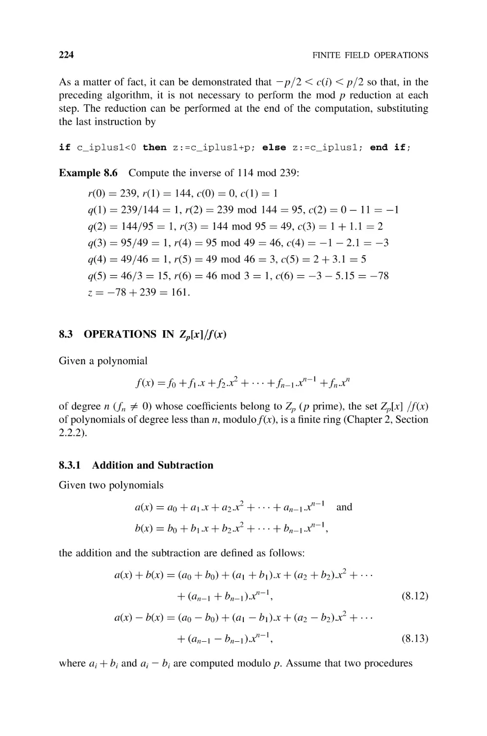
In order to test the complete system, the circuit of Figure 1.5 has been
synthesized. It is made up of:
.
the circuit of Figure 1.3 including PicoBlaze, its program memory, the interface
registers, and the exponentiator;
13
1.7 A FIRST EXAMPLE
.
.
a finite state machine generating the commands and characters corresponding to
the example of Section 1.7.1;
a circuit that interfaces the board with signals d(7..0) controllable from the
host computer ([XSA2002]):
d(7) cannot be used,
d(3..0) are used for selecting one of the outputs (out_0 to out_15) or
inputs (in_0 to in_15),
d(6..4) are control signals,
d(6.4)
000
nop
001
write
010
read
011
reset
100
address
strobe
in_15
in_14
...
in_0
Command
...
character
message and
command command
generation
system
under test
(figure 1.3)
reset
done&done&done&done
out_15
out_14
...
out_8
host
d
interface
...
out_7
signature(31:28)
out_6
signature(27:24)
out_5
signature(32:20)
out_4
signature(19:16)
out_3
signature(15:12)
out_2
signature(11:8)
out_1
signature(7:4)
out_0
signature(3:0)
LED
decoder
result
Figure 1.5 Prototype.
done
signature
14
INTRODUCTION
.
in this application the write and address strobe commands are not used;
when the read command is active, the hexadecimal representation of the 4-bit
vector selected with d(3..0) is displayed on the LED of the board;
the 7-segment LED decoder.
The VHDL model of the circuit of Figure 1.5 (firma.vhd) is also included in
section1_7.zip as well as the file describing the pin assignment (pines.ucf).
The whole system (Figure 1.5) can be synthesized with ISE, the synthesis program
of Xilinx, and downloaded to the XSA-100 board.
1.8
BIBLIOGRAPHY
[DEM2002] G. De Micheli, R. Ernst, and W. Wolf (eds.), Readings in Hardware/Software
Co-Design, Morgan Kaufmann Publishers, San Francisco, CA, 2002.
[GAJ1994] D. D. Gajski, F. Vahid, S. Narayan, and J. Gong, Specification and Design of
Embedded Systems, Prentice Hall, Englewood Cliffs, NJ, 1994.
[XIL2002] Xilinx Inc, PicoBlaze 8-bit Microcontroller for Virtex-E and Spartan-II/IIE
Devices, application note XAPP213 (v2.0), Dec. 2002; http://www.xilinx.com
[XSA2002] XSA Board V1.1, V1.2 User Manual, June 2002; http://www.xess.com.
2
MATHEMATICAL BACKGROUND
This chapter presents some topics in mathematics; it is intended to make this
book self-contained. For further details the reader is referred to textbooks on
algebra ([COH1993], [GIL2003], [HER1975], [HUN1974]), mathematical analysis
([APO1974], [RUD1976]), number theory ([KOB1994], [ROS1992]), finite fields
([McC1987]), and cryptography ([MEN1996]).
2.1
2.1.1
NUMBER THEORY
Basic Definitions
Definitions 2.1
1. The set of natural numbers1 N ¼ f0, 1, 2, 3, . . .g.
2. The set of integers Z ¼ f . . . , 23, 22, 21, 0, 1, 2, 3, . . . g.
Definition 2.2 Given two integers x and y, y divides x (y is a divisor of x) if there
exists an integer z such that x ¼ z.y.
1
For convenience, the element zero has been included in N.
Synthesis of Arithmetic Circuits: FPGA, ASIC, and Embedded Systems
By Jean-Pierre Deschamps, Géry J. A. Bioul, and Gustavo D. Sutter
Copyright # 2006 John Wiley & Sons, Inc.
15
16
MATHEMATICAL BACKGROUND
Definition 2.3 Given two integers x and y, with y . 0, there exist two integers q
(the quotient) and r (the remainder) such that
x ¼ q:y þ r,
where
0 r , y:
It can be proved that q and r are unique. Then (notation)
r ¼ x mod y,
q ¼ x div y:
An alternative definition is the following.
Definition 2.4 (Integer Division) Given two integers x and y, with y . 0, there
exist two integers q (the quotient) and r (the remainder) such that
x ¼ q:y þ r,
where
0 r , y if x 0 and
y , r 0 if x , 0:
It can be proved that q and r are unique. Then (notation)
r ¼ x rem y,
q ¼ x=y:
Examples 2.1
1. x ¼ 216, y ¼ 3:
16 mod 3 ¼ 2, 16 div 3 ¼ 6, 16 ¼ 6:3 þ 2,
16 rem 3 ¼ 1, 16=3 ¼ 5, 16 ¼ 5:3 þ ( 1)
2. x ¼ 215, y ¼ 3:
15 mod 3 ¼ 0, 15 div 3 ¼ 5, 15 ¼ 5:3 þ 0,
15 rem 3 ¼ 0, 15=3 ¼ 5, 15 ¼ 5:3 þ 0:
Definitions 2.5
1. Given two integers x and y, z is the greatest common divisor of x and y if
z is a natural number (nonnegative integer),
z divides both x and y,
any other common divider of x and y is also a divider of z.
Notation: z ¼ gcd(x, y).
2. Given two integers x and y, they are said to be relatively prime if gcd(x,
y) ¼ 1.
3. An integer p . 1 is said to be prime if its only positive divisors are 1 and p.
17
2.1 NUMBER THEORY
2.1.2
Euclidean Algorithms
Given two natural numbers x and y, the Euclidean algorithm for natural numbers
computes gcd(x, y). It is based on a series of integer divisions:
r(i 1) ¼ q(i):r(i) þ r(i þ 1),
where
0 r(i þ 1) , r(i):
Observe that any divider of r(i 2 1) and r(i) is also a divider of r(i) and r(i þ 1)
so that
gcd(r(i 1), r(i)) ¼ gcd(r(i), r(i þ 1)):
Initially,
r(0) ¼ x and
r(1) ¼ y:
Then compute
r(0) ¼ q(1):r(1) þ r(2),
r(1) ¼ q(2):r(2) þ r(3),
r(2) ¼ q(3):r(3) þ r(4),
...
r(n 3) ¼ q(n 2):r(n 2) þ r(n 1),
r(n 2) ¼ q(n 1):r(n 1) þ r(n),
where r(1) . rð2Þ . r(n) ¼ 0 and gcd(r(i 2 1), r(i)) ¼ gcd(r(i), r(i þ 1)), so that
gcd(x, y) ¼ gcd(r(0), r(1)) ¼ ¼ gcd(r(n 1), r(n)) ¼ gcd(r(n 1), 0)
¼ r(n 1):
Example 2.2
Let r(0) ¼ x ¼ 8580; r(1) ¼ y ¼ 4070;
8580 ¼ 2:4070 þ 440
4070 ¼ 9:440 þ 110
440 ¼ 4:110 þ 0
Then gcd(8580,4070) ¼ 110.
18
MATHEMATICAL BACKGROUND
In the extended Euclidean algorithm a series of coefficients b(i) and c(i) are
calculated in parallel with the computation of r(0), r(1), r(2), . . . , r(n):
b(0) ¼ 1,
c(0) ¼ 0,
b(1) ¼ 0,
c(1) ¼ 1,
b(2) ¼ b(0) b(1):q(1),
c(2) ¼ c(0) c(1):q(1),
...
...
b(n 1) ¼ b(n 3) b(n 2):q(n 2), c(n 1) ¼ c(n 3) c(n 2):q(n 2)
It can be demonstrated by induction that
r(i) ¼ b(i):x þ c(i):y, 8 i ¼ 0, 1, 2, . . . , n 1:
In particular,
gcd(x,y) ¼ r(n 1) ¼ b(n 1): x þ c(n 1):y:
In conclusion, the extended Euclidean algorithm expresses the greatest common
divisor z of two natural numbers x and y as a linear combination of x and y, that is,
z ¼ b: x þ c:y:
Algorithm 2.1
Extended Euclidean Algorithm
if x=0 then z:=y; b:=0; c:=1;
elsif y=0 then z:=x; b:=1; c:=0;
else
r_i:=x; r_iplus1:=y; b_i:=1; c_i:=0; b_iplus1:=0;
c_iplus1:=1;
while r_iplus1>0 loop
q:=r_i/r_iplus1; r_iplus2:=r_i mod r_iplus1;
b_iplus2:=b_i-b_iplus1*q; c_iplus2:=c_i-c_iplus1*q;
r_i:=r_iplus1; r_iplus1:=r_iplus2;
b_i:=b_iplus1; b_iplus1:=b_iplus2;
c_i:=c_iplus1; c_iplus1:= c_iplus2;
end loop;
z:=r_i; b:=b_i; c:=c_i;
end if;
Example 2.3 Let ri ¼ x ¼ 230490; riþ1 ¼ y ¼ 43290; bi ¼ ciþ1 ¼ 1;
biþ1 ¼ ci ¼ 0.
(2:1)
19
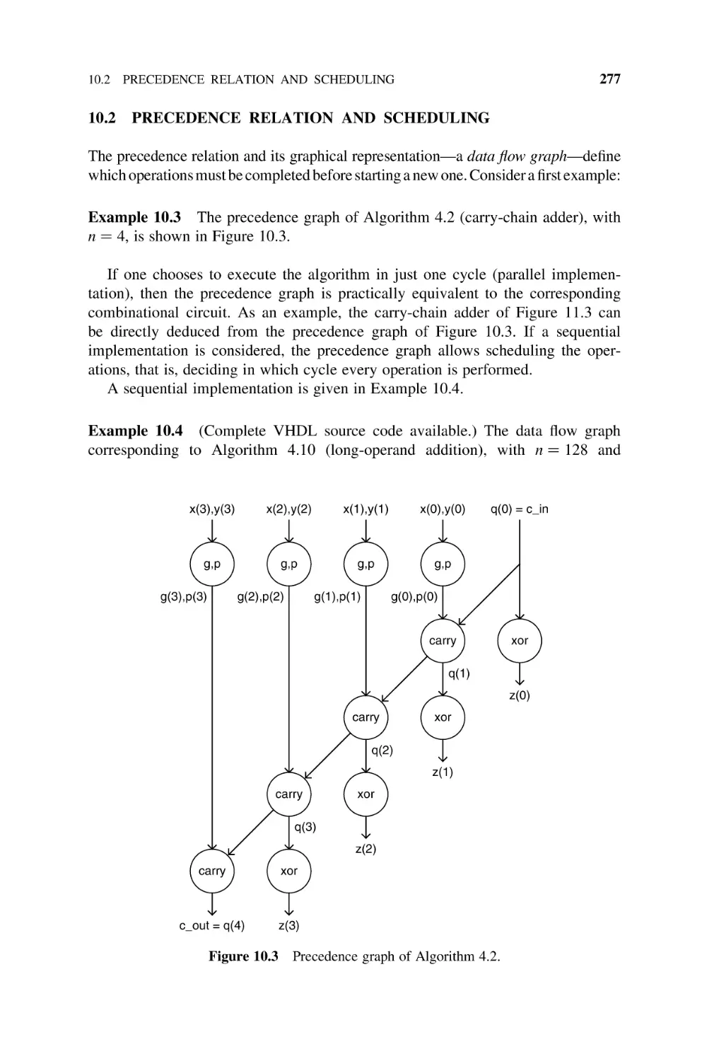
2.1 NUMBER THEORY
Step 1:
q ¼ 230490=43290 ¼ 5; riþ2 ¼ 230490 mod 43290 ¼ 14040;
biþ2 ¼ 1 0 5 ¼ 1; ciþ2 ¼ 0 1 5 ¼ 5;
ri ¼ 43290; riþ1 ¼ 14040;
bi ¼ 0;
biþ1 ¼ 1;
ci ¼ 1;
ciþ1 ¼ 5;
Step 2:
q ¼ 43290=14040 ¼ 3; riþ2 ¼ 43290 mod 14040 ¼ 1170;
biþ2 ¼ 0 1 3 ¼ 3; ciþ2 ¼ 1 þ 5 3 ¼ 16;
ri ¼ 14040; riþ1 ¼ 1170;
bi ¼ 1;
biþ1 ¼ 3;
ci ¼ 5;
ciþ1 ¼ 16;
Step 3:
q ¼ 14040=1170 ¼ 12;
biþ2 ¼ 1 þ 3 12 ¼ 37;
riþ2 ¼ 14040 mod 1170 ¼ 0;
ciþ2 ¼ 5 16 12 ¼ 197;
ri ¼ 1170;
bi ¼ 3;
riþ1 ¼ 0;
biþ1 ¼ 37;
ci ¼ 16;
ciþ1 ¼ 197;
b ¼ bi ¼ 3; c ¼ ci ¼ 16; gcd(230490, 432900) ¼ z ¼ ri ¼ 1170
¼ 3 230490 þ 16 43290
2.1.3
Congruences
Definition 2.6 Given two integers x and y, and a positive integer n, x is congruent
to y modulo n if n divides the difference (x 2 y).
Notation:
x ; y(mod n):
Property 2.1 (Basic Properties of Congruences)
1. x ; y (mod n) if and only if (x mod n) ¼ (y mod n) (Definition 2.3).
2. The relation x ; y (mod n) is an equivalence relation (reflexive, symmetric,
and transitive).
20
MATHEMATICAL BACKGROUND
3. If x1 ; y1 (mod n) and x2 ; y2 (mod n), then
(x1 þ x2 ) ; (y1 þ y2 )(mod n),
(x1 x2 ) ; (y1 y2 )(mod n),
(x1 :x2 ) ; (y1 :y2 )(mod n):
(2:2)
From Properties 2.1(1 and 2), it can be seen that the mod n congruence relation
partitions Z into n equivalence classes. Each equivalence class contains exactly
one element of the set f0, 1, 2, . . . , n 2 1g, namely, the common value (x mod n)
for all elements x of the class. Furthermore, according to Property 2.1(3), the
addition, subtraction, and multiplication of congruence classes can be defined. As
a matter of fact, the set of equivalence classes is isomorphic to
Zn ¼ {0, 1, 2, . . . , n 1}
where the addition, the subtraction, and the multiplication are defined by
(x þ y) mod n, (x y) mod n, (x:y) mod n,
8 x and y in Zn :
Definition 2.7 Given two elements x and y of Zn, such that x.y ¼ 1, then y is said to
be the multiplicative inverse of x. If such an inverse exists, it is unique.
Notation:
y ¼ x1 :
Property 2.2
x has a multiplicative inverse if and only if gcd(x, n) ¼ 1.
Proof If x.y ¼ 1 mod n, then x.y ¼ q.nþ1 so that any divisor of x and n is also a
divisor of 1. Thus gcd(x, n) ¼ 1.
If gcd(x, n) ¼ 1, then (relation (2.1)) there exist b and c such that 1 ¼ b.x þ c.n, so
that x21 ¼ b.
More generally, we have the following.
Properties 2.3
1. Let g ¼ gcd(a, n). Then the equation a.x ; d (mod n) has a solution x if and
only if g divides d.
2. The solutions of a.x ; d (mod n) are the same as the solutions of
(a/g).x ; (d/g) (mod n/g).
3. There are g solutions, all of them congruent modulo n/g.
Proof
1. If ax ; d (mod n), then a.x 2 d ¼ q.n. As g divides both a and n, it also
divides d. If g divides d, then d ¼ q.g. According to (2.1), g is a linear
21
2.1 NUMBER THEORY
combination of a and n; that is, g ¼ b.a þ c.n. So d ¼ q(b.a þ c.n) and x ¼ q.b
is a solution.
2. If g divides d and a.x ; d (mod n), that is, a.x 2 d ¼ q.n, then (a/g).x 2
(d/g) ¼ q.(n/g) and (a/g).x ; (d/g) (mod n/g). Inversely, if (a/g).x ;
(d/g) (mod n/g) then a.x ; d (mod n).
3. As a/g and n/g are relatively prime, then there is a unique solution within
Zn/g, namely, x ¼ x0 ¼ (d/g).(a/g)21 mod n/g. The complete set of solutions
within Zn is
xk ¼ x0 þ k:(n=g),
8k ¼ 0, 1, . . . , g 1:
Observe that if k , g and x0 , (n/g), then xk (n/g) 2 1 þ (g 2 1).(n/g)
¼ n 2 1.
Properties 2.4 (Chinese Remainder Theorem) Consider s pairwise relatively
prime integers m1, m2, . . . , ms whose product is equal to M. Then the system
N ; r1 (mod m1 ),
N ; r2 (mod m2 ),
...
N ; rs (mod ms ),
(2:3)
has a unique solution N within ZM (jajm stands for a mod m):
N ¼ S1is mi :jri =mi jmi
M
,
(2:4)
where
M ¼ P1is mi ;
mi ¼ M=mi :
(2:5)
The ri are called residues modulo mi.
Proof In order to compute a solution of system (2.3) observe that every mi is
relatively prime with every mj ( j = i) so that every mj is relatively prime with mj ¼
M/mj. Then mj has a multiplicative inverse and
N ¼ (m1 ):(r1 =m1 ) mod m1 þ (m2 ):(r2 =m2 ) mod m2 þ
þ (ms ):(rs =ms ) mod ms ,
(2:6)
is obviously a solution. The uniqueness is deduced from the fact that different systems have different solutions, and that there are exactly as many different systems as
elements in ZM.
22
MATHEMATICAL BACKGROUND
The computation of (mi )21mod mi can be performed with the extended Euclidean
algorithm: as mi is relatively prime with M/mj, the algorithm generates b and c such that
1 ¼ b:mi þ c:(M=mj ),
and
(mi )1 ¼ c mod mi :
Garner’s algorithm 2.2 ([GAR1959], [MEN1996]) computes N using a technique
slightly different from the straight computation of (2.4). It computes first the
mixed-radix digits within a preliminary step of a procedure step computing the
base-B digits through a mixed-radix to base-B conversion (see mixed-radix system—
Chapter 3).
A procedure inversion_step using the Euclidean algorithm to compute (mj)21
mod mi is first defined as
procedure inversion_step (m(j), m(i): in natural; invm(j): out
natural);
Algorithm 2.2
Garner’s Algorithm
Assume N is given, according to (2.3), by its set of residues ri ¼ N mod mi:
for i in 2..s loop
c(i):=1;
for j in 1..(i-1) loop
inversion_step (m(j), m(i), invm(j));
c(i):=invm(j)*c(i) mod m(i);
end loop;
end loop;
u:=r(1); x:=u; b(1):=1;
for i in 2..s loop
b(i):=b(i-1)*m(i-1);
end loop;
for i in 2..s loop
u:=(r(i) 2 x)*c(i) mod m(i);
x:=x+u*b(i);
end loop;
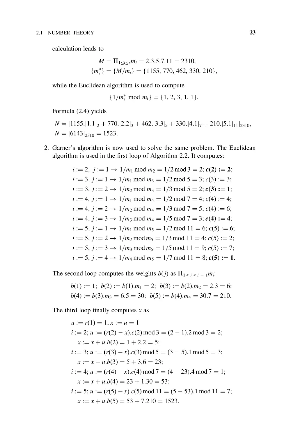
Examples 2.4
1. Let frig ¼ f1, 2, 3, 4, 5g be the set of remainders (residual expression) of a
natural number N with respect to the respective set of moduli fmig ¼ f2, 3,
5, 7, 11g. To compute the base-10 expression of N using (2.4), one first
needs to compute fmi g and f1/mi mod mig. A straightforward base-10
23
2.1 NUMBER THEORY
calculation leads to
M ¼ P1is mi ¼ 2:3:5:7:11 ¼ 2310,
{mi } ¼ {M=mi } ¼ {1155, 770, 462, 330, 210},
while the Euclidean algorithm is used to compute
{1=mi mod mi } ¼ {1, 2, 3, 1, 1}:
Formula (2.4) yields
N ¼ j1155:j1:1j2 þ 770:j2:2j3 þ 462:j3:3j5 þ 330:j4:1j7 þ 210:j5:1j11 j2310 ,
N ¼ j6143j2310 ¼ 1523:
2. Garner’s algorithm is now used to solve the same problem. The Euclidean
algorithm is used in the first loop of Algorithm 2.2. It computes:
i :¼ 2; j :¼ 1 ! 1=m1 mod m2 ¼ 1=2 mod 3 ¼ 2; cð2Þ :¼ 2;
i :¼ 3; j :¼ 1 ! 1=m1 mod m3 ¼ 1=2 mod 5 ¼ 3; cð3Þ :¼ 3;
i :¼ 3; j :¼ 2 ! 1=m2 mod m3 ¼ 1=3 mod 5 ¼ 2; cð3Þ :¼ 1;
i :¼ 4; j :¼ 1 ! 1=m1 mod m4 ¼ 1=2 mod 7 ¼ 4; cð4Þ :¼ 4;
i :¼ 4; j :¼ 2 ! 1=m2 mod m4 ¼ 1=3 mod 7 ¼ 5; cð4Þ :¼ 6;
i :¼ 4; j :¼ 3 ! 1=m3 mod m4 ¼ 1=5 mod 7 ¼ 3; cð4Þ :¼ 4;
i :¼ 5; j :¼ 1 ! 1=m1 mod m5 ¼ 1=2 mod 11 ¼ 6; cð5Þ :¼ 6;
i :¼ 5; j :¼ 2 ! 1=m2 mod m5 ¼ 1=3 mod 11 ¼ 4; cð5Þ :¼ 2;
i :¼ 5; j :¼ 3 ! 1=m3 mod m5 ¼ 1=5 mod 11 ¼ 9; cð5Þ :¼ 7;
i :¼ 5; j :¼ 4 ! 1=m4 mod m5 ¼ 1=7 mod 11 ¼ 8; cð5Þ :¼ 1:
The second loop computes the weights b( j) as P1 j i 2 1mi:
bð1Þ :¼ 1; bð2Þ :¼ bð1Þ:m1 ¼ 2; bð3Þ :¼ bð2Þ:m2 ¼ 2:3 ¼ 6;
bð4Þ :¼ bð3Þ:m3 ¼ 6:5 ¼ 30; bð5Þ :¼ bð4Þ:m4 ¼ 30:7 ¼ 210:
The third loop finally computes x as
u :¼ rð1Þ ¼ 1; x :¼ u ¼ 1
i :¼ 2; u :¼ ðrð2Þ 2 xÞ:cð2Þ mod 3 ¼ ð2 1Þ:2 mod 3 ¼ 2;
x :¼ x þ u:bð2Þ ¼ 1 þ 2:2 ¼ 5;
i :¼ 3; u :¼ ðrð3Þ xÞ:cð3Þ mod 5 ¼ ð3 2 5Þ:1 mod 5 ¼ 3;
x :¼ x u:bð3Þ ¼ 5 þ 3:6 ¼ 23;
i :¼ 4; u :¼ ðrð4Þ xÞ:cð4Þ mod 7 ¼ ð4 23Þ:4 mod 7 ¼ 1;
x :¼ x þ u:bð4Þ ¼ 23 þ 1:30 ¼ 53;
i :¼ 5; u :¼ ðrð5Þ xÞ:cð5Þ mod 11 ¼ ð5 53Þ:1 mod 11 ¼ 7;
x :¼ x þ u:bð5Þ ¼ 53 þ 7:210 ¼ 1523:
24
MATHEMATICAL BACKGROUND
Observe that the first two loops are independent and therefore may be computed
in parallel. Moreover, if the modulus system is fixed, the c(i) and b(i) are computed
once then stored for further use.
Definitions 2.8
1. The set of elements x of Zn relatively prime with n is the multiplicative
group Zn:
Zn ¼ {x [ Zn jgcd(x, n) ¼ 1}:
2. The Euler phi function f(n) is the number of elements in Zn.
According to Property 2.2, Zn is the set of invertible elements of Zn. In particular,
if p is a prime number then
Zp ¼ {1, 2, . . . , p 1}
and
f ( p) ¼ p 1:
Properties 2.5 (Fermat’s Little Theorem) Let p be a prime.. Any integer x
satisfies xp ; x (mod p), and any integer x not divisible by p satisfies x p21 ; 1
(mod p).
Proof If x is not divisible by p and if i..x ; j.x (mod p), that is, (i 2 j).x ¼ q.p, then
i ; j (mod p). Thus
(1:x):(2:x): . . . ((p 1):x) ; 1:2: . . . ( p 1)(mod p),
as the p 2 1 above multiples of x are distinct and nonzero, they must be congruent to
1, 2, 3, . . . , p 2 1 in some order.
So
( p 1)!:x p1 ; ( p 1)! (mod p),
or
ð p 1)!:(x p1 1) ; 0 (mod p):
As p does not divide (p 2 1)!,
(x p1 1) ; 0 (mod p),
25
2.2 ALGEBRA
that is,
x p1 ; 1(mod p) and
x p ; x (mod p):
If x is divisible by p, then xp ; x ; 0 (mod p).
Corollary 2.1
then
Let p be a prime.. If x is not divisible by p and if r ; s (mod p 2 1),
xr ; xs (mod p):
Proof Assume that r . s. Then r ¼ q.(p 2 1) þ s and 1 ; 1q ; (xp21)q ; xr2s
(mod p), so that xr ; xs (mod p).
Definitions 2.9
1. The order of an element x of Zn is the least positive integer t such that xt ; 1
(mod n).
2. If the order of x is equal to the number f(n) of elements in Zn, then x is said to
be a generator or primitive element of Zn.
3. If Zn has a generator, then Zn is said to be cyclic.
Observe that if x is a generator then Zn ¼ fx1, x2, x3, . . . , xf(n)g.
Example 2.5
Z7 ¼ f0, 1, 2, 3, 4, 5, 6g and Z7 ¼ f1, 2, 3, 4, 5, 6g;
7 is prime and f(7) ¼ 6;
11 ; 1 (mod 7), 23 ; 1 (mod 7), 36 ; 1 (mod 7), 43 ; 1 (mod 7), 56 ;
1 (mod 7), 62 ; 1 (mod 7).
There are two generators: 3 and 5. For example,
31 ; 3 (mod 7), 32 ; 2 (mod 7), 33 ; 6 (mod 7), 34 ; 4 (mod 7), 35 ;
5 (mod 7), 36 ; 1 (mod 7).
2.2
2.2.1
ALGEBRA
Groups
Definition 2.10 A group (G, , 1) consists of a set G with a binary operation and
an identity element 1 satisfying the following three axioms:
1. x (y z) ¼ (x y) z,8x, y, z [ G (associativity);
2. x 1 ¼ 1 x ¼ x, 8 x [ G (identity element);
26
MATHEMATICAL BACKGROUND
3. for each element x of G there exists an element x21, called the inverse of x,
such that
x x1 ¼ x1 x ¼ 1:
If, furthermore,
4. xy ¼ yx,8x, y [ G (commutativity), the group is said to be commutative (or
Abelian).
Axioms 1 and 2 define a semigroup.
Examples 2.6
(Z, þ, 0), (Zn, þ, 0), (Zn, ., 1)
The following definitions generalize Definitions 2.9.
Definitions 2.11
1. The order of an element x of a finite group G is the least positive integer t such that
xt ¼ x x x ¼ 1:
2. If the order of x is equal to the number n of elements in G, then x is said to be a
generator of G.
3. If G has a generator, then G is said to be cyclic.
Property 2.6 The order of an element x of a finite group G divides the number of
elements in G..
Proof First observe that if H is a subgroup of G, then an equivalence relation on G
can be defined: g1 ; g2 if there exists an element h in H such that g1.h ¼ g2. The
number of elements in an equivalence class is equal to the number jHj of elements
in H. Thus the number jGj of elements in G is equal to jHj. jG/Hj, with G/H the set
of classes and jG/Hj the number of classes. In other words the number of elements
of a subgroup divides the number of elements of the group. It remains to observe that
the set fx, x2, . . . , xt ¼ 1g, where t is the order of x, is a subgroup, so that the number
t of elements of the subgroup divides the number of elements in G.
Example 2.7
(Z7, ., 1);
3 and 5 are generators;
the subgroup generated by 2 is f2, 4, 1g; the corresponding classes are then f2, 4,
1g and f6, 5, 3g; the number of elements (3) of the subgroup divides the number of
elements (6) of Z7.
27
2.2 ALGEBRA
2.2.2
Rings
Definition 2.12 A ring (R, þ, , 0, 1) consists of a set R with two binary
operations þ and , an additive identity element 0, and a multiplicative identity
element 1 satisfying the following axioms:
(R, þ, 0) is a commutative group;
x (y z) ¼ (x y) z,8x, y, z [ R (associativity);
x 1 ¼ 1 x ¼ x,8x [ R;
x (y þ z) ¼ (x y) þ (x z) and (x þ y) z ¼ (x z) þ (y z),8x, y, z [ R
(distributivity).
If, furthermore,
5. x y ¼ y x, 8x, y [ R (commutativity), the ring is said to be commutative.
1.
2.
3.
4.
Examples 2.8
(Z, þ, ., 0, 1), (Zn, þ, ., 0, 1)
2.2.3
Fields
Definition 2.13 A field (F, þ, , 0, 1) consists of a set F with two binary
operations þ and , an additive identity element 0, and a multiplicative identity
element 1 satisfying the following axioms:
1. (F, þ, , 0, 1) is a commutative ring;
2. all nonzero elements of F have a multiplicative inverse.
Example 2.9
(Zp, þ, ., 0, 1), where p is a prime.
2.2.4
Polynomial Rings
Definitions 2.14
1. If F is a field, then a polynomial in the indeterminate x over F is an expression
of the form
f (x) ¼ an : xn þ an1 :xn1 þ þ a1 : x þ a0 ,
where ai [ F, 8 i [ f0, 1, . . . , ng.
2. The largest integer m (if any) such that am = 0 is the degree of f (x). It is
denoted deg( f ) and am is called the leading coefficient. If all the coefficients
of f (x) are equal to 0, then f (x) is called the zero polynomial and its degree
defined to be equal to 21. The 0-degree polynomials are also called constant
polynomials.
28
MATHEMATICAL BACKGROUND
3. A monic polynomial is a polynomial whose leading coefficient is equal to 1.
4. The polynomial ring F[x] is the ring formed by the set of all polynomials in
the indeterminate x with coefficients in F. The two operations are the standard
polynomial addition and multiplication, with coefficient arithmetic performed
in F. The additive identity element 0 is the zero polynomial. The multiplicative identity element 1 is the monic constant polynomial.
Definition 2.15 Thanks to the fact that F is a field, so that all the nonzero
coefficients have an inverse, the standard polynomial division can also be performed. Thus, if g(x) and h(x) = 0 are polynomials in F[x], then there exist two
polynomials q(x) (the quotient) and r(x) (the remainder) in F[x] such that
g(x) ¼ q(x):h(x) þ r(x),
where deg(r) , deg(h):
(2:7)
Notation:
r(x) ¼ g(x) mod h(x),
q(x) ¼ g(x) div h(x):
Definitions 2.16
1. Given two polynomials g(x) and h(x), h(x) divides g(x) (or h(x) is a divisor of
g(x)) if there exists a polynomial q(x) such that g(x) ¼ q(x).h(x).
2. Given two polynomials g(x) and h(x), not both equal to 0, the greatest common
divisor of g(x) and h(x) is the monic polynomial of greatest degree which
divides both g(x) and h(x).
3. gcd(0, 0) ¼ 0.
4. A polynomial f (x) of degree at least 1 is said to be irreducible if it cannot be
written as the product of two polynomials, each of positive degree.
A variant of the Euclidean algorithm for polynomials (VZG2003) expresses the
greatest common divider of two polynomials g(x) and h(x) in the form
gcd(g, h) ¼ b(x):g(x) þ c(x):h(x):
The algorithm is based on the fact that if u(x) and v(x) are two polynomials such
that
deg(u) ¼ m,
deg(v) ¼ t
and m . t,
that is,
u(x) ¼ um :xm þ um1 :xm1 þ þ u1 :x þ u0 ,
v(x) ¼ vt : xt þ vt1 : xt1 þ þ v1 : x þ v0 ,
29
2.2 ALGEBRA
then
v(x):um :(vt )1 :xmt ¼ (vt : xt þ vt1 :xt1 þ þ v1 : x þ v0 ):um :(vt )1 : xmt
¼ um : xm þ r 0 (x)
where deg(r0 ) , m, so that
u(x) ¼ (v(x):um :(vt )1 :xmt r 0 (x)) þ um1 :xm1 þ þ u1 :x þ u0
¼ v(x):um :(vt )1 :xmt þ r(x)
(2:8)
where
r(x) ¼ um1 :xm1 þ þ u1 :x þ u0 r 0 (x)
so that
deg(r) , m
and
max(deg(r), deg(v)) , deg(u):
Furthermore,
gcd(u,v) ¼ gcd(v,r):
The sequence of operations is almost the same as for computing the greatest
common divider of two integers. A series of polynomials r(0), r(1), r(2), . . . are
generated. Initially, assume that deg(g) . deg(h) and define
r(0) ¼ g(x) and
r(1) ¼ h(x):
At each step the decomposition (2.8) is used:
u(x) ¼ r(i 1),
v(x) ¼ r(i),
m ¼ deg(r(i 1)),
t ¼ deg(r(i)),
deg(r(i 1)) . deg(r(i))
so that
r(i 1) ¼ q(i): r(i) þ r(i þ 1)
where
q(i) ¼ um :(vt )1 : xmt , r(i þ 1) ¼ r(i 1) q(i):r(i),
deg(r(i þ 1)) , m ¼ deg(r(i 1)):
At the end of the step, r(i) and r(i þ 1) are interchanged if deg(r(i)) ,
deg(r(i þ 1)).
30
MATHEMATICAL BACKGROUND
Operations:
r(0) ¼ g(x),
r(1) ¼ h(x),
r(0) ¼ r(1):q(1) þ r(2),
r(1) ¼ r(2):q(2) þ r(3),
if deg(r(1)) , deg(r(2)) interchange r(1) and r(2),
if deg(r(2)) , deg(r(3)) interchange r(2) and r(3),
r(2) ¼ r(3):q(3) þ r(4),
if deg(r(3)) , deg(r(4)) interchange r(3) and r(4),
...
r(n 3) ¼ r(n 2):q(n 2) þ r(n 1),
if deg(r(n 2)) , deg(r(n 1))
interchange r(n 2) and r(n 1),
r(n 2) ¼ r(n 1):q(n 1) þ r(n),
where
deg(r(0)) . deg(r(1)) . . deg(r(n)) ¼ 0
and
gcd(r(i), r(i þ 1)) ¼ gcd(r(i þ 1), r(i þ 2)),
so that
gcd(g, h) ¼ gcd(r(0), r(1)) ¼ ¼ gcd(r(n 1), r(n)):
Let r0 be the coefficient of x0 in r(n). If r0 ¼ 0, then
gcd(g, h) ¼ gcd(r(n 1), 0) ¼ r(n 1):
If r0 = 0, then
gcd(g, h) ¼ gcd(r(n 1), r0 ) ¼ 1:
In parallel with the computation of r(0), r(1), r(2), . . . , r(n), two series of polynomials b(i) and c(i) are generated:
b(0) ¼ 1,
b(1) ¼ 0,
b(2) ¼ b(0) b(1):q(1),
if deg(r(1)) , deg(r(2)) interchange b(1) and b(2),
...
b(n 1) ¼ b(n 3) b(n 2):q(n 2),
b(n) ¼ b(n 2) b(n 1):q(n 1):
if deg(r(n 2)) , deg(r(n 1))
interchange b(n 2) and b(n 1),
31
2.2 ALGEBRA
c(0) ¼ 0,
c(1) ¼ 1,
c(2) ¼ c(0) c(1):q(1),
...
if deg(r(1)) , deg(r(2)) interchange c(1) and c(2),
c(n 1) ¼ c(n 3) c(n 2):q(n 2),
if deg(r(n 2)) , deg(r(n 1))
interchange c(n 2) and c(n 1),
c(n) ¼ c(n 2) c(n 1):q(n 1):
It can be demonstrated by induction that
r(i) ¼ b(i):g(x) þ c(i):h(x),
8 i ¼ 0, 1, 2, . . . , n:
So, if r0 ¼ 0, then
gcd(g, h) ¼ r(n 1) ¼ b(n 1):g(x) þ c(n 1):h(x),
and if r0 = 0, then
gcd(g, h) ¼ 1 ¼ r01 :r(n) ¼ r01 :b(n):g(x) þ r01 :c(n):h(x):
In the following algorithm u stands for r(i 2 1), v for r(i), r for r(i þ 1), b for
b(i 2 1), d for b(i), bb for b(i þ 1), c for c(i 2 1), e for c(i), and cc for c(i þ 1):
Algorithm 2.3
Variant of the Extended Euclidean Algorithm for Polynomials
u:=g; v:=h; b:=1; c:=0; d:=0; e:=1;
m:=degree(u); t:=degree(v);
if t=0 then
if v(0)=0 then z=u; else z:=1; b:=0; c:=(v(0))-1; end if;
elsif m=0 then
if u(0)=0 then z=v; b:=0; c:=1; else z:=1; b:=(u(0))-1;
end if;
else
while t>0 loop
if m<t then swap(u, v); swap(b, d); swap(c, e); swap(m, t);
end if;
q:=u(m)*(v(t))-1*xm-t; r:=u-v*q; bb:=b-d*q; cc:=c-e*q;
u:= v; v:=r; b:=d; c:=e; d:=bb; e:=cc;
m:=t; t:=degree(v);
end loop;
if v(0)=0 then z:=u; else z:=1; b:=d*(v(0))-1;
c:=e*(v(0))-1;
end if;
end if;
32
MATHEMATICAL BACKGROUND
2.2.5
Congruences of Polynomial
Definition 2.17 Given three polynomials g(x), h(x), and f(x) in F[x], g(x) is
congruent to h(x) modulo f(x) if f(x) divides g(x) 2 h(x).
Notation:
g(x) ; h(x)(mod f (x)):
Properties 2.7 (Properties of Congruences)
1. g(x) ; h(x) (mod f(x)) if and only if (g(x) mod f(x)) ¼ (h(x) mod f(x))
(Definition 2.15);
2. the relation g(x) ; h(x) (mod f(x)) is an equivalence relation (reflexive,
symmetric, and transitive);
3. if g1(x) ; h1(x) (mod f(x)) and g2(x) ; h2(x) (mod f(x)), then
g1 (x) þ h1 (x) ; g2 (x) þ h2 (x)(mod f (x)), g1 (x) h1 (x) ; g2 (x) h2 (x)
(2:9)
(mod f (x)), g1 (x):h1 (x) ; g2 (x):h2 (x)(mod f (x)):
From Properties 2.7(1 and 2) it can be seen that the congruence relation partitions
F[x] into equivalence classes. If n is the degree of f(x), then each equivalence class
contains exactly one polynomial of degree d , n. So, if F is a finite field, then the
number of equivalence classes is equal to jFjn, where jFj is the number of elements
in F. Furthermore, according to Property 2.7(3), the addition, subtraction, and
multiplication of congruence classes can be defined. As a matter of fact, the set of
equivalence classes is isomorphic to
{g(x) [ F½xjdeg(g) , n}
where the addition, the subtraction, and the multiplication are defined by
(g(x) þ h(x)) mod f (x),
(g(x) h(x)) mod f (x), (g(x):h(x)) mod f (x):
The set of equivalence classes is denoted F[x]/f(x).
Properties 2.8
1. F[x]/f(x) is a commutative ring.
2. If f(x) is irreducible, then F[x]/f(x) is a field.
Proof
1. Consequence of Property 2.7(3).
2. If f(x) is irreducible, then the greatest common divisor of f(x) and g(x) = 0 is
1. Using the Euclidean algorithm (Algorithm 2.2), b(x) and c(x) can be
33
2.2 ALGEBRA
computed such that
1 ¼ b(x):f (x) þ c(x):g(x)
and
c(x) ¼ (g(x))1 mod f (x):
Definition 2.18 Let p be a prime, F ¼ Zp, and f(x) be an irreducible polynomial of
degree n over Zp. The corresponding field F[x]/f(x) contains q ¼ pn elements and is
called either Fq or GF(q) (Galois field).
As a matter of fact, it can be demonstrated that any finite field contains q ¼ pn
elements, for some prime p and some positive integer n, and is isomorphic to Fq
(whatever the irreducible polynomial f(x) of degree n over Zp). In particular, if
n ¼ 1, then the corresponding field Fp is isomorphic to Zp.
The set of 0-degree polynomials (the constants) is a subfield of Fq isomorphic
to Fp. If g(x) is a 0-degree polynomial (an element of Fp) then, according to the
Fermat’s little theorem, (g(x))p ¼ g(x). Conversely, it can be demonstrated that if
a polynomial g(x) satisfies the condition (g(x))p ¼ g(x), then g(x) is a constant.
Another interesting property of Fq is that the set Fq of nonzero polynomials is a
cyclic group. Let g(x) be a nonzero polynomial, that is, an element of Fq, and assume
that the order of g(x) is t. According to the Property 2.6, t divides q 2 1, so that
(g(x))q21 ¼ (g(x))t.k ¼ 1k ¼ 1. Consider now a polynomial g(x) and define
h(x) ¼ (g(x))r, where r ¼ (q 2 1)/( p 2 1). According to the previous property,
(h(x))p21 ¼ (g(x))q21 ¼ 1 and (h(x))p ¼ h(x), so that h(x) is a constant polynomial.
A last property, useful for performing arithmetic operations, is that (g(x) þ
h(x))p ¼ (g(x))p þ (h(x))p. It is a straightforward consequence of the fact that
all the binomial coefficients ( p!/(i!).(p 2 i)!) are multiples of p, except for i ¼ 0
or p.
To summarize:
Properties 2.9 (Some Useful Properties of Finite Fields)
1.
2.
3.
4.
5.
6.
7.
The set of 0-degree polynomials in Fq is a subfield of Fq isomorphic to Fp.
Given g(x) in Fp, then (g(x))p ¼ g(x) (Fermat’s little theorem).
Given g(x) in Fq such that (g(x))p ¼ g(x); then g(x) [ Fp.
The set of nonzero polynomials of Fq is a cyclic group denoted Fq.
Given g(x) in Fq, then (g(x))q ¼ g(x).
Given g(x) and h(x) in Fq, then (g(x) þ h(x))p ¼ (g(x))p þ (h(x))p.
If r ¼ (pn 2 1)/(p 2 1), that is, r ¼ 1 þ p þ p2 þ þ pn1 , and g(x) is an
element of Fq, then (g(x))r is an element of Fp.
34
MATHEMATICAL BACKGROUND
Example 2.10 p ¼ 2, n ¼ 4, f(x) ¼ 1 þ x þ x4 so that x4 ; 1 þ x mod f(x); a ¼ x
is a generator of the cyclic group F16:
a1 ¼ x,
a2 ¼ x2 ,
a3 ¼ x3 ,
a4 ¼ x4 ; 1 þ x,
a5 ¼ x::(1 þ x) ¼ x þ x2 ,
a6 ¼ x:(x þ x2 ) ¼ x2 þ x3 ,
a7 ¼ x:(x2 þ x3 ) ¼ x3 þ x4 ; 1 þ x þ x3 ,
a8 ¼ (a4 )2 ¼ (1 þ x)2 ¼ 1 þ x2 ,
a9 ¼ x:(1 þ x2 ) ¼ x þ x3 ,
a10 ¼ x:(x þ x3 ) ¼ x2 þ x4 ; 1 þ x þ x2 ,
a11 ¼ x:(1 þ x þ x2 ) ¼ x þ x2 þ x3 ,
a12 ¼ x:(x þ x2 þ x3 ) ¼ x2 þ x3 þ x4 ; 1 þ x þ x2 þ x3 ,
a13 ¼ x:(1 þ x þ x2 þ x3 ) ¼ x þ x2 þ x3 þ x4 ; 1 þ x2 þ x3 ,
a14 ¼ x:(1 þ x2 þ x3 ) ¼ x þ x3 þ x4 ; 1 þ x3 ,
a15 ¼ x:(1 þ x3 ) ¼ x þ x4 ; 1;
Given a polynomial g(x) ¼ g0 þ g1.x þ g2.x2 þ g3.x3, then
(g(x))2 ¼ g0 þ g1 :x2 þ g2 :x4 þ g3 :x6 ; g0 þ g1 :x2 þ g2 :(1 þ x) þ g3 :x2 :(1 þ x)
¼ (g0 þ g2 ) þ g2 :x þ (g1 þ g3 ):x2 þ g3 :x3 ;
if (g(x))2 ¼ g(x), then
g0 þ g2 ¼ g0 , g2 ¼ g 1 , g 1 þ g3 ¼ g3 ;
thus
g1 ¼ g2 ¼ g3 ¼ 0,
and g(x) ¼ g0, that is, an element of Fp (Property 2.9(3)).
35
2.3 FUNCTION APPROXIMATION
2.3
FUNCTION APPROXIMATION
Numerous techniques are used to evaluate functions. According to the type of the
function at hand, some evaluation methods may be more appropriate than others.
For instance, a method well suited for a polynomial may not be the best for an exponential function. Polynomial approximation is most often recommended for function
evaluation as any continuous function can be approximated in this way, and the
implementation only consists of additions, multiplications, and powers.
Taylor and MacLaurin series are the most classic approaches to approximate
functions. The series lead to precise numerical techniques to compute a function
very near to one point, but precision can be lost for a bigger range of values.
Trigonometric, logarithmic, and exponential function computations are typical
applications.
Definition 2.19
1. Taylor series. If a function f(x) has continuous derivatives up to (n þ 1)th
order, then this function can be expanded in the following fashion:
S0in ((x a)i =i!):(d i f (x)=dxi )x¼a þ Rn ,
(2:10)
called a Taylor expansion at point a. Rn is called the remainder after nþ1
terms. When this expansion converges over a certain range of x, that is, when
limn!1 Rn ¼ 0,
(2:11)
the expansion is called a Taylor series of f(x) at point a.
2. MacLaurin series. If (2.10) is expressed at point a ¼ 0, the series is called a
MacLaurin series:
S0in ((x)i =i!):(di f (x)=dxi )x¼0 þ Rn :
Examples 2.11
(2:12)
Taylor– MacLaurin series expansions of exponential functions:
ex ¼ 1 þ x þ x2 =2! þ x3 =3! þ
1,x,1
(2::13)
ex:x ¼ 1 x2 þ x4 =2! x6 =3! þ x8 =4!
1 , x , 1
(2:14)
ax ¼ ex: ln a ¼ 1 þ x: ln a þ (x: ln a)2 =2! þ (x: ln a)3 =3! þ
1 , x , 1
(2:15)
36
MATHEMATICAL BACKGROUND
Taylor– MacLaurin series expansions of logarithmic functions:
ln x ¼ (x 1) (x 1)2 =2 þ (x 1)3 =3
0,x2
(2:16)
x.0
(2:17)
x 1=2
(2:18)
1,x1
(2:19)
ln x ¼ 2:½(x 1)=(x þ 1) þ ((x 1)=(x þ 1))3 =3
þ ((x 1)=(x þ 1))5 =5 þ
ln x ¼ (x 1)=x þ ((x 1)=x)2 =2 þ ((x 1)=x)3 =3 þ
ln (1 þ x) ¼ x x =2 þ x =3 x =4 þ x =5
2
3
4
5
Taylor– MacLaurin series expansions of trigonometric functions:
sin x ¼ x x3 =3! þ x5 =5! x7 =7! þ
1 , x , 1
(2:20)
cos x ¼ x x2 =2! þ x4 =4! x6 =6! þ
1 , x , 1
(2:21)
jxj , p=2
(2:22)
tan x ¼ x þ x3 =3 þ 2:x5 =15 þ 17: x7 =315
þ þ 22:n :(22:n 1):Bn :x2:n1 =(2:n)! þ
cot x ¼ 1=x x=3 x3 =45 2:x5 =945 22:n :Bn : x2:n1 (2:n)! þ
0 , jxj , p
(2:23)
where Bn are the Bernoulli numbers ([ROS2000]).
2.4
BIBLIOGRAPHY
[APO1974] T. M. Apostol, Mathematical Analysism, 2nd ed., Addison Wesley, Reading, MA,
1974.
[COH1993] H. Cohen, A Course in Computational Algebraic Number Theory, SpringerVerlag, Berlin, 1993.
[GAR1959] H. Garner, The residue number system. IRE Trans. Electron. Comput., EC-8:
140 – 147 (1959).
[GIL2003] W. J. Gilbert and W. K. Nicholson, Modern Algebra with Applications, John
Wiley & Sons, Hoboken, NJ, 2003.
[HER1975] I. N. Herstein, Topics in Algebra, 2nd ed., Xerox College Pub., Lexington, MA,
1975.
[HUN1974] T. W. Hungerford, Algebra, Holt, Rinehart and Winston, New York, 1974.
[KOB1994] N. Koblitz, A Course in Number Theory and Cryptography, Springer-Verlag,
New York, 1994.
[McC1987] R. J. McCeliece, Finite Fields for Computer Scientists and Engineeers, Kluwer
Academic Publishers, Boston, 1987.
2.4 BIBLIOGRAPHY
37
[MEN1996] A. J. Menezes, P.C. van Oorschot, and S. C. Vanstone, Handbook of Applied
Cryptography, CRC Press, Boca Raton, FL, 1996.
[ROS1992] K. H. Rosen, Elementary Number Theory and Its Applications, Addison-Wesley,
Reading, MA, 1992.
[ROS2000] K. H. Rosen (Editor-in-Chief), Handbook of Discrete and Combinatorial
Mathematics, CRC Press, Boca Raton, FL, 2000.
[RUD1976] W. Rudin, Principles of Mathematical Analysis (International Series in Pure &
Applied Mathematics), McGraw-Hill Science/Engineering/Math, New York, 1976.
[VZG2003] J. von zur Gathen and J. Gerhard, Modern Computer Algebra, Cambridge University Press, Cambridge, UK, 2003.
3
NUMBER REPRESENTATION
Arithmetic deals with operations on numbers: addition, subtraction, and so on.
Thus number representation is a fundamental topic in arithmetic ([ERC2004],
[PAR1999]). The choice of a number representation system has repercussions on
the complexity of the algorithms executing the arithmetic operations, and thus on
the costs and performances of the circuits that implement those algorithms. Apart
from the cost and performance, another aspect to take into account, when choosing
a number representation system, is the interface with other circuits or, simply, the
human interface. Consider an example: the residue number system (RNS) allows
the implementation of very fast and cost-effective arithmetic circuits. Nevertheless,
the RNS needs some type of relatively expensive input and output interfaces since
human beings don’t use it, and the AD/DA converters don’t understand this type
of representation. Thus the use of a RNS is limited to cases in which the extra
cost of the RNS encoding and decoding is negligible with respect to the total
cost. In this chapter the most common number representation systems are described.
The chapter is divided into three sections corresponding to natural numbers,
integers, and real numbers.
3.1
3.1.1
NATURAL NUMBERS
Weighted Systems
Any natural number (nonnegative integer) can be represented, in a unique way, in
the form of a sum of powers Bi of some natural number B greater than 1, each of
Synthesis of Arithmetic Circuits: FPGA, ASIC, and Embedded Systems
By Jean-Pierre Deschamps, Géry J. A. Bioul, and Gustavo D. Sutter
Copyright # 2006 John Wiley & Sons, Inc.
39
40
NUMBER REPRESENTATION
them multiplied by a natural number smaller than B. The following theorem defines
the base-B numeration system.
Theorem 3.1 Given a natural number B greater than 1, any natural number x
smaller than Bn can be expressed in the form
x ¼ xn1 :Bn1 þ xn2 :Bn2 þ þ x0 :B0
where every coefficient xi is a natural number smaller than B. Furthermore, there is
only one possible vector (xn21 xn22 x0) representing x.
The following algorithm computes the coefficients xi:
Algorithm 3.1
for i in 0..n 2 1 loop x(i):= x mod B; x:= x/B; end loop;
Definitions 3.1
1. The most commonly used values of B are 10 (decimal system), 2 (binary
system), 16 (hexadecimal system), and 8 (octal system). The coefficients xi
of the base-B representation of x are called the base-B digits of x. The
binary digits are called bits. The hexadecimal digits 10, 11, 12, 13, 14, and
15 are usually replaced by letters: A, B, C, D, E, and F.
2. This type of representation is called positional as the weight Bi associated with
the digit xi depends on i, that is, on the position of the digit within the vector
(xn21 xn22 x0).
3. The base-B digits could in turn be encoded in another base. As an example,
if B ¼ 10 and the decimal digits are represented in the form of 4-bit binary
vectors, the so-obtained system is called binary-coded decimal (BCD).
Example 3.1
Compute the hexadecimal representation of 287645:
287645 ¼ 17977:16 þ 13
17977 ¼ 1123:16 þ 9
1123 ¼ 70:16 þ 3
70 ¼ 4:16 þ 6
4 ¼ 0:16 þ 4
287645 ¼ 4:164 þ 6:163 þ 3:162 þ 9:161 þ 13:160 ¼ ½4639Dbase16 :
It is possible to define mixed numeration systems or mixed-radix systems, that is
with several bases. For instance, the time is expressed in days of 24 hours, hours of
41
3.1 NATURAL NUMBERS
60 minutes, minutes of 60 seconds, seconds of 1000 milliseconds, and so on. The
generalization of Theorem 3.1 is the following.
Theorem 3.2 Given n natural numbers bn21, bn22 . . . b0, greater than 1, any
natural number x smaller than Bn ¼ bn21.bn22 . . b0, can be expressed in the form
x ¼ xn1 :Bn1 þ xn2 :Bn2 þ þ x0 :B0
where
B0 ¼ 1, B1 ¼ b0 , B2 ¼ b1 :b0 , . . . , Bn1 ¼ bn2 :bn3 : :b0 ,
and every coefficient xi is a natural number smaller than bi. Furthermore, there is
only one possible vector (xn21 xn22 x0) representing x.
Base-B and mixed-radix numeration systems are weighted systems. In base B the
weights are Bi, that is the successive powers of B, while the weights in the mixedradix system are given by
Bi ¼ bi1 :bi2 : :b0 :
The following algorithm computes the coefficients xi.
Algorithm 3.2
for i in 0..n-1 loop x(i):=x mod b(i); x:=x/b(i); end loop;
Example 3.2
11, 12):
Compute the representation of 287645 in the mixed base (13, 12, 15,
287645 ¼ 23970:12 þ 5
23970 ¼ 2179:11 þ 1
2179 ¼ 145:15 þ 4
145 ¼ 12:12 þ 1
12 ¼ 0:13 þ 12
287645 ¼ 12:(12:15:11:12) þ 1:(15:11:12) þ 4:(11:12) þ 1:12 þ 5:
Comment 3.1 Given a natural number s, the conversion from the base-B representation of x (Theorem 3.1) to its base-Bs representation, and inversely, is straightforward. Suppose that n ¼ s.q (if n were not divisible by s, then (dn/se.s – n)
initial 0’s should be added). Then
x ¼ Xq1 :(Bs )q1 þ Xq2 :(Bs )q2 þ þ X0 :(Bs )0
42
NUMBER REPRESENTATION
where
Xi ¼ xi:sþs1 :Bs1 þ xi:sþs2 :Bs2 þ þ xi:s :B0 :
As an example, the binary representation of the decimal number 287645 is
01000110001110011101. The conversion to its hexadecimal representation is
straightforward:
½0100 0110 0011 1001 1101base 2 ¼ ½4639Dbase 16 :
3.1.2
Residue Number System
A residue number system (RNS) is defined by a set of s moduli fmig. If the mis are
pairwise prime, the RNS is called nonredundant. The RNS-representation of a given
natural number N is the vector R(N), whose components ri are the respective
residues modulo mi, that is, the successive remainders of the integer division N/mi
ri ¼ N mod mi :
The least common multiple (lcm) of fmig is the range of the RNS, generally denoted
M. The greatest natural number that can be represented in the RNS defined by fmig is
M 1 ¼ (m1 1, m2 1, . . . , ms 1):
If the mi s are pairwise prime then
M ¼ P1is mi
Garner’s algorithm 2.2, restricted to the computation of the successive values of u,
provides the mixed-radix components with respect to the weights
B(1) ¼ 1,
B(i) ¼ P1ji1 mj ;
si2
(see Example 2.4).
3.2
INTEGERS
The most natural way of representing an integer is the sign-magnitude representation system. Nevertheless, it is not the most convenient for executing arithmetic
operations. Several representation methods are now described.
3.2.1
Sign-Magnitude Representation
Any integer can be represented in the form þx or 2x, where x is a natural number.
The natural number x can be represented in base B (Theorem 3.1), and instead of
43
3.2 INTEGERS
using the ‘þ’ and ‘2’ symbols, an additional (sign) digit equal to 0 (nonnegative
number) or 1 (negative number) is added:
Definition 3.2 The integer represented in the form xn21 xn22 x1 x0, where xn21
is the sign bit, is
xn2 :Bn2 þ xn3 :Bn3 þ þ x0 :B0
(xn2 :Bn2 þ xn3 :Bn3 þ þ x0 :B0 )
if xn1 ¼ 0,
if xn1 ¼ 1:
The range of represented numbers is 2Bn21 , x , Bn21.
Comment 3.2 The number of vectors (xn21 xn22 x1 x0), where xn21 is the sign
bit, is equal to 2.Bn21, while the range 2Bn21 , x , Bn21 only includes 2.Bn21 2 1
integers. The difference is due to the fact that the vector (100 0) does not represent any number (zero is a natural number so that its sign bit should always be
equal to 0). Nevertheless, the integer zero could also be accepted with two representations, namely, 000 0 (plus zero) and 100 0 (minus zero).
3.2.2
Excess-E Representation
Another way of representing a negative number x consists in associating a natural
number R(x) to x, where R is a one-to-one function, and R(x) is represented in
base B.
Definition 3.3
In the excess-E numeration system, where E is a natural number,
R(x) ¼ x þ E,
so that the integer represented in the form xn21 xn22 x1 x0 is
xn1 :Bn1 þ xn2 :Bn2 þ þ x0 :B0 E
and the range of represented numbers is
E x Bn E:
Comments 3.3
1. If B is even, an E is chosen equal to Bn/2; then the number represented in the
form xn21 xn22 x1 x0 is
xn1 :Bn1 þ xn2 :Bn2 þ þ x0 :B0 E
¼ (xn1 B=2):Bn1 þ xn2 :Bn2 þ þ x0 :B0 :
44
NUMBER REPRESENTATION
The sign definition rule is the following one: if x is negative then xn21 , B/2;
if x is nonnegative then xn21 B/2.
2. In some practical cases the value of E is different from Bn/2. As an example,
in the ANSI/IEEE simple-precision floating-point system (Section 3.3), the
exponent is an 8-bit number representing an integer x belonging to the
range 2127 x 128, according to the excess-E method with E ¼ 127
and not 128.
3. If B ¼ 2 and E ¼ 2n21, then the number represented in the form xn21
xn22 x1 x0 is
(xn1 1):2n1 þ xn2 :2n2 þ þ x0
¼ x0n1 :2n1 þ xn2 :2n2 þ þ x0 ,
where x0n21 stands for the complement of xn21.
4. The representation function R is unate, so that the magnitude comparison is
easy.
Example 3.3
E ¼ 106/2.
Represent x ¼ 2287645 with n ¼ 6 digits in base B ¼ 10 with
B6 ¼ 1000000,
B6 =2 ¼ 500000,
R(x) ¼ x þ E ¼ 500000 287645 ¼ 212355
Observe that
(2 10=2):105 þ 12355 ¼ 300000 þ 12355 ¼ 287645
3.2.3
B’s Complement Representation
As in the preceding case, a one-to-one function R(x), associating a natural number to
x, is defined as follows.
Definition 3.4 In the B’s complement numeration system every integer x belonging
to the range – Bn/2 x , Bn/2 is represented by
R(x) ¼ x mod Bn ,
45
3.2 INTEGERS
so that the integer represented in the form xn21 xn22 x1 x0 is
xn1 :Bn1 þ xn2 :Bn2 þ þ x0
if xn1 :Bn1 þ xn2 :Bn2 þ þ x0 , Bn =2,
(3:1)
xn1 :Bn1 þ xn2 :Bn2 þ þ x0 Bn
if xn1 :Bn1 þ xn2 :Bn2 þ þ x0 Bn =2:
(3:2)
Conditions (3.1) and (3.2) can be written in the form
xn1 :Bn1 þ xn2 :Bn2 þ þ x0
if (xn1 B=2):Bn1 þ xn2 :Bn2 þ þ x0 , 0,
(3:3)
xn1 :Bn1 þ xn2 :Bn2 þ þ x0 Bn
if (xn1 B=2):Bn1 þ xn2 :Bn2 þ þ x0 0,
(3:4)
and if B is even the latter conditions are equivalent to
xn1 :Bn1 þ xn2 :Bn2 þ þ x0
if xn1 , B=2,
(3:5)
xn1 :Bn1 þ xn2 :Bn2 þ þ x0 Bn
if xn1 B=2
(3:6)
(take into account that xn22.Bn22 þ þ x0 , Bn21). Thus, if B is even, the integer
represented by xn21 xn22 x1 x0 is
x ¼ x0n1 :Bn1 þ xn2 :Bn2 þ þ x0 ,
x0n1
¼ xn1 B
where
if xn1 B=2 and x0n1 ¼ xn1
if xn1 , B=2,
(3:7)
and the sign definition rule is the following one:
if x is negative then xn1 B=2;
if x is nonnegative then xn1 , B=2:
In particular, if B ¼ 2 the number represented in the form xn21 xn22 x1 x0 is
xn1 :2n1 þ xn2 :2n2 þ þ x0 ,
(3:8)
and the most significant bit xn21 is also the sign bit:
if x , 0 then xn1 ¼ 1,
and if x 0 then xn1 ¼ 0:
(3:9)
46
NUMBER REPRESENTATION
Comments 3.4
1. The B’s complement system is based on a congruence, namely, R(x) ¼ x mod
Bn, so that the arithmetic operations are easy (Chapters 4 and 5).
2. In order to represent an n-digit number with n þ 1 digits (digit extension), the
following rule must be used (B even):
if xn1 B=2, then xn ¼ B 1,
and if xn1 , B=2, then xn ¼ 0:
Actually, in the first case,
(B 1 B):Bn þ xn1 :Bn1 ¼ Bn þ xn1 :Bn1 ¼ (xn1 B):Bn1 ,
and in the second case,
0:Bn þ xn1 :Bn1 ¼ xn1 :Bn1 :
3. If B ¼ 2 (20s complement system) the (n þ 1)-bit vector xn21 xn21 xn22 x1
x0 represents the same number as the n-bit vector xn21 xn22 x1 x0 (sign bit
extension).
The B’s complement method is almost exclusively used with B ¼ 2, in which case
the most significant bit is also the sign bit (3.9). In the general case, the most significant digit must be compared with B/2 in (3.7) in order to deduce the sign of x. A
reduced B’s complement numeration system could also be defined in which the
most significant digit xn21 is either 0 or B 2 1.
Definition 3.5 In the reduced B’s complement numeration system (B even), every
integer x belonging to the range – Bn21 x , Bn21 is represented by
R(x) ¼ x mod Bn :
If 0 x , Bn1 , then
R(x) ¼ x , Bn1 and xn1 ¼ 0,
and if Bn1 x , 0, then
R(x) ¼ Bn þ x Bn Bn1 ¼ (B 1):Bn1 and xn1 ¼ B 1:
Thus the integer represented by xn21 xn22 x1 x0 is
x ¼ Bn1 þ xn2 :Bn2 þ þ x0 if xn1 ¼ B 1 and
x ¼ xn2 :Bn2 þ þ x0 if xn1 ¼ 0,
(3:10)
and the sign definition rule is the following one:
if x is negative then xn1 ¼ B 1;
if x is nonnegative then xn1 ¼ 0:
47
3.2 INTEGERS
In fact, the reduced B’s complement representation is deduced from the nonreduced
one by adding a digit (digit extension, Comment 3.4(2)) if the most significant digit
is different from 0 or B 2 1.
As in the binary case the (n þ 1)-digit vector xn21 xn21 xn22 x1 x0 represents
the same number as the n-digit vector xn21 xn22 x1 x0.
Example 3.4
with B ¼ 10:
Represent x ¼ 2287645 with n ¼ 6 digits in B’s complement form
B6 ¼ 1000000,
B6 =2 ¼ 500000,
R(x) ¼ x þ B6 ¼ 712355
Observe that
x05 ¼ 7 10 ¼ 3,
3:105 þ 12355 ¼ 287645:
In reduced B’s complement
(2287645 ,2 Bn21 ¼ 250000):
form,
n¼7
digits
are
necessary
R(x) ¼ x þ B7 ¼ 9712355:
Observe that 2106 þ 712355 ¼ 2287645 and that 9712355 is deduced from 712355
by adding one digit according to the digit extension rule.
3.2.4
Booth’s Encoding
According to relation (3.8) the 20s complement representation xn21 xn22 x1 x0 of
an integer x could also be seen as a signed-digit representation
xn1 :2n1 þ xn2 :2n2 þ þ x0
where xn21 [ {21, 0} and all other digits xi [ {0, 1}. The Booth’s encoding
([BOO1951]) generates another signed-digit representation:
Definition 3.6 Consider an integer y whose 2’s complement representation is xn21
xn22 x0 and define
y0 ¼ x0 ,
y1 ¼ x1 þ x0 ,
y2 ¼ x2 þ x1 ,
..
..
.
.
yn1 ¼ xn1 þ xn2 :
(3:11)
48
NUMBER REPRESENTATION
Then by multiplying the first equation by 20, the second by 21, the third one
by 22, and so on, and adding up the n equations, the following relation is
obtained:
yn1 :2n1 þ yn2 :2n2 þ þ y0 :20 ¼ xn1 :2n1
þ xn2 :2n2 þ þ x0 :20 :
The vector (yn21 yn22 y0) whose components yi belong to {21, 0, 1} is the
Booth-1 representation of x and
x ¼ yn1 :2n1 þ yn2 :2n2 þ þ y0 :20
(3:12)
Observe that the Booth’s representation of an integer is formally the same as the
binary representation of a natural number. The Booth’s encoding method can be
generalized.
Definition 3.7 Consider an integer whose 2’s complement representation is xn21
xn22 x0, with n = 2.m bits, and define
y0 ¼ 2:x1 þ x0 ,
y1 ¼ 2:x3 þ x2 þ x1 ,
y2 ¼ 2:x5 þ x4 þ x3 ,
..
..
.
.
ym1 ¼ 2:x2:m1 þ x2:m2 þ x2:m3
(3:13)
Then by multiplying the first equation by 40, the second by 41, the third by 42, and
so on, and adding up the m equations, the following relation is obtained:
ym1 :4m1 þ ym2 :4m2 þ þ y0 :40 ¼ xn1 :2n1
þ xn2 :2n2 þ þ x0 :20 :
The vector (ym21 ym22 y0) whose components yi belong to {22, 21, 0, 1, 2} is
the Booth-2 representation of x and
x ¼ ym1 :4m1 þ ym2 :4m2 þ þ y0 :40
More generally, a Booth-r representation can be defined as follows:
(3:14)
49
3.2 INTEGERS
Definition 3.8 Let x be an integer whose 2’s complement representation is xn21
xn22 x0, with n ¼ r.m bits, and define
y0 ¼ xr1 :2r1 þ xr2 :2r2 þ þ x1 :2 þ x0 ,
yi ¼ xi:rþr1 :2r1 þ xi:rþr2 :2r2 þ þ xi:rþ1 :2 þ xi:r
þ xi:r1 , 8i [ {1, 2, . . . , m 1}:
(3:15)
The vector (ym21 ym22 y0) whose components yi belong to
r1
2 , (2r1 1), . . . , 2, 1, 0, 1, 2, . . . , 2r1 1, 2r1
(3:16)
is the Booth-r representation of x and
x ¼ ym1 :Bm1 þ ym2 :Bm2 þ þ y0 :B0 ,
where B ¼ 2r :
(3:17)
Comments 3.5
1. Given an integer x whose 2’s complement representation is xn21 xn22 . . . x0,
with n ¼ r.m bits, the following signed digits could be defined (one for
each r-bit slice):
yi ¼ xi:rþr1 :2r1 þ xi:rþr2 :2r2 þ þ xi:rþ1 :2
þ xi:r ,
8i [ {0, 1, 2, . . . , m 2}
ym1 ¼ xm:r1 :2r1 þ xm:r2 :2r2 þ þ xm:rþ1 :2 þ xm:r ,
(3:18)
so that
yi [ {0, 1, 2, . . . , 2r 1}8i [ {0, 1, 2, . . . , m 2},
(3:19)
ym1 [ { 2r1 , (2r1 1), . . . , 2, 1, 0},
and
x ¼ ym1 :Bm1 þ ym2 :Bm2 þ þ y0 :B0 ,
where B ¼ 2r :
(3:20)
Nevertheless, for r . 1, the total range defined by (3.19), namely
{2r1 , (2r1 1), . . . , 2, 1, 0, 1, 2, . . . , 2r 1},
is larger then the range defined by (3.16).
2. The range (3.16) contains B þ 1 values, from 2B/2 to B/2, where B = 2r. This
means that the total number of expressions (3.17) is equal to (B þ 1)m. The
50
NUMBER REPRESENTATION
numbers x defined by (3.17) are included between 2(B/2).(Bm 2 1)/(B 2 1)
and (B/2).(Bm 2 1)/(B 2 1), so that the range of x contains 1 þ B.(Bm 2 1)/
(B 2 1) integers. Except when m = 1, the following inequality is satisfied:
1 þ B:(Bm1 )=(B 1) , (B þ 1)m :
Thus the set of digits (3.16) is redundant as the number of different expressions
is greater than the range of the represented numbers.
Example 3.5 Compute the Booth’s encoding of 2287645; the 2’s complement
representation of 2287645 is;
1 0 1 1 1 0 0 1 1 1 0 0 0 1 1 0 0 0 1 1;
according to (3.11) its Booth-1 representation is
1 1 0 0 1 0 1 0 0 1 0 0 1 0 1 0 0 1 0 1,
and according to (3.13) its Booth-2 representation is
1 0 2 2 1 0 2 2 1 1:
By substituting two successive bits by a 4-valued digit (comments 3.5) the following
representation is obtained:
2 3 2 1 3 0 1 2 0 3:
Other expressions can be deduced from the previous one by applying simple rules
such as
(2):4 þ 3:1 ¼ (1):4 þ (1):1, 1:4 þ 3:1 ¼ 2:4 þ (1):1, 0:4 þ 3:1
¼ 1:4 þ (1):1:
Thus, in the preceding expression 22 3 2 1 3 0 1 2 0 3, the underlined pairs can
be substituted by 21 2 1, 2 21 and 1 2 1, respectively, yielding the following
equivalent expression:
1 1 2 2 1 0 1 2 1 1:
Observe that the latter is different from the Booth-2 representation, in spite of using
the same digits (Comment 3.5(2)).
51
3.3 REAL NUMBERS
3.3
REAL NUMBERS
As regards the real numbers, there are two types of approximations: fixed-point and
floating-point numeration systems. The fixed-point system is a simple extension of
the integer representation system; it allows the representation of a relatively reduced
range of numbers with some constant absolute precision. The floating point system
allows the representation of a very large range of numbers, with some constant
relative precision.
Definitions 3.9
1. In a fixed-point numeration system, the number represented in the form
xnp1 xnp2 x1 x0 :x1 x2 xp
(3:21)
is x/Bp, where x is the integer represented by the same sequence of digits without point.
2. Let xmin and xmax be the minimum and maximum integers that can be represented with n digits, that is, xmin ¼ 1 2 Bn21 and xmax ¼ Bn2121 in
sign-magnitude representation, and xmin ¼ 2Bn/2 and xmax ¼ Bn/2 21 in
B’s complement or excess-Bn/2 representation. Then, any real number x
belonging to the interval
Bp :xmin x Bp :xmax
can be represented in the form (3.21) with some error equal to the absolute
value of the difference between x and its representation.
3. The distance d between exactly represented numbers is equal to the unit in
the least significant position (ulp), that is, B2p, so that the maximum error
is equal to
ulp=2 ¼ Bp =2:
4. The maximum relative error is equal to ulp/(2.jxj) ¼ 1/(2.jxj.Bp). If x = 0
then jxj B2p, so that the maximum relative error is less than or equal to 12.
Example 3.6 The range of numbers x that can be represented in B’s complement,
with B ¼ 10, n ¼ 9 digits, and ulp ¼ 1023 is
106 =2 x , 106 =2:
The following numbers can be exactly represented:
500000:000, 499999:999, 499999:998, . . . , 0:001, 0:000,
0:001, . . . , 499999:999:
52
NUMBER REPRESENTATION
The distance between them is equal to ulp ¼ 0.001.
Definitions 3.10
1. In a floating-point numeration system, the representation consists of two
numbers: a fixed-point number (the significand) þs or 2s, where s is a nonnegative number, and an integer (the exponent) e. The corresponding number
is +s.be, where b is the chosen base (not necessarily equal to B).
2. Let smin, smax, emin, and emax be the minimum and maximum values of s and e,
respectively. The range of represented numbers is
smax :bemax x smax :bemax
(3:22)
and the minimum absolute value of a represented number is
jxj smin :bemin :
(3:23)
3. Let ulp be the unit in the least representative position of the significand. Then
the distance D between exactly represented numbers is D ¼ d.be, where
d ¼ ulp is the distance between two successive values of the significand.
Thus the value of D depends on the exponent e. The maximum error is
equal to
Dmax =2 ¼ ulp:bemax =2:
4. The maximum relative error is equal to D/(2.jxj) ¼ ulp.be/(2.s.be) ¼ ulp/2.s.
As in the preceding case (Definition 3.9(4)) the maximum relative error is less
than or equal to 12.
Comment 3.6 In a floating-point system, with q digits for representing the absolute
value s of the significand and t digits for representing the exponent, the range of
positive numbers is
ulp:bemin x , ulp:Bq :bemax ,
the maximum error is equal to
max errorfloating ¼ ulp:bemax =2,
and the maximum relative error is equal to 12.
In a fixed-point system with q þ t digits, the range of positive numbers is
ulp x , ulp:Bqþt ,
53
3.3 REAL NUMBERS
the maximum error is equal to
max errorfixed ¼ ulp=2,
and the maximum relative error is equal to 12.
In order to compare both systems, one can compute the quotient rr (relative
range) between the maximum and the minimum value of x (x positive). In the floating-point system
rrfloating ¼ Bq :bemax emin ,
(3:24)
rrfixed ¼ Bqþt :
(3:25)
and in the fixed point system
Taking into account that emax 2 emin ffi Bt, it is obvious that
rrfloating .. rrfixed :
Nevertheless, the maximum relative errors are equal. As regards the maximum
errors, their values depend on the ulp (not necessarily the same value in both cases).
Example 3.7 In the ANSI/IEEE ([ANS1985]) single-precision floating-point
system, the significand is a sign-magnitude integer
+s ¼ +1:s1 s2 s23 ,
where s21 s22 . . . s223 is called the mantissa, and the exponent is an excess 2 127
integer e7 e6 . . . e0. The 32-bit word
sign e7 e6 e0 s1 s2 s23
represents the number
(1)sign :(1 þ s1 :21 þ s2 :22 þ þ s23 :223 ):2e ,
where e ¼ e7 :27 þ e6 :26 þ þ e0 :20 127:
Thus
smin ¼ 1, smax ¼ 1:11 1 ffi 2, ulp ¼ 223 , emin ¼ 127, emax ¼ 128:
54
NUMBER REPRESENTATION
Nevertheless, emin and emax are not used for representing ordinary numbers; they are
used for representing
0 ffi þ1:0 2127 , 0 ffi 1:0 2127 , þ 1 ffi 1:0 2128 , 1 ffi 1:0 2128 ,
and other nonordinary numbers. The actual minimum and maximum values are
emin ¼ 126,
emax ¼ 127,
so that the range of represented numbers is 22.2127 , x , 2.2127, that is
2128 , x , 2128 ,
and the minimum positive represented number is 1.22126.
3.4
BIBLIOGRAPHY
[ANS1985] ANSI and IEEE, IEEE Standard for Binary Floating-Point Arithmetic, ANSI/
IEEE Standard, Std 754-1985, New York, 1985.
[BOO1951] A. D. Booth, A signed binary multiplication technique. Q. J. Mechanics Appl.
Math., June: 236– 240 (1951).
[ERC2004] M. Ercegovac and T. Lang. Digital Arithmetic, Morgan Kaufmann Publishers,
San Francisco, CA, 2004.
[PAR1999] B. Parhami, Computer Arithmetic: Algorithms and Hardware Designs, Oxford
University Press, New York, 1999.
4
ARITHMETIC OPERATIONS:
ADDITION AND SUBTRACTION
Addition is used as a primitive operation for computing most arithmetic functions,
so that it deserves particular attention. The classical pencil and paper algorithm
implies the sequential computation of a set of carries, each of them depending on
the preceding one. As a consequence, the execution time of any program, or circuit,
based on the classical algorithm is proportional to the number n of digits of the operands. In order to minimize the computation time, several general ideas have been
proposed. One of them consists of modifying the classical algorithm in such a
way that the computation time of each carry is minimal; the time complexity is
still proportional to n, but the proportionality constant is smaller. Another approach
rests on the use of a different numeration system; instead of adding two base-B ndigit numbers, two base-Bs (n/s)-digit numbers are considered. Several algorithms,
different from the classical one and generally based on some kind of tree structure,
have been proposed. If their implicit parallelism can be exploited, execution times
proportional to log n are reached.
4.1
4.1.1
ADDITION OF NATURAL NUMBERS
Basic Algorithm
Consider the base-B representations of two n-digit numbers:
x ¼ xn1 :Bn1 þ xn2 :Bn2 þ þ x0 :B0 ,
y ¼ yn1 :Bn1 þ yn2 :Bn2 þ þ y0 :B0 :
Synthesis of Arithmetic Circuits: FPGA, ASIC, and Embedded Systems
By Jean-Pierre Deschamps, Géry J. A. Bioul, and Gustavo D. Sutter
Copyright # 2006 John Wiley & Sons, Inc.
55
56
ARITHMETIC OPERATIONS: ADDITION AND SUBTRACTION
The following (pencil and paper) algorithm computes the (n þ 1)-digit representation of z ¼ x þ y þ cin where cin is an initial carry equal to 0 or 1.
Algorithm 4.1
Classic Addition
q(0):=c_in;
for i in 0..n-1 loop
if x(i)+y(i)+q(i)>B-1 then q(i+1):=1; else q(i+1):=0;
end if;
z(i):=(x(i)+y(i)+q(i)) mod B;
end loop;
z(n):=q(n);
As q(i þ 1) is a function of q(i) the execution time of Algorithm 4.1 is proportional
to n. In order to reduce the execution time of each iteration step, Algorithm 4.1 can
be modified. First, define two binary functions of two B-valued variables, namely,
the propagate (p) and generate (g) functions:
p(a, b) ¼ 1 if a þ b ¼ B 1,
g(a, b) ¼ 1 if a þ b . B 1,
p(a, b) ¼ 0 otherwise;
g(a, b) ¼ 0 otherwise:
(4:1)
The next carry qiþ1 can be calculated as follows:
if p(x(i), y(i))=1 then q(i+1):=q(i); else q(i+1):=g(x(i),
y(i)); end if;
The corresponding modified algorithm is the following one.
Algorithm 4.2
Carry-Chain Addition
--computation of the generation and propagation conditions:
for i in 0..n-1 loop g(i):=g(x(i),y(i)); p(i):=p(x(i),y(i));
end loop;
--carry computation:
q(0):=c_in;
for i in 0..n-1 loop
if p(i)=1 then q(i+1):=q(i); else q(i+1):=g(i); end if;
end loop;
-sum computation
for i in 0..n-1 loop z(i):=(x(i)+y(i)+q(i)) mod B; end loop;
z(n):=q(n);
Comments 4.1
1. Observe that the first iteration includes 2.n B-ary operations (computation of
g(i) and p(i)) that could be executed in parallel. The second iteration is made
up of n iteration steps that must be executed sequentially (as q(i þ 1) is a function of q(i)) and consists of binary operations only. The last iteration includes
57
4.1 ADDITION OF NATURAL NUMBERS
n B-ary operations (computation of z(i)) that could be executed in parallel.
Algorithm 4.2 thus splits the operations into concurrent B-ary ones (first
and third iterations) and sequential binary ones (second iteration). The sequential binary operations are the same whatever the base B. The expected computation time reduction is due to the substitution of the (relatively) complex
instruction
if x(i)+y(i)+q(i)>B-1 then q(i+1):=1; else q(i+1):=0;
end if;
by the simpler one
if p(i)=1 then q(i+1):=q(i); else q(i+1):=g(i); end if;
2. The preceding instruction sentence is equivalent to the following Boolean
equation:
q(i þ 1) ¼ p(i):q(i) _ not(p(i)):g(i):
(4:2)
Furthermore, if the preceding relation is used, then the definition of the
generate function can be modified:
g(a, b) ¼ 1 if a þ b . B 1, g(a, b) ¼ 0 if a þ b , B 1,
g(a, b) ¼ 0 or 1 (don’t care) otherwise:
3. Another Boolean equation equivalent to (4.2) is
q(i þ 1) ¼ g(i) _ p(i):q(i):
(4:3)
If the preceding relation is used, then the definition of the propagate function
can be modified:
p(a, b) ¼ 1 if a þ b ¼ B 1,
p(a, b) ¼ 0 if a þ b , B 1,
p(a, b) ¼ 0 or 1 (don’t care) otherwise:
4.1.2
Faster Algorithms
The values of q(1), q(2), . . . , q(n) could also be calculated in parallel:
Property 4.1
8i ¼ 1, 2, . . . , n:
q(i) ¼ g(i 1) _ g(i 2)::p(i 1) _ g(i 3):p(i 2):p(i 1)
_ g(i 4):p(i 3):p(i 2):p(i 1)_
_ g(0):p(1): :p(i 1) _ q(0):p(0):p(1): :p(i 1),
(4:4)
where symbol _ stands for the Boolean sum, g(i) ¼ g(x(i), y(i)) and p(i) ¼ p(x(i),
y(i)).
58
ARITHMETIC OPERATIONS: ADDITION AND SUBTRACTION
Relation (4.4) is deduced from (4.3) by induction. The corresponding algorithm is
the following one.
Algorithm 4.3
--computation of the generation and propagation conditions:
for i in 0..n-1 loop g(i):=g(x(i),y(i)); p(i):=p(x(i),y(i));
end loop;
--carry computation:
q(0):=c_in;
for i in 1..n loop
q(i):=g(i-1) or g(i-2)*p(i-1) or...or g(0)*p(1)*...*
p(i-1) or q(0)*p(0)*p(1)*...*p(i-1);
end loop;
--sum computation
for i in 0..n-1 loop z(i):=(x(i)+y(i)+q(i)) mod B; end loop;
z(n):=q(n);
The preceding algorithm is made up of three iterations whose operations could be
executed in parallel as q(i) just depends on the operands x, y, and c_in but not on
the preceding carries. Nevertheless, the execution of
q(i):=g(i-1) or g(i-2)*p(i 2 1) or...or g(0)*p(1)*...*p(i-1)
or q(0)*p(0)*p(1)*...*p(i-1);
implies the computation of a (2.i þ 1)-variable switching function—a (2.n þ 1)-variable function in the case of q(n). Except for small values of n, specific algorithms must
be defined for computing these functions. For that purpose two new concepts are introduced: the dot operation and the generalized generate and propagate functions:
Definitions 4.1
1. Given two 2-component binary vectors ai ¼ (ai0, ai1) and ak ¼ (ak0, ak1) the
dot operation † defines an application from B22 B22 into B22:
ai † ak ¼ (ai0 _ ak0 :ai1 , ai1 :ak1 ):
It can easily be demonstrated that it is a noncommutative associative operation; (0,1) is the neutral element and (0,0) the left 0-element.
2. Given the generate and propagation functions g(i) and p(i), for
i [ f0, 1, . . . , n 2 1g, the generalized generate and propagate functions
g(i:i-k) and p(i:i-k), for i [ f0, 1, . . . , n 2 1g and k [ f0, 1, . . . , ig are
defined as follows:
(g(i:i k), p(i:i k)) ¼ (g(i), p(i)) † (g(i 1), p(i 1))
†(g(i 2), p(i 2)) † † (g(i k), p(i k)):
(4:5)
The following property is deduced from (4.4) and from the preceding definitions.
4.1 ADDITION OF NATURAL NUMBERS
59
Property 4.2
q(i þ 1) ¼ g(i:i k) _ p(i:i k)::q(i k):
(4:6)
Then Algorithm 4.3 can be modified as follows.
Algorithm 4.4
--computation of the generation and propagation conditions:
for i in 0..n-1 loop g(i):=g(x(i),y(i)); p(i):=p(x(i),y(i));
end loop;
--computation of the generalized generation and propagation
conditions:
for i in 1..n loop
(g(i-1:0), p(i-1:0)):=(g(i-1), p(i-1)) dot (g(i-2),
p(i-2)) dot ... dot (g(0), p(0));
end loop;
--carry computation:
q(0):=c_in;
for i in 1..n loop q(i):=g(i-1:0) or p(i-1:0)*q(0); end loop;
--sum computation:
for i in 0..n-1 loop z(i):=(x(i)+y(i)+q(i)) mod B; end loop;
z(n):=q(n);
The second iteration of Algorithm 4.4, that is, the computation of all pairs
(g(i 2 1, 0), p(i 2 1, 0)), can be performed in several ways. It is a particular case
of a more general problem: Given a set of input data a(0), a(1), . . . , a(n 2 1) and
an associative operator † (dot), compute
b(0) ¼ a(0),
b(1) ¼ a(1) † a(0),
b(2) ¼ a(2) † a(1) † a(0),
...
(4:7)
b(n 1) ¼ a(n 1) † † a(1) † a(0):
The simplest (naı̈ve) algorithm is
b(0):=a(0); for i in 1..n21 loop b(i):=a(i) dot b(i 2 1); end loop;
whose execution time is proportional to n. Nevertheless, better algorithms have been
proposed, among others ([BRE1982], [LAD1980], [KOG1973], [HAN1987],
[SUG1990]). Two of them are described below; they are based on the definition
of a procedure dot_procedure computing Equations (4.7); its input and output
60
ARITHMETIC OPERATIONS: ADDITION AND SUBTRACTION
parameters are a natural number n (the number of input data), and two n-component
vectors (the input data and the output result):
procedure dot_procedure (n:in natural;
a:in data_vector(0..n-1); b:out data_vector(0..n-1));
Assume that n is a power of 2 (0’s should be added if necessary). A first algorithm
consists of:
computing
c(0) ¼ a(1) † a(0),
c(1) ¼ a(3) † a(2),
...
c((n=2) 1) ¼ a(n 1) † a(n 2);
calling dot_procedure with parameters n/2, c, and d, so that
d(0) ¼ b(1),
d(1) ¼ b(3),
d(2) ¼ b(5),
...
d((n=2) 1) ¼ b(n 1);
computing the missing components of b;
b(2) ¼ a(2) † d(0), b(4) ¼ a(4) † d(1), . . . , b(n 2) ¼ a(n 2) † d((n=2) 2):
The computation scheme (or precedence graph, Chapter 10) is shown in
Figure 4.1 (with n ¼ 16). The corresponding recursive algorithm is the following.
Algorithm 4.5
Dot Procedure (1)
procedure dot_procedure (n:in natural; a:in data_vector(0..
n-1); b:out data_vector(0..n-1)) is
c,d: data_vector(0..(n/2)-1);
begin
if n=2 then b(0):=a(0); b(1):=a(1) dot a(0);
else
for i in 0..(n/2)-1 loop c(i):=a((2*i)+1) dot a(2*i);
end loop;
dot_procedure (n/2, c, d);
b(0):=a(0);
for i in 1..(n/2)-1 loop b(2*i):=a(2*i) dot d(i-1);
b((2*i)+1):=d(i); end loop;
end if;
end dot_procedure;
61
4.1 ADDITION OF NATURAL NUMBERS
a(15) a(14) a(13) a(12) a(11) a(10) a(9)
c(7)
c(6)
c(5)
a(8)
a(7)
c(4)
a(6)
a(5)
c(3)
a(4)
a(3)
c(2)
a(2)
a(1)
c(1)
a(0)
c(0)
8-input dot procedure
d(7)
d(6)
a(14)
b(15)
d(5)
a(12)
b(14) b(13)
b(12)b(11)
Figure 4.1
d(4)
a(10)
d(3)
a(8)
b(10) b(9)
b(8) b(7)
d(2)
a(6)
b(6) b(5)
d(1)
a(4)
b(4) b(3)
d(0)
a(2)
b(2) b(1) b(0)
A 16-input dot procedure (first algorithm).
Both for loops are made up of dot operations that can be executed in parallel.
The total execution time T(n) is equal to Tdot þ T(n/2) þ Tdot, with T(2) ¼ Tdot,
so that
TAlgorithm 4:5 (n) ¼ (2:( log2 n) 1):Tdot :
(4:8)
The second algorithm consists of:
calling dot_procedure with parameters n/2, a(0 . . (n/2) 2 1), and b(0 . .
(n/2) 2 1);
calling dot_procedure with parameters n/2, a((n/2) . . n 2 1), and c, so that
c(0) ¼ a(n=2),
c(1) ¼ a((n=2) þ 1) † a(n=2),
...
c((n=2) 1) ¼ a(n 1) † a(n 2) † † a(n=2);
computing the missing components of b,
b(n=2) ¼ c(0) † b((n=2) 1),
b((n=2) þ 1) ¼ c(1) † b( (n=2) 1),
...
b(n 1) ¼ c((n=2) 1) † b((n=2) 1):
62
ARITHMETIC OPERATIONS: ADDITION AND SUBTRACTION
a(15) a(14) a(13) a(12) a(11) a(10) a(9) a(8)
a(7) a(6) a(5) a(4) a(3) a(2) a(1) a(0)
8-input dot procedure
8-input dot procedure
c(7) c(6) c(5) c(4) c(3) c(2) c(1) c(0)
b(6) b(5) b(4) b(3) b(2) b(1) b(0)
b(15) b(14) b(13) b(12) b(11) b(10)
b(9)
b(8) b(7)
Figure 4.2 A 16-input dot procedure (second algorithm).
The computation scheme is shown in Figure 4.2 (with n ¼ 16), and the corresponding recursive algorithm is the following.
Algorithm 4.6
Dot Procedure (2)
procedure dot_procedure (n:in natural; a:in data_vector(0..
n-1);b:out data_vector(0..n-1)) is
c: data_vector(0..(n/2)-1);
begin
if n=2 then b(0):=a(0); b(1):=a(1) dot a(0);
else
dot_procedure (n/2, a(0..(n/2)-1), b(0..(n/2)-1);
dot_procedure (n/2, a((n/2)-1..n-1), c);
for i in 0..n/2-1 loop b(i+(n/2)):=c(i) dot b((n/2)-1);
end loop;
end if;
end dot_procedure;
Both procedure calls can be executed in parallel, and the for loop is made up of dot
operations that can also be executed in parallel. The total execution time T(n) is
equal to T(n/2) þ Tdot, with T(2) ¼ Tdot, so that
TAlgorithm 4:6 (n) ¼ ( log2 n):Tdot :
(4:9)
The following algorithm is deduced from Algorithm 4.4 and the definition of dot_
procedure.
63
4.1 ADDITION OF NATURAL NUMBERS
Algorithm 4.7
Parallel-Prefix Addition
a, b: data_vector(0..n-1, 0..1);
begin
--computation of the generation and propagation conditions:
for i in 0..n-1 loop a(i,0):=g(x(i),y(i)); a(i,1):=p(x(i),
y(i))); end loop;
--computation of the generalized generation and propagation
--conditions:
dot_procedure(n, a, b);
--carry computation:
q(0):=c_in;
for i in 1..n loop q(i):=b(i,0) or b(i,1)*q(0); end loop;
--sum computation
for i in 0..n-1 loop z(i):=(x(i)+y(i)+q(i)) mod B; end loop;
z(n):=q(n);
The preceding algorithm is made up of three iterations, whose operations can be
executed in parallel, and a call to dot_procedure. The procedure execution time
depends on the number of digits n; according to (4.8) or (4.9) it is proportional to
log(n). The execution time of the iterations is independent of n. Thus for
great values of n, the execution time of Algorithm 4.7 is practically proportional
to log(n).
A logarithmic execution time can be obtained with a different algorithm using
two new procedures. The first one,
procedure carry_lookahead_procedure (n:in natural; a:in data_
vector(0..n-1, 0..1); c_in: in bit; q:out bit_vector(1..n));
computes the n carries q(1), q(2), . . . , q(n), in function of the n generation and
propagation conditions g(t) ¼ a(t,0) and p(t) ¼ a(t,1), and of c_in, that is,
q(t) ¼ a(t 1,0) _ a(t 2,0):a(t 1,1) _ _ a(0,0):a(1,1): :a(t 1,1)_
c in:a(0,1):a(1,1): :a(t 1,1), 8t [ {1, 2, . . . , n}:
The second one,
procedure carry_procedure (n:in natural; b:in data_vector(0..
n-1, 0..1); c_in: in bit; q:out bit_vector(1..n));
computes the n carries q(1), q(2), . . . , q(n), in function of the n generalized
generation and propagation conditions g(t:0) ¼ b(t,0) and p(t:0) ¼ b(t,1), and of
c_in, that is,
q(t) ¼ b(t 1,0) _ c in:b(t 1,1):
(4:10)
64
ARITHMETIC OPERATIONS: ADDITION AND SUBTRACTION
Assume that n can be factorized under the form n ¼ k.s. The algorithm
consists of:
calling k times the dot_procedure with parameters s, a( j.s . . j.s þ s 2 1) and
c( j, 0. .s 2 1), where j [ f0, 1, . . . , k 2 1g, so that
c( j, 0) ¼ a( j:s) ¼ (g( j:s), p( j:s)),
c( j, 1) ¼ a( j:s þ 1) † a( j:s) ¼ (g( j:s þ 1: j:s), p( j:s þ 1: j:s),
...
c( j, s 1) ¼ a( j:s þ s 1) † a( j:s þ s 2) † † a( j:s)
¼ (g( j:s þ s 1: j:s), p( j:s þ s 1: j:s);
calling carry_lookahead_procedure with parameters k, c(0 . . k 2 1, s 2 1),
c_in and d, so that
d( j) ¼ g( j:s 1:0) _ c in:p( j:s 1:0) ¼ q( j:s);
calling k times the carry_procedure with parameters s 2 1, c( j, 0 . . s 2 2),
d( j), and e( j, 0 . . s 2 2), where j [ f0, 1, . . . , k 2 1g, so that
e( j,i) ¼ (g( j:s þ i: j:s) _ q( j:s):p( j:s þ i: j:s) ¼ q(j:s þ i þ 1):
The computation scheme is shown in Figure 4.3 (with k ¼ s ¼ 4), and the corresponding recursive algorithm is the following:
Algorithm 4.8
procedure carry_lookahead_procedure
(n:in natural; a:in data_vector(0..n-1, 0..1); c_in: in bit;
q:out bit_vector(1..n)) is
c: data_vector(0..k-1, 0..s-1, 0..1); d: bit_vector(0..
k-1);
begin
for j in 0..k-1 loop dot_procedure(s, a(j*s..j*s+s-1), c(j,
0..s-1)); end loop;
carry_lookahead_procedure (k, c(0..k-1, s-1), c_in, d);
for j in 0..k-1 loop
carry_procedure(s-1, c(j, 0..s-2), d(j), e(j, 0..s-2));
end loop;
for j in 1..k-1 loop q(j*s):=d(j); end loop;
for j in 0..k-1 loop
for i in 0..s-2 loop q(j*s+i+1):=e(j, i); end loop;
end loop;
end carry_lookahead_procedure;
65
4.1 ADDITION OF NATURAL NUMBERS
a(15) a(14) a(13) a(12)
a(11) a(10) a(9) a(8)
a(7) a(6) a(5) a(4)
a(3) a(2) a(1) a(0)
4-input dot
procedure
4-input dot
procedure
4-input dot
procedure
4-input dot
procedure
c(3,2)c(3,1)c(3,0)
c(3,3)
c(2,2)c(2,1)c(2,0)
c(2,3)
c(1,2)c(1,1)c(1,0)
c(1,3)
c(0,2)c(0,1)c(0,0)
c(0,3)
4-input carry_lookahead_procedure
d(4)
d(2)
d(3)
c(3,2)c(3,1)c(3,0)
c(2,2)c(2,1)c(2,0)
carry_
procedure
carry_
procedure
q(16) q(15) q(14) q(13)
q(12) q(11) q(10) q(9)
q(0)
d(1)
c(1,2)c(1,1)c(1,0)
carry_
procedure
q(8) q(7) q(6) q(5)
c(0,2)c(0,1)c(0,0)
carry_
procedure
q(4) q(3) q(2) q(1)
Figure 4.3 A 16-input carry_lookahead_procedure.
The procedure carry_procedure computes (4.10):
procedure carry_procedure
(n:in natural; b:in data_vector(0..n 2 1, 0..1); c_in: in bit;
q:out bit_vector(1..n))
is begin
for t in 1..n loop q(t)=b(t 2 1,0) v c_in.b(t 2 1,1); end loop;
end carry_procedure;
Let T(n) be the execution time of carry_lookahead_procedure, T1(n)
the execution time of dot_procedure, and T2 the execution time of any one
of the equations (4.10). The k calls to dot_procedure can be executed
in parallel, and the same occurs with the k calls to carry_procedure.
Furthermore, within carry_procedure the equations (4.10) can be calculated in
parallel. Thus
T(k:s) ¼ T1 (s) þ T(k) þ T2 :
Assume now that n ¼ s1. s2. . . . . sm. The algorithm obtained by recursively
calling the carry_lookahead_procedure has a computation time that can be
66
ARITHMETIC OPERATIONS: ADDITION AND SUBTRACTION
calculated as follows:
T(s1 :s2 : :sm ) ¼ T1 (s1 ) þ T(s2 : :sm ) þ T2 ,
T(s2 : :sm ) ¼ T1 (s2 ) þ T(s3 : :sm ) þ T2 ,
...
T(sm1 :sm ) ¼ T1 (sm1 ) þ T(sm ) þ T2 ,
T(sm ) ¼ T1 (sm ) þ T2 ,
so that
T(s1 :s2 : :sm ) ¼ T1 (s1 ) þ T1 (s2 ) þ þ T1 (sm ) þ m:T2 :
(4:11)
In particular, if n ¼ sm then
T(n) ¼ m:(T1 (s) þ T2 ), where m ¼ logs n:
(4:12)
The complete addition algorithm is the following.
Algorithm 4.9
Carry-Lookahead Addition
a: data_vector(0..n-1, 0..1);
begin
--computation of the generation and propagation conditions:
for i in 0..n-1 loop a(i,0):=g(x(i),y(i)); a(i,1):=p(x(i),
y(i))); end loop;
--carry computation
carry_lookahead_procedure(n, a, c_in, q);
q(0):=c_in;
--sum computation
for i in 0..n-1 loop z(i):=(x(i)+y(i)+q(i)) mod B; end loop;
z(n):=q(n);
4.1.3
Long-Operand Addition
In the case of long-operand additions it may be necessary to break down the n-digit
operands into s-digit slices. A typical example is the implementation of n-bit arithmetic operations within an m-bit microprocessor, with m , n. Taking into account
that an n-digit base-B number can also be considered as being an (n/s)-digit base-Bs
number (Comment 3.1) a modified version of the basic algorithm 4.1 can be used.
The iteration body of Algorithm 4.1 must be substituted by a procedure
natural_addition, which computes the sum of two s-digit numbers:
procedure natural_addition (s: in natural; carry: in bit; x, y:
in digit_vector(0..s-1); next_carry: out bit; z: out digit_
vector(0..s-1);
4.1 ADDITION OF NATURAL NUMBERS
67
Any one of the previously proposed algorithms (4.1, 4.2, 4.7, or 4.9) can be used
for defining the natural_addition procedure. Then the following algorithm
computes x þ y þ cin.
Algorithm 4.10
Long-Operand Addition
q:=c_in;
for i in 0..n/s-1 loop
natural_addition(s, q, x(i*s..(i*s)+s-1), y(i*s..(i*s)+s-1),
q, z(i*s..(i*s)+s-1));
end loop;
z(n):=q;
Depending on the selection of the natural_addition procedure, the corresponding execution time is proportional to either (n/s).s ¼ n or (n/s).log s.
Observe that modified versions of the other algorithms would not give shorter
execution times: all of them include n sentences
z(i):=(x(i)+y(i)+q(i)) mod B;
equivalent, in base Bs, to n/s sentences
natural_addition(s, q(i), x(i*s..(i*s)+s-1), y(i*s..(i*s)+
s-1), not_used, z(i*s..(i*s)+s-1));
As the n/s preceding sentences must be executed sequentially (long-operand
constraint), the execution time would still be proportional to either (n/s).s ¼ n or
(n/s).log(s).
4.1.4
Multioperand Addition
Another important operation is the multioperand addition, that is, the computation
of z ¼ x(0) þ x(1) þ . . . þ x(m21), where every x(i) is a natural number. Assume that
the overall sum z does not exceed n digits and that all operands are expressed
with n digits. The following algorithm computes z.
Algorithm 4.11
Basic Multioperand Addition
accumulator:=0;
for j in 0..m-1 loop
natural_addition(n, 0, accumulator, x(j), not_used,
accumulator);
end loop;
z:=accumulator;
Its execution time is proportional to m.n or m.log n depending on the selected
natural_addition procedure.
68
ARITHMETIC OPERATIONS: ADDITION AND SUBTRACTION
An interesting concept for executing multioperand additions is the stored-carry
form encoding of the result of a 3-operand addition. Assume that a procedure
procedure three-to-two(w, x, y: in natural; u, v: out natural);
has been defined; it computes u and v such that
w þ x þ y ¼ u þ v:
Then the following algorithm computes the sum z ¼ x(0) þ x(1) þ . . . þ x(m21) of m
natural numbers.
Algorithm 4.12
three-to-two(x(0), x(1), x(2), u(0), v(0));
for j in 3..m-1 loop
three-to-two (x(j), u(j-3), v(j-3), u(j-2), v(j-2));
end loop;
natural_addition(n, 0, u(m-3), v(m-3), not_used, z);
The three-to-two procedure consists in expressing the sum z of three natural
numbers (w, x, y) under the form of a pair (u, v) of two natural numbers in such a
way that z ¼ u þ v. Assume now that w, x, and y are n-digit numbers, and q_in
is a 1-digit number. The following algorithm computes two n-digit numbers u and
v, and a 1-digit number q _out, such that
w þ x þ y þ q in ¼ q out:Bn þ u þ v:
Algorithm 4.13
(4:13)
Stored-Carry Encoding
procedure stored-carry_encoding(w, x, y: in digit_vector(0..
n-1); q _in: in digit; u, v: out digit_vector(0..n-1); q _out:
out digit) is
begin
q(0):=q _in;
for i in 0..n-1 loop
q(i+1):=(w(i)+x(i)+y(i))/B;
u(i):=(w(i)+x(i)+y(i)) mod B;
end loop;
v:=q(0..n-1); q_out:=q(n);
end stored-carry_encoding;
Algorithm 4.13 is similar to the basic addition algorithm 4.1: two digits are
computed at each step, and the first one, q(i þ 1), can be considered as a B-ary
carry (instead of a binary one when B . 2). Nevertheless, q(i þ 1) does
not depend on q(i) so that the n iteration steps can be executed in parallel. In
other words, at each step the carry q(i þ 1) is stored instead of being transferred
4.1 ADDITION OF NATURAL NUMBERS
69
to the next iteration step. For that reason the pair (u, v) is said to be the stored-carry
form of z.
The following multioperand algorithm, where x( j, i) stands for x( j)(i), is deduced
from Algorithms 4.12 and 4.13 (assuming that z is an n-digit number and that all
operands are expressed with n digits).
Algorithm 4.14
Carry-Save Addition
stored-carry_encoding(x(0, 0..n-1), x(1, 0..n-1), x(2,
0..n-1), 0, u(0, 0..n-1), v(0, 0..n-1), not_used);
for j in 3..m-1 loop
stored-carry_encoding (x(j,0..n-1), u(j-3, 0..n-1),
v(j 2 3, 0..n-1), 0, u(j-2, 0..n-1),
v(j-2, 0..n-1), not_used);
end loop;
z(0):=u(m-3, 0);
natural_addition(n-1, 0, u(m-3, 1..n-1), v(m-3, 1..n-1),
not_used, z(1..n-1));
The carry-save addition algorithm is made up of m 2 2 calls to stored-carry_
encoding and a call to an (n 2 1)-digit addition procedure, so that the execution
time is roughly proportional to m þ n or m þ log(n), instead of m.n or m.log(n).
Comments 4.2
1. Instead of the three-to-two procedure, more general p-to-k procedures
could be defined, as well as multioperand addition algorithms in which
p 2 k new operands are added at each step. The generalized version of Algorithm 4.12 would include m ffi (n 2 k)/(p 2 k) steps to reach k operands. Each
step could be decomposed in a similar way as in the case of Algorithm 4.13.
For instance, with p ¼ 7 and k ¼ 3, each step of the generalized algorithm
4.12 should compute the sum of seven numbers w(0), w(1), . . . , w(6), and
encode the result as a three-component vector; the generalized version of
Algorithm 4.13 should compute
q(i+2):=(w(0, i)+w(1, i)+...+w(6, i))/(B**2);
r(i+1):=(w(0, i)+w(1, i)+...+w(6, i)-q(i+2)*(B**2))/B;
u(i):=(w(0, i)+w(1, i)+...+w(6, i)) mod B;
at each iteration step (observe that if B 2, then 7.(B 2 1) , B2). This idea,
mainly applicable to the case of hardware implementations, will be developed
in Chapter 11.
2. Another idea mainly applicable to hardware implementations is the
substitution of the iterations (as in Algorithms 4.11, 4.12, and 4.14) by tree
structures. It will also be developed in Chapter 11.
70
4.1.5
ARITHMETIC OPERATIONS: ADDITION AND SUBTRACTION
Long-Multioperand Addition
A long-multioperand addition can be executed by combining Algorithms 4.10 and
4.11.
Algorithm 4.15
accumulator:=0;
for j in 0..m-1 loop
q:=0;
for i in 0..n/s-1 loop
natural_addition(s, q, accumulator(i*s..(i*s)+s-1),
x(j,i*s..(i*s)+s-1), q, accumulator(i*s..(i*s)+s-1));
end loop;
end loop;
z:=accumulator;
Its execution time is proportional to either m.(n/s).s ¼ m.n or m.(n/s).log(s).
The stored-carry encoding could be used too. The reduction of m n-digit operands
to 2 n-digit operands can be performed by breaking down each n-digit operand
into n/s s-digit ones and calling the stored-carry_encoding procedure
(m 2 2).(n/s) times. Then the so-obtained operands are added.
Algorithm 4.16
Carry-Save Long-Multioperand Addition
--m-to-2 reduction:
q:=0;
for i in 0..n/s-1 loop
stored-carry_encoding (x(0, i*s..(i*s)+s-1),
x(1, i*s..(i*s)+s-1), x(2, i*s..(i*s)+s-1),
q, u(i*s..(i*s)+s-1), v(i*s..(i*s)+s-1), q);
end loop;
for j in 3..m-1 loop
q:=0;
for i in 0..n/s-1 loop
stored-carry_encoding (x(j, i*s..(i*s)+s-1), u(i*s..(i*s)
+s-1), v(i*s..(i*s)+s-1),q, u(i*s..(i*s)+s-1),
v(i*s..(i*s)+s-1), q);
end loop;
end loop;
--2-operand addition:
q:=0;
for i in 0..n/s-1 loop
natural_addition(s, q, u(i*s..(i*s)+s-1), v(i*s..(i*s)+
s-1), q, z(i*s..(i*s)+s-1));
end loop;
71
4.3 INTEGERS
The m-to-2 reduction is performed in (m22).(n/s) steps, and the 2-operand addition
execution time is proportional to either (n/s).s ¼ n or (n/s).log s. The total
execution time is roughly proportional to either (n/s).(m þ s) or (n/s).(m þ log s)
instead of (n/s).m.s or (n/s).m.log s.
4.2
SUBTRACTION OF NATURAL NUMBERS
The following (pencil and paper) algorithm computes the n-digit representation of
z ¼ x 2 y 2 bin where bin is an initial borrow equal to 0 or 1; if z is negative—
that means that z is not a natural number—the output borrow q(n) is equal to 1.
Algorithm 4.17
Subtraction
q(0):=b_in;
for i in 0..n-1 loop
if x(i)-y(i)-q(i)<0 then q(i+1):=1; else q(i+1):=0;
end if; r(i):=(x(i)-y(i)-q(i)) mod B;
end loop;
negative:=q(n);
Another method consists in treating the subtraction of natural numbers as a
particular case of the subtraction of integers (next section).
4.3
INTEGERS
In the case of integer numbers, the addition and subtraction algorithms depend
on the particular representation. Three nonredundant representation methods are
considered in what follows: B’s complement, sign-magnitude, and excess-E
(Chapter 3).
4.3.1
B’s Complement Addition
Given two n-digit B’s complement integers x and y, and an initial carry cin equal to 0
or 1, then z ¼ x þ y þ cin is an (n þ 1)-digit B’s complement integer. Assume that
x and y are represented with nþ1 digits. Then the natural numbers associated
with x, y, and z are R(x) ¼ x mod Bnþ1, R(y) ¼ y mod Bnþ1, and R(z) ¼ z mod
Bnþ1 (Definition 3.4), so that
R(z) ¼ (x þ y þ cin ) mod Bnþ1 ¼ (R(x) þ R(y) þ cin ) mod Bnþ1 :
Thus a straightforward addition algorithm consists in representing x and y with nþ1
digits and adding the corresponding natural numbers, as well as the initial carry,
modulo Bnþ1 (that means without taking into account the output carry). In order
72
ARITHMETIC OPERATIONS: ADDITION AND SUBTRACTION
to represent x and y with one additional digit, Comment 3.2 is taken into account. As
before, the procedure natural_addition computes the sum of two natural
numbers.
Algorithm 4.18
B’s Complement Addition
if x(n-1)<B/2 then x(n):=0; else x(n):=B-1; end if;
if y(n-1)<B/2 then y(n):=0; else y(n):=B-1; end if;
natural_addition(n+1, c_in, x, y, not_used, z);
Example 4.1 Assume that B ¼ 10, n ¼ 4, cin ¼ 0, x ¼ 22345, and y ¼ 23674..
Both x and y are negative so that they are represented by R(x) ¼
22345 þ 104 ¼ 7655 and R(y) ¼ 23674 þ 104 ¼ 6326. First represent x and y
with five digits: R(x) ¼ 97655 and R(y) ¼ 96326. Then add up R(x) and R(y)
modulo 105: (97655 þ 96326) mod 105 ¼ 93981. As 9 B/2 ¼ 5, the integer represented by 93981 is negative and equal to 93981 2 105 ¼ 26019, that is, the sum
of x and y.
4.3.2
B’s Complement Sign Change
Given an n-digit B’s complement integer x, the inverse z ¼ 2x of x is an (n þ 1)digit B’s complement integer (actually the only case when 2x cannot be represented
with n digits is when x ¼ 2Bn/2 and 2x ¼ Bn/2; i.e., 2x ¼ 20.Bn þ (B/2).
Bn21 þ 0.Bn22 þ . . . þ 0.B0). The computation of the representation of 2x is
based on the following property.
Property 4.3 Given two m-digit base-B natural numbers a ¼ am21.Bm21 þ am22.
Bm22 þ . . . þ a0. B0 and b ¼ (B 2 1 2 am21).Bm21 þ (B 2 1 2 am22).Bm22 þ . . .
þ (B 2 1 2 a0).B0, then
b ¼ Bm a 1:
(4:14)
Assume that x is represented with n þ 1 digits, and define x0 as being the natural
number deduced from R(x) by substituting every digit xi by x0i ¼ B 2 1 2 xi. Then,
according to Property 4.3,
x0 ¼ Bnþ1 R(x) 1
and
R(x) ¼ (x) mod Bnþ1 ¼ (Bnþ1 R(x)) mod Bnþ1 ¼ (x0 þ 1) mod Bnþ1 :
(4:15)
A straightforward inversion algorithm consists in representing x with n þ 1 digits,
complementing every digit to B 2 1, then adding 1.
73
4.3 INTEGERS
Algorithm 4.19
B’s Complement Sign Change
if x(n-1)<B/2 then x(n):=0; else x(n):=B-1; end if;
for i in 0..n loop x’(i):=B-1-y(i); end loop;
natural_addition(n+1, 1, x’, 0, not_used, z);
Examples 4.2
1. Assume that B ¼ 10, n ¼ 4, x ¼ 2345; x is nonnegative and is represented by
R(x) ¼ x ¼ 2345. First represent x with five digits: R(x) ¼ 02345. Then complement all digits to B 2 1 ¼ 9, and add 1: (97654 þ 1) mod 105 ¼ 97655.
The integer represented by 97655 is 97655 2 105 ¼ 22345, that is, 2x.
2. If x ¼ 25000 then the four-digit representation of x is 5000 and its five-digit
one is 95000. By complementing all digits and adding 1 the obtained result is
(04999 þ 1) mod 105 ¼ 05000, which is the representation of the nonnegative
number 5000.
3. If x ¼ 0 then the four-digit representation of x is 0000 and its five-digit one is
00000. By complementing all digits and adding 1 the obtained result is
(99999 þ 1) mod 105 ¼ 00000, which is the representation of the nonnegative
number 0.
An alternative sign-change algorithm is based on the following observation: if x
is represented under the form
R(x) ¼ xn :Bn þ þ xkþ1 :Bkþ1 þ xk :Bk ,
where xk . 0, then the representation of 2x is
R(x) ¼ (B 1 xn ):Bn þ þ (B 1 xkþ1 ):Bkþ1
þ (B 1 xk ):Bk þ (B 1):Bk1 þ þ (B 1):B0 þ 1
¼ (B 1 xn ):Bn þ þ (B 1 xkþ1 ):Bkþ1 þ (B xk ):Bk :
In the following algorithm, the binary variable first_non_zero, initially equal
to 0, is set to 1 as soon as the first nonzero digit of x is encountered.
Algorithm 4.20
B’s Complement Sign Change (Alternative Algorithm)
if x(n-1)<B/2 then x(n):=0; else x(n):=B-1; end if;
first_non_zero:=0;
for i in 0..n loop
if first_non_zero=0 then
if x(i)=0 then z(i):=0; else z(i):=B-x(i); first_non_zero
:=1; end if;
else z(i):=B-1-x(i);
end if;
end loop;
74
ARITHMETIC OPERATIONS: ADDITION AND SUBTRACTION
4.3.3
B’s Complement Subtraction
Given two n-digit B’s complement integers x and y, and an input borrow bin equal to
0 or 1, then z ¼ x 2 y 2 bin is an (n þ 1)-digit B’s complement integer. Assume that
x and y are represented with n þ 1 digits. Then the natural numbers associated with
x, 2y, and z are R(x) ¼ x mod Bnþ1, R(2y) ¼ (y0 þ 1) mod Bnþ1 (relation (4.15))
and R(z) ¼ z mod Bnþ1, so that
R(z) ¼ (x y bin ) mod Bnþ1 ¼ (R(x) þ y0 þ (1 bin )) mod Bnþ1 :
Thus a straightforward subtraction algorithm consists in representing x and y with
n þ 1 digits, complementing the digits of y, and adding, modulo Bnþ1, the corresponding natural numbers, as well as the inverted input borrow.
Algorithm 4.21
B’s Complement Subtraction
if x(n-1)<B/2 then x(n):=0; else x(n):=B-1; end if;
if y(n-1)<B/2 then y(n):=0; else y(n):=B-1; end if;
for i in 0..n loop y’(i):=B-1-y(i); end loop;
c_in:=1-b_in;
natural_addition(n+1, x, y’, c_in, z, not_used);
Example 4.3 Assume that B ¼ 10, n ¼ 4, bin ¼ 1, x ¼ 22345, and y ¼ 3674; x is
negative and y nonnegative, so that they are represented by R(x) ¼
22345 þ 104 ¼ 7655 and R(y) ¼ y ¼ 3674. First represent x and y with five
digits: R(x) ¼ 97655 and R(y) ¼ 03674. Then compute y0 ¼ 96325, cin ¼
1 2 bin ¼ 0 and (R(x) þ y0 þ cin) mod 105 ¼ (97655 þ 96325) mod 105 ¼ 93980.
The integer represented by 93980 is equal to 93980 2 105 ¼ 26020, that is,
2234523674 2 1.
4.3.4
B’s Complement Overflow Detection
In some cases it may be necessary to know whether the result of an operation actually is an (n þ 1)-digit number and not an n-digit one. A typical case is the arithmetic
unit of a general-purpose computer: both the operands and the result are n-bit numbers, and an overflow flag is raised if the result does not fit within n bits. Assume that
the previous algorithms (addition, inversion, and subtraction) are executed without
extending the operands to n þ 1 bits:
1. Consider the case of addition. An overflow can occur when both operands
have the same sign. First observe that if x and y belong to the interval
2Bn/2 x, y , Bn/2, then 2Bn x þ y þ cin 2.(Bn/2 2 1) þ 1 ¼ Bn 2 1;
that is,
Bn x þ y þ cin , Bn :
(4:16)
75
4.3 INTEGERS
So, if x and y are nonnegative, the sum x þ y þ cin could be greater than or
equal to Bn/2. As R(x) ¼ x and R(y) ¼ y, then R(z) ¼ (x þ y þ cin) mod Bn,
and according to the previous hypothesis and to (4.16)
Bn =2 x þ y þ cin , Bn ,
that is,
(B=2):Bn1 x þ y þ cin , Bn ,
so that z(n) ¼ 0 and z(n 2 1) B/2.
The conclusion is that the sum of two nonnegative numbers, plus an initial
carry, generates an apparently negative number if only n digits are available
(z(n 2 1) B/2).
If x and y are negative the sum x þ y þ cin could be smaller than 2Bn/2. As
R(x) ¼ Bn þ x and R(y) ¼ Bn þ y, then R(z) ¼ (2.Bn þ x þ y þ cin) mod Bn,
and according to the previous hypothesis and to (4.16)
2:Bn Bn 2:Bn þ x þ y þ cin , 2:Bn Bn =2,
that is,
Bn 2:Bn þ x þ y þ cin , Bn þ (B=2):Bn1 ,
so that
z(n) ¼ 1, z(n 1) , B=2:
The conclusion is that the sum of two negative numbers, plus an initial
carry, generates an apparently nonnegative number if only n digits are available (z(n 2 1) , B/2).
To summarize, the overflow detection is carried out just looking at the sign
digits of the operands and the result. Under Boolean form:
add ovf ¼ ½(x(n 1) , B=2) and (y(n 1) , B=2) and (z(n 1) B=2)
or ½(x(n 1) B=2) and (y(n 1) B=2)
and (z(n 1) , B=2):
(4:17)
2. It has already been observed that, in the case of the sign-change operation, the
only overflow situation is when x ¼ 2Bn/2, namely, x(n 2 1) ¼ B21 and
x(n 2 2) ¼ . . . ¼ x(0) ¼ 0. The inversion algorithm, with n digits, generates
z ¼ x. Once again it’s just a matter of looking at the sign digits of both the
operand and the result:
inv ovf ¼ (x(n 1) B=2) and (z(n 1) B=2):
(4:18)
3. If a subtraction is performed, an overflow could occur if one operand is
negative and the other one nonnegative. First observe that if x and y belong
76
ARITHMETIC OPERATIONS: ADDITION AND SUBTRACTION
to the interval 2Bn/2 x, y , Bn/2 then 22.(Bn/2) 2 1 , x 2 y 2 bin ,
2.(Bn/2), that is,
Bn x y bin , Bn :
(4:19)
If x 0 and y , 0 the difference x 2 y 2 bin could be greater than or equal to
Bn/2. As R(x) ¼ x, R(y) ¼ Bn þ y, y0 þ 1 ¼ Bn 2 R(y) ¼ 2y, R(z) ¼ (R(x) þ
y0 þ 1 2 bin) mod Bn ¼ (x 2 y 2 bin) mod Bn, then according to the previous
hypothesis and to (4.19)
(B=2):Bn1 ¼ Bn =2 x y bin , Bn ,
so that z(n) ¼ 0, z(n 2 1) B/2.
The conclusion is that the difference between a nonnegative number and a negative one, minus an initial borrow, generates an apparently negative number if only n
digits are used (z(n 2 1) B/2).
If x , 0 and y 0 the difference x 2 y 2 bin could be smaller than 2Bn/2. As
R(x) ¼ Bn þ x, R(y) ¼ y, y0 þ 1 ¼ Bn 2 R(y) ¼ Bn 2 y, R(z) ¼ (R(x) þ y0 þ 1 2 bin)
mod Bn ¼ (2.Bn þ x 2 y 2 bin) mod Bn, then according to the previous hypothesis
and to (4.19)
2:Bn Bn ¼ Bn 2:Bn þ x y bin , 2:Bn Bn =2 ¼ Bn þ (B=2):Bn1 ;
so that z(n) ¼ 1, z(n 2 1) , B/2.
The conclusion is that the difference between a negative number and a nonnegative one, minus an initial borrow, generates an apparently nonnegative number if
only n digits are used (z(n 2 1) B/2).
As in the preceding cases the overflow detection is carried out just looking at the
sign digits of the operands and the result. Under Boolean form:
sub ovf ¼ ½(x(n 1) , B=2) and (y(n 1) B=2) and (z(n 1) B=2)
or ½(x(n 1) B=2) and (y(n 1) , B=2)
and (z(n 1) , B=2):
Examples 4.4
(4:20)
(B ¼ 10, n ¼ 4)
1. Assume that cin ¼ 0, x ¼ 2345, and y ¼ 4674, and that the value of x þ y þ cin
is computed. Then R(x) ¼ x ¼ 2345 and R(y) ¼ y ¼ 4674, so that (R(x) þ
R(x) þ cin) mod 10000 ¼ 7019, that is, the representation of the negative
number 22981.
2. Assume now that cin ¼ 0, x ¼ 24726, and y ¼ 22174, and that the value
of x þ y þ cin is computed. Then R(x) ¼ 10000 2 4726 ¼ 5274 and
77
4.3 INTEGERS
R(y) ¼ 10000 2 2174 ¼ 7826, so that (R(x) þ R(x) þ cin) mod 10000 ¼
3100, that is, the representation of the nonnegative number 3100.
3. Compute the difference between x ¼ 2345 and y ¼ 24726, with bin ¼ 0. The
corresponding representations are R(x) ¼ x ¼ 2345 and R(y) ¼ 10000 2
4726 ¼ 5274, so that y0 ¼ 4725 and (2345 þ 4725 þ 1) mod 10000 ¼ 7071,
that is, the representation of the negative number 22929.
Comments 4.3
About the reduced B’s complement representation (Comment 3.2):
1. The sign extension just consists in duplicating the sign digit.
2. If B ¼ 2, there is no difference between the reduced and the nonreduced 2’s
complement representation.
3. If x and y are n-digit reduced B’s complement numbers, then 2Bn21 x,
y , Bn21, so that
2:Bn1 x þ y þ cin , 2:Bn1
and
2:Bn1 x y bin , 2:Bn1 :
If, furthermore, B . 2 and B is even, so that B 4, then 2.Bn21 Bn/2 and
Bn =2 x þ y þ cin , Bn =2
and
Bn =2 x y bin , Bn =2:
Thus both x þ y þ cin and x 2 y 2 bin are n-digit B’s complement numbers.
There is an overflow if the result is not a reduced B’s complement number,
that is, if the sign digit does not belong to f0, B 2 1g. Actually the sign
digit is equal to B22 in the case of a negative overflow (result , 2Bn21)
and to 1 in the case of a positive one (result Bn21).
Examples 4.5
(B ¼ 10, n ¼ 3, 10’s complement reduced form)
1. Assume that cin ¼ 0, x ¼ 74, and y ¼ 41, and that the value of x þ y is computed. Then R(x) ¼ x ¼ 074 and R(y) ¼ y ¼ 041, so that (R(x) þ R(x) þ cin)
mod 1000 ¼ 115, a number whose sign digit does not belong to f0, 9g.
2. Assume now that cin ¼ 0, x ¼ 274, and y ¼ 241, and that the value of x þ y
is computed. Then R(x) ¼ 1000 2 74 ¼ 926 and R(y) ¼ 1000 2 41 ¼ 959, so
that (R(x) þ R(x) þ cin) mod 1000 ¼ 885, a number whose sign digit does not
belong to f0, 9g—actually the representation in nonreduced form of
885 2 1000 ¼ 2115.
3. Compute the difference between x ¼ 74 and y ¼ 241, with bin ¼ 0. The corresponding representations are R(x) ¼ x ¼ 074 and R(y) ¼ 1000 2 41 ¼ 959,
so that y0 ¼ 040 and (074 þ 040 þ 1) mod 1000 ¼ 115, a number whose sign
digit does not belong to f0, 9g—actually the representation in nonreduced
form of 115.
78
ARITHMETIC OPERATIONS: ADDITION AND SUBTRACTION
4.3.5
Excess-E Addition and Subtraction
The addition and subtraction algorithms are based on the following properties.
Properties 4.4 Given two excess-E integers x and y, an initial binary carry cin and
an initial borrow bin, then
R(x þ y þ cin) ¼ R(x) þ R(y) þ cin 2 E,
R(x 2 y 2 bin) ¼ R(x) 2 R(y) 2 bin þ E,
R(2x) ¼ 2R(x) þ 2.E.
Proof According to Definition 3.3, R(x) ¼ x þ E, R(y) ¼ y þ E, and R(x þ y þ
cin) ¼ x þ y þ cin þ E, so
RðxÞ þ RðyÞ þ cin E ¼ ðx þ EÞ þ ðy þ EÞ þ cin E ¼ x þ y þ cin þ E
¼ Rðx þ y þ cin Þ;
RðxÞ RðyÞ bin þ E ¼ ðx þ EÞ ðy þ EÞ bin þ E ¼ x y bin þ E
¼ Rðx y bin Þ;
RðxÞ þ 2:E ¼ ðx þ EÞ þ 2:E ¼ x þ E ¼ RðxÞ:
If x and y are two n-digit excess-E integers, and if z ¼ x þ y þ cin is also an n-digit
excess-E integer, then a straightforward addition algorithm consists in representing x
and y with n þ 1 digits, adding them up with cin and subtracting E. The result R(z) is
an (n þ 1)-digit natural number whose first digit is 0.
Assume that a procedure natural_subtraction has been defined:
procedure natural_subtraction (s: in natural; borrow: in bit;
x, y: in digit_vector(0..s-1); next_borrow: out bit; z: out
digit_vector(0..s-1);
The following algorithms compute z ¼ x þ y þ cin.
Algorithm 4.22
Excess-E Addition
x(n):=0; y(n):=0;
natural_addition(n+1, x, y, c_in, w, not_used);
natural_subtraction(n+1, w, E, 0, z, not_used);
if z(n)>0 then overflow:=true; end if;
Similar algorithms can be defined for computing z ¼ x 2 y 2 bin and z ¼ 2x:
Algorithm 4.23
Excess-E Subtraction
x(n):=0; y(n):=0;
natural_addition(n+1, x, E, 0, w, not_used);
natural_subtraction(n+1, w, y, b_in, z, not_used);
if z(n)>0 then overflow:=true; end if;
79
4.3 INTEGERS
Algorithm 4.24
Excess-E Sign Change
x(n):=0;
E_by_2(0):=0;
for i in 1..n loop E_by_2(i):=E(i-1); end loop;
natural_subtraction(n+1, E_by_2, x, 0, z, not_used);
if z(n)>0 then overflow:=true; end if;
Examples 4.6
(B ¼ 10, n ¼ 4, excess 5000)
1. Assume that cin ¼ 0, x ¼ 2345, and y ¼ 1674, and that the value of x þ y þ cin
is computed. Then R(x) ¼ 07345 and R(y) ¼ 06674, so that R(x) þ R(y) þ
cin 2 05000 ¼ 09019, that is, the representation of 4019.
2. Assume now that cin ¼ 0, x ¼ 22345, and y ¼ 1674, and that the value of x þ
y þ cin is computed. Then R(x) ¼ 02655 and R(y) ¼ 06674, so that R(x) þ
R(y) þ cin 2 05000 ¼ 4329, that is, the representation of 2671.
3. Compute the sum of x ¼ 2345 and y ¼ 4726, with cin ¼ 0. The corresponding
representations are R(x) ¼ 07345 and R(y) ¼ 09726, so that R(x) þ R(y) þ
cin 2 05000 ¼ 12071 and the overflow flag is raised.
4. Compute the difference between x ¼ 2345 and y ¼ 4726, with bin ¼ 0. The
corresponding representations are R(x) ¼ 07345 and R(y) ¼ 09726, so that
R(x) 2 R(y) 2 bin þ 05000 ¼ 2619, that is, the representation of 22381.
5. Compute the difference between x ¼ 22345 and y ¼ 4726, with bin ¼ 0. The
corresponding representations are R(x) ¼ 02655 and R(y) ¼ 09726, so that
R(x) 2 R(y) 2 bin þ 05000 ¼ 97929 (modulo Bnþ1 ¼ 100000) and the overflow flag is raised.
6. Compute the inverse of x ¼ 25000. The corresponding representation is
R(x) ¼ 00000 so that 2 R(x) þ 2 . 05000 ¼ 10000 and the overflow flag is
raised.
4.3.6
Sign – Magnitude Addition and Subtraction
Given two n-digit sign-magnitude integers x and y, then z ¼ x þ y þ cin is an
(n þ 1)-digit sign-magnitude integer. The following algorithm computes z.
Algorithm 4.25
if sign(x)=sign(y) then a:=abs(x)+abs(y); else a:=abs(x)abs(y);
end if;
if a<0 then sign(z):=sign(y); abs(z):=-a; else sign(z):=
sign(x); abs(z):=a; end if;
It is equivalent to the following algorithm (at the digit level).
80
ARITHMETIC OPERATIONS: ADDITION AND SUBTRACTION
Algorithm 4.26
Sign-Magnitude Addition
abs_x:=x(0..n-2)&0; abs_y:=y(0..n-2)&0;
if x(n-1)=y(n-1) then
natural_addition(n, abs_x, abs_y, 0, a, not_used);
else
for i in 0..n-1 loop abs_y’(i):=B-1-abs_y(i); end loop;
natural_addition(n, abs_x, abs_y’, 1, a, not_used);
end if;
if a(n-1)=B-1 then
z(n):=y(n-1);
for i in 0..n-1 loop a’(i):=B-1-a(i); end loop;
natural_addition(n, 0, a’, 1, z(0..n-1), not_used);
else
z(n):=x(n-1); z(0..n-1):=a;
end if;
Example 4.7 (B ¼ 10, n ¼ 5). Assume that x ¼ þ2345 and y ¼ 27674. First
express the absolute values with five digits: abs(x) ¼ 02345 and abs(y) ¼ 07674.
As the signs are different, compute 02345 þ 92325 þ 1 ¼ 94671. The first digit is
equal to 9, indicating a negative value. The sign of the result is the same as the
sign of y (2) and the absolute value of the result is 05328 þ 1 ¼ 05329. So the
final result is 25329.
Comment 4.4 With algorithm 4.26, if sign(x) ¼ 0, sign(y) ¼ 1, and abs(x) ¼
abs(y), the result is þ0; if sign(x) ¼ 1, sign(y) ¼ 0, and abs(x) ¼ abs(y), the
result is 20.
The subtraction x 2 y is equivalent to the addition x þ minus_y where
minus_y ¼ 2y, and the computation of minus_y is straightforward:
minus_y(n-1):=1-y(n-1); minus_y (0..n-2):=y(0..n-2);
4.4
BIBLIOGRAPHY
[BRE1982] R. Brent and H. T. Kung, A regular layout for parallel adders. IEEE Trans.
Comput., C-31(3): 260– 264 (1982).
[HAN1987] T. Han and D. A. Carlson, Fast area-efficient VLSI adders. In: Proceedings of the
8th Symposium on Computer Arithmetic, 1987, pp. 49 – 56.
[KOG1973] P. M. Kogge and H. S. Stone, A parallel algorithm for the efficient solution of a
general class of recurrence equations. IEEE Trans. Comput., C-22(8): 786 – 793 (1973).
[LAD1980] R. E. Ladner and M. J. Fischer, Parallel prefix computation. J. ACM 27(10): 831 –
838 (1980).
[SUG1990] B. Sugla and D. Carlson, Extreme area-time tradeoffs in VLS. IEEE Trans.
Comput. 39(2): 251– 257 (1990).
5
ARITHMETIC OPERATIONS:
MULTIPLICATION
Basically, multiplication is a very simple operation as it most often reduces to multioperand addition. In early computers, multiplication was assumed too complex to
receive a combinational implementation, typically considered too expensive at
this time. For this historical reason, in most textbooks on computer arithmetic,
multiplication algorithms are strongly biased by the sequential implementations.
In this chapter, the authors attempt to remain consistent with their general philosophy, presenting the algorithms in a way that never settles on a specific implementation technique. Although the Ada-like language, utilized in the algorithm
descriptions, could suggest some kind of sequential implementations, the actual
interpretations cannot involve any choice between space or time iteration of the presented step-by-step processes. This approach is particularly well suited to provide
the designer, with a range of options, based on the diversity of technologies at
hand, speed –cost compromises, and other constraints to be dealt with. Actually, it
is important to realize that the algorithmic complexity is not necessarily tied to
the actual required performance of some practical application.
Base-B is generally assumed, while base-2 is extensively treated whenever the
specificity of the binary system results in prominent features or allows significant
algorithmic simplifications. Most multiplication algorithms share a common feature:
they produce, in one way or another, all the digitwise partial products of the operands. The complexity of the corresponding cell or procedure is thus a key point to
be considered by the designer when selecting the base. As quoted in Chapter 3,
Synthesis of Arithmetic Circuits: FPGA, ASIC, and Embedded Systems
By Jean-Pierre Deschamps, Géry J. A. Bioul, and Gustavo D. Sutter
Copyright # 2006 John Wiley & Sons, Inc.
81
82
ARITHMETIC OPERATIONS: MULTIPLICATION
the most used bases are 2 (binary), 4 (quaternary or radix-4), 8 (octal or radix-8), 16
(hexadecimal or radix-16), and 10 (decimal). The examples treated in this chapter
will be limited to those bases, although most theorems hold for any base B. As
far as the technology deals with two-level signals and devices, binary coding is
assumed in most practical implementations. Nevertheless, from the algorithmic
point of view, the base coding aspect is not relevant.
Logarithmic techniques for multiplication are not generally used because logarithm computation algorithms do not exhibit a better complexity behavior than
multiplication itself. Actually, if look-up tables (LUTs) are available, the process
is interesting because it reduces to a simple addition. Nevertheless, the cost of
look-up tables is formidable except for small operand sizes.
Let us point out, finally, that the fast evolution of technology may change the
optimization criteria and the performance factors of some types of physical
implementations. So it is quite difficult to forecast future interest in the respective
algorithm options. This chapter presents the most used multiplication algorithms
while Chapter 12 is devoted to multiplier design with some typical FPGA and IC
implementations.
5.1
5.1.1
NATURAL NUMBERS MULTIPLICATION
Introduction
The most basic multiplication algorithms for n-digit m-digit B-ary natural
numbers (shift and add algorithms) proceed in two phases:
1. Digitwise partial products (n m),
2. Multioperand addition.
The classic computation scheme to introduce multiplication is given in Figure 5.1a,
where partial products appear lined up according to their respective weight. This
scheme is historically related to the pencil and paper implementation of the operation. This simple scheme is easily built up by noting that the partial products xi yj are
lined up in the column whose index k ¼ i þ j corresponds to the weight Bk. Observe
that whenever B . 2, the partial products may need two base-B digits. For B . 2, a
possible multiplication scheme is displayed at Figure 5.1b, where XiYj and xi yj stand,
respectively, for the integer product
Xi Yj ¼ (xi :yj )=B
(5:1)
xi yj ¼ (xi :yj ) mod B
(5:2)
and the mod B product
Observe that the column index k remains i þ j for products (5.2) but is computed as
i þ j þ 1 for products (5.1).
83
5.1 NATURAL NUMBERS MULTIPLICATION
(a)
x3ym–1
x2ym –1
x1 ym –1
x0ym –1
x2y3
x3y2
…
x3y3
…
…
…
…
xn–1ym–1
…
xn –1y3
xn –1y1
(b)
X3Ym –1
xn –1ym –1
Figure 5.1
…
x0y2
x1y1
x2y0
x0y1 x0y0
x1y0
X1 Ym –1
x2ym –1
xn –1y0
X0Ym –1
x1 ym –1
…
…
…
X3Y3
…
…
…
…
…
x0ym –1
X2Y3
x3y3
X3Y2
X1Y3
x2 y3
X2Y2
x3y2
X3Y1
…
Xn –1Ym –1
x0y3
x1y2
x2y1
x3y0
…
xn –1y2
X2Ym –1
x3ym –1
x1y3
x2y2
x3y1
X0Y3
x1y3
X1Y2
x2y2
X2Y1
x3y1
X3Y0
x0y3
X0Y2
x1y2
X1Y1
x2 y1
X2Y0
x3y0
x0y2 x0y1 x0y0
X0Y1 X0Y0
x1y1 x1y0
X1 Y0
x2y0
…
xn –1y2 xn –1y1
… xn –1y3
Xn –1Y3 Xn –1Y2 Xn –1Y1 Xn –1Y0
xn –1 y0
(a) Multiplication scheme and (b) multiplication scheme for B . 2.
The cost/speed constraints are key factors to set trade-offs between combinational parallel schemes and sequential implementations. The most popular algorithms, with a number of implementation schemes, are proposed in what follows,
where n-digit by m-digit operands are considered for generality.
5.1.2
Shift and Add Algorithms
5.1.2.1 Shift and Add 1 Multiplication is known as a commutative operation in
which both operands play the same mathematical role. At the algorithmic point of
view, the situation is somewhat different. Actually, in most algorithm descriptions,
one of the operands, called the multiplicator, is viewed as some kind of parameter
set, while the other one, the multiplicand, is viewed as a data set.
Let the multiplicator X and the multiplicand Y be given by
X ¼ xn1 :Bn1 þ xn2 :Bn2 þ þ x0 :B0 ,
Y ¼ ym1 :Bm1 þ ym2 :Bn2 þ þ y0 :B0 ,
xi , yi [ {0, 1, . . . , B 1},
Let
Z ¼ X:Y
with
Z ¼ znþm1 :Bnþm1 þ znþm2 :Bnþm2 þ þ z0 :B0 :
(5:3)
84
ARITHMETIC OPERATIONS: MULTIPLICATION
Since
0 X Bn 1 and
0 Y Bm 1,
then
0 Z (Bn 1):(Bm 1):
Equation (5.3) can be written
Z ¼ xn1 :Y:Bn1 þ xn2 :Y:Bn2 þ þ x2 :Y:B2 þ x1 :Y:B þ x0 :Y,
(5:4)
then expanded as
Z ¼ (( . . . ((0:B þ xn1 :Y):B þ xn2 :Y):B þ þ x2 :Y):B þ x1 :Y):B þ x0 :Y, (5:5)
called the Hörner expansion. This suggests the following algorithm.1
Algorithm 5.1
Hörner Shift and Add 1
P(n):=0;
for i in 0..n-1 loop
P(n-1-i):=P(n-i)*B+X(n-1-i)*Y;
end loop;
Z:=P(0);
5.1.2.2 Shift and Add 2 It will be shown in Chapter 12 that a right to left
factorization (5.6) reduces by half the adder length.
Z=Bn ¼ B1 :(xn1 :Y þ B1 :(xn2 :Y þ þ B1 :(x1 :Y þ B1 :(x0 :Y þ 0)) )):
(5:6)
Algorithm 5.2
Hörner Shift and Add 2
P(0):=0;
for i in 0..n-1 loop
P(i+1):=(P(i)+X(i)*Y)/B;
end loop;
Z=P(n)*(B**n);
The difference between the roles of X and Y clearly appears in the recurrence
formula of the Hörner Algorithms 5.1 and 5.2. At each step, the multiplicand Y is
In the used Ada-like language, * stands for multiplication, * * stands for exponentiation, and / stands
without ambiguity for division integer or not.
1
5.1 NATURAL NUMBERS MULTIPLICATION
85
multiplied by X(k) then either (Algorithm 5.1) added to the (left-)shifted result of the
preceding step or (Algorithm 5.2) added to the result of the preceding step and then
(right-)shifted. The multiplicator component X(k) sets how many times the multiplicand Y has to be added. For B ¼ 2, the process is quite simple because, at each step,
X(k) [ {0,1} just sets if Y has to be added or not, while, whenever B 3, nontrivial
partial products have to be generated.
Example 5.1
m¼5
Let X ¼ 367169 and Y ¼ 24512 be two decimal numbers: n ¼ 6,
The Hörner expressions (5.5) and (5.6) backing Algorithms 5.1 and 5.2 respectively, are:
Z ¼ (( (3:24512):10 þ 6:24512):10 þ 7:24512):10 þ 1:24512):10
þ 6:24512):10 þ 9:24512
and
Z=106 ¼ (( (9:24512):101 þ 6:24512):101 þ 1:24512):101
þ 7:24512):101 þ 6:24512):101 þ 3:24512):101
Let us compute step by step.
Hörner Algorithm 5.1
Step
Step
Step
Step
Step
Step
1: P(5) ¼
2: P(4) ¼ (P(5)
3: P(3) ¼ (P(4)
4: P(2) ¼ (P(3)
5: P(1) ¼ (P(2)
6: P(0) ¼ (P(1)
(324512) ¼
73536
10 þ 624512)) ¼
882432
10 þ 724512)) ¼
8995904
10 þ 124512)) ¼ 89983552
10 þ 624512)) ¼ 899982592
10 þ 924512)) ¼ 9000046528 = Z
Hörner Algorithm 5.2
Step 1: P(1) ¼
(924512)
Step 2: P(2) ¼ (P(1) þ (624512))
Step 3: P(3) ¼ (P(2) þ (124512))
Step 4: P(4) ¼ (P(3) þ (724512))
Step 5: P(5) ¼ (P(4) þ (624512))
Step 6: P(6) ¼ (P(5) þ (324512))
Z ¼ 9000046528
1021 ¼
22060.8
21
10 ¼
16913.28
21
10 ¼
04142.528
21
10 ¼ 17572.6528
21
10 ¼ 16464.46528
21
10 ¼ 09000.046528 ¼ Z/106
This example illustrates the fact that in Algorithm 5.2, a digit is extracted at each
step, so the complexity of the sum is always limited to n digits. In Algorithm 5.1,
86
ARITHMETIC OPERATIONS: MULTIPLICATION
n þ m digits are involved, and no digit is extracted before the end of the process. The
same would occur in a standard addition process, whenever adding from left to right
instead of right to left.
5.1.2.3
Extended Shift and Add Algorithm: XY 1 C 1 D
n
m
Z ¼ X:Y (B 1Þ:(B 1) ¼ B
nþm
Observe that
n
B Bm þ 1;
in such a way that the full digit capacity of Z is not used, namely, n þ m digits that
would allow one to represent numbers up to (Bnþm 21). So, for the design of a
device using this capacity, it is convenient to define the function
Z ¼ X:Y þ C þ D,
where C and D are n-digit and m-digit numbers, respectively, in such a way that
Z (Bn 1):(Bm 1) þ (Bn 1) þ (Bm 1) ¼ Bnþm 1:
The modified Hörner Algorithm 5.2 is expressed as follows.
Algorithm 5.3
Extended Shift and Add
P(0):=D;
for i in 0..n21 loop
P(i+1):=(P(i)+X(i)*Y+C(i))/B;
end loop;
Z:=P(n)*(B**n);
Property 5.1 In the preceding algorithm, P(i) is an m þ i number whose integer
and fractional parts contain m and i digits, respectively
5.1.2.4 Cellular Shift and Add
Cellular Ripple-Carry Algorithm
be written in the form
The recurrence operation of Algorithm 5.3 can
P(i) þ xi :(y0 þ y1 :B þ þ ym1 :Bm1 ) þ ci
where, according to Property 5.1,
P(i) ¼ pm1þi :Bm1 þ pm2þi :Bm2 þ þ pi :B0 þ pi1 :B1
þ pi2 :B2 þ þ p0 :Bi
so that
P(i þ 1) ¼ (( pm1þi þ xi :ym1 ):Bm1 þ þ ( pi þ xi :y0 ):B0 þ ci
þ pi1 :B1 þ þ p0 :Bi )=B:
(5:7)
In what follows, p(i, j) stands for the jth digit of P(i). Expression (5.7) can be
computed by an algorithm for adding natural numbers (basic addition Algorithm
87
5.1 NATURAL NUMBERS MULTIPLICATION
4.1). Assuming that p(i, m þ i 2 1), . . . , p(i, 0) are the m þ i digits of P(i), then the
m þ i þ 1 digits p(i þ 1, m þ i), . . . , p(i þ 1, 0) of P(i þ 1) are computed as follows
(symbol / stands for integer division):
for j in 0..m-1 loop p(0, j):=D(j); end loop;
carry(i, 0):=C(i);
for j in 0..i-1 loop p(i+1, j):=p(i, j); end loop;
for j in 0..m-1 loop
p(i+1, i+j):=(p(i, i+j)+X(i)*Y(j)+carry(i, j)) mod B;
carry(i, j+1):=(p(i, i+j)+X(i)*Y(j)+carry(i, j))/B;
end loop;
p(i+1, m+i):=carry(i, m);
Observe that p(i, i þ j) B 2 1 and xi.yj (B 2 1)2, so that if carry(i, j) B 2 1
then carry(i, j) þ p(i, i þ j) þ xi. yj is a two-digit number ( B2 2 1), namely,
[carry(i, j þ 1), sum(i, j)] or carry(i, j þ 1).B þ sum(i, j). Thus an essential difference with the basic addition algorithm 4.1 (in base B . 2) comes from the range
of the carry [0, B 2 1] instead of [0,1].
The precedence graph (Chapter 10) of the multiplication algorithm for n ¼ 3,
m ¼ 4, is shown in Figure 5.2.
Algorithm 5.4
Cellular Ripple-Carry
(Symbol / stands for integer division)
for j in 0..m-1 loop p(0, j):=D(j); end loop,
for i in 0..n-1 loop
D(3)
D(2)
p(0,3)
c(0,4)
p(1,4)
c(1,4)
p(2,5)
c(2,4)
p(3,6)
z(6)
x(2), y(3)
c(2,3)
p(3,5)
z(5)
Figure 5.2
x(1), y(3)
c(1,3)
p(2,4)
x(2), y(2)
c(2,2)
p(3,4)
z(4)
x(0), y(3)
c(0,3)
p(1,3)
x(1), y(2)
c (1,2)
p(2,3)
x(2), y(1)
c(2,1)
p(3,3)
z(3)
D(1)
p(0,2)
x(0), y(2)
c(0,2)
p(1,2)
x(1), y(1)
c(1,1)
p(2,2)
x(2), y(0)
p(0,1)
x(0), y(1)
c(0,1)
p(1,1)
x(1), y(0)
p(0,0)
x(0), y(0)
c(0,0)
C(0)
p(1,0)
c(1,0)
p(2,1)
C(1)
p(2,0)
c(2,0)
p(3,2)
z(2)
D(0)
C(2)
p(3,1)
z(1)
p(3,0)
z(0)
Ripple-carry multiplication algorithm– precedence graph (n ¼ 3; m ¼ 4).
88
ARITHMETIC OPERATIONS: MULTIPLICATION
carry(i, 0):=C(i);
for j in 0..i-1 loop p(i+1, j):=p(i, j); end loop;
for j in 0..m-1 loop
p(i+1, i+j):=(p(i, i+j)+X(i)*Y(j)+carry(i, j)) mod B;
carry(i, j+1):=(p(i, i+j)+X(i)*Y(j)+carry(i, j))/B;
end loop;
p(i+1, m+i):=carry(i, m);
end loop;
for j in 0..m+n-1 loop Z(j):=p(n, j); end loop;
Comment 5.1 The main loop, named (i, j)-cell loop, computes the functions
carry(i, j þ 1) and sum(i, j). The other loops are used for indexing purposes, such
as assigning p(0, j) to D( j) or carry(i, 0) to C(i). The name cell takes its origin
from the full-combinational cellular array implementation (Chapter 12, Section
12.2.3) of this algorithm. Actually, the (i, j)-cell can be implemented by any mix
of hardware and firmware, where the choice can be made by the designer according
to the resources at hand. As it will be shown in Chapter 12, the indexing is not trivial
because the time performances can be directly and significantly affected. In a fullhardware implementation (Chapter 12), indexing p(i, j) corresponds to connection
assignments between cells, as it already appears in Figure 5.2, where clear relationships come out between input and output indexes of (i, j)-cells.
Cellular Carry –Save Algorithm The following carry–save algorithm differs from
the ripple-carry algorithm 5.4 by the indexing loops and a final adding stage loop.
The basic concepts of carry-save adders (CSAs, Chapter 4) are applied in the way
carries are saved from one loop to the other one, allowing more parallelism in the
cell computation. The precedence graph of the carry-save multiplication algorithm
for n ¼ 3, m ¼ 4, is shown in Figure 5.3.
Algorithm 5.5
Carry-Save
(Symbol / stands for integer division)
for j in 0..m-1 loop p(0, j):=D(j); carry(0, j):=C(j); end
loop;
for i in 0..n-2 loop p(i+1, m+i):=0; end loop;
for i in 0..n-1 loop
for j in 0..i-1 loop p(i+1, j):=p(i, j); end loop;
for j in 0..m-1 loop
p(i+1, i+j):=(p(i, i+j)+X(i)*Y(j)+carry(i, j)) mod B;
carry(i+1, j):=(p(i, i+j)+X(i)*Y(j)+carry(i, j))/B;
end loop;
end loop;
for j in 0..n-1 loop Z(j):=p(n, j); end loop;
k(0):=0; p(n, n+m-1):=0;
for j in 0..m-1 loop
Z(j+n):=(p(n, n+j)+c(n, j)+k(j)) mod B;
k(j+1):=(p(n, n+j)+c(n, j)+k(j))/B;
end loop;
89
k(4)
z(6)
H.A.
c(3,3)
z(5)
F.A.
z(4)
F.A.
k(1)
z(3)
H.A.
k(0)
c(2,0)
z(2)
p(3,2)
x(2), y(0)
0
c(1,1)
p(2,2)
x(1), y(1)
p(1,2)
c(1,0)
z(1)
p(3,1)
p(2,1)
x(1), y(0)
p(3,0)
p(2,0)
z(0)
C(0)
c(0,0)
p(1,0)
x(0), y(0)
D(0)
C(1) p(0,0)
c(0,1)
p(1,1)
x(0), y(1)
D(1)
C(2) p(0,1)
c(0,2)
p(0,2)
D(2)
x(0), y(2)
c(3,0)
c(2,1)
p(3,3)
x(2), y(1)
c(3,1)
c(1,2)
p(2,3)
x(1), y(2)
p(1,3)
c(0,3)
0
Carry-save multiplication algorithm– precedence graph (n ¼ 3; m ¼ 4).
k(2)
p(3,4)
c(2,2)
p(2,4)
x(2), y(2)
c(3,2)
c(2,3)
p(3,5)
Figure 5.3
k(3)
p(3,6)
0
x(2), y(3)
p(2,5)
0
c(1,3)
p(1,4)
x(1), y(3)
0
x(0), y(3)
p(0,3)
D(3)
90
ARITHMETIC OPERATIONS: MULTIPLICATION
Comment 5.2 The (i, j)-cell loop computation scheme of the carry-save algorithm
is much the same as that of the ripple-carry one. But a final adding loop has to be
executed. Nevertheless, thanks to the reindexing, significant time is saved by
taking a better profit of parallelism, either in the software execution or in hardware
implementation. In particular, a data-flow machine with m processing units could
implement the program within n steps whose elementary time delay would be that
of one (i, j)-cell. Despite their aspect, the precedence graphs of Figures 5.2 and 5.3
are not circuits, because no assumption is made about the way cells are implemented.
Nevertheless, assuming a full combinational circuit implementation for such cells
would convert those figures to explicit circuit schemes (Chapter 12).
Whenever B ¼ 2, the practical implementation of the (i, j)-cell is quite simple,
because the partial products xi.yj are expressed by a single bit while two B-ary
digits are generally needed for higher base values.
Let us point out that the precedence graph of Figure 5.3 presents several 0 inputs.
Therefore the related border cells may be accordingly simplified.
5.1.3
Long-Operand Algorithm
In the case of long-operand multiplications, it may be necessary to break down
the n-digit (or m-digit) operands into s-digit slices. Assume that a procedure
multiplier has been defined; it computes the product of two s-digit numbers
(symbol / stands for integer division):
procedure multiplier (s: in natural; carry, w, x, y: in
digit_vector (0..s 2 1); next_carry, z: out digit_vector
(0..s-1)) is
begin
z:=(carry+w+x*y)mod(B**s);
next_carry:=(carry+w+x*y)/(B**s);
end multiplier;
The procedure multiplier generates two s-digit numbers ( Bs 2 1). The next
algorithm computes the product Z ¼ X.Y, where X is an n-digit number and Y is an
m-digit one.
Algorithm 5.6
Long-Operand
for k in 0..s-1 loop zero(k):=0; end loop;
for j in 0..m/s-1 loop p(0, j):=zero; end loop;
for i in 0..n/s-1 loop
carry(i,0):=zero;
for j in 0..m/s-1 loop
multiplier(s, carry(i, j), p(i, i+j), X(i*s..i*s+s-1),
Y(i*s..i*s+s-1), carry(i, j+1), sum(i, j));
end loop;
91
5.2 INTEGERS
p(i+1, m/s+i):=carry(i, m);
for j in 0..i-1 loop p(i+1, j):=p(i, j); end loop;
for j in 0..m-1 loop p(i+1, j+i):=sum(i, j); end loop;
end loop;
for j in 0..m/s+n/s-1 loop Z(j*s..j*s+s - 1):=p(n,j);
end loop;
5.2
INTEGERS
Conceptually, the simplest method for multiplying signed integers consists in computing, from the representations of the operands X and Y, the corresponding absolute
value of the product together with the appropriate sign. The absolute value of
the product would be obtained by one of the methods described before, while the
product sign would be readily given through the exclusive OR function applied to
a suitable binary representation of the respective signs. The process would then
be completed by the computation of the signed representation of the result. This
method is appropriate whenever the operands are provided in sign-magnitude
form. In this case, signed multiplication appears trivial. In the case of B’s complement or signed-digit representations, other methods have to be recommended.
5.2.1
B’s Complement Multiplication
Let X and Y be two integers represented in the reduced B’s complement numeration
system (Chapter 3, Comment 3.2):
R(X) ¼ xn1 :Bn1 þ xn2 :Bn2 þ þ x0 :B0 ,
R(Y) ¼ ym1 :Bm1 þ ym2 :Bm2 þ þ y0 :B0 ,
xn1 , ym1 [ {0, B 1} and xi , yj [ {0, 1, . . . , B 1},
(5:8)
8i = n 1, 8j = m 1;
xn21 and ym21 are called sign-digits (sign-bits for B ¼ 2). The respective weights of
X and Y can be positive or negative according to the following definitions.
X and Y can be expressed in the form
X ¼ x0n1 :Bn1 þ xn2 :Bn2 þ þ x0 :B0 ,
Y ¼ y0m1 :Bm1 þ ym2 :Bm2 þ þ y0 :B0 ,
(5:9)
where x 0n21 ¼ 0 if xn21 ¼ 0 and x 0n21 ¼ 21 if xn21 ¼ B 2 1; y 0n21 ¼ 0 if yn21 ¼ 0
and y 0n21 ¼ 21 if yn21 ¼ B 2 1.
It can easily be shown that this sign-digit convention is well suited for the sign
extension operation. Actually, under the above sign-digit interpretations, xn21
(resp. ym21) can be indefinitely reproduced on the left side of the digit string without
changing the numerical value of the expressed number. This takes for granted that
92
ARITHMETIC OPERATIONS: MULTIPLICATION
the leftmost digit of the new string is viewed as the new sign-digit while the other
digits remain positively weighted.
So X and Y, respectively belong to the ranges
Bn1 X Bn1 1
and
Bm1 Y Bm1 1,
and the product Z ¼ X.Y belongs to the range
Bnþm2 , Z Bnþm2
and can be represented in the form
R(Z) ¼ z0nþm1 :Bnþm1 þ znþm2 :Bnþm2 þ þ z0 :B0 :
5.2.1.1 Mod Bnþm B’s Complement Multiplication A straightforward multiplication algorithm can be deduced from the fact that the representation of a number
x in the B’s complement system can be mapped to a number R(x) ¼ x mod Bn, n
being the number of digits of the representation. X and Y are first represented
with n þ m digits. Then
X ; R(X) mod Bnþm
and
Y ; R(Y) mod Bnþm ,
so that
Z ¼ X:Y ; R(X):R(Y) mod Bnþm
and
R(Z) ¼ R(X):R(Y) mod Bnþm
Assume that a truncated_multiplication procedure has been defined, which
computes c ¼ a.b mod Bnþm, a and b being two (n þ m)-digit base-B natural numbers:
procedure truncated_multiplication
(a, b: in digit_vector(0..n+m-1); c: out digit_vector(0..
n+m-1);
Any natural-number multiplication algorithm may be used, as the mod Bnþm
reduction is just a matter of truncating the results.
Algorithm 5.7
Mod Bn1m B’s Complement Multiplication
for i in n..m+n-1 loop x(i):=x(n-1); end loop;
for i in m..m+n-1 loop y(i):=y(m-1); end loop;
truncated_multiplication(x, y, z);
The first two loops consist of sign extension up to n þ m digits.
93
5.2 INTEGERS
Example 5.2
B ¼ 10
n ¼ m ¼ 3,
X ¼ 253,
Y ¼ 65,
R(X) ¼ 1000 2 53 ¼ 947,
R(Y) ¼ 065,
6-digit representations: R(X) ¼ 999947, R(Y) ¼ 000065,
R(X). R(Y) ¼ 999947 65 ¼ 64996555
R(Z) ¼ 64996555 mod 106 ¼ 996555
Z ¼ 2105 þ 96555 ¼ 23445
5.2.1.2 Signed Shift and Add Another method is based on a modification of the
Hörner algorithm 5.2. It consists in subtracting Y from the last partial result P(n 2 1)
whenever the digit X(n 2 1) ¼ B21 (X negative).
Algorithm 5.8
Signed Shift and Add
P(0):=0;
for i in 0..n-2 loop
P(i+1):=(P(i)+X(i)*Y)/B;
end loop;
if X(n-1)=0 then P(n):=P(n-1)/B; else P(n):=(P(n-1)-Y)/B;
end if;
Z:=P(n)*(B**n);
Example 5.3
X ¼ 53
Let
and Y ¼ 65;
B ¼ 10,
n ¼ m ¼ 3,
R(X) ¼ 1000 53 ¼ 947, R(Y) ¼ 065, R(65) ¼ 9935
Step 1: P(1) ¼
(765) 1021 ¼ 0045.5
Step 2: P(2) ¼ (P(1) þ (465)) 1021 ¼ 0030.55
Step 3: P(3) ¼ (P(2) þ (9935)) 1021 ¼ 996.555
996:555 103 ¼ 996555
Z ¼ 105 þ 96555 ¼ 3445
5.2.1.3 Postcorrection B’s Complement Multiplication A third method, introduced by Baugh and Wooley ([BAU73]) for array multipliers in base 2, is deduced
from relations (5.9). The negative (sign-digit) and positive parts of the multiplicator
multiply the negative and positive parts of the multiplicand. Actually, the result of
multiplication of the positive parts is then corrected by three supplementary terms
depending on the respective sign-digits. The computation scheme is described in
what follows.
The product Z ¼ X.Y can be expressed in the form
Z ¼ (x0n1 :Bn1 þ X0 ):(y0m1 :Bm1 þ Y0 )
94
ARITHMETIC OPERATIONS: MULTIPLICATION
where x0n21 and ym21 are the sign-digits while X0 and Y0, are, respectively, (n 2 1)and (m 2 1)-digit natural numbers:
X0 ¼ xn2 :Bn2 þ þ x0 :B0
and
Y0 ¼ ym2 :Bm2 þ þ y0 :B0 :
Thus
Z ¼ x0n1 :y0m1 :Bnþm2 þ x0n1 :Y0 :Bn1 þ y0m1 :X0 :Bm1 þ X0 :Y0 :
(5:10)
The product X0.Y0 is a straight multiplication of natural numbers. The sign-digit
product is different from zero only when both operands are negative, and consists
of a (positive) shifted 1, (n þ m 2 2) positions to the left. The other two terms
are, respectively, (n 2 1)-shifted Y0 and (m 2 1)-shifted X0, to be subtracted only
when x0n21 = 0 or y0m21 = 0, respectively. Suitable sign extensions have to be
performed on each of the four terms.
Assume that the following procedures have been previously defined: a
multiplication procedure that computes c ¼ a.b, a being an (n 2 1)-digit
base-B natural number and b an (m 2 1)-digit one:
procedure multiplication (a: in digit_vector(0..n-2); b: in
digit_vector(0..m-2); c: out digit_vector(0..n+m-3);
an addition procedure that computes c ¼ a þ b mod Bnþm, a, b, and c being
(n þ m)-digit B’s complement numbers:
procedure addition (a, b: in digit_vector(0..n+m-1); c: out
digit_vector(0..n+m-1);
a subtraction procedure that computes c ¼ a 2 b mod Bnþm, a, b, and c being
(n þ m)-digit B’s complement numbers:
procedure subtraction (a, b: in digit_vector(0..n+m-1); c: out
digit_vector(0..n+m-1).
In the following algorithm, shifted_one stands for the (n þ m)-digit
representation of Bnþm22:
Algorithm 5.9
Postcorrection B’s Complement Multiplication
multiplication (X(0..n-2), Y(0..m-2), a(0..n+m-3));
a(m+n-1):=0; a(m+n-2):=0;
if x(n-1)=B-1 then
for i in 0..n-2 loop b(i):=0; end loop;
for i in 0..m-2 loop b(i+n-1):=y(i); end loop;
95
5.2 INTEGERS
b(n+m-1):=0; b(n+m-2):=0;
subtraction (a, b, c);
else c:=a; end if;
if y(m-1)=B-1 then
for i in 0..m-2 loop d(i):=0; end loop;
for i in 0..n-2 loop d(i+m-1):=x(i); end loop;
d(n+m-1):=0; d(n+m-2):=0;
subtraction (c, d, e);
else e:=c; end if;
if x(n-1)=B-1 and y(n-1)=B-1 then addition (e, shifted_one,
z); else z:=e; end if;
The above program is structured in four parts: a multiplication, two conditional
shift-and-subtract procedures, and a conditional shifted-one addition. According
to the resources at hand, it may be suitable to implement the shift-and-subtract procedure by a sign-change procedure followed by a shift, and then an addition
procedure. In this case as well, the sign-digit of each operand is conditioning the procedure execution. The sign-change procedure on an n-digit number X is described
as follows:
for i in 0..n-1 loop x(i):=B-1-x(i);
end loop;
X:=X+1;
Example 5.4
Let
X ¼ 53 and Y ¼ 65; B ¼ 10, n ¼ m ¼ 3,
R(X) ¼ 1000 53 ¼ 947, R(Y) ¼ 1000 65 ¼ 935
multiplication procedure X0 ¼ 47, Y0 ¼ 35, 47 35 ¼ 1645
a ¼ 001645(6-digit representation)
b ¼ 003500
c ¼ (001645 þ 996499 þ 1) mod 106 ¼ 998145
d ¼ 004700
e ¼ (998145 þ 995299 þ 1) mod 106 ¼ 993445
z ¼ (993445 þ 010000) mod 106 ¼ 003445
Comment 5.3 The only case where Z cannot be expressed as an (m þ n 2 1)digit number is when X ¼ 2Bn21 and Y ¼ 2 Bm21, so that Z ¼ Bnþm22 and its
representation is 010 . . . 0. The previous algorithms could be modified accordingly: first detect whether R(X) ¼ R(2Bn21) ¼ (B 2 1)0 0 . . . 0 and R(Y) ¼
R(2Bm21) ¼ (B 2 1) 0 0 . . . 0; if so, R(Z) ¼ 010 . . . 0. In the contrary case the
computation can be performed with n þ m21 digits. Then the obtained result
Z(n þ m 2 2..0) is extended to n þ m digits by defining Z(n þ m 2 1) ¼ Z(n þ m 2 2).
96
5.2.2
ARITHMETIC OPERATIONS: MULTIPLICATION
Postcorrection 2’s Complement Multiplication
In base 2, the postcorrection 2’s complement multiplication2 algorithm is simplified
thanks to the carry-free feature of the partial products xi.yj computation (BAU1973).
Since the base is 2, equation (5.10) can be written
Z ¼ X0 :Y0 þ xn1 :ym1 :Bnþm2 xn1 :Y0 :Bn1 ym1 :X0 :Bm1 :
(5:11)
As well as in the general case, the first two terms may be computed through a straight
natural number multiplication procedure and a correction by a (m þ n 2 2)-shifted
positive bit (xn21.ym21). This shifted-one correction occurs whenever xn21 and
ym21 are both 1. The two terms 2xn21.Y0.Bn21 and 2yn21.X0.Bm21 can be computed through (sign-change procedure) a bitwise complementation of the shifted
products xn21.(0Y0) and ym21.(0X0), then adding 1 at levels n 2 1 and m 2 1,
respectively. Observe that the sign-bit of (n 2 1)-shifted xn21.(0Y0) and (m 2 1)
shifted ym21.(0X0), share the same position: n þ m 2 2. So a single negativeweight 1 at level n þ m21 will replace the two negative-weight 1’s at level
n þ m 2 2. Whenever n ¼ m, adding 1 twice at level n21 can be done through
adding 1 once at level n. Let’s point out that, whenever xn21 and/or yn21 are
zero, changing sign of xn21.Y0 and/or yn21.X0 doesn’t affect the result. Figures
5.4 and 5.5 illustrate the computation scheme. Although this scheme suggests a
Figure 5.4
Figure 5.5
A 2’s complement multiplication scheme (n ¼ 6, m ¼ 4)
A 2’s complement multiplication scheme (n ¼ m ¼ 4).
^ , dot, or no-symbol stand for Boolean AND, while þ stands for real sum. x or not stand for the Boolean
complementation (not function).
2
97
5.2 INTEGERS
combinational circuit (Chapter 12), any sequential or programmed implementation
can profit from the described features. The sign-bit 1, set at level n þ m 2 1, will
vanish whenever a positive carry will occur at this level. An equivalent option, without assigning the initial sign-bit 1, would be to complement the final bit znþm21.
5.2.3
Booth Multiplication for Binary Numbers
The Booth algorithm and the modified Booth algorithm ([BOO1951], [DAV1977]),
have been and still are very popular ([KOR1993], [OBE1964], [PAR1999]) in a
number of implementations of signed multiplication for 2’s complement binary
numbers. In most applications, the size of the slices (parameter r) does not
exceed 2, in order to limit the complexity of the coded-digit products. Actually,
for r ¼ 2, one has to deal with shift, add, and subtract operations only. For greater
values of r, the complexity of partial products is a significant part of the speed/cost
compromises. Observe that, thanks to the sign extension availability, n/r may be
considered integer without loss of generality. For B’s complement representations,
the method doesn’t seem attractive, not only because of the partial products complexity but because of the coding itself. Nevertheless, from the theoretical point
of view, the extension is straightforward, as will be shown in Section 5.2.4.
5.2.3.1 Booth-r Algorithms
(Chapter 3, Definition 3.6):
Assume that the Booth-r representation of X is used
X ¼ x0k1 :Bk1 þ x0k2 :Bk2 þ þ x00 :B0 ,
with
n ¼ r:k,
B ¼ 2r
and (Booth-r coding)
x0i ¼ xi:rþr1 :2r1 þ xi:rþr2 :2r2 þ xi:rþr3 :2r3
þ þ xi:rþ2 :22 þ xi:rþ1 :2 þ xi:r þ xi:r1
(5:12)
Then, Hörner Algorithm 5.2 (shift and add 2) can readily be used for computing
Z ¼ X.Y.
Algorithm 5.10
Booth-r Multiplication
P(0):=0;
for i in 0..k-1 loop
P(i+1):=(P(i)+X’(i)*Y)/(2**r);
end loop;
Z:=P(n)*(2**n);
98
ARITHMETIC OPERATIONS: MULTIPLICATION
The product x0i.Y is equal to
x0i :Y ¼ xi:rþr1 :Y:2r1 þ xi:rþr2 :Y:2r2 þ þ xi:rþ2 :Y:22
þ xi:rþ1 :Y:2 þ xi:r :Y þ xi:r1 :Y
(5:13)
so that the computation can be performed as follows.
Algorithm 5.11
Booth-r Multiplication
P(0):=0;
for i in 0..k-1 loop
if X((i*r)-1)=1 then sum(-1):=Y; else sum(-1):=0; end if;
for j in 0..r-2 loop
if X((i*r)+j)=1 then sum(j):=sum(j-1)+Y*(2**j); else
sum(j):=sum(j-1); end if;
end loop;
if X((i*r)+r-1)=1 then sum(r-1):=sum(r-2)-Y*(2**(r-1)); else
sum(r-1):=sum(r-2); end if;
P(i+1):=(P(i)+sum(r-1))/(2**r);
end loop;
Z:=P(n)*(2**n);
5.2.3.2 Per Gelosia Signed-Digit Algorithm Another method, the Per Gelosia
([DAV1977]), consists in encoding both operands according to the Booth-r
coding formula (5.12) and modifying the cellular shift and add Algorithm 5.4. It
can be proved that, given integers a, b, c, and d belonging to the interval [22r21,
2r21], p ¼ a.b þ c þ d can be decomposed in a unique way under the form
p1 :2r þ p0
(5:14)
r21
r21
where both p1 and p0 belong to the interval [22 , 2 2 1]. Digits p1 and p0 can
thus be represented by r-tuples in 2’s complement notation. Booth-r coded digits
x0(i) or y0( j), according to formula (5.12), can be proved to belong to the interval
[22r21, 2r21]. So the products of Booth-r coded digits x0(i) and y0( j) can be specified
in the form (5.14). Assume that two functions G and H have been defined which
compute p1 ¼ G(a, b, c, d ) and p0 ¼ H(a, b, c, d). Assume moreover that a
Booth_encode procedure has been defined to compute the Booth-r digits of X
and Y, respectively. An extra Booth_decode procedure is needed to express the
final result, given in r-bit signed digits, in the classical 2’s complement binary form.
Algorithm 5.12
Per Gelosia Booth-r Signed Digit Multiplication
XX:=Booth_encode(X); YY:=Booth_encode(Y);
for j in 0..m/r-1 loop p(0, j):=0; end loop;
for i in 0..n/r-1 loop
carry(i, 0):=0;
for j in 0..m/r-1 loop
sum(i, j):=H(XX(i), YY(j), carry(i, j), p(i, i+j));
carry(i, j+1):=G(XX(i), YY(j), carry(i, j), p(i, i+j));
end loop;
99
5.2 INTEGERS
p(i+1, m/r+i):=carry(i, m/r);
for j in 0..i-1 loop p(i+1, j):=p(i, j); end loop;
for j in 0..m/r-1 loop p(i+1, j+i):=sum(i, j); end loop;
end loop;
for j in 0..n/r+m/r-1 loop ZZ(j):=p(n/r, j); end loop;
Z:=Booth_decode(ZZ);
Figure 5.6 displays the (i, j)-cell, to illustrate the indexing suggested in the above
algorithm. The carry-save Algorithm 5.5 could have been used to provide a better
overall algorithmic complexity.
Example 5.5
Let
n ¼ m ¼ 12;
r ¼ 3;
X ¼ 101 011 110 001(decimal 1295)
Y ¼ 011 100 010 011 (decimal 1811)
Booth-3 coding (expressed in decimal for convenience) is performed as follows
XX
XX
XX
XX
XX
(0) ¼ 1 þ 0 ¼ 1
(1) ¼ 2 þ 0 ¼ 2
(2) ¼ 3 þ 1 ¼ 4
(3) ¼ 3 þ 0 ¼ 3
¼ 3 4 2 1
YY (0) ¼ 3 þ 0 ¼ 3
YY (1) ¼ 2 þ 0 ¼ 2
YY (2) ¼ 4 þ 0 ¼ 4
YY (3) ¼ 3 þ 1 ¼ 4
YY ¼ 4 4 2 3
The operations are illustrated in Figure 5.7 where the result is expressed as
Z ¼ 1, 1, 1, 4, 4, 4, 4, 3
or
1:87 1:86 þ 1:85 4:84 4:83 4:82 4:8 þ 3; in decimal Z ¼ 2345245:
p(i,i+j) = s(i–1,j+1)
i,j
c(i,j+1)
p(i+1,i+j) = s(i,j)
Figure 5.6
Booth-r (i, j)-cell.
c(i,j)
100
ARITHMETIC OPERATIONS: MULTIPLICATION
c
G(a,b,c,d)
0
d
a,b
3,–3
–1
H(a,b,c,d)
2,–3
–1
–4,–3
1
4,–3
–1
1
2
–1
4,4
–4,4
1
1
Figure 5.7
4,–2
2,4
1
–4,–2
0
3,4
–1
0
2,–2
0
3,–2
3
0
3
0
1
0
2
–2
0
0
3,1
0
2
1
2,1
0
0
0
–4,1
0
0
1
–4
4,1
–4
0
–4
–4
3
Booth multiplication, Example 5.5.
Let us point out that, although Booth-coded operands are in the range [22r21,
þ2r21], signed-digit results Z(i) are in the range [22r21, þ2r21 2 1]. So in
the example (r ¼ 3), 4 will never appear as a digit result. This means that the
Booth_encode procedure successively generates (r þ 1)-bit signed digits while
the Booth_decode will generate, step-by-step, r-bit-digit outputs from r-bit
inputs and carry-in.
The Booth_encode and Booth_decode functions are defined as follows:
Algorithm 5.13
Booth_encode
X(-1):=0;
for i in 0..n/r-1 loop
a:=X((i*r)-1);
for j in 0..r-2 loop a:=(a+X((i*r)+j))/2; end loop;
a:=(a-X((i*r)+r-1))/2;
XX(i):=a*(2**r);
end loop;
Algorithm 5.14.a
Booth_decode 1
a:=0;
for i in 0..n/r-1 loop
a:=(a+XX(i))/(2**r);
end loop;
X:=a*(2**n);
101
5.2 INTEGERS
Example 5.6
Let
n ¼ 15;
r ¼ 3;
YY ¼ 1 4 4 2 3 ¼ 001, 100, 100, 010, 011
The result is built up in 2’s complement representation,
Step 1: (000 þ 011)/23 ¼ 000011/23 ¼ 000.011
Step 2: (000.011 þ 010)/23 ¼ 010.011/23 ¼ 000.010011
Step 3: (000.010011 2 100)/23 ¼ 100.010011/23-the first bit (sign-bit) is negative
so the shift involves sign extension: 100.010011/23 ¼ 111.100010011
Step 4: (111.100010011 2 100)/23 = 1011.100010011/23 ¼ 111.011100010011
Step 5: (111.011100010011 þ001)/23 ¼ 0.000011100010011
Step 6: YY ¼ 0.000011100010011215 ¼ 011100010011 (decimal 1811).
Another way to decode the signed-digit expression of Z(i) rests on a procedure that
roughly corresponds to the reverse application of the coding process described in
Algorithm 5.13 (Booth_encode). Assuming
zi ¼ zi:rþr1 :2r1 þ zi:rþr2 :2r2 þ zi:rþr3 :2r3 þ þ zi:rþ2 :22
þ zi:rþ1 :2 þ zi:r
r1
zþ
þ zi:rþr2 :2r2 þ zi:rþr3 :2r3 þ þ zi:rþ2 :22
i ¼ zi:rþr1 :2
þ zi:rþ1 :2 þ zi:r , i ¼ 0,1, . . . , k 1
(5:15)
and assuming moreover
z0:1 ¼ c0 in ¼ 0; ck in ¼ zk:r (sign-bit),
The 2’s complement expression Z00 of the result will be given by the following
algorithm.
Algorithm 5.14.b
Booth_decode 2
(z stands for the Boolean complement of z)
for i in 0,1,..k-2 loop
if ci_in=0
then
z00i=z+i; ci+1_in=zi.r+r-1
else
z00i=(z+i-ci_in) mod 2r; ci+1_in=zi.r+r-1 _ (z̄i.r+r-2.z̄i.r+r-3.
...z̄i.r); end if;
end loop;
if ck-1_in=0
then
z00k-1 =z+k-1; zk.r=zk.r-1
else
z00k-1=(z+k-1-ck-1_in) mod 2r; zk.r=zkr-1 _ (z̄k.r-2.z̄k.r-3.
...z̄(k-1).r); end if;
102
ARITHMETIC OPERATIONS: MULTIPLICATION
The above algorithm actually sets all signed digits to a positive value carrying a
negative correction bit to the following digit (on the left) whenever necessary.
The last correction bit zk.r is the sign bit.
Example 5.7
Let
n ¼ 15; r ¼ 3; k ¼ 5; Z ¼ 1 4 4 2 3 ¼ 001, 100, 100, 010, 011
The result is built up in 2’s complement representation,
Step 1: c0_in ¼ 0 ¼) z000 ¼ 011; c1_in ¼ z2 ¼ 0.
Step 2: c1_in ¼ 0 ¼) z001 ¼ 010; c2_in ¼ z5 ¼ 0.
Step 3: c2_in ¼ 0 ¼) z002 ¼ 100; c3_in ¼ z8 ¼ 1.
Step 4: c3_in ¼ 1 ¼) z003 ¼ (100 – 001) mod 8 ¼ 011; c4_in ¼ z11 _ (z̄10.z̄9)
¼ 1.
Step 5: c4_in ¼ 1 ¼) z004 ¼ (001 – 001) mod 8 ¼ 000; z15 ¼ z14 _ (z̄13.z̄12)
¼ 0;
00
Z ¼ z004 z003 z002 z001 z000 ¼ 0 000011100010011
5.2.4 Booth Multiplication for Base-B Numbers
(Booth-r Algorithm in Base B)
The above algorithms may be extended to base B . 2, within the following
conditions.
B is assumed even, and the sign-digit xn1 [ {0,1, . . . , B 1}is valued þ xn1
whenever xn1 , B=2 and xn1 B, otherwise. The sign function sign(x) is
defined as
sign(x) ¼ b2: x=Bc:
(5:16)
This means that
sign(x) ¼ 1 if x B=2
(X negative)
sign(x) ¼ 0 if x , B=2
(X positive):
and
A base-B signed number X ¼ xn21, xn22, . . . , x1, x0 is thus given by the expression
X ¼ (xn1 B:sign(xn1 )):Bn1 þ xn2 :Bn2 þ þ x2 :B2 þ x1 :B þ x0
(5:17)
Then, given an n-digit base-B integer shredded into n/r r-digit slices, the generalized Booth coding can be performed according to
x0i ¼ (xi:rþr1 B:sign(xi:rþr1 )):Br1 þ xi:rþr2 :Br2 þ þ xi:rþ2 :B2
þ xi:rþ1 :B þ xi:r þ sign(xi:r1 )
(5:18)
103
5.2 INTEGERS
This means that each slice is viewed as a B’s complement r-digit number. So whenever xi.rþr21 B/2, a correction þ sign(xi.rþr21) has to be made at the next left
digit xi.rþr.
Example 5.8
Let
n ¼ 24; r ¼ 4; B ¼ 10
X ¼ 0000 9124 6458 2123 5252 5632 2145
Booth-4 coding
X ¼ 0001 9125 6458 2124 5253 5632 2145 ¼ x06 , x05 , x04 , x03 , x02 , x01 , x00
1 has to be added at the end of every slice whose next digit (on the right) is greater
than 4.
The decimal values of Booth digits are given by
x06 ¼ 1
x05 ¼ 1000 þ 125 ¼ 875
x04 ¼ 4000 þ 458 ¼ 3542
x03 ¼ 2124
x02 ¼ 5000 þ 253 ¼ 4747
x01 ¼ 5000 þ 632 ¼ 4368
x00 ¼ 2145
Assuming C ¼ 104,
X ¼ 1:C 6 875:C5 3542:C 4 þ 2124:C 3 4747:C2 4368:C þ 2145
¼ 9124 6458 2123 5252 5632 2145
Algorithm 5.15
Booth-r in Base B
The Booth-r multiplication, Algorithm 5.11, can be modified as follows.
P(0):=0;
for i in 0..k-1 loop
if X((i*r)-1) B/2 then sum(-1):=Y; else sum(-1):=0; end if;
for j in 0..r-2 loop
sum(j):=sum(j-1)+X((i*r)+j)*Y*(B**j);
end loop;
if X((i*r)+r-1) B/2 then sum(r-1):=sum(r-2)+(X((i*r)+r-1)
-B)*Y*(B**(r-1));
else sum(r-1):=sum(r-2)+X((i*r)+r-1)*Y*(B**(r-1));
end if; P(i+1):=(P(i)+sum(r-1))/(B**r);
end loop;
Z:=P(n)*(B**n);
104
ARITHMETIC OPERATIONS: MULTIPLICATION
The complexity of the partial products computation is an important drawback for the
above algorithm. Moreover, increasing the base or increasing the side of the slices in
Booth coding are approaches conceptually similar. Both techniques reduce the
number of computational steps, but the rise of the step complexity is the price to
be paid. The Booth algorithm in base-B could be more suitable for some Per Gelosia
inspired applications with suitable hardware resources such as look-up table (LUT)
to implement the partial products within acceptable times. Obviously, increasing B
and/or r would quickly make the LUT size unmanageable.
5.3
5.3.1
SQUARING
Base-B Squaring
Although any multiplication system could readily be used for squaring, specialized
systems can provide both time and cost savings. Actually, normal multiplication
requires n2 partial products while the maximum depth of the adding tree reaches
n (maximum column depth in Figure 5.1a). Squaring only needs n(n 2 1)/2 partial
products, plus n digit-squares. Moreover, the adding process is simplified by the fact
that each nonsquare partial product digit appears twice. As far as partial products are
multiplied by two beforehand, the maximum depth of the adding tree is reduced to
dn=2e. The complexity of squaring in base B . 2 comes from the fact that digit
double products could need up to three digits while squaring only needs two. So
the saving in column depth is consumed by second-order carries. For the particular
case B ¼ 2, the digit squaring is trivial as double products are performed through
straight shifts. Moreover, Boolean simplification provides further reductions in
the depth of the adding tree.
5.3.1.1 Cellular Carry – Save Squaring Algorithm Algorithm 5.16 is a modification of the cellular carry-save Algorithm 5.5. It computes X2 þ C þ D; the main
difference rests upon the (i, j)-cell loops, adding squares whenever i ¼ j, and
adding double products otherwise, to the successive carries and partial sums. What
is saved in computing the double products is somewhat consumed by the carries, to
be handled by additional adding procedures. Actually, to cope with the basic
scheme suggested by Algorithm 5.5, the only modification (besides that of the partial
products) rests on the substitution of some (i, j)-cell procedures by half-adder ones.
Algorithm 5.16
Carry-Save Squaring
(Symbol / stands for integer division)
for j in 0..n-1 loop p(0, j):=D(j); carry1(0, j):=C(j);
carry2(0, j):=0;end loop;
p(1, n):=0;
sum(0, 0):=(carry1(0, 0)+p(0, 0)+X(0)**2) mod B;
carry1(1, 0):=((carry1(0, 0)+p(0, 0)+X(0)**2)/B) mod B;
carry2(1, 1):=(carry1(0, 0)+p(0, 0)+X(0)**2)/B**2;
for j in 1..n-1 loop
105
5.3 SQUARING
sum(0, j):=(carry1(0, j)+carry2(0, j)+p(0, j)+2*X(0)*X(j))
mod B;
carry1(1,j):=((carry1(0,j)+carry2(0,j)+p(0,j)+2*X(0)*
X(j))/B) mod B;
carry2(1,j+1):=(carry1(0,j)+carry2(0,j)+p(0,j)+2*X(0)*X(j))/B**2;
end loop;
for j in 0..n-1 loop p(1,j):=sum(0,j);end loop;
p(2, n+1):=carry2(1, n);
for i in 1..n-2 loop
for j in 0..i-1 loop
sum(i, j):=(carry1(i,j)+p(i, i+j)) mod B;
carry1(i+1,j):=(carry1(i,j)+p(i, i+j))/B;
end loop;
sum(i,i):=(carry1(i,i)+carry2(i,i)+p(i,i+i)+X(i)**2) mod B;
carry1(i+1,i):=((carry1(i,i)+carry2(i,i)+p(i,i+i)+X(i)**2)
/B) mod B;
carry2(i+1,i+1):=(carry1(i,i)+carry2(i,i)+p(i, i+i)+X(i)**2)
/B**2;
for j in i+1..n-1 loop
sum(i,j):=(carry1(i,j)+carry2(i,j)+p(i,i+j)+2*X(i)*X(j))
mod B;
carry1(i+1, j):=((carry1(i, j)+carry2(i, j)+p(i,i+j)+2*
X(i)*X(j))/B) mod B;
carry2(i+1, j+1):=(carry1(i, j)+carry2(i, j)+p(i, i+j)+2*
X(i)*X(j))/B**2;
end loop;
for j in 0..i-1 loop p(i+1, j):=p(i, j); end loop;
for j in 0..n-1 loop p(i+1, j+i):=sum(i, j); end loop;
p(i+2, n+i+1):=carry2(i+1, n);
end loop;
for j in 0..n-2 loop
sum(n-1, j):=(carry1(n-1, j)+p(n-1, n-1+j))mod B;
carry1(n, j):=(carry1(n-1, j)+p(n-1, n-1+j))/B;
end loop;
sum(n-1, n-1):=(carry1(n-1, n-1)+carry2(n-1, n-1)+p(n-1,
2*n-2)+X(n-1)**2) mod B;
carry1(n, n-1):=((carry1(n-1, n-1)+carry2(n-1, n-1)+p(n-1,
2*n-2)+X(n-1)**2)/B) mod B;
carry2(n, n):=(carry1(n-1, n-1)+carry2(n-1, n-1)+p(n-1,
2*n-2)+X(n-1)**2)/B**2;
for j in 0..n-2 loop p(n, j):=p(n-1, j); end loop;
for j in 0..n-1 loop p(n, n-1+j):=sum(n-1, j); end loop;
p(n, 2*n):= carry2(n, n);
for j in 0..n-1
k(0):=0;
for j in 0..n-1
Z(j+n):=(p(n,
k(j+1):=(p(n,
end loop;
loop Z(j):=p(n, j); end loop;
loop
n+j)+carry1(n, j)+k(j)) mod B;
n+j)+carry1(n, j)+k(j))/B;
106
ARITHMETIC OPERATIONS: MULTIPLICATION
It is straightforward to figure out the relative computational complexity of a specialized squaring procedure, with respect to classic multiplication. Let us point out that
the n(n þ 1)/2 base-B partial products (either double products or squares) will generate less than 3n(n þ 1)/2 base-B digits to be added according to some selected
algorithm. Using the common multiplication algorithm, this quantity is 2n2. Asymptotically, a 25% saving can be expected, through the best use of the adding tree
reduction (multioperand addition; Chapter 11). Although some extra benefit could
be taken from the fact that the upper carry digit belongs to {0; 1}, the potential
time/cost saving doesn’t look attractive for general-purpose computers. Some combinational implementations are presented in Chapter 12. As a matter of fact, squaring is not statistically frequent in most applications where suitable multiplication
resources are generally available. So the interest of designing special devices for
base-B squaring remains limited. On the contrary, significant advantages can be
taken from specific features of base-2 representation, as shown in the following
section.
5.3.2
Base-2 Squaring
The following three Boolean relations are key properties allowing important simplifications to the squaring computation scheme.
1: x0 ^ x0 ¼ x0 ,
x0 [ {0, 1}
(5:19)
the square of a binary digit is itself (carry-free).
2: xi x j þ xi x j ¼ 2xi x j ¼ (xi x j , 0)base 2 ,
xi , x j [ {0, 1}
(5:20)
the operation of adding a partial product to itself may be replaced by a leftshift.
3: xi x j þ x j ¼ (xi x j , x i x j )base 2 :
(5:21)
Thanks to these properties, the computation scheme of Figure 5.1 can be reduced as
shown in Figure 5.8.
This scheme is easily built up by noting that columns of index k even are made up
with products xixj such that i , j and i þ j ¼ k 2 1 and x k=21 xk=2 , while columns of
index k odd follow the same rule but with the additional term x(k21)/221x(k21)/2
instead of xk/221xk/2. In total, n(n þ 1)/2 partial products have to be considered
Figure 5.8
Squaring computation scheme.
107
5.4 BIBLIOGRAPHY
instead of n2 for the classical multiplication scheme. With respect to a full multiplication scheme, the saving is now 50% (asymptotically). The most popular techniques to deal with this problem are related to multioperand addition procedures
(Chapter 11) using various methods for reducing the number of operands
([DAD1965], [OBE1964], [WAL1964]).
Whenever methods for squaring can be fast enough to compete with multiplication, an interesting alternative for multiplying is inferred from the following
formula:
4X:Y ¼ ½(X þ Y)2 (X Y)2
(5:22)
So binary multiplication can be made from two squares, three signed additions, and
one shift. For small numbers, a look-up table inspired technique may be an interesting approach for fast multiplication using squares. We conclude this section by
observing that general integer exponentiation can be performed using squaring
and multiplication as primitive operations. A suitable factorization of the exponent
would minimize the quantity of multiplying/squaring steps.
5.4
BIBLIOGRAPHY
[BAU1973] C. R. Baugh and B. A. Wooley, A two’s complement parallel array multiplication
algorithm. IEEE Trans. Comput., C-22: 1045– 1047 (1973).
[BOO1951] A. D. Booth, A signed binary multiplication technique. Q. J. Mech. Appl. Math.
4: 236 – 240 (1951).
[DAD1965] L. Dadda, Some schemes for parallel multipliers. Alta Frequenza 34: 349 – 356
(1965).
[DAV1977] M. Davio and G. Bioul, Fast parallel multiplication. Philips Res. Rpts. 32: 44– 70
(1977).
[KOR1993] I. Koren, Computer Arithmetic Algorithms, Prentice Hall, Englewood Cliffs, NJ,
1993.
[MAS1990] M. Nagamatsu, et al., A 15-ns 32 32-b CMOS multiplier with an improved
parallel structure. IEEE J. Solid-State Circuits 25(2): 494 – 499 (1990).
[OBE1964] S. F. Oberman and M. Flynn, Advanced Computer Arithmetic Design, WileyInterscience, Hoboken, NJ, 2001.
[OKL1996] V. G. Oklobdzija, D. Villeger, and S. S. Liu, A method for speed optimized
partial product reduction and generation of fast parallel multipliers using an algorithmic
approach. IEEE Trans. Comput. 45(3): 294– 305 (1996).
[PAR1999] Behrooz Parhami, Computer Arithmetic, Algorithms and Hardware Designs,
Oxford University Press, New York, 1999.
[WAN1995] Z. Wang, G. A. Jullien, and W. C. Miller, A new design technique for column
compression multipliers. IEEE Trans. Comput. 44(8): 962 – 970 (1995).
[WAL1964] C. S. Wallace, A suggestion for fast multipliers. IEEE Trans. Electron. Comput.
EC-13(Feb): 14– 17 (1964).
6
ARITHMETIC OPERATIONS:
DIVISION
Integer or finite length fractional numbers can be multiplied exactly, whenever
sufficient length is allowed for the result. Division doesn’t share this feature. As a
matter of fact, division generally does not provide a finite length result. The accuracy must be defined beforehand by setting the unit in the least significant position
(ulp) of the result. The number of algorithmic cycles will therefore depend on the
desired accuracy, not on the operand length.
Digit recurrence algorithms represent the most common class of division techniques: a single quotient-digit is produced at each computation step. The classic
pencil and paper method belongs to this class. The time complexity is thus a
linear function of the desired number of quotient-digits. SRT division
([SWE1957], [ROB1958], [TOC1958]) has been widely used in computer applications. The digit recurrence algorithmic step mainly consists in an estimation of
the greatest multiple of the divisor to be subtracted from the remainder.
Functional iteration is another class of algorithms. These algorithms use function-solving techniques to converge, from an initial estimation, toward the quotient
with the required precision. The main feature of this method rests on the faster than
linear convergence, typically quadratic. The main drawbacks are the step complexity and the need for additional computations to provide the final remainder, thus
increasing the rounding complexity. The most used functional iteration techniques
are based on Newton –Raphson convergence equations and Taylor –MacLaurin
expansions (Goldschmidt’s algorithm). This technique has been used in several
commercial applications.
Synthesis of Arithmetic Circuits: FPGA, ASIC, and Embedded Systems
By Jean-Pierre Deschamps, Géry J. A. Bioul, and Gustavo D. Sutter
Copyright # 2006 John Wiley & Sons, Inc.
109
110
ARITHMETIC OPERATIONS: DIVISION
Very high radix and variable latency classes of algorithms are described in the
literature ([OBE1995]). Their practical use is more limited and more justified for
specific applications ([OBE1995], [BRI1993]).
A number of division methods, more or less related to the above four main
classes, are described in the literature ([OBE1997], [PAR1999], [FLY2001],
[ERC2004]).
6.1
NATURAL NUMBERS
Let X and Y be two natural numbers with Y . 0. Define Q and R, respectively, as the
quotient and the remainder of the division of X by Y, with an accuracy of p fractional
base-B digits:
B p :X ¼ Q:Y þ R;
where Q and R are natural numbers, and R , Y. In other words,
X ¼ (Q:Bp ):Y þ (R:Bp ), with R:Bp , Y:Bp ,
(6:1)
so that the unit in the least significant position (ulp) of Q.B2p and R.B2p is equal to
B2p. In the particular case where p ¼ 0, that is,
X ¼ Q:Y þ R,
with R , Y,
(6:2)
Q and R are the quotient and the remainder of the integer division of X by Y.
The basic algorithm applies to operands X and Y such that
X , Y:
(6:3)
In the general case, to ensure that X , Y, a previous alignment step is necessary.
Assume that X is an m-digit base-B number, that is, X , Bm; then
substitute Y by Y 0 ¼ Bm.Y, so that Y 0 Bm.1. X;
compute the quotient Q and the remainder R 0 of the division of X by Y 0, with an
accuracy of p þ m fractional base-B digits, that is,
B pþm :X ¼ Q:Y 0 þ R 0 , with R 0 , Y 0
so that
B p :X ¼ Q:Y þ R,
with R ¼ R 0 =Bm , Y:
The next theorem constitutes the justification of the basic division algorithm.
Theorem 6.1 Fundamental Equation of Division Given two natural numbers a
and b such that a , b, there exists two natural numbers q and r satisfying
Ba ¼ q.b þ r, with q [ {0, 1, . . . , B 1} and r , b.
111
6.1 NATURAL NUMBERS
The iterative application of the preceding theorem, that is,
B:r(0) ¼ q(1):Y þ r(1),
r(1) , Y,
B:r(1) ¼ q(2):Y þ r(2),
...
r(2) , Y,
(6:4)
B:r(p 1) ¼ q(p):Y þ r(p), r(p) , Y,
with r(0) ¼ X, generates the following relation,
X:B p ¼ (q(1):B p1 þ q(2):B p2 þ þ q(p):B0 ):Y þ r(p),
(6:5)
Q ¼ q(1):B p1 þ q(2):B p2 þ þ q(p):B0 and R ¼ r(p):
(6:6)
so that
Assume that a procedure division_step has been defined
procedure division_step (a, b: in natural; q, r: out
natural);
that computes q and r such that B:a ¼ q:b þ r, with q [ {0, 1, . . . , B 1} and
r , b. Then the following basic division algorithm is a straightforward application
of (6.4) and (6.5).
Algorithm 6.1
Basic Division
r(0):=X;
for i in 1..p loop
division_step (r(i 2 1), Y, q(i), r(i));
end loop,
It generates the base-B representation q(1)q(2) q( p) of Q and the remainder
R ¼ r(p). If B ¼ 2 the division_step procedure is very simple.
Algorithm 6.2
Base-2 Division Step
z:=2*a-b;
if z<0 then q:=0; r:=2*a; else q:=1; r:=z; end if;
If B is greater than 2 the division step is more complex, namely:
Algorithm 6.3
Base-B Division Step
if B*a<b then q:=0; r:=B*a;
elsif B*a<2*b then q:=1; r:=B*a-b;
elsif B*a<3*b then q:=2; r:=B*a-(2*b);
..
elsif B*a<(B-1)*b then q:=B-2; r:=B*a-((B-2)*b);
else q:=B-1; r:=B*a-((B21)*b);
112
ARITHMETIC OPERATIONS: DIVISION
Observe that at every step of Algorithm 6.1, the new remainder r(i) is equal to
B.r(i 2 1) 2 q(i).Y. If q(i) ¼ 0 then r(i) ¼ B.r(i 2 1) and the preceding
remainder r(i 2 1) is said to be restored (actually, restored and shifted). For that
reason, the basic division algorithm is also known as the restoring division
algorithm.
Comment 6.1 If a previous alignment is necessary, instead of substituting Y by
Y 0 ¼ Bm.Y, an alternative option is to substitute X by X 0 ¼ X/B and Y by
Y 0 ¼ Bm21.Y, and to compute the quotient Q and the remainder R 0 of the division
of X 0 by Y 0, with an accuracy of p þ m fractional base-B digits, that is,
B pþm :X 0 ¼ B pþm1 :X ¼ Q:Y 0 þ R 0 ,
with
R0 , Y 0,
so that
Bp :X ¼ Q:Y þ R,
with
R ¼ R 0 =Bm1 , Y:
Observe that the substitution of X by X 0 is equivalent to the substitution of the first
algorithm step, namely,
B:X ¼ q(1):Y þ r(1),
r(1) , Y
by
X ¼ q(1):Y þ r(1),
r(1) , Y:
Examples 6.1
1. Compute 12/15 with an accuracy of 8 fractional bits:
r(0) ¼ 12,
2:12 15 0 ! q(1) ¼ 1,
2:9 15 0 ! q(2) ¼ 1,
2:3 15 , 0 ! q(3) ¼ 0,
r(1) ¼ 24 15 ¼ 9,
r(2) ¼ 18 15 ¼ 3,
r(3) ¼ 6,
2:6 15 , 0 ! q(4) ¼ 0,
2:12 15 0 ! q(5) ¼ 1,
r(4) ¼ 12,
r(5) ¼ 24 15 ¼ 9,
2:9 15 0 ! q(6) ¼ 1,
2:3 15 , 0 ! q(7) ¼ 0,
r(6) ¼ 18 15 ¼ 3,
r(7) ¼ 6,
2:6 15 , 0 ! q(8) ¼ 0,
r(8) ¼ 12:
So Q ¼ 11001100 ¼ 204, R ¼ 12, and 28.12 ¼ 204.15 þ 12.
2. (Integer division) Given an 8-bit natural number X (X , 256) and a positive
integer Y, the integer division of X by Y is computed as follows. The divisor Y is
substituted by Y 0 ¼ Y.256, the accuracy is equal to p þ m ¼ 0 þ 8 ¼ 8 bits, and
the final remainder R 0 will be substituted by R ¼ R 0/256. As an example, assume
113
6.1 NATURAL NUMBERS
that X ¼ 124 and Y ¼ 15:
Y 0 ¼ 15:256 ¼ 3840,
r(0) ¼ 124,
2:124 3840 , 0 ! q(1) ¼ 0,
r(1) ¼ 248,
2:248 3840 , 0 ! q(2) ¼ 0,
2:496 3840 , 0 ! q(3) ¼ 0,
r(2) ¼ 496,
r(3) ¼ 992,
2:992 3840 , 0 ! q(4) ¼ 0,
r(4) ¼ 1984,
2:1984 3840 0 ! q(5) ¼ 1,
2:128 3840 , 0 ! q(6) ¼ 0,
2:256 3840 , 0 ! q(7) ¼ 0,
2:512 3840 , 0 ! q(8) ¼ 0,
r(5) ¼ 3968 3840 ¼ 128,
r(6) ¼ 256,
r(7) ¼ 512,
r(8) ¼ 1024:
Thus Q ¼ 00001000 ¼ 8, R ¼ 1024/256 ¼ 4, and 124 ¼ 8.15 þ 4.
The same operation can be performed taking into account Comment 6.1:
Y 0 15:128 ¼ 1920,
r(0) ¼ 124=2,
124 1920 , 0 ! q(1) ¼ 0,
2:124 1920 , 0 ! q(2) ¼ 0,
r(1) ¼ 124,
r(2) ¼ 248,
2:248 1920 , 0 ! q(3) ¼ 0,
r(3) ¼ 496,
2:496 1920 , 0 ! q(4) ¼ 0,
2:992 1920 0 ! q(5) ¼ 1,
r(4) ¼ 992,
r(5) ¼ 1984 1920 ¼ 64,
2:64 1920 , 0 ! q(6) ¼ 0,
2:128 1920 , 0 ! q(7) ¼ 0,
r(6) ¼ 128,
r(7) ¼ 256,
2:256 1920 , 0 ! q(8) ¼ 0,
r(8) ¼ 512:
Thus Q ¼ 00001000 ¼ 8, R ¼ 512/128 ¼ 4, and 124 ¼ 8.15 þ 4.
3. Given a 6-bit natural number X and a 3-bit positive integer Y, compute X/Y
with an accuracy of p ¼ 4. To ensure that X , Y, the divisor is substituted by
Y 0 ¼ Y.26, the division is performed with an accuracy of p ¼ 4 þ 6 ¼ 10, and the
final remainder will be divided by 26. Assume that X ¼ 101011 (43) and Y ¼ 111
(7), so that Y 0 ¼ 111000000:
Initial step, i ¼ 0
r(0) ¼ X ¼ 000101011;
i ¼ 1; 2:r(0) Y 0
0001010110 0111000000 , 0 ! q(1) ¼ 0;
i ¼ 2; 2:r(1) Y 0
r(1) ¼ 001010110 (restoring)
114
ARITHMETIC OPERATIONS: DIVISION
0010101100 0111000000 , 0 ! q(2) ¼ 0;
r(2) ¼ 010101100 (restoring)
0
i ¼ 3; 2:r(2) Y
0101011000 0111000000 , 0 ! q(3) ¼ 0;
r(3) ¼ 101011000 (restoring)
0
i ¼ 4; 2:r(3) Y
1010110000 0111000000 ¼ 011110000 0 ! q(4) ¼ 1;
r(4) ¼ 011110000
i ¼ 5; 2:r(4) Y 0
0111100000 0111000000 ¼ 000100000 0 ! q(5) ¼ 1;
r(5) ¼ 000100000
i ¼ 6; 2:r(5) Y 0
0001000000 0111000000 , 0 ! q(6) ¼ 0;
i ¼ 7; 2:r(6) Y 0
r(6) ¼ 001000000 (restoring)
0010000000 0111000000 , 0 ! q(7) ¼ 0;
r(7) ¼ 010000000 (restoring)
0
i ¼ 8; 2:r(7) Y
0100000000 0111000000 , 0 ! q(8) ¼ 0;
r(8) ¼ 100000000 (restoring)
0
i ¼ 9; 2:r(8) Y
1000000000 0111000000 ¼ 001000000 0 ! q(9) ¼ 1;
r(9) ¼ 001000000
i ¼ 10; 2:r(9) Y 0
0010000000 0111000000 , 0 ! q(10) ¼ 0;
r(10) ¼ 010000000
Thus
Q ¼ 0001100010 (98), R ¼ 010000000 (128),
so that
43:24 ¼ 98:7 þ 128=26 ,
0
that is, 43 ¼ (98=16):7 þ (2=16):
Observe that Y is a multiple of 2 , so that the subtraction 2.r(i) 2 Y 0 is performed
with the four (highlighted) most significant bits of 2.r(i) and Y 0; the other bits of
2.r(i) are just propagated to the next step.
Another observation is that all numbers are even. A better solution is to substitute
Y by Y 0 ¼ Y.25 and X by X/2 (Comment 6.1). Then 2.r(0) ¼ X ¼ 000101011. The
computation is the same as before without the final bit (always equal to 0). The
final result is
6
Q ¼ 0001100010 (98),
R ¼ 01000000 (64),
so that
43:24 ¼ 98:7 þ 64=25 ,
that is, 43 ¼ (98=16):7 þ (2=16):
Let us point out that most scientific hand calculators feature integer binary
operations. Therefore, to produce a nonzero quotient, the initial multiplication of
the dividend by 2p is compulsory.
115
6.1 NATURAL NUMBERS
Algorithm 6.3 is quite unpractical. A better solution consists in looking first for a
tentative value qt of q. This process assumes that a normalization procedure sets both
a and b as n-digit natural numbers such that a , b and Bn . b Bn21; that is, the
leftmost digit of b is non-zero. The input parameters of the division_step
procedure are a and b. One defines the truncated values at and bt of a and b as
follows (/ stands for integer division):
at ¼ a=Bn3
and
bt ¼ b=Bn2 :
(6:7)
Observe that, as a , b, at , b/Bn23 , Bn/Bn23 ¼ B3; bt , Bn/Bn22 ¼ B2 and
bt Bn21/Bn22 ¼ B.
The tentative value of q, that is, qt, is computed from
at ¼ qt :bt þ rt , with rt , bt :
A 5-input (B-ary) look-up table (LUT) may be used as a fast computing device for
that purpose.
Lemma 6.1 Given an n-digit dividend X, an n-digit divisor Y, and a remainder r(i)
such that (/ stands for integer division)
r(i) , Y,
r(0) ¼ X,
rt (i) ¼ B:r(i)=B
n2
Yn1 = 0,
¼ r(i)=Bn3 ,
(6:8)
Yt ¼ Y=Bn2 ,
and defining qt as
qt ¼ rt (i)=Yt ,
(6:9)
then the correct value of q ¼ B.r(i)/Y is either qt or qt – 1, that is,
qt 1 B:r(i)=Y qt :
(6:10)
From relations (6.8) and (6.9), it is obvious that Bn21 Y Bn 2 1, while
qt B 2 1.
If the k most significant digits of a given divisor Y are equal to 0, then a previous
(normalizing) step will require substituting Y by Y.Bk so that Y.Bk Bn21, while r(i)
may be assumed an n-digit number with any number of zeros upfront. If an n-digit
dividend X is given greater then the n-digit divisor Y, then a previous (normalizing)
step will require substituting X by X/B.
Proof
from
The rightmost part of inequality (6.10) (/ stands for real division) is derived
B:r(i)=Y (rt (i):Bn2 þ a)=Yt :Bn2 ,
(6:11)
116
ARITHMETIC OPERATIONS: DIVISION
where a stands for B.r(i) 2rt(i).Bn22; so a , Bn22 and
B:r(i)=Y , (rt (i) þ 1)=Yt
and
bB:r(i)=Yc qt :
(6:12)
The leftmost part of inequality (6.10) is proven as follows.
Equation (6.8) can be written
rt (i):Bn2 B:r(i),
(6:13)
rt (i) qt :Yt 0:
(6:14)
B:r(i) qt :(Y b) 0,
(6:15)
while (6.9) can be written
Using (6.13) in (6.14),
where b stands for Y 2 Yt .Bn22; so b , Bn22, then, as qt B 2 1
qt :b , Bn1 Y,
(6:16)
B:r(i) (qt 1):Y . 0,
(6:17)
B:r(i)=Y . qt 1 then bB:r(i)=Yc qt 1,
(6:18)
allowing (6.15) to be written
or
which completes the proof.
Algorithm 6.4
Restoring Base-B Division Step
at:=a/B**(n-3); bt:=b/B**(n-2);
qt:=at/bt;
remainder:=B*a-qt*b;
if remainder<0 then q:=qt-1; r:=remainder+b;
else q:=qt; r:=remainder; end if;
In this case, the restoring operation consists of adding the divisor to the remainder
whenever the latter is negative. Then the remainder is iteratively shifted as in the
basic division algorithm.
117
6.2 INTEGERS
Example 6.2
Compute 752024/876544 (base 10):
q(0) ¼ 0, r(0) ¼ 752024;
i¼1
at ¼ 752, bt ¼ 87, qt ¼ 752=87 ¼ 8,
remainder ¼ 10 752024 8 876544 ¼ 507888 . 0,
q(1) ¼ 8, r(1) ¼ 507888;
i¼2
at ¼ 507, bt ¼ 87, qt ¼ 507=87 ¼ 5,
remainder ¼ 10 507888 5 876544 ¼ 696160 . 0,
q(2) ¼ 5, r(2) ¼ 696160;
i¼3
at ¼ 696, bt ¼ 87, qt ¼ 696=87 ¼ 8,
remainder ¼ 10 696160 8 876544 ¼ 50752 , 0,
q(3) ¼ 7, r(3) ¼ 50752 þ 876544 ¼ 825792;
i¼4
at ¼ 825, bt ¼ 87, qt ¼ 825=87 ¼ 9,
remainder ¼ 10 825792 9 876544 ¼ 369024 . 0,
q(4) ¼ 9, r(4) ¼ 369024;
i¼5
at ¼ 369, bt ¼ 87, qt ¼ 369=87 ¼ 4,
remainder ¼ 10 369024 4 876544 ¼ 184064 . 0,
q(5) ¼ 4, r(5) ¼ 184064
So
752024:105 ¼ 85794 876544 þ 184064 or
752024 ¼ 0:85794 876544 þ 1:84064:
6.2
6.2.1
INTEGERS
General Algorithm
Let X be an integer and Y a natural number with Y . 0. Define Q and R respectively
as the quotient and the remainder of the division of X by Y, with an accuracy of p
fractional base-B digits:
B p :X ¼ Q:Y þ R,
118
ARITHMETIC OPERATIONS: DIVISION
where Q and R are integers, 2Y R , Y and sign(R) ¼ sign(X). In other words,
X ¼ (Q:Bp ):Y þ (R:Bp ),
Y:B
p
R:B
p
, Y:B
p
and
with
p
sign(R:B ) ¼ sign(X),
(6:19)
so that the unit in the least significant position (ulp) of Q.B2p and R.B2p is equal to
B2p. In the particular case where p ¼ 0, that is,
X ¼ Q:Y þ R,
with Y R , Y
and sign(R) ¼ sign(X),
(6:20)
Q and R are the quotient and the remainder of the integer division of X by Y.
The basic algorithm applies to operands X and Y such that
Y X , Y:
(6:21)
In the general case, to ensure that 2Y X , Y, a previous alignment step is
necessary. Assume that X is an m-digit reduced B’s complement number, that is,
2Bm21 X , Bm21; then
substitute Y by Y 0 ¼ Bm21.Y, so that Y 0 Bm21.1 . X and 2Y 0 2 Bm21.1 X;
compute the quotient Q and the remainder R 0 of the division of X by Y 0, with an
accuracy of p þ m21 fractional base-B digits, that is,
B pþm1 :X ¼ Q:Y 0 þ R0 , with Y 0 R 0 , Y 0
and
sign(R0 ) ¼ sign(X),
that is,
B p :X ¼ Q:Y þ R,
with Y R ¼ R 0 =Bm1 , Y
and sign(R) ¼ sign(X):
Comment 6.2 If X is negative and X.Bp is an exact multiple of Y, for example,
X.Bp ¼ K.Y, then the remainder must be negative, so that
Q ¼ (K þ 1) and
R ¼ Y:
Nevertheless, the desired result was (probably)
Q¼K
and
R ¼ 0:
An alternative definition of the quotient and remainder could be
B p :X ¼ Q:Y þ R,
that is, Definition 2.4.
with Y , R , Y
and
sign(R) ¼ sign(X) if R = 0,
119
6.2 INTEGERS
The digit-recurrence algorithms are based on the following sequence of
equations:
X ¼ r(0),
B:r(0) ¼ q(1):Y þ r(1),
B:r(1) ¼ q(2):Y þ r(2),
Y r(1) , Y,
Y r(2) , Y,
(6:22)
...
B:r( p 1) ¼ q( p):Y þ r( p),
Y r( p) , Y:
Multiply the first equation by Bp, the second by Bp21, the third by Bp22, and so on.
Then sum up the p þ 1 equations. The following relation is obtained:
B p :X ¼ (q(1):B p1 þ q(2):B p2 þ þ q( p):B0 ):Y þ r( p),
with
Y r( p) , Y:
(6:23)
So
Q ¼ q(1):B p1 þ q(2):B p2 þ þ q( p):B0
and
R ¼ r( p):
(6:24)
As a matter of fact, the 2-unknowns (q(i þ 1), r(i þ 1)) system
B:r(i) ¼ q(i þ 1):Y þ r(i þ 1),
with
Y r(i þ 1) , Y,
has two solutions as the interval 2Y r(i þ 1) , Y includes two values of r(i þ 1)
such that r(i þ 1) ; B.r(i) mod Y. Thus different algorithms can be defined according to the way the values of r(i þ 1) and q(i þ 1) are chosen. The range of q(i þ 1) is
given by the following inequalities:
q(i þ 1) ¼ (B:r(i) r(i þ 1))=Y , (B:Y þ Y)=Y ¼ (B þ 1),
q(i þ 1) ¼ (B:r(i) r(i þ 1))=Y . (B:Y Y)=Y ¼ (B þ 1);
thus
B q(i þ 1) B::
(6:25)
The diagram of Figure 6.1 (the Robertson diagram) gives, for every value of B.r(i),
the two possible values of r(i þ 1) along with the corresponding value of q(i þ 1).
According to (6.25) the values of q(i) computed with (6.22) are not necessarily
base-B digits. If the minimum and maximum values 2B and B are not used, then
q(i) is a signed base-B digit. An easy way to transform the obtained signed-digit
120
ARITHMETIC OPERATIONS: DIVISION
r(i+1)
Y
q (i+1)
-B
-B.Y
-(B-1)
-2
-(B-1).Y ...
-2.Y
-1
0
-Y
1
Y
2
2.Y ...
B –1
(B–1).Y
B
B.Y
B.r (i )
-Y
Figure 6.1
Robertson diagram: computation of r(i þ 1) and q(i þ 1).
representation into a nonsigned one (e.g., a B’s complement representation) consists
in defining, at each step, the ith component of two new variables q _ pos and q _ neg:
if q(i) . 0 then q _ pos ¼ q(i), q _ neg ¼ 0,
if q(i) ¼ 0 then q _ pos ¼ 0, q _ neg ¼ 0,
if q(i) , 0 then q _ pos ¼ 0, q _ neg ¼ 2q(i),
so that both q _ pos and q _ neg are p-digit base-B numbers. It remains to compute
q ¼ q pos q neg:
As a matter of fact, the conversion from the signed-digit representation to a B’s
complement one can also be performed on the fly ([ERC1987], [ERC1992],
[OBE1997]).
A final step is necessary in order that the condition sign(R) ¼ sign(X) be satisfied:
if R , 0 and X 0 then substitute R by R þ Y and Q by Q 2 1;
if R 0 and X , 0 then substitute R by R 2 Y and Q by Q þ 1.
Comment 6.3 If a previous alignment is necessary, instead of substituting Y by
Y 0 ¼ Bm21.Y, an alternative option is to substitute X by X 0 ¼ X/B and Y by
Y 0 ¼ Bm22.Y, and to compute the quotient Q and the remainder R 0 of the division
of X 0 by Y 0, with an accuracy of p þ m21 fractional base-B digits, that is,
B pþm1 :X 0 ¼ B pþm2 :X ¼ Q:Y 0 þ R 0 ,
0
with Y 0 R 0 , Y 0
and
0
sign(R ) ¼ sign(X )
so that
B p :X ¼ Q:Y þ R;
with
Y R ¼ R 0 =Bm2 , Y
and
sign(R) ¼ sign(X):
Observe that the substitution of X by X 0 is equivalent to the substitution of the first
algorithm step, namely,
B:X ¼ q(1):Y þ r(1),
Y r(1) , Y
121
6.2 INTEGERS
r (i +1)
Y
q(i +1)
0
1
Y
Figure 6.2
B –1
2
2.Y
....
(B –1).Y
B.Y
B.r (i )
Restoring algorithm.
by
X ¼ q(1):Y þ r(1),
6.2.2
Y r(1) , Y:
Restoring Division Algorithm
A simple way of choosing between the two possible values of r(i þ 1) is to add the
condition
sign(r(i þ 1)) ¼ sign(r(i)),
so that all remainders have the same sign as X. Assume that X is nonnegative. Then
the diagram of Figure 6.1 is reduced to the right upper quarter (Figure 6.2). The corresponding algorithm is the classical restoring algorithm of Section 6.1.
6.2.3
Base-2 Nonrestoring Division Algorithm
In the binary case, the diagram of Figure 6.1 (without the minimum and maximum
values 22 and 2) is reduced to the diagram of Figure 6.3a. The way the values of
r(i þ 1) and q(i þ 1) are chosen is shown in Figure 6.3b. The main difference
with respect to the recovering algorithm is that the decision about the values of
r(i þ 1) and q(i þ 1) only depends on the sign of r(i), and it is no longer necessary
to compare 2.r(i) with Y:
if 2.r(i) is nonnegative, then choose q(i þ 1) ¼ 1 and r(i þ 1) ¼ 2.r(i) 2 Y;
if 2.r(i) is negative, then choose q(i þ 1) ¼ 21 and r(i þ 1) ¼ 2.r(i) þ Y.
The corresponding algorithm is the following:
Algorithm 6.5
Nonrestoring Division, First Version
r(0):=X;
for i in 0..p-1 loop
if r(i)<0 then q_pos(i+1):=0; q_neg(i+1):=1;
r(i+1):=2*r(i)+Y;
else q_pos(i+1):=1; q_neg(i+1):=0; r(i+1):=2*r(i)-Y;
end if;
end loop;
122
ARITHMETIC OPERATIONS: DIVISION
r(i+1)
Y
q(i +1)
–1
–2.Y
0
–Y
1
Y
2.Y
2.r (i )
–Y
(a)
r (i+1)
Y
–1
q(i +1)
–2.Y
1
–Y
Y
2.Y
2.r (i )
–Y
(b)
Figure 6.3
Base-2 nonrestoring algorithm.
Q:=q _ pos-q _ neg;
R:=r(p);
if X>=0 and R<0 then R:=R+Y; Q:=Q-1;
elsif X<0 and R>=0 then R:=R-Y; Q:=Q+1;
end if;
Nevertheless, a better algorithm, including an implicit on-the-fly conversion, can be
used. At each step, instead of computing q(1), q(2), and so on, the following values
are computed:
q 0 (0) ¼ (1 þ q(1))=2, q 0 (1) ¼ (1 þ q(2))=2, . . . , q 0 ( p 1) ¼ (1 þ q( p))=2: (6:26)
Observe that these new coefficients are bits:
if q(i) ¼ 1, then q 0(i 2 1) ¼ 1;
if q(i) ¼ 21, then q 0(i 2 1) ¼ 0.
123
6.2 INTEGERS
According to (6.24) and (6.26),
Q ¼ q(1):2 p1 þ q(2):2 p2 þ þ q( p):20
¼ (2:q 0 (0) 1):2 p1 þ (2:q 0 (1) 1):2 p2 þ þ (2:q 0 ( p 1) 1):20
¼ 2(q 0 (0):2 þ q 0 (1):2 p2 þ þ q 0 ( p 1):20 ) (2 p 1)
(6:27)
¼ (1 q 0 (0)):2 p þ q 0 (1):2 p1 þ þ q 0 ( p 1):21 þ 1:20 :
Thus the vector
(1 q 0 (0)) q 0 (1) q 0 ( p 1) 1
is the 2’s complement representation of Q.
The corresponding algorithm is the following:
Algorithm 6.6
Nonrestoring Division, Second Version
r(0):=X;
for i in 0..p-1 loop
if r(i)<0 then Q(i):=0; r(i+1):=2*r(i)+Y;
else Q(i):=1; r(i+1):=2*r(i)-Y;
end if;
end loop;
Q(0):=1-Q(0); Q(p):=1; R:=r(p);
if X>=0 and R<0 then R:=R+Y; Q:=Q-1;
elsif X<0 and R>=0 then R:=R-Y; Q:=Q+1;
end if;
Observe that, before the final sign correction, the obtained quotient Q is always odd.
Examples 6.3
1. Compute 212/15 with an accuracy of 8 fractional bits:
r(0) ¼ 12,
q(0) ¼ 0,
q(1) ¼ 0,
r(1) ¼ 24 þ 15 ¼ 9,
r(2) ¼ 18 þ 15 ¼ 3,
q(2) ¼ 0,
q(3) ¼ 1,
r(3) ¼ 6 þ 15 ¼ 9,
r(4) ¼ 18 15 ¼ 3,
q(4) ¼ 1,
r(5) ¼ 6 15 ¼ 9,
q(5) ¼ 0,
q(6) ¼ 0,
r(6) ¼ 18 þ 15 ¼ 3,
r(7) ¼ 6 þ 15 ¼ 9,
q(7) ¼ 1,
r(8) ¼ 18 15 ¼ 3:
124
ARITHMETIC OPERATIONS: DIVISION
So Q ¼ 100110011 ¼ 2205, R ¼ 3, and 28.(212) ¼ (2205).15 þ 3. The sign
correction
generates
the
final
result:
Q ¼ (2205) þ 1 ¼ 2204,
R ¼ 3 2 15 ¼ 212, so that 28.(212) ¼ (2204).15 þ (212).
2. (Integer division) Given a 9-bit integer X (2256 X , 256) and a positive
integer Y, the integer division of X by Y is computed as follows. The divisor Y is substituted by Y 0 ¼ Y.256, the accuracy is equal to p þ m 2 1 ¼ 0 þ 9 2 1 ¼ 8 bits,
and the final remainder R 0 will be substituted by R ¼ R 0/256. As an example,
assume that X ¼ 2247 and Y ¼ 15:
Y 0 ¼ 15:256 ¼ 3840,
r(0) ¼ 247,
q(0) ¼ 0,
q(1) ¼ 1,
r(1) ¼ 494 þ 3840 ¼ 3346,
r(2) ¼ 6692 3840 ¼ 2852,
q(2) ¼ 1,
q(3) ¼ 1,
r(3) ¼ 5704 3840 ¼ 1864,
r(4) ¼ 3728 3840 ¼ 112,
q(4) ¼ 0,
r(5) ¼ 224 þ 3840 ¼ 3616,
q(5) ¼ 1,
q(6) ¼ 1,
r(6) ¼ 7232 3840 ¼ 3392,
r(7) ¼ 6784 3840 ¼ 2944,
q(7) ¼ 1,
r(8) ¼ 5888 3840 ¼ 2048:
So, Q ¼ 111101111 ¼ 217, R ¼ 2048/256 ¼ 8, and 2247 ¼ (217).15 þ 8. The
sign correction generates the final result: Q ¼ (217) þ 1 ¼ 216, R ¼ 8 2 15 ¼
27, so that 2247 ¼ (216).15 þ (27).
The same operation can be performed taking into account Comment 6.3:
Y 0 ¼ 15:128 ¼ 1920,
r(0) ¼ 247=2,
q(0) ¼ 0,
r(1) ¼ 247 þ 1920 ¼ 1673,
q(1) ¼ 1,
q(2) ¼ 1,
r(2) ¼ 3346 1920 ¼ 1426,
r(3) ¼ 2852 1920 ¼ 932,
q(3) ¼ 1,
r(4) ¼ 1864 1920 ¼ 56,
q(4) ¼ 0,
q(5) ¼ 1,
r(5) ¼ 112 þ 1920 ¼ 1808,
r(6) ¼ 3616 1920 ¼ 1696,
q(6) ¼ 1,
q(7) ¼ 1,
r(7) ¼ 3392 1920 ¼ 1472,
r(8) ¼ 2944 1920 ¼ 1024:
So, Q ¼ 111101111 ¼ 217, R ¼ 1024/128 ¼ 8, and 2247 ¼ (217).15 þ 8.
The sign correction generates the final result: Q ¼ (217) þ 1 ¼ 216, R ¼ 8215 ¼
27, so that 2247 ¼ (216).15 þ (27).
3. Given a 7-bit 2’s complement integer X and a 6-bit natural number Y belonging
to the interval 223.Y X , 23.Y, compute X/Y with an accuracy of p ¼ 5.
125
6.2 INTEGERS
To ensure that 2Y X , Y, the divisor is substituted by Y 0 ¼ 22.Y, the dividend by
X 0 ¼ X/2, the division is performed with an accuracy of p ¼ 5 þ 3 ¼ 8, and the
final remainder will be divided by 22. Assume that X ¼ 1010101 (243) and
Y ¼ 000111 (7):
r(0) ¼ X 0 ;
2:r(0) ¼ X ¼ 1010101 , 0;
i¼0
q(0) ¼ 0;
2:r(0) þ Y 0 ¼ r(1) ¼ 1010101 þ 0011100 ¼ 1110001 , 0
i¼1
q(1) ¼ 0;
2:r(1) þ Y 0 ¼ r(2) ¼ 1100010 þ 0011100 ¼ 1111110 , 0
i¼2
q(2) ¼ 0;
i¼3
2:r(2) þ Y 0 ¼ r(3) ¼ 1111100 þ 0011100 ¼ 0011000 0
q(3) ¼ 1;
i¼4
2:r(3) Y 0 ¼ r(4) ¼ 0110000 0011100 ¼ 0010100 0
q(4) ¼ 1;
2:r(4) Y 0 ¼ r(5) ¼ 0101000 0011100 ¼ 0001100 0
i¼5
q(5) ¼ 1;
2:r(5) Y 0 ¼ r(6) ¼ 0011000 0011100 ¼ 1111100 , 0
i¼6
q(6) ¼ 0;
2:r(6) þ Y 0 ¼ r(7) ¼ 1111000 þ 0011100 ¼ 0010100 0
i¼7
q(7) ¼ 1;
i¼8
2:r(7) Y 0 ¼ r(8) ¼ 0101000 0011100 ¼ 0001100 0
q(8) ¼ 1
Thus Q ¼ 100111011 and R ¼ 0001100. Since X , 0 and r(8) . 0, a correction has to
be made:
Q ¼ 100111011 þ 1 ¼ 100111100 ( ¼ 196);
R ¼ 0001100 0011100
¼ 1110000 ( ¼ 16)
so that (243).32 ¼ (2196).7 þ (216/4), that is, 243 ¼ (2196/32).7 þ (24/32).
Observe that Y 0 is a multiple of 22, so that the operation 2.r(i) + Y 0 is performed
with the five (boldface) most significant bits of 2.r(i) and Y 0; the other bits of 2.r(i)
are just propagated to the next step.
4. Given a 7-bit 2’s complement integer X and a 6-bit natural number Y belonging to the interval 224.Y X , 24.Y, compute X/Y with an accuracy of p ¼ 4.
To ensure that 2Y X , Y, the divisor is substituted by Y 0 ¼ 23.Y, the dividend
by X 0 ¼ X/2, the division is performed with an accuracy of p ¼ 4 þ 4 ¼ 8,
126
ARITHMETIC OPERATIONS: DIVISION
and the final remainder will be divided by 23. Assume that X ¼ 00101011 (43) and
Y ¼ 000101 (5):
r(0) ¼ X 0 ;
2:r(0) ¼ X ¼ 0101011 0;
i¼0
q(0) ¼ 1;
2:r(0) Y 0 ¼ r(1) ¼ 0101011 0101000 ¼ 0000011 0
i¼1
q(1) ¼ 1;
2:r(1) Y 0 ¼ r(2) ¼ 0000110 0101000 ¼ 1011110 , 0
i¼2
q(2) ¼ 0;
2:r(2) þ Y 0 ¼ r(3) ¼ 10111100 þ 0101000 ¼ 1100100 , 0
i¼3
q(3) ¼ 0;
i¼4
2:r(3) þ Y 0 ¼ r(4) ¼ 1001000 þ 0101000 ¼ 1110000 , 0
q(4) ¼ 0;
i¼5
2:r(4) þ Y 0 ¼ r(5) ¼ 1100000 þ 0101000 ¼ 0001000 0
q(5) ¼ 1;
2:r(5) þ Y 0 ¼ r(6) ¼ 0010000 0101000 ¼ 1101000 , 0
i¼6
q(6) ¼ 0;
2:r(6) þ Y 0 ¼ r(7) ¼ 1010000 þ 0101000 ¼ 1111000 , 0
i¼7
q(7) ¼ 0;
2:r(7) þ Y 0 ¼ r(8) ¼ 1110000 þ 0101000 ¼ 0011000 0
i¼8
q(8) ¼ 1
Thus Q ¼ 010001001 ( ¼ 137) and R ¼ 0011000 ( ¼ 24). Since X 0 and
r(8) 0, no corrections have to be made, so that 43.16 ¼ 137.5 þ 24/23, that is,
43 ¼ (137/16).5 þ (3/16).
6.2.4
SRT Radix-2 Division
Consider again the diagram of Figure 6.3a. There are two overlapping areas such that
if 2Y 2.r(i),0 then q(i þ 1) can be chosen equal to either 21 or 0;
if 0 2.r(i) , Y then q(i þ 1) can be chosen equal to either 0 or 1.
The initial goal of the SRT-2 procedure was to reduce the number of additions or
subtractions, choosing q(i þ 1) ¼ 0 and r(i þ 1) ¼ 2.r(i) as often as possible.
Another advantage of the existence of overlapping areas is that, within particular
conditions of allowed range on the remainder, the choice of q(i þ 1) can be done
as a function of the truncated values of Y and r(i). The drawback is the nonunique
form of the final quotient because of the use of a redundant quotient-digit set,
namely, {21, 0, 1}. This is solved through a final conversion process.
127
6.2 INTEGERS
If the strategy consists in selecting q(i þ 1) ¼ 0 whenever possible, the selection
is achieved according to the following rule (Figure 6.3a):
if 2.r(i) , 2Y, then q(i þ 1) ¼ 21;
if 2Y 2.r(i) , Y, then q(i þ 1) ¼ 0;
if 2.r(i) Y, then q(i þ 1) ¼ 1.
In practice, detecting the situation that allows q(i þ 1) ¼ 0 (i.e., 2Y
2.r(i) , Y) is not straightforward, unless through a trial subtraction, an operation
to be avoided whenever possible to make the savings effective. Sweeney, Robertson,
and Tocher ([SWE1957], [ROB1958], [TOC1958]) suggest an alternative solution
to this question. Instead of allowing the range 2Y r(i) , Y for the partial
remainders, a restricted range is enforced.
Let Y be an n-bit natural number whose most significant bit is equal to 1, that is,
2n1 Y , 2n ,
and X an integer belonging to the range
2n1 X , 2n1 ;
(an n-bit 2’s complement number) so that 2Y X , Y. Then the system (6.22),
with B ¼ 2, is substituted by the following:
X ¼ r(0),
2:r(0) ¼ q(1):Y þ r(1),
2n1 r(1) , 2n1 ,
2:r(1) ¼ q(2):Y þ r(2),
...
2n1 r(2) , 2n1 ,
2:r(p 1) ¼ q( p):Y þ r( p),
(6:28)
2n1 r( p) , 2n1 :
The corresponding graphical representation is shown in Figure 6.4a.
The selection of q(i þ 1) and r(i þ 1) is done as follows (Figure 6.4b):
if 2.r(i) , 22n21, then q(i þ 1) ¼ 21, r(i þ 1) ¼ 2.r(i) þ Y;
if 22n21 2.r(i) , 2n21, then q(i þ 1) ¼ 0, r(i þ 1) ¼ 2.r(i);
if 2.r(i) 2n21, then q(i þ 1) ¼ 1, r(i þ 1) ¼ 2.r(i) 2 Y.
Observe that w ¼ 2.r(i) belongs to the interval 22n w , 2n. If it is represented as
an (n þ 1)-bit 2’s complement number, the comparison with 2n21 is very simple and
can be done with the two most significant bits: See Table 6.1.
128
ARITHMETIC OPERATIONS: DIVISION
r (i +1)
Y
2n –1
0
–1
q(i+1)
1
2n–1
–2 n –Y
–2 n–1
–2.Y
2n
2.Y 2.r(i)
Y
–2n–1
–Y
(a)
r(i +1)
Y
q (i+1)
2n –1
0
–1
–2 n –Y
–2n–1
–2.Y
1
2n
2n–1
Y
2.Y 2.r (i)
n–1
–2
–Y
(b)
Figure 6.4
SRT-2 division algorithm.
The corresponding algorithm is the following:
Algorithm 6.7
SRT-2 Division
r(0):=X;
for i in 0..p-1 loop
if 2.r(i)<-(2**(n-1)) then q _ pos(i+1):=0; q _ neg(i+1):=1;
r(i+1):=2*r(i)+Y;
elsif 2.r(i)>=2**(n-1) then q _ pos(i+1):=1; q _ neg(i+1):=0;
r(i+1):=2*r(i)-Y;
else q _ pos(i+1):=0; q _ neg(i+1):=0; r(i+1):=2*r(i);
end if;
end loop;
Q:=q _ pos-q _ neg;
R:=r(p);
if X>=0 and R<0 then R:=R+Y; Q:=Q-1;
elsif X<0 and R>=0 then R:=R-Y; Q:=Q+1;
end if;
TABLE 6.1
SRT-2 Algorithm: Selection of q(i 1 1)
wn
wn21
q(i þ 1)
0
0
1
1
0
1
0
1
0
1
21
0
129
6.2 INTEGERS
Examples 6.4
1. Given an 8-bit 2’s complement integer X (2128 X , 128) and an 8-bit positive integer Y whose most significant bit is equal to 1 (128 Y , 256), compute the
quotient and the remainder of the division of X by Y. The range of possible values of
w is 2256 w , 256. This range is partitioned into three intervals: w , 2128,
2128 w , 128 and 128 w, to which correspond the values 21, 0, and 1 for
q(i þ 1). Assume that X ¼ 284, Y ¼ 247 and p ¼ 8:
r(0) ¼ 84,
2:r(0) , 128
128 , 2:r(1)
2:r(2) , 128
128 2:r(3) , 128
128 , 2:r(4)
128 2:r(5) , 128
128 2:r(6) , 128
128 2:r(7) , 128
q(1) ¼ 1,
q(2) ¼ 1,
q(3) ¼ 1,
q(4) ¼ 0,
q(5) ¼ 1,
q(6) ¼ 0,
q(7) ¼ 0,
q(8) ¼ 0,
r(1) ¼ 2:r(0) þ Y
r(2) ¼ 2:r(1) Y
r(3) ¼ 2:r(2) þ Y
r(4) ¼ 2:r(3)
r(5) ¼ 2:r(4) Y
r(6) ¼ 2:r(5)
r(7) ¼ 2:r(6)
r(8) ¼ 2:r(7)
¼ 168 þ 247 ¼ 79,
¼ 158 247 ¼ 89,
¼ 178 þ 247 ¼ 69,
¼ 138,
¼ 276 247 ¼ 29,
¼ 58
¼ 116,
¼ 232,
So q _ pos ¼ 01001000 (¼ 72), q _ neg ¼ 10100000 ( ¼ 160), Q ¼ 72 2 160 ¼
288, R ¼ 232. The sign correction generates the final result: Q ¼ (288) þ
1 ¼ 287, R ¼ 232 2 247 ¼ 215, so that (284).256 ¼ (287).247 þ (215).
2. Let X ¼ 0101001101 (¼ 333) be a 2’s complement 10-bit integer and
Y ¼ 1101000000 (¼ 832) a 10-bit natural number whose most significant bit is
equal to 1. Compute X/Y with an accuracy of p ¼ 8. At each step w will be
represented in the form of a 2’s complement number with 10 þ 1 ¼ 11 bits. For
adding or subtracting Y, a 2’s complement 11-bit representations will be used:
Y ¼ 01101000000,
Y ¼ 10011000000:
The step-by-step procedure is described as follows.
Step #
Remainder Computation
i¼0
w ¼ 2.X ¼ 01010011010
w10 w9 ¼ 01 ! q(1) ¼ 1
w
Y
r(1)
i¼1
q_pos
q_neg
1
0
0
0
01010011010
10011000000
1101011010
w ¼ 2.r(1) ¼ 11010110100
w10 w9 ¼ 11 ! q(2) ¼ 0
130
ARITHMETIC OPERATIONS: DIVISION
Step #
Remainder Computation
w
0
r(2)
i¼2
0
0
1
0
0
0
0
1
0
0
w ¼ 2.r(3) ¼ 00101010000
w
0
r(4)
00101010000
00000000000
0101010000
w ¼ 2.r(4) ¼ 01010100000
w10 w9 ¼ 01 ! q(5) ¼ 1
w
Y
r(5)
01010100000
10011000000
1101100000
w ¼ 2.r(5) ¼ 11011000000
w10 w9 ¼ 11 ! q(6) ¼ 0
w
0
r(6)
i¼6
1
10101101000
01101000000
0010101000
w10 w9 ¼ 00 ! q(4) ¼ 0
i¼5
0
w ¼ 2.r(2) ¼ 10101101000
w
Y
r(3)
i¼4
q_neg
11010110100
00000000000
1010110100
w10 w9 ¼ 10 ! q(3) ¼ 21
i¼3
q_pos
11011000000
00000000000
1011000000
w ¼ 2.r(6) ¼ 10110000000
w10 w9 ¼ 10 ! q(7) ¼ 21
w
Y
r(7)
i¼7
10110000000
01101000000
0011000000
w ¼ 2.r(7) ¼ 00110000000
w10 w9 ¼ 00 ! q(8) ¼ 0
w
0
r(8)
00110000000
00000000000
0110000000
( ¼ 384)
131
6.2 INTEGERS
As the final remainder is positive, Y doesn’t need to be added, and Q is given by:
Q ¼ Q pos Q neg ¼ 10001000 00100010 ¼ 01100110 ( ¼ 102):
The overall operation can be resumed as
333:28 ¼ 102:832 þ 384:
6.2.5
SRT Radix-2 Division with Stored-Carry Encoding
The most time-consuming operation, at each step of algorithm 6.7, is clearly the computation of the new remainder r(i þ 1): n-bit addition. The key idea for saving this time
is to perform a carry-save sum, that is, a reduction of three operands to two (storedcarry encoding, Chapter 4). So every remainder r(i) will be expressed in the form of
a sum of two 2’s complement numbers. The SRT-2 carry-save algorithm departs
from Algorithm 6.7 by the range allowed for the successive remainders and by the
way the values of q(i þ 1) and r(i þ 1) are chosen as functions of r(i).
Let Y be an n-bit natural number whose most significant bit is equal to 1, that is,
2n1 Y , 2n ,
(6:29)
and let X be an integer belonging to the range 2Y X , Y, so that
2n , X , 2n
(an (n þ 1)-bit 2’s complement number). Then the system (6.22), with B ¼ 2, generates the quotient Q and the remainder R of the division of X by Y with an accuracy
of p fractional bits. The selection of q(i þ 1) and r(i þ 1) must be done as shown in
Figure 6.3a.
Every remainder r(i) belongs to the range 2Y r(i) , Y, so that r(i) satisfies the
following inequalities
2n , Y r(i) , Y , 2n ,
and w ¼ 2.r(i) belongs to the interval
2nþ1 , w , 2nþ1 :
(6:30)
In 2’s complement, with n þ 3 bits,
110000 0 , w , 010000 0:
All along the algorithm execution, w will be represented in stored-carry form, that is,
in the form
w¼sþc
where s and c are (n þ 3)-bit numbers (Figure 6.5a).
132
(a) n +2 n +1 n
ARITHMETIC OPERATIONS: DIVISION
(b) n +2 n +1 n n –1
n –1
(c)
s
...
st
c
...
c
...
ct
w
...
w
...
s
...
w'
w ''
Figure 6.5 Stored-carry representation of w ¼ 2.r(i).
Define w 0 as being the truncated value of w ¼ 2.r( j), namely (Figure 6.5b)
w 0 ¼ bw=2n1 c:
According to (6.30),
4 , w=2n1 , 4:
Thus
4 w 0 3:
(6:31)
The maximum difference between w and w 0.2n21 is smaller than 2n21, that is,
w 2n1 , w 0 :2n1 w:
(6:32)
Define the truncated values st and ct of s and c as
st ¼ bs=2n1 c
and
ct ¼ bc=2n1 c,
and w00 as being the result of adding st and ct (Figure 6.5c). The difference between
w 0 and w00 is the possible carry from the rightmost positions, so that
w 0 1 w00 w 0 :
(6:33)
5 w00 3,
(6:34)
Thus, from (6.31) and (6.33),
that is, in 2’s complement,
1011 w00 0011,
133
6.2 INTEGERS
and from (6.32) and (6.33),
w 2n , w00 :2n1 w,
(6:35)
w00 :2n1 w , w00 :2n1 þ 2n :
(6:36)
that is,
The selection of q(i þ 1) is done as follows (see Figure 6.3a):
if 25 w00 , 21, that is, 25 w00 2 2, then (6.36) w , 0 and
q(i þ 1) ¼ 21;
if 21 w00 , 0, that is, w00 ¼ 21, then (6.36) and (6.29) 2Y 22n21 w ,
2n21 Y, and q(i þ 1) ¼ 0;
if 0 w00 3, then (6.36) 0 w, and q(i þ 1) ¼ 1.
The corresponding selection rules are show in Table 6.2.
Assume that carry_save is a function that expresses the sum of three integers in
the form of two integers (stored-carry encoding, Chapter 4). Then define an
srt_step procedure:
procedure srt_step (s, c, Y: in integer; q _ pos, q _ neg: out
bit; next_s, next_c: out integer) is
begin
w’’:=s(n+2..n-1)+c(n+2..n-1);
case w’’ is
when 0000|0001|0010|0011|=>
q _ pos:=1; q_neg:=0; (next_s, next_c):=carry_save(s, c,
-Y);
when 1011|1100|1101|1110=>
q _ pos:=0; q _ neg:=1; (next_s, next_c):=carry_save(s, c, Y);
when others=>
q _ pos:=0; q _ neg:=0; (next_s, next_c):=carry_save(s, c, 0);
end case;
end srt_step;
The SRT-2 algorithm can now be stated as follows (s 0 and c 0 stand for s/2 and c/2):
Algorithm 6.8
SRT-2 Division with Stored-Carry Encoding
s’(0):=x; c’(0):=0;
for i in 0..p-1 loop
srt_step(2*s’(i), 2*c’(i), y, q _ pos(p-1-i), q _ neg(p-1-i),
s’(i+1), c’(i+1));
end loop;
r:=s’(p)+c’(p);
q:=q _ pos-q _ neg;
if x>=0 and r<0 then r:=r+y; q:=q-1;
elsif x<0 and r>=0 then r:=r-y; q:=q+1;
end if;
134
ARITHMETIC OPERATIONS: DIVISION
TABLE 6.2 SRT-2 Algorithm with Stored-Carry
Encoding: Selection of q(i 1 1)
w00
0000
0001
0010
0011
0100
0101
0110
0111
1000
1001
1010
1011
1100
1101
1110
1111
q(i þ 1)
1
1
1
1
—
—
—
—
—
—
—
21
21
21
21
0
Comment 6.4 When X belongs to the interval 2Y X , 2n21, it has been
observed ([SUT2004]) that w00 never reaches 3, that is, 25 w00 2. Then
Table 6.2 can be modified as shown Table 6.3.
The most significant bit of w00, that is, w003, is no longer necessary and Table 6.3 is
reduced Table 6.4.
TABLE 6.3
w00
0000
0001
0010
0011
0100
0101
0110
0111
1000
1001
1010
1011
1100
1101
1110
1111
Modified q(i 1 1) Selection Table
q(i þ 1)
1
1
1
—
—
—
—
—
—
—
—
21
21
21
21
0
135
6.2 INTEGERS
TABLE 6.4
w002
w001
Reduced q(i 1 1) Selection Table
w000
q(i þ 1)
000
001
010
011
100
101
110
111
1
1
1
21
21
21
21
0
Examples 6.5
1. Let X ¼ 001110111011 (¼955) be a 12-bit 2’s complement integer and
Y ¼ 11010101101 (¼1709) an 11-bit positive integer. Compute X/Y with an
accuracy of p ¼ 8. At each step s and c will be represented in the form of 2’s
complement integers with 11 þ 3 ¼ 14 bits. For adding or subtracting Y, 2’s
complement 13-bit representations will be used:
Y ¼ 0011010101101,
Y ¼ 1100101010011:
The step-by-step procedure is described as follows (nop stands for no operation):
Step #
Carry-Save Remainder Computation
i¼0
s ¼ 2.X ¼ 00011101110110; st ¼ 0001
q_pos
q_neg
1
0
1
0
c ¼ 00000000000000; ct ¼ 0000
w 00 ¼ 0001 ! q(0) ¼ 1 ! subtract Y
s
c
Y
next s 0
next c 0
i¼1
00011101110110
00000000000000
1100101010011
1111000100101
0001010100100
s ¼ 11110001001010; st ¼ 1111
c ¼ 00010101001000; ct ¼ 0001
w 00 ¼ 0000 ! q(1) ¼ 1 ! subtract Y
s
c
Y
next s 0
next c 0
11110001001010
00010101001000
1100101010011
0000001010001
1101010010100
136
ARITHMETIC OPERATIONS: DIVISION
Step #
Carry-Save Remainder Computation
i¼2
s ¼ 00000010100010; st ¼ 0000
c ¼ 11010100101000; ct ¼ 1101
w 00 ¼ 1101 ! q(2) ¼ 21 ! add Y
s
c
Y
next s0
next c0
i¼3
1
0
1
0
0
0
0
0
0
10011001001110
01001010100000
0011010101101
1001001000011
0110101011000
s ¼ 10010010000110; st ¼ 1001
c ¼ 01101010110000; ct ¼ 0110
w 00 ¼ 1111 ! q(4) ¼ 0 ! nop
s
c
next s 0
next c 0
10010010000110
01101010110000
1111000110110
0000100000000
s ¼ 11110001101100; st ¼ 1111
c ¼ 00001000000000; ct ¼ 0000
w 00 ¼ 1111 ! q(5) ¼ 0 ! nop
i¼6
0
s ¼ 10011001001110; st ¼ 1001
c ¼ 01001010100000; ct ¼ 0100
s
c
Y
next s 0
next c 0
i¼5
q_neg
00000010100010
11010100101000
0011010101101
1001100100111
0100101010000
w 00 ¼ 1101 ! q(3) ¼ 21 ! add Y
i¼4
q_pos
s
11110001101100
c
00001000000000
1111001101100
next s 0
0000000000000
next c 0
s ¼ 11110011011000; st ¼ 1111
c ¼ 00000000000000; ct ¼ 0000
w 00 ¼ 1111 ! q(6) ¼ 0 ! nop
s
c
next s 0
next c0
11110011011000
00000000000000
1110011011000
0000000000000
137
6.2 INTEGERS
i¼7
s ¼ 11100110110000; st ¼ 1110
c ¼ 00000000000000; ct ¼ 0000
w 00 ¼ 1110 ! q(7) ¼ -1 ! add Y
s
c
Y
next s 0
next c 0
r(8)
0
11100110110000
00000000000000
0011010101101
1111100011101
0000101000000
0000001011101
1
( ¼ 93)
As the final remainder is positive, the divisor Y doesn’t need to be added to the
final remainder r(8), and Q is given by
Q ¼ Q pos Q neg ¼ 11000000 00110001;
In 2’s complement:
Q ¼ 011000000 þ 111001111 ¼ 010001111 ( ¼ 143):
The overall operation can be resumed as
955:256 ¼ 143:1709 þ 93:
2. Let Y be an 8-bit positive integer whose most significant bit is equal to 1
(128 Y , 256) and let X be a 9-bit 2’s complement integer (2256 X , 255).
In order to compute the X/Y with an accuracy of 4 fractional bits, X is first
divided by 2 (Comment 6.3) and the division is performed with an accuracy of 5
fractional bits. Assume that X ¼ 100000111 (2249) and Y ¼ 10010011 (147). At
each step s and c will be represented in the form of 2’s complement integers with
8 þ 3 ¼ 11 bits. For adding or subtracting Y, 2’s complement 10-bit representations
will be used:
Y ¼ 0010010011,
Y ¼ 1101101101:
The step-by-step procedure is described as follows (nop stands for no operation):
Step # Carry-Save Remainder Computation
i¼0
q_pos
q_neg
0
1
s ¼ X ¼ 11100000111; st ¼ 1110
c ¼ 00000000000; ct ¼ 0000
w 00 ¼ 1110 ! q(0) ¼ 21 ! add Y
s
c
Y
next s 0
next c 0
11100000111
00000000000
0010010011
1110010100
0000000110
138
ARITHMETIC OPERATIONS: DIVISION
Step # Carry-Save Remainder Computation
i¼1
q_neg
0
1
0
1
1
0
0
1
s ¼ 11100101000; st ¼ 1110
c ¼ 00000001100; ct ¼ 0000
w ¼ 1110 ! q(1) ¼ 21 ! add Y
00
s
c
Y
next s 0
next c 0
i¼2
11100101000
00000001100
0010010011
1110110111
0000010000
s ¼ 11101101110; st ¼ 1110
c ¼ 00000100000; ct ¼ 0000
w ¼ 1110 ! q(2) ¼ 21 ! add Y
00
s
c
Y
next s0
next c 0
i¼3
q_pos
11101101110
00000100000
0010010011
1111011101
0001000100
s ¼ 11110111010; st ¼ 1111
c ¼ 00010001000; ct ¼ 0001
w 00 ¼ 0000 ! q(3) ¼ 1 ! subtract Y
s
11110111010
c
00010001000
1101101101
Y
0001011111
next s 0
next c 0
1101010000
s ¼ 00010111110; st ¼ 0001
i¼4
c ¼ 11010100000; ct ¼ 1101
00
w ¼ 1110 ! q(4) ¼ 21 ! add Y
s
00010111110
c
11010100000
0010010011
Y
next s 0
1010001101
0101100100
next c 0
r(5)
1111110001
( ¼ 15)
As the final remainder is negative, the divisor Y doesn’t need to be subtracted
from the final remainder r(5), and Q is given by
Q ¼ Q pos Q neg ¼ 00010 11101;
139
6.2 INTEGERS
In 2’s complement
Q ¼ 000010 þ 100011 ¼ 100101( ¼ 27):
The overall operation can be resumed as
(249=2):32 ¼ (27):147 þ (15)
that is,
249 ¼ (27=16):147 þ (15=16):
P– D Diagram
6.2.6
Apart from the Robertson diagram, another popular graphical tool used to illustrate
the quotient selection problem is the P – D (partial remainder –divisor) plot diagram
([FRE1961]). It is a representation of the domain where possible values of the quotient-digit may be assigned. First define normalized values of Y, r(i), r(i þ 1), w, w0,
and w00:
d ¼ Y=2n , r ¼ r(i)=2n ,
r þ ¼ r(i þ 1)=2n ,
y ¼ w=2n ,
(6:37)
so that
r ¼ y=2
(6:38)
and the normalized values of w0 and w00 are
r 0 ¼ w 0 =2,
r 00 ¼ w00 =2:
(6:39)
Thus
1
2
d , 1,
d r , d,
2 r 0 32, and
52 r 00 32:
(6:40)
With these normalized values, the selection of q ¼ q(i þ 1) corresponding to
Algorithm 6.8 (SRT division with stored-carry encoding) is done as follows
(Figure 6.6):
if 52 r 00 , 12 , then q ¼ 1;
if 12 r 00 , 0, then q ¼ 0;
if 0 r 00 32 , then q ¼ 1.
In the P –D diagram, the coordinates (2.r, d) are linked to none, one, or several
acceptable values of q. Figure 6.7 displays the P– D diagram associated to the
140
ARITHMETIC OPERATIONS: DIVISION
r + = 2.r – q.d
–1
–2.d
q=
q=
q=
–5/2
1
0
–1
d
1/2
–1/2
1
3/2
d
–d
2.r
2.d
[
–d [
r''
[
[
q = –1
[
q=0
]
q =1
quotient–digit selection axis
Figure 6.6
Robertson diagram.
partial remainder diagram of Figure 6.6. The domain presented in Figure 6.7
covers the (2.r, d) coordinates compatible with the conditions 12 d , 1 and
22d 2.r , 2.d. This domain is divided into six zones separated by the lines
2.r ¼ 22.d, 2.r ¼ 2d, 2.r ¼ 0, 2.r ¼ d, and 2.r ¼ 2.d. Above the line 2.r ¼ 2.d
and under the line 2.r ¼ 22.d lie two never reached zones; they correspond to coordinates out of range. Between the lines 2.r ¼ 22.d and 2.r ¼ 2d, the value 21 has
to be assigned to q; this zone corresponds to the coordinates 2.r in the interval
[22.d, 2 d[ of the diagram in Figure 6.6. Between the lines 2.r ¼ 2d and
2.r ¼ 0, either value 21 or 0 may be assigned to q; this zone corresponds to the
coordinates 2.r in the interval [2d, 0[ of the diagram in Figure 6.6. In the same
way, one can show that in the positive field, the zone between the lines 2.r ¼ 0
and 2.r ¼ d corresponds to q in {0,1}, while the zone between the lines 2.r ¼ d
and 2.r ¼ 2.d correspond to q ¼ 1.
Now the q selection strategy, defined in Figure 6.6, can be mapped on the P –D
plot diagram: the lines r00 ¼ 2 12 and r 00 ¼ 0, highlighted in Figure 6.7, set the limits
for choosing q ¼ 21, 0, or 1. As it appears in the following section, the P –D plot
diagram is particularly well suited to deal with high-radix (bases 2k with k 2)
because of more complex quotient-digit selection rules.
Actually, the P –D plot diagram as shown in Figure 6.7 is the level zero of a tridimensional (3-D) diagram whose third (vertical) axis would be rþ, assuming that
the horizontal axes are 2.r and d. Equations rþ ¼ 2.r 2 q.d for q ¼ 21,0, and 1
now represent planes crossing level zero at lines 2.r ¼ 2d, 2.r ¼ 0, and 2.r ¼ d,
respectively. The diagram of Figure 6.6 is the intersection, at some allowed coordinate of d, of this tridimensional figure with a plane parallel to axes rþ, 2.r, that is,
parallel to plane d ¼ 0. Figure 6.8 shows the 3-D Robertson/P –D diagram for
the plane corresponding to q ¼ 21. Lines 2.r ¼ 2d, 2.r ¼ 0, and 2.r ¼ d (from
P – D plot diagram at rþ ¼ 0) are highlighted in Figure 6.8, together with line
rþ ¼ 2.r 2 q.d (from the Robertson diagram at d ¼ 34).
141
6.2 INTEGERS
010.000
2.r
010.000
[
[
r ''
Never reached
zone
01.100
2.r
01.100
.d
=2
q=1
01.000
[
01.000
d
2.r =
0.100
0.100
or 1
q =0
0.000
[
0.100
[
0.000
[
r'' ≥0; 2.r ≥0
q set to 1
0.101
0.110
n
[ d = Y/ 2
0.111
01.000
1.100
r''<–½ ; 2.r<0
q set to –1
1.000
q=0
[
1.100
2.r =
–
or –1
[
–½ =r'' ; –½ ≤2.r<½
q set to 0
d
[
1.000
q = –1
10.100
2.r
10.100
Never reached
zone
10.000
=–
2.d
[
10.000
Note: sign–bits are bold faced
101.100
Figure 6.7 P – D plot diagram.
142
ARITHMETIC OPERATIONS: DIVISION
r + = 2.r – q.d
q = –1
r + = 2.r – q.d
d = 0.11; q = –1
01.000
0.111
0.110
0.101
0.100
2.r = –d
0
1.001
2.r = d
1.010
2.r = 0
1.011
0
0.
01
.1
01
.0
01
1
0.
6.2.7
.1
10
.0
10
Figure 6.8
1
1.
d
01.000
0
1.
or
is
iv
0
0.
D
0.100
0.101
0.110
0.111
ainde
R em
r 2.r
Tridimensional Robertson/P – D diagram for q ¼ 21.
SRT-4 Division
The SRT method can be extended to any base 2k with a variety of quotient-digit sets.
Nevertheless, the step complexity increases with k as more comparisons are
involved in the quotient-digit selection process and more divisor multiples have
to be computed. The designer will consider trade-offs between cycle time and the
number of cycles. A lot of alternatives are proposed in the literature ([ERC1990],
[ERC2004], [FAN1989], [MON1994], [QUA1992], [SRI1995], [TAY1985]). An
SRT-4 (B ¼ 22) algorithm, with redundant quotient-digit sets, is presented in the
following.
One assumes that X and Y are n-bit 2’s complement integers with
2n2 Y , 2n1 ,
Y X , Y:
(6:41)
143
6.2 INTEGERS
r (i+1) = 4.r (i ) – q.Y
3
q=
2
q=
1
–1
0
q=
–2Y
q=
–3Y
q=
q=
–2
q=
–3
Y
4.r (i )
–4.Y
Y
–Y
2.Y
3.Y
4.Y
–Y
Figure 6.9
SRT-4 partial remainder diagram.
A first version is given with the quotient-digit set [23, 3]. This means that the multiples +2.Y and +3.Y have to be generated according to the possible selection of
q ¼ q(i þ 1) ¼ +2 or +3. The Robertson diagram is given in Figure 6.9.
The new remainder r(i þ 1) is now computed as 4.r(i) 2 q(i þ 1).Y, where
q(i þ 1) is selected in such a way that r(i þ 1) can be kept in the range [2Y, Y[;
the maximum allowed range for 4.r(i) is now [22nþ1, 2nþ1[. As it will appear
later, it is no longer possible to locate a point (4.r(i), Y) in some zone [k.Y,
(k þ 1).Y] of Figure 6.9, only from the numerical value 4.r(i). One also needs
extra information on Y. The P – D plot diagram presented in Figure 6.10 emphasizes
this point and illustrates a possible quotient-digit selection strategy (r stands for r(i)
and q for q(i þ 1)). Although the q-select zones are symmetric with respect to the Yaxis, the way to select q is not. This comes from the fact that, in 2’s complement
representation, truncated nonsign bits are always positive whatever the sign is. As
in Figure 6.7, lines 4.r ¼ q.Y are defining q-select zones. From Figure 6.9 one can
check that between the vertical lines 4.r ¼ k.Y and 4.r ¼ (k þ 1).Y, q can be
either k or k þ 1; this does not hold for the outermost zones where q has to be 23
or 3, according to the side; these zones are shown in Figure 6.10.
In Figure 6.10, the values on axis 4.r and Y have been truncated by n 2 2 and
n 2 4 bits, respectively. For clarity, sign-bits appear as bold characters. The remaining bits are actually the only ones needed for algorithmic purposes. The q-selection
strategy is illustrated in Figure 6.10 where heavy lines stand for border limit lines
between consecutive options for q. The symbols “number & arrows” and “[”,
lying on a border-line, respectively, highlight the choice for q, the zone covered
by this choice, and the inclusion of the limit line in that choice. At coordinates
4.r ¼ 010, 01, 11, and 10, horizontal border-lines still hold between regions of
different options for q. This is no longer valid for values between [100, 101,[ and
011, 0100[, where so-called staircase lines emphasize that the selection in that
case depends on Y too. Take a closer look at those border-lines to make sure that
the selections proposed in Figure 6.10 are correct. First, remember that the bits
deleted are always positive, so the head bits of 4.r or Y (truncated coordinates 4.r,
Y) stand for the minimum of the nonintegers 4.r/2n22 and Y/2n24; notice that the
rightmost point of any border-line is never reached as Y never reaches 01000. For
144
ARITHMETIC OPERATIONS: DIVISION
01000
[
4.r / 2n –2
0111
Never reached
zone
0110
4.r
q∈
.Y
=4
0101
=
4.r
p4
[
3
[
3
[
p1
[
2
[
011
}
{ 2, 3
3
p3
0100
q∈
3.Y
{3}
2.Y
4.r =
p2
q∈{
1,2}
2
2
[
010
4.r = Y
00
1
1
q ∈ {0,1}
[
01
[
Y / 2n–4
[
0100
0101
0110
0111
q ∈ {–1,0}
0
[
11
01000
0
4.r = –Y
[
4.r =
–2.Y
–2
[
101
–1
–1
10
q∈{
–2,–1}
[ –2
4.r
=
–3.Y
q∈
1011
4.r
=
1010
1001
Never reached
zone
–2
–2
[
100
–4.
Y
q∈
{–3,
–2 }
{–3 }
1000
Note: sign–bits are bold faced
Figure 6.10
P – D plot diagram for SRT-4 division.
145
6.2 INTEGERS
TABLE 6.5
SRT-4 Quotient-Digit Selection Table
4r(i)
4
[3, 4[
[3, 4[
[2, 3[
[1, 2[
[21, 1[
[22, 21[
[23, 22[
[24, 23[
[24, 23[
,24
Y
q(i þ 1)
—
[4, 6[
[6, 8[
—
—
—
—
—
[6, 8[
[4, 6[
—
3
3
2
2
1
0
21
22
22
23
23
these two reasons, the border-lines labeled 22, 21, 0, 1, and 2, in Figure 6.10, may
include all the edge line points in the choice for q, extremities and corners included.
The situation of the line labeled 3 is somewhat different: the choice q ¼ 3 for the
point labeled p1 is valid because p1 stands between two zones where this choice
is allowed. The same principle holds for point p4 that moreover is never reached
because of the above-mentioned limit condition on Y. Points p2 and p3 appear
more critical as they are corner points in between border-lines with different choices.
p3 ¼ 3 is valid for standing inside a zone where this choice is allowed. p2 has to be
excluded from the choice q ¼ 3 (line p1 ! p2) because, with full coordinates, this
point could fall either in the zone q [ {1,2} or in the zone q [ {2,3}; thus p2 is
given the value 2 of line p2 ! p3.
The complete selection process can be resumed in Table 6.5.
Comment 6.5 For the sake of simplicity the truncated part of the exact n-bit
remainder r(i) has been considered as coordinate references on Figure 6.10; four
bits of the shifted remainder are required by the SRT-4 division algorithm 6.9.
The carry-save techniques are applicable in this case, as far as a sufficient quantity
of bits are saved in the st , ct representation of the remainder; moreover, the flexibility
in the choice of the quotient-digit set, as well as that of the q-selection strategy,
allows one to consider a number of alternatives in the algorithms. As in the SRT-2
case, the carry-save computation still has to be implemented in a way that prevents
each of the carry-save components s0 and c0 from exceeding the (n þ 2)-bit length.
Algorithm 6.9
SRT-4 Division
(/ Stands for integer division)
yt:=y/2**n-4
r(0):=X
for i in 0..p-1 loop
146
ARITHMETIC OPERATIONS: DIVISION
4.rt(i):=4.r(i)/2**n-2
if 4.rt(i)<-4 then q(i+1):=-3; q _ pos(i+1):=0; q _ neg
(i+1):=3; r(i+1):=4.r(i)+3*Y;
elsif 4.rt(i)<-3 then
if yt<6 then q(i+1):=-3; q_pos(i+1):=0; q_neg(i+1):=3;
r(i+1):=4.r(i)+3*Y; else q(i+1):=-2; q _ pos(i+1):=0;
q _ neg(i+1):=2; r(i+1):=4.r(i)+2*Y; end if;
elsif 4.rt(i)<-2 then q(i+1):=-2; q_ pos(i+1):=0;
q_ neg(i+1):=2; r(i+1):=4.r(i)+2*Y;
elsif 4.rt(i)<-1 then q(i+1):=-1; q_ pos(i+1):=0;
q_ neg(i+1):=1; r(i+1):=4.r(i)+Y;
elsif 4.rt(i)<1 then q(i+1):=0; q_ pos(i+1):=0;
q_ neg(i+1):=0; r(i+1):=4.r(i);
elsif 4.rt(i)<2 then q(i+1):=1; q_ pos(i+1):=1;
q_ neg(i+1):=0; r(i+1):=4.r(i)-Y;
elsif 4.rt(i)<3 then q(i+1):=2; q_ pos(i+1):=2;
q_ neg(i+1):=0; r(i+1):=4.r(i)-2*Y;
elsif 4.rt(i)<4 then
if yt>=6 then q(i+1):=2; q _pos(i+1):=2; q _neg(i+1):=0;
r(i+1):=4.r(i)-2*Y; else q(i+1):=3; q _pos(i+1):=0;
q_ neg(i+1):=3; r(i+1):=4.r(i)+3*Y; end if;
else q(i+1):=3; q _pos(i+1):=0; q _neg(i+1):=3;
r(i+1):=4.r(i)+3*Y; end if;
end loop;
q:=q_pos - q _neg;
If r(p)>=0 then R:=r(p); else R:=r(p)+Y; q:=q-1;
Example 6.6 Let X ¼ 010110111100101100110 and Y ¼ 011010110 be 2’s
complement numbers Compute X/Y with an accuracy of p ¼ 6.
According to the conditions X in [2Y, Y [, and 2n22 Y , 2n21, a first preliminary
scaling of Y is necessary: Y ¼ 011010110000000000000. So, p ¼ 6 þ 12 ¼ 18,
n ¼ 21, and two more bits will be necessary to express the multiples of Y.
First compute the multiples of Y as follows
Y ¼ 00011010110000000000000
2:Y ¼ 00110101100000000000000
3:Y ¼ 01010000010000000000000
Y ¼ 11100101010000000000000
2:Y ¼ 11001010100000000000000
3:Y ¼ 10101111110000000000000
For q-selection purposes one has to compute the integer division
Y=217 ¼ 0110 (decimal 6)
147
6.2 INTEGERS
The step-by-step procedure is described as follows (sign-bits are bold face; nop
stands for no operation; symbol/stands for integer division).
Step i
Remainder Computation
0
r(0) ¼ 00010110111100101100110
4.r(0) ¼ 01011011110010110011000
23.Y ¼ 10101111110000000000000
r(1) ¼ 00001011100010110011000
4.rt (i)
(decimal)
q-select
(decimal) q_pos q_neg
4.r(0)/219 ¼ 5
54
3
3
0
2
2
0
21
0
1
0
0
0
22
0
2
1
4.r(1) ¼ 00101110001011001100000
22.Y ¼ 11001010100000000000000
r(2) ¼ 11111000101011001100000
4.r(1)/219 ¼ 2
2 [ [2, 3[
2
4.r(2) ¼ 11100010101100110000000
þ1.Y ¼ 00011010110000000000000
r(3) ¼ 11111101011100110000000
4.r(2)/219 ¼ 22
22 [ [22, 21[
3
4.r(3) ¼ 11110101110011000000000
nop ¼ 00000000000000000000000
r(4) ¼ 11110101110011000000000
4.r(3)/219 ¼ 21
21 [ [21, 1[
4
4.r(4) ¼ 11010111001100000000000
þ2.Y ¼ 00110101100000000000000
r(5) ¼ 00001100101100000000000
4.r(4)/219 ¼ 23
23 [ [23, 22[
5
4.r(5) ¼ 00110010110000000000000
22.Y ¼ 11001010100000000000000
r(6) ¼ 11111101010000000000000
4.r(5)/219 ¼ 3
3 [ [3, 4[
Y [ [6, 8[
2
2
0
6
4.r(6) ¼ 11110101000000000000000
nop ¼ 00000000000000000000000
r(7) ¼ 11110101000000000000000
4.r(6)/219 ¼ 21
21 [ [21, 1[
0
0
0
7
4.r(7) ¼ 11010100000000000000000
þ2.Y ¼ 00110101100000000000000
r(8) ¼ 00001001100000000000000
4.r(7)/219 ¼ 23
23 [ [23, 22[
22
0
2
8
4.r(8) ¼ 00100110000000000000000
22.Y ¼ 11001010100000000000000
r(9) ¼ 11110000100000000000000
4.r(8)/219 ¼ 2
2 [ [2, 3[
2
2
0
As r(9) , 0, Y has to be added to the final remainder,
R ¼ 11110000100000000000000
þ 00011010110000000000000
¼ 00001011010000000000000,
and the quotient has to be reduced by one unit. This can be done by reducing
q _ pos(8) to 1.
148
ARITHMETIC OPERATIONS: DIVISION
So the final quotient is given by
Q ¼ Q pos Q neg,
that is,
Q ¼ (3, 2, 0, 0, 0, 2, 0, 0, 1) (0, 0, 1, 0, 2, 0, 0, 2, 0,) ¼ (3, 1, 2, 3, 2, 1, 3, 2, 1):
In binary, Q ¼ 0110110111001111001, and the overall operation (accuracy 18 and
pre-scaling 12) can be resumed as
010110111100101100110:218 ¼ 0110110111001111001:011010110:212
þ 00001011010:212 :
Comment 6.6 As far as the final computation time for Q ¼ Q pos Q neg may
be considered negligible with respect to the whole process, it may not be necessary
to speed up the final conversion process. The influence of the conversion on the
overall time will mainly depend on the required accuracy and the size of operands.
On the other hand, the final correction on the last remainder, whenever negative,
may be processed in parallel with the conversion process. To minimize the
impact of the conversion time, several on-the-fly conversion algorithms have been
proposed in the literature ([ERC1987], [ERC1992], [OBE1997]). Basically these
algorithms perform the conversion as the digits are produced. Prescaling the divisor
or both operands is another idea proposed in the literature ([ERC1983],
[SVO1963]); as far as an efficient method can be used to make the divisor close
enough to 1, the quotient-digit selection depends on the dividend only. As time
has to be consumed for the scaling operation, the advantages are not clear in general
cases. The SRT-4 algorithm has been used in the early Pentium processors and was
the origin of the famous Pentium bug; the error, due to flaws in the look-up tables,
was not detected on the test bench because the probability of addressing the tables at
those incorrect entries was actually very weak ([EDE1997]).
6.2.8
Base-B Nonrestoring Division Algorithm
In bases other than 2 or 2k (high-radix), nonrestoring division algorithms have
received little attention in the literature. Nevertheless, for the sake of generality, a
more general approach on division algorithms with extended quotient-digit sets
will be developed in the following.
Definitions 6.1
1. A system of digits (weights) fdi g is said to be complete when it is able to represent any number as a weighted sum of powers of the base B; a nonredundant
quotient-digit system in base B is defined as a complete system of exactly B
digits, that is, the minimum quantity of needed digit values to express the
149
6.2 INTEGERS
2.
3.
4.
5.
6.
quotient (or any number) as a base-B number. The set f0, 1, . . . , B 2 1g is
most commonly used.
In a redundant quotient-digit set, the number of allowed quotient-digits is
greater than B. The most used sets are of the form f2a, 2a þ1, . . . , 0, . . . ,
a 2 1, ag with a dB=2e, that is, a symmetric set of consecutive integers.
The redundancy factor r is defined as r ¼ a/(B 2 1).
A quotient-digit set with a ¼ dB=2e is said to be minimally redundant.
A quotient-digit set with a ¼ B 2 1 (r ¼ 1) is said to be maximally redundant.
A quotient-digit set with a . B 2 1 (r . 1) is said to be over-redundant.
The first algorithm to be presented for base-B nonrestoring division uses a redundant quotient-digit set f0, 1, 2, . . . , Bg. A tentative quotient estimation is made from
the truncated operands-look-up tables (LUTs) can be used to speed up this phase –
then a possible correction has to be carried out in order to convert the obtained
quotient into a final nonredundant representation. The following lemmas and
theorems justify the algorithm.
Let
Lemmas 6.2
B:R ¼ rnþ1 , rn , rn1 , . . . , r1 , r0 ,
Y ¼ yn1 , yn2 , . . . , y1 , y0
(6:42)
be two base-B positive integers (B 3, n 3). B.R, the shifted remainder, and Y, the
divisor, comply with the following conditions:
B:R=Y , (B þ 1),
Bn1 Y Bn 1:
(6:43)
Define moreover
Rt ¼ bB:R=Bn3 c;
Yt ¼ bY=Bn3 c; q ¼ bB:R=Yc;
qt ¼ bRt =Yt c; qt ¼ bRt =(Yt þ 1)c:
(6:44)
Lemma 6.2.1
0 qt B þ 1,
0 qt B,
Proof
The inequalities 0 qt and 0 qt , are trivial.
(6:45)
150
ARITHMETIC OPERATIONS: DIVISION
Condition (6.43) can be written
B:R , (B þ 1):Y;
as
Rt :Bn3 B:R
and
Y , (Yt þ 1):Bn3 ,
then
Rt :Bn3 , (B þ 1):(Yt þ 1):Bn3 ! Rt , (B þ 1):(Yt þ 1):
(6:46)
Definitions (6.44) imply that B2 Yt B3 2 1 ! B þ 1 , Yt or (B þ 1)/Yt , 1;
thus
Rt =Yt , (B þ 1):(Yt þ 1)=Yt ¼ (B þ 1) þ (B þ 1)=Yt ,
and
qt ¼ bRt =Yt c B þ 1,
which completes the proof of the first inequality (6.45).
The second inequality (6.45) is deduced from (6.46), written as
Rt :Bn3 =(Yt þ 1):Bn3 , (B þ 1) ! Rt =(Yt þ 1) , (B þ 1):
Then
qt ¼ bRt =(Yt þ 1)c B,
which completes the proof of the second inequality (6.45).
Lemma 6.2.2
qt 1 qt qt :
Proof
(6:47)
The fundamental equation of division for Rt/Yt may be written
Rt ¼ qt :Yt þ r
with
r , Yt ,
(6:48)
Equation (6.48) may be expressed in any of the following two forms:
Rt ¼ qt :(Yt þ 1) þ r qt ,
(6:49)
151
6.2 INTEGERS
or
Rt ¼ (qt 1):(Yt þ 1) þ r qt þ (Yt þ 1),
(6:50)
If r 2 qt 0, (6.49) may be written
Rt ¼ qt :(Yt þ 1) þ r ,
with
qt ¼ qt
and
r ¼ r qt , (Yt þ 1):
(6:51)
Otherwise r 2 qt , 0, and (6.50) is written
Rt ¼ qt :(Yt þ 1) þ r ,
with
qt ¼ qt 1 and
r ¼ r qt þ (Yt þ 1) , (Yt þ 1):
(6:52)
Observe that, as qt B þ 1, and B2 Yt, then qt ,Yt, and r cannot be negative. The
proof is now complete.
Lemma 6.2.3
qt q qt :
Proof
(6:53)
The following inequality is straightforward
Rt :Bn3 =(Yt þ 1):Bn3 , B:R=Y (Rt þ 1):Bn3 =Yt :Bn3 ,
1 ¼ 1 B3n ,
or
Rt =(Yt þ 1) , B:R=Y (Rt þ 1)=Yt ,
then
bRt =(Yt þ 1)c bB:R=Yc b(Rt þ 1)=Yt c ! qt q qt :
Lemmas 6.2.2 and 6.2.3 may be merged and expressed in the following theorem.
Theorem 6.2
Assuming (6.44),
Rt ¼ bB:R=Bn3 c; Yt ¼ bY=Bn3 c;
qt ¼ bRt =Yt c;
qt ¼ bRt =(Yt þ 1)c,
q ¼ bB:R=Yc;
152
ARITHMETIC OPERATIONS: DIVISION
then
qt 1 qt q qt :
(6:54)
Theorem 6.3 Let R(i) and Y be the ith remainder and the divisor, respectively, as
defined in (6.42). Definitions given in (6.44) hold. The initial dividend is denoted
B.R(0). Define moreover
R(i þ 1) ¼ B:R(i) q:Y;
R (i þ 1) ¼ B:R(i) qt :Y:
(6:55)
If
0 B:R(i) , (B þ 1):Y,
then
0 B:R (i þ 1) , (B þ 1):Y:
Proof
(6:56)
If qt ¼ q, then
R (i þ 1) ¼ R(i þ 1) ¼ B:R(i) q:Y , Y ! B:R (i þ 1) , (B þ 1):Y:
Otherwise, using Theorem 6.2 (6.54)
q ¼ qt
and
qt ¼ qt 1 ¼ q 1:
This situation corresponds to the conditions of (6.52), where
r ¼ Rt (i) qt :Yt , qt , B 1 ! r þ 1 ¼ Rt (i) þ 1 qt :Yt , B Yt =B:
On the other hand,
R(i þ 1) , (Rt (i) þ 1):Bn3 qt :Yt :Bn3 ¼ (r þ 1):Bn3 , Yt :Bn3 =B
Y=B:
(6:57)
As qt ¼ q 21,
R(i þ 1) ¼ B:R(i) q:Y
and
R (i þ 1) ¼ B:R(i) (q 1):Y,
153
6.2 INTEGERS
then
R (i þ 1) ¼ R(i þ 1) þ Y , (B þ 1):Y=B,
which completes the proof.
The base-B nonrestoring division algorithm, presented below, applies to the
n-digit base-B numbers X (dividend) and Y (divisor). A normalizing operation has
to set Y to comply with the second condition (6.43), namely, Bn21 Y Bn 2 1.
The first condition (6.43), assuming X ¼ B.R(0), is written
B:R(0)=Y , (B þ 1)
(6:58)
and is always true. Nevertheless, if floating-point representation standards are used,
the dividend X is set (shifted) to the greatest value such that X , Y. The tentative
quotient-digits qt are computed by dividing the truncated remainder by (Yt þ 1),
that is, the truncated divisor augmented by 1. The redundant set of quotient-digits
is in the range [0, B]. Whenever B is selected a correction (þ1) has to be carried
out to the preceding quotient-digit, generating a possible carry propagation. This
correction may be done on-the-fly, or at the end of the process, as a conversion
step. The following algorithm generates two quotient-digit vectors Q and Q1
whose final sum (Q þ B.Q1) is the actual quotient.
Algorithm 6.10
Nonrestoring Base-B Division Step
rt:=B*r/B**(n-3); yt:=y/B**(n-3);
qt:=rt/yt+1; qt1:=qt/B; qt0:=qt modB;
remainder:=B*r-qt*y;
Example 6.7 X and Y are positive 5-digit decimal numbers Compute X/Y as
45598/45522 with an accuracy of p ¼ 7. To ensure that X , Y, a preliminary normalization procedure sets the operands to 045598 and 455220, respectively (n ¼ 6,
p ¼ 7 þ 1 ¼ 8).
qt1 qt0
Step #
Remainder Computation
i¼0
Yt þ1 ¼ 456, B.R(0) ¼ 045598, (B.R(0))t ¼ 045,
qt(0) ¼ 045/456 ¼ 0,
Remainder ¼ 45598 2 0 ¼ 45598
0
0
B.R(1) ¼ 455980, (B.R(1))t ¼ 455,
qt(1) ¼ 455/456 ¼ 0,
Remainder ¼ 455980 – 0 ¼ 455980
0
0
i¼1
154
ARITHMETIC OPERATIONS: DIVISION
Step #
i¼2
i¼3
i¼4
i¼5
i¼6
i¼7
i¼8
Remainder Computation
qt1 qt0
B.R(2) ¼ 4559800, (B.R(2))t ¼ 4559,
qt(2) ¼ 4559/456 ¼ 9,
Remainder ¼ 4559800 2 4096980 ¼ 462820
0
9
B.R(3) ¼ 4628200, (B.R(3))t ¼ 4628,
qt(3) ¼ 4628/456 ¼ 10,
Remainder ¼ 4628200 – 4552200 ¼ 76000
1
0
B.R(4) ¼ 760000, (B.R(4))t ¼ 760,
qt(4) ¼ 760/456 ¼ 1,
Remainder ¼ 760000 2 455220 ¼ 304780
0
1
B.R(5) ¼ 3047800, (B.R(5))t ¼ 3047,
qt(5) ¼ 3047/456 ¼ 6,
Remainder ¼ 3047800 2 2731320 ¼ 316480
0
6
B.R(6) ¼ 3164800, (B.R(6))t ¼ 3164,
qt(6) ¼ 3164/456 ¼ 6,
Remainder ¼ 3164800 2 2731320 ¼ 433480
0
6
B.R(7) ¼ 4334800, (B.R(7))t ¼ 4334,
qt(7) ¼ 4334/456 ¼ 9,
Remainder ¼ 4334800 2 4096980 ¼ 237820
0
9
B.R(8) ¼ 2378200, (B.R(8))t ¼ 2378,
qt(8) ¼ 2378/456 ¼ 5,
Remainder ¼ 2378200 2 2276100 ¼ 102100
0
5
The final correction is expressed as
009016695 þ 001000000 ¼ 010016695,
and the overall operation can be resumed as
45598:108 ¼ 455220:10016695 þ 102100:
The decimal system has been used without ambiguity to represent the accuracy in
the multiplicative factor 108.
The minimum redundancy of the quotient-digit set allows an easy correction
procedure: adding 1 at level i 2 1 whenever a quotient-digit q(i) reaches B. The
remainder computation is aided by the fact that the remainder is always positive.
The tentative quotient-digits may be extracted from look-up tables, or computed
by a specific circuit. Instead of computing the remainder as a full k-digit subtraction,
155
6.3 CONVERGENCE (FUNCTIONAL ITERATION) ALGORITHMS
a carry-save technique may be applied to store the remainder as the signed sum of
two k-digit numbers.
6.3
6.3.1
CONVERGENCE (FUNCTIONAL ITERATION) ALGORITHMS
Introduction
Functional iteration algorithms represent division as a function. Numerical calculus
techniques are used to solve, for example, Newton –Raphson equations or Taylor–
MacLaurin expansions. These methods provide better than linear convergence, but
the step complexity is somewhat more important than the one involved in digit
recurrence algorithms. Since functional iteration algorithms use multiplication as
a basic operation, the step complexity will mainly depend on the performance of
the multiplication resources at hand ([FER1967], [FLY1970]). In practice, whenever
the division process is integrated in a general-purpose arithmetic processor, one of
the advantages comes from the availability of multiplication without additional
hardware cost. It has been reported ([OBE1994], [FLY1997]) that, in typical floating-point applications, sharing multipliers does not significantly affect the overall
performances of the arithmetic unit. In what follows, the divisor d is assumed to
be a positive and normalized number such that, for example, 1/B d , 1. In
most practical binary applications, IEEE normalization standards are used:
1 d , 2.
6.3.2
Newton – Raphson Iteration Technique
Coming back to the general division equation written
D ¼ d:Q þ r,
(6:59)
the theoretical exact quotient (r ¼ 0) may be written
Q ¼ D=d ¼ D:(1=d):
Actually, the Newton – Raphson method first computes the reciprocal x of the divisor
d, with the required precision, and then the result is multiplied by the dividend D.
Using x ¼ 1/d as a root target, the priming function
f (x) ¼ 1=x d,
(6:60)
may be considered for root extraction {xj f (x) ¼ 0}. To solve f (x) ¼ 0, the following
equation is iteratively used to evaluate x:
xiþ1 ¼ xi f (xi )=f 0 (xi ),
where f 0(xi) stands for (df/dx)i, that is, the first derivative of f (x) at point xi.
(6:61)
156
ARITHMETIC OPERATIONS: DIVISION
f (x )
f(xi)
f(xi+1)
α
f(xi+2)
xi
xi+1
xi+2
x
Figure 6.11 Newton – Raphson convergence graph.
The first steps of (6.61) are depicted in Figure 6.11. Equality (6.61) is readily
inferred from
f 0 (xi ) ¼ tan (a) ¼ f (xi )=(xi xiþ1 ),
that points to xiþ1 as the intersection of the x-axis with the tangent to f (x) at x ¼ xi.
Function (6.60) is continuous and derivable in the area (close enough to the root)
where the successive approximations are processed. In base B, assuming d in
[1/B, 1[, any value of x in ]1, B] could be chosen as a first approximation. To
speed up the convergence process, a look-up table (LUT) is generally used for a
first approximation. Let x0 (=0) be this first approximation; then
f (x0 ) ¼ 1=x0 d,
½df =dx0 ¼ 1=x0 2 :
Using (6.61):
x1 ¼ x0 :(2 d:x0 ),
and recursively
x2 ¼ x1 :(2 d:x1 ),
...
xiþ1 ¼ xi :(2 d:xi ):
(6:62)
157
6.3 CONVERGENCE (FUNCTIONAL ITERATION) ALGORITHMS
In base 2, if d is initially set to
1
2
d , 1,
(6:63)
then
1 , 1=d 2:
Selecting x0 within the range 1 , x0 2 will ensure a quadratic convergence.
Actually, assuming xi ¼ 1/d þ 1i, error 1iþ1 can be evaluated, according to
(6.62), as
1=d þ 1iþ1 ¼ (1=d þ 1i ):(2 d:(1=d þ 1i )),
(6:64)
j1iþ1 j ¼ d:12i ,
(6:65)
ending at
which means that, at each step, the number of relevant digits is multiplied by two. If
x0 is drawn from a t-digit precision LUT, the minimum precision p will be reached
after k ¼ dlog2 p=te steps.
Algorithm 6.11
Reciprocal Computation
x(0):=LUT (d);
for i in 0..k-1 loop
x(i+1):=x(i)*(2-d*x(i));
end loop;
Q:=x(k);
Example 6.8
Let d ¼ 0.1618280 (base 10) and compute 1/d with precision 32.
Assume a look-up table with 4-digit precision.
x0 ¼ 6:179(LUT),
d:x0 ¼ 0:1618280 6:179 ¼ 0:99993521,
x1
¼ 6:179 (2 0:99993521) ¼ 6:1794003,
d:x1 ¼ 0:1618280 6:1794003 ¼ 0:9999999917484,
x2 ¼ 6:1794003 (2 0:9999999917484) ¼ 6:179400350989939,
d:x2 ¼ 0:1618280 6:179400350989939 ¼ 0:999999999999999848492,
x3 ¼ 6:179400350989939 (2 0:999999999999999848492),
¼ 6:1794003509899399362285883777837 + 1031 :
In Example 6.8, one can observe that the error is always by default (as
2 2 dxi . 1). This is in agreement with the monotony of the convergence
(Figure 6.11). Nevertheless, the practical convergence could appear different
according to the way the rounding on the last digit is made: by excess or by default.
158
ARITHMETIC OPERATIONS: DIVISION
Two dependent multiplications and one subtraction are needed at each computation
step. In base B the subtraction can be substituted by (i) setting the integer part to 1
and (ii) a digitwise (B 2 1)’s complement operation then (iii) adding 1 at the last
digit level; the add-1 operation can be skipped to speed up the process at the cost
of a slower convergence rate. In base 2 the subtraction is actually a 2’s complement
operation, which in turn can be replaced by a bitwise complementation at the cost of
a slower convergence rate. Example 6.9 illustrates the algorithm in base 2.
Example 6.9
Let d ¼ 0.1010111 in base 2; compute 1/d with precision 32.
Assume a look-up table with 4-digit (rounded) precision.
x0 ¼ 1:100 (LUT);
d:x0 ¼ 0:1010111 1:100 ¼ 1:0000010100;
2 d:x0 ¼ 0:1111101100;
x1 ¼ 1:100 0:1111101100 ¼ 1:0111100 8 bits rounded;
d:x1 ¼ 0:1010111 1:0111100 ¼ 0:11111111100100;
2 d:x1 ¼ 1:00000000011100;
x2 ¼ 1:0111100 1:00000000011100 ¼ 1:011110001010010
16 bits rounded;
d:x2 ¼ 0:1010111 1:011110001010010 ¼ 0:1111111111111111011110;
2 d:x2 ¼ 1:0000000000000000100010;
x3 ¼ 1:011110001010010 1:0000000000000000100010
¼ 1:0111100010100100110010000001011 + 231
The same example is now treated replacing the 2’s complement operation by
bitwise complementation.
x0 ¼ 1:100 (LUT),
d:x0 ¼ 0:1010111 1:100 ¼ 1:0000010100;
not d:x0 ¼ 0:1111101011;
x1 ¼ 1:100 0:1111101011 ¼ 1:0111100 8 bits rounded;
d:x1 ¼ 0:1010111 1:0111100 ¼ 0:11111111100100;
not d:x1 ¼ 1:00000000011011;
x2 ¼ 1:0111100 1:00000000011011
¼ 1:011110001001111 16 bits rounded;
d:x2 ¼ 0:1010111 1:011110001001111 ¼ 0:1111111111111011011001;
not d:x2 ¼ 1:0000000000000100100110;
x3 ¼ 1:011110001001111 1:0000000000000100100110
¼ 1:01111000101001001100 + 220 other next bits irrelevant
6.3 CONVERGENCE (FUNCTIONAL ITERATION) ALGORITHMS
6.3.3
159
MacLaurin Expansion—Goldschmidt’s Algorithm
Taylor expansions are well-known mathematical tools for the numerical calculus
of functions. The MacLaurin series, as the Taylor expansion of the function
1/(1 þ x), is the base of a division algorithm called Goldschmidt’s algorithm
([GOL1964]).
Consider the classical Taylor expansion at point p
f (x) ¼ S0im ½(x p)i =i!:(di f (x)=dxi )x¼p ,
(6:66)
applied to the function
f (x) ¼ 1=(1 þ x):
(6:67)
At the point x ¼ 0, the following MacLaurin expansion is established:
1=(1 þ x) ¼ 1 x þ x2 x3 þ x4 x5 þ ,
(6:68)
or equivalently,
1=(1 þ x) ¼ (1 x):(1 þ x2 ):(1 þ x4 ):(1 þ x8 ):(1 þ x16 ) ,
(6:69)
This is the foundation of Goldschmidt’s algorithm. As the Newton – Raphson
method does, the series expansion technique consists of computing the reciprocal
1/d of the divisor d. The series 1/(1 þ x) at x ¼ 0 is easier to compute than 1/x
at x ¼ 1. The problem at hand is now to let D/d converge toward Q/1, which is
readily achieved through successive multiplications by the factors of MacLaurin
expression (6.69).
For this purpose, the following is assumed:
x ¼ d 1,
1=B d , 1 (base-B normalized form):
(6:70)
The procedure is then carried out as follows:
Q ¼ D=d ¼ D:½1=(1 þ x)
¼ D:(1 x):(1 þ x2 ):(1 þ x4 ):(1 þ x8 ):(1 þ x16 ) ,
(6:71)
160
ARITHMETIC OPERATIONS: DIVISION
d(0) and D(0) are set to d and D respectively; a look-up table evaluation procedure
could refine this first approximation to get a better convergence rate. Then
d(1) ¼ d(0):(1 x) ¼ d(0):(2 d(0)),
D(1) ¼ D(0):(2 d(0)),
d(2) ¼ d(1):(1 þ x2 ) ¼ d(1):(2 d(1)),
D(2) ¼ D(1):(2 d(1)),
d(i) ¼ d(i 1):(2 d(i 1)),
D(i) ¼ D(i 1):(2 d(i 1)):
Algorithm 6.12
(6:72)
Goldschmidt’s Algorithm
d(0):=LUT (divisor); DD(0):=LUT (dividend);
for i in 1..k-1 loop
d(i):=d(i-1)*(2-d(i-1));
DD(i):=DD(i-1)*(2-d(i-1));
end loop;
Q:=DD(k-1);
Comments 6.7
1. Each step is made up of one subtraction (2’s complement in base 2) and two
multiplications.
2. At step i, the computed value of d(i) is given by d(i) ¼ 1 2 xexp(i) where
exp(i) ¼ 2i; since (6.70) 1/B d , 1, then (1 2 B)/B x , 0, as initial prescaling of d and D is carried out, a fast quadratic convergence is ensured: each
correction factor (1 þ xexp(i)) will duplicate the precision.
3. The complexity of the Newton– Raphson method is similar to the one
involved in Goldschmidt’s algorithm. Nevertheless, Goldschmidt’s method
directly provides the quotient while Newton – Raphson computes the
reciprocal first, then a further multiplication is needed. Moreover, in
Newton– Raphson, the two multiplications are dependent so they have to
be processed sequentially while parallelism is allowed in Goldschmidt’s
method.
4. Newton Raphson’s convergence method is self-correcting in the sense that
any error (i.e., taking bitwise complement instead of 2’s complement) is corrected in the following steps. On the contrary any error in Goldschmidt’s
algorithm will never be corrected. The final result will be the quotient
of D(j)/d(j), assuming step j is the step where the last errors have been
committed.
5. Goldschmidt’s algorithm has been used in the IBM System/360 model 91
([AND1967]) and, more recently, in the IBM System/390 ([SCHW1999])
6.4 BIBLIOGRAPHY
161
and AMD-K7 microprocessor ([OBE1999]). Another algorithm based on
series expansions has been implemented in IBM’s Power3 ([SCHM1999]).
6. Goldschmidt’s algorithm is suited for combinatorial implementations; factors
of (6.72) can be calculated in parallel.
Example 6.10
precision 32.
Let D ¼ 0.152525, d ¼ 0.161828 (base 10); compute D/d with
A look-up table with four-digit precision would approximate 1/d at 6.179, so
multiplying both d and D by this value allows presetting d(0) and D(0) while
reducing the number of steps:
D(0) ¼ 0:152525 6:179 ¼ 0:942451975,
d(0) ¼ 0:161828 6:179 ¼ 0:999935212,
d(1) ¼ 0:999935212 (2 0:999935212) ¼ 0:999999995802515056,
D(1) ¼ 0:942451975 (2 0:999935212) ¼ 0:9425130345785563
d(2) ¼ 0:999999995802515056 (2 0:999999995802515056)
¼ 0:99999999999999998238112014489332,
D(2) ¼ 0:9425130345785563 (2 0:999999995802515056)
¼ 0:94251303853474057216724145450635
d(3) ¼ 0:99999999999999998238112014489332
(2 0:99999999999999998238112014489332)
¼ 0:99999999999999999999999999999999,
D(3) ¼ 0:94251303853474057216724145450635
(2 0:99999999999999998238112014489332)
¼ 0:94251303853474058877326544232143
Comment 6.8 An important question about convergence algorithms is the evaluation of the exact (i.e., minimum) amount of bits necessary for any prescaling or
intermediate calculations, to ensure a correct result within the desired precision.
Actually, the accurate calculus of rounding errors (LUT data as well as outputs
from intermediate operations) is not a straightforward matter. This mathematical
problem has been treated extensively in the literature ([DAS1995], [COR1999],
[EVE2003]). Using extrabits is a safe and easy way to ensure correctness;
nevertheless, a careful error computation can lead to significant savings
([EVE2003]).
6.4
BIBLIOGRAPHY
[AND1967] S. F. Anderson, J. G. Earle, R. E. Goldschmidt, and D. M. Powers, The
IBM System/360 Model 91: Floating-point execution unit. IBM J. Res. Dev., 11 (Jan.):
34 – 53 (1967).
162
ARITHMETIC OPERATIONS: DIVISION
[ATK1968] D. E. Atkins, Higher-radix division using estimates of the divisor and partial
remainders. IEEE Trans. Comput., C-17(10): 925 – 934 (1968).
[BRI1993] W. S. Briggs and D.W. Matula, A 17 69 bit multiply and add unit with redundant binary feedback and single cycle latency. In: Proceedings of the 11th IEEE Symposium on Computer Arithmetic, July 1993, pp. 163 – 170.
[COR1999] M. A. Cornea-Hasegan, R. A. Golliver, and P. Markstein, Correctness proofs outline for Newton –Raphson based floating-point divide and square root algorithms: In:
Proceedings of the 14th IEEE Symposium on Computer Arithmetic, 1999, pp. 96 – 105.
[DAS1995] D. DasSarma and D. W. Matula, Faithfull bipartite ROM reciprocal tables. In
Proceedings of the 12th IEEE Symposium Computer Arithmetic, 1995 pp. 17 – 28.
[EDE1997] A. Edelman, The mathematics of the Pentium division bug. SIAM Rev. 39(1):
54 – 67 (1997).
[ERC1983] M. D. Ercegovac, A higher radix division with simple selection of quotient
digits. In Proceedings of the 6th IEEE Symposium Computer Arithmetic, July 1983,
pp. 94 – 98.
[ERC1987] M. D. Ercegovac and T. Lang, On-the-fly conversion of redundant into
conventional representations. IEEE Trans. Comput., 36(7): 895 – 897 (1987).
[ERC1990] M. D. Ercegovac and T. Lang, Simple radix-4 division with operands scaling.
IEEE Trans. Comput., 39(9): 1204– 1207 (1990).
[ERC1992] M. D. Ercegovac and T. Lang, On-the-fly rounding. IEEE Trans. Comput. 41,
(12):1497– 1503 (1992).
[ERC2004] M. D. Ercegovac and T. Lang, Digital Arithmetic, Morgan Kaufmann, San
Francisco, CA, 2004.
[EVE2003] G. Even, P.-M. Seidel, and W. E. Ferguson, A parametric error analysis of Goldschmidt’s division algorithm. In: Proceedings of the 16th IEEE Symposium on Computer
Arithmetic, June 2003.
[FAN1989] J. Fandrianto, Algorithm for high-speed shared radix-8 division and radix-8
square root. In Proceedings of the Ninth IEEE Symposium on Computer Arithmetic,
July 1989, pp. 68– 75.
[FER 1967] D. Ferrari, A division method using a parallel multiplier. IEEE Trans. Comput.,
16: 224 – 226, (April 1967).
[FLY1970] M. J. Flynn, On division by functional iteration. IEEE Trans. Comput. 19: (August
1970).
[FLY1997] M. J. Flynn, Modern Research in Computer Arithmetic, Stanford Architecture and
Arithmetic Group, Stanford Technical Report, 1997.
[FLY2001] M. J. Flynn and S. F. Oberman, Advanced Computer Arithmetic Design, WileyInterscience, Hoboken, NJ, 2001.
[FRE1961] C. V. Freiman, Statistical analysis of certain binary division algorithms. IRE Proc.
49: 91 – 103 (1961).
[GOL1964] R. Goldschmidt, Applications of Division by Convergence. Master’s thesis, MIT,
June 1964.
[MON1994] P. Montuschi and L. Ciminiera, Radix-8 division with over-redundant digit set.
J. VLSI Signal Processing 7 (3): 259– 270 (1994).
[NAD1956] M. Nadler, A high speed electronic arithmetic unit for automatic computing
machines. Acta Tech. (Prague), 6: 464– 478 (1956).
6.4 BIBLIOGRAPHY
163
[OBE1994] S. F. Oberman and M. J. Flynn, Design issues in floating point division. Technical
Report No. CSL-TR-94-647, Computer Systems Laboratory, Stanford University, December 1994.
[OBE1995] S. F. Oberman and M. J. Flynn, An analysis of division algorithms and implementations. Stanford Technical Report CSL-TR-95-675, July 1995.
[OBE1997] S. F. Oberman and M. J. Flynn, Division algorithms and implementations. IEEE
Trans. Comput. 46: 833– 854 (Aug. 1997).
[OBE1999] S. F. Oberman, Floating point division and square root algorithms and implementation in the AMD-K7 microprocessor. In: Proceedings of the 14th IEEE Symposium on
Computer Arithmetic, April 1999, pp. 106– 115.
[PAR1999] B. Parhami, Computer Arithmetic, Algorithms and Hardware Designs, Oxford
University Press, New York, 1999.
[QUA1992] N. Quach and M. Flynn, A radix-64 floating-point divider. Technical Report
CSL-TR-92 – 529, Computer Systems Laboratory, Stanford University, June 1992.
[ROB1958] J. E. Robertson, A new class of digital division methods. IRE Trans. Electron.
Comput., EC-7: 218– 222 (Sept. 1958).
[SCHM1999] M. S. Schmookler, R. C. Agarwal, and F. G. Gustavson, Series approximation
methods, for divide and square root in the Power3 Microprocessor. In: Proceedings of the
14th IEEE Symposium Computer Arithmetic, April 1999, pp. 116 – 123.
[SCHW1999] E. M. Schwarz, R.M. Smith, and C. A. Krygowski, The S/390 G5 floating point
unit supporting hex and binary architectures. In: Proceedings of the 14th IEEE Symposium
on Computer Arithmetic, April 1999, pp. 258 – 265.
[SRI1995] H. Srinivas and K. Parhi, A fast radix-4 division algorithm and its architecture.
IEEE Trans. Comput. 44(6): 826–831 (1995).
[SUT2004] G. Sutter, G. Bioul, and J.-P. Deschamps, Comparative study of SRT-dividers
in FPGA. In: Lecture Notes in Computer Science, Vol. 3203, Springer-Verlag, 2004,
pp. 209 – 220.
[SVO1963] A. Svoboda, An algorithm for division. Stroje na Zpracovani Informaci, 9: 25– 34
(1963).
[SWE1957] J. Cocke and D. W. Sweeney, High speed arithmetic in a parallel device. IBM
Technical Report, February 1957.
[TAY1985] G. S. Taylor, Radix 16 SRT dividers with overlapped quotient selection stages.
In: Proceedings of the Seventh IEEE Symposium on Computer Arithmetic, June 1985,
pp. 64 – 71.
[TOC1958] T. D. Tocher, Techniques of multiplication and division for automatic binary
computer. Q. J. Mech. Appl. Math., 2: 364– 384 (1958).
7
OTHER ARITHMETIC OPERATIONS
This chapter is devoted to arithmetic functions and operations other than the
four basic ones. Number representation systems conversion procedures are first
analyzed; they play a prominent role in arithmetic processes since a variety of
algorithms are designed for a wide-ranging number of systems and/or bases
(radices). Further on, this chapter reviews classical methods for approximating logarithmic, exponential, and trigonometric functions. Polynomial approximation,
Taylor– MacLaurin series, and convergence methods are described with a special
attention to CORDIC algorithms and their applications to trigonometric functions.
Square rooting algorithms founded on digit recurrence and convergence methods
are finally surveyed.
A common feature of a number of modern algorithm implementations is
the increased use of look-up tables (LUTs), a practice fully compatible with the
evolution of the ROM technology toward larger size and lower cost. The main
consequence of LUT-based techniques is then a low-cost speed-up of the overall
procedures.
7.1
BASE CONVERSION
Given the representation of a number in a specific system, conversion operations
consist of finding the representation of this number in another system. Arithmetic
Synthesis of Arithmetic Circuits: FPGA, ASIC, and Embedded Systems
By Jean-Pierre Deschamps, Géry J. A. Bioul, and Gustavo D. Sutter
Copyright # 2006 John Wiley & Sons, Inc.
165
166
OTHER ARITHMETIC OPERATIONS
algorithms deal with a diversity of systems such as base-B for naturals or signed
systems for integers; the most common signed systems are sign-magnitude,
B’s complement, excess-k, or signed-digit systems such as Booth coding. Finally,
special attention is paid to floating-point representations for computer applications.
Redundant systems are also important in arithmetic operations, among others in
multiplication (Booth algorithm, Chapter 5) or division (SRT, Chapter 6). Booth
coding and redundant base-B coding are generally related to specific algorithms;
the conversion techniques are therefore developed in the sections devoted to
the respective algorithms. Floating-point conversion is reviewed in Chapter 16.
The most classic problem to deal with is the base conversion for base-B unsigned representations: given a number by its representation in base B1, find its corresponding
representation in base B2.
Let the base-B1 (source system) representation of a natural number x be given by
x ¼ xn1 :B1n1 þ xn2 :B1n2 þ þ x0 :B01 ,
(7:1)
weighted sum of powers of B. The problem at hand is to compute the base-B2
(target system) representation of x
þ ym2 :Bm2
þ þ y0 :B02 :
x ¼ ym1 :Bm1
2
2
(7:2)
A first simple solution consists of computing (7.1) in the target system. Expression
(7.1) may be written under the Hörner form (Chapter 5) as
x ¼ (( (0:B1 þ xn1 ):B1 þ xn2 ):B1 þ ):B1 þ x0 ,
(7:3)
then iteratively computed in base B2. The following algorithm generates the value
of x in base-B2 from its base-B1 representation (xn-1, xn-2, . . . , x0):
acc:=0; for i in 0..n-1 loop acc:=acc*B1+x(n 2 1 2 i);
end loop; x:=acc;
In order to generate the base-B2 representation of x, the preceding algorithm is
executed in base B2. The base-B2 representation of acc.B1 þ xn212i is generated
by the following set of integer divisions:
acc0 :B1 þ xn1i ¼ B2 :q1 þ r0 ,
acc1 :B1 þ q1 ¼ B2 :q2 þ r1 ,
acc2 :B1 þ q2 ¼ B2 :q3 þ r2 ,
...
accm1 :B1 þ qm1 ¼ B2 :qm þ rm1 :
where acci is the digit i of acc expressed in base B2.
167
7.1 BASE CONVERSION
From the preceding system the following equality is deduced:
m1
acc:B1 þ xn1i ¼ Bm
þ rm2 :Bm2
þ þ r0 :B02 :
2 :qm þ rm1 :B2
2
Choose the value of m in such a way that Bn1 Bm
2 . In the last equality qm ¼ 0.
The following algorithm executes the assignation acc:=acc.B1 þ xn212i in base B2:
q:=x(n-1-i);
for j in 0..m-1 loop q:=(acc(j)*B1+q)/B2;
acc(j):=(acc(j)*B1+q) mod B2; end loop;
The complete conversion algorithm is then given as follows:
Algorithm 7.1
Base Conversion Algorithm
– acc:=0;
for j in 0..m-1 loop acc(j):=0; end loop;
for i in 0..n-1 loop
--acc:=acc*B1+x(n-1-i);
q:=x(n-1-i);
for j in 0..m-1 loop q:=(acc(j)*B1+q)/B2;
acc(j):=(acc(j)*B1+q) mod B2; end loop;
end loop;
--x:=acc;
for j in 0..m-1 loop x(j):=acc(j); end loop;
The basic computation primitive calculates
qþ ¼ (acc(j):B1 þ q)=B2 , accþ ( j) ¼ (acc(j):B1 þ q) mod B2
(7:4)
where
q, qþ [ {0, 1, . . . , B1 1},
acc(j), accþ (j) [ {0, 1, . . . , B2 1}:
Examples 7.1
1. Compute the hexadecimal representation of the decimal number (9128)10.
Observing that 163 , 104 , 164, one selects m ¼ 4.
2. Compute the decimal representation of the hexadecimal number (23A8)16.
Observing that 104 , 164 , 105, one should select m ¼ 5; actually, m ¼ 4
is sufficient for this particular case so m ¼ 4 is selected to reduce the
number of useful steps.
168
OTHER ARITHMETIC OPERATIONS
Problem 2 is the back-conversion of the result of problem 1; both examples are
presented in parallel columns of the following table.
(9128)10 ! base 16
(23A8)16 ! base 10
acc ¼ (0 0 0 0)
0.10 þ 9 ¼ 16.0 þ 9
0.10 þ 0 ¼ 16.0 þ 0
acc ¼ (0 0 0 0)
0.16 þ 2 ¼ 10.0 þ 2
0.16 þ 0 ¼ 10.0 þ 0
acc ¼ (0 0 0 9)
9.10 þ 1 ¼ 16.5 þ 11
0.10 þ 5 ¼ 16.0 þ 5
0.10 þ 0 ¼ 16.0 þ 0
acc ¼ (0 0 0 2)
2.16 þ 3 ¼ 10.3 þ 5
0.16 þ 3 ¼ 10.0 þ 3
0.16 þ 0 ¼ 10.0 þ 0
acc ¼ (0 0 5 11)
11.10 þ 2 ¼ 16.7 þ 0
5.10 þ 7 ¼ 16.3 þ 9
0.10 þ 3 ¼ 16.0 þ 3
0.10 þ 0 ¼ 16.0 þ 0
acc ¼ (0 0 3 5)
5.16 þ 10 ¼ 10.9 þ 0
3.16 þ 9 ¼ 10.5 þ 7
0.16 þ 5 ¼ 10.0 þ 5
0.16 þ 0 ¼ 10.0 þ 0
acc ¼ (0 3 9 0)
0.10 þ 8 ¼ 16.0 þ 8
9.10 þ 0 ¼ 16.5 þ 10
3.10 þ 5 ¼ 16.2 þ 3
0.10 þ 2 ¼ 16.0 þ 2
acc ¼ (2 3 10 8)
(9128)10 ¼ (23A8)16
acc ¼ (0 5 7 0)
0.16 þ 8 ¼ 10.0 þ 8
7.16 þ 0 ¼ 10.11 þ 2
5.16 þ 11 ¼ 10.9 þ 1
0.16 þ 9 ¼ 10.0 þ 9
acc ¼ (9 1 2 8)
(23A8)16 ¼ (9128)10
Decimal-to-binary and binary-to-decimal conversions may readily be handled by
Algorithm 7.1. According to the prominent role of those particular cases in digital
system implementations, special attention has been given to them in the literature.
Basically three methods are more commonly described for decimal-to-binary conversion. The first one consists of subtracting from the successive remainders R the
greatest power of 2 (2p) inferior or equal to R. Successive exponents p identify
the bit-1 positions of the desired binary expression. Step i of a nonrestoring version
of this algorithm would add or subtract 2(n212i) according to the sign of the preceding remainder: adding 2(n212i) to a negative remainder and conversely. The second
method consists of computing the remainders (parity) of the integer division by 2 of
the successive decimal quotients, starting from the decimal number to be converted.
The third method is the adaptation of Algorithm 7.1. At the implementation level,
the complexity would depend on the form decimal digits are provided. Decimal
169
7.1 BASE CONVERSION
numbers are generally assumed represented in BCD form (binary coded decimal,
Chapter 3). Then algorithms are implemented as a sequence of binary operations.
A close look at Example 7.2(3) shows that the first step of the third method
(Algorithm 7.2) actually sets the leftmost decimal digit to BCD; so this step can
be skipped if the decimal number to convert is already BCD coded. In this algorithm,
the successive steps iteratively perform the multiplication of the intermediate result
(stored in acc) by the base (10)10 ¼ (1010)2, and then add the next (binary coded)
decimal digit. Let us point out moreover that multiplying a number N by (1010)2
can readily be implemented as 2.N þ 8.N or 2.(N þ 4.N), that is, a simple
1-shifted(N þ 2-shiftedN) operation. Assuming m and n to be the number of
digits of the decimal and binary representations, respectively, the time complexity
(in number of steps) of the first two methods is n while the third one is m. The
step complexity has to be evaluated in the context of the implementation resources.
The BCD-to-binary conversion algorithm can be stated as follows.
Algorithm 7.2
BCD-to-Binary Conversion Algorithm
– acc:=(bcdm21, bcdm22,..bcd0);
for j in 0..m-1 loop acc(j):=bcd(j); end loop;
bin(m-1):=acc(m-1);
for j in 1..m-1 loop bin(m-1-j):=(bin(m-j)+bin(m-j)*100)*10
+acc(m-j-1); end loop;
x:=bin(0);
Examples 7.2
Convert in binary (922)10
1. Nonrestoring 2p subtracting.
922 29 ¼ 410 ! x9 ¼ 1
410 28 ¼ 154 ! x8 ¼ 1
154 27 ¼ 26 ! x7 ¼ 1
26 26 ¼ 38 ! x6 ¼ 0
38 þ 25 ¼ 6 ! x5 ¼ 0
6 þ 24 ¼
10 ! x4 ¼ 1
10 2 ¼
2 ! x3 ¼ 1
2 22 ¼ 2 ! x2 ¼ 0
3
2 þ 21 ¼
0 ! x1 ¼ 1
0
0 2 ¼ 1 ! x0 ¼ 0
(922)10 ¼ (1110011010)2
170
OTHER ARITHMETIC OPERATIONS
2. Division-by-2.
922=2
461=2
230=2
115=2
57=2
28=2
14=2
7=2
3=2
1=2
¼ 461 þ 0
¼ 230 þ 1
¼ 115 þ 0
¼ 57 þ 1
¼ 28 þ 1
¼ 14 þ 0
¼ 7þ0
¼ 3þ1
¼ 1þ1
¼ 0þ1
(922)10 ¼ (1110011010)2
3. Algorithm 7.2.
acc ¼ 1001, 0010, 0010; m ¼ 3;
bin(2) ¼ 1001
Step 1
bin(1) ¼ (1001 þ 100100).10 þ 0010 ¼ 1011100
Step 2
bin(0) ¼ (1011100 þ 101110000).10 þ 0010 ¼ (1110011010)2
(922)10 ¼ (1110011010)2
The most intuitive method to achieve a binary-to-decimal conversion is to compute the decimal representations of the relevant powers of 2, and then add them
together. This corresponds to the decimal computation of the expression Sixi.2i.
An algorithm consisting of computing the remainders of successive divisions by
ten doesn’t appear easy to implement. Algorithm 7.1 looks the most attractive as
it still reduces to a straight application of the Hörner expansion (7.3). Assuming
that a BCD representation is desired for the converted result, the binary-to-BCD
algorithmic step performs the multiplication of the intermediate result (stored in
acc) by the base 2 ¼ (10)2, and then adds the next bit. For this purpose, define a
procedure to multiply a BCD number by 2 (BCDx2 procedure). Note that a shifted
(multiplied by 2) 4-bit binary number (x3, x2, x1, x0) (1001) can be coded in BCD
form (y(1)3, y(1)2, y(1)1, y(1)0; y(0)3, y(0)2, y(0)1, y(0)0), applying the following
simple rules:
y(1)3 ¼ y(1)2 ¼ y(1)1 ¼ y(0)0 ¼ 0,
(7:5)
y(1)0 ¼ x3 _ (x2 :(x1 _ x0 ),
(y(0)3 , y(0)2 , y(0)1 , y(0)0 ) ¼ ½(x2 , x1 , x0 , 0) þ (0, y(1)0 , y(1)0 , 0) mod 16:
(7:6)
(7:7)
Observe that the x2 operation on a single BCD digit leaves y(i)0 at 0; on a full BCD
number y(i)0 will assume the value of the carry (7.6) coming from the right neighbor
7.1 BASE CONVERSION
171
digit; this carry will not propagate further. This feature allows a parallel digit processing in the BCDx2 procedure.
Steps i and i þ 1 of the procedure BCDx_step are defined according to (7.6) to (7.7):
Step i
y(i þ 1)0: ¼ x(i)3 _ (x(i)2.(x(i)1 _ x(i)0)), carry to step (i þ 1)
y(i): ¼ (x(i)2, x(i)1, x(i)0, y(i)0) þ (0, y(i þ 1)0, y(i þ 1)0, 0)] mod 16.
Step i þ 1
y(i þ 2)0: ¼ x(i þ 1)3 _ (x(i þ 1)2.(x(i þ 1)1 _ x(i þ 1)0)), carry to step (i þ 2),
y(i þ 1): ¼ (x(i þ 1)2, x(i þ 1)1, x(i þ 1)0, y(i þ 1)0)
þ (0, y(i þ 2)0, y(i þ 2)0, 0)] mod 16.
As quoted above, all the steps may be executed in parallel. The above equations
define the procedure BCDx2_step computing the BCD expression of its BCD
input multiplied by two:
procedure BCDx2_step (bcd(i): in bcd; 2bcd (i): out bcd)
Algorithm 7.3 describes the binary-to-BCD version of Algorithm 7.1.
Algorithm 7.3
Binary-to-BCD Conversion Algorithm
--acc:=(binn-1, binn-2,.., bin0);
for j in 0..n-1 loop acc(j):=bin(j); end loop;
bcd(n-1):=acc(n-1);
for j in 1..n-1 loop
procedure BCDx2_step (bcd(n-j));
bcd(n-1-j):=2bcd(n-j)+acc(n-j-1); end loop;
x:=bcd(0);
Example 7.3
Convert in BCD (1011101011101001)2; n ¼ 16
acc ¼ 1011101011101001
Initial step
bcd (15) ¼ 0001
Step 1
2bcd(15) ¼ 0010
bcd(14) ¼ 0010 þ 0 ¼ 0010
Step 2
2bcd(14) ¼ 0100
bcd(13) ¼ 0100 þ 1 ¼ 0101
Step 3
2bcd(13) ¼ 1 0000
bcd(12) ¼ 1 0000 þ 1 ¼ 1 0001
172
OTHER ARITHMETIC OPERATIONS
Step 4
Step 5
Step 6
Step 7
Step 8
Step 9
Step
Step
Step
Step
Step
Step
2bcd(12) ¼ 10 0010
bcd(11) ¼ 10 0010 þ 1 ¼ 10 0011
2bcd(11) ¼ 100 0110
bcd(10) ¼ 100 0110 þ 0 ¼ 100 0110
2bcd(10) ¼ 1001 0010
bcd(9) ¼ 1001 0010 þ 1 ¼ 1001 0011
2bcd(9) ¼ 1 1000 0110
bcd(8) ¼ 1 1000 0110 þ 0 ¼ 1 1000 0110
2bcd(8) ¼ 11 0111 0010
bcd(7) ¼ 11 0111 0010 þ 1 ¼ 11 0111 0011
2bcd(7) ¼ 111 0100 0110
bcd(6) ¼ 111 0100 0110 þ 1 ¼ 111 0100 0111
10
2bcd(6) ¼ 1 0100 1001 0100
bcd(5) ¼ 1 0100 1001 0100 þ 1 ¼ 1 0100 1001 0101
11
2bcd(5) ¼ 10 1001 1001 0000
bcd(4) ¼ 10 1001 1001 0000 þ 0 ¼ 10 1001 1001 0000
12
2bcd(4) ¼ 101 1001 1000 0000
bcd(3) ¼ 101 1001 1000 0000 þ 1 ¼ 101 1001 1000 0001
13
2bcd(3) ¼ 1 0001 1001 0110 0010
bcd(2) ¼ 1 0001 1001 0110 0010 þ 0 ¼ 1 0001 1001 0110 0010
14
2bcd(2) ¼ 10 0011 1001 0010 0100
bcd(1) ¼ 10 0011 1001 0010 0100 þ 0 ¼ 10 0011 1001 0010 0100
15
2bcd(1) ¼ 100 0111 1000 0100 1000
bcd(0) ¼ 100 0111 1000 0100 1000 þ 1 ¼ 100 0111 1000 0100 1001
(1011101011101001)2 ¼ (100 0111 1000 0100 1001)BCD ¼ (47849)10
Comments 7.1 Algorithm 7.3 needs n steps to convert an n-bit binary number
into BCD. This figure can go down by processing 2-bit, 3-bit, or 4-bit slices per
step, that is, handling the binary vector as a base-4, octal, or hexadecimal
number, respectively. Nevertheless, the step complexity will be significantly
increased because the adding part is no longer carry-propagation free, as it is in
the binary case: adding one unit to an even number (2bcd) never generates a carry.
7.2 RESIDUE NUMBER SYSTEM CONVERSION
7.2
7.2.1
173
RESIDUE NUMBER SYSTEM CONVERSION
Introduction
The residue number system (RNS) is not widely used in practice; nevertheless, in
some specific classes of algorithms, the RNS can provide an important speed-up
by replacing operations on large numbers by parallel processing on small size
operands ([GAR1959], [SZA1967]). A residue number system is defined as a
system of s natural numbers fmig called moduli, the greatest of which is generally
denoted m. The RNS representation of a given integer N, with respect to fmig, is
the vector r, the components of which, called residues modulo-mi, are the s
successive remainders of the integer divisions N/mi. Residues are denoted
ri ¼ jNjmi :
(7:8)
The least common multiple (lcm) of a system fmig is the range, denoted M, of the
related RNS system, that is, the quantity of different integers that can be represented
in the system. Whenever a system fmig consists of pairwise prime moduli, the associated RNS is said to be nonredundant. Selection of moduli, as small as possible, maximizes the speed of RNS arithmetic operations, as operand sizes never exceed the size
of greatest modulus m. The most important drawbacks of the RNS are the complexity
of overflow detection and the conversion process. Whenever those operations are not
critical in the overall complexity of the application at hand, the RNS is fully justified.
7.2.2
Base-B to RNS Conversion
The most intuitive method for base-B to RNS coding consists in performing the
successive mod mi reductions as shown in the following example (see Chapter 8
for reduction mod m).
Example 7.4
Let fmig ¼ f31, 17, 7, 5, 3g and N ¼ (789)10; compute frig
s ¼ 5;
r1 ¼ 789 mod 3 ¼ 0
r2 ¼ 789 mod 5 ¼ 4
r3 ¼ 789 mod 7 ¼ 5
r4 ¼ 789 mod 17 ¼ 7
r5 ¼ 789 mod 31 ¼ 14
(789)10 ¼ (14, 7, 5, 4, 0)RNS
A faster method consists in precomputing modulo mi the B multiples of the successive powers of B; for n base-B digits, n B s modulo mi reductions are needed
The RNS expressions of the relevant powers of B are first extracted from the look-up
table, and then added modulo mi componentwise to achieve the RNS conversion.
Table 7.1 shows the precomputed residues related to the first 5 powers of 10 with
the set of 5 moduli f23, 17, 7, 5, 6g.
174
OTHER ARITHMETIC OPERATIONS
TABLE 7.1 RNS f23, 17, 7, 5, 6g: Precomputed Residues for Multiples of the
First 5 Powers of 10
Mod !
23 17 7 5 6 Mod !
23 17 7 5 6 Mod !
ai.10 #
ai.10 #
ai.10 #
0
2
23 17 7 5 6
4
0
0
0 0 0 0
0
1
1
1 1 1 1
0
0 0 0 0
0
0
0 0 0 0
100
8 15 2 0 4
10000
18
4 4 0 4
13
8 1 0 2
2
2
2 2 2 2
200
16 13 4 0 2
20000
3
3
3 3 3 3
300
1 11 6 0 0
30000
8 12 5 0 0
4
4
4 4 4 4
400
9
9 1 0 4
40000
3 16 2 0 4
5
5
5 5 0 5
500
17
7 3 0 2
50000
21
3 6 0 2
6
6
6 6 1 0
600
2
5 5 0 0
60000
16
7 3 0 0
7
7
7 0 2 1
700
10
3 0 0 4
70000
11 11 0 0 4
8
8
8 1 3 2
800
18
1 2 0 2
80000
6 15 4 0 2
9
9
9 2 4 3
3 16 4 0 0
90000
1
ai.101 #
900
2 1 0 0
ai.103 #
0
0 0 0 0
0
10
10 10 3 0 4
1000
11 14 6 0 4
20
20
3 6 0 2
2000
22 11 5 0 2
7 13 2 0 0
3000
10
8 4 0 0
4000
21
5 3 0 4
9
2 2 0 2
30
40
50
0
17
6 5 0 4
4 16 1 0 2
5000
0
0 0 0 0
60
14
9 4 0 0
6000
20 16 1 0 0
70
1
2 0 0 4
7000
8 13 0 0 4
80
11 12 3 0 2
8000
19 10 6 0 2
90
21
9000
5 6 0 0
7
7 5 0 0
Example 7.5 Let fmig ¼ f23, 17, 7, 5, 6g and N ¼ (81148)10; compute frig.
s ¼ 5 and the range is computed as 23.17.7.5.6 ¼ 82110. From Table 7.1, the
following RNS expressions (boldface lighted in the table) are extracted:
80000 ¼ (06, 15, 04, 00, 02)RNS
1000 ¼ (11, 14, 06, 00, 04)RNS
100 ¼ (08, 15, 02, 00, 04)RNS
40 ¼ (17, 06, 05, 00, 04)RNS
8 ¼ (08, 08, 01, 03, 02)RNS
175
7.2 RESIDUE NUMBER SYSTEM CONVERSION
RNS f23, 17, 7, 5, 6g: Precomputed Residues for the First 22 Powers of 2
TABLE 7.2
i
Mod !
23
17
7
5
i
6
i
Mod !
23
17
7
5
6
i
2 #
2 #
0
1
1
1
1
1
1
11
2048
1
8
4
3
2
1
2
2
2
2
2
2
12
4096
2
16
1
1
4
2
4
4
4
4
4
4
13
8192
4
15
2
2
2
3
8
8
8
1
3
2
14
16384
8
13
4
4
4
4
16
16
16
2
1
4
15
32768
16
9
1
3
2
5
32
9
15
4
2
2
16
65536
9
1
2
1
4
6
64
18
13
1
4
4
17
131072
18
2
4
2
2
7
128
13
9
2
3
2
18
262144
13
4
1
4
4
8
256
3
1
4
1
4
19
524288
3
8
2
3
2
9
512
6
2
1
2
2
20
1048576
6
16
4
1
4
10
1024
12
4
2
4
4
21
2097152
12
15
1
2
2
The component wise sums are computed as
r1 ¼ (02 þ 04 þ 04 þ 04 þ 02) mod 6 ¼ 4
r2 ¼ (00 þ 00 þ 00 þ 00 þ 03) mod 5 ¼ 3
r3 ¼ (04 þ 06 þ 02 þ 05 þ 01) mod 7 ¼ 4
r4 ¼ (15 þ 14 þ 15 þ 06 þ 08) mod 17 ¼ 7
r5 ¼ (06 þ 11 þ 08 þ 17 þ 08) mod 23 ¼ 4
(81148)10 ¼ (4, 7, 4, 3, 4)RNS
For B ¼ 2, the table is simplified because just one residue expression is needed
per power of 2. Table 7.2 shows the residues of powers of 2 in the same RNS
used for Table 7.1. The complexity of Table 7.2 is lower than that of Table 7.1.
This is paid for by an increased average quantity of power-of-2 residues to be
added during the second phase of the conversion process. Observe that both
Tables 7.1 and 7.2 are easily reduced thanks to the cyclic feature of the remainder
sequences. Those tables are thus readily compacted. It is worth pointing out that a
careful choice of moduli can lower the computational complexity for a number of
applications ([GAR 1959], [SZA 1967], [SOD1986]).
Example 7.6
compute frig.
Let fmig ¼ f23, 17, 7, 5, 6g and N ¼ (10011110011111100)2;
176
OTHER ARITHMETIC OPERATIONS
s ¼ 5 and the range is computed as 23.17.7.5.6 ¼ 82110. From Table 7.2, the
following RNS expressions are extracted
216 ¼ (09, 01, 02, 01, 04)
213 ¼ (04, 15, 02, 02, 02)
212 ¼ (02, 16, 01, 01, 04)
211 ¼ (01, 08, 04, 03, 02)
210 ¼ (12, 04, 02, 04, 04)
27 ¼ (13, 09, 02, 03, 02)
26 ¼ (18, 13, 01, 04, 04)
25 ¼ (09, 15, 04, 02, 02)
24 ¼ (16, 16, 02, 01, 04)
23 ¼ (08, 08, 01, 03, 02)
22 ¼ (04, 04, 04, 04, 04)
The componentwise sums are computed as
r1 ¼ (04 þ 02 þ 04 þ 02 þ 04 þ 02 þ 04 þ 02 þ 04 þ 02 þ 04) mod 6 ¼ 4
r2 ¼ (01 þ 02 þ 01 þ 03 þ 04 þ 03 þ 04 þ 02 þ 01 þ 03 þ 04) mod 5 ¼ 3
r3 ¼ (02 þ 02 þ 01 þ 04 þ 02 þ 02 þ 01 þ 04 þ 02 þ 01 þ 04) mod 7 ¼ 4
r4 ¼ (01 þ 15 þ 16 þ 08 þ 04 þ 09 þ 13 þ 15 þ 16 þ 08 þ 04) mod 17 ¼ 7
r5 ¼ (09 þ 04 þ 02 þ 01 þ 12 þ 13 þ 18 þ 09 þ 16 þ 08 þ 04) mod 23 ¼ 4
(10011110011111100)2 ¼ (4, 7, 4, 3, 4)RNS
Algorithm 7.4 converts an n-digit fxig base-B number N into an s-moduli fmjg
RNS representation R. One assumes given a n-input n.s-output LUT to store the
B n s possible residues rj(i) of xi.Bi; i [ f0, 1, . . . , n 2 1g, j [ f1, 2, . . . , sg,
xi [ f0, 1, . . . , B 2 1g. Let LUT(x(i), i, j) be the RNS component rj(i) of
xi.Bi. The RNS expression of N is then computed as the RNS sum
r(1) þ r(2) þ . . . þ r(s).
Algorithm 7.4
Base-B to RNS Conversion
for i in 0..n-1 loop
for j in 1..s loop
acc (i,j):=LUT(x(i), i, j); end loop;
end loop;
for j in 1..s loop
R:=0;
for i in 0..n-1 loop
177
7.2 RESIDUE NUMBER SYSTEM CONVERSION
R:=(R + acc(i,j)) mod m(j); end loop;
R(j):=R;
end loop;
7.2.3
RNS to Base-B Conversion
Theorem 7.1
Chinese Remainder Theorem (CRT)
The Chinese remainder theorem (7.9), presented in Chapter 2 (Properties 2.4), is the
key theorem for some RNS decoding algorithms. It can be stated as follows. Let fmig
be a nonredundant system of s moduli, while frig is the RNS representation of an
integer N in this system. Then (jajmod m stands for a mod m)
jNjM ¼ S1is mi jri =mi jmi mod M ,
(7:9)
where
M ¼ P1is mi ;
mi ¼ M=mi :
The following method for RNS to base-B conversion is a straightforward
application of (7.9). As in the preceding case, some precomputations are assumed,
namely, fmi g and f(1/mi ) mod mig. The algorithm consists of computing, in base B,
s products [ri.(1/mi )] mod mi, and one mod M sum of s 2-operand products. Algorithms for mod m operations are detailed in Chapter 8. Algorithms 7.5 and 7.6 convert a RNS expression into a base-B one. Define the following procedures for
computing M, fmi g, and f(1/mi ) mod mig: M_procedure and star_procedure.
Algorithms 7.5
Algorithm 7.5.1
procedure M_procedure (s:in natural; m:in data_vector(1..s);
M:out natural)
is
m: data_vector(1..s);
begin
M:=1;
for i in 1..s loop M:=M*m(i); end loop;
Algorithm 7.5.2
procedure star_procedure (s:in natural; M:in data; m:in
data_vector(1..s); mstar:out data_vector(1..s);
invmstar:out data_vector(1..s)
is
m: data_vector(1..s); M: data
begin
for i in 1..s loop mstar(i):=M/m(i);
invmstar(i):=(m(i)/M)mod m(i); end loop;
end star_procedure;
178
OTHER ARITHMETIC OPERATIONS
Algorithm 7.6
CRT RNS to Base-B Conversion
Let (ri) be the RNS representation of a number N in a system defined by the moduli
fmig. After calling M_procedure and star_procedure, the base-B representation
of N is computed according to (7.9) as follows:
for i in 1..s loop
acc:=0; acc:=acc+(mstar(i)*((r(i)*invmstar(i)) mod m(i)))
mod M; end loop;
N:=acc;
Another method to convert the RNS to base-B consists in converting the RNS into an
intermediate representation system called a mixed-radix unsigned digit system
([HUA1983]) or a mixed numeration system. According to Chapter 3, a mixed
numeration system is a weighted positional integer representation system that can
be defined by
1. a set of n positions or ranks numbered from n 2 1 to 0 when written from left
to right;
2. a set of natural numbers fbn21, . . . , b1, b0g, called radices, in one-to-one
correspondence with the ranks;
3. a set of natural numbers fBn, Bn21, . . . , B1, B0g, called weights, computed as
B0 ¼ 1
B1 ¼ b0 :B0
...
Bn ¼ bn1 :Bn1 ¼ P0in1 bi :
It can be shown that any integer X, such that (Bn 2 1) X 0, has a unique
representation
xn1 ; . . . ; x1 ; x0
such that
X ¼ Bn1 :xn1 þ þ B1 :x1 þ B0 :x0 ,
0 x i bi 1
(7:10)
It is straightforward to note that the range of a mixed-radix system is the same as
the one of a RNS system with radix set fbig as moduli. The RNS to mixed-radix
conversion algorithm consists of an iterative extraction of the remainders modulo
bi (substep 1), subtracting this remainder from the RNS expression (substep 2)
and dividing the new RNS expression by bi (substep 3). The sequence of remainders
is the desired mixed-radix representation. This procedure is resumed in Algorithm
7.7, where b(i) stands for the modulus i, r( j) stands for the RNS component j of
number N, and mr(k) stands for the mixed-radix component k.
7.2 RESIDUE NUMBER SYSTEM CONVERSION
Algorithm 7.7
179
Mixed-Radix Digit_extraction_step Procedure
--Step 1
for j in 1..s loop
acc(j):=r(j); end loop;
--substep1
mr(0):=acc(1);
--substep2
for j in 1..s loop
r1(j):=(acc(1))mod b(j);
end loop;
--substep3
for j in 2..s loop
acc(j):=(acc(j)/b(1))mod
...
--step i
--substep1
mr(i-1):=acc(i);
--substep2
for j in i..s loop
ri(j):=(acc(i))mod b(j);
end loop;
--substep3
for j in i+1..s loop
acc(j):=(acc(j)/b(i))mod
acc(j):=(acc(j)-r1(j))mod b(j);
b(j);
acc(j):=(acc(j)-ri(j))mod b(j);
b(j);
In order to speed-up the division procedure, the inverses of bi modulo bj=i are
precomputed; doing so, divisions are replaced by multiplications. The process is
explained through the following simple numeric example.
Example 7.7 Let f7, 3, 5g be the set of moduli defining a source RNS and (6, 2, 3) be
a number N expressed in this system. The corresponding target mixed-radix system is
defined by the set of radices f7, 3, 5g leading to the set of weights f105, 15, 5, 1g. The
range is thus [0, 104], equal to that of the source RNS. Observe that the moduli (resp.
radices) do not need to be ordered by size, but the same order has to be respected for
both systems. Strictly needed precomputed inverses are
j1=3j7 ¼ 5; j1=5j3 ¼ 2; j1=5j7 ¼ 3:
Substep 1 of step 1 extracts 3 as the remainder modulo 5 of N: the first rightmost mixedradix digit of N is thus 3; substep 2 consists of subtracting 3, expressed in the RNS as
(3, 0, 3), from N
(6, 2, 3) (3, 0, 3) ¼ (3, 2, 0),
and substep 3 consists of dividing by 5,
(3, 2, 0)=5 ¼ (3:j1=5j7 , 2:j1=5j3 , 0) ¼ (j3:3j7 , j2:2j3 , 0) ¼ (2, 1, 0):
180
OTHER ARITHMETIC OPERATIONS
The problem is now reduced to the moduli f7, 3g and the number (2, 1). The next step 2
is described as follows.
Step 2:
Substep 1: 1 is the second mixed radix digit as the remainder modulo 3;
Substep 2: (2, 1) 2 (1, 1) ¼ (1, 0);
Substep 3: (1, 0)/3 ¼ (1.j1/3j7, 0) ¼ (1.5, 0) ¼ (5, 0).
Step 3: Extract 5 as the last mixed-radix digit.
The desired mixed-radix representation is (5, 1, 3)M-R. Using the above computed
weights, the base-B expression can readily be computed; for example, in base 10
N ¼ 5:15 þ 1:5 þ 3 ¼ (83)10 :
Observe that the inverse of the leftmost modulus is not needed while the other
inverses are computed modulo the left side moduli only.
Comment 7.2 Garner’s algorithm ([GAR1959]), for RNS to base-B conversion
(Chapter 2), actually computes the mixed-radix digits within a preliminary step of a
procedure computing the base-B digits through a mixed-radix to base-B conversion.
7.3 LOGARITHMIC, EXPONENTIAL, AND TRIGONOMETRIC
FUNCTIONS
Most often the computation of functions such as logarithms and exponential or
trigonometric functions are made through software-implemented algorithms applied
to floating-point representations. Hardware or microprogrammed systems are
mainly justified for special-purpose computing devices such as ASIC or embedded
systems. As it is generally not possible to get an exact result, approximation methods
have to be used together with error estimation techniques. Newton –Raphson,
Taylor– MacLaurin series, or polynomial approximations are the most common
approaches to compute these functions. For trigonometric functions, CORDIC
(linear convergence) algorithms are well suited. Arguments included in the range
[1, 2[ (floating-point IEEE standard) are suitable for most approximation methods
that need to limit the range of the argument. Whenever a specific range is imposed
on the operands, a prescaling operation may be necessary: so an initial step may be
included in the algorithmic procedure. Crucial questions for approximation methods
are error estimation and effective rounding techniques; these problems start from
table design (first approximation LUT) up to the final result. Numerous methods,
algorithms, and implementations are proposed in the literature ([SPE1965],
[CHE1972], [ERC1977], [COD1980], [KOS1991], [MAR1990], [TAN1991],
[ERC1995], [PAL2000], [CAO2001]). As for the basic operations, the choice will
depend on the speed/cost compromises and other constraints imposed on the
designer. Approximation methods usually assume the availability of the four
7.3 LOGARITHMIC, EXPONENTIAL, AND TRIGONOMETRIC FUNCTIONS
181
basic operations as arithmetic primitives at hand, together with look-up tables for a
first “reasonably good” approximation to start from.
7.3.1
Taylor – MacLaurin Series
The classical Taylor expansion (at point a) formula can be written
S0in ((x a)i =i!):d i f (x)=dxi )x¼a þ Rn :
(7:11)
When this expansion converges over a certain range of x, that is, when
lim Rn ¼ 0,
n!1
(7:12)
the expansion is referred to as the Taylor series; if a ¼ 0, it is called the MacLaurin
series (Chapter 2).
Consider the convergence behavior of the exponential functions expressed by the
following series at x ¼ 0:
ex ¼ S0in (xi =i!) þ Rn ,
e
x
i
¼ S0in ((x) =i!) þ Rn ,
ax ¼ ex: ln (a) ¼ S0in ((x: ln (a))i =i!) þ Rn :
(7:13)
(7:14)
(7:15)
The above expressions can be factorized (Hörner scheme) to suggest a simple
iterative computational step; for example, (7.13) for n ¼ 8 can be written
(( (x=8 þ 1):x=7 þ 1):x=6 þ 1):x=5 þ 1):x=4 þ 1):x=3 þ 1):
x=2 þ 1):x þ 1 þ R8 :
(7:16)
Formula (7.16) can be computed in 8 divide-and-add steps with an error inferior to
(1 þ 0.1).x9/9! . R8, that is, for 0 x 1/2, an error 1 (maximum for x ¼ 1/2)
given by
1max , (1:1):(1=2)9 =9! , 6:109 :
(7:17)
Actually, (7.16), computed at x ¼ 1/2, yields (rounded down) 1.6487212650; tendecimal precision computation of e1/2 yields (rounded up) 1.6487212708, that is,
an error inferior to the value computed at (7.17). Obviously, the convergence is
faster as x becomes smaller, so a prescaling operation could be necessary if the
number of algorithmic steps is fixed. Expression (7.14) can be factorized (Hörner
scheme) as
(( (x=8 1):x=7 þ 1):x=6 1):x=5 þ 1):x=4 1):x=3 þ 1):
x=2 1):x þ 1 þ R8 :
(7:18)
Formula (7.18) is computed in the same way as (7.16), but because of the alternating
signs, the absolute value of the error 1max is somewhat smaller, actually x9/9!.
182
OTHER ARITHMETIC OPERATIONS
Expression (7.15) is quite similar to (7.14) excepted for the prescaling: the range of
x.ln (a) has to be considered instead of just that of x.
Logarithmic function series are also easy to compute, in particular, ln (x) can be
written
ln (x) ¼ S1in ( )iþ1 :(x 1)i =i þ Rn ,
0,x2
(7:19)
or, for n ¼ 10 (Hörner scheme),
(( ((1 x)=10 þ 1=9):(x 1) 1=8):(x 1)
þ 1=7):(x 1) 1=2):(x 1) þ 1):(x 1) þ R8 :
(7:20)
A close analysis of (7.19) shows that in the range [1, 2] the convergence rate can be
very slow; typically, for x ¼ 2, the error 1max is expressed as
j1max j , 1=2:(n þ 1):
(7:21)
If the range is restricted to [0, 1/2], the maximum error after n steps will be
j1max j , 1=2n :(n þ 1),
(7:22)
that is, for x ¼ 1/2, less than 1024 after 10 steps.
Prescaling the argument of logarithmic functions, together with the
corresponding result adjustment, does not involve a significant increase in the
overall complexity. Actually, if the argument has been initially divided by k, a
correction term þln (k) has to be added to adjust the final result. For exponential
functions the general prescaling problem is generally not straightforward. The particular case of the function 2N, with N expressed in floating point, can be processed
as follows. Let m.2k be the floating-point representation of N; m is the mantissa and k
the exponent. The scaling process consists of reducing N as
Ns ¼ m:2k bm:2k c ¼ 0:m(kþ1) m(kþ2)
(7:23)
So, assuming E ¼ bm.2kc, one can write
2N ¼ 2NsþE ¼ 2Ns :2E
where 2Ns is the mantissa of 2N and E the exponent. So the scaling process reduces
the computation of 2N to that of 2Ns.
Trigonometric functions are also readily expressed as series, in particular,
sin (x) ¼ S0in ()i :(x)2:iþ1 =(2:i þ 1)! þ Rn ,
1 , x 1
(7:24)
or, for n ¼ 6 (Hörner scheme)
(( (x2 =156 1):x2 =110 þ 1):x2 =72 1):x2 =42 þ 1):x2 =20 1)x2 =6
þ 1):x þ R8 :
(7:25)
To get a fast convergence rate, scaling is also required in this case. Since trigonometric functions are periodic, the scaling can be a straight reduction of the argument
to, for example, the range [2 p/2, þ p/2], using trigonometric equivalence
7.3 LOGARITHMIC, EXPONENTIAL, AND TRIGONOMETRIC FUNCTIONS
183
relations; this can thus be processed without calling for any postcorrection to the
final result. If the range [2 p/2, þ p/2] holds, the convergence rate is fair: 1max
(forjxj ¼ p/2) can be expressed as
j1max j , (p=2)2:nþ3 =(2:n þ 3)!:
(7:26)
That is, for n ¼ 6, j1maxj , 1029.
7.3.2
Polynomial Approximation
Basically, polynomial approximation methods consist of building a polynomial P(x) of
degree n, that matches the target function at n points. The principle is general for continuous functions. Taylor–MacLaurin series are particular cases. The choice of the
matching points is not fixed, neither is the degree of the polynomial nor the quantity
of them (e.g., several polynomials may approximate the same function in separate
ranges). A number of methods and algorithms have been proposed in the literature.
Moreover, prescaling is often recommended to speed-up the convergence. A classical
numerical calculus technique is used to compute the coefficients of the approximation
polynomial, once the degree and the desired matching points fxkg are selected; it basically consists of resolving nþ1 equations, linear in fcig, of the form
P(xk ) ¼ f (xk ),
(7:27)
Sci.xik and f (xk) are, respectively, the degree-n polynomial and the func-
where P(xk) ¼
tion to approximate, both computed at xk. Several alternative methods exist to obtain
these coefficients without actually solving (7.27). The polynomial coefficients are
computed once, then stored; the way the polynomial is then computed for a given
value of the argument defines the algorithm computing the approximated function at
this argument. A Hörner-type factorization is a first approach to define an iterative
computation step.
Comment 7.3 Hörner Scheme Revisited In Sections 7.3.1 and 7.3.2, the Hörner
scheme was mentioned as a possible iterative way to implement algorithms.
Whenever pipelined or parallel arithmetic operators are available, this approach
could be significantly improved; for instance, if one can take advantage of multiple
multiply-and-add and squaring units, a useful generalized Hörner scheme may be
defined as follows.
Let
P(x) ¼ (( (x:ck1 þ ck2 ):x þ ck3 ):x þ þ c1 ):x þ c0
(7:28)
be the Hörner expansion of the polynomial P(x).
Let
Ci2 (x) ¼ x:c2iþ1 þ c2i :
(7:29)
184
OTHER ARITHMETIC OPERATIONS
An extended Hörner expression can be written
2
2
2
P(x) ¼ (( (Ck1
(x):x2 þ Ck2
(x)):x2 þ Ck3
(x)):x2 þ þ C12 ):x2 þ C02 (x):
(7:30)
Assuming available operators computing (7.29) and squaring units, the number of
steps is roughly divided by two. Expressions (7.29) and (7.30) can be generalized
further; assuming
Cim (x) ¼ xm1 :cmiþm1 þ þ x:cmiþ1 þ cmi
¼ ( (cmiþm1 :x þ cmiþm2 ):x þ þ cmiþ1 ):x þ cmi ,
(7:31)
m
m
m
m
P(x) ¼ (( (Ck1
(x):xm þ C m
k2 (x)):x þ C k3 (x)):x
þ þ C1m ):xm þ C0m (x),
(7:32)
one can write
called the generalized Hörner expansion (GHE), which takes advantage of higher
level primitive polynomial operators. Expansion (7.32) corresponds to a polynomial
of degree k.m 2 1. Therefore, thanks to the availability of parallel and/or pipelined
operators, multiple level Hörner computation schemes can be built to speed-up
the overall process. For instance, a degree-63 polynomial could be computed in 9
multiply-and-add steps if a 3-level scheme is used. First, 16 degree-3 polynomials
can be computed (3 steps); four degree-15 polynomials are then worked out using
the degree-3 polynomials as primitives (3 steps), and another 3 steps are finally
needed to compute the degree-63 polynomial using the degree-16 ones as primitives.
A practical implementation of this circuit is shown in Chapter 14.
7.3.3 Logarithm and Exponential Functions Approximation
by Convergence Methods
Convergence methods consist of two parallel processes on two related sequences;
typically, one sequence converges to 1 (multiplicative normalization) or 0 (additive
normalization) while the other one converges to the function to approximate. Division
using Goldschmidt’s algorithm is an example of multiplicative normalization: while
the divisor sequence converges to 1, the dividend converges to the desired quotient.
7.3.3.1 Logarithm Function Approximation by Multiplicative Normalization
Define
c(i) ¼ 1 þ ai :2i ,
ai [ {1, 0, 1}
(7:33)
as the multiplicative normalizing function, where ai is selected in such a way that the
sequence
x(i þ 1) ¼ x(i):c(i) (auxiliary sequence),
x(i) [ B(2n )
(7:34)
7.3 LOGARITHMIC, EXPONENTIAL, AND TRIGONOMETRIC FUNCTIONS
185
converges toward 1. Then the sequence
y(i þ 1) ¼ y(i) ln c(i)
(7:35)
can be set to converge toward the result ln (x). If y(0) and x(0) are, respectively, set to
0 and to the argument x, and assuming x(p) ffi 1, one can write
x( p) ¼ x:Pi c(i) ffi 1 ! 1=x ffi Pi c(i);
y( p) ¼ y Si ln c(i) ¼ ln Pi c(i) ¼ ln (x):
(7:36)
To make the convergence of (7.34) possible, the argument x needs to be in a range
such that
x: min lim P1ip c(i) 1 and x: max lim P1ip c(i) 1
p!1
p!1
that is,
.
x 1 lim P1ip (1 2i ) and
p!1
.
x 1 lim P1ip (1 þ 2i ),
p!1
that is, 0:42 x 3:45:
(7:37)
This means that the argument x could need to be prescaled to fall in the range (7.37).
An argument x in the range [1, 2[ (such as, e.g., a floating-point mantissa) fits perfectly; otherwise use a straightforward prescaling operation that replaces x by x0 such
that x ¼ x0.2s (x0 in [1, 2[). The algorithm computes ln (x0), then a final additive correction of s.ln (2) is completed. Observe that the lower bound of (7.37) can be lowered to 0.21, as (1 þ 20) can be accepted as a first normalizing factor for computing
x(1).
In practical implementations of this algorithm, look-up tables are used to read out
the successive values of ln (1 + 22i), needed to compute y(i þ 1) of (7.35). For x in
[1/2, 2[, ai can be selected according to the following rules:
a0 ¼ 0,
(7:38)
if x(i) . 1, ai ¼ xi (i),
i 1,
if x(i) , 1, ai ¼ þxi (i):not(xi1 (i)),
(7:39)
i 1:
(7:40)
The above rules are justified by the following two lemmas, also showing that the
convergence rate reaches precision p after p steps (linear convergence).
Lemma 7.1
Let
x(k) ¼ 1 þ 2k þ 1,
0 1 2k 2n ,
k n,
(7:41)
186
OTHER ARITHMETIC OPERATIONS
be the n-bit auxiliary sequence vector at step k; then
1 22k x(k):(1 2k ) , 1 þ 2k :
(7:42)
Proof The left inequality is trivial, it corresponds to 1 ¼ 0. The right inequality is
deduced from the computation of x(k).(1 2 22k) for 1 maximum, 22k 2 22n.
The practical interpretation of (7.42) is the impact of rule (7.39) on x(k þ 1) whenever x(k) is greater than one with a fractional part made up of a (k 2 1)-zero string
and a one at position k. Then x(k þ 1) will be either greater than one, exhibiting a
similar pattern with at least one zero more, or inferior to one (x0(k þ 1) ¼ 0) with
at least 2k ones as the header of the fractional part. In both cases, the target value
x(p) ¼ 1 is approximated by x(k þ 1) with at least one bit more.
Lemma 7.2
Let
x(k) ¼ 1 2k þ 1,
0 1 2k 2n ,
k n,
(7:43)
be the n-bit auxiliary sequence vector at step k, then
1 22k x(k):(1 þ 2k ) , 1 þ 2k :
(7:44)
Proof The right inequality is trivial, it corresponds to 1 ¼ 0. The left inequality
is deduced from the computation of x(k).(1 þ 22k) for 1 maximum, that is,
22k 2 22n.
The practical interpretation of (7.44) is the impact of rule (7.40) on x(k þ 1)
whenever x(k) is less than one with a fractional part made up of a k-one string and a
zero at position k þ 1. Then x(k þ 1) will be either less than one, exhibiting a similar
pattern with at least 2k ones as the header of the fractional part, or greater than one
(x0(k þ 1) ¼ 1) with at least k þ 1 zeros as the header of the fractional part. In both
cases, the target value x(p) ¼ 1 is approximated by x(k þ 1) with at least one bit more.
Comment 7.4
1. The selection (7.38) is justified by the fact that a decision about multiplying by
ai.22iþ1 (7.33) cannot be made before knowing the next bit. Actually,
considering bit x0 only (either 1 or 0) one cannot know whether the sequence
x(i) is already 1 (end of convergence process) or not.
2. When x(i) . 1, the strategy described by (7.39) consists of detecting the first
nonzero bit of x(i) then multiplying by (222i þ 1). When x(i) . 1, Lemma
7.1 shows that, at step i, bits x2k .2i (i) are all zeros.
3. When x(i) , 1, the strategy described by (7.40) consists of detecting the last
nonzero bit of x(i) then multiplying by (22i þ 1). When x(i) 1, Lemma 7.2
shows that, at step i, bits x2k.2i (i) are all ones.
187
7.3 LOGARITHMIC, EXPONENTIAL, AND TRIGONOMETRIC FUNCTIONS
Algorithm 7.8
Logarithm Computation by Multiplicative Normalization
The argument x is in [1/2, 2[: x ¼ x(0).x(1) x(2) . . . x(n). Let xx(i, j) be the component j of xx(i) ¼ xx(i, 0).xx(i, 1) xx(i, 2) . . . xx(i, n). Let lut(i) ¼ ln
(1 þ a(i).22i) read from the table.
a(0):=0; c(0):=1; xx(1):=x; yy(1):=0;
for i in 1..p-1 loop
if xx(i)=1 then exit; end if;
if xx(i)>1 then a(i):=-xx(i,i) else
a(i):=xx(i,i)*not(xx(i,i+1)); end if;
c(i):=1+a(i)*2**(-i); xx(i+1):=xx(i)*c(i);
yy(i+1):=yy(i)-lut(i);
end loop;
Example 7.8 In this example the auxiliary sequence x(i) is computed in the binary
system, while, for readability, the sequence y(i) is computed in decimal; the
precision is then readily verified. The functional values ln (1 + 22i) are assumed
given by look-up tables. x is in [1, 2[.
Let
x ¼ x(0) ¼ x0 :x1 x2 x3 x4 x5 ¼ 1:10111 ¼ (1:71875)10
y(0) ¼ 0
Compute ln (x) with precision p ¼ 8.
i
c(i)
ai.22i þ 1
x (i þ 1)
x(i).c(i)
—
—
x(0) ¼ 1.10111
—
a0 ¼ 0
0.220 þ 1
c(0) ¼ 1
(1.10111).(1)
x(1) ¼ 1.1011100
0
a1 ¼ 21
2221 þ 1
c(1) ¼ 0.1
(1.1011100).(0.1)
x(2) ¼ 0.11011100
ai
—
0
1
22
2
a2 ¼ 1
2 þ1
c(2) ¼ 1.01
23
3
4
5
6
7
ln c (i)
20.69314718
y(i þ 1)
y(i)–ln c (i)
y(0) ¼ 0
0
0.69314718
(0.11011100).(1.01)
x(3) ¼ 1.00010011
0.223143551 0.470003628
0
a3 ¼ 0
0.2 þ 1
c(3) ¼ 1
(1.00010011).1
x(4) ¼ 1.00010011
a4 ¼ 21
2224 þ 1
c(4) ¼ 0.1111
(1.00010011).(0.1111)
x(5) ¼ 1.00000010
a5 ¼ 0
0.225 þ 1
c(5) ¼ 1
(1.00000010).1
x(6) ¼ 1.00000010
0
0.534542149
a6 ¼ 0
0.226 þ 1
c(6) ¼ 1
(1.00000010).1
x(7) ¼ 1.00000010
0
0.534542149
a7 ¼ 21
2227 þ 1
c(7) ¼ 0.1111111
(1.00000010).(0.1111111)
x(8) ¼ 1 (rounded up)
0.470003628
20.064538521 0.534542149
20.007843177 0.542385326
188
OTHER ARITHMETIC OPERATIONS
The actual decimal value of ln (1.71875) is 0.541597282+1029, the difference from
the computed result is less than 8.1024 , 2210.
As it appears in the preceding example, whenever ai ¼ 0, the only effect of step i
on the computation process consists of incrementing the step number; both
sequences x(i) and y(i) remain unchanged. So, by detecting strings of 0 or 1 in
x(i), one could readily jump to the next nontrivial computation step. The following
example illustrates this feature.
Example 7.9 As in the preceding example the auxiliary sequence x(i) is computed
in the binary system, while sequence y(i) is computed in decimal The functional
values ln (1 + 22i) are given by look-up tables. x is now in [1/2, 2[. Strings 00 . .
or 11 . . are highlighted by bold type.
Let
x ¼ x(0) ¼ x0 :x1 x2 x3 x4 x5 ¼ 0:10011 ¼ (0:59375)10
y(0) ¼ 0
Compute ln (x) with precision p ¼ 10 (see Table 7.3).
The actual decimal value of ln (0.59375) is 20.521296923 + 1029, the
difference from the computed result is less than 4.1026 , 2210.
7.3.3.2
Define
Exponential Function Approximation by Additive Normalization
ln c(i) ¼ ln (1 þ ai :2i ),
ai [ { 1, 0, 1}
(7:45)
as the additive normalizing function, where ai is selected in such a way that the
sequences
x(i þ 1) ¼ x(i) ln c(i) (auxiliary sequence)
(7:46)
converges toward 0. Then the sequence (main sequence)
y(i þ 1) ¼ y(i):c(i)
(7:47)
can be set to converge toward the result ex. If y(0) and x(0) are, respectively, set to 1
and to the argument x, and assuming x( p) ffi 0, one can write
x( p) ¼ x Si ln c(i) ffi 0 ! x ffi Si ln c(i) ¼ ln Pi c(i);
y(p) ¼ y:Pi c(i) ¼ Pi c(i) ¼ eln (Pc(i)) ¼ ex :
To make the convergence of (7.46) possible, the argument x needs to be in a range
such that
x min lim S1ip ln c(i) ;0 and x max lim S1ip ln c(i) 0,
p!1
that is,
i
x lim S1ip ln (1 2 )
p!1
p!1
and
x
lim S1ip ln (1 þ 2 ) 0,
i
p!1
(7:48)
189
(0.10011).(1)
x(1) ¼ 0.1001100000
(0.1001100000).(1.1)
x(2) ¼ 0.1110010000
0.2 þ 1
c(0) ¼ 1
221 þ 1
c(1) ¼ 1.1
—
1.223 þ 1
c(3) ¼ 1.001
—
2229 þ 1
c(9) ¼ 0.111111111
a0 ¼ 0
a1 ¼ 1
a2 ¼ 0
a3 ¼ 1
a4 ! a8
¼0
a9 ¼ 21
0
1
2
3
4!8
9
0
(1.0000000010).(0.111111111)
x(10) ¼ 1 (rounded up)
—
x(9) ¼ x(4)
(0.111001).(1.001)
x(4) ¼ 1.0000000010
—
x(3) ¼ x(2)
20.001955035
—
0.117783035
—
0.405465108
—
x(0) ¼ 0.1001100000
—
20
—
ln c (i)
x (i þ 1)
x(i).c(i)
—
c(i)
ai.22i þ 1
ai
i
TABLE 7.3
20.521293108
—
20.523248143
—
20.405465108
0
y(0) ¼ 0
y(i þ 1)
y(i) 2 ln c (i)
190
OTHER ARITHMETIC OPERATIONS
or
1:242 x 0:869:
(7:49)
Observe that the upper bound of (7.48) can be raised to 1.562, as ln (1 þ 20) can be
accepted as the first normalizing factor for computing x(1). This extends the range
(7.49) to]21.242, 1.562]. Here again, the argument x could need to be prescaled to
fall in the (extended) range (7.49). The range [1, 2[ (floating-point mantissa) doesn’t
fit any more; the range [21, 1[ does. A possible prescaling operation can replace x by
0
x0 such that x ¼ x0.2s (x0 in [21, 1[). The algorithm first computes ex , then ex is pro0
vided after an s-time squaring (square rooting if s , 0) correction on ex . In particular, a single shift reduces the range [1, 2[to [1/2, 1[: x ¼ x0.2 ! x0 in [1/2, 1[;
0
squaring ex provides ex.
In the practical implementations of this algorithm, look-up tables are used to read
out the successive values of ln (1 + 22i), needed to compute x(i þ 1) of (7.46). For x
in [21, 1[, ai can be selected according to the following rule:
whenever nonzero, ai holds the same sign as x(i), then
jai j ¼ 1 if j ln (1 þ ai :2i )j 2:jx(i)j,
jai j ¼ 0 otherwise:
(7:50)
This simple rules ensures that, at each step, jx(i)j will either decrease or stay
unchanged; ai ¼ 0 prevents x(i) from increasing. Precision p is reached after p steps.
An interesting feature of the method comes from the following relation:
lim ln (1 þ 2i ) ¼ 2i :
i!1
(7:51)
22i is the first term of the Taylor –MacLaurin series (7.19). The approximation
ln (1 þ 22i) ffi 22i produces an error bounded by (222i), that is, less than 2220
after 10 steps. This very fast convergence behavior (see Table 7.3) can be used to
speed-up the algorithm. If the desired precision p is great enough, the algorithmic
procedure can be stopped after p/2 iteration steps; at this point one can write
x(p=2) ¼ 0:00 0x p=2þ1 x p=2þ2 xn ¼ S p=2þ1in xi :2i ,
x(p) ffi x( p=2) S p=2þ1ip xi :2i ffi x(p=2) S p=2þ1ip ln (1 þ xi :2i ) ffi 0,
(7:52)
corresponding to the selection ai ¼ xi, 8i p/2.
Actually (7.52), the convergence of x(p) to zero, is settled by subtracting
Sp/2þ1ip xi.22i from x(p/2); for p/2 great enough xi.22i can be approximated
by ln (1 þ xi.22i), (i p/2).
On the other hand, for p great enough (22i small enough),
P p=2þ1ip (1 þ xi :2i ) ffi (1 þ S p=2þ1ip xi :2i ) ffi (1 þ x( p=2)):
(7:53)
7.3 LOGARITHMIC, EXPONENTIAL, AND TRIGONOMETRIC FUNCTIONS
191
As a consequence, the final p/2 iteration steps can be replaced by
y( p) ¼ y( p=2):(1 þ x(p=2)):
(7:54)
The auxiliary sequence has been built up to x(p/2), then settled to x( p) ¼ 0 by
(7.52); the main sequence y(p) can be computed from y(p/2) in just one computation step (7.54). Algorithm 7.9 resumes the general procedure. Chapter 14
describes an implementation including the above-mentioned one-step simplification
for the last p/2 steps.
Algorithm 7.9
Exponential Computation by Additive Normalization
The argument x is in [21, 1[. Let lutn(i) ¼ (1 2 22i), lutp(i) ¼ (1 þ 22i),
lutlnn(i) ¼ ln (1-22i) and lutlnp(i) ¼ ln (1 þ 22i) be read from look-up tables.
xx(0):=x; yy(0):=1;
for i in 0..p-1 loop
if xx(i)=0 then exit, end if;
if xx(i)<0 then
if abs(lutlnn(i))<=abs(2*xx(i)) then
xx(i+1):=xx(i)-lutlnn(i); yy(i+1):=yy(i)*lutn(i);
else xx(i+1):=xx(i); yy(i+1):=yy(i); end if;
else
if abs(lutlnp(i))<=abs(2*xx(i)) then
xx(i+1):=xx(i)-lutlnp(i); yy(i+1):=yy(i)*lutp(i);
else xx(i+1):=xx(i); yy(i+1):=yy(i); end if;
end if;
end loop;
Example 7.10 For the sake of readability, the following example is treated
in decimal. Table 7.4 exhibits the values of ln (1 þ 22i) and ln (1 2 22i) for
i ¼ 0, 1, . . . , 15. This table is used to compute the successive values of x (i).
The problem at hand is to compute e0.65625 with precision 2232. The first 16 steps
are displayed in Table 7.5. The desired precision is reached through a final single
step computing (7.54) for p ¼ 16. The result is 1.92755045011, while the exact
result rounded to the 11th decimal is e0.65625 ¼ 1.92755045016. This makes a difference around 5.10211 , 2232.
Comment 7.5
The general exponentiation function xy may be computed as
(7:55)
xy ¼ ey ln (x) ,
which may be calculated by logarithm computation and multiplication. The particular cases of integer powers (squaring, cubing, etc.) may be calculated through customized multiplication schemes. Convergence methods, such as the one described
above, are most often used to implement exponentiation algorithms. An important
particular case is the square root (power 12) for which a classical digit recurrence
algorithm, very similar to division, can easily be adapted. Square rooting is reviewed
in Section 7.4.
192
1 þ 22i
2
1.5
1.25
1.125
1.0625
1.03125
1.015625
1.0078125
1.00390625
1.001953125
1.0009765625
1.00048828125
1.000244140625
1.0001220703125
1.00006103515625
1.000030517578125
0
1
2
3
4
5
6
7
8
9
10
11
12
13
14
15
Look-Up Table ln(1 + 2i )
i
TABLE 7.4
0
0.5
0.75
0.875
0.9375
0.96875
0.984375
0.9921875
0.99609375
0.998046875
0.9990234375
0.99951171875
0.999755859375
0.9998779296875
0.99993896484375
0.999969482421875
1 2 22i
0.693147180559945
0.405465108108164
0.223143551314210
0.117783035656383
0.060624621816435
0.030771658666754
0.015504186535965
0.007782140442055
0.003898640415657
0.001951220131262
0.000976085973055
0.000488162079501
0.000244110827527
0.000122062862526
0.000061033293681
0.000030517112473
lutp(i) ¼ ln (1 þ 22i)
2
20.693147180559945
20.287682072451781
20.133531392624523
20.064538521137571
20.031748698314580
20.015748356968139
20.007843177461026
20.003913899321136
20.001955034835803
20.000977039647827
20.000488400498109
20.000244170432174
20.000122077763687
20.000061037018971
20.000030518043796
lutn(i) ¼ ln (1 2 22i)
193
ln (1 þ 22i) (ai ¼ 1)
0.693147180559945
0.405465108108164
0.223143551314210
0.117783035656383
0.060624621816435
0.030771658666754
0.015504186535965
0.007782140442055
0.003898640415657
0.001951220131262
0.000976085973055
0.000488162079501
0.000244110827527
0.000122062862526
0.000061033293681
0.000030517112473
0
1
2
3
4
5
6
7
8
9
10
11
12
13
14
15
e0:65625
i
TABLE 7.5
1
0
0
0
21
1
0
0
21
0
1
0
21
0
1
0
ai
y(i þ 1)
y(0) ¼ 1
y(1) ¼ y(0).(1 þ 220)
y(2) ¼ y(1)
y(3) ¼ y(2)
y(4) ¼ y(3)
y(5) ¼ y(4).(1 2 224)
y(6) ¼ y(5).(1 þ 225)
y(7) ¼ y(6)
y(8) ¼ y(7)
y(9) ¼ y(8).(1 2 228)
y(10) ¼ y(9)
y(11) ¼ y(10).(1 þ 2210)
y(12) ¼ y(11)
y(13) ¼ y(12).(1 2 2212)
y(14) ¼ y(13)
y(15) ¼ y(14).(1 þ 2214)
y(16) ¼ y(15) ¼ 1.9275685068
x(i þ 1) ¼ x(i) – ln (1 þ ai.22i)
x(0) ¼ 0.6562500000
20.036897180559945
20.036897180559945
20.036897180559945
20.036897180559945
0.027641340577626
20.003130318089128
20.003130318089128
20.003130318089128
0.000783581232008
0.000783581232008
20.000192504741047
20.000192504741047
0.000051665691127
0.000051665691127
20.000009367602554
20.000009367602554
y(32) ¼ y(16).(1 þ x(16)) ¼ 1.9275685068 x 0.9999906324 ¼ 1.92755045011
Exact result rounded to the 11th decimal: e0.65625 ¼ 1.92755045016
—
20.693147180559945
20.287682072451781
20.133531392624523
20.064538521137571
20.031748698314580
20.015748356968139
20.007843177461026
20.003913899321136
20.001955034835803
20.000977039647827
20.000488400498109
20.000244170432174
20.000122077763687
20.000061037018971
20.000030518043796
ln (1 2 22i) (ai ¼ 21)
194
7.3.4
OTHER ARITHMETIC OPERATIONS
Trigonometric Functions—CORDIC Algorithms
CORDIC algorithms ([VOL1959], [ERC1987], [DEL1989], [VOL2000]) belong to
the class of linear convergence methods. They are particularly well suited to evaluation of trigonometric functions, although they apply to a number of other functions
such as the logarithm, exponential, or square root. Historically, the Coordinate
Rotation Digital Computer had been designed as a special-purpose digital computer
for airborne computation in real-time. The CORDIC techniques were then extended
for solving trigonometric relationships involved in plane coordinate rotation and
conversion from Cartesian to polar coordinate systems. The CORDIC algorithms
converge linearly (one bit per cycle) and are rather simple to implement in practice.
Conceptually, the method consists of computing the new coordinates of a given
vector after rotation by a given angle a; after rotation, the unit vector (0, 0) 2 (1, 0)
would get its new end point coordinates as (cos a, sin a).
Let (0, 0) 2 (x1, y1) be the vector (0, 0) 2 (x0, y0) rotated by an angle a
(Figure 7.1), the basic rotation formulas are given by
x1 ¼ x0 cos a y0 sin a
(7:56)
y1 ¼ x0 sin a þ y0 cos a
(7:57)
The CORDIC algorithm defines, as the auxiliary sequence, the residual rotation
remaining to be completed after step i, namely,
aiþ1 ¼ ai ai :
(7:58)
If a0 is the desired rotation angle, the auxiliary sequence will be set to converge
to zero while the main sequence converges toward the function to evaluate.
The method replaces rotations as defined by formulas (7.56) and (7.57) by
pseudorotations as illustrated in Figure 7.2. Pseudorotations expand coordinates
by a factor of 1/cos ai ¼ (1 þ tan2 ai)1/2; (7.56) and (7.57) for step i are replaced by
xiþ1 ¼ xi yi tan ai ¼ (xi cos ai yi sin ai ):(1 þ tan2 ai )1=2
(7:59)
yiþ1 ¼ xi tan ai þ yi ¼ (xi sin ai þ yi cos ai ):(1 þ tan2 ai )1=2 :
(7:60)
and
Assuming x0 and y0 to be the initial coordinates x and y, after p rotations by angle
ai, the recursive use of (7.59) and (7.60) leads to
x p ¼ (x cos (Sai ) y sin (Sai )):P(1 þ tan2 ai )1=2
(7:61)
y p ¼ (x sin (Sai ) þ y cos (Sai )):P(1 þ tan2 ai )1=2 :
(7:62)
and
On the other hand, assuming a to be the overall rotation angle, that is, the argument
of the trigonometric function to be evaluated, then the auxiliary sequence is written
a p ¼ a S ai :
(7:63)
195
7.3 LOGARITHMIC, EXPONENTIAL, AND TRIGONOMETRIC FUNCTIONS
The set faig is selected in order to make (7.61) and (7.62) easy to calculate and, in
particular, to be able to precompute the factor P(1 þ tan2 ai)1/2. For this sake, faig is
pre-set except for the sign; then, convergence will be achieved by a suitable strategy
on sign selection. In the following, an algorithm is developed for computing sine and
cosine functions.
Let the set faig be such that
tan ai ¼ si 2i ,
s [ { 1, 1}:
(7:64)
Equations (7.59) and (7.60) can then be written
xiþ1 ¼ xi yi :si 2i
(7:65)
yiþ1 ¼ xi :si 2i þ yi ,
(7:66)
aiþ1 ¼ ai tan1 (si 2i ):
(7:67)
and
while (7.58) becomes
After p iterations, ap is assumed close enough to zero, and (7.63) a ¼ Sai; yp and xp,
computed iteratively by (7.65) and (7.66), are introduced in (7.61) and (7.62),
respectively, leading to
xp ¼ k:(x cos a y sin a)
(7:68)
yp ¼ k:(x sin a þ y cos a),
(7:69)
and
y
x1,y1
y1 = x0 sin α +y0 cos α
x0,y0
x'
α
α
0
Figure 7.1
x
x1 = x0 cos α – y0 sinα
Basic rotation formulas.
196
OTHER ARITHMETIC OPERATIONS
y
x' i+1, y'i+1 = x i+1/cos α, yi+1/cos α
x i+1, yi+1
x i, yi
αi
x
0
Figure 7.2
Pseudorotations.
where the factor k ¼ P(1 þ tan2ai)1/2 can be precomputed since tan2ai is not dependent on the sign of ai. Then, setting the initial values x0 ¼ x ¼ 1/k and y0 ¼ y ¼ 0,
the cosine and sine functions are given by xp and yp, respectively.
Precomputed values of tan21 (si 22i) are stored in a look-up table. The size of the
look-up table sets the precision p. Table 7.6 shows the first 25 values of tan21 (si 22i)
together with the fast converging values of k ¼ P(1 þ tan2 ai)1/2: for i 20,
k ¼ 1.646760258121 and x0 ¼ x ¼ 1/k ¼ 0.607252935009. The strategy for
selecting the sign si is trivial. Since each angle ai (Table 7.6) is smaller than half
the preceding angle ai21, the convergence may be achieved by selecting si ¼ sign
(ai21). The domain of convergence is greater than [2908, 908], so any trigonometric
value can be computed (with a prospective use of trigonometric relations for angle
reduction). More precisely, for 25-step precision, the range is [299.888, 99.888], +
the sum of the ai listed in Table 7.6. Algorithm 7.10 describes the CORDIC procedure for computing sin a and cos a. Without loss of generality, the decimal
system has been used for a better readability.
Algorithm 7.10
Sine and Cosine CORDIC Procedure
Let lut(i) be ai ¼ tan21 (22i) read from the table.
x(0):=0.607252935009; y(0):=0; a(0):=a;
if a(0)=0 then x(0):=1; y(0):=0; exit; end if;
for i in 0..p-1 loop
if a(i)=0 then exit; end if;
if a(i)>0 then s(i):=1 else s(i):=-1; end if;
x(i+1):=x(i)-(y(i)*s(i)*2**(-i));
y(i+1):=y(i)+(x(i)*s(i)*2**(-i));
a(i+1):=a(i)-(s(i)*lut(i));
end loop;
7.3 LOGARITHMIC, EXPONENTIAL, AND TRIGONOMETRIC FUNCTIONS
TABLE 7.6
i
0
1
2
3
4
5
6
7
8
9
10
11
12
13
14
15
16
17
18
19
20
21
22
23
24
25
197
Look-Up Table for tan1 (2i )
2i
2
1.0000000000
0.5000000000
0.2500000000
0.1250000000
0.0625000000
0.0312500000
0.0156250000
0.0078125000
0.0039062500
0.0019531250
0.0009765625
0.0004882813
0.0002441406
0.0001220703
0.0000610352
0.0000305176
0.0000152588
0.0000076294
0.0000038147
0.0000019073
0.0000009537
0.0000004768
0.0000002384
0.0000001192
0.0000000596
0.0000000298
ai ¼ tan1 (2i ) ai ¼ tan1 (2i )
(rad)
(deg)
(1 þ tan2 ai )1=2 k ¼ P(1 þ tan2 ai )1=2
0.7853981634
0.4636476090
0.2449786631
0.1243549945
0.0624188100
0.0312398334
0.0156237286
0.0078123411
0.0039062301
0.0019531225
0.0009765622
0.0004882812
0.0002441406
0.0001220703
0.0000610352
0.0000305176
0.0000152588
0.0000076294
0.0000038147
0.0000019073
0.0000009537
0.0000004768
0.0000002384
0.0000001192
0.0000000596
0.0000000298
45.0000000000
26.5650511771
14.0362434679
7.1250163489
3.5763343750
1.7899106082
0.8951737102
0.4476141709
0.2238105004
0.1119056771
0.0559528919
0.0279764526
0.0139882271
0.0069941137
0.0034970569
0.0017485284
0.0008742642
0.0004371321
0.0002185661
0.0001092830
0.0000546415
0.0000273208
0.0000136604
0.0000068302
0.0000034151
0.0000017075
1.41421356
1.11803399
1.03077641
1.00778222
1.00195122
1.00048816
1.00012206
1.00003052
1.00000763
1.00000191
1.00000048
1.00000012
1.00000003
1.00000001
1.00000000
1.00000000
1.00000000
1.00000000
1.00000000
1.00000000
1.00000000
1.00000000
1.00000000
1.00000000
1.00000000
1.00000000
1.4142135623731
1.5811388300842
1.6298006013007
1.6424840657522
1.6456889157573
1.6464922787125
1.6466932542736
1.6467435065969
1.6467560702049
1.6467592111398
1.6467599963756
1.6467601926847
1.6467602417620
1.6467602540313
1.6467602570986
1.6467602578655
1.6467602580572
1.6467602581051
1.6467602581171
1.6467602581201
1.6467602581208
1.6467602581210
1.6467602581211
1.6467602581211
1.6467602581211
1.6467602581211
In binary, the operations involved in one step of Algorithm 7.10 are: two i-bit
shifts, one table look-up, and three signed additions. Computation of x(i þ 1),
y(i þ 1) and a(i þ 1) are independent; hardware implementations can thus profit
from the potential parallelism. In this case, the elementary step delay is that of a
table look-up (or a shift—whatever operation is slower) plus a signed addition.
Algorithm 7.10 is illustrated in Example 7.11.
Example 7.11 Let a ¼ 758; compute the binary expression of cos a and sin a
Table 7.6 displays the first steps of the algorithm. Since the binary system is at
hand, the initial value of x, namely x(0) ¼ 0.60725293500910, has to be expressed
in binary, with the appropriate precision. In the example, 13 bits have been used
(x(0) ¼ 0.1001101101110) to set the procedure for a 12-bit precision. The results
after 5 steps (Table 7.7) are cos 758 ¼ x(5) ¼ 0.0100001011011 and sin
758 ¼ y(5) ¼ 0.1111011011111. The first seven bits are correct but this precision
is irrelevant because too few steps have been completed. The average convergence
198
OTHER ARITHMETIC OPERATIONS
TABLE 7.7
cos 7588 sin 7588 : First Five Computational Steps
21
i
0
1
2
3
4
22i
1.0000000000
0.1000000000
0.0100000000
0.0010000000
0.0001000000
2i
lut(i) ¼ tan 2
(deg)
45.000000000
26.565051177
14.036243468
7.125016349
3.576334375
s(i)
1
1
1
21
21
x(0) ¼
0:1001101101110
y(0) ¼ 0
a ¼ 758
x(i þ 1) ¼
x(i) 2 y(i).s(i).22i
0.1001101101110
0.0100110110111
0.0001001101101
0.0011001100110
0.0100001011011
y(i þ 1) ¼
y(i) þ x(i).s(i).22i
0.1001101101110
0.1110100100110
0.1111110010011
0.1111101000110
0.1111011011111
a(i þ 1) ¼
a(i) 2 s(i).lut(i)
30.000000000
3.434948823
210.601294645
23.476278296
0.100056079
rate (1 bit per step) is reached after a sufficient number of steps, namely, whenever
tan21 22i is close enough to 22i; Table 7.6 shows that for i ¼ 10, tan21 22i may be
set to 2i with an error inferior to 4.1027.
The next decimal example runs 28 computational steps (Table 7.8). In
this example, the results are cos 308 ¼ x(28) ¼ 0.8660254031 and sin 308 ¼
y(28) ¼ 0.5000000012. In both cases, the error is O(1029), that is, O(2228).
7.4
SQUARE ROOTING
Square rooting deserves special attention because of its frequent use in a number of
applications ([ERC1994], [OBE1999]). Although square rooting can be viewed as a
particular case of the exponential operation, the similarity with division is a more
important consideration for the choice of algorithms. Several techniques in base-B
and in binary systems are reviewed in this section.
7.4.1
Digit Recurrence Algorithm—Base-B Integers
Let
X ¼ x2n1 , x2n2 , . . . , x1 , x0 ,
xi [ {0, 1, . . . , B 1}
(7:70)
be the 2n-digit base-B radicand.
The square root Q and the remainder R are denoted
Q ¼ qn1 , qn2 , . . . , q1 , q0
qi [ {0, 1, . . . , B 1}
(7:71)
and
R ¼ rn , rn1 , . . . , r1 , r0
ri [ {0, 1, . . . , B 1}
(7:72)
respectively.
The remainder
R ¼ X Q2
(7:73)
199
22i
1.0000000000
0.5000000000
0.2500000000
0.1250000000
0.0625000000
0.0312500000
0.0156250000
0.0078125000
0.0039062500
0.0019531250
0.0009765625
0.00048828125
0.000244140625
1.220703125.1024
6.103515625.1025
3.0517578125.1025
1.5258789063.1025
7.6293945313.1026
3.8146972656.1026
1.9073486328.1026
9.5367431641.1027
4.7683715820.1027
2.3841857910.1027
1.1920928955.1027
5.9604644775.1028
2.9802322388.1028
1.4901161194.1028
7.4505805969.1029
3.7252902985.1029
0
1
2
3
4
5
6
7
8
9
10
11
12
13
14
15
16
17
18
19
20
21
22
23
24
25
26
27
28
cos 3088 , sind 3088
i
TABLE 7.8
45.0000000000
26.5650511771
14.0362434679
7.12501634890
3.57633437500
1.78991060825
8.9517371021.1021
4.4761417086.1021
2.2381050037.1021
1.1190567707.1021
5.5952891894.1022
2.7976452617.1022
1.3988227142.1022
6.9941136754.1023
3.4970568507.1023
1.7485284270.1023
8.7426421369.1024
4.3713210687.1024
2.1856605344.1024
1.0928302672.1024
5.4641513360.1025
2.7320756680.1025
1.3660378340.1025
6.8301891700.1026
3.4150945850.1026
1.7075472925.1026
8.5377364625.1027
4.2688682313.1027
2.1344341156.1027
lut(i) ¼ tan2122i
(deg)
1
21
1
21
1
1
21
1
21
21
1
1
21
1
21
21
21
1
21
21
21
21
1
21
1
1
1
21
21
s(i)
0.6072529350
0.9108794025
0.8349727856
0.9013910754
0.8747051554
0.8596016660
0.8675805128
0.8636960212
0.8656647435
0.8666425151
0.8661552804
0.8659112498
0.8660333684
0.8659723349
0.8660028581
0.8660181181
0.8660257477
0.8660219330
0.8660238403
0.8660247940
0.8660252709
0.8660255093
0.8660253901
0.8660254497
0.8660254199
0.8660254050
0.8660253975
0.8660254013
0.8660254031
x(0) ¼ 0.607252935
x(i þ 1) ¼
x(i) 2 y(i).s(i).22i
0.6072529350
0.3036264675
0.5313463181
0.4269747199
0.4833116621
0.5106461982
0.4972149222
0.5039928950
0.5006190824
0.4989283309
0.4997746615
0.5001975889
0.4999861848
0.5000919018
0.5000390470
0.5000126187
0.4999994043
0.5000060116
0.5000027079
0.5000010561
0.5000002302
0.4999998173
0.5000000237
0.4999999205
0.4999999721
0.4999999979
0.5000000108
0.5000000044
0.5000000012
y(0) ¼ 0
y(i þ 1) ¼
y(i) þ x(i).s(i).22i
-15
11.56505118
22.471192291
4.653824058
1.077489683
27.124209252.1021
1.827527850.1021
22.648613858.1021
24.105088547.1022
7.085479160.1022
1.490189970.1022
21.307455292.1022
9.136742266.1024
26.080439449.1023
22.583382598.1023
28.348541711.1024
3.941004264.1025
23.977220642.1024
21.791560108.1024
26.987298407.1025
21,523147071.1025
1.208928597.1025
21.571092374.1026
5.259096796.1026
1.844002211.1026
1.364549189.1027
27.173187274.1027
22.904319042.1027
27.698849268.1028
a ¼ 308
a(i þ 1) ¼
a(i) 2 s(i).lut(i)
200
OTHER ARITHMETIC OPERATIONS
complies with the condition
R 2Q,
(7:74)
ensuring that Q ¼ bX c:
The classical pencil and paper method, described in what follows, assumes that
all roots of 2-digit numbers are available ((B2 21) (B 2 1) look-up table). Allowing the first digit of X to be zero, the radicand can always be sliced into n 2-digit
groups. Algorithm 7.11 computes the square root of the 2n-digit integer X. The
symbol stands for integer multiplication, while ** and / stand for integer exponentiation and division respectively. One defines the function P(i, k) as
1=2
P(i, k) ¼ (2 B Q(n i) þ k) k B (2 (n i))
Algorithm 7.11
(7:75)
Integer Square Rooting in Base B
R(0):=X; Q(n-1):=0;
q(n-1):=SQR (R(0)/B**(2*n-2));
Q(n-2):=q(n-1);
R(1):=R(0)-(q(n-1)**2)*(B**(2*n-2));
for i in 2..n loop
if P(i, B-1)<=R(i-1) then R(i):=R(i-1)- P(i, B-1);
q(n-i):=B-1;
Q(n-i-1):=B*Q(n-i)+q(n-i);
elsif P(i, B-2)<=R(i) then R(i):=R(i-1)- P(i, B-2);
q(n-i):=B-2;
Q(n-i-1):=B*Q(n-i)+q(n-i);
elsif
...
elsif P(i, 1) <=R(i) then R(i):=R(i-1)- P(i, 1); q(n-i):=1;
Q(n-i-1):=B*Q(n-i)+q(n-i);
else R(i):=R(i-1); q(n-i):=0; Q(n-i-1):=B*Q(n-i)+q(n-i);
end if;
end loop;
Example 7.12
Compute the square root of X ¼ (591865472)10
Slicing (n ¼ 5) gives X ¼ R(0) ¼ 05 ’91 ’86 ’54 ’72
Step 1
Q(4) ¼ 0
Q(3) ¼ q(4) ¼ b51=2 c ¼ 2
R(1) ¼
0591865472
0400000000
¼
191865472
201
7.4 SQUARE ROOTING
Step 2
P(2,9) ¼ 49:9:106 . R(1)
P(2,8) ¼ 48:8:106 . R(1)
...
P(2,4) ¼ 44:4:106 ¼ 176000000 , R(1)
R(2) ¼
191865472
176000000
¼
015865472
q(3) ¼ 4; Q(2) ¼ 10:2 þ 4 ¼ 24
Step 3
...
P(3,3) ¼ 483:3:104 ¼ 14490000 , R(2)
R(3) ¼
15865472
¼
14490000
01375472
q(2) ¼ 3;
Q(1) ¼ 10:24 þ 3 ¼ 243
Step 4
...
P(4,2) ¼ 4862:2:102 ¼ 972400 , R(3)
R(4) ¼
1375472
972400
¼ 0403072
q(1) ¼ 2; Q(0) ¼ 10:243 þ 2 ¼ 2432
Step 5
...
P(4,8) ¼ 48648:8:100 ¼ 389184 , R(4)
R(5) ¼
403072
389184
¼
013888 : final remainder
q(0) ¼ 8;
Q( 1) ¼ Q ¼ 24328 : integer square root of 591865472:
X ¼ Q2 þ R(5) : 591865472 ¼ 243282 þ 13888:
Comments 7.6 The process can be carried on further, up to the desired quantity of
digits after the decimal point.
202
OTHER ARITHMETIC OPERATIONS
The function P(i, k) (7.75) of Algorithm 7.11 is used to compute the greatest value of
k verifying P(i, k) R (i 2 1).
Actually, k can be defined algebraically by the formula
k ¼ bB:Q(n i) þ (B2 :Q2 (n i) þ R(i 1)=B2(ni) )1=2 c,
(7:76)
the integer part of the solution to k0 [ R such that
R(i 1) ¼ P(i, k0 ),
(7:77)
P(i, k) R(i 1) , P(i, k þ 1):
(7:78)
where
Obviously formula (7.76), using the square root, is useless for algorithmic
implementation. Other methods must therefore be derived to get k verifying (7.78).
Techniques for square rooting in base B . 2 are quite similar to those for base-B
division. The recurrence formula for the remainder is given by
R(i) ¼ R(i 1) P(i, q(n i)),
(7:79)
P(i, q(n i)) ¼ (2B:Q(n i) þ q(n i)):q(n i):B2(ni) ,
(7:80)
with
for 2n-digit integers.
7.4.2
Restoring Binary Shift-and-Subtract Square Rooting Algorithm
In base 2, the computation of the function P(i, k) is obviously more straightforward,
since just 0 or 1 have to be considered for k. Moreover, since P(i, 0) ¼ 0, just P(i, 1),
hereafter denoted P(i), is computed,
P(i) ¼ (4:Q(n i) þ 1):22(ni) :
(7:81)
Defining
P(i)=(4*Q(n-i)+1)*2**(2*(n-i)),
Algorithm 7.11 can be simplified as follows.
Algorithm 7.12
Integer Binary Square Rooting; Restoring
R(0):=X; Q(n-1):=0; q(n):=0; P(1):=2**(2*(n-1));
for i in 1..n, loop
if R(i-1)-P(i)>=0
then R(i):=R(i-1)-P(i); q(n-i):=1;
Q(n-i-1):=2*Q(n-i)+q(n-i);
else R(i):=R(i-1); q(n-i):=0; Q(n-i-1):=2*Q(n-i)+
q(n-i);
(7.82)
203
7.4 SQUARE ROOTING
end if;
end loop;
Example 7.13
Compute the square root of
X ¼ 101101100011
(n ¼ 6)
Step 1
P(1)
¼
10000000000
R(0) P(1) ¼
101101100011
10000000000
¼ 011101100011 ¼ R(1) 0
q(5) ¼ 1; Q(4) ¼ 1
Step 2
P(2)
¼
R(1) P(2) ¼
10100000000
011101100011
10100000000
¼ 001001100011 ¼ R(2) 0
q(4) ¼ 1; Q(3) ¼ 11
Step 3
¼
1101000000
R(2) P(3) ¼
P(3)
1001100011
1101000000
,0
R(3) ¼ R(2) ¼ 1001100011
q(3) ¼ 0; Q(2) ¼ 110
Step 4
P(4)
¼
110010000
R(3) P(4) ¼
1001100011
110010000
¼ 0011010011 ¼ R(4) 0
q(2) ¼ 1; Q(1) ¼ 1101
204
OTHER ARITHMETIC OPERATIONS
Step 5
P(5)
¼
R(4) P(5) ¼
11010100
11010011
11010100
,0
R(5) ¼ R(4)
q(1) ¼ 0;
Q(0) ¼ 11010
Step 6
P(6)
¼
R(5) P(6) ¼
¼
¼
1101001
11010011
1101001
01101010 ¼ R(6) 0
q(0) ¼ 1; Q( 1) ¼ Q ¼ 110101
X ¼ Q2 þ R(6):101101100011 ¼ (110101)2 þ 1101010
Comments 7.7
1. Generality is not lost assuming 2n digits for the radicand X; a first digit zero
can always be assumed.
2. Step 1 of Algorithm 7.12 actually computes q(n-1) as the integer square root of
the leftmost two bits of the radicand X. If X is not headed by “00”, q(n21) will
always be one.
7.4.3
Nonrestoring Binary Add-and-Subtract Square Rooting Algorithm
As well as in the classical binary division algorithm, restoring the remainder,
whenever negative, is not necessary since the following operation can cope with a
negative remainder and perform in a single operation the restoring process together
with the next step operation.
Considering a current step i, notice that when
R(i 1) P(i) 0,
(7:83)
the nonrestoring algorithm proceeds like the restoring one.
Whenever
R(i 1) P(i) , 0,
(7:84)
the restoring process would add back P(i) to the partial result (7.84), set q(n 2 i) to
zero, then subtract P(i þ 1) from restored R(i 2 1). These operations can be
substituted by adding, to the partial result (7.84), the following expression
P (i þ 1) ¼ P(i) P(i þ 1)
(7:85)
at the next step i þ 1.
205
7.4 SQUARE ROOTING
Since, from step i (7.84), q(n 2 i) ¼ qn2i ¼ 0, one can write:
2(ni)
P(i)
¼ qn1
qniþ2
qniþ1
0
1
zfflfflfflfflffl}|fflfflfflfflffl{
000 0
(7:86)
and
2(ni1)
P(i þ 1)
qn1
¼0
qniþ2
zfflffl}|fflffl{
qn1 0 1 0 0
#
set to 0
qniþ1
(7:87)
then
2(ni1)
P (i þ 1) ¼ P(i) P(i þ 1) ¼ qn1
qniþ2
qniþ1
zfflffl}|fflffl{
0 1 1 0 0 (7:88)
Assuming
Qni1 ¼ qn1
qni ,
(7.88) can be written
P (i þ 1) ¼ P(i) P(i þ 1) ¼ ½(4:Qni1 ) þ 11:22(ni1)
i 2:
(7:89)
The nonrestoring binary square rooting method is described in Algorithm 7.13,
where P(i) and Pstar(i) are defined as follows
P(i):=(4*Q)n-i)+1)*2**(2*(n-i)),
Pstar(i):=(4*Q(n-i)+11)*2**)2*(n-i)).
Algorithm 7.13
Integer Binary Square Rooting; Nonrestoring
R(0):=X; Q(n-1):=0; q(n):=0; P(1):=2**(2*(n-1));
R(1):=R(0)- P(1);
if R(1)>=0
then q(n-1):=1; Q(n-2):=1;
else q(n-1):=0; Q(n-2):=0;
end if;
for i in 2..n loop
if R(i-1)>=0
then R(i):=R(i-1)- P(i);
else R(i):=R(i-1)+Pstar(i);
end if;
if R(i)>=0
then q(n-i):=1; Q(n-i-1):=2*Q(n-i)+q(n-i);
else q(n-i):=0; Q(n-i-1):=2*Q(n-i)+q(n-i);
end if;
end loop;
(7.90)
(7.91)
206
OTHER ARITHMETIC OPERATIONS
As well as for nonrestoring division algorithms, a final correction may be necessary.
Whenever the final remainder is negative, it needs to be adjusted to the previous
positive one.
Example 7.14
type
Note: 2’s complement notation is used; the sign bit is in boldface
Compute the square root of
X¼ 0
1
1 0
0
1
1 0
1
0
0
0 0
1
(n ¼ 7)
Step 1
P(1) ¼ 0 1 0 0 0 0 0 0 0 0 0 0 0 0;
P(1) ¼ 1 1 0 0 0 0 0 0 0 0 0 0 0 0
R(1) ¼ R(0) P(1) ¼ 0 1 1 0 0 1 1 0 1 0 0 0 0 1
1 1 0 0 0 0 0 0 0 0 0 0 0 0
0 1 0 0 1 1 0 1 0 0 0 0 1 ¼ R(1) 0
R(1) 0 ) q(6) ¼ 1; Q(5) ¼ 1
Step 2
P(2) ¼ 0 1 0 1 0 0 0 0 0 0 0 0 0 0;
P(2) ¼ 1 0 1 1 0 0 0 0 0 0 0 0 0 0
R(2) ¼ R(1) P(2) ¼ 0 1 0 0 1 1 0 1 0 0 0 0 1
1 0 1 1 0 0 0 0 0 0 0 0 0 0
1 0 1 0 1 1 0 1 0 0 0 0 1 ¼ R(2) , 0
R(2) , 0 ) q(5) ¼ 0; Q(4) ¼ 10
Step 3
P (3) ¼ 0 1 0 1 1 0 0 0 0 0 0 0 0
R(3) ¼ R(2) þ P (3) ¼ 1 0 1 0 1 1 0 1 0 0 0 0 1
0 1 0 1 1 0 0 0 0 0 0 0 0
0 1 0 1 0 0 0 0 1 ¼ R(3) 0
R(3) 0 ) q(4) ¼ 1; Q(3) ¼ 101
207
7.4 SQUARE ROOTING
Step 4
P(4) ¼ 0 1 0 1 0 1 0 0 0 0 0 0 ;
P(4) ¼ 1 0 1 0 1 1 0 0 0 0 0 0
R(4) ¼ R(3) P(4) ¼ 0 0 0 0 1 0 1 0 0 0 0 1
1 0 1 0 1 1 0 0 0 0 0 0
1 0 1 1 0 1 1 0 0 0 0 1 ¼ R(4) , 0
R(4) , 0 ) q(3) ¼ 0; Q(2) ¼ 1010
Step 5
P (5) ¼ 0 1 0 1 0 1 1 0 0 0 0
R(5) ¼ R(4) þ P (5) ¼ 1 0 1 1 0 1 1 0 0 0 0 1
0 0 1 0 1 0 1 1 0 0 0 0
1 0 0 0 0 1 0 0 0 1 ¼ R(5) , 0
R(5) , 0 ) q(2) ¼ 0; Q(1) ¼ 10100
Step 6
P (6) ¼ 0 1 0 1 0 0 1 1 0 0
R(6) ¼ R(5) þ P (6) ¼ 1 0 0 0 0 1 0 0 0 1
0 1 0 1 0 0 1 1 0 0
1 0 1 0 1 1 1 0 1 ¼ R(6) , 0
R(6) , 0 ) q(1) ¼ 0; Q(0) ¼ 101000
Step 7
P (7) ¼ 0 1 0 1 0 0 0 1 1
R(6) þ P (7) ¼ 1 0 1 0 1 1 1 0 1
0 1 0 1 0 0 0 1 1
0 0 0 0 0 0 0 0 0 ¼ R(7) ¼ 0
R(7) ¼ 0 ) q(0) ¼ 1; Q ¼ 1010001,
the exact square root.
208
OTHER ARITHMETIC OPERATIONS
Comments 7.8 The square rooting methods developed in the preceding sections
are classic and easy to implement. The main component involved in the step
complexity is the signed sum. One digit is obtained at each step (digit recurrence),
so, for a desired precision p, p n-digit adding stages are involved, combinationally or
sequentially implemented. To speed-up the process, fast adders may be used. SRT
type algorithms have been developed for square rooting, using the feature of
carry-save redundant adders ([ERC2004]). On the other hand, convergence algorithms have been developed, such as Newton – Raphson, reviewed in the following
section.
7.4.4
Convergence Method—Newton – Raphson
The priming function for square root computation could be
f (x) ¼ x2 X,
(7:92)
which has a root at x=X 1/2.
To solve f (x)=0, the same equation used for inverse computation can be used:
xiþ1 ¼ xi f (xi )=f 0 (xi )
(7:93)
xiþ1 ¼ 1=2(xi þ X=xi ):
(7:94)
or
Formula (7.94) involves a division and an addition at each step, which makes
Newton– Raphson’s method apparently less attractive in this case. Nevertheless,
computing the inverse square root 1/X 1/2, then multiplying by the radicand X,
leads to a more effective solution.
The priming function is now
f (x) ¼ 1=x2 X,
(7:95)
with root x=1/X 1/2, and the equation of convergence is given by
xiþ1 ¼ ðxi =2Þ:ð3 x : x2i Þ;
(7:96)
which involves three multiplications, one subtraction (3’s complement), and one
division by 2 (shift in base 2). A final multiplication is needed: the inverse square
root by the radicand.
7.5
BIBLIOGRAPHY
[CAO2001] J. Cao, B. W. Wei, and J. Cheng, High-performance architecture for elementary
functions generation. In: Proceedings of the 15th IEEE Symposium on Computer Arithmetic, 2001, pp. 136– 144.
[CHE1972] T. C. Chen, Automatic computation of exponentials, logarithms, ratios, and
square roots. IBM J. Res. Dev., 16: 380– 388 (1972).
7.5 BIBLIOGRAPHY
209
[COD1980] W. J. Cody and W. Waite, Software Manual for the Elementary Functions,
Prentice-Hall, Englewood, Cliffs, NJ, 1980.
[DEL1989] J.-M. Delosme, CORDIC algorithms, theory and extensions. SPIE Adv.
Algorithms Architecture Signal Processing IV 1152: 131 – 145 (1989).
[ERC1977] M. D. Ercegovac, A general hardware-oriented method for evaluation of functions and computations in a digital computer. IEEE Trans. Comput., 26(7): 667 – 680
(1977).
[ERC1987] M. D. Ercegovac and T. Lang, Fast cosine/sine implementation using on-line
CORDIC. In: Proceedings of the 21st Asilomar Conference on Signals, Systems, Computers, 1987, pp. 222– 226.
[ERC1994] M. D. Ercegovac and T. Lang, Division and Square-Root: Digit-Recurrence
Algorithms and Implementations, Kluwer Academic Publishers, Norwell, MA, 1994.
[ERC1995] M. D. Ercegovac, FPGA implementation of polynomial evaluation algorithms. In:
Proceedings of SPIE Photonics East ’95 Conference, Vol. 2607, pp. 177 – 188, 1995.
[ERC2004] M. D. Ercegovac and T. Lang, Digital Arithmetic. Morgan Kaufmann, San
Francisco, CA, 2004.
[GAR1959] H. L. Garner, The residue number system. IRE Trans. Electron. Comput., EC 8:
140 – 147 (1959).
[HUA1983] C. Huang, A fully parallel mixed-radix conversion algorithm for residue number
applications. IEEE Trans. Comput. 32(4): 398 – 402 (1983).
[KOS1991] D. K. Kostopoulos, An algorithm for the computation of binary logarithms. IEEE
Trans. Comput., 40(11): 1267 –1270 (1991).
[MAR1990] P. W. Markstein, Computations of elementary functions on IBM RISC System/
6000 processor. IBM J. Res. Dev., 111– 119 (1990).
[OBE1999] S. F. Oberman, Floating point division and square root algorithms and
implementation in the AMD-K7 microprocessor. In: Proceedings of the 14th IEEE
Symposium Computer on Arithmetic, 1999, pp. 106 – 115.
[PAL2000] V. Paliouras, K. Karagianni, and T. Stouraitis, A floating-point processor for fast
and accurate sine/cosine evaluation. IEEE Trans. Circuits Systems II: Analog and Digital
Signal Processing, 47 (5): pp. 441– 451 (2000).
[SPE1965] W. H. Specker, A class of algorithms for ln (x), exp (x), sin (x), cos (x), tan21(x)
and cot21(x). IEEE Trans. Electron. Comput., EC 14: 85 – 86 (1965).
[SZA1967] N. S. Szabo and R.I. Tanaka, Residue Arithmetic and Its Applications to Computer
Technology. McGraw-Hill, New York, 1967.
[TAN1991] P. K. Tang, Table look-up algorithms for elementary functions and their error
analysis. In: Proceedings of the 10th IEEE Symposium on Computer Arithmetic, 1991,
pp. 232 – 236.
[VOL1959] J. E. Volder, The CORDIC trigonometric computing technique. IRE Trans.
Electron. Comput., EC 8: 330– 334 (1959).
[VOL2000] J. E. Volder, The birth of CORDIC. J. VLSI Signal Processing Syst., 25: 101 – 105
(2000).
8
FINITE FIELD OPERATIONS
Finite field operations are used as computation primitives for executing numerous
cryptographic algorithms, especially those related with the use of public keys (asymmetric cryptography). Classical examples are ciphering deciphering, authentication,
and digital signature protocols based on RSA-type or elliptic curve algorithms. Other
classical applications of finite fields are error correcting codes and residue number
systems. This chapter proposes algorithms allowing the execution of the main arithmetic operations (addition, subtraction, multiplication) in finite rings Zm and polynomial rings Zp[x]/f (x). In the case of Zm, an exponentiation algorithm based on
the Montgomery multiplication concept is also described. If p is prime and f (x) is
an irreducible polynomial, then Zp, Zp[x]/f (x), GF(p), and GF(pn) are finite fields
for which inversion algorithms are proposed.
8.1
OPERATIONS IN Zm
Given a natural number m . 1, the set Zm ¼ f0, 1, . . . , m 2 1g is a ring whose operations are defined modulo m (Chapter 2):
ðx þ yÞ mod m; ðx yÞ mod m; and ðx:yÞ mod m:
Synthesis of Arithmetic Circuits: FPGA, ASIC, and Embedded Systems
By Jean-Pierre Deschamps, Géry J. A. Bioul, and Gustavo D. Sutter
Copyright # 2006 John Wiley & Sons, Inc.
211
212
8.1.1
FINITE FIELD OPERATIONS
Addition
Given two natural numbers x and y belonging to the interval 0 x, y , m, compute
z ¼ (x þ y) mod m. Taking into account that
0 x þ y , 2:m,
z must be equal to either x þ y or x þ y 2 m. The corresponding algorithm is the
following.
Algorithm 8.1
Modulo m Addition
z1:=x+y; z2:=z1 2 m;
if z2>=0 then z:=z2; else z:=z1; end if;
Assume now that Bn21 , m Bn and that x and y are n-digit base-B numbers.
Consider three cases:
if x þ y , m then x þ y , Bn, (x þ y) þ (Bn 2 m) , Bn, z ¼ x þ y;
if m x þ y , Bn then (x þ y) þ (Bn 2 m) Bn, z ¼ x þ y 2 m ¼ ((x þ y)
þ (Bn 2 m)) mod Bn;
if Bn x þ y then (x þ y 2 Bn) þ (Bn 2 m) ¼ x þ y 2 m ¼ z.
So Algorithm 8.1 can be substituted by the following one where all operands have
n digits.
Algorithm 8.2
Base B Modulo m Addition
z1:=(x+y) mod B**n; c1:=(x+y)/B**n;
z2:=(z1+B**n - m) mod B**n; c2:=(z1+B**n - m)/B**n;
if c1=0 and c2=0 then z:=z1; else z:=z2; end if;
Example 8.1
Assume that B ¼ 10, n ¼ 3, m ¼ 750, so that Bn 2 m ¼ 250:
if x ¼ 247 and y ¼ 391 then x þ y ¼ 638, ((x þ y) mod Bn) þ (Bn 2 m) ¼ 638 þ
250 ¼ 888, so that c1 ¼ c2 ¼ 0 and z ¼ (x þ y) mod Bn ¼ 638;
if x ¼ 247 and y ¼ 597 then x þ y ¼ 844, ((x þ y) mod Bn) þ (Bn 2 m) ¼ 844 þ
250 ¼ 1094, so that c1 ¼ 0, c2 ¼ 1, and z ¼ (((x þ y) mod Bn) þ (Bn 2m))
mod Bn ¼ 094;
if x ¼ 247 and y ¼ 912 then x þ y ¼ 1159, ((x þ y) mod Bn) þ (Bn2m) ¼
159 þ 250 ¼ 409, so that c1 ¼ 1, c2 ¼ 0, and z ¼ ((x þ y) mod Bn) þ
(Bn 2m)) mod Bn ¼ 409.
8.1 OPERATIONS IN Zm
8.1.2
213
Subtraction
Given two natural numbers x and y belonging to the interval 0 x, y , m, compute
z ¼ (x 2 y) mod m. Taking into account that
m , x y , m,
z must be equal to either x 2 y or x 2 y þ m. The corresponding algorithm is the
following.
Algorithm 8.3
Modulo m Subtraction
z1:=x 2 y; z2:=z1+m;
if z1<0 then z:=z2; else z:=z1; end if;
If Bn21 , m Bn, and x and y are n-digit base-B numbers, consider two cases:
if 2m , x 2 y,0 then Bn 2 m , x þ (Bn 2 y) , Bn, x þ (Bn 2 y) þ m . Bn,
z ¼ x 2 y þ m ¼ (x þ (Bn 2 y) þ m) mod Bn;
if 0 , x 2 y then Bn , x þ (Bn 2y), z ¼ x 2 y ¼ (x þ (Bn 2y)) mod Bn.
Algorithm 8.3 can be substituted by the following algorithm where all operands
have n digits.
Algorithm 8.4
Base B Modulo m Subtraction
z1:=(x+B**n 2 y) mod B**n; c1:=(x+B**n 2 y)/B**n;
z2:=(z1+m) mod B**n;
if c1=1 then z:=z1; else z:=z2; end if;
Example 8.2
Assume that B ¼ 10, n ¼ 3, m ¼ 750:
if x ¼ 247 and y ¼ 391 then Bn 2 y ¼ 609, xþ (Bn 2 y) ¼ 247 þ 609 ¼ 856, so
that c1 ¼ 0 and z ¼ (((xþ (Bn 2 y)) mod Bn) þ m) mod Bn ¼ (856 þ 750)
mod 1000 ¼ 606;
if x ¼ 391 and y ¼ 247 then Bn 2 y ¼ 753, xþ (Bn 2 y) ¼ 391 þ 753 ¼ 1144, so
that c1 ¼ 1 and z ¼ (xþ (Bn 2 y)) mod Bn ¼ 144.
8.1.3
Multiplication
Given x and y [ Zm ¼ f0, 1, . . . , m 2 1g, compute z ¼ x.y mod m. Assume that x, y,
and m are represented in base B and that m , Bn (if m ¼ Bn the modulo m reduction
is trivial).
214
FINITE FIELD OPERATIONS
8.1.3.1 Multiply and Reduce The first algorithm consists of (1) multiplying x by
y, obtaining a 2.n-digit intermediate result p, and (2) reducing p modulo m. The following multiplication and division procedures must have been defined:
procedure multiply (x, y: in digit_vector (0..n-1); z: out
digit_vector (0..2*n-1));
procedure divide (x: in digit_vector (0..2*n-1); y: in
digit_vector (0..n-1); q: out digit_vector (0..n-1); r:
out digit_vector (0..n-1));
Given two natural numbers x and y, the first procedure generates the product z ¼ x.y,
and the second one the quotient q and the remainder r such that x ¼ q.y þ r, with
r , y. For that purpose any one of the multiplication (Chapter 5) and division
(Chapter 6) algorithms can be used. The following algorithm is based on the property:
z ¼ x.y mod m if, and only if, z , m and there exists a natural number q such that
x.y ¼ q.m þ z.
Algorithm 8.5
Base B Modulo m Multiplication, Multiply and Reduce
multiply (x, y, p);
divide (p, m, q, z);
8.1.3.2 Modified Shift-and-Add Algorithm An alternative solution consists of
using Algorithm 5.1 and reducing modulo m in every step.
Algorithm 8.6
Modulo m Shift-and-Add Algorithm
p(n):=0;
for i in 0..n-1 loop
p(n-1-i):=(p(n-i)*B+x(n-1-i)*y) mod m;
end loop;
z:=p(0);
Assume now that Bn21 , m Bn and that x and y are n-digit base-B numbers.
Observe that
p(n i):B þ x(n 1 i):y (m 1):B þ (B 1):(m 1)
¼ (2:B 1):(m 1) , (2:B 1):Bn
(8:1)
so that p(n 2 i).B þ x(n 2 1 2 i).y is an (n þ 2)-digit number and
p(n i):B þ x(n 1 i):y ¼ q:m þ r
(8:2)
8.1 OPERATIONS IN Zm
215
where
q , 2:B 1
(8:3)
is a 2-digit number. In order to execute Algorithm 8.6, two procedures must be
defined: the first one computes x.B þ a.y, where x and y are n-digit numbers and
a is a digit:
procedure shift_and_add (x, y: in digit_vector (0..n-1); a: in
digit; z: out digit_vector(0..n+1));
the second one is a division procedure:
procedure divide (x: in digit_vector (0..n+1); y: in digit_
vector (0..n-1); q: out digit_vector (0..1); r: out
digit_vector (0..n-1));
Algorithm 8.6 can be substituted by the following algorithm where all operands have
n digits:
Algorithm 8.7
Base-B Modulo m Shift-and-Add Algorithm
p(n):=0;
for i in 0..n21 loop
shift_and_add (p(n-i), y, x(n-1-i), z1);
divide (z1, m, q, p(n-1-i));
end loop;
z:=p(0);
In base B ¼ 2 the execution of the main operation of Algorithm 8.6, namely,
p(n 1 i) ¼ (p(n i):2 þ x(n 1 i):y) modulo m,
can be performed in a slightly different way. According to (8.2) and (8.3)
p(n i):2 þ x(n 1 i):y ¼ q:m þ r
where q , 3, so that q is either 0, 1, or 2.
Algorithm 8.8
p1:=p(n-i)*2; p2:=p1+x(n-i-1)*y-m;
if p2<0 then p3:=p2+m; p(n-1-i):=p3;
else
p3:=p2-m;
if p3<0 then p(n-1-i):=p2; else p(n-1-i):=p3; end if;
end if;
216
FINITE FIELD OPERATIONS
Algorithm 8.8 can be simplified. On the one hand p2 and p3 cannot be
simultaneously negative:
p2 ¼ 2:p(n i) þ x(n i 1):y m,
so that 2m p2 , 2.m; if p2,0 then p3 ¼ p2 þ m 2 m þ m ¼ 0. On the other
hand, instead of computing
p2 ¼ p1 þ x(n i 1):y m,
the value of k ¼ m 2 y can be precalculated (outside the main loop) so that p2 is
equal to either p1 2 m if x(n 2 i 2 1) ¼ 0 or p1 2 k ¼ p1 2 m þy if
x(n 2 i 2 1) ¼ 1. The modified algorithm is the following.
Algorithm 8.9
Base-2 Modulo m Shift-and-Add Algorithm
p(n):=0; k:=m-y;
for i in 0..n-1 loop
if x(n-i-1)=0 then w:=m; else w:=k; end if;
p1:=p(n-i)*2; p2:=p1-w;
if p2<0 then p3:=p2+m; else p3:=p2-m; end if;
if p3<0 then p(n-1-i):=p2; else p(n-1-i):=p3; end if;
end loop;
z:=p(0);
8.1.3.3 Montgomery Multiplication In some cases the use of the Montgomery
product concept ([MON1985]) allows one to reduce the computation complexity.
Only the binary case (B¼2) will be studied. The corresponding algorithm is based
on the fact that, given three n-bit natural numbers x, y, and m, such that
m odd, x , m, and y , m,
it is relatively easy to find a natural number z , m such that
(z:2n ) mod m ¼ x:y mod m:
(8:4)
As m is an odd number, the greatest common divisor of 2n and m is 1, so that there
exits a natural number, denoted 22n, such that 22n. 2n ¼ 1 mod m, and the preceding
relation can be written in the form
z ¼ x:y:2n mod m:
(8:5)
Relation (8.5) defines the Montgomery product of x by y. The following algorithm
computes z.
8.1 OPERATIONS IN Zm
217
Algorithm 8.10 Montgomery Product
r(0):=0;
for i in 1..n loop
a:=r(i-1)+x(i-1)*y;
r(i):=(a+a(0)*m)/2;
end loop;
if r(n)<m then z:=r(n);
else z:=r(n)-m; end if;
It is based on the following lemmas.
Lemma 8.1
r(i):2i ; (x(i 1):2i1 þ x(i 2):2i2 þ þ x(0):20 ):y mod m,
Proof
8i . 0:
First observe that if m is odd (m(0)¼1) then at each step a þ a(0).m is even:
(a þ a(0):m) mod 2 ¼ (a(0) þ a(0):m(0)) mod 2 ¼ (a(0) þ a(0)) mod 2 ¼ 0:
Then the property is demonstrated by induction. At the first execution of the
iteration,
a ¼ r(0) þ x(0):y ¼ x(0):y;
r(1):2 ¼ a þ a(0):m ¼ x(0):y þ a(0):m ; x(0):y mod m:
At step number i,
a ¼ r(i 1) þ x(i 1):y,
r(i):2i ¼ a:2i1 þ a(0):2i1 :m ¼ r(i 1):2i1 þ x(i 1):2i1 :y þ a(0):2i1 :m
; (x(i 2):2i2 þ þ x(0):20 ):y þ x(i 1):2i1 :y mod m
; (x(i 1):2i1 þ þ x(0):20 ):y mod m:
Lemma 8.2
r(i) , 2:m:
Proof The property is demonstrated by induction. At the first execution of the
iteration,
a ¼ r(0) þ x(0):y ¼ x(0):y y , m,
r(1) ¼ (a þ a(0):m)=2 (a þ m)=2 , (m þ m)=2 ¼ m:
218
FINITE FIELD OPERATIONS
At step number i,
a ¼ r(i 1) þ x(i 1):y , 2:m þ y , 3:m,
r(i) ¼ (a þ a(0):m)=2 , (3:m þ m)=2 ¼ 2:m:
A direct consequence of Lemmas 8.1 and 8.2 is that
r(n):2n ; x:y mod m
and
r(n) , 2:m,
so that z is either r(n) or r(n) 2 m.
Assume that the procedure Montgomery_product has been defined:
procedure
Montgomery_product
(x,
y,
(0..n 2 1); z: out bit_vector (0..n 2 1));
m:
in
bit_vector
and that the value of
exp 2n ¼ 22:n mod m
(8:6)
has been previously computed. Then z ¼ x.y mod m can be computed as follows:
z ¼ (x:y:2n ):22:n :2n mod m ¼ (x:y:2n ):( exp 2n):2n mod m:
Algorithm 8.11
Modular Product Based on the Montgomery Product
Montgomery_product (x, y, m, z1);
Montgomery_product (z1, exp_2n, m, z);
Example 8.3 n ¼ 8, m ¼ 239, x ¼ 217, y ¼ 189; in base 2, x ¼ 11011001;
exp_2n ¼ 216 mod 239 ¼ 50.
First compute the Montgomery product of x and y:
r(0) ¼ 0,
a ¼ r(0) þ x(0):y ¼ 189; r(1) ¼ (189 þ 239)=2 ¼ 214;
a ¼ r(1) þ x(1):y ¼ 214; r(2) ¼ 214=2 ¼ 107;
a ¼ r(2) þ x(2):y ¼ 107; r(3) ¼ (107 þ 239)=2 ¼ 173;
a ¼ r(3) þ x(3):y ¼ 173 þ 189 ¼ 362; r(4) ¼ 362=2 ¼ 181;
a ¼ r(4) þ x(4):y ¼ 181 þ 189 ¼ 370; r(5) ¼ 370=2 ¼ 185;
a ¼ r(5) þ x(5):y ¼ 185; r(6) ¼ (185 þ 239)=2 ¼ 212;
a ¼ r(6) þ x(6):y ¼ 212 þ 189 ¼ 401; r(7) ¼ (401 þ 239)=2 ¼ 320;
8.1 OPERATIONS IN Zm
219
a ¼ r(7) þ x(7):y ¼ 320 þ 189 ¼ 509; r(8) ¼ (509 þ 239)=2 ¼ 374;
z1 ¼ 374 239 ¼ 135;
in base 2 z1 ¼ 10000111;
then compute the Montgomery product of z1 and exp_2n:
r(0) ¼ 0,
a ¼ r(0) þ x(0):y ¼ 50; r(1) ¼ 50=2 ¼ 25;
a ¼ r(1) þ x(1):y ¼ 25 þ 50 ¼ 75; r(2) ¼ (75 þ 239)=2 ¼ 157;
a ¼ r(2) þ x(2):y ¼ 157 þ 50 ¼ 207; r(3) ¼ (207 þ 239)=2 ¼ 223;
a ¼ r(3) þ x(3):y ¼ 223; r(4) ¼ (223 þ 239)=2 ¼ 231;
a ¼ r(4) þ x(4):y ¼ 231; r(5) ¼ (231 þ 239)=2 ¼ 235;
a ¼ r(5) þ x(5):y ¼ 235; r(6) ¼ (235 þ 239)=2 ¼ 237;
a ¼ r(6) þ x(6):y ¼ 237; r(7) ¼ (237 þ 239)=2 ¼ 238;
a ¼ r(7) þ x(7):y ¼ 238 þ 50 ¼ 288; r(8) ¼ 288=2 ¼ 144;
z ¼ 144;
conclusion: 217 189 mod 239 ¼ 144.
In the case of multioperand modular products an elegant presentation—not
always an effective one—is based on the definition of a mapping T from Zm into Zm:
T(x) ¼ x:2n mod m:
(8:7)
Use the following notation for representing the Montgomery product:
MP(x,y) ¼ x:y:2n mod m:
(8:8)
Then the following properties are evident:
T(x) ¼ MP(x, exp 2n),
1
T (x) ¼ MP(x, 1),
MP(T(x), T(y)) ¼ T(x:y mod m),
(8:9)
(8:10)
(8:11)
8 x and y in Zm.
According to (8.11), the transformation T replaces the mod m product by the Montgomery product. The following algorithm computes the product
z ¼ x1 :x2 : :xk mod m:
220
FINITE FIELD OPERATIONS
Algorithm 8.12 Multioperand Modular Product Based on the
Montgomery Product
for i in 1..k loop Montgomery_product(x(i), exp_2n, m,
y(i)); end loop;
p(1):=y(1);
for i in 2..k loop Montgomery_product(p(i-1), y(i), m,
p(i)); end loop;
z:=Montgomery_product(p(k), 1, m, z);
The preceding algorithm includes 2.k Montgomery products, instead of k modular
products if a classical multioperand product algorithm were used. Generally, the
shorter computation time of the Montgomery product does not compensate the multiplication by 2 of the number of primitive operations. This drawback disappears if
many operands are known to be identical, as is the case if an exponential function
such as xk is computed (Section 8.1.4).
8.1.3.4 Specific Ring In the preceding algorithms m is a parameter whose value is
any natural number greater than 1. For some particular values of m, specific algorithms can be defined. As an example, if m ¼ Bk 2 c for some small c, the modulo m
reduction is easier. Assume that x is a 2.n-digit number (the product of two n-digit
numbers) and m ¼ Bn 2 c, with c Bn. Then x can be decomposed in the form
x ¼ x1.Bn þ x0, with x1 and x0 smaller than Bn, so that
x mod m ¼ (x1 :Bn þ x0 ) mod m ¼ (x1 :c þ x0 )mod m,
where
x0 ¼ x1 :c þ x0 x1 :Bn þ x0 ¼ x:
So instead of reducing x modulo m, the first operation consists of computing x0, and
then reducing x0. If x0 is still greater than Bn, the same transformation can be performed, that is, x0 ¼ x01 .Bn þ x00 , x00 ¼ x01 .c þ x00 , and so on. Eventually a number z
is obtained such that z , Bn and x mod m ¼ z mod m.
Algorithm 8.13
Modulo m Reduction
z:=x;
while z>=B**n loop
z1:=z/B**n; z0:=z mod B**n; z:=z1*c+z0;
end loop;
z:=z mod m;
In base B ¼ 2, with m 2n21, the last instruction is replaced by
if z >=m then z:=z2m; end if;
8.1 OPERATIONS IN Zm
221
Example 8.4
B ¼ 2, n ¼ 8, m ¼ 239, x ¼ 217, y ¼ 189;
In order to compute z ¼ x.y mod 239, first compute p ¼ x.y ¼ 41013; then reduce p
mod 239 ¼ 28 2 17:
41013 ¼ 160:256 þ 53 ; 160:17 þ 53 ¼ 2773;
2773 ¼ 10:256 þ 213 ; 10:17 þ 213 ¼ 383;
383 ¼ 1:256 þ 127 ; 1:17 þ 127 ¼ 144;
Z ¼ 144:
Even more specific algorithms can be used.
Example 8.5 Assume again that B ¼ 2, n ¼ 8, m ¼ 239 ¼ 28 2 17 and that x is a
2.n-bit number. The computation of x mod 239 can be performed as follows:
decompose x in the form x ¼ x2.212 þ x1.28 þ x0;
replace 212 by 33 ¼ 212 mod 239, and 28 by 17 ¼ 28 mod 239, so that x0 ¼ x2.33 þ
x1.17 þ x0;
x0 is a 10-bit number that can be decomposed in the form x0 ¼ x01.28 þ x00;
replace 28 by 17 so that x00 ¼ x01.17 þ x00;
x00 is a 9-bit number, smaller than 3.17 þ 256 ¼ 307, so that x mod 239 is equal to
either x00 or x00 2 239.
If x ¼ 41013 then
41013 ¼ 10:4096 þ 0:256 þ 53 ; 10:33 þ 0:17 þ 53 ¼ 383;
383 ¼ 1:256 þ 127 ; 1:17 þ 127 ¼ 144:
8.1.4
Exponentiation
Given x and y [ Zm ¼ f0, 1, . . . , m 2 1g, compute e ¼ yx mod m. Assume that x, y,
and m are represented in base 2 and that m , 2n. Then
x ¼ x(0) þ 2:x(1) þ þ 2n1 :x(n 1),
and e can be written in the form (a so-called Horner scheme)
e ¼ (( ((12 :yx(n1) )2 :yx(n2) )2 )2 :yx(1) )2 :yx(0) mod m:
The corresponding algorithm is the following.
222
FINITE FIELD OPERATIONS
Algorithm 8.14
e:=1;
for i in 1..n loop
e:=(e*e) mod m;
if x(n-i)=1 then e:=(e*y) mod m; end if;
end loop;
This algorithm includes a lot of mod m products. Nevertheless, all the operands
are either 1, y, or a previously obtained value (e), so that an alternative solution is the
use of the Montgomery product (Section 8.1.3.3, relations (8.7) to (8.11)). The computation is performed as follows:
1. Substitute the initial operands 1 and y by T(1) ¼ 2n mod m and T(y) ¼
MP(y, exp_2n).
2. Execute the main loop of Algorithm 8.14 substituting the mod m products by
Montgomery products.
3. Compute T21(e) ¼ MP(e, 1).
Assume that exp_n ¼ 2n mod m and exp_2n ¼ 22n mod m have been previously
computed. The following algorithm computes e ¼ yx mod m:
Algorithm 8.15
e_transformed:=exp_n;
Montgomery_product (y, exp_2n, m, y_transformed);
for i in 1..n loop
Montgomery_product (e_transformed, e_transformed, m,
e_transformed);
if x(n-i)=1 then
Montgomery_product (e_transformed, y_transformed, m,
e_transformed); end if;
end loop;
Montgomery_product (e_transformed, 1, m, z);
8.2
OPERATIONS IN GF( p)
If p is a prime number, then Zp is the Galois field GF(p), and every nonzero element
y of Zp has an inverse y21. Unless p is small—in which case all inverses could have
been previously computed and stored in a table—the computation of z ¼ x21 mod p
is based on the extended Euclidean algorithm (Chapter 2, Section 2.1.2), which
allows the expression of the greatest common divider of two natural numbers x
and y in the form
gcd(x, y) ¼ b:x þ c:y
8.2 OPERATIONS IN GF( p)
223
where b and c are integers. Given x and p, the computation of z ¼ x21 mod p is made
up of a sequence of integer divisions:
r(0) ¼ p
r(1) ¼ x
r(0) ¼ r(1):q(1) þ r(2)
r(1) ¼ r(2):q(2) þ r(3)
r(2) ¼ r(3):q(3) þ r(4)
and so on.
c(0) ¼ 0
c(1) ¼ 1
c(2) ¼ c(0) c(1):q(1)
c(3) ¼ c(1) c(2):q(2)
c(4) ¼ c(2) c(3):q(3)
It has been demonstrated (Chapter 2, Section 2.1.2) that r(i) ¼ b(i).p þ c(i).x, so that
r(i) ; c(i):x mod p:
Taking into account that
r(3) , r(2) , x , p,
and
gcd(r(2), r(3)) ¼ gcd(r(1), r(2)) ¼ gcd(r(0), r(1)) ¼ gcd(p, x) ¼ 1,
after some finite number of steps, a remainder r(i þ 2) is obtained such that
r(i þ 2) ¼ 0
and
gcd(r(i þ 1), r(i þ 2)) ¼ r(i þ 1) ¼ 1;
so
1 ; c(i þ 1):x mod p
and
z ¼ c(i þ 1) mod p:
The corresponding algorithm is the following.
Algorithm 8.16
Inversion in Zp
r_i:=p; r_iplus1:=x; c_i:=0; c_iplus1:=1;
while r_iplus1>1 loop
q:=r_i/r_iplus1; r_iplus2:=r_i mod r_iplus1;
c_iplus2:=(c_i-q*c_iplus1) mod p;
r_i:=r_iplus1; r_iplus1:=r_iplus2; c_i:=c_iplus1;
c_iplus1:=c_iplus2;
end loop;
z:=c_iplus1;
224
FINITE FIELD OPERATIONS
As a matter of fact, it can be demonstrated that 2p/2 , c(i) , p/2 so that, in the
preceding algorithm, it is not necessary to perform the mod p reduction at each
step. The reduction can be performed at the end of the computation, substituting
the last instruction by
if c_iplus1<0 then z:=c_iplus1+p; else z:=c_iplus1; end if;
Example 8.6
Compute the inverse of 114 mod 239:
r(0) ¼ 239, r(1) ¼ 144, c(0) ¼ 0, c(1) ¼ 1
q(1) ¼ 239=144 ¼ 1, r(2) ¼ 239 mod 144 ¼ 95, c(2) ¼ 0 11 ¼ 1
q(2) ¼ 144=95 ¼ 1, r(3) ¼ 144 mod 95 ¼ 49, c(3) ¼ 1 þ 1:1 ¼ 2
q(3) ¼ 95=49 ¼ 1, r(4) ¼ 95 mod 49 ¼ 46, c(4) ¼ 1 2:1 ¼ 3
q(4) ¼ 49=46 ¼ 1, r(5) ¼ 49 mod 46 ¼ 3, c(5) ¼ 2 þ 3:1 ¼ 5
q(5) ¼ 46=3 ¼ 15, r(6) ¼ 46 mod 3 ¼ 1, c(6) ¼ 3 5:15 ¼ 78
z ¼ 78 þ 239 ¼ 161:
8.3
OPERATIONS IN Zp[x]/f(x)
Given a polynomial
f (x) ¼ f0 þ f1 :x þ f2 :x2 þ þ fn1 :xn1 þ fn :xn
of degree n ( fn = 0) whose coefficients belong to Zp (p prime), the set Zp[x] /f (x)
of polynomials of degree less than n, modulo f (x), is a finite ring (Chapter 2, Section
2.2.2).
8.3.1
Addition and Subtraction
Given two polynomials
a(x) ¼ a0 þ a1 :x þ a2 :x2 þ þ an1 :xn1
and
b(x) ¼ b0 þ b1 :x þ b2 :x2 þ þ bn1 :xn1 ,
the addition and the subtraction are defined as follows:
a(x) þ b(x) ¼ (a0 þ b0 ) þ (a1 þ b1 ):x þ (a2 þ b2 ):x2 þ
þ (an1 þ bn1 ):xn1 ,
(8:12)
a(x) b(x) ¼ (a0 b0 ) þ (a1 b1 ):x þ (a2 b2 ):x2 þ
þ (an1 bn1 ):xn1 ,
(8:13)
where ai þ bi and ai 2 bi are computed modulo p. Assume that two procedures
8.3 OPERATIONS IN Zp[x]/f(x)
225
procedure modular_addition (a, b: in coefficient; m: in
module; c: out coefficient);
procedure modular_subtraction (a, b: in coefficient; m: in
module; c: out coefficient);
have been defined. They compute (a þ b) mod m and (a 2 b) mod m (see Sections
8.1.1 and 8.1.2). Then the addition and subtraction of polynomials are performed
componentwise.
Algorithm 8.17
Addition of Polynomials
for i in 0..n-1 loop
modular_addition (a(i), b(i), p, c(i));
end loop;
Algorithm 8.18
Subtraction of Polynomials
for i in 0..n-1 loop
modular_subtraction (a(i), b(i), p, c(i));
end loop;
8.3.2
Multiplication
Given two polynomials
a(x) ¼ a0 þ a1 :x þ a2 :x2 þ þ an1 :xn1
and
b(x) ¼ b0 þ b1 :x þ b2 :x2 þ þ bn1 :xn1 ,
their product z(x)¼a(x).b(x) can be computed as follows:
z(x) ¼ a0 :b(x) þ a1 :b(x):x þ a2 :b(x):x2 þ þ an1 :b(x):xn1
¼ ( ((0:x þ an1 :b(x)):x þ an2 :b(x)):x þ þ a1 :b(x)):x
þ a0 :b(x):
The corresponding formal algorithm is the following.
Algorithm 8.19
z:=zero;
for i in 1..n loop z:=z*x+a(n-i)*b; end loop;
The computation primitives necessary for executing Algorithm 8.19 are:
the multiplication of a polynomial by x,
the multiplication of a polynomial by a coefficient,
the addition of polynomials.
(8:14)
226
FINITE FIELD OPERATIONS
The addition is performed componentwise (Algorithm 8.17). The multiplication of a
polynomial by a coefficient is also computed componentwise. Assume that a
procedure
procedure modular_product (a, b: in coefficient; m: in module;
c: out coefficient);
has been defined. It computes c ¼ a.b mod m (see Section 8.1.3). Then the following
procedure computes the product of a(x) by a coefficient b:
procedure by_coefficient (a: in polynomial; b: in coefficient;
p: in module; c: out polynomial)
is begin
for i in 0..n-1 loop modular_product(a(i), b, p, c(i));
end loop;
end procedure;
It remains to generate a procedure for computing the multiplication of a
polynomial a(x) by x. First observe that
f0 þ f1 :x þ f2 :x2 þ þ fn1 :xn1 þ fn :xn ; 0 mod f ,
so that
xn ; r0 þ r1 :x þ r2 :x2 þ þ rn1 :xn1 mod f ,
(8:15)
ri ¼ fi =fn mod p:
(8:16)
where
Compute now a(x).x:
(a0 þ a1 :x þ a2 :x2 þ þ an1 :xn1 ):x ¼ a0 :x þ a1 :x2 þ
þ an2 :xn1 þ an1 :xn
; a0 :x þ a1 :x2 þ þ an2 :xn1 þ ðr0 þ r1 :x þ r2 :x2 þ þ rn1 :xn1 Þ
¼ an1 :r0 þ (a0 þ an1 :r1 ):x þ (a1 þ an1 :r2 ):x2 þ
þ (an2 þ an1 :rn1 ):xn1 :
The corresponding procedure is
procedure by_x (a: in polynomial; p: in module; b:
out polynomial) is
begin
modular_product (a(n-1), r(0), p, b(0));
for i in 1..n-1 loop
8.3 OPERATIONS IN Zp[x]/f(x)
227
modular_product (a(n-1), r(i), p, c);
modular_addition (a(i-1), c, p, b(i));
end loop;
end procedure;
Thus Algorithm 8.19 is equivalent to the following one.
Algorithm 8.20
Multiplication of Polynomials, First Version
for i in 0..n-1 loop z(i):=0; end loop;
for i in 1..n loop
by_x(z, p, z1);
by_coefficient(b, a(n-i), p, z2);
for j in 0..n-1 loop modular_addition(z1(j), z2(j),
p, z(j)); end loop;
end loop;
The preceding algorithm can be decomposed at the coefficient level. The operations corresponding to the main loop are the following:
next_z(0)=(z(n-1).r(0)+b(0).a(n-i)) mod p,
next_z(1)=(z(0)+z(n-1).r(1)+b(1).a(n-i)) mod p,
next_z(2)=(z(1)+z(n-1).r(2)+b(2).a(n-i)) mod p,
...
next_z(n-1)=(z(n-2)+z(n-1).r(n-1)+b(n-1).a(n-i)) mod p,
z=next_z.
The complete algorithm is the following (the values of ri ¼ 2fi/fn mod p should
have been previously computed).
Algorithm 8.21
Multiplication of Polynomials, Second Version
for i in 0..n-1 loop z(i):=0; end loop,
for i in 1..n loop
modular_product (z(n-1), r(0), p, c(0)); -- c0=zn-1.r0 mod p
modular_product (a(n-i), b(0), p, d(0)); -- d0=an-i.b0 mod p
modular_addition (c(0), d(0), p, next_z(0));
-- next_z0=zn-1.r0+an-i.b0 mod p
for i in 1..n-1 loop
modular_product (z(n-1), r(i), p, c(i)); -- ci=zn-1.ri mod p
modular_product (a(n-i), b(i), p, d(i)); -- di=an-i.bi mod p
modular_addition (c(i), d(i), p, e(i)); -- ei=zn-1.ri+an-i.bi mod p
modular_addition (z(i-1), e(i), p, next_z(i));
-- next_zi=zi-1+zn-1.ri+an-i.bi mod p
end loop;
z:=next_z;
end loop;
228
FINITE FIELD OPERATIONS
Instead of addressing a new coefficient of a at each step (a(n 2 1), a(n 2 2), . . . ,
a(0)), an alternative solution is to use a procedure
right_rotate procedure(a: inout polynomial)
that substitutes a0 þ a1.x þ a2.x2 þ . . . þ an21.xn21 by an21 þ a0.x þ a1.x2 þ . . . þ
an22.xn21.
Algorithm 8.22
Multiplication of Polynomials, Third Version
for i in 0..n-1 loop z(i):=0; end loop;
for i in 1..n loop
modular_product (z(n-1), r(0), p, c(0));
modular_product (a(n-1), b(0), p, d(0));
modular_addition (c(0), d(0), p, next_z(0));
for i in 1..n21 loop
modular_product (z(n-1), r(i), p, c(i));
modular_product (a(n-1), b(i), p, d(i));
modular_addition (c(i), d(i), p, e(i));
modular_addition (z(i-1), e(i), p, next_z(i));
end loop;
z:=next_z;
righ_rotate(a);
end loop;
8.4
OPERATIONS IN GF( pn)
If f is an irreducible polynomial then Zp[x]/f (x) is the Galois field GF( pn), so
that every nonzero polynomial a(x) has a multiplicative inverse a21(x). Given
two polynomials
a ¼ a0 þ a1 :x þ a2 :x2 þ þ an1 :xn1
f ¼ f0 þ f1 :x þ f2 :x þ þ fn1 :x
2
n1
and
þ fn :xn ,
a variant of the extended Euclidean algorithm (Chapter 2, Section 2.1.2) allows the
expression of the greatest common divider of f and a in the form
gcd( f , a) ¼ b:a þ c:f :
In particular, if gcd( f, a) ¼ 1 then a21(x) ¼ b(x) mod f.
The following formal algorithm, in which degree(a) returns the degree of a and
swap(a, b) interchanges a and b, computes z(x) ¼ a21(x).
8.4 OPERATIONS IN GF( pn)
229
Algorithm 8.23
u:=f; v:=a; c:=0; e:=1;
m:=degree(u); t:=degree(v);
if t=0 then result:=(v(0))-1;
else
while t>0 loop
if m<t then swap(u,v); swap(c,e); swap(m,t);
q:=u(m)*(v(t))-1*xm-t; r:=u-(v*q); cc:=c-(e*q);
u:=v; v:=r; c:=e; e:=cc;
m:=t; t:=deg(v);
end loop;
z:=e*(v(0))-1;
end if;
Example 8.7
p ¼ 2, n ¼ 4, f (x) ¼ 1 þ x þ x4 , a(x) ¼ 1 þ x2 ;
As p ¼ 2, Algorithm
v21(t) ¼ v(0) ¼ 1.
8.23
can
be
simplified;
in
particular,
u(m) ¼
Compute a21(x):
u ¼ 1 þ x þ x4 , v ¼ 1 þ x2 , c ¼ 0, e ¼ 1
m ¼ 4, t ¼ 2
q ¼ x2 , r ¼ 1 þ x þ x4 (1 þ x2 ):x2 ¼ 1 þ x þ x2 , cc ¼ 0 1:x2 ¼ x2
u ¼ 1 þ x2 , v ¼ 1 þ x þ x2 , c ¼ 1, e ¼ x2
m ¼ 2, t ¼ 2
q ¼ 1, r ¼ 1 þ x2 (1 þ x þ x2 ):1 ¼ x, cc ¼ 1 x2 :1 ¼ 1 þ x2
u ¼ 1 þ x þ x2 , v ¼ x, c ¼ x2 , e ¼ 1 þ x2
m ¼ 2, t ¼ 1
q ¼ x, r ¼ 1 þ x þ x2 x:x ¼ 1 þ x, cc ¼ x2 (1 þ x2 ):x ¼ x þ x2 þ x3
u ¼ x, v ¼ 1 þ x, c ¼ 1 þ x2 , e ¼ x þ x2 þ x3
m ¼ 1, t ¼ 1
q ¼ 1, r ¼ x (1 þ x):1 ¼ 1, cc ¼ 1 þ x2 (x þ x2 þ x3 ):1 ¼ 1 þ x þ x3
u ¼ 1 þ x, v ¼ 1, c ¼ x þ x2 þ x3 , e ¼ 1 þ x þ x3
m ¼ 1, t ¼ 0
z ¼ 1 þ x þ x3 :
230
FINITE FIELD OPERATIONS
Effectively,
(1 þ x2 ):(1 þ x þ x3 ) ¼ 1 þ x þ x3 þ x2 þ x3 þ x5 ¼ 1 þ x þ x2 þ x5
¼ (1 þ x þ x4 ):x þ 1 ¼ 1 mod (1 þ x þ x4 ):
In order to execute Algorithm 8.23, the following procedures must be defined:
.
the procedure
procedure degree (a: in polynomial; deg: out natural);
.
computes the degree deg of a;
the procedure
procedure invert (a: in coefficient; p: in module; b: out
coefficient);
.
.
computes a21 mod p; Algorithm 8.16 could be used;
the procedure by_coefficient has already been defined;
the procedure
procedure add (a, b: in polynomial; p: in module; c: out
polynomial);
.
computes the sum of two polynomials; Algorithm 8.17 could be used;
the procedure
procedure sub (a, b: in polynomial; p: in module; c: out
polynomial);
.
computes the difference of two polynomials; Algorithm 8.18 could be used;
the procedure
procedure shift (a: in polynomial; k: in natural; c: out
polynomial);
computes c(x) ¼ a(x).xk; it is equivalent to a k-position right-shift of the
coefficients of a, with the k lower-degree coefficients set to 0.
The following algorithm is deduced from Algorithm 8.23 and from the previous
procedure definitions (zero and one stand for the polynomials 0 and 1, respectively):
Algorithm 8.24
Inversion in GF(pn)
u:=f(0..n-1); f_n:=f(n); v:=a; c:=zero; e:=one;
degree(v,t);
if t=0 then
invert(v(0), p, result(0)); for i in 1..n-1
loop result(i):=0; end loop;
8.4 OPERATIONS IN GF( pn)
231
else
j:=n-t;
--the initial value of m is deg(f)=n
invert(v(t), p, inverted_v_t); --(v(t))-1
k:=(f_n*inverted_v_t) mod p;
--f_n.(v(t))-1
by_coefficient(v, k, p, k_v);
--v.f_n.(v(t))-1
shift(k_v, j, shifted_v);
--v.f_n.(v(t))-1.xn-t=v.q
sub(u, shifted_v, p, r);
--r=u - v.q
by_coefficient (e, k, p, e_v); --e.f_n.(v(t))-1
shift(e_v, j, shifted_e);
--e.f_n.(v(t))-1.xn-t=e.q
sub(c, eq, p, cc);
--cc=c - e.q
degree(r, deg_v);
j:=t - deg_v;
if j>=0 then u:=v; v:=r; c:=e; e:=cc; m:=t; t:=deg_v;
else u:=r; c:=cc; m:=deg_v; end if;
while t>0 loop
j:=m-t;
invert(v(t), p, inverted_v_t); --(v(t))-1
k:=(u(m)*inverted_v_t) mod p;
--u(m).(v(t))-1
by_coefficient (v, k, p, k_v);
--v.u(m).(v(t))-1
shift(k_v, j, shifted_v);
--v.u(m).(v(t))-1.xn-t=v.q
sub(u, shifted_v, p, r);
--r=u - v.q
by_coefficient(e, k, p, e_v);
--e.u(m).(v(t))-1
shift(e_v, j, shifted_e);
--e.u(m).(v(t))-1.xn-t=e.q
sub(c, eq, p, cc);
--cc=c - e.q
degree(r, deg_v);
j:=t - deg_v;
if j>=0 then u:=v; v:=r; c:=e; e:=cc; m:=t; t:=deg_v;
else u:=r; c:=cc; m:=deg_v; end if;
end loop;
invert(v(0), p, inverted_v_t);
--(v(0))-1
by_coefficient(e, inverted_v_t, p, result);
--e. (v(0))-1
end if;
A different method, based on a modification of the Itoh – Tsujii algorithm
([ITO1988]), can be used if f (x) is a binomial ([WOO2000], [BAI2001]). First
observe that if r ¼ 1 þ p þ p2 þ . . . þ pn21, then (Chapter 2, Section 2.2.4) (a(x))r
is an element of Zp (a 0-degree polynomial). As
(a(x))1 ¼ (a(x))r1 =(a(x))r ,
the problem is reduced to the computation of exponential functions in GF(pn) and to
the inversion in GF(p).
The following formal algorithm computes z(x) ¼ a21(x).
Algorithm 8.25
b:=1;
for i in 1..n-1 loop
d:=a**(p**i);
b:=b*d;
end loop;
--d=ar(i) where r(i)=pi
--b=1.ar(1).....ar(i-1).ar(i)
--b=ar-1
232
FINITE FIELD OPERATIONS
g:=b*a;
k:=(1/g(0)) mod p;
z:=b*k;
--g=ar
--k=1/ar
--z=ar-1/ar=a-1
In order to execute the preceding algorithm the following procedures must be
defined:
.
the procedure
procedure multiply (a, b, f: in polynomial; p: in module;
z: out polynomial);
.
.
computes the product of a by b modulo f; Algorithm 8.20, 8.21, or 8.22 could be
used;
the procedures by_coefficient and invert have already been defined;
the procedure
procedure exponentiation (a, f: in polynomial; p: in
module; i: in natural; b: out polynomial);
computes ar(i) modulo f, where r(i) ¼ pi.
It remains to generate the preceding procedure. First recall (Chapter 2, Section
2.2.5) that if a, b, . . . , g are elements of GF(pn), then
(a þ b þ þ g) p ¼ a p þ b p þ þ g p :
(8:17)
More generally, if r(i) ¼ pi, then
(a þ b þ þ g)r(i) ¼ ar(i) þ br(i) þ þ g r(i) :
Observe also that, given a coefficient ak (an element of Zp), then
akp ¼ ak ,
and, more generally,
akr(i) ¼ ak :
From (8.17) and (8.18) the following relation is deduced:
(a(x))r(i) ¼ a0 þ a1 :xr(i) þ a2 :x2:r(i) þ þ an1 :x(n1):r(i) :
Assume now that f is a binomial
f (x) ¼ xn c
(8:18)
8.4 OPERATIONS IN GF( pn)
233
and that n divides p 2 1 ( p mod n ¼ 1), so that
pi ¼ q(i):n þ 1:
Then
xk:r(i) ¼ xk:q(i):n :xk ¼ (xn )k:q(i) :xk ¼ ck:q(i) :xk :
The values of
fki ¼ ck:q(i) mod p
(8:19)
can be computed in advance (an algorithm for computing fki is given in Appendix
8.1), so that
(a(x))r(i) ¼ a0 þ f1i :a1 :xr þ f2i :a2 :x2 þ þ f(n1)i :an1 :xn1 :
(8:20)
The corresponding exponentiation procedure is the following:
procedure exponentiation (a, f: in polynomial; p: in module;
i: in natural; b: out polynomial) is
begin
b(0):=a(0);
for k in 1..n21 loop modular_product (f(k,i), a(k), p, b(k));
end loop;
end procedure;
The complete inversion algorithm is deduced from Algorithm 8.25.
Algorithm 8.26
Inversion, Second Version
b:=one;
for i in 1..n-1 loop
exponentiation (a, f, p, i, d);
multiply (b, d, f, p, e);
end loop;
multiply (e, a, f, p, g);
h:=g(0);
invert (h, p, k);
by_coefficient (e, k, p, z);
--d=(a(x))r(i)
--e:=b.(a(x))r(i)
--e=(a(x))r-1
--g=(a(x))r
--k=h-1
--z=(a(x))r-1/(a(x))r
In order to reduce the number of calls to the exponentiation procedure the
following property can be used.
234
FINITE FIELD OPERATIONS
Property 8.1 If s ¼ 1 þ p þ p2 þ . . . þ pk and t ¼ 1 þ p þ p2 þ . . . þ pl, where k
is odd and l ¼ (k 2 1)/2, then
(a(x))s ¼ (a(x))t :((a(x))t:u ,
where u ¼ pk2l.
Proof
t:u ¼ ð1 þ p þ p2 þ þ pl Þ:pkl ¼ pkl þ pklþ1 þ þ pk ,
where
k l ¼ k (k 1)=2 ¼ (k þ 1)=2 ¼ l þ 1,
so that
t þ t:u ¼ 1 þ p þ p2 þ þ pk :
If kþ1 is a power of 2, that is, k ¼ 2m 2 1, then l ¼ 2m21 2 1, and the same
decomposition can be recursively applied. The following algorithm computes
z(x) ¼ (a(x))s, where s ¼ 1 þ p þ p2 þ . . . þ pk with k ¼ 2m 2 1.
Algorithm 8.27
b(0):=a;
for j in 0..m-1 loop
exponentiation (b(2*j), f, p, 2**j, b(2*j+1));
multiply (b(2*j), b(2*j+1), f, p, b(2*(j+1)));
end loop;
z:=b(2*m);
Example 8.8 k ¼ 7, m ¼ 3; in the following computation scheme r(i) stands for pi,
so that r(i).r( j) ¼ r(i þ j).
b(0) ¼ a,
b(1) ¼ ar(1) ,
b(2) ¼ b(0):b(1) ¼ a1þr(1) ,
b(3) ¼ (b(2))r(2) ¼ ar(2)þr(3) ,
b(4) ¼ b(3):b(4) ¼ a1þr(1)þr(2)þr(3) ,
b(5) ¼ (b(4))r(4) ¼ ar(4)þr(5)þr(6)þr(7) ,
b(6) ¼ b(4):b(5) ¼ a1þr(1)þr(2)þr(3)þr(4)þr(5)þr(6)þr(7) ,
z ¼ b(6):
8.4 OPERATIONS IN GF( pn)
235
Assume now that n21 is a power of 2, that is,
n ¼ 2m þ 1:
(8:21)
Then
r ¼ 1 þ p þ p2 þ þ pn1 ¼ 1 þ p þ p2 þ þ pkþ1 , where k ¼ 2m 1,
and
(a(x))r1 ¼ (a(x))s:p ,
where s ¼ 1 þ p þ p2 þ þ pk :
The preceding algorithm can be used for computing
b(2:m) ¼ (a(x))s :
It remains to compute
e ¼ (b(2:m)) p ¼ (a(x))s:p ¼ (a(x))r1
and
g ¼ e:a ¼ (a(x))r :
The complete inversion algorithm, when
f (x) ¼ xn c, p mod n ¼ 1, n ¼ 2m þ 1,
(8:22)
is the following.
Algorithm 8.28
Inversion, Third Version
b(0):=a;
for j in 0..m-1 loop
exponentiation (b(2*j), f, p, 2**j, b(2*j+1));
multiply (b(2*j), b(2*j+1), f, p, b(2*(j+1)));
end loop;
--b(2.m)=(a(x))s
exponentiation (b(2*m), f, p, 1, e);
--e=(a(x))s.p=(a(x))r-1
multiply (e, a, f, p, g);
--g=(a(x))r
h:=g(0);
invert(h, p, k);
--k=h-1
by_coefficient (e, k, p, z);
--z=(a(x))r-1/(a(x))r
Observe that the main iteration is executed m times instead of n 2 1 ¼ 2m times
as in Algorithm 8.26.
236
FINITE FIELD OPERATIONS
Example 8.9
If p ¼ 239 and f (x) ¼ x17 2 2, then Algorithm 828 can be applied:
239 ¼ 14:17 þ 1, n ¼ 17 ¼ 24 þ 1;
the coefficients fki can be computed with Algorithm A 8.1.
Another example is the binomial x622 with
p ¼ 42,798,677,629 ¼ 232 387;
42,798,677,629 ¼ 7,133,112,938:6 þ 1:
As n 2 1 is not a power of 2, Algorithm 8.28 must be slightly modified.
8.5
BIBLIOGRAPHY
[BAI2001] D. V. Bailey and C. Paar, Efficient arithmetic in finite field extensions with application in elliptic curve cryptography. J. Cryptol., 14(3): 153 – 176 (2001).
[ITO1988] T. Itoh and S. Tsujii, A fast algorithm for computing multiplicative inverses in
GF(2m) using normal bases. Math. Computation 44(4): 519 – 521 (1985).
[MON1985] P. Montgomery, modular multiplication without trial division. Math. Computation 44(4): 519– 521 (1985).
[ROS1999] M. Rosing, Elliptic Curve Cryptography. Manning Publications, Greenwich, CT,
1999.
[WOO2000] A. D. Woodbury, Elliptic curve cryptography on smart cards without coprocessors. IFIP CARDIS, 71– 92 (2000).
APPENDIX 8.1
COMPUTATION OF fki
First compute the value of q(i) such that pi ¼ q(i).n þ 1.
Lemma A8.1
8i . 1:q(i) ¼ p:q(i 1) þ q(1):
Proof
(A8:1)
By induction,
pi ¼ p:pi1 ¼ p:(q(i 1):n þ 1) ¼ p:q(i 1):n þ p ¼ p:q(i 1):n þ q(1):n þ 1
¼ ( p:q(i 1) þ q(1)):n þ 1,
so that
q(i) ¼ p:q(i 1) þ q(1):
Then compute cq(i) mod p.
APPENDIX 8.1 COMPUTATION OF fki
237
Lemma A8.2
cq(i) mod p ¼ ci:q(1) mod p:
Proof
(A8:2)
By induction,
cq(i) mod p ¼ c p:q(i1)þq(1) mod p ¼ (cq(i1) ) p :cq(1) mod p ¼ cq(i1) :cq(1) mod p
¼ c(i1):q(1) :cq(1) mod p ¼ ci:q(1) mod p:
It remains to compute fki ¼ ck.q(i).
Lemma A8.3
fki ¼ bk:i mod p,
Proof
where b ¼ cq(1) mod p:
(A8:3)
According to (A8.2),
ck:q(i) mod p ¼ ci:q(1):k mod p ¼ (cq(1) )k:i mod p:
Example A8.1
case:
(Complete Ada source code available.) Consider the following
c ¼ 2, p ¼ 239, n ¼ 17:
First observe that 239 ¼ 14.17þ1 so that
q(1) ¼ 14 and b ¼ 214 mod 239 ¼ 132;
then compute
f11 ¼ 132,
f12 ¼ 132:132 mod 239 ¼ 216,
f13 ¼ 216:132 mod 239 ¼ 71,
...
f21 ¼ ( f11 )2 mod 239 ¼ 132:132 mod 239 ¼ 216,
f22 ¼ ( f12 )2 mod 239 ¼ 216:216 mod 239 ¼ 51,
f23 ¼ ( f13 )2 mod 239 ¼ 71:71 mod 239 ¼ 22,
...
238
FINITE FIELD OPERATIONS
f31 ¼ ( f11 )3 mod 239 ¼ 216:132 mod 239 ¼ 71,
f32 ¼ ( f12 )3 mod 239 ¼ 51:216 mod 239 ¼ 22,
f33 ¼ ( f13 )3 mod 239 ¼ 22:71 mod 239 ¼ 128,
and so on.
The following Ada program computes all the coefficients fki (the complete source
code is available).
Algorithm A8.1
Ada Program for Computing fki
procedure frobenius is
type frobenius_matrix is array (0.n-1, 0.n-1) of
coefficient;
f: frobenius_matrix;
q, qq: polynomial;
quotient, power: coefficient;
cr: character;
begin
quotient:=p/n;
for i in 1..n-1 loop
q(i):=(p*q(i-1)+quotient) mod p;
end loop;
power:=(2**quotient) mod p;
qq(0):=1;
for i in 1..n-1 loop
qq(i):=(power*qq(i-1)) mod p;
end loop;
for i in 1..n-1 loop
f(0,i):=1;
for k in 1..n-1 loop
f(k,i):=(f(k-1, i)*qq(i)) mod p;
end loop;
end loop;
for k in 1..n-1 loop
for i in 1..n-1 loop
put("f("); put(k); put(","); put(i); put(")=");
put(f(k,i));
new_line;
end loop;
get(cr);
end loop;
end frobenius;
9
HARDWARE PLATFORMS
This chapter is devoted to the hardware platforms available to implement the algorithms described in the preceding chapters. In the first section, some generalities in
electronic system design are presented. The hardware platforms are then classified
as instruction-set processor, ASIC based, and reconfigurable hardware. Special
emphasis is given to FPGA technologies.
9.1
DESIGN METHODS FOR ELECTRONIC SYSTEMS
With the passing of time, integrated circuit (IC) technology has provided a variety
of implementation formats for system designers. The implementation format defines
the technology to be used, how the switching elements are organized and how the
system functionality will be materialized. The implementation format also affects
the way systems are designed and sets the limits of the system complexity. Today
the majority of IC systems are based on complementary metal-oxide semiconductor
(CMOS) technology. In modern digital systems, CMOS switching elements are
prominent in implementing basic Boolean functions such as AND, OR, and NOT.
With respect to the organization of switching elements, regularity and granularity
of elements are essential parameters. The regularity has a strong impact on the
design effort, because the reusability of a fairly regular design can be very
simple. The problem raised by the regularity is that the structure may limit the
usability and the performances of the resource. The granularity expresses the
level of functionality encapsulated into one design object. Examples of fine-grain,
Synthesis of Arithmetic Circuits: FPGA, ASIC, and Embedded Systems
By Jean-Pierre Deschamps, Géry J. A. Bioul, and Gustavo D. Sutter
Copyright # 2006 John Wiley & Sons, Inc.
239
240
HARDWARE PLATFORMS
medium-grain, and coarse-grain are logic gates, arithmetic and logic units (ALUs),
and intellectual property components (processor, network interfaces, etc.), respectively. The granularity affects the number of required design objects and, thereby, the
required design or integration effort.
Depending on how often the structure of the system can be changed, the three main
approaches for implementing its functionality are dedicated systems, reconfigurable
systems, and programmable systems. In a dedicated system, the structure is fixed at
the design time, as in application-specific integrated circuits (ASICs). In programmable systems, the data path of the processor core, for example, is configured by
every instruction fetched from memory during the decode-phase. The traditional
microprocessor-based computer is the classical example. In reconfigurable systems,
the structure of the system can be altered by changing the configuration data, as in
field programmable gate arrays (FPGAs).
9.1.1
Basic Blocks of Integrated Systems
The basic building blocks for digital ICs are input, output, data path, memory, and
control, as in a common computer (Figure 9.1). Additionally, a communication network is necessary to interconnect the blocks. The implementation format of each
basic block can, at least theoretically, be any combination of the previous classes.
The data path consists of regular elements, as in reconfigurable arrays, or dedicated pipelined blocks, as in superscalar processors. The granularity of data path
elements can vary from single gates to processor arrays in multiprocessor architectures. A typical data path consists of an interconnection of basic logic (AND, OR,
etc.), arithmetic operators (adders, multipliers, shifters, complement), and registers
to store the intermediate results.
The memory can be characterized by size, number of ports, latency, and
bandwidth. Latency is the access delay of a randomly chosen data element and
bandwidth is the data rate. Memory components are typically two-dimensional
regular structures, and latency is inversely proportional to the size of memory.
The bandwidth depends on the memory buses, the internal organization of the
Memory
Input
Control
Output
Datapath
Figure 9.1
network.
Components of a generic digital processor; arrows represent interconnection
9.1 DESIGN METHODS FOR ELECTRONIC SYSTEMS
241
memory, and the access logic. The memory is typically organized hierarchically.
The faster and more expensive memories are near the data path; slower, bigger
and cheaper memories are used to store less-frequently accessed data.
The main two memory classes are volatile memories, such as, for example, static
random-access memory (SRAM) or dynamic random-access memory (DRAM), and
nonvolatile memories, such as read-only memory, (ROM), and FLASH memory.
SRAM is a fast memory, but typical implementations need six transistors per bit.
DRAM is a dense memory, with only one transistor per bit, but the latency
(i.e., access delay) is high. The FLASH memory also suffers from high latencies.
The DRAM and FLASH memories are internally asynchronous and have different
latencies for random and sequential accesses. For DRAM, in particular, a variety
of solutions have been proposed for speeding up the overall performances, among
them fast page mode accesses, synchronous interfaces, and intelligent control
interfaces.
The communication network is another important component of an electronic
system. Communication channels can be divided into dedicated channels (signals)
and shared channels (buses and networks). The buses connect subsystems, and networks connect full systems according to the classical definition. The dedicated channels may be static point-to-point connections or dynamic switched connections. The
buses can be further divided into data path memory and input/output (I/O) buses,
parallel and serial buses, or synchronous and asynchronous buses, according to
their purpose or physical implementation.
The control module determines what actions are carried out by the data path at
any time, when and how memory, I/O modules, and data path are communicated or
related. A controller is implemented as a finite state machine (FSM). The logic of a
FSM can be implemented in different ways, with basic logic gates (AND, OR,
NOT), using arrays of programmable logic devices (PLDs), or programming a
memory (microprogramming). The way to implement FSM registers depends on
the selected technology.
The input/output modules are used to connect the system to the outside world.
These modules are most often slower than the other system parts. The throughput
necessary in the I/O defines the communication network and the whole system
organization.
9.1.2
Recurring Topics in Electronic Design
In the electronics industry, competition of one form or another leads to smaller,
faster, cheaper, and better products and related manufacturing techniques. Gordon
Moore’s ([MOO1965]) insight, that the density of chips would double every 18
months, has proved incredibly accurate, and there is no end in sight. Nowadays, electronics industry leaders apply this principle to forecast three generations ahead. This
competition and rapid growth create outstanding electronic design challenges.
9.1.2.1 Design Challenge: Optimizing Design Metrics The obvious design goal
is to construct and implement within the desired functionality, but the key design
242
HARDWARE PLATFORMS
challenge comes from the need for simultaneous optimizations with respect to
numerous design metrics. The most common metrics are cost, size (physical
space required by the system), performance, power consumption, flexibility, timeto-prototype (time needed to build a first working version of the system), timeto-market, maintainability, correctness, and safety. Competition generally exists
between design metrics criteria; improving one may worsen others (Figure 9.2).
Expertise with both software and hardware is needed to optimize design metrics.
The designer must feel comfortable with various technologies in order to choose
the best for a given application within given constraints. Some key concepts in
electronic design are presented in what follows.
9.1.2.2 Cost in Integrated Circuits When costs in electronic design are considered, one needs to worry about two main kinds of costs:
1. Cost of development, sometimes called nonrecurring engineering (NRE) cost.
2. Cost of manufacturing each copy of the system, called unit cost (UC).
The total cost, TC, is then readily calculated as
TC ¼ NRE þ UC:Q,
where Q stands for the quantity of units. The final cost, FC, per product (per-product
cost) is then equal to
FC ¼ TC=Q ¼ NRE=Q þ UC:
Trade-off strategies have to be implemented in relation to NRE and manufacturing
costs. For example, according to Sperling ([SPE2003]), the NRE cost for the design
of an ASIC, within the 100 nm, or less technology, can run around several million
U.S. dollars; thus the manufactured quantities need to be important, that is, great
enough to offset the impact of the NRE cost on the final cost. Figure 9.3 shows
Power
Several other
metrics
Performance
Flexibility
System
Size
Maintainability
Time-to-market
NRE cost
Figure 9.2
Design metrics competition.
243
9.1 DESIGN METHODS FOR ELECTRONIC SYSTEMS
TC
A
B
NRE B
NRE A
Q
Figure 9.3 Cost evaluation as a function of manufactured quantities.
the evolution of the total costs with respect to manufactured quantities, marking low
and high initial NRE costs (lines A and B, respectively).
9.1.2.3 Moore’s Law In 1965, just four years after the first planar integrated
circuit was discovered, Gordon Moore, cofounder of IntelTM , made his famous
observation about chip density growth. This is since referred to as ‘Moore’s law’.
In his original paper ([MOO1965]), Moore observed an exponential growth in the
number of transistors per integrated circuit and predicted that this trend would
continue. In the following years, the pace slowed down a little bit, but data density
has doubled approximately every 18 months, and this is the current definition of
Moore’s law. Figure 9.4 shows transistor density increment for IntelTM processors.
In today’s electronic world, these rules are also valid for memory capacities and
computer systems performance.
9.1.2.4 Time-to-Market The time-to-market is the time required to develop a
product up to the point it can be sold to customers. In today’s electronics, it is
Transistors
1E9
1E8
Itanium II
Itanium
Moore´s law
in Intel processors
Pentium 4
Pentium III
Pentium II
Pentium
1E7
1000000
i486
i386
100000
286
8086
10000
8080
8008
1000 4004
System
4004
8008
8080
8086
286
Intel386
Intel486
Pentium
Pentium II
Pentium III
Pentium 4
Itanium
Itanium 2
Year of
Introduction
1971
1972
1974
1978
1982
1985
1989
1993
1997
1999
2000
2002
2003
Transistors
2,250
2,500
5,000
29,000
120,000
275,000
1,180,000
3,100,000
7,500,000
24,000,000
42,000,000
220,000,000
410,000,000
1970 1975 1980 1985 1990 1995 2000 2005
Figure 9.4
Moore’s law for transistor capacity in IntelTM microprocessors.
244
HARDWARE PLATFORMS
one of the most important metrics. In most design projects, the average timeto-market constraint is about 6 to12 months; extra delays could lead to unaffordable
costs. An important related concept is the market window, that is, the period during
which the product would have the highest sales. Figure 9.5 shows a typical market
window and a simplified revenue model. In this model, the product life is equal to
2.P and the revenue’s peak occurs at the half-life P; D represents the time delay.
This simplified model assumes that both market rise and market fall behaviors are
linear; the market rise slope is the same for both on-time and delayed entries while
the market fall assumes, for both cases, the same date for market zero. Time–
revenue diagrams of market entries define triangles representing market penetration;
triangle areas represent revenues. The percentage of revenue losses, materialized by
the difference between the on-time and the delayed zone areas are then readily computed as 1 2 (2.P 2 D)(P 2 D)/2.P2, where 2.P is the full lifetime of the product
and D the delay. For instance, a delay of 5 weeks for a product with a lifetime
2.P of one year (52 weeks) generates a loss of roughly 27%, but with a 3-month
delay (13 weeks) the loss rises to 62.5%! This shows that delays are extremely
expensive and therefore one of the most important driving forces in the IC industry;
this motivates efforts toward new methodologies, design methods, and EDA tools.
9.1.2.5 Performance Metric The performance design metric is widely used to
measure the “system quality,” but it is also widely abused. The clock frequency
and quantity of instructions per second are common criteria, but they are not
always good enough as performance measures. For instance, in a digital camera,
the user cares more about how fast it starts up or processes images, than about the
internal clock frequency or instructions processing speed of the internal processor.
More accurate and useful performance metrics are latency and throughput. Latency
(response time) measures the time between the start and end of a task: in the camera
Revenue
Revenue
Peak revenue on-time
R
On-time
rke
l
fal
Ma
Delayed
t
rke
Ma
t ri
se
R.(P-D)/P
Peak revenue delayed
Time
On-time entry
D
P
2P Time
Delayed entry
Figure 9.5
Typical distribution of a market window—simplified revenue model.
9.2 INSTRUCTION SET PROCESSORS
245
example, it could be the time to process an image, for example, 0.25 second
(camera A) or 0.20 second (camera B). The throughput is defined as the quantity
of tasks performed per second, for example, for the above cameras, 4 and 5
images per second, respectively. Observe that the throughput can be greater than
the inverse of the latency thanks to possible concurrency or pipelining, for example,
camera A could process 8 images per second, instead of 4, by capturing a new image
while the previous image is being stored. Another useful metric is speedup, that is,
comparing two performances: in the previous example, the throughput speedup of
the pipelined processor of camera A over the one of camera B, is computed as A’s
performance/B’s performance, that is, 8/5 ¼ 1.6.
9.1.2.6 The Power Dimension With the booming market of portable electronic
devices, power consumption has turned out to be an important parameter in the
design of integrated circuits. It allows avoiding expensive packaging: the chip lifetime is increased, cooling is simplified, and battery-powered systems take advantage
of increased autonomy and reduced weight.
There are two modes of power dissipation in integrated circuits: power generated
during static operation or dynamic operation. Static power dissipation comes
from currents flowing while no switching occurs. These include currents due to
pn-junctions, static currents due to device biasing, and leakage currents. Dynamic
power dissipation is a result of switching activities, whenever currents cause capacitances to be charged or discharged while performing logic operations. In CMOS
devices the dissipated dynamic power P is proportional to the loading of capacitances C, the switching frequency F, and the square of supply voltage V:
P ¼ k:C:F:V 2 :
While power was becoming important in CMOS devices, designers have developed
a number of tools and techniques to reduce the required power consumption.
In CMOS devices, most of the power is used for voltage value switching on a
wire; therefore most of the power reduction techniques try hard to ensure that a
signal is not changed unless it really should be, then preventing other wasteful
power sources. The power saving techniques range from simply turning off the processor/system when inactive—a technique used in almost all portable systems—to a
careful power control of individual chip components. Observe, moreover, that
power is very strongly related to the chip performance. A circuit can almost
always be designed to require less energy for a task, if it is given more time to
complete it. This has recently led to a set of techniques for dynamical control of
the performances, to be kept as small as necessary to minimize the power used.
9.2
INSTRUCTION SET PROCESSORS
This section is devoted to architectures that execute a reduced set of instructions
(reduced instruction set computer—RISC). Belonging to this category are
246
HARDWARE PLATFORMS
Microprocessors
General-purpose
processor (GPP)
GPP proper:
general-purpose
applications
Figure 9.6
Microcontrollers:
industrial
applications
Application-specif ic
processor (ASP)
DSP (digital signal
processor): for
extensive numerical
real-time aplications
ASIP (application-specific
instruction set processors):
hardware / instruction set
especifically designed for
one special aplication
Classification of microprocessors according to level of specialization.
processors, microprocessors, digital signal processors (DSPs), application specific
instruction set processors (ASIPs), and others. A first classification of microprocessors is presented in Figure 9.6; it is based on the levels of specialization.
The first microprocessors were sequential processors based on Von Neumann
architecture. Initially, poor compilers and the lack of processor-memory bandwidth
resulted in complex instruction sets: complex instruction set computers (CISCs).
In the early 1980s, developments of RISC and VLSI technologies enabled the
implementation of pipelined architectures, larger register banks, and more address
space in a single-chip processor. In the 1990s the focus was on the exploitation
of instruction-level parallelism, which eventually resulted in the modern generalpurpose processors (GPPs). Superscalar processors and very long instruction
word (VLIW) architectures are examples of dynamic and static parallelism.
An important dimension in processor architectures is the application orientation
that has led to a variety of different types of instruction sets and organizations.
Today, together with general-purpose processors (GPPs), microcontrollers share
the feature of including memory and peripherals integrated into the same chip.
Digital signal processors (DSPs) were invented to perform stream-based processing,
such as filtering. The Harvard architecture,1 involving advanced addressing, efficient interfaces, and powerful functional units such as fast multipliers and barrel
shifters, provides superior performances in limited application spaces. Multimedia
processors are targeted by applications where data parallelism can be exploited efficiently, for example, real-time compression and decompression of audio and video
streams, and generation of computer graphics. Multimedia processors can be divided
into microprocessors with multimedia instruction extensions and highly parallel
DSPs. Network processors have an effective interconnection network between the
processing elements, operating in parallel, and efficient instructions for packet
The name comes from the Harvard Mark 1 relay-based computer, with stored instructions on punched
tape and data in relay latches.
1
9.2 INSTRUCTION SET PROCESSORS
247
classification. Reconfigurable data path processors (RDPPs), have coarse-grain
reconfigurable functional units such as ALUs or multipliers. Application-specific
instruction set processors (ASIPs) are designed for a particular application set.
The general ASIP idea is that the complete instruction set, together with the selection of the architecture template, is based on the application analysis. Applicationspecific processors are synthesized from the application description using a built-in
architecture template. The strategy is to extract the computation resources from the
application description and to synthesize the control that minimizes the resources
within given performance constraints.
9.2.1
Microprocessors
The main classification starts from the differences between CISC and RISC processors. Actually, that is quite a philosophical classification, since most of today’s
processors are combinations of these models. Other criteria in the hardware classification of microprocessors are VLIW and superscalar architectures. Figure 9.7
describes the main microprocessor classes.
Another classification can be made according to the memory access. There are
two fundamental memory access architectures: Von Neumann and Harvard.
(Figure 9.8). In the first one, the memory is shared between instructions (program)
and data; one data bus and one address bus only are used between processor and
memory. Instructions and data have to be fetched in sequential order (known as
the Von Neumann bottleneck); this limits the operation bandwidth. On the other
hand, the Harvard architecture uses different memories for their instructions and
data, requiring dedicated buses for each of them. Instructions and operands can
therefore be fetched simultaneously. Different program and data bus widths are
possible, allowing program and data memory to be better optimized with respect
Figure 9.7 Types and characteristics of microprocessors, using the hardware structures as
classification criteria.
248
HARDWARE PLATFORMS
Von Neumann
CPU
data
n bits
address
m bits
Program
and Data
Memory
Figure 9.8
Harvard
Program
Memory
Program
j bits
address
k bits
CPU
data
n bits
address
m bits
Data
Memory
Von Neumann and Harvard architectures.
to the architectural requirements. A compromise between these two approaches is
known as modified Harvard architecture, where programs and data are cached
separately but are ultimately stored in one memory and connected over one bus.
The Von Neumann design is simpler than the Harvard one. Von Neumann’s
architecture has an efficient utilization of memory; it is the choice for most of the
general-purpose processors. On the other hand, most DSPs and microcontrollers
use Harvard architecture for streaming data; it allows greater and more predictable
memory bandwidth.
9.2.2
Microcontrollers
Microcontrollers are single-chip computers; they are relatively slow and have very
little memory, but cost less and are very easy to interface with real world devices.
They are typically programmed in either C language (even subsets of C) or assembly
languages. Microcontrollers are like single-chip computers; they are often
embedded into other systems acting as processing/controlling units. For example,
modern keyboards, microwave ovens, or washing machines use microcontrollers
for decoding and controlling simple functions.
Microcontrollers usually adopt RISC architecture with a very small instruction
set. A microcontroller virtually holds a complete system within it, with a CPU
core, memory (ROM and RAM), and I/O circuits. Furthermore, a timer unit is
available for operations based on time periods. A serial port is used for the data communication between devices or to a PC. Typically, small ROM-type memories are
used to store the program codes. Another small RAM is used for data storage and
stack management tasks. Traditionally, an 8- or 16-bit data path is used. Some
microcontroller ports can be used to operate LEDs and relays, as well as logic circuit
inputs. Recent high-end families of microcontrollers use a 32-bit data path, bigger
memories, additional I/O capabilities such as A/D-D/A converters, faster standards
of communications (e.g. CAN, USB, Ethernet), as well as connections with radio
frequency or infrared circuits.
9.2.3
Embedded Processors Everywhere
Computing systems are everywhere. One first thinks about general-purpose computers (e.g., PCs, laptops, mainframes, servers), but another type of computing system,
that is far more common, is the embedded computing system. These are computing
249
9.2 INSTRUCTION SET PROCESSORS
systems embedded within electronic devices (radios, TV sets, phones, most home
appliances, etc.). In fact, as a rough definition, practically any computing system
other than a general-purpose computer. Billions of units are produced yearly,
versus millions of general-purpose units only. They number perhaps close to one
hundred per household or per high-end automobile.
The average new car has dozens of microprocessors inside. Embedded processors
are present in every PC system: the keyboard and the mouse hold processors and
there is a small CPU in each hard disk drive, floppy drive, CD-ROM/DVD drive,
and so on. Except for graphics chips, most of these tiny helpers are 8-bit processors
sourced by a number of companies. The very first IBMTM PC/XT system already
included about half a dozen different processor chips besides the 8088 CPU. The
volume of 8-bit embedded chips is enormous and growing steadily. Today the
estimated sale of these little processors is rounding three billion chips per year!
9.2.4
Digital Signal Processors
Digital signal processing deals with digital representations of signals; digital processors are used to analyze, modify, or extract information from signals: the digital
signal processor (DSP) is an electronic system that processes digital signals.
Internally, the signals are digitally represented as sequences of samples. Digital
signals are obtained from physical signals via transducers (e.g., microphones) and
analog-to-digital converters (ADCs); then digital signals can be converted back
to physical analog signals using digital-to-analog converters (DACs) as shown in
Figure 9.9.
Some of the most common application areas of DSPs are:
.
.
.
Image Processing: pattern recognition, robotic vision, image enhancement,
facsimile, satellite weather map, 3-D rendering, and animation.
Instrumentation and Control: spectrum analysis, position and rate control,
noise reduction, data compression, guidance, and GPS processing.
Audio and Video Processing: speech recognition, speech synthesis, text to
speech, digital audio, equalization, and machine vision.
Analog
Data
Host
and / or Other
Systems
Analog-toDigital
Converter
Digital-toAnalog
Converter
Analog
Data
DSP
System
Digital Data
Figure 9.9
Digital Data
Typical DSP interaction with the real world.
250
.
.
.
HARDWARE PLATFORMS
Military: secure communications, radar processing, sonar processing, and
missile guidance.
Telecommunications: echo cancellation, adaptive equalization, video conference, data communications, digital cellular telephony, pagers, wireless systems,
and modems.
Biomedical: patient monitoring, scanners, electronic brain mappers, ECG
analysis, and X-ray storage and enhancement.
Typical algorithms implemented to carry out these tasks deal with finite (infinite)
impulse response (FIR and IIR) filtering, frequency– time transformation, fast
Fourier transform (FFT), and other correlation and convolution operations. The
most important operations that a DSP needs to achieve are repetitive numerical
computations with attention to numerical reliability (precision). Most of the tasks
are real-time processes, and a high bandwidth memory is necessary, mostly through
array accesses.
Though there are many DSPs, they are mostly designed with the same few basic
operations in mind: they share the same set of basic characteristics. Most DSP operations require additions and multiplications. So DSPs usually involve hardware
adders and multipliers, which can be used in parallel within a single instruction:
multiply and accumulate (MAC) units.
The main differences between digital signal processors and general-purpose
processors are related to the essence of problems they can respectively solve. Infinite
streams of data, to be processed in real-time, are common applications for DSPs.
Normally, DSPs have relatively small programs and data storage requirements; in
addition, they run intensive arithmetic processes with a low amount of control
and branching (in critical loops). Other remarkable DSP features are:
.
.
.
.
.
They tend to be designed for just one program. Hence OS are much simpler;
there is neither virtual memory or protection, nor typical OS facilities.
Sometimes they run hard real-time applications. One must cope with anything
that could happen in a time slot: all possible interruptions or exceptions must be
accounted for, and their combined delays must be subtracted from the time
interval.
Algorithms are the most important and the binary compatibility is not an issue.
A high amount of I/O with analog interfaces.
Like other embedded processors, they are energy and cost efficient.
9.2.5
Application-Specific Instruction Set Processors
An application-specific instruction set processor (ASIP), alternatively referred to as
a programmable platform, is a stored-memory CPU whose architecture is tailored
for a particular set of applications. Programmability allows changes to the
implementation so it can be used in several different products. Usually the ASIPs
have high data path utilization. Application-specific architecture provides smaller
9.2 INSTRUCTION SET PROCESSORS
251
silicon area and higher speed with respect to a general-purpose processor. Performance/cost enhancements are achieved using special-purpose registers and buses to
complete the required computations, avoiding useless generality. Furthermore,
special-purpose function units are implemented to perform long operations in
fewer cycles. In addition, special-purpose control units allow execution of
common combinations of instructions in fewer cycles. ASIPs mainly deal with
audio/video processing, network processing, cellular telephony, wireless
applications, and more. Another approach, related to ASIPs, is called reconfigurable instruction set processors (RISPs), where a processor core is coupled with
reconfigurable logic and internal memory in order to extend functionalities and
capabilities.
9.2.6
Programming Instruction Set Processors
The programming languages, used to program instruction set processors, depend on
applications and specializations. The general-purpose processors use a wide variety
of programming languages based on different programming paradigms, but when
one moves to more specific fields, where microcontrollers, DSPs, or ASIPs are preferred, assembly language or C/Cþþ are most often used. Java is also present in
embedded system design but it is still dominated by C/Cþþ .
The assembly language is a human-readable representation of a machine language
that uses a reduced vocabulary of short words, such as, for example, MOV A(x),B(x).
Some years ago, when CPU speed and storage space used to be measured in kilohertz
and kilobytes, respectively, assembly language was the most cost-efficient way to
implement programs; it is less used nowadays, as megas and gigas are more
common prefixes, so that efficiency is getting less critical. Nevertheless, today’s
small microcontrollers are still programmed in assembly languages.
C offers smart compromises between the efficiency of coding in assembly
language and the convenience and portability of writing in a well-structured,
high-level language. By keeping many of its commands and syntax analogous to
those common machine languages, and with several generations of optimizing
compilers behind it, C makes it easy to write efficient codes without resigning
readability. Cþþ is probably the most widely supported language today, and most
commercial software products are written in Cþþ . The name reflects why. When
it was introduced, it took all the benefits of the then-reigning development
language C. Then it added the next set of features programmers were looking for:
object-oriented programming. So, programmers didn’t have to throw anything
away and redo it: they just added these techniques to their repertoire, as needed.
Free and commercial tools are available from various sources for just about any
operating system (OS).
Most general-purpose processors are dominated by Windows, Linux, and Unix
based OSs. In the embedded systems world, where real-time constraints, small
memories, and other specific features appear, the range of possibilities is widening.
In very small microcontrollers, no OS at all appears. For almost all OSs, the C/Cþþ
is the de-facto programming language.
252
9.3
HARDWARE PLATFORMS
ASIC DESIGNS
Application-specific integrated circuits (ASICs) refer to those integrated circuits
specifically built for preset tasks. Why use an ASIC solution instead of another
off-the-shelf technology—programmable logic device (PLD, FPGA), or a microprocessor/microcontroller system? There are, indeed, many advantages in ASICs with
respect to other solutions: increased speed, lower power consumption, lower cost
(for mass production), better design security (difficult reverse engineering), better
control of I/O characteristics, and more compact board design (less complex
PCB, less inventory costs). However, there are important disadvantages: long turnaround time from silicon vendors (several weeks), expensive for low-volume
production, very high NRE cost (high investment in CAD tools, workstations, and
engineering manpower), and, finally, once committed to silicon the design cannot
be changed.
Application-specific components can be classified into full-custom ASICs, semi
custom ASICs, and field programmable ICs (Figure 9.10). This latter, sometimes
referred to as programmable ASICs, will be analyzed in Section 9.4: programmable
logic.
9.3.1
Full-Custom ASIC
In a full-custom ASIC all mask layers are customized (Figure 9.11). Full-custom
designs offer the highest performance and the smallest die size, with the disadvantages of increased design time, higher complexity and costs, together with the
highest risk of failure. This design option only makes sense when neither libraries
nor IP cores are available, or when very high performances are required. Time
Application-Specific
Components
Full-Custom
ASIC
Semicustom
ASIC
Gate Arrays
Figure 9.10
Programmable IC
PLD FPGA
Standard Cells
Application-specific components.
253
9.3 ASIC DESIGNS
Figure 9.11
In a full-custom design every layer must be defined.
after time, fewer projects are really “full-custom,” because of the very high cost and
the prohibitively slow time-to-market. Most of the full-custom works are related to
library cell generation or minor parts of a full design. Examples of full-custom
IC specific parts are high-voltage (automobile, avionic), analog processing and
analog/digital communication devices, sensors and transducers. Traditionally,
microprocessors and memories were exclusively full-custom, but the industry is
increasingly turning to semicustom ASIC techniques in these areas too.
9.3.2
Semicustom ASIC
In order to reduce the unaffordable cost of full custom in most projects, a wide
variety of design approaches have been developed to shorten design time, cut
down costs, and automate the processes. These approaches are commonly called
semicustom. Semicustom designs are performed at logic (gate) level. As such,
they lose some of the flexibility available from a full-custom fashion—that is the
price paid for a much easier design technique. Semicustom solutions can be further
categorized into gate array and standard cell.
9.3.2.1 Gate-Array ASIC Gate arrays (GAs) are basically composed of continuous arrays of p- and n-type transistors. The silicon vendor provides master or
base wafers, to be then personalized according to the interconnection information
supplied by the customer. Therefore, the designer supplies the personalized information that defines the connections between transistors in the gate array. Although
a gate array standardizes the chip at the geometry level, user interaction is still typically carried out at logic level. The mapping, from transistors to gates, is performed
through an ad hoc CAD tool. The gate array (also called masked gate array, or
254
HARDWARE PLATFORMS
Channels
Base Cell
Base Cell
Figure 9.12
Gate array architectures: channeled and channelless gate arrays.
prediffused array) uses library components and macros that reduce the development
time. Two main types of gate arrays can be mentioned: channeled and channelless
(Figure 9.12). In a channeled gate array, the interconnections are drawn within predefined spaces (channels) between rows of logic cells. In a channelless gate array
(channelfree gate array or sea-of-gates), there are no connection channels; the connections are drawn with the upper metal layers, that is, on the top of the logic cells.
In both cases, only some mask layers (the upper ones) must be customized.
9.3.2.2 Standard-Cell-Based ASIC Standard cells are logic components (e.g.,
gates, multiplexers, adders, flip-flops) previously designed and stored in a library.
A design is created using these library cells as inputs to a CAD system: logic
schematic diagram or hardware description language (HDL) code description.
Next, a further CAD tool automatically converts the design into a chip layout.
Standard-cell designs are typically organized on the chip, as rows of constant
height cells (Figure 9.13). Together with logic-level component cells, standardcell systems typically offer-higher-level functions such as multipliers and memory
arrays. This allows the use of predesigned (or automatically generated) high-level
components to complete the design.
Standard Cell Area
(Flexible blocks)
cell
1
cell
7
cell
13
cell
2
cell cell
8
9
cell
14
cell cell
3
4
cell
10
cell
5
cell
11
cell
15
cell
6
cell
12
cell cell
16 17
Megacell
cell
18
Megacell
Full-custom Blocks
(Fixed Blocks)
Figure 9.13 Typical standard cell layout.
255
9.3 ASIC DESIGNS
9.3.3
Design Flow in ASIC
Figure 9.14 shows a typical semicustom ASIC design flow (excepted for the
test vector generation). The steps in a traditional ASIC design flow (with a brief
description) are:
.
.
.
.
.
.
Design Entry: enters the design using either a hardware description language
such as VHDL or Verilog (see Section 9.5) or a schematic entry.
Logic Synthesis: from the HDL or schematic entry, extracts a netlist, that is, a
description of the logic cells and their connections. The synthesis tool can infer
a hardware implementation with the behavior as the HDL description.
System Partitioning: divides a large system into ASIC-sized pieces.
Prelayout (Behavioral) Simulation: checks the circuit working.
Floorplanning: arranges the different blocks of the circuit on the chip.
Placement: sets the cell locations in a block.
Routing: creates the connections between cells and blocks.
Design Specification
Pre-layout
Simulation
Design
Entry
Logic
Synthesis
Netlist
Logical Design
VHDL / Verilog /
schematic
Design Iterations
.
System
Partitioning
Post-layout
Simulation
Floorplanning
Circuit
Extraction
Routing
Block
Logic Cell
Design Rule
Check
End: ready for fabrication
Figure 9.14
ASIC design flow.
Physical Design
Placement
Chip
256
.
.
.
HARDWARE PLATFORMS
Extraction (Back Annotation): determines the resistance and capacitance of the
interconnections and calculates delays for simulation purposes.
Postlayout (Physical) Simulation: checks the circuit working after including
the delays created by interconnection loads.
Design Rule Check (DRC): verifies that the circuit layout complies with the
specifications of the design rules. DRC tools can range from a simple physical
spacing check-up to complex tests.
9.4
PROGRAMMABLE LOGIC
Logic devices can be classified into two broad categories: fixed and programmable.
Circuits in a fixed logic device are permanent: they perform one function or set of
functions, and once manufactured, they cannot be changed, as traditional ASICs
can. On the other hand, programmable logic devices (PLDs) are standard, offthe-shelf parts that can be modified at any time to perform any number of functions.
A key benefit of using PLDs is that, during the design phase, designers can change
the circuitry as often as they want until the design operates satisfactorily. PLDs are
based on rewritable memory technology: to modify the design, the device only needs
to be reprogrammed. Reusability is a further attractive feature of PLDs. Many
types of programmable logic devices are currently available. The range of market
products includes small devices capable of implementing a handful of logic
equations up to huge FPGAs that can hold an entire processor core plus a number
of peripherals. Besides this impressive diversity of sizes, numerous alternative
architectures are offered to the designer. Within programmable logic devices, two
major types deserve to be highlighted: the complex programmable logic device
(CPLD) and field programmable gate array (FPGA). They are described below.
9.4.1
Programmable Logic Devices (PLDs)
At the low end of the spectrum stand the original programmable logic devices
(PLDs). They were the first chips that could be used as hardware implementation
of a flexible digital logic design. For instance, a couple of the 74xxx board parts
could be removed and replaced by a single PLD. Other names also stand for this
class of device: programmable logic array (PLA), programmable array of logic
(PAL), and generic array logic (GAL). A PLD is made of a fully connected set
of macrocells. These macrocells typically consist of some combinational logic (typically AND/OR gates and a flip-flop: Figure 9.15). A small Boolean equation can
thus be built within each macrocell. This equation will convert the state of some
binary inputs into a binary output and, if necessary, store that output in a flip-flop
until the next clock edge. Obviously, the characteristics of the available logic
gates and flip-flops are specific to each manufacturer and product family. But the
general idea holds for any product. Hardware descriptions for these simple PLDs
are generally either written in languages like ABEL or PALASM (the HDL equivalent of assembler) or drawn with the help of a schematic capture tool.
257
9.4 PROGRAMMABLE LOGIC
Programmable
AND plane
Inputs+Buffers+Inverters
AND plane
Outputs
OR plane
Flip-flops
Inputs,
Buffers,
Inverters
Flip-flops (optional)
Fixed OR
plane
Inverters + Outputs
Figure 9.15
Typical PLD architecture.
As chip densities increased, PLD manufacturers naturally developed their products toward larger parts, called complex programmable logic devices (CPLDs).
In a certain respect, CPLDs can be described as several PLDs (plus some programmable interconnection) in a single chip. The larger size of a CPLD allows
implementing either more logic equations or more complicated designs.
Figure 9.16 contains a block diagram of a typical CPLD: within each logic block
stands the equivalent of one PLD. Because CPLDs can hold larger designs than
PLDs, their potential uses are quite wide-ranging. Sometimes they are used for
simple applications, like address decoding, but more often they contain highperformance control-logic or complex finite state machines. At the high-end
(in terms of numbers of gates), there is some overlapping with FPGAs in potential
applications. Traditionally, CPLDs have been preferred over FPGAs whenever highperformance logic is required. Because of its less flexible internal architecture,
delays through a CPLD are more predictable and usually shorter.
Logic
Block
Logic
Block
Logic
Block
Figure 9.16
Logic
Block
Switch
Matrix
Logic
Block
Logic
Block
Internal structure of a theoretical CPLD.
258
HARDWARE PLATFORMS
9.4.2
Field Programmable Gate Array (FPGA)
Field programmable gate arrays (FPGAs) can be used to implement just about any
hardware design. One common use of the FPGA is the prototyping of a piece of
hardware that will eventually be implemented later into an ASIC. Nevertheless,
FPGAs have been increasingly used as the final product platforms. Their use
depends, for a given project, on the relative weights of desired performances,
development, and production costs. See Section 9.1.2.2.
9.4.2.1 Why FPGA? A Short Historical Survey By the early 1980s, most of the
typical logic circuit systems were implemented within a small variety of standard
large scale integrated (LSI) circuits: microprocessors, bus-I/O controllers, system
timers, and so on. Nevertheless, every system still had the need for random “glue
logic” to connect the large ICs, for example, generate global control signals and
data formatting (serial to parallel, multiplexing, etc.). Custom ICs were often
designed to replace the large amount of glue logic and consequently reduce system
complexity and manufacturing cost, as well as improve performances. However,
custom ICs are expensive to develop, while generating time-to-market (TTM)
delays because of the prohibitive design time. Therefore the custom IC approach
was only viable for products with very high volume (lowering the NRE cost
impact), and not TTM sensitive. Coping with this problem, XilinxTM (a startup company) introduced, in 1984,2 the FPGA technology as an alternative to custom ICs
for implementing glue logic. Thanks to computer-aided design (CAD) tools,
FPGA circuits can be implemented in a relatively short amount of time: no physical
layout process, no mask making, no IC manufacturing, lower NRE costs, and short
TTM.
9.4.2.2 Basic FPGA Concepts The basic FPGA architecture consists of a twodimensional array of logic blocks and flip-flops with means for the user to configure
(i) the function of each logic blocks, (ii) the inputs/outputs, and (iii) the interconnection between blocks (Figure 9.17). Families of FPGAs differ from each
other by the physical means for implementing user programmability, arrangement
of interconnection wires, and basic functionality of the logic blocks.
Programming Methods
.
2
There are three main types of programmability:
SRAM Based (e.g., XilinxTM , AlteraTM ): FPGA connections are achieved using
pass-transistors, transmission gates, or multiplexers that are controlled by
SRAM cells (Figure 9.18). This technology allows fast in-circuit reconfiguration. The major disadvantages are the size of the chip, required by the RAM
technology, and the needs of some external source (usually external nonvolatile
memory chips) to load the chip configuration. The FPGA can be programmed
an unlimited number of times.
The original idea has been published and patented by Sven E. Wahlstrom ([WAH1967]).
259
9.4 PROGRAMMABLE LOGIC
Programmable
basic logic block
Programmable
input / output
Programmable
interconnections
Figure 9.17 Basic architecture of FPGA: two-dimensional array of programmable logic
cells, interconnections, and input/ouput.
.
.
Antifuse Technology (e.g., ActelTM , QuicklogicTM ): an antifuse remains in a
high-impedance state until it is programmed into a low-impedance or “fused”
state (Figure 9.18). This technology can be used only once on one-time
programmable (OTP) devices; it is less expensive than the RAM technology.
EPROM/EEPROM Technology (various PLDs): this method is the same as that
used in EPROM/EEPROM memories. The configuration is stored within the
device, that is, without external memory. Generally, in-circuit reprogramming
is not possible.
Look-Up Tables The way logic functions are implemented in a FPGA is another
key feature. Logic blocks that carry out logical functions are look-up tables
(LUTs), implemented as memory, or multiplexer and memory. Figure 9.19 shows
these alternatives, together with an example of memory contents for some basic
operations. A 2n 1 ROM can implement any n-bit function. Typical sizes for n
are 2, 3, 4, or 5.
In Figure 9.19a, an n-bit LUT is implemented as a 2n1 memory; the input
address selects one of 2n memory locations. The memory locations (latches) are normally loaded with values from the user’s configuration bit-stream. In Figure 9.19b,
(b)
SRAM
(a)
Figure 9.18
Temporary high voltage
creates permanent short
circuit
Programming methods: (a) SRAM connection and (b) antifuse.
260
HARDWARE PLATFORMS
(a)
(c)
(b)
INPUTS AND OR XOR NAND
F
00
01
10
11
Output
Address
Data
Control
signals
0
0
0
1
0
1
1
1
0
1
1
0
1
1
1
0
...
S1 S0
Figure 9.19 Look-up table implemented as (a) memory or (b) multiplexer and memory.
(c) Memory contents example for different logic functions.
the multiplexer control inputs are the LUT inputs. The result is a general-purpose
“logic gate.” An n-LUT can implement any n-bit function.
An n-LUT is a direct implementation of a function truth table. Each latch
location holds the value of the function corresponding to one input combination.
An example of a 4-LUT is shown in Figure 9.20.
FPGA Logic Block A simplified FPGA logic block can be designed with a LUT,
typically a 4-input LUT, implementing a combinational logic function, and a
register that optionally stores the output of the logic generator (Figure 9.21).
9.4.3
XilinxTM Specifics
This section is devoted to the description of the Xilinx Virtex family ([XIL2001])
and, in particular, the Spartan II ([XIL2004c]), a low cost version of Virtex. The
Virtex II ([XIL2004a]) device family is a more recent and powerful architecture,
INPUTS
latch
INPUTS
latch
16
latch
16 x 1 OUTPUT
mux
0000
0001
0010
0011
0100
...
1101
1110
1111
latch
F(0,0,0,0)
F(0,0,0,1)
F(0,0,1,0)
F(0,0,1,1)
stored in 1st latch
stored in 2 nd latch
stored in 3 rd latch
...
F(1,1,1,0)
F(1,1,1,1)
stored in 15th latch
stored in 16th latch
Registers programmed
as part of configuration
bit-stream
Figure 9.20
4-LUT implementation and the truth-table contents.
261
9.4 PROGRAMMABLE LOGIC
Logic block
SRAM
set by configuration
bit-stream
1
Output
Inputs
4-LUT
FF
0
4-input look-up table
Figure 9.21
A basic FPGA logic block.
sharing most of the capabilities and basic concepts of Virtex. Spartan III
([XIL2004b]) is the low-cost version of Virtex II. Finally, Virtex II-Pro features
additional hardwired Power-PC processors. For simplicity, minor details are omitted
in the following.
All Xilinx FPGAs contain the same basic resources (Figure 9.22):
.
.
.
.
.
Configurable logic blocks (CLBs), containing combinational logic and register
resources.
Input/output blocks (IOBs), interface between the FPGA and the outside world.
Programmable interconnections (PIs).
RAM blocks.
Other resources: three-state buffers, global clock buffers, boundary scan logic,
and so on.
Furthermore, Virtex II and Spartan III devices contain resources such as dedicated
multipliers and a digital clock manager (DCM). The Virtex II-Pro also includes
embedded Power-PC processors and full-duplex high-speed serial transceivers.
RAM Blocks
Input / Output
Blocks (IOBs)
Dedicated
Multipliers
Programmable
Interconnections
(PIs)
Figure 9.22
Virtex II.
Configurable
Logic Blocks
(CLBs)
Example of distribution of CLBs, IOBs, PIs, RAM blocks, and multipliers in
262
HARDWARE PLATFORMS
9.4.3.1 Configurable Logic Blocks (CLBs) The basic building block of Xilinx
CLBs is the slice. Virtex and Spartan II hold two slices in one CLB, while Virtex
II and Spartan III hold four slices per CLB. Each slice contains two 4-input function
generators (F/G), carry logic, and two storage elements. Each function generator
output drives both the CLB output and the D-input of a flip-flop. Figure 9.23
shows a detailed view of a single Virtex slice. Besides the four basic function
generators, the Virtex/Spartan II CLB contains logic that combines function generators to provide functions of five or six inputs. The look-up tables and storage
elements of the CLB have the following characteristics:
.
.
Look-Up Tables (LUTs): Xilinx function generators are implemented as 4-input
look-up tables. Beyond operating as a function generator, each LUT can be programmed as a (161)-bit synchronous RAM. Furthermore, the two LUTs can
be combined within a slice to create a (162)-bit or (321)-bit synchronous
RAM, or a (161)-bit dual-port synchronous RAM. Finally, the LUT can
also provide a 16-bit shift register, ideal for capturing high-speed data.
Storage Elements: The storage elements in a slice can be configured either as
edge-triggered D-type flip-flops or as level-sensitive latches. The D-inputs
can be driven either by the function generators within the slice or directly
from the slice inputs, bypassing the function generators. As well as clock and
clock enable signals, each slice has synchronous set and reset signals.
9.4.3.2 Input/Output Blocks (IOBs) The Xilinx IOB includes inputs and outputs
that support a wide variety of I/O signaling standards. The IOB storage elements act
either as D-type flip-flops or as latches. For each flip-flop, the set/reset (SR) signals
can be independently configured as synchronous set, synchronous reset, asynchronous preset, or asynchronous clear. Pull-up and pull-down resistors and an optional
weak-keeper circuit can be attached to each pad. IOBs are programmable and can be
categorized as follows:
.
.
.
Input Path: A buffer in the IOB input path is routing the input signals either
directly to internal logic or through an optional input flip-flop.
Output Path: The output path includes a 3-state output buffer that drives
the output signal onto the pad. The output signal can be routed to the buffer
directly from the internal logic or through an optional IOB output flip-flop.
The 3-state control of the output can also be routed directly from the internal
logic or through a flip-flop that provides synchronous enable and disable
signals.
Bidirectional Block: This can be any combination of input and output
configurations.
9.4.3.3 RAM Blocks Xilinx FPGA incorporates several large RAM memories
(block select RAM). These memory blocks are organized in columns along the
chip. The number of blocks, ranging from 8 up to more than 100, depends on the
263
9.4 PROGRAMMABLE LOGIC
(a)
Cout
YB
CY
G4
G3
G2
G1
I3
I2
I1
I0
LUT
WE
Y
O
init
D Q
ce
DI
0
YQ
rev
1
XB
BY
F5in
F6
CK WSO BY
DG
WE
A4 WSH
DI
BX
CY
F5
F5
X
BX
G4
G3
G2
G1
I3
I2
I1
I0
WE
LUT
init
D Q
ce
DI
O
XQ
rev
0
1
SR
CLK
CE
Cin
(b)
T
TCE
D
Q
Week
Keeper
ce
SR
O
OCE
D
Q
OBUFT
ce
PAD
SR
I
IQ
Q
D
ce
IBUF
SR
Vref
SR
CLK
ICE
Figure 9.23
Simplified Virtex slice and IOB.
device size and family. In Virtex/Spartan II, each block is a fully synchronous
dual-ported 4096-bit RAM, with independent control signals for each port.
The data width of the two ports can be configured independently. In Virtex II/
Spartan III, each block provides 18-kbit storage.
264
HARDWARE PLATFORMS
9.4.3.4 Programmable Routing Adjacent to each CLB stands a general routing
matrix (GRM). The GRM is a switch matrix through which resources are connected
(Figure 9.24); the GRM is also the means by which the CLB gains access to the general-purpose routing. Horizontal and vertical routing resources for each row or
column include:
.
.
.
.
.
Long Lines: bidirectional wires that distribute signals across the device.
Vertical and horizontal long lines span the full height and width of the device.
Hex Lines route signals to every third or sixth block away in all four directions.
Double Lines: route signals to every first or second block away in all four directions.
Direct Lines: route signals to neighboring blocks—vertically, horizontally, and
diagonally.
Fast Lines: internal CLB local interconnections from LUT outputs to LUT
inputs.
The routing performance factor of internal signals is the longest delay path that
limits the speed of any worst-case design. Consequently, the Xilinx routing architecture and its place-and-route software were defined in a single optimization process.
Xilinx devices provide high-speed, low-skew clock distribution. Virtex provides
four primary global nets that drive any clock pin; instead, Virtex II has 16 global
clock lines—eight per quadrant.
9.4.3.5 Arithmetic Resources in Xilinx FPGAs Modern FPGAs have special
circuitry to speed-up arithmetic operations. Therefore adders, counters, multipliers,
and other common operators work much faster than the same operations built from
LUTs and normal routing only.
Dedicated carry logic provides fast arithmetic carry capability for high-speed
arithmetic functions. There is one carry chain per slice; the carry chain height is 2
bits per slice. The arithmetic logic includes one XOR gate that allows a 1-bit full
adder to be implemented within the available LUT (see Section 11.1.10). In addition,
a dedicated AND gate improves the efficiency of multiplier implementations (see
Section 12.1.7).
The dedicated carry path can also be used to cascade function generators for
implementing wide logic functions.
9.4.4
FPGA Generic Design Flow
The FPGA design flow has several points in common with the semicustom ASIC
design flow. Figure 9.25 presents a simplified FPGA design flow. The successive
process phases (blocks) of Figure 9.25 are described as follows:
.
Design Entry: creation of design files using schematic editor or hardware
description language (Verilog, VHDL, Abel).
265
Switch
Matrix
Cin
slice
X0Y0
slice
X0Y1
Cout
Cin
slice
X1Y0
slice
X1Y1
Cout
IOB
Switch
Matrix
Fast connections to neighbors
Figure 9.24
Switch
Matrix
Switch
Matrix
Switch
Matrix
Switch
Matrix
Switch
Matrix
Switch
Matrix
Switch
Matrix
IOB
IOB
IOB
IOB
IOB
IOB
Switch
Matrix
Switch
Matrix
Switch
Matrix
Switch
Matrix
Switch
Matrix
Switch
Matrix
IOB
IOB
SelectRAM
Switch
Matrix
Routing in Virtex II devices.
IOB
IOB
IOB
IOB
Switch
Matrix
Switch
Matrix
IOB
Switch
Matrix
Multiplier Block
Switch
Matrix
Switch
Matrix
Switch
Matrix
Switch
Matrix
Switch
Matrix
Switch
Matrix
266
HARDWARE PLATFORMS
Design
entry
Functional
simulation
Design
synthesis
partition
Area and
static timing
reports
place
route
Back
annotation
Timming
simulation
Program
generation
In-circuit
verification
Device
programing
Figure 9.25
.
.
.
.
.
.
.
Design Implementation
Design
Verification
FPGA design flow.
Design Synthesis: a process that starts from a high level of logic abstraction
(typically Verilog or VHDL) and automatically creates a lower level of logic
abstraction using a library of primitives.
Partition (or Mapping): a process assigning to each logic element a specific
physical element that actually implements the logic function in a configurable
device.
Place: maps logic into specific locations in the target FPGA chip.
Route: connections of the mapped logic.
Program Generation: a bit-stream file is generated to program the device.
Device Programming: downloading the bit-stream to the FPGA.
Design Verification: simulation is used to check functionalities. The simulation
can be done at different levels. The functional or behavioral simulation does not
take into account component or interconnection delays. The timing simulation
uses back-annotated delay information extracted from the circuit. Other reports
are generated to verify other implementation results, such as maximum
frequency and delay and resource utilization.
The partition (or mapping), place, and route processes are commonly referred to as
design implementation.
9.5 HARDWARE DESCRIPTION LANGUAGES (HDLs)
9.5
267
HARDWARE DESCRIPTION LANGUAGES (HDLs)
A hardware description language (HDL) is a computer language designed for
formal description of electronic circuits. It can describe a circuit operation, its
structure, and the input stimuli to verify the operation (using simulation). A HDL
model is a text-based description of the temporal behavior and/or the structure of
an electronic system. In contrast to a software programming language, the HDL
syntax and semantics include explicit notations for expressing time and concurrencies, which are the primary attributes of hardware. Languages, whose only
characteristics are to express circuit connectivity within a hierarchy of blocks, are
properly classified as netlist languages. One of the most popular netlist formats
and industry standards is EDIF, acronym for Electronic Data Interchange Format
([EIA2004]).
Traditional programming languages such as C/Cþþ (augmented with special
constructions or class libraries) are sometimes used for describing electronic circuits.
They do not include any capability for expressing time explicitly and, consequently,
are not proper hardware description languages. Nevertheless, several products based
on C/Cþþ have recently appeared: Handel-C ([CEL2004]), System-c ([SYS2004]),
and other Java-like based such as JHDL ([JHD2004]) or Forge ([XIL2004d]).
Using a proper subset of nearly any hardware description or software programming language, software programs called synthesizers can infer hardware logic
operations from the language statements and produce an equivalent netlist of generic
hardware primitives to implement the specified behavior.
9.5.1
Today’s and Tomorrow’s HDLs
The two main players in this field are VHDL and Verilog. VHDL stands for VHSIC
(very high speed integrated circuits) hardware description language. In the 1980s the
U.S. Department of Defense and the IEEE sponsored the development of this hardware description language with the goal to develop very high-speed integrated
circuits. It has now become one of the industry’s standard languages used to describe
digital systems. Around the same time another language, later called Verilog, with
similarity to the C-language syntax, was developed. In 1989, Cadence Company
acquired the license, and later, in 1990, opened Verilog to the public. Both VHDL
and Verilog are powerful languages that allow describing and simulating complex
digital systems. Verilog is popular within Silicon Valley companies; while VHDL
is used more by governments, in Europe, in Japan, and in most of the universities
worldwide. Most major CAD frameworks now support both languages.
Another recognized HDL is ABEL (advanced Boolean equation language); it has
been specifically designed for programmable logic devices. ABEL is less powerful
than the formerly mentioned languages and is less used in the industry. Growth in
complexity and strict time-to-market requirements for new system designs
demand faster and simpler ways to describe system behaviors. The Cþþ and Java
extensions, to support hardware description, seem to have a future because of the
possibility to describe both hardware and software. The biggest challenge in this
268
HARDWARE PLATFORMS
field is to have powerful synthesizers that can recognize and extract hardware and
software from a previous nonhardware-oriented code. Most examples in this book
are presented in VHDL.
9.6
FURTHER READINGS
This chapter presented several topics related to the hardware platforms available to
implement algorithms; further readings are recommended. In the field of ASIC
design, outstanding references are [RAB2003] and [SMI1997]; a prominent Internet
site is [SMI2004]. Furthermore, the web sites of electronic design automation
(EDA) major companies (Cadence, Mentor, Synopsys, etc.) offer excellent sources
of information.
The field of embedded systems design is a world in itself. The literature on design
methodologies within different technologies has been booming in the last years.
Some good surveys can be found in [VAH2002] and [WOL2001]. A good introduction to the FPGA is available on the Xilinx web page ([XIL2004]), offering detailed
information on products, tools, and datasheets. Other manufacturers such as Altera,
Atmel, and Quicklogic also feature very complete web pages. Finally, a number of
annual symposia are dedicated to FPGA applications and technologies, among them
the IEEE Symposium on FPGAs for Custom Computing Machines (FCCM), the
International Workshop on Field Programmable Logic and Applications (FPL),
and the ACM/SIGDA International Symposium on Field-Programmable Gate
Arrays (FPGA).
About VHDL, [ASH1996], [MAZ1993], and [RUS2000] may be consulted, while
numerous free-access tutorials can be found on the internet: [SPI2001], [ZHA2004],
[GLA2004]. A number of free VHDL simulators, tutorials, examples, and useful
references are also available from most CAD companies.
9.7
BIBLIOGRAPHY
[ASH1996] P. J. Ashenden, The Designer’s Guide to VHDL. Morgan Kaufmann, San
Francisco, CA, 1996.
[CEL2004] Celoxica Ltd, Handel-C: Software-Compiled System Design [online], [cited Sept.
2004], available from: http://www.celoxica.com/.
[EIA2004] Electronic Industries Alliance (EIA), The Electronic Design Interchange Format
(EDIF) Standard [online], [cited Sept. 2004], available from: http//:www.edif.org.
[GLA2004] W. H. Glauert, VHDL Tutorial [online]. Universität Erlangen-Nürnberg
[cited Sept. 2004], available from http://www.vhdl-online.de/.
[JHD2004] JHDL Java Hardware Description Language Home Page [online]. BYU
(Brigham Young University) JHDL, Open Source FPGA CAD Tools [cited Sept. 2004],
available from: http://www.jhdl.org.
[MAZ1993] S. Mazor and P. Langstraat, A Guide to VHDL. Kluwer Academic Publishers,
Norwell, MA, 1993.
9.7 BIBLIOGRAPHY
269
[MOO1965] G. E. Moore, Cramming more components onto integrated circuits. Electronics
38(8), Apr. 19(1965).
[RAB2003] J. Rabaey, A. Chandrakasan, and B. Nikolic, Digital Integrated Circuits, 2nd ed.
Prentice Hall, Englewood Cliffs, NJ, 2003.
[RUS2000] A. Rushton, VHDL for Logic Synthesis, 2nd ed. Wiley, Hoboken, NJ, 1998.
[SMI1997] M. J. S. Smith, Application-Specific Integrated Circuits. Addison-Wesley,
Reading, MA, 1997.
[SMI2004] Michael Smith, ASICs. . . the website [online], [cited Sept. 2004], available from
http://www-ee.eng.hawaii.edu/~msmith/ASICs/HTML/ASICs.htm.
[SPE2003] E. Sperling, FPGAs vs. ASICs [online]. Electronic News, Dec. 2003, available
from http://www.reed-electronics.com/electronicnews/.
[SPI2001] J. Van der Spiegel, VHDL Tutorial. University of Pennsylvania, Dept. of Electrical
Engineering, 2001. Available from http://www.seas.upenn.edu/~ee201/
vhdl/vhdl_primer.html.
[SYS2004] The System-C community. Everything You Want to Know About System-C
[online], [cited Sept. 2004], available from http://www.systemc.org.
[VAH2002] F. Vahid and T. Givargis, Embedded System Design: A Unified Hardware/
Software Introduction. Wiley, Hoboken, NJ, 2002.
[WAH1967] S. E. Wahlstrom, Programmable logic arrays—cheaper by the millions.
Electronics 40(25): 90– 95, (Dec. 1967).
[WOL2001] W. H. Wolf, Computers as Components Principles of Embedded Computing
System Design. Morgan Kaufmann, XXX, 2001.
[XIL2001] Xilinx, Inc., Virtex 2.5 V Field Programmable Gate Arrays, DS003-1 (v2.5),
April 2001. Available from http//:www.xilinx.com.
[XIL2004] Xilinx, Inc., The Web Page for Programmable Logic [online], [cited Sept. 2004],
available from: http://www.xilinx.com.
[XIL2004a] Xilinx, Inc., Virtex-II Platform FPGAs: Complete Data Sheet, DS031 (v3.3),
June 2004. Available from http//:www.xilinx.com.
[XIL2004b] Xilinx, Inc., Spartan-III FPGA Family: Complete Data Sheet, DS099 (v1.5),
July 2004. Available from: http//: www.xilinx.com.
[XIL2004c] Xilinx, Inc., Spartan-II 2.5V FPGA Family: Complete Data Sheet, DS001 (v2.5),
Sept. 2004. Available from http//:www.xilinx.com.
[XiL2004d] Xilinx, Inc., Forge Registration Instructions [online]. A Java-based design
language/application that produces a synthesizable Verilog netlist [cited Sept. 2004],
available from http://www.xilinx.com/ise/advanced/forge_get.htm.
[ZHA2004] W. Zhang, VHDL Tutorial: Learn by Example, [online]. University of California
Riverside [cited Sept. 2004], available from http://www.cs.ucr.edu/content/
esd/labs/tutorial/.
10
CIRCUIT SYNTHESIS:
GENERAL PRINCIPLES
This chapter is a summary of digital system architecture. The general problem dealt
with is the synthesis of a digital circuit implementing some given algorithm, in such
a way that a set of conditions related to the costs and the delays are satisfied. The
costs to be taken into account could be
.
.
the number of cells in the case of an application specific integrated circuit
(ASIC) or a field programmable gate array (FPGA),
the number of integrated circuits if standard components are used.
There are other costs, among them those related to the circuit packages, such as
.
.
the number of pins of the integrated circuits,
the electric power consumption.
The most important timing conditions concern the data input and output operations, among others,
.
.
the maximum delay between the input of a data set and the output of the result
(latency),
the maximum sample frequency (throughput).
Synthesis of Arithmetic Circuits: FPGA, ASIC, and Embedded Systems
By Jean-Pierre Deschamps, Géry J. A. Bioul, and Gustavo D. Sutter
Copyright # 2006 John Wiley & Sons, Inc.
271
272
10.1
CIRCUIT SYNTHESIS: GENERAL PRINCIPLES
RESOURCES
In order to synthesize a digital circuit the designer has to develop—or states the
necessity to develop—computation, memory, and connection resources:
.
.
.
The computation resources are deduced from the operations included in the
algorithm; they are characterized by their functions, their computation times,
and their costs.
The memory resources are registers, banks of registers, random access or readonly memories, stacks, and queues, characterized by their minimum setup and
hold times, maximum propagation time, and read and write cycles, among other
features, as well as by their costs.
The connection resources are multiplexers and tristate buffers used for controlling the transfer of data between computation resources and registers; they are
characterized by their propagation times and costs.
Consider two examples
Example 10.1 (Combinational circuit; complete VHDL source code available.)
Synthesize an n-bit adder based on Algorithm 4.2 with B ¼ 2. The corresponding
computation resources are:
.
.
.
the carry-propagate function p defined by p(a, b) ¼ 1 iff a þ b ¼ 1, that is, a
2-input XOR gate;
the carry-generate function g defined by g(a, b) ¼ 1 if a þ b . 1, any value if
a þ b ¼ 1, 0 if a þ b , 1 (Comment 4.1(2)) so that g could be chosen equal to
a, b or a . b; let it be b;
the 3-operand mod 2 sum: mod_sum(a, b, c) ¼ (a þ b þ c) mod 2, that is, a
3-input XOR gate equivalent to two 2-input ones.
The only connection resource type is a 2-to-1 multiplexer able to transfer either q(i)
or g(i) to q(i þ 1).
If there is no restriction as regards the number of resources, a combinational
(memoryless) circuit can be synthesized. An example is shown in Figure 10.1 (its
corresponding FPGA implementation is described in Chapter 11).
Its costs and delays are equal to
Cadder (n) ¼ n:(2:CXOR2 þ Cmux21 )
and
Tadder (n) ¼ 2:TXOR2 þ (n 2 1):Tmux21
(10:1)
where CXOR2 and CMUX221 are, respectively, the costs of a 2-input XOR gate and
of a 2-to-1 one-bit multiplexer, while TXOR2 and Tmux221 are the corresponding
propagation times.
273
10.1 RESOURCES
c_out
q(n)
x(n–1)
p(n–1)
y(n–1)
0
1
z(n–1)
g(n–1)
q(n–1)
.....................
q(3)
x(2)
p(2)
y(2)
0
1
g(2)
z(2)
q(2)
x(1)
p(1)
y(1)
0
1
g(1)
z(1)
q(1)
x(0)
p(0)
y(0)
0
1
g(0)
z(0)
q(0)
c_in
Figure 10.1 Combinational n-bit adder.
The corresponding VHDL model is the following one:
entity example10_1 is
port (
x, y: in std_logic_vector(n-1 downto 0);
c_in: in std_logic;
z: out std_logic_vector(n-1 downto 0);
c_out: out std_logic
);
end example10_1;
architecture circuit of example10_1 is
signal p, g: std_logic_vector(n-1 downto 0);
signal q: std_logic_vector(n downto 0);
begin
q(0)<=_in;
iterative_step: for i in 0 to n-1 generate
p(i)<=x(i) xor y(i);
g(i)<=y(i);
274
CIRCUIT SYNTHESIS: GENERAL PRINCIPLES
with p(i) select q(i+1)<=q(i) when ‘1’, g(i) when others;
z(i)<=p(i) xor q(i);
end generate;
c_out<=q(n);
end circuit;
Example 10.2 (Complete VHDL source code available.) As a second example—
this one including memory resources—an m-operand n-bit adder is synthesized. It is
based on Algorithm 4.11 with B ¼ 2. The only computation resource is an n-bit
adder. A memory resource, namely, an n-bit register, is necessary in order to
store the value of the variable accumulator. Two connection resources must be
used: the first one, an m-to-1 n-bit multiplexer, selects the second operand x( j) as
a function of j; the other one, a 2-to-1 n-bit multiplexer loads either 0 or the
adder output within the register.
The corresponding circuit is made up of a data path (Figure 10.2) and a control
unit generating the signals op_select, clear, and load. In order to allow the connection of the circuit to some main processor, the control unit is also in charge of a
start/done communication protocol.
x(0) x(1)
x(m–1)
.........
op_select
0
.........
1
n–bit adder
0
clear
1
load
ce
clk
m–1
0
n–bit register
z
Figure 10.2
Data path of an m-operand adder.
275
10.1 RESOURCES
The cost C and the delay T of the data path are equal to
C ¼ n:(m 1):Cmux21 þ Cadder (n) þ n:CFF
and
(log2 m):Tmux21 þ Tadder (n) þ TFF
(10:2)
where CFF is the cost of a 1-bit register (e.g, a D flip-flop) and TFF is the propagation
time—it is assumed that the m-to-1 multiplexer is implemented by a tree-like
log2 m level circuit made up of 2-to-1 multiplexers.
The datapath VHDL model is the following one:
entity data_path is
port(
operands: in operand_matrix;
clk, clear, load: in std_logic;
op_select: in std_logic_vector(logm-1 downto 0);
z: out std_logic_vector(n-1 downto 0)
);
end data_path;
architecture circuit of data_path is
signal op_1, op_2, adder_out, reg_in, reg_out:
std_logic_vector(n-1 downto 0);
begin
op_1 <=operands(conv_integer(op_select));
op_2<=reg_out;
adder_out<=op_1+op_2;
with clear select reg_in<=adder_out when ‘0’,
conv_std_logic_vector(0, n) when others;
process(clk)
begin
if clk’event and clk=‘1’ then
if load=‘1’ then reg_out<=reg_in; end if;
end if;
end process;
z<=reg_out;
end circuit;
The control unit is a finite state machine whose VHDL model is the following one:
entity control_unit is
port(
clk, start, reset: in std_logic;
done, clear, load: out std_logic;
op_select: out std_logic_vector(logm-1 downto 0)
);
end control_unit;
276
CIRCUIT SYNTHESIS: GENERAL PRINCIPLES
architecture fsm of control_unit is
subtype state is integer range-3 to m;
signal current_state: state;
begin
process(clk, reset)
begin
case current_state is
when -3=>clear<=‘1’; load<=‘0’;
op_select<=conv_std_logic_vector(0, logm); done<=‘1’;
when -2=>clear<=‘1’; load<=‘0’;
op_select<=conv_std_logic_vector(0, logm); done<=‘1’;
when -1=>clear<=‘1’; load<=‘1’;
op_select<=conv_std_logic_vector(0, logm); done<=‘1’;
when 0 to m-1=>clear<=‘0’; load<=‘1’;
op_select<=conv_std_logic_vector(current_state, logm);
done<=‘0’;
when m=>clear<=‘0’; load<=‘0’;
op_select<=conv_std_logic_vector(0, logm); done<=‘1’;
end case;
if reset=‘1’ then current_state<=-3;
elsif clk’event and clk=‘1’ then
case current_state is
when -3=>if start=‘0’ then
current_state<=current_state+1; end if;
when -2=>if start=‘1’ then
current_state<=current_state+1; end if;
when -1=>current_state<=current_state+1;
when 0 to m-1=>current_state<=current_state+1;
when m=>current_state<=-3;
end case;
end if;
end process;
end fsm;
If a minimum number of state-encoding variables are used, and if the combinational
cost is small compared with the state-register one, the cost of the control unit is
roughly equal to log2(m þ 4).CFF.
The total cost of the m-operand adder is equal to
C(n, m) ffi n:(m 1):Cmux21 þ Cadder (n) þ (n þ log2 (m þ 4)):CFF
(10:3)
and its computation time to
T(n, m) ¼ m:Tclk ,
where Tclk . ( log2 m):Tmux21 þ Tadder (n) þ TFF
(10:4)
277
10.2 PRECEDENCE RELATION AND SCHEDULING
10.2
PRECEDENCE RELATION AND SCHEDULING
The precedence relation and its graphical representation—a data flow graph—define
which operations must be completed before starting a new one. Consider a first example:
Example 10.3 The precedence graph of Algorithm 4.2 (carry-chain adder), with
n ¼ 4, is shown in Figure 10.3.
If one chooses to execute the algorithm in just one cycle (parallel implementation), then the precedence graph is practically equivalent to the corresponding
combinational circuit. As an example, the carry-chain adder of Figure 11.3 can
be directly deduced from the precedence graph of Figure 10.3. If a sequential
implementation is considered, the precedence graph allows scheduling the operations, that is, deciding in which cycle every operation is performed.
A sequential implementation is given in Example 10.4.
Example 10.4 (Complete VHDL source code available.) The data flow graph
corresponding to Algorithm 4.10 (long-operand addition), with n ¼ 128 and
x(3),y(3)
x(2),y(2)
x(1),y(1)
x(0),y(0)
g,p
g,p
g,p
g,p
g(3),p(3)
g(2),p(2)
g(1),p(1)
q(0) = c_in
g(0),p(0)
carry
xor
q(1)
z(0)
carry
xor
q(2)
z(1)
carry
xor
q(3)
z(2)
carry
xor
c_out = q(4)
z(3)
Figure 10.3
Precedence graph of Algorithm 4.2.
278
CIRCUIT SYNTHESIS: GENERAL PRINCIPLES
s ¼ 32, is shown in Figure 10.4. A possible 4-cycle schedule is indicated. In every
cycle a 32-digit addition is performed so that only one 32-digit adder is necessary.
The scheduled precedence graph also gives information about the memory resources:
every arc crossing a cycle dotted line corresponds to a variable computed during
some cycle and to be used during one of the following ones. So some memory
resource is necessary in order to store its value (except in the case of inputs assumed
constant during the whole computation). A practical implementation of the data path,
with B ¼ 2, is shown in Figure 10.5. The memory resources are four 32-bit registers
—with a clock enable input—storing the four parts of the result and a D flip-flop that
stores the successive carries. The corresponding cost C and delay T are equal to
C ¼ 192:Cmux21 þ Cadder (32) þ 129:CFF
(10:5)
T ¼ 4:Tclk ,
(10:6)
where Tclk . 2:Tmux21 þ Tadder (32) þ TFF :
The following VHDL model describes a generic version of the data path whose
parameters are the number of bits n and the number of slices m ¼ n/s:
entity data_path is
port (
x, y: in long_operand;
clk, reset, load_cy,: in std_logic;
x(127..96),y(127..96) x(95..64),y(95..64) x(63..32),y(63..32) x(31..0),y(31..0)
c_in
32-bit
sum
cycle 1
32-bit
sum
cycle 2
32-bit
sum
cycle 3
32-bit
sum
cycle 4
z(128) z(127..96)
z(95..64)
z(63..32)
z(31..0)
Figure 10.4 Precedence graph of Algorithm 4.10.
279
10.2 PRECEDENCE RELATION AND SCHEDULING
x(127..96) x(95..64) x(63..32) x(31..0) y(127..96) y(95..64) y(63..32) y(31..0)
2
select
3
2
1
0
3
2
1
0
reset
clear c_out
Q D
ce
load _3
clk
load_ cy
ce
clk
carry
c_i n
32-bit adder
load_2
ce
l oad_1
clk
z(127..96)
ce
load_0
clk
z(95..64)
ce
clk
z(63..32)
z(31..0)
Figure 10.5 A 128-bit adder.
word_select: std_logic_vector(logm-1 downto 0);
load: std_logic_vector(m-1 downto 0);
z: out long_operand;
carry: out std_logic
);
end data_path;
architecture circuit of data_path is
signal op_1, op_2, adder_out: std_logic_vector(n downto 0);
signal c_in, c_out: std_logic;
begin
op_1<=(‘0’&x(conv_integer(word_select)));
op_2<=(‘0’&y(conv_integer(word_select)));
adder_out<=op_1+op_2+c_in;
c_out<=adder_out(n);
process(clk)
begin
if reset=‘1’ then c_in<=‘0’;
elsif clk’event and clk=‘1’ then
if load_cy=‘1’ then c_in<=c_out; end if;
end if;
end process;
280
CIRCUIT SYNTHESIS: GENERAL PRINCIPLES
process(clk)
begin
if clk’event and clk=‘1’ then
for i in 0 to m-1 loop
if load(i)=‘1’ then z(i)<=adder_out(n-1 downto 0);
end if; end loop;
end if;
end process;
carry<=c_in;
end circuit;
An additional control unit must be designed in order to generate the control
signals as well as controlling the start/done communication protocol. It can be
modeled by a finite state machine:
entity control_unit is
port (
clk, reset, start: in std_logic;
done, load_cy: out std_logic;
word_select: std_logic_vector(logm-1 downto 0);
load: out std_logic_vector(m-1 downto 0)
);
end control_unit;
architecture fsm of control_unit is
subtype state is integer range -3 to m;
signal current_state: state;
begin
process(clk, reset)
begin
case current_state is
when -3=>load<=conv_std_logic_vector(0, m); load_cy<=
‘0’; word_select<=conv_std_logic_vector(0, logm);
done<=‘1’;
when -2=>load<=conv_std_logic_vector(0, m); load_cy<=
‘0’; word_select<=conv_std_logic_vector(0, logm);
done<=‘1’;
when -1=>load<=conv_std_logic_vector(0, m); load_cy<=
‘0’; word_select<=conv_std_logic_vector(0, logm);
done<=‘1’;
when 0 to m-1=>load<=conv_std_logic_vector(2**
(current_state), m); load_cy<=‘1’; word_select<=
conv_std_logic_vector(current_state,
logm); done<=‘0’;
when m=>load<=conv_std_logic_vector(0, m); load_cy<=
‘0’; word_select<=conv_std_logic_vector(0, logm);
done<=‘1’;
end case;
if reset=‘1’ then current_state<=-3;
281
10.3 PIPELINE
elsif clk’event and clk=‘1’ then
case current_state is
when -3=>if start=‘0’ then current_state<=
current_state+1; end if;
when -2=>if start=‘1’ then current_state<=
current_state+1; end if;
when -1=>current_state<=current_state+1;
when 0 to m-1=>current_state<=current_state+1;
when m=>current_state<=-3;
end case;
end if;
end process;
end fsm;
If a minimum number of state-encoding variables are used, and if the
combinational cost is small compared with the state-register one, the cost of the
control unit is roughly equal to log2(m þ 4).CFF. The total cost of the long-operand
adder is equal to
C(n, m) ffi 2:(m 1):(n=m):Cmux21 þ Cadder (n=m) þ (n þ 1 þ log2 (m þ 4)):CFF
(10:7)
and its computation time to
T(n, m) ¼ m:Tclk ,
10.3
where Tclk . ( log2 m):Tmux21 þ Tadder (n=m) þ TFF : (10:8)
PIPELINE
A very useful implementation technique, especially for signal processing circuits, is
pipelining.
Example 10.5 Consider again a 128-bit adder made up of four 32-bit adders. A
parallel (combinational) implementation is described in Figure 10.6. The computation time (latency) of the circuit is roughly equal to 4.T, where T is the computation
time of a 32-bit adder, so that the maximum sample rate of the input operands x and y
is equal to 1/(4.T). The corresponding pipelined circuit is shown in Figure 10.7: a
register is inserted between the computation resources assigned to successive
cycles, in such a way that a new addition can be started as soon as the first cycle of
the preceding addition has been completed, that is, every T seconds. In this way
the latency is still equal to 4.T. Nevertheless, the sample rate is equal to 1/T instead
of 1/(4.T).
Comments 10.1
1. The extra cost of the pipeline registers could appear to be prohibitive.
Nevertheless, in many data processing systems there is a continuous flow of
282
CIRCUIT SYNTHESIS: GENERAL PRINCIPLES
x(127..96) y(127..96)
x(95..64)
y(95..64)
x(63..32)
y(63..32)
x(31..0)
y(31..0) c_ in
32-bit adder
32-bit adder
3 2-bit adder
32-b it adder
z(128)
z(127..96)
z(95..64)
Figure 10.6
z(63..32)
z(31..0)
Parallel 128-bit adder.
new operands so that dynamic latches, instead of static ones, can be used,
and an n-bit register practically reduces to n pass transistors (full-custom
implementation). Latchless pipelining techniques have also been reported
([FLY1997]).
2. The insertion of pipeline registers also has a positive effect on the power
consumption: the presence of synchronization barriers all along the circuit
drastically reduces the number of generated spikes.
3. Most often, the basic cell of the field programmable gate arrays includes a flipflop so that the insertion of pipeline registers does not necessarily increase the
total cost, computed in terms of used basic cells. The pipeline registers could
consist of flip-flops not used in the nonpipelined version.
10.4
SELF-TIMED CIRCUITS
Instead of synthesizing synchronous circuits, an alternative solution, especially in
the case of large circuits, is self-timing. As a matter of fact, the synchronous
approach has some pitfalls:
.
.
It assumes that all clock events happen at the same time over the complete
circuit; this is not the case in reality (clock skew).
The simultaneous transition of all clock signals might generate noise problems.
283
10.4 SELF-TIMED CIRCUITS
x(127..96) y(127..96)
x(95..64) y(95..64)
x(63..32) y(63..32)
x(31..0) y(31..0) c_in
32-bit adder
225-bit register
32-bit adder
193-bit register
3 2-bit adder
161-bit register
32-b it adder
129-bit register
z(128)
z(127..96)
z(95..64)
Figure 10.7
.
z(63..32)
z(31..0)
Pipelined 128-bit adder.
The latency and throughput of the circuit are linked to the worst-case delay of
the slowest element instead of the average case.
As a generic example, consider the pipelined circuit of Figure 10.8. To each
block, for example number i, are associated a maximum delay tmax(i) and an average
one tav(i). The latency and throughput of the circuit of Figure 10.8 are equal to n.Tclk
284
CIRCUIT SYNTHESIS: GENERAL PRINCIPLES
t max (1),
t av (1)
t max (0),
t av (0)
t max (n–1),
t av (n –1)
. ..
clk
Figure 10.8
Generic pipelined circuit.
and 1/Tclk, respectively where Tclk . maxftmax(0), tmax(1), . . . , tmax(n 2 1)g, that is,
latency . n: max {tmax (0), tmax (1), . . . , tmax (n 1)},
throughout , 1= max {tmax (0), tmax (1), . . . , tmax (n 1)}:
(10:9)
A self-timed version of the same circuit is shown in Figure 10.9. The control is
based on a request/acknowledge handshaking protocol:
.
.
.
the Req input of block 0 is raised; if block 0 is free the data is registered (en),
and the Ack signal is raised.
The start signal of block 0 is raised; after some amount of time the done
signal of block 0 goes high indicating the completion of the computation.
A Req to block number 1 is issued; if block 1 is free, the output of block 0 is
registered and the Ack signal is raised; and so on.
If the probability distribution of the internal data were uniform, inequalities
(10.9) would be substituted by the following ones:
average latency . tav (0) þ tav (1) þ þ tav (n 1),
average throughput , 1= max {tav (0) þ tav (1), . . . , tav (n 1)}:
t max (0),
t av (0)
en
start
done
Req
en start
done
en start
Req
Req
Handshaking
protocol
Ack
t max(2),
t av (2)
t max (1),
t av (1)
Handshaking
protocol
Ack
Figure 10.9
Handshaking
protocol
Ack
Self-timed pipelined circuit.
(10:10)
. ..
done
285
10.4 SELF-TIMED CIRCUITS
A detailed presentation of self-timed circuit design is given in [RAB2003]. As
regards the synthesis of the functional blocks (the data path), the done signal
must be generated. A systematic way of detecting the end of the computation
consists of using a redundant encoding of the binary signals: every signal s is
represented by a pair (s1, s0) according to the definition of Table 10.1.
The circuit will be designed in such a way that during the initialization (reset),
and as long as the value of s has not yet been computed, (s1, s0) ¼ (0, 0). Once the
value of s is known, s1 ¼ s and s0 ¼ not(s).
Assume that the circuit includes n signals s1, s2, . . . , sn. Every signal si is
substituted by a pair (si1, si0). Then the done flag is computed as follows:
done ¼ (s11 þ s10 ):(s21 þ s20 ) . . . (sn1 þ sn0 ):
(10:11)
During the initialization (reset) and as long as at least one of the signals is in
transition, the corresponding pair is equal to (0, 0), so that done ¼ 0. The
done flag will be raised only when all signals have a stable value.
Example 10.6 (Complete VHDL source code available). In order to synthesize an
n-bit adder to be used within a self-timed circuit, Algorithm 4.2 must be replaced by
Algorithm 10.1. The carry-propagate (p) and carry-generate (g) functions
have already been defined (Example 10.1). The carry-kill function k is the
complement of the carry-generate function g. It can be defined as follows
(see comment 4.1(2)): k(a, b) ¼ 1 if a þ b , 1, any value if a þ b ¼ 1, and 0 if
a þ b . 1, so that k can be chosen equal to (for example) not(b).
Algorithm 10.1
Self-Timed Adder
--computation of the carry-generate, carry-kill and carrypropagate functions:
for i in 0..n-1 loop
g(i):=g(x(i),y(i)); k(i):=k(x(i), y(i)); p(i):=p(x(i),
y(i));
end loop;
--carry computation:
q(0):=c_in; qb(0):=not(c_in);
for i in 0..n-1 loop
if start=1 then
TABLE 10.1
s
s1
s0
Reset or in transition
0
1
0
0
1
0
1
0
286
CIRCUIT SYNTHESIS: GENERAL PRINCIPLES
if p(i)=1 then q(i+1):=q(i); qb(i+1):=qb(i); else
q(i+1):=g(i); qb(i+1):=k(i);
end if;
else q(i+1):=0; qb(i+1):=0;
end if;
end loop;
--completion detection
done:=(q(1) or qb(1)) and (q(2) or qb(2)) and...and (q(n) or
qb(n));
--sum computation
for i in 0..n-1 loop
z(i):=(x(i)+y(i)+q(i)) mod 2;
end loop;
z(n):=q(n);
In order to generate a circuit similar to the one of Figure 10.1, Algorithm 10.1 is
slightly modified.
Algorithm 10.2
Self-Timed Adder (Modified)
for i in 0..n-1 loop
g(i):=start and g(x(i),y(i)); k(i):=start and k(x(i), y(i));
p(i):=start and p(x(i),y(i));
end loop;
q(0):=c_in; qb(0):=not(c_in);
for i in 0..n-1 loop
if p(i)=1 then q(i+1):=q(i); qb(i+1):=qb(i); else
q(i+1):=g(i); qb(i+1):=k(i); end if;
end loop;
done:=(q(1) or qb(1)) and (q(2) or qb(2)) and...and
(q(n) or qb(n));
for i in 0..n-1 loop
z(i):=(p(i)+q(i)) mod 2;
end loop;
z(n):=q(n);
The basic cell of the corresponding iterative circuit is shown in Figure 10.10.
q (i +1)
x(i)
y(i)
p(i)
0
x(i)
not(y(i))
1
g(i)
start
qb(i+1)
Figure 10.10
0
1
k(i)
z(i)
q (i)
p(i)
start
Iterative circuit basic cell.
qb(i)
287
10.4 SELF-TIMED CIRCUITS
It remains to compute the done condition:
done ¼ (q(1) þ qb(1)):(q(2) þ qb(2)): :(q(n) þ qb(n)):
(10:12)
The average computation time of an n-bit adder is proportional to log(n), so that the
computation of the done condition should be performed by a circuit whose
maximum delay is (at most) proportional to log(n). An example with n ¼ 64 is
given in Figure 10.11. If the delay of the 4-input OR-AND gates is equal to the
delay of the 4-input NAND gates then the computation time is equal to 3.tgate,
where tgate is the common delay. More generally, the delay is equal to (log4(n)).tgate.
The following VHDL model can be used to simulate the circuit (equation (10.12)
is computed by a process corresponding to the behavior of the corresponding circuit
block):
Figure 10.11
Completion signal generation (n ¼ 64).
288
CIRCUIT SYNTHESIS: GENERAL PRINCIPLES
entity example10_6 is
port (
x, y: in std_logic_vector(n-1 downto 0);
c_in, start: in std_logic;
z: out std_logic_vector(n-1 downto 0);
c_out, done: out std_logic
);
end example10_6;
architecture circuit of example10_6 is
signal p, g, k: std_logic_vector(n-1 downto 0);
signal q, qb: std_logic_vector(n downto 0);
begin
q(0)<=c_in; qb(0)<=not(c_in);
iterative_step: for i in 0 to n-1 generate
p(i)<=start and (x(i) xor y(i));
g(i)<=start and y(i);
k(i)<=start and not(y(i));
with p(i) select q(i=1)<=q(i) when ‘1’, g(i) when others;
with p(i) select qb(i+1)<=qb(i) when ‘1’, k(i) when
others; z(i)<=p(i) xor q(i);
end generate;
process(q, qb)
variable accumulator: std_logic;
begin
accumulator:=q(1) or qb(1);
for i in 2 to n loop
accumulator:=accumulator and (q(i) or qb(i));
end loop;
done<=accumulator;
end process;
c_out<=q(n);
end circuit;
10.5
BIBLIOGRAPHY
[DEM1994] G. De Micheli, Synthesis and Optimization of Digital Circuits, McGraw-Hill,
New York, 1994.
[DES2002] J.-P. Deschamps, Sı́ntesis de circuitos digitales: un enfoque algorı́tmico
[Synthesis of Arithmetic Circuits: An Algorithmic Approach], Thomson, Madrid, 2002
(In Spanish).
[FLY1997] M. Flynn, Modern Research in Computer Arithmetic. Stanford Architecture and
Arithmetic Group, 1997.
[GAJ1994] D. D. Gajski, F. Vahid, S. Narayan, and J. Gong, Specification and Design of
Embedded Systems. Prentice Hall, Englewood Cliffs, NJ, 1994.
[RAB2003] J. M. Rabaey, A. Chandrakasan, and B. Nikolic, Digital Integrated Circuits: A
Design Perspective. Prentice Hall, Engle-wood Cliffs, NJ, 2003.
11
ADDERS AND SUBTRACTORS
Two-operand addition is a primitive operation included in practically all arithmetic
algorithms. As a consequence, the efficiency of an arithmetic circuit strongly
depends on the way the adders are implemented. A key point in two-operand
adder implementation is the way the carries are computed. It has been seen in
Chapter 4 that the computation time of a circuit based on the classical pencil and
paper algorithm is proportional to the number n of digits of the operands. If this
type of algorithm is used, it is important to reduce the multiplicative constant
(delay per digit). Another option is to reduce the value of n, that is, to change the
numeration system base. In order to get very fast adders, some of the logarithmdelay algorithms presented in Chapter 4 can be used. Another important topic,
dealt with in this chapter, is the implementation of multioperand adders. The
stored-carry form encoding defined in Chapter 4 is used to synthesize fast multioperand adders. Some ideas for implementing (relatively) low-cost and fast asynchronous adders are presented in the last section.
11.1
11.1.1
NATURAL NUMBERS
Basic Adder (Ripple-Carry Adder)
The structure of an n-digit ripple-carry adder is shown in Figure 11.1. The full adder
(FA) cell calculates q(i þ 1) and z(i) as a function of x(i), y(i), and q(i), according to
Synthesis of Arithmetic Circuits: FPGA, ASIC, and Embedded Systems
By Jean-Pierre Deschamps, Géry J. A. Bioul, and Gustavo D. Sutter
Copyright # 2006 John Wiley & Sons, Inc.
289
290
ADDERS AND SUBTRACTORS
x(n–1) y(n–1)
z(n) = q(n)
FA
x(1) y(1)
q(n–1) q(2)
....
z(n–1)
FA
x(0) y(0)
q(1)
z(1)
Figure 11.1
FA
q(0) = c_in
z(0)
Basic adder.
the iteration body of Algorithm 4.1:
q(i þ 1) ¼ 1 if x(i) þ y(i) þ q(i) . B 1, q(i þ 1) ¼ 0 otherwise;
z(i) ¼ (x(i) þ y(i) þ q(i)) mod B:
(11:1)
Let CFA and TFA be the cost and the computation time of an FA cell. The cost and
computation time of an n-digit basic adder are equal to
Cbasicadder (n) ¼ n:CFA
and
Tbasicadder (n) ¼ n:TFA :
(11:2)
Examples 11.1
1. In base 2 the FA equations (11.1) are
q(i þ 1) ¼ x(i):y(i) _ x(i):q(i) _ y(i):q(i), z(i) ¼ x(i) y(i) q(i)
(11:3)
(_: or function, : xor function).
2. In base 10 the FA equations are
q(i þ 1) ¼ 1 if x(i) þ y(i) þ q(i) . 9, q(i þ 1) ¼ 0 otherwise;
z(i) ¼ (x(i) þ y(i) þ q(i)) mod 10:
(11:4)
The decimal digits can be represented as 4-bit binary numbers (BCD—binary-coded
decimal representation) so that a decimal full adder is a 9-input, 5-output binary
circuit. It can be implemented using classical methods and tools of combinational
logic synthesis. Another option is to decompose it further on. The following
algorithm computes (11.4):
s:=x(i)+y(i)+q(i);
if s>9 then z(i):=(s+6) mod 16; q(i+1):=1; else z(i):=s;
q(i+1):=0; end if;
The corresponding circuit (Figure 11.2) is made up of a 4-bit binary adder that
computes s (a 5-bit number), a 4-input 1-output combinational circuit that computes
q(i þ 1) ¼ s4 _ s3 :(s2 _ s1 ),
291
11.1 NATURAL NUMBERS
and another 4-bit binary adder that computes the BCD 4-bit expression of the
sum
(z3 (i) z2 (i) z1 (i) z0 (i)) ¼ (s3 s2 s1 s0 ) þ (0 q(i þ 1) q(i þ 1) 0),
so that
z0 (i) ¼ s0 ,
z1 (i) ¼ s1 q(i þ 1), c2 ¼ s1 :q(i þ 1),
z2 (i) ¼ s2 q(i þ 1) c2 , c3 ¼ s2 :q(i þ 1) _ s2 :c2 _ q(i þ 1):c2 ,
z3 (i) ¼ s3 q(i þ 1):
Observe that in the preceding example z1 and z3 can be computed by half-adder
(HA) cells whose equations are deduced from (11.3) substituting one of the operands, say, y(i), by zero:
q(i þ 1) ¼ x(i):q(i), z(i) ¼ x(i) q(i):
More generally (base B), the half-adder equations are
q(i þ 1) ¼ 1 if x(i) þ q(i) . B 1, ¼ 0 otherwise;
(11:5)
z(i) ¼ (x(i) þ q(i)) mod B:
x3(i) y3(i)
x2(i) y2(i)
x1(i) y1(i)
x0(i) y0(i)
FA
FA
FA
FA
s4
s3
s2
s1
s0
s4 v s3.(s2 v s1)
q (i+1)
HA
c3
z3(i)
Figure 11.2
FA
z2(i)
c2
HA
z1(i)
Decimal full adder.
z0(i)
q(i)
292
ADDERS AND SUBTRACTORS
11.1.2
Carry-Chain Adder
The structure of an n-digit adder with separate carry calculation is shown in
Figure 11.3. It is based on Algorithm 4.2. The G-P (generate – propagate) cell
calculates the generate and propagate functions (4.1), that is,
g(i) ¼ 1 if x(i) þ y(i) . B 1, ¼ 0 otherwise,
(11:6)
p(i) ¼ 1 if x(i) þ y(i) ¼ B 1, ¼ 0 otherwise:
The Cy.Ch. (carry-chain) cell computes the next carry, that is,
q(i þ 1) ¼ q(i) if p(i) ¼ 1,
q(i þ 1) ¼ g(i) otherwise,
so that g(i) generates a carry, whatever happened upstream in the carry chain, and
p(i) propagates the carry from level i 2 1. The mod B sum cell calculates
z(i) ¼ (x(i) þ y(i) þ q(i)) mod B:
Let CGP and TGP, CCy.Ch. and TCy.Ch., and Csum and Tsum be the cost and the
computation time of a G-P cell, Cy.Ch. cell, and mod B sum cell, respectively.
The cost and computation time of an n-digit carry-chain adder are equal to
Ccarrychainadder (n) ¼ n:(CGP þ CCy:Ch: þ Csum ),
(11:7)
Tcarrychainadder (n) ¼ TGP þ (n 1):TCy:Ch: þ Tsum :
As regards the computation time, the critical path is shaded in Figure 11.3. It has
been assumed that Tsum . TCy.Ch..
x(n–1) y(n–1)
x(n–2) y(n–2)
G–P
G–P
g(n–1)
p(n–1) g(n–2)
x(1)
y(1)
x(0)
G–P
p(n–2)
q(n–1)
g(1)
q(n–2)
q(2)
...
y(0)
G–P
p(1)
g(0)
p(0)
q(1)
Cy.Ch.
Cy.Ch.
x(n–1) y(n–1)
x(n–2) y(n–2)
mod B sum
mod B sum
mod B sum
mod B sum
z(n–1)
z(n–2)
z(1)
z(0)
z(n) = q(n)
Figure 11.3
Cy.Ch.
x(1)
y(1)
Carry-chain adder.
Cy.Ch.
x(0)
y(0)
q(0)=c_in
293
11.1 NATURAL NUMBERS
Another interesting time is the delay Tcarry(n) from q(0) to q(n) assuming that all
propagate and generate functions have already been calculated:
Tcarry (n) ¼ n:TCy:Ch: :
(11:8)
Comments 11.1
1. The carry-chain cells are binary circuits while the generate– propagate and the
mod B sum cells are B-ary ones.
2. The carry-chain cell is functionally equivalent to a 2-to-1 binary multiplexer
(Figure 11.4a), so that, according to (11.7), the per-digit delay of a carry-chain
adder is equal to the delay Tmux2-1 of a 2-to-1 binary multiplexer, whatever the
base B. Furthermore (Comment 4.1.(2)) the definition of the generate function
can be relaxed:
g(i) ¼ 1 if x(i) þ y(i) . B 1, g(i) ¼ 0 if x(i) þ y(i) , B 1, g(i)
¼ 0 or 1 (don’t care) otherwise:
If B ¼ 2 and the carry-chain cell of Figure 11.4a is used, then p(i) ¼ x(i) y(i)
and g(i) can be chosen equal to for example, y(i). The corresponding n-bit adder
is shown in Figure 10.1. Its cost and computation time are given by (10.1).
3. Another way to synthesize the carry-chain cell—the Manchester carry
chain—is shown in Figure 11.4b. First observe that the complement of the
carries is computed. It works as follows: the output node (the complement
of q(i þ 1)) is precharged when the synchronization signal clk is equal to
0; when clk ¼ 1 the output node is discharged if either p(i) ¼ 1 and the preceding node (the complement of q(i)) has been discharged, or if g(i) ¼ 1. In
(b)
VDD
clk
(a)
p(i)
0
q(i+1)
g(i)
q(i)
p(i)
g(i)
q(i+1)
1
q(i)
clk
Figure 11.4
Carry-chain cells.
294
ADDERS AND SUBTRACTORS
order that it works properly g(i) and p(i) should not be equal to 1 at the same
time so that the definition of g cannot be relaxed as in the preceding case.
Example 11.2 (Complete VHDL source code available). Generate a generic
n-digit base-B carry-chain adder:
entity example11_2 is
port (
x, y: in digit_vector(n-1 downto 0);
c_in: in std_logic;
z: out digit_vector(n-1 downto 0);
c_out: out std_logic
);
end example11_2;
architecture circuit of example11_2 is
signal p, g: std_logic_vector(n-1 downto 0);
signal q: std_logic_vector(n downto 0);
begin
q(0)<=c_in;
iterative_step: for i in 0 to n-1 generate
p(i)<=‘1’ when x(i)+y(i)=B-1 else ‘0’;
g(i)<=‘1’ when x(i)+y(i)>B-1 else‘0’;
with p(i) select q(i+1)<=q(i) when ‘1’, g(i) when others;
z(i)<=(x(i)+y(i)+conv_integer(q(i))) mod B;
end generate;
c_out<=q(n);
end circuit;
11.1.3
Carry-Skip Adder
Consider a group of s successive cells within a carry chain (Figure 11.5). If all
propagate functions p(i.s), p(i.s þ 1), . . . , p(i.s þ s 2 1) within the group are equal
to 1 then q(i.s þ s) ¼ q(i.s), and the carry q(i.s) is said to be propagated through
the group. In the contrary case, there is at least one cell, say, number i.s þ j, such
that p(i.s þ j) ¼ 0 so that q(i.s þ j þ 1) ¼ g(i.s þ j). Assume that cell number
i.s þ j is the last one such that p(i.s þ j) ¼ 0 and p(i.s þ j þ 1) ¼
g(i.s+s–1) p(i.s+s–1)
q(i.s+s)
Cy.Ch.
g(i.s+1)
...
Figure 11.5
p(i.s+1) g(i.s)
Cy.Ch.
An s-bit carry chain.
p(i.s)
Cy.Ch.
q(i.s)
295
11.1 NATURAL NUMBERS
¼ p(i.s þ s 2 1) ¼ 1. Then q(i.s þ s) ¼ g(i.s þ j), and the carry q(i.s þ s) is said to
be locally computed within the group.
An n-bit carry-skip carry chain is made up of n/s s-bit carry chains interconnected through 2-to-1 multiplexers (Figures 11.6 and 11.7). Besides the generate
and propagate functions, the generalized propagate functions p(i.s þ s 2 1:i.s) ¼
p(i.s þ s 2 1) . . p(i.s þ 1).p(i.s) must also be computed.
The structure of a carry-skip adder is shown in Figure 11.8. It is made up of n G-P
cells, n Cy.Ch. cells, n mod B sum cells, n/s 2-to-1 multiplexers, and n/s s-input
AND gates (or any equivalent circuit) for computing p(i.s þ s 2 1:i.s). Its cost
and computation time are equal to
Ccarryskipadder (n,s) ¼ n:(CGP þ CCy:Ch: þ Csum )
þ (n=s):(Cmux21 þ CAND(s) ),
(11:9)
Tcarryskipadder (n,s) ¼ TGP þ s:TCy:Ch: þ (n=s 1):Tmux21
þ (s 1):TCy:Ch: þ Tsum :
The critical path of the carry chain is shaded in Figure 11.7. It has been assumed that
s.TCy.Ch. . TAND(s) and Tsum . TCy.Ch. þ Tmux2-1, so that in the first group p(s 2 1:0)
is computed in parallel with the multiplexer inputs, and in the last group the critical
path is from q(n 2 s) to z(n 2 1) through s 2 1 Cy.Ch. cells and one mod B sum cell.
As before another interesting time is the delay Tcarry(n,s) from q(0) to q(n) assuming that all propagate, generate, and generalized propagate functions have already
been calculated:
Tcarry (n,s) ¼ s:TCy:Ch: þ (n=s):Tmux21 :
(11:10)
Comments 11.2
1. For great values of n and s the computation time (11.9) is roughly equal to
(n/s).Tmux221 þ 2.s.TCy.Ch.. It must be compared with (11.7), that is, (approximately), n.TCy.Ch.. The computation time reduction is due to the fact that the
locally generated carries are calculated in parallel.
p(i.s+s–1:i.s) g(i.s+s –1) p(i.s+s–1)
q(i.s+s)
0
g(i.s+1)
p(i.s+1) g(i.s)
Cy.Ch.
...
Figure 11.6
Carry chain: s-bit group.
Cy.Ch.
1
p(i.s)
Cy.Ch.
q(i.s)
296
0
ADDERS AND SUBTRACTORS
Cy.Ch. ... Cy.Ch.
Cy.Ch.
1
0
Cy.Ch. ... Cy.Ch.
Cy.Ch.
0
Cy.Ch.
...
1
... Cy.Ch.
Cy.Ch.
1
Figure 11.7
Carry-skip carry chain.
2. The s rightmost Cy.Ch. cells of Figure 11.7 belong to the critical path, so that
the first multiplexer should be deleted, unless the corresponding adder is used
as a building block for larger adders.
Multilevel carry-skip adders can be defined. For example, each s-bit carry chain in
Figure 11.7 could in turn be substituted by s/t t-bit carry chains. The corresponding
delay Tcarry(n, s, t) from q(0) to q(n) assuming that all propagate, generate, and
generalized propagate functions have already been calculated is
Tcarry (n, s, t) ¼ Tcarry (s, t) þ (n=s):Tmux21 ,
so that, according to (11.10),
Tcarry (n, s, t) ¼ t:TCy:Ch: þ (s=t þ n=s):Tmux21 :
x(n–1:n–s)y(n–1:n–s)
x(2.s–1:s) y(2.s–1:s)
G–P cells
AND gate
G–P cells
AND gate
q(n)
Figure 11.6
(s–bit group)
q(n–s)
q(n–1:n–s+1)
q(2.s) Figure 11.6
(s–bit group)
...
x(s–1:0)
(11:11)
y(s–1:0)
G–P cells
AND gate
q(s)
F`igure 11.6
(s–bit group)
q(2.s–1:s+1)
q(s –1:1)
x(n–1:n–s) y(n–1:n–s)
x(2.s–1:s) y(2.s–1:s)
x(s –1:0) y(s –1:0)
mod B sum
cells
mod B sum
cells
mod B sum
cells
z(n–1:n–s)
z(2.s–1:s)
Figure 11.8
Carry-skip adder structure.
z(s –1:0)
q(0)
297
11.1 NATURAL NUMBERS
If three levels are used then
Tcarry (n, s, t, u) ¼ u:TCy:Ch: þ (t=u þ s=t þ n=s):Tmux21 ,
(11:12)
and so on. In particular, if n ¼ sm,
Tcarry (n, sm1 , sm2 , . . . , s) ¼ s:TCy:Ch: þ (s2 =s þ s3 =s2 þ þ sm =sm1 ):Tmux21
¼ s:TCy:Ch: þ (m 1):s:Tmux21 ,
(11:13)
that is,
Tcarry (n, sm1 , sm2 , . . . , s) ¼ s:TCy:Ch: þ ( logs n 1):s:Tmux21 :
(11:14)
If the computation time of every generalized propagation function is assumed to be
shorter than the propagation time of the corresponding (partial) carry chain, then the
delay of the complete adder is equal to (11.14) plus the delay of a G-P cell and of a
mod B sum cell, that is, a logarithmic delay.
Example 11.3 (Complete VHDL source code available). Generate a generic
n-digit base-B carry-skip adder:
entity carry_skip is
port(
x, y: in digit_vector(s-1 downto 0);
c_in: in std_logic;
c_out: out std_logic_vector(s downto 1)
);
end carry_skip;
architecture circuit of carry_skip is
signal p, g: std_logic_vector(s-1 downto 0);
signal generalized_p: std_logic;
signal q: std_logic_vector(s downto 0);
begin
q(0)<=c_in;
iterative_step: for i in 0 to s-1 generate
p(i)<=‘1’ when x(i)+y(i)=B-1 else ‘0’;
g(i)<=‘1’ when x(i)+y(i)>B-1 else‘0’;
with p(i) select q(i+1)<=q(i) when ‘1’, g(i) when others;
end generate;
process(p)
variable accumulator: std_logic;
begin
accumulator:=p(0);
for i in 1 to s-1 loop accumulator:=accumulator and p(i);
298
ADDERS AND SUBTRACTORS
end loop;
generalized_p<=accumulator;
end process;
with generalized_p select c_out(s)<=c_in when ‘1’, q(s) when
others;
carries: for i in 1 to s-1 generate c_out(i)<=q(i);
end generate;
end circuit;
entity example11_3 is
port(
x, y: in digit_vector(n-1 downto 0);
c_in: in std_logic;
z: out digit_vector(n-1 downto 0);
c_out: out std_logic
);
end example11_3;
architecture circuit of example11_3 is
component carry_skip...end component;
signal q: std_logic_vector(n downto 0);
begin
q(0)<=c_in;
ext_iteration: for i in 0 to n_div_s-1 generate
csa_carry_chain: carry_skip port map(x(i*s+s-1 downto
*s), y(i*s+s-1 downto i*s), q(i*s), q(i*s+s downto
i*s+1));
int_iteration: for j in 0 to s-1 generate
z(i*s+j)<=(x(i*s+j)+y(i*s+j)+conv_integer(q(i*s+j)))
mod B;
end generate;
end generate;
c_out<=q(n);
end circuit;
11.1.4
Optimization of Carry-Skip Adders
Assume that in the carry-skip adder of Figure 11.7 the last carry of group number j,
namely, q( j.s þ s 2 1), has been generated or killed (Example 10.6) within the first
cell of group number i and propagated toward group number j. Then the computation
time of q( j.s þ s 2 1), assuming that all the propagate, generate, and generalized
propagate functions have already been calculated, is equal to
t(i, j) ¼ (2:s 1):TCy:Ch: þ ( j i):Tmux21 :
In particular (worst case), if j ¼ n/s 2 1 and i ¼ 0, then
t(0, n=s 1) ¼ (2:s 1):TCy:Ch: þ (n=s 1):Tmux21 :
(11:15)
299
11.1 NATURAL NUMBERS
The theoretical minimum value of t(0, n/s 2 1) is obtained when 2.s.TCy.Ch. ¼
n/s.Tmux2-1, that is,
s ¼ (n:a=2)1=2
(11:16)
a ¼ Tmux21 =TCy:Ch: :
(11:17)
where
The corresponding value of (11.15) is approximately
t(0, n=s 1) ffi 4:s:TCy:Ch: ¼ (8:n:TCy:Ch :Tmux21 )1=2 :
(11:18)
A better solution is obtained if the groups are allowed to have different sizes.
Assume that the group sizes are s0, s1, . . . , sk21, where s0 þ s1 þ . . . þ sk21 ¼ n.
Then the computation of the last carry of group number j, assuming that it has
been generated or killed within the first cell of group number i, and propagated
toward group number j, is equal to
t(i, j) ¼ (si þ sj 1):TCy:Ch: þ ( j i):Tmux21 :
(11:19)
The corresponding optimization problem can be stated as follows:
define k, s0, s1, . . . , sk21, such that the cost function
c(k, s0 , s1 , . . . , sk1 ) ¼ maxi, j {(si þ s j ):TCy:Ch: þ ( j i):Tmux21 }
be minimum and
s0 þ s1 þ þ sk1 ¼ n:
(11:20)
Obviously it’s a complex problem. Nevertheless, an interesting solution is deduced
from the following observation: if the difference j 2 i is big (it means that group i is
one of the first ones and group j one of the last ones), then si and sj should be small;
conversely, if the difference j 2 i is small (it could mean that groups i and j are close
to the center), then si and sj are allowed to have bigger values. Thus choose
s0 ¼ sk1 , s1 ¼ sk2 , . . . ; sk=21 ¼ sk=2
(11:21)
(assuming that k is even). Furthermore, in order that the values of the computation
times t(0, k 2 1), t(1, k 2 2), . . . , t(k/2 2 1, k/2) be equal, then
2:s1 :TCy:Ch : þ (k 3):Tmux21 ¼ 2:s0 :TCy:Ch: þ (k 1):Tmux21 ,
2:s2 :TCy:Ch: þ (k 5):Tmux21 ¼ 2:s0 :TCy:Ch: þ (k 1):Tmux21 ,
2:sk=21 :TCy:Ch: þ (k (k 1)):Tmux21 ¼ 2:s0 :TCy:Ch: þ (k 1):Tmux21 ,
300
ADDERS AND SUBTRACTORS
that is,
s1 ¼ s0 þ a, s2 ¼ s0 þ 2:a, . . . , sk=21 ¼ s0 þ (k=2 1):a,
(11:22)
where a is defined by (11.17). The value of s0 is deduced from (11.20), (11.21), and
(11.22):
n ¼ 2:(s0 þ (s0 þ a) þ (s0 þ 2:a) þ þ (s0 þ (k=2 1):a))
¼ k:s0 þ (k=2 1):(k=2):a,
and
s0 ¼ n=k 12:(k=2 1):a:
(11:23)
The corresponding value of t(0,k 2 1) is approximately equal to
t(0, k 1) ffi 2:s0 :TCy:Ch: þ (k 1):Tmux21
¼ 2:(n=k 12:(k=2 1):a):TCy:Ch: þ (k 1):Tmux21 :
(11:24)
In order to minimize (11.24), the value of k is chosen in such a way that
2:(n=k):TCy:Ch: ¼ k:Tmux21 (k=2):a:TCy:Ch: ,
that is, using (11.17)
2:(n=k) ¼ (k=2):a,
(11:25)
k ¼ (4:n=a)1=2 :
(11:26)
so that
Substituting k by (11.26) in (11.23) yields
s0 ¼ a=2:
(11:27)
According to (11.19), (11.21), and (11.17) the value of the carry computation time is
t(0,k 1) ¼ (2:s0 1):TCy:Ch: þ (k 1):Tmux21 ,
and, for k great enough,
t(0,k 1) ffi k:Tmux21 ¼ (4:n:TCy:Ch: :Tmux21 )1=2 :
(11:28)
301
11.1 NATURAL NUMBERS
Thus the variable size approach allows the reduction of the delay by a factor 21/2
(compare (11.18) and (11.28)).
Comment 11.3 Generally, Tmux2-1 and TCy.Ch. have the same order of magnitude,
so that a ffi 1; s0 should be chosen equal to 1 and k to approximately ((1 þ 4.n)1/2
2 1) in order that (11.23) be satisfied with s0 ¼ a ¼ 1.
Example 11.4 With n ¼ 64 and s0 ¼ a ¼ 1, the number of groups is equal to
((1 þ 4.64)1/2 2 1) ffi 15. A possible choice is
s0 ¼ 1, s1 ¼ 2, s2 ¼ 3, s3 ¼ 4, s4 ¼ 5, s5 ¼ 6, s6 ¼ 7, s7 ¼ 8,
s8 ¼ 7, s9 ¼ 6, s10 ¼ 5, s11 ¼ 4, s12 ¼ 3, s13 ¼ 2, s14 ¼ 1:
Calculating some carry computation times (11.19):
t(0, 14) ¼ TCy:Ch: þ 14:Tmux21 ,
t(7, 8) ¼ 14:TCy:Ch: þ Tmux21 ,
t(4, 13) ¼ 6:TCy:Ch: þ 9:Tmux21 ,
The fixed group-size approach, with a ¼ 1, gives the following results:
s ¼ (n:a=2)1=2 ffi 6
and
k ¼ n=s ffi 10:
Choose, for example, ten groups, six of 6 digits and four of 7 digits. Then (11.15)
t(0, 9) ¼ 11:TCy:Ch: þ 9:Tmux21 ,
which is significantly greater than the above values with heterogeneous size blocks.
11.1.5
Base-Bs Adder
In a base-Bs adder, every slice of Figure 11.3 is replaced by the circuit of
Figure 11.9. The combinational circuit computes the generalized generate and
propagate functions (Definitions 4.1)
G ¼ g(i:s þ s 1:i:s)
and
P ¼ p(i:s þ s 1:i:s):
(11:29)
Its cost and computer time are equal to
CbaseB s (n,s) ¼ n:(CGP þ CCy:Ch: þ Csum ) þ (n=s):Ccirc:comb: ,
TbaseB s (n,s) ¼ TGP þ Tcirc:comb: þ (n=s þ s 2):TCy:Ch: þ Tsum :
(11:30)
302
ADDERS AND SUBTRACTORS
x(i.s+s–1) y(i.s+s–1)
x(i.s+1)
......
G–P
g(i.s+s–1)
p(i.s+s–1)
y(i.s+1)
x(i.s)
G–P
y(i.s)
G–P
g(i.s+1) p(i.s+1) g(i.s)
p(i.s)
x(i.s+s–1:i.s) y(i.s+s–1:i.s)
Combination al circuit (equations (11.29))
G–P
G
P
G
q(i+1)
P
q(i)
Cy.Ch.
x(i.s+s–1:i.s) y(i.s+s–1:i.s)
g(i.s+s–2) p(i.s+s–2)
mod
Bs
g(i.s)
p(i.s)
sum
Cy.Ch.
...
Cy.Ch.
q(i.s)
z(3:0)
x(i.s+s–1) y(i.s+s–1)x(i.s+s–2) y(i.s+s–2)
x(i.s)
y(i.s)
mod B sum
mod B sum
mod B sum
z(i.s+s–1)
z(i.s+s– 2)
z(i.s)
Figure 11.9
s
Base-B adder cell.
The computation of G and P can be performed with the dot operation
(Definitions 4.1):
(G,P) ¼ (g(i:s þ s 1:i:s), (p(i:s þ s 1:i:s))
¼ (g(i:s þ s 1), p(i:s þ s 1)) (g(i:s þ s 2), p(i:s þ s 2))
† †(g(i:s), p(i:s)):
Let Cdot and Tdot be the cost and computation time of a dot operator. As the dot operation is associative, the computation can be executed by a (log2 s)-level tree of
(s 2 1) dot operators, so that
Ccirc:comb: ¼ (s 1):Cdot
and Tcirc:comb: ¼ ðlog2 s):Tdot
and, using those values in (11.30),
CbaseB s (n,s) ¼ n:(CGP þ (1 1=s):Cdot þ CCy:Ch: þ Csum ),
TbaseB s (n,s) ¼ TGP þ (log2 s):Tdot þ (n=s þ s 2):TCy:Ch: þ Tsum :
(11:31)
303
11.1 NATURAL NUMBERS
11.1.6
Carry-Select Adder
Once again the adder is decomposed into n/s groups of s adder steps. For every
group a conditional carry chain is generated (Figure 11.10). It computes the functions q0(i.s þ j) and q1(i.s þ j) according to the canonical expansion
q(i:s þ j) ¼ not(q(i:s)):q0 (i:s þ j) þ q(i:s):q1 (i:s þ j),
(11:32)
that is, the carry is equal to q0(i.s þ j) when q(i.s) ¼ 0, and to q1(i.s þ j) when
q(i.s) ¼ 1.
An s-digit carry-select adder cell is shown in Figure 11.11. It is made up of an
s-bit conditional carry chain, s 2-to-1 binary multiplexers that select the actual
carry value (either q0(i.s þ j) or q1(i.s þ j)) as a function of q(i.s), as well as the
G-P and mod B sum cells.
The complete adder structure is shown in Figure 11.12. Its cost and computation
time (see the shaded blocks) are equal to
Ccarryselect (n,s) ¼ n:(CGP þ 2:CCy:Ch: þ Cmux21 þ Csum ) s:(CCy:Ch: þ Cmux21 ),
Tcarryselect (n, s) ¼ TGP þ s:TCy:Ch: þ (n=s 1):Tmux þ Tsum :
(11:33)
Multilevel carry-select adders can be defined. With two s-bit conditional carry
chains (Figure 11.10), as well as two s-bit 2-to-1 multiplexers, a (2.s)-bit conditional
carry chain can be generated (Figure 11.13). Assume that
q(s þ j) ¼ not(q(s)):q00 (s þ j) þ q(s):q01 (s þ j):
Then replace in the preceding equation q(s) by not(q(0)).q0(s) þ q(0).q1(s):
q(s þ j) ¼ ½not(q(0)):not(q0 (s)) þ q(0):not(q1 (s)):q00 (s þ j)
þ ½not(q(0)):q0 (s) þ q(0):q1 (s):q01 (s þ j)
¼ not(q(0)):½not(q0 (s)):q00 (s þ j)
þ q0 (s):q01 (s þ j) þ q(0):½not(q1 (s)):q00 (s þ j) þ q1 (s):q01 (s þ j);
thus
q0 (s þ j) ¼ not(q0 (s)):q00 (s þ j) þ q0 (s):q01 (s þ j),
q1 (s þ j) ¼ not(q1 (s)):q00 (s þ j) þ q1 (s):q01 (s þ j):
Let Tcond.carry(s) be the computation time of a conditional carry chain. Then,
according to Figure 11.13,
Tcond:carry (2:s) ¼ Tcond:carry (s) þ Tmux21 :
(11:34)
304
q0 (i.s+s) q1 (i .s+s)
Figure 11.10
q0 (i.s+s–1) q1(i.s+s–1)
...
An s-bit conditional carry chain.
p(i.s)
Cy.Ch.
Cy.Ch.
g(i.s)
q0(i.s+s–2) q1 (i.s+s–2) q0(i.s+1) q1(i.s+1)
Cy.Ch.
p(i.s+s–2)
Cy.Ch.
g(i.s+s–2)
Cy.Ch.
p(i.s+s–1)
Cy.Ch.
g(i.s+s–1)
1
0
305
q(i.s+s)
0
1
.....
0
An s-bit carry-select carry chain.
z(i.s+s–2)
z(i.s+s–1)
Figure 11.11
mod B sum
0
mod B sum
1
x(i.s+s–2) y(i.s+s–2)
0
Cy.Ch.
Cy.Ch.
p(i.s+s–2)
x(i.s+s–1) y(i.s+s–1)
1
Cy.Ch.
Cy.Ch.
p(i.s+s–1)
g(i.s+s–2)
G–P
G–P
g(i.s+s–1)
x(i.s+s – 2) y(i.s+s–2)
x(i.s+s–1) y(i.s+s–1)
1
y(i.s)
z(i.s)
mod B sum
y(i.s)
Cy.Ch.
Cy.Ch.
p(i.s)
G–P
x(i.s)
g(i.s)
x(i.s)
q(i.s)
1
0
306
ADDERS AND SUBTRACTORS
G–P
G–P
Cy.Ch.
Cy.Ch.
0
G–P
G–P
Cy.Ch.
Cy.Ch.
...
G–P
0
...
Cy.Ch.
1
Cy.Ch.
...
mod B
sum
Cy.Ch.
Cy.Ch.
Cy.Ch.
G–P
...
Cy.Ch.
1
...
...
mod B
sum
mod B
sum
mod B
sum
mod B
sum
mod B
sum
Figure 11.12 Carry-select adder.
A recursive use of the decomposition of Figure 11.13 allows one to generate a
(2p.s)-bit conditional carry chain whose computation time is equal to
Tcond:carry (2 p :s) ¼ Tcond:carry (s) þ p:Tmux21 ,
that is,
Tcond:carry (n) ¼ Tcond:carry (s) þ log2 (n=s):Tmux21 :
(11:35)
The computation time of the corresponding n-digit adder is equal to (11.35) plus the
delay of one G-P cell and of one mod B sum cell—a logarithmic behavior.
g(2.s–1..s)
p(2.s –1..s)
g(s –1..0)
s-bit conditional
carry-chain
s-bit conditional
carry-chain
q'1(2.s..s+1)
p(s –1..0)
q'0(2.s..s+1)
q1(s)
1
0
q1(2.s..s+1)
Figure 11.13
1
q0(s)
0
q0(2.s..s+1)
q1(s..1)
A (2.s)-bit conditional carry chain.
q0(s..1)
11.1 NATURAL NUMBERS
307
Example 11.5 (Complete VHDL source code available). Generate a generic
n-digit base-B carry-select adder:
entity carry_select is
port (
x, y: in digit_vector(s-1 downto 0);
c_in: in std_logic;
c_out: out std_logic_vector(s downto 1)
);
end carry_select;
architecture circuit of carry_select is
signal p, g: std_logic_vector(s-1 downto 0);
signal q0, q1: std_logic_vector(s downto 0);
begin
q0(0)<=‘0’; q1(0)<=‘1’;
iterative_step: for i in 0 to s-1 generate
p(i)<=‘1’ when x(i)+y(i)=B-1 else ‘0’;
g(i)<=‘1’ when x(i)+y(i)>B-1 else‘0’;
with p(i) select q0(i+1)<=q0(i) when ‘1’, g(i) when
others;
with p(i) select q1(i+1)<=q1(i) when ‘1’, g(i) when
others;
with c_in select c_out(i+1)<=q0(i+1) when ‘0’, q1(i+1)
when others;
end generate;
end circuit;
entity example11_5 is
port (
x, y: in digit_vector(n-1 downto 0);
c_in: in std_logic;
z: out digit_vector(n-1 downto 0);
c_out: out std_logic
);
end example11_5;
architecture circuit of example11_5 is
component carry_select . . .
signal q: std_logic_vector(n downto 0);
begin
<substitute the carry_skip component by the carry_select
one in example11_3>
end circuit;
11.1.7
Optimization of Carry-Select Adders
In the carry-select adder of Figure 11.12, assuming that all the generate and propagate functions have been previously computed, the computation time of the carries
308
ADDERS AND SUBTRACTORS
of group number j is equal to
t( j) ¼ s:TCy:Ch: þ j:Tmux21 :
(11:36)
t(n=s 1) ¼ s:TCy:Ch: þ (n=s 1):Tmux21 :
(11:37)
In particular (worst case),
The minimum value of (11.37) is obtained when s.TCy.Ch. ¼ n/s.Tmux2-1, that is,
when
s ¼ (n:a)1=2
(11:38)
where a is defined by (11.17). The corresponding value of (11.37) is approximately
equal to
t(n=s 1) ffi 2:s:TCy:Ch: ¼ (4:n:TCy:Ch: :Tmux21 )1=2 :
(11:39)
As for carry-skip adders, a better solution is obtained if the groups are allowed to
have different sizes, say, s0, s1, . . . , sk21, where s0 þ s1 þ þ sk21 ¼ n. Every
multiplexer receives two types of input signals: the locally generated carries (q0
and q1) and the output carry of the preceding group whose value controls the selection of either q0 or q1. If all groups have the same size, then the locally generated
carries of the latest groups are available much sooner than the control signal propagated all along the previous groups. In order that both types of signals arrive more or
less at the same time, the latest blocks should be longer than the first ones. For group
number j the computation time of the control signal is
tcontrol ( j) ¼ s0 :TCy:Ch: þ ( j 1):Tmux21 ,
(11:40)
and the computation time of the local carries is
tcarries ( j) ¼ s j :TCy:Ch: :
(11:41)
Choosing sj in such a way that
s0 :TCy:Ch: þ j:Tmux21 ¼ s j :TCy:Ch:
that is,
s j ¼ s0 þ j:a,
(11:42)
where a is defined by (11.17), the computation time of q( j) is equal to
t( j) ¼ max {s0 :TCy:Ch: þ j:Tmux21 , s j :TCy:Ch: þ Tmux21 }
¼ s j :TCy:Ch: þ Tmux21 :
(11:43)
309
11.1 NATURAL NUMBERS
Compute the value of s0 such that both (11.42) and (11.20) are satisfied:
n ¼ s0 þ (s0 þ a) þ (s0 þ 2:a) þ þ (s0 þ (k 1):a)
¼ k:s0 þ (k 1):(k=2):a,
and
s0 ¼ n=k 12 :(k 1):a:
(11:44)
According to (11.42), (11.43), and (11.44),
t(k 1) ¼ (n=k 12 :(k 1):a þ (k 1):a):TCy:Ch: þ Tmux21
(11:45)
whose minimum value is obtained when
n=k ¼ 12 :k:a,
that is,
k ¼ (2:n=a)1=2 :
(11:46)
Substituting k by the preceding value in (11.44) yields
s0 ¼ a=2:
(11:47)
According to (11.42), (11.43), (11.46), and (11.47),
t(k 1) ¼ sk1 :TCy:Ch: þ Tmux21 ¼ (k:a a=2):TCy:Ch: þ Tmux21
ffi (2:n:Tmux21 :TCy:Ch: )1=2 :
(11:48)
The delay has been reduced by a factor of 21/2 (compare (11.38) with
(11.47)).
Comment 11.4 Generally, Tmux2-1 and TCy.Ch. have the same order of magnitude,
so that a ffi 1; s0 should be chosen equal to 1 and k to approximately (( 14 þ 2.n)1/2
2 12) in order that (11.44) be satisfied with s0 ¼ a ¼ 1.
310
ADDERS AND SUBTRACTORS
Example 11.6 With n ¼ 64 and s0 ¼ a ¼ 1, the number of groups is equal to
((14 þ 2.64)1/2 2 1/2) ffi 11. A possible choice is
s0 ¼ 1, s1 ¼ 2, s2 ¼ 3, s3 ¼ 4, s4 ¼ 5, s5 ¼ 6,
s6 ¼ 7, s7 ¼ 8, s8 ¼ 9, s9 ¼ 9, s10 ¼ 10:
According to (11.43),
t(10) ¼ 10:TCy:Ch þ Tmux21 :
The fixed group-size approach, with a ¼ 1, gives the following results:
s ¼ (n:a)1=2 8
and
k ¼ n=s ¼ 8:
Thus (11.39)
t(10) ¼ 16:TCy:Ch: :
11.1.8
Carry-Lookahead Adders (CLAs)
Figure 11.14 shows an n-bit carry-lookahead carry chain, based on the recursive
algorithm 4.8. It is made up of two types of components:
the dot component implements equations (4.5);
the carry component implements equations (4.6), that is,
q(i:s þ j) ¼ g(i:s þ j 1:i:s) _ p(i:s þ j 1:i:s):q(i:s), 8j ¼ 1, 2, . . . , s 1:
Let Cdot(s) and Tdot(s) be the cost and delay of an s-bit dot component, and Ccarry
and Tcarry the cost and delay of a circuit computing the switching function
f ¼ x _ y.z. The cost Ccla(n) and the computation time Tcla(n) of the n-bit carrylookahead carry chain are equal to
Ccla (n) ¼ (n=s):(Cdot (s) þ (s 1):Ccarry ) þ Ccla (n=s),
Tcla (n) ¼ Tdot (s) þ Tcla (n=s) þ Tcarry :
(11:49)
A recursive use of equations (11.49) demonstrates that
Ccla (n) ¼ ½(n=s) þ (n=s2 ) þ þ (n=sk ):(Cdot (s) þ (s 1):Ccarry ) þ Ccla (n=sk ),
Tcla (n) ¼ k:(Tdot (s) þ Tcarry ) þ Tcla (n=sk ):
(11:50)
311
11.1 NATURAL NUMBERS
g(n–1..n–s)
p(n–1..n–s)
g(2.s–1..s)
dot
g(s–1..0)
dot
g(n–2:n–s)
g(n–3:n–s)
...
g(n–s:n–s)
g(n–1:n–s)
p(2.s–1..s)
p(n–2:n–s)
p(n–3:n–s)
...
p(n–s:n–s)
...
g(2.s–2:s)
g(2.s–3:s)
...
g(s:s)
g(2.s–1:s)
p(n–1:n–s)
p(s–1..0)
dot
g(s–2:0)
g(s–3:0)
...
g(0:0)
p(2.s–2:s)
p(2.s–3:s)
...
p(s:s)
g(s–1:0)
p(2.s–1:s)
p(s–2:0)
p(s–3:0)
...
p(0:0)
p(s–1:0)
c_in
(n/s)-bit carry-lookahead carry chain
g(n–2:n–s)
g(n–3:n–s)
...
g(n–s:n–s)
p(n–2:n–s)
p(n–3:n–s)
...
p(n–s:n–s)
g(2.s–2:s)
g(2.s–3:s)
...
g(s:s)
p(2.s–2:s)
p(2.s–3:s)
...
p(s:s)
g(s–2:0)
g(s–3:0)
...
g(0:0)
p(s–2:0)
p(s–3:0)
...
p(0:0)
...
carry
q(n)
carry
q(n–1..n–s+1)
q(n–s)
Figure 11.14
q(2.s)
q(2.s–1..s+1)
carry
q(s)
q(s–1..1)
q(0)
n-bit carry-lookahead carry chain.
In particular, if n ¼ sk then, as Ccla(1) ¼ Ccarry and Tcla(1) ¼ Tcarry,
Ccla (n) ¼ ½(n 1)=(s 1):Cdot (s) þ n:Ccarry ,
Tcla (n) ¼ ( logs n):Tdot (s) þ (1 þ logs n)Tcarry :
(11:51)
The computation time of the corresponding n-digit adder is equal to (11.51) plus
the delay of a G-P cell and of a mod B sum cell: that is, a logarithmic computation
time.
Example 11.7 (Complete VHDL source code available.) Generate a generic twolevel n-digit base-B carry-lookahead adder. The following model is based on
Figure 11.14. In order to obtain a three-level carry-lookahead adder, the behavioral
312
ADDERS AND SUBTRACTORS
description of the (n/s)-bit carry chain should be replaced by a structural description
based on Figure 11.14 with n substituted by n/s, and so on.
entity cla_carry_chain is
port (
g, p: in std_logic_vector(n-1 downto 0);
c_in: in std_logic;
c_out: out std_logic_vector(n downto 0)
);
end cla_carry_chain;
architecture circuit of cla_carry_chain is
component dot...end component;
component carry...end component;
signal q: std_logic_vector(n downto 0);
signal gg, pp: std_logic_vector(n-1 downto 0);
signal ggg, ppp, generalized_ggg, generalized_ppp:
std_logic_vector(n_div_s-1 downto 0);
signal qqq: std_logic_vector(n_div_s downto 1);
begin
dot_iteration: for i in 0 to n_div_s-1 generate
dot_instantiation: dot port map(g(i*s+s-1 downto i*s),
p(i*s+s-1 downto i*s), gg(i*s+s-1 downto i*s),pp(i*s+s-1
downto i*s));
end generate;
input_connections: for i in 0 to n_div_s-1 generate
ggg(i)<=gg(i*s+s-1); ppp(i)<=pp(i*s+s-1);
end generate;
–––––––––––––––––––––––––––––––––––––––––––––
– – behavioral description of an (n_div_s)-bit cla carry
– – chain:
generalized_ggg(0)<=ggg(0); generalized_ppp(0)<=ppp(0);
cla_carry_chain_description: for i in 1 to n_div_s-1 generate
qqq(i)<=generalized_ggg(i-1) or (generalized_ppp(i-1) and
c_in);
dot_operation(ggg(i), ppp(i),
generalized_ggg(i-1), generalized_ppp(i-1),
generalized_ggg(i), generalized_ppp(i));
end generate;
qqq(n_div_s)<=generalized_ggg(n_div_s-1) or
(generalized_ppp(n_div_s-1) and c_in);
–––––––––––––––––––––––––––––––––––––––––––––
output_connections: for i in 1 to s generate
q(i*s)<=qqq(i);
end generate;
q(0)<=c_in;
carry_iteration: for i in 0 to s-1 generate
carry_instantiation: carry port map(gg(i*s+s-2 downto i*s),
11.1 NATURAL NUMBERS
313
pp(i*s+s-2 downto i*s), q(i*s), q(i*s+s-1 downto i*s+1));
end generate;
output_carries_iteration: for i in 0 to s 2 generate
c_out(i)<=q(i);
end generate;
end circuit;
entity example11_7 is
port (
x, y: in digit_vector(n-1 downto 0);
c_in: in std_logic;
z: out digit_vector(n-1 downto 0);
c_out: out std_logic
);
end example11_7;
architecture circuit of example11_7 is
component cla_carry_chain...end component;
signal p, g: std_logic_vector(n-1 downto 0);
signal q: std_logic_vector(n downto 0);
begin
iterative_step: for i in 0 to n-1 generate
p(i)<=‘1’ when x(i)+y(i)=B-1 else ‘0’;
g(i)<=‘1’ when x(i)+y(i)>B-1 else‘0’;
z(i)<=(x(i)+y(i)+conv_integer(q(i))) mod B;
end generate;
cla_carry_chain_instantiation: cla_carry_chain port map(g, p,
c_in, q);
c_out<=q(n);
end circuit;
Definition 11.1 A carry-lookahead generator (Figure 11.15a) is a (2.s þ 1)-input
(s þ 1)-output combinational circuit equivalent to the circuit of Figure 11.15b. It
computes the following switching functions:
g(s 1:0) ¼ g(s 1) _ g(s 2):p(s 1) _ g(s 3):p(s 2):p(s 1) _
_ g(0):p(1):p(2): :p(s 1),
p(s 1:0) ¼ p(0):p(1): :p(s 2):p(s 1),
q(1) ¼ g(0) _ c in:p(0),
q(2) ¼ g(1:0) þ c in:p(1:0) ¼ g(1) _ g(0):p(1) _ c in:p(0):p(1),
314
ADDERS AND SUBTRACTORS
(b)
g(s–1..0)
(a)
p(s–1..0)
dot
g(s–1..0) p(s–1..0)
q(s–1..1)
g(s–1:0) p(s–1:0)
CLA
c_in
g(s–2:0)
g(s–3:0)
...
g(0:0)
p(s–2:0)
p(s–3:0)
...
p(0:0)
carry
g(s–1:0)
c_in
p(s–1:0)
q(s–1..1)
Figure 11.15
Carry-lookahead generator.
q(3) ¼ g(2:0) þ c in:p(2:0) ¼ g(2) _ g(1):p(2) _ g(0):p(1):p(2)
_ c in:p(0):p(1):p(2),
q(s 1) ¼ g(s 2:0) þ c in:p(s 2:0) ¼ g(s 2) _ g(s 3):p(s 2)
_ g(s 4):p(s 3):p(s 2) _ _ g(0):p(1):p(2): :p(s 2)
_ c in:p(0):p(1): :p(s 3):p(s 2):
An n-bit carry-lookahead carry chain made up of carry-lookahead generators is
shown in Figure 11.16 (just another way to draw the circuit of Figure 11.14).
Example 11.8
written
Let n ¼ 16, s ¼ 4, that is, n/s ¼ 4. The CLA equations can be
q(0) ¼ c in,
q(1) ¼ g(0) _ c in:p(0),
q(2) ¼ g(1) _ g(0):p(1) _ c in:p(0):p(1),
q(3) ¼ g(2) _ g(1):p(2) _ g(0):p(1):p(2) _ c in:p(0):p(1):p(2),
q(4) ¼ g(3:0) _ c in:p(3:0),
q(5) ¼ g(4) _ q(4):p(4),
q(6) ¼ g(5) _ g(4):p(5) _ q(4):p(4):p(5),
q(7) ¼ g(6) _ g(5):p(6) _ g(4):p(5):p(6) _ q(4):p(4):p(5):p(6),
q(8) ¼ g(7:4) _ g(3:0):p(7:4) _ c in:p(3:0):p(7:4),
q(9) ¼ g(8) _ q(8):p(8),
315
g(n–1:n–s)
p(n–1:n–s)
Figure 11.16
CLA
...
q(2.s)
g(2.s–1:s)
CLA
q(s)
p(2.s–1:s)
q(2.s–1..s+1)
p(2.s–1..s)
g(2.s–1..s)
g(s–1:0)
CLA
p(s– 1 ..0)
g(s–1..0)
An n-bit carry-lookahead carry chain (second version).
....
(n/s)-bit carry-lookahead carry chain
q(n –s)
q(n–1..n–s+1)
p(n–1..n–s)
g(n–1..n–s)
q(n)
c_in
p(s–1:0)
q(s–1..1)
q(0)
316
ADDERS AND SUBTRACTORS
q(10) ¼ g(9) _ g(8):p(9) _ q(8):p(8):p(9),
q(11) ¼ g(10) _ g(9):p(10) _ g(8):p(9):p(10) _ q(8):p(8):p(9):p(10),
q(12) ¼ g(11:8) _ g(7:4):p(11:8) _ g(3:0):p(7:4):p(11:8)
_ c in:p(3:0):p(7:4):p(11:8),
q(13) ¼ g(12) _ q(12):p(12),
q(14) ¼ g(13) _ g(12):p(13) _ q(12):p(12):p(13),
q(15) ¼ g(14) _ g(13):p(14) _ g(12):p(13):p(14) _ q(12):p(12):p(13):p(14),
q(16) ¼ g(15:12) _ g(11:8):p(15:12) _ g(7:4):p(11:8):p(15:12)_
g(3:0):p(7:4):p(11:8):p(15:12) _ c in:p(3:0):p(7:4):p(11:8):p(15:12):
The complete circuit is shown in Figure 11.17.
Definition 11.2 An augmented full adder (AFA), whose symbol is shown in
Figure 11.18, calculates g(i), p(i), and z(i) as a function of x(i), y(i), and q(i):
g(i) ¼ 1 if x(i) þ y(i) . B 1, ¼ 0 otherwise,
p(i) ¼ 1 if x(i) þ y(i) ¼ B 1, ¼ 0 otherwise,
z(i) ¼ (x(i) þ y(i) þ q(i)) mod B:
Carry-lookahead generators and augmented full adders are the building blocks for
synthesizing carry-lookahead adders.
Example 11.9
The circuit of Figure 11.19 is an s2-digit carry-lookahead adder.
q(16)
q(12)
q(15..13)
g(15..12) p(15..12)
q(11..9)
g(11..8) p(11..8)
CLA
g(15:12)
q(4)
q(8)
g(7..4) p(7..4)
CLA
p(15:12) g(11:8)
q(3..1)
g(3..0) p(3..0)
CLA
p(11:8)
q(0)
q(7..5)
g(7:4)
CLA
p(7:4)
g(3:0)
p(3:0)
....
(16/4)-bit carry-lookahead carry chain
c_in
Figure 11.17
A 16-bit carry-lookahead carry-chain.
317
11.1 NATURAL NUMBERS
x(i)
y(i)
z(i)
AFA
g(i)
p(i)
Figure 11.18
x(n–1)
y(n–1)
x(1)
y(1)
...
p(n–1)
g(1)
x(0)
y(0)
p(1)
g(2.s–1:s)
z(0)
AFA
q(1)
g(0)
s-bit CLA
...
p(n–1:n–s)
z(1)
AFA
q(n–1)
s-bit CLA
g(n–1:n–s)
Augmented full adder.
z(n–1)
AFA
g(n–1)
q(i)
p(0)
q(0)
s-bit CLA
p(2.s–1:s)
g(s–1:0)
s–bit
CLA
CLA
c_in
g(n–1..0)
c_out
p(n–1..0)
g(n–1:0) v p(n–1:0).c_in
Figure 11.19 An s2-digit carry-lookahead adder.
318
ADDERS AND SUBTRACTORS
11.1.9
Prefix Adders
An n-bit prefix carry chain, based on the recursive algorithm 4.5 (BRE1982), is
shown in figure 11.20. It is made up of components implementing the associative
dot operation (Definitions 4.1), so that (4.5)
(g(i), p(i)) † (g(i 1), p(i 1)) † (g(i 2), p(i 2)) † † (g(i k), p(i k))
¼ (g(i:i k), p(i:i k)):
An n-bit prefix carry chain generates all the generalized generate and propagate
functions of type g(i:0) and p(i:0), respectively. They have been underlined in
Figure 11.20.
Let Cdot and Tdot be the cost and delay of the dot operator. According to
Figure 11.20, the cost and computation time of an n-bit prefix carry chain (a
Brent – Kung carry chain) are equal to
CBrentKung (n) ¼ CBrentKung (n=2) þ (n 1):Cdot ,
(11:52)
TBrentKung (n) ¼ TBrentKung (n=2) þ 2:Tdot :
A recursive use of equations (11.52) yields
CBrentKung (n) ¼ CBrentKung (n=2k ) þ (2k 1):n=2k1 :Cdot k:Cdot ,
(11:53)
TBrentKung (n) ¼ TBrentKung (n=2k ) þ 2:k:Tdot :
g(n–1) p(n–1) g(n–2) p(n–2)
g(3)
p(3)
g(2)
p(2)
g (1 ) p(1)
g(0)
p(0)
...
g(n–1:n–2)
p(n–1:n–2)
g(3:2)
p(3:2)
g(1:0)
p(1:0)
(n/2)-bit prefix carry chain
g(n–1:0)
p(n–1:0)
g(n–3:0)
g(3:0)
p(3:0)
g(1:0)
p(1:0)
p(n–3:0)
g(n–2) p(n–2)
g(4)
p(4)
g(2) p(2)
...
g(n–2:0)
p(n–2:0)
Figure 11.20
g(4:0)
p(4:0)
g(2:0)
p(2:0)
An n-bit Brent – Kung prefix carry chain.
g(0:0)
p(0:0)
319
11.1 NATURAL NUMBERS
In particular, if n ¼ 2kþ1 then
CBrentKung (n) ¼ CBrentKung (2) þ (2:n 4):Cdot ( log2 n 1):Cdot
¼ (2:n 2 log2 n):Cdot ,
(11:54)
TBrentKung (n) ¼ (2: log2 n 1):Tdot :
Comment 11.5 According to (11.54), TBrent–Kung(4) ¼ 3.Tdot. It corresponds to the
following scheduled algorithm:
1. (g(3:2), p(3:2)): ¼ (g(3), p(3)) † (g(2), p(2)); (g(1:0), p(1:0)): ¼ (g(1),
p(1)) † (g(0), p(0));
2. (g(3:0), p(3:0)): ¼ (g(3:2), p(3:2)) † (g(1:0), p(1:0));
3. (g(2:0), p(2:0)): ¼ (g(2), p(2)) † (g(1:0), p(1:0));
Nevertheless, the operations of cycles 2 and 3 could be executed in parallel, so that
TBrent – Kung(4) ¼ 2.Tdot. More generally,
TBrentKung (n) ¼ (2: log2 n 2):Tdot :
(11:55)
In order to get the carries, an additional carry component (Figure 11.15b) should be
added for computing
q(i) ¼ g(i 1:0) þ p(i 1:0):c in,
8i ¼ 1, 2, . . . , n 1:
Example 11.10 (Complete VHDL source code available.) Generate a generic
n-digit Brent – Kung base-B prefix adder. The following model is based on
Figure 11.20.
entity prefix_2 is...
...
entity prefix_n_div_2 is...
entity prefix_n is
port (
g, p: in std_logic_vector(n-1 downto 0);
gg, pp: out std_logic_vector(n-1 downto 0)
);
end prefix_n;
architecture circuit of prefix_n is
component prefix_n_div_2...end component;
signal a, b, aa, bb: std_logic_vector(n_div_2-1 downto 0);
begin
320
ADDERS AND SUBTRACTORS
first_iteration: for i in 0 to n_div_2-1 generate
dot_operation(g(2*i+1), p(2*i+1), g(2*i), p(2*i), a(i),
b(i));
end generate;
component_instantiation: prefix_n_div_2 port map (a, b, aa,
bb);
second_iteration: for i in 1 to n_div_2-1 generate
dot_operation(g(2*i), p(2*i), aa(i-1), bb(i-1), gg(2*i),
pp(2*i));
end generate;
gg(0)<=g(0); pp(0)<=p(0);
third_iteration: for i in 0 to n_div_2-1 generate
gg(2*i+1)<=a(i); pp(2*i+1)<=b(i);
end generate;
end circuit;
entity example11_10 is
port (
x, y: in digit_vector(n-1 downto 0);
c_in: in std_logic;
z: out digit_vector(n-1 downto 0);
c_out: out std_logic
);
end example11_10;
architecture circuit of example11_10 is
component prefix_n...end component;
signal p, g, pp, gg: std_logic_vector(n-1 downto 0);
signal q: std_logic_vector(n downto 0);
begin
q(0)<=c_in;
iterative_step: for i in 0 to n-1 generate
p(i)<=‘1’ when x(i)+y(i)=B-1 else ‘0’;
g(i)<=‘1’ when x(i)+y(i)>B-1 else‘0’;
z(i)<=(x(i)+y(i)+conv_integer(q(i))) mod B;
end generate;
component_instantiation: prefix_n port map(g, p, gg, pp);
carry_computation: for i in 1 to n generate
q(i)<=gg(i-1) or (pp(i-1) and q(i-1));
end generate;
c_out<=q(n);
end circuit;
Another n-bit prefix carry chain, based on the recursive algorithm 4.6 ([LAD1980]),
is shown in Figure 11.21.
Let Cdot and Tdot be the cost and delay of the dot operator. According to
Figure 11.21 the cost and computation time of an n-bit prefix carry chain (a
321
...
p(n–1:n/2)
g(n/2:n/2)
p(n/2:n/2)
...
Figure 11.21
g(1)
p(1)
g(0)
...
An n-bit Ladner – Fischer prefix carry chain.
g(1:0)
p(1:0)
g(0:0)
(n/2)-bit prefix carry chain
g(n/2+1) p(n/2+1) g(n/2) p(n/2) g(n/2–1) p(n/2–1)
g(n–1:0) p(n–1:0) g(n/2+1:0) p(n/2+1:0) g(n/2:0) p(n/2:0) g(n/2–1:0) p(n/2–1:0)
g(n–1:n/2)
...
(n/2)-bit prefix carry chain
g(n–1) p(n–1)
p(0:0)
p(0)
322
ADDERS AND SUBTRACTORS
Ladner – Fischer carry chain) are equal to
CLadnerFischer (n) ¼ 2:CLadnerFischer (n=2) þ (n=2):Cdot ,
TLadnerFischer (n) ¼ TLadnerFischer (n=2) þ Tdot :
(11:56)
A recursive use of equations (11.56) yields
CLadnerFischer (n) ¼ 2k :CLadnerFischer (n=2k ) þ k:(n=2):Cdot ,
TLadnerFischer (n) ¼ TLadnerFischer (n=2k ) þ k:Tdot :
(11:57)
In particular, if n ¼ 2kþ1 then
CLadnerFischer (n) ¼ (n=2):CLadnerFischer (2) þ ( log2 n 1):(n=2):Cdot
¼ ( log2 n):(n=2):Cdot ,
(11:58)
TLadnerFischer (n) ¼ TLadnerFischer (2) þ ( log2 n 1):Tdot ¼ ( log2 n):Tdot
Comments 11.6
1. Several types of adders have been analyzed. As regards their cost and computation time, they can be classified into three groups:
. The ripple-carry and the carry-chain adders have O(n) cost and computation
time, and the same occurs with the slice-based structures (carry-skip,
base-Bs, carry-select) if s (the slice size) is a previously defined constant.
. In the case of the carry-skip and carry-select adders, the value of s can be
optimized (Sections 11.1.4 and 11.1.7). Furthermore, the groups can have
different sizes. Then the cost is O(n) and the computation time O(n1/2).
. The carry-lookahead and the prefix adders have O(n) cost (or even
O(n.log(n)) and O(log(n)) computation time.
2. Other parallel-prefix structures have been proposed, including [KOG1973],
[HAN1987], and [SUG1990], all of them characterized by a logarithmic computation time.
11.1.10
FPGA Implementation of Adders
11.1.10.1 Carry-Chain Adders FPGAs generally contain dedicated computation
resources for generating fast adders. As an example, the Virtex-family programmable
arrays (Chapter 9) include logic gates and multiplexers that, along with the generalpurpose look-up tables, allow one to build effective carry-chain adders. The basic
adder cell (Figure 11.22) allows implementation of the ripple adder of Figure 10.1.
The carry chain is made up of multiplexers belonging to adjacent configurable
blocks. The look-up table is used for implementing the exclusive-or function:
p(i) ¼ x(i) xor y(i):
323
11.1 NATURAL NUMBERS
q(i+1)
q(i+1)
x(i)
y(i)
p(i)
LUT
0
1
z(i)
q(i)
Figure 11.22
Basic cell.
The computation time Tadder(n) of an n-bit adder is equal to
Tadder (n) ¼ TLUT þ (n 1):Tmuxcy þ TXOR2
(11:59)
where tLUT is the computation delay of a general-purpose look-up table, tmux-cy the
delay of a dedicated multiplexer along with the delay of the connection to the next
adjacent block, and tXOR2 the delay of the 2-input XOR gate. It has been assumed
that tXOR2 . tmux-cy. The delay from q(0) to q(n), assuming that all p(i) functions
have already been calculated, is
Tcarry (n) ¼ n:Tmuxcy :
(11:60)
Every slice of the Virtex family includes two cells so that the cost Cadder(n) of an n-bit
adder is equal to
Cadder (n) ¼ n=2 slices.
(11:61)
The computation time tLUT of a look-up table, as well as the average propagation time
tconnection of a general-purpose connection, are much longer than tmux-cy (the delay of a
dedicated multiplexer plus the connection to the next adjacent block). As a consequence, techniques such as the carry-lookahead or prefix adders, based on more complex computation resources (carry-lookahead generator, dot operation) and
connection schemes, are generally inefficient. However, the carry-skip and carryselect techniques can be used. As an example, the FPGA implementation of carryskip adders is analyzed in the next section.
11.1.10.2 Carry-Skip Adders A key point in order to get fast circuits is the use of
dedicated carry-logic multiplexers for any iterative subcircuit belonging to one of
the critical paths. In the case of a carry-skip carry chain, both the circuits computing
p(i.s þ s-1:i.s) in every group (Figure 11.6) and the carry-skip multiplexers (shaded
in Figure 11.7) can be implemented with carry-logic multiplexers. The computation
of p(i.s þ s 2 1:i.s) is performed by the circuit of Figure 11.23. The look-up tables
324
ADDERS AND SUBTRACTORS
p(i.s+s–1:i.s)
x(i.s+s–1)
x(i.s+s–2)
y(i.s+s–1)
y(i.s+s–2)
LUT
0
1
0
.........................
x(i.s+3)
x(i.s+2)
y(i.s+3)
y(i.s+2)
LUT
0
1
0
x(i.s+1)
x(i.s)
y(i.s+1)
y(i.s)
Figure 11.23
LUT
0
1
0
1
Computation of p(i.s þ s 2 1:i.s).
compute
p(i:s):p(i:s þ 1) ¼ (x(i:s) xor y(i:s)):(x(i:s þ 1) xor y(i:s þ 1)),
p(i:s þ 2):p(i:s þ 3) ¼ (x(i:s þ 2) xor y(i:s þ 2)):(x(i:s þ 3) xor y(i:s þ 3)),
and so on.
The corresponding cost and delay are equal to
C p ¼ s=4 slices,
T p ¼ TLUT þ (s=2):Tmuxcy :
(11:62)
The multiplexers that select the output carry of every group—the so-called carryskip multiplexers—belong to the critical path of the circuit, so that they must be
implemented with dedicated carry multiplexers, as shown in Figure 11.24, where
qq(i.s) is the carry locally generated by group number i 2 1. Observe that the
connection of p(i.s þ s 2 1:i.s) to the internal multiplexer must be done through
the look-up table. The corresponding cost and propagation time are, respectively,
equal to
Cskip ¼ (n=s)=2 slices,
Tskip ¼ TLUT þ (n=s):Tmuxcy :
(11:63)
325
11.1 NATURAL NUMBERS
q(n)
p(n–1:n–s)
qq(n)
p(n–1:n–s)
LUT
0
1
q(n–s)
.........................
q(2.s)
p(2.s–1:s)
p(2.s–1:s)
qq(2.s)
LUT
0
1
q(s)
p(s–1:0)
qq(s)
p(s–1:0)
LUT
0
1
q(0)
Figure 11.24
Carry-skip multiplexers.
The implementation of an s-bit group of the adder is shown in figure 11.25. Its cost
and delay are equal to
Cgroup ¼ s=2 slices, Tgroup ¼ TLUT þ s:Tmuxcy :
(11:64)
The complete circuit architecture is shown in Figure 11.26. The cost and computation time of an n-bit s-group carry-skip adder are equal to
Ccarryskipadder (n,s) ¼ (n=s):(Cgroup þ C p ) þ Cskip ¼ 0:75:n þ 0:5:(n=s),
Tcarryskipadder ¼ max fTgroup þ Tconnection , T p þ Tconnection þ TLUT g
þ (n=s þ s 2):Tmuccy þ Tconnection þ TXOR2
¼ TLUT þ max {(2:s þ n=s 2):Tmuxcy :, TLUT
þ (1:5:s þ n=s 2):Tmuxcy :} þ 2:Tconnection þ TXOR2 :
(11:65)
As mentioned earlier (Comment 11.2(2)), the first carry-skip multiplexer is not
necessary unless the adder is used as a building block for generating larger adders.
326
ADDERS AND SUBTRACTORS
qq((i+1).s)
x(i.s+s–1)
y(i.s+s–1)
LUT
p(i.s+s–1)
0
1
z(i.s+s–1)
.........................
x(i.s+1)
y(i.s+1)
LUT
p(i.s+1)
0
1
z(i.s+1)
x(i.s)
y(i.s)
p(i.s)
LUT
0
1
z(i.s)
q(i.s)
Figure 11.25
An s-bit group.
According to (11.65) the shortest theoretical delay is obtained when 2.s þ n/s or
1,5.s þ n/s is minimum, that is, when
s ffi (n=2)1=2 , n=s ffi (2:n)1=2 ,
or s ffi (n=1,5)1=2 , n=s ffi (1,5:n)1=2 :
(11:66)
11.1.10.3 Experimental Results Several adders have been implemented
[BIO2003] within a Spartan II-family FPGA. The synthesis was performed with
the Xilinx Synthesis Technology (XST) and the physical implementation with the
Xilinx ISE (Integrated System Environment) Version 5.1. In order to take advantage
of the resources, the design was implemented instantiating the low-level FPGA
components and using relative placement & routing (RPR).
The results are summarized in Table 11.1. The first column (s ¼ n) gives the
delay of a traditional adder. The last column gives the frequency increase of the fastest adder with respect to the traditional one. Additionally, Table 11.2 gives the area
expressed in terms of FPGA slices.
Thanks to the use of the dedicated carry-logic circuitry for all blocks included
within the critical path, the frequency increase for long-operand adders is substantial: more than 500% for a 1024-bit adder.
327
11.1 NATURAL NUMBERS
Figure 11.26
11.1.11
Complete carry-skip adder.
Long-Operand Adders
In the case of long-operand additions, the n-digit operands can be split down into
s-digit groups and the addition computed according to Algorithm 4.10. The complete
circuit is made up of an s-digit adder (procedure natural_addition of algorithm
TABLE 11.1 Experimental Results: Delay
Delay in ns
n
s¼n
s¼8
s ¼ 16
s ¼ 32
Frequency
Increase
64
96
128
256
512
1024
14 ns
16 ns
23 ns
38 ns
77 ns
159 ns
13 ns
14 ns
14 ns
—
—
—
12
13
14
16
20
28
—
—
—
17 ns
20 ns
25 ns
13%
21%
63%
141%
296%
531%
ns
ns
ns
ns
ns
ns
328
ADDERS AND SUBTRACTORS
TABLE 11.2 Experimental Results: Area
Area in Slices
Area Overhead
n
s¼n
s¼8
s ¼ 16
s ¼ 32
s¼8
s ¼ 16
s ¼ 32
64
96
128
256
512
1024
32
48
64
128
256
512
47
73
99
—
—
—
41
66
91
191
391
791
—
—
—
179
375
767
47%
52%
55%
—
—
—
28%
38%
42%
49%
53%
54%
—
—
—
40%
46%
50%
4.10), connection resources giving access to the s-digit groups, a D-flip-flop that
stores the carries (q in Algorithm 4.10), and a control unit whose kernel is an
(n/s)-state counter. An example was seen in Chapter 10 (Example 10.4), where
the access to the successive groups was through (n/s)-to-1 s-bit multiplexers.
11.1.12
Multioperand Adders
11.1.12.1 Sequential Multioperand Adders In order to compute z ¼ x(0) þ x(1) þ
þ x(m21), where every x(i) is a natural number, Algorithm 4.11 can be used. The
corresponding sequential circuit is made up of an n-digit adder, an n-digit register,
and a control unit; furthermore, some kind of connection resource (equivalent to an
m-to-1 n-digit multiplexer) must be used in order to enter the m operands.
Example 11.11 (Complete VHDL code available.) Generate a generic m-operand
n-digit adder. The circuit is shown in Figure 11.27.
The corresponding VHDL description (B ¼ 2) is the following one:
entity example11_11 is
port (
x: in operands;
clk, start, reset: in std_logic;
done: out std_logic;
z: inout std_logic_vector(n-1 downto 0)
);
end example11_11;
architecture circuit of example11_11 is
signal adder_out, op_1: std_logic_vector(n-1 downto 0);
signal operand_select: std_logic_vector(logm-1 downto 0);
signal load, clear: std_logic;
subtype state is integer range -3 to m;
signal current_state: state;
329
11.1 NATURAL NUMBERS
x(0) x(1)
x(m-1)
...
start done
0
1
m–1
n-digit adder
control
unit
clear
reset
clk
Figure 11.27
load n-digit register
clk
Sequential multioperand adder.
begin
- -data path:
op_1<=x(conv_integer(operand_select));
adder_out<=op_1+z;
process(clk)
begin
if clear=‘1’ then z<=conv_std_logic_vector(0,n);
elsif clk’event and clk=‘1’ then
if load=‘1’ then z<=adder_out; end if;
end if;
end process;
- -control unit
process(clk, reset)
begin
case current_state is
when -3=>load<=‘0’; clear<=‘0’;
operand_select<=conv_std_logic_vector(0, logm);
done<=‘1’;
when -2=>load<=‘0’; clear<=‘0’;
operand_select<=conv_std_logic_vector(0, logm);
done<=‘1’;
when -1=>load<=‘0’; clear<=‘1’;
operand_select<=conv_std_logic_vector(0, logm);
done<=‘1’;
when 0 to m-1=>load<=‘1’; clear<=‘0’;
330
ADDERS AND SUBTRACTORS
operand_select<=conv_std_logic_vector(current_state,
logm); done<=‘0’;
when m=>load<=‘0’; clear<=‘0’;
operand_select<=conv_std_logic_vector(0, logm);
done<=‘1’;
end case;
if reset=‘1’ then current_state<=-3;
elsif clk’event and clk=‘1’ then
case current_state is
when -3=>if start=‘0’ then current_state <=
current_state+1; end if;
when -2=>if start=‘1’ then current_state <=
current_state+1; end if;
when -1=>current_state<=current_state+1;
when 0 to m-1=>current_state<=current_state+1;
when m=>current_state<=-3;
end case;
end if;
end process;
end circuit;
The cost and computation time of the preceding m-operand n-digit sequential
adder are equal to
Csequential (m, n) ¼ Cadder (n) þ Cregister (n) þ Ccontrol (m) þ Cmultiplexer (m, n),
(11:67)
Tsequential (m, n) ¼ m:(Tadder (n) þ TPmax þ TSUmín ) ffi m:Tadder (n),
where Cadder(n) is the cost of an n-digit adder, Cregister(n) the cost of an n-digit
register, Ccontrol(m) the cost of the control unit, approximately proportional to
log2 m (the number of internal state variables of an m-state machine), Cmultiplexer(m,
n) the cost of an m-to-1 n-digit multiplexer, Tadder(n) the computation time of an
n-digit adder, TPmax the maximum propagation time of a D-flip-flop, and TSUmin
its minimum set up time.
In the case of a long-multioperand adder, the n-digit register is substituted by an
(n/s)-word s-digit register bank, the 2-operand n-digit adder by a 2-operand s-digit
adder, and the control unit is an m.(n/s)-state counter.
In conclusion, the computation time of an m-operand n-digit sequential adder is
approximately proportional to m.log2 n if a fast adder is used.
11.1.12.2 Combinational Multioperand Adders The combinational circuit that
corresponds to Algorithm 4.11 is an iterative circuit made up of m-1 2-operand
n-digit adders. If every 2-operand n-digit adder is a simple ripple-carry adder,
then the complete circuit is a two-dimensional array made up of (m 2 1).n full
adders (Figure 11.28).
331
11.1 NATURAL NUMBERS
x(0)(n–1) x(1)(n–1) x(0)(n–2) x(1)(n–2) x(0)(n–3) x(1)(n–3)
x(0)(0)
x(1)(0)
x(2)(n–1)
x(2)(n–2)
x(2)(n–3)
x(2)(0)
x(3)(n–1)
x(3)(n–2)
x(3)(n–3)
x(3)(0)
...
....
x(m–1) (n–1)
z(n–1)
x(m–1) (n–2)
z(n–2)
Figure 11.28
x(m–1) (n–3)
z(n–3)
x(m–1) (0)
z(0)
Multioperand addition array.
The corresponding cost and computation time—one of the critical paths has been
shaded—are equal to
Cadderarray (m, n) ¼ (m 1):n:CFA ,
Tadderarray (m, n) ¼ (m þ n 2):TFA :
(11:68)
As regards the computation time, a better solution is a binary tree of 2-operand
n-digit adders instead of an iterative circuit. An example in which every 2-operand
n-digit adder is a simple ripple-carry adder is shown in Figure 11.29 (with n ¼ 3 and
m ¼ 8). The depth of the tree is equal to log2 m. Its cost and computation time—see
the shaded critical path—are equal to
Caddertree (m, n) ¼ (m 1):n:CFA ,
Taddertree (m, n) ¼ (n þ log2 m 1):TFA :
(11:69)
332
Figure 11.29
z(2)
Multioperand addition tree.
z(0)
x (4)(2) x(5) (2) x(4)(1) x(5)(1) x (4)(0) x (5)(0) x(6) (2) x(7)(2) x(6) (1) x (7)(1) x (6)(0)x(7) (0)
z(1)
x(0)(2) x(1)(2) x(0) (1) x(1) (1) x (0)(0) x(1) (0) x(2)(2) x(3) (2) x(2) (1) x (3)(1) x(2)(0) x(3) (0)
333
11.1 NATURAL NUMBERS
Comments 11.7
1. In both the array (Figure 11.28) and the tree (Figure 11.29) circuits, the ripplecarry adder can be substituted by a faster one. Then the computation time
would be proportional to the product of the number of computation steps
(the number of lines of the array or the depth of the tree) by log2 n, that is,
(m 2 1).log2 n or log2 m.log2 n. Observe that if m . (n þ log2 n)/(log2
n 2 1), then (m 2 1).log2 n is greater than m þ n, and if log2 m . n/
(log2 n 2 1) then log2 m.log2 n is greater than log2 m þ n, so that, for certain
values of m and n, the use of fast 2-operand n-digit adders could generate a
slower multioperand adder than the one obtained with simple carry-ripple
ones.
2. All operands as well as the result were assumed to be n-digit base-B numbers.
If all the operands belong to the same range, and the result is known to be an
n-digit number whatever the value of the operands, then the operands can be
represented with (n 2 k) digits where k ffi logB m. The previously described
circuits should be pruned and the cost evaluation modified.
11.1.12.3 Carry-Save Adders The stored-carry encoding (Algorithm 4.13) consists of representing the result of a 3-operand n-digit addition under the form of
two n-digit numbers:
w þ x þ y ¼ u þ v:
(11:70)
According to Algorithm 4.13, the computation of u and v can be performed by an
n-cell iterative circuit (Figure 11.30) whose basic cell, a 3-operand 1-digit adder,
implements the two following functions:
q(i þ 1) ¼ (w(i) þ x(i) þ y(i))=B,
(11:71)
z(i) ¼ (w(i) þ x(i) þ y(i)) mod B:
In the binary case (B ¼ 2), the 3-operand 1-bit adder is a full adder. This is not so in
the nonbinary case (B 3), since the maximum value of (w(i) þ x(i) þ y(i))/B, that
w(n–1) x(n–1) y(n–1) w(n–2) x(n–2) y(n–2)
1–digit adder
1–digit adder
q(n) z(n–1)
q(n–1)
w(1)
...
z(n–2)
x(1)
y(1)
1–digit adder
q(2)
z(1)
w(0) x(0)
y(0)
1–digit adder
q(1)
z(0)
c_out
u(n–1) v(n–1)
u(n–2) v(n–2)
Figure 11.30
u(1) v(1)
Stored-carry encoder.
u(0) v(0)
c_in
334
ADDERS AND SUBTRACTORS
is, 3.(B 21)/B ¼ 3 2 (3/B), could be equal to 0, 1, or 2 so the carry could be equal
to 2.
An m-operand carry-save array (Algorithm 4.14) is shown in Figure 11.31. The
result is assumed to be the sum of two n-digit numbers u and v, and the same
comment as before (Comment 11.7(2)) can be made. In order to get the actual (nonencoded) result, an additional 2-operand n-digit adder is necessary for computing
u þ v (last instruction of Algorithm 4.14). The corresponding cost and computation
time (without the final addition) are equal to
Ccarrysavearray (m, n) ¼ (m 2):n:C1digitadder ,
(11:72)
Tcarrysavearray (m, n) ¼ (m 2):T1digitadder :
With the additional 2-operand n-digit adder, the cost and computation time are
equal to
Ccarrysaveadder (m, n) ¼ (m 2):n:C1digitadder þ Cadder (n)
(11:73)
Tcarrysaveadder (m, n) ¼ (m 2):T1digitadder þ Tadder (n):
Comments 11.8
1. If one of the operands of the stored-carry encoder of Figure 11.30, say, y, has
all its digits equal to 0 or 1, then the 1-digit adders can be substituted by full
x(0)(n–1) x(1)(n–1) x(2)(n–1)
x(0)(n–2) x(1)(n–2) x(2)(n–2)
1-digit adder
1-digit adder
x(3)(n–1)
x(0)(1)
...
x(3)(n–2)
1-digit adder
x(4)(n–1)
x(2)(1)
1-digit adder
1-digit adder
...
...
x(1)(0)
x(2)(0)
x(3)(0)
1-digit adder
x(4)(1)
1-digit adder
x(0)(0)
1-digit adder
x(3)(1)
x(4)(n–2)
1-digit adder
x(1)(1)
0
1-digit adder
x(4)(0)
1-digit adder
0
1-digit adder
...
x(m–1)(n–1)
x(m–1)(n–2)
1-digit adder
x(m–1) (1)
1-digit adder
...
x(m–1) (0)
1-digit adder
0
1-digit adder
0
u(n–1)
v(n–1)
u(n–2)
v(n–2)
Figure 11.31
u(1)
Carry-save array.
v(1)
u(0)
v(0)
335
11.1 NATURAL NUMBERS
adders and v also has all its digits equal to 0 or 1. Thus, if one of the inputs of
the carry-save array of Figure 11.31 has all its digits equal to 0 or 1, then all
the 1-digit adders can be substituted by full adders.
2. The computation time and cost of the carry-save array of Figure 11.31 are
practically the same as the ones of a simple combinational (carry-propagate)
adder: compare (11.73) with (11.68) assuming that T1-digit-adder ¼ TFA,
C1-digit-adder ¼ CFA and that the 2-operand adder is a ripple-carry one so that
Tadder(n) ¼ n.TFA and Cadder(n) ¼ n.CFA. The conclusion will be different if
a sequential implementation is considered.
A sequential implementation of the carry-save adder is shown in Figure 11.32.
Initially u and v are equal to 0 so that (Comment 11.8(1)) the n-digit stored-carry
encoder is made up of full adders and v has all its digits equal to 0 or 1. The
computation time is equal to
Tsequential (m, n) ffi m:TFA þ Tadder (n):
x(0) x(1)
x(m–1)
...
start done
0
m –1
n-digit stored-carry encoder
control
unit
reset
clk
1
clk
clear
clear
n-digit
load
register
load
n-bit
register
u
v
n-digit adder
z
Figure 11.32
Sequential carry-save adder.
(11:74)
336
ADDERS AND SUBTRACTORS
Compare now (11.74) with (11.67). If ripple-carry 2-operand adders are used, the
computation times are approximately equal to
m.n.TFA (Figure 11.27, sequential carry-propagate adder),
(m þ n).TFA (Figure 11.32, sequential carry-save adder).
The carry-save adder is much faster than the carry-propagate one.
Example 11.12 (Complete VHDL code available.) Generate a generic m-operand
n-digit sequential carry-save adder (the 2-operand n-digit adder summing up u and v
is not included).
entity example11_12 is
port (
x: in operands;
clk, start, reset: in std_logic;
done: out std_logic;
u: inout digit_vector(n-1 downto 0);
v: inout std_logic_vector(n-1 downto 0)
);
end example11_12;
architecture circuit of example11_12 is
signal op_1, reg_in_u: digit_vector(n-1 downto 0);
signal reg_in_v: std_logic_vector(n-1 downto 0);
signal operand_select: std_logic_vector(logm-1 downto 0);
signal load, clear: std_logic;
subtype state is integer range -3 to m;
signal current_state: state;
begin
– – data path:
op_1<=x(conv_integer(operand_select));
reg_in_v(0)<=‘0’;
encoder: for i in 0 to n-2 generate
reg_in_v(i+1)<=‘0’ when op_1(i)+u(i)+conv_integer(v(i))
< B else ‘1’;
reg_in_u(i)<=(op_1(i)+u(i)+conv_integer(v(i))) mod B;
end generate;
reg_in_u(n-1)<=(op_1(n-1)+u(n-1)+conv_integer(v(n-1)))
mod B;
process(clk)
begin
if clear=‘1’ then u<=zero; v<=(others=>‘0’);
elsif clk’event and clk=‘1’ then
if load=‘1’ then u<=reg_in_u; v<=reg_in_v; end if;
end if;
337
11.1 NATURAL NUMBERS
end process;
- -control unit:
<see example11_11>
end circuit;
11.1.12.4 Parallel Counters The stored-carry encoder of Figure 11.30 is made up
of 3-operand 1-digit adders, each of them computing (11.71)
q(i þ 1) ¼ (w(i) þ x(i) þ y(i))=B,
z(i) ¼ (w(i) þ x(i) þ y(i)) mod B:
In other words, it reduces the sum of three digits to the (weighted) sum of two digits:
w(i) þ x(i) þ y(i) ¼ q(i þ 1):B þ z(i):
(11:75)
This type of computation resource is also called a parallel (3,2)-counter as it counts
the total number of units among w(i), x(i), and y(i) and expresses the result as a
2-digit number. More generally, the following computation resource is defined.
Definition 11.3 A base-B (p,k)-counter is a p-input k-output circuit whose
behavior is defined by the following equation
x0 þ x1 þ þ x p1 ¼ y0 þ y1 :B þ þ yk1 :Bk1 ,
(11:76)
where all xi and yj are B-ary digits. The output vector y represents the total number of
units among the p components of the input vector x.
As a matter of fact, a base-B ( p,k)-counter is just a base-B p-operand 1-digit
adder. The maximum value of the first member of (11.76) is p.(B 2 1) so that the
following relation must be satisfied:
p:(B 1) Bk 1:
(11:77)
Thus the minimum value of k is given by the following relation:
k logB (1 þ p:(B 1)):
(11:78)
If k ¼ logB(1 þ p.(B 2 1)) then the full capacity of the counter is used. Whatever the
base B, this occurs if p ¼ B þ 1 and k ¼ 2:
p:(B 1) ¼ (B þ 1):(B 1) ¼ B2 1 ¼ Bk 1:
More generally, a full capacity base-B counter can be generated for all values of
p such that p.(B 2 1) can be expressed in the form Bk 2 1. If B ¼ 2 the preceding
338
ADDERS AND SUBTRACTORS
rule amounts to p ¼ Bk 2 1, for example, p ¼ 3 and k ¼ 2, p ¼ 7 and k ¼ 3, p ¼ 15
and k ¼ 4, and so on.
By connecting n (p, k)-counters in parallel, a (p, k)-stored-carry encoder is
obtained. An example is given in Figure 11.33 with B ¼ 2, p ¼ 7, and k ¼ 3. The
behavior of the circuit is defined by the following equation:
x(0) þ x(1) þ þ x(6) þ 2:cin 1 þ cin
¼ u þ v þ w þ (2:cout 1 þ cout
0a
0a
þ cin
þ cout
0b
0b ):2
n
(11:79)
Observe that a (3,2)-stored-carry encoder is what was called a stored-carry encoder
in the preceding section (Figure 11.30).
The (p,k)-stored-carry encoder can in turn be used as a building block for generating carry-save adders. As an example, the circuit of Figure 11.34 is a binary carrysave tree that computes the sum of 31 numbers x(i) and expresses the result in the
following form:
x(0) þ x(1) þ þ x(30) ¼ y þ z þ w:
In order to complete the adder, a (3,2)-stored-carry encoder (Figure 11.30) would
substitute the sum y þ z þ w by the sum of two numbers, say, u þ v. Then it
remains to compute u þ v with a 2-operand adder. As a matter of fact, every
(7,3)-stored-carry encoder is made up of (7,3)-counters, that is, 7-operand 1-bit
adders (Figure 11.33). Each of them can be synthesized with full adders
(Figure 11.35). So
C(7,3)storedcarryencoder ¼ 4:n:CFA ,
T(7,3)storedcarryencoder ¼ 3:TFA :
x(0..6)(n–1)
x (0..6)(3)
x (0..6)(2)
x (0..6)(1)
x (0..6)(0)
7-operand
1-bit adder
7-operand
1-bit adder
7-operand
1-bit adder
7-operand
1-bit adder
7-operand
1-bit adder
C out_1
Cin_1
...
C out_0a
Cin_0a
C out_0b
Cin_0b
u(n–1)
u(3)
v(n–1)
v(3)
w(n–1)
w(3)
u(2)
v(2)
w(2)
u(1)
v(1)
w(1)
Figure 11.33 Binary n-bit (7,3)-stored-carry encoder.
u(0)
v(0)
w(0)
339
11.1 NATURAL NUMBERS
x (0) x (1)
x(2..8)
x (9..15)
(7,3)-storedcarry encoder
0
0
0
x (16..22)
0
0
0
(7,3)-storedcarry encoder
(7,3)-storedcarry encoder
0
0
0
(7,3)-stored-carry encoder
x(23..29)
0
0
0
(7,3)-storedcarry encoder
(7,3)-stored-carry encoder
z
Figure 11.34
0
0
0
0
0
0
0
0
0
(7,3)-stored-carry encoder
y
x(30)
w
A 31-to-3 carry-save tree.
Then, according to Figures 11.34 and 11.35,
C31to3carrysavetree ¼ 7:C(7,3)storedcarryencoder ¼ 28:n:CFA ,
T31to3carrysavetree ¼ 3:T(7,3)storedcarryencoder ¼ 9:TFA ,
Cadder (31, n) ¼ C31to3carrysavetree þ C(3,2)storedcarryencoder
þ Cadder (n) ¼ 29:n:CFA þ Cadder (n),
Tadder (31, n) ¼ T31to3carrysavetree þ T(3,2)storedcarryencoder
þ Tadder (n) ¼ 10:n:TFA þ Tadder (n):
(11:80)
The same binary (7,3)-counter can be used in a different way. As an example,
Figure 11.36 is a binary 5-operand ripple-carry adder.
x1
x0
x2
x3
FA
x4
FA
FA
FA
y2
y1
y0
Figure 11.35
A 7-operand 1-bit adder.
x5
x6
340
ADDERS AND SUBTRACTORS
x(3 )(2) (2) x(1 )(2) (0)
x (2)
x (2)
x (4)(2)
x(3 )(1) (2) x (1)(1) (0)
x (1)
x (1)
x (4)(1)
x (3)(0) (2 ) x( 1)(0) (0 )
x (0)
x (0)
x(4 )(0)
0
0
...
(7,3)-counter
(7,3)-counter
(7,3)-cou nter
0
z2
Figure 11.36
z1
z0
Binary 5-operand ripple-carry adder.
An easy method for understanding the working of many arithmetic circuits is the
dot notation. As an example, the function of a (7,3)-counter (namely, to reduce the
sum of seven digits to three digits) is shown in Figure 11.37a, and that of the corresponding (7,3)-stored-carry encoder (namely, to substitute the sum of seven numbers by the sum of three numbers) in Figure 11.37b.
This type of notation facilitates the understanding of more complex counters. As
an example, the function of a (5,5;4)-counter (Figure 11.38a) is to reduce the sum of
five 2-digit numbers to four digits. So it is defined by the following relation:
x(0) (i) þ þ x(4) (i) þ B:(x(0) (i þ 1) þ þ x(4) (i þ 1)) ¼ u(i) þ B:u(i þ 1)
þ B2 :v(i þ 2) þ B3 :v(i þ 3):
By connecting in parallel n such (5,5;4)-counters (Figure 11.38b), a (5,2)-storedcarry-encoder is generated. Its function is to substitute the sum of five numbers
by the sum of two numbers.
(a)
(b)
.....
u
v
w
Figure 11.37 (a) A (7,3) counter and (b) a (7,3) stored-carry encoder.
341
11.1 NATURAL NUMBERS
(b)
(a)
.....
u
v
Figure 11.38
(a) A (5,5;4) counter and (b) a (5,2) stored-carry encoder.
A (5,5;4)-counter, implemented with (3,2)-counters, is shown in Figure 11.39,
and a (5,2)-stored-carry encoder in Figure 11.40.
According to Figures 11.39 and 11.40, the cost and computation time of the (5,2)stored-carry encoder are equal to
C(5,2)storedcarryencoder ¼ 6:C(3,2)counter :(n=2) ffi 3:n:CFA ,
T(5,2)storedcarryencoder ¼ 3:T(3,2)counter ffi 3:TFA :
The (5,2)-stored-carry encoder can be used for generating carry-save trees. For
example, a 26-to-2 carry-save tree is shown in Figure 11.41. It expresses the sum
x (0)(i+1) x (1)(i+1) x (2)(i+1) x (3)(i+1) x(4)(i+1) x (0)(i)
x(1)(i)
x (2)(i) x (3)(i) x (4)(i)
(3,2)-counter
(3,2)-counter
(3,2)-counter
(3,2)-counter
(3,2)-counter
(3,2)-counter
v(i+3)
v(i+2)
u(i+1)
Figure 11.39
A (5,5;4) counter.
u(i)
342
ADDERS AND SUBTRACTORS
x(0..5)(n-1..n-2)
(5,5;4)-counter
x (0..5 )(5..4)
...
x (0..5 )(3..2)
(5,5;4)-counter
(5,5;4)-counter
x (0..5)(1..0)
(5,5;4)-counter
cou t_ 1
c in_ 1
c in_ 0
cou t_ 0
v(n-1) v(n-2)
u(n-1) u(n-2)
u(5) v(5) u(4) v(4)
u(3) v(3) u(2) v(2)
u(1) v(1) u(0 ) v(0)
A (5,2) stored-carry encoder.
Figure 11.40
of 26 numbers x , x , . . . , x , under the form y þ z. With an additional 2-operand adder, a 26-operand adder is generated. Its cost and computation time are equal
to
(0)
(1)
(25)
C(26, n) ¼ 8:C(5,2)storedcarryencoder þ Cadder (n) ffi 24:n:CFA þ Cadder (n),
T(26, n) ¼ 3:T(5,2)storedcarryencoder þ Tadder (n) ffi 9:TFA þ Tadder (n):
(11:81)
The (5,5;4)-counter is a particular case of the following type of computation resource:
Definition 11.4 A (pr21, pr22, . . . , p0; k)-counter is a ( pr21 þ pr22 þ . . . þ p0)input k-output combinational circuit whose behavior is defined by the following
equation:
ðS0ip(0) xi0 ) þ B:(S0ip(1) xi1 ) þ þ Br1 :(S0ip(r1) xir1 )
¼ y0 þ y1 :B þ þ yk1 :Bk1 ,
x (0)
x(1..5)
x (6..10)
(5,2)-storedcarry encoder
0
0
(5,2)-storedcarry encoder
x(11..15)
0
(5,2)-storedcarry encoder
0
x (16..20)
0
0
(5,2)-storedcarry encoder
x (21..25)
0
0
(5,2)-storedcarry encoder
0
0
(5,2)-stored-carry encoder
(5,2)-stored-carry encoder
0
0
0
(5,2)-stored-carry encoder
0
y
z
Figure 11.41
A 26-to-2 carry-save tree.
0
0
11.1 NATURAL NUMBERS
343
(where p(j) stands for pj). The output vector y represents the number of units within
the input vector x0, plus B times the number of units within the input vector x1, plus
B2 times the number of units within the input vector x2, and so on.
Example 11.13 (Complete VHDL code available.) Generate the VHDL model of
a binary 31-to-3 carry-save tree (Figure 11.34):
entity seven_to_three is
port (
x_0, x_1, x_2, x_3, x_4, x_5, x_6: in std_logic;
y_2, y_1, y_0: out std_logic
);
end seven_to_three;
architecture circuit of seven_to_three is
component full_adder...end component;
signal a, b, c, d, e: std_logic;
begin
fa_1: full_adder port map(x_3, x_4, x_5, b, a);
fa_2: full_adder port map(x_0, x_1, x_2, d, c);
fa_3: full_adder port map(c, a, x_6, e, y_0);
fa_4: full_adder port map(d, b, e, y_2, y_1);
end circuit;
entity stored_carry_encoder is
port (
x_0, x_1, x_2, x_3, x_4, x_5, x_6:
in std_logic_vector(n-1 downto 0);
u, v, w: out std_logic_vector(n-1 downto 0)
);
end stored_carry_encoder;
architecture circuit of stored_carry_encoder is
component seven_to_three...end component;
signal v_n, w_n, w_nn: std_logic;
begin
v(0)<=‘0’; w(1)<=‘0’; w(0)<=‘0’;
main_loop: for i in 0 to n-3 generate
iterative_step: seven_to_three port map (x_0(i),x_1(i),
x_2(i),x_3(i),x_4(i),x_5(i),x_6(i),
w(i+2), v(i+1), u(i));
end generate;
second_last_step: seven_to_three port map
(x_0(n-2),x_1(n-2),x_2(n-2),x_3(n-2),x_4(n-2),
x_5(n-2),x_6(n-2), w_n, v(n-1), u(n-2));
last_step: seven_to_three port map
(x_0(n-1),x_1(n-1),x_2(n-1),x_3(n-1),x_4(n-1),
x_5(n-1),x_6(n-1), w_nn, v_n, u(n-1));
344
ADDERS AND SUBTRACTORS
end circuit;
entity carry_save_tree is
port (
x_0, x_1, . . . , x_30: in std_logic_vector(n-1 downto 0);
y, z, w: out std_logic_vector(n-1 downto 0)
);
end carry_save_tree;
architecture circuit of carry_save_tree is
component stored_carry_encoder...end component;
signal a1, a2, . . . , a12: std_logic_vector(n-1 downto 0);
signal b1, b2, b3, b4, b5, b6: std_logic_vector(n-1
downto 0);
begin
encoder_1: stored_carry_encoder port map(x_2, x_3, x_4, x_5,
x_6, x_7, x_8, a1, a2, a3);
encoder_2: stored_carry_encoder port map(x_9, x_10, x_11,
x_12, x_13, x_14, x_15, a4, a5, a6);
encoder_3: stored_carry_encoder port map(x_16, x_17, x_18,
x_19, x_20, x_21, x_22, a7, a8, a9);
encoder_4: stored_carry_encoder port map(x_23, x_24, x_25,
x_26, x_27, x_28, x_29, a10, a11, a12);
encoder_5: stored_carry_encoder port map(x_1, a1, a2, a3, a4,
a5, a6, b1, b2, b3);
encoder_6: stored_carry_encoder port map(a7, a8, a9, a10,
a11, a12, x_30,b4, b5, b6);
encoder_7: stored_carry_encoder port map(x_0, b1, b2, b3, b4,
b5, b6, y, z, w);
end circuit;
11.1.13
Subtractors and Adder-Subtractors
Given two n-digit natural numbers x and y, and an input borrow b_in, the difference
z¼x 2 y 2 b_in could be a negative number. So, in the case of natural numbers,
the subtractors must have a status output (a flag), indicating that the result of the subtraction is not a natural number. A first option consists in implementing Algorithm
4.17. The corresponding circuit—a ripple-carry subtractor—is made up of n fullsubtractor (FS) cells (Figure 11.42) whose behavior is the following:
q(i þ 1) ¼ 1 if x(i) y(i) q(i) , 0, ¼ 0 otherwise;
z(i) ¼ (x(i) y(i) q(i)) mod B:
Another option is to use a simplified version of the Algorithm 4.21.
Algorithm 11.1
Natural Number Subtraction
for i in 0 . . . n loop y0 (i):= B-1-y(i); end loop;
c_in:=1-b_in;
(11:82)
345
11.1 NATURAL NUMBERS
x(n-1) y(n-1)
negative=q(n)
x(1) y(1)
q(n-1) q(2)
....
FS
z(n-1)
FS
x(0) y(0)
q(1)
z(1)
Figure 11.42
q(0)=b_in
FS
z(0)
Ripple-carry subtractor.
natural_addition(n, x, y0 , c_in, z, c_out);
negative:=1-c_out;
The advantage of the second method is that any type of adder can be used, so that
all the adder implementations presented in the preceding sections can be considered.
Furthermore, it’s easy to design an adder/subtractor based on Algorithm 11.1
(Figure 11.43a):
if control ¼ 0 the circuit computes the (n þ 1)-digit number z ¼ x þ y þ d_in,
where z(n) ¼ d_out;
if control ¼ 1 and if x 2 y 2 d_in is nonnegative, the circuit computes the n-digit
number z ¼ x 2 y 2 d_in and the d_out output flag is put to 0; if x 2 y 2 d_in
is negative, the d_out output flag is raised.
x
(a)
y
inv
(b)
y
B n–1–y
0
control
control
1
operand_2
n XOR gates
c_out
c_in
n-digit adder
d_in
operand_2
control
d_out
z(n–1 .. 0)
Figure 11.43
Adder-subtractor.
346
ADDERS AND SUBTRACTORS
In the preceding circuit the combinational block inv is made up of n identical
subcircuits that compute B 2 1 2 y(i) for every digit y(i) of y. If B ¼ 2 then every
subcircuit is an inverter. Furthermore, the n inverters and the multiplexer could be
replaced by n XOR gates (Figure 11.43b).
Example 11.14 (Complete VHDL code available.) Generate the VHDL model of
an adder-subtractor (Figure 11.43).
entity example11_14 is
port (
x, y: in digit_vector(n-1 downto 0);
control, d_in: in std_logic;
z: out digit_vector(n-1 downto 0);
d_out: out std_logic
);
end example11_14;
architecture circuit of example11_14 is
signal minus_y, operand_2: digit_vector(n-1 downto 0);
signal carries: std_logic_vector(n downto 0);
begin
invert: for i in 0 to n-1 generate minus_y(i)<=B-1-y(i);
end generate;
with control select
operand_2<=y when ‘0’, minus_y when others;
carries(0)<=control xor d_in;
adder: for i in 0 to n-1 generate
iterative_step: z(i)<=(x(i)+operand_2(i)+
conv_integer(carries(i))) mod B;
carries(i+1)<=‘0’ when x(i)+operand_2(i)+
conv_integer(carries(i))<B else ‘1’;
end generate;
d_out<=carries(n) xor control;
end circuit;
11.1.14
Termination Detection
Self-timed circuits (Section 10.4) constitute an attractive option to build reliable
and time-effective circuits. An example of their implementation has been seen in
Chapter 10 (Example 10.6). In this section a slightly different approach is proposed:
instead of computing the actual done condition a simpler condition is computed;
nevertheless in most cases it will be equivalent to the done one ([BIO2003]).
For that purpose an n-bit adder is decomposed into n/s s-bit groups, and the
propagation conditions p(i.s þ s 2 1:i.s) are computed as in the case of an s-bit
carry-skip chain (Figure 11.6). Assume now that all the propagation conditions
p(i.s þ s 2 1:i.s), i ¼ 0, . . . , n/s 2 1, are equal to 0. Then all the carries must
have been generated or killed within the group or its predecessor. As a consequence,
347
11.1 NATURAL NUMBERS
sum completion for the n-bit adder is guaranteed after a time delay less than
Tcompletion (s) ¼ Tadder (2:s),
(11:83)
where Tadder(2.s) is the computation time of a partial adder made up of two successive groups.
The probability a of all propagation conditions p(i.s þ s 2 1:i.s) being equal to 0
is
a ¼ (1 ( 12 )s )n=s :
(11:84)
Observe that if s is great enough, then
a ffi 1 (n=s):( 12 )s ,
(11:85)
in such a way that if n/s
2s, then a ffi 1. Some particular values are given in
Table 11.3.
Define the stat-done flag as follows:
stat-done ¼ not( p(s 1:0) _ p(2:s 1:s) _ _ p(n:s 1:(n 1):s)):
An example of how to use the stat-done flag is shown in Figure 11.44. The circuit
of Figure 11.44a is assumed to be part of a signal processing system. It is made up of
an n-bit adder that generates the stat-done flag and an output register. The clock
period must be greater than both Tcompletion (11.83) and the computation time of
stat-done. The adder works as follows (Figure 11.44.b):
.
.
if stat-done is equal to 1, the addition is performed within one clock cycle;
if stat-done is equal to 0, a wait instruction is executed; the delay value is
defined by the maximum computation time (a value that can be previously computed); according to Table 11.3 the value of s can be chosen in such a way that
the probability of stat-done being equal to 0 is very small.
The minimum clock period is equal to
Tmin (n, s) ¼ max{Tcompletion (s), Tstatdone (n, s)}
(11:86)
TABLE 11.3 Probability a of All p(i.s 1 s 2 1:i.s) Being Equal to 0
s¼8
s ¼ 12
s ¼ 16
n/s ¼ 1
n/s ¼ 2
n/s ¼ 4
n/s ¼ 8
n/s ¼ 16
n/s ¼ 32
n/s ¼ 64
0.9960
0.9997
0.9999
0.9922
0.9995
0.9999
0.9844
0.9990
0.9999
0.9691
0.9980
0.9998
0.9392
0.9961
0.9997
0.8822
0.9922
0.9995
0.7784
0.9844
0.9990
348
ADDERS AND SUBTRACTORS
(a)
x
(b)
y
x <= first_operand
1
z
register
clk
y <= second_operand
stat_done
adder
ce
sum
stat_done
0
wait
load
sum <= z
Figure 11.44
Statistical approach.
where Tcompletion(s) is the computation time of a partial adder made up of two
successive groups, and Tstat-done(n, s) is the computation time of the statdone flag.
The average computation time is equal to
Taverage (n, s) ¼ a:Tmin (n, s) þ (1 a):Tadder (n) ¼ Tmin (n, s)
þ (1 a):(Tadder (n) Tmin (n, s)):
(11:87)
Using (11.85),
Taverage (n, s) ffi Tmin (n, s) þ (n=s):(1=2)s :(Tadder (n) Tmin (n, s)):
(11:88)
For great values of n, the value of s can be chosen in such a way that
Taverage (n, s) ffi Tmin (n, s):
11.1.15
(11:89)
FPGA Implementation of the Termination Detection
The computation of the stat-done flag is performed as follows:
.
Computation of p(s 2 1 : 0), p(2.s 2 1: s), . . . , p(n.s 2 1 : (n 2 1).s). An FPGA
implementation is shown in Figure 11.23; the corresponding cost Cp and delay
Tp are equal to (11.62)
Cp ¼ s=4 slices,
.
Tp ¼ TLUT þ (s=2):Tmuxcy :
The computation of stat-done ¼ not(p(s 2 1 : 0) _ p(2.s 2 1: s) _ _
p(n.s 2 1 : (n 2 1).s)) is performed with the circuit of Figure 11.45; the
349
11.1 NATURAL NUMBERS
stat_done
p(n–1:n–s)
p(n–s–1:n–2.s)
p(n–2.s–1:n–3.s)
p(n–3.s–1:n–4.s)
pb(n/s–1:n/s–4)
0
LUT
1
0
.........................
p(8.s–1:7.s)
p(7.s–1:6.s)
p(6.s–1:5.s)
p(5.s–1:4.s)
LUT
pb(7:4)
0
1
0
p(4.s–1:3.s)
p(3.s–1:2.s)
p(2.s–1:s)
p(s–1:0)
LUT
Figure 11.45
pb(3:0)
0
1
0
1
stat-done flag generation.
look-up tables compute
pb(3:0) ¼ not( p(4:s 1:3:s)):not( p(3:s 1:2:s))
:not( p(2:s 1:s)):not( p(s 1:0)),
pb(7:4) ¼ not( p_ (8:s 1:7:s)):not(p(7:s 1:6:s))
:
:not( p(6:s 1:5:s)):not( p(5 s 1:4:s)),
and so on
Its cost Cpb and computation time Tpb are equal to
C pb ¼ n=(8:s) slices,
T pb ¼ TLUT þ (n=(4:s)):Tmuxcy :
(11:90)
The cost Cstat-done and computation time Tstat-done of the stat-done flag are
equal to
Cstatdone ¼ Cp þ C pb ¼ s=4 þ n=(8:s) slices,
Tstatdone ¼ Tp þ T pb ¼ 2:TLUT þ ((s=2) þ (n=(4:s)):Tmuxcy þ Tconnection :
(11:91)
The previous values (11.62), (11.90), and (11.91) are correct as long as both s/4 and
n/(8.s) are smaller than the number of rows of the selected circuit matrix. Assume
now that s/2 is also smaller than the number of rows. Then every s-bit group of
350
ADDERS AND SUBTRACTORS
the adder (Figure 11.25) can be placed within one column, so that Tcompletion, namely
the computation time of a 2.s-digit adder, is equal to (see relation (11.59))
Tcompletion ¼ TLUT þ (2:s 1):Tmuxcy þ TXOR2 þ Tconnection :
(11:92)
According to (11.86), (11.91), and (11.92), the minimum clock period Tclk of the
system of Figure 11.44 is equal to
Tmin (n, s) ¼ max {Tcompletion (s), Tstatdone (n, s)}
¼ TLUT þ Tconnection þ max {TLUT þ ((s=2) þ (n=(4:s)):Tmuxcy ,
(2:s 1):Tmuxcy þ TXOR2 }:
(11:93)
Example 11.15 Several adders have been implemented within a Spartan II FPGA.
Tools and conditions are similar to the ones used in Section 11.1.10.3. The main
results are summarized in Table 11.4.
11.2
11.2.1
INTEGERS
B’s Complement Adders and Subtractors
The B’s complement adder of Figure 11.46a is deduced from Algorithm 4.18. It consists of an (n þ 1)-digit adder and two instances of the combinational circuit ext
(digit extension) whose function is to represent x and y with an additional digit
(sign digit):
ext(a) ¼ B 1 if a B=2,
ext(a) ¼ 0 if a , B=2:
Another circuit is shown in Figure 11.46b. Instead of generating an (n þ 1)-digit
output, this second adder generates an n-digit output and an overflow flag (Equation
4.17) is raised if the result cannot be expressed with n digits.
TABLE 11.4 Experimental Results
n
256
256
256
512
512
512
1024
1024
s
8
16
32
8
16
32
16
32
Tadder(n)
38
38
38
77
77
77
159
159
ns
ns
ns
ns
ns
ns
ns
ns
Tstat-done
8
8
8
9
9
9
10
10
ns
ns
ns
ns
ns
ns
ns
ns
Tcompletion
6
7
13
6
7
13
7
13
ns
ns
ns
ns
ns
ns
ns
ns
Tmin
8 ns
8 ns
13 ns
9 ns
9 ns
13 ns
10 ns
13 ns
351
11.2 INTEGERS
(b)
(a)
x(n–1..0)
x(n–1..0)
y(n–1..0)
y(n–1..0)
x(n–1)
x(n–1)
y(n–1)
ext
y(n–1)
ext
x(n)
n-digit adder
y(n)
z(n–1)
(n+1)-digit adder
(4.17)
z(n..0)
ovf
Figure 11.46
z(n–1..0)
B’s complement adders.
In order to synthesize a subtractor, or an adder-subtractor, another type of combinational circuit, namely, inv, is necessary. Given an n-digit number a, it computes
inv(a) ¼ (B 1 a(n 1), B 1 a(n 2), . . . , B 1 a(0)):
Two versions of a B’s complement adder-subtractor are shown in Figure 11.47. The
first one generates the exact (n þ 1)-digit result. The other one generates an n-digit
result and an overflow flag according to the relations (4.17) and (4.20). In both circuits the control signal defines the operation: addition (control ¼ 0) or subtraction (control ¼ 1).
Comments 11.9
1. If the reduced B’s representation is used—in particular, if B ¼ 2—the digit
extension just consists of repeating the most significant bit.
2. If B ¼ 2, the circuit inv is made up of n inverters. Furthermore the n inverters
and the multiplexer could be replaced by n XOR gates (as in Figure 11.43b).
Example 11.16 (Complete VHDL code available.) Generate the VHDL model of
a B’s complement adder-subtractor (Figure 11.47a):
entity example11_16 is
port (
x, y: in digit_vector(n-1 downto 0);
control, d_in: in std_logic;
z: out digit_vector(n downto 0)
);
end example11_16;
352
ADDERS AND SUBTRACTORS
(a)
x(n–1..0)
(b)
y(n–1..0)
x(n–1..0)
y(n–1..0)
inv
0
x(n–1)
control
0
op_2(n–1)
ext
x(n)
1
inv
ext
x(n–1)
op_2(n–1)
1
control
op_2(n–1..0)
op_2(n–1..0)
op_2(n)
n–digit adder
(n+1)–digit adder
d_in
d_in
z(n..0)
(4.17)
control (4.20)
ovf
z(n–1..0)
Figure 11.47 B’s complement adder-subtractors.
architecture circuit of example11_16 is
signal minus_y, operand_2: digit_vector(n-1 downto 0);
signal carries: std_logic_vector(n downto 0);
signal x_n, operand_2_n: digit;
begin
invert: for i in 0 to n-1 generate minus_y(i)<=B-1-y(i);
end generate;
with control select operand_2<=y when ‘0’,
minus_y when others;
x_n<=0 when x(n-1)<B/2 else B-1;
operand_2_n<=0 when operand_2(n-1)<B/2 else B-1;
carries(0)<=control xor d_in;
adder: for i in 0 to n-1 generate
iterative_step:
z(i)<=(x(i)+operand_2(i)+conv_integer(carries(i))) mod B;
carries(i+1)<=‘0’ when x(i)+operand_2(i)+conv_integer
(carries(i))<B else ‘1’;
end generate;
z(n)<=(x_n+operand_2_n+conv_integer(carries(n))) mod B;
end circuit;
11.2.2
Excess-E Adders and Subtractors
The circuit of Figure 11.48a, where E0 stands for the (n þ 1)-digit representation of
Bnþ1 2 1 2 E, is an excess-E adder based on Algorithm 4.22. The pos ( positive)
353
11.2 INTEGERS
(b)
(a)
x
y
0
x
0
0
(n+1)-digit adder
w
E
(n+1)-digit adder
c_in
c_in
w
E'
y
inv
(n+1)-digit adder
z(n)
B–1
1
y'
(n+1)-digit adder
pos
b_in
z(n)
ovf z(n–1 .. 0)
pos
ovf z(n-1 .. 0)
Figure 11.48
Excess-E adder and subtractor.
circuit detects whether z(n) is greater than 0, or not—if B ¼ 2, the pos circuit is a
simple connection. An excess-E subtractor, based on Algorithm 4.23, is shown
in Figure 11.48b. As before, the inv circuit computes the (B 2 1)’s complement
y0 of y.
Example 11.17 (Complete VHDL code available.) Generate the VHDL model of
an excess-E adder and subtractor.
– – excess-E adder
entity example11_17 is
port (
x, y: in digit_vector(n-1 downto 0);
c_in: in std_logic;
z: out digit_vector(n-1 downto 0);
ovf: out std_logic
);
end example11_17;
architecture circuit of example11_17 is
signal w: digit_vector(n downto 0);
signal carries_1, carries_2: std_logic_vector(n downto 0);
signal z_n: digit;
354
ADDERS AND SUBTRACTORS
begin
--first adder:
carries_1(0)<=c_in;
adder_1: for i in 0 to n-1 generate
iterative_step: w(i)<=(x(i)+y(i) +
conv_integer(carries_1(i))) mod B;
carries_1(i+1)<=‘0’ when x(i)+y(i)+conv_integer
(carries_1(i))<B else ‘1’;
end generate;
last_step_1: w(n)<=conv_integer(carries_1(n));
--second adder:
carries_2(0)<=‘1’;
adder_2: for i in 0 to n-1 generate
iterative_step: z(i)<=(w(i)+minus_excess(i)
+conv_integer(carries_2(i))) mod B;
carries_2(i+1)<=‘0’ when w(i)+minus_excess(i)+
conv_integer(carries_2(i))<B else ‘1’;
end generate;
last_step_2:z_n<=(w(n)+minus_excess(n)+conv_integer
(carries_2(n))) mod B;
ovf<=‘1’ when z_n>0 else ‘0’;
end circuit;
--excess-E subtractor
entity example11_17bis is
port (
x, y: in digit_vector(n-1 downto 0);
b_in: in std_logic;
z: out digit_vector(n-1 downto 0);
ovf: out std_logic
);
end example11_17bis;
architecture circuit of example11_17bis is
signal w: digit_vector(n downto 0);
signal carries_1, carries_2: std_logic_vector(n downto 0);
signal z_n: digit;
begin
--first adder:
carries_1(0)<=‘0’;
adder_1: for i in 0 to n-1 generate
iterative_step: w(i)<=(x(i)+excess(i)+
conv_integer(carries_1(i))) mod B;
carries_1(i+1)<=‘0’ when x(i)+excess(i)+
conv_integer(carries_1(i))<B else ‘1’;
end generate;
last_step_1: w(n)<=(excess(n)+conv_integer(carries_1(n)))
mod B;
--second adder:
355
11.2 INTEGERS
carries_2(0)<=not(b_in);
adder_2: for i in 0 to n-1 generate
iterative_step: z(i)<=(w(i)+
(B-1-y(i))+
conv_integer(carries_2(i))) mod B;
carries_2(i+1)<=‘0’ when w(i)+(B-1-y(i))+
conv_integer(carries_2(i))<B else ‘1’;
end generate;
last_step_2: z_n<=(w(n)+(B-1)+conv_integer(carries_2(n)))
mod B;
ovf<=‘1’ when z_n>0 else ‘0’;
end circuit;
11.2.3
Sign-Magnitude Adders and Subtractors
The circuit of Figure 11.49 implements Algorithm 4.26. The combinational circuit
comp (comparator) detects whether a(n21) is greater than or equal to B/2; if B ¼ 2
x(n–2 .. 0) y(n–2 .. 0)
inv
0 B–1
x(n–1)
y(n–1)
0 1 0 1
0
n–digit adder
a
a(n–1)
comp
inv
x(n–1)y(n–1)
0 1
0 1
0
n–digit adder
z(n)
z(n–1 .. 0)
Figure 11.49
Sign-magnitude adder.
356
ADDERS AND SUBTRACTORS
the comp circuit is a simple connection. As before, the inv circuit computes the
(B 2 1)’s complement of y or a. The control signal defines the operation: addition
(control ¼ 0) or subtraction (control ¼ 1).
As the sign-change operation amounts to inverting the sign bit, the synthesis of a
subtractor, or of an adder-subtractor, is straightforward: it’s just a matter of substituting y(n 2 1) by not ( y(n 2 1)), or by (y(n 2 1) xor control).
Example 11.18 (Complete VHDL code available.) Generate the VHDL model of
a sign-magnitude adder (Figure 11.49):
entity example11_18 is
port (
x, y: in digit_vector(n-2 downto 0);
sign_x, sign_y: in std_logic;
z: out digit_vector(n-1 downto 0);
sign_z: out std_logic
);
end example11_18;
architecture circuit of example11_18 is
signal minus_y: digit_vector(n-2 downto 0);
signal operand_2, a, operand_2bis: digit_vector(n-1
downto 0);
signal minus_a: digit_vector(n-1 downto 0);
signal carries_1, carries_2: std_logic_vector(n-1 downto 0);
begin
invert_y: for i in 0 to n-2 generate minus_y(i)<=B-1-y(i);
end generate;
carries_1(0)<=sign_x xor sign_y;
with carries_1(0) select operand_2(n-2 downto 0)<=y when ‘0’,
minus_y when others;
with carries_1(0) select operand_2(n-1)<=0 when ‘0’,
B-1 when others;
adder_1: for i in 0 to n-2 generate
iterative_step: a(i)<=(x(i)+operand_2(i)+
conv_integer(carries_1(i))) mod B;
carries_1(i+1)<=‘0’ when x(i)+operand_2(i)+
conv_integer(carries_1(i))<B else ‘1’;
end generate;
a(n-1)<=(operand_2(n-1)+conv_integer(carries_1(n-1)))
mod B;
invert_a: for i in 0 to n-1 generate minus_a(i)<=B-1-a(i);
end generate;
carries_2(0)<=‘0’ when a(n-1)<B/2 else ‘1’;
with carries_2(0) select operand_2bis<=a when ‘0’,
minus_a when others;
with carries_2(0) select sign_z<=sign_x when ‘0’,
sign_y when others;
11.3 BIBLIOGRAPHY
357
adder_2: for i in 0 to n-2 generate
iterative_step:
z(i)<=(operand_2bis(i)+conv_integer(carries_2(i))) mod B;
carries_2(i+1)<=‘0’ when operand_2bis(i)+
conv_integer(carries_2(i))<B else ‘1’;
end generate;
z(n-1)<=(operand_2bis(n-1)+conv_integer(carries_2(n-1)))
mod B;
end circuit;
11.3
BIBLIOGRAPHY
[BIO2003] G. Bioul, J.-P. Deschamps, and G. Sutter, Efficient FPGA implementation of
carry-skip adders. In: Proceedings of the 3rd Reconf. Computing and Applications
(JCRA 03), UAM, Madrid, Sept. 2003, pp. 81 – 90.
[BRE1982] R. Brent and H. T. Kung, A regular layout for parallel adders. IEEE Trans.
Comput., C-31(3): 260– 264 (1982).
[HAN1987] T. Han and D. A. Carlson, Fast area-efficient VLSI adders. In: Proceedings of the
8th Symposium on Computer Arithmetic, 1987, pp. 49 – 56.
[KOG1973] P. M. Kogge and H. S. Stone, A parallel algorithm for the efficient solution of a
general class of recurrence equations. IEEE Trans. Comput., C-22(8), 786 – 793 (1973).
[LAD1980] R. E. Ladner and M. J. Fischer, Parallel prefix computation. J. ACM 27: 831 – 838
(1980).
[SUG1990] B. Sugla and D. Carlson, Extreme area-time tradeoffs in VLSI. IEEE Trans.
Comput., 39(2), 251– 257 (1990).
12
MULTIPLIERS
According to speed/cost requirements, the technology at hand, and a number of
other circumstantial criteria, such as expandability, user-configurable features,
copy protection, or power consumption, a great quantity of theoretical and practical
multiplier implementations have been proposed in the literature. This chapter presents classic multipliers in base B with emphasis on base 2. In particular, attention
is paid to multiplication array multipliers and adding tree reduction techniques.
Based on the extended-Booth representation, the Per Gelosia multiplier is described
as a particular multiplication array for signed-digit numbers. Some typical FPGA
implementations are presented.
As a matter of fact, combinational multipliers are inherently faster, although
generally less cost effective, than their corresponding (same algorithm) sequential
implementation. The cost criterion is to be taken in a general theoretical context
of hardware consumption, not directly related to the money price; it is well
known that the price is more related to the batch size of production than to the
gate cost itself. As mentioned in Chapter 9, PLA integrated circuit (IC) technology
is a good example of inexpensive mass production; FPGA, for its reusability feature,
may be considered cheap whenever it is used for special (low-quantity requirement)
circuit design or simply for prototype design.
Synthesis of Arithmetic Circuits: FPGA, ASIC, and Embedded Systems
By Jean-Pierre Deschamps, Géry J. A. Bioul, and Gustavo D. Sutter
Copyright # 2006 John Wiley & Sons, Inc.
359
360
12.1
12.1.1
MULTIPLIERS
NATURAL NUMBERS
Basic Multiplier
According to the Hörner expansion presented in Chapter 5, formula (5.6),
Z=Bn ¼ B1 :(xn1 :Y þ B1 :(xn2 :Y þ þ B1 :(x1 :Y þ B1 :(x0 :Y þ 0)) )),
is easily mapped into a combinational circuit to materialize Algorithm 5.2 (shift and
add 2). A basic space iteration of the shift and add multiplier in base B is shown in
Figure 12.1. The function Z implemented by this n-digit m-digit multiplier is
Z ¼ X:Y þ D:
where D ¼ P(0) is an m-digit number.
Whenever B . 2, the size of the result Z is m þ n; moreover, (m þ 1)-digit adders
are needed, because xi.Y may exceed Bm 2 1. Otherwise, in the binary case, the size
of the result is limited to m þ n 2 1, and m-digit adders meet the requirement. After
each addition step, a digit result appears as the rightmost digit of the shifted sum.
According to the case at hand, inverting the role of multiplicand and multiplicator
may appear useful. The effects of this permutation are that the products yi.X are
n-digit products (instead of m for xi.Y), while the n (m þ 1)-digit adders are switched
for m (n þ 1)-digit ones. Obviously the size of the result doesn’t change.
The hardware cost of this circuit is high because of the n (resp. m) adders
involved. The time is roughly equal to n (m þ 1)-digit (resp. m (n þ 1)-digit)
adders. As will be observed later, if ripple-carry adders are used, this implementation reduces to the ripple-carry multiplier (Section 12.1.3.1).
Example 12.1 (Complete VHDL source code available.) Generate a generic
n-digit by m-digit base-B basic multiplier.The first multiplier step called is
mult_by_1_digit:
entity mult_by_1_digit is
Port (
A: in digit_vector(M-1 downto 0);
B: in digit_vector(M-1 downto 0);
x_i: in digit;
P: out digit_vector(M downto 0)
);
end mult_by_1_digit;
architecture Behavioral of mult_by_1_digit is
begin
process(B, A, x_i)
variable carry: digit_vector(M downto 0);
begin
361
12.1 NATURAL NUMBERS
x n –1 Y
*
x2
Y
*
.....
x1
Y
x0
*
P(0)
Y
*
(m+1)-digit adder
:B
P(1)
(m+1)-digit adder
:B
P(2)
(m+1)-digit adder
:B
P(n–1)
(m+1)-digit adder
Z(m+n –1.. n –1) Z(n–2)
Z(1)
Figure 12.1
Basic base-B multiplier.
carry(0):=0;
for i in 0 to M-1 loop
P(i)<=(B(i)*X_i+A(i)+carry(i)) mod BASE;
carry(i+1):=(B(i)*X_i+A(i)+carry(i))/BASE;
end loop;
P(M)<=carry(M);
Z (0)
362
MULTIPLIERS
end process;
end Behavioral;
The multiplier structure of Figure 12.1 is:
entity basic_base_B_mult is
port (
X: in digit_vector(N-1 downto 0);
Y: in digit_vector(M-1 downto 0);
P: out digit_vector(N+M-1 downto 0)
);
end basic_base_B_mult;
architecture simple_arch of basic_base_B_mult is
type connections is array (0 to N) of digit_vector(M downto 0);
signal wires: connections;
begin
wires(0)<=(others=>0);
iterac: for i in 0 to N-1 generate
mult: mult_by_1_digit port map (wires(i)(M downto 1),
Y, X(i), wires(i+1));
p(i)<=wires(i+1)(0);
end generate;
p(M+N-1 downto N)<=wires(N)(M downto 1);
end simple_arch;
Example 12.2 (Complete VHDL source code available.) Generate a generic n-bit
by m-bit base-2 basic multiplier. The first multiplier step called is mult_by_1_bit:
entity mult_by_1_bit is
Port (
A: in std_logic_vector (M-1 downto 0);
B: in std_logic_vector (M-1 downto 0);
X_i: in std_logic;
S: out std_logic_vector (M downto 0)
);
end mult_by_1_bit;
architecture Behavioral of mult_by_1_bit is
begin
add_mux: process(x_i,A,B)
begin
if x_i=‘1’ then
S<=(‘0’ & A)+B;
else
12.1 NATURAL NUMBERS
363
S<=(‘0’ & A);
end if;
end process;
end Behavioral;
The multiplier structure is:
entity basic_base2_mult is
port (
X: in std_logic_vector (N-1 downto 0);
Y: in std_logic_vector (M-1 downto 0);
P: out std_logic_vector (N+M-1 downto 0)
);
end basic_base2_mult;
architecture simple_arch of basic_base2_mult is
type connect is array (0 to N) of std_logic_vector (M downto 0);
signal wires: connect;
begin
wires(0)<=(others=>‘0’);
iterac: for i in 0 to N-1 generate
mult: mult_by_1_bit port map (wires(i)(M downto 1), Y, X(i),
wires(i+1));
p(i)<=wires(i+1)(0);
end generate;
p(M+N-1 downto N)<=wires(N)(M downto 1);
end simple_arch;
12.1.2
Sequential Multipliers
Shift and add Algorithms 5.1 and 5.2 are actually more suited for time iteration, that
is, using the same adder recursively. As an example, a sequential multiplier derived
from Algorithm 5.2 is shown in Figure 12.2. Initially, the n-digit shift register contains X. If the m-digit register is preset to P(0) ¼ D then Z ¼ X.Y þ D after n clock
cycles.
12.1.3
Cellular Multiplier Arrays
Most combinational multipliers belong to the class of multiplication arrays. An
essential characteristic of multiplication arrays is that they rest on computation
primitives that are independent of the data size. The multiplication process consists
of two main phases: in the first phase, the digit-by-digit products xi yj are computed;
in the second phase, the addition phase, those products are added. These phases are
not necessarily successive. According to the type of implementation some mix can
happen between making products and adding them. This occurs typically when a
364
MULTIPLIERS
Y
xi
*
(m+1)-digit adder
:B
P(i+1)
m -digit register
n -digit shift register
P(i)
Figure 12.2
Sequential base-B shift and add multiplier.
reduced set of cells is used sequentially. Most multiplication arrays start from the
basic pencil and paper scheme described in Chapter 5, Figure 5.1. Actually, in the
literature, the cell arrays are generally presented according to this scheme, obviously
not related to the place and route process result in the physical circuits. Most often,
partial products are represented by simple dots, whose coordinates (i, j) in the
scheme stand for the actual indices of the digit product being represented.
Example 12.3 (Complete VHDL source code available.) Generate a generic n-digit
by m-digit base-B basic sequential multiplier. The basic cell mult_by_1_digit is
similar as in Example 12.1. The circuit of Figure 12.2 including the state machine is:
entity basic_base_B_mult_seq is
port (
clk: in std_logic;
ini: in std_logic;
X: in digit_vector(N-1 downto 0);
Y: in digit_vector(M-1 downto 0);
done: out std_logic;
P: out digit_vector(N+M-1 downto 0)
);
end basic_base_B_mult_seq;
architecture simple_seq_arch of basic_base_B_mult_seq is
signal reg_X: digit_vector(N-1 downto 0);
365
12.1 NATURAL NUMBERS
signal reg_Y, reg_P: digit_vector(M-1 downto 0);
signal n_reg_P: digit_vector(M downto 0);
signal counter: integer range 0 to N+1;
signal work: std_logic;
begin
state_mach: process (clk, work, ini)
begin
if clk’event and clk=‘0’ then
if ini=‘1’ then
work<=‘1’; counter<=0;
reg_P<=(others=>0);
reg_X<=X; reg_Y<=Y;
elsif work=‘1’ then
counter<=counter+1;
reg_P<=n_reg_P(M downto 1);
reg_X<=n_reg_P(0) & reg_X(N-1 downto 1);
if (counter=N) then
P<=reg_P & reg_X;
work<=‘0’;
end if;
end if;
end if;
end process;
mult: mult_by_1_digit port map (reg_P,reg_Y,reg_X(0),n_
reg_P);
done<=not work;
end simple_seq_arch;
12.1.3.1 Ripple-Carry Multiplier The space iteration of Algorithm 5.4 (cellular
ripple-carry algorithm) is materialized by the combinational circuit displayed in
Figure 12.4. The basic cell (Figure 12.3) computes
ci( jþ1) ¼ ( pi(iþj) þ xi :y j þ cij )=B
and
p(iþ1)(iþj) ¼ sum(i, j) ¼ ( pi(iþj) þ xi :y j þ cij ) mod B:
The implementation of the basic cell depends on the cost/speed trade-off to be
considered by the designer. A full-custom high-speed circuit option would suggest,
for binary-coded digits (e.g., high-radix or binary-coded decimal—BCD), a look-up
table procedure or a 3-level combinational implementation. In the case of BCD
digits, the problem at hand is that of a simultaneous synthesis of eight 16-variable
366
MULTIPLIERS
pi(i+j)
ci (j+1)
cij
ij
p(i+1)(i+j)
(a)
x i yj
x i yj
Multiplier
base B
c ij
p i(i+j)
c ij
Full adder
base 2
Full adder
base B
Half adder
base B
c i(j+1)
c i(j+1)
p i(i+j)
p(i+1)(i+j)
p(i+1)(i+j)
ci (j+1)
xi
yj
LUT
(p i(i+j) + x i . y j) m od 2
0
1
pi(i+j)
p(i+1)(i+j)
FPGA - bas e 2
cij
(b)
Figure 12.3
Basic cell: (a) symbol and (b) details.
functions. Thanks to the symmetry, this problem is affordable but the hardware cost
could be prohibitive compared to the one suggested by Figure 12.3b with standard
adders and multipliers or using FPGA. The circuit of Figure 12.4 displays the ripplecarry array for an n-digit m-digit multiplier. It is the direct mapping of the
precedence graph presented in Chapter 5, Figure 5.2.
367
12.1 NATURAL NUMBERS
p0(m–1)
c0m
p01
0(m–1)
01
p00
00
c00
p1m
1(m–1)
11
10
c10
p(n–2)(n+m–3)
(n–2)(m–1)
(n–2)1
(n–2)0
c(n–2)0
p(n–1)(n+m–2)
(n–1)(m–1)
pn(n+m–1)
pn(n+m–2)
(n–1)1
pnn
c(n–1)0
(n–1)0
pn(n–1)
Figure 12.4
pn(n–2)
pn2
pn1
pn0
Ripple-carry multiplier.
Comment 12.1 In base 2, the circuit of Figure 12.3b is reduced to an AND (carryfree) gate for the binary product and a base-2 full adder. Although this could suggest
a cell implementation with one additional gate delay, classic synthesis techniques
readily provide 3-level implementations at a reasonable cost.
Example 12.4 (Complete VHDL source code available.) Generate a generic n-bit
by m-bit base-2 ripple-carry multiplier. The first multiplier cell (Figure 12.3b) is:
entity basic_mul_cell is
Port (
x_i, y_j: in std_logic;
cin, pin: in std_logic;
cout, pout: out std_logic;
);
end basic_mul_cell;
architecture behavioral of basic_mul_cell is
signal int_p: std_logic;
begin
int_and<=x_i and y_j;
cout<=(cin and pin) or (cin and int_p) or (pin and int_p);
pout<=cin xor int_p xor pin;
end behavioral;
The multiplier structure (Figure 12.4) is:
entity ripple_carry_mult is
Port (
368
MULTIPLIERS
X: in std_logic_vector(N-1 downto 0);
Y: in std_logic_vector(M-1 downto 0);
P: out std_logic_vector(M+N-1 downto 0));
end ripple_carry_mult;
architecture behavioral of ripple_carry_mult is
component basic_mul_cell
type connect is array (0 to N) of std_logic_vector
(M downto 0);
signal cin, pin, cout, pout: connect;
begin
init: for i in 0 to N-1 generate cin(i)(0)<=‘0’; end generate;
pin(0)<=(others=>‘0’);
ext_loop: for i in 0 to N21 generate
int_loop: for j in 0 to M21 generate
cell: basic_mul_cell port map(X(i), Y(j),
cin(i)(j), pin(i)(j), cout(i)(j), pout(i)(j));
cin(i)(j+1)<=cout(i)(j);
j0: if j=0 generate p(i)<=pout(i)(j); end generate;
jn: if j>0 generate pin(i+1)(j-1)<=pout(i)(j); end generate;
end generate;
pin(i+1)(M-1)<=cin(i)(M);
end generate;
P(M+N21 downto N)<=pin(N)(M-1 downto 0);
end behavioral;
12.1.3.2 Carry-Save Multiplier The space iteration of Algorithm 5.5 is materialized by the combinational circuit displayed in Figure 12.5. The basic cell now
computes
c(iþ1)j ¼ ( pi(iþj) þ xi :y j þ cij )=B
and
p(iþ1)(iþj) ¼ sum(i, j) ¼ ( pi(iþj) þ xi :y j þ cij ) mod B:
This is a straightforward application of the carry-save technique of Chapter 11
(Figure 11.40). A carry-save multiplier, with m¼n, is shown in Figure 12.5.
The basic cell is the same as that of Figure 12.3a, with a single difference: the
carry output (ci( jþ1) in the ripple-carry array) is now indexed as c(iþ1)j. This
means that this carry is now connected as input to cell (i þ 1, j), instead of cell
(i, j þ 1) for the ripple-carry. This reindexing technique corresponds to new connection assignments as it appears in Figure 12.5. Basically the array is similar to the
ripple-carry one with respect to the number of cells but an additional n-bit adder
369
12.1 NATURAL NUMBERS
p0(n–1) c0(n–1)
p02
c02
p01
0(n–1)
02
01
11
10
c01
p00
c00
00
0
1(n–1)
0
(n–1)(n–1)
(n–1)1
HA
FA
HA
pn(2.n–1)
pn(2.n–2)
pnn
Figure 12.5
(n–1)0
pn(n–1)
pn1
pn0
Carry-save multiplier.
is necessary at the bottom of the array. Observe that, due to the maximum length of
the result, the leftmost half-adder has carry necessarily zeroed; this module may
accordingly be reduced to a single XOR gate. As will be shown in the following section, the time saving of the carry-save array with respect to the ripple-carry one is
asymptotically 33.3%, while the cost increase remains negligible (n).
Example 12.5 (Complete VHDL source code available.) Generate a generic n-bit
by m-bit base-2 carry-save multiplier. The multiplier cell (Figure 12.3b) is the same
as in Example 12.4. The multiplier structure (Figure 12.5) is:
entity carry_save_mult is
Port (
X: in std_logic_vector(N-1 downto 0);
Y: in std_logic_vector(M-1 downto 0);
P: out std_logic_vector(M+N-1 downto 0));
end carry_save_mult;
architecture behavioral of carry_save_mult is
type connect is array (0 to N) of std_logic_vector (M downto 0);
signal cin, pin, cout, pout: connect;
begin
pin(0)<=(others=>‘0’); cin(0)<=(others => ‘0’);
ext_loop: for i in 0 to N-1 generate
int_loop: for j in 0 to M-1 generate
cell: basic_mul_cell port map(X(i), Y(j),
370
MULTIPLIERS
cin(i)(j), pin(i)(j), cout(i)(j), pout(i)(j));
cin(i+1)(j)<=cout(i)(j);
j0:if j=0 generate p(i)<= pout(i)(j); end generate;
jn:if j>0 generate pin(i+1)(j-1)<=pout(i)(j); end generate;
end generate;
pin(i+1)(M-1)<=‘0’;
end generate;
P(M+N-1 downto N)<= pin(N)(M-1 downto 0)+cin(N)(M-1 downto 0);
end behavioral;
12.1.3.3 Figures of Merit Assuming that T2 and C2 are the respective time
and gate complexity of the standard cells displayed in Figure 12.3, the ripplecarry (n-digit n-digit) multiplier has overall figures given by:
TRCM ¼ (3:n 2):T2
(12:1)
CRCM ¼ n2 :C2
(12:2)
while the carry-save implementation scheme gives
TCSM ¼ 2:n:T2
(12:3)
CCSM ¼ n:(n þ 1):C2
(12:4)
(the same cost C2 is assumed for the half and full adder cells).
Moreover, if the adding stage is implemented through a fast adding technique,
formula (12.3) can be improved.
12.1.4
Multipliers Based on Dissymmetric Br 3 Bs Cells
This section is a generalization of multiplier arrays to dissymmetric multiplication
cells. First, a particular case is treated with xi and yj as 2-digit and 4-digit base-B
numbers, respectively; in base 2 it corresponds to radix-16 by radix-4 multiplication.
The elementary unit computes a 2-digit carry
cij out ¼ ( pij in þ xi :y j þ cij in)=B4
(integer division)
(12:5)
and a 4-digit sum
pij out ¼ sum(i, j) ¼ ( pij in þ xi :y j þ cij in) mod B4 :
(12:6)
A possible implementation is shown in Figure 12.6, where GHA and GFA are
generalized half-adder (two 2-digit operands), and full adder (three 2-digit operands)
respectively. Figure 12.7 illustrates a typical array for a 12-digit 6-digit
371
12.1 NATURAL NUMBERS
yj
y3
y2
y1
y0
x1
xi
x0
cijin
c1
c0
4-digit x 2-digit
multiplier
p0
GFA
p1
p2
GHA
GFA
cijout
pHout
p3
pLin
pijin
pHin
pLout
pijout
pLin
pHin
3
2
1
0
1
5
cijout
xiyj + pijin + cijin
3
2
pHout
Figure 12.6
cijin
0
4
1
0
pLout
A 4-digit 2-digit multiplication cell.
ripple-carry multiplication with additive operands; for clarity, inputs related to xi
and yj have been omitted.
In Figure 12.7 the digits of the additive operands C and D are displayed at the top
and right inputs of the array. The construction is self-explanatory and can readily be
expanded to 4m-digit by 2n-digit arrays. Figure 12.7 shows that the concepts of carry
and sum, as defined at formulas (12.5) and (12.6), are somewhat artificial; as a
matter of fact, one could have defined a 4-bit carry and a 2-bit sum. Each file of
cells behaves as a ripple-carry adder producing xi.Y þ ci þ Piin, shifted 2 positions
to the left with respect to the preceding file.
A carry-save array can be derived but the interconnection structure is somewhat
more irregular than that of base-2 multiplications, as it appears in Figure 12.8a. As in
the preceding array, inputs corresponding to xi and yj have been omitted; cell inputs
and outputs have been labeled according to the exponent of the corresponding power
of B weights. The cell inputs and outputs can be, expressed respectively, as
(z2 :B4 þ z1 :B2 þ z0 ) þ ( pH in:B2 þ pL in) þ cL in
and
cH out:B4 þ pH out:B2 þ pL out,
372
7
6
5
4
3
(3
j= ..0)
0
2
Y
D(3..0)
1
0
1
(0,1)
(0,0)
3
(2,2)
17 16
(2,1)
15 14 13 12
Figure 12.7
(1,1)
11 10 9
(1,0)
(2,0)
8
7
6
5
2
4
X(1..0)
i=0
X(3..2)
i=1
C(5..4)
(1,2)
0
C(3..2)
(0,2)
C(1..0)
8
Y
D(7..4)
Y
D(11..8)
11 10 9
(7
j= ..4)
1
(1
1
j= ..8
2
)
MULTIPLIERS
5
X(5..4)
4
i=2
3
2
1
0
Multiplication ripple-carry array using 4-digit by 2-digit cells-X.Y þ C þ D.
where coefficients of powers of B are 2-digit numbers. So with regard to cell
coordinates (i, j), the input and output labels are set, respectively, as
pH in ¼ 3 þ 2i þ 4j, 2 þ 2i þ 4j; pL in ¼ 1 þ 2i þ 4j,
0 þ 2i þ 4j; cL in ¼ 1 þ 2i þ 4j, 0 þ 2i þ 4j
and
pH out ¼ 3 þ 2i þ 4j, 2 þ 2i þ 4j;
0 þ 2i þ 4j;
pL out ¼ 1 þ 2i þ 4j,
cH out ¼ 5 þ 2i þ 4j, 4 þ 2i þ 4j:
To make the drawing simpler, inputs and outputs have been reorganized according to the cell presented in Figure 12.8b. The overall circuit is shown in
Figure 12.8c; it is strictly equivalent to the one presented in Figure 12.8a.
Observe that a ripple-carry adder has been selected for adding the two numbers
provided after the carry-save reduction. This alternative is arbitrary; the choice of
the adder type is left to the designer.
Application of carry-save reduction to arbitrary m-digit by n-digit cells is
manageable but circuits are less regular.
373
16
15
14
15
16
17
12
11
14
11
12
10
10
11
10
0 0
(1,2)
12
10
13
13 12 11 10
14
13
12
13
12
13
15
4-digit
Full Adder 11
GFA
10
13
(2,2)
14
0 0
12
13
11
12
13
11
9
9
9
10
9
8
8
9
8
8
9
8
Y
7
10
11
9
8
7
8
6
9
6
7
(1,1)
8
6
7
6
0 0 0 0
4-digit
Half Adder 7
GHA
6
(2,1)
10
(0,2)
10
D(11..8)
)
.8
1.
(1
8
9
7
8
9
7
5
5
5
(2,0)
6
(0,1)
6
D(7..4)
4
4
5
4
4
5
4
Y(
6
7
5
3
3
(1,0)
4
2
2
3
2
C(5..4) C(3..2)
)
.4
7.
4
5
3
1
1
(0,0)
2
D(3..0)
0
1
0
0
)
.0
3.
Y(
C(1..0)
X(5..4)
X(3..2)
X(1..0)
Figure 12.8 (a) Multiplication carry-save array using 4-digit by 2-digit cells—X.Y þ C þ D. (b) Carry-save cell, input –
output settings. (c) Multiplication carry-save array using 4-digit by 2-digit cells—X.Y þ C þ D.
17 16 15 14
14
4-digit + 1digit
Half Adder
GHA
17
(a)
374
MULTIPLIERS
cLin
pH in
pLin
cLin
1
3
1
9
2
0
(i,j)
5
4
3
1
0
13
8 11 10 9
12
11
11 10 13 12 11 10
8
5
8
7
4
7
6
5
4
1
0
6
9
8
7
6
9
8
7
6
9
11 10 9
8
8 11 10 9
8
3
2
1
0
X(1..0)
(0,0)
5
4
3
2
5
4
3
2
5
4
3
2
1
0
X(3..2)
(1,0)
(1,1)
15 14 13 12 11 10
pLout
)
8
(1,2)
7
6
5
4
(2,1)
7
6
5
4
7
6
5
4
3
2
X(5..4)
(2,0)
9
13 12 11 10 9
8
13 12 11 10
13
9
8
4-digit 12
Full Adder
GFA 11
4-digit 8
Half Adder
GHA 7
17 16 15 14 13 12
9
(0,1)
13 12 11 10 9
(2,2)
10
0 0 C (5..4) D (7..4) C (3..2) C (1..0) D (3:0)
(0,2)
13 12 15 14 13 12
8
Y (7 ..4
Y(1 1
D(1 1..8)
9
cHout pHout
..8 )
(c)
10
(2,1)
cHout pHout pLout
9
11
or
2
00 00 00
8
pLin
0)
0
pHin
Y(3 ..
(b)
8
7
6
5
4
00 00
17
4-digit
+ 16
1-digit
15
Half Adder
GHA 14
14
17 16 15 14
10
6
9
6
10
C out 14
7
Cout 10
13 12 11 10
0
9 8 7 6
Figure 12.8
(Continued.)
5 4 3
2 1 0
12.1 NATURAL NUMBERS
375
Example 12.6 (Complete VHDL source code available.) Generate a generic n-bit
by m-bit base-2 ripple-carry multiplier using a 4 by 2 digits multiplier cell. The basic
4 2 bits multiplier cell (Figure 12.6) is:
entity mul_4x2_cell is
Port (
x_i: in std_logic_vector(1 downto 0);
y_j: in std_logic_vector(3 downto 0);
cin: in std_logic_vector(1 downto 0);
din: in std_logic_vector(3 downto 0);
cout: out std_logic_vector(1 downto 0);
dout: out std_logic_vector(3 downto 0));
end mul_4x2_cell;
architecture behavioral of mul_4x2_cell is
signal int_prod, int_result: std_logic_vector(5 downto 0);
begin
int_prod<=x_i*y_j;
int_result<=int_prod+cin+din;
dout<=int_result(3 downto 0);
cout<=int_result(5 downto 4);
end behavioral;
The multiplier structure (Figure 12.7) is:
package mypackage is
constant HORZ_CELL: natural:=2;
constant VERT_CELL: natural:=5;
constant N: natural:=VERT_CELL*2;
constant M: natural:=HORZ_CELL*4;
end mypackage;
entity ripple_carry_4x2_mult is
Port (
X: in std_logic_vector(N-1 downto 0);
Y: in std_logic_vector(M21 downto 0);
P: out std_logic_vector(M+N-1 downto 0));
end ripple_carry_4x2_mult;
architecture behavioral of ripple_carry_4x2_mult is
type connect_x2 is array (0 to VERT_CELL, 0 to HORZ_CELL) of
std_logic_vector (1 downto 0); signal cin, cout: connect_x2;
type connect_x4 is array (0 to VERT_CELL, 0 to HORZ_CELL) of
std_logic_vector (3 downto 0); signal din, dout: connect_x4;
begin
376
MULTIPLIERS
iniH: for i in 0 to HORZ_CELL-1 generate
din(0, i)<="0000"; end generate;
iniV: for i in 0 to VERT_CELL-1 generate
cin(i, 0)<="00"; end generate;
ext_loop: for i in 0 to VERT_CELL-1 generate
int_loop: for j in 0 to HORZ_CELL-1 generate
cell: mul_4x2_cell port map(
X((i+1)*2-1 downto i*2),Y((j+1)*4-1 downto j*4),
cin(i,j), din(i,j), cout(i,j), dout(i,j));
cin(i,j+1)<=cout(i,j);
j_0: if j=0 generate
P((i+1)*2-1 downto i*2)<=dout(i,j)(1 downto 0);
din(i+1,j)(1 downto 0)<=dout(i,j)(3 downto 2);
end generate;
jn0: if j>0 generate
din(i+1,j-1)(3 downto 2)<=dout(i,j)(1 downto 0);
din(i+1,j)(1 downto 0)<=dout(i,j)(3 downto 2);
end generate;
end generate;
din(i+1,HORZ_CELL-1)(3 downto 2)<=cin(i,HORZ_CELL);
end generate;
outp_loop: for i in 0 to HORZ_CELL-1 generate
P((i+1)*4+N-1 downto i*4+N)<=din(VERT_CELL,i);
end generate;
end behavioral;
Example 12.7 (Complete VHDL source code available.) Generate a generic n-bit
by m-bit sequential multiplier for signed operands. The basic multiplier cell is:
entity mult_by_1_bit is
Port (
A: in std_logic_vector(M-1 downto 0);
B: in std_logic_vector(M-1 downto 0);
op: in std_logic; - -(add/sub)=1 or nothing
a_s: in std_logic; - -add or subtract
P: out std_logic_vector(M downto 0)
);
end mult_by_1_bit;
architecture behavioral of mult_by_1_bit is
begin
process(B, A, op, a_s)
begin
12.1 NATURAL NUMBERS
if op=‘1’ then
if a_s=‘0’ then P<=(A(M-1) & A)+(B(M-1) & B);
else P<=(A(M-1) & A)-(B(M-1) & B);
end if;
else P<=(A(M-1) & A);
end if;
end process;
end behavioral;
The multiplier including the state machine is:
entity signed_mult_seq is
port (
clk: in std_logic;
ini: in std_logic;
X: in std_logic_vector(N-1 downto 0);
Y: in std_logic_vector(M21 downto 0);
done: out std_logic;
P: out std_logic_vector(N+M21 downto 0)
);
end signed_mult_seq;
architecture simple_seq_arch of signed_mult_seq is
signal reg_X: std_logic_vector(N-1 downto 0);
signal reg_Y, reg_P: std_logic_vector(M21 downto 0);
signal n_reg_P: std_logic_vector(M downto 0);
signal counter: integer range 0 to N;
signal work, add_sub: std_logic;
begin
state_mach: process (clk, work, ini)
begin
if clk’event and clk=‘0’ then
if ini=‘1’ then
work<=‘1’; add_sub<=‘0’;
counter<=0;
reg_X<=X; reg_Y<=Y; reg_P<=(others => ‘0’);
elsif work=‘1’ then
counter<=counter+1;
reg_P<=n_reg_P(M downto 1);
reg_X<=n_reg_P(0) & reg_X(N-1 downto 1);
if (counter=N-2) then
add_sub<=‘1’;
end if;
if (counter=N-1) then
P<=n_reg_P & reg_X(N-1 downto 1);
work<=‘0’;
377
378
MULTIPLIERS
end if;
end if;
end if;
end process;
done<=not work;
mult: mult_by_1_bit port map (reg_P, reg_Y,
reg_X(0), add_sub, n_reg_P);
end simple_seq_arch;
12.1.5
Multipliers Based on Multioperand Adders
A straightforward way to translate relation (5.4) to a multiplication circuit consists
of (i) generating all (shifted) products xn21.Y.Bn21, xn22.Y.Bn22, . . . , x2.Y.B2,
x1.Y.B, x0.Y and (ii) adding them. The corresponding circuit structure is shown in
Figure 12.9.
The multioperand adder can be synthesized according to any one of the methods
proposed in Section 11.1.12: carry-save array, carry-save tree (Wallace/Dadda tree)
([WAL1964], [DAD1965]), ( p, k)-counter-based adders, and ripple-carry multioperand adders.
Examples 12.8
1. An 8-bit 7-bit multiplier using carry-save tree.
Multioperand adding techniques, as described in Chapter 11, are used to perform
a 2-stage reduction tree followed by a 2-operand sum. Parallel counters up to (7,3)
xn–1
x1
Y
∗
Y
x0
∗
.......
∗B
∗ Bn–1
Multioperand adder
Z
Figure 12.9 Multiplier structure.
Y
∗
379
12.1 NATURAL NUMBERS
Figure 12.10
An 8-bit 7-bit multiplier: dot diagram.
are used at the first stage, in such a way that the second stage provides two operands
using full adders and half-adders only. Figure 12.10 shows the dot diagram while
Figure 12.11 displays the carry-save tree according to Section 11.1.12.4. The
detailed circuit is shown in Figure 12.12.
2. 8-bit 7-bit multiplier using one-stage carry-save tree with (2, 3; 3), (1, 5; 3),
(6, 3), (7, 3) counters and a 3-operand ripple-carry adder made up of parallel
counters.
CSA (7,3)
∗4
∗2
CSA (3,2)
∗2
2-operand adder
Z 0 –14
Figure 12.11
An 8-bit 7-bit multiplier: 7-operand carry-save tree.
380
0
z14
HA
HA
z13
FA
HA
FA
z12
FA
FA
FA
z11
FA
(4,3)
FA
z10
FA
(5,3)
z9
FA
FA
Figure 12.12
FA
(6,3)
FA
z7
FA
(7,3)
FA
z6
FA
An 8-bit 7-bit multiplier circuit.
z8
FA
(7,3)
(6,3)
FA
z5
FA
(5,3)
HA
z4
FA
z3
H.A
H.A
(4,3)
z2
H.A
FA
z1 z0
H.A
12.1 NATURAL NUMBERS
381
Figure 12.13 An 8-bit 7-bit multiplier dot diagram. First stage is a carry-save reduction.
In this example, the carry-save reduction stage is carried out by counters, easy to
synthesize as 7-input (at most) Boolean functions or LUTs. The dot diagram
reduction process is illustrated in Figure 12.13. As in the preceding example, the
three operands of the second stage could readily be reduced to two, by half
adders and full adders. As an alternative a ripple-carry adder made up from (5,
3)-counters is presented in Figures 12.14 (dot diagram) and 12.15 (circuit).
3. When inexpensive fast counters are available, an m-bit by 31-bit multiplier
can be designed as a 31-to-5 reduction stage—using (31, 5) counters—followed
Figure 12.14 An 8-bit 7-bit multiplier dot diagram. Second stage is a ripple-carry-counter
adder.
382
FA
Z13
HA
Z14
Z12
(5,3)
Z11
(5,3)
(1,5;3)
Figure 12.15
(2,3;3)
Z9
(5,3)
Z8
(5,3)
(7,3)
Z7
(5,3)
(7,3)
Z6
(4,3)
Z5
(4,3)
(6,3)
Z4
(4,3)
(3,2)
(2,3;3)
Z3
FA
An 8-bit 7-bit multiplier circuit with ripple-carry (5, 3)-counter adder.
Z10
(5,3)
(6,3)
Z2
(4,3)
Z1
HA
Z0
383
12.1 NATURAL NUMBERS
y3 y2 y1 y0
x3 x2 x1 x0
x0 .Y
Binary products dot scheme.
Figure 12.16
by a 5-operand ripple-carry adder such as the one displayed in Figure 11.45 of the
preceding chapter.
12.1.6
Per Gelosia Multiplication Arrays
12.1.6.1 Introduction Whenever base B is greater than 2, partial products appear
less straightforward than what is involved in binary products (straight AND operation). Moreover, base-B elementary products generate carries. This basic difference
between respective multiplication processes is illustrated in Figures 12.16 and
12.17, where dot schemes are presented without loss of generality for 4-digit
multiplication.
Figure 12.16 displays the classical shift and add scheme, where each line i stands
for the binary expression of xi.Y. The problem is reduced to a multioperand sum
y3 y2 y1 y0
x3 x2 x1 x0
x0 .Y
{
Figure 12.17 Base-B products dot scheme.
384
MULTIPLIERS
process. In Figure 12.17, the dot diagram suggests that xi.Y is not explicitly completed, xi.Y is presented as a subdiagram, where each xi.yj appears as a shifted
double dot dealing with carries generated through partial products generation. Per
Gelosia technique doesn’t compute xi.Y, allowing a parallel treatment of all partial
products xi.yj. Each 2-digit partial product is then part of a multioperand base-B
adding scheme ([DAV1977]).
12.1.6.2 Adding Tree for Base-B Partial Products The adding stage dot
diagram of Figure 12.17, generalized to n-bit n-bit B-ary multiplication, is
represented in Figure 12.18. The maximum depth of the tree displayed in
Figure 12.18 is 2.n 2 1; therefore, (m, k) B-ary counters can be fruitfully used to
reduce the tree. An example is given hereafter for n ¼ 4.
Example 12.9 We present a reduction tree for 4-digit 4-digit multiplication in
base 6. (3, 2), (5, 2), and (7, 2) counters are needed to proceed to a 2-operand
reduction in one stage. Then a B-ary ripple-carry adder can be used (Figure 12.19).
Observe that, as far as 2.n 2 1 doesn’t exceed B þ 1, (m, 2)-counters can be used
to get the two summands within one reduction stage (sufficient condition). Whenever n increases with respect to B, a k-operand reduction can be made with
(m, k)-counters, with k . 2, and/or more reduction stages.
The 4-digit x 4-digit multiplication circuit is shown in Figure 12.20, where partial
products xi.yj are quoted as (Pij1, Pij0). With this indexing rule, each column L of the
adding tree is characterized by:
i þ j þ k ¼ L,
with k [ {0, 1},
L being the rank of the column.
...
...
...
...
Figure 12.18
Adding stage dot diagram for n-digit base-B multiplication.
385
12.1 NATURAL NUMBERS
Figure 12.19
(4 4)-digit dot scheme.
Comment 12.2 According to Section 11.1.12 of Chapter 11, multioperand addition
(m n-bit operands), using a carry-save reduction tree followed by a fast (logarithmic
delay) adder, has an overall computation time given by T(m,n) ¼ O(log m.n).
P 300 P 201 P 210 P 111 P 120 P 021 P 030
P 200 P 101 P 110 P 011 P 020
(7,2) counter
(5,2) counter
(3,2) counter
L=3
L=2
L=1
c3
P 331
L=7
z7
P 321
z3
P330
P 231
c2
P 311 P 320 P 221 P 230
P 100
z2
P131
P 001
c1
P 301 P 310 P 211 P 220
P 010
z1
P121 P 130
(3,2) counter
(5,2) counter
(7,2) counter
L =6
L=5
L=4
c6
z6
c5
z5
C(6 . .1)
Z(7. . 2)
c4
Z(1 . . 0)
6 - digit
B-ary adder
Figure 12.20
Counters and adder stage.
z4
P 000
L= 0
z0
P031
386
MULTIPLIERS
Considering that the partial products can be performed in parallel, this order of magnitude can be assumed for implementations of m-digit by n-digit multiplication
based on this technique.
12.1.7
FPGA Implementation of Multipliers
In order to take advantage of the Virtex-family slice structure, relation (5.4) can be
slightly modified as follows (B ¼ 2, n even):
Z ¼ (2:xn1 þ xn2 ):Y:2n2 þ þ (2:x3 þ x2 ):Y:22 þ (2:x1 þ x0 ):Y:
(12:7)
Every term of the preceding sum can be computed with an (m þ 1)-cell iterative
circuit whose basic ij-cell (computation of (2.xiþ1 þ xi).Y) is shown in Figure 12.21.
The look-up table computes
xi :y j xor xiþ1 :y j1 ,
so that
pi ¼ xi :y j xor xiþ1 :y j1 xor cin and
cout ¼ xi :y j :xiþ1 :y j1 _ xi :y j :cin _ xiþ1 :y j1 :cin ,
where cin ¼ cj and cout ¼ cjþ1.
Thus (m þ 1).n/2 ij-cells are needed: i ¼ 2k, k [ [0,(n 2 2)/2]; j [ [0, m];
y21 ¼ ym ¼ 0.
It remains to compute the sum (12.7) of the so obtained (and previously shifted)
n/2 terms. Figure 12.22 displays the complete circuit for n ¼ 6, m ¼ 4. As before,
inputs x and y are not represented. Observe that the iterative line i actually computes
c out
xi
yj
xi+1
yj-1
LUT
0
cout
1
pi
(i,j)
pi
cin
cin
Figure 12.21
Slice configuration.
387
12.1 NATURAL NUMBERS
z9
HA
z8
p 44
FA
(4,4)
HA
z7
p 43
FA
(4,3)
p 24
(2,4)
HA
z6
p 42
FA
(4,2)
p 23
FA
(2,3)
p 04
z5
p 41
(0,4)
FA
(4,1)
p 22
FA
(2,2)
p 03
(0,3)
z4
p 40
HA
(4,0)
z3
p21
(2,1)
FA
p 02
(0,2)
z2
p20
(2,0)
HA
p 01
z1
p 00
z0
(0,1)
(0,0)
Figure 12.22
A 4-bit by 6-bit multiplier on FPGA.
388
MULTIPLIERS
a 2-operand sum. The look-up tables recursively compute the values of the propagate function as defined in Chapter 4. Figure 12.22 corresponds to ripple-carry
adders implementation; nevertheless, each option remains open to the designer.
The carry-skip technique (Chapter 11, Section 11.1.10.2) is particularly well
suited for high-speed adders on FPGA ([BIO2003]). In Figure 12.22, a carry-save
reduction tree, using full adders, provides two operands processed by a ripplecarry adder. This last adding step could also be left open to the designer.
The cost in terms of (i, j)-cells of this implementation is given by
Cmn ¼ n:(m þ 1)=2:
The cost of the carry-save reduction, with full adders, is asymptotically equal to
Ccarrysave ¼ O(n:m)
while the cost of the 2-operand adder is linear with n þ m.
The delays mainly depend on the type of adders and elementary counter cells
selected for carry-save reduction. This delay may be expressed as
Tmult ¼ Textendedadder (m) þ Tcarrysave þ Tadder ,
where Textended-adder (m) stands for the time delay involved in the iterative circuit
computing (2.xiþ1 þ xi).Y, Tadder stands for the delay of the final adding stage, and
Tcarry-save represents the carry-save reduction tree delay.
Observe that Textended-adder (m) depends only on m, because functions (2.xiþ1 þ
xi).Y are computed in parallel. Whenever n , m, the number of operands to be
added decreases but the operand length increases, so that the final adding stage
will be accordingly longer.
12.2
12.2.1
INTEGERS
B’s Complement Multipliers
A straightforward implementation of Algorithm 5.7 (Section 5.3.1.1: mod Bnþm B’s
complement multiplication) consists of extending the representation of X and Y to
n þ m digits and computing the n þ m less significant digits of R(Z) ¼ R(X).R(Y).
For that purpose any natural-number multiplier can be used. As an example,
assume that a carry-save multiplier is used (Figure 12.5). The adder, ripple-carry,
or whatever is no longer necessary as the n þ m most significant digits must be truncated. So the array is limited to the rightmost n þ m columns of the array represented
in Figure 12.5. The cost and computation time of the obtained array are
C(n, m) ¼ ((m þ n):(m þ n þ 1)=2):C2 ,
T(n, m) ¼ (m þ n):T2 ,
where C2 and T2 are the cost and propagation time of the cell of Figure 12.3.
389
12.2 INTEGERS
If m ¼ n, then C(n) ¼ n.(2.n þ 1).C2, and T(n, m) ¼ 2.n.T2. The computation
time is the same as in the case of the natural numbers (12.3) but the cost is
almost twice the cost CCSM ¼ n.(n þ 1).C2 given by formula (12.4).
Another option is to implement Algorithm 5.8. A circuit similar to the ripplecarry multiplier of Figure 12.4 can be used. Every cell of the last row
(Figure 12.3 with i ¼ n 2 1) must be replaced by a different one whose behavior
is defined by the following rules:
if xn-1=0 then
for j in 0. . .m-1 loop
pn(n-1+j)=p(n-1)(n-1+j); c(n-1)(j+1)=0;
endloop;
else
c(n-1)1=(c(n-1)j+p(n-1)(n-1+j)+B-y0)/B;
pn(n-1)=(c(n-1)j+p(n-1)(n-1+j)+B-y0)mod B;
for j in 1. . .m21 loop
c(n-1)(j+1)=(c(n-1)j+p(n-1)(n-1+j)+B-1-yj)/B;
pn(n-1+j)=(c(n-1)j+p(n-1)(n-1+j)+B-1-yj)mod B; endloop;
The cost and the computation time are (practically) the same as in the case of a
ripple-carry multiplier for natural numbers.
A third option is a straightforward implementation of relation (5.10) of Section
5.2.1.3:
Z ¼ x0n1 :y0m1 :Bnþm2 þ x0n1 :Y0 :Bn1 þ y0m1 :X0 :Bm1 þ X0 :Y0 :
The block diagram, shown in Figure 12.23, has to be interpreted in the following
manner.
The product X0.Y0 is an (n þ m 2 2)-bit positive number with sign extension.
y'm–1
x'n–1
X0
y'm–1* –X 0
s.e.
s.e.
4-operand
0
s.e.
0
X0
Y0
(n–1) x (m–1)
multiplier
array
AND
GATE
x'n–1 * –Y
0
Figure 12.23
x'n–1 y'm–1
Y0
0
.
0
s.e.
0
(n+m)-digit B-ary adder / subtractor
Postcorrection B’s complement multiplication scheme.
390
.
.
.
.
MULTIPLIERS
0
0
xn21
, ym21
[ f0,1g stand for sign digits xn21, ym21 [ f0,B 2 1g (see Chapter 5,
Section 5.2.1.3).
0
0
0
0
If xn21
¼ 0 (resp. ym21
¼ 0), correction xn21
.Y0.Bn21 (resp. ym21
.X0.Bm21)
vanishes.
0
0
Whenever xn21
(resp. ym21
) is nonzero, the correcting term is built up by
changing the sign of (0, Y0) left-shifted by (n 2 1) positions with sign extension
(resp. (0, X0) left-shifted by (m 2 1) positions with sign extension).
0
0
Whenever both xn21
and ym21
are nonzero, a left-shifted 1 ((n þ m 2 2)
positions plus sign extension) is added.
The above-mentioned operations are a lot simpler in 2’s complement; moreover
thanks to the simplifications suggested by Baugh and Wooley ([BAU1973]), the
circuit of Figure 12.4 or 12.5 can be used with the following modifications:
.
.
.
In the basic cell (Figure 12.3b), the and products xi.ym21 (i ¼ 0,1, . . . , n 2 2)
and xn21.yj ( j ¼ 0,1, . . . , m 2 2) have to be complemented, which is readily
achieved by replacing the AND by a NAND gate in the corresponding cells.
Observe that xn21.ym21 remains unchanged.
A bit 1 has to be added at levels m 2 1 and n 2 1 (a single 1 at level n if m ¼ n).
A bit 1 (sign) has to be added at level m þ n 2 1 (at level 2n 2 1 if m ¼ n).
The cost and the computation time are (practically) the same as in the case of the
corresponding multiplier array for natural numbers (Figure 12.4 or 12.5).
12.2.2
Booth Multipliers
12.2.2.1 Booth-1 Multiplier One first considers a Booth-1 representation for the
n-bit binary 2’s complement number X. In this case r ¼ 1 means k ¼ n and B ¼ 2.
According to formula (5.12) of Chapter 5, Booth-1 coding is defined as
x01 ¼ 0; x0i ¼ xi þ xi1 ,
i ¼ 0, . . . , n 1:
The circuit corresponding to Algorithm 5.10 (Section 5.2.3.1) is an iterative one
made up of n steps (Figure 12.24a). Step number i generates the value of
P(i þ 1) ¼ piþ1 zi z0 as a function of P(i) ¼ pi zi21 z0, Y, xi21, and xi according to the following recurrence formulas:
piþ1 ¼ ( pi þ (xi1 xi ):Y)=2;
i ¼ 0, . . . , n 1; p0 ¼ 0:
zi ¼ ( pi þ (xi1 xi ):Y) mod 2,
(12:8)
The final result is pnzn21 z0. Observe that all pi are m-bit numbers and that the
circuit corresponding to equation (12.8) behaves like an adder/subtractor controlled
by xi21 and xi; in particular, the Boolean function S ¼ not xi21 ^ xi may be used to
control the sign of Y (negative if S ¼ 1) while the function P ¼ xi21 xi controls if
391
12.2 INTEGERS
(a)
pi
Y
x i–1
m–bit adder / subtractor
xi
zi
pi+1
(b)
pi,m–1
pi,1 pi,0
Ym–1
Y1
Y0
xi–1
xi
...
...
...
m-bit 2's complement
Cin
adder
zi
pi+1
Figure 12.24
(a) Booth-1 multiplier step. (b) Booth-1 multiplier step implementation.
+Y is added (P ¼ 1) or not (P ¼ 0). Figure 12.24b depicts a possible implementation of the m-bit adder/subtractor assuming both pi and Y expressed in 2’s
complement.
Example 12.10 Let X ¼ 101011 and Y ¼ 01101 (n ¼ 6, m ¼ 5), both given in 2’s
complement representation The circuit of Figure 12.24b (p0 is assumed 0) will
compute recursively:
z0 ¼ (00000 2 01101) mod 2 ¼ 1
p1 ¼ (00000 2 01101)/2
¼ 11001
z1 ¼ (11001 þ 0) mod 2
¼1
x21 2 x0 ¼ 21
x0 2 x1 ¼ 0
392
MULTIPLIERS
p2 ¼ (11001
z2 ¼ (11100
p3 ¼ (11100
z3 ¼ (00100
p4 ¼ (00100
z4 ¼ (11011
p5 ¼ (11011
z5 ¼ (00100
p6 ¼ (00100
Z ¼ 101011
þ
þ
þ
2
2
þ
þ
2
2
3
0)/2
01101) mod 2
01101)/2
01101) mod 2
01101)/2
01101) mod 2
01101)/2
01101) mod 2
01101)/2
01101
¼ 11100
¼1
¼ 00100
¼1
¼ 11011
¼0
¼ 00100
¼1
¼ 11011
5 11011101111.
x1 2 x2 ¼ þ1
x2 2 x3 ¼ 21
x3 2 x4 ¼ þ1
x4 2 x5 ¼ 21
12.2.2.2 Booth-2 Multiplier Let us focus now on the Booth-2 representation. In
this case, r ¼ 2, k ¼ n/2, and B ¼ 2. According to formula (5.12) of Chapter 5,
Booth-2 coding is defined as
x01 ¼ 0; x0i ¼ 2:x2:iþ1 þ x2:i þ x2:i1 ,
i ¼ 0, . . . , n=2 1,
thus xi0 [ f22, 2 1,0,1,2g.
The circuit corresponding to Algorithm 5.10 (Section 5.2.3.1) is now made up of
k ¼ n/2 iterative steps (Figure 12.25a). Step number i generates the value of
P(i þ 1) ¼ piþ1 z2.iþ1 z0 as a function of P(i) ¼ pi z2.i21 z0, Y, x2.i21, x2.i,
and x2.iþ1:
piþ1 ¼ ( pi þ (x2:i1 þ x2:i 2:x2:iþ1 ):Y)=4,
z2:iþ1 z2:i ¼ ( pi þ (x2:i1 þ x2:i 2:x2:iþ1 ):Y) mod 4:
(12:9)
Two bit results z2.iþ1 and z2.i are generated at each step. The final result is
pkz2.k21 z0. Observe that all pi are still m-bit numbers but the circuit corresponding to equation (12.9) must now be able to compute pi þ Y, pi 2 Y, pi þ 2.Y, and
pi 2 2.Y. The corresponding behavior is that of an adder/subtractor/left-shifter controlled by x2.i21, x2.i and x2.iþ1, as shown in Figure 12.25a. The control functions
may be expressed as
S ¼ x2:iþ1
P ¼ not½(x2:i1 ^ x2:i ^ x2:iþ1 ) _ not(x2:i1 _ x2:i _ x2:iþ1 )
(12:10)
SL ¼ not(x2:i x2:i1 )
S controls the sign (S ¼ 1 for negative), P ¼ 1 enables the sum (P ¼ 0 for adding
zero), and SL controls a one-position left-shift of Y (SL ¼ 1 for shift). Shift registers
are common in most microprocessors, but for high-speed shift, more specific circuits
may be designed (Figure 12.25b). A possible combinational implementation of the
control circuit is presented in Figure 12.25c. In FPGA implementations, high-speed
look-up tables are used to implement those control functions. Figure 12.25d presents
a detailed combinational implementation of the Booth-2 multiplier step.
393
12.2 INTEGERS
pi
(a)
Y
x2.i–1
(m+1)–bit adder / subtractor / shifter
x2.i
x2.i+1
z2.i
z2.i+1
pi+1
(b)
Ym–1
0
Y2
Y1
Y0
0
0
1
...
0
1
0
1
...
0
1
0
1
1: left–shift
Y'm
Y'm–1
(c)
...
Y'2
Y'1
Y'0
x2.i+1 x2.i x2.i–1
S
P
SL
Figure 12.25 (a) Booth-2 multiplier step. (b) A 1-bit left-shifter. (c) Control circuit for
Booth-2 multiplier. (d) Booth-2 multiplier step implementation.
394
MULTIPLIERS
0 Ym–1
(d)
Y1 Y0
...
Left–shifter
left-shifter
pi,m–1
pi,1 pi,0
Y'm ...
SL
Y'1 Y'0
S
...
P
...
...
(m+1)-bit
Cin
2's complement adder
z2i
pi+1
Figure 12.25
z2i+1
(Continued.)
The most prominent feature of the Booth-2 algorithm with respect to Booth-1
rests on the number of steps: n/2 instead of n. Matching up Figures 12.24a –
12.24b to Figures 12.25a – 12.25d highlights the fact that the hardware complexity
is quite similar for both implementations. Booth-2 needs additional resources: a shifter, an (m þ 1)-bit adder instead of an m-bit adder, and a slightly more sophisticated
control circuit.
Example 12.11 Let X ¼ 10101101 and Y ¼ 01101 (n ¼ 8, m ¼ 5), both given
in 2’s complement representation. The circuit of Figures 12.25a – 12.25d (p0 is
assumed 0) will compute recursively:
z1, z0 ¼ (000000 þ 001101) mod 4 ¼ 0, 1
p1 ¼ (000000 þ 001101)/4
¼ 000011
z3, z2 ¼ (000011 2 001101) mod 4 ¼ 1, 0
¼ 111101
p2 ¼ (000011 2 001101)/4
z5, z4 ¼ (111101 2 001101) mod 4 ¼ 0, 0
¼ 111100
p3 ¼ (111101 2 001101)/4
x21 þ x0 2 2.x1 ¼ þ1
x1 þ x2 2 2.x3 ¼ 21
x3 þ x4 2 2.x5 ¼ 21
12.2 INTEGERS
395
z7, z6 ¼ (111100 2 01101) mod 4 ¼ 1,1
x5 þ x6 2 2.x7 ¼ 21
p4 ¼ (111100 2 01101)/4
¼ 1011
Z
¼ 10101101 3 01101
¼ 101111001001
Note: For clarity, all successive values of pi, but the last one, have been extended
to 6 bits.
Comment 12.3 Higher-level Booth-r multipliers (r . 2) appear more intricate
because of the complexity of the xi0. For example, Booth-3 coding would generate
xi0 digits in the range [24, þ4]. Besides adding, shifting and sign change, implementation of multiplication by 3 is also needed. A possible approach might consist of a
previous computation of the suitable multiples of Y, to be then stored in a fast-access
memory.
Example 12.12 (Complete VHDL source code available.) Generate a generic n-bit
by m-bit Booth-1 multiplier for signed operands. The basic multiplier cell
(Figure 12.24) is:
entity booth_1_cell is
Port (
P: in std_logic_vector(M21 downto 0);
Y: in std_logic_vector(M21 downto 0);
x_i: in std_logic_vector(1 downto 0);
S: out std_logic_vector(M downto 0)
);
end booth_1_cell;
architecture behavioral of booth_1_cell is
begin
the_mux: process(x_i,P, Y)
begin
case x_i is
when "00"=>S<=(P(M21) & P);
when "01"=>S<=(P(M21) & P)+(Y(M21) & Y);
when "10"=>S<=(P(M21) & P)-(Y(M 2 1) & Y);
when "11"=>S<=(P(M21) & P);
when others=>NULL;
end case;
end process;
end behavioral;
The complete Booth-1 multiplier is:
entity booth_1 is
port (
X: in std_logic_vector (N-1 downto 0);
Y: in std_logic_vector (M-1 downto 0);
396
MULTIPLIERS
P: out std_logic_vector (N+M-1 downto 0)
);
end booth_1;
architecture simple_arch of booth_1 is
type connect is array (0 to N) of std_logic_vector (M downto 0);
signal wires: connect;
signal eX: std_logic_vector (N downto 0);
begin
eX(N downto 1)<=X; eX(0)<=‘0’;
wires(0)<=(others=>‘0’);
iterac: for i in 0 to N-1 generate
mult: booth_1_cell port map (wires(i)(M downto 1), Y,
eX(i+1 downto i), wires(i+1));
p(i)<=wires(i+1)(0);
end generate;
P(M+N-1 downto N)<=wires(N)(M downto 1);
end simple_arch;
Example 12.13 (Complete VHDL source code available.) Generate a generic n-bit
by m-bit Booth-2 multiplier for signed operands. The basic multiplier cell
(Figure 12.25) is:
entity booth_2_cell is
Port (
P: in std_logic_vector(M-1 downto 0);
Y: in std_logic_vector(M-1 downto 0);
X_i: in std_logic_vector(2 downto 0);
Z: out std_logic_vector(1 downto 0);
P_n: out std_logic_vector(M-1 downto 0)
);
end booth_2_cell;
architecture behavioral of booth_2_cell is
signal long_P, long_Y, long_Y_2: std_logic_vector(M+1 downto
0);
signal S: std_logic_vector(M+1 downto 0);
begin
long_P<=P(M21) & P(M 2 1) & P;
long_Y<=Y(M 2 1) & Y(M 2 1) & Y;
long_Y_2<=Y(M 2 1) & Y & ‘0’;
the_mux: process(x_i, long_P, long_Y, long_Y_2)
begin
case x_i is
when "000"=>S<=long_P;
when "001"=>S<=long_P+ long_Y;
when "010"=>S<=long_P+ long_Y;
when "011"=>S<=long_P+long_Y_2;
12.2 INTEGERS
397
when "100"=>S<=long_P-long_Y_2;
when "101"=>S<=long_P-long_Y;
when "110"=>S<=long_P-long_Y;
when "111"=>S<=long_P;
end case;
end process;
P_n<=S(M+1 downto 2); Z<=S(1 downto 0);
end behavioral;
The complete Booth-2 multiplier is:
entity booth_2 is
port (
X: in std_logic_vector (N-1 downto 0);
Y: in std_logic_vector (M-1 downto 0);
P: out std_logic_vector (N+M-1 downto 0)
);
end booth_2;
architecture simple_arch of booth_2 is
type con is array (0 to N/2+1) of std_logic_vector (M-1 downto
0);
Signal wires: con
Signal eX: std_logic_vector (N+1 downto 0);
begin
eX<=X(N-1) & X & ’00 ;
wires(0)<=(others=>‘0’);
iter: for i in 0 to (N+1)/2-1 generate
mult: booth_2_cell port map (wires(i), Y,
eX(2*i+2 downto 2*i), p(2*i+1 downto 2*i),wires(i+1));
end generate;
p(M+N-1 downto N+(N mod 2))<=
wires((N+1)/2)(M-(N mod 2)-1 downto 0);
end simple_arch;
12.2.2.3 Signed-Digit Multiplier Another type of multiplier can be deduced
from Algorithm 5.12, in Section 5.2.3.2. It consists of a multiplier array processing
Booth-coded signed digits. It is made up of an n/r by m/r array of signed-digit cells.
The concept is introduced revisiting the example treated in Chapter 5: the 12-bit by
12-bit multiplier (m ¼ n ¼ 12) with Booth-3 (r ¼ 3) digit coding. The general structure is shown in Figure 5.7. Assuming that the operands X and Y are initially given
by their 2’s complement representations, the method involves a preliminary coding
according to formula (5.12) (see Algorithm 5.13: Booth_encode) and a final
decoding process (Algorithm 5.14: Booth_decode). The Booth encoder and
Booth decoder cells (r ¼ 3) are shown in Figures 12.26 and 12.27, respectively.
In this case, the bidimensional array uses cells computing functions G(a, b, c, d )
398
MULTIPLIERS
x3.i+2
x'i3
x'i2
Figure 12.26
x3.i+1
x3.i x3.i–1
HA
HA
x'i1
x'i0
Booth-3 encoder cell.
and H(a, b, c, d ) such that a.b þ c þ d ¼ G.23þ H; a, b, c and d being elements of
the set E ¼ f24, 23, . . . , þ 3, þ 4g. If 2’s complement codification is selected
for the elements of E, the Booth encoding of X (resp. Y ) can be achieved with the
circuit of Figure 12.26. The input – output relation is given by
x3:iþ2 :22 þ x3:iþ1 :2 þ x3:i þ x3:i1 ¼ x0i3 :23 þ x0i2 :22 þ x0i1 :2 þ x0i01
(12:11)
According to formula (5.14), for r ¼ 3, cell outputs G and H are in the range
[24, þ3]; actually as a, b, c, and d belong to the set E, the number (G, H) is in
the following range:
(3, 0) (G, H) (3, 0); in decimal 24 G:23 þ H 24
In the same way, the adding array (Figure 5.7) produces signed digits in the range
[24, þ3].
ai
4-bit adder
z'i
z3.i
z3.i+1
z3.i+2
ai+1
Figure 12.27
Booth-3 decoder cell.
399
12.2 INTEGERS
A first option for the decoding of the multiplier output Z is an iterative circuit
made up of (m þ n)/3 steps (Algorithm 5.14a). Step number i generates the value
of A(i þ 1) ¼ aiþ1 z3.iþ2 z0 as a function of A(i) ¼ aiz3.i21 z0 and Z(i):
aiþ1 ¼ (ai þ Z(i))=8;
z3:iþ2 z3:iþ1 z3:i ¼ (ai þ Z(i)) mod 8:
(12:12)
Algorithm 5.14b of Chapter 5 provides an alternative decoding circuit as
described in Figure 12.28. Step i computes r new bits of the aimed 2’s complement
expression of Z(i), as a function of a carry (from the preceding step) and the r corresponding bits (signed digit zi) of the signed-digit expression of Z(i). This function
actually subtracts modulo 2r from zi0 (zi with its sign bit turned positive), the carry
generated at the preceding step; the carry ciþ1 is also generated. This carry ciþ1 is
the result of the potential positive adjustment of the first bit of (zi0 2 ci). The circuit
of Figure 12.28 is the materialization of the Boolean functions implementing the bitwise subtraction modulo-8:
z003i
00
z3iþ1
z003iþ2
ciþ1
¼ z3i ci ,
¼ z3i :z3iþ1 _ z3iþ1 :notci _ ci :notz3i :notz3iþ1 ,
(12:13)
¼ z3iþ2 ci :notz3i :notz3iþ1 ,
¼ z3iþ2 _ ci :notz3i :notz3iþ1 :
Figure 12.29 displays the generalized Booth-r decoder cell based on the same
principle. The proposed cell may obviously be used sequentially or integrated in a
full combinational iterative circuit.
Z 3i+2
Z 3i+1
Z 3i
step i (r = 3)
Ci+1
Ci
Z"3i+2
Z"3i+1
Z"3i
Figure 12.28 Booth-3 signed-digit decoder cell.
400
MULTIPLIERS
Zi
r
zi.r+r–1
ci+1
...
ci
zi.r+r–2
zi.r+r–3
ci
z i.r
Subtractor modulo 2 r
(Z i – c i )
ci
r
Z"i
Figure 12.29 Booth-r signed-digit decoder cell.
Example 12.14 (Complete VHDL source code available.) Generate a generic n-bit
by m-bit Booth-3 multiplier for signed operands. The basic multiplier cell
(Figure 12.27) is:
entity booth_3_cell is
Port (
P: in std_logic_vector(M-1 downto 0);
Y: in std_logic_vector(M-1 downto 0);
x_i: in std_logic_vector(3 downto 0);
Z: out std_logic_vector(2 downto 0);
P_n: out std_logic_vector(M-1 downto 0)
);
end booth_3_cell;
architecture behavioral of booth_3_cell is
signal s,l_P,l_Y,l_Y2,l_Y3,l_Y4: std_logic_vector(M+2 downto
0);
begin
l_P<=P(M-1) & P(M-1) & P(M-1) & P;
l_Y<=Y(M-1)&Y(M-1)&Y(M-1)&Y; l_Y2<=Y(M-1)&Y(M-1)&Y&‘0’;
l_Y3<=l_Y+ l_Y_2; l_Y4<=Y(M21) & Y & "00";
the_mux: process(x_i,l_P, l_Y, l_Y2, l_Y3, l_Y4)
begin
case x_i is
when "0000"|"1111"=>s<=l_P;
when "0001"|"0010"=>s<=l_P+ l_Y;
12.2 INTEGERS
401
when "0011"|"0100"=>s<=l_P+l_Y2;
when "0101"|"0110"=>s<=l_P+l_Y3;
when "0111"
=>s<=l_P+l_Y4;
when "1000"
=>s<=l_P-l_Y4;
when "1001"|"1010"=>s<=l_P-l_Y3;
when "1011"|"1100"=>s<=l_P-l_Y2;
when "1101"|"1110"=>s<=l_P-l_Y;
end case;
end process;
P_n<=s(M+2 downto 3); Z<=s(2 downto 0);
end behavioral;
The complete Booth-3 multiplier is:
entity booth_3 is
port (
X: in std_logic_vector (N21 downto 0);
Y: in std_logic_vector (M21 downto 0);
P: out std_logic_vector (N+M21 downto 0)
);
end booth_3;
architecture simple_arch of booth_3 is
type connections is array (0 to (N+2)/3+1) of std_logic_vector
(M21 downto 0); signal wires: connections;
signal eX: std_logic_vector (N+2 downto 0);
constant bitsC: integer:=(3-(N mod 3)) mod 3;
begin
eX<=X(N21) & X(N 2 1) & X & ‘0’; wires(0)<=(others => ‘0’);
iter: for i in 0 to (N+2)/3-1 generate
mult: booth_3_cell port map (wires(i), Y,
eX(3*i+3 downto 3*i),p(3*i+2 downto 3*i),wires(i+1));
end generate;
P(M+N21 downto N+bitsC)<=wires((N+2)/3)(M-bitsC-1 downto 0);
end simple_arch;
Comment 12.4 The Per Gelosia adding technique can be applied. As an example,
if m ¼ n ¼ 12 and r ¼ 3, X and Y are represented with 4 digits belonging to
E ¼ {24, 23, . . . , 4}. The product of two digits belongs to the interval [216,
16] and can be represented with two 3-bit 2’s complement digits, thus within the
range [(24, 24), (3, 3)] in decimal [236, 27]; as before, the digits of pij are
constrained to belong to the range [24, 3], which is sufficient to represent 2-digit
numbers in the required range. A possible structure for the adding stage of the
multiplier is described in what follows.
All the products pij ¼ xi.yj are computed; xi and yj can be encoded with 4 bits
(binary Booth encoding within E), while the 2-digit number pij needs 6 bits only;
this corresponds to a cell with 8 inputs and 6 outputs. Moreover, it is possible to
402
MULTIPLIERS
design an 8-input cell performing the coding together with the product as 6 Boolean
functions of 8 variables: each 4-bit Booth-coded input is replaced by the 3 bits from
the corresponding slice plus the 1 bit, from the next rightmost slice, involved in the
Booth-coding operation. Standard minimization techniques can be used to provide a
three-level NAND-gate circuit ([DAV1977]); alternatively, ROM (LUT) or PLA
can be used.
The weighted sum of all pij can be performed according to the computation
scheme of Figure 12.19, where each dot stands for a 3-bit 2’s complement
number; the sum of seven (or less) elements of {24, 2 3, . . . , 3} belongs to the
interval [228, 21] and can be represented by two digits within [(23, 2 4),
(3, 2 3)]. So, (7, 2), (5, 2), and (3, 2) counters can be synthesized to handle the overall sum. The scheme of Figure 12.20 is applicable but counters are now signed-digit
counters; therefore, the design is somewhat different but with complexity comparable to that of base-8 counters. A (7, 2) signed-digit counter made up of signeddigit adders (Figure 12.30a) is presented in Figure 12.30b. Another alternative for
the reducing stage is a carry-save array made up of signed-digit full adders. The
signed digit full adder (SDFA: Figure 12.31) is similar to the adder of
x
y
3
z ∈ {–4,–3,...,3}
3
3
SDA
2's complement
signed-digit
adder
c
s
(a) 2's complement signed-digit adder
3
3
c ∈ {–1,0,1}
s ∈ {–4,-3,...,3}
SDA
c
(7,2) SDC
SDA
s
c
c
s
s
S
1
SDA
s
c
0
S ∈ {–3,–2,...,3}
1
Figure 12.30
0
(b) (7,2) signed-digit counter
SDA
c
S
s
S ∈ {–4,–3,...,3}
0
Signed-digit counter.
403
12.2 INTEGERS
x
3
c out
∈ {–4,–3,...,3}
y
3
c in
SDFA
2
∈ {–1,0,1}
2
3
s ∈ {–4,–3,...,3}
Figure 12.31
Signed-digit full adder.
Figure 12.30a but is somewhat simpler in the sense that only 2-bit carries within
{21,0,1} are generated; this reduces the cell complexity to 8-input/5-output,
instead of 9-input/6-output.
In the same way that Booth encoding can be skipped, thanks to a special design of
the multiplying cells, the output adders (SDOFA: Figure 12.32) from the final
adding stage (e.g., ripple-carry adder) can be designed to cope with the Booth decoding process too. Actually, each adder of the chain has to add, with carry, signed
digits in the range [24,3]. In order to avoid negative digits as a result (except for
the last carry out), the adder cell is redesigned to generate a 3-bit positive digit
sum S and a signed carry-out C in the range [22,1] accepting a carry-in in the
same range [22,1]. It is straightforward to note that the result of the above-mentioned sum remains in the (decimal) range [210, 7] and can be expressed in a
x
y
3
c out ∈ {–2,0,1}
2
∈ {–4,–3,...,3}
3
SDOFA
c in
∈ {–2,0,1}
2
3
s∈
Figure 12.32
{7,6,...,0}
Signed-digit output full adder.
404
MULTIPLIERS
unique way in the form
(C1 :2 þ C0 ):23 þ (S2 :22 þ S1 :21 þ S0 ),
Ci , S j [ {0, 1}
(12:14)
where Ci and Sj are the binary components of the signed carry-out C and the (positive) sum S, respectively. The inputs of the corresponding signed-digit output full
adder (SDOFA) cell are similar to those of the SDFA of Figure 12.31 but the
3-bit output is now a positive 3-bit number while the carry-in and the carry-out
are 2-bit signed digits in the range [22,1]. The functions to be implemented are
thus accordingly different. The last generated carry holds the bit-sign of the result.
12.2.3
FPGA Implementation of the Booth-1 Multiplier
An FPGA implementation of the circuit of Figure 12.24a is shown in Figure 12.33.
The LUT functions are the following ones:
xi–1
xi
Ym–1(i)
Pm–1(i)
LUT
(m+1)
Pm–1(i)
cm
xi–1
xi
Ym–1(i)
Pm–1(i)
LUT
m
0 1
Pm–2(i)
cm–1
xi–1
xi
Ym–2(i)
Pm–2(i)
LUT
(m–1)
0 1
Pm–3(i)
cm–2
.....
c1
xi–1
xi
Y0(i)
P0(i)
0 1
LUT_1
P–1(i)
c0
xi–1
xi
Figure 12.33
0 1
LUT_0
0 1
FPGA implementation of a Booth-1 multiplier step.
405
12.2 INTEGERS
Figure 12.34
FPGA implementation of a Booth-1 multiplier.
if xi21 ¼ 1 and xi ¼ 0 then LUT_0 generates 0 and the other ones generate
Yj xor Pj (addition);
if xi-1 ¼ 0 and xi ¼ 1 then LUT_0 generates 1 and the other ones generate
not(Yj) xor Pj (subtraction);
if xi21 ¼ xi then LUT_0 generates 0 and the other ones generate Pj, so that
cjþ1 ¼ not(Pj).Pj þ Pj.cj ¼ 0 (c0 ¼ 0) and Pj21(i þ 1) ¼ 0 xor Pj(i) ¼ Pj(i).
The general structure of the whole circuit (without LUT_0), along with one of the
critical paths, is shown in Figure 12.34. The cost is equal to
C(n, m) ¼ n:(m þ 2)=2 slices,
and the computation time to
T(n, m) ¼ (n þ m):Tmuxcy þ n:(TLUT þ TXOR ) þ (n 1):Tconnection :
Observe that if m is not much greater than n then
T(n, m) n:(TLUT þ TXOR ) þ (n 1):Tconnection ,
so that the computation time is similar to that of a carry-save array.
406
12.3
MULTIPLIERS
BIBLIOGRAPHY
[BAU1973] C. R. Baugh and B. A. Wooley, A two’s complement parallel array multiplication
algorithm. IEEE Trans. Comput. C-22: 1045– 1047 (1973).
[BIO2003] G. Bioul, J.-P. Deschamps, and G. Sutter. Spartan-II/Virtex Implementation of
High Speed Adders. URJC Madrid, Technical Report, Feb. 2003.
[BOO1951] A. D. Booth, A signed binary multiplication technique. Q. J. Mech. Appl. Math.
4: 236 – 240 (1951).
[DAD1965] L. Dadda, Some schemes for parallel multipliers. Alta Frequenza 34: 349 – 356
(1965).
[DAV1977] M. Davio and G. Bioul, Fast parallel multiplication. Philips Res. Rpts. 32:
44 – 70 (1977).
[WAL1964] C. S. Wallace, A suggestion for fast multipliers. IEEE Trans. Electron. Comput.
EC-13: 14– 17 (1964).
13
DIVIDERS
Chapter 6 shows that division is somewhat more intricate than the other three basic
arithmetic operations. In the earliest computer applications, division was most often
implemented as an assembly language program using the other arithmetic operations
as primitives. Such was the case for multiplication too in elementary pioneer
processors. The progress of technology together with increasing user needs have
motivated designer efforts toward faster implementations of most arithmetic functions in general, and division in particular. This chapter presents implementations
of the two most important classes of division algorithms, namely, digit recurrence
(one digit at a time) and convergence types.
13.1
NATURAL NUMBERS
Let Y be an n-bit positive number and X a natural number belonging to the range
0 X , Y, so that it can also be represented as an n-bit number. The circuit corresponding to the basic division algorithm 6.1 (with q(i) substituted by q(p 2 i) in
order that the least significant bit of q be q(0)) is an iterative circuit made up of
p cells, which implement the division_step procedure (Figure 13.1). The
divider structure is shown in Figure 13.2 (combinational and sequential
implementations). In the binary case the division_step block (base-2 division
step, Algorithm 6.2) consists of an (n þ 1)-bit subtractor and an n-bit 2-to-1
multiplexer (Figure 13.1). The corresponding cost C(n, p) and computation
Synthesis of Arithmetic Circuits: FPGA, ASIC, and Embedded Systems
By Jean-Pierre Deschamps, Géry J. A. Bioul, and Gustavo D. Sutter
Copyright # 2006 John Wiley & Sons, Inc.
407
408
DIVIDERS
a_by_2(n..0)
b(n–1..0)
0
sign
q
(n+1)-bit subtractor
a_by_2(n–1..0)
1
0
r
Figure 13.1
Basic cell of a binary restoring divider.
time T(n, p) are equal to
C(n, p) ¼ p:(Csubtractor (n þ 1) þ n:Cmux )
(13:1)
T(n, p) ¼ p:(Tsubtractor (n þ 1) þ Tmux ):
(13:2)
and
Example 13.1 (Complete VHDL source code available.) Generate a generic n-bits
base-2 restoring divider. The division step of Figure 13.1 is:
entity restoring_cell is
port (
a_by_2: in STD_LOGIC_VECTOR (N downto 0);
b: in STD_LOGIC_VECTOR (N-1 downto 0);
q: out STD_LOGIC;
r: out STD_LOGIC_VECTOR (N-1 downto 0)
);
end restoring_cell;
architecture cel_arch of restoring_cell is
signal subst: STD_LOGIC_VECTOR (N downto 0);
begin
subst <= a_by_2 - b;
multiplexer: process (a_by_2,b,subst)
409
13.1 NATURAL NUMBERS
r(0)=X
Y
0
division_step
q(p–1)
r(0)=X
r(1)
r(i–1)
0
division_step
q(p–2)
Y
0
shift register
Q
q(p–i)
i th division_step
Clk
r(i)
...
register
r(p–1)
Clk
0
q(0)
division_step
r(p)
Figure 13.2
Divider structure.
begin
if subst(N)=‘1’ then r<=a_by_2(N-1 downto 0);
else r<=subst(N-1 downto 0);
end if;
end process;
q<=not subst(N);
end cel_arch;
The divider structure of Figure 13.2 is:
entity div_rest_frac is
port (
X: in STD_LOGIC_VECTOR (N-1 downto 0);
Y: in STD_LOGIC_VECTOR (N-1 downto 0);
410
DIVIDERS
Q: out STD_LOGIC_VECTOR (P-1 downto 0);
R: out STD_LOGIC_VECTOR (N-1 downto 0)
);
end div_rest_frac;
architecture div_arch of div_rest_frac is
type connect is array (0 to P-1) of STD_LOGIC_VECTOR (N downto
0);
Signal rem_in, rem_out: connect;
begin
rem_in(0)<=X&‘0’;
divisor: for i in 0 to P-1 generate
rest_cell: restoring_cell port map (rem_in(i),
Y, Q(P-i-1), rem_out(i)(N-1 downto 0));
rem_in(i+1)<=rem_out(i)(N-1 downto 0)&‘0’;
end generate;
R<=rem_out(P-1)(N-1 downto 0);
end div_arch;
Given an m-bit natural X and an n-bit positive integer Y, that is,
0 X , 2m
and
1 Y , 2n ,
synthesize an integer divider, that is, a circuit generating two natural numbers Q and
R such that
X ¼ Q:Y þ R,
with
R , Y:
For that purpose (Section 6.1) Y must be substituted by Y 0 ¼ 2m.Y. Then the division
of X by Y 0 is computed with an accuracy of m bits, so that
2m :X ¼ Q:Y 0 þ R0 ,
with R0 , Y 0 ,
and
X ¼ Q:Y 0 :2m þ R0 :2m ¼ Q:Y þ R0 :2m ,
with R ¼ R0 =2m , Y:
A better option (Comment 6.1) is to substitute X by X0 ¼ X/2 and Y by Y 0 ¼ 2m21.Y.
The final remainder R0 is divided by 2m21. The corresponding circuit is shown in
Figure 13.3.
Observe that, at each step, the difference between an (m þ n)-bit number (twice
the previous remainder) and Y.2m21 is computed (Figure 13.4), so that the number of
bits of the internal subtractor is n þ 1 (not n þ m) as the m 2 1 least significant bits
of 2.r(i) are just propagated to the cell output.
Example 13.2 (Complete VHDL source code available.) Generate a generic m-bit
by n-bit base-2 integer divider. The basic cell is the same as before (Figure 13.1).
411
13.1 NATURAL NUMBERS
2m–1.Y
2.r(0)=X
m
n+m–1
00...0
n
division_step
q(m–1)
n+m–1
r(1)
0
division_step
q(m–2)
n+m–1
...
r(m–1)
0
q(0)
division_step
n
m–1
R
Figure 13.3
Integer divider for natural operands.
The VHDL model is based on Figure 13.3, taking into account the observation of
Figure 13.4.
entity div_rest_nat is
port (
X: in STD_LOGIC_VECTOR (M-1 downto 0);
Y: in STD_LOGIC_VECTOR (N-1 downto 0);
Q: out STD_LOGIC_VECTOR (M-1 downto 0);
R: out STD_LOGIC_VECTOR (N-1 downto 0)
);
end div_rest_nat;
412
DIVIDERS
2.r (i )
2m –1.Y
0
n +1 bits
m –1 bits
...
...
...
Figure 13.4
0
...
0
0
Basic operation.
architecture div_arch of div_rest_nat is
type connect is array (0 to M-1) of STD_LOGIC_VECTOR (N
downto 0);
signal wires_in, wires_out: connect;
signal zeros: STD_LOGIC_VECTOR (N-1 downto 0);
begin
zeros<=(others=>‘0’);
wires_in(0)<=zeros&X(M-1);
divisor: for i in 0 to M-1 generate
rest_cell: restoring_cell port map (wires_in(i),
Y, Q(M-i-1), wires_out(i)(N-1 downto 0));
end generate;
wires_conections: for i in 0 to M-2 generate
wires_in(i+1)<=wires_out(i)(N-1 downto 0)&X(M-i-2);
end generate;
R<=wires_out(M-1)(N-1 downto 0);
end div_arch;
In non binary cases the division_step block is more complex. The base-B division step described in Algorithm 6.3 consists of checking increasing values of
the quotient-digit q up to the minimum value verifying
B:a , q:b,
(13:3)
where B.a and b are the shifted remainder and the divisor, respectively; if qmin is the
minimum value of q verifying (13.3), then qmin21 is the asserted quotient-digit.
This method is easy but quite ineffective. The restoring base-B division step
described by Algorithm 6.4 is faster because only one value of q has to be checked
at every step. The corresponding circuit is shown in Figure 13.5. It includes a 5-input
2-output look-up table, an (n1)-digit multiplier, an (n þ 1)-digit subtractor, an
n-digit adder, and (n þ 1) 2-to-1 multiplexers. As far as B is greater than 2, the
n-digit adder may not be replaced by a direct connection of a to the inputs 1 of
the (n þ 1) 2-to-1 multiplexers; in this case the restoring process doesn’t actually
restore the previous remainder, but consists of adding one divisor to a negative
new remainder. The adding stage could be nevertheless eliminated if two subtractions are executed in parallel (2qt.b and 2(qt 2 1).b); then the multiplexers
would select the correct remainder according to the sign of the result. This would
provide a saving in cycle time, without significantly increasing the hardware cost.
413
13.1 NATURAL NUMBERS
a
a(n–1.. n–3) b(n–1.. n –2)
b
look-up table
q
1
qt
qt-1
0
×
0
sign
(n+1)-digit
subtractor
n-digit adder
0
1
r
Figure 13.5 Basic cell of a nonbinary divider.
The cost and the computation time of the corresponding divider are, respectively,
C(n, p) ¼ p:(CLUT (5, 2) þ Cmultiplier (n1) þ Csubtractor (n þ 1)
þ Cadder (n) þ (n þ 1):Cmux )
(13:4)
and
T(n, p) ¼ p:(TLUT (5, 2) þ Tmultiplier (n1) þ Tsubtractor (n þ 1)
þ Tadder (n) þ Tmux ):
(13:5)
Example 13.3 (Complete VHDL source code available.) Generate a generic
n-digits base-B restoring divider. The division step of Figure 13.5 is:
entity rest_baseB_step is
port (
a: in digit_vector(N-1 downto 0);
b: in digit_vector(N-1 downto 0);
414
DIVIDERS
q: out digit;
r: out digit_vector(N-1 downto 0)
);
end rest_baseB_step;
architecture behavioral of rest_baseB_step is
signal at: digit_vector(2 downto 0);
signal bt: digit_vector(1 downto 0);
signal qt, qt_1: digit;
signal q_x_b, a_x_B, re, r_plus_b: digit_vector(N downto 0);
signal sign: bit;
begin
at<=a(N-1 downto N-3);
bt<=b(N-1 downto N-2);
a_x_B(N downto 1)<=a; a_x_B(0)<=0;
LUT: look_up_table port map(at, bt, qt, qt_1);
mult: base_b_mult port map(qt, B, q_x_b);
subt: base_b_subt port map(a_x_B, q_x_b, re, sign);
adder: base_b_adder port map(re(N-1 downto 0), B, r_plus_b);
multiplexers: process (sign,qt_1, qt, r_plus_b,re)
begin
if sign=‘1’ then
q<=qt_1; r<=r_plus_b(N-1 downto 0);
else q<=qt; r<=re(N-1 downto 0);
end if;
end process;
end behavioral;
The divider structure is:
entity div_rest_baseB is
port (
A: in digit_vector(N-1 downto 0);
B: in digit_vector(N-1 downto 0);
Q: out digit_vector(P-1 downto 0);
R: out digit_vector(N-1 downto 0)
);
end div_rest_baseB;
architecture div_arch of div_rest_baseB is
type connections is array (0 to P) of digit_vector(N-1
downto 0);
Signal wires: connections;
begin
wires(0)<=A;
divisor: for i in 0 to P-1 generate
rest_step: rest_baseB_step port map (wires(i),
B, Q(P-i-1), wires(i+1));
end generate;
415
13.2 INTEGERS
R<=wires(P)(N-1 downto 0);
end div_arch;
13.2
13.2.1
INTEGERS
Base-2 Nonrestoring Divider
Let Y be an n-bit positive number and X an integer belonging to the range 2Y X ,
Y, so that it can be represented as an (n þ 1)-bit 2’s complement number. The circuit
corresponding to the nonrestoring algorithm 6.6 (with q(i) substituted by q(p 2 i) in
order that the least significant bit of q be q(0)) is shown in Figures 13.6 (basic cell),
13.7 (divider structure, combinational and sequential implementations), and 13.8
(correction circuit).
The cost and computation time of the corresponding divider are
C(n, p) ¼ p:Cadder=subtractor (n þ 1) þ 2:Cmux
þ Cadder (p þ 1) þ Cadder (n þ 1),
(13:6)
and
T(n, p) ¼ p:Tadder=subtractor (n þ 1) þ Tmux
þ max (Tadder (p þ 1), Tadder (n þ 1)):
(13:7)
Examples 13.4 (Complete VHDL source code available.) Generate a VHDL
model of a generic base-2 nonrestoring divider (Figures 13.6, 13.7, and 13.8):
entity nonr_cell is
port (
a: in STD_LOGIC_VECTOR (N-1 downto 0);
a_by_2(n..0)
b(n –1..0)
0
q
A/S
(n+1)-bit adder/subtractor
r(n..0)
Figure 13.6
Nonrestoring divider: basic cell.
416
DIVIDERS
r(0)(n..0)=X
q(p)
Y(n–1..0)
r(0)(n)
r(0)(n–1..0)
0
r(i)(n)
Y
0
r(i)(n–1..0)
division_step
division_step
r(1)(n..0)
q(p–1)
r(i+1)(n..0)
r(1)(n)
r(1)(n–1..0)
0
register
Clk
division_step
Clk
r(2)(n..0)
shift register
Q
.....
q(p–i)
....
r(p–1)(n..0)
1
q(1)
r(p–1)(n)
r(p–1)
(n–1..0)
q(p) q(p–1)
q(1)q(0)
0
division_step
q(0)
1
r(p)(m..0)
Figure 13.7
Nonrestoring divider: general structure.
b: in STD_LOGIC_VECTOR (N-1 downto 0);
q: in STD_LOGIC;
r: out STD_LOGIC_VECTOR (N downto 0)
);
end nonr_cell;
architecture nr_cel_arch of nonr_cell is
signal a_by_2: STD_LOGIC_VECTOR (N downto 0);
begin
a_by_2<=a(N-1 downto 0)&‘0’;
adder_subtracter: process (a_by_2,b,q)
417
13.2 INTEGERS
q(p..0)
1
X(n), r(p)(n)
0
0
–1
10 00 11 01
r(p)
–Y 0
Y
10 00 11 01
(p+1)-bit adder
(n+1)-bit adder
Q
R
Figure 13.8
0
Nonrestoring divider: correction circuit.
begin
if q=‘1’ then r<=a_by_2+b;
else r<=a_by_2 - b;
end if;
end process;
end nr_cel_arch;
The final correction circuit of Figure 13.8 is:
entity correction_cell is
port (
Q: in std_logic_vector(P downto 0);
R: in std_logic_vector(N downto 0);
Y: in std_logic_vector(N-1 downto 0);
x_n: in std_logic;
r_n: in std_logic;
adj_Q: out std_logic_vector(P downto 0);
adj_R: out std_logic_vector(N downto 0)
);
end correction_cell;
architecture correction_arch of correction_cell is
signal selector: std_logic_vector(1 downto 0);
begin
selector<=x_n&r_n;
correction: process (selector,Q,R,Y)
begin
case selector is
when "10"=>adj_Q<=Q+1; adj_R<=R - Y;
when "01"=>adj_Q<=Q-1; adj_R<=R+Y;
when others=>adj_Q<=Q; adj_R<=R;
end case;
end process;
end correction_arch;
418
DIVIDERS
The divider structure is:
entity div_nr is
port (
X: in STD_LOGIC_VECTOR (N downto 0);
Y: in STD_LOGIC_VECTOR (N-1 downto 0);
Q: out STD_LOGIC_VECTOR (P downto 0);
R: out STD_LOGIC_VECTOR (N downto 0)
);
end div_nr;
architecture div_arch of div_nr is
type connect is array (0 to P) of STD_LOGIC_VECTOR (N downto 0);
Signal wires: connect;
Signal QQ: STD_LOGIC_VECTOR (P downto 0);
begin
wires(0)<=X;
divisor: for i in 0 to P-1 generate
nr_step: nonr_cell port map (wires(i)(N-1 downto 0),
Y, wires(i)(N), wires(i+1));
end generate;
QQ(P)<=wires(0)(N);
Quotient: for i in 1 to P-1 generate
QQ(P-i)<=not wires(i)(N);
end generate;
QQ(0)<=‘1’;
final_adjust: correction_cell port map (QQ(P downto 0),
wires(P), Y, X(N), wires(P)(N), Q, R);
end div_arch;
Given two n-bit normalized numbers, that is, two natural numbers X and Y
such that
2n1 X , 2n and 2n1 Y , 2n ,
synthesize a circuit generating the quotient Q and the remainder R with an accuracy
of p bits, that is,
2p :X ¼ Q:Y þ R:
In order that the dividend be smaller than the divider, X is substituted by
X/2 , 2n21 Y. According to Comment 6.3, it’s only a matter of defining
2.r(0) ¼ X (instead of 2.X) and performing the division with an accuracy of p þ 1
bits. The corresponding iterative circuit is shown in Figure 13.9. The final correction
circuit is simpler: X is positive so that, in Figure 13.8, X(n) ¼ 0.
419
13.2 INTEGERS
r(0)(n–1..0)=X
Y(n–1..0)
0
division_step
r(1)(n..0)
q(p–1)
r(1)(n)
r(1)(n–1..0)
0
division_step
r(2)(n..0)
....
r(p –1)(n..0)
q(1)
r(p –1)(n)
r(p –1)(n –1..0)
0
division_step
r(p)(n..0)
q(0)
r(p)(n)
simplified
correction circuit
r(p)(n –1..0)
conditional_adder
remainder(n–1..0)
Figure 13.9 Divider for normalized numbers.
Example 13.5 (Complete VHDL source code available.) Generate the VHDL
model of a divider for normalized base-2 numbers (Figure 13.9 with the basic cell
of Figure 13.6):
entity nr_cell is
port (
a_by_2: in STD_LOGIC_VECTOR (N downto 0);
b: in STD_LOGIC_VECTOR (N-1 downto 0);
420
DIVIDERS
q: in STD_LOGIC;
r: out STD_LOGIC_VECTOR (N downto 0)
);
end nr_cell;
architecture nr_cel_arch of nr_cell is
begin
adder_subtracter: process (q,a_by_2,b)
begin
if q=‘1’ then r<=a_by_2+b;
else r<=a_by_2 - b;
end if;
end process;
end nr_cel_arch;
The correction cell of Figure 13.8 (if necessary) is reduced to a conditional
adder, and the last quotient bit (q(0)) is the negative of the last-remainder’s
most-significant-bit.
entity cond_adder is
port (
a: in STD_LOGIC_VECTOR (N-1 downto 0);
b: in STD_LOGIC_VECTOR (N-1 downto 0);
sel: in STD_LOGIC;
r: out STD_LOGIC_VECTOR (N-1 downto 0)
);
end cond_adder;
architecture cond_adder_arch of cond_adder is
begin
conditional_adder: process (sel,a,b)
begin
if sel=‘1’ then r<=a+b;
else r<=a;
end if;
end process;
The divider structure of Figure 13.9 is:
entity div_nr_norm is
port (
X: in STD_LOGIC_VECTOR (N-1 downto 0);
Y: in STD_LOGIC_VECTOR (N-1 downto 0);
Q: out STD_LOGIC_VECTOR (P-1 downto 0);
R: out STD_LOGIC_VECTOR (N-1 downto 0)
);
end div_nr_norm;
421
13.2 INTEGERS
architecture div_arch of div_nr_norm is
type connect is array (0 to P+1) of STD_LOGIC_VECTOR (N
downto 0); Signal r_in, r_out: connect;
Signal op: STD_LOGIC_VECTOR (P+1 downto 0);
begin
wires_in(0)<=‘0’&X; op(0)<=‘0’;
divisor: for i in 0 to P generate
nr_step: nr_cell port map (r_in(i), b=>Y, op(i), r_out(i));
Q(P-i)<=not wires_out(i)(N); op(i+1)<=r_out(i)(N);
r_in(i+1)<=r_out(i)(N-1 downto 0)&‘0’;
end generate;
rem_adj: cond_adder port map (r_out(P)(N-1 downto 0),
Y, r_out(P)(N), R);
end div_arch;
13.2.2
Base-B Nonrestoring Divider
Figure 13.10 depicts the basic cell corresponding to the non restoring base-B
division step of Algorithm 6.10. It includes an 8-input 2-output look-up table
(LUT), a 2-digit by n-digit multiplier, and an (n þ 2)-digit subtractor. The LUT
inputs are rt, entered as the five leftmost digits B.r(i)(n þ 1..n 2 3) of the shifted
remainder, and Yt, entered as the three leftmost digits Y(n 2 1..n 2 3) of the divisor;
the 2-digit output corresponds to the result qt of the integer division rt/Yt þ 1,
namely the selected 2-digit quotient.
The LUT size and cost can become prohibitive for increasing values of B, so
a fast 5-digit by 3-digit base-B divider can be designed as an alternative. The
r(i)(n..0)
Y(n-1..0)
r(i)(n..n-4)
Y(n-1..n-3)
8-input 2-output
LUT
qt1
qt0
2xn-digit multiplier
0
qt.Y
(n+2)-digit subtractor
r(i+1)
Figure 13.10
Base-B nonrestoring divider: basic cell.
422
DIVIDERS
multiplier output is the product qt.Y of the selected quotient by the divisor. According to the resources at hand those products may be precalculated then stored for fast
retrieval. The subtractor computes the new remainder as the difference B.r(i) 2 qt.Y.
Finally, a carry-save computation of r(i þ 1) could be implemented but conditions
over the quotient-digit set have to be relaxed. The divider structure is shown in
Figure 13.11.
The cost and computation time of the nonrestoring divider basic cell of
Figure 13.10 are given by
Cdivision
step (n)
¼ CLUT (8, 2) þ Cmultiplier (2n) þ Csubtractor (n þ 2),
(13:8)
Tdivision
step (n)
¼ TLUT (8, 2) þ Tmultiplier (2n) þ Tsubtractor (n þ 2),
(13:9)
¼ TLUT (8, 2) þ Tmultiplier (2n) þ Tfull adder þ Tsign-bit ,
(13:10)
and
or
Tdivision
step (n)
if carry-save is implemented.
X
Y
qt1(p-1)
division_step
qt0(p-1)
r(0)=X
r(i-1)
r(1)
Q
p-digit
qt1(p-2)
qt0(p-2)
Y
base-B shift registers
division_step
qt1(p-i)
Qt1
base-B
Clk
adder
Qt0
...
qt0(p-i)
(p-i) th division_step
r(i)
Clk
base-B register
r(p-1)
p-digit base-B
adder
qt1(0)
qt0(0)
division_step
Clk
Clk'
Q
r(p)
Figure 13.11
Nonrestoring base-B divider: general structure.
423
13.2 INTEGERS
The cost and computation time of the non restoring base-B divider of
Figure 13.11 are given by
C(n, p) ¼ p:Cdivision
step (n)
þ Cadder (p),
(13:11)
T(n, p) ¼ p:Tdivision
step (n)
þ Tadder (p):
(13:12)
and
Example 13.6 (Complete VHDL source code available.) Generate a generic ndigit base-B nonrestoring divider. The division step of Figure 13.10 is:
entity nr_baseB_step is
port (
a: in digit_vector(N downto 0);
b: in digit_vector(N-1 downto 0);
q1, q0: out digit;
r: out digit_vector(N downto 0)
);
end nr_baseB_step;
architecture behavioral of nr_baseB_step is
signal rt: digit_vector(4 downto 0);
signal yt: digit_vector(2 downto 0);
signal qt1,qt0: digit;
signal a_x_BASE, q_x_b, remainder: digit_vector(N downto 0);
begin
rt<=a(N downto N-4);
yt<=b(N-1 downto N-3);
a_x_BASE(N downto 1)<=a(N-1 downto 0); a_x_BASE(0)<=0;
LookUpTable:look_up_table port map (rt, yt, qt1, qt0);
mult: base_b_2_x_n_mult port map (qt1&qt0, B, q_x_b);
subtractor: base_b_subt port map (a_x_BASE, q_x_b, remainder);
q1<=qt1; q0<=qt0;
r<=remainder;
end behavioral;
The divider structure is:
entity div_nr_baseB is
port (
A: in digit_vector(N-1 downto 0);
B: in digit_vector(N-1 downto 0);
Q: out digit_vector(P-1 downto 0);
R: out digit_vector(N-1 downto 0)
);
end div_nr_baseB;
424
DIVIDERS
architecture div_arch of div_nr_baseB is
type connections is array (0 to P) of digit_vector(N downto 0);
Signal wires: connections;
signal Q_1, Q_0: digit_vector(P downto 0);
begin
wires(0)<=0&A;
divisor: for i in 0 to P-1 generate
rest_step: nr_baseB_step port map (wires(i), B,
Q_1(P-i), Q_0(P-i-1), wires(i+1));
end generate;
correction: rem_adjust port map (wires(P), B, Q_1(0), R);
final_adder: base_B_adder port map (Q_1(P-1 downto 0),
Q_0(P-1 downto 0), Q);
end div_arch;
13.2.3
SRT Dividers
13.2.3.1 SRT-2 Divider The SRT-2 divider with full computation of the remainder will be presented first. Let Y be an n-bit normalized number (Example 6.4.2) and
X an n-bit 2’s complement integer, that is,
2n1 Y , 2n
and
2n1 X , 2n1 :
Then Algorithm 6.7 (with q(i) substituted by q(p 2 i) in order that the least significant bit of q be q(0)) can be applied. At each step the following operation is
performed:
r(i þ 1) ¼ 2:r(i) q(p i 1):Y,
where r(i þ 1) and r(i) are n-bit 2’s complement numbers, and Y an n-bit natural and
q( p 2 i 2 1) a signed bit (21, 0 or 1) whose value is defined (Table 6.1) as a
function of w(n) and w(n 2 1), that is, r(i)(n 2 1) and r(i)(n 2 2).
The basic cell is shown in Figure 13.12. If en ¼ 0, then r ¼ a_by_2; if en ¼ 1
then r ¼ a_by_2 + b where the operation is selected by op (0: add; 1: subtract).
The divider structure is shown in Figure 13.13. The combinational circuit
implements Table 13.1. Observe that op(p-i-1) can be chosen equal to
q _ pos(p-i-1), so that it is a 2-input 3-input combinational circuit. An additional
(not represented) (p þ 1)-bit subtractor generates Q ¼ q _ pos-q _ neg. Furthermore, a correction circuit, similar to that of Figure 13.8, is necessary if the condition
sign(R) ¼ sign(X) must hold.
The cost and computation time of the non restoring divider basic cell of
Figure 13.12 are given by
Cdivision
step (n)
¼ n:CAND2 þ Cadder=subtractor (n)
(13:13)
425
13.2 INTEGERS
a_by_2(n –1..0)
b(n –1..0)
en
op
A/S n-bit adder/subtractor
r(n –1..0)
Figure 13.12
SRT-2 divider: basic cell.
and
Tdivision
step (n)
¼ TAND2 þ Tadder=subtractor (n):
(13:14)
The cost and computation time of a nonrestoring SRT-2 divider (Figure 13.13
with an additional ( p þ 1)-bit subtractor for computing q _ pos-q _ neg), without
the correction circuit, are given by
C(n, p) ¼ p:Cdivision
þ p:CLUT (2, 3) þ Csubtractor (p þ 1)
(13:15)
þ p:TLUT (2, 3) þ Tsubtractor (p þ 1),
(13:16)
step (n)
and
T(n, p) ¼ p:Tdivision
step (n)
where CLUT(2, 3) and TLUT(2, 3) are the cost and computation time of a 2-input
3-output combinational circuit (e.g., a look-up table).
Comment 13.1 The SRT-2 algorithm is very similar to the base-2 nonrestoring
algorithm. The latter is based on the diagram of Figure 6.4b while the former is
based on the diagram of Figure 6.3b. At the circuit level, the similarity is quite
evident: compare Figures 13.7 (nonrestoring) and 13.13 (SRT-2), taking into account
that in the first case X is an (n þ 1)-bit 2’s complement number and in the second case
an n-bit 2’s complement number. The difference is that the SRT-2 method needs a
2-input table in order to select the next quotient bit value, while the nonrestoring
algorithm only needs a 1-bit table (an inverter). Furthermore, the SRT-2 circuit
needs an additional output subtractor, or some kind of on-the-fly conversion circuit.
As regards the cost and computation time, the nonrestoring method should always
426
DIVIDERS
r(0)(n–1..0)=X
q_pos(p–1), q_neg(p–1) combin.
circuit
Y(n–1..0)
r(0)(n–1,n–2)
r(0)(n–2..0)
0
en(p–1), op(p–1)
division_step
r(1)(n–1..0)
q_pos(p–2), q_neg(p–2) combin.
circuit
r(1)(n–1,n–2)
r(1)(n–2..0)
0
en(p–2), op(p–2)
division_step
r(2)(n–1..0)
.....
r(p–1)(n–1..0)
q_pos(0), q_neg(0)
combin.
circuit
r(p–1)(n–1,n–2)
0
r(p–1)(n–2..0)
en(0), op(0)
division_step
r(p)(n–1..0)
SRT-2 divider: general structure.
Figure 13.13
TABLE 13.1 Selection of q _ pos(p-i-1), q _ neg(p-i-1), en(p-i-1), and
op(p-i-1)
r(i)(n 2 1)
0
0
1
1
r(i)(n 2 2)
q _ pos
(p-i-1)
q _ neg
(p-i-1)
en(p-i-1)
op(p-i-1)
0
1
0
1
0
1
0
0
0
0
1
0
0
1
1
0
—
1
0
—
427
13.2 INTEGERS
be better than (or equivalent to) the SRT-2 method. The real advantage of the base-2
SRT algorithm is when stored-carry encoding is used (next section).
Example 13.7 (Complete VHDL source code available.) Generate a generic n-bits
base-2 SRT divider. The division step of Figure 13.12 is:
entity srt_cell is
port (
r_by_2: in STD_LOGIC_VECTOR (N-1 downto 0);
y: in STD_LOGIC_VECTOR (N-1 downto 0);
en, op: in STD_LOGIC;
r_n: out STD_LOGIC_VECTOR (N-1 downto 0)
);
end srt_cell;
architecture behavioral of srt_cell is
begin
cell: process (en,op,y,r_by_2)
begin
if en=‘1’ then
if op=‘1’ then r_n<=r_by_2-y;
else r_n<=r_by_2+y;
end if;
else r_n<=r_by_2;
end if;
end process;
end behavioral;
The combinational circuit of Table 13.1 is:
entity comb_circ is
port (
r: in STD_LOGIC_VECTOR (1 downto 0);
q _ pos, q _ neg: out STD_LOGIC;
en, op: out STD_LOGIC);
end comb_circ;
architecture behavioral of comb_circ is
begin
combinational: process (r)
begin
case r is
when "00"=>q_pos<=‘0’; q_neg<=‘0’;
when "01"=>q_pos<=‘1’; q_neg<=‘0’;
when "10"=>q_pos<=‘0’; q_neg<=‘1’;
when "11"=>q_pos<=‘0’; q_neg<=‘0’;
when others=>NULL;
end case;
end process;
end behavioral;
en<=‘0’;
en<=‘1’;
en<=‘1’;
en<=‘0’;
op<=‘-’;
op<=‘1’;
op<=‘0’;
op<=‘-’;
428
DIVIDERS
The divider structure of Figure 13.13 is:
entity SRT_radix2 is
port (
X: in STD_LOGIC_VECTOR (N-1 downto 0);
Y: in STD_LOGIC_VECTOR (N-1 downto 0);
Q: out STD_LOGIC_VECTOR (P downto 0);
R: out STD_LOGIC_VECTOR (N-1 downto 0)
);
end SRT_radix2;
architecture srt_arch of SRT_radix2 is
type connect is array (0 to P) of STD_LOGIC_VECTOR (N downto 0);
signal r_in, r_out: connect;
signal QQ, Q _ pos, Q _ neg, en, op: STD_LOGIC_VECTOR (P downto 0);
begin
r_in(0)<=X&‘0’;
divisor: for i in 0 to P-1 generate
comb: comb_circ port map(r_in(i)(N downto N-1),
Q _ pos(P-i-1), Q _ neg(P-i-1), en(P-i-1), op(P-i-1));
div_step: srt_cell port map (r_in(i)(N-1 downto 0), Y,
en(P-i-1), op(P-i-1),r_out(i)(N-1 downto 0));
r_in(i+1)<=r_out(i)(N-1 downto 0)&‘0’;
end generate;
QQ<=(‘0’&Q _ pos) - (‘0’&Q _ neg);
final_adjust: correction_cell port map (QQ, r_in(P)(N downto 1),
Y, x_n=>X(N-1), r_in(P)(N), Q, R);
end srt_arch;
13.2.3.2 SRT-2 Divider with Carry-Save Computation of the Remainder Let Y
be an n-bit normalized number and X an integer belonging to the range 2Y X , Y,
so that it can be expressed as an (n þ 1)-bit 2’s complement integer. Then Algorithm
6.8 can be applied. At each step the following operation is performed (recall that s0
and c0 stand for s/2 and c/2):
(s0 (i þ 1) þ c0 (i þ 1)) ¼ 2:s0 (i) þ 2:c0 (i)) q(p i 1):Y,
where s0 (i þ 1), c0 (i þ 1), s0 (i), and c0 (i) are (n þ 2)-bit 2’s complement numbers, Y is
an n-bit natural number, and q(p 2 i 2 1) is a signed bit (21, 0 or 1) whose value
is defined (Figure 6.5 and Table 6.2) as a function of s(i)(n þ 2..n 2 1) and
c(i)(n þ 2..n 2 1), that is, s0 (i)(n þ 1..n 2 2) and c0 (i)(n þ 1..n 2 2).
The basic cell is shown in Figure 13.14. The carry-save adder is a set of full
adders working in parallel (Chapter 11), so that its computation time does not
depend on the operand size. If en ¼ 0, then (s0 (i þ 1) þ c0 (i þ 1)) ¼ 2.s0 (i) þ 2.
c0 (i)); if en ¼ 1 then (s0 (i þ 1) þ c0 (i þ 1)) ¼ 2.s0 (i) þ 2.c0 (i)) + Y, where the
operation is selected by op (0: add; 1: subtract). The divider structure is shown in
429
13.2 INTEGERS
s'(i)(n+1..0)
Y(n–1..0)
c'(i)(n+1..0)
en
00
op
A/S
(n+2)-bit carry-save
adder/subtractor
s'(i+1)(n+1..0)
Figure 13.14
c'(i+1)(n+1..0)
SRT-2 carry-save divider: basic cell.
Figure 13.16. The combinational circuit (Figure 13.15) implements the circuit of
Table 13.2. An additional (not represented) p-bit subtractor generates Q ¼
q_pos 2 q_neg. Another additional (not represented) (n þ 1)-bit adder generates
r( p) ¼ s0 ( p) þ c0 (p), that is, the decoded value of the final remainder. Furthermore,
a correction circuit, similar to that of Figure 13.6, is necessary if the condition
sign(R) ¼ sign(X) is to hold.
The cost and computation time of the carry-save basic cell of Figure 13.14 are
given by
Cdivision
step (n)
¼ n:CAND2 þ Ccarry-save adder (n þ 2)
s'(n+1..n–2)
c'(n+1..n–2)
4-bit adder
w''(3..0)
Table 13.2
q_pos, q_neg, en, op
Figure 13.15 Selection of q _ pos, q _ neg,en,op.
(13:17)
430
DIVIDERS
s'(0)(n+1..0)=X
c'(0)(n+1..0)=0
Y(n–1..0)
s'(0)(n+1..n–2)
q_pos(p–1), q_neg(p–1)
combin.
circuit
c'(0)(n+1..n–2)
0
s'(0)(n..0)
0
c'(0)(n..0)
en(p–1), op(p–1)
division_step
s'(1)(n+1..0)
q_pos(p–2), q_neg(p–2)
c'(1)(n+1..0)
s'(1)(n+1..n–2)
combin.
circuit
c'(1)(n+1..n–2)
0
0
s'(1)(n..0)
c'(1)(n..0)
en(p–2), op(p–2)
division_step
c'(2)(n+1..0)
s'(2)(n+1..0)
...
q_pos(0), q_neg(0)
...
...
s'(p–1)(n+1..n–2)
combin.
circuit
c'(p–1)(n+1..n–2)
0
0
s'(p–1)(n..0)
c'(p–1)(n..0)
en(0), op(0)
division_step
s'(p)(n+1..0)
Figure 13.16
c'(p)(n+1..0)
SRT-2 carry-save divider: general structure.
and
Tdivision
step
¼ TAND2 þ Tcarry-save adder (1):
(13:18)
Observe that (Table 13.2) the control signals op and en can be chosen equal to
op ¼ q neg
and en ¼ q pos _ q neg,
(13:19)
so that the circuit of Figure 13.15 can be synthesized with a 4-bit adder, a 4-input
2-output look-up table, and some additional logic gates. According to Comment
431
13.2 INTEGERS
TABLE 13.2 Definitions
w00
0000
0001
0010
0011
0100 to 1010
1011
1100
1101
1110
1111
q _ pos
q _ neg
en
op
1
1
1
1
—
0
0
0
0
0
0
0
0
0
—
1
1
1
1
0
1
1
1
1
—
1
1
1
1
0
0
0
0
0
—
1
1
1
1
—
6.4, in some cases a 3-bit adder can be used. So, the cost and computation time of the
circuit of Figure 13.15 are approximately equal to
Ccomb:circuit ¼ Cadder (4) þ CLUT (4, 2)
(13:20)
Tcomb:circuit ¼ Tadder (4) þ TLUT (4, 2):
(13:21)
and
The cost and computation time of a carry-save SRT-2 divider, that is,
Figure 13.16 with an additional (p þ 1)-bit subtractor for computing q _ pos 2
q _ neg, and an additional (n þ 1)-bit adder for computing r(p) ¼ s0 (p) þ c0 (p)),
without the correction circuit, are given by
C(n, p) ¼ p:Cdivision step (n) þ p:Ccomb:circuit þ Csubtractor (p þ 1)
þ Cadder (n þ 1),
(13:22)
T(n, p) ¼ p:Tdivision step þ p:Tcomb:circuit
þ max (Tsubtractor (p þ 1), Tadder (n þ 1)):
(13:23)
and
Thus, the computation time is a linear (not quadratic) function of p and n.
Example 13.8 (Complete VHDL source code available.) Generate a generic n-bit
base-2 SRT divider with carry-save remainder. The correction cell is similar to that
of Figure 13.8. The division step of Figure 13.14 is:
entity srt_cs_cell is
port (
y: in std_logic_vector (N-1 downto 0);
432
DIVIDERS
s, c: in std_logic_vector (N+1 downto 0);
en, op: in std_logic;
next_s, next_c: out std_logic_vector (N+1 downto 0)
);
end srt_cs_cell;
architecture behavioral of srt_cs_cell is
signal op_y, sum: std_logic_vector (N+1 downto 0);
signal cy: std_logic_vector (N+2 downto 0);
begin
process (en, op, y)
begin
if en=‘0’ then op _ y<=(others=>‘0’);
else if op=‘1’ then op _ y<="00"&y;
else op_ y <=("11"¬(y))+1;
end if;
end if;
end process;
adder: for i in 0 to N+1 generate
sum(i)<=op_y(i) xor c(i) xor s(i);
cy(i+1)<=(op_ y(i)and c(i))or(op_ y(i)and s(i))or(s(i)and
c(i));
end generate;
next_s<=sum;
next_c<=cy(N+1 downto 1)&‘0’;
end behavioral;
The combinational circuit of Figure 13.16 is:
entity srt_cs_selection is
port (
s, c: in std_logic_vector (3 downto 0);
en, op: out std_logic;
q _ pos, q _ neg: out std_logic
);
end srt_cs_selection;
architecture behavioral of srt_cs_selection is
signal t: std_logic_vector (3 downto 0);
begin
t<=s+c;
process (t)
begin
case t is
when "0000"|"0001"|"0010"|"0011"=>
q _ pos<=‘1’; q _ neg<=‘0’; en<=‘1’; op<=‘0’;
when "1011"|"1100"|"1101"|"1110"=>
q _ pos<=‘0’; q _ neg<=‘1’; en<=‘1’; op<=‘1’;
13.2 INTEGERS
433
when others=>--"1111" and 0100 to 1010
q _ pos<=‘0’; q _ neg<=‘0’; en<=‘0’; op<=‘-’;
end case;
end process;
end behavioral;
The divider structure is:
entity srt_carry_save_r2 is
port (
X: in std_logic_vector (N downto 0);
Y: in std_logic_vector (N-1 downto 0);
Q: out std_logic_vector (P downto 0);
R: out std_logic_vector (N downto 0)
);
end srt_carry_save_r2;
architecture rtl of srt_carry_save_r2 is
type rems is array (0 to P) of std_logic_vector (N+2 downto 0);
signal c, s, c_o, s_o: rems;
signal q _ pos, q _ neg, en, op: std_logic_vector (P-1 downto 0);
signal qq: std_logic_vector (P downto 0);
signal rr: std_logic_vector (N+1 downto 0);
begin
s(0)<=X(N)&X&‘0’; c(0)<=(others=>‘0’);
gen _ p: for i in 0 to P-1 generate
selc: srt_cs_selection port map(s(i)(N+2 downto N-1),
c(i)(N+2 downto N-1), en(P-i-1), op(P-i-1),
q _ pos(P-i-1), q _ neg(P-i-1));
cell: srt_cs_cell port map (Y, c(i)(N+1 downto 0),
s(i)(N+1 downto 0), en(P-i-1), op(P-i-1),
c_o(i)(N+1 downto 0), s_o(i)(N+1 downto 0));
c(i+1)<=c_o(i)(N+1 downto 0)&‘0’;
s(i+1)<=s_o(i)(N+1 downto 0)&‘0’;
end generate;
rr<=c(P)+s(P); qq<=(‘0’&q_pos) - q_neg;
final_adjust: correction_cell port map (QQ, rr(N+1 downto 1),
Y, X(N), rr(N+1), Q, R);
end rtl;
Comment 13.2 The circuit of Figure 13.15 is an 8-input 2-output combinational
circuit (en and op are assumed to be generated by equations (13.19)). As this circuit
belongs to the critical path (p.Tcomb.circuit in (13.22)), instead of a 4-bit adder and a
4-input 2-output combinational circuit (Figure 13.15), alternative options are an
8-input 2-output optimized logic circuit, generated with Boolean minimization
techniques, or an 8-input 2-output look-up table. If the most significant bits
434
DIVIDERS
s0 (n þ 1) and c0 (n þ 1) are not used (Comment 6.4), the combinational circuit has 6
inputs and 2 outputs.
13.2.3.3 FPGA Implementation of the Carry-Save SRT-2 Divider A FPGA
implementation of the binary SRT divider cell of Figure 13.16 is shown in
Figure 13.17.
y(n+1)
c'(i)(n)
LUT
0
1
s'(i+1)(n+1)
s'(i)(n)
y(n)
c'(i)(n–1)
c'(i+1)(n+1)
LUT
0
1
s'(i+1)(n)
s'(i)(n–1)
...
...
c'(i+1)(3)
y(2)
c'(i)(1)
LUT
0
1
s'(i+1)(2)
s'(i)(n+1..n–2)
s'(i)(1)
c'(i+1)(2)
4-bit
c'(i)(n+1..n–2) adder
y(1)
c'(i)(0)
LUT
0
1
s'(i+1)(1)
s'(i)(0)
LUTs
22LUT's
q_pos
q_neg
c'(i+1)(1)
LUT
2 LUTs
s'(i+1)(0)
y(0)
0
c'(i+1)(0)
Figure 13.17 SRT-2 carry-save divider: basic cell FPGA implementation.
435
13.2 INTEGERS
Assuming a ripple-carry FPGA implementation for the 4-bit adder, the cost and
computation time of the cell of Figure 13.17 are given by
Ccell ¼ (n=2 þ 5) slices,
(13:24)
Tcell ¼ 3:TLUT þ 3:Tmux-cy þ 3:Tconnection þ 2:TXOR2 :
(13:25)
The critical path is shaded in Figure 13.17. The cost and computation time of the
binary SRT divider (Figure 13.16) are then
C(n, p) ¼ p:Ccell þ (p þ n þ 2)=2 slices,
(13:26)
T(n, p) ¼ p:(Tcell þ Tconnection ) þ TLUT þ max (p þ 1, n þ 1):Tmux-cy :
(13:27)
Observe that Tcell is a constant value so that the computation time is a linear function
of p (and n if n . p).
13.2.4
SRT-4 Divider
A possible implementation of the basic cell for the SRT-4 divider is displayed in
Figure 13.18. It corresponds to Algorithm 6.9. One assumes that 2.Y and 3.Y are
y n–1 yn–2
4.rn–1
4.rn–2
4.rn–3
4.rn–4
0
0
Y
2.Y
3.Y
0
0
0
1
1
0
1
1
2 LUT's
1
|q|
4.rn–1
4.rn–2
4.rn–3
4.rn–4
2 LUT's
4.rn–1
4.rn–2
4.rn–3
4.rn–4
2 LUT's
0
1
4.r(i)
0
A/S
adder / subtractor
1
r(i+1)
Figure 13.18
SRT-4 divider: basic cell.
436
DIVIDERS
readily available from some preliminary multiples generation and storage procedure. This cell is made up of an adder/subtractor whose inputs 0, Y, 2.Y, or 3.Y
are selected through a 4-to-1 multiplexer. The q-selection circuit controls this multiplexer together with the Ā/S input of the adder/subtractor. This circuit takes advantage of the fact that the Y coordinates of the border line staircase threshold are
identified by the Boolean equation yn-1.yn-2 ¼ 1, as shown in the P – D diagram of
Figure 6.10.
The main part of the circuit may be implemented by ROMs or look-up tables: a
programmable logic array has been used in the q-selection hardware of the Pentium
SRT-4 division implementation. The general structure of the SRT-4 divider is shown
in Figure 13.19. A correction circuit similar to that of Figure 13.8 is still needed.
Moreover, an output circuit converts the final quotient Q into a nonredundant 2’s
complement form. If Q is given in the form of a signed 2’s complement 3-bit
digit vector, a circuit implementing the Booth_decode Algorithm 5.14a or 5.14b
may be used. To speed up the decoding operation, on-the-fly conversion algorithms
have been presented in the literature ([ERC1987], [ERC1992], [ERC1994],
[MON1994]).
Y
X
multiples generator
0, Y, 2.Y, 3.Y
Y
0 0
r(0)=X
|q|
sign
0, Y, 2.Y, 3.Y
r(i)
division_step
0 0
shift registers
Q
p-bit quotient converter
r(1)
Clk
|q|
sign
|q(i+1)|
|Q|
0 0
sign vector
division_step
sign
Clk
ith division_step
r(i+1)
register
...
r(p–1) 0 0
Clk'
Q
|q|
sign
p–bit converter
division_step
r(p)
Figure 13.19
SRT-4 divider: general structure.
Cl k
437
13.2 INTEGERS
The cost and computation time of the SRT-4 basic cell of Figure 13.18 are
given by
Cbasic cell ¼ 6:CLUT þ 6:Cmux þ CAND2 þ Cadder=subtractor (n þ 1),
(13:28)
Tbasic cell ¼ TLUT þ 3:Tmux þ Tadder=subtractor (n þ 1),
(13:29)
where the multiplexer 4 – 1 is assumed to be built up from 3 multiplexers 2 –1. The
cost and computation time of the SRT-4 divider (Figure 13.19) are then
C(n, p) ¼ Cmult generator þ p:Cbasic cell þ Cconverter (p),
(13:30)
T(n, p) ¼ Tmult generator þ p:Tbasic cell þ Tconverter (p):
(13:31)
To simplify the multiples of Y computation, an alternative of the SRT-4 algorithm
has been proposed with a quotient-digit set reduced to f22,21, 0, 1, 2g; so, the
operations on Y are reduced to shifts only. Moreover, the range of the remainder
can be restricted, typically [22.Y/3, 2.Y/3]. The drawback of this method is the
increased complexity of the quotient selection tables. Actually, more steps appear
in the staircase borderlines of the P –D plot; this means more bits are needed
from both the divisor Y and the shifted remainder 4.r(i) to achieve a correct selection
of q. The designer is faced with an increased hardware cost for look-up tables, to be
balanced against some hardware savings for Y multiples generation. Finally, depending on the available design resources and options, the basic step complexity could
slow down the overall process: multiples are computed only once while p cycles
are needed to produce the full quotient.
Example 13.9 (Complete VHDL source code available.) Generate a generic n-bit
base-4 SRT divider with 2’s complement remainder. The division step of
Figure 13.18 is:
entity srt_r4_step is
port (
r: in STD_LOGIC_VECTOR (N+2 downto 0);
b: in STD_LOGIC_VECTOR (N-1 downto 0);
Q: out STD_LOGIC_VECTOR (2 downto 0);
r_n: out STD_LOGIC_VECTOR (N+2 downto 0)
);
end srt_r4_step;
architecture behavior of srt_r4_step is
signal mult_m: std_logic_vector(N+1 downto 0);
signal Q_digit: std_logic_vector(2 downto 0);
begin
selection: Qsel port map (rt=>r(N+2 downto N-1),
d_2=>b(N-2), q=>Q_digit);
438
DIVIDERS
Q<=Q_digit;
mult_m<=b*Q_digit(1 downto 0);
add_subtract: process(mult_m,Q_digit,r)
begin
if Q_digit(2)=‘1’ then
r_n<=r - mult_m;
else r_n<=r+mult_m;
end if;
end process;
end behavior;
The divider structure is:
entity div_SRT_r4 is
port (
X: in STD_LOGIC_VECTOR (N-1 downto 0);
Y: in STD_LOGIC_VECTOR (N-1 downto 0);
Q: out STD_LOGIC_VECTOR (P-1 downto 0);
R: out STD_LOGIC_VECTOR (N-1 downto 0)
);
end div_SRT_r4;
architecture div_arch of div_SRT_r4 is
type connect is array (0 to P) of STD_LOGIC_VECTOR (N+2
downto 0); Signal wires: connect;
type Qmatrix is array (0 to P-2) of STD_LOGIC_VECTOR (2
downto 0); Signal Q_digit: Qmatrix;
Signal add,subst,the_adjust: STD_LOGIC_VECTOR (P-1 downto 0);
signal adjust: STD_LOGIC;
begin
wires(0)<="0"&X&"00";
divisor: for i in 0 to P-1 generate
div_in: if i mod 2=0 generate
in_step: srt_r4_step port map (r=>wires(i),
b=>Y, Q=>Q_digit(i), r_n=>wires(i+1));
wires(i+2)<=wires(i+1)(N downto 0)&"00";--X 4
end generate;
end generate;
adjust<=wires(P-1)(N+2);
correction_step: process (adjust, wires(P))
begin
if adjust=‘0’ then
R<=wires(P-1)(N-1 downto 0);
else R<=wires(P-1)(N-1 downto 0)+Y;
end if;
end process;
439
13.2 INTEGERS
Quotient: process(Q_digit)
begin
for i in 0 to P-1 loop
if i mod 2=0 then
if Q_digit(i)(2)=‘1’ then--positive
add(P-i-1 downto P-i-2)<=Q_digit(i)(1 downto 0);
subst(P-i-1 downto P-i-2)<="00";
else- -negative
add(P-i-1 downto P-i-2)<="00";
subst(P-i-1 downto P-i-2)<=Q_digit(i)(1 downto 0);
end if;
end if;
end loop;
end process;
the_adjust(0)<=adjust; the_adjust(P-1 downto 1)<=(others=>
‘0’);
Q<=add-subst-the_adjust;
end div_arch;
13.2.5
Convergence Dividers
Two convergence dividers are presented in this section: the Newton –Raphson
divider and the Goldschmidt divider. Basically, the complexity of the involved
algorithms is proved to be better than the one of recurrence dividers (Chapter 6).
Nevertheless, the overall performances will depend on the performance of the
multiplication involved in each step. So the use of these dividers should be
considered as part of a more complex system such as, for example, an arithmetic
and logic unit.
13.2.5.1 Newton –Raphson Divider
divider computes (formula (6.62))
The basic cell of the Newton –Raphson
xiþ1 ¼ xi :(2 d:xi ),
that is, two dependent multiplications and a subtraction. As quoted in Chapter 6, a
B’s complement operation may replace the subtraction. The basic cell and the general structure of an n-digit, precision p Newton– Raphson divider are shown in
Figure 13.20, where it is assumed that p n. The basic cell can iteratively use
the same multiplier; this would require two clock cycles per step. Assuming
d 0.1, t þ 2 digit LUT inputs ensure a t-bit precision (error , B2t) in the first
estimation. Then, the minimum precision p will be achieved after k ¼ dlog2 p/te
steps. The final multiplication of the dividend by x(k), the inverse of the divisor,
is implicit in the general structure of Figure 13.20.
The cost and computation time of the Newton –Raphson basic cell, using a single
multiplier within two clock cycles, are given by
Cbasic cell ¼ Cmultiplier (p) þ Csubtractor (p),
(13:32)
Tbasic cell ¼ 2:Tmultiplier (p) þ Tsubtractor (p):
(13:33)
440
DIVIDERS
x(i)
d
d(1..t+1)
precision t LUT
p-bit multiplier
1/d
0
1
1: start
x(i)
d
p-bit subtractor
2-d.x(i)
ith division_step
p-bit multiplier
x(i+1)
register
Clk
x(i+1)
ith division_step
Figure 13.20
general structure
Newton – Raphson divider.
The cost and computation time of the Newton– Raphson divider as shown in
Figure 13.20 are then
C(p) ¼ CLUT (2(tþ2) t) þ Cmux þ Cmultiplier (p) þ Csubtractor (p) þ Cregister (p),
(13:34)
T(k, p) ¼ TLUT (2(tþ2) t) þ Tmux þ (2:k þ 1):Tmultiplier (p) þ k:Tsubtractor ,
(13:35)
where (i) a k-step sequential implementation, (ii) a 2-cycle division step (one
multiplier), and (iii) a shared (with basic cell) multiplier for the final multiplication
have been assumed.
Example 13.10 (Complete VHDL source code available.) Generate a generic n-bit
base-2 Newton –Raphson inverter. The division step of Figure 13.20 is:
entity newton_raphson_step is
generic(L: integer);
port (
r: in std_logic_vector (L downto 0);
441
13.2 INTEGERS
d: in std_logic_vector (N-1 downto 0);
r_n: out std_logic_vector (2*L downto 0)
);
end newton_raphson_step;
architecture behavioral of newton_raphson_step is
signal r_x_d, r_x_d_neg: std_logic_vector (L+N downto 0);
signal r_n_long: std_logic_vector (2*L+N+1 downto 0);
begin
r_x_d<=r*d;
r_x_d_neg<=not(r_x_d)+1;
r_n_long<=r*r_x_d_neg;
r_n<=r_n_long(2*L+N downto N);
end behavioral;
The inverter structure is:
entity newton_raphson is
port (
X: in std_logic_vector (N-1 downto 0);
Q: out std_logic_vector (P downto 0)
);
end newton_raphson;
architecture behavioral of newton_raphson is
constant LOG_P: natural:=log_base_2(P);
constant LOG_F: natural:=log_base_2(F);
type rmd is array (0 to LOG_P-1) of std_logic_vector (P
downto 0);
signal r: rmd;
signal lut_val: std_logic_vector (F downto 0);
begin
lut: LUT_Newton_Raphson port map (x=>X, l=>lut_val);
r(LOG_F-1)(P downto P-F)<=lut_val;
gen_p: for i in LOG_F to LOG_P-1 generate
cell: newton_raphson_step generic map(2**i)
port map (r=>r(i-1)(P downto P-2**i),
d=>X, r_n=>r(i)(P downto P-2**(i+1)));
end generate;
Q<=r(LOG_P-1)(P downto 0);
end behavioral;
13.2.5.2 Goldschmidt Divider
computes (formulas (6.72))
The basic cell of the Goldschmidt divider
d(i) ¼ d(i 1):(2 d(i 1))
442
DIVIDERS
and
D(i) ¼ D(i 1):(2 d(i 1)):
D(0) and d(0) are initially set to the dividend and the divisor, respectively. The basic
cell and the general structure of the Goldschmidt divider are presented in
Figure 13.21. As stated in Chapter 6, a look-up table procedure can refine those
initial values in order to speed up the convergence process. This alternative is not
represented in the basic cell scheme. An important feature of the Goldschmidt
basic cell is the independence of the multipliers; so the multiplications may be
either performed in parallel or pipelined into a unique multiplier. The pipeline
alternative is quite attractive for its lower cost in most design environments. A
typical case is that of Xilinx FPGA, where flip-flops are readily available in every
slice.
The cost and computation time of the Goldschmidt basic cell, using a single
pipelined multiplier, are given by
Cbasic cell ¼ Cppmultiplier (p) þ Csubtractor (p),
Tbasic cell ¼ Tppmultiplier (p) þ Tsubtractor (p):
(13:36)
(13:37)
The cost and computation time of the Goldschmidt divider as shown in Figure 13.21
are then
C(p) ¼ 2:Cmux þ Cppmultiplier (p) þ Csubtractor (p) þ 2:Cregister (p),
(13:38)
T(k, p) ¼ Tmux þ k:Tppmultiplier (p) þ k:Tsubtractor :
d(i)
(13:39)
d(0)
D(0)
1
1
D(i)
0
d(i)
0
D(i)
p-bit subtractor
2-d(i)
(i+1)th division_step
p-bit multiplier
p-bit multiplier
d(i+1)
D(i+1)
register
d(i+1)
D(i+1)
(i+1)th division_step
Figure 13.21
Clk
register
Clk
general structure
Goldschmidt divider: basic cell and general structure.
1: start
13.2 INTEGERS
443
Example 13.11 (Complete VHDL source code available.) Generate a generic n-bit
base-2 Goldschmidt divider. The division step of Figure 13.21 is:
entity goldschmidt_step is
generic(L: integer:=4);
port (
r: in std_logic_vector (P-1 downto 0);
d: in std_logic_vector (P-1 downto 0);
r_n: out std_logic_vector (P-1 downto 0);
d_n: out std_logic_vector (P-1 downto 0)
);
end goldschmidt_step;
architecture behavioral of goldschmidt_step is
signal d_neg: std_logic_vector (L downto 0);
signal d_neg_long: std_logic_vector (P downto 0);
signal r_n_long, d_n_long: std_logic_vector (P+L downto 0);
begin
d_neg_long<=not(‘0’&d);
d_neg<=d_neg_long(P downto P-L);
r_n_long<=r*d_neg;
r_n<=r_n_long(P+L-1 downto L);
d_n_long<=d*d_neg;
d_n<=d_n_long(P+L-1 downto L);
end behavioral;
The divider structure is:
entity goldschmidt is
port (
X: in std_logic_vector (N-1 downto 0);
Y: in std_logic_vector (N-1 downto 0);
Q: out std_logic_vector (P-1 downto 0)
);
end goldschmidt;
architecture behavioral of goldschmidt is
type re is array (0 to LOGP+1) of std_logic_vector (P-1
downto 0);
signal r, d: re;
begin
r(0)(P-1 downto P-N)<=X; r(0)(P-N-1 downto 0)<=
(others=>‘0’);
d(0)(P-1 downto P-N)<=Y; d(0)(P-N-1 downto 0)<=
(others=>‘0’);
gen_p: for i in 0 to LOG_P-1 generate
cell: goldschmidt_step generic map(2**(i+1))
port map (r(i),d(i),r(i+1), d(i+1));
444
DIVIDERS
end generate;
celln: goldschmidt_step generic map(P)
port map (r(LOG_P), d(LOG_P), r(LOG_P+1), d(LOG_P+1));
Q<=r(LOG_P+1)(P-1 downto 0);
end behavioral;
13.2.5.3 Comparative Data Between Newton –Raphson (NR) and Goldschmidt
(G) Implementations From the algorithmic point of view the main facts are
(Chapter 6):
.
.
.
.
.
.
G algorithm converges toward the quotient while NR algorithm doesn’t, it
converges toward the inverse of the divisor and then multiplies by the dividend.
G is not self-correcting, errors propagate; NR compensates errors.
Multiplications are independent in G, not in NR.
Neither algorithm can provide the exact remainder.
Both algorithms essentially consist of two multiplications and one subtraction
(or base complement).
For both algorithms, convergence rate is quadratic.
At the implementation level the main consequences of the preceding are the
following:
.
.
.
An additional multiplication is needed by NR; this consumes time, increases
cost or both but this can be negligible in the overall performance.
The rounding operations are more critical for G.
Multiplications can be made in parallel or pipelined in G; this can save time at a
reasonable cost.
As a conclusion on convergence methods, one can state that those algorithms
compete with each other. The technology at hand, the performance criteria, and a
number of constraints are finally the key for a reasonable algorithm selection. Experimental designers feel that as well as sound theoretical options, smart designing
techniques may significantly improve the overall quality of a particular algorithm
implementation. Newton –Raphson dividers have been used, among others, by
Intel and IBM ([INT1989], [MAR1990]); Goldschmidt dividers appear in some
IBM and Advanced Micro Device processors ([AND1967], [OBE1999]).
13.3
BIBLIOGRAPHY
[AND1967] S. F. Anderson, J. G. Earle, R. E. Goldschmidt, and D. M. Powers, The IBM
System/360 Model 91: Floating-point execution unit. IBM J. Res. Dev. 11: 34 – 53 (1967).
13.3 BIBLIOGRAPHY
445
[ERC1987] M. D. Ercegovac and T. Lang, On-the-fly conversion of redundant into conventional representations. IEEE Trans. Comput. 36(7): 895 – 897 (1987).
[ERC1992] M. D. Ercegovac and T. Lang, On-the-fly rounding. IEEE Trans. Comput. 41(12):
1497– 1503 (1992).
[ERC1994] M. D. Ercegovac and T. Lang, Division and Square-Root: Digit-Recurrence
Algorithms and Implementations. Kluwer Academic Publishers, New York, 1994.
[INT1989] Intel i860 64-bit Microprocessor Programmer’s Reference Manual, 1989.
[MAR1990] P. W. Markstein, Computation of the elementary functions on the IBM RISC
System/6000 Processor. IBM J. Res. Dev., 111 – 119 (1990).
[MON1994] P. Montuschi, and L. Ciminiera, Over-redundant digit sets and the design of
digit-by-digit division units. IEEE Trans. Comput., 43(3): 269 – 277 (1994).
[OBE1999] S. F. Oberman, Floating point division and square root algorithms and implementation in the AMD-K7 Microprocessor. Proceedings of the 14th IEEE Symposium
on Computer Arithmetic, 106– 115 (1999).
14
OTHER ARITHMETIC OPERATORS
This chapter is devoted to implementations of arithmetic functions reviewed in
Chapter 7. As in the preceding chapters, several alternatives will be proposed
for the algorithms previously described. As mentioned before, the ever-increasing
availability of fast, low-cost memory blocks (ROM, RAM) motivates the development of affordable logical circuits as alternatives to micro-programmed
implementations. On the other hand, reconfigurable devices such as the FPGA
offer another approach for low-cost circuits implementing special functions normally not efficient within general-purpose arithmetic units. This chapter presents
combinational and sequential circuits, FPGA implementation, and VHDL models
for most of the algorithms developed in Chapter 7.
14.1
14.1.1
BASE CONVERSION
General Base Conversion
The general conversion algorithm described in Algorithm 7.1 for natural numbers
has a mainly theoretical interest. In the context of general-purpose binary
computers, a general circuit to convert n-digit base-B1 numbers into m-digit
base-B2 ones doesn’t seem to warrant practical interest. A block diagram
is nevertheless presented in Figure 14.1 to illustrate a possible implementation
of such a circuit, assuming a binary coding for the digits in both bases.
Synthesis of Arithmetic Circuits: FPGA, ASIC, and Embedded Systems
By Jean-Pierre Deschamps, Géry J. A. Bioul, and Gustavo D. Sutter
Copyright # 2006 John Wiley & Sons, Inc.
447
448
OTHER ARITHMETIC OPERATORS
n–digit shift register X
x0
x1
m–digit shift register acc
xn–1
...
accm–1
1–digit shift signal
...
acc1 acc0
1–digit shift signal
c
0
1
∗ B1
adder
/ B2
q+
Figure 14.1
acc+
Block diagram of a general base converter.
The multiplier by B1, the adder stage, and the divider by B2 are binary operators
defined as follows:
.
.
.
The multiplier-by-B1 has a (1 þ blog2 (B2 2 1)c)-bit input and a (2 þ blog2
(B2 2 1)c þ blog2 B1c)-bit output.
The adder stage inputs are the output of the multiplier, and a (1 þ blog2
(B1 2 1)c)-bit digit; the output is a (1 þ blog2 (B2.B1 2 1)c)-bit digit.
The divider-by-B2 input is the output of the adder while the outputs, namely, the
quotient qþ and the remainder accþ, are, respectively, (1þ blog2 (B1 2 1)c)-bit
and (1 þ blog2 (B2 2 1)c)-bit digits.
At the start, the shift register X of Figure 14.1 is loaded with the n-digit base-B1
number to be converted, while the result will be stored in the m-digit shift register
acc initially set to zero. Control signals are then generated as follows, according to
Algorithm 7.1:
.
.
at the first step (i ¼ 0; j ¼ 0) the multiplexer control signal c is set to 1, then
( j 1) c is reset to 0 until i is incremented ( j back to zero);
each time j is incremented, a shift signal generates a circular 1-digit right-shift
of register acc;
449
14.1 BASE CONVERSION
.
each time j is reset to zero (from m 2 1), i is incremented and shift signals
generate circular 1-digit right-shifts of both registers X and acc; the multiplexer
control signal c is set to 1, then reset to zero as soon as j ¼ 1.
The cost C(n, m) and computation time T(n, m) of the implementation suggested
by Figure 14.1 are
C(n, m) ¼ Cregister (n; B1 ) þ Cregister (m; B2 ) þ Cmux2
(1 þ blog2 (B1 1)c) þ CmultB1 þ Cadder þ CdivB2 ,
T(n, m) ¼ n:m:(Tshift þ TmultB1 þ Tadder þ TdivB2 ),
(14:1)
where m is such that
Bn1 Bm
2;
(14:2)
m ¼ dn: logB2 B1 e:
(14:3)
m is thus computed as
14.1.2
BCD to Binary Converter
14.1.2.1 Nonrestoring 2p Subtracting Implementation To make sense, this
implementation assumes that the successive powers of 2 are expressed in BCD
and that a BCD subtractor is available. Figure 14.2 presents a block diagram of a
possible implementation. The BCD-coded 2p (p ¼ 0, 1, . . . , n 2 1) may be read
from a look-up table. The allowed range for a given BCD number X is
X 2n 1,
(14:4)
that is,
n . log2 X:
Figure 14.2 presents a combinational (part (a)) and a sequential (part (b)) implementation circuit. In both instances, the successive BCD powers of 2 have to be
generated. The sequential circuit requires a multiplexer to initialize the process by
loading the data XBCD. The complemented successive sign-bits are the desired
binary components of X.
The cost C(n) and computation time T(n) of the combinational implementation
suggested by Figure 14.2a are (excluding registers)
C(n) ¼ n:Cadder-subtractorBCD ,
T(n) ¼ n:Tadder-subtractorBCD :
(14:5)
450
(a)
OTHER ARITHMETIC OPERATORS
2n–1
X
_
adder-subtractor
A/S
1
(b)
Xn–1
sign bit
Counter
n–1→ 0
LUT
2n–2
XBCD
_
adder-subtractor
A/S
c
Xn–2
sign bit
0
1
acc
2p
.
.
.
20
_
.
.
.
_
adder-subtractor
A/S
adder-subtractor
sign bit
A/S
shift register
Xbin
sign bit
Figure 14.2
X0
Nonrestoring BCD to binary converter.
For the sequential implementation, the computation time behavior is roughly the
same while the cost C(n) is reduced to
C(n) ¼ Cadder-subtractor BCD þ Cmux2 (m) þ CLUT :
(14:6)
14.1.2.2 Shift-and-Add BCD to Binary Converter According to the first step of
Algorithm 7.2, the leftmost BCD digit is multiplied by ten and added to the next
right neighbor digit. The next iteration steps then consist of multiplying the successive results by ten and adding the next right neighbor digit. Multiplication by ten
(binary coded 1010) is handled by a double shift as illustrated in the following.
X(i):1010 ¼ (X(i):100 þ X(i)):10,
(14:7)
where X(i) is a 4-bit binary number (BCD code). The current step i is then completed
by adding X(i 2 1) to the result.
A customized multiplier by ten can be designed or, alternatively, operation (14.7)
can be handled by a 2-bit shift, a sum, and a 1-bit shift. Figure 14.3 depicts a 2-adder
451
14.1 BASE CONVERSION
xbin (m–j)
x (m–j–1)
0 0
n-bit adder
0
n-bit adder
xbin (m–j–1)
Figure 14.3
Shift-and-add BCD to binary converter: elementary step.
circuit to carry out the elementary step:
Xbin (m j 1) ¼ (Xbin (m j):100 þ Xbin (m j)):10 þ X(m j 1):
(14:8)
Figure 14.4 presents a combinational (part (a)) and a sequential (part (b))
implementation circuit. The sequential circuit requires a multiplexer to initialize
the process by loading the data XBCD(m 2 1). The cost C(m) and computation
time T(m) of the combinational implementation of Figure 14.4a are
C(m) ¼ 2:(m 1):Cadder (n),
T(m) ¼ 2:(m 1):Tadder (n):
(14:9)
For the sequential implementation the computation time behavior is roughly the
same while the cost C(n) is reduced to
C(n) ¼ 2:Cadder (n) þ Cmux2 (n) þ CBCDreg (m 1) þ Cacc (n),
(14:10)
Formula (14.3) for B2 ¼ 10 and B1 ¼ 2 gives
m ¼ dn: log10 2e,
that is, m=n 0:3:
(14:11)
Thus, comparing formulas (14.9) to (14.5), we find better cost and computation time
behaviors for the shift-and-add implementation. Moreover, the binary adder is simpler than the BCD adder-subtractor needed in the nonrestoring implementation of
Section 14.1.2.1.
452
(a)
OTHER ARITHMETIC OPERATORS
xBCD (m–1)
xBCD (m–2)
Step 1
(b)
xm–1
0
c
1
BCD shift register
xm–2 xm–3
xbin(m–2)
...
x0
xBCD (m–3)
1–digit shift signal
acc.
step2
0 0
.
.
.
n–bit adder
xbin(1)
xBCD (0)
0
n–bit adder
step (m–1)
xbin(0)
Figure 14.4
14.1.3
Shift-and-add BCD to binary converter.
Binary to BCD Converter
The binary-to-BCD conversion procedure described by Algorithm 7.3 basically
consists in doubling the BCD partial result bcd(i) and adding the next bit from
the binary expression to be converted. Two basic procedures have to be defined:
1. Add a 1-bit number to a BCD number.
2. Multiplication by two of a BCD number.
Since the binary digit x also stands for the BCD number 000x, the first procedure
is just a straight BCD sum. The multiplication by two is less straightforward for
BCD numbers than for binary numbers (shift). The procedure BCDx2_step,
described in Chapter 7, may be carried out in parallel on each BCD digit. Assuming
that each digit is 1-bit left shifted, a carry is computed and set to 0 whenever the
shifted digit is not greater than 9; otherwise the carry is set to 1 and a correction
of (0110)2 is added modulo 16 to the shifted BCD digit. The computed carry can
be used to feed the correction input of the mod 16 adder. Since the next left neighbor
digit has also been 1-bit shifted, the carry will stand at the rightmost position of the
next digit without generating carry propagation. The Boolean expression (Chapter 7)
y(i þ 1)0 ¼ x(i)3 _ (x(i)2 :(x(i)1 _ x(i)0 ))
(14:12)
453
14.1 BASE CONVERSION
generates a carry y(i þ 1)0 ¼ 0 whenever the BCD digit X(i) is not greater than 4,
that is,
(x(i)3 x(i)2 x(i)1 x(i)0 ) (0100),
y(i þ 1)0 ¼ 1 otherwise. Figure 14.5a shows the carry circuit. Figure 14.5b displays
the BCDx2_step circuit.
The circuits of Figure 14.6 implement the full conversion process described in
Algorithm 7.3. Observe that the first three steps are trivial, so one can initialize
the computation scheme with the partial result bcd(n 2 3) ¼ (0 xn21 xn22 xn23);
the next partial results bcd(n 2 j) are then iteratively multiplied by two and added
to (0 0 0 xn2j21). The cost C(n) and computation time T(n) of the combinational
x(i)3 x(i)2 x(i)1 x(i)0
(a) carry computation circuit
y (i+1) 0
(b) Y BCD = 2×XBCD
X(i+2) (2..0)
...
0
X(i) (3..0)
X(i+1) (3..0)
y (i+2) 0
0
X(i+1) (2..0)
0
0
X(i–1) (3..0)
y (i+1) 0
X(i) (2..0)
0
0
Adder mod 16
Adder mod 16
Adder mod 16
Y (i+2)(3..0)
Y (i+1) (3..0)
Y (i)(3..0)
Figure 14.5
BCDx2_step implementation circuit.
y (i) 0
...
454
OTHER ARITHMETIC OPERATORS
(a)
0 xn–1 xn–2 xn–3
BCDx2
0
0
0 xn–4
(b)
( 0 xn–1 xn–2 xn–3)
2.bcd(n–3)
m–digit BCD adder
c
0
1
BCDx2
0
0
acc
0 x n–5
2.bcd(n–4)
m–digit BCD adder
BCDx2
0
0
0 xn–j–1
...
2.bcd(n–j)
m–digit BCD adder
BCDx2
0
0
0
x0
2.bcd(1)
m–digit BCD adder
bcd(0) = XBCD
Figure 14.6
BCD to binary converter.
implementation of Figure 14.6a are
C(n) ¼ (n 3):(CBCDx2 (m) þ CadderBCD (m)),
T(n) ¼ (n 3):(TBCDx2 (m) þ TadderBCD (m)):
(14:13)
For the sequential implementation (Figure14.6b) the computation time behavior
is roughly the same while the cost C(n) is reduced to
C(n) ¼ CBCDx2 (m) þ CadderBCD (m) þ Cmux2 (m) þ Cacc (m):
The relation (14.11) between m and n still holds.
(14:14)
455
14.1 BASE CONVERSION
14.1.4
Base-B to RNS Converter
Let
X ¼ xn1 , xn2 , . . . , x1 , x0 ,
xi [ {0, 1, . . . , B 1},
(14:15)
be an n-digit B-ary number to be converted in a RNS system defined by the non
redundant set of moduli {mj}, j ¼ 1, 2, . . . , s. One assumes that
Bn 1 M ¼ P1 js m j ,
(14:16)
otherwise the conversion would be modulo M.
The most straightforward circuit to convert base-B to RNS consists of a set of
dividers by the respective moduli mj (Figure 14.7). The remainders Rj are the desired
RNS components: results of the successive reductions modulo mj. The design problem is thus that of the synthesis of integer dividers by mj. Optimization techniques
generally start from the selection of the set of moduli. As quoted in Chapters 8 and
15, specific moduli can lead to better algorithms and higher performance
implementations.
The converter circuit presented in Figure 14.8 implements Algorithm 7.4. It is
assumed that the xi and mj are binary coded, as well as the outputs: RNS components
rj, and Rj. The circuit first computes the RNS expressions of xi.Bi (i ¼ 0, 1, . . . ,
n 2 1) then adds them. This operation corresponds to s multioperand additions
mod mj ( j ¼ 0, 1, . . . , s).
The n.s values rj(i) of (xi.Bi) mod mj are read from n look-up tables LUTi such as
those displayed in Figure 7.1 to illustrate Example 7.5. Since the factor Bi is implicit,
only dlog2(B)e binary inputs are needed to address any LUTi and Sj(dlog2 (mj)e)
binary outputs are required to code the RNS expression of (xi.Bi). The size CLUT
X
/ m1
/ m2
reduction
mod m 1
reduction
mod m 2
R1
R2
Figure 14.7
...
Base-B to RNS converter.
/ ms
reduction
mod ms
Rs
456
OTHER ARITHMETIC OPERATORS
m1 m2
x0
ms
m1 m2
x1
LUT 0
r1(0)
r2(0) ... rs(0)
ms
LUT 1
r1(1)
...
m1 m2
...
xn–1
r2(1) ... rs(1)
n-operand adder
mod m 1
n-operand adder
mod m 2
R1
R2
Figure 14.8
LUT n–1
r1(n–1)
...
ms
r2(n–1)... rs(n–1)
...
n-operand adder
mod m s
...
Rs
Base-B to RNS converter using LUTs.
of LUTi, expressed as a number of binary entries, is given by
CLUT ¼ B:S1 js log2 m j ,
8i:
(14:17)
The n-operand adder mod mj can be designed as a tree of 2-operand adders. From
the cost and computation time point of view, the choice of the modulus set is
critical. The cost C(n, s) and computation time T(n, s) of the circuit presented in
Figure 14.8 are
C(n, s) ¼ n:CLUT þ S j Cn-operandadder (m j ),
T(n, s) ¼ TLUT þ max j (Tn-operandadder (m j )):
14.1.5
(14:18)
CRT RNS to Base-B Converter
The implementation proposed in this section is based on the Chinese remainder
theorem (Algorithm 7.6); it is assumed that {mi } and {(1/mi ) mod mi} are
available from look-up tables. The circuit presented in Figure 14.9 is made up of
s multipliers mod M, s multipliers mod mj ( j ¼ 1, 2, . . . , s), and 1 multioperand
adder mod M.
If binary coding is assumed, log2 mi bits will be required for the inputs and
outputs of the respective multipliers mod mj, and log2 M bits for the multipliers
mod M and the multioperand adder mod M. The cost C(M, s) and computation
457
14.1 BASE CONVERSION
r1
|1/m*1| m
r2
1
multiplier mod m 1
|1/m*2| m
rs
2
...
multiplier mod m 2
m*1
m*2
multiplier mod M
multiplier mod M
|1/m*s| m
s
multiplier mod m s
m*s
...
multiplier mod M
multioperand adder mod M
Figure 14.9
CRT RNS to base-B converter.
time T(M, s) of the circuit presented in Figure 14.9 are
C(M, s) ¼ 2:CLUT þ S j Cmult (m j ) þ s:Cmult (M) þ Cs-operandadder (M),
T(M, s) ¼ TLUT þ maxj (Tmult (m j )) þ Tmult (M) þ Ts-operandadder (M):
(14:19)
The size of the look-up tables is bounded by s.log2 m bits (m is the greatest modulus).
Given the range M, a set of pairwise prime moduli {mi} may be selected as
minimal according to some particular criterion ([GAR1959], [SZA1967]). So if a
strategy is defined to select the set of moduli from a given range M, the cost and
time complexity can actually be computed as a function of M only.
If a parameterized circuit can be synthesized to achieve mod mi multiplication, a
low-cost iterative sequential circuit can be designed (Figure 14.10).
The cost C(M, s) and computation time T(M, s) of the circuit presented in
Figure 14.10 are roughly
C(M, s) ¼ 2:CLUT (m) þ Cmult (m) þ Cmult (M) þ C2-operandadder (M) þ Cacc (M),
T(M, s) ¼ s:(TLUT (m) þ Tmult (m) þ Tmult (M) þ T2-operandadder (M)),
(14:20)
where m stands for the greatest modulus of the set {mj}. It is assumed that
TLUT (m j ) ffi TLUT (m);
CLUT (m j ) ¼ CLUT (m),
8j,
Tmult (m j ) ffi Tmult (m);
Cmult (m j ) ¼ Cmult (m),
8j:
(14:21)
458
OTHER ARITHMETIC OPERATORS
LUT
i
m* i
LUT
|1/m* i| m
i
i
ri
multiplier mod m i
i
multiplier mod M
acc
adder mod M
Figure 14.10
CRT RNS to base-B sequential converter.
The preceding examples emphasize the fact that RNS converter design mainly
consists of finite field operator design (Chapters 8 and 15). Nevertheless, this
result may be seen as a part of the more general problem coming out of the complete
design of a RNS system; this involves the modulus set selection, the RNS arithmetic
unit design, and the coding –decoding process implementation. Typically, modulus
selection plays a prominent role in the complexity of RNS arithmetic operators,
including coding– decoding units. Special moduli such as Mersenne numbers,
2n 2 1 or more generally Bn 2 c, with c Bn (Chapter 8), are often considered;
as quoted before carefully selected moduli can lead to specific algorithms for
which implementations can be derived with better time/cost characteristics.
14.1.6
RNS to Mixed-Radix System Converter
Since the conversion from mixed-radix system to base-B is straightforward, the
following implementation can be set to achieve the RNS to base-B conversion.
459
14.1 BASE CONVERSION
According to Chapters 3 and 7, let
X ¼ Bn1 :xn1 þ þ B1 :x1 þ B0 :x0 ,
0 xi bi –1,
(14:22)
be a mixed-radix expression in a system defined by the set of radices {b0, b1, . . . ,
bn21} setting down the set of weights {B0, B1, . . . , Bn21} such that B0 ¼ 1 and
Bi ¼ P0 ji1 b j ,
i ¼ 1, 2, . . . , n 1:
(14:23)
The mixed-radix digit_extraction algorithm 7.7 achieves the conversion from
a source RNS system with a set of moduli {mi} to a target mixed-radix system with
the same set {mi} as radix set. The mi do not need to be ordered by size or whatever;
that same order must be respected for both source and target systems. Nevertheless,
ordering the residues ri from left to right, by decreasing the size of the mi, makes
trivial the iterative RNS coding of the successive residues with respect to the left
side moduli, as required by substep 2 of each iteration step. In the iterative circuit,
presented in Figure 14.11, the initial RNS expression is denoted R1(s..1), assuming
mi . mj, 8i, j such that i . j. The first mixed-radix digit x0 (substep 1) is readily
extracted as R1(1). The next stage (substep 2) achieves the RNS subtraction
R1(s..1) 2 R1(1); as the mi are ordered by increasing size from right to left,
R1(1) , mi .1, 8i, the RNS components of R1(1) are repeatedly R1(1). The third
stage (substep 3) divides its RNS input R2(s..2) by m1: this operation is achieved
through componentwise multiplication mod mi.1 of R2(i) by (1/m1) mod mi.
From the result R2(s..2), the next mixed-radix digit x1 is extracted as R2(2). Step k
starts with input Rk (s..k); xk21 is first extracted as Rk (k) then (substep 2) the subtractor computes Rkþ1(s..k þ 1) ¼ Rk (s..k) 2 Rk (k); the third substep finally multiplies
Rkþ1(s..k þ 1) by 1/mk through componentwise multiplication mod mi.k of
Rkþ1(i) by (1/mk) mod mi.
Example 14.1 This example illustrates a converter for a RNS source system with
the following set of 6 (s) moduli (ordered by size) defining a range of 23881935:
m6 ¼ 31, m5 ¼ 29, m4 ¼ 23, m3 ¼ 15, m2 ¼ 11, m1 ¼ 7
(14:24)
The LUT design is first tackled by computing the inverses of mi modulo mj .i.
Table 14.1 displays the contents of the LUTs related to the respective (1/mi).
According to Figure 14.11, the specific circuit can be built with 5 (s 2 1) sets
(LUT þ subtractor þ multiplier) as shown in Figure 14.12, where a numeric example
is worked out. The source RNS expression is given as R1 ¼ (11, 10, 9, 8, 7, 6) for
which the target mixed-radix expression is computed as X ¼ (12, 22, 3, 3, 8, 6).
460
OTHER ARITHMETIC OPERATORS
R1(s..1) R1(1)
x0
...
RNS subtractor
R2(s..2)
LUT
(1/m1) mod m i>1
R2(1) = 0
RNS multiplier
R*2(i) = R2(i).(1/m1) mod m i
R*2(2)
R*2(s..2)
x1
...
RNS subtractor
R3(s..3)
LUT
(1/ms–2 ) mod m i>s–2
...
... ...
Rs–1(s,s–1)
R3(2) = 0
Rs–1(s–2) = 0
RNS multiplier
R*s–1(i) = Rs–1(i).(1/ms–2 ) mod m i
R*s–1(s–1)
R*s –1(s,s–1)
xs–2
...
RNS subtractor
Rs(s)
LUT
(1/ms–1) mod m s
Rs(s–1) = 0
RNS multiplier
R*s(s) = Rs(s).(1/ms–1) mod m s
R*s(s)
xs–1
Figure 14.11
RNS to mixed-radix system converter.
461
14.1 BASE CONVERSION
TABLE 14.1 Inverse (1/mi) mod mj>i
mod #
1/7
1/11
1/15
1/23
1/29
11
15
23
29
31
8
13
10
25
9
11
21
8
17
20
2
29
24
27
15
The mixed-radix system weights, computed from (14.24), are
B0 ¼ 1, B1 ¼ 7, B2 ¼ 77, B3 ¼ 1155, B4 ¼ 26565, B5 ¼ 770385,
from which the decimal value of X can be computed as 9832808.
If standard LUT and RNS operators are used, the cost C(s) and computation time
T(s) of the circuit presented in Figure 14.11 are
C(s) ¼ (s 1):(CLUT þ Cmult þ Csubt ),
T(s) ¼ (s 1):(Tmult þ Tsubt );
(14:25)
otherwise, the sizes of the operators may decrease step by step as appears in figures
14.11 and 14.12. Observe that the sizes of the moduli are also involved in the overall
complexity. The sequential implementation of the circuit depicted in Figure 14.11 is
given in figure 14.13. In that case, the maximum size is required for the subtractor
and multiplier units. Three multiplexers are used to initialize the process with the
source RNS expression R1(s..1), and to extract the first mixed-radix digit x0. As
the size (number of residues) of Ri (s..i) decreases step by step after each subtraction,
a special mod shift operator is needed to adjust the result Riþ1(s..i þ 1) before the
multiplier stage. In the same way, a connecting box sets the connections Ri (i) to
the subtractor. The cost C(s, m) and computation time T(s, m) of the circuit presented
in Figure 14.13 are
C(s) ¼ CLUT þ 2:Cmux (s, m) þ Cmux (m) þ Cmult (s, m)
þ Csubt (s, m) þ Cconn (s, m) þ Cm:shift (s, m) þ Cacc (s, m) þ Creg (s, m),
T(s) ¼ (s 1):(Tmult (s, m) þ Tsubt (s, m) þ Tmux (s, m) þ Tconn þ Tshift ),
(14:26)
where m stands for the greatest modulus ms.
For practical implementations, binary coding is used for residues and moduli; so
standard digital cells may be used to synthesize all the elements of Figures 14.11 to
14.13. Observe that the circuits presented are conceptually independent of the
coding selected; the available technology will lead the choice.
462
OTHER ARITHMETIC OPERATORS
R1 = (11, 10, 9, 8, 7, 6)
(6, 6, 6, 6, 6, 6)
x0 = 6
RNS subtractor
R2 = (5, 4, 3, 2, 1)
LUT
(1/7) mod m i
9, 25, 10, 13, 8
RNS multiplier
(8, 8, 8, 8, 8)
R*2 = (14, 13, 7, 11, 8)
x1 = 8
RNS subtractor
R3 = (6, 5, 22, 3)
LUT
(1/11) mod m i
17, 8, 21, 11
RNS multiplier
(3, 3, 3, 3)
R*3 = (9, 11, 2, 3)
x2 = 3
RNS subtractor
R4 = (6, 8, 22)
LUT
(1/15) mod m i
29, 2, 20
RNS multiplier
(3, 3, 3)
R*4 = (19, 16, 3)
x3 = 3
RNS subtractor
R5 = (16, 13)
LUT
(1/23) mod m i
27, 24
RNS multiplier
(22, 22)
R*5 = (29, 22)
x4 = 22
RNS subtractor
R6 = (7)
LUT
(1/29) mod m i
15
RNS multiplier
R*6 = (12)
x5 = 12
Figure 14.12
RNS to mixed-radix conversion (Example 14.1).
463
14.2 POLYNOMIAL COMPUTATION CIRCUITS
R1(s..1)
R1(1)
start
0
1
R*i(s..i)
0
1
R*i(i)
cp
connecting box
...
RNS subtractor
mod shift
Ri+1(s..i+1)
cp
LUT(j)
(1/mj) mod m i
RNS multiplier
R*i+1(s..i+1)
cp
R*i+1(i+1)
x0
acc
start
0
1
shift register (X)
cp
Figure 14.13
14.2
RNS to mixed-radix converter.
POLYNOMIAL COMPUTATION CIRCUITS
Polynomial approximation methods are often used to calculate special functions
such as logarithmic, exponential, of trigonometric (Chapter 7). In Section 7.3.2 a
recursive multilevel computation scheme was proposed as a generalization of
the Hörner expansion technique to compute polynomials: the generalized
Hörner expansion (GHE). Using formulas (7.30) –(7.32), the example suggested
in Section 7.3.2 is implemented in this section. The example consists of a
3-level GHE implementing a degree-63 polynomial to be computed in 9 multiply-and-add steps. First, 16 degree-3 polynomials can be computed (3 steps);
then four degree-15 polynomials are worked out using the degree-3 polynomials
as primitives (3 steps); another 3 steps are finally needed to compute the
464
OTHER ARITHMETIC OPERATORS
degree-63 polynomial using the degree-16 ones as primitives. The respective
cells to be implemented correspond to the following polynomials:
First stage cells (Figure 14.14a)
Ci4 (x) ¼ c4iþ3 :x3 þ c4iþ2 :x2 þ c4iþ1 :x þ c4i
¼ ð(c4iþ3 :x þ c4iþ2 ):x þ c4iþ1 ):x þ c4i ,
i ¼ 0, 1, . . . , 15:
(14:27)
Second stage cells (Figure 14.15a)
4
4
4
4
C 16
j (x) ¼ ð(C4jþ3 (x):x þ C4jþ2 (x)):x
4
4
þ C4jþ1
(x)):x4 þ C4j
(x),
j ¼ 0, 1, 2, 3:
(14:28)
a
b
x
c4i+3
x
a.x+b
c4i+2
c4i+3 c4i+2 c4i+1
c4i
x
c4i+1
C4i(x)
c4i
(a) First-stage degree-3 GHE cell
C4i (x)
c63 c62 c61 c60
x
c7 c6 c5 c 4
x
c3 c2 c1 c0
...
C415 (x)
C41(x)
(b) First-stage GHE: 16 degree-3 cells
Figure 14.14
GHE degree-63 polynomial: first stage.
C40(x)
x
465
14.2 POLYNOMIAL COMPUTATION CIRCUITS
a
x4
b
C44j+3
x4
a.x4+b
C44j+2
C44j+3 C44j+2 C44j+1
C44j
x4
C44j+1
C16j (x)
C44j
(a) Second-stage degree-15 GHE cell
C16j (x)
C415
C414
C413
C16
3 (x)
C412
x4
C411
C410
C49
C16
2 (x)
C48
x4
C47
C46
C45
C44
x4
C43
C16
1 (x)
C42
C41
C40
x4
C16
0 (x)
(b) Second-stage GHE: 4 degree-15 cells
Figure 14.15 GHE degree-63 polynomial: second stage.
Third stage cell (Figure 14.16a)
C 64 (x) ¼ ð(C316 (x):x16 þ C216 (x)):x16 þ C116 (x)):x16 þ C016 (x):
(14:29)
The 16 first-stage cells are represented in figure 14.14b; the 4 second-stage
cells are represented in Figure 14.15b, and the full 3-stage circuit is shown in
Figure 14.16b.
Each cell of Figure 14.16 implements recursively the function a.xk þ b: three
times in this example. Observe that the sizes of the operands increase with
the stage level. The practical implementation of the basic cells may depart from
the direct application of the Hörner scheme. Nevertheless, the synthesis problem
may become quickly unmanageable, for example, dealing with integer numbers
with a significant precision; observe that the inputs of the output cell of
Figure 14.16 are made up of four degree-15 polynomials and one power of x
(x16). Actually, as far as a sufficient precision is desired for the intermediate
polynomial results, the number of binary variables to handle may become prohibitive for hardware implementation (LUT or circuits). Firmware approaches can be
466
OTHER ARITHMETIC OPERATORS
a
x16
b
C16
3
x16
a.x16+b
C16
2
C163
C162
C16
1
C16
0
x16
C16
1
C64(x)
C16
0
(a) Third-stage degree-63 GHE cell
C64(x)
c(59..56)
c(63..60)
C415
C414
c(51..48)
c(55..52)
C413
C412
c(43..40)
x
c(47..44)
x4 C411
C16
3 (x)
C410
c(35..32)
c(39..36)
C49
C48
c(27..24)
x
x4
c(19..16)
c(31..28)
c(23..20)
C47
C45
C16
2 (x)
C46
C44
C16
1 (x)
c(11..8)
x
x4
c(15..12)
C43
C42
c(3..0)
c(7..4)
C41
C40
x
x4
C16
0 (x)
x16
C64(x)
(b) Full GHE circuit degree-63 polynomial
Figure 14.16
GHE degree-63 polynomial: full GHE 3-stage circuit.
suitable alternatives. Special applications of particular finite fields (e.g., GF(2)) look
more realistic for a full hardware implementation.
The overall circuit complexity will depend on the cell cost and computation
time. According to the degree of the polynomial to synthesize, several
cell sizes can be foreseen. Whenever this size is selected, the value k (power
of x) is set for the next stage level. Cell sizes and number of stages are optimization parameters to be considered by the designer according to the time/cost
constraints. As an alternative to the synthesis of degree-63 polynomials,
one could have considered a 6-level tree using cells C2(x), C4(x), C8(x), . . . ,
C64 (x).
467
14.3 LOGARITHM OPERATOR
The cost and computation time of an s-level tree using cells Ct(x) (t ¼ rs2i;
0 i s 2 1) to synthesize polynomials of degree n ¼ rs 2 1, are given by
C(n) ¼ S0is1 r i :C(r si ),
T(n) ¼ S0is1 T(r si ),
(14:30)
where C(rs2i) and T(rs2i) stand for the cost and computation time of computing cell
Ct(x), t ¼ rs2i.
14.3
LOGARITHM OPERATOR
This section presents an implementation for binary logarithms computation using
multiplicative normalization. As shown in Section 7.3.3.1, the main (logarithm)
sequence may be computed in another base different from the auxiliary sequence,
built up in binary. The implementation, displayed in Figure 14.17, handles all data
and results in binary. Algorithm 7.8 (logarithm computation by multiplicative normalization) assumes that the numerical values of (1 þ 22i), (1 2 22i), ln (1 þ 22i), and
ln (1 2 22i) are available. In practical implementations, those values are read out
from a look-up table to be preset by the designer. As the precision of the result is
linear (1 bit-result per step), then, for p-bit precision, 2p logarithms ln (1 + 22i)
and 2p values (1 + 22i) have to be precomputed and loaded. On the other hand, the
precision of the stored values has to be defined too: if p is the required precision for
the result, at least p bits are needed per LUT entry. Actually, to cope with the errors
generated by rounding and error propagation, some more bits have to be included.
Nevertheless, 4p2 is a fair order of magnitude of the LUT cost. The argument X is
in [1/2, 2].
A counter, not represented in the circuit displayed in figure 14.17, may be used to
increment step number i. LUT outputs are thus updated while, at the same time, a
combinational circuit computes x2i(i) and x2i(i).not x2i21(i). During the second
phase of step i, the registers X and acc are loaded with X(i þ 1) and acc(i þ 1),
respectively. The final result is stored in the register acc after step p:
ln x ¼ acc(p):
Observe that the stop condition test (x(i) ¼ 1 ?), which is optional, is not represented
in Figure 14.17.
The cost and computation time are given by
C(p) ¼ 4:CLUT (p2 ) þ 2:Cmux4 (p) þ Cmux2
þ Cmultiplier (p) þ Csubtractor (p)
þ Ccomb:circ: (p) þ Cacc (p) þ Creg (p),
T(p) ¼ p:(max (TLUT (p2 ), (Tcomb:circ: (p) þ Tmux2 ))
þ Tmux4 (p) þ Tmultiplier (p)),
(14:31)
468
OTHER ARITHMETIC OPERATORS
LUT
(1+2 −i)
1
1
00
01
10
11
multiplier
LUT
(1–2 −i)
...
x0 , x–1
cp
combinational
circuit
step number
i≥1
1
0
LUT
ln (1+2−i)
0
0
LUT
ln (1–2−i)
i
x–i(i)
x–i(i).not(x–i–1(i))
00
01
10
11
_
+
subtractor
acc
Figure 14.17
x–p
cp
Logarithm computation circuit using multiplicative normalization.
where the delay Tmultiplier( p) of the multiplier is assumed greater than the one of the
subtractor.
14.4
EXPONENTIAL OPERATOR
This section presents an implementation for binary exponential computation using
additive normalization, as described in Section 7.3.3.2. The implementation of
Algorithm 7.9, presented in Figure 14.18, is somewhat similar to the preceding
one. It also handles binary coded data and results; the same look-up tables are
required to read out the numerical values of (1 þ 22i), (1 2 22i), ln (1 þ 22i), and
ln (1 2 22i). Nevertheless, the argument X is now in [21, 1[, so to implement the
auxiliary sequence computations, a signed-number subtractor is needed. As the
main sequence (computing ex) starts with 1 and always multiplies by positive numbers (1 + 22i), the multiplier device can be simpler, dealing with natural numbers
only. Figure 14.18 assumes a 2’s complement coding for the argument X, so the
first bit of x(i) may be used to control the multiplexers selecting the LUT outputs.
14.4 EXPONENTIAL OPERATOR
Figure 14.18
469
Exponential computation circuit using additive normalization.
The X register requires a length corresponding to the desired precision, plus some
additional bits (not represented) to cope with rounding errors. As quoted in Chapter
7, the sign of x(i) can be used to select the candidate values to subtract (auxiliary
sequence) and to multiply (main sequence) but a further comparison is needed to
470
OTHER ARITHMETIC OPERATORS
proceed. This comparison ensures that x(i) will either decrease or stay unchanged
after each step. A specific comparison circuit (comp. circuit) can be designed to
compare the absolute values of 2.x(i) and ln c(i); c(i) ¼ 1 þ 22i if x0(i) 0,
c(i) ¼ 1 2 22i otherwise. If ln c(i) is smaller or equal to 2.x(i), then ln c(i) is subtracted from x(i) while y(i) is multiplied by c(i); otherwise the operations are neutralized: subtracting 0 from x(i) and multiplying y(i) by 1. For that purpose, the output of
comp. circuit is used to control the multiplexers located at the respective inputs of
the subtractor and multiplier. According to the assumptions of Example 7.10
(Section 7.3.3.2), x(0) ¼ X and y(0) ¼ 1, the steps are numbered from 0 to p 2 1,
while x(i þ 1) and y(i þ 1) are computed at step i. After step i ¼ p 2 1, a final multiplication of y(p) by (1 þ x(p)) doubles the precision. This operation, appropriately
timed, is materialized in figure 14.18 by a signed adder connected to the output
of register X. The output of this adder is connected to the multiplier through a
multiplexer (muxp) controlled by C(p): C(p) ¼ 1 at step p.
As in the preceding implementation circuit, a counter (not represented) may be
used to generate step number i. During the second phase of clock pulse i, registers
X and acc are loaded with x(i þ 1) and y(i þ 1), respectively. At step p, register acc
only has to be loaded, while the control input of multiplexer muxp is set to C( p) ¼ 1.
The final result is stored in register acc after step p:
ex ¼ acc(p):
Observe that the stop condition test (x(i) ¼ 0 ?), which is optional, is not represented
in Figure 14.18.
The cost and computation time are given by
C(p) ¼ 4:CLUT (p2 ) þ 5:Cmux2 (p) þ Cmultiplier (2p) þ Csubtractor (p)
þ Cadder (p) þ Ccomp:circ: (p) þ Cacc (p) þ Creg (p),
T(p) ¼ p:(TLUT (p2 ) þ 3:Tmux2 (p) þ Tcomp:circ: (p)
þ Tmultiplier (2:p)) þ Tadder (p) þ Tmux2 (p) þ Tmultiplier (p),
(14:32)
where the delay Tmultiplier(2.p) of the multiplier is assumed greater that the one of the
subtractor.
14.5
SINE AND COSINE OPERATORS
This section presents an implementation for sine and cosine computation using
CORDIC Algorithm 7.10 as described in Section 7.3.4. The circuit presented in
Figure 14.19 is basically made up of three loop-circuits. The auxiliary sequence
(upper loop) computes the successive values of the residual rotation angle ai. A lookup table provides the successive values of tan21 22i to be added or subtracted from
the current angle value ai stored in register A: if ai is negative, aiþ1 is computed as
aiþ1 ¼ ai þ tan1 2i :
(14:33)
471
14.5 SINE AND COSINE OPERATORS
step nr
i≥0
LUT
tan–1 2 –i
_
A/S
±
+
adder / subtractor
sign
cp
Register A
A(0) = argument angle
i
_
A/S
i
right shif ter
i positions
+
±
_
A/S
adder / subtractor
Register Y → sin A(0)
cp
Y (0) = 0
Figure 14.19
right shifter
i positions
±
+
adder / subtractor
Register X → cos A(0)
cp
X(0) = 0.10011011011101001110110110101000010
CORDIC algorithm implementation for sine and cosine computation.
Otherwise, if ai is positive,
aiþ1 ¼ ai tan1 2i :
(14:34)
The initial value a0 is the argument angle a.
The main sequences, computing sin a (register Y) and cos a (register X ) are built
up according to the following rules:
Y(0) ¼ 0; X(0) ¼ 0:10011011011101001110110110101000010
(binary value of1=k):
If ai is positive,
xiþ1 ¼ xi yi :2i ;
yiþ1 ¼ yi þ xi :2i :
(14:35)
472
OTHER ARITHMETIC OPERATORS
Otherwise, if ai is negative,
xiþ1 ¼ xi þ yi :2i ;
yiþ1 ¼ yi xi :2i :
(14:36)
As quoted in Section 7.3.4, the argument a can be selected in [299.888, þ99.888]. In
practice, the range can be restricted to [2908, þ908]. 2’s Complement notation is
appropriate to represent data and (intermediate) results; operand length needs to
cope with the required precision p, so LUT, adders/subtractors, shifters, and registers are accordingly designed. As before, a counter (not represented) may be used to
generate the step number. Index i actualizes LUT addresses and shifter range control. After p steps, registers Y and X hold sin a and cos a, respectively. The cost
and computation time are given by
C(p) ¼ CLUT (p2 ) þ 3:Cadder=subtractor (p)
þ 2:Cshifter (p) þ 3:CReg (p) þ 2:CInv ,
T(p) ¼ p:(TLUT (p2 ) þ Tadder=subtractor (p)):
14.6
(14:37)
SQUARE ROOTERS
This section presents implementations of binary square rooters based on restoring
shift-and-subtract Algorithm 7.12, nonrestoring shift-and-subtract Algorithm 7.13,
and the Newton– Raphson method of Section 7.4.4.
14.6.1
Restoring Shift-and-Subtract Square Rooter (Naturals)
The circuits presented in Figures 14.20 and 14.21, implementing Algorithm 7.12, are
somewhat similar to the restoring divider presented in Chapter 13. Binary 2’s complement notation is assumed. The restoring process is achieved by a multiplexer
selecting the previous remainder in case of a negative result from the subtraction
step. The key difference rests on the expression P(i) to be subtracted from the successive remainder R(i 2 1). The final result Q(21) is built up by concatenation of
the complemented sign bits, from q(n 2 1) to q(0). The function P(i) is computed
as (formula (7.82) of Chapter 7)
P(i) ¼ (4:Q(n i) þ 1):22(ni) :
(14:38)
To achieve this function (14.38), pseudo-operators are displayed in Figure 14.20 as
shifters: they stand for the rules to be respected to connect Q(n 2 i) to the subtractor
input P(i); input P(i) is made up of Q(n 2 i), followed, from left to right, by the
string ‘01’ then by a string of 2.(n 2 i) zeros.
At step 1, registers are initialized as
R(0) ¼ X;
P(1) ¼ 22(n1) ;
Q(n 1) ¼ 0:
(14:39)
473
14.6 SQUARE ROOTERS
P(1) = 22(n–1)
R(0) = X
q(n–1)
Q(n–1) = 0
sign
+
subtractor
–
01
shifter
. 22(n–2)
R(0) – P(1)
1
Step 1
0
R(1)
P(2)
Q(n–2)
q(n–2)
sign
+
subtractor
–
01
shifter
. 22(n–3)
R(1) – P(2)
1
Step 2
0
R(2)
P(3)
Q(n–3)
R(i–1)
Q(n–i)
R(i–1)
P(i)
+
–
q(n–i)
...
sign
subtractor
01
shifter
. 22(n–i–1)
...
R(i–1) – P(i)
1
Step i
0
R(i)
P(i+1)
...
Q(n–i–1)
R(n–1)
Q(0)
R(n–1)
P(n)
+
–
q(0)
...
sign
subtractor
R(n–1) – P(n)
1
0
Step n
...
Q(–1)
Figure 14.20
R(n)
Restoring 2n-bit square rooter, combinational implementation.
474
OTHER ARITHMETIC OPERATORS
After n steps the integer square root of X and the remainder R are stored as
X 1=2 ¼ Q(1);
R ¼ R(n):
(14:40)
The cost and computation time of a combinational 2n-bit square rooter (n-bit square
root), as shown in Figure 14.20, are given by
C(p) ¼ n:(Csubtractor (2:n) þ Cmux2 (2:n) þ Cinv ),
T(p) ¼ n:(Tsubtractor (2:n) þ Tmux2 (2:n)),
(14:41)
where Tmux2 is assumed greater than the inverter delay.
The sequential implementation presented in Figure 14.21 needs a nontrivial
indexed shifter device to connect Q(n 2 i 2 1) to the subtractor input, through
register P(i þ 1). Synchronized registers ensure one digit per step. The cost and
computation time of a sequential 2n-bit square rooter (n-bit square root), as
shown in Figure 14.21, are given by
C(p) ¼ Csubtractor (2:n) þ Cmux2 (2:n) þ Cindshifter (2:n) þ Cinv þ 6:Creg (2:n),
T(p) ¼ n:(Tsubtractor (2:n) þ max (Tmux2 (2:n), Tinv þ Tindshifter (2:n))):
(14:42)
P(1) = 22(n–1)
cp'
R(0) = X
cp'
R(i–1)
P(i)
Q(n–1) = 0
cp'
Q(n–i)
q(n–i)
sign
cp
+
subtractor
–
Q(n–i–1)
R(i–1) – P(i)
cp
01
i
indexed shifter
. 22(n–i–1)
P(i+1)
Figure 14.21
1
0
cp
Restoring 2n-bit square rooter, sequential implementation.
475
14.6 SQUARE ROOTERS
14.6.2
Nonrestoring Shift-and-Subtract Square Rooter (Naturals)
The circuits presented in Figures 14.22 and 14.23, implementing Algorithm 7.13, are
somewhat similar to the nonrestoring divider presented in Chapter 13. Binary 2’s
complement notation is assumed. The nonrestoring feature brings on two main
differences with respect to the circuits of Figures 14.20 and 14.21. One first observes
that the arithmetic cell is now an adder/subtractor whose operation (Add/Subtract)
is controlled by the sign of the preceding partial remainder. The other key difference
rests on the expression P(i) to be added/subtracted from the successive remainder
R(i 2 1). The final result Q(21) is still built up by concatenation of the complemented sign bits, from q(n 2 1) to q(0). Function P(i) is now computed as (formulas
(7.90) and (7.91) of Chapter 7)
‘
P(i) ¼ (4:Q(n i) þ ‘01 ):22(ni) ,
if R(i 1) 0 (q(n i þ 1) ¼ 0)
(14:43)
or
‘
P(i) ¼ Pstar(i) ¼ (4:Q(n i) þ ‘11 ):22(ni) ,
if R(i 1) , (0 (q(n i þ 1) ¼ 1):
(14:44)
Formulas (14.43) and (14.44) may be merged as
P(i) ¼ (4:Q(n i) þ 2:q(n i þ 1) þ 1):22(ni) :
(14:45)
This allows the use of a unique set of connecting rules materialized by the pseudooperators (shifters) in Figure 14.22 or the indexed shifters in Figure 14.23.
At step 1, registers are initialized as
R(0) ¼ X;
P(1) ¼ 22(n1) ;
Q(n 1) ¼ 0:
(14:46)
As X is positive, the first arithmetic operation is a subtraction: R(0) 2 P(1). After n
steps the integer square root of X and the remainder R are stored as
X 1=2 ¼ Q(1);
R ¼ R(n):
(14:47)
If R(n) is negative, the final remainder needs to be adjusted to the last positive partial
remainder. The cost and computation time of a combinational 2n-bit square rooter
(n-bit square root), as shown in Figure 14.22, are given by
C(p) ¼ n:(Cadder=subtractor (2:n) þ Cinv ),
T(p) ¼ n:(Tadder=subtractor (2:n) þ Tinv ):
(14:48)
The sequential implementation presented in Figure 14.23 needs an indexed shifter
device to connect Q(n 2 i 2 1) to the subtractor input, through register P(i þ 1).
476
OTHER ARITHMETIC OPERATORS
P(1) = 22(n–1)
R(0) = X
1
q(n–1)
Q(n–1) = 0
_
A/S +
sign
+
adder/subtractor
1
Step 1
shifter
. 22(n–2)
R(1) = R(0) – P(1)
P(2)
Q(n–2)
q(n–1) _
A/S +
q(n–2)
sign
+
adder/subtractor
1
Step 2
shifter
. 22(n–3)
R(2) = R(1) + P(2)
P(3)
Q(n–3)
R(i–1)
Q(n–i) ...
q(n–i+1) _
A/S
q(n–i)
sign
+
P(i)
+
adder/subtractor
1
...
Step i
shifter
. 22(n–i–1)
R(i) = R(i–1) + P(i)
P(i+1)
Q(n–i–1)
...
Q(0)
...
R(n–1)
q(1) _
A/S +
q(0)
sign
P(n)
+
adder/subtractor
Step n
...
Q(–1)
Figure 14.22
R(n) = R(n–1) + P(n)
Nonrestoring 2n-bit square rooter, combinational implementation.
477
14.6 SQUARE ROOTERS
R(0) = X
cp'
R(i–1)
P(1) = 22(n–1)
cp'
P(i)
Q(n–1) = 0
cp'
Q(n–i)
q(n–i)
cp
q(n–i+1) _
+
A/R +
adder / subtractor
sign
Q(n–i–1)
R(i) = R(i–1) + P(i)
cp
1
i
indexed shifter
. 22(n–i–1)
P(i+1)
Figure 14.23
cp
Nonrestoring 2n-bit square rooter, sequential implementation.
Synchronized registers ensure one digit per step. The cost and computation time of a
sequential 2n-bit square rooter (n-bit square root), as shown in Figure 14.23, are
given by
C(p) ¼ Cadder=subtractor (2:n) þ Cindshifter (2:n) þ Cinv þ 6:Creg (2:n),
T(p) ¼ n:(Tadder=subtractor (2:n) þ Tinv þ Tindshifter (2:n)):
14.6.3
(14:49)
Newton – Raphson Square Rooter (Naturals)
The iteration equation (7.96)
xiþ1 ¼ 12xi (3 X x2i ),
(14:50)
converges toward the inverse square root 1/X 1/2. A dedicated implementation is
depicted in Figure 14.24. The iteration step involves one squaring unit, two multipliers, and one dedicated (3’s complement) subtractor. A pseudo-operator (shifter)
stands for a right-shift operation, readily achieved by an appropriate loopconnection to the multiplexer represented in the general structure of Figure 14.24.
The operators are designed according to the required precision p. A look-table
(LUT), addressed by the truncated argument Xt, provides a first t-bit evaluation of
1/X 1/2; its dimension is (roughly) t.2t bits.
The outputs of the operators are rounded up at the required precision p; several
bits may be added to cope with rounding and error propagation. The argument length
is assumed not greater than 2p. Although the argument is a natural number, the
478
OTHER ARITHMETIC OPERATORS
x(i)
X
Xt
p-bit
square
precision-t LUT
CP
1/X½
pxp-bit multiplier
0
3
1
1: start
X
x(i)
p-bit subtractor
3-X.x2(i)
ith iteration step
pxp-bit multiplier
x(i+1)
CP
acc
shifter
x(i+1)
ith
iteration step
Figure 14.24
general structure
Newton– Raphson iteration circuit: 2p-bit square rooter.
intermediate results, as well as the final one, are not. Floating-point notation is
recommended to optimize the overall precision. Example 14.2 illustrates this point.
Example 14.2
Let
X ¼ 01011011
whose 16-bit precision root X 2 is 1001:1000101000011 1 , 213 :
1
Assume that the LUT value x(0) of 1/X1/2 is 11.225, 2-bit approximation corresponding to the inverse of X 1/2
root of the truncated 2-bit value Xt ¼ 01100000
t
(rounded up). The following table shows the first two steps of computation with
rounding to 16 bits.
i
x(i)2
X.x(i)2
3 2 X.x(i)2
1
2
x(i þ 1) ¼
x(i).(3 2 X.x(i)2)
1100110011.2210
100011001101.2210
1101001100111.2216
0
1001.2210
1 1010111001000101.2222 1111011111001010.2216 1000001000001101.2214 1101011010011010.2219
479
14.7 BIBLIOGRAPHY
After step 2 (i ¼ 1), the approximation of X 1/2 is
X:x(2) ¼ 1011011
1101011010011010:219 ¼ 1001:1000100100010111110
showing 10-bit accuracy.
The cost and computation time of the Newton –Raphson square rooter ( p-bit
square root), as shown in Figure 14.24, are given by
C(p) ¼ CLUT (t
2t ) þ Csquare (p) þ 2:Cmultiplier (p)
þ Csubtractor (p) þ Cmux2 (p) þ Cacc (p),
T(p) ¼ TLUT (t 2t ) þ k:(Tsquare (p)
þ 2:Tmultiplier (p) þ Tsubtractor (p) þ Tmux2 (p)),
(14:51)
where k ¼ log2 (p/t).
Comment 14.1 An important question about algorithms using look-up tables, and
convergence algorithms in particular, is the evaluation of the exact (i.e., minimum)
amount of bits necessary for any prescaling or intermediate calculations to ensure a
correct result within the desired precision. Theoretically, the Newton –Raphson
algorithms provide a quadratic convergence rate, doubling the number of exact
bits at each step. In practice, the accuracy of the look-up tables together with the
rounding errors could slow down that rate, unless additional bits are provided to
represent LUT data and intermediate results. Actually, the accurate calculus of
rounding errors is not a straightforward matter. This mathematical problem has
been treated extensively in the literature ([COR1999], [DAS1995], [TAN1991]).
Using extra-bits is a safe and easy way to ensure correctness; nevertheless, a careful
error computation can lead to significant savings.
14.7
BIBLIOGRAPHY
[COR1999] M. A. Cornea-Hasegan, R. A. Golliver, and P. Markstein, Correctness proofs
outline for Newton – Raphson based floating-point divide and square root algorithms.
Proceedings of the 14th IEEE Symposium on Computer Arithmetic, 1999, pp. 96 – 105.
[DAS1995] D. DasSarma and D. W. Matula, Faithfull bipartite ROM reciprocal tables.
Proceedings of the 12th IEEE Symposium on Computer Arithmetic, 1995, pp. 17 – 28.
[GAR1959] H. L. Garner, The residue number system. IRE Trans. Electron. Comput., EC 8:
140 – 147 (1959).
[SZA1967] N. S. Szabo and R. I. Tanaka, Residue Arithmetic and Its Applications to
Computer Technology. McGraw-Hill, New York, 1967.
[TAN1991] P. K. Tang, Table look-up algorithms for elementary functions and their error analysis. Proceedings of the 10th IEEE Symposium on Computer Arithmetic, 1991, pp. 232–236.
15
CIRCUITS FOR FINITE FIELD
OPERATIONS
This chapter deals with the synthesis of circuits implementing the main finite field
operations: addition, subtraction, product, exponentiation, and inversion. The
reason why these operations should be implemented in hardware, instead of just
being programmed for some target microprocessor, is the reduction of the computation time. This is particularly true in the case of computer and communications
systems including the execution of cryptographic algorithms for security purposes:
they use very long operands so that their software-only execution time could become
prohibitively long for some real-time applications. An efficient solution is the development of specific circuits (coprocessors) executing the most time-consuming
operations.
15.1
15.1.1
OPERATIONS IN Zm
Adders and Subtractors
The structure of a base-B modulo m adder is shown in Figure 15.1. It is based on
Algorithm 8.2. Its cost is equal to
Cmod-adder (n) ¼ 2:Cadder (n) þ n:Cmux2-1:
(15:1)
Synthesis of Arithmetic Circuits: FPGA, ASIC, and Embedded Systems
By Jean-Pierre Deschamps, Géry J. A. Bioul, and Gustavo D. Sutter
Copyright # 2006 John Wiley & Sons, Inc.
481
482
CIRCUITS FOR FINITE FIELD OPERATIONS
x
c1
y
Bn–m
n-digit adder
z1
c2
n-digit adder
z1
c1
c2
z2
0
1
z
Figure 15.1
Modulo m adder.
If every adder is a ripple-carry adder made up of full-adder cells, then its
computation time is equal to
Tmod-adder (n) ffi (n þ 1):TFA þ Tmux :
(15:2)
The structure of a modulo m subtractor is shown in Figure 15.2. It is based on
Algorithm 8.4. Its cost and computation time are practically the same as in the
case of the modulo m adder.
Cmod-subtractor (n) ¼ 2:Cadder (n) þ n:Cmux21 :
(15:3)
If every n-digit adder is a ripple-carry adder made up of full-adder cells, then its
computation time is equal to
Tmod-subtractor (n) ffi (n þ 1):TFA þ Tmux :
(15:4)
Example 15.1 (Complete VHDL source code available.) Generate VHDL models
of binary (B ¼ 2) modulo m adders and subtractors:
entity mod_adder is
port (
x, y: in std_logic_vector(n-1 downto 0);
15.1 OPERATIONS IN Zm
483
Bn –y
x
m
n-digit adder
z1
n-digit adder
z2
z1
1
0
z
Figure 15.2
Modulo m subtractor.
z: out std_logic_vector(n-1 downto 0)
);
end mod_adder;
architecture circuit of mod_adder is
signal z1, z2: std_logic_vector(n-1 downto 0);
signal c1, c2: std_logic;
signal long_x, long_y, long_result1, long_z1, minus_m,
long_result2: std_logic_vector(n downto 0);
begin
long_x<=‘0’&x; long_y<=‘0’&y;
long_result1<=long_x+long_y;
c1<=long_result1(n);
z1<=long_result1(n-1 downto 0);
long_z1<=‘0’&z1;
minus_m<=conv_std_logic_vector((2**n)-m, n+1);
long_result2<=long_z1+minus_m;
c2<=long_result2(n);
z2<=long_result2(n-1 downto 0);
z<=z1 when (c1 or c2)=‘0’ else z2;
end circuit;
entity mod_subtractor is
port (
x, y: in std_logic_vector(n-1 downto 0);
484
CIRCUITS FOR FINITE FIELD OPERATIONS
z: out std_logic_vector(n-1 downto 0)
);
end mod_subtractor;
architecture circuit of mod_subtractor is
signal z1, z2, inv_y: std_logic_vector(n-1 downto 0);
signal c1: std_logic;
signal long_x, long_inv_y, long_result1:
std_logic_vector(n downto 0);
begin
long_x<=‘0’&x;
inversion: for i in 0 to n-1 generate
inv_y(i)<=not(y(i));
end generate;
long_inv_y<=‘0’&inv_y;
long_result1<=long_x+long_inv_y+‘1’;
c1<=long_result1(n);
z1<=long_result1(n-1 downto 0);
z2<=z1+conv_std_logic_vector(m, n);
z<=z1 when c1=‘1’ else z2;
end circuit;
15.1.2
Multiplication
15.1.2.1 Multiply and Reduce A first multiplier structure is shown in
Figure 15.3. It is based on Algorithm 8.5. As regards the division, observe that
the divider is greater than the dividend ( p ¼ x.y ,m.m ,m.Bn). Furthermore,
it can be assumed that m Bm21; in the contrary case all numbers could be
x
y
m.Bn
multiplier
p(2.n–1:0)
(q(n–1:0))
divider
z
Figure 15.3
Multiply and reduce algorithm implementation.
15.1 OPERATIONS IN Zm
485
represented with one digit less. The cost and computation time are equal to
Cmultiply-reduce (n) ¼ Cmultiplier (n, n) þ Cdivider (2:n, n),
Tmultiply-reduce (n) ¼ Tmultiplier (n, n) þ Tdivider (2:n, n):
As regards the computation time observed, if an SRT divider (see Chapter 13,
Section 13.2.3) is used, the total computation time is a linear function of n.
15.1.2.2 Shift and Add Another multiplier structure can be deduced from
Algorithm 8.6. It’s an iterative circuit whose basic cell is shown in Figure 15.4.
The total cost and computation time are equal to
Cshift-add (n) ¼ n:(Cmultiplier (n, 1) þ Cadder (n þ 1) þ Cdivider (n þ 2, 2)),
Tshift-add (n) ¼ n:(Tmultiplier (n,1) þ Tadder (n þ 1) þ Tdivider (n þ 2, 2)):
In base B ¼ 2, Algorithm 8.9 can be used. The corresponding iterative circuit is
shown in Figure 15.5. Observe that, in Figure 15.5b,
p1 ¼ 2.p, where 0 p , m, such that 0 p1 , 2.m;
p2 ¼ p1 2 w, where w ¼ m or w ¼ m 2 y, with 0 y , m, so that
2m p2 , 2.m;
p3 ¼ p2 2 m if 0 p2 , 2.m, so that 2m p3 , m; p3 ¼ p2 þ m if
2m p2 , 0, so that 0 p3 , m; conclusion: 2m p3 , m.
Thus p2 is an (n þ 2)-bit number and p3 an (n þ 1)-bit number.
p(n–i)
y
x(n–1–i)
multiplier
0
adder
m
(q(1:0))
divider
p(n–i+1)
Figure 15.4 Shift-and-add basic cell.
486
CIRCUITS FOR FINITE FIELD OPERATIONS
m
(a)
y
(b)
p(0) = 0
k
p(i)
n-bit
subtractor
m
k
0
iterative_step
(figure b.)
x n–1
0
0
1
00
x n–i
w
p(1)
iterative_step
(figure b.)
x n–2
sign2 =
p2(n+1)
p(2)
....
p(n–1)
iterative_step
(figure b.)
m
(n+2)-bit
subtractor
0
p 2(n..0)
(n+1)-bit
adder/subtractor
p 2(n–1..0)
p 3(n–1..0)
sign3 =
p3 (n)
1
0
x0
z = p(n)
p(i+1)
Figure 15.5
Shift-and-add modular multiplier.
Example 15.2 (Complete VHDL source code available.) Generate the VHDL
model of a binary (B ¼ 2) modulo m shift-and-add multiplier:
entity iterative_step is
port (
p, k: in std_logic_vector(n-1 downto 0);
x: in std_logic;
next_p: out std_logic_vector(n-1 downto 0)
);
end iterative_step;
architecture circuit of iterative_step is
signal w, module: std_logic_vector(n-1 downto 0);
signal sign2, sign3: std_logic;
signal p1, long_w, p2: std_logic_vector(n+1 downto 0);
signal long_module, p3: std_logic_vector(n downto 0);
begin
module<=conv_std_logic_vector(m, n);
15.1 OPERATIONS IN Zm
487
w<=module when x=‘0’ else k;
long_w<="00"&w;
p1<=‘0’&p&‘0’; p2<=p1-long_w; sign2<=p2(n+1);
long_module<=‘0’&module;
with sign2 select p3<=p2(n downto 0)+long_module when ‘1’,
p2(n downto 0)-long_module when others;
sign3<=p3(n);
next_p<=p2(n-1 downto 0) when sign3=‘1’
else p3(n-1 downto 0);
end circuit;
entity mod_multiplier is
port (
x, y: in std_logic_vector(n-1 downto 0);
z: out std_logic_vector(n-1 downto 0)
);
end mod_multiplier;
architecture circuit of mod_multiplier is
component iterative_step..end component;
signal p: p_vector;
signal k, module: std_logic_vector(n-1 downto 0);
begin
module<=conv_std_logic_vector(m, n);
k<=module-y;
p(0)<=zero;
iteration: for i in 0 to n-1 generate
step: iterative_step port map (p(i), k, x(n-i-1), p(i+1));
end generate;
z<=p(n);
end circuit;
15.1.2.3 Montgomery Multiplication The iterative circuit of Figure 15.6a
implements the Montgomery multiplication (Algorithm 8.10). It can be used for
computing the modular product (Algorithm 8.12) or the modular exponentiation
(Algorithm 8.15).
The cost of the Montgomery cell of Figure 15.6b is equal to
CMontgomery-cell (n) ¼ 2:Cadder (n þ 2) þ 2:n:CAND
and its computation time, if ripple-carry adders are used, is
TMontgomery-cell (n) ¼ (n þ 3):TFA þ TAND :
The total cost is equal to
CMontgomery (n) ¼ n:(2:Cadder (n þ 2) þ 2:n:CAND ) þ Csubtractor (n þ 2) þ n:Cmux2-1 :
488
CIRCUITS FOR FINITE FIELD OPERATIONS
(a)
y
r(0) = 0
iterative_step
(figure b)
x0
(b)
r(1)
y
r(i)
x(i)
iterative_step
(figure b)
x1
r(2)
0
....
00
r(n–1)
(n+2)-bit adder
iterative_step
(figure b)
0
xn–1
a
m
a(0)
00 m
r(n)
00
(n+2)-bit
subtractor
r(n)(n–1..0)
(n+2)-bit adder
sign
0
1
r(i+1)
z
Figure 15.6
Montgomery multiplier.
If ripple adders are used then
CMontgomery (n) ffi 2:n:(n þ 2):CFA
and
TMontgomery (n) ffi 4:n:TFA :
(15:5)
Example 15.3 (Complete VHDL source code available.) Generate the VHDL
model of a binary (B ¼ 2) Montgomery multiplier:
entity Montgomery_step is
port (
r: in std_logic_vector(n downto 0);
y: in std_logic_vector(n-1 downto 0);
15.1 OPERATIONS IN Zm
x: in std_logic;
next_r: out std_logic_vector(n downto 0)
);
end Montgomery_step;
architecture circuit of Montgomery_step is
signal long_r, y_by_x, a, m_by_a, two_r:
std_logic_vector(n+1 downto 0);
signal module: std_logic_vector(n-1 downto 0);
begin
long_r<=‘0’&r;
and_gates1: for i in 0 to n-1 generate
y_by_x(i)<=y(i) and x;
end generate;
y_by_x(n)<=‘0’; y_by_x(n+1)<=‘0’;
a<=long_r+y_by_x;
module<=conv_std_logic_vector(m, n);
and_gates2: for i in 0 to n-1 generate
m_by_a(i)<=module(i) and a(0);
end generate;
m_by_a(n)<=‘0’; m_by_a(n+1)<=‘0’;
two_r<=a+m_by_a;
next_r<=two_r(n+1 downto 1);
end circuit;
entity Montgomery_multiplier is
port (
x, y: in std_logic_vector(n-1 downto 0);
z: out std_logic_vector(n-1 downto 0)
);
end Montgomery_multiplier;
architecture circuit of Montgomery_multiplier is
component Montgomery_step...end component;
signal r: r_vector;
signal module: std_logic_vector(n-1 downto 0);
signal long_r_n, long_module, dif:
std_logic_vector(n+1 downto 0);
begin
module<=conv_std_logic_vector(m, n);
r(0)<=zero;
iteration: for i in 0 to n-1 generate
step: Montgomery_step port map (r(i), y, x(i), r(i+1));
end generate;
long_r_n<=‘0’&r(n); long_module<="00"&module;
dif<=long_r_n - long_module;
with dif(n+1) select z<=dif(n-1 downto 0) when ‘0’,
r(n)(n-1 downto 0) when others;
end circuit;
489
490
CIRCUITS FOR FINITE FIELD OPERATIONS
15.1.2.4 Modulo (Bk-c) Reduction In the case where m ¼ Bk 2 c for some small
c the modulo m reduction can be performed with Algorithm 8.13. The corresponding
cell is shown in Figure 15.7a: z is assumed to be a q-digit number and c a t-digit one.
The value of new_z is smaller than the initial value z. After several steps, a number
last_z is obtained with the following properties: last_z mod m ¼ x mod m, and
last_z , Bn. If m Bn21, then x mod m ¼ last_z 2 q.m for some q , B. The
total cost and computation time depend on the number of steps, that is, on the
particular values of x and m. An additional one-step divider is necessary in order
to generate the final result (Figure 15.7b).
Example 15.4 (Complete VHDL source code available.) Generate the VHDL
model of a circuit that computes x modulo 2n 2 c, x being a 2.n-bit number (e.g.,
the result of multiplying two n-bit numbers). The structure of the data path is
shown in Figure 15.8.
entity data_path is
port (
x: in std_logic_vector(2*n-1 downto 0);
clk, sel, enable: in std_logic;
z: out std_logic_vector(n-1 downto 0);
equal_zero: out std_logic
);
end data_path;
architecture circuit of data_path is
signal next_x1, next_x0, x1, x0, y1, y0:
std_logic_vector(n-1 downto 0);
signal x1_by_c, long_x0, y: std_logic_vector(2*n-1 downto 0);
signal long_y0, minus_m, y0_minus_m:
std_logic_vector(n downto 0);
(a)
z(q–1:n)
c(t–1:0) z(n–1:0)
(b)
last_z
m.B
multiplier
(q)
divider
adder
x mod m
new_z
Figure 15.7
(a) Mod m reduction cell. (b) Divider.
15.1 OPERATIONS IN Zm
491
x(2.n–1 .. n)
0
x(n–1 .. 0)
1
0
2.n–bit register
c
x0
(n x n)–bit
multiplier
0
x1
1
CE
sel
enable
2.n–bit
adder
y
y1 = y(2.n–1 .. n)
equal_zero
y0 = y(n–1 .. 0)
2n–m
0
(n+1)-bit
adder
y0
0
1
sign
z
Figure 15.8 Data path of the modulo (2n 2 c) reduction circuit.
begin
with sel select next_x1<=y1 when ‘0’, x(2*n-1 downto n)
when others;
with sel select next_x0<=y0 when ‘0’, x(n-1 downto 0)
when others;
process(clk)
begin
if clk’event and clk=‘1’ then
if enable=‘1’ then x1<=next_x1; x0<=next_x0; end if;
end if;
492
CIRCUITS FOR FINITE FIELD OPERATIONS
end process;
x1_by_c<=x1*conv_std_logic_vector(c, n);
long_x0<=zero&x0;
y<=x1_by_c+long_x0;
y1<=y(2*n-1 downto n); y0<=y(n-1 downto 0);
equal_zero<=‘1’ when y1=zero else ‘0’;
long_y0<=‘0’& y0;
minus_m<=conv_std_logic_vector(2**n - m, n+1);
y0_minus_m<=long_y0+minus_m;
with y0_minus_m(n) select z<=y0_minus_m(n-1 downto 0)
when ‘1’, y0 when others;
end circuit;
entity control_unit is
port (
clk, reset, start, equal_zero: in std_logic;
done, sel, enable: out std_logic
);
end control_unit;
architecture rtl of control_unit is
subtype internal_state is natural range 0 to 3;
signal state: internal_state;
begin
process(clk, reset)
begin
case state is
when 0=>sel<=‘1’; enable<=‘0’; done<=‘1’;
when 1=>sel<=‘1’; enable<=‘0’; done<=‘1’;
when 2=>sel<=‘1’; enable<=‘1’; done<=‘0’;
when 3=>sel<=‘0’; enable<=‘1’; done<=‘0’;
end case;
if reset=‘1’ then state<=0;
elsif clk’event and clk=‘1’ then
case state is
when 0=>if start=‘0’ then state<=state+1; end if;
when 1=>if start=‘1’ then state<=state+1; end if;
when 2=>state<=state+1;
when 3=>if equal_zero=‘1’ then state<=0;end if;
end case;
end if;
end process;
end rtl;
entity mod_reduction is
port (
x: in std_logic_vector(2*n-1 downto 0);
clk, reset, start: in std_logic;
z: out std_logic_vector(n-1 downto 0);
15.1 OPERATIONS IN Zm
493
done: out std_logic
);
end mod_reduction;
architecture circuit of mod_reduction is
component data_path...end component;
component control_unit...end component;
signal sel, enable, equal_zero: std_logic;
begin
component1: data_path port map(x, clk, sel, enable, z,
equal_zero);
component2: control_unit port map(clk, reset, start,
equal_zero, done, sel, enable);
end circuit;
As was mentioned in Chapter 8, for some particular values of m (still) more specific
algorithms can be used.
Example 15.5 (Complete VHDL source code available.) The circuit of Figure 15.9
implements a mod 239 reduction circuit based on the algorithm of Example 8.5.
x(11..8)&x(11..8)
0
x(7..0)
x'(9..8)&0&0&x'(9..8)
0
000
9-bit adder
0
9-bit adder
0
x(15..12)&0&x(15..12)
0
x'(7..0)
x''(8..0) –239(273)
x''(7..0)
0
10-bit adder
10-bit adder
dif
dif(9)
x'(9..0)
dif(7..0)
0
1
x mod 239
Figure 15.9
Mod 239 reduction circuit.
494
CIRCUITS FOR FINITE FIELD OPERATIONS
Observe that if x ¼ x(15) x(14) . . . x(0) and x0 ¼ x0 (9) x0 (8) . . . x0 (0), then
x2 ¼ x(15)x(14)x(13)x(12), x1 ¼ x(11)x(10)x(9)x(8),
x0 ¼ x(7)x(6) x(0),
17:x1 ¼ 16:x1 þ x1 ¼ x(11)x(10)x(9)x(8)x(11)x(10)x(9)x(8),
33:x2 ¼ 32:x2 þ x2 ¼ x(15)x(14)x(13)x(12)0x(15)x(14)x(13)x(12),
x01 ¼ x0 (9)x0 (8), x00 ¼ x0 (7)x0 (6) x0 (0),
17:x01 ¼ 16:x01 þ x01 ¼ x0 (9)x0 (8)00x0 (9)x0 (8):
If x can be any 16-bit number, then
17:x1 þ x0 17:15 þ 255 ¼ 510 (a 9-bit number),
x01 ¼ 33:x2 þ 17:x1 þ x0 33:15 þ 17:15 þ 255 ¼ 1005 (a 10-bit number),
x00 ¼ 17:x01 þ x00 17:15 þ 255 ¼ 510 (a 9-bit number):
15.1.2.5 Exponentiation The data path of Figure 15.10 allows us to execute
Algorithm 8.15. Its cost and computation time are equal to
Cexponentiation (n) ¼ CMontgomery (n) þ 2:n:CFF þ n:(2:Cmux2-1 þ Cmux4-1 ),
Texponentiation (n) ¼ TMontgomery (n) þ TFF þ Tmux4-1 þ Tmux2-1 :
(15:6)
If ripple-carry adders are used within the Montgomery multiplier, then (15.5):
Cexponentiation (n) ffi 2:n:(n þ 2):CFA þ 2:n:CFF þ n:(2:Cmux21 þ Cmux4-1 ),
(15:7)
Texponentiation (n) ffi 4:n:TFA þ TFF þ Tmux4-1 þ Tmux2-1 :
For large values of n:
Cexponentiation (n) ffi 2:n2 :CFA ,
(15:8)
Texponentiation (n) ffi 4:n:TFA :
Example 15.6 (Complete VHDL source code available.) Generate the VHDL
model of a circuit that computes yx modulo m, where x and y are two n-bit numbers.
The structure of the data path is shown in Figure 15.10.
entity exp_data_path is
port (
y: in std_logic_vector(n-1 downto 0);
sel: in std_logic_vector(1 downto 0);
clk, enable_e, enable_y: in std_logic;
z: out std_logic_vector(n-1 downto 0)
);
end exp_data_path;
15.1 OPERATIONS IN Zm
y
495
e_t
y_t
exp_2n
01, 10, 11
00
00
1
01
10
11
sel
n-bit Montgomery multiplier
(figure 15.6)
exp_n
00
01, 10, 11
n-bit register
CE
e_t
Figure 15.10
sel
enable_e
n-bit register
CE
enable_y
y_t
Data path of the exponentiation circuit.
architecture circuit of exp_data_path is
signal mult_in1, mult_in2, mult_out, reg_e_in, e_t, y_t,
exp_n, exp_2n: std_logic_vector(n-1 downto 0);
component Montgomery_multiplier...end component;
begin
exp_2n<=conv_std_logic_vector(int_exp_2n, n);
with sel select mult_in1<=y when "00", e_t when others;
with sel select mult_in2<=exp_2n when "00", e_t when "01",
y_t when "10", one when others;
multiplier: Montgomery_multiplier
port map (mult_in1, mult_in2, mult_out);
exp_n<=conv_std_logic_vector(int_exp_n, n);
with sel select reg_e_in<=exp_n when "00", mult_out when
others;
process(clk)
begin
if clk’event and clk=‘1’ then
if enable_e=‘1’ then e_t<=reg_e_in; end if;
end if;
496
CIRCUITS FOR FINITE FIELD OPERATIONS
end process;
process(clk)
begin
if clk’event and clk=‘1’ then
if enable_y=‘1’ then y_t<=mult_out; end if;
end if;
end process;
z<=e_t;
end circuit;
entity exp_control_unit is
port (
clk, reset, start: in std_logic;
x: in std_logic_vector(n-1 downto 0);
done, enable_e, enable_y: out std_logic;
sel: out std_logic_vector(1 downto 0)
);
end exp_control_unit;
architecture rtl of exp_control_unit is
subtype internal_state is natural range 0 to 7;
signal state: internal_state;
subtype count is integer range 0 to n-1;
signal counter: count;
begin
process(clk, reset)
begin
case state is
when 0=>sel<="00"; enable_e<=‘0’; enable_y<=‘1’;
done<=‘1’;
when 1=>sel<="00"; enable_e<=‘0’; enable_y<=‘1’;
done<=‘1’;
when 2=>sel<="00"; enable_e<=‘1’; enable_y<=‘0’;
done<=‘0’;
when 3=>sel<="00"; enable_e<=‘0’; enable_y<=‘1’;
done<=‘0’;
when 4=>sel<="01"; enable_e<=‘1’; enable_y<=‘0’;
done<=‘0’;
when 5=>sel<="10"; enable_e<=‘1’; enable_y<=‘0’;
done<=‘0’;
when 6=>sel<="10"; enable_e<=‘0’; enable_y<=‘0’;
done<=‘0’;
when 7=>sel<="11"; enable_e<=‘1’; enable_y<=‘0’;
done<=‘0’;
end case;
if reset=‘1’ then state<=0; counter<=n-1;
elsif clk’event and clk=‘1’ then
case state is
when 0=>if start=‘0’ then state<=state+1; end if;
15.2 INVERSION IN GF( p)
497
when 1=>if start=‘1’ then state<=state+1; end if;
when 2=>state<=state+1;
when 3=>state<=state+1; counter<=n-1;
when 4=>if x(counter)=‘1’ then state<=state+1;
else state<=6; end if; counter<=counter - 1;
when 5=>state<=state+1;
when 6=>if counter<0 then state<=state+1;
else state<=4; end if;
when 7=>state<=0;
end case;
end if;
end process;
end rtl;
entity exponentiate is
port (
x, y: in std_logic_vector(n-1 downto 0);
clk, reset, start: in std_logic;
z: out std_logic_vector(n-1 downto 0);
done: out std_logic
);
end exponentiate;
architecture circuit of exponentiate is
component exp_data_path...end component;
component exp_control_unit...end component;
signal sel: std_logic_vector(1 downto 0);
signal enable_e, enable_y: std_logic;
begin
first_component: exp_data_path port map (y, sel, clk,
enable_e, enable_y, z);
second_component: exp_control_unit port map (clk, reset,
start, x, done, enable_e, enable_y, sel);
end circuit;
15.2
INVERSION IN GF(p)
For relatively small p, the value of x21 for all x [ f1, . . . , p 2 1g can be computed in
advance and stored within a look-up table. For larger values of p, Algorithm 8.16 can
be used. As was already mentioned in Section 8.2, the value of c(i) belongs to the
interval 2p/2 , c(i) , p/2, so that
Bn1 , c(i) , Bn1
and all c(i) can be represented with n digits in reduced B’s complement form. The
value of r(i) belongs to the interval p r(i)1 so that all r(i) are n-digit base B
numbers. The data path of the corresponding circuit is shown in Figure 15.11.
498
CIRCUITS FOR FINITE FIELD OPERATIONS
Example 15.7 (Complete VHDL source code available.) Generate the VHDL
model of a circuit that computes z ¼ x21 modulo p, where x and p are two n-bit
numbers, with x , p. The structure of the data path is shown in Figure 15.11.
entity inv_data_path is
port (
x: in std_logic_vector(n-1 downto 0);
clk, first_step, enable: in std_logic;
gt_one: out std_logic;
z: out std_logic_vector(n-1 downto 0)
);
end inv_data_path;
x
r(i+1)
p
r(i+2)
0
1
0
n-digit
register
1
n-digit
register
r(i)
c(i+1)
0
c(i+2)
1
0
1
0
1
n-digit
register
n-digit
register
c(i)
r(i+1)
first_step
enable
c(i+1)
greater
than 1?
gt_one
n-digit divider
r(i) = q.r(i+1) + r(i+2)
n-digit multiplier and subtractor
c(i+2) = c(i) – q.c(i+1)
r(i+2)
c(i+2)
p
n-digit
adder
sign_bit
1
0
z
Figure 15.11
Modulo p inverter.
15.2 INVERSION IN GF( p)
499
architecture circuit of inv_data_path is
signal r_i, r_iplus1, r_iplus2, c_i, c_iplus1, c_iplus2,
next_r_i, next_r_iplus1, next_c_i, next_c_iplus1, zero,
one, module, q: std_logic_vector(n-1 downto 0);
component functional_divider...end component;
component functional_multiplier...end component;
begin
zero<=conv_std_logic_vector(0, n);
one<=conv_std_logic_vector(1, n);
module<=conv_std_logic_vector(p, n);
with first_step select next_r_i<=r_iplus1 when ‘0’, module
when others;
with first_step select next_r_iplus1<=r_iplus2 when ‘0’, x
when others;
with first_step select next_c_i<=c_iplus1 when ‘0’, zero
when others;
with first_step select next_c_iplus1<=c_iplus2 when ‘0’, one
when others;
divider: functional_divider port map (r_i, r_iplus1, q,
r_iplus2);
multiplier: functional_multiplier port map (c_i, c_iplus1,
q, c_iplus2);
process(clk)
begin
if clk’event and clk=‘1’ then
r_i<=next_r_i; r_iplus1<=next_r_iplus1; c_i<=next_c_i;
end if;
end process;
process(clk)
begin
if clk’event and clk=‘1’ then
if enable=‘1’ then c_iplus1<=next_c_iplus1; end if;
end if;
end process;
gt_one<=‘1’ when r_iplus1>one else ‘0’;
with c_iplus1(n-1) select z<=c_iplus1 when ‘0’, c_iplus1+
module when others;
end circuit;
entity inv_control_unit is
port (
clk, reset, start, gt_one: in std_logic;
first_step, enable, done: out std_logic
);
end inv_control_unit;
architecture rtl of inv_control_unit is
subtype internal_state is natural range 0 to 3;
signal state: internal_state;
begin
500
CIRCUITS FOR FINITE FIELD OPERATIONS
process(clk, reset)
begin
case state is
when 0=>first_step<=‘1’; enable<=‘0’; done<=‘1’;
when 1=>first_step<=‘1’; enable<=‘0’;
done<=‘1’;
when 2=>first_step<=‘1’; enable<=‘1’; done<=‘0’;
when 3=>first_step<=‘0’;
if gt_one=‘1’ then enable<=‘1’; else enable<=‘0’;
end if; done<=‘0’;
end case;
if reset=‘1’ then state<=0;
elsif clk’event and clk=‘1’ then
case state is
when 0=>if start=‘0’ then state<=state+1; end if;
when 1=>if start=‘1’ then state<=state+1; end if;
when 2=>state<=state+1;
when 3=>if gt_one=‘0’ then state<=0; end if;
end case;
end if;
end process;
end rtl;
entity field_inverter is
port (
x: in std_logic_vector(n-1 downto 0);
clk, reset, start: in std_logic;
z: out std_logic_vector(n-1 downto 0);
done: out std_logic
);
end field_inverter;
architecture circuit of field_inverter is
component inv_data_path...end component;
component inv_control_unit...end component;
signal first_step, enable, gt_one: std_logic;
begin
first_component: inv_data_path port map (x, clk, first_step,
enable, gt_one, z);
second_component: inv_control_unit port map (clk, reset,
start,
gt_one, first_step, enable, done);
end circuit;
15.3
OPERATIONS IN Zp[x]/f(x)
An adder or a subtractor in Zp ½x=f (x) is just a set of n modulo p adders or subtractors working in parallel (Algorithms 8.17 and 8.18).The same occurs with the
15.3 OPERATIONS IN Zp[x]/f(x)
501
multiplication of a polynomial by an element of Zp : the corresponding circuit is a set
of modulo p multipliers working in parallel (Section 8.3.2, procedure by_
coefficient). In order to multiply two polynomials, Algorithm 8.22 can be used.
The corresponding data path is shown in Figure 15.12. Initially, a(x) must be
stored in a (nonrepresented) p-ary shift register, which implements the right_
rotate function.
The circuit of Figure 15.12 includes 2.n multipliers and n adders. For relatively
large values of p, the corresponding cost could be excessive. Another solution is a
completely sequential implementation (see next example).
Example 15.8 (Complete VHDL source code available.) Generate a sequential
multiplier based on Algorithm 8.21. A possible data path is shown in
Figure 15.13. The VHDL descriptions of the data path and of the control unit are
the following:
entity poly_data_path is
port (
a, b: in polynomial;
clk, clear_z, write_enable: std_logic;
addr_i, addr_j: in address;
z: inout polynomial
);
end poly_data_path;
r(1)
mod p
multiplier
r(n–1)
mod p
multiplier
z(0)
mod p
adder
z(1)
mod p
adder
CE
CL
mod p
multiplier
mod p
multiplier
mod p
adder
...
CE
CL
mod p
multiplier
CE
CL
mod p
multiplier
a(n–1)
clk_en
clear
b(0)
b(1)
Figure 15.12
z(n–1)
r(0)
b(n–1)
Multiplier in GF(pn).
502
CIRCUITS FOR FINITE FIELD OPERATIONS
en(n)
write_enable
en(n–1)
address
...
en(n–2) decoder
addr_j
en(0)
m–bit register
...
m–bit register
provi
m–bit register
z(n–2)
z(0)
m–bit register
z(n–1)
0
r(n–1)
r(1)
r(0)
b(n–1)
...
0
...
n–2
n–1
0
z(j–1)
...
n–2
n–1
b(1)
b(0)
...
0
...
r(j)
n–2
n–1
b(j)
a(n–1)
a(1) a(0)
...
addr_i
0
...
n–2
n–1
a(n–i–1)
next_z = z(j–1) + z(n–1).r(j) + a(n–i–1).b(j) mod p
Figure 15.13
Sequential multiplier in GF( pn).
architecture circuit of poly_data_path is
component main_operation . . . end component;
signal z_jminus1, z_nminus1, r_j, a_nminus, b_j, next_z,
provi: std_logic_vector(m-1 downto 0);
signal en: std_logic_vector(n downto 0);
signal r: polynomial;
begin
r<=poly_module;
--multiplexers
z_jminus1<=z(n-addr_j-2) when addr_j<n-1 else zero;
r_j<=r(n-addr_j-1) when addr_j<n else zero;
b_j<=b(n-addr_j-1) when addr_j<n else zero;
a_nminus<=a(n-addr_i-1);
--
15.3 OPERATIONS IN Zp[x]/f(x)
503
z_nminus1<=z(n-1);
main_component: main_operation port map(z_jminus1,
z_nminus1, r_j, a_nminus, b_j, next_z);
--address decoder:
process(addr_j, write_enable)
begin
for i in 0 to n-2 loop
if addr_j=n-i-1 and write_enable=‘1’ then en(i)<=‘1’;
else en(i)<=‘0’; end if;
end loop;
if addr_j=n and write_enable=‘1’ then en(n-1)<=‘1’; else
en(n-1)<=‘0’; end if;
if addr_j=0 and write_enable=‘1’ then en(n)<=‘1’; else
en(n)<=‘0’; end if;
end process;
-registers: for i in 0 to n-2 generate
process(clk)
begin
if clk’event and clk=‘1’ then
if clear_z=‘1’ then z(i)<=zero;
elsif en(i)=‘1’ then z(i)<=next_z; end if;
end if;
end process;
end generate;
process(clk)
begin
if clk’event and clk=‘1’ then
if clear_z=‘1’ then z(n-1)<=zero;
elsif en(n-1)=‘1’then z(n-1)<=provi; end if;
end if;
end process;
process(clk)
begin
if clk’event and clk=‘1’ then
if en(n)=‘1’ then provi<=next_z; end if;
end if;
end process;
end circuit;
library ieee; use ieee.std_logic_1164.all;
use work.mypackage.all;
entity poly_control_unit is
port (
clk, reset, start: in std_logic;
addr_i, addr_j: inout natural;
clear_z, write_enable, done: out std_logic
);
end poly_control_unit;
504
CIRCUITS FOR FINITE FIELD OPERATIONS
architecture rtl of poly_control_unit is
subtype internal_state is natural range 0 to 5;
signal state: internal_state;
begin
process(clk, reset)
begin
case state is
when 0=>clear_z<=‘0’; write_enable<=‘0’; done<=‘1’;
when 1=>clear_z<=‘0’; write_enable<=‘0’; done<=‘1’;
when 2=>clear_z<=‘1’; write_enable<=‘0’; done<=‘0’;
when 3=>clear_z<=‘0’; write_enable<=‘0’; done<=‘0’;
when 4=>clear_z<=‘0’; write_enable<=‘1’; done<=‘0’;
when 5=>clear_z<=‘0’; write_enable<=‘0’; done<=‘0’;
end case;
if reset=‘1’ then state<=0;
elsif clk’event and clk=‘1’ then
case state is
when 0=>if start=‘0’ then state<=state+1; end if;
when 1=>if start=‘1’ then state<=state+1; end if;
when 2=>addr_i<=0; state<=state+1;
when 3=>addr_j<=0; state<=state+1;
when 4=>if addr_j=n then state<=state+1; else
addr_j<=addr_j+1; end if;
when 5=>if addr_i=n-1 then state<=0;
else addr_i<=addr_i+1; state<=3; end if;
end case;
end if;
end process;
end rtl;
15.4
INVERSION IN GF( pn)
In order to execute Algorithm 8.24, the computation resources that correspond to the
procedures should be synthesized. Most of them (invert, by_coefficient, sub)
have been studied in the preceding sections. The shift procedure can be implemented
with a barrel shifter ([ULL1984]). The implementation of the degree
procedure could be based on the following iterative algorithm.
Algorithm 15.1
Degree Computation
state(n):=0;
for i in 1..n-1 loop
if state (n-i+1)=0 and a(n-i)=0 then state (n-i):=0;
else state (n-i):=1; end if;
end loop;
degree_a:=count (state);
15.4 INVERSION IN GF( pn)
505
where the count function returns the number of 1’s in state. The corresponding
iterative circuit includes n 2 1 cells. Each of them computes state(i) as a function
of a(i) and state(i+1): if state(i+1) ¼ 0 and a(i) ¼ 0 then state(i) ¼ 0;
in all other cases state(i) ¼ 1. The circuit that generates the output degree is
an (n 2 1)-to-log2(n) binary counter.
The data path corresponding to Algorithm 8.24 is shown in Figure 15.14. It is
made up of the following computation resources:
degree: implements the degree procedure,
shifter: implements the shift procedure,
coefficient_inverter: implements the invert procedure,
subtractor: implements the sub procedure,
coefficient_multiplier: implements the by_coefficient procedure.
Furthermore, a lot of memory (registers) and connection (multiplexers) resources
are necessary. The computation time is proportional to the number of executions of
the main iteration (Algorithm 8.24, while t>0 loop...end loop). As the
degree of r is reduced at every step, the maximum number of iteration steps is n.
Example 15.9 (Complete VHDL source code available.) Generate the VHDL
model of a circuit that computes (a(x))21 modulo f (x):
entity polynomial_inverter is
port (
a: in polynomial;
result: out polynomial;
start, clk, reset: in std_logic;
done: out std_logic
);
end polynomial_inverter;
architecture circuit of polynomial_inverter is
component degree . . . end component;
component selector . . . end component;
component shifter . . . end component;
component coefficient_inverter . . . end component;
component subtractor . . . end component;
component coefficient_multiplier . . . end component;
signal u, next_u, v, next_v, c, next_c, e, next_e, k_by_v,
k_by_v_shifted, r, k_by_e, k_by_e_shifted, cc, r_a:
polynomial;
signal m, next_m, t, next_t, j, deg_v: index;
signal uu_m, next_u_m, u_m, v_t, v_t_inverted, k, k_v:
coefficient; signal load, sign, t_equal_zero: std_logic;
signal mux_control: std_logic_vector (1 downto 0);
subtype state_type is natural range 0 to 8;
506
CIRCUITS FOR FINITE FIELD OPERATIONS
a
v
f
r
r
0 1 2,3
control
0
v
e
cc
1
cc
e
0 1 2,3
0 1 2,3
0 1 2,3
n.log_p-bit
register
n.log_p-bit
register
n.log_p-bit
register
v
c
e
next_u
n.log_p-bit
register
load
u
t deg(v)
n
0 1 2,3
control
log_n-bit
register
load
deg(v)
t
0,1
2,3
n-to-1
multiplexer
f(n)
log_n-bit
register
m
0
t
control
0,1,2
k
log_p-bit
register
3
coefficient
multiplier
e
k
coefficient
multipliers
k.v
k.e
shifter
shifter
c
j
j
j
k.v.x
log_p-bit
subtractors
1,2,3
u(m)
coefficient
multipliers
u
next_u(m)
k.e.x
a
log_p-bit
subtractors
0
cc
r
1,2,3
control
degree
result
deg(v)
Figure 15.14
n-to-1
multiplexer
v(t)
coefficient
inverter
(v(t))-1
j
v
v
m
(v(t))–1
k
log_n-bit
subtractor
next_u
Inverter in GF(pn).
load
t
15.4 INVERSION IN GF( pn)
507
signal state: state_type;
begin
--data_path
f<=irreducible; f_n<=irreducible_n;
process (clk)
begin
if clk’event and clk=‘1’ then
if load=‘1’ then u<=next_u; v<=next_v; c<=next_c;
e<=next_e; m<=next_m; t<=next_t; u_m<=next_u_m;
end if;
end if;
end process;
process (mux_control, f_n, f, v, r, a, e, cc, t, deg_v, k,
v_t_inverted, uu_m)
begin
case mux_control is
when "00"=>next_u<=f; next_v<=a;
next_c<=zero_polynomial; next_e<=one_polynomial;
next_m<=conv_std_logic_vector(n, logn);
next_t<=deg_v; next_u_m<=f_n; r_a<=a; k_v<=k;
when "01";=>next_u<=v; next_v<=r; next_c<=e;
next_e<=cc; next_m<=t; next_t<=deg_v;
next_u_m<=uu_m; r_a<=r; k_v<=k;
when "10"=>next_u<=r; next_v<=v; next_c<=cc;
next_e<=e; next_m<=deg_v; next_t<=t;
next_u_m<=uu_m; r_a<=r; k_v<=k;
when others=>next_u<=r; next_v<=v; next_c<=cc;
next_e<=e; next_m<=deg_v; next_t<=t;
next_u_m<=uu_m; r_a<=r; k_v<=v_t_inverted;
end case;
end process;
j<=m - t;
selector1: selector port map (next_u, m, uu_m);
selector2: selector port map (v, t, v_t);
inverter: coefficient_inverter port map (v_t, v_t_inverted);
multiplier1: coefficient_multiplier
port map (u_m, v_t_inverted, k);
multipliers1:
for i in 0 to n-1 generate
multiplier2: coefficient_multiplier
port map (v(i), k, k_by_v(i));
end generate;
shifter1: shifter port map (k_by_v, j, k_by_v_shifted);
subtractors1: for i in 0 to n-1 generate
subtractor1: subtractor port map
(u(i), k_by_v_shifted(i), r(i));
end generate;
multipliers2:
for i in 0 to n-1 generate
508
CIRCUITS FOR FINITE FIELD OPERATIONS
multiplier3: coefficient_multiplier
port map (e(i), k_v, k_by_e(i));
end generate;
shifter2: shifter port map (k_by_e, j, k_by_e_shifted);
subtractors2: for i in 0 to n-1 generate
subtractor2: subtractor port map
(c(i), k_by_e_shifted(i), cc(i));
end generate;
degree1: degree port map (r_a, deg_v);
sign<=‘0’ when conv_integer(t)>=conv_integer(deg_v)
else ‘1’;
t_equal_zero<=‘1’ when conv_integer(t)=0 else ‘0’;
result<=k_by_e;
--control unit:
process (clk, reset, state)
begin
case state is
when 0=>load<=‘0’; mux_control<="11"; done<=‘1’;
when 1=>load<=‘0’; mux_control<="11"; done<=‘1’;
when 2=>load<=‘1’; mux_control<="00"; done<=‘0’;
when 3=>load<=‘0’; mux_control<="00"; done<=‘0’;
when 4=>load<=‘1’; mux_control<="01"; done<=‘0’;
when 5=>load<=‘1’; mux_control<="10"; done<=‘0’;
when 6=>load<=‘0’; mux_control<="01"; done<=‘0’;
when 7=>load<=‘0’; mux_control<="10"; done<=‘0’;
when 8=>load<=‘0’; mux_control<="11"; done<=‘0’;
end case;
if reset=‘1’ then state<=0;
elsif clk’event and clk=‘1’ then
table (log_n x (n–1).log_p bits) storing the constants fsi
(s = 1, 2, 4, ... , 2 m–1)
s
f1s
a(0)
b(0)
a(1)
f3s
f2s
a(2)
a(3)
f4s
a(4)
coefficient
multiplier
coefficient
multiplier
coefficient
multiplier
coefficient
multiplier
b(1)
b(2)
b(3)
b(4)
Figure 15.15
fn–1 s
Exponentiation.
a(n–1)
...
coefficient
multiplier
b(n–1)
15.4 INVERSION IN GF( pn)
509
case state is
when 0=>if start=‘0’ then state<=1; end if;
when 1=>if start=‘1’ then state<=2; end if;
when 2=>state<=3;
when 3=>if t_equal_zero=‘1’ then state<=8;
elsif sign=‘0’ then state<=4;
else state<=5; end if;
a
start
reset
mul_done
first
1
0
first
s
exp_in
control unit
last
exponentiator
s
by_one
a
last
mul_start
exp_out
1
enable
0
done
mul_in
mul_start
reset
polynomial multiplier
mul_done
inv_in = mul_out(0)
mul_out
by_one
1
table
(p x log_p) bits)
0
acc_in
enable
inv_out
n.log_p-bit register
multiplier
xn
acc
inv_a
Figure 15.16
Inverter in GF(239 ).
17
510
CIRCUITS FOR FINITE FIELD OPERATIONS
when 4=>state<=6;
when 5=>state<=7;
when 6=>if t_equal_zero=‘1’ then state<=8;
elsif sign=‘0’ then state<=4;
else state<=5; end if;
when 7=>if t_equal_zero=‘1’ then state<=8;
elsif sign=‘0’ then state<=4;
else state<=5; end if;
when 8=>state<=0;
end case;
end if;
end process;
end circuit;
As mentioned earlier (Chapter 8), a different method of inversion can be used if f (x)
is a binomial. In particular, if
f (x) ¼ xn c,
p mod n ¼ 1, n ¼ 2m þ 1,
then Algorithm 8.28 can be used. The computation resources corresponding to the
procedures must be synthesized. Most of them (multiply, invert, by_
coefficient) have been studied in the preceding sections. The exponentiation
procedure can be implemented by a table storing the coefficients fsi (Appendix
8.1) for s ¼ 1, 2, 22, . . . , 2m21, and n 2 1 coefficient multipliers (Figure 15.15).
Example 15.10 (Complete VHDL source code available.) The circuit of Figure
15.16 implements the inversion in GF(pn) with
p ¼ 239 and
f (x) ¼ x17 2:
As p is small, the inversion in GF(239) is implemented by a table storing x21 mod
239 for all x in f1, 2, . . . , 238g.
15.5
BIBLIOGRAPHY
[AGN1991] G. B. Agnew, R. C. Mullin and S. A. Vanstone, An implementation of elliptic
curve cryptosystems over F155
2 . Cryptology, 3: 63 – 79 (1991).
[DES2002] J.-P. Deschamps and G. Sutter, FPGA implementation of modular multipliers. In:
Proceedings of the XVII Design of Circuits and Integrated Systems Conference, Santander,
Spain, November 2002, pp. 107– 112.
[DES2003] J.-P. Deschamps and G. Sutter, Multiplication in a finite extension ring, In:
Proceedings of the XVIII Design of Circuits and Integrated Systems Conference,
Ciudad Real, Spain, November 2003, pp. 181 – 185.
[KIM2002] C. H. Kim, S. Oh and J. Lim, A new hardware architecture for operations in
GF(2n). IEEE Trans. Comput. 51(1): 90– 92 (2002).
15.5 BIBLIOGRAPHY
511
[PAA1996] C. Paar, A new architecture for a parallel finite field multiplier with low complexity on composite fields. IEEE Trans. Comput., 45(7):856 – 861 (1996).
[ULL1984] J. Ullman, Computational Aspects of VLSI, Computer Science Press, Maryland,
1984.
[WOO2000] A. D. Woodbury, D. V. Bailey, and C. Paar, Elliptic curve cryptography on smart
cards without coprocessors. IFIP CARDIS 71 – 92 (2000).
16
FLOATING-POINT UNIT
There are many data processing applications (e.g., image and voice processing),
which use a large range of values and need a relatively high precision. In such
cases, instead of encoding the information in the form of integers or fixed-point
numbers, an alternative solution is a floating-point representation (Chapter 3). In
the first section of this chapter, a method is proposed for defining a particular floating-point representation system as a function of the application specification. The
next section is devoted to the algorithms for executing the basic arithmetic operations. The two following sections define the main rounding methods and introduce
the concept of guard digit. Finally, the last few sections propose basic implementations of the arithmetic operations, namely, addition and subtraction, multiplication, division, and square root.
16.1
FLOATING-POINT SYSTEM DEFINITION
Assume that a set of real numbers x belonging to the interval
xmax x xmax
is represented in such a way that the following specifications are satisfied:
d1 is the maximum distance between small exactly-represented non zero
numbers;
Synthesis of Arithmetic Circuits: FPGA, ASIC, and Embedded Systems
By Jean-Pierre Deschamps, Géry J. A. Bioul, and Gustavo D. Sutter
Copyright # 2006 John Wiley & Sons, Inc.
513
514
FLOATING-POINT UNIT
d2 is the maximum distance between large exactly-represented numbers;
xmin is the maximum distance between 0 and the smallest exactly-represented
numbers:
where the adjectives small and large refer to the absolute value of the corresponding
numbers.
Every number x will be represented in the form +s.be, with b 2, s being the
significand and e the exponent.
In order to make the implementation of the arithmetic operations easier (Section
16.2), the two following conditions must be satisfied:
1. The significand s is represented in base B ¼ b.
2. The significand belongs to the interval
1 s B ulp:
(16:1)
Thus x is expressed in the form
(1:s1 s2 ::sp ):B,
where emin e emax :
The values of p, emin, and emax are chosen in such a way that
p
Bemin xmin , that is, emin logB (xmin ),
emin
B :B d1 ,
Bp :Bemax d2 ,
2:Bemax xmax
Example 16.1
(16:2)
that is, emin p logB (d1 ),
that is, emax p logB (d2 ),
(16:3)
(16:4)
that is, emax logB (xmax =2):
(16:5)
Define a floating-point representation system where
xmax ¼ 230 , xmin ¼ 230 , d1 ¼ 250 , d2 ¼ 210 :
Choose B ¼ 2. A straightforward solution of the system (16.2) –(16.5) is
emax ¼ log2 (xmax =2) ¼ 29:
p ¼ emax log2 (d2 ) ¼ 30 10 ¼ 20,
emin ¼ min {p þ log2 (d1 ), log2 (xmin )} ¼ min {20 50, 30} ¼ 30:
The smallest nonzero exactly-represented positive number is 2230; the distance
between small exactly-represented numbers is
220 :230 ¼ 250 ;
the largest exactly-represented positive number is
ð1:11 . . . 11Þ:229 ffi 230 ;
the distance between large exactly-represented numbers is
ð0:00 . . . 01Þ:229 ¼ 220 :229 ¼ 29 , 210 :
515
16.2 ARITHMETIC OPERATIONS
16.2
ARITHMETIC OPERATIONS
First analyze the main arithmetic operations and generate the corresponding computation algorithms.
16.2.1
Addition of Positive Numbers
Given two positive floating-point numbers s1.Be1 and s2.Be2 their sum s.Be is computed as follows.
Assume that e1 is greater than or equal to e2; then (alignment) the sum of s1.Be1
and s2.Be2 can be expressed in the form s.Be, where
s ¼ s1 þ s2 =(Be1e2 ) and e ¼ e1:
(16:6)
The value of s belongs to the interval
1 s 2:B 2:ulp
(16:7)
so that s could be greater than or equal to B. If it is the case, that is, if
B s 2:B 2:ulp,
(16:8)
then (normalization) substitute s by s/B, and e by e þ 1, so that the value of s.Be is
the same as before, and the new value of s satisfies
1 s 2 (2=B):ulp B ulp, B 2:
(16:9)
The significands s1 and s2 of the operands are multiples of ulp. If e1 is greater than
e2, the value of s could no longer be a multiple of ulp and some rounding function
should be applied to s. Assume that
s0 , s , s00 ¼ s0 þ ulp,
s0 and s00 being two successive multiples of ulp. Then the rounding function associates to s either s0 or s00 , according to some rounding strategy. According to (16.9) and
to the fact that 1 and B 2 ulp are multiples of ulp, it is obvious that
1 s0 , s00 B ulp:
Nevertheless, if condition (16.8) does not hold, that is, if
1 s , B,
(16:10)
B ulp , s , B,
(16:11)
s could belong to the interval
516
FLOATING-POINT UNIT
so that rounding(s) could be equal to B. A new normalization step would be
necessary, that is, substitution of s ¼ B by s ¼ 1 and e by e þ 1.
Algorithm 16.1
Sum of Positive Numbers
if e1>=e2 then e:=e1; s:=s1+(s2/B*(e1-e2));
else e:=e2; s:=(s1/B*(e2-e1))+s2; end if;
if s>=B then e:=e+1; s:=s/B; end if;
s:=round(s);
if s>=B then e:=e+1; s:=s/B; end if;
Examples 16.2 Assume that B ¼ 10 and ulp ¼ 1024, so that the numbers are
represented in the form s.10e where 1 s 9.9999.
1. Compute z ¼ (3.4375 103) þ (2.5491 1021):
alignment: z ¼ (3:4375 þ 0:00025491) 103 ¼ 3:43775491 103 ,
3:43775491 , 10,
rounding:
s ffi 3:4378,
3:4378 , 10,
z ¼ 3:4378 103
2. Compute z ¼ (9.4375 103) þ (8.6247 102):
alignment: z ¼ (9:4375 þ 0:86247) 103 ¼ 10:29997 103 ,
normalization: s ¼ 1:029997, e ¼ 4,
rounding: s ffi 1:0300,
1:0300 , 10,
z ¼ 1:0300 104 :
3. Compute z ¼ (9.4375 103) þ (5.6247 102):
alignment: z ¼ (9:4375 þ 0:56247) 103 ¼ 9:99997 103 ,
9:99997 , 10,
rounding: s ffi 10:0000,
normalization: s ¼ 1:0000, e ¼ 4,
z ¼ 1:0000 104 :
Comment 16.1 The addition of two positive numbers could produce an overflow,
as the final value of e could be greater than emax.
517
16.2 ARITHMETIC OPERATIONS
16.2.2
Difference of Positive Numbers
Given two positive floating-point numbers s1.Be1 and s2.Be2 their difference s.Be is
computed as follows:
Assume that e1 is greater than or equal to e2; then (alignment) the difference
between s1.Be1 and s2.Be2 can be expressed in the form s.Be, where
s ¼ s1 s2 =(Be1e2 ) and e ¼ e1 :
(16:12)
The value of s belongs to the interval
(B ulp) s B ulp:
(16:13)
If s is negative, then it is substituted by 2s and the sign of the final result will be
modified accordingly. If s is equal to 0, an exception equal_zero could be
raised. It remains to consider the case where
0 , s B ulp:
The value of s could be smaller than 1. In order to normalize the significand, a
procedure
procedure leading_zeroes(s: in fixed_point; k: out natural)
must be executed: it counts the number of initial 00 s of the representation of s. In
other words, it looks for the minimum exponent k such that s.Bk 1. Then s is
substituted by s.Bk and e by e 2 k. Thus, the relation (16.10) holds, that is,
1 s , B:
It remains to round (up or down) the significand and to normalize it if necessary.
Algorithm 16.2
Difference of Positive Numbers
if e1>=e2 then e:=e1; s:=s1-(s2/B**(e1-e2));
else e:=e2; s:=(s1/B**(e2-e1))-s2; end if;
if s<0 then s:=-s; sign:=1; end if;
leading_zeroes(s, k);
s:=s*(B**k); e:=e-k;
s:=round(s);
if s>=B then e:=e+1; s:=s/B; end if;
Examples 16.3 Assume again that B ¼ 10 and ulp ¼ 1024, so that the numbers
are represented in the form s.10e where 1 s 9.9999. For computing the
difference, the 10’s complement system is used.
518
FLOATING-POINT UNIT
1. Compute z ¼ (3.45181021) 2 (7.2471103):
alignment:
z ¼ (0:00034518 7:2471)103
¼ (00:00034518 þ 92:75289999 þ 1)103
¼ 92:75324518 103 ,
change the sign:
7:24675482 1,
s ¼ 07:24675481 þ 1 ¼ 7:24675482,
rounding: s ¼ 7:2468,
7:2468 , 10
z ¼ 7:2468103 :
2. Compute z ¼ (1.0014103) 2 (9.9491102):
alignment: z ¼ (1:0014 0:99491)103
¼ (01:0014 þ 99:00508 þ 1)103 ¼ 00:00649103 ,
00:00649 , 0,
leading zeroes: s ¼ 6:4900, e ¼ 0,
rounding: s ¼ 6:4900,
6:4900 , 10,
z ¼ 6:4900 100 :
3. Compute z ¼ (1.0714104) 2 (7.1403102):
alignment: z ¼ (1:0714 0:071403)104
¼ (01:0714 þ 99:928596 þ 1)104 ¼ 00:999997104 ,
00:999997 . 0,
leading zeroes: s ¼ 9:99997,
rounding: s ¼ 10:0000,
s ¼ 1:0000,
normalization:
e ¼ 3,
e ¼ 4,
z ¼ 1:000010 :
4
Comment 16.2 The difference of two positive numbers could produce an underflow, as the final value of e could be smaller than emin.
16.2.3
Addition and Subtraction
Given two floating-point numbers (21)sign1.s1.Be1 and (21)sign2.s2.Be2, and a
control variable operation, an algorithm is defined for computing
z ¼ (1)sign :s:Be ¼ (1)sign1 :s1 :Be1 þ (1)sign2 :s2 :Be2 , if operation ¼ 0,
z ¼ (1)sign :s:Be ¼ (1)sign1 :s1 :Be1 (1)sign2 :s2 :Be2 , if operation ¼ 1:
519
16.2 ARITHMETIC OPERATIONS
TABLE 16.1
operation
0
0
0
0
1
1
1
1
sign1
sign2
0
0
1
1
0
0
1
1
0
1
0
1
0
1
0
1
actual operation
s1 þ s2
s1 2 s2
2(s1 2 s2)
2(s1 þ s2)
s1 2 s2
s1 þ s2
2(s1 þ s2)
2(s1 2 s2)
Once the significands have been aligned, the actual operation (addition or subtraction of the significands) depends on the values of operation, sign1, and
sign2 (Table 16.1).
The following algorithm, based on Algorithms 16.1 and 16.2 as well as
Table 16.1, computes z.
Algorithm 16.3
Addition and Subtraction
if e1>=e2 then e:=e1; s2:=s2/B**(e1-e2);
else e:=e2; s1:=s1/B**(e2-e1); end if;
sign:=sign1;
if operation xor sign1 xor sign2=0 then
s:=s1+s2;
if s>=B then e:=e+1; s:=s/B; end if;
s:=round(s);
if s>=B then e:=e+1; s:=s/B; end if;
else
s:=s1-s2;
if s<0 then s:=-s; sign:=1-sign; end if;
leading_zeroes(s, k);
s:=s*(B**k); e:=e-k;
s:=round(s);
if s>=B then e:=e+1; s:=s/B; end if;
end if;
As regards the hardware implementation, the following equivalent algorithm is
better.
Algorithm 16.4
Addition and Subtraction, Second Version
if operation=1 then sign2:=1-sign2; end if;
if e1<e2 then swap(sign1, sign2); swap(s1, s2); swap (e1, e2);
end if;
e:=e1; s2:=s2/B**(e1-e2); sign:=sign1;
if sign xor sign2=0 then
520
FLOATING-POINT UNIT
s:=s1+s2;
if s>=B then e:=e+1; s:=s/B; end if;
else
if (e1=e2) and (s1<s2) then swap(s1, s2); sign:=1-sign;
end if;
s:=s1-s2;
leading_zeroes(s, k);
s:=s*(B**k); e:=e-k;
end if;
s:=round(s);
if s>=B then e:=e+1; s:=s/B; end if;
16.2.4
Multiplication
Given two floating-point numbers (21)sign1.s1.Be1 and (21)sign2.s2.Be2, their
product (21)sign.s.Be is computed as follows:
sign ¼ sign1 xor sign2 ,
s ¼ s1 :s2 ,
e ¼ e1 þ e2 :
(16:14)
The value of s belongs to the interval
1 s (B ulp)2 ,
(16:15)
and could be greater than or equal to B. If it is the case, that is, if
B s (B ulp)2 ,
(16:16)
then (normalization) substitute s by s/B, and e by e þ 1. The new value of s satisfies
1 s (B ulp)2 =B ¼ B 2:ulp þ (ulp)2 =B , B ulp
(16:17)
(ulp , B so that 2 2 ulp/B . 1).
It remains to round the significand and to normalize if necessary.
Algorithm 16.5
Multiplication
sign:=sign1 xor sign2; s:=s1*s2; e:=e1+e2;
if s>=B then e:=e+1; s:=s/B; end if;
s:=round(s);
if s>=B then e:=e+1; s:=s/B; end if;
Examples 16.4 Assume that B ¼ 10 and ulp ¼ 1024, so that the numbers are
represented in the form s.10e, where 1 s 9.9999.
521
16.2 ARITHMETIC OPERATIONS
1. Compute z ¼ (3.4382103)(2.54711021):
z ¼ 8:75743922 102 ,
8:75743922 , 10,
rounding: s ffi 8:7574,
8:7574 , 10,
z ¼ 8:7574102 :
2. Compute z ¼ (9.4300103)(8.6200102):
z ¼ 81:2866105 ,
normalization: s ¼ 8:12866,
rounding:
e ¼ 6,
s ffi 8:1287,
8:1287 , 10,
z ¼ 8:1287106 :
3. Compute z ¼ (4.7619102)(2.1000103):
z ¼ 9:99999105 ,
9:99999 , 10,
rounding: s ffi 10:00,
normalization: s ¼ 1, e ¼ 6,
z ¼ 1:0000106 :
Comment 16.3 The product of two real numbers could produce an overflow as the
final value of e could be greater than emax.
16.2.5
Division
Given two floating-point numbers (21)sign1.s1.Be1 and (21)sign2.s2.Be2 their
quotient (21)sign.s.Be is computed as follows:
sign ¼ sign1 xor sign2 ,
s ¼ s1 =s2 ,
e ¼ e1 e2
(16:18)
The value of s belongs to the interval
1=B , s B ulp,
(16:19)
and could be smaller than 1. If that is the case, that is if s ¼ s1/s2 , 1, then
s1 , s2 ,
s1 s2 ulp,
s1 =s2 1 ulp=s2 , 1 ulp=B,
and
1=B , s , 1 ulp=B:
(16:20)
522
FLOATING-POINT UNIT
Then (normalization) substitute s by s.B, and e by e 2 1. The new value of s satisfies
1 , s , B ulp
(16:21)
It remains to round the significand.
Algorithm 16.6
Division
sign:=sign1 xor sign2; s:=s1/s2; e:=e1 2 e2;
if s<1 then e:=e21; s:=s*B; end if;
s:=round(s);
Examples 16.5 Assume that B ¼ 10 and ulp ¼ 1024, so that the numbers are
represented in the form s.10e, where 1 s 9.9999.
1. Compute z ¼ (3.4375103)/(2.54911021):
z ¼ 1:3485152102 ,
1:3485152 1,
rounding:
s ffi 1:3485,
z ¼ 1:3485102 :
2. Compute z ¼ (2.54911021)/(3.4375103):
z ¼ 0:74155564104 ,
normalization: s ¼ 7:4155564, e ¼ 5,
rounding: s ffi 7:4156,
z ¼ 7:4156105 :
Comment 16.4 The quotient of two real numbers could produce an underflow, as
the final value of e could be smaller than emin.
16.2.6
Square Root
Given a positive floating-point number s1.Be1, its square root s.Be is computed as
follows:
if e1 is even,
if e1 is odd,
s ¼ (s1 )1=2 , e ¼ e1 =2;
s ¼ (s1 =B)1=2 , e ¼ (e1 þ 1)=2:
(16:22)
(16:23)
In the first case (16.22),
1 s (B ulp)1=2 , B ulp:
(16:24)
523
16.2 ARITHMETIC OPERATIONS
In the second case (16.23),
(1=B)1=2 s 1,
(16:25)
and (normalization) s must be substituted by s.B and e by e 2 1, so that
1 s , B:
It remains to round the significand and to normalize if necessary.
Algorithm 16.7
Square Root
if (e1 mod 2)=1 then s1:=s1/B; e1:=e1+1; end if;
s:=square_root(s1); e:=e1/2;
if s<1 then e:=e-1; s:=s*B; end if;
s:=round(s);
if s>=B then e:=e+1; s:=s/B; end if;
Examples 16.6 Assume that B ¼ 10 and ulp ¼ 1024, so that the numbers are represented in the form s.10e, where 1 s 9.9999.
1. Compute z ¼ (9.9491102)1/2:
2 even ,
z ¼ 3:1542194 101
rounding:
s ffi 3:1542,
z ¼ 3:1542101
2. Compute z ¼ (3.45181021)1/2:
1 odd,
s ¼ 0:34518,
e ¼ 0,
z ¼ 0:5875202100 ,
normalization: s ¼ 5:875202,
rounding:
e ¼ 1,
s ffi 5:8752,
z ¼ 5:8752101 :
3. Compute z ¼ (9.9999103)1/2:
3 odd ,
s ¼ 0:99999,
e ¼ 4,
z ¼ 0:9999949102 ,
normalization: s ¼ 9:999949,
e ¼ 1,
some rounding schemes (e.g., toward infinite) generate s ffi 10:0000,
normalization: s ¼ 1:0000, e ¼ 2,
z ¼ 1:0000102 :
524
FLOATING-POINT UNIT
Comments 16.5 The square rooting of a real number could produce an underflow,
as the final value of e could be smaller than emin.
16.3
ROUNDING SCHEMES
Given a real number x and a floating-point representation system, the following
situations could occur:
1. jxj , smin.Bemin, that is, an underflow situation.
2. jxj . smax.Bemax, that is an overflow situation.
3. jxj ¼ s.Be, where emin e emax and smin s smax.
In the third case, either s is a multiple of ulp, in which case a rounding operation is
not necessary, or it is included between two multiples s0 and s00 of ulp:
s0 , s , s00 :
The rounding operation associates to s either s0 or s00 , according to some rounding
strategy. The most common are the following ones.
Definitions 16.1
1. The truncation (round toward 0, chopping) method is accomplished by dropping the extra digits, that is,
round(s) ¼ s0 if s is positive,
round(s) ¼ s00 if s is negative:
2. The round toward plus infinity is defined by
round(s) ¼ s00 ,
whatever the sign of x,
and the round toward minus infinity by
round(s) ¼ s0 :
3. The round to nearest method associates s with the closest value, that is,
if s , s0 þ ulp=2, round(s) ¼ s0 ,
and if s . s0 þ ulp=2, round(s) ¼ s00 :
If the distances to s0 and s00 are the same, that is, if s ¼ s0 þ ulp/2, there are several
options. For instance:
round(s) ¼ s0 ;
round(s) ¼ s00 ;
round(s) ¼ s0 if s0 is an even multiple of ulp, round(s) ¼ s00 if s00 is an even
multiple of ulp;
round(s) ¼ s0 if s0 is an odd multiple of ulp, round(s) ¼ s00 if s00 is an odd
multiple of ulp.
16.4 GUARD DIGITS
525
The preceding schemes (round to the nearest) produce the smallest absolute error,
and the two last ones (tie to even, tie to odd) also produce the smallest average absolute error (unbiased, 0-bias representation systems).
Assume now that the exact result of an operation, after normalization, is
s ¼ 1:s1 s2 s3 . . . sp js( pþ1) s( pþ2) s( pþ3) ::
where ulp is equal to B2p (the j symbol indicates the separation between the digit
which corresponds to the ulp and the following ones). Whatever the chosen rounding
scheme (Definitions 16.1), it is not necessary to have previously computed all the
digits s2( p þ 1) s2( p þ 2) . . .; it is sufficient to know whether all the digits s2( p þ 1)
s2( p þ 2) . . . are equal to 0, or not. For example, the following algorithm computes
round(s) if the round to the nearest, tie to even scheme is used:
Algorithm 16.8
Round to the Nearest, Tie to Even
s1:=1.s(-1) s(-2)...s(-p);
s2:=s-s1-s(-(p+1)).ulp/B; - -s2=0.00..0|0 s-(p+2) s-(p+3)..
if s(-(p+1))<B/2 then round:=s1;
elsif s(-(p+1))>B/2 then round:=s1+ulp;
elsif s(-(p+1))=B/2 and s2>0 then round:=s1+ulp;
elsif s(-(p+1))=B/2 and s2=0 and (s(-p) mod 2)=0 then
round:=s1;
elsif s(-(p+1))=B/2 and s2=0 and (s(-p) mod 2)=1 then
round:=s1+ulp;
end if;
In order to execute the preceding algorithm it is sufficient to know
the value of s1 ¼ 1.s21 s22 s23 . . . s2p,
the value of s2( p þ 1),
whether s2 ¼ 0.00 . . . 0 j 0 s2( p þ 2) s2( p þ 3) . . . is equal to 0, or not.
16.4
GUARD DIGITS
Consider the exact result r of an operation, before normalization. According to
(16.7), (16.13), (16.15), (16.19), (16.24) and (16.25),
r , B2 , that is , r ¼ r1 r0 :r1 r2 r3 . . . rp jr( pþ1) r( pþ2) r( pþ3) . . . :
The normalization operation (if necessary) is accomplished by
dividing the result by B (sum of positive numbers, multiplication),
multiplying the result by B (division, square root),
multiplying the result by Bk (difference of positive numbers).
526
FLOATING-POINT UNIT
Furthermore, if the operation is a difference of positive numbers (Algorithm 16.2),
consider two cases:
.
.
if e1 2 e2 2, then r ¼ s1 2 s2/(Be12e2) . 1 2 B/B2 ¼ 1 2 1/B 1/B (as
B 2), so that the number k of leading zeroes is equal to 0 or 1, and the normalization operation (if necessary, i.e., k ¼ 1) is accomplished by multiplying the
result by B;
if e1 2 e2 1, then the result before normalization is either
r0 :r1 r2 r3 . . . rp jr( pþ1) 00 . . .
(e1 e2 ¼ 1)
or
r0 :r1 r2 r3 . . . rp j000 . . .
(e1 e2 ¼ 0)
A consequence of the preceding analysis is that the result after normalization can
be either
r0 :r1 r2 r3 . . . rp jr( pþ1) r( pþ2) r( pþ3) . . .
(16:26)
(no normalization operation),
or
r1 :r0 r1 r2 . . . rpþ1 jrp r( pþ1) r( pþ2) . . .
(divide by B),
(16:27)
or
r1 :r2 r3 r4 . . . r( pþ1) jr( pþ2) r( pþ3) r( pþ4) . . .
(multiply by B),
(16:28)
or
rk :r(kþ1) r(kþ2) . . . rp r( pþ1) 0 . . . 0j00 . . .
(multiply byBk where k . 1):
(16:29)
For executing a rounding operation, the worst case is (16.28). In particular, for
executing Algorithm 16.8, it is necessary to know
the value of s1 ¼ r21.r22 r23 r24 . . . r2( p þ 1),
the value of r2( p þ 2),
whether s2 ¼ 0.00 . . . 0 j 0 r2( p þ 3) r2( p þ 4) . . . is equal to 0, or not.
527
16.5 ADDER-SUBTRACTOR
The conclusion is that the result r of an operation, before normalization, must be
computed in the form
r ffi r1 r0 :r1 r2 r3 . . . rp jr( pþ1) r( pþ2) T,
that is with two guard digits r2( p þ 1) and r2( p þ 2), and an additional sticky digit T
equal to 0 if all the other digits (r2( p þ 3), r2( p þ 4), . . .) are equal to 0, and equal to
any positive value otherwise.
After normalization, the significand will be obtained in the following general
form:
s ffi 1:s1 s2 s3 . . . sp js( pþ1) s( pþ2) s( pþ3) :
The new version of Algorithm 16.8 is the following:
Algorithm 16.9
Round to the Nearest, Tie to Even, Second Version
s1:=1.s(-1) s(-2)...s(-p);
if s(-(p+1))<B/2 then round:=s1;
elsif s(-(p+1))>B/2 then round:=s1+ulp;
elsif s(p+2)>0 or s(p+3)>0 then round:=s1+ulp;
elsif s(-p) mod 2=0 then round:=s1;
else round:=s1+ulp;
end if;
16.5
ADDER-SUBTRACTOR
An adder-subtractor based on Algorithm 16.4 will now be synthesized. It is made up
of four parts, namely, alignment, addition, normalization, and rounding.
16.5.1
Alignment
The alignment circuit implements the three first lines of the algorithm, that is,
if operation=1 then sign2:=1 - sign2; end if;
if e1<e2 then swap(sign1, sign2); swap(s1, s2); swap (e1, e2);
end if;
e:=e1; s2:=s2/B**(e1-e2); sign:=sign1;
An example of the implementation is shown in Figure 16.1. The principal component is a shifter.
Given a (2.p þ 4)-component vector
½a(0)a( 1)a(2) . . . a((2:p þ 3)),
the shifter generates a (2.p þ 4)-component output vector
½00 . . . 0a(0)a( 1) . . . a(d (2:p þ 3)),
where 0 d p þ 3:
528
FLOATING-POINT UNIT
sign 2
operation
actual_sign 2
e1
e2
sign 1
subtractor
s1
s2
0
1
subtractor
e1 –e2
0
e 2–e1
0
1
1
0
1
0
1
0
1
sign(e1 –e2)
s
e
sign
new_sign 2
000
aligned_s 1
0
p+3
...
(0..–p) –(p+1) –(p+2) –(p+3)
min
new_s 2
d
–(2.p+3)
right shifter (from 0 to p+3 positions)
(0..–p) –(p+1) –(p+2) –(p+3)
dif
–(2.p+3)
...
sticky digit generation
sticky digit
aligned_s 2
Figure 16.1
Alignment circuit.
The sticky-digit circuit generates an output value 1 if at least one of its inputs is positive. If B ¼ 2, the sticky-digit circuit is an OR circuit. Observe that if e12 e2 is equal
to p þ 3, then the shifter output is equal to
[0 0..0 new_s2(0) new_s2(-1)..new_s2(-p)].
529
16.5 ADDER-SUBTRACTOR
Taking into account that new_s2 is either s1 or s2, i.e. a normalized significand,
new_s2(0) is positive. Thus the sticky digit is equal to 1 and the value of
aligned_s2 is
[0 0..0 0 1].
If e1 2 e2 were greater than p þ 3, the value of aligned_s2 should be the same, so
that it is not necessary to shift new_s2 more than p þ 3 positions.
16.5.2
Additions
Depending on the respective signs of the aligned operands, one of the following
operations must be executed:
.
.
if they have the same sign, the sum aligned_s1 þ aligned_s2 must be
computed;
if they have different signs, the difference aligned_s1 2 aligned_s2 is
computed, and if the difference is negative, the alternative difference
aligned_s2 2 aligned_s1 must be computed.
In the circuit of Figure 16.2 two additions are performed in parallel:
result=aligned_s1±aligned_s2,
aligned_s1
aligned_s2
inv
0
0
B-1
0
1
inv
sign
sign2
0
B–1
(p+5)-digit adder
(p+5)-digit adder
alt_result
result
int_operation
Figure 16.2
Adders.
1
530
FLOATING-POINT UNIT
where the actual operation is selected with the signs of the operands, and
alt_result=aligned_s2-aligned_s1.
16.5.3
Normalization
The normalization circuit executes the following part of Algorithm 16.4:
if sign xor sign=0 then
s:=s1+s2;
if s>=B then e:=e+1; s:=s/B; end if;
else
if (e1=e2) and (s1<s2) then swap(s1, s2); sign:=1-sign;
end if;
s:=s1-s2;
leading_zeroes(s, k);
s:=s*(B**k); e:=e-k;
end if;
If the number of leading zeroes is greater than p þ 3, that is, s1 2 s2 , B2( p þ 2),
then s2 . s1 2 B2( p þ 2). If e1 were greater than e2, then s2 (B 2 ulp)/
B ¼ 1 2 B2( p þ 1) so that 1 2 B2( p þ 1) s2 . s1 2 B2( p þ 2) 1 2 B2( p þ 2),
that is, B2( p þ 1) , B2( p þ 2): impossible! Thus the only case where the number
of leading zeroes can be greater than p þ 3 is when e1 ¼ e2 and s1 ¼ s2. If more
than p þ 3 leading 00 s are detected in the circuit of Figure 16.3, a zero_flag is
raised.
As the arithmetic operations have already been performed (addition circuit,
Figure 16.2), it remains to execute the following algorithm where operation is
the internal operation computed in Figure 16.2:
if operation=0 then
s:=result;
if s>=B then e:=e+1; s:=s/B; end if;
else
if (e1=e2) and (s1<s2) then s:=alt_result; sign:=1-sign;
else s:=result; end if;
leading_zeroes(s, k);
s:=s*(B**k); e:=e-k;
end if;
A possible implementation is shown in Figure 16.3.
16.5.4
Rounding
An example of the rounding circuit implementation is shown in Figure 16.4. If the
round to the nearest, tie to even method is used (Algorithm 16.8), the block named
rounding decision computes the following Boolean function decision:
531
16.5 ADDER-SUBTRACTOR
result
e
alt_result
/B
result(1)
> 0?
(result(1)>0?)
1 0
1 0
0
result
+1
0
dif
1
= 0?
e
k
leading
0's
zero_flag
x Bk
–k
sign
operation
0
1 0
1 0
new_sign
new_s
1
new_e
Normalization.
Figure 16.3
e
s(0 .. –p)
cy_out
(p+1)-digit
half adder
1 (ulp)
1.00...0
0 1
1
s –p
s –(p+1)
s –(p+2)
s –(p+3)
rounding
decision
0
1
0
1
new_s
Figure 16.4
0
new_e
Rounding.
+1
sign
532
FLOATING-POINT UNIT
if s(-(p+1))<B/2 then decision:=0;
elsif s(-(p+1))>B/2 then decision:=1;
elsif (s(-(p+1))=B/2) and (s(-(p+2))>0) and (s(-(p+3))>0)
then decision:=1;
elsif (s(-(p+1))=B/2) and (s(-(p+2))=0) and (s(-(p+3))=0) and
((s(-p) mod 2)=0) then decision:=0;
elsif (s(-(p+1))=B/2) and (s(-(p+2))=0) and (s(-(p+3))=0) and
((s(-p) mod 2)=1) then decision:=1;
end if;
Example 16.7 (Complete VHDL code available.) Generate the VHDL model of a
generic floating-point adder-subtractor. It is made up of four blocks:
1. Alignment (Figure 16.1):
entity alignment is
port (
sign1, sign2, operation: in std_logic;
e1, e2: in integer;
s1, s2: in digit_vector(0 downto -p);
dif: inout natural;
sign, new_sign2: out std_logic;
e: out natural;
aligned_s1, aligned_s2: out digit_vector(0 downto -(p+3))
);
end alignment;
architecture behavior of alignment is
signal actual_sign2: std_logic;
signal s, new_s2: digit_vector(0 downto -p);
signal shift_length: natural;
signal sticky: digit;
begin
actual_sign2<=operation xor sign2;
swap: process(sign1, actual_sign2, e1, e2, s1, s2, s)
begin
if e1<e2 then
dif<=e2-e1; e<=e2; sign<=actual_sign2;
new_sign2<=sign1; s<=s2; new_s2<=s1;
else
dif<=e1 - e2; e<=e1; sign<=sign1;
new_sign2<=actual_sign2; s<=s1; new_s2<=s2;
end if;
aligned_s1(-(p+1))<=0; aligned_s1(-(p+2))<=0;
aligned_s1(-(p+3))<=0;
for i in 0 downto -p loop aligned_s1(i)<=s(i); end loop;
16.5 ADDER-SUBTRACTOR
533
end process swap;
barrel_shifter: process(dif, shift_length, new_s2, sticky)
variable a: digit_vector(0 downto -(2*p+3));
variable acc_or: digit;
begin
for i in -(p+1) downto -(2*p+3) loop a(i):=0; end loop;
for i in 0 downto -p loop a(i):=new_s2(i); end loop;
if dif<p+3 then shift_length<=dif;
else shift_length<=p+3; end if;
if shift_length>0 then
for j in 1 to shift_length loop
for i in -(2*p+3) to -1 loop a(i):=a(i+1); end loop;
a(0):=0;
end loop;
end if;
acc_or:=0;
for i in -(p+3) downto -(2*p+2) loop
if (a(i)>0) or (acc_or>0) then acc_or:=1; end if;
end loop;
sticky<=acc_or;
aligned_s2<=a(0 downto -(p+2))&sticky;
end process barrel_shifter;
end behavior;
2. Addition (Figure 16.2):
entity addition is
port (
sign, sign2: in std_logic;
aligned_s1, aligned_s2: in digit_vector(0 downto -(p+3));
int_operation: inout std_logic;
result, alt_result: out digit_vector(1 downto -(p+3))
);
end addition;
architecture rtl of addition is
signal long_s, long_s2: digit_vector(1 downto -(p+3));
signal inv_s, inv_s2: digit_vector(1 downto -(p+3));
signal carry1: mybit_vector(1 downto -(p+3));
signal carry2: mybit_vector(1 downto -(p+3));
begin
int_operation<=sign xor sign2;
long_s<=0&aligned_s1; long_s2<=0&aligned_s2;
inverters1: for i in -(p+3) to 1 generate
inv_s2(i)<=B-1-long_s2(i) when int_operation=‘1’
else long_s2(i);
end generate;
534
FLOATING-POINT UNIT
inverters2: for i in -(p+3) to 1 generate
inv_s(i)<=B-1-long_s(i);
end generate;
carry1(-(p+3))<=int_operation;
first_adder: for i in -(p+3) to 0 generate
carry1(i+1)<=‘1’ when long_s(i)+inv_s2(i) +
conv_integer(carry1(i))>B-1 else ‘0’;
result(i)<=(long_s(i)+inv_s2(i) +
conv_integer(carry1(i))) mod B;
end generate;
result(1)<=(long_s(1)+inv_s2(1)+conv_integer(carry1(1)))
mod B;
carry2(-(p+3))<=‘1’;
second_adder: for i in -(p+3) to 0 generate
carry2(i+1)<=‘1’ when inv_s(i)+long_s2(i) +
conv_integer(carry2(i))>B-1 else ‘0’;
alt_result(i)<=(inv_s(i)+long_s2(i) +
conv_integer(carry2(i))) mod B;
end generate;
alt_result(1)<=(inv_s(1)+long_s2(1)+
conv_integer(carry2(1))) mod B;
end rtl;
3. Normalization (Figure 16.3):
entity normalization is
port (
sign, operation: in std_logic;
e, dif: in natural;
result, alt_result: in digit_vector(1 downto -(p+3));
new_sign, zero_flag: out std_logic;
new_s: out digit_vector(0 downto -(p+3));
new_e: out natural
);
end normalization;
architecture behavior of normalization is
signal result_div_B, s1, s, s2: digit_vector(0 downto (p+3));
signal exp1, k, exp2: natural;
signal sign1, sign2: std_logic;
begin
divide_by_B: for i in -(p+3) to 0 generate
result_div_B(i)<=result(i+1);
end generate;
s1<=result(0 downto -(p+3)) when result(1)=0 else
result_div_B;
exp1<=e when result(1)=0 else e+1; sign1<=sign;
s<=alt_result(0 downto -(p+3)) when (dif=0) and
16.5 ADDER-SUBTRACTOR
535
(result(1)>0) else result(0 downto -(p+3));
leading_zeroes: process(s)
variable var_k: natural;
begin
var_k:=0;
for i in 0 downto -(p+3) loop
if s(i)>0 then exit; end if;
var_k:=var_k+1;
end loop;
if var_k=p+4 then zero_flag<=‘1’; else zero_flag<=‘0’;
end if;
k<=var_k;
end process leading_zeroes;
shift_k: process (s, k)
variable a: digit_vector(0 downto -(p+3));
begin
a:=s;
if k>0 then
for i in 1 to k loop
for i in 0 downto -(p+2) loop a(i):=a(i-1); end loop;
a(-(p+3)):=0;
end loop;
end if;
s2<=a;
end process shift_k;
exp2<=e-k;
sign2<=not(sign) when (dif=0) and (result(1)>0) else sign;
new_s<=s1 when operation=‘0’ else s2;
new_e<=exp1 when operation=‘0’ else exp2;
new_sign<=sign1 when operation=‘0’ else sign2;
end behavior;
4. Rounding (Figure 16.4):
entity rounding is
port (
s: in digit_vector(0 downto -(p+3));
e: in natural;
new_s: out digit_vector(0 downto -p);
new_e: out natural
);
end rounding;
architecture behavior of rounding is
begin
process(s)
variable carry: digit_vector(1 downto -p);
variable sum: digit_vector(0 downto -p);
536
FLOATING-POINT UNIT
begin
if s(-(p+1))<B_div_2 then new_s<=s(0 downto -p);
new_e<=e;
elsif (s(-(p+1))>B_div_2) or (s(-(p+2))>0) or
(s(-(p+3))>0) or (s(-p) mod 2=1) then
--plus ulp
carry(-p):=1;
for i in -p to 0 loop
if s(i)+carry(i)>B-1 then carry(i+1):=1;
else carry(i+1):=0; end if;
sum(i):=(carry(i)+s(i)) mod B;
end loop;
-----if carry(1)=1 then
new_s(0)<=1;
for i in -1 downto -p loop new_s(i)<=0; end loop;
new_e<=e+1;
else new_s<=sum; new_e<=e; end if;
else new_s<=s(0 downto -p); new_e<=e;
end if;
end process;
end behavior;
It remains to assemble the four blocks (Figure 16.5):
entity adder_subtractor is
port (
sign1, sign2, operation: in std_logic;
e1, e2: in integer;
s1, s2: in digit_vector(0 downto -p);
sign, zero_flag: out std_logic;
e: out natural;
s: out digit_vector(0 downto -p)
);
end adder_subtractor;
architecture circuit of adder_subtractor is
component alignment...end component;
component addition...end component;
component normalization...end component;
component rounding...end component;
signal sign_a, sign2_a, int_operation: std_logic;
signal e_a, dif, e_n: natural;
signal aligned_s1, aligned_s2, s_n:
digit_vector(0 downto -(p+3));
signal result, alt_result:
digit_vector(1 downto -(p+3));
537
16.6 MULTIPLIER
operation
sign1
sign2
e1
e2
s1
s2
sign1
sign2
e1
e2
s1
s2
operation
new_sign
sign 2
sign
alignment
e
dif
sign2
aligned_s1
aligned_s2
aligned_s1
aligned_s2
result
alt_result
result
alt_result
addition
int_operation
sign
zero_flag
operation
e
zero_flag
new_sign
dif
normalization
new_e
new_s
e
s
rounding
new_e
sign
new_s
e
Figure 16.5
s
Adder-subtractor.
begin
alignment_component: alignment port map (sign1, sign2,
operation, e1, e2, s1, s2, dif, sign_a, sign2_a, e_a,
aligned_s1, aligned_s2);
addition_component: addition port map (sign_a, sign2_a,
aligned_s1, aligned_s2, int_operation, result, alt_result);
normalization_component: normalization port map (sign_a,
int_operation, e_a, dif, result, alt_result,
sign, zero_flag, s_n, e_n);
rounding_component: rounding port map (s_n, e_n, s, e);
end circuit;
16.6
MULTIPLIER
A basic multiplier deduced from Algorithm 16.5 is shown in Figure 16.6. The
rounding circuit is the same as in the case of the adder-subtractor (Figure 16.4).
538
FLOATING-POINT UNIT
s1
s2
e1
e2
sign1 sign2
adder
(p+1)–by–(p+1)–digit
multiplier
e
1 .. –2.p
sign
–(p+2) .. –2.p
1 .. –(p+1)
sticky digit generation
product(–(p+2))
product(1 .. –(p+2))
/B
product(1)
> 0?
+1
1 0
1 0
0
s
e
rounding
new_s
new_e
s
Figure 16.6
e
Multiplier.
Example 16.8 (Complete VHDL code available.) Generate the VHDL model of a
generic floating-point multiplier. It is made up of four blocks:
1. Multiplication. The multiplication circuit corresponds to a ( p þ 1)-by-( p þ 1)
multiplier, an adder and a XOR gate—Figure 16.6—and generates the exact
value of the product. Any type of multiplier can be used (Chapter 12). In
this model, a simple parallel multiplier has been used:
16.6 MULTIPLIER
539
entity multiplication is
port (
s1, s2: in digit_vector(0 downto -p);
sign1, sign2: in std_logic;
e1, e2: in integer;
s: out digit_vector(1 downto -2*p);
sign: out std_logic;
e: out integer
);
end multiplication;
architecture circuit of multiplication is
component basic_base_B_mult...end component;
...
end circuit;
2. Generation of the guard digits. This block computes the sticky digit and concatenates its value with positions 1 down to 2( p þ 1) of the exact product:
entity guard_digits is
port (
s: in digit_vector(1 downto -2*p);
product: out digit_vector(1 downto -(p+2))
);
end guard_digits;
architecture behavior of guard_digits is
begin
process(s)
variable acc_or: digit;
begin
acc_or:=0;
for i in -(p+2) downto -2*p loop
if (s(i)>0) or (acc_or>0) then acc_or:=1; end if;
end loop;
product<=s(1 downto -(p+1))&acc_or;
end process;
end behavior;
3. Normalization. This block updates the significand as well as the exponent if
the value of product (Figure 16.6) is greater than or equal to B:
entity normalization is
port (
e: in natural;
product: in digit_vector(1 downto -(p+2));
new_s: out digit_vector(0 downto -(p+3));
new_e: out natural
);
end normalization;
540
FLOATING-POINT UNIT
architecture rtl of normalization is
signal product_div_B: digit_vector(0 downto -(p+3));
begin
divide_by_B: for i in -(p+3) to 0 generate product_div_
B(i)<=product(i+1); end generate;
new_s<=product(0 downto -(p+2))&0 when product(1)=0 else
product_div_B;
new_e<=e when product(1)=0 else e+1;
end rtl;
4. The rounding block is the same as before (Figure 16.4):
entity rounding is
port (
s: in digit_vector(0 downto -(p+3));
e: in natural;
new_s: out digit_vector(0 downto -p);
new_e: out natural
);
end rounding;
It remains to assemble the four blocks:
entity fp_multiplier is
port (
sign1, sign2: in std_logic;
e1, e2: in integer;
s1, s2: in digit_vector(0 downto -p);
sign: out std_logic;
e: out natural;
s: out digit_vector(0 downto -p)
);
end fp_multiplier;
architecture circuit of fp_multiplier is
component multiplication...end component;
component guard_digits...end component;
component normalization...end component;
component rounding...end component;
signal e_m, e_n: natural;
signal s_m: digit_vector(1 downto -2*p);
signal s_g: digit_vector(1 downto -(p+2));
signal s_n: digit_vector(0 downto -(p+3));
begin
multiplication_component: multiplication
port map (s1, s2, sign1, sign2, e1, e2, s_m, sign, e_m);
guard_digits_component: guard_digits port map (s_m, s_g);
normalization_component: normalization
541
16.6 MULTIPLIER
port map (e_m, s_g, s_n, e_n);
rounding_component: rounding port map (s_n, e_n, s, e);
end circuit;
If a carry-save multiplier is used, the part of the circuit that generates the value of
product can be modified (Figure 16.7). The multiplier generates two (2.p þ 2)-
digit numbers u and v (stored-carry encoding of the product). Then it remains to generate the carry cy corresponding to the position number 2(p þ 1) as well as the
sticky_digit.
The computation of cy can be performed with any one of the methods described
in Chapter 11. The sticky_digit can be generated directly from the stored-carry
representation (Chapter 8 of [ERC2004]). For that purpose, observe that the equality
u( (p þ 2), (p þ 3), . . . , 2:p) þ v( (p þ 2), (p þ 3), . . . , 2:p)
¼ 0 mod B p1
s1
s2
(p+1)–by–(p+1)–digit
carry–save multiplier
u(1 .. –2.p)
v(1 .. –2.p)
–(p+2) .. –2.p
1 .. –(p+1)
–(p+2) .. –2.p
1 .. –(p+1)
(p+3)–digit adder
cy
carry
generation
product(–(p+2))
product(1 .. –(p+2))
Figure 16.7
Multiplier with stored-carry encoding.
sticky digit
generation
542
FLOATING-POINT UNIT
is equivalent to
u((p þ 2), (p þ 3), . . . , 2:p) þ v((p þ 2), (p þ 3), . . . , 2:p)
þ (B p1 1) ¼ (B p1 1) mod B p1 ,
(16:30)
where
B p1 1 ¼ (B 1, B 1, . . . , B 1):
First encode the result of (16.30) in stored-carry form, that is,
u( (p þ 2), (p þ 3), . . . , 2:p) þ v( (p þ 2), (p þ 3), . . . , 2:p)
þ (B p1 1) ¼ s( (p þ 2), (p þ 3), . . . , 2:p)
þ c( (p þ 2), (p þ 3), . . . , 2:p):
Relation (16.30) is equivalent to
s( (p þ 2), (p þ 3), . . . , 2:p) þ c( (p þ 2), (p þ 3), . . . , 2:p)
¼ (B 1, B 1, . . . , B 1),
and the preceding relation only holds if, for every position i, the sum s(i) þ c(i) is
equal to B 2 1. Thus the sticky digit is equal to 0 if, and only if,
s(i) þ c(i) ¼ B 1,
8i in {(p þ 2), (p þ 3), . . . , 2:p}:
The corresponding circuit is shown in Figure 16.8. The comp block works as
follows:
if a þ b ¼ B 1 then comp(a, b) ¼ 1; else comp(a, b) ¼ 0:
If B ¼ 2 the comp circuit is a 2-input XOR gate.
16.7
DIVIDER
A basic divider deduced from algorithm 16.6 is shown in Figure 16.9. The inputs
of the ( p þ 1)-digit divider are s1/B and s2 (Comment 6.1), so that the dividend is
smaller than the divisor. The precision is chosen equal to p þ 3 digits. Thus (see
Section 6.1) the outputs quotient and remainder satisfy the relation
(s1 =B):B pþ3 ¼ s2 :q þ r,
where r , s2 ,
543
16.7 DIVIDER
u(–(p+2) .. –2.p)
v(–(p+2) .. –2.p)
(B–1, B–1, ... , B–1)
stored–carry encoder
c(–(p+2))
s(–(p+2))
comp
c(–(p+3))
c in = 0
s(–(p+3))
c(–2.p)
comp
...
s(–2.p)
comp
sticky_digit
Figure 16.8
Sticky digit generation.
that is,
s1 =s2 ¼ q:B( pþ2) þ (r=s2 ):B( pþ2)
where (r=s2 ):B( pþ2) , B( pþ2) :
The sticky digit is equal to 1 if r . 0 and to 0 if r ¼ 0. The final approximation of
the exact result is
quotient ¼ q:Bðpþ2Þ þ sticky digit: Bðpþ3Þ :
Example 16.9 (Complete VHDL code available.) Generate the VHDL model of a
generic floating-point divider. It is made up of three blocks:
1. Division. This block includes the (p þ 2)-digit divider, the subtractor, the xor
gate, and the sticky digit generation circuit. Any type of divider can be used
(Chapter 13). In this model a modified (dividend ¼ s1/B) restoring divider has
been used:
entity division is
port (
s1, s2: in digit_vector(0 downto -p);
sign1, sign2: in std_logic;
e1, e2: in integer;
544
FLOATING-POINT UNIT
s1/B
s2
e1
e2
sign1 sign2
0
subtractor
(p+1)–digit
divider
q
r
0 .. –(p+2)
e
p .. 0
sign
sticky digit generation
quotient(–(p+3))
quotient(0 .. –(p+3))
*B
quotient(0)
> 0?
–1
0 1
1
0
s
e
rounding
new_s
new_e
s
Figure 16.9
e
Divider.
s: out digit_vector(0 downto -(p+3));
sign: out std_logic;
e: out integer
);
end division;
architecture circuit of division is
component modif_div_rest_baseB...end component;
...
end circuit;
16.7 DIVIDER
545
2. Normalization. This circuit multiplies the quotient by B, and decreases the
exponent accordingly, if the quotient is smaller than 1:
entity normalization is
port (
e: in natural;
s: in digit_vector(0 downto -(p+3));
new_s: out digit_vector(0 downto -(p+3));
new_e: out natural
);
end normalization;
architecture rtl of normalization is
signal quotient_by_B: digit_vector(0 downto -(p+3));
begin
multiply_by_B: for i in -(p+2) to 0 generate
quotient_by_B(i)<=s(i-1);
end generate;
quotient_by_B(-(p+3))<=0;
new_s<=quotient_by_B when s(0)=0 else s;
new_e<=e-1 when s(0)=0 else e;
end rtl;
3. Rounding. The rounding circuit is the same as before, or even simpler (it is not
necessary to normalize after rounding):
entity rounding is
port (
s: in digit_vector(0 downto -(p+3));
e: in natural;
new_s: out digit_vector(0 downto -p);
new_e: out natural
);
end rounding;
It remains to assemble the three parts:
entity fp_divider is
port (
sign1, sign2: in std_logic;
e1, e2: in integer;
s1, s2: in digit_vector(0 downto -p);
sign: out std_logic;
e: out natural;
s: out digit_vector(0 downto -p)
);
end fp_divider;
546
FLOATING-POINT UNIT
architecture circuit of fp_divider is
component division...end component;
component normalization...end component;
component rounding...end component;
signal e_d, e_n: natural;
signal s_d, s_n: digit_vector(0 downto -(p+3));
begin
divider_component: division
port map (s1, s2, sign1, sign2, e1, e2, s_d, sign, e_d);
normalization_component: normalization port map (e_d, s_d,
s_n, e_n);
rounding_component: rounding port map (s_n, e_n, s, e);
end circuit;
16.8
SQUARE ROOT
A basic square-rooter deduced from Algorithm 16.7 is shown in Figure 16.10. If e1 is
even, the square-rooter input is
s0 ¼ (s1 :B p ):B pþ4 ¼ s1 :B2:( pþ2) ,
(16:31)
s0 ¼ (s1 :B p ):B pþ3 ¼ (s1 =B):B2:( pþ2) :
(16:32)
and if e1 is odd
In both cases s0 can be represented as a (2.p þ 5)-digit integer. The square-root
algorithms (Chapter 7) generate Q and R such that
s0 ¼ Q2 þ R,
where R 2:Q,
(16:33)
so that Q2 s0 and (Q þ 1)2 . s0 . Observe that Q is a (p þ 3)-digit integer and R a
( p þ 4)-digit integer; then, according to (16.33),
s0 :B2:( pþ2) ¼ (Q:B( pþ2) )2 þ R:B2:( pþ2) ,
so that (Q.B2( p þ 2))2 s0 .B22.( p þ 2) and (Q.B2( p þ 2) þ B2( p þ 2))2 . s0 .B22.( p þ 2).
Thus Q.B2( p þ 2) is the square root of either s1 (16.31) or s1/B (16.32), with a
precision of p þ 2 fractional digits. The sticky digit is equal to 1 if R . 0 and to
0 if R ¼ 0. The final approximation of the exact result is
root ¼ Q:Bðpþ2Þ þ sticky digit: Bðpþ3Þ :
547
16.8 SQUARE ROOT
s1.Bp
e1
0
+1
0
0
1
0
mod 2
1
Bp+3
s'
(2.p+5)–digit
square rooter
Q
/2
R
p+3 .. 0
0 .. –(p+2)
e
sticky digit generation
root(–(p+3))
root(0 .. –(p+3))
*B
root(0)
> 0?
–1
0 1
1
0
s
e
rounding
new_s
new_e
s
Figure 16.10
e
Square-rooter.
548
16.9
FLOATING-POINT UNIT
COMMENTS
1. Unless the result r of an arithmetic operation is known to be included between
either 2xmax and 2xmin, or xmin and xmax, an underflow (jrj , xmin) or overflow (jrj . xmax) could exist. The corresponding circuits should include
additional components for detecting this type of situation. For example, the
adder-subtractor of Figure 16.5 generates the signal zero_flag if the result
is equal to 0.
2. A similar comment can be done if some special values (e.g., 1, 21) must be
represented.
3. The proposed circuits are straightforward implementations of the basic algorithms described in Section 16.2. A lot of improvements have been proposed in
order to reduce the latency of the corresponding circuits. See, for example,
[ERC2004] and [PAR2000].
4. The exponents e are integers included in some predefined interval emin e
emax. Any type of representation can be used. For example (already mentioned
in Chapter 3), in the ANSI/IEEE single-precision floating-point system the
exponents are excess-127 integers.
16.10
BIBLIOGRAPHY
[ERC2004] M. Ercegovac and T. Lang, Digital Arithmetic. Morgan Kaufmann, San
Francisco, 2004.
[OBE1997] S. F. Oberman and M. J. Flynn, Design issues in division and other floating-point
operations. IEEE Trans. Comput., 46(2): 154 – 161 (1997).
[PAR2000] B. Parhami, Computer Arithmetic: Algorithms and Hardware Design. Oxford
University Press, New York, 2000.
INDEX
Ack signal, 284
Ada, 81
Adder, 272, 289
augmented full, 316
base-B, 294
base-Bs, 301, 302
B’s complement, 350
carry-chain, 292, 294, 322
carry-lookahead, 310, 311, 317
carry-save, 335
carry-select, 303, 306, 307
carry-skip, 294–298, 323, 325, 327
decimal, 291
excess-E, 352
5-operand, 340
floating point, 527
FPGA implementation, 322
integers, 350
long-operand, 327
modulo m, 481
m-operand, 274
multioperand, 328–330
natural numbers, 289
pipelined, 282
ripple-carry, 289
self-timed, 285, 286
7-operand 1-bit, 339
sign-magnitude, 355
statistical approach, 348
termination detection, 346
Adder–subtractor, 344, 345
B’s complement, 352
floating point, 537
Addition, 55
basic algorithm, 56
B’s complement, 71
carry-chain, 56
carry-lookahead, 66
carry-save, 69
carry-save long multioperand, 70
excess-E, 78
floating point numbers, 515, 518
integer(s), 71
long multioperand, 70
long-operand, 66, 67
modulo m, 212
multioperand, 67
natural numbers, 55
parallel-prefix, 63
sign-magnitude, 79
Additive normalization, 468
algorithm, 2
Alignment, 527
circuit, 528
Application specific instruction set processors
(ASIP), 246, 250
Synthesis of Arithmetic Circuits: FPGA, ASIC, and Embedded Systems
By Jean-Pierre Deschamps, Géry J. A. Bioul, and Gustavo D. Sutter
Copyright # 2006 John Wiley & Sons, Inc.
549
550
Application specific integrated circuits (ASIC), 2,
240, 252, 271
design flow, 255
full-custom, 252
gate array, 253
semicustom, 253
standard-cell based, 254
Array
carry-save, 334
multioperand addition, 331
ASIC, see Application specific integrated circuits
ASIP, see Application specific instruction set
processors
Augmented full adder, 316
B’s complement, 166
adder, 350
adder–subtractor, 352
addition, 72
multiplication, 91
numeration system, 44
overflow detection, 74
reduced numeration system, 46
sign change, 72, 73
sign extension, 77
subtraction, 74
subtractor, 350
Base conversion, 165
algorithm, 167
base-B to RNS, 173
BCD to binary, 169
binary to BCD, 171
binary to decimal, 168
CRT RNS to base-B, 178
decimal to binary, 168
hexadecimal example, 167
RNS to base-B, 177
Base converter, 447
base-B to RNS, 455, 456
BCD to binary, 449
binary to BCD, 452
CRT RNS to base-B, 456
general, 447, 448
nonrestoring BCD to binary, 449
RNS to base-B, 456
RNS to mixed-radix conversion, 462, 463
RNS to mixed-radix system, 458
shift-and-add BCD to binary, 450, 452
Baugh and Wooley, 93, 390
BCD, see Binary coded decimal
Bernoulli numbers, 36
Binary. See also Binary coded decimal
BCD to, 449, 450
INDEX
coded, 365
digit, 40
system, 6
to BCD, 452
Binary coded decimal (BCD), 40, 290, 365, 449,
450
to binary, 449, 450
binary to, 452
Bit, see Binary, digit
Booth
algorithm, 96
coded input, 402
coded signed digits, 397
coding, 166
decode, 397
encode, 397
encoding, 47
multiplier, 390
Booth-1, 390
Booth-2, 392
representation, 48
Booth-3, 395, 397
decoder cell, 398
Booth-r
decoder cell, 399
representation system, 48
signed-digit decoder cell, 400
Brent–Kung carry chain, 318
Carry procedure, 63
Carry chain, 295
adder, 292, 294, 322
Brent–Kung, 318
carry-lookahead, 314, 316
carry-select, 305
carry-skip, 295
cell, 292, 293
conditional, 303, 306
Ladner– Fisher, 322
Manchester, 293
prefix, 318, 321
Carry-generate function, 272, 285. See also
Generate function
Carry-kill function, 285
Carry-lookahead, 66
adder, 310, 311, 317
carry chain, 314, 316
generator, 313, 314
procedure, 63, 66
Carry-propagate function, 272, 285. See also
Propagate function
Carry-save, 388, 422, 428
array, 334, 369, 371
INDEX
multiplier, 368
reduction stage, 372, 381
sequential adder, 335
tree, 339, 342, 343, 378, 379
Carry-select adder, 303, 307
carry chain, 305
cell, 303
optimization, 307
Carry-skip adder, 294–297, 323, 325, 327
multiplexer, 324, 325
optimization, 298
Carry-stored form, 131
Chinese remainder theorem (CRT), 21, 177, 456
RNS to base-B, 456
Chopping, floating-point numbers, 524
CISC, see Complex instruction set computers
Clock skew, 282
Coefficient, leading, 27
Communication network, 241
Completion signal, see Done condition
Complex instruction set computers (CISC), 246
Complex programmable logic devise (CPLD), 256
Conditional carry chain, 303, 306
Congruence, 19
class, 20
modulo f (x), 32
modulo n, 19
of polynomials, 32
Control module, 241
Control unit, 274
Convergence, 407
methods, 165
Coordinate rotation digital computer (CORDIC),
165, 180, 193, 470, 471
basic rotation formulas, 195
pseudorotations, 193
sine and cosine procedure, 196
Coprocessor, 9
CORDIC, see Coordinate rotation digital computer
Cosine, see Sine and cosine
Cost in electronic design, 242
Counter(s), 381, 384
(5,5,4)-, 341
(7,3)-, 340
(p,k)-, 337
(pr21, pr22, . . . , p0, k)-, 342
parallel, 337, 379
CPLD, see Complex programmable logic device
CRT, see Chinese remainder theorem
Cy.ch cell, see Carry-chain cell
Data flow graph, 277
Data path, 10, 240, 274
551
Decimal full adder, 291
Deg, see Degree
Degree, polynomial, 27
Difference, floating-point numbers, 517
Digit extension, 46, 47
Digit recurrence, 165, 407
algorithms, 109, 119
Digital signal processor (DSP), 2, 246, 249
Dissymmetric cells, 370
Distance, 51, 514
Divider
base-2 nonrestoring, 415
base-B, 421
base-B nonrestoring, 421
binary restoring, 408
carry-save basic cell, 429
carry-save SRT-2, 434
convergence, 439
floating-point, 542
FPGA, 434
Goldschmidt, 441, 444
integer, 411
Newton–Raphson, 439, 440, 444
nonrestoring, 416
normalized numbers, 419
on-the-fly conversion, 425
SRT, 424
SRT-2, 424
SRT-2 carry-save, 428, 430
SRT-2 carry-save in FPGA, 434
SRT-4, 435, 436
structure, 409
Division
base-2 nonrestoring algorithm, 121
base-2 step, 111
base-B nonrestoring, 148
base-B step, 111
floating-point numbers, 521
fundamental equation of, 110
integer(s), 16, 117
natural numbers, 110
nonrestoring base-B, 153
restoring, 7, 8
restoring algorithm, 121
restoring base-B, 116
SRT radix-2, 126
SRT radix-2 with stored-carry encoding, 131
SRT radix-4, 142, 145
Divisor, 15, 28
Done
condition, 284, 287
flag, 284
signal, 284
552
Dot
component, see Dot operator
diagram, 381
operation, 58
operator, 302, 310
procedure, 60, 62
DSP, see Digital signal processor
Embedded
processor, 248, 250
system, 1, 251, 268
Encoder
Booth, 397
stored-carry, 333, 338
Equivalence
class, 20, 32
relation, 32
Error
maximum, 51, 52, 53
maximum relative, 52, 53
relative, 51
Euclidean algorithm, 17
extended, 18, 22
extended for polynomials, 31
for polynomials, 28
Euler phi function, 24
Excess-E
adder, 352
addition, 78
representation, 43
sign change, 79
subtraction, 78
subtractor, 352
Excess-k, 166
Exponent, 182, 514
Exponential, 165, 180, 181, 463, 468
additive normalization, 188, 191
binary computation, 468
computation circuit, 469
convergence methods, 184
Exponentiation, 6
modulo m, 221, 494
Exponentiator, 10, 12
Extended Booth, 359
Fermat’s little theorem, 24, 33
Field, 27, 32
finite field operations, 211, 481
Field programmable gate array (FPGA), 2, 8, 82,
258, 271, 359, 366, 386, 387, 404, 434
arithmetic resources in Xilinx, 264
basic concepts, 258
configurable logic blocks (CLB), 262
INDEX
generic design flow, 264
input/output blocks (IOB), 262
logic block, 260
look-up table (LUT), 259
programming methods, 258
Xilinx specifics, 260
Fixed-point numeration system, 51
Flag
done, 284
stat-done, 347
Floating-point numbers
adder, 527
adder–subtractor, 537
addition, 515, 518
arithmetic operations, 515
chopping, 524
difference, 517
divider, 542
division, 521
multiplication, 520
multiplier, 537
multiplier with stored-carry encoding, 541
normalization, 515, 523
normalization circuit, 530
overflow, 524
rounding, 515
rounding circuit, 530
rounding schemes, 524
square root, 522, 546
subtraction, 518
subtractor, 527
truncation, 524
underflow, 524
unit, 513
Floating-point numeration system, 51, 52, 513, 514
ANSI/IEEE, 44, 53
unbiased, 525
FPGA, see Field-programmable gate array
Frobenius numbers, 236
Full adder
augmented, 316
cell, 289
generalized, 370
decimal, 291
Full subtractor cell, 344
Function approximation, 35
Galois field, 33
operations, 222
Garner’s algorithm, 22, 23, 180
Gate array, 2. See also Field programmable gate
array; Integrated circuit
Gcd, see Greatest common divisor
553
INDEX
Generalized full adder (GFA), 370
Generalized generate function, 58, 301
Generalized half adder (GHA), 370
Generalized Hörner expansion (GHE), 184, 463,
466
Generate function, 56, 292, 293
generalized, 58, 301
Generator, 25, 26
GF( p)
inversion, 497
operations, 222
GF( pn)
exponentiation, 510
inversion, 229, 230, 231, 233, 235
inverter, 504, 506
multiplier, 501
operations, 228
GFA, see Generalized full adder
GHA, see Generalized half adder
GHE, see Generalized Hörner expansion
Goldschmidt, 441, 444
algorithm, 109, 159
Greatest common divisor (gcd), 16, 17, 18, 28
Group, 25
Abelian, 26
commutative, 26
cyclic, 25, 26, 33
multiplicative, 24
Guard digits, 525
Half adder cell, 291
generalized, 370
Hardware description language, 267
Verilog, 267
VHDL, 267
Hardware platform, 2, 8, 239
Hash function, 4
HDL, see Hardware description language
Hexadecimal system, 6
Hörner, 166, 170, 181
expansion, 84, 360
generalized expansion, 184, 463, 466
scheme revisited, 183
IC, see Integrated circuit
Identity element
additive, 27
multiplicative, 27
Input/output modules, 241
Integrated circuit, 239–255
application specific, see ASIC
Integrated system
basic blocks, 240
cost, 242
design metrics, 241
performance metric, 244
Intellectual property (IP), 240
Inverse, multiplicative, 20
Inversion
Itoh–Tsujii algorithm, 231
in GF(p), 497
in GF(pn), 229–231, 233, 235
in Zp, 223
Inverter
GF(p), 497
GF(pn), 504, 506
modulo p, 498
IP, see Intellectual property
Ladner–Fischer carry chain, 321, 322
Latchless pipelining technique, 282
Latency, 271, 281, 283
average, 284
Logarithm, 165, 180, 182, 463, 467
computation circuit, 468
convergence methods, 184
multiplicative normalization, 184, 187
Long-operand adder, 327
Look-up tables, 82, 165. See also Field
programmable gate array, look up tables
LUT, see Look-up tables
MacLaurin expansion, 159
MacLaurin series, 35
Manchester carry chain, 293
Mantissa, 182
Market window, 244
Memory, 240
Mersenne, 458
Microcontroller, 2, 248
Microprocessor, 2, 247
Mixed numeration system, 178
Mixed-radix, 459
unsigned digit system, 178
Modulo (Bk-c) reduction, 490
Modulo m
adder, 481
addition, 212
exponentiation, 221, 494
multiplier, 484. See also Modulo m
multiplication
reduction, 220
subtraction, 213
subtractor, 481
554
Modulo m multiplication, 213
Montgomery product, 216, 218
multioperand, 220
multiply and reduce, 214, 484
shift and add, 214, 485
Modulo p inverter, 498
Montgomery product, 211, 216, 218, 487
multioperand, 220
Moore’s law, 243
Multioperand, 384
adder combinational, 330
adder sequential, 328, 329
adders, 378
addition array, 331
addition basic algorithm, 67
addition tree, 332
Multiplexer carry-skip, 324, 325
Multiplicand, 360
Multiplication
array, 359, 363
Booth, 96
Booth for base-B numbers, 102
Booth-r, 97
B’s complement, 91
cellular carry-save, 88
cellular ripple-carry, 86
cellular shift and add, 86
dissymmetric cell, 370
extended shift and add, 86
floating point numbers, 520
Hörner shift and add, 84
integer(s), 91
long-operand, 90
mod Bn+m B’s complement, 92
modulo m, 7, 213
Montgomery product, 211
natural, 7
natural numbers, 82
Per Gelosia, 359, 383
Per Gelosia signed-digit, 98
polynomials, 227
post-correction 2’s complement, 96
post-correction B’s complement, 93, 389
shift and add, 83
signed shift and add, 93
Multiplicative normalization, 467
Multiplicator, 360
Multiplier
base-B, 361
based on multioperand adders, 378
Booth, 390
Booth-1, 390, 404
Booth-2, 392
INDEX
Booth-3, 395
Booth-r, 395
B’s complement, 388
carry-save, 368, 388
cellular, 363
floating point, 537
FPGA implementation, 386, 387, 404
modulo m Montgomery, 487
modulo m, 484
ripple-carry, 360, 365, 367
sequential, 363
Newton–Raphson, 109, 155, 180, 208, 439, 444,
477
convergence graph, 156
Nonrecurring engineering cost (NRE), 242, 252
Normalization
additive, 468
circuit, 530
exponential additive, 188, 191
floating point numbers, 515, 523
multiplicative, 467
NRE, see Nonrecurring engineering cost
Number
integer, 15, 42
natural, 15, 39
representation, 1, 6
Number representation system(s), 39
positional, 40
weighted, 39
Number theory, 15
Numeration system
base-B, 40
binary, 40
decimal, 40
fixed-point, 51
hexadecimal, 40
mixed-radix, 22, 40
octal, 40
Order of an element, 25, 26
Overflow
detection, 74
floating-point, 524
Parallel (3,2)-counter, 337
Parallel counter, 379
Partial remainder–divisor plot diagram, see P-D
diagram
Partitioning hardware–software, 3, 8
P-D diagram, 139, 140
Pentium bug, 148
Per Gelosia, 98, 383, 401
555
INDEX
f(n), 24
PicoBlaze, 8, 9, 12
Pipeline, 281, 283
latchless technique, 282
(p,k)-counter, 378
PLD, see Programmable logic device
Polynomial, 27
approximation, 180, 183
computation, 463
constant, 27
irreducible, 28
monic, 28
multiplication, 227
zero, 27
0-degree, 33
Power consumption, 242, 245
Precedence graph, 277
relation, 277
scheduled, 278
Precision
absolute, 51
relative, 51
Prefix carry chain, 318
Prescaling, 185
Prime, 16
relatively, 16, 24
Primitive element, 25
Private key, 5
Processor, 245. See also Application specific
instruction set processors; Complex instruction set computers; Digital signal processor;
Reduced instruction set computer; Very long
instruction word
embedded, 248, 250
general-purpose (GPP), 246
harvard architecture, 246
microcontroller, 2, 248
microprocessor, 2, 247
programming instruction-set, 251
superscalar, 247
von Neumann architecture, 246
Product, modular, 8
Programmable logic, 256. See also Field programmable gate array
Programmable logic device (PLD), 256
Propagate function, 56, 292
generalized, 58, 301
Prototype, 12
Prototyping board, 8
Q-select, 143
Quotient, 16, 28, 110
Quotient-digit
nonredundant, 148
redundant, 149
Range
of positive numbers, 52
of represented numbers, 52
relative, 53
Rate, sample, 281
Reciprocal computation, 157
Reduced instruction set computer (RISC), 245, 248
Redundant
base-B coding, 166
set of digits, 50
systems, 166
Remainder, 16, 28, 110
carry-stored representation, 132
Req signal, 284
Residue number system (RNS), 39, 42, 173, 455,
458
to mixed-radix, 458
representation, 42
Residues modulo mi, 173
Resource
computation, 272
connection, 272
memory, 272
Ring, 27
commutative, 32
finite, 211
polynomial, 27, 211
Ripple-carry
adder, 289, 360
array, 366, 372
B-ary adder, 384
multioperand adders, 378
multiplier, 360, 365
RISC, see Reduced instruction set computer
RNS, see Residue number system
Robertson diagram, 119, 139
Rounding
circuit, 530
floating-point numbers, 515
schemes, 524
Sample rate, 281
Scheduling, 277
SDFA, see Signed-digit, full adder
Self-timed
adder, 285
circuit, 282
pipelined circuit, 284
Self-timing, 282
Semigroup, 26
556
Sign bit extension, 46
Signed systems, 166
Signed-digit, 166
counter, 402
full adder, 402
multiplier, 397
representation, 47
Significand, 514
Sign-magnitude, 166
adder, 355
addition, 79
representation, 42
subtraction, 79
subtractor, 355
Sine and cosine, 470
CORDIC algorithm, 471
SOC, see System-on-chip
Spartan, 8, 260–263
Square root, 104
base-2, 106
base-B, 104
cellular carry-save, 104
floating-point, 522, 546
Square rooter, 472
Newton–Raphson, 477
nn-restoring shift-and-subtract, 475
restoring shift-and-subtract, 472
Square rooting, 165, 198
convergence method, 208
digit recurrence, 198
integer in base-B, 200
Newton-Raphson, 208
nonrestoring binary add-and-subtract, 204
restoring binary shift-and-subtract, 202
Standard cell, 2
Start signal, 284
Stat-done flag, 347, 349
Statistical approach, 348
Sticky bit, 527
Stored-carry encoder, 68, 333
(5,2)-, 342
(5,2)-, 341
(7,3)-, 338, 340
(p,k)-, 338
form, 68, 69
Subfield, 33
Subtraction, 55
B’s complement, 74
excess-E, 78
floating-point numbers, 518
modulo m, 213
natural numbers, 71, 344
sign magnitude, 79
INDEX
Subtractor, 289, 344
B’s complement, 350
excess-E, 352
floating-point, 527
modulo m, 481
ripple-carry, 344
sign-magnitude, 355
Synthesis, 3, 10, 14, 271
System-on-chip (SOC), 2. See also Embedded
systems
Taylor expansion, 35
Taylor series, 35
Taylor-MacLaurin, 165, 180, 183
expansions, 109, 155
series, 181
Termination detection, 346
FPGA implementation, 348
Throughput, 271, 283
average, 284
Time-to-market, 243
Tree
carry-save, 339, 342, 343
multioperand addition, 332
Wallace/Dadda, 378
Trigonometric, 165, 182, 193, 463
functions, 180
Truncation, floating-point numbers, 524
Ulp, see Unit in the least significant position
Underflow, floating-point, 524
Unit in the least significant position (ulp), 51, 52,
109
Verilog, 267
Very long instruction word (VLIW), 246
VHDL, 267
Virtex, 260–265
VLIW, see Very long instruction word
Wallace/Dadda tree, 378
Zn, 24
Zp
inversion, 223
operations, 222
Zp [x]/f (x)
adder, 500
addition, 224
multiplication, 225
operations, 224, 500
subtraction, 224
subtractor, 500