


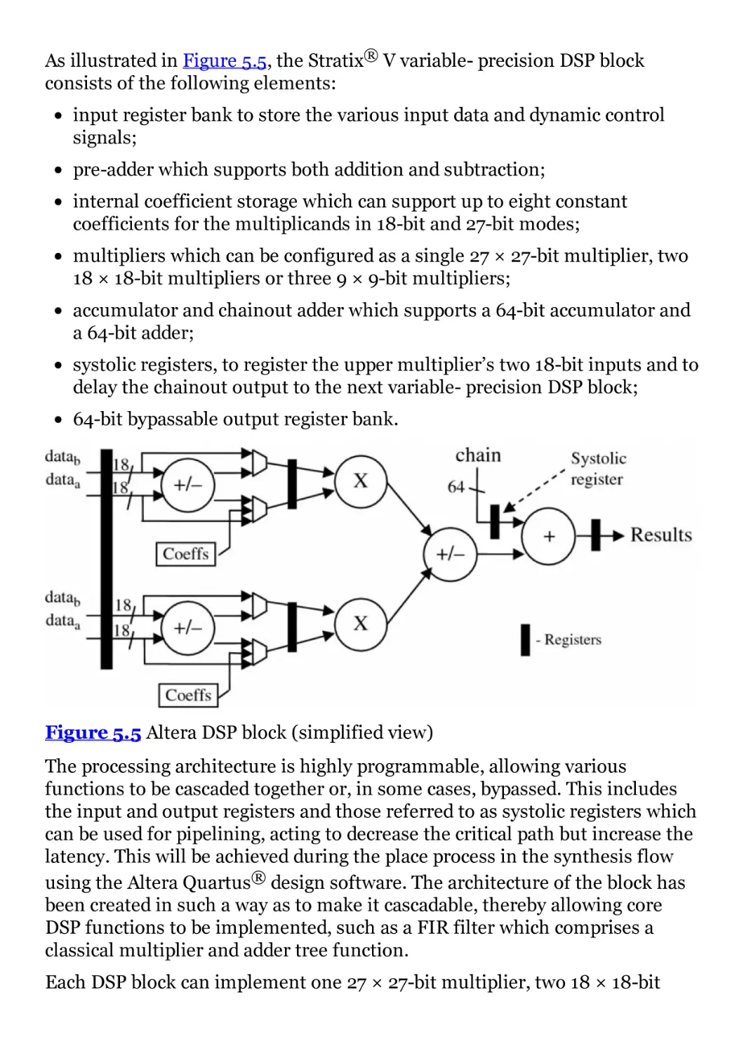

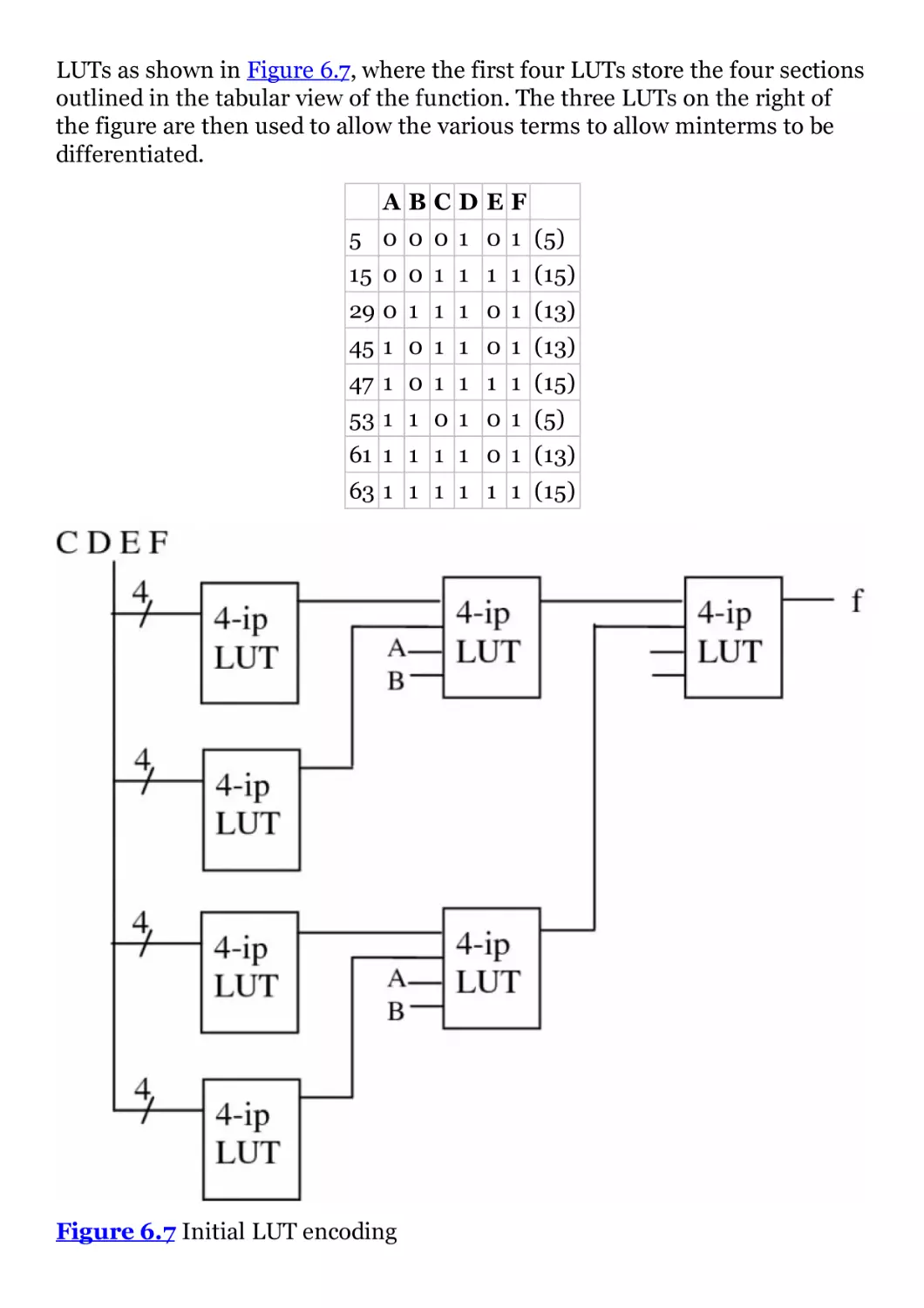
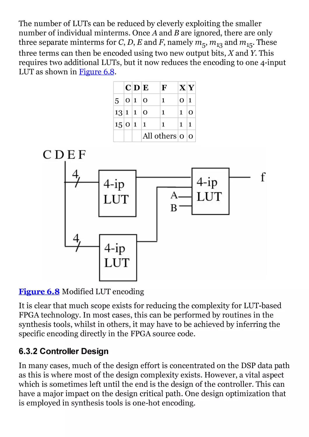

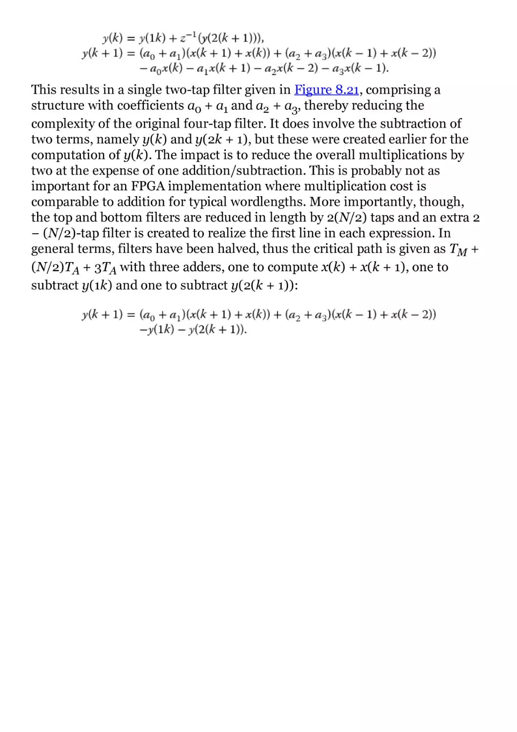
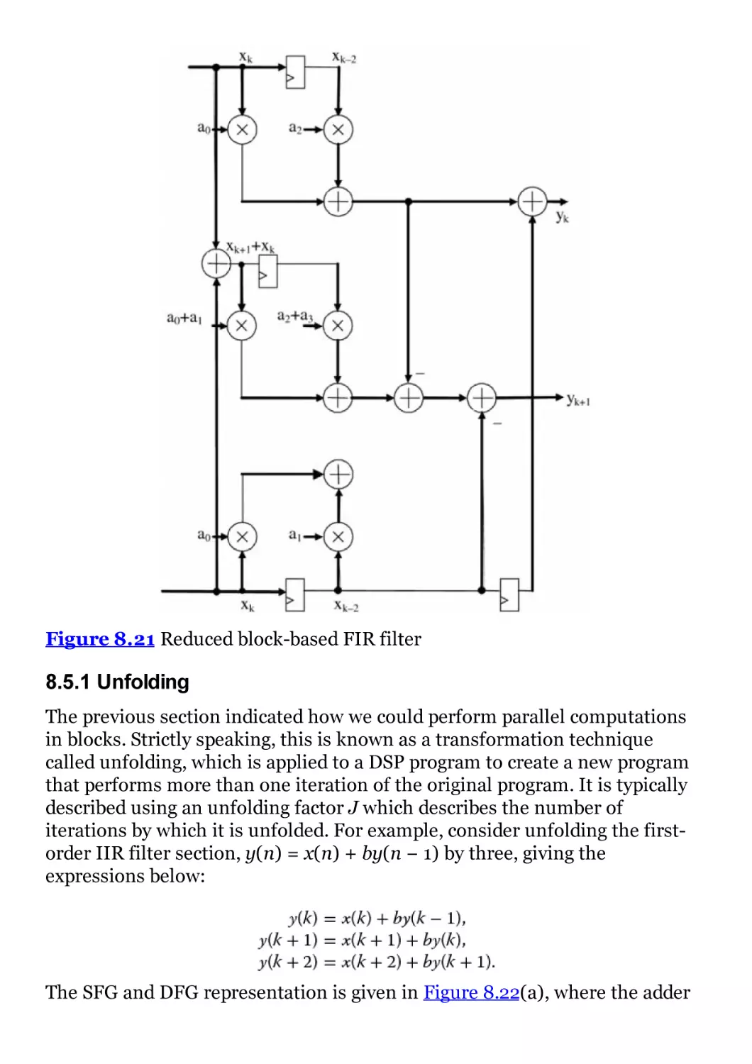
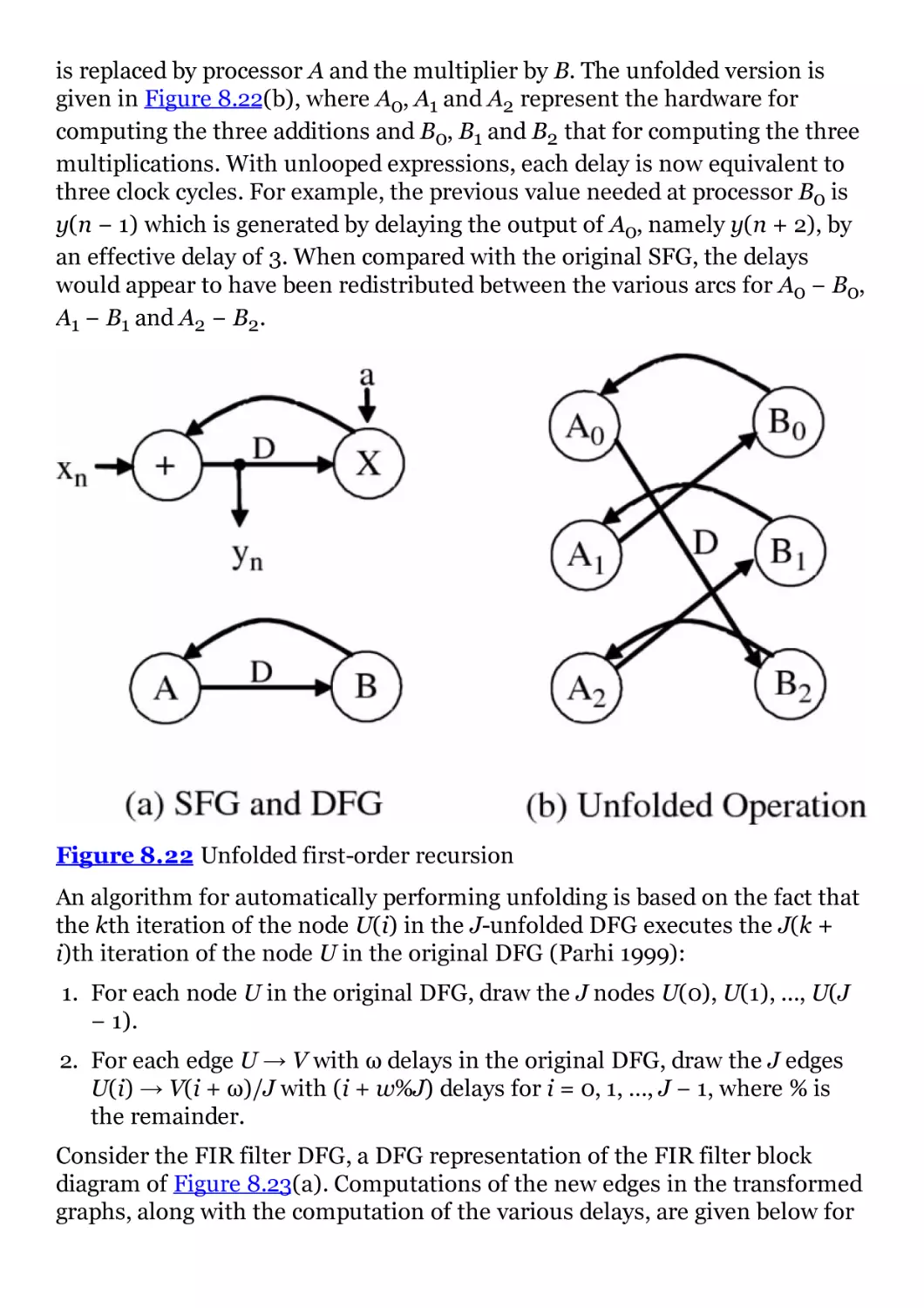
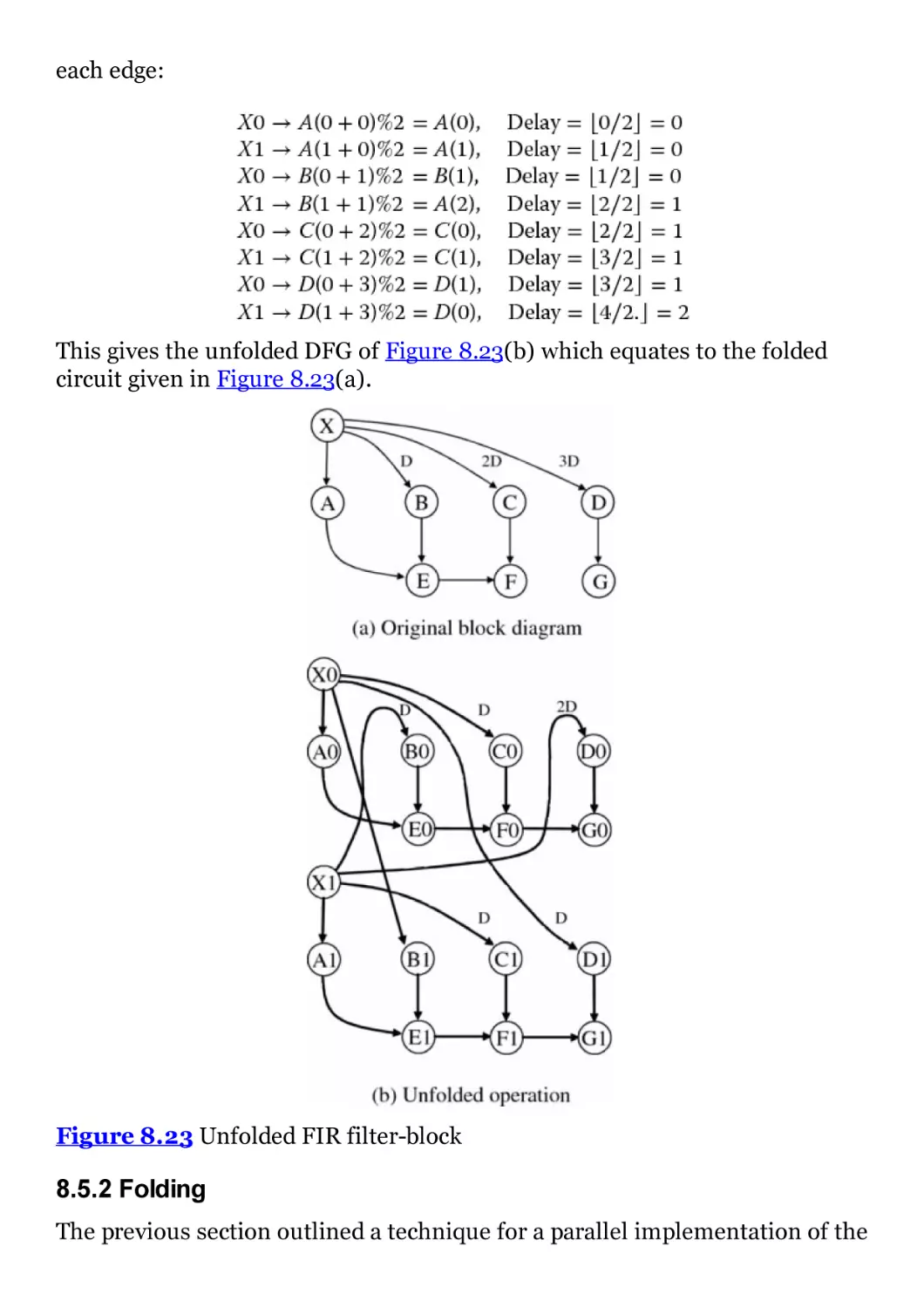


Автор: Woods R. McAllister J. Lightbody G.
Теги: integrated circuits synthesis arithmetic circuits fpga asic embedded systems digital design hardware synthesis electronic circuits hardware development wiley interscience publisher
ISBN: 9781119077954
Год: 2017


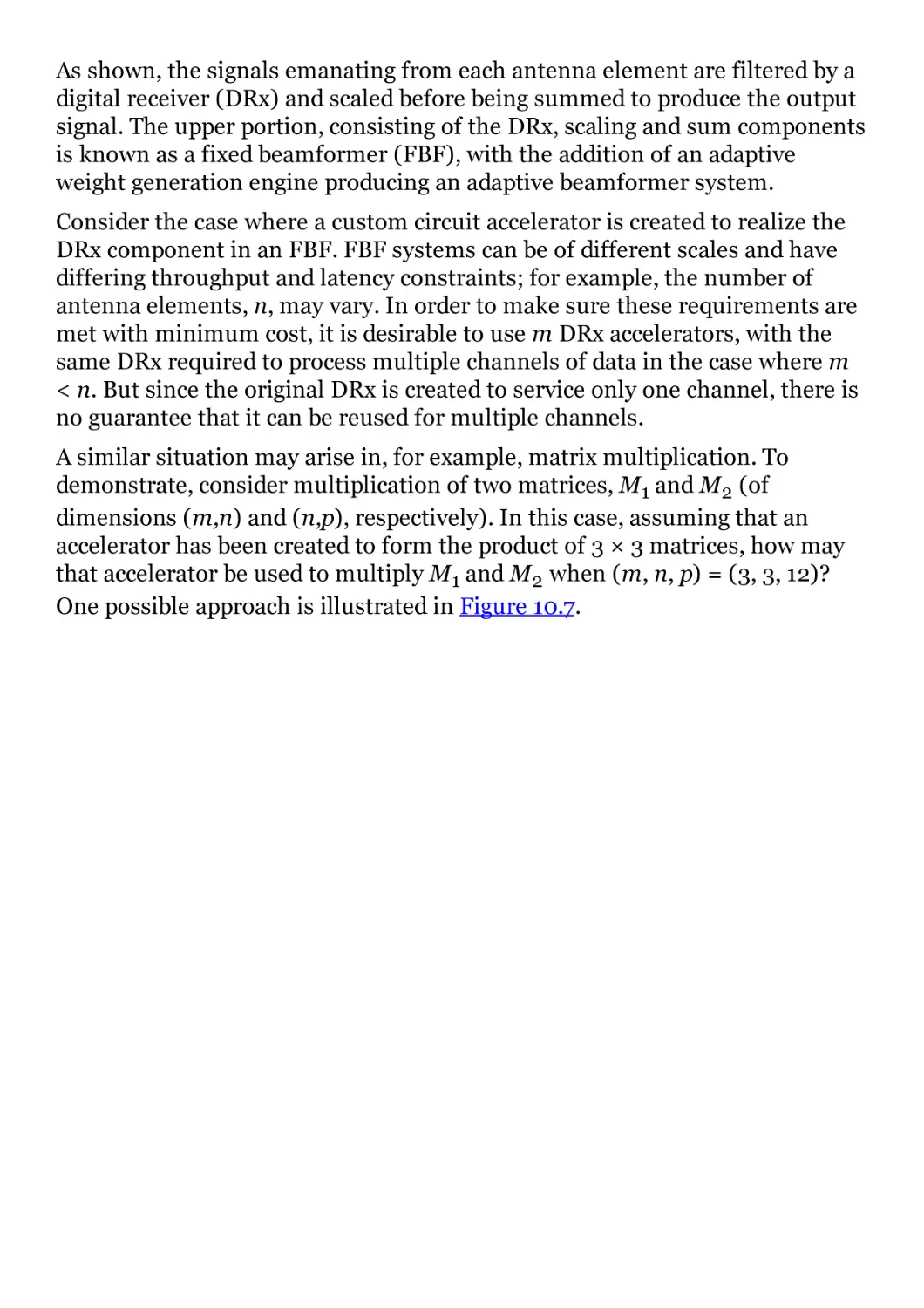
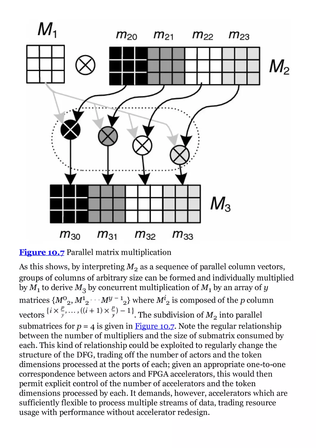
FPGA-based Implementation
of Signal Processing Systems
Second Edition
Roger Woods
Queen’s University, Belfast, UK
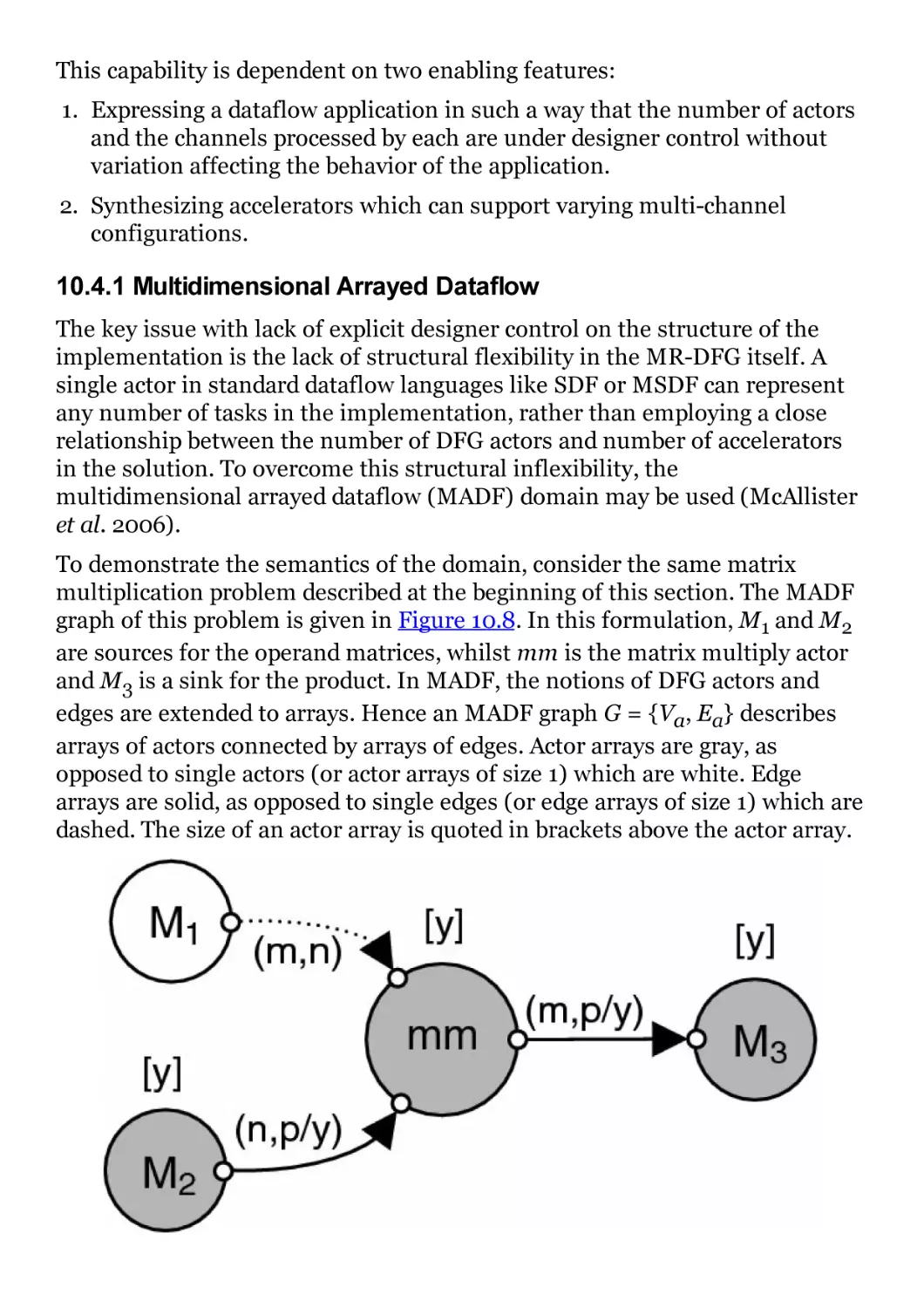
John McAllister
Queen’s University, Belfast, UK
Gaye Lightbody
University of Ulster, UK
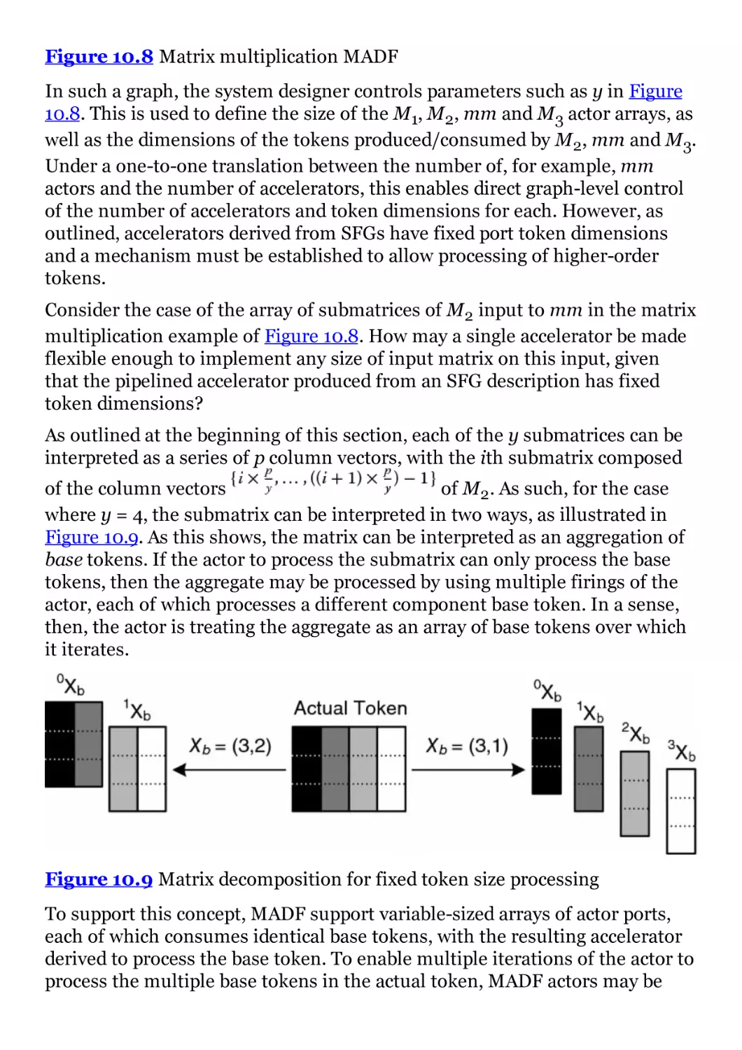
Ying Yi
SN Systems — Sony Interactive Entertainment, UK
This edition first published 2017
© 2017 John Wiley & Sons, Ltd
All rights reserved. No part of this publication may be reproduced, stored in a retrieval system, or
transmitted, in any form or by any means, electronic, mechanical, photocopying, recording or
otherwise, except as permitted by law. Advice on how to obtain permission to reuse material from
this title is available at http://www.wiley.com/go/permissions.
The right of Roger Woods, John McAllister, Gaye Lightbody and Ying Yi to be identified as the
authors of this work has been asserted in accordance with law.
Registered Offices
John Wiley & Sons, Inc., 111 River Street, Hoboken, NJ 07030, USA
John Wiley & Sons, Ltd., The Atrium, Southern Gate, Chichester, West Sussex, PO19 8SQ, UK
Editorial Office
The Atrium, Southern Gate, Chichester, West Sussex, PO19 8SQ, UK
For details of our global editorial offices, customer services, and more information about Wiley
products visit us at www.wiley.com.
Wiley also publishes its books in a variety of electronic formats and by print-on-demand. Some
content that appears in standard print versions of this book may not be available in other formats.
Limit of Liability/Disclaimer of Warranty
While the publisher and authors have used their best efforts in preparing this work, they make no
representations or warranties with respect to the accuracy or completeness of the contents of this
work and specifically disclaim all warranties, including without limitation any implied warranties of
merchantability or fitness for a particular purpose. No warranty may be created or extended by
sales representatives, written sales materials or promotional statements for this work. The fact
that an organization, website, or product is referred to in this work as a citation and/or potential
source of further information does not mean that the publisher and authors endorse the
information or services the organization, website, or product may provide or recommendations it
may make. This work is sold with the understanding that the publisher is not engaged in rendering
professional services. The advice and strategies contained herein may not be suitable for your
situation. You should consult with a specialist where appropriate. Further, readers should be aware
that websites listed in this work may have changed or disappeared between when this work was
written and when it is read. Neither the publisher nor authors shall be liable for any loss of profit or
any other commercial damages, including but not limited to special, incidental, consequential, or
other damages.
Library of Congress Cataloging-in-Publication Data
Names: Woods, Roger, 1963- author. | McAllister, John, 1979- author. |
Lightbody, Gaye, author. | Yi, Ying (Electrical engineer), author.
Title: FPGA-based implementation of signal processing systems / Roger Woods,
John McAllister, Gaye Lightbody, Ying Yi.
Description: Second editon. | Hoboken, NJ : John Wiley & Sons Inc., 2017. |
Revised edition of: FPGA-based implementation of signal processing systems /
Roger Woods … [et al.]. 2008. | Includes bibliographical references and index.
Identifiers: LCCN 2016051193 | ISBN 9781119077954 (cloth) | ISBN 9781119077978 (epdf) |
ISBN 9781119077961 (epub)
Subjects: LCSH: Signal processing--Digital techniques. | Digital integrated
circuits. | Field programmable gate arrays.
Classification: LCC TK5102.5 .F647 2017 | DDC 621.382/2--dc23 LC record available at
https://lccn.loc.gov/2016051193
Cover Design: Wiley
Cover Image: © filo/Gettyimages;
(Graph) Courtesy of the authors
The book is dedicated by the main author to his wife, Pauline, for all for her support and
care, particularly over the past two years.
The support from staff from the Royal Victoria Hospital and Musgrave Park Hospital is
greatly appreciated.
CONTENTS
Preface
List of Abbreviations
1 Introduction to Field Programmable Gate Arrays
1.1 Introduction
1.2 Field Programmable Gate Arrays
1.3 Influence of Programmability
1.4 Challenges of FPGAs
Bibliography
2 DSP Basics
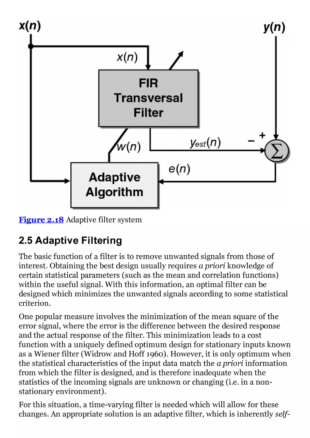
2.1 Introduction
2.2 Definition of DSP Systems
2.3 DSP Transformations
2.4 Filters
2.5 Adaptive Filtering
2.6 Final Comments
Bibliography
3 Arithmetic Basics
3.1 Introduction
3.2 Number Representations
3.3 Arithmetic Operations
3.4 Alternative Number Representations
3.5 Division
3.6 Square Root
3.7 Fixed-Point versus Floating-Point
3.8 Conclusions
Bibliography
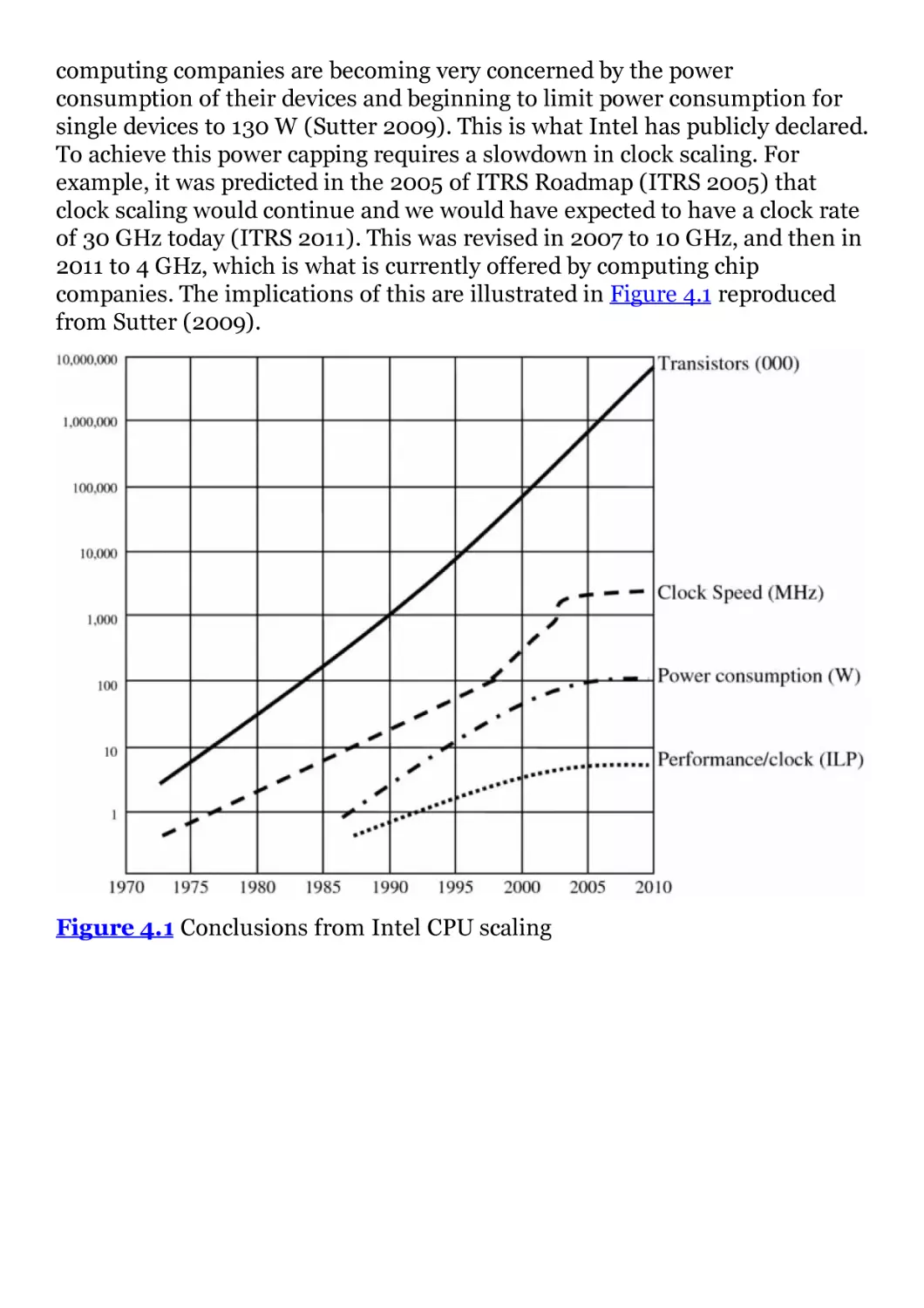
4 Technology Review
4.1 Introduction
4.2 Implications of Technology Scaling
4.3 Architecture and Programmability
4.4 DSP Functionality Characteristics
4.5 Microprocessors
4.6 DSP Processors
4.7 Graphical Processing Units
4.8 System-on-Chip Solutions
4.9 Heterogeneous Computing Platforms
4.10 Conclusions
Bibliography
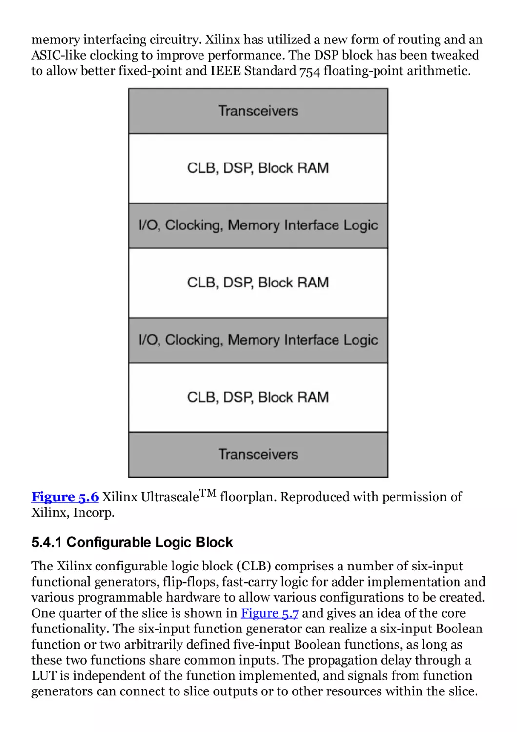
5 Current FPGA Technologies
5.1 Introduction
5.2 Toward FPGAs
5.3 Altera Stratix® V and 10 FPGA Family
5.4 Xilinx UltrascaleTM/Virtex-7 FPGA families
5.5 Xilinx Zynq FPGA Family
5.6 Lattice iCE40isp FPGA Family
5.7 MicroSemi RTG4 FPGA Family
5.8 Design Stratregies for FPGA-based DSP Systems
5.9 Conclusions
Bibliography
6 Detailed FPGA Implementation Techniques
6.1 Introduction
6.2 FPGA Functionality
6.3 Mapping to LUT-Based FPGA Technology
6.4 Fixed-Coefficient DSP
6.5 Distributed Arithmetic
6.6 Reduced-Coefficient Multiplier
6.7 Conclusions
Bibliography
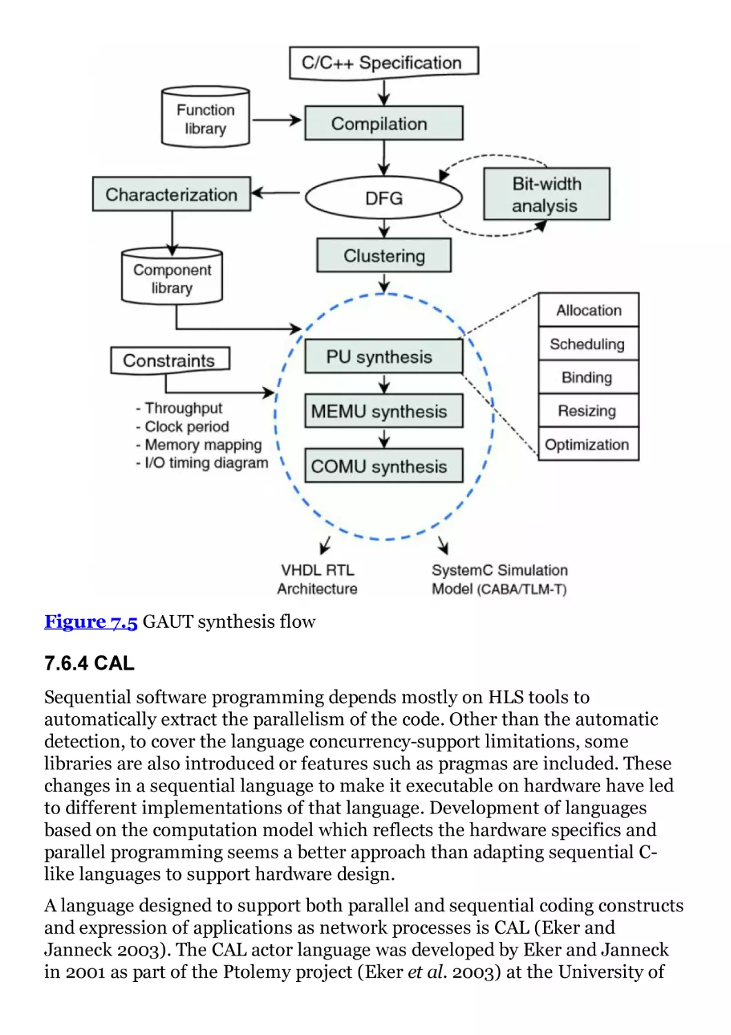
7 Synthesis Tools for FPGAs
7.1 Introduction
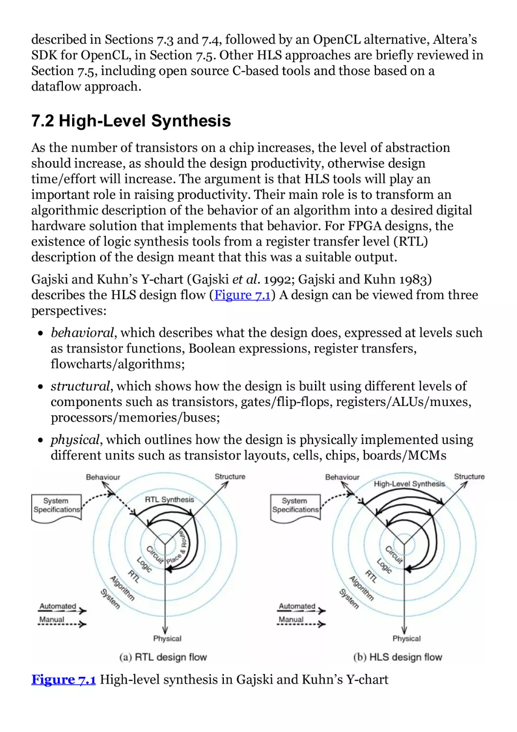
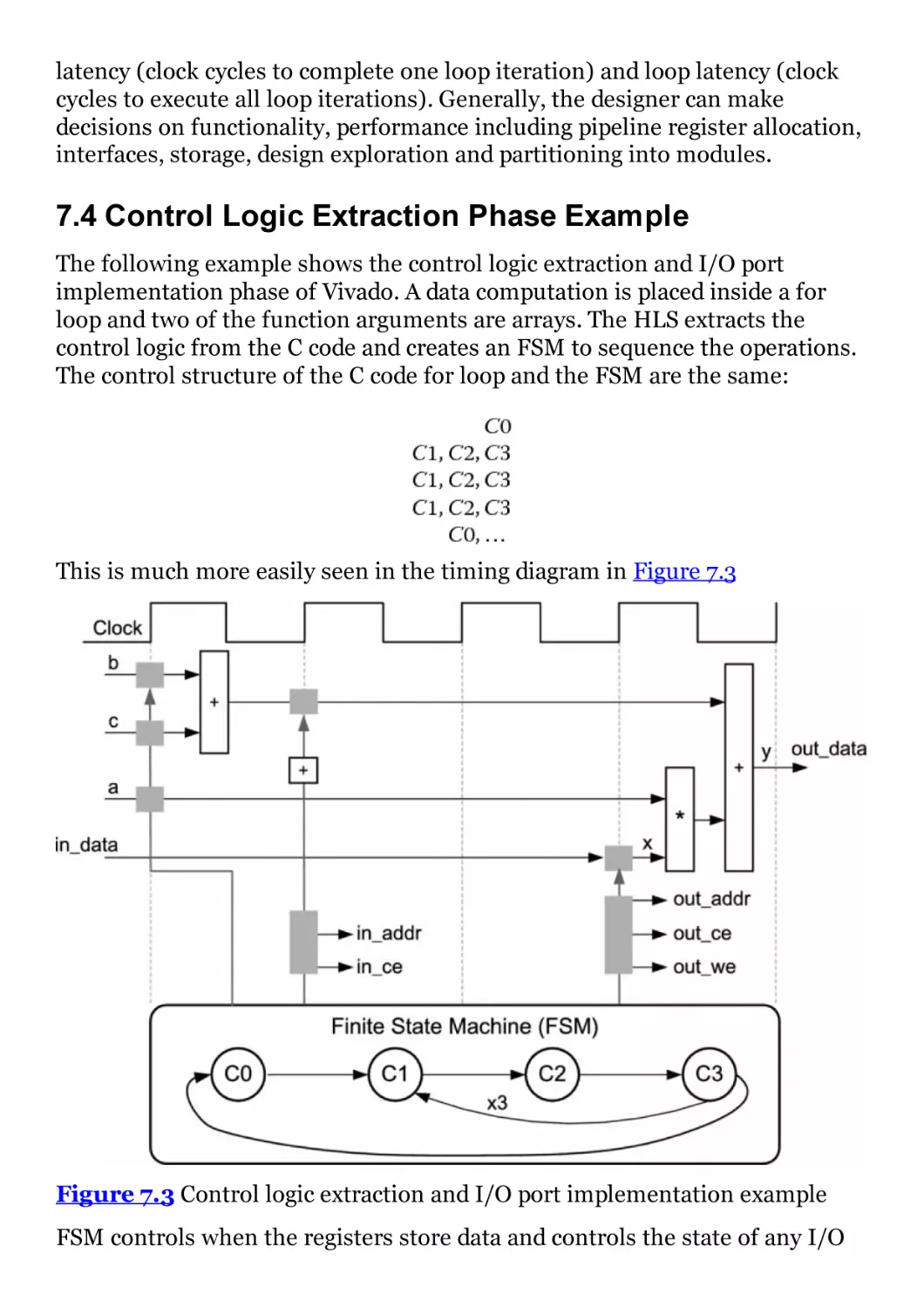
7.2 High-Level Synthesis
7.3 Xilinx Vivado
7.4 Control Logic Extraction Phase Example
7.5 Altera SDK for OpenCL
7.6 Other HLS Tools
7.7 Conclusions
Bibliography
8 Architecture Derivation for FPGA-based DSP Systems
8.1 Introduction
8.2 DSP Algorithm Characteristics
8.3 DSP Algorithm Representations
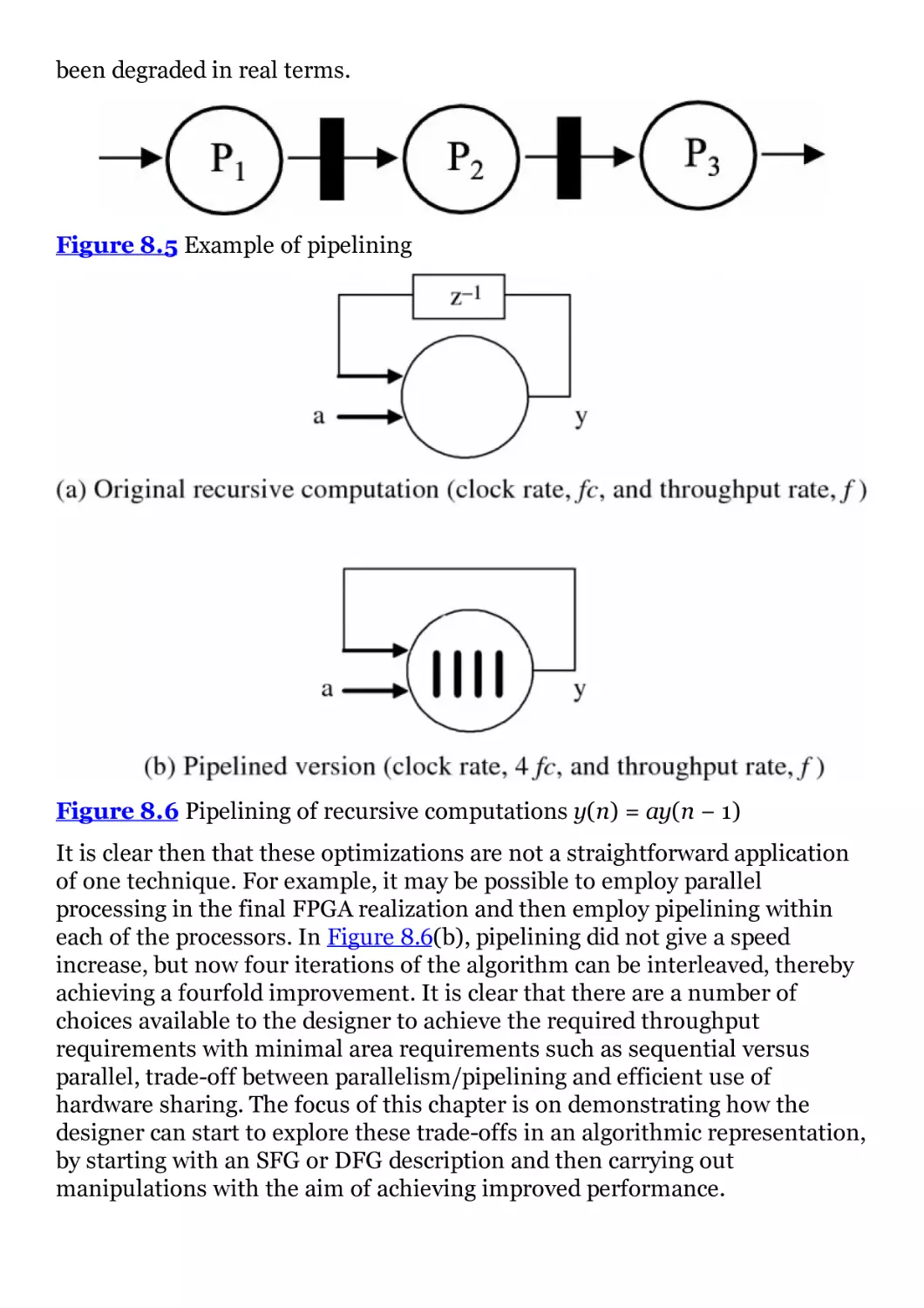
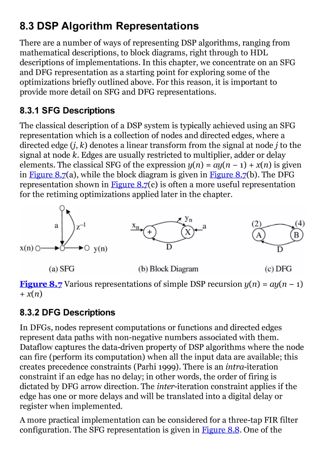
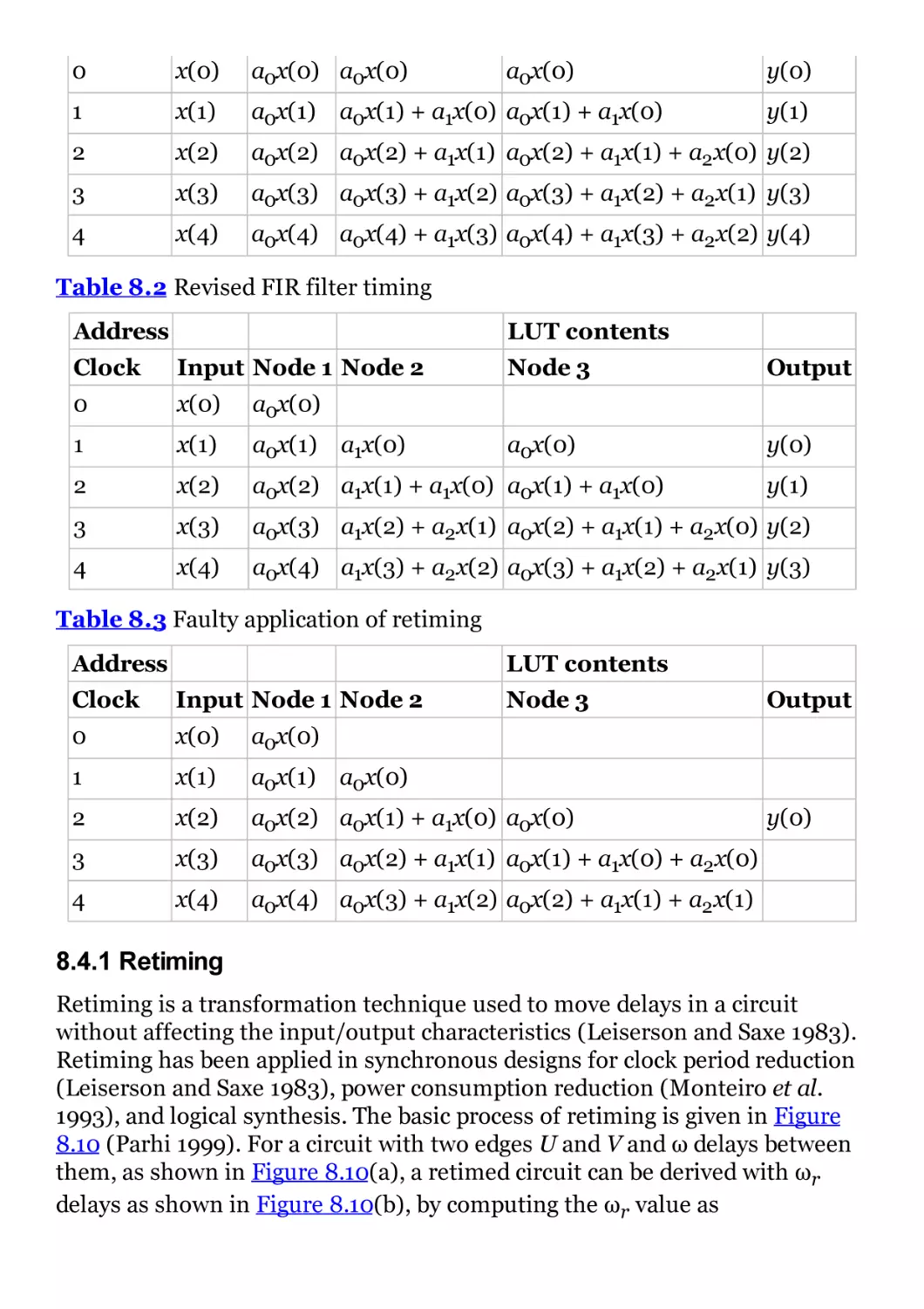
8.4 Pipelining DSP Systems
8.5 Parallel Operation
8.6 Conclusions
Bibliography
9 Complex DSP Core Design for FPGA
9.1 Introduction
9.2 Motivation for Design for Reuse
9.3 Intellectual Property Cores
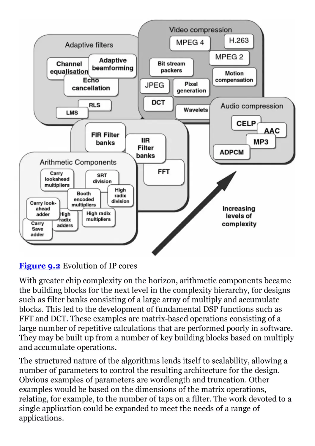
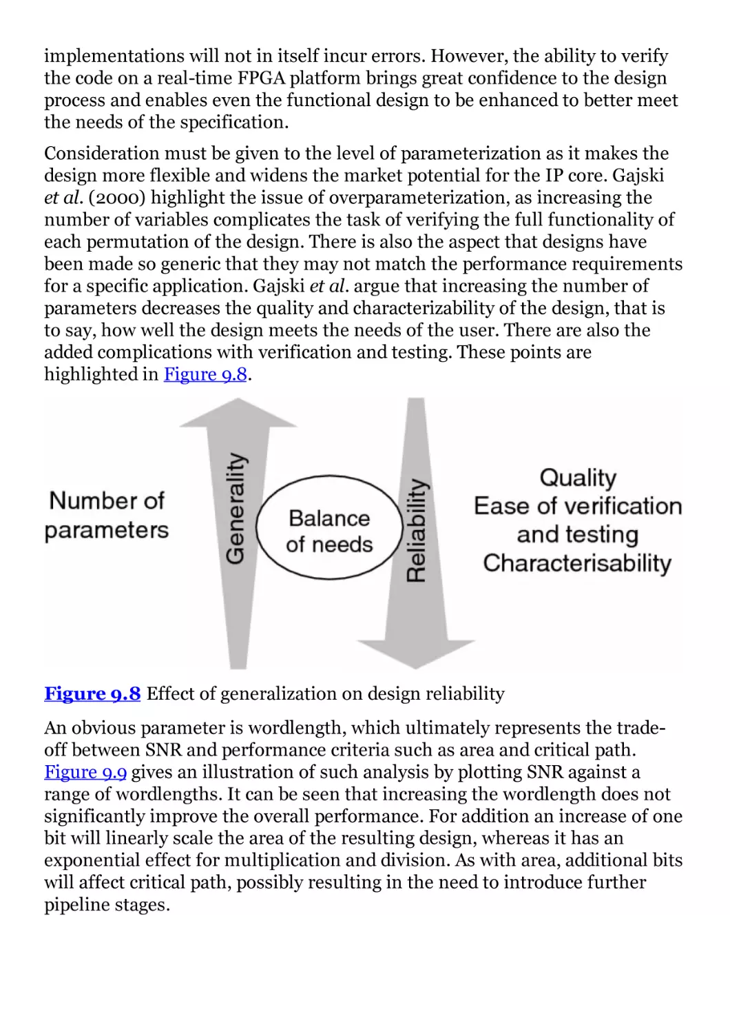
9.4 Evolution of IP cores
9.5 Parameterizable (Soft) IP Cores
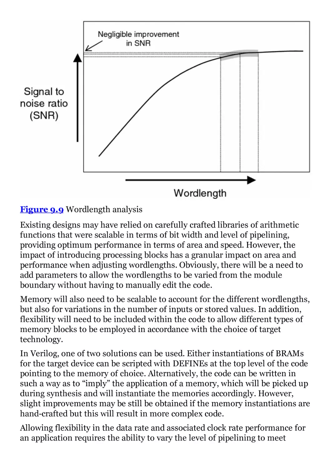
9.6 IP Core Integration
9.7 Current FPGA-based IP cores
9.8 Watermarking IP
9.9 Summary
Bibliography
10 Advanced Model-Based FPGA Accelerator Design
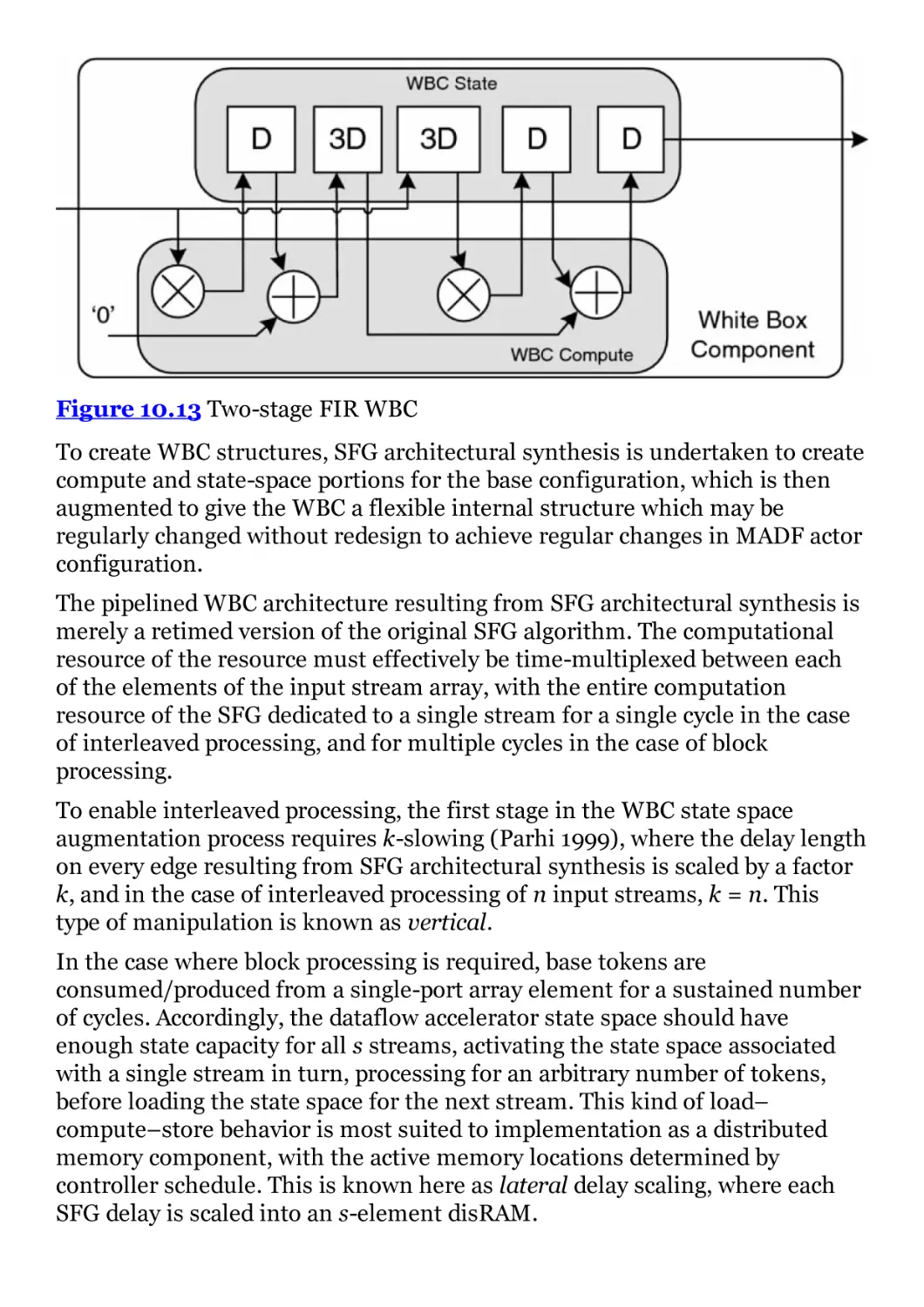
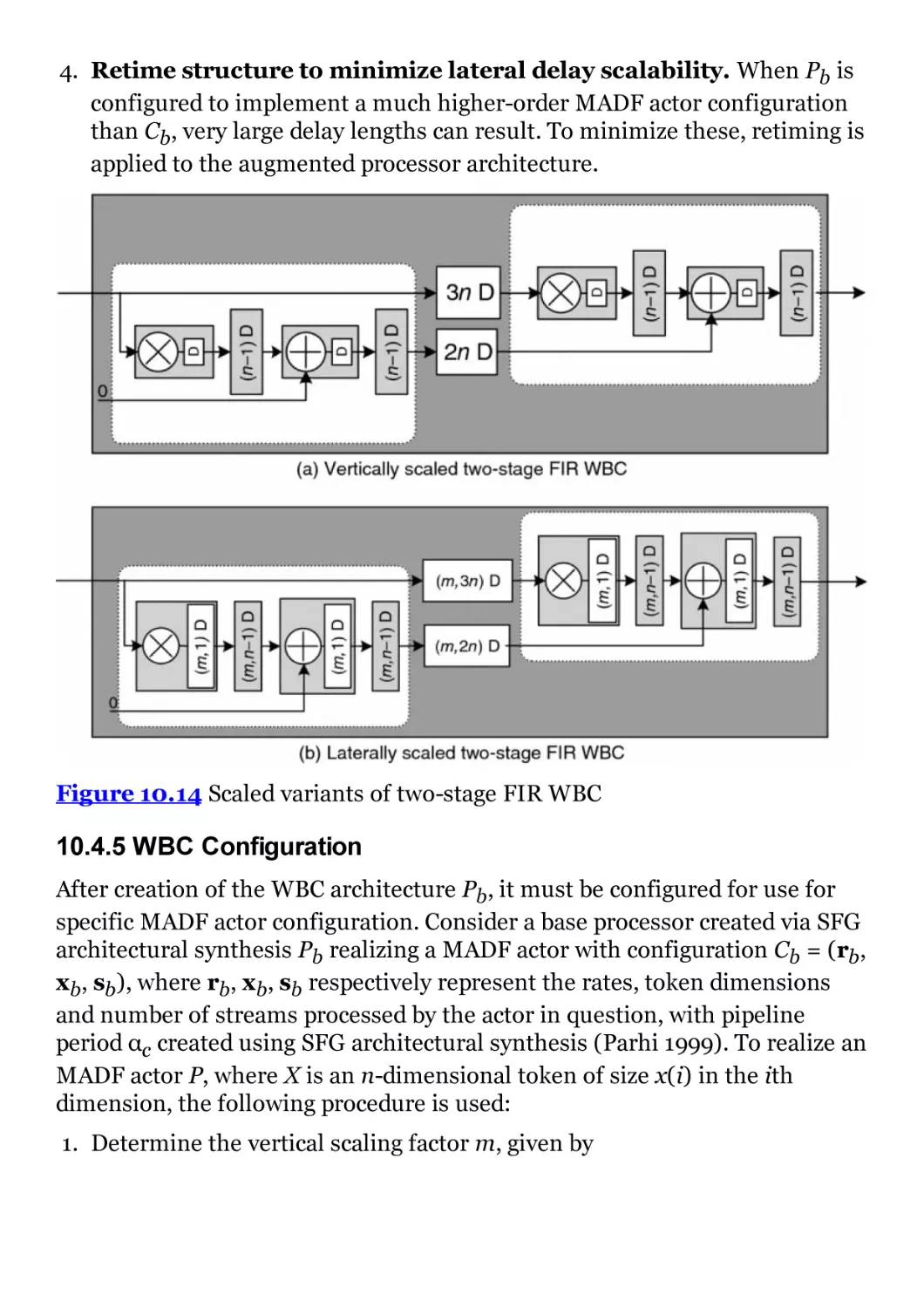
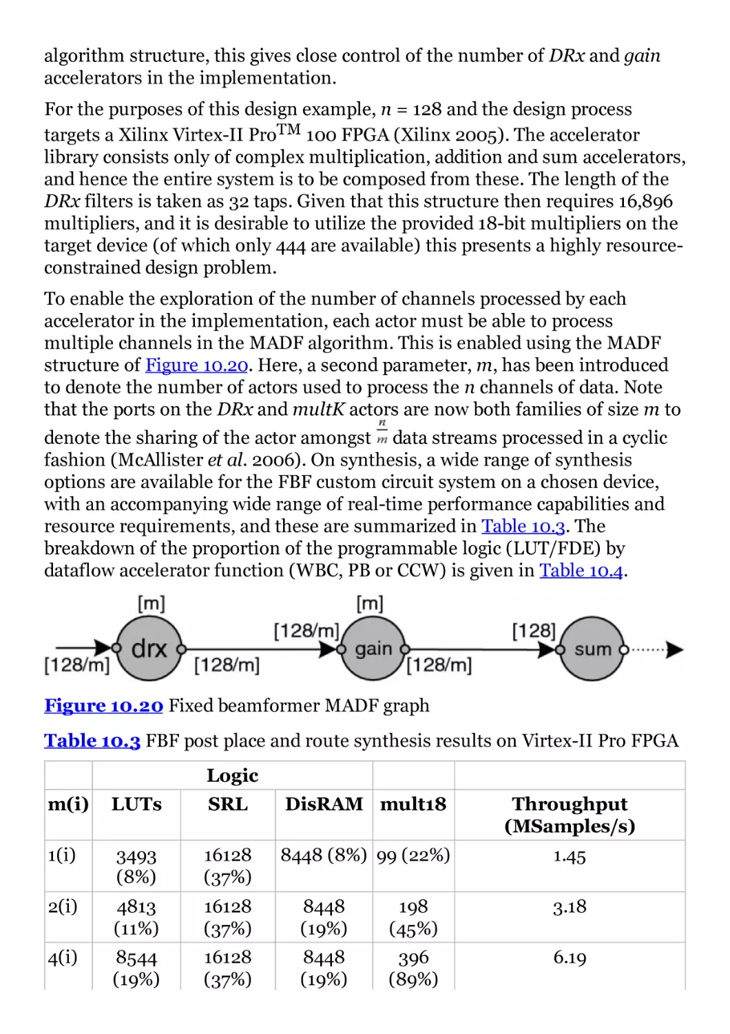
10.1 Introduction
10.2 Dataflow Modeling of DSP Systems
10.3 Architectural Synthesis of Custom Circuit Accelerators from DFGs
10.4 Model-Based Development of Multi-Channel
Dataflow Accelerators
10.5 Model-Based Development for Memory-Intensive Accelerators
10.6 Summary
Notes
Bibliography
11 Adaptive Beamformer Example
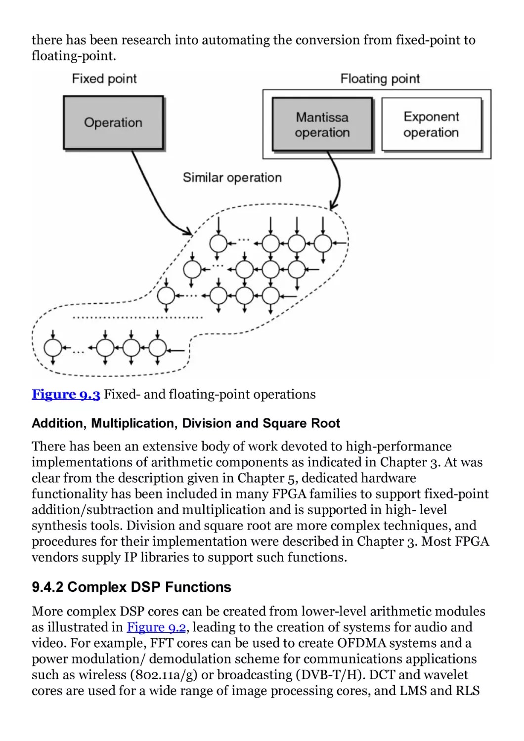
11.1 Introduction to Adaptive Beamforming
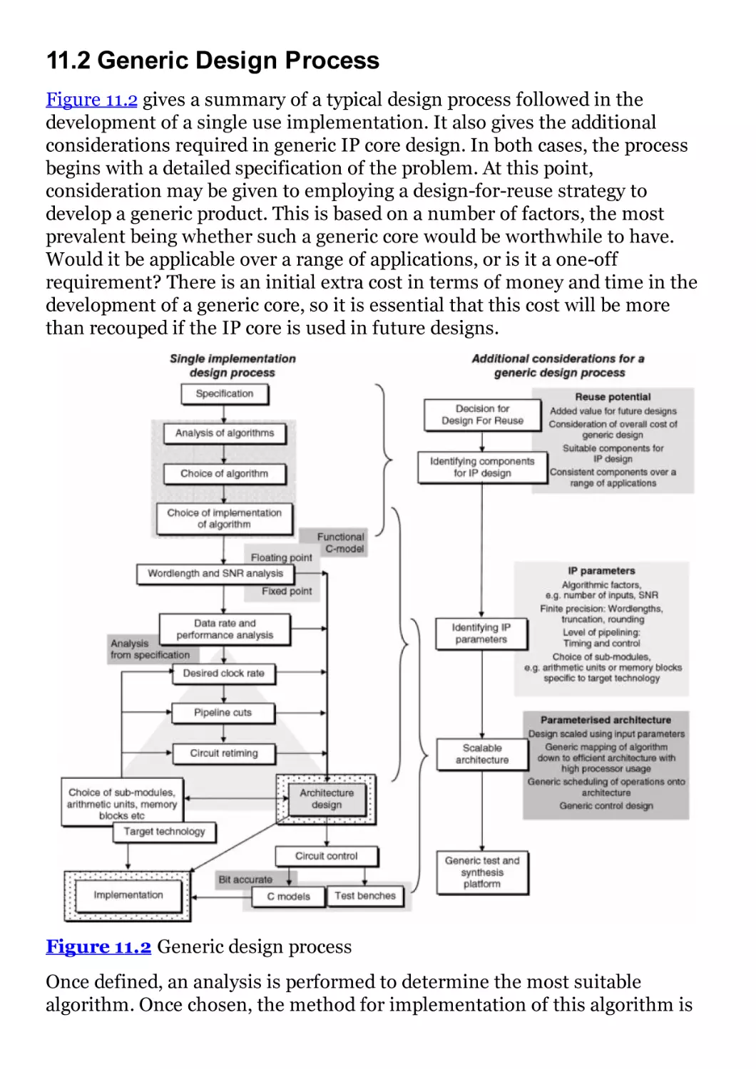
11.2 Generic Design Process
11.3 Algorithm to Architecture
11.4 Efficient Architecture Design
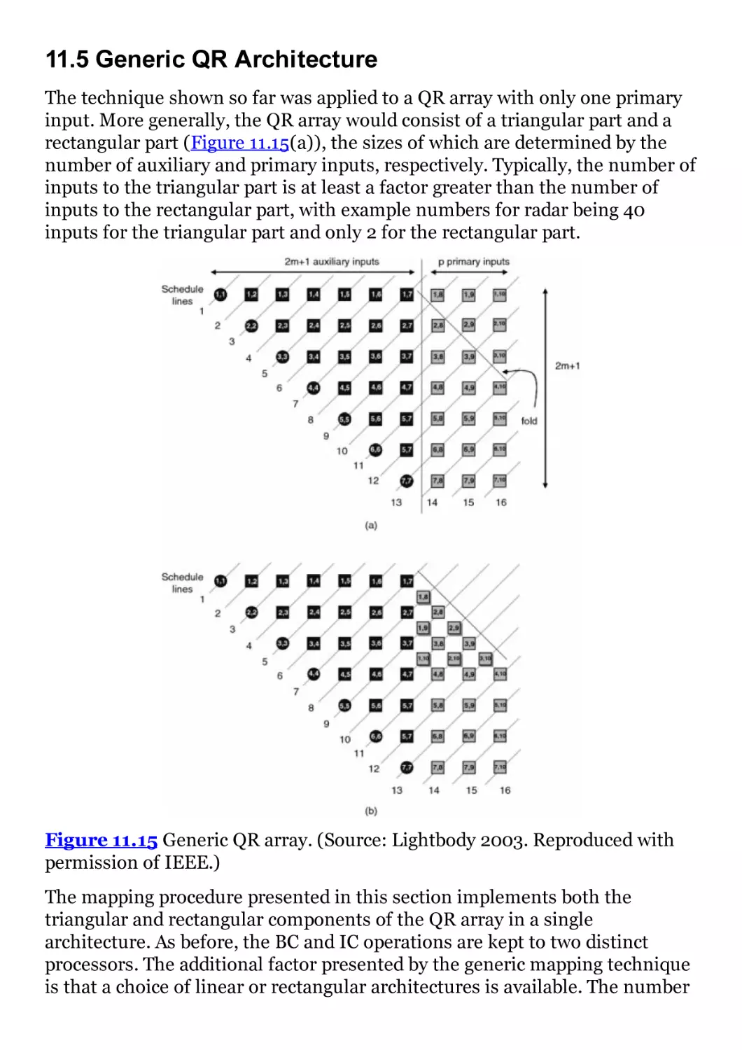
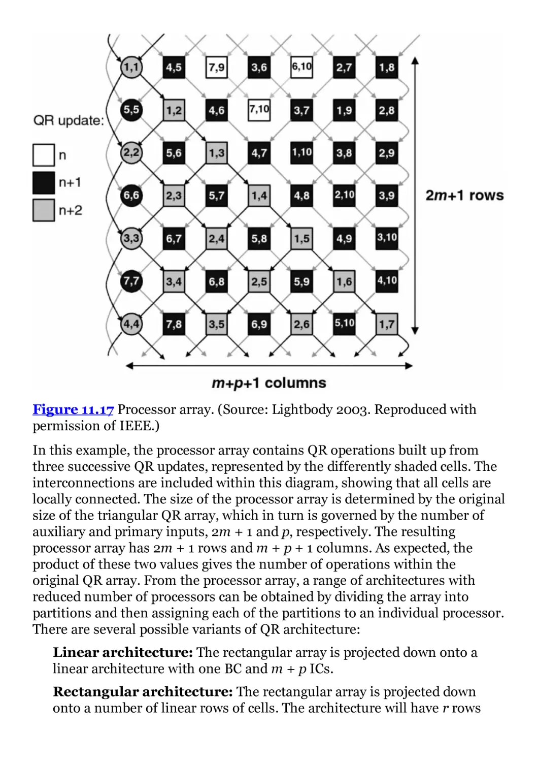
11.5 Generic QR Architecture
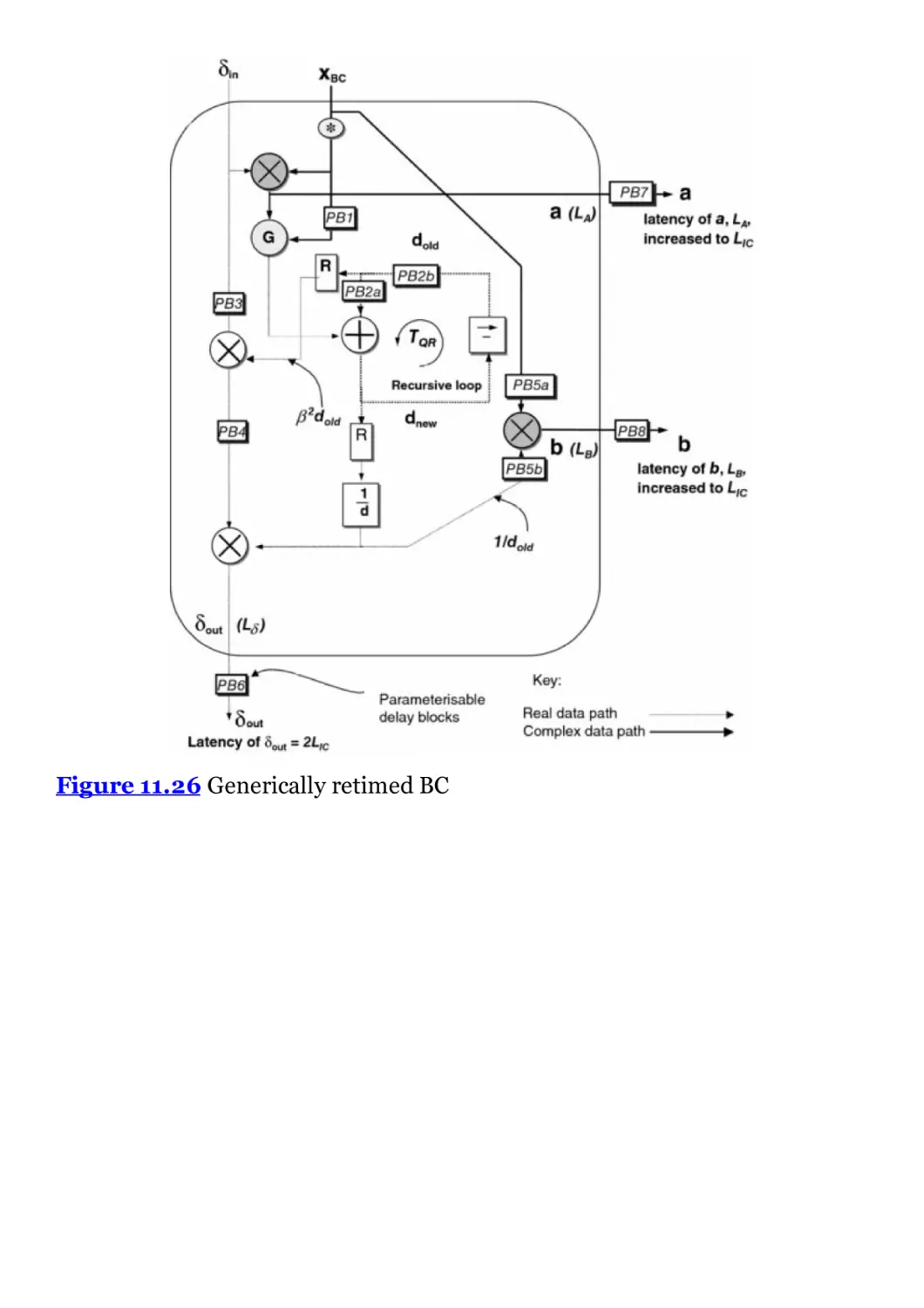
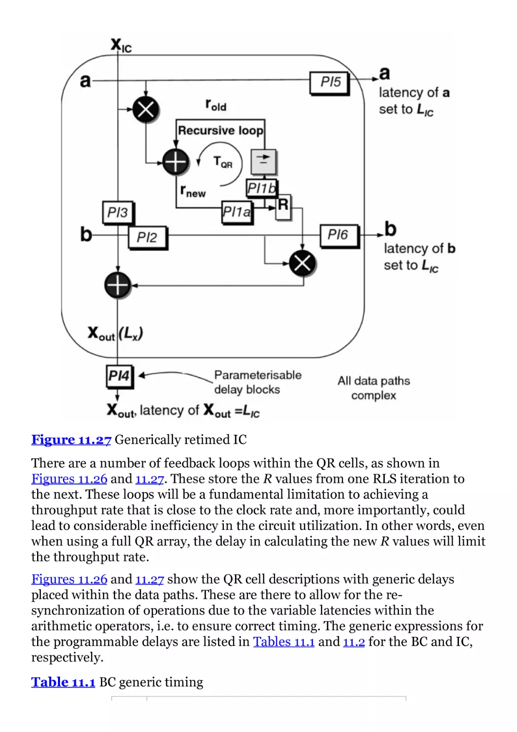
11.6 Retiming the Generic Architecture
11.7 Parameterizable QR Architecture
11.8 Generic Control
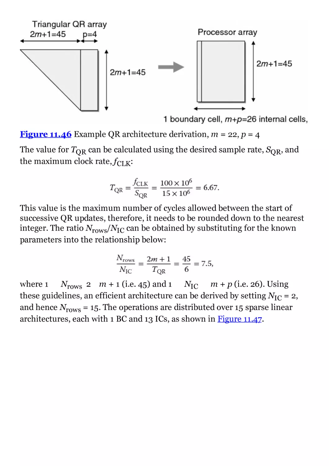
11.9 Beamformer Design Example
11.10 Summary
Bibliography
12 FPGA Solutions for Big Data Applications
12.1 Introduction
12.2 Big Data
12.3 Big Data Analytics
12.4 Acceleration
12.5 k-Means Clustering FPGA Implementation
12.6 FPGA-Based Soft Processors
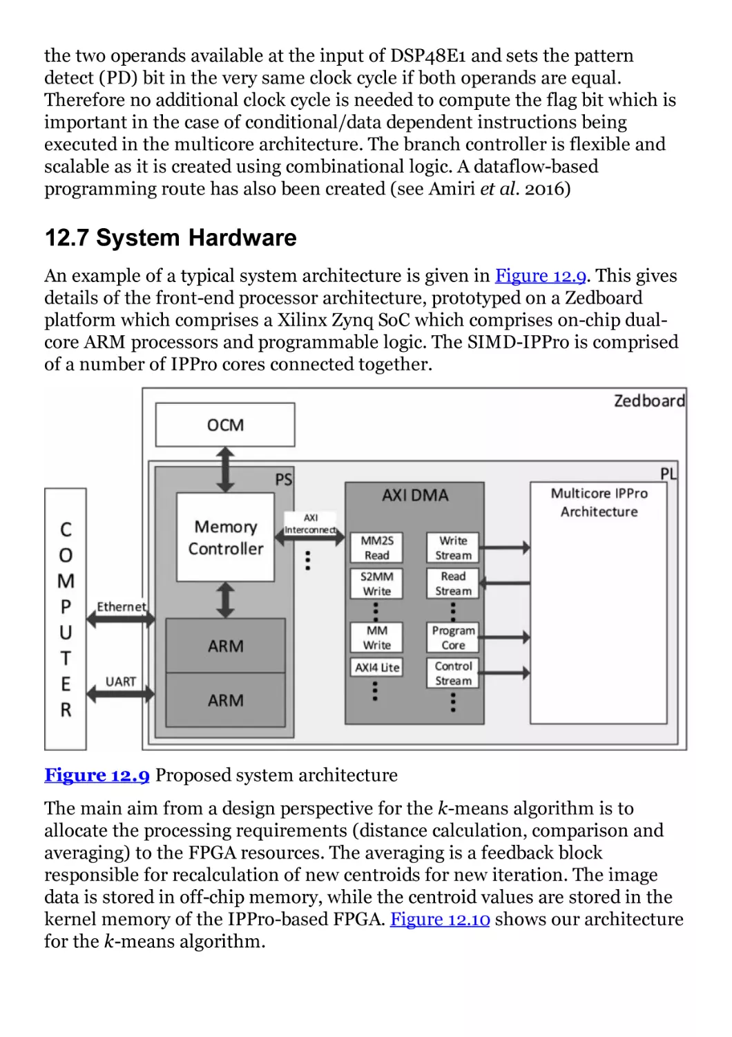
12.7 System Hardware
12.8 Conclusions
Bibliography
13 Low-Power FPGA Implementation
13.1 Introduction
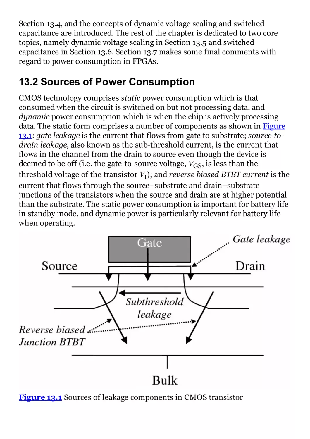
13.2 Sources of Power Consumption
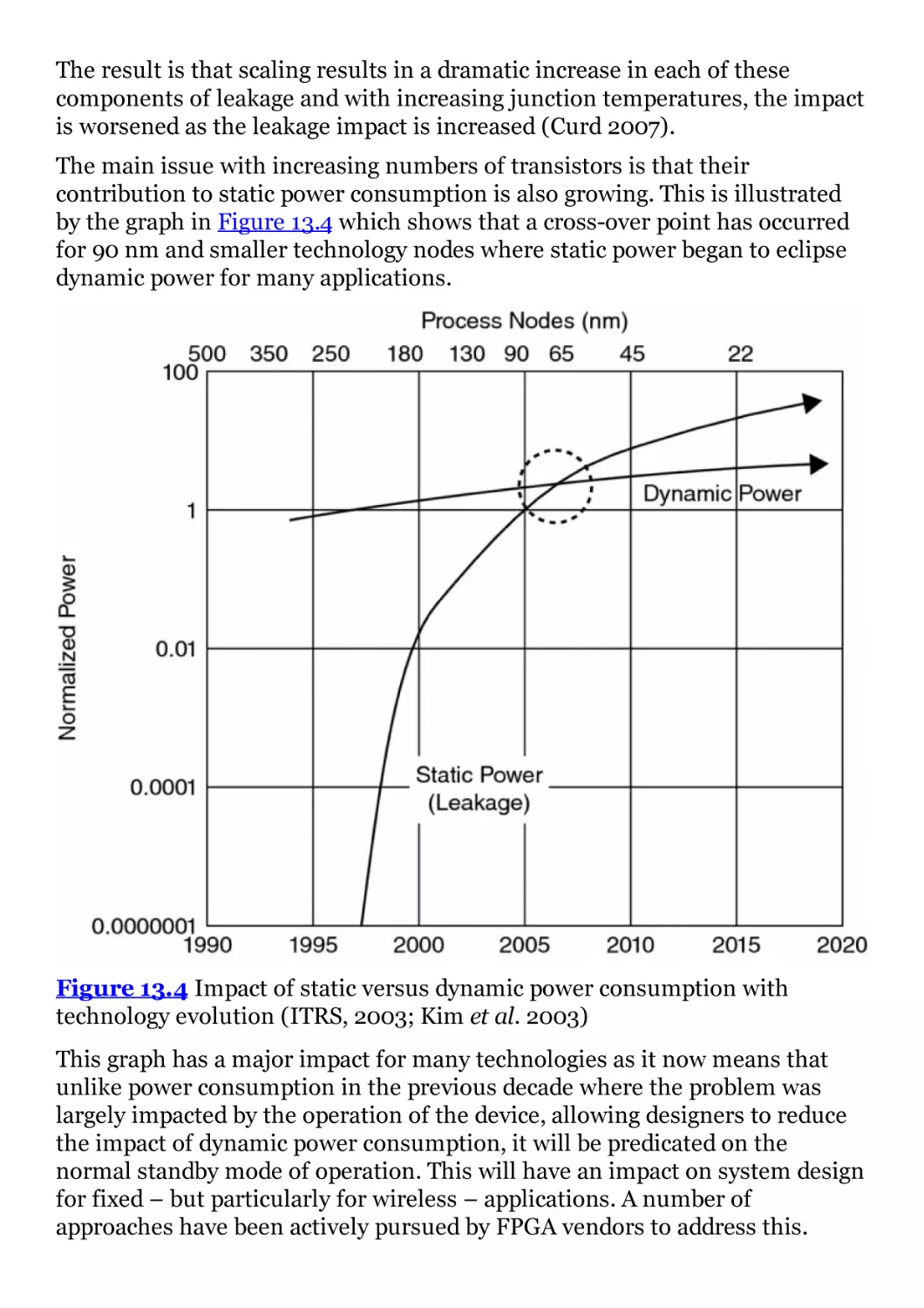
13.3 FPGA Power Consumption
13.4 Power Consumption Reduction Techniques
13.5 Dynamic Voltage Scaling in FPGAs
13.6 Reduction in Switched Capacitance
13.7 Final Comments
Bibliography
14 Conclusions
14.1 Introduction
14.2 Evolution in FPGA Design Approaches
14.3 Big Data and the Shift toward Computing
14.4 Programming Flow for FPGAs
14.5 Support for Floating-Point Arithmetic
14.6 Memory Architectures
Bibliography
Index
EULA
List of Tables
Chapter 1
Table 1.1
Chapter 3
Table 3.1
Table 3.2
Table 3.3
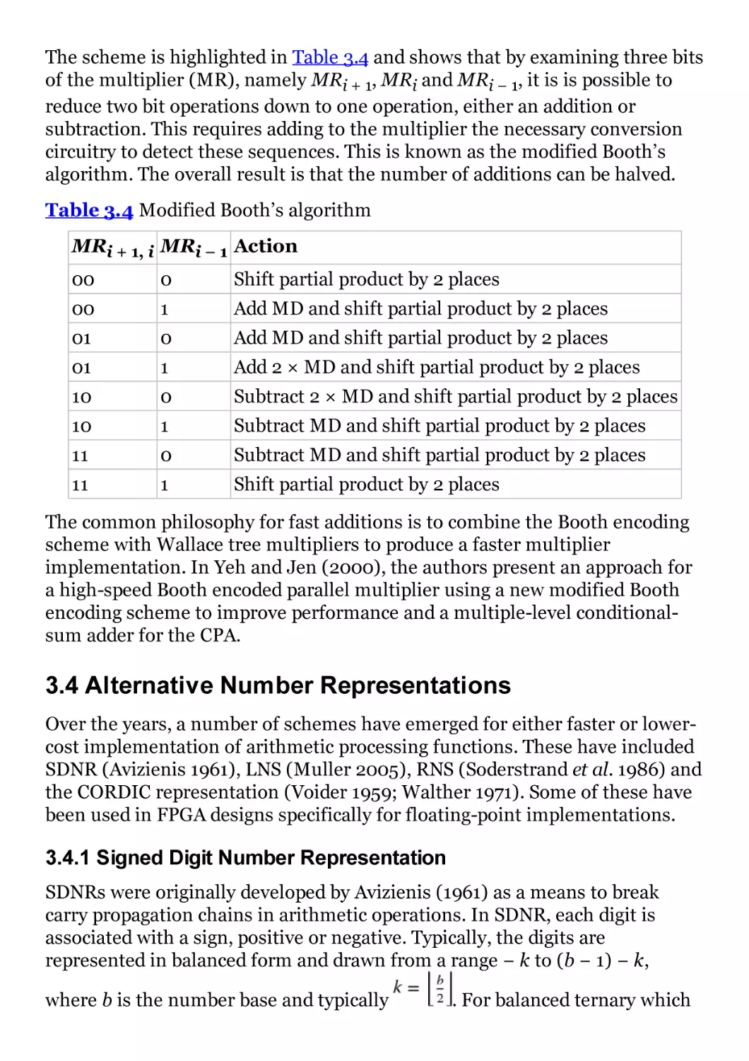
Table 3.4
Table 3.5
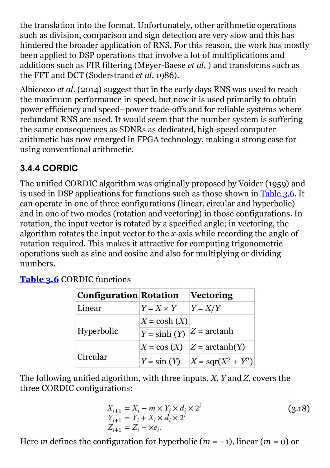
Table 3.6
Table 3.7
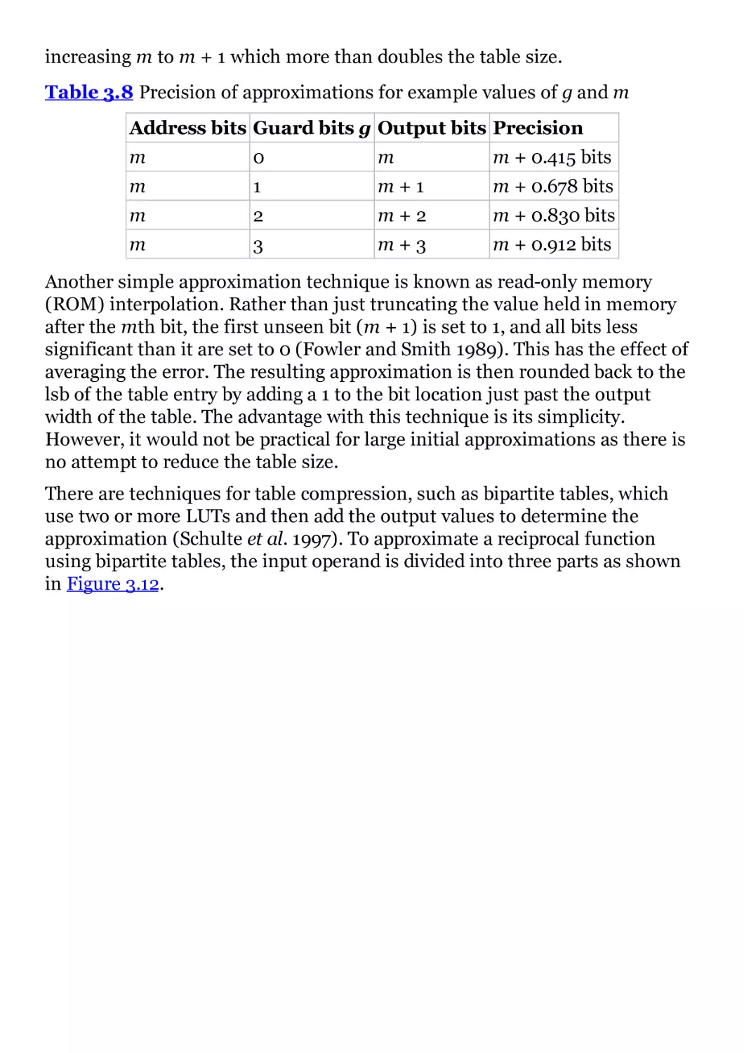
Table 3.8
Table 3.9
Table 3.10
Table 3.11
Chapter 4
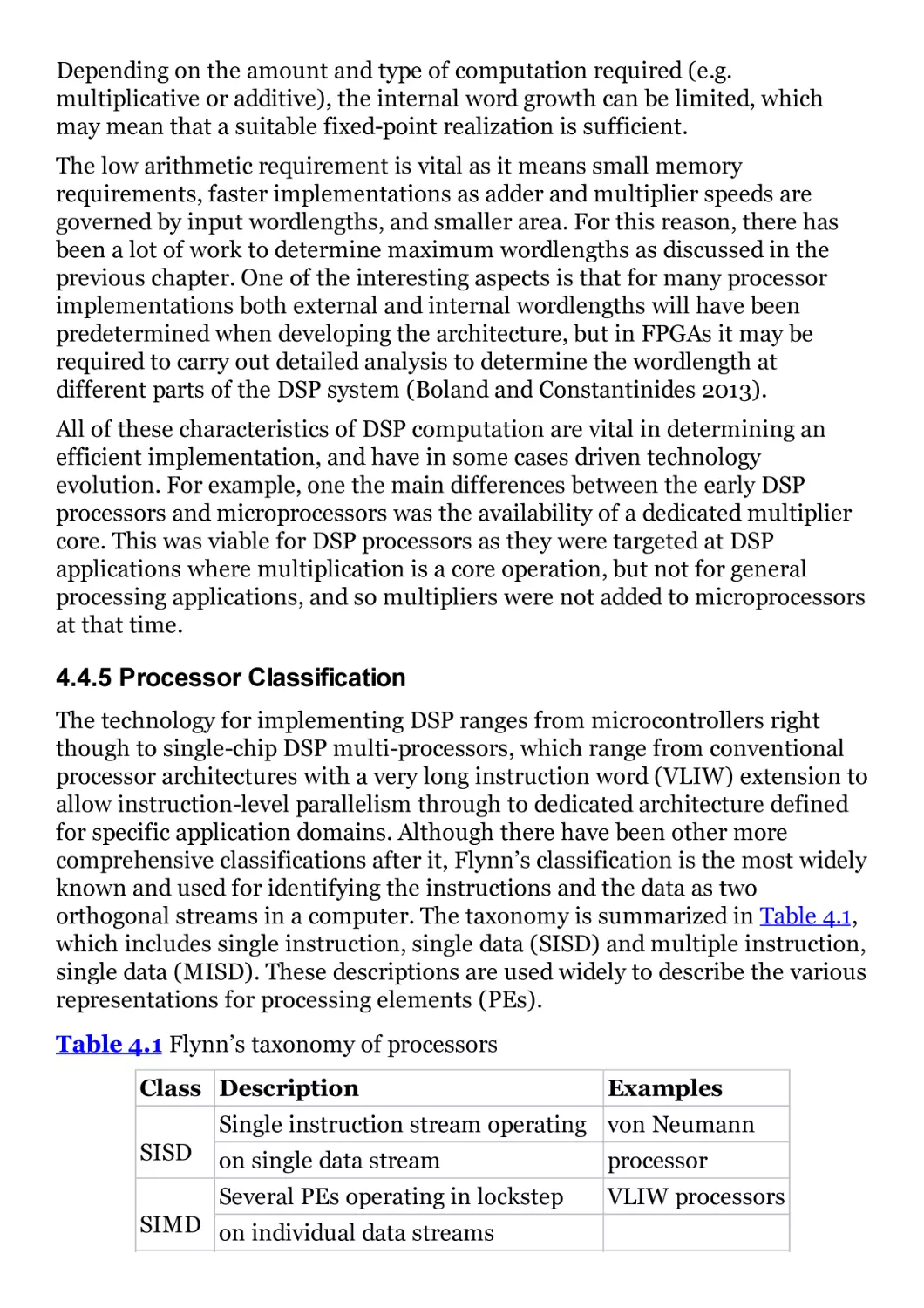
Table 4.1
Table 4.2
Chapter 5
Table 5.1
Table 5.2
Table 5.3
Table 5.4
Chapter 6
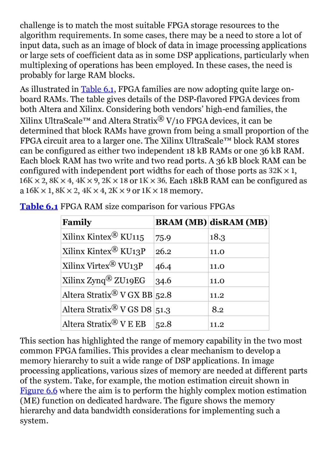
Table 6.1
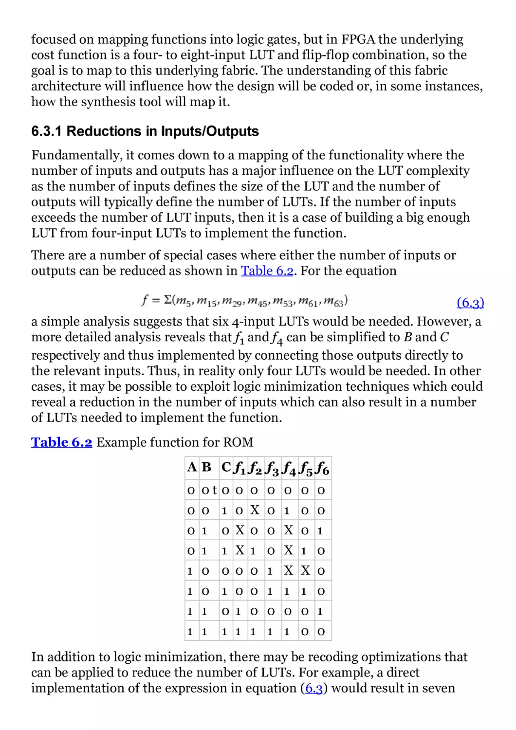
Table 6.2
Table 6.3
Table 6.4
Chapter 8
Table 8.1
Table 8.2
Table 8.3
Table 8.4
Table 8.5
Chapter 9
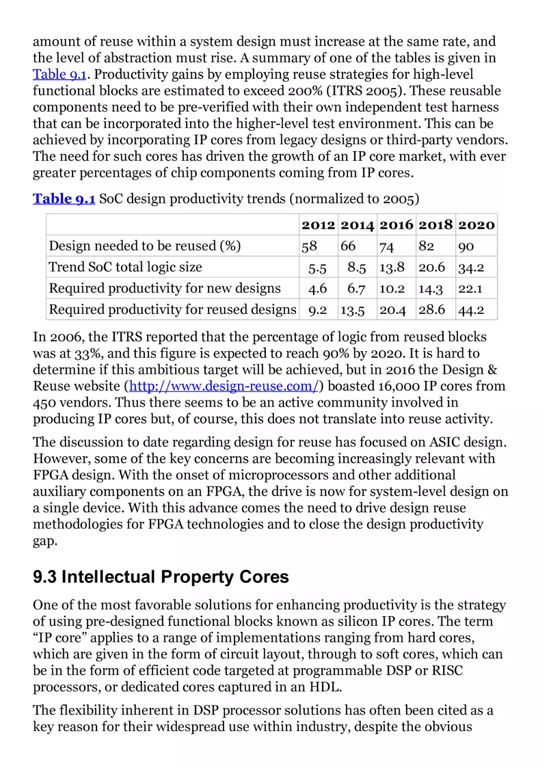
Table 9.1
Chapter 10
Table 10.1
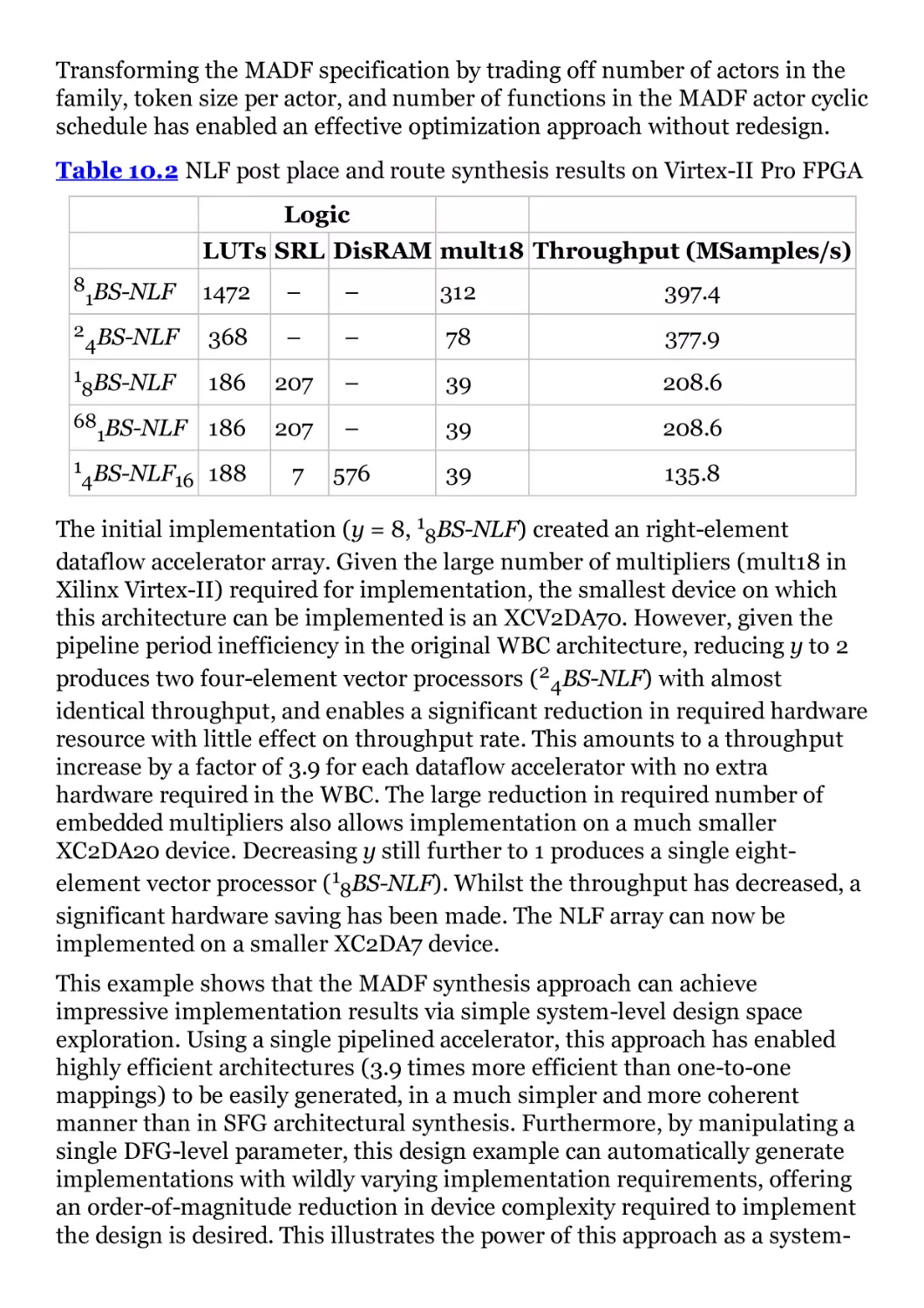
Table 10.2
Table 10.3
Table 10.4
Table 10.5
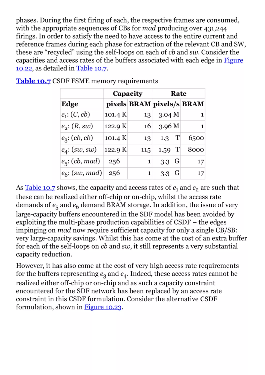
Table 10.6
Table 10.7
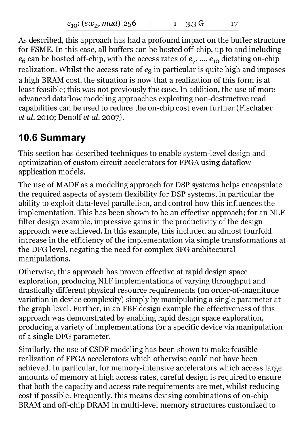
Table 10.8
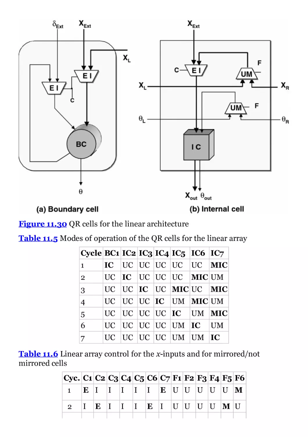
Chapter 11
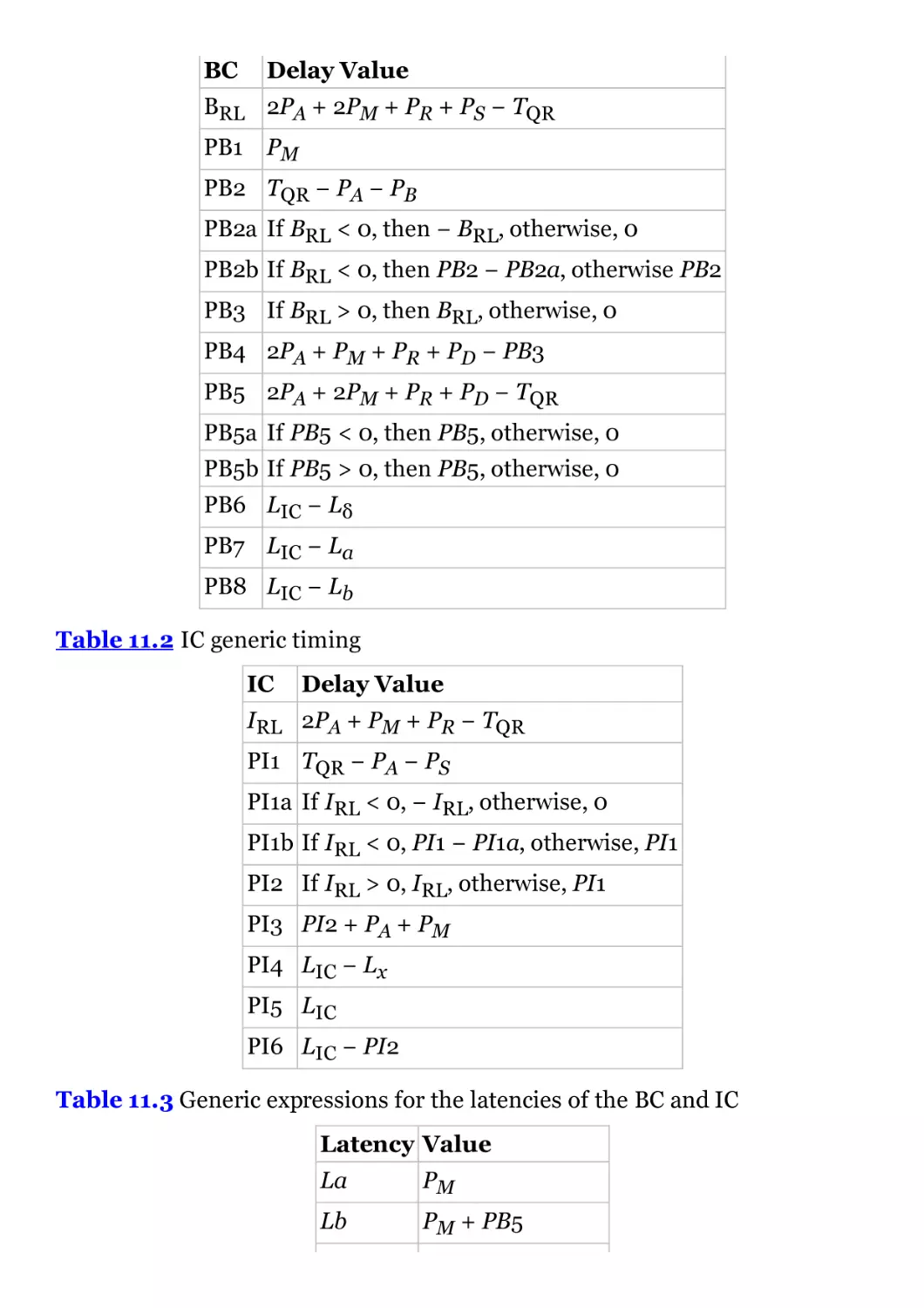
Table 11.1
Table 11.2
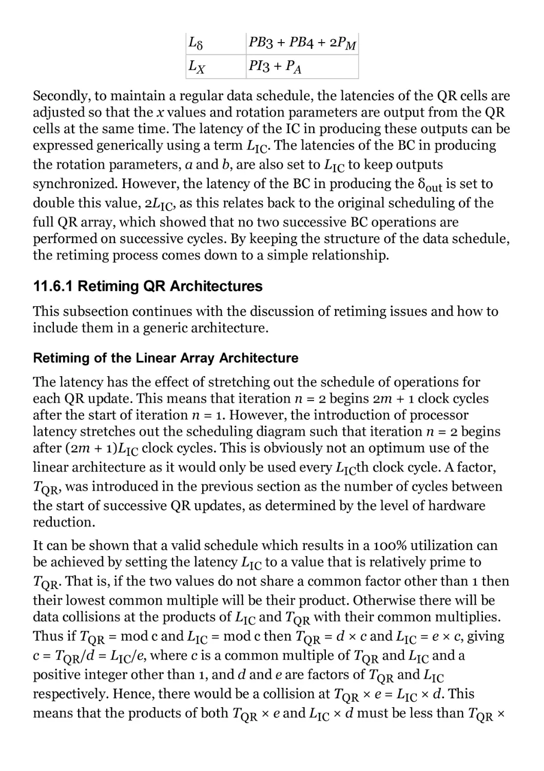
Table 11.3
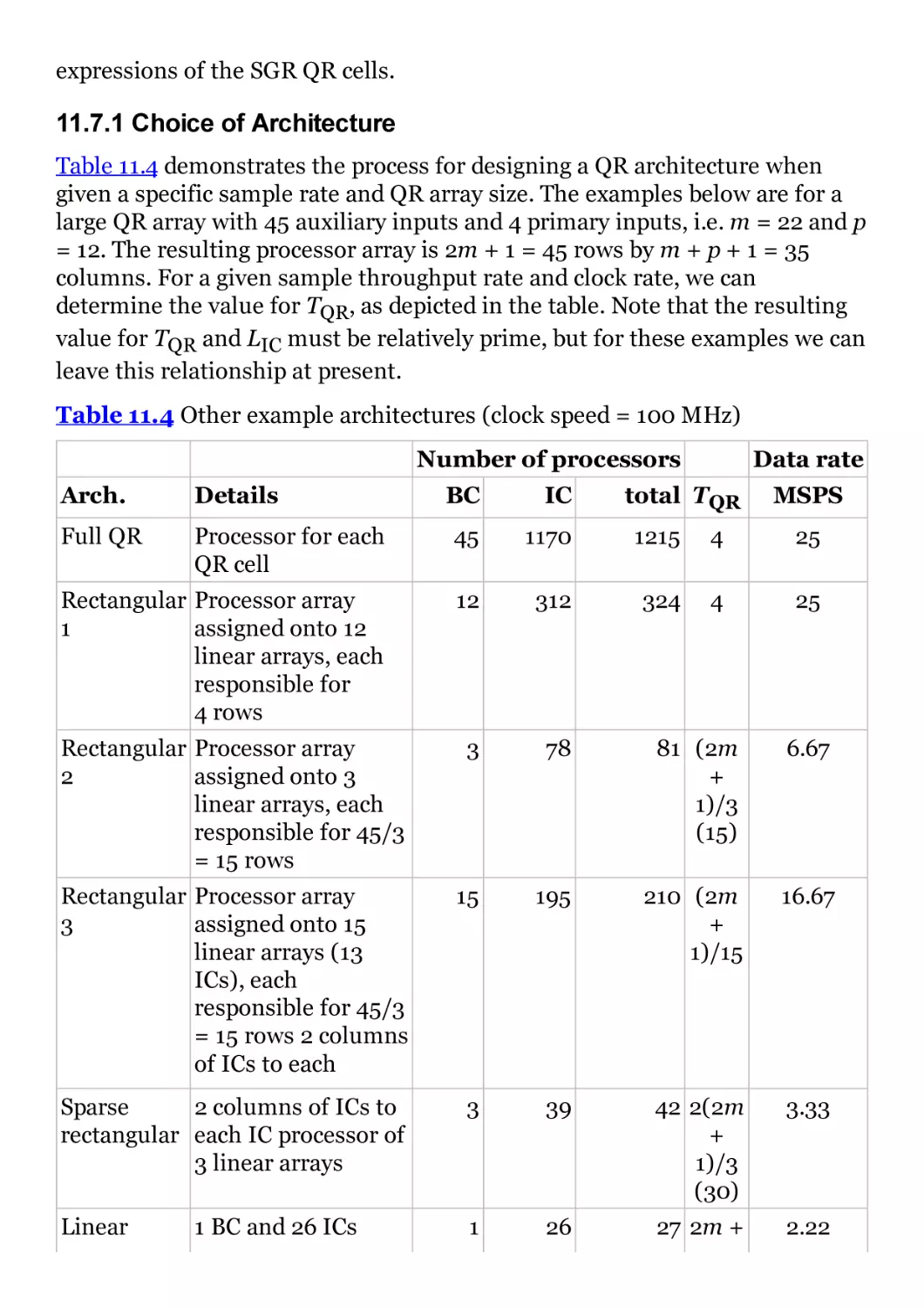
Table 11.4
Table 11.5
Table 11.6
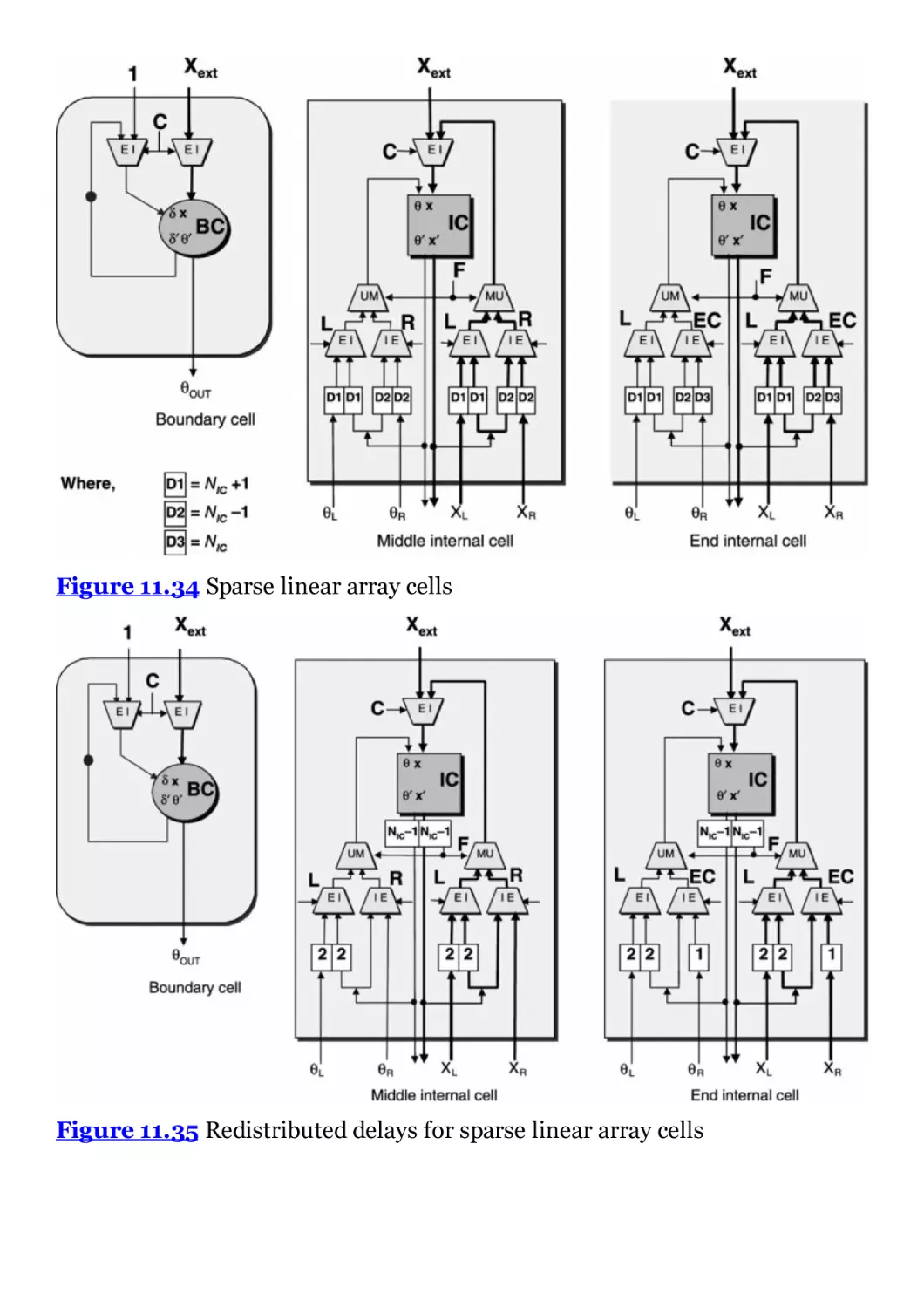
Table 11.7
Table 11.8
Chapter 12
Table 12.1
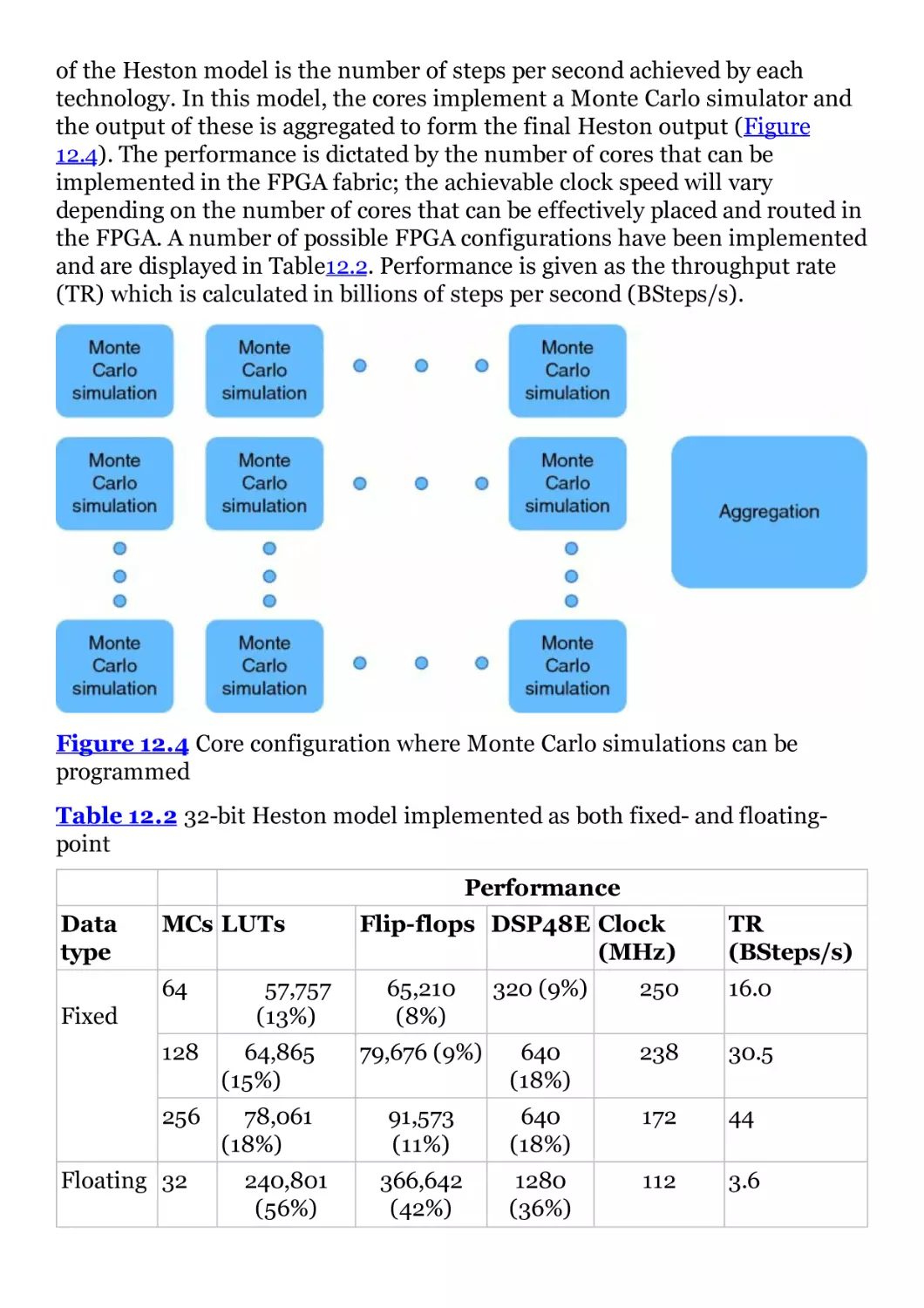
Table 12.2
Table 12.3
Table 12.4
Table 12.5
Chapter 13
Table 13.1
Table 13.2
Table 13.3
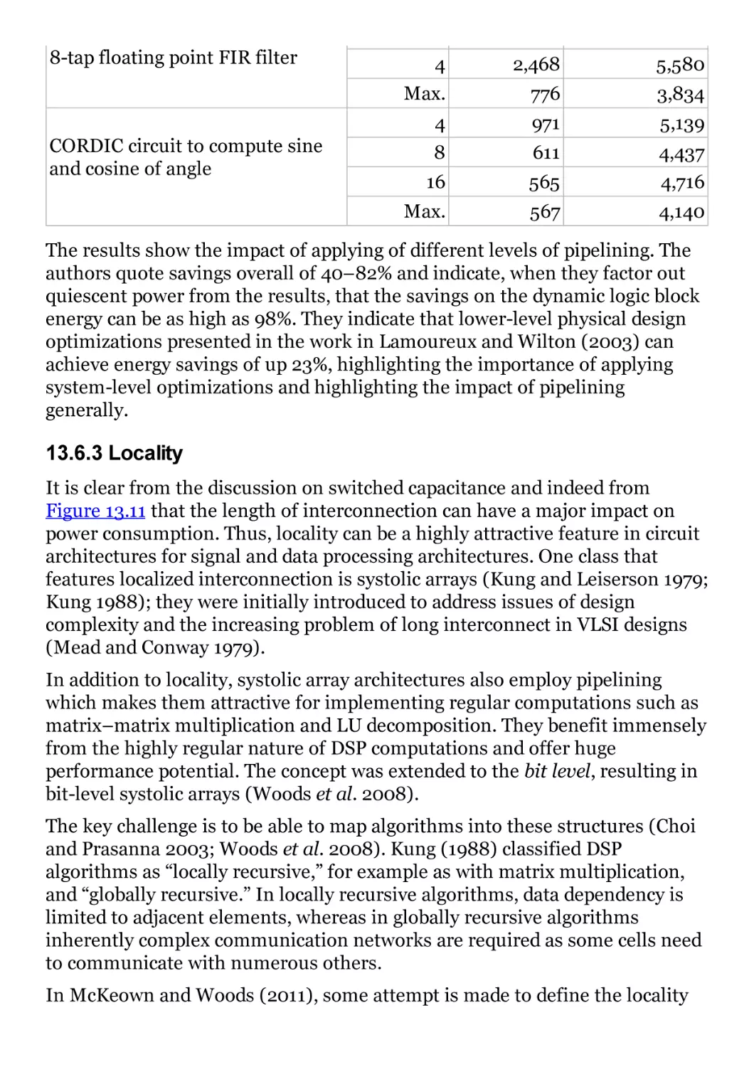
Table 13.4
Table 13.5
List of Illustrations
Chapter 1
Figure 1.1 Moore’s law
Figure 1.2 Change in ITRS scaling prediction for clock frequencies
Chapter 2
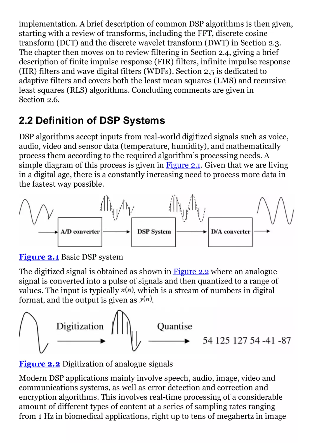
Figure 2.1 Basic DSP system
Figure 2.2 Digitization of analogue signals
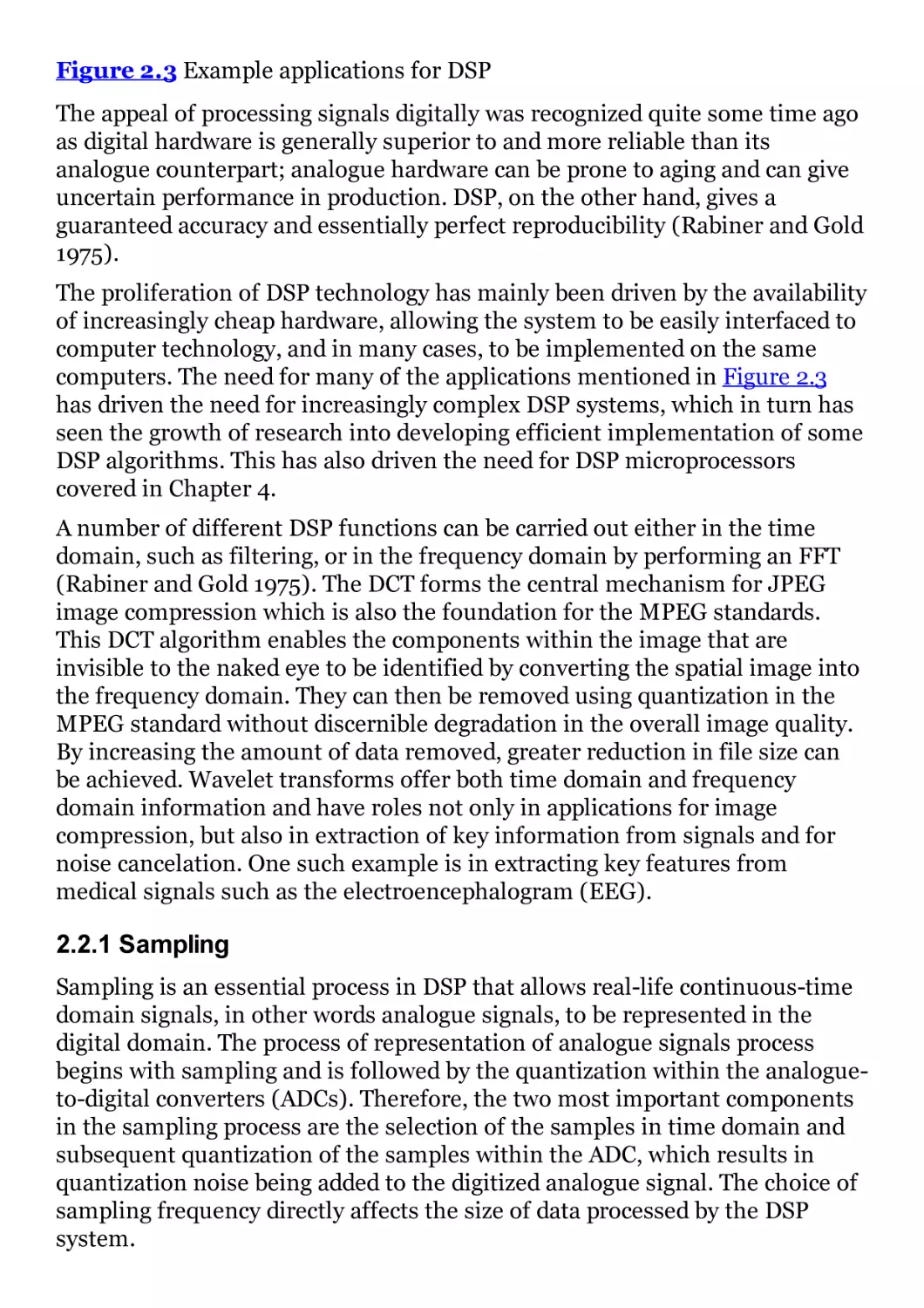
Figure 2.3 Example applications for DSP
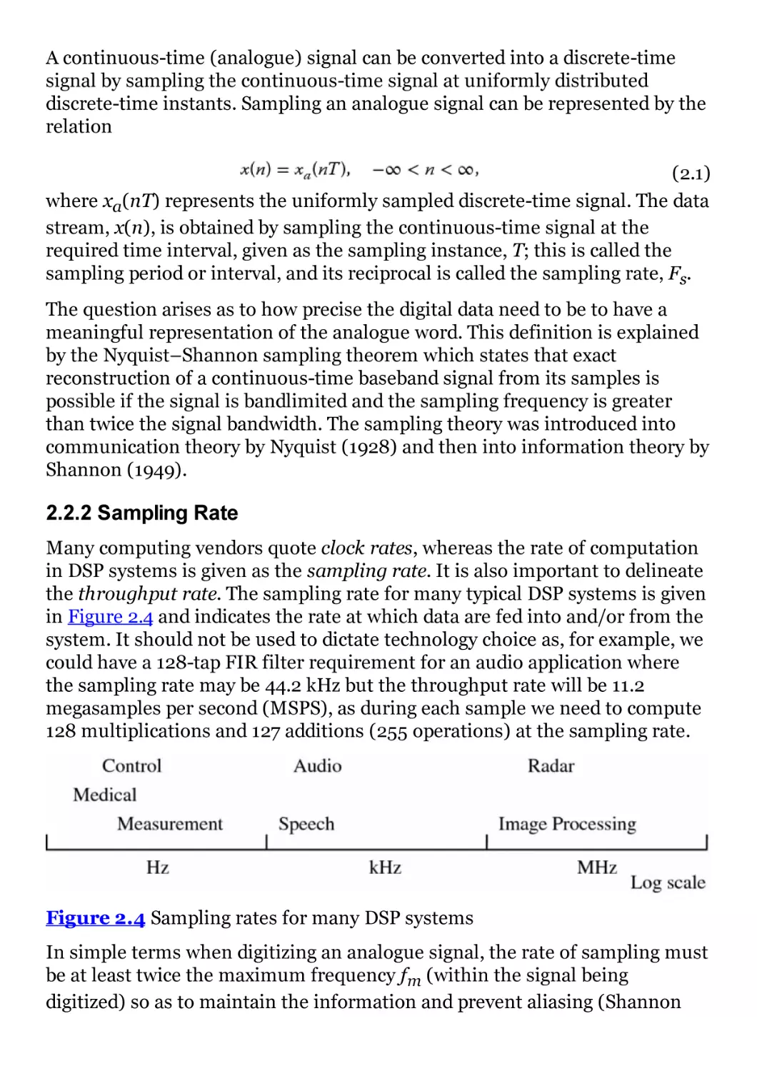
Figure 2.4 Sampling rates for many DSP systems
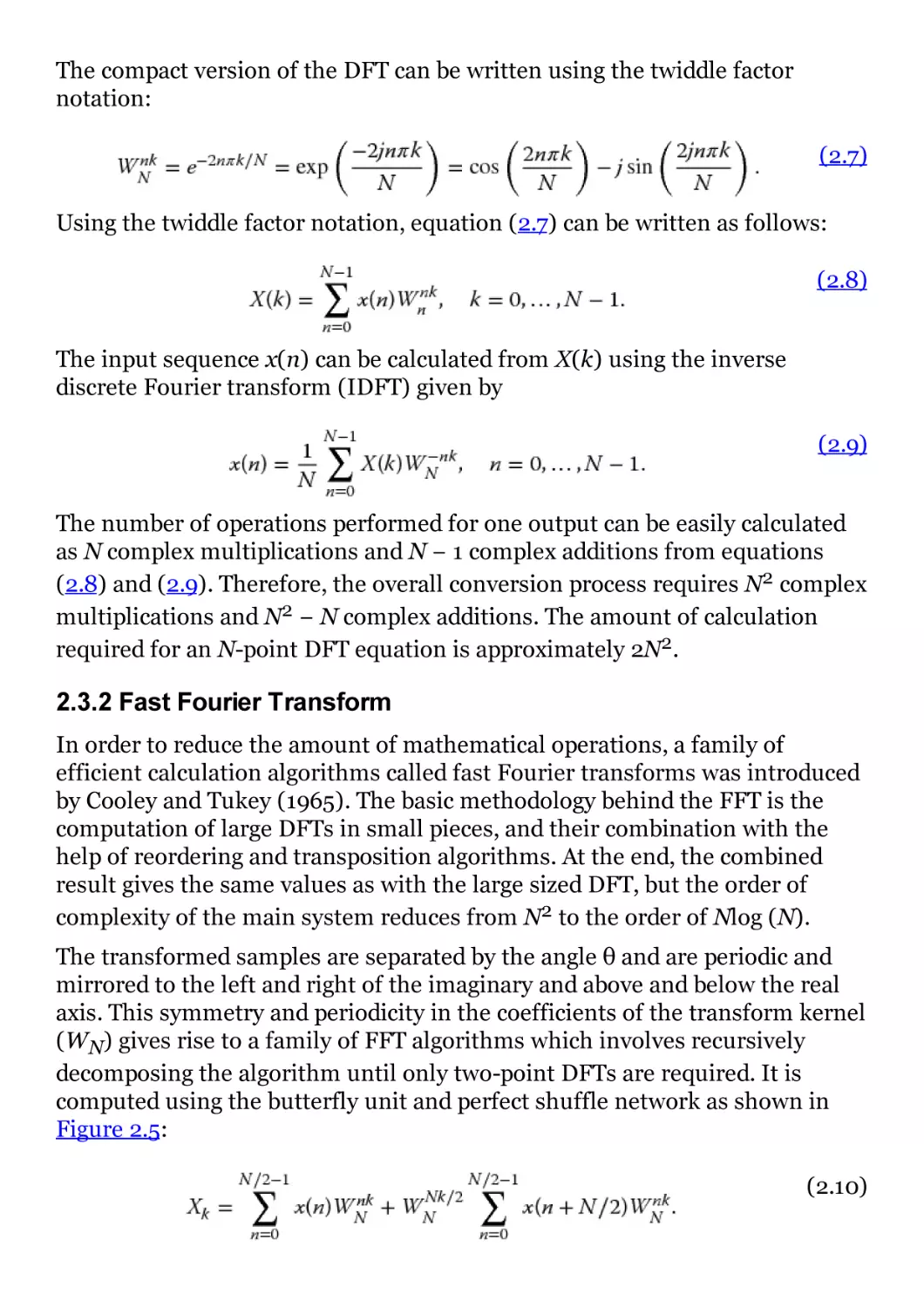
Figure 2.5 Eight-point radix-2 FFT structure
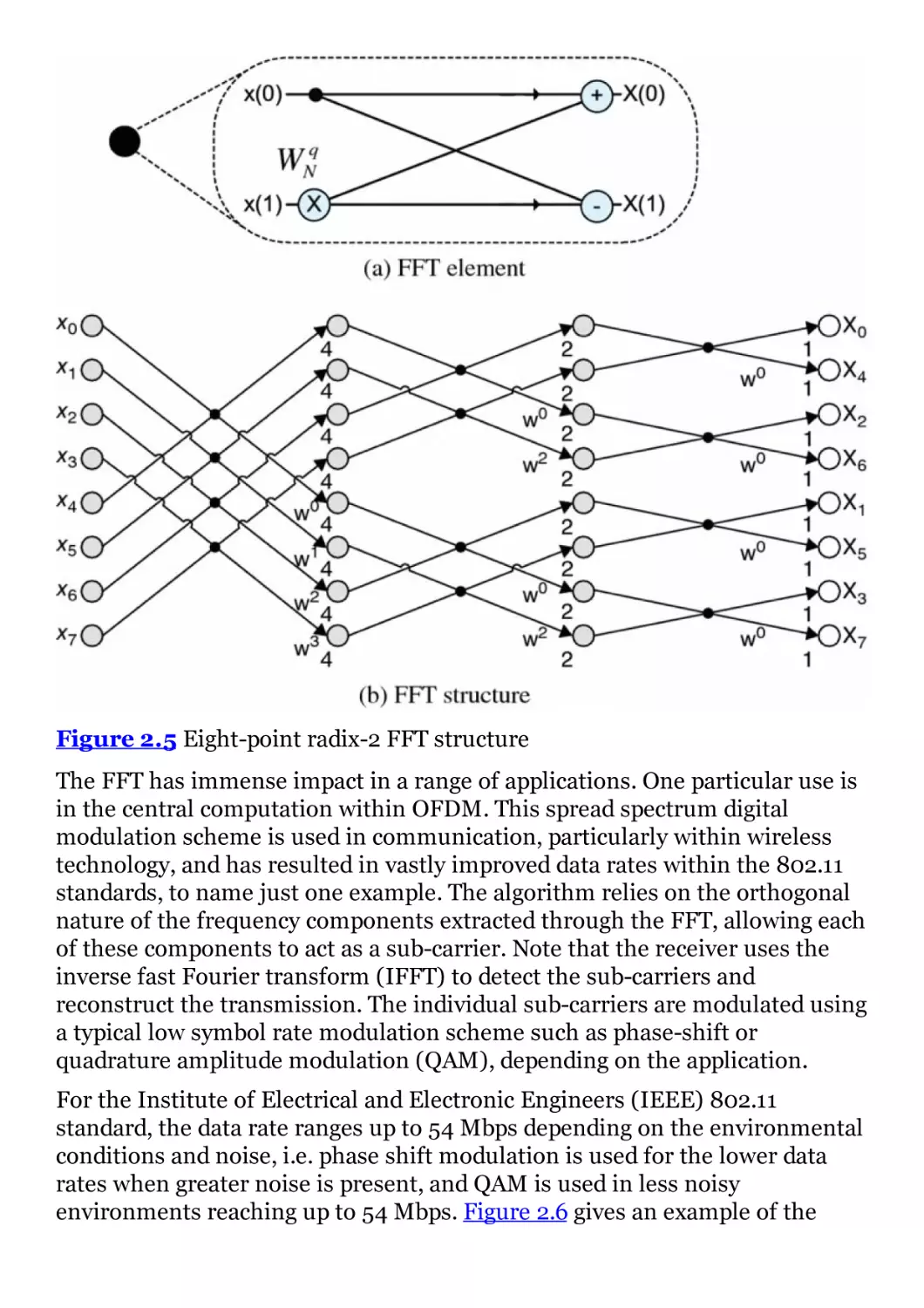
Figure 2.6 Wireless communications transmitter
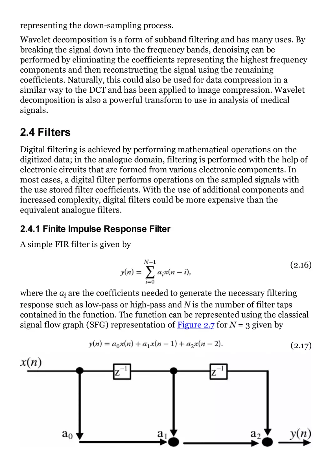
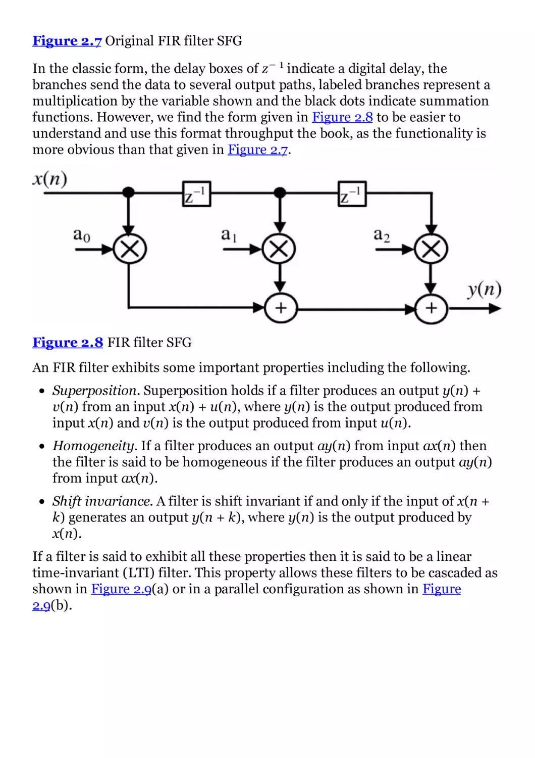
Figure 2.7 Original FIR filter SFG
Figure 2.8 FIR filter SFG
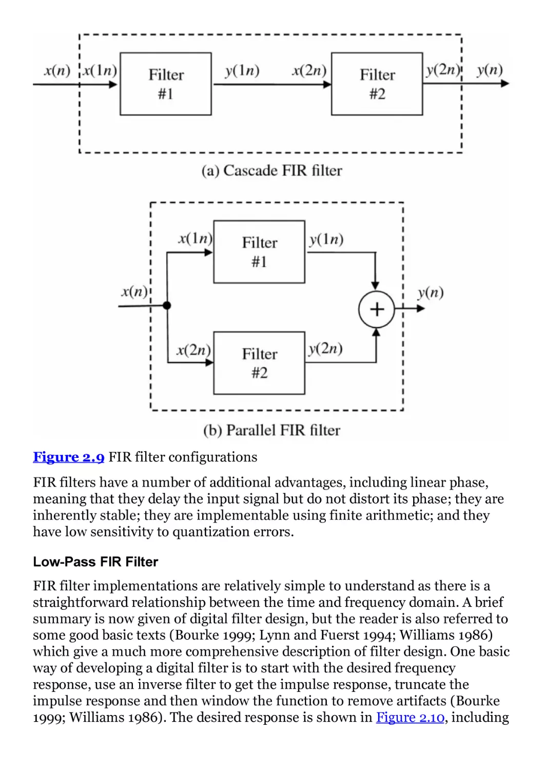
Figure 2.9 FIR filter configurations
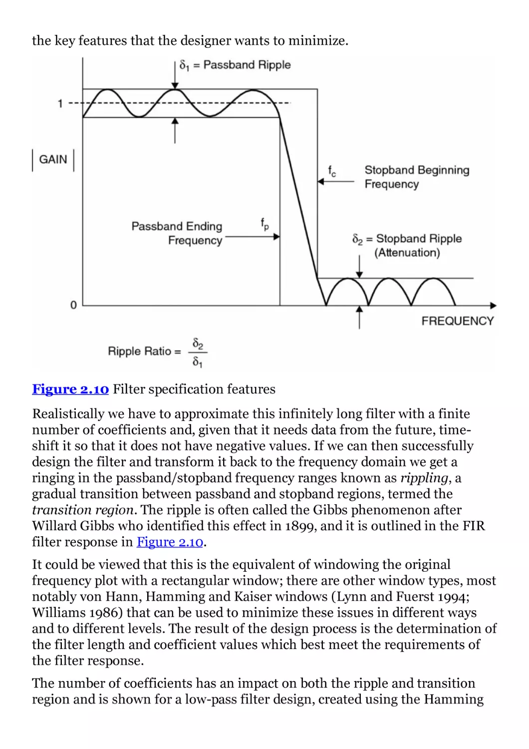
Figure 2.10 Filter specification features
Figure 2.11 Low-pass filter response
Figure 2.12 Direct form IIR filter
Figure 2.13 IIR filter distortion
Figure 2.14 Frequency impact of warping
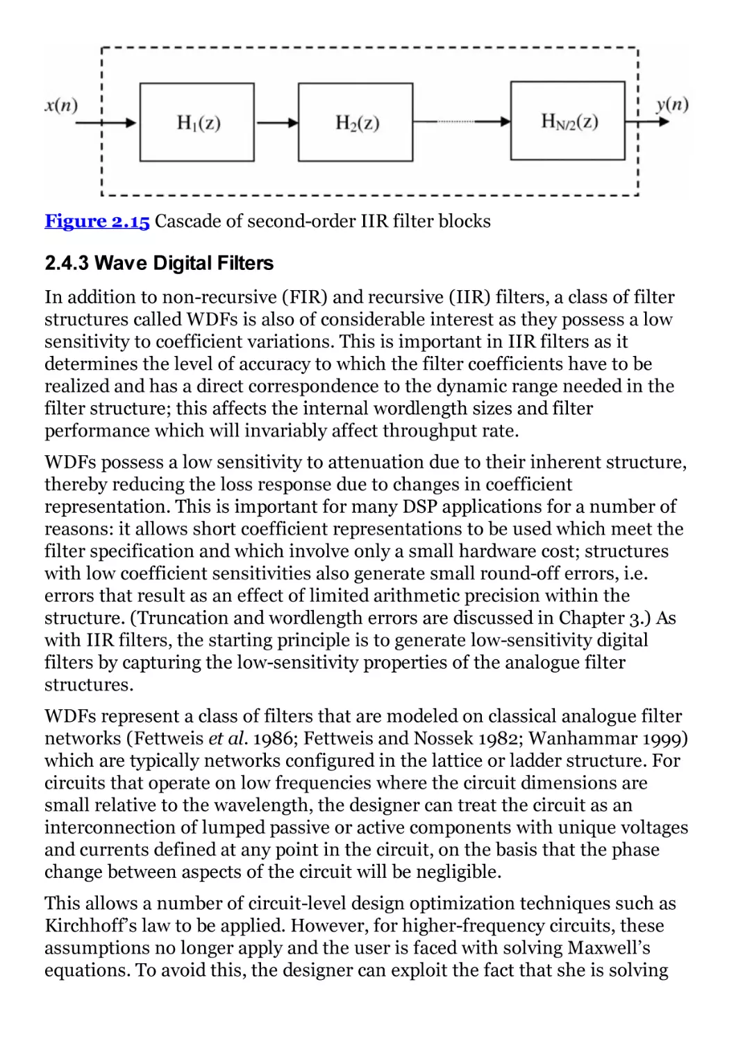
Figure 2.15 Cascade of second-order IIR filter blocks
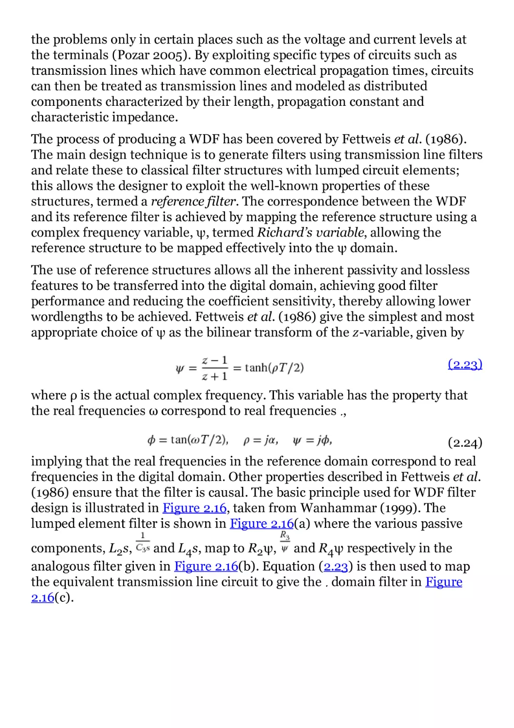
Figure 2.16 WDF configuration
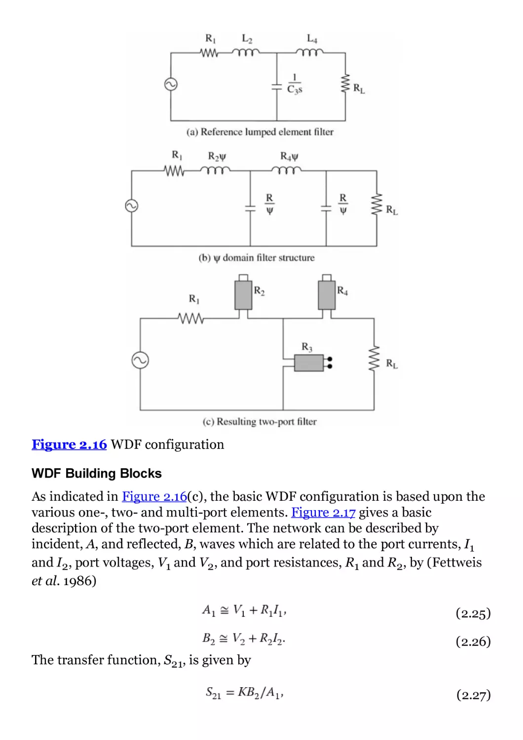
Figure 2.17 WDF building blocks
Figure 2.18 Adaptive filter system
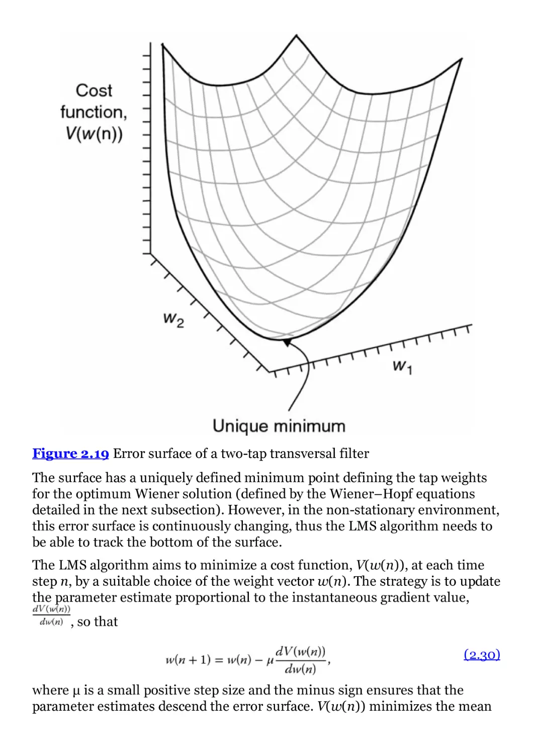
Figure 2.19 Error surface of a two-tap transversal filter
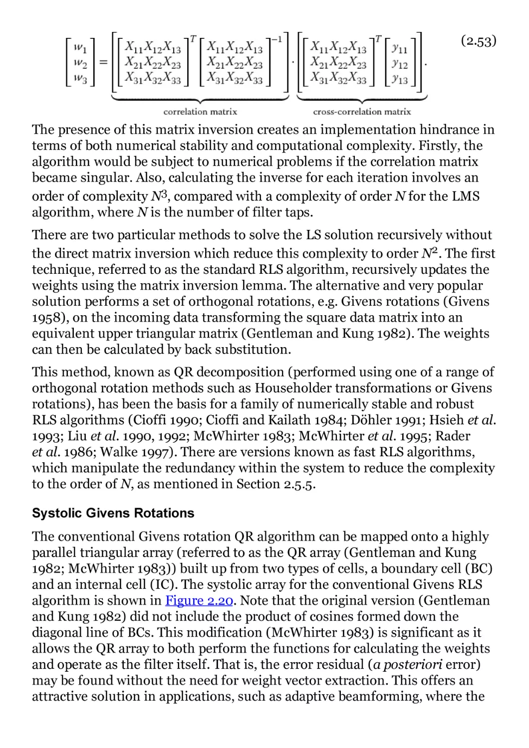
Figure 2.20 Systolic QR array for the RLS algorithm
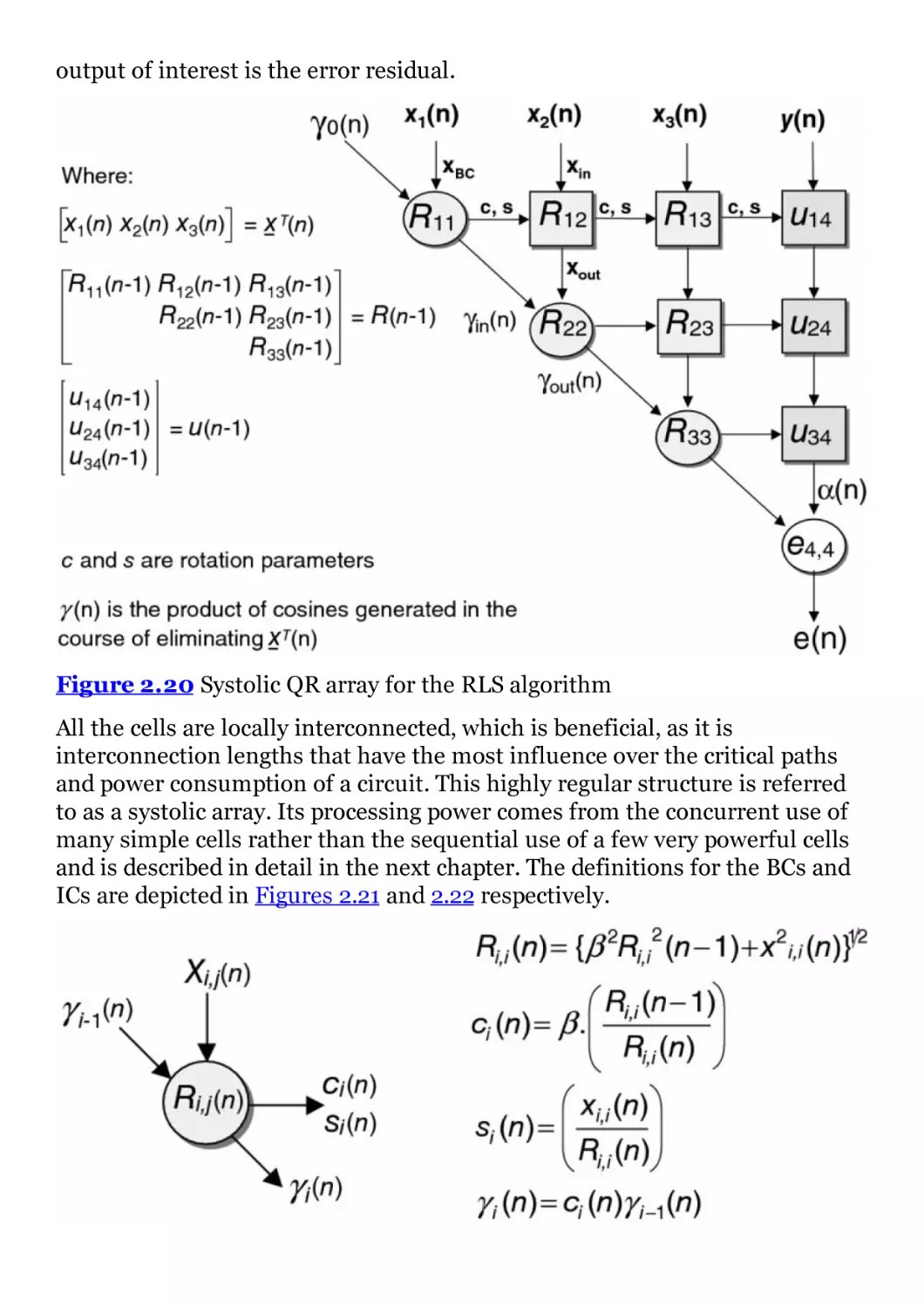
Figure 2.21 BC for QR-RLS algorithm
Figure 2.22 IC for QR-RLS algorithm
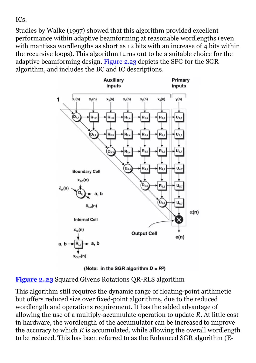
Figure 2.23 Squared Givens Rotations QR-RLS algorithm
Chapter 3
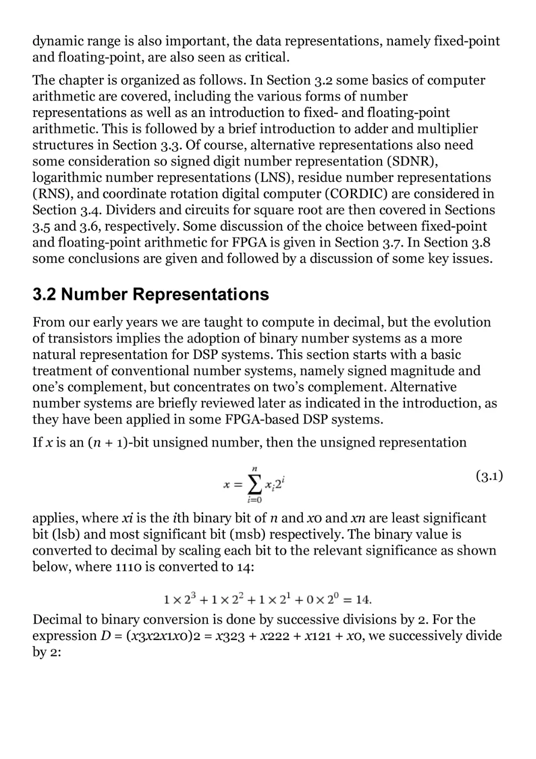
Figure 3.1 Number wheel representation of four-bit numbers
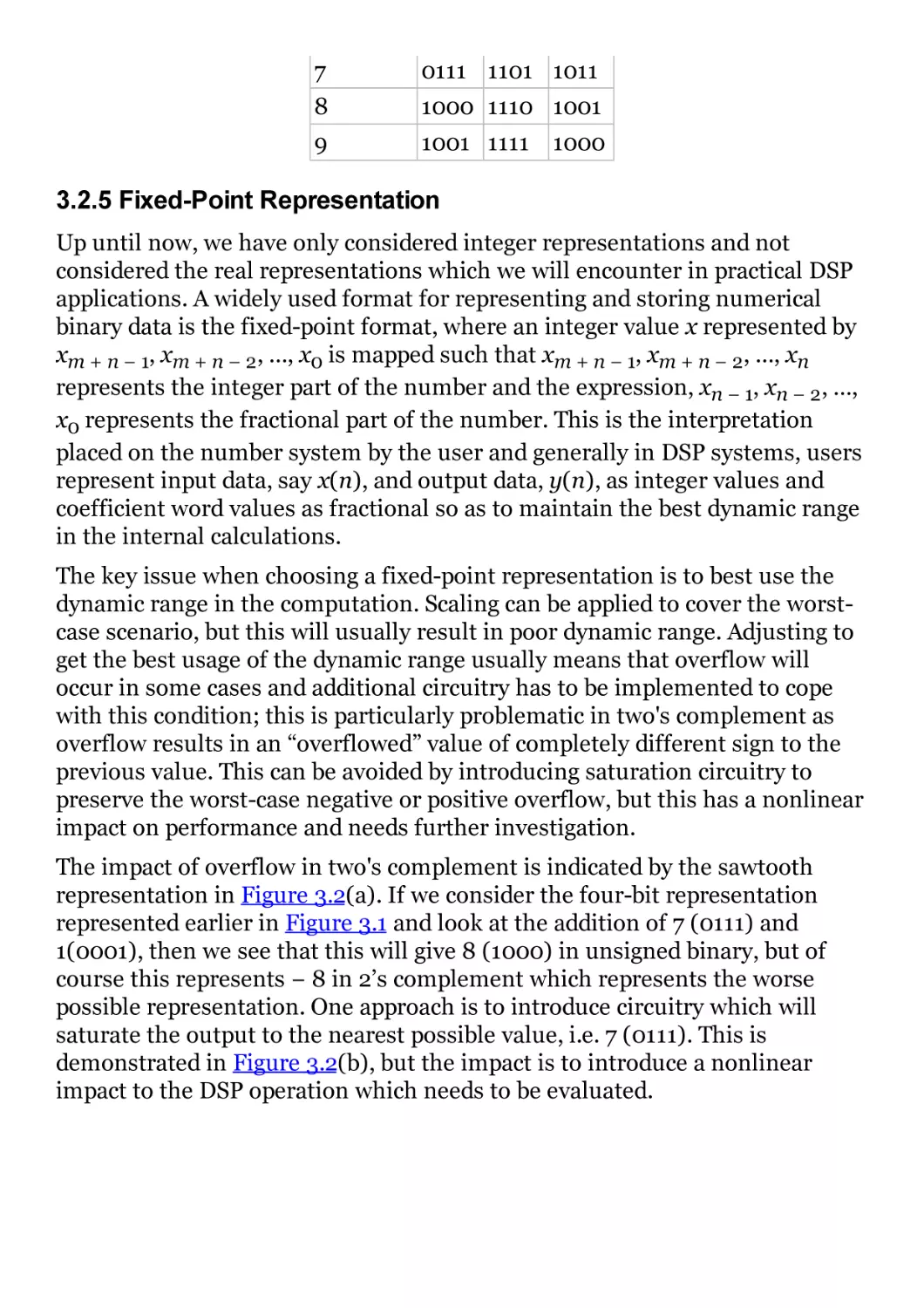
Figure 3.2 Impact of overflow in two's complement
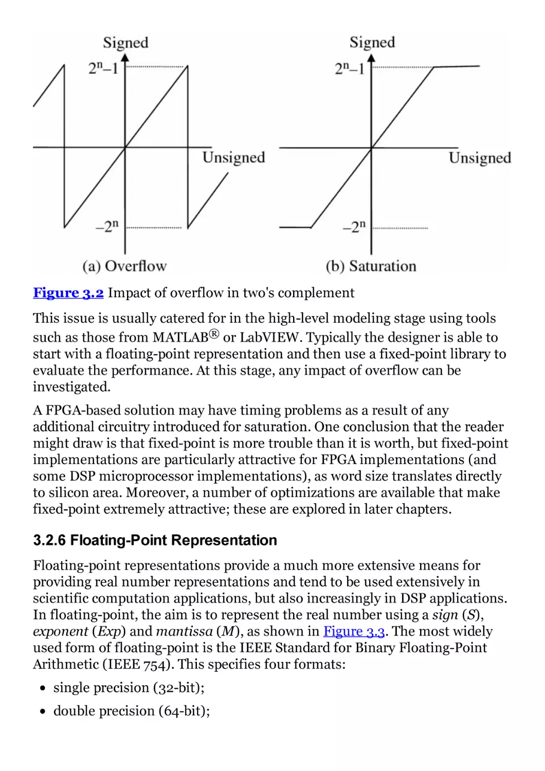
Figure 3.3 Floating-point representations
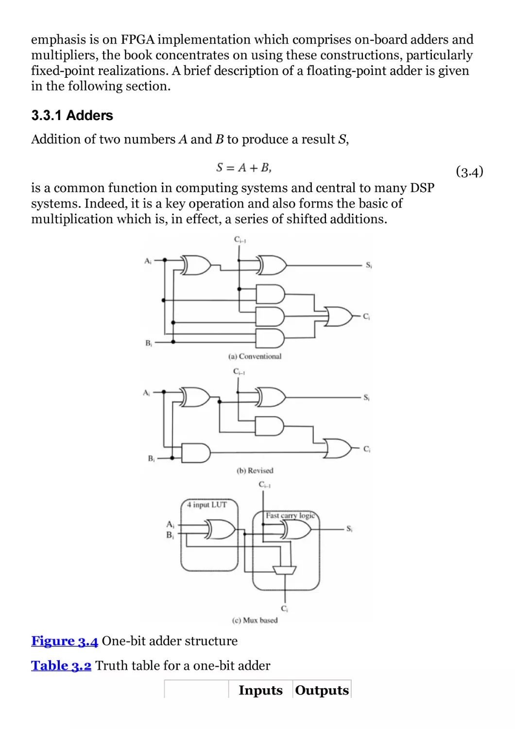
Figure 3.4 One-bit adder structure
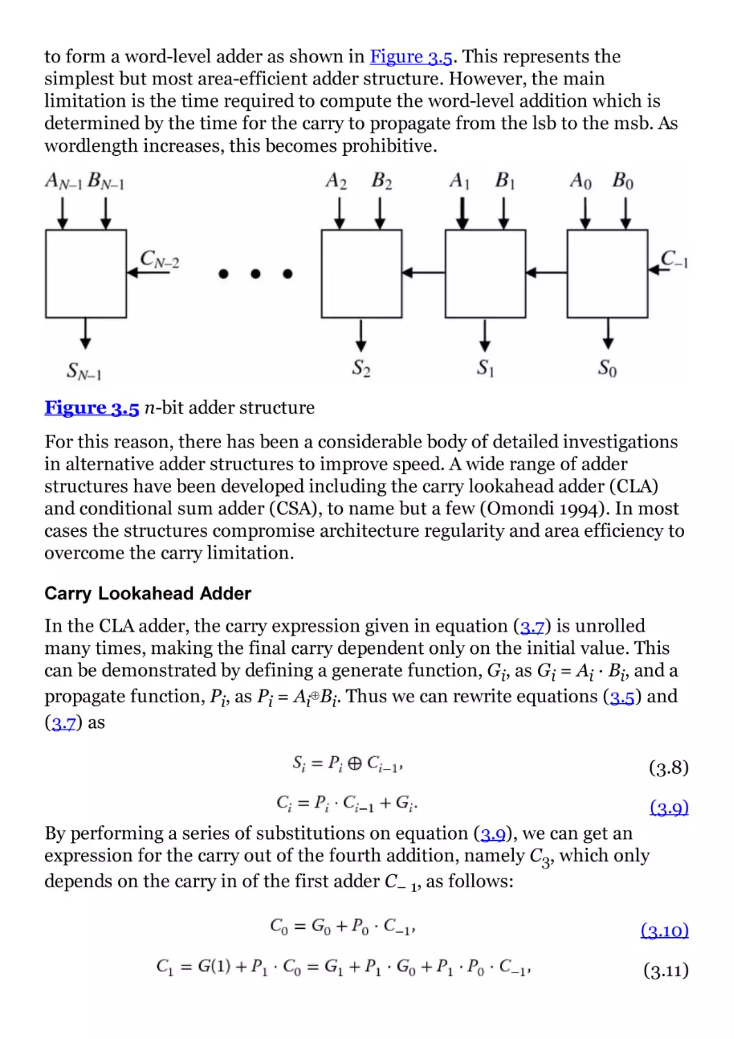
Figure 3.5 n-bit adder structure
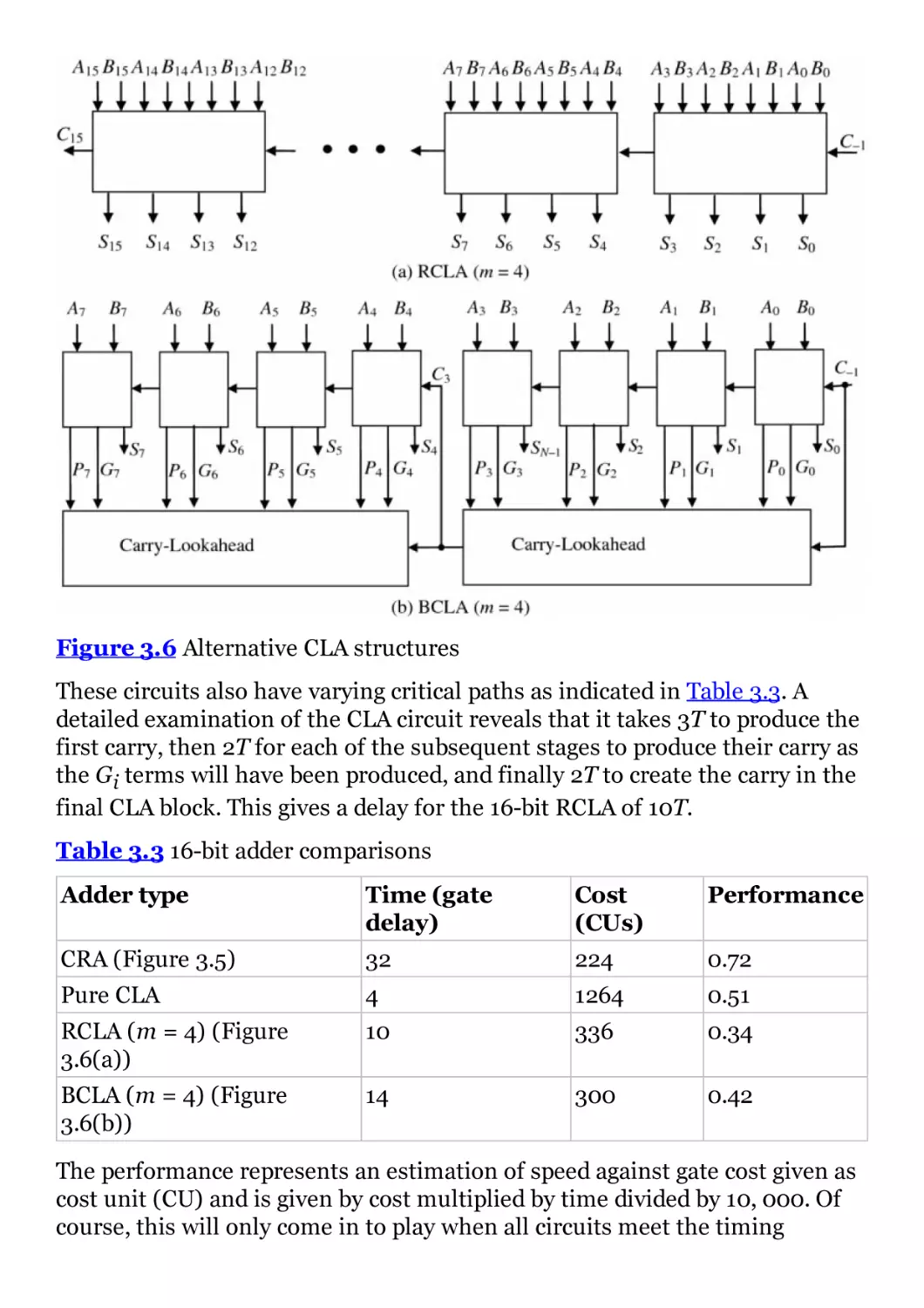
Figure 3.6 Alternative CLA structures
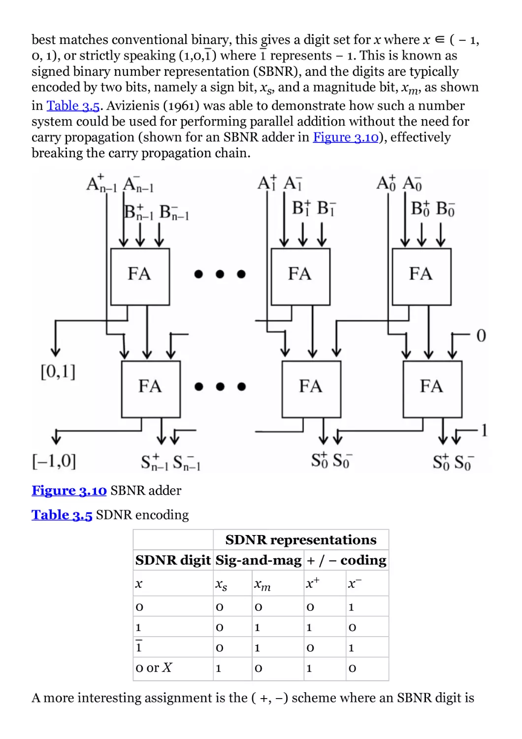
Figure 3.7 Carry-save adder
Figure 3.8 Carry-save array multiplier
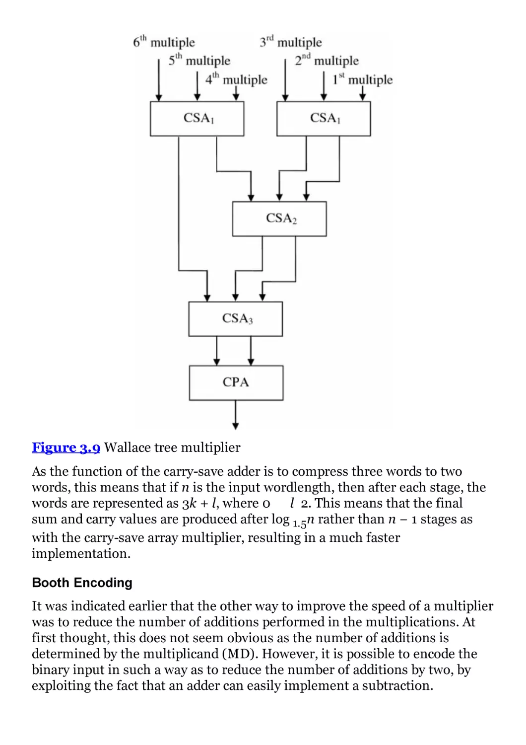
Figure 3.9 Wallace tree multiplier
Figure 3.10 SBNR adder
Figure 3.11 Quadratic convergence
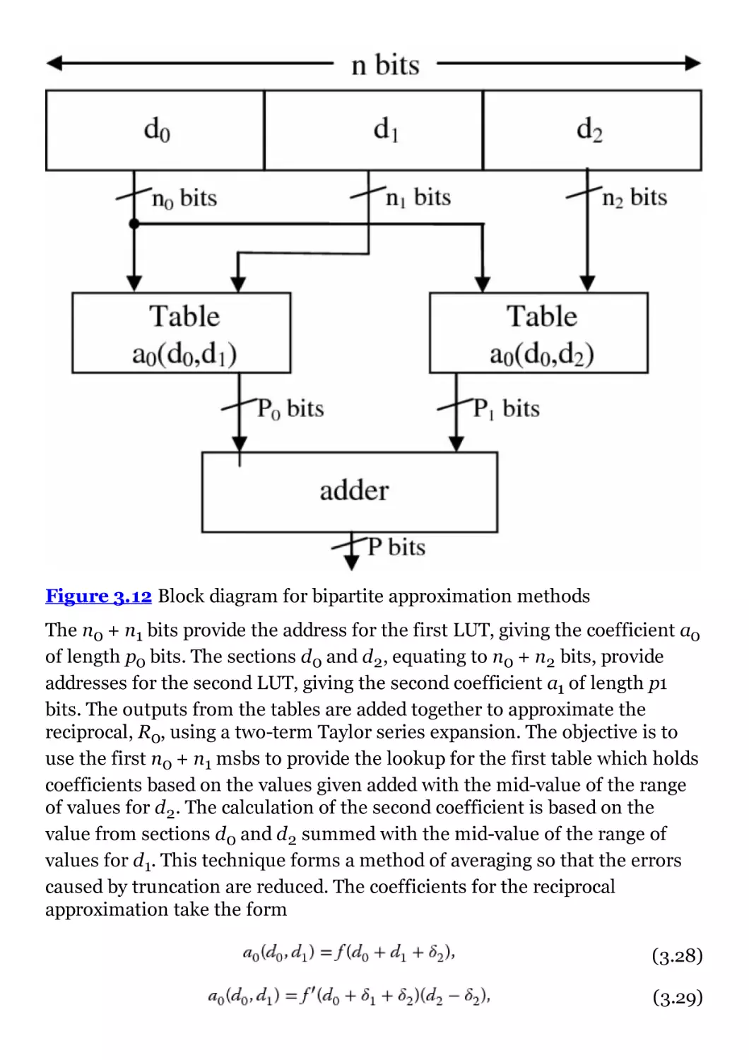
Figure 3.12 Block diagram for bipartite approximation methods
Chapter 4
Figure 4.1 Conclusions from Intel CPU scaling
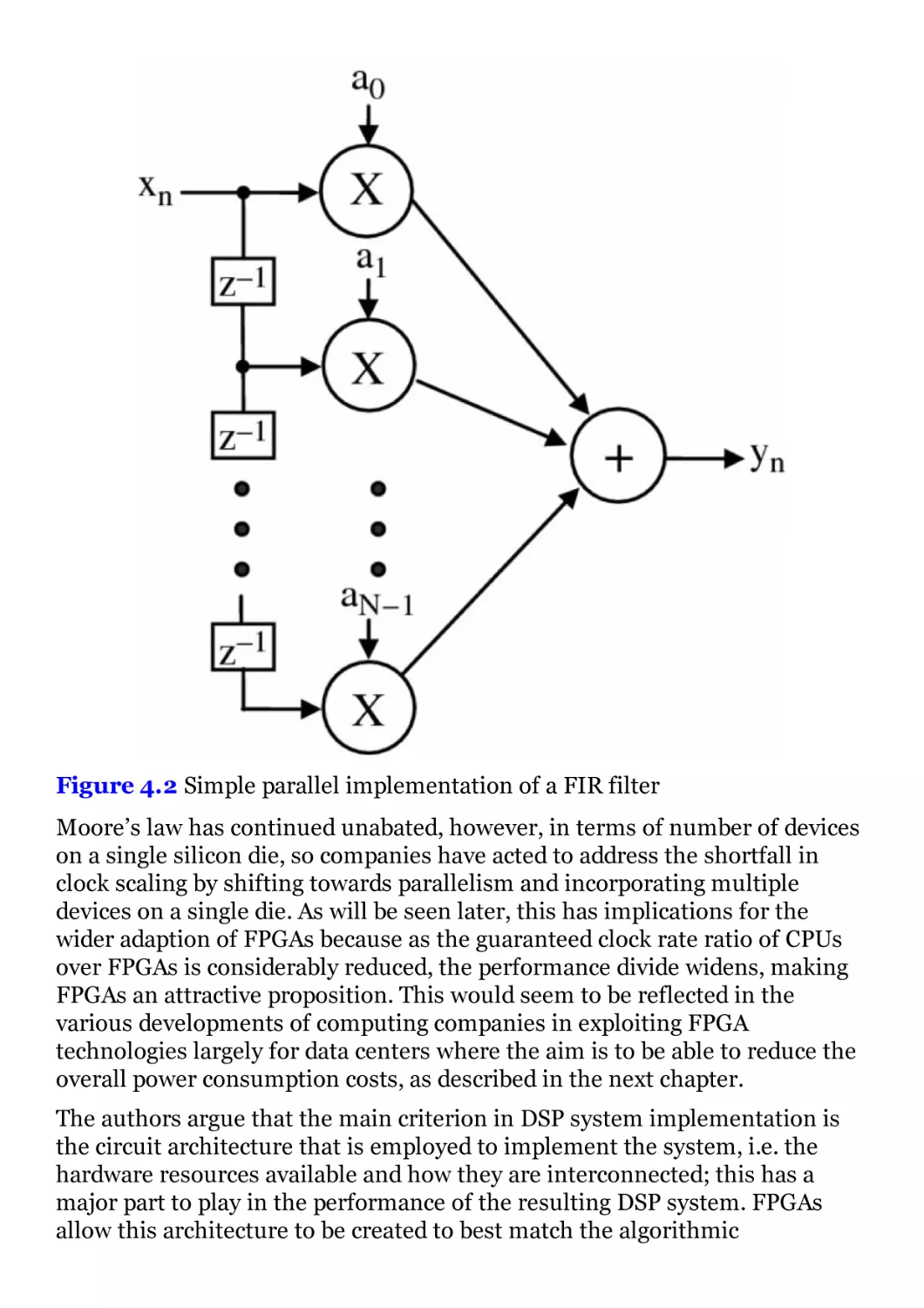
Figure 4.2 Simple parallel implementation of a FIR filter
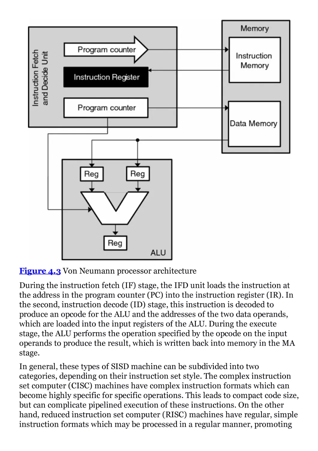
Figure 4.3 Von Neumann processor architecture
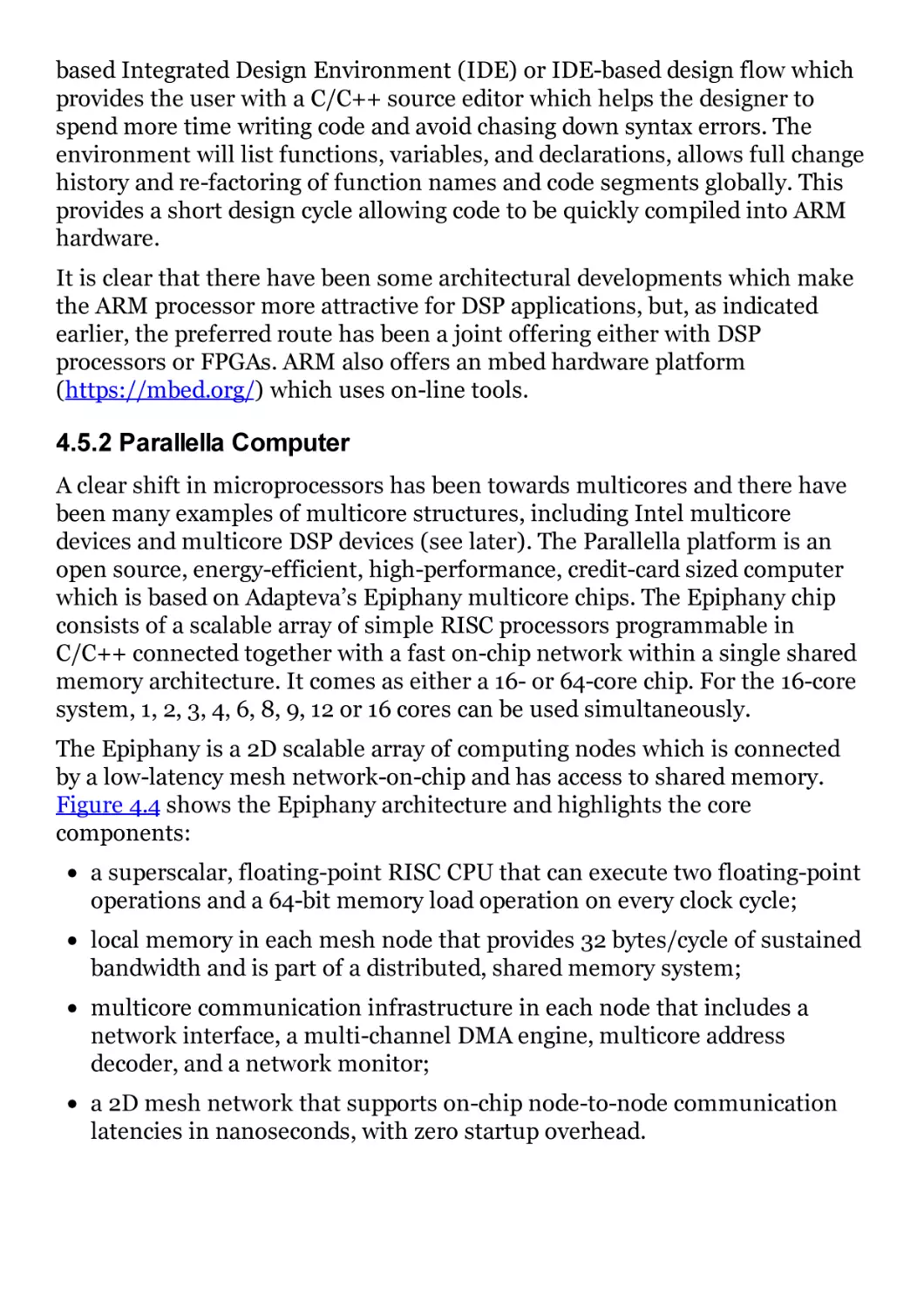
Figure 4.4 Epiphany architecture
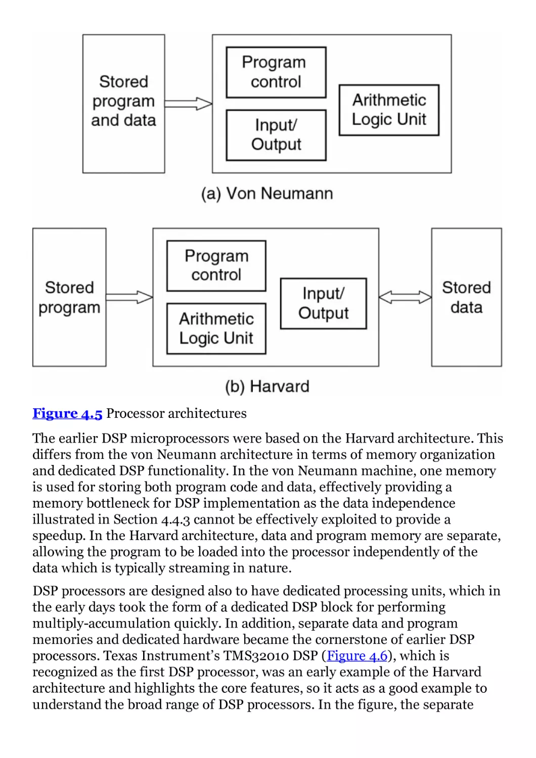
Figure 4.5 Processor architectures
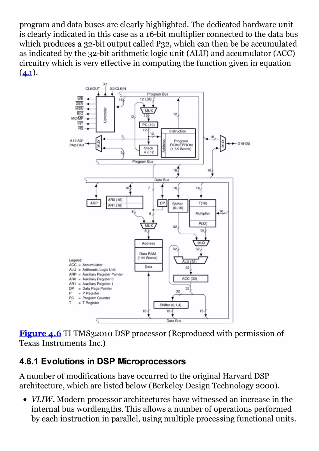
Figure 4.6 TI TMS32010 DSP processor (Reproduced with permission
of Texas Instruments Inc.)
Figure 4.7 TMS320C6678 multicore fixed and floating-point DSP
microprocessor
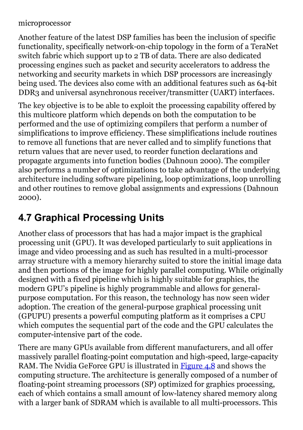
Figure 4.8 Nvidia GeForce GPU architecture
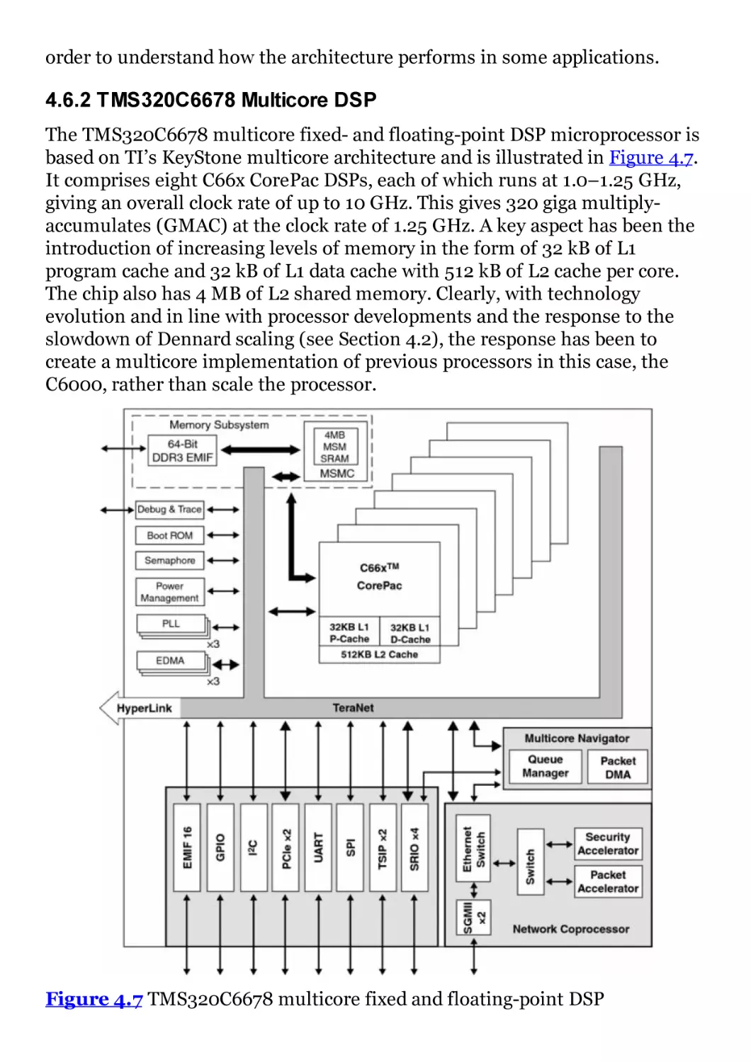
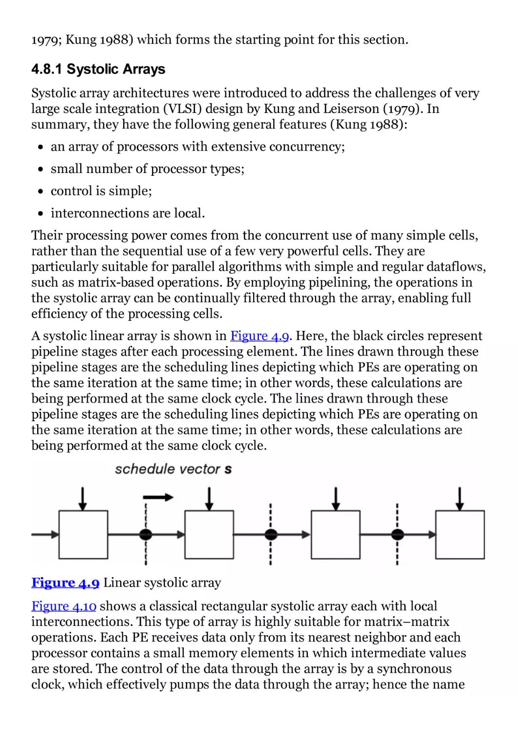
Figure 4.9 Linear systolic array
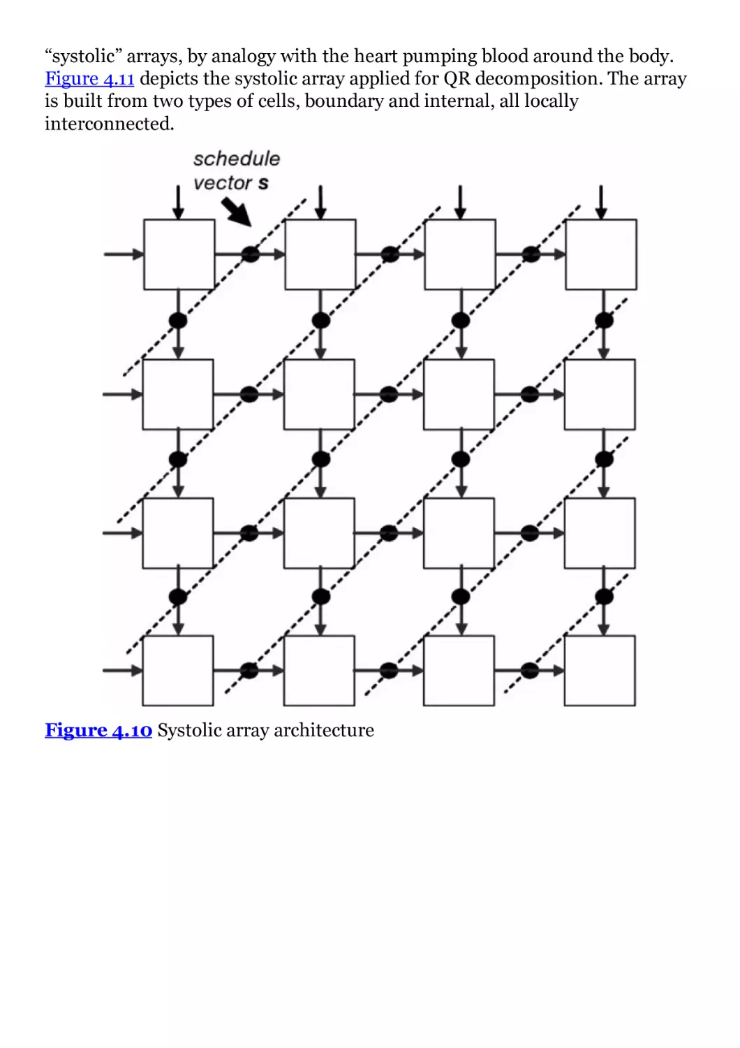
Figure 4.10 Systolic array architecture
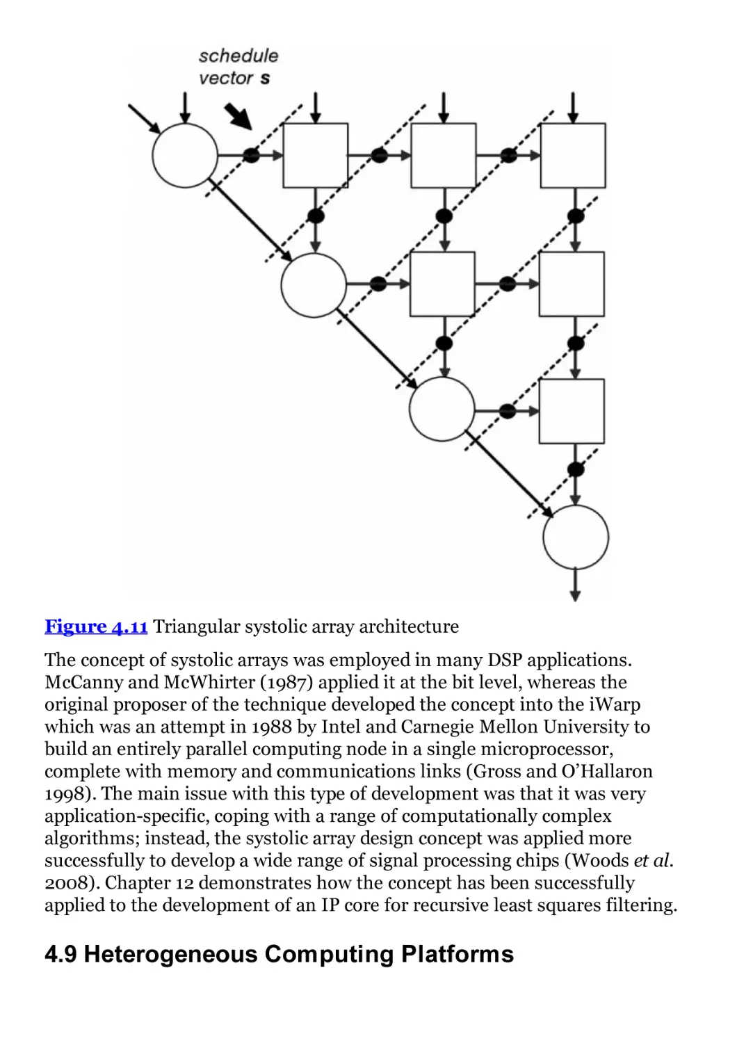
Figure 4.11 Triangular systolic array architecture
Chapter 5
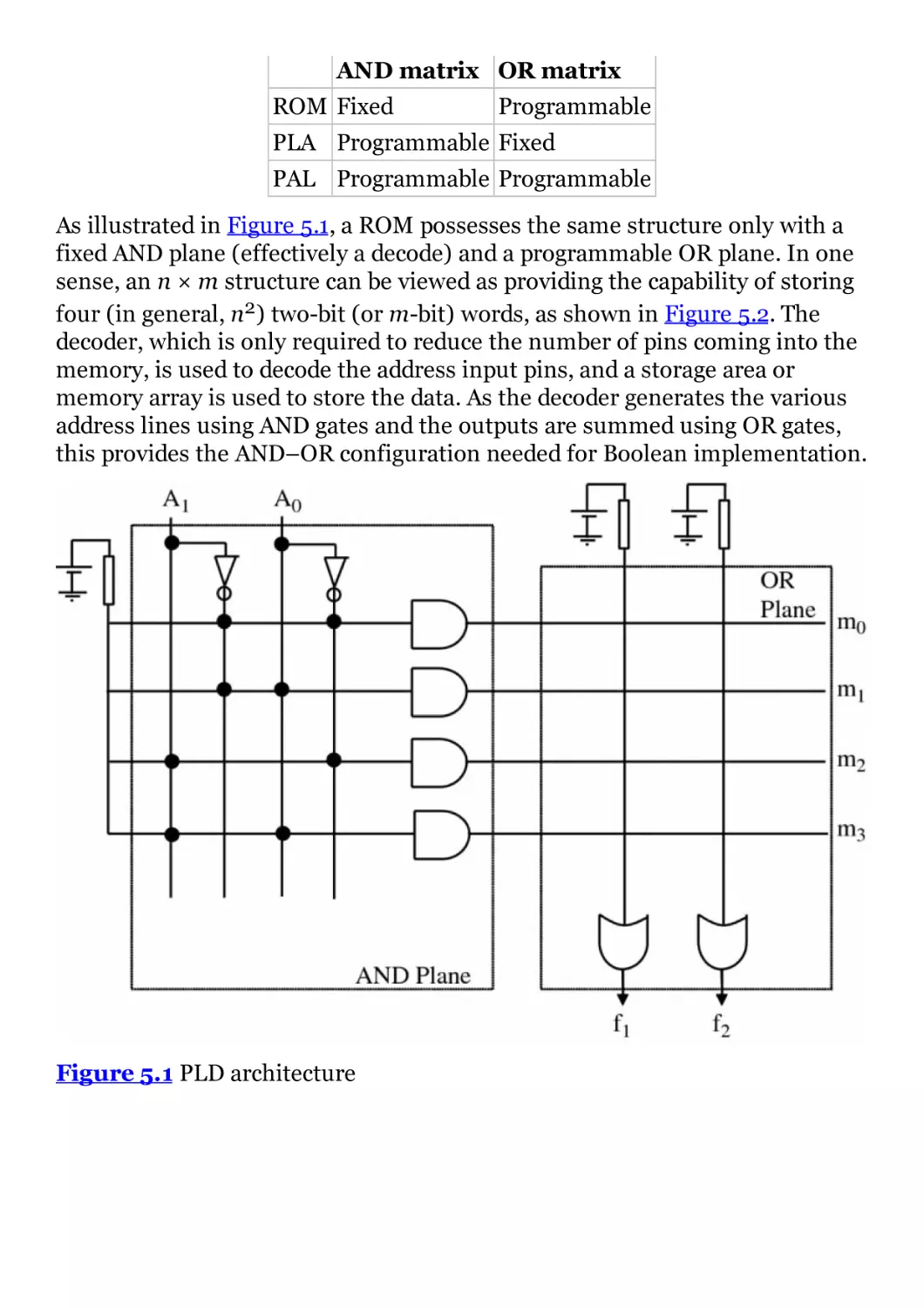
Figure 5.1 PLD architecture
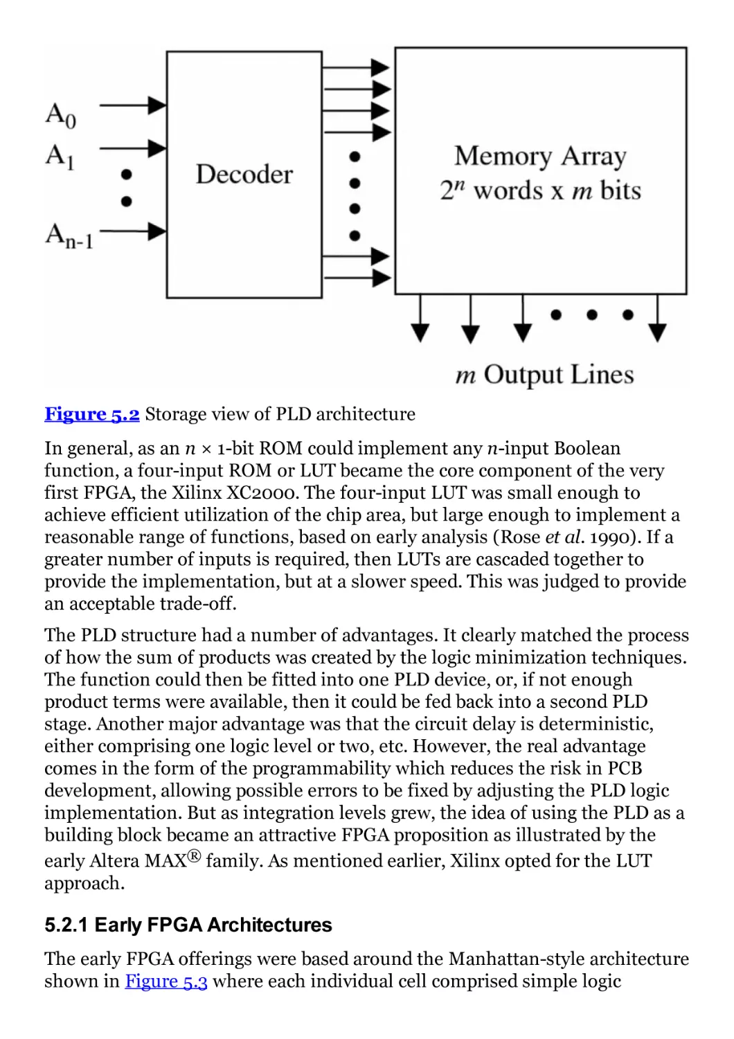
Figure 5.2 Storage view of PLD architecture
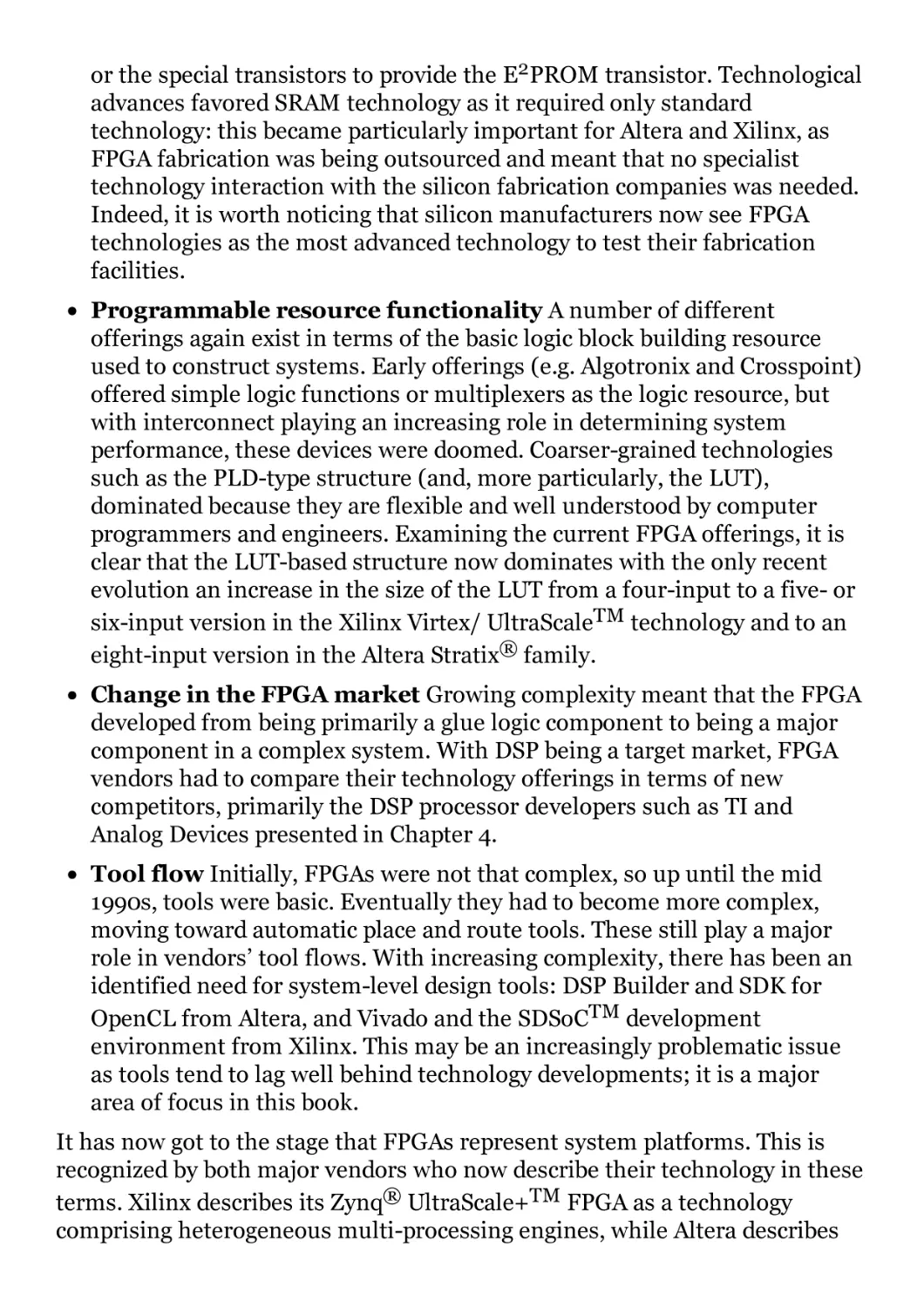
Figure 5.3 Early Manhattan architecture
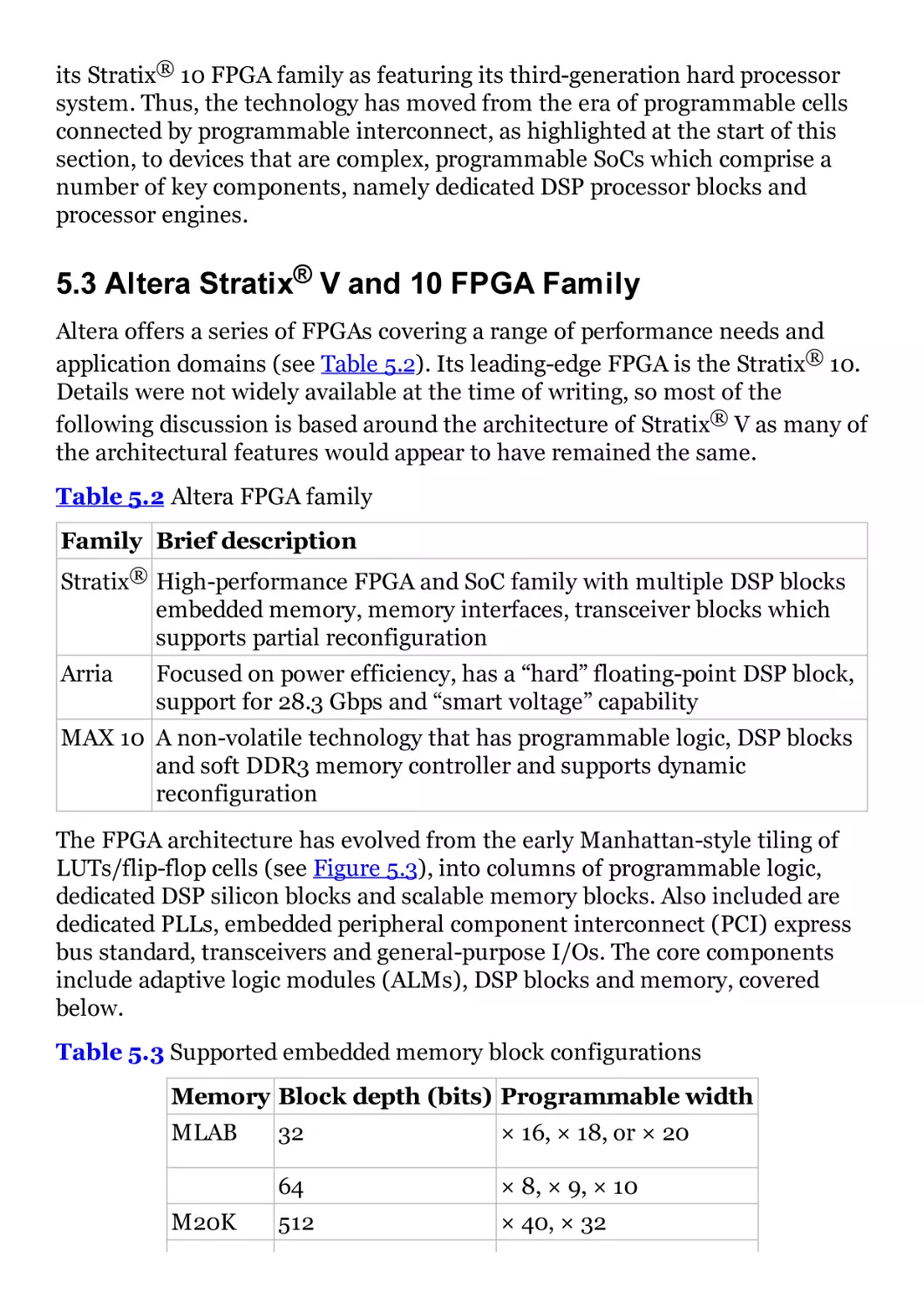
Figure 5.4 Adaptive logic module
Figure 5.5 Altera DSP block (simplified view)
Figure 5.6 Xilinx UltrascaleTM floorplan. Reproduced with
permission of Xilinx, Incorp.
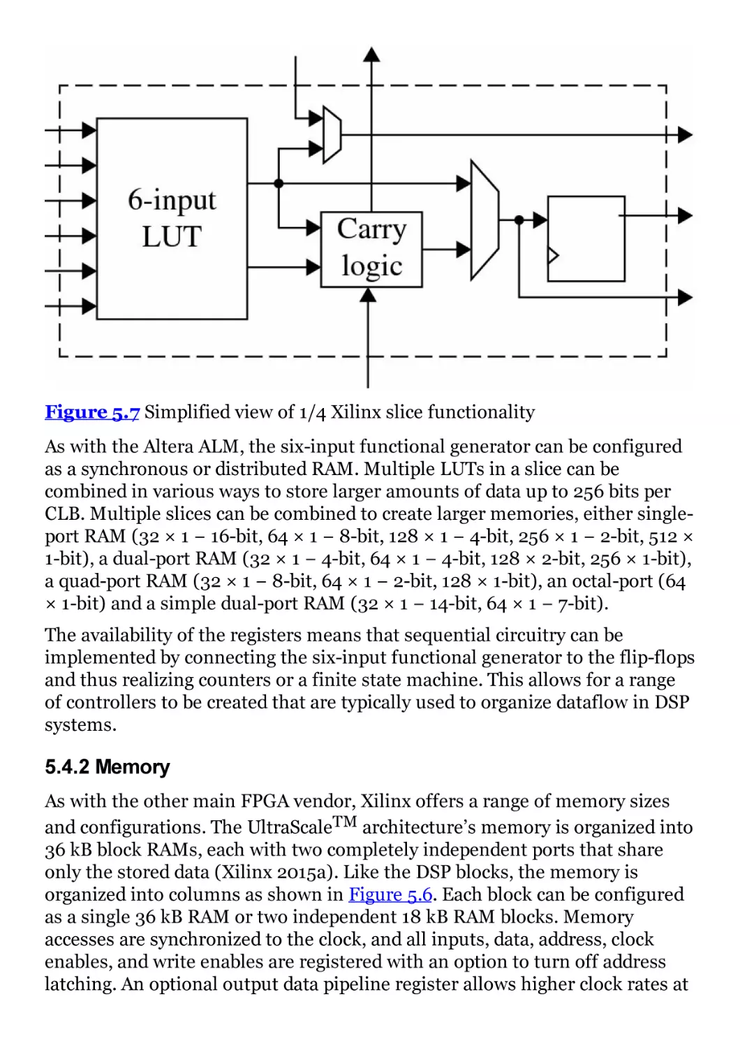
Figure 5.7 Simplified view of 1/4 Xilinx slice functionality
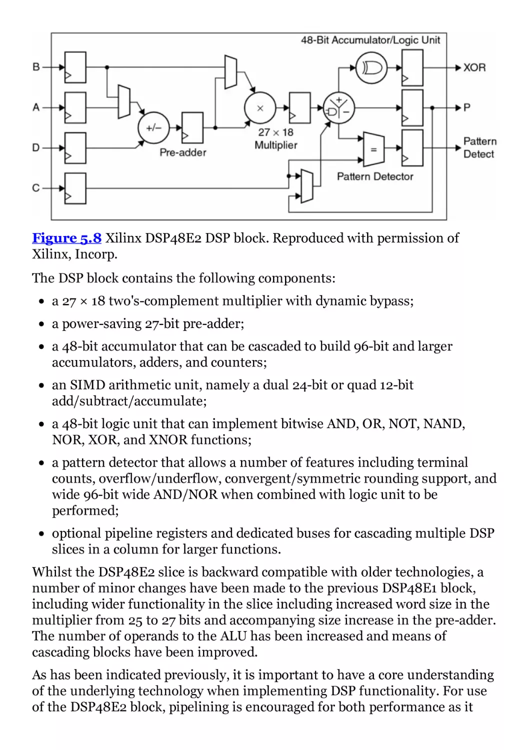
Figure 5.8 Xilinx DSP48E2 DSP block. Reproduced with permission
of Xilinx, Incorp.
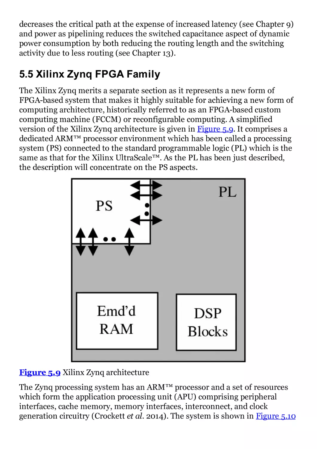
Figure 5.9 Xilinx Zynq architecture
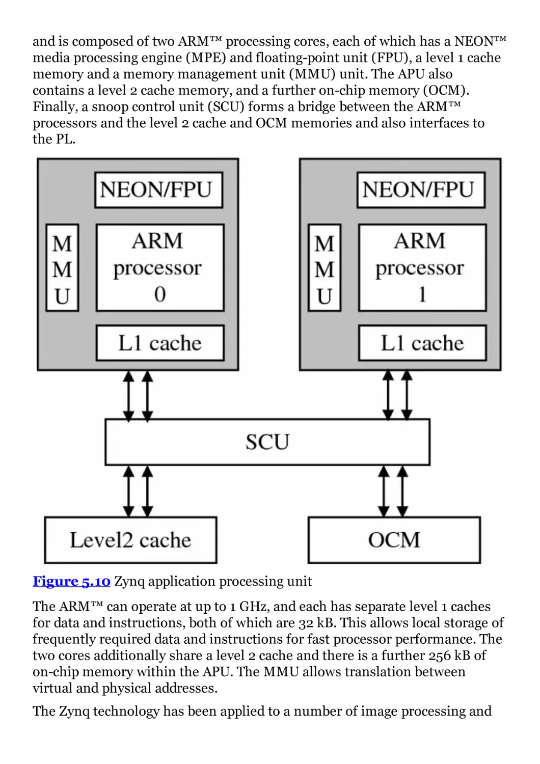
Figure 5.10 Zynq application processing unit
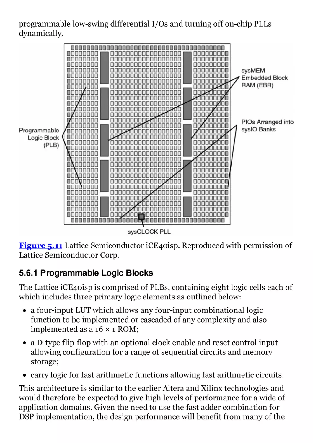
Figure 5.11 Lattice Semiconductor iCE40isp. Reproduced with
permission of Lattice Semiconductor Corp.
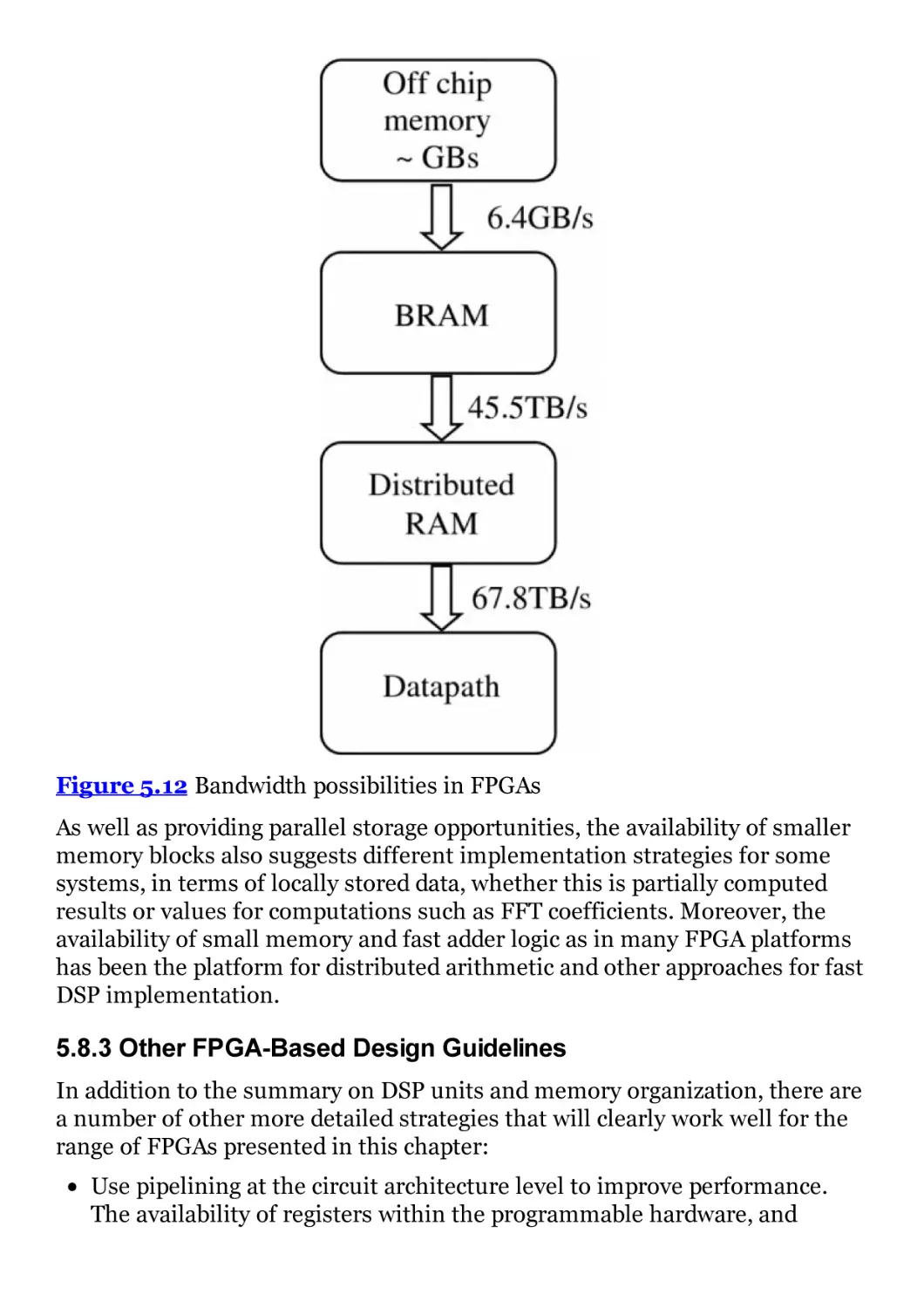
Figure 5.12 Bandwidth possibilities in FPGAs
Chapter 6
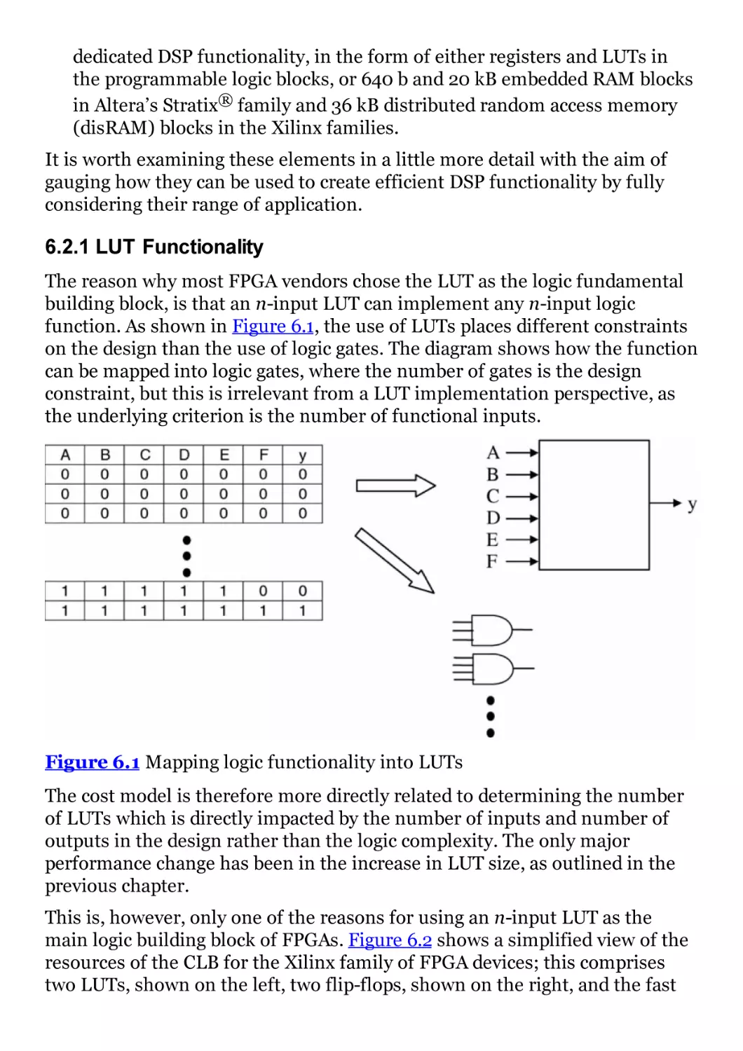
Figure 6.1 Mapping logic functionality into LUTs
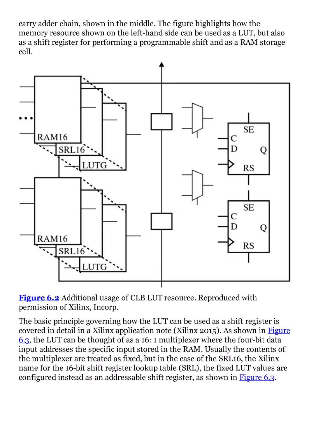
Figure 6.2 Additional usage of CLB LUT resource. Reproduced with
permission of Xilinx, Incorp.
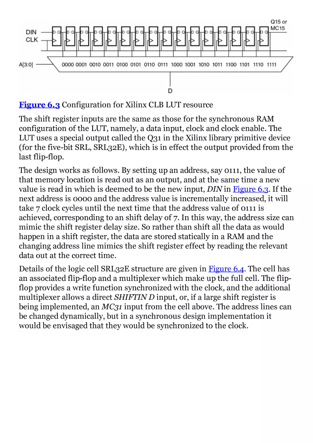
Figure 6.3 Configuration for Xilinx CLB LUT resource
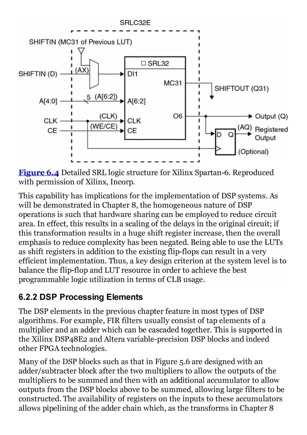
Figure 6.4 Detailed SRL logic structure for Xilinx Spartan-6.
Reproduced with permission of Xilinx, Incorp.
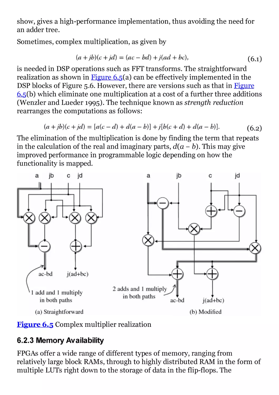
Figure 6.5 Complex multiplier realization
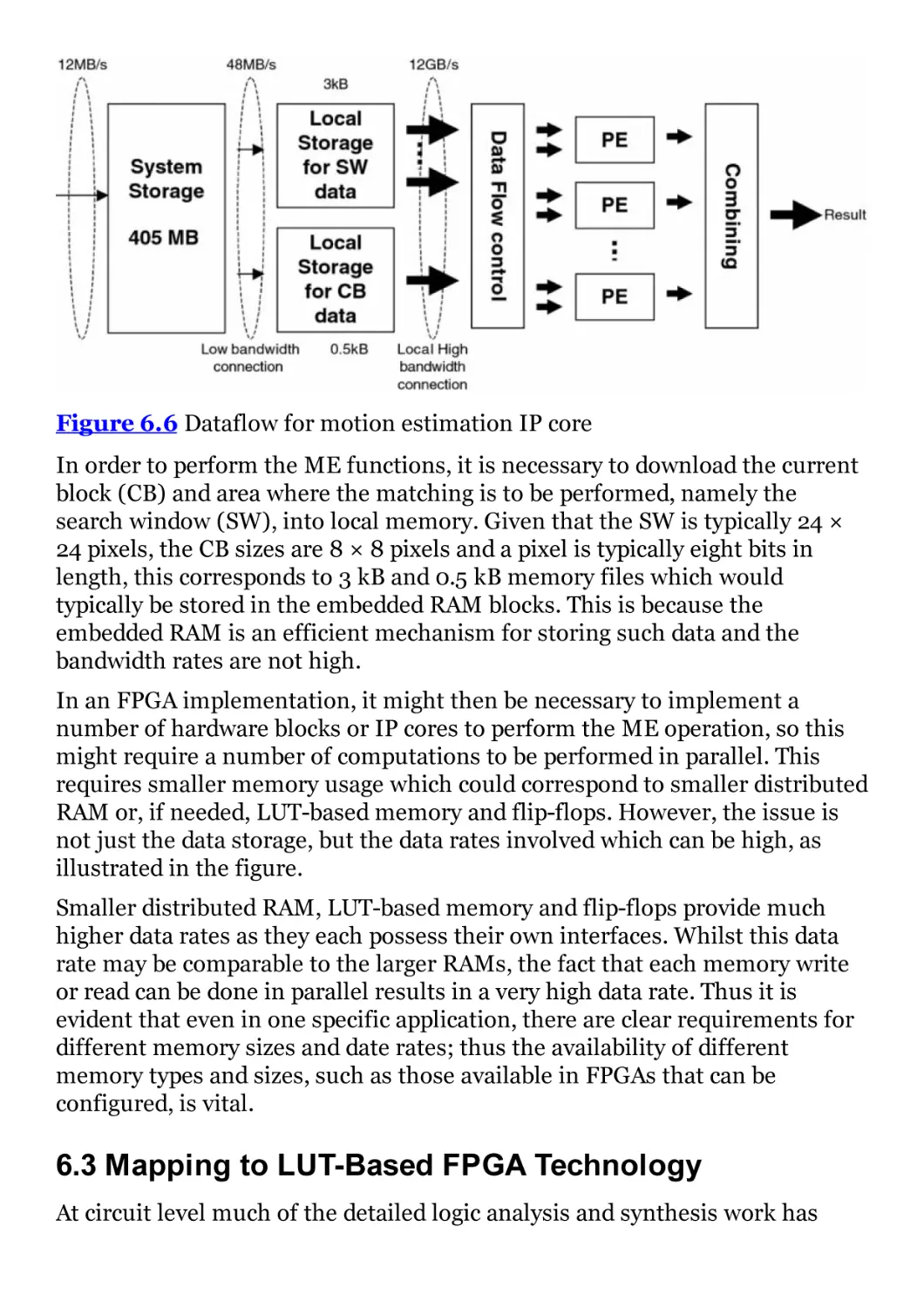
Figure 6.6 Dataflow for motion estimation IP core
Figure 6.7 Initial LUT encoding
Figure 6.8 Modified LUT encoding
Figure 6.9 Low-pass FIR filter
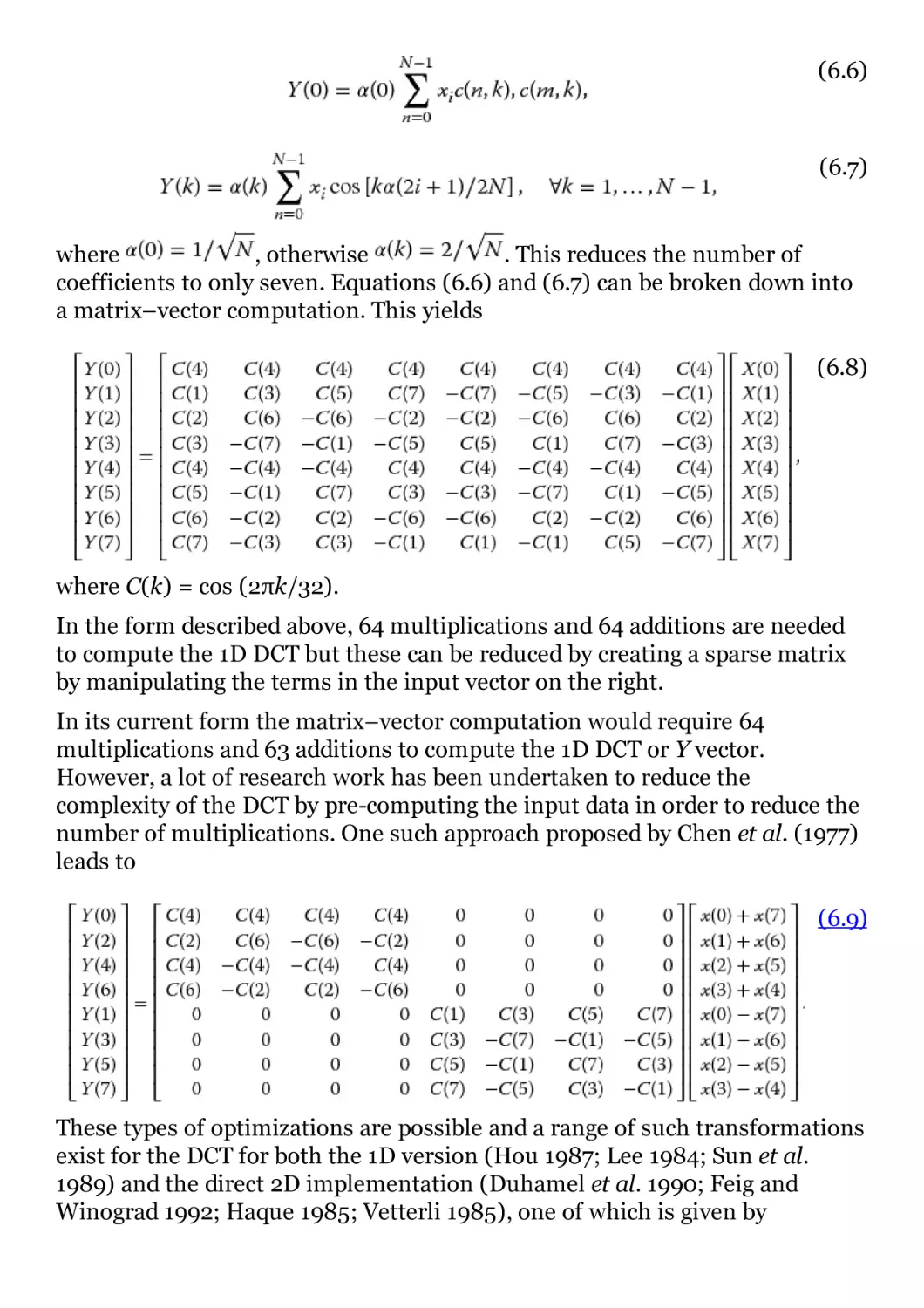
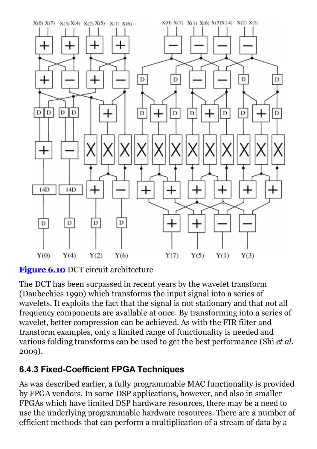
Figure 6.10 DCT circuit architecture
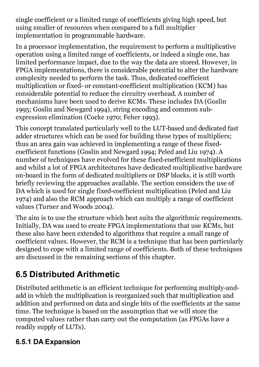
Figure 6.11 LUT-based 8-bit multiplier
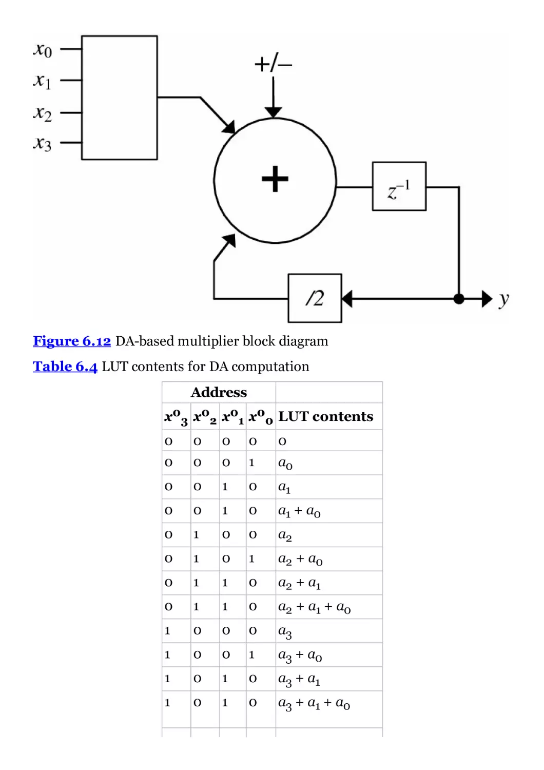
Figure 6.12 DA-based multiplier block diagram
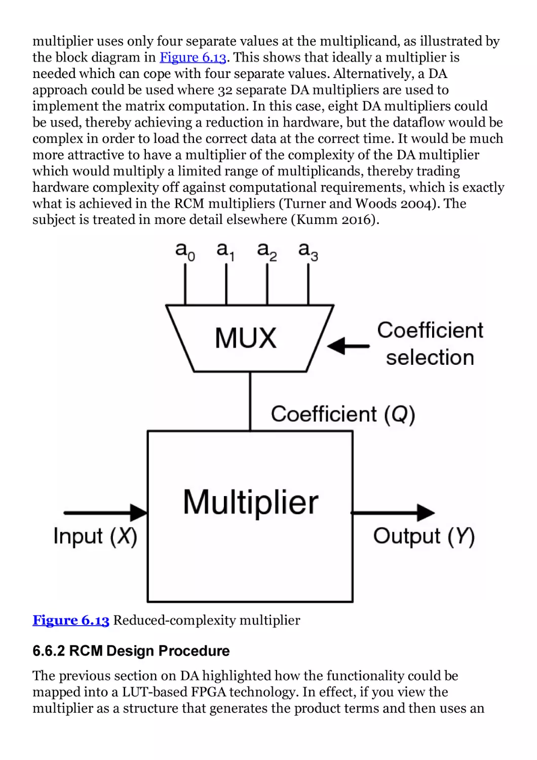
Figure 6.13 Reduced-complexity multiplier
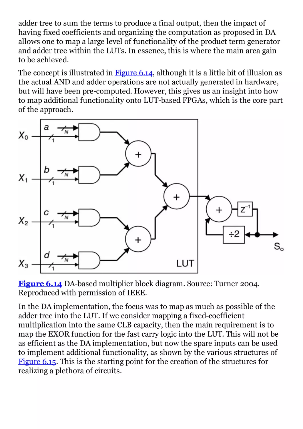
Figure 6.14 DA-based multiplier block diagram. Source: Turner 2004.
Reproduced with permission of IEEE.
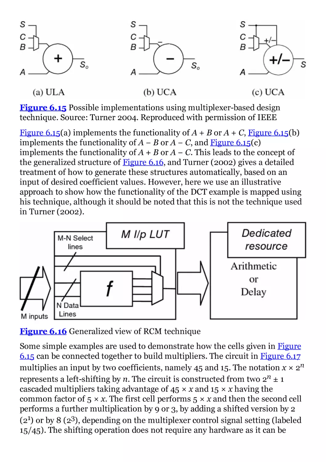
Figure 6.15 Possible implementations using multiplexer-based design
technique. Source: Turner 2004. Reproduced with permission of IEEE
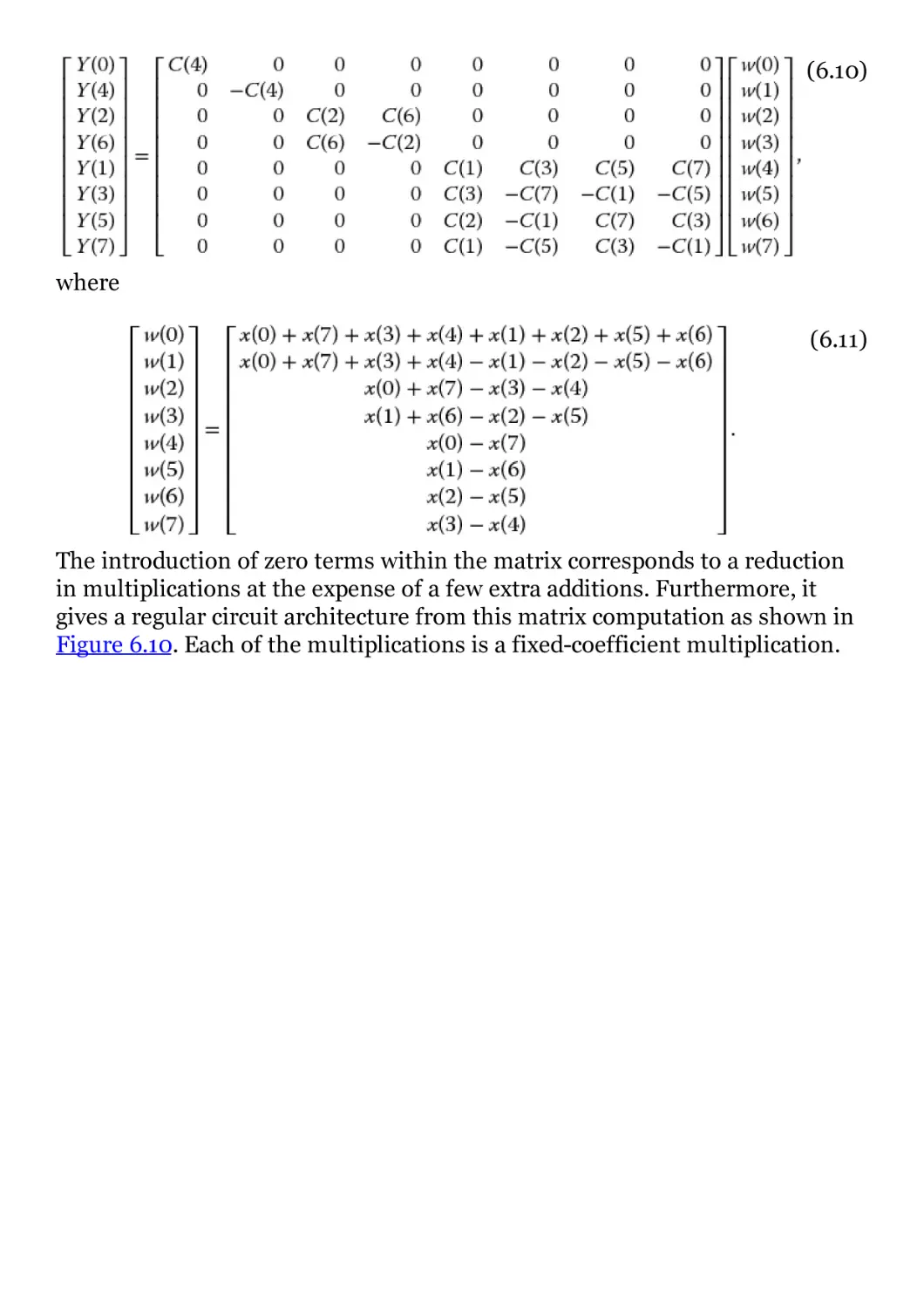
Figure 6.16 Generalized view of RCM technique
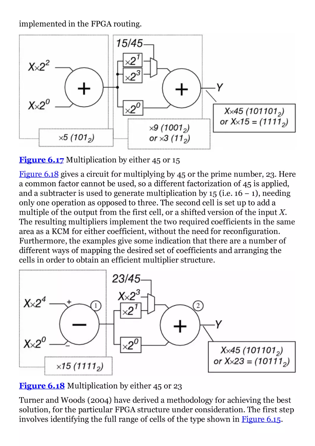
Figure 6.17 Multiplication by either 45 or 15
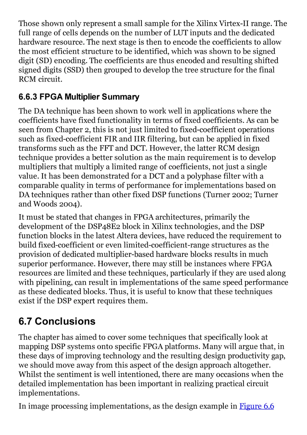
Figure 6.18 Multiplication by either 45 or 23
Chapter 7
Figure 7.1 High-level synthesis in Gajski and Kuhn’s Y-chart
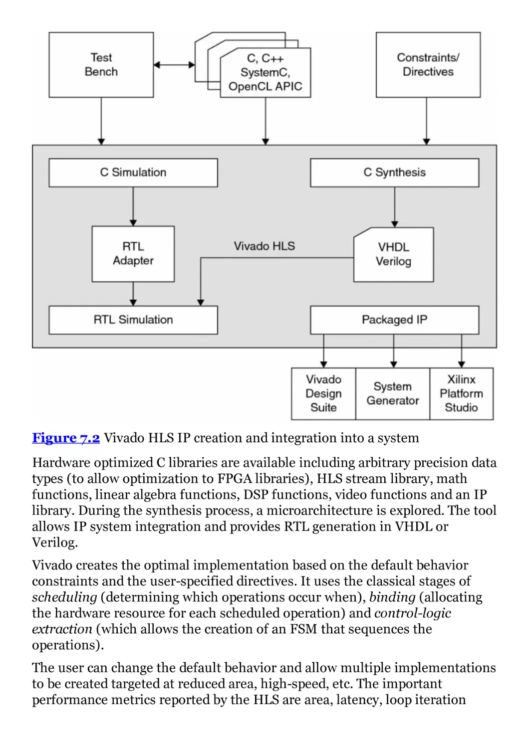
Figure 7.2 Vivado HLS IP creation and integration into a system
Figure 7.3 Control logic extraction and I/O port implementation
example
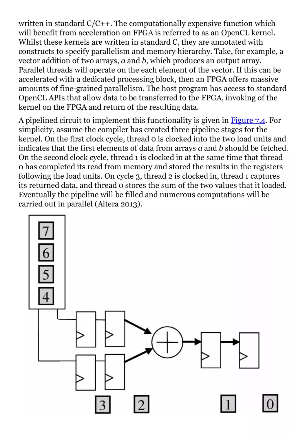
Figure 7.4 Pipelined processor implementation
Figure 7.5 GAUT synthesis flow
Chapter 8
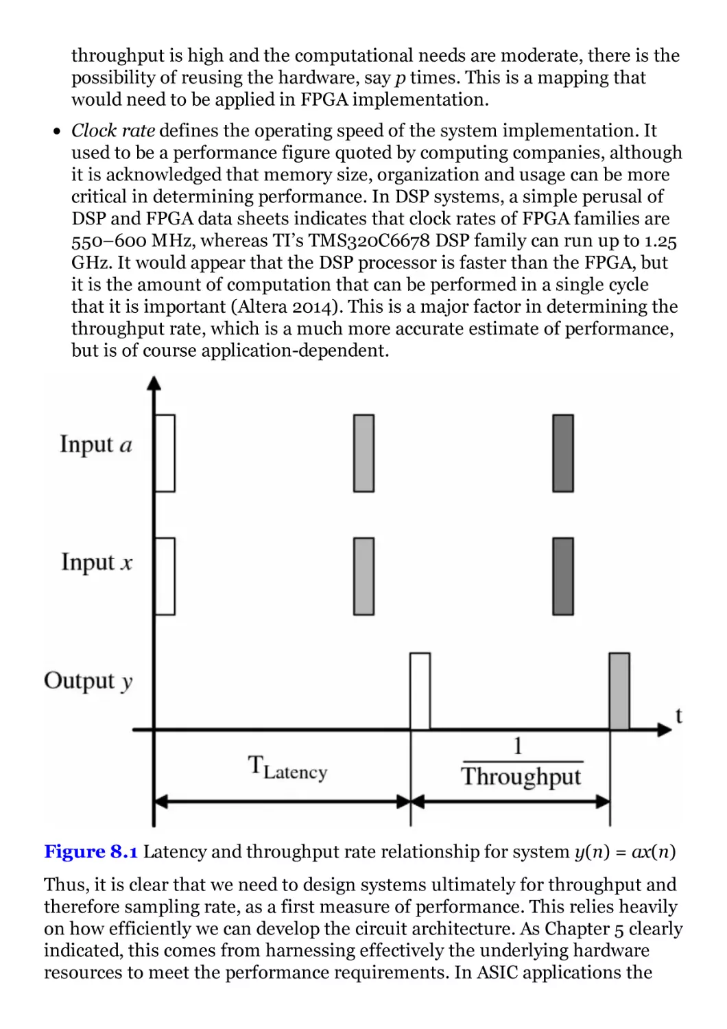
Figure 8.1 Latency and throughput rate relationship for system y(n) =
ax(n)
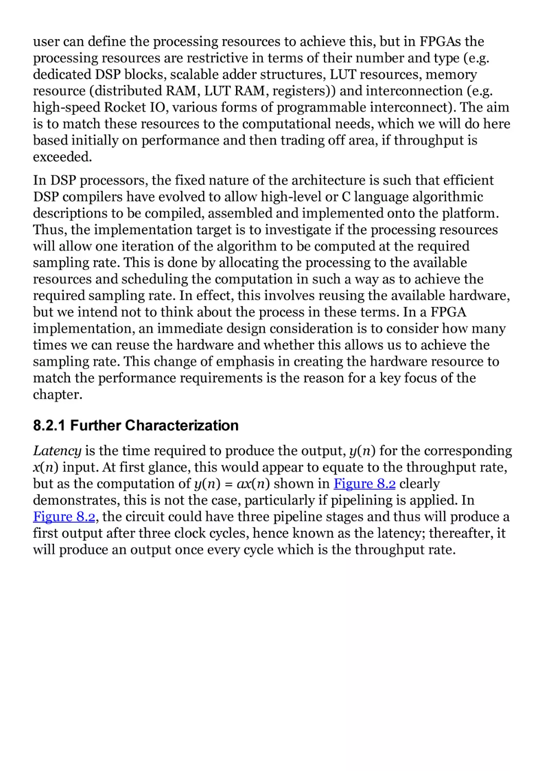
Figure 8.2 Latency and throughput rate relationship for system y(n)
= ay(n − 1)
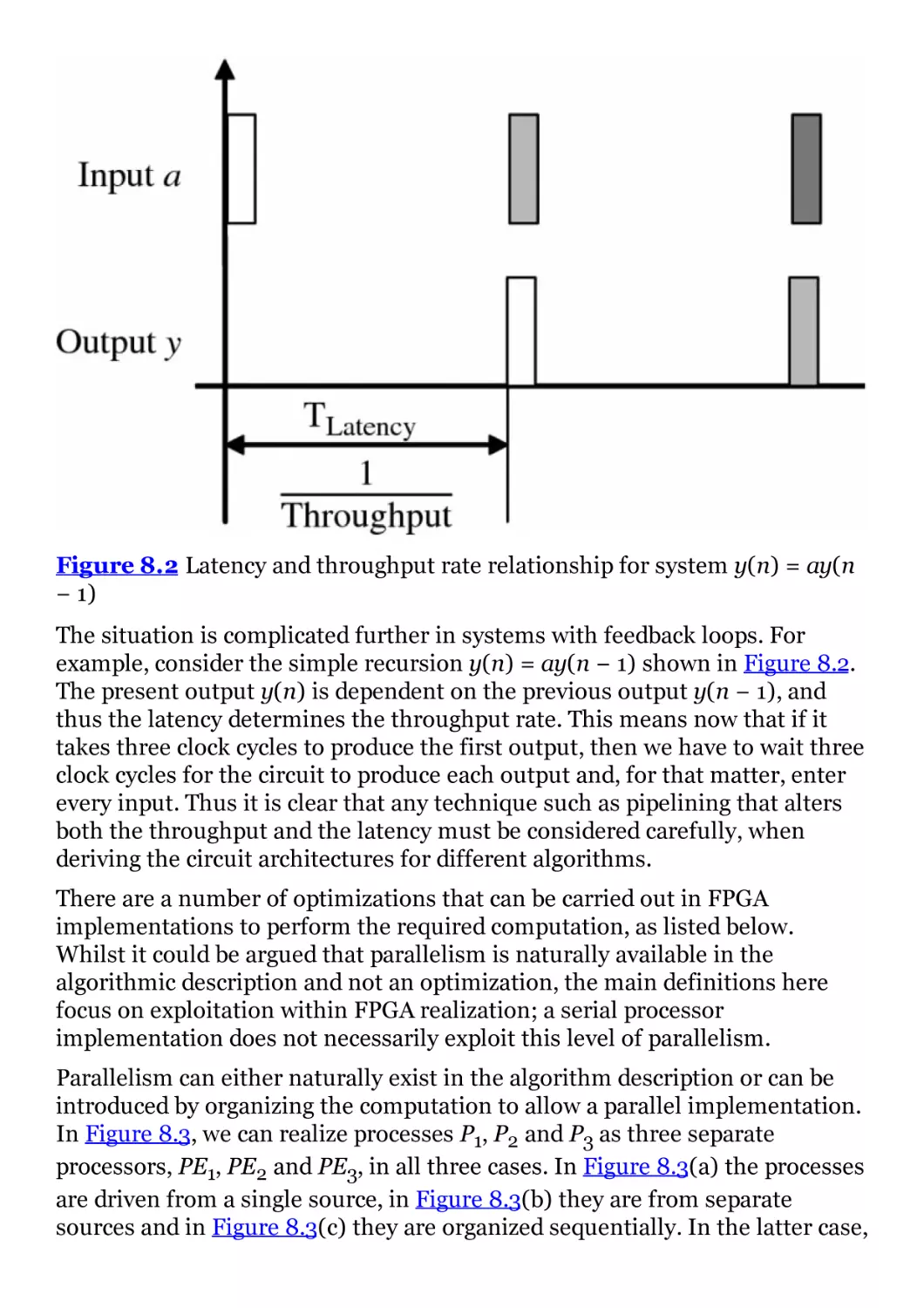
Figure 8.3 Algorithms realizations using three processes P1, P2 and P3
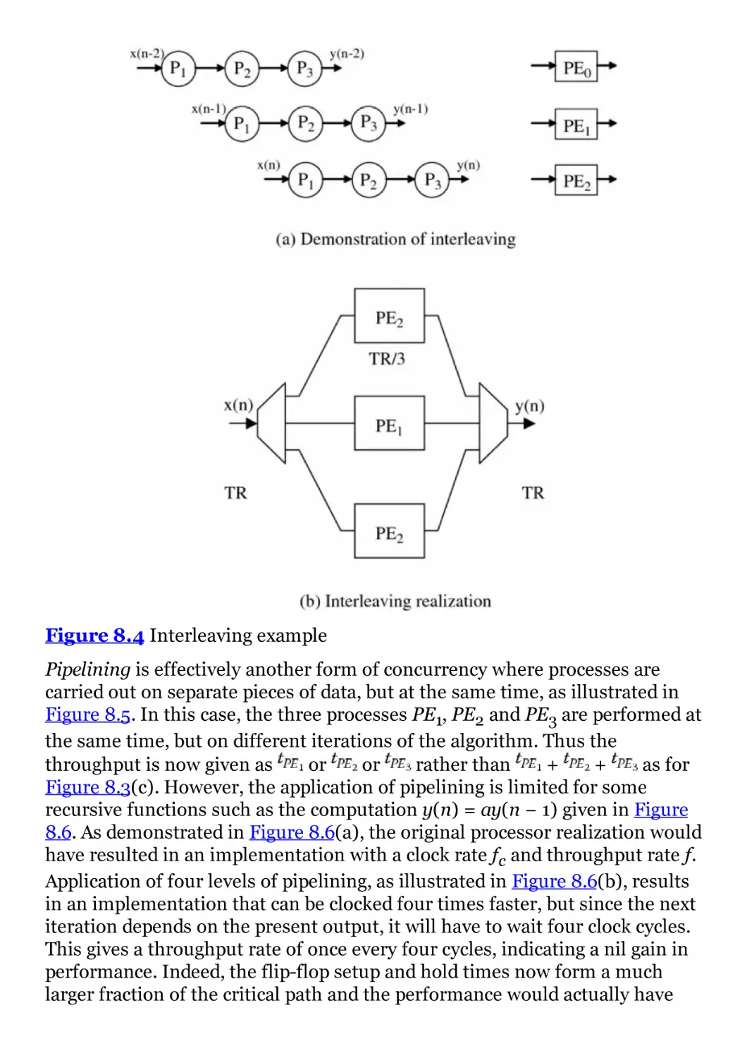
Figure 8.4 Interleaving example
Figure 8.5 Example of pipelining
Figure 8.6 Pipelining of recursive computations y(n) = ay(n − 1)
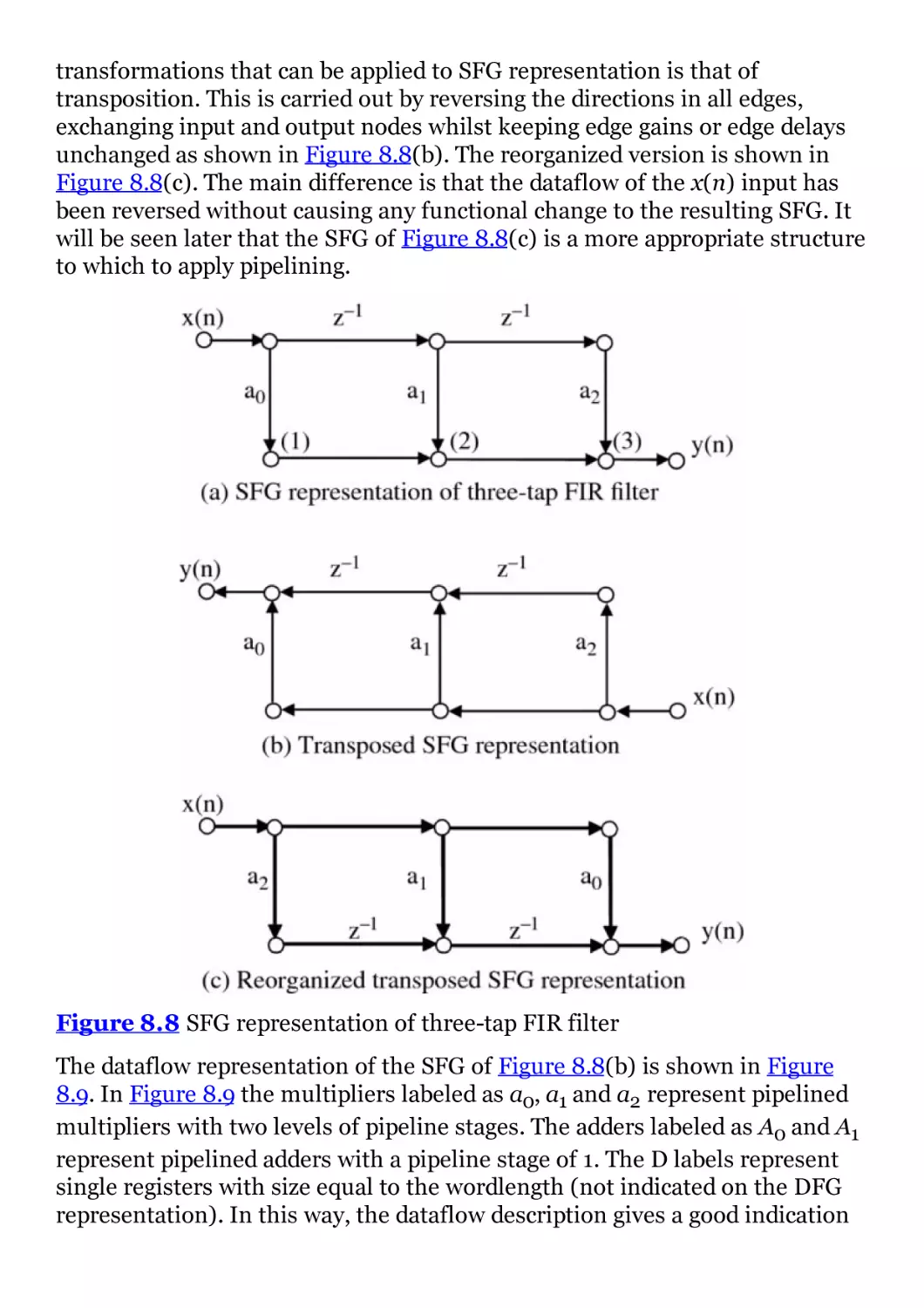
Figure 8.7 Various representations of simple DSP recursion y(n) =
ay(n − 1) + x(n)
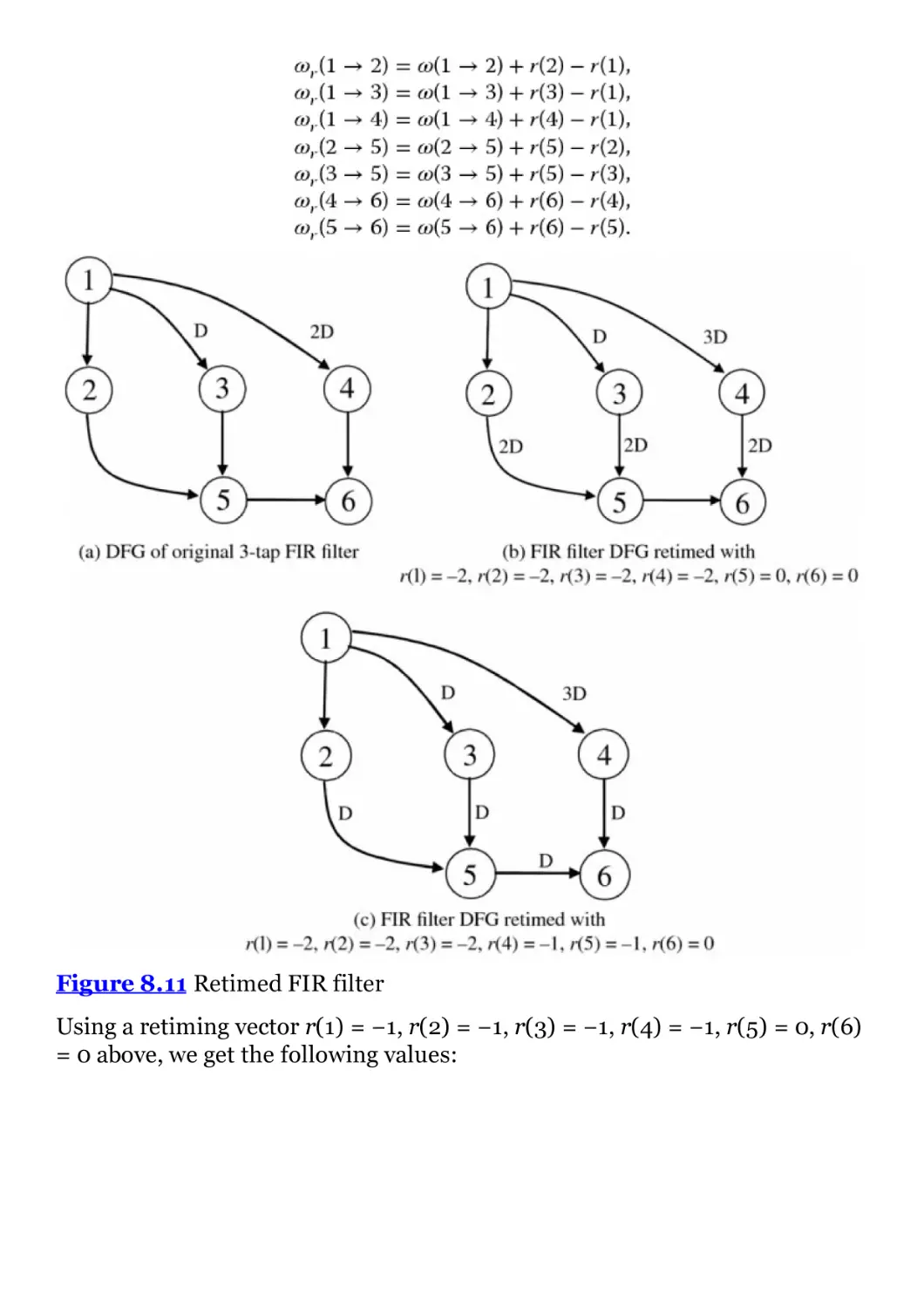
Figure 8.8 SFG representation of three-tap FIR filter
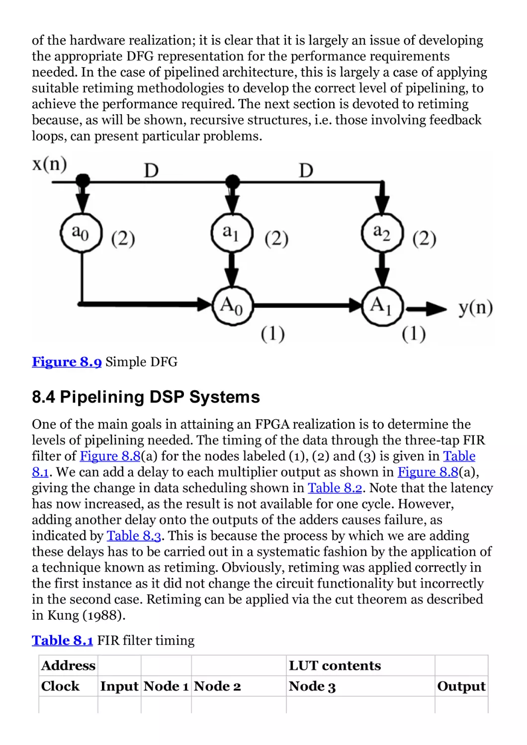
Figure 8.9 Simple DFG
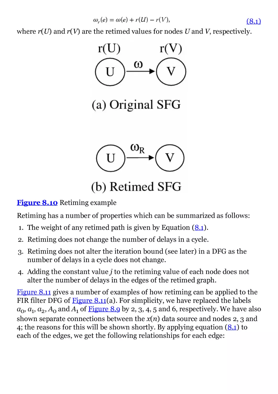
Figure 8.10 Retiming example
Figure 8.11 Retimed FIR filter
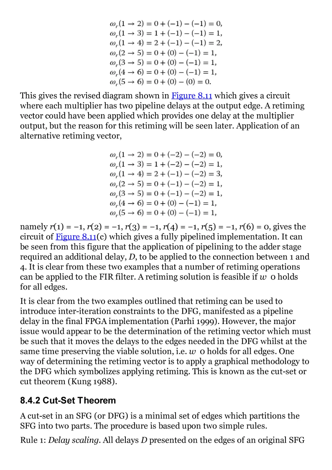
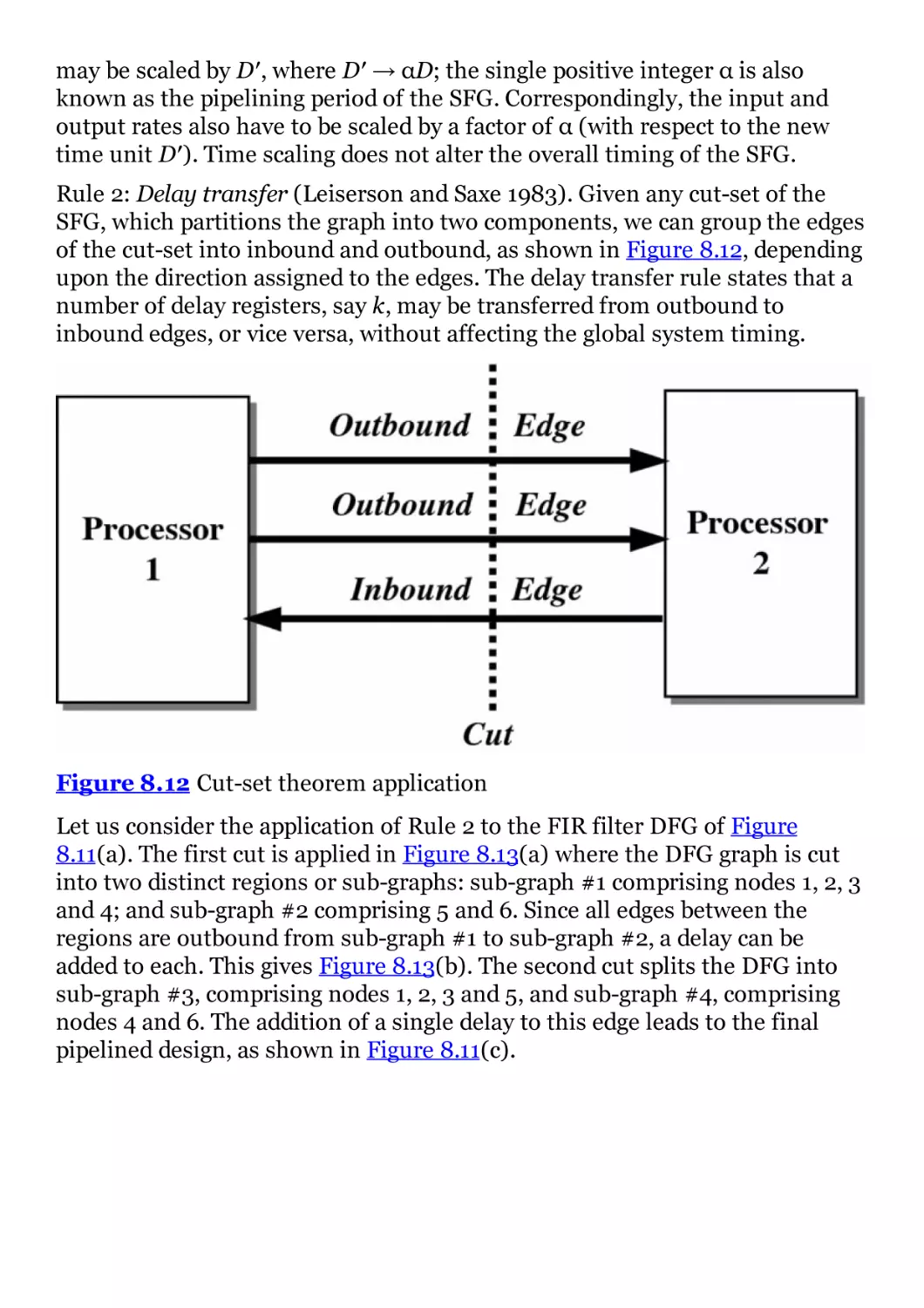
Figure 8.12 Cut-set theorem application
Figure 8.13 Cut-set timing applied to FIR filter
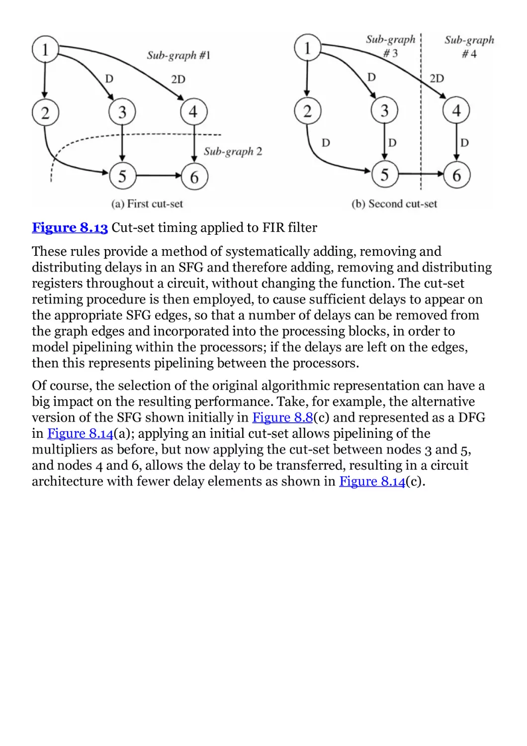
Figure 8.14 Cut-set timing applied to FIR filter
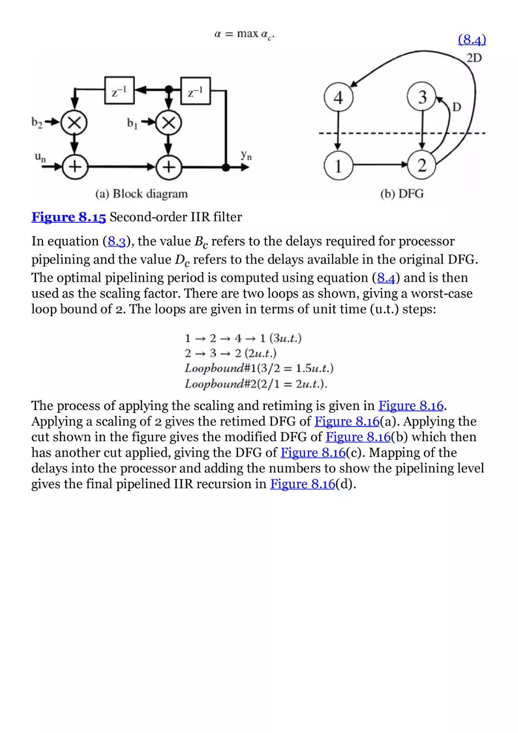
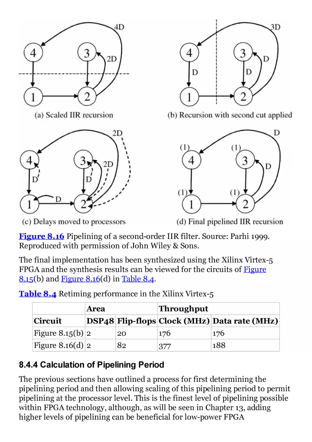
Figure 8.15 Second-order IIR filter
Figure 8.16 Pipelining of a second-order IIR filter. Source: Parhi 1999.
Reproduced with permission of John Wiley & Sons.
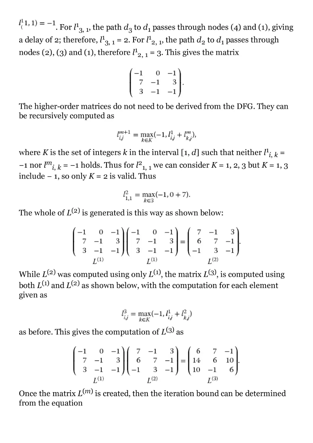
Figure 8.17 Simple DFG example (Parhi 1999)
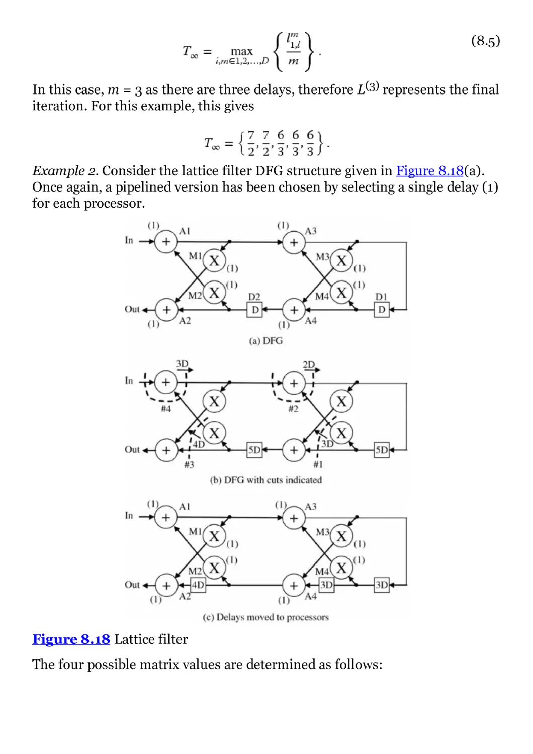
Figure 8.18 Lattice filter
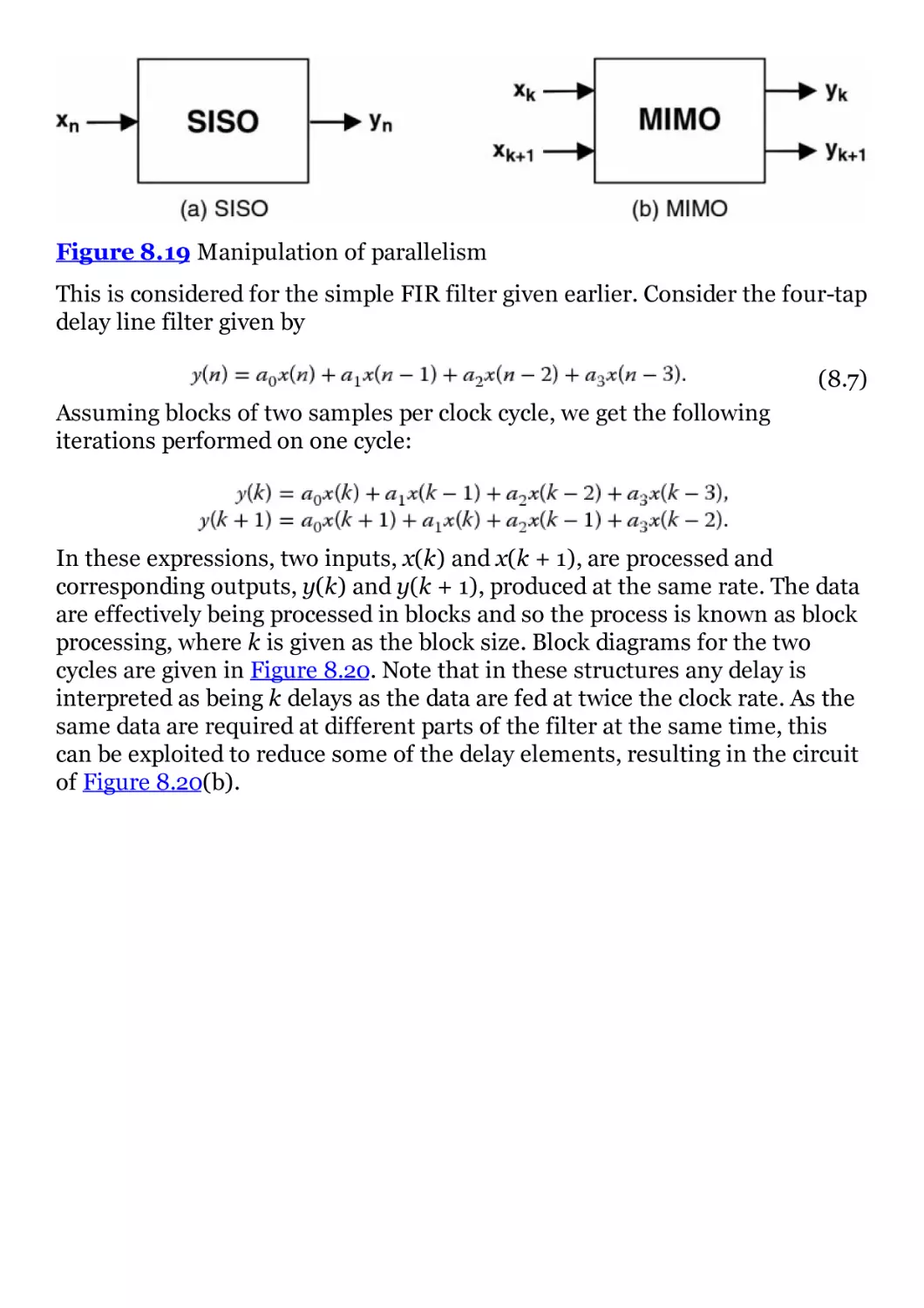
Figure 8.19 Manipulation of parallelism
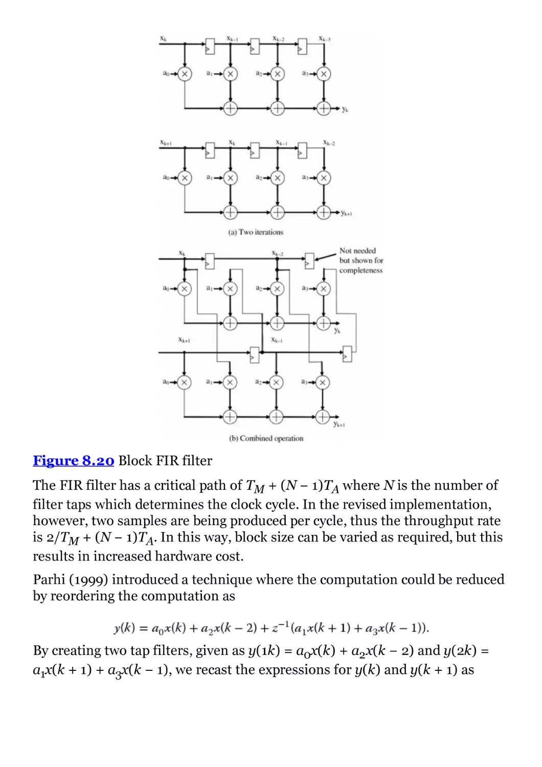
Figure 8.20 Block FIR filter
Figure 8.21 Reduced block-based FIR filter
Figure 8.22 Unfolded first-order recursion
Figure 8.23 Unfolded FIR filter-block
Figure 8.24 Folded FIR filter section
Figure 8.25 Folding transformation
Figure 8.26 Folding process
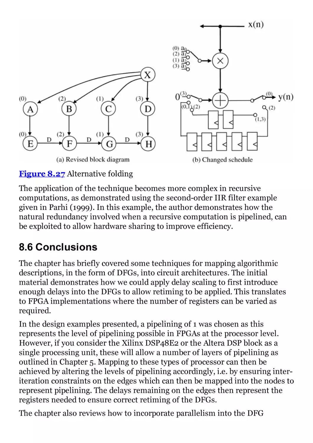
Figure 8.27 Alternative folding
Chapter 9
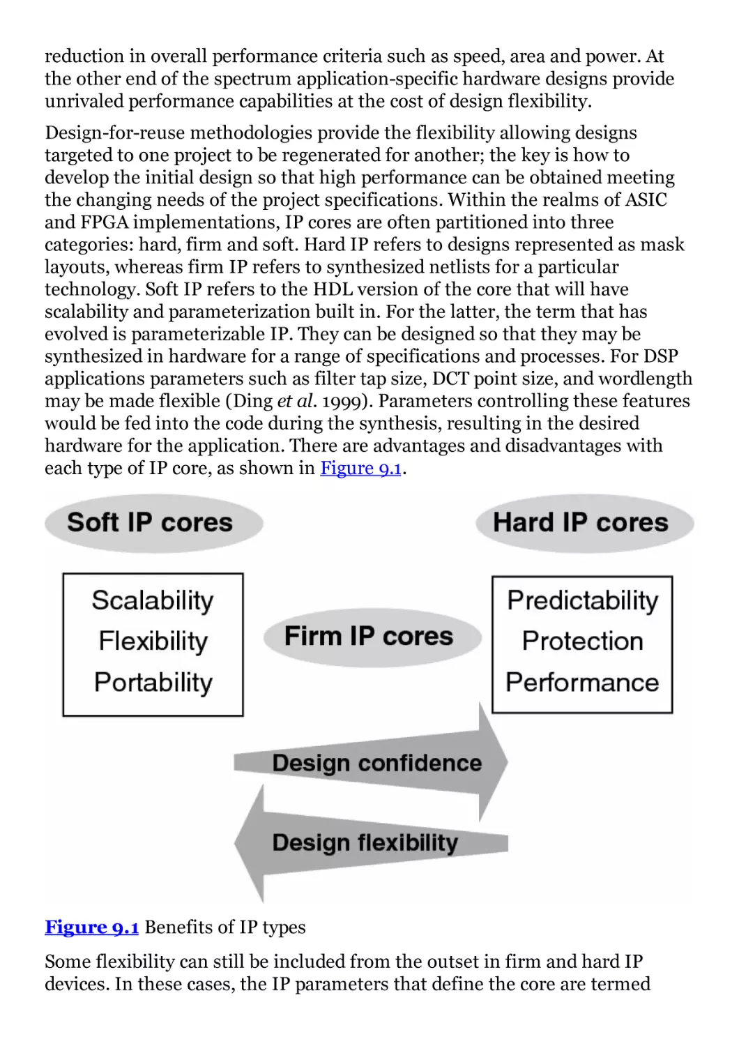
Figure 9.1 Benefits of IP types
Figure 9.2 Evolution of IP cores
Figure 9.3 Fixed- and floating-point operations
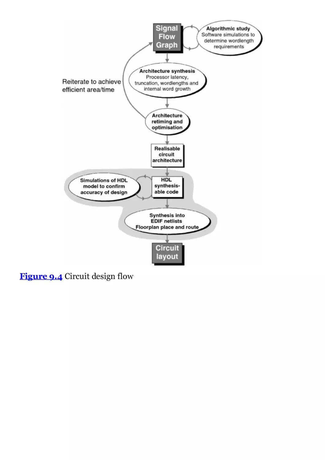
Figure 9.4 Circuit design flow
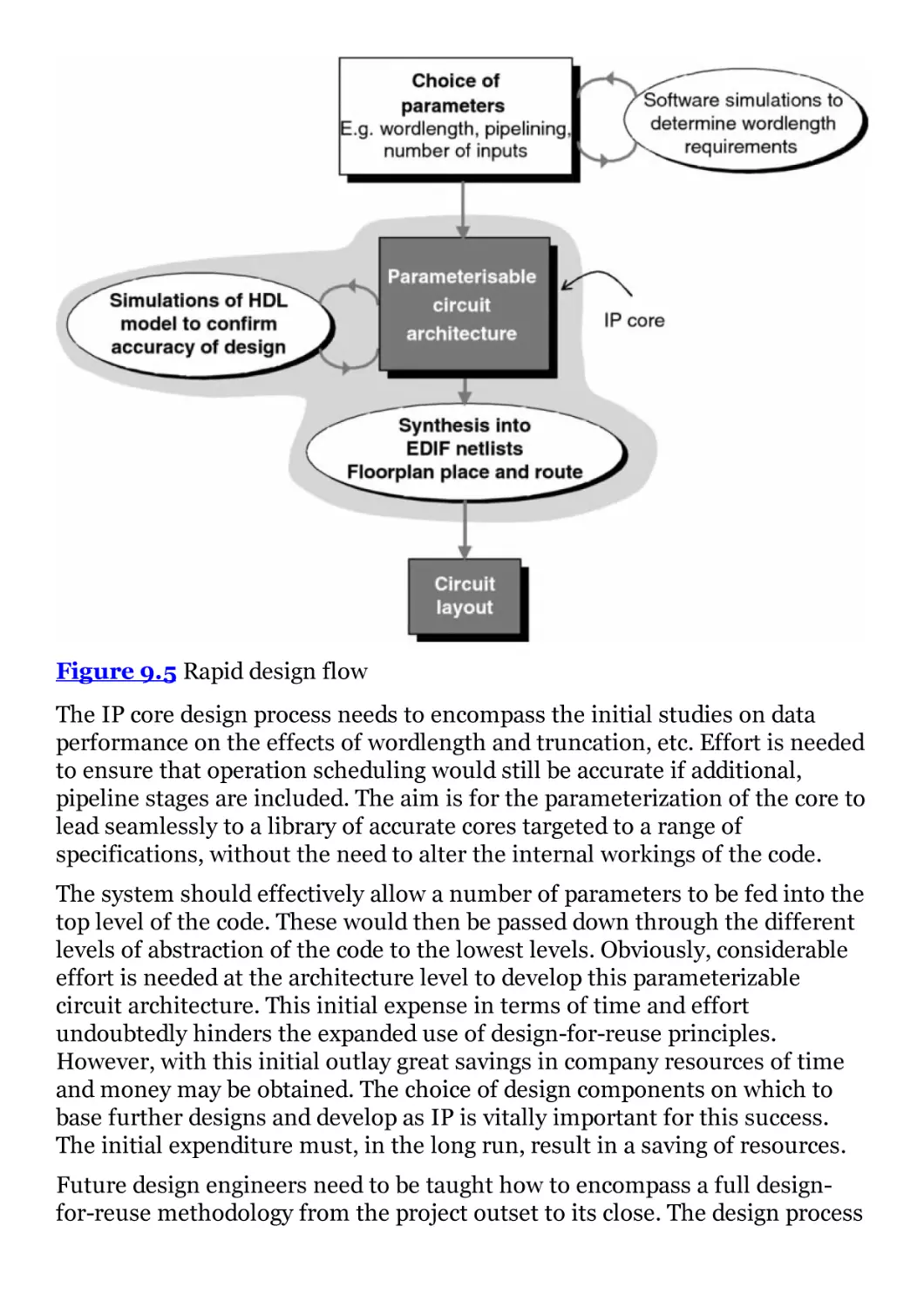
Figure 9.5 Rapid design flow
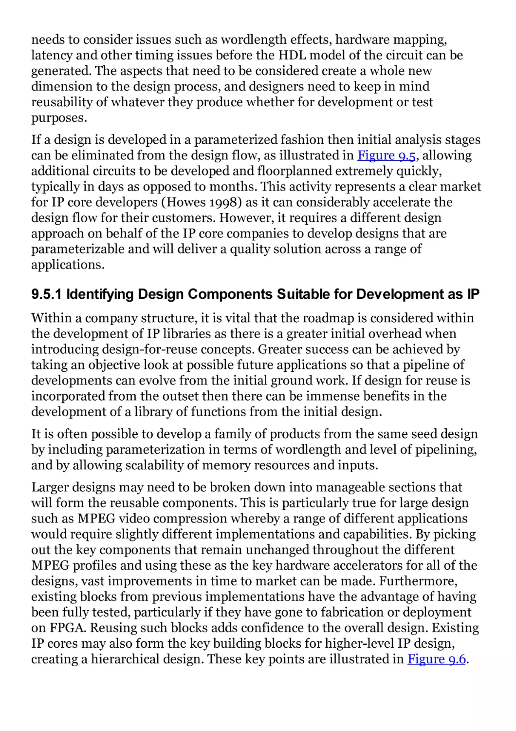
Figure 9.6 Components suitable for IP
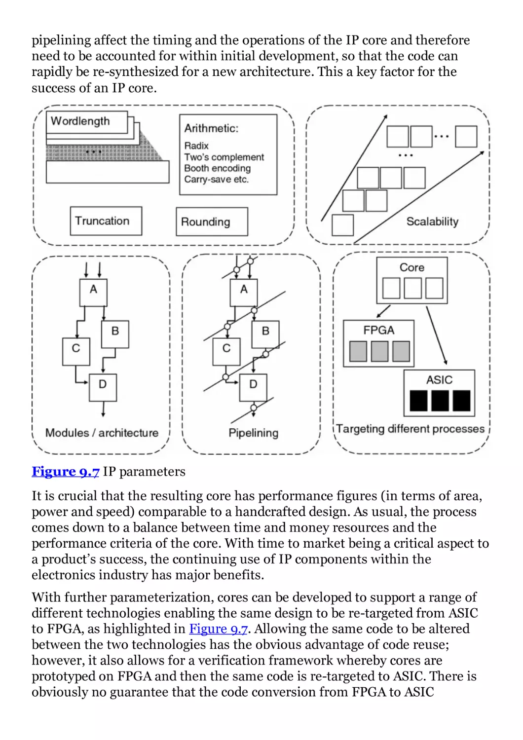
Figure 9.7 IP parameters
Figure 9.8 Effect of generalization on design reliability
Figure 9.9 Wordlength analysis
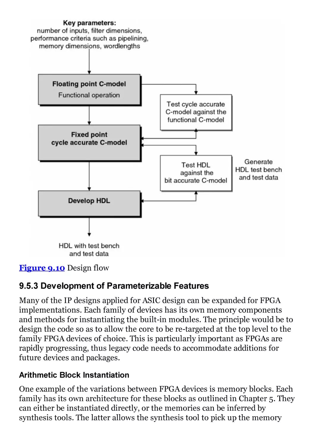
Figure 9.10 Design flow
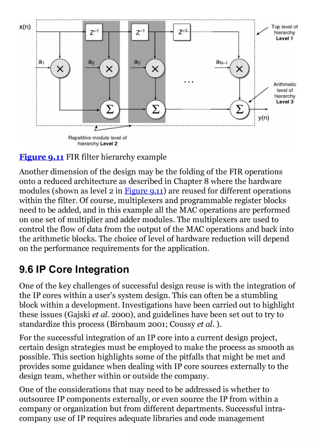
Figure 9.11 FIR filter hierarchy example
Chapter 10
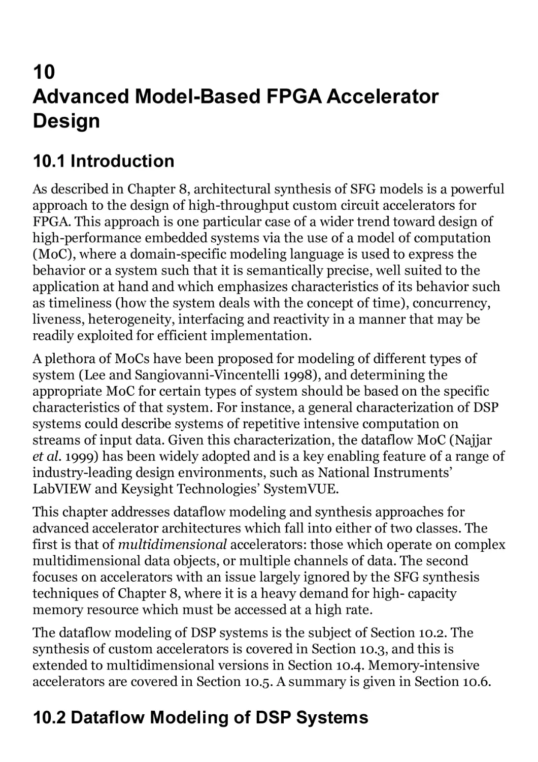
Figure 10.1 Simple KPN structure
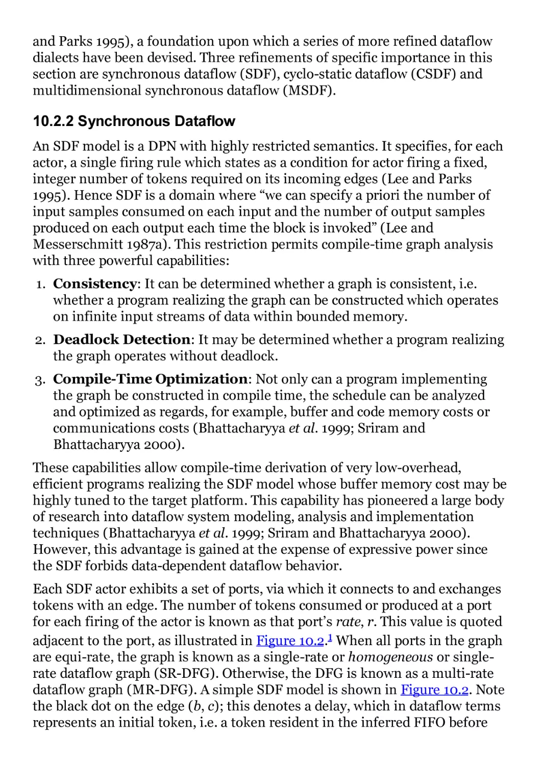
Figure 10.2 Simple SDF graph
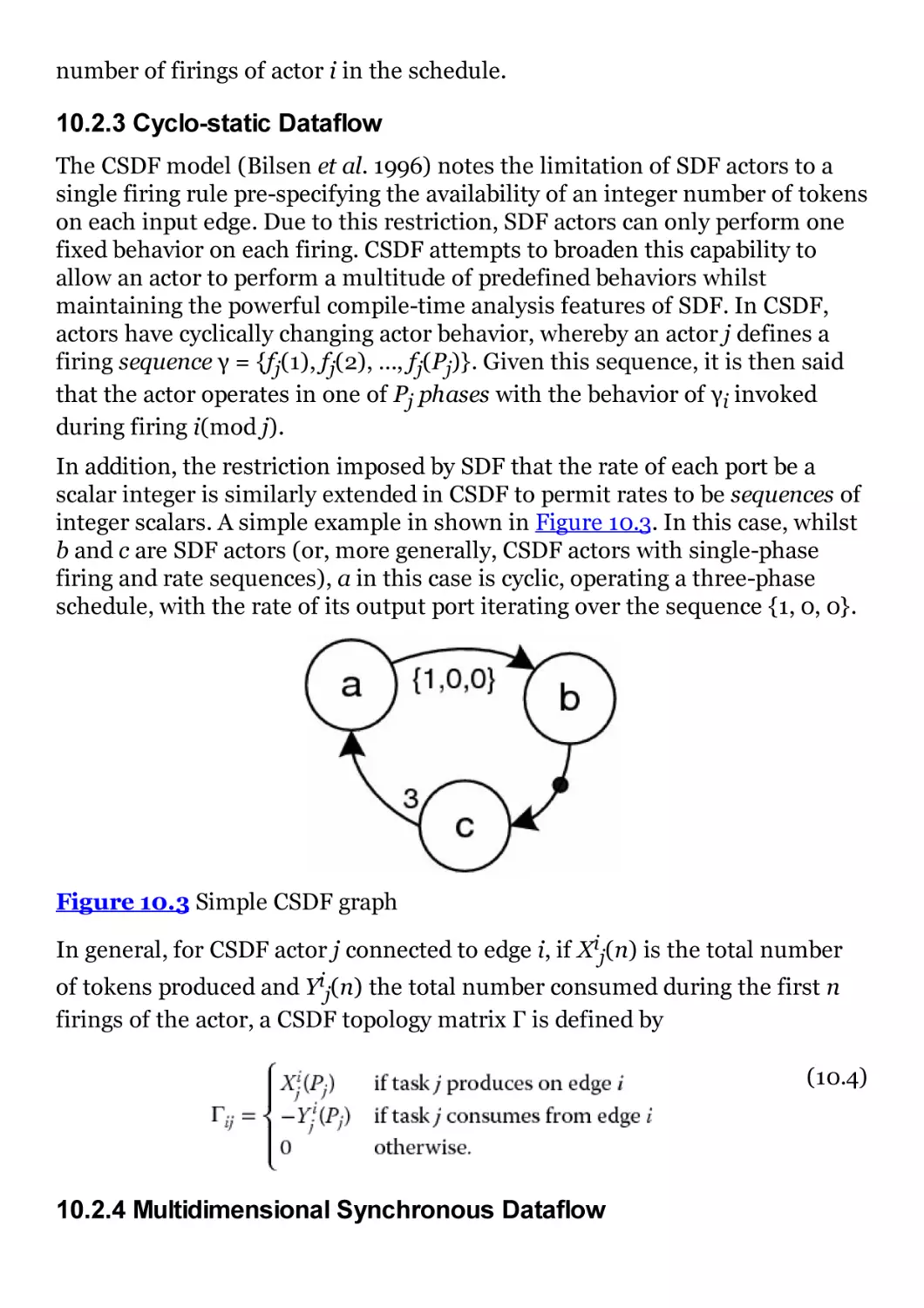
Figure 10.3 Simple CSDF graph
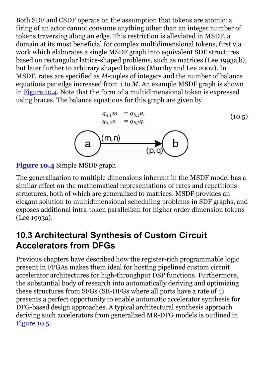
Figure 10.4 Simple MSDF graph
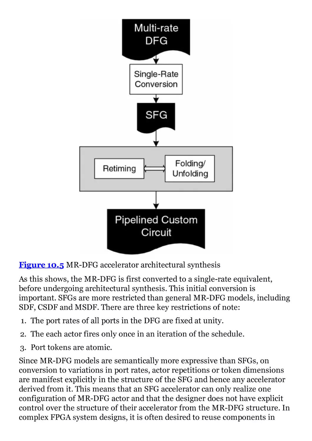
Figure 10.5 MR-DFG accelerator architectural synthesis
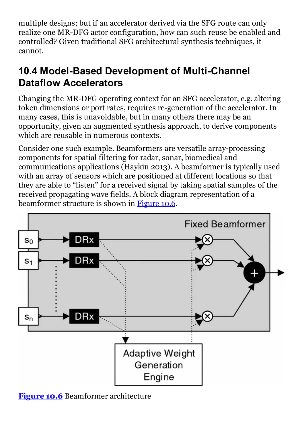
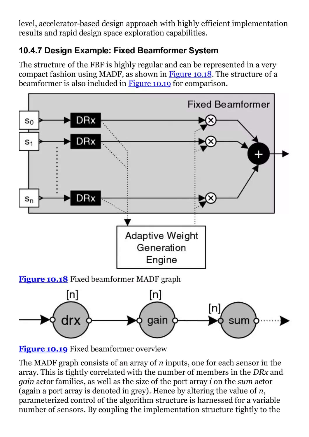
Figure 10.6 Beamformer architecture
Figure 10.7 Parallel matrix multiplication
Figure 10.8 Matrix multiplication MADF
Figure 10.9 Matrix decomposition for fixed token size processing
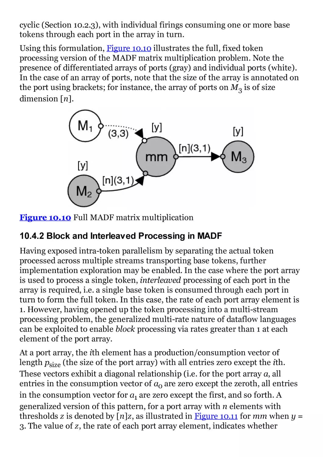
Figure 10.10 Full MADF matrix multiplication
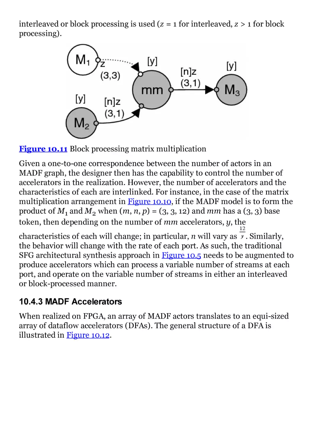
Figure 10.11 Block processing matrix multiplication
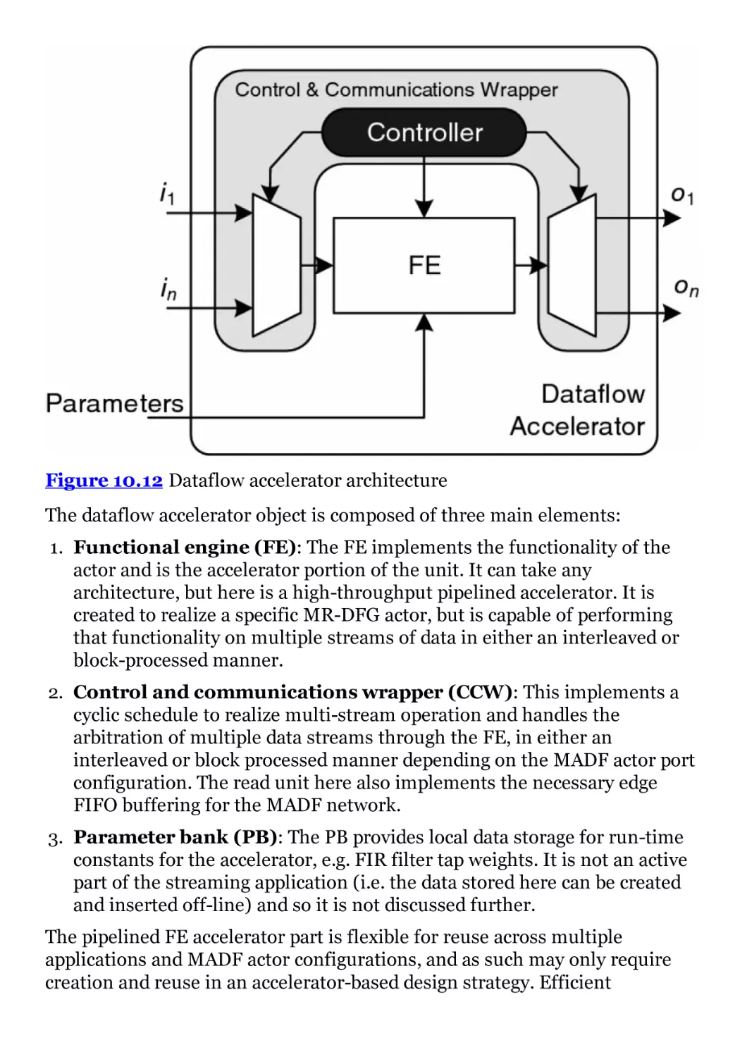
Figure 10.12 Dataflow accelerator architecture
Figure 10.13 Two-stage FIR WBC
Figure 10.14 Scaled variants of two-stage FIR WBC
Figure 10.15 Eight-channel NLF filter bank MADF graph
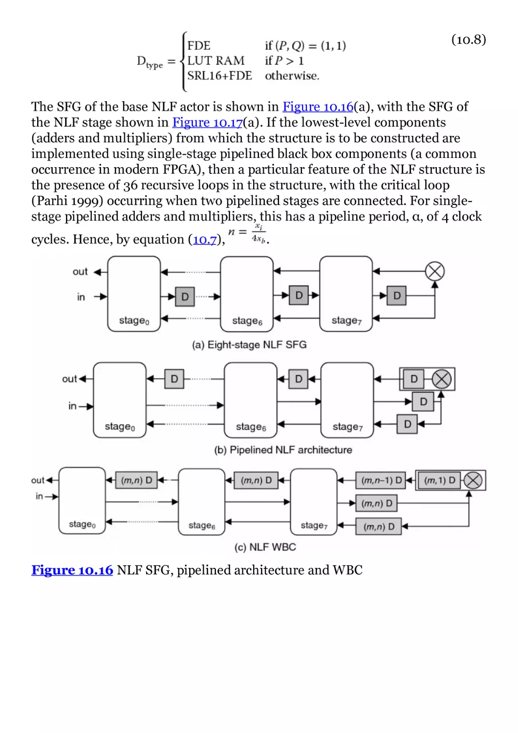
Figure 10.16 NLF SFG, pipelined architecture and WBC
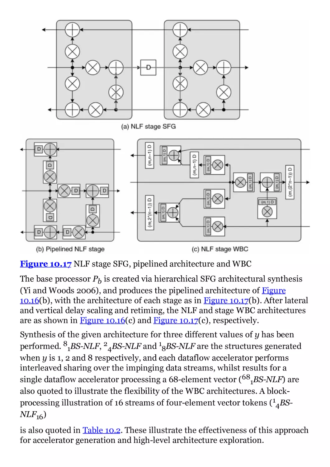
Figure 10.17 NLF stage SFG, pipelined architecture and WBC
Figure 10.18 Fixed beamformer MADF graph
Figure 10.19 Fixed beamformer overview
Figure 10.20 Fixed beamformer MADF graph
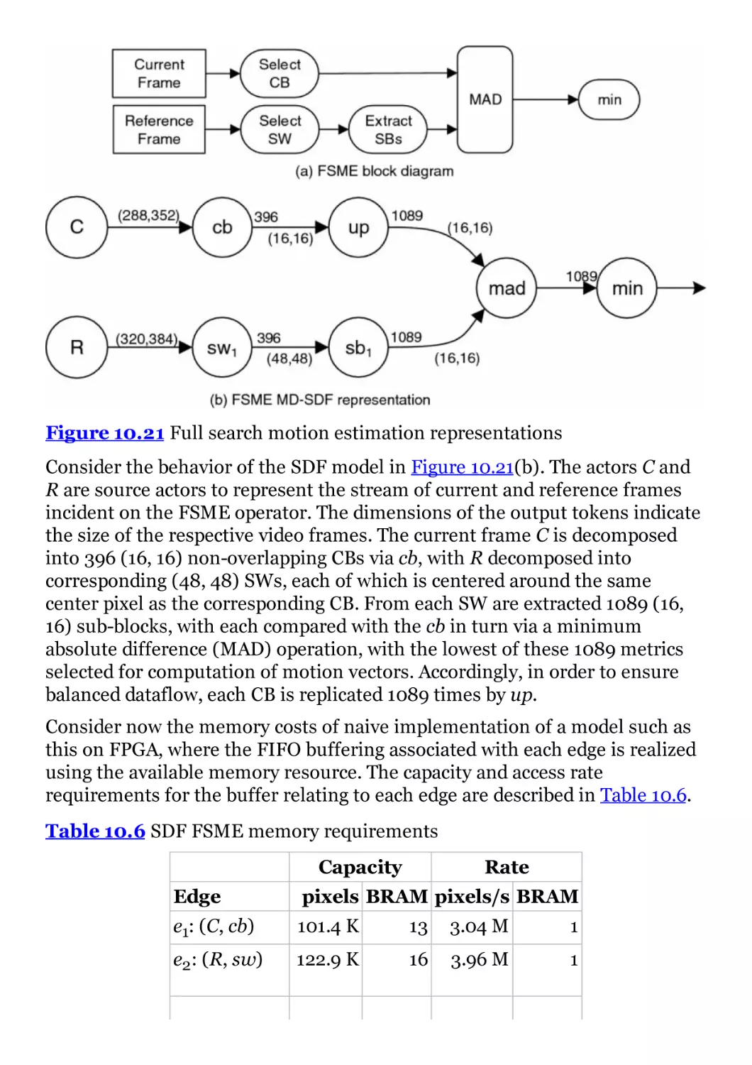
Figure 10.21 Full search motion estimation representations
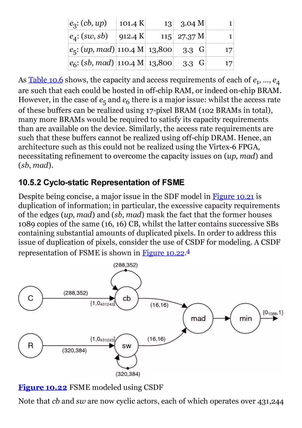
Figure 10.22 FSME modeled using CSDF
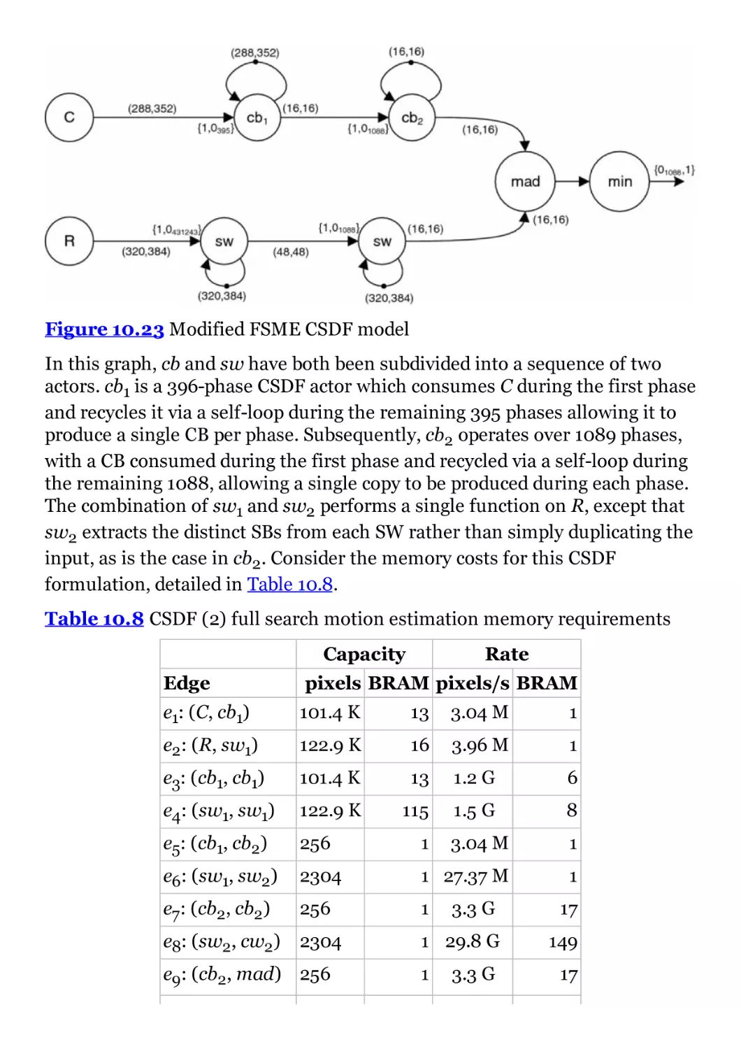
Figure 10.23 Modified FSME CSDF model
Chapter 11
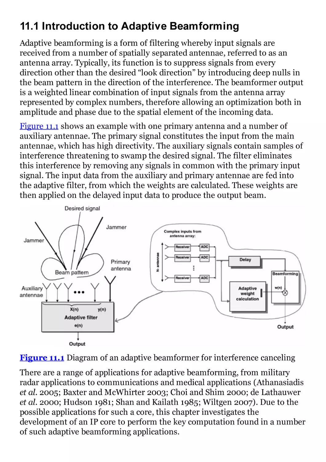
Figure 11.1 Diagram of an adaptive beamformer for interference
canceling
Figure 11.2 Generic design process
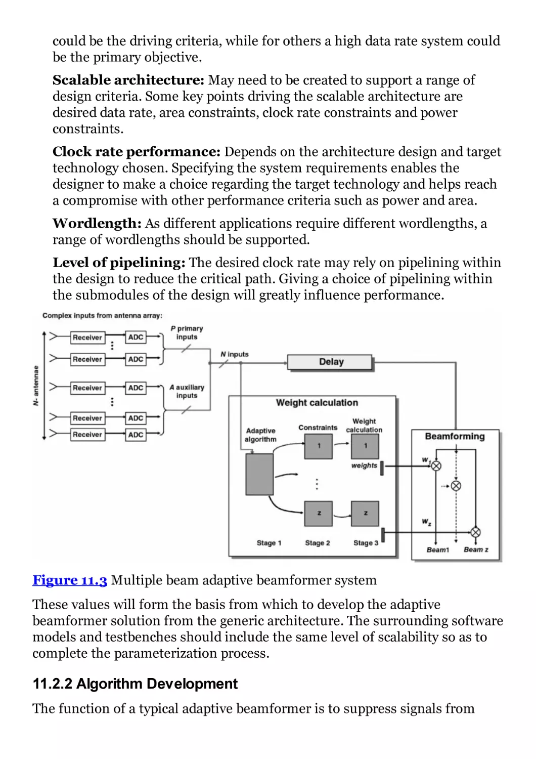
Figure 11.3 Multiple beam adaptive beamformer system
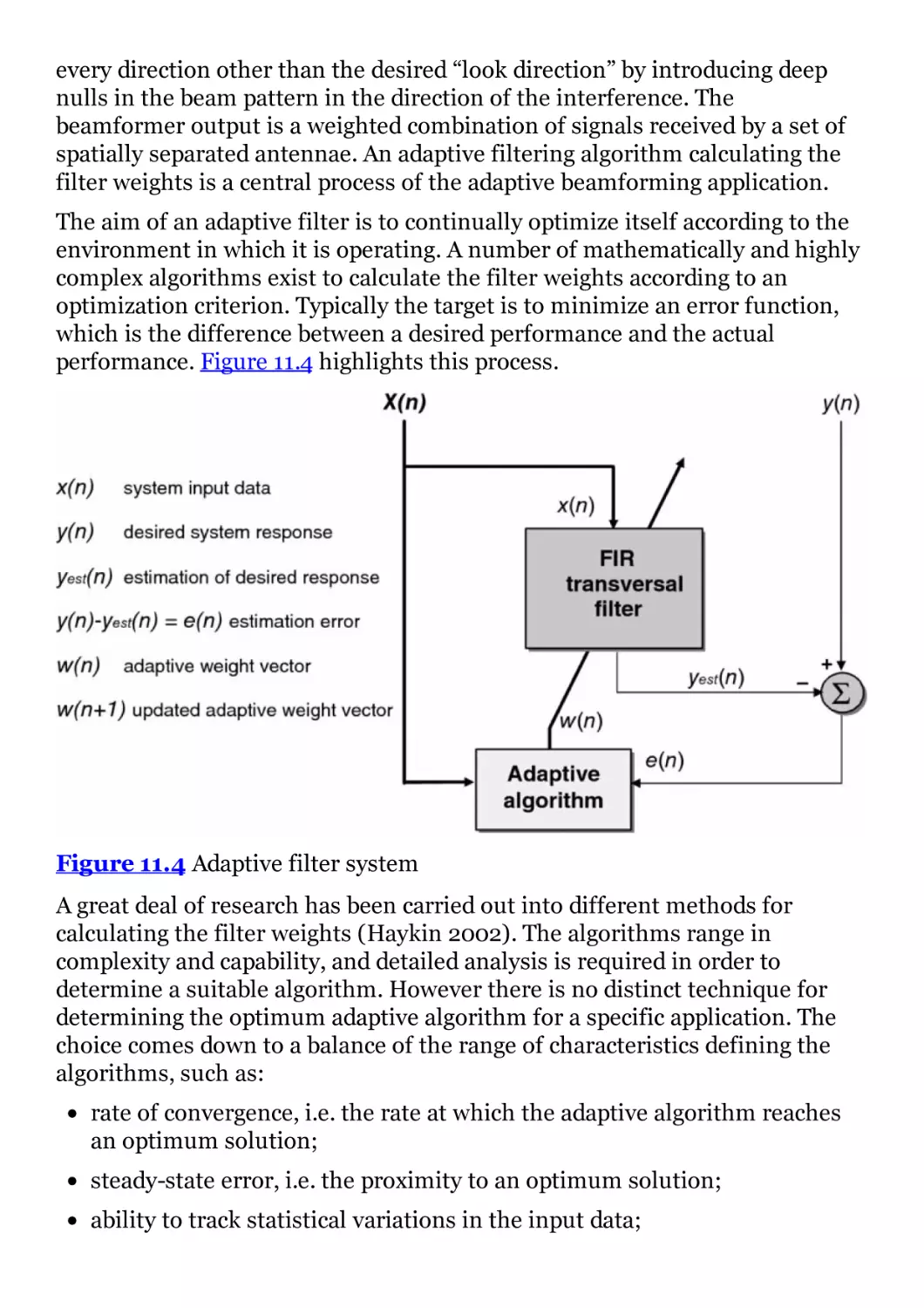
Figure 11.4 Adaptive filter system
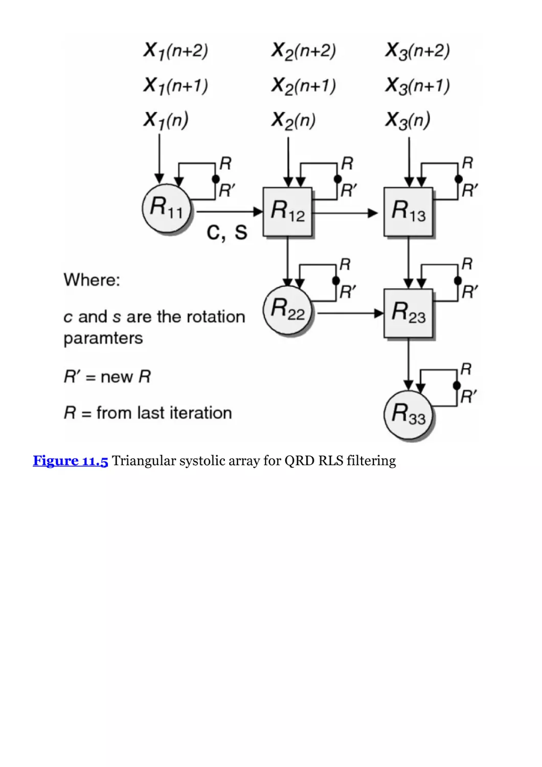
Figure 11.5 Triangular systolic array for QRD RLS filtering
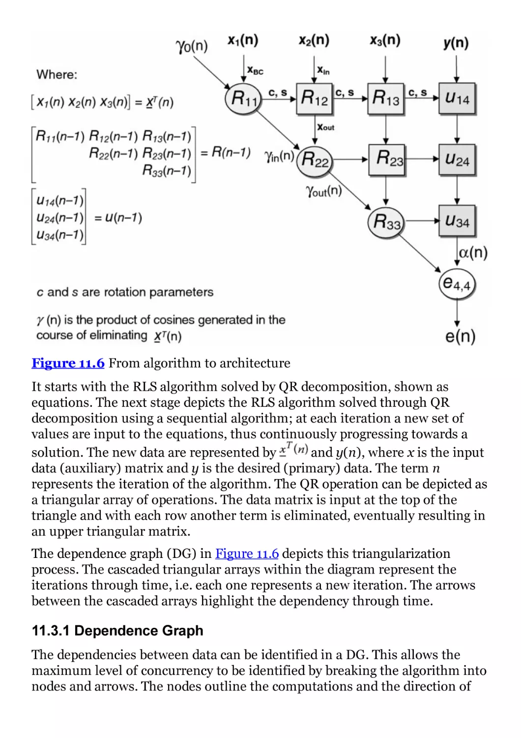
Figure 11.6 From algorithm to architecture
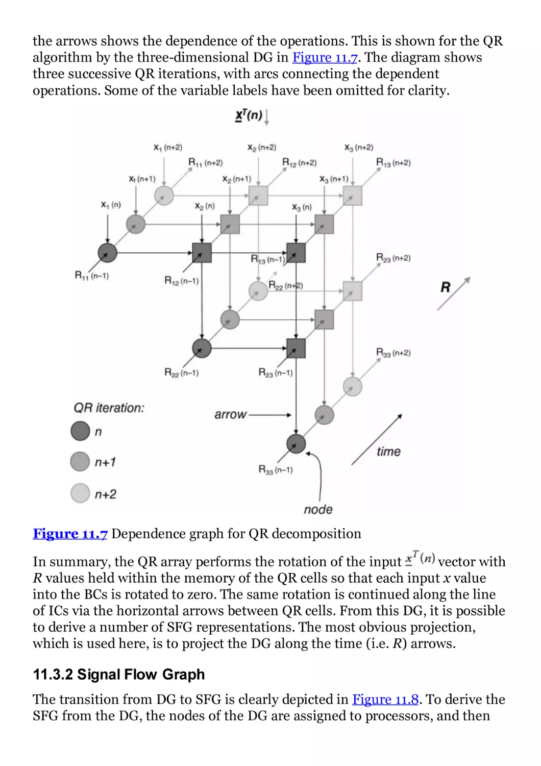
Figure 11.7 Dependence graph for QR decomposition
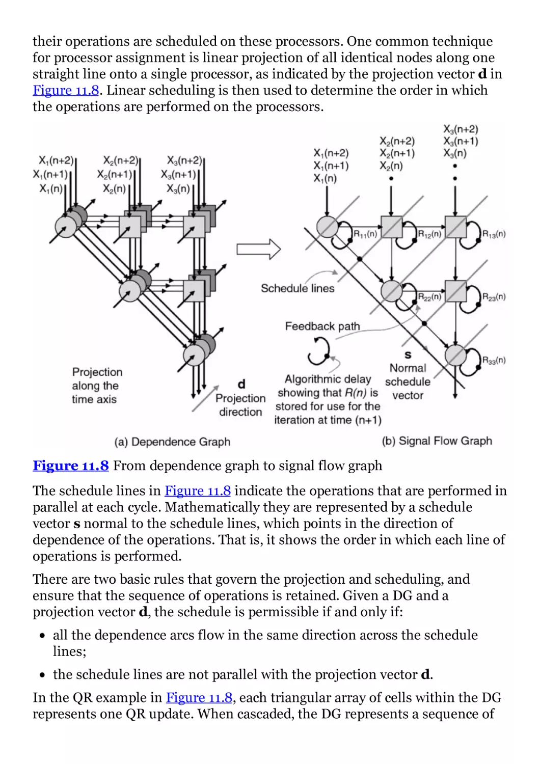
Figure 11.8 From dependence graph to signal flow graph
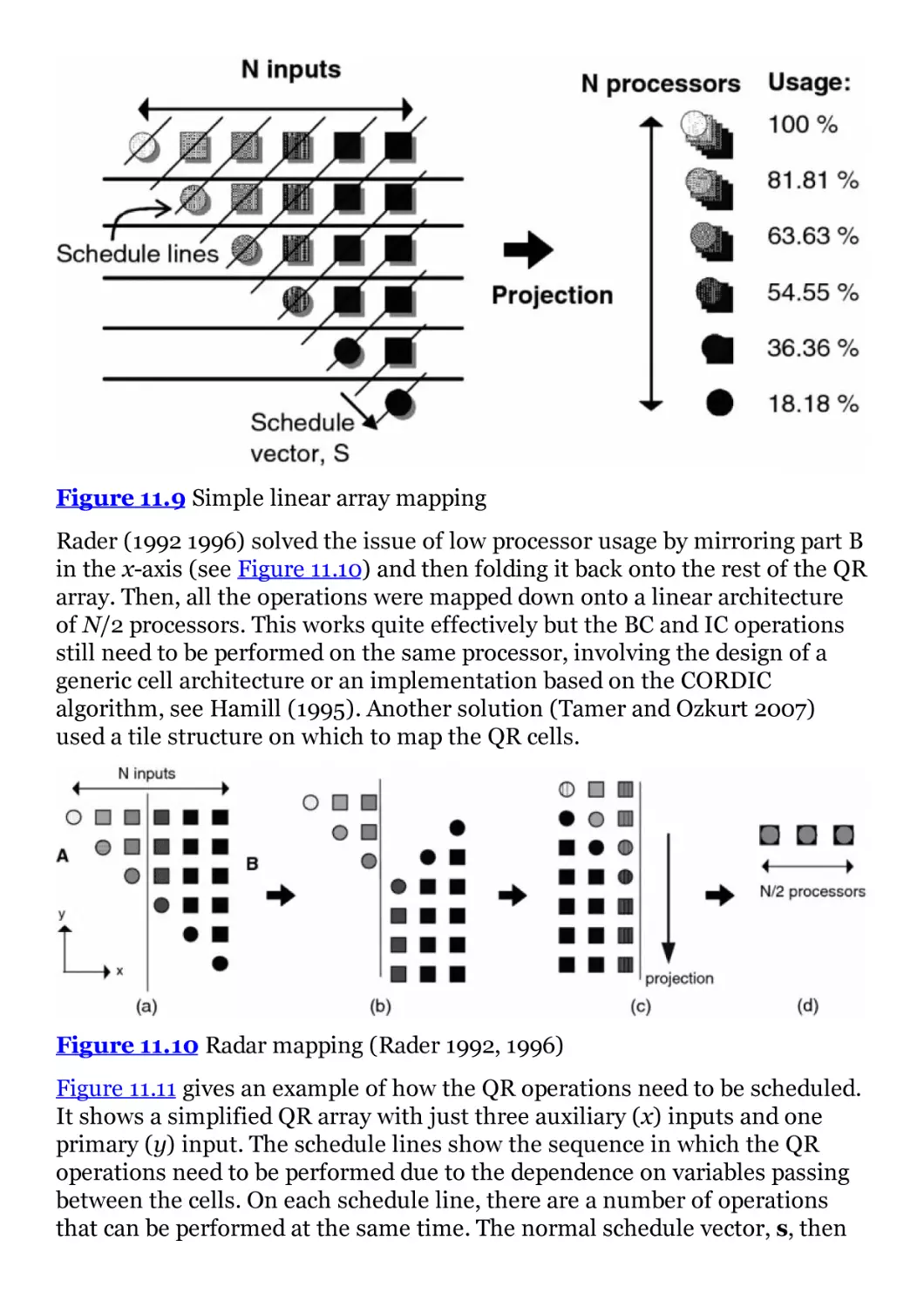
Figure 11.9 Simple linear array mapping
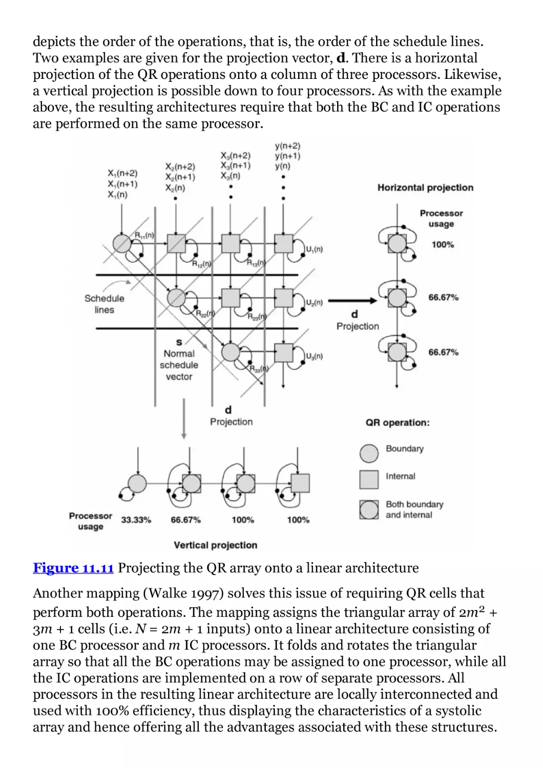
Figure 11.10 Radar mapping (Rader 1992, 1996)
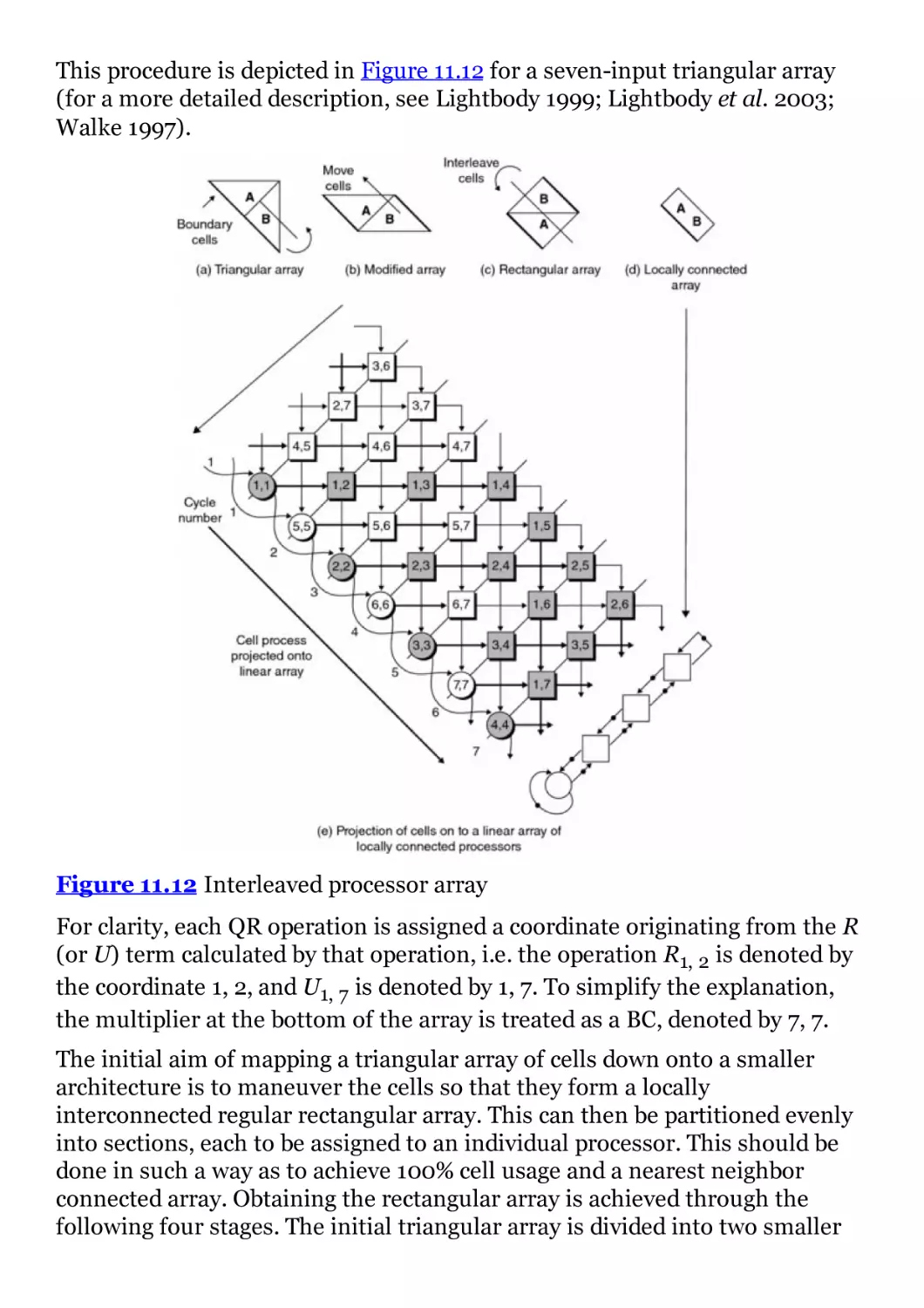
Figure 11.11 Projecting the QR array onto a linear architecture
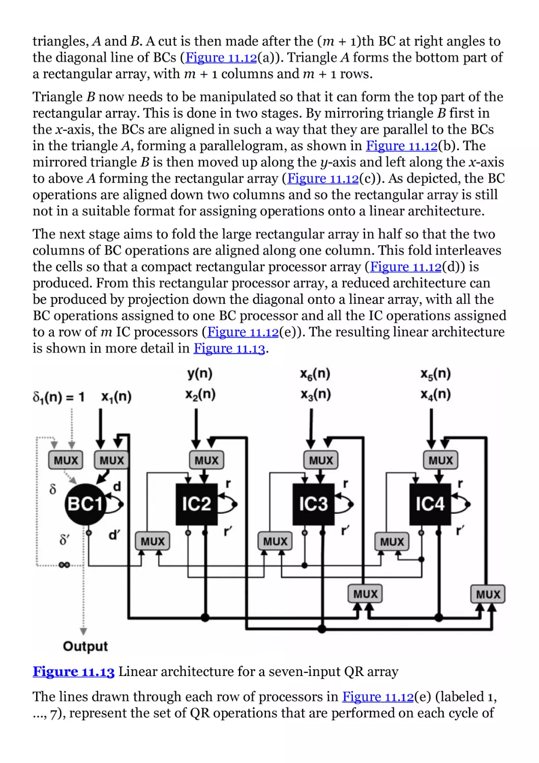
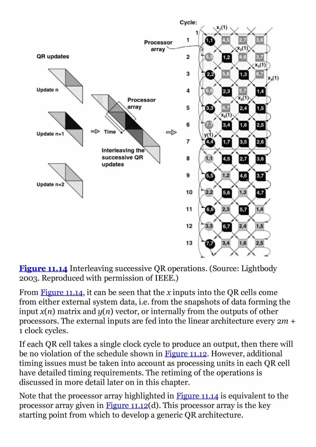
Figure 11.12 Interleaved processor array
Figure 11.13 Linear architecture for a seven-input QR array
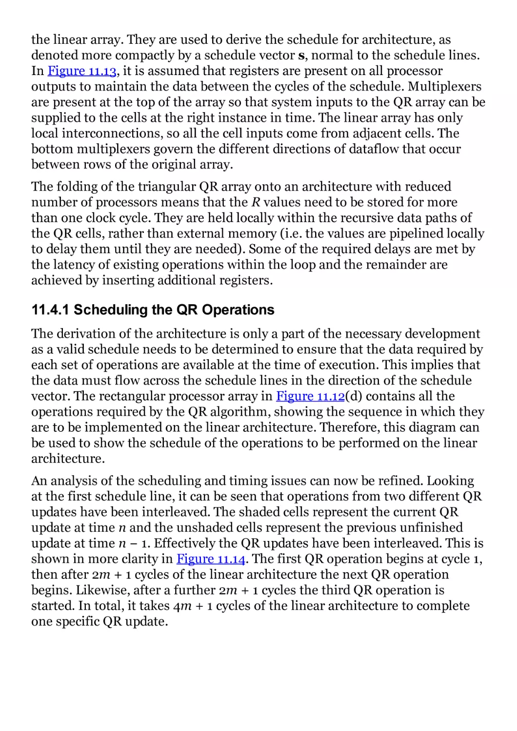
Figure 11.14 Interleaving successive QR operations. (Source:
Lightbody 2003. Reproduced with permission of IEEE.)
Figure 11.15 Generic QR array. (Source: Lightbody 2003. Reproduced
with permission of IEEE.)
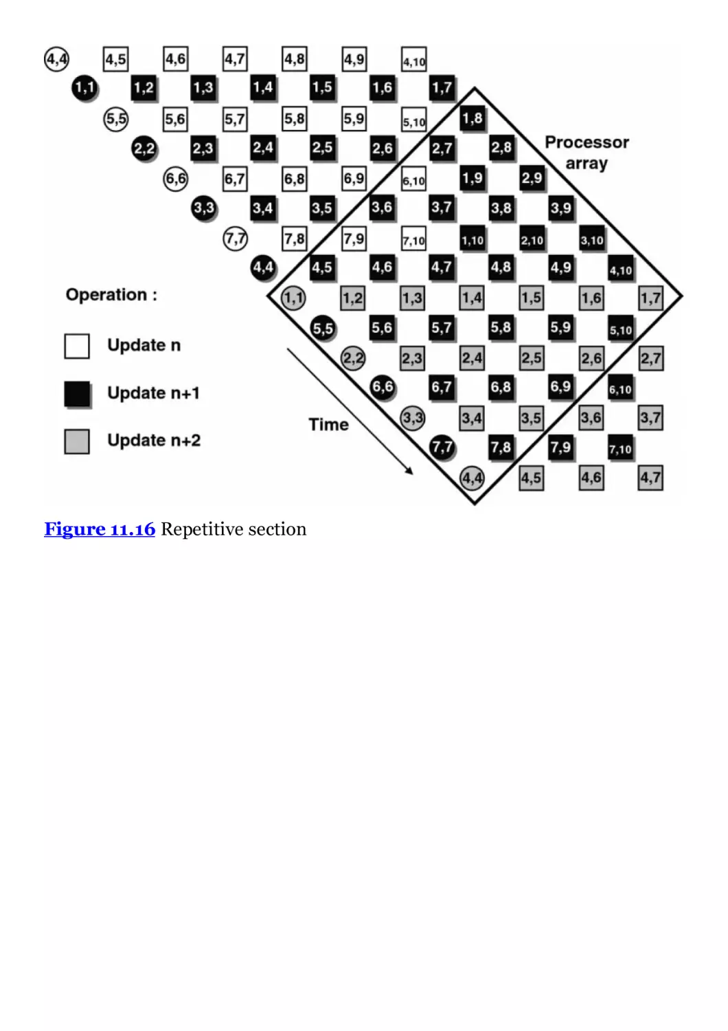
Figure 11.16 Repetitive section
Figure 11.17 Processor array. (Source: Lightbody 2003. Reproduced
with permission of IEEE.)
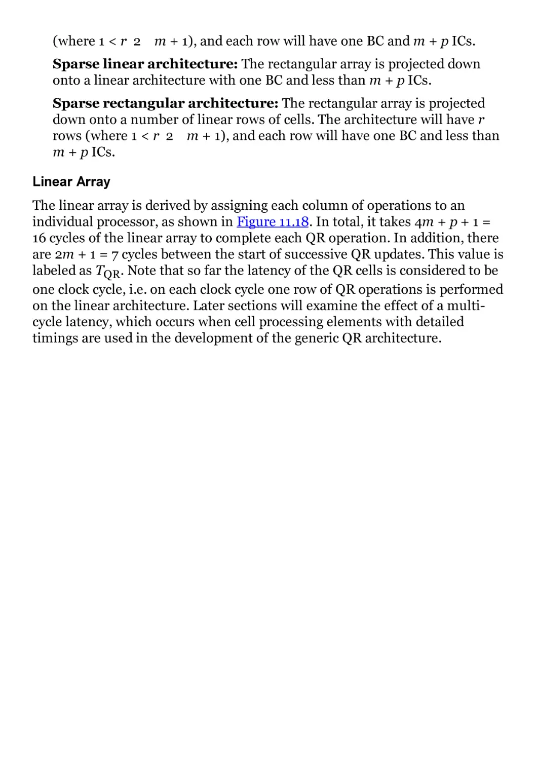
Figure 11.18 Linear array. (Source: Lightbody 2003. Reproduced with
permission of IEEE.)
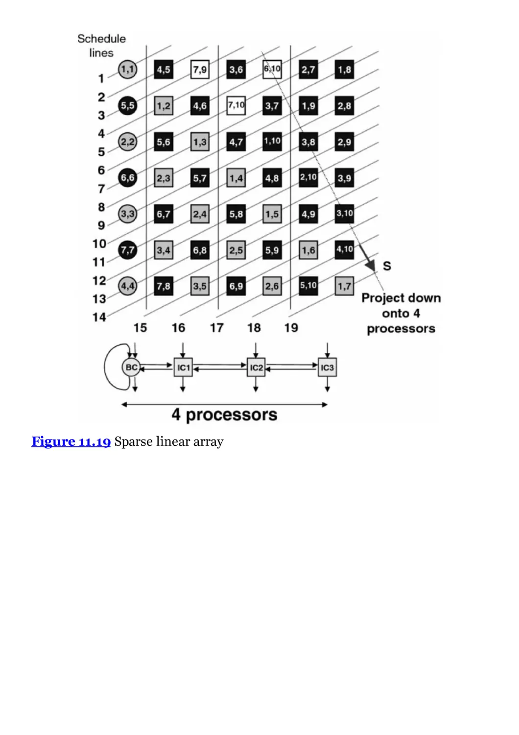
Figure 11.19 Sparse linear array
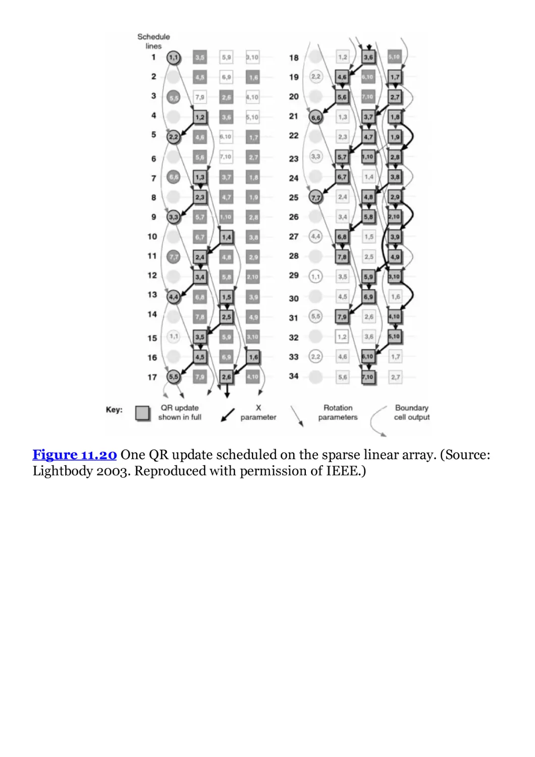
Figure 11.20 One QR update scheduled on the sparse linear array.
(Source: Lightbody 2003. Reproduced with permission of IEEE.)
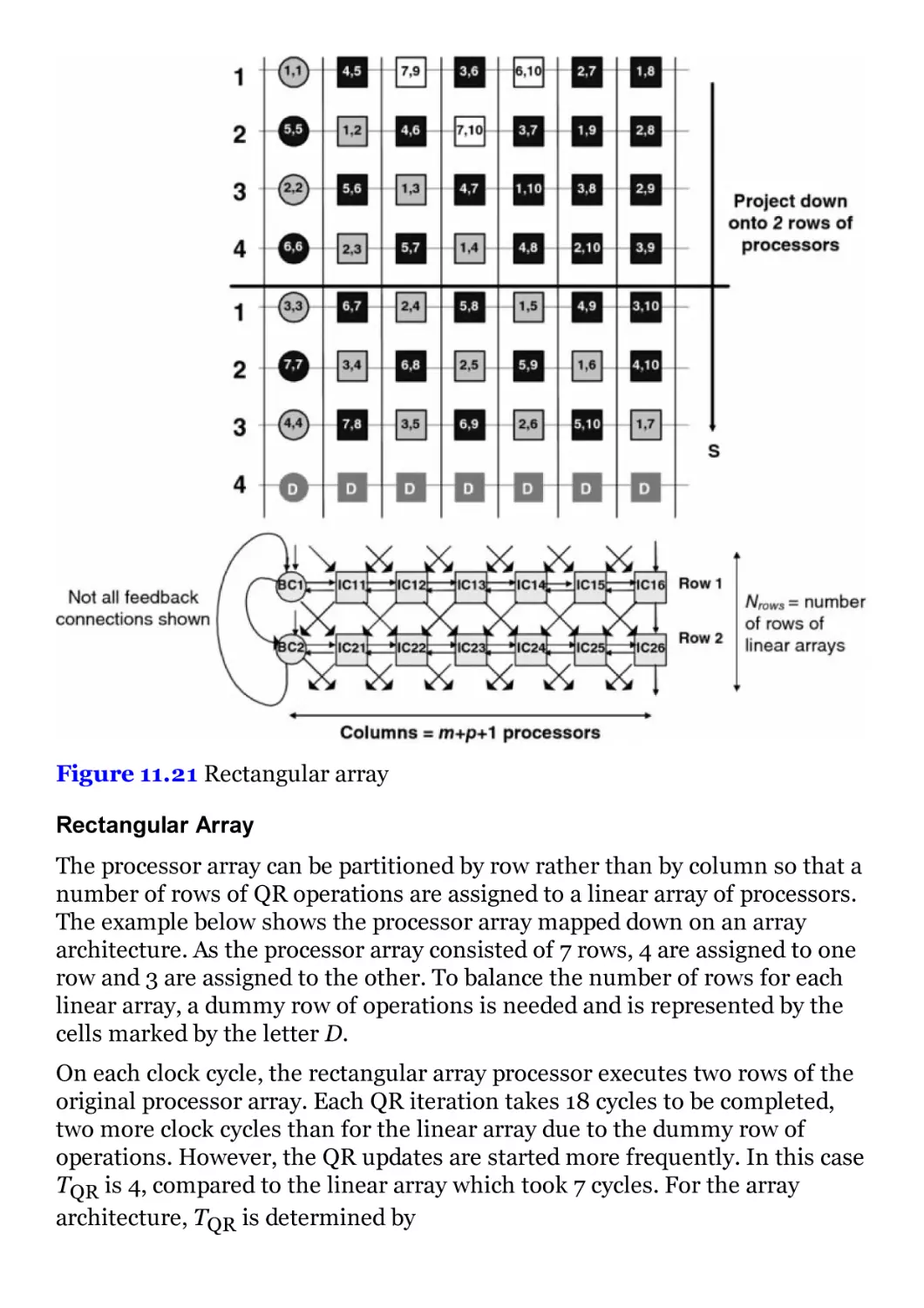
Figure 11.21 Rectangular array
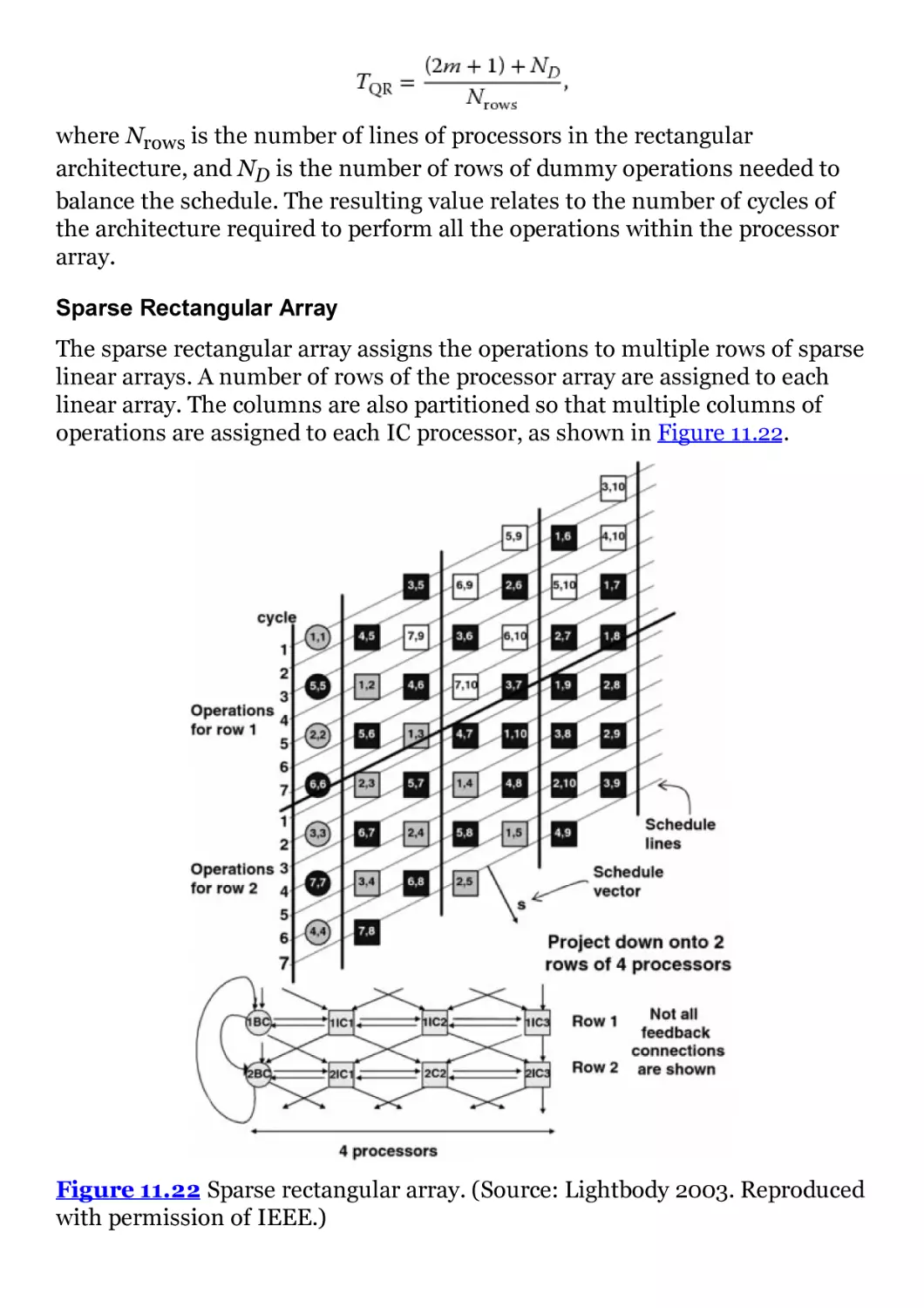
Figure 11.22 Sparse rectangular array. (Source: Lightbody 2003.
Reproduced with permission of IEEE.)
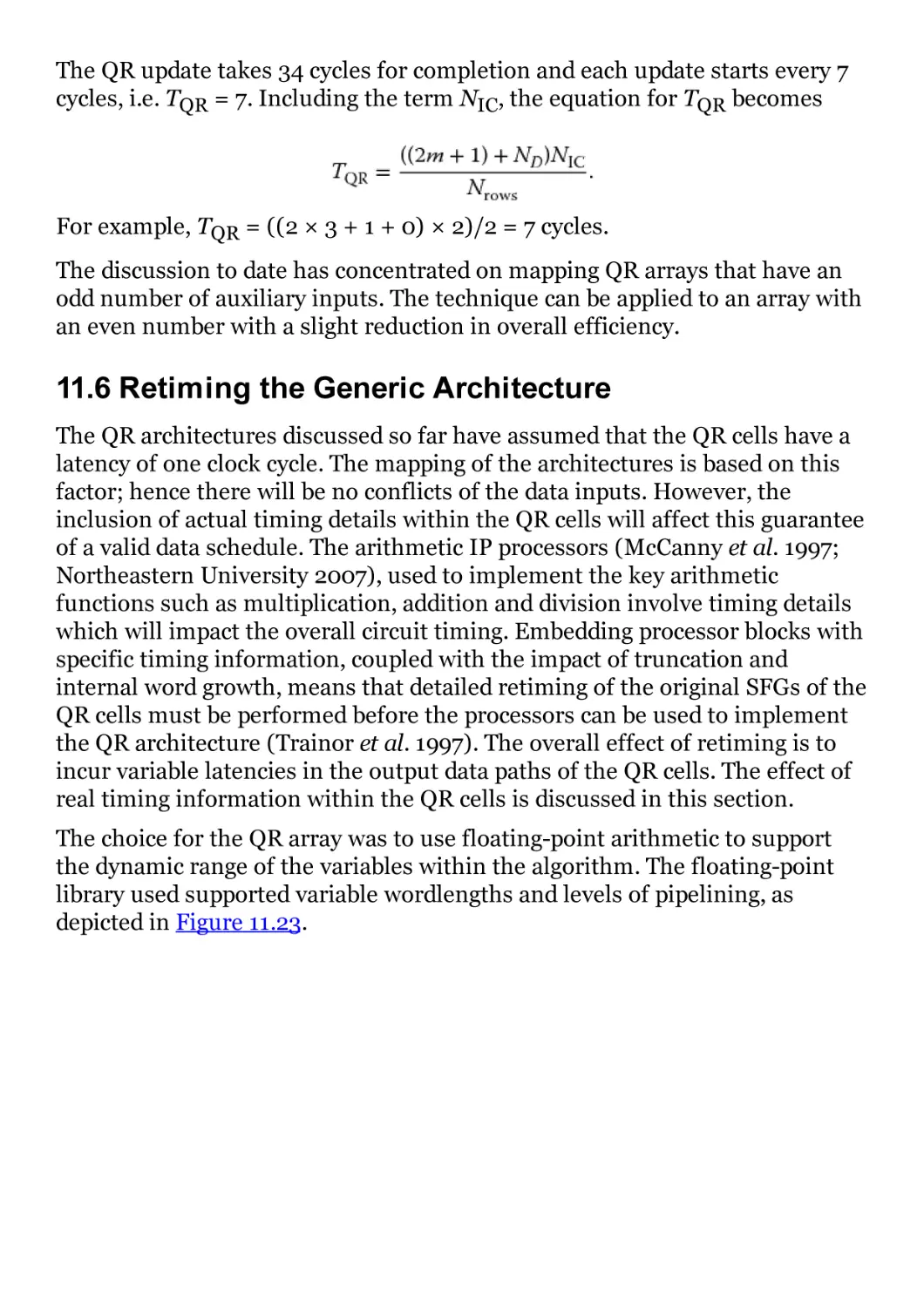
Figure 11.23 Arithmetic modules. (Source: Lightbody 2003.
Reproduced with permission of IEEE.)
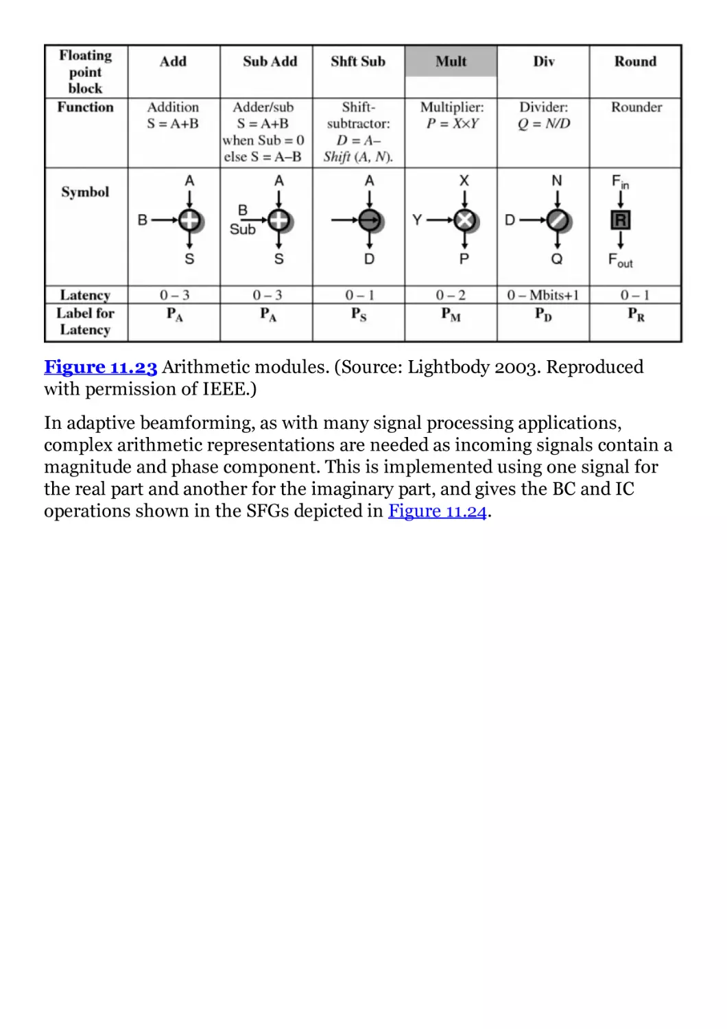
Figure 11.24 Cell SFGs for the complex arithmetic SGR QR algorithm.
(Source: Lightbody 2003. Reproduced with permission of IEEE.)
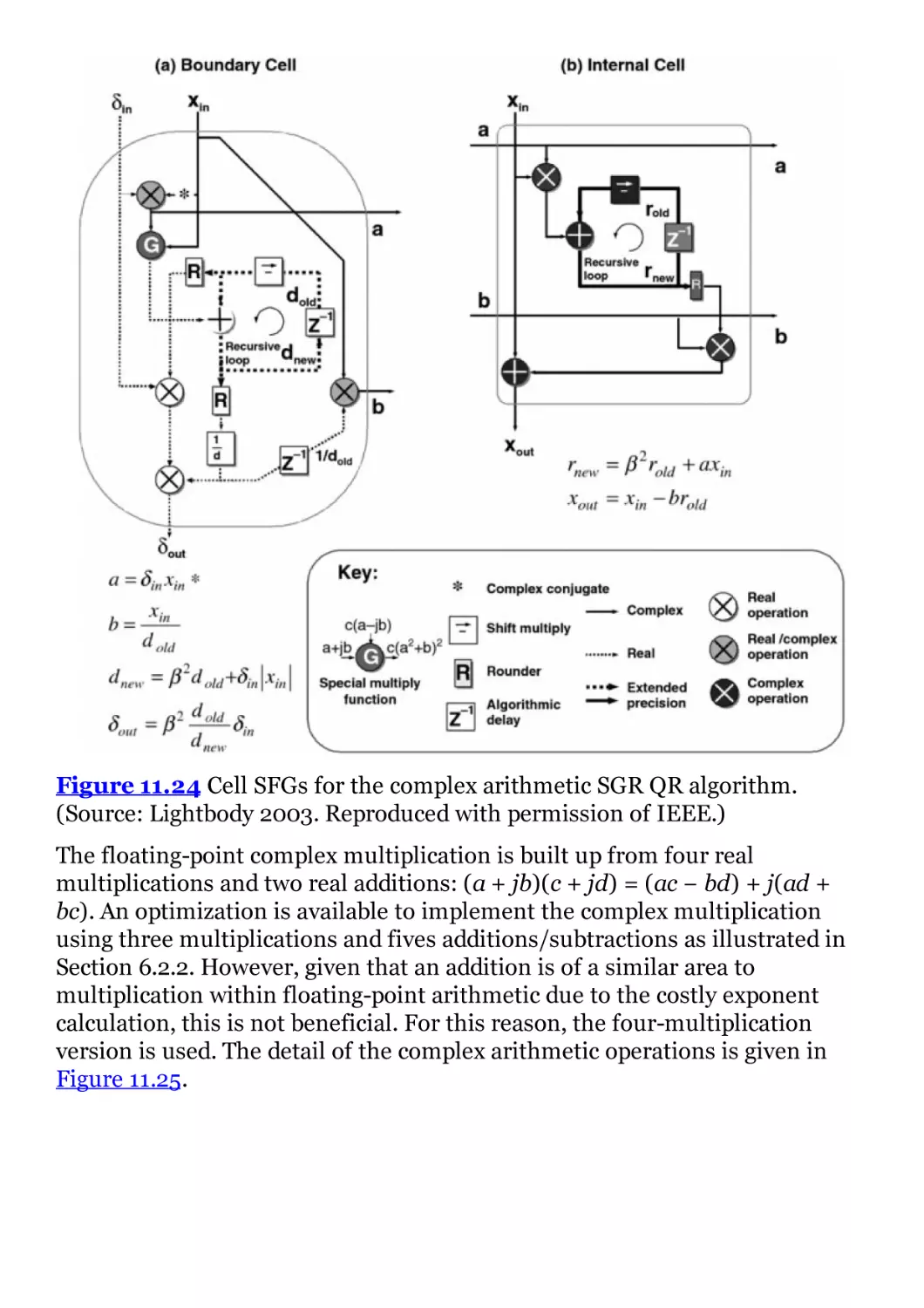
Figure 11.25 Arithmetic modules. (Source: Lightbody 2003.
Reproduced with permission of IEEE.)
Figure 11.26 Generically retimed BC
Figure 11.27 Generically retimed IC
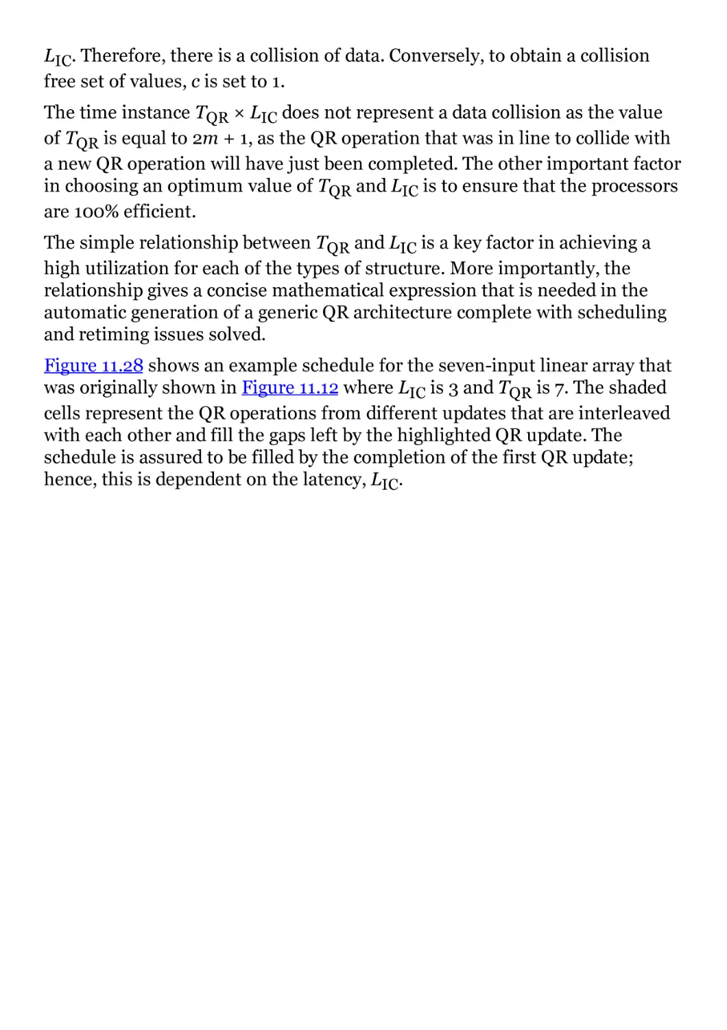
Figure 11.28 Schedule for a linear array with an IC latency of 3
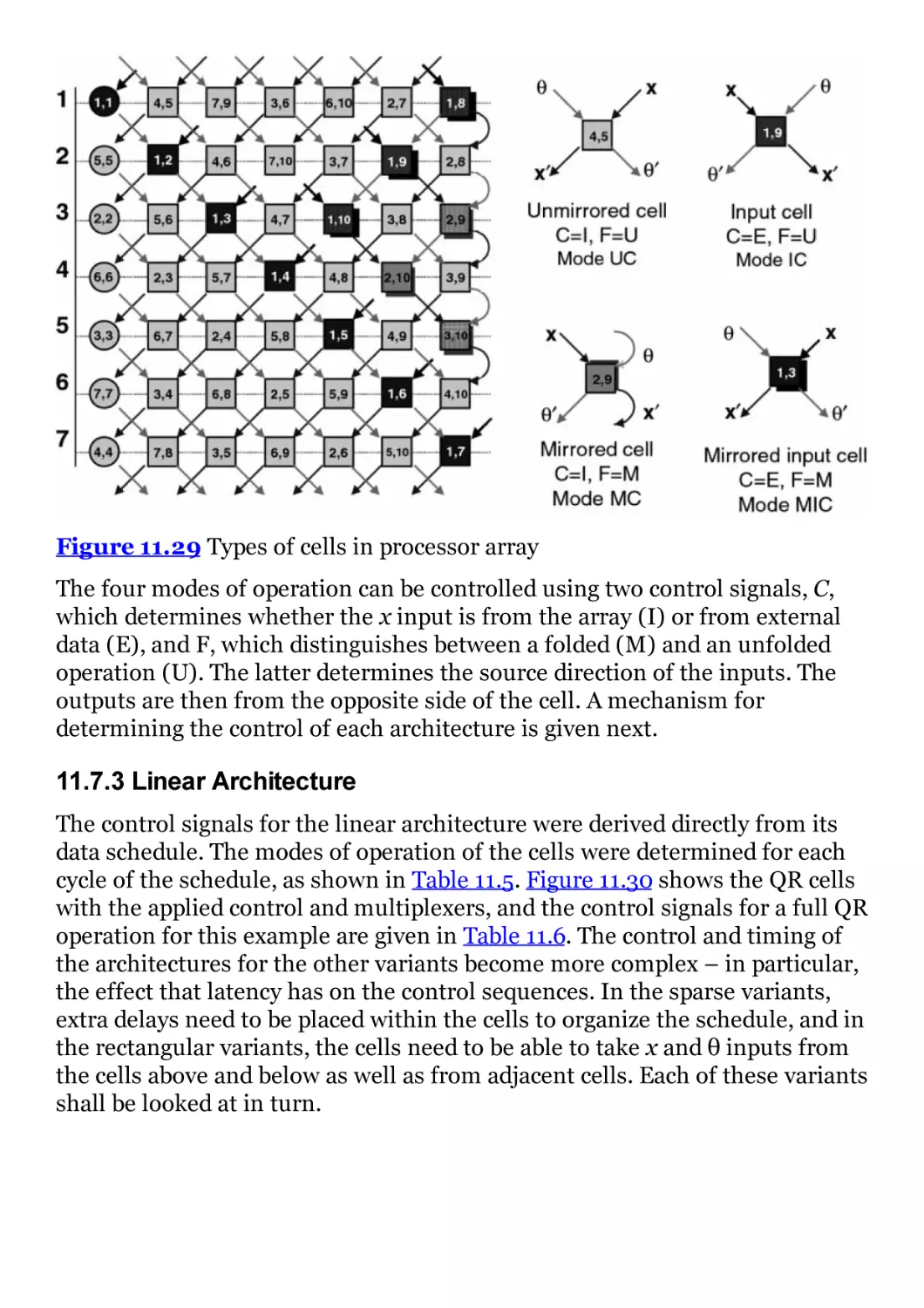
Figure 11.29 Types of cells in processor array
Figure 11.30 QR cells for the linear architecture
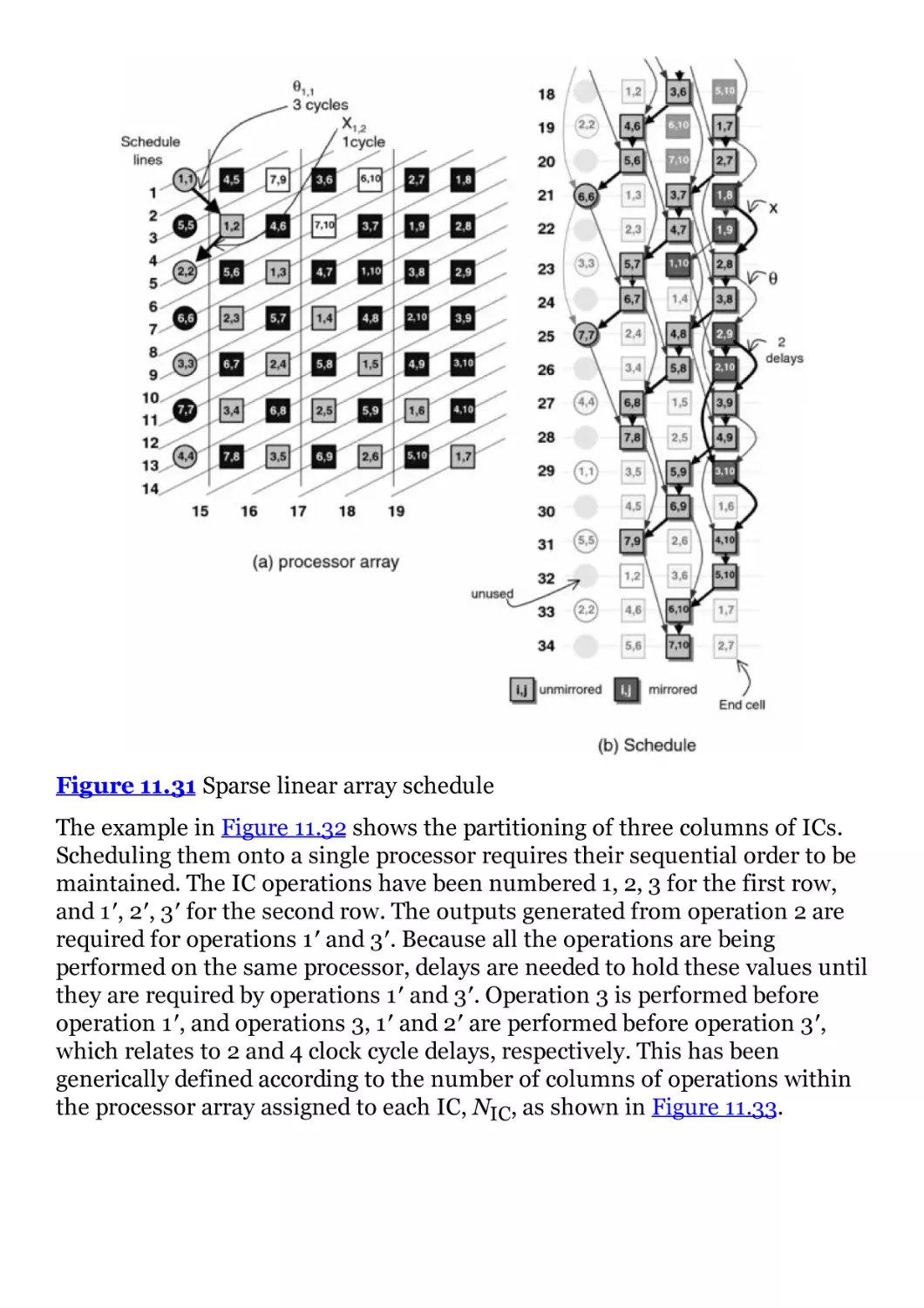
Figure 11.31 Sparse linear array schedule
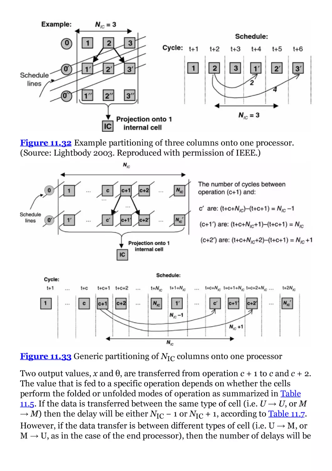
Figure 11.32 Example partitioning of three columns onto one
processor. (Source: Lightbody 2003. Reproduced with permission of
IEEE.)
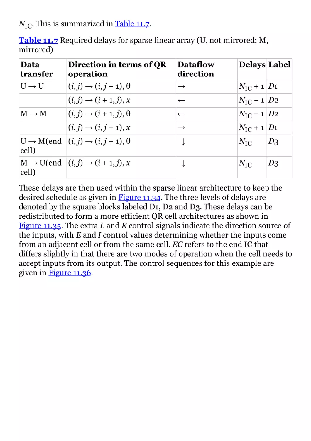
Figure 11.33 Generic partitioning of NIC columns onto one processor
Figure 11.34 Sparse linear array cells
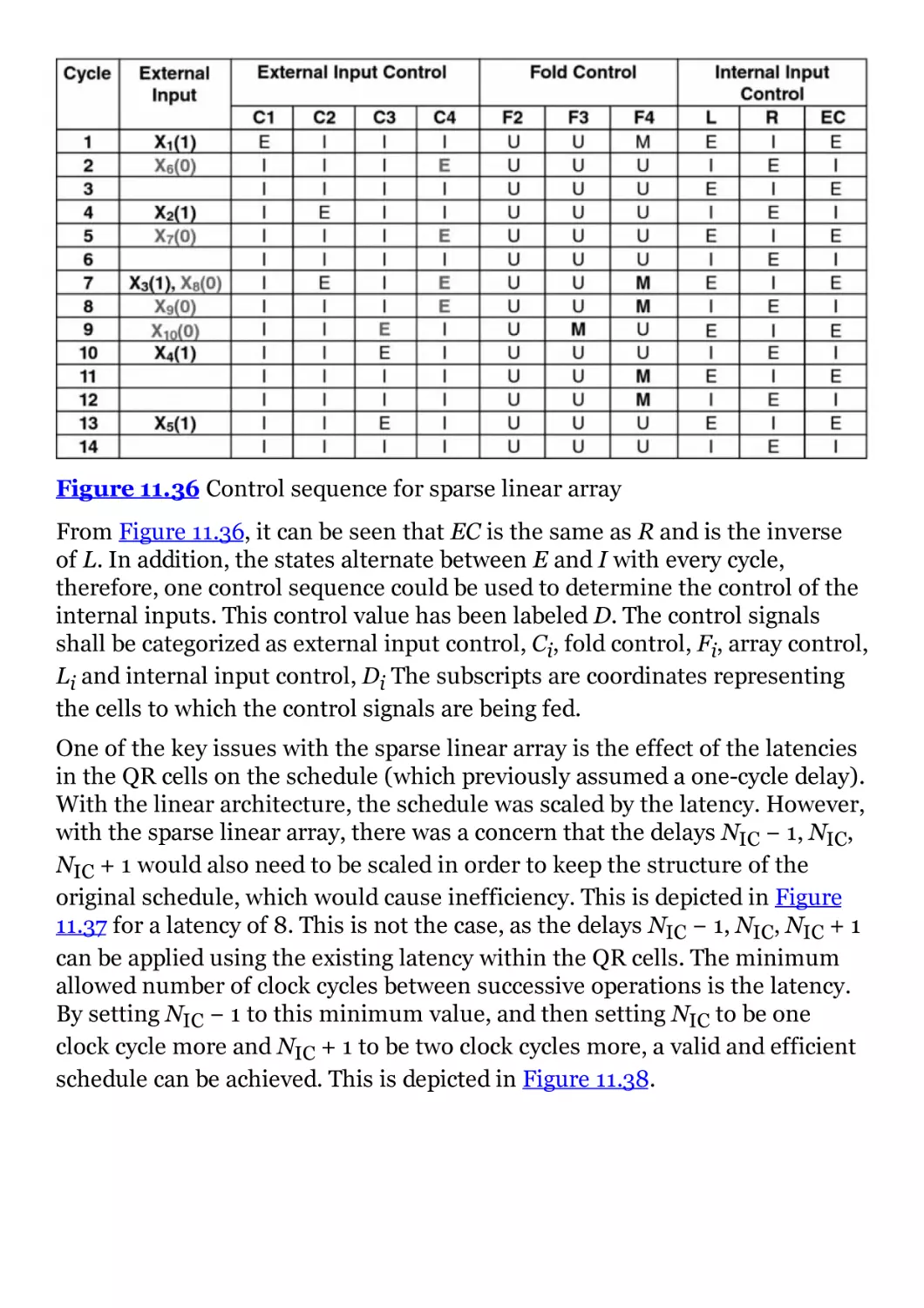
Figure 11.35 Redistributed delays for sparse linear array cells
Figure 11.36 Control sequence for sparse linear array
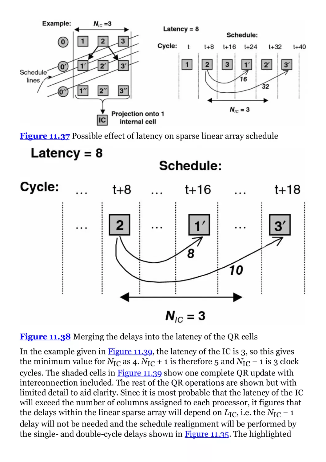
Figure 11.37 Possible effect of latency on sparse linear array schedule
Figure 11.38 Merging the delays into the latency of the QR cells
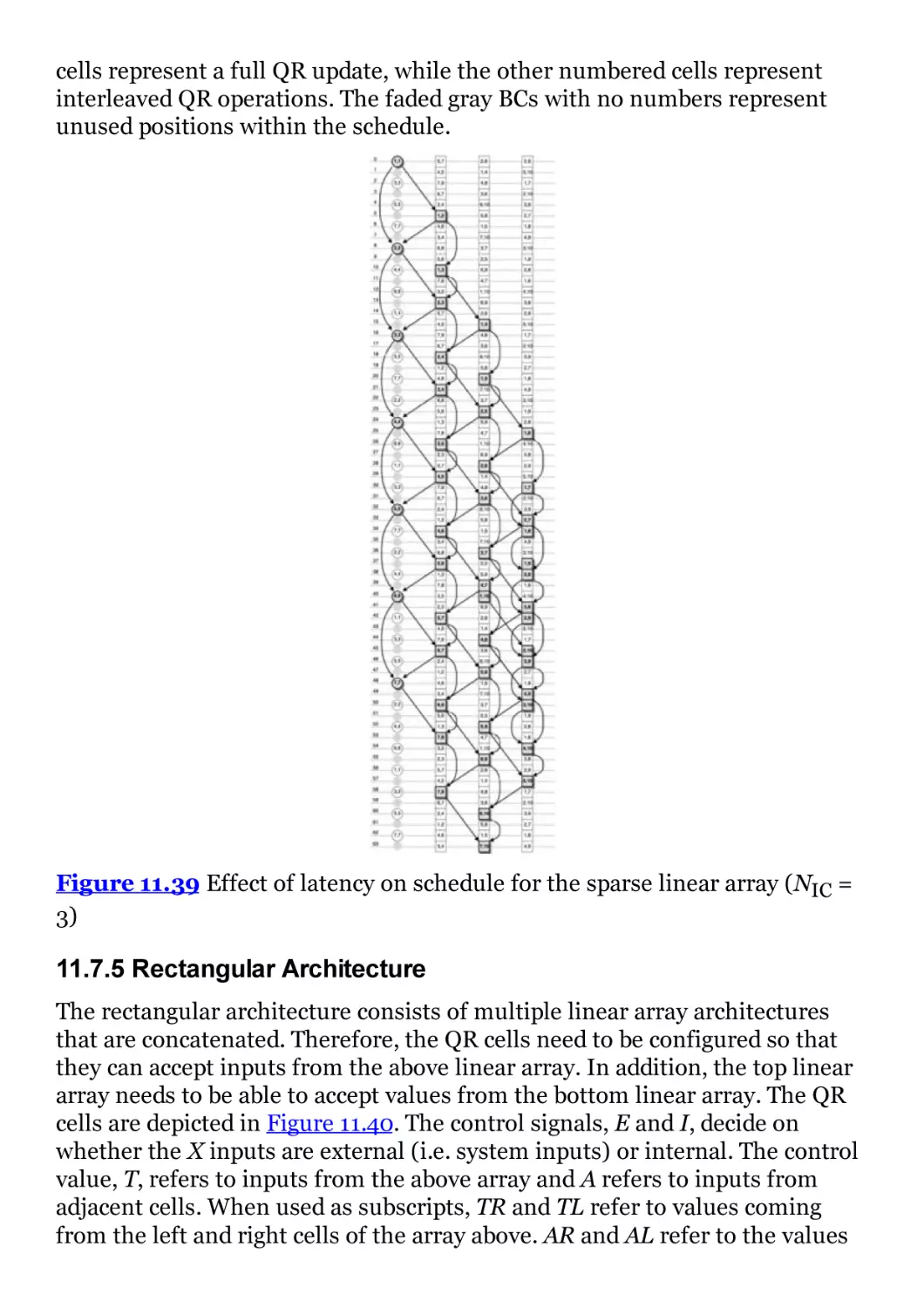
Figure 11.39 Effect of latency on schedule for the sparse linear array
(NIC = 3)
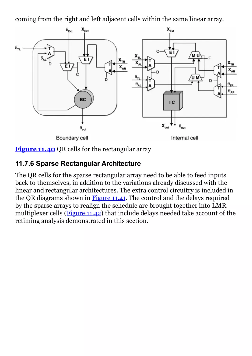
Figure 11.40 QR cells for the rectangular array
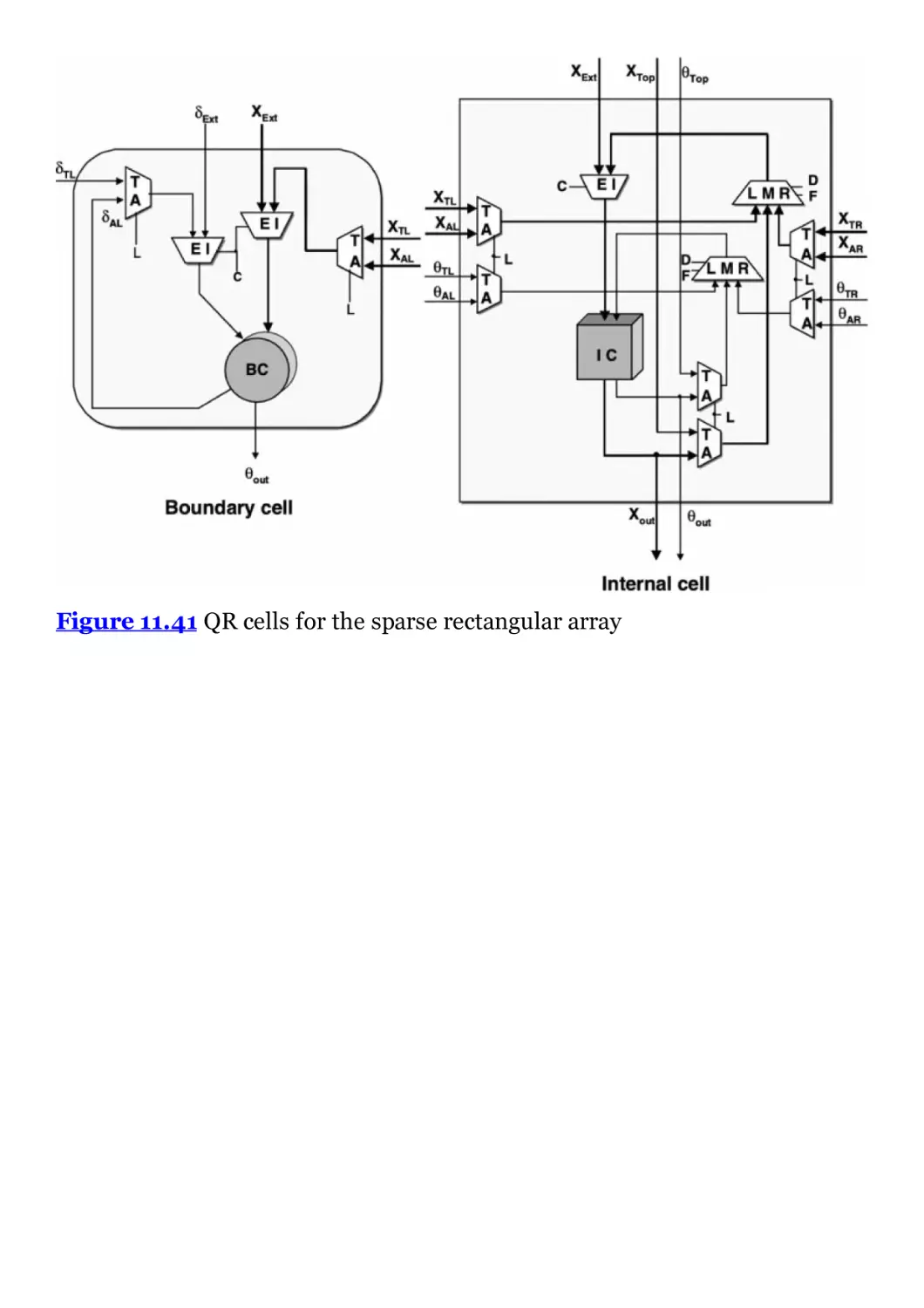
Figure 11.41 QR cells for the sparse rectangular array
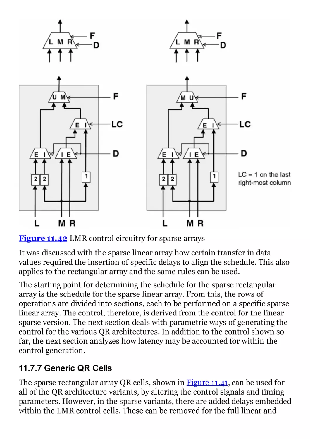
Figure 11.42 LMR control circuitry for sparse arrays
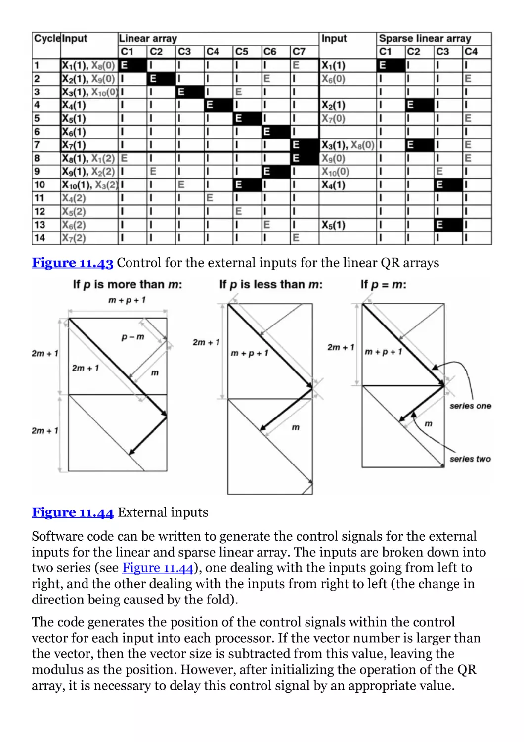
Figure 11.43 Control for the external inputs for the linear QR arrays
Figure 11.44 External inputs
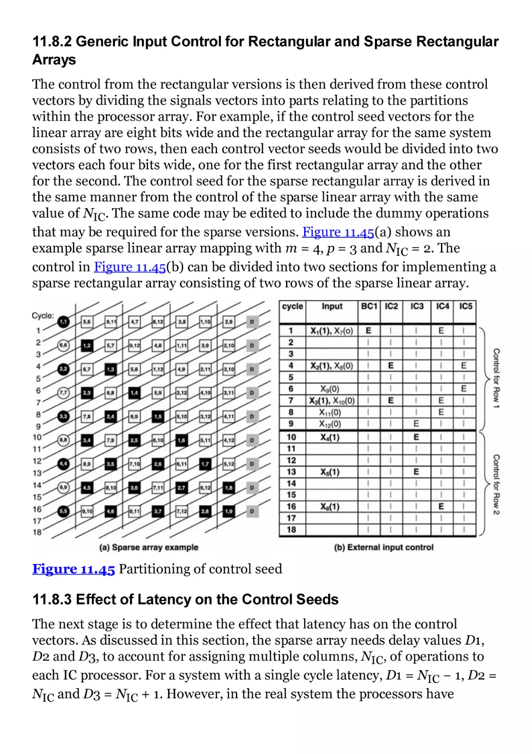
Figure 11.45 Partitioning of control seed
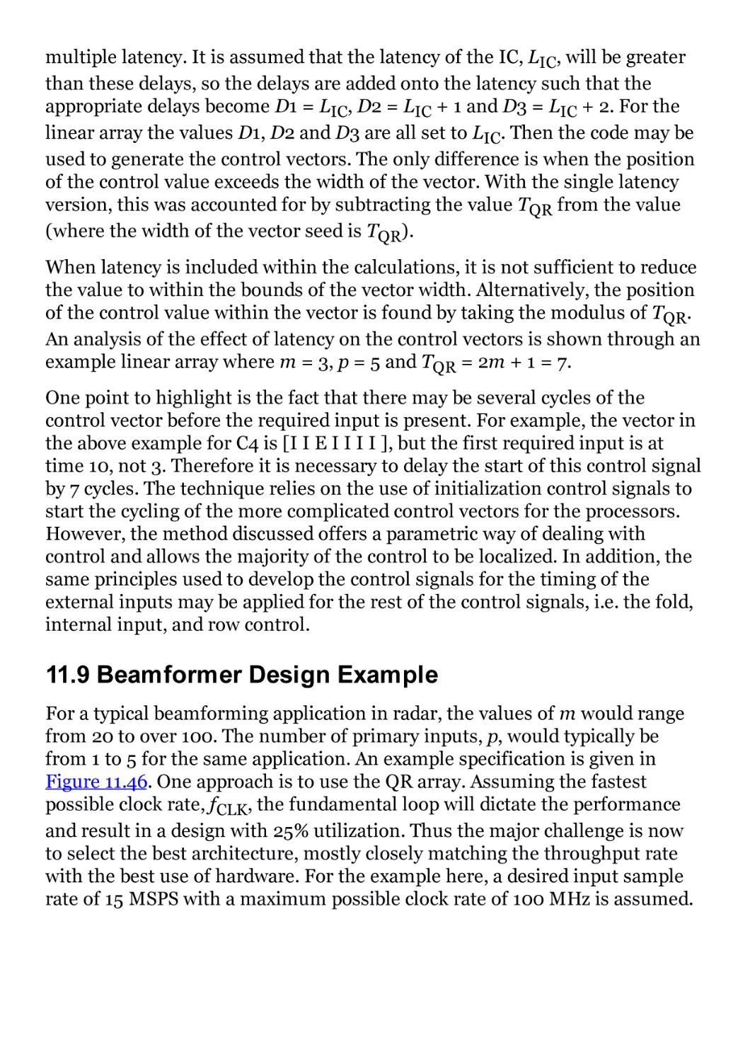
Figure 11.46 Example QR architecture derivation, m = 22, p = 4
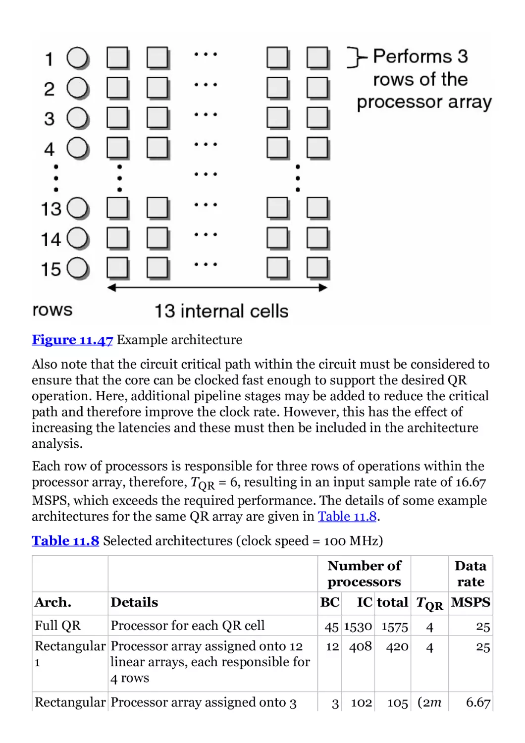
Figure 11.47 Example architecture
Chapter 12
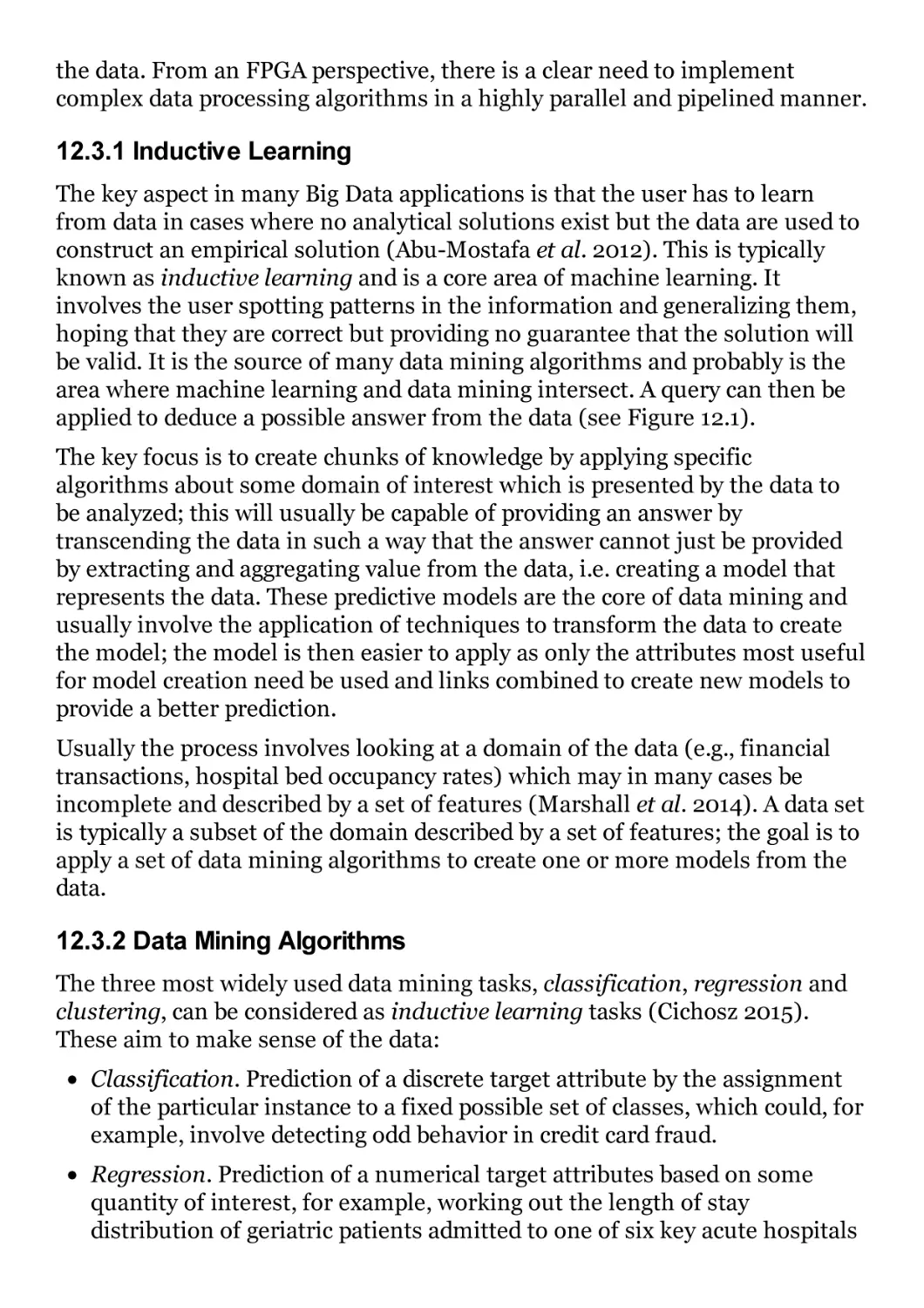
Figure 12.1 Inference of data. Source: Cichosz 2015. Reproduced with
permission of John Wiley & Sons.
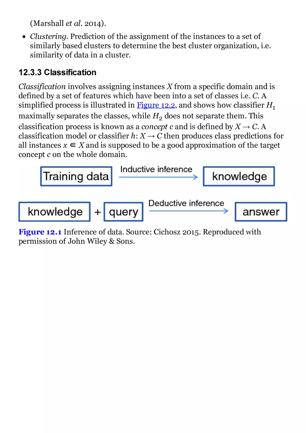
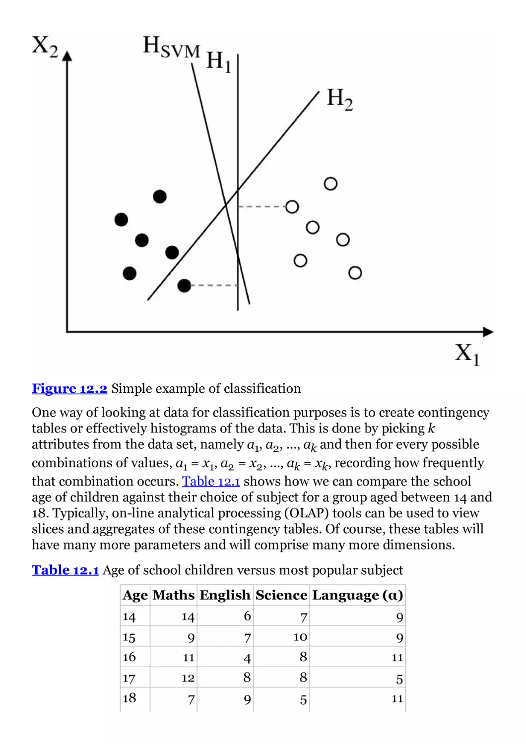
Figure 12.2 Simple example of classification
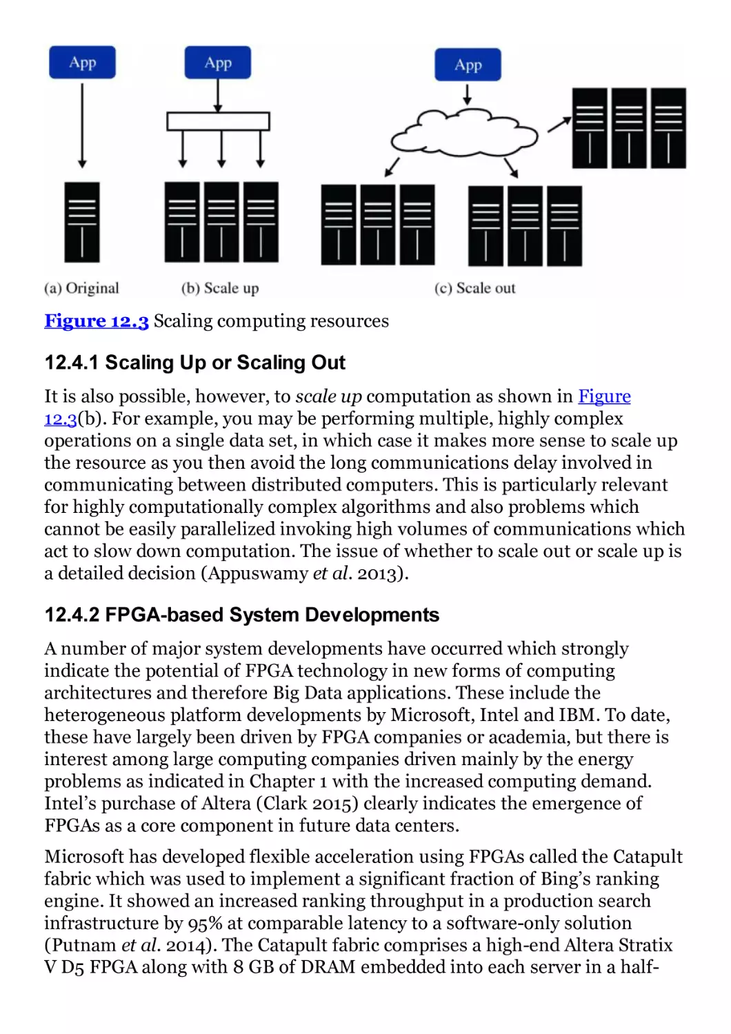
Figure 12.3 Scaling computing resources
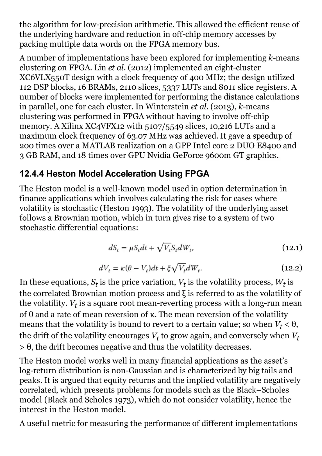
Figure 12.4 Core configuration where Monte Carlo simulations can be
programmed
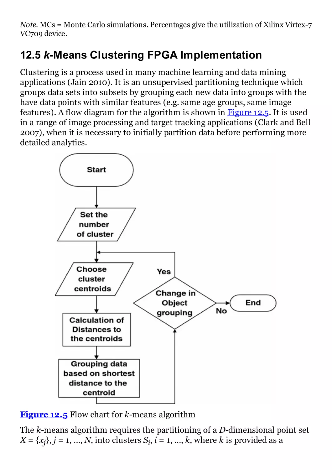
Figure 12.5 Flow chart for k-means algorithm
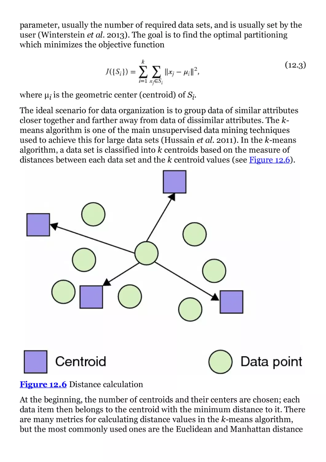
Figure 12.6 Distance calculation
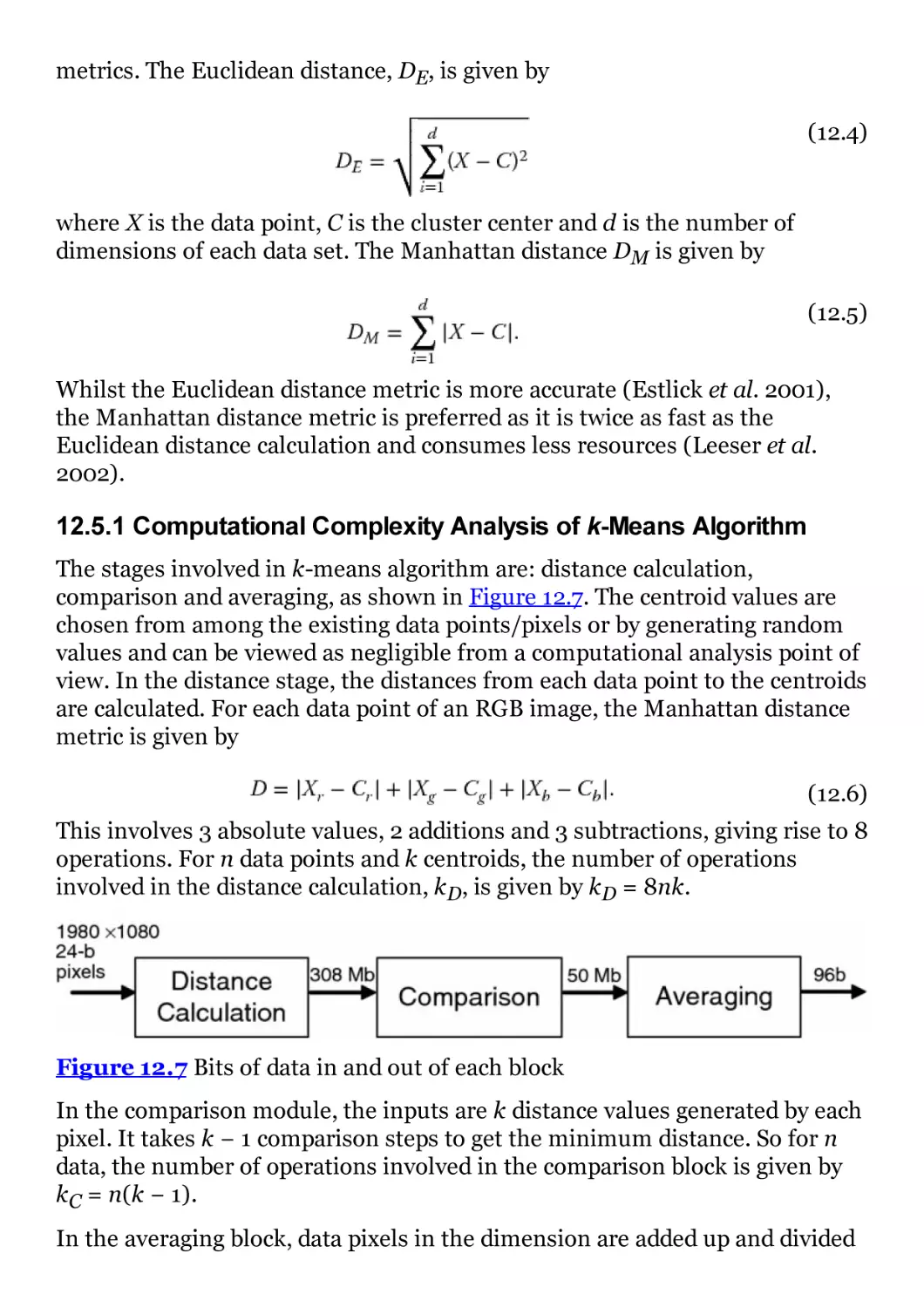
Figure 12.7 Bits of data in and out of each block
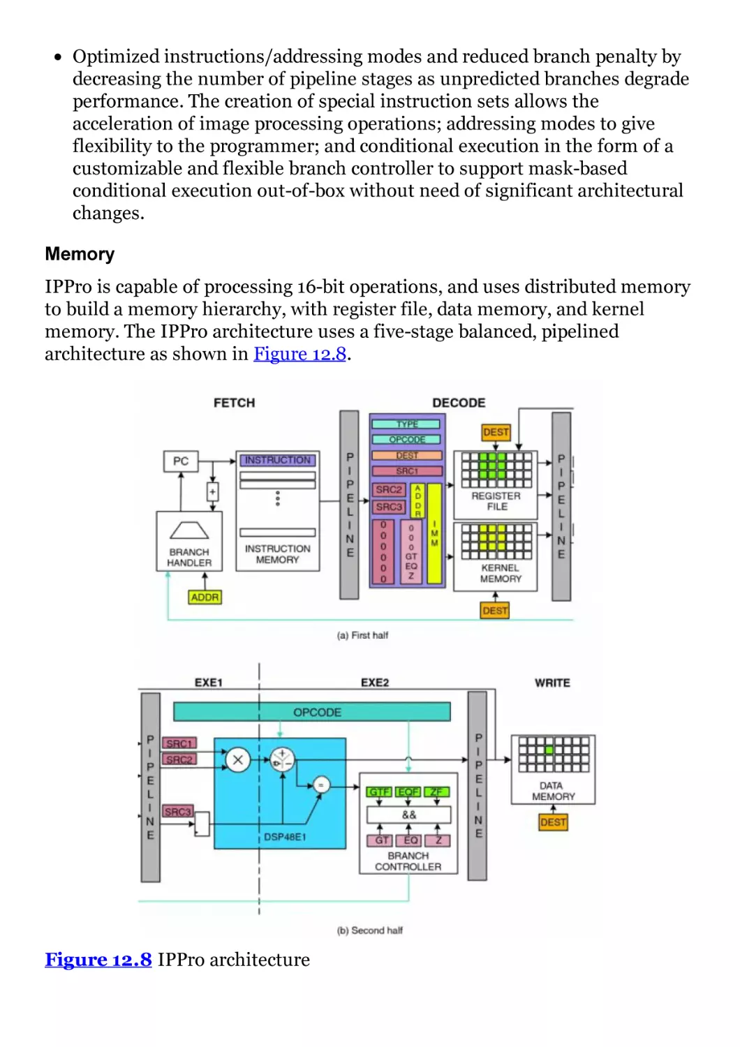
Figure 12.8 IPPro architecture
Figure 12.9 Proposed system architecture
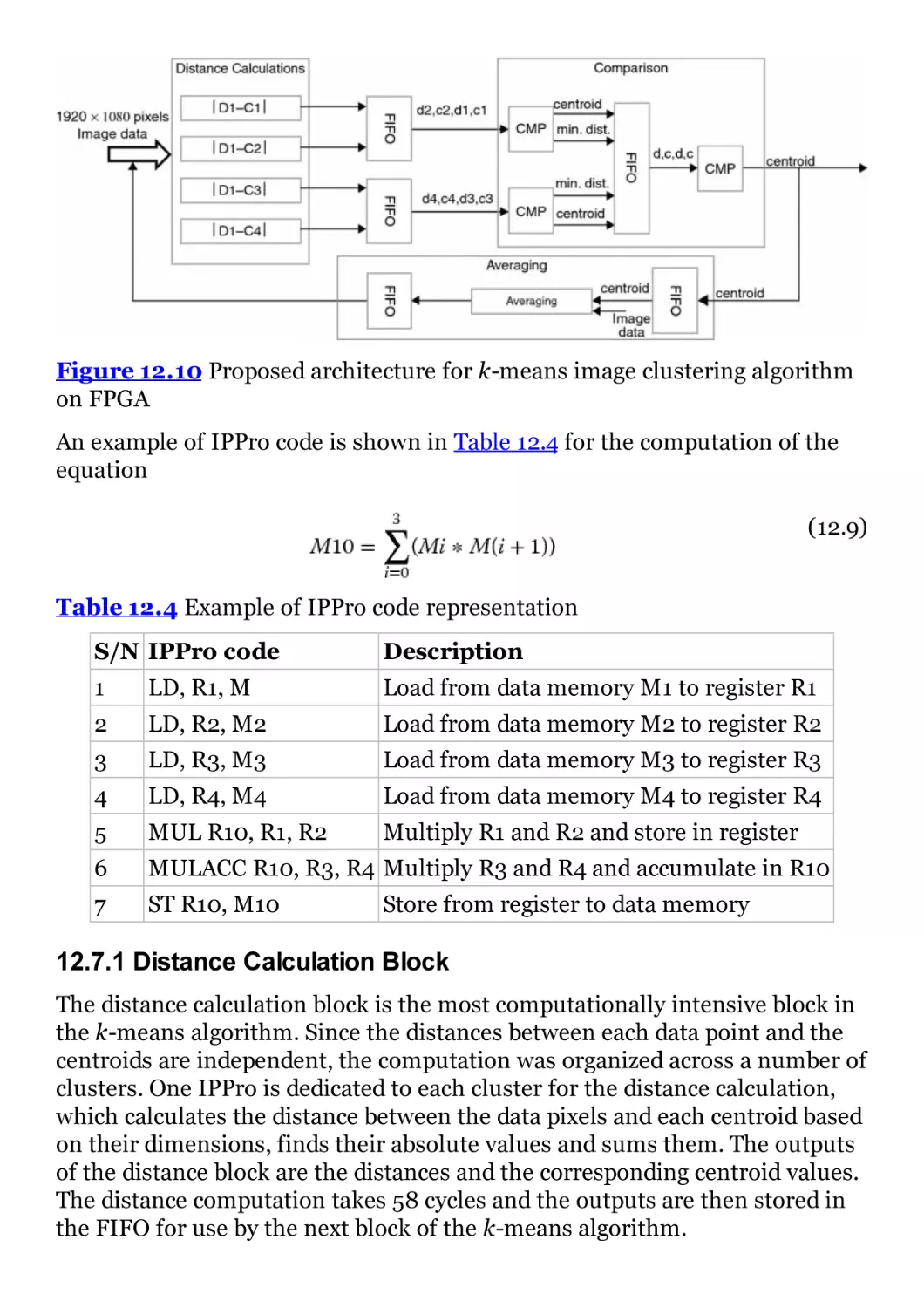
Figure 12.10 Proposed architecture for k-means image clustering
algorithm on FPGA
Chapter 13
Figure 13.1 Sources of leakage components in CMOS transistor
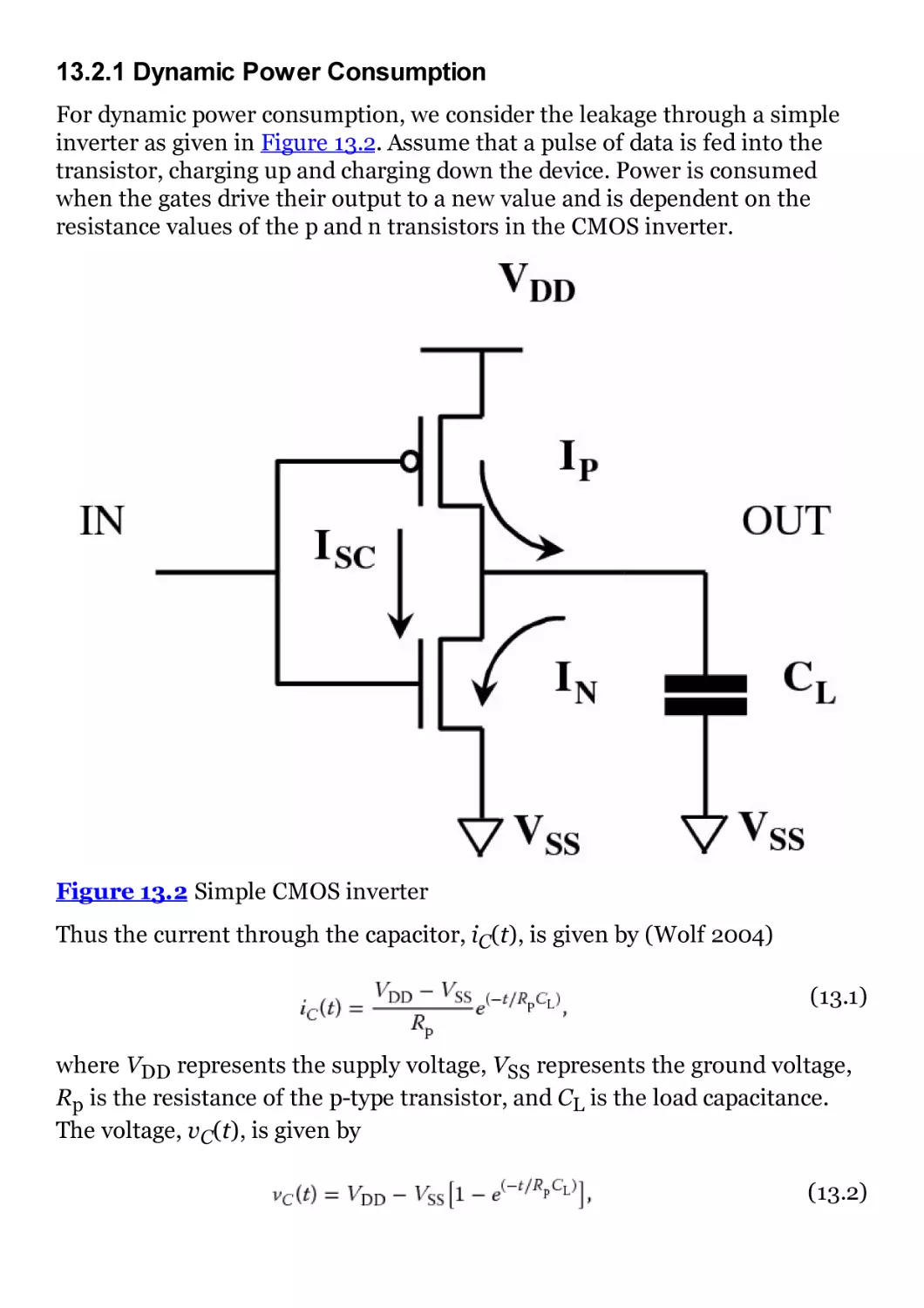
Figure 13.2 Simple CMOS inverter
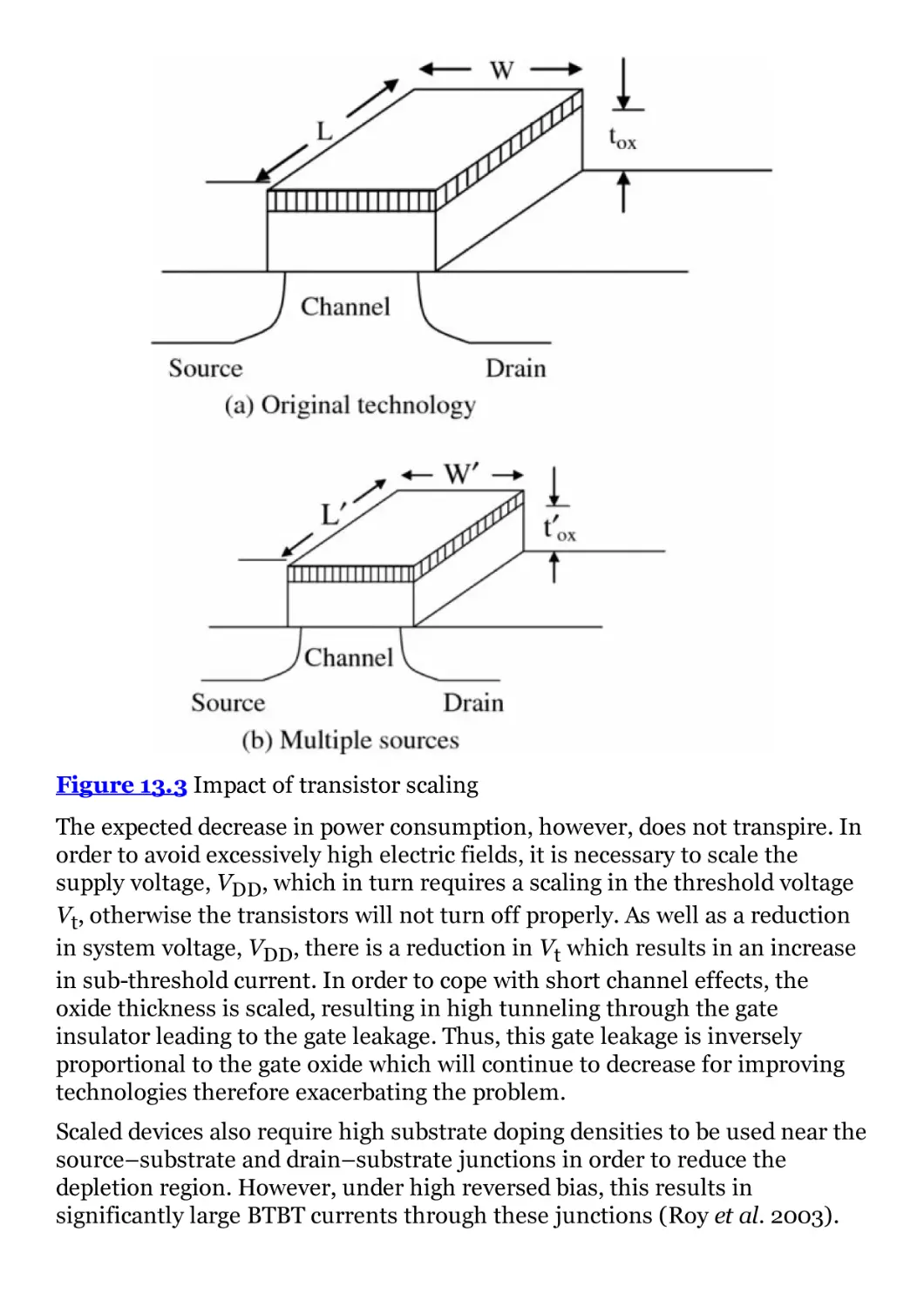
Figure 13.3 Impact of transistor scaling
Figure 13.4 Impact of static versus dynamic power consumption with
technology evolution (ITRS, 2003; Kim et al. 2003)
Figure 13.5 Estimated power consumption for mobile backhaul on
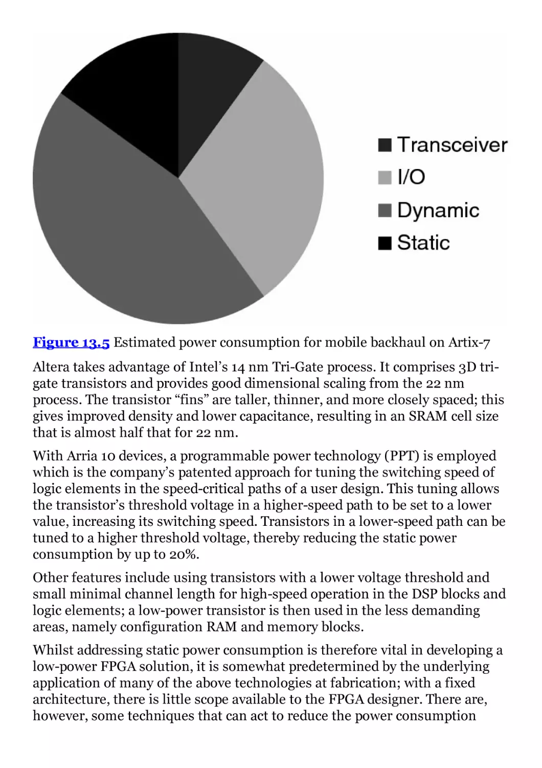
Artix-7
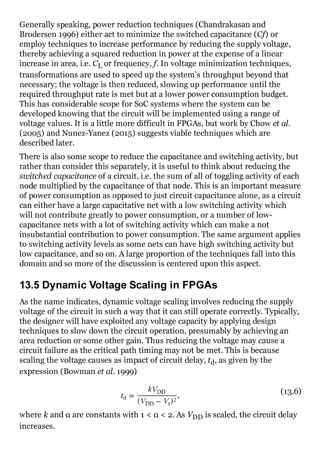
Figure 13.6 Use of parallelism (and voltage scaling) to lower power
consumption
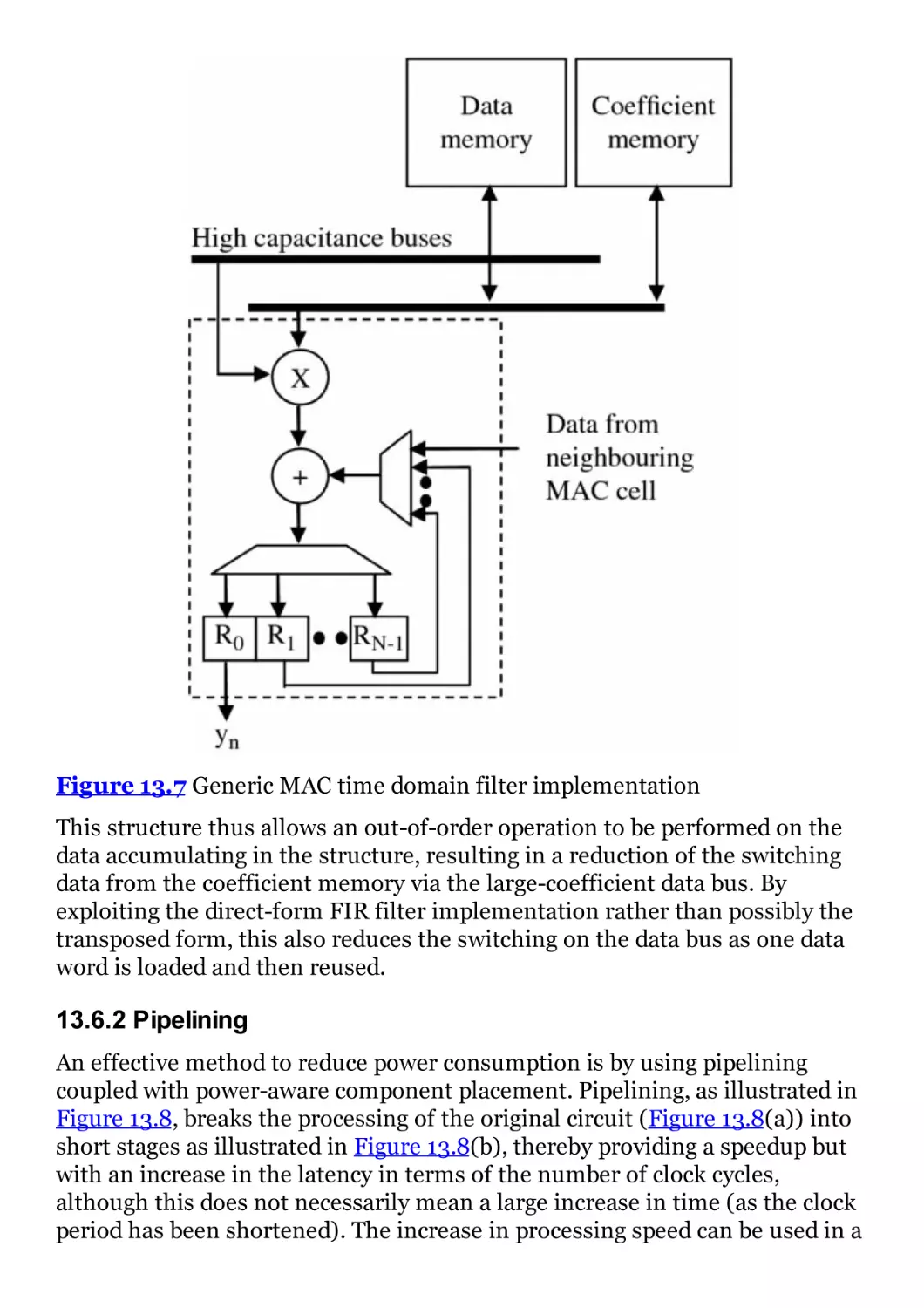
Figure 13.7 Generic MAC time domain filter implementation
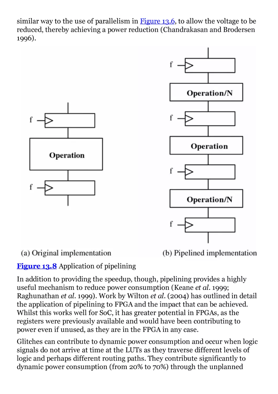
Figure 13.8 Application of pipelining
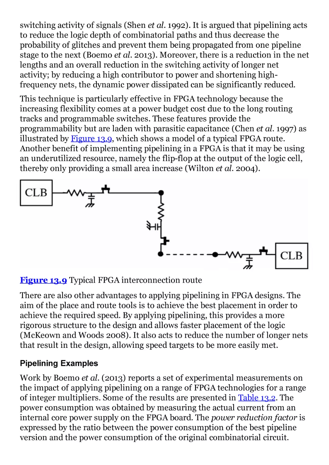
Figure 13.9 Typical FPGA interconnection route
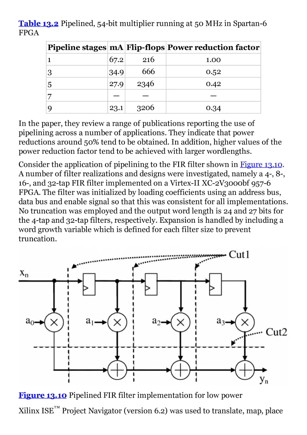
Figure 13.10 Pipelined FIR filter implementation for low power
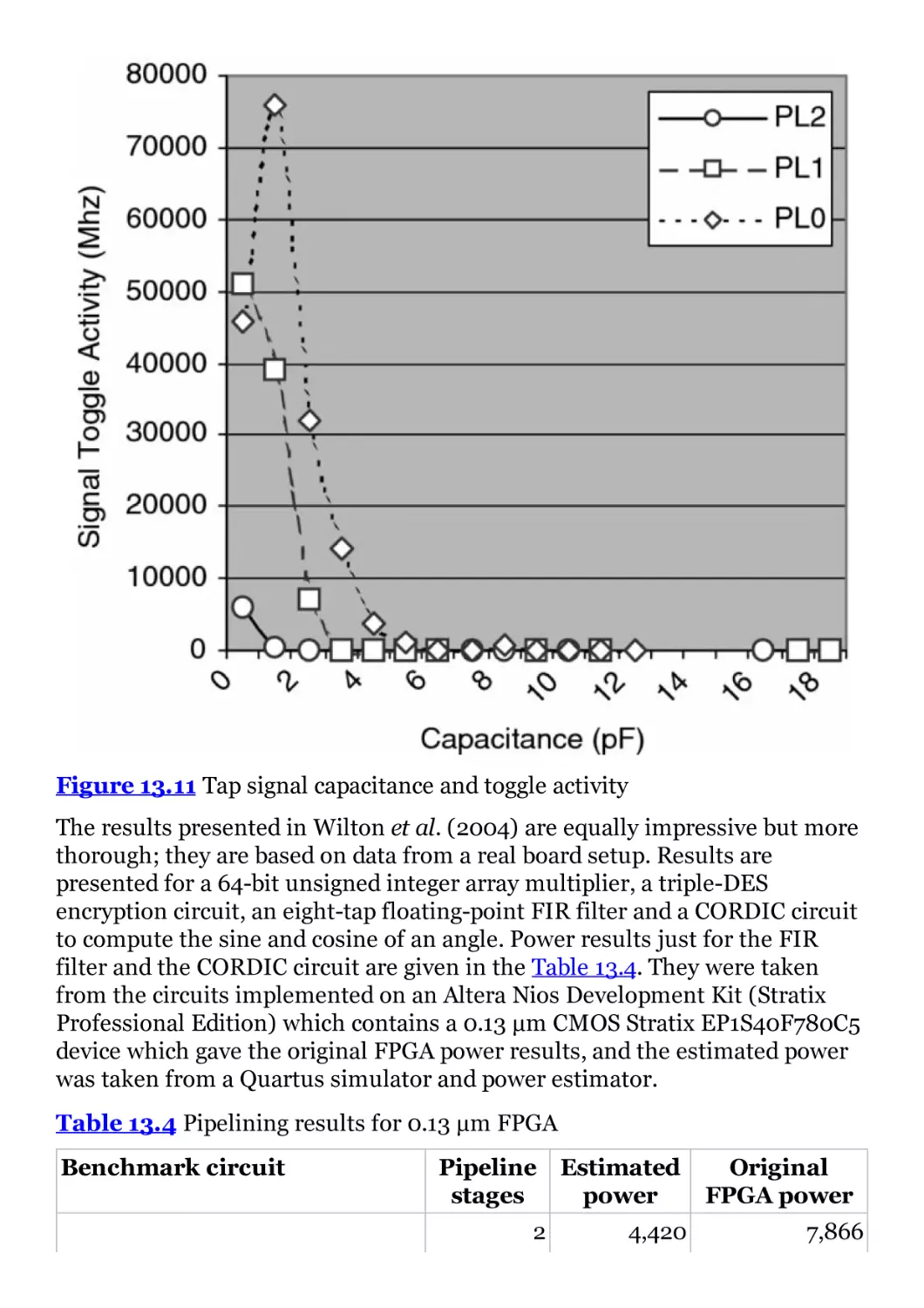
Figure 13.11 Tap signal capacitance and toggle activity
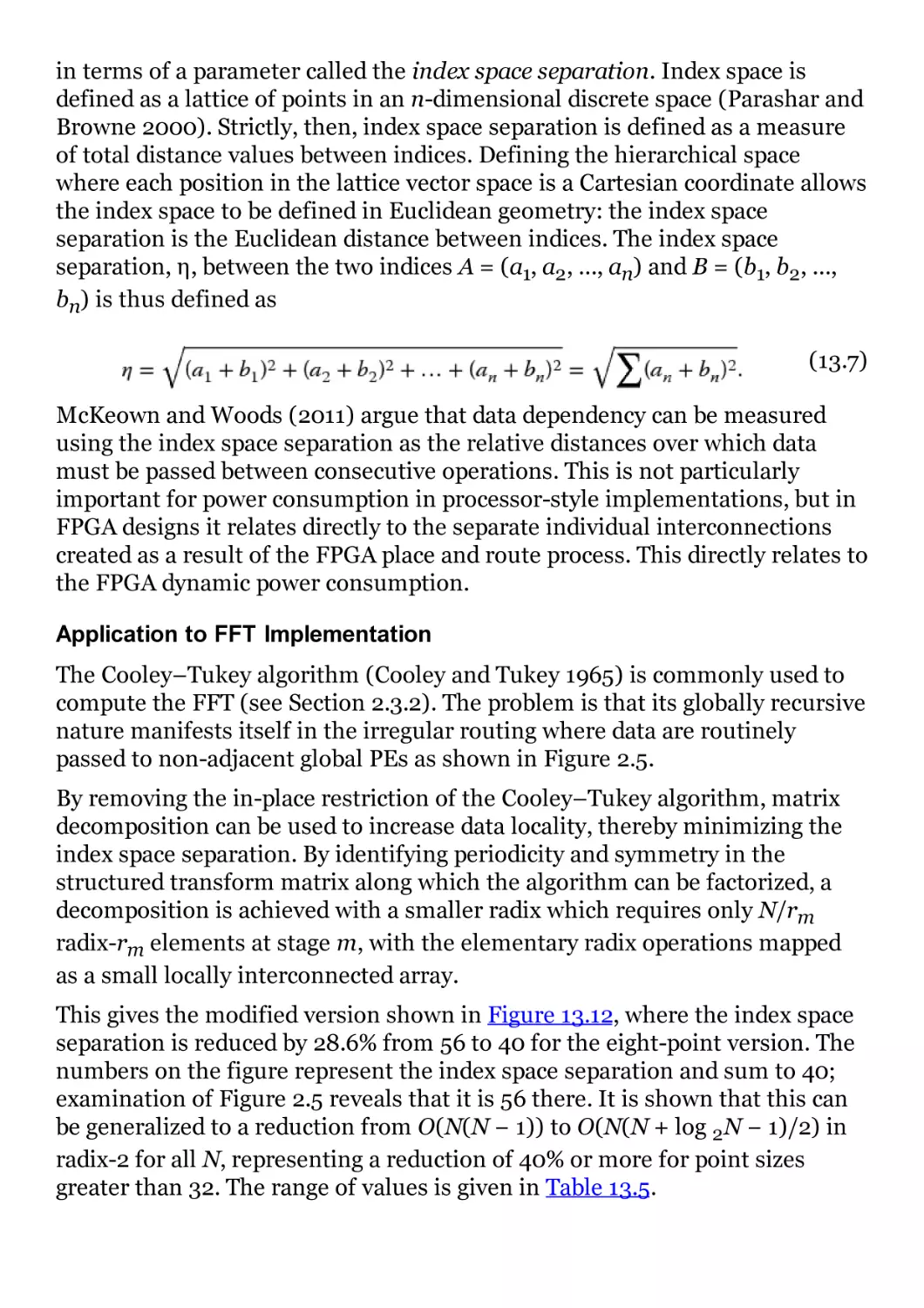
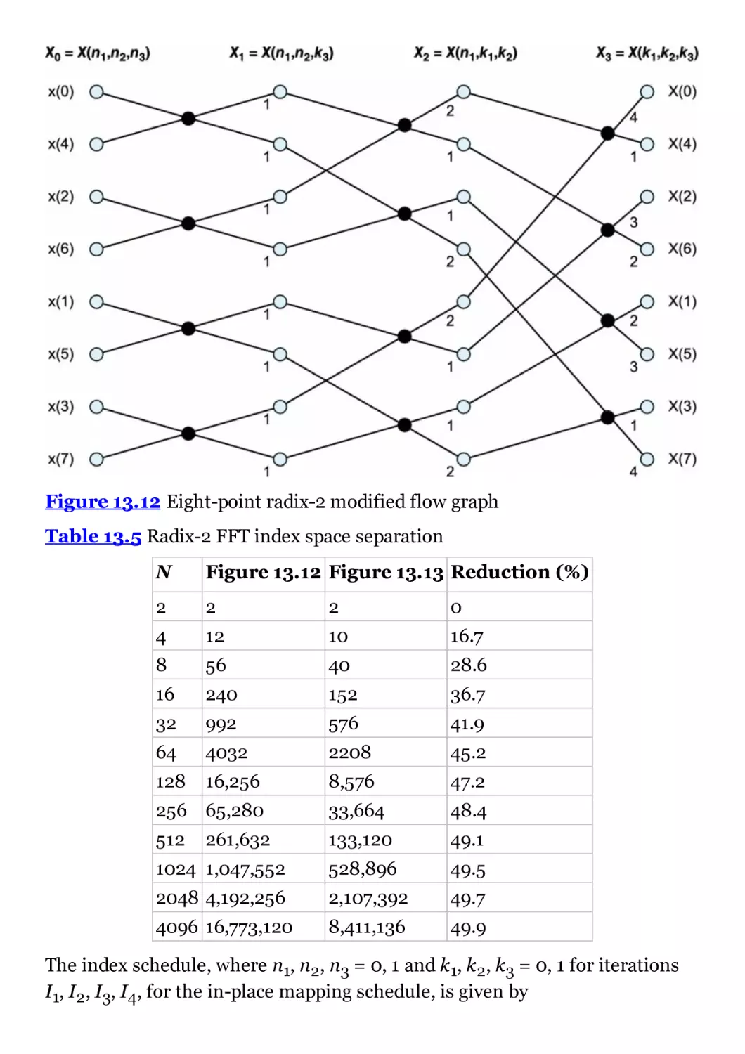
Figure 13.12 Eight-point radix-2 modified flow graph
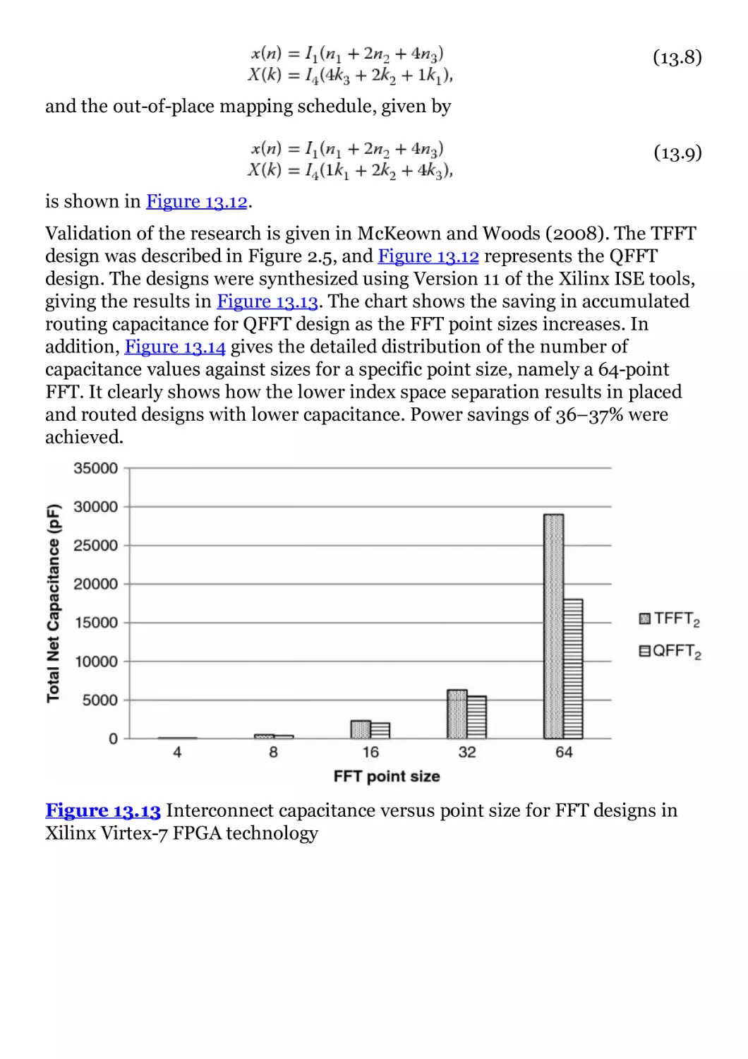
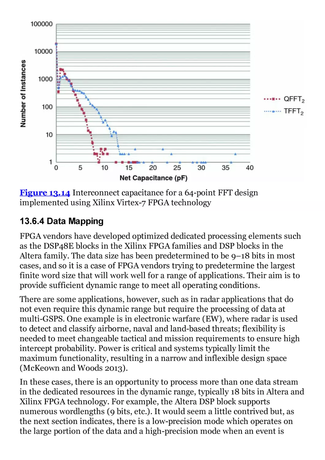
Figure 13.13 Interconnect capacitance versus point size for FFT
designs in Xilinx Virtex-7 FPGA technology
Figure 13.14 Interconnect capacitance for a 64-point FFT design
implemented using Xilinx Virtex-7 FPGA technology
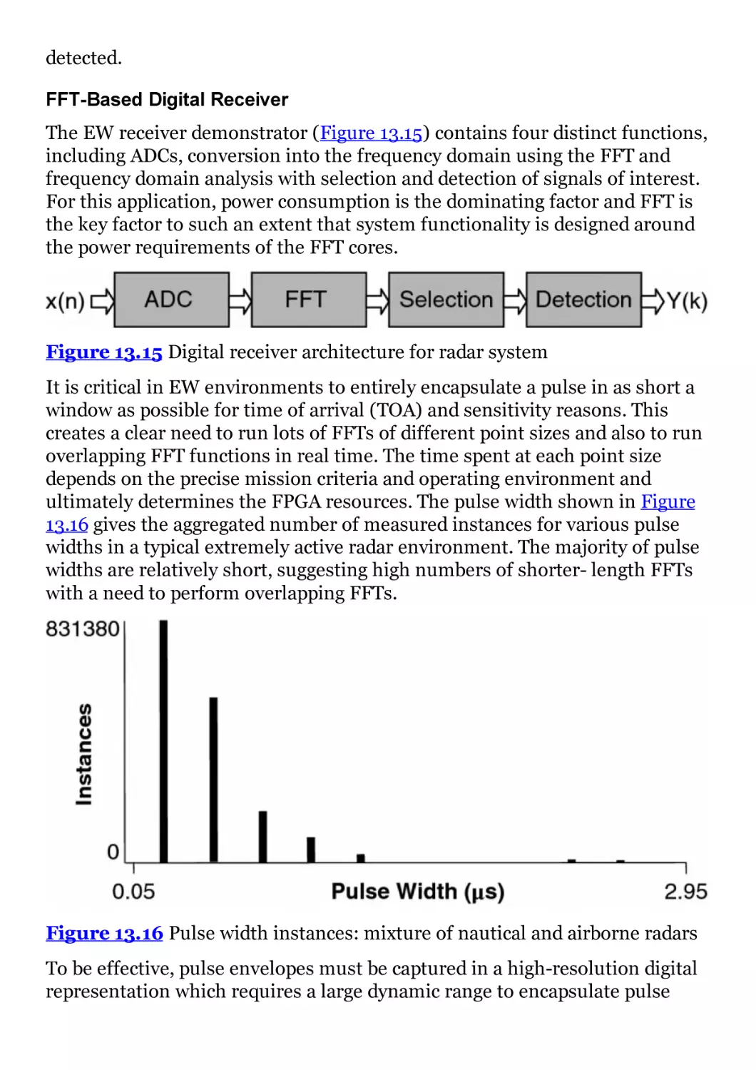
Figure 13.15 Digital receiver architecture for radar system
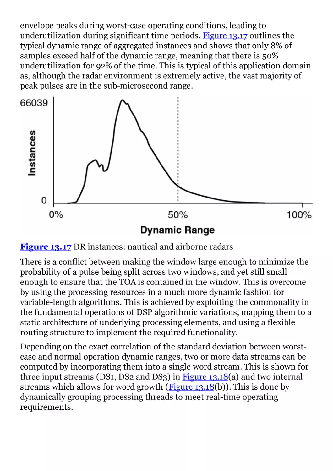
Figure 13.16 Pulse width instances: mixture of nautical and airborne
radars
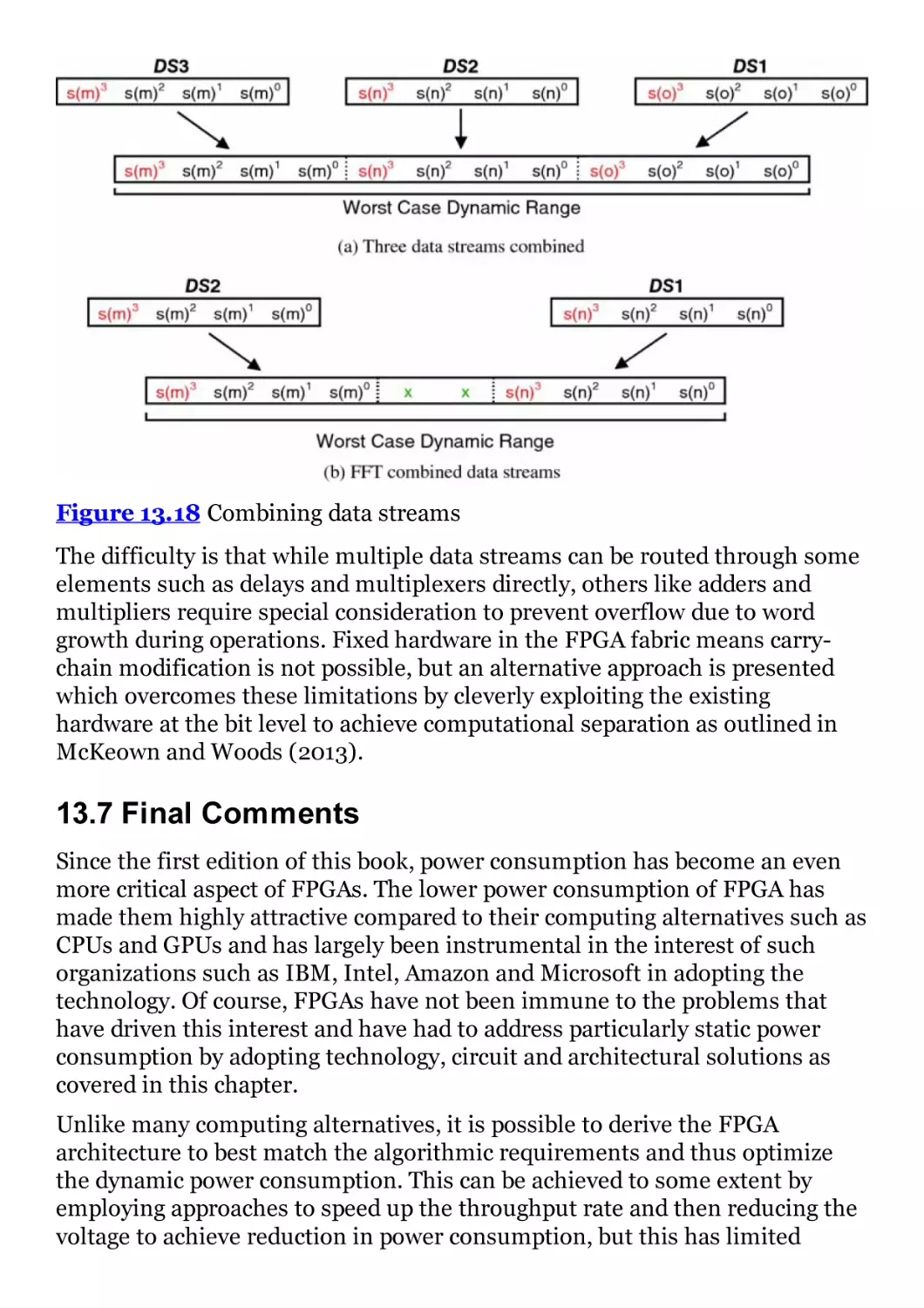
Figure 13.17 DR instances: nautical and airborne radars
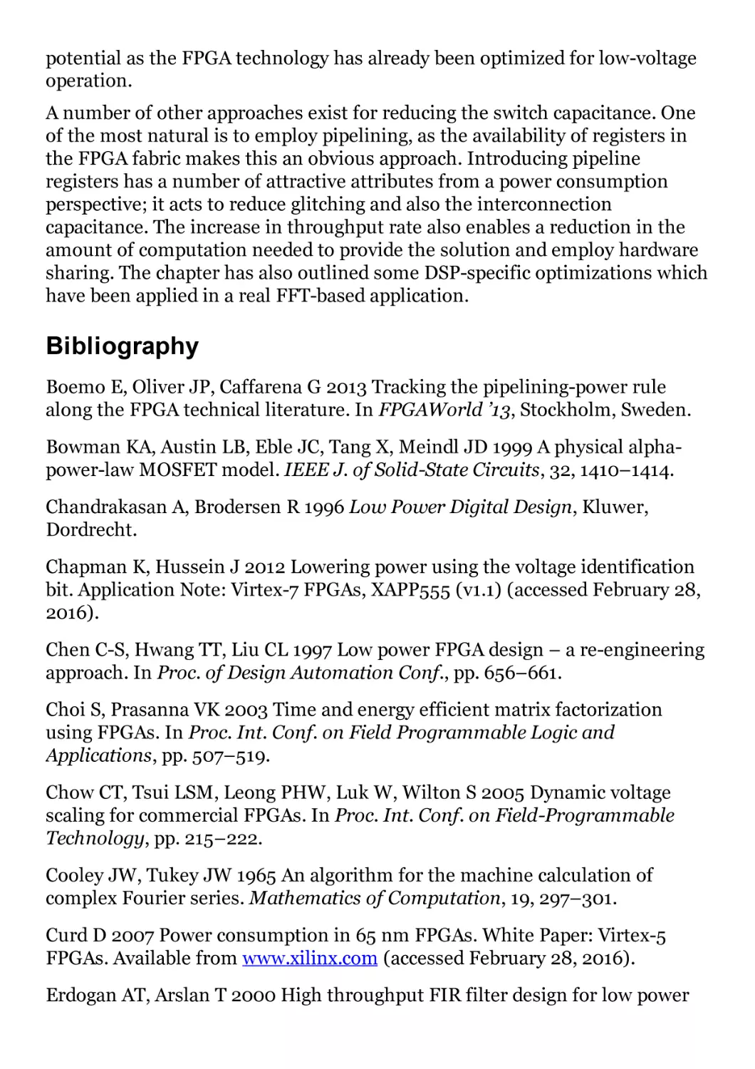
Figure 13.18 Combining data streams
Preface
DSP and FPGAs
Digital signal processing (DSP) is the cornerstone of many products and
services in the digital age. It is used in applications such as high-definition TV,
mobile telephony, digital audio, multimedia, digital cameras, radar, sonar
detectors, biomedical imaging, global positioning, digital radio, speech
recognition, to name but a few! The evolution of DSP solutions has been
driven by application requirements which, in turn, have only been possible to
realize because of developments in silicon chip technology. Currently, a mix
of programmable and dedicated system-on-chip (SoC) solutions are required
for these applications and thus this has been a highly active area of research
and development over the past four decades.
The result has been the emergence of numerous technologies for DSP
implementation, ranging from simple microcontrollers right through to
dedicated SoC solutions which form the basis of high-volume products such
as smartphones. With the architectural developments that have occurred in
field programmable gate arrays (FPGAs) over the years, it is clear that they
should be considered as a viable DSP technology. Indeed, developments made
by FPGA vendors would support this view of their technology. There are
strong commercial pressures driving adoption of FPGA technology across a
range of applications and by a number of commercial drivers.
The increasing costs of developing silicon technology implementations have
put considerable pressure on the ability to create dedicated SoC systems. In
the mobile phone market, volumes are such that dedicated SoC systems are
required to meet stringent energy requirements, so application-specific
solutions have emerged which vary in their degree of programmability, energy
requirements and cost. The need to balance these requirements suggests that
many of these technologies will coexist in the immediate future, and indeed
many hybrid technologies are starting to emerge. This, of course, creates a
considerable interest in using technology that is programmable as this acts to
considerably reduce risks in developing new technologies.
Commonly used DSP technologies encompass software programmable
solutions such as microcontrollers and DSP microprocessors. With the
inclusion of dedicated DSP processing engines, FPGA technology has now
emerged as a strong DSP technology. Their key advantage is that they enable
users to create system architectures which allow the resources to be best
matched to the system processing needs. Whilst memory resources are
limited, they have a very high-bandwidth, on-chip capability. Whilst the
prefabricated aspect of FPGAs avoids many of the deep problems met when
developing SoC implementations, the creation of an efficient implementation
from a DSP system description remains a highly convoluted problem which is
a core theme of this book.
Book Coverage
The book looks to address FPGA-based DSP systems, considering
implementation at numerous levels.
Circuit-level optimization techniques that allow the underlying FPGA
fabric to be used more intelligently are reviewed first. By considering the
detailed underlying FPGA platform, it is shown how system requirements
can be mapped to provide an area-efficient, faster implementation. This is
demonstrated for a number of DSP transforms and fixed coefficient
filtering.
Architectural solutions can be created from a signal flow graph (SFG)
representation. In effect, this requires the user to exploit the highly
regular, highly computative, data-independent nature of DSP systems to
produce highly parallel, pipelined FPGA-based circuit architectures. This is
demonstrated for filtering and beamforming applications.
System solutions are now a challenge as FPGAs have now become a
heterogeneous platform involving multiple hardware and software
components and interconnection fabrics. There is a need for a higher-level
system modeling language, e.g. dataflow which will facilitate architectural
optimizations but also to address system-level considerations such as
interconnection and memory.
The book covers these areas of FPGA implementation, but its key
differentiating factor is that it concentrates on the second and third areas
listed above, namely the creation of circuit architectures and system-level
modeling; this is because circuit-level optimization techniques have been
covered in greater detail elsewhere. The work is backed up with the authors’
experiences in implementing practical real DSP systems and covers numerous
examples including an adaptive beamformer based on a QR-based recursive
least squares (RLS) filter, finite impulse response (FIR) and infinite impulse
response (IIR) filters, a full search motion estimation and a fast Fourier
transform (FFT) system for electronic support measures. The book also
considers the development of intellectual property (IP) cores as this has
become a critical aspect in the creation of DSP systems. One chapter is given
over to describing the creation of such IP cores and another to the creation of
an adaptive filtering core.
Audience
The book is aimed at working engineers who are interested in using FPGA
technology efficiently in signal and data processing applications. The earlier
chapters will be of interest to graduates and students completing their
studies, taking the readers through a number of simple examples that show
the trade-off when mapping DSP systems into FPGA hardware. The middle
part of the book contains a number of illustrative, complex DSP system
examples that have been implemented using FPGAs and whose performance
clearly illustrates the benefit of their use. They provide insights into how to
best use the complex FPGA technology to produce solutions optimized for
speed, area and power which the authors believe is missing from current
literature. The book summarizes over 30 years of learned experience of
implementing complex DSP systems undertaken in many cases with
commercial partners.
Second Edition Updates
The second edition has been updated and improved in a number of ways. It
has been updated to reflect technology evolutions in FPGA technology, to
acknowledge developments in programming and synthesis tools, to reflect on
algorithms for Big Data applications, and to include improvements to some
background chapters. The text has also been updated using relevant examples
where appropriate.
Technology update: As FPGAs are linked to silicon technology advances,
their architecture continually changes, and this is reflected in Chapter 5. A
major change is the inclusion of the ARM® processor core resulting in a shift
for FPGAs to a heterogeneous computing platform. Moreover, the increased
use of graphical processing units (GPUs) in DSP systems is reflected in
Chapter 4.
Programming tools update: Since the first edition was published, there
have been a number of innovations in tool developments, particularly in the
creation of commercial C-based high-level synthesis (HLS) and open
computing language (OpenCL) tools. The material in Chapter 7 has been
updated to reflect these changes, and Chapter 10 has been changed to reflect
the changes in model-based synthesis tools.
“Big Data” processing: DSP involves processing of data content such as
audio, speech, music and video information, but there is now great interest in
collating huge data sets from on-line facilities and processing them quickly.
As FPGAs have started to gain some traction in this area, a new chapter,
Chapter 12, has been added to reflect this development.
Organization
The FPGA is a heterogeneous platform comprising complex resources such as
hard and soft processors, dedicated blocks optimized for processing DSP
functions and processing elements connected by both programmable and fast,
dedicated interconnections. The book focuses on the challenges of
implementing DSP systems on such platforms with a concentration on the
high-level mapping of DSP algorithms into suitable circuit architectures.
The material is organized into three main sections.
First Section: Basics of DSP, Arithmetic and Technologies
Chapter 2 starts with a DSP primer, covering both FIR and IIR filtering,
transforms including the FFT and discrete cosine transform (DCT) and
concluding with adaptive filtering algorithms, covering both the least mean
squares (LMS) and RLS algorithms. Chapter 3 is dedicated to computer
arithmetic and covers number systems, arithmetic functions and alternative
number representations such as logarithmic number representations (LNS)
and coordinate rotation digital computer (CORDIC). Chapter 4 covers the
technologies available to implement DSP algorithms and includes
microprocessors, DSP microprocessors, GPUs and SoC architectures,
including systolic arrays. In Chapter 5, a detailed description of commercial
FPGAs is given with a concentration on the two main vendors, namely Xilinx
and Altera, specifically their UltraScaleTM/Zynq® and Stratix® 10 FPGA
families respectively, but also covering technology offerings from Lattice and
MicroSemi.
Second Section: Architectural/System-Level Implementation
This section covers efficient implementation from circuit architecture onto
specific FPGA families; creation of circuit architecture from SFG
representations; and system-level specification and implementation
methodologies from high-level representations. Chapter 6 covers only briefly
the efficient implementation of FPGA designs from circuit architecture
descriptions as many of these approaches have been published; the text
covers distributed arithmetic and reduced coefficient multiplier approaches
and shows how these have been applied to fixed coefficient filters and DSP
transforms. Chapter 7 covers HLS for FPGA design including new sections to
reflect Xilinx’s Vivado HLS tool flow and also Altera’s OpenCL approach. The
process of mapping SFG representations of DSP algorithms onto circuit
architectures (the starting point in Chapter 6) is then described in Chapter 8.
It shows how dataflow graph (DFG) descriptions can be transformed for
varying levels of parallelism and pipelining to create circuit architectures
which best match the application requirements, backed up with simple FIR
and IIR filtering examples.
One of the ways to perform system design is to create predefined designs
termed IP cores which will typically have been optimized using the techniques
outlined in Chapter 8. The creation of such IP cores is outlined in Chapter 9
and acts to address the key to design productivity by encouraging “design for
reuse.” Chapter 10 considers model-based design for heterogeneous FPGA
and focuses on dataflow modeling as a suitable design approach for FPGAbased DSP systems. The chapter outlines how it is possible to include
pipelined IP cores via the white box concept using two examples, namely a
normalized lattice filter (NLF) and a fixed beamformer example.
Third Section: Applications to Big Data, Low Power
The final section of the book, consisting of Chapters 11–13, covers the
application of the techniques. Chapter 11 looks at the creation of a soft, highly
parameterizable core for RLS filtering, showing how a generic architecture
can be created to allow a range of designs to be synthesized with varying
performance. Chapter 12 illustrates how FPGAs can be applied to Big Data
applications where the challenge is to accelerate some complex processing
algorithms. Increasingly FPGAs are seen as a low-power solution, and FPGA
power consumption is discussed in Chapter 13. The chapter starts with a
discussion on power consumption, highlights the importance of dynamic and
static power consumption, and then describes some techniques to reduce
power consumption.
Acknowledgments
The authors have been fortunate to receive valuable help, support and
suggestions from numerous colleagues, students and friends, including:
Michaela Blott, Ivo Bolsens, Gordon Brebner, Bill Carter, Joe Cavallaro, Peter
Cheung, John Gray, Wayne Luk, Bob Madahar, Alan Marshall, Paul
McCambridge, Satnam Singh, Steve Trimberger and Richard Walke.
The authors’ research has been funded from a number of sources, including
the Engineering and Physical Sciences Research Council, Xilinx, Ministry of
Defence, Qinetiq, BAE Systems, Selex and Department of Employment and
Learning for Northern Ireland.
Several chapters are based on joint work that was carried out with the
following colleagues and students: Moslem Amiri, Burak Bardak, Kevin
Colgan, Tim Courtney, Scott Fischaber, Jonathan Francey, Tim Harriss, JeanPaul Heron, Colm Kelly, Bob Madahar, Eoin Malins, Stephen McKeown,
Karen Rafferty, Darren Reilly, Lok-Kee Ting, David Trainor, Richard Turner,
Fahad M Siddiqui and Richard Walke.
The authors thank Ella Mitchell and Nithya Sechin of John Wiley & Sons and
Alex Jackson and Clive Lawson for their personal interest and help and
motivation in preparing and assisting in the production of this work.
List of Abbreviations
1D
One-dimensional
2D
Two-dimensional
ABR
Auditory brainstem response
ACC
Accumulator
ADC
Analogue-to-digital converter
AES
Advanced encryption standard
ALM
Adaptive logic module
ALU
Arithmetic logic unit
ALUT
Adaptive lookup table
AMD
Advanced Micro Devices
ANN
Artificial neural network
AoC
Analytics-on-chip
API
Application program interface
APU
Application processing unit
ARM
Advanced RISC machine
ASIC
Application-specific integrated circuit
ASIP
Application-specific instruction processor
AVS
Adaptive voltage scaling
BC
Boundary cell
BCD
Binary coded decimal
BCLA
Block CLA with intra-group, carry ripple
BRAM
Block random access memory
CAPI
Coherent accelerator processor interface
CB
Current block
CCW
Control and communications wrapper
CE
Clock enable
CISC
Complex instruction set computer
CLA
Carry lookahead adder
CLB
Configurable logic block
CNN
Convolutional neural network
CMOS
Complementary metal oxide semiconductor
CORDIC
Coordinate rotation digital computer
CPA
Carry propagation adder
CPU
Central processing unit
CSA
Conditional sum adder
CSDF
Cyclo-static dataflow
CWT
Continuous wavelet transform
DA
Distributed arithmetic
DCT
Discrete cosine transform
DDR
Double data rate
DES
Data Encryption Standard
DFA
Dataflow accelerator
DFG
Dataflow graph
DFT
Discrete Fourier transform
DG
Dependence graph
disRAM
Distributed random access memory
DM
Data memory
DPN
Dataflow process network
DRx
Digital receiver
DSP
Digital signal processing
DST
Discrete sine transform
DTC
Decision tree classification
DVS
Dynamic voltage scaling
DWT
Discrete wavelet transform
E2PROM
Electrically erasable programmable read-only memory
EBR
Embedded Block RAM
ECC
Error correction code
EEG
Electroencephalogram
EPROM
Electrically programmable read-only memory
E-SGR
Enhanced Squared Givens rotation algorithm
EW
Electronic warfare
FBF
Fixed beamformer
FCCM
FPGA-based custom computing machine
FE
Functional engine
FEC
Forward error correction
FFE
Free-form expression
FFT
Fast Fourier transform
FIFO
First-in, first-out
FIR
Finite impulse response
FPGA
Field programmable gate array
FPL
Field programmable logic
FPU
Floating-point unit
FSM
Finite state machine
FSME
Full search motion estimation
GFLOPS
Giga floating-point operations per second
GMAC
Giga multiply-accumulates
GMACS
Giga multiply-accumulate per second
GOPS
Giga operations per second
GPUPU
General-purpose graphical processing unit
GPU
Graphical processing unit
GRNN
General regression neural network
GSPS
Gigasamples per second
HAL
Hardware abstraction layer
HDL
Hardware description language
HKMG
High-K metal gate
HLS
High-level synthesis
I2C
Inter-Integrated circuit
I/O
Input/output
IC
Internal cell
ID
Instruction decode
IDE
Integrated design environment
IDFT
Inverse discrete Fourier transform
IEEE
Institute of Electrical and Electronic Engineers
IF
Instruction fetch
IFD
Instruction fetch and decode
IFFT
Inverse fast Fourier transform
IIR
Infinite impulse response
IM
Instruction memory
IoT
Internet of things
IP
Intellectual property
IR
Instruction register
ITRS
International Technology Roadmap for Semiconductors
JPEG
Joint Photographic Experts Group
KCM
Constant-coefficient multiplication
KM
Kernel memory
KPN
Kahn process network
LAB
Logic array blocks
LDCM
Logic delay measurement circuit
LDPC
Low-density parity-check
LLVM
Low-level virtual machine
LMS
Least mean squares
LNS
Logarithmic number representations
LPDDR
Low-power double data rate
LS
Least squares
lsb
Least significant bit
LTI
Linear time-invariant
LUT
Lookup table
MA
Memory access
MAC
Multiply-accumulate
MAD
Minimum absolute difference
MADF
Multidimensional arrayed dataflow
MD
Multiplicand
ME
Motion estimation
MIL-STD
Military standard
MIMD
Multiple instruction, multiple data
MISD
Multiple instruction, single data
MLAB
Memory LAB
MMU
Memory management unit
MoC
Model of computation
MPE
Media processing engine
MPEG
Motion Picture Experts Group
MPSoC
Multi-processing SoC
MR
Multiplier
MR-DFG
Multi-rate dataflow graph
msb
Most significant bit
msd
Most significant digit
MSDF
Multidimensional synchronous dataflow
MSI
Medium-scale integration
MSPS
Megasamples per second
NaN
Not a Number
NLF
Normalized lattice filter
NRE
Non-recurring engineering
OCM
On-chip memory
OFDM
Orthogonal frequency division multiplexing
OFDMA
Orthogonal frequency division multiple access
OLAP
On-line analytical processing
OpenCL
Open computing language
OpenMP
Open multi-processing
ORCC
Open RVC-CAL Compiler
PAL
Programmable Array Logic
PB
Parameter bank
PC
Program counter
PCB
Printed circuit board
PCI
Peripheral component interconnect
PD
Pattern detect
PE
Processing element
PL
Programmable logic
PLB
Programmable logic block
PLD
Programmable logic device
PLL
Phase locked loop
PPT
Programmable power technology
PS
Processing system
QAM
Quadrature amplitude modulation
QR-RLS
QR recursive least squares
RAM
Random access memory
RAN
Radio access network
RCLA
Block CLA with inter-block ripple
RCM
Reduced coefficient multiplier
RF
Register file
RISC
Reduced instruction set computer
RLS
Recursive least squares
RNS
Residue number representations
ROM
Read-only memory
RT
Radiation tolerant
RTL
Register transfer level
RVC
Reconfigurable video coding
SBNR
Signed binary number representation
SCU
Snoop control unit
SD
Signed digits
SDF
Synchronous dataflow
SDK
Software development kit
SDNR
Signed digit number representation
SDP
Simple dual-port
SERDES
Serializer/deserializer
SEU
Single event upset
SFG
Signal flow graph
SGR
Squared Givens rotation
SIMD
Single instruction, multiple data
SISD
Single instruction, single data
SMP
Shared-memory multi-processors
SNR
Signal-to-noise ratio
SoC
System-on-chip
SOCMINT
Social media intelligence
SoPC
System on programmable chip
SPI
Serial peripheral interface
SQL
Structured query language
SR-DFG
Single-rate dataflow graph
SRAM
Static random access memory
SRL
Shift register lookup table
SSD
Shifted signed digits
SVM
Support vector machine
SW
Search window
TCP
Transmission Control Protocol
TFLOPS
Tera floating-point operations per second
TOA
Time of arrival
TR
Throughout rate
TTL
Transistor-transistor logic
UART
Universal asynchronous receiver/transmitter
ULD
Ultra-low density
UML
Unified modeling language
VHDL
VHSIC hardware description language
VHSIC
Very high-speed integrated circuit
VLIW
Very long instruction word
VLSI
Very large scale integration
WBC
White box component
WDF
Wave digital filter
1
Introduction to Field Programmable Gate Arrays
1.1 Introduction
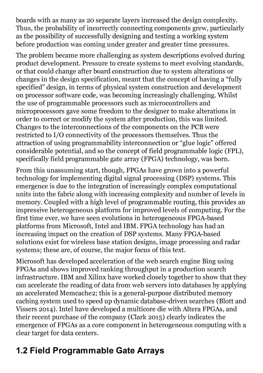
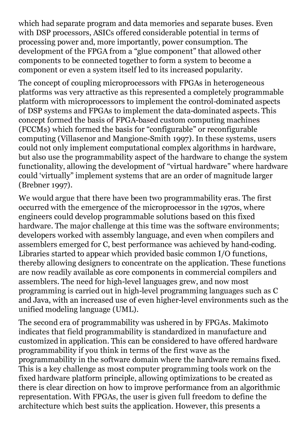
Electronics continues to make an impact in the twenty-first century and has
given birth to the computer industry, mobile telephony and personal digital
entertainment and services industries, to name but a few. These markets have
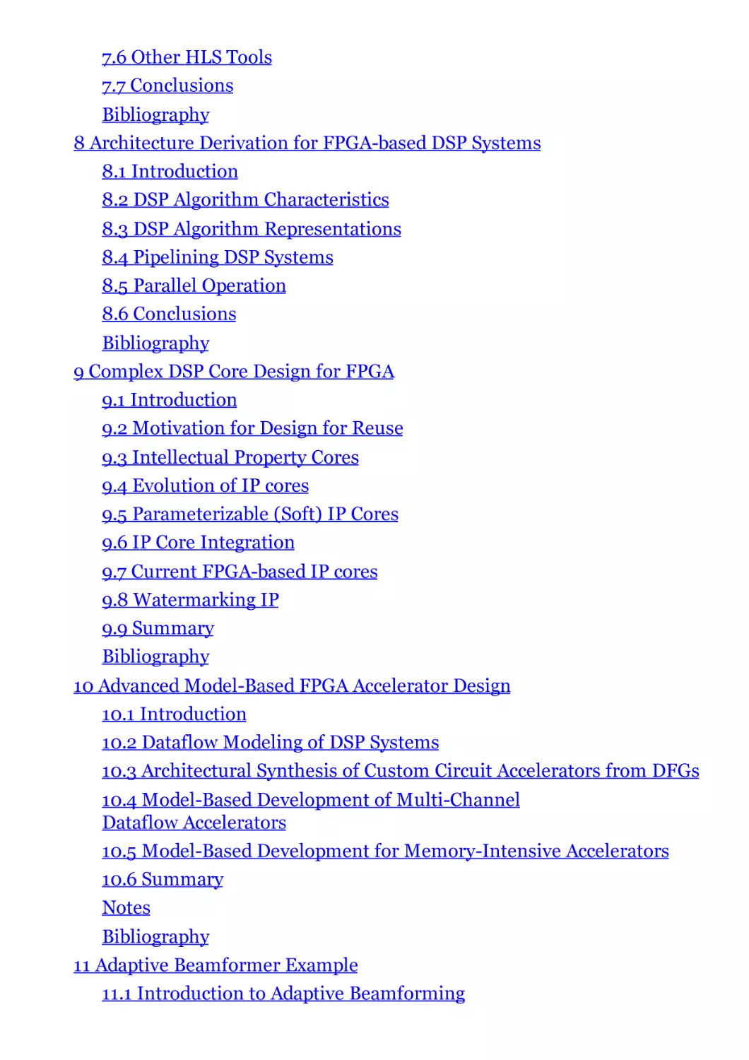
been driven by developments in silicon technology as described by Moore’s
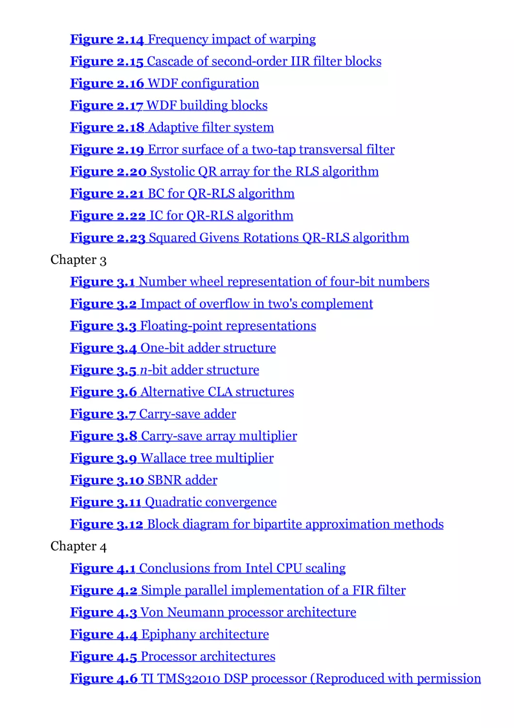
law (Moore 1965), which is represented pictorially in Figure 1.1. This has seen
the number of transistors double every 18 months. Moreover, not only has
the number of transistors doubled at this rate, but also the costs have
decreased, thereby reducing the cost per transistor at every technology
advance.
Figure 1.1 Moore’s law
In the 1970s and 1980s, electronic systems were created by aggregating
standard components such as microprocessors and memory chips with digital
logic components, e.g. dedicated integrated circuits along with dedicated
input/output (I/O) components on printed circuit boards (PCBs). As levels of
integration grew, manufacturing working PCBs became more complex, largely
due to greater component complexity in terms of the increase in the number
of transistors and I/O pins. In addition, the development of multi-layer
boards with as many as 20 separate layers increased the design complexity.
Thus, the probability of incorrectly connecting components grew, particularly
as the possibility of successfully designing and testing a working system
before production was coming under greater and greater time pressures.
The problem became more challenging as system descriptions evolved during
product development. Pressure to create systems to meet evolving standards,
or that could change after board construction due to system alterations or
changes in the design specification, meant that the concept of having a “fully
specified” design, in terms of physical system construction and development
on processor software code, was becoming increasingly challenging. Whilst
the use of programmable processors such as microcontrollers and
microprocessors gave some freedom to the designer to make alterations in
order to correct or modify the system after production, this was limited.
Changes to the interconnections of the components on the PCB were
restricted to I/O connectivity of the processors themselves. Thus the
attraction of using programmability interconnection or “glue logic” offered
considerable potential, and so the concept of field programmable logic (FPL),
specifically field programmable gate array (FPGA) technology, was born.
From this unassuming start, though, FPGAs have grown into a powerful
technology for implementing digital signal processing (DSP) systems. This
emergence is due to the integration of increasingly complex computational
units into the fabric along with increasing complexity and number of levels in
memory. Coupled with a high level of programmable routing, this provides an
impressive heterogeneous platform for improved levels of computing. For the
first time ever, we have seen evolutions in heterogeneous FPGA-based
platforms from Microsoft, Intel and IBM. FPGA technology has had an
increasing impact on the creation of DSP systems. Many FPGA-based
solutions exist for wireless base station designs, image processing and radar
systems; these are, of course, the major focus of this text.
Microsoft has developed acceleration of the web search engine Bing using
FPGAs and shows improved ranking throughput in a production search
infrastructure. IBM and Xilinx have worked closely together to show that they
can accelerate the reading of data from web servers into databases by applying
an accelerated Memcache2; this is a general-purpose distributed memory
caching system used to speed up dynamic database-driven searches (Blott and
Vissers 2014). Intel have developed a multicore die with Altera FPGAs, and
their recent purchase of the company (Clark 2015) clearly indicates the
emergence of FPGAs as a core component in heterogeneous computing with a
clear target for data centers.
1.2 Field Programmable Gate Arrays
The FPGA concept emerged in 1985 with the XC2064™ FPGA family from
Xilinx. At the same time, a company called Altera was also developing a
programmable device, later to become the EP1200, which was the first highdensity programmable logic device (PLD). Altera’s technology was
manufactured using 3-μm complementary metal oxide semiconductor
(CMOS) electrically programmable read-only memory (EPROM) technology
and required ultraviolet light to erase the programming, whereas Xilinx’s
technology was based on conventional static random access memory (SRAM)
technology and required an EPROM to store the programming.
The co-founder of Xilinx, Ross Freeman, argued that with continuously
improving silicon technology, transistors were going to become cheaper and
cheaper and could be used to offer programmability. This approach allowed
system design errors which had only been recognized at a late stage of
development to be corrected. By using an FPGA to connect the system
components, the interconnectivity of the components could be changed as
required by simply reprogramming them. Whilst this approach introduced
additional delays due to the programmable interconnect, it avoided a costly
and time-consuming PCB redesign and considerably reduced the design risks.
At this stage, the FPGA market was populated by a number of vendors,
including Xilinx, Altera, Actel, Lattice, Crosspoint, Prizm, Plessey, Toshiba,
Motorola, Algotronix and IBM. However, the costs of developing technologies
not based on conventional integrated circuit design processes and the need for
programming tools saw the demise of many of these vendors and a reduction
in the number of FPGA families. SRAM technology has now emerged as the
dominant technology largely due to cost, as it does not require a specialist
technology. The market is now dominated by Xilinx and Altera, and, more
importantly, the FPGA has grown from a simple glue logic component to a
complete system on programmable chip (SoPC) comprising on-board physical
processors, soft processors, dedicated DSP hardware, memory and high-speed
I/O.
The FPGA evolution was neatly described by Steve Trimberger in his FPL2007
plenary talk (see the summary in Table 1.1). The evolution of the FPGA can be
divided into three eras. The age of invention was when FPGAs started to
emerge and were being used as system components typically to provide
programmable interconnect giving protection to design evolutions and
variations. At this stage, design tools were primitive, but designers were quite
happy to extract the best performance by dealing with lookup tables (LUTs) or
single transistors.
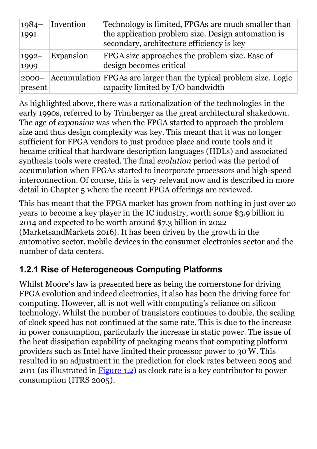
Table 1.1 Three ages of FPGAs
Period Age
Comments
1984– Invention
1991
Technology is limited, FPGAs are much smaller than
the application problem size. Design automation is
secondary, architecture efficiency is key
1992–
1999
FPGA size approaches the problem size. Ease of
design becomes critical
Expansion
2000– Accumulation FPGAs are larger than the typical problem size. Logic
present
capacity limited by I/O bandwidth
As highlighted above, there was a rationalization of the technologies in the
early 1990s, referred to by Trimberger as the great architectural shakedown.
The age of expansion was when the FPGA started to approach the problem
size and thus design complexity was key. This meant that it was no longer
sufficient for FPGA vendors to just produce place and route tools and it
became critical that hardware description languages (HDLs) and associated
synthesis tools were created. The final evolution period was the period of
accumulation when FPGAs started to incorporate processors and high-speed
interconnection. Of course, this is very relevant now and is described in more
detail in Chapter 5 where the recent FPGA offerings are reviewed.
This has meant that the FPGA market has grown from nothing in just over 20
years to become a key player in the IC industry, worth some $3.9 billion in
2014 and expected to be worth around $7.3 billion in 2022
(MarketsandMarkets 2016). It has been driven by the growth in the
automotive sector, mobile devices in the consumer electronics sector and the
number of data centers.
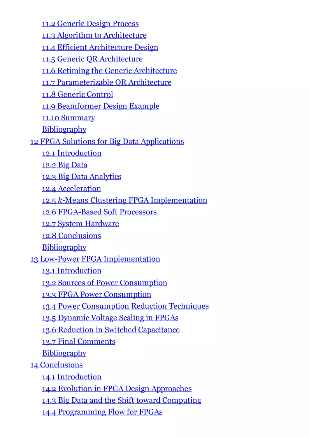
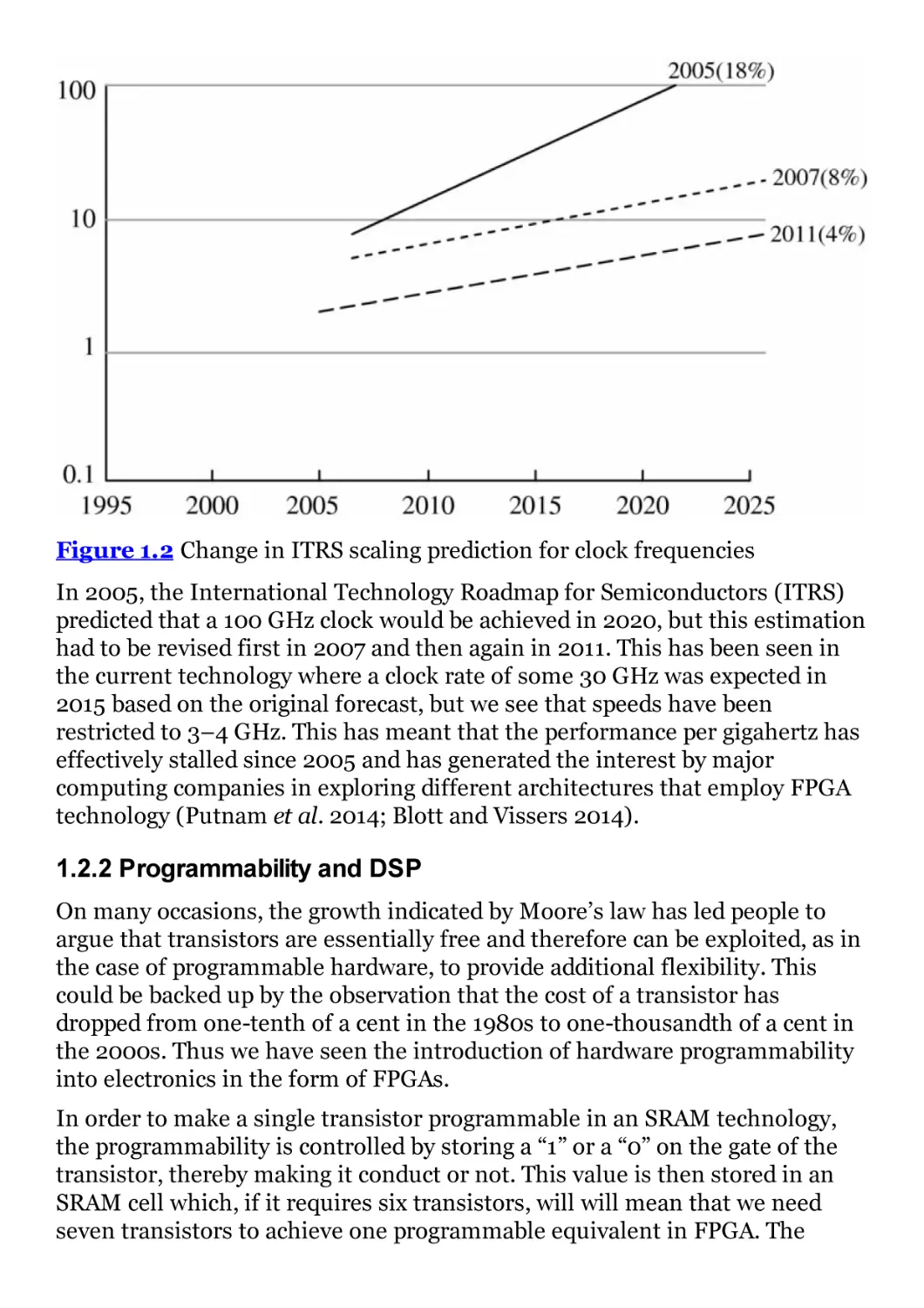
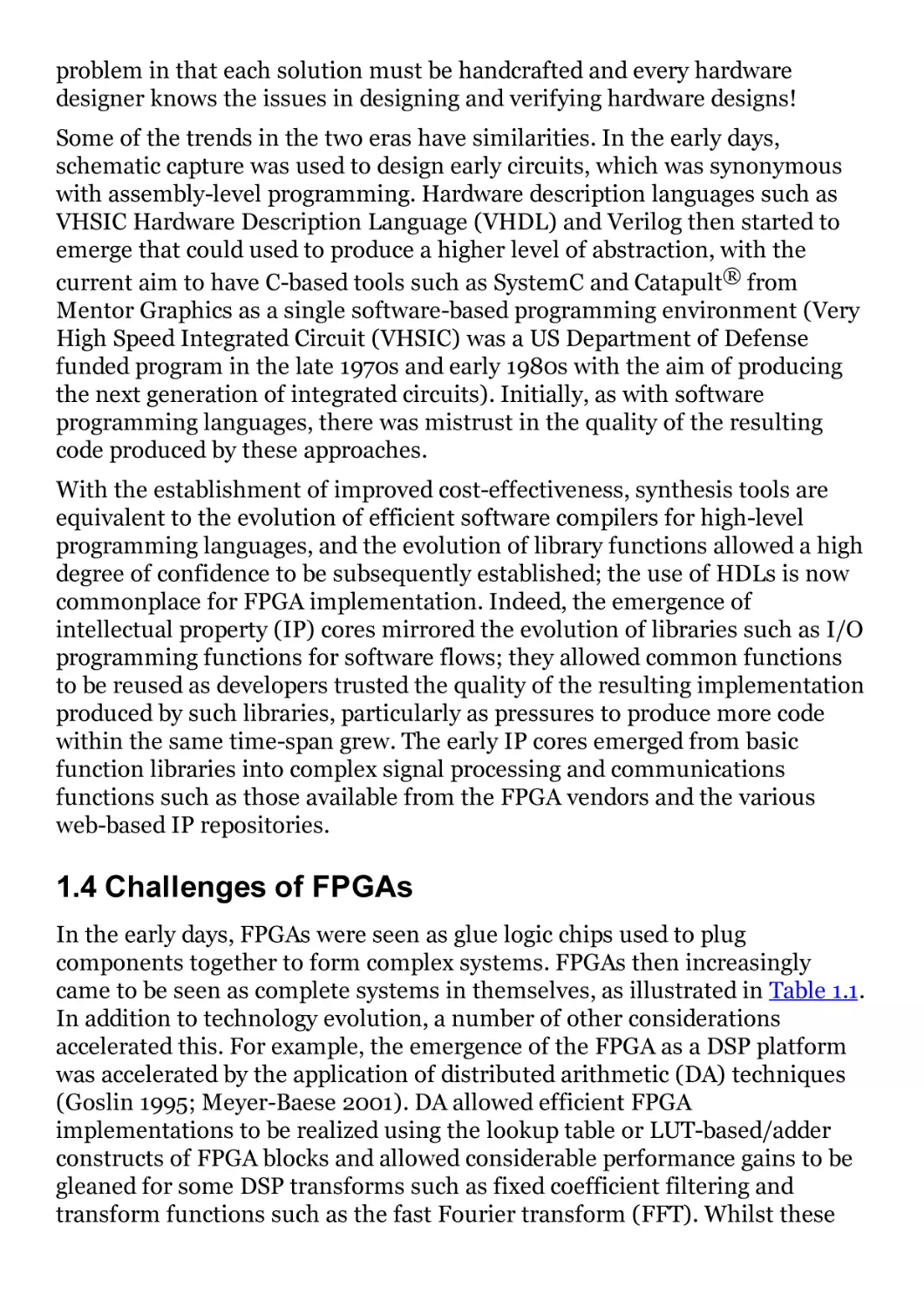
1.2.1 Rise of Heterogeneous Computing Platforms
Whilst Moore’s law is presented here as being the cornerstone for driving
FPGA evolution and indeed electronics, it also has been the driving force for
computing. However, all is not well with computing’s reliance on silicon
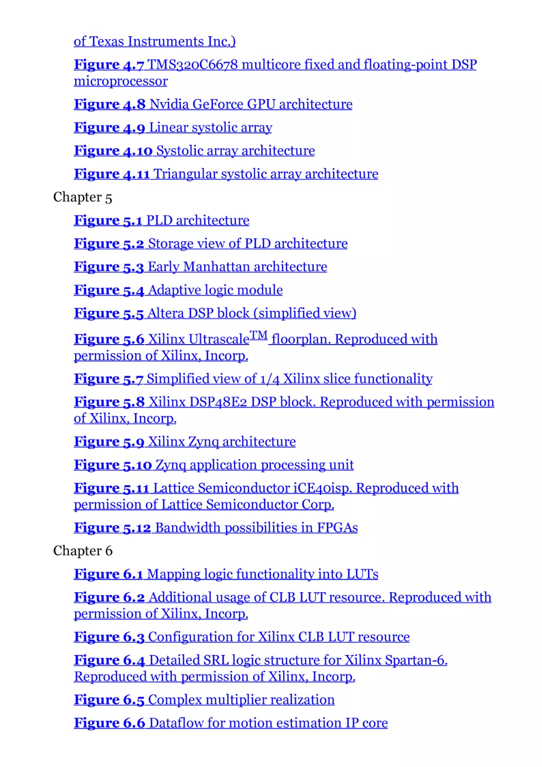
technology. Whilst the number of transistors continues to double, the scaling
of clock speed has not continued at the same rate. This is due to the increase
in power consumption, particularly the increase in static power. The issue of
the heat dissipation capability of packaging means that computing platform
providers such as Intel have limited their processor power to 30 W. This
resulted in an adjustment in the prediction for clock rates between 2005 and
2011 (as illustrated in Figure 1.2) as clock rate is a key contributor to power
consumption (ITRS 2005).
Figure 1.2 Change in ITRS scaling prediction for clock frequencies
In 2005, the International Technology Roadmap for Semiconductors (ITRS)
predicted that a 100 GHz clock would be achieved in 2020, but this estimation
had to be revised first in 2007 and then again in 2011. This has been seen in
the current technology where a clock rate of some 30 GHz was expected in
2015 based on the original forecast, but we see that speeds have been
restricted to 3–4 GHz. This has meant that the performance per gigahertz has
effectively stalled since 2005 and has generated the interest by major
computing companies in exploring different architectures that employ FPGA
technology (Putnam et al. 2014; Blott and Vissers 2014).
1.2.2 Programmability and DSP
On many occasions, the growth indicated by Moore’s law has led people to
argue that transistors are essentially free and therefore can be exploited, as in
the case of programmable hardware, to provide additional flexibility. This
could be backed up by the observation that the cost of a transistor has
dropped from one-tenth of a cent in the 1980s to one-thousandth of a cent in
the 2000s. Thus we have seen the introduction of hardware programmability
into electronics in the form of FPGAs.
In order to make a single transistor programmable in an SRAM technology,
the programmability is controlled by storing a “1” or a “0” on the gate of the
transistor, thereby making it conduct or not. This value is then stored in an
SRAM cell which, if it requires six transistors, will will mean that we need
seven transistors to achieve one programmable equivalent in FPGA. The
reality is that in an overall FPGA implementation, the penalty is nowhere as
harsh as this, but it has to be taken into consideration in terms of ultimate
system cost.
It is the ability to program the FPGA hardware after fabrication that is the
main appeal of the technology; this provides a new level of reassurance in an
increasingly competitive market where “right first time” system construction
is becoming more difficult to achieve. It would appear that that assessment
was vindicated in the late 1990s and early 2000s: when there was a major
market downturn, the FPGA market remained fairly constant when other
microelectronic technologies were suffering. Of course, the importance of
programmability has already been demonstrated by the microprocessor, but
this represented a new change in how programmability was performed.
The argument developed in the previous section presents a clear advantage of
FPGA technology in overcoming PCB design errors and manufacturing faults.
Whilst this might have been true in the early days of FPGA technology,
evolution in silicon technology has moved the FPGA from being a
programmable interconnection technology to making it into a system
component. If the microprocessor or microcontroller was viewed as
programmable system component, the current FPGA devices must also be
viewed in this vein, giving us a different perspective on system
implementation.
In electronic system design, the main attraction of the microprocessor is that
it considerably lessens the risk of system development. As the hardware is
fixed, all of the design effort can be concentrated on developing the code. This
situation has been complemented by the development of efficient software
compilers which have largely removed the need for the designer to create
assembly language; to some extent, this can even absolve the designer from
having a detailed knowledge of the microprocessor architecture (although
many practitioners would argue that this is essential to produce good code).
This concept has grown in popularity, and embedded microprocessor courses
are now essential parts of any electrical/electronic or computer engineering
degree course.
A lot of this process has been down to the software developer’s ability to
exploit an underlying processor architecture, the von Neumann architecture.
However, this advantage has also been the limiting factor in its application to
the topic of this text, namely DSP. In the von Neumann architecture,
operations are processed sequentially, which allows relatively straightforward
interpretation of the hardware for programming purposes; however, this
severely limits the performance in DSP applications which exhibit high levels
of parallelism and have operations that are highly data-independent. This
cries out for parallel realization, and whilst DSP microprocessors go some way
toward addressing this situation by providing concurrency in the form of
parallel hardware and software “pipelining,” there is still the concept of one
architecture suiting all sizes of the DSP problem.
This limitation is overcome in FPGAs as they allow what can be considered to
be a second level of programmability, namely programming of the underlying
processor architecture. By creating an architecture that best meets the
algorithmic requirements, high levels of performance in terms of area, speed
and power can be achieved. This concept is not new as the idea of deriving a
system architecture to suit algorithmic requirements has been the
cornerstone of application-specific integrated circuit (ASIC) implementations.
In high volumes, ASIC implementations have resulted in the most costeffective, fastest and lowest-energy solutions. However, increasing mask costs
and the impact of “right first time” system realization have made the FPGA a
much more attractive alternative.
In this sense, FPGAs capture the performance aspects offered by ASIC
implementation, but with the advantage of programmability usually
associated with programmable processors. Thus, FPGA solutions have
emerged which currently offer several hundreds of giga operations per second
(GOPS) on a single FPGA for some DSP applications, which is at least an
order of magnitude better performance than microprocessors.
1.3 Influence of Programmability
In many texts, Moore’s law is used to highlight the evolution of silicon
technology, but another interesting viewpoint particularly relevant for FPGA
technology is Makimoto’s wave, which was first published in the January 1991
edition of Electronics Weekly. It is based on an observation by Tsugio
Makimoto who noted that technology has shifted between standardization
and customization. In the 1960s, 7400 TTL series logic chips were used to
create applications; and then in the early 1970s, the custom large-scale
integration era emerged where chips were created (or customized) for specific
applications such as the calculator. The chips were now increasing in their
levels of integration and so the term “medium-scale integration” (MSI) was
born. The evolution of the microprocessor in the 1970s saw the swing back
towards standardization where one “standard” chip was used for a wide range
of applications.
The 1980s then saw the birth of ASICs where designers could overcome the
fact that the sequential microprocessor posed severe limitations in DSP
applications where higher levels of computations were needed. The DSP
processor also emerged, such as the TMS32010, which differed from
conventional processors as they were based on the Harvard architecture
which had separate program and data memories and separate buses. Even
with DSP processors, ASICs offered considerable potential in terms of
processing power and, more importantly, power consumption. The
development of the FPGA from a “glue component” that allowed other
components to be connected together to form a system to become a
component or even a system itself led to its increased popularity.
The concept of coupling microprocessors with FPGAs in heterogeneous
platforms was very attractive as this represented a completely programmable
platform with microprocessors to implement the control-dominated aspects
of DSP systems and FPGAs to implement the data-dominated aspects. This
concept formed the basis of FPGA-based custom computing machines
(FCCMs) which formed the basis for “configurable” or reconfigurable
computing (Villasenor and Mangione-Smith 1997). In these systems, users
could not only implement computational complex algorithms in hardware,
but also use the programmability aspect of the hardware to change the system
functionality, allowing the development of “virtual hardware” where hardware
could ‘virtually” implement systems that are an order of magnitude larger
(Brebner 1997).
We would argue that there have been two programmability eras. The first
occurred with the emergence of the microprocessor in the 1970s, where
engineers could develop programmable solutions based on this fixed
hardware. The major challenge at this time was the software environments;
developers worked with assembly language, and even when compilers and
assemblers emerged for C, best performance was achieved by hand-coding.
Libraries started to appear which provided basic common I/O functions,
thereby allowing designers to concentrate on the application. These functions
are now readily available as core components in commercial compilers and
assemblers. The need for high-level languages grew, and now most
programming is carried out in high-level programming languages such as C
and Java, with an increased use of even higher-level environments such as the
unified modeling language (UML).
The second era of programmability was ushered in by FPGAs. Makimoto
indicates that field programmability is standardized in manufacture and
customized in application. This can be considered to have offered hardware
programmability if you think in terms of the first wave as the
programmability in the software domain where the hardware remains fixed.
This is a key challenge as most computer programming tools work on the
fixed hardware platform principle, allowing optimizations to be created as
there is clear direction on how to improve performance from an algorithmic
representation. With FPGAs, the user is given full freedom to define the
architecture which best suits the application. However, this presents a
problem in that each solution must be handcrafted and every hardware
designer knows the issues in designing and verifying hardware designs!
Some of the trends in the two eras have similarities. In the early days,
schematic capture was used to design early circuits, which was synonymous
with assembly-level programming. Hardware description languages such as
VHSIC Hardware Description Language (VHDL) and Verilog then started to
emerge that could used to produce a higher level of abstraction, with the
current aim to have C-based tools such as SystemC and Catapult® from
Mentor Graphics as a single software-based programming environment (Very
High Speed Integrated Circuit (VHSIC) was a US Department of Defense
funded program in the late 1970s and early 1980s with the aim of producing
the next generation of integrated circuits). Initially, as with software
programming languages, there was mistrust in the quality of the resulting
code produced by these approaches.
With the establishment of improved cost-effectiveness, synthesis tools are
equivalent to the evolution of efficient software compilers for high-level
programming languages, and the evolution of library functions allowed a high
degree of confidence to be subsequently established; the use of HDLs is now
commonplace for FPGA implementation. Indeed, the emergence of
intellectual property (IP) cores mirrored the evolution of libraries such as I/O
programming functions for software flows; they allowed common functions
to be reused as developers trusted the quality of the resulting implementation
produced by such libraries, particularly as pressures to produce more code
within the same time-span grew. The early IP cores emerged from basic
function libraries into complex signal processing and communications
functions such as those available from the FPGA vendors and the various
web-based IP repositories.
1.4 Challenges of FPGAs
In the early days, FPGAs were seen as glue logic chips used to plug
components together to form complex systems. FPGAs then increasingly
came to be seen as complete systems in themselves, as illustrated in Table 1.1.
In addition to technology evolution, a number of other considerations
accelerated this. For example, the emergence of the FPGA as a DSP platform
was accelerated by the application of distributed arithmetic (DA) techniques
(Goslin 1995; Meyer-Baese 2001). DA allowed efficient FPGA
implementations to be realized using the lookup table or LUT-based/adder
constructs of FPGA blocks and allowed considerable performance gains to be
gleaned for some DSP transforms such as fixed coefficient filtering and
transform functions such as the fast Fourier transform (FFT). Whilst these
techniques demonstrated that FPGAs could produce highly effective solutions
for DSP applications, the idea of squeezing the last aspect of performance out
of the FPGA hardware and, more importantly, spending several personmonths creating such innovative designs was now becoming unacceptable.
The increase in complexity due to technology evolution meant that there was
a growing gap in the scope offered by current FPGA technology and the
designer’s ability to develop solutions efficiently using currently available
tools. This was similar to the “design productivity gap” (ITRS 1999) identified
in the ASIC industry where it was perceived that ASIC design capability was
only growing at 25% whereas Moore’s law growth was 60%. The problem is
not as severe in FPGA implementation as the designer does not have to deal
with sub-micrometer design issues. However, a number of key issues exist:
Understanding how to map DSP functionality into FPGA. Some of
the aspects are relatively basic in this arena, such as multiply-accumulate
(MAC) and delays being mapped onto on-board DSP blocks, registers and
RAM components, respectively. However, the understanding of floatingpoint versus fixed-point, wordlength optimization, algorithmic
transformation cost functions for FPGA and impact of routing delay are
issues that must be considered at a system level and can be much harder
to deal with at this level.
Design languages. Currently hardware description languages such as
VHDL and Verilog and their respective synthesis flows are well
established. However, users are now looking at FPGAs, with the recent
increase in complexity resulting in the integration of both fixed and
programmable microprocessor cores as a complete system. Thus, there is
increased interest in design representations that more clearly represent
system descriptions. Hence there is an increased electronic design
automation focus on using C as a design language, but other
representations also exist such as those methods based on model of
computation (MoC), e.g. synchronous dataflow.
Development and use of IP cores. With the absence of quick and
reliable solutions to the design language and synthesis issues, the IP
market in SoC implementation has emerged to fill the gap and allow rapid
prototyping of hardware. Soft cores are particularly attractive as design
functionality can be captured using HDLs and efficiently translated into
the FPGA technology of choice in a highly efficient manner by
conventional synthesis tools. In addition, processor cores have been
developed which allow dedicated functionality to be added. The attraction
of these approaches is that they allow application-specific functionality to
be quickly created as the platform is largely fixed.
Design flow. Most of the design flow capability is based around
developing FPGA functionality from some form of higher-level
description, mostly for complex functions. The reality now is that FPGA
technology is evolving at such a rate that systems comprising FPGAs and
processors are starting to emerge as an SoC platform or indeed, FPGAs as
a single SoC platform as they have on-board hard and soft processors,
high-speed communications and programmable resource, and this can be
viewed as a complete system. Conventionally, software flows have been
more advanced for processors and even multiple processors as the
architecture is fixed. Whilst tools have developed for hardware platforms
such as FPGAs, there is a definite need for software for flows for
heterogeneous platforms, i.e. those that involve both processors and
FPGAs.
These represent the challenges that this book aims to address and provide the
main focus for the work that is presented.
Bibliography
Blott M, Vissers K 2014 Dataflow architectures for 10Gbps line-rate keyvalue-stores. In Proc. IEEE Hot Chips, Palo Alto, CA.
Brebner G 1997 The swappable logic unit. In Proc. IEEE Symp. on FCCM,
Napa, CA, pp. 77–86.
Clark D 2015 Intel completes acquisition of Altera. Wall Street J., December
28.
Goslin G 1995 Using Xilinx FPGAs to design custom digital signal processing
devices. In Proc. DSPX, pp. 565–604.
ITRS 1999 International Technology Roadmap for Semiconductors,
Semiconductor Industry Association. Downloadable from
http://public.itrs.net (accessed February 16, 2016).
ITRS 2005 International Technology Roadmap for Semiconductors: Design.
available from http://www.itrs.net/Links/2005ITRS/Design2005.pdf
(accessed February 16, 2016).
MarketsandMarkets 2016 FPGA Market, by Architecture (SRAM Based FPGA,
Anti-Fuse Based FPGA, and Flash Based FPGA), Configuration (High-End
FPGA, Midrange FPGA, and Low-End FPGA), Application, and Geography Trends & Forecasts to 2022. Report Code: SE 3058, downloadable from
marketsandmarkets.com (accessed February 16, 2016).
Meyer-Baese U 2001 Digital Signal Processing with Field Programmable
Gate Arrays Springer, Berlin.
Moore GE 1965 Cramming more components onto integrated circuits. In
Electronics. Available from http://www.cs.utexas.edu/
fussell/courses/cs352h/papers/moore.pdf (accessed February 16, 2016).
Putnam A, Caulfield AM, Chung ES, Chiou D, Constantinides K, Demme J,
Esmaeilzadeh H, Fowers J, Gopal GP, Gray J, Haselman M, Hauck S, Heil S,
Hormati A, Kim J-Y, Lanka S, Larus J, Peterson E, Pope S, Smith A, Thong J,
Xiao PY, Burger D 2014 A reconfigurable fabric for accelerating large-scale
datacenter services. In Proc. IEEE Int. Symp. on Computer Architecture,
pp. 13–24.
Villasenor J, Mangione-Smith WH 1997 Configurable computing. Scientific
American, 276(6), 54–59.
2
DSP Basics
2.1 Introduction
In the early days of electronics, signals were processed and transmitted in
their natural form, typically an analogue signal created from a source signal
such as speech, then converted to electrical signals before being transmitted
across a suitable transmission medium such as a broadband connection. The
appeal of processing signals digitally was recognized quite some time ago for a
number of reasons. Digital hardware is generally superior and more reliable
than its analogue counterpart, which can be prone to aging and can give
uncertain performance in production.
DSP, on the other hand, gives a guaranteed accuracy and essentially perfect
reproducibility (Rabiner and Gold 1975). In addition, there is considerable
interest in merging the multiple networks that transmit these signals, such as
the telephone transmission networks, terrestrial TV networks and computer
networks, into a single or multiple digital transmission media. This provides a
strong motivation to convert a wide range of information formats into their
digital formats.
Microprocessors, DSP microprocessors and FPGAs are a suitable platform for
processing such digital signals, but it is vital to understand a number of basic
issues with implementing DSP algorithms on, in this case, FPGA platforms.
These issues range from understanding both the sampling rates and
computation rates of different applications with the aim of understanding
how these requirements affect the final FPGA implementation, right through
to the number representation chosen for the specific FPGA platform and how
these decisions impact the performance. The choice of algorithm and
arithmetic requirements can have severe implications for the quality of the
final implementation.
As the main concern of this book is the implementation of such systems in
FPGA hardware, this chapter aims to give the reader an introduction to DSP
algorithms to such a level as to provide grounding for many of the examples
that are described later. A number of more extensive introductory texts that
explain the background of DSP systems can be found in the literature, ranging
from the basic principles (Lynn and Fuerst 1994; Williams 1986) to more
comprehensive texts (Rabiner and Gold 1975).
Section 2.2 gives an introduction to basic DSP concepts that affect hardware
implementation. A brief description of common DSP algorithms is then given,
starting with a review of transforms, including the FFT, discrete cosine
transform (DCT) and the discrete wavelet transform (DWT) in Section 2.3.
The chapter then moves on to review filtering in Section 2.4, giving a brief
description of finite impulse response (FIR) filters, infinite impulse response
(IIR) filters and wave digital filters (WDFs). Section 2.5 is dedicated to
adaptive filters and covers both the least mean squares (LMS) and recursive
least squares (RLS) algorithms. Concluding comments are given in
Section 2.6.
2.2 Definition of DSP Systems
DSP algorithms accept inputs from real-world digitized signals such as voice,
audio, video and sensor data (temperature, humidity), and mathematically
process them according to the required algorithm’s processing needs. A
simple diagram of this process is given in Figure 2.1. Given that we are living
in a digital age, there is a constantly increasing need to process more data in
the fastest way possible.
Figure 2.1 Basic DSP system
The digitized signal is obtained as shown in Figure 2.2 where an analogue
signal is converted into a pulse of signals and then quantized to a range of
values. The input is typically
, which is a stream of numbers in digital
format, and the output is given as
.
Figure 2.2 Digitization of analogue signals
Modern DSP applications mainly involve speech, audio, image, video and
communications systems, as well as error detection and correction and
encryption algorithms. This involves real-time processing of a considerable
amount of different types of content at a series of sampling rates ranging
from 1 Hz in biomedical applications, right up to tens of megahertz in image
processing applications. In a lot of cases, the aim is to process the data to
enhance part of the signal (e.g. edge detection in image processing), eliminate
interference (e.g. jamming signals in radar applications), or remove erroneous
input (e.g. echo or noise cancelation in telephony); other DSP algorithms are
essential in capturing, storing and transmitting data, audio, images, and video
compression techniques have been used successfully in digital broadcasting
and telecommunications.
Over the years, much of the need for such processing has been standardized;
Figure 2.3 shows some of the algorithms required in a range of applications.
In communications, the need to provide efficient transmission using
orthogonal frequency division multiplexing (OFDM) has emphasized the need
for circuits for performing FFTs. In image compression, the evolution initially
of the Joint Photographic Experts Group (JPEG) and then the Motion Picture
Experts Group (MPEG) led to the development of the JPEG and MPEG
standards respectively involving a number of core DSP algorithms, specifically
DCT and motion estimation and compensation.
Figure 2.3 Example applications for DSP
The appeal of processing signals digitally was recognized quite some time ago
as digital hardware is generally superior to and more reliable than its
analogue counterpart; analogue hardware can be prone to aging and can give
uncertain performance in production. DSP, on the other hand, gives a
guaranteed accuracy and essentially perfect reproducibility (Rabiner and Gold
1975).
The proliferation of DSP technology has mainly been driven by the availability
of increasingly cheap hardware, allowing the system to be easily interfaced to
computer technology, and in many cases, to be implemented on the same
computers. The need for many of the applications mentioned in Figure 2.3
has driven the need for increasingly complex DSP systems, which in turn has
seen the growth of research into developing efficient implementation of some
DSP algorithms. This has also driven the need for DSP microprocessors
covered in Chapter 4.
A number of different DSP functions can be carried out either in the time
domain, such as filtering, or in the frequency domain by performing an FFT
(Rabiner and Gold 1975). The DCT forms the central mechanism for JPEG
image compression which is also the foundation for the MPEG standards.
This DCT algorithm enables the components within the image that are
invisible to the naked eye to be identified by converting the spatial image into
the frequency domain. They can then be removed using quantization in the
MPEG standard without discernible degradation in the overall image quality.
By increasing the amount of data removed, greater reduction in file size can
be achieved. Wavelet transforms offer both time domain and frequency
domain information and have roles not only in applications for image
compression, but also in extraction of key information from signals and for
noise cancelation. One such example is in extracting key features from
medical signals such as the electroencephalogram (EEG).
2.2.1 Sampling
Sampling is an essential process in DSP that allows real-life continuous-time
domain signals, in other words analogue signals, to be represented in the
digital domain. The process of representation of analogue signals process
begins with sampling and is followed by the quantization within the analogueto-digital converters (ADCs). Therefore, the two most important components
in the sampling process are the selection of the samples in time domain and
subsequent quantization of the samples within the ADC, which results in
quantization noise being added to the digitized analogue signal. The choice of
sampling frequency directly affects the size of data processed by the DSP
system.
A continuous-time (analogue) signal can be converted into a discrete-time
signal by sampling the continuous-time signal at uniformly distributed
discrete-time instants. Sampling an analogue signal can be represented by the
relation
(2.1)
where xa(nT) represents the uniformly sampled discrete-time signal. The data
stream, x(n), is obtained by sampling the continuous-time signal at the
required time interval, given as the sampling instance, T; this is called the
sampling period or interval, and its reciprocal is called the sampling rate, Fs.
The question arises as to how precise the digital data need to be to have a
meaningful representation of the analogue word. This definition is explained
by the Nyquist–Shannon sampling theorem which states that exact
reconstruction of a continuous-time baseband signal from its samples is
possible if the signal is bandlimited and the sampling frequency is greater
than twice the signal bandwidth. The sampling theory was introduced into
communication theory by Nyquist (1928) and then into information theory by
Shannon (1949).
2.2.2 Sampling Rate
Many computing vendors quote clock rates, whereas the rate of computation
in DSP systems is given as the sampling rate. It is also important to delineate
the throughput rate. The sampling rate for many typical DSP systems is given
in Figure 2.4 and indicates the rate at which data are fed into and/or from the
system. It should not be used to dictate technology choice as, for example, we
could have a 128-tap FIR filter requirement for an audio application where
the sampling rate may be 44.2 kHz but the throughput rate will be 11.2
megasamples per second (MSPS), as during each sample we need to compute
128 multiplications and 127 additions (255 operations) at the sampling rate.
Figure 2.4 Sampling rates for many DSP systems
In simple terms when digitizing an analogue signal, the rate of sampling must
be at least twice the maximum frequency fm (within the signal being
digitized) so as to maintain the information and prevent aliasing (Shannon
1949). In other words, the signal needs to be bandlimited, meaning that there
is no spectral energy above the maximum frequency fm. The Nyquist sampling
rate fs is then determined as 2fm, usually by human factors (e.g. perception).
A simple example is the sampling of speech, which is standardized at 8 kHz.
This sampling rate is sufficient to provide an accurate representation of the
spectral components of speech signals, as the spectral energy above 4 kHz,
and probably 3 kHz, does not contribute greatly to signal quality. In contrast,
digitizing music typically requires a sample rate of 44.2 kHz to cover the
spectral range of 22.1 kHz as it is acknowledged that this is more than
sufficient to cope with the hearing range of the human ear which typically
cannot detect signals above 18 kHz. Moreover, this increase is natural due to
the more complex spectral composition of music when compared with speech.
In other applications, the determination of the sampling rate does not just
come down to human perception, but involves other aspects. Take, for
example, the digitizing of medical signals such as EEGs which are the result
of electrical activity within the brain picked up from electrodes in contact with
the surface of the skin. In capturing the information, the underlying
waveforms can be heavily contaminated by noise. One particular application
is a hearing test whereby a stimulus is applied to the subject’s ear and the
resulting EEG signal is observed at a certain location on the scalp. This test is
referred to as the auditory brainstem response (ABR) as it looks for an evoked
response from the EEG in the brainstem region of the brain, within 10 ms of
the stimulus onset.
The ABR waveform of interest has a frequency range of 100–3000 Hz,
therefore bandpass filtering of the EEG signal to this region is performed
during the recording process prior to digitization. However, there is a slow
response roll-off at the boundaries and unwanted frequencies may still be
present. Once digitized the EEG signal may be filtered again, possibly using
wavelet denoising to remove the upper and lower contaminating frequencies.
The duration of the ABR waveform of interest is 20 ms, 10 ms prior to
stimulus and 10 ms afterward. The EEG is sampled at 20 kHz, therefore with
a Nyquist frequency of 10 kHz, which exceeds twice the highest frequency
component (3 kHz) present in the signal. This equates to 200 samples, before
and after the stimulus.
2.3 DSP Transformations
This section gives a brief overview of some of the key DSP transforms
mentioned in Chapter 13, including a brief description of applications and
their use.
2.3.1 Discrete Fourier Transform
The Fourier transform is the transform of a signal from the time domain
representation to the frequency domain representation. In basic terms it
breaks a signal up into its constituent frequency components, representing a
signal as the sum of a series of sines and cosines.
The Fourier series expansion of a periodic function, f(t), is given by
(2.2)
where, for any non-negative integer n, ωn is the nth harmonic in radians of
f(t) given by
(2.3)
the an are the even Fourier coefficients of f(t), given by
(2.4)
and the bn are the odd Fourier coefficients, given by
(2.5)
The discrete Fourier transform (DFT), as the name suggests, is the discrete
version of the continuous Fourier transform, applied to sampled signals. The
input sequence is finite in duration and hence the DFT only evaluates the
frequency components present in this portion of the signal. The inverse DFT
will therefore only reconstruct using these frequencies and may not provide a
complete reconstruction of the original signal (unless this signal is periodic).
The DFT converts a finite number of equally spaced samples of a function, to
a finite list of complex sinusoids, where the transformation is ordered by
frequency. This transformation is commonly described as transferring a
sampled function from time domain to frequency domain. Given the N-point
of equally spaced sampled function x(n) as an input, the N-point DFT is
defined by
(2.6)
where n is the time index and k is the frequency index.
The compact version of the DFT can be written using the twiddle factor
notation:
(2.7)
Using the twiddle factor notation, equation (2.7) can be written as follows:
(2.8)
The input sequence x(n) can be calculated from X(k) using the inverse
discrete Fourier transform (IDFT) given by
(2.9)
The number of operations performed for one output can be easily calculated
as N complex multiplications and N − 1 complex additions from equations
(2.8) and (2.9). Therefore, the overall conversion process requires N2 complex
multiplications and N2 − N complex additions. The amount of calculation
required for an N-point DFT equation is approximately 2N2.
2.3.2 Fast Fourier Transform
In order to reduce the amount of mathematical operations, a family of
efficient calculation algorithms called fast Fourier transforms was introduced
by Cooley and Tukey (1965). The basic methodology behind the FFT is the
computation of large DFTs in small pieces, and their combination with the
help of reordering and transposition algorithms. At the end, the combined
result gives the same values as with the large sized DFT, but the order of
complexity of the main system reduces from N2 to the order of Nlog (N).
The transformed samples are separated by the angle θ and are periodic and
mirrored to the left and right of the imaginary and above and below the real
axis. This symmetry and periodicity in the coefficients of the transform kernel
(WN) gives rise to a family of FFT algorithms which involves recursively
decomposing the algorithm until only two-point DFTs are required. It is
computed using the butterfly unit and perfect shuffle network as shown in
Figure 2.5:
(2.10)
Figure 2.5 Eight-point radix-2 FFT structure
The FFT has immense impact in a range of applications. One particular use is
in the central computation within OFDM. This spread spectrum digital
modulation scheme is used in communication, particularly within wireless
technology, and has resulted in vastly improved data rates within the 802.11
standards, to name just one example. The algorithm relies on the orthogonal
nature of the frequency components extracted through the FFT, allowing each
of these components to act as a sub-carrier. Note that the receiver uses the
inverse fast Fourier transform (IFFT) to detect the sub-carriers and
reconstruct the transmission. The individual sub-carriers are modulated using
a typical low symbol rate modulation scheme such as phase-shift or
quadrature amplitude modulation (QAM), depending on the application.
For the Institute of Electrical and Electronic Engineers (IEEE) 802.11
standard, the data rate ranges up to 54 Mbps depending on the environmental
conditions and noise, i.e. phase shift modulation is used for the lower data
rates when greater noise is present, and QAM is used in less noisy
environments reaching up to 54 Mbps. Figure 2.6 gives an example of the
main components within a typical communications chain.
Figure 2.6 Wireless communications transmitter
The IEEE 802.11a wireless LAN standard using OFDM is employed in the 5
GHz region of the US ISM band over a channel bandwidth of 125 MHz. From
this bandwidth 52 frequencies are used, 48 for data and four for
synchronization. The latter point is very important, as the basis on which
OFDM works (i.e. orthogonality) relies on the receiver and transmitter being
perfectly synchronized.
2.3.3 Discrete Cosine Transform
The DCT is based on the DFT, but uses only real numbers, i.e. the cosine part
of the transform, as defined in the equation
(2.11)
This two-dimensional (2D) form of the DCT is a vital computational
component in the JPEG image compression and also features in MPEG
standards:
(2.12)
where u is the horizontal spatial frequency for 0 u < 8, v is the vertical
spatial frequency for 0 v < 8, α(u) and α(v) are constants, fx, y is the value
of the (x, y) pixel and Fu, v is the value of the (u, v) DCT coefficient.
In JPEG image compression, the DCT is performed on the rows and the
columns of the image block of 8 × 8 pixels. The resulting frequency
decomposition places the more important lower-frequency components at the
top left-hand corner of the matrix, and the frequency of the components
increases when moving toward the bottom right-hand part of the matrix.
Once the image has been transformed into numerical values representing the
frequency components, the higher frequency components may be removed
through the process of quantization as they will have less importance in
image quality. Naturally, the greater the amount to be removed the higher the
compression ratio; at a certain point, the image quality will begin to
deteriorate. This is referred to as lossy compression. The numerical values for
the image are read in a zigzag fashion.
2.3.4 Wavelet Transform
A wavelet is a fast-decaying waveform containing oscillations. Wavelet
decomposition is a powerful tool for multi-resolution filtering and analysis
and is performed by correlating scaled versions of this original wavelet
function (i.e. the mother wavelet) against the input signal. This decomposes
the signal into frequency bands that maintain a level of temporal information
(Mallat 1989). This is particularly useful for frequency analysis of waveforms
that are pseudo-stationary where the time-invariant FFT may not provide the
complete information.
There are many families of wavelet equations such as the Daubechies, Coiflet
and Symmlet (Daubechies 1992). Wavelet decomposition may be performed
in a number of ways, namely the continuous wavelet transform (CWT) or
DWT which is described in the next section.
Discrete Wavelet Transform
The DWT is performed using a series of filters. At each stage of the DWT, the
input signal is passed though a high-pass and a low-pass filter, resulting in the
detail and approximation coefficients.
The equation for the low-pass filter is
(2.13)
where g denotes high-pass. By removing half the frequencies at each stage,
the signal information can be represented using half the number of
coefficients, hence the equations for the low and high filters become
(2.14)
and
(2.15)
respectively, where h denotes low-pass, and where n has become 2n,
representing the down-sampling process.
Wavelet decomposition is a form of subband filtering and has many uses. By
breaking the signal down into the frequency bands, denoising can be
performed by eliminating the coefficients representing the highest frequency
components and then reconstructing the signal using the remaining
coefficients. Naturally, this could also be used for data compression in a
similar way to the DCT and has been applied to image compression. Wavelet
decomposition is also a powerful transform to use in analysis of medical
signals.
2.4 Filters
Digital filtering is achieved by performing mathematical operations on the
digitized data; in the analogue domain, filtering is performed with the help of
electronic circuits that are formed from various electronic components. In
most cases, a digital filter performs operations on the sampled signals with
the use stored filter coefficients. With the use of additional components and
increased complexity, digital filters could be more expensive than the
equivalent analogue filters.
2.4.1 Finite Impulse Response Filter
A simple FIR filter is given by
(2.16)
where the ai are the coefficients needed to generate the necessary filtering
response such as low-pass or high-pass and N is the number of filter taps
contained in the function. The function can be represented using the classical
signal flow graph (SFG) representation of Figure 2.7 for N = 3 given by
(2.17)
Figure 2.7 Original FIR filter SFG
In the classic form, the delay boxes of z − 1 indicate a digital delay, the
branches send the data to several output paths, labeled branches represent a
multiplication by the variable shown and the black dots indicate summation
functions. However, we find the form given in Figure 2.8 to be easier to
understand and use this format throughput the book, as the functionality is
more obvious than that given in Figure 2.7.
Figure 2.8 FIR filter SFG
An FIR filter exhibits some important properties including the following.
Superposition. Superposition holds if a filter produces an output y(n) +
v(n) from an input x(n) + u(n), where y(n) is the output produced from
input x(n) and v(n) is the output produced from input u(n).
Homogeneity. If a filter produces an output ay(n) from input ax(n) then
the filter is said to be homogeneous if the filter produces an output ay(n)
from input ax(n).
Shift invariance. A filter is shift invariant if and only if the input of x(n +
k) generates an output y(n + k), where y(n) is the output produced by
x(n).
If a filter is said to exhibit all these properties then it is said to be a linear
time-invariant (LTI) filter. This property allows these filters to be cascaded as
shown in Figure 2.9(a) or in a parallel configuration as shown in Figure
2.9(b).
Figure 2.9 FIR filter configurations
FIR filters have a number of additional advantages, including linear phase,
meaning that they delay the input signal but do not distort its phase; they are
inherently stable; they are implementable using finite arithmetic; and they
have low sensitivity to quantization errors.
Low-Pass FIR Filter
FIR filter implementations are relatively simple to understand as there is a
straightforward relationship between the time and frequency domain. A brief
summary is now given of digital filter design, but the reader is also referred to
some good basic texts (Bourke 1999; Lynn and Fuerst 1994; Williams 1986)
which give a much more comprehensive description of filter design. One basic
way of developing a digital filter is to start with the desired frequency
response, use an inverse filter to get the impulse response, truncate the
impulse response and then window the function to remove artifacts (Bourke
1999; Williams 1986). The desired response is shown in Figure 2.10, including
the key features that the designer wants to minimize.
Figure 2.10 Filter specification features
Realistically we have to approximate this infinitely long filter with a finite
number of coefficients and, given that it needs data from the future, timeshift it so that it does not have negative values. If we can then successfully
design the filter and transform it back to the frequency domain we get a
ringing in the passband/stopband frequency ranges known as rippling, a
gradual transition between passband and stopband regions, termed the
transition region. The ripple is often called the Gibbs phenomenon after
Willard Gibbs who identified this effect in 1899, and it is outlined in the FIR
filter response in Figure 2.10.
It could be viewed that this is the equivalent of windowing the original
frequency plot with a rectangular window; there are other window types, most
notably von Hann, Hamming and Kaiser windows (Lynn and Fuerst 1994;
Williams 1986) that can be used to minimize these issues in different ways
and to different levels. The result of the design process is the determination of
the filter length and coefficient values which best meet the requirements of
the filter response.
The number of coefficients has an impact on both the ripple and transition
region and is shown for a low-pass filter design, created using the Hamming
and Dolph–Chebyshev schemes in MATLAB®. The resulting frequency
responses are shown in Figures 2.11 and 2.12 for 100 and 400, taps
respectively. The impact of increasing the number of taps in the roll-off
between the two bands and the reduction in ripple is clear.
Figure 2.11 Low-pass filter response
Figure 2.12 Direct form IIR filter
Increasing the number of coefficients clearly allows a better approximation of
the filter but at the cost of the increased computation needed to compute the
additional taps, and impacts the choice of windowing function.
2.4.2 Infinite Impulse Response filter
The main disadvantage of FIR filters is the large number of taps needed to
realize some aspects of the frequency response, namely sharp cut-off
resulting in a high computation cost to achieve this performance. This can be
overcome by using IIR filters which use previous values of the output as
indicated in the equation
(2.18)
This is best expressed in the transfer function expression
(2.19)
and is shown in Figure 2.12.
The design process is different from FIR filters and is usually achieved by
exploiting the huge body of analogue filter designs by transforming the splane representation of the analogue filter into the z domain. A number of
design techniques can be used such as the impulse invariant method, the
match z-transform and the bilinear transform. Given an analogue filter with a
transfer function, HA(s), a discrete realization, HD(z), can be readily deduced
by applying a bilinear transform given by
(2.20)
This gives a stable digital filter. However, in higher frequencies, distortion or
warping is introduced as shown in Figure 2.13. This warping changes the band
edges of the digital filter as illustrated in Figure 2.14 and gives a transfer
function expression comprising poles and zeros:
(2.21)
Figure 2.13 IIR filter distortion
Figure 2.14 Frequency impact of warping
The main concern is to maintain stability by ensuring that the poles are
located within the unit circle. There is a direct relationship between the
location of these zeros and poles and the filter properties. For example, a pole
on the unit circle with no zero to annihilate it will produce an infinite gain at a
certain frequency (Meyer-Baese 2001).
Due to the feedback loops as shown in Figure 2.12, the structures are very
sensitive to quantization errors, a feature which increases as the filter order
grows. For this reason, filters are built from second-order IIR filters defined
by
(2.22)
leading to the structure of Figure 2.15.
Figure 2.15 Cascade of second-order IIR filter blocks
2.4.3 Wave Digital Filters
In addition to non-recursive (FIR) and recursive (IIR) filters, a class of filter
structures called WDFs is also of considerable interest as they possess a low
sensitivity to coefficient variations. This is important in IIR filters as it
determines the level of accuracy to which the filter coefficients have to be
realized and has a direct correspondence to the dynamic range needed in the
filter structure; this affects the internal wordlength sizes and filter
performance which will invariably affect throughput rate.
WDFs possess a low sensitivity to attenuation due to their inherent structure,
thereby reducing the loss response due to changes in coefficient
representation. This is important for many DSP applications for a number of
reasons: it allows short coefficient representations to be used which meet the
filter specification and which involve only a small hardware cost; structures
with low coefficient sensitivities also generate small round-off errors, i.e.
errors that result as an effect of limited arithmetic precision within the
structure. (Truncation and wordlength errors are discussed in Chapter 3.) As
with IIR filters, the starting principle is to generate low-sensitivity digital
filters by capturing the low-sensitivity properties of the analogue filter
structures.
WDFs represent a class of filters that are modeled on classical analogue filter
networks (Fettweis et al. 1986; Fettweis and Nossek 1982; Wanhammar 1999)
which are typically networks configured in the lattice or ladder structure. For
circuits that operate on low frequencies where the circuit dimensions are
small relative to the wavelength, the designer can treat the circuit as an
interconnection of lumped passive or active components with unique voltages
and currents defined at any point in the circuit, on the basis that the phase
change between aspects of the circuit will be negligible.
This allows a number of circuit-level design optimization techniques such as
Kirchhoff’s law to be applied. However, for higher-frequency circuits, these
assumptions no longer apply and the user is faced with solving Maxwell’s
equations. To avoid this, the designer can exploit the fact that she is solving
the problems only in certain places such as the voltage and current levels at
the terminals (Pozar 2005). By exploiting specific types of circuits such as
transmission lines which have common electrical propagation times, circuits
can then be treated as transmission lines and modeled as distributed
components characterized by their length, propagation constant and
characteristic impedance.
The process of producing a WDF has been covered by Fettweis et al. (1986).
The main design technique is to generate filters using transmission line filters
and relate these to classical filter structures with lumped circuit elements;
this allows the designer to exploit the well-known properties of these
structures, termed a reference filter. The correspondence between the WDF
and its reference filter is achieved by mapping the reference structure using a
complex frequency variable, ψ, termed Richard’s variable, allowing the
reference structure to be mapped effectively into the ψ domain.
The use of reference structures allows all the inherent passivity and lossless
features to be transferred into the digital domain, achieving good filter
performance and reducing the coefficient sensitivity, thereby allowing lower
wordlengths to be achieved. Fettweis et al. (1986) give the simplest and most
appropriate choice of ψ as the bilinear transform of the z-variable, given by
(2.23)
where ρ is the actual complex frequency. This variable has the property that
the real frequencies ω correspond to real frequencies ,
(2.24)
implying that the real frequencies in the reference domain correspond to real
frequencies in the digital domain. Other properties described in Fettweis et al.
(1986) ensure that the filter is causal. The basic principle used for WDF filter
design is illustrated in Figure 2.16, taken from Wanhammar (1999). The
lumped element filter is shown in Figure 2.16(a) where the various passive
components, L2s,
and L4s, map to R2ψ, and R4ψ respectively in the
analogous filter given in Figure 2.16(b). Equation (2.23) is then used to map
the equivalent transmission line circuit to give the domain filter in Figure
2.16(c).
Figure 2.16 WDF configuration
WDF Building Blocks
As indicated in Figure 2.16(c), the basic WDF configuration is based upon the
various one-, two- and multi-port elements. Figure 2.17 gives a basic
description of the two-port element. The network can be described by
incident, A, and reflected, B, waves which are related to the port currents, I1
and I2, port voltages, V1 and V2, and port resistances, R1 and R2, by (Fettweis
et al. 1986)
(2.25)
(2.26)
The transfer function, S21, is given by
(2.27)
where
(2.28)
Figure 2.17 WDF building blocks
In a seminal paper, Fettweis et al. (1986) show that the loss, α, can be related
to the circuit parameters, namely the inductance or capacitance and
frequency, ω, such that the loss is ω = ω0, indicating that for a well-designed
filter, the sensitivity of the attenuation is small through its passband, thus
giving the earlier stated advantages of lower coefficient wordlengths.
As indicated in Figure 2.17, the basic building blocks for the reference filters
are a number of these common two-port and three-port elements or adapters.
Some of these are given in Figure 2.18, showing how they are created using
multipliers and adders.
Figure 2.18 Adaptive filter system
2.5 Adaptive Filtering
The basic function of a filter is to remove unwanted signals from those of
interest. Obtaining the best design usually requires a priori knowledge of
certain statistical parameters (such as the mean and correlation functions)
within the useful signal. With this information, an optimal filter can be
designed which minimizes the unwanted signals according to some statistical
criterion.
One popular measure involves the minimization of the mean square of the
error signal, where the error is the difference between the desired response
and the actual response of the filter. This minimization leads to a cost
function with a uniquely defined optimum design for stationary inputs known
as a Wiener filter (Widrow and Hoff 1960). However, it is only optimum when
the statistical characteristics of the input data match the a priori information
from which the filter is designed, and is therefore inadequate when the
statistics of the incoming signals are unknown or changing (i.e. in a nonstationary environment).
For this situation, a time-varying filter is needed which will allow for these
changes. An appropriate solution is an adaptive filter, which is inherently self-
designing through the use of a recursive algorithm to calculate updates for
the filter parameters. These then form the taps of the new filter, the output of
which is used with new input data to form the updates for the next set of
parameters. When the input signals are stationary (Haykin 2002), the
algorithm will converge to the optimum solution after a number of iterations,
according to the set criterion. If the signals are non-stationary then the
algorithm will attempt to track the statistical changes in the input signals, the
success of which depends on its inherent convergence rate versus the speed at
which statistics of the input signals are changing.
In adaptive filtering, two conflicting algorithms dominate the area, the RLS
and the LMS algorithm. The RLS algorithm is a powerful technique derived
from the method of least squares (LS). It offers greater convergence rates
than its rival LMS algorithm, but this gain is at the cost of increased
computational complexity, a factor that has hindered its use in real-time
applications.
A considerable body of work has been devoted to algorithms and VLSI
architectures for RLS filtering with the aim of reducing this computational
complexity (Cioffi 1990; Cioffi and Kailath 1984; Döhler 1991; Frantzeskakis
and Liu 1994; Gentleman 1973; Gentleman and Kung 1982; Givens 1958;
Götze and Schwiegelshohn 1991; Hsieh et al. 1993; McWhirter 1983;
McWhirter et al. 1995; Walke 1997). Much of this work has concentrated on
calculating the inverse of the correlation matrix, required to solve for the
weights, in a more stable and less computationally intensive manner than
straightforward matrix inversion.
The standard RLS algorithm achieves this by recursively calculating updates
for the weights using the matrix inversion lemma (Haykin 2002). An
alternative and very popular solution performs a set of orthogonal rotations,
(e.g. Givens rotations (Givens 1958)) on the incoming data matrix,
transforming it into an equivalent upper triangular matrix. The filter
parameters can then be calculated by back substitution. This method, known
as QR decomposition, is an extension of QR factorization that enables the
matrix to be re-triangularized, when new inputs are present, without the need
to perform the triangularization from scratch. From this beginning, a family
of numerically stable and robust RLS algorithms has evolved from a range of
QR decomposition methods such as Givens rotations (Givens 1958) and
Householder transformations (Cioffi 1990).
2.5.1 Applications of Adaptive Filters
Because of their ability to operate satisfactorily in non-stationary
environments, adaptive filters have become an important part of DSP in
applications where the statistics of the incoming signals are unknown or
changing. One such application is channel equalization (Drewes et al. 1998)
where the intersymbol interference and noise within a transmission channel
are removed by modeling the inverse characteristics of the contamination
within the channel. Another is adaptive noise cancelation where background
noise is eliminated from speech using spatial filtering. In echo cancelation,
echoes caused by impedance mismatch are removed from a telephone cable
by synthesizing the resounding signal and then subtracting it from the
original received signal.
The key application for this research is adaptive beamforming (Litva and Lo
1996; Moonen and Proudler 1998; Ward et al. 1986). The function of a typical
adaptive beamformer is to suppress signals from every direction other than
the desired “look direction” by introducing deep nulls in the beam pattern in
the direction of the interference. The beamformer output is a weighted
combination of signals received by a set of spatially separated antennae, one
primary antenna and a number of auxiliary antennae. The primary signal
constitutes the input from the main antenna, which has high directivity. The
auxiliary signals contain samples of interference threatening to swamp the
desired signal. The filter eliminates this interference by removing any signals
in common with the primary input signal.
2.5.2 Adaptive Algorithms
There is no distinct technique for determining the optimum adaptive
algorithm for a specific application. The choice comes down to a balance
between the range of characteristics defining the algorithms, such as rate of
convergence (i.e. the rate at which the adaptive algorithm reaches within a
tolerance of optimum solution); steady-state error (i.e. the proximity to an
optimum solution); ability to track statistical variations in the input data;
computational complexity; ability to operate with ill-conditioned input data;
and sensitivity to variations in the wordlengths used in the implementation.
Two methods for deriving recursive algorithms for adaptive filters use Wiener
filter theory and the LS method, resulting in the LMS and RLS algorithms,
respectively. The LMS algorithm offers a very simple yet powerful approach,
giving good performance under the right conditions (Haykin 2002). However,
its limitations lie with its sensitivity to the condition number of the input data
matrix as well as slow convergence rates. In contrast, the RLS algorithm is
more elaborate, offering superior convergence rates and reduced sensitivity to
ill-conditioned data. On the negative side, the RLS algorithm is substantially
more computationally intensive than the LMS equivalent.
Filter coefficients may be in the form of tap weights, reflection coefficients or
rotation parameters depending on the filter structure, i.e. transversal, lattice
or systolic array, respectively (Haykin 2002). However, in this research both
the LMS and RLS algorithms are applied to the basic structure of a transversal
filter (Figure 2.18), consisting of a linear combiner which forms a weighted
sum of the system inputs, x(n), and then subtracts them from the desired
signal, y(n), to produce an error signal, e(n):
(2.29)
In Figure 2.18, w(n) and w(n + 1) are the adaptive and updated adaptive
weight vectors respectively, and yest(n) is the estimation of the desired
response.
2.5.3 LMS Algorithm
The LMS algorithm is a stochastic gradient algorithm, which uses a fixed stepsize parameter to control the updates to the tap weights of a transversal filter
as in Figure 2.18 (Widrow and Hoff 1960). The algorithm aims to minimize
the mean square error, the error being the difference between y(n) and
yest(n). The dependence of the mean square error on the unknown tap
weights may be viewed as a multidimensional paraboloid referred to as the
error surface, as depicted in Figure 2.19 for a two-tap example (Haykin 2002).
Figure 2.19 Error surface of a two-tap transversal filter
The surface has a uniquely defined minimum point defining the tap weights
for the optimum Wiener solution (defined by the Wiener–Hopf equations
detailed in the next subsection). However, in the non-stationary environment,
this error surface is continuously changing, thus the LMS algorithm needs to
be able to track the bottom of the surface.
The LMS algorithm aims to minimize a cost function, V(w(n)), at each time
step n, by a suitable choice of the weight vector w(n). The strategy is to update
the parameter estimate proportional to the instantaneous gradient value,
, so that
(2.30)
where μ is a small positive step size and the minus sign ensures that the
parameter estimates descend the error surface. V(w(n)) minimizes the mean
square error, resulting in the following recursive parameter update equation:
(2.31)
The recursive relation for updating the tap weight vector (i.e. equation (2.30))
may be rewritten as
(2.32)
and represented as filter output
(2.33)
estimation error
(2.34)
and tap weight adaptation
(2.35)
The LMS algorithm requires only 2N + 1 multiplications and 2N additions per
iteration for an N-tap weight vector. Therefore it has a relatively simple
structure and the hardware is directly proportional to the number of weights.
2.5.4 RLS Algorithm
In contrast, RLS is a computationally complex algorithm derived from the
method of least squares in which the cost function, J(n), aims to minimize
the sum of squared errors, as shown in equation (2.29):
(2.36)
Substituting equation (2.29) into equation (2.36) gives
(2.37)
Converting from the discrete time domain to a matrix–vector form simplifies
the representation of the equations. This is achieved by considering the data
values from N samples, so that equation (2.29) becomes
(2.38)
which may be expressed as:
(2.39)
The cost function J(n) may then be represented in matrix form as
(2.40)
This is then multiplied out and simplified to give
(2.41)
where XT(n) is the transpose of X(n). To find the optimal weight vector, this
expression is differentiated with respect to w(n) and solved to find the weight
vector that will drive the derivative to zero. This results in a LS weight vector
estimation, wLS, which is derived from the above expression and can be
expressed in matrix form as
(2.42)
These are referred to as the Wiener–Hopf normal equations
(2.43)
(2.44)
(2.45)
where, (n) is the correlation matrix of the input data, X(n), and θ(n) is the
cross-correlation vector of the input data, X(n), with the desired signal vector,
y(n). By assuming that the number of observations is larger that the number
of weights, a solution can be found since there are more equations than
unknowns.
The LS solution given so far is performed on blocks of sampled data inputs.
This solution can be implemented recursively, using the RLS algorithm,
where the LS weights are updated with each new set of sample inputs.
Continuing this adaptation through time would effectively perform the LS
algorithm on an infinitely large window of data and would therefore only be
suitable for a stationary system. A weighting factor may be included in the LS
solution for application in non-stationary environments. This factor assigns
greater importance to the more recent input data, effectively creating a
moving window of data on which the LS solution is calculated. The forgetting
factor, β, is included in the LS cost function (from equation (2.39)) as
(2.46)
where β(n − i) has the property 0 < β(n − i) 1, i = 1, 2, …, N. One form of
the forgetting factor is the exponential forgetting factor:
(2.47)
where λ is a positive constant with a value close to but less than one. Its value
is of particular importance as it determines the length of the data window that
is used and will affect the performance of the adaptive filter. The inverse of 1
− λ gives a measure of the “memory” of the algorithm. The general rule is that
the longer the memory of the system, the faster the convergence and the
smaller the steady-state error. However, the window length is limited by the
rate of change in the statistics of the system. Applying the forgetting factor to
the Wiener–Hopf normal equations (2.43)–(2.45), the correlation matrix and
the cross-correlation matrix become
(2.48)
(2.49)
The recursive representations are then expressed as
(2.50)
or more concisely as
(2.51)
Likewise, θ(n) can be expressed as
(2.52)
Solving the Wiener–Hopf normal equations to find the LS weight vector
requires the evaluation of the inverse of the correlation matrix, as highlighted
by the following example matrix–vector expression below:
(2.53)
The presence of this matrix inversion creates an implementation hindrance in
terms of both numerical stability and computational complexity. Firstly, the
algorithm would be subject to numerical problems if the correlation matrix
became singular. Also, calculating the inverse for each iteration involves an
order of complexity N3, compared with a complexity of order N for the LMS
algorithm, where N is the number of filter taps.
There are two particular methods to solve the LS solution recursively without
the direct matrix inversion which reduce this complexity to order N2. The first
technique, referred to as the standard RLS algorithm, recursively updates the
weights using the matrix inversion lemma. The alternative and very popular
solution performs a set of orthogonal rotations, e.g. Givens rotations (Givens
1958), on the incoming data transforming the square data matrix into an
equivalent upper triangular matrix (Gentleman and Kung 1982). The weights
can then be calculated by back substitution.
This method, known as QR decomposition (performed using one of a range of
orthogonal rotation methods such as Householder transformations or Givens
rotations), has been the basis for a family of numerically stable and robust
RLS algorithms (Cioffi 1990; Cioffi and Kailath 1984; Döhler 1991; Hsieh et al.
1993; Liu et al. 1990, 1992; McWhirter 1983; McWhirter et al. 1995; Rader
et al. 1986; Walke 1997). There are versions known as fast RLS algorithms,
which manipulate the redundancy within the system to reduce the complexity
to the order of N, as mentioned in Section 2.5.5.
Systolic Givens Rotations
The conventional Givens rotation QR algorithm can be mapped onto a highly
parallel triangular array (referred to as the QR array (Gentleman and Kung
1982; McWhirter 1983)) built up from two types of cells, a boundary cell (BC)
and an internal cell (IC). The systolic array for the conventional Givens RLS
algorithm is shown in Figure 2.20. Note that the original version (Gentleman
and Kung 1982) did not include the product of cosines formed down the
diagonal line of BCs. This modification (McWhirter 1983) is significant as it
allows the QR array to both perform the functions for calculating the weights
and operate as the filter itself. That is, the error residual (a posteriori error)
may be found without the need for weight vector extraction. This offers an
attractive solution in applications, such as adaptive beamforming, where the
output of interest is the error residual.
Figure 2.20 Systolic QR array for the RLS algorithm
All the cells are locally interconnected, which is beneficial, as it is
interconnection lengths that have the most influence over the critical paths
and power consumption of a circuit. This highly regular structure is referred
to as a systolic array. Its processing power comes from the concurrent use of
many simple cells rather than the sequential use of a few very powerful cells
and is described in detail in the next chapter. The definitions for the BCs and
ICs are depicted in Figures 2.21 and 2.22 respectively.
Figure 2.21 BC for QR-RLS algorithm
Figure 2.22 IC for QR-RLS algorithm
The data vector
is input from the top of the array and is progressively
eliminated by rotating it within each row of the stored triangular matrix R(n −
1) in turn. The rotation parameters c and s are calculated within a BC such
that they eliminate the input, xi, i(n). These parameters are then passed
unchanged along the row of ICs continuing the rotation. The output values of
the ICs, xi + 1, j(n), become the input values for the next row. Meanwhile, new
inputs are fed into the top of the array, and so the process repeats. In the
process, the R(n) and u(n) values are updated to account for the rotation and
then stored within the array to be used on the next cycle.
For the RLS algorithm, the implementation of the forgetting factor, λ, and the
product of cosines, γ, need to be included within the equations. Therefore the
operations of the BCs and ICs have been modified accordingly. A notation has
been assigned to the variables within the array. Each R and u term has a
subscript, denoted by (i, j), which represents the location of the elements
within the R matrix and u vector. A similar notation is assigned to the X input
and output variables. The cell descriptions for the updated BCs and ICs are
shown in Figures 2.21 and 2.22, respectively. The subscripts are coordinates
relating to the position of the cell within the QR array.
2.5.5 Squared Givens Rotations
There are division and square root operations within the cell computation for
the standard Givens rotations (Figures 2.21 and 2.22). There has an extensive
body of research into deriving Givens rotation QR algorithms which avoid
these complex operations, while reducing the overall number of computations
(Cioffi and Kailath 1984; Döhler 1991; Hsieh et al. 1993; Walke 1997). One
possible QR algorithm is the squared Givens rotation (SGR) (Döhler 1991).
Here the Givens algorithm has been manipulated to remove the need for the
square root operation within the BC and half the number of multipliers in the
ICs.
Studies by Walke (1997) showed that this algorithm provided excellent
performance within adaptive beamforming at reasonable wordlengths (even
with mantissa wordlengths as short as 12 bits with an increase of 4 bits within
the recursive loops). This algorithm turns out to be a suitable choice for the
adaptive beamforming design. Figure 2.23 depicts the SFG for the SGR
algorithm, and includes the BC and IC descriptions.
Figure 2.23 Squared Givens Rotations QR-RLS algorithm
This algorithm still requires the dynamic range of floating-point arithmetic
but offers reduced size over fixed-point algorithms, due to the reduced
wordlength and operations requirement. It has the added advantage of
allowing the use of a multiply-accumulate operation to update R. At little cost
in hardware, the wordlength of the accumulator can be increased to improve
the accuracy to which R is accumulated, while allowing the overall wordlength
to be reduced. This has been referred to as the Enhanced SGR algorithm (E-
SGR) (Walke 1997).
However, even with the level of computation reduction achievable by the SGR
algorithm, the complexity of the QR cells is still large. In addition, the number
of processors within the QR array increases quadratically with the number of
inputs, such that for an N-input system, (N2 + N)/2 QR processors are
required; furthermore, implementing a processor for each cell could offer data
rates far greater than those required by most applications. The following
section details the process of deriving an efficient architecture with generic
properties for implementing the SGR QR-RLS algorithm.
2.6 Final Comments
The chapter has given a brief review of DSP algorithms with the aim of
providing a foundation for the work presented in this book. Some of the
examples have been the focus of direct implementation using FPGA
technology with the aim of giving enhanced performance in terms of the
samples produced per second or a reduction in power consumption. The main
focus has been to provide enough background to understand the examples,
rather than an exhaustive primer for DSP.
In particular, the material has concentrated on the design of FIR and IIR
filtering as this is a topic for speed optimization, particularly the material in
Chapter 8, and the design of RLS filters, which is the main topic of Chapter 11
and considers the development of an IP core for an RLS filter solved by QR
decomposition. These chapters represent a core aspect of the material in this
book.
Bibliography
Bourke P 1999 Fourier method of designing digital filters. Available at
http://paulbourke.net/miscellaneous/filter/ (accessed April 2, 2016).
Cioffi J 1990 The fast Householder filters RLS adaptive algorithm RLS
adaptive filter. In Proc. IEEE Int. Conf. on Acoustics, Speech and Signal
Processing, pp. 1619–1621.
Cioffi J, Kailath T 1984 Fast, recursive-least-squares transversal filters for
adaptive filtering. IEEE Trans. on ASSP, 32(2), 304–337.
Cooley JW, Tukey JW 1965 An algorithm for the machine computation of the
complex Fourier series. Mathematics of Computation, 19, 297–301.
Daubechies I 1992 Ten Lectures on Wavelets. Society for Industrial and
Applied Mathematics, Philadelphia.
Döhler R 1991 Squared Givens rotation. IMA Journal of Numerical Analysis,
11(1), 1–5.
Drewes C, Hasholzner R, Hammerschmidt JS 1998 On implementation of
adaptive equalizers for wireless ATM with an extended QR-decompositionbased RLS-algorithm. In Proc. IEEE Intl Conf. on Acoustics, Speech and
Signal Processing, pp. 3445–3448.
Fettweis A, Gazsi L, Meerkotter K 1986 Wave digital filter: Theory and
practice. Proc. IEEE, 74(2), pp. 270–329.
Fettweis A, Nossek J 1982 On adaptors for wave digital filter. IEEE Trans. on
Circuits and Systems, 29(12), 797–806.
Frantzeskakis EN, Liu KJR 1994 A class of square root and division free
algorithms and architectures for QRD-based adaptive signal processing. IEEE
Trans. on Signal Proc. 42(9), 2455–2469.
Gentleman WM 1973 Least-squares computations by Givens transformations
without square roots, J. Inst. Math. Appl., 12, 329–369.
Gentleman W, Kung H 1982 Matrix triangularization by systolic arrays. In
Proc. SPIE, 298, 19–26.
Givens W 1958 Computation of plane unitary rotations transforming a
general matrix to triangular form. J. Soc. Ind. Appl. Math, 6, 26–50.
Götze J, Schwiegelshohn U 1991 A square root and division free Givens
rotation for solving least squares problems on systolic arrays. SIAM J. Sci.
Stat. Compt., 12(4), 800–807.
Haykin S 2002 Adaptive Filter Theory. Publishing House of Electronics
Industry, Beijing.
Hsieh S, Liu K, Yao K 1993 A unified approach for QRD-based recursive leastsquares estimation without square roots. IEEE Trans. on Signal Processing,
41(3), 1405–1409.
Litva J, Lo TKY 1996 Digital Beamforming in Wireless Communications,
Artec House, Norwood, MA.
Liu KJR, Hsieh S, Yao K 1990 Recursive LS filtering using block Householder
transformations. In Proc. of Int. Conf. on Acoustics, Speech and Signal
Processing, pp. 1631–1634.
Liu KJR, Hsieh S, Yao K 1992 Systolic block Householder transformations for
RLS algorithm with two-level pipelined implementation. IEEE Trans. on
Signal Processing, 40(4), 946–958.
Lynn P, Fuerst W 1994 Introductory Digital Signal Processing with Computer
Applications. John Wiley & Sons, Chicester.
Mallat SG 1989 A theory for multiresolution signal decomposition: the
wavelet representation. IEEE Trans. on Pattern Analysis and Machine
Intelligence, 11(7), 674–693.
McWhirter J 1983 Recursive least-squares minimization using a systolic
array. In Proc. SPIE, 431, 105–109.
McWhirter JG, Walke RL, Kadlec J 1995 Normalised Givens rotations for
recursive least squares processing. In VLSI Signal Processing, VIII, pp. 323–
332.
Meyer-Baese U 2001 Digital Signal Processing with Field Programmable
Gate Arrays, Springer, Berlin.
Moonen M, Proudler IK 1998 MDVR beamforming with inverse updating. In
Proc. European Signal Processing Conference, pp. 193–196.
Nyquist H 1928 Certain topics in telegraph transmission theory. Trans.
American Institute of Electrical Engineers, 47, 617–644.
Pozar DM 2005 Microwave Engineering. John Wiley & Sons, Hoboken, NJ.
Rabiner L, Gold B 1975 Theory and Application of Digital Signal Processing.
Prentice Hall, New York.
Rader CM, Steinhardt AO 1986 Hyperbolic Householder transformations,
definition and applications. In Proc. of Int. Conf. on Acoustics, Speech and
Signal Processing, pp 2511–2514.
Shannon CE 1949 Communication in the presence of noise. Proc. Institute of
Radio Engineers, 37(1), 10–21.
Walke R 1997 High sample rate Givens rotations for recursive least squares.
PhD thesis, University of Warwick.
Wanhammar L 1999 DSP Integrated Circuits Academic Press, San Diego, CA.
Ward CR, Hargrave PJ, McWhirter JG 1986 A novel algorithm and
architecture for adaptive digital beamforming. IEEE Trans. on Antennas and
Propagation, 34(3), 338–346.
Widrow B, Hoff, Jr. ME 1960 Adaptive switching circuits. IRE WESCON Conv.
Rec., 4, 96–104.
Williams C 1986 Designing Digital Filters. Prentice Hall, New York.
3
Arithmetic Basics
3.1 Introduction
The choice of arithmetic has always been a key aspect for DSP
implementation as it not only affects algorithmic performance, but also can
impact system performance criteria, specifically area, speed and power
consumption. This usually centers around the choice of a floating-point or a
fixed-point realization, and in the latter case, a detailed study is needed to
determine the minimal wordlength needed to achieve the required
performance. However, with FPGA platforms, the choice of arithmetic can
have a much wider impact on the performance as the system designer can get
a much more direct return from any gains in terms of reducing complexity.
This will either reduce the cost or improve the performance in a similar way
to an SoC designer.
A key requirement of DSP implementations is the availability of suitable
processing elements, specifically adders and multipliers; however, many DSP
algorithms (e.g. adaptive filters) also require dedicated hardware for
performing division and square roots. The realization of these functions, and
indeed the choice of number systems, can have a major impact on hardware
implementation quality. For example, it is well known that different DSP
application domains (e.g. image processing, radar and speech) can have
different levels of bit toggling not only in terms of the number of transitions,
but also in the toggling of specific bits (Chandrakasan and Brodersen 1996).
More specifically, the signed bit in speech input can toggle quite often, as data
oscillates around zero, whereas in image processing the input typically is all
positive. In addition, different applications can have different toggling activity
in their lower significant bits. This can have a major impact in reducing
dynamic power consumption.
For these reasons, it is important that some aspects of computer arithmetic
are covered, specifically number representation as well as the implementation
choices for some common arithmetic functions, namely adders and
multipliers. However, these are not covered in great detail as the reality is that
in the case of addition and multiplication, dedicated hardware has been
available for some time on FPGA and thus for many applications the lowestarea, fastest- speed and lowest-power implementations will be based on these
hardware elements. As division and square root operations are required in
some DSP functions, it is deemed important that they are covered here. As
dynamic range is also important, the data representations, namely fixed-point
and floating-point, are also seen as critical.
The chapter is organized as follows. In Section 3.2 some basics of computer
arithmetic are covered, including the various forms of number
representations as well as an introduction to fixed- and floating-point
arithmetic. This is followed by a brief introduction to adder and multiplier
structures in Section 3.3. Of course, alternative representations also need
some consideration so signed digit number representation (SDNR),
logarithmic number representations (LNS), residue number representations
(RNS), and coordinate rotation digital computer (CORDIC) are considered in
Section 3.4. Dividers and circuits for square root are then covered in Sections
3.5 and 3.6, respectively. Some discussion of the choice between fixed-point
and floating-point arithmetic for FPGA is given in Section 3.7. In Section 3.8
some conclusions are given and followed by a discussion of some key issues.
3.2 Number Representations
From our early years we are taught to compute in decimal, but the evolution
of transistors implies the adoption of binary number systems as a more
natural representation for DSP systems. This section starts with a basic
treatment of conventional number systems, namely signed magnitude and
one’s complement, but concentrates on two’s complement. Alternative
number systems are briefly reviewed later as indicated in the introduction, as
they have been applied in some FPGA-based DSP systems.
If x is an (n + 1)-bit unsigned number, then the unsigned representation
(3.1)
applies, where xi is the ith binary bit of n and x0 and xn are least significant
bit (lsb) and most significant bit (msb) respectively. The binary value is
converted to decimal by scaling each bit to the relevant significance as shown
below, where 1110 is converted to 14:
Decimal to binary conversion is done by successive divisions by 2. For the
expression D = (x3x2x1x0)2 = x323 + x222 + x121 + x0, we successively divide
by 2:
So if 14 is converted to binary, this is done as follows:
3.2.1 Signed Magnitude
In signed magnitude systems, the n − 1 lower significant bits represent the
magnitude, and the msb, xn, bit represents the sign. This is best represented
pictorially in Figure 3.1(a), which gives the number wheel representation for a
four-bit word. In the signed magnitude notation, the magnitude of the word is
decided by the three lower significant bits, and the sign determined by the
sign bit, or msb. However, this representation presents a number of problems.
First, there are two representations of 0 which must be resolved by any
hardware system, particularly if 0 is used to trigger any event (e.g. checking
equality of numbers). As equality is normally achieved by checking bit-by-bit,
this complicates the hardware. Lastly, operations such as subtraction are
more complex, as there is no way to check the sign of the resulting value,
without checking the size of the numbers and organizing accordingly. This
creates overhead in hardware realization and prohibits the number system’s
use in practical systems.
Figure 3.1 Number wheel representation of four-bit numbers
3.2.2 One’s Complement
In one's-complement systems, the assignment of the bits is done differently.
It is based around representing the negative version of the numbers as the
inverse or one's complement of the original number. This is achieved by
inverting the individual bits, which in practice can easily be achieved through
the use of an inverter.
The conversion for an n-bit word is given by
(3.2)
and the pictorial representation for a four-bit binary word is given in Figure
3.1(b). The problem still exists of two representations of 0. Also, a correction
needs to be carried out when performing one's complement subtraction
(Omondi 1994). Once again, the need for special treatment of 0 is prohibitive
from an implementation perspective.
3.2.3 Two’s Complement
In two's-complement systems, the inverse of the number is obtained by
inverting the bits of the original word and adding 1. The conversion is given by
(3.3)
and the pictorial representation for a four-bit binary word given in Figure
3.1(c). Whilst this may seem less intuitively obvious than the previous two
approaches, it has a number of advantages: there is a single representation for
0, addition and more importantly subtraction can be performed readily in
hardware and if the number stays within range, overflow can be ignored in the
computation. For these reasons, two's complement has become the dominant
number system representation.
This representation therefore efficiently translates into efficient hardware
structures for the core arithmetic functions and means that addition and
subtraction is easily implemented. As will be seen later, two's complement
multiplication is a little more complicated but the single representation of 0 is
the differentiator. As will be seen in the next section, the digital circuitry
naturally falls out from this.
3.2.4 Binary Coded Decimal
By applying different weighting, a number of other binary codes can be
applied as shown in Table 3.1. The following codes are usually called binary
coded decimal (BCD). The 2421 is a nine's complement code, i.e. 5 is the
inverse of 4, 6 is the inverse of 3, etc. With the Gray code, successive decimal
digits differ by exactly one bit. This coding styles tends to be used in lowpower applications where the aim is to reduce the number of transitions (see
Chapter 13).
Table 3.1 BCD codes
BCD
Decimal 8421 2421 Gray
0
0000 0000 0000
1
0001 0001 0001
2
0010 0010 0011
3
0011 0011 0010
4
0100 0100 0110
5
0101 1011 1110
6
0110 1100 1010
7
0111 1101 1011
8
1000 1110 1001
9
1001 1111
1000
3.2.5 Fixed-Point Representation
Up until now, we have only considered integer representations and not
considered the real representations which we will encounter in practical DSP
applications. A widely used format for representing and storing numerical
binary data is the fixed-point format, where an integer value x represented by
xm + n − 1, xm + n − 2, …, x0 is mapped such that xm + n − 1, xm + n − 2, …, xn
represents the integer part of the number and the expression, xn − 1, xn − 2, …,
x0 represents the fractional part of the number. This is the interpretation
placed on the number system by the user and generally in DSP systems, users
represent input data, say x(n), and output data, y(n), as integer values and
coefficient word values as fractional so as to maintain the best dynamic range
in the internal calculations.
The key issue when choosing a fixed-point representation is to best use the
dynamic range in the computation. Scaling can be applied to cover the worstcase scenario, but this will usually result in poor dynamic range. Adjusting to
get the best usage of the dynamic range usually means that overflow will
occur in some cases and additional circuitry has to be implemented to cope
with this condition; this is particularly problematic in two's complement as
overflow results in an “overflowed” value of completely different sign to the
previous value. This can be avoided by introducing saturation circuitry to
preserve the worst-case negative or positive overflow, but this has a nonlinear
impact on performance and needs further investigation.
The impact of overflow in two's complement is indicated by the sawtooth
representation in Figure 3.2(a). If we consider the four-bit representation
represented earlier in Figure 3.1 and look at the addition of 7 (0111) and
1(0001), then we see that this will give 8 (1000) in unsigned binary, but of
course this represents − 8 in 2’s complement which represents the worse
possible representation. One approach is to introduce circuitry which will
saturate the output to the nearest possible value, i.e. 7 (0111). This is
demonstrated in Figure 3.2(b), but the impact is to introduce a nonlinear
impact to the DSP operation which needs to be evaluated.
Figure 3.2 Impact of overflow in two's complement
This issue is usually catered for in the high-level modeling stage using tools
such as those from MATLAB® or LabVIEW. Typically the designer is able to
start with a floating-point representation and then use a fixed-point library to
evaluate the performance. At this stage, any impact of overflow can be
investigated.
A FPGA-based solution may have timing problems as a result of any
additional circuitry introduced for saturation. One conclusion that the reader
might draw is that fixed-point is more trouble than it is worth, but fixed-point
implementations are particularly attractive for FPGA implementations (and
some DSP microprocessor implementations), as word size translates directly
to silicon area. Moreover, a number of optimizations are available that make
fixed-point extremely attractive; these are explored in later chapters.
3.2.6 Floating-Point Representation
Floating-point representations provide a much more extensive means for
providing real number representations and tend to be used extensively in
scientific computation applications, but also increasingly in DSP applications.
In floating-point, the aim is to represent the real number using a sign (S),
exponent (Exp) and mantissa (M), as shown in Figure 3.3. The most widely
used form of floating-point is the IEEE Standard for Binary Floating-Point
Arithmetic (IEEE 754). This specifies four formats:
single precision (32-bit);
double precision (64-bit);
single extended precision;
double extended precision.
Figure 3.3 Floating-point representations
The single-precision format is a 32-bit representation where 1 bit is used for S,
8 bits for Exp and 23 bits for M. This is illustrated in Figure 3.3(a) and allows
the representation of the number x where x is created by 2Exp − 127 × M as the
exponent is represented as unsigned, giving a single-extended number of
approximately ± 1038.52. The double-precision format is a simple extension of
the concept to 64 bits, allowing a range of ± 10308.25, and is illustrated in
Figure 3.3(b); the main difference between this and single precision being the
offset added to the exponent and the addition of zero padding for the
mantissa.
The following simple example shows how a real number, − 1082.5674 is
converted into IEEE 754 floating-point format. It can be determined that S = 1
as the number is negative. The number (1082) is converted to binary by
successive division (see earlier), giving 10000111010. The fractional part
(0.65625) is computed in the same way as above, giving 10101. The parts are
combined to give the value 10000111010.10101. The radix point is moved left,
to leave a single 1 on the left, giving 1.000011101010101 × 210. Filling with 0s
to get the 23-bit mantissa gives the value 10000111010101010000000. In this
value the exponent is 10 and, with the 32-bit IEEE 754 format bias of 127, we
have 137 which is given as 10001001 in binary (giving the representation in
Figure 3.3(a)).
3.3 Arithmetic Operations
This section looks at the implementation of various arithmetic functions,
including addition and multiplication but also division and square root. As the
emphasis is on FPGA implementation which comprises on-board adders and
multipliers, the book concentrates on using these constructions, particularly
fixed-point realizations. A brief description of a floating-point adder is given
in the following section.
3.3.1 Adders
Addition of two numbers A and B to produce a result S,
(3.4)
is a common function in computing systems and central to many DSP
systems. Indeed, it is a key operation and also forms the basic of
multiplication which is, in effect, a series of shifted additions.
Figure 3.4 One-bit adder structure
Table 3.2 Truth table for a one-bit adder
Inputs Outputs
A B Ci − 1 Si
0 0 0
0
Ci
0 0 1
1
0
0 1 0
1
0
0 1 1
0
1
Ci = Ci − 1 1 0 0
1
0
1 0 1
0
1
1 1 0
0
1
1 1 1
1
1
0
A single-bit addition function is given in Table 3.2, and the resulting
implementation in Figure 3.4(a). This form comes directly from solving the
one-bit adder truth table leading to
(3.5)
(3.6)
and the logic gate implementation of Figure 3.4(a).
By manipulating the expression for Ci, we can generate the alternative
expression
(3.7)
This has the advantage of sharing the expression Ai⊕Bi between both the Si
and Ci expressions, saving one gate but as Figure 3.4(b) illustrates, at the cost
of an increased gate delay.
The truth table can also be interpreted as follows: when Ai = Bi, then Ci = Bi
and Si = Ci − 1; and when
, then Ci = Ci − 1 and
. This implies a
multiplexer for the generation of the carry and, by cleverly using Ai⊕Bi
(already generated in order to develop Si), very little additional cost is
required. This is the preferred construction for FPGA vendors as indicated by
the partition of the adder cell in Figure 3.4(c). By providing a dedicated EXOR
and mux logic, the adder cell can then be built using a LUT to generate the
additional EXOR function.
3.3.2 Adders and Subtracters
Of course, this only represents a single-bit addition, but we need to add words
rather than just bits. This can be achieved by chaining one-bit adders together
to form a word-level adder as shown in Figure 3.5. This represents the
simplest but most area-efficient adder structure. However, the main
limitation is the time required to compute the word-level addition which is
determined by the time for the carry to propagate from the lsb to the msb. As
wordlength increases, this becomes prohibitive.
Figure 3.5 n-bit adder structure
For this reason, there has been a considerable body of detailed investigations
in alternative adder structures to improve speed. A wide range of adder
structures have been developed including the carry lookahead adder (CLA)
and conditional sum adder (CSA), to name but a few (Omondi 1994). In most
cases the structures compromise architecture regularity and area efficiency to
overcome the carry limitation.
Carry Lookahead Adder
In the CLA adder, the carry expression given in equation (3.7) is unrolled
many times, making the final carry dependent only on the initial value. This
can be demonstrated by defining a generate function, Gi, as Gi = Ai · Bi, and a
propagate function, Pi, as Pi = Ai⊕Bi. Thus we can rewrite equations (3.5) and
(3.7) as
(3.8)
(3.9)
By performing a series of substitutions on equation (3.9), we can get an
expression for the carry out of the fourth addition, namely C3, which only
depends on the carry in of the first adder C− 1, as follows:
(3.10)
(3.11)
(3.12)
(3.13)
Adder Comparisons
It is clear from the expressions in equations (3.10)–(3.13) that this results in
a very expensive adder structure due to this unrolling. If we use the gate
model by Omondi (1994), where any gate delay is given by T and gate cost or
area is defined in terms of 2n (a two-input AND gates is 2, a three-input AND
gates is 3, etc.) and EXORs count as double (i.e. 4n), then this allows us to
generate a reasonable technology-independent model of computation. In this
case, the critical path is given as 4T, which is only one more delay than that
for the one-bit adder of Figure 3.4(b).
For the CRA adder structure in Figure 3.4(b), it can be seen that the adder
complexity is determined by two 2-input AND gates (cost 2 × 2), i.e. 4, and
one 2-input NOR gate, i.e. 2, and then two 2-input EXOR gates, which is 2 × 4
(remember there is a double cost for EXOR gates). This gives a complexity of
14, which if we multiply up by 16 gives a complexity of 224 as shown in the
first line of Table 3.2. The delay of the first adder cell is 3T, followed by n − 2
delays of 2T and a final delay of T, this giving an average of 2nT delays, i.e.
32T.
If we unloop the computation of equations (3.10)–(3.13) a total of 15 times,
we can get a structure with the same gate delay of 4T, but with a very large
gate cost i.e. 1264, which is impractical. For this reason, a merger of the CLA
technique with the ripple carry structure is preferred. This can be achieved
either in the form of the block CLA with inter-block ripple (RCLA) which in
effect performs a four-bit addition using a CLA and organizes the structure as
a CRA (see Figure 3.6(a)), or a block CLA with intra-group, carry ripple
(BCLA) which uses the CLA for the computation of the carry and then uses
the lower-cost CRA for the reset of the addition (see Figure 3.6(b)).
Figure 3.6 Alternative CLA structures
These circuits also have varying critical paths as indicated in Table 3.3. A
detailed examination of the CLA circuit reveals that it takes 3T to produce the
first carry, then 2T for each of the subsequent stages to produce their carry as
the Gi terms will have been produced, and finally 2T to create the carry in the
final CLA block. This gives a delay for the 16-bit RCLA of 10T.
Table 3.3 16-bit adder comparisons
Adder type
Time (gate
delay)
Cost
(CUs)
Performance
CRA (Figure 3.5)
32
224
0.72
Pure CLA
4
1264
0.51
RCLA (m = 4) (Figure
3.6(a))
10
336
0.34
BCLA (m = 4) (Figure
3.6(b))
14
300
0.42
The performance represents an estimation of speed against gate cost given as
cost unit (CU) and is given by cost multiplied by time divided by 10, 000. Of
course, this will only come in to play when all circuits meet the timing
requirements, which is unusual as it is normally speed that dominates with
choice of lowest area then coming as a second measure. However, it is useful
in showing some kind of performance measure.
3.3.3 Adder Final Remarks
To a large extent, the variety of different adder structures trade off gate
complexity with system regularity, as many of the techniques end up with
structures that are much less regular. The aim of much of the research which
took place in the 1970s and 1980s was to develop higher-speed structures
where transistor switching speed was the dominant feature. However, the
analysis in the introduction to this book indicates the key importance of
interconnect, and somewhat reduces the impact of using specialist adder
structures. Another critical consideration for FPGAs is the importance of
being able to scale adder word sizes with application need, and in doing so,
offer a linear scale in terms of performance reduction. For this reason, the
ripple-carry adder has great appeal in FPGAs and is offered in many of the
FPGA structures as a dedicated resource (see Chapter 5).
In papers from the 1990s and early 2000s there was an active debate in terms
of adder structure (Hauck et al. 2000; Xing and Yu ). However, it is clear that,
even for adder trees that are commonly used to sum numerous multiplication
operations as commonly occurs in DSP applications, the analysis outlined in
(Hoe et al. 2011) supports the use of the dedicated CRA adder structures on
FPGAs.
3.3.4 Multipliers
Multiplication can be simply performed through a series of additions.
Consider the example below, which illustrates how the simple multiplication
of 5 by 11 is carried out in binary. The usual procedure in computer arithmetic
is to align the data in a vertical line and shift right rather than shift left, as
shown below. However, rather than perform one single addition at the end to
add up all the multiples, each multiple is added to an ongoing product called a
partial product. This means that every step in the computation equates to the
generation of the multiples using an AND gate and the use of an adder to
compute the partial product.
A parallel addition can be computed by performing additions at each stage of
the multiplication operation. This means that the speed of operation will be
defined by the time required to compute the number of additions defined by
the multiplicand. However, if the adder structures of Figure 3.5 were to be
used, this would result in a very slow multiplier circuit. Use of alternative fast
adders structures (some of which were highlighted in Table 3.3) would result
in improved performance but this would be a considerable additional cost.
Fast Multipliers
The received wisdom in speeding up multiplications is to either speed up the
addition or reduce the number of additions. The latter is achieved by recoding
the multiplicand, commonly termed Booth’s encoding (discussed shortly).
However, increasing the addition speed is achieved by exploiting the carrysave adder structure of Figure 3.7. In conventional addition, the aim is to
reduce (or compress) two input numbers into a single output. In
multiplication, the aim is to reduce multiple numbers, i.e. multiplicands,
down to a single output value. The carry-save adder is a highly efficient
structure that allows us to compress three inputs down to two outputs at the
cost of a CRA addition but with the speed of the individual cells given in
Figure 3.4(b) or (c), namely two or three gate delays.
Figure 3.7 Carry-save adder
Thus it is possible to create a carry-save array multiplier as shown in Figure
3.8. An addition is required at each stage, but this is a much faster, smaller
CSA addition, allowing a final sum and carry to be quickly generated. A final
adder termed a carry propagation adder (CPA) is then used to compute the
final addition using one of the fast addition circuits from earlier.
Figure 3.8 Carry-save array multiplier
Even though each addition stage is reduced to two or three gate delays, the
speed of the multiplier is then determined by the number of stages. As the
word size m grows, the number of stages is then given as m − 2. This
limitation is overcome in a class of multipliers known as Wallace tree
multipliers (Wallace 1964), which allows the addition steps to be performed
in parallel. An example is shown in Figure 3.9.
Figure 3.9 Wallace tree multiplier
As the function of the carry-save adder is to compress three words to two
words, this means that if n is the input wordlength, then after each stage, the
words are represented as 3k + l, where 0 l 2. This means that the final
sum and carry values are produced after log 1.5n rather than n − 1 stages as
with the carry-save array multiplier, resulting in a much faster
implementation.
Booth Encoding
It was indicated earlier that the other way to improve the speed of a multiplier
was to reduce the number of additions performed in the multiplications. At
first thought, this does not seem obvious as the number of additions is
determined by the multiplicand (MD). However, it is possible to encode the
binary input in such a way as to reduce the number of additions by two, by
exploiting the fact that an adder can easily implement a subtraction.
The scheme is highlighted in Table 3.4 and shows that by examining three bits
of the multiplier (MR), namely MRi + 1, MRi and MRi − 1, it is is possible to
reduce two bit operations down to one operation, either an addition or
subtraction. This requires adding to the multiplier the necessary conversion
circuitry to detect these sequences. This is known as the modified Booth’s
algorithm. The overall result is that the number of additions can be halved.
Table 3.4 Modified Booth’s algorithm
MRi + 1, i MRi − 1 Action
00
0
Shift partial product by 2 places
00
1
Add MD and shift partial product by 2 places
01
0
Add MD and shift partial product by 2 places
01
1
Add 2 × MD and shift partial product by 2 places
10
0
Subtract 2 × MD and shift partial product by 2 places
10
1
Subtract MD and shift partial product by 2 places
11
0
Subtract MD and shift partial product by 2 places
11
1
Shift partial product by 2 places
The common philosophy for fast additions is to combine the Booth encoding
scheme with Wallace tree multipliers to produce a faster multiplier
implementation. In Yeh and Jen (2000), the authors present an approach for
a high-speed Booth encoded parallel multiplier using a new modified Booth
encoding scheme to improve performance and a multiple-level conditionalsum adder for the CPA.
3.4 Alternative Number Representations
Over the years, a number of schemes have emerged for either faster or lowercost implementation of arithmetic processing functions. These have included
SDNR (Avizienis 1961), LNS (Muller 2005), RNS (Soderstrand et al. 1986) and
the CORDIC representation (Voider 1959; Walther 1971). Some of these have
been used in FPGA designs specifically for floating-point implementations.
3.4.1 Signed Digit Number Representation
SDNRs were originally developed by Avizienis (1961) as a means to break
carry propagation chains in arithmetic operations. In SDNR, each digit is
associated with a sign, positive or negative. Typically, the digits are
represented in balanced form and drawn from a range − k to (b − 1) − k,
where b is the number base and typically
. For balanced ternary which
best matches conventional binary, this gives a digit set for x where x ∈ ( − 1,
0, 1), or strictly speaking (1,0, ) where represents − 1. This is known as
signed binary number representation (SBNR), and the digits are typically
encoded by two bits, namely a sign bit, xs, and a magnitude bit, xm, as shown
in Table 3.5. Avizienis (1961) was able to demonstrate how such a number
system could be used for performing parallel addition without the need for
carry propagation (shown for an SBNR adder in Figure 3.10), effectively
breaking the carry propagation chain.
Figure 3.10 SBNR adder
Table 3.5 SDNR encoding
SDNR representations
SDNR digit Sig-and-mag + / − coding
x
xs
xm
x+
x−
0
0
0
0
1
1
0
1
1
0
0
1
0
1
1
0
1
0
0 or X
A more interesting assignment is the ( +, −) scheme where an SBNR digit is
encoded as (x+, x−), where x = x+ + (x− − 1). Alternatively, this can be thought
of as x− = 0 implying − 1, x− = 1 implying 0, x+ = 0 implying 0, and x+ = 1
implying 1. The key advantage of this approach is that it provides the ability to
construct generalized SBNR adders from conventional adder blocks.
This technique was effectively exploited to allow the design of high- speed
circuits for arithmetic processing and digital filtering (Knowles et al. 1989)
and also for Viterbi decoding (Andrews 1986). In many DSP applications such
as filtering, the filter is created with coefficient values such that for fixedpoint DSP realizations, the top part of the output word is then required after
truncation. If conventional pipelining is used, it will take several cycles for the
first useful bit to be generated, seemingly defeating the purpose of using
pipelining in the first place.
Using SBNR arithmetic, it is possible to generate the result msb or strictly
most significant digit (msd) first, thereby allowing the computation to
progress much more quickly. In older technologies where speed was at a
premium, this was an important differentiator and the work suggested an
order-of-magnitude improvement in throughput rate. Of course, the
redundant representation had to be converted back to binary, but several
techniques were developed to achieve this (Sklansky 1960).
With evolution in silicon processes, SBNR representations are now being
overlooked in FPGA design as it requires use of the programmable logic
hardware and is relatively inefficient, whereas conventional implementations
are able to use the dedicated fast adder logic which will be seen in later
chapters. However, its concept is very closely related to binary encoding such
as Booth’s encoding. There are many fixed-point applications where these
number conventions can be applied to reduce the overall hardware cost whilst
increasing speed.
3.4.2 Logarithmic Number Systems
The argument for LNS is that it provides a similar range and precision to
floating-point but offers advantages in complexity over some floating-point
applications. For example, multiplication and division are simplified to fixedpoint addition and subtraction, respectively (Haselman et al. 2005; Tichy et al.
2006).
If we consider that a floating-point number is represented by
(3.14)
then logarithmic numbers can be viewed as a specific case of floating-point
numbers where the mantissa is always 1, and the exponent has a fractional
part (Koren 2002). The logarithmic equivalent, L, is then described as
(3.15)
where SA is the sign bit which signifies the sign of the whole number and
ExpA is a two's complement fixed-point number where the negative numbers
represent values less than 1.0. In this way, LNS numbers can represent both
very large and very small numbers. Typically, logarithmic numbers will have a
format where two bits are used for the flag bit (to code for zero, plus/minus
infinity, and Not a Number (NaN (Detrey and de Dinechin 2003)), and then k
bits and l bits represent the integer and fraction respectively (Haselman et al.
2005).
A major advantage of the LNS is that multiplication and division in the linear
domain ares replaced by addition or subtraction in the log domain:
(3.16)
However, the operations of addition and subtraction are more complex. In
Collange et al. (2006), the development of an LNS floating-point library is
described and it is shown how it can be applied to some arithmetic functions
and graphics applications.
However, LNS has only really established itself in small niche markets,
whereas floating-point number systems have become a standard. The main
advantage comes from computing a considerable number of operations in the
algorithmic domain where the advantages are seen as conversion is problem.
Conversions are not exact and error can accumulate for multiple conversions
(Haselman et al. 2005). Thus whilst there has been some floating-point
library developments, FPGA implementations have not been very common.
3.4.3 Residue Number Systems
RNS representations are useful in processing large integer values and
therefore have application in computer arithmetic systems, as well as in some
DSP applications (see later), where there is a need to perform large integer
computations. In RNS, an integer is converted into a number which is an Ntuple of smaller integers called moduli, given by (mN, mN − 1, …, m1). An
integer X is represented in RNS by an N-tuple (xN, xN − 1, …, x1), where Xi is a
non-negative integer, satisfying
(3.17)
where qi is the largest integer such that 0 qi ( mi − 1) and the value xi is
known as the residue of X modulo mi. The main advantage of RNS is that
additions, subtractions and multiplications are inherently carry-free due to
the translation into the format. Unfortunately, other arithmetic operations
such as division, comparison and sign detection are very slow and this has
hindered the broader application of RNS. For this reason, the work has mostly
been applied to DSP operations that involve a lot of multiplications and
additions such as FIR filtering (Meyer-Baese et al. ) and transforms such as
the FFT and DCT (Soderstrand et al. 1986).
Albicocco et al. (2014) suggest that in the early days RNS was used to reach
the maximum performance in speed, but now it is used primarily to obtain
power efficiency and speed–power trade-offs and for reliable systems where
redundant RNS are used. It would seem that the number system is suffering
the same consequences as SDNRs as dedicated, high-speed computer
arithmetic has now emerged in FPGA technology, making a strong case for
using conventional arithmetic.
3.4.4 CORDIC
The unified CORDIC algorithm was originally proposed by Voider (1959) and
is used in DSP applications for functions such as those shown in Table 3.6. It
can operate in one of three configurations (linear, circular and hyperbolic)
and in one of two modes (rotation and vectoring) in those configurations. In
rotation, the input vector is rotated by a specified angle; in vectoring, the
algorithm rotates the input vector to the x-axis while recording the angle of
rotation required. This makes it attractive for computing trigonometric
operations such as sine and cosine and also for multiplying or dividing
numbers.
Table 3.6 CORDIC functions
Configuration Rotation
Vectoring
Linear
Y = X/Y
Y=X×Y
X = cosh (X)
Hyperbolic
Y = sinh (Y) Z = arctanh
X = cos (X) Z = arctanh(Y)
Circular
Y = sin (Y)
X = sqr(X2 + Y2)
The following unified algorithm, with three inputs, X, Y and Z, covers the
three CORDIC configurations:
(3.18)
Here m defines the configuration for hyperbolic (m = −1), linear (m = 0) or
circular (m = 1), and di is the direction of rotation, depending on the mode of
operation. For rotation mode di = −1 if Zi < 0 else + 1, while in vectoring mode
di = +1 if Yi < 0 else − 1. Correspondingly, the value of ei as the angle of
rotation changes depending upon the configuration. The value of ei is
normally implemented as a small lookup table within the FPGA and is defined
in Table 3.7 and outlines the pre-calculated values that are typically stored in
LUTs, depending upon the configuration.
Table 3.7 CORDIC angle of rotation
Configuration ei
Linear
2− i
Hyperbolic
arctanh(2− i)
Circular
The reduced computational load experienced in implementing CORDIC
operations in performing rotations (Takagi et al. 1991) means that it has been
used for some DSP applications, particularly those implementing matrix
triangularization (Ercegovac and Lang 1990) and RLS adaptive filtering (Ma
et al. ) as this latter application requires rotation operations.
These represent dedicated implementations, however, and the restricted
domain of the approaches where a considerable performance gain can be
achieved has tended to limit the use of CORDIC. Moreover, given that most
FPGA architectures have dedicated hardware based on conventional
arithmetic, this somewhat skews the focus towards conventional two'scomplement-based processing. For this reason, much of the description and
the examples in this text have been restricted to two's complement. However,
both main FPGA vendors have CORDIC implementations in their catalogs.
3.5 Division
Division may be thought of as the inverse process of multiplication, but it
differs in several aspects that make it a much more complicated function.
There are a number of ways of performing division, including recurrence
division and division by functional iteration. Algorithms for division and
square root have been a major research area in the field of computer
arithmetic since the 1950s. The methods can be divided into two main classes,
namely digit-by-digit methods and convergence methods. The digit-by-digit
methods, also known as direct methods, are somewhat analogous to the
pencil-and-paper method of computing quotients and square roots. The
results are computed on a digit-by-digit basis, msd first. The convergence
methods, which include the Newton–Raphson algorithm and the Taylor series
expansion, require the repeated updating of an approximation to the correct
result.
3.5.1 Recurrence Division
Digit recurrence algorithms are well-accepted subtractive methods which
calculate quotients one digit per iteration. They are analogous to the penciland-paper method in that they start with the msbs and work toward the lsbs.
The partial remainder is initialized to the dividend, then on each iteration a
digit of the quotient is selected according to the partial remainder. The
quotient digit is multiplied by the divisor and then subtracted from the partial
remainder. If negative, the restoring version of the recurrence divider restores
the partial remainder to the previous value, i.e. the results of one subtraction
(comparison) determine the next division iteration of the algorithm, which
requires the selection of quotient bits from a digit set. Therefore, a choice of
quotient bits needs to be made at each iteration by trial and error. This is not
the case with multiplication, as the partial products may be generated in
parallel and then summed at the end. These factors make division a more
complicated algorithm to implement than multiplication and addition.
When dividing two n-bit numbers, this method may require up to 2n + 1
additions. This can be reduced by employing the non-restoring recurrence
algorithm in which the digits of the partial remainder are allowed to take
negative and positive values; this reduces the number of
additions/subtractions to n. The most popular recurrence division method is
an algorithm known as the SRT division algorithm which was named for the
three researchers who independently developed it, Sweeney, Robertson and
Tocher (Robertson 1958; Tocher 1958).
The recurrence methods offer simple iterations and smaller designs, however,
they also suffer from high latencies and converge linearly to the quotient. The
number of bits retired at each iteration depends on the radix of the arithmetic
being used. Larger radices may reduce the number of iterations required, but
will increase the time for each iteration. This is because the complexity of the
selection of quotient bits grows exponentially as the radix increases, to the
point that LUTs are often required. Therefore, a trade-off is needed between
the radix and the complexity; as a result, the radix is usually limited to 2 or 4.
3.5.2 Division by Functional Iteration
The digit recurrence algorithms mentioned in the previous subsection retire a
fixed number of bits at each iteration, using only shift and add operations.
Functional iterative algorithms employ multiplication as the fundamental
operation and produce at least double the number of correct bits with each
iteration (Flynn 1970; Ito et al. 1995; Obermann and Flynn 1997; Oklobdzija
and Ercegovac 1982). This is an important factor as there may be as many as
three multiplications in each iteration. However, with the advantage of at
least quadratic convergence, a 53-bit quotient can be achieved in six
iterations, as illustrated in Figure 3.11.
Figure 3.11 Quadratic convergence
3.6 Square Root
Methods for performing the square root operation are similar to those for
performing division. They fall broadly into the two categories, digit recurrence
methods and methods based on convergence techniques. This section gives a
brief overview of each.
3.6.1 Digit Recurrence Square Root
Digit recurrence methods can be based on either restoring or non-restoring
techniques, both of which operate msd first. The algorithm is subtractive, and
after each iteration the resulting bit is set to 0 if a negative value is found, and
then the original remainder is ’restored’ as the new remainder. If the digit is
positive, a 1 is set and the new remainder is used. The “non-restoring”
algorithm allows the negative value to persist and then performs a
compensation addition operation in the next iteration. The overall process of
the square root and division algorithms is very similar, and, as such, there
have been a number of implementations of systolic arrays designed to
perform both arithmetic functions (Ercegovac and Lang 1991; Heron and
Woods 1999).
The performance of the algorithms mentioned has been limited due to the
dependence of the iterations and the propagated carries along each row. The
full values need to be calculated at each stage to enable a correct comparison
and decision to be made. The SRT algorithm is a class of non-restoring digitby-digit algorithms in which the digit can assume both positive and negative
non-zero values. It requires the use of a redundant number scheme (Avizienis
1961), thereby allowing digits to take the values 0, − 1 or 1. The most
important feature of the SRT method is that the algorithm allows each
iteration to be performed without full-precision comparisons at each
iteration, thus giving higher performance.
Consider a value R for which the algorithm is trying to find the square root,
and Si the partial square root obtained after i iterations. The scaled remainder,
Zi, at the ith step is
(3.19)
where 1/4 R < 1 and hence 1/2 S < 1. From this, a recurrence relation
based on previous remainder calculations can be derived as (McQuillan et al.
1993)
(3.20)
where si is the root digit for iteration i − 1. Typically, the initial value for Z0
will be set to R, while the initial estimate of the square root, S1, is set to 0.5
(due to the initial boundaries placed on R).
There exist higher-radix square root algorithms (Ciminiera and Montuschi
1990; Cortadella and Lang 1994; Lang and Montuschi 1992). However, for
most algorithms with a radix greater than 2, there is a need to provide an
initial estimate for the square root from a LUT. This relates to the following
subsection.
3.6.2 Square Root by Functional Iteration
As with the convergence division in Section 3.6.1, the square root calculation
can be performed using functional iteration. It can be additive or
multiplicative. If additive, then each iteration is based on addition and will
retire the same number of bits with each iteration. In other words, they
converge linearly to the solution. One example is the CORDIC
implementation for performing the Givens rotations for matrix
triangularization (Hamill et al. 2000). Multiplicative algorithms offer an
interesting alternative as they double the precision of the result with each
iteration, that is, they converge quadratically to the result. However, they have
the disadvantage of increased computational complexity due to the
multiplications within each iterative step.
Similarly to the approaches used in division methods, the square root can be
estimated using Newton–Raphson or series convergence algorithms. For the
Newton–Raphson method, an iterative algorithm can be found by using
(3.21)
and choosing f(x) that has a root at the solution. One possible choice is f(x) =
x2 − b which leads to the following iterative algorithm:
(3.22)
This has the disadvantage of requiring division. An alternative method would
be to aim to drive the algorithm toward calculating the reciprocal of the
square root, 1/x2. For this, f(x) = 1/x2 − b is used, which leads to the following
iterative algorithm:
(3.23)
Once solved, the square root can then be found by multiplying the result by
the original value, X, that is,
.
Another method for implementing the square root function is to use series
convergence, i.e. Goldschmidt’s algorithm (Soderquist and Leeser 1995),
which produces equations similar to those for division (Even et al. 2003). The
aim of this algorithm is to compute successive iterations to drive one value to
1 while driving the other value to the desired result. To calculate the square
root of a value a, for each iteration:
(3.24)
(3.25)
where we let x0 = y0 = a. Then by letting
(3.26)
x → 1 and consequently
. In other words, with each iteration x is
driven closer to 1 while y is driven closer to
. As with the other convergence
examples, the algorithm benefits from using an initial estimate of
to
pre-scale the initial values of x0 and y0.
In all of the examples given for both the division and square root convergence
algorithms, vast improvements in performance can be obtained by using a
LUT to provide an initial estimate to the desired solution. This is covered in
the following subsection.
3.6.3 Initial Approximation Techniques
The number of iterations for convergence algorithms can be vastly reduced by
providing an initial approximation to the result read from a LUT. For example,
the simplest way of forming the approximation R0 to the reciprocal of the
divisor D is to read an approximation to 1/D directly from a LUT. The first m
bits of the n-bit input value D are used to address the table entry of p bits
holding an approximation to the reciprocal. The value held by the table is
determined by considering the maximum and minimum errors caused by
truncating D from n to m bits.
The time to access a LUT is relatively small so it provides a quick evaluation
of the first number of bits to a solution. However, as the size of the input
value addressing the LUT increases, the size of the table grows exponentially.
For a table addressed by m bits and outputting p bits, the table size will have
2m entries of width p bits. Therefore, the size of the LUT soon becomes very
large and will have slower access times.
A combination of p and m can be chosen to achieve the required accuracy for
the approximation, with the smallest possible table. By denoting the number
of bits by which p is larger than m as the number of guard bits g, the total
error Etotal (Sarma and Matula 1993) may be expressed as
(3.27)
Table 3.8 shows the precision of approximations for example values of g and
m. These results are useful in determining whether adding a few guard bits
might provide sufficient additional accuracy in place of the more costly step in
increasing m to m + 1 which more than doubles the table size.
Table 3.8 Precision of approximations for example values of g and m
Address bits Guard bits g Output bits Precision
m
0
m
m + 0.415 bits
m
1
m+1
m + 0.678 bits
m
2
m+2
m + 0.830 bits
m
3
m+3
m + 0.912 bits
Another simple approximation technique is known as read-only memory
(ROM) interpolation. Rather than just truncating the value held in memory
after the mth bit, the first unseen bit (m + 1) is set to 1, and all bits less
significant than it are set to 0 (Fowler and Smith 1989). This has the effect of
averaging the error. The resulting approximation is then rounded back to the
lsb of the table entry by adding a 1 to the bit location just past the output
width of the table. The advantage with this technique is its simplicity.
However, it would not be practical for large initial approximations as there is
no attempt to reduce the table size.
There are techniques for table compression, such as bipartite tables, which
use two or more LUTs and then add the output values to determine the
approximation (Schulte et al. 1997). To approximate a reciprocal function
using bipartite tables, the input operand is divided into three parts as shown
in Figure 3.12.
Figure 3.12 Block diagram for bipartite approximation methods
The n0 + n1 bits provide the address for the first LUT, giving the coefficient a0
of length p0 bits. The sections d0 and d2, equating to n0 + n2 bits, provide
addresses for the second LUT, giving the second coefficient a1 of length p1
bits. The outputs from the tables are added together to approximate the
reciprocal, R0, using a two-term Taylor series expansion. The objective is to
use the first n0 + n1 msbs to provide the lookup for the first table which holds
coefficients based on the values given added with the mid-value of the range
of values for d2. The calculation of the second coefficient is based on the
value from sections d0 and d2 summed with the mid-value of the range of
values for d1. This technique forms a method of averaging so that the errors
caused by truncation are reduced. The coefficients for the reciprocal
approximation take the form
(3.28)
(3.29)
where δ1 and δ2 are constants exactly halfway between the minimum and
maximum values for d1 and d2, respectively.
The benefit is that the two small LUTs will have less area than the one large
LUT for the same accuracy, even when the size of the addition is considered.
Techniques to simplify the bipartite approximation method also exist. One
method (Sarma and Matula 1995) eliminates the addition by using each of the
two LUTs to store the positive and negative portions of a redundant binary
reciprocal value. These are “fused” with slight recoding to round off a couple
of low-order bits to obtain the required precision of the least significant bit.
With a little extra logic, this recoding can convert the redundant binary values
into Booth encoded operands suitable for input into a Booth encoded
multiplier.
3.7 Fixed-Point versus Floating-Point
If the natural assumption is that the “most accurate is always best,” then
there appears to be no choice in determining the number representation, as
floating-point will be chosen. Historically, though, the advantage of FPGAs
was in highly efficient implementation of fixed-point arithmetic as some of
the techniques given in Chapter 7 will demonstrate. However, the situation is
changing as FPGA vendors start to make architectural changes which make
implementation of floating-point much more attractive, as will be seen in
Chapter 5.
The decision is usually made based on the actual application requirements.
For example, many applications vary in terms of the data word sizes and the
resulting accuracy. Applications can require different input wordlengths, as
illustrated in Table 3.9, and can vary in terms of their sensitivity to errors
created as a result of limited, internal wordlength. Obviously, smaller input
wordlengths will have smaller internal accuracy requirements, but the
perception of the application will also play a major part in determining the
internal wordlength requirements. The eye is tolerant of wordlength
limitations in images, particularly if they appear as distortion at high
frequencies, whereas the ear is particularly intolerant to distortion and noise
at any frequency, but specifically high frequency. Therefore cruder truncation
may be possible with some image processing applications, but less so in audio
applications.
Table 3.9 Typical wordlengths
Application
Word sizes (bits)
Control systems 4–10
Speech
8–13
Audio
16–24
Video
8–10
Table 3.10 gives an estimation of the dynamic range capabilities of some
fixed-point representations. It is clear that, depending on the internal
computations being performed, many DSP applications can give an acceptable
signal-to-noise ratio (SNR) with limited wordlengths, say 12–16 bits. Given
the performance gain of fixed-point over floating-point in FPGAs, fixed-point
realizations have dominated, but the choice will also depend on application
input and output wordlengths, required SNR, internal computational
complexity and the nature of computation being performed, i.e. whether
specialist operations such as matrix inversions or iterative computations are
required.
Table 3.10 Fixed wordlength dynamic range
Wordlength (bits) Wordlength range
Dynamic range dB
8
− 127 to + 127
20log 28 ≈ 48
16
− 32768 to + 32767
20log 216 ≈ 96
24
− 8388608 to + 8388607 20log 224 ≈ 145
A considerable body of work has been dedicated to reducing the number
precision to best match the performance requirements. Constantinides et al.
(2004) look to derive accurate bit approximations for internal wordlengths by
considering the impact on design quality. A floating-point design flow is
presented in Fang et al. (2002) which takes an algorithmic input and
generates floating-point hardware by performing bit width optimization, with
a cost function related to hardware, but also to power consumption. This
activity is usually performed manually by the designer, using suitable fixedpoint libraries in tools such as MATLAB® or LabVIEW, as suggested earlier.
3.7.1 Floating-Point on FPGA
Up until recently, FPGAs were viewed as being poor for floating-point
realization. However, the adoption of a dedicated DSP device in each of the
main vendors’ FPGA families means that floating-point implementation has
become much more attractive, particularly if a latency can be tolerated.
Table 3.11 gives area and clock speed figures for floating core implementation
on a Xilinx Virtex-7 device. The speed is determined by the capabilities of the
DSP48E1 core and pipelining within the programmable logic.
Table 3.11 Xilinx floating-point LogiCORE v7.0 on Virtex-7
Function
DSP48 LUT Flip-flops Speed (MHz)
Single range multiplier
2
96
166
462
Double range multiplier
10
237
503
454
Single range accumulator 7
3183 3111
360
Double range accumulator 45
31738 24372
321
Single range divider
0
801
579
Double range divider
0
3280 1982
1354
116.5
The area comparison for floating-point is additionally complicated as the
relationship between multiplier and adder area is now changed. In fixedpoint, multipliers are generally viewed to be N times bigger than adders,
where N is the wordlength. However, in floating-point, the area of floatingpoint adders is not only comparable to that of floating-point multipliers but,
in the case of double point precision, is much larger than that of a multiplier
and indeed slower. This corrupts the assumption, at the DSP algorithmic
stage, that reducing the number of multiplications in favor of additions is a
good optimization.
Calculations in Hemsoth (2012) suggest that the current generation of
Xilinx’s Virtex-7 FPGAs is about 4.2 times faster than a 16-core
microprocessor. This figure is up from a factor of 2.9× as reported in an
earlier study in 2010 and suggests that the inclusion of dedicated circuitry is
improving the floating-point performance. However, these figures are based
on estimated performance and not on a specific application implementation.
They indicate 1.33 tera floating-point operations per second (TFLOPS) of
single-precision floating-point performance on one device (Vanevenhoven
2011).
Altera have gone one stage further by introducing dedicated hardened
circuitry into the DSP blocks to natively support IEEE 754 single-precision
floating-point arithmetic (Parker 2012). As all of the complexities of IEEE 754
floating-point are built within the hard logic of the DSP blocks, no
programmable logic is consumed and similar clock rates to those for fixedpoint designs are achieved. With thousands of floating-point operators built
into these hardened DSP blocks, the Altera Arria® 10 FPGAs are rated from
140 giga floating-point operations per second (GFLOPS) to 1.5 TFLOPS across
the 20 nm family. This will also be employed in the higher-performance
Altera 14 nm Stratix® 10 FPGA family, giving a performance range right up to
10 TFLOPS!
Moreover, the switch to heterogeneous SoC FPGA devices also offers floatingpoint arithmetic in the form of dedicated ARM processors. As will be seen in
subsequent chapters, this presents new mapping possibilities for FPGAs as it
is now possible to map the floating-point requirements into the dedicated
programmable ARM resources and then employ the fixed-point capabilities of
dedicated SoC.
3.8 Conclusions
This chapter has given a brief grounding in computer arithmetic basics and
given some idea of the hardware needed to implement basic computer
arithmetic functions and some more complex functions such as division and
square root. Whilst the chapter outlines the key performance decisions, it is
clear that the availability of dedicated adder and multiplier circuitry has made
redundant a lot of FPGA-based research into new types of adder/multiplier
circuits using different forms of arithmetic.
The chapter has also covered some critical aspects of arithmetic
representations and the implications that choice of either fixed- or floatingpoint arithmetic can have in terms of hardware implementation, particularly
given the current FPGA support for floating-point. It clearly demonstrates
that FPGA technology is currently very appropriate for fixed-point
implementation, but increasingly starting to include floating-point arithmetic
capability.
Bibliography
Albicocco P, Cardarilli GC, Nannarelli A, Re M 2014 Twenty years of research
on RNS for DSP: Lessons learned and future perspectives. In Proc. Int. Symp.
on Integrated Circuits, pp. 436–439, doi: 10.1109/ISICIR.2014.7029575.
Andrews M 1986 A systolic SBNR adaptive signal processor. IEEE Trans. on
Circuits and Systems, 33(2), 230–238.
Avizienis A 1961 Signed-digit number representations for fast parallel
arithmetic. IRE Trans. on Electronic Computers, 10, 389–400.
Chandrakasan A, Brodersen R 1996 Low Power Digital Design. Kluwer,
Dordrecht.
Ciminiera L, Montuschi P 1990 Higher radix square rooting. IEEE Trans. on
Computing, 39(10), 1220–1231.
Collange S, Detrey J, de Dinechin F 2006 Floating point or Ins: choosing the
right arithmetic on an application basis. In Proc. EUROMICRO Conf. on
Digital System Design, pp. 197–203.
Constantinides G, Cheung PYK, Luk W 2004 Synthesis and Optimization of
DSP Algorithms. Kluwer, Dordrecht.
Cortadella J, Lang T 1994 High-radix division and square-root with
speculation. IEEE Trans. on Computers, 43(8), 919–931.
Detrey J, de Dinechin FAV 2003 HDL library of LNS operators. In Proc. 37th
IEEE Asilomar Conf. on Signals, Systems and Computers, 2, pp. 2227–2231.
Ercegovac MD, Lang T 1990 Redundant and on-line cordic: Application to
matrix triangularization. IEEE Trans. on Computers, 39(6), 725–740.
Ercegovac MD, Lang T 1991 Module to perform multiplication, division, and
square root in systolic arrays for matrix computations. J. of Parallel
Distributed Computing, 11(3), 212–221.
Even G, Seidel PM, Ferguson W 2003 A parametric error analysis of
Goldschmidt’s division algorithm. In Proc. IEEE Symp. on Computer
Arithmetic, pp. 165–171.
Fang F, Chen T, Rutenbar RA 2002 Floating-point bit-width optimisation for
low-power signal processing applications. In Proc. of IEEE Int. Conf. on
Acoustics, Speech and Signal Processing, 3, pp. 3208–3211.
Flynn M 1970 On division by functional iteration. IEEE Trans. on Computers,
19(8), 702–706.
Fowler DL, Smith JE 1989 High speed implementation of division by
reciprocal approximation. In Proc. IEEE Symp. on Computer Arithmetic,
pp. 60–67.
Hamill R, McCanny J, Walke R 2000 Online CORDIC algorithm and VLSI
architecture for implementing QR-array processors. IEEE Trans. on Signal
Processing, 48(2), 592–598.
Hauck S, Hosler MM, Fry TW 2000 High-performance carry chains for
FPGAs. IEEE Trans. on VLSI Systems, 8(2), 138–147.
Haselman M, Beauchamp M, Wood A, Hauck S, Underwood K, Hemmert KS
2005 A comparison of floating point and logarithmic number systems for
FPGAs. In Proc. IEEE Symp. on FPGA-based Custom Computing Machines,
pp. 181–190.
Hemsoth N 2012. Latest FPGAs show big gains in floating point performance.
HPCWire, April 16.
Heron JP, Woods RF 1999 Accelerating run-time reconfiguration on FCCMs.
Proc. IEEE Symp. on FPGA-based Custom Computing Machines, pp. 260–
261.
Hoe DHK, Martinez C, Vundavalli SJ 2011 Design and characterization of
parallel prefix adders using FPGAs. In Proc. IEEE Southeastern Symp. on
Syst. Theory, pp. 168–172.
Ito M, Takagi N, Yajima S 1995 Efficient initial approximation and fast
converging methods for division and square root. In Proc. IEEE Symp. on
Computer Arithmetic, pp. 2–9.
Knowles S, Woods RF, McWhirter JG, McCanny JV 1989 Bit-level systolic
architectures for high performance IIR filtering. J. of VLSI Signal Processing,
1(1), 9–24.
Koren I 2002 Computer Arithmetic Algoritmns, 2nd edition A.K. Peters,
Natick, MA.
Lang T, Montuschi P 1992 Higher radix square root with prescaling. IEEE
Trans. on Computers, 41(8), 996–1009.
Ma J, Deprettere EF, Parhi K I997 Pipelined cordic based QRD-RLS adaptive
filtering using matrix lookahead. In Proc. IEEE Int. Workshop on Signal
Processing Systems, pp. 131–140.
McQuillan SE, McCanny J, Hamill R 1993 New algorithms and VLSI
architectures for SRT division and square root. In Proc. IEEE Symp. on
Computer Arithmetic, pp. 80–86.
Meyer-Baese U, García A, Taylor F. 2001. Implementation of a
communications channelizer using FPGAs and RNS arithmetic. J. VLSI Signal
Processing Systems, 28(1–2), 115–128.
Muller JM 2005 Elementary Functions, Algorithms and Implementation.
Birkhäuser, Boston.
Obermann SF, Flynn MJ 1997 Division algorithms and implementations.
IEEE Trans. on Computers, 46(8), 833–854.
Oklobdzija V, Ercegovac M 1982 On division by functional iteration. IEEE
Trans. on Computers, 31(1), 70–75.
Omondi AR 1994 Computer Arithmetic Systems. Prentice Hall, New York.
Parker M 2012 The industry’s first floating-point FPGA. Altera Backgrounder.
http://bit.ly/2eF01WT
Robertson, J 1958 A new class of division methods. IRE Trans. on Electronic
Computing, 7, 218–222.
Sarma DD, Matula DW 1993 Measuring the accuracy of ROM reciprocal
tables. In Proc. IEEE Symp. on Computer Arithmetic, pp. 95–102.
Sarma DD, Matula DW 1995 Faithful bipartite ROM reciprocal tables. In Proc.
IEEE Symp. on Computer Arithmetic, pp. 17–28.
Schulte MJ, Stine IE, Wires KE 1997 High-speed reciprocal approximations.
In Proc. IEEE Asilomar Conference on Signals, Systems and Computers,
pp. 1183–1187.
Sklansky J 1960 Conditional sum addition logic. IRE Trans. on Electronic
Computers, 9(6), 226–231.
Soderquist P, Leeser M 1995 An area/performance comparison of subtractive
and multiplicative divide/square root implementations. In Proc. IEEE Symp.
on Computer Arithmetic, pp. 132–139.
Soderstrand MA, Jenkins WK, Jullien GA, Taylor FJ 1986 Residue Number
Systems Arithmetic: Modern Applications in Digital Signal Processing. IEEE
Press, Piscataway, NJ.
Takagi N, Asada T, Yajima S 1991 Redundant CORDIC methods with a
constant scale factor for sine and cosine computation. IEEE Trans. on
Computers, 40(9), 989–995.
Tichy M, Schier J, Gregg D 2006 Efficient floating-point implementation of
high-order (N)LMS adaptive filters in FPGA. In Bertels K, Cardoso JMP,
Vassiliadis (eds) Reconfigurable Computing: Architectures and Applications,
Lecture Notes in Computer Science 3985, pp. 311–316. Springer, Berlin.
Tocher K 1958 Techniques of multiplication and division for automatic binary
computers. Quart. J. of Mech. and Applied Mathematics. 1l(3), 364–384.
Vanevenhoven T 2011, High-level implementation of bit- and cycle-accurate
floating-point DSP algorithms with Xilinx FPGAs. Xilinx White Paper: 7
Series FPGAs WP409 (v1.0).
Voider JE 1959 The CORDIC trigonometric computing technique. IRE Trans.
on Electronic Computers, 8(3), 330–334.
Wallace CS 1964 A suggestion for a fast multiplier. IEEE Trans. on Electronic
Computers, 13(1), 14–17.
Walther JS 1971 A unified algorithm for elementary functions. In Proc. Spring
Joint Computing Conference, pp. 379–385.
Xing S, Yu WWh 1998. FPGA adders: performance evaluation and optimal
design. IEEE Design and Test of Computers, 15(1), 24–29.
Yeh W-C, Jen C-W 2000 High-speed Booth encoded parallel multiplier design,
IEEE Trans. on Computers, 49(7), 692–701.
4
Technology Review
4.1 Introduction
The technology used for DSP implementation is very strongly linked to the
astonishing developments in silicon technology. As was highlighted in the
introduction to this book, the availability of a transistor which has continually
decreased in cost has been the major driving force in creating new markets
and has overseen the development of a number of DSP technologies. Silicon
technology has offered an increasingly cheaper platform, and has done so at
higher speeds and at a lower power cost. This has inspired a number of core
markets, such as computing, mobile telephony and digital TV.
As Chapter 2 clearly indicated, there are numerous advantages for digital
systems, specifically guaranteed accuracy, essentially perfect reproducibility
and better aging; these developments are seen as key to the continued
realization of future systems. The earliest DSP filter circuits were pioneered
by Leland B. Jackson and colleagues at Bell Laboratories in the late 1960s and
early 1970s (see Jackson 1970). At that time, the main aim was to create
silicon chips to perform basic functions such as FIR and IIR filtering. A key
aspect was the observation that the binary operation of the transistor was well
matched to digital operations required in DSP systems.
From these early days, a number of technologies emerged, ranging from
simple microcontrollers which can process systems with sampling rates
typically in the moderate kilohertz range, right through to dedicated SoC
solutions that give performance in the teraOPS region. The processor style
architecture has been exploited in various forms, ranging from single- to
multicore processor implementations, DSP microprocessors with dedicated
hardware to allow specific DSP functionality to be realized efficiently, and
reconfigurable processor architectures. Specialized DSP functionality has also
been added to conventional central processing units (CPUs) and applicationspecific instruction processors (ASIPs) that are used for specific markets. All
of these are briefly discussed in this chapter with the aim of giving a
perspective against which FPGAs should be considered.
The major change between this chapter and its first edition counterpart
concerns microprocessors: there has been a major development in
architectures, particularly with the evolution of the Intel multicore and Xeon
Phi, resulting in a body of work on parallel programming (Reinders and
Jeffers 2014). In addition, multicore DSP architectures have evolved. Finally,
graphical processing units (GPUs) are also included as they are now being
widely used in many other fields than graphics including DSP. As Chapter 5 is
dedicated to the variety of FPGA architectures, the FPGA perspective is only
alluded to. Major themes include level of programmability, the programming
environment (including tools, compilers and frameworks), the scope for
optimization of specifically DSP functionality on the required platform, and
the quality of the resulting designs in terms of area, speed, throughput, power
and even robustness.
Section 4.2 starts with some remarks on silicon technology scaling and how
Dennard scaling has broken down, leading to the evolution of parallelism into
conventional DSP platforms. Section 4.3 outlines some further thoughts on
architecture and programmability and gives some insights towards the
performance limitations of the technologies, and also comments on the
importance of programmability. In Section 4.4 the functional requirements of
DSP systems are examined, highlighting issues such as computational
complexity, parallelism, data independence and arithmetic advantages. The
section ends with a brief definition of technology classification and introduces
concepts of single instruction, multiple data (SIMD) and multiple instruction,
multiple data (MIMD). This is followed by a brief description of
microprocessors in Section 4.5 with some more up-to-date description of
multicore architectures. DSP processors are then introduced in Section 4.6
along with some multicore examples. Section 4.7 is a new section on GPUs as
these devices have started to be used in some DSP applications. For
completeness, solutions based on the system-on-chip (SoC) are briefly
reviewed in Section 4.8, which includes the development of parallel machines
including systolic array architectures. A core development has been the
partnering of various technologies, namely ARM processors and DSP
microprocessors, and ARM processors incorporated in FPGA fabrics. A
number of examples of this evolution are given in Section 4.9. Section 4.10
gives some thoughts on how the various technologies compare and sets the
scene for FPGAs in the next chapter.
4.2 Implications of Technology Scaling
Since the first edition of this book, there has been a considerable shift in the
direction of evolution of silicon, largely driven by concerns in silicon scaling.
Dennard’s law builds on Moore’s law, relating how the performance of
computing is growing exponentially at roughly the same rate as Moore’s law.
This was driven by the computing and supercomputing industries and
therefore, by association, refers to DSP technologies.
The key issue is that Dennard’s law is beginning to break down as many
computing companies are becoming very concerned by the power
consumption of their devices and beginning to limit power consumption for
single devices to 130 W (Sutter 2009). This is what Intel has publicly declared.
To achieve this power capping requires a slowdown in clock scaling. For
example, it was predicted in the 2005 of ITRS Roadmap (ITRS 2005) that
clock scaling would continue and we would have expected to have a clock rate
of 30 GHz today (ITRS 2011). This was revised in 2007 to 10 GHz, and then in
2011 to 4 GHz, which is what is currently offered by computing chip
companies. The implications of this are illustrated in Figure 4.1 reproduced
from Sutter (2009).
Figure 4.1 Conclusions from Intel CPU scaling
Figure 4.2 Simple parallel implementation of a FIR filter
Moore’s law has continued unabated, however, in terms of number of devices
on a single silicon die, so companies have acted to address the shortfall in
clock scaling by shifting towards parallelism and incorporating multiple
devices on a single die. As will be seen later, this has implications for the
wider adaption of FPGAs because as the guaranteed clock rate ratio of CPUs
over FPGAs is considerably reduced, the performance divide widens, making
FPGAs an attractive proposition. This would seem to be reflected in the
various developments of computing companies in exploiting FPGA
technologies largely for data centers where the aim is to be able to reduce the
overall power consumption costs, as described in the next chapter.
The authors argue that the main criterion in DSP system implementation is
the circuit architecture that is employed to implement the system, i.e. the
hardware resources available and how they are interconnected; this has a
major part to play in the performance of the resulting DSP system. FPGAs
allow this architecture to be created to best match the algorithmic
requirements, but this comes at increased design cost. It is interesting to
compare the various approaches, and this chapter aims to give an overview of
the various technologies available for implementing DSP systems, using
relevant examples where applicable, and the technologies are compared and
contrasted.
4.3 Architecture and Programmability
In many processor-based systems, design simply represents the creation of
the necessary high-level code with some thought given to the underlying
technology architecture, in order to optimize code quality and thus improve
performance. Crudely speaking, though, performance is sacrificed to provide
this level of programmability. Take, for example, the microprocessor
architecture based on the von Neumann sequential model where the
underlying architecture is fixed and the maximum achievable performance
will be determined by efficiently scheduling the algorithmic requirements
onto the inherently sequential processing architecture. If the computation
under consideration is highly parallel in nature (as is usually the case in DSP),
then the resulting performance will be poor.
If we were to take the other extreme and develop an SoC-based architecture
that best matches the parallelism of computational complexity of the
algorithm (as will be outlined in the final section of this chapter), then the
best performance in terms of area, speed and power consumption should be
achieved. This requires a number of design activities to ensure that hardware
implementation metrics best match the application performance criteria and
that the resulting design operates correctly.
To more fully understand this concept of generating a circuit architecture,
consider the “state of the art” in 1969. Hardware capability in terms of
numbers of transistors was limited and thus highly valued, so the processing
in the filters described in Jackson (1970) had to be undertaken in a rather
serial fashion. Current FPGA technology provides hundreds of bit parallel
multipliers, so the arithmetic style and resulting performance are quite
different, implying a very different sort of architecture. The aim is thus to
make the best use of the available hardware against the performance criteria
of the application. Whilst this approach of developing the hardware to match
the performance needs is highly attractive, the architecture development
presents a number of problems related to the very process of producing this
architecture, namely design time, verification and test of the architecture in
all its various modes, and all the issues associated with producing a design
that is right first time.
Whilst the implementation of these algorithms on a specific hardware
platform can be compared in terms of metrics such as throughput rate,
latency, circuit area, energy, and power consumption, one major theme that
can also be used to differentiate these technologies is programmability
(strictly speaking, ease of programmability). As will become clear in the
descriptive material in this section, DSP hardware architectures can vary in
their level of programmability. A simple platform with a fixed hardware
architecture can then be easily programmed using a high-level software
language as, given the fixed nature of the platform, efficient software
compilers can be (and indeed have been) developed to create the most
efficient realizations. However, as the platform becomes more complex and
flexible, the complexity and efficiency of these tools are compromised, as now
special instructions have to be introduced to meet this functionality and the
problem of parallel processing rears its ugly head.
In this case, the main aim of the compiler is to take source code that may not
have been written for the specific hardware architecture, and identify how
these special functions might be applied to improve performance. In a crude
sense, we suggest that making the circuit architecture programmable achieves
the best efficiency in terms of performance, but presents other issues with
regard to evolution of the architecture either to meet small changes in
applications requirements or relevance to similar applications. This highlights
the importance of tools and design environments, described in Chapter 7.
SoC is at the other end of the spectrum from a programmability perspective;
in this case, the platform will have been largely developed to meet the needs
of the system under consideration or some domain-specific, standardized
application. For example, OFDM access-based systems such as LTE-based
mobile phones require specific DSP functionality such as orthogonal
frequency division multiple access (OFDMA) which can be met by developing
an SoC platform comprising processors and dedicated hardware IP blocks.
This is essential to meet the energy requirements for most mobile phone
implementations. However, silicon fabrication costs have now pushed SoC
implementation into a specialized domain where typically solutions are either
for high volume, or have specific domain requirements, e.g. ultra-low power
in low- power sensors.
4.4 DSP Functionality Characteristics
DSP operations are characterized as being computationally intensive,
exhibiting a high degree of parallelism, possessing data independence, and in
some cases having lower arithmetic requirements than other highperformance applications, e.g. scientific computing. It is important to
understand these issues more fully in order to judge their impact for mapping
DSP algorithms onto hardware platforms such as FPGAs.
4.4.1 Computational Complexity
DSP algorithms can be highly complex. For example, consider the N-tap FIR
filter expression given in Chapter 2 and repeated here:
(4.1)
In effect, this computation indicates that a0 must be multiplied by x(n),
followed by the multiplication of a1 by x(n − i) to which it must be added, and
so on. Given that the tap size is N, this means that the computation requires
N multiplications followed by N − 1 additions in order to compute y(n) as
shown below:
(4.2)
Given that another computation will start on the arrival of next sample,
namely xn + 1, this defines the computations required per cycle, namely 2N
operations (N multiplications and N additions) per sample or two operations
per tap. If a processor implementation is targeted, then this requires, say, a
loading of the data every cycle, which would need two or three cycles (to load
data and coefficients) and storage of the accumulating sum. This could mean
an additional three operations per cycle, resulting in six operations per tap or,
overall, 6N operations per sample. For an audio application with a sampling
rate of 44.2 kHz, a 128-tap filter will require 33.9 MSPS, which may seem
realistic for some technologies, but when you consider image processing rates
of 13.5 MHz, these computational rates quickly explode, resulting in a
computation rate of 10 gigasamples per second (GSPS). In addition, this may
only be one function within the system and thus represent only a small
proportion of the total processing required.
For a processor implementation, the designer will determine if the hardware
can meet the throughput requirements by dividing the clock speed of the
processor by the number of operations that need to be performed each cycle,
as outlined above. This can give a poor return in performance, since if N is
large, there will be a large disparity between clock and throughput rates. The
clock rate may be fast enough to provide the necessary sampling rate, but it
will present problems in system design, both in delivering a very fast clock
rate and controlling the power consumption, particularly dynamic power
consumption, as this is directly dependent on the clock rate.
4.4.2 Parallelism
The nature of DSP algorithms is such that high levels of parallelism are
available. For example, the expression in equation (4.1) can be implemented
in a single processor, or a parallel implementation, as shown in Figure 4.1,
where each element in the figure becomes a hardware component therefore
implying 127 registers for the delay elements, 128 MAC blocks for computing
the products, a1x(N − i), where i = 0, 1, 2, …, N − 1, and their addition which
can of course, be pipelined if required.
In this way, we have the hardware complexity to compute an iteration of the
algorithm in one sampling period. Obviously, a system with high levels of
parallelism and the needed memory storage capability will accommodate this
computation in the time necessary. There are other ways to derive the
required levels of parallelism to achieve the performance, outlined in
Chapter 8.
4.4.3 Data Independence
The data independence property is important as it provides a means for
ordering the computation. This can be highly important in reducing the
memory and data storage requirements. For example, consider N iterations of
the FIR filter computation of equation (4.1), below. It is clear that the x(n)
datum is required for all N calculations and there is nothing to stop us
performing the calculation in such a way that N computations are performed
at the same time for y(n), y(n + 1), …, y(n + N − 1), using the x(n) datum and
thus removing any requirement to store it:
Obviously the requirement is now to store the intermediate accumulator
terms. This obviously presents the designer with a number of different ways
of performing system optimization, and in this case gives in a variation of
schedule in the resulting design. This is just one implication of data
independence.
4.4.4 Arithmetic Requirements
In many DSP technologies, the wordlength requirements of the input data are
such that the use of internal precision can be considerably reduced. For
example, consider the varying wordlengths for the different applications as
illustrated at the end of Chapter 3. Typically, the input wordlength will be
determined by the precision of the ADC device creating the source material.
Depending on the amount and type of computation required (e.g.
multiplicative or additive), the internal word growth can be limited, which
may mean that a suitable fixed-point realization is sufficient.
The low arithmetic requirement is vital as it means small memory
requirements, faster implementations as adder and multiplier speeds are
governed by input wordlengths, and smaller area. For this reason, there has
been a lot of work to determine maximum wordlengths as discussed in the
previous chapter. One of the interesting aspects is that for many processor
implementations both external and internal wordlengths will have been
predetermined when developing the architecture, but in FPGAs it may be
required to carry out detailed analysis to determine the wordlength at
different parts of the DSP system (Boland and Constantinides 2013).
All of these characteristics of DSP computation are vital in determining an
efficient implementation, and have in some cases driven technology
evolution. For example, one the main differences between the early DSP
processors and microprocessors was the availability of a dedicated multiplier
core. This was viable for DSP processors as they were targeted at DSP
applications where multiplication is a core operation, but not for general
processing applications, and so multipliers were not added to microprocessors
at that time.
4.4.5 Processor Classification
The technology for implementing DSP ranges from microcontrollers right
though to single-chip DSP multi-processors, which range from conventional
processor architectures with a very long instruction word (VLIW) extension to
allow instruction-level parallelism through to dedicated architecture defined
for specific application domains. Although there have been other more
comprehensive classifications after it, Flynn’s classification is the most widely
known and used for identifying the instructions and the data as two
orthogonal streams in a computer. The taxonomy is summarized in Table 4.1,
which includes single instruction, single data (SISD) and multiple instruction,
single data (MISD). These descriptions are used widely to describe the various
representations for processing elements (PEs).
Table 4.1 Flynn’s taxonomy of processors
Class Description
Examples
Single instruction stream operating von Neumann
SISD
on single data stream
processor
Several PEs operating in lockstep
VLIW processors
SIMD on individual data streams
Few practical
MISD
examples
Several PEs operating independently Multi-processor
MIMD on separate data streams
4.5 Microprocessors
The classical von Neumann microprocessor architecture is shown in Figure
4.3. This sequentially applies a variety of instructions to specified data in turn.
The architecture consists of five types of unit: a memory containing data and
instructions, an instruction fetch and decode (IFD) instruction, arithmetic
logic unit (ALU) and the memory access (MA) unit. These units correspond to
the four different stages of processing, which repeat for every instruction
executed on the machine:
1. Instruction fetch
2. Instruction decode
3. Execute
4. Memory access.
Figure 4.3 Von Neumann processor architecture
During the instruction fetch (IF) stage, the IFD unit loads the instruction at
the address in the program counter (PC) into the instruction register (IR). In
the second, instruction decode (ID) stage, this instruction is decoded to
produce an opcode for the ALU and the addresses of the two data operands,
which are loaded into the input registers of the ALU. During the execute
stage, the ALU performs the operation specified by the opcode on the input
operands to produce the result, which is written back into memory in the MA
stage.
In general, these types of SISD machine can be subdivided into two
categories, depending on their instruction set style. The complex instruction
set computer (CISC) machines have complex instruction formats which can
become highly specific for specific operations. This leads to compact code size,
but can complicate pipelined execution of these instructions. On the other
hand, reduced instruction set computer (RISC) machines have regular, simple
instruction formats which may be processed in a regular manner, promoting
high throughput via pipelining, but will have increased code size.
The von Neumann processor architecture is designed for general-purpose
computing, and is limited for embedded applications, due to its highly
sequential nature. This makes this kind of processor architecture suitable for
a wide range of applications. However, whilst embedded processors must be
flexible, they are often tuned to a particular application and have advanced
performance requirements, such as low power consumption or high
throughput. A key evolution in this area has been the ARM series of
processors which have been primarily developed for embedded applications
and, in particular, mobile phone applications. More recently they have
expanded to the wider internet of things (IoT) markets and also data servers,
specifically microservers (Gillan 2014).
4.5.1 ARM Microprocessor Architecture Family
The ARM family of embedded microprocessors are a good example of RISC
processor architectures, exhibiting one of the key trademarks of RISC
processor architectures, namely that of instruction execution path pipelining.
The pipelines of these processor architectures (as identified for the ARM
processor family in Table 4.2) are capable of enabling increased throughput of
the unit, but only up to a point. A number of innovations have developed as
the processor has developed.
ARM7TDMI has a three-stage pipeline with a single interface to memory.
ARM926EJ-S has a five-stage pipeline with a memory management unit
with various caches and DSP extensions. The DSP extension is in the form
of a single-cycle 32 × 16-bit multiplier and supports instructions that are
common in DSP architectures, i.e. variations on signed multiplyaccumulate, saturated add and subtract, and counting leading zeros.
ARM1176JZ(F)-S core has moved to a eight-stage pipeline with
improved performance in terms of branch prediction, a vector floatingpoint unit and intelligent energy management.
ARM11 MPCore technology has moved to multicore and has up to four
MP11 processors with cache coherency and an interrupt controller.
ARM Cortex-A8 has moved to a 14-stage pipeline and has an on-board
NEON media processor.
Table 4.2 ARM microprocessor family overview
Processor
Instruction sets
ARM7TDMI,
Thumb
ARM922T
Extensions
ARM926EJ-S
Improved
ARM/Thumb
ARM946E-S
DSP instructions
Jazelle
ARM966E-S
ARM1136JF-S
SIMD instructions
ARM1176JZF-S
Unaligned data support
Thumb-2, TrustZonezelle
ARM11 MPCore
CortexA8/R4/M3/M1
Thumb-2
v7A (applications) - NEON
Thumb-2
v7R (real-time) - H/W divide
Thumb-2
V7M (microcontroller) - H/W
Divide & Thumb-2 only
With increased pipeline depth comes increased control complexity, a factor
which places a limit on the depth of pipeline which can produce justifiable
performance improvements. After this point, processor architectures must
exploit other kinds of parallelism for increased real-time performance.
Different techniques and exemplar processor architectures to achieve this are
outlined in Section 4.5.2.
The key innovation of the ARM processor is that the company believes that
the architecture comprises the instruction set and the programmer’s model.
Most ARMs implement two instruction sets, namely the 32-bit ARM
instruction set and the 16-bit Thumb instruction set. The Thumb set has been
optimized for code density from C code as this represents a very large
proportion of example ARM code. It also gives improved performance from
narrow memory which is critical in embedded applications.
The latest ARM cores include a new instruction set, Thumb-2, which provides
a mixture of 32-bit and 16-bit instructions and maintains code density with
increased flexibility. The Jazelle-DBX cores have been developed to allow the
users to include executable Java bytecode. A number of innovations targeted
at DSP have occurred, e.g. as in the ARM9 family where DSP operations were
supported. The evolution in the ARM to support DSP operations has not
substantially progressed beyond that highlighted. A more effective route has
been to incorporate the ARM processor with both DSP processors, which is
discussed in Section 4.9.
ARM Programming Route
The most powerful aspect of microprocessors is the mature design flow that
allows programming from C/C++ source files. ARM supports an Eclipse-
based Integrated Design Environment (IDE) or IDE-based design flow which
provides the user with a C/C++ source editor which helps the designer to
spend more time writing code and avoid chasing down syntax errors. The
environment will list functions, variables, and declarations, allows full change
history and re-factoring of function names and code segments globally. This
provides a short design cycle allowing code to be quickly compiled into ARM
hardware.
It is clear that there have been some architectural developments which make
the ARM processor more attractive for DSP applications, but, as indicated
earlier, the preferred route has been a joint offering either with DSP
processors or FPGAs. ARM also offers an mbed hardware platform
(https://mbed.org/) which uses on-line tools.
4.5.2 Parallella Computer
A clear shift in microprocessors has been towards multicores and there have
been many examples of multicore structures, including Intel multicore
devices and multicore DSP devices (see later). The Parallella platform is an
open source, energy-efficient, high-performance, credit-card sized computer
which is based on Adapteva’s Epiphany multicore chips. The Epiphany chip
consists of a scalable array of simple RISC processors programmable in
C/C++ connected together with a fast on-chip network within a single shared
memory architecture. It comes as either a 16- or 64-core chip. For the 16-core
system, 1, 2, 3, 4, 6, 8, 9, 12 or 16 cores can be used simultaneously.
The Epiphany is a 2D scalable array of computing nodes which is connected
by a low-latency mesh network-on-chip and has access to shared memory.
Figure 4.4 shows the Epiphany architecture and highlights the core
components:
a superscalar, floating-point RISC CPU that can execute two floating-point
operations and a 64-bit memory load operation on every clock cycle;
local memory in each mesh node that provides 32 bytes/cycle of sustained
bandwidth and is part of a distributed, shared memory system;
multicore communication infrastructure in each node that includes a
network interface, a multi-channel DMA engine, multicore address
decoder, and a network monitor;
a 2D mesh network that supports on-chip node-to-node communication
latencies in nanoseconds, with zero startup overhead.
Figure 4.4 Epiphany architecture
The Adapteva processor has been encapsulated in a small, high-performance
and low-power computer called the Parallella Board. The main processor is a
dual-core ARM A9 and also a Zynq FPGA. The board can run a Linux-based
operating system. The main memory of the board is contained in an SD card
and this also includes the operating files for the system. There is 1 GB of
shared memory between the ARM host processor and the Epiphany
coprocessor.
The system is programmed in C/C++, but there are a number of extra
commands which are specific to the Parallella Board and handle data transfer
between the Epiphany and the ARM host processor. It can be programmed
with most of the common parallel programming methods, such as SIMD and
MIMD, using parallel frameworks like open computing language (OpenCL) or
Open Multi-Processing (OpenMP). Two programs need to be written, one for
the host processor and one for the Epiphany itself. These programs are then
linked when they are compiled.
Programming Route
The Parallela is programmed by the Epiphany software development kit
(SDK), known as eSDK, and is based on standard development tools including
an optimizing C-compiler, functional simulator, debugger, and multicore IDE.
It can directly implement regular ANSI-C and does not require any C-subset,
language extensions, or SIMD style programming. The eSDK interfaces with a
hardware abstraction layer (HAL) which allows interaction with the hardware
through the user application.
The key issue with programming the hardware is to try to create the program
in such a way that the functionality will efficiently use the memory of each
core which has an internal memory of 32 kB which is split into four separate
8 kB banks. Also, every core also has the ability to quickly access the memory
of the other cores which means that streaming will work effectively as data
can then be passed in parallel. The cores also have access to the memory
shared with the ARM processor, which suggests a means of supplying input
data.
Efficiency is then judged by how effectively the computation can be
distributed across each core, so it is a case of ensuring an efficient partition.
This will ensure that a good usage of the core functionality can be achieved
which preserves the highly regular dataflow of the algorithm so that data
passing maps to the memory between cores. This may require a spatial
appreciation of the architecture to ensure that the functionality efficiency is
preserved and a regular matching occurs. This allow the realization to exploit
the fast inter-core data transfers and thus avoid multiple accesses in and out
of shared memory.
4.6 DSP Processors
As was demonstrated in the previous section, the sequential nature of
microprocessor architectures makes them unsuitable for efficient
implementation of complex DSP systems. This has spurred the development
of dedicated types of processors called DSP microprocessors such as Texas
Instrument’s TMS32010 which have features that are particularly suited for
DSP processing. These features have been encapsulated in the Harvard
architecture illustrated in Figure 4.5.
Figure 4.5 Processor architectures
The earlier DSP microprocessors were based on the Harvard architecture. This
differs from the von Neumann architecture in terms of memory organization
and dedicated DSP functionality. In the von Neumann machine, one memory
is used for storing both program code and data, effectively providing a
memory bottleneck for DSP implementation as the data independence
illustrated in Section 4.4.3 cannot be effectively exploited to provide a
speedup. In the Harvard architecture, data and program memory are separate,
allowing the program to be loaded into the processor independently of the
data which is typically streaming in nature.
DSP processors are designed also to have dedicated processing units, which in
the early days took the form of a dedicated DSP block for performing
multiply-accumulation quickly. In addition, separate data and program
memories and dedicated hardware became the cornerstone of earlier DSP
processors. Texas Instrument’s TMS32010 DSP (Figure 4.6), which is
recognized as the first DSP processor, was an early example of the Harvard
architecture and highlights the core features, so it acts as a good example to
understand the broad range of DSP processors. In the figure, the separate
program and data buses are clearly highlighted. The dedicated hardware unit
is clearly indicated in this case as a 16-bit multiplier connected to the data bus
which produces a 32-bit output called P32, which can then be be accumulated
as indicated by the 32-bit arithmetic logic unit (ALU) and accumulator (ACC)
circuitry which is very effective in computing the function given in equation
(4.1).
Figure 4.6 TI TMS32010 DSP processor (Reproduced with permission of
Texas Instruments Inc.)
4.6.1 Evolutions in DSP Microprocessors
A number of modifications have occurred to the original Harvard DSP
architecture, which are listed below (Berkeley Design Technology 2000).
VLIW. Modern processor architectures have witnessed an increase in the
internal bus wordlengths. This allows a number of operations performed
by each instruction in parallel, using multiple processing functional units.
If successful, the processor will be able to use this feature to exploit these
multiple hardware units; this depends on the computation to be
performed and the efficiency of the compiler in utilizing the underlying
architecture. This is complicated by the move toward higher-level
programming languages which require good optimizing compilers that can
efficiently translate the high-level code and eliminate any redundancies
introduced by the programmer.
Increased number of data buses. In many recent devices the number of
data buses has been increased. The argument is that many DSP operations
involve two operands, thus requiring three p1eces of information
(including the instruction) to be fed from memory. By increasing the
number of buses, a speedup is achieved, but this also increases the
number of pins on the device. However, some devices gets around this by
using a program cache, thereby allowing the instruction bus to double as a
data bus when the program is being executed out of the program cache.
Pipelining. Whilst the introduction of VLIW has allowed parallelism,
another way to exploit concurrency is to introduce pipelining, both within
the processing units in the DSP architecture, and in the execution of the
program. The impact of pipelining is to break the processing time into
smaller units, thereby allowing several overlapping computations to take
place at once, in the same hardware. However, this comes at the expense
of increased latency. Pipelining can also be employed within the processor
control unit which controls the program fetch, instruction dispatch and
instruction decode operation.
Fixed point operations. Some DSP systems only require fixed-point
arithmetic and do not need the full-precision arithmetic offered by some
DSP processing units. For this reason, fixed-point and floating-point DSP
microprocessors have evolved to match application environments.
However, even in fixed-point, some applications do not require the full
fixed-point range of some processors, e.g. 32 bits in the TMS320C64xx
series processor, and therefore inefficiency exists. For example, for a filter
application in image processing applications, the input wordlength may
vary between 8 and l6 bits, and coefficients could take 12–16 bits. Thus,
the multiplication stage will not require anything larger than a 16 × 16-bit
multiplier. The DSP processors exploit this by organizing the processing
unit, e.g. the TMS320C6678, by allowing multiple multiplications to be
take place in one time unit, thereby improving the throughput rate. Thus,
the processors are not compromised in terms of the internal wordlength
used.
These optimizations have evolved over a number of years. and have led to
improved performance. However, it is important to consider the operation in
order to understand how the architecture performs in some applications.
4.6.2 TMS320C6678 Multicore DSP
The TMS320C6678 multicore fixed- and floating-point DSP microprocessor is
based on TI’s KeyStone multicore architecture and is illustrated in Figure 4.7.
It comprises eight C66x CorePac DSPs, each of which runs at 1.0–1.25 GHz,
giving an overall clock rate of up to 10 GHz. This gives 320 giga multiplyaccumulates (GMAC) at the clock rate of 1.25 GHz. A key aspect has been the
introduction of increasing levels of memory in the form of 32 kB of L1
program cache and 32 kB of L1 data cache with 512 kB of L2 cache per core.
The chip also has 4 MB of L2 shared memory. Clearly, with technology
evolution and in line with processor developments and the response to the
slowdown of Dennard scaling (see Section 4.2), the response has been to
create a multicore implementation of previous processors in this case, the
C6000, rather than scale the processor.
Figure 4.7 TMS320C6678 multicore fixed and floating-point DSP
microprocessor
Another feature of the latest DSP families has been the inclusion of specific
functionality, specifically network-on-chip topology in the form of a TeraNet
switch fabric which support up to 2 TB of data. There are also dedicated
processing engines such as packet and security accelerators to address the
networking and security markets in which DSP processors are increasingly
being used. The devices also come with an additional features such as 64-bit
DDR3 and universal asynchronous receiver/transmitter (UART) interfaces.
The key objective is to be able to exploit the processing capability offered by
this multicore platform which depends on both the computation to be
performed and the use of optimizing compilers that perform a number of
simplifications to improve efficiency. These simplifications include routines
to remove all functions that are never called and to simplify functions that
return values that are never used, to reorder function declarations and
propagate arguments into function bodies (Dahnoun 2000). The compiler
also performs a number of optimizations to take advantage of the underlying
architecture including software pipelining, loop optimizations, loop unrolling
and other routines to remove global assignments and expressions (Dahnoun
2000).
4.7 Graphical Processing Units
Another class of processors that has had a major impact is the graphical
processing unit (GPU). It was developed particularly to suit applications in
image and video processing and as such has resulted in a multi-processor
array structure with a memory hierarchy suited to store the initial image data
and then portions of the image for highly parallel computing. While originally
designed with a fixed pipeline which is highly suitable for graphics, the
modern GPU’s pipeline is highly programmable and allows for generalpurpose computation. For this reason, the technology has now seen wider
adoption. The creation of the general-purpose graphical processing unit
(GPUPU) presents a powerful computing platform as it comprises a CPU
which computes the sequential part of the code and the GPU calculates the
computer-intensive part of the code.
There are many GPUs available from different manufacturers, and all offer
massively parallel floating-point computation and high-speed, large-capacity
RAM. The Nvidia GeForce GPU is illustrated in Figure 4.8 and shows the
computing structure. The architecture is generally composed of a number of
floating-point streaming processors (SP) optimized for graphics processing,
each of which contains a small amount of low-latency shared memory along
with a larger bank of SDRAM which is available to all multi-processors. This
is contained with the shared-memory multi-processors (SMP). The
architecture allows parallel execution of numerous SIMD functions.
Figure 4.8 Nvidia GeForce GPU architecture
Since products from different manufacturers will inevitably differ in their
low-level implementation, there are a number of abstract application
programming interfaces (APIs) including CUDA and OpenCL. CUDA can used
to program the devices and allow the software developer to access the
massively parallel SIMD architecture of modern GPUs for general processing
tasks. CUDA was developed by Nvidia and is an extension of C to enable
programming of GPU devices; it allows easy management of parallelism and
handles communications with the host. OpenCL is a broadly supposed open
standard, defined by the Khronos Group, that allows programming of both
GPUs and CPUs. It is supported by Intel, AMD, Nvidia, and ARM, and is the
GPGPU development platform most widely used by developers in both the
USA and Asia-Pacific.
The key aspect of GPU is hundreds of cores that can be used for highly
parallel implementation of graphics algorithms and high levels of memory. As
numerous computations or threads can run on each processor engine, the
GPU has thousands of threads. Because the architecture is fixed and is now
being applied to a wider range of applications, the technology is cheap,
certainly compared to DSP microprocessor and FPGAs.
4.7.1 GPU Architecture
GPU implementations work well for streaming applications where large
amounts of data will be streamed to the GPU and then processed. Obviously
this is the case for image and video processing which is what the hardware
was developed for in the first instance. When programming the device, it is
paramount to consider the architectural implications of the hardware, to
produce efficient code. It could be argued to some some extent that this places
much more emphasis on the programmer’s ability to get the performance out
of the hardware, but this is increasingly the case for multicore technology.
For example, the multi-processors share one off-chip global memory and it is
not cached, so it is very important to achieve memory coalescing (Luo et al.
2010). Memory coalescing occurs when consecutive threads access
consecutive memory locations. In this case, it is important to coalesce several
memory transactions into one transaction, as there is a shared memory
within each SMP which is common to all the streaming processors inside the
multi-processor. As the shared memory is on chip, it can be accessed within a
smaller number of clock cycles, whereas the global memory will be typically
an order of magnitude larger.
Thus the memory can be viewed as follows:
Global memory is typically several gigabytes and is available to the GPU
processors. It is used for fast caching to the motherboard RAM, as it is
used to read and write large amounts of data and is normally associated
with blocks of threads.
Local shared memory is smaller (tens of kilobytes) and can be accessed
extremely quickly, so it can really speed up computations, since the
instruction access cost is much lower compared to global memory. It is
usually associated with a block of threads
Private thread memory, as the name suggests, is a very small bank of
memory used within each thread for variables and temporary storage
during the computation.
By carefully observing the memory structure and ensuring that the
computation is inherently parallel enough, it is possible to achieve a speedup.
For example, the work on breadth-first search graph operation (Luo et al.
2010) shows that a tenfold increase in the number of vertices computed only
incurs a fivefold increase in the compute time. GPUs have also been applied
to some DSP algorithms such as the low-density parity-check (LDPC) decoder
(Wang et al. 2011). The challenge has been to use the threads to fully occupy
the GPU computation resources when decoding the LDPC codes and
organizing the computation in such a way as to minimize the memory access
times. Work by Falcao et al. (2012) has compared the programming of a GPU
and CPU using OpenCL.
4.8 System-on-Chip Solutions
Up to now, the DSP technology offerings have been in the form of some type
of predefined architectural offering. The major attraction of dedicated ASIC
offerings is that the architecture can be developed to specifically match the
algorithmic requirements, allowing the level of parallelism to be created to
ultimately match the performance requirements. For the earlier 128-tap FIR
filter, it is possible to dedicate a multiplier and adder to each multiplication
and addition respectively, thereby creating a fully parallel implementation.
Moreover, this can then be pipelined in order to speed up the computation,
giving if required an N times speedup for an N-tap filter. How the designer
can achieve this is described in detail in Chapter 8.
When considering programmability, SoC solutions will have been developed
with programmable parts as well as dedicated acceleration blocks. Indeed, the
C6000 DSP described in Section 4.6.2 could be considered to be a DSP SoC.
Therefore, such an approach would have to be driven by a critical factor such
as immense computational performance or power consumption or indeed
both, in order to justify the considerable costs and risks in creating a DSP SoC
in the first place. This is normally counterbalanced by increasing the levels of
programmability, but this causes an increase in test and verification times.
Non-recurring engineering (NRE) costs are such that the cost of producing a
number of prototypes now typically exceeds the financial resources of most
major manufacturers. Thus the argument for using dedicated SoC hardware
has to be compelling. Currently, it is mostly only mass market smartphones
and other mobile devices which can justify this.
Whilst the sequential model has served well in the sense that it can
implement a wide range of algorithms, the real gain from DSP
implementation comes from parallelism of the hardware. For this reason,
there has been considerable interest in developing parallel hardware solutions
evolving from the early days of the transputer. However, it is capturing this
level of parallelism that is the key issue. A key architecture which was
developed to capture parallelism was the systolic array (Kung and Leiserson
1979; Kung 1988) which forms the starting point for this section.
4.8.1 Systolic Arrays
Systolic array architectures were introduced to address the challenges of very
large scale integration (VLSI) design by Kung and Leiserson (1979). In
summary, they have the following general features (Kung 1988):
an array of processors with extensive concurrency;
small number of processor types;
control is simple;
interconnections are local.
Their processing power comes from the concurrent use of many simple cells,
rather than the sequential use of a few very powerful cells. They are
particularly suitable for parallel algorithms with simple and regular dataflows,
such as matrix-based operations. By employing pipelining, the operations in
the systolic array can be continually filtered through the array, enabling full
efficiency of the processing cells.
A systolic linear array is shown in Figure 4.9. Here, the black circles represent
pipeline stages after each processing element. The lines drawn through these
pipeline stages are the scheduling lines depicting which PEs are operating on
the same iteration at the same time; in other words, these calculations are
being performed at the same clock cycle. The lines drawn through these
pipeline stages are the scheduling lines depicting which PEs are operating on
the same iteration at the same time; in other words, these calculations are
being performed at the same clock cycle.
Figure 4.9 Linear systolic array
Figure 4.10 shows a classical rectangular systolic array each with local
interconnections. This type of array is highly suitable for matrix–matrix
operations. Each PE receives data only from its nearest neighbor and each
processor contains a small memory elements in which intermediate values
are stored. The control of the data through the array is by a synchronous
clock, which effectively pumps the data through the array; hence the name
“systolic” arrays, by analogy with the heart pumping blood around the body.
Figure 4.11 depicts the systolic array applied for QR decomposition. The array
is built from two types of cells, boundary and internal, all locally
interconnected.
Figure 4.10 Systolic array architecture
Figure 4.11 Triangular systolic array architecture
The concept of systolic arrays was employed in many DSP applications.
McCanny and McWhirter (1987) applied it at the bit level, whereas the
original proposer of the technique developed the concept into the iWarp
which was an attempt in 1988 by Intel and Carnegie Mellon University to
build an entirely parallel computing node in a single microprocessor,
complete with memory and communications links (Gross and O’Hallaron
1998). The main issue with this type of development was that it was very
application-specific, coping with a range of computationally complex
algorithms; instead, the systolic array design concept was applied more
successfully to develop a wide range of signal processing chips (Woods et al.
2008). Chapter 12 demonstrates how the concept has been successfully
applied to the development of an IP core for recursive least squares filtering.
4.9 Heterogeneous Computing Platforms
Since the first edition of this book, there have been many alternative
developments due to scaling issues, but rather than evolve existing platforms
to cater for DSP processing, the focus has been to derive new forms of
multicore platforms:
Multicore architectures such as the Parallela (highlighted in
Section 4.5.2) which offers high levels of parallelism, and coprocessing
architectures such as the Intel Xeon Phi™ processor which delivers up to
2.3 times higher peak FLOPS and up to 3 times more performance per
watt. The technology has been used for 3D image reconstruction in
computed tomography which has primarily been accelerated using FPGAs
(Hofmann et al. 2014). They show how not only parallelization can be
applied but also that SIMD vectorization is critical for good performance.
DSP/CPU processor architectures such as KeyStone™ II multicore
processors, e.g. the 66AK2Hx platform which comprises a quad-ARM
Cortex-A15 MPCore™ processor with up to eight TMS320C66x highperformance DSPs using the KeyStone II multicore architecture. This has
been applied for cloud radio access network (RAN) stations; Flanagan
(2011) shows how the platform can provide scalability.
SoC FPGAs have evolved by incorporating processors (primarily the ARM
processor) on the FPGA fabric. These effectively present a
hardware/software system where the FPGA programmable fabric can be
used to accelerate the data-intensive computation and the processor can
be used for control and interfacing. This is discussed in more detail in the
next chapter.
4.10 Conclusions
This chapter has highlighted the variety of technologies used for
implementing complex DSP systems. These compare in terms of speed, power
consumption and, of course, area, although this is a little difficult to ascertain
for processor implementations. The chapter has taken a specific slant on
programmability with regard to these technologies and, in particular, has
highlighted how the underlying chip architecture can limit the performance.
Indeed, the fact that it is possible to develop SoC architectures for ASIC and
FPGA technologies is the key feature in achieving the high performance
levels. It could be argued that the fact that FPGAs allow circuit architectures
and that they are programmable are the dual factors that make them so
attractive for some system implementation problems.
Whilst the aim of the chapter has been to present different technologies and,
in some cases, compare and contrast them, the reality is that modem DSP
systems are now collections of these different platforms. Many companies are
now offering complex DSP platforms comprising CPUs, DSP processors and
embedded FPGA. Thus the next chapter views FPGAs both as heterogeneous
platforms in themselves but also as part of these solutions.
Bibliography
Berkeley Design Technology 2000 Choosing a DSP processor. Available at
http://www.bdti.com/MyBDTI/pubs/choose_2000.pdf (accessed November
6, 2016).
Boland DP, Constantinides GA 2013 Word-length optimization beyond
straight line code. In Proc. ACM/SIGDA Int. Symp. on Field Programmable
Gate Arrays, pp. 105–114.
Dahnoun, N 2000 Digital Signal Processing Implementation Using the
TMS320C6000TM DSP Platform. Prentice Hall, Harlow.
Falcao G, Silva V, Sousa L, Andrade J 2012 Portable LDPC decoding on
multicores using OpenCL. IEEE Signal Processing Mag., 29(4), 81–109.
Flanagan T 2011 Creating cloud base stations with TI’s KeyStone multicore
architecture. Texas Instruments White Paper (accessed June 11, 2015).
Gillan CJ 2014 On the viability of microservers for financial analytics. In Proc.
IEEE Workshop on High Performance Computational Finance, pp. 29–36.
Gross T, O’Hallaron DR 1998 iWarp: Anatomy of a Parallel Computing
System. MIT Press, Cambridge, MA.
Hofmann J, Treibig J, Hager G, Welleinet G 2014 Performance engineering
for a medical imaging application on the Intel Xeon Phi accelerator. In Proc.
27th Int. Conf. on Architecture of Computing Systems, pp. 1–8.
ITRS 2005 International Technology Roadmap for Semiconductors: Design.
available from http://www.itrs.net/Links/2005ITRS/Design2005.pdf
(accessed February 16, 2016).
International Technology Roadmap for Silicon 2011 Semiconductor Industry
Association. Available at http://www.itrs.net/ (accessed June 11, 2015).
Jackson LB 1970 Roundoff noise analysis for fixed-point digital filters realized
in cascade or parallel form. IEEE Trans. Audio Electroacoustics 18, 107–122.
Kung HT, Leiserson CE 1979 Systolic arrays (for VLSI). In Proc. on Sparse
Matrix, pp. 256–282.
Kung SY 1988 VLSI Array Processors. Prentice Hall, Englewood Cliffs, NJ.
Luo L, Wong M, Hwu W-M 2010 An effective GPU implementation of
breadth-first search. In Proc. Design Automation Conf., Anaheim, CA, pp. 52–
55.
McCanny J, McWhirter JG. 1987 Some systolic array developments in the UK.
IEEE Computer, 20(7), 51–63.
Reinders J, Jeffers J 2014 High Performance Parallelism Pearls: Multicore
and Many-Core Programming Approaches. Morgan Kaufmann, Waltham,
MA.
Sutter H 2009 The free lunch is over: A fundamental turn toward concurrency
in software. Available at http://www.gotw.ca/publications/concurrencyddj.htm (accessed June 11, 2015).
Wang G, Wu M, Yang S, Cavallaro JR 2011 A massively parallel
implementation of QC-LDPC decoder on GPU. In Proc. IEEE 9th Symp. on
Application Specific Processors, pp. 82–85.
Woods RF, McCanny JV, McWhirter JG. 2008 From bit level systolic arrays to
HDTV processor chips. J. of VLSI Signal Processing 53(1–2), 35–49.
5
Current FPGA Technologies
5.1 Introduction
The analysis at the end of previous chapter makes it clear that the choice of
the specific technology and the resulting design approach directly impacts the
performance that will be achieved. For example, the use of simple DSP
microcontrollers typically implies a DSP system with relatively low
performance requirements such as medical or industrial control systems. The
design effort is only that needed to produce efficient C or C++ source code for
its implementation, and indeed it may be possible to use the software
compilers associated with MATLAB® or LabVIEW that the user may have
used as the initial design environment to scope the requirements such as
wordlength and system complexity.
This design approach can be applied for the full range of “processor”- style
platforms, but it may be required that dedicated handcrafted C code is
produced to achieve the necessary performance. This is probably particularly
relevant in applications where performance requirements are tight. Also, the
hardware may possess dedicated functionality that is not well supported
within the high-level tool environment. In these cases, it is clear that the
platform will be chosen to meet some superior area, speed and power
performance criteria.
Mindspeed’s T33xx family of wireless application processors (Mindspeed
2012) have been directly targeted at base stations for mobile services and thus
have dedicated functionality such as forward error correction (FEC) and
Mindspeed application processor DSP blocks for advanced signal processing
and encryption functions. In these cases, the user has to compromise on ease
of design, in order to take advantage of the specific architectural feature
offered by the technology or use company-specific tool sets to achieve the
necessary performance. This notion is taken to the extreme in the SoC arena
where the user is faced with creating the circuit architecture to best match the
performance requirements.
Working towards this ultimate performance is effectively what an FPGA
platform offers. From “glue logic” beginnings, FPGAs have now become an
advanced platform for creating high- performance, state-of-the-art systems.
Indeed, many high-performance data-processing environments are starting to
see the benefits of this technology. The purpose of this chapter is to give a
review of the current FPGA technologies with a focus on how they can be
used in creating DSP systems. The chapter acts to stress key features and
leaves the detail to the vendors’ data sheets. Whilst a number of technologies
are available, the focus is on the latest commercial offerings from the two
dominant vendors, namely Xilinx and Altera, whilst giving a brief description
of the other solutions.
Section 5.2 gives a brief historical perspective on FPGAs, describing how they
have emerged from being a fine-grained technology to a complex SoC
technology. Section 5.3 describes the Altera Stratix® 10 FPGA family, the
most powerful FPGA family that the company offers. The next sections then
go on to describe the FPGA technology offerings from Xilinx, specifically the
UltraScaleTM (Section 5.4) and Zynq® (Section 5.5) FPGA families. The
technologies offered by Microsemi and Lattice offer specific features that are
very relevant in certain markets. For this reason, Lattice’s iCE40isp family of
small, low-power, integrated mobile FPGAs is described in Section 5.6, and
Microsemi’s RTG4, a radiation tolerant (RT) FPGA for signal processing
applications, is described in Section 5.7. Section 5.8 attempts to summarize
the key features of recent FPGA devices and gives some insights into FPGAbased DSP system design. Some conclusions are given in Section 5.9.
5.2 Toward FPGAs
In the 1970s, logic systems were created by building PCB boards consisting of
transistor-transistor logic (TTL) logic chips. However, as functions got larger,
the logic size and levels increased and thus compromised the speed of design.
Typically, designers used logic minimization techniques, such as those based
on Karnaugh maps or Quine–McCluskey minimization, to create a sum of
products expression by generating the product terms using AND gates and
summing them using an OR gate.
The concept of creating a structure to achieve implementation of this
functionality was captured in the early programmable array logic (PAL)
device, introduced by Monolithic Memories in 1978. The PAL comprised a
programmable AND matrix connected to a fixed OR matrix which allowed
sum of products structures to be implemented directly from the minimized
expression. The concept of an AND and OR matrix became the key feature of a
class of devices known as programmable logic devices (PLDs); a brief
classification is given in Table 5.1, the final member of which is of course the
ROM.
Table 5.1 PLD types
AND matrix OR matrix
ROM Fixed
Programmable
PLA Programmable Fixed
PAL Programmable Programmable
As illustrated in Figure 5.1, a ROM possesses the same structure only with a
fixed AND plane (effectively a decode) and a programmable OR plane. In one
sense, an n × m structure can be viewed as providing the capability of storing
four (in general, n2) two-bit (or m-bit) words, as shown in Figure 5.2. The
decoder, which is only required to reduce the number of pins coming into the
memory, is used to decode the address input pins, and a storage area or
memory array is used to store the data. As the decoder generates the various
address lines using AND gates and the outputs are summed using OR gates,
this provides the AND–OR configuration needed for Boolean implementation.
Figure 5.1 PLD architecture
Figure 5.2 Storage view of PLD architecture
In general, as an n × 1-bit ROM could implement any n-input Boolean
function, a four-input ROM or LUT became the core component of the very
first FPGA, the Xilinx XC2000. The four-input LUT was small enough to
achieve efficient utilization of the chip area, but large enough to implement a
reasonable range of functions, based on early analysis (Rose et al. 1990). If a
greater number of inputs is required, then LUTs are cascaded together to
provide the implementation, but at a slower speed. This was judged to provide
an acceptable trade-off.
The PLD structure had a number of advantages. It clearly matched the process
of how the sum of products was created by the logic minimization techniques.
The function could then be fitted into one PLD device, or, if not enough
product terms were available, then it could be fed back into a second PLD
stage. Another major advantage was that the circuit delay is deterministic,
either comprising one logic level or two, etc. However, the real advantage
comes in the form of the programmability which reduces the risk in PCB
development, allowing possible errors to be fixed by adjusting the PLD logic
implementation. But as integration levels grew, the idea of using the PLD as a
building block became an attractive FPGA proposition as illustrated by the
early Altera MAX® family. As mentioned earlier, Xilinx opted for the LUT
approach.
5.2.1 Early FPGA Architectures
The early FPGA offerings were based around the Manhattan-style architecture
shown in Figure 5.3 where each individual cell comprised simple logic
structures and cells were linked by programmable connections. Thus, the
FPGA could be viewed as comprising the following:
programmable logic units that can be programmed to realize different
digital functions;
programmable interconnect to allow different blocks to be connected
together;
programmable I/O pins.
Figure 5.3 Early Manhattan architecture
This was ideal for situations where FPGAs were viewed as glue logic as
programmability was then the key to providing redundancy and protection
against PCB board manufacture errors; it might even provide a mechanism to
correct design faults. However, technology evolution, outlined by Moore’s
law, now provided scalability for FPGA vendors. During the 1980s, this was
exploited by FPGA vendors in scaling their technology in terms of numbers of
levels of interconnectivity and number of I/Os. However, it was recognized
that this approach had limited scope, as scaling meant that interconnect was
becoming a major issue and technology evolution now raised the interesting
possibility that dedicated hardware could be included, such as dedicated
multipliers and, more recently, ARM™ processors. In addition, the system
interconnectivity issue would be alleviated by including dedicated
interconnectivity in the form of Serializer/Deserializer (SERDES) and
RapidIO. Technology evolution has had a number of implications for FPGA
technology:
Technology debate In the early days, three different technologies
emerged, namely conventional SRAM, anti-fuse and electrically erasable
programmable read-only memory (E2PROM) technologies. The latter two
technologies both require special steps to create either the anti-fuse links
or the special transistors to provide the E2PROM transistor. Technological
advances favored SRAM technology as it required only standard
technology: this became particularly important for Altera and Xilinx, as
FPGA fabrication was being outsourced and meant that no specialist
technology interaction with the silicon fabrication companies was needed.
Indeed, it is worth noticing that silicon manufacturers now see FPGA
technologies as the most advanced technology to test their fabrication
facilities.
Programmable resource functionality A number of different
offerings again exist in terms of the basic logic block building resource
used to construct systems. Early offerings (e.g. Algotronix and Crosspoint)
offered simple logic functions or multiplexers as the logic resource, but
with interconnect playing an increasing role in determining system
performance, these devices were doomed. Coarser-grained technologies
such as the PLD-type structure (and, more particularly, the LUT),
dominated because they are flexible and well understood by computer
programmers and engineers. Examining the current FPGA offerings, it is
clear that the LUT-based structure now dominates with the only recent
evolution an increase in the size of the LUT from a four-input to a five- or
six-input version in the Xilinx Virtex/ UltraScaleTM technology and to an
eight-input version in the Altera Stratix® family.
Change in the FPGA market Growing complexity meant that the FPGA
developed from being primarily a glue logic component to being a major
component in a complex system. With DSP being a target market, FPGA
vendors had to compare their technology offerings in terms of new
competitors, primarily the DSP processor developers such as TI and
Analog Devices presented in Chapter 4.
Tool flow Initially, FPGAs were not that complex, so up until the mid
1990s, tools were basic. Eventually they had to become more complex,
moving toward automatic place and route tools. These still play a major
role in vendors’ tool flows. With increasing complexity, there has been an
identified need for system-level design tools: DSP Builder and SDK for
OpenCL from Altera, and Vivado and the SDSoCTM development
environment from Xilinx. This may be an increasingly problematic issue
as tools tend to lag well behind technology developments; it is a major
area of focus in this book.
It has now got to the stage that FPGAs represent system platforms. This is
recognized by both major vendors who now describe their technology in these
terms. Xilinx describes its Zynq® UltraScale+TM FPGA as a technology
comprising heterogeneous multi-processing engines, while Altera describes
its Stratix® 10 FPGA family as featuring its third-generation hard processor
system. Thus, the technology has moved from the era of programmable cells
connected by programmable interconnect, as highlighted at the start of this
section, to devices that are complex, programmable SoCs which comprise a
number of key components, namely dedicated DSP processor blocks and
processor engines.
5.3 Altera Stratix® V and 10 FPGA Family
Altera offers a series of FPGAs covering a range of performance needs and
application domains (see Table 5.2). Its leading-edge FPGA is the Stratix® 10.
Details were not widely available at the time of writing, so most of the
following discussion is based around the architecture of Stratix® V as many of
the architectural features would appear to have remained the same.
Table 5.2 Altera FPGA family
Family Brief description
Stratix® High-performance FPGA and SoC family with multiple DSP blocks
embedded memory, memory interfaces, transceiver blocks which
supports partial reconfiguration
Arria
Focused on power efficiency, has a “hard” floating-point DSP block,
support for 28.3 Gbps and “smart voltage” capability
MAX 10 A non-volatile technology that has programmable logic, DSP blocks
and soft DDR3 memory controller and supports dynamic
reconfiguration
The FPGA architecture has evolved from the early Manhattan-style tiling of
LUTs/flip-flop cells (see Figure 5.3), into columns of programmable logic,
dedicated DSP silicon blocks and scalable memory blocks. Also included are
dedicated PLLs, embedded peripheral component interconnect (PCI) express
bus standard, transceivers and general-purpose I/Os. The core components
include adaptive logic modules (ALMs), DSP blocks and memory, covered
below.
Table 5.3 Supported embedded memory block configurations
Memory Block depth (bits) Programmable width
MLAB
M20K
32
× 16, × 18, or × 20
64
× 8, × 9, × 10
512
× 40, × 32
1K
× 20, × 16
2K
× 10, × 8
4K
× 5, × 4
8K
×2
16K
×1
5.3.1 ALMs
The ALM is the core programmable unit and extends the basic concept of the
four-input LUT and D-type flip-flop which has been the core FPGA
programmable part for many years. As shown in Figure 5.4, it contains LUTbased resources that can be divided between two combinational adaptive
lookup tables (ALUTs) and four registers, allowing various configurations.
Figure 5.4 Adaptive logic module
With up to eight inputs for the two combinational ALUTs, one ALM can
implement various combinations of two functions, allowing backward
compatibility with the older four-input LUT architectures. One ALM can also
implement any function with up to six-input and certain seven-input
functions. After many years of four-input LUTs, it has now been deemed
viable to use large LUT sizes. In addition, the user can configure the ALM as a
simple dual-port SRAM in the form of a 64 × 1 or a 32 × 2 block. The ALM
output can be registered and unregistered versions of the LUT or adder
output. The register output can also be fed back into the LUT to reduce fanout delay.
It also contains four programmable registers, each with the functionality of
clocks, synchronous and asynchronous clear, synchronous load and circuitry
to drive signals to the clock and clear control signals; this providing a very
wide range of functionality. The registers can be bypassed and the output of
the LUT can directly drive the ALM outputs.
These ALMs are contained within logic array blocks (LABs), and the LAB
contains dedicated logic for driving control signals to its ALMs; it has two
unique clock sources and three clock enable signals. LAB-wide signals control
the register logic using two clear signals, and the Stratix® V device has a
device-wide reset pin that resets all the registers in the device.
5.3.2 Memory Organization
The Stratix® V device contains two types of memory blocks each of which can
be clocked at 600 MHz:
M20K The Stratix® V contains up to 11.2 GB of 20 kB blocks of dedicated
memory resources. The M20K blocks are ideal for larger memory arrays
while still providing a large number of independent ports.
640-bit memory LABs (MLABs) These are memory blocks that are
configured from the LABs and can be configured as wide or shallow
memory arrays for use as shift registers, wide shallow first-in, first-out
(FIFO) buffers, and filter delay lines. For the Stratix® V devices, the ALMs
can be configured as ten 32 × 2 blocks, giving a 32 × 20-bit or 64 × 10-bit
simple dual-port SRAM block per MLAB.
The mixed-width port configuration is supported in the simple and true dualport RAM memory modes in various configurations (Altera 2015a). The aim is
to provide many modes of operation of the memory hierarchy to support as
much functionality as possible, a summary of which is given in Table 5.4.
With the streaming nature of DSP and image processing systems, there is a
need to delay data, which is typically achieved using shift registers and FIFOs,
both of which are supported, and for many DSP operations there is a need to
store fixed coefficient values, which the ROM and indeed RAM mode of
operation will permit. In more complex modes of operation, there is a need to
access and change temporary information, which is supported in the various
RAM mode configurations. It is the FPGA vendor’s goal to provide underlying
support for the many modes of DSP functionality required.
Table 5.4 Memory configurations
Memory Brief description
mode
Singleport
RAM
Supports one read/one write operation. Read enable port can be
used to show the previous held values during the most recent
active read enable or to show new data being written
Simple
One read on port B and one write on port A, i.e. different locations
dual-port
RAM
True
Any combination of two port operations: two reads, two writes, or
dual-port one read and one write at two different clock frequencies
RAM
Shift
register
Can create w × m × n shift register for input data width (w), tap
size (m), and tap number (n). Can also cascade memory blocks
ROM
Can use memory as ROM. Various configuration of registered and
unregistered address lines and outputs
FIFO
buffers
Allow single and dual clock asynchronous FIFO buffers
Various clock modes are supported for the memory. This includes single,
where a single clock controls all registers of the memory block; read/write,
where a separate clock is available for each read and write port; input/output,
where a separate clock is available for each input and output port; and
independent, where a separate clock is available for each port (A and B).
Bit parity checking is supported where the parity bit is the fifth bit associated
with every four data bits in data widths of 5, 10, 20, and 40. The error
correction code (ECC) support provided allows detection and correction of
data errors at the output of the memory, providing single, double-adjacent
and triple-adjacent error detection in a 32-bit word.
5.3.3 DSP Processing Blocks
Each variable-precision DSP block spans one LAB row height and offers a
range of multiplicative and additive support functionality targeted at support
for DSP functionality, specifically 9-bit, 18-bit, 27-bit, and 36-bit wordlength
support and even based around an 18 × 25 multiplier block with built-in
addition, subtraction, and 64-bit accumulation unit to combine multiplication
results.
As illustrated in Figure 5.5, the Stratix® V variable- precision DSP block
consists of the following elements:
input register bank to store the various input data and dynamic control
signals;
pre-adder which supports both addition and subtraction;
internal coefficient storage which can support up to eight constant
coefficients for the multiplicands in 18-bit and 27-bit modes;
multipliers which can be configured as a single 27 × 27-bit multiplier, two
18 × 18-bit multipliers or three 9 × 9-bit multipliers;
accumulator and chainout adder which supports a 64-bit accumulator and
a 64-bit adder;
systolic registers, to register the upper multiplier’s two 18-bit inputs and to
delay the chainout output to the next variable- precision DSP block;
64-bit bypassable output register bank.
Figure 5.5 Altera DSP block (simplified view)
The processing architecture is highly programmable, allowing various
functions to be cascaded together or, in some cases, bypassed. This includes
the input and output registers and those referred to as systolic registers which
can be used for pipelining, acting to decrease the critical path but increase the
latency. This will be achieved during the place process in the synthesis flow
using the Altera Quartus® design software. The architecture of the block has
been created in such a way as to make it cascadable, thereby allowing core
DSP functions to be implemented, such as a FIR filter which comprises a
classical multiplier and adder tree function.
Each DSP block can implement one 27 × 27-bit multiplier, two 18 × 18-bit
multipliers or three 9 × 9-bit multipliers. It can also be made to perform
floating-point arithmetic through the use of additional functionality. The
multiplier can support signed and unsigned multiplication and can
dynamically switch between the two without any loss of precision. The DSP
block can also be configured to operate as a complex multiplier.
The unit can be configured as an adder, a subtracter, or as an accumulator,
based on its required mode of operation, and has been designed to
automatically switch between adder and subtracter functionality. The DSP
blocks have been co-located with the dedicated embedded memory devices to
allow coefficients and data to be effectively stored and for memory-intensive
DSP applications to be implemented.
5.3.4 Clocks and Interconnect
The Stratix® architecture is organized with three clock networks that are fixed
in a hierarchical structure of global clocks which are configured in an H tree
structure to balance delay; regional clocks which give low clock skew for logic
contained within that quadrant; and periphery clocks which have higher skew
than the other clocks. The clock utilizes the Altera MultiTrack interconnect
which provides low-skew clock and control signal distribution. It consists of
continuous, performance-optimized routing lines of different lengths and
speeds used for inter- and intra-design block connectivity.
The FPGA also provides robust clock management and synthesis for device
clock management, external system clock management, and high-speed I/O
interfaces. It also contains up to 32 fractional phase locked loops (PLLs) that
can function as fractional PLLs or integer PLLs, and output counters are
dedicated to each fractional PLL that support integer or fractional frequency
synthesis. This system of clocking and PLLs should be sufficient to provide
low-latency synchronous connections required in many DSP systems.
5.3.5 Stratix® 10 innovations
Stratix® 10 builds on the Stratix® V architecture but with improved DSP
performance. It is manufactured on the Intel 14 nm tri-gate process which
improves planar transistor technology by creating a “wraparound” gate on the
source-to-drain “channel,” and gives better performance, reduces active and
leakage power, gives better transistor density and a reduction in transistor
susceptibility to charged particle single event upsets (SEUs). It offers
improved floating-point arithmetic performance and improved bandwidth via
the new HyperFlex™ architecture (Altera 2015b). The technology also
comprises a 64-bit quad-core ARM™ CortexTM-A53, integrated 28.05- and
14.1-Gbps transceivers, up to 6 × 72 DDR3 memory interfaces at 933 MHz and
2.5 TMACS of signal processing performance.
HyperFlex™ is a high-speed interconnection architecture that allows users to
employ “hyper-registers” which are associated with each individual routing
segment in the device and can allow the speed to be improved; they can also
be bypassed. The registers are also available at the inputs of all functional
blocks such as ALMs, M20K blocks, and DSP blocks. The concept is based
around pipelining to avoid long interconnect delays by employing retiming
procedures without the need for user effort. It results in an average
performance gain of 1.4 × for Stratix® 10 devices compared to previous
generation high-performance FPGAs.
The Stratix® 10 device offers an improved DSP block which in larger devices
can deliver up to 11.5 TMAC or 23 TMAC when using the pre-adder and 9.3
TFLOPS of single-precision, floating-point performance using dedicated
hardened circuitry (Altera 2015b). The fixed-point functionality operates at 1
GHz and its floating-point modes operate at 800 MHz. The company argues
that this gives a superior power efficiency of 80 GFLOPS/W when compared
to GPUs.
5.4 Xilinx UltrascaleTM/Virtex-7 FPGA families
Xilinx’s latest FPGA technology is centered on its UltraScale™ family which
has been implemented in both a 16 nm and a 20 nm CMOS technology using
planar and FinFET technologies and 3D scaling. In addition to the classical
FPGA offerings, there is a strong focus on multi-processing SoC (MPSoC)
technologies. In addition, multiple integrated ASIC-class blocks for 100G
Ethernet, 150G Interlaken, and PCIe Gen4 are available to allow fast and
efficient data transfer into the FPGA. Static and dynamic power gating is
available to address the increasing energy concerns. Advanced encryption
standard (AES) bitstream decryption and authentication, key obfuscation, and
secure device programming are also included to address security aspects.
The family comprises the Kintex® UltraScale+TM which is focused on low
power and the Virtex® UltraScale+TM which is focused on performance. The
family also includes the Zynq® UltraScale+TM which incorporates hardware
processing technologies in the form of ARM™ processors. UltraRAM has been
incorporated to provide larger on-chip SRAM memory. DDR4 can support up
to 2666 Mb/s for massive memory interface bandwidth.
The FPGA resources are organized in columns as indicated in Figure 5.6.
These include CPUs, DSP blocks called DSP48E2 components and block
random access memory (BRAM). High-speed transceivers are used to get the
data in and out of the FPGA device quickly, in addition to clocking and
memory interfacing circuitry. Xilinx has utilized a new form of routing and an
ASIC-like clocking to improve performance. The DSP block has been tweaked
to allow better fixed-point and IEEE Standard 754 floating-point arithmetic.
Figure 5.6 Xilinx UltrascaleTM floorplan. Reproduced with permission of
Xilinx, Incorp.
5.4.1 Configurable Logic Block
The Xilinx configurable logic block (CLB) comprises a number of six-input
functional generators, flip-flops, fast-carry logic for adder implementation and
various programmable hardware to allow various configurations to be created.
One quarter of the slice is shown in Figure 5.7 and gives an idea of the core
functionality. The six-input function generator can realize a six-input Boolean
function or two arbitrarily defined five-input Boolean functions, as long as
these two functions share common inputs. The propagation delay through a
LUT is independent of the function implemented, and signals from function
generators can connect to slice outputs or to other resources within the slice.
Figure 5.7 Simplified view of 1/4 Xilinx slice functionality
As with the Altera ALM, the six-input functional generator can be configured
as a synchronous or distributed RAM. Multiple LUTs in a slice can be
combined in various ways to store larger amounts of data up to 256 bits per
CLB. Multiple slices can be combined to create larger memories, either singleport RAM (32 × 1 − 16-bit, 64 × 1 − 8-bit, 128 × 1 − 4-bit, 256 × 1 − 2-bit, 512 ×
1-bit), a dual-port RAM (32 × 1 − 4-bit, 64 × 1 − 4-bit, 128 × 2-bit, 256 × 1-bit),
a quad-port RAM (32 × 1 − 8-bit, 64 × 1 − 2-bit, 128 × 1-bit), an octal-port (64
× 1-bit) and a simple dual-port RAM (32 × 1 − 14-bit, 64 × 1 − 7-bit).
The availability of the registers means that sequential circuitry can be
implemented by connecting the six-input functional generator to the flip-flops
and thus realizing counters or a finite state machine. This allows for a range
of controllers to be created that are typically used to organize dataflow in DSP
systems.
5.4.2 Memory
As with the other main FPGA vendor, Xilinx offers a range of memory sizes
and configurations. The UltraScaleTM architecture’s memory is organized into
36 kB block RAMs, each with two completely independent ports that share
only the stored data (Xilinx 2015a). Like the DSP blocks, the memory is
organized into columns as shown in Figure 5.6. Each block can be configured
as a single 36 kB RAM or two independent 18 kB RAM blocks. Memory
accesses are synchronized to the clock, and all inputs, data, address, clock
enables, and write enables are registered with an option to turn off address
latching. An optional output data pipeline register allows higher clock rates at
the cost of an extra cycle of latency.
BRAMs can be configured vertically to create large, fast memory arrays, and
FIFOs with greatly reduced power consumption. BRAM sites that remain
unused in the user design are automatically powered down and there is an
additional pin on the BRAM to control the dynamic power gating feature. The
BRAMs can be configured as
-bit,
-bit,
-bit,
(or 8)bit,
(or 16)-bit,
(or 32)-bit, or 512 × 72 (or 64)-bit. The two
ports can have different aspect ratios without any constraints. Moreover, as
each block RAM can be organized as two 18 kB block RAMs, they be
configured to any aspect ratio from
to 512 × 36-bit.
Only in simple dual-port (SDP) mode can data widths greater than 18 bits (18
kB RAM) or 36 bits (36 kB RAM) be accessed. This may have implications for
how the memory will be used in the prospective DSP system. In this mode,
one port is dedicated to read operation, the other to write operation. In SDP
mode, one side (read or write) can be variable, while the other is fixed to
32/36 or 64/72. Both sides of the dual-port 36 kB RAM can be of variable
width.
The memory also has an error detection and correction and each 64-bit-wide
BRAM can generate, store, and utilize eight additional Hamming code bits and
perform single-bit and double-bit error detection during the read process. The
ECC logic can also be used when writing to or reading from external 64- to 72bit-wide memories.
5.4.3 Digital Signal Processing
Each DSP slice fundamentally consists of a dedicated 27 × 18-bit two's
complement multiplier and a 48-bit accumulator (Xilinx 2015c) as shown in
Figure 5.8. The multiplier can be dynamically bypassed, and two 48-bit inputs
can feed a SIMD arithmetic unit (dual 24-bit add/subtract/accumulate or
quad 12-bit add/subtract/accumulate), or a logic unit that can generate any
one of ten different logic functions of the two operands. The DSP slice
includes an additional pre-adder which improves the performance in densely
packed designs and reduces the DSP slice count by up to 50%. The 96-bit-wide
XOR function, programmable to 12, 24, 48, or 96-bit wide, enables
performance improvements when implementing FEC and cyclic redundancy
checking algorithms. The DSP also includes a 48-bit-wide pattern detector
that can be used for convergent or symmetric rounding. The pattern detector
is also capable of implementing 96-bit-wide logic functions when used in
conjunction with the logic unit.
Figure 5.8 Xilinx DSP48E2 DSP block. Reproduced with permission of
Xilinx, Incorp.
The DSP block contains the following components:
a 27 × 18 two's-complement multiplier with dynamic bypass;
a power-saving 27-bit pre-adder;
a 48-bit accumulator that can be cascaded to build 96-bit and larger
accumulators, adders, and counters;
an SIMD arithmetic unit, namely a dual 24-bit or quad 12-bit
add/subtract/accumulate;
a 48-bit logic unit that can implement bitwise AND, OR, NOT, NAND,
NOR, XOR, and XNOR functions;
a pattern detector that allows a number of features including terminal
counts, overflow/underflow, convergent/symmetric rounding support, and
wide 96-bit wide AND/NOR when combined with logic unit to be
performed;
optional pipeline registers and dedicated buses for cascading multiple DSP
slices in a column for larger functions.
Whilst the DSP48E2 slice is backward compatible with older technologies, a
number of minor changes have been made to the previous DSP48E1 block,
including wider functionality in the slice including increased word size in the
multiplier from 25 to 27 bits and accompanying size increase in the pre-adder.
The number of operands to the ALU has been increased and means of
cascading blocks have been improved.
As has been indicated previously, it is important to have a core understanding
of the underlying technology when implementing DSP functionality. For use
of the DSP48E2 block, pipelining is encouraged for both performance as it
decreases the critical path at the expense of increased latency (see Chapter 9)
and power as pipelining reduces the switched capacitance aspect of dynamic
power consumption by both reducing the routing length and the switching
activity due to less routing (see Chapter 13).
5.5 Xilinx Zynq FPGA Family
The Xilinx Zynq merits a separate section as it represents a new form of
FPGA-based system that makes it highly suitable for achieving a new form of
computing architecture, historically referred to as an FPGA-based custom
computing machine (FCCM) or reconfigurable computing. A simplified
version of the Xilinx Zynq architecture is given in Figure 5.9. It comprises a
dedicated ARM™ processor environment which has been called a processing
system (PS) connected to the standard programmable logic (PL) which is the
same as that for the Xilinx UltraScale™. As the PL has been just described,
the description will concentrate on the PS aspects.
Figure 5.9 Xilinx Zynq architecture
The Zynq processing system has an ARM™ processor and a set of resources
which form the application processing unit (APU) comprising peripheral
interfaces, cache memory, memory interfaces, interconnect, and clock
generation circuitry (Crockett et al. 2014). The system is shown in Figure 5.10
and is composed of two ARM™ processing cores, each of which has a NEON™
media processing engine (MPE) and floating-point unit (FPU), a level 1 cache
memory and a memory management unit (MMU) unit. The APU also
contains a level 2 cache memory, and a further on-chip memory (OCM).
Finally, a snoop control unit (SCU) forms a bridge between the ARM™
processors and the level 2 cache and OCM memories and also interfaces to
the PL.
Figure 5.10 Zynq application processing unit
The ARM™ can operate at up to 1 GHz, and each has separate level 1 caches
for data and instructions, both of which are 32 kB. This allows local storage of
frequently required data and instructions for fast processor performance. The
two cores additionally share a level 2 cache and there is a further 256 kB of
on-chip memory within the APU. The MMU allows translation between
virtual and physical addresses.
The Zynq technology has been applied to a number of image processing and
evolvable applications. A Zyng-based FPGA-based traffic sign recognition
system has been developed for driver assistance applications (Siddiqui et al.
2014; Yan and Oruklu 2014). Dobai and Sekanina (2013) argue that the
technology has the potential to become “the next revolutionary step in
evolvable hardware design.”
As FPGAs become more popular in computing systems, there is no doubt that
these type of architectures will become popular. Computing vendors develop
memory interfaces to directly read from and write to the FPGA directly, such
as IBM’s coherent accelerator processor interface (CAPI). The use of FPGAs
to process data will only become prevalent if data can be quickly loaded and
offloaded.
5.6 Lattice iCE40isp FPGA Family
Lattice Semiconductor offers a range of low-power and low-cost products. Its
technologies include those listed below:
MachXO is a non-volatile technology that includes multi-time
programmable non-volatile configuration memory and infinitely
reconfigurable flash memory. It is contained in small wafer-level chipscale packaging and is available with low-voltage cores. They comprise
mainly LUTs, DRAM and SRAM and various other supporting
functionality.
LatticeECP3 is mainly a communications FPGA targeted at industrial,
telecommunications or automotive infrastructure equipment; it
implements SERDES giving up to 16 channels at 3.125 Gbps and 800 Mbps
DDR3 access.
iCE40 is a family of ultra-low power, non-volatile FPGAs fabricated in a 40
nm CMOS low-power process and targeted at a range of hand-held and
battery-powered applications.
The iCE40isp is chosen as the focus here as it is targeted at low power
consumption applications and represents an alternative when compared to
the earlier FPGA families. It comprises ultra-low density (ULD) devices with
small power consumption. It has five devices with densities ranging from 384
to 7680 LUTs arranged into programmable logic blocks (PLBs), along with
DSP functional blocks, embedded block random access memory (EBR) and
PLLs. The architecture (see Figure 5.11) is comprised of a tiling of PLBs
connected to a number of EBRs. There are also Inter-Integrated Circuit (I2C)
and Serial Peripheral Interface (SPI) cores that enable flexible device
configuration through SPI which gives advantages in interfacing for image
processing. Static and dynamic power consumption reduction is achieved by
programmable low-swing differential I/Os and turning off on-chip PLLs
dynamically.
Figure 5.11 Lattice Semiconductor iCE40isp. Reproduced with permission of
Lattice Semiconductor Corp.
5.6.1 Programmable Logic Blocks
The Lattice iCE40isp is comprised of PLBs, containing eight logic cells each of
which includes three primary logic elements as outlined below:
a four-input LUT which allows any four-input combinational logic
function to be implemented or cascaded of any complexity and also
implemented as a 16 × 1 ROM;
a D-type flip-flop with an optional clock enable and reset control input
allowing configuration for a range of sequential circuits and memory
storage;
carry logic for fast arithmetic functions allowing fast arithmetic circuits.
This architecture is similar to the earlier Altera and Xilinx technologies and
would therefore be expected to give high levels of performance for a wide of
application domains. Given the need to use the fast adder combination for
DSP implementation, the design performance will benefit from many of the
techniques highlighted in Chapter 6.
5.6.2 Memory
Using programmable logic resources, an EBR implements a variety of logic
functions, each with configurable input and output data widths. The EBR is
the embedded block RAM of the device, each 4 kB in size, and can be
configured to create a number of memory configurations and sequential
digital circuits (Lattice 2015):
random-access memory (RAM) which can be configured as single-port
RAM with a common address, enable, and clock control lines or two-port
RAM with separate read and write control lines, address inputs and
enable;
register file and scratchpad RAM;
FIFO memory for data buffering applications;
256-bit deep by 16-bit wide ROM with registered outputs, contents loaded
during configuration;
counters and sequencers.
5.6.3 Digital Signal Processing
As with other FPGA families, a DSP block is used which is an embedded block
which can be configured into combination of the following functional units by
selecting appropriate parameter values (Lattice 2014):
a single 16 × 16-bit multiplier (generating 32-bit product output);
two independent 8 × 8-bit multipliers (generating two independent 16-bit
product output);
a single 32-bit accumulator;
two independent 16-bit accumulators;
a single 32-bit adder/subtracter;
two independent 16-bit adder/subtracters;
a single 32-bit multiply-add/multiply-subtracter;
two independent 16-bit multiply-adders/multiply-subtracters.
The key features of the Lattice iCE40isp FPGA family make it look similar to
the other FPGA families, so the design process is similar to many of the other
FPGAs. The key design focus is clearly the low-power design aspect.
5.7 MicroSemi RTG4 FPGA Family
Built on 65 nm process technology, Microsemi’s RTG4 FPGA is a flash-based
FPGA fabric with high-performance SERDES interfaces. Its key feature is its
use of uPROM, a non-volatile flash memory, which uses the same flash
technology as the FPGA configuration cells. uPROM is immune to memory
upsets and has a total ionizing dose performance exceeding 100 krad, similar
to the FPGA flash configuration cells. RTG4 devices have up to 374 kB of
uPROM memory.
The RTG4 has up to 151,824 registers which are radiation hardened. Each
logic element contains a four-input LUT with fast carry chains which can
operate up to 300 MHz. There are also multiple embedded memory blocks
and dedicated arithmetic units. A high-speed serial interface provides 3.125
Gbps native SERDES communication, while the DDR2/DDR3/ low-power
double data rate (LPDDR) memory controllers provide high-speed memory
interfaces. The RTG4 FPGA fabric is composed of four blocks, the logic
module, LSRAM, uSRAM, and Mathblocks.
The RTG4 FPGAs are manufactured on a process with substantial reliability
capability and are qualified to military standard (MIL-STD)-883 Class B. The
devices are immune to SEU-induced changes in configuration, and thus no
reconfiguration is required. The hardwired SEU-resistant flip-flops in the
logic cells and in the Mathblocks avoid any data errors, due to radiation.
5.7.1 Programmable Logic Blocks
The logic module is the basic logic element and has the following advanced
features:
a fully permutable four-input LUT optimized for lowest power;
a dedicated carry chain based on carry lookahead technique;
a separate SEU-hardened flip-flop that can be used independently of the
LUT where each flip-flop has its own synchronous reset while there is only
one global asynchronous reset that drives all flip-flops.
The four-input LUTs can be configured to implement either a four-input
combinatorial function or an arithmetic function, where the LUT output is
XORed with the carry input to generate the sum output. Once again, the DSP
system implementations will benefit from many of the techniques highlighted
in Chapter 6. The availability of the carry lookahead technique will offer a
performance gain as described in Chapter 3.
5.7.2 Memory
The RTG4 FPGA has a number of different memory flavors:
Dual-port LSRAM is targeted for storing large amounts of data when
implementing specific functions. Each block can store up to 24.5 kB and
contains two independent data ports, A and B. The LSRAM block is
synchronous and the data output ports have pipeline registers which have
control signals that are independent of the SRAM’s control signals.
The three-port uSRAM has two read ports, A and B, which are
independent of each other and can operate synchronously or
asynchronously, and one write port, C, which is always synchronous. The
uSRAM block can store up to 1.5 kB and is primarily targeted for building
embedded FIFOs or storing DSP coefficients.
The Non-volatile, flash uPROM memory can be used for power-on
initialization of RAMs and embedded IPs. The RTG4 devices have up to
374 kB of uPROM memory.
The uSRAMs are ideally suited to serve the needs of coefficient storage, and
LSRAMs are used for data storage.
5.7.3 Mathblocks for DSP
The RTG4 comprises a number of custom 18 × 18-bit multiply-accumulate
(MAC) blocks for efficient implementation of complex DSP algorithms. Each
block has the following features:
native 18 × 18-bit signed multiplications;
dot product multiplication;
built-in addition, subtraction, and accumulation units to combine
multiplication results efficiently.
5.8 Design Stratregies for FPGA-based DSP Systems
Previous sections have described how the FPGA has evolved from an early
interconnection technology to one involving processors and dedicated DSP
technology features. The changes from a DSP perspective largely come down
to changes in processing capabilities and memory.
5.8.1 DSP Processing Elements
As will be seen in the following sections, most FPGAs have leaned toward
incorporation of a DSP block which is targeted mainly at fixed-point capability
by allowing computations of the order of 9–10 bits. Accumulation capability is
usually based around the need to accumulate numerous multiplications, as is
the case for various forms of filtering and DSP transforms. The fact that the
block is a dedicated silicon function means that it can run at reasonable clock
rate, 500–600 MHz for the FPGAs considered here. Moreover, the capability
to allow it to run at this higher speed is permitted by allowing pipelining to be
employed.
This effectively means that this block should be treated as a fundamental
building block for DSP systems and should be a core consideration when
developing high-level models. For example, given the wordlength of typically
9 (or 18) bits, designers should treat increase in wordlength as a nonlinear
function, i.e. when the design wordlength is increased from 9–10 bits, this
represents a doubling in hardware. Thus these wordlength borderlines (9–10
and 18–19 bits) should be considered in the wordlength analysis.
Also the details of the actual DSP clocks should be taken into consideration in
the detailed system modeling. Rather than just a multiplicative resource as in
the earlier FPGAs, these DSP blocks have been developed with a lot of
additive capability. In some cases, this can allow adder trees or linear chains
of adders to be created. Again, this should be taken into consideration when
developing the system description for the required algorithm.
5.8.2 Memory Organization
Compared to the computational processors, FPGAs are considered to have low
levels of memory, and this has seen to be a major inhibitor for use in
computational acceleration. However, as Figure 5.12 indicates for the Xilinx
Virtex-7 FPGA, this is presented as a layered structure and thus can be
thought of in the same way as cache memories in processors. The major
positive aspect is the availability of high levels of bandwidth, as the figure
highlights. Thus a strategy based on parallelism to take advantage of the large
number of computational blocks would be highly beneficial.
Figure 5.12 Bandwidth possibilities in FPGAs
As well as providing parallel storage opportunities, the availability of smaller
memory blocks also suggests different implementation strategies for some
systems, in terms of locally stored data, whether this is partially computed
results or values for computations such as FFT coefficients. Moreover, the
availability of small memory and fast adder logic as in many FPGA platforms
has been the platform for distributed arithmetic and other approaches for fast
DSP implementation.
5.8.3 Other FPGA-Based Design Guidelines
In addition to the summary on DSP units and memory organization, there are
a number of other more detailed strategies that will clearly work well for the
range of FPGAs presented in this chapter:
Use pipelining at the circuit architecture level to improve performance.
The availability of registers within the programmable hardware, and
indeed the DSP units, means the pipelining can be deployed at no cost as
the resources are readily available.
Use the LUTs in the CLB functionality to implement efficient shift
registers as RAM for storing filter coefficients. This comes from the
capability implemented by most FPGA vendors to allow the LUTs to be
used in in various modes.
Develop DSP applications with a clear understanding of implementations
of DSP block wordlengths so as to avoid using general-purpose
interconnect. This involves restricting the usage to one column for highest
performance and lowest power.
Time multiplexing when resources are limited as the circuitry has been
designed to operate at a specific speed and will be otherwise underutilized.
This is because multiplexers are readily available and located near the
LUTs and fast adder circuitry.
It may also be advisable to use the CLB carry logic to implement small
multipliers, adders, and counters rather than underutilize valuable DSP
unit resources. This may be relevant in cases where FPGA resources are
limited or the design is complex and could be accommodated in a smaller
FPGA fabric.
5.9 Conclusions
The chapter has highlighted the variety of different technologies used for
implementing DSP complex systems. These compare in terms of speed, power
consumption and, of course, area (although this is a little difficult to ascertain
for processor implementations). The chapter has taken a specific slant on
programmability with regard to these technologies and, in particular, has
highlighted how the underlying chip architecture can limit the performance.
Indeed, the fact that it is possible to develop SoC architectures for ASIC and
FPGA technologies is the key feature in achieving the high performance
levels. It could be argued that the fact that FPGAs allow circuit architectures
and are programmable are the dual factors that makes them so attractive for
some system implementation problems.
Whilst the aim of the chapter has been to present different technologies and,
in some cases, compare and contrast them, the reality is that modem DSP
systems are now collections of these different platforms. Many companies are
now offering complex DSP platforms comprising CPUs, DSP processors and
embedded FPGA.
Bibliography
Altera Corp. 2015a Stratix V device overview. SV51001 2015.10.01. Available
from www.altera.com (accessed February 16, 2016).
Altera Corp. 2015b A new FPGA architecture and leading-edge FinFET process
technology promise to meet next generation system requirements. WP01220-1.1. Available from www.altera.com (accessed February 16, 2016).
Altera Corp. 2015 Stratix 10: The most powerful, most efficient FPGA for
signal processing. Backgrounder. Available from www.altera.com (accessed
February 16, 2016).
Crockett LH, Elliot RA, Enderwitz MA, Stewart RW 2014 The ZYNQ Book:
Embedded Processing with the ARM Cortex-A9 on the Xilinx Zynq-7000 All
Programmable SoC. Strathclyde Academic Media, Glasgow.
Dobai R, Sekanina L 2013 Towards evolvable systems based on the Xilinx
Zynq platform. In Proc. IEEE Int. Conf. on in Evolvable Systems pp. 89–95.
Lattice Semiconductor Corp. 2014 DSP function usage guide for iCE40
devices. Technical Note TN1295. Available from www.latticesemi.com
(accessed February 16, 2016).
Lattice Semiconductor Corp. 2015 Memory usage guide for iCE40 devices.
Technical Note TN1250. Available from www.latticesemi.com (accessed
February 16, 2016).
Mindspeed 2012 Transcede® T33xx family of wireless application processors.
Available from https://support.mindspeed.com/products /basebandprocessors/transcede-3000, (accessed June 2, 2015).
Rose JS, Francis RJ, Lewis D, Chow P 1990 Architecture of fieldprogrammable gate arrays: The effect of logic block functionality on area
efficiency. IEEE J. of Solid State Circuits, 25(5), 1217–1225.
Siddiqui FM, Russell M, Bardak B, Woods R, Rafferty K 2014 IPPro: FPGA
based image processing processor. In Proc. IEEE Int. Conf. in Signal
Processing Systems, pp. 1–6.
Xilinx 2015a UltraScale Architecture Configurable Logic Block. User Guide
UG574 v1.4. Available from www.xilinx.com (accessed February 16, 2016).
Xilinx 2015b UltraScale Architecture Memory Resources. User Guide UG573
v1.3. Available from www.xilinx.com (accessed February 16, 2016).
Xilinx 2015c UltraScale Architecture DSP Slice. User Guide UG579 v1.3.
Available from www.xilinx.com (accessed February 16, 2016).
Yan H, Oruklu E 2014 Real-time traffic sign recognition based on Zynq FPGA
and ARM SoCs. In Proc. IEEE Int. Conf. on in Electro/Information
Technology, pp. 373–376.
6
Detailed FPGA Implementation Techniques
6.1 Introduction
Chapter 4 highlighted the wide range of technologies available for
implementing DSP systems and Chapter 5 described the various FPGA
offerings. The remaining chapters now describe the issues for implementing
complex DSP systems onto FPGA-based heterogeneous platforms and also a
single FPGA device! This encompasses considerations such as selection of a
suitable model for DSP system implementation, partitioning of DSP
complexity into hardware and software, mapping of DSP functions efficiently
onto FPGA hardware, development of a suitable memory architecture, and
achievement of design targets in terms of throughput, area and energy.
However, it is imperative that the reader understands the detailed FPGA
implementation of DSP functionality in order that this process is inferred
correctly at both the system partitioning and circuit architecture development
stages.
A key advantage of FPGAs is that the user can develop highly parallel,
pipelined circuitry which can offer very high levels of performance. If these
individual circuits can be optimized to exploit specific features of the
underlying hardware, then this will offer increased speed or allow more
processing functionality, or even both. This comes from efficiently mapping
data paths or, in some cases, the controlling circuitry which controls the flow
of data, into FPGA hardware. Controllers are usually mapped into finite state
machines (FSMs) or implemented as software routines in dedicated
processors such as the ARM™ processor in the Xilinx Zynq® or Altera
Stratix® 10 devices.
There are a number of areas where circuit-level optimizations may come into
play. For example, the user must consider how circuitry maps into LUT-based
architectures and schemes for implementing efficient FSMs. A lot of these
optimizations are included in synthesis compiler tools so are only briefly
reviewed here. Other features may be specific to the data paths and exploit the
underlying FPGA hardware features.
At the system partitioning level, for example, it may become clear that the
current system under consideration will consume more than the dedicated
multiplicative resources available. The designer can then restrict the design
space so that the mapping ensures that only the dedicated multiplier
resources are used, or other FPGA resources such as LUTs and dedicated
adders, to implement the additional multiplicative need. Indeed, if the DSP
functions use operators where the coefficients do not change, then it may be
possible to build area-efficient fixed-coefficient multipliers. From a circuit
architecture perspective, it may be possible to balance the use of the FPGA
dedicated DSP blocks against the LUT/fast adder hardware, thus providing a
balance between FPGA resource area and throughput rate. For this reason,
techniques for efficiently implementing LUT-based structures for single and
limited range of coefficients are covered.
Section 6.2 treats the programmable logic elements in the FPGA and
highlights how the LUT and dedicated adder circuitry can be used for
implementing logic and DSP functionality. Some simple optimizations for
mapping into LUTs and efficient implementation of FSMs are covered in
Section 6.3. In Section 6.4, the class of fixed-coefficient filters and transforms
is described with some discussion on how they can be mapped efficiently into
programmable logic. Techniques called distributed arithmetic and reduced
coefficient multiplier (RCM) used to implemented fixed or limited-range
coefficient functions are then described in Sections 6.5 and 6.6, respectively.
Final comments are made in Section 6.7.
6.2 FPGA Functionality
The previous chapter highlighted a number of different FPGA technologies,
which to a large extent could be classified as having the following
characteristics:
Programmable elements comprising of a small memory element, typically
a LUT, registers(s) and some form of fast addition. The LUT resource
varies in size resource from a four-input in the Lattice’s iCE40isp and
Microsemi’s RTG4 FPGA, through a six-input in Xilinx’s Zynq® and
UltraScale+TM families, to an eight-input LUT in Altera’s Stratix® V and
10 families. Most fast adder circuitry is based around a single-bit adder
with the other functionality implemented in the LUT.
Dedicated DSP resources usually targeted at fixed-point multiplyaccumulate functionality, typically 18-bit data input for Xilinx, Microsemi
RTG4 and Altera FPGAs and 16-bit for the Lattice iCE40isp. Additional
accumulation and subtracter circuitry is available for creating FIR filter
and transform circuitry. The wordlengths are such that they are highly
suitable for fixed-point implementation for a range of audio, speech, video
and radar applications.
Distributed memory can be used for storage of values or creation of
dedicated DSP functionality, in the form of either registers and LUTs in
the programmable logic blocks, or 640 b and 20 kB embedded RAM blocks
in Altera’s Stratix® family and 36 kB distributed random access memory
(disRAM) blocks in the Xilinx families.
It is worth examining these elements in a little more detail with the aim of
gauging how they can be used to create efficient DSP functionality by fully
considering their range of application.
6.2.1 LUT Functionality
The reason why most FPGA vendors chose the LUT as the logic fundamental
building block, is that an n-input LUT can implement any n-input logic
function. As shown in Figure 6.1, the use of LUTs places different constraints
on the design than the use of logic gates. The diagram shows how the function
can be mapped into logic gates, where the number of gates is the design
constraint, but this is irrelevant from a LUT implementation perspective, as
the underlying criterion is the number of functional inputs.
Figure 6.1 Mapping logic functionality into LUTs
The cost model is therefore more directly related to determining the number
of LUTs which is directly impacted by the number of inputs and number of
outputs in the design rather than the logic complexity. The only major
performance change has been in the increase in LUT size, as outlined in the
previous chapter.
This is, however, only one of the reasons for using an n-input LUT as the
main logic building block of FPGAs. Figure 6.2 shows a simplified view of the
resources of the CLB for the Xilinx family of FPGA devices; this comprises
two LUTs, shown on the left, two flip-flops, shown on the right, and the fast
carry adder chain, shown in the middle. The figure highlights how the
memory resource shown on the left-hand side can be used as a LUT, but also
as a shift register for performing a programmable shift and as a RAM storage
cell.
Figure 6.2 Additional usage of CLB LUT resource. Reproduced with
permission of Xilinx, Incorp.
The basic principle governing how the LUT can be used as a shift register is
covered in detail in a Xilinx application note (Xilinx 2015). As shown in Figure
6.3, the LUT can be thought of as a 16: 1 multiplexer where the four-bit data
input addresses the specific input stored in the RAM. Usually the contents of
the multiplexer are treated as fixed, but in the case of the SRL16, the Xilinx
name for the 16-bit shift register lookup table (SRL), the fixed LUT values are
configured instead as an addressable shift register, as shown in Figure 6.3.
Figure 6.3 Configuration for Xilinx CLB LUT resource
The shift register inputs are the same as those for the synchronous RAM
configuration of the LUT, namely, a data input, clock and clock enable. The
LUT uses a special output called the Q31 in the Xilinx library primitive device
(for the five-bit SRL, SRL32E), which is in effect the output provided from the
last flip-flop.
The design works as follows. By setting up an address, say 0111, the value of
that memory location is read out as an output, and at the same time a new
value is read in which is deemed to be the new input, DIN in Figure 6.3. If the
next address is 0000 and the address value is incrementally increased, it will
take 7 clock cycles until the next time that the address value of 0111 is
achieved, corresponding to an shift delay of 7. In this way, the address size can
mimic the shift register delay size. So rather than shift all the data as would
happen in a shift register, the data are stored statically in a RAM and the
changing address line mimics the shift register effect by reading the relevant
data out at the correct time.
Details of the logic cell SRL32E structure are given in Figure 6.4. The cell has
an associated flip-flop and a multiplexer which make up the full cell. The flipflop provides a write function synchronized with the clock, and the additional
multiplexer allows a direct SHIFTIN D input, or, if a large shift register is
being implemented, an MC31 input from the cell above. The address lines can
be changed dynamically, but in a synchronous design implementation it
would be envisaged that they would be synchronized to the clock.
Figure 6.4 Detailed SRL logic structure for Xilinx Spartan-6. Reproduced
with permission of Xilinx, Incorp.
This capability has implications for the implementation of DSP systems. As
will be demonstrated in Chapter 8, the homogeneous nature of DSP
operations is such that hardware sharing can be employed to reduce circuit
area. In effect, this results in a scaling of the delays in the original circuit; if
this transformation results in a huge shift register increase, then the overall
emphasis to reduce complexity has been negated. Being able to use the LUTs
as shift registers in addition to the existing flip-flops can result in a very
efficient implementation. Thus, a key design criterion at the system level is to
balance the flip-flop and LUT resource in order to achieve the best
programmable logic utilization in terms of CLB usage.
6.2.2 DSP Processing Elements
The DSP elements in the previous chapter feature in most types of DSP
algorithms. For example, FIR filters usually consist of tap elements of a
multiplier and an adder which can be cascaded together. This is supported in
the Xilinx DSP48E2 and Altera variable-precision DSP blocks and indeed
other FPGA technologies.
Many of the DSP blocks such as that in Figure 5.6 are designed with an
adder/subtracter block after the two multipliers to allow the outputs of the
multipliers to be summed and then with an additional accumulator to allow
outputs from the DSP blocks above to be summed, allowing large filters to be
constructed. The availability of registers on the inputs to these accumulators
allows pipelining of the adder chain which, as the transforms in Chapter 8
show, gives a high-performance implementation, thus avoiding the need for
an adder tree.
Sometimes, complex multiplication, as given by
(6.1)
is needed in DSP operations such as FFT transforms. The straightforward
realization as shown in Figure 6.5(a) can be effectively implemented in the
DSP blocks of Figure 5.6. However, there are versions such as that in Figure
6.5(b) which eliminate one multiplication at a cost of a further three additions
(Wenzler and Lueder 1995). The technique known as strength reduction
rearranges the computations as follows:
(6.2)
The elimination of the multiplication is done by finding the term that repeats
in the calculation of the real and imaginary parts, d(a − b). This may give
improved performance in programmable logic depending on how the
functionality is mapped.
Figure 6.5 Complex multiplier realization
6.2.3 Memory Availability
FPGAs offer a wide range of different types of memory, ranging from
relatively large block RAMs, through to highly distributed RAM in the form of
multiple LUTs right down to the storage of data in the flip-flops. The
challenge is to match the most suitable FPGA storage resources to the
algorithm requirements. In some cases, there may be a need to store a lot of
input data, such as an image of block of data in image processing applications
or large sets of coefficient data as in some DSP applications, particularly when
multiplexing of operations has been employed. In these cases, the need is
probably for large RAM blocks.
As illustrated in Table 6.1, FPGA families are now adopting quite large onboard RAMs. The table gives details of the DSP-flavored FPGA devices from
both Altera and Xilinx. Considering both vendors’ high-end families, the
Xilinx UltraScale™ and Altera Stratix® V/10 FPGA devices, it can be
determined that block RAMs have grown from being a small proportion of the
FPGA circuit area to a larger one. The Xilinx UltraScale™ block RAM stores
can be configured as either two independent 18 kB RAMs or one 36 kB RAM.
Each block RAM has two write and two read ports. A 36 kB block RAM can be
configured with independent port widths for each of those ports as
,
,
,
,
or
. Each 18kB RAM can be configured as
a
,
,
,
or
memory.
Table 6.1 FPGA RAM size comparison for various FPGAs
Family
BRAM (MB) disRAM (MB)
Xilinx Kintex® KU115
75.9
18.3
Xilinx Kintex® KU13P
26.2
11.0
Xilinx Virtex® VU13P
46.4
11.0
Xilinx Zynq® ZU19EG
34.6
11.0
Altera Stratix® V GX BB 52.8
11.2
Altera Stratix® V GS D8 51.3
8.2
Altera Stratix® V E EB
11.2
52.8
This section has highlighted the range of memory capability in the two most
common FPGA families. This provides a clear mechanism to develop a
memory hierarchy to suit a wide range of DSP applications. In image
processing applications, various sizes of memory are needed at different parts
of the system. Take, for example, the motion estimation circuit shown in
Figure 6.6 where the aim is to perform the highly complex motion estimation
(ME) function on dedicated hardware. The figure shows the memory
hierarchy and data bandwidth considerations for implementing such a
system.
Figure 6.6 Dataflow for motion estimation IP core
In order to perform the ME functions, it is necessary to download the current
block (CB) and area where the matching is to be performed, namely the
search window (SW), into local memory. Given that the SW is typically 24 ×
24 pixels, the CB sizes are 8 × 8 pixels and a pixel is typically eight bits in
length, this corresponds to 3 kB and 0.5 kB memory files which would
typically be stored in the embedded RAM blocks. This is because the
embedded RAM is an efficient mechanism for storing such data and the
bandwidth rates are not high.
In an FPGA implementation, it might then be necessary to implement a
number of hardware blocks or IP cores to perform the ME operation, so this
might require a number of computations to be performed in parallel. This
requires smaller memory usage which could correspond to smaller distributed
RAM or, if needed, LUT-based memory and flip-flops. However, the issue is
not just the data storage, but the data rates involved which can be high, as
illustrated in the figure.
Smaller distributed RAM, LUT-based memory and flip-flops provide much
higher data rates as they each possess their own interfaces. Whilst this data
rate may be comparable to the larger RAMs, the fact that each memory write
or read can be done in parallel results in a very high data rate. Thus it is
evident that even in one specific application, there are clear requirements for
different memory sizes and date rates; thus the availability of different
memory types and sizes, such as those available in FPGAs that can be
configured, is vital.
6.3 Mapping to LUT-Based FPGA Technology
At circuit level much of the detailed logic analysis and synthesis work has
focused on mapping functions into logic gates, but in FPGA the underlying
cost function is a four- to eight-input LUT and flip-flop combination, so the
goal is to map to this underlying fabric. The understanding of this fabric
architecture will influence how the design will be coded or, in some instances,
how the synthesis tool will map it.
6.3.1 Reductions in Inputs/Outputs
Fundamentally, it comes down to a mapping of the functionality where the
number of inputs and outputs has a major influence on the LUT complexity
as the number of inputs defines the size of the LUT and the number of
outputs will typically define the number of LUTs. If the number of inputs
exceeds the number of LUT inputs, then it is a case of building a big enough
LUT from four-input LUTs to implement the function.
There are a number of special cases where either the number of inputs or
outputs can be reduced as shown in Table 6.2. For the equation
(6.3)
a simple analysis suggests that six 4-input LUTs would be needed. However, a
more detailed analysis reveals that f1 and f4 can be simplified to B and C
respectively and thus implemented by connecting those outputs directly to
the relevant inputs. Thus, in reality only four LUTs would be needed. In other
cases, it may be possible to exploit logic minimization techniques which could
reveal a reduction in the number of inputs which can also result in a number
of LUTs needed to implement the function.
Table 6.2 Example function for ROM
A B C f1 f2 f3 f4 f5 f6
0 0t 0 0 0 0 0 0 0
0 0 1 0 X 0 1 0 0
0 1
0 X 0 0 X 0 1
0 1
1 X 1 0 X 1 0
1 0 0 0 0 1 X X 0
1 0 1 0 0 1 1 1 0
1 1
0 1 0 0 0 0 1
1 1
1 1 1 1 1 0 0
In addition to logic minimization, there may be recoding optimizations that
can be applied to reduce the number of LUTs. For example, a direct
implementation of the expression in equation (6.3) would result in seven
LUTs as shown in Figure 6.7, where the first four LUTs store the four sections
outlined in the tabular view of the function. The three LUTs on the right of
the figure are then used to allow the various terms to allow minterms to be
differentiated.
ABCDEF
5 0 0 0 1 0 1 (5)
15 0 0 1 1 1 1 (15)
29 0 1 1 1 0 1 (13)
45 1 0 1 1 0 1 (13)
47 1 0 1 1 1 1 (15)
53 1 1 0 1 0 1 (5)
61 1 1 1 1 0 1 (13)
63 1 1 1 1 1 1 (15)
Figure 6.7 Initial LUT encoding
The number of LUTs can be reduced by cleverly exploiting the smaller
number of individual minterms. Once A and B are ignored, there are only
three separate minterms for C, D, E and F, namely m5, m13 and m15. These
three terms can then be encoded using two new output bits, X and Y. This
requires two additional LUTs, but it now reduces the encoding to one 4-input
LUT as shown in Figure 6.8.
CDE
F
XY
5 0 1 0
1
0 1
13 1 1 0
1
1 0
15 0 1 1
1
1 1
All others 0 0
Figure 6.8 Modified LUT encoding
It is clear that much scope exists for reducing the complexity for LUT-based
FPGA technology. In most cases, this can be performed by routines in the
synthesis tools, whilst in others, it may have to be achieved by inferring the
specific encoding directly in the FPGA source code.
6.3.2 Controller Design
In many cases, much of the design effort is concentrated on the DSP data path
as this is where most of the design complexity exists. However, a vital aspect
which is sometimes left until the end is the design of the controller. This can
have a major impact on the design critical path. One design optimization that
is employed in synthesis tools is one-hot encoding.
For a state machine with m possible states with n possible state bits, the
number of possible state assignments, Ns, is given by
(6.4)
This represents a very large number of states. For example, for n = 3 and m =
4, this gives 1680 possible state assignments.
In one-hot encoding, the approach is to use as many state bits as there are
states and assign a single “1” for each state. The “1” is then propagated from
from one flip-flop to the next. For example, a four-bit code would look like
0001, 0010, 0100, 1000. Obviously, four states could be represented by twobit code requiring only two rather than four flip-flops, but using four flipflops, i.e. four states, leaves 12 unused states (rather than none in the two-bit
case), allowing for much greater logic minimization and, more importantly, a
lower critical path, (i.e. improved speed).
6.4 Fixed-Coefficient DSP
The techniques in the previous section refer to efficient optimizations that
can be applied to mapping a general range of functions in a LUT-based FPGA
technology. In many cases, particularly the one-hot encoding, these
optimizations are included within the HDL-based synthesis tools. Indeed, it is
usually preferable to avoid hard-coding optimizations such as the recoding
described in Section 6.3.1 into the HDL source and to leave such
optimizations to the synthesis tools by providing the algorithm description in
as pure a form as possible. However, it is still important to have an
appreciation of such processes.
In this section, a number of DSP-specific optimization techniques are
explored. These come about as a result of the features of a number of DSP
operations such as filtering where the coefficient values have been fixed or
operand values are fixed as a result of the applied mathematical
transformations.
Fixed-coefficient DSP functions include filtering for a single application such
as bandpass FIR filters; in such examples, the filter will have been designed
for a specific role in a DSP system. In addition, there are structures in multirate filtering such as polyphase filtering (Turner et al. 2002; Vaidyanathan
1990) where structures will result which will have fixed coefficients. In
addition, there are a number of DSP transforms such as the FFT, DCT and
discrete sine transform (DST). In these cases, scope exists for using the FPGA
resources in an highly efficient manner, resulting in very high-performance
FPGA implementations.
6.4.1 Fixed-Coefficient FIR Filtering
Let us consider a simple application of a bandpass filter design such as the
one demonstrated in Figure 6.9. The filter was described in MATLAB® and its
details are given below. The filter is viewed as having a bandpass between
0.35 and 0.65 times the normalized frequency. The maximum frequency
range is designed to occur with the 0.45–0.55 range, and outside this range
the filter is deemed to have a magnitude of − 60 dB.
Figure 6.9 Low-pass FIR filter
To create a realistic implementation, we have set the coefficient wordlength to
eight bits. The performance is compromised as shown in the figure,
particularly in reducing the filter’s effectiveness in reducing the “not
required” frequencies, particularly at the normalized frequency of 0.33 where
the magnitude has risen to 48 dB. The resulting filter coefficients are listed in
Table 6.3 and have been quantized to eight bits.
Table 6.3 Eight-bit bandpass FIR filter coefficients
−0.0010 0.0020 0.0029 −0.0039 −0.0068
0.0098 −0.0098 −0.0117 0.0098
0.0029 −0.0117 −0.0225
−0.0771
0.0908
0.0078 −0.0029
0.0342 0.0488 −0.0625
0.1035 −0.1133 −0.1201
0.1240 −0.1201 −0.1133
0.0078
0.1035
0.1240
0.0908 −0.0771
−0.0625
0.0488
0.0342 −0.0225 −0.0117 0.0029
−0.0029
0.0078 0.0098 −0.0117 −0.0098 0.0098
0.0078 −0.0068 −0.0039 0.0029 0.0020 −0.0010
f = fdesign.bandpass(.35,.45,.55,.65,60,1,60);
Hd = design(f, ’equiripple’);
fvtool(Hd)
Hf = Hd;
Hf.Arithmetic = ’fixed’;
set(Hf, ’CoeffWordLength’, 8);
fvtool(Hf)
6.4.2 DSP Transforms
A number of transforms commonly used in DSP applications also result in
structures where multiplication is required by a single or limited range of
coefficients, largely depending on how the transform is implemented. These
transforms include the FFT (Cooley and Tukey 1965), the DCT (Natarajan and
Rao 1974) and the DST.
The FFT transforms a signal from the time domain into the frequency
domain, effectively transforming a set of data points into a sum of
frequencies. Likewise, the DCT transforms the signal from the time domain
into the frequency domain, by transforming the input data points into a sum
of cosine functions oscillating at different frequencies. It is an important
transformation, and has been widely adopted in image compression
techniques.
The 2D DCT works by transforming an N × N block of pixels to a coefficient
set which relates to the spatial frequency content that is present in the block.
It is expressed as
(6.5)
where c(n, k) = cos (2n + l)πk/2N and c(m, k) = cos (2m + l)πk/2N, and the
indices k and l range from 0 to N − 1 inclusive. The values a(k) and a(l) are
scaling variables. Typically, the separable property of the function is exploited,
to allow it to be decomposed into two successive lD transforms; this is
achieved using techniques such as row–column decomposition which
requires a matrix transposition function between the two one-dimensional
(1D) transforms (Sun et al. 1989).
The equation for an N-point 1D transform, which relates an input data
sequence x(i), i = 0…N − 1, to the transformed values Y(k), k = 0…N − 1, is
given by
(6.6)
(6.7)
where
, otherwise
. This reduces the number of
coefficients to only seven. Equations (6.6) and (6.7) can be broken down into
a matrix–vector computation. This yields
(6.8)
where C(k) = cos (2πk/32).
In the form described above, 64 multiplications and 64 additions are needed
to compute the 1D DCT but these can be reduced by creating a sparse matrix
by manipulating the terms in the input vector on the right.
In its current form the matrix–vector computation would require 64
multiplications and 63 additions to compute the 1D DCT or Y vector.
However, a lot of research work has been undertaken to reduce the
complexity of the DCT by pre-computing the input data in order to reduce the
number of multiplications. One such approach proposed by Chen et al. (1977)
leads to
(6.9)
These types of optimizations are possible and a range of such transformations
exist for the DCT for both the 1D version (Hou 1987; Lee 1984; Sun et al.
1989) and the direct 2D implementation (Duhamel et al. 1990; Feig and
Winograd 1992; Haque 1985; Vetterli 1985), one of which is given by
(6.10)
where
(6.11)
The introduction of zero terms within the matrix corresponds to a reduction
in multiplications at the expense of a few extra additions. Furthermore, it
gives a regular circuit architecture from this matrix computation as shown in
Figure 6.10. Each of the multiplications is a fixed-coefficient multiplication.
Figure 6.10 DCT circuit architecture
The DCT has been surpassed in recent years by the wavelet transform
(Daubechies 1990) which transforms the input signal into a series of
wavelets. It exploits the fact that the signal is not stationary and that not all
frequency components are available at once. By transforming into a series of
wavelet, better compression can be achieved. As with the FIR filter and
transform examples, only a limited range of functionality is needed and
various folding transforms can be used to get the best performance (Shi et al.
2009).
6.4.3 Fixed-Coefficient FPGA Techniques
As was described earlier, a fully programmable MAC functionality is provided
by FPGA vendors. In some DSP applications, however, and also in smaller
FPGAs which have limited DSP hardware resources, there may be a need to
use the underlying programmable hardware resources. There are a number of
efficient methods that can perform a multiplication of a stream of data by a
single coefficient or a limited range of coefficients giving high speed, but
using smaller of resources when compared to a full multiplier
implementation in programmable hardware.
In a processor implementation, the requirement to perform a multiplicative
operation using a limited range of coefficients, or indeed a single one, has
limited performance impact, due to the way the data are stored. However, in
FPGA implementations, there is considerable potential to alter the hardware
complexity needed to perform the task. Thus, dedicated coefficient
multiplication or fixed- or constant-coefficient multiplication (KCM) has
considerable potential to reduce the circuitry overhead. A number of
mechanisms have been used to derive KCMs. These includes DA (Goslin
1995; Goslin and Newgard 1994), string encoding and common subexpression elimination (Cocke 1970; Feher 1993).
This concept translated particularly well to the LUT-based and dedicated fast
adder structures which can be used for building these types of multipliers;
thus an area gain was achieved in implementing a range of these fixedcoefficient functions (Goslin and Newgard 1994; Peled and Liu 1974). A
number of techniques have evolved for these fixed-coefficient multiplications
and whilst a lot of FPGA architectures have dedicated multiplicative hardware
on-board in the form of dedicated multipliers or DSP blocks, it is still worth
briefly reviewing the approaches available. The section considers the use of
DA which is used for single fixed-coefficient multiplication (Peled and Liu
1974) and also the RCM approach which can multiply a range of coefficient
values (Turner and Woods 2004).
The aim is to use the structure which best suits the algorithmic requirements.
Initially, DA was used to create FPGA implementations that use KCMs, but
these also have been extended to algorithms that require a small range of
coefficient values. However, the RCM is a technique that has been particularly
designed to cope with a limited range of coefficients. Both of these techniques
are discussed in the remaining sections of this chapter.
6.5 Distributed Arithmetic
Distributed arithmetic is an efficient technique for performing multiply-andadd in which the multiplication is reorganized such that multiplication and
addition and performed on data and single bits of the coefficients at the same
time. The technique is based on the assumption that we will store the
computed values rather than carry out the computation (as FPGAs have a
readily supply of LUTs).
6.5.1 DA Expansion
Assume that we are computing the sum of products computation in
(6.12)
where the values x(i) represent a data stream and the values a0, a1, …, aN − 1
represent a series of coefficient values. Rather than compute the partial
products using AND gates, we can use LUTs to generate these and then use
fast adders to compute the final multiplication. An example of an eight-bit
LUT-based multiplier is given in Figure 6.11; it can seen that this multiplier
would require 4 kB of LUT memory resource, which would be considerable.
For the multiplicand, MD, MD0 − 7 is the lower eight bits and MD8 − 15 is the
higher eight bits. The same idea is applied to the multiplier, MR.
Figure 6.11 LUT-based 8-bit multiplier
The memory requirement is vastly reduced (to 512 bits for the eight-bit
example) when the coefficients are fixed, which now makes this an attractive
possibility for an FPGA architecture. The obvious implementation is to use a
LUT-based multiplier circuit such as that in Figure 6.11 to perform the
multiplication a0x(0). However, a more efficient structure results by
employing DA (Meyer-Baese 2001; Peled and Liu 1974; White 1989). In the
following analysis (White 1989), it should be noted that the coefficient values
a0, a1, …, aN − 1 are fixed. Assume the input stream x(n) is represented by a
2’s-complement signed number which would be given as
(6.13)
where xj(n).2j denotes the jth bit of x(n) which in turn is the nth sample of
the stream of data x. The term x0(n) denotes the sign bit and so is indicated as
negative in the equation. The data wordlength is thus M bits. The
computation of y can then be rewritten as
(6.14)
Multiplying out the brackets, we get
(6.15)
The fully expanded version of this is
Reordering, we get
(6.16)
and once again the expanded version gives a clearer idea of how the
computation has been reorganized:
Given that the coefficients are now fixed values, the term ∑N − 1i = 0aixi(n) in
equation (6.16) has only 2K possible values and the term ∑N − 1i = 0ai( −
x0(n)) has only 2K possible values. Thus the implementation can be stored in
a LUT of size 2 × 2K bits which, for the earlier eight-bit example, would
represent 512 bits of storage.
This then shows that if we use the x inputs as the addresses to the LUT, then
the stored values are those shown in Table 6.4. By rearranging the equation
(6.17)
to achieve the representation
(6.18)
we see that the contents of the LUT for this calculation are simply the inverse
of those stored in Table 6.2 and can be performed by subtraction rather than
addition for the 2’s-complement bit. The computation can either be
performed using parallel hardware or sequentially, by rotating the
computation around an adder, as shown in Figure 6.12 where the final stage
of computation is a subtraction rather than addition.
Figure 6.12 DA-based multiplier block diagram
Table 6.4 LUT contents for DA computation
Address
x03 x02 x01 x00 LUT contents
0 0 0 0
0
0
0
0
1
a0
0
0
1
0
a1
0
0
1
0
a1 + a0
0
1
0
0
a2
0
1
0
1
a2 + a0
0
1
1
0
a2 + a1
0
1
1
0
a2 + a1 + a0
1
0
0
0
a3
1
0
0
1
a3 + a0
1
0
1
0
a3 + a1
1
0
1
0
a3 + a1 + a0
1
1
0
0
a3 + a2
1
1
0
1
a3 + a2 + a0
1
1
1
0
a3 + a2 + a1
1
1
1
0
a3 + a2 + a1 + a0
6.5.2 DA Applied to FPGA
It is clear that this computation can be performed using the basic CLB
structure of the earlier Xilinx XC400 and early Virtex FPGA families and the
logic element in the earlier Altera families where the four-bit LUT is used to
store the DA data; the fast adder is used to perform the addition and the data
are stored using the flip-flop. In effect, a CLB can perform one bit of the
computation meaning that now only eight LUTs are needed to perform the
computation, admittedly at a slower rate than a parallel structure, due to the
sequential nature of the computation. The mapping effectiveness is increased
as the LUT size is increased in the later FPGA families.
This technique clearly offers considerable advantages for a range of DSP
functions where one part of the computation is fixed. This includes some
fixed FIR and IIR filters, a range of fixed transforms, namely the DCT and
FFT, and other selected computations. The technique has been covered in
detail elsewhere (Meyer-Baese 2001; Peled and Liu 1974; White 1989), and a
wide range of application notes are available from each FPGA vendor on the
topic.
6.6 Reduced-Coefficient Multiplier
The DA approach has enjoyed considerable success and was the focal point of
the earlier FPGA technologies in DSP computations. However, the main
limitation of the technique is that the coefficients must be fixed in order to
achieve the area reduction gain. If some applications require the full
coefficient range then a full programmable multiplier must be used, which in
earlier devices was costly as it had to be built of existing LUT and adder
resources, but in more recent FPGA families has been provided in the form of
dedicated DSP blocks. However, in some applications such as the DCT and
FFT, there is the need for a limited range of multipliers.
6.6.1 DCT Example
Equation (6.9) can be implemented with a circuit where a fully programmable
multiplier and adder combination are used to implement either a row or a
column, or possibly the whole circuit. However, this is inefficient as the
multiplier uses only four separate values at the multiplicand, as illustrated by
the block diagram in Figure 6.13. This shows that ideally a multiplier is
needed which can cope with four separate values. Alternatively, a DA
approach could be used where 32 separate DA multipliers are used to
implement the matrix computation. In this case, eight DA multipliers could
be used, thereby achieving a reduction in hardware, but the dataflow would be
complex in order to load the correct data at the correct time. It would be much
more attractive to have a multiplier of the complexity of the DA multiplier
which would multiply a limited range of multiplicands, thereby trading
hardware complexity off against computational requirements, which is exactly
what is achieved in the RCM multipliers (Turner and Woods 2004). The
subject is treated in more detail elsewhere (Kumm 2016).
Figure 6.13 Reduced-complexity multiplier
6.6.2 RCM Design Procedure
The previous section on DA highlighted how the functionality could be
mapped into a LUT-based FPGA technology. In effect, if you view the
multiplier as a structure that generates the product terms and then uses an
adder tree to sum the terms to produce a final output, then the impact of
having fixed coefficients and organizing the computation as proposed in DA
allows one to map a large level of functionality of the product term generator
and adder tree within the LUTs. In essence, this is where the main area gain
to be achieved.
The concept is illustrated in Figure 6.14, although it is a little bit of illusion as
the actual AND and adder operations are not actually generated in hardware,
but will have been pre-computed. However, this gives us an insight into how
to map additional functionality onto LUT-based FPGAs, which is the core part
of the approach.
Figure 6.14 DA-based multiplier block diagram. Source: Turner 2004.
Reproduced with permission of IEEE.
In the DA implementation, the focus was to map as much as possible of the
adder tree into the LUT. If we consider mapping a fixed-coefficient
multiplication into the same CLB capacity, then the main requirement is to
map the EXOR function for the fast carry logic into the LUT. This will not be
as efficient as the DA implementation, but now the spare inputs can be used
to implement additional functionality, as shown by the various structures of
Figure 6.15. This is the starting point for the creation of the structures for
realizing a plethora of circuits.
Figure 6.15 Possible implementations using multiplexer-based design
technique. Source: Turner 2004. Reproduced with permission of IEEE
Figure 6.15(a) implements the functionality of A + B or A + C, Figure 6.15(b)
implements the functionality of A − B or A − C, and Figure 6.15(c)
implements the functionality of A + B or A − C. This leads to the concept of
the generalized structure of Figure 6.16, and Turner (2002) gives a detailed
treatment of how to generate these structures automatically, based on an
input of desired coefficient values. However, here we use an illustrative
approach to show how the functionality of the DCT example is mapped using
his technique, although it should be noted that this is not the technique used
in Turner (2002).
Figure 6.16 Generalized view of RCM technique
Some simple examples are used to demonstrate how the cells given in Figure
6.15 can be connected together to build multipliers. The circuit in Figure 6.17
multiplies an input by two coefficients, namely 45 and 15. The notation x × 2n
represents a left-shifting by n. The circuit is constructed from two 2n ± 1
cascaded multipliers taking advantage of 45 × x and 15 × x having the
common factor of 5 × x. The first cell performs 5 × x and then the second cell
performs a further multiplication by 9 or 3, by adding a shifted version by 2
(21) or by 8 (23), depending on the multiplexer control signal setting (labeled
15/45). The shifting operation does not require any hardware as it can be
implemented in the FPGA routing.
Figure 6.17 Multiplication by either 45 or 15
Figure 6.18 gives a circuit for multiplying by 45 or the prime number, 23. Here
a common factor cannot be used, so a different factorization of 45 is applied,
and a subtracter is used to generate multiplication by 15 (i.e. 16 − 1), needing
only one operation as opposed to three. The second cell is set up to add a
multiple of the output from the first cell, or a shifted version of the input X.
The resulting multipliers implement the two required coefficients in the same
area as a KCM for either coefficient, without the need for reconfiguration.
Furthermore, the examples give some indication that there are a number of
different ways of mapping the desired set of coefficients and arranging the
cells in order to obtain an efficient multiplier structure.
Figure 6.18 Multiplication by either 45 or 23
Turner and Woods (2004) have derived a methodology for achieving the best
solution, for the particular FPGA structure under consideration. The first step
involves identifying the full range of cells of the type shown in Figure 6.15.
Those shown only represent a small sample for the Xilinx Virtex-II range. The
full range of cells depends on the number of LUT inputs and the dedicated
hardware resource. The next stage is then to encode the coefficients to allow
the most efficient structure to be identified, which was shown to be signed
digit (SD) encoding. The coefficients are thus encoded and resulting shifted
signed digits (SSD) then grouped to develop the tree structure for the final
RCM circuit.
6.6.3 FPGA Multiplier Summary
The DA technique has been shown to work well in applications where the
coefficients have fixed functionality in terms of fixed coefficients. As can be
seen from Chapter 2, this is not just limited to fixed-coefficient operations
such as fixed-coefficient FIR and IIR filtering, but can be applied in fixed
transforms such as the FFT and DCT. However, the latter RCM design
technique provides a better solution as the main requirement is to develop
multipliers that multiply a limited range of coefficients, not just a single
value. It has been demonstrated for a DCT and a polyphase filter with a
comparable quality in terms of performance for implementations based on
DA techniques rather than other fixed DSP functions (Turner 2002; Turner
and Woods 2004).
It must be stated that changes in FPGA architectures, primarily the
development of the DSP48E2 block in Xilinx technologies, and the DSP
function blocks in the latest Altera devices, have reduced the requirement to
build fixed-coefficient or even limited-coefficient-range structures as the
provision of dedicated multiplier-based hardware blocks results in much
superior performance. However, there may still be instances where FPGA
resources are limited and these techniques, particularly if they are used along
with pipelining, can result in implementations of the same speed performance
as these dedicated blocks. Thus, it is useful to know that these techniques
exist if the DSP expert requires them.
6.7 Conclusions
The chapter has aimed to cover some techniques that specifically look at
mapping DSP systems onto specific FPGA platforms. Many will argue that, in
these days of improving technology and the resulting design productivity gap,
we should move away from this aspect of the design approach altogether.
Whilst the sentiment is well intentioned, there are many occasions when the
detailed implementation has been important in realizing practical circuit
implementations.
In image processing implementations, as the design example in Figure 6.6
indicated, the derivation of a suitable hardware architecture is predicated on
the understanding of what the underlying resources are, both in terms of
speed and size. Thus a clear understanding of the practical FPGA limitations
is important in developing a suitable architecture. Some of the other fixedcoefficient techniques may be useful in applications where hardware is
limited and users may wish to trade off the DSP resource against other parts
of the application.
Whilst it has not been specifically covered in this chapter, a key aspect of
efficient FPGA implementation is the development of efficient design styles.
A good treatment of this was given by Keating and Bricaud (1998). Their main
aim was to highlight a number of good design styles that should be
incorporated in the creation of efficient HDL code for implementation on SoC
platforms. In addition to indications for good HDL coding, the text also
offered some key advice on mixing clock edges, developing approaches for
reset and enabling circuitry and clock gating. These are essential, but it was
felt that the scope of this book was to concentrate on the generation of the
circuit architecture from a high level.
Bibliography
Chen WA, Harrison C, Fralick SC 1977 A fast computational algorithm for the
discrete cosine transform. IEEE Trans. on Communications, 25(9), 1004–
1011.
Cocke J 1970 Global common subexpression elimination. Proc. Symp. on
Compiler Construction, Sigplan Notices 5(7), 1970, pp. 20–24.
Cooley JW, Tukey JW 1965 An algorithm for the machine computation of the
complex Fourier series. Mathematics of Computation, 19, 297–301.
Daubechies I 1990 The wavelet transform, time-frequency localization and
signal analysis. IEEE Trans. on Information Theory 36(5), 961–1005.
Duhamel P, Guillemot C, Carlach J 1990 A DCT chip based on a new
structured and computationally efficient DCT algorithm. In Proc. IEEE Int.
Symp. on Circuits and Systems, 1, pp. 77–80.
Feher B 1993 Efficient synthesis of distributed vector multipliers. In Proc.
Elsevier Symposium on Microprocessing and Microprogramming, 38(1–5),
pp. 345–350.
Feig E, Winograd S 1992 Fast algorithms for the discrete cosine transform.
IEEE Trans. on Signal Processing 40(9), 2174–2193.
Goslin G 1995 Using Xilinx FPGAs to design custom digital signal processing
devices. Proc. of the DSPX, pp. 565–604.
Goslin G, Newgard B 1994 16-tap, 8-bit FIR filter applications guide. Xilinx
Application note. Version 1.01. Available from http://www.xilinx.com
(accessed June 11, 2015).
Haque MA 1985 A two-dimensional fast cosine transform. IEEE Trans. on
Acoustics, Speech, and Signal Processing, 33(6), 1532–1539.
Hou HS 1987 A fast recursive algorithm for computing the discrete cosine
transform. IEEE Trans. on Acoustics, Speech, and Signal Processing, 35(10),
1455–1461.
Keating M and Bricaud P 1998 Reuse Methodology Manual for System-On-AChip Designs. Kluwer Academic Publishers, Norwell, MA.
Lee BG 1984 A new algorithm to compute the discrete cosine transform. IEEE
Trans. on Acoustics, Speech and Signal Processing 32(6), 1243–1245.
Kumm M 2016 Multiplication Optimizations for Field Programmable Gate
Arrays. Springer Vieweg, Wiesbaden.
Meyer-Baese U 2001 Digital Signal Processing with Field Programmable
Gate Arrays. Springer, Berlin.
Natarajan T, Rao KR 1974 Discrete cosine transform. IEEE Trans. on
Computers, 23(1), 90–93.
Peled A, Liu B 1974 A new hardware realisation of digital filters. IEEE Trans.
on Acoustics, Speech and Signal Processing, 22(6), 456–462.
Shi G, Liu W, Zhang L, Li F 2009 An efficient folded architecture for liftingbased discrete wavelet transform. IEEE Trans. on Circuits and Systems II:
Express Briefs, 56(4), 290–294.
Sun MT, Chen TC, Gottlieb AM 1989 VLSI implementation of a 16x16 discrete
cosine transform. IEEE Trans. on Circuits and Systems, 36(4), 610–617.
Turner RH 2002 Functionally diverse programmable logic implementations
of digital processing algorithms. PhD thesis, Queen’s University Belfast.
Turner RH, Woods R, Courtney T 2002 Multiplier-less realization of a polyphase filter using LUT-based FPGAs. In Proc. Int. Conf. on Field
Programmable Logic and Application, pp. 192–201.
Turner RH, Woods R 2004 Highly efficient, limited range multipliers for LUTbased FPGA architectures. IEEE Trans. on VLSI Systems 12(10), 1113–1118.
Vaidyanathan PP 1990 Multirate digital filters, filter banks, polyphase
networks, and applications: a tutorial. Proc. of the IEEE, 78(1), 56–93.
Vetterli M 1985 Fast 2-D discrete cosine transform. In Proc. IEEE Conf.
Acoustics, Speech and Signal Processing, pp. 1538–1541.
Wenzler A, Lueder E 1995 New structures for complex multipliers and their
noise analysis. In Proc. IEEE Int. Symp. on Circuits and Systems, 2, pp. 1432–
1435.
White SA 1989 Applications of distributed arithmetic to digital signal
processing. IEEE Acoustics, Speech and Signal Processing Magazine, 6(3), 4–
19.
Xilinx Inc. 2015 UltraScale Architecture Configurable Logic Block: User
Guide. UG574 (v1.2). Available from http://www.xilinx.com (accessed June
11, 2015).
7
Synthesis Tools for FPGAs
7.1 Introduction
In the 1980s, the VHSIC program was launched which was a major initiative
to identify the need for high-level tools for the next generation of integrated
circuits. From this the VHDL language and associated synthesis tools were
developed; these were seen as a step function for the design of integrated
circuits and, until recently, represented the key design entry mechanism for
FPGAs. To avoid the high license costs which would act to prevent FPGA
users from using their technology, each of the main vendors developed their
own tools.
To a great extent, though, this has strengthened the view of FPGAs as a
hardware technology, something that is viewed as difficult to program. For
this reason, we have seen a major interest in developing high-level synthesis
(HLS) tools to make this a more easily programmable technology for software
developers. Xilinx has launched the Vivado tools which allow users to
undertake C-based synthesis using Xilinx FPGA technology. Altera have
developed an approach based on OpenCL, called SDK for Open Computing
Language, which allows users to exploit the parallel version of C, developed
for GPUs.
A number of other tools have been developed, including C-based synthesis
tools both in the commercial (Catapult® and Impulse-C) and academic
(GAUT, CAL and LegUp) domain with some focus on FPGA, and higher-level
tools such as dataflow-based synthesis tools. The tools that have been chosen
and described in this chapter are the ones specifically linked to FPGAs.
The purpose of the chapter is not to provide a detailed description of the tools
as these are described much better and in much more detail in their literature,
but to give some insight into the tools and their capabilities from a synthesis
point of view and also because they would appear to be closely linked to
FPGAs. In particular, there is an interest in how much of the architectural
mapping outlined in Chapter 8 has now been automated. In particular, the
approaches that are of interest are those which allow the algorithmic
parallelism to be exploited and also those that permit pipelining to be
introduced.
Section 7.2 discusses HLS and describes the problems of using C to model
hardware. A C-based approach, specifically Xilinx Vivado HLS tools, is
described in Sections 7.3 and 7.4, followed by an OpenCL alternative, Altera’s
SDK for OpenCL, in Section 7.5. Other HLS approaches are briefly reviewed in
Section 7.5, including open source C-based tools and those based on a
dataflow approach.
7.2 High-Level Synthesis
As the number of transistors on a chip increases, the level of abstraction
should increase, as should the design productivity, otherwise design
time/effort will increase. The argument is that HLS tools will play an
important role in raising productivity. Their main role is to transform an
algorithmic description of the behavior of an algorithm into a desired digital
hardware solution that implements that behavior. For FPGA designs, the
existence of logic synthesis tools from a register transfer level (RTL)
description of the design meant that this was a suitable output.
Gajski and Kuhn’s Y-chart (Gajski et al. 1992; Gajski and Kuhn 1983)
describes the HLS design flow (Figure 7.1) A design can be viewed from three
perspectives:
behavioral, which describes what the design does, expressed at levels such
as transistor functions, Boolean expressions, register transfers,
flowcharts/algorithms;
structural, which shows how the design is built using different levels of
components such as transistors, gates/flip-flops, registers/ALUs/muxes,
processors/memories/buses;
physical, which outlines how the design is physically implemented using
different units such as transistor layouts, cells, chips, boards/MCMs
Figure 7.1 High-level synthesis in Gajski and Kuhn’s Y-chart
In traditional RTL design flow (Figure 7.1(a)), the behavioral system
specifications of the design down to RT level are handled manually by the
designer. RTL synthesis and place and route tools is automatically performed,
whereas the verification within the automated parts is necessary to match the
design against the top-level specifications.
Martin and Smith (2009) provide an outline of the various stages of HLS and
suggest that we are now in the third generation after several previous
attempts. The first generation was motivated by the observation over two
decades ago that RTL-based design was becoming tedious, complicated, and
inefficient as such designs exploded to tens of thousands of lines. To solve
this, “behavioral synthesis” was introduced where the detailed description of
the architecture was to be replaced with abstract code specifying the design.
This required research into sophisticated electronic design automation tools
and resulted in the production of multiple behavioral synthesis tools.
However, this first attempt failed as the tools were limited and only very
small designs were synthesizable; a key example was Synopsys’s “Behavioral
Compiler.” For the second generation, behavioral synthesis was again pursued
by academia to fix its problems, and HLS was pursued with improvements
such as:
synthesizing more complex and diverse architectures not just simple data
paths;
synthesizing design I/Os to realize units supporting interface standards
and protocols;
dividing the processing elements into multiple pipelines;
changing the source language from VHDL or Verilog to the more popular C
and C++ languages used by embedded systems designers;
finding a way to show the trade-offs considered to the designer, namely,
speed versus area versus power consumption, latency versus throughput,
and memory versus logic.
Since the design space to be explored was vast, thousands of solutions could
be created by the tool to find the best one, so it took a long time to develop
appropriate HLS-based tools.
While the HLS idea was being developed, another method of raising the
abstraction layer was introduced to the market: schematic design to create
complicated systems through inserting large reusable IPs, such as processor
cores and memory structures, comprising about 80–90% of the design, and
10–20% RTL design including differentiating features. Despite the wide
adoption of IP reuse through schematic design, HLS tools reached a level of
quality to produce high-performance results for complex algorithms, in
particular DSP problems. HLS tools were used to design high-performance IP
blocks at high-level languages rather than create the whole system.
With the inclusion of fast processors on chips in SoCs, some designers started
to code the 10–20% differentiating part of their design, as software on the
processors, hence avoiding any RTL coding in the schematic method. Altera’s
OpenCL was designed for software engineers who needed software code
running on large parallel processor architectures, and also FPGA hardware, as
it requires little understanding of hardware.
Given that the previous attempts were viewed to have failed, Martin and
Smith (2009) suggest several reasons why this generation of tools would
succeed:
A focus on applications where the tools are being applied in domains
where they are expected to have a higher probability of success.
Algorithm and system designers with the right input languages, allowing
them to use languages with which they are comfortable (e.g. C variants,
MATLAB®), thus avoiding the learning of special languages.
Use of compiler-based optimizations which has enabled designers to
achieve improved design outputs.
Performance requirements need significant amounts of signal and
multimedia processing and thus need hardware acceleration.
With FPGAs, the measurement criteria are different than for ASIC as the
design has to “fit” into a discrete FPGA size and has to work fast enough,
but within the FPGA speed and size capacity; thus HLS synthesis with
FPGA targets is a perfect way of quickly getting an algorithm into
hardware.
Overall, the tools appear to be based on C, C++ or C-like tool entry which, as
the authors have outlined above, is a major advantage.
7.2.1 HLS from C-Based Languages
Thus there has always been a challenge in using C to model hardware. Given
the sequential nature of C, a lot of C-based synthesis tools will translate the C
description into some internal data model and then use a series of
functionalities to extract the processes, ports and interconnections. This is
central to a lot of the design approaches, and a lot of the classical synthesis
tools tend to lean on their major investment in classical synthesis tools to
achieve the mapping.
Of course, the alternative approach is to adopt C-based languages such as
OpenCL, which allows parallelism to be captured. In addition to the ability to
capture algorithmic representation, OpenCL defines an application program
interface (API) that allows programs running on the host to launch kernels on
the compute platform. The language has been driven by the major
developments in GPUs which initially developed for processing graphics, but
are now applied to a wide range of applications.
The next two sections describe these two varying approaches, one from Xilinx
which is based upon C-based synthesis called Vivado and the other from
Altera called SDK for OpenCL. While initially Xilinx and Altera created HLS
tools which were complementary and created for different groups of users,
they have started to add similar functionality to each other’s tools.
7.3 Xilinx Vivado
The Xilinx Vivado HLS tool converts a C specification into an RTL
implementation synthesizable into a Xilinx FPGA (Feist 2012). C
specifications can be written in C, C++, SystemC, or as an OpenCL API C
kernel. The company argues that it saves development time, provides quick
functional verification, and offers users controlled synthesis and portability.
Figure 7.2 shows that the algorithm can be specified C, C++, or SystemC.
These functions are synthesized into RTL blocks and the top-level function
arguments are synthesized into RTL I/O ports. Each loop iteration is
scheduled to be executed in programmable logic and loops can be unrolled
using directives to allow for all iterations to run in parallel. C code arrays are
synthesized into block RAM.
Figure 7.2 Vivado HLS IP creation and integration into a system
Hardware optimized C libraries are available including arbitrary precision data
types (to allow optimization to FPGA libraries), HLS stream library, math
functions, linear algebra functions, DSP functions, video functions and an IP
library. During the synthesis process, a microarchitecture is explored. The tool
allows IP system integration and provides RTL generation in VHDL or
Verilog.
Vivado creates the optimal implementation based on the default behavior
constraints and the user-specified directives. It uses the classical stages of
scheduling (determining which operations occur when), binding (allocating
the hardware resource for each scheduled operation) and control-logic
extraction (which allows the creation of an FSM that sequences the
operations).
The user can change the default behavior and allow multiple implementations
to be created targeted at reduced area, high-speed, etc. The important
performance metrics reported by the HLS are area, latency, loop iteration
latency (clock cycles to complete one loop iteration) and loop latency (clock
cycles to execute all loop iterations). Generally, the designer can make
decisions on functionality, performance including pipeline register allocation,
interfaces, storage, design exploration and partitioning into modules.
7.4 Control Logic Extraction Phase Example
The following example shows the control logic extraction and I/O port
implementation phase of Vivado. A data computation is placed inside a for
loop and two of the function arguments are arrays. The HLS extracts the
control logic from the C code and creates an FSM to sequence the operations.
The control structure of the C code for loop and the FSM are the same:
This is much more easily seen in the timing diagram in Figure 7.3
Figure 7.3 Control logic extraction and I/O port implementation example
FSM controls when the registers store data and controls the state of any I/O
control signals. Addition of b and c is moved outside the for loop and into
state C0. The FSM generates the address for an element in C1 and an adder
increments to count how many times that the design iterates around C1, C2,
and C3. In C2, the block RAM returns the data for in_data and stores as x. By
default, arrays are synthesized into block RAMs. In C3, the calculations are
performed and output is generated. Also the address and control signals are
generated to store the value outside the block.
void F (int in [3], char a, char b, char c, int out[3]){
int x, y;
for (int i = 0; i ¡ 3; i++) {
x = int [i];
y = a * x + b + c;
out [i] = y;
}
}
7.5 Altera SDK for OpenCL
Altera makes the case that the OpenCL standard inherently offers the ability
to describe parallel algorithms to be implemented on FPGAs at a much higher
level of abstraction than HDLs. The company argues that the OpenCL
standard more naturally matches the highly parallel nature of FPGAs than do
sequential C programs. OpenCL allows the programmer to explicitly specify
and control the thread-level parallelism, allowing it to be exploited on FPGAs
as the technology offers very high levels of parallelism.
OpenCL is a low-level programming language created by Apple derived from
standard ANSI C. It has a lot of the functionality of C but does not have
certain headers, function pointers, recursion, variable-length arrays or bit
fields. However, it has a number of extensions to extract parallelism and also
includes an API which allows the host to communicate with the FPGA-based
hardware accelerators, either from one accelerator to another or to the host
over PCI Express. In addition, an I/O channel API is needed to stream data
into a kernel directly from a streaming I/O interface such as 10Gb Ethernet.
The Altera SDK for OpenCL tools provides the designer with a range of
functionality to implement OpenCL on heterogeneous platforms including an
emulator to step through the code on an x86, a detailed optimization report to
highlight loop dependencies, a profiler and a compiler capable of performing
over 300 optimizations on the kernel code and producing the entire FPGA
image in one step.
In standard OpenCL, the OpenCL host program is a pure software routine
written in standard C/C++. The computationally expensive function which
will benefit from acceleration on FPGA is referred to as an OpenCL kernel.
Whilst these kernels are written in standard C, they are annotated with
constructs to specify parallelism and memory hierarchy. Take, for example, a
vector addition of two arrays, a and b, which produces an output array.
Parallel threads will operate on the each element of the vector. If this can be
accelerated with a dedicated processing block, then an FPGA offers massive
amounts of fine-grained parallelism. The host program has access to standard
OpenCL APIs that allow data to be transferred to the FPGA, invoking of the
kernel on the FPGA and return of the resulting data.
A pipelined circuit to implement this functionality is given in Figure 7.4. For
simplicity, assume the compiler has created three pipeline stages for the
kernel. On the first clock cycle, thread 0 is clocked into the two load units and
indicates that the first elements of data from arrays a and b should be fetched.
On the second clock cycle, thread 1 is clocked in at the same time that thread
0 has completed its read from memory and stored the results in the registers
following the load units. On cycle 3, thread 2 is clocked in, thread 1 captures
its returned data, and thread 0 stores the sum of the two values that it loaded.
Eventually the pipeline will be filled and numerous computations will be
carried out in parallel (Altera 2013).
Figure 7.4 Pipelined processor implementation
In addition to the kernel pipeline, Altera’s OpenCL compiler creates interfaces
to external and internal memory. This can include the connections to external
memory via a global interconnect structure that arbitrates multiple requests
to a group of external DDR memories and also through a specialized
interconnect structure to on-chip RAMs. These specialized interconnect
structures ensure high performance and best organization of requests to
memory.
Altera SDK for OpenCL is in full production release and supports a variety of
host CPUs, including the embedded ARM® Cortex®-A9 processor cores. It
supports scalable solutions on multiple FPGAs and multiple boards as well as
a variety of memory targets, such as DDR SDRAM, QDR SRAM and internal
FPGA memory. Half-precision as well as single- and double-precision
floating-point is also supported.
7.6 Other HLS Tools
Obviously, FPGA vendors have a key role in producing place and route tools
as this is an essential stage in implementing users’ designs in their
technologies. More recently, this has been extended to HLS tools particularly
as the user base of their technology expands to more general applications of
computing. Whilst the previous two sections have highlighted the two major
FPGA vendors’ approach to HLS, there have also been a number of other
approaches, both commercial and academic. A sample of such tools is
included in this section in no particular order of importance or relevance.
7.6.1 Catapult
Mentor Graphics offers the Catapult® HLS platform which allows users to
enter their design in C, SystemC or C++ and produce RTL code to allow
targeting to FPGA. The key focus is the tool’s ability to produce correct-byconstruction, error-free, power-optimized RTL (Mentor Graphics 2014). The
tool derives an optimal hardware microarchitecture and uses this to explore
multiple options for optimal power, performance and area. This allows design
iteration and faster reuse.
Whilst the tool was initially aimed at a wide range of applications, it has now
been focused towards power optimization. In addition, the goal of reduction
in design and verification has been achieved by having a fixed architecture
and optimizing on it. Indeed, the presentation material indicates that the
approach of mapping to a fixed architecture has to be undertaken at the
design capture stage. This is interesting, given the recent trend of creating soft
processors on FPGA as outlined in Chapter 12.
The PowerPro® product allows fast generation of fully verified, poweroptimized RTL for ASIC, SOC and FPGA designs. The company argues that
this allows analysis of both static and dynamic RTL power usage and allows
the user to automatically or manually create power-optimized RTL. From an
FPGA perspective, there is clearly a route for trading off parallelism and
pipelining as outlined in Chapter 8 as this can be used to alter the power
profile as outlined in Chapter 13. Whilst the latter description talks about this
from a generated architecture, this approach uses a fixed architecture.
7.6.2 Impulse-C
Impulse-C is available from from Impulse Accelerated Technologies (see
Impulse Accelerated Technologies 2011) and provides a C-to-gates workflow.
Algorithms are represented using using a communicating sequential process
and a library of specific functions, and then described in Impulse-C, which is a
standard ANSI C language. The communication between processes is
performed mainly by data streams or shared memories, which translates into
physical wires or memory storage. Signals can also be transferred to other
processes as flags for non-continuous communication. The key is that this
allows capture of process parallelization and communication.
The code can be compiled using a standard C compiler and then translated
into VHDL or Verilog. As well as the code for the functional blocks, the tools
can generate the controller functionality from the communication channels
and synchronization mechanisms. Pragma directives are used to control the
hardware generation throughout the C code, for example, and to allow loop
unrolling, pipelining or primitive instantiation. Also existing IP cores in the
form of VHDL code can be incorporated.
Each defined processes is translated to a software thread allowing the
algorithm to be debugged and profiled using using standard tools. The codesign environment includes tools for co-simulation and co-execution of the
algorithms. The approach is targeted at heterogeneous platforms allowing
compilation onto processors and optimization onto a programmable logic
platform. Impulse-C code can be implemented in a growing number of
hardware platforms and, specifically, Altera and Xilinx FPGA technologies.
The tools have been applied to core DSP functions, many of which were
described in Chapter 2, but also more complex systems, specifically, filters
and many image processing algorithms including edge enhancement, object
recognition, video compression and decompression and hyperspectral
imaging. There have also been some financial applications, specifically to
high-frequency trading.
7.6.3 GAUT
GAUT is an academic HLS tool (http://www.gaut.fr/) that has been targeted
at DSP applications (Coussy et al. 2008). It allows the user to start from a
C/C++ description of the algorithm and supports fixed-point representation
to allow more efficient implementation on FPGAs. The user can set the
throughput rate and the clock period as well as other features such as
memory mapping (Corre et al. 2004) and I/O timing diagrams (Coussy et al.
2006). The tool synthesizes an architecture consisting of a processing unit, a
memory unit and a communication and interface block. The processing unit is
composed of logic and arithmetic operators, storage elements, steering logic
and an FSM controller.
The flow for the tool is given in Figure 7.5. It starts with the design of the
architecture, which involves selecting the arithmetic operators, then the
memory registers and memory banks involving memory optimization,
followed by the communication paths such as memory address generators
and the communication interfaces. It generates not only VHDL models but
also the testbenches and scripts necessary for the Modelsim simulator. It has
been applied to a Viterbi decoder and a number of FIR and LMS filters, giving
a reduction in code of around two orders of magnitude.
Figure 7.5 GAUT synthesis flow
7.6.4 CAL
Sequential software programming depends mostly on HLS tools to
automatically extract the parallelism of the code. Other than the automatic
detection, to cover the language concurrency-support limitations, some
libraries are also introduced or features such as pragmas are included. These
changes in a sequential language to make it executable on hardware have led
to different implementations of that language. Development of languages
based on the computation model which reflects the hardware specifics and
parallel programming seems a better approach than adapting sequential Clike languages to support hardware design.
A language designed to support both parallel and sequential coding constructs
and expression of applications as network processes is CAL (Eker and
Janneck 2003). The CAL actor language was developed by Eker and Janneck
in 2001 as part of the Ptolemy project (Eker et al. 2003) at the University of
California at Berkeley. CAL is a high-level programming language of the form
of a dataflow graph (DFG), for writing actors which transform input streams
into output streams. CAL is an ideal language for use as a single behavioral
description for software and hardware processing elements.
A subset of the CAL language which has been standardized by the ISO MPEG
committee is reconfigurable video coding or RVC-CAL. The main reason for
the introduction of RVC is to provide reuse of commonalities among various
MPEG standards, and their extension through system-level specifications
(Eker et al. 2003). This provides a more flexible and faster path to introducing
new MPEG standards. The RVC framework is being developed by the MPEG
to provide a unified high-level specification of current and future MPEG video
coding technologies using dataflow models. In this framework, a decoder is
generated by configuring video coding modules which are standard MPEG
toolbox libraries or propriety libraries. RVC-CAL is used to write the reference
software of library elements. A decoder configuration is defined in XML
language by connecting a set of RVC-CAL modules.
The RVC-CAL language limits the advanced features of the CAL language.
There are some tools available for development of applications based on RVCCAL language as summarized in the following.
The Open RVC-CAL Compiler (ORCC) is an open source dataflow
development environment and compiler framework which uses RVC-CAL,
allows the transcompilation of actors and generates equivalent codes
depending on the chosen back-ends (Eker et al. 2003). ORCC is developed
within the Eclipse-based IDE as a plug-in with graphical interfaces to ease the
design of dataflow applications.
CAL2HDL (Janneck et al. 2008) was the first implementation of a direct
hardware code generation from CAL dataflow programs. A CAL actor language
is first converted into an XML language independent model from which
Verilog code can be generated using an open source tool. The tool supports a
limited subset of CAL actor language such that complex applications cannot
be easily expressed or synthesized using this tool. In addition, Xronos (Bezati
et al. 2013) is an evolution of CAL2HDL and TURNUS (Brunei et al. 2013) is a
framework used for iterative design space exploration of RVC-CAL programs
to find design solutions which satisfy performance constraints or optimize
parts of the system.
7.6.5 LegUp
LegUp is an open source HLS tool that allows a standard C source program to
be synthesized onto a hybrid FPGA-based hardware/software system (Canis
et al. ). The authors envisage implementing their designs onto an FPGA-based
32-bit MIPS soft processor and synthesized FPGA accelerators. It has been
created using modular C++ and uses the state-of-the-art LLVM compiler
framework for high-level language parsing and its standard compiler
optimizations (LLVM 2010). It also uses a set of benchmark C programs that
can be used to a combined hardware/software system and allows specific
functionality to be added (Hara et al. 2009).
7.7 Conclusions
The chapter has briefly covered some of the tools used to perform HLS. The
purpose of the chapter has been to give a brief overview of some relevant
tools which may in some cases cover the types of optimizations covered in
Chapter 8. In some cases the tools start with a high-level description in C or
C++ and can produce HDL output in the form of VHDL or Verilog, allowing
vendors’ tools to be used to produce the bit files.
C-based tools are particularly useful as many of the FPGA platforms are SoC
platforms comprising processors, memory and high-speed on-chip
communications. The ability to explore optimization across such platforms is
vital and will become increasingly so as future systems requirements evolve
as heterogeneous FPGA platforms become ever more complex. Such issues
are addressed in the tools outlined in Chapter 10.
Bibliography
Altera Corp. 2013 Implementing FPGA Design with the OpenCL Standard.
White paper WP-01173-3.0. Available from www.altera.com (accessed June 11,
2015).
Bezati E, Mattavelli M, Janneck JW 2013 High-level synthesis of dataflow
programs for signal processing systems. In Proc. Int. Symp. on Image and
Signal Processing and Analysis, pp. 750–754.
Brunei SC, Mattavelli M, Janneck JW 2013 TURNUS: A design exploration
framework for dataflow system design. In Proc. IEEE Int. Symp. on Circuits
and Systems. doi 10.1109/ISCAS.2013.6571927
Canis A, Choi J, Aldham M, Zhang V, Kammoona A, Czajkowski T, Brown SD,
Anderson JH. 2013. LegUp: An open-source high-level synthesis tool for
FPGA-based processor/accelerator systems. ACM Trans. Embedded
Computing Systems, 13(2), article 24.
Corre G, Senn E, Bomel P, Julien N, Martin E 2004 Memory accesses
management during high level synthesis. In Proc. IEEE Int. Conf. on
CODES+ISSS, pp. 42–47.
Coussy P, Casseau E, Bomel P, Baganne A, Martin E 2006 A formal method
for hardware IP design and integration under I/O and timing constraints.
ACM Trans. on Embedded Computing Systems, 5(1), 29–53.
Coussy P, Chavet C, Bomel P, Heller D, Senn E, Martin E 2008 GAUT: A highlevel synthesis tool for DSP applications. In Coussy P, Morawiec A (eds) HighLevel Synthesis: From Algorithm to Digital Circuit, pp. 147–169. Springer,
New York.
Eker J, Janneck J 2003 CAL language report. Technical Report UCB/ERL M 3.
University of California at Berkeley.
Eker J, Janneck JW, Lee EA, Liu J, Liu X, Ludvig J, Neuendorffer S, Sachs S,
Xiong Y 2003 Taming heterogeneity – the Ptolemy approach. Proc. IEEE,
91(1), 127–144.
Feist T 2012 Vivado design suite. White Paper WP416 (v1.1). Available from
www.xilinx.com (accessed May 11, 2016).
Gajski DD, Dutt ND, Wu AC, Lin SY-L 1992 High-Level Synthesis:
Introduction to Chip and System Design. Kluwer Academic, Norwell, MA.
Gajski DD, Kuhn RH 1983 Guest editors’ introduction: New VLSI tools.
Computer, 16(2), 11–14.
Hara Y, Tomiyama H, Honda S, Takada H. 2009 Proposal and quantitative
analysis of the CHStone benchmark program suite for practical C-based highlevel synthesis. J. of Information Processing, 17, 242–254.
Impulse Accelerated Technologies 2011 Impulse codeveloper C-to-FPGA tools.
Available from http://www.impulseaccelerated.com/products_universal. htm
(accessed May 11, 2016).
Janneck JW, Miller ID, Parlour DB, Roquier G, Wipliez M, Raulet M 2008
Synthesizing hardware from dataflow programs: An MPEG-4 simple profile
decoder case study. In Proc. Workshop on Signal Processing Systems, pp.
287–292.
LLVM 2010. The LLVM compiler infrastructure project. Available from
http://www.llvm.org (accessed May 11, 2016).
Martin G, Smith G 2009 High-level synthesis: Past, present, and future. IEEE
Design & Test of Computers, 26(4), 18–25.
Mentor Graphics 2014 High-level synthesis report 2014. Available from
http://s3.mentor.com/public_documents/whitepaper/resources/mentorpaper_940
(accessed May 11, 2016).
8
Architecture Derivation for FPGA-based DSP
Systems
8.1 Introduction
The technology review in Chapter 4 and the detailed circuit implementation
material in Chapter 5 clearly demonstrated the need to develop a circuit
architecture when implementing DSP algorithms in FPGA technology. The
circuit architecture allows the performance needs of the application to be
captured effectively. One optimization is to implement the high levels of
parallelism available in FIR filters directly in hardware, thereby allowing a
performance increase to be achieved by replicating the functionality in FPGA
hardware. In addition, it is possible to pipeline the SFG or DFG heavily to
exploit the plethora of available registers in FPGA; this assumes that the
increased latency in terms of clock cycles, incurred as a result of the
pipelining (admittedly at a smaller clock period), can be tolerated. It is clear
that optimizations made at the hardware level can have direct cost
implications for the resulting design. Both of these aspects can be captured in
the circuit architecture.
In Chapter 5 it was shown how this trade-off is much easier to explore in
“fixed architectural” platforms such as microprocessors, DSP processors or
even reconfigurable processors, as appropriate tools can be or have been
developed to map the algorithmic requirements efficiently onto the available
hardware. As already discussed, the main attraction of using FPGAs is that the
available hardware can be developed to meet the specific needs of the
algorithm. However, this negates the use of efficient compiler tools as, in
effect, the architectural “goalposts” have moved as the architecture is created
on demand! This fact was highlighted in Chapter 7 which covered some of the
high-level tools that are being developed either commercially or in
universities and research labs. Thus, it is typical that a range of architecture
solutions are explored with cost factors that are computed at a high level of
abstraction.
In this chapter, we will explore the direct mapping of simple DSP systems or,
more precisely, DSP components such as FIR or IIR filters, adaptive filters,
etc. as these will now form part of more complex systems such as
beamformers and echo cancelers. The key aim is to investigate how changes
applied to SFG representations can impact the FPGA realizations of such
functions, allowing the reader to quickly work in the SFG domain rather than
in the circuit architecture domain. This trend will become increasingly
prevalent throughout the book as we attempt to move to a higher-level
representation. The later chapters demonstrate how higher levels of
abstraction can be employed to allow additional performance improvements
by considering system-level implications.
Section 8.2 looks at the DSP characteristics and gives some indication of how
these map to FPGA. The various representations of DSP systems are outlined
in Section 8.3. Given that a key aspect of FPGA architecture is distributed
memory, efficient pipelining is a key optimization and so is explored in detail
in Section 8.4. The chapter then goes on to explore how the levels of
parallelism can be adjusted in the implementation in order to achieve the
necessary speed at both lower or higher area costs; duplicating the hardware
is formally known as “unfolding” and sharing the available hardware is called
“folding,” and both of these techniques are explored in Section 8.5.
Throughout the chapter, the techniques are applied to FIR, IIR and lattice
filters and explored using the Xilinx Virtex-5 FPGA family. This material
relies heavily on the excellent text by Parhi (1999).
8.2 DSP Algorithm Characteristics
By their very nature, DSP algorithms tend to be used in applications where
there is a demand to process high volumes of information. As highlighted in
Chapter 2, the sampling rates can range from kilohertz, as in speech
environments, right through to megahertz, as in the case of image processing
applications. It is vital to clearly define a number of parameters with regard to
system implementation of DSP systems:
Sampling rate can be defined as the rate at which we need to process the
DSP signal samples for the system or algorithm under consideration. For
example, in a speech application, the maximum bandwidth of speech is
typically judged to be 4 kHz, and the Nyquist rate indicates a sampling rate
of 8 kHz.
Throughout rate (TR) defines the rate at which data samples are
processed. In some cases, the aim of DSP system implementation is to
match the throughput and sampling rates, but in systems with lower
sampling rates (speech and audio), this would result in underutilization of
the processing hardware. For example, speech sampling rates are 8 kHz,
but the speeds of many DSP processors are of the order of hundreds of
megahertz. In these cases there is usually a need to perform a large
number of computations per second, which means that the throughput
rate can be several times (say, p) the sampling rate. In cases where the
throughput is high and the computational needs are moderate, there is the
possibility of reusing the hardware, say p times. This is a mapping that
would need to be applied in FPGA implementation.
Clock rate defines the operating speed of the system implementation. It
used to be a performance figure quoted by computing companies, although
it is acknowledged that memory size, organization and usage can be more
critical in determining performance. In DSP systems, a simple perusal of
DSP and FPGA data sheets indicates that clock rates of FPGA families are
550–600 MHz, whereas TI’s TMS320C6678 DSP family can run up to 1.25
GHz. It would appear that the DSP processor is faster than the FPGA, but
it is the amount of computation that can be performed in a single cycle
that it is important (Altera 2014). This is a major factor in determining the
throughput rate, which is a much more accurate estimate of performance,
but is of course application-dependent.
Figure 8.1 Latency and throughput rate relationship for system y(n) = ax(n)
Thus, it is clear that we need to design systems ultimately for throughput and
therefore sampling rate, as a first measure of performance. This relies heavily
on how efficiently we can develop the circuit architecture. As Chapter 5 clearly
indicated, this comes from harnessing effectively the underlying hardware
resources to meet the performance requirements. In ASIC applications the
user can define the processing resources to achieve this, but in FPGAs the
processing resources are restrictive in terms of their number and type (e.g.
dedicated DSP blocks, scalable adder structures, LUT resources, memory
resource (distributed RAM, LUT RAM, registers)) and interconnection (e.g.
high-speed Rocket IO, various forms of programmable interconnect). The aim
is to match these resources to the computational needs, which we will do here
based initially on performance and then trading off area, if throughput is
exceeded.
In DSP processors, the fixed nature of the architecture is such that efficient
DSP compilers have evolved to allow high-level or C language algorithmic
descriptions to be compiled, assembled and implemented onto the platform.
Thus, the implementation target is to investigate if the processing resources
will allow one iteration of the algorithm to be computed at the required
sampling rate. This is done by allocating the processing to the available
resources and scheduling the computation in such a way as to achieve the
required sampling rate. In effect, this involves reusing the available hardware,
but we intend not to think about the process in these terms. In a FPGA
implementation, an immediate design consideration is to consider how many
times we can reuse the hardware and whether this allows us to achieve the
sampling rate. This change of emphasis in creating the hardware resource to
match the performance requirements is the reason for a key focus of the
chapter.
8.2.1 Further Characterization
Latency is the time required to produce the output, y(n) for the corresponding
x(n) input. At first glance, this would appear to equate to the throughput rate,
but as the computation of y(n) = ax(n) shown in Figure 8.2 clearly
demonstrates, this is not the case, particularly if pipelining is applied. In
Figure 8.2, the circuit could have three pipeline stages and thus will produce a
first output after three clock cycles, hence known as the latency; thereafter, it
will produce an output once every cycle which is the throughput rate.
Figure 8.2 Latency and throughput rate relationship for system y(n) = ay(n
− 1)
The situation is complicated further in systems with feedback loops. For
example, consider the simple recursion y(n) = ay(n − 1) shown in Figure 8.2.
The present output y(n) is dependent on the previous output y(n − 1), and
thus the latency determines the throughput rate. This means now that if it
takes three clock cycles to produce the first output, then we have to wait three
clock cycles for the circuit to produce each output and, for that matter, enter
every input. Thus it is clear that any technique such as pipelining that alters
both the throughput and the latency must be considered carefully, when
deriving the circuit architectures for different algorithms.
There are a number of optimizations that can be carried out in FPGA
implementations to perform the required computation, as listed below.
Whilst it could be argued that parallelism is naturally available in the
algorithmic description and not an optimization, the main definitions here
focus on exploitation within FPGA realization; a serial processor
implementation does not necessarily exploit this level of parallelism.
Parallelism can either naturally exist in the algorithm description or can be
introduced by organizing the computation to allow a parallel implementation.
In Figure 8.3, we can realize processes P1, P2 and P3 as three separate
processors, PE1, PE2 and PE3, in all three cases. In Figure 8.3(a) the processes
are driven from a single source, in Figure 8.3(b) they are from separate
sources and in Figure 8.3(c) they are organized sequentially. In the latter case,
the processing is inefficient as only one processor will be used at any one
time, but it is shown here for completeness.
Figure 8.3 Algorithms realizations using three processes P1, P2 and P3
Interleaving can be employed to speed up computation, by sharing a number
of processors to compute iterations of the algorithm in parallel, as illustrated
in Figure 8.4 for the sequential algorithm of Figure 8.3(c). In this case, the
three processors PE1, PE2 and PE3 perform three iterations of the algorithm
in parallel and each row of the outlined computation is mapped to an
individual processor, PE1, PE2 and PE3.
Figure 8.4 Interleaving example
Pipelining is effectively another form of concurrency where processes are
carried out on separate pieces of data, but at the same time, as illustrated in
Figure 8.5. In this case, the three processes PE1, PE2 and PE3 are performed at
the same time, but on different iterations of the algorithm. Thus the
throughput is now given as
or
or
rather than
+
+
as for
Figure 8.3(c). However, the application of pipelining is limited for some
recursive functions such as the computation y(n) = ay(n − 1) given in Figure
8.6. As demonstrated in Figure 8.6(a), the original processor realization would
have resulted in an implementation with a clock rate fc and throughput rate f.
Application of four levels of pipelining, as illustrated in Figure 8.6(b), results
in an implementation that can be clocked four times faster, but since the next
iteration depends on the present output, it will have to wait four clock cycles.
This gives a throughput rate of once every four cycles, indicating a nil gain in
performance. Indeed, the flip-flop setup and hold times now form a much
larger fraction of the critical path and the performance would actually have
been degraded in real terms.
Figure 8.5 Example of pipelining
Figure 8.6 Pipelining of recursive computations y(n) = ay(n − 1)
It is clear then that these optimizations are not a straightforward application
of one technique. For example, it may be possible to employ parallel
processing in the final FPGA realization and then employ pipelining within
each of the processors. In Figure 8.6(b), pipelining did not give a speed
increase, but now four iterations of the algorithm can be interleaved, thereby
achieving a fourfold improvement. It is clear that there are a number of
choices available to the designer to achieve the required throughput
requirements with minimal area requirements such as sequential versus
parallel, trade-off between parallelism/pipelining and efficient use of
hardware sharing. The focus of this chapter is on demonstrating how the
designer can start to explore these trade-offs in an algorithmic representation,
by starting with an SFG or DFG description and then carrying out
manipulations with the aim of achieving improved performance.
8.3 DSP Algorithm Representations
There are a number of ways of representing DSP algorithms, ranging from
mathematical descriptions, to block diagrams, right through to HDL
descriptions of implementations. In this chapter, we concentrate on an SFG
and DFG representation as a starting point for exploring some of the
optimizations briefly outlined above. For this reason, it is important to
provide more detail on SFG and DFG representations.
8.3.1 SFG Descriptions
The classical description of a DSP system is typically achieved using an SFG
representation which is a collection of nodes and directed edges, where a
directed edge (j, k) denotes a linear transform from the signal at node j to the
signal at node k. Edges are usually restricted to multiplier, adder or delay
elements. The classical SFG of the expression y(n) = ay(n − 1) + x(n) is given
in Figure 8.7(a), while the block diagram is given in Figure 8.7(b). The DFG
representation shown in Figure 8.7(c) is often a more useful representation
for the retiming optimizations applied later in the chapter.
Figure 8.7 Various representations of simple DSP recursion y(n) = ay(n − 1)
+ x(n)
8.3.2 DFG Descriptions
In DFGs, nodes represent computations or functions and directed edges
represent data paths with non-negative numbers associated with them.
Dataflow captures the data-driven property of DSP algorithms where the node
can fire (perform its computation) when all the input data are available; this
creates precedence constraints (Parhi 1999). There is an intra-iteration
constraint if an edge has no delay; in other words, the order of firing is
dictated by DFG arrow direction. The inter-iteration constraint applies if the
edge has one or more delays and will be translated into a digital delay or
register when implemented.
A more practical implementation can be considered for a three-tap FIR filter
configuration. The SFG representation is given in Figure 8.8. One of the
transformations that can be applied to SFG representation is that of
transposition. This is carried out by reversing the directions in all edges,
exchanging input and output nodes whilst keeping edge gains or edge delays
unchanged as shown in Figure 8.8(b). The reorganized version is shown in
Figure 8.8(c). The main difference is that the dataflow of the x(n) input has
been reversed without causing any functional change to the resulting SFG. It
will be seen later that the SFG of Figure 8.8(c) is a more appropriate structure
to which to apply pipelining.
Figure 8.8 SFG representation of three-tap FIR filter
The dataflow representation of the SFG of Figure 8.8(b) is shown in Figure
8.9. In Figure 8.9 the multipliers labeled as a0, a1 and a2 represent pipelined
multipliers with two levels of pipeline stages. The adders labeled as A0 and A1
represent pipelined adders with a pipeline stage of 1. The D labels represent
single registers with size equal to the wordlength (not indicated on the DFG
representation). In this way, the dataflow description gives a good indication
of the hardware realization; it is clear that it is largely an issue of developing
the appropriate DFG representation for the performance requirements
needed. In the case of pipelined architecture, this is largely a case of applying
suitable retiming methodologies to develop the correct level of pipelining, to
achieve the performance required. The next section is devoted to retiming
because, as will be shown, recursive structures, i.e. those involving feedback
loops, can present particular problems.
Figure 8.9 Simple DFG
8.4 Pipelining DSP Systems
One of the main goals in attaining an FPGA realization is to determine the
levels of pipelining needed. The timing of the data through the three-tap FIR
filter of Figure 8.8(a) for the nodes labeled (1), (2) and (3) is given in Table
8.1. We can add a delay to each multiplier output as shown in Figure 8.8(a),
giving the change in data scheduling shown in Table 8.2. Note that the latency
has now increased, as the result is not available for one cycle. However,
adding another delay onto the outputs of the adders causes failure, as
indicated by Table 8.3. This is because the process by which we are adding
these delays has to be carried out in a systematic fashion by the application of
a technique known as retiming. Obviously, retiming was applied correctly in
the first instance as it did not change the circuit functionality but incorrectly
in the second case. Retiming can be applied via the cut theorem as described
in Kung (1988).
Table 8.1 FIR filter timing
Address
Clock
LUT contents
Input Node 1 Node 2
Node 3
Output
0
x(0)
a0x(0) a0x(0)
a0x(0)
1
x(1)
a0x(1)
2
x(2)
a0x(2) a0x(2) + a1x(1) a0x(2) + a1x(1) + a2x(0) y(2)
3
x(3)
a0x(3) a0x(3) + a1x(2) a0x(3) + a1x(2) + a2x(1) y(3)
4
x(4)
a0x(4) a0x(4) + a1x(3) a0x(4) + a1x(3) + a2x(2) y(4)
a0x(1) + a1x(0) a0x(1) + a1x(0)
y(0)
y(1)
Table 8.2 Revised FIR filter timing
Address
LUT contents
Clock
Input Node 1 Node 2
0
x(0)
a0x(0)
1
x(1)
a0x(1)
2
x(2)
a0x(2) a1x(1) + a1x(0) a0x(1) + a1x(0)
3
x(3)
a0x(3) a1x(2) + a2x(1) a0x(2) + a1x(1) + a2x(0) y(2)
4
x(4)
a0x(4) a1x(3) + a2x(2) a0x(3) + a1x(2) + a2x(1) y(3)
a1x(0)
Node 3
Output
a0x(0)
y(0)
y(1)
Table 8.3 Faulty application of retiming
Address
LUT contents
Clock
Input Node 1 Node 2
Node 3
0
x(0)
a0x(0)
1
x(1)
a0x(1)
2
x(2)
a0x(2) a0x(1) + a1x(0) a0x(0)
3
x(3)
a0x(3) a0x(2) + a1x(1) a0x(1) + a1x(0) + a2x(0)
4
x(4)
a0x(4) a0x(3) + a1x(2) a0x(2) + a1x(1) + a2x(1)
Output
a0x(0)
y(0)
8.4.1 Retiming
Retiming is a transformation technique used to move delays in a circuit
without affecting the input/output characteristics (Leiserson and Saxe 1983).
Retiming has been applied in synchronous designs for clock period reduction
(Leiserson and Saxe 1983), power consumption reduction (Monteiro et al.
1993), and logical synthesis. The basic process of retiming is given in Figure
8.10 (Parhi 1999). For a circuit with two edges U and V and ω delays between
them, as shown in Figure 8.10(a), a retimed circuit can be derived with ωr
delays as shown in Figure 8.10(b), by computing the ωr value as
(8.1)
where r(U) and r(V) are the retimed values for nodes U and V, respectively.
Figure 8.10 Retiming example
Retiming has a number of properties which can be summarized as follows:
1. The weight of any retimed path is given by Equation (8.1).
2. Retiming does not change the number of delays in a cycle.
3. Retiming does not alter the iteration bound (see later) in a DFG as the
number of delays in a cycle does not change.
4. Adding the constant value j to the retiming value of each node does not
alter the number of delays in the edges of the retimed graph.
Figure 8.11 gives a number of examples of how retiming can be applied to the
FIR filter DFG of Figure 8.11(a). For simplicity, we have replaced the labels
a0, a1, a2, A0 and A1 of Figure 8.9 by 2, 3, 4, 5 and 6, respectively. We have also
shown separate connections between the x(n) data source and nodes 2, 3 and
4; the reasons for this will be shown shortly. By applying equation (8.1) to
each of the edges, we get the following relationships for each edge:
Figure 8.11 Retimed FIR filter
Using a retiming vector r(1) = −1, r(2) = −1, r(3) = −1, r(4) = −1, r(5) = 0, r(6)
= 0 above, we get the following values:
This gives the revised diagram shown in Figure 8.11 which gives a circuit
where each multiplier has two pipeline delays at the output edge. A retiming
vector could have been applied which provides one delay at the multiplier
output, but the reason for this retiming will be seen later. Application of an
alternative retiming vector,
namely r(1) = −1, r(2) = −1, r(3) = −1, r(4) = −1, r(5) = −1, r(6) = 0, gives the
circuit of Figure 8.11(c) which gives a fully pipelined implementation. It can
be seen from this figure that the application of pipelining to the adder stage
required an additional delay, D, to be applied to the connection between 1 and
4. It is clear from these two examples that a number of retiming operations
can be applied to the FIR filter. A retiming solution is feasible if w 0 holds
for all edges.
It is clear from the two examples outlined that retiming can be used to
introduce inter-iteration constraints to the DFG, manifested as a pipeline
delay in the final FPGA implementation (Parhi 1999). However, the major
issue would appear to be the determination of the retiming vector which must
be such that it moves the delays to the edges needed in the DFG whilst at the
same time preserving the viable solution, i.e. w 0 holds for all edges. One
way of determining the retiming vector is to apply a graphical methodology to
the DFG which symbolizes applying retiming. This is known as the cut-set or
cut theorem (Kung 1988).
8.4.2 Cut-Set Theorem
A cut-set in an SFG (or DFG) is a minimal set of edges which partitions the
SFG into two parts. The procedure is based upon two simple rules.
Rule 1: Delay scaling. All delays D presented on the edges of an original SFG
may be scaled by D′, where D′ → αD; the single positive integer α is also
known as the pipelining period of the SFG. Correspondingly, the input and
output rates also have to be scaled by a factor of α (with respect to the new
time unit D′). Time scaling does not alter the overall timing of the SFG.
Rule 2: Delay transfer (Leiserson and Saxe 1983). Given any cut-set of the
SFG, which partitions the graph into two components, we can group the edges
of the cut-set into inbound and outbound, as shown in Figure 8.12, depending
upon the direction assigned to the edges. The delay transfer rule states that a
number of delay registers, say k, may be transferred from outbound to
inbound edges, or vice versa, without affecting the global system timing.
Figure 8.12 Cut-set theorem application
Let us consider the application of Rule 2 to the FIR filter DFG of Figure
8.11(a). The first cut is applied in Figure 8.13(a) where the DFG graph is cut
into two distinct regions or sub-graphs: sub-graph #1 comprising nodes 1, 2, 3
and 4; and sub-graph #2 comprising 5 and 6. Since all edges between the
regions are outbound from sub-graph #1 to sub-graph #2, a delay can be
added to each. This gives Figure 8.13(b). The second cut splits the DFG into
sub-graph #3, comprising nodes 1, 2, 3 and 5, and sub-graph #4, comprising
nodes 4 and 6. The addition of a single delay to this edge leads to the final
pipelined design, as shown in Figure 8.11(c).
Figure 8.13 Cut-set timing applied to FIR filter
These rules provide a method of systematically adding, removing and
distributing delays in an SFG and therefore adding, removing and distributing
registers throughout a circuit, without changing the function. The cut-set
retiming procedure is then employed, to cause sufficient delays to appear on
the appropriate SFG edges, so that a number of delays can be removed from
the graph edges and incorporated into the processing blocks, in order to
model pipelining within the processors; if the delays are left on the edges,
then this represents pipelining between the processors.
Of course, the selection of the original algorithmic representation can have a
big impact on the resulting performance. Take, for example, the alternative
version of the SFG shown initially in Figure 8.8(c) and represented as a DFG
in Figure 8.14(a); applying an initial cut-set allows pipelining of the
multipliers as before, but now applying the cut-set between nodes 3 and 5,
and nodes 4 and 6, allows the delay to be transferred, resulting in a circuit
architecture with fewer delay elements as shown in Figure 8.14(c).
Figure 8.14 Cut-set timing applied to FIR filter
8.4.3 Application of Delay Scaling
In order to investigate delay scaling, let us consider a recursive structure such
as the second-order IIR filter section given by
(8.2)
The block diagram and the corresponding DFG is given in Figures 8.15(a) and
8.15(b), respectively. The target is to apply pipelining at the processor level,
thereby requiring a delay D on each edge. The problem is that there is not
sufficient delay in the 2 → 3 → 2 loop to apply retiming. For example, if the
cut shown in the figure were applied, this would end up moving the delay on
edge 3 → 2 to edge 2 → 3. The issue is resolved by applying time scaling, by
working out the worse-case pipelining period, as defined by
(8.3)
(8.4)
Figure 8.15 Second-order IIR filter
In equation (8.3), the value Bc refers to the delays required for processor
pipelining and the value Dc refers to the delays available in the original DFG.
The optimal pipelining period is computed using equation (8.4) and is then
used as the scaling factor. There are two loops as shown, giving a worst-case
loop bound of 2. The loops are given in terms of unit time (u.t.) steps:
The process of applying the scaling and retiming is given in Figure 8.16.
Applying a scaling of 2 gives the retimed DFG of Figure 8.16(a). Applying the
cut shown in the figure gives the modified DFG of Figure 8.16(b) which then
has another cut applied, giving the DFG of Figure 8.16(c). Mapping of the
delays into the processor and adding the numbers to show the pipelining level
gives the final pipelined IIR recursion in Figure 8.16(d).
Figure 8.16 Pipelining of a second-order IIR filter. Source: Parhi 1999.
Reproduced with permission of John Wiley & Sons.
The final implementation has been synthesized using the Xilinx Virtex-5
FPGA and the synthesis results can be viewed for the circuits of Figure
8.15(b) and Figure 8.16(d) in Table 8.4.
Table 8.4 Retiming performance in the Xilinx Virtex-5
Area
Circuit
Throughput
DSP48 Flip-flops Clock (MHz) Data rate (MHz)
Figure 8.15(b) 2
20
176
176
Figure 8.16(d) 2
82
377
188
8.4.4 Calculation of Pipelining Period
The previous sections have outlined a process for first determining the
pipelining period and then allowing scaling of this pipelining period to permit
pipelining at the processor level. This is the finest level of pipelining possible
within FPGA technology, although, as will be seen in Chapter 13, adding
higher levels of pipelining can be beneficial for low-power FPGA
implementations. However, the computation of the pipelining period was only
carried out on a simple example of an IIR filter second-order section, and
therefore much more efficient means of computing the pipelining period are
needed. A number of different techniques exist, but the one considered here is
the longest path matrix algorithm (Parhi 1999).
8.4.5 Longest Path Matrix Algorithm
A series of matrices is constructed and the iteration bound is found by
examining the diagonal elements. If d is the number of delays in DFG, then
create L(m) matrices, where m = 1, 2, …, d, such that element l11, j is the
longest path from delay element d which passes through exactly m − 1 delays
(not including di and dj); if no path exists, then l1i, j = −1. The longest path can
be computed using the Bellman–Ford or Floyd–Warshall algorithm (Parhi
1999).
Example 1. Consider the example given in Figure 8.17. Since the aim is to
produce a pipelined version of the circuit, we have started with the pipelined
version indicated by the (l) expression included in each processor. This can be
varied by changing the expression to (0) if the necessary pipelining is not
required, or to a higher value, e.g. (2) or (3), if additional pipelined delays are
needed in the routing to aid placement and routing or for low-power
implementation.
Figure 8.17 Simple DFG example (Parhi 1999)
The first stage is to compute the L(m) matrices, beginning with L(1). This is
done by generating each term, namely l1i, j, which is given as the path from
delay di through to dj. For example, d1 to d1 passes through either 1 (d1 → d2
→ 2 → 3 → 1 → d1) or 2 delays (d1 → d2 → 2 → d4 → 1 → d1), therefore
. For l13, 1, the path d3 to d1 passes through nodes (4) and (1), giving
a delay of 2; therefore, l13, 1 = 2. For l12, 1, the path d2 to d1 passes through
nodes (2), (3) and (1), therefore l12, 1 = 3. This gives the matrix
The higher-order matrices do not need to be derived from the DFG. They can
be recursively computed as
where K is the set of integers k in the interval [1, d] such that neither l1i, k =
−1 nor lmi, k = −1 holds. Thus for l21, 1 we can consider K = 1, 2, 3 but K = 1, 3
include − 1, so only K = 2 is valid. Thus
The whole of L(2) is generated is this way as shown below:
While L(2) was computed using only L(1), the matrix L(3), is computed using
both L(1) and L(2) as shown below, with the computation for each element
given as
as before. This gives the computation of L(3) as
Once the matrix L(m) is created, then the iteration bound can be determined
from the equation
(8.5)
In this case, m = 3 as there are three delays, therefore L(3) represents the final
iteration. For this example, this gives
Example 2. Consider the lattice filter DFG structure given in Figure 8.18(a).
Once again, a pipelined version has been chosen by selecting a single delay (1)
for each processor.
Figure 8.18 Lattice filter
The four possible matrix values are determined as follows:
thereby giving
The higher-order matrix L2 is then calculated as shown below:
This gives the iteration bound
(8.6)
For this example, this gives
Applying this scaling factor to the lattice filter DFG structure of Figure 8.18(b)
gives the final structure of Figure 8.18(c), which has pipelined processors as
indicated by the (1) expression added to each processor. This final circuit was
created by applying delays across the various cuts and applying retiming at the
processor level to transfer delays from input to output.
8.5 Parallel Operation
The previous section has highlighted methods to allow levels of pipelining to
be applied to an existing DFG representation, mostly based on applying
processor-level pipelining as this represents the greatest level applicable in
FPGA realizations. This works on the principle that increased speed is
required, as demonstrated by the results in Table 8.4, and more clearly speed
improvements with FIR filter implementations. Another way to improve
performance is to parallelize up the hardware (Figure 8.19). This is done by
converting the SISO system such as that in Figure 8.19(a) into a MIMO
system such as that illustrated in Figure 8.19(b).
Figure 8.19 Manipulation of parallelism
This is considered for the simple FIR filter given earlier. Consider the four-tap
delay line filter given by
(8.7)
Assuming blocks of two samples per clock cycle, we get the following
iterations performed on one cycle:
In these expressions, two inputs, x(k) and x(k + 1), are processed and
corresponding outputs, y(k) and y(k + 1), produced at the same rate. The data
are effectively being processed in blocks and so the process is known as block
processing, where k is given as the block size. Block diagrams for the two
cycles are given in Figure 8.20. Note that in these structures any delay is
interpreted as being k delays as the data are fed at twice the clock rate. As the
same data are required at different parts of the filter at the same time, this
can be exploited to reduce some of the delay elements, resulting in the circuit
of Figure 8.20(b).
Figure 8.20 Block FIR filter
The FIR filter has a critical path of TM + (N − 1)TA where N is the number of
filter taps which determines the clock cycle. In the revised implementation,
however, two samples are being produced per cycle, thus the throughput rate
is 2/TM + (N − 1)TA. In this way, block size can be varied as required, but this
results in increased hardware cost.
Parhi (1999) introduced a technique where the computation could be reduced
by reordering the computation as
By creating two tap filters, given as y(1k) = a0x(k) + a2x(k − 2) and y(2k) =
a1x(k + 1) + a3x(k − 1), we recast the expressions for y(k) and y(k + 1) as
This results in a single two-tap filter given in Figure 8.21, comprising a
structure with coefficients a0 + a1 and a2 + a3, thereby reducing the
complexity of the original four-tap filter. It does involve the subtraction of
two terms, namely y(k) and y(2k + 1), but these were created earlier for the
computation of y(k). The impact is to reduce the overall multiplications by
two at the expense of one addition/subtraction. This is probably not as
important for an FPGA implementation where multiplication cost is
comparable to addition for typical wordlengths. More importantly, though,
the top and bottom filters are reduced in length by 2(N/2) taps and an extra 2
− (N/2)-tap filter is created to realize the first line in each expression. In
general terms, filters have been halved, thus the critical path is given as TM +
(N/2)TA + 3TA with three adders, one to compute x(k) + x(k + 1), one to
subtract y(1k) and one to subtract y(2(k + 1)):
Figure 8.21 Reduced block-based FIR filter
8.5.1 Unfolding
The previous section indicated how we could perform parallel computations
in blocks. Strictly speaking, this is known as a transformation technique
called unfolding, which is applied to a DSP program to create a new program
that performs more than one iteration of the original program. It is typically
described using an unfolding factor J which describes the number of
iterations by which it is unfolded. For example, consider unfolding the firstorder IIR filter section, y(n) = x(n) + by(n − 1) by three, giving the
expressions below:
The SFG and DFG representation is given in Figure 8.22(a), where the adder
is replaced by processor A and the multiplier by B. The unfolded version is
given in Figure 8.22(b), where A0, A1 and A2 represent the hardware for
computing the three additions and B0, B1 and B2 that for computing the three
multiplications. With unlooped expressions, each delay is now equivalent to
three clock cycles. For example, the previous value needed at processor B0 is
y(n − 1) which is generated by delaying the output of A0, namely y(n + 2), by
an effective delay of 3. When compared with the original SFG, the delays
would appear to have been redistributed between the various arcs for A0 − B0,
A1 − B1 and A2 − B2.
Figure 8.22 Unfolded first-order recursion
An algorithm for automatically performing unfolding is based on the fact that
the kth iteration of the node U(i) in the J-unfolded DFG executes the J(k +
i)th iteration of the node U in the original DFG (Parhi 1999):
1. For each node U in the original DFG, draw the J nodes U(0), U(1), …, U(J
− 1).
2. For each edge U → V with ω delays in the original DFG, draw the J edges
U(i) → V(i + ω)/J with (i + w%J) delays for i = 0, 1, …, J − 1, where % is
the remainder.
Consider the FIR filter DFG, a DFG representation of the FIR filter block
diagram of Figure 8.23(a). Computations of the new edges in the transformed
graphs, along with the computation of the various delays, are given below for
each edge:
This gives the unfolded DFG of Figure 8.23(b) which equates to the folded
circuit given in Figure 8.23(a).
Figure 8.23 Unfolded FIR filter-block
8.5.2 Folding
The previous section outlined a technique for a parallel implementation of the
FIR filter structure. However, in some cases, there is a desire to perform
hardware sharing, i.e. folding, to reduce the amount of hardware by a factor,
say k, and thus also reduce the sampling rate. Consider the FIR filter block
diagram of Figure 8.24(a). By collapsing the filter structure onto itself four
times, i.e. folding by four, the circuit of Figure 8.24(b) is derived. In the
revised circuit, the hardware requirements have been reduced by four with
the operation scheduled onto the single hardware units, as illustrated in Table
8.5.
Figure 8.24 Folded FIR filter section
Table 8.5 Scheduling for Figure 8.24(b)
Cycle Adder Adder
Adder
System
clock input input
output
output
0
a3
0
a3x(0)
y(3)′′′
1
a2
0
a2x(0)
y(2)′′
2
a1
0
a1x(0)
y(1)′
3
a0
0
a0x(0)
y(0)
4
a3
0
a3x(1)
y(4)′′′
5
a2
a2x(1)
a2x(1) + a3x(0)
y(3)′′
6
a1
a1x(1)
a1x(1) + a2x(0)
y(2)′
a0
a0x(1)
a1x(1) + a2x(0)
7
y(1)
a3x(2)
y(5)′′′
8
a3
0
9
a2
a2x(1) + a3x(0) a2x(1) + a2x(1) + a3x(0) y(4)′′
The timing of the data in terms of the cycle number number is given by 0, 1, 2
and 3, respectively, which repeats every four cycles (strictly, this should by k,
k + 1, k + 2 and k + 3). It is clear from the table that a result is only generated
once every four cycles, in this case on the 4th, 8th, ..., cycle. The partial results
are shown in brackets as they are not generated as an output. The expression
y(3)′′′ signifies the generation of the third part of y(3), y(3)′′ means the
second part of y(3), etc.
This folding equation is given by
(8.8)
where all inputs of a simplex component arrive at the same time and the
pipelining levels from each input to an output are the same (Parhi 1999). In
equation (8.8), w(e) is the number of delays in the edge
, N is the
pipelining period, Pu is the pipelining stages of the Hu output pin, and u and v
are folding orders of the nodes U and V that satisfy 0 u, v
N − 1.
Consider the edge e connecting the nodes U and V with w(e) delays shown in
Figure 8.25(a), where the nodes U and V may be hierarchical blocks. Let the
executions of the ith iteration of the nodes U and V be scheduled at time units
NL + u and NL + v respectively, where u and v are folding orders of the nodes
U and V that satisfy 0 u, v
N − 1.
Figure 8.25 Folding transformation
The folding order of a node is the time partition to which the node is
scheduled to execute in hardware (Parhi 1999). Hu and Hv are the functional
units that execute the nodes U and V, respectively. N is the folding factor and
is defined as the number of operations folded onto a single functional unit.
Consider the lth iteration of the node U. If the Hu output pin is pipelined by
Pu stages, then the result of the node U is available at the time unit Nl + u +
Pu, and is used by the (l + w(e))th iteration of the node V. If the minimum
value of the data time format of Hu input pin is Av, this input pin of the node
V is executed at N(l + w(e)) + v + Av. Therefore, the result must be stored for
= [N(l + w(e)) + v + Av] −[Nl + Pu + Av + u] time units. The path
from Hu to Hv needs
delays, and data on this path are inputs Hv at
Nl + v + Av, as illustrated in Figure 8.25(b). Therefore, the folding equation
for hierarchical complexity component is given by
(8.9)
This expression can be systematically applied to the block diagram of Figure
8.25(a) to derive the circuit of Figure 8.25(b). For ease of demonstration, the
DFG of Figure 8.26(a) is used. In the figure, an additional adder, H has been
added for simplicity of folding. In Figure 8.26(a), we have used a number of
brackets to indicate the desired ordering of the processing elements. Thus, the
goal indicated is that we want to use one adder to implement the
computations a3x(n), a2x(n), a1x(n) and a0x(n) in the order listed. Thus,
these timings indicate the schedule order values u and v. The following
computations are created as below, giving the delays and timings required as
shown in Figure 8.26(a):
Figure 8.26 Folding process
Figure 8.27(a) shows how a reverse in the timing ordering leads to a slightly
different folded circuit in Figure 8.27(b) where the delays on the feedback
loop have been changed and the timings on the multiplexers have also been
altered accordingly. This example demonstrates the impact of changing the
time ordering on the computation. The various timing calculations are shown
below:
The example works on a set of order operations given as (1), (3), (2) and (4),
respectively, and requires two different connections between adder output
and input with different delays, namely 3 and 6.
Figure 8.27 Alternative folding
The application of the technique becomes more complex in recursive
computations, as demonstrated using the second-order IIR filter example
given in Parhi (1999). In this example, the author demonstrates how the
natural redundancy involved when a recursive computation is pipelined, can
be exploited to allow hardware sharing to improve efficiency.
8.6 Conclusions
The chapter has briefly covered some techniques for mapping algorithmic
descriptions, in the form of DFGs, into circuit architectures. The initial
material demonstrates how we could apply delay scaling to first introduce
enough delays into the DFGs to allow retiming to be applied. This translates
to FPGA implementations where the number of registers can be varied as
required.
In the design examples presented, a pipelining of 1 was chosen as this
represents the level of pipelining possible in FPGAs at the processor level.
However, if you consider the Xilinx DSP48E2 or the Altera DSP block as a
single processing unit, these will allow a number of layers of pipelining as
outlined in Chapter 5. Mapping to these types of processor can then be
achieved by altering the levels of pipelining accordingly, i.e. by ensuring interiteration constraints on the edges which can then be mapped into the nodes to
represent pipelining. The delays remaining on the edges then represent the
registers needed to ensure correct retiming of the DFGs.
The chapter also reviews how to incorporate parallelism into the DFG
representation, which again is a realistic optimization to apply to FPGAs,
given the hardware resources available. In reality, a mixture of parallelism
and pipelining is usually employed in order to allow the best implementation
in terms of area and power that meets the throughput requirement.
These techniques are particularly suitable in generating IP core functionality
for specific DSP functionality. As Chapter 11 illustrates, these techniques are
now becoming mature, and the focus is moving to creating efficient system
implementations from high-level descriptions where the node functionality
may already have been captured in the form of IP cores. Thus, the rest of the
book concentrates on this higher-level problem.
Bibliography
Altera Corp. 2014 Understanding peak floating-point performance claims.
Techical White Paper WP-01222-1.0. Available from www.altera.com
(accessed May 11, 2016)].
Leiserson CE, Saxe JB 1983 Optimizing synchronous circuitry by retiming. In
Proc. 3rd Caltech Conf. on VLSI, pp. 87–116.
Kung SY 1988 VLSI Array Processors. Prentice Hall, Englewood Cliffs, NJ.
Monteiro J, Devadas S, Ghosh A 1993 Retiming sequential circuits for low
power. Proc. IEEE Int. Conf. on CAD, pp. 398–402.
Parhi KK 1999 VLSI Digital Signal Processing Systems: Design and
Implementation. John Wiley & Sons, New York.
9
Complex DSP Core Design for FPGA
9.1 Introduction
It is feasible to incorporate many billions of gates on a single chip, permitting
extremely complex functions to be built as a complete SoC. This offers
advantages of lower power, greater reliability and reduced cost of
manufacture and has enabled an expansion of FPGA capabilities with devices
such as Altera’s Stratix® 10 and Xilinx’s UltraScaleTM FPGA families. With
their vast expanse of usable logic comes the problem of implementing
increasingly complex systems on these devices.
This problem has been coined the “design productivity gap” (ITRS 1999) and
has increasingly become of major concern within the electronics industry.
Whilst Moore’s law predicts that the number of available transistors will grow
at a 58% annual growth rate, there will only be a 21% annual growth rate in
design productivity. This highlights a divergence that will not be closed by
incremental improvements in design productivity. Instead a complete shift in
the methodology of designing and implementing multi-million-gate chips is
needed that will allow designers to concentrate on higher levels of abstraction
within the designs.
As the silicon density increases, the design complexity increases at a far
greater rate since silicon systems are now composed of more facets of the full
system design and may combine components from a range of technological
disciplines. Working more at the system level, designers become more heavily
involved with integrating the key components without the freedom to delve
deeply into the design functionality. Existing design and verification
methodologies have not progressed at the same pace, consequently adding to
the widening gap between design productivity and silicon fabrication capacity.
Testing and verification have become a major aspect of electronic design.
Verification of such complex systems has now become the bottleneck in
system-level design as the difficulties scale exponentially with the chip
complexity. Design teams may often spend as much as 90% of their
development effort on block or system-level verification (Rowen 2002).
Verification engineers now often outnumber design engineers. There are
many design and test strategies being investigated to develop systems to
accelerate chip testing and verification. With the increasing level of
components on a single piece of silicon there is an increasing risk involved in
the verification of the device. Added to this is the increased difficulty in
testing design components integrated from a third party. So much more is at
stake, with both time and monetary implications. The industry consensus on
the subject is well encapsulated by Rowen (2002): “Analysts widely view
earlier and faster hardware and software validation as a critical risk-reducer
for new product development projects.”
This chapter will cover the evolution of reusable design processes,
concentrating on FPGA-based IP core generation. Section 9.2 discusses design
for reuse, and Section 9.3 goes on to to talk about reusable IP cores.
Section 9.4 discusses the evolution of IP cores, and Section 9.5 goes on to talk
about parameterizable IP cores. Section 9.6 describes IP core integration and
Section 9.7 covers current FPGA-based IP cores. Section 9.8 presents
watermarking. Concluding comments are made in Section 9.9.
9.2 Motivation for Design for Reuse
There is a need to develop design and verification methodologies that will
accelerate the current design process so that the design productivity gap will
be narrowed (Bricaud 2002). To enable such an achievement, a great effort is
needed to research the mechanics of the design, testing and verification
processes, an area that to date has so often has been neglected. Design for
reuse is heralded to be one of the key drivers in enhancing productivity,
particularly aiding system-level design.
In addition to exponentially increased transistor counts, the systems
themselves have become increasingly complex due to the combination of
complete systems on a single device, with component heterogeneity bringing
with it a host of issues regarding logic design and, in particular, testing and
verification. Involving full system design means that designers need to know
how to combine all the different components building up to a full systemlevel design. The sheer complexity of the full system design impacts the
design productivity and creates ever more demanding time-to-market
deadlines. It is a multidimensional problem trying to balance productivity
with design issues such as power management and manufacturability.
Design productivity can be enhanced by employing design-for-reuse strategies
throughout the entire span of the project development from initial design
through to functional testing and final verification. By increasing the level of
abstraction, the design team can focus on pulling together the key
components of the system-level design, using a hierarchical design approach.
The 2005 International Technology Roadmap for Semiconductors report
covers the need for design for reuse in great depth (ITRS 2005). To increase
overall productivity and keep pace with each technology generation, the
amount of reuse within a system design must increase at the same rate, and
the level of abstraction must rise. A summary of one of the tables is given in
Table 9.1. Productivity gains by employing reuse strategies for high-level
functional blocks are estimated to exceed 200% (ITRS 2005). These reusable
components need to be pre-verified with their own independent test harness
that can be incorporated into the higher-level test environment. This can be
achieved by incorporating IP cores from legacy designs or third-party vendors.
The need for such cores has driven the growth of an IP core market, with ever
greater percentages of chip components coming from IP cores.
Table 9.1 SoC design productivity trends (normalized to 2005)
2012 2014 2016 2018 2020
Design needed to be reused (%)
58
66
74
Trend SoC total logic size
5.5
8.5 13.8
Required productivity for new designs
4.6
6.7
Required productivity for reused designs 9.2 13.5
82
90
20.6 34.2
10.2 14.3
22.1
20.4 28.6 44.2
In 2006, the ITRS reported that the percentage of logic from reused blocks
was at 33%, and this figure is expected to reach 90% by 2020. It is hard to
determine if this ambitious target will be achieved, but in 2016 the Design &
Reuse website (http://www.design-reuse.com/) boasted 16,000 IP cores from
450 vendors. Thus there seems to be an active community involved in
producing IP cores but, of course, this does not translate into reuse activity.
The discussion to date regarding design for reuse has focused on ASIC design.
However, some of the key concerns are becoming increasingly relevant with
FPGA design. With the onset of microprocessors and other additional
auxiliary components on an FPGA, the drive is now for system-level design on
a single device. With this advance comes the need to drive design reuse
methodologies for FPGA technologies and to close the design productivity
gap.
9.3 Intellectual Property Cores
One of the most favorable solutions for enhancing productivity is the strategy
of using pre-designed functional blocks known as silicon IP cores. The term
“IP core” applies to a range of implementations ranging from hard cores,
which are given in the form of circuit layout, through to soft cores, which can
be in the form of efficient code targeted at programmable DSP or RISC
processors, or dedicated cores captured in an HDL.
The flexibility inherent in DSP processor solutions has often been cited as a
key reason for their widespread use within industry, despite the obvious
reduction in overall performance criteria such as speed, area and power. At
the other end of the spectrum application-specific hardware designs provide
unrivaled performance capabilities at the cost of design flexibility.
Design-for-reuse methodologies provide the flexibility allowing designs
targeted to one project to be regenerated for another; the key is how to
develop the initial design so that high performance can be obtained meeting
the changing needs of the project specifications. Within the realms of ASIC
and FPGA implementations, IP cores are often partitioned into three
categories: hard, firm and soft. Hard IP refers to designs represented as mask
layouts, whereas firm IP refers to synthesized netlists for a particular
technology. Soft IP refers to the HDL version of the core that will have
scalability and parameterization built in. For the latter, the term that has
evolved is parameterizable IP. They can be designed so that they may be
synthesized in hardware for a range of specifications and processes. For DSP
applications parameters such as filter tap size, DCT point size, and wordlength
may be made flexible (Ding et al. 1999). Parameters controlling these features
would be fed into the code during the synthesis, resulting in the desired
hardware for the application. There are advantages and disadvantages with
each type of IP core, as shown in Figure 9.1.
Figure 9.1 Benefits of IP types
Some flexibility can still be included from the outset in firm and hard IP
devices. In these cases, the IP parameters that define the core are termed
static IP (Junchao et al. 2001), whereby registers internal to the final design
can be set to allow a multiplexing of internal circuits so as to reconfigure the
functionality of the design. Reconfiguration has been a subject of great
interest for FPGAs, particularly with their increasing capabilities (see Alaraje
and DeGroat 2005).
In contrast, the IP parameters within soft IP cores are termed dynamic IP
parameters. They are often local or global parameters such as data widths,
memory sizes and timing delays. Control circuitry may also be parameterized,
allowing scalability of the design. Parameters may be set to allow the same
primary code to optimize for different target technologies from ASIC libraries
to different FPGA implementations.
Many companies offer IP products based around DSP solutions, that is, where
the IP code is embedded onto DSP processors. This offers full flexibility, but
with the obvious reduction in performance in terms of area, power and speed.
Texas Instruments and particularly ARM™ are two examples of successful
companies supplying chipsets with supporting libraries of embedded
components.
In a similar manner, there are now many companies delivering firm and soft
IP cores. Several FPGA companies not only sell the chips on which the user’s
designs can be implemented, but can also provide many of the fundamental
building blocks needed to create these designs. The availability of such varied
libraries of functions and the blank canvas of the FPGA brings great power to
even the smallest design team. They no longer have to rely on internal experts
in certain areas, allowing them to concentrate on the overall design, with the
confidence that the cores provided by the FPGA vendors have been tested
through use by previous companies. The following list of current IP vendors
(Davis 2006) shows the diversity of IP products:
CEVA: The CEVA families of silicon IP cores are fully programmable lowpower architectures for signal processing and communications
(http://www.ceva-dsp.com/).
Barco-Silex: IP cores in RTL HDL form or netlist for cryptography
functions including AES, Data Encryption Standard (DES) and hashing,
public key and video products including JPEG 2000, JPEG, MPEG-2 and
VC-2 LD (http://www.barco-silex.com).
OpenCores: OpenCores is the world’s largest site for development of
hardware IP cores as open source (www.opencores.org).
Digital Blocks: VHDL and Verilog core for various network functionality
including UDP, IPv4, IPv6 and Transmission Control Protocol (TCP)
(http://www. digitalblocks.com/).
Within hard IP cores, components can be further defined (Chiang 2001),
although arguably the definitions could be applied across all variations of IP
cores, with the pre-silicon stage relating more to the soft IP core and the
production stage relating to a pre-implemented fixed design hard IP core:
Pre-silicon: Given a one-star rating if design verified through simulation.
Foundry verified: Given a three-star rating if verified on a particular
process.
Production: Given a five-star rating if the core is production proven.
When developing IP, vendors often offer low-cost deals so as to attract system
designers to use their new product and prove its success. Once silicon proven,
the product offers a market edge over competing products.
9.4 Evolution of IP cores
As technology advances, the complexity of the granularity of the cores blocks
increases. This section gives a summary of the evolution of IP cores.
Within the realms of ASICs, families of libraries evolved bringing a high level
of granularity to synthesis. At the lowest level the libraries define gated
functions and registers. With increased granularity, qualified functional
blocks were available within the libraries for functions such as UARTs,
Ethernet and USBs. Meanwhile, within the domain of DSP processors,
companies such as TI were successfully producing software solutions for
implementation on their own devices.
The development of families of arithmetic functions is where the role of IP
cores in design for reuse for ASIC and FPGA designs came to play. It was a
natural progression from the basic building blocks that supported ASIC
synthesis. The wealth of dedicated research into complex and efficient ways of
performing some of the most fundamental arithmetic operations lent itself to
the design of highly sophisticated IP cores operating with appealing
performance criteria.
Figure 9.2 illustrates the evolution of IP cores and how they have increased in
complexity, with lower-level blocks forming key components for the higher
levels of abstraction. The arithmetic components block shows a number of
key mathematical operations, such as addition, multiplication and division,
solved and implemented using the techniques described in Chapter 3. The list
is far from conclusive.
Figure 9.2 Evolution of IP cores
With greater chip complexity on the horizon, arithmetic components became
the building blocks for the next level in the complexity hierarchy, for designs
such as filter banks consisting of a large array of multiply and accumulate
blocks. This led to the development of fundamental DSP functions such as
FFT and DCT. These examples are matrix-based operations consisting of a
large number of repetitive calculations that are performed poorly in software.
They may be built up from a number of key building blocks based on multiply
and accumulate operations.
The structured nature of the algorithms lends itself to scalability, allowing a
number of parameters to control the resulting architecture for the design.
Obvious examples of parameters are wordlength and truncation. Other
examples would be based on the dimensions of the matrix operations,
relating, for example, to the number of taps on a filter. The work devoted to a
single application could be expanded to meet the needs of a range of
applications.
Other more complicated foundation blocks were developed from the basic
arithmetic functions. More complicated filter-based examples followed such
as adaptive filters implemented by the rudimentary LMS algorithm or the
more extravagant QR-RLS algorithm (see Chapter 11). Highly mathematical
operations lend themselves well to IP core design. Other examples, such as
FEC chains and encryption, whereby there is a highly convoluted
manipulation of values have also been immensely successful.
IP cores have now matured to the level of full functions that might previously
have been implemented on independent devices. Again there is an increased
level of complexity. Within image processing, the DCT is a key algorithm for
JPEG and MPEG functions. Each of these will be covered in more detail
below.
9.4.1 Arithmetic Libraries
Figure 9.2 lists a number of basic mathematical operations, namely addition,
multiplication, division and square root. The efficient hardware
implementation of even the most basic of these, addition, has driven an area
of research, breaking down the operations to their lowest bit level of
abstraction and cleverly manipulating these operations to enhance the overall
performance in terms of area, clock speed and output latency (Koren 1993).
This subsection gives some detail on the choice of arithmetic components and
how parameters could be included within the code.
Fixed-Point and Floating-Point Arithmetic
The arithmetic operations may be performed using fixed-point or floatingpoint arithmetic. With fixed-point arithmetic, the bit width is divided into a
fixed-width magnitude component and a fixed-width fractional component.
Due to the fixed bit widths, overflow and underflow detection are vital to
ensuring that the resulting values are accurate. Truncation or rounding would
be needed to protect against such problems.
With floating-point arithmetic, the numbers are stored in a sign–magnitude
format. The most significant bit represents the sign. The next component
represents an exponential value. Biasing is used to enable the exponent to
represent very small and very large number. The remaining data width is the
mantissa, which represents the fractional component of the number and is
given the boundaries of greater than or equal to 1 but less than 2. The greater
flexibility of floating-point enables a wider range of achievable values.
Although number representation within the data width differs for fixed-point
and floating-point design, there is overlap in how the main functionality of
the operation is performed, as illustrated for multiplication in Figure 9.3;
there has been research into automating the conversion from fixed-point to
floating-point.
Figure 9.3 Fixed- and floating-point operations
Addition, Multiplication, Division and Square Root
There has been an extensive body of work devoted to high-performance
implementations of arithmetic components as indicated in Chapter 3. At was
clear from the description given in Chapter 5, dedicated hardware
functionality has been included in many FPGA families to support fixed-point
addition/subtraction and multiplication and is supported in high- level
synthesis tools. Division and square root are more complex techniques, and
procedures for their implementation were described in Chapter 3. Most FPGA
vendors supply IP libraries to support such functions.
9.4.2 Complex DSP Functions
More complex DSP cores can be created from lower-level arithmetic modules
as illustrated in Figure 9.2, leading to the creation of systems for audio and
video. For example, FFT cores can be used to create OFDMA systems and a
power modulation/ demodulation scheme for communications applications
such as wireless (802.11a/g) or broadcasting (DVB-T/H). DCT and wavelet
cores are used for a wide range of image processing cores, and LMS and RLS
filtering cores applied to a range of adaptive beamformers and echo
cancelation systems.
9.4.3 Future of IP Cores
As the level of abstraction within the core building blocks in designs
increases, the role of the designer moves toward that of a system integrator,
particularly with development using current FPGA devices enabling full
system functionality on a single device. For the growth in IP core usage to
continue, other aspects of the design flow will need to be addressed. This has
driven developments in higher-level languages along with associated
synthesis tools.
9.5 Parameterizable (Soft) IP Cores
This section covers the development of parameterizable IP cores for DSP
functions. The starting point for the hardware design of a mathematical
component may be the SFG representation of the algorithm. Here, a graphical
depiction of the algorithm shows the components required within the design
and their interdependence. The representation could be at different levels,
from the bit-level arithmetic operations through to the cell-level functions.
Figure 9.4 shows the conventional design flow for a DSP-based circuit design,
starting from the SFG representation of the algorithm. If a certain aspect of
the specification were to be changed, such as wordlength, then the traditional
full design flow would need to be repeated. The development of the IP core
where the HDL is parameterized allows this flow to be dramatically altered, as
shown in Figure 9.5.
Figure 9.4 Circuit design flow
Figure 9.5 Rapid design flow
The IP core design process needs to encompass the initial studies on data
performance on the effects of wordlength and truncation, etc. Effort is needed
to ensure that operation scheduling would still be accurate if additional,
pipeline stages are included. The aim is for the parameterization of the core to
lead seamlessly to a library of accurate cores targeted to a range of
specifications, without the need to alter the internal workings of the code.
The system should effectively allow a number of parameters to be fed into the
top level of the code. These would then be passed down through the different
levels of abstraction of the code to the lowest levels. Obviously, considerable
effort is needed at the architecture level to develop this parameterizable
circuit architecture. This initial expense in terms of time and effort
undoubtedly hinders the expanded use of design-for-reuse principles.
However, with this initial outlay great savings in company resources of time
and money may be obtained. The choice of design components on which to
base further designs and develop as IP is vitally important for this success.
The initial expenditure must, in the long run, result in a saving of resources.
Future design engineers need to be taught how to encompass a full designfor-reuse methodology from the project outset to its close. The design process
needs to consider issues such as wordlength effects, hardware mapping,
latency and other timing issues before the HDL model of the circuit can be
generated. The aspects that need to be considered create a whole new
dimension to the design process, and designers need to keep in mind
reusability of whatever they produce whether for development or test
purposes.
If a design is developed in a parameterized fashion then initial analysis stages
can be eliminated from the design flow, as illustrated in Figure 9.5, allowing
additional circuits to be developed and floorplanned extremely quickly,
typically in days as opposed to months. This activity represents a clear market
for IP core developers (Howes 1998) as it can considerably accelerate the
design flow for their customers. However, it requires a different design
approach on behalf of the IP core companies to develop designs that are
parameterizable and will deliver a quality solution across a range of
applications.
9.5.1 Identifying Design Components Suitable for Development as IP
Within a company structure, it is vital that the roadmap is considered within
the development of IP libraries as there is a greater initial overhead when
introducing design-for-reuse concepts. Greater success can be achieved by
taking an objective look at possible future applications so that a pipeline of
developments can evolve from the initial ground work. If design for reuse is
incorporated from the outset then there can be immense benefits in the
development of a library of functions from the initial design.
It is often possible to develop a family of products from the same seed design
by including parameterization in terms of wordlength and level of pipelining,
and by allowing scalability of memory resources and inputs.
Larger designs may need to be broken down into manageable sections that
will form the reusable components. This is particularly true for large design
such as MPEG video compression whereby a range of different applications
would require slightly different implementations and capabilities. By picking
out the key components that remain unchanged throughout the different
MPEG profiles and using these as the key hardware accelerators for all of the
designs, vast improvements in time to market can be made. Furthermore,
existing blocks from previous implementations have the advantage of having
been fully tested, particularly if they have gone to fabrication or deployment
on FPGA. Reusing such blocks adds confidence to the overall design. Existing
IP cores may also form the key building blocks for higher-level IP design,
creating a hierarchical design. These key points are illustrated in Figure 9.6.
Figure 9.6 Components suitable for IP
9.5.2 Identifying Parameters for IP Cores
Identifying the key parameters when developing an IP core requires a detailed
understanding of the range of implementations in which the core may be
used. It is important to isolate what variables exist within possible
specifications. The aim is to create as much flexibility in the design as
possible, but only to the extent that the additional work will be of benefit in
the long run. Overparameterization of a design affects not only the
development but also the verification and testing time needed to ensure that
all permutations of the core have been considered. In other words, consider
the impact on the design time and design performance by adding an
additional variable and weigh this up with thoughts on how the added
flexibility will broaden the scope of the IP core.
Figure 9.7 lists some of example parameters: modules/architecture,
wordlength, memory, pipelining, control circuitry, and test environment.
Aspects such as wordlength or truncation can be parameterized. Other
features can be used to allow full scalability, such as scaling the number of
taps in an FIR filter. The diagram highlights the flexibility of allowing
different modules depending on the application, or enabling the level of
pipelining to be varied. Scalable parameters such as wordlength and level of
pipelining affect the timing and the operations of the IP core and therefore
need to be accounted for within initial development, so that the code can
rapidly be re-synthesized for a new architecture. This a key factor for the
success of an IP core.
Figure 9.7 IP parameters
It is crucial that the resulting core has performance figures (in terms of area,
power and speed) comparable to a handcrafted design. As usual, the process
comes down to a balance between time and money resources and the
performance criteria of the core. With time to market being a critical aspect to
a product’s success, the continuing use of IP components within the
electronics industry has major benefits.
With further parameterization, cores can be developed to support a range of
different technologies enabling the same design to be re-targeted from ASIC
to FPGA, as highlighted in Figure 9.7. Allowing the same code to be altered
between the two technologies has the obvious advantage of code reuse;
however, it also allows for a verification framework whereby cores are
prototyped on FPGA and then the same code is re-targeted to ASIC. There is
obviously no guarantee that the code conversion from FPGA to ASIC
implementations will not in itself incur errors. However, the ability to verify
the code on a real-time FPGA platform brings great confidence to the design
process and enables even the functional design to be enhanced to better meet
the needs of the specification.
Consideration must be given to the level of parameterization as it makes the
design more flexible and widens the market potential for the IP core. Gajski
et al. (2000) highlight the issue of overparameterization, as increasing the
number of variables complicates the task of verifying the full functionality of
each permutation of the design. There is also the aspect that designs have
been made so generic that they may not match the performance requirements
for a specific application. Gajski et al. argue that increasing the number of
parameters decreases the quality and characterizability of the design, that is
to say, how well the design meets the needs of the user. There are also the
added complications with verification and testing. These points are
highlighted in Figure 9.8.
Figure 9.8 Effect of generalization on design reliability
An obvious parameter is wordlength, which ultimately represents the tradeoff between SNR and performance criteria such as area and critical path.
Figure 9.9 gives an illustration of such analysis by plotting SNR against a
range of wordlengths. It can be seen that increasing the wordlength does not
significantly improve the overall performance. For addition an increase of one
bit will linearly scale the area of the resulting design, whereas it has an
exponential effect for multiplication and division. As with area, additional bits
will affect critical path, possibly resulting in the need to introduce further
pipeline stages.
Figure 9.9 Wordlength analysis
Existing designs may have relied on carefully crafted libraries of arithmetic
functions that were scalable in terms of bit width and level of pipelining,
providing optimum performance in terms of area and speed. However, the
impact of introducing processing blocks has a granular impact on area and
performance when adjusting wordlengths. Obviously, there will be a need to
add parameters to allow the wordlengths to be varied from the module
boundary without having to manually edit the code.
Memory will also need to be scalable to account for the different wordlengths,
but also for variations in the number of inputs or stored values. In addition,
flexibility will need to be included within the code to allow different types of
memory blocks to be employed in accordance with the choice of target
technology.
In Verilog, one of two solutions can be used. Either instantiations of BRAMs
for the target device can be scripted with DEFINEs at the top level of the code
pointing to the memory of choice. Alternatively, the code can be written in
such a way as to “imply” the application of a memory, which will be picked up
during synthesis and will instantiate the memories accordingly. However,
slight improvements may be still be obtained if the memory instantiations are
hand-crafted but this will result in more complex code.
Allowing flexibility in the data rate and associated clock rate performance for
an application requires the ability to vary the level of pipelining to meet
critical path requirements. This may tie in to changes in the wordlength and
often a variation in the number if pipeline stages are to be part of the reusable
arithmetic cores. Obviously, an increase or decrease in the number of pipeline
cuts in one module will have a knock-on effect on timing for the associated
modules and the higher level of hierarchy as discussed in Chapters 8 and 10.
Thus, control over the pipeline cuts within the lower-level components must
be accessible from the higher level of the module design, so that lower-level
code will not need to be edited manually. Control circuitry is coupled strongly
with the level of pipelining and therefore must include some level of
scalability to ensure that the design is totally parameterizable.
An alternative method of developing parameterizable cores can be used to
develop a software code to automate the scripting of the HDL version of the
module. This is particularly useful with Verilog as it does not have the same
flexibility in producing scalable designs as VHDL does.
Parameterized Design and Test Environment
All associated code accompanying the IP core should be designed with
scalability in mind. Bit-accurate C-models used for functional verification
should have the capability to vary bit widths to match the IP core. For cycle
accurate testing, the timing must also be considered. Testbenches and test
data derivation are also required to be parameterizable, allowing for a fully
automation generation of an IP core and it associated test hardness. The use
of software such as a C-model to generate the test hardness and test data files
may be advantageous in the development of the IP core. This is illustrated in
Figure 9.10.
Figure 9.10 Design flow
9.5.3 Development of Parameterizable Features
Many of the IP designs applied for ASIC design can be expanded for FPGA
implementations. Each family of devices has its own memory components
and methods for instantiating the built-in modules. The principle would be to
design the code so as to allow the core to be re-targeted at the top level to the
family FPGA devices of choice. This is particularly important as FPGAs are
rapidly progressing, thus legacy code needs to accommodate additions for
future devices and packages.
Arithmetic Block Instantiation
One example of the variations between FPGA devices is memory blocks. Each
family has its own architecture for these blocks as outlined in Chapter 5. They
can either be instantiated directly, or the memories can be inferred by
synthesis tools. The latter allows the synthesis tool to pick up the memory
blocks directly from the library and map the register values to this memory or
even to ROM blocks. This has obvious benefits in that the code does not
become FPGA family-specific.
There may still be a benefit in manually instantiating the memory blocks as a
slight improvement in usage of the blocks can sometimes be achieved.
However, the code is specified for the target device.
Arithmetic Block Instantiation
Different target FPGAs may have variants of arithmetic operations available
for the user. Typically the FPGA will contain a number of high-performance
DSP blocks for instantiation. If the code is to be employed over a range of
FPGA families and even between FPGA and ASIC, then there needs to be a
facility to define the operator choice at the top level. Within Verilog, this
would be done through the use of DEFINEs held in a top-level file, allowing
the user to tailor the design to their current requirements.
9.5.4 Parameterizable Control Circuitry
For complex modules, there may be a need to allow for scalable control
circuitry, i.e. a framework that will allow for the changes in parameters, such
as the knock-on effect from additional pipelining delays. Any increase in the
number of inputs or wordlength may have an effect on the scheduling and
timing of the module. It may be possible to develop the control circuitry to
cope with these variations.
9.5.5 Application to Simple FIR Filter
This section concludes with an example of parametric design applied to a
simple FIR filter. The key parameters for the design will be highlighted and
suggestions made concerning how they can be incorporated into the code.
Recall the difference equation for an FIR filter (equation (4.2)).
In this example, the FIR filter has three levels of hierarchy as depicted in
Figure 9.11:
Level 1: This is the top level of the filter structure with input x() and
output y(n).
Level 2: The top level of the FIR filter can be composed of a single DSP
processing block to compute a0x(n) followed by an addition.
Level 3: This is the arithmetic operation level, consisting of a single
multiply, add and delay modules.
Figure 9.11 FIR filter hierarchy example
Another dimension of the design may be the folding of the FIR operations
onto a reduced architecture as described in Chapter 8 where the hardware
modules (shown as level 2 in Figure 9.11) are reused for different operations
within the filter. Of course, multiplexers and programmable register blocks
need to be added, and in this example all the MAC operations are performed
on one set of multiplier and adder modules. The multiplexers are used to
control the flow of data from the output of the MAC operations and back into
the arithmetic blocks. The choice of level of hardware reduction will depend
on the performance requirements for the application.
9.6 IP Core Integration
One of the key challenges of successful design reuse is with the integration of
the IP cores within a user’s system design. This can often be a stumbling
block within a development. Investigations have been carried out to highlight
these issues (Gajski et al. 2000), and guidelines have been set out to try to
standardize this process (Birnbaum 2001; Coussy et al. ).
For the successful integration of an IP core into a current design project,
certain design strategies must be employed to make the process as smooth as
possible. This section highlights some of the pitfalls that might be met and
provides some guidance when dealing with IP core sources externally to the
design team, whether within or outside the company.
One of the considerations that may need to be addressed is whether to
outsource IP components externally, or even source the IP from within a
company or organization but from different departments. Successful intracompany use of IP requires adequate libraries and code management
structures. Incorporating IP components from other design teams can often
be the main barrier slowing down the employment of design-for-reuse
strategies in system-level design.
9.6.1 Design Issues
Greater success can be obtained by taking an objective look at possible future
applications so that a pipeline of developments can evolve from the initial
ground work. If design for reuse is incorporated from the outset then there
can be immense benefits in the development of a library of functions from the
initial design.
Need to determine the parts of the design that will be useful in future
developments.
What are possible future applications?
Study the roadmap for the product.
Is there a possibility of development of a family of products from the same
seed design?
How can a larger design be partitioned into manageable re-usable
sections?
Find existing level of granularity, i.e. is there any previous IP available that
could provide a starting level for development?
Outsourcing IP
One of the limiting factors of using outsourced IP is the lack of confidence in
the IP. The IP can be thought of as having different grades, with one star
relating to a core verified by simulation, and three stars relating to a core that
has been verified through simulation on the technology (i.e. a gate-level
simulation). A five-star IP core provides the most confidence as it has been
verified through implementation (Chiang 2001).
FPGA vendors have collaborated with the IP design houses to provide a
library of functions for implementation on their devices. The backing of the
FPGA vendors brings a level of confidence to the user. The aspect of core
reliability is not as crucial for FPGA as it is for ASIC. However, it is still
important. Time wasted on issues of IP integration into the user’s product
may be critical to the success of the project.
Certain questions could be answered to help determine the reliability of an IP
vendor:
Has the core been in previous implementations for other users?
Do the company supply user guide and data book documentation?
Does the core come supplied with its own testbench and some test data?
Will the company supply support with the integration, and will this incur
an added cost?
In-house IP
For a small company within the same location, it would be a much easier task
to share and distribute internal IP. However, this task is logistically difficult
for larger companies spanning a number of locations, some of which may be
affected by time zones as well as physical distance.
It would be wise for the company to introduce a structure for IP core design
and give guidelines on the top-level design format. Stipulating a standard
format for the IP cores could be worthwhile and create greater ease of
integration. Forming a central repository for the cores once they have been
verified to an acceptable level would be necessary to enable the company’s full
access to the IP. Most companies already employ some method of code
management to protect their products.
Interface Standardization
IP integration is a key issue as it ensures IP reuse and core configurability. IP
cores are becoming more complex and configurable and can have numerous
ports and hundreds of different configurations. Thus the provision of
standardized interfaces is vital and the IP-XACT standard provides a
mechanism for standardizing IP interfaces. It is now an IEEE standard (IEEE
2014) and is a mechanism to express and exchange information about design
IP and its required configuration.
IP-XACT was developed by the Spirit consortium to enable sharing of
standard component descriptions from multiple component vendors (Murray
and Rance 2015). It defines an XML schema that is very easy to process and
has the ability to make IP more “integration-ready” through interface
standardization. It is argued that it can result in a 30% improvement in the
time and cost of SoC integration.
It allows the creation of an interface on the component that contains a wellknown set of ports called a bus interface; it can generally have high- level
transactional or dataflow characteristics and behave as master or slave and
also have different variants like direction and size. Once defined, these bus
definitions can be used in conjunction with IP-XACT component descriptions
to describe hardware interfaces which define the physical ports and allow
mapping of these ports to the standardized definition.
Once this mapping has been defined, it is a case of checking that all of the
required ports in a bus definition have been mapped, all directions are correct,
all port widths are consistent with the bus definition, and there is no illegal
mapping of ports.
9.7 Current FPGA-based IP cores
There are a number of cores available, both open source and commercial
offerings. The open source cores tend to be available from the OpenCores
website (opencores.org) and commercial offerings are available from a range
of sites (see www.design-reuse.com/). The FPGA vendors also have their own
IP repositories.
Xilinx through LogiCore and their partner offer IP cores for DSP and math,
embedded communications, memory interfaces and controllers and video
and imaging.
Altera’s MegaCore® outlines cores for some FIR filters, FFTs, DRAM and
SRAM controllers and their third-party providers offer a wide range of
cores for communications, interfaces, DSP and video processing.
Microsemi CompanionCore’s portfolio offers a comprehensive collection
of data security, image and vision processing, communications and
processors, bus interfaces and memory controller cores.
Lattice Semiconductor’s IP portfolio comprises cores for DSP, Ethernet,
PCI Express and video processing and display.
The FPGA companies aim to develop IP core technology to ensure a better
relationship with their customer base and may look to provide this IP to
ensure FPGA sales. Thus in many cases, the IP requirements tend to be driven
by the customer base. Also, FPGA companies will sometimes provide IP
through their university programmes to stimulate technical interest in this
areas.
9.8 Watermarking IP
Protecting FPGA IP has become a key research area both in terms of
protecting the investment that the IP vendors have made but also as a
reassurance to their customers that their investment was indeed worthwhile
and has not been tampered with. For these reasons, an increasing amount of
attention has been paid to developing techniques for ensuring this protection
(Teich and Ziener 2011).
One solution is to hide a unique signature in the core, essentially termed
watermarking, although there are also techniques for validating the core with
no additional signature (Teich and Ziener 2011). Identification methods are
based on the extraction of unique characteristics of the IP core, e.g. LUT
contents for FPGA IP cores allowing the core author to be identified.
The concept of digital watermarking FPGA was first proposed by Lach et al.
(1998). The owner’s digital signature is embedded into an unused LUT located
in a constrained area of unused slices in the FPGA at the place and route level
of the implementation. This area is then obfuscated in the design using
unused interconnect and “don’t care” inputs of neighboring LUTs. The
approach uses additional area and may impact timing and be vulnerable to
attacks that look to remove the signature.
An alternative approach in Jain et al. (2003) embeds the watermark at the
place and route stage by modifying the non-critical path delay between nonsynchronous registers. It does not need additional hardware resources but can
impact the path delay, and thus the performance of the design. The DesignTag
is a novel, patented, security tag by Kean et al. (2008) which is used to verify
the authenticity of a semiconductor device. It comprises a small, digital circuit
which communicates through the package with an external sensor.
9.9 Summary
This chapter began by highlighting the need for design for reuse to address
the challenges of building increasingly complex SoC devices. The increasing
levels of silicon technology have stressed the need to reuse good designs from
previous projects.
Design for reuse has been achieved by the creation of IP cores either in the
form of pre-designed functional layout such as the ARM cores which present
the user with a hardware platform on which they can develop software to
implement the required functionality, or parameterized HDL code which can
produce highly efficient code for programmable logic implementation. The
aim of the HDL code is to capture the good design practice and procedures in
such a way that HDL code is provided with a series of parameters which can
be set and produce efficient implementation across a range of performance
needs.
The process requires the creation of a base design from which a range of
implementations can be derived where the area and speed will scale with
change in parameters, otherwise it is frustrating for the designer to optimize
the parameters for the best design. This process is demonstrated in detail in
Chapter 11 for a QR-based RLS filter.
Bibliography
Alaraje N, DeGroat JE 2005 Evolution of reconfigurable architectures to
SoFPGA. In Proc. 48th Midwest Symp. on Circuits and Systems, 1, pp. 818–
821.
Birnbaum M 2001 VSIA quality metrics for IP and SoC. In Proc. Int. Symp. on
Quality Electronic Design, pp. 279–283.
Bricaud P 2002 Reuse Methodology Manual for System-On-A-Chip Designs.
Springer, New York.
Chiang S 2001 Foundries and the dawn of an open IP era. Computer, 34(4),
43–46.
Coussy P, Casseau E, Bomel P, Baganne A, Martin E. 2006. A formal method
for hardware IP design and integration under I/O and timing constraints.
ACM Trans. Embedded Computing Systems, 5(1), 29–53.
Davis L 2006 Hardware components, semiconductor-digital-programmable
logic IP cores. Available from www.interfacebus.com/IPCoreVendors.html
(accessed May 11, 2016).
Ding TJ, McCanny JV, Hu Y 1999 Rapid design of application specific FFT
cores. IEEE Trans. Signal Processing, 47(5), 1371–1381.
Gajski DD, Wu ACH, Chaiyakul V, Mori S, Nukiyama T, Bricaud P 2000
Essential issues for IP reuse. In Proc. Design Automation Conf., pp. 37–42.
Howes J 1998 IP new year. New Electronics, 31(1), 41–42.
IEEE 2014 IEEE Standard for IP-XACT, Standard Structure for Packaging,
Integrating, and Reusing IP within Tool Flows. Available from
http://standards.ieee.org/ (accessed May 11, 2016).
ITRS 1999 International Technology Roadmap for Semiconductors,
Semiconductor Industry Association. http://public.itrs.net (accessed May 11,
2016).
ITRS 2005 International Technology Roadmap for Semiconductors: Design.
available from http://www.itrs.net/Links/2005ITRS/Design2005.pdf
(accessed May 11, 2016).
Jain AK, Yuan L, Pari PR, Qu G 2003 Zero overhead watermarking technique
for FPGA designs. In Proc. 13th ACM Great Lakes Symp. on Very Large Scale
Integration, pp. 147–152.
Junchao Z, Weiliang C, Shaojun W 2001 Parameterized IP core design. In
Proc. 4th Int. Conf. on Application Specific Integrated Circuits, pp. 744–747.
Kean T, McLaren D, Marsh C 2008 Verifying the authenticity of chip designs
with the DesignTag system. In Proc. IEEE Int. Workshop on HardwareOriented Security and Trust, pp. 59–64.
Koren I 1993 Computer Arithmetic Algorithms. Prentice Hall, Englewood
Cliffs, NJ.
Lach J, Mangione-Smith WH, Potkonjak M 1998 Signature hiding techniques
for FPGA intellectual property protection. In Proc. IEEE/ACM Int. Conf. on
Computer-Aided Design, pp. 186–189.
Murray D and Rance S 2015 Leveraging IP-XACT standardized IP interfaces
for rapid IP integration. ARM White paper. Available from
https://www.arm.com/ (accessed May 11, 2016).
Rowen C 2002 Reducing SoC simulation and development time. Computer.
35(12), 29–34.
Teich J, Ziener D 2011 Verifying the authorship of embedded IP cores:
Watermarking and core identification techniques. Plenary talk. Int. Conf. on
Engineering of Reconfigurable Systems and Algorithms. Available at
http://ersaconf.org/ersa11/program/teich.php
10
Advanced Model-Based FPGA Accelerator
Design
10.1 Introduction
As described in Chapter 8, architectural synthesis of SFG models is a powerful
approach to the design of high-throughput custom circuit accelerators for
FPGA. This approach is one particular case of a wider trend toward design of
high-performance embedded systems via the use of a model of computation
(MoC), where a domain-specific modeling language is used to express the
behavior or a system such that it is semantically precise, well suited to the
application at hand and which emphasizes characteristics of its behavior such
as timeliness (how the system deals with the concept of time), concurrency,
liveness, heterogeneity, interfacing and reactivity in a manner that may be
readily exploited for efficient implementation.
A plethora of MoCs have been proposed for modeling of different types of
system (Lee and Sangiovanni-Vincentelli 1998), and determining the
appropriate MoC for certain types of system should be based on the specific
characteristics of that system. For instance, a general characterization of DSP
systems could describe systems of repetitive intensive computation on
streams of input data. Given this characterization, the dataflow MoC (Najjar
et al. 1999) has been widely adopted and is a key enabling feature of a range of
industry-leading design environments, such as National Instruments’
LabVIEW and Keysight Technologies’ SystemVUE.
This chapter addresses dataflow modeling and synthesis approaches for
advanced accelerator architectures which fall into either of two classes. The
first is that of multidimensional accelerators: those which operate on complex
multidimensional data objects, or multiple channels of data. The second
focuses on accelerators with an issue largely ignored by the SFG synthesis
techniques of Chapter 8, where it is a heavy demand for high- capacity
memory resource which must be accessed at a high rate.
The dataflow modeling of DSP systems is the subject of Section 10.2. The
synthesis of custom accelerators is covered in Section 10.3, and this is
extended to multidimensional versions in Section 10.4. Memory-intensive
accelerators are covered in Section 10.5. A summary is given in Section 10.6.
10.2 Dataflow Modeling of DSP Systems
10.2.1 Process Networks
The roots of the most popular current dataflow languages lie in the Kahn
process network (KPN) model (Kahn 1974). The KPN model describes a set of
parallel processes (or “computing stations”) communicating via unidirectional
FIFO queues – the general structure of a KPN is shown in Figure 10.1. A
computing station maps streams of data tokens impinging along its input
lines, using localized memory, onto streams on its output lines.
Figure 10.1 Simple KPN structure
In DSP systems, the tokens are usually digitized input data values.
Continuous input to the system generates streams of input data, prompting
the computing stations to produce streams of data on the system outputs. The
semantics of mapping between streams of data in KPN makes this modeling
approach a good match with the behavior of DSP systems. A KPN structure
can be described as a graph G = (V, E), where V is a set of vertices (the
computing stations) and E a set of directed edges connecting the vertices. An
edge connecting source and sink computing stations a and b respectively is
uniquely identified using the tuple (a, b).
Lee and Parks (1995) developed this modeling framework further into the
dataflow process network (DPN) domain. DPN models augment KPN
computing stations with semantics which define how and under what
conditions mapping between streams occurs. Specifically, a stream is said to
be composed of a series of data tokens by invocation or firing of a dataflow
actor; tokens input to an actor are translated to tokens output. Firing only
occurs when one of a series of rules is satisfied. Each rule defines a pattern,
such as the available number of tokens at the head of an edge FIFO, and when
the pre-specified pattern for each input edge is satisfied, the actor may fire.
When it does so, tokens are consumed from incoming edge FIFOs and
resulting tokens produced on outgoing edges. Via repeated firing, each actor
maps a succession, or a stream, of tokens on its input edges to streams on its
output edges. Combined, the KPN and DPN models provide a functional
modeling foundation with important properties, such as determinism (Lee
and Parks 1995), a foundation upon which a series of more refined dataflow
dialects have been devised. Three refinements of specific importance in this
section are synchronous dataflow (SDF), cyclo-static dataflow (CSDF) and
multidimensional synchronous dataflow (MSDF).
10.2.2 Synchronous Dataflow
An SDF model is a DPN with highly restricted semantics. It specifies, for each
actor, a single firing rule which states as a condition for actor firing a fixed,
integer number of tokens required on its incoming edges (Lee and Parks
1995). Hence SDF is a domain where “we can specify a priori the number of
input samples consumed on each input and the number of output samples
produced on each output each time the block is invoked” (Lee and
Messerschmitt 1987a). This restriction permits compile-time graph analysis
with three powerful capabilities:
1. Consistency: It can be determined whether a graph is consistent, i.e.
whether a program realizing the graph can be constructed which operates
on infinite input streams of data within bounded memory.
2. Deadlock Detection: It may be determined whether a program realizing
the graph operates without deadlock.
3. Compile-Time Optimization: Not only can a program implementing
the graph be constructed in compile time, the schedule can be analyzed
and optimized as regards, for example, buffer and code memory costs or
communications costs (Bhattacharyya et al. 1999; Sriram and
Bhattacharyya 2000).
These capabilities allow compile-time derivation of very low-overhead,
efficient programs realizing the SDF model whose buffer memory cost may be
highly tuned to the target platform. This capability has pioneered a large body
of research into dataflow system modeling, analysis and implementation
techniques (Bhattacharyya et al. 1999; Sriram and Bhattacharyya 2000).
However, this advantage is gained at the expense of expressive power since
the SDF forbids data-dependent dataflow behavior.
Each SDF actor exhibits a set of ports, via which it connects to and exchanges
tokens with an edge. The number of tokens consumed or produced at a port
for each firing of the actor is known as that port’s rate, r. This value is quoted
adjacent to the port, as illustrated in Figure 10.2.1 When all ports in the graph
are equi-rate, the graph is known as a single-rate or homogeneous or singlerate dataflow graph (SR-DFG). Otherwise, the DFG is known as a multi-rate
dataflow graph (MR-DFG). A simple SDF model is shown in Figure 10.2. Note
the black dot on the edge (b, c); this denotes a delay, which in dataflow terms
represents an initial token, i.e. a token resident in the inferred FIFO before
any has been produced by the source actor.
Figure 10.2 Simple SDF graph
If, for actor j connected to edge i, xij (yij) is the rate of the connecting port, an
SDF graph can be characterized by a topology matrix Γ, given by
(10.1)
This topology matrix permits compile-time verification of consistency,
specifically by determining a number of firings of each actor so that a program
schedule may be derived which is balanced, i.e. it may repeat an infinite
number of times within bounded memory. It does so by ensuring that the net
gain in the number of tokens on each edge, as a result of executing an
iteration of the schedule, is zero (Lee 1991). This is achieved by balancing the
relative number of firings of each actor according to the rates of the ports via
which they are connected. Specifically, for every actor a, which fires
proportionally qa times in an iteration of the schedule and produces ra tokens
per firing, connected to actor b, which fires proportionally qb times and
consumes rb tokens per firing, since for operation in bounded memory an
iteration of the schedule must see all FIFO queues return to their initial state
(Lee and Messerschmitt 1987b), the equation
(10.2)
holds. Collecting such an equation for each edge in the graph, a system of
balance equations is constructed, which is written compactly as
(10.3)
where the repetitions vector, q, describes the number of firings of each actor
in an iteration of the execution schedule of the graph and where qi is the
number of firings of actor i in the schedule.
10.2.3 Cyclo-static Dataflow
The CSDF model (Bilsen et al. 1996) notes the limitation of SDF actors to a
single firing rule pre-specifying the availability of an integer number of tokens
on each input edge. Due to this restriction, SDF actors can only perform one
fixed behavior on each firing. CSDF attempts to broaden this capability to
allow an actor to perform a multitude of predefined behaviors whilst
maintaining the powerful compile-time analysis features of SDF. In CSDF,
actors have cyclically changing actor behavior, whereby an actor j defines a
firing sequence γ = {fj(1), fj(2), …, fj(Pj)}. Given this sequence, it is then said
that the actor operates in one of Pj phases with the behavior of γi invoked
during firing i(mod j).
In addition, the restriction imposed by SDF that the rate of each port be a
scalar integer is similarly extended in CSDF to permit rates to be sequences of
integer scalars. A simple example in shown in Figure 10.3. In this case, whilst
b and c are SDF actors (or, more generally, CSDF actors with single-phase
firing and rate sequences), a in this case is cyclic, operating a three-phase
schedule, with the rate of its output port iterating over the sequence {1, 0, 0}.
Figure 10.3 Simple CSDF graph
In general, for CSDF actor j connected to edge i, if Xij(n) is the total number
of tokens produced and Yij(n) the total number consumed during the first n
firings of the actor, a CSDF topology matrix Γ is defined by
(10.4)
10.2.4 Multidimensional Synchronous Dataflow
Both SDF and CSDF operate on the assumption that tokens are atomic: a
firing of an actor cannot consume anything other than an integer number of
tokens traversing along an edge. This restriction is alleviated in MSDF, a
domain at its most beneficial for complex multidimensional tokens, first via
work which elaborates a single MSDF graph into equivalent SDF structures
based on rectangular lattice-shaped problems, such as matrices (Lee 1993a,b),
but later further to arbitrary shaped lattices (Murthy and Lee 2002). In
MSDF, rates are specified as M-tuples of integers and the number of balance
equations per edge increased from 1 to M. An example MSDF graph is shown
in Figure 10.4. Note that the form of a multidimensional token is expressed
using braces. The balance equations for this graph are given by
(10.5)
Figure 10.4 Simple MSDF graph
The generalization to multiple dimensions inherent in the MSDF model has a
similar effect on the mathematical representations of rates and repetitions
structures, both of which are generalized to matrices. MSDF provides an
elegant solution to multidimensional scheduling problems in SDF graphs, and
exposes additional intra-token parallelism for higher order dimension tokens
(Lee 1993a).
10.3 Architectural Synthesis of Custom Circuit
Accelerators from DFGs
Previous chapters have described how the register-rich programmable logic
present in FPGAs makes them ideal for hosting pipelined custom circuit
accelerator architectures for high-throughput DSP functions. Furthermore,
the substantial body of research into automatically deriving and optimizing
these structures from SFGs (SR-DFGs where all ports have a rate of 1)
presents a perfect opportunity to enable automatic accelerator synthesis for
DFG-based design approaches. A typical architectural synthesis approach
deriving such accelerators from generalized MR-DFG models is outlined in
Figure 10.5.
Figure 10.5 MR-DFG accelerator architectural synthesis
As this shows, the MR-DFG is first converted to a single-rate equivalent,
before undergoing architectural synthesis. This initial conversion is
important. SFGs are more restricted than general MR-DFG models, including
SDF, CSDF and MSDF. There are three key restrictions of note:
1. The port rates of all ports in the DFG are fixed at unity.
2. The each actor fires only once in an iteration of the schedule.
3. Port tokens are atomic.
Since MR-DFG models are semantically more expressive than SFGs, on
conversion to variations in port rates, actor repetitions or token dimensions
are manifest explicitly in the structure of the SFG and hence any accelerator
derived from it. This means that an SFG accelerator can only realize one
configuration of MR-DFG actor and that the designer does not have explicit
control over the structure of their accelerator from the MR-DFG structure. In
complex FPGA system designs, it is often desired to reuse components in
multiple designs; but if an accelerator derived via the SFG route can only
realize one MR-DFG actor configuration, how can such reuse be enabled and
controlled? Given traditional SFG architectural synthesis techniques, it
cannot.
10.4 Model-Based Development of Multi-Channel
Dataflow Accelerators
Changing the MR-DFG operating context for an SFG accelerator, e.g. altering
token dimensions or port rates, requires re-generation of the accelerator. In
many cases, this is unavoidable, but in many others there may be an
opportunity, given an augmented synthesis approach, to derive components
which are reusable in numerous contexts.
Consider one such example. Beamformers are versatile array-processing
components for spatial filtering for radar, sonar, biomedical and
communications applications (Haykin 2013). A beamformer is typically used
with an array of sensors which are positioned at different locations so that
they are able to “listen” for a received signal by taking spatial samples of the
received propagating wave fields. A block diagram representation of a
beamformer structure is shown in Figure 10.6.
Figure 10.6 Beamformer architecture
As shown, the signals emanating from each antenna element are filtered by a
digital receiver (DRx) and scaled before being summed to produce the output
signal. The upper portion, consisting of the DRx, scaling and sum components
is known as a fixed beamformer (FBF), with the addition of an adaptive
weight generation engine producing an adaptive beamformer system.
Consider the case where a custom circuit accelerator is created to realize the
DRx component in an FBF. FBF systems can be of different scales and have
differing throughput and latency constraints; for example, the number of
antenna elements, n, may vary. In order to make sure these requirements are
met with minimum cost, it is desirable to use m DRx accelerators, with the
same DRx required to process multiple channels of data in the case where m
< n. But since the original DRx is created to service only one channel, there is
no guarantee that it can be reused for multiple channels.
A similar situation may arise in, for example, matrix multiplication. To
demonstrate, consider multiplication of two matrices, M1 and M2 (of
dimensions (m,n) and (n,p), respectively). In this case, assuming that an
accelerator has been created to form the product of 3 × 3 matrices, how may
that accelerator be used to multiply M1 and M2 when (m, n, p) = (3, 3, 12)?
One possible approach is illustrated in Figure 10.7.
Figure 10.7 Parallel matrix multiplication
As this shows, by interpreting M2 as a sequence of parallel column vectors,
groups of columns of arbitrary size can be formed and individually multiplied
by M1 to derive M3 by concurrent multiplication of M1 by an array of y
matrices {M02, M12⋅⋅⋅My − 12} where Mi2 is composed of the p column
vectors
. The subdivision of M2 into parallel
submatrices for p = 4 is given in Figure 10.7. Note the regular relationship
between the number of multipliers and the size of submatrix consumed by
each. This kind of relationship could be exploited to regularly change the
structure of the DFG, trading off the number of actors and the token
dimensions processed at the ports of each; given an appropriate one-to-one
correspondence between actors and FPGA accelerators, this would then
permit explicit control of the number of accelerators and the token
dimensions processed by each. It demands, however, accelerators which are
sufficiently flexible to process multiple streams of data, trading resource
usage with performance without accelerator redesign.
This capability is dependent on two enabling features:
1. Expressing a dataflow application in such a way that the number of actors
and the channels processed by each are under designer control without
variation affecting the behavior of the application.
2. Synthesizing accelerators which can support varying multi-channel
configurations.
10.4.1 Multidimensional Arrayed Dataflow
The key issue with lack of explicit designer control on the structure of the
implementation is the lack of structural flexibility in the MR-DFG itself. A
single actor in standard dataflow languages like SDF or MSDF can represent
any number of tasks in the implementation, rather than employing a close
relationship between the number of DFG actors and number of accelerators
in the solution. To overcome this structural inflexibility, the
multidimensional arrayed dataflow (MADF) domain may be used (McAllister
et al. 2006).
To demonstrate the semantics of the domain, consider the same matrix
multiplication problem described at the beginning of this section. The MADF
graph of this problem is given in Figure 10.8. In this formulation, M1 and M2
are sources for the operand matrices, whilst mm is the matrix multiply actor
and M3 is a sink for the product. In MADF, the notions of DFG actors and
edges are extended to arrays. Hence an MADF graph G = {Va, Ea} describes
arrays of actors connected by arrays of edges. Actor arrays are gray, as
opposed to single actors (or actor arrays of size 1) which are white. Edge
arrays are solid, as opposed to single edges (or edge arrays of size 1) which are
dashed. The size of an actor array is quoted in brackets above the actor array.
Figure 10.8 Matrix multiplication MADF
In such a graph, the system designer controls parameters such as y in Figure
10.8. This is used to define the size of the M1, M2, mm and M3 actor arrays, as
well as the dimensions of the tokens produced/consumed by M2, mm and M3.
Under a one-to-one translation between the number of, for example, mm
actors and the number of accelerators, this enables direct graph-level control
of the number of accelerators and token dimensions for each. However, as
outlined, accelerators derived from SFGs have fixed port token dimensions
and a mechanism must be established to allow processing of higher-order
tokens.
Consider the case of the array of submatrices of M2 input to mm in the matrix
multiplication example of Figure 10.8. How may a single accelerator be made
flexible enough to implement any size of input matrix on this input, given
that the pipelined accelerator produced from an SFG description has fixed
token dimensions?
As outlined at the beginning of this section, each of the y submatrices can be
interpreted as a series of p column vectors, with the ith submatrix composed
of the column vectors
of M2. As such, for the case
where y = 4, the submatrix can be interpreted in two ways, as illustrated in
Figure 10.9. As this shows, the matrix can be interpreted as an aggregation of
base tokens. If the actor to process the submatrix can only process the base
tokens, then the aggregate may be processed by using multiple firings of the
actor, each of which processes a different component base token. In a sense,
then, the actor is treating the aggregate as an array of base tokens over which
it iterates.
Figure 10.9 Matrix decomposition for fixed token size processing
To support this concept, MADF support variable-sized arrays of actor ports,
each of which consumes identical base tokens, with the resulting accelerator
derived to process the base token. To enable multiple iterations of the actor to
process the multiple base tokens in the actual token, MADF actors may be
cyclic (Section 10.2.3), with individual firings consuming one or more base
tokens through each port in the array in turn.
Using this formulation, Figure 10.10 illustrates the full, fixed token
processing version of the MADF matrix multiplication problem. Note the
presence of differentiated arrays of ports (gray) and individual ports (white).
In the case of an array of ports, note that the size of the array is annotated on
the port using brackets; for instance, the array of ports on M3 is of size
dimension [n].
Figure 10.10 Full MADF matrix multiplication
10.4.2 Block and Interleaved Processing in MADF
Having exposed intra-token parallelism by separating the actual token
processed across multiple streams transporting base tokens, further
implementation exploration may be enabled. In the case where the port array
is used to process a single token, interleaved processing of each port in the
array is required, i.e. a single base token is consumed through each port in
turn to form the full token. In this case, the rate of each port array element is
1. However, having opened up the token processing into a multi-stream
processing problem, the generalized multi-rate nature of dataflow languages
can be exploited to enable block processing via rates greater than 1 at each
element of the port array.
At a port array, the ith element has a production/consumption vector of
length psize (the size of the port array) with all entries zero except the ith.
These vectors exhibit a diagonal relationship (i.e. for the port array a, all
entries in the consumption vector of a0 are zero except the zeroth, all entries
in the consumption vector for a1 are zero except the first, and so forth. A
generalized version of this pattern, for a port array with n elements with
thresholds z is denoted by [n]z, as illustrated in Figure 10.11 for mm when y =
3. The value of z, the rate of each port array element, indicates whether
interleaved or block processing is used (z = 1 for interleaved, z > 1 for block
processing).
Figure 10.11 Block processing matrix multiplication
Given a one-to-one correspondence between the number of actors in an
MADF graph, the designer then has the capability to control the number of
accelerators in the realization. However, the number of accelerators and the
characteristics of each are interlinked. For instance, in the case of the matrix
multiplication arrangement in Figure 10.10, if the MADF model is to form the
product of M1 and M2 when (m, n, p) = (3, 3, 12) and mm has a (3, 3) base
token, then depending on the number of mm accelerators, y, the
characteristics of each will change; in particular, n will vary as . Similarly,
the behavior will change with the rate of each port. As such, the traditional
SFG architectural synthesis approach in Figure 10.5 needs to be augmented to
produce accelerators which can process a variable number of streams at each
port, and operate on the variable number of streams in either an interleaved
or block-processed manner.
10.4.3 MADF Accelerators
When realized on FPGA, an array of MADF actors translates to an equi-sized
array of dataflow accelerators (DFAs). The general structure of a DFA is
illustrated in Figure 10.12.
Figure 10.12 Dataflow accelerator architecture
The dataflow accelerator object is composed of three main elements:
1. Functional engine (FE): The FE implements the functionality of the
actor and is the accelerator portion of the unit. It can take any
architecture, but here is a high-throughput pipelined accelerator. It is
created to realize a specific MR-DFG actor, but is capable of performing
that functionality on multiple streams of data in either an interleaved or
block-processed manner.
2. Control and communications wrapper (CCW): This implements a
cyclic schedule to realize multi-stream operation and handles the
arbitration of multiple data streams through the FE, in either an
interleaved or block processed manner depending on the MADF actor port
configuration. The read unit here also implements the necessary edge
FIFO buffering for the MADF network.
3. Parameter bank (PB): The PB provides local data storage for run-time
constants for the accelerator, e.g. FIR filter tap weights. It is not an active
part of the streaming application (i.e. the data stored here can be created
and inserted off-line) and so it is not discussed further.
The pipelined FE accelerator part is flexible for reuse across multiple
applications and MADF actor configurations, and as such may only require
creation and reuse in an accelerator-based design strategy. Efficient
generation of FIFO buffers and controllers for automatic generation of
dedicated dataflow hardware is a well-researched area (Dalcolmo et al. 1998;
Harriss et al. 2002; Jung and Ha 2004; Williamson and Lee, 1996). The
remainder of this section addresses realization of the FE.
10.4.4 Pipelined FE Derivation for MADF Accelerators
The FE part of a dataflow accelerator is a pipelined accelerator, designed as a
white box component (WBC) (Yi and Woods 2006). It is one whose structure
is parameterized such that it may be reused in various forms in various
systems. In the case of MADF accelerators, these parameterized factors are
summarized in Table 10.1.
Table 10.1 WBC parameterization
Parameter
Significance
Streams
Number of streams realized by accelerator is to be shared
Blocking Factor Blocking (factor > 1) or interleaved (factor = 1) modes.
The WBC is derived via architectural synthesis of an SFG representing a
specific multi-rate actor instance. To understand how this structure may be
reused for multi-stream operation, consider an example two-stage FIR filter
WBC, as illustrated in Figure 10.13. The WBC is composed of a computational
portion, composed of all of the arithmetic operators, and a state space
including any delay elements, shift registers or memories.2 A standard SFG
synthesis process such as that in Yi and Woods (2006) will create both, but it
is only the state space which restricts the result to a specific MADF actor
configuration. The key to designing reusable, configurable accelerators lies in
the proper arbitration of the state space and appropriate design of the
circuitry such that the data relevant to multiple streams may be stored and
properly arbitrated onto the computation portion to enable block or
interleaved processing.
Figure 10.13 Two-stage FIR WBC
To create WBC structures, SFG architectural synthesis is undertaken to create
compute and state-space portions for the base configuration, which is then
augmented to give the WBC a flexible internal structure which may be
regularly changed without redesign to achieve regular changes in MADF actor
configuration.
The pipelined WBC architecture resulting from SFG architectural synthesis is
merely a retimed version of the original SFG algorithm. The computational
resource of the resource must effectively be time-multiplexed between each
of the elements of the input stream array, with the entire computation
resource of the SFG dedicated to a single stream for a single cycle in the case
of interleaved processing, and for multiple cycles in the case of block
processing.
To enable interleaved processing, the first stage in the WBC state space
augmentation process requires k-slowing (Parhi 1999), where the delay length
on every edge resulting from SFG architectural synthesis is scaled by a factor
k, and in the case of interleaved processing of n input streams, k = n. This
type of manipulation is known as vertical.
In the case where block processing is required, base tokens are
consumed/produced from a single-port array element for a sustained number
of cycles. Accordingly, the dataflow accelerator state space should have
enough state capacity for all s streams, activating the state space associated
with a single stream in turn, processing for an arbitrary number of tokens,
before loading the state space for the next stream. This kind of load–
compute–store behavior is most suited to implementation as a distributed
memory component, with the active memory locations determined by
controller schedule. This is known here as lateral delay scaling, where each
SFG delay is scaled into an s-element disRAM.
Given the two general themes of lateral and vertical delay scalability, an
architectural synthesis process for reusable WBC accelerators to allow multistream actor and accelerator reuse involves four steps:
1. Perform MADF actor SFG architectural synthesis. For a chosen
MADF actor, C is fixed and defined as the base configuration Cb. This is
converted to SFG for architectural synthesis. The MADF actor Cb is the
minimum possible set of configuration values for which the resulting
pipelined architecture, the base processor Pb, may be used, but by regular
alteration of the parameterized structure the processor can implement
integer supersets of the configuration. The lower the configuration values
in the base, the greater the range of higher-order configurations that the
component can implement. To more efficiently implement higher-order
configurations, Cb can be raised to a higher value. For a two-stage FIR, Cb
= {1, 1, 1}, the WBC of the Pb is shown in Figure 10.13.
2. Vertical delay scalability for interleaved processing. To implement
k-slowing for variable interleaved operation, the length of all delays must
be scaled by a constant factor m. All the lowest-level components
(adder/multipliers) are built from pre-designed accelerators which have
fixed pipelined depths (in the case of Figure 10.13 these are all 1) which
cannot be altered by the designer. To enable the scaling of these delays,
these are augmented with delays on their outputs to complete the scaling
of the single pipeline stages to that of length m. The resulting FIR circuit
architecture for the pipelined FIR of Figure 10.13 is shown in Figure
10.14(a). The notation (m) D refers to an array of delays with dimensions
(1, m). Note that all delay lengths are now a factor of m, the vertical scaling
factor, and note the presence of the added delay chains on the outputs of
the lowest-level components. This type of manipulation is ideally suited to
FPGA where long delays are efficiently implemented as shift registers
(Xilinx 2005).
3. Lateral delay scalability for block processing. For block processing
the circuit delays are scaled by a vertical scaling factor n post lateral
scaling to allow combined interleaved/block processing if required. This
results in arrays of delays with dimensions (m, n). The resulting FIR
circuit architecture when this is applied to the circuit of Figure 10.14(a) is
shown in Figure 10.14(b). Note the presence of the vertical scaling factor
on all delay arrays. This kind of miniature embedded-RAM-based behavior
is ideally suited to FPGA implementation, since these can implement
small disRAM in programmable logic. These disRAMs have the same
timing profile as a simple delay (Xilinx 2005), and as such do not upset
edge weights in the circuit architecture.
4. Retime structure to minimize lateral delay scalability. When Pb is
configured to implement a much higher-order MADF actor configuration
than Cb, very large delay lengths can result. To minimize these, retiming is
applied to the augmented processor architecture.
Figure 10.14 Scaled variants of two-stage FIR WBC
10.4.5 WBC Configuration
After creation of the WBC architecture Pb, it must be configured for use for
specific MADF actor configuration. Consider a base processor created via SFG
architectural synthesis Pb realizing a MADF actor with configuration Cb = (rb,
xb, sb), where rb, xb, sb respectively represent the rates, token dimensions
and number of streams processed by the actor in question, with pipeline
period αc created using SFG architectural synthesis (Parhi 1999). To realize an
MADF actor P, where X is an n-dimensional token of size x(i) in the ith
dimension, the following procedure is used:
1. Determine the vertical scaling factor m, given by
(10.6)
2. k-slow Pb by the factor m.
3. Scale primitive output delays to length (m − 1) × l, where l is the number
of pipeline stages in the primitive.
4. Scale all delays laterally by the scaling factor n, given by
(10.7)
10.4.6 Design Example: Normalized Lattice Filter
In order to demonstrate the effectiveness of this kind of architectural
synthesis and exploration approach, it is applied to an eight-channel filter
bank design problem, where each filter takes the form of a normalized lattice
filter (NLF) (Parhi 1999). The MADF graph is shown in Figure 10.15, with
accelerators realizing the nlf actors to be created.
Figure 10.15 Eight-channel NLF filter bank MADF graph
As Figure 10.15 shows, in and out arrays generate an array of eight scalar
tokens which are processed by the nlf array. The designer controls the size of
the nlf actor array by manipulating the variable y on the graph canvas. This in
turn determines n, the size of the port array of each element of the nlf actor
array. To test the efficiency of this MADF synthesis and exploration approach
the SFG architectural synthesis capability for Pb synthesis is limited to
retiming (i.e. advanced architectural explorations such as folding/unfolding
are not performed), placing the emphasis for implementation optimization
entirely on the MADF design and exploration capabilities. The base processor
Pb operates on scalar tokens with Cb = (1, 1, 1) to maximize flexibility by
maximizing the number of achievable configurations. The target device is the
smallest possible member of the Virtex-II ProTM family which can support
the implementation. This enables two target-device-specific design rules for
efficient synthesis:
(10.8)
The SFG of the base NLF actor is shown in Figure 10.16(a), with the SFG of
the NLF stage shown in Figure 10.17(a). If the lowest-level components
(adders and multipliers) from which the structure is to be constructed are
implemented using single-stage pipelined black box components (a common
occurrence in modern FPGA), then a particular feature of the NLF structure is
the presence of 36 recursive loops in the structure, with the critical loop
(Parhi 1999) occurring when two pipelined stages are connected. For singlestage pipelined adders and multipliers, this has a pipeline period, α, of 4 clock
cycles. Hence, by equation (10.7),
.
Figure 10.16 NLF SFG, pipelined architecture and WBC
Figure 10.17 NLF stage SFG, pipelined architecture and WBC
The base processor Pb is created via hierarchical SFG architectural synthesis
(Yi and Woods 2006), and produces the pipelined architecture of Figure
10.16(b), with the architecture of each stage as in Figure 10.17(b). After lateral
and vertical delay scaling and retiming, the NLF and stage WBC architectures
are as shown in Figure 10.16(c) and Figure 10.17(c), respectively.
Synthesis of the given architecture for three different values of y has been
performed. 81BS-NLF, 24BS-NLF and 18BS-NLF are the structures generated
when y is 1, 2 and 8 respectively, and each dataflow accelerator performs
interleaved sharing over the impinging data streams, whilst results for a
single dataflow accelerator processing a 68-element vector (681BS-NLF) are
also quoted to illustrate the flexibility of the WBC architectures. A blockprocessing illustration of 16 streams of four-element vector tokens (14BSNLF16)
is also quoted in Table 10.2. These illustrate the effectiveness of this approach
for accelerator generation and high-level architecture exploration.
Transforming the MADF specification by trading off number of actors in the
family, token size per actor, and number of functions in the MADF actor cyclic
schedule has enabled an effective optimization approach without redesign.
Table 10.2 NLF post place and route synthesis results on Virtex-II Pro FPGA
Logic
LUTs SRL DisRAM mult18 Throughput (MSamples/s)
8 BS-NLF
1
1472
–
–
312
397.4
2 BS-NLF
4
368
–
–
78
377.9
1 BS-NLF
8
186
207
–
39
208.6
68 BS-NLF
1
186
207
–
39
208.6
7
576
39
135.8
1 BS-NLF
4
16 188
The initial implementation (y = 8, 18BS-NLF) created an right-element
dataflow accelerator array. Given the large number of multipliers (mult18 in
Xilinx Virtex-II) required for implementation, the smallest device on which
this architecture can be implemented is an XCV2DA70. However, given the
pipeline period inefficiency in the original WBC architecture, reducing y to 2
produces two four-element vector processors (24BS-NLF) with almost
identical throughput, and enables a significant reduction in required hardware
resource with little effect on throughput rate. This amounts to a throughput
increase by a factor of 3.9 for each dataflow accelerator with no extra
hardware required in the WBC. The large reduction in required number of
embedded multipliers also allows implementation on a much smaller
XC2DA20 device. Decreasing y still further to 1 produces a single eightelement vector processor (18BS-NLF). Whilst the throughput has decreased, a
significant hardware saving has been made. The NLF array can now be
implemented on a smaller XC2DA7 device.
This example shows that the MADF synthesis approach can achieve
impressive implementation results via simple system-level design space
exploration. Using a single pipelined accelerator, this approach has enabled
highly efficient architectures (3.9 times more efficient than one-to-one
mappings) to be easily generated, in a much simpler and more coherent
manner than in SFG architectural synthesis. Furthermore, by manipulating a
single DFG-level parameter, this design example can automatically generate
implementations with wildly varying implementation requirements, offering
an order-of-magnitude reduction in device complexity required to implement
the design is desired. This illustrates the power of this approach as a system-
level, accelerator-based design approach with highly efficient implementation
results and rapid design space exploration capabilities.
10.4.7 Design Example: Fixed Beamformer System
The structure of the FBF is highly regular and can be represented in a very
compact fashion using MADF, as shown in Figure 10.18. The structure of a
beamformer is also included in Figure 10.19 for comparison.
Figure 10.18 Fixed beamformer MADF graph
Figure 10.19 Fixed beamformer overview
The MADF graph consists of an array of n inputs, one for each sensor in the
array. This is tightly correlated with the number of members in the DRx and
gain actor families, as well as the size of the port array i on the sum actor
(again a port array is denoted in grey). Hence by altering the value of n,
parameterized control of the algorithm structure is harnessed for a variable
number of sensors. By coupling the implementation structure tightly to the
algorithm structure, this gives close control of the number of DRx and gain
accelerators in the implementation.
For the purposes of this design example, n = 128 and the design process
targets a Xilinx Virtex-II ProTM 100 FPGA (Xilinx 2005). The accelerator
library consists only of complex multiplication, addition and sum accelerators,
and hence the entire system is to be composed from these. The length of the
DRx filters is taken as 32 taps. Given that this structure then requires 16,896
multipliers, and it is desirable to utilize the provided 18-bit multipliers on the
target device (of which only 444 are available) this presents a highly resourceconstrained design problem.
To enable the exploration of the number of channels processed by each
accelerator in the implementation, each actor must be able to process
multiple channels in the MADF algorithm. This is enabled using the MADF
structure of Figure 10.20. Here, a second parameter, m, has been introduced
to denote the number of actors used to process the n channels of data. Note
that the ports on the DRx and multK actors are now both families of size m to
denote the sharing of the actor amongst data streams processed in a cyclic
fashion (McAllister et al. 2006). On synthesis, a wide range of synthesis
options are available for the FBF custom circuit system on a chosen device,
with an accompanying wide range of real-time performance capabilities and
resource requirements, and these are summarized in Table 10.3. The
breakdown of the proportion of the programmable logic (LUT/FDE) by
dataflow accelerator function (WBC, PB or CCW) is given in Table 10.4.
Figure 10.20 Fixed beamformer MADF graph
Table 10.3 FBF post place and route synthesis results on Virtex-II Pro FPGA
Logic
m(i)
LUTs
SRL
DisRAM mult18
Throughput
(MSamples/s)
1(i)
3493
(8%)
16128
(37%)
8448 (8%) 99 (22%)
1.45
2(i)
4813
(11%)
16128
(37%)
8448
(19%)
198
(45%)
3.18
4(i)
8544
(19%)
16128
(37%)
8448
(19%)
396
(89%)
6.19
1(b)
3490
(8%)
0 (0%)
24576
(56%)
99 (22%)
1.45
2(b)
4812
(11%)
0 (0%)
24576
(56%)
198
(45%)
3.51
4(b)
8554
(19%)
0 (0%)
24576
(56%)
396
(89%)
1.45
Table 10.4 FBF implementation resource breakdown
LUT
FDE
m(i) %WBC %CCW %PB %WBC %CCW %PB
1(i)
3.7
31.3
6.5
1.3
0
98.7
2(i)
3.6
28.7
69.5
0.9
0
99.1
4(i)
3.2
25.5
71.3
0.3
0
99.7
1(b)
3.7
31.3
6.5
1.3
0
98.7
2(b)
3.6
28.7
69.5
1.0
0
99.0
4(b)
3.2
25.5
71.3
0.3
99.7
From an initial implementation consisting of a single accelerator process a
128-element vector (i.e. interleave shared across the 128 input streams),
increasing the value of m by 2 and 4 has produced corresponding increases in
throughput by factors of 2.2 and 4.3 respectively, and it should be noted that
the architectures used for accelerator sharing amongst multiple streams
exhibit minimal resource differences. This is a direct result of the abstraction
of the accelerator architectures for target portability. Whilst the overheads in
terms of LUTs (which may be configured as 16-bit SRL or disRAMs) for the
WBC wrapping in the dataflow accelerator are high (up to 35%), the major
part of this is required entirely for storage of on-chip filter tap and multiplier
weights in the SFO parameter banks. This storage penalty is unavoidable
without exploiting on-chip embedded BRAMs. In addition, the overhead levels
decrease with increasing values of m since the number of tap weights remains
constant independent of m. The CCW incurs little LUT overhead, instead
exploiting the embedded muxF5/muxF6/muxF7/muxF8 fabric of the FPGA
(Xilinx 2005) to implement the switching. These are not used at all anywhere
else in the design and hence are plentiful. Finally, it should be noted that all
the accelerators in the system are 100% utilized depending on input data.
10.5 Model-Based Development for MemoryIntensive Accelerators
The previous section addressed techniques for representing, deriving and
optimizing FPGA accelerators for pipelined streaming operators. It is notable,
though, that these operations are all performed on scalar data elements,
which imposes a small overhead for storage of memory; for the most part
memory can be realized using registers, SRLs or disRAMs. However, in a great
many cases the demands for buffer memory are high, particularly in
applications such as image and video processing where large frames of data
are to be handled. In these situations, how are large quantities of buffer
memory realized, handled and optimized?
Consider the memory resources on a Xilinx Virtex-6 FPGA in the context of a
typical memory-intensive operation for video processing: full search motion
estimation (FSME) on CIF 352 × 288 video frames at 30 frames per second.
The resources at the designer’s disposal with which this operation may be
realized are summarized in Table 10.5.3 When gauging the anticipated access
rate of an on-chip BRAM, it is necessary to take into account the anticipated
clock rate of the final synthesize accelerator and the entire system in which it
resides; hence, whilst peak clock rates may reach 600 MHz, operation at
around 200 MHz is much more reasonable. The designer’s challenge is to
collect these resources in such a fashion that: data are hosted off-chip where
possible to minimize the on-chip buffering cost, and the final accelerator
architecture meets real-time performance requirements.
Table 10.5 Memory resources available on Virtex-6
Number
Off-chip 1 Pixel BRAM 215
Capacity
2 GB
8K
Access rate (pixels/s) 600 MHz 230 MB/s 600 Mpixel/s
200 MHz 230 MB/s 200 Mpixel/s
10.5.1 Synchronous Dataflow Representation of FSME
A block diagram of the FSME operation is shown in Figure 10.21(a), and an
SDF representation of the FSME operation is shown in, is shown in Figure
10.21(b).
Figure 10.21 Full search motion estimation representations
Consider the behavior of the SDF model in Figure 10.21(b). The actors C and
R are source actors to represent the stream of current and reference frames
incident on the FSME operator. The dimensions of the output tokens indicate
the size of the respective video frames. The current frame C is decomposed
into 396 (16, 16) non-overlapping CBs via cb, with R decomposed into
corresponding (48, 48) SWs, each of which is centered around the same
center pixel as the corresponding CB. From each SW are extracted 1089 (16,
16) sub-blocks, with each compared with the cb in turn via a minimum
absolute difference (MAD) operation, with the lowest of these 1089 metrics
selected for computation of motion vectors. Accordingly, in order to ensure
balanced dataflow, each CB is replicated 1089 times by up.
Consider now the memory costs of naive implementation of a model such as
this on FPGA, where the FIFO buffering associated with each edge is realized
using the available memory resource. The capacity and access rate
requirements for the buffer relating to each edge are described in Table 10.6.
Table 10.6 SDF FSME memory requirements
Capacity
Rate
Edge
pixels BRAM pixels/s BRAM
e1: (C, cb)
101.4 K
13
3.04 M
1
e2: (R, sw)
122.9 K
16
3.96 M
1
e3: (cb, up)
101.4 K
e4: (sw, sb)
912.4 K
13
3.04 M
1
115 27.37 M
1
e5: (up, mad) 110.4 M 13,800
3.3 G
17
e6: (sb, mad) 110.4 M 13,800
3.3 G
17
As Table 10.6 shows, the capacity and access requirements of each of e1, …, e4
are such that each could be hosted in off-chip RAM, or indeed on-chip BRAM.
However, in the case of e5 and e6 there is a major issue: whilst the access rate
of these buffers can be realized using 17-pixel BRAM (102 BRAMs in total),
many more BRAMs would be required to satisfy its capacity requirements
than are available on the device. Similarly, the access rate requirements are
such that these buffers cannot be realized using off-chip DRAM. Hence, an
architecture such as this could not be realized using the Virtex-6 FPGA,
necessitating refinement to overcome the capacity issues on (up, mad) and
(sb, mad).
10.5.2 Cyclo-static Representation of FSME
Despite being concise, a major issue in the SDF model in Figure 10.21 is
duplication of information; in particular, the excessive capacity requirements
of the edges (up, mad) and (sb, mad) mask the fact that the former houses
1089 copies of the same (16, 16) CB, whilst the latter contains successive SBs
containing substantial amounts of duplicated pixels. In order to address this
issue of duplication of pixels, consider the use of CSDF for modeling. A CSDF
representation of FSME is shown in Figure 10.22.4
Figure 10.22 FSME modeled using CSDF
Note that cb and sw are now cyclic actors, each of which operates over 431,244
phases. During the first firing of each, the respective frames are consumed,
with the appropriate sequences of CBs for mad producing over 431,244
firings. In order to satisfy the need to have access to the entire current and
reference frames during each phase for extraction of the relevant CB and SW,
these are “recycled” using the self-loops on each of cb and sw. Consider the
capacities and access rates of the buffers associated with each edge in Figure
10.22, as detailed in Table 10.7.
Table 10.7 CSDF FSME memory requirements
Capacity
Rate
Edge
pixels BRAM pixels/s BRAM
e1: (C, cb)
101.4 K
13
3.04 M
1
e2: (R, sw)
122.9 K
16
3.96 M
1
e3: (cb, cb)
101.4 K
13
1.3 T
6500
e4: (sw, sw)
122.9 K
115
1.59 T
8000
e5: (cb, mad)
256
1
3.3 G
17
e6: (sw, mad)
256
1
3.3 G
17
As Table 10.7 shows, the capacity and access rates of e1 and e2 are such that
these can be realized either off-chip or on-chip, whilst the access rate
demands of e5 and e6 demand BRAM storage. In addition, the issue of very
large-capacity buffers encountered in the SDF model has been avoided by
exploiting the multi-phase production capabilities of CSDF – the edges
impinging on mad now require sufficient capacity for only a single CB/SB:
very large-capacity savings. Whilst this has come at the cost of an extra buffer
for each of the self-loops on cb and sw, it still represents a very substantial
capacity reduction.
However, it has also come at the cost of very high access rate requirements
for the buffers representing e3 and e4. Indeed, these access rates cannot be
realized either off-chip or on-chip and as such a capacity constraint
encountered for the SDF network has been replaced by an access rate
constraint in this CSDF formulation. Consider the alternative CSDF
formulation, shown in Figure 10.23.
Figure 10.23 Modified FSME CSDF model
In this graph, cb and sw have both been subdivided into a sequence of two
actors. cb1 is a 396-phase CSDF actor which consumes C during the first phase
and recycles it via a self-loop during the remaining 395 phases allowing it to
produce a single CB per phase. Subsequently, cb2 operates over 1089 phases,
with a CB consumed during the first phase and recycled via a self-loop during
the remaining 1088, allowing a single copy to be produced during each phase.
The combination of sw1 and sw2 performs a single function on R, except that
sw2 extracts the distinct SBs from each SW rather than simply duplicating the
input, as is the case in cb2. Consider the memory costs for this CSDF
formulation, detailed in Table 10.8.
Table 10.8 CSDF (2) full search motion estimation memory requirements
Capacity
Rate
Edge
pixels BRAM pixels/s BRAM
e1: (C, cb1)
101.4 K
13
3.04 M
1
e2: (R, sw1)
122.9 K
16
3.96 M
1
e3: (cb1, cb1)
101.4 K
13
1.2 G
6
e4: (sw1, sw1)
122.9 K
115
1.5 G
8
e5: (cb1, cb2)
256
1
3.04 M
1
e6: (sw1, sw2)
2304
1 27.37 M
1
e7: (cb2, cb2)
256
1
3.3 G
17
e8: (sw2, cw2)
2304
1 29.8 G
149
e9: (cb2, mad) 256
1
3.3 G
17
e10: (sw2, mad) 256
1
3.3 G
17
As described, this approach has had a profound impact on the buffer structure
for FSME. In this case, all buffers can be hosted off-chip, up to and including
e6 can be hosted off-chip, with the access rates of e7, …, e10 dictating on-chip
realization. Whilst the access rate of e8 in particular is quite high and imposes
a high BRAM cost, the situation is now that a realization of this form is at
least feasible; this was not previously the case. In addition, the use of more
advanced dataflow modeling approaches exploiting non-destructive read
capabilities can be used to reduce the on-chip cost even further (Fischaber
et al. 2010; Denolf et al. 2007).
10.6 Summary
This section has described techniques to enable system-level design and
optimization of custom circuit accelerators for FPGA using dataflow
application models.
The use of MADF as a modeling approach for DSP systems helps encapsulate
the required aspects of system flexibility for DSP systems, in particular the
ability to exploit data-level parallelism, and control how this influences the
implementation. This has been shown to be an effective approach; for an NLF
filter design example, impressive gains in the productivity of the design
approach were achieved. In this example, this included an almost fourfold
increase in the efficiency of the implementation via simple transformations at
the DFG level, negating the need for complex SFG architectural
manipulations.
Otherwise, this approach has proven effective at rapid design space
exploration, producing NLF implementations of varying throughput and
drastically different physical resource requirements (on order-of-magnitude
variation in device complexity) simply by manipulating a single parameter at
the graph level. Further, in an FBF design example the effectiveness of this
approach was demonstrated by enabling rapid design space exploration,
producing a variety of implementations for a specific device via manipulation
of a single DFG parameter.
Similarly, the use of CSDF modeling has been shown to make feasible
realization of FPGA accelerators which otherwise could not have been
achieved. In particular, for memory-intensive accelerators which access large
amounts of memory at high access rates, careful design is required to ensure
that both the capacity and access rate requirements are met, whilst reducing
cost if possible. Frequently, this means devising combinations of on-chip
BRAM and off-chip DRAM in multi-level memory structures customized to
the application and performance requirements. The design of an FSME
accelerator has highlighted both capacity and access rate issues which have
been overcome by intuitive employment of CSDF modeling, allowing an
otherwise infeasible accelerator to be realized on the Virtex-6 FPGA.
Notes
1 By convention, this annotation is omitted in cases where the rate is 1.
2 Henceforth only delay elements are considered.
3 Assuming BRAM configuration as 8K × 4-bit BRAM, six of which are used
to construct a three-byte “pixel BRAM”.
4 Note that, henceforth, the notation mn, as seen in Figure 10.22, represents a
length-n sequence of elements, each of which takes the value m.
Bibliography
Bilsen G, Engels M, Lauwereins R, Peperstraete J 1996 Cyclo-static dataflow.
IEEE Trans. on Signal Processing, 44(2), 397–408.
Bhattacharyya SS, Murthy PK, Lee EA 1999 Synthesis of embedded software
from synchronous dataflow specifications. J. of VLSI Signal Processing, 21(2),
151–166.
Dalcolmo J, Lauwereins R, Ade M 1998 Code generation of data dominated
DSP applications for FPGA targets. In Proc. Int. Workshop on Rapid System
Prototyping, pp. 162–167.
Denolf K, Bekooij M, Gerrit J, Cockx J, Verkest D, Corporaal H 2007
Exploiting the expressiveness of cyclo-static dataflow to model multimedia
implementations. EURASIP J. on Advances in Signal Processing, 2007,
084078.
Fischaber S, Woods R, McAllister J 2010 SoC memory hierarchy derivation
from dataflow graphs. J. of VLSI Signal Processing, 60(3), 345–361.
Harriss T, Walke R, Kienhuis B, Deprettere EF 2002 Compilation from Matlab
to process networks realised in FPGA. Design Automation for Embedded
Systems, 7(4), 385–403.
Haykin S 2013 Adaptive Filter Theory, 5th edn. Pearson, Upper Saddle River,
NJ.
Jung H, Ha S 2004 Hardware synthesis from coarse-grained dataflow
specification for fast HW/SW cosynthesis. In Proc. Int. Conf. on
Hardware/Software Codesign and System Synthesis, pp. 24–29.
Kahn G 1974 The semantics of a simple language for parallel programming.
Proc. IFIP Congress, pp. 471–475.
Lee EA 1991 Consistency in dataflow graphs. IEEE Trans. on Parallel and
Distributed Systems, 2(2), 223–235.
Lee EA 1993a Multidimensional streams rooted in dataflow. IFIP
Transactions: Proceedings of the IFIP WG10.3. Working Conf. on
Architectures and Compilation Techniques for Fine and Medium Grain
Parallelism, A-23, pp. 295–306.
Lee EA 1993b Representing and exploiting data parallelism using
multidimensional dataflow diagrams. In Proc. IEEE Int. Conf. on Acoustics,
Speech, and Signal Processing, pp. 453–456.
Lee EA, Messerschmitt DG 1987a Synchronous data flow. Proc. of the IEEE,
75(9), 1235–1245.
Lee EA, Messerschmitt DG 1987b Static scheduling of synchronous data flow
programs for digital signal processing. IEEE Trans. on Computers, 36(1), 24–
35.
Lee EA, Parks TM 1995 Dataflow process networks. Proc. of the IEEE, 83(5),
773–801.
Lee EA, Sangiovanni-Vincentelli A 1998 A framework for comparing models of
computation. IEEE Trans. on Computer-Aided Design of Integrated Circuits
and Systems, 17(12), 1217–1229.
McAllister J, Woods R, Walke R,d Reilly D 2006 Multidimensional DSP core
synthesis for FPGA. J. of VLSI Signal Processing Systems for Signal, Image
and Video Technology, 43(2), 207–221.
Murthy PK, Lee EA 2002 Multidimensional synchronous dataflow. IEEE
Trans. on Signal Processing, 50(8), 2064–2079.
Najjar WA, Lee EA, Gao GR 1999 Advances in the dataflow computational
model. Parallel Computing, 25(4), 1907–1929.
Parhi, KK 1999 VLSI Digital Signal Processing Systems: Design and
Implementation. John Wiley & Sons, New York.
Sriram S, Bhattacharyya SS 2000 Embedded Multiprocessors: Scheduling
and Synchronization. Marcel-Dekker, New York.
Williamson MC, Lee EA 1996 Synthesis of parallel hardware implementations
from synchronous dataflow graph specifications. In Proc. 30th Asilomar Conf.
on Signals, Systems and Computers, 2, pp. 1340–1343.
Xilinx Inc. 2005 Virtex-II Pro and Virtex-II Pro X Platform FPGAs: Complete
Data Sheet. Available from http://www.xilinx.com (accessed June 11, 2015).
Yi Y, Woods R 2006 Hierarchical synthesis of complex DSP functions using
IRIS. IEEE Trans. on Computer-Aided Design of Integrated Circuits and
Systems, 25(5), 806–820.
11
Adaptive Beamformer Example
The material in Chapter 9 highlighted the importance of IP in the design of
complex FPGA-based systems. In particular, the use of soft IP has had a major
impact in creating such systems. This has created a new market, as witnessed
by the Design & Reuse website (http://www.design-reuse.com/) which has
16,000 IP cores from 450 vendors, and the open source cores available from
the OpenCores website (opencores.org). This, along with the major FPGA
vendors’ cores (LogiCore from Xilinx and MegaCore® from Altera) as well as
their partners’ programs, represents a core body of work.
A lot of companies and FPGA developers will have invested a lot of effort into
creating designs which well match their specific application. It may then seem
relatively straightforward to extend this effort to create soft IP for a range of
application domains for this function. However, the designer may have
undertaken a number of optimizations specific to a FPGA family which will
not transfer well to other vendors. Moreover, the design may not necessarily
scale well to the functional parameters.
The ability to create an IP core requires a number of key stages. Firstly, the
designer needs to generate the list of parameters to which the core design
should scale. The architecture should then be designed such that it scales
effectively across these parameters; to be done effectively, this requires a
detailed design process. The description is considered in this chapter for a QRbased IP core for adaptive beamforming. It is shown how an original
architecture developed for the design can then be mapped and folded to
achieve an efficient scalable implementation based on the system
requirements.
Section 11.1 provides an introduction to the topic of adaptive beamforming.
Section 11.2 outlines the generic process and then how it is applied to adaptive
beamforming. Section 11.3 discusses how the algorithm is mapped to the
architecture and shows how it is applied to the squared Givens rotations for
RLS filtering. The efficient architecture design is then outlined in Section 11.4
and applied to the QR design example. Section 11.5 outlines the design of a
generic QR architecture. A key aspect of the operation is the retiming the
generic architecture which is covered in Section 11.6. Section 11.7 covers the
parameterizable QR architecture, and the generic control is then covered in
Section 11.8. The application to the beamformer design is then addressed in
Section 11.9, with final comments given in Section 11.10.
11.1 Introduction to Adaptive Beamforming
Adaptive beamforming is a form of filtering whereby input signals are
received from a number of spatially separated antennae, referred to as an
antenna array. Typically, its function is to suppress signals from every
direction other than the desired “look direction” by introducing deep nulls in
the beam pattern in the direction of the interference. The beamformer output
is a weighted linear combination of input signals from the antenna array
represented by complex numbers, therefore allowing an optimization both in
amplitude and phase due to the spatial element of the incoming data.
Figure 11.1 shows an example with one primary antenna and a number of
auxiliary antennae. The primary signal constitutes the input from the main
antennae, which has high directivity. The auxiliary signals contain samples of
interference threatening to swamp the desired signal. The filter eliminates
this interference by removing any signals in common with the primary input
signal. The input data from the auxiliary and primary antennae are fed into
the adaptive filter, from which the weights are calculated. These weights are
then applied on the delayed input data to produce the output beam.
Figure 11.1 Diagram of an adaptive beamformer for interference canceling
There are a range of applications for adaptive beamforming, from military
radar applications to communications and medical applications (Athanasiadis
et al. 2005; Baxter and McWhirter 2003; Choi and Shim 2000; de Lathauwer
et al. 2000; Hudson 1981; Shan and Kailath 1985; Wiltgen 2007). Due to the
possible applications for such a core, this chapter investigates the
development of an IP core to perform the key computation found in a number
of such adaptive beamforming applications.
11.2 Generic Design Process
Figure 11.2 gives a summary of a typical design process followed in the
development of a single use implementation. It also gives the additional
considerations required in generic IP core design. In both cases, the process
begins with a detailed specification of the problem. At this point,
consideration may be given to employing a design-for-reuse strategy to
develop a generic product. This is based on a number of factors, the most
prevalent being whether such a generic core would be worthwhile to have.
Would it be applicable over a range of applications, or is it a one-off
requirement? There is an initial extra cost in terms of money and time in the
development of a generic core, so it is essential that this cost will be more
than recouped if the IP core is used in future designs.
Figure 11.2 Generic design process
Once defined, an analysis is performed to determine the most suitable
algorithm. Once chosen, the method for implementation of this algorithm is
key as, even with simple addition, there are a number of different arithmetic
techniques; these impact on the overall performance of a circuit, in terms, for
example, of area compactness, critical path, and power dissipation.
Within a design, there may only be a number of key components that will be
suitable to implement as IP cores. These are the parts of the design that will
have a level of consistency from application to application. It is imperative to
determine expected variations for future specifications. Are all these variables
definable with parameters within the generic design, or would other
techniques be required to create the flexibility of the design? An example of
this could be hardware and software co-design. Here, the fixed components
could be implemented as IP cores driven by a software harness adding the
needed flexibility for further developments.
The choice of fixed-point or floating-point arithmetic is also vital. From the
data rate and performance analysis, a decision can be made regarding certain
issues for the architecture design. A desired clock rate may be required to
meet certain data rate requirements. Again this will relate to the target
technology or specific FPGA device. Clock rate and area criteria will also
influence the choice of submodules within the design and the level at which
they may need to be pipelined so as to meet circuit speeds.
What we have is an interlinked loop, as depicted in Figure 11.2, with each
factor influencing a number of others. With additional pipeline cuts there will
be effects on circuit timing and area as well as the desired improvement in
clock rate. All these factors influence the final architecture design. It is a
multidimensional optimization with no one parameter operating in isolation.
Within a generic design, different allowable ranges may be set on the
parameters defining the generated architectures. Different wordlength
parameters will then have a knock-on effect on the level of pipelining
required to meet certain performance criteria. The choice of submodules will
also be an important factor. The target technology will determine the
maximum achievable data rates and also the physical cost of the
implementation.
Again, for a generic design, choices could be made available for a range of
target implementations. Parameters could be set to switch between ASICspecific and FPGA-specific code. Even within a certain implementation
platform, there should be parameters in place to support a range of target
technologies or devices, so as to make the most of their capabilities and the
availability of on board processors or arithmetic units.
There may also be a need for a refined architecture solution meeting the
performance criteria but at a reduced area cost. This is the case when the
algorithm functionality is mapped down onto a reduced number of
processors, the idea being that the level of hardware for the design could be
scaled to meet the performance criteria of the application. With scalable
designs comes the need for scalable control circuitry and scheduling and
retiming of operations. These factors form the key mechanics of a successful
generic design. Generating an architecture to meet the performance criteria of
a larger design is one thing, but developing the generic scheduling and control
of such a design is of a different level of complexity.
Software modeling of the algorithm is essential in the design development.
Initially, the model is used to functionally verify the design and to analyze
finite precision effects. It then forms the basis for further development,
allowing test data to be generated and used within a testbench to validate the
design. For the generic IP core, the software modeling is an important part of
the design-for-reuse process. A core may be available to meet the needs of a
range of applications; however, analysis is still required from the outset to
determine the desired criteria for the implementation, such as SNR and data
wordlengths. The software model is used to determine the needs for the
system, and from this analysis a set of parameters should be derived and used
to generate a suitable implementation using the IP core.
11.2.1 Adaptive Beamforming Specification
Adaptive beamforming is a general algorithm applicable in a range of
applications, from medical separation of signals to military radar applications.
The key factor for development of a generic design is to determine the key
component within a range of adaptive beamforming applications that would
be consistent to some degree and could therefore be suitable to develop as an
IP core. To widen the potential of the core, it will need to be able to support a
varied range of specifications dealing with issues such as the following:
Number of inputs: A varying number of auxiliary and primary inputs
need to be supported (Figure 11.3). The weights are calculated for a block
of the input data coming from N antennae and then applied to the same
input data to generate the beamformer output for that block. For the final
design, a more efficient post-processor is developed to extract the weights
such as that described in Shepherd and McWhirter (1993).
Supporting a range of FPGA/ASIC technologies: By including some
additional code and parameters the same core design can be re-targeted to
a different technology. Doing this could enable a design to be prototyped
on FPGA before targeting to ASIC.
Support for performance criteria: The variation in adaptive
beamformer applications creates a wide span of desired features. For
example, mobile communications power considerations and chip area
could be the driving criteria, while for others a high data rate system could
be the primary objective.
Scalable architecture: May need to be created to support a range of
design criteria. Some key points driving the scalable architecture are
desired data rate, area constraints, clock rate constraints and power
constraints.
Clock rate performance: Depends on the architecture design and target
technology chosen. Specifying the system requirements enables the
designer to make a choice regarding the target technology and helps reach
a compromise with other performance criteria such as power and area.
Wordlength: As different applications require different wordlengths, a
range of wordlengths should be supported.
Level of pipelining: The desired clock rate may rely on pipelining within
the design to reduce the critical path. Giving a choice of pipelining within
the submodules of the design will greatly influence performance.
Figure 11.3 Multiple beam adaptive beamformer system
These values will form the basis from which to develop the adaptive
beamformer solution from the generic architecture. The surrounding software
models and testbenches should include the same level of scalability so as to
complete the parameterization process.
11.2.2 Algorithm Development
The function of a typical adaptive beamformer is to suppress signals from
every direction other than the desired “look direction” by introducing deep
nulls in the beam pattern in the direction of the interference. The
beamformer output is a weighted combination of signals received by a set of
spatially separated antennae. An adaptive filtering algorithm calculating the
filter weights is a central process of the adaptive beamforming application.
The aim of an adaptive filter is to continually optimize itself according to the
environment in which it is operating. A number of mathematically and highly
complex algorithms exist to calculate the filter weights according to an
optimization criterion. Typically the target is to minimize an error function,
which is the difference between a desired performance and the actual
performance. Figure 11.4 highlights this process.
Figure 11.4 Adaptive filter system
A great deal of research has been carried out into different methods for
calculating the filter weights (Haykin 2002). The algorithms range in
complexity and capability, and detailed analysis is required in order to
determine a suitable algorithm. However there is no distinct technique for
determining the optimum adaptive algorithm for a specific application. The
choice comes down to a balance of the range of characteristics defining the
algorithms, such as:
rate of convergence, i.e. the rate at which the adaptive algorithm reaches
an optimum solution;
steady-state error, i.e. the proximity to an optimum solution;
ability to track statistical variations in the input data;
computational complexity;
ability to operate with ill-conditioned input data;
sensitivity to variations in the wordlengths used in the implementation.
As was discussed in Chapter 2, two methods for deriving recursive algorithms
for adaptive filters use Wiener filter theory and the method of least squares,
resulting in the LMS and the RLS algorithms, respectively. Whilst the LMS
algorithm is simpler, its limitations lie in its sensitivity to the condition
number of the input data matrix as well as slow convergence rates. In
contrast, the RLS algorithm is more elaborate, offering superior convergence
rates and reduced sensitivity to ill-conditioned data. On the negative side, the
RLS algorithm is substantially more computationally intensive than the LMS
equivalent, although it is preferred here.
In particular, the QR-RLS decomposition is seen as the algorithm for
adaptively calculating the filter weights (Gentleman and Kung 1982; Kung
1988; McWhirter 1983). It reduces the computation order of the calculations
and removes the need for a matrix inversion, giving a more stable
implementation.
11.3 Algorithm to Architecture
A key aspect of achieving a high-performance implementation is to ensure an
efficient mapping of the algorithm into hardware. This involves developing a
hardware architecture in which independent operations are performed in
parallel so as to increase the throughput rate. In addition, pipelining may be
employed within the processor blocks to achieve faster throughput rates. One
architecture that uses both parallelism and pipelining is the systolic array
(Kung 1988). As well as processing speed, Chapter 13 highlights its impact on
power consumption. The triangular systolic array (Figure 11.5), first
introduced in Chapter 2, consists of two types of cells, referred to as BCs and
ICs. Figure 11.6 illustrates the process from algorithm to architecture for this
implementation.
Figure 11.5 Triangular systolic array for QRD RLS filtering
Figure 11.6 From algorithm to architecture
It starts with the RLS algorithm solved by QR decomposition, shown as
equations. The next stage depicts the RLS algorithm solved through QR
decomposition using a sequential algorithm; at each iteration a new set of
values are input to the equations, thus continuously progressing towards a
solution. The new data are represented by
and y(n), where x is the input
data (auxiliary) matrix and y is the desired (primary) data. The term n
represents the iteration of the algorithm. The QR operation can be depicted as
a triangular array of operations. The data matrix is input at the top of the
triangle and with each row another term is eliminated, eventually resulting in
an upper triangular matrix.
The dependence graph (DG) in Figure 11.6 depicts this triangularization
process. The cascaded triangular arrays within the diagram represent the
iterations through time, i.e. each one represents a new iteration. The arrows
between the cascaded arrays highlight the dependency through time.
11.3.1 Dependence Graph
The dependencies between data can be identified in a DG. This allows the
maximum level of concurrency to be identified by breaking the algorithm into
nodes and arrows. The nodes outline the computations and the direction of
the arrows shows the dependence of the operations. This is shown for the QR
algorithm by the three-dimensional DG in Figure 11.7. The diagram shows
three successive QR iterations, with arcs connecting the dependent
operations. Some of the variable labels have been omitted for clarity.
Figure 11.7 Dependence graph for QR decomposition
In summary, the QR array performs the rotation of the input
vector with
R values held within the memory of the QR cells so that each input x value
into the BCs is rotated to zero. The same rotation is continued along the line
of ICs via the horizontal arrows between QR cells. From this DG, it is possible
to derive a number of SFG representations. The most obvious projection,
which is used here, is to project the DG along the time (i.e. R) arrows.
11.3.2 Signal Flow Graph
The transition from DG to SFG is clearly depicted in Figure 11.8. To derive the
SFG from the DG, the nodes of the DG are assigned to processors, and then
their operations are scheduled on these processors. One common technique
for processor assignment is linear projection of all identical nodes along one
straight line onto a single processor, as indicated by the projection vector d in
Figure 11.8. Linear scheduling is then used to determine the order in which
the operations are performed on the processors.
Figure 11.8 From dependence graph to signal flow graph
The schedule lines in Figure 11.8 indicate the operations that are performed in
parallel at each cycle. Mathematically they are represented by a schedule
vector s normal to the schedule lines, which points in the direction of
dependence of the operations. That is, it shows the order in which each line of
operations is performed.
There are two basic rules that govern the projection and scheduling, and
ensure that the sequence of operations is retained. Given a DG and a
projection vector d, the schedule is permissible if and only if:
all the dependence arcs flow in the same direction across the schedule
lines;
the schedule lines are not parallel with the projection vector d.
In the QR example in Figure 11.8, each triangular array of cells within the DG
represents one QR update. When cascaded, the DG represents a sequence of
QR updates. By projecting along the time axis, all the QR updates may be
assigned onto a triangular SFG as depicted in Figure 11.8(b). In the DG, the R
values are passed through time from one QR update to another, represented
by the cascaded triangular arrays. This transition is more concisely
represented by the loops in Figure 11.8(b), which feed the R values back into
the cells via an algorithmic delay needed to hold the values for use in the next
QR update. This is referred to as a recursive loop.
The power of the SFG is that it assumes that all operations performed within
the nodes take one cycle, as with the algorithmic delays, represented by small
black nodes, which are a necessary part of the algorithm. The result is a more
concise representation of the algorithm than the DG.
The rest of this chapter gives a detailed account of the processes involved in
deriving an efficient architecture and hence hardware implementation of the
SFG representation of the algorithm. In particular, the emphasis is on
creating an intuitive design that will be parameterizable, therefore enabling a
fast development for future implementations.
11.4 Efficient Architecture Design
With the complexity of the SGR QR-RLS algorithm, coupled with the number
of processors increasing quadratically with the number of inputs, it is vital to
generate efficient QR array architectures tailored to the applications that meet
desired performance with the lowest area cost. This is achievable by mapping
the triangular functionality down onto a smaller array of processors. Deriving
an efficient architecture for this QR array is complicated by its triangular
shape and the position of the BCs along the diagonal. A simple projection of
operations from left to right onto a column of N processors leads to an
architecture where the processors are required to perform both the IC and BC
operations (which were described in Chapter 2). In addition, while the first
processor is used 100% efficiently, this rate usage decreases down the column
of processors such that the Nth processor is only used once in every N cycles.
This results in an overall efficiency of about 60% as shown in Figure 11.9.
Figure 11.9 Simple linear array mapping
Rader (1992 1996) solved the issue of low processor usage by mirroring part B
in the x-axis (see Figure 11.10) and then folding it back onto the rest of the QR
array. Then, all the operations were mapped down onto a linear architecture
of N/2 processors. This works quite effectively but the BC and IC operations
still need to be performed on the same processor, involving the design of a
generic cell architecture or an implementation based on the CORDIC
algorithm, see Hamill (1995). Another solution (Tamer and Ozkurt 2007)
used a tile structure on which to map the QR cells.
Figure 11.10 Radar mapping (Rader 1992, 1996)
Figure 11.11 gives an example of how the QR operations need to be scheduled.
It shows a simplified QR array with just three auxiliary (x) inputs and one
primary (y) input. The schedule lines show the sequence in which the QR
operations need to be performed due to the dependence on variables passing
between the cells. On each schedule line, there are a number of operations
that can be performed at the same time. The normal schedule vector, s, then
depicts the order of the operations, that is, the order of the schedule lines.
Two examples are given for the projection vector, d. There is a horizontal
projection of the QR operations onto a column of three processors. Likewise,
a vertical projection is possible down to four processors. As with the example
above, the resulting architectures require that both the BC and IC operations
are performed on the same processor.
Figure 11.11 Projecting the QR array onto a linear architecture
Another mapping (Walke 1997) solves this issue of requiring QR cells that
perform both operations. The mapping assigns the triangular array of 2m2 +
3m + 1 cells (i.e. N = 2m + 1 inputs) onto a linear architecture consisting of
one BC processor and m IC processors. It folds and rotates the triangular
array so that all the BC operations may be assigned to one processor, while all
the IC operations are implemented on a row of separate processors. All
processors in the resulting linear architecture are locally interconnected and
used with 100% efficiency, thus displaying the characteristics of a systolic
array and hence offering all the advantages associated with these structures.
This procedure is depicted in Figure 11.12 for a seven-input triangular array
(for a more detailed description, see Lightbody 1999; Lightbody et al. 2003;
Walke 1997).
Figure 11.12 Interleaved processor array
For clarity, each QR operation is assigned a coordinate originating from the R
(or U) term calculated by that operation, i.e. the operation R1, 2 is denoted by
the coordinate 1, 2, and U1, 7 is denoted by 1, 7. To simplify the explanation,
the multiplier at the bottom of the array is treated as a BC, denoted by 7, 7.
The initial aim of mapping a triangular array of cells down onto a smaller
architecture is to maneuver the cells so that they form a locally
interconnected regular rectangular array. This can then be partitioned evenly
into sections, each to be assigned to an individual processor. This should be
done in such a way as to achieve 100% cell usage and a nearest neighbor
connected array. Obtaining the rectangular array is achieved through the
following four stages. The initial triangular array is divided into two smaller
triangles, A and B. A cut is then made after the (m + 1)th BC at right angles to
the diagonal line of BCs (Figure 11.12(a)). Triangle A forms the bottom part of
a rectangular array, with m + 1 columns and m + 1 rows.
Triangle B now needs to be manipulated so that it can form the top part of the
rectangular array. This is done in two stages. By mirroring triangle B first in
the x-axis, the BCs are aligned in such a way that they are parallel to the BCs
in the triangle A, forming a parallelogram, as shown in Figure 11.12(b). The
mirrored triangle B is then moved up along the y-axis and left along the x-axis
to above A forming the rectangular array (Figure 11.12(c)). As depicted, the BC
operations are aligned down two columns and so the rectangular array is still
not in a suitable format for assigning operations onto a linear architecture.
The next stage aims to fold the large rectangular array in half so that the two
columns of BC operations are aligned along one column. This fold interleaves
the cells so that a compact rectangular processor array (Figure 11.12(d)) is
produced. From this rectangular processor array, a reduced architecture can
be produced by projection down the diagonal onto a linear array, with all the
BC operations assigned to one BC processor and all the IC operations assigned
to a row of m IC processors (Figure 11.12(e)). The resulting linear architecture
is shown in more detail in Figure 11.13.
Figure 11.13 Linear architecture for a seven-input QR array
The lines drawn through each row of processors in Figure 11.12(e) (labeled 1,
…, 7), represent the set of QR operations that are performed on each cycle of
the linear array. They are used to derive the schedule for architecture, as
denoted more compactly by a schedule vector s, normal to the schedule lines.
In Figure 11.13, it is assumed that registers are present on all processor
outputs to maintain the data between the cycles of the schedule. Multiplexers
are present at the top of the array so that system inputs to the QR array can be
supplied to the cells at the right instance in time. The linear array has only
local interconnections, so all the cell inputs come from adjacent cells. The
bottom multiplexers govern the different directions of dataflow that occur
between rows of the original array.
The folding of the triangular QR array onto an architecture with reduced
number of processors means that the R values need to be stored for more
than one clock cycle. They are held locally within the recursive data paths of
the QR cells, rather than external memory (i.e. the values are pipelined locally
to delay them until they are needed). Some of the required delays are met by
the latency of existing operations within the loop and the remainder are
achieved by inserting additional registers.
11.4.1 Scheduling the QR Operations
The derivation of the architecture is only a part of the necessary development
as a valid schedule needs to be determined to ensure that the data required by
each set of operations are available at the time of execution. This implies that
the data must flow across the schedule lines in the direction of the schedule
vector. The rectangular processor array in Figure 11.12(d) contains all the
operations required by the QR algorithm, showing the sequence in which they
are to be implemented on the linear architecture. Therefore, this diagram can
be used to show the schedule of the operations to be performed on the linear
architecture.
An analysis of the scheduling and timing issues can now be refined. Looking
at the first schedule line, it can be seen that operations from two different QR
updates have been interleaved. The shaded cells represent the current QR
update at time n and the unshaded cells represent the previous unfinished
update at time n − 1. Effectively the QR updates have been interleaved. This is
shown in more clarity in Figure 11.14. The first QR operation begins at cycle 1,
then after 2m + 1 cycles of the linear architecture the next QR operation
begins. Likewise, after a further 2m + 1 cycles the third QR operation is
started. In total, it takes 4m + 1 cycles of the linear architecture to complete
one specific QR update.
Figure 11.14 Interleaving successive QR operations. (Source: Lightbody
2003. Reproduced with permission of IEEE.)
From Figure 11.14, it can be seen that the x inputs into the QR cells come
from either external system data, i.e. from the snapshots of data forming the
input x(n) matrix and y(n) vector, or internally from the outputs of other
processors. The external inputs are fed into the linear architecture every 2m +
1 clock cycles.
If each QR cell takes a single clock cycle to produce an output, then there will
be no violation of the schedule shown in Figure 11.12. However, additional
timing issues must be taken into account as processing units in each QR cell
have detailed timing requirements. The retiming of the operations is
discussed in more detail later on in this chapter.
Note that the processor array highlighted in Figure 11.14 is equivalent to the
processor array given in Figure 11.12(d). This processor array is the key
starting point from which to develop a generic QR architecture.
11.5 Generic QR Architecture
The technique shown so far was applied to a QR array with only one primary
input. More generally, the QR array would consist of a triangular part and a
rectangular part (Figure 11.15(a)), the sizes of which are determined by the
number of auxiliary and primary inputs, respectively. Typically, the number of
inputs to the triangular part is at least a factor greater than the number of
inputs to the rectangular part, with example numbers for radar being 40
inputs for the triangular part and only 2 for the rectangular part.
Figure 11.15 Generic QR array. (Source: Lightbody 2003. Reproduced with
permission of IEEE.)
The mapping procedure presented in this section implements both the
triangular and rectangular components of the QR array in a single
architecture. As before, the BC and IC operations are kept to two distinct
processors. The additional factor presented by the generic mapping technique
is that a choice of linear or rectangular architectures is available. The number
of IC processors may be reduced further, allowing more flexibility in the level
of hardware reduction. However, at least one BC processor is required, even if
the number of ICs is reduced below one row. Note that the connections have
been removed from Figure 11.15 and in later following diagrams in order to
reduce the complexity of the diagram and aid clarity.
11.5.1 Processor Array
In the previous section, the triangular structure of the QR array was
manipulated into a rectangular processor array of locally interconnected
processors, as shown in Figure 11.12(d). From this starting point, the
operations can be mapped onto a reduced architecture. A simplified method
for creating the processor array is demonstrated in the following example.
The processor array is obtained through two steps. Firstly, a fold is made by
folding over the corner of the array after the mth cell from the right-hand
side, as depicted in Figure 11.15. The cells from the fold are interleaved
between the rows of unfolded cells as shown. The next stage is to remove the
gaps within the structure by interleaving successive QR updates in the same
manner as shown in Figure 11.14. The choice of position of the fold and the
size of the triangular part of the array are important. By placing the fold after
the mth cell from the right-hand side, a regular rectangular array of
operations can be produced.
This is shown in greater detail in the Figure 11.16, which shows that there is a
section which repeats over time and contains each of all the required QR
operations. This section is referred to as the processor array. It is more clearly
depicted in Figure 11.17, which shows just the repetitive section from Figure
11.16.
Figure 11.16 Repetitive section
Figure 11.17 Processor array. (Source: Lightbody 2003. Reproduced with
permission of IEEE.)
In this example, the processor array contains QR operations built up from
three successive QR updates, represented by the differently shaded cells. The
interconnections are included within this diagram, showing that all cells are
locally connected. The size of the processor array is determined by the original
size of the triangular QR array, which in turn is governed by the number of
auxiliary and primary inputs, 2m + 1 and p, respectively. The resulting
processor array has 2m + 1 rows and m + p + 1 columns. As expected, the
product of these two values gives the number of operations within the
original QR array. From the processor array, a range of architectures with
reduced number of processors can be obtained by dividing the array into
partitions and then assigning each of the partitions to an individual processor.
There are several possible variants of QR architecture:
Linear architecture: The rectangular array is projected down onto a
linear architecture with one BC and m + p ICs.
Rectangular architecture: The rectangular array is projected down
onto a number of linear rows of cells. The architecture will have r rows
(where 1 < r 2 m + 1), and each row will have one BC and m + p ICs.
Sparse linear architecture: The rectangular array is projected down
onto a linear architecture with one BC and less than m + p ICs.
Sparse rectangular architecture: The rectangular array is projected
down onto a number of linear rows of cells. The architecture will have r
rows (where 1 < r 2 m + 1), and each row will have one BC and less than
m + p ICs.
Linear Array
The linear array is derived by assigning each column of operations to an
individual processor, as shown in Figure 11.18. In total, it takes 4m + p + 1 =
16 cycles of the linear array to complete each QR operation. In addition, there
are 2m + 1 = 7 cycles between the start of successive QR updates. This value is
labeled as TQR. Note that so far the latency of the QR cells is considered to be
one clock cycle, i.e. on each clock cycle one row of QR operations is performed
on the linear architecture. Later sections will examine the effect of a multicycle latency, which occurs when cell processing elements with detailed
timings are used in the development of the generic QR architecture.
Figure 11.18 Linear array. (Source: Lightbody 2003. Reproduced with
permission of IEEE.)
Sparse Linear Array
A further level of hardware reduction is given in Figure 11.19, resulting in a
sparse linear array. Here the number of IC processors has been halved. When
multiple columns (i.e. NIC columns) of IC operations are assigned to each
processor then the number of iterations of the architecture is increased by
this factor. Hence, for the sparse linear array, TQR is expressed as the product
of 2m + 1 (used in the linear array) and NIC. The schedule for the sparse
linear array example is illustrated in Figure 11.20.
Figure 11.19 Sparse linear array
Figure 11.20 One QR update scheduled on the sparse linear array. (Source:
Lightbody 2003. Reproduced with permission of IEEE.)
Figure 11.21 Rectangular array
Rectangular Array
The processor array can be partitioned by row rather than by column so that a
number of rows of QR operations are assigned to a linear array of processors.
The example below shows the processor array mapped down on an array
architecture. As the processor array consisted of 7 rows, 4 are assigned to one
row and 3 are assigned to the other. To balance the number of rows for each
linear array, a dummy row of operations is needed and is represented by the
cells marked by the letter D.
On each clock cycle, the rectangular array processor executes two rows of the
original processor array. Each QR iteration takes 18 cycles to be completed,
two more clock cycles than for the linear array due to the dummy row of
operations. However, the QR updates are started more frequently. In this case
TQR is 4, compared to the linear array which took 7 cycles. For the array
architecture, TQR is determined by
where Nrows is the number of lines of processors in the rectangular
architecture, and ND is the number of rows of dummy operations needed to
balance the schedule. The resulting value relates to the number of cycles of
the architecture required to perform all the operations within the processor
array.
Sparse Rectangular Array
The sparse rectangular array assigns the operations to multiple rows of sparse
linear arrays. A number of rows of the processor array are assigned to each
linear array. The columns are also partitioned so that multiple columns of
operations are assigned to each IC processor, as shown in Figure 11.22.
Figure 11.22 Sparse rectangular array. (Source: Lightbody 2003. Reproduced
with permission of IEEE.)
The QR update takes 34 cycles for completion and each update starts every 7
cycles, i.e. TQR = 7. Including the term NIC, the equation for TQR becomes
For example, TQR = ((2 × 3 + 1 + 0) × 2)/2 = 7 cycles.
The discussion to date has concentrated on mapping QR arrays that have an
odd number of auxiliary inputs. The technique can be applied to an array with
an even number with a slight reduction in overall efficiency.
11.6 Retiming the Generic Architecture
The QR architectures discussed so far have assumed that the QR cells have a
latency of one clock cycle. The mapping of the architectures is based on this
factor; hence there will be no conflicts of the data inputs. However, the
inclusion of actual timing details within the QR cells will affect this guarantee
of a valid data schedule. The arithmetic IP processors (McCanny et al. 1997;
Northeastern University 2007), used to implement the key arithmetic
functions such as multiplication, addition and division involve timing details
which will impact the overall circuit timing. Embedding processor blocks with
specific timing information, coupled with the impact of truncation and
internal word growth, means that detailed retiming of the original SFGs of the
QR cells must be performed before the processors can be used to implement
the QR architecture (Trainor et al. 1997). The overall effect of retiming is to
incur variable latencies in the output data paths of the QR cells. The effect of
real timing information within the QR cells is discussed in this section.
The choice for the QR array was to use floating-point arithmetic to support
the dynamic range of the variables within the algorithm. The floating-point
library used supported variable wordlengths and levels of pipelining, as
depicted in Figure 11.23.
Figure 11.23 Arithmetic modules. (Source: Lightbody 2003. Reproduced
with permission of IEEE.)
In adaptive beamforming, as with many signal processing applications,
complex arithmetic representations are needed as incoming signals contain a
magnitude and phase component. This is implemented using one signal for
the real part and another for the imaginary part, and gives the BC and IC
operations shown in the SFGs depicted in Figure 11.24.
Figure 11.24 Cell SFGs for the complex arithmetic SGR QR algorithm.
(Source: Lightbody 2003. Reproduced with permission of IEEE.)
The floating-point complex multiplication is built up from four real
multiplications and two real additions: (a + jb)(c + jd) = (ac − bd) + j(ad +
bc). An optimization is available to implement the complex multiplication
using three multiplications and fives additions/subtractions as illustrated in
Section 6.2.2. However, given that an addition is of a similar area to
multiplication within floating-point arithmetic due to the costly exponent
calculation, this is not beneficial. For this reason, the four-multiplication
version is used. The detail of the complex arithmetic operations is given in
Figure 11.25.
Figure 11.25 Arithmetic modules. (Source: Lightbody 2003. Reproduced
with permission of IEEE.)
The SFGs for the BCs and ICs are given in Figures 11.26 and 11.27,
respectively. These diagrams show the interconnections of the arithmetic
modules within the cell architectures. Most functions are self-explanatory,
except for the shift-subtracter. For small values of x, the operation
can
be approximated by 1 − x2 which may be implemented by a series of shifts
denoted by D = A − Shift(A, N). This operation is used to implement the
forgetting factor, β, within the feedback paths of the QR cells. This value, β, is
close to 1, therefore x is set to 1 − β for the function application.
Figure 11.26 Generically retimed BC
Figure 11.27 Generically retimed IC
There are a number of feedback loops within the QR cells, as shown in
Figures 11.26 and 11.27. These store the R values from one RLS iteration to
the next. These loops will be a fundamental limitation to achieving a
throughput rate that is close to the clock rate and, more importantly, could
lead to considerable inefficiency in the circuit utilization. In other words, even
when using a full QR array, the delay in calculating the new R values will limit
the throughput rate.
Figures 11.26 and 11.27 show the QR cell descriptions with generic delays
placed within the data paths. These are there to allow for the resynchronization of operations due to the variable latencies within the
arithmetic operators, i.e. to ensure correct timing. The generic expressions for
the programmable delays are listed in Tables 11.1 and 11.2 for the BC and IC,
respectively.
Table 11.1 BC generic timing
BC
Delay Value
BRL 2PA + 2PM + PR + PS − TQR
PB1
PM
PB2 TQR − PA − PB
PB2a If BRL < 0, then − BRL, otherwise, 0
PB2b If BRL < 0, then PB2 − PB2a, otherwise PB2
PB3 If BRL > 0, then BRL, otherwise, 0
PB4 2PA + PM + PR + PD − PB3
PB5 2PA + 2PM + PR + PD − TQR
PB5a If PB5 < 0, then PB5, otherwise, 0
PB5b If PB5 > 0, then PB5, otherwise, 0
PB6 LIC − Lδ
PB7 LIC − La
PB8 LIC − Lb
Table 11.2 IC generic timing
IC
Delay Value
IRL 2PA + PM + PR − TQR
PI1 TQR − PA − PS
PI1a If IRL < 0, − IRL, otherwise, 0
PI1b If IRL < 0, PI1 − PI1a, otherwise, PI1
PI2 If IRL > 0, IRL, otherwise, PI1
PI3 PI2 + PA + PM
PI4 LIC − Lx
PI5 LIC
PI6 LIC − PI2
Table 11.3 Generic expressions for the latencies of the BC and IC
Latency Value
La
PM
Lb
PM + PB5
Lδ
PB3 + PB4 + 2PM
LX
PI3 + PA
Secondly, to maintain a regular data schedule, the latencies of the QR cells are
adjusted so that the x values and rotation parameters are output from the QR
cells at the same time. The latency of the IC in producing these outputs can be
expressed generically using a term LIC. The latencies of the BC in producing
the rotation parameters, a and b, are also set to LIC to keep outputs
synchronized. However, the latency of the BC in producing the δout is set to
double this value, 2LIC, as this relates back to the original scheduling of the
full QR array, which showed that no two successive BC operations are
performed on successive cycles. By keeping the structure of the data schedule,
the retiming process comes down to a simple relationship.
11.6.1 Retiming QR Architectures
This subsection continues with the discussion of retiming issues and how to
include them in a generic architecture.
Retiming of the Linear Array Architecture
The latency has the effect of stretching out the schedule of operations for
each QR update. This means that iteration n = 2 begins 2m + 1 clock cycles
after the start of iteration n = 1. However, the introduction of processor
latency stretches out the scheduling diagram such that iteration n = 2 begins
after (2m + 1)LIC clock cycles. This is obviously not an optimum use of the
linear architecture as it would only be used every LICth clock cycle. A factor,
TQR, was introduced in the previous section as the number of cycles between
the start of successive QR updates, as determined by the level of hardware
reduction.
It can be shown that a valid schedule which results in a 100% utilization can
be achieved by setting the latency LIC to a value that is relatively prime to
TQR. That is, if the two values do not share a common factor other than 1 then
their lowest common multiple will be their product. Otherwise there will be
data collisions at the products of LIC and TQR with their common multiplies.
Thus if TQR = mod c and LIC = mod c then TQR = d × c and LIC = e × c, giving
c = TQR/d = LIC/e, where c is a common multiple of TQR and LIC and a
positive integer other than 1, and d and e are factors of TQR and LIC
respectively. Hence, there would be a collision at TQR × e = LIC × d. This
means that the products of both TQR × e and LIC × d must be less than TQR ×
LIC. Therefore, there is a collision of data. Conversely, to obtain a collision
free set of values, c is set to 1.
The time instance TQR × LIC does not represent a data collision as the value
of TQR is equal to 2m + 1, as the QR operation that was in line to collide with
a new QR operation will have just been completed. The other important factor
in choosing an optimum value of TQR and LIC is to ensure that the processors
are 100% efficient.
The simple relationship between TQR and LIC is a key factor in achieving a
high utilization for each of the types of structure. More importantly, the
relationship gives a concise mathematical expression that is needed in the
automatic generation of a generic QR architecture complete with scheduling
and retiming issues solved.
Figure 11.28 shows an example schedule for the seven-input linear array that
was originally shown in Figure 11.12 where LIC is 3 and TQR is 7. The shaded
cells represent the QR operations from different updates that are interleaved
with each other and fill the gaps left by the highlighted QR update. The
schedule is assured to be filled by the completion of the first QR update;
hence, this is dependent on the latency, LIC.
Figure 11.28 Schedule for a linear array with an IC latency of 3
11.7 Parameterizable QR Architecture
The main areas of parameterization include the wordlength, the latency of
arithmetic functions, and the value of TQR. Different specifications may
require different finite precision, therefore the wordlength is an important
parameter. The QR cells have been built up using a hierarchical library of
arithmetic functions, which are parameterized in terms of wordlength, with
an option to include pipelining to increase the operation speed as required.
These parameters are passed down through the hierarchy of the HDL
description of the QR cells to these arithmetic functions. Another
consideration is the value of TQR, which determines the length of the memory
needed within the recursive loops of the QR cells which hold the R and u
values from one QR update to the next. Both TQR and the level of pipelining
within the arithmetic functions are incorporated in generic timing
expressions of the SGR QR cells.
11.7.1 Choice of Architecture
Table 11.4 demonstrates the process for designing a QR architecture when
given a specific sample rate and QR array size. The examples below are for a
large QR array with 45 auxiliary inputs and 4 primary inputs, i.e. m = 22 and p
= 12. The resulting processor array is 2m + 1 = 45 rows by m + p + 1 = 35
columns. For a given sample throughput rate and clock rate, we can
determine the value for TQR, as depicted in the table. Note that the resulting
value for TQR and LIC must be relatively prime, but for these examples we can
leave this relationship at present.
Table 11.4 Other example architectures (clock speed = 100 MHz)
Number of processors
Arch.
Details
Full QR
Data rate
BC
IC
Processor for each
QR cell
45
1170
Rectangular Processor array
1
assigned onto 12
linear arrays, each
responsible for
4 rows
12
312
Rectangular Processor array
2
assigned onto 3
linear arrays, each
responsible for 45/3
= 15 rows
3
78
81 (2m
+
1)/3
(15)
6.67
Rectangular Processor array
3
assigned onto 15
linear arrays (13
ICs), each
responsible for 45/3
= 15 rows 2 columns
of ICs to each
15
195
210 (2m
+
1)/15
16.67
Sparse
2 columns of ICs to
rectangular each IC processor of
3 linear arrays
3
39
42 2(2m
+
1)/3
(30)
3.33
Linear
1
26
27 2m +
2.22
1 BC and 26 ICs
total TQR
1215 4
324
4
MSPS
25
25
1
(45)
Sparse
linear
2 columns of ICs
assigned to each IC
processor of a linear
array
1
13
14 2(2m
+ 1)
(90)
1.11
The general description for TQR, as shown above, can be rearranged to give
the following relationship:
This result is rounded down to the nearest integer. There are three
possibilities:
If
then a sparse linear array is needed.
If
then a linear array is needed.
If
then a rectangular array is needed.
Depending on the dimensions of the resulting architecture, the designer may
decide to opt for a sparse rectangular architecture.
Note that the maximum throughput that the full triangular array can meet is
limited to 25 MSamples/s due to the four-cycle latency within the QR cell
recursive path for the specific implementation listed in Lightbody et al. The
first rectangular array solution is meeting the same throughput performance
as the full QR array using only 408 ICs and 12 BCs, instead of the full array
which requires 1530 ICs and 45 BCs.
11.7.2 Parameterizable Control
A key aspect of the design of the various architectures is the determination of
the control data needed to drive the multiplexers in these structures. Due to
the various mappings that have been applied, it is more relevant of think of
the IC operation as having four different modes of operation: input, mirrored
input, unmirrored cell and mirrored cell (Figure 11.29). The mirrored ICs are
the result of the fold used to derive the rectangular processor array from the
QR array and simply reflect a different dataflow. The cell orientation is
governed by the multiplexers and control, and is therefore an issue
concerning control signal generation.
Figure 11.29 Types of cells in processor array
The four modes of operation can be controlled using two control signals, C,
which determines whether the x input is from the array (I) or from external
data (E), and F, which distinguishes between a folded (M) and an unfolded
operation (U). The latter determines the source direction of the inputs. The
outputs are then from the opposite side of the cell. A mechanism for
determining the control of each architecture is given next.
11.7.3 Linear Architecture
The control signals for the linear architecture were derived directly from its
data schedule. The modes of operation of the cells were determined for each
cycle of the schedule, as shown in Table 11.5. Figure 11.30 shows the QR cells
with the applied control and multiplexers, and the control signals for a full QR
operation for this example are given in Table 11.6. The control and timing of
the architectures for the other variants become more complex – in particular,
the effect that latency has on the control sequences. In the sparse variants,
extra delays need to be placed within the cells to organize the schedule, and in
the rectangular variants, the cells need to be able to take x and θ inputs from
the cells above and below as well as from adjacent cells. Each of these variants
shall be looked at in turn.
Figure 11.30 QR cells for the linear architecture
Table 11.5 Modes of operation of the QR cells for the linear array
Cycle BC1 IC2 IC3 IC4 IC5 IC6 IC7
1
IC
UC UC UC UC
UC
MIC
2
UC IC UC UC UC
3
UC UC IC UC MIC UC
4
UC UC UC IC UM MIC UM
5
UC UC UC UC IC
6
UC UC UC UC UM IC
7
UC UC UC UC UM UM IC
MIC UM
MIC
UM MIC
UM
Table 11.6 Linear array control for the x-inputs and for mirrored/not
mirrored cells
Cyc. C1 C2 C3 C4 C5 C6 C7 F1 F2 F3 F4 F5 F6
1
E I
I
I
I
I
2
I
E U U U U U M
E I
I
I
E I
U U U U M U
3
I
I
E I
E I
I
U U U M U M
4
I
I
I
E I
I
I
U U U U M U
5
I
I
I
I
E I
I
U U U U U M
6
I
I
I
I
I
E I
U U U U U U
7
I
I
I
I
I
I
E U U U U U U
8
E I
I
I
I
I
E U U U U U M
9
I
E I
I
I
E I
10
I
I
E I
11
I
I
I
E I
12
I
I
I
13
I
I
I
E I
U U U U M U
I
U U U M U M
I
I
U U U U M U
I
E I
I
U U U U U M
I
I
E I
U U U U U U
11.7.4 Sparse Linear Architecture
Figure 11.31(a) shows two columns of operations being assigned onto each IC.
From the partial schedule shown in Figure 11.31(b), it can be seen that the
transition of a value from left to right within the array requires a number of
delays. The transfer of θ1 from BC(1, 1), to the adjacent IC(1, 2) takes three
cycles. However, the transfer of X12 from the IC to the BC only takes one
cycle.
Figure 11.31 Sparse linear array schedule
The example in Figure 11.32 shows the partitioning of three columns of ICs.
Scheduling them onto a single processor requires their sequential order to be
maintained. The IC operations have been numbered 1, 2, 3 for the first row,
and 1′, 2′, 3′ for the second row. The outputs generated from operation 2 are
required for operations 1′ and 3′. Because all the operations are being
performed on the same processor, delays are needed to hold these values until
they are required by operations 1′ and 3′. Operation 3 is performed before
operation 1′, and operations 3, 1′ and 2′ are performed before operation 3′,
which relates to 2 and 4 clock cycle delays, respectively. This has been
generically defined according to the number of columns of operations within
the processor array assigned to each IC, NIC, as shown in Figure 11.33.
Figure 11.32 Example partitioning of three columns onto one processor.
(Source: Lightbody 2003. Reproduced with permission of IEEE.)
Figure 11.33 Generic partitioning of NIC columns onto one processor
Two output values, x and θ, are transferred from operation c + 1 to c and c + 2.
The value that is fed to a specific operation depends on whether the cells
perform the folded or unfolded modes of operation as summarized in Table
11.5. If the data is transferred between the same type of cell (i.e. U → U, or M
→ M) then the delay will be either NIC − 1 or NIC + 1, according to Table 11.7.
However, if the data transfer is between different types of cell (i.e. U → M, or
M → U, as in the case of the end processor), then the number of delays will be
NIC. This is summarized in Table 11.7.
Table 11.7 Required delays for sparse linear array (U, not mirrored; M,
mirrored)
Data
transfer
Direction in terms of QR
operation
Dataflow
direction
Delays Label
U→U
(i, j) → (i, j + 1), θ
→
NIC + 1 D1
(i, j) → (i + 1, j), x
←
NIC − 1 D2
(i, j) → (i + 1, j), θ
←
NIC − 1 D2
(i, j) → (i, j + 1), x
→
NIC + 1 D1
U → M(end (i, j) → (i, j + 1), θ
cell)
↓
NIC
D3
M → U(end (i, j) → (i + 1, j), x
cell)
↓
NIC
D3
M→M
These delays are then used within the sparse linear architecture to keep the
desired schedule as given in Figure 11.34. The three levels of delays are
denoted by the square blocks labeled D1, D2 and D3. These delays can be
redistributed to form a more efficient QR cell architectures as shown in
Figure 11.35. The extra L and R control signals indicate the direction source of
the inputs, with E and I control values determining whether the inputs come
from an adjacent cell or from the same cell. EC refers to the end IC that
differs slightly in that there are two modes of operation when the cell needs to
accept inputs from its output. The control sequences for this example are
given in Figure 11.36.
Figure 11.34 Sparse linear array cells
Figure 11.35 Redistributed delays for sparse linear array cells
Figure 11.36 Control sequence for sparse linear array
From Figure 11.36, it can be seen that EC is the same as R and is the inverse
of L. In addition, the states alternate between E and I with every cycle,
therefore, one control sequence could be used to determine the control of the
internal inputs. This control value has been labeled D. The control signals
shall be categorized as external input control, Ci, fold control, Fi, array control,
Li and internal input control, Di The subscripts are coordinates representing
the cells to which the control signals are being fed.
One of the key issues with the sparse linear array is the effect of the latencies
in the QR cells on the schedule (which previously assumed a one-cycle delay).
With the linear architecture, the schedule was scaled by the latency. However,
with the sparse linear array, there was a concern that the delays NIC − 1, NIC,
NIC + 1 would also need to be scaled in order to keep the structure of the
original schedule, which would cause inefficiency. This is depicted in Figure
11.37 for a latency of 8. This is not the case, as the delays NIC − 1, NIC, NIC + 1
can be applied using the existing latency within the QR cells. The minimum
allowed number of clock cycles between successive operations is the latency.
By setting NIC − 1 to this minimum value, and then setting NIC to be one
clock cycle more and NIC + 1 to be two clock cycles more, a valid and efficient
schedule can be achieved. This is depicted in Figure 11.38.
Figure 11.37 Possible effect of latency on sparse linear array schedule
Figure 11.38 Merging the delays into the latency of the QR cells
In the example given in Figure 11.39, the latency of the IC is 3, so this gives
the minimum value for NIC as 4. NIC + 1 is therefore 5 and NIC − 1 is 3 clock
cycles. The shaded cells in Figure 11.39 show one complete QR update with
interconnection included. The rest of the QR operations are shown but with
limited detail to aid clarity. Since it is most probable that the latency of the IC
will exceed the number of columns assigned to each processor, it figures that
the delays within the linear sparse array will depend on LIC, i.e. the NIC − 1
delay will not be needed and the schedule realignment will be performed by
the single- and double-cycle delays shown in Figure 11.35. The highlighted
cells represent a full QR update, while the other numbered cells represent
interleaved QR operations. The faded gray BCs with no numbers represent
unused positions within the schedule.
Figure 11.39 Effect of latency on schedule for the sparse linear array (NIC =
3)
11.7.5 Rectangular Architecture
The rectangular architecture consists of multiple linear array architectures
that are concatenated. Therefore, the QR cells need to be configured so that
they can accept inputs from the above linear array. In addition, the top linear
array needs to be able to accept values from the bottom linear array. The QR
cells are depicted in Figure 11.40. The control signals, E and I, decide on
whether the X inputs are external (i.e. system inputs) or internal. The control
value, T, refers to inputs from the above array and A refers to inputs from
adjacent cells. When used as subscripts, TR and TL refer to values coming
from the left and right cells of the array above. AR and AL refer to the values
coming from the right and left adjacent cells within the same linear array.
Figure 11.40 QR cells for the rectangular array
11.7.6 Sparse Rectangular Architecture
The QR cells for the sparse rectangular array need to be able to feed inputs
back to themselves, in addition to the variations already discussed with the
linear and rectangular architectures. The extra control circuitry is included in
the QR diagrams shown in Figure 11.41. The control and the delays required
by the sparse arrays to realign the schedule are brought together into LMR
multiplexer cells (Figure 11.42) that include delays needed take account of the
retiming analysis demonstrated in this section.
Figure 11.41 QR cells for the sparse rectangular array
Figure 11.42 LMR control circuitry for sparse arrays
It was discussed with the sparse linear array how certain transfer in data
values required the insertion of specific delays to align the schedule. This also
applies to the rectangular array and the same rules can be used.
The starting point for determining the schedule for the sparse rectangular
array is the schedule for the sparse linear array. From this, the rows of
operations are divided into sections, each to be performed on a specific sparse
linear array. The control, therefore, is derived from the control for the linear
sparse version. The next section deals with parametric ways of generating the
control for the various QR architectures. In addition to the control shown so
far, the next section analyzes how latency may be accounted for within the
control generation.
11.7.7 Generic QR Cells
The sparse rectangular array QR cells, shown in Figure 11.41, can be used for
all of the QR architecture variants, by altering the control signals and timing
parameters. However, in the sparse variants, there are added delays embedded
within the LMR control cells. These can be removed for the full linear and
rectangular array versions, by allowing them to be programmable so that they
may be set to zero for the non-sparse versions. The key to the flexibility in the
parameterizable QR core design is the generic generation of control signals.
This is discussed in the following section.
11.8 Generic Control
The previous section detailed the various architectures derived from the QR
array. Some detail was given of the control signals needed to operate the
circuits. This section looks at generic techniques for generating the control
signals that may be applied to all the QR architecture variants. It is suggested
that a software interface is used to calculate each control sequence as a bitvector seed (of length TQR) that may be fed through a linear feedback register
which will allow this value to be cyclically output bit by bit to the QR cells.
The first stage in developing the control for the QR array is to look at the
generic processor array which gives the control needed for the linear array.
From this, the control signals may be folded and manipulated into the
required sequence for the sparse linear arrays. The control for the rectangular
versions may be generated quite simply from the control for the linear
architectures.
11.8.1 Generic Input Control for Linear and Sparse Linear Arrays
A new external x-input is fed into a cell of the linear array on each clock cycle,
starting from the leftmost cell, reaching the leftmost cell and then folding
back until all the 2m + p + 1 inputs are fed into the array for that specific QR
update. This is highlighted for one set of QR inputs in Figure 11.43. The next
set of inputs follow the same pattern but start after TQR cycles. The result is a
segment of control signals that repeat every TQR cycles (which is 7 for the
linear array example and 14 for the sparse linear array example). The aim is to
automatically generate vectors, containing TQR bits, which represent the
repeating sections for each of the control signals, C1 to C7. The key point is to
determine when the next set of QR inputs starts in relation to the previous
set. This can be determined mathematically from the dimensions of the
original QR array and the resulting processor array from which the QR
architectures are derived, i.e. a QR array with 2m + 1 auxiliary inputs and p
primary inputs leads to a processor array with 2m + 1 rows and m + p + 1
columns. This relationship is depicted by Figure 11.44. The heavy lines
indicate the series of inputs for one QR update, and relate to the highlighted
control for the external inputs for the linear array example in Figure 11.43.
Figure 11.43 Control for the external inputs for the linear QR arrays
Figure 11.44 External inputs
Software code can be written to generate the control signals for the external
inputs for the linear and sparse linear array. The inputs are broken down into
two series (see Figure 11.44), one dealing with the inputs going from left to
right, and the other dealing with the inputs from right to left (the change in
direction being caused by the fold).
The code generates the position of the control signals within the control
vector for each input into each processor. If the vector number is larger than
the vector, then the vector size is subtracted from this value, leaving the
modulus as the position. However, after initializing the operation of the QR
array, it is necessary to delay this control signal by an appropriate value.
11.8.2 Generic Input Control for Rectangular and Sparse Rectangular
Arrays
The control from the rectangular versions is then derived from these control
vectors by dividing the signals vectors into parts relating to the partitions
within the processor array. For example, if the control seed vectors for the
linear array are eight bits wide and the rectangular array for the same system
consists of two rows, then each control vector seeds would be divided into two
vectors each four bits wide, one for the first rectangular array and the other
for the second. The control seed for the sparse rectangular array is derived in
the same manner from the control of the sparse linear array with the same
value of NIC. The same code may be edited to include the dummy operations
that may be required for the sparse versions. Figure 11.45(a) shows an
example sparse linear array mapping with m = 4, p = 3 and NIC = 2. The
control in Figure 11.45(b) can be divided into two sections for implementing a
sparse rectangular array consisting of two rows of the sparse linear array.
Figure 11.45 Partitioning of control seed
11.8.3 Effect of Latency on the Control Seeds
The next stage is to determine the effect that latency has on the control
vectors. As discussed in this section, the sparse array needs delay values D1,
D2 and D3, to account for assigning multiple columns, NIC, of operations to
each IC processor. For a system with a single cycle latency, D1 = NIC − 1, D2 =
NIC and D3 = NIC + 1. However, in the real system the processors have
multiple latency. It is assumed that the latency of the IC, LIC, will be greater
than these delays, so the delays are added onto the latency such that the
appropriate delays become D1 = LIC, D2 = LIC + 1 and D3 = LIC + 2. For the
linear array the values D1, D2 and D3 are all set to LIC. Then the code may be
used to generate the control vectors. The only difference is when the position
of the control value exceeds the width of the vector. With the single latency
version, this was accounted for by subtracting the value TQR from the value
(where the width of the vector seed is TQR).
When latency is included within the calculations, it is not sufficient to reduce
the value to within the bounds of the vector width. Alternatively, the position
of the control value within the vector is found by taking the modulus of TQR.
An analysis of the effect of latency on the control vectors is shown through an
example linear array where m = 3, p = 5 and TQR = 2m + 1 = 7.
One point to highlight is the fact that there may be several cycles of the
control vector before the required input is present. For example, the vector in
the above example for C4 is [I I E I I I I ], but the first required input is at
time 10, not 3. Therefore it is necessary to delay the start of this control signal
by 7 cycles. The technique relies on the use of initialization control signals to
start the cycling of the more complicated control vectors for the processors.
However, the method discussed offers a parametric way of dealing with
control and allows the majority of the control to be localized. In addition, the
same principles used to develop the control signals for the timing of the
external inputs may be applied for the rest of the control signals, i.e. the fold,
internal input, and row control.
11.9 Beamformer Design Example
For a typical beamforming application in radar, the values of m would range
from 20 to over 100. The number of primary inputs, p, would typically be
from 1 to 5 for the same application. An example specification is given in
Figure 11.46. One approach is to use the QR array. Assuming the fastest
possible clock rate, fCLK, the fundamental loop will dictate the performance
and result in a design with 25% utilization. Thus the major challenge is now
to select the best architecture, mostly closely matching the throughput rate
with the best use of hardware. For the example here, a desired input sample
rate of 15 MSPS with a maximum possible clock rate of 100 MHz is assumed.
Figure 11.46 Example QR architecture derivation, m = 22, p = 4
The value for TQR can be calculated using the desired sample rate, SQR, and
the maximum clock rate, fCLK:
This value is the maximum number of cycles allowed between the start of
successive QR updates, therefore, it needs to be rounded down to the nearest
integer. The ratio Nrows/NIC can be obtained by substituting for the known
parameters into the relationship below:
where 1
Nrows 2 m + 1 (i.e. 45) and 1
NIC
m + p (i.e. 26). Using
these guidelines, an efficient architecture can be derived by setting NIC = 2,
and hence Nrows = 15. The operations are distributed over 15 sparse linear
architectures, each with 1 BC and 13 ICs, as shown in Figure 11.47.
Figure 11.47 Example architecture
Also note that the circuit critical path within the circuit must be considered to
ensure that the core can be clocked fast enough to support the desired QR
operation. Here, additional pipeline stages may be added to reduce the critical
path and therefore improve the clock rate. However, this has the effect of
increasing the latencies and these must then be included in the architecture
analysis.
Each row of processors is responsible for three rows of operations within the
processor array, therefore, TQR = 6, resulting in an input sample rate of 16.67
MSPS, which exceeds the required performance. The details of some example
architectures for the same QR array are given in Table 11.8.
Table 11.8 Selected architectures (clock speed = 100 MHz)
Number of
processors
Arch.
Details
Full QR
Processor for each QR cell
Rectangular Processor array assigned onto 12
1
linear arrays, each responsible for
4 rows
Rectangular Processor array assigned onto 3
Data
rate
BC
IC total TQR MSPS
45 1530 1575 4
25
12 408
3 102
420
4
105 (2m
25
6.67
2
linear arrays, each responsible for
45/3 = 15 rows
+
1)/3
(15)
Sparse
3 columns of ICs to each IC
rectangular processor of 3 linear arrays
3
51
54 2(2m
+
1)/3
(30)
3.33
Linear
1 BC and 34 ICs
1
34
35 2m +
1
(45)
2.22
Sparse
linear
2 columns of ICs assigned to each
IC processor of a linear array
1
17
18 2(2m
+ 1)
(90)
1.11
The value for TQR for the full QR array implementation is determined by the
latency in the recursive loop of the QR cells (consisting of a floating- point
addition and a shift subtract function). For the example shown, the QR array
needs to wait four clock cycles for the calculation of the value in the recursive
loop, which therefore determines the sample rate of the system. This example
emphasizes the poor return of performance of the full QR implementation at
such a high cost of hardware. The same performance can be achieved by using
the first rectangular array example with only about one quarter the number of
processors.
11.10 Summary
The goal of this chapter was to document each of the stages of development
for an IP core for adaptive beamforming. The main aspects covered were the
design choices made with regard to:
the decision to use design-for-reuse strategies to develop an IP core;
determination of the algorithm;
determination of a suitable component to design as an IP core;
specifying the generic parameters;
algorithm to architecture development;
scalable architectures;
scalable scheduling of operations and control.
Each stage listed above was detailed for the adaptive beamforming example.
Background information was supplied regarding the RLS choice of algorithm
decided upon for the adaptive weight calculations. The key issue with the
algorithm used is its computational complexity. Techniques and background
research were summarized showing the derivation of the simplified QR-RLS
algorithm suitable for implementation on a triangular systolic array. Even
with such reduction in the complexity there may still be a need to map the full
QR array down onto a reduced architecture set.
This formed a key component of the chapter, giving a step-by-step overview of
how such a process can be achieved while maintaining a generic design.
Consideration was given to architecture scalability and the effects of this on
operation scheduling. Further detail was given of the effects of processor
latency and retiming on the overall scheduling problem, showing how such
factors could be accounted for upfront. Finally, examples were given on how
control circuitry could be developed so as to scale with the architecture, while
maintaining performance criteria. It is envisaged that the principles covered
by this chapter should be expandable to other IP core developments.
Bibliography
Athanasiadis T, Lin K, Hussain Z 2005 Space-time OFDM with adaptive
beamforming for wireless multimedia applications. In Proc. 3rd Int. Conf. on
Information Technology and Applications, pp. 381–386.
Baxter P, McWhirter J 2003 Blind signal separation of convolutive mixtures.
In Proc. IEEE Asilomar Conf. on Signals, Systems and Computers, pp. 124–
128.
Choi S, Shim D 2000 A novel adaptive beamforming algorithm for a smart
antenna system in a CDMA mobile communication environment. IEEE Trans.
on Vehicular Technology, 49(5), 1793–1806.
de Lathauwer L, de Moor B, Vandewalle J 2000 Fetal electrocardiogram
extraction by blind source subspace separation. IEEE Trans. on Biomedical
Engineering, 47(5), 567–572.
Gentleman W, Kung H 1982 Matrix triangularization by systolic arrays. In
Proc. SPIE, 298, 19–26.
Hamill R 1995 VLSI algorithms and architectures for DSP arithmetic
computations. PhD thesis, Queen’s University Belfast.
Haykin S 2002 Adaptive Filter Theory, 4th edn. Prentice Hall, Upper Saddle
River, NJ.
Hudson J 1981 Adaptive Array Principles. IET, Stevenage.
Kung S 1988 VLSI Array Processors. Prentice Hall, Englewood Cliffs, NJ.
Lightbody G 1999 High performance VLSI architectures for recursive least
squares adaptive filtering. PhD thesis, Queen’s University Belfast.
Lightbody G, Woods R, Walke R 2003 Design of a parameterizable silicon
intellectual property core for QR-based RLS filtering. IEEE Trans. on VLSI
Systems, 11(4), 659–678.
McCanny J, Ridge D, Hu Y, Hunter J 1997 Hierarchical VHDL libraries for
DSP ASIC design. In Proc. IEEE Int. Conf. on Acoustics, Speech, and Signal
Processing, pp. 675–678.
McWhirter J 1983 Recursive least-squares minimization using a systolic
array. In Proc. SPIE, 431, 105–109.
Northeastern University 2007 Variable precision floating point modules.
http://www.coe.neu.edu/Research/rcl/projects/floatingpoint/index.htmlprojects
(accessed November 7, 2016).
Rader C 1992 MUSE –a systolic array for adaptive nulling with 64 degrees of
freedom, using Givens transfomations and wafer scale integration. In Proc.
Int. Conf. on Application Specific Array Processors, pp. 277–291.
Rader C 1996 VLSI systolic arrays for adaptive nulling. IEEE Signal
Processing Magazine, 13(4), 29–49.
Shan T, Kailath T 1985 Adaptive beamforming for coherent signals and
interference. IEEE Trans. on Acoustics, Speech and Signal Processing, 33(3),
527–536.
Shepherd TJ, McWhirter JG 1993 Systolic adaptive beamforming. In Haykin
S, Litva J, Shepherd TJ (eds) Array Signal Processing, pp. 153–243. Springer,
Berlin.
Tamer O, Ozkurt A 2007 Folded systolic array based MVDR beamformer. In
Proc. Int. Symp. on Signal Processing and its Applications, pp. 1–4.
Trainor D, Woods R, McCanny J 1997 Architectural synthesis of digital signal
processing algorithms using IRIS. J. of VLSI Signal Processing, 16(1), 41–55.
Walke R 1997 High sample rate Givens rotations for recursive least squares.
PhD thesis, University of Warwick.
Wiltgen T 2007 Adaptive beamforming using ICA for target identification in
noisy environments. Master’s thesis, Virginia Tech.
12
FPGA Solutions for Big Data Applications
12.1 Introduction
We live in an increasingly digitized world where the amount of data being
generated has grown exponentially – a world of Big Data (Manyika et al.
2011). The creation of large data sets has emerged as a hot topic in recent
years. The availability of this valuable information presents the possibility of
analyzing these large data sets to give a competitive and productivity
advantage. The data come from a variety of sources, including the collection
of productivity data from manufacturing shop floors, delivery times, detailed
information on company sales or indeed the enormous amount of
information currently being created by social media sites. It is argued that by
analyzing social media trends, it should be possible to create potentially
greater revenue generating products.
Big Data analytics (Zikopoulos et al. 2012) is the process by which value is
created from these data and involves the loading, processing and analysis of
large data sets. Whilst database analytics is a well-established area, the
increase in data size has driven interest in using multiple distributed
resources to undertake computations, commonly known as scaling out. This
is achieved using a process known as MapReduce (Dean and Ghemawat
2004) which helps the user to distribute or map data across many distributed
computing resources to allow the computation to be performed, and then
bringing all of these computed outputs together, or reducing, to produce the
result. ApacheTM Hadoop® (Apache 2015) is an open source resource for
achieving this.
Given this distributed nature of processing, the authors could therefore be
accused of being opportunistic in including this hot topic in a book dedicated
to implementation of DSP systems using FPGA technology, but there is sound
reasoning for doing so. Data analytics comprises the implementation of
computationally complex algorithms, and for classes of algorithms that
cannot be scaled out there is a need to improve processing within the single
computing unit. This is known as scaling up and requires the realization of
efficient, scalable hardware to achieve this functionality. As will be
demonstrated in this chapter, the process is similar to many of those applied
to signal processing examples.
There is certainly a strong case, increasingly targeted at FPGA, for developing
scaled-up solutions for a number of key data mining tasks, specifically
classification, regression and clustering. Such algorithms specifically include
decision tree classification (DTC), artificial neural networks (ANNs) and
support vector machines (SVMs). There is a strong case for developing FPGAbased solutions to achieve scaling up as performance and especially power
will become increasingly important. This chapter considers the
implementation of such algorithms and, in particular, the k-means clustering
algorithm.
Big data concepts are introduced in Section 12.2. Details are given on Big Data
analytics and various forms of data mining are introduced in Section 12.3. In
Section 12.4, the acceleration of Big Data analytics is discussed and the
concepts of scaling up and scaling out are introduced. The case for using
FPGAs to provide acceleration is made and a number of FPGA
implementations reviewed, including the acceleration of the Heston model for
determining share options. The computation of k-means clustering is then
described in Section 12.5. The idea of using processors to make the
heterogeneous FPGA-based computing platform more programmable is
introduced in Section 12.6 and then applied to k-means clustering in
Section 12.7. Some conclusions are given in Section 12.8.
12.2 Big Data
The number of digital information sources continues to grow as we look to
digitize all sorts of information. These sources range from output from social
media, storage of text information from mobile phones, personal digitized
information (e.g. medical records), and information from the increasing
number of security cameras. This growth of information as been labeled Big
Data and is recorded in terms of exabytes (1018) and zettabytes (1021).
Of course, not only has the term “Big Data” emerged to define this new type of
information, but marketing forces have pushed for the definition of its
various forms. Big Data has been classified in terms of a number of
characteristics namely, volume, velocity, variety, veracity and value, the socalled “five Vs.” Some of the key features of these are outlined below.
Volume, of course, refers to the amounts of data being generated. Whether
this is social media data from emails, tweets etc. or data generated from
sensor data (e.g. security cameras, telemetric sources), there is now a need
to store these zettabytes or even brontobytes (1027) of information. On
Facebook alone, 10 billion messages are sent per day! Such data sets are
too large to store and analyze using traditional structured database
technology, and so there is a push to store them in unstructured form
using distributed systems.
Velocity refers to the rate at which these new data sets are generated and
distributed. In our new era of instant financial transactions and
smartphone connectivity, there is a need for immediate response (within
seconds). This has major consequences for not only the computing
infrastructure but also the communications technology to ensure fast lowlatency connectivity. Lewis (2014) relates the major activity and cost
involved in creating a fiber link between Chicago and New York just to
shave several milliseconds off the latency for financial markets!
Variety refers to the different flavors of data, whether it be social media
data which may be incomplete, transitory data or even financial data which
have to be secure. Whilst structured data databases would have been used
in the past for storing information, it is estimated that 80% of the world’s
data is now unstructured, and therefore cannot be put easily into
conventional databases.
Veracity refers to the trustworthiness of the data. Social media data are
transitory and less reliable as they may be incorrect (and possibly
deliberately so) and of poor quality, whereas security camera information
is inaccurate but possibly of low quality or low information content. The
challenge is then to develop algorithms to cope with the quality of data
and possibly use volume as a means of improving the information content.
Value is probably the most relevant data characteristic as it represents the
inherent worth of the information. There is no doubt that it represents the
most important aspect of Big Data as it allows us to make sense of it.
However, a major challenge is to be able to extract the value from the data
which is central aspect of Big Data analytics.
These are the challenges for Big Data analytics: it may be useful to have a
high volume of valuable information that has strong veracity, but this is only
useful if we can make sense of the information. Thus whilst Hadoop may
provide an infrastructure for storing and passing information for processing,
it is the implementation of very complex analytics that is critical. Note that
McNulty (2014) talks about Big Data in terms of the “seven Vs,” adding
variability and visualization to our list above.
12.3 Big Data Analytics
The availability of such a rich form of data now presents the possibility of
identifying important value. For example, insurance companies currently
employ statistical models on the multiple sources of information available,
including previous premium prices and even on-media and spending habits,
to work out appropriate and acceptable insurance premiums! Of course,
considerable potential also exists for analyzing Big Data for marketing
reasons, and this represents a key driver for many of the data analytics
algorithms. With 1.2 billion people using apps, blogs and forums to post,
share and view content, there is a considerable body of available information.
Another very relevant area is security. With terrorism being a regular issue in
our world today, new forms of technology are increasingly being used by
terrorists to communicate with each other; these range from using mobile
phones to entering information on social media sites. Extremist and terrorist
groups use the internet for a wide variety of purposes, including
dissemination of propaganda, recruitment, and development and execution of
operational objectives.
As the volume and velocity of social media data rise exponentially, cyber
threats are increasing in complexity, scale and diversity. Social media
intelligence (SOCMINT) is an emerging science that aims to address this
challenge through enhanced analytics that can present a step-change in a
defense intelligence community’s ability to instantaneously classify and
interpret social media data, identify anomalies and threats, and prevent future
attacks (Omand et al. 2012).
It is therefore clear that Big Data analytics is a growing field of study and
seems to involve applying existing and new algorithms to make sense of data.
It is argued that this is not simply statistics or the result of applying data
mining algorithms and that the challenges of Big Data require the
development of new forms of algorithms. To this end, the term “Big Data
scientist” has been used to describe a specialist who is able to develop new
forms of the most suitable statistical and data mining techniques to data
analysis. The key is to create value from Big Data, and this presents a new
computing problem as it involves analysis of data sets that are at least of the
order of terabytes.
With the increase in data size, the concept of using multiple distributed
resources to undertake Big Data computations is now becoming
commonplace. A key development was the creation of MapReduce, which is a
programming model to allow algorithms and large data sets to be distributed
on a parallel, distributed computing platform and then brought back together
to produce the result. The open source manifestation of MapReduce has been
through ApacheTM Hadoop® (Apache 2015). This is one of the earliest open
source software resources for reliable, scalable, distributed computing. A
number of evolutions have occurred including a structured query language
(SQL) engine, Impala (Cloudera 2016), a generic scheduler, Yarn, and API file
formats, namely Crunch.
A lot of hype surrounds Big Data, but there are also a number of major
technical challenges in terms of acquiring, storing, processing and visualizing
the data. From an FPGA perspective, there is a clear need to implement
complex data processing algorithms in a highly parallel and pipelined manner.
12.3.1 Inductive Learning
The key aspect in many Big Data applications is that the user has to learn
from data in cases where no analytical solutions exist but the data are used to
construct an empirical solution (Abu-Mostafa et al. 2012). This is typically
known as inductive learning and is a core area of machine learning. It
involves the user spotting patterns in the information and generalizing them,
hoping that they are correct but providing no guarantee that the solution will
be valid. It is the source of many data mining algorithms and probably is the
area where machine learning and data mining intersect. A query can then be
applied to deduce a possible answer from the data (see Figure 12.1).
The key focus is to create chunks of knowledge by applying specific
algorithms about some domain of interest which is presented by the data to
be analyzed; this will usually be capable of providing an answer by
transcending the data in such a way that the answer cannot just be provided
by extracting and aggregating value from the data, i.e. creating a model that
represents the data. These predictive models are the core of data mining and
usually involve the application of techniques to transform the data to create
the model; the model is then easier to apply as only the attributes most useful
for model creation need be used and links combined to create new models to
provide a better prediction.
Usually the process involves looking at a domain of the data (e.g., financial
transactions, hospital bed occupancy rates) which may in many cases be
incomplete and described by a set of features (Marshall et al. 2014). A data set
is typically a subset of the domain described by a set of features; the goal is to
apply a set of data mining algorithms to create one or more models from the
data.
12.3.2 Data Mining Algorithms
The three most widely used data mining tasks, classification, regression and
clustering, can be considered as inductive learning tasks (Cichosz 2015).
These aim to make sense of the data:
Classification. Prediction of a discrete target attribute by the assignment
of the particular instance to a fixed possible set of classes, which could, for
example, involve detecting odd behavior in credit card fraud.
Regression. Prediction of a numerical target attributes based on some
quantity of interest, for example, working out the length of stay
distribution of geriatric patients admitted to one of six key acute hospitals
(Marshall et al. 2014).
Clustering. Prediction of the assignment of the instances to a set of
similarly based clusters to determine the best cluster organization, i.e.
similarity of data in a cluster.
12.3.3 Classification
Classification involves assigning instances X from a specific domain and is
defined by a set of features which have been into a set of classes i.e. C. A
simplified process is illustrated in Figure 12.2, and shows how classifier H1
maximally separates the classes, while H2 does not separate them. This
classification process is known as a concept c and is defined by X → C. A
classification model or classifier h: X → C then produces class predictions for
all instances x ∈ X and is supposed to be a good approximation of the target
concept c on the whole domain.
Figure 12.1 Inference of data. Source: Cichosz 2015. Reproduced with
permission of John Wiley & Sons.
Figure 12.2 Simple example of classification
One way of looking at data for classification purposes is to create contingency
tables or effectively histograms of the data. This is done by picking k
attributes from the data set, namely a1, a2, …, ak and then for every possible
combinations of values, a1 = x1, a2 = x2, …, ak = xk, recording how frequently
that combination occurs. Table 12.1 shows how we can compare the school
age of children against their choice of subject for a group aged between 14 and
18. Typically, on-line analytical processing (OLAP) tools can be used to view
slices and aggregates of these contingency tables. Of course, these tables will
have many more parameters and will comprise many more dimensions.
Table 12.1 Age of school children versus most popular subject
Age Maths English Science Language (α)
14
14
6
7
9
15
9
7
10
9
16
11
4
8
11
17
12
8
8
5
18
7
9
5
11
Classification algorithms comprise DTC, ANNs, Bayesian classifiers and SVM.
DTC is carried out in two steps: a decision tree model is built up using records
for which the category is known beforehand, then it is applied to other records
to predict their class affiliation. They are attractive as they provide high
accuracy even when the size of the data set increases (Narayanan et al. 2007).
They are used for detecting spam e-mail messages and categorizing cells in
MRI scans. They yield comparable or better accuracy when compared to
ANNs.
ANNs comprise parallel and distributed networks of simple processing units
interconnected in a layered arrangement, typically of three layers. They are
based on the neural operation of the brain and are trained using some initial
data. There was a lot of interest in the 1980s and 1990s in this approach, but it
fell short of its potential. However, there has now been a resurgence of
interest in a form of ANNs called convolutional neural networks (CNNs)
(Krizevsky 2014). CNNs comprise layers of alternative local translationinvariant features, followed by switchable task-specific loss functions which
are trained with stochastic gradient descent. The parameters are very large
and represent a significant training challenge, but they show considerable
potential. They are highly amenable to FPGA implementation due to the
considerable routing resources that FPGAs offer.
Bayesian classifiers are a family of simple probabilistic classifiers based on
applying Bayes’ theorem which relates current probability to the prior
probability. They tend to be useful in applications where the underlying
probability has independent parameters. For example, clementine oranges
may be characterized by being orange in color, squishy and 5 cm in diameter,
but these features are considered to be independent of each other. So even if
these parameters are interdependent, a naive Bayes classifier considers all of
these properties to independently contribute to the probability that this fruit
is a clementine orange!
An SVM formally constructs a hyperplane or set of hyperplanes in a high- or
infinite-dimensional space, which can be used for classification, regression, or
other tasks. Intuitively, a good separation is achieved by the hyperplane that
has the largest distance to the nearest training data point of any class. This
would be given as the hyperplane HSVM in Figure 12.2 which would seem to
best split the two groups by providing the best distance as well.
12.3.4 Regression
Regression is also an inductive learning task that can be thought of as
classification with continuous classes, which means that the regression
model predicts numerical values rather than discrete class labels (Cichosz
2015). It tends to be thought of in the classical statistical approach where we
are trying to fit a regression model to a set of data, but if we view it as an
algorithm applied in a data mining context, then we can think of regression as
being able to provide numerical prediction. This leads to the development of a
series of algorithms which can be used to predict the future demand for a
product, volume of sales, or occupancy of beds in a hospital ward (Marshall
et al. 2014).
In mathematical terms, for a target function f, X → represents the true
assignment of numerical values to all instances from the domain. This can be
determined using a training set T⊆D⊂X for regression which will contain
some or all of the labeled instances for which the target set is available. The
key is to find the relationship between the dependent and independent
variables. The value of dependent variable is of most importance to
researchers and depends on the value of other variables. Independent
variables are used to explain the variation in the dependent variable.
Regression is classified into two types: simple regression, with one
independent variable; and multiple regression, which has several independent
variables. In simple regression, the aim is to create a regression equation
involving several regression coefficients and then determine a best fit using
the data; this involves determining the best linear relationship between the
dependent and the independent variables. In multiple regression analysis, the
coefficients indicate the change in dependent variables assuming the values of
the other variables are constant. A number of tests of statistical significance
are then applied, one of which is the F-test.
12.3.5 Clustering
A cluster is a group of objects that belong to the same class, so clustering is
the process of making a group of abstract objects into classes of similar
objects. It is applied to a broad range of applications such as market research,
pattern recognition and image processing. Its main advantage over
classification is that it is adaptable to changes and helps single out useful
features that distinguish different groups.
Clustering methods can be classified as partitioning, hierarchical, densitybased, grid-based, model-based and constraint-based. For a database of n
objects, the partitioning method constructs k
n partitions of the data, each
of which will represent a cluster and where each group must contain an object
and each object must belong to one group only. A well-known method is
called k-means clustering (see Section 12.5).
12.3.6 The Right Approach
Whilst this section has highlighted a number of machine learning algorithms,
it is important to identify the right estimator for the job. The key observation
is that different estimators are better suited to different types of data and
different problems. The scikit website (http://scikitlearn.org/stable/tutorial/machine_learning_map/index.html) provides a
useful indication of how to progress from a data perspective with Python open
source files.
The first stage is to determine if the user is looking to predict a category. If so,
then classification or clustering will be applied; otherwise the user will look to
apply regression and/or dimension reduction. If the categories and labels are
known, then the user will apply classification; if the labels are not known,
then the user will apply clustering to determine the organization.
If applying classification to a small data set (i.e. less than 100,000 samples),
then a stochastic gradient descent learning routine is recommended;
otherwise other classifiers such as SVMs are recommended (Bazi and Melgani
2006). If the data are labeled, then the choice of clustering will depend on the
number samples. If the categories are known then various forms of k-means
clustering are applied, otherwise it is best to apply a form of a Bayesian
classifier.
Of course, this does not represent an expert view for choosing the right
approach, and the main purpose of this section is just to provide an overview.
We highlight some of the algorithmic characteristics which best match
FPGAs; in particular, we are interested in the highly parallel computation but
also the high level of interconnection of ANNs as these match well the
numerous routing capabilities of modern FPGAs. This is a particularly
attractive feature as this algorithmic interconnect would have to be mapped as
multiple memory accesses in processors.
12.4 Acceleration
MapReduce involves scaling out the computation across multiple computers.
Thus, it is possible to use resources temporarily for this purpose, and vendors
such as Amazon now allow you to hire resources, with a higher premium
being charged for more powerful computers in November 2016, Amazon
announced a new resource called EC2 which allows access to FPGA resources
(Amazon 2016). Figure 12.3 illustrates the process. For an original
computation as illustrated in Figure 12.3(a), Figure 12.3(c) shows how it is
possible to use Hadoop® to scale out the computation to improve
performance. This works well for problems that can be easily parallelized and
distributed, such as performing multiple searches on a distributed search
engine.
Figure 12.3 Scaling computing resources
12.4.1 Scaling Up or Scaling Out
It is also possible, however, to scale up computation as shown in Figure
12.3(b). For example, you may be performing multiple, highly complex
operations on a single data set, in which case it makes more sense to scale up
the resource as you then avoid the long communications delay involved in
communicating between distributed computers. This is particularly relevant
for highly computationally complex algorithms and also problems which
cannot be easily parallelized invoking high volumes of communications which
act to slow down computation. The issue of whether to scale out or scale up is
a detailed decision (Appuswamy et al. 2013).
12.4.2 FPGA-based System Developments
A number of major system developments have occurred which strongly
indicate the potential of FPGA technology in new forms of computing
architectures and therefore Big Data applications. These include the
heterogeneous platform developments by Microsoft, Intel and IBM. To date,
these have largely been driven by FPGA companies or academia, but there is
interest among large computing companies driven mainly by the energy
problems as indicated in Chapter 1 with the increased computing demand.
Intel’s purchase of Altera (Clark 2015) clearly indicates the emergence of
FPGAs as a core component in future data centers.
Microsoft has developed flexible acceleration using FPGAs called the Catapult
fabric which was used to implement a significant fraction of Bing’s ranking
engine. It showed an increased ranking throughput in a production search
infrastructure by 95% at comparable latency to a software-only solution
(Putnam et al. 2014). The Catapult fabric comprises a high-end Altera Stratix
V D5 FPGA along with 8 GB of DRAM embedded into each server in a half-
rack of 48 servers. The FPGAs are directly wired to each other in a 6 × 8 twodimensional torus, allowing services to allocate scaling of the FPGA
resources.
The authors implement a query and document request by getting the server to
retrieve the document and its metadata and form several metastreams. A “hit
vector” is generated which describes the locations of query words in each
metastream; a tuple is also created for each word in the metastream that
matches a query and describes the relative offset from the previous tuple, the
matching query term, and a number of other properties. The frequency of use
can then be computed, along with free-form expressions (FFEs) which are
computed by arithmetically combining computed features. These are then
used in a machine learning model which determines the document’s position
in the overall ranked list of documents returned to the user.
IBM and Xilinx have worked closely together to develop Memcache2, a
general-purpose distributed memory caching system used to speed up
dynamic database-driven searches (Blott and Vissers 2014). By developing a
solution that allows tight integration between network, computer and
memory and by implementing a completely separate TCP/IP stack, they are
able to achieve an order-of-magnitude speed improvement over an Intel
Xeon® solution. This improvement is even greater when considering power,
which is a key issue in data centers.
12.4.3 FPGA Implementations
There have been a number of classification and regression implementations
on FPGAs. Among these are a number of ANNs, including work implementing
a general regression neural network (GRNN) used for iris plant and thyroid
disease classification (Polat and Yıldırım 2009). They have developed an
FPGA implementation using VHDL-based tools; it comprises summation,
exponential, multiplication and division operations. However, the inability to
realize the Taylor series efficiently in FPGA has meant that the
implementation would not run much faster than the MATLAB model running
in software on a P4 3 GHz, 256 MB RAM personal computer compared to a
fixed-point Xilinx Spartan3 xc3s2000.
An FPGA-based coprocessor for SVMs (Cadambi et al. 2009) implemented on
an off-the-shelf PCI-based FPGA card with a Xilinx Virtex-5 FPGA and 1 GB
DDR2 memory gave an improvement of 20 times over a dual Opteron 2.2 GHz
processor CPU with lower power dissipation. For training, it achieved end-toend computation speeds of over 9 GMACs, rising to 14 GMACs for SVM
classification using data packing. This was achieved by exploiting the low
precision and highly parallel processing of FPGA technology by customizing
the algorithm for low-precision arithmetic. This allowed the efficient reuse of
the underlying hardware and reduction in off-chip memory accesses by
packing multiple data words on the FPGA memory bus.
A number of implementations have been explored for implementing k-means
clustering on FPGA. Lin et al. (2012) implemented an eight-cluster
XC6VLX550T design with a clock frequency of 400 MHz; the design utilized
112 DSP blocks, 16 BRAMs, 2110 slices, 5337 LUTs and 8011 slice registers. A
number of blocks were implemented for performing the distance calculations
in parallel, one for each cluster. In Winterstein et al. (2013), k-means
clustering was performed in FPGA without having to involve off-chip
memory. A Xilinx XC4VFX12 with 5107/5549 slices, 10,216 LUTs and a
maximum clock frequency of 63.07 MHz was achieved. It gave a speedup of
200 times over a MATLAB realization on a GPP Intel core 2 DUO E8400 and
3 GB RAM, and 18 times over GPU Nvidia GeForce 9600m GT graphics.
12.4.4 Heston Model Acceleration Using FPGA
The Heston model is a well-known model used in option determination in
finance applications which involves calculating the risk for cases where
volatility is stochastic (Heston 1993). The volatility of the underlying asset
follows a Brownian motion, which in turn gives rise to a system of two
stochastic differential equations:
(12.1)
(12.2)
In these equations, St is the price variation, Vt is the volatility process, Wt is
the correlated Brownian motion process and ξ is referred to as the volatility of
the volatility. Vt is a square root mean-reverting process with a long-run mean
of θ and a rate of mean reversion of κ. The mean reversion of the volatility
means that the volatility is bound to revert to a certain value; so when Vt < θ,
the drift of the volatility encourages Vt to grow again, and conversely when Vt
> θ, the drift becomes negative and thus the volatility decreases.
The Heston model works well in many financial applications as the asset’s
log-return distribution is non-Gaussian and is characterized by big tails and
peaks. It is argued that equity returns and the implied volatility are negatively
correlated, which presents problems for models such as the Black–Scholes
model (Black and Scholes 1973), which do not consider volatility, hence the
interest in the Heston model.
A useful metric for measuring the performance of different implementations
of the Heston model is the number of steps per second achieved by each
technology. In this model, the cores implement a Monte Carlo simulator and
the output of these is aggregated to form the final Heston output (Figure
12.4). The performance is dictated by the number of cores that can be
implemented in the FPGA fabric; the achievable clock speed will vary
depending on the number of cores that can be effectively placed and routed in
the FPGA. A number of possible FPGA configurations have been implemented
and are displayed in Table12.2. Performance is given as the throughput rate
(TR) which is calculated in billions of steps per second (BSteps/s).
Figure 12.4 Core configuration where Monte Carlo simulations can be
programmed
Table 12.2 32-bit Heston model implemented as both fixed- and floatingpoint
Performance
Data
type
MCs LUTs
64
Fixed
57,757
(13%)
Flip-flops DSP48E Clock
(MHz)
TR
(BSteps/s)
65,210
(8%)
320 (9%)
250
16.0
128
64,865
(15%)
79,676 (9%)
640
(18%)
238
30.5
256
78,061
(18%)
91,573
(11%)
640
(18%)
172
44
366,642
(42%)
1280
(36%)
112
3.6
Floating 32
240,801
(56%)
Note. MCs = Monte Carlo simulations. Percentages give the utilization of Xilinx Virtex-7
VC709 device.
12.5 k-Means Clustering FPGA Implementation
Clustering is a process used in many machine learning and data mining
applications (Jain 2010). It is an unsupervised partitioning technique which
groups data sets into subsets by grouping each new data into groups with the
have data points with similar features (e.g. same age groups, same image
features). A flow diagram for the algorithm is shown in Figure 12.5. It is used
in a range of image processing and target tracking applications (Clark and Bell
2007), when it is necessary to initially partition data before performing more
detailed analytics.
Figure 12.5 Flow chart for k-means algorithm
The k-means algorithm requires the partitioning of a D-dimensional point set
X = {xj}, j = 1, …, N, into clusters Si, i = 1, …, k, where k is provided as a
parameter, usually the number of required data sets, and is usually set by the
user (Winterstein et al. 2013). The goal is to find the optimal partitioning
which minimizes the objective function
(12.3)
where μi is the geometric center (centroid) of Si.
The ideal scenario for data organization is to group data of similar attributes
closer together and farther away from data of dissimilar attributes. The kmeans algorithm is one of the main unsupervised data mining techniques
used to achieve this for large data sets (Hussain et al. 2011). In the k-means
algorithm, a data set is classified into k centroids based on the measure of
distances between each data set and the k centroid values (see Figure 12.6).
Figure 12.6 Distance calculation
At the beginning, the number of centroids and their centers are chosen; each
data item then belongs to the centroid with the minimum distance to it. There
are many metrics for calculating distance values in the k-means algorithm,
but the most commonly used ones are the Euclidean and Manhattan distance
metrics. The Euclidean distance, DE, is given by
(12.4)
where X is the data point, C is the cluster center and d is the number of
dimensions of each data set. The Manhattan distance DM is given by
(12.5)
Whilst the Euclidean distance metric is more accurate (Estlick et al. 2001),
the Manhattan distance metric is preferred as it is twice as fast as the
Euclidean distance calculation and consumes less resources (Leeser et al.
2002).
12.5.1 Computational Complexity Analysis of k-Means Algorithm
The stages involved in k-means algorithm are: distance calculation,
comparison and averaging, as shown in Figure 12.7. The centroid values are
chosen from among the existing data points/pixels or by generating random
values and can be viewed as negligible from a computational analysis point of
view. In the distance stage, the distances from each data point to the centroids
are calculated. For each data point of an RGB image, the Manhattan distance
metric is given by
(12.6)
This involves 3 absolute values, 2 additions and 3 subtractions, giving rise to 8
operations. For n data points and k centroids, the number of operations
involved in the distance calculation, kD, is given by kD = 8nk.
Figure 12.7 Bits of data in and out of each block
In the comparison module, the inputs are k distance values generated by each
pixel. It takes k − 1 comparison steps to get the minimum distance. So for n
data, the number of operations involved in the comparison block is given by
kC = n(k − 1).
In the averaging block, data pixels in the dimension are added up and divided
by the number in their dimensions in that cluster, giving an updated centroid
value for the following frame. For a data pixel there are d additions, so for n
data there are nd additions and kd divisions. Hence the number of operations
involved in the averaging block, KA, is given by
(12.7)
(d = 3 for an RGB image).
The total number of operations, Ktotal, in the k-means algorithm is thus given
by
(12.8)
Figure 12.7 shows the number of operations and bits in and out of each block
for 8 clusters. The number of operations in the distance calculation block is
the highest and increases as the number of clusters increases. The operations
in the distance calculation block are independent and as such can be put in
parallel to speed up execution.
12.6 FPGA-Based Soft Processors
As some of the examples earlier in this book and even those reviewed in this
chapter have indicated, FPGAs give a performance advantage when the user
can develop an architecture to best match the computational requirements of
the algorithm. The major problem with this approach is that generating the
architecture takes a lot of design effort, as was illustrated in Chapter 8.
Moreover, any simple change to the design can result in the creation of a new
architecture which then incurs the full HDL-based design cycle which can be
time-consuming. For this reason, there has been a lot of interest in FPGAbased software processors.
A number of FPGA-based image processors have been developed over the
years, including the Xilinx MicroBlaze (Xilinx 2009) and the Altera Nios II
processor (Altera 2015), both of which have used extensively. These
processors can be customized to match the required applications by adding
dedicated hardware for application-specific functions. The approach is
supported by the FPGA company’s software compilers. However, attempts to
make the processor more programmable compromises the performance and
have not taken advantage of recent technological FPGA developments.
A number of other processor realizations have been reported, including a
vector processing approach (Russell 1978) which uses fixed, pipelined
functional units (FUs) that can be interconnected; this takes advantage of the
plethora of registers available in FPGAs. A soft vector processor VESPA
architecture (Yiannacouras et al. 2012) employs vector chaining, control flow
execution support and a banked register file to reduce execution time. Both
approaches are limited to a clock rate of less than 200 MHz which is much
less than the 500–700 MHz that is possible in implementing FPGA designs
directly.
VENICE (Severance and Lemieux 2012) is a processor-based solution that
provides support for operations on unaligned vectors, and FlexGrip (Andryc
et al. 2013) is an FPGA-based multicore architecture that allows mapping of
pre-compiled CUDA kernels which is scalable, programmable and flexible.
However, both solutions only operate at 100 MHz. They offer flexibility, but
the low frequency will result in relatively poorer implementations when
compared to dedicated implementations.
Chu and McAllister (2010) have created a programmable, heterogeneous
parallel soft-core processor architecture which is focused on
telecommunications applications. Similarly, iDEA (Cheah et al. 2012) is a
nine-stage, pipelined, soft-core processor which is based around the DSP48E1
and supports basic arithmetic and logical instructions by utilizing limited
FPGA resources. The design runs at 407 MHz which is 1.93 times faster than
Xilinx MicroBlaze and significantly faster than previous work. This improved
performance provides a better proposition for achieving a soft-core-based
approach for data applications. In this book, we concentrate on a processor
that has been developed for image processing.
12.6.1 IPPro FPGA-Based Processor
A custom-designed DSP48-based RISC architecture, called IPPro (Siddiqui
et al. 2014) has been developed; it uses the Xilinx DSP48E2 primitive as the
ALU for faster processing and supports a wide range of instructions and
various memory accesses. The following design decisions were made to
optimize FPGA performance and image processing needs:
High processing capability is required to handle the large amount of data
(30–40 MB/s) needed for real-time video streaming. This is achieved by
explicitly mapping the operations and logic to the underlying FPGA
resource primitives and ensuring a good match. This allowed a 350–450
MIPS performance per processor to be achieved.
Efficient memory utilization by distributing memory to hide data transfer
overheads between main and local memory to keep IPPro busy in
processing data. This matches the distributed nature of memory in FPGA
resources. Dedicated kernel memory accelerates the linear filter
operations and also reduces the code size by avoiding excessive load/store
instructions and maximizing memory reusability.
Optimized instructions/addressing modes and reduced branch penalty by
decreasing the number of pipeline stages as unpredicted branches degrade
performance. The creation of special instruction sets allows the
acceleration of image processing operations; addressing modes to give
flexibility to the programmer; and conditional execution in the form of a
customizable and flexible branch controller to support mask-based
conditional execution out-of-box without need of significant architectural
changes.
Memory
IPPro is capable of processing 16-bit operations, and uses distributed memory
to build a memory hierarchy, with register file, data memory, and kernel
memory. The IPPro architecture uses a five-stage balanced, pipelined
architecture as shown in Figure 12.8.
Figure 12.8 IPPro architecture
IPPro is capable of running at 337 MHz on a Xilinx SoC, in particular
XC7Z020-3, using one DSP48E, one BRAM and 330 slice registers per
processor. The main idea of the processor was to keep it compact,
reprogrammable and scalable as much as possible to achieve high throughput
rates compared to custom-made HDL designs. It contains small, fast and
efficient memory to locally store data and keep ALU busy in processing data.
This helps to hide data transfer overheads between the main and local
memories.
It supports various instructions and memory accesses and is capable of
processing signed 16-bit operations. The IPPro processor architecture uses
five-stage balanced pipelining and supports streaming mode operation where
the input and output data are read and written back to FIFO structures, as
shown in Figure 12.8.
IPPro strikes a balance between programmability and the need to maintain
FPGA performance. Overall it has the following addressing modes: from local
memory to local memory; from local memory to FIFO (LM–FIFO); from
kernel memory to FIFO. The local memory is composed of general-purpose
registers used mainly for storing operands of instructions or pixels. This
memory currently contains 32 sixteen-bit registers. A FIFO is a single internal
register of IPPro where the input and output streams from/to an external
FIFO are stored. Kernel memory is a specialized location for coefficient
storage in windowing and filtering operations with 32 sixteen-bit registers.
Data Path
The complete IPPro data path is shown in Figure 12.8. It has a loadstore fivestage balanced pipelined architecture giving a fixed latency of five clock cycles.
It exploits the features of the Xilinx DSP48E1 to implement all of the
supported instructions and provides a balance between hardware resource
utilization, performance, throughput, latency and branch penalty. A balanced
pipeline simplifies the compiler tool chain development compared to variable
pipeline architecture. The deep pipeline comes at the cost of larger latency
and branch penalty which adversely affects the overall performance. Various
techniques predict branches, but none of them was deemed to give a shorter
latency. The five pipeline stages are as follows:
1. Fetch (IF)
2. Decode (ID)
3. Execute 1 (EXE1)
4. Execute 2 (EXE2)
5. Write Back (WB).
Instruction Set
An example of the supported instructions can be seen in Table 12.3. This table
shows the IPPro LM–FIFO addressing mode instructions and some
miscellaneous others. The IPPro instruction set is capable of processing basic
arithmetic and logical operations for different addressing modes. In addition
to the unary and binary instructions, it has support for trinary expressions
such as MULADD, MULSUB, MULACC.
Table 12.3 Instruction set
LM–FIFO
Misc
ADD
LOR
JMP
GET
SUB
LNOR
BNEQ PUSH
MUL
LNOT
BEQ
NOP
MULADD LNAND BZ
BYPASS
MULSUB LAND
BNZ
DIV
MULACC LSL
BS
LXOR
LSR
BNS
LXNR
MIN
BNGT
MAX
BGT
Given the limited instruction support and requirements from the application
domain, it is envisaged that coprocessor(s) could be added to provide better
support for more complex processes such as division and square root.
Ongoing research is being undertaken to design such a coprocessor (Kelly
et al. 2016).
Flags and Branches
Flags are important status indicators in processors and used to handle
exceptions encountered during data computation. IPPro currently supports
the following data flags but is flexible enough to allow new flags to be defined
by modifying the branch controller shown in Figure 12.8:
1. Greater than (GTF)
2. Equal (EQF)
3. Zero (ZF)
4. Sign Flag (SF).
The flags are generated using the pattern detector function which is
embedded inside the DSP48E1 block as dedicated functionality. It compares
the two operands available at the input of DSP48E1 and sets the pattern
detect (PD) bit in the very same clock cycle if both operands are equal.
Therefore no additional clock cycle is needed to compute the flag bit which is
important in the case of conditional/data dependent instructions being
executed in the multicore architecture. The branch controller is flexible and
scalable as it is created using combinational logic. A dataflow-based
programming route has also been created (see Amiri et al. 2016)
12.7 System Hardware
An example of a typical system architecture is given in Figure 12.9. This gives
details of the front-end processor architecture, prototyped on a Zedboard
platform which comprises a Xilinx Zynq SoC which comprises on-chip dualcore ARM processors and programmable logic. The SIMD-IPPro is comprised
of a number of IPPro cores connected together.
Figure 12.9 Proposed system architecture
The main aim from a design perspective for the k-means algorithm is to
allocate the processing requirements (distance calculation, comparison and
averaging) to the FPGA resources. The averaging is a feedback block
responsible for recalculation of new centroids for new iteration. The image
data is stored in off-chip memory, while the centroid values are stored in the
kernel memory of the IPPro-based FPGA. Figure 12.10 shows our architecture
for the k-means algorithm.
Figure 12.10 Proposed architecture for k-means image clustering algorithm
on FPGA
An example of IPPro code is shown in Table 12.4 for the computation of the
equation
(12.9)
Table 12.4 Example of IPPro code representation
S/N IPPro code
Description
1
LD, R1, M
Load from data memory M1 to register R1
2
LD, R2, M2
Load from data memory M2 to register R2
3
LD, R3, M3
Load from data memory M3 to register R3
4
LD, R4, M4
Load from data memory M4 to register R4
5
MUL R10, R1, R2
Multiply R1 and R2 and store in register
6
MULACC R10, R3, R4 Multiply R3 and R4 and accumulate in R10
7
ST R10, M10
Store from register to data memory
12.7.1 Distance Calculation Block
The distance calculation block is the most computationally intensive block in
the k-means algorithm. Since the distances between each data point and the
centroids are independent, the computation was organized across a number of
clusters. One IPPro is dedicated to each cluster for the distance calculation,
which calculates the distance between the data pixels and each centroid based
on their dimensions, finds their absolute values and sums them. The outputs
of the distance block are the distances and the corresponding centroid values.
The distance computation takes 58 cycles and the outputs are then stored in
the FIFO for use by the next block of the k-means algorithm.
12.7.2 Comparison Block
The comparison block receives the distance and the associated centroid values
from the distance calculation block serially. It compares the distance values
and selects the minimum value, along with the centroid value that stands for
the minimum value. These outputs are part of the inputs to the next
comparison block. The last comparison block produces one centroid output
which replaces the image data that it represents, in order to give a clustered
image in the final iteration. The centroid values as an output of the
comparison stage are fed into the averaging block. It takes 81 cycles to
compare eight distance values representing eight clusters.
12.7.3 Averaging
This block receives the centroid values from the comparison block and uses
them to group the image data according to their order. For instance, when it
receives centroid 1, and then image pixel D1, it puts D1 under the cluster 1
group. In our architecture, the averaging block avoids performing the division
operation at the end of the iteration, by averaging each group’s value each
time there is an addition; this is done by performing a binary shift to the right
by one position. This is an approximation to doing division at the end of the
pixel count. The outputs of the averaging block are the new centroid values
for the next iteration. It takes 76 cycles to process a pixel for eight clusters.
12.7.4 Optimizations
Some of the ways that we used to achieve the optimization are: data
parallelism, cluster parallelism and code reduction. The focus of the design is
to reduce the IPPro assembly code to the best possible by ensuring that the
most suitable and shortest codes are used to represent the algorithmic
decomposition.
The computation was profiled for different multicore arrangements and the
resulting realizations then compared in terms of execution time. After a
number of mappings of cores per function, it was decided that one core would
be used for the distance calculation, three cores for the comparison block and
one core for the averaging block. Table 12.5 shows the results for 4, 8 and 9
centroids in terms of number of cycles, execution time, latency and
throughput profiled for a high-definition image of 1920 × 1080 in a single
iteration using color images when the clock frequency is 530 MHz.
Table 12.5 Results for 4, 8 and 9 centroids image clustering
Dist.
No. of clusters
4
8
Comp.
9
4
8
9
Aver.
4
8
9
No. of cycles
106 106 106 52
78
104 39
75
84
Execution time (s) 0.41 0.41 0.41 0.20 0.30 0.41 0.15 0.29 0.32
Latency (μs)
0.2 0.2 0.2 0.10 0.15 0.20 0.07 0.14 0.15
Throughput (MP/s) 5
5
5
10.0 6.7
5
14
7.2 6.5
12.8 Conclusions
The purpose of the chapter was to acknowledge the major developments in
the area of Big Data applications. This area and the need to develop data
centers to meet the increasing needs of the Big Data analytics have done more
than any recent developments to see FPGAs being used in modern computing
systems. The interest by Intel, IBM and Microsoft has been substantial,
ranging from major joint projects with the two main FPGA companies to the
purchase of Altera by Intel.
In some cases, FPGAs offer computing gains over processor-based
alternatives such as CPUs, DSP microprocessors and GPUs, particularly if
power consumption is taken into consideration. Indeed, this is seen as a
major advantage of FPGA technologies, so if they can offer a performance
advantage for even a small range of functionality, then this would be seen as
beneficial. Given that some of the data mining algorithms have characteristics
similar to those seen in DSP algorithms, then it would appear that FPGAs
have a major role to play in future computing systems. For this reason, the
authors were motivated to include a chapter in this revised edition of the
book.
Certainly the abolition of high-level programming languages described in
Chapter 7, and processor architectures such as the IPPro system described in
this chapter, will have a major impact on how these systems will be built and
programmed. In any case, the length of time need to compile high-level
languages onto FPGA hardware will need to be addressed.
Bibliography
Abu-Mostafa YS, Magdon-Ismail M, Lin H-T 2012 Learning from Data.
AMLbook.com.
Altera Corp. 2015 Nios II (Gen2) Processor Reference Handbook, ver
2015.04.02. Available from http://www.altera.com (accessed February, 28
2016).
Amazon, 2016 Developer Preview – EC2 Instances (F1) with Programmable
Hardware. Available from https://aws.amazon.com/blogs/aws/developer-
preview-ec2-instances-f1-with-programmable-hardware/ (accessed December
28, 2016)
Amiri M, Siddiqui FM, Kelly C, Woods R, Rafferty K and Bardak B 2016 FPGAbased soft-core processors for image processing applications. J. of VLSI Signal
Processing, DOI: 10.1007/s11265-016-1185-7.
Andryc K, Merchant M, Tessier R 2013 FlexGrip: A soft GPGPU for FPGAs. In
Proc. Int. Conf. on Field Programmable Technology, pp. 230–237.
Apache 2015 Welcome to ApacheTM Hadoop®. Available from
http://hadoop.apache.org/ (accessed January 19, 2015).
Appuswamy R, Gkantsidis C, Narayanan D, Hodson O, Rowstron A 2013
Scale-up vs scale-out for Hadoop: Time to rethink? In Proc. ACM 4th Annual
Symp. on Cloud Computing, article no. 20.
Bazi Y, Melgani F 2006 Toward an optimal SVM classification system for
hyperspectral remote sensing images. IEEE Trans. on Geoscience and Remote
Sensing, 44(11), 3374–3385.
Black F, Scholes M 1973 The pricing of options and corporate liabilities.
Journal of Political Economy, 81 (3), pp. 637–654.
Blott M, Vissers K 2014 Dataflow architectures for 10Gbps line-rate keyvalue-stores. In Proc. IEEE Hot Chips, Palo Alto, CA.
Cadambi S, Durdanovic I, Jakkula V, Sankaradass M, Cosatto E, Chakradhar S,
Graf HP 2009 A Massively Parallel FPGA-based coprocessor for support
vector machines. In Proc. IEEE Int. Symp. FPGA-based Custom Computing
Machine, pp. 115–122.
Cheah HY, Fahmy S, Maskell D 2012 iDEA: A DSP block based FPGA soft
processor. In Int. Conf. on Field Programmable Technology, pp. 151–158.
Chu X, McAllister J 2010 FPGA based soft-core SIMD processing: A MIMOOFDM fixed-complexity sphere decoder case study. In Proc. IEEE Int. Conf.
on Field Programmable Technology, pp. 479–484.
Cichosz P 2015 Data Mining Algorithms: Explained Using R. John Wiley &
Sons, Chichester.
Clark D 2015 Intel completes acquisition of Altera. Wall Street J., December
28. Available from http://www.wsj.com/articles/intel-completes-acquisitionof-altera-1451338307 (accessed March 4, 2016).
Clark D, Bell J 2007 Multi-target state estimation and track continuity for the
particle PHD filter. IEEE Trans. on Aerospace Electronics Systems, 43(4),
1441–1453.
Cloudera 2016 Impala SQL Language Reference. Available from
http://www.cloudera.com/documentation.html (accessed March 4, 2016).
Dean J and Ghemawat S 2004 MapReduce: Simplified data processing on
large clusters. In Proc. 6th Symp. on Operating Systems Design &
Implementation.
Estlick M, Leeser M, Theiler J, Szymanski JJ 2001 Algorithmic
transformations in the implementation of k-means clustering on
reconfigurable hardware. In Proc. ACM/SIGDA 9th Int. Symp. on Field
Programmable Gate Arrays, pp. 103–110.
Heston S 1993 A closed-form solution for options with stochastic volatility.
Review of Financial Studies, 6, 327–343.
Hussain HM, Benkrid K, Seker H, Erdogan AT 2011 FPGA implementation of
k-means algorithm for bioinformatics application: An accelerated approach to
clustering microarray data. In Proc. NASA/ESA Conf. on Adaptive Hardware
and Systems, pp. 248–255.
Jain A K 2010 Data clustering: 50 years beyond K-means. Pattern Recognition
Letters, 31(8), 651–666.
Kelly C, Siddiqui FM, Bardak B, Wu Y, Woods R 2016 FPGA based soft-core
processors hardware and compiler optimizations. In Proc. Int. Symp. of
Applied Reconfigurable Computing, pp. 78–90.
Krizevsky A 2014 One weird trick for parallelizing convolutional neural
networks. arXiv:1404.5997 (accessed March 4, 2016).
Leeser ME, Belanovic P, Estlick M, Gokhale M, Szymanski JJ, Theiler JP 2002
Applying reconfigurable hardware to the analysis of multispectral and
hyperspectral imagery. In Proc. Int. Symp. on Optical Science and
Technology, pp. 100–107.
Lewis M 2014 Flash Boys: A Wall Street Revolt. Norton, New York.
Lin Z, Lo C, Chow P 2012 K-means implementation on FPGA for
highdimensional data using triangle inequality. In Proc. IEEE Int. Conf. on
Field Programmable Logic, pp. 437–442.
Manyika J, Chui M, Brown B, Bughin J, Dobbs R, Roxburgh C, Hung Byers A
2011 Big data: The next frontier for innovation, competition, and productivity.
McKinsey Global Institute Report.
Marshall AH, Mitchell H, Zenga M 2014 Modelling the length of stay of
geriatric patients in the Emilia Romagna hospitals using Coxian phase-type
distributions with covariates. In Carpita M, Brentari E, Qannari EM (eds)
Advances in Latent Variables: Methods, Models and Applications, pp. 1–13.
Springer, Cham.
McNulty E 2014 Understanding Big Data: The seven V’s. Dataconomy.
Availavle at http://dataconomy.com/seven-vs-big-data/, (accessed March 4,
2016).
Narayanan R, Honbo D, Memik G, Choudhary A, Zambreno J 2007 An FPGA
implementation of decision tree classification. In Proc. Conf. on Design
Automation and Test in Europe, pp. 189–194.
Omand D, Bartlett J, Miller C 2012 #Intelligence. Available at
http://www.demos.co.uk/ publications/intelligence [Accessed 19 January
2015].
Polat Ö and Yıldırım T 2009 FPGA implementation of a general regression
neural network: An embedded pattern classification system. Digital Signal
Processing, 20(3), 881–886.
Putnam A, Caulfield AM, Chung ES, Chiou D, Constantinides K, Demme J,
Esmaeilzadeh H, Fowers J, Gopal GP, Gray J, Haselman M, Hauck S, Heil S,
Hormati A, Kim J-Y, Lanka S, Larus J, Peterson E, Pope S, Smith A, Thong J,
Xiao PY, Burger D 2014 A reconfigurable fabric for accelerating large-scale
datacenter services. In Proc. IEEE Int. Symp. on Computer Architecture, pp.
13–24.
Russell RM 1978 The CRAY-1 computer system. Communications of the ACM,
21, 63–72.
Severance A, Lemieux G 2012 VENICE: A compact vector processor for FPGA
applications. In Proc. Int. Conf. on Field-Programmable Technology, pp. 261–
268.
Siddiqui FM, Russell M, Bardak B, Woods R, Rafferty K 2014 IPPro: FPGA
based image processing processor. In Proc. IEEE Workshop on Signal
Processing Systems, pp. 1–6.
Winterstein F, Bayliss S, Constantinides G 2013 FPGA-based K-means
clustering using tree-based data structures. In Proc. Int. Conf. on Field
Programmable Logic and Applications, pp. 1–6.
Xilinx Inc. 2009 MicroBlaze Processor Reference Guide Embedded
Development Kit. EDK 11.4 UG081 (v10.3). Available from
http://www.xilinx.com (accessed February 28, 2016).
Yiannacouras P, Steffan JG, Rose J 2012 Portable, flexible, and scalable soft
vector processors. IEEE Trans. on VLSI Systems, 20(8), 1429–1442.
Zikopoulos P, Eaton C, DeRoos R, Deutsch T, Lapos G 2012 Understanding
Big Data: Analytics for Enterprise Class Hadoop and Streaming Data.
McGraw-Hill, New York.
13
Low-Power FPGA Implementation
13.1 Introduction
A key trend in the introduction was technology scaling and how increasing
power consumption has become a worrying aspect of modern computing
design. As was highlighted in Chapter 1, this has led to serious interest by
major computing companies such as Intel, IBM and Microsoft in exploiting
FPGA technology. Whilst in some cases FPGA implementations may offer
only moderate computational improvement over CPU/GPU implementations,
the equivalent designs tend to operate at much lower clock rates and power is
directly proportional to this factor.
Power consumption scales down with technology evolution, and so for much
of the 1980s and 1990s the new technology evolution offered an increased
number of transistors operating not only at increased speed, but also at
reduced power consumption. As scaling increased, though, leakage power,
caused by the increasingly imperfect performance of the gate oxide thickness,
increased. As the gate leakage is inversely proportional to the gate oxide
thickness, this became and continues to be an increasingly important
problem.
Even though some would argue to the contrary, the switch to FPGAs could be
considered to be the low-power solution for high-performance computing
companies, and there are a number of important reasons to reducing FPGA
power consumption. As power consumption is directly related to increased
temperature, improved FPGA implementations have immediate benefits for
the design of the power supply to the complete system; this can result in
cheaper systems and fewer components, giving a reduction in PCB area and a
reduction in thermal management costs.
System reliability is related to the issue of heat dissipation, and low values
result in improved chip lifetimes. Xilinx indicates that “a decrease of 10° in
device operating temperature can translate to a 2X increase in component
life” (Curd 2007), thus reducing the power consumption of the FPGA
implementation has clear cost and reliability implications.
Section 13.2 looks at the various sources of power and introduces the concepts
of static and dynamic power consumption. Section 13.3 outlines some of the
approaches applied by FPGA vendors in reducing power consumption. An
introduction to power consumption minimization techniques is given in
Section 13.4, and the concepts of dynamic voltage scaling and switched
capacitance are introduced. The rest of the chapter is dedicated to two core
topics, namely dynamic voltage scaling in Section 13.5 and switched
capacitance in Section 13.6. Section 13.7 makes some final comments with
regard to power consumption in FPGAs.
13.2 Sources of Power Consumption
CMOS technology comprises static power consumption which is that
consumed when the circuit is switched on but not processing data, and
dynamic power consumption which is when the chip is actively processing
data. The static form comprises a number of components as shown in Figure
13.1: gate leakage is the current that flows from gate to substrate; source-todrain leakage, also known as the sub-threshold current, is the current that
flows in the channel from the drain to source even though the device is
deemed to be off (i.e. the gate-to-source voltage, VGS, is less than the
threshold voltage of the transistor Vt); and reverse biased BTBT current is the
current that flows through the source–substrate and drain–substrate
junctions of the transistors when the source and drain are at higher potential
than the substrate. The static power consumption is important for battery life
in standby mode, and dynamic power is particularly relevant for battery life
when operating.
Figure 13.1 Sources of leakage components in CMOS transistor
13.2.1 Dynamic Power Consumption
For dynamic power consumption, we consider the leakage through a simple
inverter as given in Figure 13.2. Assume that a pulse of data is fed into the
transistor, charging up and charging down the device. Power is consumed
when the gates drive their output to a new value and is dependent on the
resistance values of the p and n transistors in the CMOS inverter.
Figure 13.2 Simple CMOS inverter
Thus the current through the capacitor, iC(t), is given by (Wolf 2004)
(13.1)
where VDD represents the supply voltage, VSS represents the ground voltage,
Rp is the resistance of the p-type transistor, and CL is the load capacitance.
The voltage, vC(t), is given by
(13.2)
and so the energy required to charge the capacitor, EC, is
(13.3)
where
and
is the voltage and current, respectively, needed to charge the
load capacitance.
The same charge will then be dissipated through the n-type transistor when
the capacitance is discharging; therefore, in a cycle of operation of the
transistor, the total energy consumption of the capacitance will be
. When this is factored in with the normal operation of the
design, which can be assumed to synchronous and operating at a clock
frequency of f, this will define the total power consumed, namely
. However, this assumes that every transistor is charging and
discharging at the rate of the clock frequency, which will never happen.
Therefore, a quantity denoting what proportion of transistors are changing,
namely α, is introduced. For different applications, the value of α will vary as
shown in Table 13.1.
Table 13.1 Typical switching activity levels
Signal
Activity (α)
Clock
0.5
Random data signal
0.5
Simple logic circuits driven by random data
Finite state machines
Video signals
Conclusion
0.4–0.5
0.08–0.18
0.1(msb)–0.5(lsb)
0.05–0.5
This gives the expression for the dynamic power consumption of a circuit,
(13.4)
which when VSS is assumed to be 0, reduces to the more recognized
expression
(13.5)
In addition, short-circuit current can be classified as dynamic power
consumption. Short-circuit currents occur when the rise/fall time at the gate
input is larger than the output rise/fall time, causing imbalance and meaning
that the supply voltage, VDD, is short-circuited for a very short time. This will
happen in particular when the transistor is driving a heavy capacitative load
which, it could be argued, can be avoided in good design. To some extent,
therefore, short-circuit power consumption is manageable.
13.2.2 Static Power Consumption
Technology scaling has provided the impetus for many product evolutions as
it means that transistor dimensions will be adjusted as illustrated in Figure
13.3. Simply speaking, scaling by k means that the new dimensions shown in
Figure 13.3(b) are given by L′ = 1/k(L), W′ = 1/k(W) and t′ox = 1/k(tox). It is
clear that this translates to a k2 increase in the number of transistors, an
increase in transistor speed and an expected decrease in transistor power as
currents will also be reduced.
Figure 13.3 Impact of transistor scaling
The expected decrease in power consumption, however, does not transpire. In
order to avoid excessively high electric fields, it is necessary to scale the
supply voltage, VDD, which in turn requires a scaling in the threshold voltage
Vt, otherwise the transistors will not turn off properly. As well as a reduction
in system voltage, VDD, there is a reduction in Vt which results in an increase
in sub-threshold current. In order to cope with short channel effects, the
oxide thickness is scaled, resulting in high tunneling through the gate
insulator leading to the gate leakage. Thus, this gate leakage is inversely
proportional to the gate oxide which will continue to decrease for improving
technologies therefore exacerbating the problem.
Scaled devices also require high substrate doping densities to be used near the
source–substrate and drain–substrate junctions in order to reduce the
depletion region. However, under high reversed bias, this results in
significantly large BTBT currents through these junctions (Roy et al. 2003).
The result is that scaling results in a dramatic increase in each of these
components of leakage and with increasing junction temperatures, the impact
is worsened as the leakage impact is increased (Curd 2007).
The main issue with increasing numbers of transistors is that their
contribution to static power consumption is also growing. This is illustrated
by the graph in Figure 13.4 which shows that a cross-over point has occurred
for 90 nm and smaller technology nodes where static power began to eclipse
dynamic power for many applications.
Figure 13.4 Impact of static versus dynamic power consumption with
technology evolution (ITRS, 2003; Kim et al. 2003)
This graph has a major impact for many technologies as it now means that
unlike power consumption in the previous decade where the problem was
largely impacted by the operation of the device, allowing designers to reduce
the impact of dynamic power consumption, it will be predicated on the
normal standby mode of operation. This will have an impact on system design
for fixed – but particularly for wireless – applications. A number of
approaches have been actively pursued by FPGA vendors to address this.
13.3 FPGA Power Consumption
Xilinx has addressed the impact of high static power in its Virtex-5 and
subsequent devices by employing a triple oxide (Curd 2007). Triple oxide is
used to represent the three levels of oxide thickness used in FPGAs. A thin
oxide is used for the small, fast transistors in the FPGA core, a thick oxide is
used for the higher-voltage swing transistors in the I/O which do not have to
be fast, and a third or middle-level oxide called a midox oxide is used for the
configuration memory cells and interconnect pass transistors.
The midox slightly thicker gate oxide dramatically reduces leakage current
when compared to the thin oxide equivalent, as the Vt reduces both the
source-to-drain leakage and gate leakage. The midox transistor is used in noncritical areas in the FPGA, such as in the configuration memory used to store
the user design, which do not need to be updated during device operation. In
addition, it is used for the routing transistors, once again as the speed of
operation is not critical. The impact is to reduce the leakage current of
millions of transistors in the FPGA, thus dramatically reducing the power
consumption.
In addition to the triple-oxide innovation, some architectural trends have
acted to also reduce the power. This has been based largely around the shift to
the six-input LUT in Virtex-5 which the company argues gives a 50% increase
in logic capacity per LUT, and the shift to the larger eight-input LUT for
Altera. The key effect is that more logic is mapped locally within the LUT
where smaller transistors are used. Since transistor leakage is measured in
current per unit width, smaller transistors will have less leakage and fewer
large transistors are needed.
The Xilinx 7 series was characterized by a shift to TSMC’s high-performance,
low-power 28 nm process called 28HPL. It was the first to use a high-K metal
gate (HKMG) process. The company argues that the shift to 20 nm in
UltraScaleTM should result in 40% overall device-level power savings over
Xilinx 7 series FPGAs and up to 60% savings at 16 nm. This then gives an
indicative reduction in static power consumption as indicated by the
estimated power figures for mobile backhaul in Artix-7 (Figure 13.5).
Figure 13.5 Estimated power consumption for mobile backhaul on Artix-7
Altera takes advantage of Intel’s 14 nm Tri-Gate process. It comprises 3D trigate transistors and provides good dimensional scaling from the 22 nm
process. The transistor “fins” are taller, thinner, and more closely spaced; this
gives improved density and lower capacitance, resulting in an SRAM cell size
that is almost half that for 22 nm.
With Arria 10 devices, a programmable power technology (PPT) is employed
which is the company’s patented approach for tuning the switching speed of
logic elements in the speed-critical paths of a user design. This tuning allows
the transistor’s threshold voltage in a higher-speed path to be set to a lower
value, increasing its switching speed. Transistors in a lower-speed path can be
tuned to a higher threshold voltage, thereby reducing the static power
consumption by up to 20%.
Other features include using transistors with a lower voltage threshold and
small minimal channel length for high-speed operation in the DSP blocks and
logic elements; a low-power transistor is then used in the less demanding
areas, namely configuration RAM and memory blocks.
Whilst addressing static power consumption is therefore vital in developing a
low-power FPGA solution, it is somewhat predetermined by the underlying
application of many of the above technologies at fabrication; with a fixed
architecture, there is little scope available to the FPGA designer. There are,
however, some techniques that can act to reduce the power consumption
from a dynamic power consumption designer perspective.
13.3.1 Clock Tree Isolation
One of the main contributors to static power consumption is the clock signal
through its distribution network, namely a clock tree and the circuits
connected to it which it will act to toggle on a regular basis, particularly if the
design is synchronous. As the description in Chapter 5 indicated, most FPGAs
have a number of clock signals with PPLs and individual dedicated clock tree
networks which can be turned off and on as required. Static power
consumption reduction is achieved by turning off parts of the clock networks
on the FPGA using, for example, multiplexing and then employing clever
placement and routing techniques to ensure this can be achieved effectively
(Huda et al. 2009).
Xilinx has provided an automated capability, in its Vivado® Design Suite
v2013.1 and onwards, to its standard place and route flow. It performs an
analysis on all portions of the design, detecting sourcing registers that do not
contribute to the result for each clock cycle. It then utilizes the abundant
supply of clock enables (CEs) available in the logic to create fine-grained
clock-gating. This is successful as each CE typically drives only eight registers,
providing a good level of granularity to match most bus sizes. Intelligent
clock-gating optimization can also be used for dedicated BRAM in simple or
dual-port mode by using additional logic to control the array and avoiding
unnecessary memory accesses.
13.4 Power Consumption Reduction Techniques
It is clear from equation (13.5) that a number of factors impact dynamic
power consumption. The voltage, VDD, will have been predetermined by the
FPGA vendor (and optimized to provide low-power operation), and any scope
to reduce this voltage will be made available to the user via the design
software. The process for achieving this has been outlined by the vendors
(Chapman and Hussein 2012).
This only leaves scope for adjusting the other parameters, namely the toggling
rate presumed to be the clock frequency, f times the switching activity α and
the load capacitance, CL. However, any technique that acts to adjust the clock
frequency f and/or switching activity α should be developed on the
understanding that the overall clock rate for the system will generally have
been determined by the application and that the switching activity will be
governed again by the application domain, meaning that levels shown in
Table 13.1 should be given consideration.
Generally speaking, power reduction techniques (Chandrakasan and
Brodersen 1996) either act to minimize the switched capacitance (Cf) or
employ techniques to increase performance by reducing the supply voltage,
thereby achieving a squared reduction in power at the expense of a linear
increase in area, i.e. CL or frequency, f. In voltage minimization techniques,
transformations are used to speed up the system’s throughput beyond that
necessary; the voltage is then reduced, slowing up performance until the
required throughput rate is met but at a lower power consumption budget.
This has considerable scope for SoC systems where the system can be
developed knowing that the circuit will be implemented using a range of
voltage values. It is a little more difficult in FPGAs, but work by Chow et al.
(2005) and Nunez-Yanez (2015) suggests viable techniques which are
described later.
There is also some scope to reduce the capacitance and switching activity, but
rather than consider this separately, it is useful to think about reducing the
switched capacitance of a circuit, i.e. the sum of all of toggling activity of each
node multiplied by the capacitance of that node. This is an important measure
of power consumption as opposed to just circuit capacitance alone, as a circuit
can either have a large capacitative net with a low switching activity which
will not contribute greatly to power consumption, or a number of lowcapacitance nets with a lot of switching activity which can make a not
insubstantial contribution to power consumption. The same argument applies
to switching activity levels as some nets can have high switching activity but
low capacitance, and so on. A large proportion of the techniques fall into this
domain and so more of the discussion is centered upon this aspect.
13.5 Dynamic Voltage Scaling in FPGAs
As the name indicates, dynamic voltage scaling involves reducing the supply
voltage of the circuit in such a way that it can still operate correctly. Typically,
the designer will have exploited any voltage capacity by applying design
techniques to slow down the circuit operation, presumably by achieving an
area reduction or some other gain. Thus reducing the voltage may cause a
circuit failure as the critical path timing may not be met. This is because
scaling the voltage causes as impact of circuit delay, td, as given by the
expression (Bowman et al. 1999)
(13.6)
where k and α are constants with 1 < α < 2. As VDD is scaled, the circuit delay
increases.
Voltage scaling should be only applied to the FPGA core as it is important that
the I/O pins operate to the specifications to which they have been designed.
Whilst the circuit delay increases, only parts of the circuit need to operate at
the shortest circuit delay, which means that there is scope for reducing the
voltage for a large portion of the circuit without impacting performance. Of
course, the design has to be reliable across a range of devices, and there can
be a variation in delay times as well as operating temperature.
The approach shown in Figure 13.6 outlines how a transformation can be
applied to reduce power consumption. Parallelism and voltage scaling can be
employed to reduce the power consumption of a circuit. If the performance is
met with the functional units shown in Figure 13.6(a), then parallelism can be
used to give the circuit shown in Figure 13.6(b); as this circuit can now
operate much faster than the original, there is scope to reduce power by
scaling the voltage to the resulting circuit. This may seem counterproductive
as the circuit has a larger area, resulting in increased capacitance and
switching activity, but the power reduction due to the VDD2 scaling in
addition to the scaling in frequency will more than outweigh any increase.
Figure 13.6 Use of parallelism (and voltage scaling) to lower power
consumption
The impact of adaptive voltage scaling can be addressed in a number of ways,
adding circuitry to detect exactly when this happens with a specific FPGA
implementation and detecting the correct voltage threshold to achieve lower
power operation (Chow et al. 2005; Ryan and Calhoun 2010) or applying
design techniques to speed up circuit operation. Chow et al. (2005) work on
the first principle of assuming the original circuit, scaling down the internal
voltage supply and then checking for any possible errors on correct operation.
Of course, the approach can be used for parallelization as shown in Figure
13.6.
The authors argue that on the basis that the designer can observe any two
types of design errors as a result of the voltage scaling in normal operation, it
is just a case of trying to work out two other types of error, namely I/O errors
(due to the lower-voltage core circuit having to interface with the I/O which is
operating at the original voltage) and delay errors (occurring as a result of the
critical path now possibly not meeting the timing). In the case of I/O errors,
the danger is that a high output signal from the core will be too small for the
threshold voltage of the I/O buffer to correctly detect its value.
The lowest supply voltage is estimated at runtime and adjusted accordingly. A
logic delay measurement circuit (LDCM) (Gonzalez et al. 1997) is used with
an external monitor to adjust the FPGA internal voltage at 200 ms intervals.
Typical power savings of 20–30% were achieved with a Xilinx Virtex 300E-8
device in a number of experiments. Nunez-Yanez et al. (2007) present a
similar approach that applies dynamic voltage scaling (DVS) by adjusting first
the voltage, then searching for a suitable operating frequency using the
LDCM. Energy savings of up to 60% on an XC4VSX35-FF668-10C FPGA, were
achieved by scaling down from 1.2 V to 0.9 V.
Nunez-Yanez (2015) extends this work by proposing adaptive voltage scaling
(AVS) which uses voltage scaling together with dynamic reconfiguration and
clock management. By exploiting the available application-dependent timing
margins, a power reduction up to 85% from operating at 0.58 V (compared to
a nominal 1 V) is achieved. He argues that the energy requirements at 0.58 V
are approximately five times lower compared to the nominal voltage. This is
achieved through the development of an AVS unit which monitors the delay
properties and adjusts the voltage to operate at the lowest-energy point for a
given frequency.
These techniques are very design-specific and involve implementation of
dedicated circuitry to achieve the power reduction. They are probably relevant
for designs where strict power consumption needs to be achieved and the
design is less likely to change. Moreover, they may have to be checked for
every FPGA component used as chip performance tends to vary.
13.6 Reduction in Switched Capacitance
The previous techniques require that the voltage is scaled (typically only the
internal voltage) but do not deal with the results of the application of this
scaling. However, as suggested earlier, it is also possible to reduce the
switched capacitance of the circuit. A number of techniques are considered
which are well understood in the literature even though, in some cases, some
have not been directly applied to FPGAs.
13.6.1 Data Reordering
In DSP processor implementations described in Chapter 4, the architecture is
typically composed of data and program memory connected to the processor
via data buses; this is also the case in the increasing number of FPGA-based
processors such as the one described in detail in Chapter 12. In these
architectures, therefore, the capacitance of the buses will be fixed, but in
some cases it may be possible to reorder the data computation in order to
minimize the Hamming difference and thereby achieve a reduction in the
switching activity on large capacitative buses. Consider the trivial example of
a four-tap filter given by y(n) = a0x(n) + a1x(n − 1) + a2x(n − 2) + a3x(n − 3)
where the coefficient are as follows:
It can be seen that if the coefficients are loaded in the normal numerical
order, namely a0, a1, a2, a3 and back to a0, then this will require 14 transitions
which will involve charging and discharging of the line capacitance of the
interconnect, which could be considerable. By changing the order of loading,
the number of transitions can be reduced as shown above. The main issue is
then to resolve the out-of-order operation of the filter.
In Erdogan and Arslan (2002), the authors show how this can be applied to
the design of FIR filters to achieve a reported 62% reduction in power
consumption. The architecture reproduced from their earlier paper (Erdogan
and Arslan 2000) presents a MAC structure comprising a multiplier and adder
which are fed by program and coefficient data from the memory. This type of
structure is shown in Figure 13.7. The structure can be made cascadable by
feeding the output of the previous section into the current block.
Figure 13.7 Generic MAC time domain filter implementation
This structure thus allows an out-of-order operation to be performed on the
data accumulating in the structure, resulting in a reduction of the switching
data from the coefficient memory via the large-coefficient data bus. By
exploiting the direct-form FIR filter implementation rather than possibly the
transposed form, this also reduces the switching on the data bus as one data
word is loaded and then reused.
13.6.2 Pipelining
An effective method to reduce power consumption is by using pipelining
coupled with power-aware component placement. Pipelining, as illustrated in
Figure 13.8, breaks the processing of the original circuit (Figure 13.8(a)) into
short stages as illustrated in Figure 13.8(b), thereby providing a speedup but
with an increase in the latency in terms of the number of clock cycles,
although this does not necessarily mean a large increase in time (as the clock
period has been shortened). The increase in processing speed can be used in a
similar way to the use of parallelism in Figure 13.6, to allow the voltage to be
reduced, thereby achieving a power reduction (Chandrakasan and Brodersen
1996).
Figure 13.8 Application of pipelining
In addition to providing the speedup, though, pipelining provides a highly
useful mechanism to reduce power consumption (Keane et al. 1999;
Raghunathan et al. 1999). Work by Wilton et al. (2004) has outlined in detail
the application of pipelining to FPGA and the impact that can be achieved.
Whilst this works well for SoC, it has greater potential in FPGAs, as the
registers were previously available and would have been contributing to
power even if unused, as they are in the FPGA in any case.
Glitches can contribute to dynamic power consumption and occur when logic
signals do not arrive at time at the LUTs as they traverse different levels of
logic and perhaps different routing paths. They contribute significantly to
dynamic power consumption (from 20% to 70%) through the unplanned
switching activity of signals (Shen et al. 1992). It is argued that pipelining acts
to reduce the logic depth of combinatorial paths and thus decrease the
probability of glitches and prevent them being propagated from one pipeline
stage to the next (Boemo et al. 2013). Moreover, there is a reduction in the net
lengths and an overall reduction in the switching activity of longer net
activity; by reducing a high contributor to power and shortening highfrequency nets, the dynamic power dissipated can be significantly reduced.
This technique is particularly effective in FPGA technology because the
increasing flexibility comes at a power budget cost due to the long routing
tracks and programmable switches. These features provide the
programmability but are laden with parasitic capacitance (Chen et al. 1997) as
illustrated by Figure 13.9, which shows a model of a typical FPGA route.
Another benefit of implementing pipelining in a FPGA is that it may be using
an underutilized resource, namely the flip-flop at the output of the logic cell,
thereby only providing a small area increase (Wilton et al. 2004).
Figure 13.9 Typical FPGA interconnection route
There are also other advantages to applying pipelining in FPGA designs. The
aim of the place and route tools is to achieve the best placement in order to
achieve the required speed. By applying pipelining, this provides a more
rigorous structure to the design and allows faster placement of the logic
(McKeown and Woods 2008). It also acts to reduce the number of longer nets
that result in the design, allowing speed targets to be more easily met.
Pipelining Examples
Work by Boemo et al. (2013) reports a set of experimental measurements on
the impact of applying pipelining on a range of FPGA technologies for a range
of integer multipliers. Some of the results are presented in Table 13.2. The
power consumption was obtained by measuring the actual current from an
internal core power supply on the FPGA board. The power reduction factor is
expressed by the ratio between the power consumption of the best pipeline
version and the power consumption of the original combinatorial circuit.
Table 13.2 Pipelined, 54-bit multiplier running at 50 MHz in Spartan-6
FPGA
Pipeline stages mA Flip-flops Power reduction factor
1
67.2
216
1.00
3
34.9
666
0.52
5
27.9
2346
0.42
7
—
—
—
9
23.1
3206
0.34
In the paper, they review a range of publications reporting the use of
pipelining across a number of applications. They indicate that power
reductions around 50% tend to be obtained. In addition, higher values of the
power reduction factor tend to be achieved with larger wordlengths.
Consider the application of pipelining to the FIR filter shown in Figure 13.10.
A number of filter realizations and designs were investigated, namely a 4-, 8-,
16-, and 32-tap FIR filter implemented on a Virtex-II XC-2V3000bf 957-6
FPGA. The filter was initialized by loading coefficients using an address bus,
data bus and enable signal so that this was consistent for all implementations.
No truncation was employed and the output word length is 24 and 27 bits for
the 4-tap and 32-tap filters, respectively. Expansion is handled by including a
word growth variable which is defined for each filter size to prevent
truncation.
Figure 13.10 Pipelined FIR filter implementation for low power
Xilinx ISE™ Project Navigator (version 6.2) was used to translate, map, place
and route the designs, and sub-programs of the ISE™ design suite were used
to compile component libraries, manually place and route and generate post
place and route VHDL files for XPower. Xpower was then used to generate
simulation results for Table 13.3.
Table 13.3 Internal signal/logic power consumption of various filters
FIR filter tap size
Technique 4
8
16
32
PL0
8.4
89.7
272.0
964.2
PL1
3.1 (−63%) 29.1 (−68%) 89.7 (−67%) 391.7 (−59%)
PL2
1.5 (−82%) 6.7 (−93%)
8.1 (−97%) 16.4 (−98%)
The unpipelined version (PL0) was used to benchmark the results, with the
only change being the latency imposed by pipelining stages. A speech data file
was used to simulate the designs, the filter clock speed was 20 MHz and the
simulation time was 200 μs. Two levels of pipelining were investigated; a
layer of pipelining after the multipliers as shown by Cut2 and given as PL1 in
Table 13.3; another pipeline cut in the adder (and delay) chain, Cut1, in
addition to the first level of pipelining was then applied and defined as PL2 in
Table 13.3, i.e. PL2 encompasses Cut1 and Cut2.
The results show power reductions of 59–63% for single-stage pipelined
versions and 82–98% for two-stage pipelined versions, depending on filter
size. Whilst this is quite dramatic and only based on simulation, it gives some
idea of the power reduction possible. It is clear that pipelining becomes more
effective as filter size and thus design area and interconnection lengths
increase, giving greater opportunity for power-aware placement. Net lengths
are shortened by placing interconnected components closely together.
This acts to reduce power consumption in two ways: firstly by decreasing the
net capacitance, and secondly by reducing toggling. Partitioning the design
into pipelined stages further reduces power consumption by diminishing the
ripple effect of propagation delays. This can be seen in Figure 13.11, which
shows post place and route capacitance in pF rounded to the nearest integer
plotted against the summation of the toggling activity on nets with equivalent
capacitance. These values are plotted for PL0, PL1 and PL2, showing that not
only is toggle activity reduced on high-capacity nets but overall there are
fewer toggles in the design when power reduction techniques are
implemented.
Figure 13.11 Tap signal capacitance and toggle activity
The results presented in Wilton et al. (2004) are equally impressive but more
thorough; they are based on data from a real board setup. Results are
presented for a 64-bit unsigned integer array multiplier, a triple-DES
encryption circuit, an eight-tap floating-point FIR filter and a CORDIC circuit
to compute the sine and cosine of an angle. Power results just for the FIR
filter and the CORDIC circuit are given in the Table 13.4. They were taken
from the circuits implemented on an Altera Nios Development Kit (Stratix
Professional Edition) which contains a 0.13 μm CMOS Stratix EP1S40F780C5
device which gave the original FPGA power results, and the estimated power
was taken from a Quartus simulator and power estimator.
Table 13.4 Pipelining results for 0.13 μm FPGA
Benchmark circuit
Pipeline
stages
2
Estimated
power
4,420
Original
FPGA power
7,866
8-tap floating point FIR filter
CORDIC circuit to compute sine
and cosine of angle
4
2,468
5,580
Max.
776
3,834
4
971
5,139
8
611
4,437
16
565
4,716
Max.
567
4,140
The results show the impact of applying of different levels of pipelining. The
authors quote savings overall of 40–82% and indicate, when they factor out
quiescent power from the results, that the savings on the dynamic logic block
energy can be as high as 98%. They indicate that lower-level physical design
optimizations presented in the work in Lamoureux and Wilton (2003) can
achieve energy savings of up 23%, highlighting the importance of applying
system-level optimizations and highlighting the impact of pipelining
generally.
13.6.3 Locality
It is clear from the discussion on switched capacitance and indeed from
Figure 13.11 that the length of interconnection can have a major impact on
power consumption. Thus, locality can be a highly attractive feature in circuit
architectures for signal and data processing architectures. One class that
features localized interconnection is systolic arrays (Kung and Leiserson 1979;
Kung 1988); they were initially introduced to address issues of design
complexity and the increasing problem of long interconnect in VLSI designs
(Mead and Conway 1979).
In addition to locality, systolic array architectures also employ pipelining
which makes them attractive for implementing regular computations such as
matrix–matrix multiplication and LU decomposition. They benefit immensely
from the highly regular nature of DSP computations and offer huge
performance potential. The concept was extended to the bit level, resulting in
bit-level systolic arrays (Woods et al. 2008).
The key challenge is to be able to map algorithms into these structures (Choi
and Prasanna 2003; Woods et al. 2008). Kung (1988) classified DSP
algorithms as “locally recursive,” for example as with matrix multiplication,
and “globally recursive.” In locally recursive algorithms, data dependency is
limited to adjacent elements, whereas in globally recursive algorithms
inherently complex communication networks are required as some cells need
to communicate with numerous others.
In McKeown and Woods (2011), some attempt is made to define the locality
in terms of a parameter called the index space separation. Index space is
defined as a lattice of points in an n-dimensional discrete space (Parashar and
Browne 2000). Strictly, then, index space separation is defined as a measure
of total distance values between indices. Defining the hierarchical space
where each position in the lattice vector space is a Cartesian coordinate allows
the index space to be defined in Euclidean geometry: the index space
separation is the Euclidean distance between indices. The index space
separation, η, between the two indices A = (a1, a2, …, an) and B = (b1, b2, …,
bn) is thus defined as
(13.7)
McKeown and Woods (2011) argue that data dependency can be measured
using the index space separation as the relative distances over which data
must be passed between consecutive operations. This is not particularly
important for power consumption in processor-style implementations, but in
FPGA designs it relates directly to the separate individual interconnections
created as a result of the FPGA place and route process. This directly relates to
the FPGA dynamic power consumption.
Application to FFT Implementation
The Cooley–Tukey algorithm (Cooley and Tukey 1965) is commonly used to
compute the FFT (see Section 2.3.2). The problem is that its globally recursive
nature manifests itself in the irregular routing where data are routinely
passed to non-adjacent global PEs as shown in Figure 2.5.
By removing the in-place restriction of the Cooley–Tukey algorithm, matrix
decomposition can be used to increase data locality, thereby minimizing the
index space separation. By identifying periodicity and symmetry in the
structured transform matrix along which the algorithm can be factorized, a
decomposition is achieved with a smaller radix which requires only N/rm
radix-rm elements at stage m, with the elementary radix operations mapped
as a small locally interconnected array.
This gives the modified version shown in Figure 13.12, where the index space
separation is reduced by 28.6% from 56 to 40 for the eight-point version. The
numbers on the figure represent the index space separation and sum to 40;
examination of Figure 2.5 reveals that it is 56 there. It is shown that this can
be generalized to a reduction from O(N(N − 1)) to O(N(N + log 2N − 1)/2) in
radix-2 for all N, representing a reduction of 40% or more for point sizes
greater than 32. The range of values is given in Table 13.5.
Figure 13.12 Eight-point radix-2 modified flow graph
Table 13.5 Radix-2 FFT index space separation
N
Figure 13.12 Figure 13.13 Reduction (%)
2
2
2
0
4
12
10
16.7
8
56
40
28.6
16
240
152
36.7
32
992
576
41.9
64
4032
2208
45.2
128
16,256
8,576
47.2
256 65,280
33,664
48.4
512
133,120
49.1
1024 1,047,552
528,896
49.5
2048 4,192,256
2,107,392
49.7
4096 16,773,120
8,411,136
49.9
261,632
The index schedule, where n1, n2, n3 = 0, 1 and k1, k2, k3 = 0, 1 for iterations
I1, I2, I3, I4, for the in-place mapping schedule, is given by
(13.8)
and the out-of-place mapping schedule, given by
(13.9)
is shown in Figure 13.12.
Validation of the research is given in McKeown and Woods (2008). The TFFT
design was described in Figure 2.5, and Figure 13.12 represents the QFFT
design. The designs were synthesized using Version 11 of the Xilinx ISE tools,
giving the results in Figure 13.13. The chart shows the saving in accumulated
routing capacitance for QFFT design as the FFT point sizes increases. In
addition, Figure 13.14 gives the detailed distribution of the number of
capacitance values against sizes for a specific point size, namely a 64-point
FFT. It clearly shows how the lower index space separation results in placed
and routed designs with lower capacitance. Power savings of 36–37% were
achieved.
Figure 13.13 Interconnect capacitance versus point size for FFT designs in
Xilinx Virtex-7 FPGA technology
Figure 13.14 Interconnect capacitance for a 64-point FFT design
implemented using Xilinx Virtex-7 FPGA technology
13.6.4 Data Mapping
FPGA vendors have developed optimized dedicated processing elements such
as the DSP48E blocks in the Xilinx FPGA families and DSP blocks in the
Altera family. The data size has been predetermined to be 9–18 bits in most
cases, and so it is a case of FPGA vendors trying to predetermine the largest
finite word size that will work well for a range of applications. Their aim is to
provide sufficient dynamic range to meet all operating conditions.
There are some applications, however, such as in radar applications that do
not even require this dynamic range but require the processing of data at
multi-GSPS. One example is in electronic warfare (EW), where radar is used
to detect and classify airborne, naval and land-based threats; flexibility is
needed to meet changeable tactical and mission requirements to ensure high
intercept probability. Power is critical and systems typically limit the
maximum functionality, resulting in a narrow and inflexible design space
(McKeown and Woods 2013).
In these cases, there is an opportunity to process more than one data stream
in the dedicated resources in the dynamic range, typically 18 bits in Altera and
Xilinx FPGA technology. For example, the Altera DSP block supports
numerous wordlengths (9 bits, etc.). It would seem a little contrived but, as
the next section indicates, there is a low-precision mode which operates on
the large portion of the data and a high-precision mode when an event is
detected.
FFT-Based Digital Receiver
The EW receiver demonstrator (Figure 13.15) contains four distinct functions,
including ADCs, conversion into the frequency domain using the FFT and
frequency domain analysis with selection and detection of signals of interest.
For this application, power consumption is the dominating factor and FFT is
the key factor to such an extent that system functionality is designed around
the power requirements of the FFT cores.
Figure 13.15 Digital receiver architecture for radar system
It is critical in EW environments to entirely encapsulate a pulse in as short a
window as possible for time of arrival (TOA) and sensitivity reasons. This
creates a clear need to run lots of FFTs of different point sizes and also to run
overlapping FFT functions in real time. The time spent at each point size
depends on the precise mission criteria and operating environment and
ultimately determines the FPGA resources. The pulse width shown in Figure
13.16 gives the aggregated number of measured instances for various pulse
widths in a typical extremely active radar environment. The majority of pulse
widths are relatively short, suggesting high numbers of shorter- length FFTs
with a need to perform overlapping FFTs.
Figure 13.16 Pulse width instances: mixture of nautical and airborne radars
To be effective, pulse envelopes must be captured in a high-resolution digital
representation which requires a large dynamic range to encapsulate pulse
envelope peaks during worst-case operating conditions, leading to
underutilization during significant time periods. Figure 13.17 outlines the
typical dynamic range of aggregated instances and shows that only 8% of
samples exceed half of the dynamic range, meaning that there is 50%
underutilization for 92% of the time. This is typical of this application domain
as, although the radar environment is extremely active, the vast majority of
peak pulses are in the sub-microsecond range.
Figure 13.17 DR instances: nautical and airborne radars
There is a conflict between making the window large enough to minimize the
probability of a pulse being split across two windows, and yet still small
enough to ensure that the TOA is contained in the window. This is overcome
by using the processing resources in a much more dynamic fashion for
variable-length algorithms. This is achieved by exploiting the commonality in
the fundamental operations of DSP algorithmic variations, mapping them to a
static architecture of underlying processing elements, and using a flexible
routing structure to implement the required functionality.
Depending on the exact correlation of the standard deviation between worstcase and normal operation dynamic ranges, two or more data streams can be
computed by incorporating them into a single word stream. This is shown for
three input streams (DS1, DS2 and DS3) in Figure 13.18(a) and two internal
streams which allows for word growth (Figure 13.18(b)). This is done by
dynamically grouping processing threads to meet real-time operating
requirements.
Figure 13.18 Combining data streams
The difficulty is that while multiple data streams can be routed through some
elements such as delays and multiplexers directly, others like adders and
multipliers require special consideration to prevent overflow due to word
growth during operations. Fixed hardware in the FPGA fabric means carrychain modification is not possible, but an alternative approach is presented
which overcomes these limitations by cleverly exploiting the existing
hardware at the bit level to achieve computational separation as outlined in
McKeown and Woods (2013).
13.7 Final Comments
Since the first edition of this book, power consumption has become an even
more critical aspect of FPGAs. The lower power consumption of FPGA has
made them highly attractive compared to their computing alternatives such as
CPUs and GPUs and has largely been instrumental in the interest of such
organizations such as IBM, Intel, Amazon and Microsoft in adopting the
technology. Of course, FPGAs have not been immune to the problems that
have driven this interest and have had to address particularly static power
consumption by adopting technology, circuit and architectural solutions as
covered in this chapter.
Unlike many computing alternatives, it is possible to derive the FPGA
architecture to best match the algorithmic requirements and thus optimize
the dynamic power consumption. This can be achieved to some extent by
employing approaches to speed up the throughput rate and then reducing the
voltage to achieve reduction in power consumption, but this has limited
potential as the FPGA technology has already been optimized for low-voltage
operation.
A number of other approaches exist for reducing the switch capacitance. One
of the most natural is to employ pipelining, as the availability of registers in
the FPGA fabric makes this an obvious approach. Introducing pipeline
registers has a number of attractive attributes from a power consumption
perspective; it acts to reduce glitching and also the interconnection
capacitance. The increase in throughput rate also enables a reduction in the
amount of computation needed to provide the solution and employ hardware
sharing. The chapter has also outlined some DSP-specific optimizations which
have been applied in a real FFT-based application.
Bibliography
Boemo E, Oliver JP, Caffarena G 2013 Tracking the pipelining-power rule
along the FPGA technical literature. In FPGAWorld ’13, Stockholm, Sweden.
Bowman KA, Austin LB, Eble JC, Tang X, Meindl JD 1999 A physical alphapower-law MOSFET model. IEEE J. of Solid-State Circuits, 32, 1410–1414.
Chandrakasan A, Brodersen R 1996 Low Power Digital Design, Kluwer,
Dordrecht.
Chapman K, Hussein J 2012 Lowering power using the voltage identification
bit. Application Note: Virtex-7 FPGAs, XAPP555 (v1.1) (accessed February 28,
2016).
Chen C-S, Hwang TT, Liu CL 1997 Low power FPGA design – a re-engineering
approach. In Proc. of Design Automation Conf., pp. 656–661.
Choi S, Prasanna VK 2003 Time and energy efficient matrix factorization
using FPGAs. In Proc. Int. Conf. on Field Programmable Logic and
Applications, pp. 507–519.
Chow CT, Tsui LSM, Leong PHW, Luk W, Wilton S 2005 Dynamic voltage
scaling for commercial FPGAs. In Proc. Int. Conf. on Field-Programmable
Technology, pp. 215–222.
Cooley JW, Tukey JW 1965 An algorithm for the machine calculation of
complex Fourier series. Mathematics of Computation, 19, 297–301.
Curd D 2007 Power consumption in 65 nm FPGAs. White Paper: Virtex-5
FPGAs. Available from www.xilinx.com (accessed February 28, 2016).
Erdogan AT, Arslan T 2000 High throughput FIR filter design for low power
SoC applications. In Proc. 13th Annual IEEE Conf. on ASIC/SOC, pp. 374–
378.
Erdogan AT, Arslan T 2002 Implementation of FIR filtering structures on
single multiplier DSPs. IEEE Trans. on Circuits and Systems II, 49(3), 223–
229.
Gonzalez R, Gordon B, Horowitz M 1997 Supply and threshold scaling for low
power CMOS. IEEE J. of Solid-State Circuits, 32(8), 1210–1216.
Huda S, Mallick M, Anderson JH 2009 Clock gating architectures for FPGA
power reduction. In Proc. Int. Conf. on Field Programmable Logic and
Applications, pp. 112–118.
ITRS 2003 International Roadmap for Semiconductors. Available from
http://public.itrs.net (accessed February 28, 2016).
Keane G, Spanier JR, Woods R 1999 Low-power design of signal processing
systems using characterization of silicon IP cores. In Proc of 33rd Asilomar
Conference on Signals, Systems and Computers, pp. 767–771.
Kim NS, Austin T, Baauw D, Mudge T, Flautner K, Hu JS, Irwin MJ, Kandemir
M, Narayanan V 2003 Leakage current: Moore’s law meets static power. IEEE
Computer, 36(12), 68–75.
Kung HT, Leiserson CE 1979 Systolic arrays (for VLSI). In Proc. on Sparse
Matrix, pp. 256–282.
Kung SY 1988 VLSI Array Processors. Prentice Hall, Englewood Cliffs, NJ.
Lamoureux J, Wilton SJE 2003 On the interaction between power-aware
FPGA CAD algorithms. In Proc. IEEE/ACM Int. Conf. on Computer Aided
Design.
McKeown S, Woods R 2008 Algorithmic factorisation for low power FPGA
implementation through increased data locality. In Proc. of IEEE Int. Symp.
VLSI Design, Automation and Test, pp. 271–274.
McKeown S, Woods R 2011 Low power FPGA implementation of fast DSP
algorithms: Characterisation and manipulation of data locality. IET Proc. on
Computer and Design Techniques, 5(2), 136–144.
McKeown S, Woods R 2013 Power efficient FPGA implementations of
transform algorithms for radar-based digital receiver applications. IEEE
Trans. on Industrial Electronics, 9(3), 1591–1600.
Mead C, Conway L 1979 Introduction to VLSI Systems. Addison-Wesley,
Reading, MA.
Nunez-Yanez J 2015 Adaptive voltage scaling with in-situ detectors in
commercial FPGAs. IEEE Trans. on Computers, 641, 45–53.
Nunez-Yanez J, Chouliaras V, Gaisler J 2007 Dynamic voltage scaling in a
FPGA-based system-on-chip. In Proc. Int. Conf. on Field Programmable Logic
and Applications, pp. 459–462.
Parashar M, Browne JC 2000 Systems engineering for high performance
computing software: The HDDA/DAGH infrastructure for implementation of
parallel structured adaptive mesh refinement. In Baden SB, Chrisochoides NP,
Gannon DB, Norman ML (eds) Structured Adaptive Mesh Refinement
(SAMR) Grid Methods, IMA Volumes in Mathematics and its Applications,
117, pp. 1–18. Springer, New York
Raghunathan A, Dey S, Jia NK 1999 Register transfer level power optimization
with emphasis on glitch analysis and reduction. IEEE Trans. Computer Aided
Design, 18(8), 114–131.
Roy K, Mukhopadhyay S, Meimand H 2003 Leakage current mechanisms and
leakage reduction technqiues in deep-submicron CMOS circuits. Proc. IEEE,
91(2), 305–327.
Ryan J, Calhoun B 2010 A sub-threshold FPGA with low-swing dual-VDD
interconnect in 90nm CMOS. In Proc. IEEE Custom Integrated Circuits
Conf., pp. 1–4.
Shen A, Kaviani A, Bathala K 1992 On average power dissipation and random
pattern testability of CMOS combinational logic networks. In IEEE Int. Conf.
on Computer Aided Design, pp. 402–407.
Wilton SJE, Luk W, Ang SS 2004 The impact of pipelining on energy per
operation in field-programmable gate arrays. Proc. of Int. Conf. on Field
Programmable Logic and Applications, pp. 719—728.
Wolf W 2004 FPGA-Based System Design. Prentice Hall, Upper Saddle River,
NJ.
Woods RF, McCanny JV, McWhirter JG 2008 From bit level systolic arrays to
HDTV processor chips. J. of VLSI Signal Processing, 53(1–2), 35–49.
14
Conclusions
14.1 Introduction
The aim of this book has been to cover many of the techniques needed to
create FPGA solutions for signal and data processing systems. Interest in
FPGAs for such systems has grown since the first edition as vendors have
targeted this market and introduced innovations into their technology
offerings to make them more attractive. This has included dedicated DSP
blocks typically comprising 18-bit MAC blocks and increased memory units
but also increased parallelism in terms of resources and the ability to employ
pipelining to improve speed of operation. To support this activity, FPGA
companies have created a range of IP cores (for customers to use in their
designs) and design tools to create such implementations.
The main attraction of using FPGAs is that the resulting designs provide a
very high quality of performance, particularly if MSPS/mm2/W is considered.
This is possible as the designer is able to create an architecture which is a
good match to the algorithmic needs, rather than striving to map the
requirements onto a fixed architecture as is the case in microcontrollers, DSP
microprocessors or GPUs, even though vendors increasingly offer multicore
platforms. The main design challenge is to create a suitable architecture for
the algorithmic requirements.
The creation of this suitable FPGA architecture comes from employing the
right level of parallelism and pipelining to match initially the throughput rate
and then area and power consumption requirements. The key approach taken
in this book has been to derive an efficient circuit architecture which
successfully utilizes the underlying resources of the FPGA to best match the
computational and communication requirements of the applications. This was
demonstrated using simple design examples such as FIR, IIR and lattice filer
structures in Chapter 8 as well as more complex examples such as the fixed
beamformer in Chapter 10 and the adaptive beamformer in Chapter 11.
The purpose of this chapter is to give some attention to emerging issues and
provide some insight into future challenges for FPGAs. In Section 14.2,
attention is given to the changes in design methods as FPGA architectures
have emerged. The rest of the chapter considers a range of issues likely to be
important in the future. Firstly, more consideration is given in Section 14.3 to
the use of FPGAs in Big Data applications and the implications for FPGAs in
high-performance computing. Connected to this is the need to allow FPGAs to
be more effectively integrated in future computing systems, and this is
considered in Section 14.4. In Sections 14.5 and 14.6, the key issues of
floating-point arithmetic and memory architectures are then covered.
14.2 Evolution in FPGA Design Approaches
The emergence of a dedicated DSP block as outlined in Chapter 5 has now
simplified the mapping of design functions. This is particularly relevant for
fixed-point DSP systems with wordlengths from 8 to 12 bits (a core target
market for FPGAs) as these designs readily map into the 18-bit DSP blocks if
wordlength growth has been addressed. The use of pipelining is easily
achievable through use of programmable pipeline registers in the DSP blocks
and the plethora of scalable resisters in the main programmable logic fabric.
Moreover, since the first edition of this book, there have been a number of
innovations in FPGA design, primarily focused around design tools. The
ability to trade off levels of parallelism and pipelining has been encapsulated
to some extent within FPGA vendor synthesis tools such as the Xilinx Vivado,
where the starting position is a C description; this is clearly aimed at
engineering companies as C is key design language. The Altera perspective has
been to start with an OpenCL description and then use the conventional
FPGA place and route implementation tools to produce the final bit files for
programming the FPGA.
There has been a major growth in the availability of soft IP cores such as
parameterized HDL cores for a range of telecommunications, signal and
image processing applications, as well as dedicated memory interface circuitry
and soft processor cores. The availability of commercial cores through the
Design & Reuse website (http://www.design-reuse.com/), which has 16,000
IP from 450 vendors, and open source cores from the OpenCores website
(opencores.org) provides a strong “plug-and-play” design ethos to system
design; this will be an increasingly important aspect as system complexities
grow.
The evolution of FPGAs to SoC platforms has transformed the design problem
from one only concerned with HDL-based implementation to a highly
parallel, programmable logic fabric to a hardware/software system design
challenge involving the incorporation of IP cores. Of course, the shift toward
hardware/software FPGAs is not new, as in the early 2000s the Xilinx VirtexII incorporated a PowerPC processor into the FPGA die, but this was not truly
supported as a hardware/software environment. This has now meant an
explosion in requirements for design teams with skills in embedded system
programming, memory partitioning and incorporation of system components
and accompanying system timing issues.
14.3 Big Data and the Shift toward Computing
An interesting development highlighted in Chapters 1 and 12 is the interest
taken by major computing companies such as Microsoft, Intel and IBM in
FPGAs. Whilst FPGAs have been around for many decades, it has only been in
the last couple of years that these major companies have shown an interest in
employing this technology. This has been driven by energy concerns and this
computing infrastructure driven by the emergence of data science and
accompanying data centers to provide the infrastructure for undertaking such
data inquiries.
The new computing infrastructures are challenging as they need to access
large and varied sources of data distributed across websites and then create
in-memory databases in a dynamic fashion to create microservers that will
perform both transactional and analytical processing. The former is being
undertaken on general- purpose computers using dedicated hardware to
undertake the latter form of processing. One example is the Nanostreams
project (www.nanostreams.eu) which is looking to create an applicationspecific heterogeneous analytics-on-chip (AoC) engine to perform such
processing. It includes an AoC accelerator being developed by Analytics
Engines Ltd. that is based on FPGAs in the form of a programmable,
customizable processing core called Nanocore which acts to give
improvements in performance and energy-efficiency over GPUs.
Microsoft has undertaken research into novel, FPGA-based data center
architectures and created a reconfigurable fabric called Catapult. They argue
that “datacenter providers are faced with a conundrum: they need continued
improvements in performance and efficiency, but cannot obtain those
improvements from general-purpose systems” (Putnam et al. 2014). The
system comprises a bed of 1632 servers equipped with FPGAs giving gains in
search throughput and latency for Bing, giving 95% greater ranking
throughput in a production search infrastructure at comparable latency to a
software-only solution (Putnam et al. 2014).
The IBM work with Xilinx has focused on accelerating Memcache2, a generalpurpose distributed memory caching system used to speed up dynamic
database-driven searches (Blott and Vissers 2014). Intel’s purchase of Altera
(Clark 2015) clearly indicates a clear aim of employing FPGAs in
heterogeneous computing for data centers.
Unlike processors, FPGAs offer the capability of turning off and on resources,
thus allowing scaling. This provides a more direct relationship between power
consumed and the processing employed. Therefore, we can create an
implementation where the dynamic power can be adjusted to match the
processing granularity needed by the user. This can be further refined by
adjusting the voltage and employing clock gating to reduce the overall static
power consumed. As outlined in Chapter 13, this further improvement may be
possible but at the cost of increased design effort.
14.4 Programming Flow for FPGAs
A topic closely associated with the further adoption of FPGAs in computing
applications is the design flow. Whilst progress has been made in increasing
the level of abstraction, thus removing the need to get software designers to
learn specialized HDLs for programming FPGAs and allowing them to employ
C descriptions in Vivado and even OpenCL, the compile times will still seem
strangely long to programmers.
These tools now allow developers to write their programs in high-level
languages (well, high-level for an engineer!) and then use aspects of the tools
to gauge speed requirements against FPGA resources. However, compile
times of typically hours will seem alien to programmers and will be
prohibitive to further adoption of the technology. Considerable efforts are
being made to overcome this limitation (including efforts by this book’s
authors) by building multi-processors which can then be programmed in
software.
This seems counterproductive for several reasons. Firstly, the FPGA vendors
have already introduced the MicroBlaze (Xilinx) and NIOS (Altera)
processors. Secondly, the advantage of the FPGA is in creating applicationspecific implementations, thus overcoming the fixed multi-processor
architecture which is exactly what is being proposed here. So this is the
conundrum: how to gain the advantages of FPGA performance without having
to undertake much of the work highlighted in this book.
14.5 Support for Floating-Point Arithmetic
A conscious decision to first introduce scalable adder structures in early
FPGAs and then dedicated multiplicative complexity in latter versions, such
as the Stratix® III family from Altera and the Virtex™-5 FPGA family from
Xilinx, has greatly influenced the use of FPGAs for DSP systems. Along with
the availability of distributed memory, this has driven further interest in
using FPGAs for computing due to the extremely high computation rates
required.
If FPGAs are to be applied to computing or even supercomputing applications,
then support for floating-point is needed. Chapter 5 outlined the progress that
FPGA vendors have made in incorporating floating-point arithmetic in FPGAs,
particularly in the Altera Arria® 10 family. This FPGA contains multiple IEEE
754 single-precision multipliers and IEEE 754 single-precision adders in each
DSP block. This provides support for a variety of addition, multiplication and
MAC floating-point operations, useful for a variety of vector operations.
The Arria® 10 FPGA family gives a peak performance of 3340 GMACs and
1366 GFLOPS. The technology has been incorporated into the new 510T from
Nallatech which is termed an “extreme compute acceleration” technology
targeted at data centers. It is an FPGA PCIe Gen3 card comprising two Altera
Arria 10 1150 GX FPGAs providing up to 3 TFLOPS with 4 GB DDR3 per
FPGA. The card offers hybrid memory cube memory architectures using a
high-speed process technology through-silicon via bonded memory die. Altera
offers a single Arria FPGA card called a DK-SOC-10AS066S-ES development
kit. Other FPGA-based platform vendors include Alphadata, Accelize and
Picocomputing (now Micron).
14.6 Memory Architectures
The support for parallel and pipelining operations was highlighted as the
major attraction of FPGAs when considered for implementing DSP systems.
However, one factor that has received some attention throughout this book is
the availability of a wide range of different sizes of parallel memory, whether
in the form of distributed RAM blocks, simple LUTs or a single register.
As highlighted by Wulf and McKee (1995), the memory wall gives a
depressing view for fixed computer architectures as the ratio of the memory
access time to the processor cycle time increases. Whilst some approaches try
to address this via technology and increased use of multi-level caches (Baer
and Wang 1988), FPGAs get around the problem by naturally developing a
highly parallel solution with a distributed memory architecture. This happens
through deliberate derivation of a distributed memory architecture or as a
result of an algorithmic optimization, as for example in the application of
pipelining which, in effect, results in the creation of distributed memory. This
approach is particularly suited to many signal and data systems due to data
independence and high computation rates.
This means that there needs to be a focus on ensuring memory utilization
rather than computation. This was seen in the Imagine processor (Kapasi
et al. 2002) where the memory architecture was developed for the class of
algorithms needed, and in some of the FPGA examples in Chapters 6, where
different memory, i.e. LUTs in the forms of SRLs, was selected in preference
to flip-flops to provide more efficient implementation delay chains, either
because of lack of flip-flop resources or more relevant selection of resources.
However, this has tended to be a good design decision or optimization using
the routines available in design tools, rather than a conscious need to develop
memory-orientated architectures. Work by Fischaber et al. (2010) has
suggested how design of memory can be directed from the dataflow level.
Bibliography
Baer J-L, Wang W-H. 1988. On the inclusion properties for multi-level cache
hierarchies. In Proc. 15th Ann. Int. Symp. on Computer Architecture, 73–80.
Blott M, Vissers K 2014 Dataflow architectures for 10Gbps line-rate keyvalue-stores. In Proc. IEEE Hot Chips, Palo Alto, CA.
Clark D 2015 Intel completes acquisition of Altera. Wall Street J., December
28.
Fischaber S, Woods R, McAllister J 2010 SoC memory hierarchy derivation
from dataflow graphs. Journal of Signal Processing Systems, 60(3), 345–361.
Kapasi UJ, Dally WJ, Rixner S, Owens JD, Khailany B 2002 The Imagine
stream processor. In Proc. IEEE Int. Conf on Computer Design: VLSI in
Computers and Processors, pp. 282–288.
Putnam A, Caulfield AM, Chung ES, Chiou D, Constantinides K, Demme J,
Esmaeilzadeh H, Fowers J, Gopal GP, Gray J, Haselman M, Hauck S, Heil S,
Hormati A, Kim J-Y, Lanka S, Larus J, Peterson E, Pope S, Smith A, Thong J,
Xiao PY, Burger D 2014 A reconfigurable fabric for accelerating large-scale
datacenter services. In Proc. IEEE Int. Symp. on Computer Architecture, pp.
13–24.
Wulf WA, McKee SA 1995 Hitting the memory wall: implications of the
obvious. In SIGARCH Comput. Archit. News, 23(1), 20–24.
Index
a
Acceleration
Accelerator
Adaptive filter
adaptive beamforming
algorithms
applications
LMS
LS weights
RLS
tap weight
Adder
1-bit
carry-save
comparison
n-bit
SBNR
ALM
Altera
adaptive logic module
DSP block
HyperFlex
M20K
memory
MLAB
Stratix 10
Stratix V
Analogue filter networks
AND matrix
Antennae
Applications
beamformer
digital receiver
fixed beamformer
lattice filter
motion estimation
security
Architectural synthesis
Architecture
choice
generic
Manhattan
Arithmetic
binary coded decimal
CORDIC
fixed-point
floating-point
logarithmic number systems
one’s complement
residue number systems
signed digit number representation
signed magnitude
two’s complement
Arithmetic requirements
ARM
Array mapping
linear
rectangular
sparse linear
sparse rectangular
b
Bayesian classifiers
Beamformer
adaptive
specifications
Big data
Black–Scholes
Block processing
Block RAM
c
C6000 DSP
CAL
Catapult
CIF
Circuit architecture
Classification
CLB
Clock
Clock networks
Clock tree isolation
Clustering
CMOS inverter
Complex multiplier
Computational complexity
Consistency
Control circuitry
Controller
CPU
DSP microprocessors
Epiphany
TMS320C667
CUDA
Current block
Custom circuit
Cut-set theorem
d
DA
Data
independence
inference
value
variety
velocity
veracity
volume
Data analytics
Data bus
Data mapping
Data mining
Data reordering
Dataflow
cyclo-static dataflow
dataflow process networks
firing
homogeneous
multi-rate
multidimensional
multidimensional arrayed
single-rate
synchronous dataflow
Dataflow accelerator
DCT
Delay scaling
Dennard’s law
Dependence graph
Design
flow
languages
Design choices
Design reuse
DFG
Digital receiver
Digitization
Discrete cosine transform
Discrete Fourier transform
Discrete wavelet transform
Distributed arithmetic
Distributed RAM
Division
approximation
DRx
DSP
fixed-coefficient
interleaving
parallelism
pipelining
processing elements
recursive filters
DSP characteristics
DSP description
DFG
SFG
DSP microprocessor
TMS32010
TMS320C667
DSP microprocessors
DSP system
cuts
examples
sampling rate
DSP transformations
DSP transforms
Dynamic voltage scaling
e
Edge
Epiphany
eSDK
Euclidean distance
f
Fast Fourier transform
FDE
Field programmable gate array
FIFO
Filter
finite impulse response
infinite impulse response
WDF
Finance
Black–Scholes
Heston
Finite state machine
FIR filter
fixed-coefficient
retimed
Floating-point
Folding
FPGA
bandwidth
challenges
data path
DSP block
evolution
mapping
market
memory
processors
programmability
technologies
tools
Virtex-II Pro
FPGA acceleration
FPGA implementation
k-means clustering
Black–Scholes
Heston
FSM
FSME
g
GAUT
Givens rotations
square root free
GPU
architecture
SMP
Graphical processing unit
h
HAL
Hardware abstraction layer
Harvard
Heston
Heterogeneous computing
High-level synthesis
C-based
CAL
Catapult
GAUT
Impulse-C
LegUp
SDK for OpenCL
Vivado
i
IBM
iCE40isp
IIR filter
pipelining
IIR filters
low-pass
Impulse-C
Inductive learning
Intel
Interference canceling
Interleaved processing
Interleaving
IP cores
IP design process
ITRS roadmap
k
k-means clustering
averaging
comparison
distance
FPGA
optimizations
k-slowing
Karnaugh map
l
Latency
Lattice filter
LegUp
LMS filter
Locality
Logarithmic number systems
Longest path matrix algorithm
Lookup table
Low power
FFT
LUT
encoding
reduction
m
Manhattan distance
Memory
Mentor Graphics
Microsoft
Catapult
Mindspeed
T33xx
Minimum absolute difference
Model of computation
Monolithic Memories
Moore’s law
Motion estimation
Multiplier
Booth’s encoding
carry-save
Mult18
Wallace
n
Normalized lattice filter
Number representations
binary coded decimal
one’s complement
signed digit number representation
signed magnitude
two’s complement
Nvidia GeForce GPU
Nyquist rate
o
OpenCL
OpenCL Details
Operations
division
square root
OR matrix
p
PAL
Parallelism
Parallella
Pipelining
Pipelining period
PLA
PLD
PLL
Port
Power consumption
Altera
dynamic
FPGA
static
switching activity
Xilinx
Printed circuit boards
Process networks
dataflow process networks
Kahn process networks
Processor
branches
flags
instruction set
Processors
Program bus
Programmability
Programmmable
array logic
logic array
logic devices
q
QR array
linear
rectangular
retiming
sparse linear
sparse rectangular
QR cell
boundary cell
internal cell
QR-RLS decomposition
Quine–McCluskey
r
Radar
RAM
Rate
RCM
design procedure
Read-only memory
Reconfigurable computing
Reduced coefficient multiplier
Regression
Residue number systems
Retiming
algorithm
cut-set theorem
delay scaling
delay transfer
RLS algorithm
Givens
RLS filter
RLS filters
ROM
implementation
s
Sampling rate
Sampling theory
Scaling
out
up
Scheduling
deadlock
folding
repetitions vector
self-loop
unfolding
SDK for OpenCL
Search engine
Search window
SFG
Shift register
Signal flow graph
Signed digit number representations
SMP
Social media intelligence
Squared Givens rotations
SRL
Stratix
Support vector machine
SVM
FPGA
Switched capacitance
Synthesis tools
GAUT
Systolic array
triangular
array
linear
t
Technology
scaling
Throughput rate
Token
Topology matrix
Transforms
DFT
DWT
Triple-oxide transistor
u
Unfolding
v
Vivado
Von Neumann
w
Wave digital filter
two-port adaptor
Wavelet transform
White box component
Wiener–Hopf normal equations
Wordlength
x
Xilinx
block RAM
CLB
DSP48E2
memory
Ultrascale
Virtex-7
Virtex-II Pro
Zynq
z
Zynq
APU
ARM
programmable logic
programmable system
WILEY END USER LICENSE AGREEMENT
Go to www.wiley.com/go/eula to access Wiley’s ebook EULA.
Table of Contents
Preface
List of Abbreviations
1 Introduction to Field Programmable Gate Arrays
1.1 Introduction
1.2 Field Programmable Gate Arrays
1.3 Influence of Programmability
1.4 Challenges of FPGAs
Bibliography
2 DSP Basics
2.1 Introduction
2.2 Definition of DSP Systems
2.3 DSP Transformations
2.4 Filters
2.5 Adaptive Filtering
2.6 Final Comments
Bibliography
3 Arithmetic Basics
3.1 Introduction
3.2 Number Representations
3.3 Arithmetic Operations
3.4 Alternative Number Representations
3.5 Division
3.6 Square Root
3.7 Fixed-Point versus Floating-Point
3.8 Conclusions
Bibliography
4 Technology Review
4.1 Introduction
4.2 Implications of Technology Scaling
4.3 Architecture and Programmability
4.4 DSP Functionality Characteristics
4.5 Microprocessors
4.6 DSP Processors
4.7 Graphical Processing Units
21
27
42
42
43
48
50
52
54
54
55
59
65
77
89
89
93
93
94
100
111
116
118
124
127
127
132
132
133
136
137
141
147
152
4.8 System-on-Chip Solutions
4.9 Heterogeneous Computing Platforms
4.10 Conclusions
Bibliography
5 Current FPGA Technologies
155
158
159
160
162
5.1 Introduction
5.2 Toward FPGAs
5.3 Altera Stratix® V and 10 FPGA Family
5.4 Xilinx UltrascaleTM/Virtex-7 FPGA families
5.5 Xilinx Zynq FPGA Family
5.6 Lattice iCE40isp FPGA Family
5.7 MicroSemi RTG4 FPGA Family
5.8 Design Stratregies for FPGA-based DSP Systems
5.9 Conclusions
Bibliography
162
163
168
174
179
181
184
185
188
188
6 Detailed FPGA Implementation Techniques
191
6.1 Introduction
6.2 FPGA Functionality
6.3 Mapping to LUT-Based FPGA Technology
6.4 Fixed-Coefficient DSP
6.5 Distributed Arithmetic
6.6 Reduced-Coefficient Multiplier
6.7 Conclusions
Bibliography
7 Synthesis Tools for FPGAs
7.1 Introduction
7.2 High-Level Synthesis
7.3 Xilinx Vivado
7.4 Control Logic Extraction Phase Example
7.5 Altera SDK for OpenCL
7.6 Other HLS Tools
7.7 Conclusions
Bibliography
8 Architecture Derivation for FPGA-based DSP Systems
8.1 Introduction
8.2 DSP Algorithm Characteristics
8.3 DSP Algorithm Representations
191
192
199
203
209
214
219
220
223
223
224
227
229
230
232
237
237
240
240
241
248
8.4 Pipelining DSP Systems
8.5 Parallel Operation
8.6 Conclusions
Bibliography
9 Complex DSP Core Design for FPGA
9.1 Introduction
9.2 Motivation for Design for Reuse
9.3 Intellectual Property Cores
9.4 Evolution of IP cores
9.5 Parameterizable (Soft) IP Cores
9.6 IP Core Integration
9.7 Current FPGA-based IP cores
9.8 Watermarking IP
9.9 Summary
Bibliography
10 Advanced Model-Based FPGA Accelerator Design
10.1 Introduction
10.2 Dataflow Modeling of DSP Systems
10.3 Architectural Synthesis of Custom Circuit Accelerators from DFGs
10.4 Model-Based Development of Multi-Channel Dataflow Accelerators
10.5 Model-Based Development for Memory-Intensive Accelerators
10.6 Summary
Notes
Bibliography
11 Adaptive Beamformer Example
11.1 Introduction to Adaptive Beamforming
11.2 Generic Design Process
11.3 Algorithm to Architecture
11.4 Efficient Architecture Design
11.5 Generic QR Architecture
11.6 Retiming the Generic Architecture
11.7 Parameterizable QR Architecture
11.8 Generic Control
11.9 Beamformer Design Example
11.10 Summary
Bibliography
12 FPGA Solutions for Big Data Applications
250
263
274
275
276
276
277
278
281
285
296
299
299
300
300
303
303
303
308
310
328
334
335
335
338
339
340
345
350
357
367
376
392
395
398
399
401
12.1 Introduction
12.2 Big Data
401
402
12.3 Big Data Analytics
12.4 Acceleration
12.5 k-Means Clustering FPGA Implementation
12.6 FPGA-Based Soft Processors
12.7 System Hardware
12.8 Conclusions
Bibliography
403
410
415
418
423
426
426
13 Low-Power FPGA Implementation
13.1 Introduction
13.2 Sources of Power Consumption
13.3 FPGA Power Consumption
13.4 Power Consumption Reduction Techniques
13.5 Dynamic Voltage Scaling in FPGAs
13.6 Reduction in Switched Capacitance
13.7 Final Comments
Bibliography
14 Conclusions
14.1 Introduction
14.2 Evolution in FPGA Design Approaches
14.3 Big Data and the Shift toward Computing
14.4 Programming Flow for FPGAs
14.5 Support for Floating-Point Arithmetic
14.6 Memory Architectures
Bibliography
Index
EULA
431
431
432
438
440
441
443
458
459
462
462
463
464
465
465
466
467
468
484