/


Теги: electrical engineering electronics
Год: 2010
Текст
AU6987
USB2.0 Universal Flash Disk
Controller
Technical Reference Manual
Rev. 1.0.1
25 July. 2010
Free Datasheet http://www.datasheet4u.com/
AU6987
USB2.0 Universal Flash Disk
Controller
Rev. 1.0.1
25 July. 2010
F
r
e
AU6987 USB2.0 Universal Flash Disk Controller V1.0.1
Copyright
Copyright © 1997 - 2009. Alcor Micro, Corp. All Rights Reserved. No part of this data
sheet may be reproduced, transmitted, transcribed, stored in a retrieval system or
translated into any language or computer language, in any form or by any means,
electronic, mechanical, magnetic, optical, chemical, manual or otherwise, without prior
written permission from Alcor Micro, Corp.
Trademark Acknowledgements
The company and product names mentioned in this document may be the trademarks
or registered trademarks of their manufacturers.
Disclaimer
Alcor Micro, Corp. reserves the right to change this product without prior notice. Alcor
Micro, Corp. makes no warranty for the use of its products and bears no responsibility
for any errors that appear in this document. Specifications are subject to change
without prior notice.
Revision History
Date
Revision
Description
July 2009
0.90
Preliminary Release
July 2010
1.0.1
Official Release
Contact Information:
Web site: http://www.alcormicro.com/
Taiwan
Alcor Micro, Corp.
9F., No.66, Sanchong Rd.,
Nangang District, Taipei 115,
Taiwan, R.O.C.
Phone: 886-2-2653-5000
Fax: 886-2-2786-8567
San Jose Office
2025 Gateway Place, Suite 335
San Jose, CA 95110
USA
Phone: (408) 453-9530
Fax: (408) 453-9523
China ShenZhen Office
Rm.2407-08, Industrial Bank Building
No.4013, Shennan Road,
ShenZhen,China. 518026
Phone: (0755) 8366-9039
Fax: (0755) 8366-9101
Los Angeles Office
8351 Elm Ave, Suite 103
Rancho Cucamonga, CA 91730
USA
Phone: (909) 483-8821
Fax: (909) 944-0464
Free Datasheet http://www.datasheet4u.com/
AU6987 USB2.0 Universal Flash Disk Controller V1.0.1
<Memo>
Free Datasheet http://www.datasheet4u.com/
AU6987 USB2.0 Universal Flash Disk Controller V1.0.1
Table of Contents
1. Introduction ............................................................ 3
1.1 Description...................................................................................3
1.2 Features........................................................................................3
2. Application Block Diagram ................................... 5
3. Pin Assignment ...................................................... 6
4. System Architecture and Reference Design ....... 12
4.1 AU6987 Block Diagram ...............................................................12
5. Electrical Characteristics ...................................... 13
5.1 Absolute Maximum Ratings........................................................13
5.2 Recommended Operating Conditions .......................................13
5.3 General DC Characteristics ........................................................13
5.4 DC Electrical Characteristics of 3.3V I/O Cells..........................14
5.5 USB Transceiver Characteristics ...............................................14
6. Mechanical Information ......................................... 18
7. Abbreviations ......................................................... 20
i
Free Datasheet http://www.datasheet4u.com/
AU6987 USB2.0 Universal Flash Disk Controller V1.0.1
List of Figures
Figure 2.1 Block Diagram .......................................................................5
Figure 3.1 AU6987-GHL Pin Assignment Diagram...............................6
Figure 3.2 AU6987-GIL Pin Assignment Diagram ................................9
Figure 4.1 AU6987 Block Diagram.........................................................12
Figure 6.1 48 LQFP Mechanical Information Diagram .........................18
Figure 6.2 64 LQFP Mechanical Information Diagram .........................19
List of Tables
Table 3.1 AU6987-GHL Pin Descriptions ..............................................7
Table 3.3 AU6987-GIL Pin Descriptions ................................................10
Table 5.1 Absolute Maximum Ratings...................................................13
Table 5.2 Recommended Operating Conditions ..................................13
Table 5.3 General DC Characteristics ...................................................13
Table 5.4 DC Electrical Characteristics of 3.3V I/O Cells.....................14
Table 5.5 Electrical characteristics .......................................................14
Table 5.6 Static characteristic:Digital pin...........................................15
Table 5.7 Static characteristic:Analog I/O pins(DP/DM) ...............15
Table 5.8 Dynamic characteristic:Analog I/O pins(DP/DM) ..........16
ii
Free Datasheet http://www.datasheet4u.com/
AU6987 USB2.0 Universal Flash Disk Controller V1.0.1
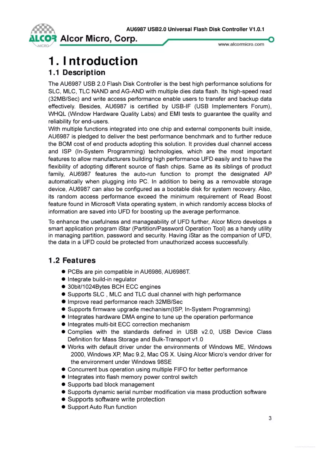
1. Introduction
1.1 Description
The AU6987 USB 2.0 Flash Disk Controller is the best high performance solutions for
SLC, MLC, TLC NAND and AG-AND with multiple dies data flash. Its high-speed read
(32MB/Sec) and write access performance enable users to transfer and backup data
effectively. Besides, AU6987 is certified by USB-IF (USB Implementers Forum),
WHQL (Window Hardware Quality Labs) and EMI tests to guarantee the quality and
reliability for end-users.
With multiple functions integrated into one chip and external components built inside,
AU6987 is pledged to deliver the best performance benchmark and to further reduce
the BOM cost of end products adopting this solution. It provides dual channel access
and ISP (In-System Programming) technologies, which are the most important
features to allow manufacturers building high performance UFD easily and to have the
flexibility of adopting different source of flash chips. Same as its siblings of product
family, AU6987 features the auto-run function to prompt the designated AP
automatically when plugging into PC. In addition to being as a removable storage
device, AU6987 can also be configured as a bootable disk for system recovery. Also,
its random access performance exceed the minimum requirement of Read Boost
feature found in Microsoft Vista operating system, in which randomly access blocks of
information are saved into UFD for boosting up the average performance.
To enhance the usefulness and manageability of UFD further, Alcor Micro develops a
smart application program iStar (Partition/Password Operation Tool) as a handy utility
in managing partition, password and security. Having iStar as the companion of UFD,
the data in a UFD could be protected from unauthorized access successfully.
1.2 Features
PCBs are pin compatible in AU6986, AU6986T.
Integrate build-in regulator
30bit/1024Bytes BCH ECC engines
Supports SLC , MLC and TLC dual channel with high performance
z Improve read performance reach 32MB/Sec
z Supports firmware upgrade mechanism(ISP, In-System Programming)
z Integrates hardware DMA engine to tune up the operation performance
z Integrates multi-bit ECC correction mechanism
z Complies with the standards defined in USB v2.0, USB Device Class
Definition for Mass Storage and Bulk-Transport v1.0
z Works with default driver under the environments of Windows ME, Windows
2000, Windows XP, Mac 9.2, Mac OS X. Using Alcor Micro’s vendor driver for
the environment under Windows 98SE
z Concurrent bus operation using multiple FIFO for better performance
z Integrates into flash memory power control switch
z Supports bad block management
z Supports dynamic serial number modification via mass production software
z Supports software write protection
z Support Auto Run function
z
z
z
z
3
Free Datasheet http://www.datasheet4u.com/
AU6987 USB2.0 Universal Flash Disk Controller V1.0.1
z Support erasable and read-only mode AP Disk
z Companion application program with UFD – iStar available for users
¾ To have UFD partition management function
¾ To do password protection for the security in data access
¾ To guard data files with software write protection function
¾ To lock up PC by UFD as the key
z Available in 48-pin LQFP 7x7mm package to support 4CE pin flashx2pcs
z Available in 64-pin LQFP 7x7mm package to support 4CE pin flashx4pcs
4
Free Datasheet http://www.datasheet4u.com/
AU6987 USB2.0 Universal Flash Disk Controller V1.0.1
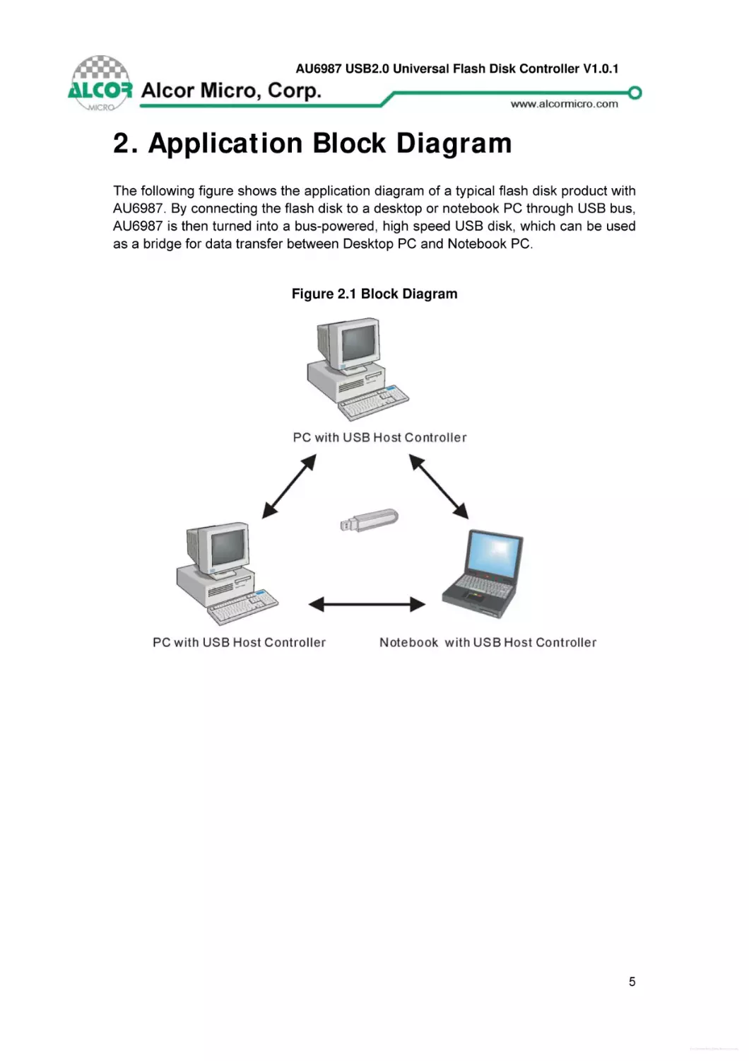
2. Application Block Diagram
The following figure shows the application diagram of a typical flash disk product with
AU6987. By connecting the flash disk to a desktop or notebook PC through USB bus,
AU6987 is then turned into a bus-powered, high speed USB disk, which can be used
as a bridge for data transfer between Desktop PC and Notebook PC.
Figure 2.1 Block Diagram
5
Free Datasheet http://www.datasheet4u.com/
AU6987 USB2.0 Universal Flash Disk Controller V1.0.1
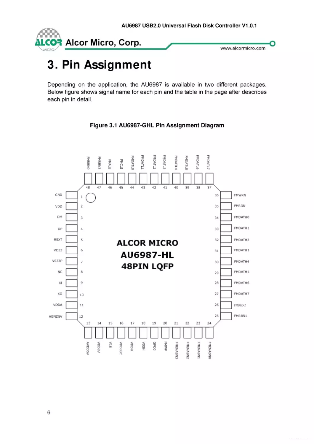
3. Pin Assignment
Depending on the application, the AU6987 is available in two different packages.
Below figure shows signal name for each pin and the table in the page after describes
each pin in detail.
Figure 3.1 AU6987-GHL Pin Assignment Diagram
6
Free Datasheet http://www.datasheet4u.com/
AU6987 USB2.0 Universal Flash Disk Controller V1.0.1
Table 3.1 AU6987-GHL Pin Descriptions
Pin #
Pin Name
I/O
Description
1
GND
GND
2
VDD
I
3
DM
I/O
USB DM
4
DP
I/O
USB DP
5
REXT
I
External resistor 330 to ground
6
VD33
I
3.3V power
7
VS33P
GND
Ground
8
VSSA
GND
Ground
9
XI
I
12 MHz oscillator input
10
XO
O
12 MHz oscillator output
11
VDDA
I
1.8V power for PLL
12
AGND5V
I
Ground
13
AVDD5V
I
5V input power pin
14
VDD3V
O
3.3V output power pin
15
V18
O
1.8V output for Core
16
WPN
O
Flash Write Protect Pin( Low Active)
17
VDDH
I
3.3V input power pin
18
VSSH
GND
19
GPO
O
blanking when system access
20
FMWP
I
Flash Write Protect Pin by Firmware(High Active)
21
FMENABN3
O
Flash 3 select pin
22
FMENABN2
O
Flash 2 select pin
23
FMENABN1
O
Flash 1 select pin
24
FMENABN0
O
Flash 0 select pin
25
26
FMRBN1
FMRBN2
I
I
Flash 1 ready pin
Flash 2 ready pin
27
FMDATH7
I/O
Flash high data 7 pin
28
FMDATH6
I/O
Flash high data 6 pin
29
FMDATH5
I/O
Flash high data 5 pin
30
FMDATH4
I/O
Flash high data 4 pin
31
FMDATH3
I/O
Flash high data 3 pin
Ground
1.8V power
Ground
7
Free Datasheet http://www.datasheet4u.com/
AU6987 USB2.0 Universal Flash Disk Controller V1.0.1
Pin #
Pin Name
I/O
Description
32
FMDATH2
I/O
Flash high data 2 pin
33
FMDATH1
I/O
Flash high data 1 pin
34
FMDATH0
I/O
Flash high data 0 pin
35
FMRDN
O
Flash read signal
36
FMWRN
O
Flash write signal
37
FMDATL7
I/O
Flash low data 7 pin
38
FMDATL6
I/O
Flash low data 6 pin
39
FMDATL5
I/O
Flash low data 5 pin
40
FMDATL4
I/O
Flash low data 4 pin
41
FMDATL3
I/O
Flash low data 3 pin
42
FMDATL2
I/O
Flash low data 2 pin
43
FMDATL1
I/O
Flash low data 1 pin
44
FMDATL0
I/O
Flash low data 0 pin
45
FMCLE
O
Flash command latch pin
46
FMALE
O
Flash address latch pin
47
FMRBN3
I
Flash 3 ready pin
48
FMRBN0
I
Flash 0 ready pin
8
Free Datasheet http://www.datasheet4u.com/
AU6987 USB2.0 Universal Flash Disk Controller V1.0.1
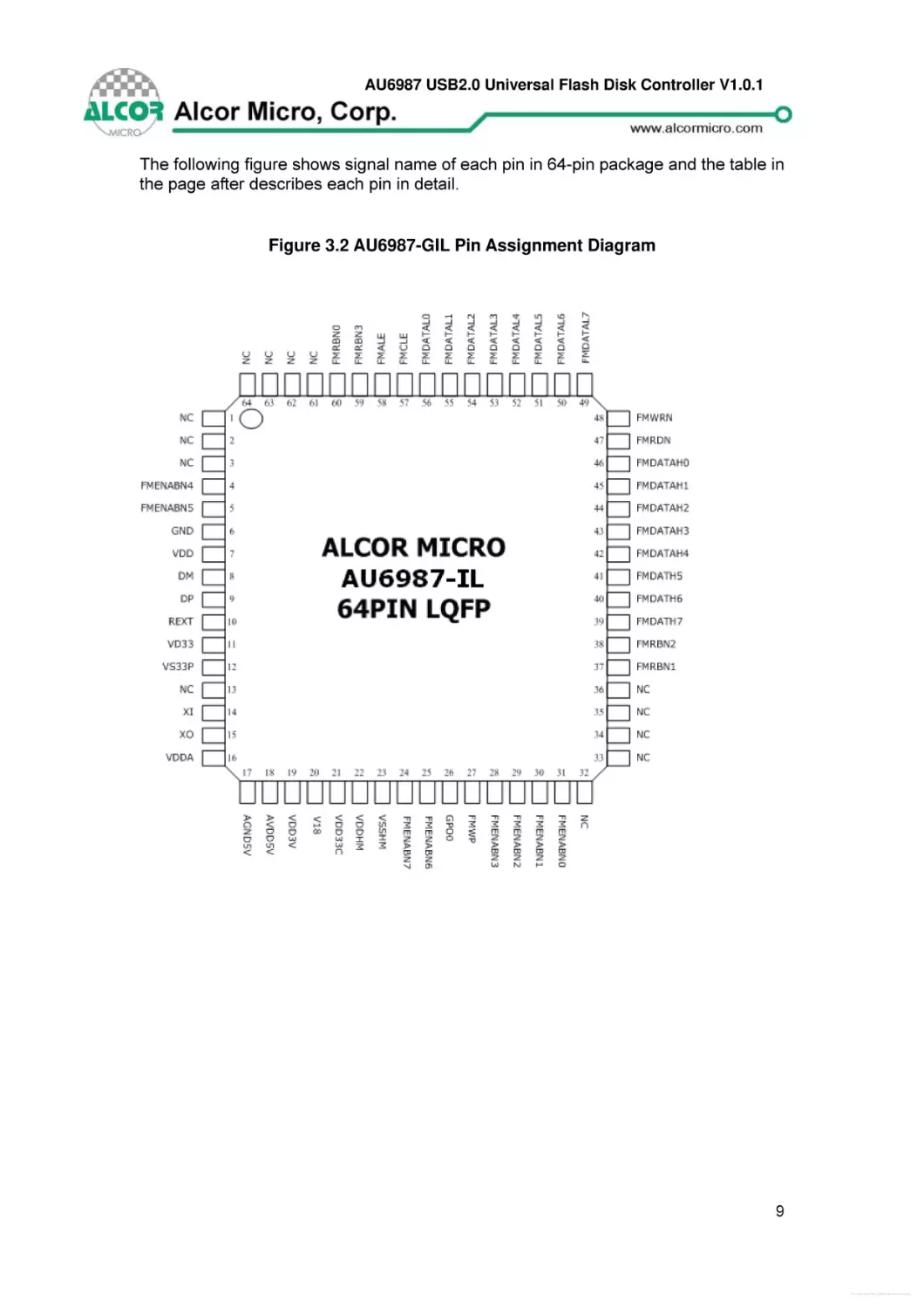
The following figure shows signal name of each pin in 64-pin package and the table in
the page after describes each pin in detail.
Figure 3.2 AU6987-GIL Pin Assignment Diagram
9
Free Datasheet http://www.datasheet4u.com/
AU6987 USB2.0 Universal Flash Disk Controller V1.0.1
Table 3.3 AU6987-GIL Pin Descriptions
Pin #
Pin Name
I/O
Description
1
NC
-
NC
2
NC
-
NC
3
NC
-
NC
4
FMENABN4
O
Flash 4 select pin
5
FMENABN5
O
Flash 5 select pin
6
GND
GND
7
VDD
I
8
DM
I/O
USB DM
9
DP
I/O
USB DP
10
REXT
I
External resistor 330 to ground
11
VD33
I
3.3V power
12
VS33P
GND
Ground
13
VSSA
GND
Ground
14
XI
I
12 MHz oscillator input
15
XO
O
12 MHz oscillator output
16
VDDA
I
1.8V power for PLL
17
AGND5V
I
Ground
18
AVDD5V
I
5V input power pin
19
VDD3V
O
3.3V output power pin
20
V18
O
1.8V output for Core
21
WPN
O
Flash Write Protect Pin( Low Active)
22
VDDHM
I
3.3V input power pin
23
VSSHM
GND
24
FMENABN7
O
Flash 7 select pin
25
FMENABN6
O
Flash 6 select pin
26
GPO
O
blanking when system access
27
FMWP
I
Flash Write Protect Pin by Firmware(High Active)
28
FMENABN3
O
Flash 3 select pin
29
FMENABN2
O
Flash 2 select pin
30
FMENABN1
O
Flash 1 select pin
31
FMENABN0
O
Flash 0 select pin
32
NC
-
NC
Ground
1.8V power
Ground
10
Free Datasheet http://www.datasheet4u.com/
AU6987 USB2.0 Universal Flash Disk Controller V1.0.1
Pin #
Pin Name
I/O
Description
33
NC
I
Hardware test T0
34
NC
I
Hardware test T1
35
NC
I
Hardware test T2
36
NC
-
-
37
FMRBN1
I
Flash 1 ready pin
38
FMRBN2
I
Flash 2 ready pin
39
FMDATH7
I/O
Flash high data 7 pin
40
FMDATH6
I/O
Flash high data 6 pin
41
FMDATH5
I/O
Flash high data 5 pin
42
FMDATH4
I/O
Flash high data 4 pin
43
FMDATH3
I/O
Flash high data 3 pin
44
FMDATH2
I/O
Flash high data 2 pin
45
FMDATH1
I/O
Flash high data 1 pin
46
FMDATH0
I/O
Flash high data 0 pin
47
FMRDN
O
Flash read signal
48
FMWRN
O
Flash write signal
49
FMDATL7
I/O
Flash low data 7 pin
50
FMDATL6
I/O
Flash low data 6 pin
51
FMDATL5
I/O
Flash low data 5 pin
52
FMDATL4
I/O
Flash low data 4 pin
53
FMDATL3
I/O
Flash low data 3 pin
54
FMDATL2
I/O
Flash low data 2 pin
55
FMDATL1
I/O
Flash low data 1 pin
56
FMDATL0
I/O
Flash low data 0 pin
57
FMCLE
O
Flash command latch pin
58
FMALE
O
Flash address latch pin
59
FMRBN3
I
Flash 3 ready pin
60
FMRBN0
I
Flash 0 ready pin
61
NC
-
NC
62
NC
-
NC
63
NC
-
NC
64
NC
-
NC
11
Free Datasheet http://www.datasheet4u.com/
AU6987 USB2.0 Universal Flash Disk Controller V1.0.1
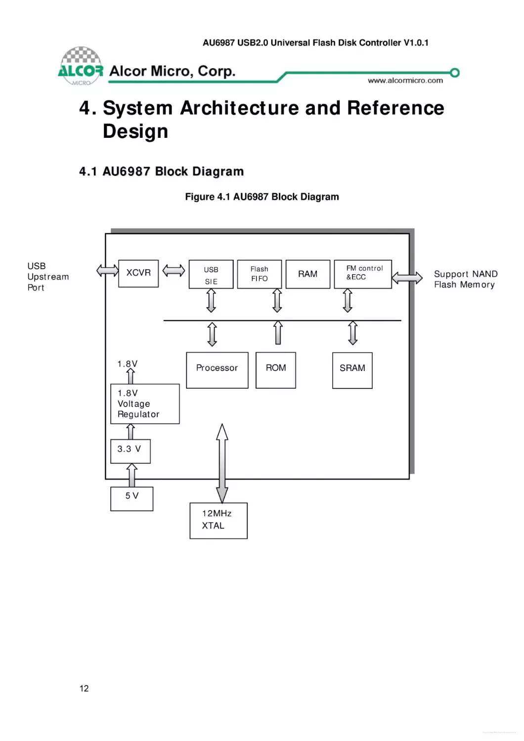
4. System Architecture and Reference
Design
4.1 AU6987 Block Diagram
Figure 4.1 AU6987 Block Diagram
USB
Upstream
Port
XCVR
1.8V
USB
SIE
Processor
Flash
FIFO
ROM
RAM
FM control
&ECC
Support NAND
Flash Memory
SRAM
1.8V
Voltage
Regulator
3.3 V
5V
12MHz
XTAL
12
Free Datasheet http://www.datasheet4u.com/
AU6987 USB2.0 Universal Flash Disk Controller V1.0.1
5. Electrical Characteristics
5.1 Absolute Maximum Ratings
Table 5.1 Absolute Maximum Ratings
Symbol
Parameter
Rating
Units
VDDH
Power Supply
-0.3 to VDDH +0.3
V
VIN
Input Signal Voltage
-0.3 to 3.6
V
VOUT
Output Signal Voltage
-0.3 to VDDH +0.3
V
TSTG
Storage Temperature
-40 to 150
O
C
5.2 Recommended Operating Conditions
Table 5.2 Recommended Operating Conditions
Symbol
Parameter
Min.
Typ.
Max.
Units
ADD
5V Power Supply
4.75
5.0
5.25
V
VDDH
Power Supply
3.0
3.3
3.6
V
VDD
Digital Supply
1.62
1.8
1.98
V
VIN
Input Signal Voltage
0
3.3
3.6
V
TOPR
Operating Temperature
0
O
70
C
5.3 General DC Characteristics
Table 5.3 General DC Characteristics
Symbol
Parameter
Conditions
Min.
Typ. Max.
Units
IIN
Input current
No pull-up or
pull-down
-10
±1
10
μA
IOZ
Tri-state leakage current
-10
±1
10
μA
CIN
Input capacitance
Pad Limit
2.8
ρF
COUT
Output capacitance
Pad Limit
2.8
ρF
CBID
Bi-directional buffer
capacitance
Pad Limit
2.8
ρF
13
Free Datasheet http://www.datasheet4u.com/
AU6987 USB2.0 Universal Flash Disk Controller V1.0.1
5.4 DC Electrical Characteristics of 3.3V I/O Cells
Table 5.4 DC Electrical Characteristics of 3.3V I/O Cells
Limits
Symbol
Parameter
Conditions
Min. Typ. Max.
VDDH
Power supply
Vil
Input low voltage
Vih
Input high voltage
Vol
Output low voltage
∣Iol∣=2~16mA
Voh
Output high voltage
∣Ioh∣=2~16mA
2.4
Rpu
Input pull-up resistance
PU=high, PD=low
55
75
110
KΩ
Input pull-down resistance PU=low, PD=high
40
75
150
KΩ
-10
±1
10
μA
-10
±1
10
μA
Rpd
3.3V I/O
3.0
3.3
Unit
3.6
V
0.8
V
LVTTL
Iin
Input leakage current
Ioz
Tri-state output leakage
current
2.0
Vin= VDDH or 0
V
0.4
V
V
5.5 USB Transceiver Characteristics
Table 5.5 Electrical characteristics
Symbol
Parameter
VD33
Min.
Typ.
Analog supply Voltage
3.0
3.3
3.6
V
VDDU
VDDA
Digital supply Voltage
1.62
1.8
1.98
V
ICC
Operating supply current
55
mA
120
μA
ICC (susp)
Conditions
High speed operating
at 480 MHz
In suspend mode,
current with 1.5kΩ
Suspend supply current
pull-up resistor on pin
RPU disconnected
Max. Unit
14
Free Datasheet http://www.datasheet4u.com/
AU6987 USB2.0 Universal Flash Disk Controller V1.0.1
Table 5.6 Static characteristic:Digital pin
Symbol
Parameter
Conditions
Min.
Typ.
Max.
Unit
0.8
V
Input levels
VIL
Low-level input voltage
VIH
High-level input voltage
2.0
V
Output levels
VOL
Low-level output voltage
VOH
High-level output voltage
0.2
VDDH-0.2
V
V
VD33=3.0V~3.6V;VDDU,VDDA=1.62V~1.98V;Temp=0℃~70℃
Symbol
VHSDIFF
VHSCM
Table 5.7 Static characteristic:Analog I/O pins(DP/DM)
Parameter
Conditions
Min. Typ. Max. Unit
USB2.0 Transceiver(HS)
Input Levels(differential receiver)
∣VI(DP)-VI(DM)∣
High speed differential
measured at the
300
input sensitivity
connection as
application circuit
High speed data signaling
-50
common mode voltage
range
VHSSQ
High speed squelch
detection threshold
VHSDSC
High speed disconnection
detection threshold
VHSOI
VHSOL
VHSOH
VCHIRPJ
VCHIRPK
Squelch detected
No squelch detected
Disconnection
detected
Disconnection not
detected
Output Levels
High speed idle level
output voltage(differential)
High speed low level
output voltage(differential)
High speed high level
output voltage(differential)
Chirp-J output voltage
(differential)
Chirp-K output voltage
(differential)
mV
500
mV
100
mV
150
mV
625
mV
525
mV
-10
10
mV
-10
10
mV
-360
400
mV
700
1100
mV
-900
-500
mV
Resistance
15
Free Datasheet http://www.datasheet4u.com/
AU6987 USB2.0 Universal Flash Disk Controller V1.0.1
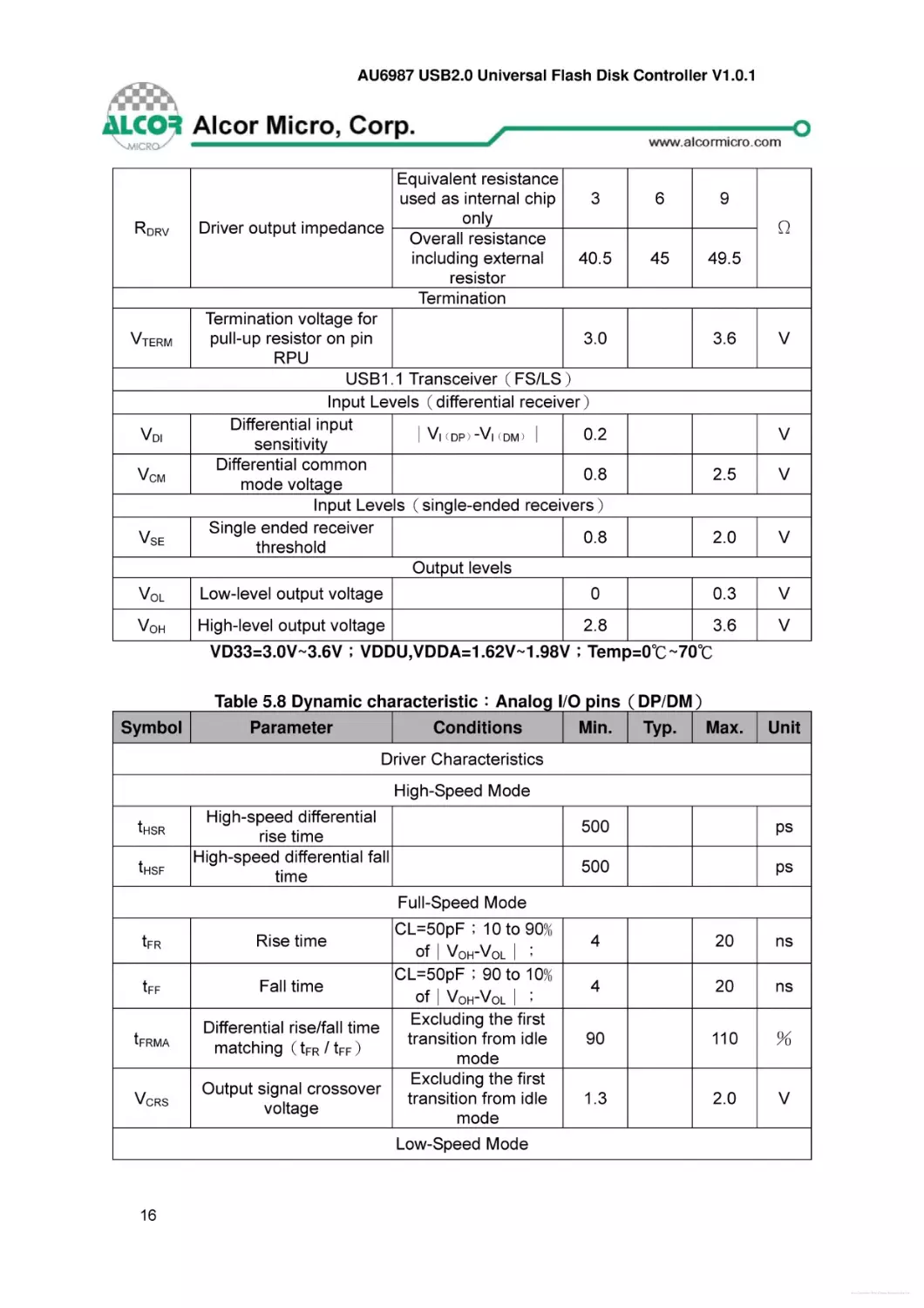
RDRV
VTERM
VDI
VCM
VSE
Equivalent resistance
3
used as internal chip
only
Driver output impedance
Overall resistance
including external
40.5
resistor
Termination
Termination voltage for
pull-up resistor on pin
3.0
RPU
USB1.1 Transceiver(FS/LS)
Input Levels(differential receiver)
Differential input
∣VI(DP)-VI(DM)∣
0.2
sensitivity
Differential common
0.8
mode voltage
Input Levels(single-ended receivers)
Single ended receiver
0.8
threshold
Output levels
6
9
Ω
45
49.5
3.6
V
V
2.5
V
2.0
V
VOL
Low-level output voltage
0
0.3
V
VOH
High-level output voltage
2.8
3.6
V
VD33=3.0V~3.6V;VDDU,VDDA=1.62V~1.98V;Temp=0℃~70℃
Table 5.8 Dynamic characteristic:Analog I/O pins(DP/DM)
Symbol
Parameter
Conditions
Min.
Typ.
Max.
Unit
Driver Characteristics
High-Speed Mode
tHSR
tHSF
High-speed differential
rise time
High-speed differential fall
time
500
ps
500
ps
Full-Speed Mode
tFR
tFF
tFRMA
VCRS
CL=50pF;10 to 90﹪
of∣VOH-VOL∣;
CL=50pF;90 to 10﹪
Fall time
of∣VOH-VOL∣;
Excluding the first
Differential rise/fall time
transition from idle
matching(tFR / tFF)
mode
Excluding the first
Output signal crossover
transition from idle
voltage
mode
Rise time
4
20
ns
4
20
ns
90
110
%
1.3
2.0
V
Low-Speed Mode
16
Free Datasheet http://www.datasheet4u.com/
AU6987 USB2.0 Universal Flash Disk Controller V1.0.1
tLR
Rise time
tLF
Fall time
tLRMA
Differential rise/fall time
matching(tLR / tLF)
VCRS
Output signal crossover
voltage
VOH
High-level output voltage
CL=200pF-600pF;
10 to 90﹪of
∣VOH-VOL∣;
CL=200pF-600pF;
90 to 10﹪of
∣VOH-VOL∣;
Excluding the first
transition from idle
mode
Excluding the first
transition from idle
mode
75
300
ns
75
300
ns
80
125
%
1.3
2.0
V
2.8
3.6
V
17
Free Datasheet http://www.datasheet4u.com/
AU6987 USB2.0 Universal Flash Disk Controller V1.0.1
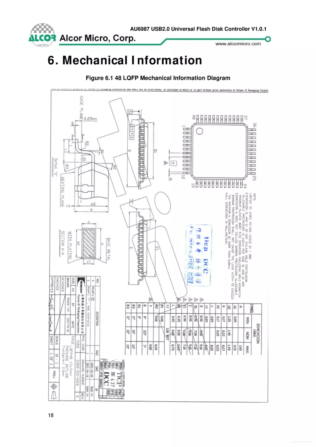
6. Mechanical Information
Figure 6.1 48 LQFP Mechanical Information Diagram
18
Free Datasheet http://www.datasheet4u.com/
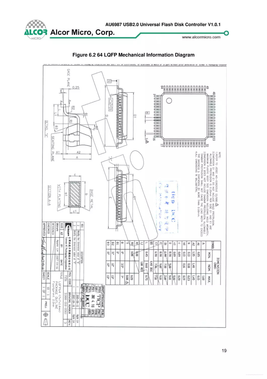
AU6987 USB2.0 Universal Flash Disk Controller V1.0.1
Figure 6.2 64 LQFP Mechanical Information Diagram
19
Free Datasheet http://www.datasheet4u.com/
AU6987 USB2.0 Universal Flash Disk Controller V1.0.1
7. Abbreviations
In this chapter some of the terms and abbreviations used throughout the technical
reference manual are listed as follows.
SIE
CF
MD
SMC
MS
SD
MMC
UTMI
Serial Interface Engine
Compact Flash
Micro Drive
SmartMedia Card
Memory Stick
Secure Digital
Multimedia Card
USB Transceiver Macrocell Interface
About Alcor Micro, Corp.
Alcor Micro, Corp. designs, develops and markets highly integrated and advanced
peripheral semiconductor, and software driver solutions for the personal computer
and consumer electronics markets worldwide. We specialize in USB solutions and
focus on emerging technology such as USB and IEEE 1394. The company offers a
range of semiconductors including controllers for USB hub, integrated keyboard/USB
hub and USB Flash memory card reader…etc. Alcor Micro, Corp. is based in Taipei,
Taiwan, with sales offices in Taipei, Japan, Korea and California. Alcor Micro is
distinguished by its ability to provide innovative solutions for spec-driven products.
Innovations like single chip solutions for traditional multiple chip products and
on-board voltage regulators enable the company to provide cost-efficiency solutions
for the computer peripheral device OEM customers worldwide.
20
Free Datasheet http://www.datasheet4u.com/