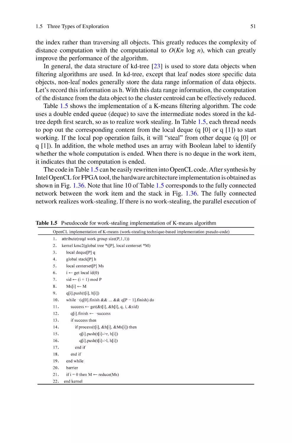
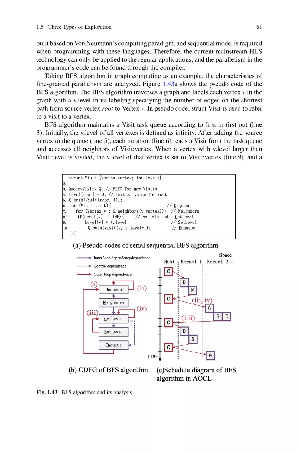
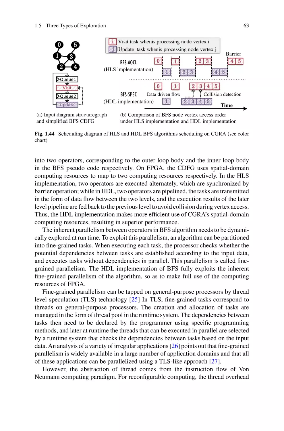
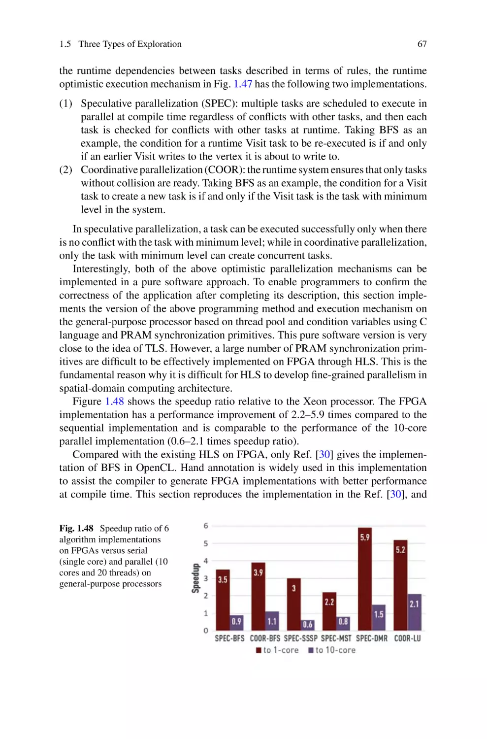
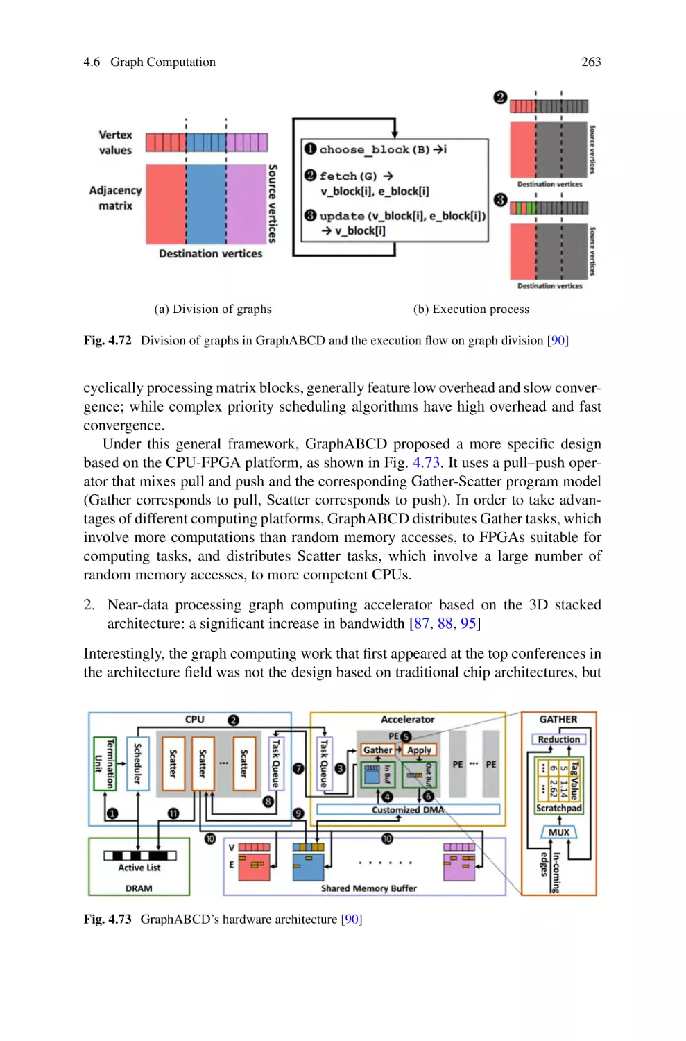
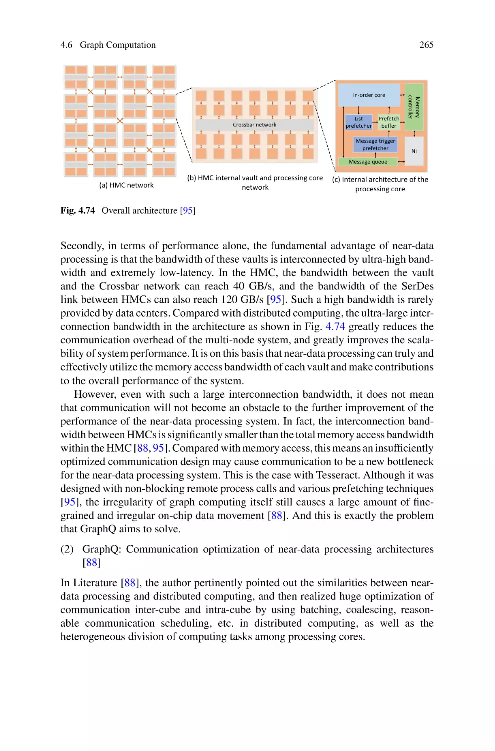
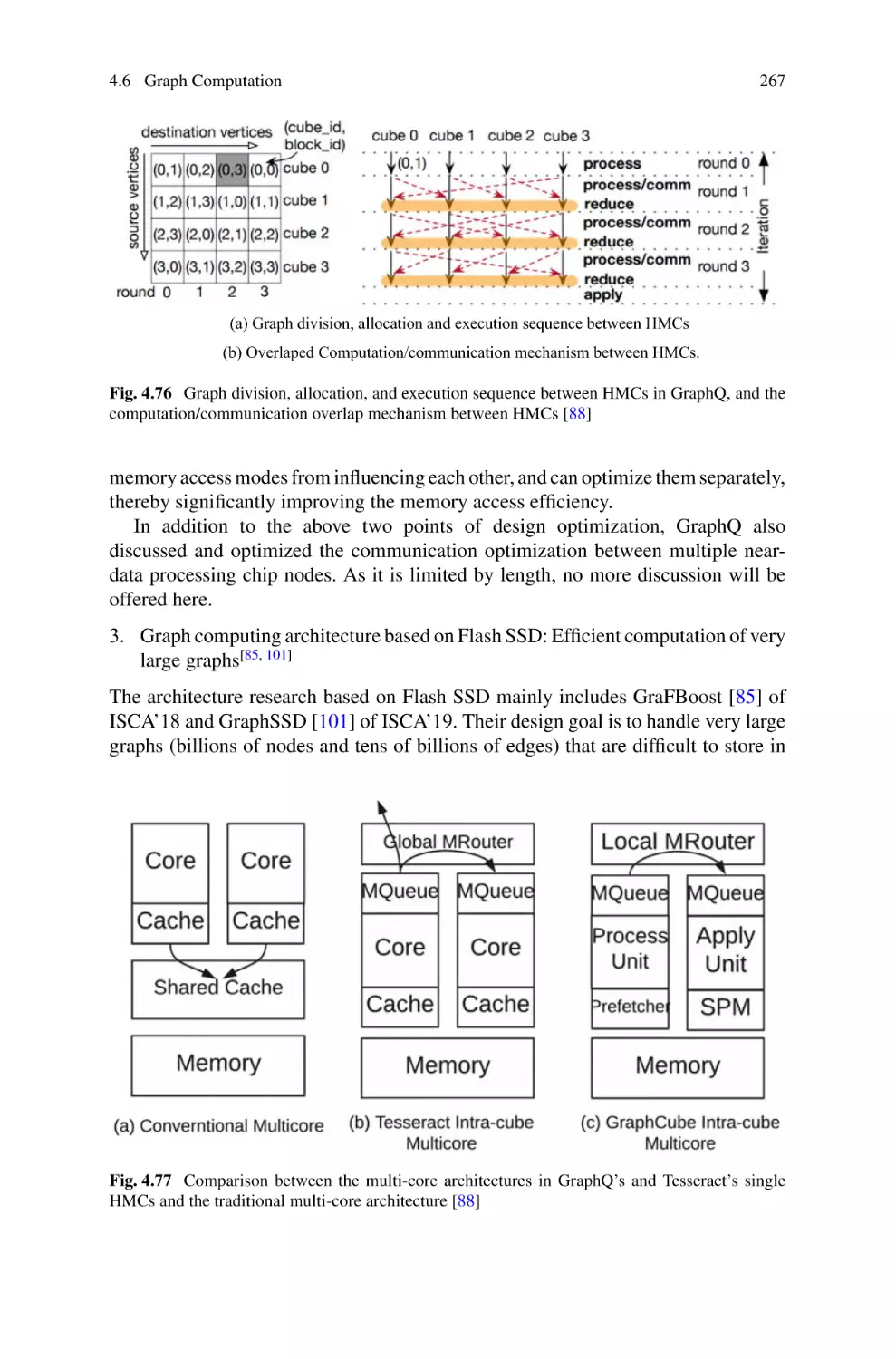
/


Автор: Liu L. Wei Sh. Zhu J. Deng Ch.
Теги: informatics software computer technology
ISBN: 978-981-19-7635-3
Год: 2023
Похожие


Текст
Leibo Liu · Shaojun Wei ·
Jianfeng Zhu · Chenchen Deng
Software
Defined Chips
Volume II
Software Defined Chips
Leibo Liu · Shaojun Wei · Jianfeng Zhu ·
Chenchen Deng
Software Defined Chips
Volume II
Leibo Liu
School of Integrated Circuits
Tsinghua University
Beijing, China
Shaojun Wei
School of Integrated Circuits
Tsinghua University
Beijing, China
Jianfeng Zhu
School of Integrated Circuits
Tsinghua University
Beijing, China
Chenchen Deng
Beijing National Research Center for
Information Science and Technology
Tsinghua University
Beijing, China
ISBN 978-981-19-7635-3
ISBN 978-981-19-7636-0 (eBook)
https://doi.org/10.1007/978-981-19-7636-0
Jointly published with Science Press
The print edition is not for sale in China mainland. Customers from China mainland please order the print
book from: Science Press.
© Science Press 2023
This work is subject to copyright. All rights are solely and exclusively licensed by the Publisher, whether
the whole or part of the material is concerned, specifically the rights of reprinting, reuse of illustrations,
recitation, broadcasting, reproduction on microfilms or in any other physical way, and transmission or
information storage and retrieval, electronic adaptation, computer software, or by similar or dissimilar
methodology now known or hereafter developed.
The use of general descriptive names, registered names, trademarks, service marks, etc. in this publication
does not imply, even in the absence of a specific statement, that such names are exempt from the relevant
protective laws and regulations and therefore free for general use.
The publishers, the authors, and the editors are safe to assume that the advice and information in this book
are believed to be true and accurate at the date of publication. Neither the publishers nor the authors or
the editors give a warranty, expressed or implied, with respect to the material contained herein or for any
errors or omissions that may have been made. The publishers remain neutral with regard to jurisdictional
claims in published maps and institutional affiliations.
This Springer imprint is published by the registered company Springer Nature Singapore Pte Ltd.
The registered company address is: 152 Beach Road, #21-01/04 Gateway East, Singapore 189721,
Singapore
Foreword
When my old friend Prof. Shaojun Wei asked me to write a foreword for his book
Software Defined Chip, I really felt a little bit uneasy. Professor Wei Shaojun is an
expert in the field of integrated circuits in China, while I’m a layman of chips. To be
honest, I don’t think I’m qualified for this. What emboldened me to accept this mission
is that, on the one hand, chips and software are closely connected, both of which
are the most fundamental elements of various systems in this era of information,
while, on the other hand, the name of the book “software defined” is related to my
expertise and also what I have been progressively promoting and publicizing for all
these years.
Looking back to the history of computer development, software has been existing
as the “appurtenance” of hardware (mainly integrated circuit chips) for a long period
of time since the first-generation computer was born in the 1940s. After the high-level
programming language emerged in the late 1950s, the word “software” started to be
proposed in a parallel position with “hardware”, and has since gradually become independent and formed an independent branch subject of computer science. However,
software had not gotten rid of hardware and became independent products and
commodities until late 1970 when the software industry saw its surge. For decades,
the collaborative development of software and hardware has underpinned the modern
information industry, and provided a constantly upgraded source of power for the
development of an information-based human society. Especially after the large-scale
commercialization of the Internet in the mid-1990s, a massive and influential social
and economic reform took place. The Wintel system we are familiar with is an
example of the collaborative development of software and hardware. Software and
integrated circuits are the cores and souls of the information technology industry,
playing a huge role as enablers and radiators.
In recent years, next-generation information technologies and their applications,
represented by cloud computing, big data, artificial intelligence, and Internet of
Things, have widely covered and influenced every part of our society, economy,
and lives. Digital transformation and development have become a trend of time for
traditional industries. The digital economy is now a new economic form after the
v
vi
Foreword
industrial economy. The digital civilization is approaching, and the human community is now on the verge of an information society. As one of the core enabling
technologies of this era, software has been ubiquitously pervading all walks of life,
evoking profound changes from the inside. Software not only is an important part of
the information infrastructure, but is also becoming the infrastructure for social and
economic activities of mankind in the information era by redefining the infrastructure in the traditional physical world and the infrastructure for social and economic
activities. It is a key support for the progression and advancement of human civilization. In this sense, we are stepping into an era where software defines everything,
featuring that everything is interconnected and programmable.
Originating from a “software-defined network”, the word “software-defined”
has been a popular term in the field of information technologies in recent years.
The software-defined network has posed a significant impact and change on the
network communication industry, redefined the traditional network architecture, and
even reshaped the structure of the traditional communication industry. Subsequently,
software-defined memory, software-defined environments, and software-defined data
centers kept popping up one after another. Currently, “Software-Defined Everything
(SDX)” for ubiquitous information technology resources is reshaping the traditional
information technology system and has become an important development trend of
the information technology industry. Also, the term “software-defined” has begun
to extend out of the information world and reach the physical world and the human
society to play its critical role of “enabling, assignment, and intelligentization”. It
has also begun to redefine the worldwide landscape where human, machines, and
things are combined.
From the perspective of a software technology researcher, the software-defined
technology is virtually the “virtualization of basic resources” and “programmability
of management tasks”. In fact, those are always principles of the design and implementation of computing operating systems. The focus is to virtualize the underlying infrastructure resources and open up APIs to achieve flexible and customizable resource management by programmable means. Meanwhile, it condenses and
bears the commonalities of the industry to better support and adapt to the needs and
changes of the upper-level business system. Therefore, I regard “software-defined” as
a methodology based on platform thinking. The so-called “SDX” means constructing
an “operating system” for “X”.
For years, my team and I have been focusing on software-defined technologies in the field of computing systems and Industrial Internet of Things. We have
achieved some positive results. Also, I have tried my best to promote and publicize the
“software-defined” concept on different occasions, including manufacturing, equipment, smart cities, smart homes, etc. However, chips were never in it. As software
must run on a chip, my inertial thinking was that only a system built on chips can be
defined by software. The first time I heard the term “software-defined chip (SDC)”
was from Prof. Wei. In the third Future Chip Forum, organized by Prof. Wei at the
end of 2018 with the theme “Reconfigurable Chip Technology”, I was invited to
make a report on soft-defined everything. This was an opportunity for me to learn
SDCs and expand my knowledge of “software-defined”.
Foreword
vii
Integrated circuits are of the most complicated design and manufacturing technologies in human history, fully symbolizing the fruits of human wisdom. Also, the
integrated circuit industry is a strategic, fundamental, and leading industry to support
the national economic and social development and guarantee national security. It
is a research field of national strategic importance. As information technology is
making continuous breakthroughs, numerous emerging applications keep springing
up and gain strong development momentum, raising highly demanding requirements
for data processing and computing efficiency. The traditional chip architecture is
being greatly challenged while digital chips cannot reach high energy efficiency
and high flexibility simultaneously, which has become a problem recognized by the
international community.
Based on the profound accumulation in the research of integrated circuit design
methodologies, Prof. Wei and his team proposed the SDC architecture and its design
paradigm, with which software dynamically defines the chip functions, and promotes
the transformation of the digital chip architecture and design paradigm. This study not
only leads the generalized field of computing chips, but also provides an important
lesson for the common problems faced in the era of software-defined technologies. I
am very glad to see that they have deeply expanded on the development background,
technical connotation, key applications, and future development of SDCs based on
their understanding of the technical trend of the information industry and research
outcomes long accumulated in relevant fields, and published China’s first book in
this field. Here, I would like to extend my sincere congratulations!
I believe that this book can act as an important reference for information technology researchers and practitioners, thereby deepening their knowledge and understanding of “software-defined”, and greatly contributing to the cultivation of information technology talents, industrial development, and ecosystem construction of
China.
Summer of 2021
Hong Mei
Preface
Our team has been studying dynamically reconfigurable chips since 2006. In 2014,
we wrote the book “Reconfigurable Computing” and published it in Science Press.
The book introduces the basic concepts of reconfigurable computing, as well as
the hardware architecture and mapping mechanism of dynamically reconfigurable
chips. In the past 5–6 years, we further worked on the theories and technologies
of SDCs based on the previous outcomes on reconfigurable computing. Softwaredefined chips (SDCs) and dynamically reconfigurable chips are much alike yet greatly
different. Dynamically reconfigurable chips hold an upward view based on chips,
with the focus on solving the problems of the circuit itself, while SDCs hold a
downward view, with the focus on, in addition to the circuit as always, programming
paradigms, compiling systems, etc. After unremitting efforts, our team has published
dozens of influential academic papers in solid-state circuits, computer architecture,
electronic design automation and other fields involved by SDCs, and many invention
patents have been granted in China and the US. We have enabled a series of marketoriented technical applications for major national projects, and solved some practical
challenges encountered in industrial production. Now we compile our research results
on SDCs, analysis of cutting-edge technologies, and thoughts about the future development of computing chips into a book and share it with all of you. However, as we
still lack sufficient knowledge, we look forward to your criticisms and suggestions
if there is anything improper in the book.
SDC is a new paradigm of computing chip architecture design. It is expected to
fill the gap between software and hardware, and directly define the runtime functions of hardware with software, so that the chip can swiftly adjust to software
changes while featuring high performance, low power consumption, high flexibility,
high programmability, unrestricted capacity, and ease of use, which are rarely seen
simultaneously on traditional computing chips. There are two main reasons why
SDCs have such technical advantages: Firstly, it is featured with mixed-grained
but mostly coarse-grained reconfigurable processing elements instead of the traditional fine-grained lookup table logic to greatly reduce redundant resources. The
energy efficiency is improved by one or two orders of magnitude compared with
traditional programmable devices (such as FPGA), and by two or three orders of
ix
x
Preface
magnitude compared with instruction-driven processors (such as CPU), rivaling that
of application specific circuits (such as ASIC). Secondly, it supports dynamic partial
reconfiguration, and the switching time can be within a few nanoseconds. Therefore, the capacity can be expanded through the fast time-division multiplexing of
the hardware, and is no longer limited by the physical scale of the circuits. In other
words, similar to the CPU that can run software codes of any size, an SDC can
hold digital logic of any size and any number of gates, which is very different from
an FPGA. Meanwhile, dynamic reconfiguration can better fit with the serialization
characteristics of software programs than static reconstruction, and it is more efficient when programming in high-level languages. Software developers who do not
have knowledge of circuits can efficiently program SDCs with purely software-based
thinking. Lowering the threshold of use will enable agile chip development, speed
up application iteration and system deployment, and greatly expand the use of chips.
Software Defined Chip has two volumes. The first volume mainly introduces the
conceptual evolution, technical principles, key issues, hardware architecture, and
compiling system of SDCs. This book is the second volume and will focus on the
following topics: How is the usability of SDCs achieved? What challenges does the
programming model face? What are the intrinsic advantages in security and reliability? What technical difficulties are SDCs still facing? How will the technology
develop in the future? What applications have been achieved? What are the advantages of applications compared with traditional computing chips? Which areas have
better development prospects in the future?
This book is divided into five chapters: Chapter 1 introduces the programming
model of SDCs. By reviewing the co-evolution of architectures and programming
models of modern general-purpose processors, it analyzes the programming models
of SDCs as an emerging computing architecture, discusses how the chip design can
address the problems of “memory wall”, “power wall”, and “I/O wall” brought by
the unbalanced development of semiconductor device technologies, and sums up
the ternery paradox of programming models, that is, a programming model cannot
achieve high generality, high development efficiency, and high execution efficiency
at the same time. This chapter also proposes three possible research directions for
the programming models of SDCs. Chapter 2 introduces the intrinsic security and
reliability of SDCs. In terms of security, it takes the fault attack of a cryptographic
chip as an example to introduce how to use the dynamic partial reconfiguration
feature to improve the resistance against side-channel attacks, and how to make full
use of the abundant computing units and interconnections to construct a physical
unclonable function (PUF) to improve hardware security. In terms of reliability, it
takes Network-on-a-Chip (NoC) of SDCs as an example to introduce an efficient
topology reconstruction method to improve the fault tolerance of the system, along
with the algorithm mapping optimization technology after the topology is dynamically changed. Chapter 3 focuses on the main technical bottlenecks faced by SDCs
in terms of flexibility, efficiency, and usability, expands on the possibility of new
design concepts, and envisions the future development trend of SDC technologies.
Chapter 4 analyzes the target application fields of SDCs, and introduces design
cases of SDCs in artificial intelligence, 5G communications, cryptography, graph
Preface
xi
computing, network protocol processing, and other applications. Chapter 5 envisions
the application of SDCs in emerging scenarios in the future, with the focus on the
application in emerging technologies such as evolutionary computing, post-quantum
cryptography, and fully homomorphic encryption.
This book embodies the collective wisdom of the reconfigurable computing team
at Tsinghua University accumulated in the past 10 years. Thanks to many postdoctoral, doctoral, master, and undergraduate students, and engineers for their unremitting efforts. They are Jianfeng Zhu, Chenchen Deng, Wenping Zhu, Honglan Jiang,
Jiaji He, Bohan Yang, Zhaoshi Li, Neng Zhang, Huiyu Mo, Xingchen Man, Longlong Chen, Yufeng Huang, Yibo Wu, Weiyi Sun, Dibei Chen, Baofen Yuan, Liwei
Sun, Ang Li, Jinyi Chen, Xiangyu Kong, Hanning Wang, and Siming Kou. Thanks
to Prof. Shaojun Wei for his helpful support and guidance on the writing of this
book, and special thanks to Academician Hong Mei, a well-known expert in system
software and software engineering, for reviewing this book and writing a foreword.
Finally, I would also like to appreciate my wife and children (Tuo Tuo and Dou Dou)
for their understanding and supporting of my work. You are an important driver of
my work and advancement in the future!
Tsinghua Garden in June 2021
Leibo Liu
Contents
1 Programming Model . . . . . . . . . . . . . . . . . . . . . . . . . . . . . . . . . . . . . . . . . . .
1.1 Dilemma of the Programming Model of Software-Defined
Chips . . . . . . . . . . . . . . . . . . . . . . . . . . . . . . . . . . . . . . . . . . . . . . . . . . . .
1.2 Three Routes . . . . . . . . . . . . . . . . . . . . . . . . . . . . . . . . . . . . . . . . . . . . .
1.3 Three Obstacles . . . . . . . . . . . . . . . . . . . . . . . . . . . . . . . . . . . . . . . . . . .
1.3.1 Von Neumann Architecture and Random Access
Machine Model . . . . . . . . . . . . . . . . . . . . . . . . . . . . . . . . . . . .
1.3.2 Memory Wall . . . . . . . . . . . . . . . . . . . . . . . . . . . . . . . . . . . . .
1.3.3 Power Wall . . . . . . . . . . . . . . . . . . . . . . . . . . . . . . . . . . . . . . .
1.3.4 I/O Wall . . . . . . . . . . . . . . . . . . . . . . . . . . . . . . . . . . . . . . . . . .
1.4 Impossible Trinity . . . . . . . . . . . . . . . . . . . . . . . . . . . . . . . . . . . . . . . . .
1.5 Three Types of Exploration . . . . . . . . . . . . . . . . . . . . . . . . . . . . . . . . .
1.5.1 Spatial Domain Parallelism and Irregular
Application . . . . . . . . . . . . . . . . . . . . . . . . . . . . . . . . . . . . . . .
1.5.2 Programming Model of Spatial Domain Parallelism . . . . .
1.6 Summary and Prospect . . . . . . . . . . . . . . . . . . . . . . . . . . . . . . . . . . . . .
References . . . . . . . . . . . . . . . . . . . . . . . . . . . . . . . . . . . . . . . . . . . . . . . . . . . . .
2 Hardware Security and Reliability . . . . . . . . . . . . . . . . . . . . . . . . . . . . . . .
2.1 Security . . . . . . . . . . . . . . . . . . . . . . . . . . . . . . . . . . . . . . . . . . . . . . . . . .
2.1.1 Countermeasures Against Fault Attacks . . . . . . . . . . . . . . .
2.1.2 Countermeasures Against Side Channel Attacks . . . . . . . .
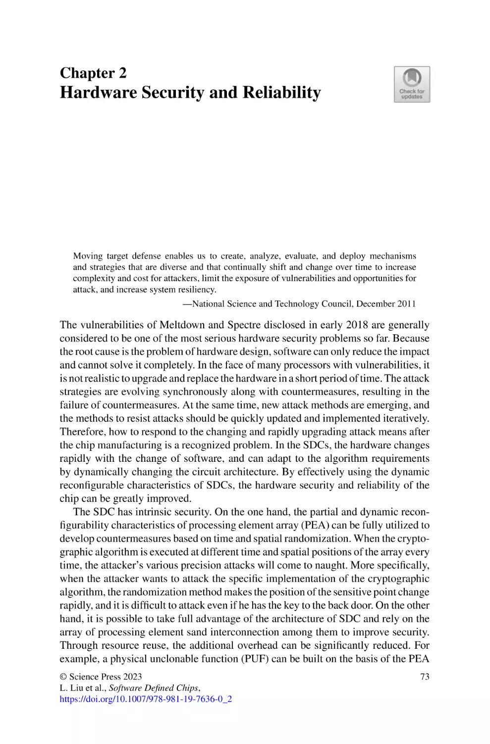
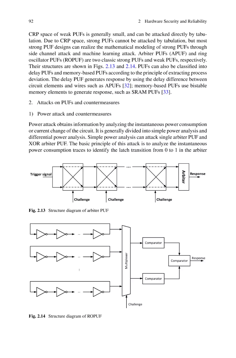
2.1.3 PUF Technology Based on SDC . . . . . . . . . . . . . . . . . . . . .
2.2 Reliability . . . . . . . . . . . . . . . . . . . . . . . . . . . . . . . . . . . . . . . . . . . . . . . .
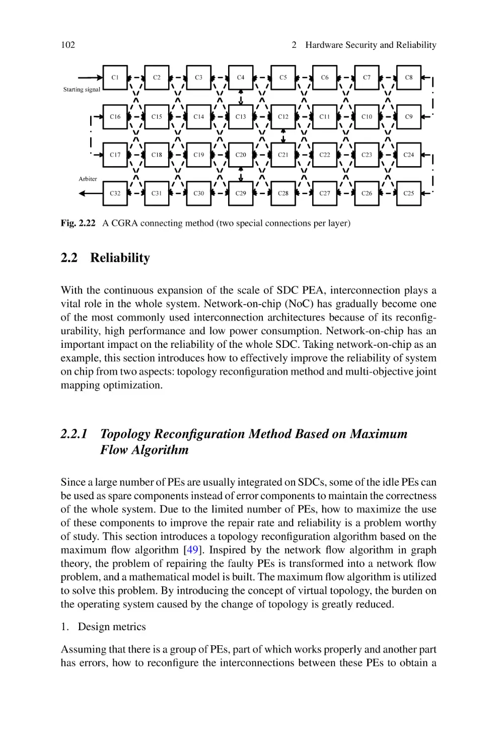
2.2.1 Topology Reconfiguration Method Based
on Maximum Flow Algorithm . . . . . . . . . . . . . . . . . . . . . . .
2.2.2 Multi-objective Mapping Optimization Method
for Reconfigurable Network-on-Chip . . . . . . . . . . . . . . . . .
References . . . . . . . . . . . . . . . . . . . . . . . . . . . . . . . . . . . . . . . . . . . . . . . . . . . . .
1
2
3
6
7
9
14
25
28
31
32
37
68
70
73
74
74
79
90
102
102
112
131
xiii
xiv
Contents
3 Technical Difficulties and Development Trend . . . . . . . . . . . . . . . . . . . . .
3.1 Analysis of Technical Difficulties . . . . . . . . . . . . . . . . . . . . . . . . . . . .
3.1.1 Flexibility: Programmability Design Coordinating
the Software and Hardware . . . . . . . . . . . . . . . . . . . . . . . . . .
3.1.2 Efficiency: Tradeoff Between Hardware Parallelism
and Utilization . . . . . . . . . . . . . . . . . . . . . . . . . . . . . . . . . . . .
3.2 Instruction-Level Parallelism . . . . . . . . . . . . . . . . . . . . . . . . . . . . . . . .
3.3 Data-Level Parallelism . . . . . . . . . . . . . . . . . . . . . . . . . . . . . . . . . . . . .
3.4 Memory-Level Parallelism . . . . . . . . . . . . . . . . . . . . . . . . . . . . . . . . . .
3.5 Task-Level Parallelism . . . . . . . . . . . . . . . . . . . . . . . . . . . . . . . . . . . . .
3.6 Speculation Parallelism . . . . . . . . . . . . . . . . . . . . . . . . . . . . . . . . . . . .
3.6.1 Ease of Use: Optimizing Virtualized Hardware
with Software Scheduling . . . . . . . . . . . . . . . . . . . . . . . . . . .
3.6.2 Prospects on Development Trend . . . . . . . . . . . . . . . . . . . . .
3.7 Independent Task-Level Parallelism . . . . . . . . . . . . . . . . . . . . . . . . . .
3.8 Data-Level Parallelism . . . . . . . . . . . . . . . . . . . . . . . . . . . . . . . . . . . . .
3.9 Bit-Level Parallelism . . . . . . . . . . . . . . . . . . . . . . . . . . . . . . . . . . . . . .
3.10 Optimization of Memory Access Patterns . . . . . . . . . . . . . . . . . . . . .
3.10.1 Multi-Level Parallelism Design
for In-/near-Memory Computing . . . . . . . . . . . . . . . . . . . . .
3.11 Implementation of Instruction-Level Parallelism in SDCs . . . . . . .
3.12 Implementation of Data-Level Parallelism in SDCs . . . . . . . . . . . . .
3.13 Implementation of Task-Level Parallelism in SDCs . . . . . . . . . . . . .
3.14 Implementation of Speculation Parallelism in SDCs . . . . . . . . . . . .
3.15 Efficiency of Memory in the SDC . . . . . . . . . . . . . . . . . . . . . . . . . . . .
3.15.1 Software-Transparent Hardware Dynamic
Optimization Design . . . . . . . . . . . . . . . . . . . . . . . . . . . . . . .
3.16 Virtualization of SDCs . . . . . . . . . . . . . . . . . . . . . . . . . . . . . . . . . . . . .
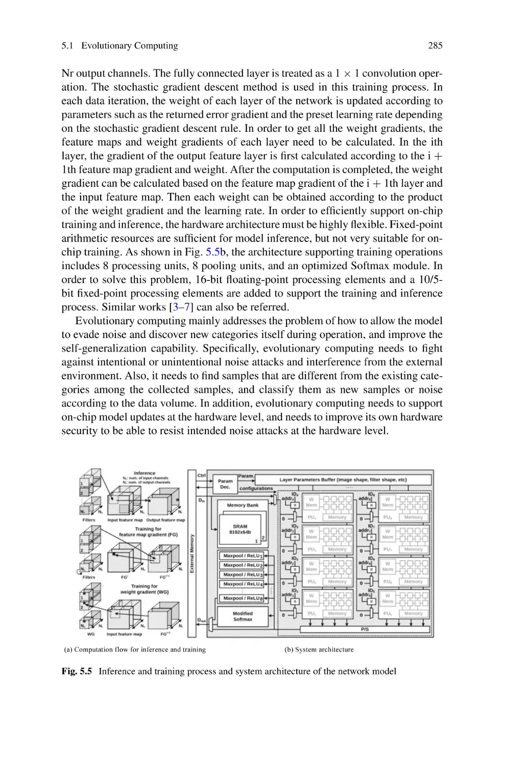
3.17 Online Training by Means of Machine Learning . . . . . . . . . . . . . . .
References . . . . . . . . . . . . . . . . . . . . . . . . . . . . . . . . . . . . . . . . . . . . . . . . . . . . .
135
136
4 Current Application Fields . . . . . . . . . . . . . . . . . . . . . . . . . . . . . . . . . . . . . .
4.1 Analysis of Application Fields . . . . . . . . . . . . . . . . . . . . . . . . . . . . . .
4.2 Artificial Intelligence . . . . . . . . . . . . . . . . . . . . . . . . . . . . . . . . . . . . . .
4.2.1 Algorithm Analysis . . . . . . . . . . . . . . . . . . . . . . . . . . . . . . . .
4.2.2 State-of-the-Art Artificial Intelligence Chips . . . . . . . . . . .
4.2.3 Software-Defined Artificial Intelligence Chip . . . . . . . . . .
4.3 5G Communication Baseband . . . . . . . . . . . . . . . . . . . . . . . . . . . . . . .
4.3.1 Algorithm Analysis . . . . . . . . . . . . . . . . . . . . . . . . . . . . . . . .
4.3.2 State-of-the-Art Research on Communication
Baseband Chips . . . . . . . . . . . . . . . . . . . . . . . . . . . . . . . . . . .
4.3.3 Software-Defined Communication Baseband Chip . . . . . .
4.4 Cryptographic Computation . . . . . . . . . . . . . . . . . . . . . . . . . . . . . . . . .
4.4.1 Analysis of Cryptographic Algorithms . . . . . . . . . . . . . . . .
167
168
171
171
174
187
192
194
136
139
139
140
140
141
141
144
146
149
149
149
150
150
151
151
152
153
157
160
160
161
163
200
206
214
215
Contents
xv
4.4.2
Current Status of the Research on Cryptographic
Chips . . . . . . . . . . . . . . . . . . . . . . . . . . . . . . . . . . . . . . . . . . . .
4.4.3 Software-Defined Cryptographic Chips . . . . . . . . . . . . . . .
4.5 Hardware Security of the Processor . . . . . . . . . . . . . . . . . . . . . . . . . .
4.5.1 Background . . . . . . . . . . . . . . . . . . . . . . . . . . . . . . . . . . . . . . .
4.5.2 Analysis of CPU Hardware Security Threats . . . . . . . . . . .
4.5.3 Existing Countermeasures . . . . . . . . . . . . . . . . . . . . . . . . . . .
4.5.4 CPU Hardware Security Technology Based
on Software-Defined Chips . . . . . . . . . . . . . . . . . . . . . . . . . .
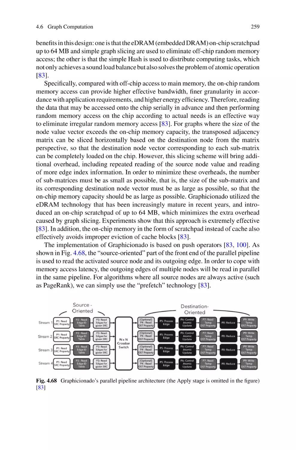
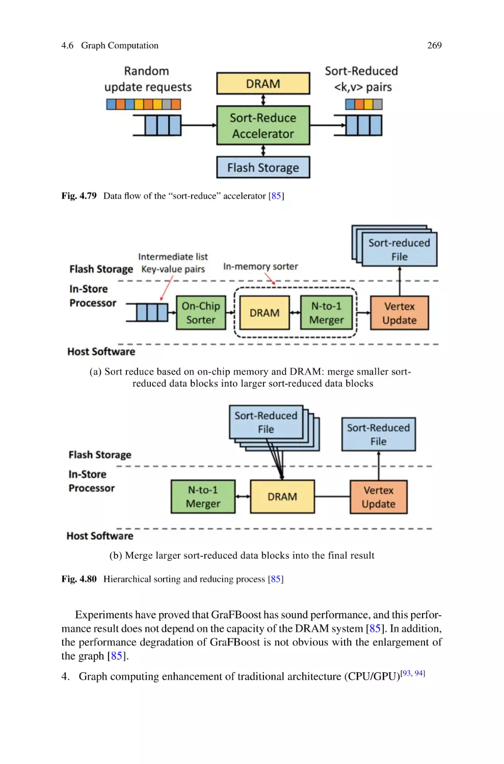
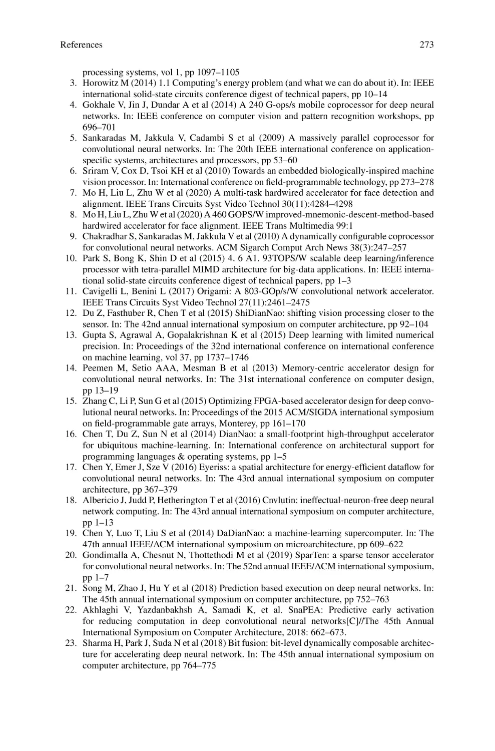
4.6 Graph Computation . . . . . . . . . . . . . . . . . . . . . . . . . . . . . . . . . . . . . . . .
4.6.1 Background of Graph Algorithms . . . . . . . . . . . . . . . . . . . .
4.6.2 Programming Model of Graph Computation . . . . . . . . . . .
4.6.3 Research Progress of Hardware Architecture
for Graph Computing . . . . . . . . . . . . . . . . . . . . . . . . . . . . . . .
4.6.4 Outlook . . . . . . . . . . . . . . . . . . . . . . . . . . . . . . . . . . . . . . . . . .
References . . . . . . . . . . . . . . . . . . . . . . . . . . . . . . . . . . . . . . . . . . . . . . . . . . . . .
5 Future Application Prospects . . . . . . . . . . . . . . . . . . . . . . . . . . . . . . . . . . . .
5.1 Evolutionary Computing . . . . . . . . . . . . . . . . . . . . . . . . . . . . . . . . . . .
5.1.1 Background and Concept of Evolutionary
Computing . . . . . . . . . . . . . . . . . . . . . . . . . . . . . . . . . . . . . . . .
5.1.2 The Evolution and State-Of-The-Art Research . . . . . . . . .
5.1.3 Software-Defined Evolutionary Computing Chip . . . . . . .
5.2 Post-Quantum Cryptography . . . . . . . . . . . . . . . . . . . . . . . . . . . . . . . .
5.2.1 Concept and Application of Post-Quantum
Cryptographic Algorithms . . . . . . . . . . . . . . . . . . . . . . . . . .
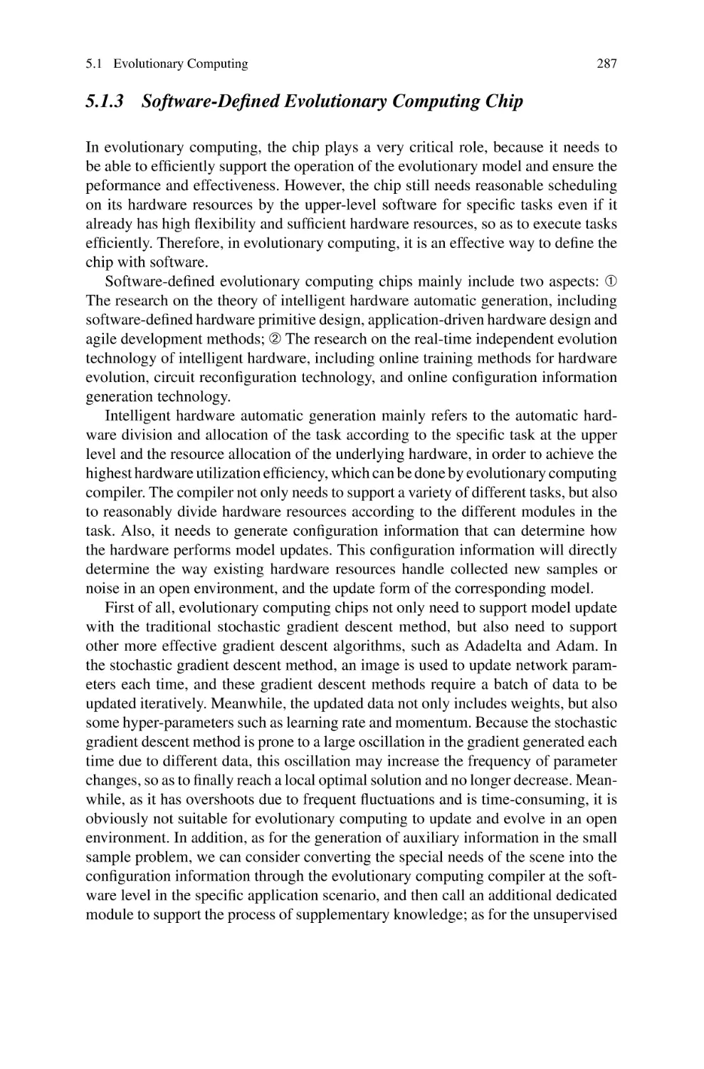
5.3 Current Status of Post-Quantum Cryptographic Algorithms . . . . . .
5.3.1 Status Quo of the Research on Post-Quantum
Cryptographic Chips . . . . . . . . . . . . . . . . . . . . . . . . . . . . . . .
5.3.2 Software-Defined Post-Quantum Cryptographic
Chip . . . . . . . . . . . . . . . . . . . . . . . . . . . . . . . . . . . . . . . . . . . . .
5.4 Fully Homomorphic Encryption . . . . . . . . . . . . . . . . . . . . . . . . . . . . .
5.4.1 Concept and Application of Fully Homomorphic
Encryption . . . . . . . . . . . . . . . . . . . . . . . . . . . . . . . . . . . . . . . .
5.4.2 Status Quo of the Research on Fully Homomorphic
Encryption Chips . . . . . . . . . . . . . . . . . . . . . . . . . . . . . . . . . .
5.4.3 Software-Defined Fully Homomorphic Encryption
Computing Chip . . . . . . . . . . . . . . . . . . . . . . . . . . . . . . . . . . .
References . . . . . . . . . . . . . . . . . . . . . . . . . . . . . . . . . . . . . . . . . . . . . . . . . . . . .
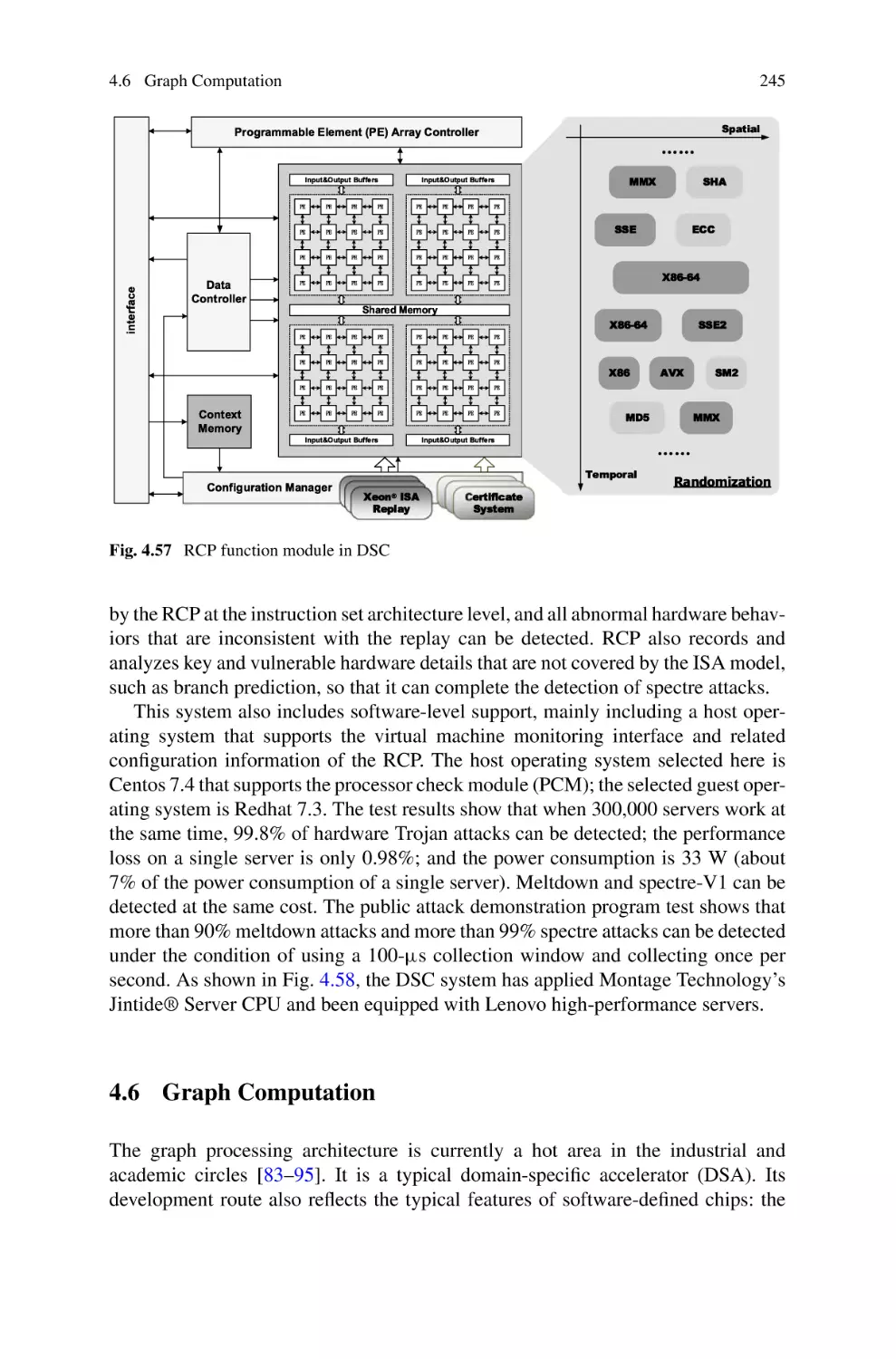
221
226
232
234
235
236
238
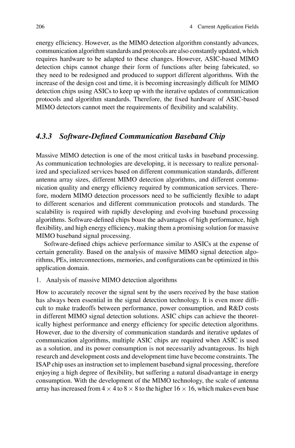
245
247
251
257
270
272
279
280
280
281
287
288
289
291
294
299
301
301
304
307
315
Introduction
Software Defined Chip has two volumes, and this book is the second volume. By
retrospecting the co-evolution of modern general-purpose processors and programming models, this book analyzes the research focus of the programming model of
Software-Defined Chips (SDCs). How to utilize the dynamic reconfigurable feature
of the SDC to improve the security and reliability of chip hardware is also presented.
Challenges and envisions the direction of future technological breakthroughs of
SDCs are discussed. This book covers the latest research of SDCs in artificial intelligence, cryptographic computing, 5G communications, and other fields, as well as
future-oriented emerging applications.
This book is suitable for scientific researchers, senior graduate students, and
engineers in related industries engaged in electronic engineering and computer
science.
xvii
Chapter 1
Programming Model
All problems in computer science can be solved by another level of indirection, except for
the problem of too many layers of indirection.
—David Wheeler [1].
The main difference between software-defined chips (SDCs) and ASIC is that SDCs
need to execute user-written software like general-purpose processor. ASIC is only
for specific applications. It only needs to provide special APIs without considering
how programmers program it while the function of SDCs is finally realized by
programmers. A necessary condition for a set of hardware to attract a large number
of users to invest in the development of software is that the software on the hardware is forward compatible: even if the new generation of hardware design has
changed dramatically, the software previously written by users can still run correctly
on the new chip. The “language” for dialogue between software and hardware is the
programming model.
The programming model in general sense refers to all levels of abstraction from
application to chip. In the long development process of general-purpose processor
chips, a complex hierarchical layer of indirection model composed of abstraction
levels such as programming language, compiler intermediate representation and
instruction set architecture has gradually formed. In these models, the upper layer
of indirection hides the complexity of the lower layer of indirection in turn. For
example, to hide the complex process control caused by that the instruction counter
can arbitrarily jump (e.g., jump class instruction in x86 instruction set), the programming language layer provides a variety of process control statements, such as statements in C language. In this way, when developing applications, programmers only
need to develop applications for specific layer of indirection without considering the
complexity of the underlying implementation.
However, as a new computing architecture different from general-purpose
processor and ASIC in both chip architecture and programming model design, the
SDCs faces the dilemma of “chicken-and-egg” in the programming model: without
SDC programming model, the design of SDCs is like “water without a source”,
lacking a software to guide the direction of chip design; without the design of SDCs,
© Science Press 2023
L. Liu et al., Software Defined Chips,
https://doi.org/10.1007/978-981-19-7636-0_1
1
2
1 Programming Model
the programming model design of SDCs is like “a tree without roots”, lacking a
hardware to test the effectiveness of programming model.
To break the dilemma, this chapter will review the co-evolution of modern generalpurpose processor architecture and programming model. Section 1.1 analyzes the
causes and effects of the dilemma in detail. Section 1.2 examines the layer of indirection structure of modern programming models, and then summarizes the design
routes of three programming models. Section 1.3 examines how the chip design and
programming model should deal with the “three walls” caused by the unbalanced
process development of semiconductor devices, namely “memory wall”, “power
wall” and “I/O wall”. More and more complex hardware has spawned a variety of
programming models. Section 1.4 summarizes the “Impossible Trinity of programming model” from the evolution process of programming model: the new programming model cannot obtain high generality, high development efficiency and high
execution efficiency at the same time. At most, it can only achieve two goals at
the same time and abandon the other goal. Combined with the processing method
of hardware complexity in the abstraction level of computing system, the rationality of Impossible Trinity can be explained empirically. Finally, based on the
“Impossible Trinity”, Sect. 1.5 puts forward three possible research directions for
the programming model dilemma of SDCs.
1.1 Dilemma of the Programming Model
of Software-Defined Chips
In the past 60 years, humans have created a spectacle: the performance of chips
continues to grow exponentially, and the applications based on chips become more
and more complex and diverse. As the contract between the chip and the application,
the programming model ensures that the past applications can be easily transplanted
to the future chip through the consistency of the contract. However, the end of Moore’s
law, like taking away the firewood from under the cauldron, has destroyed the spectacle of the computing industry. For SDCs, the chip design should be freed from the
constraint of old contract and be reconsidered from the relationship between chips,
programming models and applications.
Without SDC programming model, the architecture design of SDCs is like “water
without a source”, lacking a software to guide the direction of hardware design. In
the research of architecture, the most direct response to the paradigm shift of hardware is to invent a new (domain-specific) programming model. Although the new
programming model is attractive in the short term, it usually means that programmers must rewrite the code, and will bring serious obstacles to understanding and
communication to the software development team, making the learning curve steep.
In the rapid iteration stage of hardware architecture, a lot of human and material
resources are directly spent, and it is unrealistic to design and develop an automated
1.2 Three Routes
3
compiler for the evolving architecture. This makes it difficult for the target application to respond quickly to the decisions in hardware design when designing a new
hardware paradigm, resulting in the dilemma of no software available.
Without the architecture of SDCs, the programming model design of SDCs is like
“a tree without roots”, lacking a hardware to support the development of programming model. The programming model functions to hide the complex hardware mechanism. In an era when Moore’s law is still effective in enhancing the performance
of general-purpose processors, the design of programming models is much simpler
than today. Although the hardware mechanism of the processor may change greatly
between generations, the instruction set architecture (ISA) of the new generation
processor only needs to add a few or several types of instructions. Therefore, the
programming model, compiler and programming language of the previous generation can be applied to the new generation processor with only a few changes
made. However, with the failure of Moore’s law in enhancing processor performance,
specialization has become the most important performance source of the new generation of hardware. It is difficult to abstract this specialized hardware with a unified
or similar ISA. Therefore, different new hardware requires different programming
models. When the emerging hardware paradigm has not been finalized, it is difficult
for the programming model to clarify which hardware mechanisms to hide.
If the paradox of “chicken-and-egg” cannot be solved, the development of SDCs
will face two outcomes, that is, either the stagnation of hardware development due
to the inability of software to adapt, or the inability of software to use hardware for
innovation. To break this dilemma, we need to fundamentally rethink how to design,
program and use SDCs.
We believe that we can gather the fragmented common sense, and then more
consistently understand the design method of SDCs programming model through
review of the co-evolution of modern general-purpose processor architecture and
programming model, reflection on historical experience and discussion on concepts.
1.2 Three Routes
As mentioned in the introduction of this chapter, the layer of indirection is the main
driving force for the growth and productivity progress of the computing industry.
Today, most computer architects may not know the working principle of modern
microprocessors nor the technological process of semiconductor manufacturing.
However, by maintaining these interrelated layers of indirections, computer professionals can efficiently code (e.g., using Python) at a higher abstraction level. This
makes today’s applications developed.
Figure 1.1 shows typical layers of indirection from top (application) to bottom
(chip) in today’s computing industry. According to the traditional software and hardware partition method, software is above ISA and hardware is below ISA. The higher
the abstraction level of the layer of indirection, the higher the development efficiency
of the program; reversely, the higher the complexity in the lower layer of indirection,
4
Application
developer
Higher abstraction level
Application
Higher complexity
Fig. 1.1 Typical diagram of
layers of indirection from top
(application) to bottom
(chip) in computer science
1 Programming Model
Algorithm
Programming language
Software
Assembly language
Instruction set architecture
Microarchitecture
Register transport layer
Physical layer
Hardware
Compiler
designer
Architecture
designer
Hardware
developer
Abstraction level
the higher the execution efficiency of the program. A new layer of indirection is
introduced to hide the complexity of the layer of indirection below it, thus improving
the development efficiency.
If a wide range of applications in the whole computing industry are like rows of
high-rise buildings, then each layer of indirection is a floor, and the programming
model is the cement that binds them together. The programming model in narrow
sense refers to the contract between layers from the application layer to the microarchitecture layer. Specifically, the programming model specifies which behaviors in
the upper layer are legal and the execution mechanism of each behavior in the lower
layer. Similar contracts also exist from the microarchitecture layer to the physical
layer. For example, netlist files are used as contracts from the register transport layer
to the device layer. These contracts are not in the scope of programming model
discussed in this chapter since application developers do not deal with them.
However, as stated in the second half of the introduction of this chapter, excessive
layer of indirections is a difficult problem to solve. A key problem here is that the
introduction of each layer of indirection will cause a loss of performance on the
chip. More layers of indirection will cause greater performance loss. Therefore, the
programming languages with high abstraction level, such as Python and JavaScript,
are mainly designed to improve development efficiency and expand the scope of
application. To achieve these two goals, high-level languages have many common
features. For example, they are usually interpreted by single thread and have garbage
collection mechanism based on simple algorithms such as reference count. Because
of these characteristics, the execution efficiency of high level languages is very
low. In 2020, Science magazine published a paper on computer architecture, There
Is Enough Space At The Top [2]. An example shows that the execution time of
matrix multiplication program written in Python is 100–60,000 times that of program
written in highly optimized C language by developers at the same level, as shown in
Table 1.1. Not only that, high-level languages also need more memory to execute.
For example, integers in Python occupy 24 bytes instead of 4 bytes in C language
(because each object carries type information, reference count, etc.), and the memory
overhead of data structures such as lists or dictionaries is more than 4 times that of
C++. Of course, these high-level languages are not designed to make efficient use of
hardware. However, when the performance of the chip no longer increases with the
progress of Moore’s law, the execution efficiency gap between high-level language
1.2 Three Routes
5
Table 1.1 Comparison of acceleration of 4096 × 4096 matrix multiplication performed by different
programs [2]
Version
Implementation
Running
time/s
GFLOPS
Absolute
acceleration
Relative
acceleration
Fraction of
peak/%
1
Python
25552.48
0.005
1
–
0.00
2
Java
2372.68
0.058
11
10.8
0.01
3
C
542.67
0.253
47
4.4
0.03
4
Parallel loops
69.80
1969
366
78
0.24
5
Parallel divide
and conquer
3.80
36.180
6.727
18.4
4.33
6
Plus
vectorization
1.10
124.914
23,224
3.5
14.96
7
Plus AVX
intrinsics
0.41
337
62,806
2.7
40.45
Note Each version represents a continuous refinement on the Python source code. Running time
refers to the execution rime of this version. GFLOPS refers to the number of 64-bit floating-point
operations performed by this version per second (in billions). Absolute acceleration is the relative
speed of Python, while the relative acceleration with additional precision bits in the display is the
acceleration compared with the previous version. The fraction of peak is the ratio of 835 GFLOPS
compared to the computer
and high-performance language has become a gold mine that has not been fully
explored.
According to which layer of indirection developers mainly use in the development
process, practitioners in the computing industry are roughly divided into four types
(Fig. 1.1): hardware developers are responsible for designing circuits and manufacturing chips, mainly designing ALU, cache and other modules at the circuit level;
the architecture designer is responsible for designing the micro architecture ISA,
building the computing system using the modules designed by the hardware developers, and providing the functions of the computing system to the upper developers
in the form of ISA or API; the compiler designer is responsible for designing the
programming language and compiler tool chain according to the application requirements and architecture characteristics, so that the application written by the application developer can be automatically transformed into the machine code that can be
executed by the target architecture; the application developer is responsible for using
programming language to develop applications. Referring to the previous definition,
the programming model can be regarded as a language for dialogue between application developers and hardware developers. The language is designed by architecture
designers and compiler designers.
Considering the different types of practitioners responsible for hiding complex
hardware mechanisms, we can briefly summarize the design routes of three programming models. First, some hardware mechanisms only need to be considered by the
architecture designer, and generally do not require the intervention of the compiler.
For example, in today’s popular domain-specific accelerators, architects usually
6
1 Programming Model
provide a set of simple APIs or special instructions for upper-level compilers and
application developers to call directly. Secondly, some hardware mechanisms can be
handled by the compiler designer without being understood by the application developer. For example, hundreds of registers in the CPU can be allocated automatically
by the compiler. Finally, the performance potential of many hardware mechanisms
must be fully developed by application developers according to the needs of applications. For example, the concurrent execution mechanism of multithreaded processor
needs application developers to write programs in parallel programming language to
be fully utilized.
The three design routes bring different characteristics to the programming model.
The development of programming model is the process of balancing these three
routes. The design motivation and programming methods of typical hardware
mechanisms will be reviewed in chronological order.
1.3 Three Obstacles
Gene Amdahl is world famous for his “Amdahl’s Law” [3]. This law points out that
the marginal benefit of parallel computing performance decreases with the increase
of the number of threads. However, Amdahl also proposed the second principle [3]
in 1967, which is called “Amdahl’s Rule of Thumb” or “Another Amdahl’s Law”:
hardware architecture design needs to balance computing power, memory bandwidth
and I/O bandwidth. The ratio of ideal processor computing performance, memory
bandwidth and I/O bandwidth ratio is 1:1:1, that is, the computing performance of
the processor of million instructions per second (MIPS) requires 1 MB of memory
and 1 Mbit/s of I/O bandwidth.
“Amdahl’s Rule of Thumb” was once regarded as a golden rule when it was
proposed, but it is little known today. The reason is that since 1985, due to the
development of integrated circuit technology, the ratio of memory bandwidth to
I/O bandwidth of computing system cannot be maintained at the ideal ratio of
1:1:1 with computing performance. As shown in Fig. 1.2, the growth rates of CPU
computing performance, memory bandwidth, disk bandwidth and network bandwidth are different in different time periods. Just as the dislocation between two
plates in crustal movement will form cliffs, the performance dislocation of different
modules in the computing system will also form a “high wall”. Today, 60 years
after the birth of integrated circuits, the three “high walls” recognized by industry
and academia are: the “memory wall” formed by the dislocation of memory performance and CPU performance after 1995, the “power wall” formed by the dislocation of CPU performance and chip power consumption after 2005, and the “I/O
wall” formed by the dislocation of CPU performance and I/O bandwidth after 2015.
To cross these three walls and maintain the balance of the system, researchers of
architecture, programming model, compiler and software engineering have designed
many complex mechanisms. Taking the programming model as the axis, there are
some mechanisms that can be implemented only through hardware design without
1.3 Three Obstacles
7
I/O wall
Processor
Improved relative bandwidth
Power wall
Memory wall
Network
Disk
Year
Fig. 1.2 Changes of CPU computing performance, memory bandwidth, disk bandwidth and
network bandwidth over time from 1980 to 2020 (when the tension of hardware performance dislocation cannot be solved in the previous architecture—programming model design, the computing
system encountered “memory wall”, “power wall” and “I/O wall” [4]) (see color chart)
changing the programming model, such as multilevel cache; Other mechanisms
require changing the programming model, but they can complete the transformation of new and old applications through automatic compilation technology, so as to
remain transparent to programmers, such as VLIW technology; There are also some
mechanisms that must be explicitly developed and utilized by programmers, such as
multithreading technology. Although the design goal of all programming models is
to facilitate programmers to develop and utilize the underlying hardware mechanism,
due to the complexity of the hardware mechanism, the corresponding programming
models are also miscellaneous and difficult to unify [5].
1.3.1 Von Neumann Architecture and Random Access
Machine Model
To clarify the technical context of the programming model and provide a breakthrough idea for the design of SDC programming model, this section will return
to the classical Von Neumann architecture and random access machine (RAM)
programming model and start the journey of traceability. During the journey, we
will take the memory ordering relationship between “write data” and “write flag” in
the message queue data structure as an example to explain how to meet the application requirements with the emergence of increasingly rich hardware mechanisms
and programming models.
The original computer only loaded programs with fixed purposes, and its hardware
was composed of various gate circuits. A specific program is executed by a fixed
circuit board assembled from these gate circuits. Therefore, if the program function
8
1 Programming Model
needs to be modified, the circuit board must be reassembled. In 1945, Von Neumann
put forward the design concept of “stored program” computer. Its basic idea is to
encode computer instructions and store them in the computer memory, that is, storedprogram computer. By treating instructions as a special type of static data, a storedprogram computer can easily change its program and change its work tasks under
program control. This is the beginning of Von Neumann computer system. This
design concept led to the separation of software and hardware, which gave birth to
the profession of programmer. At the same time, the practice of treating instructions
as data gave birth to assembly language, compiler, and other automatic programming
tools, and introduced the prototype of programming model. In addition, with the help
of “automatically programming programs”, that is, compiler, programmers can write
programs in a way that is easier for humans to understand.
Figure 1.3 shows the structure diagram of Von Neumann architecture. Von
Neumann’s paper identified five components in the “computer structure”: processing
element, controller, memory, input device and output device. Since then, the
processing element and controller unit are integrated in the processor, the capacity
of memory is expanding, and the input and output devices are constantly updated.
The evolution of these basic components is the development process of modern
computing system. However, the performance dislocation of processor, memory,
and peripherals in the evolution forces humans to design more and more complex
hardware mechanisms and programming models.
The programming model corresponding to Von Neumann architecture is RAM
model [5]. RAM model is a kind of Turing machine, which is equivalent to general
Turing machine. In the RAM model, the execution state and data of the application
are stored in a limited number of registers in the processor and external memory, as
shown in Fig. 1.4. The registers in the processor only save the intermediate state of
application execution, and all data should be reflected in the memory finally.
To give a main line in the traceability journey, this section briefly introduces the
process of inserting elements in the circular queue.
Queue is a basic abstract data structure and a linear table of FIFO. Figure 1.5 shows
a circular queue implemented using an array, which needs to maintain two flags: the
queue head flag and the queue tail flag. The queue only allows insert operations at
the backend and read operations at the frontend. To simplify the discussion, only the
CPU
Arithmetic logic unit
(ALU)
Memory
(data and instructions)
Input device
Register
Output device
Control logic
Fig. 1.3 Design concept of Von Neumann structure
1.3 Three Obstacles
Fig. 1.4 Sequence of two
writes of processor and two
writes in memory under
RAM model
9
Processor i
...
Register
(intermediate state of execution)
Monolithic memory
Fig. 1.5 When adding
elements to the circular
queue, it is necessary to
ensure that the write data is
before the write flag
Fetch data
Add new
data
...
Processor:
Write data → Write flag
Memory:
Write data → Write flag
void enqueue (int x) {
while (!queue.full()) {
queue[tail] = x;
tail++;
}
}
Ring Buffer
Free old data
single-producer single-consumer queue is considered here, that is, at any time, at
most one write thread inserts data into the queue and one read thread reads data from
the queue. When inserting an element into the queue, the program needs to query
the tail flag status (! queue. full()); then write the data (queue [tail] = x), and finally
update the queue tail flag (tail++), as shown in the code in Fig. 1.5. Next, we will
gradually explore how various hardware mechanisms and programming models can
meet the order-preserving requirements of “read flag - write data - write flag”.
As the first stop of the journey, the order-preserving method in RAM model is
simple and direct. As long as the processor executes the application with the reading
flag before the writing data, and the writing data before the writing flag, the queue
data in the memory will be updated before the queue tail flag.
1.3.2 Memory Wall
Since Robert Noyce and Jack Kilby invented the integrated circuit in 1958, various
components in Von Neumann architecture began to be gradually replaced by integrated circuits: first, processor, and then memory (IBM invented DRAM based on
integrated circuit in 1965, and the early magnetic memory was replaced by integrated
circuit). Moore’s Law in 1965 and Dennard’s Law in 1974 set a road map for the
development of integrated circuits. Because both processor and memory are applicable to Moore’s Law, the “Amdahl’s Rule of Thumb” is also observed. For a long
time, the performance of computing system has been advancing with Moore’s Law.
However, the crisis lurks in the prosperous times. Due to the limitations of transistor level circuit design, the read latency of DRAM first lags behind Moore’s Law.
As shown in Fig. 1.6, the unit storing 1-bit data in DRAM memory is composed of a
10
1 Programming Model
Sense amplifier
Word line
Vsignal
Read/write
transistor
Cparasitic
Cstorage
Performance
Fig. 1.6 Schematic diagram of 1-bit data unit in DRAM (data is stored in C storage , controlled by
read–write transistor and read out through sense amplifier)
Processor
Memory
Fig. 1.7 Based on the performance in 1980, the gap between the processor performance (the time
interval between two memory accesses of the processor) and the DRAM memory access delay
gradually widened (around 2005, the gap gradually narrowed as the processor performance was
limited by power consumption [4])
capacitor and a transistor. Capacitors are used to store data, and transistors are used
to control the charge and discharge of capacitors. When reading data, the transistor is
gated. The electric charge stored on the capacitor will change the source voltage very
slightly. After that, the sense amplifier can detect this slight change. The structure
amplifies the small positive change of voltage to the high level (representing logic
1) and the small negative change of voltage to the low level (representing logic 0).
The sensing process is a slow process, and as the transistor size becomes smaller and
the capacitor size becomes smaller, the longer time the sensing process takes. The
time of the sensing process determines the access time of the DRAM. Therefore, the
reduction speed of DRAM access time is far behind the reduction speed of the time
interval between two memory accesses of the processor under Moore’s Law. This is
the “memory wall” encountered in the development of Von Neumann architecture.
Figure 1.7 clearly shows the “memory wall” problem. If each memory access
takes tens to hundreds of cycles to wait for the response of DRAM, the performance
improvement of the processor will become meaningless. To solve this problem,
two swords have been forged in the research of computer architecture: cache and
memory-level parallelism (MLP).
Cache uses the principle of locality to reduce the number of CPU accesses to
main memory. In short, the instructions and data being accessed by the processor
1.3 Three Obstacles
11
and the DRAM area nearby may be accessed many times in the future. Therefore,
when accessing this area for the first time, the area will be copied to the cache. When
accessing the instructions or data of this area later, there is no need to access the
DRAM. After the introduction of cache, the memory in Von Neumann architecture
has become a hierarchical storage structure.
Cache is a completely transparent part of the programming model. Although
programmers can optimize the program code according to the characteristics of
cache to obtain better performance, programmers usually cannot directly intervene
in the operation of cache. Therefore, the cache problem is generally not considered
in the exploration of programming model design space.1
MLP refers to the ability of the processor to process multiple memory access
instructions at the same time. Multiple access requests from the processor can be
processed concurrently between the cache and DRAM of the hierarchical storage
structure, and between multiple banks of DRAM. For example, when the memory
access instruction is not hit in the cache and needs to wait for the data in the DRAM,
once the subsequent memory access instruction is hit in the cache, the processor
can complete the subsequent memory access instruction first, so as to avoid the
processor blocking on the missed memory access instructions with large delay.
Although MLP cannot reduce the access delay of a single operation, it increases
the available bandwidth of the storage system and improves the overall performance
of the system.
To realize MLP, hardware developers design hardware mechanisms such as multithreading concurrent execution, instruction multi-issue and instruction reordering.
Their purpose is to introduce multiple concurrent and independent memory access
instructions to develop MLP. But their interaction with the programming model is
much more complex than cache.
Thread-level parallelism requires application developers to use parallel programming language to explicitly develop and debug. Although the scheduling process
of concurrent execution of threads on the processor can be completely completed
by the hardware mechanism and transparent to the programming model, the parallelism between multiple threads in the application must be developed by the developer according to the requirements of the target application. Compiler-dependent
automatic parallelization has always been the focus of programming language and
compiler research, but up to now, the exploration of task level and thread-level parallelism in practical applications still depends on the efforts of application developers.
Thread-level parallelism programming is still a high threshold task.
Instruction multi-issue requires the discovery of instructions without dependencies. The step of finding instructions without dependencies can be completed dynamically when the processor executes instructions by using hardware mechanisms, that
is, superscalar processor architecture; it can also be used by the compiler to develop
the instruction-level parallelism statically during compilation, that is, the VLIW
1
The lower level programming model will open the cache line size to programmers as an important
parameter of the processor. However, this has become the consensus of all programming models,
and there is no need to explore it in the design space.
12
1 Programming Model
processor architecture. For general-purpose processors, the performance of VLIW
architecture is much worse than that of superscalar architecture because it is difficult to find enough instructions to be issued by compiler static profiling. Because
the performance loss caused by the compiler is greater than the performance and
power loss caused by the implementation of the hardware entirely, the instruction
multi-issue mechanism of general-purpose processor finally abandons VLIW and
is implemented entirely by hardware. Similar to cache, instruction multi-issue is
ultimately completely transparent to the programming model.
Instruction reordering suspends instructions with a long delay, especially for
memory access instructions that have a cache miss, and executes the subsequent
instructions first. Although the reorder buffer of superscalar processor can reorder
a few dozens of instructions, a wider range of instruction reordering will lead to
a sharp increase in the complexity of hardware design, and the marginal cost will
soon exceed the marginal utility. Therefore, the reordering between a wide range of
instructions (hundreds of instructions) can only be completed by the static profiling of
the compiler. Finally, through the joint efforts of hardware developers and compiler
designers, instruction reordering is transparent to application developers.
The interaction between a single hardware mechanism and the programming
model already needs so many design considerations. The coexistence of multiple
hardware mechanisms will make the design of the programming model more
complex. Here, we use an example of write data—write flag to observe the trouble
that the processor with multithreading and instruction reordering mechanism will
bring to the design of programming model.
Figure 1.8 shows a case of developing MLP using multithreading and instruction reordering in a single-producer single-consumer queue. Thread 0 and Thread 1
perform write and read operations on the message queue respectively. The memory
access instructions in the two threads can be executed concurrently. Under the totalstore order (TSO) model of X86 instruction set architecture, the order of the thread
0’s two writes is exactly the same as that seen in memory. However, to develop MLP
on a larger scale, the compiler will also reorder write instructions. The interaction of
these two hardware mechanisms will make the programming model more complex.
Figure 1.8 shows a possible error: if the compiler reorders the write data (I1) and write
flag (I2) instructions, the processor will execute I2 first and then I1; If the processor
switches from Thread 0 to Thread 1 after executing I2, Thread 1 will believe that the
Thread 0’s data has been written according to the result of read flag, and then read
the wrong data. It can be seen that the original programming model fails under the
combined action of the two mechanisms.
To avoid the wrong result of compiler instruction reordering in multi-threaded
environment, the programming model needs to be further optimized. Different applications have completely different requirements on whether to reorder specific instructions, which is difficult to be covered by a set of compiler static profiling methods.
Therefore, the application developer assumes the task of deciding whether to reorder
specific instructions. In C language, there are two kinds of semantics related to
instruction reordering: (1) the instructions corresponding to variables with volatile
1.3 Three Obstacles
13
Processor:
If 12 is before 11 and the thread is switched after 12,
an error occurs
Initially, tail = 0, Q [0], Q [1] is undefined
Reorder buffer
X86
CPU
Storage buffer
R1 = 1, error occurs when R2 is not defined!
Programmer:
Write data (11)
Write flag (12)
Compiler
L1 Cache
Cache hierarchy of
writeback mechanism
Main memory
Main memory: consistent
with processor
Fig. 1.8 In the case of multithreading, the compiler reordering instructions may cause errors when
the processor executes because the write order changes
qualifiers will not be reordered by the compiler at all. In Fig. 1.8, application developers can add volatile qualifiers when defining tail variables to avoid reordering
instructions related to read and write tail by the compiler. However, the addition of
volatile prevents many reordering that would not have caused errors, resulting in
performance loss. (2) barrier programming primitives can prevent the instructions
before and after barrier from being reordered by the compiler. In Fig. 1.8, the application developer can insert a barrier primitive between the write flag and the write
data to prevent the write flag and the write data from being reordered by the compiler.
However, if the program is not as simple as in the example, to accurately insert the
barrier primitive, the application developer needs to have a deep understanding of
the process of multi-threaded concurrent execution, and needs a lot of debugging
work, which will greatly reduce the usability of the programming model.
It can be seen from this example that for the general programming model on the
general-purpose processor, if a hardware mechanism needs the processing of the
programming model, the related programming model design may have two results,
that is, the execution efficiency will be lost due to the addition of the compiler layer
of indirection, such as volatile qualifier; or the development efficiency is lost because
the application developer needs to have insight into the hardware mechanism, such
as the barrier primitive.
Cache and MLP are widely used hardware mechanisms proven through the practice test in this period. However, there are many hardware mechanisms that have
not been used in history because no appropriate usage has been found. One of
the most typical examples is scratchpad, which is completely controlled by the
programmer. The scratchpad buffers data on demand, reducing access to DRAM.
Figure 1.9 compares the similarities and differences between scratchpad and cache.
They are banks different from main memory. Generally, the read and write speed is
much faster than main memory. However, the cache has the same address space as the
14
Fig. 1.9 Comparison
between cache and
scratchpad in
general-purpose processor
1 Programming Model
Address space
Main memory
(DRAM)
Address space
Scratchpad
(SRAM)
Main memory
(DRAM)
Cache
(SRAM)
CPU
(a) Cache configuration
CPU
(b) Scratchpad configuration
main memory, which is transparent to the programming model; while the scratchpad
and main memory belong to different address spaces, which need to be explicitly used
by application developers or compiler designers. Since there is no need to maintain
the complex data flags in the cache, the scratchpad has better performance and power
consumption than the cache when executing the same data flow. However, scratchpad
has never found a way to integrate with programming model in the application field
of general-purpose processor. Firstly, the scratchpad will introduce address spaces
with different behaviors, which will destroy the memory model with unified address
in RAM programming model. Secondly, unlike compiler-based cache optimization,
memory translation using scratchpads must fully handle the remapping of main
memory addresses related to virtual memory. These disadvantages make it never
become the mainstream mechanism of general-purpose processor. The scratchpad
was not used on a large scale until it was used in GPU more than ten years later.
In short, in the “memory wall” period, the new hardware mechanism tries to
avoid destroying the illusion of “single thread + single memory” created by the RAM
programming model of Von Neumann architecture. The cache mechanism adds faster
SRAM memory to the original DRAM, but these SRAM only cache the copies in the
main memory DRAM, maintaining the illusion of a single memory. In the era of single
core processor as the mainstream platform, ordinary application developers do not
need to worry about the problem of multi-threaded development of MLP. Moreover,
since there is only one core physically and only one thread is executing at any point
in time, it is much easier to verify the correctness of multi-threaded programs than
multi-core processors. On the contrary, the hardware mechanism that destroys this
illusion, such as scratchpad, has not been listed in the mainstream hardware design.
1.3.3 Power Wall
Moore’s Law ensures that the speed of a single transistor increases exponentially,
and the area and cost decrease exponentially. With the increasing number and density
1.3 Three Obstacles
15
Dennard: “We can keep power consumption constant.”
S3
S=1.4x
Faster transistor
S=1.4x
Lower capacitance
S2
2
S =2x
More transistors
Vdd pass
S = 1.4x and S2 = 2x scaling
S
The threshold voltage cannot drop again
1
Fig. 1.10 Dennard Scaling ended around 2006 due to the threshold voltage (S in the figure is the
scaling factor between the two generation semiconductor processes, generally speaking, s = 1.4,
that is, the area of a single transistor in the next generation process is 1/2 of the previous generation
(the length and width are reduced to 1/1.4 of the previous generation respectively), the performance
is 1.4 times that of the previous generation, and the capacitance is 1/1.4 of the previous generation)
of transistors integrated on a single chip, heat dissipation must be considered in chip
manufacturing. In 1974, Dennard et al. proposed [6], the size of the chip is reduced
by 1/S and the frequency is increased by S times. As long as the working voltage of
the chip is correspondingly reduced by 1/S, the power consumption per unit area will
remain constant. Figure 1.10 shows how Dennard Scaling ensures constant power
consumption per unit area of the chip. Under the new generation semiconductor
process, the number of transistors per unit area will increase by S2 times and the
frequency will increase by S times, but the power consumption per unit area can
remain unchanged. Guaranteed by Dennard Scaling, chip manufacturing companies
such as Intel can quickly improve the working frequency of the chip and integrate
more transistors to provide more complex functions without considering the heat
dissipation of the chip. From Intel 4004 in 1971 to Intel Core 2 processor in 2006,
the working voltage of the chip gradually decreased from 15 V to about 1 V.
However, in 2005, the working voltage of the chip has been reduced to about 0.9 V,
which is very close to the threshold voltage of the transistor (0.4–0.8 V). Limited
by the material and structure of the transistor, the threshold voltage is difficult to
be further reduced, so the working voltage of the chip can no longer be reduced.
Since then, the power consumption per unit area will be doubled for every half
reduction in the size of the chip. Worse still, when the working voltage approaches
the threshold voltage, the leakage power consumption from the transistor gate to
the substrate accounts for an increasing proportion of the total power consumption
[7]. The new generation semiconductor process will face the challenge of increasing
power consumption per unit area of chip, which is the problem of “power wall” of
chip.
To overcome the problem of “power wall”, the idea of “dark silicon” has been
widely adopted in chip design since 2005 [8], that is, the working area of full speed
operation (lighting) on the chip is limited through the design of multi-core and
heterogeneous architecture, so as to make the chip meet the power consumption
16
1 Programming Model
Fig. 1.11 Processor layout of Intel Skylake architecture (there are four CPU cores and one GPU
on a single chip. At any given point in time, only some circuits are working, thus meeting the power
consumption constraint [9]) (see color chart)
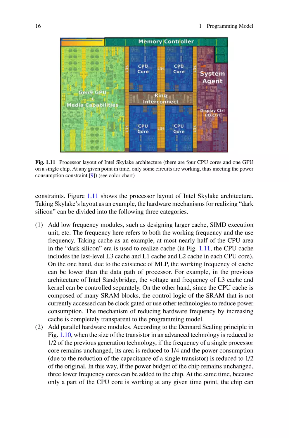
constraints. Figure 1.11 shows the processor layout of Intel Skylake architecture.
Taking Skylake’s layout as an example, the hardware mechanisms for realizing “dark
silicon” can be divided into the following three categories.
(1) Add low frequency modules, such as designing larger cache, SIMD execution
unit, etc. The frequency here refers to both the working frequency and the use
frequency. Taking cache as an example, at most nearly half of the CPU area
in the “dark silicon” era is used to realize cache (in Fig. 1.11, the CPU cache
includes the last-level L3 cache and L1 cache and L2 cache in each CPU core).
On the one hand, due to the existence of MLP, the working frequency of cache
can be lower than the data path of processor. For example, in the previous
architecture of Intel Sandybridge, the voltage and frequency of L3 cache and
kernel can be controlled separately. On the other hand, since the CPU cache is
composed of many SRAM blocks, the control logic of the SRAM that is not
currently accessed can be clock gated or use other technologies to reduce power
consumption. The mechanism of reducing hardware frequency by increasing
cache is completely transparent to the programming model.
(2) Add parallel hardware modules. According to the Dennard Scaling principle in
Fig. 1.10, when the size of the transistor in an advanced technology is reduced to
1/2 of the previous generation technology, if the frequency of a single processor
core remains unchanged, its area is reduced to 1/4 and the power consumption
(due to the reduction of the capacitance of a single transistor) is reduced to 1/2
of the original. In this way, if the power budget of the chip remains unchanged,
three lower frequency cores can be added to the chip. At the same time, because
only a part of the CPU core is working at any given time point, the chip can
1.3 Three Obstacles
17
close some cores through technologies such as clock gating and power gating
to further reduce power consumption. In reality, since 2005, x86 architecture
processors no longer focus on increasing the frequency of chips, but increasing
the number of processor cores on new chips. The BIG-LITTLE architecture
of ARM architecture places high-performance BIG core and energy-efficient
LITTLE core on one chip at the same time, making full use of the design space
brought by the parallel hardware module mechanism. However, to make full use
of the performance of the chip, application developers have to learn the skills of
multithreading programming. The parallel mechanism based on Multithreading
makes the performance of hardware difficult to be fully developed by application
developers.
(3) Specialized hardware. To ensure its generality, general-purpose processor will
have a lot of hardware redundancy. In 2010, a study on running H.264 decoding
on general-purpose processor [10] showed that the energy consumed by the
execution unit of general-purpose processor accounted for only 5% of the total
energy, and a large amount of energy was consumed in the fetch, decoding
and other modules of the processor. Therefore, designing specialized hardware modules on a chip according to the application requirements and then
constituting a heterogeneous system-on-chip (SoC) can greatly improve its
energy efficiency. The GPU integrated on the Skylake architecture processor
in Fig. 1.11 is customized for processing image rendering. In addition, SIMD
processing elements such as Intel SSE/AVX can also be regarded as specialized hardware. SIMD processing element uses a controller to control multiple
processing elements, and performs the same operation on each data in a group
of data vectors at the same time, so as to amortize the processor’s overhead of
fetching and decoding on this group of data vectors. Of course, SIMD units are
only suitable for scenarios where there is very regular data-level parallelism.
The popularity of specialized hardware and heterogeneous SoC has brought
about the “Babel Problem” of programming model: different specialized hardware modules need different programming models; when the same application
runs on different specialized hardware, it takes a lot of manpower to “translate”
the application.
Although the “power wall” problem did not stop the pace of Moore’s law, it
destroyed the RAM programming model on Von Neumann architecture. As chip
multi-processor (CMP) and heterogeneous architecture have gradually become the
mainstream hardware design methods, application developers are forced to face
parallel programming model and heterogeneous programming model.
The parallel programming model breaks the illusion of “single thread” in RAM
model, that is, physically, multiple cores need applications to provide thread-level
parallelism, and SIMD vector processing elements in a single core need applications to provide data-level parallelism. These impose higher requirements for application developers. Before the emergence of “power wall”, parallel programming
was a difficult knowledge for a few supercomputer application developers; after the
18
1 Programming Model
emergence of “power wall”, almost all application developers have to face the challenge of parallel programming. How to reduce the difficulty of parallel application
development has become the core issue of architecture, programming model and
programming language.
The heterogeneous programming model breaks the illusion of “single memory”
of RAM model, that is, the CPU-GPU heterogeneous architecture violates the mechanism of a single CPU facing a unique address space for the first time. Application
developers must start to consider how to efficiently migrate data between different
storage structures or address spaces. It is worth mentioning that the problems encountered by the scratchpad in the “memory wall” era, such as designing the ISA/API for
data movement across multiple address space and remapping virtual memory, which
are not friendly to application developers, have been partially solved by specialization
on the CPU-GPU system.
In addition, the interaction of multiple concurrent threads and multiple concurrent
banks will bring greater complexity. For example, when a single-chip multi-core
processor is combined with an on-chip multilevel cache storage system, different
processors on the chip may obtain inconsistent results when accessing data at the same
address because the timing of data update in different caches is inconsistent. These
problems are collectively called cache-consistency model problems, which greatly
affect the design of processor architecture, programming model and programming
language.
At the time of the collapse of existing programming models, emerging programming models are flourishing. Their characteristics are hard to sum up. Therefore,
this section will continue to use the example of inserting elements in circular queues
to trace the development direction of programming models in the era of “power
wall”. Specifically, this section will analyze how to ensure the order of “write data write flag” when inserting elements with thread-level parallel programming model,
cache-consistency model and heterogeneous programming model.
First, since the general-purpose processor turned to multi-core architecture,
programming models for developing thread-level parallelism have emerged. From
the early Pthread and OpenMP based on C language to the recent Golang and C++ 20
co-routine, almost all new routes have made a good commitment to solving the problems of multi-core parallel programming. Unfortunately, “there has been nothing
perfect since the olden days”. These new routes either fail to exploit the full potential
of a specific application scenario on a specific architecture (such as Java), or have a
very steep learning curve (such as C++).
Java is the most widely used parallel programming language at present. It is widely
used in enterprise web application development and mobile application development. One of the motives for Sun Microsystems to design Java in 1990 was that
the C language widely used at that time needed the help of platform related Pthread
or OpenMP libraries and lacked native support for multi-threaded features. Java
provides multithreading support at the language level by introducing keywords such
as synchronized when it was originally designed. For circular queues, application
developers can directly call the thread-safe queue provided in the Java library, or
1.3 Three Obstacles
19
they can carefully read the Java memory model and concurrency control primitives
to design a queue by themselves.
However, the performance problem of Java has been widely criticized. Many
language features of Java are to support cross-platform and full-scene development
(improve generality). At the same time, Java also provides a large number of libraries
to reduce the overhead of learning and debugging and improve development efficiency. For the thread-safe queue (java.util.concurrent.ArrayBlockingQueue) in the
Java library, the user only needs to directly call its add() function to complete the
operation of inserting elements, without considering the order relationship between
the above multiple reads and writes. However, to adapt to various queue application scenarios, ArrayBlockingQueue provides a general queue implementation that
supports “multiple-producer multiple-consumer”, that is, any number of threads can
insert elements concurrently, and any number of threads can take out elements concurrently. For other application scenarios, such as “single-producer single-consumer”
queue, although application developers can obtain higher performance through
simpler synchronization, calling ArrayBlockingQueue directly misses this opportunity. Research shows that compared with the native ArrayBlockingQueue, the queue
design for “single-producer single-consumer” in Java can improve the throughput
dozens of times. However, to achieve better performance, application developers
need to fully understand their own needs, Java memory model, operating system
thread scheduling mechanism, multiprocessor cache-consistency mechanism and so
on. It can be seen from this example that in the face of the problem of thread-level
parallel programming, Java gives priority to ensuring generality. At the same time,
application developers can choose between development efficiency and operation
efficiency according to their own needs.
Second, as the design of CMP architecture becomes more and more complex, hardware designers begin to try to open more and more hardware mechanisms directly
to application developers, expecting to make the hardware more effectively adapt
to the use scenario with the help of application developers. Among them, adding
std::memory_order to the standard library after C++ 11 allows application developers to independently determine the order relationship between multiple reads and
writes according to the multi-core cache-consistency model of the specific processor
platform. Due to the subtle differences among cache-consistency models of different
processor platforms, application developers need to understand the design details
of the processor when using it. Therefore, the learning cost and development difficulty of std::memory_order are very high. Next, taking the “write data - write flag”
sequence of circular queue insertion as an example, we will briefly introduce design
philosophy of std::memory_order.
Figure 1.12 shows a simplified on-chip dual core processor architecture. The two
processor cores exchange data through shared memory. Compared with Fig. 1.8,
the order of the two write operations is influenced by a new factor, in addition to
the reordering of instructions by the compiler and processor cores: under the action
of cache, even if processor core 0 (Core 0) and main memory complete two write
operations in the order of “write data - write flag”, processor core 1 (core 1) may
not observe the writing results in this order. Consider the two threads in Fig. 1.8.
20
Fig. 1.12 In the
cache-consistency model of
the on-chip multi-core
processor, it is necessary to
consider not only whether
the write order seen by the
main memory is consistent
with the processor core
initiating the write operation,
but also whether other
processor cores can observe
the same order
1 Programming Model
Write data
Write flag
Write data
Core 0
Core 1
Reorder buffer
Reorder buffer
Storage cache
Storage cache
L1 cache
L1 cache
Write flag
Main memory
Store writeback level
Storage: Write data
Write flag
Suppose Thread 0 runs on processor core 0 and Thread 1 runs on processor core
1. When processor core 0 executes I1 and I2 of Fig. 1.8, and Q [tail] and tail are
written respectively, the propagation speed of the two writes to processor core 1 may
be inconsistent. For example, I1 has a write loss when writing Q [tail], so it needs to
wait for the cache line where Q [tail] is located in main memory to be retrieved into
L1 cache, that is, hundreds of cycles; When the latter instruction I2 writes tail, L1
cache write hits will occur. At this point, should the latter write wait until the result
of the previous write can be observed by processor core 1 before writing to the L1
cache?
Different processor architectures have different answers to this question. The
cache-consistency model of processor architecture is to answer whether multiple
processor cores observe the same order of write operations, read operations and
atomic operations. Figure 1.13 shows several mainstream cache-consistency models.
In the figure, A–F represent multiple sequential memory accesses initiated by a
thread, including reads (e.g., B=), writes (e.g., =A), atomic acquire and atomic
release. The arrow between two memory accesses indicates that other processor
cores can definitely observe the order of these two accesses. “E=” and “F=” are two
write operations on one processor core. It can be seen that under the TSO model
represented by x86 instruction set architecture, all processor cores will observe a
completely consistent “write data - write flag” order. Application developers do not
need to consider the order of write access on X86 multi-core platform, which reduces
the difficulty of application development. However, all write accesses on the X86
platform must wait until the effect of the previous write access on the same thread can
be observed by all processor cores before they can be transmitted to other processor
cores. This severely limits the scalability of the processor core. To obtain better
scalability, the processor instruction set architectures proposed in recent years, such
as ARMv8 and RISC-V all adopt the released consistency model. As can be seen from
Fig. 1.13, the released consistency model has no requirements for the propagation
order of two writes on a processor core. If the application developer has requirements
1.3 Three Obstacles
21
=A
=A
B=
B=
acquire (S);
C=
B=
acquire (S);
C=
=D
release (S);
F=
(a) Sequential
consistency
acquire (S);
=D
release (S);
release (S);
E=
(b) Total order
consistency
acquire (S);
(c) Partial order
consistency
acquire (S);
C=
=D
release (S);
E=
F=
=A
B=
C=
=D
F=
=A
B=
C=
E=
E=
=A
=D
release (S);
E=
F=
(d) Weak order
consistency
F=
(e) Released
consistency
Fig. 1.13 Several mainstream cache-consistency models [4]
for the propagation order of writing, it needs to rely on the programming language
or assembly language to explicitly call the atomic operation.
Similar to the volatile tag in C language, the C++ 11 standard library provides the
atomized variable library std::atomic. To enable programmers to fully tap the potential of instruction set architecture according to specific application scenarios during
cross-platform development, the standard library std::memory_order of C++ 11 adds
four types of attributes to the atomized memory access of variables, namely, relaxed
ordering, release-acquire ordering, release-consume ordering, and sequentiallyconsistent ordering. By default, the attribute of std::atomic is sequentially-consistent
ordering: multiple atomic read–write operations in a thread, as well as the order of
atomic read–write and normal read-write, it will maintain the original order when
propagating to other processor cores. By default, the sequentially-consistent ordering
std::atomic has exactly the same semantics as volatile tags in C language. The default
std::atomic is very easy to use, but there is a performance loss. For example, on RISCV, if the tail variable in Fig. 1.8 is declared as std::atomic, not only the write order
of Q [tail] and tail will be propagated in order (that is, the write of Q [tail] will wait
for other processors to see the write result of tail), but also the order between any
read–write operation and tail will be propagated in order.
std::memory_order can realize finer control of memory read–write order, as
shown in Fig. 1.14. The tail tag is declared as type std::atomic. std::atomic type
in C++ 11 can be read and written using the load()/store() function. The attribute
of std::memory_order can be specified during reading and writing. Figure 1.14 uses
22
1 Programming Model
Thread 0
Thread 1
I1: Q[tail] = 1;
I3: R1 = tail.load(std::memory_order_acquire);
I2: tail.store(1, std::memory_order_release);
I4: R2 = Q[R1];
If the write result of I2 is read by I3, I4 must be able to observe the write operation of I1
Fig. 1.14 Fine-grained control over the “write data - write flag” order using std::memory_order in
C++ 11
the release–acquire order: all read and write operations before the store () are not
allowed to be moved to be after the store (); all read and write operations after load
() are not allowed to be moved to be before this load (). In this way, if the value
written by I2 is successfully read by I3, all writes to memory before I2 in Thread 0
are visible to Thread 1 at this time.
It can be seen from this example that opening the mechanisms such as chip multiprocessor cache consistency directly to application developers who are very familiar
with the hardware architecture can fully tap the potential of hardware mechanisms in
specific application scenarios. Of course, on the one hand, the learning curve is steep;
on the other hand, the development cost is also very high, that is, when application
developers face the complexity of hardware mechanism, they need a lot of debugging
and verification to ensure the correct operation of real applications.
Third, after this turbulent period, the most significant change is that with the popularity of GPU, application developers begin to learn and adapt to the heterogeneous
programming model represented by CUDA. Under the constraint of “power wall”,
the improvement speed of CPU computing power is much slower than the growth of
data volume. In contrast, GPU saves a lot of overhead in the process of fetching and
decoding by specializing the data parallelism, so it can invest more power budget
in the design of improving computing power. Figure 1.15 shows the comparison of
single precision and double precision floating point peak computing power between
CPU and GPU in recent years. It can be seen that the gap between the peak computing
power of CPU and GPU is becoming larger.
Of course, for computing chips, it is not enough to only improve the peak performance. The key to the large-scale use of chips is to have suitable target applications
and programming methods. At present, the most important application on GPU is data
intensive application, and the most mainstream programming method is NVIDIA’s
CUDA programming language.
Due to the simplification of control logic, the current programming method of
GPGPU requires application developers to understand the details of the underlying
hardware mechanism. Although these cumbersome details will seriously affect the
work efficiency of application developers, most application developers still choose
to use GPU instead of CPU to obtain higher performance in the face of data intensive
applications. Specifically, application developers need to package 32 or 64 mutually independent threads (different architectures have different SIMD concurrency
requirements) into a lock-step thread group in the control flow, so as to amortize the
overheads of control logic such as fetching and decoding in multithreaded SIMD
1.3 Three Obstacles
23
Fig. 1.15 Comparison of floating-point peak computing power (GFLOPS/s) between CPU and
GPU [11] (see color chart)
processors; application developers should create as many thread groups as possible
for each multithreaded SIMD processor to hide the access delay of DRAM; and
they also need to keep or distribute data addresses in one or several memory blocks
to achieve the expected memory performance. At present, all GPU programming
models, including CUDA and OpenCL, have similar and steep programming method
learning curves. Overall, the GPGPU programming model sacrifices usability for
high energy efficiency.
Initially, CUDA was only used in areas where there were few and sophisticated
application developers such as scientific computing. These developers tend to pay
higher learning and development costs in exchange for better application execution
performance. Most ordinary application developers have no motivation or opportunity to learn CUDA. However, after 2012, the rise of deep learning applications represented by AlexNet [12] promoted the popularity of GPGPU programming methods
represented by CUDA among ordinary application developers.
The emerging big data processing applications represented by deep learning bring
massive data-level parallelism, which can make full use of the computing power of
GPU. This makes application developers willing to pay additional learning costs
and be familiar with various hardware mechanisms of GPGPU, so as to develop and
utilize the performance potential of GPGPU for data intensive applications. Today,
the GPGPU programming model represented by CUDA has been widely accepted.
More and more applications with high computing power have been customized and
tailored according to the requirements of GPGPU programming model, so as to
make full use of the high computing power of GPGPU. CUDA and OpenCL have
also become the most widely used programming methods in general data intensive
applications, and have been extended to FPGA, CGRA and other architectures for
data intensive applications [13].
24
1 Programming Model
Since the computational part of CUDA is neither suitable nor requiring to implement queues, this section will not discuss CUDA programming model in detail.
However, the process of CPU dispatching tasks to GPGPU is also carried out in the
form of task queue. With the evolution of GPU architecture, the implementation of
this task queue becomes more and more complex. The existing GPGPUs are vertically integrated in a way that the driver manages the task queue architecturally so
that the APIs for inserting elements and removing elements from the task queue can
be opened only to application developers and compiler designers.
Figure 1.16 shows the typical connection mode between GPU and CPU in heterogeneous system. It can be seen that the CPU is connected with the integrated GPU
through the internal interface of the processor (such as Intel cache consistency interface (CCI)), and connected with the discrete GPU through PCIe bus. Integrated GPUs
communicate with the CPU within the same chip with very low latency (about dozens
of to hundreds of nanoseconds (ns)), making it easy for integrated GPUs to maintain
cache consistency with the CPU. Discrete GPUs, on the other hand, communicate
with the CPU via PCIe with latency in the order of microseconds, making it difficult
to maintain cache consistency with the CPU. Therefore, the design consideration of
task queue under integrated graphics card is not much different from that of multicore processor; for discrete GPUs, we need to consider how to use the mechanism
of PCIe peripherals to improve the reading and writing efficiency of the queue.
For example, PCIe provides a doorbell mechanism to avoid frequent PCIe reads and
writes when the queue inserts elements. Application developers do not need to understand the details of PCIe or the difference between PCIe and the internal interface of
the processor. They only need to call the API related to task queue. The underlying
implementation details are entirely the responsibility of the architecture layer and
driver.
To sum up, GPGPU task queue greatly enhances its usability and execution
efficiency by sacrificing generality.
Fig. 1.16 Two methods for
connecting CPU and GPU in
a heterogeneous system
Core 0
Integrated GPU
Application
L1 cache
L3 cache
GPU on- chip
Cache
Consistent area
discrete Independent GPU
1.3 Three Obstacles
25
1.3.4 I/O Wall
Von Neumann architecture can be divided into three functional modules: memory,
processing unit, and peripherals. The previous two crises were caused by the
mismatch between memory speed and computing speed, and the mismatch between
computing power consumption and memory power consumption. In the past
computer textbooks, it has been emphasized that the speed of peripherals is much
slower than the computing speed. However, since around 2015, this dogma that has
lasted for decades has gradually lapsed. Today, the mismatch between peripheral
speed and computing/storage speed is forming a new “I/O wall”.
Figure 1.17 shows the change trend of bandwidth among hard disk, network,
and CPU-DRAM from 1995 to 2020. It can be seen that the network bandwidth
has increased rapidly after 2010; after 2015, the speed of hard disk has increased
rapidly. In the same period, the bandwidth growth rate of CPU-DRAM lags far
behind the growth rate of network and hard disk. There are two main reasons for
this phenomenon: (1) the successive emergence of “memory wall” and “power wall”
makes the growth rate of bandwidth of CPU-DRAM far behind the pace of Moore’s
Law. At present, the bandwidth of DDR interface of the mainstream CPU-DRAM
is doubled every 5–7 years; (2) the technological breakthrough of network and hard
disk in the physical layer has led to the explosive growth of their bandwidth. In the
first decade of the twenty-first century, the mainstream network transmission medium
is copper twisted pair, and the mainstream storage medium is disk. After 2010, the
optical communication module in the data center began to popularize. Compared
Hard disk bandwidth/device
Unlimited memory bandwidth
Network bandwidth/cable
DRAM bandwidth/CPU slot
Year
Fig. 1.17 Changes of hard disk, network, and DRAM bandwidth over time [14] (see color chart)
26
1 Programming Model
with the network card based on copper twisted pair, the bandwidth of a single fiber
network card increased rapidly from 1 to 10 Gbit/s. After 2015, solid state disk
(SSD) gradually replaced hard disk drive (HDD). Previous HDDs used mechanical
motors to address on the disk. Limited by the speed of the disk (about 15,000 r/min),
the bandwidth of a single HDD can only reach hundreds of megabytes per second.
However, with the development of flash technology, especially the progress of flash
sustainability, SSD began to replace HDD. The addressing process of SSD is similar
to DRAM, which is completely driven by electrical signals, so the bandwidth is no
longer limited by the addressing speed.
Since the growth rate of I/O bandwidth is far greater than that of CPU-DRAM
bandwidth, the classical Von Neumann architecture has been difficult to meet the
bandwidth requirements of peripherals, and emerging architecture designs have
spurted forth. For example, Intel has added data direct I/O (DDIO) technology to the
“Xeon” series processor product line for the data center, which can bypass DRAM
and allow peripherals (mainly network cards) to directly write data packets to the
LLC of the CPU. Although DDIO successfully bypassed the “memory wall” of CPU
access to DRAM and achieved commercial success, with the continuous growth of
the bandwidth of a single network card beyond Moore’s Law, the computing speed
of CPU is still difficult to keep up with the bandwidth requirements of the network
card. For example, for the mainstream 100 Gbit/s network card in the current data
center, if 64B network packets are used, the CPU needs to process one packet every
3.3 ns. The main frequency of a typical data center CPU is about 2 GHz, and the
latency to access LLC is about 5 ns (20 processor cycles). Therefore, the performance of mainstream CPUs in matching 100 Gbit/s NICs is already difficult to meet
the bandwidth demand of NICs; handling next-generation 400 Gbit/s NICs is far
from enough. In terms of storage, with SSD becoming the mainstream technology,
the storage bandwidth is completely limited by the I/O interface speed of CPU. At
present, the mainstream storage device interface adopts NVMe standard, which is
interconnected with CPU based on PCIe interface. With the popularity of PCIe Gen
5, it can be predicted that the computing speed of CPU is difficult to keep up with the
growth of memory bandwidth. The problem of “I/O wall” has increasingly become
a key bottleneck restricting the performance of computing system.
For the previous example of inserting elements into the circular queue, the emergence of “I/O wall” also brings new design space. At present, the Infiniband network
commonly used in high-performance computing provides remote direct memory
access (RDMA). RDMA allows the local CPU to directly read and write the remote
memory through the RDMA network card, bypassing the remote CPU, thus overcoming the obstruction of the “I/O wall” to a certain extent. However, the existing
RDMA support for memory read–write primitives is limited by the complexity of
the network card, including only read, write and atomic CAS (compare and swap)
operations. Moreover, the latency of RDMA is much larger than the memory access
latency, and the latency of end-to-end access is still much larger than 1 µs for the
lowest latency Infiniband network available. If RDMA is used to implement circular
queue insertion elements, considering that there may be multiple hosts reading and
writing to the queue at the same time, a “multiple-producer multiple-consumer”
1.3 Three Obstacles
0 us
27
1 us
2 us
3 us
Local application
Local NIC
Remote memory
2 us
Local application
Local NIC
RDMA
read
RDMA-based
network
Remote NIC
1 us
0 us
4 us
RDMA
CAS
Conflict
window
Atomic append via RDMA
Intelligent
2×
RDMA
read
network
CAS
Remote NIC
Read
Remote memory
2×write
Atomic append in a single back and forthround trip
Fig. 1.18 When using the existing read (), write () and CAS () atomic append in RDMA to implement circular queue insertion elements, it is necessary to communicate back and forth in the network
at least 3 times; using the new atomic append primitive requires only one round-trip communication
[15]
insertion operation needs to be supported::first check whether there is enough free
space in the queue, then modify the pointer atomically to allocate memory in the
queue, then write the data, and finally write the tag to make the data valid (at the
same time, it is necessary to detect whether the write is damaged). With RDMA, operations can only be performed on a remote page through a series of RDMA requests.
As shown in Fig. 1.18, RDMA read will first check the available space, then occupy
the position with atomic CAS operation, then send a request to write data, and finally
need to write flags. Overall, it will take at least 3 network round trips to complete
this operation (write data and write markers can share the same network packet), and
at least 5 µs for even the fastest networks today. Moreover, this latency is already
approaching the physical limit of the transmission of signals such as optoelectronics
in the medium, and is difficult to reduce as technology advances.
To solve the impact of network latency on the performance of remote circular
queue based on RDMA, academia began to explore adding more complex RDMA
primitives and reducing the number of request turnbacks. For the insert operation, an
optimization method is to add the “atomic append” primitive in RDMA, as shown in
Fig. 1.18. The local node sends the primitive of adding elements in the queue to the
remote node. The remote node is responsible for reading and writing this primitive
with local memory, so as to avoid frequent back and forth remote reading and writing
operations.
Today (2021), how to solve the problem of “I/O wall” is still an open question. The academia and industry have put forward a large number of research and
solutions. Most research and solutions are trying to make Von Neumann architecture more heterogeneous: add computing functions for network and memory, so as
to offload the original CPU computing to peripherals. The exploration in the two
directions of network and storage has been uniformly summarized by the academic
community as software-defined network/memory. Specifically, the software-defined
network offloads the network protocol stack, such as transport layer security (TLS)
protocol in TCP/IP protocol and some underlying data access APIs, to the intelligent
28
1 Programming Model
network card for computation; software-defined memory offloads some requirements
of the memory, such as logging, RAID, compression, etc., to the processing element
close to the memory for computation. The combination of software-defined network,
software-defined memory and SDCs will make a splash in the next decade.
1.4 Impossible Trinity
In Sect. 1.3, with the development of semiconductor technology, some hardware
mechanisms designed by Von Neumann architecture to solve the three obstacles of
“memory wall”, “power wall” and “I/O wall” are briefly introduced. Figure 1.19
roughly shows the evolution of the hardware architecture in response to the “three
high walls”. Overall, the hardware architecture is developing towards specialization
and parallelization.
Figure 1.20 is a summary of some hardware mechanisms involved in Sect. 1.3
and their advantages and disadvantages to programming. It can be seen that these
hardware mechanisms can be roughly divided into four categories according to their
effects:
(1) Some hardware mechanisms represented by cache are completely transparent
to the programming model. These hardware mechanisms are very friendly to
upper application developers and compiler designers, and are universal to most
applications. However, the power consumption/area overhead of these hardware mechanisms may be large, but most of them have entered the mainstream
architecture design.
(2) The cost for learning and developing some hardware mechanisms represented
by thread-level parallelism is very high. The premise of fully developing the
performance potential of these hardware mechanisms is that application developers should write programs according to the needs of applications and the
organization of hardware architecture. However, to excellent developers, these
I/O device
I/O device
I/O device
Accelerator
Accelerator
Cache
Cache
Cache
Memory
Main memory
Main memory
Main memory
Von Neumann
architecture
Memory wall
(1995 to present)
Power wall
(since 2005)
I/O wall
(2015 to present)
Fig. 1.19 Evolution of Von Neumann architecture to hardware specialization after encountering
“three high walls”
1.4 Impossible Trinity
29
Classification
Advantages
Disadvantages
a)
Completely transparent to the
programming model
High hardware overhead
High execution efficiency and
universal
High learning and
development costs
Hardware Mechanism
Multilevel cache
Instruction multi-issue
Thread-level parallelism
b)
Scratchpad
C++ std::memory_order
Multithreaded secure queue
container
c)
Easy to develop and universal
Not fully tap the potential
of architecture
d)
Easy to develop and high
execution efficiency
Poor compatibility
Instruction reordering
RDMA-based queue
GPU task queue
Fig. 1.20 Some hardware mechanisms of “memory wall”, “power wall” and I/O design and their
advantages and disadvantages for programming
hardware mechanisms usually have high performance and good application
generality. Some of these hardware mechanisms have been widely used after
their invention, such as a variety of atomic operation instructions; some have
become standard in subsequent hardware architectures as application developers have become more familiar with them years later, such as multithreading,
scratchpad, etc.; many more mechanisms have been forgotten in the archives
of history because they cannot be efficiently used by application developers.
Perhaps in the future, when facing new challenges, these hardware mechanisms
will be discovered and effectively utilized again from the old pile.
(3) Some hardware mechanisms represented by instruction reordering have high
requirements for compilation technology, and the existing compilation technology is difficult to develop the full performance potential of a specific application on a specific architecture. To fully develop the performance of this kind of
hardware, it is usually necessary for expert programmers to bypass the compiler
and write programs directly using assembly instructions. For example, SIMD
execution unit on x86 architecture requires application developers to directly
use SIMD instruction set to realize data-level parallelism of specific applications; the multi-port register file in GPU stream processor requires application
developers to distribute SIMT access requests on different ports according to the
access characteristics of specific applications. However, the existing compiler
technology is difficult to meet these needs, so that the performance obtained by
the average application developer using existing compilers will have a large gap
compared to that of expert programmers. It is worth noting that for a certain
hardware mechanism, the execution efficiency (or performance) of a programming model is poor, which means that for a series of applications, there is a
great gap between the performance obtained by using this programming model
and the performance obtained by the best programming model.
30
1 Programming Model
(4) The hardware mechanism represented by GPGPU task queue has poor compatibility, which is reflected in that it can only be used in specific applications on
specific architectures. This kind of mechanism is usually provided to application developers as several simple instructions or APIs, which is easy to learn. At
the same time, specialized design can give full play to the potential of a specific
architecture. Most of the domain-specific accelerators represented by Google
TPU adopt similar hardware mechanisms and programming models.
From the experience of existing programming models, we can summarize the
Impossible Trinity of programming model, that is, a new and effective programming
model cannot achieve high development efficiency (easy to use), high operation efficiency (high performance) and good generality at the same time. Figure 1.21 vividly
shows the Impossible Trinity in the form of “Impossible Triangle”: the programming model represented by CUDA has high performance and good generality, but
the development efficiency is low; the programming model represented by NumPy
is easy to use and universal, but its performance is low; the programming model
represented by TensorFlow has high performance and good usability, but the compatibility is poor (only applicable to deep learning). These three types of programming
models in turn correspond to the complex hardware mechanism that is difficult to
completely hide the programming model to be solved by application developers,
compiler designers and architecture designers, as shown in Fig. 1.22.
It should be noted that although the three types of programming models in Fig. 1.21
are fixed on the three vertices of the triangle, in fact, these programming models are
Fig. 1.21 Impossible Trinity of programming model
Fig. 1.22 Causes of
Impossible Trinity: how to
deal with the hardware
mechanism that is difficult to
completely hide
Modern computing hierarchy
Application
Programming
language
class A{
private a;
public b;
…}
JAVA
def say():
a=
1.5 Three Types of Exploration
Fig. 1.23 Typical hardware
mechanisms are ordered
according to the difficulty of
hiding
31
Parallelism
Easy to hide
Hard to hide
Instruction-level parallelism
Pipeline parallelism
Memory level parallelism
Predictive parallelism
Data-level parallelism
Thread-level parallelism
Spatial domain parallelism
Specialization
Heterogeneous SOC
Domain accelerator
Near-data processing
Scratchpad
non-polarized and evolving all the time. First, in reality, programming models are
often located inside triangles, biased to a vertex or an edge. For example, CUDA loses
generality to some extent, but it is not extremely difficult to develop. Programming
models that are widely used need to find a compromise between the three goals.
Secondly, the programming model has been evolving. For example, the earliest
CUDA has poor generality and is only suitable for graphics rendering and some
scientific computing applications. With the gradual addition of new mechanisms
such as unified address space in CUDA by NVIDIA, and the wide application of
deep learning in machine learning applications, CUDA has become more and more
universal.
Figure 1.23 shows typical parallelism and specialized hardware mechanisms,
ordered by the difficulty of hiding the programming model. Among them, datalevel parallelism, spatial domain parallelism and scratchpad, which are difficult to
hide, are common hardware mechanisms in SDCs, making programmability one of
the most important challenges of SDCs.
1.5 Three Types of Exploration
According to the “Impossible Trinity”, how to make application developers make
more effective use of the newly added hardware mechanism should be considered in
the programming model design of SDCs in combination with the existing programming model. The most important new hardware mechanism in SDCs is spatial domain
parallelism. Therefore, combined with the application field, this section will first
discuss the similarities and differences between spatial domain parallelism and the
existing hardware mechanisms such as thread-level parallelism, data-level parallelism and data flow parallelism from the perspective of application. Specifically,
compared with other parallelism, spatial domain parallelism can execute applications with irregular memory access and irregular control flow more efficiently.
Starting from the existing programming model that can develop spatial domain parallelism, this section explores how to add support for spatial domain parallelism to the
existing SDC programming model from three directions according to the “Impossible
Trinity”.
32
1 Programming Model
1.5.1 Spatial Domain Parallelism and Irregular Application
Irregular applications generally refer to the applications in the fields of sparse matrix
algebra and graph computing, as well as the applications using nonlinear data structures such as trees and sets. Many practical problems belong to irregular applications.
For example, the collaborative filtering problem in machine learning and Bayesian
Graph model belong to graph computing; cluster analysis methods such as K-means
algorithm in data mining need set structure; relational database uses B+ tree data
structure to implement index. Among the 13 classifications of algorithm space given
by the University of California, Berkeley [16], only two types of algorithms (dense
linear algebra and spectral analysis) have almost no irregular parts, while the irregular parts of four types of algorithms (unstructured mesh, combinatorial logic, finite
state machine, and alternation and backtracking) dominate.
Spatial domain parallelism has the potential to deal with various irregularities.
To illustrate this point, this book will first classify the irregularity in applications
with reference to existing research [17], and then point out the potential advantages
of SDCs in dealing with irregular applications by comparing SDCs with current
mainstream accelerators GPGPU and ASIC [18].
The first type of irregularity is the control dependence introduced by
complex control flow. In C language, it is represented by branch statements,
bounded/unbounded loops, sub function calls and so on. Because the control dependence expressed by control flow determines the actual execution order of statements,
complex control flow will lead to the serial execution of statements. In addition, the
statements between different branches generated by control flow often need to be
mutually exclusive, which is difficult to be executed at the same time. Therefore, once
the complex control flow appears in the application, it is often difficult to achieve
efficient parallelization.
The second type of irregularity is the runtime dependencies introduced by shared
data structures. Many common data structures, such as trees and graphs, will introduce shared data involving irregular access into the algorithm. The concurrency
of these accesses needs to be determined according to the specific access address
at run time, but cannot be determined at compile time. The mainstream parallel
programming methods under Von Neumann architecture provide a variety of synchronization primitives based on parallel random access machine (PRAM) to solve this
problem, such as locks, semaphores and so on. These synchronization primitives are
customized for the shared memory model. It is much more difficult to implement them
on SDCs based on non-Von Neumann architecture than a general-purpose processor.
At the same time, it is difficult for the compiler to schedule and prefetch data at
compile time due to uncertain dependencies. This will result in a large delay in the
chip’s access to irregular data. Therefore, how to achieve irregular access to shared
data without relying on PRAM model synchronization primitives and effectively
hide access latency is the key to solve this kind of irregularity.
In most irregular applications, these two kinds of irregularity coexist. For example,
in the field of graph computing, to access the dynamic graph data structure, it is often
1.5 Three Types of Exploration
33
necessary to use nested unbounded loops to traverse the vertex of the graph in the
program; in the field of branch and backtracking algorithm, the branches not entered
are generally saved in a shared stack to temporarily store the previous branch results
for backtracking. Therefore, to deal with irregular applications, we need to consider
the implementation of these two kinds of irregularity at the same time.
At present, the two most popular emerging hardware architectures are GPGPU
based on SIMT computing paradigm and neural network accelerator based on data
flow computing paradigm. These two kinds of hardware architectures make use
of the flexibilities in time domain and spatial domain respectively, and achieve a
good speedup effect in the application of rules. Figure 1.24 shows how to extend
a sequential thread on a general-purpose processor (the color from light to dark
indicates the sequence of operations in the thread) to the parallel implementation
under SIMT paradigm and data flow paradigm. In SIMT paradigm, a thread is copied
and allocated to a large number of parallel computing resources provided by GPGPU
in space. Because all threads are controlled by the same instruction flow, concurrent
computing resources do not bring additional fetching and decoding operations, so it
obtains higher energy efficiency than general-purpose processors. In addition, under
the data flow paradigm, spatial computing resources correspond to each operation in
the thread in turn, and then form a spatial pipeline. When there is no dependence on
the data between different threads, the data corresponding to each thread is sent to
the pipeline in turn according to the compiler’s scheduling. Each level in the pipeline
is activated when the data arrives, which completely avoids the additional fetching
and decoding overhead of the general-purpose processor.
When there is complex control flow in the task, the single instruction flow in
the spatial domain of SIMT paradigm will lead to a waste of computing resources,
and the data flow paradigm can convert the control flow into data flow and integrate
it freely into the spatial-domain pipeline. Figure 1.25 illustrates this situation by
taking a branch statement as an example. In the SIMT paradigm, since there is
only one instruction flow in the spatial domain that controls the execution of all
threads, the instruction flow must first control all threads to execute the first branch,
and then control all threads to execute the second branch. When different threads
execute branch statements and enter different branches respectively, each thread still
executes the first branch and the second branch successively under the control of
Spatial
Single Single instruction, multiple
threads SIMT
thread
Data flow
Dataflow
Time
Fig. 1.24 Parallelizing a
regular single threaded
program using SIMT
computing paradigm and
data flow computing
paradigm (see color chart)
ě ě
ě ě
34
1 Programming Model
Spatial
Fig. 1.25 Parallelism of
branch statements (if else) in
tasks under SIMT paradigm
and data flow paradigm (see
color chart)
Data flow
Dataflow
Time
Single Single instruction, multiple
threads SIMT
thread
a single instruction flow, while each thread only needs to execute one branch on a
general-purpose processor. Since SIMT paradigm is not free in spatial domain, it will
waste a lot of computing resources on unnecessary branches when executing complex
control flow, especially when there are nested branch statements in the application.
The judgment results of branch statements in the data flow paradigm are transmitted
to the next level computing unit as the data in the pipeline, and different branches
correspond to different computing units in space. When a branch is selected for the
data corresponding to a thread, only the computing unit corresponding to the branch
is activated by the data flow of the thread. Therefore, the data flow paradigm uses
its flexibility of computing resources in spatial domain to avoid wasting computing
resources on unnecessary branches.
When there are runtime dependencies in the task, the SIMT paradigm can hide
the access delay through fast thread switching in the time domain, and the pipeline of
the data flow paradigm can continue to execute only after all potential dependencies
in the time domain are solved. Figure 1.26 illustrates this situation. In the data flow
paradigm, once the compiler finds that there is a dependence between the two stages
of the pipeline that cannot be solved by the compiler, even if the dependence does not
exist at run time (for example, two threads read and write two addresses successively
through pointers. If the compiler cannot confirm that the two addresses must be
different, it must assume that there is a dependence between these reads and writes to
ensure correctness), the next stage in the pipeline still needs to wait for all operations
of the previous stage to complete before execution. Since the data flow paradigm is
not free in the time domain, its corresponding pipeline must wait for all dependencies
to be resolved in the time domain before it can continue to run. SIMT paradigm has
similar flexibilities to general-purpose processor in time domain. It can solve some
runtime dependencies by using the synchronization primitives under the PRAM
model. At the same time, the GPGPU supports the cheap switching of threads. Once
the data required by one group of threads to continue computing is not ready, the
computing resources can quickly switch to another group of threads to continue
computing under the control of the instruction flow until all the data of this group
of threads are ready. Therefore, SIMT paradigm uses its flexibility of computing
resources in time domain to hide the access delay of shared data, and simplifies the
1.5 Three Types of Exploration
Spatial
Single Single instruction, multiple
threads SIMT
thread
Data flow
Dataflow
Time
Fig. 1.26 Parallelism of
runtime dependencies in
tasks under SIMT paradigm
and data flow paradigm (see
color chart)
35
programming of shared data structure by supporting some PRAM synchronization
primitives.
The SDCs based on reconfigurable computing paradigm has the characteristics
of “array computing and function reconfiguration”. It is manifested in the parallel
execution of multiple PEs and interconnect in spatial domain and continuous and
rapid reconfiguration of array functions in time domain. Figure 1.27 shows the flexibilities of the SDCs in time domain and spatial domain by taking the mapping results
of eight regular cycles of three operations on the SDCs as an example. To simplify
the discussion, it is assumed that there are only four processing elements (PEs) on
the SDC architecture, and only one feasible mapping of the loop on the four PEs
is shown here. Since each PE and the interconnect between PEs are specified by
the configuration information at run time, the function of SDCs in spatial domain is
very flexible. To reduce the times of reading and loading configuration information,
a mapping method of spatial pipeline similar to data flow paradigm is adopted in
Fig. 1.27 to make the data in the loop flow between PE1–PE3 and PE2–PE4 respectively. Also, since the functions of each PE and interconnect can be reconfigured at
run time, PE1 and PE2 at the upstream of the pipeline in Fig. 1.27 are reconfigured
into the third operation in the loop after completing the first operation. This not only
ensures that the loop can be unrolled on computing resources, but also avoids the
limitation of computing resources.
As can be seen from the example in Fig. 1.27, the SDCs have both flexibilities
in time domain and spatial domain. Therefore, there may be a design scheme to
solve the above two kinds of irregularities on the SDCs at the same time, so as
to expand the application field that the SDCs can support to irregular applications.
Of course, SDCs are not without shortcomings. Compared with the free switching
of instructions in the time domain of SIMT paradigm, SDCs are more expensive
to reconfigure and need to avoid frequent switching; compared with the free data
transmission mode in the spatial domain of the data flow paradigm, the SDCs needs
to sacrifice a certain data transmission flexibility to control the reconfigurable data
transmission cost. The specific implementation of the flexibility of the SDCs in time
domain and spatial domain still needs to be carefully weighed according to the target
application field.
36
1 Programming Model
Fig. 1.27 Flexibilities of reconfigurable computing paradigm in time domain and spatial domain
(see color chart)
Table 1.2 summarizes the expected results of the SDCs compared to the SIMT
paradigm and the data flow paradigm in dealing with the two types of irregularities. The SDC paradigm is relatively free in both the time and spatial domains and
can handle irregular applications that are difficult to be addressed by other types of
parallelism. This is both its strength and the source of the problems it faces. The flexibility of a processor is not determined by what applications its architecture has the
potential to execute, but by what applications programmers can develop on the architecture. When designing any new feature on hardware architecture, it is important
to consider how the programmer will use it. To achieve collaborative optimization
in time domain and spatial domain, it is bound to design a new programming model
based on the original programming model.
Table 1.2 Expected results of the SDCs compared to the SIMT paradigm and the data flow
paradigm in dealing with two types of irregularities
Irregularity
Complex control flow
SIMT paradigm
Spatial domain is not flexible
Time domain is free
Computing resources are wasted on Multiple groups of threads freely
unnecessary branches
switch to hide data access latency
Runtime dependence
Data flow paradigm Spatial domain is flexible
Control flow flows freely in spatial
pipeline
Time domain is not free
Computing resources need to wait
for all dependencies to be resolved
SDCs
Time domain is relatively free
Reconfiguration in the time domain
mitigates the impact of data latency
Spatial domain is relatively flexible
Control flow is converted into data
flow in spatial domain
1.5 Three Types of Exploration
37
1.5.2 Programming Model of Spatial Domain Parallelism
At present, the hardware architecture and programming model design of spatial
domain parallelism are still evolving rapidly. There is no conclusion about the architecture design of spatial domain parallelism in industry and academia. Dynamic data
flow architecture, FPGA, CGRA, TIA, and other architectures are considered to be
suitable for spatial domain parallelism. From this section, starting from the most
widely used FPGA programming model, we explore the programming method of
spatial domain parallelism.
(1) Exploration of sacrificing the generality
On the road of sacrificing generality, hardware mechanisms such as spatial domain
parallelism are mainly handled by architecture designers. Application developers
describe their requirements in the form of domain-specific library or domain-specific
language. Each application has its own unique problems. Taking the sparse linear
algebra field represented by sparse matrix–vector multiplication as an example, this
section briefly introduces the design considerations of programming model at the
expense of generality. For the design methods of programming models in other
application fields, such as graph computing, artificial intelligence, etc., refer to
Chap. 4.
Sparse matrix–vector multiplication (SpMV) means that sparse matrix A is
multiplied by vector x to obtain another vector y, as follows:
y = Ax
(1.1)
where matrix A is m × n sparse matrix; X is the n-dimensional vector to be multiplied; y is the m-dimensional result vector. Sparse matrix was first proposed in the
1960s to make full use of sparsity when solving linear equations. It can better solve
some problems that cannot be solved by dense matrix [4]. There is no strict mathematical quantitative definition of sparse matrix, but it usually refers to a matrix
with a large number of elements of zero. The most significant application of sparse
matrix is using the iterative method to solve sparse linear equations. In the iterative
method, the computation of SpMV takes the longest time. Studies have shown that the
computation of SpMV takes the longest time, accounting for more than 75% of the
total computation time, in solving large-scale systems of linear equations using the
indirect method [19]. In addition, the computation of convolution in neural networks
can usually be converted into matrix multiplication operations, which in turn consist
of a series of matrix vector multiplication operations. Therefore, the convolutional
operations in sparse neural networks can be finally converted into solving SpMV as
well. Therefore, it is very necessary to accelerate SpMV algorithm.
For bandwidth constrained applications such as SpMV, bandwidth utilization (BU)
is generally used as the performance evaluation metric, which is defined as GFLOPS
per unit bandwidth. However, due to the irregular control flow and data memory
access mode of sparse matrix vector multiplication, the computation and memory
38
1 Programming Model
access cannot be well adapted in the traditional Von Neumann architecture. This
leads to low utilization of processing elements and bandwidth, which is only 0.1–
10% of the peak performance. With the progress of semiconductor manufacturing
technology, reconfigurable computing paradigm-based FPGA has developed into
a high-performance computing platform with highly parallel computing and deep
pipeline resources, and is increasingly used in various servers to accelerate large
parallel applications. Moreover, due to the reconfigurability of hardware, FPGA can
be reprogrammed to perform new types of computing tasks, so as to meet the everchanging needs of a wide range of industries. As a large-scale parallel application,
the research on the implementation and optimization of SpMV on FPGA has become
a hot spot in the field of scientific research and engineering.
Although FPGAs can accelerate SpMV well with their abundant parallel
computing resources, the performance degrades when the size of the matrix exceeds
the capacity of FPGA on-chip storage resources. In other words, FPGA alone cannot
solve the large-scale SpMV problem. At present, the mainstream sparse matrix
expressions include compressed sparse row (CSR) and coordinate (COO), which
are designed for Von Neumann architecture. On FPGA, sparse matrix operations
can be efficiently implemented through the computational mode of spatial-domain
pipeline. The existing expression forms have a large amount of redundant information in this mode, which leads to the waste of memory bandwidth. The spatial-domain
pipeline computing mode based on reconfigurable computing paradigm is adopted to
design a new sparse matrix expression, which is expected to improve the bandwidth
utilization of FPGA in processing sparse matrix applications.
Sparse matrix contains a large number of zero elements. To save storage space and
reduce the redundant computation of zero elements, compressed storage is usually
used. The storage format of sparse matrix is also closely related to the performance
of sparse matrix vector multiplication. Therefore, many studies start from the optimization of storage format of sparse matrix to improve the performance of SpMV. At
present, the commonly used storage formats are COO, CSR and compressed sparse
column (CSC).
COO format is a triplet format, that is, the format consists of three arrays. These
three arrays are val, row_idx and col_idx, which stores the numerical value, row index
and column index of non-zero elements in the sparse matrix respectively. Generally
speaking, the non-zero elements of a sparse matrix are stored in these three arrays
in order from left to right and from top to bottom. However, since the COO format
records the value, row index and column index of each non-zero element, the nonzero elements are independent of each other and can be stored in any order. Compared
with the storage method of dense matrix, COO format can save a lot of storage space.
In the compressed storage format, the COO format is relatively flexible, but compared
with the storage methods described below, the storage space is not optimal.
COO records a lot of information, and is not very efficient for accessing specific
elements because of its unordered arrangement, and the storage space is still large.
Therefore, researchers have proposed a further compression format, namely CSR
format. CSR format is also composed of three arrays, but the elements in the array are
not linear one-to-one correspondence. The three arrays are val, col_idx and row_ptr.
1.5 Three Types of Exploration
39
Where, val and col_idx array, like the COO format, stores the values and column
indices of non-zero elements in the sparse matrix respectively, but the order of storing
the matrix here can only be from left to right and from top to bottom, that is, it is
stored in the order of row priority. The third array row_ptr stores the offset of the first
non-zero element of each row in val and col_idx, that is, row_ptr [i] is the position
of the first non-zero element in row i of the sparse matrix in val and col_idx array.
The size of the row_ptr array is usually N + 1, where N is the number of rows of
the matrix. The last element of row_ptr is the total number of non-zero elements
of sparse matrix. Corresponding to CSR compression by row, there is also a CSC
format compressed by column.
Compared with COO format, although the elements of the three arrays in CSR
and CSC format do not correspond linearly one-to-one, they store more concise
information, save more storage space, and access specific element values faster.
CSR and CSC are the most common compression storage formats at present. For
example, CSC format is used to store sparse matrix in MATLAB.
At present, the problems about SpMV performance mainly come from the
following challenges:
(1) Irregular memory access. Since sparse matrices are usually compressed, the
access to vector x is usually irregular. Taking CSR storage format as an example,
the access address to vector x is col_idx array elements, so the elements of each
col_idx array must be loaded into memory first and then used as the address
of the access vector x. This indirect access directly leads to irregular access to
vector x, and finally affects the computational performance of SpMV.
(2) Load imbalance. Since the number of non-zero elements in each row or column
of the sparse matrix is not the same, the size of the data set to be accumulated
in different rows and columns is not the same when computing partial multiply
accumulate. This leads to the load imbalance of PEs responsible for different
rows, resulting in a situation where the PEs responsible for fewer data sets are
computed first and are in an idle waiting state, reducing the overall computational
efficiency.
(3) Large-scale matrix problem. Many current designs, which rely on the on-chip
storage resources of FPGAs, eliminate the problem of irregular memory access
by caching vector x or intermediate results in block random access memory
(BRAM) on the FPGA. However, when the matrix size increases beyond the
FPGA on-chip memory capacity, these designs become powerless. Although
most designs choose to use the block strategy for processing, blocking will
cause the intermediate results to move back and forth between the on-chip
memory and off-chip memory of FPGA, increase the amount of data memory
access, and ultimately affect the overall performance. Moreover, blocking will
also bring the problem of zero rows or short rows, which will also affect the
performance.
(4) Zero row or short row problem. Zero row or short row means that the number of
non-zero elements contained in some rows of the sparse matrix is zero or very
small. Short rows can lead to the need for zero-padding in some PEs, resulting
40
1 Programming Model
in idling, which has a great impact on performance. Zero rows are generally
generated in the process of sparse matrix blocking, requiring additional circuits
and more complex control to eliminate them, which improves the difficulty and
complexity of the design.
To solve these problems, this book designs a heterogeneous accelerator suitable for SpMV according to the characteristics of CPU-FPGA heterogeneous platform. The irregular access operation is executed on the CPU side and the irregular
control flow part is executed on the FPGA side, thus enabling the whole design
to achieve high bandwidth non-blocking computation with much higher bandwidth
utilization. Firstly, a new storage format of sparse matrix adapted to CPU-FPGA
architecture, namely coordinated compressed column (CCC) format, is introduced,
and compared with common storage formats. Among them, the memory accesses
of different formats are compared, because this factor directly affects the performance of bandwidth constrained applications. Then, the overall design framework
of SpMV accelerator is proposed, and then the data acquisition algorithm at the
CPU end is introduced. The algorithm can ensure that the data at the FPGA end
will not conflict, so the computation can be performed without blocking. Finally, the
hardware implementation of FPGA data flow is described.
As the name suggests, CCC format is a combination of COO format and CSC
format, and consists of three arrays. Firstly, the matrix is partitioned according to
the threshold (where the threshold is the amount related to the computing resources
at the FPGA side), that is, the number of matrix rows contained in a partition is
threshold (the part less than the threshold row is classified as a partition), as shown in
Fig. 1.28. With partition as the unit, data is stored in each partition in a manner similar
to CSC, that is, in the order of column priority from top to bottom and from left to
right, but different from the three arrays in CSC format, the three arrays of CCC are
the same as COO, namely val, row_idx and col_idx stores the value, row index and
column index of non-zero elements respectively. The advantage of this is that the
linear characteristic of non-zero array is retained, so that the corresponding elements
of vector x can be well used to replace col_idx in CCC format when CPU assembles
data. In this way, the data transmitted from CPU to FPGA is more conducive to
SpMV computation. Assuming that the threshold is 2, the CCC format of the sparse
matrix A in Fig. 1.28, again as an example, is shown in Fig. 1.29 [20].
After the CCC format is adopted, the data can flow to the processing unit at the
FPGA end without blocking. The computation process of the whole design is roughly
Fig. 1.28 Sparse matrix
after one partition
0
1
2
3
4
5
0
1
0
0
2
0
3
1
0
4
5
0
0
0
2
0
0
6
0
7
0
3
8
0
0
0
9
a
4
0
0
0
b
c
0
5
d
0
e
0
0
f
Partition_0
Partition_1
Partition_2
1.5 Three Types of Exploration
41
Fig. 1.29 Sparse matrix in
Fig. 1.28 in CCC format
as follows: firstly, the CPU loads the matrix data and uses the corresponding x vector
element to replace the column index information in CCC format. Then, the value, the
row index, and the corresponding x vector elements of the matrix flow to the FPGA
side to perform data flow processing. The computing cycle is based on one partition.
The computing of the next partition will not begin until all non-zero elements in the
partition being processed are computed. Since the products of non-zero elements
from the same row need to be accumulated together, the non-zero elements of the
same row need to be marked (here is the row index), which is represented by tokens
in FPGA. In this way, the irregular memory address access is executed on the CPU,
while the irregular control part, namely token comparison and reduction operation,
is executed on the FPGA.
Based on the characteristics of CPU-FPGA heterogeneous architecture and the
proposed CCC format, the whole SpMV accelerator is designed. The overall design
idea is to load the irregular data access part into the CPU, and the irregular control flow
part is executed on the FPGA. On the CPU side, to make better use of data locality,
the column priority access mode of CCC format is adopted for sparse matrix, so that
the access to x vector elements is sequential. At the FPGA end, the computation
units of multiplication and accumulation are separated. The multiplier computes the
product of matrix non-zero elements and x vector in the order of column priority, and
the accumulator is responsible for accumulating non-zero elements from the same
row. Due to the limited resources at the FPGA end, the computing resources of the
accumulator are limited. Therefore, the number of accumulators is called threshold.
At the same time, there can only be non-zero elements of the threshold row for
multiplication and accumulation, which requires that the CPU side can only take
the elements of the threshold row when extracting data. Therefore, unlike the CSC
format, which spans all rows according to column priority, only threshold rows can
be crossed here. This also explains the basis of the previous CCC format partition
threshold.
In this way, the computation of the whole system is divided as follows: the CPU
first converts the original sparse matrix into CCC format, and then takes out the nonzero elements in CCC format and the elements of corresponding vector x to form a
transaction. The transaction is transmitted to the FPGA side through shared memory.
Once the FPGA side reads the data, it immediately performs the computation. After
computing a partition, it sends the result back to the CPU. On CPU-FPGA heterogeneous platforms with shared memory, a transaction generally corresponds to a cache
line. The whole execution process can be completely pipelined without blocking, so
the bandwidth utilization is very high. The execution process of the whole system is
shown in Fig. 1.30.
42
1 Programming Model
FPGA end
CPU end
Shared memory
Initial
sparse
matrix
Format
Vector
x
FPGA
write
Result
vector y
Conversion
Cacheline 1
CCC
Storage
matrix
………
Cacheline n
FPGA
read
SpMV
computing
kernel
Fig. 1.30 Overall design architecture of SpMV accelerator customized for spatial-domain pipeline
Specifically, the workflow of this design can be summarized into the following
three steps:
(1) Format conversion. Format conversion is mainly to convert the storage format
of sparse matrix from the original format (such as COO, CSR, or CSC) to CCC
format.
(2) Data extraction. In this step, the CPU assembles the sparse matrix and vector x in
CCC format into a transaction according to the data acquisition algorithm, writes
it to the shared memory, and then transmits it to FPGA. To achieve non-blocking
data flow computation at the FPGA side, the matrix non-zero data in the cache
line read by the FPGA every cycle must come from different rows so that the
partial products do not flow to the same accumulator after the computation of
multiplication, thus avoiding the blocking caused by data conflicts. Therefore,
this book designs a data extraction algorithm on the CPU side, which can filter
out the data from the same row when extracting data on the CPU side.
(3) Computation execution. This step performs the main multiplication and addition
operation of SpMV. Once the FPGA side reads the data, it starts to execute
immediately. This process is completely deep pipelined and can fully utilize
data and pipeline parallelism. According to the above discussion, to meet the
requirements of pipelined non-blocking execution, the number of accumulators
at the FPGA end must be equal to the threshold of partition in CCC format.
Intuitively, it’s better for a smaller threshold, because the larger the threshold,
the more accumulator resources are required. However, the threshold cannot
be too small, which is mainly due to two considerations. On the one hand,
there must be enough non-zero elements from different rows assembled into
a cache line, so that the CPU can effectively fetch data. On the other hand, a
larger threshold means that the data in a transaction has a greater probability
of coming from different rows, which requires less filling of invalid elements,
which is very beneficial to the CPU data extraction algorithm. See the following
1.5 Three Types of Exploration
43
contents for the data extraction algorithm. Therefore, in the design of this book,
various factors are weighed, and the value of threshold is set to 32.
According to the above discussion, each accumulator at the FPGA end is responsible for the product accumulation of non-zero elements from the same row. If two
or more non-zero elements in a cache line come from the same row, data conflict will
occur because they will flow to the same accumulator in the same clock cycle. There
are two ways to resolve this data conflict. The first method is to design a buffer to
cache the data causing data conflict. However, this method will cause congestion and
waiting, which will affect the throughput between CPU and FPGA and is incompatible with the goal of non-blocking execution. More seriously, in extreme cases, all
non-zero elements need to be cached, which is obviously not conducive to design.
Another method is to ensure that the data in the same transaction comes from the
same row through a specific algorithm when extracting data from the CPU. The data
extraction process continues until all non-zero elements are sent to the FPGA end.
After the FPGA side reads the data transmitted from the CPU side, it immediately starts to perform multiplication and addition operation. On the FPGA side, the
whole hardware implementation mainly includes three units, that is, the PE_MULT
responsible for multiplication computation, PE_MUX responsible for data flow and
PE_REDUCE responsible for accumulation reduction, as shown in Fig. 1.31. Since
a cache line contains three combined pairs from val, row_idx array and vector x
elements, the number of multipliers is set to 3. It is worth noting that more multipliers will not bring additional performance improvement, because FPGA is a data
flow execution mode. As long as there is data, it can process all the data immediately.
After receiving the computation start signal at the FPGA end, first, the three elements
of val array and the corresponding vector x element flow to the multiplier to perform
multiplication, and the corresponding row_idx array elements are used as PE_MUX
gating signal. The output of the multiplier then flows to the PE_MUX unit, which
is connected to 32 accumulators, each of which is responsible for the accumulation of parts from the same row of non-zero elements. For each clock cycle, three
outputs from the PE_MULT unit flow to the PE_MUX unit. According to the row
index information, data from PE_MUX will flow to the corresponding accumulator
circuit. When the CPU fetches data, an identification signal will be set at the end of
each partition to indicate the end of the partition. Therefore, once the accumulator
circuit detects the identification signal, it ends the accumulation of this section of
data and generates an output result. Then, in the next clock cycle, the accumulator
starts to accumulate the product of the data of the next partition.
To evaluate the performance of the heterogeneous domain-specific accelerator,
the target platform selected for the experiment is Intel HARP-2. HARP-2 is an
experimental server with shared memory CPU-FPGA heterogeneous architecture. It
integrates CPU and FPGA in one chip, so that the interconnection bandwidth between
them is higher and the delay is lower.
This book implements the whole design on the HARP-2 platform [21]. The
comprehensive resource utilization is shown in Table 1.3. It can be seen that the
whole design uses less than 40% of the logic resources on the FPGA and very few
44
1 Programming Model
PE_MULT unit
Cache
line
from
CPU
PE_MUX unit
PE_REDUCE unit
val(0)
x(0)
Multiplier 0
Reduction
circuit 0
val(1)
x(1)
Multiplier 1
Reduction
circuit 1
...
...
………
………
val(k)
x(k)
Multiplier k
Reduction
circuit k
MUX
circuit
Subset
of
result
vector
y
row_idx(0), row_idx(1),…,
row_idx(k)
Fig. 1.31 Overall framework of SpMV computing kernel at FPGA end
DSP computing resources (less than 1%, because it is limited by the system bandwidth between CPU and FPGA). If the bandwidth increases, then the design is easily
scalable by simply adding more multipliers, multiplexers, and accumulators, and
there are enough resources left on the FPGA to meet this demand. Therefore, this
design has strong scalability.
For computing applications, the performance of the design is generally measured
by the number of operations performed per unit time. Since the problem under study
is a double-precision floating point SpMV, the absolute performance of the design
can be measured in terms of the number of floating-point operations per unit of time,
i.e., GFLOPS. In SpMV computation, a total of Nz floating point multiplication operations (non-zero, that is, the number of non-zero elements in the sparse matrix) and
about Nz floating point addition operations are performed. Therefore, the GFLOPS
computation is expressed as 2Nz divided by the total computation time T, i.e.
GFLOPS = 2Nz/T
(1.2)
Among them, T includes the time consumed by the CPU side to extract data, the
data transmission time from the CPU to the FPGA, the multiplication and addition
computation time at the FPGA side, and the transmission time of the result vector
Table 1.3 Resource usage of heterogeneous sparse linear algebra system at FPGA end
Module
Adaptive logic module
(%)
Block random access
memory (%)
DSP block
Accelerator function
unit
34
10
Less than 1%
5
5
Cache consistency
interface
0%
1.5 Three Types of Exploration
45
back to the CPU from the FPGA. T does not include the time when the sparse matrix
is converted from the original storage format to CCC format. This is part of the
operation that is preprocessed. In irregular operations such as SpMV, preprocessing
is acceptable.
The reason why GFLOPS is absolute performance is that the characteristics and
related parameters of various systems are different, such as system bandwidth, the
number of accelerators, FPGA type and other characteristics. These factors affect
the performance of the final design. In particular, the system bandwidth directly
affects the performance of bandwidth constrained applications such as SpMV. The
larger the system bandwidth, the better the final performance of SpMV, which is
particularly obvious in our proposed design. Therefore, if we want to fairly compare
the performance of SpMV accelerator under different systems, it is not accurate to
only use the absolute performance GFLOPS as the metric. Based on this, this book
uses bandwidth utilization (BU) as a relative metric to describe the final performance.
BU is the absolute performance per unit bandwidth, that is, the designed GFLOPS is
divided by the system bandwidth, and its unit is GFLOPS/GB, as shown in Eq. (1.3):
BU = GFLOPS/bandwidth
(1.3)
Another metric, the designed throughput, can also indirectly reflect the utilization of bandwidth. Throughput is expressed as the total amount of cache line data
transferred, cl_trans, divided by the transaction transmission time from the CPU to
the FPGA, T_trans, as shown in Eq. (1.4):
throughput = cl_trans/T_trans
(1.4)
Since not all the data contained in the cache line is valid, the throughput also
does not fully reflect the bandwidth utilization. The invalid data in the cache line is
mainly reflected in the following aspects: (1) in the CPU side data fetch algorithm,
if the data in the three boxes conflict, the invalid data will be filled; (2) in the data
fetch algorithm, the end of each partition will be filled with an identification signal
indicating the end; (3) the size of the cache line does not fully match the data size.
The data size of the combination including val, row_idx arrays and x vector is 60
Bytes, while the size of the cache line is 64 Bytes, so there are elements of 4 Bytes
that are invalid. However, the throughput can well reflect the non-blocking execution
of the system. The closer the throughput is to the system bandwidth, the better the
non-blocking execution of the design. Therefore, in this design, the throughput of
the benchmark will also be reported.
The performance and bandwidth utilization results of the benchmarks on the
heterogeneous sparse linear algebra acceleration module are shown in Fig. 1.32. It can
be found that among the 17 test matrices, the values of GFLOPS are very close. This
can be expected in our design, because the performance bottleneck of this design is
the bandwidth between CPU and FPGA, which is independent of the attribute of input
sparse matrix. Therefore, although the sparsity and non-zero element distribution of
different sparse matrices are different, the measured GFLOPS are roughly the same.
46
1 Programming Model
Fig. 1.32 Performance results of heterogeneous sparse linear algebra acceleration module in test
matrix
Similarly, the throughput of 17 test matrices can also be calculated. The calculation
results show that the throughput of all test matrices is close to 12 GB/s, which is the
same as the system bandwidth, indicating that the design occupies all of the system
bandwidth, which is almost a full bandwidth calculation with efficient non-blocking
execution. Therefore, it can be expected that the bandwidth utilization is also high.
The results of the GFLOPS comparison with the design of Grigoras et al. [19]
on the Maxeler Vertics platform are shown in Fig. 1.33. It can be seen that the
design architecture proposed in this section can achieve similar orders of magnitude
of GFLOPS values as the implementation on the Maxeler Vertics platform. For
matrices with higher sparsity (i.e., fewer non-zero elements), GFLOPS of the design
in this section is higher. This is because the design in Ref. [19] generates an optimal
architecture according to the attributes of the input sparse matrix, so that the access
continuity of each block is as close as possible to the access characteristics of dense
matrix vector multiplication. Therefore, for denser matrices, the performance of
this approach is better, while the performance gradually decreases as the matrix
sparsity increases. For the design proposed in this section, the design is insensitive
to the attributes and structure of sparse matrices because irregular data access and
irregular computation execution are placed on the CPU and FPGA, respectively,
and the GFLOPS are similar under the design in this section regardless of sparser
or denser sparse matrices. It is worth noting that the bandwidth between CPU and
FPGA of Maxeler Vertics platform used in Ref. [19] is three times that of HARP-2
platform used for our design. Therefore, the bandwidth utilization rate designed in
this section is much higher than that of Maxeler Vertics platform. The bandwidth
utilization computation results of both are shown in Fig. 1.33. As can be obtained
from Fig. 1.33, the average bandwidth utilization of the architecture proposed in this
section is 0.094 GFLOP/GB, and the average bandwidth utilization of the architecture
proposed in the Ref. [19] using the Maxeler Vertics platform is 0.031 GFLOP/GB.
Therefore, 2 times improvement is achieved compared with Ref. [19].
1.5 Three Types of Exploration
47
Fig. 1.33 Comparison of
performance and bandwidth
utilization with Ref. [19]
From the perspective of the implementation of the programming model, the design
of this book is very friendly to application developers and compiler designers. The
architecture designer only needs to provide a set of APIs for conversion between
common sparse matrix formats and CCC formats, as well as common sparse matrix
operator APIs, to allow application developers to use sparse linear algebra acceleration modules based on heterogeneous reconfigurable architectures. Moreover, this
programming model is well compatible forward: no matter what changes are made
to the reconfigurable architecture, such as sharing DRAM directly with the CPU,
switching from FPGA to CGRA, etc., the hardware changes can be completely transparent to the compiler designer and the application developer because the programming model leaves the complexity of the hardware architecture to the architecture
designer. In short, the CCC format of sparse matrix sacrifices generality for better
performance and development efficiency.
(2) Exploration of sacrificing the development efficiency
One of the key issues that makes it difficult for spatial domain parallelism to be used by
application developers is that application developers are more familiar with PRAM
model under Von Neumann architecture and imperative programming languages
based on PRAM model, such as C and Java. Since each thread on a general-purpose
processor executes step by step according to instructions, and the human brain is more
familiar with describing tasks step by step, imperative programming is more friendly
to application developers. Today, most programming languages are imperative.
48
1 Programming Model
In imperative programming languages, parallelism is usually expressed as threadlevel parallelism and data-level parallelism. Different threads execute concurrent
instructions at the same time. When synchronization between threads is required,
application developers use synchronization primitives such as locks, semaphores and
barriers in shared memory as needed. Data-level parallelism is explicitly expressed
by application developers through SIMD instructions.
However, it is difficult for imperative programming languages to express spatial
domain parallelism. On the one hand, there are many concurrent modules in spatial
domain parallelism. When using the thread abstraction of imperative programming
language, each module should correspond to a thread. This would make programming extremely complicated. On the other hand, synchronization between spatially
parallel modules is very frequent. For example, when multiple modules form a
pipeline, a handshake synchronization may be required between the two modules
every clock cycle. The synchronization primitive based on shared memory in imperative programming language is difficult to meet such frequent synchronization requirements. To address this challenge, an attempt is made here to replace the existing
imperative programming model by using the channel primitives from the communicating sequential processes (CSP) concurrent programming model for exchanging
messages to more efficiently develop spatial domain parallelism in applications [22].
CSP uses a set of independent processes to describe applications. Processes
interact with each other only through message passing channels. The channel for
exchanging messages is pre declared between processes, and then each process
synchronizes by writing and reading data to and from the channel at run time. In CSP,
channel describes a primitive for communication between multiple modules, which
has the characteristics of low latency and high concurrency. At present, mainstream
FPGA HLS language manufacturers have also added channel supporting syntax to
their own language, such as Intel’s FPGA SDK for OpenCL. Corresponding to the
hardware implementation of the SDCs, this channel can be abstracted to correspond
to some concrete FIFO queues, that is, using the channel technology, different kernels
can be directly linked through FIFO queues. Figure 1.34 shows the overall framework
diagram of the channel. The FIFO in the figure is the channel primitive.
The following describes some characteristics of channel data transmission with
a specific example. Table 1.4 shows a code example of synchronization between
modules using channel primitives. The code describing the single channel data transmission can be synthesized into the data transmission hardware structure shown in
Fig. 1.35 on the SDCs. In Table 1.4, the Producer kernel writes 10 elements ([0, 9])
to channel t0, and the Consumer kernel reads 5 elements from the channel each time
it is executed. In the first read, it can be seen from the diagram of Fig. 1.35 that the
Consumer kernel will read the five values of 0–4. Since the data in the channel will
exist until the entire code loaded into the FPGA is fully executed, the Consumer
kernel will not stop running after reading the data in the channel only once. After
reading the five values of the first time, it will continue to execute the second time.
The values read this time are 5–9.
The above example code will not have a problem when the Producer executes
only once, but it may have a deadlock when the producer kernel needs to execute
1.5 Three Types of Exploration
49
Main processor
Initialization
FIFO
FIFO
Kernel 1
FIFO
FIFO
Kernel 2
FIFO
Kernel 0
Kernel N
FIFO
I/O
channel
I/O
channel
RAM
Fig. 1.34 Synchronization between modules (i.e., Kernel in the figure) in spatial domain parallelism
using channels
Table 1.4 Code example of synchronization between modules using channels
Example of single channel data transmission codes
channel int t0;
__kernel void Producer() {
for (int c= 0; c<10; c++) {
write_channel (t0, c);
}
}
__kernel void Consumer (__global uint *restrict target) {
for (int c= 0; c<5; c++) {
target[i] = read_channel (t0);
}
}
Fig. 1.35 Schematic diagram of hardware structure of single channel data transmission
multiple times. This is because, in the example, the Producer kernel generates 10 data
at a time, while the Consumer kernel reads only 5 data at a time, which requires that
the Consumer kernel is executed twice every time the Producer kernel is executed
to ensure the normal execution of the program. If the Consumer kernel executes less
than twice, the Producer kernel will stop because the channel data is not fully read
and the channel is occupied. If the Consumer kernel executes more than twice, the
Consumer kernel will stall because there is no readable data in the channel.
In the process of using channels to describe applications, channels with cache
(read_channel_nb and write_channel_nb) and channels without cache (read_channel
and write_channel) may be used. When there is not a strict balance between read
and write operations, cached channels are usually used to deal with the unexpected
stagnation of the kernel. Channels with caching can be implemented by introducing
the depth parameter in the channel declaration.
50
1 Programming Model
Usually, the channel with cache is used to control the connection of data, such
as limiting the throughput of data or providing a synchronous way to access shared
memory. When the channel has no cache, the next write operation can be executed
only after the last read operation is completed. Otherwise, the write operation will
stall, which will lead to the decline of transmission efficiency and sometimes program
exceptions. In the channel with cache, the write operation cannot be performed until
the data has not been written to the cache, which not only shortens the delay, but
also provides the possibility for more concurrent execution. Of course, if the cache
is full, the next write operation still needs to wait until the read operation reads data
from the cache to free up storage space.
This section will use channels to build concurrent data structures (CDS) suitable
for spatial domain parallelism, and then use these CDS to implement a k-means
algorithm, which is compared with the existing implementation based on HLS.
Three different concurrent data structures are constructed: single-producer singleconsumer queue (SPSC queue), single-producer single-consumer stack (SPSC stack)
and multiple-producer multiple-consumer stack (MPMC stack).
Compared with the traditional sequential data structure, the design of concurrent
data structure is more difficult and challenging. This is because different threads or
different processing units use concurrent data structure interleaved, and this might
lead to many unexpected results. All possible situations must be considered in
advance to ensure the high efficiency of parallel execution and the correctness and
accuracy of the results.
This section will introduce the design and implementation of a single-producer
single-consumer parallel queue constructed by channel. To evaluate the performance
of this concurrent queue data structure, it will be implemented on FPGA and evaluated
with K-means algorithm.
K-means algorithm comes originally from signal processing and is a very
commonly used method for cluster analysis in data mining today. K-means algorithm aims to divide n objects into K clusters, so that each object is in the cluster
closest to its cluster centroid. Generally speaking, after a finite number of iterations,
the K-means algorithm will converge to a stable result, that is, a stable state in which
the cluster centroid and the classification of each object do not change. That is, for
a given object (x 1 , x 2 , …, x n ), each object here is a vector with dimension d. The
purpose of K-means algorithm is to divide the n objects into K (K ≤ n) sets S = {s1 ,
s2 , …, sK }, so as to minimize the sum of Euclidean distances from all objects to their
classification centroid.
The above iterative computation process is K-means Lloyd algorithm, in which
the computational complexity of each iteration is O(Kn2 ). In the Lloyd algorithm, in
the step of assigning the elements in the data object set to the nearest centroid, the
number of distances need to be calculated is nK; in recalculating the centroids, the
standard method requires a sum operation of n data points. To reduce the computational complexity, the K-means filtering algorithm adds an index structure to the data
object based on the K-means Lloyd algorithm. Thus, in the process of finding the most
suitable classification or cluster centroid, the number of unnecessary distance computations between the cluster centroid and the data objects can be reduced by querying
1.5 Three Types of Exploration
51
the index rather than traversing all objects. This greatly reduces the complexity of
distance computation with the computational to O(Kn log n), which can greatly
improve the performance of the algorithm.
In general, the data structure of kd-tree [23] is used to store data objects when
filtering algorithms are used. In kd-tree, except that leaf nodes store specific data
objects, non-leaf nodes generally store the data range information of data objects.
Let’s record this information as h. With this data range information, the computation
of the distance from the data object to the cluster centroid can be effectively reduced.
Table 1.5 shows the implementation of a K-means filtering algorithm. The code
uses a double ended queue (deque) to save the intermediate nodes stored in the kdtree depth first search, so as to realize work stealing. In Table 1.5, each thread needs
to pop out the corresponding content from the local deque (q [0] or q [1]) to start
working. If the local pop operation fails, it will “steal” from other deque (q [0] or
q [1]). In addition, the whole method uses an array with Boolean label to identify
whether the whole computation is ended. When there is no deque in the work item,
it indicates that the computation is ended.
The code in Table 1.5 can be easily rewritten into OpenCL code. After synthesis by
Intel OpenCL for FPGA tool, the hardware architecture implementation is obtained as
shown in Fig. 1.36. Note that line 10 of Table 1.5 corresponds to the fully connected
network between the work item and the stack in Fig. 1.36. The fully connected
network realizes work-stealing. If there is no work-stealing, the parallel execution of
Table 1.5 Pseudocode for work-stealing implementation of K-means algorithm
OpenCL implementation of K-means (work-stealing technique-based implementation pseudo-code)
1
attribute(reqd work group size(P,1,1))
2
kernel kmc2(global tree *t[P], local centerset *M)
3
local deque[P] q
4
global stack[P] h
5
local centerset[P] Ms
6
i ← get local id(0)
7
sid ← (i + 1) mod P
8
Ms[i] ← M
9
q[i].push(t[i], h[i])
10
while ¬(q[0].finish && ... && q[P − 1].finish) do
11
success ← get(&t[i], &h[i], q, i, &sid)
12
q[i].finish ← ¬success
13
if success then
14
if process(t[i], &h[i], &Ms[i]) then
q[i].push(t[i]->r, h[i])
15
q[i].push(t[i]->l, h[i])
16
17
end if
18
end if
19
end while
20
barrier
21
22
if i = 0 then M ← reduce(Ms)
end kernel
52
1 Programming Model
Fig. 1.36 Hardware
diagram of K-means filtering
algorithm implemented using
work-stealing and stack
0
Input subtree
1
2
Mi
FPGA
Heap 0
Heap 1
Heap 2
Stack 0
Stack 1
Stack 2
Workitem 0
Workitem 1
Workitem 2
Ms[0]
Ms[1]
Ms[2]
REDUCE
Mi+1
work items is determined by the topology of kd-tree. In extreme cases, if all nodes of
kd-tree have only the left subtree, only one work item will be executed. In the case
of work-stealing, whether the kd-tree subtree is balanced or not, its corresponding
tasks are transmitted to three work items as a whole. Therefore, the parallelism of
the whole program code is well guaranteed.
Although work-stealing solves the problem of task dynamic balance among
multiple parallel work items, it will still have many sequential execution parts in the
process of actual operation, so that the overall parallel development is still limited.
According to Table 1.5, its implementation can be abstracted into three major steps:
GET, PROCESS, and PUSH, and then a data flow diagram and timing diagram of
the way they are implemented can be drawn. As shown in Fig. 1.37, in the case of
two work items, the end of each iteration must wait until all GET, PROCESS, and
PUSH operations in this round of the cycle in both work items are finished before
moving on to the next cycle. As we can understand from the timing diagram, in
this case, although the algorithm has some parallelism (i.e., the two work items are
executed in parallel), within a single work item, the parallelism of the algorithm is
very low, even lower than the general execution in serial. This is because at the end
of each cycle, even though a single work item quickly executes the three operations
GET, PROCESS, and PUSH, it cannot immediately execute the next cycle; it must
wait until the slowest one among all work items is executed before proceeding to the
next cycle. Obviously, this is very inefficient, which gives an opportunity to further
improve the parallelism of the algorithm.
One of the essential reasons for this reduced parallelism is that during the execution
of the loop, the data to be read in the next loop must come from the data written in the
previous loop, which creates an inter-loop dependence during the execution of the
program, and this dependence causes the start of the next loop to wait for the slowest
1.5 Three Types of Exploration
Work-item
Work-item
GET
53
Work item 1
Work item 2
While(all q finish)
GETi
PROCESS
PUSH
GETi
PROCESSi
PROCESSi
PUSHi
PUSHi
GETi+1
GETi+1
While(all q finish)
Time
Fig. 1.37 Data flow diagram and timing diagram of the work-stealing implementation
execution of all work items to finish, thus reducing the parallelism of the program
execution. If read and write operations can be put into a task queue, and the task
queue can be executed in parallel, such dependencies will no longer exist, and the
parallelism of the program will be further improved. In terms of specific hardware,
this idea needs to be implemented through double-ended FIFO, and such a FIFO is
required to have independent read and write ports.
However, there is a lack of tools in previous imperative programming languages
to describe such a double-ended FIFO that can be executed in parallel. For the
implementation of Table 1.5, to achieve such a read/write parallelism, there must
be two nested while loops to detect the double ended FIFO. In the current HLS
language, such nested loops cannot be pipelined. This is because in such cases, the
internal initiation interval (II) is difficult to be determined accurately, so there is no
way to expand these operations into the form of pipeline.
Fortunately, such a concurrent polling of a SPSC queue can be implemented with
channels. In OpenCL, the non-blocking channel with specified depth corresponds
to a double-ended FIFO on FPGA, which greatly simplifies the design of doubleended FIFO and makes it possible to improve the parallelism of the algorithm by
implementing a single-producer single-consumer parallel queue. Such a concurrent
data structure can greatly improve the parallelism of K-means algorithm. It not only
has simple design, but also has high stability. While ensuring the performance, its
accuracy is the same as that of previous methods. This is because with such a parallel
queue structure, the tasks executed by work items can be pipelined conveniently, and
pipelining can greatly improve the program performance.
Table 1.6 is a pseudo code example of implementing the K-means algorithm
using a single-producer single-consumer queue. This sample code consists of two
kernels. The PROCESS kernel is used to traverse the entire kd-tree and perform the
necessary computation and filtering of the cluster centroids during the traversal; the
UPDATE kernel is used to update the set of cluster centroids when the corresponding
conditions are met during the processing of the PROCESS kernel. In the example
code, two channels are instantiated, one of which, update_c, is used to receive and
pass signals from the PROCESS kernel to the UPDATE kernel that meet the criteria
for updating the set of cluster centroids. The other task_c is an important part of the
54
1 Programming Model
Table 1.6 Pseudo code example of implementing K-means by using the SPSC queue
Pseudo code example of implementing K-means using SPSC queue
1
channel Task task_c;
2
channel Update update_c;
kernel PROCESS(global Tree *tree, global Centerset *m)
3
while true do
4
Task t = READ_CHANNEL(task_c);
5
if Update u = FILTER(t, tree, m) then
6
7
8
9
WRITE_CHANNEL(update_c, u);
else
WRITE_CHANNEL(task_c, t.left);
WRITE_CHANNEL(task_c, t.right);
10
end if
11
end while
kernel UPDATE(global Centerset *m)
12
bool terminated = false; // flag for finishing traversal
13
while not terminated do
14
Update u = READ_CHANNEL(update_c);
15
terminated = UPDATE_CENTER(m, u);
16
end while
single-producer single-consumer concurrent queue data structure. This task queue
either generates two new tasks (as shown in line 8 and line 9 in Table 1.6) or passes
a signal to the UPDATE kernel to update the set of cluster centroid (as shown in line
6).
The FILTER function in Table 1.6 calculates the distance between the current
node and the cluster centroids in the candidate list, and finds the one with the smallest
distance. If the current node is a leaf node, the data in the leaf node will be directly
counted in the classification of the cluster centroid with the smallest distance; if it
is not a leaf node, the cluster centroid that is “inferior” than the smallest distance
will be excluded, thus reducing the computation of distance. After the exclusion, a
further judgment is made, that is, whether there is only one cluster centroid left in the
remaining candidate list, if yes, then all the following data nodes are within the range
of this cluster centroid, then all the following data objects are put into the range of
this cluster centroid. If not, the operation is performed according to the subsequent
children of the current node. If there is only a left node, the content of the left node
is sent to the parallel queue for subsequent processing; accordingly, if there is only a
right node, the content of the right node is sent to the parallel queue for subsequent
processing; if there are left and right nodes in the children nodes, both are sent to
the parallel queue for subsequent processing. This cycle continues until the update
signal appears or all nodes of the kd-tree are traversed, then the update operation of
the cluster centroid starts.
In the UPDATE module, signals and data from the parallel task queue are received
through the channel. When a signal is received to update the cluster centroids, the
UPDATE module calculates the mean value of the data nodes within the newly
received cluster centroids and transmits the new cluster centroids to the parallel task
queue, which also transmits the corresponding data and signals to the PROCESS
1.5 Three Types of Exploration
55
kernel for the next step. Throughout the algorithm, updating, passing the updated
data, and receiving the updated signals are repeated until the cluster centroid no
longer change or change within a given error range, and then the algorithm is truly
finished.
Figure 1.38 shows the hardware diagram on FPGA after the synthesis of K-means
filtering algorithm implemented by SPSC queue. As can be seen from Fig. 1.38, the
three modules PROCESS, UPDATE, and SPSC are all connected by channels. Since
the whole channel is a double-ended FIFO, the data fed into SPSC at the same time
do not have any dependence on each other, so the whole process of feeding in and
out data is non-blocking, and there is almost no waiting time between processing
the data of the previous round and the next round in the PROCESS module. As soon
as the input data starts feeding, the data will be generated continuously until the
whole kd-tree is traversed or the condition for the end of the algorithm is met, so
that the whole process of operation is highly pipelined. Figure 1.39 shows a case
after this method is adopted. This solves the bottleneck of the previous K-means
filtering algorithm implemented on FPGAs, where multiple modules had to wait for
each other and the execution time was determined by the slowest module, and further
experiments will show a great performance improvement brought by this change.
Although the single-producer single-consumer parallel queue is a good solution to the problem of pipeline operations within a single work item, thus further
enhancing the parallelism of program execution, there is a fatal problem with this
design, namely, when assigning tasks using the double-ended single-producer singleconsumer queue, it is equivalent to performing a breadth-first search (BFS) on the
kd-tree. This leads to the fact that this queue must have the capacity of half of the
nodes in the kd-tree, which is the only way to ensure that there is no deadlock during
the whole operation. In other words, if sufficient capacity is not provided, the queue
may get stuck, thus causing a deadlock in PROCESS module. Generally, the number
of nodes in the kd-tree is huge, and if the queue needs to have half the capacity of the
nodes, it is quite demanding on the hardware resources, and also due to the limited
hardware resources, it will further limit the application of this method in the case of
large-scale data structures.
Input channel cache
PROCESS
SPSC queue
Cache to be updated
UPDATE
Cache updated
Output channel cache
Fig. 1.38 Hardware diagram of K-means algorithm implemented by SPSC queue
56
1 Programming Model
RdC RDC: read data from channel
WrC write data back to channel
RdC
PROCESS
RdC
WrC
PROCESS
RdC
WrC
PROCESS
WrC
Time
Fig. 1.39 Timing diagram of the PROCESS module processing data in the ideal case
To solve this limitation, it would be a good choice to provide a pre-order traversal
using a stack instead of a queue. In this case, the size of the stack would only need
to be the depth of the kd-tree, which would be much less than half the number of
nodes of the kd-tree, providing a higher scalability for large-scale data applications.
Table 1.7 shows the pseudo code implemented with single-producer single-consumer
parallel stack.
To ensure a pre-sorted traversal of the K-means algorithm, the instantiated channel
task_c in the single-producer single-consumer queue needs to be replaced by a
specific kernel, named SPSC_STACK (see the code in Table 1.7). In Table 1.7, the
Table 1.7 SPSC stack pseudo codes
SPSC stack pseudo codes
1
channel Task push_c;
2
channel Task pop_c;
3
__attribute__((autorun))
kernel SPSC_STACK()
4
local Stack stack;
5
while true do
6
Task t;
7
if READ_CHANNEL_NB(push_c, &t) then
8
pushStack(&stack, t);
9
end if
10
if t =peekStack(&stack) then
11
12
13
if WRITE_CHANNEL_NB(pop_c, t) then
popStack(&stack);
end if
14
end if
15
end while
1.5 Three Types of Exploration
57
attribute of autorun in line 3 is used to declare the SPSC_STACK is kernel module,
which will run automatically after the program is loaded on FPGA. Through such a
statement, the SPSC_STACK module can be used as a standalone service kernel. A
stack data type will be instantiated and defined as a double-ended BRAM (the data
type defined in the local memory module of OpenCL will be stored in this unit) for the
entire SPSC_STACK execution. In each cycle or iteration, the SPSC_STACK kernel
will detect the push channel (line 7 in the code) and write the previously defined
stack data type into the channel (here, a minor modification is made to the syntax of
read_channel_nb in Intel FPGA OpenCL to better adapt to this application). At the
same time, if the stack is not empty, it will try to read the contents of the stack and
pop a task from the channel (line 11 of the code). Due to the non-blocking nature
of the channel, this interface to the SPSC_STACK kernel is very simple and easy
to use compared to the imperative programming paradigm. In this case, PROCESS
only needs to detect push and pop channels for task insertion and extraction.
Since the K-means algorithm implemented using the framework in Fig. 1.38 does
not make good use of the FPGA resources, i.e., after using such a framework, there
are still a lot of idle resources in the FPGA that are not utilized. There is a need to find
a way to extend our design to maximize the use of idle resources in the FPGA, which
would also maximize the parallelism of the algorithm. Of course, the first simple
way to think of is to simply instantiate multiple copies of the framework. However,
although this approach can make use of the idle resources in the FPGA, since the
entire kd-tree access process is dynamic, if it is simply copied, the balance between
multiple modules will be difficult to maintain, and it is likely that multiple modules
will wait for the slowest one to finish executing, and the pipeline operation within the
program will be greatly affected. Therefore, if we want to maximize the use of idle
resources in the FPGA while ensuring sufficient parallelism for the program, we need
to maintain dynamic load balancing while extending the framework of Fig. 1.38.
To solve such a problem, this section constructs a concurrent data structure
of multiple-producer multiple-consumer stack based on single-producer singleconsumer stack. When constructing such a multiple-producer multiple-consumer
stack concurrent data structure, a regular work allocation strategy is adopted to ensure
dynamic load balance. Work distribution is a strategy of proactive synchronization
(from the perspective of task creator). In this strategy, new tasks are evenly distributed
to idle processing units, and work-stealing is a reactive asynchronous strategy. In this
asynchronous strategy, idle processing units try to steal tasks from other elements
or processing units asynchronously. Either work distribution or work-stealing is a
better way to perform dynamic balancing. One of the main reasons for choosing load
balancing with work allocation is that in the Intel FPGA OpenCL syntax, it is not
recommended to have multiple read operations or multiple write operations acting
on the same channel, because this design is very unfriendly to pipeline. Figure 1.40
shows the framework of the K-means algorithm implemented with multiple-producer
multiple-consumer stack.
It is also implemented on HARP-2 platform. The three K-means filtering algorithms described in this section can be implemented on FPGA using Intel OpenCL
for FPGA tool. The experiments begin by comparing the constructed concurrent
58
1 Programming Model
DISTRIBUTOR
Input channel cache
SPEC_STACK
PROCESS
Cache to be updated
UPDATE
DISTRIBUTOR
Cache updated
Output channel cache
Fig. 1.40 Implementations of K-means clustering algorithm with multiple-producer multipleconsumer stack
single-producer single-consumer stack with a sequential baseline, and although this
is a sequential baseline it is also a carefully optimized version.
In the experiments, the baseline executes in 0.0198 s per iteration on the HARP-2
platform, while the concurrent SPSC stack we constructed executes in 0.0013 s per
iteration.
Figure 1.41 shows the comparison between the performance improvement of the
algorithm implemented with the concurrent multiple-producer multiple-consumer
stack and the ideal performance improvement. It can be seen from the figure that on
the basis of the performance improvement of the concurrent single-producer singleconsumer stack by 15.2 times compared with the baseline, it can achieve a speed
improvement of about 3.5 times at most (in the case of four work items). It can
be found from the figure that with the increase of the number of work items, the
improvement of program performance is also linear, and the value of performance
improvement is very close to the ideal situation, which fully shows that the concurrent multiple-producer multiple-consumer stack constructed is scalable in improving
program parallelism, which is of great significance to program parallelism.
Fig. 1.41 Comparison between multiple-producer multiple-consumer stack version and ideal speed
increase
1.5 Three Types of Exploration
59
Fig. 1.42 Comparison of hardware resources implemented by different K-means filtering algorithms (see color chart)
The hardware resources consumed by the program is also a very important
reference metric, which is also of great significance for further optimization and
improvement of the algorithm.
Figure 1.42 compares the hardware resources of different implementations. The
SPSC slightly decreases in the use of logic functions compared with the baseline,
because after using the channel to build concurrent data structure, the logic of the
whole program execution is clearer and there are less complex dependencies, which
makes the proportion of the corresponding hardware logic resources decrease; in
terms of RAM resources, the SPSC has a slight increase, because the use of channels
to build a concurrent data structure inevitably increases the overhead of memory
resources, which is one of the main reasons for the increase in RAM resources;
in terms of DSP resources consumption, there is not much difference between the
SPSC and the baseline, and the DSP resources consumption of the SPSC is slightly
reduced, which could also be an optimization brought by the simplified logic.
In Fig. 1.42, MPMC_P2 and MPMC_P4 represents the resource consumption
of MPMC with 2 work items and 4 work items respectively. Compared with the
SPSC, the two versions have improved in the consumption of logic resources, RAM
resources and DSP resources. This is because the MPMC is essentially a reuse of
the SPSC. Therefore, when the hardware resources permit, it will give priority to
depleting all available resources to maximize the use of idle resources in the hardware.
After switching from imperative programming language to CSP programming
language and from imperative synchronization primitives such as locks and atomics
weight to channel synchronization primitives, spatial domain parallelism can be
developed and utilized more effectively. The SDCs with spatial domain parallelism
as one of the main advantaged can take CSP programming language (such as Golang)
as an alternative to imperative programming language.
It should be noted that the channel synchronization primitive actually sacrifices the
development efficiency of the application. On the one hand, because the human brain
is more familiar with imperative, that is, describing tasks step by step, when switching
60
1 Programming Model
from imperative programming language to CSP programming language, application developers need to “translate” existing applications. On the other hand, the
existing program debugging process is based on imperative programming language.
The common debugging methods represented by breakpoints are almost completely
ineffective for the CSP programming language. Several CDS in this section are
developed with a significant amount of time spent in the debugging process. Therefore, when CSP channel primitives develop spatial domain parallelism by sacrificing
development efficiency in exchange for generality and execution efficiency.
(3) Exploration of sacrificing the execution efficiency
According to the analysis in Sect. 1.5.1 [18, 24], the complex control flow and
runtime dependence of irregular applications make it difficult for existing FPGA
programming methods to utilize their parallelism. Referring to the runtime parallel
programming method for irregular applications on general-purpose processors, this
section proposes a fine-grained pipelined parallel programming model applied to
FPGA and CGRA to extra fine-grained parallelism in irregular applications.
A common feature of advanced programming methods (such as HLS, stream
computing programming methods, etc.) that have been applied to FPGA is that the
parallelism in the application is extracted at compile time. As a result, these programming methods are only applicable to regular applications with a relatively small
number of control flows and structured data access patterns. However, many important computing intensive applications, such as graph computing and computational
graphics, have control flows that are difficult to predict by static profiling and data
structures with poor locality. Therefore, the current implementation of these applications on FPGAs can only use the underlying HDL to extract the inherent parallelism
of the application. For example, to handle sparse matrix-like applications, computational resources on FPGAs can be manually mapped to dedicated sparse matrix
preprocessing logic that analyzes the input data to parallelize the computational
process; graph computing application often customize the FPGA access path to tap
into the parallelism of graph data structures. This shows that although there are many
parallelism in these irregular applications to be developed, the existing high-level
programming model of FPGA cannot effectively express their parallelism, and can
only rely on the underlying HDL to specialize the parallelism of these applications.
The key to solve the programmability problem of irregular applications is to deal
with the mismatch between FPGA execution mechanism and existing high-level
programming methods. According to Sect. 1.5.1, the execution mechanism of FPGA
needs to specify the specific implementation of time-domain and spatial-domain flexibilities in the computing paradigm. HDL with a lower abstraction level matches this
execution mechanism by providing an abstraction of multiple mutually independent
processes operates in parallel. However, the design of large-scale applications via
HDL requires consideration of the collaboration between a large number of concurrent processes at a low abstraction level, which makes it difficult for application
developers to write and debug HDL programs efficiently. In contrast, HLS based
on high-level languages such as C/C++ reduces the difficulty for programmers to
develop by increasing the abstraction level. However, these high-level languages are
1.5 Three Types of Exploration
61
built based on Von Neumann’s computing paradigm, and sequential model is required
when programming with these languages. Therefore, the current mainstream HLS
technology can only be applied to the regular applications, and the parallelism in the
programmer’s code can be found through the compiler.
Taking BFS algorithm in graph computing as an example, the characteristics of
fine-grained parallelism are analyzed. Figure 1.43a shows the pseudo code of the
BFS algorithm. The BFS algorithm traverses a graph and labels each vertex v in the
graph with a v.level in its labeling specifying the number of edges on the shortest
path from source vertex root to Vertex v. In pseudo code, struct Visit is used to refer
to a visit to a vertex.
BFS algorithm maintains a Visit task queue according to first in first out (line
3). Initially, the v.level of all vertexes is defined as infinity. After adding the source
vertex to the queue (line 5), each iteration (line 6) reads a Visit from the task queue
and accesses all neighbors of Visit:vertex. When a vertex with v.level larger than
Visit::level is visited, the v.level of that vertex is set to Visit::vertex (line 9), and a
Fig. 1.43 BFS algorithm and its analysis
62
1 Programming Model
new task Visit(v, t.level+1) is added to the task queue (line 10). Figure 1.43b shows
the CDFG of the BFS algorithm nested loop (lines 6–11). Each vertex represents the
basic operation in a Visit task, and each edge represents the dependence between
operations.
If the compiler looks for the parallelism of the BFS algorithm only at the compile
time, it can find that all loop bodies of the intra loop (line 7) are independent of each
other, because given a vertex, there is no dependence between all operations when
querying the v.level of each of its neighbors. This is also shown in Fig. 1.43b.
The irregularity of BFS is mainly reflected in two aspects: first, the creation of Visit
task is dynamic, which makes it very difficult for the compiler to statically scheduling.
In the BFS algorithm, the tasks created by the outer loop depend on the connectivity
between the vertexes in the graph structure to be processed (dependencies i and ii
in Fig. 1.43b, while the number of inner loop tasks varies depending on the number
of outgoing edges (i.e., the number of tasks that depend on that task) at each vertex
(dependence iv). To resolve these dependencies, the implementation of the BFS
algorithm on a general-purpose processor requires a complex control flow using
multiple layers of loops and branch statements nested together. Second, dynamic
access to shared memory will lead to runtime dependencies (dependence iii). For
BFS algorithm, the access of outer loop to shared memory must be synchronized by
PRAM synchronization primitive to avoid access conflict when reading and writing
vertexes.
The existing programming model based on HLS only explores the parallelism
of BFS algorithm at compile time. After synthesizing the OpenCL description of
a BFS with Altera OpenCL (AOCL) SDK and analyzing its results, the scheduling
diagram in Fig. 1.43c can be obtained. The BFS is split into two kernels: Kernel 1
checks if a neighbor vertex has been accessed and marks it if not; Kernel 2 accesses
the marked vertex. In the BFS implementation of AOCL, the above irregularities
need to be resolved by the host general-purpose processor (Host) interacting with
the FPGA. Each Kernel corresponds to multiple pipelines on the FPGA. Host then
lets the FPGA execute Kernel 1 and Kernel 2 sequentially through reconfiguration
until Kernel 2 cannot find any vertex that needs to be accessed. Through the Host, all
inter-loop dependencies in Fig. 1.43b are resolved. However, the execution process
is over serialized. The Host program inserts a barrier operation between two Kernel
calls to ensure that there is no collision in data access between loops.
HDL implementations of the BFS algorithm have been available on CGRA with
better performance than general purpose processors. Analysis of these implementations reveals that they all use structures that cannot be expressed in existing HLS
programming approaches. First, task collection and allocation in HLS implementation are carried out through complex instruction flow on the host, while task collection
and allocation in HDL are driven by data flow. Secondly, all possible memory access
conflicts are avoided through barrier operation in HLS, while in HDL, the index is
dynamically checked at runtime to avoid conflicting access.
Based on the above two improvements, the BFS implementation performance of
HDL is much better than that of HLS. Figure 1.44 compares the scheduling diagrams.
Without losing generality, the five operators in the previous CDFG are combined
1.5 Three Types of Exploration
63
Visit task whenis processing node vertex i
|Update task whenis processing node vertex j
Barrier
BFS-AOCL
(HLS implementation)
Queue1
Visit
BFS-SPEC
Queue2
Update
Data driven flow
(HDL implementation)
(a) Input diagram structuregraph
and simplified BFS CDFG
Collision detection
Time
(b) Comparison of BFS node vertex access order
under HLS implementation and HDL implementation
Fig. 1.44 Scheduling diagram of HLS and HDL BFS algorithms scheduling on CGRA (see color
chart)
into two operators, corresponding to the outer loop body and the inner loop body
in the BFS pseudo code respectively. On FPGA, the CDFG uses spatial-domain
computing resources to map to two computing resources respectively. In the HLS
implementation, two operators are executed alternately, which are synchronized by
barrier operation; while in HDL, two operators are pipelined, the tasks are transmitted
in the form of data flow between the two levels, and the execution results of the later
level pipeline are fed back to the previous level to avoid collision during vertex access.
Thus, the HDL implementation makes more efficient use of CGRA’s spatial-domain
computing resources, resulting in superior performance.
The inherent parallelism between operators in BFS algorithm needs to be dynamically explored at run time. To exploit this parallelism, an algorithm can be partitioned
into fine-grained tasks. When executing each task, the processor checks whether the
potential dependencies between tasks are established according to the input data,
and executes tasks without dependencies in parallel. This parallelism is called finegrained parallelism. The HDL implementation of BFS fully exploits the inherent
fine-grained parallelism of the algorithm, so as to make full use of the computing
resources of FPGA.
Fine-grained parallelism can be tapped on general-purpose processors by thread
level speculation (TLS) technology [25] In TLS, fine-grained tasks correspond to
threads on general-purpose processors. The creation and allocation of tasks are
managed in the form of thread pool in the runtime system. The dependencies between
tasks then need to be declared by the programmer using specific programming
methods, and later at runtime the threads that can be executed in parallel are selected
by a runtime system that checks the dependencies between tasks based on the input
data. An analysis of a variety of irregular applications [26] points out that fine-grained
parallelism is widely available in a large number of application domains and that all
of these applications can be parallelized using a TLS-like approach [27].
However, the abstraction of thread comes from the instruction flow of Von
Neumann computing paradigm. For reconfigurable computing, the thread overhead
64
1 Programming Model
of implementing a general-purpose processor using reconfiguration of computing
resources in the time domain is too large. Therefore, TLS technology is difficult to
be applied to FPGA. This chapter studies an attempt to propose new programming
methods to develop fine-grained parallelism in applications based on the flexibility of
FPGAs in the spatial domain and the way tasks are carried out in the spatial domain
in HDL implementations.
This section presents a new reconfigurable computing programming process. The
model can exploit the fine-grained parallelism in the application according to the
programmer’s description, and then implement the application on FPGA in the form
of runtime parallel execution pipeline. By giving part of the parallelism development
tasks to the compiler and runtime system, the programming model in this section has
high development efficiency, but needs to sacrifice a certain execution efficiency.
Figure 1.45 shows the development process of the programming model. Firstly,
programmers analyze irregular applications and express them using parallel programming method based on fine-grained pipelining. In this programming method, applications are disassembled into fine-grained tasks, and the dependencies between tasks
are described by rules. To facilitate the debugging of the program, this section designs
a set of pure software debugging environment based on the general-purpose processor
to debug the programmer’s declaration. There is no additional dependence between
tasks and rules, so multiple tasks or rules can be easily pipelined in parallel. Single
task or rule can generate pipeline on FPGA through HLS. To combine the tasks and
rules, this section designs a set of rule templates, so that the task and promise can be
executed in parallel. Finally, the process can be implemented by non-rule application
on FPGA.
In the fine-grained pipelined parallel programming method, the two core problems
are how to describe tasks and how to describe rules. To solve these two problems,
first formally decompose irregular applications into fine-grained tasks, which solves
the complex control flow in irregular applications; then give the syntax of rules and
express the runtime dependencies in irregular applications in terms of rules.
Generally speaking, applications with fine-grained parallelism are organized
through loops. The loop can be abstracted into a task. The loop accesses the task
queue to fetch tasks at execution time and then adds new tasks to the task queue.
The classical compilation theory [28] divides loops into for-all and for-each loops
General-purpose processor
Dependence
Decision template
Specialization
Irregular
application
Analysis
Taskdependence
Control
data flow
Synthesize
Fig. 1.45 Fine grained pipelined parallel programming flow on CGRA
Application of
reconfigurable
processor
1.5 Three Types of Exploration
65
Fig. 1.46 Fine-grained task abstraction from two levels of nested loops of the BFS algorithm
according to the execution order. Their semantics and their sequential execution
mechanism are as follows.
(1) for-all loop: all loop iterations can be executed in parallel. During sequential
execution, the system selects any loop for iterative execution.
(2) for-each loop: the later iterations need to get the execution results of the previous
iterations when they are executed. During sequential execution, the runtime
system executes each iteration in the order of iteration.
In fine-grained parallelism, the loop bodies of the above two loops can be
abstracted as tasks, and a task can create a new task as it executes. The order relationship between tasks is determined by the loop type. Figure 1.46 shows how to extract
tasks from code and the order relationship between tasks by taking the two-layer
nested loop of BFS algorithm as an example. Here the outer loop is a for-each loop,
i.e., there is a sequential relationship between the iterations in that loop for execution
(indicated by a one-way arrow in the figure); while the inner loop is a for-all loop,
i.e., there is no sequential relationship between the iterations in that loop (indicated
by a two-way arrow in the figure). Two types of loops correspond to two types of
tasks, respectively.
Fine-grained parallelism defers the resolution of inter-task dependencies to the
runtime, thus avoiding the problem of over-serialization of tasks during compile-time
scheduling. However, it is not easy to express the runtime dependencies between
tasks understandable by the compiler in applications. This section refers to the
event-condition-action (ECA) syntax in database programming [29] to customize
a programming approach to express runtime dependencies for FPGAs.
(1) Event refers to the activation of a task, or a task reaches a specific operation
on its loop body. When an event occurs in the system, the index and data fields
generating the event are broadcast to all rules in the system.
(2) Condition is a Boolean expression composed of the index and data field of event
and those of the parent tasks generating the rule.
(3) Action is limited to returning a Boolean value to the parent task that generated
the rule, and the task can use the Boolean value to make a judgment.
Reviewing the pseudocode and CDFG of the previous BFS algorithm shown
in Fig. 1.43, the dependencies i, ii and iv in the BFS CDFG have been expressed
66
1 Programming Model
through the for-each fine-grained task set. The dependence iii in the CDFG can be
expressed in this natural language: during the execution of task Visit i, when the
concurrent task Visit j in the system accesses the same vertex, if j < i, then the task
Visit i re-executes; otherwise, the task Visit i writes back the execution result. In the
previous HDL implementation of BFS, the pipeline follow a similar natural language
description to resolve dependencies at runtime.
Using tasks and rules, programmers can describe fine-grained parallelism without
resorting to complex control flow. Later at execution time, the runtime system can
execute tasks concurrently using a set of well-ordered tasks and resolve runtime
dependencies based on input data with the help of rules.
A single task or rule is very simple and can be implemented on FPGA based
on the existing HLS method. However, the combination of multiple tasks and rules
cannot be generated automatically with the help of existing HLS methods. To solve
this problem, this section proposes a template rule engine, as shown in Fig. 1.47.
Figure 1.47 from left to right is the task declaration, the pipeline implementation
of the task on FPGA, the rule engine on FPGA and the rule declaration. Since the
inter-task dependencies are translated into rules, the task pipeline can be composed
by simply arranging the operators in the tasks in space using HLS. Each kind of task
corresponds to one or more pipeline(s).
Figure 1.47 uses spatial domain parallelism to realize runtime optimistic execution, thus developing fine-grained parallelism for applications. Optimistic parallel
execution in runtime generally refers to the following execution mechanisms: the
compiler does not completely solve the dependencies between parallel tasks. The
runtime system needs to schedule tasks optimistically, and then decide which tasks
can be parallel according to the input data. Specifically, given the set of tasks and
Data flow diagram of fine-grained task
operator and dependencydependence
relationship between operators
Pipeline 2
Rule engine
Pipeline 1
Dequeue
t11
t10
Allocator
(10, ..)
...
2
Neighbors t6
...
t3
t2
8
_
Promise Lanes
Enqueue
4
3
2
7
true
false
Fig. 1.47 Cooperative execution of tasks and rules on CGRA
Event Bus
2
Return Buffer
1.5 Three Types of Exploration
67
the runtime dependencies between tasks described in terms of rules, the runtime
optimistic execution mechanism in Fig. 1.47 has the following two implementations.
(1) Speculative parallelization (SPEC): multiple tasks are scheduled to execute in
parallel at compile time regardless of conflicts with other tasks, and then each
task is checked for conflicts with other tasks at runtime. Taking BFS as an
example, the condition for a runtime Visit task to be re-executed is if and only
if an earlier Visit writes to the vertex it is about to write to.
(2) Coordinative parallelization (COOR): the runtime system ensures that only tasks
without collision are ready. Taking BFS as an example, the condition for a Visit
task to create a new task is if and only if the Visit task is the task with minimum
level in the system.
In speculative parallelization, a task can be executed successfully only when there
is no conflict with the task with minimum level; while in coordinative parallelization,
only the task with minimum level can create concurrent tasks.
Interestingly, both of the above optimistic parallelization mechanisms can be
implemented in a pure software approach. To enable programmers to confirm the
correctness of the application after completing its description, this section implements the version of the above programming method and execution mechanism on
the general-purpose processor based on thread pool and condition variables using C
language and PRAM synchronization primitives. This pure software version is very
close to the idea of TLS. However, a large number of PRAM synchronization primitives are difficult to be effectively implemented on FPGA through HLS. This is the
fundamental reason why it is difficult for HLS to develop fine-grained parallelism in
spatial-domain computing architecture.
Figure 1.48 shows the speedup ratio relative to the Xeon processor. The FPGA
implementation has a performance improvement of 2.2–5.9 times compared to the
sequential implementation and is comparable to the performance of the 10-core
parallel implementation (0.6–2.1 times speedup ratio).
Compared with the existing HLS on FPGA, only Ref. [30] gives the implementation of BFS in OpenCL. Hand annotation is widely used in this implementation
to assist the compiler to generate FPGA implementations with better performance
at compile time. This section reproduces the implementation in the Ref. [30], and
Fig. 1.48 Speedup ratio of 6
algorithm implementations
on FPGAs versus serial
(single core) and parallel (10
cores and 20 threads) on
general-purpose processors
68
1 Programming Model
compares its performance with the FPGA implementation performance of two BFS
runtime parallel algorithms. On the USA-road dataset, the execution time of BFS
in the Reference is 124.1 s, while in this section, the execution time based on speculative parallelization BFS (SPEC-BFS) is 0.47 s, and the execution time based
on coordinative parallelization BFS (COOR-BFS) is 0.64 s. It can be seen that the
programming model proposed in this section greatly improves the performance of
BFS algorithm. Except for BFS and single-source shortest path (SSSP) algorithms,
the algorithms tested in this section can only be executed in parallel at run time.
Therefore, several other algorithms can only be implemented sequentially under the
current AOCL framework, and can hardly use the parallel computing resources of
FPGA. Therefore, there is no parallel implementation of these algorithms in the
existing HLS literature. This section relies on the runtime parallel execution mechanism to exploit fine-grained parallelism, and implements the automatic parallelism
of these algorithms on FPGA for the first time.
Although the approach in this section provides a huge performance improvement
over existing HLS approach, there is still a large performance gap compared with
the hardware accelerator on FPGA implemented by HDL. In short, the fine-grained
pipelined programming model trades for better development efficiency by sacrificing
execution efficiency, and takes into account the generality of the programming model.
1.6 Summary and Prospect
Taking the “three high walls” faced by the development of semiconductor technology
as the main line, this chapter traces the co-evolution process of hardware and software
in the development of computing chip industry in recent 60 years, and comes to a
seemingly pessimistic Impossible Trinity, that is, the new programming model cannot
give consideration to generality, development efficiency and execution efficiency.
This is a great challenge to the innovation of SDC programming model.
To a certain extent, the generality of programming model determines the flexibility of the chip, the development efficiency determines the software ecological
environment of the chip, and the execution efficiency determines the chip efficiency.
To reduce the NRE cost of the chip, it is necessary to ensure that the chip has
a large enough application market, and its programming model covers as many
applications as possible to meet the needs of as many customers as possible; to
improve the computing and energy efficiency of the chip, the chip architecture
and programming model need to be domain-specific for applications; to build a
good software development ecological environment, the chip should have enough
customers on the one hand, and be friendly to application developers on the other
hand. Under the Impossible Trinity, it seems that these three goals can never be
achieved simultaneously.
Fortunately, the GPGPU architecture and deep learning-like applications that have
emerged in the last decade have systematically illustrated how to improve the energy
efficiency of chips in specific applications and build a healthy software ecosystem
1.6 Summary and Prospect
69
without destroying the flexibility of chips. Ten years ago, only a few expert programmers in the field of graphics rendering and scientific computing could fully utilize
the computing potential of GPUs. Limited by the computing power of CPU, deep
learning algorithms are difficult to be extended to large-scale data sets with practical significance. However, the convolutional neural network AlexNet appeared in
2012 changed this state. AlexNet redesigned the software algorithm for the hardware
architecture of GPU, effectively utilized the high computing power of GPU, realized
the breakthrough of deep learning from quantitative change to qualitative change,
and attracted a large number of programmers to join the software ecology of GPU.
Since then, based on the previous GPU architecture, the GPU architecture designer
has customized the arithmetic logic unit and datapath of the hardware architecture for
the computation process of deep learning. For example, the Nvidia Volta architecture
incorporates a dedicated tensor processing element in each stream processor, which
is widespread in deep learning applications such as convolutional neural networks.
A recent study showed that [31] in deep learning applications, the energy efficiency
of the latest GPU chip is much higher than that of CPU and FPGA, and close to that
of ASIC. At the same time, based on the original architecture and the progress of
semiconductor process, these GPUs can more efficiently execute applications such
as graphics rendering and scientific computing. In addition, GPU design companies
such as Nvidia and AMD are avoiding a complete redesign of the overall architecture by incrementally updating their existing GPU architectures with specialized
designs for deep learning applications, thereby balancing chip flexibility and energy
efficiency and amortize the growing NRE costs required in chip design and manufacturing with increasing volumes. By domain-specific arithmetic logic units and data
paths based on the existing GPU architecture, GPU can provide high energy-efficient
computing power on the basis of ensuring flexibility.
The example of deep learning implementation on GPU also shows that to obtain
better speedup ratios and higher energy efficiency from the new architecture requires
application developers to modify and optimize the original algorithms. For applications that did not run on the GPU before, the existing algorithms are usually highly
customized for the CPU, and running under the GPU architecture cannot achieve the
optimal efficiency. For example, high-performance algorithms designed for CPUs
usually emphasize a balance of computation and access memory; GPU architectures, by reducing instruction overhead and providing specialized execution units,
have much lower computation overhead than CPUs, while access overhead remains
almost constant. This causes the problem of “incompatibility” when the CPU optimized algorithm is directly transplanted to the GPU, that is, the computing speed
on the GPU is much faster than the access speed, and the algorithm is completely
limited by the access bandwidth. Thus, when the algorithm on CPU is transplanted
to GPUs, it is essential to develop data locality to reduce the number of accesses to
external memory during algorithm execution by using the SRAM of GPUs.
However, at present, many emerging architectures try to subvert the existing
programming model in the R&D stage, ignoring user habits, which brings great
learning costs to software developers. It is worth affirming that GPU has made a
lot of efforts in guiding application developers to modify algorithms according to
70
1 Programming Model
the new architecture, and finally formed a set of guidance process for beginners:
after directly replicating the programming approach on CPUs and replacing looplevel parallelism with data-level parallelism, it makes the application’s performance
on GPU equal to CPUs or with a small improvement; after gradually modifying the
algorithm according to the best practices in GPU programming, the application eventually achieves a performance improvement by tens to hundreds of times. Based on
the development process familiar to application developers, GPU gradually guides
application developers to be familiar with GPU architecture, and finally makes the
GPU programming model applied to more and more fields.
Therefore, the SDC needs to be used in several critical applications first, so that
its performance and energy efficiency can be improved dozens of times than the
existing architecture to attract users in these application areas; then the ecological
environment of the existing hardware architecture should be leveraged to gradually
guide application developers to adapt to new hardware features. This is the starting
point for this chapter to explore three categories of programming models for SDCs,
starting from the FPGA programming model.
References
1. Contributors W, David Wheeler (computer scientist)—Wikipedia. https://en.wikipedia.org/w/
index.php?title=David_Wheeler_(computer_scientist)&oldid=989191659 [2020-10-20]
2. Leiserson CE, Thompson NC, Emer JS et al (2020) There’s plenty of room at the top: what will
drive computer performance after Moore’s law? Science 368(6495). https://doi.org/10.1126/
science.aam9744
3. Contributors W, Amdahl’s law—Wikipedia. https://en.wikipedia.org/w/index.php?title=Amd
ahl%27s_law&oldid=991970624 [2020-10-20]
4. Hennessy JL, Patterson DA (2011) Computer architecture: a quantitative approach. Elsevier,
Amsterdam
5. Contributors W, Random-access machine—Wikipedia. https://en.wikipedia.org/w/index.php?
title=Random-access_machine&oldid=991980016 [2020-10-20]
6. Dennard RH, Gaensslen FH, Rideout VL et al (1974) Design of ion-implanted MOSFET’s
with very small physical dimensions. IEEE J Solid-State Circuits 9(5):256–268
7. Horowitz M (2014) Computing’s energy problem (and what we can do about it). In: IEEE
international solid-state circuits conference, pp 10–14
8. Taylor MB (2012) Is dark silicon useful?: harnessing the four horsemen of the coming dark
silicon apocalypse. In: Proceedings of the 49th annual design automation conference, pp 1131–
1136
9. Skylake(quad-core)(annotated).png-WikiChip.
https://en.wikichip.org/wiki/File:skylake_
(quad-core)_(annotated).png [2020-10-20]
10. Hameed R, Qadeer W, Wachs M et al (2010) Understanding sources of inefficiency in generalpurpose chips. In: ISCA’10, pp 37–47
11. Linux performance in cloud (2019). http://techblog.cloudperf.net/2019 [2020-10-20]
12. Krizhevsky A, Sutskever I, Hinton GE (2017) ImageNet classification with deep convolutional
neural networks. Commun ACM 60(6):84–90
13. Voitsechov D, Etsion Y (2014) Single-graph multiple flows: energy efficient design alternative
for GPGPUs. In: ISCA’14, pp 205–216
14. Kruger F, CPU bandwidth: the worrisome 2020 trend. https://blog.westerndigital.com/cpu-ban
dwidth-the-worrisome-2020-trend [2020-12-24]
References
71
15. Blanas S, Scaling the network wall in data-intensive computing. https://www.sigarch.org/sca
ling-the-network-wall-in-data-intensive-computing [2019-02-20]
16. Asanovic K, Bodik R, Catanzaro BC et al (2006) The landscape of parallel computing research:
a view from Berkeley. University of California, Berkeley
17. Nowatzki T, Gangadhar V, Sankaralingam K (2015) Exploring the potential of heterogeneous
von Neumann/data flow execution models. In: Proceedings of the 42nd annual international
symposium on computer architecture, pp 298–310
18. Li Z (2018) Research on key technologies of programming model and hardware architecture
of highly flexible reconfigurable processor. Tsinghua University, Beijing
19. Grigoras P, Burovskiy P, Luk W (2016) CASK: open-source custom architectures for
sparse kernels. In: Proceedings of the 2016 ACM/SIGDA international symposium on
field-programmable gate arrays, pp 179–184
20. Lu K, Li Z, Liu L et al (2019) ReDESK: a reconfigurable data flow engine for sparse kernels on
heterogeneous platforms. In: IEEE/ACM international conference on computer-aided design,
pp 1–8
21. Gupta PK (2015) Intel Xeon+ FPGA platform for the data center. In: Workshop presentation,
reconfigurable computing for the masses, really, pp 1–10
22. Yan H, Li Z, Liu L et al (2019) Constructing concurrent data structures on FPGA with channels.
In: Proceedings of the ACM/SIGDA international symposium on field-programmable gate
arrays, pp 172–177
23. Kun Z, Qiming H, Rui W et al (2008) Real-time KD-tree construction on graphics hardware.
ACM Trans Graph 126:189–193
24. Li Z, Liu L, Deng Y et al (2017) Aggressive pipelining of irregular applications on reconfigurable hardware. In: The 44th annual international symposium on computer architecture, pp
575–586
25. Gayatri R, Badia RM, Aygaude E (2014) Loop level speculation in a task based programming
model. In: International conference on high performance computing, pp 1–5
26. Pingali K, Nguyen D, Kulkarni M et al (2011) The Tao of parallelism in algorithms. In: ACM
SIGPLAN conference on programming language design and implementation, pp 1–7
27. Hassaan MA, Nguyen DD, Pingali KK (2015) Kinetic dependence graphs. In: Architectural
support for programming languages and operating systems, pp 457–471
28. Kennedy K (2002) Optimizing compilers for modern architectures: a dependence-based
approach. Morgan Kaufmann Publishers, San Francisco
29. Ho C, Kim SJ, Sankaralingam K (2015) Efficient execution of memory access phases using
data flow specialization. In: International symposium on computer architecture, pp 118–130
30. Krommydas K, Feng WC, Antonopoulos CD et al (2016) OpenDwarfs: characterization of
Dwarf-based benchmarks on fixed and reconfigurable architectures. J Sig Process Syst 1–21
31. Dally W, Yatish T, Song H (2020) Domain-specific hardware accelerators. Commun ACM
63(7):48–57
Chapter 2
Hardware Security and Reliability
Moving target defense enables us to create, analyze, evaluate, and deploy mechanisms
and strategies that are diverse and that continually shift and change over time to increase
complexity and cost for attackers, limit the exposure of vulnerabilities and opportunities for
attack, and increase system resiliency.
—National Science and Technology Council, December 2011
The vulnerabilities of Meltdown and Spectre disclosed in early 2018 are generally
considered to be one of the most serious hardware security problems so far. Because
the root cause is the problem of hardware design, software can only reduce the impact
and cannot solve it completely. In the face of many processors with vulnerabilities, it
is not realistic to upgrade and replace the hardware in a short period of time. The attack
strategies are evolving synchronously along with countermeasures, resulting in the
failure of countermeasures. At the same time, new attack methods are emerging, and
the methods to resist attacks should be quickly updated and implemented iteratively.
Therefore, how to respond to the changing and rapidly upgrading attack means after
the chip manufacturing is a recognized problem. In the SDCs, the hardware changes
rapidly with the change of software, and can adapt to the algorithm requirements
by dynamically changing the circuit architecture. By effectively using the dynamic
reconfigurable characteristics of SDCs, the hardware security and reliability of the
chip can be greatly improved.
The SDC has intrinsic security. On the one hand, the partial and dynamic reconfigurability characteristics of processing element array (PEA) can be fully utilized to
develop countermeasures based on time and spatial randomization. When the cryptographic algorithm is executed at different time and spatial positions of the array every
time, the attacker’s various precision attacks will come to naught. More specifically,
when the attacker wants to attack the specific implementation of the cryptographic
algorithm, the randomization method makes the position of the sensitive point change
rapidly, and it is difficult to attack even if he has the key to the back door. On the other
hand, it is possible to take full advantage of the architecture of SDC and rely on the
array of processing element sand interconnection among them to improve security.
Through resource reuse, the additional overhead can be significantly reduced. For
example, a physical unclonable function (PUF) can be built on the basis of the PEA
© Science Press 2023
L. Liu et al., Software Defined Chips,
https://doi.org/10.1007/978-981-19-7636-0_2
73
74
2 Hardware Security and Reliability
to realize lightweight authentication or security key generation while completing the
basic encryption and decryption operation.
Effective fault tolerance mechanism is very important to ensure the reliability of
integrated circuits. SDCs usually integrate a large number of processing elements
(PEs), and idle PEs can be used as spare components to replace error components
to maintain the correctness of the whole system. Due to the limited number of PEs,
how to maximize the use of redundant hardware resources on the chip to improve the
repair rate and reliability is a problem worthy of research. By designing an efficient
topology reconfiguration method, the fault tolerance of the system can be greatly
improved. At the same time, how to ensure that the algorithm can still be efficiently
mapped to the SDC after the dynamic reconfiguration of topology is also a problem
to be considered.
Section 2.1 of this chapter will introduce the intrinsic security of the SDC against
physical attacks of the cryptographic chip. Examples including semi-invasive attacks
such as fault attacks and non-invasive attacks such as side channel attacks, are given
to demonstrate the resistance enhancement using partial and dynamical reconfigurations. In addition, how to use the computing resources of the SDC to build PUF, and
how to use PUF to improve the security of software-defined cryptographic chip are
described. Section 2.2 takes the network-on-chip of SDC as an example to introduce
how to efficiently use redundant units to repair the on-chip communication network
and improve reliability when the router or PE fails, and how to find an optimal
mapping considering performance, energy consumption and reliability when the
topology and routing algorithm change dynamically.
2.1 Security
2.1.1 Countermeasures Against Fault Attacks
As a physical attack, fault attack obtains confidential information by maliciously
injecting faults, which has a great potential threat to hardware security. Meanwhile,
the accuracy of fault injection is greatly improved in the past few years. For example,
the spatial and temporal accuracy of laser injection has reached logic gate level
and sub nanosecond level [1], which makes it possible to inject two faults at the
sensitive points of cryptographic algorithm computation at the same time. However,
the current countermeasures cannot resist this double fault attack. This is because at
present, the most commonly used countermeasure against fault attacks is redundant
computing, e.g., to copy double hardware with the same computation function and
determine whether an error is made by comparing two results. When the accuracy
of fault injection has been able to inject the same fault into two computation paths
at the same time, the fault cannot be detected effectively by comparison. Although
it seems that double fault attack can be dealt with by increasing the number of
redundant circuits, when more advanced fault injection attack methods appear, such
2.1 Security
75
countermeasures against fault attacks based on redundancy and comparison do not
seem to be sustainable, but bring a lot of overhead.
The SDC has the characteristics of dynamic reconfiguration, which can introduce
spatial randomness into the computation path and randomly change the computation
time, so that the probability of successful fault injection is greatly reduced. This
characteristic can play an important role in resisting double fault attack [2]. Compared
with the current passive fault detection methods, this section introduces three active
defense methods based on SDC, which greatly reduces the probability of successful
fault injection, so as to improve the ability of the chip to resist double fault attack.
These three methods are discussed in detail below [3].
1. Round based relocation (RBR)
The key to the success of fault attack is to find the precise time and spatial location which can produce particular kinds of faulty ciphertext, which is defined as a
sensitive point in this book. The key of round based relocation technology based on
absolute spatial randomization is to change the configuration of computing array in
the process of executing the algorithm each time, so as to realize the randomization
of the spatial position of sensitive points. To make full use of hardware resources
to improve randomness, spatial randomization can be implemented in each control
step of RBR. When the number of stages of a data flow diagram is s, the highest
achievable randomness is also s. Figure 2.1 shows an example of RBR. The round
function in the figure has three stages, and the PEs of the same row in the computation array are set to the same stage. When the spatial randomness is 3, the three
mapping methods in the figure will be adopted randomly with a probability of 1/3
of each. Compared with the original fixed mapping method, only 7 PEs are needed
to complete the computation. Using RBR method requires two additional PEs. In
different application scenarios, the randomness can be greater than or less than 3
according to the application requirements and available hardware resources. For
example, when the spatial randomness is 4, the additional three PEs in row 4 need
to be used, so the randomness increases, and the additional hardware overhead also
increases. Generally speaking, because of the diffusion characteristics of iterative
ciphers, most sensitive points exist in the last few rounds of cryptographic algorithm
encryption. Round based relocation circuits based on absolute spatial randomization
are mostly used in the last few rounds. At the same time, this method can also be
used in other rounds to further improve security.
Figure 2.2 is a hardware diagram supporting the implementation of RBR technology. To implement random mapping, the configuration controller used to control
the functions of PEs and interconnection needs to introduce a random number
generator (RNG). Compared with the configuration without randomization, it is not
necessary to repeatedly save each stage of configuration information, but the correspondence between contexts and actual hardware resources needs to be changed.
To reconfigure the round function, the configuration contexts are fetched from the
context memory, which takes several additional cycles, but compared with the entire
cryptographic computation cycle (usually in the order of hundreds of cycles), the
performance overhead can be ignored. RBR uses each computing stage as the control
76
2 Hardware Security and Reliability
Fig. 2.1 Schematic diagram of RBR
step of spatial randomization. This fine-grained reconfiguration method can effectively reduce the hardware resource overhead of countermeasures, compared to the
traditional division method using the sub-function of the algorithm.
2. Register pair swap (RPS) technology
The register pair swap technology based on relative spatial randomization randomly
changes the interconnection relationship between ALU and register in each PE pair,
Fig. 2.2 Schematic diagram of RBR hardware support
2.1 Security
77
so that the output of ALU executing sensitive operation points is stored in different
registers during different executions. This is because previous research results show
that distributed memory units such as registers are more vulnerable to fault attacks
than full combinational logic [1]. After using RPS technology, if one of two PEs is
a sensitive point and the fault is injected into its corresponding register, the success
probability of fault injection will only be 50% of the original. At this time, the corresponding spatial randomness is 2. The spatial randomness can be further improved
by upgrading to register pair swap of multiple PEs. However, it should be controlled
that the additional multi-input MUX will not affect the critical path of the computing
array, so as to avoid the negative impact of the reduction of clock frequency on the
performance of the whole computing array.
Figure 2.3 is a hardware diagram supporting RPS technology. To ensure that the
output of ALU can still be sent to the correct PE after randomization and storage in
the register, each PE is added with two 2-to-1 MUXs controlled by the same 1-bit
RNG. The additional hardware of RPS is 2-to-1 MUX and RNG. However, they
add about tens of logic gates and thousands of gates respectively, which is almost
negligible compared with the whole SDC computing array (more than one million
gates). The RBR based on absolute spatial randomization introduced earlier does not
make full use of the randomness between PEs of the same level. The implementation
of RPS can further improve the spatial randomness by taking PE in the same level as
PE pairs. This randomness is directly introduced by the random number generator to
change the connection relationship between ALU and register, which is not related
to the mapping method, so it is not necessary to change the hardware structure of
the configuration controller. RBR and RPS introduce spatial randomness between
stages and within stages respectively. When they are used at the same time, the total
spatial randomness can be regarded as the product of their respective randomness.
Fig. 2.3 RPS hardware support
78
2 Hardware Security and Reliability
3. Random delay insertion (RDI) technology
As shown in Fig. 2.4, the random delay insertion technology introduces randomness
in the time dimension by inserting a random number of redundant cycles before the
last few rounds of operations where the sensitive point is located. Assuming that the
sensitive points are distributed in the tth round of the algorithm computation, the
tth round of computation will be carried out after waiting for a random number of
cycles followed by the end of the t − 1th round of computation. In fact, higher time
randomness can be achieved by changing the operation order in the cryptographic
algorithm on the premise that the sequence of two operations will not affect the final
computation result. For cryptographic algorithms with high security requirements,
most operations cannot meet the commutative property. Inserting a random number
of redundant cycles is a more feasible way for cryptographic computing chips. At
the same time, to avoid time attack, in the redundancy period of random insertion,
the PEs in the computing array is still performing false operations (e.g., the original
computing operation, but the operands are irrelevant data). Therefore, it will not
be distinguished because the power consumption of idle PE is significantly reduced.
The implementation of RDI also requires introduction of RNG into the configuration
logic, and the additional computation cycles will bring additional performance overhead, which is determined by the relative proportion between the redundant cycles
and the original computation time required by the algorithm.
Fig. 2.4 Schematic diagram
of RDI method
2.1 Security
79
Taking the AES algorithm implementation against the very threatening doublefault attack as an example, after introducing the countermeasures to the reconfigurable cryptographic processor, the resistance against the fault attack has been significantly improved. The overhead of the countermeasure is also very small. At the same
time, three countermeasures are used. Under the constraints of throughput reduction
of 5%, area overhead of 35% and power consumption overhead of 10%, the resistance against reconfigurable cryptographic processor is improved by 2–4 orders of
magnitude [3].
2.1.2 Countermeasures Against Side Channel Attacks
The attack method based on fault injection has certain generality, that is, it can attack
different types of SDCs, while the side channel attack method is a special attack
technology for cryptographic chips. Therefore, the software-defined cryptographic
chips will also be threatened by the side channel attack. This section first introduces
the basic concepts and attack methods of side channel attack, and discusses the generally applicable countermeasures against side channel attacks; then, combined with
the intrinsic characteristics of software-defined cryptographic chip, the high-level
evaluation technology of software-defined cryptographic chip side channel security
in detail is introduced. On the basis of effectively locating the source of side channel
vulnerability, this section introduces the countermeasures against electromagnetic
attack based on redundant resources and randomization from the aspects of hardware architecture, configuration and circuit design method, with a focus on new
multi probe local electromagnetic attack method and the trade-off between energy
efficiency and flexibility.
1. Overview of countermeasures against side channel attacks
Cryptographic algorithm ensures the confidentiality, integrity and availability of
information. Its hardware implementation technology (i.e. cryptographic chip technology) is the physical basis of information system security. As the hardware carrier
of cryptographic algorithm, cryptographic chip plays a key role in the application
of information security [4]. In recent years, the frequent occurrence of cyber space
security events has made information security more and more widely concerned.
The underlying basis of information security is the security of integrated circuit
hardware. For all kinds of cryptographic chips, attackers always try to use various
attack means to obtain sensitive information such as passwords, so as to threaten
the security of the whole information system. The growing demand for information
security applications has brought unprecedented challenges to the design and application of software-defined cryptographic chips. In the actual use of software-defined
cryptographic chip, the security design of cryptographic chip itself is the core of security defense strategy. For all kinds of cryptographic algorithms, due to the intensive
control execution and data processing of the algorithm itself, the SDC has natural
80
2 Hardware Security and Reliability
advantages in implementing the application of different kinds of cryptographic algorithms. However, different from the traditional general-purpose processors driven by
instruction stream and the cryptographic ASICs t driven by data stream, the softwaredefined cryptographic chip adopts a computing method that combines the flexibility
of instruction driven structure and the high energy efficiency of data driven structure.
Like other types of cryptographic chips, SDC also faces the security threat from side
channel attacks.
For all kinds of cryptographic chips, attackers always try to use various attack
means to obtain sensitive information such as keys. In terms of attack methods,
they are mainly divided into invasive attacks, semi-invasive attacks and non-invasive
attacks [5]. Invasive attack destroys the circuit package by opening the cover to expose
the bare chip, and then directly obtains the sensitive information inside the chip by
means of reverse engineering and microprobe. However, its technical threshold and
attack cost are very high, and it will cause irreversible permanent damage to the
attack object [6]. Semi-invasive attacks also remove the package of the chip, but
there is no need to establish an actual electrical connection with the chip under test,
so it will not cause substantial mechanical damage to the circuit [7]. Generally, fault
injection attacks based on laser and other means can be classified as such attacks,
but it is still difficult to implement such attacks. The non-invasive attack does not
need to destroy the integrated circuit package, but obtains sensitive data such as
keys by analyzing the operation information in the working process of the integrated
circuit [8]. Non-invasive attack is easy to implement, and the attack process does not
need large overhead, making it a mainstream attack method. Side channel attack is
the most important type of non-invasive attack. It collects the power consumption,
electromagnetic, delay and other side channel information generated by the chip,
and uses the data analysis method to obtain the sensitive information inside the chip
according to its correlation with the input/output data and algorithm key. At present,
it is one of the most important security threats faced by cryptographic chips. The
general flow of side channel attack is shown in Fig. 2.5.
Side channel attack was first proposed by American cryptologist Kocher in the
late 1990s [9]. In terms of actual attack effect, the attack efficiency of side channel
attack is much stronger than that of traditional cryptographic analysis methods, which
poses a great threat to the security of cryptographic chips. Taking the channel attack
on the power consumption as an example, a variety of cryptographic algorithms
such as RSA [10], AES [11], ECC [12], SM3 [13], SM4 [14], PRESENT [15] have
been implemented by researchers to crack sensitive information on hardware platforms such as smart cards [16], processors [16], microcontrollers [17], FPGA [18],
and ASIC [19]. Also, the attack algorithm also covers simple power analysis (SPA)
[20], differential power analysis (DPA) [8], correlation power analysis (CPA) [21],
mutual information analysis (MIA) [22], template analysis (TA) [23], etc. In addition, various side channel information and side channel analysis methods can be
combined into new attack strategies, such as the attack method combining fault
attack and power consumption analysis [24]. Although there is no example of side
channel attack against software-defined cryptographic chip, the software-defined
cryptographic chips are vulnerable to side channel attack because they are driven
2.1 Security
81
Plaintext
Secret key
Cryptographic
chip
Output
Input
Side channel
information acquisition
Run-time
Power consumption
Electromagnetic
radiation
Ciphertext
Side channel attack
Side channel data analysis
Key cracked
Fig. 2.5 General flow of side channel attack
with the hybrid operation mode of “configuration contexts and data flow”, and the
operation state of the chip is closely related to the characteristics of cryptographic
algorithms. In addition, different from the traditional side channel attack intended
to obtain sensitive information such as keys, the side channel attack against the
software-defined cryptographic chip can additionally crack the operation state of
the software-defined cryptographic chip, which will not only cause the leakage of
sensitive information such as keys, but also steal the “configuration stream” which
is the core intellectual property.
The traditional methods to defend against side channel attacks are intended to
increase the difficulty for attackers to crack sensitive information such as keys.
Generally, there are two kinds of technologies: masking and hiding [25]. Masking
technology can remove the correlation by introducing randomness into the intermediate value of algorithm operation. The data to be protected needs to be masked, and
then the cryptographic chip calculates the masked data and removes the mask before
the final data output. In this way, the data will be masked in the whole operation
process, which improves the difficulty of attack. Through the hiding technology, the
sensitive information is hidden by introducing random noise and reducing signalto-noise ratio, or the circuits are accurately designed to ensure that the side channel
information of different operations in the whole operation process is almost the
same. Hiding technology does not need additional operations on encrypted data,
nor does it need to have a deep understanding of cryptographic algorithms. Many
researchers have proposed various countermeasures against side channel attack that
can be applied to different levels. However, using the reconfiguration technology
of cryptographic chips to resist side channel attacks is still in its infancy, and there
is no mature solution that can be applied to software-defined cryptographic chips.
Only some researchers have studied the side channel security strategy of SDC based
82
2 Hardware Security and Reliability
on FPGA platform. Some researchers have analyzed the DPA attack principle on
the FPGA platform and implemented countermeasures against side channel attacks
such as hiding, confusion and noise injection [26], but they have not studied and
utilized the reconfiguration characteristics of FPGA. In 2012, some researchers cooperated with the industry to explore the countermeasures against side channel attacks
of a series of hardware platforms such as FPGA [27], and discussed the balance
between flexibility and security. For cryptographic chips with reconfigurable characteristics, countermeasures against side channel attacks based on software-defined
cryptographic chips was proposed in 2014 [28], as shown in Fig. 2.6. For the specific
computation configuration composed of gray PEs, the “idle” PEs are configured
to perform dummy operations or complementary operations, so as to hide the real
operation. However, because the scheme only schedules the “idle” PE and does not
optimize the cryptographic operation sequence itself, it fails to hide the key information from the source, and there is still a risk of side channel information leakage.
In 2015, dynamic logic reconfiguration based on Spartan-6 series FPGA platform
was implemented [29], and the lookup table was optimized to realize S-box to verify
the resistance against power side channel attacks. In 2019, based on ZYNQ UltraScale + Series FPGA, some researchers further explored the use of software-defined
technology to implement the dynamic change of cryptographic circuit layout [30],
so as to improve the security level against side channel attacks. In terms of tapping
the potential of software-defined cryptographic chip features to resist side channel
attacks, some researchers have conducted in-depth research on the principle of fault
attack [3, 31], and optimized the hardware architecture, but have not analyzed the
side channel vulnerability.
Fig. 2.6 Schematic diagram of countermeasures against side channel attacks based on idle PEs
2.1 Security
83
Considering the unique operation characteristics and special development process
of software-defined cryptographic chips, it is often difficult to directly apply the traditional countermeasures. Therefore, to more effectively implement the side channel
security protection strategy and comprehensively consider the intrinsic characteristics of the software-defined cryptographic chip, this section will introduce the software defined hardware architecture and configuration strategy analysis oriented to
the side channel vulnerability analysis to develop the countermeasures against side
channel attacks suitable for the software-defined cryptographic chip under the guidance of classical masking and hiding methods and explore the migratable technology
on the hardware platform of general software-defined cryptographic chip.
2. High-level evaluation of side channel security for software-defined cryptographic
chip
Considering the complexity of IC chip design, even if the software-defined cryptographic chip has post-silicon reconfigurable characteristics, if it is found that there
are obvious side channel security hidden dangers after the cryptographic chip is taped
out, the remedial measures will still bring great overhead; in addition, to more efficiently develop countermeasures against side channel attacks, it is necessary to know
the side channel vulnerability source of the software-defined cryptographic chip in
advance and locate it accurately. Therefore, while developing pre-silicon security
evaluation and countermeasures against side channel attacks, how to accurately and
quantitatively evaluate the side channel security level of software-defined cryptographic chip is particularly critical. Considering the special operation mechanism
of software-defined cryptographic chip, it is necessary to build a set of evaluation
system suitable for software-defined cryptographic chip. Also, considering that the
software-defined cryptographic chip will be dynamically reconfigured in real time to
change the chip function, the operation state of the software-defined cryptographic
chip must be considered when carrying out the side channel security quantitative
evaluation for the software-defined cryptographic chip.
The existing side channel security evaluation technology measures the difficulty
of cracking the key and other sensitive information in the cryptographic chip by
collecting the side channel information of the cryptographic chip in the process
of algorithm execution, using statistical analysis method and certain information
leakage model. Considering that the software-defined cryptographic chip itself is a
complex system, including both hardware circuits and the dynamic configuration
controller, the side channel evaluation method of software-defined cryptographic
chip must be different from the traditional cryptographic chip evaluation method. It
is necessary to fully consider the characteristics of the computing form of softwaredefined cryptographic chip. Combined with the existing hardware architecture and
compilation paradigm, the information leakage weights of “configuration stream”
and “data flow” should be differentiated, and the information leakage model should
be optimized corresponding to the circuit modules that potentially leak sensitive
information. As shown in Eq. (2.1), R(t) is the radiation measurement varying with
time. The initial and ending operating states of the ith logic unit in the circuit are
Ai and Bi respectively. On the basis of the traditional Hamming distance model, the
84
2 Hardware Security and Reliability
differentiated weight ratio Fi is added to make the information leakage model more
suitable for the evaluation of software defined hardware.
R(t) =
n
∑
Fi × ( Ai ⊕ Bi )
(2.1)
i=1
Based on the optimized information leakage model, the non-uniform probability
distribution and Student’s t-test are introduced in the spatio-temporal hybrid scenario.
Based on the test vector leakage assessment (TVLA) methodology, the level of
side channel difference of the chip is evaluated in the form of the expectation of
successful key cracking, and side channel security quantization evaluation algorithm
suitable for the intensive computation and control of software-defined cryptographic
chip is formed. As shown in Eq. (2.2), X 1 and X 2 are the mean values of side
channel information of the circuit under different driving excitation, S12 and S22 are
variances, n1 and n2 are the sample capacities. T-distribution theory is used to infer
the probability of difference, so as to compare whether the difference between the
two averages is significant. If the absolute value of T exceeds 4.5, it is considered that
there is a significant information leakage. The model can also quantitatively evaluate
the separate circuit modules.
T =/
X1 − X2
(
(n 1 −1)S12 +(n 2 −1)S22
n 1 +n 2 −2
1
n1
+
1
n2
)
(2.2)
To verify the resistance of the software-defined cryptographic chip against side
channel attack in the real cases, it is necessary to build a side channel experimental
platform. Considering that the traditional test platform is often only for exciting
the chip under test and collecting the side channel information leakage, and will
not synchronously monitor the operation status of the chip, additional monitoring
of chip operation status is therefore needed to complete the side channel security
evaluation of software-defined cryptographic chip. The test platform framework to
be built is shown in Fig. 2.7. On the basis of the traditional side channel test system, the
monitoring of the working state of the chip is added through the debugging interface.
Through the actual test of software-defined cryptographic chip, the improvement
effect of specific security level can be verified.
The hardware core of software-defined cryptographic chip is reconfigurable
processing unit (RPU). Software-defined arrays often contain multiple block
computing units (BCU), data exchange modules, high-speed buses and other peripheral circuits, as shown in Fig. 2.8. At the same time, the software-defined cryptographic chip can correctly perform the corresponding operations only with the
support of certain configuration strategies. Configuration contexts schedule the hardware of the chip and allocate computing resources, while the data flow is the data
to be processed and returned operation results. BCU can analyze the data header
of configuration contexts, encrypt/decrypt the plaintext/ciphertext data according to
2.1 Security
85
Digital Oscilloscope
Configuration
ch1 ch2 ch3 ch4
Oscilloscope
Network
cable
Side channel information
Signal amplification
Test auxiliary signal
Interface Debugging
PCIE
GPIO
Host PC
SDC Chip
Configura
tion
control
Operation
execution
Probe
Fig. 2.7 Block diagram of test system (including chip condition monitoring)
different control commands, control the flow direction of data flow and complete
the computation. BCU has multiple processing elements (PE), which mainly include
ALU, S-BOX, SHIFT, GF, DP, BENES and other modules. It can complete arithmetic
and logic operations (including addition, subtraction, and, or, XOR, etc.), S-box table
lookup, left/right shift (including rotating shift), permutation, finite field product, etc.
The fundamental reason for the leakage of side channel information is that there
is correlation between the side channel information and the intermediate value of
algorithm operation, and the side channel information is generated by the hardware
circuit during operation. Therefore, it is necessary to analyze the nonlinear logic
Software-defined cryptographic chip
BCU #0
Data register
Data flow
configuration
contexts
PE
PE
PE
PE
Memory
ALU
Data store/load unit
Port
BCU #2
BCU #31
Fig. 2.8 Hardware architecture of software-defined cryptographic chip
Other peripheral
circuits
BCU #1
86
2 Hardware Security and Reliability
operation circuit modules in the PEs one by one, and carry out single bit decomposition and tracking of the data flow, locate the bits directly related to sensitive
information such as key, and establish the mapping relationship between data flow
and side channel information leakage based on Hamming distance leakage model.
Different from the traditional cryptographic chip, the software-defined cryptographic
chip will reconfigure the chip functions during operation, change the interconnection
and data path of the internal PEA of the chip, etc. Since the software-defined array
contains multiple BCUs, it is necessary to consider the change of the computing
mode of the cryptographic chip by the configuration contexts and the scheduling of
computing resources, so as to further decouple the mapping relationship between the
configuration contexts and data flow and the circuit modules that easily leak sensitive
information. In this way, a side channel vulnerability analysis and location method
can be used for software-defined cryptographic chips.
The XOR operation and multivariate XOR operation in the most widely used
S-box operation in symmetric cryptographic algorithms are used as examples for
illustration, which are listed in Table 2.1. The software-defined cryptographic chip
performs XOR operation instruction as SBOXB_PREXOR, indicating the XOR operation of the encryption operation result rs1 and the extension key rs2 of the previous
round, and stores the result in rd, that is, rd = sboxa(rs1^rs2). For this instruction,
to evaluate the possible information leakage of the actual circuit, it is necessary to
determine the BCU module and internal PE performing the operation according to
the configuration contexts, and determine the specific operation data according to
the data flow. For another example, the multivariate operation XOR instruction is
TRIRS.XOR, which means that the XOR operation is performed on rs1, rs2 and rs3,
and the results are stored in rd, that is, rd = rs1^rs2^rs3. It is also necessary to determine the specific operation data and the PE of the operation, and consider the side
channel information difference between different PEs in the cooperative working
state. Referring to the above analysis methods for specific instructions, the existing
instruction set is summarized, and the mapping between the configuration contexts
and data flow and the circuit module that can easily leak sensitive information is
established combined with the complete configuration policy. As shown in Fig. 2.9,
it is necessary to conduct fine-grained analysis of the instruction flow, decompose
the configuration contexts and data flow, and determine the specific data and corresponding hardware modules related to the intermediate value of algorithm operation
at each time according to the encryption operation timeline, so as to calculate and
evaluate the information leakage.
3. Countermeasures against side channel attack based on redundant resources and
randomization
Table 2.1 Example of instruction flow analysis
Instruction name
Instruction format
Function description
SBOXA_PREXOR
0000001_rs2_rs1_010_rd_0001011
rd = sbox (rs1 XOR rs2)
TRIRS.XOR
rs3_2’b11_rs2_rs1_000_rd_1000011
rd = rs1 XOR rs2 XOR rs3
2.1 Security
87
0
~
6
Analysis of
control
instruction
Peripheral circuit
32-bit instruction
7
~
11
12
~
14
15
~
31
BCU BCU BCU
BCU BCU BCU
Analysis of
data
instruction
Power consumption
Electromagnetic
radiation
Fig. 2.9 Side-channel analysis of software-defined cryptographic chip
The first two subsections introduce the side channel attack and evaluation of the
software-defined cryptographic chip. This section will describe the countermeasures
against the side channel attacks based on the security evaluation and in combination
with the intrinsic characteristics of the software-defined cryptographic chip, so as to
improve the reliability and security level of the software-defined cryptographic chip.
Next, the research on spatial and temporal dynamic hybrid reconfiguration strategy
based on sensitive information hiding is introduced from the aspects of hardware
architecture, configuration and control, and circuit design method. For softwaredefined cryptographic chips, because different types of cryptographic algorithms
need to be switched in real applications, the scheme based on masking is bound to
put forward higher requirements for the development of reconfiguration strategy, and
the hardware architecture needs to be modified to support masking and unmasking
operations; the scheme based on hiding will not affect the cryptographic operation itself. It is universal for different cryptographic algorithms and is suitable for
software-defined cryptographic chips.
Firstly, the principle of reducing side channel information leakage based on hiding
scheme is analyzed. The side channel information leakage of software-defined cryptographic chip is recorded as H overall , which is generally composed of three parts,
including information leakage H d closely related to data operation, information
leakage H ind not directly related to data operation, and side channel information
leakage H n caused by various noises, as shown in Eq. (2.3), where H d is the variable
concerned by the attacker.
Hoverall = Hd + Hind + Hn
(2.3)
88
2 Hardware Security and Reliability
To break the internal relationship between the existing side channel information
leakage, H d can be hidden by introducing additional “interference variables” related
to data operation. The introduced variables is expressed as H Δ , as shown in Eq. (2.4):
Hoverall = Hd + Hind + Hn + HΔ
(2.4)
The core idea of general side channel attack is to calculate the correlation between
the traces and the intermediate value of the speculation key with the help of a large
number of side channel traces and under the guidance of a certain information leakage
model. Taking the widely used Pearson correlation coefficient as an example, the
computation formula of correlation coefficient ρ is shown in Eq. (2.5), where, E (•)
and Var (•) represent the mean and variance of the corresponding data, and signalto-noise ratio (SNR) represents the signal to noise ratio between H ind + H n and
H d + H Δ . Through derivation, it can be found that the correlation coefficient of
the final overall side channel information leakage H overall is directly related to Var
(H Δ ) and Var (H d ), and the level of information leakage can be reduced by adding
additional interference H Δ and reducing information leakage H d closely related to
data operation.
E(W · Hoverall ) − E(W ) · E(Hoverall )
Var (W ) · Var (Hd + Hind + Hn + HΔ )
E(W · Hd ) − E(W ) · E(Hd )
/
/
=√
(HΔ )
(Hind +HΔ )
1 + Var
Var (W ) · Var (Hd ) 1 + Var
Var (Hd )
Var (Hd +HΔ )
ρ(W ,Hoverall ) = √
=
ρ(W ,Hd )
1
·/
1
(HΔ )
1 + SNR
1 + Var
Var (Hd )
(2.5)
It is necessary to fully utilize the post-silicon reconfiguration characteristics of
software-defined cryptographic chips, comprehensively schedule the redundant of
hardware resources on the chip, comprehensively analyze the principles of attack
behavior based on the existing hardware architecture, and develop countermeasures
in both the temporal and spatial domains. The dynamic random fake operations are
introduced in the temporal domain to break the correlation between the internal
operation of the circuit and the side channel information without affecting the main
computation sequence to increase the H Δ variable; meanwhile, the dynamic random
dummy operations are introduced into the main computation sequence to reduce the
HD variable. In the spatial domain, the sequences of main operation, fake operations
and dummy operations are mixed into different BCUs and PEs on the chip to form
a hybrid spatial and -temporal dynamic reconfiguration scheme. At the same time,
the additional operation and insertion time are studied to evaluate the maximum
randomness that can be introduced. As shown in Fig. 2.10, unprotected sequences
are executed sequentially in the same PE of the same BCU, which is more vulnerable to attack, while execution with protection strategy are randomly dispersed in
2.1 Security
89
Execution Time
Configure
Unprotected
T1
T2
T3
T4
T5
T6
T7
a
b
c
d
e
f
g
contexts
RNG
Configuration
controller
BCU BCU BCU BCU BCU BCU BCU
#0 #0
#0
#0
#0
#0 #0
Execution Time
T1
a
T2
b
T3
c
T4
T5
T6
T7
T8
T9
a
b
c
d
e
f
g
d
Protected
Real operations
b
d
f
e
a
c
f
e
f
PE
g
b
c
d
e
f
g
g
BCU BCU BCU BCU BCU BCU BCU BCU BCU
#3 #18 #20 #20 #6
#0 #5
#7 #26
a
BCU
Dynamic fake and
dummy operations
Fig. 2.10 Schematic diagram of spatial and temporal dynamic hybrid reconfiguration strategy (see
color chart)
different BCUs and PEs at first, and dynamic random fake and dummy operations
are additionally introduced.
The reconfiguration scheme with protection strategy can not only resist power
side channel attacks, but also local electromagnetic side channel attacks due to the
introduction of spatial dynamic random characteristics. In addition, considering that
dynamic random reconfiguration will increase the amount of configuration contexts
and reduce the chip configuration speed, it is also necessary to verify the function
integrity and energy efficiency. By appropriately increasing the operating frequency
and reusing the same configuration information, and feeding back the verification
results through iterative optimization, the configuration strategy is optimized to
minimize the additional overhead caused by security improvement.
4. Prospect of security design automation
In real cases, for software-defined cryptographic chips, algorithm analysis are
required for various cryptographic algorithms. The existing process generally only
pursues high energy efficiency and low resource overhead, but insufficient consideration is given to security design. The countermeasures against side-channel attacks
based on redundant resources and randomization introduced in the previous sections
needs to balance parameters such as power consumption, overhead and security
90
2 Hardware Security and Reliability
General development process
Computing
architecture
Security design automation
Hardware architecture
design
Function design
requirements of softwaredefined cryptographic chip
Processing element array
Side channel information
acquisition and analysis
3
2
Configuration
system
Design of reconfiguration
strategy and mapping
method
Increase
Side channel security
requirements
On-chip interconnection
Spatial and temporal dynamic
hybrid reconfiguration strategy
Guide
1
Side channel security
quantitative evaluation
technology
Configuration controller
On-chip memory
feedback
Side channel vulnerability analysis
technology
Fig. 2.11 Security design automation for software-defined cryptographic chips
level. The best method is to introduce security design automation, increase support
for security attributes and options for security consideration in the analysis of various
algorithms. The implementation of security design automation needs to be closely
combined with the existing development process, as shown in Fig. 2.11. On the
basis of the general development process, the demand for the side channel security is increased. Firstly, the spatial and temporal dynamic hybrid reconfiguration
strategy is added to the existing design process, and then the initial security evaluation is provided with the help of high-level security evaluation technology. After the
algorithm development is completed and implemented on the software-defined cryptographic chip, the final quantitative evaluation of side channel security is completed
with the help of the actual side channel information acquisition and analysis system.
With this iterative process, the security design automation is realized.
2.1.3 PUF Technology Based on SDC
As the ancient Greek philosopher Heraclitus said, “People cannot step twice into the
same river”, an identical design layout and production process cannot guarantee that
two chips are identical. Various undesirable process deviations in traditional chip
production make it possible to identify each individual chip. This unique identification also enables a variety of cryptographic applications. Semiconductor physically
unclonable function (PUF) is considered as an essential module of hardware trusted
root in hardware security system, which can identify the unique characteristics of
integrated circuit chips. This type of module is often designed to be very sensitive to
the process deviation in the chip production process. The PUF on each chip produces
a unique response output according to the specific challenge input. There are many
ways to classify PUFs. The most common way is defined according to the relationship between the area growth and the growth of challenge-response pair (CRP)
implemented by PUF (Fig. 2.12): weak PUF is defined as the polynomial relationship between the growth of CRP and the growth of area; and strong PUF is defined
as the exponential relationship. In practical applications, weak PUF is often used to
replace the high-cost secure nonvolatile memory to store sensitive information in the
2.1 Security
91
Strong PUF
Weak PUF
?
Fig. 2.12 PUFs classified into weak PUFs and strong PUFs
encryption system, such as key; in addition to generating keys, strong PUF will also
be used for lightweight authentication.
The SDC endows PUF with the characteristic of dynamic reconfiguration, which
provides a new foundation and security anchor for the further wide application of
PUF. Dynamic reconfiguration can enhance the availability of PUF and improve
its ability to resist machine learning attacks. When the existing PUF is used to
generate the key, since the key extraction function is designed in advance, it cannot
be updated after chip production. Once the service life of the key ends or there is a
risk of leakage, it cannot be revoked or updated. The reconfiguration feature of SDC
enhances the availability of the existing PUF that generates the key. Strong PUFs used
as lightweight authentication applications are often threatened by machine learning
modeling. Up to now, almost all strong PUFs have been completely or to some extent
broken by various machine learning algorithms. The dynamic reconfigurability of
SDC can purposefully change the computing circuit in PUF implementation, making
machine learning more difficult or even impossible.
1. Evaluation metrics of PUFs
PUF uses the uncontrollable and inevitable process deviation in the manufacturing
process of integrated circuit itself to produce unique output on each individual chip.
Under the same manufacturing process and parameters, due to the incomplete consistency within the chip, each chip has its own unique PUF CRP relationship. Based
on the needs of the application field, the four metrics of PUF are often evaluated:
uniformity, uniqueness, reliability and avalanche effect. Uniformity represents the
ratio of 1 and 0 in the response of PUF to different input challenges. The ideal value
of uniformity is 50%. Uniqueness means that the response of different chips to the
same challenge is random enough, and the ideal value is 50%. Reliability is defined
as the consistency of outputs generated by the same PUF at different times against
the same input challenge; reliability is measured by bit error rate. The ideal value
is 0, which means there is no bit error rate. Avalanche effect is used to measure the
importance of each challenge bit in PUF design. Ideally, any bit of the input challenge
changes by a single bit, and the probability of response change is 50%.
As shown in Fig. 2.12, PUFs can be divided into weak PUFs and strong PUFs
according to the algorithm attribute of challenge-response pair (CRP) behavior. The
92
2 Hardware Security and Reliability
CRP space of weak PUFs is generally small, and can be attacked directly by tabulation. Due to CRP space, strong PUFs cannot be attacked by tabulation, but most
strong PUF designs can realize the mathematical modeling of strong PUFs through
side channel attack and machine learning attack. Arbiter PUFs (APUF) and ring
oscillator PUFs (ROPUF) are two classic strong PUFs and weak PUFs, respectively.
Their structures are shown in Figs. 2.13 and 2.14. PUFs can also be classified into
delay PUFs and memory-based PUFs according to the principle of extracting process
deviation. The delay PUF generates response by using the delay difference between
circuit elements and wires such as APUFs [32]; memory-based PUFs use bistable
memory elements to generate response, such as SRAM PUFs [33].
2. Attacks on PUFs and countermeasures
1) Power attack and countermeasures
Power attack obtains information by analyzing the instantaneous power consumption
or current change of the circuit. It is generally divided into simple power analysis and
differential power analysis. Simple power analysis can attack single arbiter PUF and
XOR arbiter PUF. The basic principle of this attack is to analyze the instantaneous
power consumption traces to identify the latch transition from 0 to 1 in the arbiter
Arbiter
Trigger signal
Challenge
Challenge
Response
Challenge
Fig. 2.13 Structure diagram of arbiter PUF
…
…
…
Multiplexer
Comparator
Comparator
Comparator
…
Challenge
Fig. 2.14 Structure diagram of ROPUF
Response
2.1 Security
93
PUF, so as to determine the current single arbiter PUF latch unit state. For the XOR
arbiter PUF composed of multiple arbiters PUF in parallel, the number of 0 and 1 in
the latch or arbiter can be analyzed by simple power consumption, but the specific
location with output of 1 or 0 cannot be located. Therefore, it is necessary to consider
the structural characteristics when attacking [34].
Reference [34] adopts the divide and conquer method to attack this kind of PUF.
After obtaining the total number of outputs of 1 by using simple power analysis, it
selectively uses CRP conducive to the attack to carry out machine learning attacks
on each parallel arbiter PUF, that is, CRP with the output of all parallel arbiters PUF
of 1 or 0 is selected for training the model, to realize the high-precision modeling of
a single arbiter PUF, and then realize the high-accuracy attack. Differential power
analysis is an effective attack method for XOR arbiter PUF. By comparing the power
traces before and after response, the fitting model with minimum variance is obtained
by gradient optimization algorithm, and the corresponding model is obtained [35].
To resist power consumption attack, the hiding method can be adopted. A common
way is to balance the power consumption of each gate in different output logic, such
as using dual track circuit [36]. The two data tracks of each gate are charged and
discharged in each clock cycle. The two tracks are charged equally, and the charge
and discharge are data independent. The overall charge and discharge are always a
constant. Complementary operation is also a common hiding method. Two different
output corresponding operations of 0 and 1 are carried out at the same time, so that
the total power consumption corresponding to different actual outputs is consistent.
For example, the arbiter PUF can use two symmetric reverse output signals and two
latches to balance the power consumption.
2) Fault attack and countermeasures
Fault attack performs attacks by faulty information and behaviors. The output
response of PUF is not completely stable due to the thermal noise and environmental changes in practical use. Using the reliability information of PUF response,
combined with the covariance matrix adaptation evolution strategy (CMA-ES), the
machine learning attack can attack the XOR arbiter PUF. This method focuses on
attacking a single PUF, and the unreliability introduced by other PUFs is regarded
as noise. Each additional PUF only adds additional noise, which transforms the
relationship between the complexity of machine learning and the number of XORs
from exponential relationship to linear relationship, reducing the difficulty of attack
[37]. If it is assumed that the attacker can get access to PUFs, it can trigger faulty
behavior by adjusting the power supply voltage or changing environmental factors,
and increase unstable CRP to accelerate the attack and improve the accuracy of the
attack.
According to the principle of fault attack, error detection technology can be used
to reduce errors and improve attack resistance. Common methods include classic
error detection techniques such as spatial redundancy and temporal redundancy. If
the attacker cannot access and control PUF, the attacker cannot get error information
or reliability information by limiting the number of CRP reuse, that is, each CRP
is allowed to be used only once. In addition, more different PUF designs aim to
94
2 Hardware Security and Reliability
APUF d2
Response1
Multiplexer
APUF d1
Response2
…
APUF d2n
Response
Response2n
Select
n
APUF s1
APUF s2
…
APUF sn
Challenge
Fig. 2.15 MPUF
overcome reliability problems. Figure 2.15 shows a multiplexer PUF (mux PUF,
MPUF) structure including a single MUX and multiple arbiter PUFs. The reliability
of MPUF response decreases with the increase of the number of arbiter PUFs, but
the rate is lower than that of XOR arbitrators, so it has higher resistance to related
attacks [38].
3) Electromagnetic attack and countermeasures
Electromagnetic (EM) attacks are mainly used to attack oscillator based PUF designs
such as ROPUF. Electromagnetic attack guesses the output of PUF with more than
50% accuracy by obtaining the oscillator frequency information. For the electromagnetic attack of ROPUF, the frequency amplitude spectrum is calculated through
the obtained electromagnetic traces, the frequency amplitude difference is compared
to distinguish the frequency range of the oscillator. Then, the average frequency
difference or average frequency amplitude is calculated to identify the specific chip
area with the highest leakage. The average between the frequency amplitude spectra
obtained many times is compared to extract two distinct frequencies of two ring
oscillators each time, and finally generate a complete ROPUF model [39].
To reduce electromagnetic leakage, special transistor level technology can be
used to hide electromagnetic information, but this kind of method requires additional design overhead and will lose circuit performance in most cases. Designers
may need to prepare a large number of special standard units for each key element,
while careful place and route is required. To prevent electromagnetic attack based on
2.1 Security
95
microprobe, special package is required to prevent from opening of the package and
approaching the chip surface, but, which greatly increases the manufacturing cost.
Another protection method is to install an active shield on or around the chip, but
driving the shield consumes more power. Electromagnetic sensors can be designed
to resist electromagnetic attacks. The electric coupling between the probe and the
measured object makes it impossible for the probe to complete the measurement
without disturbing the original magnetic field. This method uses a sensor based on
LC oscillator to detect intrusion, which is suitable for any electromagnetic analysis
and fault injection attack, in which the electromagnetic probe is placed near the
detection target circuit [40].
For the electromagnetic attack of a specific ROPUF its resistance can be improved
by compact layout. For example, the adjacent oscillator array is placed by imitating
the position of sine wave and cosine wave. The electromagnetic domains leaked by
the two adjacent oscillators will overlap, so that the electromagnetic detector cannot
distinguish the frequency of a single ring oscillator. In addition, the resistance to
electromagnetic attack can also be enhanced by specially designing the working
mode of ROPUF. For example, each ring oscillator can be used only once in a
single comparison to prevent the identification of ring oscillators or compare all ring
oscillators at the same time. The disadvantage is that both methods will increase the
hardware overhead.
4) Machine learning attack and countermeasures
(1) Attack strategy
Machine learning attack is a powerful attack method against PUF, which can be
divided into three types of attacks: white-box, gray-box and black-box according to
the level of knowledge of the target. The black box attack is the simplest. The attacker
does not need to know the inside of the target or model it in advance, but with enough
CRPs. However, the disadvantage of black box attack is low attack accuracy. White
box attack requires the attacker to fully understand the internal structure and working
condition of the target, model the target, and carry out machine learning attack based
on the model. White box attack has the highest complexity and accuracy. Gray box
attack is between black box attack and white box attack.
Neural network (NN), logistic regression (LR), covariance matrix adaptation
evolution strategy (CMA-ES) and support vector machine (SVM) are common
machine learning attack methods. Most of the existing PUFs are designed without
considering the resistance to machine learning attacks. For the most classic arbiter
PUF, the above four machine learning attack methods can successfully attack the
arbiter PUF even in the case of black box. The arbiter PUF has a simple mathematical model. In the case of white box attack, the attack accuracy is very high, which
can be close to 100%.
(2) Attack countermeasures
To enhance the ability of PUF to resist machine learning attacks, the attack difficulty can be increased by increasing the complexity of PUF infrastructure design.
96
2 Hardware Security and Reliability
Fig. 2.16 XOR PUF
Challenge
PUF
1
PUF
2
Response
…
PUF
n
XOR PUF is a PUF that can resist machine learning attacks to a certain extent
[41]. As shown in Fig. 2.16, multiple identical PUFs are combined through XOR
gates to produce final output. Compared with a single PUF, an XOR PUF improves
the resistance to machine learning attacks. However after the new attack method is
proposed, its resistance to machine learning attacks is greatly weakened. For example,
the reliability-based machine learning attack method can weaken the resistance of
the XOR arbiter PUF to machine learning attacks from the original exponential
relationship with the number of XOR inputs to a linear relationship [37].
Various variants of arbiter PUF have been proposed to deal with machine learning
attacks, such as lightweight security arbiter PUF and feedforward arbiter PUF [42].
However, they have been successfully broken by machine learning attacks. Using LR
to attack 128 level lightweight security PUFs with 5 XOR input modules, the attack
accuracy can reach 99%; the attack accuracy of CMA-ES based attack on 128 level
feedforward PUFs with 10 feedforward loops can also reach more than 97% [43].
3. SDC-based Physical unclonable function technology
The traditional physical unclonable function often has static challenge response.
Without considering the possible noise in the response, the same challenge always
gives the same response. The SDC-based physical unclonable function is also called
reconfigurable physical unclonable function (rPUF), which was first proposed in
Lim’s master’s thesis [44] in 2004.
The SDC-based physical unclonable function can transform the existing physical
unclonable function into a new physical unclonable function through a variety of
reconfiguration methods. The newly generated physical unclonable function has a
new, uncontrollable and unpredictable CRPs. On one hand, reconfigurability provides
revocability for the existing PUFs for lightweight authentication system and key
generation. On the other hand, it also prolongs the life of PUFs for the lightweight
authentication system with limited authentication times. When the SDC-based physical unclonable function utilizes the feature of reconfiguration, it is transformed into
a new physical unclonable function. This new physical unclonable function should
inherit all the security and non-security features of the original physical unclonable
function, and the only change is CRPs. To ensure that this reconfiguration process will
not introduce new security risks, the reconfiguration process must be uncontrollable.
2.1 Security
97
The reconfiguration technology of SDC-based physical unclonable function can
be divided into two kinds: one is the intrinsic reconfiguration that changes the intrinsic
physical feature of the hardware carrier of physical unclonable function, and the
other is the reconfiguration of computing circuit in the implementation of physical
unclonable function.
(1) Reconfigurable PUF based on updating of intrinsic physical properties
Under the influence of external factors, the intrinsic physical parameters used as
physical unclonable functions have changed uncontrollably, resulting in the uncontrollable and irreversible renewal to the CRPs of physical unclonable functions. This
process is considered as a reconfigurable operation for physical unclonable function
based on intrinsic physical difference update. Here, two examples are used to introduce the reconfigurable physical unclonable function based on the update of intrinsic
physical properties.
(2) Polymer-based optical reconfigurable unclonable function
A reconfigurable optical PUF is proposed in Ref. [45]. The physical properties of this
physical unclonable function come from the light scattering particles on the surface
of the polymer. The challenge space is defined as containing the specific position and
incident angle of laser beam, while the response space contains all possible speckle
patterns. Figure 2.17 shows two response examples of the response space [45]. The
implementation of this physical unclonable function can work in two modes: (1) when
the laser irradiates the polymer surface in the normal mode, the physical unclonable
function generates a stable speckle mode; (2) when the laser works at a higher current,
the high-intensity laser beam will melt the polymer surface, resulting in the change of
the position of scattered particles, and the changed structure will freeze after cooling,
so as to reconfigure the implementation of the physical unclonable function.
Although the existing technology has been able to highly integrate the laser source
and the material suitable for making the optical PUFs [46], the cost of integrating
(a) Before reconfiguration
Fig. 2.17 Optically reconfigurable PUF
(b) After reconfiguration
98
2 Hardware Security and Reliability
the laser source on the chip and the sensor required to extract the speckle pattern are
the practical obstacles to the wide application of the reconfigurable optical PUF.
1) Reconfigurable physical unclonable function based on phase change memory
As a new type of fast nonvolatile memory, phase change memory can also be
used as the carrier of reconfigurable physical unclonable function. Phase change
bit memory is usually made of chalcogenide glass containing one or more chalcogenide compound(s). Now common phase change materials are based on germanium
antimony tellurium (GeSbTe) alloys. After heating under special mode, it can switch
between crystalline and amorphous status, thus having different resistance values and
therefore can be used to store different values. Generally speaking, GeSbTe alloy has
high resistance in amorphous state and low resistance in crystalline state. Both crystalline and amorphous states can be encoded into logic “1” and “0”, or intermediate
states can be encoded into multiple bits to increase the storage capacity in a unit cell.
Reference [45] proposed that the control accuracy of phase change in some
phase change memories is less than that of resistance measurement. Therefore, if
the controllable accuracy of the phase change can only divide all the resistance value
intervals corresponding to the controllable phase change into n segments, but the
measurement accuracy of the resistance can further subdivide each N segment. as
shown in Fig. 2.18, the measurement accuracy of the resistance value allows people
to divide each N segment into left and right intervals, then they can be encoded. The
single bit information in this left and right interval can be easily read out, but in the
process of reconfiguration, it means changing the phase. This single bit information
is not controlled, that is, it can be reconfigured to generate a non-volatile random
state through this uncontrollable process. Since phase change bit memory can be used
as embedded memory in integrated circuits, the reconfigurable physical unclonable
function based on phase change memory is also feasible.
2) Physical unclonable function based on reconfigurable architecture
As shown in Fig. 2.12, PUF can be divided into weak PUF and strong PUF according
to the algorithm attribute of CRP behavior. Strong PUF is mainly composed of two
parts, namely, physical unclonable intrinsic characteristics and computing circuit.
References [47] and [48] studied the specific implementation of reconfigurable
computing circuit to change the physical unclonable function. This kind of PUF
generally relies on software-defined chips. As a deterministic digital circuit, the
reconfigurability of computing circuit can be realized by traditional reconfigurable
hardware.
r=0
left
r=1
right
Logic0
r=0
left
r=1
right
Logic1
r=0
left
r=1
right
Resistance
Logic0
Fig. 2.18 Reconfigurable physical unclonable function based on phase change bit memory
2.1 Security
99
As shown in Fig. 3.1 in Volume I, CGRA is composed of PE and the interconnection between them. PE is the basic unit for performing operations, including MUX,
Register, ALU and other components. Through the programming of configuration
contexts, the function of PEs can be changed. There are various forms of interconnection between PEs determined by configuration contexts, such as 2D-mesh and
mesh plus.
A single SDC can be configured to execute multiple cryptographic algorithms at
the same time. When it runs, the idle PE on the chip can be used to perform fake
operations to improve the ability to resist physical attacks. SDC is considered to be
one of the ideal platforms for cryptographic applications. PUF based on dynamic
reconfigurable PEA can be used to provide high-quality random source and secure
key storage.
As mentioned earlier, the delay PUF generates a response by comparing the
same path delay of two paths, and the memory-based PUF generates a response
by extracting the metastable structure of SRAM or other cross coupled inverters.
The SDC has rich computing resources to generate corresponding PUF responses by
composing diverse delay paths, making it easy to implement delay PUFs.
(1) Reconfigurable physical unclonable function based on PE interconnections.
In Ref. [47], the delay PUF based on a single PE of the SDC is called PEPUF.
PEPUF generates single bit output by comparing the delay between PEs of the same
architecture. The signal generated at the same time propagates in two delay paths
with the same topology. The arbiter at the end of the path is used to judge the order
of arrival signals and generate single bit output. The arbiter can use RS latch with
small area and good transient characteristics.
The challenge of PUF is mapped to the input of PE. Taking the PEPUF shown in
Fig. 2.19 as an example, each PE has two groups of inputs of X 0 = (x0 , x1 , x2 , x3 )
and X 1 = (x4 , x5 , x6 , x7 ), and generates four-bit outputs of O0 = (o0 , o1 , o2 , o3 )
and O0' = (o0' , o1' , o2' , o3' ) respectively. The response of the PEPUF is determined by
judging the arrival order of the two PE output signals by the arbiter.
PEPUF is a delay PUF that generates the response by using the intrinsic delay of
operation in PE. The PEPUF shown in single PEPUF in Fig. 2.19 is a single-stage
PEPUF, and the available challenges are configuration contexts and inputs. Different
PE configuration contexts can configure PE into different functions, so the internal
specific computation module can be selected as the basic unit for extracting intrinsic
process deviation. Common configurable functions include addition and subtraction
in arithmetic computation and “and”, “or”, “not” and “XOR” in logic operation.
The interconnections between PEs is another type of important resource to implement PUFs. To make full use of these resources, a single PEPUF can be interconnected to form a multi-stage PEPUF. The intrinsic delay of interconnection itself can
also be used to add more entropy.
In the multi-module PEPUF, part of the challenge serves as a choice of interconnection path. As shown in the example of multi module PEPUF structure in Fig. 2.20,
the PEPUF connected by light gray shadow module and the PEPUF connected by
100
2 Hardware Security and Reliability
x0
x1
x2
x3
x4
x5
x6
x7
o0
PE
y0
Arbiter 1
y1
Arbiter 2
y2
Arbiter 3
y3
o2
o3
x0
x1
x2
x3
x4
x5
x6
x7
Arbiter 0
o1
o ’0
o ’1
PE’
o ’2
o ’3
Fig. 2.19 Structure of single module PEPUF
dark gray shadow module have complete topology. When reaching the arbiter, the
delay difference between the two lines only comes from the process deviation during
the production of SDCs.
(2) Analysis of PEPUF implementation flexibility
Here the analysis explores the implementation space of PEPUF by changing the
interconnect form on a multi-interconnect CGRA implementation. Figure 2.21 is a
structure with 32 delay units on a specific CGRA, which is arranged in 4 rows and
Fig. 2.20 Example of
multi-module PEPUF
structure
PE
PE
PE
PE
PE
PE
PE
PE
PE
PE
PE
PE
PE
PE
PE
PE
PE
PE
PE
PE
PE
PE
PE
PE
PE
PE
PE
PE
PE
PE
Arbiter
2.1 Security
101
C1
C2
C3
C4
C5
C6
C7
C8
C16
C15
C14
C13
C12
C11
C10
C9
C17
C18
C19
C20
C21
C22
C23
C24
C32
C31
C30
C29
C28
C27
C26
C25
Starting signal
Arbiter
Fig. 2.21 A CGRA connecting method
8 columns. For convenience of description, the units in row X and column Y in the
structure are marked with (X, Y), and the rows and columns are counted from 0.
To simplify the research, it is specified that the starting signal must be input by the
upper left corner unit, and the output of the lower left corner delay unit is connected
to the arbiter. The left end of the unit (0, 0) shown in the figure is connected to the
starting signal, and the left end of the output unit (3, 0) is connected to the arbiter.
The intermediate general unit (X, Y ) can be connected to six adjacent delay units
through configuration, which are located at (X − 1, Y − 1), (X, Y − 1), (X + 1, Y
− 1), (X − 1, Y + 1), (X, Y + 1) and (X + 1, Y + 1). In addition to the general
connection, there are also special connections for the delay units in columns 0 and
7 of the CGRA structure. The special connections in Fig. 2.21 are as follows: the
left ends of delay units (1, 0) and (2, 0) are connected to each other; the right ends
of delay units (0, 7) and (1, 7) are connected with each other, and the right ends of
delay units (2, 7) and (3, 7) are connected with each other. The connection between
the units in Fig. 2.21 is represented by a dotted line, indicating that this connection
can be dynamically configured at run time. Therefore, the length of PUF constructed
through the basic unit is not fixed.
To facilitate research, the first unit must be (0, 0) and the last unit must be (3,
0). It is also specified that the path of PEPUFs cannot pass through the same PE
twice. Based on the above three constraints, the construction algorithm traverses and
searches the number of PEPUF and interconnections that can be used in the CGRA.
The results show that the number of PEPUF with a length of 16 can be obtained in
the 32 unit structure is 19,220; the number of PEPUF with a length of 32 can be
constructed is 56,675. There is only one special connection between every two rows
in Fig. 2.21, which limits the flexibility of PEPUF. Therefore, it can be considered
to increase the number of special connections per row in the CGRA structure to
increase the flexibility of the PEPUF path, as shown in Fig. 2.22
102
2 Hardware Security and Reliability
C1
C2
C3
C4
C5
C6
C7
C8
C16
C15
C14
C13
C12
C11
C10
C9
C17
C18
C19
C20
C21
C22
C23
C24
C32
C31
C30
C29
C28
C27
C26
C25
Starting signal
Arbiter
Fig. 2.22 A CGRA connecting method (two special connections per layer)
2.2 Reliability
With the continuous expansion of the scale of SDC PEA, interconnection plays a
vital role in the whole system. Network-on-chip (NoC) has gradually become one
of the most commonly used interconnection architectures because of its reconfigurability, high performance and low power consumption. Network-on-chip has an
important impact on the reliability of the whole SDC. Taking network-on-chip as an
example, this section introduces how to effectively improve the reliability of system
on chip from two aspects: topology reconfiguration method and multi-objective joint
mapping optimization.
2.2.1 Topology Reconfiguration Method Based on Maximum
Flow Algorithm
Since a large number of PEs are usually integrated on SDCs, some of the idle PEs can
be used as spare components instead of error components to maintain the correctness
of the whole system. Due to the limited number of PEs, how to maximize the use
of these components to improve the repair rate and reliability is a problem worthy
of study. This section introduces a topology reconfiguration algorithm based on the
maximum flow algorithm [49]. Inspired by the network flow algorithm in graph
theory, the problem of repairing the faulty PEs is transformed into a network flow
problem, and a mathematical model is built. The maximum flow algorithm is utilized
to solve this problem. By introducing the concept of virtual topology, the burden on
the operating system caused by the change of topology is greatly reduced.
1. Design metrics
Assuming that there is a group of PEs, part of which works properly and another part
has errors, how to reconfigure the interconnections between these PEs to obtain a
2.2 Reliability
103
NoC with correct functions is the problem we want to solve. It is desired to increase
the repair rate as much as possible while reducing the cost such as increase in reconfiguration time, change in topology, increase in area, decrease in throughput rate,
and increase in latency. Since area, throughput and delay are common metrics for
evaluating NoC, they will not be repeated here. The following describes the other
three evaluation metrics, namely, repair rate, reconfiguration time and topology.
Repair rate is an important metric to evaluate the effectiveness of a repair method.
It is defined as the probability that all faulty PEs can be repaired by spare PEs. The
repair rate of different methods is different. Since the hardware resources on the
chip are limited, the goal is to provide as many repair schemes as possible for each
defective PE, so that they can be repaired effectively.
Reconfiguration time determines whether a method can be executed when the
system is running, which depends on the computation time of the repair algorithm.
The reconfiguration time has a great impact on the performance of the whole system.
If the error can be detected during operation and repaired through reconfiguration,
the system does not need to stop and wait for repair, thus improving the performance.
In addition, when the chip is under mass production and test, the reconfiguration time
is also an important metric, because it is closely related to the production cost of the
chip. Therefore, it is best to minimize the reconfiguration time.
In the process of reconfiguration, topology needs to be considered. Because the
location of the faulty PE is not known in advance, when the faulty PE is replaced by
the spare PE, the resulting topology may become irregular and lead to performance
degradation. For example, Fig. 2.23a is a 4 × 4 two-dimensional mesh structure.
Suppose that a column of spare PE is added to improve the reliability of the chip,
as shown in Fig. 2.23b. When the faulty PE is replaced by the spare PE, as shown
in Fig. 2.23c, d, different chips may be of different topologies, and these topologies
may be different from the desired structure. In this way, the operating system will
have a heavy burden when optimizing parallel programs on different topologies [50].
To solve this problem, some concepts about topologies are first introduced below.
Reference topology is defined as the desired topology [51]. For example, Fig. 2.23a
is a 4 × 4 reference topology of two-dimensional mesh. Figure 2.24a has 4 spare
PEs and 4 faulty PEs. The faulty PEs are No. 2, No. 7, No. 8 and No. 19 respectively.
Physical topology is a structure composed of PE working normally, as shown in
Fig. 2.24b. Although this topology is different from the reference topology, these
PEs can still form a 4 × 4 processor. In the reconstructed chip, each PE is considered
to be virtually connected to the PEs around it. Therefore, the reconstructed topology
is defined as virtual topology. Figure 2.24c is an example of 4 × 4 two-dimensional
mesh virtual topology. In Fig. 2.24c, No. 3, No. 6, No. 9 and No. 13 are four virtual
neighbours of No. 12 PE, and No. 13 PE is virtually considered to be located below
No. 12 PE, although they are physically adjacent to the left and right. Although No. 9
PE and No. 12 PE are actually 3 steps apart, they are considered to be adjacent in the
virtual topology. For operating systems and other applications, the virtual topology is
the same regardless of the actual physical topology. In this way, the operating system
can more easily optimize parallel programs and allocate tasks.
104
2 Hardware Security and Reliability
(a) Desired target design
(b) of the implementation on the chip
(c) Chip with faulty PEs case I
Error-free PE
(d) Chip with faulty PEs case II
Spare PE
Faulty PE
Router
Fig. 2.23 Faulty PEs changing the topology of the target design
2. Reconfiguration method and algorithm
Two methods are presented here to solve the topology reconfiguration problem and
analyze the reconfiguration time, throughput and latency. The first is the maximum
flow (MF) algorithm. This method assumes that the data transmission between PEs
is evenly distributed and will not change the basic topology of the system. However,
in real application, the amount of data transmission between different PEs is not
evenly distributed. Therefore, an improved algorithm, minimum cost maximum flow
algorithm, is proposed, which adds a cost characteristic to model different PEs.
If the data transmission volume between PEs is evenly distributed, the faulty
information is obtained in the manufacturing test. The information about which PEs
are faulty and which are spare PEs is stored in a centralized topology reconfiguration
controller. The controller is implemented by an ARM 7 processor. Assuming that
the non-spare PE at (x, y) is faulty, in an effective repair scheme, the function of the
PE is replaced by the PE normally working at (x' , y' ). More specifically, the PE of
(x' , y' ) is renumbered as (x, y) in the reconstructed network. Packets originally sent
to (x, y) will be sent to (x' , y' ). The renumbering process of faulty PE is completed
2.2 Reliability
105
1
2
3
4
5
6
7
8
9
10
Spare PE
11
12
13
14
15
Faulty PE
16
17
18
19
20
Router
Fault-free PE
(a) Chip topology with faulty PEs
1
3
6
11
12
13
16
17
18
(b) Physical topology
4
5
1
3
4
5
9
10
6
12
9
10
14
15
11
13
14
15
20
16
17
18
20
(c) Virtual topology
Fig. 2.24 Schematic diagram of reference topology of 4 × 4 two-dimensional mesh
during reconfiguration. Because only the number is changed and the routing policy
is not changed, there is no additional overhead at run time. In this way, packets are
sent to logically adjacent nodes through NoC. When the PE of (x, y) is replaced by
the PE of (x' , y' ), the PE of (x' , y' ) is then replaced by the PE of (x'' , y'' ) until the
replacement process ends with a spare PE. The ordered sequence (x, y), (x' , y' ), (x'' ,
y' ), … in this substitution process is defined as the repair path. This is a sequence
that logically replaces the faulty PE with the spare PE. Inspired by the compensation
path proposed in Ref. [52], a general method for reconstructing networks is proposed,
that is, determining the repair path. Once the repair path is determined, the virtual
adjacent node of each PE can be determined, so that the virtual topology can be
obtained. Figure 2.25 shows an example to illustrate the concept of repair path and
reconstructed virtual topology.
At the top of the Fig. 2.25a, there are three faulty PEs, which are respectively
connected to the spare PE by three repair paths. No. 3 PE is wrong, it is replaced
by No. 4 PE, and No. 4 PE is replaced by No. 5 spare PE. In this way, the packet
that should have been sent to PE No. 3 will be sent to PE No. 4. For example, in the
original topology, if the data is to be sent from No. 9 PE to No. 3 PE, the transmission
path should be 9-8-3. However, in the reconstructed topology, the transmission path
is 10-9-4. This indicates that each PE in the original topology is renumbered in the
106
2 Hardware Security and Reliability
1
2
3
4
5
6
7
4
5
6
7
8
9
10
11
8
9
10
11
12
13
14
15
12
13
14
15
16
17
18
19
20
16
17
18
19
(a) 4x4 network structure indicating repair path
Fault-free PE
Spare PE
(b) Reconstructed virtual topology
Repair path
Faulty PE
Router
Fig. 2.25 Schematic diagram of a 4 × 4 mesh indicating the repair path and its topology structure
after reconfiguration
virtual topology. This mapping process is completed through a lookup table, which
is stored in each router. After the reconfiguration controller calculates the repair path,
the new coordinates are assigned to each PE.
After finding the faulty PE, to repair the error, the repair path must start from the
faulty PE and end at a spare PE. Since data packets can only be transmitted to physical
adjacent nodes through NoC, PE sequences on the repair path must be physically
connected, that is, the repair path must be continuous. If there are multiple repair
paths in the network, these paths cannot intersect. In the virtual topology, each PE
can only be mapped to one coordinate. Path intersection means that the PE at the
intersection will be mapped to two coordinates, so this situation is not allowed. To
summarize, a set of repair paths must meet the following conditions:
(1) Each repair path is continuous.
(2) The repair path set must cover all faulty non-spare PEs.
(3) Each two repair paths cannot intersect with each other.
The MF repair algorithm is introduced next, which analyzes whether a network
can be completely repaired and how to get the repair paths if it can be repaired.
If all faulty PEs in the network can be repaired, MF will generate a set of repair
paths; if it cannot be completely repaired, MF will generate a set of repair paths that
can repair the faulty PE to a maximum extent. The problem of generating a set of
non-intersection and continuous repair paths can be transformed into the maximum
flow problem. The maximum flow problem is a classic combinatorial optimization
problem, that is, how to determine the maximum flow between source and target in
a network with capacity constraints on nodes and edges. The relationship between
the repair path and the MF algorithm will be described below (Fig. 2.26).
The mesh is regarded as a directed graph, where each repair path can be regarded
as a unit flow from the faulty PE to the spare PE. Thus, the problem of the maximum
2.2 Reliability
(a) Multi-source multi-target network
107
(b) Single-source single-target network with flow
and repair path
Fig. 2.26 Determination of repair path using maximum flow algorithm
flow is that there are multiple sources and multiple targets. The capacity limit of each
node and edge is set to “1”, so that each node and each edge is guaranteed to appear at
most once in the repair path. A super source point is added to point to all faulty PEs,
and all spare PEs are merged to a super target point. At this time, a single-source and
single-target network is formed. Since each repair path is a unit flow from the source
point to the target point, the maximum traffic of the network is equal to the number
of faulty PEs that can be repaired. If all faulty PEs can find the repair path, that is,
all faulty PEs can be repaired, then the maximum network traffic is equal to the total
number of faulty PEs. In this way, the problem of NoC topology reconfiguration is
transformed into the problem of maximum flow in the graph theory.
A mesh can be represented by a directed graph G(V, E). V is the set of nodes in the
network and E is the set of edges. F is the set of faulty nodes. Each node represents
a PE and the corresponding router, and the directed edge connecting the two nodes
is the link between the routers. The capacity of each edge and each node is 1. The
following is the mathematical description of the problem.
(1) The node set is defined as V ' = V ∪ {S, T }, S is the source point and T is the
target point.
(2) The edge set E connecting the nodes in V ' is defined as follows.
➀ For each pair of adjacent nodes (i, j) in the mesh, the two edges of i → j
and j → i are defined;
➁ For each spare node v ∈ V , an edge v → T is defined.
➂ For each faulty node v ∈ F, an edge S → v is defined.
(3) Define the capacity of each edge as 1.
(4) Define the capacity of each node to 1.
(5) For the graph constructed above, the maximum flow problem is solved.
108
2 Hardware Security and Reliability
By solving the above problem, the maximum flow of the graph and each flow
will be obtained. The maximum flow in the graph indicates how many faulty PEs
can be repaired, and each flow represents a repair path. According to the repair path,
the virtual topology can be obtained, as shown in Fig. 2.26b. The virtual number of
each PE is stored in the router and called at run time. In addition, if the maximum
flow is not equal to the number of faulty PE, it indicates that some errors cannot be
repaired. That is, in the current fault pattern, a set of repair paths containing all faulty
PEs cannot be found. Figure 2.27 shows an error pattern that cannot be completely
repaired. There are 6 faulty PEs and 6 spare PEs. One of the spare PEs is faulty. In
this mode, only 3 failures can be repaired, and the repair path is also drawn in the
figure.
3. Theoretical analysis of reconfiguration time and performance
Finding the maximum flow between the source and target can ensure that as many
faulty PEs as possible are repaired by the spare PE, so as to improve the reliability
of the network. The time complexity of the maximum flow problem is polynomial.
S
Faulty node
Spare node
Link
Flow and repair path
T
Fig. 2.27 Example of a fault pattern that cannot be completely repaired
2.2 Reliability
109
Generally, the time complexity is O(V 3 ) [53], V is the number of nodes. For mediumsized sparse graphs, if the edge capacity is an integer, the time complexity can be
reduced to O(V ElogU ), E is the number of edges, and U is the upper limit of edge
capacity [54]. The execution time of traditional simulated annealing (SA) algorithm
is uncertain, but it cannot be solved in polynomial time [53]. When the scale of the
problem increases, the time complexity will be very high. Since the method proposed
here can be solved in polynomial time, it can be executed once after chip fabrication
or periodically at runtime without incurring a large reconfiguration time cost.
From the perspective of NoC, it is necessary to establish a model to evaluate
the performance degradation of different virtual topologies. A metric called distance
factor (DF) is introduced in Ref. [51]. Obviously, in an irregular topology, the average
distance between nodes is greater than the reference topology, so the delay is longer.
DF is used to describe the average distance between virtual adjacent nodes, so this
metric also reflects the average delay and throughput of the network. The distance
factor between nodes m and n is defined as their physical distance (DFmn = Hopsmn ).
The distance factor (DFn ) of node n is defined as the average distance factor between
node n and all k virtual adjacent nodes around it:
DFn =
k
1∑
DFmn
k m=1
(2.6)
The distance factor DF of a topology is defined as the average value of DFn of all
N nodes in the topology.
DF =
N
1 ∑
DFn
N N =1
(2.7)
Obviously, the DF of the reference topology is the smallest, because each node is
physically adjacent to the virtual adjacent node. For example, in a two-dimensional
mesh, DF = 1, which indicates that the distance between each pair of virtual adjacent
nodes is 1. A smaller DF indicates that the transmission delay between the virtual
neighboring nodes is smaller and they are physically close to each other.
The performance of MF repair algorithm is evaluated by experiments. Two repair
schemes are used as the comparison baseline, namely shifting [55] and switching
schemes [56]. These two methods are represented by “N:1” and “N:2” respectively.
Figure 2.28 shows examples of these two methods. The shifting method adds a
column of spare PEs on the right border of the mesh. If there is an faulty PE in
a line, shift from the faulty PE and repair it with a spare PE. This method can
accommodate one faulty PE per row. The switching method adds a column of spare
PEs on the left and right boarder of the mesh respectively. Each row of this method can
tolerate two failures. Therefore, there are two types of topology in the experiment,
namely N × (N + 1) and N × (N + 2) meshes, corresponding to the above two
repair methods respectively. The MF repair algorithm uses exactly the same spare
110
2 Hardware Security and Reliability
hardware resources, i.e., N × (N + 1) topology is used for both methods when MF
is compared with N:1, and N × (N + 2) topology is used for both methods when MF
is compared with N:2. Under the same topology and fault pattern, each method may
obtain different virtual topology, so the performance may be different. Figure 2.28d
and e shows examples of different virtual topologies obtained by N:2 and MF repair
algorithms respectively.
Two different sizes of meshes, N = 4 and N = 8, are used in the simulation. The
failure rate of PE ranges from 1 to 10%. 10,000 groups of faulty patterns are randomly
generated for each size. In some fault patterns, MF can fix all errors, while N:1 and
N:2 cannot. For example, if there are more than two failures in a line, MF method
can get a virtual topology with correct function, but N:1 and N:2 cannot. However,
in the following experiments, this situation is not considered because DF cannot be
calculated at this time. DF is calculated only when both methods can completely
repair errors in the network. Figure 2.29 shows the comparison results of DF. DF
increases with the increase of failure rate. N:1 and MF have the same DF, because
for those fault patterns that can be repaired by these two methods at the same time,
the solution obtained by using N:1 is exactly the same as MF, so DF is the same. In
other words, N:1 is a subset of MF. The DF of MF is smaller than that of N:2. N:2
can only repair the faulty PE with a spare PE in the same row and does not take the
characteristics of the repair path into account. Figure 2.28d and e give the results of
a 4 × 6 faulty mesh repaired with N:2 and MF methods, respectively. As shown in
Fig. 2.28c, No. 10 PE is faulty. Using the N:2 method, the repair path can only be
9-8-7. MF is more flexible, and the repair path can be 4-5-6. DF of N:2 is 1.3958,
while DF of MF is 1.2187. MF is based on breadth first search to find the shortest
repair path as far as possible. This advantage becomes more and more obvious with
the increase of mesh size. In the comparison between N:2 and MF, for an fault pattern,
the solution MF obtained by N:2 can also be obtained. This shows that MF can get a
solution no worse than N:2. According to the definition of DF, the average distance
between virtual adjacent nodes obtained by MF is the same as N:1, but less than
N:2. Therefore, it can be predicted that the throughput and delay obtained by MF
are better than the two comparison schemes. The prediction is also confirmed by the
throughput rate and latency results measured by the simulated experimental results.
4. Minimum-cost MF approach
In the above discussion, all elements in the system are considered to be the same. In
real applications, the amount of data transmission between PEs and the load on the
link may be different. To model more accurately, these differences should be given
different weights. To solve this problem, an improved minimum cost MF method [57]
is proposed to obtain the maximum flow and reduce the cost under the given limit.
The construction of directed flow graph is similar to MF. There are a super source
point and a super target point, and the capacity of each node and edge is limited to
1. A new variable-cost is also introduced in the graph. Cost can be defined on nodes
or edges. It can model different metrics in the network, such as edge delay, hardware
cost, production cost and so on. Then the problem can be solved by the minimum
cost maximum flow algorithm, and the time complexity is polynomial [54].
2.2 Reliability
111
1
2
3
4
5
1
3
4
5
6
7
8
9
10
6
7
9
10
11
12
13
14
15
11
12
13
14
16
17
18
19
20
16
17
18
20
(a) 4 x 5 network with faulty PE
(b) Virtual topology reconstructed using N: 1
1
2
3
4
5
6
7
8
9
10
11
12
13
14
15
16
17
18
Fault-free PE
Spare PE
Faulty PE
Router
19
20
21
22
23
24
(c) 4 x 6 mesh with faulty PE
2
3
4
5
2
3
5
6
7
8
9
12
8
9
4
12
14
15
16
17
14
15
16
17
20
21
22
23
20
21
22
23
(d) Virtual topology reconstructed using N: 2
(e) Virtual topology reconstructed using MF
Fig. 2.28 Example of reconfiguration using N:1, N:2, and MF
The experimental results show that the repair rate of MF can be improved by
50% with the same hardware resources. Compared with the fault-free system, the
throughput decreases by only 2.5% and the delay increases by less than 4%. MF
method makes maximum use of redundant hardware resources, and its reliability
is higher than that of previous methods. The reconfiguration time of this method is
112
2 Hardware Security and Reliability
Fig. 2.29 DF comparison results of MF, N:1 and N:2 for meshes of different sizes and different
failure rates
polynomial and can be used for real-time reconfiguration. In addition, the concept
of virtual topology greatly reduces the burden of operating system. By transforming
the topology reconfiguration problem into the network flow problem in graph theory,
the reliability of reconfigurable system is improved. The idea of using the maximum
flow algorithm to improve the utilization of redundant hardware resources is not
limited to two-dimensional mesh topology, but also can be used in other topologies.
The location of faulty PE and spare PE can also be arbitrary. The core idea is the
same, that is, all the faulty PEs are merged into a super source point and all the spare
PEs are merged into a super target point, thus forming a directed graph, and then
solving the maximum flow problem for this graph.
2.2.2 Multi-objective Mapping Optimization Method
for Reconfigurable Network-on-Chip
To meet the requirements of SDC dynamic reconfiguration, the best mapping of
network-on-chip needs to be determined by an accurate and flexible evaluation model
oriented efficient mapping method. Therefore, this section discusses three aspects of
modeling analysis, mapping method and experimental verification [58].
1. Modeling analysis
1) Background
In the research, the target application is usually represented by the application characteristic graph (APCG) shown in Fig. 2.30a. The APCG is bidirectional graph, in
which each node corresponds to an IP, and the edge of connecting nodes represents
the communication between IP. The traffic between IPs is defined by the weight of
2.2 Reliability
113
IP1
R1
R2
R3
R4
R5
R6
R7
R8
R9
30
40
132
IP2
93
IP5
IP3
11
12
37
53
IP4
31
IP6
(a) Target application characteristic graph
(b) NoC architecture
Fig. 2.30 Examples of target application characteristic graph and NoC architecture
the edges, as shown by the number on each edge. Figure 2.30b is an example of
a network-on-chip architecture, which is also bidirectional. Each node represents a
router and a PE, and each edge represents the link between routers. The links between
each two nodes are bidirectional lines. If the total number of communication paths
of a network-on-chip is defined as N, N = 24 in Fig. 2.30b. The application mapping
discussed here is to find the best node and edge correspondence between the APCG
and the NoC architecture.
The types of errors occurring in a SDC computing array can usually be defined
as hard errors or soft errors. The location where the error occurs includes router,
PE and communication path. All hard errors and soft errors occurring in the PE
can be replaced using spare PEs [59], and the optimal mapping needs to be found
by remapping after the replacement. The soft errors in routers and communication
paths are handled by waiting for the soft errors to disappear, but the effects of these
soft errors on reliability, communication energy consumption and performance are
considered in the modeling process. A soft error in the router may affect one or more
links connected to the router, resulting failure in data transmission to the destination
router. The worst-case assumption is adopted in the study, that is, any error in the
router is considered to be the case that all links connected to the router are faulty. In
this way, errors in routers can be attributed to link errors. In the process of modeling,
the error that needs to be considered can be simplified as a soft error in links.
The probability of link errors in NoC may be affected by many factors, such
as the temperature of the chip near links, the errors of adjacent modules and so
on. The specific model of link errors affected by different factors are not discussed
here, but the failure probability of each link is considered separately in the multiobjective optimization modeling. In other words, the method can be applied to any
link error model. When n of the N links are faulty, there are a total of M = C Nn error
scenarios if all possible locations of faulty links. Since the corresponding reliability,
114
2 Hardware Security and Reliability
communication energy consumption and performance in these M different cases are
very different, these M error cases will be taken into account in the modeling process.
2) Reliability model
Although the actual method to deal with soft errors of links in the simulation process
is to wait for the soft errors to disappear before transmitting data, the impact of link
errors on communication paths should still be considered in the reliability model.
Because in the cycle when the error occurs, data cannot be transmitted through the
link with errors. In the reliability model, the communication path with error and the
communication path without error should be distinguished.
The reliability model is mainly completed in two steps: ➀ find out all feasible
communication paths according to the routing algorithm; ➁ judge whether there is
a communication path between the source and the destination according to the link
error, which can successfully transmit the data to the destination, and assign a binary
ID to the reliability. When n links have errors, the reliability of the ith error condition
SD
. For example, Fig. 2.31 shows two
from source S to destination D is defined as Ri,n
different faulty scenarios when three links are faulty, where R4 is the source and R9 is
the destination. In Fig. 2.31a, errors occur in paths 6, 14 and 21. For the deterministic
routing algorithm, the communication path can be determined in advance. If it is an
X-Y routing algorithm, the communication path is R4-R5-R6-R9; if it is a Y-X routing
algorithm, the communication path R4-R7-R8-R9. In the error case in Fig. 2.31a,
for the X-Y routing algorithm, data cannot be transmitted from R4 to R9, that is to
49
= 0. However, for the Y-X routing algorithm, the data can be successfully
say R1,3
49
transmitted from R4 to R9. In this case, R1,3
= 1. For adaptive routing, there may be
multiple feasible transmission paths between source and destination. For example,
for the adaptive routing with the shortest distance, there are three communication
paths between R4 and R9, namely R4-R5-R6-R9, R4-R5-R8-R9 and R4-R7-R8R9. In the case of wrong interconnection in Fig. 2.31a, although the data cannot be
transmitted normally through R4-R5-R6-R9, the other two communication paths are
feasible. Then, no matter which path is selected, the reliability of R4 to R9 in this
49
= 1. Figure 2.31b shows the second error condition. Errors have
error case is R1,3
occurred in the 6th, 13th and 23rd links. In this error case, data cannot be successfully
49
= 0. When
transmitted from R4 to R9 regardless of the routing algorithm, i.e. R2,3
considering the reliability of the communication path between the source S and the
destination D, all M = C Nn faulty scenarios with n faulty links are taken into account,
as shown in Eq. (2.8):
RSD =
N ∑
M
∑
SD
Ri,n
PI,n
(2.8)
n=0 i=1
where, PI,n represents the failure probability of the ith faulty scenario when n links
are wrong, as shown in Eq. (2.9). Where, I represents the set of n faulty links in the
ith error case.
2.2 Reliability
115
Fig. 2.31 Example of two different error conditions when errors occur in three communication
paths
PI,n =
N
∏
j=1, j∈I
pj ×
N
∏
(1 − p j )
(2.9)
j=1, j ∈I
/
p j represents the failure probability of link j, so that the failure probability of all
links can be different.
3) Communication energy consumption model
The energy consumption of practical application in network-on-chip mainly includes
three parts: the computation energy consumption of PE, the static energy consumption of network-on-chip and the communication energy consumption of data transmitted by network-on-chip. The PE here are assumed to be homogeneous, so when
running the same application with different mapping methods, the total computational
energy consumption will still be the same for different mapping methods. The energy
consumption in the first part is not considered in the modeling. The static energy
consumption is usually affected by the fabrication process, working temperature and
working voltage, but only the working temperature will be slightly different due to
different mapping methods. Previous research results showed that different mapping
will bring temperature changes of 1–2 °C [60]. At the same time, HSpice simulation results show that such a temperature change will bring up to 9.44% of the static
energy consumption change. In the process size of 14 nm, the static energy consumption accounts for about 5–20% of the total energy consumption [61]. Accordingly,
the static energy consumption change of 9.44% will only account for 0.5–1.9% of
the total energy consumption change. Therefore, the effects of different mapping
methods on the working temperature and then on the static energy consumption of
the second part are not considered. Different mapping methods have the greatest
impact on the communication energy consumption of the third part, and the focus
is on the energy consumption difference under different mapping methods rather
than the absolute value of energy consumption. Therefore, the modeling object only
116
2 Hardware Security and Reliability
considers the communication energy consumption of data transmitted by the third
part of the network-on-chip.
The network-on-chip communication energy consumption is calculated using the
Bit Energy model [62], that is, the communication energy consumption consumed
by transmitting data between source routing S and target routing D is calculated by
using the energy consumption of single bit data through a router E Rbit and an interconnection wire E Lbit . When n interconnection wires have errors, the communication
energy consumption in case ith is shown in Eq. (2.10):
[
]
SD
SD
SD
E i,n
= V S D E Rbit (di,n
+ 1) + E Lbit di,n
(2.10)
SD
where, V S D is the communications volume from S to D; di,n
is the number of interconnection wire on the communication path under the ith error condition when n interconnection wire have errors. Similar to the reliability model, the energy consumption
under all M error conditions is taken into account. The energy consumption from S
to D communication path is shown in Eq. (2.11):
E SD =
N ∑
M
∑
SD
E i,n
PI,n
(2.11)
n=0 i=1
where, PI,n as shown in Eq. (2.9), is the failure probability of the ith case when n
interconnection wire are faulty.
For the deterministic routing algorithm, the communication path between the
source routing and the target routing is determined in advance, so the number of
routes and interconnection wires through which data transmission passes can also be
determined in advance. For the adaptive routing algorithm, the communication path
SD
in Eq. (2.10) is
is updated at run time with the data transmission, that is, the di,n
also updated at run time. Therefore, the communication energy consumption model
is suitable for both deterministic routing algorithm and adaptive routing algorithm.
4) Performance model
The performance of communication network is mainly evaluated from two aspects:
delay and throughput. The performance modeling here will quantitatively analyze
the delay, while the throughput will be qualitatively analyzed from the bandwidth
limit. The delay can be divided into three parts: ➀ the time of transmitting data from
the source routing to the target routing when there is no error and no blocking on
the interconnection wire; ➁ the time of waiting for the soft error to disappear; ➂ the
waiting time caused by blocking.
The performance model uses wormhole as the switching technique, and the delay
of body flit and tail flit is the same as that of head flit. To simplify the model, only
the delay of the head flit is modeled, which is defined as the time interval between
the creation of the head flit at the source node and the reception of the head flit at
the target node. The delay of the first part is the time required to transmit the head
flit from the source node to the target node, as shown in Eq. (2.12):
2.2 Reliability
117
SD
SD
SD
Ci,n
= tw di,n
+ tr (di,n
+ 1)
(2.12)
where, tw and tr represent the time required to transmit a flit through an interconnection wire and a router, respectively. In this study, when the head flit encounters
the faulty interconnection wire, the method is to wait for a clock cycle and try to
retransmit until the soft error disappears and the transmission is successful. Since it
is impossible to accurately estimate the number of cycles each interconnection wire
needs to recover from a soft error, the average waiting time is used to represent the
waiting time caused by the jth interconnection wire, as shown in Eq. (2.13):
F j = lim ( p j + 2 p 2j + 3 p 3j + · · · + T p Tj ) =
T →∞
pj
(1 − p j )2
(2.13)
where, p j is the failure probability of the jth interconnection wire; T is the number
of clock cycles that the head flit needs to wait. Similar to the way of computing
communication energy consumption in Eq. (2.10), Eqs. (2.12) and (2.13) can also be
applied to adaptive routing. When the communication path is updated according to
the system information, the length of the data transmission path between the source
node and the target node is updated accordingly.
During the actual operation of the application, multiple head flits may need to
pass through one router at the same time, resulting in the delay caused by blocking
in the third part. The queue mode of first-in-first-processing is adopted to calculate
the delay caused by blocking, and each router is regarded as a service desk. For
deterministic routing, when the source node and target node have been determined,
the transmission path of the head flit is determined. When blocking occurs, the head
flit waiting to be transmitted can only be arranged in one queue, that is, in this case,
only one service desk in the queue can serve the data. For adaptive routing, the
communication path will be updated with the system information, so the head flit
may be transmitted to different routers according to the state of the communication
network, which means that multiple service desks may serve the head flit. Assume
that the number of service desks is m. There are vc virtual channels in each router,
and these virtual channels can also serve as service desks in the queuing model.
Therefore, the G/G/m-FIFO queue is used to calculate the waiting time caused by
blocking. In this queue, the arrival interval and service time are considered to be
independent general random distributions. Using Allen-Cunneen Equation [63], the
K
,
waiting time from the uth input port to the vth output port of the Kth router is Wu→v
as shown in Eqs. (2.14)–(2.16):
K
Wu→v
=(
W0K
W0K
)(
)
∑
∑
K
K
1 − Ux=u ρx→v
1 − Ux=u+1 ρx→v
C 2A K + C S2 K
Pm+vc
u→v
v
×
× ρvK
=
2(m + vc)ρ
μvK
(2.14)
(2.15)
118
2 Hardware Security and Reliability
⎧
Pm + cv =
ρ m+vc +ρ
,
2
m+vc+1
ρ
2
,
ρ > 0.7
ρ≤0.7
(2.16)
where, C 2A K is the variation coefficient of the arrival queue of router K, and the arrival
u→v
queue of each router in the arrival network is determined by the target application.
C S2 K is the variation coefficient of the service queue of router K. The service time at
v
the vth output port of the Kth router consists of the following three parts: ➀ the mere
time of transmitting a flit from the Kth router to the K + 1th router; ➁ the waiting
time for data allocation from the uth input port to the vth output port of the K +
1th router; ➂ waiting time for the vth output port of the K + 1th router to become
idle, that is, the service time of the vth output port of the K + 1th router. Since
each output port of the K + 1th router has an important impact on the service time
of the vth output port of route K, correlation tree and recursive algorithm are used
for computation. Taking the K + 1th router as the root node, the next router will be
added to the correlation tree only when the next router communicates with the current
router, otherwise the router will be abandoned. The addition of correlation tree nodes
will continue until the router only communicates with the processing unit and has
no communication with other routers. When the correlation tree is established, the
service time of the leaf node is calculated first, and then the service time of the parent
node is backtracked upward using a recursive algorithm until the service time of the
root node is calculated. The average service time of the vth output port of the Kth
router is SvK , the second moment of the service time distribution of the output port v
( )2
of router K is SvK , and the service array variation coefficient of Server K is C S2 K ,
v
as shown in Eq. (2.17):
SvK =
V
∑
λK
u→x
x=1
(
SvK
)2
=
λxK
V
∑
λK
x=1
K +1
(tw + tr + Wu→x
+ SxK +1 )
u→x
λxK
)2
(
K +1
tw + tr + Wu→x
+ SxK +1
(
C S2vK
=(
SvK
SvK
(2.17)
)2
)2 − 1
The parameters used in Eqs. (2.14)–(2.17) are determined by the actual target
application and communication network, and the relevant definitions are shown in
Table 2.2.
To sum up, when the ith error occurs in n interconnection lines, the head flit delay
between source node S and target node D is shown in Eq. (2.18):
2.2 Reliability
119
Table 2.2 Definitions of relevant parameters in delay model
Parameter Definition
K
ρx→v
The ratio of the time when the output port v of router K is occupied by the input port
X
ρvK , ρ
ρvK =
K
λx→v
Average flit information input rate (flit/cycle)
U
∑
x=1
K
λx→v
μvK , ρ =
V
∑
ρvK
v=1
μvK
Average service rate (cycle/flit)
U
The total number of input ports of a router
V
The total number of output ports of a router
SD
di,n
+1
SD
SD
SD
L i,n
= Ci,n
+
di,n
∑
FJ (t) +
t=1
∑
(t)
WUK(t)→V
(t)
(2.18)
t=1
where J(t) is a function for computing the serial number of the tth interconnection
wire on the communication path; K(t) is a function for computing the serial number of
the tth router on the communication path; U(t) and V (t) are functions for computing
the input port and output port numbers of the tth router, respectively. Similarly, when
various error conditions are taken into account in the total delay computation, the
total delay is shown in Eq. (2.19):
L SD =
N ∑
M
∑
SD
L i,n
PI,n
(2.19)
n=0 i=1
where, PI,n is the failure probability of the ith error condition when n interconnection
wires occur.
The throughput is considered based on the quantitative analysis of bandwidth
constraints. As shown in Eq. (2.20), bandwidth constraints can balance the traffic of
each node as much as possible to ensure throughput.
∑[
]
f (Pmap(S),map(D) , l) × V S D ≤ B(l)
(2.20)
S,D
where, l is the serial number of the interconnect, and B(l) is the maximum bandwidth of the lth interconnection wire. Pmap(S),map(D) is the communication path
mapped from source node S to target node D. The binary function shown in
Eq. (2.21) f (Pmap(S),map(D) , l) represents whether the lth interconnection wire is on
the corresponding communication path.
⎧
f (Pmap(S),map(D) , l) =
1,
0,
l ∈ Pmap(S),map(D)
l∈
/ Pmap(S),map(D)
(2.21)
120
2 Hardware Security and Reliability
(5) Reliability efficiency model
The key to find the optimal mapping method is to find the best balance among reliability, energy consumption and performance, but in fact, the relationship between the
three is usually mutually restricted. For example, the increase in reliability is likely to
be at the cost of increased energy consumption and reduced performance. Therefore,
reliability efficiency model is proposed to measure the relationship among reliability,
energy consumption and performance. Reliability efficiency (R/EL) is defined as the
reliability benefit brought by a unit of power-delay product. In different application scenarios, the corresponding reliability, energy consumption and performance
requirements may be very different. For example, the primary requirement for most
mobile devices is low power consumption, while the primary requirement for devices
used for space exploration is high reliability. Therefore, it is necessary to introduce a
weight parameter into the reliability efficiency model to distinguish the importance
of the three. After introducing the weight parameter, the reliability efficiency model
from the source node to the target node is shown in Eq. (2.22):
SD
Reff
=
(R S D − minre)α
1 + E SD × L SD
(2.22)
where, α is the weight parameter; minre is the minimum reliability requirement of
the system for the communication path. Weight parameter α is the weight used to
adjust the relative importance of reliability and power-delay product. The value of
minre depends on many factors, such as the surrounding environment of the networkon-chip, application scenarios, system requirements and so on. For example, the
reliability requirement of a parallel supercomputer only allows its interconnection
architecture to lose packets at most once within 10,000 working hours [12], so that
the corresponding minre value can be calculated according to the failure probability.
In practical application, users can determine the specific value of minre in a more
systematic way according to different needs. For a specific mapping mode, the total
reliability efficiency is defined by Eq. (2.23):
Reff =
∑
SD
Reff
× Y SD
(2.23)
S,D
where, Y S D is a binary function used to indicate whether there is data transmission
between source node S and target node D. If there is communication between S and
D, then Y S D = 1, otherwise Y S D = 0.
2. Mapping method
Network-on-chip can be regarded as a complete graph, and the method of finding
the optimal mapping can be abstracted as finding a path with the least cost that
can cover all nodes in the complete graph. In this way, the problem of finding
the optimal mapping can be transformed into the traveling salesman problem. It
2.2 Reliability
121
has been proved that the traveling salesman problem is a non-deterministic polynomial complete (NPC) problem. In most cases, the computational complexity of
NPC problems is very high. Classical algorithms such as simulated annealing and
branch and bound (BB) methods are used to reduce the computational complexity
of such problems. The main goal of this section is to reduce the computational
complexity as much as possible to meet the requirements of dynamic reconfiguration
on the premise of finding the optimal mapping. To further reduce the computational
complexity, a priority and compensation factor oriented branch and bound (PCBB)
mapping method is proposed. Before introducing the PCBB mapping method, a brief
introduction of the BB mapping method is given.
1) BB mapping method
BB mapping method finds the optimal solution of an objective function by establishing a search tree. In the process of finding the optimal mapping, the objective
function is the reliability efficiency model established earlier. The process of finding
the optimal solution can be realized by BB mapping method. Figure 2.32 is a simple
example of a search tree, showing the process of mapping an application with three
IPs to NoC. Each box in the figure represents a possible mapping method and is also
a node of the search tree. The root node of the search tree is the starting point of
the search tree and also the beginning of the mapping. The three spaces in the box
indicate that no IPs have been mapped to the NoC. As the IP is mapped to the first
node of NoC, a new search tree node is generated. The intermediate node located
on the branch of the search tree represents the partial mapping that some IPs have
been mapped to the NoC. The number in the box represents the sequence number of
the IP mapped to the NoC, and the position corresponding to the number and space
represents the sequence number of the node on the NoC. For example, the intermediate node “23_” represents that IP2 and IP3 are mapped to the first and second NoC
nodes respectively, while IP1 has not been mapped. After the leaf node is generated,
that is, all IPs are successfully mapped to the corresponding nodes on the NoC, the
establishment of the search tree is completed. In the process of establishing the search
tree, to reduce the computational complexity, only the nodes that may become the
optimal solution will be established and retained. For any intermediate node, if the
maximum benefit of the node is less than the maximum benefit of the current optimal
solution, the node cannot become the optimal solution and will be deleted directly.
When these intermediate nodes are deleted, the child nodes of this node will not be
generated, which greatly reduces the complexity of search.
2) PCBB mapping method
From the BB mapping method, it can be seen that the intermediate node closer to
the root node has more child nodes, which means higher computational complexity.
If there is a non-optimal mapping in this part of intermediate nodes, the node can
be identified and deleted as soon as possible, then the overhead of the whole search
algorithm will be greatly reduced. Therefore, the priority allocation method can be
122
2 Hardware Security and Reliability
Root node
2__
23_
Leaf node
___
1__
3__
21_
13_
12_
231
132
123
Fig. 2.32 Example of mapping an application with three IPs to a search tree on NoC
used to identify and delete these non-optimal mapping intermediate nodes close to
the root node as soon as possible, so as to reduce the computational complexity of the
whole search process. The IP is prioritized according to the total IP communication
volume of the target application. The IP with the largest communication volume has
the highest priority. In the mapping process, the mapping order of IPs is from high
to low according to its priority.
In the BB mapping method, when the maximum benefit of the intermediate node
is less than the maximum benefit of the current optimal solution, the intermediate
node will be deleted, where the maximum benefit is calculated based on the reliability
benefit model proposed earlier. Accurately computing the reliability benefit can help
us find a mapping model closer to the actual optimal solution, but it also means higher
computational complexity. Therefore, to find a compromise between accuracy and
computational complexity, a compensation factor β is introduced to the criteria for
deleting intermediate nodes, as shown in Eq. (2.24):
UB < max{Reff }/(1 + β)
(2.24)
where, UB is the maximum value of reliability benefit, including the following three
parts: ➀ reliability efficiency UBm,m between mapped IPs; ➁ reliability efficiency
UBm,n between mapped IP and unmapped IP; ➂ reliability efficiency UBn,n between
unmapped IPs. Where, UBm,m can be directly calculated by Eq. (2.23), while UBm,n
and UBn,n can be estimated by mapping the remaining IPs through greedy algorithm respectively. Although the estimated value will be slightly higher than the
real value, this will not affect the deletion criteria in Eq. (2.24). Because if the estimated maximum reliability benefit of the intermediate node is still less than the
maximum value of the current optimal solution, the real reliability benefit must also
satisfy Eq. (2.24). Otherwise, the intermediate node will be generated as one of the
comparison objects for the next mapping.
3) Remapping process
The previous discussion is to find the best mapping mode considering reliability,
communication energy consumption and performance when the target application is
mapped to NoC for the first time. Here, another aspect of the method of mapping
2.2 Reliability
123
the target application to NoC: remapping is considered. Remapping needs to be
implemented dynamically when an application runs on the NoC and an error occurs
in the interconnect, router, or processing unit, or when the application requirements
change. In other words, when the NoC is reconstructed at runtime, the best mapping
needs to be updated dynamically To improve the efficiency of remapping, when a
demand for recalculating the optimal mapping is initiated, such as when an error
occurs, the mapping before the error occurs is first stored into memory as the current
optimal mapping. In this way, the overhead of computing many intermediate nodes
from scratch is saved, so as to speed up the computation speed of remapping. At the
same time, the reliability efficiency of the current mapping is also calculated as the
maximum value of the current reliability benefit. The following mapping patterns will
be compared, generated or discarded step by step according to the PCBB mapping
method described above. The code for remapping the whole process is shown in
Fig. 2.33.
4) Analysis of computational complexity
PCBB mapping method reduces the computational complexity by priority allocation
based on BB mapping method, and uses compensation factor to balance the computational overhead and accuracy. Here, the complexity of the method of finding the
optimal mapping is analyzed from the following two aspects: ➀ the computational
complexity of computing the reliability efficiency Reff of each intermediate node; ➁
the computational overhead caused by the comparison and decision of node deletion
if (need reconfiguration){
Read(LastMap);
MaxGain=LastMap -> gain;
MaxUpperBound=LastMap->upperbound;
}
else{
MaxGain=-1;
MaxUpperBound=-1;
}
initialization;
while(Q is not empty){
Establish(child);
if(child->gain< MaxGain or child->upperbound<MaxUpperBound){
delete child;
}
else{
insert child in Q;
if ( all IPs are mapped)
BestMap=child;
if(child->gain > MaxGain)
MaxGain= child->gain;
if (child->upperbound > MaxUpperBound)
MaxUpperBound= child->upperbound;
}
}
Fig. 2.33 Remapping process code
124
2 Hardware Security and Reliability
in the mapping process. In the actual implementation process, many intermediate
data (e.g., routing table, communication energy consumption, etc.) can be stored in
memory in advance. Therefore, similar basic operations are required for computing
the reliability efficiency of each intermediate node. The computational complexity
2.5
).
of this part is exponential with the number of NoC nodes (N NoC ), i.e., O(NNoC
Since it is impossible to accurately estimate the number of deleted nodes on each
layer of branch, it is advisable to assume that the number of remaining intermediate
nodes on each layer of branch is q, and the total computational complexity is shown
in Eq. (2.25):
2.5
CC = O(NNoC
× q NNoC /2−1 )
(2.25)
3. Experimental verification
The verification experiment mainly includes three aspects: the accuracy of the optimal
mapping method, reconfigurability, and verification of the efficiency of the solution
method. A software platform written in C++ is used to find the optimal mapping
mode and calculate the time required for the search process. The optimal mapping
method is evaluated by mapping the target application to the network-on-chip for
layout level simulation. A 7 × 7 2-D Mesh network-on-chip is designed in the
experiment. The network-on-chip at the register transfer level is first implemented
in Verilog, followed by synthesis using the TSMC 65 nm process to obtain the
layout after placement and routing. The area of NoC is about 1.14 × 0.96 mm2 , with
working frequency up to 200 MHz. The designed network-on-chip is also verified
on Xilinx XC7V585TFFG1157-3 FPGA, accounting for only 13.45% of the total
FPGA resources. In the reliability efficiency model defined in Eq. (2.22), the models
of reliability, energy consumption and delay are established on the premise that the
interconnection wire failure probability is independent of each other. This is enough
to prove that the interconnection wire error model developed now or even in the future
can be embedded in the method proposed above. A simple interconnection wire
error model is used to prove that the method in this section is also applicable when
the failure probabilities if interconnection wires are different. The interconnection
wires are divided into two groups according to the communication volume. The
group with larger communication volume has higher failure probability ph , while
the group with smaller communication volume has lower failure probability pl . In all
simulation processes, errors are randomly injected into the on-chip interconnection
network with these two failure probabilities according to different locations of the
interconnection wire. In the experiment, it is assumed that there is no need for special
emphasis on reliability, communication energy consumption or performance, so the
weight coefficient α is 1 and the minimum reliability constant minre is 0. Reliability
in the simulation is measured by the probability of successful transmitting a flit
from the source node to the target node, and the communication energy consumption
is directly obtained from the layout level simulation results. In all simulations, a
packet consists of 8 flits, including 1 head flit, 6 body flit and 1 tail flit. The delay is
determined by the delay of the head flit, that is, the time interval when the head flit
2.2 Reliability
Table 2.3 Target
applications and specific
information
125
Application name IP number Min/Max volumes NoC size
MPEG4
9
1/942
9
Telecom
16
11/71
16
Ami25
25
1/4
25
Ami49
49
1/14
49
H264
14
3280/124,417,508
16
HEVC
16
697/1,087,166
16
Freqmine
12
12/6174
16
Swaption
15
145/47,726,417
16
is generated at the source node and received by the target node. The throughput is
obtained according to the average number of flits of information transmitted by each
router in the simulation.
1) Accuracy verification
To verify the optimal mapping method found in this section, PCBB, BB [64] and
SA mapping methods are compared from three aspects: reliability, communication
energy and performance. A total of eight applications are selected, as shown in
Table 2.3. The first four applications selected are the same applications with the BB
mapping approach [64] and are commonly used in reality, while the last four selected
are applications with higher communication volumes to meet the needs of reconfigurable computing arrays based on network-on-chip with increasing complexity.
H264 and HEVC are two video coding standards, while Freqmine and Swaption
are selected from Princeton Application Repository for Shared-Memory Computers
(PARSEC) [65]. The number of IPS for these applications is determined based on the
principle of balancing the communication volume between IPs as much as possible.
The BB mapping method is only limited to two-dimensional Mesh topology and
X-Y routing, so the same setting is used in accuracy verification. SA mapping method
is a classical algorithm to find the local optimal solution of objective function through
probability algorithm, which lacks the model of reliability, communication energy
and performance. Therefore, for fair comparison, the results of this method are based
on the reliability efficiency model proposed above. When the interconnection wire
failure probability is greater than 50%, the whole communication network is likely
to fail to work normally. Therefore, in the simulation, the failure probability of
interconnection line is set to be less than 0.5. Where, pl = 0.0001, 0.001, 0.025,
0.04, 0.0625, 0.1, 0.25, 0.5 and ph = 0.001, 0.025, 0.04, 0.0625, 0.1, 0.25, 0.5.
Table 2.4 lists the maximum, minimum and average values of 5000 groups of failure
probability injection experimental results. It can be seen from the average value in
the table that PCBB mapping method has significant advantages over BB mapping
method and SA mapping method in all aspects. The reliability, communication energy
and performance will be further explained in the following part.
(1) Reliability
126
2 Hardware Security and Reliability
Table 2.4 Overview of the optimal mapping found by the PCBB mapping method compared with
the BB mapping method and SA mapping method in various aspects (unit: %)
Comparison item
Compared with BB mapping
method
Reliability
−0.96
Communication energy
Compared with SA mapping
method
Minimum Maximum Average Minimum Maximum Average
106.8
8.2
−20.8
167.0
4.2
−1.1
52.3
21.2
−8.2
65.1
6.7
Latency
2.4
37.1
15.5
−3.5
25.3
8.9
Throughput
0.7
22.2
9.3
3.5
22.2
8.5
The comparison of the reliability of PCBB, BB and SA mapping methods for
eight applications relative to different interconnection wire failure probabilities is as
follows: when the failure probability is small ( pl ≤0.025), the reliability of the optimal
mapping found by PCBB mapping method and the other two mapping methods is
almost the same, because when the failure probability is small, almost all mapping
methods have high reliability. With the increase of failure probability ( pl > 0.025),
PCBB mapping method has obvious advantages over the other mapping methods.
Although the results of PCBB mapping method are not as good as SA mapping
method in a few cases (25%), the computation time of SA mapping method is much
longer than PCBB mapping method. The possible reason here is that the accuracy
of PCBB mapping method may be sacrificed for the improvement of speed. More
detailed discussion will be further explained in relevant sections. Overall, compared
with BB mapping method and SA mapping method, PCBB mapping method obtains
8.2% and 4.2% reliability gain.
(2) Communication energy consumption
In the comparison of communication energy consumption, in most cases (73.4%),
the communication energy consumption of the optimal mapping found by PCBB
mapping method is smaller than that of the other two methods. The rest cases is
probably due to the adoption of acceleration and the deletion of the optimal intermediate node. From the overall average value, the communication energy consumption
of PCBB mapping method is still 21.2 and 6.7% lower than that of BB mapping
method and SA mapping method.
(3) Performance
Performance comparison includes latency and throughput, and latency itself is closely
related to throughput. Therefore, the result of latency is compared by changing the
value of throughput after finding the optimal mapping under the failure probability
of pl = 0.01, ph = 0.1. When the throughput is low, the latency is about 15 cycles/flit.
With the increase of throughput, the whole network gradually enters saturation. From
the average results, the latency of PCBB mapping method is 15.5% less than that of
BB mapping method. This advantage lies in the quantitative analysis of latency in
2.2 Reliability
127
the reliability model. Those mapping modes with more blocking and greatly affected
by faulty interconnection can be easily eliminated, while the mapping with lower
latency will be retained as an alternative to the optimal mapping. Compared with
the SA mapping method based on the same model, the PCBB mapping method also
has an average latency reduction of 8.5%, which further proves the accuracy of the
method of finding the optimal solution.
With different failure probabilities, the changes of throughput are compared.
When the injection rate is small, the throughput of different failure probabilities
is basically the same. To consider the impact of different failure probabilities on the
throughput, the injection rate in the experiment is 1 flit/(cycle · node). At this time, the
network has reached saturation. As the failure probability increases, the throughput
decreases. At the same time, although the throughput is only modeled qualitatively
through bandwidth constraints without corresponding quantitative model, the optimal
mapping found by PCBB mapping method has obvious advantages. From the average
value, the throughput gain of PCBB mapping method can reach 9.3% and 8.5%
respectively compared with BB mapping method and SA mapping method.
2) Verification of computation efficiency
To meet the needs of remapping at run time, the computational complexity needs to
be reduced as much as possible while ensuring accuracy. Here, the computation time
required to map the target application to NoC for the first time is compared with BB
mapping method and SA mapping method. At the same time, the three run on the
same computing platform: 2 × Intel ® Xeon ® E5520 CPU, 2.27 GHz main frequency
and 16 GB memory. In the PCBB mapping method, the compensation factor β is 0,
so as to maximize the speed of finding the optimal solution. The computation time
and corresponding ratio of the best mapping of the eight applications are shown in
Table 2.5. It can be seen that PCBB mapping method can find the optimal mapping
faster than BB mapping method and SA mapping method. In the previous discussion,
it can be seen that the accuracy of PCBB mapping method in finding the optimal
mapping is better than both in most cases. The advantage of speed is mainly due to
the priority allocation in the search method. It can give priority to the IP with large
communication volume, and delete the intermediate node closer to the root node,
which reduces the computational overhead to a great extent.
3) verification of reconfigurability
(1) Feasibility
In addition to minimizing the time overhead for the first mapping, it is also necessary
to support recalculating the optimal mapping for the new topology and routing algorithm at runtime in case of errors or other situations that require remapping. A total
of the following experiments are conducted depending on the different scenarios that
require remapping.
According to the needs of different applications, the SDC computing array may
need to change the interconnection structure, that is, the topology and routing algorithm of the network-on-chip may change during operation. This experiment will
128
2 Hardware Security and Reliability
Table 2.5 Comparison of computation time of PCBB, BB and SA mapping methods
Application name
PCBB/s
0.02
MPEG4
BB/s
SA/s
0.03
37.4
BB/PCBB
SA/PCBB
1.5
1870
Telecom
0.65
2.65
156.7
4.1
241
Ami25
7.38
9.62
1397.3
1.3
189
Ami49
18.14
13,064.4
1.7
720
31.6
H264
0.50
2.68
486.8
5.4
974
HEVC
0.64
3.19
340.3
5.0
532
Freqmine
0.87
1.77
335.5
2.0
386
Swaption
0.45
2.03
385.5
4.5
857
run the eight applications shown in Table 2.3 starting from the most commonly
used two-dimensional Mesh topology and X-Y deterministic routing algorithm, then
change the topology and routing algorithm of NoC, and recalculate the optimal
mapping corresponding to the reconstructed NoC. The four common topology and
routing algorithm combinations after the change are obtained from a review article
that studies 60 network-on-chip literature [66]. The survey mentioned 66 topologies and 67 routing algorithms. There are three most common topologies: 56.1%
are Mesh/Torus, 12.1% are self-customized, and 7.6% are ring. Routing algorithms
are usually divided into two categories: deterministic routing (62.7%) and adaptive routing (37.3%). Therefore, Torus, Spidergon, de Brujin Graph, and Mesh are
selected as the verification topologies among these three common topologies, and
deterministic and adaptive routing algorithms are also selected as routing algorithms,
as shown in Table 2.6. The remapping time for these four NoC topologies and routing
algorithms is shown in Table 2.7. For different applications, with the increase of application scale, the remapping time is also gradually increasing, which is consistent with
the theoretical analysis of Eq. (2.25). More importantly, it can be seen that the remapping time under various conditions are within the requirements of the reconfigurable
architecture.
The hard errors of interconnection wire, router and processing unit are solved by
redundant replacement. When the replacement occurs, the communication between
nodes will change, so it is also necessary to find the optimal mapping again. Router
Table 2.6 Combinations of different network-on-chip topologies and routing algorithms to verify
reconfigurability
Combination No. Topology
Routing algorithm
Name
Classification
Name
Classification
I
Torus
Mesh/Torus
OddEven
Adaptive routing
II
Spidergon
Ring
CrossFirst
Deterministic routing
III
de Brujin Graph Self-customization Deflection
Deterministic routing
IV
Mesh
Mesh/Torus
Fulladaptive Adaptive routing
2.2 Reliability
129
Table 2.7 Comparison of computation time of remapping after NoC topology and routing
algorithm change (unit: s)
Application name
I
II
III
IV
MPEG4
0.02
0.01
0.01
0.03
Telecom
0.57
0.56
0.57
0.56
Ami25
3.67
3.7
3.81
3.66
Ami49
8.06
6.26
6.96
6.81
H264
0.56
0.56
0.57
0.57
HEVC
0.56
0.57
0.58
0.56
Freqmine
0.57
0.57
0.57
0.57
Swaption
0.57
0.56
0.57
0.57
failures can be attributed to all interconnection wires connected to it. Table 2.8 shows
the computation time of finding the optimal mapping again after failures in different
numbers of interconnection wires, which is one order of magnitude smaller than the
results in Table 2.7.
Relevant research [67] proposed two methods of remapping after errors occur
in processing units. The PCBB mapping method uses the same applications and is
compared with them as shown in Table 2.9. Although PCBB mapping method is
slightly slower than LICF, they are basically in the same order of magnitude. At
the same time, the computation time of the remapping of PCBB mapping method is
much less than that of MIQP, and the search space of PCBB mapping method is much
larger than that of the two methods. In general, the computing time of remapping
caused by errors also meets the requirements of dynamic reconfiguration.
(2) Energy consumption
After exploring the feasibility of reconfigurability, the energy consumption of remapping using the PCBB mapping method also needs to be considered. For the case
Table 2.8 Comparison of computation time of remapping after interconnection line error (unit:
ms)
Application name
MPEG4
Number of error interconnection lines
3
6
9
12
10
12
13
12
Telecom
25
24
23
25
Ami25
50
54
53
54
Ami49
83
83
81
80
H264
24
23
25
23
HEVC
26
27
24
27
Freqmine
24
25
25
24
Swaption
25
24
22
22
130
2 Hardware Security and Reliability
Table 2.9 Comparison of the computation time for remapping after an error occurs in the processing
unit (unit: s)
Application
(number of IPS)
NOC size
Auto-Indust
(9IP)
4I
TGFF-1
(12IP)
Number of errors
LICF [67]
MIQP [67]
PCBB
(this section)
2
0.01
0.2
0.03
4
0.02
2.51
0.04
6
0.04
51.62
0.06
7
0.04
177.72
0.08
2
0.01
0.44
0.02
3
0.02
1.34
0.05
4
0.03
4.3
0.06
where the entire NoC topology and routing algorithm are changed due to application requirements, remapping is the only option, so its cost can be ignored for now.
However, for the case where an error occurs and redundancy is used for replacement,
the simplest and most straightforward method other than remapping is to move the IP
on the node where the error occurs to the nearest available node without changing the
mapping location of other IPs. For this case, the energy consumption of remapping
is discussed by selecting the example of Swaption mapped to a two-dimensional
Mesh network-on-chip with X-Y routing. Table 2.10 compares the costs of simply
replacing and remapping nearby in different cases. The cost in Table 2.10 is defined
by Eq. (2.26):
Cost = (energy consumption of new mapping mode + energy consumption of moving IP)
(2.26)
− The energy consumption of the mapping mode before the error occurs
It can be seen from the comparison results in Table 2.10 that when the number
of moving IPs is small and the redundant unit is close to the faulty unit, it is more
Table 2.10 Comparison of energy consumption cost between remapping and nearest replacement
Distance between a
redundant unit and an
error unit
Number of mobile IPs
Nearby replacement
cost/J
Remapping cost/J
1
1
−0.03
0.02
2
4
−0.10
−0.05
3
3
−0.08
−0.08
4
2
0.04
−0.10
5
4
0.14
−0.16
6
3
0.32
−0.23
7
2
0.43
−0.16
8
2
0.83
−0.27
References
131
advantageous to simply replace it nearby. However, if the redundant unit is far away
from the faulty unit or the number of IP to be moved is large due to communication
paths, even if some IPs need to be moved, the energy consumption after remapping
can be reduced through multi-objective optimization. In contrast, simple replacement
nearby brings a significant increase in energy consumption. From the perspective of
energy, the advantages of remapping are obvious.
References
1. van Woudenberg JGJ, Witteman MF, Menarini F (2011) Practical optical fault injection on
secure microcontrollers. In: Workshop on fault diagnosis and tolerance in cryptography, pp
91–99
2. Bo W (2018) Research on high energy efficiency reconfigurable cryptographic processor
architecture and its anti physical attack technology. Tsinghua University, Beijing
3. Wang B, Liu L, Deng C et al (2016) Against double fault attacks: injection effort model, space
and time randomization based countermeasures for reconfigurable array architecture. IEEE
Trans Inf Forensics Secur 11(6):1151–1164
4. Leibo L, Bo W, Shaojun W et al (2018) Reconfigurable computing cryptographic processor.
Science Press, Beijing
5. Anderson R, Kuhn M (1996) Tamper resistance—a cautionary note. In: Proceedings of the 2nd
Usenix workshop on electronic commerce, pp 1–11
6. Skorobogatov S (2011) Physical attacks on tamper resistance: progress and lessons. In:
Proceedings of the 2nd ARO special workshop on hardware assurance, pp 1–10
7. Skorobogatov SP (2005) Semi-invasive attacks: a new approach to hardware security analysis
8. Kocher P, Jaffe J, Jun B (1999) Differential power analysis. In: Annual international cryptology
conference, pp 388–397
9. Kocher PC (1996) Timing attacks on implementations of Diffie-Hellman, RSA, DSS, and other
systems. Springer, Berlin
10. Yen S, Lien W, Moon S et al (2005) Power analysis by exploiting chosen message and internal
collisions: vulnerability of checking mechanism for RSA-decryption. Springer, pp 183–195
11. Ors SB, Gurkaynak F, Oswald E et al (2004) Power-analysis attack on an ASIC AES implementation. In: International conference on information technology: coding and computing, pp
546–552
12. Kadir SA, Sasongko A, Zulkifli M (2011) Simple power analysis attack against elliptic curve
cryptography processor on FPGA implementation. In: Proceedings of the 2011 international
conference on electrical engineering and informatics, pp 1–4
13. Guo L, Wang L, Li Q et al (2015) Differential power analysis on dynamic password token
based on SM3 algorithm, and countermeasures. In: The 11th international conference on
computational intelligence and security, pp 354–357
14. Qiu S, Bai G (2014) Power analysis of a FPGA implementation of SM4. In: The 5th international
conference on computing, communications and networking technologies, pp 1–6
15. Duan X, Cui Q, Wang S et al (2016) Differential power analysis attack and efficient countermeasures on PRESENT. In: The 8th IEEE international conference on communication software
and networks, pp 8–12
16. Li H, Wu K, Peng B et al (2008) Enhanced correlation power analysis attack on smart card. In:
The 9th international conference for young computer scientists, pp 2143–2148
17. Adegbite O, Hasan SR (2017) A novel correlation power analysis attack on PIC based AES-128
without access to crypto device. In: The 60th international midwest symposium on circuits and
systems, pp 1320–1323
132
2 Hardware Security and Reliability
18. Masoomi M, Masoumi M, Ahmadian M (2010) A practical differential power analysis attack
against an FPGA implementation of AES cryptosystem. In: International conference on
information society, pp 308–312
19. Sugawara T, Suzuki D, Saeki M et al (2013) On measurable side-channel leaks inside ASIC
design primitives. Springer, pp 159–178
20. Courrège J, Feix B, Roussellet M (2010) Simple power analysis on exponentiation revisited.
In: International conference on smart card research and advanced applications, pp 65–79
21. Brier E, Clavier C, Olivier F (2004) Correlation power analysis with a leakage model. In:
International workshop on cryptographic hardware and embedded systems, pp 16–29
22. Gierlichs B, Batina L, Tuyls P et al (2008) Mutual information analysis. In: International
workshop on cryptographic hardware and embedded systems, pp 426–442
23. Chari S, Rao J R, Rohatgi P (2002) Template attacks. In: International workshop on
cryptographic hardware and embedded systems, pp 13–28
24. Dassance F, Venelli A (2012) Combined fault and side-channel attacks on the AES key schedule.
In: Workshop on fault diagnosis and tolerance in cryptography, pp 63–71
25. Güneysu T, Moradi A (2011) Generic side-channel countermeasures for reconfigurable devices.
In: International workshop on cryptographic hardware and embedded systems, pp 33–48
26. Moradi A, Mischke O, Paar C (2011) Practical evaluation of DPA countermeasures on reconfigurable hardware. In: IEEE international symposium on hardware-oriented security and trust,
pp 154–160
27. Beat R, Grabher P, Page D et al (2012) On reconfigurable fabrics and generic side-channel
countermeasures. In: The 22nd International conference on field programmable logic and
applications, pp 663–666
28. Shan W, Shi L, Fu X et al (2014) A side-channel analysis resistant reconfigurable cryptographic
coprocessor supporting multiple block cipher algorithms. In: Proceedings of the 51st annual
design automation conference, pp 1–6
29. Sasdrich P, Moradi A, Mischke O et al (2015) Achieving side-channel protection with dynamic
logic reconfiguration on modern FPGAs In: IEEE international symposium on hardware
oriented security and trust, pp 130–136
30. Hettwer B, Petersen J, Gehrer S et al (2019) Securing cryptographic circuits by exploiting
implementation diversity and partial reconfiguration on FPGAs. In: Design, automation & test
in Europe conference & exhibition, pp 260–263
31. Wang B, Liu L, Deng C et al (2016) Exploration of Benes network in cryptographic processors:
a random infection countermeasure for block ciphers against fault attacks. IEEE Trans Inf
Forensics Secur 12(2):309–322
32. Devadas S, Suh E, Paral S et al (2008) Design and implementation of PUF-based “unclonable”
RFID ICs for anti-counterfeiting and security applications. In: IEEE International conference
on RFID, pp 58–64
33. Guajardo J, Kumar SS, Schrijen G et al (2007) FPGA intrinsic PUFs and their use for IP
protection. In: Cryptographic hardware and embedded systems, Vienna, pp 63–80
34. Mahmoud A, Rührmair U, Majzoobi M et al. Combined modeling and side channel attacks on
strong PUFs [EB/OL]. https://eprint.iacr.org/2013/632. Accessed 20 Dec 2020
35. Rührmair U, Xu X, Sölter J et al (2014) Efficient power and timing side channels for physical
unclonable functions. In: Cryptographic hardware and embedded systems, pp 476–492
36. Tiri K, Hwang D, Hodjat A et al (2005) Prototype IC with WDDL and differential routing–DPA
resistance assessment. In: Cryptographic hardware and embedded systems, pp 354–365
37. Delvaux J, Verbauwhede I (2013) Side channel modeling attacks on 65nm arbiter PUFs
exploiting CMOS device noise. In: IEEE International symposium on hardware-oriented
security and trust, pp 137–142
38. Sahoo DP, Mukhopadhyay D, Chakraborty RS et al (2018) A multiplexer-based arbiter PUF
composition with enhanced reliability and security. IEEE Trans Comput 67(3):403–417
39. Merli D, Schuster D, Stumpf F et al (2011) Semi-invasive EM attack on FPGA RO PUFs and
countermeasures. In: Workshop on embedded systems security, pp 1–9
References
133
40. Homma N, Hayashi Y, Miura N et al (2014) EM attack is non-invasive?—design methodology and validity verification of EM attack sensor. In: Cryptographic hardware and embedded
systems, pp 1–16
41. Suh GE, Devadas S (2007) Physical unclonable functions for device authentication and secret
key generation. In: Design automation conference, pp 9–14
42. Lee JW, Lim D, Gassend B et al (2004) A technique to build a secret key in integrated circuits
for identification and authentication applications. In: Symposium on VLSI circuits, pp 176–179
43. Jing Y, Guo Q, Yu H et al (2018) Modeling attacks on strong physical unclonable functions
strengthened by random number and weak PUF. In: IEEE VLSI test symposium, pp 1–6
44. Lim D (2004) Extracting secret keys from integrated circuits. Massachusetts Institute of
Technology, Cambridge
45. Kursawe K, Sadeghi AR, Schellekens D et al (2009) Reconfigurable physical unclonable
functions-enabling technology for tamper-resistant storage. In: IEEE International workshop
on hardware-oriented security and trust, pp 22–29
46. Škorić B, Tuyls P, Ophey W (2005) Robust key extraction from physical unclonable functions.
In: International conference on applied cryptography and network security, pp 407–422
47. Dongxing W (2018) Research on key technologies of constructing physical unclonable
functions by dynamically reconstructing computing arrays. Tsinghua University, Beijing
48. Zhou Z (2018) Research on hardware security key technologies of reconfigurable computing
processor. Tsinghua University, Beijing
49. Liu L, Ren Y, Deng C et al (2015) A novel approach using a minimum cost maximum flow
algorithm for fault-tolerant topology reconfiguration in NoC architectures. In: The 20th Asia
and South Pacific design automation conference, pp 48–53
50. Stallings W (2017) Operating systems: internals and design principles, 9th edn. Pearson,
Englewood
51. Zhang L, Han Y, Xu Q et al (2009) On topology reconfiguration for defect-tolerant NoCbased homogeneous manycore systems. IEEE Trans Very Large Scale Integr (VLSI) Syst
17(9):1173–1186
52. Varvarigou TA, Roychowdhury VP, Kailath T (1993) Reconfiguring processor arrays using
multiple-track models: the 3-track-1-spare-approach. IEEE Trans Comput 42(11):1281–1293
53. Karzanov A (1974) Determining the maximal flow in a network by the method of preflows. In:
Souviet mathematics Doklady, pp 1–8
54. Edmonds J, Karp RM (1972) Theoretical improvements in algorithmic efficiency for network
flow problems. J ACM 19(2):248–264
55. Chang Y, Chiu C, Lin S et al (2011) On the design and analysis of fault tolerant NoC architecture
using spare routers. In: The 16th Asia and South Pacific design automation conference, pp
431–436
56. Kang U, Chung H, Heo S et al (2010) 8 Gb 3-D DDR3 DRAM using through-silicon-via
technology. IEEE J Solid-State Circuits 45(1):111–119
57. Yu, Ren (2014) Research on key technologies of high reliability on-chip internetwork design.
Tsinghua University, Beijing
58. Wu, Chen (2015) Research on multi-objective joint optimization mapping method for
reconfigurable network-on-chip. Tsinghua University, Beijing
59. Chatterjee N, Chattopadhyay S, Manna K (2014) A spare router based reliable network-on-chip
design. In: IEEE International symposium on circuits and systems, pp 1957–1960
60. Kornaros G, Pnevmatikatos D (2014) Dynamic power and thermal management of NoC-based
heterogeneous MPSoCs. ACM Trans Reconfig Technol Syst 7(1):1
61. Shahidi GG (2019) Chip power scaling in recent CMOS technology nodes. IEEE Access
7:851–856
62. Ye TT, Benini L, de Micheli G (2002) Analysis of power consumption on switch fabrics in
network routers. In: Proceedings 2002 design automation conference, pp 524–529
63. Gunter Bolch SGHD (2006) Queueing networks and Markov chains: modeling and performance evaluation with computer science applications. Wiley, Manhattan
134
2 Hardware Security and Reliability
64. Ababei C, Kia HS, Yadav OP et al (2011) Energy and reliability oriented mapping for
regular networks-on-chip. In: Proceedings of the 5th ACM/IEEE international symposium
on networks-on-chip. Association for Computing Machinery, Pittsburgh, Pennsylvania, pp
121–128
65. The PARSEC Benchmark Suite [EB/OL]. https://parsec.cs.princeton.edu/overview.htm.
Accessed 30 May 2020
66. Salminen E, Kulmala A, Hamalainen TD (2008) Survey of network-on-chip proposals. White
Paper OCP-IP 1:13
67. Li Z, Li S, Hua X et al (2013) Run-time reconfiguration to tolerate core failures for realtime embedded applications on NoC manycore platforms. In: 2013 IEEE 10th International
conference on high performance computing and communications & 2013 IEEE International
conference on embedded and ubiquitous computing, pp 1990–1997
Chapter 3
Technical Difficulties and Development
Trend
A new golden age for computer architecture: Domain-specific hardware/software co-design,
enhanced security, open instruction sets, and agile chip development.
—John Hennessy and David Patterson, Turing Award, 2018
Chapter 2 of Volumn I introduces the key issues to be considered in the research of
SDC, while Chaps 3 and 4 of Volume I and Chaps 1 and 2 of Volume II introduce the
design space of these key issues from different layers and perspectives. This chapter
will focus on the main technical difficulties faced in solving these key issues. Fundamentally, the key problem that SDC hopes to solve is to realize high flexibility, ease
of use and computing efficiency on a single chip at the same time. However, these
goals themselves restrict each other: Functional flexibility means more hardware
resource redundancy, and ease of use means fewer hardware optimization opportunities, which are undoubtedly important factors that make it difficult to improve
computing efficiency. Until today, most mainstream computing chip designs reflect
the embarrassing trade-offs of chip developers: CPU perfectly realizes functional
flexibility through time division multiplexing of a small number of computing logic
units and other components, but computing logic only occupies a very small area in
its chip design. When dealing with many applications, the non-computing resources
of CPU’s (e.g. instruction flow control logic) are essentially redundant; at the other
extreme, ASIC maximizes the computing efficiency of its underlying circuit through
spatial-domain parallelism, pipelining and specialized design. However, its productivity is very poor due to tens of million or even hundreds of million dollars of design
and production costs and years of development time, which can only be applied to a
small number of widely used application fields. However, the key problem of SDCs
is not simply to make a trade-off between flexibility, ease of use and computing
efficiency to meet the target constraints (which is what many accelerator chips are
doing at present), but to find the shortcomings of existing design methods and theories from the perspective of architecture innovation, so as to improve flexibility,
computing efficiency or ease of use without sacrificing the other two objectives.
Therefore, this chapter analyzes the main technical difficulties of using the existing
chip design methods and ideas to realize the SDC in terms of flexibility, efficiency
© Science Press 2023
L. Liu et al., Software Defined Chips,
https://doi.org/10.1007/978-981-19-7636-0_3
135
136
3 Technical Difficulties and Development Trend
and ease of use. In view of these technical difficulties, the possibility of new design
concept is further discussed, and the future development trend of SDC is prospected.
3.1 Analysis of Technical Difficulties
FPGA, CPU and even GPU chips have formed a mature ecosystem from software
to hardware. For example, using Verilog language to program FPGA has become a
standard method. GPGPU can be programmed by using CUDA or OpenCL standards.
These software and hardware workflows have good efficiency, performance and
ease of use, and can enable applications to make full use of the parallel processing
ability of underlying hardware, so they are widely accepted. However, SDC is still in
the development stage of establishing software and hardware ecosystem, and there
is no perfect standard that has been widely commercialized. There are still many
problems to be solved when establishing and improving the ecosystem or standard.
Most of these problems are not unique to SDCs. For example, how to provide more
hardware specific parallel processing capabilities to applications without making
the programming model too complex and daunting, or the “memory wall” problem
caused by memory bandwidth constraints, are common problems in chip design.
However, the solutions to these problems are not universal. Different underlying
hardware may have completely different processing methods, so these problems are
still the focus of SDC research. Of course, there are some unique challenges in
SDC, which are related to its specific hardware and programming, computing and
execution model. Generally speaking, the challenges faced by SDC mainly include
three aspects: How to conduct programmability design coordinating the software
and hardware to obtain flexibility, how to balance the parallelism and utilization of
hardware to develop efficiently, and how to use software-scheduled virtualization
forhardware optimization to improve ease of use.
3.1.1 Flexibility: Programmability Design Coordinating
the Software and Hardware
The SDC needs to be flexible enough to support different computing tasks and applications, which will inevitably lead to the redundancy of hardware resources. The
SDC should reduce this redundancy as much as possible while meeting the application requirements, so as to improve the utilization of hardware. This requires close
cooperation between software and hardware to find an optimal balance point of the
system. Therefore, the first challenge of SDC is how to realize the programmability
design coordinating the software and hardware.
3.1 Analysis of Technical Difficulties
137
One of the most direct problems in hardware/software co-design is how to design
the programming model. The programming model defines how software or applications use the underlying hardware. It has two purposes: One is computing efficiency.
It’s desired to expose more details of the underlying hardware, so that the software
can make full use of the capabilities provided by its hardware to improve the utilization of hardware; the second is programming efficiency. It’s desired to abstract the
hardware as much as possible, so that software designers can program without much
in-depth understanding of the underlying hardware. These two purposes are obviously contradictory. Too much abstraction of the hardware is not allowed if the application performance needs to be deeply optimized, and it is not practical to provide all
the underlying details to the programmer if the system is aiming at ease to program.
Therefore, a compromise acceptable to both sides is needed. At present, there are
few research on this topic, so there is no effective and easy-to-use programming
model. For different applications or SDCs in different research, different programming models are often used, but there is no programming model whose programmability and performance can meet the requirements for wide commercialization. It is
very urgent to find a programming model that is most suitable for SDC. This is one
of the most important preconditions for SDC ecosystem to be widely accepted by
academia and industry. Therefore, the programmability is still the main challenge
faced by SDC.
For SDCs, it is natural to explore what is the most suitable programming model
from both hardware and software perspectives, and what are the challenges.
From the perspective of hardware, SDC is a computing architecture with much
higher complexity than other computing architectures.
Different from CPU, SDC is a two-dimensional distributed spatial computing
array, which supports higher dimensional parallelism and stronger computing power
compared with CPU. These hardware capabilities need to be made available to software in a easy-to-program manner, which is even more difficult than the VLIW
programming model. This is because although VLIW can provide parallel programming capability of PEs, the underlying control logic of its different instructions can
only be integrated into a long instruction in a decoupled manner, while SDCs may
have data commmunication between all PEs and their neighbors at the same moment.
Different from GPU, SDC has dynamically configurable interconnection, its PEs
do not communicate through shared memory, but communicate directly. Generally
speaking, the GPU first move the data in the main memory to the VRAM of the GPU
through PCIe, and then executes the program based on the shared memory model.
However, SDCs are different in that they require to explicitly define how data flows
in order to function.
SDCs are different from FPGAs in that the underlying computational units are
coarse-grained and can perform different functional computations and can be dynamically switched according to different configuration. Therefore, the scheduling and
partitioning of tasks in SDC is more complex than FPGA. In addition, although HLS
technology has been developed for some time, FPGA programming with high-level
language is still not widely used, mainly because the performance gap between HLS
and programming directly with low-level language is too large. Therefore, it can be
138
3 Technical Difficulties and Development Trend
concluded that it is more challenging to use high-level language to program SDCs
than to program FPGA.
Clearly, the complex hardware architecture of SDC is one of the most fundamental
and difficult challenges in the programmability design coordinating software and
hardware. Moreover, the hardware design of the SDC can also be adjusted according
to the needs of the application. This introduces a new variable for programming
model design, namely hardware function, which greatly increases the difficulty of
programming model design.
From the perspective of software, the mainstream programming models are
sequential style, which cannot make full use of the two-dimensional fine-grained
parallel processing ability of SDC, so they are not suitable for the software and hardware co-design. As mentioned above, the challenge in programming model design
is essentially that software can only provide coarse-grained parallelism if it abstracts
off the underlying architecture at a high level, but meanwhile the programmability
will be too poor if the developer programs the underlying architecture directly at a
low level. From the perspective of software, programmers cannot fully understand
the implementation details of the underlying hardware. A good programming model
should be able to provide the core features of the underlying architecture as much
as possible without making the programming work too complex, so that the software can control and make use of the parallelism provided by most of the hardware.
Generally speaking, the software should be enabled to easily extract the computing
power provide by hardware to the greatest extent. This is usually not an easy task.
As we can see on FPGA, HLS provides the possibility of high-level programming. It
automatically synthesizes high-level languages into hardware description languages,
but the performance is far from practical use; The manual programming of low-level
hardware description languages such as VHDL consumes a large amount of work
and has poor programmability. Of course, there are also successful examples. For
example, CUDA is a good example of using high-level language to program GPGPU.
This is because the GPU is a very regular parallel processing unit and has a single
computational mode, so the CUDA model which has an abstraction of the mode
can make efficient use of the parallelism of the GPU and brings little burden to
programmers.
It is very challenging to design a general programming model for SDC. However, it
can be noted that most SDCs are designed for specific fields, such as machine learning.
Therefore, drawing on the idea of DSL, a more feasible way is to design different
programming models for different application fields. Due to restricting the computing
model, programming models designed for a domain can be optimized in advance
according to the data and control characteristics of that domain, so the functionality
provided by the hardware can be relatively more fixed, which drastically reduces the
design space of programming models. As a result, programming models designed
for the domain are likely to achieve high hardware utilization compared to generalpurpose programming models. Nevertheless, this direction still faces the challenge of
extracting application characteristics for different application domains, considering
their effective implementation on the underlying hardware, and incorporating them
into the design of the programming model.
3.2 Instruction-Level Parallelism
139
Overall, the flexibility of SDCs needs to be guaranteed by the programmability
design coordinating the hardware and software. One of the main issues is how to
design a programming model for SDCs. The complexity of hardware, the limitations
of existing software, and the customizability of hardware functions finally make the
design space of programming model very large and complex. This shows that finding
the optimal system advantage of combining hardware and software is very difficult,
but it is urgent to be considered for the development of SDCs.
3.1.2 Efficiency: Tradeoff Between Hardware Parallelism
and Utilization
The performance of computing architecture is mainly defined by its throughput, that
is, how much specific data can be processed per unit time, or how many operations
can be completed. For example, the number of floating-point operations per second
(FLOPS) or the number of specific operations per second (e.g., multiplication and
addition) are used to define the computing power of high-performance computers
and application accelerators, while the amount of data transmitted per second (i.e.
bandwidth) is used to evaluate the performance of network switches or routers.
Throughput is actually an indicator of system parallelism, which reflects how many
requests or contents a system can process at the same time. In modern computing
architecture, many parallelism can be utilized in each part. For example, in superscalar CPU, multiple instructions can be issued, branch prediction and out-of-order
execution can be performed, and multi-core processor can process multiple threads
at the same time. These are three different levels of parallelism, which have a very
important contribution to the improvement of processor performance. Of course,
different levels of parallelism will certainly affect each other in the system. When an
architecture could provide and exploit diverse parallelism better and keep conflictfree, the performance will be better, but it also leads to greater power and area. For
the convenience of research, the parallelism of the system is generally categorized
into the following types in the field of computer architecture.
3.2 Instruction-Level Parallelism
Instruction-level parallelism (ILP) refers to the ability of the system to process
multiple instructions at the same time. Instruction-level parallelism is named
primarily for CPUs, although many other architectures are also involved. For
example, superscalar processors can issue multiple instructions at a time, and VLIW
processors can split long instructions and execute them in parallel. These are methods
of developing instruction-level parallelism at compile time before execution. In addition, the out-of-order processor can dynamically use instruction-level parallelism
140
3 Technical Difficulties and Development Trend
when the code is running, and can execute multiple instructions without data dependence at the same time. The same software code can obviously execute faster on
processors with higher ILP.
3.3 Data-Level Parallelism
Data-level parallelism (DLP) refers to the ability of processing multiple data or
groups of data in one operation. When the computational pattern is relatively uniform,
using the SIMD model to process multiple data simultaneously is a common implementation of data-level parallelism. GPU is one paradigm of SIMD. Its single instruction can control multiple stream processors simultaneously based on numbering to
compute a large amount of data at the same time. In the case of single instruction
controlling single computation, operations such as instruction fetching and decoding
and committing often limit the further improvement of throughput. Therefore, datalevel parallelism can bypass the bottleneck of instruction control and greatly improve
the system throughput with high energy efficiency. Intel’s × 86 instruction set has also
evolved many times. Over time, many vector operation instruction extensions using
SIMD mode have been added, such as streaming SIMD extension (SSE), AVX2,
AVX512, etc., to provide higher parallelism and throughput for high-performance
computing.
3.4 Memory-Level Parallelism
Memory-level parallelism (MLP) refers to the ability to execute multiple different
memory access requests at the same time. Moore’s Law has led to a steady increase
in the throughput of computing chips, resulting in the increasing demand of memory
access bandwidth. However, the development of main memory bandwidth cannot
keep up with this pace, which is called the “memory wall” problem. To make
full use of instruction-level parallelism and data-level parallelism, it is necessary
to design a system with enough memory bandwidth. However, the single-access
latency of memory has hardly decreased in recent 20 years, so memory-level parallelism has become the most important and effective way to improve memory bandwidth. From the perspective of computing system, techniques such as non-blocking
caching, multiple memory controllers, and allowing multiple accesses to execute
simultaneously are all effective ways to provide memory-level parallelism. From the
perspective of memory system, main memory providing multiple access channels to
access different banks and Ranks at the same time is also a key factor in improving
MLP.
3.6 Speculation Parallelism
141
3.5 Task-Level Parallelism
Task-level parallelism refers to the ability of a system to execute multiple tasks at
the same time. For example, a multi-core processor can execute multiple threads
at the same time. Compared with a single core processor, it can greatly improve
the multitasking performance, which is finally reflected in the improvement of
throughput compared with a single core processor. In addition, a single task can
also be divided into decoupled sub tasks, and task-level parallelism can be used to
improve throughput.
3.6 Speculation Parallelism
Speculation parallelism (SP) is to speculate on the possible subsequent operations,
prepare data or execute operations in advance, so as to reduce the delay required for
waiting and improve bandwidth and throughput. If the speculation is wrong, restore
the previous context and then perform the correct operation. For example, branch
prediction and out-of-order execution in CPU is an implementation of speculation
parallelism. The parallelism discussed before improves the system performance by
increasing the number of requests executed at the same time, while the speculation
parallelism further improves the system performance by reducing the waiting time
and delay. According to Amdalh’s law, when the parallelizable parts of a system are
executed fully in parallel, the final execution time of the whole program is determined
by the serial part. Many applications contain a large number of serial instructions.
For example, the branch instructions in SPEC2006 account for about 20% of the total
instructions [1]. This part is often the bottleneck of the overall system performance,
but its performance cannot be improved by using parallelism other than speculation
parallelism. When the prediction accuracy is high enough, the cost of recovery in case
of prediction failure is small. Speculation parallelism can improve the performance
of the serial part and greatly improve the throughput of the system.
Speculation parallelism mainly predicts two kinds of dependencies, namely, the
control dependence of instructions and the ambiguous dependence of data. The
control dependence of instructions refers to the situation that the result of the
previous instruction determines whether a subsequent instruction is executed, while
the ambiguous dependence of data is a partial data dependence, which means that the
memory access address is determined by the register, and whether two instructions
have data dependence can be determined only when the instruction is executed. The
main SP techniques to solve these two dependencies in the CPU are branch prediction and out-of-order execution. Branch prediction technique records the historical
decisions of this branch instruction or other related branch instructions, then predicts
the future behavior of this branch instruction according to the history, and executes
the predicted instructions in advance. Of course, this requires the hardware to provide
prediction result detection and the mechanism to flush the pipeline after prediction
142
3 Technical Difficulties and Development Trend
failure. Therefore, some additional registers are required to record the system state at
the branch time for rollback after failure. Out-of-order execution technique is used to
solve the ambiguous dependence of data. Although true data dependencies must be
executed sequentially, instructions without true data dependencies can be executed
simultaneously by renaming operands.
Speculation parallelism can greatly improve the performance of the system, but
it will also greatly increase its power consumption and area. Predictive execution
does not improve the energy efficiency of the system, because the correct operation
always needs to be executed, while the wrong operation may also be executed and
needs to be rolled back. This is the reason why the energy efficiency of out-of-order
execution CPU is far lower than that of sequential execution CPU.
For a computing system, it is not always better to have more parallelism at different
levels, e.g., GPUs rarely use SP. This is because it is not trivial to provide different
levels of parallelism in hardware. For example, the implementation of AVX512
instruction extensions requires adding more decode control logic and arithmetic units
to the CPU, which increases the CPU’s power and area overhead. Similarly, SDCs
also need to balance between providing greater parallelism and controlling power
consumption and area, that is, they not only need to provide greater parallelism to
improve system performance, but also need to consider whether energy efficiency
and area efficiency are high enough. Otherwise, although parallelism is increased,
the cost of power and area of the system is often too large to be achievable.
According to the classification of SDC computing models in Reference [2], SCSD
computing model executes a single configuration information on a single data set
every time, which is a widely accepted, simple but effective computing model. This
method can provide a large number of instruction-level parallelism because a configuration information can integrate a large number of instructions and map them to the
spatial array for simultaneous execution. The SCMD computation model can operate
on multiple data sets with the same configuration, which can make full use of idle PE.
SCMD computing model provides greater data-level parallelism on top of SCSD.
Similar to GPU, this method is suitable for vector or streaming applications such
as multimedia. Finally, the MCMD computing model can execute multiple different
configurations in the PEA at the same time, and can switch the PEA configuration
asynchronously. Compared with SCMD, this method mainly explores the task-level
parallelism of SDC.
The more complex computing model can obviously provide greater parallelism.
For example, MCMD generally has much higher utilization of PEA than SCSD, so
it has better performance. However, the parallelism provided by complex computing
models requires more complex hardware or more powerful compilers, which cannot
be underestimated. For example, the MCMD computing model requires mapping
different tasks onto different places and timesteps of PEAs, and communication
between MCMD tasks requires explicit message passing through interconnections
due to the absence of shared memory, both of which pose great challenges for
compilers of SDCs.
Many studies have explored how to take advantage of different levels of parallelism in SDCs [3–5]. For example, TRIPS [3] supports three working modes, which
3.6 Speculation Parallelism
143
can provide instruction-level parallelism, data-level parallelism and task-level parallelism respectively; memory-level parallelism and data-level parallelism are essential
to SDCs when dealing with big data applications.
In addition to the instruction-level parallelism, data-level parallelism and tasklevel parallelism discussed above, SDCs can also support speculation parallelism.
Research [6] shows that executing loop instructions speculatively, eliminating their
dependencies and parallelizing them can improve the performance by more than
60%. This explains why speculation parallelism needs to be provided on the SDC
from the perspective of performance. After all, it is very easy for SDCs to support
the parallelism of loop instructions. However, it is not easy to implement speculation
parallelism on the SDC, because the “instructions” of the SDC are essentially a set
of configuration information, and a large number of operations will be performed in
the configuration. This leads to the need to record and reorder the memory access of
the large amount of operations if branch prediction and out-of-order execution are
applied, which will cause a great burden on the power consumption and area of the
SDC. Moreover, the performance of history-based branch predictors in SDCs has not
yet reached an acceptable level because configuration switching is not as frequent as
instruction execution [7]. Therefore, research is also needed in improving prediction
accuracy and reducing the cost of prediction miss if speculation parallelism is to be
implemented on SDCs.
In addition, the SDC also needs to provide memory-level parallelism to increase
the bandwidth of accessing memory. This is the key to ensure that other parallelism
can be fully utilized. However, there is still a lack of discussion on memory-level
parallelism in the current research of SDC, possibly because the implementation of
memory-level parallelism not only needs the cooperation of the computation fabric
and compilation of SDC, but also needs to specially design a suitable memory system,
and thus the research cost and threshold are relatively high. There are three main
challenges in memory-level parallelism design for SDCs.
First, the existing memory systems are deeply optimized for sequential streaming
access of memory. There is a row buffer in the array that can cache adjacent data
and interact with the processing chip through prefetch and burst mode to improve
bandwidth. However, the two-dimensional distributed PE of SDC often produces
distributed sparse access requests. Therefore, compared with CPU, GPU and other
computing architectures, the existing memory system is not very suitable for SDC,
which poses a severer challenge to realize memory-level parallelism.
Second, although many studies have explored that the SDC can customize and
optimize the computing architecture for different applications, there is no targeted
consideration on the memory system and application memory access mode. The
existing SDC research often uses the traditional cache and scratchpad memory, and
the main memory is even a simple abstraction, and there are few systems that combine
computing and memory. Therefore, memory often restricts the performance of the
whole system.
Third, the SDC is very suitable to be combined with in-memory computing,
which can greatly increase the memory-level parallelism. However, DRAM process
is optimized for density and is not suitable for realizing computing logic. Therefore,
144
3 Technical Difficulties and Development Trend
it is not efficientto implement SDC on DRAM. How to combine the memory with
the PEs of SDC to enable more efficient memory access has also become one of the
challenges of memory-level parallelism.
In short, an efficient SDC requires hardware to provide a large number of different
levels of parallelism and ensure utilization. However, as discussed in this section,
although the SDC has the ability to provide parallelism at all levels of computing
and memory, there are still great difficulties in coordinating different parallelism and
achieving high utilization, which restricts the improvement of the performance of
the SDC.
3.6.1 Ease of Use: Optimizing Virtualized Hardware
with Software Scheduling
New designs of hardware architecture of SDC are booming. Different architectures
often adopt different programming models, which makes it difficult to transplant the
program of SDC. A small update of architecture may lead to the need for program
rewriting. Therefore, ease of use is an important challenge for SDCs. One of the main
methods to solve the incompatibility of programs with different architectures is to use
virtualization technology to develop their ease of use through software scheduling
of virtualized entities.
Virtualization is not a cutting-edge concept. The virtualization technology of
FPGA and CPU has become very mature. For example, Intel and AMD have proposed
VT-x and AMD-V technologies respectively. In essence, they add virtualization
specific instructions to the × 86 instruction set, support the implementation of these
instructions on the microarchitecture, and add the running mode of CPU to enable it
to support the state of virtualization. The main purpose of CPU virtualization is to
safely run programs compiled into other instruction set architecture and their operating systems. Virtualization of SDCs is similar to FPGAs, with the main purpose of
improving their ease of use. Specifically, it provides layers of indirection for software
and hardware. The application software only needs to be programmed for the virtual
model without considering how to implement the virtual layer on the specific hardware. This is different from the programming model design mentioned in Sect. 3.1.1.
The layer of indirection in virtualization is not the interface of software and hardware, but a complete hardware model of SDC, which is just virtual. Programming
this layer of indirection requires the use of the programming model abstracted from
it.
At present, there are many different hardware implementations of SDCs, which
often use different computing models and execution models. The current situation
is that after the hardware architecture changes, the software needs to be rewritten,
which is a great impediment to the development of SDCs. This is partly due to the
fact that there are no widely adopted commercial products for SDCs, due to the lack
of commonly accepted performance metrics, fundamental research platforms and
3.6 Speculation Parallelism
145
Fig. 3.1 Virtualization and related support system of SDCs
compilation methods, and moreover due to the lack of paradigms and standards for
virtualizing SDCs. Virtualizing the SDC and allowing compilation to replace manual
implementation of different hardware architectures can better solve the problems of
long development cycles, high workloads, and unneccessary engineering. As shown
in Fig. 3.1, virtualization needs to unified various hardware implementations of the
SDC into a abstract model, and the application only needs to program the model. This
unified model can be naturally integrated into the operating system, and the operating
system can dynamically schedule and execute the configuration fit to the model.
The application programmed with the unified SDC model can be compiled into
configuration information by the compiler and the other tools of the specific hardware
architecture, and finally dynamically scheduled to be executed on the hardware.
However, virtualization of SDCs faces many challenges. Firstly, it is not easy
to build a unified computing model by combining the different SDC architecture in
many academic research and engineering applications. FPGA virtualization has been
widely studied since the 1990s, but SDC-related research is still lacking. As of now,
SDC control strategies, interfaces, PE functions, memory systems and even interconnect are all different, which seemingly cannot be unified in a single model. The
second challenge is compilation. SDC has complex hardware. Dynamic compilation
is not widely accepted because of its high hardware overhead. Today’s compilers
mainly rely on static compilation. Therefore, when the SDC is virtualized, how to
map the virtualized model to the specific hardware is also a big challenge. For today’s
SDC system, this work is mainly completed by the statical compiler. This is not a
wise method, because the static compiler of SDCs is already too complex to realize
the virtualization, leading to low utilization and poor performance at run time.
146
3 Technical Difficulties and Development Trend
The ease of use of SDCs needs to be guaranteed by virtualization technology.
However, as described in this section, its virtualization technology has the problems
of difficult abstraction, poor performance and high cost of software scheduling hardware. Therefore, how to efficiently realize the virtualization of software scheduling
and hardware optimization has become an important challenge for SDC.
3.6.2 Prospects on Development Trend
Section 3.1 discusses three main challenges or obstacles faced by the development of
SDCs. This section discusses the development of SDC about these three challenges,
and look forward to future development trend. First, for the problem of flexibility,
SDCs do not yet have a acknowledged solution, but because FPGAs can be viewed
as a fine-grained reconfigurable SDC, its more mature solutions and research ideas
for flexibility are worth learning from. It can be concluded that the flexibility of SDC
will depend on the software and hardware codesign driven by applications in the
future. In terms of the problem of high efficiency, developing parallelism at all levels
and using speculation is the cutting-edge trend of computing model. In addition, the
combination with emerging memory processes such as three-dimensional stacked
DRAM is a hot research direction. In terms of ease of use, the virtualization of SDC
is a research field to be developed, which needs to be further studied. Similarly, some
ideas of FPGA virtualization scheme can be used for reference. In addition, with
the characteristics of reconfigurability of the SDC, the hardware can dynamically
optimize the tasks and perform self-training on-line. This is not only helpful to
improve the ease of use of SDC, but also beneficial to its efficiency and flexibility
design. This section looks forward to the development trends of flexibility, efficiency
and ease of use.
3.6.2.1
Application-Driven Software and Hardware Co-Design
Application-driven refers to the result that the architecture design of SDC is optimized for specific applications and accelerates iteration. Nowadays, most SDCs are
not designed to become general-purpose computing chips. Between ASIC and FPGA,
mainstream SDCs are application-driven domain accelerators. Early SDC design
flows often used an application-specific iterative architecture optimization approach
similar to that used for ASICs [8–10]. In the ASIC design flow, for a specific application written in a high-level language, tools are used to analyze its features and hot
spots or hot areas in execution, and the architecture design is developed exploiting
parallelism for the parts or hot areas that are easy to optimize, and the results are
obtained after compilation and simulation. The results are then combined with the
application feature for the next iteration to analyze the hot spots that were not solved
or new bottlenecks, and then iterate the architecture design. This process is very
effective for the optimization of fixed applications, and converges quickly in most
3.6 Speculation Parallelism
147
cases. It is very suitable for ASIC design because the ASIC has a very large hardware
design space and can be optimized for any hot spots or application-specific performance bottleneck for the hardware architecture, and each iteration may discover new
hot spots, thus making the result a relatively large performance improvement so that
the final performance will be very good. In the case of large hardware design space,
it is more appropriate to adopt such an optimization iterative process that requires
only a small amount of human participation. However, the design space of SDC is
not as large as ASIC, and its computation and execution mode is regular.
In this case, the benefits of still adopting this design process are not enough to make
up for the problems it brings. For example, the automated application specific analysis
and optimization method requires a performance criteriato determine when to stop the
iteration, but in fact, for early SDCs, there is a lack of a reliable performance criteria
to judge the design advantages and disadvantages, e.g., without a clear description
of what benchmarks the design flow was referencing [11–14]. Because the problem
faced by SDCs is often domain applications rather than specific algorithm, it is
often difficult to find a benchmark with similar domain coverage. If the performance
benchmark is not properly selected, the final iterative optimization results may not be
applicable to the target field. In addition, although using this process in the design of
SDC achieves high performance finally, the efficiency is often not high because of the
long iteration cycle. Compared with ASIC, the hardware architecture and computing
mode of SDC are relatively fixed, and the design space to be explored is not so broad.
If manual heuristic and top-level design is used, the productivity and efficiency will
be much higher than that of automated process.
The software and hardware design process of the SDC should be applicationspecific, and it can be considered that integrating human intelligence into this design
process is an effective way to improve its design productivity and efficiency. The
main implementation method is to integrate the programming model into the whole
SDC design process, and design it as an important object of software and hardware
codesign, as shown in Fig. 3.2. The software flow is from ‘software application’ to
‘executable code’, and the hardware flow is from ‘engineer’ to ‘architecture description’. On the one hand, the programming model guides how to program the software
application for the hardware, on the other hand, it puts forward some requirements for
the hardware design, and guides the design of the computation model and execution
model underneath it and the final architecture implementation. The virtualization
template provides the abstract description for SDC virtualization. In the process of
forming the architecture description, the virtualization template will be very helpful
to the ease of use of the SDC. The specific virtualization methods will be discussed
in Sect. 3.2.3. As can be seen in Fig. 3.2, the programming model is in a very core
position in the software and hardware codesign process. On the one hand, it needs
to extract the application features for design; on the other hand, it also needs to
make full use of the potential of hardware. In such a software and hardware codesign
process different from ASIC, the ease of use and flexibility are greatly enhanced,
shortening the development cycles, because the engineer participate in the design of
programming model.
148
3 Technical Difficulties and Development Trend
Fig. 3.2 Software and hardware co-design integrated with programming models (see color
diagram)
Although it has been mentioned in Sect. 3.1.1 that there are still many challenges in
the design of programming model of SDC, we believe that the design and research of
programming model is an urgent problem to be solved and is one of the development
trends of SDC. This trend has also appeared in the FPGA field before. As mentioned
above, FPGA can be regarded as a fine-grained SDC, so this section will learn from its
published representative research. It is worth noting that new research results are still
published from time to time on the design of programming models for FPGAs. Here
are some examples to study the design process of FPGA. Reference [15] proposes a
high-level DSL for FPGA, which optimizes some common computing pattern such
as map, reduce and enumeration for FPGA hardware and integrates them into its
DSL. After learning this programming model, programmers can directly generate
corresponding optimized hardware modules for these computing pattern. This idea
is similar to the specific instruction set design of CPU, but the programming model
design here needs to generate hardware instead of calling specific functions of the
hardware during execution. On this basis, References [16–18] optimize the way
of compiling hardware modules and the method of exploring design space, and
propose new programming models and design frameworks. These programming
models consider new functions, such as thread prediction, and can provide higher
performance under the condition of effective utilization.
These research efforts incorporate programming models within the FPGA design
process. This design process is different from the automatic application driven
process. The programming model enables human to play an active role in the design
iterative process and provides the possibility of directly using predefined hardware
modules. Referring to FPGA, the SDC can also use the programming model. By
introducing programming model into its design process, it can develop more quickly
and effectively, so that it will be more flexible and easy to use. SDCs have some
3.9 Bit-Level Parallelism
149
development-friendly features that should be fully utilized in their programming
model design, some of which has not be considered in the programming model
design of FPGAs, which are briefly described and analyzed below.
3.7 Independent Task-Level Parallelism
The communication between PEs in SDC relies on interconnection, and its execution
relies on explicit compilation, which poses high requirement on compiler design.
And when there is no or little data exchange between tasks, the SDC can easily
map different tasks to PEAs simultaneously or sequentially. For example, a SDC
supporting the MCMD type of computing model can perform multiple task configurations in the same PEA at the same moment. Since it is relatively easy to implement
this parallelism on the computing architecture of the SDC, the programming model
needs to be designed to support such functionality.
3.8 Data-Level Parallelism
Data-level parallelism is very common in FPGA, CPU, GPU and memory since it
is very common that there is no dependency between the data they process, whether
in computing intensive applications or data intensive applications. The SDC has
a spatial computing architecture and many PEs. It almost naturally supports datalevel parallelism and has formed a relatively fixed mode. For example, SDCs of
the SCMD model can execute multiple data computations in the same PEA at the
same time. Therefore, the data-level parallelism should not be ignored in defining
the programming model of the chip.
3.9 Bit-Level Parallelism
SDC is a coarse-grained computing architecture, which often does not support bit
level operation. However, if some fine-grained units are integrated into the SDC,
the bit level parallel optimization opportunities commonly existing in the fields of
cryptography can be better utilized. If the SDC is applied to the field of cryptography,
he implementation of bit level parallel should not be ignored in the design of its
programming model.
150
3 Technical Difficulties and Development Trend
3.10 Optimization of Memory Access Patterns
The memory access patterns of applications are often very different, which is very
expensive for DRAM that is optimized for sequential read and write. The SDC is a
two-dimensional computing architecture, and each PE has the ability of independent
memory access. If the programming model of the SDC can explicitly use the memory
access characteristics of different applications, use the spatial layout for sequential
access, and place the data as close as possible to the computing location, then the
requirements for memory bandwidth can be effectively minimized. This is of great
significance to today’s limited memory bandwidth.
The existing research work on SDC design process has certain considerations in
these aspects. For example, the Reference [19] proposed a streaming data flow model.
Its design process also starts from the analysis of the application field, summarizes
the memory access, instruction access and computing characteristics of the application, and puts forward the corresponding execution model to optimize it, Then,
the required programming model is abstracted based on the execution model. This
mainly puts forward the optimization scheme for the memory access characteristics.
Reference [19] considered the mapping problem of parallel programming model,
and mapped some loops or nested patterns to PEA using multi-stage pipeline, which
is the implementation of task-level parallelism and data-level parallelism. There is
not much research work on the programming model of SDC, which needs to be
further improved. However, at the same time, application-driven hardware and software design using programming models will continue to improve, which is one of
the future development trends of SDCs.
3.10.1 Multi-Level Parallelism Design for In-/near-Memory
Computing
Section 3.2.1 has described the different levels of parallelism and the challenges
of enabling these different levels of parallelism in SDCs. Some parallelism is easy
to implement in SDC, e.g., data-level parallelism and task-level parallelism, while
although speculation parallelism may greatly improve the performance of SDC, it is
not easy to implement. This section specifically discusses how the existing research
develope different levels of parallelism in SDCs, and what is the development trend
in improving the parallelism of SDCs.
3.12 Implementation of Data-Level Parallelism in SDCs
151
3.11 Implementation of Instruction-Level Parallelism
in SDCs
Pipeline is one of the most important implementations of instruction-level parallelism in general-purpose processors. However, pipeline is not easy to be implemented in the two-dimensional spatial computing architecture of SDC, because the
spatial computing architecture is not a sequential computing process. It cannot be
pipelined by simply adding some registers and control logic, not to mention that
the SDC needs to support dynamic reconfiguration, which requires that the pipeline
is also reconfigurable. Although hardware can barely absorb the idea of pipelining,
it is still possible to exploit some instruction-level parallelism by using software
pipelining techniques; for example, the References [20–23] explores the use of software pipelining techniques to unroll operations such as loops, which can eventually
be implemented on a SDC. The way of exploiting instruction-level parallelism in
SDC is implemented by means of static compilation and dynamic scheduling. These
two ways are integrated and supported in SDC. This is different from the case where
VLIW mainly depends on compilation and the case where out-of-order processors
mainly rely on dynamic scheduling. For static compilation, VLIW or superscalar
is essentially a one-dimensional spatial computing architecture, which can process
two different instructions at the same time, while SDC is a more complex twodimensional computing architecture in space, and the same idea can be applied
to SDC. For example, a configuration of a SDC is the spatial implementation of an
instruction sequence. In essence, it is an instruction-level parallelism that trades space
for time. In addition, the data flow method can also be used in the SDC. Firstly, the
software is statically compiled into a data flow graph, and then the hardware is used
to manage the dependence of data and the execution order of operations. The next
step can be carried out whenever the data is ready. This dynamic data flow method
is similar to the out-of-order execution technology, but the out-of-order execution in
the processor is for instructions, and the data flow method is for the data flow graph
compiled by instructions. In essence, they are the implementation of instruction-level
parallelism by using dynamic scheduling. The data flow method is widely used in
SDCs [3, 19, 24, 25], and its main purpose is to reduce the unnecessary cost of control
and make it data-centric for computation.
3.12 Implementation of Data-Level Parallelism in SDCs
In fact, the SDC is more suitable for the computation and execution mode of MIMD,
because the configuration running on its two-dimensional computing architecture
can be regarded as the spatial mapping of a group of instructions, and it is easier
to execute multiple groups of different instructions at the same time in the twodimensional space. However, some researches on SDC also explore how to implement
SIMD on it. As mentioned earlier, SIMD is the standard implementation of data-level
152
3 Technical Difficulties and Development Trend
parallelism and the fundamental technology of GPGPU computing. SCMD can be
used in SDC to realize data-level parallelism, so as to reduce the cost of energy
consumption and area caused by instruction processing [5, 26].
3.13 Implementation of Task-Level Parallelism in SDCs
Task-level parallelism requires asynchronous execution of different irrelevant tasks,
but the PEA itself in many SDCs does not support asynchronous execution. This
is because the PEA operating synchronously only needs to load one configuration
to achieve good energy efficiency, hardware utilization and ease of programming.
Such a SDC uses a centralized management mode to control the chip, which is effective and energy-efficient, but does not support task-level parallelism [27–29]. The
PEA operating synchronously cannot complete the asynchronous function required
by task-level parallelism, which will cause synchronization conflict, and there will
be many problems in the communication between tasks. Of course, a single PEA
can also be used as the processor core to integrate multiple PEAs in the SDC to
realize coarse-grained task-level parallelism. This idea is similar to that of multicore processors. Reference [30] is a typical example in this regard. Also similar
to multi-core processors, the bottleneck of coarse-grained task-level parallelism is
that the utilization rate of PEA may not be high: On the one hand, SDCs are often
domain-customized, and the generality of PEA is not as high as that of CPU; on the
other hand, the learning curve of software-managed task-level parallelism on SDC
is steep.
Fine-grained task-level parallelism on PEA is not completely impossible on SDC.
Using data flow method, not only instruction-level parallelism, but also fine-grained
task-level parallelism can be realized. There are two ways of data flow: One is to
form a static data flow graph completely compiled by the compiler; the other is to
realize timely response and execution through dynamic scheduling and detection.
Both methods can achieve task-level parallelism. Static data flow can be compiled
together with the data flows of multiple tasks during compilation, so that the data
flow graph of different tasks can share a PEA in space, and then map them to the
PEA for computation [3]. This method is effective when the data dependencies of
different tasks can be expressed statically and explicitly, but it is not applicable if
there are ambiguous memory data dependencies that are difficult to solve by static
compilation. The dynamic data flow method supports the interleaved execution of
different data flow graphs in time on a static basis. Dynamic scheduling can make
better use of task-level parallelism. See Reference [25] for research in this regard. On
the other hand, task-level parallelism programming on CPU often needs to be implemented with the help of MPI or OpenMP, and the communication between different
tasks is a major bottleneck. In hardware, the communication between different tasks
in the processor can only be realized through shared memory. Its on-chip limited
SRAM resources only have cache function and are not optimized for communication. The communication between different tasks of SDC can be realized in many
3.14 Implementation of Speculation Parallelism in SDCs
153
ways. In addition to shared memory, SDCs also provide more diverse communication
methods, such as using on-chip distributed FIFO or communicating through on-chip
interconnection of wire switching. These communication methods have much higher
energy efficiency and performance than shared memory, and are also an essential part
of task-level parallelism in SDC. Although this explicit communication mode has
much higher requirements for programmers and compilers, the SDC supports these
functions, which provides a choice on whether to use and choose different task-level
parallelism communication modes according to different situations and applications,
thus increasing the space for design and optimization.
3.14 Implementation of Speculation Parallelism in SDCs
Speculation parallelism technology will execute the dependent instructions sequentially. If the prediction fails, the completed operation will be rolled back, and then the
correct instructions will be executed again. Speculation parallelism can be combined
with instruction-level parallelism, data-level parallelism and even task-level parallelism to jointly improve the parallelism and performance of the system, but additional hardware support needs to be provided. For example, additional hardware units
are required to detect when a predicate judgment arrives for a predicated operation,
and its predicated computation operation needs to be cached to isolate it from normal
operations and confirmed only when the predicate judgment arrives; for example,
rollback of completed operations needs to be supported when prediction fails, and
if memory operations are involved, then additional memory access latency is introduced. The architecture of out-of-order processor is the most classic case of the
combination of instruction-level parallelism and speculation parallelism. In terms of
task-level parallelism, the dependent threads or tasks can also be serialized in multitasking systems. As long as the rollback is guaranteed and the prediction failure rate
is low, the prediction will improve the performance in general. There are three main
ways to realize speculation parallelism in the computing and control architecture
of SDC. Although there is not much related research so far, this is the only way to
develop speculation parallelism in SDC, so it is one of the important development
trends in the future. The following describes the three ways to implement speculation
parallelism.
As shown in Fig. 3.3, this is a simple control flow. The judgment operation A
determines whether the next step is to calculate B or C, and finally obtains the result
D. Speculation parallelism executes B or C by default and rolls back in case of
execution errors.
The first implementation method of speculation parallelism is shown in Fig. 3.4,
that is, speculation parallelism is implemented on the host controller. The host
controller (usually a general-purpose processor or finite automata) statically compiles
the predicted operations into the sequence of configuration packages, and then maps
them to the PEA for execution. In the case of Fig. 3.4, if the prediction of A judgment
is true, B is executed in advance. If the prediction is successful, then the subsequent
154
3 Technical Difficulties and Development Trend
Fig. 3.3 Schematic diagram
of a predictable control flow
operations can be continued. If the prediction fails and A’s judgment is actually
false, then the incorrect configuration needs to be flushed and the correct configuration reloaded, i.e., the configuration of C is executed, and this computation process
needs to be executed again. At the same time, the prediction configuration of the
upper part has been executed, so it is necessary to undo the operation that has been
executed.
Figure 3.5 shows another possibility, that is, to implement SP in PEA. Compile
two different paths into a configuration package, and then load them into the PEA
for execution, so that two different paths can be executed at the same time. A, B
Fig. 3.4 Speculation parallelism based on the host controller
3.14 Implementation of Speculation Parallelism in SDCs
155
and C are executed at the same time. One of B and C must be predicted correctly.
Then, when A obtains the result, select one of them. The performance advantage of
this prediction is that if the operation time of B and C is shorter than that of A, they
can be completely hidden by SP. In addition, the SP in the PEA does not need to
be reloaded, which reduces the loss of misprediction [31, 32]. In fact, this method
has no loss caused by misprediction, because no operation needs to be revoked, and
correct operation will always occur. This idea of enumeration selection is widely
used in digital circuit design. For example, the carry select adder calculates the
carry enumeration respectively, and then selects the computation result according
to the final result of carry. In a broad sense, this is also a space-for-time operation.
All possibilities need to be enumerated. When there are few cases that need to be
enumerated, this method has advantages, otherwise the gain is not worth the loss.
On the one hand, the PEA cannot map too many computing blocks that need to be
enumerated at the same time. For example, in the case of Fig. 3.5, B and C need
to be executed on the PEA at the same time; on the other hand, if too many cases
need to be enumerated, the ratio of the power consumption area used to perform
correct computation to the overall power consumption area will decrease, and the
utilization of PEA will be very low. In addition, another limitation of this method
is that it cannot realize the reverse control dependence. Therefore, the speculation
parallelism provided by this method is relatively limited, and it may have better effect
in the case of limiting the application field.
Figure 3.6 is a method of implementing speculation parallelism in PE. Using this
method, first of all, the PE needs to be autonomous, that is, in this case, there is
no need for an external host controller to control the PEA, but each PE has its own
control decision-making ability, which is a distributed control mode, such as TIA
[33]. In this case, B and A are executed simultaneously, but when the correct path
is C, only B is switched to C. Of course, at the same time, the side effects of B’s
execution need to be eliminated. Compared with the speculation parallelism based
on the external controller shown in Fig. 3.4, the speculation parallelism based on the
PE itself does not require the switching of the overall configuration. If the external
main controller can perform multiple configurations on the PEA at the same time for
Fig. 3.5 Speculation
parallelism in PE array
156
3 Technical Difficulties and Development Trend
Fig. 3.6 Speculation
parallelism in autonomous
PEs
fine-grained configuration parallelism, the speculation parallelism of fine-grained
reconfiguration shown on Fig. 3.6 can also be realized on its basis.
The existing research work on speculation parallelism in SDC is carried out at
these three levels. References [31] and [34] proposed methods that use partial predicated execution to enable simultaneous execution of branches and branch decisions,
but the operations performed by branches that fail in prediction need to be restricted
to the present array. Reference [35] proposed a method of integrating branch predictors into computing blocks, where each computational block is capable of making
predictions, which is similar to the approach to implement speculation parallelism
in autonomous PE species. In addition, Reference [36] uses the forwarding control
capability of PEA to realize speculation parallelism in a single configuration, which
is exactly the method of Fig. 3.5.
In general, speculation parallelism in the PEA is the most effective method.
However, this method is essentially different from the other two methods. This
method executes the wrong and correct branches at the same time, trading space for
time, followed by the improvement of power consumption and the reduction of hardware utilization. The other two approaches will be efficient without too many wrong
branches being executed with high prediction accuracy. In addition, since a particular
strategy alone cannot achieve good performance gains in a more general context, the
implementation of speculation parallelism in PEAs and in autonomous PEs needs
to be explored and studied simultaneously. Selectively performing different levels
of prediction parallelism based on the characteristics of different computing blocks,
such as high or low prediction accuracy and whether the prediction expectation is
biased, is a promising exploration in the design space. Finally, speculation parallelism also requires an efficient memory system to support it, because the direct
consequence of a misprediction is that the data within the memory needs to be modified. Exploring more efficient speculation parallelism implementation is one of the
important development trends of SDC.
3.15 Efficiency of Memory in the SDC
157
3.15 Efficiency of Memory in the SDC
In today’s big data era, the storage space occupied by data is becoming larger and
larger, and more and more data need to be processed per unit time. Due to the limited
storage capacity of the processor, a large amount of data needs to be transported from
the main memory to the processor for computation, and then the computation results
are transported back to the main memory. If the computation of data is relatively
simple, the data processing capacity of the whole system is limited by the bandwidth
between main memory and processor. This is the increasingly serious problem of
“memory wall” [37]. No matter what kind of computing architecture and form, as
long as its data processing throughput reaches a certain level, it will inevitably face
this problem, and SDC is no exception. At present, there are four main solutions to
the problem of “memory wall”.
The first method is to use SRAM to optimize the system. Cache in general-purpose
processor memory system is a very classic design. The cache copies the data segment
with good spatial locality or reusability from the main memory to a small and fast
SRAM on the chip when it is used for the first time. Since SRAM has lower latency
and higher bandwidth compared to main memory DRAM, caching can give a huge
performance bonus to the system if the data can be reused. A considerable proportion
of the area of modern general-purpose processors is SRAM for caching. But caching
has its limitations. The problem is that if the data is only used once in the processor,
caching not only has no advantage, but also increases the power consumption of
the whole system because of redundant data movement. In fact, the biggest power
consumption of modern processors is cache. Another way to use SRAM is to design
the on-chip SRAM space accessible by the program to provide programmers with
a method to explicitly use this efficient memory location, which can transform the
optimization problem into program design and reduce the cost of hardware. For
example, every few stream processors in GPGPU share a MB-sized piece of SRAM
storage, called shared memory, among themselves. When programming with CUDA,
shared memory can be indexed and read explicitly through modifiers. Providing an
explicit interface, while combining the wisdom of the algorithm writers and enabling
people to decide when to utilize this high performance storage, still does not solve
the problem when data reusability is very poor.
Another classic method is memory compression. Memory compression has two
purposes: One is to compress the less commonly used main memory data to save
the main memory space, which is similar to the function of reserving part of the
space on the hard disk as exchange storage; second, only compressed data needs
to be transmitted between the processor and main memory, so the demand for
memory bandwidth is reduced. There are many types of compression methods such
as Hoffman coding and arithmetic coding, which are used to eliminate redundancy
of data according to its characteristics in order to reach the Shannon limit. As for the
SDC, References [38] to [40] discuss that the configuration information of the SDC is
158
3 Technical Difficulties and Development Trend
compressed in advance. In the execution process, only these compressed configurations need to be transmitted to the chip, and then the original configuration information is obtained through hardware online decoding. However, online decoding is not
an easy operation, which has demanding requirements on hardware. Complex coding
often has higher compression efficiency, but it is more difficult to realize. Therefore,
memory compression in SDCs is not very common, although memory compression
has been one of the industrial standards in today’s general-purpose processors.
The third method is to use the more advanced technology of integrated circuits
to manufacture memory closer to computing. One approach is embedded DRAM
(eDRAM), that is, DRAM is implemented on CMOS technology to provide large
memory space on chip. In the field of high-performance servers, many commercial
products have involed eDRAM. For example, IBM’s z-series processor is a loyal
supporter of eDRAM. Among them, z15 integrates 256 MB of eDRAM as L3 cache
on the computing chip, and a separate interconnect chip is fabricated to use the
vast majority of its area to fabricate 960 MB of eDRAM for shared L4 cache [41].
Although eDRAM can provide more memory space than on-chip SRAM, eDRAM
has a much lower capacity per unit area than DRAM chips which are manufactured using mature processes that have been optimized for capacity for decades
because eDRAM is manufactured using CMOS logic processes. Due to capacity
constraints, eDRAM cannot be a substitute for external modular main memory. In
addition, DRAM needs to be constantly refreshed to maintain data, which in turn
poses a significant challenge to the power consumption and heat dissipation of the
computing chip. Reference [42] specifically addresses the application-related optimization of eDRAM refresh. Today’s eDRAM is more used as a cache, just as
in IBM z-series processors. At present, few studies have discussed whether using
eDRAM can improve performance or alleviate the problem of “memory wall” in
SDCs. Considering that although cache is rarely used on SDC, it will also integrate explicitly accessible scratchpad or distributed SRAM FIFO, and these memory
will also face capacity bottlenecks, the use of eDRAM in SDC may improve the
performance of some application fields.
In addition to eDRAM, 3D stacking technology is also a new process to make
the memory location closer to computing. Micron’s HMC and the high bandwidth
memory (HBM), HBM2, and HBM2E, which have now been adopted as standards by
JEDEC, all utilize 3D stacking to stack multiple memory chips on top of each other.
Specifically, three-dimensional stacking technology uses through silicon via (TSV) to
stack multiple memory chips together to form a three-dimensional chipset. This highcapacity chipset can be directly stacked on the logic chip (e.g., HMC) or connected
with the logic chip (e.g., HBM) through a silicon substrate with interconnection, so
as to reduce the physical distance from memory to computation and greatly improve
the bandwidth. While HMC has been abandoned by Micron, HBM is widely used in
high-performance GPUs, for example, AMD’s RX Vega series uses HBM2 to provide
large bandwidth for GPUs. In 2019, SK Hynix said its HBM2E product stacks eight
memory chips together to provide a total capacity of 16 GB and a huge bandwidth of
up to 460 GB/s. In addition to having applications in GPUs, high-performance field
accelerators such as Google’s TPUv2 for neural network training and TPUv3 have
3.15 Efficiency of Memory in the SDC
159
switched from DDR3 for TPUs to HBM [43], which is also because the demand for
main memory bandwidth for neural network training is much higher than that realized
by TPU. For SDCs, the use of three-dimensional stacked storage like HBM is also
a very straightforward and effective way to boost bandwidth. With the help of the
three-dimensional stacking process, near memory computing can also be realized,
and some computing cores can be placed closer to the memory for execution. HRL
[44] stacked a logic chip at the bottom of the three-dimensional stacked memory chip,
mixing coarse-grained and fine-grained reconfigurable PEs and multiplexer units for
branch selection output. NDA [45] explored the use of TSV to stack commercially
available conventional DDR or LPDDR (low power DDR) with SDCs, analyzing their
performance and performing design space exploration. However, these studies have
not considered the communication and synchronization between different stacks,
and there is no in-depth discussion on the possibility of using a larger bit width for
communication supported by TSV.
The fourth method is to calculate directly with the memory unit, which can thoroughly solve the problem of memory bandwidth. This is because the number of bits
required to transfer computational control is generally negligible compared to the
number of bits required to transfer computational data. This idea has been put forward
in the twentieth century [46], and has become a hot spot in the academic community
for some time, but it is difficult to realize due to the limitations of hardware and
technology. Moreover, due to the considerable performance improvement brought
by Moore’s law at that time, the problem of “memory wall” was not serious. This idea
was not adopted by the industry, and then shelved by the academic community. Until
recent years, when Moore’s law is not emphasized, emerging applications requiring a
large amount of data processing such as neural networks and biological information
appeared, which revitalized this research direction. It is found that computation can
be carried out in many memory device arrays, which are called PIM. For example,
logic operation can be realized in DRAM [47, 48], computation can be carried out
in SRAM [49–51], in spin transfer torque-magnetoresistive random access memory
(STT-MRAM) [52], and in ReRAM [53], and even in phase change memory (PRAM)
[54].
The optimization in SDCs for memory systems is focused on the interface design
and on the integration with new processes. There are two optimization opportunities
for interface design, on the one hand, for applications that access memory laws, such
as neural networks, image processing, etc., a streaming memory interface can be
designed to improve memory parallelism and utilization. DySER [28] and Eyeriss
[56] are examples of streaming memory access interfaces. On the other hand, the
memory access data of most applications is fragmented and not easily combined.
At this time, memory access can be explicitly combined into the instruction set and
opened to programmers, and the manual static optimization method can be used to
improve the memory utilization efficiency [57, 58]. In addition, the new technology
of the memory system also brings new opportunities to the SDC. For example, HRL
connects the SDC and DRAM chip through TSV, which can greatly improve the
memory bandwidth of the system and accelerate the application.
160
3 Technical Difficulties and Development Trend
Generally speaking, a multi-level parallel architecture of in-/near-memory
computing is the inevitable trend of the development of SDC.
3.15.1 Software-Transparent Hardware Dynamic
Optimization Design
Today’s SDCs mostly rely on static compilation, but a dynamic compiling architecture that can optimize data flow at runtime may be more efficient for today’s mainstream applications. Therefore, a development trend of SDC is to explore the possibility of runtime online hardware optimization combined with the related research
of hardware dynamic optimization. There are two technologies that may be helpful
for software-transparent hardware dynamic optimization: one is the virtualization of
SDC, and the other is the use of machine learning for hardware online training and
dynamic optimization.
3.16 Virtualization of SDCs
Virtualization is not only a guarantee for the ease of use of SDCs, but also a way to
achieve software-transparent dynamic optimization of hardware. The virtual thread
or process formed after the virtualization of the SDC needs the operating system
or the underlying runtime system to dynamically schedule and utilize the hardware
resources. This process is invisible to software or applications. Different hardware
settings and resource allocation can be made according to the characteristics of
different virtual processes. This is a dynamic optimization process.
Currently, the exploration of virtualization for SDCs is still in its infancy, but
given its similarity to FPGAs, key techniques in FPGA virtualization design should
be learned. The first key technology is standardization, that is, the use of standardized
hardware interface, software call interface and protocol. It is not difficult to realize
standardization in SDC, but it needs to be promoted by industry and academia. The
second is the overlay. For example, the SDC is a kind of overlay of FPGA [59,
60]. The overlay abstracts the underlying details and provides the ability to use
hardware without hardware programming, which is a necessary condition for agile
development. Although the overlay of SDCs has not been widely discussed, the classification of SDCs in Reference [2] can be used as a guide for its overlay exploration.
The third is virtualization process technology. According to the dynamic scheduling
and optimization strategy, a virtualization process will be allocated some PEs and
memory resources. The virtualization process also needs to consider software and
hardware interfaces and protocols. Generally speaking, FPGA and SDC can be used
not only as an accelerator, but also as an independent co-processor. Of course, they
are more designed and used as a domain accelerator. These two different modes have
3.17 Online Training by Means of Machine Learning
161
different requirements for hardware process and its design. Nevertheless, SDC can
dynamically schedule its coarse-grained hardware resources, so it is easier to design
and execute hardware process than FPGA. However, the virtualization methods and
dynamic optimization strategies required by SDCs for different functions will be
different.
For hardware dynamic optimization, resource scheduling is the most important in
virtualization technology, especially considering that the scheduling difficulty will
be very high because the SDC has two-dimensional spatial computing architecture
and explicit data communication. The SDC does not have a predefined architectural
template; it can be reconfigured at the PEA level, as in ADRES [27]; at the PE row
level, as in PipeRench [29]; or at the individual PE level, as in TIA [33]. These
different modes correspond to different hardware resources. It is not a trivial for
the runtime system to schedule and utilize these hardware resources. However, if
the hardware resources can be effectively scheduled to match the requirements of
different virtualization processes, the performance will be greatly improved when the
higher-level software is the same. This is also the significance of hardware dynamic
optimization.
3.17 Online Training by Means of Machine Learning
In the field of computing architecture, hardware to accelerate machine learning is
emerging endlessly. At the same time, in recent years, people have begun to explore
whether machine learning can help the hardware design and system performance
optimization. When dealing with some problems, machine learning will have a great
performance improvement compared with traditional methods. Generally speaking,
machine learning can be divided into supervised learning, unsupervised learning
and reinforcement learning. The input of supervised learning is a large number of
labeled data, which is suitable for solving problems such as optimal solutions in
huge search spaces, fitting complex functional relationships, and classification. For
example, convolutional neural network (CNN) is widely used in the field of image
recognition and computer vision, while recurrent neural network (RNN) is more
common in the research of speech recognition. The input of unsupervised learning
is unlabeled data, which is mainly used to solve the dilemma of less labled data.
Reinforcement learning is the mapping between the current state and the required
action when optimizing a specific goal by using statistical methods, so it is suitable
for solving the optimization problem of complex systems for specific goals.
In computer architecture, there are many possible areas where both supervised and
reinforcement learning can be useful, such as performance modeling and simulation
of computing systems. Because each part of the computing system will affect each
other, it is often very difficult and inaccurate to predict the system performance using
traditional methods, which is an area where supervised learning is more appropriate.
Similarly, for the design space exploration of computing architecture, due to the
large design space and the huge amount of manual exploration, the use of supervised
162
3 Technical Difficulties and Development Trend
learning may provide guidance for hardware design and point out some effective optimization directions to save labor costs. The above examples are all practical problems
of hardware design considered, and there are many places where machine learning
can be applied when the system is running, which is also the focus of this section. In
the SDC, energy consumption optimization, interconnection performance optimization, configuration scheduling and predict execution, and even memory controller
can realize dynamic hardware adaptation with the help of machine learning.
DVFS can dynamically adjust the required power consumption according to the
workload of each hardware resource in the system. It is a category in which reinforcement learning can play a role. The adjustment of voltage and frequency is regarded as
an action in reinforcement learning, and the final optimization goal is system energy
consumption. Reinforcement learning can greatly reduce system energy consumption
[61, 62].
There are a large number of interconnections between PEs in the SDC. When
there are a large number of PEs and data forwarding is allowed, an network-onchip will be formed. Machine learning has many applications in computer networks,
such as load balancing, communication volume engineering and so on. Also in onchip networks, machine learning can be used to better control the flow of network
data and dynamically limit the flow of network data generated by each node to
achieve the highest network utilization. Moreover, the error correction system of
network-on-chip can also be improved by machine learning. Compared with cyclic
redundancy check (CRC), energy efficiency, delay and reliability will be greatly
improved [63, 64].
SDC is mostly designed and used as an application accelerator, so it is often
a part of heterogeneous systems. In heterogeneous systems, if the master needs
to dynamically allocate resources and schedule tasks offloaded to the accelerator,
machine learning can be used to take into account the long-term impact of task
allocation and train machine learning models online to dynamically optimize task
scheduling. In addition, the PEA of the SDC contains many PEs. If the MCMD
computation model is adopted, decisions need to be made at each time. It is necessary
to consider how to allocate PE on the array and which configurations to implement,
which will greatly improve the overall performance of the system. These decisions
can also be optimized through reinforcement learning.
The most classic application of machine learning in hardware design is branch
predictor. The new branch predictor that uses a perceptron or CNN to collect historical decisions for training and then makes branch predictions has a 3% to 5%
lower number of missed predictions per kilo instructions (MPKI) than the traditional secondary branch predictor with the highest accuracy [65]. The accuracy of
branch prediction by machine learning method is far higher than the best result that
can be achieved by traditional methods. SDCs also need to use branch predictors to
support the development of speculation parallelism. As mentioned earlier, speculation parallelism is an important research direction of SDC, and reducing prediction
loss and prediction miss rate is the only way to make speculation parallelism more
effective.
References
163
Machine learning may also make some improvements in the memory controller of
the SDC to improve memory access and the performance of the overall system. Reinforcement learning can take into account the key factors of the memory controller,
such as delay and concurrency, and then take the commands of the memory controller
as the action of reinforcement learning, so as to optimize the energy consumption or
system performance of the storage controller. In addition, Sect. 3.2.2 mentioned that
SDCs require an efficient memory system, and near-storage computing is a promising
research direction. SDCs have many different PEs, and multiple SDCs can form a
computing system together. At this time, how to distribute the workload to different
computing locations according to the principle of near memory computing can also
be used for decision-making and optimization by machine learning.
Although many aspects of the SDC can be dynamically optimized in hardware
using machine learning, online machine learning training is not trivial. A highperformance machine learning model will inevitably require a lot of computing
resources, which is also the final problem solved by the machine learning accelerator.
To realize dynamic optimization in SDC, it is necessary to balance the performance
of dynamic optimization with the additional hardware area and power consumption
required to realize dynamic optimization.
Software-transparent hardware dynamic optimization is a cutting-edge field. As
mentioned above, there are many problems to be solved in the programming model
of SDC. Using the adaptive ability of hardware, we can obtain improved hardware
performance without changing the software. This is also an important development
direction of SDC.
References
1. Bird S, Phansalkar A, John L K, et al. Performance characterization of spec CPU benchmarks
on intel’s core microarchitecture based processor[C]//SPEC Benchmark Workshop, 2007: 1–7
2. Liu L, Zhu J, Li Z et al (2019) A survey of coarse-grained reconfigurable architecture and
design: Taxonomy, challenges, and applications[J]. ACM Comput Surv 52(6):1–39
3. Sankaralingam K, Nagarajan R, Liu H et al (2004) TRIPS: A polymorphous architecture for
exploiting ILP, TLP, and DLP[J]. ACM Trans Arch Code Optim 1(1):62–93
4. Park H, Park Y, Mahlke S (2009) Polymorphic pipeline array: A flexible multicore accelerator
with virtualized execution for mobile multimedia applications[C]. In: Proceedings of the 42nd
Annual IEEE/ACM international symposium on microarchitecture, 370–380
5. Prabhakar R, Zhang Y, Koeplinger D, et al. (2017) Plasticine: A reconfigurable architecture for
parallel patterns[C]. In: The 44th annual international symposium on computer architecture,
389–402
6. Packirisamy V, Zhai A, Hsu W, et al. (2009) Exploring speculative parallelism in SPEC[C].
In: IEEE international symposium on performance analysis of systems and software, 77–88
7. Robatmili B, Li D, Esmaeilzadeh H, et al. How to implement effective prediction and forwarding
for fusable dynamic multicore architectures[C]. In: The 19th International Symposium on High
Performance Computer Architecture, 2013: 460–471
8. Chattopadhyay A. (2013) Ingredients of adaptability: A survey of reconfigurable processors[J].
VLSI Design
164
3 Technical Difficulties and Development Trend
9. Karuri K, Chattopadhyay A, Chen X, et al. (2008) A design flow for architecture exploration
and implementation of partially reconfigurable processors[J]. IEEE Transactions on Very Large
Scale Integration (VLSI) Systems, 16(10): 1281–1294
10. Stripf T, Koenig R, Becker JA (2011) Novel ADL-based compiler-centric software framework for reconfigurable mixed-ISA processors[C]. In: International conference on embedded
computer systems: architectures, modeling and simulation, 157–164
11. Bouwens F, Berekovic M, Kanstein A, et al. (2007) Architectural exploration of the ADRES
coarse-grained reconfigurable array[C]. In: International workshop on applied reconfigurable
computing, 1–13
12. Chin S A, Sakamoto N, Rui A, et al. (2017) CGRA-ME: A unified framework for CGRA
modelling and exploration[C]. In: The 28th international conference on application-specific
systems, architectures and processors (ASAP), 184–189
13. Suh D, Kwon K, Kim S, et al. (2012) Design space exploration and implementation of a
high performance and low area coarse grained reconfigurable processor[C]. In: International
conference on field-programmable technology, 67–70
14. Kim Y, Mahapatra R N, Choi K. (2009) Design space exploration for efficient resource utilization in coarse-grained reconfigurable architecture[J]. IEEE transactions on very large scale
integration (VLSI) systems, 18(10): 1471–1482
15. George N, Lee H, Novo D, et al. (2014) Hardware system synthesis from domain-specific
languages[C]. In: The 24th international conference on field programmable logic and
applications (FPL), 1–8
16. Prabhakar R, Koeplinger D, Brown KJ et al (2016) Generating configurable hardware from
parallel patterns[J]. ACM Sigplan Not 51(4):651–665
17. Koeplinger D, Prabhakar R, Zhang Y, et al. (2016) Automatic generation of efficient accelerators
for reconfigurable hardware[C]. In: The 43rd annual international symposium on computer
architecture, 115–127
18. Li Z, Liu L, Deng Y, et al. (2017) Aggressive pipelining of irregular applications on reconfigurable hardware[C]. In: The 44th annual international symposium on computer architecture,
575–586
19. Nowatzki T, Gangadhar V, Ardalani N, et al. (2017) Stream-data flow acceleration[C]. In: The
44th annual international symposium on computer architecture,:416–429
20. Rau BR, Glaeser CD (1981) Some scheduling techniques and an easily schedulable horizontal
architecture for high performance scientific computing[J]. ACM SIGMICRO Newsl 12(4):183–
198
21. Mei B, Vernalde S, Verkest D, et al. (2003) Exploiting loop-level parallelism on coarse-grained
reconfigurable architectures using modulo scheduling[C]. In: Design, automation and test in
europe conference and exhibition, 296–301
22. Hamzeh M, Shrivastava A, Vrudhula S. (2012) EPIMap: Using epimorphism to map applications on CGRAs[C]. In: Proceedings of the 49th annual design automation conference,
1284–1291
23. Hamzeh M, Shrivastava A, Vrudhula S (2013) REGIMap: Register-aware application mapping
on coarse-grained reconfigurable architectures (CGRAs)[C]. In: proceedings of the 50th annual
design automation conference, 1–10
24. Swanson S, Schwerin A, Mercaldi M et al (2007) The wavescalar architecture[J]. ACM Trans
Comput Syst 25(2):1–54
25. Voitsechov D, Etsion Y (2014) Single-graph multiple flows: Energy efficient design alternative
for GPGPUs[J]. ACM SIGARCH Comput Arch News 42(3):205–216
26. Singh H, Lee M, Lu G et al (2000) MorphoSys: An integrated reconfigurable system for
data-parallel and computation-intensive applications[J]. IEEE Trans Comput 49(5):465–481
27. Mei B, Vernalde S, Verkest D, et al. (2003) ADRES: An architecture with tightly coupled
VLIW processor and coarse-grained reconfigurable matrix[C]. In: International conference on
field programmable logic and applications, 61–70
28. Govindaraju V, Ho C, Nowatzki T et al (2012) Dyser: Unifying functionality and parallelism
specialization for energy-efficient computing[J]. IEEE Micro 32(5):38–51
References
165
29. Goldstein SC, Schmit H, Budiu M et al (2000) PipeRench: A reconfigurable architecture and
compiler[J]. Computer 33(4):70–77
30. Pager J, Jeyapaul R, Shrivastava A (2015) A software scheme for multithreading on CGRAs[J].
ACM Trans Embed Comput Syst 14(1):1–26
31. Chang K, Choi K (2008) Mapping control intensive kernels onto coarse-grained reconfigurable
array architecture[C]. In: International SoC Design Conference, 362
32. Lee G, Chang K, Choi K (2010) Automatic mapping of control-intensive kernels onto coarsegrained reconfigurable array architecture with speculative execution[C]. In: ieee international
symposium on parallel & distributed processing, workshops and PHD forum, 1–4
33. Parashar A, Pellauer M, Adler M et al (2014) Efficient spatial processing element control via
triggered instructions[J]. IEEE Micro 34(3):120–137
34. Mahlke SA, Hank RE, McCormick JE, et al. (1995) A comparison of full and partial predicated
execution support for ILP processors[C]. In: Proceedings of the 22nd annual international
symposium on computer architecture, 138–150
35. Kim C, Sethumadhavan S, Govindan M S, et al. (2007) Composable lightweight processors[C].
In:The 40th annual IEEE/ACM international symposium on microarchitecture, 381–394
36. Mahlke SA, Lin DC, Chen WY et al (1992) Effective compiler support for predicated execution
using the hyperblock[J]. ACM SIGMICRO Newsl 23(1–2):45–54
37. Kagi A, Goodman JR, Burger D (1996) Memory bandwidth limitations of future microprocessors[C]. In: The 23rd annual international symposium on computer architecture,
78.
38. Jafri S M, Hemani A, Paul K, et al. (2011) Compression based efficient and agile configuration mechanism for coarse grained reconfigurable architectures[C]. In: IEEE international
symposium on parallel and distributed processing, workshops and PHD forum, 290–293
39. Kim Y, Mahapatra RN (2009) Dynamic context compression for low-power coarse-grained
reconfigurable architecture[J]. IEEE transactions on very large scale integration (VLSI)
systems, 18(1): 15–28
40. Suzuki M, Hasegawa Y, Tuan VM, et al. (2006) A cost-effective context memory structure
for dynamically reconfigurable processors[C]. In: The 20th IEEE International Parallel &
Distributed Processing Symposium, 8
41. Saporito A (2020) The IBM z15 processor chip set[C]. IEEE hot Chips 32 symposium, 1–17
42. Tu F, Wu W, Yin S, et al. (2018) RANA: Towards efficient neural acceleration with refreshoptimized embedded DRAM[C]. In: The 45th annual international symposium on computer
architecture, 340–352
43. Norrie T, Patil N, Yoon D H, et al. (2020) Google’s training chips revealed: TPUv2 and
TPUv3[C]//IEEE Hot Chips 32 Symposium (HCS), IEEE Comput Soc, 1–70
44. Gao M, Kozyrakis C. HRL: Efficient and flexible reconfigurable logic for near-data
processing[C]. In: IEEE international symposium on high performance computer architecture,
2016: 126–137
45. Farmahini-Farahani A, Ahn JH, Morrow K, et al. (2015) NDA: Near-DRAM acceleration
architecture leveraging commodity DRAM devices and standard memory modules[C]. In: The
21st international symposium on high performance computer architecture, 283–295
46. Patterson D, Anderson T, Cardwell N et al (1997) A case for intelligent RAM[J]. IEEE Micro
17(2):34–44
47. Seshadri V, Lee D, Mullins T, et al. (2017) Ambit: In-memory accelerator for bulk bitwise operations using commodity DRAM technology[C]. In:The 50th annual IEEE/ACM international
symposium on microarchitecture, 273–287
48. Li S, Niu D, Malladi K T, et al. (2017) Drisa: A dram-based reconfigurable in-situ accelerator[C]. In: The 50th annual IEEE/ACM international symposium on microarchitecture,
288–301.
49. Zhang J, Wang Z, Verma N (2016) A machine-learning classifier implemented in a standard
6T SRAM array[C]. In: IEEE symposium on VLSI circuits (VLSI-Circuits), 1–2
50. Chen D, Li Z, Xiong T, et al. (2020) CATCAM: Constant-time alteration ternary CAM with
scalable in-memory architecture[C]. In: The 53rd annual IEEE/ACM international symposium
on microarchitecture, 342–355
166
3 Technical Difficulties and Development Trend
51. Eckert C, Wang X, Wang J, et al. (2018) Neural cache: Bit-serial in-cache acceleration of deep
neural networks[C]. In: The 45th annual international symposium on computer architecture,
383–396
52. Guo Q, Guo X, Patel R, et al. (2013) AC-DIMM: Associative computing with STT-MRAM[C]
In: Proceedings of the 40th annual international symposium on computer architecture, 189–200
53. Chi P, Li S, Xu C et al (2016) Prime: A novel processing-in-memory architecture for neural
network computation in reram-based main memory[J]. ACM SIGARCH Comput Arch News
44(3):27–39
54. Sebastian A, Tuma T, Papandreou N et al (2017) Temporal correlation detection using
computational phase-change memory[J]. Nat Commun 8(1):1–10
55. Cong J, Huang H, Ma C, et al. (2014) A fully pipelined and dynamically composable architecture of CGRA[C]. In: The 22nd annual international symposium on Field-programmable
custom computing machines, 9–16
56. Chen Y, Krishna T, Emer JS et al (2016) Eyeriss: An energy-efficient reconfigurable accelerator
for deep convolutional neural networks[J]. IEEE J Solid-State Circuits 52(1):127–138
57. Ciricescu S, Essick R, Lucas B, et al. (2003) The reconfigurable streaming vector processor
(RSVP/spl trade/)[C]. In: The 36th annual IEEE/ACM international symposium on microarchitecture, 141–150.
58. Ho C, Kim SJ, Sankaralingam K (2015) Efficient execution of memory access phases using
data flow specialization[C]. In: Proceedings of the 42nd annual international symposium on
computer architecture, 118–130
59. Jain AK, Maskell DL, Fahmy SA. (2016) Are coarse-grained overlays ready for general purpose
application acceleration on fpgas?[C]. In: The 14th international conference on dependable,
autonomic and secure computing, the 14th international conference on pervasive intelligence
and computing, the 2nd international conference on big data intelligence and computing and
cyber science and technology congress, 586–593
60. Liu C, Ng H, So HK (2015) QuickDough: A rapid FPGA loop accelerator design framework
using soft CGRA overlay[C]. In: International conference on field programmable technology,
56–63
61. Khawam S, Nousias I, Milward M, et al. (2007) The reconfigurable instruction cell array[J].
IEEE transactions on very large scale integration (VLSI) systems, 16(1): 75–85
62. Venkatesh G, Sampson J, Goulding N et al (2010) Conservation cores: Reducing the energy of
mature computations[J]. ACM Sigplan Not 45(3):205–218
63. Waingold E, Taylor M, Srikrishna D et al (1997) Baring it all to software: Raw machines[J].
Computer 30(9):86–93
64. Swanson S, Michelson K, Schwerin A, et al. (2003) WaveScalar[C]. In: Proceedings of the
36th annual IEEE/ACM international symposium on microarchitecture, 291–302
65. Bondalapati K, Prasanna VK (2002) Reconfigurable computing systems[J]. Proc IEEE
90(7):1201–1217
Chapter 4
Current Application Fields
To improve is to change; to be perfect is to change often.
—Winston S. Churchill, 1925.
With the rapid social and technological development in recent years, a torrent of new
applications continue to emerge, demanding computing power far beyond the past.
Meanwhile, computing chips have a growing demand for performance, energy efficiency and flexibility. For example, there are many types of cryptographic algorithms,
and algorithm standards are being constantly updated. When an old standard expires,
the new one will be established. The number of cryptographic algorithms in security protocols is constantly increasing, with their forms being constantly changing.
Existing algorithms may be compromised and invalidated, and safer algorithms will
be proposed soon afterwards. This poses great challenges to the flexibility of cryptographic computing chips. Software-defined chips use software to define chips dynamically and in real time. Circuits can perform nanosecond-level functional reconfiguration aligned with changes in algorithm requirements, so as to agilely and efficiently
realize multi-domain applications. In order to take advantage of the efficiency of
hardware in computing, software-defined chips need to sacrifice the flexibility of
software to some extend, that is, the acceleration will not target all types of software.
For example, the acceleration of some NumPy library functions is supported, but
not all Python libraries. Therefore, software-defined chips are mainly positioned as a
domain-specific accelerator at present, rather than a general-purpose platform. Take
CGRA, a typical software-defined chip, as an example. It provides flexible coarsegrained computing resources and interconnections, and also enhances the support
for flexible memory access and data reuse, so it is very suitable for data-intensive
computing. This is consistent with the requirements of many emerging applications.
Meanwhile, the reconfigurable computing resources of software-defined chips are
very sufficient during runtime. These redundant resources can be used to enhance
security. For example, a security check module based on redundant resources can
resist physical attacks and hardware Trojan attacks. Therefore, software-defined
chips are also very suitable for fields that require high information security.
© Science Press 2023
L. Liu et al., Software Defined Chips,
https://doi.org/10.1007/978-981-19-7636-0_4
167
168
4 Current Application Fields
In this chapter, we first analyze the advantageous application fields of softwaredefined chips in detail, and then select typical applications of the software-defined
chip technology from six different areas, i.e. artificial intelligence, 5G communication baseband, cryptographic computing, hardware security, graph computing,
and network protocols, then evaluate its performance, efficiency and security, and
compare them with traditional computing architectures (CPU, FPGA, ASIC).
4.1 Analysis of Application Fields
Software-defined chips are neither geared toward general-purpose computing, nor
do they accelerate a single application like ASICs. In general, software-defined
chips are positioned between FPGAs and ASICs among many acceleration architectures. They are mainly applied to the acceleration of a variety of applications with
similar features, so they are often used as domain-specific accelerators. In general,
the energy efficiency of software-defined chips mainly benefits from specialization,
that is, specialized architecture design according to the characteristics of applications in the domain. The performance of software-defined chips benefits from the
use of parallelization at multiple levels, including parallel computing in the spatial
domain and pipelined computing in the time domain, as well as instruction-level
parallelism, data-level parallelism, and task-level parallelism. But even so, softwaredefined chips are not suitable for all application fields. The following part briefly
discusses the application fields of software-defined chips from several perspectives.
1. Application diversity
First of all, there should be diversified application types in the target field. The
core algorithms of different applications should have similar computing features
and acceleration requirements, or some features of the application are constantly
changing over time. If applications in the field are of a single type and only a fixed core
algorithm needs to be accelerated, then ASIC accelerator specifically customized for
the application is the best option. On the contrary, if applications are diverse and the
core algorithm is constantly changing, the reconfigurable characteristic of softwaredefined chips will be more flexible, and it is allowed to use the same hardware
structure to accelerate multiple applications. For example, there are many algorithms
with different computing paradigms in the field of graph computing, such as BFS,
DFS, PageRank, etc., which have different requirements for hardware; in the field
of artificial intelligence, the scale and network structure of deep neural networks are
constantly changing. In these fields, ASICs can only accelerate a few applications,
while software-defined chips are more adaptive to the requirements for diverse and
changing algorithms.
2. Mixed data granularity
We discussed the impact of data granularity on algorithm precision and hardware
overhead in Chap. 3 of Volume I. Software-defined chips are particularly suitable
4.1 Analysis of Application Fields
169
for computing scenarios with mixed and variable granularities. For example, neural
network acceleration, communication, and cryptographic computing often require
different data granularities as they have varying algorithms. ASIC usually does not
have the characteristics of variable granularity, while FPGA starts with single-bit
logic to construct coarse-grained units for all algorithms, which consumes a lot of
hardware overhead and compilation time. In contrast, software-defined chips can
provide basic units such as 4bit or 8bit as required by different scenarios, and form
complex processing elements (PE) with simple configurations, so they can efficiently
meet the needs of different algorithms in these fields.
3. Computing density
Different from other architectures, the key of software-defined chips to achieving
high energy efficiency and high-performance computing is to make full use of the
spatial data flow computing mode brought by its computing array. This requires a
high proportion of arithmetic operation instructions and high parallelism in the application, otherwise it will be difficult to effectively utilize a large number of computing
resources in the array, thus seriously reducing the acceleration efficiency. Generally
speaking, the higher the computing density in the application and the higher the
proportion of computing time in the total operating cycle, the greater the energy efficiency is improved for software-defined chips. For example, in compute intensive
tasks with high data parallelism such as CNN and scientific computing, softwaredefined chips can achieve hundreds of times higher energy efficiency than generalpurpose accelerators such as multi-core processors or GPUs. In addition, for the
core arithmetic operation instructions in the application, most fields only need to use
multiplication and addition operations, which can ensure the simple internal structure
of the PE and reduce hardware overhead. Some algorithms require special instructions such as bit operation instructions for encryption and decryption algorithms,
and Softmax functions for neural network output layers. Software-defined chips
designed for these fields often use specialized hardware units to implement these
complex but common operations, and to achieve further performance and energy
efficiency improvement at a small overhead.
4. Application regularity
Application regularity refers to the proportion of instructions the latency and the
timing sequence of which can be statically predicted in the application. In fact,
usually only the latency of some instructions (such as arithmetic operations) is
completely predictable statically, and it is difficult to statically predict the execution
time sequence for most of the remaining instructions. The specific behavior of instructions can only be determined based on specific input data or computing results during
runtime. This leads to irregularities, such as conditions and branch instructions, and
memory access instructions with non-fixed latency. Generally speaking, most of
the algorithms that perform arithmetic operations on static data structures such as
arrays are regular (such as FFT, CNN, etc.). If the algorithm includes the processing
of dynamic data structures such as linked lists, graphs, and trees, the instructions
will include a large number of dynamic condition evaluation and dynamic address
170
4 Current Application Fields
computation instructions related to data structures, which will greatly increase the
irregularity of the application. The irregularity of the control will severely reduce the
degree of parallelism of computation, increase the pipeline initiation interval, reduce
the execution efficiency of the hardware pipeline, and limit the acceleration space
of the application. Similar to most other accelerators, the target acceleration applications of software-defined chips should not contain control flows, or only contain
a small amount of control flows with a fixed mode to ensure high energy efficiency.
Although irregularities can be alleviated by the use of the dynamic scheduling mechanism to a certain extent, it will lead to higher complexity on the architecture and
greatly increase the hardware overhead. The gains are limited. In some cases, the
energy efficiency of the accelerator may even be lower than that of general-purpose
processors. In typical irregular application scenarios such as graph computations that
will be introduced later in this chapter, graph algorithms are usually converted into
equivalent and more regular matrix operations for higher regularity at the cost of
some memory overhead.
5. Memory access mode and data reuse
In addition to higher computational parallellism, another main factor for the high
energy efficiency of software-defined chips is that they use high-bandwidth buffer-onchip for data reuse, and can be specialized and optimized for domain-specific memory
access modes, thereby effectively mitigating the bottleneck in memory access. If the
algorithm has good locality, the software-defined chip can statically move all the
data required at runtime to the buffer-on-chip, and there is no need to access the lowspeed and high-power off-chip memory system during operation, thus effectively
improving the efficiency of memory access. If the range of data accessed during the
operation of the algorithm can be statically predicted, the software-defined chip can
further improve the efficiency of data access by using scratchpad memory as the
buffer-on-chip. That’s because explicitly specifying data access and rewrite instructions can avoid complex hardware logic such as data replacement in the Cache. In
addition, for software-defined chips designed with memory-computing decoupling, if
the memory access mode rules are applied and the memory access address sequence
can be statically predicted, then coarse-grained memory access can be performed
through the static configuration of the address generation unit to make full use of the
bandwidth of the memory and apply more resources for arithmetic computation to
further improve performance. Conversely, if the memory access address in the application is random and memory access patterns are irregular such as nested memory
access, the memory access request will be sent to the cache system in series, which
not only wastes a lot of bandwidth, but may also cause data conflicts and other issues.
To sum up, software-defined chips are suitable to accelerate a domain with diversified applications, and its hardware flexibility can be fully utilized for the algorithms
with mixed data granularities, The applications with a higher degree of data parallelism, which requires a higher computation density, and the lowest possible control
irregularity, can obtain higher performance and energy efficiency. In addition, in order
to take full advantages of the on-chip memory system of software-defined chips, the
memory access mode in the application should be as regular and fixed as possible,
4.2 Artificial Intelligence
171
with sound data reusability. In fact, many acceleration domains have the abovementioned characteristics, such as artificial intelligence, 5G communication, cryptographic computing, graph computing and network protocols, etc. In the following
chapters, we will introduce the implementation of algorithms in these typical domains
and briefly describe their typical design cases of acceleration architecture.
4.2 Artificial Intelligence
4.2.1 Algorithm Analysis
John McCarthy, an American computer scientist known as the father of artificial intelligence, gave his own definition of artificial intelligence in the 1950s. He believed
that artificial intelligence, as a kind of scientific engineering, can create intelligent
machines to complete various tasks in real life as humans do. This concept is still used
today. Nowadays, the development and progress of artificial intelligence has brought
great convenience to the human society, enriched our daily lives, improved industrial production efficiency, and therefore effectively promoted the advancement and
development of society. The main process of the current artificial intelligence technology is: first to extract input features, then design corresponding models according
to specific application scenarios, and then perform further output, classification,
detection, and segmentation based on these features like human brains do. Models
are usually trained based on some given data. The early extraction method of the
artificial intelligence technology is mainly traditional descriptors. Those traditional
descriptors are mostly based on prior knowledge of images, and mathematical expressions are used to reflect this prior knowledge, which is finally implemented in the
computation of image pixels. This extracted feature is called the hand-crafted feature.
The current mainstream artificial intelligence technologies all adopt the deep learning
technology. Unlike traditional feature descriptors, deep learning can learn the distribution rules of data from a large amount of data, so that high-level features can be
extracted and used to perform tasks. At present, artificial intelligence technologies
based on deep learning have surpassed humans in many aspects [1].
So far, the human brain is the most intelligent “machine”, so it is natural to find the
corresponding artificial intelligence model by taking human brains as the model. The
human brain transmits and processes information based on nerve synapses. In order
to imitate this process, an artificial neural network model was proposed. Neurons are
usually connected to each other by dendrites and axons, as shown in Fig. 4.1. Neurons
receive signals from other neurons through dendrites and axons, and then process
them internally to generate new signal output. These input and output signals are
defined as activation values. The connection between axons and dendrites is called
a synapse. The input activation value is first multiplied by the weight in the neuron,
and then the results are added up. But usually neurons do not directly output values,
because if the sum result is output directly, then the continuous neuron output will
172
4 Current Application Fields
Fig. 4.1 Neuron
connections in the brain (x i ,
wi , f (·) and b represent
activation value, weight,
activation function and bias
respectively)
x0
w0 Synapse
Dendrite
w1x1
Neuron
yj
Axon
w2x2
be equivalent to the linear output of a neuron. Therefore, usually each neuron will
be followed by an activation function f (·). The role of this function is to introduce
nonlinear features to improve the ability of extracting features.
Figure 4.2a shows a typical artificial neural network model. The neurons in the
input layer will receive the input value for processing, and then pass the result to
the middle layer, usually called the hidden layer. After these values are processed
by the hidden layer, they will be passed to the output layer, which is the output of
the entire network. Figure 4.2 shows the computation of each layer of the network:
2
y j = f ( wi j xi +b), where wij , x i , yi represent the weight, the input activation value
t=1
and the output activation value, respectively. f() is the non-linear activation functions,
and b is the bias. The number of hidden layers of mainstream neural networks is now
more than a thousand, which is called deep neural network. Generally speaking,
the deeper the network, the higher-level features of the input information can be
obtained. In this kind of network, the original image pixels are used as its input, and
each level of the network is extracting features. The features are gradually improved
from the previous general features to high-level features related to tasks. In the last
layer, there are often special layers that are combined to output the final result.
Starting from around 2010, with the increase of training data and the enhancement
of hardware computing capabilities, deep neural networks have experienced a surging
development. In particular, the introduction of ImageNet, a database used for image
recognition and classification, provides a metric for the development and formation
of many neural networks. Nowadays, most neural network architectures are trained,
validated and implemented on this data set. The accuracy, complexity, and model
of each mainstream network on ImageNet are shown in Fig. 4.3. In 2012, a team
from Toronto used GPU to train their network structure, called AlexNet [2], which
reduced errors in the previously optimal model by approximately 10%. On the basis
of AlexNet, more and more excellent network models have been proposed. These
network models can create new precision records on ImageNet. The accuracy metric
on ImageNet are mainly divided into two categories: Top-1 and Top-5. The Top-1
error means that whether the result with the highest probability is of the correct
classified prediction of an image The Top-5 error is to determine whether the correct
4.2 Artificial Intelligence
173
Fig. 4.2 A typical model of artificial neural network
result is included in the top five scoring categories. If the result is included, the model
is considered to be correct in the classification of the image sample. As shown in
Fig. 4.3, the accuracy of image recognition is increasing day by day in both Top-1
and Top-5. It is worth noting that the Top-5 error on ImageNet by human is about
5%, while that of ResNet is now as low as less than 5%.
However, as the accuracy increases, the size of the model, especially the computational complexity, also increases sharply, which is very unfavorable for edge
computing in today’s Internet of Things. First of all, many vision tasks, such as
autonomous driving, require real-time data processing at the edge and cannot rely on
NASNet-A-Large
80
Xception
Inception-ResNet-v2
Inception-v4
NASNet-A-Large
95
SENet-154
Xception
ResNet-50
VGG-19 BN
VGG-16 BN
Top-5 accuracy %
Top-1 accuracy %
DenseNet-121
ResNet-34
MobileNet-v2
70
VGG-13 BN
VGG-11 BN
VGG-19
VGG-16
VGG-13
VGG-16 BN
ResNet-34
MobileNet-v2
VGG-19 BN
VGG-13 BN
90
VGG-11 BN
VGG-19
VGG-16
VGG-13
ShuffleNet
ShuffleNet
65
60
SENet-154
Inception-v3
ResNet-101
Inception-v3
ResNet-101
ResNet-50
DenseNet-121
75
Inception-ResNet-v2
Inception-v4
VGG-11
GoogleNet
VGG-11
GoogleNet
1M 5M 10M
50M
100M
150M
1M 5M 10M
50M
100M
150M
SqueezeNet-v1.1
SqueezeNet-v1.1
80
SqueezeNet-v1.0
SqueezeNet-v1.0
AlexNet
AlexNet
55
0
5
10
15
Operations/G-FLOPS
a
20
25
0
5
10
15
20
25
Top-5 accuracy %
b
Fig. 4.3 Complexity of mainstream networks and the accuracy of Top-1 and Top-5 on ImageNet
(The complexity is represented by the floating point operands (FLOPS) required to process an image
and the size of the circle in the figure represents the size of the network model, that is, the number
of parameters) (see color picture)
174
4 Current Application Fields
high-latency cloud computing. Meanwhile, most of these visual tasks are for video
processing, which involves a large amount of complex data processing, including
the data to be processed and the parameters of the model itself. This brings about
great challenges to hardware resources at the edge end with limited area resources.
Also, many edge-end hardware devices, such as embedded platforms like mobile
phones, have extremely limited hardware resources and power supplies. Therefore,
it is extremely important to figure out how to efficiently implement deep learning
networks on such platforms. At the same time, algorithms for artificial intelligence
are complex and diverse. Even if dedicated hardware is used for a specific task,
the area overhead and cost is unacceptable. Only by solving the above-mentioned
problems can artificial intelligence algorithms based on deep neural networks be
implemented in the era of Internet of Things, and software-defined chips can be
an excellent solution. First of all, the software-defined chips are proposed as a chip
solution to support large-scale computation of artificial intelligence algorithms. Also,
software-defined chips can fully explore the efficiency of chips, thereby improving
their energy efficiency, reducing power consumption. Dynamically reconfiguring
chip resources according to task requirements can increase the flexibility to support
a variety of tasks.
4.2.2 State-of-the-Art Artificial Intelligence Chips
Among the current artificial intelligence algorithms, CNN has been investigated
extensively. It is mainly composed of a fully-connected (FC) layer and a convolutional layer (CONV). These two network operation modes are mainly based on
multiply-and-accumulate (MAC) operations, which are easy to expand and perform
parallel operations. In the early days, CPUs or GPUs were used to process CNN.
In these platforms, CNN’s FC layer and CONV layer will be mapped into the form
of matrix multiplication for computation. At the same time, in order to increase
the degree of parallelism, single instruction multiple data (SIMD) streams or single
instruction multiple thread (SIMT) streams are often used by CPUs and GPUs to
increase the parallelism of data operations. However, when we perform convolution operations on these two platforms, input activation values need to be replicated
repeatedly to meet the requirements of matrix operations, which leads to complex
memory access operations and severely impairs the efficiency of the memory system.
Although software packages have been developed to optimize matrix multiplication
in convolution, this generally results in extra accumulation operations and more
irregular memory access operations.
In order to execute CNN more efficiently, the current mainstream architecture
includes ASIC and FPGA. Compared with GPU and CPU, these hardware platforms
are more specialized. Especially in the CNN inference process, ASIC and FPGA can
make full use of their own advantages to improve the energy efficiency dozens of
times or even hundreds of times. In these hardware platforms, bottlenecks mainly
4.2 Artificial Intelligence
175
lie in how to reduce memory access and how to avoid irregular memory access
operations. A MACoperation may require the memory read of weight, input activation
value and partial sum, and the memory write of partial sum may be involved after the
computation is completed. The worst case is that all data are stored in off-chip DRAM,
which means all memory accesses have to go through the off-chip memory. It will
seriously damage the throughput and energy efficiency of the overall computation,
because one memory access operation consumes several orders of magnitude more
energy than one MAC operation [3]. In order to solve the above problems, artificial
intelligence chips were designed. Artificial intelligence chips mainly design several
levels of local memory hierarchy to alleviate the energy overhead caused by data
movement during data processing. The energy overhead at each level of memory is
different. The energy required for reading and writing data is lower as the memory
gets closer to the PE. Therefore, a superior data flow should reduce the number of
times to read data from the memory that consumes a lot of energy. It is suggested to
read data from the memory that is as close to the PE as possible. However, considering
the area overhead and cost, the amount of data that can be stored in low-energyconsuming memory is often very limited. Therefore, a major challenge in the current
data flow design is how to improve the reuse ratio of data in low-energy-consuming
storage units based on the convolution mode of CNN.
1. CNN data flow
In the CNN data flow, there are three forms of input data reuse, as shown in Fig. 4.4.
For convolution operations, the same input data and filter weights can be reused in
a given channel, and these data reusing can generate different partial sums; in terms
of input activation value reusing, the weights of different output channels can be
applied to the same weight, so this input activation value can be reused by multiple
different output channels; in addition, if the input is processed in batches, then the
same weight can be reused in a batch of data to generate output from different input
data.
The current data flow of mainstream artificial intelligence chips is designed based
on these three methods. When the data flow is given in the CNN processing, the
compiler will map the shape and size of the CNN to the hardware for operation.
Based on different data processing characteristics, CNN data flows can be roughly
divided into the following four categories.
(1) Weight stationary
shows the computation of each layer of the network The goal of the weight stationary
is to reduce the energy consumption of reading the weights, that is, to read the weights
from the PE as much as possible in the data flow rather than from the global buffers
or DRAM. That means the reusing of weights needs to be maximized. After each
weight is read from the off-chip memory and enters the PE, it will remain stationary
for a period of time to process related computations. Because the weight remains
unchanged, the input activation value and the generated partial sum must be moved
in the PE array and the global buffer. Normally, the input activation value will be
broadcast to all PEs, and then the partial sum will be generated in the entire PE array.
176
4 Current Application Fields
Fig. 4.4 Potential data reusing opportunities in CNN
A classic example is neuFLOW [4], which uses 8 convolutional units to process a
10 × 10 convolutional kernel. There are a total of 100 MAC units, and each MAC unit
reserves a weight to support the weight stationary data flow. As shown in Fig. 4.5a,
the input activation value is broadcast to all MAC units, and the partial sums are
added up between the MAC units. In order to add the partial sums correctly, it is
necessary to allocate an extra delay storage elements in the MAC unit to store partial
sums. Other architectures also use this data flow [5–11].
(2) Output stationary data flow
The main goal of output stationary data flows is to minimize the energy consumption
of reading and writing partial sums. This kind of data flow saves the data flow of
the same output result in the same register file. The common implementation is to
stream the input activation value in the, and then broadcast the weight in the entire
PE array, as shown in Fig. 4.5b.
A typical example is ShiDianNao [12]. In this architecture, each PE generates
corresponding output by obtaining input activation values from adjacent PEs. When
the PE array executes a specific network structure, the data will be propagated vertically and horizontally. Each PE has a register to store the required data for a certain
period. At the system level, the global buffer transmits input activation values in a
stream, while weights are transmitted in the PE array in the form of broadcast. Partial
sums will be accumulated in each PE, and once a complete result is generated, it will
be sent back to the on-chip memory. The architectures in [13, 14] both use this kind
of data flow. Since the output value can come from different dimensions, the output
stationary data flow has many forms, as shown in Fig. 4.6. For example, OSA mainly
acts on the convolutional layer, so it mainly processes the results on the same output
channel of the convolutional layer at the same time, so that the data reuseing ratio can
4.2 Artificial Intelligence
177
Fig. 4.5 Data flow used in CNN processing (see color picture)
be maximized. OSC acts on the fully-connected layer. Since there is only one value
on each output channel, this data flow mainly processes output values on different
channels. OSB is somewhere in between. There are several representative structure
of the above three data flows [12–14].
(3) No local reuse data flow
The register files are of high efficiency in terms of energy (pJ/bit), but not efficient
in terms of area (µm2 /bit). In order to maximize the efficiency of on-chip memory
and minimize the bandwidth of off-chip memory, the PE is no longer provided with
local storage, but all storage is allocated to the global buffer, as shown in Fig. 4.5c.
Therefore, the difference between the no local reuse data flow and the first two is
that no data will remain stationary in the PE array. The problem is that the increased
traffic during the interaction with the global buffer. What is different is that it need
to multicast the input activation value, and single-cast the filter weights, and then the
accumulation operation is performed in the PE array.
An architecture proposed by UCLA uses this scheme [15]. The filter weights and
the input activations are first read from the global buffer, and then processed in the
178
4 Current Application Fields
Fig. 4.6 Several cases of output static data flow
MAC unit, and then the product is further added and summed using a adder tree,
and the above steps are completed within one cycle. The result will be sent back to
the global buffer. Another example is DianNao [16]. Unlike UCLA, DianNao uses
specialized registers to save partial sums in the PE array, which can further reduce
the energy overhead of reading/writing partial sums.
(4) Row stationary data flow
The Eyeriss architecture proposed a new row stationary data flow [17], which can
maximize the data reuse rate in the register files level, and greatly improve the overall
energy efficiency. Unlike the previous data flow, it not only optimizes the reuse rate
of the weights or the input activations. As shown in Fig. 4.7, when performing onedimensional convolution, the data flow saves the entire row of weights of the convolutional kernel in the PE, and then streams the input activations. The PE processes
one sliding window each time, and only needs one memory space to store the partial
sums. Because the input activations has overlaps in different sliding windows, and
those partially overlapping values can also be stored in the PE for reuseing. From
steps 1 to 3 in the figure, it can be seen that the data flow can maximize the reuseed
input and weights and the result of partial sums when performing one-dimensional
convolution.
Each PE can process a one-dimensional convolution operation, so the twodimensional convolution operation can be implemented by a combination of multiple
PEs, as shown in Fig. 4.8. For example, in order to form the output result of the first
row, it is required to provide three rows of weights and three rows of input activation
values. Therefore, we can set three PEs in one column, with each one processing one
row of convolution operation. Then their partial sums can be added in the vertical
direction to output the first row of results. In order to generate the second row of
output, another column of PEs can be arranged, and the three rows of input activation
4.2 Artificial Intelligence
179
Fig. 4.7 One-dimensional line static data flow
Fig. 4.8 Two-dimensional row stationary data flow
values can be moved downward. The first row of input activation values are discarded,
and then the fourth row of input activation values are added, and the weight remains
unchanged, thereby outputting the second row of results. Similarly, if you want to
output the third line of results, you need to set up an additional column of PEs.
This two-dimensional PE array can reduce the access to global buffers. For
example, the weight of each row is reused in the PEs on the same row. Each row
of input activation value is reused in diagonal PEs. At the same time, the partial
sum of each row is added vertically. Therefore, in this data flow, data reuseing in
two-dimensional convolution can be maximized.
In order to solve the high-dimensional convolution in the convolutional layer,
multiple rows of input data and weights will be mapped to the same PE, as shown in
Fig. 4.9. In order to reuse weights in one PE, the input activation values of different
rows will be concatenated and then go through one-dimensional convolution operation in one PE. In order to reuse input activation values in one PE, the weights of
180
4 Current Application Fields
Fig. 4.9 Different input channels and multiple rows of convolutional kernel
different rows will be concatenated in one PE for one-dimensional convolution operation. Finally, in order to increase the number of partial sum accumulation operations
in the PE, the input activation values and weights from different channels are interleaved and then run in one PE, because the partial sums in different input channels
can naturally be accumulated and then produce the final result.
The number of convolutional kernels and the number of input and output channels
that can be processed at the same time is programmable. For any model, there is an
optimal configuration, which mainly depends on the network layer parameters of
the network model and the hardware resources provided, such as the number of PEs
and size of memory at different levels. Because the parameter implementation of the
network model is already known, the most appropriate way is to design a compiler
to perform offline deployment to achieve the best results, as shown in Fig. 4.10.
Take Eyeriss as an example. As shown in Fig. 4.11, the architecture includes 14
× 12 PEs, a 108 KB global buffer, the ReLU activation function, and input feature
map compression units. Off-chip data is read into the global buffer through a 64.bit
bidirectional data bus, and then read into the PE array. The main problem to be solved
by the architecture is how to support different convolutional kernels and different
sizes of input and output feature maps.
Two mapping methods can be used to solve the problem of different convolutional
kernel sizes, as shown in Fig. 4.12. First, the replication can be used to map the shapes
that cannot fill the entire PE array. For example, for the 3rd to 5th convolutional
layers of AlexNet, only the 13 × 3 PE array can be used when performing the twodimensional convolution operation. This structure can be copied four times to support
different convolutional kernels, and output to different output channels. The second
method is folding. For example, the second convolutional layer of AlexNet requires
a 27 × 5 PE array to perform two-dimensional convolution. This can be folded into
4.2 Artificial Intelligence
181
Fig. 4.10 Mapping based on hardware resources and the network model
Fig. 4.11 Eyeriss hardware architecture
two parts: 14 × 5 and 13 × 5, and each part is vertically mapped to the PE array.
The remaining PEs will be clock gated to save energy consumption.
2. Recent design of artificial intelligence chips
The design of artificial intelligence chips needs to be optimized according to the
characteristics of the neural network. By analyzing the state-of-the-art artificial intelligence chips, it is not difficult to see that an excellent chip design often digs into
the characteristics of neural network algorithm models. Therefore, according to the
model optimization method used in the chip design, recent research on artificial
intelligence chips can be divided into the following four categories.
182
4 Current Application Fields
Folding
Replication
27
13
...
...
AlexNet 5
Layer 2
...
...
...
...
14
14
12
3
13
3
13
3
13
3
13
...
...
...
...
...
...
AlexNet
Layers 3 to3
5
Unused PEs will be
clock gated
Physical PE array
12
5
5
14
13
Physical PE array
Fig. 4.12 Two ways of copying and folding
(1) Chip design using sparse computing
Sparsity is a property that exists widely in neural networks. It refers to the situation
where the zero value of model parameters takes up a large proportion. Sparsity
brings great convenience to hardware design. It can compress a model that contains
a large number of parameters, reduce the bandwidth, energy consumption and storage
overhead of the model, so that the model can be applied on embedded systems or
edge computing chips. In chip design, the typical representative of using the sparse
design is Cnvlutin [18]. The architecture design of Cnvlutin is derived from the
DaDianNao processor [19] and it solves the problem that DaDianNao cannot skip
the zero value computation due to the internal regular data flow form. It only uses the
sparsity of the activation value. The basic idea is to decouple the movement of the
activation value vector and the weight vector first, so that they do not need to follow
the same pace every time they move; secondly, to read the corresponding weight
and non-zero activation value to complete the computation by establishing a nonzero activation value index. Therefore, Cnvlutin can skip the computation operations
whose activation value is zero. Its unit structure and computation process are shown
in Fig. 4.13. Sparse computations will inevitably bring about irregular computations,
and the resulting unbalanced use of hardware resources is a challenge that needs to
be solved in chip design. Aiming at this problem, the design of SparTen accelerator
[20] provides some methods to solve the unbalanced use of hardware resources.
The basic design idea of SparTen is to use the sparsity of the activation value and
the weight at the same time to find out the pair whose activation value and weight
4.2 Artificial Intelligence
183
Fig. 4.13 Cnvlutin’s computing unit structure and data flow form
are both non-zero by means of online computation, so as to realize non-zero value
operation only. However, as the number of non-zero weights on each convolutional
kernel is different, when the activation value vector is calculated in different PEs
and different convolutional kernels, the imbalance in hardware resource utilization
will occur. To solve this problem, SparTen proposes to sort different convolutional
kernels by sparsity, and put the convolutional kernels with complementary sparsity
into one unit to process the activation value, so as to realize basically balanced
computation time between different units. However, this will disrupt the relative
position of convolutional kernels, so the computation results need to be reordered
and output through a large permutation network.
(2) Chip design using predictive computing
Predictive computing is an emerging research hotspot in the design of artificial intelligence chips. It focuses on eliminating “invalid” computations that still exist after
using sparse computing. That is the results of these computations cannot be passed to
the next layer to be used (such as the computation generating negative value before the
ReLu activation function, and the computation generating the non-maximum value
before the MaxPool layer). “Invalid” computations widely exist in the computation
of neural network models, but they don’t affect the accuracy of the model. If these
computations can be effectively eliminated, it will be extremely beneficial to optimize the performance and power consumption of the hardware. In this context, Song
et al. [21] proposed an accelerator chip design method using predictive computing.
In this design, each input neuron is divided into two parts: the high-order bits part and
the low-order bits part. These two parts are multiplied by weights at different stages,
184
4 Current Application Fields
as shown in Fig. 4.14. The first stage is prediction. In this stage, the high-order bits
part and the weight of the activation value are calculated. Because the size of the data
is mainly determined by the high-bit part, this result can be used as a predictor to
indicate whether the result is “invalid”. The second stage is execution. In this stage,
only the low-order bits part and the weight of the corresponding activation value at
the valid position are calculated, and then added to the predictor at the corresponding
position in the previous stage to obtain a complete result. Although the design has
more computation stages, the computation time saved is negligible. The sacrifice of
accuracy can lead to relaxation of prediction conditions. If a certain degree of accuracy loss is tolerated in the application scenario, the predictive computing will reduce
more computation operations. Therefore, SnaPEA [22] proposed a design method
that effectively balances accuracy and computation. It tries to reduce as much computation as possible within the limited range of accuracy loss by setting the prediction
threshold for each layer of the neural network. SnaPEA provides more flexibility for
chip design, allowing application scenarios with different accuracy requirements to
take advantage of the benefits of predictive computing.
(3) Chip design using quantitation strategies
Quantization, also called low-precision, is a method of transforming the 32-bit
floating-point operations of a neural network into a lower bit-width fixed-point. Since
there are many redundant operations in neural network operations, although quantization reduces the operations, the accuracy of models will not be greatly affected.
Meanwhile, quantization can effectively reduce the computational complexity, the
network scale and memory. More and more the chip design using quantitative strategies are emerging. BitFusion [23] is a highly flexible chip design that supports
multiple bit-width parameter computations. In the quantized neural network model,
different layers have different parameter bit-width requirements, which requires a
PE
Input
low-order bits
Executor
Weight
Output
Shifter
Input
high-order bits
0
Predictor
Weight
Controller
Prediction stage
Execution stage
Fig. 4.14 Implementation form of predictive computing
4.2 Artificial Intelligence
185
hardware design that supports different bit-width computations, otherwise it will lead
to a waste of hardware resources. In BitFusion, 2-bit PEs are designed to split the
multiplication computation of parameters with multiple bit widths into many parts,
so that each part can be implemented in a 2-bit PE. With the support of the shift
operation, it accumulates the results of each part to generate the output. The process
is shown in Fig. 4.15. This design reduces the granularity of the PE bit width and
supports multi-bit width more flexibly, so that the chip design can effectively utilize
the quantitative strategy to improve its performance. With the development of quantization technologies, binary and ternary neural networks have also appeared one
after another. Although they remarkably compromise the accuracy, they also greatly
increase the speed of computations, thus being applied in many scenarios. Hyeonuk
et al. [24] designed hardware on the basis of the binary neural network. They use
the characteristics of binary parameters to decompose the convolutional kernel into
two parts. The similarity of the internal parameters in the decomposed convolutional
kernel is greatly improved, so the amount of computation and energy consumption
can be further reduced.
(4) Chip design using bit-level computing
Input over time
With the development of artificial intelligence technologies, especially the reduction
of bit-level parameters caused by quantization methods, researchers have put their
eyes on the use of bit-level computing for chip design. Bit-level computing can
simplify hardware design, because a smaller computation bit width requires a smaller
Fig. 4.15 Basic operation process of BitFusion
186
4 Current Application Fields
PE bit width. The AND gate can even be used in replacement of the multiplier
for single-bit computing. Therefore, in recent years, excellent chip designs have
continuously emerged in this field. Stripes [25] is an accelerator that utilizes singlebit sequential computing. When processing an activation value, it sequentially inputs
each bit of the activation value into the PE in the order from high to low, and the
multiplication operation can be completed through the AND gate and the weight. The
structure is shown in Fig. 4.16. Compared with the operation implemented by the
original parallelled multipliers, although this operation requires more computation
cycles, it’s simpler to implement, and the cost of computation cycles can also be
alleviated by more parallelled PEs. The design of the PRA [26] accelerator is a
further improvement of Stripes. It also uses the bit-sequential computation of the
activation value. However, = it proposes a method to avoid calculating the zerovalue bit. The basic idea of this method is to encode the effective bit (bit of 1) in
the activation value as an offset to guide the weight to perform a shift operation and
accumulate it into a complete output result. It should be pointed out that this method
also faces the problem of unbalanced computation time because it takes advantage of
the sparsity of bits, which is also considered in the hardware design of PRA. The use
of bit-level can also is also made possible by encoding data. Laconic [27] uses the
Booth encoding format to encode activation values and weights, and then calculates
only valid bits. The significant bits in Booth-encoded data are further reduced, so the
computation cycle and hardware resources can be reduced accordingly.
The above architectures and methods that support CNN are all based on ASIC
or FPGA. With the help of the specialized feature of these hardware platforms,
high area and energy efficiency have been achieved. However, the flexibility of these
hardware platforms is greatly limited, that is to say, this hardware can only be used in
certain specific tasks in most cases. Once they are used in more cases, their usability
will be greatly compromised, because the wiring in the ASIC has been fixed and
cannot be changed in the future; although the FPGA is programmable, it cannot
reconfigure the hardware at runtime according to task changes during the operation.
Fig. 4.16 Basic PE of stripes
4.2 Artificial Intelligence
187
In order to solve this problem and ensure the high efficiency of chips when executing
artificial intelligence algorithms, a software-defined artificial intelligence chip will
be an outstanding alternative.
4.2.3 Software-Defined Artificial Intelligence Chip
For IoT edge devices, people have proposed the concept of intelligent IoT. In terms
of definition, this concept is actually a combination of industrial IoT, artificial intelligence and advanced computing power. In terms of meaning, intelligent IoT is to
apply artificial intelligence technologies to every node of IoT, that is, intelligent
nodes. Each node can independently adapt to the environment, analyze the environment, and finally make the best decision. The Internet of Things will greatly change
people’s lifestyles and promote the progress and development of human society. The
key of the implementation and popularization of the Internet of Things is in the design
of the chip of the edge devices. The traditional IoT believes that an IoT is built when
devices are connected to 2G and 3G basebands. In fact, the intelligent IoT should
be a combination of multiple communications. In contrast, traditional devices on
the edge only have primary digital processing capabilities. As artificial intelligence
spreads out, the intelligent IoT requires a large amount of computation power on the
edge. From primary learning of devices on the edge to the massive applications of
artificial intelligence, what is required is the computing power and time efficiency of
chips on the edge devices. This is especially important for the Internet of Vehicles.
Cars need to respond very quickly to emergencies to avoid accidents. That is to say,
the underlying algorithm must be implemented at runtime. Besides, as there is a large
amount of data to be processed, and it requires a very large bandwidth to transmit the
data to the cloud in real time. It is desired to perform computations locally. Therefore,
a powerful chip is required to complete the task [28].
The demand for edge device chips mainly includes the following four aspects:
➀ high performance, low power consumption, low price, and easy to use; ➁ high
security, and related encryption functions to protect related IPs; ➂ The accuracy of the
algorithm itself for handling tasks must meet the requirements of specific scenarios.
Low accuracy is unacceptable, even if it’s fast; ➃ a truly effective smart chip cannot
be used without a perfect ecosystem, which needs to be developed and constructed
along with upstream and downstream suppliers. For chip manufacturers, the more
advanced the manufacturing process they use, the more they need to invest. The
initial investment for the 65 nm technology to the most advanced 5 nm technology
rises from several million to hundreds of million US dollars and the break-even point
also rises from several million units to hundreds of millions of units [28]. It can be
seen that it is difficult for chip manufacturers to make profits if they only rely on a
single market. In addition, as tasks become larger, chip designs are becoming more
complex, product life cycles are getting shorter, and differences are getting broader.
Therefore, in the era of the Internet of Things where the market scale is becoming
more fragmented and the task requirements are becoming more complex, chip design
188
4 Current Application Fields
companies need to constantly change their business models and continue to iterate
their own technological innovations. On the other hand, large-scale chip companies
can quickly iterate their products from top to bottom because they occupy a large
market share, which is difficult for small and medium-sized companies. The softwaredefined chipscan be modified at the software level to change the chip without repeated
design and tape out. It is a bottom-up approach in chip design and innovation.
To achieve energy-efficient artificial intelligence computing capabilities under the
demand of intelligent IoT scenarios, in addition to hardware-oriented optimization
of algorithms, designing an architecture that is easier to integrate with increasingly
changing algorithm models is also a main solution currently. Among them, the reconfigurable architecture is a highly anticipated approach that can be used to improve the
energy efficiency of artificial intelligence chips. It’s an effective method to reduce
power consumption under the premise of ensuring the efficiency and accuracy of
artificial intelligence computations [28]. Although artificial intelligence chips are
mushrooming, some chips can even perform some intelligent tasks humans can’t do,
but they are only optimized and accelerated on specific tasks, and there is a serious
lack of flexibility and adaptive capabilities in actual scenarios. The software-defined
chip, which is based on a reconfigurable architecture, can dynamically adjust the
hardware at runtime to support to different task flexibly. Also, based on the upperlevel software configuration, the chip can efficiently schedule hardware resources,
achieving an area and energy efficiency that is similar to that of ASIC.
In order to meet the increasingly diversified artificial intelligence application
scenarios, the reconfigurable architecture needs to support different types of network
layers, including various convolutional layers, fully connected layers, and hybrid
networks. Some computing architectures will design different PEs to handle different
network layers, but this will reduce the reuse rate of hardware resources. When
dealing with hybrid networks, the flexibility and energy efficiency of the hardware
will be limited. Also, the hybrid network has high fault tolerance and variation,
which means that the bit width precision, convolutional kernel size, and activation
function used in each layer may be different. Finally, for the convolutional layer
and the fully connected layer, the memory access pattern, computation density, and
data reuse modes are different. In order to improve the efficiency, the reconfigurable
architecture should support various efficient data flows and corresponding hardware
modules. The reconfigurable artificial intelligence hardware architecture compiles
mainstream models in the artificial intelligence field through a compiler, and then
generates configuration information that can cover mainstream network operators,
and stores them on the chip. The hardware are dynamically reconfigured based on
the configuration information for efficient computation.
Taking Thinker [29] as an example, the hardware architecture is shown in Fig. 4.17.
The reconfigurable architecture is composed of two PE arrays, and each PE array
is composed of 16 × 16 PEs. The memory includes two 144 KB on-chip buffers, a
1 KB shared weight buffer, and two 16 KB local buffers in the PE array.
The PE array is dynamically reconfigurable, and PEs are mainly divided into two
categories: general PEs and super PEs. Both types of PEs can support one 16 × 16-bit
multiplication or two 8 × 16-bit multiplications. As shown in Fig. 4.18, general PE
4.2 Artificial Intelligence
189
Fig. 4.17 Thinker hardware architecture
(a) General PE architecture
(b) Super PE architecture
(c) Configuration mode + status
Fig. 4.18 General PE architecture, super PE architecture and configuration mode + state
supports MAC operations at various network layers. The function of PEs is mainly
controlled by a 5-bit configuration word. The super PE has five additional operations
to the general PE: pooling, tanh and Sigmoid activation functions, scalar multiplication and -addition operations of the pooling layer, and recursive neural network gating
operations. The super PE is controlled by a 12-bit configuration word. Figure 4.19
shows the PE functions implemented by different configurations. Figure 4.19a shows
the CONV operation. In order to avoid the power consumption overhead caused by
the 0 value operation, the gating technology is used here; Fig. 4.19b shows the FC
operation, which is similar to the CONV operation; Fig. 4.19c shows the use of
several activation functions; Fig. 4.19d shows the pooling operation. It can be seen
that the PE can change the configuration and different modules are called to achieve
different functions.
190
4 Current Application Fields
Fig. 4.19 Convolution operation, fully connected operation, activation function, recursive neural
network and pooling (see color picture)
The PE state is controlled by the finite-state machine, and the state machine is
transferred according to the configuration context. Thinker’s configuration contexts
are mainly divided into three levels, PE array level, neural layer level, and PE level, as
shown in Fig. 4.20. Array configuration information includes data flow information,
batch number, number of network layers, the base address of network layer parameter,
etc. The neural layer level configuration information is used to control the operation
of a particular layer, including the input activation value and the weight base address,
as well as the size of the convolutional kernel, the number of output channels and
other information. PE level configuration information directly controls the state and
function of each PE.
In neural network operations, real-value operations are mainly to ensure the accuracy. However, with the development of algorithms, binary/ternary networks are
gradually emerging, and the precision is constantly approaching real-value networks.
Because the weights of the binary/ternary network are represented by two values [1,
−1] or three values [1, 0, −1], hardware implementation is simple without multipliers, thus greatly reducing area and power consumption. Similarly, because the
convolution method, kernel size, weight bit width (binary/ternary), the input activation value, and the activation function are different, the reconfigurable architecture
can provide efficient support for the above high flexibility requirements.
The architecture [30] uses the reconfiguration technology design to dynamically
support any binary/ternary network. This architecture can support input activation
4.2 Artificial Intelligence
191
Fig. 4.20 Thinker configuration information (the unit b in the figure stands for bit)
values of multiple bit widths, and its architecture is shown in Fig. 4.21a. The main
component of the architecture is a computing engine composed of 16 PE groups, and
each PE group contains two PEs. The memory controller allows PEs in a group to
exchange input weights and output activations. All PE units are controlled by a 12-bit
configuration word, as shown in Fig. 4.21b. S 0 –S 2 configure the adder tree to support
input activation values of different bit widths; S 3 –S 4 configure the computation mode;
S 5 –S 11 select the activation function, and whether the pooling and other layers are
valid. S 12 is a control word used to control load balance. In addition, the architecture
192
4 Current Application Fields
FIBC
Overall architecture
I/O
Datapath
Configuration
interface
Controller
SBTC
Shared
KTFR
Configuration
Memory system
PE 2
Integral
Fusion
S9
×16
Binarize/
Ternarize
Pooling
Batch Norm
ReLU/PReLU
S7S8
S5S6
S10S11
32'b
S10S11
Binarize/
Ternarize
Feature
Reconstruction
S9
Batch Norm
128'b
S3S4
Pooling
1024'b
4096'b
S0S1S2
S7S8
S5S6
Feature
Reconstruction
210
S12
Configurable
Adder Tree
512'b
Pre-Processing
Weight
SRAM
(64KB)
PE 1
PE Group 1
1024'b
Integral
Fusion
...
I/O
Data
SRAM
(128KB)
Memory
Controller
I/O
S3S4
ReLU/PReLU
1024'b
S12
S0S1S2
012
128'b
Configurable
Adder Tree
Integral 32'b
Calcula
-tion
Pre-Processing
S12
32'b
Integral
SRAM
(32KB)
32'b
PE
(a) Binary/ternary reconfigurable architecture
32'b
Function
8*2b
4*4b
2*8b
1*16b
SBTC
Convolution
FIBC
Calc. method
KTFR
No ReLU
ReLU
ReLU mode
PReLU
No
Max
Pooling mode
Average
No
Batch
Normalization
Yes
No
Quantization
Binarize
mode
Ternarize
No
Load balancing
Yes
Addertree
mode
S0
1
0
0
0
×
×
×
×
×
×
×
×
×
×
×
×
×
×
×
×
S1
1
1
0
0
×
×
×
×
×
×
×
×
×
×
×
×
×
×
×
×
S2
1
0
1
0
×
×
×
×
×
×
×
×
×
×
×
×
×
×
×
×
S3
×
×
×
×
0
1
0
×
×
×
×
×
×
×
×
×
×
×
×
×
S4
×
×
×
×
1
0
0
×
×
×
×
×
×
×
×
×
×
×
×
×
S5
×
×
×
×
×
×
×
0
1
0
×
×
×
×
×
×
×
×
×
×
S6
×
×
×
×
×
×
×
0
0
1
×
×
×
×
×
×
×
×
×
×
S7
×
×
×
×
×
×
×
×
×
×
0
1
0
×
×
×
×
×
×
×
S8
×
×
×
×
×
×
×
×
×
×
0
0
1
×
×
×
×
×
×
×
S9
×
×
×
×
×
×
×
×
×
×
×
×
×
0
1
×
×
×
×
×
S10
×
×
×
×
×
×
×
×
×
×
×
×
×
×
×
0
1
0
×
×
S11
×
×
×
×
×
×
×
×
×
×
×
×
×
×
×
0
0
1
×
×
S12
×
×
×
×
×
×
×
×
×
×
×
×
×
×
×
×
×
×
0
1
(b) State machine
Fig. 4.21 Binary/ternary reconfigurable architecture hardware and state machine (b stands for bit)
(see color picture)
also includes 32 KB of integral SRAM, 128 KB of data SRAM, 64 KB of weight
SRAM, and an integral calculation unit.
In the binary/ternary network, the critical path is usually the accumulation process
of input activation values. In order to shorten this critical path, this architecture
designs a five-stage pipeline configurable adder tree to add 32 16-bit data, as shown
in Fig. 4.22c. In order to flexibly support different bit widths of activation values, a
configurable addend adder tree and eight carry adder trees are designed. The addend
adder is shown in Fig. 4.22a, which is a 16-bit configurable and divisible adder
tree. Each configurable adder consists of eight 2-bit regular addition trees and seven
multiplexers, so that the carry can be controlled according to the bit width of the input
activation value, as shown in Fig. 4.22b. This adder tree can add two 16-bit data to
generate a 16-bit data and an 8-bit carry. Each carry adder tree is used to add each
bit in the 8-bit carry. The addend adder tree inputs one 16-bit data, and eight carry
adder trees output eight 6-bit data. According to different input activation values,
these data are concatenated and combined into four 64.bit data. It is then determined
by S 0 S 1 S 2 that which of the four output values is sent to the next accumulator. The
accumulator is composed of a 64.bit adder, a multiplexer and a 64.bit register.
4.3 5G Communication Baseband
The development of communication technologies has always been accompanied by
the progress of human society, and the advancement of communication technologies
promote the exchanges among different regions and races, the fusion of technologies and cultures, and raise production to a whole new stage, which in turn boosts
the development of communication technologies. From the first-generation analog
telecommunication system to the fifth-generation digital communication system, the
communication capacity, and quality has been improved greatly, and the latency is
4.3 5G Communication Baseband
193
A B
n'b
n'b
Cout n-b adder Cin
1'b
1'b
O
(n+1)'b
A B
16'b configurable adder
16'b
16'b
Input: 16'b data A and B
C
S0S1S2
3'b configuration bits S0S1S2
8'b
Output: 16'b sum O
3'b
O 16'b
8'b carry C
n'b regular adder
Input: n'b data A and B
1'b input carry Cin
Output: (n+1)’ b sum 0
1'b output carry Cout
(a) 16bit configurable adder tree
A13A12 B13B12
A11A10 B11B10
0
0
A15A14 B15B14
S2
C3
2-b
adder
S0
O7O6
C2
O5O4
2-b
adder
S1
C1
2-b
adder
10
O9O8
2-b
adder
A1A0 B1B0
0
10
C4
A3A2 B3B2
0
10
S0
C5 O11O10
A5A4 B5B4
0
10
C6 O13O12 S2
A7A6 B7B6
0
2-b
adder
10
S0
C7 O15O14
2-b
adder
10
2-b
adder
10
2-b
adder
A9A8 B9B8
0
S0
O3O2
C0
O1O0
(b) Adder tree structure
16'b
1'b
C1,1
8
C
C1,1
2
C
1-b adder
C12,8
2-b adder
C
1,13
1
×8
C
1,4
1
C
C
×8
1,3
1
C
1-b adder
1,2
1
C
1-b adder
C 72,1
C 82,1 1'b
2-b adder
C 3,1
7
C
...
3-b adder
×4
C
C14,2
4,1
2
C 74,1
C14,1
4-b adder
4-b adder
C 5,1
2
C 5,1
7
C
1,4
C
C1,1
1,13
C
1,14
C
1,15
C1,16
×16
C 2,2
C 2,8
C 2,7
×8
8'b
C 3,1
1'b
8
C 3,1
C 3,1
2
3,1
1
C
1,3
C 2,1
2,1
2
C12,1
C12,2
2-b adder
3,4
1
3-b adder
1,1
1
C
C12,7
2-b adder
...
1-b adder
1,14
1
1,2
C 84,1 1'b
×4
8'b
C 4,2
C 4,1
C 5,1
8 1'b
C 3,4
...
C
1,15
1
...
C
1,16
1
16'b
8'b
...
...
C1,1
7
8'b
C 5,1
8'b
C15,1
5-b adder
{42'b0, E1F15F14 F1F0}
64'b
S0S1S2
000
16'b
6'b
6'b
6'b
E1
E2
E3
6'b
6'b
6'b
×8 E6
E7
E8
...
Carry adder tree
{{18'b0,E1F15F14 F9F8},
{18'b0,E2F7F6 F1F0}}
Concatenating
{{6'b0, E1F15F14F13F12}, {6'b0, E2F11F10F9F8},
{6'b0, E3F7F6F5F4}, {6'b0, E4F3F2F1F0}}
64'b
001
64'b
Addend adder tree
F
{{E1F15F14}, {E2F13F12}, {E3F11F10}, {E4F9F8},
{E5F7F6}, {E6F5F4}, {E7F3F2}, {E8F1F0}}
64'b
010
111
64'b
Configurable adder tree
0
r_st
64'b
(C) Configurable adder tree
Fig. 4.22 16-bit configurable adder tree, adder tree structure and configurable adder tree (b stands
for bit)
lower, and the forms of communicated information is becoming diversified. The 5G
communication system now can segment the network by the needs of different applications, and give the best choice among mobile bandwidth, high reliability and low
latency, and large-scale access for different applications.
Different 5G communication technologies have different communication standards, communication algorithms, and antenna sizes. Software-defined chips have
such advantages as flexibility, scalability, high throughput, high energy efficiency, and
194
4 Current Application Fields
low latency, therefore they have promising prospects in 5G communication. Traditional baseband chips can be divided into two types: application specific integrated
circuits (ASIC) and instruction set architecture processor (ISAP). ASICs are often
designed for a specific communication standard or algorithm, and are featured with
high data throughput, high energy efficiency, and low latency. However, ASICs can
not provide customized and specialized designs, or support the evolution of communication standards and algorithms. Further, the high cost and long development cycle
of advanced fabrication technologies means that the inflexible ASIC solution has
many limitations. The ISAP solution usually includes hardware implementations
such as General Propose Processor (GPP), DSP, GPGPU, etc. Although these hardware solutions using instruction set architectures boast a certain degree of flexibility,
the ISAP solution features low energy efficiency and high power consumption area
overhead, which are essential metrics for both base stations and mobile devices. The
software-defined chip is a promising 5G communication baseband chip solution as
the hardware can be configured at runtime by software and obtain sufficient flexibility
and scalability while achieving high energy efficiency.
4.3.1 Algorithm Analysis
On the basis of previous communication technologies, 5G communication has
advanced technologies including multiple access, multi-antenna, code modulation,
new waveform design. In 5G communication, the massive multiple-input multipleoutput (MIMO) technology is usually combined with the orthogonal frequency division multiplexing (OFDM) technology proposed in 4G communication to improve
system bandwidth utilization while increasing signal transmission rate and reliability.
The use of the massive MIMO technology has greatly increased the amount of data
that the baseband needs to process. As the processing of multiple input data has
become the computing power bottleneck of baseband chips, this section introduces
the baseband processing algorithm and its core MIMO detection algorithm, which
is divided into linear detection algorithm and non-linear detection algorithm [31].
1. Baseband processing algorithm
Figure 4.23 shows a flow of a typical 5G communication baseband processing algorithm. It applies both MIMO and OFDM technologies. The system decomposes
the MIMO baseband signal processing into multiple single-channel OFDM signal
processing [32]. In single-channel signal processing, the transmitted signal undergoes channel encoding and interleaving, and is then modulated and mapped. After
the serial-to-parallel conversion, the sub-carrier mapping is performed, and the transmission data is loaded onto multiple orthogonal sub-carriers using IFFT, and then the
transmission data flow is obtained through parallel-to-serial conversion. After cyclic
prefix (CP) expansion and low pass filter (LPF), the signal is converted into an analog
signal and sent out. The received signal will go through the reverse process. The
primary data is obtained from the orthogonal carrier vector using the FFT technology.
4.3 5G Communication Baseband
Channel
encoder
Transmitter
Receiver
Channel
decodering
Signal
modulation
Signal
demodulation
195
MIMO
encode
MIMO
detect
Subcarrier
modulation
IFFT
InsertCP
CP
LPF
(FIR)
D/A
Subcarrier
modulation
IFFT
InsertCP
CP
LPF
(FIR)
D/A
Subcarrier
demodulation
IFFT
Remove CP
LPF
(FIR)
D/A
Subcarrier
demodulation
IFFT
Remove CP
LPF
(FIR)
D/A
Channel estimation
Fig. 4.23 MIMO-OFDM system baseband algorithm processing flow
The baseband processing part of the 5G communication system includes channel
encoding and decoding, signal modulation and demodulation, MIMO signal detection, fast Fourier transform (FFT) and finite impulse response (FIR) filter module.
Because the massive MIMO technology is used in the 5G communication system,
the system needs to receive and transmit a large amount of data, which raises higher
requirements on the MIMO detection hardware module, including higher energy
efficiency, flexibility, and scalability. Figure 4.24 is a simplified schematic diagram
of the MIMO system. The antenna at the receiving end will receive the signal from
the transmitting end. We can use y to represent the received signal vector. From the
communication theory, we know Eq. (4.1):
y = Hs + n
(4.1)
where y is the received signal; H is the channel matrix; s is the transmitted signal
vector; n is the noise vector. The most important thing in signal detection is to
calculate the vector of the transmitted signal by using the received signal vector
Transmitting end
S1
Receiving end
n1
x1
S2
Transmit signal
Receiving signal
Detector
nr
Sm
xnr
Fig. 4.24 MIMO system
196
4 Current Application Fields
y and the estimated channel matrix H. The MIMO detection algorithm focuses on
detection performance, and its performance is usually measured by bit error rate
(BER).
2. Linear massive MIMO detection algorithm
For massive MIMO signal detection, it is very critical to figure out how to efficiently and accurately detect the transmitted signal of the massive MIMO system. For
massive detection algorithms, attention will be paid to the precision and complexity
of the detection algorithm, because it will affect the detection performance, hardware
complexity and cost of hardware implementation. Massive MIMO detection algorithms can be divided into linear massive MIMO detection algorithms and nonlinear
massive MIMO detection algorithms. Although linear massive MIMO detection
algorithms are less precise than nonlinear detection algorithms, they excel in low
complexity. Therefore, in the scenario where high requirements are put on power
consumption rather than communication quality, linear detection algorithms can
be used for MIMO signal detection. In linear detection algorithms, the bottleneck
of computation often lies in the inversion of large matrices, especially when the
MIMO system is large. In this case, the complexity of the algorithm will be very
high, so is the cost of hardware implementation. In actual computations, linear iterative algorithms are often used to avoid complex matrix inversion. This section
focuses on linear massive MIMO detection algorithms. Common linear massive
detection algorithms can be divided into zero-force (ZF) detection algorithms and
minimum-mean-square-error (MMSE) detection algorithms [33].
In the ZF detection algorithm, the noise vector is ignored. According to the channel
model given by Eq. (4.1), after ignoring the noise, we have
y = Hs
(4.2)
Simultaneously left multiply the both sides of Eq. (4.2) by the transpose matrix
H H of the channel matrix and combine with Eq. (4.3), we have Eq. (4.4):
yMF = H H y
(4.3)
s = (H H H )−1 y M F
(4.4)
Since noise is not considered, there is an error in the Eq. (4.4). Based on the above
derivation, the transmitted signal s can be estimated through the matrix W in Eq.
(4.5):
ŝ = W y
(4.5)
where ŝ represents the estimated transmitted signal, and the estimation of the transmitted signal can now be converted to the estimation of the matrix W. In the ZF
detection algorithm, when the additive noise is ignored, the transmitted signal s can
4.3 5G Communication Baseband
197
be estimated by estimating the matrix W. If the influence of the additive noise n
is considered, the influence of noise is put into the matrix W, and the matrix W is
obtained by making the estimated signal approximate to the real transmitted signal
s. This is the MMSE detection algorithm. In order to make the estimated signal as
close to the true value as possible, we use Eq. (4.6) as the objective function:
ŝ = WNMMSE = arg min Es − W y2
W
(4.6)
Let this equation find the partial derivative and the extreme value of W, and then
we can get the estimate of the matrix W (where N0 is the spectral density of noise
and Ns is the spectral density of signal) in Eq. (4.7):
W =
N0
H H+
IN
Ns t
−1
H
HH
(4.7)
For ZF and MMSE algorithms, the most compute-intensive part of estimating the
channel matrix W is in the inverse operation of the large matrix, which is difficult to run on hardware quickly and energy-efficiently. In order to avoid the huge
complexity of the inversion operation, a variety of linear iterative algorithms have
been proposed. These algorithms use the iteration between vectors or matrices to
avoid the inversion operation of large matrices. Commonly used linear iterative
algorithms include Newman series approximation algorithm, Chebyshev iteration
algorithm, Jacobi iteration algorithm and conjugate gradient algorithm.
3. Nonlinear massive MIMO detection algorithm
As introduced above, although linear MIMO detection algorithms have the advantage of low complexity, they lack accuracy, especially when the number of users’
antennas is close to or equal to the number of antennas at the base station [34] or
high quality of the received signal is required, in which case nonlinear detection algorithms need to be used. Maximum likelihood (ML) and TASER algorithms [35] are
two common nonlinear MIMO detection algorithms. The ML algorithm is the most
accurate nonlinear detection algorithm, but its complexity increases exponentially
with the number of antennas at the transmitting end, which is not implementable for
massive MIMO systems [36]. The SD detector [37] and the K-best [38] detector are
based on the ML algorithm and achieve a balance between computational complexity
and performance by controlling the number of nodes in the search layer. The TASER
algorithm is based on semi-definite relaxation. This algorithm achieves the detection
performance similar to the ML algorithm with a polynomial level of computational
complexity in a system with a low bit rate and a fixed modulation scheme [39]. These
two algorithms will be introduced in detail below.
The ML detection algorithm finds the closest constellation point as an estimate of
the transmitted signal by traversing the set of constellation points, thereby realizing
the detection of MIMO signals. To solve s with the least mean square optimization
method, we have Eq. (4.8)
198
4 Current Application Fields
ŝ = arg min P(y|H, s) = arg min ||y − H s||2
s∈
s∈
(4.8)
To perform QR decomposition on the channel matrix and use the properties of
the upper triangular matrix R, we have Eq. (4.9)
ŝ = arg min[ f Nt (s Nt ) + · · · + f 1 (s Nt , s Nt −1 , · · · , s1 )]
s∈
(4.9)
Among them, f k s Nt , s Nt −1 , · · · , sk can be expressed as Eq. (4.10)
2
Nt
f k s Nt , s Nt −1 , · · · , sk = yk −
Rk, j s j
j=k
(4.10)
For the objective optimal estimation function in Eq. (4.9), the optimal solution can
be found by constructing a search tree. As shown in Fig. 4.25 [40], in the search tree,
there are S nodes in the first layer (S is the number of possible values for each point
in the modulation method), and its value is f Nt (s Nt ). The sum of the node values
along the path from the root node to the bottom node is a value evaluated by the
mean square of the objective function. To find the optimal path from all paths is to
find the optimal solution of the detection algorithm. The ML detection algorithm
estimates the transmitted signal by traversing all nodes, which is obviously the best
nonlinear MIMO detection algorithm. However, as can be seen from the search tree in
Fig. 4.25, the complexity of the ML detection algorithm increases exponentially with
the number of transmitting antennas. This NP-type detection algorithm is obviously
not suitable for the actual communication system, and some approximations need to
be done on this algorithm to reduce the time complexity of the algorithm.
SD detector and K-best detector are two approximate optimization methods of
ML detection algorithm. The K-best detector takes a pruning operation on the search
tree in Fig. 4.25, and only keeps the nodes on the previous K path with the smallest
metric in each layer of nodes. Although the K-best detection algorithm reduces
the time complexity of the algorithm, the latter is still high when the number of
transmitting antennas is large, and a lower K value will increase the bit error rate.
The SD detector searches the hypersphere near the received signal vector to find the
most likely transmitted signal. Therefore, while obtaining the best approximation
performance, the time complexity of finding the optimal estimation of the received
signal maintains the polynomial level. In the linear space formed by the received
signal, the norm is defined as the Euclidean distance d = ||y − H s||2 . Then just
make the Eq. (4.11) and Eq. (4.12) the smallest:
ŝ = arg min ||y − H s||2 = arg min d
W
W
(4.11)
4.3 5G Communication Baseband
199
Root node
S1=1
S1=-1
f1(1)=5
f1(-1)=1
First-level node
1
5
S2=1
S2=-1
f2(1,1)=3
f2(1,-1)=2
f2(-1,1)=1
f2(-1,-1)=2
S2=1
S2=-1
Second-level node
2
3
S3=-1
S3=1
4
Third-layer node
7
-1
S3=-1
-1
-1
-1
1
-1
1
S3=-1
4
5
4
-1
S3=1
3
1
-1
1
S3=1
3
6
-1
8
7
10
1
1
-1
S3=-1
1
1
-1
9
9
8
-1
S3=1
1
1
1
1
17
-1
1
1
1
Fig. 4.25 Search tree of the ML signal detection algorithm
di+1
2
Nt
= di + yi −
Ri, j s j
j=i
(4.12)
As shown in Fig. 4.26, when nodes in the search tree are traversed, starting from
the last level of leaf nodes, when the Euclidean distance from the search path node
to the leaf node is greater than the given D, the received signal is considered to be
outside the hypersphere, and the search path is discarded. The SD detection algorithm
searches for the path of the Euclidean distance within the given radius D, starting
from the bottom leaf node, until it finds the optimal path to the root node. The
complexity and performance of the SD detector are affected by the parameter D.
The SD-pruning detection algorithm optimizes the algorithm of the SD detector by
traversing the value of D in the search tree.
The TASER detection algorithm aims at two major scenarios, the coherent data
detection of high-order multi-user MIMO (MU-MIMO) systems and the joint channel
estimation and data detection of large-scale SIMO systems. With semidefinite relaxation, in a system with a low bit rate and a fixed modulation scheme, the performance
similar to the ML detection algorithm can be achieved under polynomial complexity.
200
4 Current Application Fields
Fig. 4.26 Search tree of the SD signal detection algorithm
4.3.2 State-of-the-Art Research on Communication
Baseband Chips
In terms of chip architecture, MIMO detection chips can be divided into ASIC and
ISAP. ASIC is based on the idea of specialization and can achieve very high area
efficiency and energy efficiency for specific MIMO detection algorithms. ISAP is
based on processors using instruction sets, including general-purpose processors
(GPP), general-purpose graphics processing units (GPGPU), DSP, and ASIP. Due to
the use of instruction sets, ISAP has higher flexibility.
1. MIMO detection chips based on ISAP
ISAP-based MIMO detection chips can be roughly divided into two categories,
namely, those using existing processor architectures such as GPP, GPGPU or DSP, or
those using ASIP. The former focuses on the mapping and optimization of algorithms
for existing architectures to obtain better performance and energy efficiency, while
the latter is more efficient in completing the detection algorithm by optimizing the
instruction set architecture (ISA) and micro-architecture for the detection algorithm.
A solution that combines multi-core processors and GPUs is proposed [41]. As
shown in Fig. 4.27, the multi-core CPU will preprocess the channel matrix based on
column-norm ordering, and then detect the MIMO signal in the GPU. Heterogeneous
solutions using multi-core CPUs and GPUs can realize highly parallel processing
of MIMO signals, which greatly improves the throughput of detection signals. The
literature [42] aimed at the use scenario of MU-MIMO on the base station side
and divided the antenna array into multiple clusters based on the GPU processing
architecture, and then detected the scattered antenna signals on each array cluster.
This solution greatly reduces the bandwidth required for communication between
decentralized detection units.
4.3 5G Communication Baseband
201
GPU
Multi-core CPU
Execute algorithm 1
Buffer data at time
t+1
Buffer data at time t
Execute
algorithm 2 and
algorithm 3
Shared
memory
Global
memory
Buffer data at time t-1
Fig. 4.27 Multi-core CPU-GPU processing framework diagram
ASIP adopts a customized instruction set, and obtains better performance and
energy efficiency than general-purpose processors by optimizing the hardware architecture. napCore [43] is an ASIP for efficient software-defined radio. This chip
improves performance and energy efficiency through a customized instruction set
and optimized memory access technology. napCore supports SIMD expansion. Its
typical application is the linear MIMO detection. napCore has achieved energy efficiency that is approaching to that of ASIC while achieving high flexibility. Figure 4.28
shows the pipeline structure of napCore. It has a seven-stage pipeline structure. The
last four stages are arithmetic operation stages. EX1 and EX2 can realize the multiplication of complex numbers. RED1 and RED2 realize the addition operation. RED2
can realize the multiply-and-accumulate operation by reading the vector memory.
In order to improve the throughput of SIMD, napCore optimizes the acquisition of
multiple operands as shown in Fig. 4.29. Through multiple multiplexers, the control
code can be generated through instruction compilation to realize the selection of
input operands in the arithmetic path. In addition, nopCore also made architectural
innovations including bypass unit and permutation networks to improve the energy
efficiency and area efficiency of the chip.
2. ASIC-based MIMO detection chip
ASIC generally adopts a fully-customized or semi-customized chip design method,
and performs hardware design for a specific MIMO detection algorithm, which
can usually achieve performance and energy area efficiency far superior to ISAP.
According to the scale of MIMO, ASIC-based MIMO detection chips can be divided
into small and medium-scale MIMO detection ASICs and massive MIMO detection
ASICs.
202
4 Current Application Fields
Fig. 4.28 Schematic diagram of napCore pipeline structure
Fig. 4.29 Schematic diagram of data acquisition for the first operand
Figure 4.30 shows the ASIC detection module of a small and medium-sized MIMO
[44, 45] which is used for 4 × 4 detection and decoding applying the MMSE linear
detection algorithm. The MMSE detection decoder adopts a four-stage pipeline,
reduces the longest critical path through the retiming technology, and improves the
throughput of the detection input signal. As shown in the hardware architecture
diagram of the MMSE detector, the first-stage pipeline is used to generate the estimate
channel matrix, while the second-stage and third-stage pipelines are used for the LU
4.3 5G Communication Baseband
203
Fig. 4.30 Diagram of MMSE detector module
decomposition of the channel matrix. In order to increase the computation speed
of the second-stage LU decomposition and prevent the working frequency of the
entire detection module from being limited, the detector uses a parallel reciprocal
structure to reduce the latency by 33.3%. According to measurements mentioned
in the literature, the ASIC-based MIMO detection chip implemented in the 65 nm
technology has achieved a data throughput rate of 1.38 Gbit/s, a power consumption
of 26.5 mW, and an energy efficiency of 19.2 pJ/bit.
With the evolution of communication standards, the scale of antenna arrays used
in communication systems has become larger and larger, and MU-MIMO has become
an indispensable part of 5G communication standards. ASICs for massive MIMO
signal detection have gradually become a research hotspot. Massive MIMO detection has been more and more applied as it can achieve high data throughput while
reducing the overhead per unit area. ASIC chips for massive MIMO linear detection
[46, 47] and non-linear detection [48] are designed. Chebyshev iterative algorithm
is used to optimize the matrix inversion in the MMSE detection algorithm [46],
avoiding tedious inversion operations. A full-pipeline hardware architecture based
on parallel Chebyshev iteration is designed as shown in Fig. 4.31. The six-stage
pipeline structure can be divided into three modules: an initial module, an iterative
module, and an approximate LLR processing module. This ASIC solution adopts
the 65 nm TSMC technology, and its energy efficiency and area efficiency reach
2.46 Gbit/(s·W) and 0.53 Gbit/(s·mm2 ) respectively. Literature [47] used a parallel
PE array on the input side to improve the throughput of the detection signal, and
applied a conjugate-gradient-based user depth pipeline in the parallel PE array to
estimate the received signal, and finally obtained the optimal detection signal on the
204
4 Current Application Fields
Fig. 4.31 Diagram of MMSE linear detection algorithm module
Fig. 4.32 Diagram of MMSE detection hardware structure
receiving side. Figures 4.32 and 4.33 show the diagrams of the top-level architecture, the parallel processing array, and the user-defined pipeline structure of the ASIC
chip. With TSMC’s 65 nm technology, the energy efficiency and area efficiency of
the ASIC chip are 2.69 Gbit/ (s·W) and 1.09 Gbit/(s·mm2 ) respectively.
An ASIC chip for the nonlinear detection algorithm in massive MIMO detection is designed based on the K-best nonlinear detection algorithm [48]. Chebyshev
decomposition is used to simplify the QR decomposition preprocessing steps of the
channel matrix and reduce the number of multiplications while increasing the degree
of parallelism. In addition, the pipeline structure of this chip adopts the partially iterative lattice reduction method to improve the accuracy of detection results. By using
the lattice basis algorithm of sorting QR decomposition, the number of comparators
is greatly reduced in the k-best signal detection stage. Figure 4.34 shows the top-level
structure of the ASIC.
3. Limitations of traditional MIMO detection chips
With the increase of the antenna scale, the existing ISAP-based MIMO detection chip
needs to process an exponentially increased amount of data, so the system cannot
realize real-time data processing, which severely restricts the application of existing
ISAP-based MIMO detection chips in 5G and future communications systems. The
MIMO detection chip based on ASIC design designs dedicated hardware circuits
for different MIMO detection algorithms. The circuit can be optimized according to
the characteristics of different algorithms. Therefore, ASIC has the advantages of
high data throughput, low latency, low power consumption per unit area, and high
4.3 5G Communication Baseband
205
(a) Parallel processing array diagram
(b) Pipeline structure diagram
Fig. 4.33 Diagram of the computational array structure
Sorted QR
decomposition unit
Partially iterative
lattice reduction unit
Inversion unit
Initialization
unit
BUFFER
Post vector unit
Fig. 4.34 Diagram of Chebyshev detection algorithm structure
K-best unit
206
4 Current Application Fields
energy efficiency. However, as the MIMO detection algorithm constantly advances,
communication algorithm standards and protocols are also constantly updated, which
requires hardware to be adapted to these changes. However, ASIC-based MIMO
detection chips cannot change their form of functions after being fabricated, so
they need to be redesigned and produced to support different algorithms. With the
increase of the design cost and time, it is becoming increasingly difficult for MIMO
detection chips using ASICs to keep up with the iterative updates of communication
protocols and algorithm standards. Therefore, the fixed hardware of ASIC-based
MIMO detectors cannot meet the requirements of flexibility and scalability.
4.3.3 Software-Defined Communication Baseband Chip
Massive MIMO detection is one of the most critical tasks in baseband processing.
As communication technologies are developing, it is necessary to realize personalized and specialized services based on different communication standards, different
antenna array sizes, different MIMO detection algorithms, and different communication quality and energy efficiency required by communication services. Therefore, modern MIMO detection processors need to be sufficiently flexible to adapt
to different scenarios and different communication protocols and standards. The
scalability is required with rapidly developing and evolving baseband processing
algorithms. Software-defined chips boast the advantages of high performance, high
flexibility, and high energy efficiency, making them a promising solution for massive
MIMO baseband signal processing.
Software-defined chips achieve performance similar to ASICs at the expense of
certain generality. Based on the analysis of massive MIMO signal detection algorithms, PEs, interconnections, memories, and configurations can be optimized in this
application domain.
1. Analysis of massive MIMO detection algorithms
How to accurately recover the signal sent by the users received by the base station
has always been essential in the signal detection technology. It is even more difficult to make tradeoffs between performance, power consumption, and R&D costs
in different MIMO signal detection solutions. ASIC chips can achieve the theoretically highest performance and energy efficiency for specific detection algorithms.
However, due to the diversity of communication standards and iterative updates of
communication algorithms, multiple ASIC chips are required when ASIC is used
as a solution, and its power consumption is not necessarily advantageous. Its high
research and development costs and development time have become constraints. The
ISAP chip uses an instruction set to implement baseband signal processing, therefore
enjoying a high degree of flexibility, but suffering a natural disadvantage in energy
consumption. With the development of the MIMO technology, the scale of antenna
array has increased from 4 × 4 to 8 × 8 to the higher 16 × 16, which makes even base
4.3 5G Communication Baseband
207
stations need to consider using low-power technologies. By changing the configuration of the PEs with software, software-defined chips can achieve energy efficiency
close to that of ASIC while maintaining flexibility, which is the biggest advantage
of this solution.
Another big advantage of software-defined chips is that different detection
schemes can be implemented by configuration on the same chip, and different detection schemes can be switched according to communication requirements to obtain
the optimal implementation. For example, MIMO signal detection algorithms can be
divided into linear signal detection algorithms and non-linear signal detection algorithms. Linear signal detection algorithms have lower computational complexity, but
are not as accurate as non-linear signal detection algorithms. Non-linear detection
algorithms have better accuracy at the cost of higher power consumption. Softwaredefined baseband chips allow us to select the optimal communication scheme in
accordance with communication environments and requirements.
The configuration of the computing space is the most critical part of softwaredefined baseband chips. It needs to analyze the behavioral pattern of massive MIMO
signal detection, the algorithm’s parallel strategy, and extract the core operator. To
analyze the behavioral pattern of massive MIMO signal detection algorithms, it
needs to identify the common and unique features of different algorithms, analyze
the main features of the algorithm, including basic structure, operation type, operation frequency, data dependence between operations, and data scheduling strategy.
By analyzing the features of various signal detection algorithms, common features
are extract from multiple algorithms to determine a set of representative algorithms
with common features. In addition, in order to make full use of the advantages of
massive MIMO signal detection software-defined chips in spatial domain operations,
it is necessary to perform parallel strategy analysis on the massive MIMO signal
detection algorithm. The results can provide a basis for the parallelism and pipeline
design in the algorithm mapping solution. The parallel strategy analysis takes a set of
representative algorithms instead of a single algorithm as the object, which helps to
realize the transfer of parallel features among a set of representative algorithms. With
the development of the massive MIMO technology, new signal detection algorithms
keep emerging. If it is based on a set of representative algorithms, the new algorithm
can be classified into a representative algorithm set according to its features. The
parallel strategy and the mapping algorithm can be referred in the set for algorithm
analysis to greatly save energy and time. After analyzing the behavior pattern and
the parallel strategy, it is necessary to extract the core operator of the massive MIMO
signal detection application. The core operator provides an important basis for the
design of the reconfigurable processing element array (PEA), especially the reconfigurable PE. The extraction of core operators requires a proper balance between the
generality and complexity of operators to avoid restrictions on the performance and
security of the algorithm.
2. Hardware architecture of software-defined communication baseband chips
The core computing component of software-defined communication baseband chips
is the reconfigurable PEA, which is mainly composed of the master control interface,
4 Current Application Fields
ARM7 master
controller
Coprocessor instructions
208
Global register address
Global register data
Master control interface
Configuration
memory
Task enabling signal
Task completion signal
Enabling signal
control word
Advanced high
performance bus
(AHB)
Configuration package length
Configuration
package address
Configuration packet
Configuration packet length_
Configuration
information
Configuration controller
Task completion signal
Configuration controller
PEA controller
Configuration controller
PE array
Task enabling signal
Shared memory address
Shared memory
(data)
Data controller
Shared memory data
Shared memory access request signal
External data
Shared memory access authorization signal
Control flow
Configuration flow
Data flow
Fig. 4.35 Diagram of PEA structure (see color picture)
the configuration controller, the data controller, the PE array controller and the PE
array, as shown in Fig. 4.35.
Software-defined communication baseband chips can use the master control interface, the configuration controller and the data controller to exchange data. The master
control interface is a coprocessor or AHB. As the main module of the master control
interface, the ARM processor can load relevant data. As the main module of AHB,
the configuration controller initiates a read request to the configuration memory and
transmits the configuration packet to the PEA. The data controller, as another main
module of AHB, initiates a read–write request to the shared memory (the on-chip
memory shared by ARM7 and PEA). The data exchange between shared memory
and main memory is performed by the ARM processor that controls the memory
access controller to handle the data, and complete the data transmission between the
PE array and the shared memory. The basic computing unit in the PE array is the
PE, and the basic unit of time is the machine cycle (the machine cycle represents the
time period from when the PE starts to execute the task in the configuration packet
to the end of the execution). The ALU generates the output by calculation the input
in each machine cycle. When a PE completes the computation of a machine cycle, it
waits for all other PEs to complete the computation of the current machine cycle, and
then enters the next machine cycle together with all other PEs. The PE notifies the
PE array after completing the execution of the configuration packet. After receiving
the signal that all the PEs have completed the execution, the PE array terminates
this set of configuration. A PE does not need to perform exactly the same number of
machine cycles for a set of configuration packets, so a PE can terminate this set of
configurations early.
4.3 5G Communication Baseband
209
3. Computing module of software-defined communication baseband chips
The computing module of a software-defined communication baseband chip is
composed of PE array, on-chip memory and the interconnection. The PE array is
the core computing part of the software-defined communication baseband detection
chip. The PE array and the corresponding data memory constitute the data path
of a software-defined communication baseband detection chip, and the architecture
of the data path directly determines the flexibility, performance and energy efficiency of the processor. Different massive MIMO signal detection algorithms greatly
differ in the granularity of basic operations of PEs (from one-bit logic operations to
thousand-bit finite field operations). This section discusses the mixed-granularity
PE architecture. It not only involves the basic designs like ALU, data, configuration
interface, and registers, but also involves the optimization of the proportion of PEs
with different granularities in the array and their corresponding positions. In addition, the mixed granularity also brings new challenges to interconnection topology.
Since PEs of different granularities also differ in the granularity of data processing,
their interconnection may involve data merging and data splitting. In a heterogeneous
interconnection system, the interconnection cost and mapping characteristics of the
algorithm need to be considered. The memory provides data support for the reconfigurable PE array. Compute-intensive and data-intensive reconfigurable massive
MIMO signal detection processors require a lot of parallel computations; therefore,
the data throughput of the memory can easily become the performance bottleneck
of the entire processor, which is called the “memory wall”. Therefore, collaborative
design is required in terms of memory organization, memory capacity, memory access
arbitration mechanism, memory interface, etc., to ensure that the performance of the
PE array is not affected and minimize the area and power consumption overhead of
the memory.
(1) PE structure
As the basic computing unit in the PE array, PE is composed of ALU and private
register files. Figure 4.36 shows the basic structure of PE. The basic time unit of
PE is the machine cycle. A machine cycle is the duration of the PE to complete
an operation. A global synchronization mechanism is adopted between PEs in one
machine cycle. In the same group of configuration packets, the PE array terminates
the group of configuration information after receiving the feedback signal that all PEs
have completed the group of configuration packets. However, different PEs do not
need to perform exactly the same number of machine cycles for a set of configuration
packets.
The bit width of parallelly processed data in the PE array is determined by the
granularity of PEs. On the one hand, if the computation granularity is too fine,
it cannot match the signal detection algorithm that needs to be supported by the
processor. The bit truncation will affect the precision of the algorithm. Multiple
operations reduce the efficiency of interconnection, controller resources and resource
allocation s, and ultimately reduce the performance and energy efficiency of the
overall implementation. On the other hand, if the computation granularity is too
210
4 Current Application Fields
Fig. 4.36 Composition of PE
coarse, only part of the bit width in the PE participates in the operation. This leads to
redundant computing resources, therefore affecting the overall performance such as
area and latency. Therefore, the computation granularity must match the detection
algorithm set supported by software-defined communication baseband chips.
Based on the analysis of the features of signal detection algorithms, both linear
and non-linear detection algorithms have their own features. The computation granularity of PE is finally determined after performing fixed-point processing on multiple
signal detection algorithms. The analysis result shows that the 32-bit word length is
sufficient to support the current requirement for computation accuracy. In addition,
the length of special operators required by some algorithms can be controlled to
16 bits with a fixed point. Therefore, the ALU design adds data concatenating and
splitting operators as well as the operations to handle high and low bits respectively.
The bit width required by the linear signal detection algorithm is basically around
32 bits. Generally speaking, the PE computation granularity for a large-capacity
MIMO signal detection processor is recommended to be equal to or greater than
32 bits. Considering the interconnections of PE, the selected granularity should be
a power of 2. Therefore, the granularity can be selected as 32 bits. It should be
noted that, in the actual architecture design, if a special algorithm set is required, the
PE processing granularity may need to be adjusted accordingly to better meet the
application requirements.
(2) Design of on-chip memory
Software-defined communication baseband processing chips use shared on-chip
memory, and each shared memory has 16 banks, which is determined by the number
4.3 5G Communication Baseband
211
of PEs in each PE array. When memory access conflicts occur between PEs, multiple
banks can alleviate memory access latency. By default, the shared memory address
contains 10 bits, of which the first two bits are tag bits used to identify which bank
the data is stored in. The data is aligned word by word, and each word has two bytes.
Each bank has an arbitrator, and each PE is connected to an arbiter. The priority is
determined by the arbitrator when multiple PEs access the bank. There is a dedicated interface between the shared memory and the PE array. The bit width of the
dedicated interface address line is 4 × 8, and that of the data line is 4 × 32. In each
machine cycle, each bank can handle data access once; a shared memory can handle
data access up to 16 times (when all 16 banks initiate access requests).
At the beginning, each bank has 16 inputs, and a fixed priority is set in the
order from 1 to 16. That means, when multiple inputs conflict during the access
(including reading and writing), the corresponding memory access operation is
executed according to the input priority 1–16. The arbitrator supports broadcasting.
If multiple PEs initiate data read requests to addresses in one cycle, the arbitrator can
satisfy all requests in one cycle. During initialization, the data in the shared memory
is read from the external memory by the ARM processor, and the result is written
into the external memory by the ARM processor.
Shared memory can be accessed in two modes:
(1) Only interact with one PE array (the number of PEA matches that of shared
memory. For example, PEA0 only interacts with shared memory 0).
(2) Interact with adjacent PE arrays.
(3) On-chip interconnection
At present, defects exist in the communication between systems in software-defined
chips used for massive MIMO detection. However, compared with the traditional
ASIC architecture, as the software-defined communication baseband chip adopts the
reconfiguration technology, the size of the PE array is greatly reduced, so the size of
the PEA can be limited to 4 × 4.
In the next-generation mobile communication system with high data throughput
and low latency demand, many detection algorithms generally require massive
MIMO signal detection system hardware to have very high parallel capabilities in
order to improve detection efficiency, thereby improving system performance. In
addition, there are frequent data exchanges in a reconfigurable system for massive
MIMO signal detection, which poses a challenge to the traditional bus structure in
terms of communication latency and efficiency. Since its appearance, the MIMO
technology has developed from ordinary MIMO to massive MIMO. The size of the
antenna array becomes larger and larger, and the number of mobile devices that the
system can accommodate is increasing. With the development of the MIMO technology, new detection algorithms have been proposed. Therefore, the future massive
MIMO signal detection system must support high scalability, while the traditional
bus structure can no longer meet the requirements. Compared with the bus structure,
the network on a chip (NoC) has the following advantages [49]:
(1) Scalability: Because its structure is flexible and variable, the number of nodes
that can be integrated is theoretically unlimited.
212
4 Current Application Fields
(2) Concurrency: The system provides good parallel communication capabilities to
improve data throughput and overall performance.
(3) Multiple clock domains: Unlike the single clock synchronization of the bus
structure, NoC adopts global asynchronization and local synchronization; each
node has its own clock domain, and different nodes communicate asynchronously through routing protocols. This fundamentally solves the area and
power consumption problems caused by the huge clock tree in the bus structure.
4. Configuration module of software-defined communication baseband chips
The configuration method of software-defined communication baseband chips
mainly involves the organization method of configuration information, the configuration mechanism, and the configuration hardware circuit design. The organization
of configuration information mainly involves the definition of configuration bits, the
structure organization of configuration information, and the compression of configuration information [50–52]. Since the massive MIMO signal detection algorithm
has high computational complexity and involves some operations that require more
configuration information (such as a large look-up table), the required configuration
information is usually of a large amount. Therefore, the organization and compression of configuration information become the key to the efficient operation of the
signal detection algorithm on the reconfigurable processor. The configuration mechanisms focus on how to schedule the configuration information corresponding to
computing resources. Massive MIMO signal detection algorithms usually need to
switch frequently between multiple subgraphs. Therefore, a corresponding configuration mechanism needs to be established to minimize the impact of configuration switching on performance. Finally, the organization method and configuration
mechanism of configuration information must be supported by the configuration
hardware. The design of the configuration module mainly includes the design of the
configuration memory, the configuration interface and the configuration controller.
Figure 4.37 briefly describes the organization mode and configuration mechanism
of configuration information.
(1) Configuration interface module
The configuration interface module mainly includes the master control interface, the
configuration controller, and the configuration packet design, as shown in Fig. 4.38.
The master control interface is used to realize collaboration between the main
processor and the software-defined baseband processor. Through the register files,
the following three functions can be realized: First, the main processor can send
configuration information to the software-defined baseband processor. Second, the
software-defined baseband processor sends operating state information to the main
processor. Third, the main processor can quickly exchange data with the coprocessor.
The configuration controller is responsible for parsing, reading and distributing the
received configuration information. The design of configuration information can be
realized through a configuration packet, which can be regarded as a large scheduling
table that controls the flow of data on the chip and the state of PEs in the array.
4.3 5G Communication Baseband
213
Fig. 4.37 Structural diagram of configuration information (see color picture)
Fig. 4.38 Configuration structure diagram
(2) Mapping method
In order to fully exert the advantages of the software-defined chip, how massive
MIMO signal detection algorithms are configured on the software-defined chip
architecture is crucial. The software-defined chip architecture is different from the
traditional Von Neumann architecture. The configuration stream is introduced on
the basis of the traditional instruction stream and data flow, which makes it more
complicated to map MIMO signal detection applications to the hardware architecture. As shown in Fig. 4.39, the main steps of mapping include the generating
data flow graph of the massive MIMO signal detection algorithm, dividing the data
flow graph into different sub-graphs, mapping the sub-graphs to the reconfigurable
214
4 Current Application Fields
Data flow diagram
Configuration 1
Configuration 2
Configuration 3
Configuration 4
Subdiagram 1
Subdiagram 2
Reconfigurable array
Subdiagram 3
Subdiagram 4
Fig. 4.39 Configuration mapping flow
massive MIMO signal detection PE array, and generate corresponding configuration information. The generation process of the data flow graph mainly includes the
expansion of the core loop, the scalar replacement and the distribution of intermediate data. During the dividing process, the complete data flow graph is divided into
multiple subgraphs with data dependence in the time domain based on the computing
resources of the reconfigurable PE array. During the process of mapping subgraphs
to software-defined communication baseband chips, the subgraph is mapped to the
PE array in the software-defined communication detection chip, and finally generates
effective configuration information.
4.4 Cryptographic Computation
As the fundamental technology to guarantee the security of data storage, communication and processing, the cryptographic algorithms are widely used in data centers,
network equipment, edge devices and IoT nodes of all aspects of the national
economy and people’s livelihood. However, different application scenarios and functions have different priorities in the selection of cryptographic algorithms in terms
of latency, power consumption, and energy efficiency. As the physical carrier for
the implementation of cryptographic algorithms, cryptographic chips also need to be
flexible enough to switch between different demands and algorithms. The softwaredefined cryptographic chip is an ideal solution to this problem. This section describes
4.4 Cryptographic Computation
215
the application of software-defined chips in the field of cryptographic computing from
the perspective of the analysis of computational attributes of cryptographic algorithms, the state-of-the-art cryptographic chips, and the design and implementation
of software-defined cryptographic chips.
4.4.1 Analysis of Cryptographic Algorithms
1. Overview of cryptographic algorithms
As a core technology to achieve information security, cryptography is a technical field
that spans multiple disciplines such as mathematics, computer science, electronics
and communications. The modern cryptography focuses on designing a variety of
provably secure cryptographic systems in response to different application environments and security threats on the basis of satisfying efficiency. As shown in Fig. 4.40,
cryptographic algorithms provide the following basic functional attributes.
(1) Confidentiality: It refers to the protection of sensitive information in the storage
or transmission state. Unauthorized individuals, entities or processes are not
allowed to access it.
(2) Integrity: It refers to maintaining the consistency of information, that is,
avoiding unauthorized tampering of information in the process of generation,
transmission, storage, and use.
(3) Authenticity: It refers to confirming the authenticity of a message/entity and
establishing trust on it.
(4) Non-repudiation: It refers to ensuring that system operators or information
processors cannot deny their actions or processing results.
In order to realize these functional attributes, different cryptographic algorithms
have been developed to support these functions. A cryptographic algorithm includes
five basic elements: plaintext, ciphertext, key, encryption, and decryption. The plaintext is the original information to be encrypted, and the ciphertext is the confidential
Confidentiality
Integrity
Authenticity
Non-repudiation
Encryption
algorithm
Hash function
Message
authentication code
Digital signature
Fig. 4.40 Requirements of cryptographic technologies for information security functions
216
4 Current Application Fields
information obtained after encryption. The key is the sensitive information used
to ensure the correct implementation of encryption and decryption. According to
Kerckhoffs’ principle, “even if all details of the cryptographic system are known, as
long as the key is not leaked, then it is safe”. The key is the core data that needs to be
protected during the implementation of cryptographic algorithms. Encryption refers
to the process of encrypting plaintext to ciphertext through an encryption algorithm,
and decryption is the process of recovering plaintext through a decryption algorithm. According to the different methods of using keys in cryptographic algorithms,
cryptographic algorithms can be divided into three major categories: symmetric cryptographic algorithms, asymmetric cryptographic algorithms (also known as public
key cryptographic algorithms), and hash functions. Symmetric cryptography refers
to a cryptographic scheme that uses the same key in the encryption and decryption process, while the public key cryptographic algorithm uses different keys in the
encryption and decryption process. The hash function is a cryptographic algorithm
that does not require a key.
Figure 4.41 is a general-purpose symmetric cryptographic algorithm model, in
which the ciphertext is obtained after encrypting the plaintext by using the key, and
transmitted to the message receiver via an untrusted channel. The message receiver
uses the same key as the sender to decrypt the ciphertext to obtain the original
plaintext. In the execution of encryption and decryption, the keys used are the same.
The key can be generated by a third party and distributed to the sender and the receiver
through a secure channel, or generated by the message sender and transmitted to the
message receiver through the secure channel. According to the different sizes of the
plaintext each time the symmetric cryptographic algorithm performs encryption, it
can be further divided into block ciphers and stream ciphers. The block cipher refers
to the plaintexts of a certain size are encrypted at a time, while the stream cipher
refers to the bit-by-bit encryption of each bit of data.
Figure 4.42 is the model of a general-purpose public key cryptographic algorithm.
The public key cryptographic algorithm includes two keys, namely a public key and
a private key. Only the private key needs to be kept in secret and it is mainly used
for decryption by the message receiver. The public key is public and is mainly used
by the message sender to encrypt the plaintext. The core of public key cryptography
is the trapdoor one-way function, that is, it is easy to compute in one direction, but
it is very difficult to solve it in the reverse direction. In other words, it is difficult
to infer the correct plaintext by only knowing the ciphertext and the public key.
Fig. 4.41 Symmetric cryptographic algorithm
4.4 Cryptographic Computation
217
Public key
Plaintext
Encryption
Private key
Ciphertext
Decryption
Plaintext
Fig. 4.42 Model of public key cryptography algorithms
The main advantage of the public key cryptographic algorithm is that both sides of
communication do not need to share the key through the secure channel in advance.
Only the public key will be involved in the data communication process, while the
private key does not need to be transmitted or shared.
The hash function is an algorithm that converts input information of any length
(message) into output information of a fixed length (hash value). The output length of
this function has nothing to do with the input length. The hash function has two main
features: collision resistance and one-wayness. Collision resistance means that the
hash values corresponding to different inputs are different, and it is very difficult to
find two different inputs corresponding to the same hash value. One-wayness means
that the input information of the hash function cannot be calculated through the hash
value. Hash functions are often used in file verification, digital signatures, message
authentication, and pseudo-random number generation in the security field.
2. Analysis of cryptographic algorithm features
Nowadays, there are two cryptographic algorithm systems, the international standards and China’s domestic standards. International cryptographic standards are
mainly drafted by the National Institute of Standards and Technology (NIST) led
by experts in the field of cryptography around the world. At present, a relatively
mature standard technology system and application ecosystem have been established.
Considering the important impact of cryptographic technologies on information and
national security, China has established an independent commercial cryptographic
system, such as the SM algorithm. Table 4.1 shows the international and domestic
cryptographic algorithms of different cryptographic types. Next, the symmetric cryptography, the public key cryptography and the hash function will be analyzed from
three perspectives, i.e. algorithm features, core operators and algorithm parallelism.
AES is the most common block cryptographic algorithm, which has several types
of different key lengths, such as AES128, AES192, and AES256. As an international cryptographic algorithm standard released in 2001, it is based on the typical
SPN structure, and the block length is 128 bits. Each encryption process involves
ten rounds of iterations. In the first nine rounds of iterations, byte substitution, row
shifting, column mixing, and key addition operations are periodically performed in
sequence. There is no column mixing in the last round of iteration. The decryption
process is similar to encryption, except the changed operation sequence Which is add
round key, inverse column mixing, row shifting, inverse byte substitution. The use
order of the round key is reversed. In addition, both the encryption and the decryption
218
Table 4.1 Mainstream
international and domestic
cryptographic algorithms
4 Current Application Fields
Type of algorithm
Symmetric
cryptography
Stream cipher
Block cipher
Public key cryptography
Hash function
Standard of
Algorithm
Name of
algorithm
International
standard
RC4
Domestic
standard
ZUC
International
standard
AES, DES,
3DES
Domestic
standard
SM1, SM4,
SM7
International
standard
RSA, ECC,
DH, ECDHE
Domestic
standard
SM2, SM9
International
standard
MD5, SHA1,
SHA2, SHA3
Domestic
standard
SM3
processes have an initial operation of key addition. Most block cryptographic algorithms are based on similar design theories. The main structures include the Feistel
network structure and the SP network structure. Therefore, different block cryptographic algorithms share many types of core computing operators, such as basic
logical operations (XOR, AND, OR and NOT), integer operations (addition, subtraction, modular addition, modular subtraction, modular multiplication and modular
inverse), shift operations with fixed or variable bits, S-Box substitution operations,
permutation operations, etc.
Different from symmetric cryptographic algorithms adopting substitution and
permutation, the public key cryptographic algorithm are constructed based on difficult mathematical problems. According to different mathematical problems, there
are mainly three types of public key cryptographic algorithms: large integer decomposition problems represented by RSA, discrete logarithm problems represented by
DSA, Diiffe-Hellman and ElGamal, elliptic curve discrete logarithm problems represented by ECDSA and ECC. For the public key cryptographic algorithm based on
large integer problems and discrete logarithm problems, the key length refers to the
number of bits required by the binary representation of the modulus n. The longer
the key length, the higher the security level, and of course the greater the amount of
computation and the slower the speed. As for RSA algorithm in real applications, the
modulus n is required to be a high-width integer, which is generally 1024 bit and 2048
bit, etc., and can even be as high as 15360 bit. The numbers of bits of the two prime
numbers p and q decomposed by modulus n are close, which is about half that of
modulus n. For the public key algorithm based on the elliptic curve discrete logarithm
problem, a smaller key can be used compared with the RSA algorithm, providing a
comparable or higher security level. For the ECC algorithm on the prime field GF
4.4 Cryptographic Computation
219
(p), the key length refers to the number of bits required by the binary representation
of p. It is usually a prime number with a bit width of 160 to 571 bits.
The core computation logic of the public key algorithm includes the modular
exponentiation, modular multiplication and modular addition operations of large
integers or large polynomials. Modular exponentiation can be converted into a
series of modular multiplication and squaring through the square-multiplication algorithm. Modular multiplication is a commonly used but also most time-consuming
operations. The computation speed of modular multiplication directly affects the
processing speed of the public key cryptographic algorithm. How to realize fast large
integer modular multiplication is the key to realize fast public key cryptographic algorithms. The most direct way of modular multiplication is to multiply first and then
find the modulus. The Montgomery modular multiplication algorithm can avoid division and transform the modular operation into multiplication and shift operations.
Therefore, the core common operations of public key cryptographic algorithms are
multiplication, addition, and shift.
The hash algorithm includes more than ten mainstream algorithms such as SM3,
MD5, and SHA1/2/3. SHA-3 and SM3 algorithms are the most typical algorithms
among them. The SHA3 algorithm was announced as the standard Keccak algorithm by NIST in October 2012. The SHA3 algorithm includes message padding,
message expansion, and iterative compression. The message padding part pads the
input message of any length with an integer multiple of the message block length.
Message expansion performs zero padding on the message block and expands to the
width of the compression function. Iterative compression is an iterative process of a
compression function, and the output of the compression function is called a chain
value. The compression function is a key part of the hash algorithm, including 24
iterations. Each iteration includes 5 steps consisting of permutation and substitution.
SM3 is a hash algorithm published by China’s State Cryptography Administration in
2012. This algorithm has the advantages of high security strength, simple structure
and high efficiency of hardware and software implementation. The SM3 algorithm
is also composed of basic functions such as message padding, message expansion,
and iterative compression.
Different hash functions can all be implemented on a common architecture
consisting of a control path and a data path. The control path is a control finite-state
machine, which generates control signals of the data path according to parameters
such as the number of iterations. The number of algorithm cycles is determined and
arithmetic modules are selected accordingly. In the data path, the input data successively goes through message padding and message expansion, then goes through
the compression function to obtain the chain value, and then stored in the compression function register after the output transformation. Then, the control unit evaluates whether the number of iterations has been reached. If the iteration has been
completed, the hash value is output; if the iteration is not completed, the compression
function is returned to perform the next round of compression. In fact, it is possible to
support various hash algorithms by adjusting the bit width, the compression function
in iterations, the number of iterations, and the parameters in the constant memory.
220
4 Current Application Fields
High computing speed
Low power consumption
Fig. 4.43 Design space of
cryptographic chips
Perform
ance
Resistance
against physical
attack
Security
Flexibility
Support
multiple types
of algorithms
3. Design space of cryptographic chips
Different from the design of traditional digital integrated circuits that seeks performance, power consumption, area and other metrics, cryptographic chips also need
to consider security in the design and implementation process. Therefore, cryptographic chips need to realize a reasonable balance among three metrics: functional
flexibility, computing performance, and security. Figure 4.43 shows the design space
of cryptographic chips formed by the constraints of these three technical metrics.
(1) Flexibility
There are many types of cryptographic algorithms, and standards are being constantly
updated. When an old standard expires, the new one will be established. The number
of cryptographic algorithms in security protocols is constantly increasing, with their
forms being constantly changing. Existing algorithms may be compromised and
invalidated, and safer algorithms will be proposed soon afterwards. The cryptographic algorithms vary greatly in type, quantity, frequency of modification and
upgrade, and the frequency of dynamic function switch, and etc. All these application requirements pose a huge challenge to the functional flexibility of cryptographic
processors.
(2) Performance
Cryptographic chips have two contradictory metrics, namely high processing performance and low computing power consumption. The former is mainly for applications
in scenarios such as data centers and servers where fast computing speed and high
throughput are required. The latter is mainly for applications such as edge computing,
Internet of Things and wearable devices where higher energy efficiency and lower
power consumption are pursued.
(3) Security
As the physical carrier for the implementation of cryptographic algorithms, the
time, electromagnetic, power consumption, and even sound generated during the
4.4 Cryptographic Computation
221
processing of the cryptographic algorithm may cause the leakage of sensitive information of the algorithm. Also, as physical attacks are increasingly mature and conveniently deployed, cryptographic chips in an open environment are facing more severe
challenges in terms of security. Therefore, it is necessary to consider necessary countermeasures against possible physical attacks in the design of cryptographic chips,
such as the implementation of constant-time circuits for timing attacks, as well as
masking and hiding methods for electromagnetic/power consumption attacks, and so
on. Countermeasures against physical attacks that are independent of cryptographic
chip functions will inevitably cause extra overhead in area, power consumption,
and even performance. Therefore, how to obtain the best resistance against physical
attacks with minimal additional overhead has always been a hot research topic in the
field of hardware security.
4.4.2 Current Status of the Research on Cryptographic Chips
According to the different optimization directions in the design space of cryptographic chips, current cryptographic chips are divided into three categories:
performance-driven cryptographic chips, flexibility-driven cryptographic chips, and
security-driven cryptographic chips.
1. Performance-driven cryptographic chips
According to different application requirements, cryptographic chips are mainly
divided into those for server applications featuring high throughput and high performance, and those for IoT and wearable computing scenarios featuring low power
consumption and high energy efficiency, both of which pursue extreme performance.
The key technologies to achieve high-performance and high-throughput processing
include pipeline design and retiming design [53–55]. A high-throughput AES architecture, which support 128-bit, 192-bit and 256-bit key, and four modes: ECB, CBC,
CTR and CCM, is proposed [54]. The overall architecture of the proposed AES
algorithm, as shown in Fig. 4.44, is mainly composed of I/O interface, FIFOsand
AES core. The datapath of the AES core adopts a two-stage pipeline design to adapt
to the timing of the datapath, while the key is also generated from a pipeline. The
architecture can alternately process two data flows on a single datapath; in the CCM
mode, the architecture can process two different data flows in parallel because CCM
only requires encryption, which effectively improves the throughput. In addition, the
architecture also uses the retiming technology to optimize the XOR operation and
multiplexer, further improving the critical path. The hardware of the architecture is
implemented using the 0.13 µm standard CMOS technology. Its frequency can reach
333 MHz, and the throughput can reach up to 4.27Gbit/s.
A new pipeline architecture based on round function for the CBC encryption mode
of AES is proposed [55]. Different functional modules of the round function adopt
a normalized design, so that the affine transformation and the linear mapping can
222
4 Current Application Fields
Fig. 4.44 High-performance AES processor architecture
use the same architecture, and the entire round function only needs a 128bit 4.to-1
multiplexer. By contrast, similar architectures usually require multiple multiplexers.
Therefore this can effectively reduce the pseudo-critical path. The architecture also
applies operation reordering and register retiming technologies, so that the inversion
operation of encryption and decryption can use the same architecture without incurring additional latency costs. As for encryption operations, then affine transformation,
column mixing, and key addition are merged by exchanging affine transformation
and row shift.; as for decryption operations, the positions of the inversion operation
and the reverse shift in byte substitution are swapped, so that the inverse transformation in byte substitution is at the very beginning of the round. The hardware of
this architecture is implemented using 65 nm, 45 nm, and 15 nm standard CMOS
technologies. Compared with other architectures, the throughput per unit area can
be increased by 53–72%.
A high-performance, highly flexible dual-domain ECC processor with a key length
of up to 576 bits is designed [53]. By initializing the elliptic curve parameters and
instruction codes stored in the ROM, it can realize basic operations required by
any dual-domain ECC, thus making it applicable to different elliptic curve constant
multiplication algorithms, such as the binary method and the Montgomery algorithm.
Also, it is applicable to different ECC standards, such as FIPS 186–2 (Federal Information Processing Standard), IEEE P1363 and ANSI X9.62 (American National
Standards Institute). The architecture includes ECC controllers, modular arithmetic
logic units, ROMs, register files and advanced high-performance bus interfaces. In
4.4 Cryptographic Computation
223
order to realize the high flexibility of the processor, the MALU in the architecture
integrates different modular arithmetic function modules, including modular addition and subtraction, modular multiplication and modular division. In addition, in
order to reduce the latency in the data path, a basic processing unit based on a carrysave adder and a ripple-carry adder is designed to implement the proposed radix-4
interleaved multiplication, the modular doubling and the modular quadrupling. By
reusing the basic processing element of MALU, the hardware utilization rate of the
processor can be improved. The hardware of the architecture is implemented using
XMC 55 nm standard CMOS technology, and its equivalent gate count is 189 K. It
takes 0.60 ms to execute the 163-bit ECC once; it takes 6.75 ms to execute the 571bit ECC once. It takes 7.29 ms to implement the 192-bit ECC algorithm on Xilinx
Virtex4 FPGA, and 49.6 ms to implement the 521-bit ECC.
The key technologies to realize low power consumption and high area efficiency
design include hardware reusing and high energy efficiency circuit design [56–58].
An AES architecture of high energy efficiency is designed [57]. Compared with the
conventional architecture, the row shift operation in the round function is omitted,
and the flip-flops in data and key storage is replaced by latches using the retiming,
thereby saving 25% of the area and 69% of the power consumption. The glitch
reduction technology adds a flipflop to the path and retiming the S-Box balances the
path latency. The architecture is implemented using the 40 nm CMOS technology
with a circuit area of 2228 equivalent gates and a voltage of 0.47 V. It achieves an
energy efficiency of 446Gbps/W and a throughput of 46.2Mbit/s. An 8-bit lightweight
nanoAES accelerator for ultra-low-power mobile system-on-chip is designed [58].
The row shift operation in nanoAES is moved to the start position of the round
operation, and the shift is realized through a sequential scan chain. The nanoAES
only uses an 8-bit S-Box. The basic operations required, such as addition, squaring
and inversion, use 4.bit logic circuits. In order to reduce the critical path latency, the
mapping operation is moved outside the critical path of the round computation in
the design, and the polynomial optimization technology is used to reduce the circuit
area by 18% and the critical path latency by 12%. The hardware of the architecture
is implemented using the 22 nm CMOS technology. The die area is 0.19 mm2 . The
encryption and decryption accelerators occupy 2200 µm2 and 2736 µm2 respectively.
The encryption and decryption accelerators have 1947 and 2090 equivalent gates
respectively. The peak energy efficiency can reach 289Gbps/W.
A high-area-efficiency hardware architecture for BLAKE algorithm (one of the
candidate algorithms for SHA3 in the second round) is proposed [56]. In order to
reduce the circuit area, the round function G is implemented by iterating 10 times
through a 32-bit adder. The module for calculating the G function is composed of two
32-bit XOR operations, a rotater and an adder; the selected state words are sorted and
used for the computation of the chain value h; the value stored in the intermediate
register can be derived from the new chain value. In addition, a semi-customized
dedicated 4 × 32-bit memory based on a clock gated latch array is designed to store
the chain value. This architecture requires a total of 5 registers, which reduces the
memory area by 34% compared with the flip-flop-based memory. The hardware of
224
4 Current Application Fields
the architecture BLAKE-32 is implemented by using the UMC 1P/6 M 0.18 µm
technology, with an area of 0.127mm2 .
2. Flexibility-driven cryptographic chips
Literature [59] proposed a processing-in-memory (PIM) cryptographic processor
Recryptor based on the ARM Cortex-M0 architecture for Internet of Things applications, which uses near-data and in-memory computing technologies to improve
energy efficiency. The processor uses 10 SRAM units to support bit-level computing
operations up to 512-bit width. Meanwhile, high-throughput near-data processing
capabilities are achieved by placing custom-designed shifters, rotater, and S-Box
close to the memory. The processor has certain reconfigurable features and supports
common public key cryptographic algorithms, symmetric cryptographic algorithms
and hash algorithms. The system architecture of Recryptor is shown in Fig. 4.45. It
includes an ARM Cortex-M0 microprocessor with 32 KB of memory, a low-power
serial bus for accessing off-chip data, an internal arbiter, and a memory composed of
4 banks. Except for a custom-designed SRAM for cryptographic computing acceleration, the other three SRAMs are all generated by a standard memory compiler.
Recryptor is taped out using the 40 nm CMOS technology, and the chip area
is 0.128mm2 . Under the operating voltage of 0.7 V and the operating frequency
of 28.8 MHz, compared with the related work, the processing speed and energy
consumption can be improved by 6.8 times and 12.8 times, respectively.
A heterogeneous multi-core processor for public key cryptographic algorithms is
proposed [60]. The processor has the advantages of low latency and high throughput.
The processor consists of two clock domains with different functions. The high clock
frequency domain includes 4 PEs, and the low clock frequency domain includes a
reduced instruction set computing (RISC) processor. The two parts are interconnected through FIFO, while RISC generates macro instructions for controlling PE
to execute computation functions. The PEs in the processor is programmable and
can provide high-performance arithmetic computations, such as long-word-length
Fig. 4.45 Computing architecture of the cryptographic processor Recryptor
4.4 Cryptographic Computation
225
modular multiplication and addition. It has a 5-stage pipeline structure like RISC and
can execute 292-bit long-word-length modular addition. The architecture is implemented using the TSMC 65 nm CMOS technology, with the highest frequency up to
960 MHz. It takes 0.087 ms to complete a 1024.bit RSA encryption.
3. Security-driven cryptographic chips
Although the cryptographic algorithm is mathematically proven to be safe in theory,
the side channel signals such as power consumption, electromagnetic signals, and
time information generated by the physical carrier cryptographic chip, still pose the
risk of the leakage of sensitive information. For cryptographic chips in physically
accessible scenarios (especially in areas such as wearables and the Internet of Things),
necessary countermeasures need to be considered. For timing attacks, it is only
required to guarantee the constant time realization of the circuit. Therefore, the
discussion here mainly focuses on the resistance against power consumption and
electromagnetic attacks. The current side channel countermeasures can be divided
into logic layer, the architecture layer and the circuit layer. In the field of side channel
security research on cryptographic chips, the minimum traces of disclosure (MTD)
is usually used to measure the side channel resistance of different technologies.
The protection goal of the logic layer is to equalize the power consumption of the
chip in each clock cycle as much as possible, in order to hide the specific computation logic in the circuit operation. Typical technologies include dual-rail logic [61],
dynamic differential logic [62], and gate-level masking [63]. For circuit implementation, this kind of technologies usually require a specially designed library file, and
will also cause a relatively large area and power consumption overhead. The architecture layer technology mainly changes the strong correlation between side channel
information and algorithm processing flow by inserting dummy operations and operating out-of-order execution. However, the side channel resistance is strongly related
to the algorithm and the specific architecture implemented. Another technology is the
custom design during the physical implementation of the circuit. Typical technologies include the current balancing technology based on switched capacitors [64], the
low-voltage linear regulator [65], and so on. Firstly, this type of technologies require
more professional design capabilities of custom circuits. Secondly, these new signal
leakage sources will also introduce additional security risks. Based on the analysis of
the white box model of the AES cryptographic chip, the signature suppression technology in the current domain is used to achieve an increase in the resistance against
electromagnetic attacks and power consumption attacks by multiple orders of magnitude [66]. By combining the current domain signature attenuation technology and
the local lower level metal routing, the current of critical correlated signals will be
greatly suppressed before reaching the supply pins. At the same time, the current on
the top metal connected to external pins is also suppressed. In this work, the protected
and unprotected versions of AES-256 under the 65 nm technology are implemented.
The experimental results show that compared with the current protection scheme, the
resistance against correlational power and electromagnetic attacks can be improved
more than 100 times with similar power consumption and area overhead.
226
4 Current Application Fields
4.4.3 Software-Defined Cryptographic Chips
This section focuses on software-defined cryptographic chips support mainstream
symmetric cryptographic algorithms and hash algorithms [67, 68]. The chip includes
a dynamically and partially reconfigurable PE array and a interconnection structure
to improve energy efficiency and area efficiency, while ensuring full flexibility of
functions. In addition, based on the spatio-temporal random dynamic features of
software-defined chips, effective countermeasures against side channel attacks is
realized. In the design process of the chip, key technologies were adopted, including
distributed control network, paralleled computation and configuration design, configuration compression and organization design. The following is a detailed description of the software-defined cryptographic chip from the perspectives of the basic
architecture, key technologies, and chip implementation results.
1. Computing architecture
The system architecture of the cryptographic chip is shown in Fig. 4.46. It is mainly
composed of two parts: a data processing engine and a configuration controller.
(1) Data processing engine
The data processing engine includes four coarse-grained reconfigurable processing
element arrays, and each array includes 4 × 8 reconfigurable processing elements
(PE) and 8 internal routing units for connecting with adjacent rows of PEs. Each PE
has four inputs and four outputs, and can support 8bit, 16bit and 32bit operations.
Considering the area overhead, two types of PEs, namely T0 and T1, are constructed
and arranged in interlaced rows. Both types of PE include a basic function unit
(BFU) and a special function unit (SFU). BFU provides all the basic functions in PE,
including arithmetic functions, logic functions and shift functions. The arithmetic
function in each PE includes a 32-bit adder, and there is a 16-bit multiplier in every
four rows. Logic functions mainly include AND, OR, NOT and XOR operations.
The shift function is mainly used to support logic and cyclic shifts up to 64 bits.
Fig. 4.46 Computing architecture of the software-defined cryptographic chip (see color picture)
4.4 Cryptographic Computation
227
The difference between T0 and T1 is mainly reflected in SFU. The SFU in T0 is
an 8 × 8 S-box with 4 configurable input/output bit widths, while the SFU in T1
is a 64.bit Benes network for non-blocking transmission from input to output in the
permutation operation. By using these two types of PEs, all operations in the current
mainstream cryptographic algorithms can be covered. With different configurations,
the functions of each PE can swap by changing the multiplexer input by each PE. The
configuration information also determines the interconnection relationship between
PEs.
Due to the large scale of the PE array, the debugging logic is debugged by
collecting the intermediate results of the PE array and the PE status. With the help
of the collected information, the debugging logic can determine whether the PE
is currently operating normally or make necessary adjustments. The token driven
network (TDN) uses a token register chain to control the computation sequence of
PEs. Each PE is enabled by a separate token register. There are a total of 16 independent token register chains to transmit the tokens generated by the PE input FIFO of the
previous line to the PE of the next row. As for the PE that is not activated by the token
register, its clock signal will be turned off to further reduce power consumption. The
register channel is used to reorder the output results of 16 threads. The size of each
channel is 32bit. GPRF is used to exchange data between different configurations,
and is composed of 256 32-bit registers to ensure that all intermediate results in the
PE can be loaded into GPRF.
(2) Configuration controller
The configuration information used to define PE functions and interconnection information is mainly generated by the configuration controller. Since there is a large
amount of identical configuration information between different algorithms, PE rows
and PEs, a hierarchical configuration mechanism can be used to minimize duplicate
configuration information. In the configuration controller, three levels of configuration storage are established for the three abstract levels of PEs, PE rows, and tasks.
This configuration structure and design can save duplicate configuration information
by about 70%, and further reduce the storage overhead and the configuration time.
The parsing register gets the command from L3 and writes it into the configuration
information register after the three-layer parsing. When the PE array is in an idle
state, the configuration switching module loads the computing configuration information into the PE and runs it. Using the data-flow-driven mode similar to ASIC,
the PE array can complete the corresponding encryption/decryption function without
changing the PE function. When the computing task is finished, the PE function can
be switched according to the configuration information.
2. Key core technologies
The design of this software-defined cryptographic chip mainly applies two technologies to improve the efficiency of the processor, namely the configuration acceleration
system (CAS) and the multi-channel storage network (MCN).
228
4 Current Application Fields
Fig. 4.47 Configuration acceleration system
(1) Configuration acceleration system
An efficient scheduling system is the key to improving the utilization of computing
resources. In traditional software-defined chips, configuration and computations are
usually performed sequentially. In other words, all processing units remain idle in
the configuration mode, which causes a great waste of computing resources. This
problem can be solved by parallelizing the system configuration with multiple independent computing tasks. As shown in Fig. 4.47, the configuration acceleration
system is mainly composed of three modules: task injection, multi-task scheduling,
and context analyzer. After the initialization is complete, the task injection module
will send commands to the multi-task scheduling module. The multitasking system
analyzes the context of multiple tasks in advance, and distributes the tasks to different
channels accordingly. The context analyzer decodes the information sent by the
multi-task scheduling module and loads the corresponding computed content into
the corresponding processing unit.
The L3 in the task injection module saves the command set loaded from the
external interface, and its depth is 256, which means up to 256 commands can be
loaded at a time. Generally, a cryptographic algorithm requires 1–20 commands to
implement, and each command is a high-level abstraction of configuration information. When configuration switching is required, the command address and read mode
corresponding to the next algorithm in L3 are loaded. Generally speaking, about 20
different algorithms can be loaded in L3 at a time. Currently two command read
modes are supported: increment counter and lookup table. When the command of
an algorithm is stored in a continuous manner, the method of the count-up counter
is adopted, while in other situations, the method of the lookup table is adopted.
The multi-task scheduling system realizes the function of multi-task scheduling
by constructing N task channels and corresponding scheduling logic between the
command queue and the reconfigurable processing unit. The required computing
resources are scheduled under the control of the command sent by the task injection
system. If the computing resources required by the current task are lower than the
number of available processing units, the task is assigned to the idle task channel
standing in the front of the queue. Since the designated task channel has no task
being executed, the task mapping can be completed immediately. Otherwise, the
task will be allocated to the task channel whose computing resources exceed its
4.4 Cryptographic Computation
229
demand, but it must not be executed until the task executed by the task channel is
completed. The evaluation work of each task channel is executed sequentially. For
the scheduling of computing resources, the priorities of each task channel are the
same. A task channel can schedule 1–4 processing units for each task according to
different task requirements. In general, the 4 processing units can be fully utilized by
multiple tasks. The multi-task scheduling system improves the resource utilization
of the processing unit while improving the computational efficiency.
The context analysis system analyzes the content sent from the multi-task
scheduling system and transmits the configuration information to the processing
unit according to the state of the corresponding processing unit. There are three
levels of configuration storage and control. As the bottom layer, L1 (computational
information) stores the operation codes of the processing unit and interconnection
configuration information. L2 (thread information) is mainly used to store the configuration information of the entire line of processing units, including the configuration
index information of processing units, interconnection of processing units, intermediate results, and specific functions such as the Benes network. L3 (task information) mainly stores the task configuration information received from the multi-task
scheduling system, including the number of rows of processing units required to
complete the task and the index in the corresponding L2 storage. This design and
implementation of the three-layer configuration information and the corresponding
parser can reduce the overall size of the configuration information while improving
the efficiency of configuration information switching. When the computing task
currently performed by the processing element array ends, the pre-parsed configuration information can immediately complete the switching of configuration information to perform the new task. The parse of the configuration information does
not need to be executed after the computation is completed. Instead, it is executed
in parallel, thereby reducing the configuration switching time of the two computing
tasks to only 3 to 4 clock cycles.
(2) Multi-channel storage network
Since many PEs produce a large number of intermediate results for subsequent
computations, it is critical to achieve efficient reading and writing of these intermediate data. In this design, a multi-channel storage network MCSN is proposed to
realize high-bandwidth parallel data interaction between PE and GPRF. In addition to
the inner router (IRT), GPRF acts as the main data exchange channel in the array and
has a serious impact on the efficiency of parallel computing. The MCSN structure in
this design is shown in Fig. 4.48. Unlike the storage solution that uses a single read–
write interface, GPRF is divided into 16 storage segments to achieve more physical
interfaces. Meanwhile, a virtual interface with each PE vector is constructed, and a
three-level interconnection between the real physical interface and the virtual interface is used to reduce the overall area. In this way, each PE can implement storage
access independently and in parallel. L2 implements the connection of 4 read–write
interfaces in a line with the memory through the storage interface of the basic module
(composed of 8 rows of PEs). By configuring the multiplexer, a line consisting of 4
230
4 Current Application Fields
independent read–write ports in the basic module is selected each time. The selection signal of the multiplexer is dynamically obtained through the read/write enable
signal in each row. In this way, it is possible to switch between different rows without
configuring the multiplexer. L3 mainly implements the direct connection between
each basic module and each memory through the real port of address decoding.
Compared with the direct storage access design using register files and multiplexers,
the area overhead of each PE access storage can be reduced to about 1/20 of the original. In addition, it can avoid the complicated configuration of each multiplexer. The
dynamic configuration switching is determined by the real-time status of the PE, so
as to avoid the latency reduction in specific application scenarios. It should be noted
that when more than 16 PEs access different addresses in the same storage or multiple
rows of PEs access the same addresses in the storage, the latency of the MCSN will
be worse than that of the decoder scheme. Therefore, scheduling tools are needed
to avoid this non-ideal situation as much as possible. In this design, configuration
and simulation tools are used to check the latency. At the same time, regression or
genetic algorithms are used to perform the optimal selection and search, so that the
average latency overhead can be contained within 15%.
3. Prototype chip implementation and performance test
In order to further validate the technological advancement of the above-mentioned
technologies on cryptographic chips, the TSMC 65 nm technology was used to tape
out the prototype of the proposed software-defined cryptographic chip. Figure 4.49
shows the die photo of the chip. The area of this processor is 9.91mm2 , and the operating frequency is 500 MHz. The processor can support all common symmetric cryptographies and hash functions. Table 4.2 is the performance statistics of the cryptographic algorithms supported by this cryptographic chip. It can be seen that the
Fig. 4.48 Multi-channel storage network
4.4 Cryptographic Computation
231
throughput rate of the three block ciphers in the non-feedback mode can reach
64Gbit/s, and the average throughput rate of the overall block cipher can reach
28.3 Gbit/s. Due to the feedback features in stream ciphers and hash functions,
the throughput rate of these algorithms will be relatively low (from 0.35 Gbit/s to
8Gbit/s). The cryptographic chip has high energy efficiency, and the power consumption used to run any algorithm is kept within 1 W (from 0.422 to 0.704 W). In order
to further evaluate the comprehensive advantages of the cryptographic chip in terms
of performance and flexibility, we compared it with a reconfigurable cryptographic
processor. Among the 7 algorithms that are both supported, 3 algorithms have the
same performance and the other 4 algorithms have their performance improved by
1.5–4 times.
A more in-depth analysis and comparison is shown in Table 4.3. In the following
table, the most commonly used AES-128 algorithm is taken as an example to compare
with related work in terms of energy consumption and area efficiency. Most of the
current work is to achieve the maximum throughput rate through pipeline acceleration, that is, 128 bits per cycle. The energy overhead of each operation is used as
an indicator of energy efficiency to compare with the coarse-grained reconfigurable
cryptographic processor. This design improves the energy efficiency by 6.2 times
while maintaining similar area efficiency; the energy efficiency is increased by 44.5
Fig. 4.49 Die photo of software-defined cryptographic chips
232
4 Current Application Fields
Table 4.2 Performance comparison of different cryptographic algorithms
Type
Algorithm
Throughput Rate/(Gbit/s)
Power Consumption/W
Block cipher
AES
64
0.625
SM4
64
0.578
Serpent
1.81
0.574
DES
32
0.588
Type
Stream cipher
Hash function
Camillia
64
0.614
Algorithm
Throughput Rate/(Gbit/s)
Power Consumption/W
Twofish
32
0.588
MISTY1
12
0.495
SEED
20
0.493
IDEA
14.25
0.473
SHACAL2
3.8
0.422
AESGCM
20.4
0.704
MORUS640
3.63
0.484
ZUC
5.32
0.588
SNOW
5.82
0.612
RC4
2
0.612
SHA256
0.8
0.577
SHA3
0.35
0.538
SM3
0.66
0.57
MD5
8
0.623
times in comparison with the FPGA-based implementation scheme; the energy efficiency and area efficiency can be improved by more than two orders of magnitude
compared with the general-purpose processor with 1000 cores; the energy efficiency
is improved by 9.1 times and area efficiency by 6390 times compared with the
Cortex-M0 processor applying the low-power processing-in-memory scheme.
4.5 Hardware Security of the Processor
The popularity of personal computers has brought long-term growth momentum
to the integrated circuit industry, and the mobile Internet allows everyone to carry
electronic chips of a certain form with them. As the Internet of Things technology
is being promoted, chips will be spread all over the world. Processor chips appear
in various applications in daily lives in various forms, from server centers for cloud
computing and financial services to base stations located all over the city for mobile
communication, and from bank card chips to medical electronic equipments. The
59.98
15.4
0.68
0.043
Power consumption/W
Energy
efficiency/(Gbit/(s·W))
Area
efficiency/(Gbit/(s·mm2 ))
21.4
Area/mm2
Throughput rate/(Gbit/s)
2.3
–
11.2
9.32 × 10⁻⁴
–
11
1.275
40.8
319
40
FPGA [70]
2.8 × 10⁻⁴
0.005
28.8
40
32
178
Technology/nm
Frequency/MHz
General-purpose processor
2 [59]
General-purpose processor
1 [69]
Table 4.3 Comparison of area efficiency and energy efficiency
6.72
14.3
6.2
6.32
128
1000
45
Reconfigurable processor
[71]
6.46
102.4
0.625
9.91
64
500
65
Software-defined chip
4.5 Hardware Security of the Processor
233
234
4 Current Application Fields
security of processor hardware is related to various fields of the national economy
and people’s livelihood.
4.5.1 Background
As the globalization of the supply chain for integrated circuits, malicious codes
and backdoors may be implemented in various stages of the manufacturing process,
such as commercial third-party IP cores, EDA software, wafer manufacturing, etc.
In addition, potential security vulnerabilities caused by the design flaw, such as
meltdown [72] and spectre [73], also make the CPU insecure. How to ensure the
safety of critical hardware devices such as CPUs while a fully controllable supply
chain is infeasible, is an urgent problem.
From the perspective of the design, manufacturing, and supply chain, the security
of integrated circuit hardware can be divided into two categories: the incompletely
credible production and supply chain, and the completely credible production and
supply chain. Although the refined division of the globalized industrial chain has
greatly reduced the entry barrier of the semiconductor industry, it enables potential
risks to the safety of integrated circuits.
As shown in Fig. 4.50, the supply chain of integrated circuits is divided into design,
validation, production, encapsulation, testing, and final application. Each step poses
potential security threats. There may be risks, such as IP leakage, third-party IP trust,
design vulnerabilities, and malicious circuit implantation, in the design stage; invalid
validation and specification vulnerabilities in the validation stage; mask tampering,
malicious implantation, and malicious fuse programming in the process of production, encapsulation and testing; the risk of invasive and non-invasive multifarious
attacks by malicious users at the final application end. Threats to hardware security
are everywhere, from the initial design, to the manufacturing test, and to the final
deployment and application.
Design
Validation
Production
Fig. 4.50 Risk of the integrated circuit supply chain
Encapsulation
Test
Application
4.5 Hardware Security of the Processor
235
4.5.2 Analysis of CPU Hardware Security Threats
Considering the highly globalized supplychain of CPU, the design and implementation of CPUs is basically a black box for end users. The hardware security of CPUs
is critical to the normal development of production and living for modern society.
Hardware vulnerabilities, hardware front doors, and malicious hardware are three
prevailing CPU hardware security threats. Among them, most of the hardware vulnerabilities are hardware design vulnerabilities caused by the principle of CPU technologies. There is not enough information at the software level to judge and prevent
such attacks. A ground-breaking innovation in the CPU architecture is required to
completely solve this problem at the hardware level. The front door of hardware
usually refers to the non-public channel reserved by the designer and manufacturer
to provide updates and long-term maintenance. However, it may leave a possible
channel for illegal attacks. Malicious hardware includes a variety of hardware Trojan
horses and hardware backdoors. Modern chips can contain billions to tens of billions
of transistors. Only by modifying dozens of them can someone implant Trojan horses
and backdoors. Locating and analyzing Trojan horses and backdoors among so many
transistors using the traditional way is tantamount to finding a needle in a haystack.
Considering that only a spot of public information about hardware front doors and
Trajan horse backdoors is available as it involves trade secrets, in this section, we
mainly expand on hardware vulnerabilities.
Since the spectre and meltdown attacks were published in 2018, attack methods
based on transient execution have mushroomed. This kind of memory leak attack is
implemented through the abnormal use of the branch prediction function in modern
processors. In 2019, a new type of attack method based on the leakage of CPU
internal cache information was published. Typical examples include RIDL [74]
(rogue in-flight data load), Fallout [75] and Zombie Load [76]. Attackers use microarchitectural data sampling to execute in advance load instructions that cause errors,
and leak critical sensitive data by bypassing information.
These new vulnerabilities exploit behavioral patterns at the processor microarchitecture level, such as out-of-order execution, speculative execution, and other
transient execution patterns. The spectre was independently discovered by Jann Horn
of Google Project Zero. The problem was also discovered by the collaborative
research of Paul Kocher, Daniel Genkin, Mike Hamburg, Moritz Lipp, and Yuval
Yarom. Spectre is not a single vulnerability that can be easily repaired. It now refers
to a combination of a type of vulnerabilities. These vulnerabilities all take advantage of the by-products of speculative execution of modern CPUs in order to speed
up execution. The spectre attack utilizes a time-based bypass attack. A malicious
process can obtain information in the mapped memory of other programs after the
speculative execution with sensitive data.
The Meltdown attack was independently discovered by three research teams,
including Jann Horn, Werner Haas and Thomas Prescher of Cyberus Technology,
and Daniel Gruss, Moritz Lipp, Stefan Mangard and Michael Schwarz from Technical University of Graz. The Meltdown attacks rely on the out-of-order execution
236
4 Current Application Fields
of instructions after the CPU goes abnormal. Some specific CPUs allow transient
instructions in the pipeline to use the result of the instruction that is about to cause
an error for calculation before the exception instruction is submitted. In this way,
low-privileged processes can obtain data in the memory space with high-privileged
protection without obtaining privileges. The Meltdown attack vulnerabilities exist
in most of Intel’s CPUs with × 86 instruction sets. Some IBM processors with
the POWER architecture and some processors with the ARM architecture are also
affected by this.
Fallout, RIDL, and zombie-load attacks are all based on data sampling vulnerabilities related to the micro-architecture in the Intel × 86 processor hyperthreading.
As a result, the security boundary that should be guaranteed by the architecture can
now be breached, causing data leakage. Unlike spectre and meltdown attacks that
collect data from CPU’s cache, RIDL and fallout attacks based on micro-architectures
bypass the CPU’s speculative execution to collect information in the CPU’s internal
cache. These internal caches include the line fill buffer, the load port buffer and the
store buffer.
4.5.3 Existing Countermeasures
As for CPU hardware security issues, traditional methods aiming at design vulnerabilities can be used to correct related CPU hardware security issues to a certain extent. In
this section, we introduce five countermeasures to common hardware design vulnerabilities, and discuss their pros, cons and limitations. Some of them are permanent
or temporary solutions to the security vulnerabilities that have been released on
specific CPUs, and some are the future design and improvements promised by CPU
manufacturers.
(1) The kernel page-table isolation (KPTI) is a software-level solution that uses
the enhanced isolation of user space and kernel space memory adopted by the
Linux kernel to alleviate the Meltdown hardware defects in the × 86 CPU. The
× 86 CPU that supports the process-context identifier (PCID) can use the KPTI
technology to avoid the refresh of the translation lookaside buffer. Literature
[77] reported that the overhead of KPTI may be as high as 30%, even with PCID
optimization.
(2) The load fence (lfence) problem. The memory barrier is a type of synchronization barrier instructions used to ensure the sequentialization of memory
operations by the CPU and the compiler. The read barrier instruction in the ×
86 CPU is lfence, and the corresponding instruction on the ARM architecture is
csdb (consumption of speculative data barrier). Literature [78] mentioned that
Microsoft uses the lfence sequential instruction set in its C/C + + compiler to
solve spectre attacks. However, on one hand, it is not easy to select an appropriate
4.5 Hardware Security of the Processor
237
position to load the lfence instruction. On the other hand, using the lfence instruction can only solve the variants of some spectre attacks in specific situations,
and will meanwhile lose up to 60% of performance.
(3) In January 2018, Google introduced the Retpoline technology, which aims to
efficiently solve spectre vulnerabilities, on its security blog. This technology
replaces indirect jump instruction with return instructions to reduce the occurrence of vulnerable out-of-order execution. Google engineers believe that the
solution they proposed for × 86 CPUs can also be used on other platforms such
as ARM. Retpoline can solve spectre attacks based on branch target buffers
(BTB), but it has no effect on attacks based on other CPU modules. Intel also
pointed out that the control-flow enforcement technology (CET) in the future
CPU technology may give a false alarm on the solution using the Retpoline
technology. A relevant paper published by Google in February 2019 showed
that the protection only relying on software cannot completely avoid spectre
vulnerabilities, and the design of CPUs must be modified.
(4) CPU manufacturers can add a feature that prohibits speculative execution of
indirect branch by updating the microcode. Meanwhile, the operating system
software also needs to be modified simultaneously to prohibit speculative execution of indirect jumps and prohibit the other thread of the physical core from
controlling the indirect branch speculation, so as to ensure that subsequent indirect branch predictions will not be controlled by the previous indirect jump.
However, these operations will cause a huge loss of CPU performance and
require simultaneous modification of microcode and system software [79].
(5) CPU manufacturers can redesign the processor micro-architecture to address
existing attack methods. For example, Intel claimed to use the “Virtual Fences”
technology to isolate speculative executions. There are many variants of
Spectre and Meltdown attacks. The new redesigned Xeon processor can avoid
VAR2-CVE-2017–5715 (Spectre) and VAR3-CVE-2017–5754 (Meltdown),
but VAR1-CVE-2017–5753 (Spectre) is still not addressed [80].
On the whole, the Meltdown attacks can currently be prevented with KPTI, but
not Spectre attacks as the software still lacks sufficient information. On the one hand,
it is difficult to extract the feature codes of malware. On the other hand, software
cannot obtain the CPU behavior from the issuance to the submission of instructions.
The problem cannot be solved at the software level, and the cost will be high. CPU
manufacturers’ modifications cannot guarantee the immunity against future attacks.
Meanwhile, the updated protection capabilities lack third-party validation support.
There are many types of unit modules in the microarchitecture. Existing methods of
software protection only protect one or two of them [79].
238
4 Current Application Fields
4.5.4 CPU Hardware Security Technology Based
on Software-Defined Chips
The essential issue of security threats at CPU hardware lies in that it is impossible
to validate the security consistency between CPU hardware implementation and
CPU design specifications [81]. On the one hand, the security validation for malicious hardware insertion requires a large test space; on the other hand, malicious
design vulnerabilities lack a golden model for security validation. The general idea
of CPU hardware security dynamic monitoring and control technology based on
software-defined chips believes that hardware architecture security is the foundation
of everything, and behavioral security is the representation. Basic insecurity will
reflect behavioral insecurity. The hardware security of the CPU can be represented
by the security validation of the CPU hardware behavior.
The purpose of the CPU hardware security dynamic monitoring and control technology is to detect behavioral security at runtime. The monitoring collection scheme
uses a security judgment mechanism with a whitelist as the main means and a blacklist
as the supplementary means to cover most of the hardware behavior of most channels. With the CPU hardware security dynamic monitoring and control technology,
it can effectively monitor attacks that use cache side channels such as Meltdown &
Spectre, hidden backdoors and illegal instructions in the CPU at a general cost less
than 10%, and eliminate the management engine (ME) subsystems and microcode
and other uncontrollable front door hardware security threats.
The effectiveness of the CPU hardware security dynamic monitoring and control
technology is built on the fact that the CPU behavior is based on the Turing machine
model. The CPU behavior is deterministic, and the behavioral safety of CPU hardware can be checked for equivalence with an equivalent Turing machine model.
Existing methods use another independent CPU for recording and replay to achieve
the purpose of monitoring [82]. However, considering the complexity and relative
closedness of contemporary CPUs, the replay of the target CPU in the instruction set
architecture cannot be satisfied by using another CPU or commercial FPGA product,
not to mention the performance in terms of energy efficiency and power consumption. However, the software-defined chip RCP can be regarded in many aspects as
an excellent platform for recording and analyzing behaviors of the target CPU in
the hardware dynamic security check (DSC). The dynamic reconfigurability of RCP
ensures that all the instruction set models of the target CPU do not need to be configured on the RCP chip at the same time, but is dynamically loaded and configured only
when needed. Also, the architecture models of multiple CPUs can be retained in the
configuration information, thus providing high flexibility and power efficiency. RCP
can also be configured with multiple cryptographic security components as needed
to meet the needs of corresponding system security.
The equivalent Turing machine model is one of the keys to monitoring the security
of CPU hardware. The core instruction state, input and output data and transfer
function of the security-extended Turing machine model in Fig. 4.51 correspond
to the instruction set model and behavior-level model. The micro-architecture state
4.5 Hardware Security of the Processor
239
corresponds to the RTL model of the CPU, and the physical state corresponds to the
transistor-level model. The outer layer of the model has greater simulation costs, but
is closer to the actual system, so the effectiveness is higher. The instruction set and
behavior-level model correspond to the security of the output channel and the storage
channel, and the RTL-level model corresponds to the software side channel security.
If there is an accurate and credible transistor-level model, it becomes possible to
monitor the hardware side channel security. But in reality, it is difficult to obtain a
credible RTL-level and transistor-level model of the CPU hardware.
The CPU hardware dynamic security check (DSC) technology is a dynamic monitoring technology based on the instruction set CPU model and the hardware behavior
security assertion. As shown in “Fig. 4.52 DSC technology schematic”, the main
process of DSC is divided into three stages: collection, validation and control.
Validation
Collection
Circuits
technology,
radiation, etc.
+Physical state
Microarchitecture
design
+Micro-architecture
state
Equivalence
test
Instruction set
design
Transistor-level model
RTL model
Control
CPU
Hardware
behavior safety
assertion
CPU control
module
Command state+
Input and output data+
Transfer function
Instruction set model
Instruction set
model
Behavioral model
Security Extension - Turing machine model
CPU
Fig. 4.51 CPU hardware security dynamic monitoring and control technology
Control
PASS I Replay
.
validation
CPU hardware level
behavior snapshot
Von Neumann Architecture (UTM)
ΣIO: data
CPU model
Watchlist
Collection
Datapath
Virtual machine level
behavior
Hardware Trojan
Controller
ΣIO: data
Microarchitecture
level behavior
Collection
Validate
Instruction set architecture
level behavior
Collection
Equivalence test
Input/
output
Memory
Feature check
Backdoor
Hardware side channel
δState
Collection
Σpm
instruction
Circuit parameter level
behavior
Validation and control
Software side channel
Security assertion
Runtime countermeasure system
PASS II Proof validation
(record)
Limited length behavior
sample
+
(validate)
Hardware state transition
process
Fig. 4.52 DSC technology schematic
+
Report specific behaviors of
hardware attacks and take
responsive measures to hardware
(control)
Instruction-level CPU model
+ hardware behavior safety
assertion
240
4 Current Application Fields
In the record stage, limited-length CPU behavior samples are collected, and the
hardware state transition process is also preserved. The start state of the CPU, the
end state of the CPU, and the input and output of the CPU during this period are
all preserved. In the validation stage, the DSC system will replay the samples and
check the equivalence of the record and replay results, and identify unanticipated
behaviors. Once an unanticipated behavior is found in the control stage, the specific
behavior of the hardware attack is reported and responsive measures are taken to the
hardware.
1. System framework
As shown in “Fig. 4.53 DSC framework and components”, the main body of the
DSC dynamic monitoring and control system includes two parts: the monitoring and
control chip die and the supervised commercial CPU chip die. The monitoring and
control module will collect its behaviors at regular intervals when the commercial
CPU chip is running. The duration of a single collection is called the collection
window. The monitoring and control module will record the initial state and end
state of the CPU at the beginning and end of the collection window. During the
entire collection window period, the monitoring and control module will take an
updated snapshot of the main memory, only recording the changed and accessed
data and its address. Meanwhile, the I/O data and asynchronous events of external
equipment, such as network cards, graphics cards and MEs, will also be collected
and recorded. As shown in Fig. 4.54, in the behavior analysis stage, the instruction
set architecture of the target CPU model will be used as a golden reference to perform
replay analysis and unexpected judgments on collected behaviors. In the behavior
control stage, extreme results of behavior analysis will be combined with the security
policy constructed with the definition of security attributes and the security level
specified by the administrator to respond to unanticipated behaviors.
2. Key technologies of DSC
The DSC system includes many key technologies. In this section, we will introduce
the key technologies involved in behavior sampling, analysis, and security control.
(1) The key technology in the behavior sampling stage
The key technology in the behavior sampling stage of the DSC system focuses
on the state and behavior collection of the CPU. It mainly includes two technical
methods: the non-intrusive sampling technology of CPU hardware behaviors and the
asynchronous event data recording and instruction boundary sequencing method on
the high-speed bus.
The goal of the non-intrusive behavior sampling technology is to collect the start
and end states of the CPU, and the data transmission behavior of all interfaces of
the CPU without interfering with the operation of the CPU. The challenge of this
technology lies in the design of behavior sampling that does not rely on the microarchitecture. Also, the sampling needs to be transparent to the software to ensure the
compatibility of the software operating environment. Meanwhile, the challenge lies
in how to record the complete runtime memory at a low cost. While sampling the CPU
4.5 Hardware Security of the Processor
241
Commercial
CPU chip die
Behavior
sampling
Behavior
control
Behavior
analysis
External devices
Main
memory
Monitoring control chip die
Collection
window
CPU
Monitoring
sampling
control
chip
Runtime CPU
analysis
control sampling
analysis
control
Fig. 4.53 DSC framework and components
?
Collected CPU initial state
Reference CPU end state
Collected CPU end state
Collected mem/IO input
Collected mem/IO output
CPU model
ISA
Reference mem/IO output
?
+
judgment
Reference execution
instruction flow
?
Behavior
assertion
Fig. 4.54 DSC analysis of CPU behaviors: replay and judgment
Replay
PASS
242
4 Current Application Fields
interface through hardware, it is necessary to ensure the compatibility of the existing
hardware interface. The existing method is divided into three parts: use a virtual
machine monitor interface (hypervisor) to collect the internal register information
of the CPU; use a custom dedicated memory tracer (MTR) to collect the accessed
memory; use a customized dedicated I/O tracer (ITR) to collect the I/O behavior of
the CPU. Among them, the dedicated I/O tracer introduces PCIE Switch to address
the issues of software compatibility and signal point-to-point integrity. The behavior
sampling technology allows for the collection without interference and low cost. The
performance loss caused by the collection of the start and end states of the CPU is
less than 2%. The performance loss caused by the sampling of the CPU-accessed
memory and the CPU-accessed I/O during the sampling window period is less than
1%.
The goal of asynchronous event recording and alignment technology is to accurately record the occurrence location of CPU asynchronous events, and provide a
basis for subsequent replay checks. The difficulty lies in the capture and positioning
of external interrupts and DMA (direct memory access), as well as the precise positioning of asynchronous events in loops and recursive calls. Due to the jump instruction, the PC pointer cannot uniquely locate the position of events in the instruction
stream. It is possible to realize accurate positioning in combination with the register
that monotonically increases with the execution of instructions, such as the branch
counter. An external interrupt will cause the CPU to exit from the virtual machine
operating mode. However, the interrupt information will be recorded in the virtual
machine control block. The capture can be completed by extracting terminal information from the virtual machine control block. The ITR will intercept and temporarily
store the current DMA request, and request an interrupt from the CPU. The CPU
will exit from the virtual machine operating mode. At this time, the DSC records the
current running status through the virtual machine monitor interface, and completes
the positioning of the DMA asynchronous time. After that, the ITR releases the
intercepted DMA operation, and the DMA request will be written to the memory.
(2) The key technology in the behavior analysis stage
The main purpose of the DSC system behavior analysis is to determine whether
the CPU behavior is in line with expectations and whether there is a vulnerability
exploitation behavior. The key technology adopted includes two behavior judgment
methods: the unanticipated behavior judgment based on the sample replay on the
CPU security behavior model, and the CPU vulnerability attack behavior judgment
based on the speculative replay.
The goal of the unanticipated behavior judgment based on the sample replay on
the CPU security behavior model is to accurately replay the CPU instruction behavior
to determine unanticipated behaviors. The challenge of this judgment method lies
in building a model of the CPU’s complete instruction architecture; how to map the
hardware behavior to the instruction set; and it is possible to inject non-deterministic
events. DSC obtains the instruction sequence according to the collected program
counter (PC). During the replay, the simulation instruction is executed on the simulation model of the CPU, including the transition of the CPU state and the impact of
4.5 Hardware Security of the Processor
243
input and output. Also, it is necessary to inject corresponding asynchronous events
at the correct instruction boundary. Experimental tests have proved that the analysis
method can find unanticipated behaviors and undefined instructions of the CPU.
The purpose of the CPU vulnerability attack behavior judgment based on the speculative replay is to detect attacks utilizing CPU speculative execution vulnerabilities.
The challenge of this judgment method is that the behavior of the vulnerability at the
instruction level is completely in line with expectations, and the software solution
cannot detect the behavior of speculative execution at the micro-architecture level.
If the matching only relies on instruction features, the detection error rate and cost
are both high.
As shown in Fig. 4.55, the CPU vulnerability attack behavior judgment based
on speculative replay is divided into two replay logics in specific implementation:
normal replay and speculative replay. The two replay logics respectively record
the memory access addresses to the virtual cache, the normal address list, and the
speculative address list (SAL). The speculative replay logic terminates when the
memory access is not in the memory recording module. But if the normal replay
instruction tries to measure the memory access latency, the CPU security model will
judge the source of the memory access address; if it comes from the SAL and is not
in the normal virtual cache, it will be determined to be an attack.
(3) The key technology in the security control stage
The main purpose of security control is to ensuring the security of the DSC system
components when the CPU behavior does not meet expectations. The key technology adopted is the credible system startup and firmware verification technology.
The main goal is to ensure the predictable startup of the behavior collection and analysis system, and to ensure the controlled execution of the CPU hardware behavior.
However, how to identify the security identity of the system and ensure the controllable and reliable update of the CPU microcode are still difficult issues that need to
be resolved. The startup process of the DSC system includes the attestation of the
RCP configuration firmware and the boot loader process based on the signature and
Xeon® Cores
Branch
taken
Branch
predicted
Speculative
replay
Normal
replay
VCACHE
Speculative
replay
SAL
Not
issued
Memory recording module
MTRs
Miss
…
…
CLFLUSH ds: [0x12340000]
…
RDTSCP
MOV eax, ptrd s: [0x12340000]
RDTSCP
…
…
RAM
Warning
a spectre attack
is detected!
SAL: speculative address list
VCACHE: virtual cache,normaladdress list
Fig. 4.55 Schematic diagram of the principle of speculative replay
244
4 Current Application Fields
the one time programmable (OTP). The microcode updates of regulated commercial
CPUs also need to be controlled. Generally speaking, the microcode of CPUs can be
updated through multiple channels, including the basic input/output system (BIOS)
and the CPU driver and system patches in the operating system. The operation of
writing the microcode can be intercepted by the security control technology, and then
the pre-programmed credential is used to verify the signature of the microcode, and
complete the identity validation and tamper-proof validation.
3. DSC prototype system
An Xeon processor is used as the monitoring and control target to validate the effectiveness of the DSC system. The software-defined processing chip RCP, ITR and
MTR are used to monitor and control the Xeon processor online. The DSC prototype
system architecture is shown in Fig. 4.56. The RCP chip is used to track the internal
register of the Xeon processor and replay the × 86 instruction set architecture model.
The ITR chip is used to track the information in the I/O channel, and the MTR is used
to track the data access on the memory. The Xeon core, RCP and ITR are encapsulated together using LGA-3647, while MTR and DDR4 are integrated on the DIMM
module.
Figure 4.57 shows the module architecture diagram of RCP in DSC. The reconfigurable PE and array can be used to map various CPU instruction set architecture
models. In the behavior analysis stage, behaviors of the Xeon processor are replayed
API
APP
Guest OS
(Linux & Windows)
Driver
Host OS + Hypervisor
X86
Core
...
X86
Core
Xeon CPU
(Skylake)
PCIe
PCIe
Xeon CPU
(Skylake)
RCP
Integrated IO
PCI e & DMI
RCP
ITR
ITR
Socket 1
Socket 0
MTR
16 Cores
Integrated IO
PCI e & DMI
HSDIMM ×12
64 GB
X86
Core
16 Cores
Integrated Memory
Controller
...
UPI
MTR
Integrated Memory
Controller
X86
Core
UPI
Firmware
HSDIMM ×12
64GB
DMI
PCIe
PCIe
IO Hub Chip
BMC
SATA
USB
BIOS
Fig. 4.56 CPU hardware security dynamic monitoring and control system for Xeon processors
4.6 Graph Computation
245
Fig. 4.57 RCP function module in DSC
by the RCP at the instruction set architecture level, and all abnormal hardware behaviors that are inconsistent with the replay can be detected. RCP also records and
analyzes key and vulnerable hardware details that are not covered by the ISA model,
such as branch prediction, so that it can complete the detection of spectre attacks.
This system also includes software-level support, mainly including a host operating system that supports the virtual machine monitoring interface and related
configuration information of the RCP. The host operating system selected here is
Centos 7.4 that supports the processor check module (PCM); the selected guest operating system is Redhat 7.3. The test results show that when 300,000 servers work at
the same time, 99.8% of hardware Trojan attacks can be detected; the performance
loss on a single server is only 0.98%; and the power consumption is 33 W (about
7% of the power consumption of a single server). Meltdown and spectre-V1 can be
detected at the same cost. The public attack demonstration program test shows that
more than 90% meltdown attacks and more than 99% spectre attacks can be detected
under the condition of using a 100-µs collection window and collecting once per
second. As shown in Fig. 4.58, the DSC system has applied Montage Technology’s
Jintide® Server CPU and been equipped with Lenovo high-performance servers.
4.6 Graph Computation
The graph processing architecture is currently a hot area in the industrial and
academic circles [83–95]. It is a typical domain-specific accelerator (DSA). Its
development route also reflects the typical features of software-defined chips: the
246
4 Current Application Fields
DDR4 DIMM with MTRs
MTR
Data Buffer
Industrial Server CPU
2.0 GHz
24 Cores
TDP 95-150W
Data Buffer
Register Clock
Driver (RCD)
MTR
MTR
MTR
MTR
Data Buffer
Data Buffer
RCP Chip
Intel Skylake
Xeon® Cores
ITR Chip
Reconfigurable
Logic Array
PCIe upstream ports
Reconfigurable
Logic Array
µController
Data
Buffers
PCIe downstream ports
Trace Peripheral Communication
15 X 20 mm2
0.5 GHz
TDP 40 W
Sample length 100us
Sample Frequency <10 Hz
High Speed
SerDes
Data Analyzing
Buffers
Jintide® Server CPU
Monitor and Control CPU
15 X 7 mm2
1.0 GHz
TDP 15W
Lenovo ThinkSystem SR651
Fig. 4.58 Deployment and application of DSC systems on commercial platforms (see color picture)
actual demand for rapid development and deployment of graph algorithms has drawn
forth unified graph computing programming models; the emergence of the programming model stimulated the research of its underlying software implementation; the
performance bottleneck encountered by software implementation has boosted the
development of graph processing hardware architecture.
In this section, we will follow this development route and introduce the “vertexcentric model” [96] that is widely accepted in the field of graph computing, starting
from the background of graph algorithms. Also, we will analyze difficulties in
its underlying optimization implementation [97], and finally discuss the hardware
architecture derived to deal with these difficulties [83–95, 101].
4.6 Graph Computation
247
4.6.1 Background of Graph Algorithms
Since Euler solved the “Seven Bridges of Königsberg” in the eighteenth century
(Fig. 4.59), the study of graph theory has made considerable progress [97]. With the
advent of computers and networks, the demand for research and application of data
structure and data processing has increased dramatically. In this context, the graph
structure benefited from its strong representation of loosely linked data, and therefore
shone in the industrial and academic circles. Algorithms based on graph data also
evolved rapidly and flourishingly, becoming the foundation and core of many application fields such as traffic engineering, social media, network security, and network
communications [97]. In the modern era of “big data”, the demand for massive data
mining has witnessed the unprecedented importance of graph algorithms. In fact,
network users are using the convenient services provided by graph algorithms almost
all the time. Whenever they are using search engines to query current hot spots, or
using video websites and e-commerce recommendation services, graph algorithms
always support the smooth operation of the entire system as the basic component of
these services.
In order to allow readers to establish a basic understanding of graph algorithms,
next, we will briefly introduce the basic knowledge of graph algorithms, including
the basic concept of graphs, the representation of graph data structures, and several
widely used graph algorithms.
1. Basic concept of graphs
A graph consists of its nodes and edges. Nodes may have attributes such as node
number and node value. Edges represent the abstract adjacency relationship between
nodes. As shown in Fig. 4.60, the box represents nodes, the black line with an
arrow represents directed edges between nodes, and the value in the box represents
node values. Node values in different graph algorithms have different meanings. For
example, in SSSP, the node value of a destination node represents the distance from
Fig. 4.59 Seven Bridges of Königsberg
248
4 Current Application Fields
Fig. 4.60 Example of a graph
the source node to the destination node; and in the PageRank algorithm, the node
value of a web page node is the PageRank value of the web page. For convenience,
the nodes are numbered 0, 1, 2, and 3 from left to right.
For a graph, we consider this graph is unchanged no matter how we change the
position of the nodes and the shape of the edges in the graph, as long as we don’t
change the attribute values of the nodes and edges and the source and destination
nodes of the edges. In mathematics, a graph G is generally defined as an ordered
two-tuple (V , E), in which V is called a vertex set and E is called an edge set. All
elements in E are all two-tuples of the V element, called edges. If the two-tuple is
ordered, the graph is a directed graph, otherwise it is an undirected graph.
2. Representation of graph data structure
The graph structure is commonly represented by the adjacency matrix. The transposed adjacency matrix of the graph structure shown in Fig. 4.60 is shown in
Fig. 4.61a.
In Fig. 4.61a, if the element of the matrix at position (i, j ) is non-zero, it means
that there is a directed edge from node j to node i. Sometimes, the edges of the graph
will also have weights. For example, in the shortest path algorithm, edge weights are
often used to represent the distance between adjacent nodes. At this time, the 1 in
the matrix will be replaced with the weight of the corresponding edge.
In real graphs, the adjacency matrix is often quite sparse, that is, most of the matrix
elements are 0. For this kind of matrix, the use of simple two-dimensional array
storage will lead to a great waste of storage space and memory access bandwidth, so
it is often expressed in CSR and other formats, as shown in Fig. 4.61b. The adjacent
node array stores the destination node numbers of each edge in the order of the source
0 1 2 3
0 1 4 7
Source node
number offset array
1 0 2 3 0 1 3 2
Adjacent node array
(a) Transposed adjacency matrix
(b) CSR representa on
Fig. 4.61 Transposed adjacency matrix and CSR representation of graph
4.6 Graph Computation
249
node numbers. The offset array stores the position of the first outgoing edge of each
source node in the adjacent node array.
3. Examples of graph algorithms
In this section, we will briefly introduce three graph algorithms: the breadth first
search algorithm, the single source shortest path algorithm, and the PageRank algorithm. Of course, there are far more than these three algorithms. But they are enough
to allow readers to establish a basic understanding of the algorithm form of graph
algorithms, and lay a foundation for the graph computing programming model that
will be introduced later.
(1) Breadth first search [97, 98]
Breadth first search (BFS) is a simple and widely used graph algorithm. Figure 4.62
shows the pseudo code and diagram of breadth first search.
As shown in Fig. 4.62b, the essence of the BFS algorithm is to visit adjacent
nodes layer by layer, starting from a source node. Specifically, as shown in the
pseudo code, the node value of the source node is initialized to 0 at the beginning
of the algorithm, and the node value of the remaining nodes is initialized to ∞, and
then the source node is put into the activation queue. In the first iteration, the source
node is dequeued, visits the adjacent nodes of all the outgoing edges of the source
node, sets its node value to 1, and puts them into the activation queue of the next
iteration. Generally, in the k th iteration, the nodes in the current activation queue
are sequentially dequeued, and visit all the adjacent nodes of its outgoing edges. If
the node value of the adjacent node is less than k, it means that the node has been
visited and no operation is needed. Otherwise, set its node value to k and add them
to the activation queue of the next iteration. Iterate repeatedly until the activation
queue is empty. After the algorithm ends, all nodes in the graph that are reachable
BFS
1
begin
2
Graph G
3
src.level = 0
4
worklist[0].add(src)
5
i=0
6
while NOT worklist[i].empty() do
7
8
9
for v: worklist[i] do
for dst: G.out_neighbors(v) do
if dst.level == inf then
dst.level = v.level + 1
10
worklist[i+1].add(dst)
11
12
(a) BFS execution diagram
i=i+1
(b) Pseudo code
Fig. 4.62 BFS execution diagram and pseudo code [98]
250
4 Current Application Fields
Bellman-Ford SSSP
1
begin
Dijkstra SSSP
1
begin
2
Graph G
2
Graph G
3
src.dist = 0
3
src.dist = 0
4
worklist[0].add(src)
4
S.clear()
5
i=0
5
T.add_all(G.V)
6
while NOT worklist[i].empty() do
6
while NOT T.empty() do
7
8
9
for v: worklist[i] do
for dst: G.out_neighbors(v) do do
temp = v.dist
+
edge(v, dst).weight
10
if dst.dist
7
v = T.find_min_dist_vertex()
8
T.pop(v)
8
for dst: G.out_neighbors(v) do do
9
dst.dist = temp
10
12
worklist[i+1].add(dst)
11
i=i+1
(a) Bellman-Ford algorithm
+
edge(v, dst).weight
11
13
temp = v.dist
temp then
12
if dst.dist
temp then
dst.dist = temp
S.add(v)
(b) Dijsktra algorithm
Fig. 4.63 Bellman-Ford algorithm pseudo code and Dijsktra algorithm pseudo code of SSSP
from the initial source node will be visited once, and the node value is the minimum
number of edges that need to go by from the source node to this node. Of course, it is
also permitted to perform additional operations other than updating the node value
during the execution of the algorithm. In this way, this basic BFS algorithm can be
extended to new algorithms serving different application fields.
(1) Single source shortest path (SSSP) algorithm [97, 98]
The goal of the SSSP algorithm is to find the shortest path from a certain source
node to other nodes, as shown in Fig. 4.63. SSSP includes two typical algorithm
implementations, namely the Bellman-Ford algorithm and the Dijsktra algorithm.
In the Bellman-Ford algorithm, the node value of the source node is initially set
to 0, and the node value of the remaining nodes is ∞, and the source node is put into
the activation queue. After that, in each iteration, the nodes in the current activation
queue are sequentially dequeued, and visit all the adjacent nodes of their outgoing
edges. When visiting an adjacent node, we should first calculate the sum of the node
value of the dequeued node and the corresponding edge weight, and then compare it
with the node value of the adjacent node, and take the smaller one as the value of the
adjacent node in the subsequent iterations. If the node value of a node is updated, the
node should be added to the activation queue in the next iteration. When the activation
queue is empty, the algorithm ends. At this point, the node value of each node is the
shortest distance between it and the source node. As you can see, the Bellman-Ford
algorithm is very similar to the BFS algorithm. In fact, if the weight of all edges is
1, then the Bellman-Ford algorithm and the BFS algorithm are equivalent.
In the Dijsktra algorithm, the node value of the source node is also initially set
to 0, and the node value of the remaining nodes is ∞. Define the set S to be the set
of nodes with the obtained shortest path to the source node, and the set T to be the
set of remaining nodes. Initially, all nodes are in T. After that, take the node with
4.6 Graph Computation
251
the smallest node value in T and put it into S in each step, visit all adjacent nodes of
its outgoing edge, and update its node value. Specifically, when visiting an adjacent
node, we should first calculate the sum of the value of the current node and the
corresponding edge weight, and then compare it with the node value of the adjacent
node, and take the smaller value as the new node value of the adjacent node. When
T becomes empty, the algorithm ends.
(2) PageRank algorithm
The goal of PageRank algorithm is to score the importance of web page nodes,
and then serve as an important basis for search engines to rank search results. The
theoretical basis of PageRank is the random surfing model based on Markov process,
which will not be expanded on here.
The execution process of the PageRank algorithm is actually quite simple. As
shown in the pseudo code in Fig. 4.64, first we should initialize the node attribute value
of each node. Here, each node has two attribute values. One is its current temporary
PageRank value, which will gradually converge to the PageRank value we hope to
obtain in the iteration process; the other is its number, which obviously remains
unchanged during the execution of the algorithm. Similar to the graph algorithm
mentioned earlier, the execution process of PageRank is repeatedly iterative until the
value of PageRank converges. Specifically, all nodes need to be traversed in each
iteration. For each node, accumulate the quotient of the PageRank value of all its
adjacent nodes on the incoming edge and the number of outgoing edges, and then
multiply and add the accumulated value and the pre-specified constant (as shown
in line 14 of Fig. 4.64), and we can obtain the new PageRank value of the node.
There are many criteria for the convergence judgment of the PageRank algorithm. A
common criterion is that, if the absolute value of the difference between the new and
old PageRank values of all nodes is less than a pre-specified constant, the algorithm
is considered to have converged and the algorithm ends.
4.6.2 Programming Model of Graph Computation
The wide application of graph algorithms in big data processing raises strict requirements for the implementation of graph algorithms. On the one hand, the performance
of graph algorithms is closely related to user experience. Only those algorithms that
can complete large-scale data processing in a short time can provide a satisfactory
user experience. This means that the implementation of each graph algorithm needs
to go through a lot of optimization to make full use of the massively parallel advantages of the shared memory system and even the distributed memory system in the
data center. On the other hand, graph algorithms are developing day by day. New
application algorithms are constantly appearing, and old application algorithms never
stop evolving. No Internet service provider expects to see a lot of engineering costs
invested to optimize and deploy each new algorithm.
252
4 Current Application Fields
P ag eR an k
1
begin
2
Graph G
3
for pr: pr_list[0] do
4
pr = (1 – alpha) / num_of_vertices
5
continue_flag = true
6
i=0
7
while continue_flag == true do
8
continue_flag = false
9
for v: G.V do
10
old = pr_list[i][v.id]
11
temp = 0
12
for src: G.in_neighbors(v) do
13
temp += pr_list[i][src.id] / src.in_degree
14
new = alpha * temp + (1 – alpha) / num_of_vertices
15
pr_list[i+1][v.id] = new
16
if abs(new – old)
17
18
epsilon
continue_flag = true
i=i+1
Fig. 4.64 Pseudo code of the PageRank algorithm [99]
A unified graph computing programming model is intended for balancing the
implementation cost and high performance of graph algorithms. This model aims
to provide programmers with a sufficiently simple and easy-to-use unified interface
describing graph algorithms, while completely abstract the underlying implementation details. The software and hardware under this model need to be designed in
a way that can provide high-performance implementation for the operation of the
model, that is, to maximize the parallelism of the algorithm.
1. Vertex-centric model [96, 97]
At present, the “vertex-centric” unified graph computing model proposed by Google
is widely accepted in the industry and academia for its intuitiveness, simplicity and
universality [96, 97]. The current graph computing architecture applies this model
(or a variant of this model) as its software interface.
The following takes the graph in Fig. 4.60 and the computations of the “maximum
propagation” algorithm on this graph as an example to describe the basic concept of
this model. The current value of each node in Fig. 4.60 is the initial value before the
algorithm is executed.
As the name implies, the core idea of the vertex-centric model is to operate with
nodes as the center. This operation is often abstracted as an operator, and the definition
of the operator is the same for every node. Generally speaking, the operators of the
same algorithm can be defined differently, and are categorized into push and pull [97].
The push operator reads the value of the “central node” and may read the weight
of the outgoing edge of the “central node”, and then uses these values to update the
4.6 Graph Computation
Fig. 4.65 Push operator and
pull operator
253
8
7->8
6->8
(a)push operator
8
7
6->8
(b)pull operator
value of the adjacent nodes of the outgoing edge. The pull operator reads the value
of the adjacent nodes of the incoming edge of the “central node”, and may read the
weight of the incoming edge, and then update the value of the “central node” [97].
Figure 4.65a shows the process of executing the push-type “maximum propagation
operator” that takes the node with the value of 8 in Fig. 4.60 as the central node. In the
figure, the value of the central node is propagated to the adjacent nodes corresponding
to its outgoing edge, and then the values of some adjacent nodes are updated after
comparison. Figure 4.65b shows the process of executing the pull-type “maximum
propagation operator” that takes the node with the value of 6 in Fig. 4.60 as the
central node.
The vertex-centric model executes the complete algorithm by executing these
operators repeatedly [96]. The specific process [96] is shown as follows:
(1) At the beginning of the algorithm, each node will be given an initial value and
an initial activation state. The initial activation state of nodes varies in different
algorithms. For example, in the “maximum propagation” algorithm, each node
will be activated at the beginning. On the contrary, only the source node is
activated in the single-source shortest path algorithm.
(2) The system needs to execute an operator on each node that is active in the current
iteration process, and activate the node whose value is updated. For the push
operator, activated nodes are those whose value is updated; for the pull operator,
activated nodes are all the nodes connected by the outgoing edge.
(3) Repeat the iteration until there are no more activated nodes.
List_Level1Figure 4.66 shows the process of executing the “maximum propagation” algorithm on the graph shown in Fig. 4.60. The process shown in the figure
adopts a bulk synchronous parallel mode and a push operator.
The versatility of the above model is obvious. For example, if a push operator is
used, and its function is defined as: access the adjacent nodes of all outgoing edges
of the central node. When visiting an adjacent node, we should first calculate the
sum of the value of the central node and the corresponding edge weight, and then
compare it with the node value of the adjacent node, and take the smaller value as
254
4 Current Application Fields
Fig. 4.66 Execution process
of “maximum propagation
algorithm” [96]
the node value in the subsequent iterations of that node. In this way, the BellmanFord algorithm mentioned above is implemented. Obviously, when the edge weight
is always 1, the above operator is also equivalent to implementing the breadth first
search algorithm. For another example, if a pull operator is used and its function is
defined as: accumulate the quotient of the PageRank value of all the adjacent nodes
of the central node and the number of outgoing edges, and then multiply and add the
accumulated value and the pre-specified constant (as shown in line 14 of Fig. 4.64),
the result is used as the new PageRank value of the central node. Then, the PageRank
algorithm is implemented [2].
During the actual execution of the graph computing model, the processing of
updated values is closely related to the parallel execution of the algorithm. Generally speaking, graph computing can be divided into two types by their execution
modes [97]: bulk-synchronous parallelism (BSP) and asynchronous parallelism.
There is only one core difference between the two, that is, whether the updated
node value is immediately visible in the current iteration: the updated node value
in the BSP only takes effect in the next iteration, while that in the asynchronous
parallelism takes effect immediately. We can also understand the difference between
4.6 Graph Computation
255
them by comparing the Jacobi iteration and the Gauss-Seidal iteration in numerical
computations.
Generally speaking, BSP is simpler to implement and easier to achieve massive
parallelism, but its convergence is slower (the number of iterations required for
convergence is larger) [97]. The asynchronous parallelism converges quickly, but it
is not easy to parallelize: in order to make the updated value immediately visible,
complex synchronous operations are required [97]. In addition, asynchronous parallelism can improve the convergence speed by aggressively scheduling the processing
sequence of different nodes [90, 97]. A typical example is the SSSP algorithm: the
Bellman-Ford algorithm applies BSP, while the Dijsktra algorithm and its variants
apply asynchronous parallelism. In fact, the Dijsktra algorithm only needs one iteration to get the final result, but it is almost impossible to parallelize, and the scheduling
cost is extremely high.
2. Matrix perspective of the vertex-centric model [97, 100]
In fact, the above algorithm model can also be viewed from a matrix perspective.
Although the “vertex-centric” algorithm model is easy to use, but people’s vision
is easily limited to the local area of the graph or the local operation of the graph
algorithm. Viewing the graph algorithm model from a matrix perspective can help
people grasp the execution process of the graph algorithm as a whole, and is more
conducive to the understanding of the graph analysis framework.
The matrix perspective of the graph algorithm model is based on the following
mathematical foundation. That is, one iteration of most graph algorithms can always
be regarded as a generalized matrix–vector multiplication defined on a certain semiring [97, 100]. The only difference between this generalized matrix–vector multiplication and an ordinary matrix–vector multiplication lies in that the original multiplication and addition operations are respectively replaced by the user-defined “edge
process” and the “reduce” operators [100]. Generally speaking, the matrix involved
in the generalized matrix–vector multiplication in the graph algorithm is the transposed adjacency matrix of the graph, and the vector involved is the node value vector
obtained in the previous iteration. The vector obtained by multiplying the matrix
vector will be applied to the old node value vector to obtain a new node value vector.
Figure 4.67 depicts the execution process of the algorithm in Fig. 4.66 from
the perspective of a matrix. In this algorithm, the function of the “edge process”
operator is equivalent to that of multiplication, that is, simply passing the old value
of the adjacent node to the “reduce” operator. The function of the “reduce” operator is
equivalent to max{·, ·}, , that is, taking the maximum value. As the “reduce” operator,
the “apply” operator also takes the maximum value. We will not explain it further as
the description in the graph is very intuitive. It is worth pointing out that, in the matrix
perspective. accessing edges column by column from top to bottom (or from bottom
to top) is equivalent to executing the push operator; accessing edges line by line from
left to right (or from right to left) is equivalent to executing the pull operator.
3. Difficulties in the implementation of graph computing
4 Current Application Fields
Temporary
value
9
8
7
6
Source node value
Source node value
9 8 7 6
0
0
0
0
Process
Reduce
Destination node value
Destination node value
256
9
8
7
6
Temporary
value
9 8 7 6
8
9
8
8
Temporary
value
9
9
8
8
Source node value
Source node value
9 9 8 8
9
9
9
9
Process
Reduce
Destination node value
Destination node value
Apply
9
9
8
8
Temporary
value
9 9 8 8
Temporary
value
9 9 9 9
0
0
0
0
Temporary
value
9
9
9
9
0
0
0
0
Source node value
9 9 9 9
Process
Reduce
Destination node value
Destination node value
Apply
9
9
9
9
9
9
9
9
Source node value
End
Apply
Fig. 4.67 Matrix perspective of the execution process of “maximum propagation algorithm” (see
color picture)
There are three difficulties in the implementation of the above graph computing
models: low computation to memory access ratio, irregularity, and extremely large
data sets [97].
(1) The computation to memory access ratio is very low. According to the various
graph algorithms mentioned above, every time a graph algorithm visits an edge
in the graph, only a few computations are performed. For example, PageRank
only performs one multiplication and addition operation every time it visits an
edge (it is noted that division can be transformed into multiplication). Therefore,
even if the parallelism of the computing unit is fully utilized, it will eventually
be limited by the memory access bandwidth, and the rich computing resources
on the chip cannot actually participate in the computation effectively.
(2) Fine-grained irregularity.
(3) ➀ Irregularity in memory access. Either the source node access or the destination
node access must involve random memory access, while the node storage is finegrained (in many cases, a node value only occupies 4 bytes). In addition, the
activation operation will also bring random memory access. These fine-grained
irregular memory accesses will cause the cache blocks in the cache system to
be evicted untimely, which in turn makes it difficult for the cache system to
4.6 Graph Computation
257
discover possible memory access localities. Since the data transmission of the
main memory system is always coarse-grained (1 cache block is transmitted at
a time, that is, 64 bytes), fine-grained random memory access directly through
the main memory system will inevitably waste a great amount of bandwidth. In
addition, too random memory accesses will often cause line misses in the DRAM
particles, which in turn causes the DRAM chips to be frequently activated and
pre-charged. Therefore it will further reduce the memory access bandwidth and
increase the memory access latency.
(4) ➁ Irregularity in parallelism. The execution of operators always requires atomicity, regardless of BSP or asynchronous parallelism. In the graph structure, there
are extensive irregular data dependence, which lead to frequent occurrences
of “write-write conflicts” and “read–write conflicts” during memory access
when graph algorithms are executed in parallel. Avoiding these conflicts will
inevitably lead to irregularity in parallelism. Additionally, it should be pointed
out that asynchronous parallelism will definitely introduce more dependences
as it requires the operation result of the operator to be immediately visible,
thereby greatly increasing the irregularity in parallelism. In short, the difference
between BSP and asynchronous parallelism reflects different ways of balance
between convergence and irregularity in parallelism. The increase in convergence will reduce the workload, but the increase in irregularity in parallelism
will increase the cost that is required to complete the same workload.
(4) The data set is extremely large. The scale of a super-large graph may exceed
the storage space of the DRAM. And this may mean that we need to access the
disk when performing graph computing, and the low performance of the disk
will bring more serious bandwidth bottlenecks.
It can be seen that the fundamental performance bottleneck of graph computing
is memory access bandwidth. In addition, the irregularity in parallelism in graph
computing will also lead to the increased complexity of the graph computing architecture design and decrease the bandwidth utilization. In fact, the software optimization based on the current hardware architecture is difficult to fundamentally solve
the above bottlenecks: the cache-based multi-core architecture is difficult to adapt
to irregular fine-grained parallelism; and the current main memory system limits the
system’s memory access bandwidth and storage capacity. This has greatly stimulated
the development of the research related to graph computing in the field of hardware
architecture, which is our main topic that will be discussed below.
4.6.3 Research Progress of Hardware Architecture for Graph
Computing
As we will see, the research ideas of graph computing hardware architecture are
always fundamentally consistent. They are intended to deal with the three challenges
mentioned above. The graph computing accelerator with traditional technological
258
4 Current Application Fields
approach still relies on the traditional main memory system, so in fact it cannot
cope with the first and the third challenges, that is, the bandwidth bottleneck and
the capacity bottleneck of the main memory system. Therefore, its contribution is
mainly around the irregularity of graph computing [83, 84, 89, 90, 92]. In order to
truly break the bandwidth bottleneck of graph computing, the academia has shifted its
attention to the near-data processing architecture based on 3D stacking [87, 88, 95].
However, it is not easy to fully tap the potential of this type of architecture due to the
obstruction of the inherent “irregularity” of graph computing. Current research based
on this architecture is also on this issue. In order to cope with the third challenge,
research on Flash SSD (Solid State Drive) architecture has also appeared in recent
years [85, 101]. Finally, there is a lot of research on graph computing acceleration
based on the existing CPU/GPU architecture in this field [93, 94]. The purpose
of this kind of research is to greatly improve the efficiency of processing graph
algorithms with the existing architecture by introducing small-overhead changes to
the existing architecture (such as introducing a DSA module with a small area and
power consumption). Of course, limited by length, what we discuss here in this
section is far from the full picture of graph computing architectures. For example, in
order to overcome the bottleneck of memory access, research on in-memory graph
computing architecture based on memristor has also emerged in recent years [86,
91]. The research of graph computing based on the existing CPU/GPU architecture
is far more than the SCU mentioned next. The main purpose of this section is to give
a brief introduction to many aspects of the work in this field, so that we can help
readers establish a basic understanding of the extensive research in the extensive
research in this field.
1. Graph computing accelerator of traditional technological approach: dealing with
irregularities in graph computing
As mentioned above, the graph computing accelerator with a traditional chip architecture can only deal with irregularities in graph computing. But this does not mean
that its design is simple in itself. In fact, as it cannot receive support from emerging
technologies, its pursuit of excellent graph computing performance will only become
more and more challenging. The first question that designers have to face is to choose
between BSP or asynchronous parallelism? Secondly, they have to figure out how to
effectively solve the various irregularities in the parallel mode. Next, we will discuss
the typical design of accelerators in different parallel modes.
(1) Accelerator for bulk-synchronous parallel mode [83, 84]
The bulk-synchronous parallel mode accelerator designs using the traditional
chip architecture include Graphicionado [83] of The International Symposium on
Microarchitecture (MICRO)’49 and GraphDynS [84] of the MICRO’52. The former
underpins the basic form of the accelerator architecture in this mode, while the latter
is an improvement of the former. Therefore, the former will be the focus of our
discussion here.
Graphicionado perfectly solves the problem of fine-grained random memory
access and fine-grained irregular parallelism in BSP mode. There are two ingenious
4.6 Graph Computation
259
benefits in this design: one is that the eDRAM (embedded DRAM) on-chip scratchpad
up to 64 MB and simple graph slicing are used to eliminate off-chip random memory
access; the other is that the simple Hash is used to distribute computing tasks, which
not only achieves a sound load balance but also solves the problem of atomic operation
[83].
Specifically, compared with off-chip access to main memory, the on-chip random
memory access can provide higher effective bandwidth, finer granularity in accordance with application requirements, and higher energy efficiency. Therefore, reading
the data that may be accessed onto the chip serially in advance and then performing
random memory access on the chip according to actual needs is an effective way
to eliminate irregular random memory access [83]. For graphs where the size of the
node value vector exceeds the on-chip memory capacity, the transposed adjacency
matrix can be sliced horizontally based on the destination node from the matrix
perspective, so that the destination node vector corresponding to each sub-matrix
can be completely loaded on the chip. However, this slicing scheme will bring additional overhead, including repeated reading of the source node value and reading
of more edge index information. In order to minimize these overheads, the number
of sub-matrices must be as small as possible, that is, the size of the sub-matrix and
its corresponding destination node vector must be as large as possible, so that the
on-chip memory capacity should be as large as possible. Graphicionado utilized the
eDRAM technology that has been increasingly mature in recent years, and introduced an on-chip scratchpad of up to 64 MB, which minimizes the extra overhead
caused by graph slicing. Experiments show that this approach is extremely effective
[83]. In addition, the on-chip memory in the form of scratchpad instead of cache also
effectively avoids improper eviction of cache blocks [83].
The implementation of Graphicionado is based on push operators [83, 100]. As
shown in Fig. 4.68, the “source-oriented” part of the front end of the parallel pipeline
is used to read the activated source node and its outgoing edge. In order to cope with
memory access latency, the outgoing edges of multiple nodes will be read in parallel
in the same pipeline. For algorithms where all source nodes are always active (such
as PageRank), we can simply use the “prefetch” technology [83].
Fig. 4.68 Graphicionado’s parallel pipeline architecture (the Apply stage is omitted in the figure)
[83]
260
4 Current Application Fields
After reading the edges, we need to start “edge process” and “reduce” computations. If the “source node” is still the center at this time, there will inevitably
be conflicts between different pipelines due to the “atomization” requirement. In
order to circumvent this problem, Graphicionado adopts a simple hash distribution
strategy, which allocates the computing tasks associated with different destination
nodes to the computing unit with the number equal to the low bit of the node number
and the corresponding eDRAM block through Crossbar (if the number of pipelines
is 8, this method amounts to giving the task to the processing element numbered
K for processing, where this task is related to the destination node in which the
node number divided by 8 gives k as the remainder [83]. In this way, the intersection of the destination node sets in the charge of different computing units (that is,
the different “destination-oriented” rear pipelines in Fig. 4.68) must be empty. This
solves the problem of different computing units accessing the same destination node
at the same time. Also, if it is considered that the distribution of the number of edges
in a node is independent of the node number, then the task load between different
computing units is relatively balanced in the long run.
(2) Asynchronous parallel mode accelerator [89, 92]
Accelerator designs based on the asynchronous parallel mode include the work of
Ozdal et al. in ISCA16 [92], and GraphPulse [89] in MICRO’53. The former design
is based on a synchronization unit similar to the reorder buffer (ROB) to realize the
detection and resolution of data dependence [89, 92]. According to the experimental
results, the complexity of this implementation limits the parallelism exploitation of
this design [92]. The latter is a dataflow-style asynchronous parallel implementation
based on “event-driven” scheduling [89]. The following texts will focus on the design
of GraphPulse.
In fact, the “event-driven” irregular parallelism exploitation is a design method
that has been widely adopted, discussed, and researched in the software and architecture fields in recent years. It has been proven to efficiently exploit task parallelism
with a large number of irregular data dependences. However, the main difficulty
in introducing this mechanism into asynchronous parallel graph computing is that
if a new event is generated for each outgoing edge of every activated source node
(because the activated source node will update the value of different destination
nodes via each of its outgoing edges), then the number of events will quickly exceed
the storage limit of the on-chip memory [89]. This is because real graphs often have
hundreds of millions or even tens of billions of edges, and the storage of normal chips
will be far exceeded even if only a small part of the edges are activated. The main
contribution of GraphPulse is the introduction of an “event-driven” mechanism and
a special “coalesce” method to greatly compress the event queue [89]. Figure 4.69
shows the overall design of GraphPulse, which is a typical “event-driven” architecture. Figure 4.70 shows the algorithm idea of “coalesce”. In short, the information
of two events that are in the same queue and have the same destination node can be
coalesced through the “reduce” operation, so that two events coalesce into one event
[89]. In this way, the size of the on-chip queue GraphPulse will certainly not exceed
the number of destination nodes currently processing in the subgraph.
4.6 Graph Computation
261
Fig. 4.69 Overall architecture of GraphPulse [89]
Fig. 4.70 Principle of the “coalesce” operation [89] (see color picture)
Figure 4.71 shows the concrete implementation of the “coalesce” operation. In
order to achieve fast “coalesce”, GraphPulse must be able to quickly find events that
can be coalesced. This is achieved through the “direct mapping” shown in the figure,
that is, events with the same destination node will be mapped to the same address,
which is somewhat similar to the “direct mapping” rule in the cache [89].
In addition, by recording and coalescing event information in the event queue,
GraphPulse also eliminates off-chip random memory access [89].
GraphABCD: Between bulk synchronization and asynchronization [90]
ISCA’20’s GraphABCD completely jumps out of the existing graph analysis
frameworks. It examines graph computing from the perspective of Block Coordinate
Descent (BCD), which has been fully studied in the field of machine learning, and
has proposed a new asynchronous framework that is between BSP and the traditional
asynchronous parallelism.
262
(a) On-chip memory address mapping of events
4 Current Application Fields
(b) Execution flow
Fig. 4.71 Implementation of “coalesce” operation [89] (see color picture)
The GraphABCD was proposed for the following two reasons: First, from the
perspective of the underlying hardware, the perspective of the computing architecture needs to be extended from a single ASIC to heterogeneous computing in order
to make full use of various computing resources of the data center. However, the
synchronization between heterogeneous computing units often introduces significant overhead. Second, from the perspective of high-level algorithms, we expect to
understand how the design parameters of graph computing frameworks affect the
convergence speed of the algorithm, and how to reach a balance between the convergence speed at the algorithm level and the synchronization overhead of heterogeneous
computing.
To this end, GraphABCD introduced the BCD perspective to examine and design
the heterogeneous graph computing framework. As shown in Fig. 4.72, the BCD
framework slices the matrix. Different from BSP and traditional asynchronous parallelism, BCD processes one sub-matrix at a time, and meanwhile makes the processing
result of the sub-matrix immediately visible to the subsequent processing. This
means: ➀ When processing a sub-matrix block, GraphABCD does not need to
face the serious data dependence problem as asynchronous parallelism does; ➁
When processing different sub-matrices, the computation results of the previous
sub-matrices can be used. Therefore the convergence can be accelerated. In this
way, GraphABCD can realize an optimal design in terms of convergence speed and
synchronization overhead. The specific algorithm flow is shown in Fig. 4.72b. In
short, GraphABCD repeatedly selects and processes a matrix block according to the
scheduling algorithm until there is no matrix block to be processed. The design space
here includes the size of the matrix block and the scheduling algorithm of the matrix
block. Generally speaking, the smaller the matrix block, the better the convergence,
but the greater the synchronization overhead. Simple scheduling algorithms, such as
4.6 Graph Computation
(a) Division of graphs
263
(b) Execution process
Fig. 4.72 Division of graphs in GraphABCD and the execution flow on graph division [90]
cyclically processing matrix blocks, generally feature low overhead and slow convergence; while complex priority scheduling algorithms have high overhead and fast
convergence.
Under this general framework, GraphABCD proposed a more specific design
based on the CPU-FPGA platform, as shown in Fig. 4.73. It uses a pull–push operator that mixes pull and push and the corresponding Gather-Scatter program model
(Gather corresponds to pull, Scatter corresponds to push). In order to take advantages of different computing platforms, GraphABCD distributes Gather tasks, which
involve more computations than random memory accesses, to FPGAs suitable for
computing tasks, and distributes Scatter tasks, which involve a large number of
random memory accesses, to more competent CPUs.
2. Near-data processing graph computing accelerator based on the 3D stacked
architecture: a significant increase in bandwidth [87, 88, 95]
Interestingly, the graph computing work that first appeared at the top conferences in
the architecture field was not the design based on traditional chip architectures, but
Fig. 4.73 GraphABCD’s hardware architecture [90]
264
4 Current Application Fields
was the near-data processing graph computing accelerator based on the 3D stacked
architecture [95]. This phenomenon is both unexpected and reasonable in a sense.
After all, compared with traditional technological paths, the 3D stacked architecture
provides a real chance of breakthrough for the memory access bottleneck of graph
computing.
This work can be traced back to ISCA’15’s Tesseract [95]. It adopts an HMC-like
architecture to provide terabyte-magnitude large-scale memory access bandwidth
for graph computing. However, as a pioneer in this field, Tesseract is also bold but
rough, which is the common feature of many pioneers of this field. The simple onchip communication scheme adopted by Tesseract in its implementation prevents it
from obtaining better performance, and this has also become the object of repeated
discussion and optimization by latecomers [87, 88]. After Tesseract, many optimization papers based on similar architectures began to emerge. For example, the GraphP
of International Symposium on High-Performance Computer Architecture (HPCA)
’18 [87] proposed to use reasonable graph division (“source-node-based” division),
reasonable communication link design and use, and other methods to reduce onchip communication and optimize the overall performance. The GraphQ [88] of
MICRO’52 is inspired by the static and structured communication scheduling in
distributed computing and completely eliminates irregular data movement on the
chip, thus greatly improving the performance of graph computing under the 3D
stacked architecture. The evolution trajectory from Tesseract to GraphP and then to
GraphQ represents a fairly clear development path. However, limited by length, we
only discuss Tesseract and GraphQ in this section.
(1) Tesseract: the pioneer of near-data processing accelerator [95]
Tesseract is the first to propose a graph computing architecture based on HMC, as
shown in Fig. 4.74. A complete Tesseract architecture consists of 16 HMCs, which
are connected through the SerDes link shown in Fig. 4.74a. Each HMC contains
eight 8 Gb DRAM layers, which are divided into 32 vaults in the vertical direction,
as shown in Fig. 4.74b. Each vault is connected to a Crossbar network via a serial
bus. In this way, the vaults of the same HMC can communicate through the Crossbar,
while the vaults in different HMCs can also transmit messages through the Crossbar
in the HMC and the SerDes link between HMCs. As shown in Fig. 4.74c, a processing
core is integrated under each vault to perform computation and communication tasks.
The adjacency matrix and node value vector of the graph are divided into different
vaults for parallel processing by their respective processing cores. In this way, we
obtain tremendous bandwidth through parallel access to such a large number of
vaults.
When talking about this kind of non-shared-memory parallel processing architecture, it is natural to think of distributed parallel computing. In fact, the distributed
parallel graph computing also gains the memory access bandwidth several times
more than a single node by means of the parallel processing of multiple nodes.
So, what is the fundamental difference between near-data processing and distributed
computing? Firstly, near-data processing accesses DRAM through TSV and uses onchip links for communication, so it surely has extremely low power consumption.
4.6 Graph Computation
265
Crossbar network
List
prefetcher
Prefetch
buffer
Message trigger
prefetcher
Memory
controller
In-order core
NI
Message queue
(a) HMC network
(b) HMC internal vault and processing core
network
(c) Internal architecture of the
processing core
Fig. 4.74 Overall architecture [95]
Secondly, in terms of performance alone, the fundamental advantage of near-data
processing is that the bandwidth of these vaults is interconnected by ultra-high bandwidth and extremely low-latency. In the HMC, the bandwidth between the vault
and the Crossbar network can reach 40 GB/s, and the bandwidth of the SerDes
link between HMCs can also reach 120 GB/s [95]. Such a high bandwidth is rarely
provided by data centers. Compared with distributed computing, the ultra-large interconnection bandwidth in the architecture as shown in Fig. 4.74 greatly reduces the
communication overhead of the multi-node system, and greatly improves the scalability of system performance. It is on this basis that near-data processing can truly and
effectively utilize the memory access bandwidth of each vault and make contributions
to the overall performance of the system.
However, even with such a large interconnection bandwidth, it does not mean
that communication will not become an obstacle to the further improvement of the
performance of the near-data processing system. In fact, the interconnection bandwidth between HMCs is significantly smaller than the total memory access bandwidth
within the HMC [88, 95]. Compared with memory access, this means an insufficiently
optimized communication design may cause communication to be a new bottleneck
for the near-data processing system. This is the case with Tesseract. Although it was
designed with non-blocking remote process calls and various prefetching techniques
[95], the irregularity of graph computing itself still causes a large amount of finegrained and irregular on-chip data movement [88]. And this is exactly the problem
that GraphQ aims to solve.
(2) GraphQ: Communication optimization of near-data processing architectures
[88]
In Literature [88], the author pertinently pointed out the similarities between neardata processing and distributed computing, and then realized huge optimization of
communication inter-cube and intra-cube by using batching, coalescing, reasonable communication scheduling, etc. in distributed computing, as well as the
heterogeneous division of computing tasks among processing cores.
266
4 Current Application Fields
For the processing of edges where the destination nodes are in another HMC
and the source node values are in the local HMC, Tesseract will transfer the relative offset information of the source node values to another HMC through a remote
call, and then the remote HMC will rely on this information to read the the source
node values from local HMCs respectively, and complete the corresponding computation. Inspired by the “batched communication” in distributed computing, GraphQ
adopts the communication optimization strategy as shown in Fig. 4.75a. As shown
on the right side of Fig. 4.75b, these source node values will first complete the
“reduce” computation locally to reduce all these values into one value. Meanwhile,
this “reduce” process will be performed in parallel for all local source nodes associated with the same remote HMC, and the final reduction results will be combined into
a “batch” message and sent to the remote HMC for further computations. In this way,
the size and number of messages are greatly reduced, the amount of communication
is greatly reduced, and the actual bandwidth utilization is improved. Meanwhile, in
order to further reduce the communication overhead, GraphQ adopts the overlapped
communication strategy shown in Fig. 4.76. Therefore, compared with scattered
remote calls, each communication step of this strategy occurs at a certain moment
and between certain objects. On the one hand, it greatly simplifies communication
scheduling. On the other hand, it avoids competition of communication resources. In
addition, the above communication process can also overlap with the computation
process (such as the “reduce” process mentioned above), which further hides the
communication overhead.
In order to improve the memory access efficiency in HMC, GraphQ divides the
computing core in HMC into Process units and the Apply units. The former mainly
involve serial memory access, and the latter involves necessary random memory
access, as shown in Fig. 4.77c. Separating them can avoid their completely different
(a) Overall schematic
(b) Batched message generation within a single HMC
Fig. 4.75 Generation and transmission of batched messages [88] (see color picture)
4.6 Graph Computation
267
(a) Graph division, allocation and execution sequence between HMCs
(b) Overlaped Computation/communication mechanism between HMCs.
Fig. 4.76 Graph division, allocation, and execution sequence between HMCs in GraphQ, and the
computation/communication overlap mechanism between HMCs [88]
memory access modes from influencing each other, and can optimize them separately,
thereby significantly improving the memory access efficiency.
In addition to the above two points of design optimization, GraphQ also
discussed and optimized the communication optimization between multiple neardata processing chip nodes. As it is limited by length, no more discussion will be
offered here.
3. Graph computing architecture based on Flash SSD: Efficient computation of very
large graphs[85, 101]
The architecture research based on Flash SSD mainly includes GraFBoost [85] of
ISCA’18 and GraphSSD [101] of ISCA’19. Their design goal is to handle very large
graphs (billions of nodes and tens of billions of edges) that are difficult to store in
Fig. 4.77 Comparison between the multi-core architectures in GraphQ’s and Tesseract’s single
HMCs and the traditional multi-core architecture [88]
268
4 Current Application Fields
the DRAM main memory system. GraphSSD realizes the optimization of graph data
access and update through a special design of SSD controller. GraFBoost proposed a
more general algorithm for optimizing SSD memory access, and designed a special
accelerator for this algorithm. As it is limited by length, only the design idea of
GraFBoost is introduced here.
The main architecture of GraFBoost includes Flash SSD, a 1 GB DRAM memory
and an accelerator [85]. Compared with DRAM, the key feature of SSD lies in that
the random and fine-grained memory accesses are more intolerable. Therefore, the
core of GraFBoost is that it proposed an algorithm, sort-reduce, that can convert all
SSD accesses associated with graph computing into sequentialized accesses, and an
accelerator for this algorithm [85]. The core idea of the sort-reduce algorithm is to
merge and sort the intermediate results generated by the push operator in the graph
computing model and stored in DRAM based on the destination node number to
which they belong, and compress the number of intermediate results in each step of
merging by utilizing the nature that the intermediate results belonging to the same
destination node can be reduced, thereby obtaining a sequentialized and compressed
update vector, as shown in Fig. 4.78b [85]. The access to SSD can be optimized
through the final sequentialized and compressed update vector; the execution efficiency of the algorithm can be improved by reducing the intermediate result in each
step of merging. Based on the above algorithm design, the architecture design and
execution process of the corresponding accelerator can be given, as shown in Figs
4.79 and 4.80. Its implementation is quite intuitive, and is completely consistent with
the idea of merging and sorting: first, divide the sequence that needs to be sorted and
reduced into small blocks that can be stored on the accelerator (FPGA), and use a
simple merge network on the accelerator to complete the sorting of small blocks.
Then use the merger tree to streamingly sort and reduce the sequence blocks larger
than on-chip memory. Finally, this process can be simply extended to sequence blocks
that exceed the DRAM storage space and repeated to obtain the final result [85].
Fig. 4.78 Execution idea of sorting and reducing (obviously (b) is better) [85]
4.6 Graph Computation
269
Fig. 4.79 Data flow of the “sort-reduce” accelerator [85]
(a) Sort reduce based on on-chip memory and DRAM: merge smaller sortreduced data blocks into larger sort-reduced data blocks
(b) Merge larger sort-reduced data blocks into the final result
Fig. 4.80 Hierarchical sorting and reducing process [85]
Experiments have proved that GraFBoost has sound performance, and this performance result does not depend on the capacity of the DRAM system [85]. In addition,
the performance degradation of GraFBoost is not obvious with the enlargement of
the graph [85].
4. Graph computing enhancement of traditional architecture (CPU/GPU)[93, 94]
270
4 Current Application Fields
In addition to the above-mentioned types of designs, there are many design works
based on existing architectures (such as CPU and GPU). These works often first
analyze and point out a certain inefficient step or process of the graph computing
framework on the current architecture, and then design a low-overhead additional
circuit specifically for this step or process and add it to the current architecture,
thereby greatly improving the implementation performance of graph computing on
the current architecture [93, 94]. The advantage of this type of design is that it
takes into account the compatibility of DSA with currently popular architectures and
existing programming models.
A typical GPU-based graph computing enhancement work is the stream
compaction unit (SCU) of ISCA’19 [94]. Stream compaction is the operation used in
GPU graph computing to extract the nodes or edges that are activated in this iteration.
In order to run graph computation efficiently, the stream compaction operation needs
to identify the graph elements that are activated in this iteration, read them out, and
then store them in a contiguous memory address sequentially and compactly. In this
way, after the next iteration starts, the GPU’s computing core can efficiently access
the activated elements by accessing this segment of continuous addresses. However,
the “stream compaction” operation is not suitable for GPU implementation. On the
one hand, the GPU’s stream computing unit is specifically designed for computing,
while the stream compaction operation only involves data movement [94]. On the
other hand, the stream compaction operation involves a large number of sparse and
fine-grained random memory accesses. These accesses cannot effectively coalesce,
so they are not friendly to the lock-step execution of stream computing units [94].
Therefore, although the “stream compaction” operation does not seem complicated,
experiments show that the percentage of its execution time is extremely high, and
is close to 60% sometimes, as shown in Fig. 4.81 [94]. Therefore, Literature [94]
proposed that a special low-overhead stream compaction unit should be added to the
GPU to improve the graph computing performance of the GPU, as shown in Fig. 4.82.
The design of the SCU is not complicated. The key lies in the sound compatibility
with the original GPU graph computing in terms of the programming model and
performance. We will not discuss it further here.
4.6.4 Outlook
As a typical DSA, the graph computing architecture and its development trajectory
reflect the distinctive features of “software-defined chips”.
At present, although new outcomes are still emerging one after another, the discussions on architectures based on the traditional vertex-centric model have verged on
maturity, However, new opportunities have come. In recent years, the emerging graph
computing applications represented by graph mining [102–104] and graph convolutional network (GCN) [105, 106] have posed new challenges to the research on
graph computing hardware architecture.
4.6 Graph Computation
271
Fig. 4.81 Computation time breakdown of BFS, SSSP and PageRank on NVIDIA GTX980 and
Tegra X1 [94]
Fig. 4.82 Basic architecture of GPU-SCU [94]
There are two distinct differences between these two types of applications and the
traditional graph computation described above.
(1) The difference in the data structure, which is reflected in two aspects: ➀ Different
data structure of the node value[104.106] . In traditional graph computing, the value
or attribute of a single node is often just a simple integer or floating point number
with a size of only 4 bytes, such as SSSP and PageRank. In the graph mining
algorithms based on graph embedding [102, 104] and graph neural networks
[105, 106], the node attribute of a single node is a vector in itself, and its length
may be as long as tens or even hundreds of bytes. This greatly increases the
storage and bandwidth consumption of node values, and makes the strategy
of eliminating random node value access based on the on-chip scratchpad in
272
4 Current Application Fields
the Graphicionado-like architecture very inefficient. Obviously, this difference
puts forward new requirements for the memory access optimization of the graph
computing architecture. ➁ The features of the graph structure may be different.
A typical example is GCN. The graph structures faced by GCN for different
application fields are obviously different in sparsity and graph size, for example
[107]. In applications such as compound structure analysis, the size of the graph
to be processed by GCN is much smaller than a large graph used by traditional
graph applications. Even the entire adjacency matrix can be completely stored
on the chip [107]. In this case, it is obviously inappropriate to still use the original
memory access and computation strategy, because the on-chip scratchpad can be
used to completely eliminate off-chip memory access. However, considering the
irregularity of graph computation itself, the efficient implementation of on-chip
graph processing may not be easy.
(2) The difference in the execution mode of graph algorithms. Obviously, since the
neural network computations are involved, the execution of GCN is significantly
different from traditional graph computing [105, 106]. Another typical example
is the graph embedding mining algorithm based on random walk. The basic
principle is to reduce the computation workload in an iteration by introducing
randomness, while maintaining statistical precision to a certain extent [102].
Obviously, this is also different from traditional graph computing, and it will
bring greater challenges to the efficient implementation of memory access and
parallelism.
Proposing new techniques and ideas to address the emerging challenges mentioned
above is a major task for the development of the graph computing architecture in
the future. However, the more profound problem lies in that these emerging graph
computing applications are not fully compatible with the graph computing models
and architectures established above, or they cannot achieve sound performance under
these architectures. In short, the universality of traditional graph computing architecture in their own domain has been challenged by emerging applications. This is also a
common problem faced by the research of domain-specific architectures: a currently
domain-flexible design may not be enough flexible anymore very soon. And this
is also the greatest challenge faced by the practical application of domain-specific
architectures. “How do we design a model framework or interface that has sound
domain flexibility and performance at present and in the future?” This is a question
that needs to be constantly asked and answered in all studies of domain-specific
architectures, including graph computing.
References
1. Mo H, Liu L, Zhu W et al (2019) Face alignment with expression- and pose-based adaptive
initialization. IEEE Trans Multimedia 21(4):943–956
2. Krizhevsky A, Sutskever I, Hinton GE (2012) ImageNet classification with deep convolutional
neural networks. In: Proceedings of the 25th international conference on neural information
References
273
processing systems, vol 1, pp 1097–1105
3. Horowitz M (2014) 1.1 Computing’s energy problem (and what we can do about it). In: IEEE
international solid-state circuits conference digest of technical papers, pp 10–14
4. Gokhale V, Jin J, Dundar A et al (2014) A 240 G-ops/s mobile coprocessor for deep neural
networks. In: IEEE conference on computer vision and pattern recognition workshops, pp
696–701
5. Sankaradas M, Jakkula V, Cadambi S et al (2009) A massively parallel coprocessor for
convolutional neural networks. In: The 20th IEEE international conference on applicationspecific systems, architectures and processors, pp 53–60
6. Sriram V, Cox D, Tsoi KH et al (2010) Towards an embedded biologically-inspired machine
vision processor. In: International conference on field-programmable technology, pp 273–278
7. Mo H, Liu L, Zhu W et al (2020) A multi-task hardwired accelerator for face detection and
alignment. IEEE Trans Circuits Syst Video Technol 30(11):4284–4298
8. Mo H, Liu L, Zhu W et al (2020) A 460 GOPS/W improved-mnemonic-descent-method-based
hardwired accelerator for face alignment. IEEE Trans Multimedia 99:1
9. Chakradhar S, Sankaradas M, Jakkula V et al (2010) A dynamically configurable coprocessor
for convolutional neural networks. ACM Sigarch Comput Arch News 38(3):247–257
10. Park S, Bong K, Shin D et al (2015) 4. 6 A1. 93TOPS/W scalable deep learning/inference
processor with tetra-parallel MIMD architecture for big-data applications. In: IEEE international solid-state circuits conference digest of technical papers, pp 1–3
11. Cavigelli L, Benini L (2017) Origami: A 803-GOp/s/W convolutional network accelerator.
IEEE Trans Circuits Syst Video Technol 27(11):2461–2475
12. Du Z, Fasthuber R, Chen T et al (2015) ShiDianNao: shifting vision processing closer to the
sensor. In: The 42nd annual international symposium on computer architecture, pp 92–104
13. Gupta S, Agrawal A, Gopalakrishnan K et al (2015) Deep learning with limited numerical
precision. In: Proceedings of the 32nd international conference on international conference
on machine learning, vol 37, pp 1737–1746
14. Peemen M, Setio AAA, Mesman B et al (2013) Memory-centric accelerator design for
convolutional neural networks. In: The 31st international conference on computer design,
pp 13–19
15. Zhang C, Li P, Sun G et al (2015) Optimizing FPGA-based accelerator design for deep convolutional neural networks. In: Proceedings of the 2015 ACM/SIGDA international symposium
on field-programmable gate arrays, Monterey, pp 161–170
16. Chen T, Du Z, Sun N et al (2014) DianNao: a small-footprint high-throughput accelerator
for ubiquitous machine-learning. In: International conference on architectural support for
programming languages & operating systems, pp 1–5
17. Chen Y, Emer J, Sze V (2016) Eyeriss: a spatial architecture for energy-efficient dataflow for
convolutional neural networks. In: The 43rd annual international symposium on computer
architecture, pp 367–379
18. Albericio J, Judd P, Hetherington T et al (2016) Cnvlutin: ineffectual-neuron-free deep neural
network computing. In: The 43rd annual international symposium on computer architecture,
pp 1–13
19. Chen Y, Luo T, Liu S et al (2014) DaDianNao: a machine-learning supercomputer. In: The
47th annual IEEE/ACM international symposium on microarchitecture, pp 609–622
20. Gondimalla A, Chesnut N, Thottethodi M et al (2019) SparTen: a sparse tensor accelerator
for convolutional neural networks. In: The 52nd annual IEEE/ACM international symposium,
pp 1–7
21. Song M, Zhao J, Hu Y et al (2018) Prediction based execution on deep neural networks. In:
The 45th annual international symposium on computer architecture, pp 752–763
22. Akhlaghi V, Yazdanbakhsh A, Samadi K, et al. SnaPEA: Predictive early activation
for reducing computation in deep convolutional neural networks[C]//The 45th Annual
International Symposium on Computer Architecture, 2018: 662–673.
23. Sharma H, Park J, Suda N et al (2018) Bit fusion: bit-level dynamically composable architecture for accelerating deep neural network. In: The 45th annual international symposium on
computer architecture, pp 764–775
274
4 Current Application Fields
24. Hyeonuk K, Jaehyeong S, Yeongjae C et al (2017) A kernel decomposition architecture
for binary-weight convolutional neural networks. In: The 54th ACM/EDAC/IEEE design
automation conference, pp 1–6
25. Judd P, Albericio J, Hetherington T et al (2016) Stripes: bit-serial deep neural network
computing. In: The 49th annual IEEE/ACM international symposium on microarchitecture,
pp 1–12
26. Albericio J, Delmás A, Judd P et al (2017) Bit-pragmatic deep neural network computing. In:
The 50th annual IEEE/ACM international symposium on microarchitecture, pp 382–394
27. Sharify S, D Lascorz A, Mahmoud M et al (2019) Laconic deep learning inference
acceleration. In: The 46th annual international symposium on computer architecture, pp
304–317
28. Sze V, Chen Y, Yang T et al (2017) Efficient processing of deep neural networks: a tutorial
and survey. Proc IEEE 105(12):2295–2329
29. Yin S, Ouyang P, Tang S et al (2018) A high energy efficient reconfigurable hybrid neural
network processor for deep learning applications. IEEE J Solid-State Circuits 53(4):968–982
30. Yin S, Ouyang P, Yang J et al (2019) An energy-efficient reconfigurable processor for binaryand ternary-weight neural networks with flexible data bit width. IEEE J Solid-State Circuits
54(4):1120–1136
31. Kim S, Sanchez JC, Rao YN et al (2006) A comparison of optimal MIMO linear and nonlinear
models for brain-machine interfaces. J Neural Eng 3(2):145–161
32. Chen M (2015) Research on key reconfigurable computing technologies oriented to
communication baseband signal processing. Southeast University, Nanjing
33. Trimeche A, Boukid N, Sakly A et al (2012) Performance analysis of ZF and MMSE equalizers
for MIMO systems. In: The 7th international conference on design & technology of integrated
systems in nanoscale era, pp 1–6
34. Wu M, Yin B, Wang G et al (2014) Large-scale MIMO detection for 3GPP LTE: algorithms
and FPGA implementations. IEEE J Sel Topics Sig Process 8(5):916–929
35. Castaneda O, Goldstein T, Studer C (2016) Data detection in large multi-antenna wireless
systems via approximate semidefinite relaxation. IEEE Trans Circuits Syst I Regul Pap
63(12):2334–2346
36. Gao X, Dai L, Hu Y et al (2015) Low-complexity signal detection for large-scale MIMO in
optical wireless communications[J]. IEEE J Sel Areas Commun 33(9):1903–1912
37. Chu X, McAllister J (2012) Software-defined sphere decoding for FPGA-based MIMO
detection. IEEE Trans Signal Process 60(11):6017–6026
38. Huang Z, Tsai P (2011) Efficient implementation of QR decomposition for gigabit MIMOOFDM systems. IEEE Trans Circuits Syst I Regul Pap 58(10):2531–2542
39. Jalden J, Ottersten B (2008) The diversity order of the semidefinite relaxation detector. IEEE
Trans Inf Theory 54(4):1406–1422
40. Liu L, Peng G, Wei S (2019) Massive MIMO detection algorithm and VLSI architecture.
Springer, Singapore
41. Roger S, Ramiro C, Gonzalez A et al (2012) Fully parallel GPU implementation of a fixedcomplexity soft-output MIMO detector. IEEE Trans Veh Technol 61(8):3796–3800
42. Li K, Sharan RR, Chen Y et al (2017) Decentralized baseband processing for massive MUMIMO systems. IEEE J Emerg Sel Topics Circuits Syst 7(4):491–507
43. Guenther D, Leupers R, Ascheid G (2016) Efficiency enablers of lightweight SDR for MIMO
baseband processing. IEEE Trans Very Large Scale Integr (VLSI) Syst 24(2):567–577
44. Tang W, Chen C, Zhang Z (2019) A 2.4 mm2 130-mW MMSE-nonbinary LDPC iterative
detector decoder for 4×4 256-QAM MIMO in 65-nm CMOS. IEEE J Solid-State Circuits
54(7):2070–2080
45. Tang W, Chen C, Zhang Z (2016) A 0.58mm2 2.76Gb/s 79.8pJ/b 256-QAM massive MIMO
message-passing detector. In: IEEE symposium on VLSI circuits (VLSI-Circuits), pp 1–2
46. Peng G, Liu L, Zhang P et al (2017) Low-computing-load, high-parallelism detection method
based on Chebyshev iteration for massive MIMO systems with VLSI architecture. IEEE Trans
Signal Process 65(14):3775–3788
References
275
47. Liu L, Peng G, Wang P et al (2020) Energy- and area-efficient recursive-conjugate-gradientbased MMSE detector for massive MIMO systems. IEEE Trans Signal Process 68:573–588
48. Peng G, Liu L, Zhou S et al (2018) Algorithm and architecture of a low-complexity and
high-parallelism preprocessing-based K-best detector for large-scale MIMO systems. IEEE
Trans Signal Process 66(7):1860–1875
49. Yang Z (2012) Modeling and simulation of reconfigurable network-on-a-chip oriented to
multiple topological structures. Nanjing University of Aeronautics and Astronautics, Nanjing
50. Atak O, Atalar A (2013) BilRC: an execution triggered coarse grained reconfigurable
architecture. IEEE Trans Very Large Scale Integr (VLSI) Syst 21(7):1285–1298
51. Lu Y, Liu L, Deng Y et al (2017) Minimizing pipeline stalls in distributed-controlled coarsegrained reconfigurable arrays with triggered instruction issue and execution. In: Proceedings
of the 54th annual design automation conference, pp 1–6
52. Liu L, Wang J, Zhu J et al (2016) TLIA: efficient reconfigurable architecture for
control-intensive kernels with triggered-long-instructions. IEEE Trans Parallel Distrib Syst
27(7):2143–2154
53. Liu Z, Liu D, Zou X (2016) An efficient and flexible hardware implementation of the dual-field
elliptic curve cryptographic processor. IEEE Trans Industr Electron 64(3):2353–2362
54. Lin S, Huang C (2007) A high-throughput low-power AES cipher for network applications.
In: Asia and South Pacific design automation conference, pp 595–600
55. Ueno R, Morioka S, Homma N et al (2016) A high throughput/gate AES hardware architecture by compressing encryption and decryption datapaths. In: International conference on
cryptographic hardware and embedded systems, pp 538–558
56. Henzen L, Aumasson J, Meier W et al (2010) VLSI characterization of the cryptographic
hash function BLAKE. IEEE Trans Very Large Scale Integr (VLSI) Syst 19(10):1746–1754
57. Zhang Y, Yang K, Saligane M et al (2016) A compact 446Gbps/W AES accelerator for mobile
SoC and IoT in 40nm. In: IEEE symposium on VLSI circuits, pp 1–2
58. Mathew S, Satpathy S, Suresh V et al (2015) 340mv—1.1v, 289Gbps/w, 2090-gate nanoaes
hardware accelerator with area-optimized encrypt/decrypt GF (24) 2 polynomials in 22nm
tri-gate cmos. IEEE J Solid-State Circuits 50(4):1048–1058
59. Zhang Y, Xu L, Dong Q et al (2018) Recryptor: a reconfigurable cryptographic cortex-M0
processor with in-memory and near-memory computing for IoT security. IEEE J Solid-State
Circuits 53(4):995–1005
60. Han J, Dou R, Zeng L et al (2015) A heterogeneous multicore crypto-processor with flexible
long-word-length computation. IEEE Trans Circuits Syst I Regul Pap 62(5):1372–1381
61. Bucci M, Giancane L, Luzzi R et al (2006) Three-phase dual-rail pre-charge logic. In:
Cryptographic hardware and embedded systems, pp 232–241
62. Hwang D D, Tiri K, Hodjat A et al (2006) AES-based security coprocessor IC in 0. 18$muhbox m $CMOS with resistance to differential power analysis side-channel attacks. IEEE
J Solid-State Circuits 41(4):781–792
63. Popp T, Kirschbaum M, Zefferer T et al (2007) Evaluation of the masked logic style MDPL
on a prototype chip. In: Cryptographic hardware and embedded systems, pp 81–94
64. Tokunaga C, Blaauw D (2009) Securing encryption systems with a switched capacitor current
equalizer. IEEE J Solid-State Circuits 45(1):23–31
65. Singh A, Kar M, Chekuri VCK et al (2019) Enhanced power and electromagnetic SCA
resistance of encryption engines via a security-aware integrated all-digital LDO. IEEE J
Solid-State Circuits 55(2):478–493
66. Das D, Danial J, Golder A et al (2020) EM and power SCA-resilient AES-256 through
>350x current-domain signature attenuation and local lower metal routing. IEEE J Solid-State
Circuits 56(1):136–150
67. Liu L, Wang B, Deng C et al (2018) Anole: a highly efficient dynamically reconfigurable
crypto-processor for symmetric-key algorithms. IEEE Trans Comput Aided Des Integr
Circuits Syst 37(12):3081–3094
68. Deng C, Wang B, Liu L et al (2019) A 60 Gb/s-level coarse-grained reconfigurable cryptographic processor with less than 1-W power. IEEE Trans Circuits Syst II Express Briefs
67(2):375–379
276
4 Current Application Fields
69. Bohnenstiehl B, Stillmaker A, Pimentel JJ et al (2017) KiloCore: a 32-nm 1000-processor
computational array. IEEE J Solid-State Circuits 52(4):891–902
70. Wang Y, Ha Y (2013) FPGA-based 40. 9-Gbits/s masked AES with area optimization for
storage area network. IEEE Trans Circuits Syst II Express Briefs 60(1):36–40
71. Sayilar G, Chiou D (2014) Cryptoraptor: high throughput reconfigurable cryptographic
processor. In: IEEE/ACM international conference on computer-aided design, pp 155–161
72. Lipp M, Schwarz M, Gruss D et al (2018) Meltdown: reading kernel memory from user space.
In: The 27th USENIX security symposium, pp 46–56
73. Kocher P, Horn J, Fogh A et al (2019) Spectre attacks: exploiting speculative execution. In:
IEEE symposium on security and privacy, pp 1–19
74. Van Schaik S, Milburn A, Österlund S et al (2019) RIDL: rogue in-flight data load. In: IEEE
symposium on security and privacy, pp 88–105
75. Canella C, Genkin D, Giner L et al (2019) Fallout: leaking data on meltdown-resistant CPUs.
In: ACM conference on computer and communications security, pp 769–784
76. Schwarz M, Lipp M, Moghimi D et al (2019) ZombieLoad: cross-privilege-boundary data
sampling. In: ACM conference on computer and communications security, pp 753–768
77. Corbet J (2020) KAISER: hiding the kernel from user space. https://lwn.net/Articles/738975
78. Kocher P (2020) Spectre mitigations in Microsoft’s C/C++ Compiler. https://www.paulko
cher.com/doc/MicrosoftCompilerSpectreMitigation.html
79. O’Donnell L (2020) Intel’s “Virtual Fences” spectre fix won’t protect against variant 4. https://
threatpost.com/intels-virtual-fences-spectre-fix-wont-protect-against-variant-4/132246
80. Intel (2020) Intel analysis of speculative execution side channels. https://newsroom.intel.
com/wp-content/uploads/sites/11/2018/01/Intel-Analysis-of-Speculative-Execution-SideChannels.pdf
81. Bhunia S, Hsiao MS, Banga M et al (2014) Hardware trojan attacks: threat analysis and
countermeasures. Proc IEEE 102(8):1229–1247
82. Shalabi Y, Yan M, Honarmand N et al (2018) Record-replay architecture as a general security
framework. In: IEEE symposium on high-performance computer architecture, pp 180–193
83. Ham TJ, Wu L, Sundaram N et al (2016) Graphicionado: a high-performance and energyefficient accelerator for graph analytics. In: The 49th annual IEEE/ACM international
symposium on microarchitecture, p 56
84. Yan M, Hu X, Li S et al (2019) Alleviating irregularity in graph analytics acceleration:
a hardware/software co-design approach. In: Proceedings of the 52nd annual IEEE/ACM
international symposium on microarchitecture, pp 615–628
85. Jun S, Wright A, Zhang S et al (2018) GraFboost: using accelerated flash storage for external
graph analytics. In: Proceedings of the 45th annual international symposium on computer
architecture, pp 411–424
86. Challapalle N, Rampalli S, Song L et al (2020) GaaS-X: graph analytics accelerator supporting
sparse data representation using crossbar architectures. In: Proceedings of the ACM/IEEE 47th
annual international symposium on computer architecture, pp 433–445
87. Zhang M, Zhuo Y, Wang C et al (2018) GraphP: reducing communication for PIM-based
graph processing with efficient data partition. In: IEEE international symposium on high
performance computer architecture, pp 544–557
88. Zhuo Y, Wang C, Zhang M et al (2019) GraphQ: scalable PIM-based graph processing. In:
Proceedings of the 52nd annual IEEE/ACM international symposium on microarchitecture,
pp 712–725
89. Rahman S, Abu-Ghazaleh N, Gupta R (2020) GraphPulse: an event-driven hardware accelerator for asynchronous graph processing. In: Proceedings of the 53rd annual IEEE/ACM
international symposium on microarchitecture. Association for Computing Machinery, pp
908–921
90. Yang Y, Li Z, Deng Y et al (2020) GraphABCD: scaling out graph analytics with asynchronous
block coordinate descent. In: Proceedings of the ACM/IEEE 47th annual international
symposium on computer architecture, pp 419–432
References
277
91. Song L, Zhuo Y, Qian X et al (2018) GraphR: accelerating graph processing using ReRAM.
In: IEEE international symposium on high performance computer architecture, pp 531–543
92. Ozdal M M, Yesil S, Kim T et al (2016) Energy efficient architecture for graph analytics
accelerators. In: Proceedings of the 43rd international symposium on computer architecture,
pp 166–177
93. Mukkara A, Beckmann N, Abeydeera M et al (2018) Exploiting locality in graph analytics
through hardware-accelerated traversal scheduling. In: Proceedings of the 51st annual
IEEE/ACM international symposium on microarchitecture, pp 1–14
94. Segura A, Arnau J, González A (2019) SCU: a GPU stream compaction unit for graph
processing. In: Proceedings of the 46th international symposium on computer architecture,
pp 424–435
95. Ahn J, Hong S, Yoo S et al (2015) A scalable processing-in-memory accelerator for parallel
graph processing. In: Proceedings of the 42nd annual international symposium on computer
architecture, pp 105–117
96. Malewicz G, Austern MH, Bik AJC et al (2010) Pregel: a system for large-scale graph
processing. In: Proceedings of the 2010 ACM SIGMOD international conference on
management of data, pp 135–146
97. Lenharth A, Nguyen D, Pingali K (2016) Parallel graph analytics. Commun ACM 59(5):78–87
98. Satish N, Sundaram N, Patwary MMA et al (2014) Navigating the maze of graph analytics
frameworks using massive graph datasets. In: Proceedings of the 2014 ACM SIGMOD
international conference on management of data, pp 979–990
99. Whang JJ, Lenharth A, Dhillon IS et al (2015) Scalable data-driven PageRank: algorithms,
system issues, and lessons learned[C]//Euro-Par. Parallel Process 2015:438–450
100. Sundaram N, Satish N, Patwary MMA et al (2015) GraphMat: high performance graph
analytics made productive. Proc VLDB Endow 8(11):1214–1225
101. Matam KK, Koo G, Zha H et al (2019) GraphSSD: graph semantics aware SSD. In:
Proceedings of the 46th international symposium on computer architecture, pp 116–128
102. Yang K, Zhang M, Chen K et al (2019) KnightKing: a fast distributed graph random walk
engine. In: Proceedings of the 27th ACM symposium on operating systems principles, pp
524–537
103. Yao P, Zheng L, Zeng Z et al (2020) A locality-aware energy-efficient accelerator for graph
mining applications. In: Proceedings of the 53rd annual IEEE/ACM international symposium
on microarchitecture. Association for Computing Machinery, pp 895–907
104. Zhang M, Wu Y, Chen K et al (2016) Exploring the hidden dimension in graphprocessing. In: Proceedings of the 12th USENIX conference on operating systems design and
implementation, pp 285–300
105. Yan M, Deng L, Hu X et al (2020) HyGCN: a GCN accelerator with hybrid architecture. In:
IEEE international symposium on high performance computer architecture, pp 15–29
106. Geng T, Li A, Shi R et al (2020) AWB-GCN: a graph convolutional network accelerator with
runtime workload rebalancing. In: Proceedings of the 53rd annual IEEE/ACM international
symposium on microarchitecture. Association for Computing Machinery, pp 922–936
107. Dwivedi VP, Joshi CK, Laurent T et al (2020) Benchmarking graph neural networks. arXiv
preprint. arXiv: 2003.00982
Chapter 5
Future Application Prospects
The best way to predict the future is to invent it.
—Alan Kay, InfoWorld, 1982
Driven by artificial intelligence, cloud computing, autonomous driving, the Internet
of Things, blockchain, quantum computing, and other emerging technologies
and applications, computing systems are becoming data-driven, flexible and selfadaptive, diversified for different requirements and personalized scenarios. As a
physical carrier for computing, traditional ASICs with fixed functions can no longer
meet the real-time functional reconfiguration requirements of future applications.
Meanwhile, FPGAs with functional reconfiguration features are also suffering the
bottlenecks in real-time agility and energy efficiency. Therefore, software-defined
chips, as an energy-efficient and highly flexible solution, will play an increasingly
prominent role in future application scenarios.
At present, data has become an important factor of production factor like oil.
Data-driven computation and analysis have brought ground-breaking changes to
productivity improvement in all sectors. In this section, we will focus on the future
intelligent computing, data security and privacy protection. The focus is put on
analyzing and envisioning the application of software-defined chips in evolutionaryintelligent computing, post-quantum cryptography, fully homomorphic encryption
and other emerging technologies. First of all, although artificial intelligence has been
deeply applied in computer vision, natural language processing and other fields, it
can only be applied in “weak intelligence” scenarios due to its inherent feasture
of non-interpretable, data dependence and other characteristics. The future “strong
intelligence” requires the ability to continuously and autonomously evolve. Firstly,
smart chips must have the ability to support flexible functions, adaptive architecture,
and agile development. Secondly, in the face of the approaching security threats
to the current public-key cryptosystem caused by quantum computing, cryptographers have begun to design the post-quantum cryptographic algorithms based on
more mathematically difficult problems and capable of resisting quantum attacks.
The standardization of post-quantum cryptographic algorithms is steadily advancing,
its corresponding implementation work and application performance evaluation are
© Science Press 2023
L. Liu et al., Software Defined Chips,
https://doi.org/10.1007/978-981-19-7636-0_5
279
280
5 Future Application Prospects
also very important. As post-quantum cryptographic algorithms feature diversified
mathematically difficult problems and multiple parameter selection options, complex
computing modes, and insufficient study on physical security, it requires support from
a computing architecture with dynamically reconfigurable functions. Also, hybridmode cryptographic chips compatible with classic public-key and post-quantum
cryptographic algorithms also need to be implemented by software-defined chips.
Finally, increasingly serious data security and privacy issues have become a constraint
in the further release of the value of massive data. Homomorphic encryption, as a
computing mode, can make data “available but invisible” under the premise of data
protection, and properly address the problem of privacy computing when data owners
and service providers are separated. But like post-quantum cryptographic algorithms,
the homomorphic encryption scheme is also in the process of rapid iterative evolution. The highly complex computing requirements and memory overhead make it
still a long way from the actual application. Based on the co-design of software
and hardware and supporting fast and run-time function reconfiguration, softwaredefined chips can accelerate the processing of homomorphic encryption, optimize
the efficiency of computation, and boost the practical application of homomorphic
encryption.
5.1 Evolutionary Computing
At present, artificial intelligence is still in a relatively fixed operating mode, that
is, specific data set—training—testing. The problem brought by this mode is that
the model cannot cope with the actual various and complicated scenes. The model
accuracy will drop sharply once the environmental factors change, which is unacceptable for increasingly complex scenarios. Therefore, future artificial intelligence
will develop in the direction of evolutionary computing. The evolutionary computing
will self-adjust the model according to the changes of the scene and the environment
to maintain high accuracy. Meanwhile, most current artificial intelligence chips can
only support and accelerate some specific model. Even if it can support different
parameters of the same model, it still cannot cope with changes in the model architecture. Therefore, the design of future smart chips will also be directed towards how
to efficiently support the development of evolutionary computing models.
5.1.1 Background and Concept of Evolutionary Computing
Different from the traditional learning from datasets in with predefined categories,
evolutionary computing is oriented to open environments and changing scenarios.
It needs to be driven by knowledge and data to further improve the generalization
and robustness of the model, as shown in Fig. 5.1. The model can discover new
5.1 Evolutionary Computing
Modeling
Tacit knowledge
Softwareization
Model/algorithm
281
Intelligence
Optimization
Accuracy
Industrial software
Chip
Embedded system
Smart machine
Perceive
Human-computer interaction data
Optimizing digital twin for cyberspace
Physical info
sensor
Machine operating data
Physical equipment for optimizing physical space
Fig. 5.1 Evolutionary system
knowledge, learn and update itself in the process of self-evolution. Also, evolutionary computing also needs to deal with noise interference and intentional noise
attacks from the environment. This also requires evolutionary computing to be able
to distinguish various samples in the environment and determine whether it is a new
sample or noise.
In order to support the efficient operation of evolutionary computing models, the
hardware needs to have new capabilities: it not only needs to support the efficient
training of evolutionary models (different from the current mainstream accelerators
that only support algorithmic models for inference), but also to ensure the correctness
and security of training.
Evolutionary computing, including model training and hardware design, has a
wide range of application prospects in reality. We can say it is the pillar in the new
era of artificial intelligence. Many current artificial intelligence application scenarios
have strong constraints on the environment and the objects for detection, such as face
recognition, intelligent beautifying, license plate recognition, etc. However, daily
applications such as smart home, autonomous driving, smart medical care, and situational awareness are typical dynamic perception tasks in open environments. These
environments are characterized by frequent changes, endless noise, and unexpected
new samples. The evolutionary computing model will be able to cope with these
challenges well. In addition, in the coming era of the Internet of Things, there will
be hundreds of millions of IoT edge devices are used, and the algorithm model of
each device needs to be updated iteratively on the local hardware. IoT devices based
on evolvable intelligence will put forward new requirements for chip functions and
power consumption, so evolvable intelligence chips are also the key to the successful
application of artificial intelligence technologies, and will become the mainstream
research trend.
5.1.2 The Evolution and State-Of-The-Art Research
Machine perception and pattern recognition (machines perceive and understand the
environment through artificial intelligence technologies) are one of the core branches
282
5 Future Application Prospects
and research directions in the field of artificial intelligence. In the past 60 years,
the theories and methods in this field have gained tremendous results, as shown
in Fig. 5.2. Especially since the introduction of deep learning methods and deep
neural networks in 2006, the performance of visual perception (image classification,
object detection and recognition, behavior recognition, etc.) and auditory perception (speech recognition) has witnessed significant improvement after combining
big data and GPU parallel computing, which almost completely surpasses the traditional pattern recognition method. Deep neural networks used in natural language
processing, Go game (AlphaGo) and other fields and have also produced significant
effects. Traditional pattern recognition methods estimate the conditional probability
density P(x|ci ) or posterior probability P(ci |x) of a predefined category on the basis
of artificial feature extraction. The former is called a generative model and the latter
is called a discriminative model. The deep neural network automatically learns the
discriminative characteristics of the task according to the data distribution and the
final artificial requirements, so it has stronger perception and recognition capabilities.
The deep learning model has made continuous breakthroughs in the recognition rate
of specific static tasks. The recognition records on the public standard database are
broken constantly, even surpassing human recognition. However, once being used
in actual open environments, the deep learning model will encounter various kinds
of problems which leads to degraded performance inconsistent with that achieved
in the laboratory environment. This is because the pattern recognition system in the
laboratory environment mostly relies on a large number of labeled samples while
offline learning takes a dominant position. It lacks the ability of logical inference
and continuous autonomous learning, thus being not suitable for open environment
perception.
At the hardware level, in order to accelerate the implementation of artificial intelligence, especially on edge platforms with demanding power consumption and latency
requirements, a large number of artificial intelligence inference accelerators have
been designed. While ensuring the precision of the algorithm, energy efficiency and
area efficiency are increasing day by day. Artifical intelligence accelerator started
from supporting to simple matrix multiplication operations (including the hardware
implementation of support-vector machines, random forests, and feature descriptors),
Early artificial intelligence (AI)
Engineering of manufacturing Intelligent
machines and programs
1950
1960
1970
Machine learning (ML)
Ability to learn without being
explicitly programmed
1980
1990
2000
2006
Deep learning (DL)
Learning based on deep neural
networks
2010
Fig. 5.2 History of evolutionary computing systems
2012
2019
Evolutionary computing
2020
...
5.1 Evolutionary Computing
283
to support subsequent artificial neural networks. The following is the optimization
of convolutional neural networks and recurrent neural networks (including quantization, prediction, pruning, etc. and the corresponding hardware architecture design,
including weight stationary dataflow, output stationary dataflow, and no-local reuse
dataflow), the goal ofwhich is to increase the data reuse rate, thereby reducing the
memory access, avoiding redundant computation, and improving the energy and area
efficiency. However, such accelerators can only support the trained and quantified
model. Once the model is changed, it will not be able to be updated at the hardware
level, in which case the model needs to be retrained, and even the hardware needs to
be redesigned to support the new model, generating a huge overhead.
In order to avoid situation that models are required to be redesigned for any
static task, extensive research has been carried out on automatic machine learning
(AutoML). Traditional deep learning model construction often includes data preparation, model construction, parameter selection, training methods, etc. These steps
are usually carried out separately and are all manually operated. This is especially
true for the selection of models and hyper-parameters. Even if prior knowledge is
added, there are still many potential optimal solutions. Manual operation is not only
inefficient, but also easy to select locally optimal result. In addition, once a model is
established in a static task, it is difficult to directly migrate this model to a different
task, resulting in a waste of resources. AutoML searches for the best hyper-parameter
and model architecure from all possible models through autonomous search, reinforcement learning, evolutionary algorithms, and gradient descent algorithms. Once
the AutoML algorithm is established, it only needs to provide the data set, and the
AutoML algorithm will automatically search for the optimal hyper-parameter and
model architecture in the current task to meet the latency and accuracy requirements of the task. However, although the AutoML method is applicable to multiple
different tasks, retraining is required for each specific task, and manual intervention
cannot be completely avoided. Meanwhile, AutoML requires the support of a lot of
hardware resources, such as multi-GPU joint distributed training. It is also very timeconsuming, making it almost impossible to directly deploy it at the edge. It can only
be searched in the cloud, and then the model is deployed at the edge. Therefore, like
traditional artificial intelligence chips, the deep learning chip can only support the
inference process of the network model, but cannot perform on-chip online updates
under this condition, and is therefore not suitable for evolutionary computing.
In order to address the problem that the hardware only supports the inference
process, many scholars have begun to study how to implement efficient on-chip
training at the edge in the past two years. As shown in Fig. 5.3, on-chip training
is widely used, especially in the customized adjustment of artificial intelligence
models based on individual consumers’ habits. It will be more practical and improve
the personalization of products.
On-chip training mainly includes two aspects: ➀ The compiler design for the
training model; ➁ The improvement of hardware resources, including hard-wire
adjustment, gradient computation module design, multi-batch computation support,
etc. The compiler that supports training is mainly mapped from the high-level neural
network model to the hardware according to the user’s needs, as shown in Fig. 5.4.
284
5 Future Application Prospects
Fig. 5.3 Potential usage scenarios of on-chip training
According to the operation of each layer of the network and the current hardware
resources, the optimized hardware language module is selected from the pre-set
module library, and then the hardwire and hardware resources are adjusted to implement this module. These modules are designed to support the operations required for
model training. Only the selected modules can be synthesized. During the training
process, each iteration of a batch of data performs weight update layer by layer, like
the inference process; the samples in each batch of data are processed one by one
[1].
The hardware implementation needs to support both training and inference
processes. The following is an example [2], and its architecture is shown in Fig. 5.5.
Figure 5.5a shows the training and inference process of CNN. In the inference
process, each convolutional layer accepts Nc channels of input data, and then outputs
Fig. 5.4 Compiler process supporting training
5.1 Evolutionary Computing
285
Nr output channels. The fully connected layer is treated as a 1 × 1 convolution operation. The stochastic gradient descent method is used in this training process. In
each data iteration, the weight of each layer of the network is updated according to
parameters such as the returned error gradient and the preset learning rate depending
on the stochastic gradient descent rule. In order to get all the weight gradients, the
feature maps and weight gradients of each layer need to be calculated. In the ith
layer, the gradient of the output feature layer is first calculated according to the i +
1th feature map gradient and weight. After the computation is completed, the weight
gradient can be calculated based on the feature map gradient of the i + 1th layer and
the input feature map. Then each weight can be obtained according to the product
of the weight gradient and the learning rate. In order to efficiently support on-chip
training and inference, the hardware architecture must be highly flexible. Fixed-point
arithmetic resources are sufficient for model inference, but not very suitable for onchip training. As shown in Fig. 5.5b, the architecture supporting training operations
includes 8 processing units, 8 pooling units, and an optimized Softmax module. In
order to solve this problem, 16-bit floating-point processing elements and a 10/5bit fixed-point processing elements are added to support the training and inference
process. Similar works [3–7] can also be referred.
Evolutionary computing mainly addresses the problem of how to allow the model
to evade noise and discover new categories itself during operation, and improve the
self-generalization capability. Specifically, evolutionary computing needs to fight
against intentional or unintentional noise attacks and interference from the external
environment. Also, it needs to find samples that are different from the existing categories among the collected samples, and classify them as new samples or noise
according to the data volume. In addition, evolutionary computing needs to support
on-chip model updates at the hardware level, and needs to improve its own hardware
security to be able to resist intended noise attacks at the hardware level.
(a) Computation flow for inference and training
(b) System architecture
Fig. 5.5 Inference and training process and system architecture of the network model
286
5 Future Application Prospects
In order to realize evolutionary computing, three major problems at the algorithm
and hardware level need to be solved:
(1) Small sample learning: In the real environment, we usually don’t have sufficient samples and new samples often appear. Therefore, from the perspective of
algorithm models, evolutionary computing needs to improve the capability of
small sample learning and generalization on new tasks through mutual knowledge of cross-modal information. At the hardware level, the chip not only
needs to support the gradient computation when updating the model with small
samples, but also needs to add up all the gradients generated by small computing
samples, and then update the weight stored on the chip. In addition, special hardware modules are needed to realize the generation of supplementary knowledge
information.
(2) Unsupervised learning: In addition to the small sample size, those samples may
possibly not have been manually tagged, this is no manual annotation has been
provided. From the perspective of algorithm models, it is possible to construct a
self-supervised learning task with logical inference capabilities, for example, a
rough classification based on pre-calibrated data instead of accurate classification of each sample; another example is to infer the correct arrangement mode
from a disordered image block sequence, or restore the logical word order from
miscellaneous natural languages. The purpose of those is to allow the model to
automatically learn from untagged data to obtain generalizable feature representations with semantic representation and logical inference. At the hardware
level, the chip needs to randomly scramble the input data, which involves disorderly access to the data in the memory. How to design the memory so that
the data rearrangement involved in the unsupervised learning model is more
hardware-friendly and does not become a bottleneck in the training process, is
similar to the “memory wall” problem in traditional artificial intelligence chips.
(3) Design of trustworthy model: A very important point of the model is that the
result of the output of the current task must be trustworthy from the algorithm to
the implementation of underlying hardware. At the algorithm level, the trustworthiness of the model can be improved by using the traditional prior knowledge of
probability density distribution and the learning of the structural pattern recognition system based on primitive attributes or component decomposition. That is
to say, each prediction result needs to offer a reasonable confidence estimate. At
the hardware level, the first thing to do is to improve the security level of the chip
to prevent intentional or unintentional noise interference from causing substantial damage to the results. In addition, the probability model needs to design a
separate hardware module with a higher security level to make a trustworthiness
evaluation on the output results of the main model each time.
5.1 Evolutionary Computing
287
5.1.3 Software-Defined Evolutionary Computing Chip
In evolutionary computing, the chip plays a very critical role, because it needs to
be able to efficiently support the operation of the evolutionary model and ensure the
peformance and effectiveness. However, the chip still needs reasonable scheduling
on its hardware resources by the upper-level software for specific tasks even if it
already has high flexibility and sufficient hardware resources, so as to execute tasks
efficiently. Therefore, in evolutionary computing, it is an effective way to define the
chip with software.
Software-defined evolutionary computing chips mainly include two aspects: ➀
The research on the theory of intelligent hardware automatic generation, including
software-defined hardware primitive design, application-driven hardware design and
agile development methods; ➁ The research on the real-time independent evolution
technology of intelligent hardware, including online training methods for hardware
evolution, circuit reconfiguration technology, and online configuration information
generation technology.
Intelligent hardware automatic generation mainly refers to the automatic hardware division and allocation of the task according to the specific task at the upper
level and the resource allocation of the underlying hardware, in order to achieve the
highest hardware utilization efficiency, which can be done by evolutionary computing
compiler. The compiler not only needs to support a variety of different tasks, but also
to reasonably divide hardware resources according to the different modules in the
task. Also, it needs to generate configuration information that can determine how
the hardware performs model updates. This configuration information will directly
determine the way existing hardware resources handle collected new samples or
noise in an open environment, and the update form of the corresponding model.
First of all, evolutionary computing chips not only need to support model update
with the traditional stochastic gradient descent method, but also need to support
other more effective gradient descent algorithms, such as Adadelta and Adam. In
the stochastic gradient descent method, an image is used to update network parameters each time, and these gradient descent methods require a batch of data to be
updated iteratively. Meanwhile, the updated data not only includes weights, but also
some hyper-parameters such as learning rate and momentum. Because the stochastic
gradient descent method is prone to a large oscillation in the gradient generated each
time due to different data, this oscillation may increase the frequency of parameter
changes, so as to finally reach a local optimal solution and no longer decrease. Meanwhile, as it has overshoots due to frequent fluctuations and is time-consuming, it is
obviously not suitable for evolutionary computing to update and evolve in an open
environment. In addition, as for the generation of auxiliary information in the small
sample problem, we can consider converting the special needs of the scene into the
configuration information through the evolutionary computing compiler at the software level in the specific application scenario, and then call an additional dedicated
module to support the process of supplementary knowledge; as for the unsupervised
288
5 Future Application Prospects
learning of evolutionary computing, the chip should be designed with a more effective and reasonable memory structure and data scheduling method to minimize data
rearrangement and loading; finally, in order to improve the security level of the chip
and avoid interference and damage by external noise, additional encryption chips
can be considered to ensure the safe operation of evolutionary computing chips and
the accuracy of the final result.
5.2 Post-Quantum Cryptography
In recent years, “quantum supremacy”, a relatively unfamiliar term, has been
mentioned more and more frequently. This is because of the 54-qubit superconducting quantum computer “Sycamore” [8] released by Google in 2019, which can
complete the computational tasks that would take 10,000 years to complete on the
IBM supercomputer in just 200 s. Accordingly, Google claimed that it had achieved
“quantum supremacy.” Also in anissue of the “Science” magazine in 2020, Pan
Jianwei’s research team from the University of Science and Technology of China
successfully constructed the 76-photon quantum computer “Jiuzhang” [9], which
is 100 trillion times faster in processing the Gaussian boson sampling problem
compared with the fastest supercomputer. In fact, “quantum supremacy” means that
the computing power for specific problems exceeds that of classical supercomputers;
the next stage is to realize a quantum simulation system with practical application
value, which can play an active role in combinatorial optimization, machine learning,
quantum chemistry, etc.; the ultimate goal is to realize a general programmable
quantum computer.
Having achieved exponential growth in memory and computing, quantum
computers have brought unprecedented improvements in the solution to complex
scientific problems. In the meanwhile, they have also brought increasingly urgent
security risks to cryptography. For future quantum computer attacks, there are
mainly two quantum security technologies: the post-quantum cryptography based
on more complex mathematical problems and the quantum cryptography based
on the quantum theory. The former is inherited from the traditional cryptography
currently in use and is compatible with classical computers, can be easily implemented on silicon.. Therefore, in this section, we only discuss post-quantum cryptography that is compatible with the currently mature silicon-based digital integrated
circuit technology.
5.2 Post-Quantum Cryptography
289
5.2.1 Concept and Application of Post-Quantum
Cryptographic Algorithms
In this section, we introduce the background and concepts of post-quantum cryptography, and the standardization progress of current post-quantum cryptography
algorithms.
1. Background of post-quantum cryptography
Quantum computing is a new computing mode that performs computation by regulating quantum information units following the law of quantum mechanics. The
superposition of quantum states allows each qubit to express two values “0” and “1”
at the same time, so that n qubits can express 2n values at the same time. This feature
enables quantum computers to achieve exponential growth in memory and computing
power compared with classical computers, thus forming quantum superiority. Meanwhile, the Shor quantum algorithm [10] proposed in 1994 can solve complex mathematical problems such as factoring large integers and discrete logarithms in polynomial time. The Grover quantum algorithm [11] can reduce the search time of disordered databases to the square root of original time. It means that when a specific entity
needs to be searched out from N disordered entities, classical computers can only
query one by one through exhaustive search while the Grover algorithm only needs
N 0.5 queries. It should be emphasized that these two algorithms cannot run on traditional classic computers. However, it is generally believed that a quantum computer
with at least one million qubits is needed to truly crack the classical cryptographic
algorithms currently in use. Although the current quantum computer has not reached
one hundred qubits, according to the quantum computer roadmap released by IBM
[12], its quantum computers will achieve a thousand qubits in around 2023, and is
expected to reach one million within ten years. DigiCert commissioned a professional research company to investigate information technology professionals in 400
companies located in the United States, Germany, and Japan [13]. 59% of them said
they are considering or deploying hybrid certificates with quantum-resistant capabilities. According to the Quantum Risk Assessment Report issued by the Global Risk
Institute (GRI) in Canada [14], the currently and commonly used RSA-1024 and
RSA-2048 can be breached by quantum computers with 4.8 million and 9.66 million
physical qubits within 13 min and 50 min, respectively. In the face of such severe
security challenges, the National Security Agency (NSA) called for switching to a
post-quantum cryptosystem as early as 2015 to deal with the security threats posed
by quantum computers. Considering the time of the standardization of quantum security cryptographic algorithms and the time of the update of cryptographic infrastructure (usually more than 10 years), and in some application scenarios (such as the
confidentiality of national, institutional, and individual sensitive information), the
attacker can store the currently intercepted information and crack the information
when the quantum attack conditions allow so. Therefore, it is particularly important to
conduct the research on cryptographic algorithms with quantum-resistant capability
290
5 Future Application Prospects
in advance, and complete the update and upgrade of cryptographic infrastructure and
cryptosystem before quantum computers are put into practical use on a large scale.
Next, we will analyze the impact of quantum computing attacks on the current classical cryptosystem. As introduced in Sect. 4.4, cryptographic algorithms are mainly
divided into public-key cryptography, symmetric cryptography, and hash functions.
As shown in Table 5.1, since most currently used public-key cryptographies such
as RSA and ECC are based on the difficult problems of large integer factoring
and discrete logarithm, the security of public-key cryptographic algorithm in the
era of quantum computing will no longer work. As for symmetric cryptography,
although quantum computers running the Grover algorithm can crack symmetric
cryptographies faster, it is completely possible to obtain the same security strength
as before by doubling the key length of the symmetric cryptographic algorithm.
Therefore, symmetric cryptography is currently considered to be quantum secure.
However, since the keys of symmetric cryptographic algorithms in most application
scenarios are exchanged through public-key cryptographic algorithms, the leakage of
the symmetric cryptographic keys caused by the cracking of the public-key cryptography still impairs the security of the symmetric cryptography. As for hash functions
without key participation, the security can also be improved by doubling the output
length.
At present, the research on quantum-safe cryptography is mainly divided into
two directions: post-quantum cryptography (PQC) and quantum cryptography. The
post-quantum cryptography, also known as quantum resistant cryptography (QRC) or
quantum safe cryptography (QSC), is a public-key cryptographic algorithm based on
more complex mathematically difficult problems and is proven safe from traditional
attacks and known quantum attacks. Due to its good compatibility with current
cryptographic algorithms and classic computers, it has gained wide attention. It
should be emphasized that these mathematically difficult problems can withstand all
known quantum algorithm attacks, and are considered quantum safe until there is
further evidence showing that they are vulnerable to quantum attacks.
Table 5.1 Influence of large-scale quantum computers on the classical cryptosystem
Cryptosystem
Cryptographic algorithm
Impact and solutions
Public key cryptography
RSA
Completely cracked
ECDSA
Completely cracked
Symmetric cryptography
Hash function
Diffie-Hellman
Completely cracked
AES
Security strength is reduced, and a larger
key size is required
3-DES
Security strength is reduced, and a larger
key size is required
SHA-1/2/3
Safety intensity is reduced, longer output
is required
5.3 Current Status of Post-Quantum Cryptographic Algorithms
291
5.3 Current Status of Post-Quantum Cryptographic
Algorithms
Since 2015, many telecommunications unions or international academic organizations such as NIST, European Telecommunications Standards Institute (ETSI), and
Institute of Electrical and Electronics Engineers (IEEE) have started studying and
standardizing post-quantum cryptography. The Chinese Association for Cryptologic
Research (CACR) held a national cryptographic algorithm design competition [15]
in 2019, which included two competition units: block ciper and public-key cryptography. With respect to the public-key cryptographic algorithm, a variety of quantumresistant public-key algorithm proposals based on lattice, multivariate, and supersingular homology were received. Among them, the LAC algorithm from the Institute
of Information Engineering of the Chinese Academy of Sciences and the Aigis algorithm from Fudan University finally won the first prize. Meanwhile, China took this
opportunity to start the standardization work of post-quantum cryptographic algorithms. In terms of international influence at present, the post-quantum cryptography
standardization carried out by NIST [16] has received the most extensive participation and attention worldwide. As shown in Fig. 5.6, since the algorithm collection
started in December 2016, NIST has received a total of 82 algorithm proposals. As
of December 2017, except the proposals that have been cracked, voluntarily withdrawn, and failed to pass the review, there had been a total of 64 effective algorithm
proposals, including 45 public-key encryption (PKC) algorithms and 19 digital signature (DS) algorithms. In January 2019, NIST announced the second round of totally
26 algorithms, including 17 PKC algorithms and 9 DS algorithms. In the third round
of algorithms announced in July 2020, NIST announced 7 finalist algorithms and 8
alternate candidates. According to the NIST statement, the initial algorithm standard
will be announced at the end of 2021 or early 2022, and will be mainly selected from
the 7 finalist algorithms. The period from 2022 to 2024 is the drafting stage of the
PQC standard. If the algorithms in this stage have security risks and other issues, a
new standard algorithm will be selected on the basis of an in-depth analysis of the
alternate algorithms.
(1) Evaluation criteria
December 2017 :
First round candidates Public key encryption
announced in (64)
Digital signature
December 2016:
Formal call for submissions
45
19
January 2019:
The second round candidates
announced (26)
July 2020:
Public key encryption
The third round schemes
Digital signature
announced (7+8)
Public key encryption
17
Digital signature
9
9
6
end of 2021 or early 2022
Draft standards
Fig. 5.6 NIST evolution process of post-quantum cryptography standardization
292
5 Future Application Prospects
According to the requirements of NIST, three metrics are mainly used to evaluate
the overall performance of post-quantum cryptographic algorithms, namely security,
cost and performance, and the implementation features of algorithms.
Security: It is necessary to achieve security not only in classical computers, but also
in quantum computers. As shown in Table 5.2, the different cracking strengths of the
AES and SHA algorithms are used to quantify the security strength of post-quantum
cryptographic algorithms.
Cost and performance: Cost includes computing efficiency and memory requirements, mainly involves the size of public-keys, ciphertexts and signatures, the computating efficiency of key generation, public and private key operations, and the probability of decryption errors. Computating efficiency refers to the executionspeed of
an algorithm. NIST hopes that the candidate algorithms can approach or even exceed
the execution speed of current public-key algorithms. Memory requirements refer
to the size of software code, RAM requirements and the number of equivalent gates
implemented by hardware.
Algorithms and implementation features: Algorithms with higher flexibility will
have advantages over other competing algorithms. The flexibility here includes the
ability to run efficiently on multiple platforms, have certain parallelism, or support
instruction set extension to achieve higher performance. Furthermore, we expect
simple and efficient design solutions.
(2) Current algorithm types
At present, post-quantum cryptographic algorithms can be divided into the following
four categories based on their basic mathematically difficult problems.
(1) The hash-based post-quantum cryptographic algorithm, which is mainly used for
digital signatures. The hash-based signature algorithm evolved from a one-time
signature scheme and uses Merkle’s hash tree authentication mechanism. The
root of the hash tree is the public-key, and the one-time authentication key is the
leaf node of the tree. The security of hash-based signature algorithms depends on
the collision resistance of the hash function. Since there is no effective quantum
algorithm that can quickly find the collision of the hash function, the hash-based
structure can resist quantum computer attacks as long as the output length is
long enough. Besides, the security of hash-based signature algorithms does not
depend on a specific hash function. Even if some of the currently used hash
Table 5.2 NIST’s definition
of the security levels of
post-quantum cryptography
Security level
Security strength
I
Exhaustive key search to break AES128
II
Collision search to break SHA256
III
Exhaustive key search tobreak AES192
IV
Collision search to break SHA384
V
Exhaustive key search to breakAES256
5.3 Current Status of Post-Quantum Cryptographic Algorithms
293
functions are compromised, a more secure hash function can be used to directly
replace the compromised one.
(2) The multivariate-based post-quantum cryptographic algorithm, which uses a
quadratic polynomial group with multiple variates in finite fields to construct
algorithms such as encryption, signature, and key exchange. The security of
multivariate-based cryptography depends on the difficulty of solving nonlinear
equations, that is, the multivariate quadratic polynomial problem. The problem
proved to be non-deterministic polynomial time difficulty. Now there are no
known classical and quantum algorithms that can quickly solve multivariatebased equations in finite fields. Compared with classic cryptographic algorithms
based on number theories, multivariate-based algorithms have a faster computation speed but a larger public-key size, so it is suitable for application scenarios
where frequent public-key transmission is not required, such as IoT devices.
(3) The lattice-based post-quantum cryptographic algorithm, which is considered
to be one of the most promising post-quantum cryptographic algorithms due to
the better balance between security, public and private key size, and computation speed. Compared with the structure of cryptographic algorithms based on
number theory problems, lattice-based algorithms can significantly increase the
computation speed, achieve higher security strength, and only slightly increase
the communication overhead. Compared with other implemented post-quantum
cryptographies, lattice-based cryptographies have a smaller public and private
key size, higher security, and faster computation speed [8]. In addition, the
lattice-based post-quantum cryptographic algorithm can realize various cryptographic structures such as encryption, digital signature, key exchange, attribute
encryption, function encryption, and fully homomorphic encryption. In recent
years, the structure of lattice-based cryptography based on the learning with
errors (LWE) problem and the ring learning with errors (RLWE) problem has
developed rapidly and is considered to be one of the technical routes that is most
likely to be standardized.
(4) The code-based post-quantum cryptographic algorithm, which uses error correction codes to correct and calculate random errors added, and is mainly used for
public-key encryption and key exchange. McEliece uses a random binary irreducible Goppa code as the private key, and the public-key is a general linear
code after transforming the private key. Courtois, Finiasz, and Sendrier use the
Niederreiter public-key encryption algorithm to construct an encoding-based
signature scheme. The main problem of encoding-based algorithms (such as
McEliece) is that the public-key size is too large.
Table 5.3 shows NIST’s statistic results of post-quantum cryptographic algorithms in the third round. It can be seen that among the 7 finalist algorithms, there
is only one encoding-based Classic McEliece algorithm and one multivariate-based
Rainbow algorithm, which are respectively used for public-key encryption and digital
signature. According to the NIST statement, if there are no special security risks or
technical difficulties, these two algorithms will acquiescently become the finalist
standard algorithms. In the meantime, one of the three lattice-based post-quantum
294
5 Future Application Prospects
Table 5.3 NIST’s statistic results of post-quantum cryptographic algorithms in the third round
Third round of
algorithms
Mathematically difficult
problems
Public key encryption
Digital signature
Finalist
algorithm
Lattice
Crystals-Kyber
Crystals-Dilithium
NTRU
Falcon
Saber
Encoding
Classic McEliece
Multivariate
Alternate
algorithm
Rainbow
Lattice
FrodoKEM
Encoding
BIKE
NTRUPrime
HQC
Super-singular homology
SIKE
Multivariate
GeMSS
Hash
SPHINCS +
Picnic
cryptographic algorithms for public-key encryption and the two lattice-based postquantum cryptographic algorithms for digital signatures will be selected as the finalist
algorithm.
5.3.1 Status Quo of the Research on Post-Quantum
Cryptographic Chips
As mentioned above, compared with existing public-key cryptographic algorithms,
post-quantum cryptographic algorithms are designed based on more difficult mathematical problems. As a result, current alternate post-quantum cryptographic algorithms are much better than classical cryptographic algorithms in terms of computational complexity, storage overhead, and bandwidth requirements. Therefore, it is
particularly necessary to accelerate the algorithm through various forms of cryptographic hardware such as ASIC, FPGA, and ISAP, so as to better boost the industrial
application of post-quantum cryptography. But in the meantime, since the current
post-quantum cryptographic algorithm standard has not yet been determined, and
each alternate algorithm will have major or minor changes and adjustments in each
iteration, the research on post-quantum cryptographic chips is not yet extensive.
1. Post-quantum cryptographic chips for ASIC implementation
Currently, the lattice-based post-quantum cryptographic processor published by
Professor Chandrakasan’s team at MIT [17, 18] is one of the few post-quantum cryptographic chips implemented on silicon chips. As a post-quantum cryptographic chip
5.3 Current Status of Post-Quantum Cryptographic Algorithms
295
Keccak
computing
core
Seed registers
1 KB
Instr.
Mem.
Poly. Cache
Poly. Cache
Keccak state
Modular
Arith.
Uint
Sampler
NTT constants
RAM
Uniform
Binomial
Gauss
Ternary
Instr.
decode
+
control
Read/write interface
Reset
Clock
Address
Write data
Read data
Interrupt
Fig. 5.7 System architecture of the reconfigurable cryptographic processor Sapphire
for IoT applications, it achieves both low power consumption and a certain degree
of configurability, and can support up to 5 lattice-based post-quantum cryptographic
algorithms. As shown in Fig. 5.7, in order to fully support the sampling function
adopted by the target algorithm, this processor implements uniform sampling, ternary
sampling, discrete Gaussian sampling, and central binomial distributed sampling
through dedicated hardware, and pays some area overhead. Meanwhile, in order to
reduce the power consumption overhead of encryption and decryption, a butterfly
processing element is sequentially used repeatedly to complete the corresponding
public-key encryption function.
Another work explores the design of the post-quantum cryptographic chip using
the number theoretical transform (NTT) algorithm and the module learning with
rounding (MLWR) algorithm. This work proposed a number theoretical transform
and inverse transform method of low computational complexity [19], and an efficient post-quantum cryptographic hardware architecture (Fig. 5.8). It can not only
reduce the computational complexity of a type of lattice-based post-quantum cryptographic algorithms, but also reduce the hardware resource overhead while increasing
the algorithm execution speed. Experimental results show that, compared with
the mainstream algorithms at the time, the computation speed of this design is
more than 2.5 times faster, and the area latency product is reduced by 4.9 times.
The crux of the low efficiency of the existing lattice-cipher-oriented number theoretic transform architecture lies in that its forward transform and inverse transform
require pre-processing and post-processing respectively. The pre-processing and
post-processing have a huge amount of computation, which is a bottleneck restricting
the increase in processing speed. By fusing the pre-processing part into the timedomain-decomposed fast Fourier transform, and fusing the post-processing part into
the frequency-domain-decomposed fast Fourier transform, the two parts of computation are completely eliminated. Compared with the classic fast Fourier transform,
this method has no additional time overhead and the hardware cost is also very small.
296
5 Future Application Prospects
pk/c
Poly.
decoding
Binomial sampling
RAM_NTT
(R2)
N/4×14 ×4
RAM_W
2N×14
Keccak
Reject sampling
sk
Poly.
decoding
μ
Encoding
c
Butterfly
unit
RAM(R0)
N/2×28
̂/ ̂
μ
̂
RAM(R1)
N/2×28
v′
Compression
Decompression
μ
Fig. 5.8 Hardware architecture of the NTT-friendly NewHope algorithm
Also, the researchers have proposed a compact processing element architecture that
can support two butterfly operations. For the specific modulus of the NewHope algorithm, they proposed a constant-time modulo reduction method that does not need to
perform multiplication operations, and designed a number theoretic transform hardware implementation architecture of low complexity accordingly, which features the
fastest execution speed among number theoretic transform hardware implementation architectures of the same scale, and whose area latency product is reduced by
nearly 3 times. In addition, this research also used architecture optimization technologies such as double bandwidth matching and time sequence hiding to further
reduce the number of clock cycles to execute the NewHope algorithm. They designed
the NewHope hardware architecture with a constant processing time.
The Saber algorithm has received extensive attention and in-depth research. In
Literature [20], the author proposed a hierarchical Karatsuba multiplication for
the 256-order polynomial multiplication used in the Saber algorithm, and made a
customized optimization and design for the computation mode in the Saber algorithm. As shown in Fig. 5.9, the architecture design of this work uses a multiplier
array to complete the Karatsuba multiplication between the 16 coefficients of two
polynomials. Meanwhile, the corresponding multiplier has completed the custom
design according to the data sampling characteristics of the binomial distribution in
the Saber algorithm.
2. Post-quantum cryptographic chips based on FPGA platform
The research team of Kris Gaj from George Mason University has been committed
to the evaluation of algorithm hardware performance in the process of international
cryptographic algorithm standardization. They have played a vital role in the standardization of AES algorithms and SHA algorithms. As shown in Fig. 5.10, the
team is currently using high-level synthesis tools to carry out software and hardware co-design on Xilinx’s FPGA platform for current post-quantum cryptographic
algorithms [21]. The optimization technologies mainly used in high-level synthesis
5.3 Current Status of Post-Quantum Cryptographic Algorithms
297
Multiplier array
Intermediate result storage
Sampler
Pseudo-random number generator
Multiplier
Binomial distributed sampling
Alignment
Pseudo-random number generator
Public key storage
Private key storage
Most significant bit
Data trimming
Adder
Reset
Input data
Clock
Output data
Fig. 5.9 Accelerator architecture optimized for the Saber algorithm
include loop unrolling and loop pipelining. Loop unrolling refers to the parallel execution of functional units that have no data dependence in the loop. It is mainly used
in application scenarios that are sensitive to computation latencies, and amounts to
exchanging for time with resources. The meaning of loop pipelining is very simple. It
is to pipeline the functional units executed sequentially in the loop, thereby reducing
the execution time of the overall loop computation. But meanwhile, the conversion
298
5 Future Application Prospects
from C/C++ language algorithm implementation to RTL-level hardware code is not
completely automatic. Necessary manual optimization of the original algorithm code
is still required. In addition, the current high-level synthesis tools cannot provide good
support for dynamic arrays, system functions, and pointers, and need to be modified
before synthesis.
In Literature [22], the author used HLS to explore the design space of the core
computing module NTT in the lattice-based cryptography, and compared it with the
code obtained by manual design and optimization. He found that the performance of
high-level synthesis implementation is significantly lower than the result of designs
by human. However, HLS can speed up the design cycle and carry out diversified
exploration of the design space.
3. Post-quantum cryptographic chips based on ISAP architecture
The research team of the Technical University of Munich, Germany, published a
paper about a post-quantum cryptographic processor RISC-V [23]. While performing
custom design on the new computing operations of the post-quantum cryptographic
algorithm, it also extends the RISC-V instruction set. In this work, the author divides
the current post-quantum cryptographic chip into two forms: the tightly coupled
accelerator and the loosely coupled accelerator. Loosely coupled accelerators are
hardware accelerators based on ASIC implementation, which perform complete
cryptographic algorithm functions. The disadvantage lies in the relatively large data
communication overhead. As shown in Fig. 5.11, this work first designed and implemented a series of hardware accelerators for the computing mode in the post-quantum
Clock unit
Zynq
Zynq processing system
AXI
AXI timer
FIFO
Input FIFO
FIFO
Output FIFO
Hardware accelerator
Fig. 5.10 System architecture of the GMU team’s software and hardware co-design
5.3 Current Status of Post-Quantum Cryptographic Algorithms
299
Fig. 5.11 System architecture of the RISCQ-V processor
cryptographic algorithm, including parallel butterfly operations, random polynomial generation, vectorized modulo operation implementation, and twiddle factor
generation. Secondly, 28 new instructions are expanded on the basis of the RISC-V
instruction set to support computations in the post-quantum cryptographic algorithm.
Finally, the design was evaluated on FPGA platform and ASIC implementation.
In addition, the research team of Fudan University published a domain-specific
post-quantum cryptographic processor architecture based on the RISC-V architecture for the lattice-based cryptographic algorithm [24]. The major creativity of this
work is: mining data-level parallelism in RLWE and MLWE alternate algorithms, and
realizing the vectorization of NTT and sampling process. Literature [25] proposed
an architecture for NTT computation under the RISC-V instruction set. As the most
complex bottleneck module of lattice-based post-quantum cryptography, the realization of polynomial multiplication is the priority of efficient hardware implementation.
This work integrates NTT into the RSIC-V pipeline architecture to accelerate NTT
processing.
5.3.2 Software-Defined Post-Quantum Cryptographic Chip
A challenge of software-defined post-quantum cryptographic chips is that there is
no algorithm standard yet. Although the number of alternate algorithms has been
greatly reduced, there are still a variety of algorithms and parameters. Meanwhile, as
the standardization work progresses, each algorithm has a possibility to be modified
and iterated.
300
5 Future Application Prospects
At present, from the perspective of hardware implementation, the top priority to
be addressed is the computational complexity of algorithms. At this stage, security is
the primary design indicator of the algorithm design team, however, the difficulty of
algorithm implementation has not been fully considered, especially the convenience
of hardware implementation. Meanwhile, these algorithms often involve knowledge
of advanced mathematics such as number theory, abstract algebra, and coding theory.
It is still difficult for hardware designers with a background in electronic engineering
to fully understand the documentation of these algorithms. Although the reference
implementation based on the C language can be used as the input of the high-level
synthesis tool, the design space cannot be fully explored either after the high-level
synthesis is adopted, and some potential optimization space is lost. Also, current
post-quantum cryptographic algorithms mainly include multiple categories based
on different mathematical problems. And each type of algorithms is different from
other types. Furthermore, lattice-based algorithms are also divided into structured
lattices and unstructured lattices, and coding-based algorithms are also divided into
algebra-based, short hamming, and low-rank algorithms by NIST. On the whole,
the computation type involved in the post-quantum cryptographic algorithms is very
different from traditional public-key cryptographic algorithms. The large integer
multiplication (including large integer multiplication modulo operation on large
prime numbers, multiplication of two large prime numbers, etc.) determines the
computational complexity of the current public-key cryptographic algorithm. But
this is only applicable to the super-singular homology type in post-quantum cryptographic algorithms. There is a certain decryption error probability problem in some
post-quantum cryptographic algorithms, which may cause time-consuming repetitive
computations, which in turn affects the average and worst decryption time. In addition, some encryption operations, key generation operations, and key encapsulation
operations require random numbers that meet a certain distribution as input. Random
sampling operations require a true random number generator and post-processing that
meets different distributions. These circuit functions are rarely involved in the current
cryptographic chip design.
The problem of side-channel protection occurs on the high-performance implementation of server-oriented applications, because it is assumed that the physical
contact scenario does not exist, so it is only necessary to meet the constant execution time during the design. However, for the lightweight implementation of mobile
devices and IoT device applications, it is necessary to fully consider possible time
sequence, power consumption, electromagnetic attacks, and memory leaks. Moreover, many side-channel protection methods are not universal, but are closely related
to the computational features of algorithms. Therefore, side channel protection is also
a challenge in the hardware design process, so are the additional resource overhead
caused by side-channel protection and the evaluation of the protection effect.
5.4 Fully Homomorphic Encryption
301
5.4 Fully Homomorphic Encryption
Cloud computing is a new service model to provide information technology
resources. It gathers massive amounts of computing and storage resources, and
provides them as commodities to users conveniently via the Internet. Because it
can significantly save users the cost of purchasing software and hardware and operation and maintenance systems, it is highly favored by most individuals and small
and medium-sized users. However, since the storage and computation of user data
are entirely offered by the cloud service provider, these data are completely visible
to the service provider. Therefore, some security-sensitive applications and data are
not suitable for the cloud-based service model. The traditional cryptosystem does
not support data processing without ciphertext. Users have to decrypt the data first
if they want to run computation on the data. The emergence of fully homomorphic
encryption (FHE) technology fundamentally solves this problem. It supports direct
processing of data without decryption while maintaining the ciphertext. Therefore,
the fully homomorphic encryption technology has bright application prospects in
cloud computing and other untrusted scenarios.
The fully homomorphic encryption technology is still under rapid development.
Major problems at present include low performance and excessive storage requirement. This technology encounters the following problems on currently mainstream
computation platforms, such as insufficient performance of general-purpose processors, excessive power consumption of graphics processors, a large amount of configuration of field programmable logic devices, and insufficient flexibility of applicationspecific integrated circuits. The fully homomorphic encryption technology is characterized by large parameters, intensive computations, high flexibility requirements,
and rich parallelism. The high performance, high flexibility, high energy efficiency,
and efficient configuration of software-defined chips make it strongly aligned with
the current development and characteristics of the fully homomorphic encryption
technology. It has a great potential to become the implementation platform for the
fully homomorphic encryption technology. Based on the introduction to the fully
homomorphic encryption technology, in this section, we discussed the potential of
using the software-defined chip method to realize the technology, and analyzed the
possible implementation methods of key components.
5.4.1 Concept and Application of Fully Homomorphic
Encryption
The traditional encryption technology is widely used to protect the security of sensitive information. However, an information system can only store encrypted information, but cannot perform any computation operation on it. The homomorphic
encryption technology was created to overcome this difficulty. It refers to a cryptographic scheme that allows direct computation of encrypted information without
302
5 Future Application Prospects
revealing plaintext information. The homomorphic encryption schemes are classified
into the following three types according to the allowed operation types and times
[26]: the partially homomorphic encryption (PHE), which allows only one type of
operations but has no limit on the number of times; the somewhat homomorphic
encryption (SWHE), which allows a limited number of operations of multiple types;
the fully homomorphic encryption, which allows an unlimited number of operations
of any type.
When using the symbol m to represent sensitive information, En(m) to represent
encrypted sensitive information, and f (·) to represent any function that you want
to process the information, then the fully homomorphic encryption scheme can be
expressed as follows: there is a certain function F(·), in which you can directly use
the plaintext En(m) to calculate F(En(m)) = En(f (m)) without knowing the key or
the plaintext m.
Figure 5.12 shows a simple example of using cloud computing services through
fully homomorphic encryption. The process can be roughly divided into 6 steps:
(1) The user first generates the public-key and the private key required for fully
homomorphic encryption, and uses the public-key to encrypt its private data;
(2) The user sends the encrypted data to the cloud server and stores it in cipher text;
(3) When the user wants to perform a certain operation on his data, he sends the
algorithm he wants to execute to the cloud server;
(4) The cloud server maps to the corresponding homomorphic algorithm based on
the algorithm as required by the user, and processes the ciphertext data;
(5) The cloud server sends the processed ciphertext result to the user, and the cloud
server cannot know the content of the result;
(6) The user decrypts the ciphertext result with the private key and restores the
plaintext content of the computation result.
Since fully homomorphic encryption can operate on ciphertext without revealing
ciphertext information, many application scenarios become realistic and practical.
Taking secure search as a typical example, it means that a series of encrypted unsorted
data is uploaded and saved on the server in advance, and the server end does not have
a decryption key. The user sends an encrypted query instruction to the server. After
processing the instruction, the server returns an index and data satisfying the query
instruction to the user, and the returned value is encrypted and invisible to the server.
This function is applicable to many application scenarios, such as secure search
of private e-mails, confidential military documents or company sensitive business
documents, searching for patient records in medical databases according to certain
Fig. 5.12 Cloud computing
flow chart of fully
homomorphic encryption
User
Cloud
5.4 Fully Homomorphic Encryption
303
specific conditions, and secure search engines, etc. In the past, secure search protocols
always faced one of the following problems: the protocol only provides a limited
search function; the computational complexity of the protocol is linearly related
to the size of the database, so it is very inefficient; or the security of the protocol
is insufficient, and important search information will be revealed [27]. The secure
search based on fully homomorphic encryption is expected to solve these problems.
Ciphertext statistics is another typical application. It means that the user provides
a large amount of encrypted data to the outsourcer, and then the outsourcer performs
statistical analysis on the data in the ciphertext state to obtain encrypted statistical
results and return them to the user. Since the data given to current cloud computing
service providers are transparent to them, it is impossible to use cloud computing to
perform statistical analysis on some confidential or private data. Instead, the fully
homomorphic encryption technology makes it possible to deliver these private data
to cloud service providers for statistical analysis.
Machine learning has been a hot research topic in various fields in recent years.
It can acquire knowledge more efficiently through learning a large amount of data,
and provide various services more intelligently and personalized. However, in some
fields, data privacy makes it inconvenient to use machine learning. For example, in
medicine and bioinformatics, machine learning can be used to efficiently analyze a
large amount of medical and genomic data, but these data cannot be shared freely
for ethical and regulatory reasons. The fully homomorphic encryption technology
can overcome these problems and implement secure machine learning in privacysensitive applications [28].
The concept of homomorphic encryption was first proposed by Rivest et al. [29] in
1978. It was used to describe a cryptographic system that can compute encrypted data
without decryption. After proposing this concept, researchers have tried to construct
different homomorphic cryptographic systems, but they were either partially homomorphic or somewhat homomorphic. It was not until 2009 that Gentry proposed
the first ideal-lattice-based fully homomorphic encryption scheme [30]. Since then,
schemes based on the approximate greatest common divisor (AGCD) [31], schemes
based on LWE or RLWE [32], schemes based on NTRU (number theory research unit)
[33] have appeared one after another. The method named bootstrapping proposed by
Gentry in the first FHE scheme can convert a somewhat homomorphic encryption
(SWHE) scheme into a fully homomorphic encryption scheme. In subsequent studies,
most of the proposed SWHE schemes are part of the fully homomorphic encryption
(FHE) scheme [26]. As the bootstrapping operation has an excessive amount of
computation, researchers began to study the bounded/leveled fully homomorphic
encryption scheme that can only perform a pre-determined limited number of operations. We can regard this scheme as the SWHE scheme. Therefore, we will combine
the SWHE scheme and the FHE scheme and discuss them later.
At present, the mainstream fully homomorphic encryption schemes include the
followings and their optimized variants: Brakerski-Gentry-Vaikuntanathan (BGV)
scheme [34], Brakerski/Fan-Vercauteren (BFV) scheme [35, 36], Lopez-Alt -TromerVaikuntanathan (LTV) scheme [33], Gentry-Sahai-Waters (GSW) scheme [37],
Cheon-Kim-Kim-Song (CKKS) scheme [38], TFHE scheme [39], etc. The BGV
304
5 Future Application Prospects
scheme is based on the difficult LWE or RLWE problems. It eliminates the bootstrapping step and adopts a hierarchical homomorphic scheme. The BGV scheme
uses SIMD to encode multiple plaintexts in one ciphertext at the same time, which
greatly improves the efficiency of ciphertext operations. Literature [40] constructed
a fully homomorphic circuit model based on this scheme, and performed homomorphic computations on the AES algorithm. The GSW program is based on the difficult
LWE problem. The LTV scheme is based on the difficult NTRU problem. The BFV
scheme, CKKS scheme and TFHE scheme are all based on the RLWE problem.
The TFHE scheme is a variant of RLWE based on the GSW scheme. It is good at
logic computations and can perform fast bootstrapping after each logic gate. The
CKKS scheme is good at floating point computations and can perform approximate
computations quickly.
5.4.2 Status Quo of the Research on Fully Homomorphic
Encryption Chips
Although the fully homomorphic encryption scheme has been continuously improved
in recent years, and the efficiency has been greatly increased, there is still a long way
to go to meet actual application requirements. The lower implementation performance of fully homomorphic encryption is the main bottleneck that prevents it from
exerting its huge application value. There are four ways to solve this problem: the
first is to study new fully homomorphic schemes to reduce the complexity of fully
homomorphic schemes; the second is to improve specific implementation algorithms,
reduce the number and computational complexity of key operations such as matrix
multiplication, polynomial multiplication, and large integer multiplication; the third
is to optimize the ciphertext application algorithm, reduce the number of ciphertext multiplications, and reduce the depth of ciphertext multiplications; the fourth
is to improve the processing capacity of the fully homomorphic encryption hardware platform, and use a variety of software and hardware technologies to improve
the processing performance of the fully homomorphic computing platform. The
first three approaches are to reduce the workload of computations, and the fourth
approach is to increase the computing power of the fully homomorphic encryption
platform. At present, the major hardware platforms of fully homomorphic encryption schemes include.general-purpose processors, GPUs, FPGAs, and ASICs The
research of fully homomorphic encryption chips is mainly based on FPGA or ASIC
for hardware architecture study.
Thanks to its flexibility, FPGA has become an important hardware platform for
accelerating homomorphic encryption. FPGA is generally used as a co-processor
to complete high-complexity computations. It forms a heterogeneous architecture
with general-purpose processors to jointly complete fully homomorphic encryption
5.4 Fully Homomorphic Encryption
305
computations. Generally, FPGA implements large integer multiplication or polynomial multiplication, and even only the NTT conversion and coefficient multiplication. For example, Literature [41] implemented a 768 k multiplier based on StratixV FPGA. Literature [42] implemented homomorphic multiplication, homomorphic
addition and key exchange on the RLWE-problem-based fully homomorphic encryption scheme (such as YASHE) based on Stratix-V FPGA. Literature [43] implemented
the homomorphic ciphertext data operation of the YASHE scheme and the SIMON64/128 block algorithm based on Virtex-7 XC7V1140T. Literature [44] implemented
the AES and Prince algorithms of the LTV scheme based on Virtex-7 XC7VX690T.
Literature [45] implemented the encryption, decryption and re-encryption operations of the FV scheme based on Virtex 6 FPGA. Literature [46] proposed a hybrid
number theoretic transform NTT method and an NTT-decoupled hardware architecture for large integer multiplication and high-order polynomial multiplication in
fully homomorphic encryption, as shown in Fig. 5.13. This architecture decomposes NTT and INTT, reduces storage overhead by half; adopts a parallel computing
architecture based on interleaved memory access, and reduces the number of clock
cycles by half. FPGA-based hardware platforms greatly improve the performance
of fully homomorphic encryption, and have lower power consumption compared
with GPUs. However, FPGAs are general-purpose devices and are not optimized
for fully homomorphic applications. FPGA also has shortcomings such as massive
configuration data and inability of dynamic reconfiguration caused by fine-grained
reconfiguration features. Due to the lack of good support for high-level languages,
FPGA development is more difficult than CPU and GPU.
ASIC hardware platforms are relatively inflexible. They are generally designed for
fixed fully homomorphic encryption schemes and fixed parameters while pursuing
Fig. 5.13 Hardware architecture of NTT-decoupled multipliers
306
5 Future Application Prospects
extreme performance, area efficiency or energy efficiency, and they have specialized hardware for acceleration. Compared with FPGA, ASIC further improves
the processing performance of fully homomorphic encryption and reduces power
consumption. Literature [47] adopted the IBM 90 nm technology to achieve 768
Kbit integer multiplication. Literature [48] adopted the TSMC 90 nm technology to
achieve million-bit integer multiplication. Literature [49] adopted the TSMC 90 nm
technology to achieve the encryption, decryption and re-encryption of the GH fully
homomorphic scheme, and basically realized the complete operation of the fully
homomorphic encryption. The NTT decoupling architecture proposed in Literature
[46] can also be used in the ASIC design. Literature [50] adopted the 55 nm technology to design a low-power chip for IoT devices, which supports homomorphic
encryption and homomorphic decryption operations. DARPA released the DPRIVE
project in 2020, which planned to develop a hardware accelerator for fully homomorphic encryption. The system architecture is shown in Fig. 5.14. The large arithmetic
word size (LAWS) architecture proposed by it is expected to be able to process
thousands of bits of data width, greatly reducing the execution time of fully homomorphic encryption. ASIC-based hardware platforms can improve the implementation performance of fully homomorphic encryption in terms of performance, area,
power consumption, cost-effectiveness, etc. However, application-specific integrated
circuits are difficult to design, with a high development cost and poor flexibility. Once
the chip is designed, it cannot be programmed or reconfigured, making it difficult to
adapt to the constantly evolving scheme and potentially diverse applications of fully
homomorphic encryption.
Fig. 5.14 DPRIVE system
architecture
Fully homomorphic algorithms
Low-level fully homomorphic programming model
(optimize fully homomorphic data representation and
computation)
Memory access, input and output
Local memory
(optimize fully homomorphic cache/data access/latency/
power consumption)
Storage management unit
Add
Multip
Modular
Shift
Conversion
LAWS hardware architecture
5.4 Fully Homomorphic Encryption
307
5.4.3 Software-Defined Fully Homomorphic Encryption
Computing Chip
Implementation platforms based on FPGA or ASIC are difficult to meet the comprehensive requirements of fully homomorphic encryption for highly flexible, highly
performing, low-power-consuming and easy-to-develop hardware platforms due to
their respective characteristics. The fully homomorphic encryption technology is
characterized by high flexibility, intensive computation, and rich parallelism. It is a
hardware platform with outstanding comprehensive indicators in flexibility, performance, power consumption, and ease of use. Therefore, it is very suitable to be implemented with the software-defined chip method. In this section, we first analyze the
necessity of using the software-defined chip method for fully homomorphic encryption, and then discusses the method of designing key modules in fully homomorphic
encryption using the software-defined chip technology.
1. Necessity of software-defined fully homomorphic encryption computing chip
The necessity of using software-defined fully homomorphic encryption computing
chips is mainly reflected in two aspects: On the one hand, fully homomorphic encryption applications have higher requirements for the flexibility, speed and energy
efficiency of the implementation platform; on the other hand, the homomorphic
encryption computation is characterized by large parameters, intensive computation,
and rich parallelism. In the following text, we analyze the necessity of using the
software-defined chip method for design from these two aspects.
(1) Application requirements
From the perspective of application requirements, the fully homomorphic encryption technology requires high flexibility for its implementation platform, which is
reflected in many aspects.
First of all, since fully homomorphic encryption is a technology that has not been
fully mature, there are a large number of and many kinds of schemes. Optimizations
to existing schemes as well as new schemes are proposed every year. These schemes
have advantages and disadvantages in terms of computational complexity, key size,
ciphertext size, and noise growth rate. At present, there is no scheme having an
absolutely advantageous position in all aspects. Therefore, different schemes need to
be selected pertinently for different requirements in different application scenarios.
Since there are multiple foundations for the construction of fully homomorphic
encryption schemes, namely, ideal-lattice-based schemes, AGCD-based schemes,
LWE- or RLWE-based schemes, and NTRU-based schemes, the basic data types
processed by these different types of schemes are relatively different, requiring
many types of processing operations. Therefore, it raises high requirements for the
flexibility of the implementation platform.
Secondly, after a specific fully homomorphic encryption scheme is selected, each
scheme still has multiple parameter sets corresponding to different security levels and
noise tolerances. The relationship between the security level and the parameter set is
308
5 Future Application Prospects
the same as that of traditional cryptographic algorithms. The higher the security level
required, the larger the corresponding parameter value. Regarding noise, fully homomorphic encryption will bear a certain amount of noise when encrypting plaintext
to generate ciphertext. Each homomorphic addition or homomorphic multiplication
in the ciphertext state will cause the noise to increase. When the noise increase
exceeds a certain limit, it will cause errors in decryption. Therefore, it requires
different numbers of homomorphic operations in different application scenarios.
Different parameter sets need to be selected accordingly to correspond to different
noise tolerances and ensure the correctness of computation.
In addition, some schemes still use different parameters in the computation after
the parameter set is determined. For example, in the LTV scheme, there are multiple
levels of homomorphic computation, and the modulus q used in each level is different.
The modulus in the first level is the largest, and then it decreases when leveling up.
In the computation process of this scheme, it is necessary to modify the value of the
modulus as the computation level advances.
In summary, different fully homomorphic encryption schemes and different
parameter sets need to be selected for different application scenarios. Some schemes
also use different parameters, which requires higher flexibility in the implementation platform. However, the fully homomorphic encryption schemes on platforms
with better flexibility, such as general-purpose processors, graphics processors, and
field programmable logic devices are disadvantageous in slow speed and excessive
power consumption. While pursuing flexibility, it is also necessary to ensure that it
is implemented at a high speed and high energy efficiency, so the software-defined
chip technology is a very potential fully homomorphic encryption platform.
(2) Computing features
The specific computing features of fully homomorphic encryption are somewhat
different from those of traditional cryptographic algorithms. These features also
make it very suitable for implementation using the software-defined chip method.
The fully homomorphic encryption scheme features huge parameters. There are
two reasons for this: one is practicability; the other is security. Practicability mainly
refers to the depth of the fully homomorphic circuit. The greater the depth, the more
operations that can be performed in the homomorphism, which means the wider the
application range. The current research focus is on fully homomorphic circuits with
a depth of 40 to 80 levels. Such a depth enables it to complete similar homomorphic
computations in 10 rounds of AES iterations. Take the LWE-based fully homomorphic encryption scheme as an example. The increase in circuit depth is accompanied
by the increase in noise. In order to ensure the correctness of computation, the noise
tolerance must be increased, which means the increase in the modulus q correspondingly. In order to ensure a larger computational depth, it is necessary to ensure that q
is as large as possible. As for security, only increasing the modulus q will mean that
the difficulty of the LWE problem is reduced, which means the reduction of security.
In order to increase the modulus q while maintaining the security, it is necessary to
increase the dimension n of the polynomial or matrix at the same time. Therefore,
in order to ensure both computational depth and security, the fully homomorphic
5.4 Fully Homomorphic Encryption
309
encryption scheme often uses a larger q and n. In most cases, the number of terms
n of the polynomial is around 215 or 216 and the coefficient is between 1200 bit or
2500 bit [43].
The fully homomorphic encryption is computationally intensive. For a polynomial with a large number of terms and large coefficients, multiplication operations
require a very large amount of computation. Polynomial multiplication is used in all
stages of a fully homomorphic encryption scheme, such as key generation, encryption and decryption, homomorphic multiplication, and linearization. Therefore, fully
homomorphic encryption includes many polynomial multiplications that require a
huge amount of computation. It determines the fact that fully homomorphic encryption is a computationally intensive algorithm, and the software-defined chip method
will gain greater benefits.
The computation of fully homomorphic encryption features rich parallelism.
Since polynomial multiplication is the most common logic and the most timeconsuming operation stage in each fully homomorphic encryption scheme, here we
mainly analyze the parallelism of polynomial multiplication. If we perform polynomial multiplication simply in a schoolbook way, we need to perform n2 times of
modular multiplication on polynomial coefficients, and these modular multiplication
operations can be fully parallelized. However, in practice, there are two problems
when implementing simple schoolbook multiplication: one is the high computational
complexity; the other is the excessive number of bits of the coefficient. Firstly, the
computational complexity of schoolbook multiplication is O(n2 ). The value is n =
215 for typical parameters. It means that it needs to run about one billion modular
multiplication operations, consuming a lot of logic resources or computing time.
Secondly, since the length of polynomial coefficients is in the order of kilobits, it is
very difficult to store and compute the entire coefficient as the basic unit.
To address these two difficulties, researchers often use the Chinese remainder
theorem (CRT) transformation and NTT to optimize polynomial multiplication [51].
The method of using CRT for optimization is shown in Fig. 5.15. CRT can disaggregate each large coefficient into multiple smaller numbers. In this way, each coefficient
of the polynomial A can be disaggregated by the same CRT to obtain multiple polynomials with smaller coefficients, namely A(1) , A(2) ,…, A(k) . Disaggregate another
polynomial B with the same method to get B(1) , B(2) ,…, B(k) . After that, perform
polynomial multiplication on polynomials A(i) and B(i) with small coefficients, and
then perform inverse Chinese remainder theorem (ICRT) transform on the result of
the multiplication C (i) to obtain the result C = A × B of the original polynomial
multiplication. The CRT algorithm makes a polynomial multiplication with large
coefficients into multiple parallel polynomial multiplications with small coefficients.
If it is disaggregated into k groups, the parallelism is increased by k times.
The CRT transform algorithm can convert polynomial multiplication with large
coefficients into polynomial multiplication with small coefficients, while the NTT
algorithm can reduce the computational complexity of polynomial multiplication
from O(n2 ) to O(nlogn). The method of accelerating polynomial multiplication using
NTT is similar to the method of accelerating convolution using FFT. The specific
steps are as follows: pass the n coefficients of polynomial A through NTT to obtain n
310
A(1)
A
A(2)
CRT
...
Fig. 5.15 CRT transform to
optimize polynomial
multiplication
5 Future Application Prospects
C(1)
A(k)
C(2)
B(2)
CRT
C
C(k)
...
B
ICRT
...
B(1)
B(k)
NTT-domain coefficients, and then use the same method to transform polynomial B to
the NTT domain, then multiply the coefficients of the two NTT-domain polynomials
pairwise, and finally apply the inverse number theoretic transform (INTT) on the
result to obtain the result of the polynomial multiplication. The following analysis is
about the parallelism of this method. The NTT-based polynomial multiplication can
be divided into three steps, namely NTT, multiplication of each coefficient pairwise,
and INTT. The computation methods of NTT and INTT are basically the same. Firstly,
the pairwise multiplication of coefficients can obviously be completely parallel.
Secondly, the NTT/INTT transform includes log operations of n layers, and each layer
of operation includes n/2 multiplications, n/2 additions, and n/2 subtractions. Among
these operations, multiplications in the same layer can be parallelized; additions and
subtractions in the same layer can be parallelized; multiplications, additions, and
subtractions in the same layer cannot be parallelized because of the data dependence
between them, and the operations of each layer cannot be parallelized.
In short, the fully homomorphic encryption scheme has big parameters, which
leads to an intensive computation and can benefit greatly from the software-defined
chip method. Meanwhile, its computations also feature rich parallelism, which is
very suitable for being implemented with the software-defined chip method.
2. Design of commonly-used key modules
In fully homomorphic encryption computations, commonly used key modules mainly
include high-order polynomial multiplication, Chinese remainder theorem and other
modules. In this section, we discuss related issues of designing these modules using
the software-defined chip method.
(1) High-order polynomial multiplication
As mentioned above, the polynomial order used in the fully homomorphic encryption
scheme is very high. If the schoolbook polynomial multiplication is used directly, the
computational complexity is O(n2 ), which is excessively large, so the NTT algorithm
and the Karatsuba algorithm are often used to reduce the computational complexity.
When the modulus q is a prime number, the NTT algorithm can be used to reduce
the complexity of polynomial multiplication from O(n2 ) to O(nlogn). At this time,
the main computation becomes the forward and inverse transform of NTT, So in the
following text, we mainly analyze the forward and inverse transform of NTT. The
actual computation method of NTT is similar to that of FFT, which is composed of
5.4 Fully Homomorphic Encryption
311
butterfly operations of log n layers. The n/2 butterfly operations of each layer can be
parallelized. In addition to the main butterfly operation, the NTT required for multiplication on a polynomial ring often requires pre-processing and post-processing,
but it can be incorporated into the butterfly operation through special processing.
First, we discuss the array structure of the NTT algorithm designed by using the
software-defined chip method. The most straightforward array structure is to map the
butterfly operation in each NTT to a processing unit. That is to say, n/2 lines and log n
columns of processing units are required. The advantage of this array structure is that
the entire NTT algorithm can be completely calculated once configured, and if there
are multiple NTT transform tasks, it can also be efficiently pipelined. However, the
disadvantage is that the required array scale is too large, and cannot be fully achieved
when the polynomial order is very large. The second array structure is to map one
layer of NTT to the processing unit, that is, n/2 processing units are required. In this
array structure, a complete layer of butterfly operations in NTT can be calculated each
time. However, due to the large differences in the operations of each layer of NTT,
reconfiguration is required after each operation, which is inefficient and requires a
special configuration strategy to improve efficiency. The third array structure is to
use a small-scale rectangular processing unit array, such as a processing unit array
with 8 lines and 4 columns. Eight lines are calculated each time when processing
the first 4 layers of NTT operations, and they can also be pipelined. However, the
disadvantage is that the data dependence of subsequent layers is more complicated.
The configuration needs to be adjusted according to the number of layers and the
workload is large. In practical applications, the appropriate array structure should be
selected according to specific requirements and available resources.
Next, let’s discuss the functional design of processing units. In our mapping,
each processing unit corresponds to a butterfly operation, so the functions of each
processing unit include: storage of pre-computed twiddle factors, modular multiplication, modular addition and modular subtraction in butterfly operations, adjustment of the sequence of modular multiplication, modular addition, and modular
subtraction according to the NTT type. Therefore, the registers required by the
processing unit include registers for storing coefficient input, registers for storing
pre-computed twiddle factors, registers for storing modulus, and status registers for
selecting decimation in time (DIT) or decimation in frequency (DIF). The logic
functions required by the processing unit include a modular multiplication operation
module, two modular addition/subtraction operation modules, and a control logic for
selecting the data path according to the configured function.
Now let’s discuss the granularity design of processing units. The granularity here
mainly refers to the granularity of modulo operation, so its size depends on the
magnitude of the modulus. Although the bit width of the modulus varies for different
fully homomorphic encryption schemes and parameter sets, after using the Chinese
remainder theorem, the large modulus can be disaggregated into a series of small
prime modulus. By selecting this series of small prime modulus as prime numbers
with the same bit width, the coefficients participating in the NTT operation can have
the same granularity. In order to improve the efficiency of data transmission and
312
5 Future Application Prospects
processing, prime numbers with the same bit width as other parts of the system are
often selected, which is generally 32 bit or 64 bit.
Then let’s discuss the interconnection structure of the array. The interconnection
structure is closely related to the overall array structure and mapping method. If
the first array structure described above is adopted, the interconnection structure
between processing units is very simple, and each processing unit only needs to have
two interconnection structures corresponding to DIT and DIF. Therefore, I won’t
expand on it here. For other array structures, processing units in the same layer do
not need an interconnection structure, and the processing units of adjacent layers do
not need a full interconnection structure as certain rules exist in their interconnection
relationship. Through the specific analysis of the NTT algorithm, it can be known
that each processing unit only needs to be connected to log n processing units in the
upper layer. In addition, please note that when the array cannot map all layers of
NTT, it is necessary to provide a data path from the output of the last layer of the
array to the input of the first layer of the array.
Finally, let’s discuss the configuration strategy. For processing units of the NTT
algorithm, the information that needs to be configured includes the function selection of the processing unit, the value of the modulus and the twiddle factor, and
the interconnection structure. In order to reduce the data volume of the configuration
information and also speed up the configuration, a hierarchical configuration method
is used instead of using complete configuration information in each configuration.
The main method is to divide the configuration information into multiple layers
according to the frequency of changes to different types of configuration information to minimize the size of the configuration information. In addition, since each
processing unit only requires a limited number of twiddle factors, we can consider
storing multiple twiddle factors locally in the processing unit during the initial configuration, and only the corresponding NTT layer number needs to be transmitted for the
subsequent configuration information. The processing unit selects the corresponding
twiddle factor according to the layer number, which can further reduce the configuration workload during computation, but at the cost of increasing the number of
registers of the processing unit.
Another commonly-used algorithm for accelerating polynomial multiplication in
fully homomorphic encryption algorithms is the Karatsuba algorithm. It is often
used to accelerate polynomial multiplication when the modulus is not a prime
number and the NTT algorithm cannot be used. The following is a brief introduction to the Karatsuba algorithm. For simplicity but without loss of generality,
we take even-term polynomials as an example in the following text, but the oddterm polynomials can also use the Karatsuba algorithm simply by zero extension
or asymmetric decomposition. Assuming that the input polynomials A and B have
n terms, the polynomial can be divided into high n/2 terms and low n/2 terms, that
is, A = A L + A H x n/2 , B = B L + B H · x n/2 . When calculating
the product of
A
and B with a direct method, it is A × B = A L + A H · x n/2 B L + B H · x n/2 =
A L B L + (A L B H + A H B L )x n/2 + A H B H · x n , we need 4th-degree n/2 term polynomial multiplication. The Karatsuba algorithm transforms the middle term (AL BH +
AH BL ) into (AL + AH )(BL + BH ) − AL BL − AH BH for computation, where AL BL and
5.4 Fully Homomorphic Encryption
313
AH BH have already been calculated, so we only need to recalculate (AL + AH )(BL +
BH ). Therefore, the Karatsuba algorithm reduces the 4th-degree polynomial multiplication to the 3rd-degree multiplication at the cost of adding two additions in the
pre-processing and some additions and subtractions in the post-processing.
When the number of polynomial terms is very large, the Karatsuba algorithm is
often used iteratively, and the higher-order polynomials are disaggregated to small
polynomials with fewer terms. Then, schoolbook polynomial multiplications are used
on each small polynomial, and in the end the final multiplication result is restored
through the iteration of post-processing. These three steps all have sound parallelism
and can be implemented using the software-defined chip method.
Firstly, we discuss the use of the software-defined chip method to accelerate
the array structure of the Karatsuba algorithm. It is planned to speed up the three
steps of pre-processing, schoolbook polynomial multiplication, and post-processing.
The pre-processing and post-processing steps have irregular structures as they adopt
recursive methods, while the schoolbook polynomial multiplication step occupies
the largest part of computation and has a very regular structure, so the array structure can be designed as per the requirements of the polynomial multiplication step,
and then the other two steps can be mapped to this array as efficiently as possible.
Since the reduced multiplication operation is equivalent to the increased addition
and subtraction operation cost when the Karatsuba algorithm iterates to a certain
extent, the numbers of polynomial terms disaggregated by the Karatsuba algorithm
for different fully homomorphic encryption schemes are very similar, and the specific
number of terms can be determined by the multiplication and addition cost of the
specific platform. Therefore, the array structure can choose a matrix that takes the
number of polynomial terms as the length and width, and determine the number of
matrices according to specific resource constraints and speed requirements.
The function of the processing unit must meet the requirements of three steps.
The polynomial multiplication step requires the processing unit to have the function of multiplying, accumulating, and temporarily storing partial products. The
pre-processing step requires to have the function of adding and temporarily storing
coefficients. The post-processing requires to have the function of addition as well
as adding and subtracting three numbers. Based on the above requirements, the
processing unit should include three logic modules: the multiplier, the addition and
subtraction, the adder, more than one coefficient register, and one function control
module.
Now, let’s discuss the granularity design of processing units. The consideration
of the granularity design is similar to the consideration in the design of the NTT
algorithm above. Generally, the CRT is used to make the granularity the same as
other parts of the system. If you want to support algorithms that do not use the
CRT, you may consider using a sequential method in the multiplier to save hardware
resources, so that the granularity of the multiplier can still be 32bit or 64bit. Then,
let’s discuss the interconnection structure of the array. According to the requirements
of polynomial multiplication mapping, each processing unit needs three data inputs,
respectively from the left unit, the lower left unit, and the external input broadcast
of the same column, while the output needs to be connected to the right unit and
314
5 Future Application Prospects
the upper right unit. Meanwhile, in order to facilitate the mapping on the array for
pre-processing and post-processing, each processing unit can be interconnected with
eight neighboring processing units, which can improve the efficiency of mapping on
the array for pre-processing and post-processing.
Finally, let’s discuss the configuration strategy. Similar to the configuration
strategy in the NTT algorithm, in order to reduce the configuration information and
increase the speed, it is necessary to use a hierarchical configuration method. Since
the function of the processing unit is almost unchanged during the process of polynomial multiplication, the configuration information corresponding to this function
can be greatly compressed, so that each control signal can be decoded locally in the
processing unit. The configuration information only contains the polynomial multiplication function code and the number of items and moduli. As for pre-processing
and post-processing, the computing operation of each processing unit is relatively
simple, but the operation structure is not regular. Frequent configuration will waste
a lot of time. You may consider idling some units for some cycles when mapping the
functions to reduce the frequency of changing the configuration.
In the previous text, we respectively introduced the use of the NTT algorithm
and the Karatsuba algorithm to accelerate high-order polynomial multiplication,
and analyzed the idea of implementing these two algorithms with the softwaredefined chip technology from the aspects of array structure, processing unit function
design, processing unit granularity selection, array interconnection structure, and
configuration strategy. These aspects must be considered when the software-defined
chip method is used for design. You can also refer to the above analysis methods
when implementing other modules.
(2) Chinese remainder theorem
Hundreds or even thousands of bits of moduli are often used in fully homomorphic encryption schemes. In order to reduce the computational complexity of such
large coefficients, researchers often use the CRT to convert computations on a large
modulus into several small moduli. The forward and inverse transform of the CRT
is required in the key switching and modulus switching steps commonly used in the
scheme.
Before using the software-defined chip method to accelerate the CRT, we must
first analyze the key operations in the algorithm. Suppose that the moduli used by the
CRT are M and m i respectively, satisfying M = Π mi . Then the operation required
for forward transform is: calculate the modulus ai = x mod mi of each mi for the
number x from 0 to M − 1. Take M i = M/mi , ci = M i × (M i −1 mod mi ), then the
inverse transform is to calculate Σ ai ci mod M. Suppose the bit width of M is N
and the bit width of mi is n, then the key operations involved in the forward and
inverse transform are the following three: find the modulus of the number with a bit
width N to the number with a bit width n; find the multiplication and summation of
the number with a bit width N and the number with a bit width n; find the modulus
of the number with a bit width about N + n to the number with a bit width N. If
the Montgomery reduction algorithm or the Barrett reduction algorithm is used for
modulo operation, the key operation is to multiply two numbers with a bit width of
References
315
about N. Therefore, the software-defined chip method can be used to accelerate this
large integer multiplication operation. The specific design ideas are discussed below.
First, let’s discuss the design of the array structure. Since the bit width of the
integer used for multiplication is relatively large, we consider using the divide and
conquer method to divide the operand into several parts with a bit width of n, find the
partial product and then accumulate it. Therefore, an array structure with a length and
width of N/n can be used. The partial product of the same multiplication is calculated
in the same column of each cycle, and the partial product result is passed to the upper
right unit in the next cycle, and the carry is passed to the right unit. The pipelining
method can increase the throughput. In addition, if hardware resources are limited, a
single-column N/n-line array structure can also be used to complete a multiplication
operation in N/n cycles.
Next, let’s discuss the functional design of processing units. The processing unit
only needs very simple functions, mainly including a multiply-accumulate unit, an
operand register and a partial product register. The multiply-accumulate unit contains
four inputs, namely two multiply inputs with a bit width of n, a partial product input
with a bit width of 2n, a carry input with a bit width of log log2 N/n. It also contains
two outputs, namely a partial product output with a bit width of 2n and a carry output
with a bit width of log2 N/n.
Now let’s discuss the granularity design of processing units. Because the bit
width n of the small modulus mi is often taken as 32bit or 64bit when the fully
homomorphic encryption scheme uses the CRT, so the multiplier can be designed
with the corresponding granularity. Then let’s discuss the interconnection structure
of the array. If a rectangular array structure with a length and width of N/n is used,
each unit needs four input connections, namely the left operand input, the operand
broadcast input of the same column, the left carry input and the lower left partial
product input. Therefore, each column of units need a broadcast input connection.
The left and the right adjacent units need a connection with a bit width n + log2 N/n.
The lower left and the upper right adjacent units need a connection with a bit width
2n. If a single-column N/n-line array structure is used, the broadcast input connection
and the interconnection of upper and lower adjacent units are required.
Finally, let’s discuss the configuration strategy. Because the function of each
processing unit is almost unchanged in this computation process, so we only need
to control the input and output of the entire array. The configuration information of
each unit only needs to select the corresponding computing mode according to the
bit width of the operand involved in the computation, and it does not need to be
changed during the computation process.
References
1. Venkataramanaiah SK, Ma Y, Yin S et al (2019) Automatic compiler based FPGA accelerator
for CNN training. In: The 29th international conference on field programmable logic and
applications, pp 166–172
316
5 Future Application Prospects
2. Lu C, Wu Y, Yang C (2019) A 2.25TOPS/W fully-integrated deep CNN learning processor
with on-chip training. In: IEEE asian solid-state circuits conference (A-SSCC), pp 65–68
3. Dey S, Chen D, Li Z et al (2018) A highly parallel FPGA implementation of sparse neural
network training. In: International conference on reconfigurable computing and FPGAs, pp
1–4
4. Chen Z, Fu S, Cao Q et al (2020) A mixed-signal time-domain generative adversarial network
accelerator with efficient subthreshold time multiplier and mixed-signal on-chip training for
low power edge devices. In: IEEE symposium on VLSI circuits, pp 1–2
5. Zhao Z, Wang Y, Zhang X et al (2019) An energy-efficient computing-in-memory neuromorphic
system with on-chip training. In: IEEE biomedical circuits and systems conference, pp 1–4
6. Tu F, Wu W, Wang Y et al (2020) Evolver: a deep learning processor with on-device
quantization-voltage-frequency tuning[J]. IEEE J Solid-State Circuits 56(2):658–673
7. Siddhartha S, Wilton S, Boland D et al (2018) Simultaneous inference and training using
on-FPGA weight perturbation techniques. In: International conference on field-programmable
technology, pp 306–309
8. Arute F, Arya K, Babbush R et al (2019) Quantum supremacy using a programmable
superconducting processor. Nature 574(7779):505–510
9. Zhong H, Wang H, Deng Y et al (2020) Quantum computational advantage using photons.
Science 370(6523):1460–1463
10. Shor PW (1994) Algorithms for quantum computation: discrete logarithms and factoring. In:
The 35th annual symposium on foundations of computer science, pp 124–134
11. Grover LK (1996) A fast quantum mechanical algorithm for database search. In: The 28th
annual ACM symposium of theory of computing, pp 212–219
12. Gambetta J (2020) IBM’s roadmap for scaling quantum technology[EB/OL]. https://www.ibm.
com/blogs/research/2020/09/ibm-quantum-roadmap [2020-10-01]
13. Digicert. Prospects and Risks of Quantum: 2019 DIGICERT Post-quantum Encryption Survey
[EB/OL]. http://www.digicert.com/resources/industry-report/2019-Post-Quantum-Gypto-Sur
vey-cn.pdf [2020-05-01]
14. Michele M, Vlad G (2020) A resource estimation framework for quantum attacks against
cryptographic functions—improvements[EB/OL]. https://globalriskinstitute.org/publications/
quantum-risk-assessment-report-part-4-2 [2020-12-02]
15. Chinese Association for Cryptologic Research. Announcement on the evaluation result of the
national cryptographic algorithm design competition [EB/OL]. https://www.cacrnet.org.cn/
site/content/854.html [2020-12-10]
16. NIST. Post-quantum cryptography standardization [EB/OL]. https://csrc.nist.gov/Projects/
post-quantum-cryptography/post-quantum-cryptography-standardization [2020-09-01]
17. Banerjee U, Pathak A, Chandrakasan AP (2019) An energy-efficient configurable lattice cryptography processor for the quantum-secure Internet of Things. In: IEEE international solid-state
circuits conference, pp 46–48
18. Banerjee U, Ukyab TS, Chandrakasan AP (2019) Sapphire: a configurable crypto-processor
for post-quantum lattice-based protocols. IACR Trans Cryptographic Hardware Embed Syst
4:17–61
19. Zhang N, Yang B, Chen C et al (2020) Highly efficient architecture of NewHope-NIST on
FPGA using low-complexity NTT/INTT. IACR Trans Cryptographic Hardware Embed Syst
49–72
20. Zhu Y, Zhu M, Yang B et al (2020) A high-performance hardware implementation of saber
based on Karatsuba algorithm[EB/OL]. https://eprint.iacr.org/2020/1037 [2020-11-01]
21. Mohajerani K, Haeussler R, Nagpal R et al (2020) FPGA benchmarking of round 2 candidates
in the NIST lightweight cryptography standardization process: methodology, metrics, tools,
and results[EB/OL]. https://eprint.iacr.org/2020/1207 [2020-03-10]
22. Ozcan E, Aysu A (2019) High-level-synthesis of number-theoretic transform: a case study for
future cryptosystems. IEEE Embed Syst Lett 12(4):133–136
23. Fritzmann T, Sigl G, Sepúlveda J (2020) RISQ-V: tightly coupled RISC-V accelerators for
post-quantum cryptography. IACR Trans Cryptographic Hardware Embed Syst 4:239–280
References
317
24. Xin G, Han J, Yin T et al (2020) VPQC: a domain-specific vector processor for post-quantum
cryptography based on RISC-V architecture. IEEE Trans Circuits Syst I Regul Pap 67(8):2672–
2684
25. Karabulut E, Aysu A (2020) RANTT: a RISC-V architecture extension for the number theoretic
transform. In: The 30th international conference on field-programmable logic and applications,
pp 26–32
26. Acar A, Aksu H, Uluagac AS et al (2018) A survey on homomorphic encryption schemes:
theory and implementation. ACM Comput Surv 51(4):1–35
27. Akavia A, Feldman D, Shaul H (2018) Secure search via multi-ring fully homomorphic
encryption. IACR Cryptol ePrint Arch 245
28. Wood A, Najarian K, Kahrobaei D (2020) Homomorphic encryption for machine learning in
medicine and bioinformatics. ACM Comput Surv 53(4):1–35
29. Rivest RL, Adleman L, Dertouzos ML (1978) On data banks and privacy homomorphisms.
Academic Press, New York
30. Gentry C (2009) A fully homomorphic encryption scheme. Stanford University, Stanford
31. van Dijk M, Gentry C, Halevi S et al (2010) Fully homomorphic encryption over the integers.
In: The 29th annual international conference on the theory and applications of cryptographic
techniques, pp 24–43
32. Brakerski Z, Vaikuntanathan V (2011) Fully homomorphic encryption from ring-LWE and
security for key dependent messages. In: Proceedings of the 31st annual conference on advances
in cryptology, pp 505–524
33. López-Alt A, Tromer E, Vaikuntanathan V (2012) On-the-fly multiparty computation on the
cloud via multikey fully homomorphic encryption. In: The 44th annual ACM symposium on
theory of computing, pp 1219–1234
34. Brakerski Z, Gentry C, Vaikuntanathan V (2012) (Leveled) fully homomorphic encryption
without bootstrapping. In: Proceedings of the 3rd innovations in theoretical computer science
conference, pp 309–325
35. Brakerski Z (2012) Fully homomorphic encryption without modulus switching from classical
GapSVP. In: The 32nd annual cryptology conference, pp 868–886
36. Fan J, Vercauteren F (2012) Somewhat practical fully homomorphic encryption. IACR Cryptol
ePrint Arch 144
37. Gentry C, Sahai A, Waters B (2013) Homomorphic encryption from learning with errors:
conceptually-simpler, asymptotically-faster, attribute-based. In: The 33rd annual cryptology
conference, pp 75–92
38. Cheon JH, Kim A, Kim M et al (2017) Homomorphic encryption for arithmetic of approximate
numbers. In: Advances in cryptology—ASIACRYPT, pp 409–437
39. Chillotti I, Gama N, Georgieva M et al (2020) TFHE: fast fully homomorphic encryption over
the torus. J Cryptol 33(1):34–91
40. Gentry C, Halevi S, Smart NP (2012) Homomorphic evaluation of the AES circuit. In: The
32nd annual international cryptology conference, pp 850–867
41. Wang W, Huang XM (2013) FPGA implementation of a large-number multiplier for fully
homomorphic encryption. In: IEEE international symposium on circuits and systems, pp 2589–
2592
42. Poppelmann T, Naehrig M, Putnam A et al (2015) Accelerating homomorphic evaluation on
reconfigurable hardware. In: The 17th international workshop on cryptographic hardware and
embedded systems, pp 143–163
43. Sinha Roy S, Järvinen K, Vercauteren F et al (2015) Modular hardware architecture for somewhat homomorphic function evaluation. In: The 17th international workshop on cryptographic
hardware and embedded systems, pp 164–184
44. Ozturk E, Doroz Y, Savas E et al (2016) A custom accelerator for homomorphic encryption
applications. IEEE Trans Comput 99:1
45. Roy SS, Vercauteren F, Vliegen J et al (2017) Hardware assisted fully homomorphic function
evaluation and encrypted search. IEEE Trans Comput 99:1
318
5 Future Application Prospects
46. Zhang N, Qin Q, Yuan H et al (2020) NTTU: an area-efficient low-power NTT-uncoupled
architecture for NTT-based multiplication. IEEE Trans Comput 69(4):520–533
47. Wang W, Huang X M, Emmart N et al (2014) VLSI design of a large-number multiplier for fully
homomorphic encryption. IEEE Trans Very Large Scale Integr (VLSI) Syst 22(9):1879–1887
48. Doroz Y, Ozturb E, Sunar B (2014) A million-bit multiplier architecture for fully homomorphic
encryption. Microprocess Microsyst 38(8):766–775
49. Doroz Y, Ozturk E, Sunar B (2015) Accelerating fully homomorphic encryption in hardware.
IEEE Trans Comput 64(6):1509–1521
50. Yoon I, Cao N, Amaravati A et al (2019) A 55 nm 50 nJ/encode 13 nJ/decode homomorphic
encryption crypto-engine for IoT nodes to enable secure computation on encrypted data. In:
IEEE custom integrated circuits conference, pp 1–4
51. Dai W, Doröz Y, Sunar B (2014) Accelerating NTRU based homomorphic encryption using
GPUs. In: IEEE high performance extreme computing conference, pp 1–6.