/


Теги: service manual

Текст
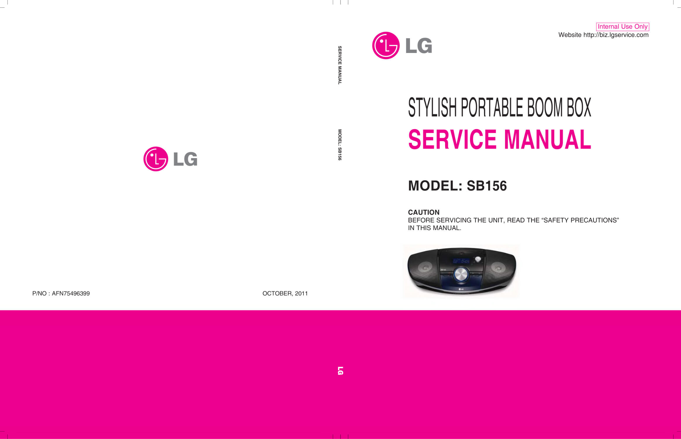
STYLISH PORTABLE BOOM BOX
SERVICE MANUAL
MODEL: SB156
CAUTION
BEFORE SERVICING THE UNIT, READ THE “SAFETY PRECAUTIONS”
IN THIS MANUAL.
MODEL: SB156 SERVICE MANUAL
P/NO : AFN75496399 OCTOBER, 2011
Website http://biz.lgservice.com
Internal Use Only
CONTENTS
SECTION 1 ........ SUMMARY
SECTION 2 ........ CABINET & MAIN CHASSIS
SECTION 3 ........ ELECTRICAL
SECTION 4 ........ REPLACEMENT PARTS LIST
1-1
SECTION 1 SUMMARY
CONTENTS
SERVICING PRECAUTIONS ................................................................................................................... 1-3
ESD PRECAUTIONS .................................................................................................................................. 1-5
HOW TO UPDATE MCS PROGRAM .................................................................................................... 1-6
SPECIFICATIONS ....................................................................................................................................... 1-7
1-2
1-3
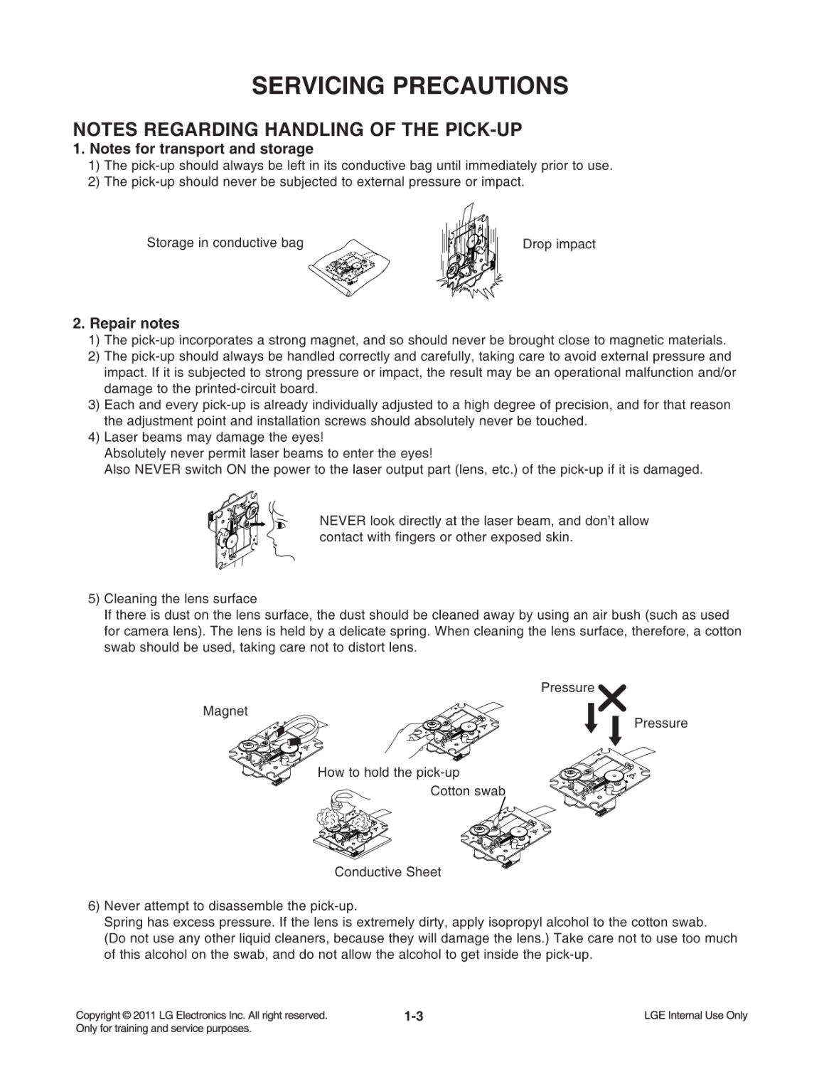
NOTES REGARDING HANDLING OF THE PICK-UP
1. Notes for transport and storage
1) The pick-up should always be left in its conductive bag until immediately prior to use.
2) The pick-up should never be subjected to external pressure or impact.
2. Repair notes
1) The pick-up incorporates a strong magnet, and so should never be brought close to magnetic materials.
2) The pick-up should always be handled correctly and carefully, taking care to avoid external pressure and
impact. If it is subjected to strong pressure or impact, the result may be an operational malfunction and/or
damage to the printed-circuit board.
3) Each and every pick-up is already individually adjusted to a high degree of precision, and for that reason
the adjustment point and installation screws should absolutely never be touched.
4) Laser beams may damage the eyes!
Absolutely never permit laser beams to enter the eyes!
Also NEVER switch ON the power to the laser output part (lens, etc.) of the pick-up if it is damaged.
5) Cleaning the lens surface
If there is dust on the lens surface, the dust should be cleaned away by using an air bush (such as used
for camera lens). The lens is held by a delicate spring. When cleaning the lens surface, therefore, a cotton
swab should be used, taking care not to distort lens.
6) Never attempt to disassemble the pick-up.
Spring has excess pressure. If the lens is extremely dirty, apply isopropyl alcohol to the cotton swab.
(Do not use any other liquid cleaners, because they will damage the lens.) Take care not to use too much
of this alcohol on the swab, and do not allow the alcohol to get inside the pick-up.
Storage in conductive bag
Drop impact
NEVER look directly at the laser beam, and don’t allow
contact with fingers or other exposed skin.
Magnet
How to hold the pick-up
Conductive Sheet
Cotton swab
Pressure
Pressure
SERVICING PRECAUTIONS
NOTES REGARDING COMPACT DISC PLAYER REPAIRS
1. Preparations
1) Compact disc players incorporate a great many ICs as well as the pick-up (laser diode). These components
are sensitive to, and easily affected by, static electricity. If such static electricity is high voltage, components
can be damaged, and for that reason components should be handled with care.
2) The pick-up is composed of many optical components and other high-precision components. Care must be
taken, therefore, to avoid repair or storage where the temperature or humidity is high, where strong magnet-
ism is present, or where there is excessive dust.
2. Notes for repair
1) Before replacing a component part, first disconnect the power supply lead wire from the unit
2) All equipment, measuring instruments and tools must be grounded.
3) The workbench should be covered with a conductive sheet and grounded.
When removing the laser pick-up from its conductive bag, do not place the pick-up on the bag. (This is
because there is the possibility of damage by static electricity.)
4) To prevent AC leakage, the metal part of the soldering iron should be grounded.
5) Workers should be grounded by an armband (1 MΩ)
6) Care should be taken not to permit the laser pick-up to come in contact with clothing, in order to prevent stat-
ic electricity changes in the clothing to escape from the armband.
7) The laser beam from the pick-up should NEVER be directly facing the eyes or bare skin.
Resistor
(1 MΩ)
Conductive
Sheet
Resistor
(1 MΩ)
Armband
1-4
1-5
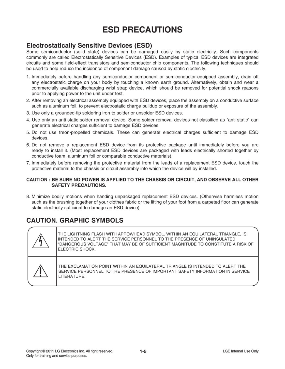
Electrostatically Sensitive Devices (ESD)
Some semiconductor (solid state) devices can be damaged easily by static electricity. Such components
commonly are called Electrostatically Sensitive Devices (ESD). Examples of typical ESD devices are integrated
circuits and some field-effect transistors and semiconductor chip components. The following techniques should
be used to help reduce the incidence of component damage caused by static electricity.
1. Immediately before handling any semiconductor component or semiconductor-equipped assembly, drain off
any electrostatic charge on your body by touching a known earth ground. Alternatively, obtain and wear a
commercially available discharging wrist strap device, which should be removed for potential shock reasons
prior to applying power to the unit under test.
2. After removing an electrical assembly equipped with ESD devices, place the assembly on a conductive surface
such as aluminum foil, to prevent electrostatic charge buildup or exposure of the assembly.
3. Use only a grounded-tip soldering iron to solder or unsolder ESD devices.
4. Use only an anti-static solder removal device. Some solder removal devices not classified as "anti-static" can
generate electrical charges sufficient to damage ESD devices.
5. Do not use freon-propelled chemicals. These can generate electrical charges sufficient to damage ESD
devices.
6. Do not remove a replacement ESD device from its protective package until immediately before you are
ready to install it. (Most replacement ESD devices are packaged with leads electrically shorted together by
conductive foam, aluminum foil or comparable conductive materials).
7. Immediately before removing the protective material from the leads of a replacement ESD device, touch the
protective material to the chassis or circuit assembly into which the device will by installed.
CAUTION : BE SURE NO POWER IS APPLIED TO THE CHASSIS OR CIRCUIT, AND OBSERVE ALL OTHER
SAFETY PRECAUTIONS.
8. Minimize bodily motions when handing unpackaged replacement ESD devices. (Otherwise harmless motion
such as the brushing together of your clothes fabric or the lifting of your foot from a carpeted floor can generate
static electricity sufficient to damage an ESD device).
CAUTION. GRAPHIC SYMBOLS
THE LIGHTNING FLASH WITH APROWHEAD SYMBOL. WITHIN AN EQUILATERAL TRIANGLE, IS
INTENDED TO ALERT THE SERVICE PERSONNEL TO THE PRESENCE OF UNINSULATED
“DANGEROUS VOLTAGE” THAT MAY BE OF SUFFICIENT MAGNITUDE TO CONSTITUTE A RISK OF
ELECTRIC SHOCK.
THE EXCLAMATION POINT WITHIN AN EQUILATERAL TRIANGLE IS INTENDED TO ALERT THE
SERVICE PERSONNEL TO THE PRESENCE OF IMPORTANT SAFETY INFORMATION IN SERVICE
LITERATURE.
ESD PRECAUTIONS
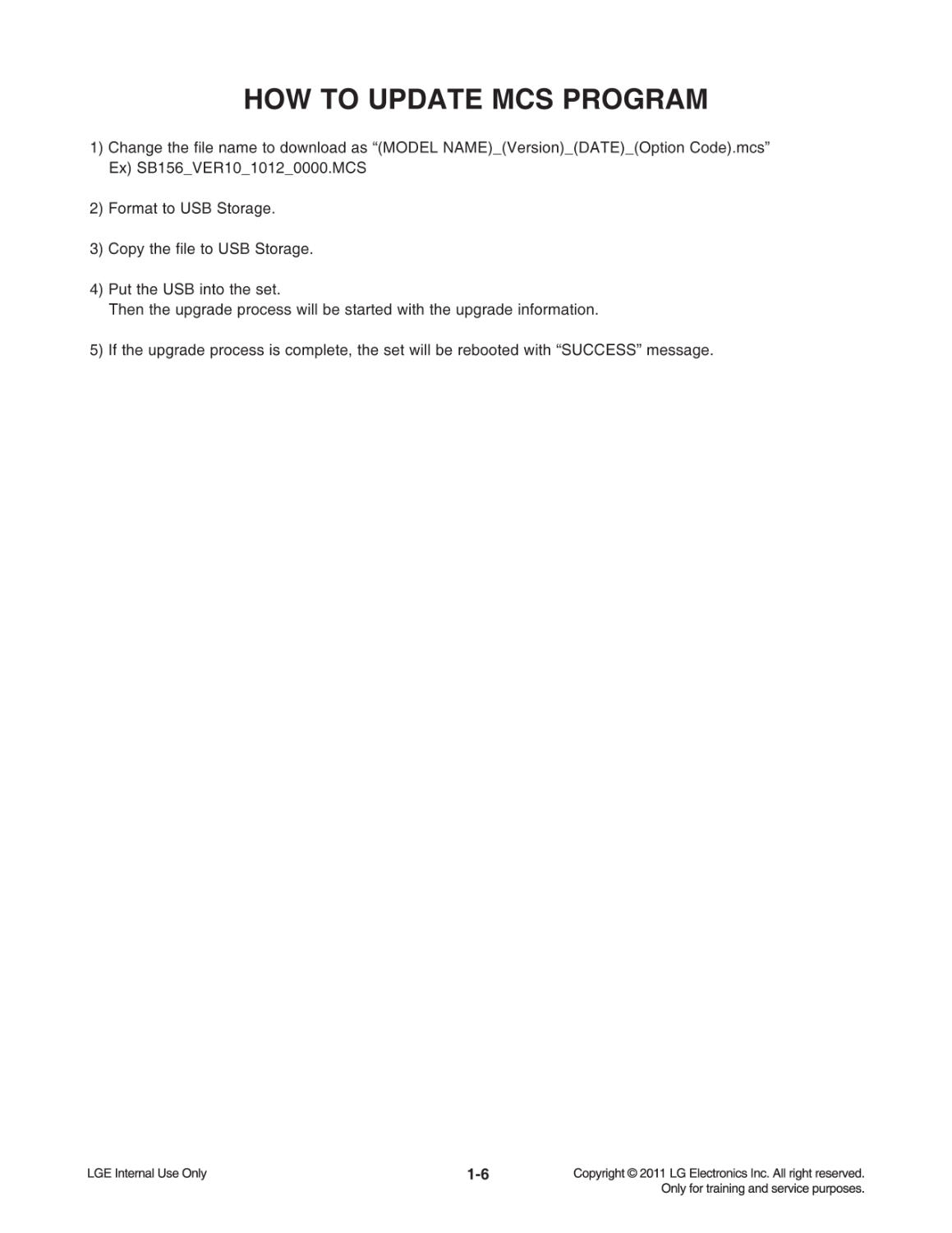
HOW TO UPDATE MCS PROGRAM
1-6
1) Change the file name to download as “(MODEL NAME)_(Version)_(DATE)_(Option Code).mcs”
Ex) SB156_VER10_1012_0000.MCS
2) Format to USB Storage.
3) Copy the file to USB Storage.
4) Put the USB into the set.
Then the upgrade process will be started with the upgrade information.
5) If the upgrade process is complete, the set will be rebooted with “SUCCESS” message.
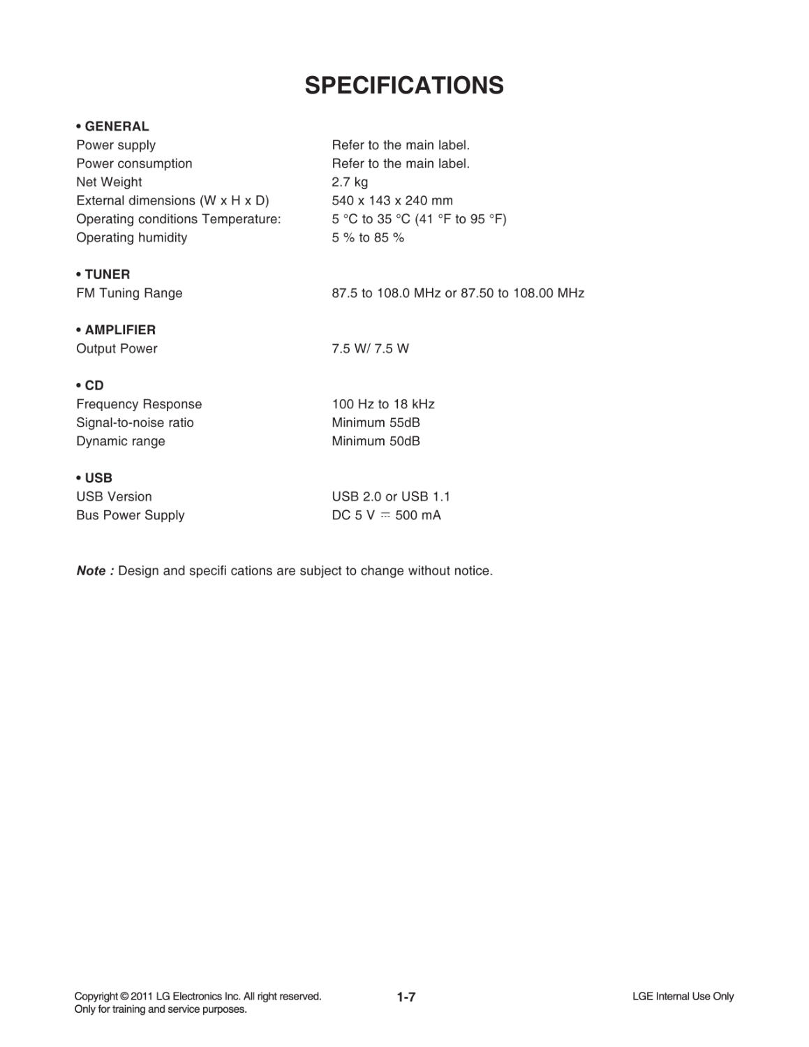
SPECIFICATIONS
• GENERAL
Power supply Refer to the main label.
Power consumption Refer to the main label.
Net Weight 2.7 kg
External dimensions (W x H x D) 540 x 143 x 240 mm
Operating conditions Temperature: 5 °C to 35 °C (41 °F to 95 °F)
Operating humidity 5 % to 85 %
• TUNER
FM Tuning Range 87.5 to 108.0 MHz or 87.50 to 108.00 MHz
• AMPLIFIER
Output Power 7.5 W/ 7.5 W
• CD
Frequency Response 100 Hz to 18 kHz
Signal-to-noise ratio Minimum 55dB
Dynamic range Minimum 50dB
• USB
USB Version USB 2.0 or USB 1.1
Bus Power Supply DC 5 V 500 mA
Note : Design and specifi cations are subject to change without notice.
1-7
1-8
MEMO
SECTION 2
CABINET & MAIN CHASSIS
CONTENTS
EXPLODED VIEWS ..................................................................................................................................... 2-3
1. CABINET AND MAIN FRAME SECTION (SB156) ................................................................................... 2-3
2. PACKING ACCESSORY SECTION ......................................................................................................... 2-5
2-1
2-2
MEMO
2-3 2-4
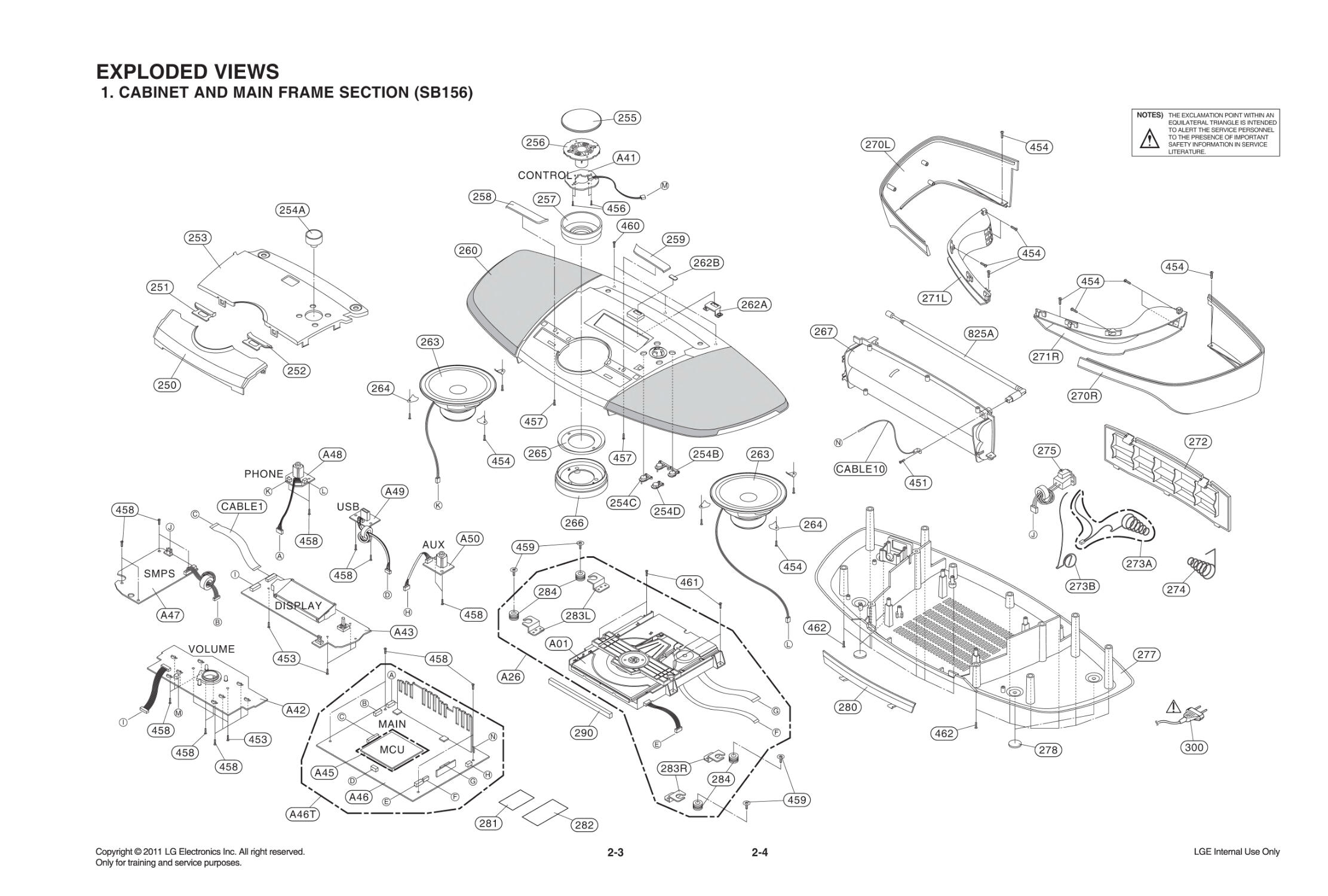
EXPLODED VIEWS
1. CABINET AND MAIN FRAME SECTION (SB156)
I
N
H
L
F
G
E
D
K
I
F
G
C
B
C
N
M
A
M
D
H
J
E
B
K
L
J
A
A46T
283L
283R
270L
262A
254A
271L
271R
270R
273B
273A
825A
262B
254B
254C
254D
459
461
458
458
453
458
458
453
458
457
460
457
458
454
454
454
454
459
454
451
454
264
263
263
458
458
A48
A47
A43
A42
A46
A45
290
A26
264
266
265
260
258
257
A41
256
255
259
267
272
275
274
284
284
277
280
278
253
251
250
252
A49
A50
PHONE
USB
AUX
DISPLAY
CONTROL
SMPS
MAIN
MCU
VOLUME
300
462
462
CABLE1
CABLE10
281
282
A01
456
NOTES) THE EXCLAMATION POINT WITHIN AN
EQUILATERAL TRIANGLE IS INTENDED
TO ALERT THE SERVICE PERSONNEL
TO THE PRESENCE OF IMPORTANT
SAFETY INFORMATION IN SERVICE
LITERATURE.
2-5 2-6
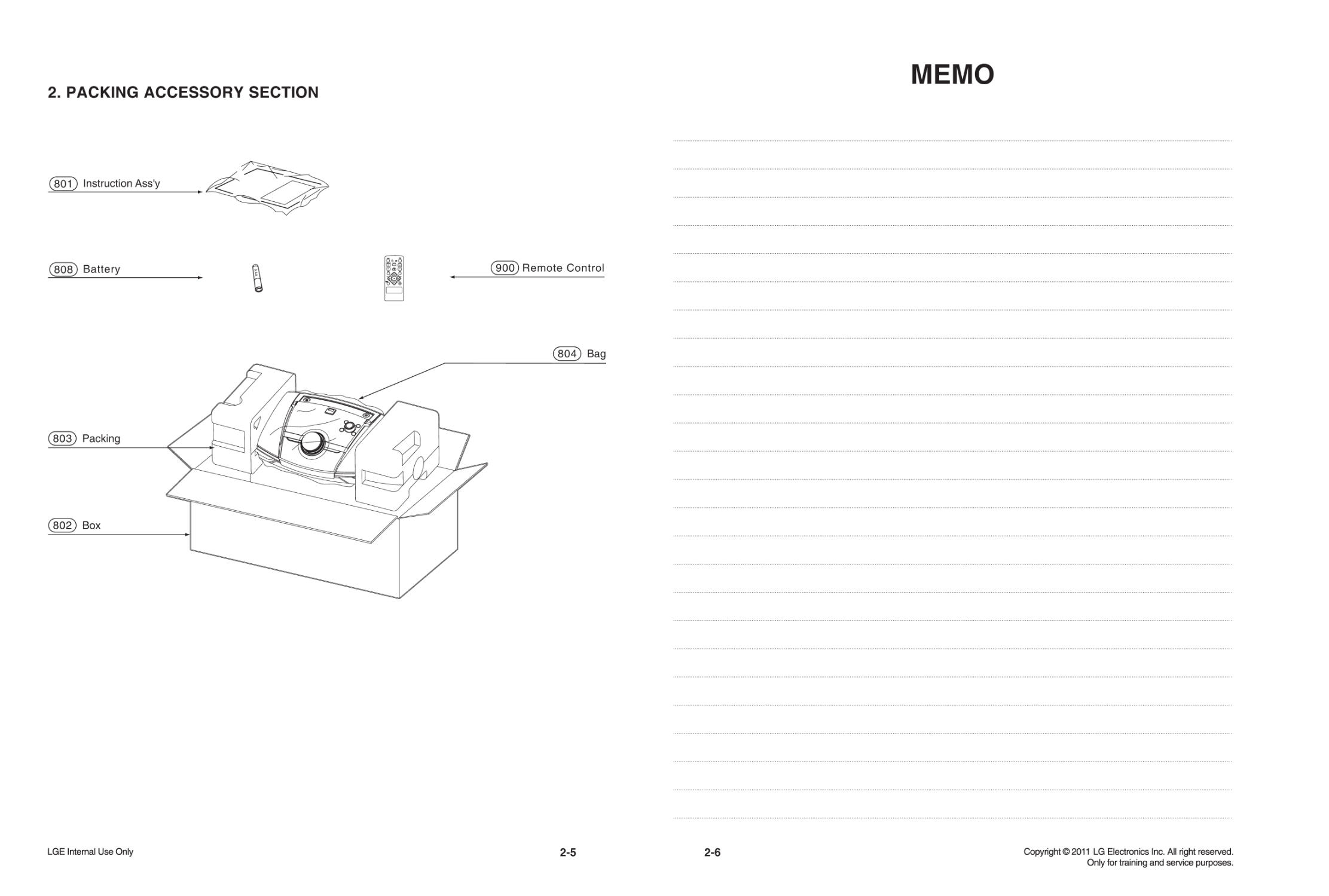
2. PACKING ACCESSORY SECTION
Box 802
Packing 803
Bag 804
808
Battery
801
Instruction Ass'y
900 Remote Control
AAA
EQ
MEMO
SECTION 3 ELECTRICAL
CONTENTS
ELECTRICAL TROUBLESHOOTING GUIDE .................................................................................... 3-2
1. SMPS PART ........................................................................................................................................... 3-2
2. MUTING CIRCUIT (MUTE) .................................................................................................................... 3-3
3. AUDIO ABNORMAL ............................................................................................................................... 3-4
4. AUDIO ABNORMAL (FUNCTION MODE) ............................................................................................. 3-5
5. U803/ 3.3 V ABNORMAL ....................................................................................................................... 3-6
6. IC603 ABNORMAL ................................................................................................................................. 3-7
7. IC600 ABNORMAL ................................................................................................................................. 3-8
8. U654 ABNORMAL .................................................................................................................................. 3-9
9. IC601 ABNORMAL ................................................................................................................................. 3-9
10. IC302 ABNORMAL ............................................................................................................................... 3-10
11. U501 ABNORMAL ................................................................................................................................ 3-10
12. U3 FM TUNER MODULE ..................................................................................................................... 3-11
13. CD PART .............................................................................................................................................. 3-12
14. CD READING CHECK ......................................................................................................................... 3-13
15. USB PART ............................................................................................................................................ 3-14
WAVEFORMS ............................................................................................................................................ 3-15
WIRING DIAGRAM ................................................................................................................................... 3-17
BLOCK DIAGRAM .................................................................................................................................... 3-19
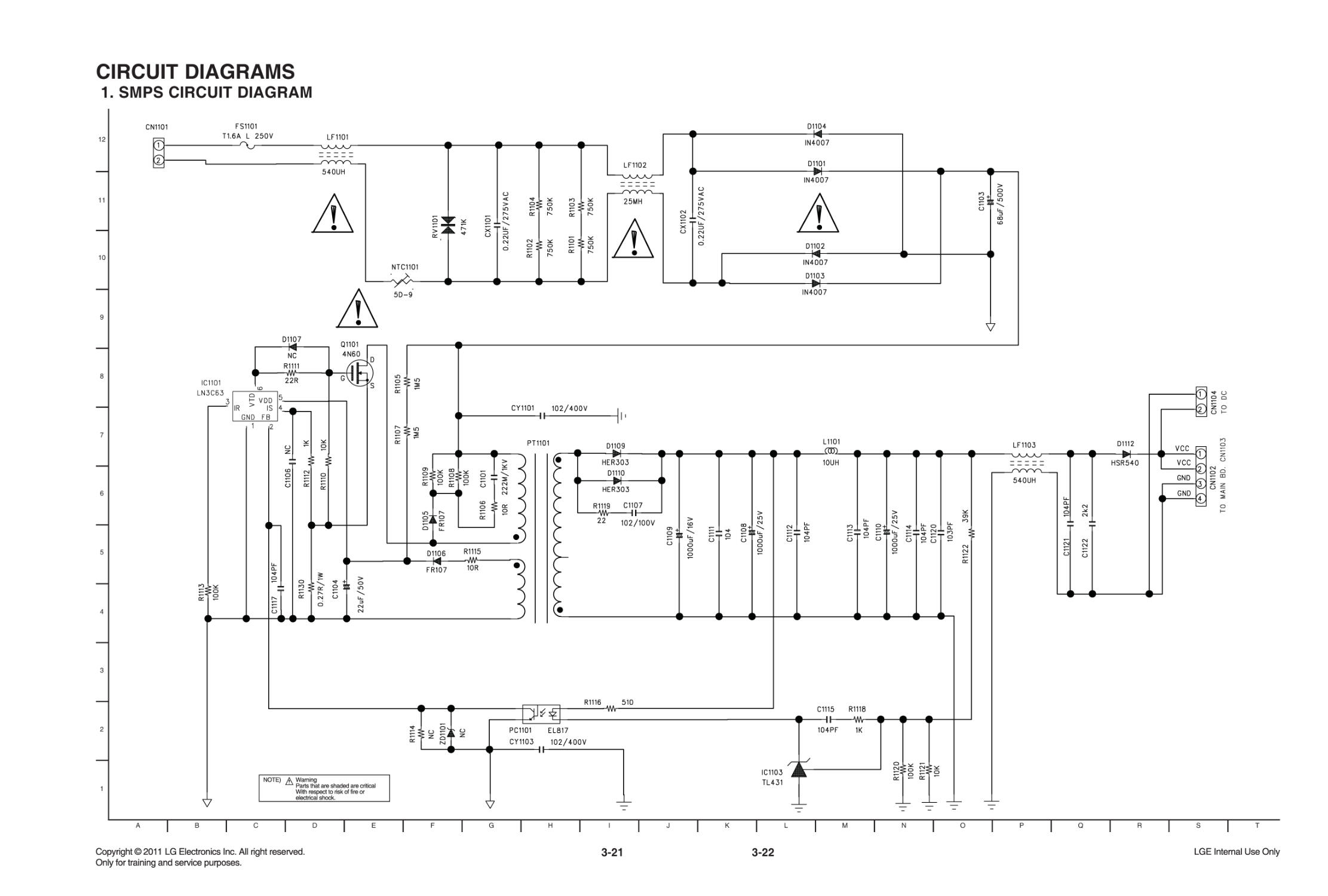
CIRCUIT DIAGRAMS ............................................................................................................................... 3-21
1. SMPS CIRCUIT DIAGRAM .................................................................................................................. 3-21
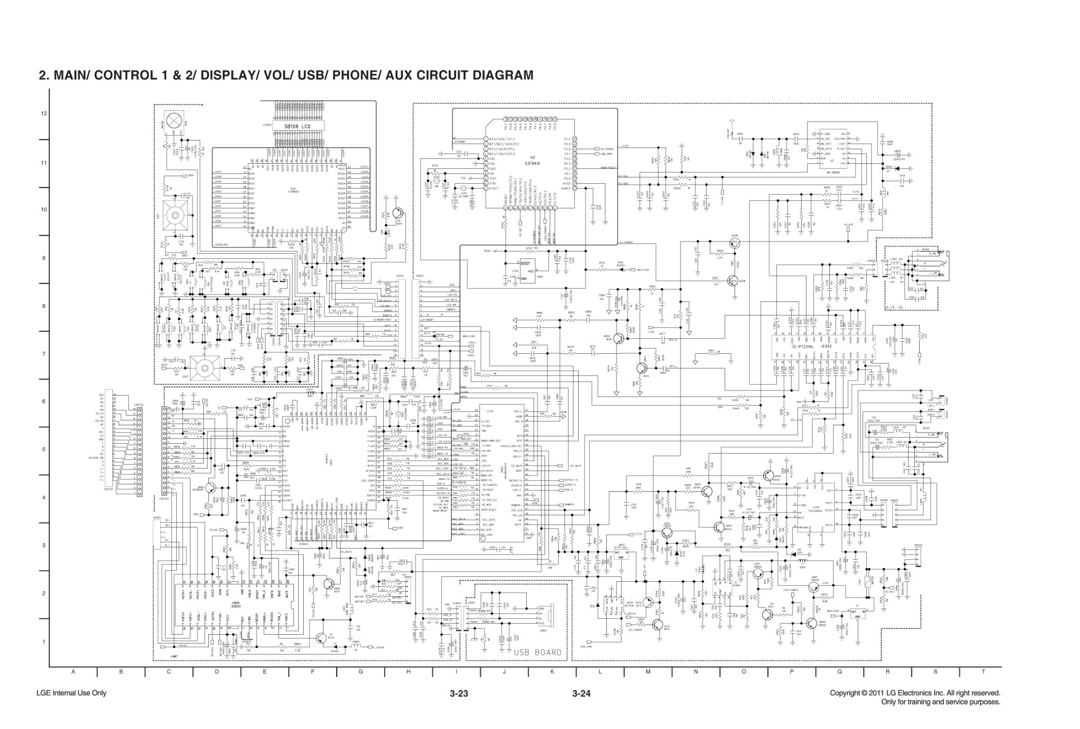
2. MAIN/ CONTROL 1 & 2/ DISPLAY/ VOL/ USB/ PHONE/ AUX CIRCUIT DIAGRAM ......................... 3-23
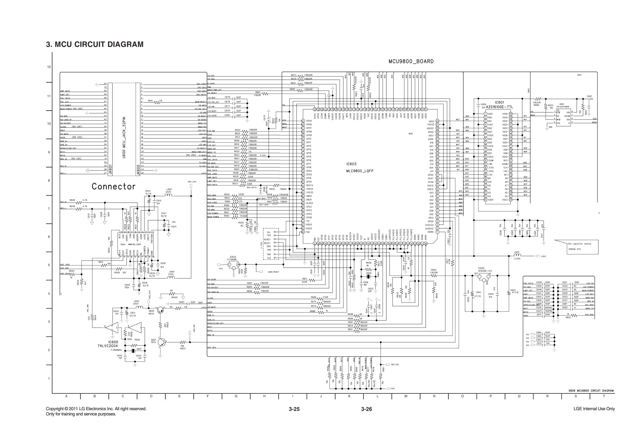
3. MCU CIRCUIT DIAGRAM .................................................................................................................... 3-25
CIRCUIT VOLTAGE CHART ................................................................................................................. 3-27
PRINTED CIRCUIT BOARD DIAGRAMS ......................................................................................... 3-29
1. MAIN P.C.BOARD ................................................................................................................................ 3-29
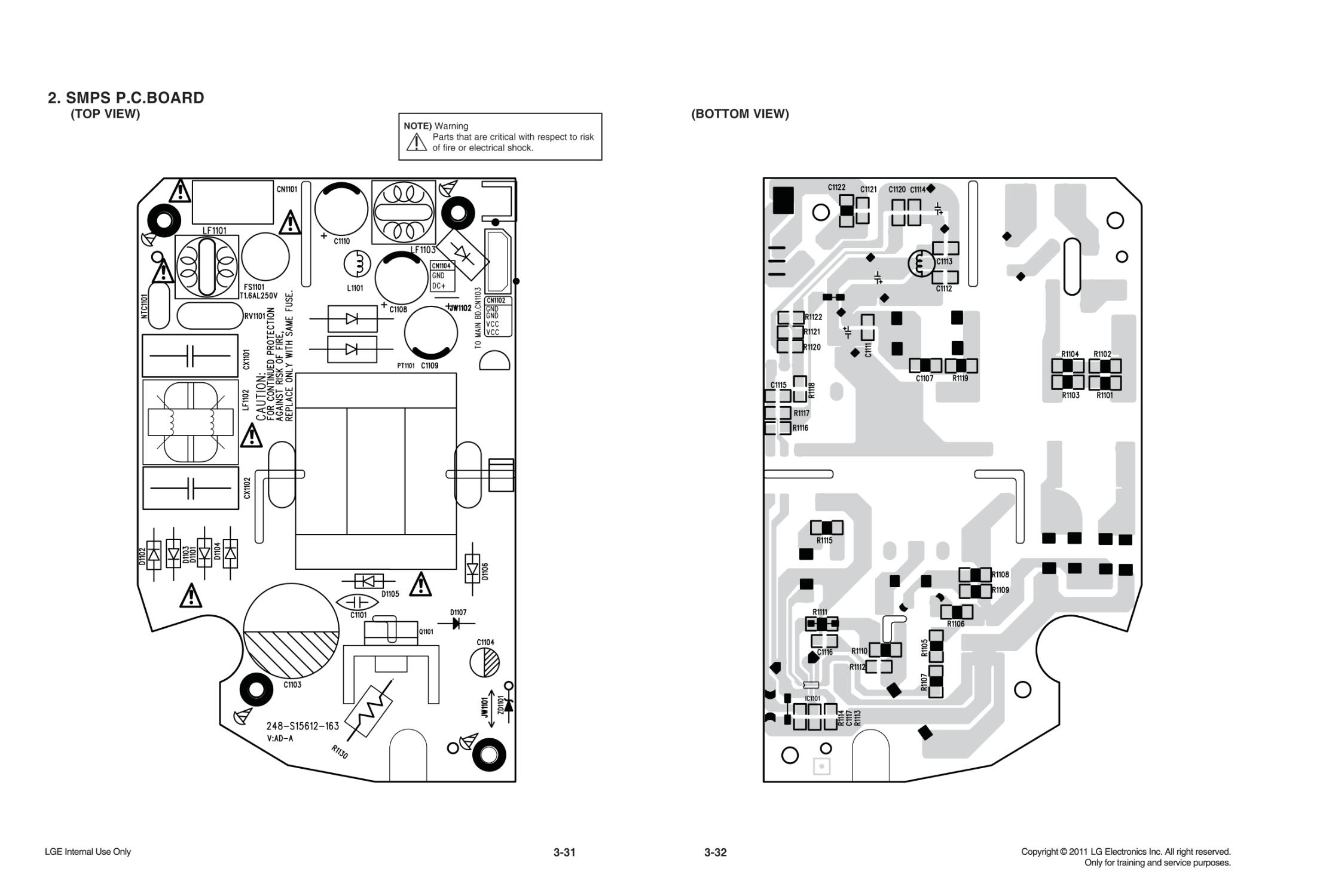
2. SMPS P.C.BOARD ............................................................................................................................... 3-31
3. MCU P.C.BOARD ................................................................................................................................. 3-33
4. VOLUME P.C.BOARD .......................................................................................................................... 3-35
5. DISPLAY P.C.BOARD .......................................................................................................................... 3-35
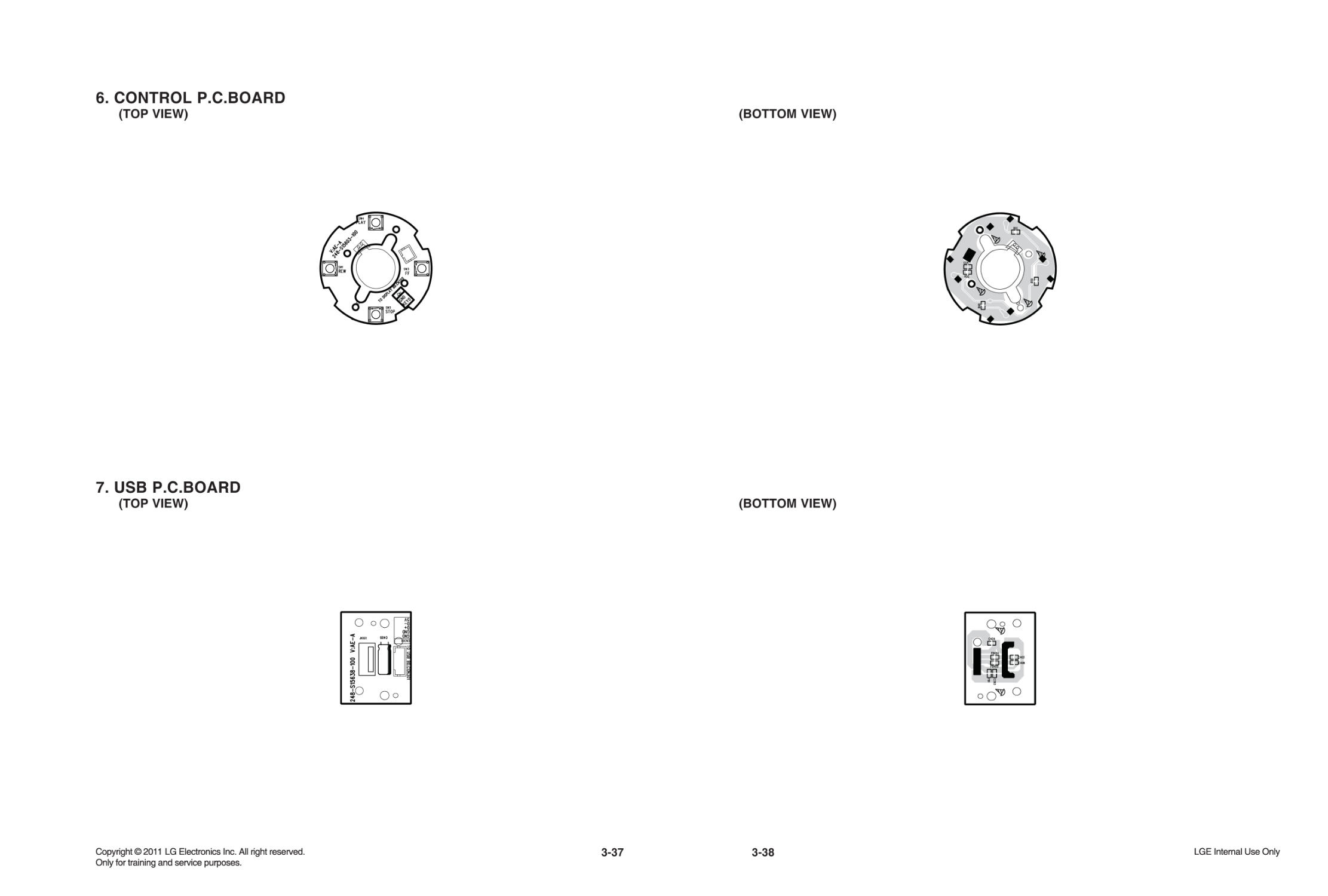
6. CONTROL P.C.BOARD ....................................................................................................................... 3-37
7. USB P.C.BOARD ................................................................................................................................. 3-37
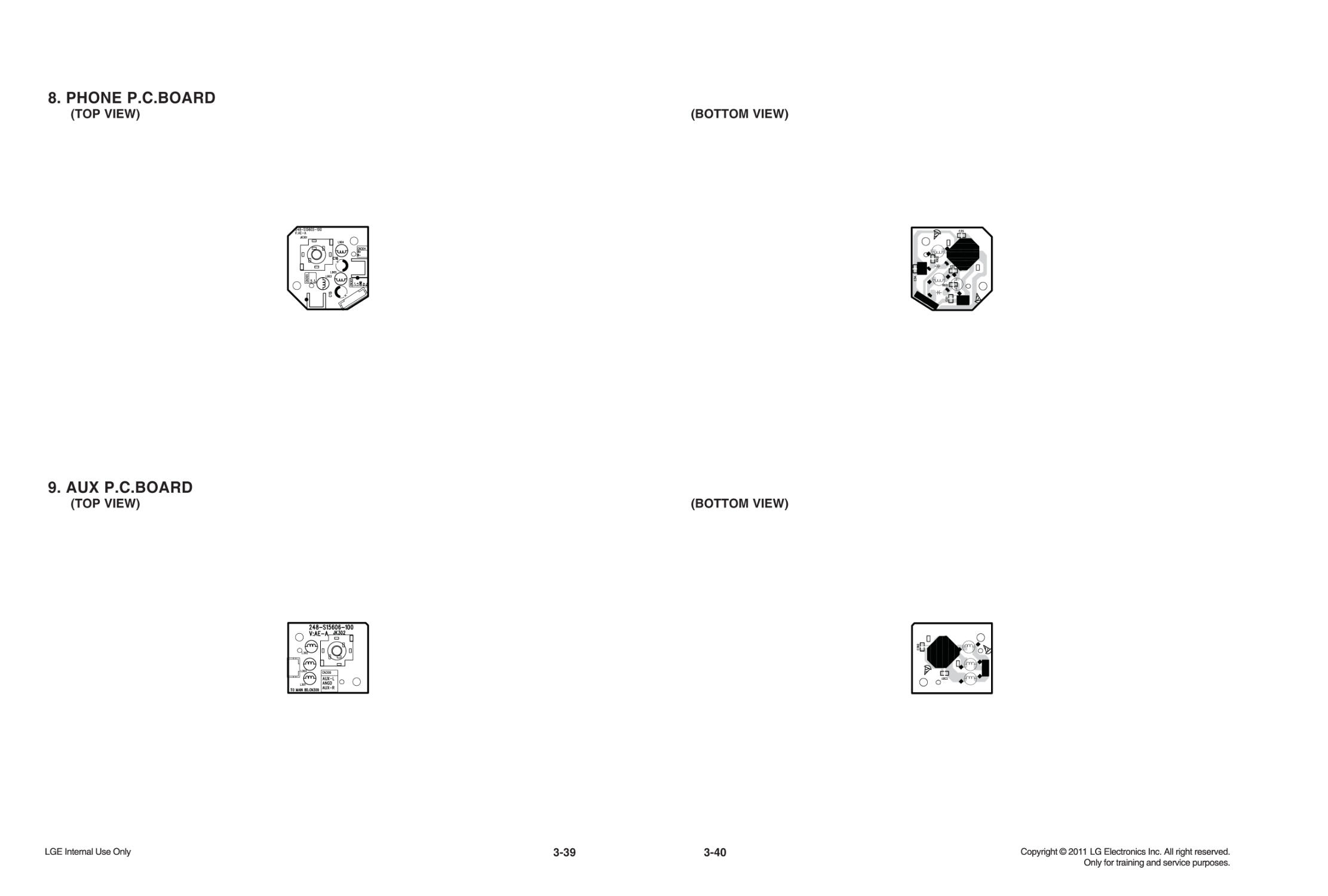
8. PHONE P.C.BOARD ............................................................................................................................ 3-39
9. AUX P.C.BOARD ................................................................................................................................. 3-39
3-1
1. SMPS PART
12 V
Replace FS1101
(Use same type Fuse)
Replace D1109-D1110
Check or replace D1106
YES
YES
YES
YES
YES
NO
NO
FS1101 nomal?
D1109-D1110 nomal?
Replace D1101-D1104
D1106 nomal?
NO
NO
NO
D1101-D1104 nomal?
Is Vcc(10V~25V)
supplied to IC1101 pin5?
Power Line of Main PCB is short
3-2
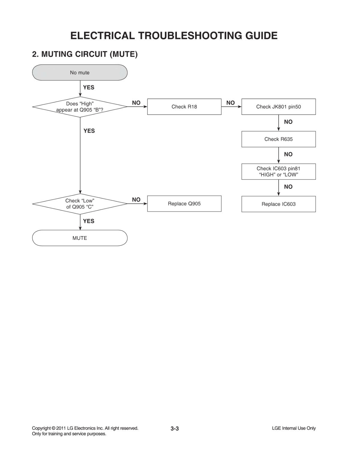
ELECTRICAL TROUBLESHOOTING GUIDE
2. MUTING CIRCUIT (MUTE)
YES
YES
YES
No mute
Check R18
Replace Q905
Check JK801 pin50
Check IC603 pin81
“HIGH” or “LOW”
Check R635
Replace IC603
NO
NO
NO
NO
NO
NO
Check “Low”
of Q905 “C”
Does “High”
appear at Q905 “B”?
MUTE
3-3
ELECTRICAL TROUBLESHOOTING GUIDE
3. AUDIO ABNORMAL
Audio abnormal
Check the connection of speakers
Check the function input
YES
YES
YES
YES
NO
NO
Check the output
of IC301 pin1,2,14,15
Check DC 12V
of IC301 pin3,13
Check “High” of IC301 pin7
NO
Check the input
signal of IC301 pin4,12
Check the Power Circuit
3-4
ELECTRICAL TROUBLESHOOTING GUIDE
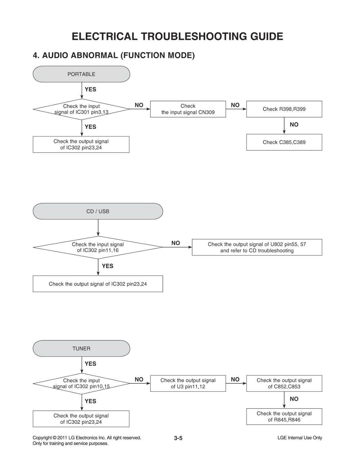
4. AUDIO ABNORMAL (FUNCTION MODE)
CD / USB
Check the output signal of U802 pin55, 57
and refer to CD troubleshooting
Check the output signal of IC302 pin23,24
YES
NO
Check the input signal
of IC302 pin11,16
YES
YES
PORTABLE
Check
the input signal CN309
Check R398,R399
Check C385,C389
Check the output signal
of IC302 pin23,24
NO NO
NO
Check the input
signal of IC301 pin3,13
YES
YES
TUNER
Check the output signal
of U3 pin11,12
Check the output signal
of C852,C853
Check the output signal
of R845,R846
Check the output signal
of IC302 pin23,24
NO NO
NO
Check the input
signal of IC302 pin10,15
3-5
ELECTRICAL TROUBLESHOOTING GUIDE
5. U803/ 3.3 V ABNORMAL
YES
YES
NO
YES
YES
YES
Portable
OK
Replace L2
Replace L1
Refer to SMPS
troubleshooting (12V)
Check
IC1 pin7 is “HIHGT”
OK OK
Check L1
OK
IC1 output normal?
YES
NO
NO
NO
NO
NO
YES YES
U803 3.3V
output normal ?
Check L2
IC1 pin2 input 12V?
Check
ECO-POWER
is “HIHGT”
3-6
ELECTRICAL TROUBLESHOOTING GUIDE
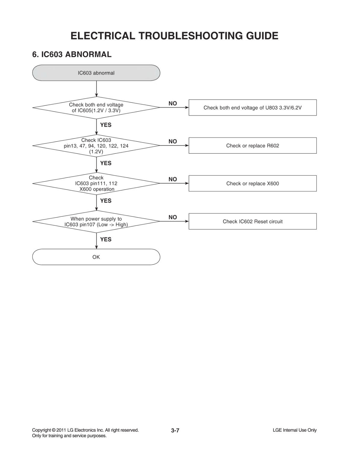
6. IC603 ABNORMAL
IC603 abnormal
Check both end voltage of U803 3.3V/6.2V
Check or replace X600
YES
YES
YES
YES
NO
NO
Check both end voltage
of IC605(1.2V / 3.3V)
Check
IC603 pin111, 112
X600 operation
Check or replace R602
Check IC602 Reset circuit
NO
NO
Check IC603
pin13, 47, 94, 120, 122, 124
(1.2V)
When power supply to
IC603 pin107 (Low -> High)
OK
3-7
ELECTRICAL TROUBLESHOOTING GUIDE
7. IC600 ABNORMAL
IC600 abnormal
Refer to power supply no 3.3V,
check or replace Q600
Check or replace L600
YES
YES
YES
YES
NO
NO
Check both end voltage
Q600 (3.3V)
Check IC604
pin13 is 3.3V
Check IC603 pin5 is “H”,
Check or replace Q601
Check or replace X601
NO
NO
Check Q601 is “H”
Check
IC600 pin1, 6
X601 operation
OK
3-8
ELECTRICAL TROUBLESHOOTING GUIDE
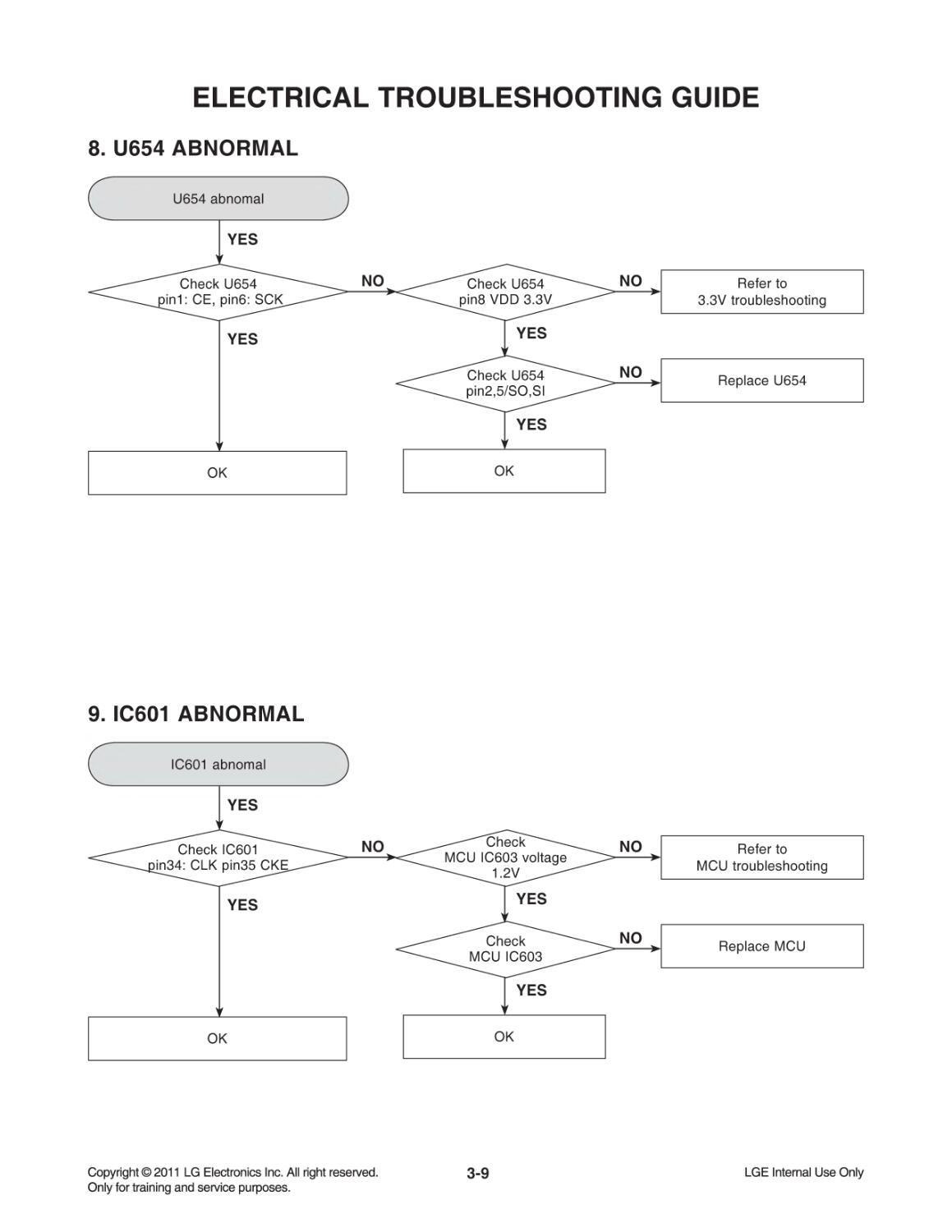
8. U654 ABNORMAL
YES
YES
U654 abnomal
OK
Refer to
3.3V troubleshooting
Replace U654
OK
NO NO
NO
YES
YES
Check U654
pin1: CE, pin6: SCK
Check U654
pin8 VDD 3.3V
Check U654
pin2,5/SO,SI
9. IC601 ABNORMAL
YES
YES
IC601 abnomal
OK
Refer to
MCU troubleshooting
Replace MCU
OK
NO NO
NO
YES
YES
Check IC601
pin34: CLK pin35 CKE
Check
MCU IC603 voltage
1.2V
Check
MCU IC603
3-9
ELECTRICAL TROUBLESHOOTING GUIDE
11. U501 ABNORMAL
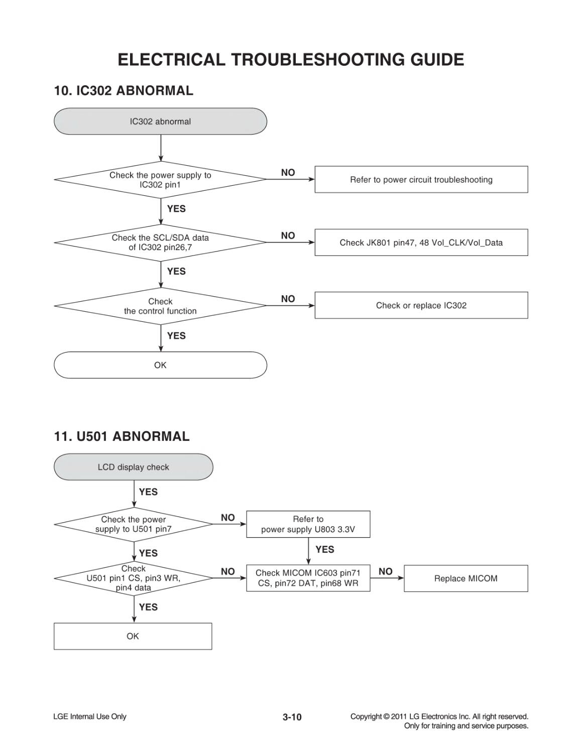
10. IC302 ABNORMAL
IC302 abnormal
Check JK801 pin47, 48 Vol_CLK/Vol_Data
Check or replace IC302
YES
YES
YES
NO
Check the SCL/SDA data
of IC302 pin26,7
Refer to power circuit troubleshooting
NO
NO
Check the power supply to
IC302 pin1
Check
the control function
OK
YES
YES
YES
LCD display check
Refer to
power supply U803 3.3V
Check MICOM IC603 pin71
CS, pin72 DAT, pin68 WR
Replace MICOM
OK
NO
NO
NO
YES
Check the power
supply to U501 pin7
Check
U501 pin1 CS, pin3 WR,
pin4 data
3-10
ELECTRICAL TROUBLESHOOTING GUIDE
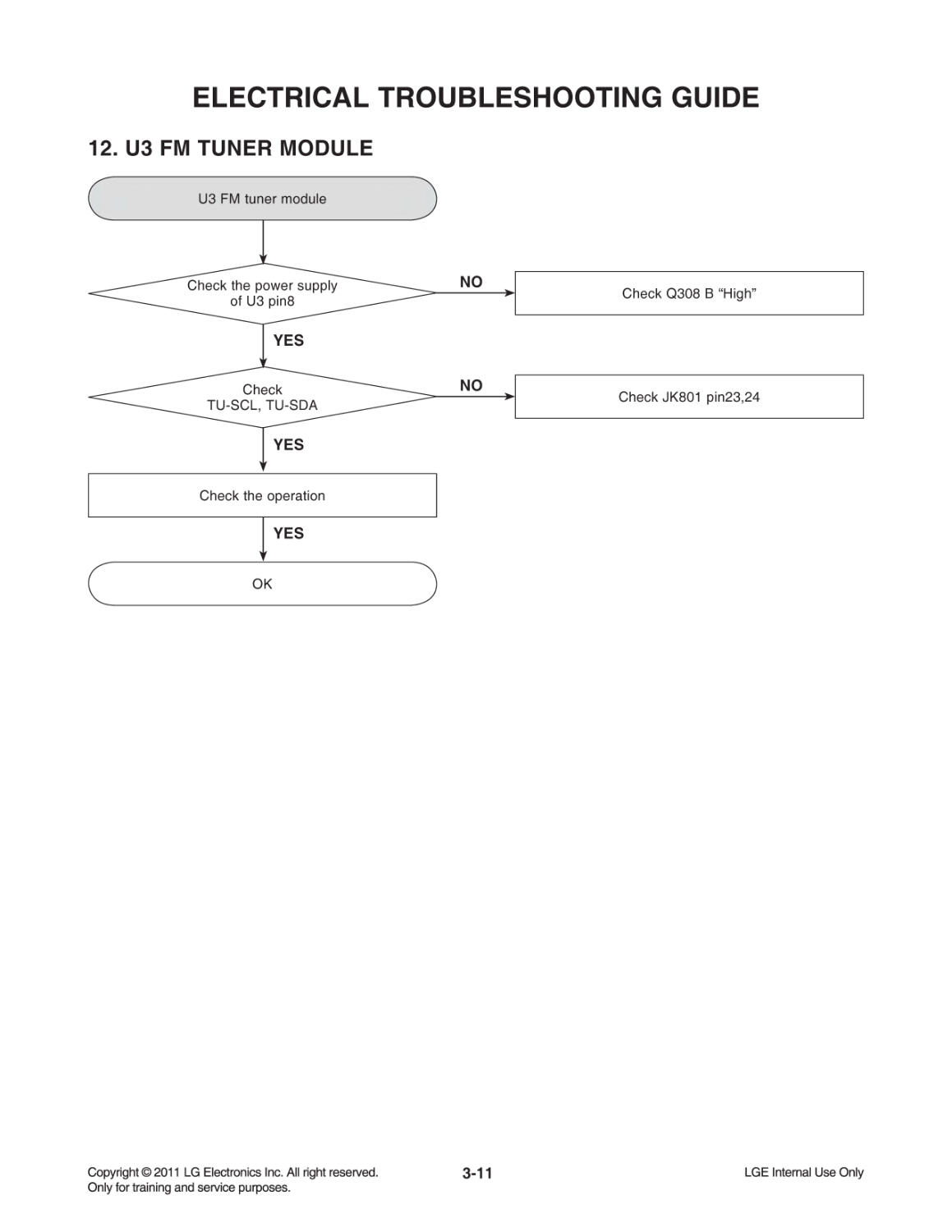
12. U3 FM TUNER MODULE
U3 FM tuner module
Check Q308 B “High”
Check the operation
YES
YES
YES
NO
Check the power supply
of U3 pin8
Check JK801 pin23,24
NO
Check
TU-SCL, TU-SDA
OK
3-11
ELECTRICAL TROUBLESHOOTING GUIDE
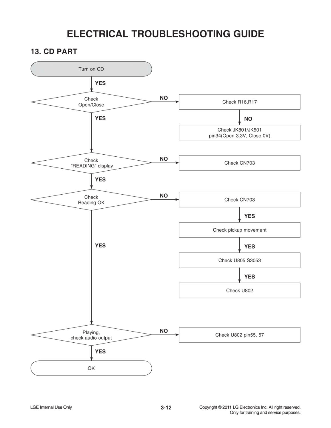
13. CD PART
Turn on CD
Check R16,R17
Check pickup movement
Check JK801/JK501
pin34(Open 3.3V, Close 0V)
Check U805 S3053
Check U802
YES
YES
YES
YES
YES
NO
Check
Open/Close
Check CN703
Check U802 pin55, 57
Check CN703
YES
NO
YES
YES
NO
NO
NO
Check
“READING” display
Playing,
check audio output
Check
Reading OK
OK
3-12
ELECTRICAL TROUBLESHOOTING GUIDE
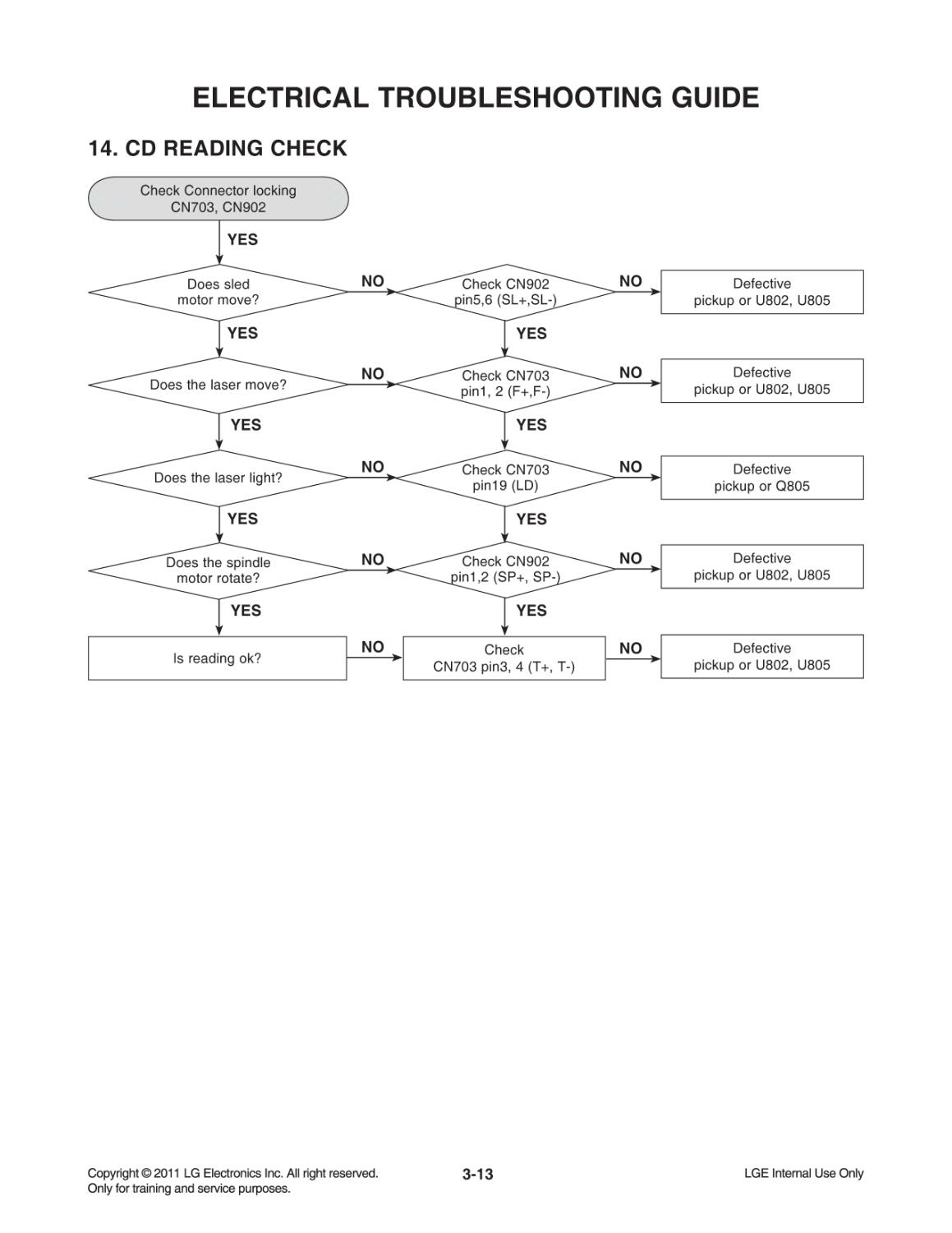
14. CD READING CHECK
YES
YES
YES
Check Connector locking
CN703, CN902
Check
CN703 pin3, 4 (T+, T-)
Defective
pickup or U802, U805
Defective
pickup or Q805
Defective
pickup or U802, U805
Defective
pickup or U802, U805
Defective
pickup or U802, U805
Is reading ok?
NO
NO
NO
NO
NO
NO
NO
NO
NO
NO
YES
YES
YES
YES
YES
YES
Does sled
motor move?
Does the laser light?
Does the laser move?
Does the spindle
motor rotate?
Check CN902
pin5,6 (SL+,SL-)
Check CN703
pin19 (LD)
Check CN703
pin1, 2 (F+,F-)
Check CN902
pin1,2 (SP+, SP-)
3-13
ELECTRICAL TROUBLESHOOTING GUIDE
15. USB PART
YES
YES
YES
YES YES
NO
Replace IC1 Replace L1
OK
YES
Turn on the USB
Check connector locking
CN301,CON301
Check
CON301 pin2_5V
Check
U802 pin55, 57
Check Power supply circuit
IC401 USB+5V
Check
CON301 pin3, 4 (D+, D-)
Check
IC302 pin11,16
Check
SMPS power supply
Check MICOM IC603
pin116, 117 (D+, D-)
NO
NO
NO
NO NO
NO NO
NO
NO
NO
Check “CHECKING”
or “USB” display
Check reading
Playing,
Check audio output
Check Power
supply circuit IC1
Check Power
supply circuit L1
3-14
ELECTRICAL TROUBLESHOOTING GUIDE
3-15
WAVEFORMS
Figure 1. USB D+
Test point: TP207 (Main board)
Vp-p = 3.80 V ± 0.3 V
Figure 2. USB D-
Test point: TP206 (Main board)
Vp-p = 3.68 V ± 0.3 V
Figure 3. DAC-MCK
Test point: TP41 (Main board)
Vp-p = 2.94 V ± 0.3 V
Figure 4. DAC-LRCK
Test point: TP43 (Main board)
Vp-p = 3.84 V ± 0.3 V
Figure 5. DAC-BCK
Test point: TP42 (Main board)
Vp-p = 3.12 V ± 0.3 V
Figure 6. DAC-DATA
Test point: TP39 (Main board)
Vp-p = 3.84 V ± 0.3 V
3-16
Figure 7. LCD-DA
Test point: TP839 (Main board)
Vp-p = 3.72 V ± 0.3 V
Figure 8. LCD-WR
Test point: TP838 (Main board)
Vp-p = 3.72 V ± 0.3 V
Figure 9. LCD-CS
Test point: Main board
Vp-p = 3.84 V ± 0.3 V
Figure 10. CD-EYE
Test point: TP (Main board)
Vp-p = 1.24 V ± 0.2 V
3-17 3-18
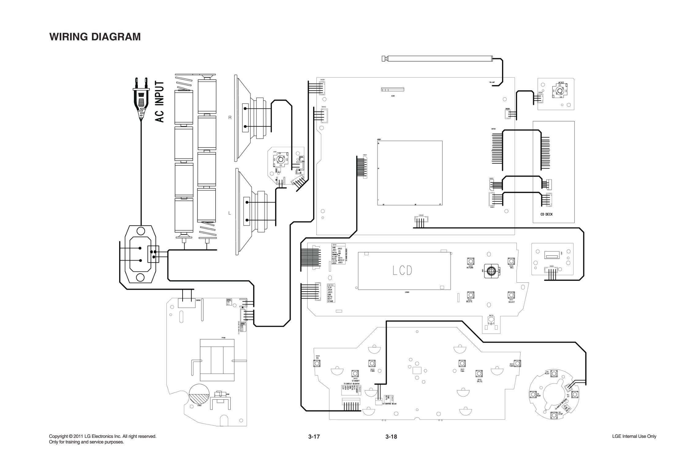
R
L
WIRING DIAGRAM
3-19 3-20
BLOCK DIAGRAM
3-21 3-22
CIRCUIT DIAGRAMS
1. SMPS CIRCUIT DIAGRAM
A
1
2
3
4
5
6
7
8
9
10
11
12
B C D E F G H I J K L M N O P Q R ST
3-23 3-24
2. MAIN/ CONTROL 1 & 2/ DISPLAY/ VOL/ USB/ PHONE/ AUX CIRCUIT DIAGRAM
A
1
2
3
4
5
6
7
8
9
10
11
12
B C D E F G H I J K L M N O P Q R ST
3-25 3-26
3. MCU CIRCUIT DIAGRAM
A
1
2
3
4
5
6
7
8
9
10
11
12
B C D E F G H I J K L M N O P Q R ST
3-27 3-28
CIRCUIT VOLTAGE CHART
3-29 3-30
PRINTED CIRCUIT BOARD DIAGRAMS
1. MAIN P.C.BOARD
(TOP VIEW) (BOTTOM VIEW)
3-31 3-32
2. SMPS P.C.BOARD
(TOP VIEW) (BOTTOM VIEW)
NOTE) Warning
Parts that are critical with respect to risk
of fire or electrical shock.
3-33 3-34
3. MCU P.C.BOARD
(TOP VIEW) (BOTTOM VIEW)
3-35 3-36
4. VOLUME P.C.BOARD
(TOP VIEW)
5. DISPLAY P.C.BOARD
(TOP VIEW)
(BOTTOM VIEW)
(BOTTOM VIEW)
3-37 3-38
6. CONTROL P.C.BOARD
(TOP VIEW)
7. USB P.C.BOARD
(TOP VIEW)
(BOTTOM VIEW)
(BOTTOM VIEW)
3-39 3-40
8. PHONE P.C.BOARD
(TOP VIEW)
9. AUX P.C.BOARD
(TOP VIEW)
(BOTTOM VIEW)
(BOTTOM VIEW)