/


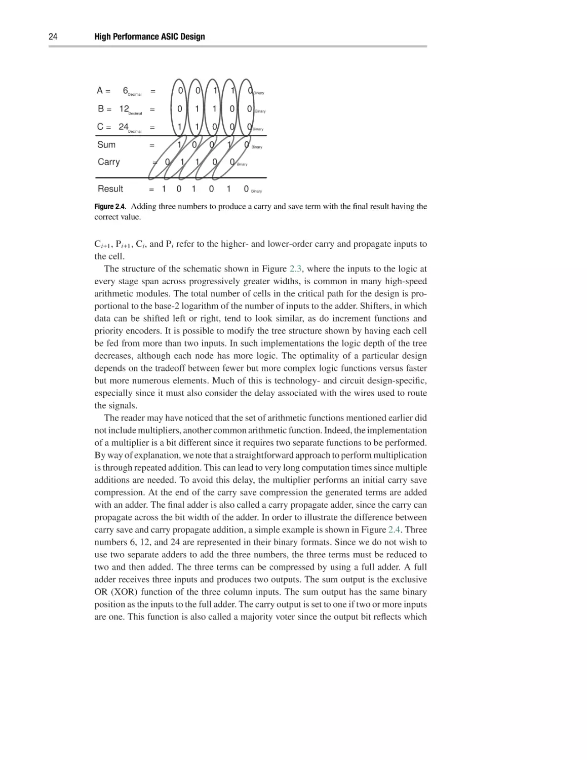
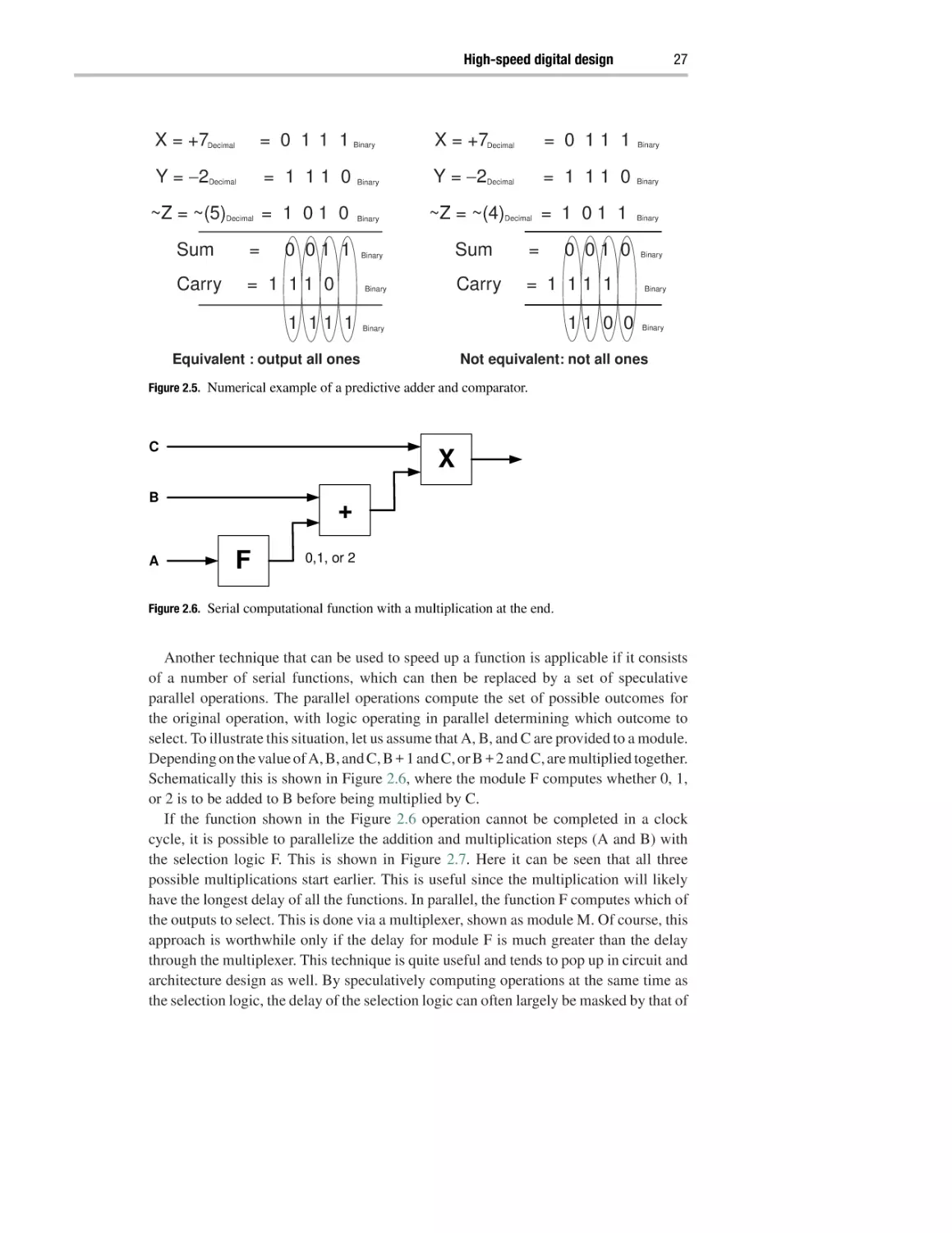
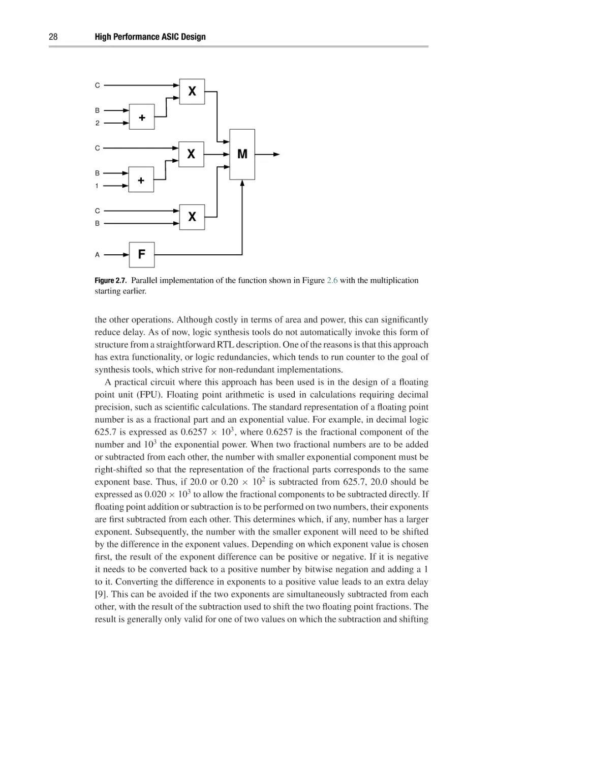


Текст
P1: SJT/...
P2: SJT
9780521873345agg.xml
CUUK158-Hossain
July 1, 2008
14:59
This page intentionally left blank
P1: SJT/...
P2: SJT
9780521873345agg.xml
CUUK158-Hossain
July 1, 2008
14:59
High Performance ASIC Design: Using Synthesizable Domino Logic
in an ASIC Flow
Presenting methodologies for high speed ASIC design developed over several years
in industry, this practical book covers issues related to the use of domino logic in an
automated framework, and brings together all the knowledge needed to apply them in
practice.
An overview of design techniques used to achieve high speed in ASIC designs is
followed by chapters describing the design and characterization of domino logic standard
cell libraries and an advanced domino logic synthesis flow. Actual results achieved by
using automated domino logic design techniques, including silicon measurements, are
presented to validate the methodology, whilst real-world design examples, such as the
implementation of the execution unit of a microprocessor and Viterbi decoder, show
how the techniques are applied in practice. This book is ideal for graduate students and
researchers in electrical and computer engineering, and also for circuit designers and
EDA engineers in industry.
razak hossain is a Senior Principal Engineer at STMicroelectonics Inc., San Diego,
California, where he has worked since 2000 on high-speed ASIC chips and design
methodologies. He earned his Ph.D. in Electrical Engineering from the University of
Rochester, New York, in 1995, after which he worked on structured custom circuit
design at Mentor Graphics Corporation, Warren, New Jersey.
P1: SJT/...
P2: SJT
9780521873345agg.xml
CUUK158-Hossain
July 1, 2008
14:59
P1: SJT/...
P2: SJT
9780521873345agg.xml
CUUK158-Hossain
July 1, 2008
14:59
High Performance ASIC Design
Using Synthesizable Domino Logic
in an ASIC Flow
Razak Hossain
STMicroelectronics
CAMBRIDGE UNIVERSITY PRESS
Cambridge, New York, Melbourne, Madrid, Cape Town, Singapore, São Paulo
Cambridge University Press
The Edinburgh Building, Cambridge CB2 8RU, UK
Published in the United States of America by Cambridge University Press, New York
www.cambridge.org
Information on this title: www.cambridge.org/9780521873345
© Cambridge University Press 2008
This publication is in copyright. Subject to statutory exception and to the
provision of relevant collective licensing agreements, no reproduction of any part
may take place without the written permission of Cambridge University Press.
First published in print format 2008
ISBN-13
978-0-511-45742-5
eBook (NetLibrary)
ISBN-13
978-0-521-87334-5
hardback
Cambridge University Press has no responsibility for the persistence or accuracy
of urls for external or third-party internet websites referred to in this publication,
and does not guarantee that any content on such websites is, or will remain,
accurate or appropriate.
P1: SJT/...
P2: SJT
9780521873345agg.xml
CUUK158-Hossain
July 1, 2008
14:59
Contents
Preface
Abbreviations
page vii
ix
1
An introduction to domino logic
1.1 CMOS and NMOS
1.2 Domino logic circuits
1.3 Clocking domino logic
1.4 Summary
1
1
5
12
15
2
High-speed digital design
2.1 Microprocessors since 1989
2.2 Microarchitectures for high speed
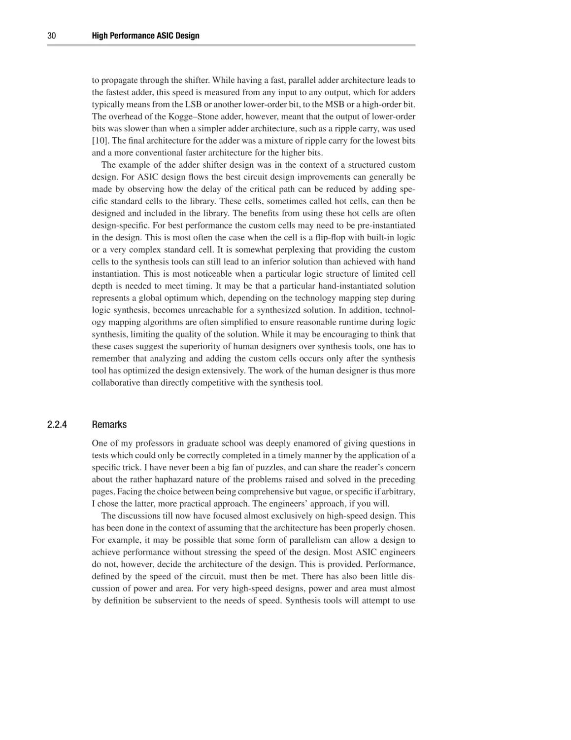
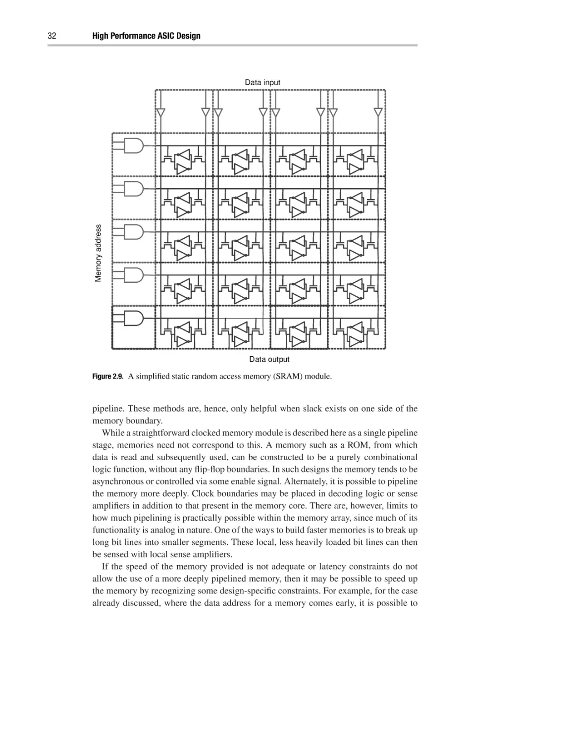
2.3 Designing and using high-speed memories
2.4 What to remember if applying domino logic
18
18
22
31
35
3
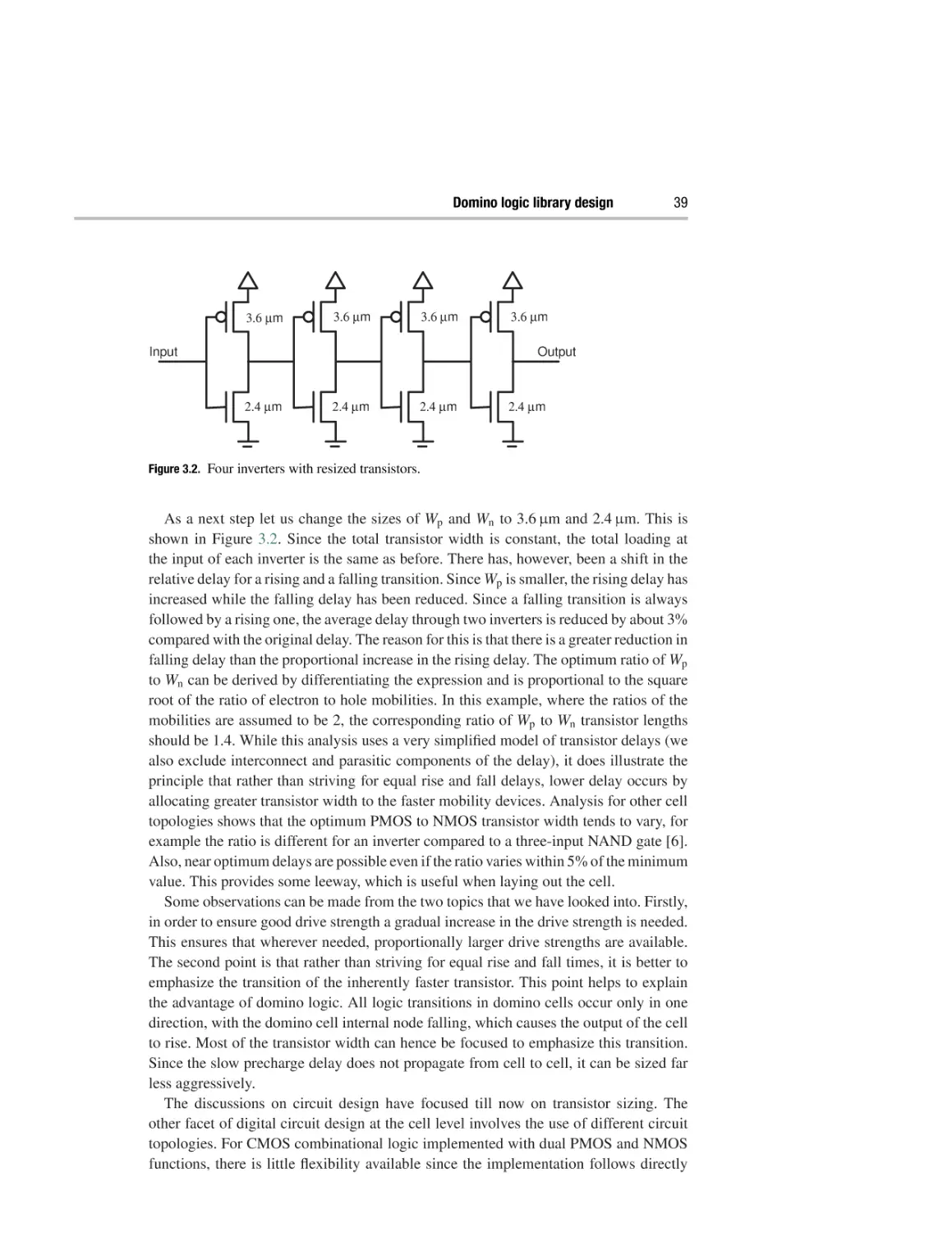
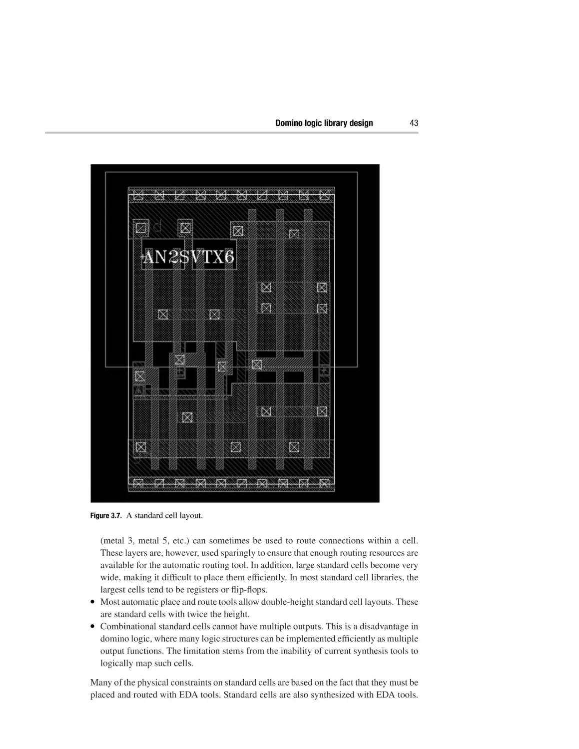
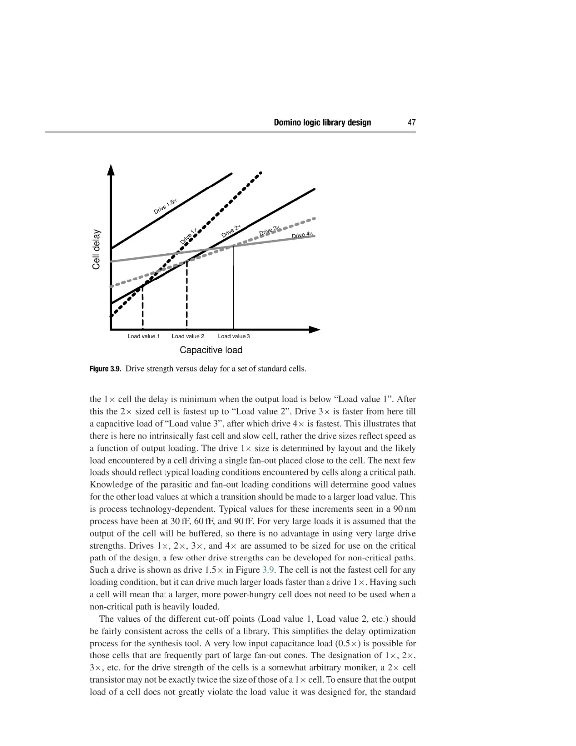
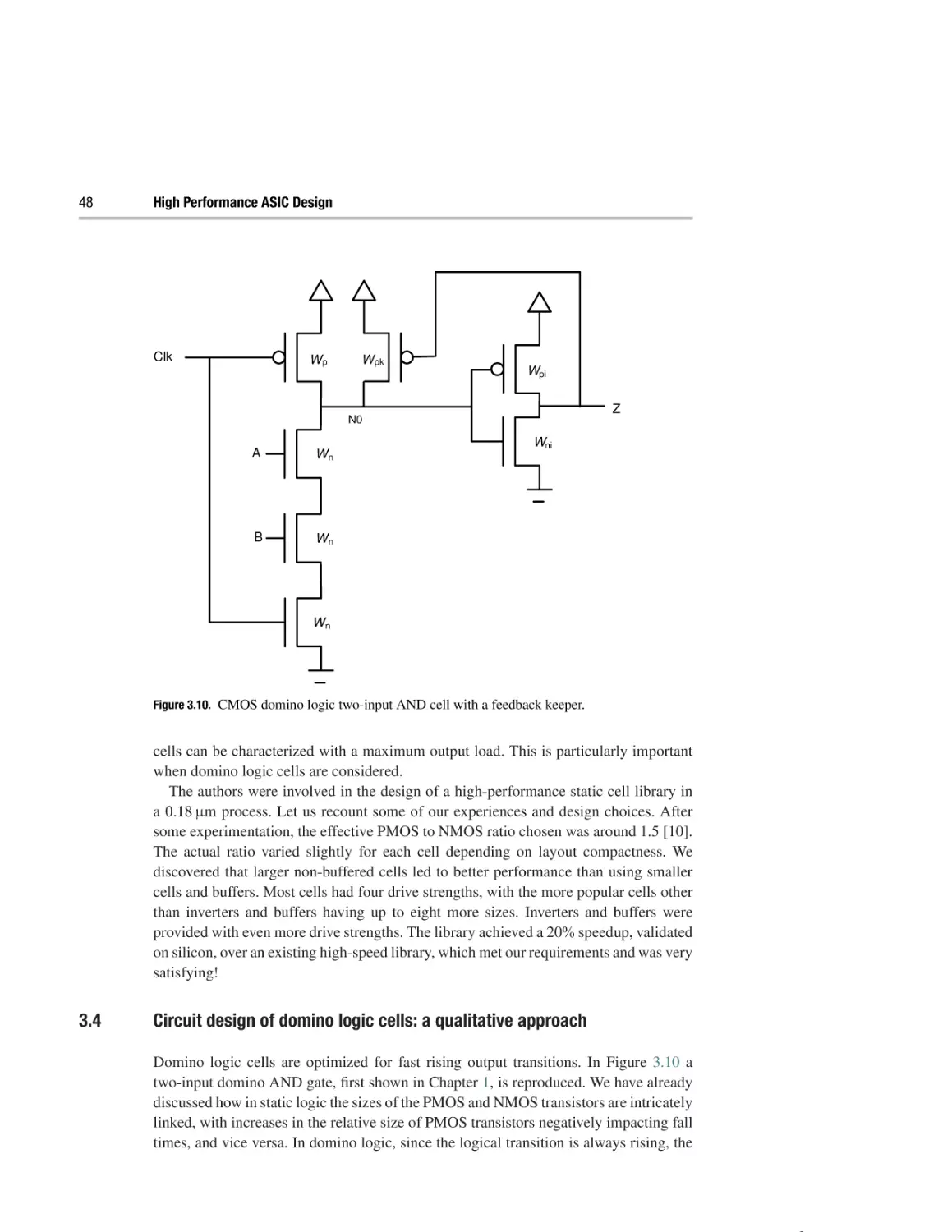
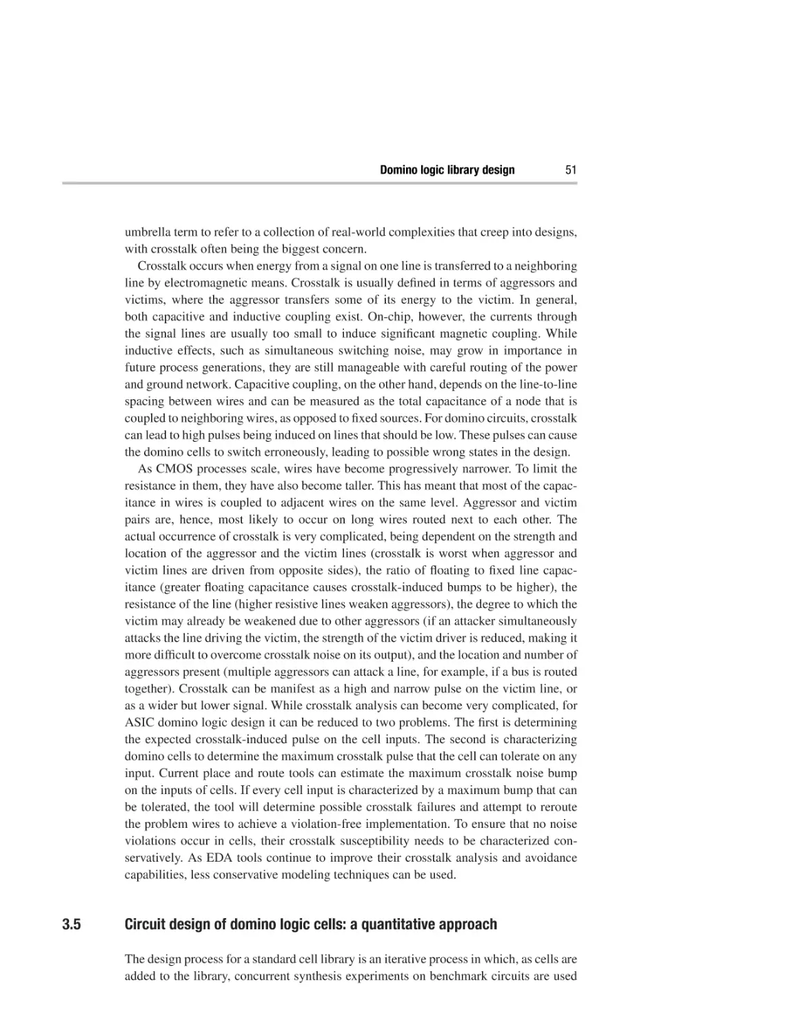
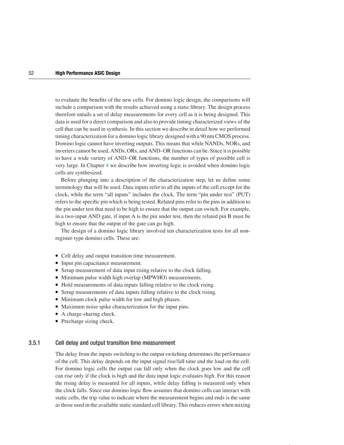
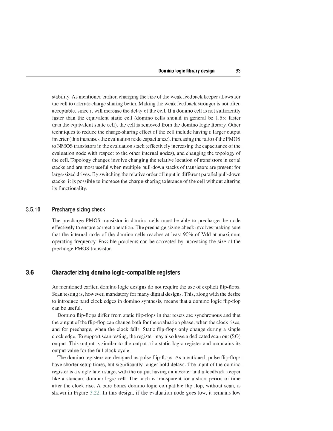
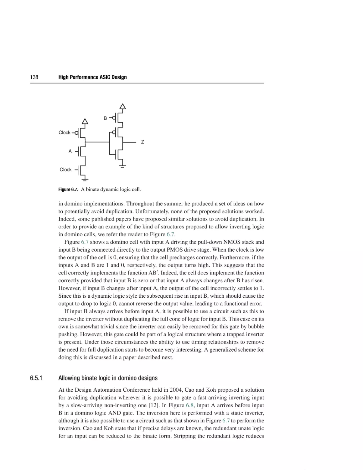
Domino logic library design
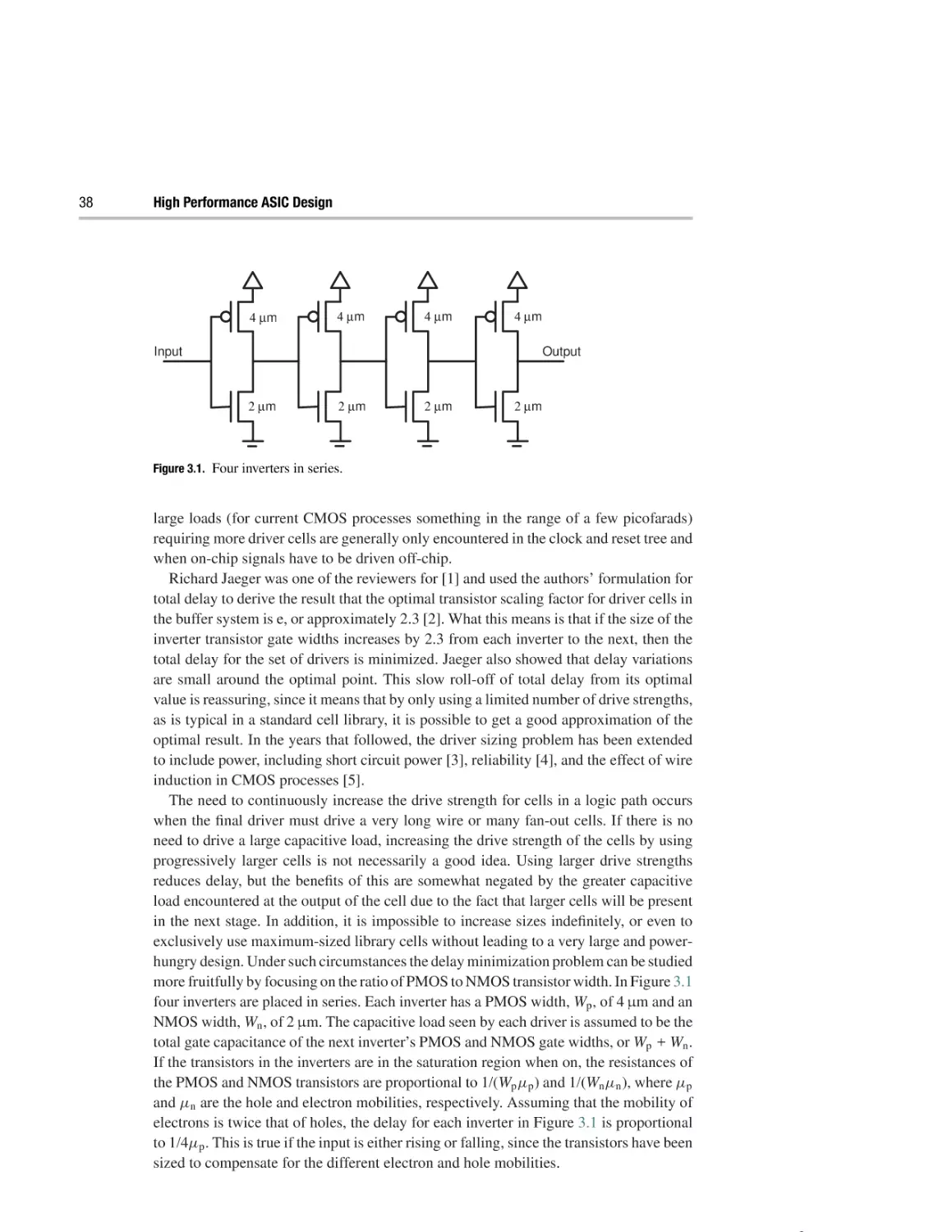
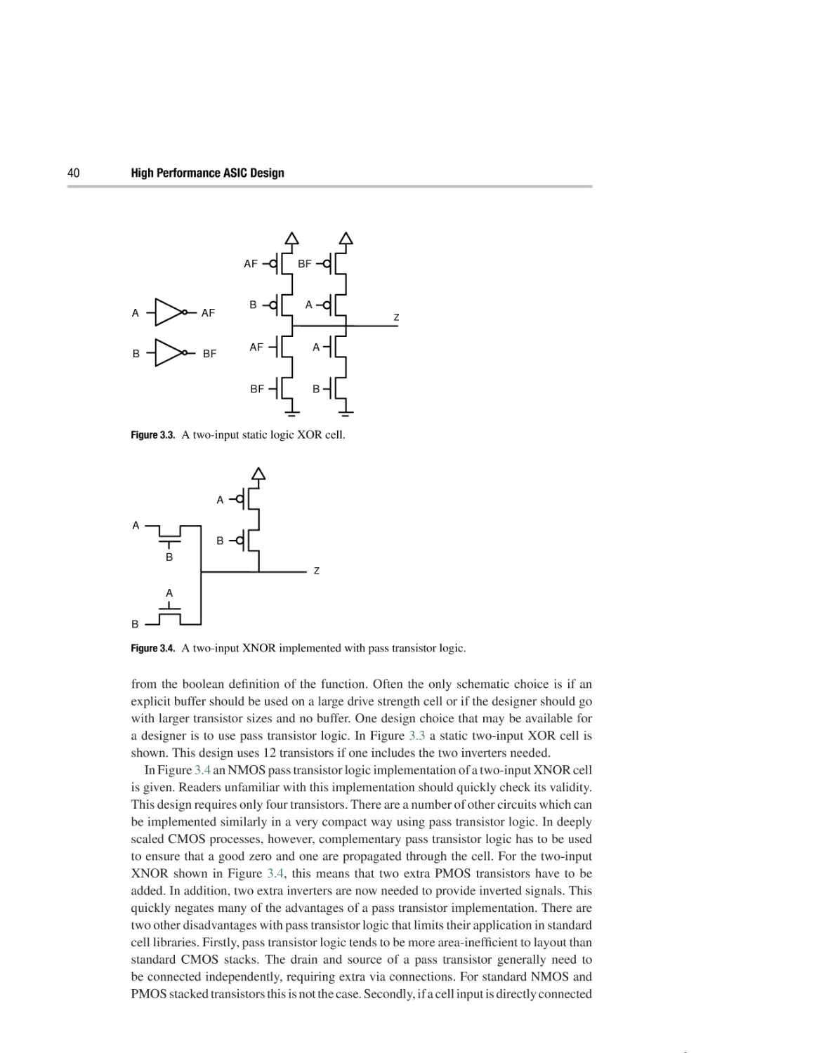
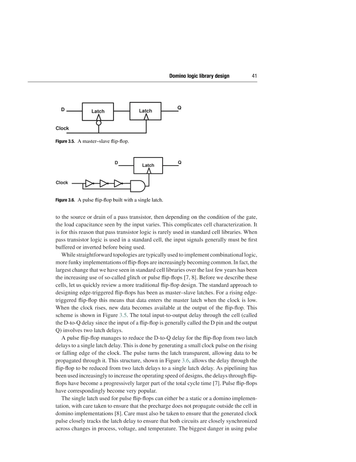
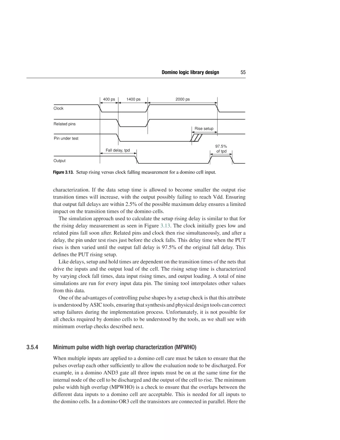
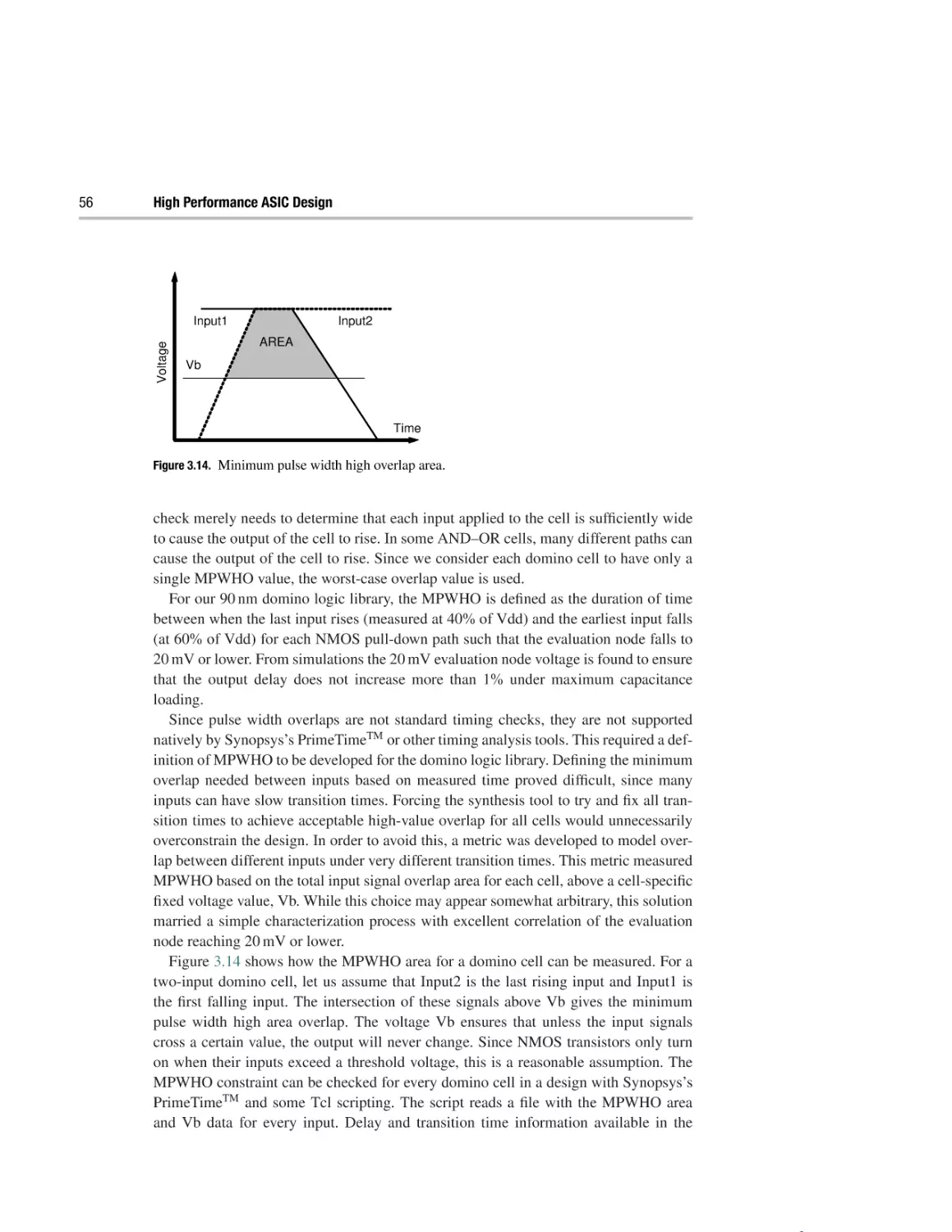
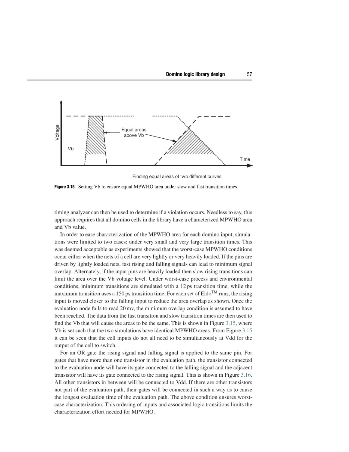
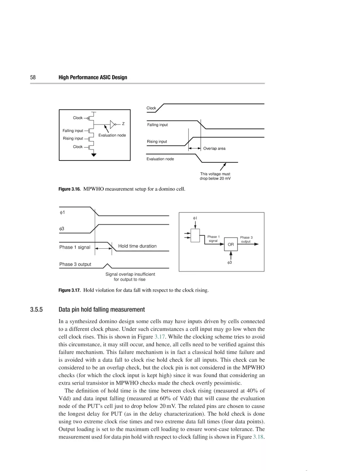
3.1 High-speed digital circuit design
3.2 An introduction to standard cells
3.3 Designing a high-performance standard cell library
3.4 Circuit design of domino logic cells: a qualitative approach
3.5 Circuit design of domino logic cells: a quantitative approach
3.6 Characterizing domino logic-compatible registers
3.7 Layout of domino logic standard cells
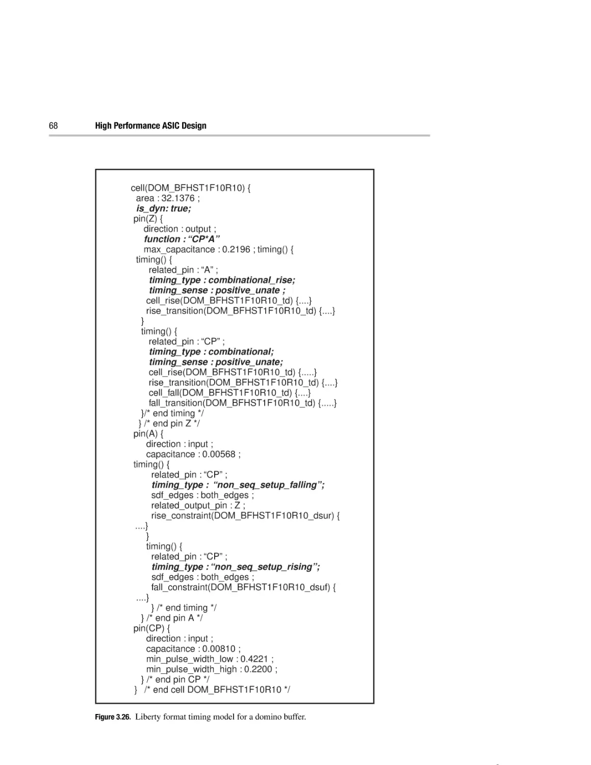
3.8 Timing models for domino logic cells
37
37
42
45
48
51
63
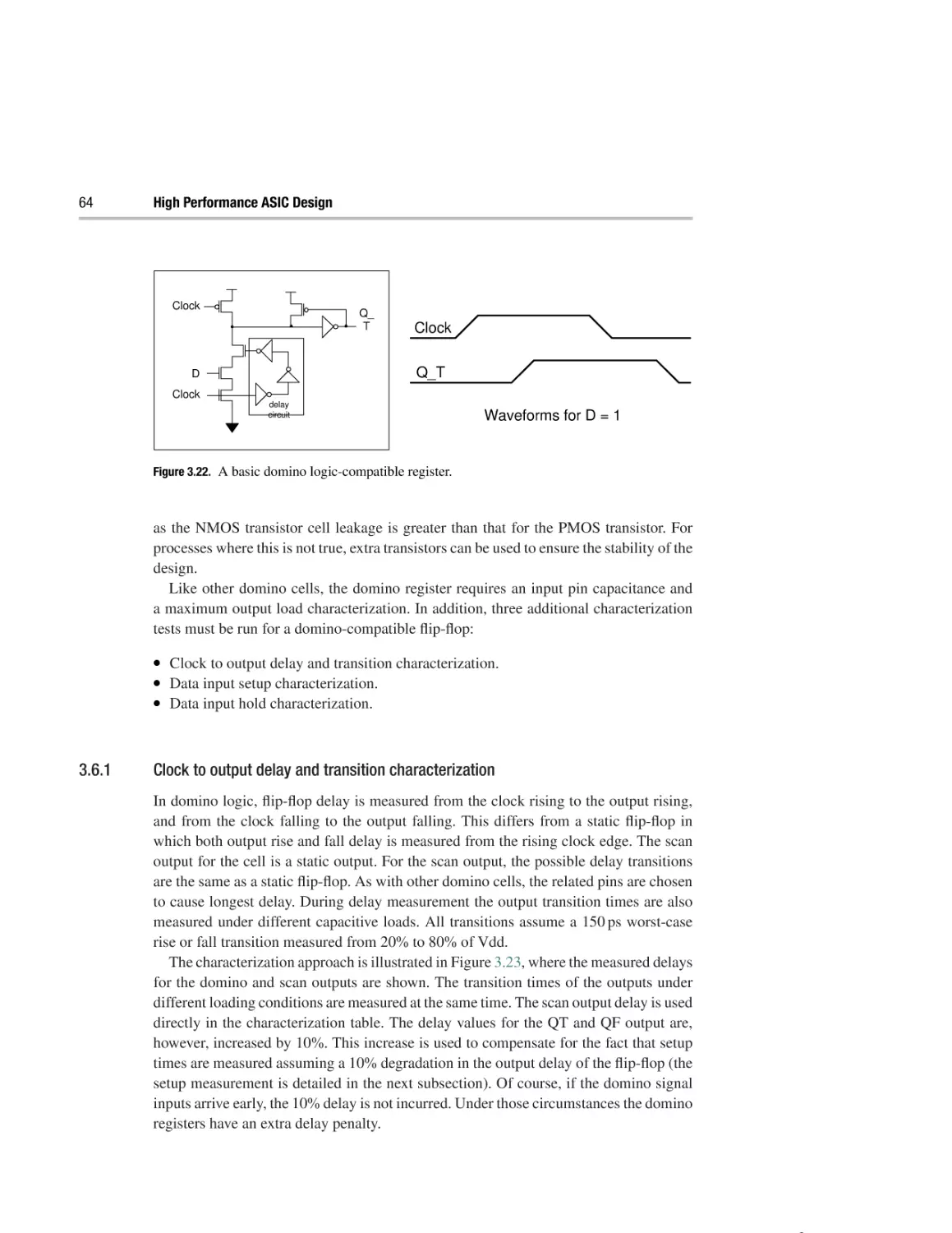
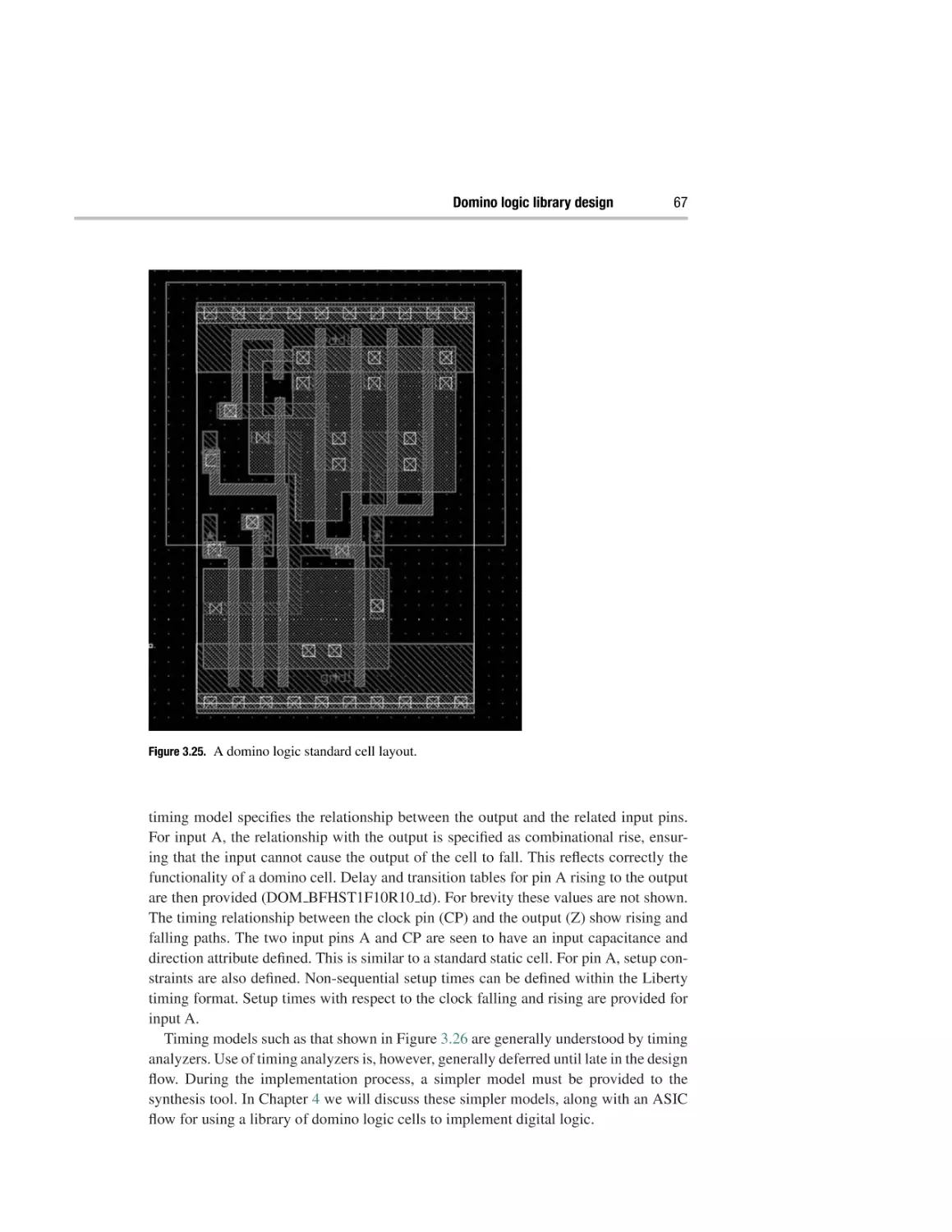
65
66
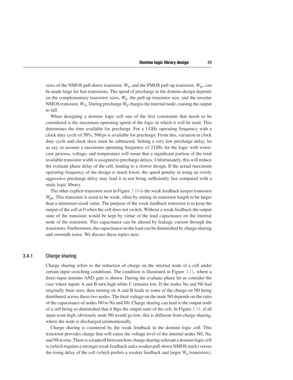
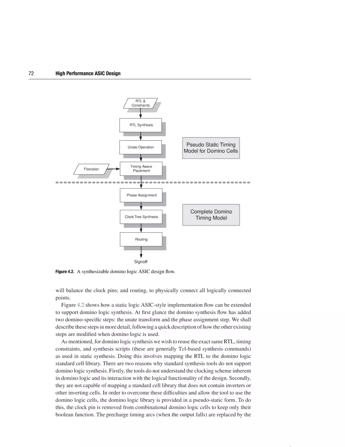
4
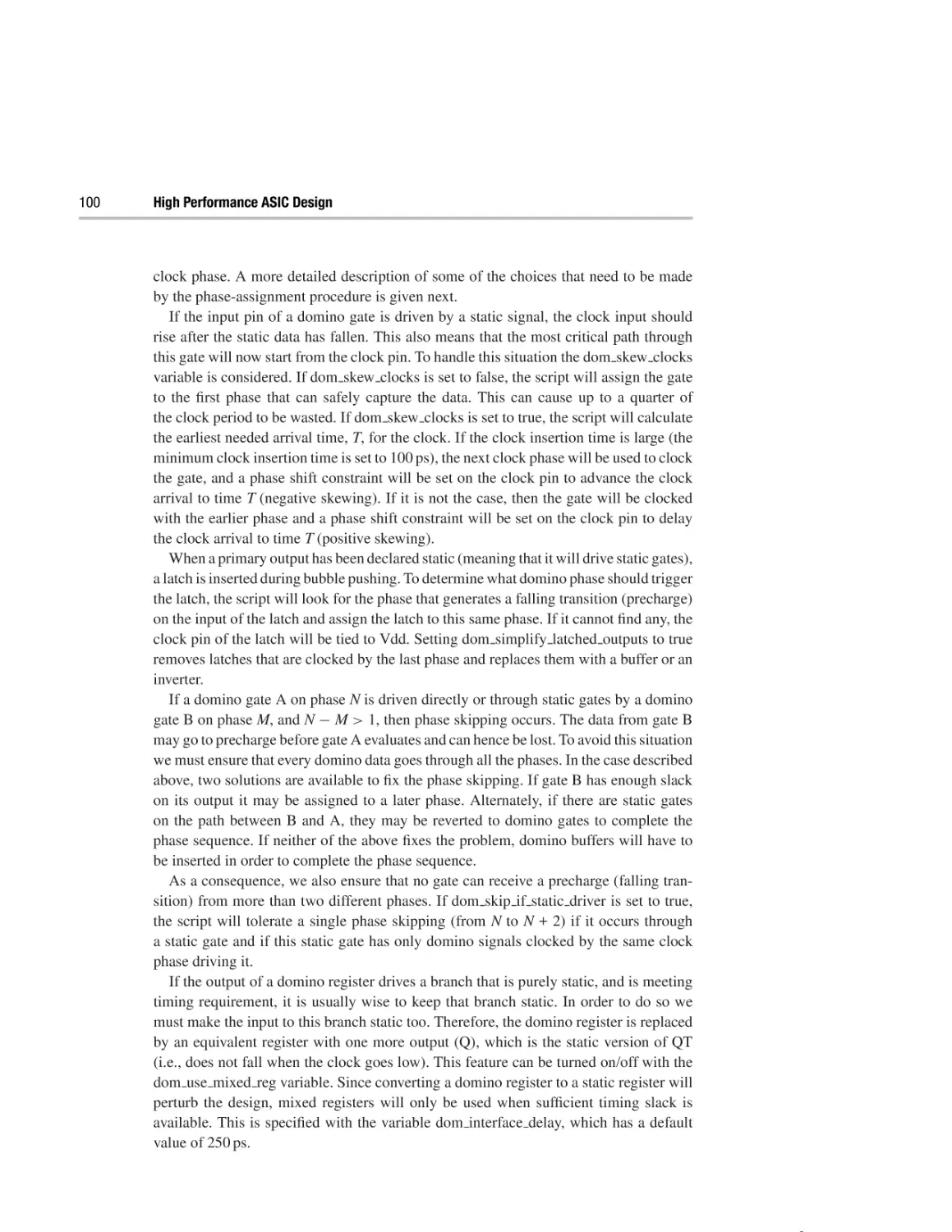
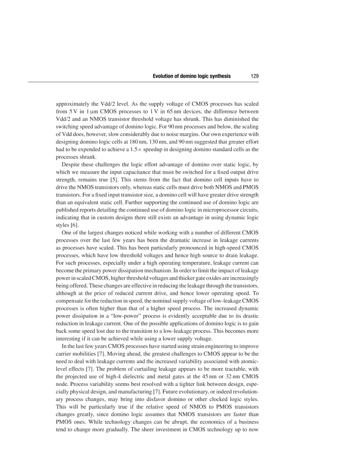
Domino logic synthesis
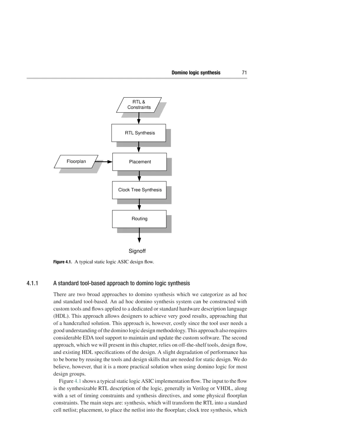
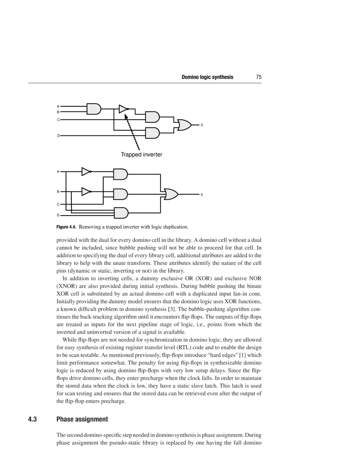
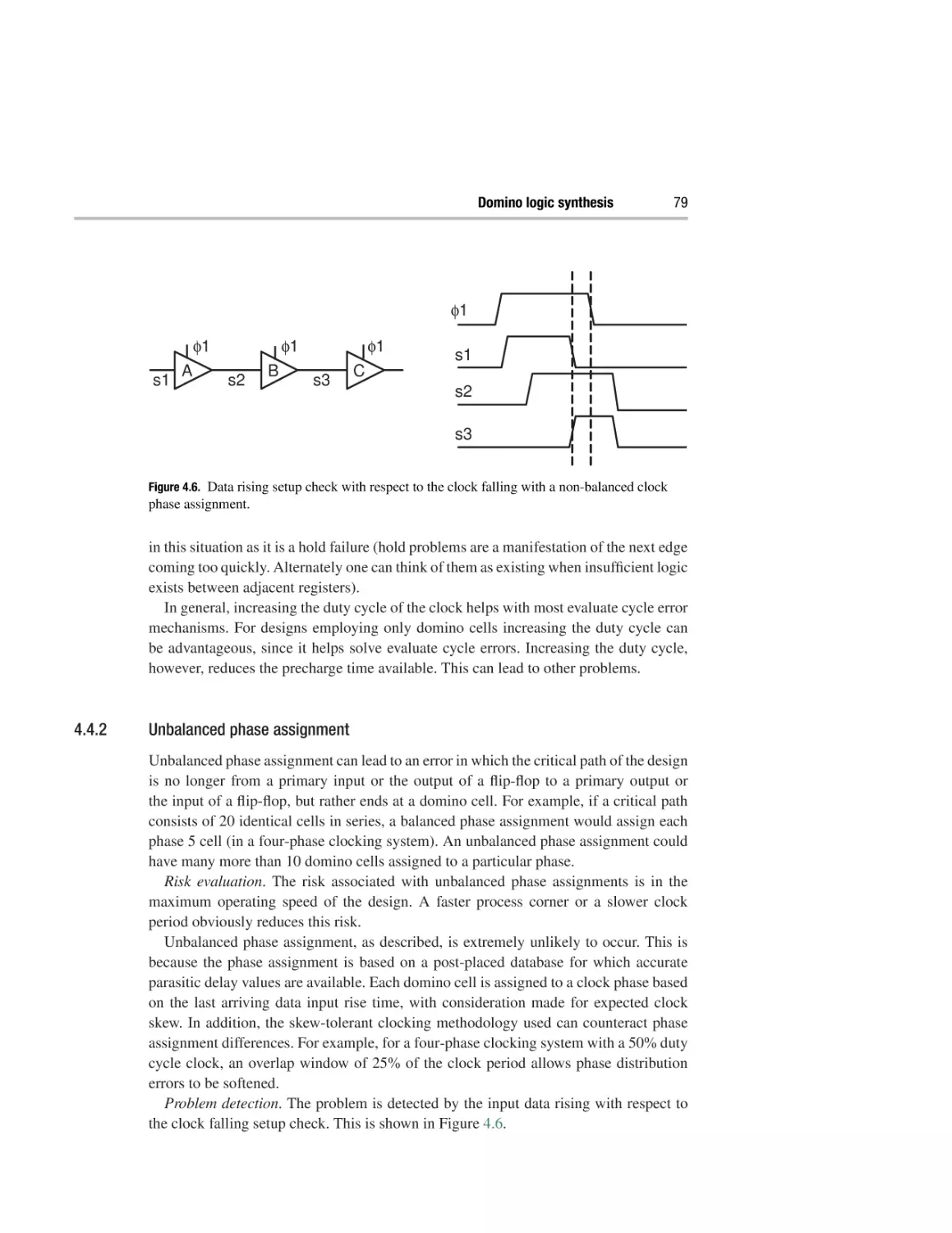
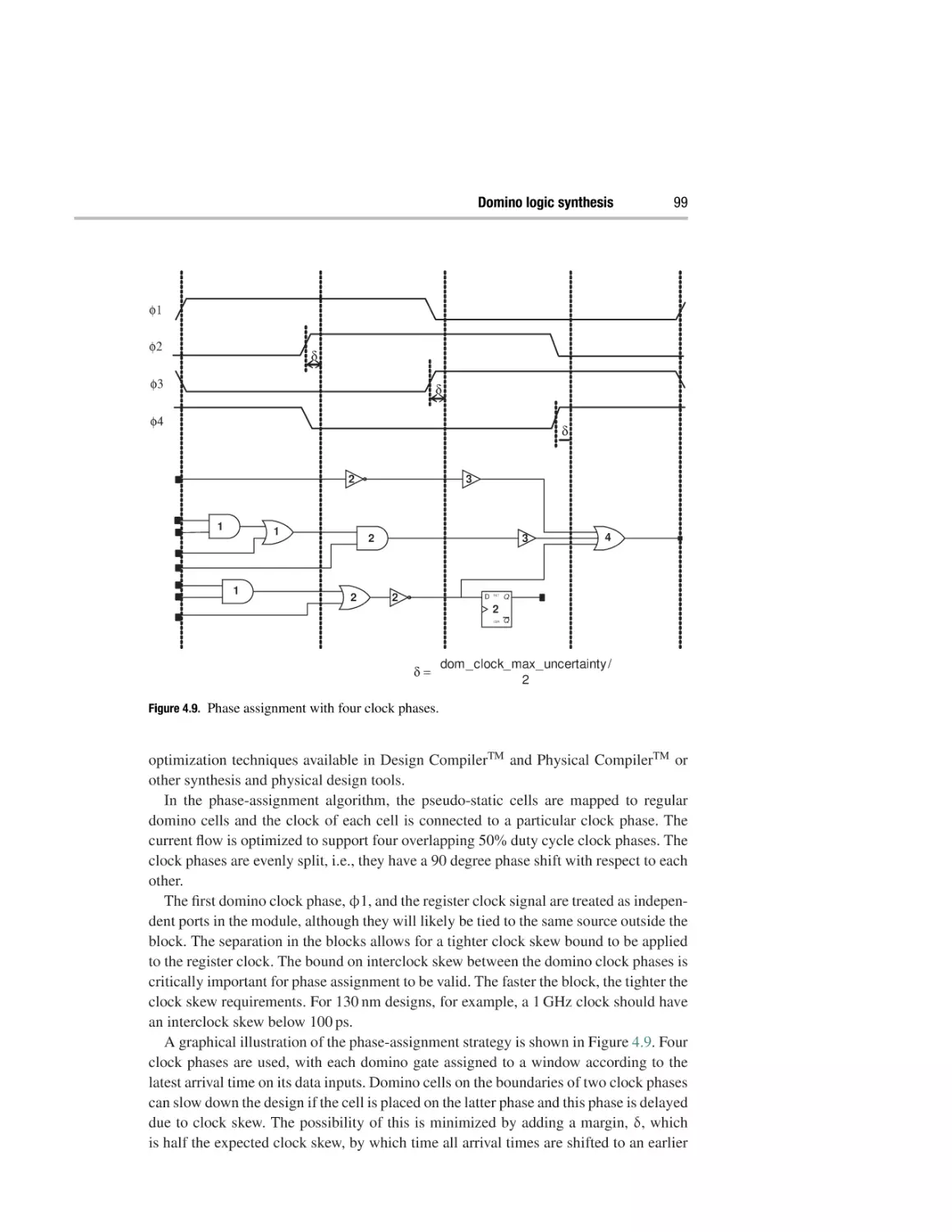
4.1 Introduction to domino logic synthesis
4.2 Unate transform
4.3 Phase assignment
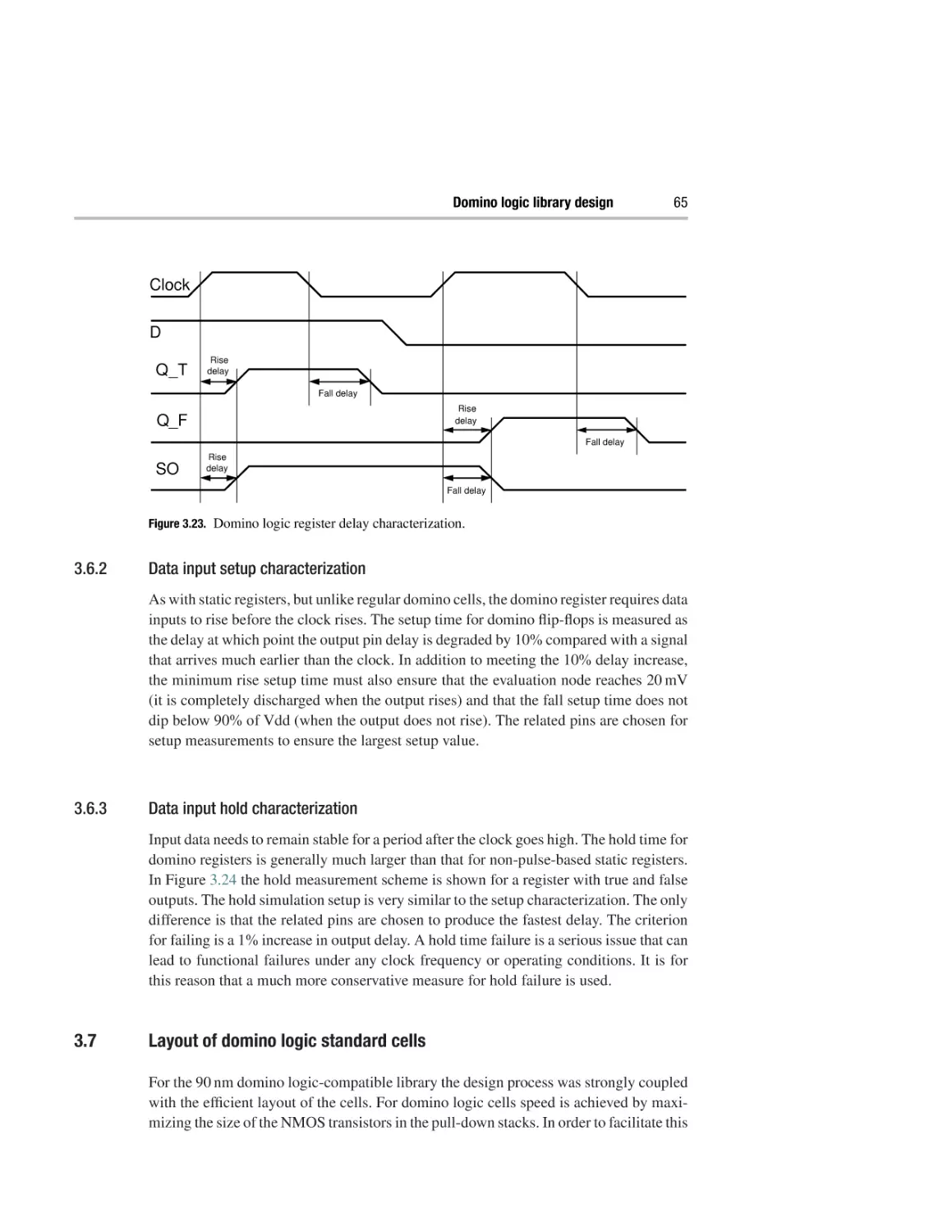
4.4 Phase-assignment rules
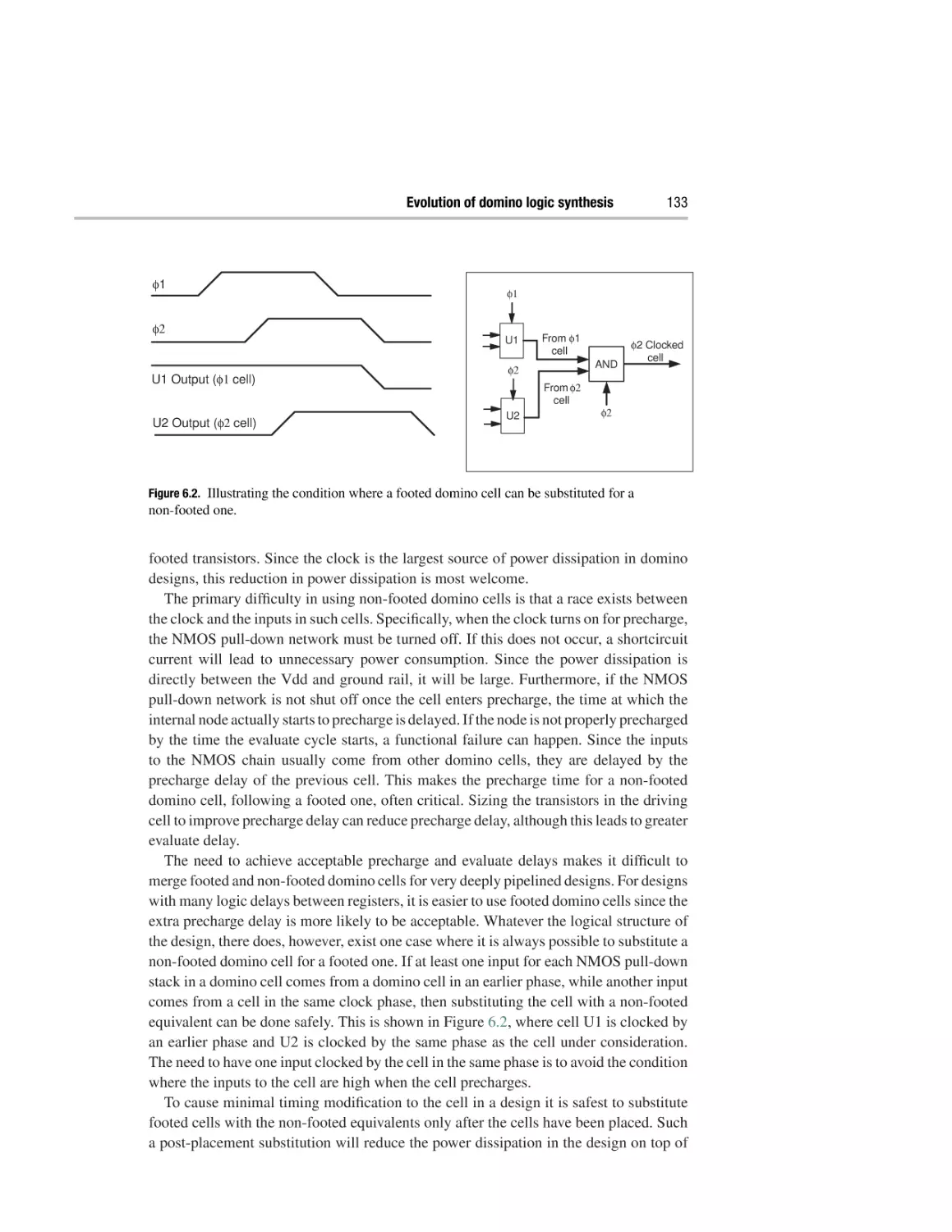
4.5 An example domino synthesis flow
4.6 Schematic capture of domino designs
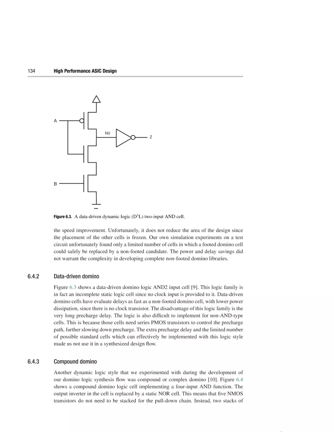
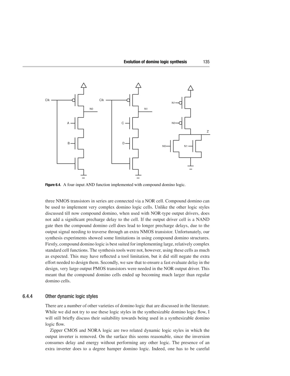
70
70
73
75
77
86
106
P1: SJT/...
P2: SJT
9780521873345agg.xml
CUUK158-Hossain
July 1, 2008
14:59
vi
Contents
5
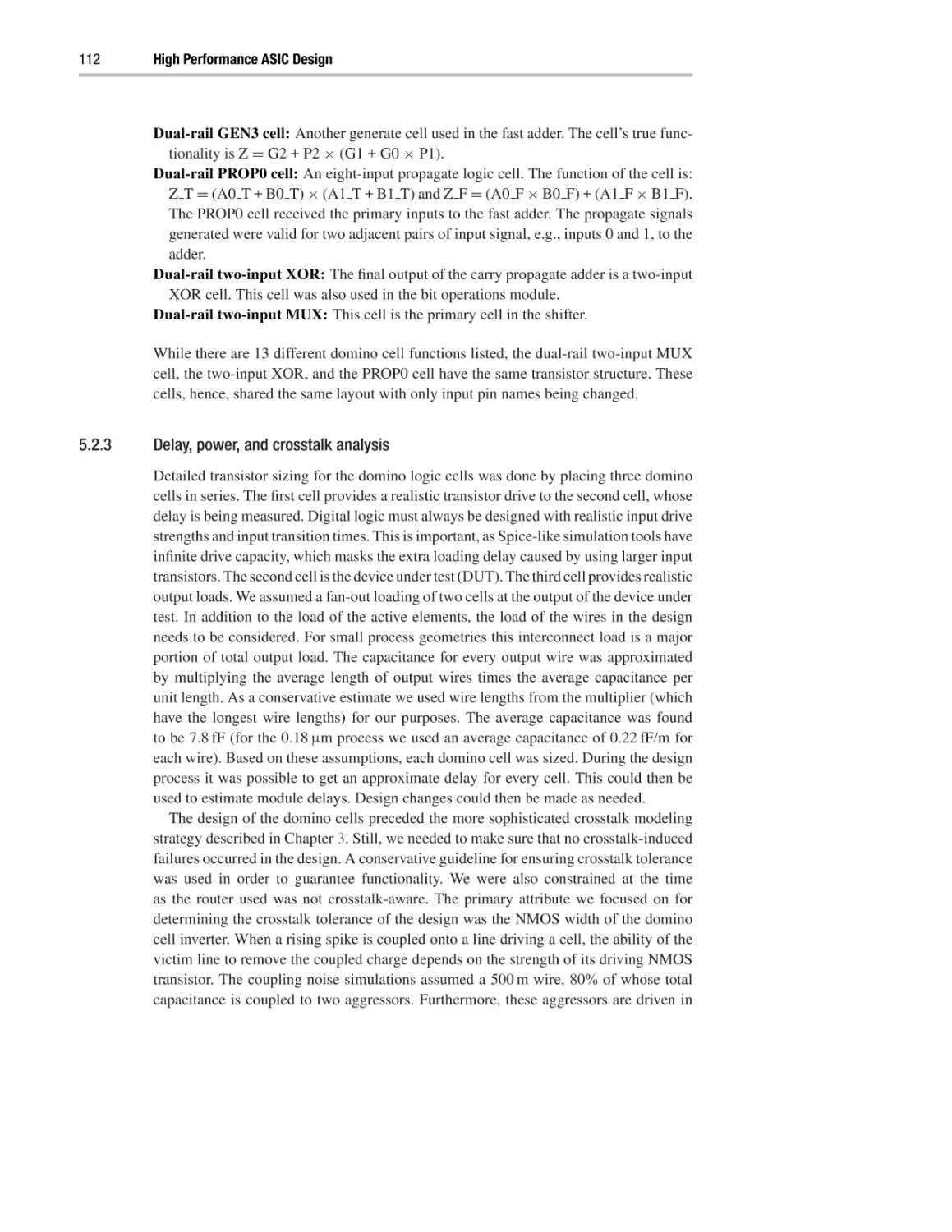
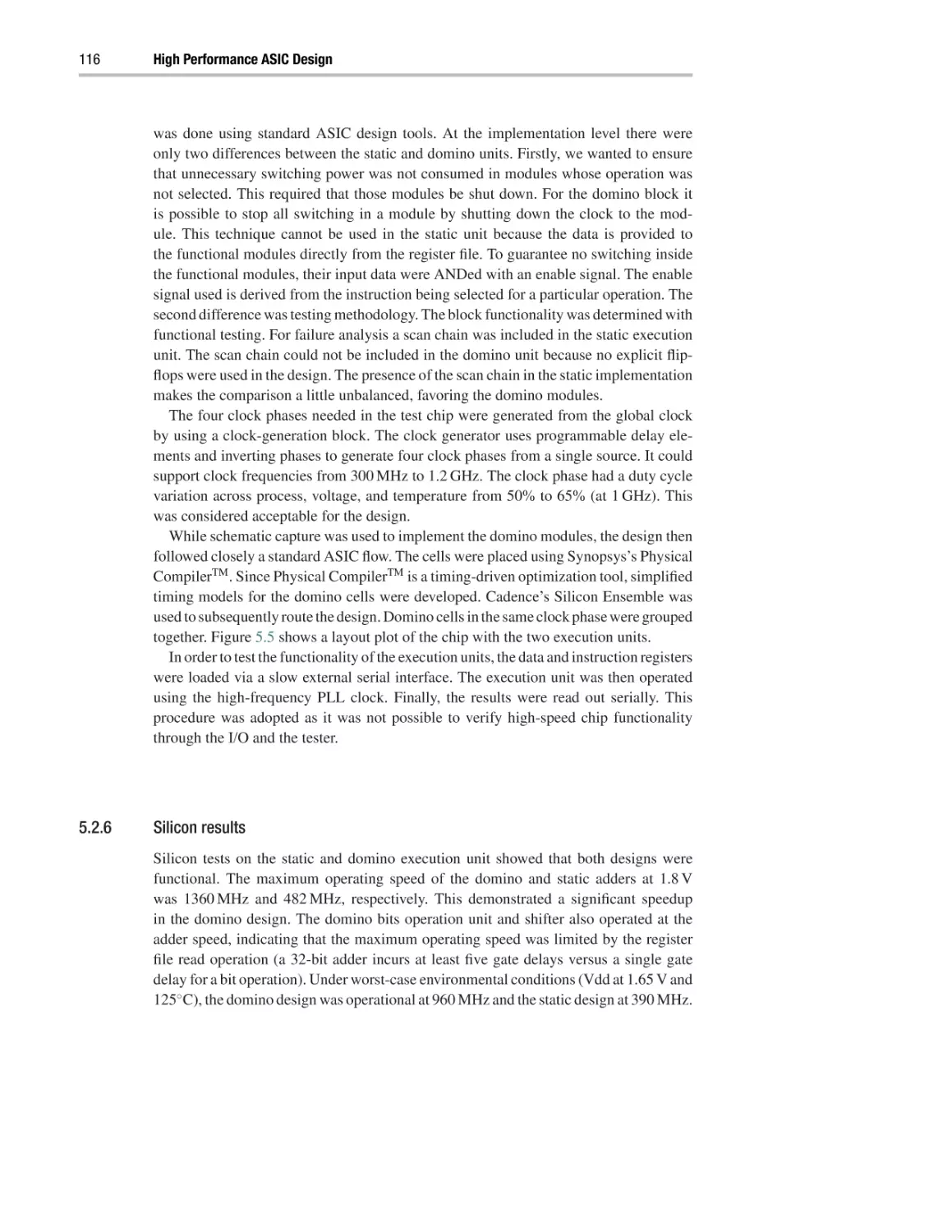
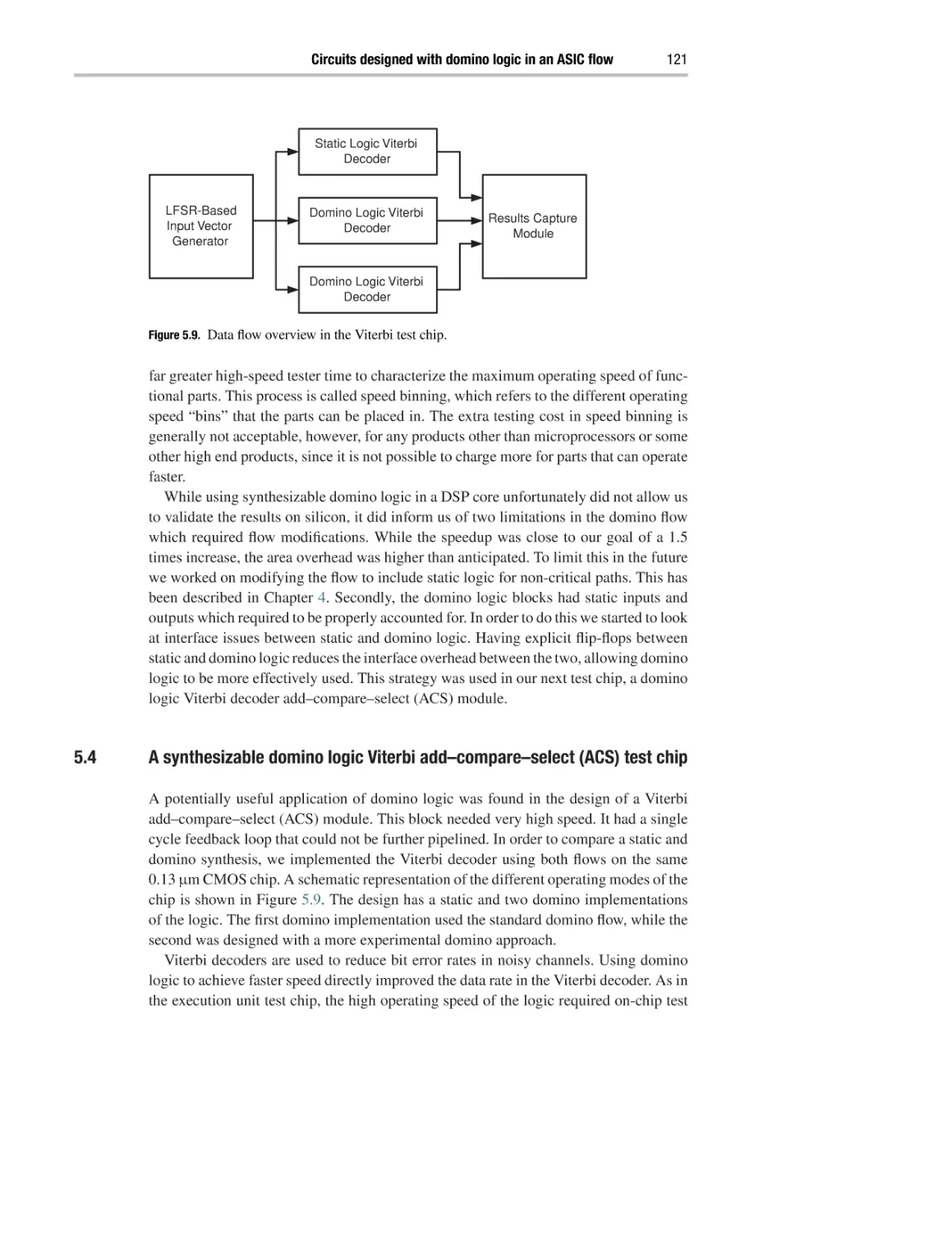
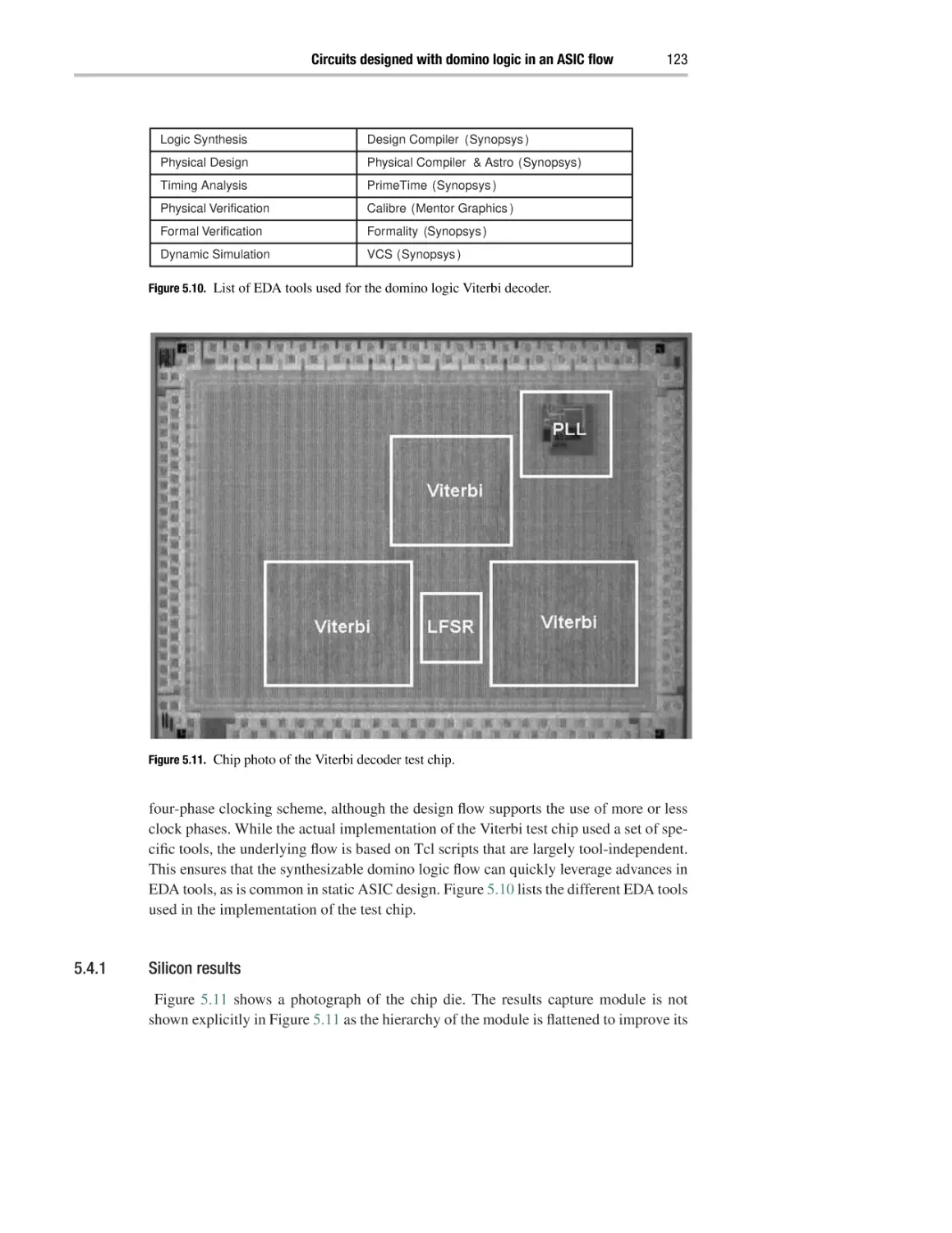
Circuits designed with domino logic in an ASIC flow
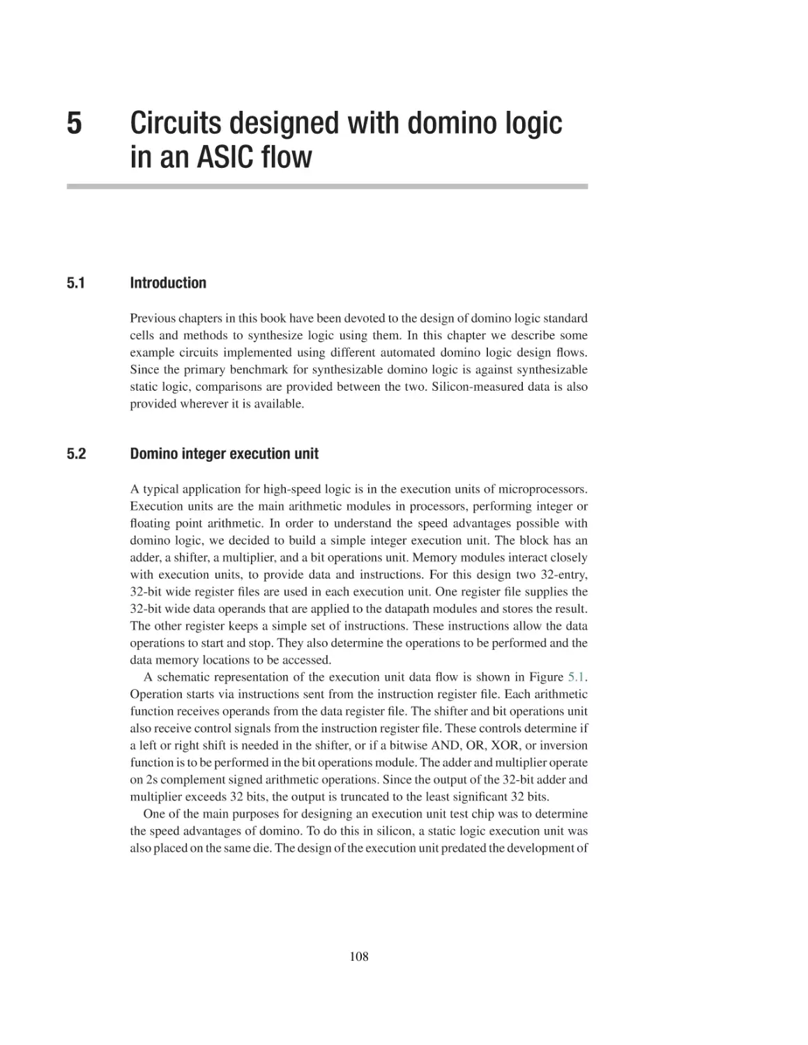
5.1 Introduction
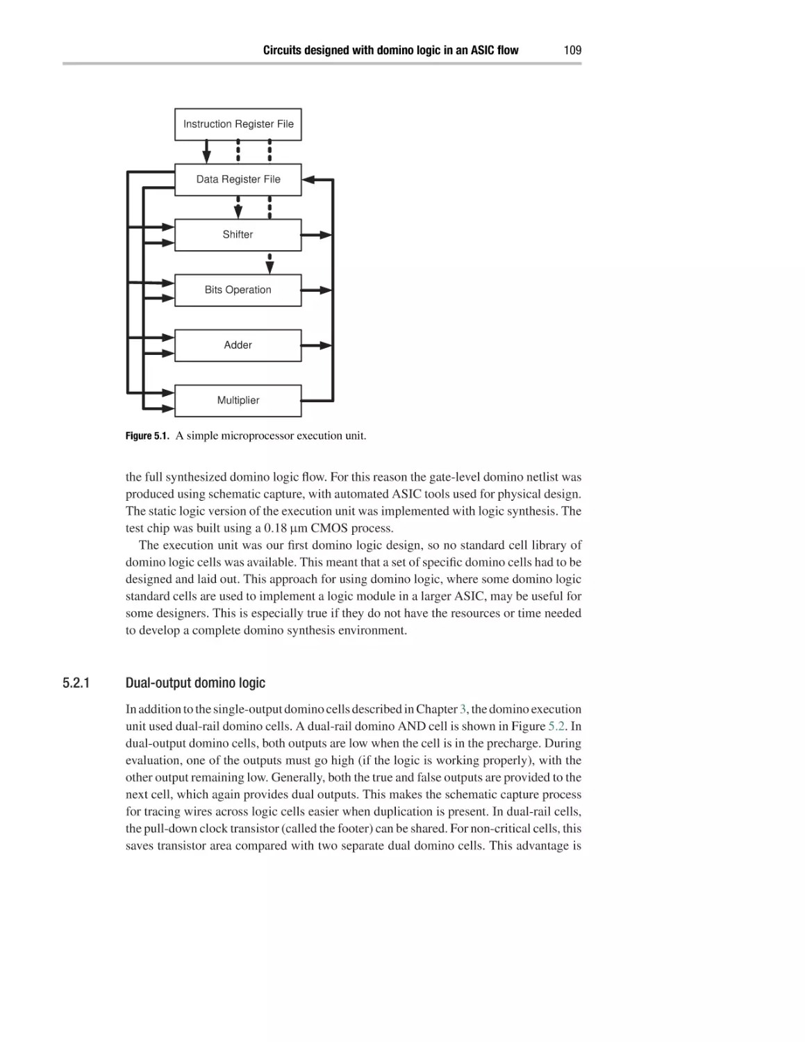
5.2 Domino integer execution unit
5.3 A synthesized domino logic DSP core
5.4 A synthesizable domino logic Viterbi add–compare–select (ACS)
test chip
5.5 Intel’s published domino logic synthesis flow
5.6 Conclusions
108
108
108
119
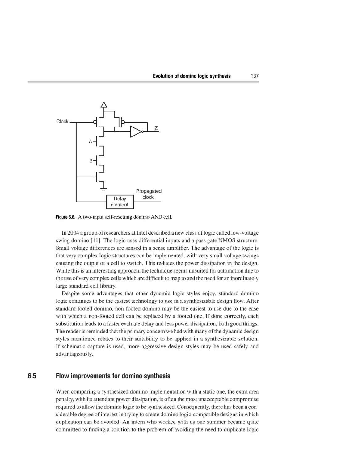
Evolution of domino logic synthesis
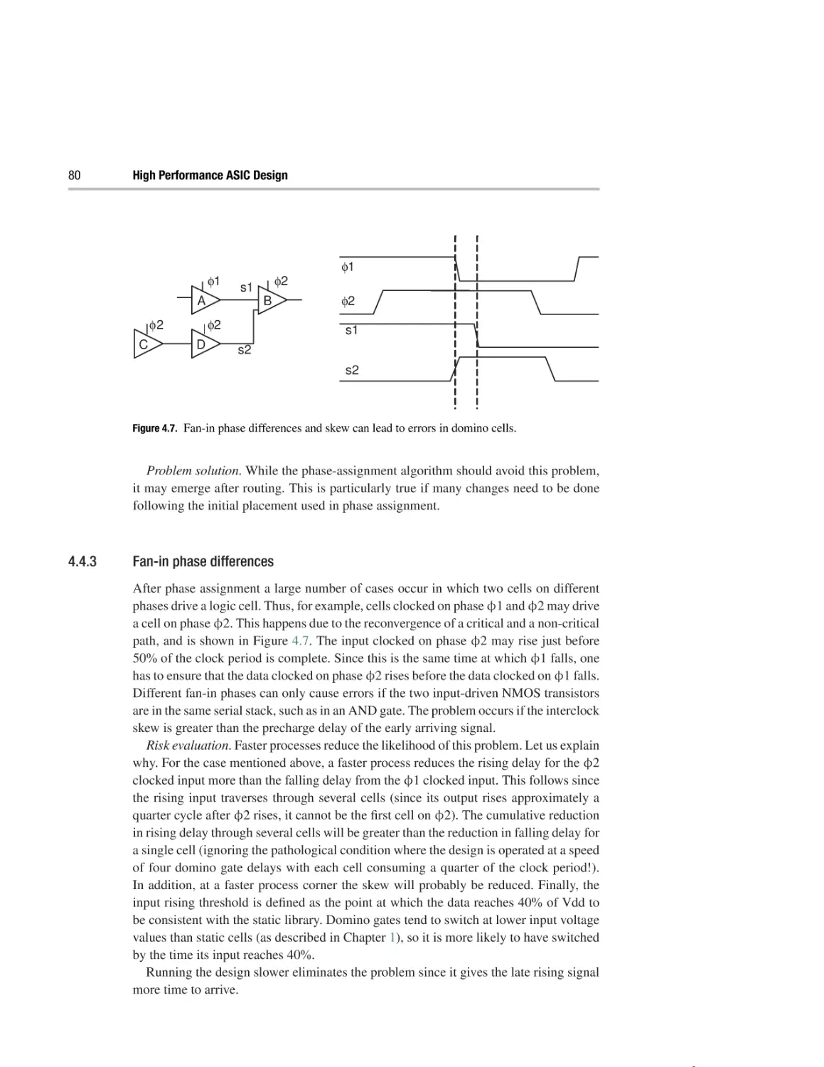
6.1 The state of digital ASIC design methodologies
6.2 Process trends and domino logic
6.3 Clocking methodology for domino circuits
6.4 Synthesizing other dynamic logic families
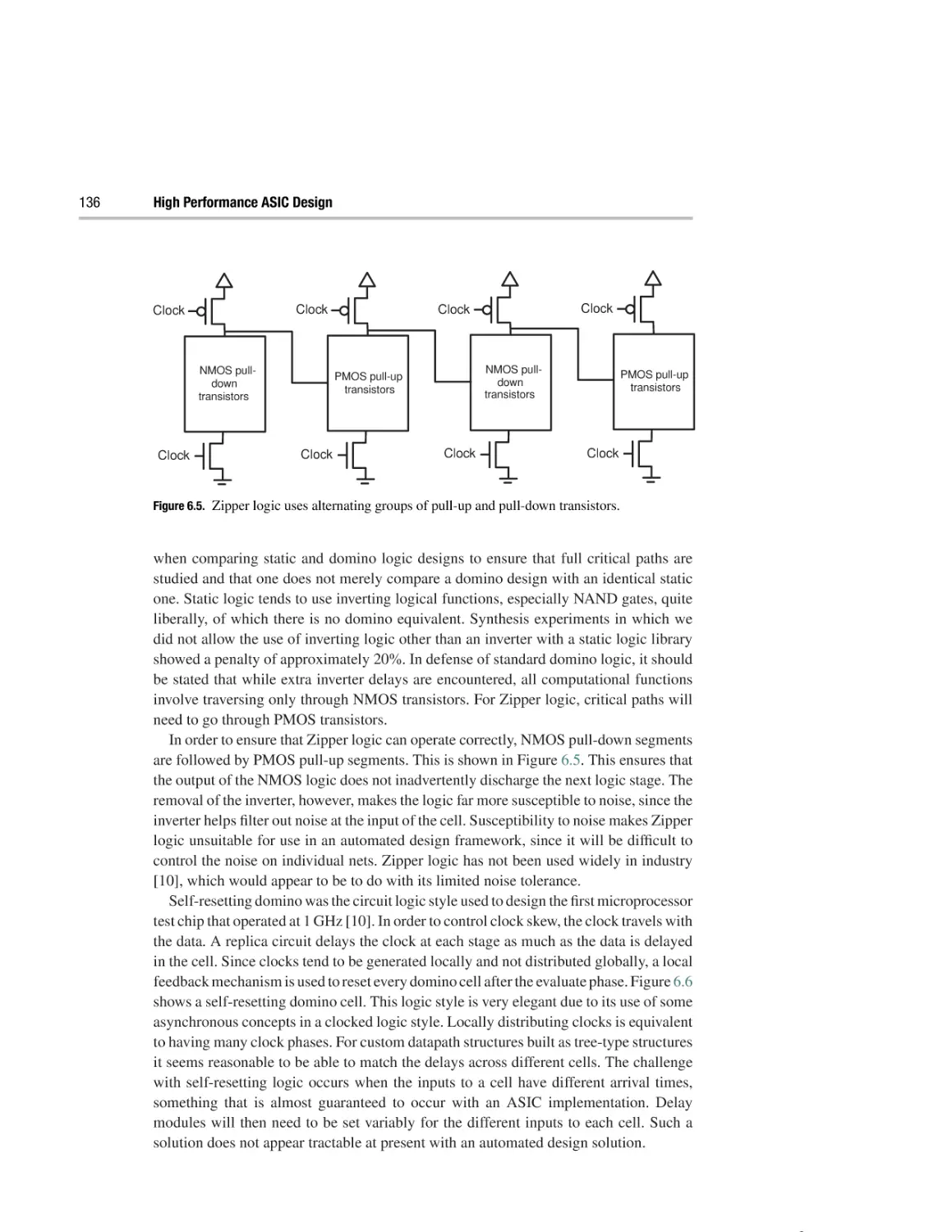
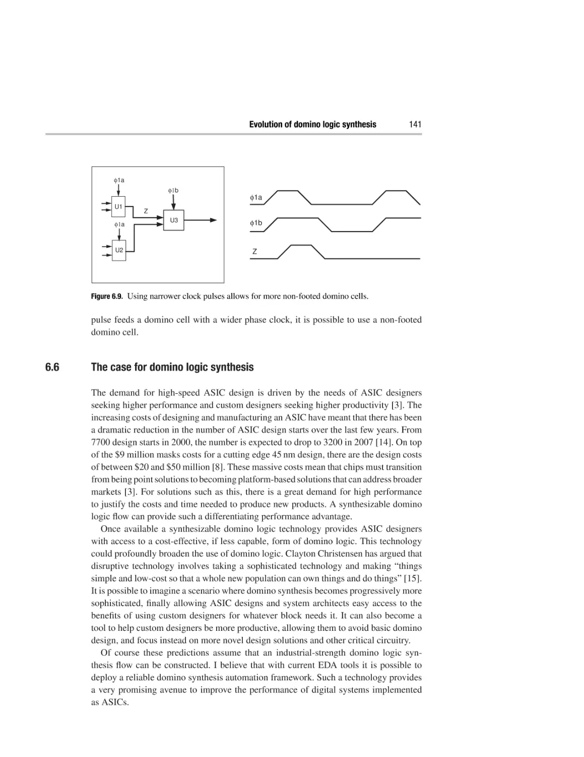
6.5 Flow improvements for domino synthesis
6.6 The case for domino logic synthesis
127
127
128
130
132
137
141
Index
143
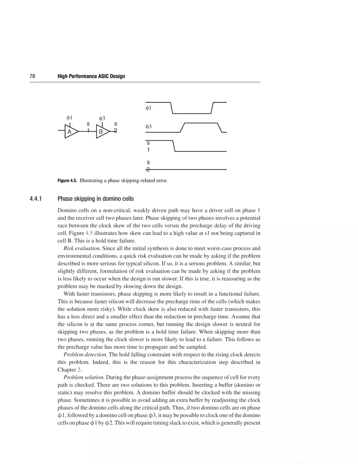
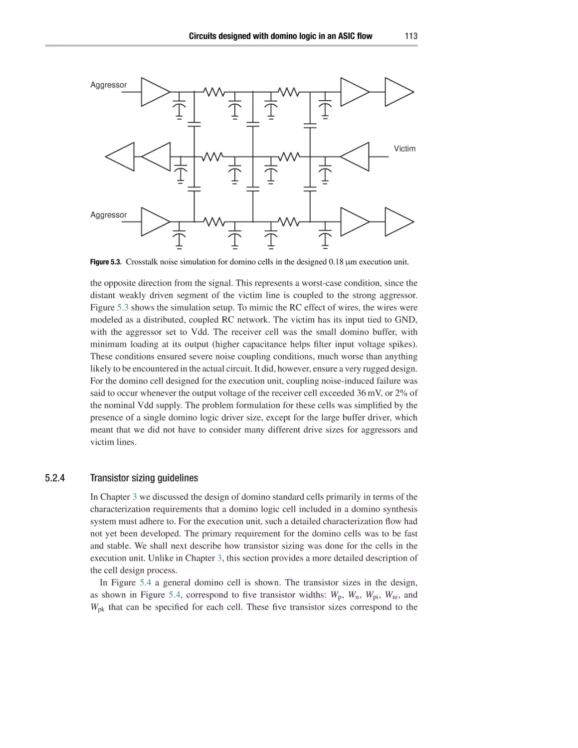
6
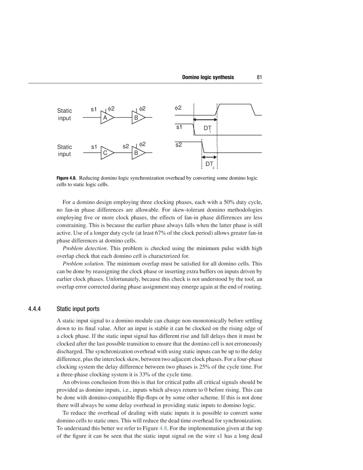
121
124
126
P1: SJT/...
P2: SJT
9780521873345agg.xml
CUUK158-Hossain
July 1, 2008
14:59
Preface
This book stems from my experience over the last few years in designing high-speed
digital logic using ASIC design flows. I discovered that while it is possible to significantly
improve performance in ASIC implementations with deep pipelining and careful physical
design, a speed penalty still had to be paid due to their exclusive use of static logic. This
spurred an interest in using domino logic with automated synthesis and place and route
tools. This book documents my experiences in automating the use of domino logic, and
shows that despite the challenges entailed in the process, it is possible to use domino
logic with industry-standard ASIC tools and achieve a significant speed improvement in
the process.
Engineering is a group activity. The development of our domino logic synthesis system
was possible due to the collaboration of many intelligent, enthusiastic, and dedicated
co-workers whose contributions I must acknowledge. First of all I would like to thank
my two chapter co-authors, Tommy Zounes and Bernard Bourgin. In addition to being
gifted and hard-working engineers, Tommy and Bernard have also always been very
generous with their knowledge and time, allowing all of their co-workers, including
me, to learn a great deal from them. The domino logic library was possible due to the
talents and efforts of Scott Anderson, Shaun Forsting, Judy Alvarez-Gallardo, Roger
Boates, Michael Lin, and Juneho Park, who helped design the schematics and also
contributed to the myriad other tasks involved with taping out a number of chips. Scott,
armed with a contagious optimism, also helped me document our early experiences
with using domino logic. Shaun Forsting converted the schematics into very efficient
layouts across a number of different CMOS processes. During the early years of the
domino logic project we were joined by two engineers from Italy: Fabrizio Viglione and
Marco Cavalli. They both worked on the first domino chips with great enthusiasm and
effectiveness. Fabrizio subsequently took the first stab at implementing our approach to
synthesizing domino logic. From France we were later joined by the affable Leonardo
Valencia, who with Cyril Adobati and Robin Wilson completed the first design that
used a fully synthesizable domino logic flow. Roy Mader and Boris Andreev worked
on the project as summer interns. Roy subsequently became a much-valued permanent
member of our group and led us in overcoming many of the onerous challenges involved
in pushing domino designs through automated place and route flows.
People work effectively only in a supporting environment. I would like to thank
our manager Naresh Soni for encouraging and supporting us in our work in domino
P1: SJT/...
P2: SJT
9780521873345agg.xml
viii
CUUK158-Hossain
July 1, 2008
14:59
Preface
synthesis, as well as Joel Monnier, who led STMicroelectronics’ Central Research and
Development organization. They provided us with the extraordinary luxury of being
allowed to innovate in an autonomous manner. Nick Richardson, who later led the
group, continued in this fine tradition and also provided more specific technical advice
on matters related to logic and architecture. In addition, I must thank the many others in
STMicroelectronics who supported us in our work on domino logic, including: Philippe
Magarshack, Jean-Pierre Schoellkopf, Sylvain Kritter, Heloise Tupin, Damien Croain,
Alain Chion, Samala Sreekiran, Sanjay Bulusu, Ezio Iacazio, and Marco Gregori.
I would like to thank my wonderful parents, Mosharaff and Inari Hossain, who have
encouraged me throughout this endeavor, and more broadly, instilled in me a love of
books and learning. Finally I must thank my beloved wife, Zakia Chowdhury, whose
support allowed me to write this book. I dedicate this book to her and my two delightful
sons, Farhan and Ishraq.
Razak Hossain
San Diego, CA
P1: SJT/...
P2: SJT
9780521873345agg.xml
CUUK158-Hossain
July 1, 2008
14:59
Abbreviations
ASIC
CMOS
CSA
CTO
DRC
DSPF
DVD
ECO
EDA
FET
fF
FO4
GHz
HDL
LFSR
LSB
LVS
MHz
MIPS
MPC
MPWH
MPWHO
MPWL
MSB
MUX
NMOS
PLL
PMOS
PUT
PVT
QoR
RC
RF
application-specific integrated circuit
complementary metal oxide semiconductor
carry save adder
clock tree optimization
design rule check
detailed standard parasitic format
digital video disc
engineering change order
electronic design automation
field effect transistor
femtofarad
fan-out of four
gigahertz
hardware description language
linear feedback shift register
least significant bit
layout versus schematic
megahertz
million instructions per second
minimum physical constraints
minimum pulse width high
minimum pulse width high overlap
minimum pulse width low
most significant bit
multiplexer
n-channel metal oxide semiconductor
phase locked loop
p-channel metal oxide semiconductor
pin under test
process, voltage, and temperature
quality of results
resistor capacitor circuit
radio frequency
P1: SJT/...
P2: SJT
9780521873345agg.xml
x
CUUK158-Hossain
July 1, 2008
14:59
Abbreviations
RISC
RTL
SDC
SOC
SRAM
TAT
VCO
VLSI
XNOR
XOR
µm
reduced instruction set computer
register transfer level
Synopsys design constraints
system-on-chip
static random access memory
turnaround time
voltage-controlled oscillator
very large scale integration
exclusive NOR
exclusive OR
micrometer
P1: SJT/...
P2: SJT
9780521873345c01.xml
CUUK158-Hossain
July 1, 2008
17:11
1
An introduction to domino logic
1.1
CMOS and NMOS
By the late 1970s complementary metal oxide semiconductor (CMOS) started to become
the process of choice for digital semiconductor designs. CMOS had originally been
proposed by Frank Wanlass in 1963 as a low standby power technology, since CMOS
logic gates dissipate almost no power when the inputs to the gate do not change [1].
This follows as CMOS contains both PMOS field effect transistors (FETs), which can
efficiently drive a high voltage, or logic one value, and NMOS transistors, which are
good at driving a zero voltage. The presence of complementary transistors allows CMOS
logic gates to be implemented so that the output voltage level is connected to the power
or ground line, but not both. This ability to avoid contention ensures that if the inputs are
not changing, then no power is dissipated. This was a major advantage of CMOS over
the other manufacturing processes then available, which dissipated constant leakage or
bias currents.
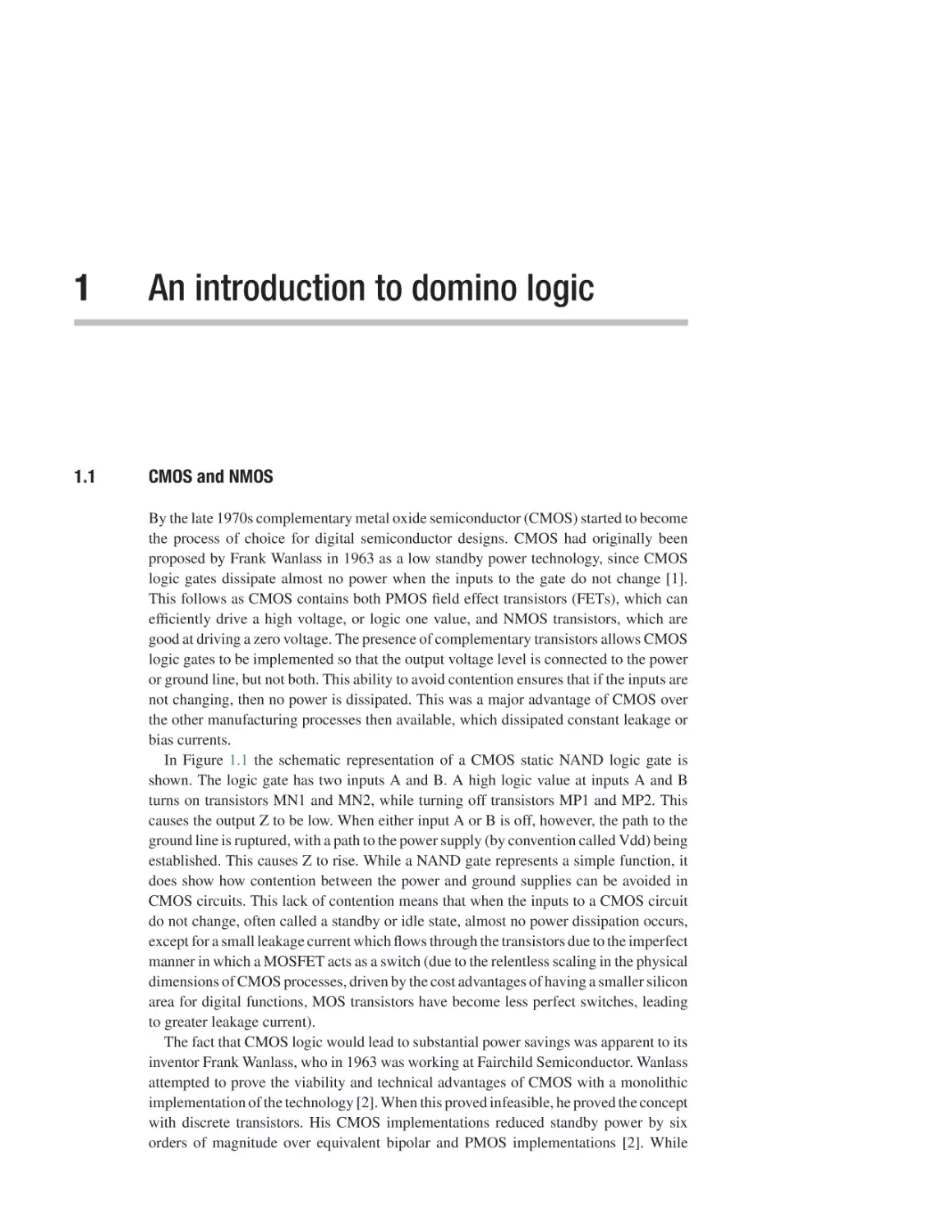
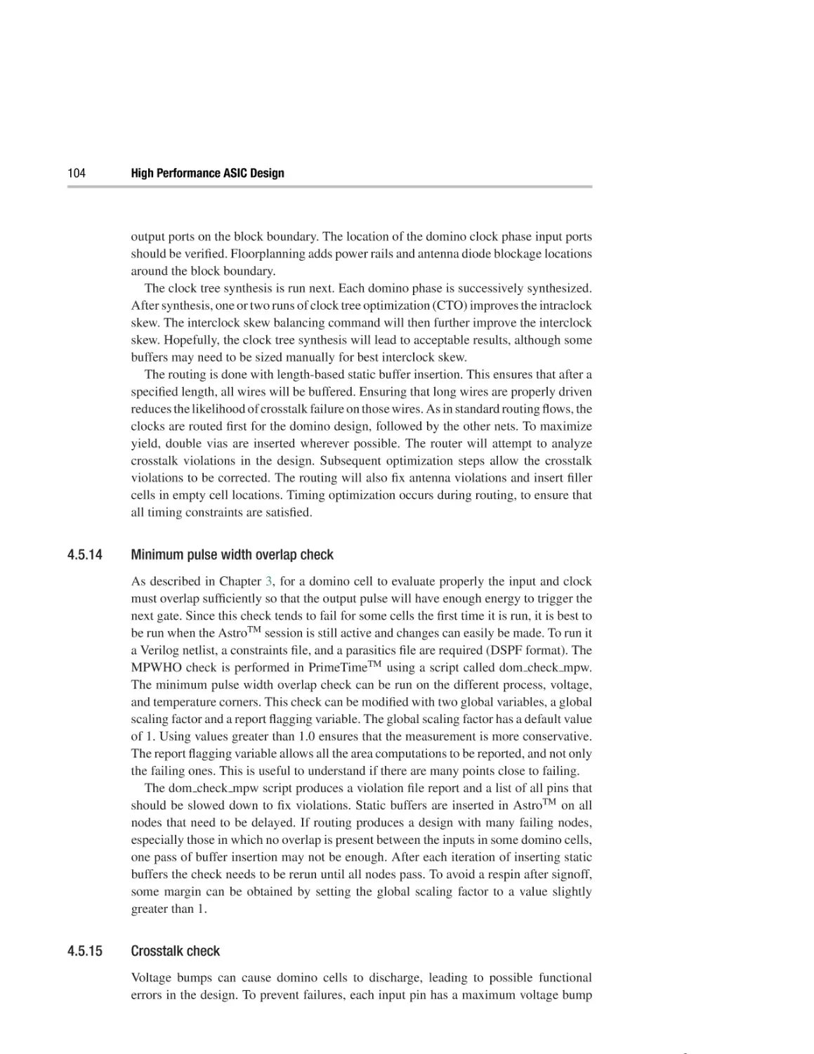
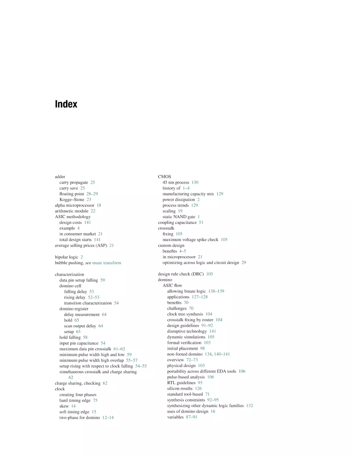
In Figure 1.1 the schematic representation of a CMOS static NAND logic gate is
shown. The logic gate has two inputs A and B. A high logic value at inputs A and B
turns on transistors MN1 and MN2, while turning off transistors MP1 and MP2. This
causes the output Z to be low. When either input A or B is off, however, the path to the
ground line is ruptured, with a path to the power supply (by convention called Vdd) being
established. This causes Z to rise. While a NAND gate represents a simple function, it
does show how contention between the power and ground supplies can be avoided in
CMOS circuits. This lack of contention means that when the inputs to a CMOS circuit
do not change, often called a standby or idle state, almost no power dissipation occurs,
except for a small leakage current which flows through the transistors due to the imperfect
manner in which a MOSFET acts as a switch (due to the relentless scaling in the physical
dimensions of CMOS processes, driven by the cost advantages of having a smaller silicon
area for digital functions, MOS transistors have become less perfect switches, leading
to greater leakage current).
The fact that CMOS logic would lead to substantial power savings was apparent to its
inventor Frank Wanlass, who in 1963 was working at Fairchild Semiconductor. Wanlass
attempted to prove the viability and technical advantages of CMOS with a monolithic
implementation of the technology [2]. When this proved infeasible, he proved the concept
with discrete transistors. His CMOS implementations reduced standby power by six
orders of magnitude over equivalent bipolar and PMOS implementations [2]. While
P1: SJT/...
P2: SJT
9780521873345c01.xml
2
CUUK158-Hossain
July 1, 2008
17:11
High Performance ASIC Design
Power
A
B
MP1
MP2
Z
A
MN1
B
MN2
Ground
Figure 1.1. A static CMOS two-input NAND cell.
impressive, this advantage of CMOS would not prove decisive for many years. Early
monolithic designs were very small, with the standby power consequently being very
small as an absolute quantity. The inferior maturity of MOS transistors meant that in
the 1960s, bipolar logic raced ahead of MOS transistors in applications. Transistor–
transistor logic (TTL) and emitter-coupled logic (ECL), developed in 1962 and 1966,
respectively, provided effective digital design techniques for bipolar transistors in the
rapidly increasing semiconductor industry, which by 1962 had surpassed a billion dollars
in annual sales [2]. The major user of CMOS in its early years was the watch industry,
where battery life was a more important attribute than speed [3]. Starting in the 1970s,
MOS technology began to mature rapidly, with much of the early industrial development
being driven by Intel, then a small Silicon Valley company. In 1971 Intel released the
4004, the world’s first microprocessor. The 4004 was built using a 10 µm line width
PMOS transistor and used 2300 transistors running at 108 kHz [4]. In 1974 Intel released
the 8-bit 8080, manufactured in a 6 µm NMOS process. The chip ran at 2 MHz and had
6000 transistors. Yield and cost concerns at the time ensured manufacturers preferred
to use a single type of MOS transistor. Since NMOS transistors were faster than PMOS
ones, due to the higher mobility of electrons over holes, the move to an NMOS process
was natural.
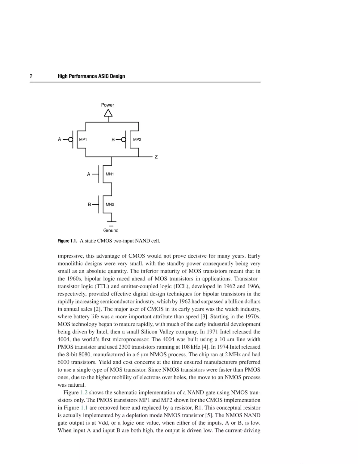
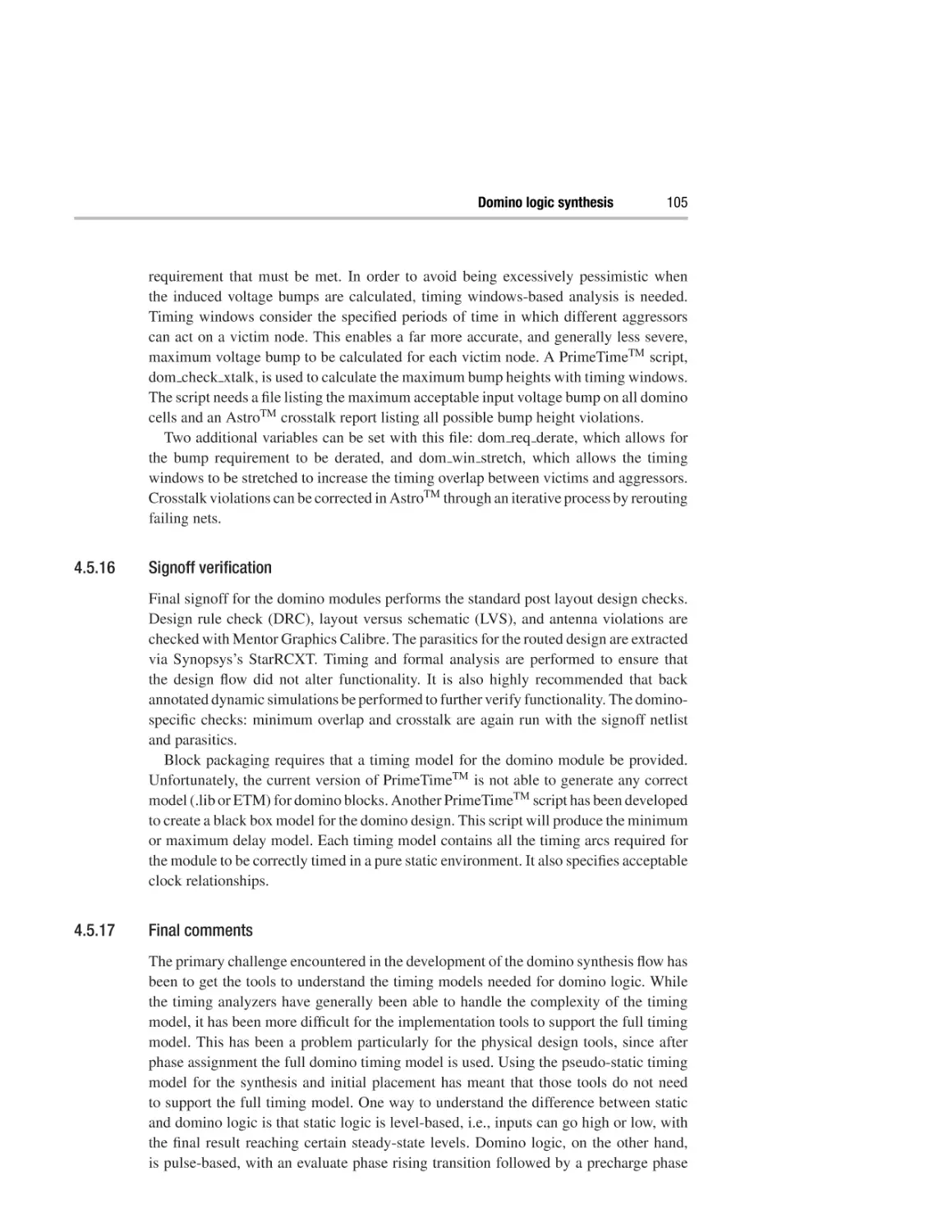
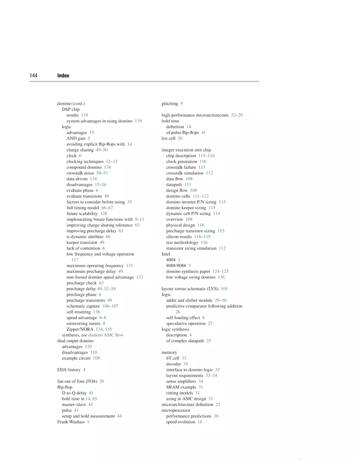
Figure 1.2 shows the schematic implementation of a NAND gate using NMOS transistors only. The PMOS transistors MP1 and MP2 shown for the CMOS implementation
in Figure 1.1 are removed here and replaced by a resistor, R1. This conceptual resistor
is actually implemented by a depletion mode NMOS transistor [5]. The NMOS NAND
gate output is at Vdd, or a logic one value, when either of the inputs, A or B, is low.
When input A and input B are both high, the output is driven low. The current-driving
P1: SJT/...
P2: SJT
9780521873345c01.xml
CUUK158-Hossain
July 1, 2008
17:11
An introduction to domino logic
3
Resistor R (implemented with a
depletion mode NMOS transistor)
Z
A
MN1
B
MN2
Figure 1.2. An NMOS two-input NAND cell.
ability of pull-down NMOS transistors must be much greater than that of the pull-up
resistor. This ensures that the output can be driven to a low voltage at the cost of higher
power dissipation. In addition to the standby power dissipation, NMOS circuits tend to
be slower than equivalent CMOS circuits. This is due to the need for a weak pull-up resistor, which results in very slow low-to-high transitions. While these disadvantages may
make NMOS appear to be unappealing, NMOS designs are more compact than CMOS
circuits. Figure 1.2 uses only two transistors and a resistor, compared with the four transistors needed by a CMOS design. Since the pull-up resistor is implemented by another
NMOS MOSFET, the NMOS design uses fewer transistors and a simpler process than
the CMOS design. The need to move to CMOS therefore arose only when the integration
level on integrated circuits (ICs) made the large standby power on the NMOS design
unacceptable. For Intel this transition occurred in 1978, when the 8088/8086 family of
microprocessors was introduced (the designs were almost identical to the 8088, having
an 8-bit bus while the 8086 has a 16-bit bus). With 29,000 transistors and a clock rate
of 5 to 10 MHz, the 8086 dissipated 1.5 W. This exceeded the 1 W per chip power limit
for plastic packaging. Increases in integration levels meant that a 32-bit processor would
dissipate 5 to 6 W, leading to severe reliability problems [6]. The CMOS version of the
8086, the 80C86, consumed only 250 mW [6]. The ability of CMOS to reduce power
dissipation with increasing integration meant that it rapidly emerged as the technology
that could best utilize fabrication advances. It is an advantage that CMOS maintains till
today (2007), with the overwhelming majority of digital IC designs in the world being
manufactured in CMOS, and the increased convergence of systems onto chips leading
CMOS to make strong inroads into analog and radio frequency (RF) designs. In 1980,
Intel’s 8088 was chosen by IBM as the microprocessor for its personal computer (PC) [4],
a step that would lead to Intel becoming, within a few years, the largest semiconductor
P1: SJT/...
P2: SJT
9780521873345c01.xml
4
CUUK158-Hossain
July 1, 2008
17:11
High Performance ASIC Design
company in the world, with its semiconductor revenues far exceeding that of IBM itself.
The rest, as they say, is history.
As semiconductor manufacturing progressed, the largest challenge to the nascent
industry was the ability to design and verify designs using the increasing number of
transistors available. This need was met by the development of a new field of software, often closely tied to dedicated hardware in its early years, called electronic design
automation (EDA). EDA developments started in the 1960s, with software developed
in-house by different semiconductor companies. In the early years of EDA the most
common tools developed were circuit and logic simulators, which allowed designers to
verify the expected functionality of a design before manufacturing. Alberto SangiovanniVincentelli states in his excellent history of EDA (The Tides of EDA) that the early tools
had limited loyalty due to the perceived limited value-added of the tools [7]. By the
late 1980s continued developments in EDA had resulted in the development of logic
synthesis, which could map a register transfer level (RTL) description to a set of standard cell gates and memory instances, and automated physical design tools, which could
physically instantiate and route the wires needed to complete the physical design. These
tools led to a marked improvement in productivity, allowing digital designs to be quickly
implemented based on a higher abstraction level, behavioral RTL description [7]. The
increasing complexity of EDA tools, along with the realization of their tremendous
usefulness, led to the rise of independent EDA companies and a rapid reduction in EDA
tool development within semiconductor companies. By the end of 2006, the EDA industry had a total available market (TAM) of 5.3 billion dollars [8], which is about 2% of
the worldwide semiconductor TAM of 260 billion dollars [9]. The success of CMOS
manufacturing technology, along with the availability of powerful EDA tools, allowed
for the widespread penetration of electronics into a multitude of applications.
People who are drawn into, and ultimately stay in, engineering are generally somewhat
private people. Our work must, by definition, be cooperative, but the bread and butter of
our daily tasks tends to be very solitary exercises. I am aware that such an audience feels
extremely uncomfortable with broad, historical utterances, reminding them of overly
optimistic forecasts they have had to sit through in darkened conference rooms with a
roll of the eye and a quick, knowing smile to a colleague. Still, I feel compelled to state the
following: I have no doubt that looking back from the future, the most important historical
event of our age will be the development and promulgation of digital technology. It will
also be seen as a profoundly positive development. I believe that all of us working in
this field should be proud of our achievements. I have said my piece and now return to
the theme of digital ASIC design.
It may have been assumed that the emergence of ASIC design methodologies would
displace all other techniques for implementing digital CMOS logic. This has not happened, as many digital designs have specific needs that cannot be achieved by using
standard ASIC techniques. In recent years the capabilities of ASIC tools have increased
greatly, largely due to the tremendous competition among the companies in the field.
Many logical and behavioral optimizations that previously had to be hand-coded for efficient implementation are now automatically incorporated in the synthesis tools. The two
most common benefits of custom design are its ability to optimize across the different
P1: SJT/...
P2: SJT
9780521873345c01.xml
CUUK158-Hossain
July 1, 2008
17:11
An introduction to domino logic
5
Clk
N0
Z
A
B
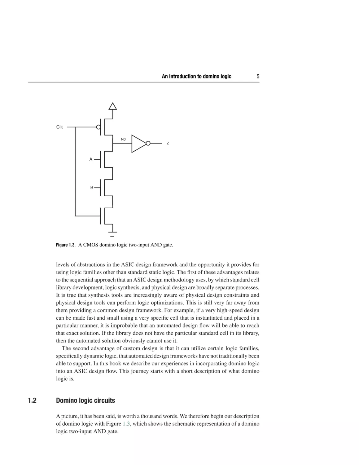
Figure 1.3. A CMOS domino logic two-input AND gate.
levels of abstractions in the ASIC design framework and the opportunity it provides for
using logic families other than standard static logic. The first of these advantages relates
to the sequential approach that an ASIC design methodology uses, by which standard cell
library development, logic synthesis, and physical design are broadly separate processes.
It is true that synthesis tools are increasingly aware of physical design constraints and
physical design tools can perform logic optimizations. This is still very far away from
them providing a common design framework. For example, if a very high-speed design
can be made fast and small using a very specific cell that is instantiated and placed in a
particular manner, it is improbable that an automated design flow will be able to reach
that exact solution. If the library does not have the particular standard cell in its library,
then the automated solution obviously cannot use it.
The second advantage of custom design is that it can utilize certain logic families,
specifically dynamic logic, that automated design frameworks have not traditionally been
able to support. In this book we describe our experiences in incorporating domino logic
into an ASIC design flow. This journey starts with a short description of what domino
logic is.
1.2
Domino logic circuits
A picture, it has been said, is worth a thousand words. We therefore begin our description
of domino logic with Figure 1.3, which shows the schematic representation of a domino
logic two-input AND gate.
P1: SJT/...
P2: SJT
9780521873345c01.xml
6
CUUK158-Hossain
July 1, 2008
17:11
High Performance ASIC Design
The AND gate shown in Figure 1.3 can be used to illustrate the functionality, the
speed advantage, and also some of the challenges involved in using this logic family. In
Figure 1.3 it can be seen that the two functional inputs, A and B, are also attended by the
clock signal, Clk. At first glance this may seem strange, since an AND gate should be
a purely combinational circuit, which unlike latches and flip-flops does not require the
presence of the clock signal. Domino logic is, however, a clocked logic family, which
means that every single logic gate has a clock signal present. When the clock signal
turns low, node N0 (which is called the evaluation or internal node – some authors refer
to it as the dynamic node) goes high, causing the output of the gate to go low. This
represents the only mechanism for the gate output to go low once it has been driven high.
The operating period of the cell when its input clock and output are low is called the
precharge phase or cycle. The next phase, when the clock is high, is called the evaluate
phase or cycle. During the evaluate phase the output of the domino AND cell can go high
provided that both inputs A and B are high, which causes the evaluation node, N0, to be
driven to a low value. The evaluate phase is the functional operating phase in domino
cells, with the precharge phase enabling the next evaluate phase to occur. The appropriate
application of the clock signal ensures that the critical path in domino cells only traverses
through cells in the evaluate phase. One of the advantages of domino logic over static
logic can also be garnered from the schematic in Figure 1.3. Since the domino cell only
switches from a low to a high direction, there is no need for the inputs A and B to drive
any pull-up PMOS transistors. The lack of a PMOS transistor means that the effective
transistor width that loads down a previous stage of logic, for a particular current drive,
favors domino over static logic. This is critical since the key to high speed is ensuring
that a speed advantage can be gained without loading down the cell greatly [10]. For
example, if a design is constructed with a set of cells with transistors of a certain size,
replacing the transistors in every cell with ones ten times larger will almost certainly lead
to a design that is faster. Provided that the initial design is properly sized, i.e., without
weak cells which have very long rise or fall times, the new design will not, however, be
ten times faster. The reason for this is that, while the drive strengths of each cell have
increased by a factor of 10, the output loading due to the input transistor capacitance
seen by each cell has also increased by approximately a factor of 10. Since larger cells
are now used in the design, its area will be larger, leading to greater wiring capacitance.
Thus, while speed gains can be achieved by optimizing cell drives, the indiscriminate
increase in drive strengths tends to limit the improvement in speed due to the increased
self-loading.
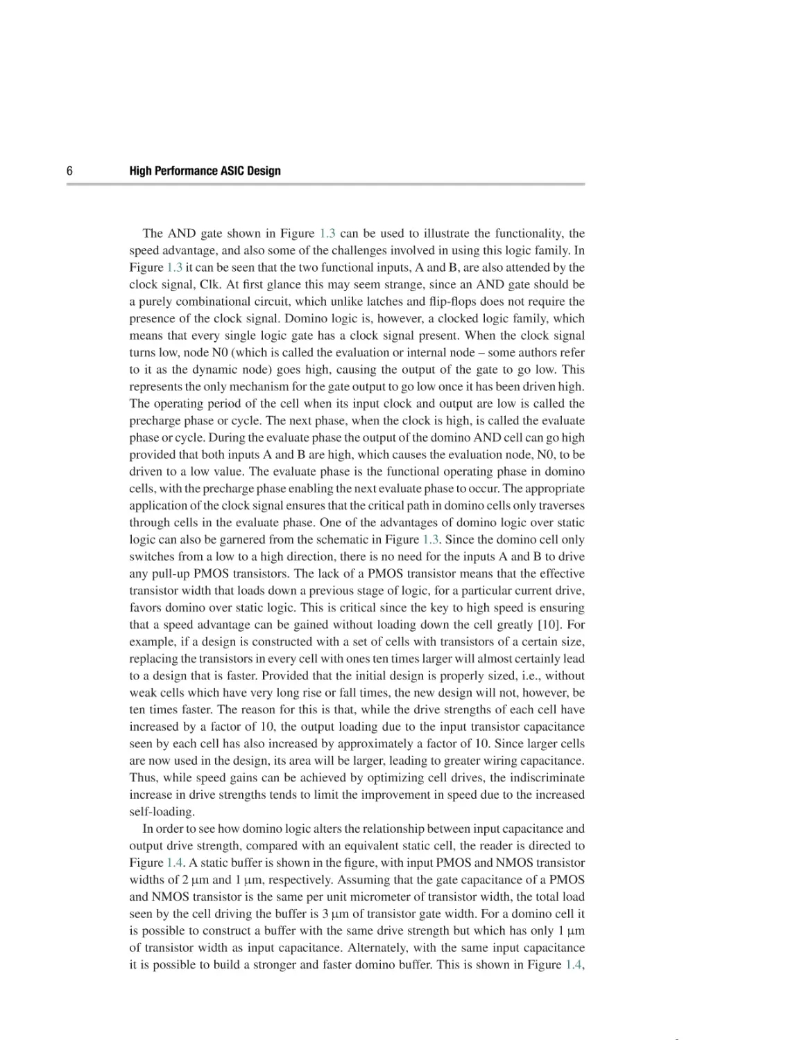
In order to see how domino logic alters the relationship between input capacitance and
output drive strength, compared with an equivalent static cell, the reader is directed to
Figure 1.4. A static buffer is shown in the figure, with input PMOS and NMOS transistor
widths of 2 µm and 1 µm, respectively. Assuming that the gate capacitance of a PMOS
and NMOS transistor is the same per unit micrometer of transistor width, the total load
seen by the cell driving the buffer is 3 µm of transistor gate width. For a domino cell it
is possible to construct a buffer with the same drive strength but which has only 1 µm
of transistor width as input capacitance. Alternately, with the same input capacitance
it is possible to build a stronger and faster domino buffer. This is shown in Figure 1.4,
P1: SJT/...
P2: SJT
9780521873345c01.xml
CUUK158-Hossain
July 1, 2008
17:11
An introduction to domino logic
2 µm
Static buffer
7
2 µm
Z
A
1 µm
1 µm
1 µm
3 µm
Clock
Z
Domino buffer
A
3 µm
1.5 µm
3 µm
Figure 1.4. A static and domino logic buffer.
where a domino buffer with input transistor width of 3 µm is shown. This particular
domino buffer is called a footer transistor, i.e., a series NMOS transistor connected to
the clock. It is possible to use domino cells with and without footer transistors, although
the absence of the footer transistor makes the design more complicated. Since the footed
clock transistor adds to the resistance of the pull-down path, the two 3 µm transistor
widths are considered roughly equivalent in terms of drive strength to a single 1.5 µm
transistor. This follows, as the resistance of a MOS transistor is inversely proportional to
its gate width, and as the total resistance of a set of resistors in series is equal to the sum
of the resistors. Since, for the static buffer, 1 µm of NMOS transistor length is driving a
2 µm PMOS and a 1 µm NMOS transistor, the effective 1.5 µm of NMOS for the domino
P1: SJT/...
P2: SJT
9780521873345c01.xml
8
CUUK158-Hossain
July 1, 2008
17:11
High Performance ASIC Design
cell has 50% greater drive strength. Thus, for the same input capacitance a domino cell
can result in greater output drive strength than a static equivalent.
There are a few points to note. Firstly, the degradation in drive strength due to the
addition of the footer transistor in a domino buffer is worse than in other domino cells
with more than two NMOS transistors in series. For example, in a three-input domino
AND cell, the number of NMOS transistors in series goes from three to four when
the footed transistor is considered. This is much better than a domino buffer where a
doubling in the height of the NMOS series stack occurs. Secondly, the PMOS pull-up
transistor for the domino cell in Figure 1.4 is shown as 1 µm. The actual size of the
PMOS transistor will depend on the time available for the output of the domino cell to
turn low when the clock falls. This delay is called the precharge delay. In general, the
PMOS pull-up transistor is smaller in a domino cell than the static equivalent. Thirdly,
the ratio of PMOS to NMOS transistor width for the static cell is given as 2. In Chapter 3
we will see that the actual ratios tend to be lower in static logic. Finally, for stability
purposes domino cells tend to use weak feedback keepers placed between the output
and the evaluation node driving the output. For simplicity, that circuit is not shown in
Figure 1.4.
In addition to being able to achieve better output drive strength for input loading,
domino cells also have a speed advantage as they avoid contention when the cells switch.
In order to understand this, one must note that the input to a static cell drives both PMOS
and NMOS transistors. Any input transition that causes the cell to switch logical states
results in a PMOS transistor being turned off and an NMOS transistor being turned on,
or vice versa. Since the inputs to the cell have finite rise and fall times, this means that
during the transition period both the PMOS and the NMOS transistors are weakly on. This
contention between the two transistors increases the input voltage level at which the cell
switches. It is possible to speed up the rise or fall transition of a static cell by increasing
or decreasing the ratio of the PMOS to NMOS transistor size. This, however, leads to
the alternate transition becoming slower. Since both transitions are equally important
in static cells, it is difficult to gain very much by skewing a particular transition. For
this reason, the switching point of most static cells tends to be close to half the supply
voltage level (Vdd). For domino cells only the rising transition is critical. If an input rise
causes the evaluation node of the domino cell to discharge, no contention exists between
PMOS and NMOS transistors. This allows domino cells to start switching when the input
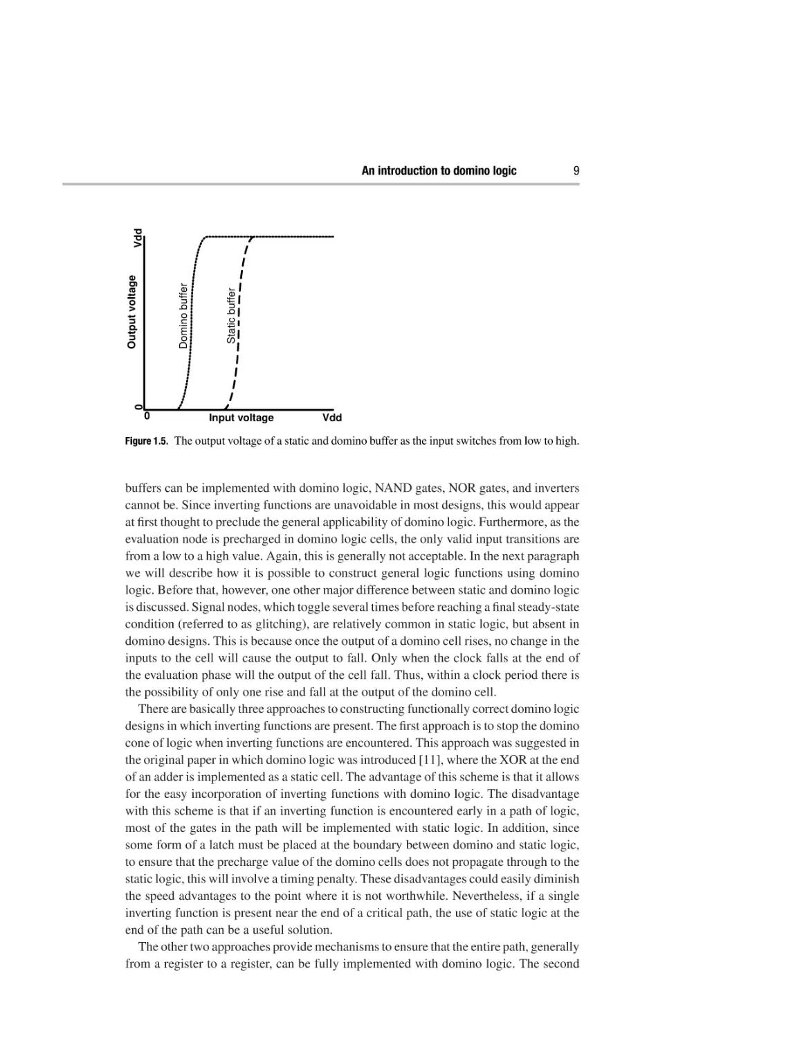
voltage level reaches an NMOS transistor threshold voltage level. Figure 1.5 illustrates
the switching behavior of a static and a domino buffer as the data input to the cell rises.
The lower switching voltage of a domino cell leads to a speedup since the input driving
cells will reach the lower NMOS threshold voltage quicker than a higher voltage level.
These factors lead to domino cells being significantly faster than equivalent static cells.
The speed advantage of a domino cell over an equivalent static design is in the range of
1.5× to 2.5×.
Domino logic is an uninverting style of logic [11]. This follows since every domino
cell is a single-stage dynamic cell followed by an inverter. Consequently, the only valid
transitions at the output of the gate during the evaluate phase are from a low to a high
value. The uninverting nature of the logic means that while AND gates, OR gates, and
CUUK158-Hossain
July 1, 2008
17:11
9
Static buffer
Domino buffer
Output voltage
Vdd
An introduction to domino logic
0
P1: SJT/...
P2: SJT
9780521873345c01.xml
0
Input voltage
Vdd
Figure 1.5. The output voltage of a static and domino buffer as the input switches from low to high.
buffers can be implemented with domino logic, NAND gates, NOR gates, and inverters
cannot be. Since inverting functions are unavoidable in most designs, this would appear
at first thought to preclude the general applicability of domino logic. Furthermore, as the
evaluation node is precharged in domino logic cells, the only valid input transitions are
from a low to a high value. Again, this is generally not acceptable. In the next paragraph
we will describe how it is possible to construct general logic functions using domino
logic. Before that, however, one other major difference between static and domino logic
is discussed. Signal nodes, which toggle several times before reaching a final steady-state
condition (referred to as glitching), are relatively common in static logic, but absent in
domino designs. This is because once the output of a domino cell rises, no change in the
inputs to the cell will cause the output to fall. Only when the clock falls at the end of
the evaluation phase will the output of the cell fall. Thus, within a clock period there is
the possibility of only one rise and fall at the output of the domino cell.
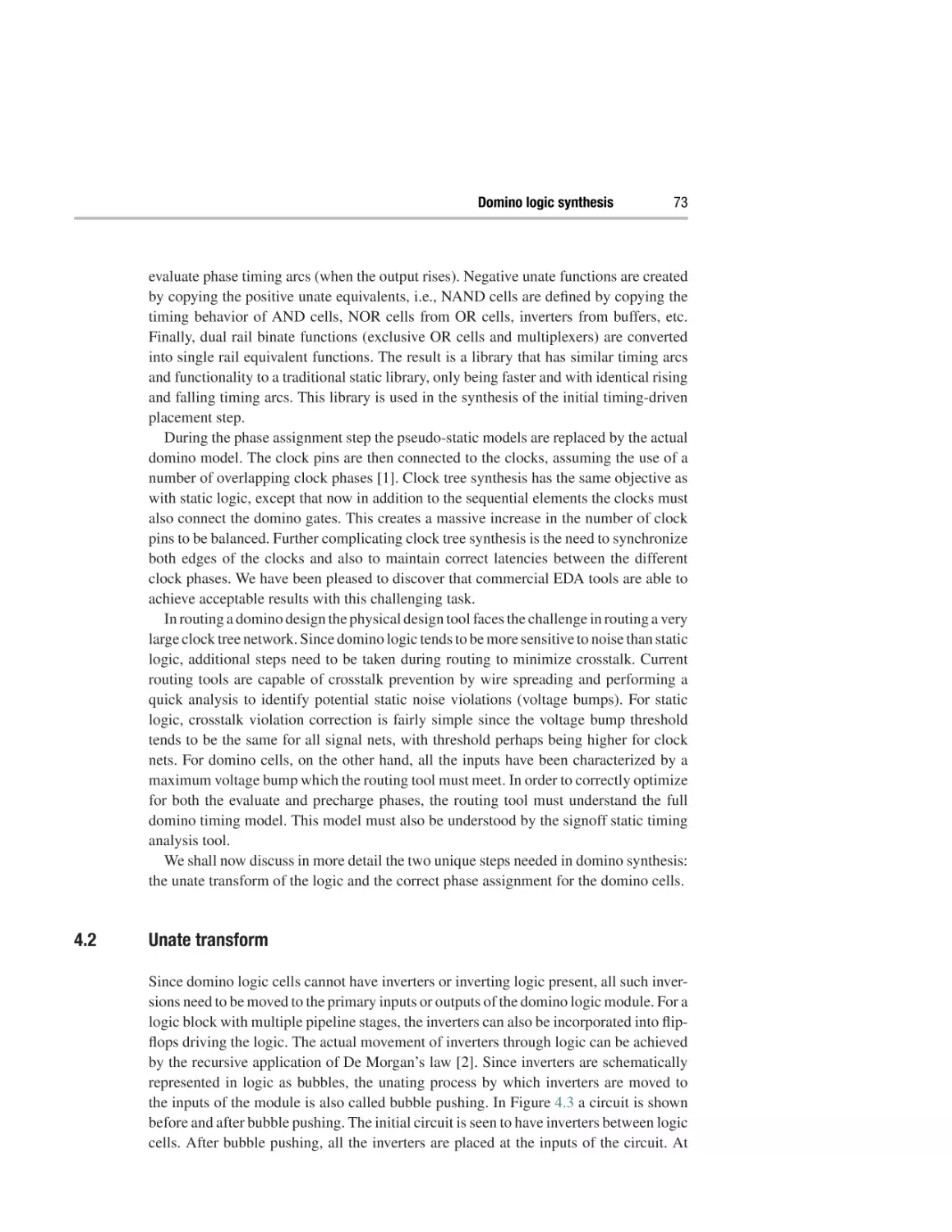
There are basically three approaches to constructing functionally correct domino logic
designs in which inverting functions are present. The first approach is to stop the domino
cone of logic when inverting functions are encountered. This approach was suggested in
the original paper in which domino logic was introduced [11], where the XOR at the end
of an adder is implemented as a static cell. The advantage of this scheme is that it allows
for the easy incorporation of inverting functions with domino logic. The disadvantage
with this scheme is that if an inverting function is encountered early in a path of logic,
most of the gates in the path will be implemented with static logic. In addition, since
some form of a latch must be placed at the boundary between domino and static logic,
to ensure that the precharge value of the domino cells does not propagate through to the
static logic, this will involve a timing penalty. These disadvantages could easily diminish
the speed advantages to the point where it is not worthwhile. Nevertheless, if a single
inverting function is present near the end of a critical path, the use of static logic at the
end of the path can be a useful solution.
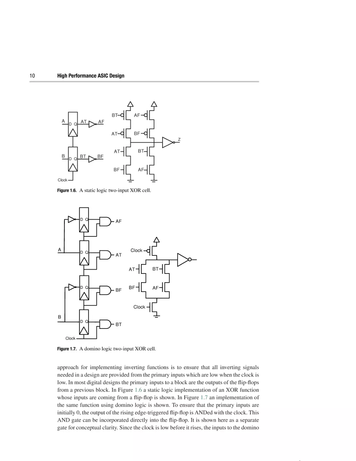
The other two approaches provide mechanisms to ensure that the entire path, generally
from a register to a register, can be fully implemented with domino logic. The second
10
CUUK158-Hossain
July 1, 2008
17:11
High Performance ASIC Design
A
D Q
AT
BT
AF
AT
BF
AF
Z
B
D Q
BT
P1: SJT/...
P2: SJT
9780521873345c01.xml
BT
AT
BT
BF
AF
BF
Clock
Figure 1.6. A static logic two-input XOR cell.
D Q
A
D Q
D Q
AF
Clock
AT
BF
AT
BT
BF
AF
Clock
B
D Q
BT
Clock
Figure 1.7. A domino logic two-input XOR cell.
approach for implementing inverting functions is to ensure that all inverting signals
needed in a design are provided from the primary inputs which are low when the clock is
low. In most digital designs the primary inputs to a block are the outputs of the flip-flops
from a previous block. In Figure 1.6 a static logic implementation of an XOR function
whose inputs are coming from a flip-flop is shown. In Figure 1.7 an implementation of
the same function using domino logic is shown. To ensure that the primary inputs are
initially 0, the output of the rising edge-triggered flip-flop is ANDed with the clock. This
AND gate can be incorporated directly into the flip-flop. It is shown here as a separate
gate for conceptual clarity. Since the clock is low before it rises, the inputs to the domino
P1: SJT/...
P2: SJT
9780521873345c01.xml
CUUK158-Hossain
July 1, 2008
17:11
An introduction to domino logic
11
cell are initially 0. Since the XOR function needs both the inverted and uninverted
versions of inputs A and B, these signals are provided directly from the flip-flops. It can
be seen that the XOR function is implemented as an AND–OR gate that implements
the function: AB + A B, which can then be provided to other logic. Ensuring that all
the inverting logic needed by the design is provided directly from the primary inputs to the
design creates a design in which no inverting functions are used. This structure is called
a unate implementation. The major drawback with this approach is that it can lead to a
duplication of all logic in the block, a significant area and power penalty.
The third approach to implement a correct design is to make sure that every domino
cell is only clocked when stable input values are present at the input of the domino
cells. For the XOR cell described above this means that if we know that after a certain
amount of time the inputs are at their correct values, the clock can rise. The advantage
with this approach is that inverted inputs do not need to be propagated from the primary
inputs of the design. While that is a major advantage, it is difficult to do in an automated
design framework. In designs generated using automated synthesis and physical design
tools, inputs tend to arrive at each gate across a large window of time. Since the domino
gate can be clocked only after all the inputs are stable, this means that the clock is the
critical path in the gate, arriving last. This can lead to a design in which the data waits for
the arrival of a clock signal at every single cell before it can proceed, slowing down the
signal path. The extra margin (to account for process variation, clock tree skew, and clock
driver granularity) that must be used to guarantee that the clock signal arrives after all
the input signals are stable, further slows down the critical path. While difficult to use for
synthesizable domino logic, it is possible to allow some binate logic for domino design
implemented in custom or structured custom frameworks, where far greater control
exists on the arrival time of every input. When using synthesizable domino logic in an
automated flow, it is best to make the design unate. We will describe in Chapter 4 some
optimizations possible to reduce the area overhead in the unating process.
One of the difficulties in deploying automated domino logic design systems is the
lack of predictability, at least from a cursory human point of view, in understanding
the structure of the design and the expected arrival times of signals at different inputs
once they have been pushed through an ASIC flow. Gate-level netlists generated by
synthesis tools appear very irregular. Layout plots highlight the differences, with one
being immediately able to tell ASIC and custom designs apart. Human efforts tend to
produce graphically regular, repetitive structures, while the output of an automated ASIC
tool tends to appear random. Whether this phenomenon reflects any particular aptitude
of human beings to discover underlying graphical patterns, or merely reflects a human
preference to arbitrarily impose order, is an open question. One has to be careful also to
remember that a haphazard-looking design may merely represent a degree of complexity
beyond human comprehension. In the world of VLSI digital design, where we must
collaborate with automated tools in all of our jobs, it is interesting to note that human
designers remain in those areas where a visual or graphical, two-dimensional regularity
is most present: custom, memory, and standard cell design. Where such regularity is
absent, most notably implementing random logic, the engineer’s task has shifted to
properly operating and supervising the automated tools which do the detailed design.
P1: SJT/...
P2: SJT
9780521873345c01.xml
12
CUUK158-Hossain
July 1, 2008
17:11
High Performance ASIC Design
Buffer
B1
Buffer
B2
Clock φ1
0 degree phase
Buffer
B3
Buffer
B4
Buffer
B5
Buffer
B6
Clock φ2
180 degree phase
Figure 1.8. Clocking scheme for a set of domino buffers.
For RF design, perhaps the most human designer-intensive implementation task, a sharp
contrast exists between the custom laid-out analog modules with their classical symmetry
and palatial isolation zones, and the teeming, chaotic ASIC-designed blocks. The RF
designers try to keep the digital modules with their noise spikes and unpredictable
harmonics as far away as possible, although with the increasing digitalization of RF and
its convergence with baseband and other purely digital functions, the haphazard cities
of digital logic are continuously encroaching on the ordered world of RF.
1.3
Clocking domino logic
Ensuring that every domino cell enters the evaluate phase (when the clock is high) with
its inputs low and that all inputs transition from 0 to 1 during the evaluate phase requires
that the design is correctly clocked. Unlike in static logic, every domino cell is clocked.
This results in the clocking strategy being far more critical and complex in domino logic,
with the wrong clocking leading to possible functional failures.
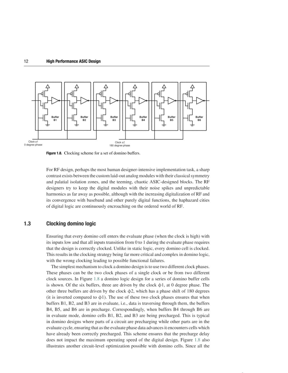
The simplest mechanism to clock a domino design is to use two different clock phases.
These phases can be the two clock phases of a single clock or be from two different
clock sources. In Figure 1.8 a domino logic design for a series of domino buffer cells
is shown. Of the six buffers, three are driven by the clock φ1, at 0 degree phase. The
other three buffers are driven by the clock φ2, which has a phase shift of 180 degrees
(it is inverted compared to φ1). The use of these two clock phases ensures that when
buffers B1, B2, and B3 are in evaluate, i.e., data is traversing through them, the buffers
B4, B5, and B6 are in precharge. Correspondingly, when buffers B4 through B6 are
in evaluate mode, domino cells B1, B2, and B3 are being precharged. This is typical
in domino designs where parts of a circuit are precharging while other parts are in the
evaluate cycle, ensuring that as the evaluate phase data advances it encounters cells which
have already been correctly precharged. This scheme ensures that the precharge delay
does not impact the maximum operating speed of the digital design. Figure 1.8 also
illustrates another circuit-level optimization possible with domino cells. Since all the
P1: SJT/...
P2: SJT
9780521873345c01.xml
CUUK158-Hossain
July 1, 2008
17:11
An introduction to domino logic
Reg1
Module
M11
Module
M12
Module
M13
Reg2
Module
M21
Module
M22
Module
M23
13
Reg3
Clock φ1
Figure 1.9. A logic module with several pipeline stages.
cells driven by a clock enter precharge at the same time, the critical path for precharge
is the time taken for a single cell to precharge. The maximum evaluate phase delay,
on the other hand, represents the maximum evaluate delay through a series of domino
cells driven by the same clock. For our purposes this means that the sum of the evaluate
delay for the buffers B1, B2, and B3 can be made equal to the precharge delay for a
single buffer (B4, B5, or B6). This difference in the speed needed by the precharge
and evaluate circuitry means that transistor sizing in a domino cell can be weighted to
heavily favor rising output transitions over falling ones. The example shown in Figure 1.8
is simplified by not considering clock skew, cell drive strengths, and cell output loading,
but it does illustrate the serial nature of the evaluate phase delay versus the parallel nature
of precharge. The ratio of time allowed for precharge to evaluate depends on the number
of serial cells clocked by a particular clock. This attribute is strongly dependent on the
microarchitecture of the design, which determines the number of cells through which
data must propagate in the evaluate phase during a clock cycle. One of the challenges
in designing domino logic-compatible standard cell libraries is that one has to assume
a maximum operating frequency of the design, since this sets a limit on the maximum
precharge delay permissible. Setting this value too low leads to a design constrained by
the precharge delays, while a very large number will optimize the precharge delay at the
expense of the evaluate delay. This will negatively impact performance if, indeed, the
maximum operating frequency of the design is significantly lower than that supported
by the precharge delays.
Figure 1.8 shows a single stage of domino logic. When a number of different pipeline
stages are present in a design, as in Figure 1.9, register stages separate the different
pipeline stages. While explicit register stages are needed in static designs, to ensure that
fast-arriving data does not corrupt data from an earlier cycle [12], these pipelines are
not needed in domino design. Since domino cells act intrinsically as a latch, they are
transparent during evaluate and shut-off during precharge, thus putting two domino gates
driven by different clock phases in series causes the data to behave as if passed through
a master–slave flip-flop. An alternate way to view this is to assume that in a domino
design the master and slave latches present in a typical flip-flop are split and distributed
throughout the logic instead of merely being at the boundary of clock phases. In addition
to its faster speed, the ability to remove explicit flip-flops is one of the major advantages
of domino logic, since the setup and clock-to-Q delay associated with traversing through
a flip-flop can be eliminated [12].
P1: SJT/...
P2: SJT
9780521873345c01.xml
14
CUUK158-Hossain
July 1, 2008
17:11
High Performance ASIC Design
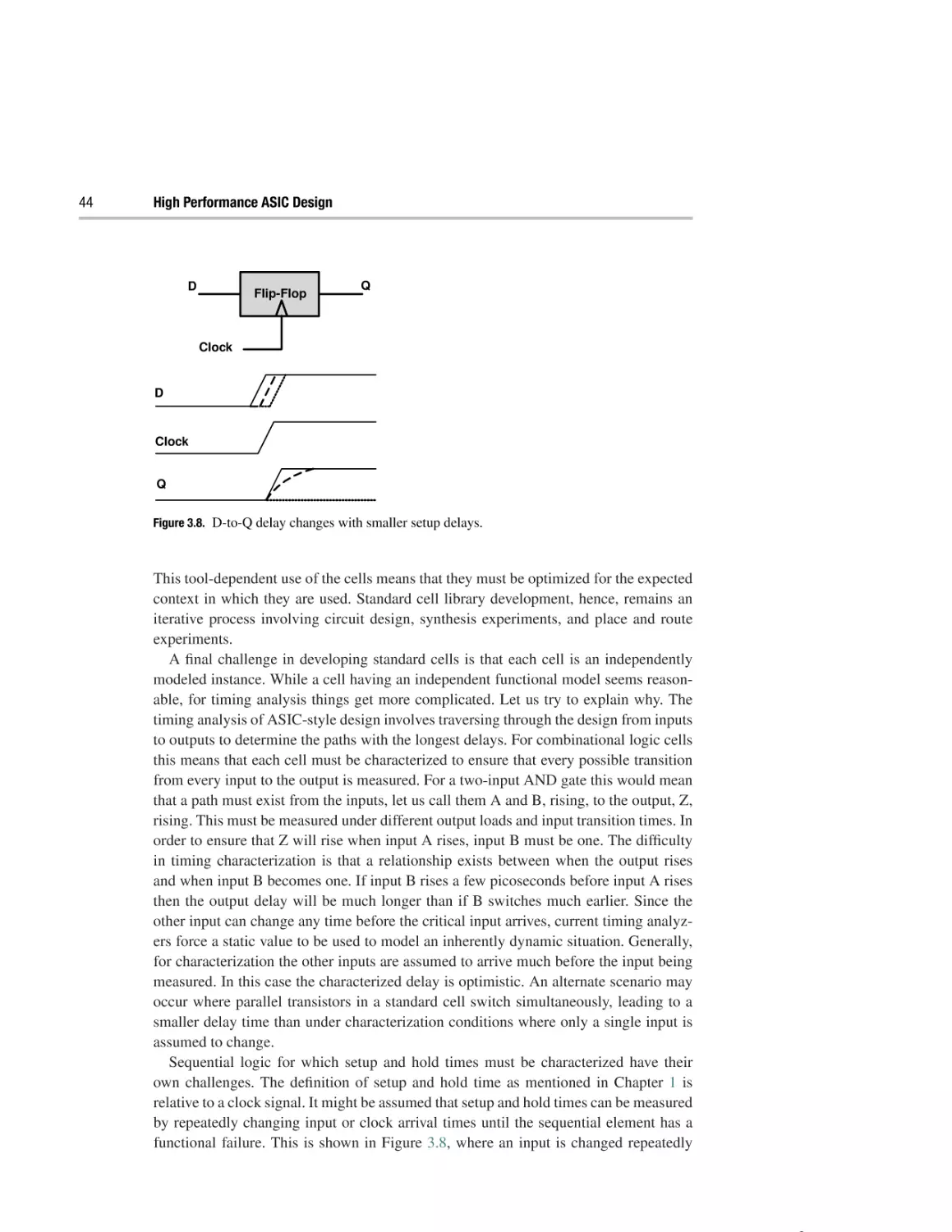
While using two clock phases will lead to a functioning domino logic design, there
are some difficulties with the approach. Care must be taken to ensure that when the clock
changes phase the next domino logic cell can capture data from the previous cycle before
the precharge value from the driving domino cells overwrites the valid output result. If
the inputs to the domino cell on the next clock phase arrive before the domino cell is
clocked, this is generally not a problem since, as discussed, the precharge delay for a
domino cell is much longer than the evaluate delay through it. However, in the presence
of clock skew the late arrival of the clock to the domino cell being evaluated can cause
the precharge data to be clocked. This is referred to as a hold time failure. For those
unfamiliar with the terminology, a quick set of definitions follows. Clock skew refers to
the difference in clock arrival time between two different circuit elements which send data
from one to the other either directly or via some combinational logic. For example, the
clock skew between two adjacent rising edge-triggered flip-flops is the time difference
between rising edges arriving at the two flip-flops. The primary cause of clock skew in
digital designs is due to the presence of a clock buffering tree, a physically distributed
series of buffers that sends the root clock signal to all of its nodes. For a complex ASIC
with many flip-flops distributed across a large chip, some clock skew is inevitable. The
other two delays associated with a clocked logic element are the setup and hold delay.
The setup delay for an input to a cell is the latest input arrival time before the cell is
clocked that will ensure that correct data is captured. The hold time of a flip-flop is the
time after the clock edge arrives for which the input data to the element must be held at
a constant value to ensure that the correct value is sampled. Setup failures are generally
due to running the design too fast and can be overcome by running the design slower.
Hold failures are more dangerous as they can lead to functional failures across all testing
conditions and must be avoided at all costs.
The possibility of hold failure, due to clock skew, is one of the challenges of using
two clock phases. In order to loosen the clock skew requirements, three or more clock
phases can be used with domino logic. For this book we focus on the use of skew-tolerant
clocking to clock the domino designs. This technique uses multiple overlapping clock
phases [12]. Assuming that the clocks each have a 50% duty cycle, and that they are
evenly distributed, each clock edge overlaps 17% with its adjacent clock. This overlap
allows longer rise or fall times, reducing the clock skew requirements and hence the
power dissipation in the clock tree network, while also reducing the possibility of hold
failures.
There is one final advantage of domino logic that is best understood in the context of
microarchitecture, where a design spans a number of pipeline stages. To understand this
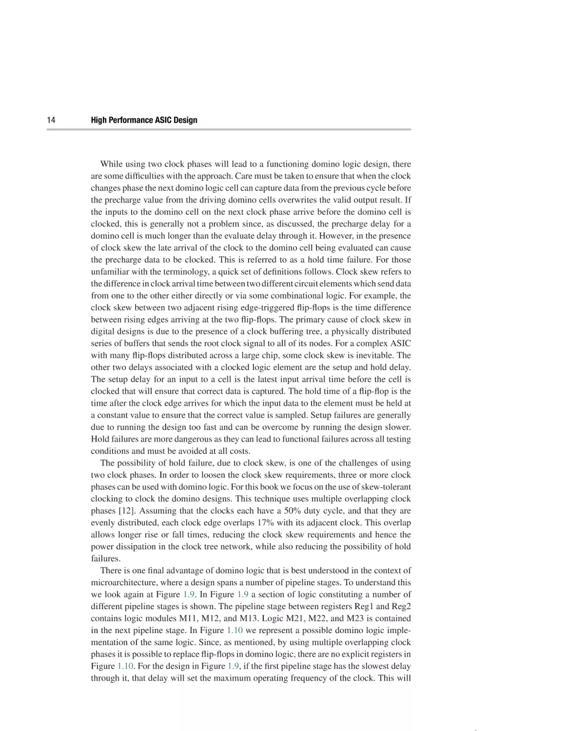
we look again at Figure 1.9. In Figure 1.9 a section of logic constituting a number of
different pipeline stages is shown. The pipeline stage between registers Reg1 and Reg2
contains logic modules M11, M12, and M13. Logic M21, M22, and M23 is contained
in the next pipeline stage. In Figure 1.10 we represent a possible domino logic implementation of the same logic. Since, as mentioned, by using multiple overlapping clock
phases it is possible to replace flip-flops in domino logic, there are no explicit registers in
Figure 1.10. For the design in Figure 1.9, if the first pipeline stage has the slowest delay
through it, that delay will set the maximum operating frequency of the clock. This will
P1: SJT/...
P2: SJT
9780521873345c01.xml
CUUK158-Hossain
July 1, 2008
17:11
An introduction to domino logic
Module
M11
Module
M12
Module
M13
Module
M21
Module
M22
15
Module
M23
Clock φ1
Clock φ2
Clock φ3
Figure 1.10. A domino logic module containing multiple pipeline stages.
not change even if the pipeline stages before and after it can be clocked much faster.
For the design in Figure 1.10, a 17% overlap occurs between two adjacent clock phases.
This means that if data enters module M12 even after the clock is high it can propagate
through the module and can possibly use the smaller delay through M21, M22, and
M23 to its advantage. This is possible because the clock for module M21 is not edgetriggered, or a hard clock, i.e., no edge-triggered value is captured at the moment that
the clock rises, but rather is level-sensitive [12]. Such a clocking system is referred to as
a soft or softened clock, ensuring that pipeline stages which need more time to complete
can seamlessly borrow some time from contiguous pipeline stages, thus allowing for
faster operating speed of the design. This property does not absolve the designer from
the requirement of trying to balance pipeline stages wherever possible, or eliminate the
need for synthesis and physical design tools to do the same. It does, however, provide a
mechanism to equalize pipeline stage delays when granularity constraints make it difficult for different stages to have exactly identical delays. In addition, process variations
due to manufacturing imperfections and cross-coupled noise may modify the delay in
different pipeline stages from the assumed values. The presence of a soft clock helps
distribute these silicon variations, limiting the impact on operating frequency. While this
technique can be, and indeed is sometimes, used with static logic, it comes for free with
skew-tolerant domino.
1.4
Summary
The use of domino logic, like just about any other design choice, has its advantages
and disadvantages. The primary advantage of domino logic is its speed of operation.
The advantage comes from the superior speed of the domino cell and the ease with
which explicit flip-flops and clock softening can be supported with domino. The primary
disadvantage of domino is its greater power dissipation, its potential area penalty, and
the complexity of using domino logic.
The higher power dissipation in domino logic is due to the fact that every single domino
cell is clocked. Power must hence be consumed to switch the domino cell every single
clock cycle. This power dissipation occurs irrespective of whether the data is traversing
the domino design or not. In addition to this, domino logic cells need to be precharged
P1: SJT/...
P2: SJT
9780521873345c01.xml
16
CUUK158-Hossain
July 1, 2008
17:11
High Performance ASIC Design
if the output is a logic one value at the end of the evaluate phase. This leads to an extra
transition that static logic does not require. If we construct a domino logic circuit by
providing the true and false values for every input, there is a possible doubling of the
number of logic gates and a proportional rise in its power dissipation.
These factors suggest that a synthesizable domino flow generally is not useful for low
power modules (in custom design great effort can be used to minimize the power impact
of domino). The easiest way to limit the power overhead is to limit its use to those areas
in a system-on-chip (SOC) where the requirements for speed necessitate its use. For an
SOC the tradeoff in power between domino and static logic is more complex than at the
cell or module level, since system-level considerations come into play. For example, if
the use of domino logic allows two cores to be replaced by a single core running much
faster, the overall power penalty for domino logic is reduced. Alternately, if domino
logic allows a timing-critical circuit to be used with low leakage transistors, while a
static implementation requires faster but leakier transistors, the power difference is more
difficult to predict. Aside from the system considerations, at the circuit level there is one
power advantage that domino designs have: their absence of glitching. Glitching leads to
extra power dissipation, due to logically unnecessary switching being absent in domino.
The area overhead of domino designs is again somewhat difficult to generalize. In
custom applications, domino designs can be smaller than corresponding static designs.
For synthesizable domino logic, the extra logic can lead to a power penalty. Since it is
assumed that synthesizable domino logic will be used sparingly, this overhead may be
acceptable for most designs.
The last and final disadvantage of domino is the complexity of the flow. Using synthesizable domino logic hopefully manages to hide the details of the complexity from
the users. This will also reduce the great time and effort required by custom designs,
although the design will be less optimized than a custom design.
Despite these disadvantages, the expeditious use of domino logic does have some
advantages. In addition to the system-level advantages mentioned earlier, there are always
some logic modules where faster speed can be utilized for greater advantage. Much of
the current research on analog design focuses on the use of very high speed digital to
complement and control analog circuitry. Again this represents a small, but critically
important, part of the total circuitry in the design, where domino can be used to its speed
advantages. Another possible application of synthesizable domino logic is in speeding
up a legacy module without incurring the cost of redesigning the microarchitecture and
porting the software. With a synthesizable domino logic solution, the effort involved
in using it becomes much lower, making it much more attractive beyond its traditional
application areas of high end microprocessors.
References
1. F. Wanlass et al., Nanowatt logic using field-effect metal-oxide semiconductor triodes, International Symposium on Solid-State Circuits, 1963.
2. http://www.icknowledge.com/history/1960s.html [accessed 29 June 2007].
P1: SJT/...
P2: SJT
9780521873345c01.xml
CUUK158-Hossain
July 1, 2008
17:11
An introduction to domino logic
17
3. http://en.wikipedia.org/wiki/CMOS [accessed 29 June 2007].
4. http://www.icknowledge.com/history/1970s.html [accessed 29 June 2007].
5. K. Bernstein, ‘Out-of-the-park home runs’, legendary digital circuits that tracked technology
scaling, IEEE SSCS Newsletter, Spring 2007.
6. S. Wolf, Silicon Processing for the VLSI Era, Volume 2: Process Integration, Lattice Press,
Sunset Beach, CA, 1990.
7. A. Sangiovanni-Vincentelli, The tides of EDA, IEEE Design and Test of Computers,
November–December 2003.
8. R. Goering, EDAC: EDA up 15 percent in 2006, http://www.eetimes.com/news/latest/
showArticle.jhtml?articleID=198900043
9. http://i.cmpnet.com/eetimes/eedesign/2007/chart1˙031507.gif
10. I. Sutherland, B. Sproull and D. Harris, Logical Effort: Designing Fast CMOS Circuits, Morgan
Kaufmann Publishers, San Francisco, CA, 1999.
11. R. H. Krambeck, C. M. Lee and H-F. S. Law, High speed compact circuits with CMOS, IEEE
Journal of Solid-State Circuits SC-17(3), June 1982.
12. D. Harris, Skew-Tolerant Circuit Design, Morgan Kaufmann Publishers, San Francisco, CA,
2001.
2
High-speed digital design
2.1
Microprocessors since 1989
In 1989 a forward-looking paper attempted to determine the characteristics of microprocessors in the year 2000. Called “Microprocessors circa 2000”, the paper hypothesized
that a high-performance microprocessor in the year 2000 would have an area of 1 square
inch (645 sq mm), contain 50 million transistors, and run at above 250 MHz [1]. The
overall performance of the microprocessor was estimated at 2000 million instructions
per second (MIPS), achieved by the employment of two or three cores, each with a performance of 750 MIPS. Forward-looking papers often have somewhat fanciful conceits
of future developments, illustrating the witticism that predictions tend to be difficult if
they involve the future. This prediction, however, was based on many years of microprocessor development, leading to a broadly accurate prediction of things to come. The
International Solid State Circuit Conference (ISSCC), held in early 2000, presented a
number of microprocessors whose transistor counts and area were within 2× of the
prediction. Since much of the area of a microprocessor is composed of on-chip memory, the prediction for transistor count was achieved soon afterwards. The prediction of
2000 MIPS for the maximum performance of the system also proved to be accurate. The
interesting discrepancy was in the way that the performance of the microprocessor was
achieved. Instead of employing a number of processors operating at 250 MHz, most high
end microprocessors were single core designs running at or above 1 GHz. At the ISSCC
held in early 2001, the Pentium 4 microprocessor was introduced by Intel. The clock
frequency of this processor was 2 GHz, with the integer execution unit running at 4 GHz.
How had such a historically anomalous jump in clock frequency been achieved in
such a short period of time? Much of this can be attributed to the intense competition
in the microprocessor market, especially for processors compatible with Intel’s ×86
family of chips. For many customers a very high clock frequency had become a critical
component in customers’ expectations when buying a computer. It can be debated how
important clock frequency is for a computer, especially since memory and I/Os are
often more severe bottlenecks. Still, clock frequency was a major marketing advantage
throughout this period, although, of late, its centrality has started to wane somewhat. In
addition, in 1992 Digital Computer Corporation released the first version of its Alpha
processor, which achieved an impressive clock rate of 200 MHz. Since 250 MHz was
the expected clock rate at the end of the decade, Digital’s ability to reach comparable
speeds eight years early spurred clock speeds to be pushed throughout the industry.
18
High-speed digital design
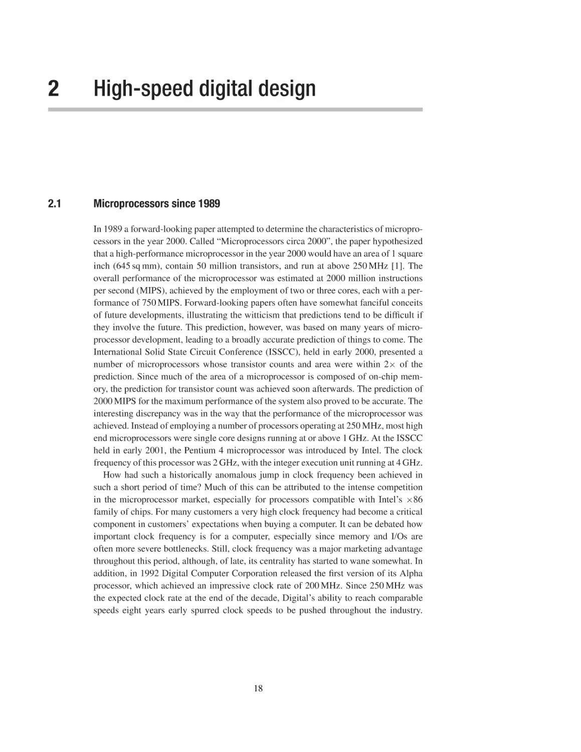
Data
Register
Combinational
logic
Register
Combinational
logic
19
Register
Clock
Figure 2.1. Pipeline stages with combinational logic between the registers.
While competition can explain the motivation for desiring high operating speed, it does
not answer the basic engineering question as to how this was achieved? The answer lies
with improvements in CMOS processes and the use of much more aggressive designs,
specifically, the use of much deeper register pipelines.
CMOS transistors in digital designs can be viewed simplistically as switches. As new
processes with smaller feature sizes become available, it is possible to scale the physical
dimensions of the transistors. For digital designs this leads to many advantages. Smaller
transistors require less energy to turn on and have smaller capacitive self-loading. They
are also faster. The speed, power, and area benefits due to shrinking a process can be
derived analytically [2]. Let us assume that at each new process generation the lateral and
vertical dimensions of the transistor are scaled by 1/S, where S is called the scaling factor.
Over the last few process generations the typical scaling factor has been approximately
1.4. Since supply voltages and gate oxides are typically also reduced, they are also
assumed to be scaled by 1/S. This leads to the delay in the transistor being reduced
by 1/S, power dissipation scaled by 1/S2 , and a power density that remains constant.
Scaling leads to a reduction in area of 1/S2 . This means that a significant reduction in
silicon area, or a large increase in functionality, is possible by porting a design to a new
CMOS process. Both of these factors help to reduce total system cost, which drives
demand further; providing positive feedback for the virtuous cycle of demand, supply,
and engineering employment.
The other factor mentioned which led to improvement in microprocessor clock frequencies through the 1990s was much better implementations, spearheaded by the use
of aggressive microarchitectures. These microarchitectures were much more deeply
pipelined. Figure 2.1 shows a pipeline stage with registers and combinational logic.
This combinational logic is called a cloud of logic and implements the function of
the circuit (due to the lack of an appropriate drawing stencil the clouds in Figure 2.1
are rendered as somewhat circular in shape). The total delay for a pipeline stage is
the delay through the combinational logic between the pipeline stage and the clocking
overhead. The clocking overhead corresponds to the clock-to-Q delay at the flip-flop
launching the data, the setup time at the flip-flop capturing the data, and the clock uncertainty due to skew and jitter. Increasing pipeline depth reduces the logic stages between
flip-flops. As we discussed in Chapter 1, it is possible to reduce significantly clocking
overhead with the use of domino logic and overlapping clock phases [3]. For deeply
pipelined designs this is particularly important due to the large proportion of total delay
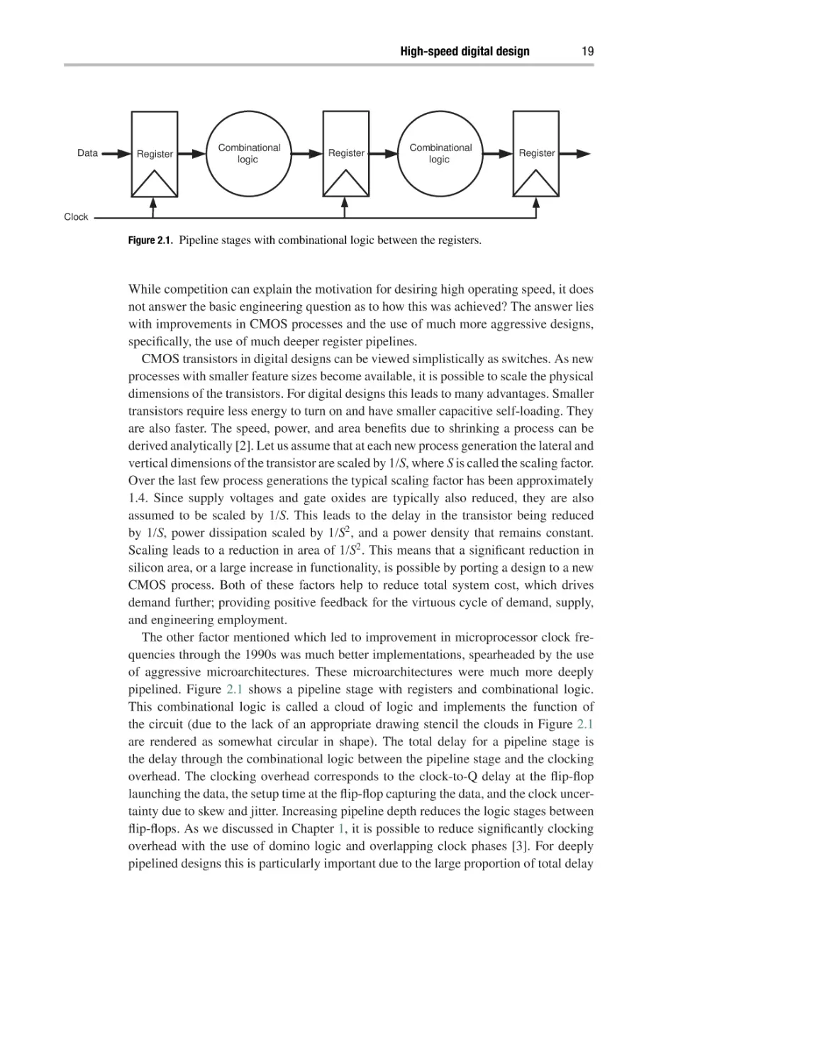
High Performance ASIC Design
33 MHz
80
Clock period (FO4)
20
60
66 MHz
100 MHz
200 MHz
40
450 MHz
20
1 GHz
2 GHz
7.8 FO4
0
Year
Tech (nm)
1990
1000
1992
800
1994
600
1996
350
1998
250
2000
180
2002
130
Figure 2.2. The year of introduction, clock frequency, and fabrication technologies of the last
seven generations of Intel processors.
Source: Used with permission from the paper “The optimal depth per pipeline stage is 6 to 8 FO4
inverter delays” by M. S. Hrishikesh et al., International Symposium on Computer Architecture,
May 2002.
consumed by clocking overhead [3]. For Intel processors in the 1990s there was a large
reduction in the logic between adjacent flip-flops, indicating the increasing emphasis
placed on deeply pipelined microarchitectures [4]. This is shown in Figure 2.2, where
the delay is given as the equivalent number of inverters driving four other inverters
(FO4). Since this measure considers delay in terms of inverter delays and not absolute
time, it is a useful metric to compare microarchitectures in a technology-independent
manner.
Figure 2.2 shows that between 1990 and 2000 the total number of FO4 stages went
from 80 to 10, an approximately 8× reduction. Assuming that a typical CMOS process
generation leads to a delay reduction of 1.4× compared with the previous generation,
an 8× improvement in delay corresponds to the delay reduction achieved by 4.4 process shrinks. This is a remarkable figure. Developing a new process node is extremely
expensive due to the high development costs and capital expenditure. Achieving speed
improvement equivalent to multiple process shrinks from improved design has tremendous benefits not only from a cost point of view, but also by allowing far more capable
designs to come to the market earlier. While Figure 2.2 shows a reduction in logic
between registers, microarchitectural improvements entail more than merely placing
more registers in the design. Efficient design requires that a certain granularity of tasks
be performed during each clock cycle. In order to ensure that this could be achieved
with fewer FO4 inverter delays of logic, domino and other custom design methodologies
started to be used extensively for very high-speed designs.
High-speed digital design
21
While the use of much deeper pipelines has led to greatly improved performance in
microprocessors, there are limits to the extent to which this approach can be applied.
Figure 2.2 is borrowed from a paper entitled “The optimal logic depth per pipeline stage
is 6 to 8 FO4 inverter delays”, which suggests that the current processors are beginning
to approach the limits of maximum pipelining [4]. Further pipelining, which leads to
more instructions being processed at the same time, does not help overall performance
since the likely occurrence of a jump instruction will lead to the pipeline needing to
be flushed. Synthesizable processor cores implemented with automatic ASIC design
flows are mimicking many of the microarchitectural features found in custom designs,
including the use of deep pipelines [5]. Synthesizable logic does not, however, have
access to domino logic or other dynamic logic styles. This is a major difference between
custom and ASIC design methodologies [5].
A point to note about high-speed ASIC design modules is to remember that while
processor design remains one of the most studied and perhaps “glamorous” aspects of
digital implementation, it is not necessarily representative of ASIC designs. The ASIC
market and the high end microprocessor market are fundamentally different in terms of
both the application space and the economies of the business. Examples of large digital
ASICs include graphics processors, cell phone baseband processors, and set top box
decoders. The critical computational modules in these blocks are often data-processing
functions which need to be implemented under very strict power and cost budgets.
Data-processing functions also tend to possess considerable intrinsic parallelism. These
functions are most competitively implemented in hardware and not with a programmable
microprocessor.
Since the end markets for the chips are in the consumer space, the average selling price
(ASP) for these products falls sharply with time. From a purely business point of view this
means that it is essential to reach the consumer markets with products quickly. For this
reason semiconductor companies are extremely uneager to use custom solutions, such
as domino logic, in ASIC products. Since high end microprocessors typically command
much higher prices, they strive to provide performance as a primary design requirement.
This leads to relatively long design cycles and almost mandates the use of considerable
customization. In addition to the faster time-to-market requirement, the applications
targeted by chips implemented with ASIC methodologies are much more cost-sensitive.
This should be no surprise to anyone who has purchased a DVD player and a personal
computer of late, since the prices paid by consumers are ultimately reflected in what
semiconductor companies can charge for their components. I remember once asking a
colleague in sales about his best business deal. The only chip pricing I had been familiar
with had been microprocessors, which were then available for prices in the range of
several hundred dollars each. My colleague thought for a second, until a large smile
broke across his face and he recounted the sale of a highly profitable part that he had
sold for less than three dollars a piece. At the time I was somewhat surprised by the
number, it seemed so low. As electronics is increasingly directed towards the consumer
market, it is worthwhile remembering that a few dollars remains the ASP for a large and
ever-increasing set of chips. Like supermarkets, the real money is made in volume (even
though the ASPs for semiconductors are low, the overall profit margins for the industry
22
High Performance ASIC Design
are much higher than those for supermarkets). It is in this context of falling ASPs and
rapid time-to-market pressures in the ASIC design space that a synthesizable domino
logic solution is proposed in this book.
Since domino logic will only be applied if existing static logic-based synthesis has
not achieved timing closure, the next section deals with techniques used to improve
the implementation of ASIC designs. Many of these techniques represent good design
practice and can be applied whether the underlying circuit technology uses static or
domino logic.
2.2
Microarchitectures for high speed
According to IBM’s original definition for computers, architecture refers to the definition
of the instruction set and other programming abstracts. The actual act of transferring this
instruction set to hardware was referred to as organization [6]. In this book we will
consider microarchitecture or logic design to refer to the design of all the logic. We
will adhere to the convention of referring to architecture as meaning the software and
algorithmic view of the design. The microarchitecture is the next step of the design,
where the architecture is mapped to logic and the first realistic timing and area estimates
made.
As mentioned earlier in the chapter, high clock speed requires the use of deeply
pipelined designs. Inserting extra pipeline stages does not of itself guarantee high performance, since it may be difficult to partition the logic evenly across a number of
different stages. Furthermore, RTL code that appears to be evenly balanced may turn
out to be less so once implemented. Under these conditions, considerable effort must be
expended to ensure that the design can run with a fast clock. Such efforts are the bread
and butter, or perhaps more appropriately in this age of globalization, the rice and dal,
of digital design. While it is possible to enumerate different approaches to achieving an
efficient microarchitecture, it may be more instructive to study some examples.
2.2.1
Fast arithmetic modules
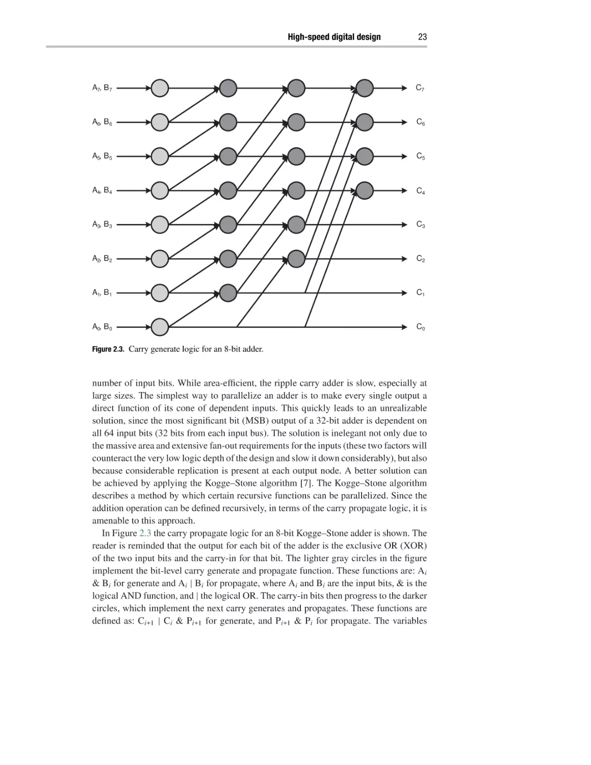
Critical paths, or the longest delay paths in digital designs, often traverse through fast
adders, multipliers, and other arithmetic functions. Sometimes these paths cannot be
further pipelined, since they have feedback requirements which require the full computational cycle to be completed every clock period. Examples of such circuits include
accumulators and Viterbi add–compare–select modules, in which data must come out of
a register, go through some logic, before being latched in the same register at the end of
the clock cycle.
There has been much research on designing high-speed arithmetic modules [6]. Rather
than repeating well-known techniques for speeding up these operations, an example
circuit is discussed to give the reader an idea of the kind of techniques used. A general
principle in speeding up arithmetic operations is to parallelize the operation as much
as possible. A ripple carry adder, for example, has a delay that is proportional to the
High-speed digital design
23
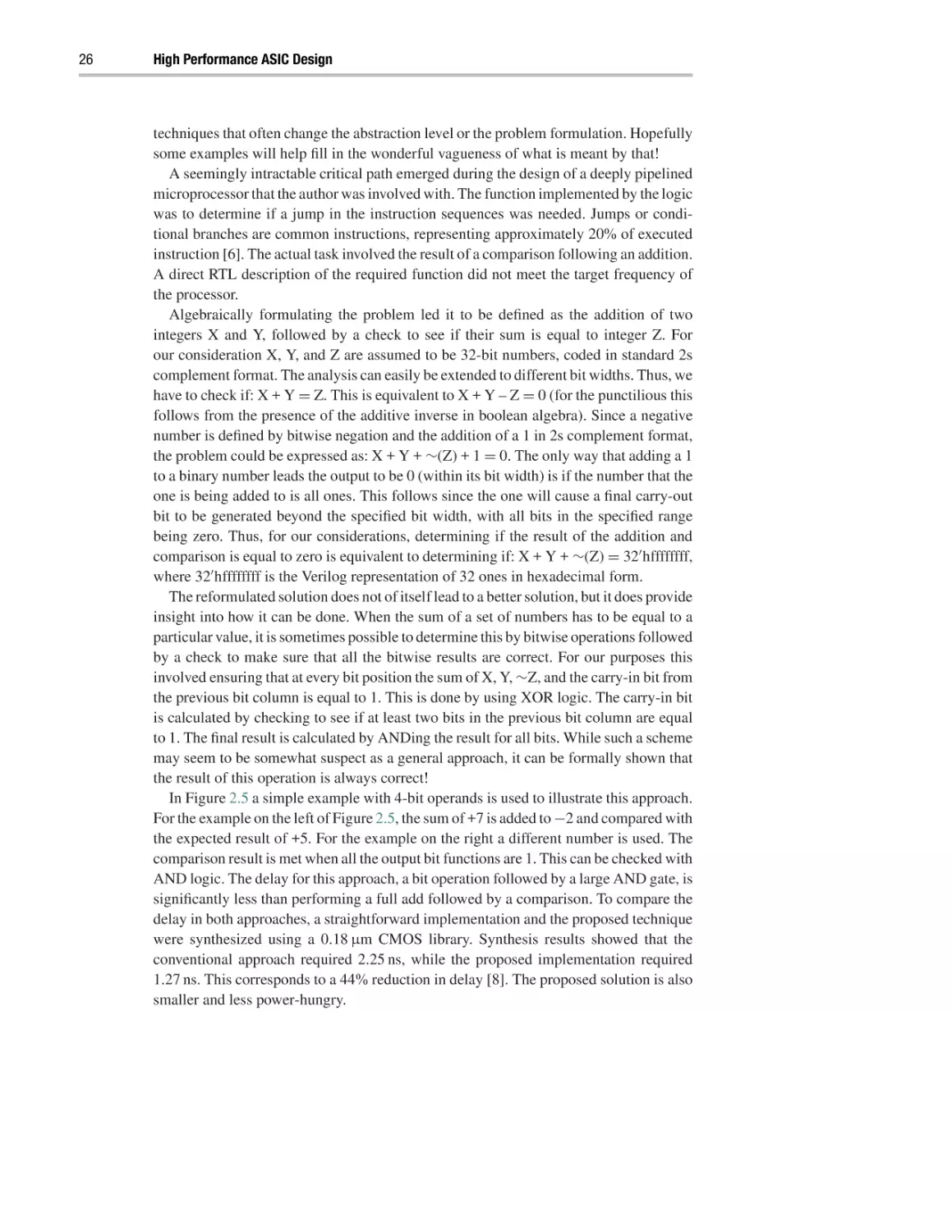
A7, B 7
C7
A6, B 6
C6
A5, B 5
C5
A4, B 4
C4
A3, B 3
C3
A2, B 2
C2
A1, B 1
C1
A0, B 0
C0
Figure 2.3. Carry generate logic for an 8-bit adder.
number of input bits. While area-efficient, the ripple carry adder is slow, especially at
large sizes. The simplest way to parallelize an adder is to make every single output a
direct function of its cone of dependent inputs. This quickly leads to an unrealizable
solution, since the most significant bit (MSB) output of a 32-bit adder is dependent on
all 64 input bits (32 bits from each input bus). The solution is inelegant not only due to
the massive area and extensive fan-out requirements for the inputs (these two factors will
counteract the very low logic depth of the design and slow it down considerably), but also
because considerable replication is present at each output node. A better solution can
be achieved by applying the Kogge–Stone algorithm [7]. The Kogge–Stone algorithm
describes a method by which certain recursive functions can be parallelized. Since the
addition operation can be defined recursively, in terms of the carry propagate logic, it is
amenable to this approach.
In Figure 2.3 the carry propagate logic for an 8-bit Kogge–Stone adder is shown. The
reader is reminded that the output for each bit of the adder is the exclusive OR (XOR)
of the two input bits and the carry-in for that bit. The lighter gray circles in the figure
implement the bit-level carry generate and propagate function. These functions are: Ai
& Bi for generate and Ai | Bi for propagate, where Ai and Bi are the input bits, & is the
logical AND function, and | the logical OR. The carry-in bits then progress to the darker
circles, which implement the next carry generates and propagates. These functions are
defined as: Ci+1 | Ci & Pi+1 for generate, and Pi+1 & Pi for propagate. The variables
24
High Performance ASIC Design
A=
6Decimal
=
0
0
1
1
0 Binary
B = 12Decimal =
0
1
1
0
0
C = 24Decimal =
1
1
0
0
0 Binary
Sum
1
Carry
Result
=
= 0
= 1
1
0
0
1
1
0
0
0
1
Binary
0 Binary
0 Binary
1
0 Binary
Figure 2.4. Adding three numbers to produce a carry and save term with the final result having the
correct value.
Ci+1 , Pi+1 , Ci , and Pi refer to the higher- and lower-order carry and propagate inputs to
the cell.
The structure of the schematic shown in Figure 2.3, where the inputs to the logic at
every stage span across progressively greater widths, is common in many high-speed
arithmetic modules. The total number of cells in the critical path for the design is proportional to the base-2 logarithm of the number of inputs to the adder. Shifters, in which
data can be shifted left or right, tend to look similar, as do increment functions and
priority encoders. It is possible to modify the tree structure shown by having each cell
be fed from more than two inputs. In such implementations the logic depth of the tree
decreases, although each node has more logic. The optimality of a particular design
depends on the tradeoff between fewer but more complex logic functions versus faster
but more numerous elements. Much of this is technology- and circuit design-specific,
especially since it must also consider the delay associated with the wires used to route
the signals.
The reader may have noticed that the set of arithmetic functions mentioned earlier did
not include multipliers, another common arithmetic function. Indeed, the implementation
of a multiplier is a bit different since it requires two separate functions to be performed.
By way of explanation, we note that a straightforward approach to perform multiplication
is through repeated addition. This can lead to very long computation times since multiple
additions are needed. To avoid this delay, the multiplier performs an initial carry save
compression. At the end of the carry save compression the generated terms are added
with an adder. The final adder is also called a carry propagate adder, since the carry can
propagate across the bit width of the adder. In order to illustrate the difference between
carry save and carry propagate addition, a simple example is shown in Figure 2.4. Three
numbers 6, 12, and 24 are represented in their binary formats. Since we do not wish to
use two separate adders to add the three numbers, the three terms must be reduced to
two and then added. The three terms can be compressed by using a full adder. A full
adder receives three inputs and produces two outputs. The sum output is the exclusive
OR (XOR) function of the three column inputs. The sum output has the same binary
position as the inputs to the full adder. The carry output is set to one if two or more inputs
are one. This function is also called a majority voter since the output bit reflects which
High-speed digital design
25
input bit is in the majority. The sum output is shifted one binary position to the left of
the input bits. The full adder works on bits from the same binary position in the numbers
being added together. In Figure 2.4 these numbers are circled. The resultant carry and
sum buses are shown below. The outputs of each full adder are shown within the slanting
ovals. Once the data is in the form of a sum and carry bus, it is added in a conventional
adder. The full adder in this example acts as a carry save adder since all it does is to help
compress three terms to two. The carry save name comes from the fact that every output
is a function of a number of input bits, with no carry propagating across cells. The delay
of a carry save adder is, thus, a single-cell delay, while a carry propagate adder will need
to traverse through a number of cells.
Most multipliers will have more than three input terms. This requires a number of full
adder stages to compress the data to two final carry save terms, which can then be added
in an adder. In addition to full adders a number of different compressor circuits can be
used, such as a four-term to two-term carry save adder (CSA42) and a five-term to threeterm carry save adder (CSA53). These compressors have a higher compression ratio
than a full adder (a full adder compresses three inputs to two outputs, whereas a CSA42
compresses four inputs to two outputs). They are, however, larger and hence slower cells.
The optimal configuration involves a tradeoff similar to that involved in designing a fast
adder: choosing between a fewer number of more complex cells, or a larger number of
faster ones. The best solution depends on the delay of the different compressor cells, the
multiplier size, and the routing delay. These metrics can vary from process to process. In
addition to multiplication, carry save addition can be used to implement three or more
input adders.
While understanding the approaches used to perform high-speed arithmetic operations is often useful, such knowledge is not essential in ASIC design. Synthesis tools
are increasingly knowledgeable about different algorithms for implementing arithmetic
functions. Tools such as Synopsys’s Design CompilerTM are also capable of optimizing
datapath logic across different modules. For example, a number of sequential adders
placed in the RTL will automatically be replaced by the more optimal solution of using
carry save addition and only one final carry propagate adder. While it is possible sometimes to improve the performance of a design by directly coding an optimized logical
solution in an RTL language, such as Verilog, such efforts tend to have a limited utility
for a great deal of effort. It is probably best to use these techniques only when a new
non-standard arithmetic module is needed, or when custom standard cells are available.
The task of implementing arithmetic functions in ASIC design flows is increasingly best
left to computers and software.
2.2.2
Predictive logic and parallel computation
While competing against synthesis tools in implementing well-understood arithmetic
modules is not recommended by the author, it does not exclude intervention by the
designer to achieve the required performance when direct synthesis is proving inadequate.
In order to achieve the desired results a set of optimizations can be attempted, using
26
High Performance ASIC Design
techniques that often change the abstraction level or the problem formulation. Hopefully
some examples will help fill in the wonderful vagueness of what is meant by that!
A seemingly intractable critical path emerged during the design of a deeply pipelined
microprocessor that the author was involved with. The function implemented by the logic
was to determine if a jump in the instruction sequences was needed. Jumps or conditional branches are common instructions, representing approximately 20% of executed
instruction [6]. The actual task involved the result of a comparison following an addition.
A direct RTL description of the required function did not meet the target frequency of
the processor.
Algebraically formulating the problem led it to be defined as the addition of two
integers X and Y, followed by a check to see if their sum is equal to integer Z. For
our consideration X, Y, and Z are assumed to be 32-bit numbers, coded in standard 2s
complement format. The analysis can easily be extended to different bit widths. Thus, we
have to check if: X + Y = Z. This is equivalent to X + Y – Z = 0 (for the punctilious this
follows from the presence of the additive inverse in boolean algebra). Since a negative
number is defined by bitwise negation and the addition of a 1 in 2s complement format,
the problem could be expressed as: X + Y + ∼(Z) + 1 = 0. The only way that adding a 1
to a binary number leads the output to be 0 (within its bit width) is if the number that the
one is being added to is all ones. This follows since the one will cause a final carry-out
bit to be generated beyond the specified bit width, with all bits in the specified range
being zero. Thus, for our considerations, determining if the result of the addition and
comparison is equal to zero is equivalent to determining if: X + Y + ∼(Z) = 32 hffffffff,
where 32 hffffffff is the Verilog representation of 32 ones in hexadecimal form.
The reformulated solution does not of itself lead to a better solution, but it does provide
insight into how it can be done. When the sum of a set of numbers has to be equal to a
particular value, it is sometimes possible to determine this by bitwise operations followed
by a check to make sure that all the bitwise results are correct. For our purposes this
involved ensuring that at every bit position the sum of X, Y, ∼Z, and the carry-in bit from
the previous bit column is equal to 1. This is done by using XOR logic. The carry-in bit
is calculated by checking to see if at least two bits in the previous bit column are equal
to 1. The final result is calculated by ANDing the result for all bits. While such a scheme
may seem to be somewhat suspect as a general approach, it can be formally shown that
the result of this operation is always correct!
In Figure 2.5 a simple example with 4-bit operands is used to illustrate this approach.
For the example on the left of Figure 2.5, the sum of +7 is added to −2 and compared with
the expected result of +5. For the example on the right a different number is used. The
comparison result is met when all the output bit functions are 1. This can be checked with
AND logic. The delay for this approach, a bit operation followed by a large AND gate, is
significantly less than performing a full add followed by a comparison. To compare the
delay in both approaches, a straightforward implementation and the proposed technique
were synthesized using a 0.18 µm CMOS library. Synthesis results showed that the
conventional approach required 2.25 ns, while the proposed implementation required
1.27 ns. This corresponds to a 44% reduction in delay [8]. The proposed solution is also
smaller and less power-hungry.
High-speed digital design
27
X = +7Decimal
= 0 1 1 1 Binary
X = +7Decimal
= 0 11 1
Binary
Y = −2Decimal
= 1 11 0
Y = −2Decimal
= 1 11 0
Binary
~Z = ~(5)Decimal = 1 0 1 0
Sum
=
Carry
= 1 11 0
Binary
Binary
0 01 1
~Z = ~(4)Decimal = 1 0 1 1
Binary
Binary
1 11 1
Sum
=
0 01 0
Carry
= 1 11 1
11 0 0
Binary
Equivalent : output all ones
Binary
Binary
Binary
Binary
Not equivalent: not all ones
Figure 2.5. Numerical example of a predictive adder and comparator.
C
X
B
A
+
F
0,1, or 2
Figure 2.6. Serial computational function with a multiplication at the end.
Another technique that can be used to speed up a function is applicable if it consists
of a number of serial functions, which can then be replaced by a set of speculative
parallel operations. The parallel operations compute the set of possible outcomes for
the original operation, with logic operating in parallel determining which outcome to
select. To illustrate this situation, let us assume that A, B, and C are provided to a module.
Depending on the value of A, B, and C, B + 1 and C, or B + 2 and C, are multiplied together.
Schematically this is shown in Figure 2.6, where the module F computes whether 0, 1,
or 2 is to be added to B before being multiplied by C.
If the function shown in the Figure 2.6 operation cannot be completed in a clock
cycle, it is possible to parallelize the addition and multiplication steps (A and B) with
the selection logic F. This is shown in Figure 2.7. Here it can be seen that all three
possible multiplications start earlier. This is useful since the multiplication will likely
have the longest delay of all the functions. In parallel, the function F computes which of
the outputs to select. This is done via a multiplexer, shown as module M. Of course, this
approach is worthwhile only if the delay for module F is much greater than the delay
through the multiplexer. This technique is quite useful and tends to pop up in circuit and
architecture design as well. By speculatively computing operations at the same time as
the selection logic, the delay of the selection logic can often largely be masked by that of
28
High Performance ASIC Design
C
B
2
X
+
C
B
1
X
+
C
X
B
A
M
F
Figure 2.7. Parallel implementation of the function shown in Figure 2.6 with the multiplication
starting earlier.
the other operations. Although costly in terms of area and power, this can significantly
reduce delay. As of now, logic synthesis tools do not automatically invoke this form of
structure from a straightforward RTL description. One of the reasons is that this approach
has extra functionality, or logic redundancies, which tends to run counter to the goal of
synthesis tools, which strive for non-redundant implementations.
A practical circuit where this approach has been used is in the design of a floating
point unit (FPU). Floating point arithmetic is used in calculations requiring decimal
precision, such as scientific calculations. The standard representation of a floating point
number is as a fractional part and an exponential value. For example, in decimal logic
625.7 is expressed as 0.6257 × 10³ , where 0.6257 is the fractional component of the
number and 103 the exponential power. When two fractional numbers are to be added
or subtracted from each other, the number with smaller exponential component must be
right-shifted so that the representation of the fractional parts corresponds to the same
exponent base. Thus, if 20.0 or 0.20 × 10² is subtracted from 625.7, 20.0 should be
expressed as 0.020 × 10³ to allow the fractional components to be subtracted directly. If
floating point addition or subtraction is to be performed on two numbers, their exponents
are first subtracted from each other. This determines which, if any, number has a larger
exponent. Subsequently, the number with the smaller exponent will need to be shifted
by the difference in the exponent values. Depending on which exponent value is chosen
first, the result of the exponent difference can be positive or negative. If it is negative
it needs to be converted back to a positive number by bitwise negation and adding a 1
to it. Converting the difference in exponents to a positive value leads to an extra delay
[9]. This can be avoided if the two exponents are simultaneously subtracted from each
other, with the result of the subtraction used to shift the two floating point fractions. The
result is generally only valid for one of two values on which the subtraction and shifting
High-speed digital design
A
29
B
LSB
LSB+1
LSB+2
Data in
LSB+3
Result
Figure 2.8. An integrated adder shifter design.
is occurring [9]. Having both operations proceed from the start, however, ensures that
the extra delay of converting a negative exponent to a positive one does not have to be
incurred. Selecting between the two operations can be left to later, by which time the
difference in the exponent values is known. The only speed penalty with this approach is
the need for an extra multiplexing function to choose the correct result. Since multiplexers
were already present in the design, the extra multiplexer required only a small penalty.
2.2.3
Optimizing across logic and circuit design
One of the reasons that custom design can achieve results superior to automated flows
is that it easily allows optimizations across different design abstractions in a flow. A
microarchitectural roadblock that may be intractable at the logic level, for example,
can be made more manageable by a change in the architecture. Similarly, by allowing
designers the freedom to design both the logic and circuit transistors, it is often possible to
achieve better results than sharply compartmentalizing the two. Of course, to be effective
this requires designers to be familiar with different levels of design abstraction. This is
often difficult for engineers to acquire, due to the rigid separation of tasks in engineering
organizations (for engineering managers reading this I urge them to allow a little more
flexibility, wherever possible, in their organizations).
To see how logic and circuit design can be designed in a complementary manner, we
shall look at an adder shifter block. This particular design was done in a 0.35 µm CMOS
technology, in which the shifter was implemented using NMOS pass transistor logic and
inverters [9]. A schematic of the path for a single input data is shown in Figure 2.8. At the
beginning of the clock cycle, inputs A and B are provided to the adder along with “Data
in”, which is a bit in the fractional component of the floating point number. In order to
speed up the operation of the adder shifter block, initial design efforts focused on using
a fast adder. Since a Kogge–Stone adder was available, it was chosen. It was discovered,
however, that using a fast parallel adder did not lead to the fastest module performance. In
order to explain this seemingly paradoxical situation, the reader is referred to Figure 2.8.
It can be seen that until the LSB output of the adder is available, data does not start
30
High Performance ASIC Design
to propagate through the shifter. While having a fast, parallel adder architecture leads to
the fastest adder, this speed is measured from any input to any output, which for adders
typically means from the LSB or another lower-order bit, to the MSB or a high-order bit.
The overhead of the Kogge–Stone adder, however, meant that the output of lower-order
bits was slower than when a simpler adder architecture, such as a ripple carry, was used
[10]. The final architecture for the adder was a mixture of ripple carry for the lowest bits
and a more conventional faster architecture for the higher bits.
The example of the adder shifter design was in the context of a structured custom
design. For ASIC design flows the best circuit design improvements can generally be
made by observing how the delay of the critical path can be reduced by adding specific standard cells to the library. These cells, sometimes called hot cells, can then be
designed and included in the library. The benefits from using these hot cells are often
design-specific. For best performance the custom cells may need to be pre-instantiated
in the design. This is most often the case when the cell is a flip-flop with built-in logic
or a very complex standard cell. It is somewhat perplexing that providing the custom
cells to the synthesis tools can still lead to an inferior solution than achieved with hand
instantiation. This is most noticeable when a particular logic structure of limited cell
depth is needed to meet timing. It may be that a particular hand-instantiated solution
represents a global optimum which, depending on the technology mapping step during
logic synthesis, becomes unreachable for a synthesized solution. In addition, technology mapping algorithms are often simplified to ensure reasonable runtime during logic
synthesis, limiting the quality of the solution. While it may be encouraging to think that
these cases suggest the superiority of human designers over synthesis tools, one has to
remember that analyzing and adding the custom cells occurs only after the synthesis
tool has optimized the design extensively. The work of the human designer is thus more
collaborative than directly competitive with the synthesis tool.
2.2.4
Remarks
One of my professors in graduate school was deeply enamored of giving questions in
tests which could only be correctly completed in a timely manner by the application of a
specific trick. I have never been a big fan of puzzles, and can share the reader’s concern
about the rather haphazard nature of the problems raised and solved in the preceding
pages. Facing the choice between being comprehensive but vague, or specific if arbitrary,
I chose the latter, more practical approach. The engineers’ approach, if you will.
The discussions till now have focused almost exclusively on high-speed design. This
has been done in the context of assuming that the architecture has been properly chosen.
For example, it may be possible that some form of parallelism can allow a design to
achieve performance without stressing the speed of the design. Most ASIC engineers
do not, however, decide the architecture of the design. This is provided. Performance,
defined by the speed of the circuit, must then be met. There has also been little discussion of power and area. For very high-speed designs, power and area must almost
by definition be subservient to the needs of speed. Synthesis tools will attempt to use
High-speed digital design
31
the slack in non-critical paths to reduce the area and the power of the design wherever
possible. Often it is possible to choose between area and power as the most important
consideration after meeting timing. It has been suggested that the best way to achieve
low power in a design is to push for maximum speed, beyond specified needs, and then
reduce speed by lowering voltage [11]. While promising, this technique is often difficult to realize due to designers being constrained in using only specific power supply
voltages.
2.3
Designing and using high-speed memories
Memories, such as static random access memories (SRAMs), read only memories
(ROMs), and register files, tend to heavily populate ASIC designs. Since these memories
often fall along the critical path in the design, a short overview of memory design is presented here. The relative speed of memory versus logic often defines many architectural
choices. For example, the use of complex instruction set architectures in early computer
systems was based on the use of off-chip instruction memories in the multi-chip systems
then present. Deeply encoded instructions were preferable since the long decode times
could be masked by the chip-to-chip communication delays. Only when semiconductor
manufacturing technology improved to the point where chips with on-chip memories
became possible was it worthwhile to move to reduced instruction set computing (RISC)
architectures. In RISC machines, simpler and faster decode logic was necessary to keep
up with the faster memory access times [11].
A simple example of a 4 × 4 SRAM memory is shown in Figure 2.9. The components
of the memory are: the row decoders on the left, the memory cell array in the center,
the input data buffers at the top, and the sense amplifiers at the bottom. Figure 2.9 gives
an overview of all the major components in an SRAM. The decoder logic ensures that
after decoding, a single row of memory addresses are enabled. The memory array stores
the memory value as horizontal data words. The sense amplifiers are used to read data
from the memory array, while the input buffers are used to drive the input data into the
memory array.
Most ASIC designers receive memory modules from internal or external memory
design groups. At the logical level a memory can be considered to be similar to a flipflop, in that the memory has a setup time, a clock-to-Q delay, and a clock insertion
delay. The setup time of a memory is the time needed for the data to be written to the
memory array. If the decoded signal address arrives with the data, the critical path for
the setup delay will include the time needed to decode it. If, however, the address comes
earlier than the data, the address path can be enabled allowing for a faster write. As
in flip-flops, it is possible to change the setup and clock-to-Q delay for a memory by
having more or less delay on the clock insertion delay. This may be useful for cases in
which slack exists on the pipeline stage preceding or following the memory module.
Techniques in which clock delays are modified to favor one side of a pipeline stage
represent zero-sum situations, i.e., the extra time available to compute a function on one
side of the pipeline is offset by having correspondingly less time on the other side of the
High Performance ASIC Design
Data input
Memory address
32
Data output
Figure 2.9. A simplified static random access memory (SRAM) module.
pipeline. These methods are, hence, only helpful when slack exists on one side of the
memory boundary.
While a straightforward clocked memory module is described here as a single pipeline
stage, memories need not correspond to this. A memory such as a ROM, from which
data is read and subsequently used, can be constructed to be a purely combinational
logic function, without any flip-flop boundaries. In such designs the memory tends to be
asynchronous or controlled via some enable signal. Alternately, it is possible to pipeline
the memory more deeply. Clock boundaries may be placed in decoding logic or sense
amplifiers in addition to that present in the memory core. There are, however, limits to
how much pipelining is practically possible within the memory array, since much of its
functionality is analog in nature. One of the ways to build faster memories is to break up
long bit lines into smaller segments. These local, less heavily loaded bit lines can then
be sensed with local sense amplifiers.
If the speed of the memory provided is not adequate or latency constraints do not
allow the use of a more deeply pipelined memory, then it may be possible to speed up
the memory by recognizing some design-specific constraints. For example, for the case
already discussed, where the data address for a memory comes early, it is possible to
High-speed digital design
33
Figure 2.10. Layout plot of a small register file (24 bits wide and 12 bits deep).
achieve speed with a more accurate characterization of the memory. Alternately, if a
particular bit in a memory is critical, it may be possible to favor the access time for that
bit or store it in a register, making sure to correctly use that value when it is needed.
When the whole memory speed is lagging despite these actions, the design may well
require a major rethink.
In Figure 2.9 the memory cell has six transistors. This cell, often abbreviated as a 6T
memory cell, has two back-to-back inverters and two access NMOS transistors. Since
static RAMs comprise a large part of the area of a chip, great effort is generally taken
to ensure that a compact 6T memory cell is available. CMOS manufacturers generally
provide layouts for the 6T memory cells where compactness is achieved by allowing
some layers to be closer to each other than is generally acceptable. These waivers in
design rules ensure a small, economical memory footprint. Since the provided memory
cells are very small, they have very limited drive abilities. To improve the speed of a
memory it is possible for a designer to create a larger memory cell. This will, however,
lead to a larger memory, especially if the CMOS manufacturer does not accept design
rule waivers for this cell (determining which design rule waivers are acceptable requires
running many process lots, an expensive and time-consuming process). The larger size
will lead to greater parasitic loading, which will tend to counteract the effect of the
greater drive strength. For these reasons most SRAMs, even high-speed ones, tend to
use process-verified memory cells.
The 6T memory cell shown drives differential outputs. This is not true for all memories.
Register files often have single-ended outputs. Since a register file’s dimensions tend to
be much smaller than a SRAM’s and their speed requirements much higher, they often
use much larger memory cells. Figure 2.10 shows the layout plot of a register file. The
physical regularity of memories can be noted in Figure 2.10. This regularity often allows
34
High Performance ASIC Design
all the routing needs for the memories to be achieved by simply abutting appropriately
designed cells. For memory designs, the primary design constraint is often efficient
layout. An interesting observation in memories is that a single-ended register file is
generally much faster than a larger SRAM with differential output sensing. This seems
contradictory, since the push–pull action of a differential design should be faster than a
single-ended approach. While this may be true in general, it has to be remembered that
a large, heavily loaded differential SRAM has much more heavily loaded bit lines than
a small, single-ended register file.
At the bottom of Figure 2.9 the sense amplifiers (often abbreviated to sense amps)
are shown. In the figure the sense amps are shown as back-to-back inverters, which is
how they can be conceptualized and indeed sometimes implemented. To improve speed,
a current mirror can be used to provide extra current for faster switching. The sense
amp is the only pure analog circuit that will be encountered in this book. It has to sense
difference in voltage much lower than Vdd, often down to several tens of millivolts.
This is made more difficult by the need to ensure correct operations across changes in
process, voltage, and temperature. A sense amplifier is a differential amplifier in that
it amplifies the voltage difference between its two inputs. While degradations for all
transistors in the sense amplifier due to temperature and process variations are obviously
not desired, they can generally be tolerated. Systemic differences between the two sides
of the sense amplifier, however, tend to be more critical. Great care is taken in circuit
design and layout to ensure that the two halves of the sense amplifier match each other.
Physical design techniques include ensuring that the layout of the two sense amplifier
halves is as symmetrical as possible, with all transistor having the same XY orientation.
This ensures that any variations in the lithographic process used to manufacture the chip
will impact the two halves of the sense amplifier similarly. In addition, sense amplifiers
may use non-minimal gate lengths for sensitive transistors. While this will reduce the
performance of the transistor, it does ensure that variations in drive strength tend to alter
the absolute difference between the matched transistors less.
If some form of current source is used in a sense amp, care must be taken to ensure
that this current is turned on only when sufficient voltage difference exists between the
two inputs to the sense amp. This not only reduces power, but also ensures that erroneous
voltage values are not sensed. A self-timed circuit, whose delay mimics the longest delay
through the memory array, is customarily used to ensure that the sense amp is turned on
when it should be. In addition to the constraints with matching transistors, sense amps
are also constrained by the need to make sure that they fit together with the cells in the
memory array. This requires each sense amplifier width to be an integer multiple of the
width of the memory cell. For a register file with a full swing output signal, the sense
amp is not an analog circuit and can be implemented with a CMOS buffer or some other
purely digital circuit.
Like sense amplifiers, decoder cells and input drivers in a memory are constrained by
layout needs. A decoder cell is generally only as high as a memory array cell. Memory
decoders can use static or dynamic logic. In some applications it is necessary to access
more than one memory location per cycle. This can be supported by allowing multiple
read ports and write ports for the memory. This requires larger memory cells, more bit
lines, and extra memory decoders.
High-speed digital design
35
From an ASIC designer point of view the primary tradeoff in memory designs is
between speed versus power and area in different memory architectures, or speed versus
memory size in different sized cuts of the same memory architecture. As in all other
aspects of VLSI design, design-specific optimizations are often possible. Since this
book is focused on the use of domino logic, the reader is reminded that if a memory
provides data to a domino block then the only acceptable output transition for the data
is from low to high during the evaluate cycle. This can be ensured by AND gating the
memory output with the clock. This logic can also be incorporated in the sense amp or
by using a domino-compatible flip-flop.
2.4
What to remember if applying domino logic
At the end of this chapter it is worthwhile to remember that as the designer prepares to
apply domino logic to help with a seemingly intractable critical delay, some points must
be verified. Firstly, the designer must be certain that standard static synthesis cannot
achieve the desired results with a superior microarchitecture, or that such an approach
does not lead to an unacceptable penalty in area or power. Secondly, if the critical path
under consideration traverses through a memory, it should be verified that speeding up the
logic will sufficiently help performance. There may be the need to use a different memory
cut or change microarchitectural partitioning. Finally, care must be taken to ensure that
the module under consideration has a reasonably “clean” interface. The inputs should
preferably come from registers, especially if they are timing-critical. These flip-flops can
then easily be transferred to domino logic-compatible ones. The output should preferably
go to a flip-flop or a logic stage with sufficient timing slack to tolerate the extra latch
inserted at the output of the domino cell. The module, and its timing challenges, should
be well understood. Throwing faster logic at improperly understood logic is like throwing
money at an improperly understood problem. Other than the fact that the money will be
spent, few other outcomes are certain.
References
1. P. P. Gelsinger et al., Microprocessors circa 2000, IEEE Spectrum, October 1989.
2. R. H. Dennard et al., Ion implanted MOSFET’s with very short channel lengths, IEEE International Electron Devices Meeting, 1973.
3. D. Harris, Skew-Tolerant Circuit Design, Morgan Kaufmann Publishers, San Francisco, CA,
2001.
4. M. S. Hrishikesh et al., The optimal depth per pipeline stage is 6 to 8 FO4 inverter delays,
29th Annual International Symposium on Computer Architecture, 2002.
5. D. Chinnery and K. Keutzer, Closing the Gap Between ASIC and Custom: Tools and Techniques for High Performance ASIC Design, Kluwer Academic Publishers, Norwell, MA,
2002.
6. J. L. Hennessy and D. A. Paterson, Computer Architecture: A Quantitative Approach, Morgan
Kaufmann Publishers, San Francisco, CA, Second Edition, 1996.
36
High Performance ASIC Design
7. P. M. Kogge and H. S. Stone, A parallel algorithm for the efficient solution of a general class
of recurrence equations, IEEE Transactions on Computers 22(8), August 1973.
8. R. Hossain and L. B. Huang, System and method for predictive comparator following addition,
US Patent Number 6820109 B2, November 2004.
9. R. Hossain, J. Herbert, J. F. Gouger and R. Bechade, A 5.2 ns cycle time floating point unit
macrocell, 24th European Solid-State Circuits Conference, The Hague, Netherlands, 1998.
10. J. C. Herbert. R. Hossain and R. A. Bechade, Floating point unit having a unified adder–shifter
design, US Patent Number 6148315, April 1998.
11. D. Markovic et al., Methods for true energy performance optimization, IEEE Journal of Solid
State Circuits 39(8), August 2004.
12. M. Johnson, Superscalar Microprocessor Design, Prentice-Hall, Englewood Cliffs, NJ, 1991.
P1: SJT/...
P2: SJT
9780521873345c03.xml
3
CUUK158-Hossain
July 1, 2008
17:15
Domino logic library design
Razak Hossain and Thomas Zounes
3.1
High-speed digital circuit design
We start our discussions on designing a domino logic library by reviewing the answer
to two classical results on sizing static CMOS inverters. While static and domino logic
are different circuit families, they are both CMOS digital design styles, with the insight
provided by studying static inverters being useful in understanding the general needs
required for any library. The first issue relates to how the transistor sizes in inverters
should scale to achieve a fast delay through a series of inverters driving a large capacitor.
For example, if the first inverter has PMOS and NMOS transistor widths of 2 and 1 µm,
what should the transistor sizes be in the next inverter? It seems obvious that the next
inverter should have larger transistor sizes to ensure that the final inverter is strong
enough to quickly drive the large load. The question that arises is how the transistor sizes
should scale from one inverter to the next to minimize total delay. If the next inverter’s
transistor size increases quickly, it will heavily load down the inverter driving it. This
will lead to a large delay. If, on the other hand, there is only a small increase in size
between adjacent inverters then a very large number of cells are needed. Again, this will
cause a large delay. The inverter sizing question leads us to think how different drives
need to be sized. It also provides insight into the performance impact that occurs when
we limit the number of drive strengths available, an inevitable consequence of using a
standard cell library. The second question we will investigate is what ratio of PMOS to
NMOS transistor widths should be used to minimize the delay through a set of inverters.
Transistor sizing is the most basic step in circuit design, with proper sizing of different
transistors being essential for good design and efficient layout. Taken together these
two questions lead us to investigate, albeit only for static inverters, what drive strengths
should be used and how each cell should be sized. This activity is essential whenever a
standard cell library needs to be designed. Let us jump right in.
In 1975, Lin and Linholm compared the area versus speed tradeoff in sizing a set of
cells used to drive a large capacitive load [1]. The intuitively obvious solution to the
problem involves a set of progressively larger driver cells, so that the final cell is capable
of driving the load circuit with a reasonable transition time. In [1] it is shown that by
having a constant propagation delay across the different sized driver cells, the overall
delay is minimized. Thus, while each cell has greater drive strength than the preceding
one, it is also driving a larger capacitive load. In VLSI design large loads tend to be seen
for nodes that have a high number of fan-outs or which are driving very long wires. Very
P1: SJT/...
P2: SJT
9780521873345c03.xml
38
CUUK158-Hossain
July 1, 2008
17:15
High Performance ASIC Design
4 µm
4 µm
4 µm
4 µm
Input
Output
2 µm
2 µm
2 µm
2 µm
Figure 3.1. Four inverters in series.
large loads (for current CMOS processes something in the range of a few picofarads)
requiring more driver cells are generally only encountered in the clock and reset tree and
when on-chip signals have to be driven off-chip.
Richard Jaeger was one of the reviewers for [1] and used the authors’ formulation for
total delay to derive the result that the optimal transistor scaling factor for driver cells in
the buffer system is e, or approximately 2.3 [2]. What this means is that if the size of the
inverter transistor gate widths increases by 2.3 from each inverter to the next, then the
total delay for the set of drivers is minimized. Jaeger also showed that delay variations
are small around the optimal point. This slow roll-off of total delay from its optimal
value is reassuring, since it means that by only using a limited number of drive strengths,
as is typical in a standard cell library, it is possible to get a good approximation of the
optimal result. In the years that followed, the driver sizing problem has been extended
to include power, including short circuit power [3], reliability [4], and the effect of wire
induction in CMOS processes [5].
The need to continuously increase the drive strength for cells in a logic path occurs
when the final driver must drive a very long wire or many fan-out cells. If there is no
need to drive a large capacitive load, increasing the drive strength of the cells by using
progressively larger cells is not necessarily a good idea. Using larger drive strengths
reduces delay, but the benefits of this are somewhat negated by the greater capacitive
load encountered at the output of the cell due to the fact that larger cells will be present
in the next stage. In addition, it is impossible to increase sizes indefinitely, or even to
exclusively use maximum-sized library cells without leading to a very large and powerhungry design. Under such circumstances the delay minimization problem can be studied
more fruitfully by focusing on the ratio of PMOS to NMOS transistor width. In Figure 3.1
four inverters are placed in series. Each inverter has a PMOS width, Wp , of 4 µm and an
NMOS width, Wn , of 2 µm. The capacitive load seen by each driver is assumed to be the
total gate capacitance of the next inverter’s PMOS and NMOS gate widths, or Wp + Wn .
If the transistors in the inverters are in the saturation region when on, the resistances of
the PMOS and NMOS transistors are proportional to 1/(Wp µp ) and 1/(Wn µn ), where µp
and µn are the hole and electron mobilities, respectively. Assuming that the mobility of
electrons is twice that of holes, the delay for each inverter in Figure 3.1 is proportional
to 1/4µp . This is true if the input is either rising or falling, since the transistors have been
sized to compensate for the different electron and hole mobilities.
P1: SJT/...
P2: SJT
9780521873345c03.xml
CUUK158-Hossain
July 1, 2008
17:15
Domino logic library design
3.6 µm
3.6 µm
3.6 µm
Input
39
3.6 µm
Output
2.4 µm
2.4 µm
2.4 µm
2.4 µm
Figure 3.2. Four inverters with resized transistors.
As a next step let us change the sizes of Wp and Wn to 3.6 µm and 2.4 µm. This is
shown in Figure 3.2. Since the total transistor width is constant, the total loading at
the input of each inverter is the same as before. There has, however, been a shift in the
relative delay for a rising and a falling transition. Since Wp is smaller, the rising delay has
increased while the falling delay has been reduced. Since a falling transition is always
followed by a rising one, the average delay through two inverters is reduced by about 3%
compared with the original delay. The reason for this is that there is a greater reduction in
falling delay than the proportional increase in the rising delay. The optimum ratio of Wp
to Wn can be derived by differentiating the expression and is proportional to the square
root of the ratio of electron to hole mobilities. In this example, where the ratios of the
mobilities are assumed to be 2, the corresponding ratio of Wp to Wn transistor lengths
should be 1.4. While this analysis uses a very simplified model of transistor delays (we
also exclude interconnect and parasitic components of the delay), it does illustrate the
principle that rather than striving for equal rise and fall delays, lower delay occurs by
allocating greater transistor width to the faster mobility devices. Analysis for other cell
topologies shows that the optimum PMOS to NMOS transistor width tends to vary, for
example the ratio is different for an inverter compared to a three-input NAND gate [6].
Also, near optimum delays are possible even if the ratio varies within 5% of the minimum
value. This provides some leeway, which is useful when laying out the cell.
Some observations can be made from the two topics that we have looked into. Firstly,
in order to ensure good drive strength a gradual increase in the drive strength is needed.
This ensures that wherever needed, proportionally larger drive strengths are available.
The second point is that rather than striving for equal rise and fall times, it is better to
emphasize the transition of the inherently faster transistor. This point helps to explain
the advantage of domino logic. All logic transitions in domino cells occur only in one
direction, with the domino cell internal node falling, which causes the output of the cell
to rise. Most of the transistor width can hence be focused to emphasize this transition.
Since the slow precharge delay does not propagate from cell to cell, it can be sized far
less aggressively.
The discussions on circuit design have focused till now on transistor sizing. The
other facet of digital circuit design at the cell level involves the use of different circuit
topologies. For CMOS combinational logic implemented with dual PMOS and NMOS
functions, there is little flexibility available since the implementation follows directly
P1: SJT/...
P2: SJT
9780521873345c03.xml
40
CUUK158-Hossain
July 1, 2008
17:15
High Performance ASIC Design
A
AF
B
BF
AF
BF
B
A
Z
AF
A
BF
B
Figure 3.3. A two-input static logic XOR cell.
A
A
B
B
Z
A
B
Figure 3.4. A two-input XNOR implemented with pass transistor logic.
from the boolean definition of the function. Often the only schematic choice is if an
explicit buffer should be used on a large drive strength cell or if the designer should go
with larger transistor sizes and no buffer. One design choice that may be available for
a designer is to use pass transistor logic. In Figure 3.3 a static two-input XOR cell is
shown. This design uses 12 transistors if one includes the two inverters needed.
In Figure 3.4 an NMOS pass transistor logic implementation of a two-input XNOR cell
is given. Readers unfamiliar with this implementation should quickly check its validity.
This design requires only four transistors. There are a number of other circuits which can
be implemented similarly in a very compact way using pass transistor logic. In deeply
scaled CMOS processes, however, complementary pass transistor logic has to be used
to ensure that a good zero and one are propagated through the cell. For the two-input
XNOR shown in Figure 3.4, this means that two extra PMOS transistors have to be
added. In addition, two extra inverters are now needed to provide inverted signals. This
quickly negates many of the advantages of a pass transistor implementation. There are
two other disadvantages with pass transistor logic that limits their application in standard
cell libraries. Firstly, pass transistor logic tends to be more area-inefficient to layout than
standard CMOS stacks. The drain and source of a pass transistor generally need to
be connected independently, requiring extra via connections. For standard NMOS and
PMOS stacked transistors this is not the case. Secondly, if a cell input is directly connected
P1: SJT/...
P2: SJT
9780521873345c03.xml
CUUK158-Hossain
July 1, 2008
17:15
Domino logic library design
D
Latch
Latch
41
Q
Clock
Figure 3.5. A master–slave flip-flop.
D
Latch
Q
Clock
Figure 3.6. A pulse flip-flop built with a single latch.
to the source or drain of a pass transistor, then depending on the condition of the gate,
the load capacitance seen by the input varies. This complicates cell characterization. It
is for this reason that pass transistor logic is rarely used in standard cell libraries. When
pass transistor logic is used in a standard cell, the input signals generally must be first
buffered or inverted before being used.
While straightforward topologies are typically used to implement combinational logic,
more funky implementations of flip-flops are increasingly becoming common. In fact, the
largest change that we have seen in standard cell libraries over the last few years has been
the increasing use of so-called glitch or pulse flip-flops [7, 8]. Before we describe these
cells, let us quickly review a more traditional flip-flop design. The standard approach to
designing edge-triggered flip-flops has been as master–slave latches. For a rising edgetriggered flip-flop this means that data enters the master latch when the clock is low.
When the clock rises, new data becomes available at the output of the flip-flop. This
scheme is shown in Figure 3.5. The total input-to-output delay through the cell (called
the D-to-Q delay since the input of a flip-flop is generally called the D pin and the output
Q) involves two latch delays.
A pulse flip-flop manages to reduce the D-to-Q delay for the flip-flop from two latch
delays to a single latch delay. This is done by generating a small clock pulse on the rising
or falling edge of the clock. The pulse turns the latch transparent, allowing data to be
propagated through it. This structure, shown in Figure 3.6, allows the delay through the
flip-flop to be reduced from two latch delays to a single latch delay. As pipelining has
been used increasingly to increase the operating speed of designs, the delays through flipflops have become a progressively larger part of the total cycle time [7]. Pulse flip-flops
have correspondingly become very popular.
The single latch used for pulse flip-flops can either be a static or a domino implementation, with care taken to ensure that the precharge does not propagate outside the cell in
domino implementations [8]. Care must also be taken to ensure that the generated clock
pulse closely tracks the latch delay to ensure that both circuits are closely synchronized
across changes in process, voltage, and temperature. The biggest danger in using pulse
P1: SJT/...
P2: SJT
9780521873345c03.xml
42
CUUK158-Hossain
July 1, 2008
17:15
High Performance ASIC Design
flip-flops is that they have longer hold times than standard flip-flops. This follows since
the output of the cell can change throughout the width of the clock pulse. Extra delay
buffers need to be used with these flip-flops to ensure hold time failures do not occur.
Hold problems become more acute if the clock pulse driving the cells has a very long rise
time, since this can adversely affect the quality of the generated pulse. While this may
seem to be a relatively easy problem to avoid, in practice it requires verifying that every
single pulse flip-flop in a design with perhaps tens of millions of instances, implemented
by a number of different design teams, has a sufficiently fast clock transition. Like so
much else in life, for VLSI design the devil lies in the detail.
3.2
An introduction to standard cells
Standard cell libraries provide a set of cells which are designed to achieve a good
mixture of high speed, small area, and low power across a wide variety of designs.
Custom design generally emphasizes performance for a specific design. Standard cells
are designed to provide acceptable performance with high productivity. The constraints
placed on standard cells are on their performance, their layout, and their need to interact
with automated design tools (correct functional models and timing characterization).
A layout plot of a standard cell is shown in Figure 3.7. A power and ground line
on the metal 1 layer (the lowest metal layer) are part of a continuous power stripe that
provides energy to the cells. In between the power and ground line, the PMOS and
NMOS transistors and connecting wires are placed. Each standard cell has a number
of metal 1 routing layers, called tracks, available along its horizontal axis. These tracks
allow for the node connections within the standard cell to be completed. Unused cell
tracks are available for the router to use. The total number of tracks available in a
standard cell library defines the largest PMOS and NMOS transistor layouts possible
without splitting the transistor into a number of parts (the act of breaking up a large
transistor into a number of fingers is referred to as folding the transistor. In computer
architecture instruction, folding refers to merging a number of simpler instructions into
a more complex one. The term, hence, is used to describe both splintering and merging
actions). Having more tracks in a library helps standard cell designers by providing
not only the possibility of larger transistor sizes, but also an easier way to connect
different points in a cell. Unfortunately, this is not often possible since more tracks
may lead to a larger design, which may not be competitive. Typically, standard cell
libraries have between 8 and 15 metal tracks with the lower number of tracks being made
available in less speed-critical, high-density libraries. Some other points to note about
standard cells:
r
r
Since standard cells are placed with alternating power (Vdd) and ground lines, every
alternate vertical row of cells needs to be flipped to ensure that the cells are correctly
connected to power and ground.
Designing very large standard cells can lead to a cell in which it is difficult to connect
all the nodes together. In addition to the metal 1, the other horizontal metal layers
P1: SJT/...
P2: SJT
9780521873345c03.xml
CUUK158-Hossain
July 1, 2008
17:15
Domino logic library design
43
Figure 3.7. A standard cell layout.
r
r
(metal 3, metal 5, etc.) can sometimes be used to route connections within a cell.
These layers are, however, used sparingly to ensure that enough routing resources are
available for the automatic routing tool. In addition, large standard cells become very
wide, making it difficult to place them efficiently. In most standard cell libraries, the
largest cells tend to be registers or flip-flops.
Most automatic place and route tools allow double-height standard cell layouts. These
are standard cells with twice the height.
Combinational standard cells cannot have multiple outputs. This is a disadvantage in
domino logic, where many logic structures can be implemented efficiently as multiple
output functions. The limitation stems from the inability of current synthesis tools to
logically map such cells.
Many of the physical constraints on standard cells are based on the fact that they must be
placed and routed with EDA tools. Standard cells are also synthesized with EDA tools.
P1: SJT/...
P2: SJT
9780521873345c03.xml
44
CUUK158-Hossain
July 1, 2008
17:15
High Performance ASIC Design
D
Flip-Flop
Q
Clock
D
Clock
Q
Figure 3.8. D-to-Q delay changes with smaller setup delays.
This tool-dependent use of the cells means that they must be optimized for the expected
context in which they are used. Standard cell library development, hence, remains an
iterative process involving circuit design, synthesis experiments, and place and route
experiments.
A final challenge in developing standard cells is that each cell is an independently
modeled instance. While a cell having an independent functional model seems reasonable, for timing analysis things get more complicated. Let us try to explain why. The
timing analysis of ASIC-style design involves traversing through the design from inputs
to outputs to determine the paths with the longest delays. For combinational logic cells
this means that each cell must be characterized to ensure that every possible transition
from every input to the output is measured. For a two-input AND gate this would mean
that a path must exist from the inputs, let us call them A and B, rising, to the output, Z,
rising. This must be measured under different output loads and input transition times. In
order to ensure that Z will rise when input A rises, input B must be one. The difficulty
in timing characterization is that a relationship exists between when the output rises
and when input B becomes one. If input B rises a few picoseconds before input A rises
then the output delay will be much longer than if B switches much earlier. Since the
other input can change any time before the critical input arrives, current timing analyzers force a static value to be used to model an inherently dynamic situation. Generally,
for characterization the other inputs are assumed to arrive much before the input being
measured. In this case the characterized delay is optimistic. An alternate scenario may
occur where parallel transistors in a standard cell switch simultaneously, leading to a
smaller delay time than under characterization conditions where only a single input is
assumed to change.
Sequential logic for which setup and hold times must be characterized have their
own challenges. The definition of setup and hold time as mentioned in Chapter 1 is
relative to a clock signal. It might be assumed that setup and hold times can be measured
by repeatedly changing input or clock arrival times until the sequential element has a
functional failure. This is shown in Figure 3.8, where an input is changed repeatedly
P1: SJT/...
P2: SJT
9780521873345c03.xml
CUUK158-Hossain
July 1, 2008
17:15
Domino logic library design
45
closer to a clock rising edge. While failure occurs when a logic one is erroneously
sensed as a zero and vice versa, this failure mode is not approached suddenly. Rather, the
failure is initially manifest with correct transitions becoming slower and slower until they
finally fail. Defining a setup or hold failure with a logic failure would mean that some
extremely slow-changing outputs are possible, leading to likely timing problems in the
next stage. For this reason, setup and hold times are generally not measured by a logical
failure. Classifying a failure point based on the percentage degradation of the delay
through the flip-flop is a better choice. While using the most realistic characterization
scheme is always the best choice, if a new library is to be used with an existing library
which has been characterized in a particular manner, one has to make sure that the two
libraries use similar approaches. If this is not done, the delays in the libraries will be
incorrectly calculated, leading to improper cell choices during synthesis and physical
design.
3.3
Designing a high-performance standard cell library
Many of the optimizations required to design a high-performance standard cell library
are part of the easy to understand, if difficult to define, category of good circuit design:
having optimized schematics and layouts; an accurate characterization of timing and
power; and ensuring that the cells are stable across variations in process, voltage, and
temperature. The library performance will need to be validated against other available
libraries. Two important activities encountered in the design of the library are defining
the number and type of standard cells and choosing the drive strengths.
3.3.1
Starting the design
The most basic choice in designing a library, defining the library cell height in metal
tracks, is often set by the competitive landscape in which the library must compete.
The designer may, hence, have no flexibility in determining this. The one qualification
attached to this situation is for the designer to be aware of what cells in an existing library
are typically used. If designing with an existing standard cell library is pushing the limits
of speed for a particular technology, the synthesis tool will be consistently using large
cell drives. Under these circumstances, designing a new library with more routing tracks
may allow for a more efficient implementation of the cells, without the need for extra
buffering. Alternately, if the design is very difficult to design, the router will need a low
utilization rate to finish its job. Here again it may be possible for a new library to be
competitive despite being taller.
The next choice to be made is the number of cells that the library is to have. This
is not often a hard number, since new cells and drives can be added throughout the
development process, with the consequences of using the new cells being evaluated
continuously. Typical numbers we have seen for general purpose libraries are around
500 standard cells. Smaller, specialized libraries focused on datapath cells, for example,
may have only a dozen cells or so. A large number of the cells in the library are inverters
P1: SJT/...
P2: SJT
9780521873345c03.xml
46
CUUK158-Hossain
July 1, 2008
17:15
High Performance ASIC Design
and buffers, provided with many different drive strengths. The other cells tend to have far
fewer drive strengths available. The number of cells in the library can mushroom quickly
once the different permutations of flip-flops are considered: with and without scan; having
dedicated or shared scan output; support for set, reset, or set and reset inputs controlled
synchronously or asynchronously; inverted, non-inverted, or dual outputs. Thankfully,
many of these variations can be included by changing a small part of the flip-flop without
having to redesign the entire cell from scratch.
Academic papers have reported that increasing the number of standard cells in a library
beyond more than a few dozen does not generally improve the speed of the design [9].
The author’s own experience in designing libraries has shown that there are few speed
advantages to a larger library after the first 50 or so most commonly used standard cells
have been introduced. As more cells are added the delay tends to reduce, although even
that is not guaranteed since adding a particular cell in the context of a specific design
and synthesis tool may actually slow down the design slightly! This seems to be related
to how the technology mapping process proceeds with different libraries. The major
advantage with larger libraries is in area reductions that are possible. Anyone who has
run a synthesis job knows that the most time-consuming part of the process is during the
slow incremental optimizations, when more efficient local substitutions are attempted.
Having a rich library helps this process. Excessively large standard cell libraries tend
to slow down synthesis due to the very long synthesis runs encountered. In addition,
design and characterization time for a library increases in proportion to its size. In recent
years characterization has become more difficult due to the increase in the number of
transistor models and environmental corners needed in new CMOS processes. Since the
Spice models for a process tend to change often during the first few years of its operation,
the characterization process has to be frequently rerun, requiring engineering resources
to be assigned long after the design is complete.
3.3.2
Choosing drive sizes
Drive sizes for a high-performance standard cell library should be chosen rationally to
allow the synthesis tool to efficiently implement the design. In this subsection we describe
the approach used by us in the design of high-performance standard cell libraries. The
approach focuses on the maximum expected load that each cell will drive.
The delay of any standard cell is proportional to the output load that the standard cell
is driving. In addition to the load-dependent component of the delay, there is an intrinsic
delay associated with the cell. This delay is due to the fact that a certain delay is required
to traverse through a cell even if the output load is zero. Increasing the size of a cell leads
to greater intrinsic delay – since the transistors of the cell are larger, they have larger
input capacitive loads (a point to remember during circuit design is to ensure that the
inputs of the cells being designed are driven by other cells and not the Spice simulator
directly. A Spice-like simulator will have an infinite drive capacity, which will mask the
delay increase due to using larger input transistor sizes). In Figure 3.9 the delay through
cells with drive size of 1×, 2×, 3×, and 4× is shown as a function of output loading. For
CUUK158-Hossain
July 1, 2008
17:15
Domino logic library design
47
×
ive
1.5
Dr
ive
2×
Dr
e 3×
Driv
×
Drive 4
D
riv
e
1×
Cell delay
P1: SJT/...
P2: SJT
9780521873345c03.xml
Load value 1
Load value 2
Load value 3
Capacitive load
Figure 3.9. Drive strength versus delay for a set of standard cells.
the 1× cell the delay is minimum when the output load is below “Load value 1”. After
this the 2× sized cell is fastest up to “Load value 2”. Drive 3× is faster from here till
a capacitive load of “Load value 3”, after which drive 4× is fastest. This illustrates that
there is here no intrinsically fast cell and slow cell, rather the drive sizes reflect speed as
a function of output loading. The drive 1× size is determined by layout and the likely
load encountered by a cell driving a single fan-out placed close to the cell. The next few
loads should reflect typical loading conditions encountered by cells along a critical path.
Knowledge of the parasitic and fan-out loading conditions will determine good values
for the other load values at which a transition should be made to a larger load value. This
is process technology-dependent. Typical values for these increments seen in a 90 nm
process have been at 30 fF, 60 fF, and 90 fF. For very large loads it is assumed that the
output of the cell will be buffered, so there is no advantage in using very large drive
strengths. Drives 1×, 2×, 3×, and 4× are assumed to be sized for use on the critical
path of the design, a few other drive strengths can be developed for non-critical paths.
Such a drive is shown as drive 1.5× in Figure 3.9. The cell is not the fastest cell for any
loading condition, but it can drive much larger loads faster than a drive 1×. Having such
a cell will mean that a larger, more power-hungry cell does not need to be used when a
non-critical path is heavily loaded.
The values of the different cut-off points (Load value 1, Load value 2, etc.) should
be fairly consistent across the cells of a library. This simplifies the delay optimization
process for the synthesis tool. A very low input capacitance load (0.5×) is possible for
those cells that are frequently part of large fan-out cones. The designation of 1×, 2×,
3×, etc. for the drive strength of the cells is a somewhat arbitrary moniker, a 2× cell
transistor may not be exactly twice the size of those of a 1× cell. To ensure that the output
load of a cell does not greatly violate the load value it was designed for, the standard
P1: SJT/...
P2: SJT
9780521873345c03.xml
48
CUUK158-Hossain
July 1, 2008
17:15
High Performance ASIC Design
Clk
Wp
W pk
Wpi
Z
N0
A
Wn
B
Wn
Wni
Wn
Figure 3.10. CMOS domino logic two-input AND cell with a feedback keeper.
cells can be characterized with a maximum output load. This is particularly important
when domino logic cells are considered.
The authors were involved in the design of a high-performance static cell library in
a 0.18 µm process. Let us recount some of our experiences and design choices. After
some experimentation, the effective PMOS to NMOS ratio chosen was around 1.5 [10].
The actual ratio varied slightly for each cell depending on layout compactness. We
discovered that larger non-buffered cells led to better performance than using smaller
cells and buffers. Most cells had four drive strengths, with the more popular cells other
than inverters and buffers having up to eight more sizes. Inverters and buffers were
provided with even more drive strengths. The library achieved a 20% speedup, validated
on silicon, over an existing high-speed library, which met our requirements and was very
satisfying!
3.4
Circuit design of domino logic cells: a qualitative approach
Domino logic cells are optimized for fast rising output transitions. In Figure 3.10 a
two-input domino AND gate, first shown in Chapter 1, is reproduced. We have already
discussed how in static logic the sizes of the PMOS and NMOS transistors are intricately
linked, with increases in the relative size of PMOS transistors negatively impacting fall
times, and vice versa. In domino logic, since the logical transition is always rising, the
P1: SJT/...
P2: SJT
9780521873345c03.xml
CUUK158-Hossain
July 1, 2008
17:15
Domino logic library design
49
sizes of the NMOS pull-down transistor, Wn , and the PMOS pull-up transistor, Wpi , can
be made large for fast transitions. The speed of precharge in the domino design depends
on the complementary transistor sizes, Wp , the pull-up transistor size, and the inverter
NMOS transistor, Wni . During precharge Wp charges the internal node, causing the output
to fall.
When designing a domino logic cell one of the first constraints that needs to be
considered is the maximum operating speed of the logic in which it will be used. This
determines the time available for precharge. For a 1 GHz operating frequency with a
clock duty cycle of 50%, 500 ps is available for precharge. From this, variation in clock
duty cycle and clock skew must be subtracted. Setting a very low precharge delay, let
us say, to assume a maximum operating frequency of 2 GHz for the logic with worstcase process, voltage, and temperature will mean that a significant portion of the total
available transistor width is assigned to precharge delays. Unfortunately, this will reduce
the evaluate phase delay of the cell, leading to a slower design. If the actual maximum
operating frequency of the design is much lower, the speed penalty in using an overly
aggressive precharge delay may lead it to not being sufficiently fast compared with a
static logic library.
The other explicit transistor seen in Figure 3.10 is the weak feedback keeper transistor
Wpk . This transistor is sized to be weak, often by setting its transistor length to be larger
than a minimum-sized value. The purpose of the weak feedback transistor is to keep the
output of the cell at 0 when the cell does not switch. Without a weak feedback the output
state of the transistor would be kept by virtue of the load capacitance on the internal
node of the transistor. This capacitance can be altered by leakage current through the
transistors. Furthermore, the capacitance on the load can be diminished by charge sharing
and crosstalk noise. We discuss these topics next.
3.4.1
Charge sharing
Charge sharing refers to the reduction of charge on the internal node of a cell under
certain input switching conditions. The condition is illustrated in Figure 3.11, where a
three-input domino AND gate is shown. During the evaluate phase let us consider the
case where inputs A and B turn high while C remains low. If the nodes Na and Nb had
originally been zero, then turning on A and B leads to some of the charge on N0 being
distributed across these two nodes. The final voltage on the node N0 depends on the ratio
of the capacitance of nodes N0 to Na and Nb. Charge sharing can lead to the output node
of a cell being so diminished that it flips the output state of the cell. In Figure 3.11, if all
input went high, obviously node N0 would go low; this is different from charge sharing,
where the node is discharged unintentionally.
Charge sharing is countered by the weak feedback in the domino logic cell. This
transistor provides charge that will cause the voltage level of the internal nodes N0, Na,
and Nb to rise. There is a tradeoff between how charge sharing-tolerant a domino logic cell
is (which requires a stronger weak feedback and a weaker pull-down NMOS stack) versus
the rising delay of the cell (which prefers a weaker feedback and larger Wp transistors).
P1: SJT/...
P2: SJT
9780521873345c03.xml
50
CUUK158-Hossain
July 1, 2008
17:15
High Performance ASIC Design
Clk
Wp
Wpk
Z
N0
A
Wn
Na
B
Wn
Nb
C
Wn
Nc
Wn
Figure 3.11. A three-input domino logic AND gate.
This tradeoff can be avoided in custom design frameworks, where the evaluate signal
arrives in a narrowly defined window of time, by turning off or weakening the feedback
transistor as the evaluate phase starts. Since we are designing domino logic to be used in
a more automated framework, such timing relationships cannot be assumed, especially
at low clock frequencies. Another approach that has been proposed to counter the effects
of charge sharing is the use of extra integral precharge transistors. We encountered two
problems with the use of such transistors in the design of domino logic circuits. Firstly,
the layout of standard cells was greatly complicated by the inclusion of internal pull-up
transistors. Secondly, since the charge-sharing input might not switch until late in the
evaluate cycle, we noticed that much of the internally stored charge was lost when low
threshold voltage transistors were used. This loss of current through leakage is strongly
dependent on the process corner and temperature used for simulations.
3.4.2
Crosstalk noise
The classical definition of noise in electronics refers to the deviation of devices from
their idealized models due to the non-continuous, quantized nature of charge. Shot noise
and thermal scattering are standard examples of this. In digital design, noise is used as an
P1: SJT/...
P2: SJT
9780521873345c03.xml
CUUK158-Hossain
July 1, 2008
17:15
Domino logic library design
51
umbrella term to refer to a collection of real-world complexities that creep into designs,
with crosstalk often being the biggest concern.
Crosstalk occurs when energy from a signal on one line is transferred to a neighboring
line by electromagnetic means. Crosstalk is usually defined in terms of aggressors and
victims, where the aggressor transfers some of its energy to the victim. In general,
both capacitive and inductive coupling exist. On-chip, however, the currents through
the signal lines are usually too small to induce significant magnetic coupling. While
inductive effects, such as simultaneous switching noise, may grow in importance in
future process generations, they are still manageable with careful routing of the power
and ground network. Capacitive coupling, on the other hand, depends on the line-to-line
spacing between wires and can be measured as the total capacitance of a node that is
coupled to neighboring wires, as opposed to fixed sources. For domino circuits, crosstalk
can lead to high pulses being induced on lines that should be low. These pulses can cause
the domino cells to switch erroneously, leading to possible wrong states in the design.
As CMOS processes scale, wires have become progressively narrower. To limit the
resistance in them, they have also become taller. This has meant that most of the capacitance in wires is coupled to adjacent wires on the same level. Aggressor and victim
pairs are, hence, most likely to occur on long wires routed next to each other. The
actual occurrence of crosstalk is very complicated, being dependent on the strength and
location of the aggressor and the victim lines (crosstalk is worst when aggressor and
victim lines are driven from opposite sides), the ratio of floating to fixed line capacitance (greater floating capacitance causes crosstalk-induced bumps to be higher), the
resistance of the line (higher resistive lines weaken aggressors), the degree to which the
victim may already be weakened due to other aggressors (if an attacker simultaneously
attacks the line driving the victim, the strength of the victim driver is reduced, making it
more difficult to overcome crosstalk noise on its output), and the location and number of
aggressors present (multiple aggressors can attack a line, for example, if a bus is routed
together). Crosstalk can be manifest as a high and narrow pulse on the victim line, or
as a wider but lower signal. While crosstalk analysis can become very complicated, for
ASIC domino logic design it can be reduced to two problems. The first is determining
the expected crosstalk-induced pulse on the cell inputs. The second is characterizing
domino cells to determine the maximum crosstalk pulse that the cell can tolerate on any
input. Current place and route tools can estimate the maximum crosstalk noise bump
on the inputs of cells. If every cell input is characterized by a maximum bump that can
be tolerated, the tool will determine possible crosstalk failures and attempt to reroute
the problem wires to achieve a violation-free implementation. To ensure that no noise
violations occur in cells, their crosstalk susceptibility needs to be characterized conservatively. As EDA tools continue to improve their crosstalk analysis and avoidance
capabilities, less conservative modeling techniques can be used.
3.5
Circuit design of domino logic cells: a quantitative approach
The design process for a standard cell library is an iterative process in which, as cells are
added to the library, concurrent synthesis experiments on benchmark circuits are used
P1: SJT/...
P2: SJT
9780521873345c03.xml
52
CUUK158-Hossain
July 1, 2008
17:15
High Performance ASIC Design
to evaluate the benefits of the new cells. For domino logic design, the comparisons will
include a comparison with the results achieved using a static library. The design process
therefore entails a set of delay measurements for every cell as it is being designed. This
data is used for a direct comparison and also to provide timing characterized views of the
cell that can be used in synthesis. In this section we describe in detail how we performed
timing characterization for a domino logic library designed with a 90 nm CMOS process.
Domino logic cannot have inverting outputs. This means that while NANDs, NORs, and
inverters cannot be used, ANDs, ORs, and AND–OR functions can be. Since it is possible
to have a wide variety of AND–OR functions, the number of types of possible cell is
very large. In Chapter 4 we describe how inverting logic is avoided when domino logic
cells are synthesized.
Before plunging into a description of the characterization step, let us define some
terminology that will be used. Data inputs refer to all the inputs of the cell except for the
clock, while the term “all inputs” includes the clock. The term “pin under test” (PUT)
refers to the specific pin which is being tested. Related pins refer to the pins in addition to
the pin under test that need to be high to ensure that the output can switch. For example,
in a two-input AND gate, if input A is the pin under test, then the related pin B must be
high to ensure that the output of the gate can go high.
The design of a domino logic library involved ten characterization tests for all nonregister-type domino cells. These are:
r
r
r
r
r
r
r
r
r
r
3.5.1
Cell delay and output transition time measurement.
Input pin capacitance measurement.
Setup measurement of data input rising relative to the clock falling.
Minimum pulse width high overlap (MPWHO) measurements.
Hold measurements of data inputs falling relative to the clock rising.
Setup measurements of data inputs falling relative to the clock rising.
Minimum clock pulse width for low and high phases.
Maximum noise spike characterization for the input pins.
A charge-sharing check.
Precharge sizing check.
Cell delay and output transition time measurement
The delay from the inputs switching to the output switching determines the performance
of the cell. This delay depends on the input signal rise/fall time and the load on the cell.
For domino logic cells the output can fall only when the clock goes low and the cell
can rise only if the clock is high and the data input logic evaluates high. For this reason
the rising delay is measured for all inputs, while delay falling is measured only when
the clock falls. Since our domino logic flow assumes that domino cells can interact with
static cells, the trip value to indicate where the measurement begins and ends is the same
as those used in the available static standard cell library. This reduces errors when mixing
P1: SJT/...
P2: SJT
9780521873345c03.xml
CUUK158-Hossain
July 1, 2008
17:15
Domino logic library design
400 ps
53
1400 ps
Clock
Related pins
200 ps
Pin under test (PUT)
Fall delay
Rise delay
Output
Fall
transition
Rise
transition
Figure 3.12. Delay and transition time measurements for a domino logic cell.
domino and static cells. For a falling signal the trip value is 60% of Vdd (as a start or
end point). When a signal is rising, the trip point is 40% of Vdd. Transition times are
measured from 20% to 80% of Vdd.
Figure 3.12 shows the waveforms used to measure delay for a 90 nm domino logic
cell. Initially, all inputs are kept high. This causes all internal nodes of the cell to be low.
The clock is then forced low, and after 400 ps, all the data inputs are also driven low.
Between the time the clock falls and the input pins fall, the internal nodes precharge. This
400 ps precharge time allows the internal nodes to be precharged to what we consider
a “reasonable” value. Let us explain the purpose for this. In a domino logic design, the
internal or evaluate node that drives the inverter is high during precharge. The data inputs
eventually go low during precharge (this depends on the phase of the driving cell), since
the driving cells also enter precharge. There is, however, a lag between when the clock
enters precharge and when the data inputs go low. During this time, internal nodes start
to precharge to an NMOS transistor threshold voltage below Vdd (Vdd – Vtn). This extra
charge on the internal nodes increases the delay in a domino circuit. The amount of time
that the input nodes are on will determine the charge on the internal nodes. In some cases,
the internal nodes may remain at 0 due to the input signals remaining low. In other cases,
the internal node may precharge to Vdd – Vtn. A precharge time of 400 ps is used during
characterization since the library has precharge delays in the range of 300 ps and 400 ps.
We believe this value reflects a realistic condition without being excessively pessimistic
or optimistic. Precharge delays vary with the process corner, so a lower value would
be more realistic when a non-worst process, voltage, and temperature (PVT) corner
is used.
The output of a domino only goes low when the clock falls. The fall delay for the cell
is measured from the falling edge of the clock input.
Output rising delay measurements are made for every cell input, including the clock.
In many cells more than one combination of inputs can cause the cell to evaluate. In such
P1: SJT/...
P2: SJT
9780521873345c03.xml
54
CUUK158-Hossain
July 1, 2008
17:15
High Performance ASIC Design
cases the input condition that leads to the longest delay is selected. To measure the rise
delay, the related pins rise with the clock. All other data pins remain off. The PUT rises
200 ps later. This 200 ps ensures that all the pins of the cell do not switch at the same
time, and represents an attempt to provide a typical condition in which the PUT will rise.
For rise delay measurement from the clock pin, all relative pins rise at the same time as
the clock.
The delay and transition simulations are done for five different output loads and five
different input transition times. Synthesis and timing analysis tools can interpolate all the
needed values based on these data points. The maximum input and clock transition used
for characterization is 150 ps (a 150 ps transition from 20% to 80% of Vdd is equivalent to
a 250 ps 0 V to Vdd transition). The maximum cell load used is the maximum capacitance
value for the particular drive. This maximum capacitance is the capacitance load that
leads to a 400 ps (0 to 100% of Vdd) falling transition for a domino cell. The falling
transition is used since this is greater than the rise transition in domino cells. Since the
maximum capacitance value depends only on the output inverter size, it is constant for
all cells of the same drive strength and does not need to be characterized independently
for every cell.
3.5.2
Input pin capacitance measurement
The input pin capacitance is measured by taking the integral of the current of the PUT’s
driving source and dividing it by Vdd. This follows as the charge stored on a capacitor
is equal to its capacitance multiplied by the voltage across it. Current is measured only
when the signal is rising, and is recorded for each of the 25 delay measurement runs.
The average of all these values is then used.
3.5.3
Setup measurement of data input rising relative to the clock falling
It is possible for an evaluate phase signal being propagated through a set of domino gates
to become progressively thinner until it finally leads to a logical failure. This failure is
manifest as a pulse that is too narrow to allow the domino cell to evaluate. The pulse
nature of domino signals means that checks must be performed to ensure correct pulse
width. One mechanism by which the output of a domino cell can have an excessively
thin pulse is if an input signal rises just before the clock falls. In order to ensure that the
output pulse is appropriately wide, a setup time is defined between the data inputs rising
and the clock falling.
Since the purpose of this setup time is to ensure proper pulse propagation, the setup
is defined to occur when the output fall delay decreases by 2.5% compared with the fall
delays generated by a very large data setup time. The decrease in the precharge delay
is due to the internal node of the domino cell not falling all the way to 0 V during the
evaluate phase. While this definition may appear to be very conservative, it is needed
to ensure output transition times do not vary much from that measured during delay
P1: SJT/...
P2: SJT
9780521873345c03.xml
CUUK158-Hossain
July 1, 2008
17:15
Domino logic library design
400 ps
1400 ps
55
2000 ps
Clock
Related pins
Rise setup
Pin under test
Fall delay, tpd
97.5%
of tpd
Output
Figure 3.13. Setup rising versus clock falling measurement for a domino cell input.
characterization. If the data setup time is allowed to become smaller the output rise
transition times will increase, with the output possibly failing to reach Vdd. Ensuring
that output fall delays are within 2.5% of the possible maximum delay ensures a limited
impact on the transition times of the domino cells.
The simulation approach used to calculate the setup rising delay is similar to that for
the rising delay measurement as seen in Figure 3.13. The clock initially goes low and
related pins fall soon after. Related pins and clock then rise simultaneously, and after a
delay, the pin under test rises just before the clock falls. This delay time when the PUT
rises is then varied until the output fall delay is 97.5% of the original fall delay. This
defines the PUT rising setup.
Like delays, setup and hold times are dependent on the transition times of the nets that
drive the inputs and the output load of the cell. The rising setup time is characterized
by varying clock fall times, data input rising times, and output loading. A total of nine
simulations are run for every input data pin. The timing tool interpolates other values
from this data.
One of the advantages of controlling pulse shapes by a setup check is that this attribute
is understood by ASIC tools, ensuring that synthesis and physical design tools can correct
setup failures during the implementation process. Unfortunately, it is not possible for
all checks required by domino cells to be understood by the tools, as we shall see with
minimum overlap checks described next.
3.5.4
Minimum pulse width high overlap characterization (MPWHO)
When multiple inputs are applied to a domino cell care must be taken to ensure that the
pulses overlap each other sufficiently to allow the evaluation node to be discharged. For
example, in a domino AND3 gate all three inputs must be on at the same time for the
internal node of the cell to be discharged and the output of the cell to rise. The minimum
pulse width high overlap (MPWHO) is a check to ensure that the overlaps between the
different data inputs to a domino cell are acceptable. This is needed for all inputs to
the domino cells. In a domino OR3 cell the transistors are connected in parallel. Here the
56
CUUK158-Hossain
July 1, 2008
17:15
High Performance ASIC Design
Input1
Voltage
P1: SJT/...
P2: SJT
9780521873345c03.xml
Input2
AREA
Vb
Time
Figure 3.14. Minimum pulse width high overlap area.
check merely needs to determine that each input applied to the cell is sufficiently wide
to cause the output of the cell to rise. In some AND–OR cells, many different paths can
cause the output of the cell to rise. Since we consider each domino cell to have only a
single MPWHO value, the worst-case overlap value is used.
For our 90 nm domino logic library, the MPWHO is defined as the duration of time
between when the last input rises (measured at 40% of Vdd) and the earliest input falls
(at 60% of Vdd) for each NMOS pull-down path such that the evaluation node falls to
20 mV or lower. From simulations the 20 mV evaluation node voltage is found to ensure
that the output delay does not increase more than 1% under maximum capacitance
loading.
Since pulse width overlaps are not standard timing checks, they are not supported
natively by Synopsys’s PrimeTimeTM or other timing analysis tools. This required a definition of MPWHO to be developed for the domino logic library. Defining the minimum
overlap needed between inputs based on measured time proved difficult, since many
inputs can have slow transition times. Forcing the synthesis tool to try and fix all transition times to achieve acceptable high-value overlap for all cells would unnecessarily
overconstrain the design. In order to avoid this, a metric was developed to model overlap between different inputs under very different transition times. This metric measured
MPWHO based on the total input signal overlap area for each cell, above a cell-specific
fixed voltage value, Vb. While this choice may appear somewhat arbitrary, this solution
married a simple characterization process with excellent correlation of the evaluation
node reaching 20 mV or lower.
Figure 3.14 shows how the MPWHO area for a domino cell can be measured. For a
two-input domino cell, let us assume that Input2 is the last rising input and Input1 is
the first falling input. The intersection of these signals above Vb gives the minimum
pulse width high area overlap. The voltage Vb ensures that unless the input signals
cross a certain value, the output will never change. Since NMOS transistors only turn
on when their inputs exceed a threshold voltage, this is a reasonable assumption. The
MPWHO constraint can be checked for every domino cell in a design with Synopsys’s
PrimeTimeTM and some Tcl scripting. The script reads a file with the MPWHO area
and Vb data for every input. Delay and transition time information available in the
CUUK158-Hossain
July 1, 2008
17:15
Domino logic library design
Voltage
P1: SJT/...
P2: SJT
9780521873345c03.xml
57
Equal areas
above Vb
Vb
Time
Finding equal areas of two different curves
Figure 3.15. Setting Vb to ensure equal MPWHO area under slow and fast transition times.
timing analyzer can then be used to determine if a violation occurs. Needless to say, this
approach requires that all domino cells in the library have a characterized MPWHO area
and Vb value.
In order to ease characterization of the MPWHO area for each domino input, simulations were limited to two cases: under very small and very large transition times. This
was deemed acceptable as experiments showed that the worst-case MPWHO conditions
occur either when the nets of a cell are very lightly or very heavily loaded. If the pins are
driven by lightly loaded nets, fast rising and falling signals can lead to minimum signal
overlap. Alternately, if the input pins are heavily loaded then slow rising transitions can
limit the area over the Vb voltage level. Under worst-case process and environmental
conditions, minimum transitions are simulated with a 12 ps transition time, while the
maximum transition uses a 150 ps transition time. For each set of EldoTM runs, the rising
input is moved closer to the falling input to reduce the area overlap as shown. Once the
evaluation node fails to read 20 mv, the minimum overlap condition is assumed to have
been reached. The data from the fast transition and slow transition times are then used to
find the Vb that will cause the areas to be the same. This is shown in Figure 3.15, where
Vb is set such that the two simulations have identical MPWHO areas. From Figure 3.15
it can be seen that the cell inputs do not all need to be simultaneously at Vdd for the
output of the cell to switch.
For an OR gate the rising signal and falling signal is applied to the same pin. For
gates that have more than one transistor in the evaluation path, the transistor connected
to the evaluation node will have its gate connected to the falling signal and the adjacent
transistor will have its gate connected to the rising signal. This is shown in Figure 3.16.
All other transistors in between will be connected to Vdd. If there are other transistors
not part of the evaluation path, their gates will be connected in such a way as to cause
the longest evaluation time of the evaluation path. The above condition ensures worstcase characterization. This ordering of inputs and associated logic transitions limits the
characterization effort needed for MPWHO.
P1: SJT/...
P2: SJT
9780521873345c03.xml
58
CUUK158-Hossain
July 1, 2008
17:15
High Performance ASIC Design
Clock
Clock
Z
Falling input
Falling input
Rising input
Evaluation node
Rising input
Clock
Overlap area
Evaluation node
This voltage must
drop below 20 mV
Figure 3.16. MPWHO measurement setup for a domino cell.
φ1
φ1
φ3
Phase 1
signal
Phase 1 signal
Hold time duration
OR
Phase 3
output
φ3
Phase 3 output
Signal overlap insufficient
for output to rise
Figure 3.17. Hold violation for data fall with respect to the clock rising.
3.5.5
Data pin hold falling measurement
In a synthesized domino design some cells may have inputs driven by cells connected
to a different clock phase. Under such circumstances a cell input may go low when the
cell clock rises. This is shown in Figure 3.17. While the clocking scheme tries to avoid
this circumstance, it may still occur, and hence, all cells need to be verified against this
failure mechanism. This failure mechanism is in fact a classical hold time failure and
is avoided with a data fall to clock rise hold check for all inputs. This check can be
considered to be an overlap check, but the clock pin is not considered in the MPWHO
checks (for which the clock input is kept high) since it was found that considering an
extra serial transistor in MPWHO checks made the check overtly pessimistic.
The definition of hold time is the time between clock rising (measured at 40% of
Vdd) and data input falling (measured at 60% of Vdd) that will cause the evaluation
node of the PUT’s cell just to drop below 20 mV. The related pins are chosen to cause
the longest delay for PUT (as in the delay characterization). The hold check is done
using two extreme clock rise times and two extreme data fall times (four data points).
Output loading is set to the maximum cell loading to ensure worst-case tolerance. The
measurement used for data pin hold with respect to clock falling is shown in Figure 3.18.
P1: SJT/...
P2: SJT
9780521873345c03.xml
CUUK158-Hossain
July 1, 2008
17:15
Domino logic library design
59
Clock
Related pins
Measured hold time
PUT
Evaluation node
Evaluation node voltage
must drop below 20 mV
Figure 3.18. Domino cell hold time measurement.
3.5.6
Data pin setup falling measurement
A requirement in domino logic is that the output of all cells must go low every cycle
before the clock rises again. If this does not happen, a false evaluation may occur. To
detect such an issue, a setup check is performed to make sure that the data input goes low
on each cell before its clock rise. The definition of this setup is the time between data
input going low and clock going high, such that the evaluation node is charged high.
Simulations determined that this check tends to always pass. For this reason a computationally simple procedure is used to measure the setup time. The setup time is defined
by measuring the distance between the input and clock pin of the cell so that they intersect
at 20% of Vdd. This is a conservative number that ensures the data input transistor and
the clock transistor are both off as the data input falls and the clock rises. This simplified
check is suitable for the test cases encountered by us in our 90 nm designs. For other
processes or designs a more thorough characterization process may be needed. One of
the reasons that we always wish to use simple characterization wherever possible is that
it allows for the library to be characterized faster. While using parallel simulations does
allow the characterization time for a library to be speeded up, the high cost of EDA
licenses and computer servers limits the number of parallel simulations that can be run.
Two input data pin transition values and two values of clock rise transition times (four
points) are used to build the setup table. Figure 3.19 graphically illustrates the setup time
measured.
3.5.7
Minimum clock pulse width for low and high phases
It is possible for a domino cell to meet all the setup and hold times but still fail due to
the clock duty cycle being severely distorted. This is manifest as a very narrow high
or low value for the clock. For clocks provided directly from a PLL, the probability
of this occurring is low. Still, as a verification check this needs to be tested, especially since clock duty cycles can vary considerably if they are generated by dividing a
faster clock source. Since this check does not require great precision, it is implemented
P1: SJT/...
P2: SJT
9780521873345c03.xml
60
CUUK158-Hossain
July 1, 2008
17:15
High Performance ASIC Design
PUT
60% Vdd
40% Vdd
20% Vdd
CP
Setup time
Figure 3.19. Data fall to clock rise setup time measurement.
Clock
40% of Vdd
60% of Vdd
Output
5% of Vdd
95% of
Vdd
MPWH
MPWL
Figure 3.20. Clock minimum pulse width characterization.
using the existing minimum pulse width checks supported by the Liberty format timing
models (often called the Synopsys.lib model). The primary limitation with using the
minimum pulse width high (MPWH) and minimum pulse width low (MPWL) check
is that it provides a single number for an input pin. In reality, the minimum clock
pulses that are acceptable depend on the clock transition times and the output loading on the cell. For our purposes this check is characterized assuming the maximum
clock transitions specified in the library and the maximum output loading for the cell in
question.
Figure 3.20 shows the MPW characterization timing. The minimum pulse width checks
are performed by initially setting high the data pins that cause the longest evaluation delay.
The clock is then forced high. The MPWH is measured from when the clock reaches
40% of Vdd, until when the output of the domino cell reaches 95% of Vdd. MPWL is
measured from when the falling clock reaches 60% of Vdd until when the output reaches
5% of Vdd. Simulations showed that the output reaching 95% of Vdd led to almost the
same delay as the clock falling to 60% of Vdd. Using the output rise point to measure
delay allowed us to avoid an iterative process of measuring acceptable clock pulse width
by sliding the clock window and replacing it with a single pass measurement.
P1: SJT/...
P2: SJT
9780521873345c03.xml
CUUK158-Hossain
July 1, 2008
17:15
Domino logic library design
3.5.8
61
Data pin maximum noise spike characterization
A major concern with domino logic is its susceptibility to crosstalk-induced noise failure.
Such noise can lead to functional failures if the evaluation node in the domino cell is
inadvertently discharged. To ensure noise tolerance of domino cells, every input of every
cell is characterized for its crosstalk tolerance. This characterized data is then used during
physical design.
For the 90 nm domino library, the chosen place and route methodology involved
using Synopsys’s AstroTM physical design tool. In AstroTM it is possible to specify the
maximum acceptable noise spike on each input pin of every cell. The router will then
attempt to ensure that this noise spike constraint is not violated. A limitation with the
version of the tool we were using was that the noise spike was calculated based only on
direct aggressors. This did not allow for the tool to consider the effect of noise being
propagated from other cells. The tool also did not enforce any constraints on the width of
the noise pulse. Since the total crosstalk-induced energy is proportional to both the height
and width of the induced voltage bump, it should be considered for crosstalk tolerance
of the design. To overcome these limitations the domino cell characterization process
assumes worst-case pulse width and that propagated noise is also present. In addition to
crosstalk, simultaneously occurring charge sharing in the domino can cause the internal
node to dip. As the evaluation node dips the output inverter’s NMOS transistor becomes
weaker, and hence less able to counter induced crosstalk noise on its line. For this reason
charge sharing is assumed to occur simultaneously with crosstalk. Characterizing the
cells under such pessimistic conditions ensures the functionality of the cells. It also goes
some way to explaining why silicon results for digital ASIC designs tend to run faster
than the simulations!
The maximum spike characterization involves applying up to two input spikes to the
cell inputs. One of these spikes is assumed to be on the PUT, while the other is to another
input pin. The second input spike is added to include the possibility of multiple crosstalk
events being simultaneously applied to the domino cell. The maximum charge-sharing
condition is applied simultaneously with the spike noise. The input noise and charge
sharing weaken the domino cell output inverter NMOS transistor. On this weakened
output, capacitively coupled noise is applied to the output node. The same output noise
is applied independently to the same cell with no input noise. The output voltage area
above 10 mV is calculated for the cell with and without noise. If the ratio of these two
values is more than 3, then the input noise is too large and a smaller applied bump is
applied until the ratio of 3 is reached.
The value of 3 is used for measuring acceptable noise bump area since up to that
value, if the noise bump is applied to another domino cell it is not seen to propagate
to the output of that domino cell. The domino cell is thus able to filter the input bump.
One of the possible problems with noise is that it cannot be allowed to propagate from
cell to cell since it could ultimately overwhelm a cell further along the logical path. The
value of 3 is very design- and technology-specific. For our purposes we discovered that
using values greater than 3 led to possible noise stability issues, while smaller values
appeared to be unnecessarily conservative. The characterization procedure is shown in
Figure 3.21.
P1: SJT/...
P2: SJT
9780521873345c03.xml
62
CUUK158-Hossain
July 1, 2008
17:15
High Performance ASIC Design
Cross coupled noise
Evaluation node
Output bump on noisy cell
Clock
Z
Rising
Noise
Low
Cc
c
Cg
n
Output bump on quiet cell
Noise
Clock
Z
10 mV
Figure 3.21. Maximum voltage spike simulation setup.
The 90 nm domino library has a maximum capacitance setting on all cell outputs
that limits the worst-case transition time to 150 ps. For simulation, the aggressor crosscoupling ratio is assumed to be 50%. Post place and route experiments showed that 85%
of nets have less than 50% of total capacitance coupled to all other nets combined. These
two factors, the maximum transition time of signals and the maximum cross-coupled
capacitance connected to an aggressor, limit the width and height of the worst aggressor
noise that can be applied to the output of the domino cell being characterized. For an
aggressor having a rise time of 300 ps, the input noise bump will be very low, but the
width will be at its maximum. When the aggressor rise time decreases, the bump will
also increase, but the width will decrease. Different aggressor rise times are generated
by having an inverter drive a variable capacitance. The capacitor value is varied until the
output area ratio is 3. Simulations have shown that worst-case crosstalk tends to occur
with low, but wide, aggressor pulses.
To simulate worst-case charging during crosstalk measurements, the simulation is setup to have all internal nodes discharge. Great effort was spent ensuring that the worstcase charge-sharing condition and input noise was applied during cell characterization (it
was not always obvious which input pins would cause worst-case noise). The maximum
noise spike is also measured for the domino cell clock pin. The clock network has a large
capacitive load being driven by a strong set of drivers, so only minimal noise spikes are
expected on it.
3.5.9
Charge-sharing check
In addition to the characterization for noise sensitivity on the input pins, a number of
checks are included to ensure the effectiveness and stability of the domino logic cells.
One of these is the charge-sharing check. One should note that while charge sharing is
assumed during the worst-case voltage spike simulation, the worst-case charge-sharing
scenario may not be checked since some inputs need to remain low to measure crosstalk.
To check the impact of charge sharing, the maximum charge-sharing condition is applied
to the cell, and its stability is determined. If the cell fails, the cell is redesigned to ensure
P1: SJT/...
P2: SJT
9780521873345c03.xml
CUUK158-Hossain
July 1, 2008
17:15
Domino logic library design
63
stability. As mentioned earlier, changing the size of the weak feedback keeper allows for
the cell to tolerate charge sharing better. Making the weak feedback stronger is not often
acceptable, since it will increase the delay of the cell. If a domino cell is not sufficiently
faster than the equivalent static cell (domino cells should in general be 1.5× faster
than the equivalent static cell), the cell is removed from the domino logic library. Other
techniques to reduce the charge-sharing effect of the cell include having a larger output
inverter (this increases the evaluation node capacitance), increasing the ratio of the PMOS
to NMOS transistors in the evaluation stack (effectively increasing the capacitance of the
evaluation node with respect to the other internal nodes), and changing the topology of
the cell. Topology changes involve changing the relative location of transistors in serial
stacks and are most useful when multiple pull-down stacks of transistors are present for
large-sized drives. By switching the relative order of input in different parallel pull-down
stacks, it is possible to increase the charge-sharing tolerance of the cell without altering
its functionality.
3.5.10
Precharge sizing check
The precharge PMOS transistor in domino cells must be able to precharge the node
effectively to ensure correct operation. The precharge sizing check involves making sure
that the internal node of the domino cells reaches at least 90% of Vdd at maximum
operating frequency. Possible problems can be corrected by increasing the size of the
precharge PMOS transistor.
3.6
Characterizing domino logic-compatible registers
As mentioned earlier, domino logic designs do not require the use of explicit flip-flops.
Scan testing is, however, mandatory for many digital designs. This, along with the desire
to introduce hard clock edges in domino synthesis, means that a domino logic flip-flop
can be useful.
Domino flip-flops differ from static flip-flops in that resets are synchronous and that
the output of the flip-flop can change both for the evaluation phase, when the clock rises,
and for precharge, when the clock falls. Static flip-flops only change during a single
clock edge. To support scan testing, the register may also have a dedicated scan out (SO)
output. This output is similar to the output of a static logic register and maintains its
output value for the full clock cycle.
The domino registers are designed as pulse flip-flops. As mentioned, pulse flip-flops
have shorter setup times, but significantly longer hold delays. The input of the domino
register is a single latch stage, with the output having an inverter and a feedback keeper
like a standard domino logic cell. The latch is transparent for a short period of time
after the clock rise. A bare bones domino logic-compatible flip-flop, without scan, is
shown in Figure 3.22. In this design, if the evaluation node goes low, it remains low
P1: SJT/...
P2: SJT
9780521873345c03.xml
64
CUUK158-Hossain
July 1, 2008
17:15
High Performance ASIC Design
Clock
Q_
T
Clock
Q_T
D
Clock
delay
circuit
Waveforms for D = 1
Figure 3.22. A basic domino logic-compatible register.
as the NMOS transistor cell leakage is greater than that for the PMOS transistor. For
processes where this is not true, extra transistors can be used to ensure the stability of the
design.
Like other domino cells, the domino register requires an input pin capacitance and
a maximum output load characterization. In addition, three additional characterization
tests must be run for a domino-compatible flip-flop:
r
r
r
3.6.1
Clock to output delay and transition characterization.
Data input setup characterization.
Data input hold characterization.
Clock to output delay and transition characterization
In domino logic, flip-flop delay is measured from the clock rising to the output rising,
and from the clock falling to the output falling. This differs from a static flip-flop in
which both output rise and fall delay is measured from the rising clock edge. The scan
output for the cell is a static output. For the scan output, the possible delay transitions
are the same as a static flip-flop. As with other domino cells, the related pins are chosen
to cause longest delay. During delay measurement the output transition times are also
measured under different capacitive loads. All transitions assume a 150 ps worst-case
rise or fall transition measured from 20% to 80% of Vdd.
The characterization approach is illustrated in Figure 3.23, where the measured delays
for the domino and scan outputs are shown. The transition times of the outputs under
different loading conditions are measured at the same time. The scan output delay is used
directly in the characterization table. The delay values for the QT and QF output are,
however, increased by 10%. This increase is used to compensate for the fact that setup
times are measured assuming a 10% degradation in the output delay of the flip-flop (the
setup measurement is detailed in the next subsection). Of course, if the domino signal
inputs arrive early, the 10% delay is not incurred. Under those circumstances the domino
registers have an extra delay penalty.
P1: SJT/...
P2: SJT
9780521873345c03.xml
CUUK158-Hossain
July 1, 2008
17:15
Domino logic library design
65
Clock
D
Q_T
Rise
delay
Fall delay
Rise
delay
Q_F
Fall delay
SO
Rise
delay
Fall delay
Figure 3.23. Domino logic register delay characterization.
3.6.2
Data input setup characterization
As with static registers, but unlike regular domino cells, the domino register requires data
inputs to rise before the clock rises. The setup time for domino flip-flops is measured as
the delay at which point the output pin delay is degraded by 10% compared with a signal
that arrives much earlier than the clock. In addition to meeting the 10% delay increase,
the minimum rise setup time must also ensure that the evaluation node reaches 20 mV
(it is completely discharged when the output rises) and that the fall setup time does not
dip below 90% of Vdd (when the output does not rise). The related pins are chosen for
setup measurements to ensure the largest setup value.
3.6.3
Data input hold characterization
Input data needs to remain stable for a period after the clock goes high. The hold time for
domino registers is generally much larger than that for non-pulse-based static registers.
In Figure 3.24 the hold measurement scheme is shown for a register with true and false
outputs. The hold simulation setup is very similar to the setup characterization. The only
difference is that the related pins are chosen to produce the fastest delay. The criterion
for failing is a 1% increase in output delay. A hold time failure is a serious issue that can
lead to functional failures under any clock frequency or operating conditions. It is for
this reason that a much more conservative measure for hold failure is used.
3.7
Layout of domino logic standard cells
For the 90 nm domino logic-compatible library the design process was strongly coupled
with the efficient layout of the cells. For domino logic cells speed is achieved by maximizing the size of the NMOS transistors in the pull-down stacks. In order to facilitate this
P1: SJT/...
P2: SJT
9780521873345c03.xml
66
CUUK158-Hossain
July 1, 2008
17:15
High Performance ASIC Design
CP
Hold time
Data input
Q_T(Q_F)
Output delay
Dip must reach 20 mW
Evaluation node for Q_T(Q_F)
Evaluation node for Q_F(Q_T)
Must not dip below 90% of Vdd
Figure 3.24. Domino register hold time characterization.
requirement, the n-wells within the cells are bent. Large NMOS transistors are placed
on the left-hand side of the cell, along with the smaller PMOS keeper and precharge
transistor. Large PMOS transistors are only needed at the output inverter of the cell.
The output inverter is positioned on the right of the cell. The layout for a domino logic
two-input AND gate is shown in Figure 3.25.
All domino logic cells are abutable with standard static cells. This is important since
the domino logic flow uses both static and domino cells which may be placed next to
each other. For large drives, it was often necessary to use multiple transistor fingers
to achieve sufficient drive. When this occurred for cells with long pull-down chains,
such as three-input and four-input AND gates, flipping the input sequence in duplicate
stacks often led to less charge sharing and better noise tolerance. As mentioned earlier, the domino logic library did not use any intermediate precharge transistors. The
layout was also greatly complicated by the presence of intermediate node precharge
transistors.
3.8
Timing models for domino logic cells
Much of this chapter has dealt with the characterization process used to model a domino
logic-compatible standard cell. In Figure 3.26 a complete timing model in the Liberty
format is shown. The model is for a domino buffer. While all the complexities of modeling
a domino cell are not shown in the figure, it does still give a flavor for how we deal with
domino logic cells.
The timing model for the buffer begins with an instantiation of the cell. After the
area of the cell is provided, the first domino-specific attribute is dyn is defined. Domino
logic-specific constructs are highlighted in italic in Figure 3.26. Since the domino logic
library contains both domino and static cells, the attribute is dyn is used to specify
if a cell is a domino design. Traversing down the model we see that the function
of the cell is defined to be the product of the clock and the input, A. The Liberty
P1: SJT/...
P2: SJT
9780521873345c03.xml
CUUK158-Hossain
July 1, 2008
17:15
Domino logic library design
67
Figure 3.25. A domino logic standard cell layout.
timing model specifies the relationship between the output and the related input pins.
For input A, the relationship with the output is specified as combinational rise, ensuring that the input cannot cause the output of the cell to fall. This reflects correctly the
functionality of a domino cell. Delay and transition tables for pin A rising to the output
are then provided (DOM BFHST1F10R10 td). For brevity these values are not shown.
The timing relationship between the clock pin (CP) and the output (Z) show rising and
falling paths. The two input pins A and CP are seen to have an input capacitance and
direction attribute defined. This is similar to a standard static cell. For pin A, setup constraints are also defined. Non-sequential setup times can be defined within the Liberty
timing format. Setup times with respect to the clock falling and rising are provided for
input A.
Timing models such as that shown in Figure 3.26 are generally understood by timing
analyzers. Use of timing analyzers is, however, generally deferred until late in the design
flow. During the implementation process, a simpler model must be provided to the
synthesis tool. In Chapter 4 we will discuss these simpler models, along with an ASIC
flow for using a library of domino logic cells to implement digital logic.
P1: SJT/...
P2: SJT
9780521873345c03.xml
68
CUUK158-Hossain
July 1, 2008
17:15
High Performance ASIC Design
cell(DOM_BFHST1F10R10) {
area : 32.1376 ;
is_dyn: true;
pin(Z) {
direction : output ;
function : “CP*A”
max_capacitance : 0.2196 ; timing() {
timing() {
related_pin : “A” ;
timing_type : combinational_rise;
timing_sense : positive_unate ;
cell_rise(DOM_BFHST1F10R10_td) {....}
rise_transition(DOM_BFHST1F10R10_td) {....}
}
timing() {
related_pin : “CP” ;
timing_type : combinational;
timing_sense : positive_unate;
cell_rise(DOM_BFHST1F10R10_td) {.....}
rise_transition(DOM_BFHST1F10R10_td) {....}
cell_fall(DOM_BFHST1F10R10_td) {....}
fall_transition(DOM_BFHST1F10R10_td) {.....}
}/* end timing */
} /* end pin Z */
pin(A) {
direction : input ;
capacitance : 0.00568 ;
timing() {
related_pin : “CP” ;
timing_type : “non_seq_setup_falling”;
sdf_edges : both_edges ;
related_output_pin : Z ;
rise_constraint(DOM_BFHST1F10R10_dsur) {
....}
}
timing() {
related_pin : “CP” ;
timing_type : “non_seq_setup_rising”;
sdf_edges : both_edges ;
fall_constraint(DOM_BFHST1F10R10_dsuf) {
....}
} /* end timing */
} /* end pin A */
pin(CP) {
direction : input ;
capacitance : 0.00810 ;
min_pulse_width_low : 0.4221 ;
min_pulse_width_high : 0.2200 ;
} /* end pin CP */
} /* end cell DOM_BFHST1F10R10 */
Figure 3.26. Liberty format timing model for a domino buffer.
P1: SJT/...
P2: SJT
9780521873345c03.xml
CUUK158-Hossain
July 1, 2008
17:15
Domino logic library design
69
References
1. H. C. Lin and L. W. Linholm, An optimized output stage for MOS integrated circuits, IEEE
Journal of Solid-State Circuits SC-10(2), April 1975.
2. R. C. Jaeger, Comments on ‘An optimized output stage for MOS integrated circuits’, IEEE
Journal of Solid-State Circuits SC-10(3), June 1975.
3. H. J. M. Veendrick, Short-circuit dissipation of static CMOS circuitry and its impact on the
design of buffer circuits, IEEE Journal of Solid-State Circuits 19(4), August 1984.
4. B. S. Cherkauer and E. G. Friedman, A unified design methodology for CMOS tapered buffers,
IEEE Transactions on Very Large Scale Integration (VLSI) Systems VLSI-3(1), March 1995.
5. Y. I. Ismail and E. G. Friedman, Effects of inductance on the propagation delay and repeater
insertion in VLSI circuits, IEEE Transactions on Very Large Scale Integration (VLSI) Systems
8(2), April 2000.
6. D. S. Kung and R. Puri, Optimal P/N width ratio selection for standard cell libraries, 1999
IEEE/ACM International Conference on Computer Aided Design, San Jose, CA, 1999.
7. D. Harris, Skew-Tolerant Circuit Design, Morgan Kaufmann Publishers, San Francisco, CA,
2001.
8. F. Klass et al., A new family of semidynamic and dynamic flip-flops with embedded logic for
high-performance processors, IEEE Journal of Solid-State Circuits 34(5), May 1999.
9. M. N. Duc and T. Sakurai, Compact yet high-performance (CyHp) library for short time-tomarket with new technologies, 2000 Conference on Asia South Pacific Design Automation,
Yokohama, Japan, 2000.
10. N. Richardson et al., The iCORETM 520 MHz synthesizable CPU core, 39th Design Automation Conference, New Orleans, LO, 1998.
P1: SJT/...
P2: SJT
9780521873345c04.xml
4
CUUK158-Hossain
July 1, 2008
19:11
Domino logic synthesis
Razak Hossain and Bernard Bourgin
4.1
Introduction to domino logic synthesis
In the earlier chapters of this book we have seen that domino logic is intrinsically faster
than static logic. The logic family is, however, more complex to use since every cell
is clocked. Furthermore, the cell outputs are only valid during the evaluate phase, with
the precharge phase resetting the cell. With domino logic the designer has to consider
not only the logical functionality of the circuit, but also the clocking scheme. Domino
logic design has traditionally only been available to those design groups who have an
absolute need for high speed and can afford to utilize large numbers of engineers to
handcraft circuits using this design style. This approach to domino logic design has
meant that design productivity associated with the use of domino logic, measured in
terms of cost and turnaround time (TAT, the time needed to complete a task) has lagged
that of automated static logic. While the quality-of-results (QoR) generally improves
with custom design, this may still lead to an unfavorable tradeoff in terms of cost versus
benefit. For many design groups a fully automated solution provides adequate or close
to adequate results.
The dynamic behavior of domino logic is part of the challenge in using it. At high
speeds the clock and data are involved in a complex timing interplay which must be
resolved correctly for proper functionality. The data for every domino cell must be
propagated before the precharge signal arrives. In addition, the nature of the logic family
makes it more susceptible to a number of different failure mechanisms including charge
sharing, crosstalk, and power bounce, which are generally not problems in static logic.
All these potential risks need to be monitored and formally checked. An automated
domino logic design system is capable of checking all specified domino logic failure
mechanisms, ensuring a highly reliable solution.
The two main advantages of automated design flows, improved engineering productivity and greater design reliability, remain valid when applied to the use of domino logic.
These two factors improve the predictability of the implementation process, allowing for
greater confidence when applied to the design of a large SOC. Project schedules for large
ASICs specify, often many months ahead, the exact dates on which different blocks have
to be available. With custom design this becomes difficult to do. Without an ability to
provide predictability with the use of domino logic, it will be much less likely to be used,
especially if the inability to complete the domino modules in a timely manner imperils
the whole project.
P1: SJT/...
P2: SJT
9780521873345c04.xml
CUUK158-Hossain
July 1, 2008
19:11
Domino logic synthesis
71
RTL &
Constraints
RTL Synthesis
Floorplan
Placement
Clock Tree Synthesis
Routing
Signoff
Figure 4.1. A typical static logic ASIC design flow.
4.1.1
A standard tool-based approach to domino logic synthesis
There are two broad approaches to domino synthesis which we categorize as ad hoc
and standard tool-based. An ad hoc domino synthesis system can be constructed with
custom tools and flows applied to a dedicated or standard hardware description language
(HDL). This approach allows designers to achieve very good results, approaching that
of a handcrafted solution. This approach is, however, costly since the tool user needs a
good understanding of the domino logic design methodology. This approach also requires
considerable EDA tool support to maintain and update the custom software. The second
approach, which we will present in this chapter, relies on off-the-shelf tools, design flow,
and existing HDL specifications of the design. A slight degradation of performance has
to be borne by reusing the tools and design skills that are needed for static design. We do
believe, however, that it is a more practical solution when using domino logic for most
design groups.
Figure 4.1 shows a typical static logic ASIC implementation flow. The input to the flow
is the synthesizable RTL description of the logic, generally in Verilog or VHDL, along
with a set of timing constraints and synthesis directives, and some physical floorplan
constraints. The main steps are: synthesis, which will transform the RTL into a standard
cell netlist; placement, to place the netlist into the floorplan; clock tree synthesis, which
P1: SJT/...
P2: SJT
9780521873345c04.xml
72
CUUK158-Hossain
July 1, 2008
19:11
High Performance ASIC Design
RTL &
Constraints
RTL Synthesis
Unate Operation
Floorplan
Pseudo Static Timing
Model for Domino Cells
Timing Aware
Placement
Phase Assignment
Clock Tree Synthesis
Complete Domino
Timing Model
Routing
Signoff
Figure 4.2. A synthesizable domino logic ASIC design flow.
will balance the clock pins; and routing, to physically connect all logically connected
points.
Figure 4.2 shows how a static logic ASIC-style implementation flow can be extended
to support domino logic synthesis. At first glance the domino synthesis flow has added
two domino-specific steps: the unate transform and the phase assignment step. We shall
describe these steps in more detail, following a quick description of how the other existing
steps are modified when domino logic is used.
As mentioned, for domino logic synthesis we wish to reuse the exact same RTL, timing
constraints, and synthesis scripts (these are generally Tcl-based synthesis commands)
as used in static synthesis. Doing this involves mapping the RTL to the domino logic
standard cell library. There are two reasons why standard synthesis tools do not support
domino logic synthesis. Firstly, the tools do not understand the clocking scheme inherent
in domino logic and its interaction with the logical functionality of the design. Secondly,
they are not capable of mapping a standard cell library that does not contain inverters or
other inverting cells. In order to overcome these difficulties and allow the tool to use the
domino logic cells, the domino logic library is provided in a pseudo-static form. To do
this, the clock pin is removed from combinational domino logic cells to keep only their
boolean function. The precharge timing arcs (when the output falls) are replaced by the
P1: SJT/...
P2: SJT
9780521873345c04.xml
CUUK158-Hossain
July 1, 2008
19:11
Domino logic synthesis
73
evaluate phase timing arcs (when the output rises). Negative unate functions are created
by copying the positive unate equivalents, i.e., NAND cells are defined by copying the
timing behavior of AND cells, NOR cells from OR cells, inverters from buffers, etc.
Finally, dual rail binate functions (exclusive OR cells and multiplexers) are converted
into single rail equivalent functions. The result is a library that has similar timing arcs
and functionality to a traditional static library, only being faster and with identical rising
and falling timing arcs. This library is used in the synthesis of the initial timing-driven
placement step.
During the phase assignment step the pseudo-static models are replaced by the actual
domino model. The clock pins are then connected to the clocks, assuming the use of a
number of overlapping clock phases [1]. Clock tree synthesis has the same objective as
with static logic, except that now in addition to the sequential elements the clocks must
also connect the domino gates. This creates a massive increase in the number of clock
pins to be balanced. Further complicating clock tree synthesis is the need to synchronize
both edges of the clocks and also to maintain correct latencies between the different
clock phases. We have been pleased to discover that commercial EDA tools are able to
achieve acceptable results with this challenging task.
In routing a domino design the physical design tool faces the challenge in routing a very
large clock tree network. Since domino logic tends to be more sensitive to noise than static
logic, additional steps need to be taken during routing to minimize crosstalk. Current
routing tools are capable of crosstalk prevention by wire spreading and performing a
quick analysis to identify potential static noise violations (voltage bumps). For static
logic, crosstalk violation correction is fairly simple since the voltage bump threshold
tends to be the same for all signal nets, with threshold perhaps being higher for clock
nets. For domino cells, on the other hand, all the inputs have been characterized by a
maximum voltage bump which the routing tool must meet. In order to correctly optimize
for both the evaluate and precharge phases, the routing tool must understand the full
domino timing model. This model must also be understood by the signoff static timing
analysis tool.
We shall now discuss in more detail the two unique steps needed in domino synthesis:
the unate transform of the logic and the correct phase assignment for the domino cells.
4.2
Unate transform
Since domino logic cells cannot have inverters or inverting logic present, all such inversions need to be moved to the primary inputs or outputs of the domino logic module. For a
logic block with multiple pipeline stages, the inverters can also be incorporated into flipflops driving the logic. The actual movement of inverters through logic can be achieved
by the recursive application of De Morgan’s law [2]. Since inverters are schematically
represented in logic as bubbles, the unating process by which inverters are moved to
the inputs of the module is also called bubble pushing. In Figure 4.3 a circuit is shown
before and after bubble pushing. The initial circuit is seen to have inverters between logic
cells. After bubble pushing, all the inverters are placed at the inputs of the circuit. At
P1: SJT/...
P2: SJT
9780521873345c04.xml
74
CUUK158-Hossain
July 1, 2008
19:11
High Performance ASIC Design
A
B
X
C
D
Y
Before bubble pushing
A
B
X
C
D
Y
After bubble pushing
Figure 4.3. Removing an inverter with bubble pushing.
this point they can be easily incorporated into domino-compatible flip-flops driving the
logic.
Unfortunately, it is not possible to always push inverters to the inputs of the block.
Under those circumstances it may be possible to remove the inverters by pushing them
forward to the outputs of the module [2]. This is not possible when an inverted and
uninverted form of the signal is part of some reconvergent logic. When this occurs the
inverter is considered to be trapped. To remove trapped inverters one must duplicate the
logic cone from the trapped inverter to its primary inputs [2]. The overhead in extra cells
needed to remove trapped inverters, with its corresponding increase in power and area,
is the main disadvantage with logic duplication. In Chapter 1 it was mentioned that,
providing extra timing slack exists, inverters can be tolerated by inserting a flip-flop and
using a hard edge to introduce the inverted and non-inverted copy of the signal at the
appropriate time. To use this technique requires very tight control of clock delays and
skews. This is difficult to do in an ASIC framework unless the design has very long cycle
times.
The example in Figure 4.4 shows the unating process for a design containing AND
cells, OR cells, and inverters. Indeed, for domino synthesis it is possible to construct
functionally correct designs by initially mapping the combinational logic to these cells
and then applying the unating process. For production devices this approach is not, however, recommended as it has a number of limitations. Firstly, the synthesis of arbitrary
functions to only these three logical gates leads to a sub-optimal implementation compared with directly mapping the design to a complete cell library. Secondly, the solution
assumes that logic is combinational. Partitioning a complex design into combinational
and sequential blocks is time-consuming and forces the domino logic to be synthesized
differently from the static logic. The process can also lead to errors.
In order to transcend these problems and provide a more efficient solution, domino
logic synthesis is allowed to directly utilize all the domino cells in the library. Since
the unate process requires the use of De Morgan’s law, the pseudo-static library is also
P1: SJT/...
P2: SJT
9780521873345c04.xml
CUUK158-Hossain
July 1, 2008
19:11
Domino logic synthesis
75
A
B
C
X
D
Trapped inverter
A
B
X
C
D
Figure 4.4. Removing a trapped inverter with logic duplication.
provided with the dual for every domino cell in the library. A domino cell without a dual
cannot be included, since bubble pushing will not be able to proceed for that cell. In
addition to specifying the dual of every library cell, additional attributes are added to the
library to help with the unate transform. These attributes identify the nature of the cell
pins (dynamic or static, inverting or not) in the library.
In addition to inverting cells, a dummy exclusive OR (XOR) and exclusive NOR
(XNOR) are also provided during initial synthesis. During bubble pushing the binate
XOR cell is substituted by an actual domino cell with a duplicated input fan-in cone.
Initially providing the dummy model ensures that the domino logic uses XOR functions,
a known difficult problem in domino synthesis [3]. The bubble-pushing algorithm continues the back-tracking algorithm until it encounters flip-flops. The outputs of flip-flops
are treated as inputs for the next pipeline stage of logic, i.e., points from which the
inverted and uninverted version of a signal is available.
While flip-flops are not needed for synchronization in domino logic, they are allowed
for easy synthesis of existing register transfer level (RTL) code and to enable the design
to be scan testable. As mentioned previously, flip-flops introduce “hard edges” [1] which
limit performance somewhat. The penalty for using flip-flops in synthesizable domino
logic is reduced by using domino flip-flops with very low setup delays. Since the flipflops drive domino cells, they enter precharge when the clock falls. In order to maintain
the stored data when the clock is low, they have a static slave latch. This latch is used
for scan testing and ensures that the stored data can be retrieved even after the output of
the flip-flop enters precharge.
4.3
Phase assignment
The second domino-specific step needed in domino synthesis is phase assignment. During
phase assignment the pseudo-static library is replaced by one having the full domino
P1: SJT/...
P2: SJT
9780521873345c04.xml
76
CUUK158-Hossain
July 1, 2008
19:11
High Performance ASIC Design
timing model. The clock pin is now visible in the domino cells and needs to be attached
to the proper clock phase. Since timing data is very important in the phase assignment
procedure, this task is done after placement so that actual wiring delays can be considered.
Attaching clock phases to domino cells not only specifies the timing relationship of the
final design, but also determines if the design is functional. It is possible to apply a
number of different clocking schemes to domino designs. For our purposes a four-phase
clocking scheme (with each clock having a 50% duty cycle) is the preferred domino
clocking methodology as it reduces the skew requirements on the clock [1].
What makes the phase assignment process difficult is that the synthesis process is performed only under worst-case evaluate cycle conditions. This is necessary as no current,
commercially available synthesis tool can understand the dual operating mode of domino
logic. Using the evaluate cycle delays to perform synthesis is a reasonable assumption,
since it is the critical condition for well-conditioned domino circuits. Nevertheless, the
precharge cycle is also important, especially when we start including non-clocked cells
in the design. Complicating the matter further is that precharge delays must be considered for both the fast and slow process and environmental corners, to test for hold and
precharge failures, respectively. Thus, a design must be phase-assigned to ensure that the
final circuit works correctly in two different operating modes (evaluate and precharge)
under different operating conditions (worst and best). During phase assignment, timing
analysis is done to ensure that all the known failure mechanisms are detected. While
a certain number of corrections, such as changing gates from static to domino logic or
adding buffers are acceptable, a large number of repeated checks and alterations should
be avoided. This is to avoid globally altering the initial synthesis and placement results.
After phase assignment the design is routed, which will cause the parasitics values to
change from the placed estimates. The phase-assignment process must be stable enough
to tolerate these alterations without requiring extensive changes as there is no easy way
to iterate across the entire design space. The solution to the phase-assignment problem,
hence, must be such that it will lead to designs that are very likely to be stable moving
forward, i.e., they are close to correct by construction.
This leads to the natural question as to what a correct domino design is. It is a design
that should satisfy three conditions: firstly, it must be functional from a very low speed
to the maximum operating frequency; secondly, it must be fast (specifically faster than
an equivalent static design, otherwise why design in domino); and thirdly, it should be an
implementation that consumes the least area, power, routing resources, and other standard
metrics. It is somewhat meaningless to say that area is more important than power, or
some other criteria, since requirements will differ across designs. Any measure to reduce
the area or the power consumption of the design is welcome, provided it does not affect
the possible functionality of the design. This is necessary as synthesized domino logic is
a new technique, with any silicon failure likely to trigger a severe aversion to using the
technique in the future. Also, due to the ubiquitous presence of the clock, certain failure
mechanisms such as hold time failures, if tolerated in the phase-assignment script by
using margins, are statistically more likely to lead to a problem than in static design. The
three criteria, and their relative importance, should be remembered when sophisticated
phase-assignment optimizations are considered. These optimizations generally involve
P1: SJT/...
P2: SJT
9780521873345c04.xml
CUUK158-Hossain
July 1, 2008
19:11
Domino logic synthesis
77
trading off power or area for greater risk, and as such are not as important as guaranteed
functionality and speed of operation.
In order to ensure that the domino logic design implemented with multiple clock
phases is functionally correct, the following guidelines should be followed in the phaseassignment process:
r
r
r
r
All logic paths in a domino logic design must proceed monotonically from phase φ1
through phase φ4. The clock phases are labeled φ1 to φn. They are all assumed to
have equally spaced phase shifts. David Harris, in his book Skew-Tolerant Circuit
Design [1], does not recommend allowing any phase skipping, where two logically
connected domino cells have a phase difference of greater than 1. While we tend to
avoid phase skipping in domino synthesis, it is not forbidden.
No inverters or inverting logic can be used in logic paths, other than immediately after
a static input or just before a flip-flop. This follows directly from the basis of domino
logic. We do, however, allow inverters on signals driven by special static inputs, such
as in the reset and clock tree networks.
The static input signals must be clocked by a domino gate which rises after the static
signal is stable, i.e., the input delay of the signal, plus the worst-case clock skew
between the modules (or more strictly, when the static falling edge is stable). If a
static input is stable at or after 75% of the clock cycle, it must be clocked at a flip-flop
and not a domino cell. Static output signals must not receive a domino precharge signal
that can be sampled. A static primary input or output signal is one that is received
from, or sent to, a module implemented with standard static logic.
The domino primary inputs are specified by a maximum rise delay and a minimum
fall delay. This delay also includes the effect of intermodule skew. The constraints file
specifies which clock phase drives the domino input signal.
If the specified rules are followed, a domino logic implementation will be functional.
The design may not be able to operate at the maximum synthesized frequency, due to
minimum overlap failures or precharge failures, but we are getting close to functional
domino synthesis flow. If static logic cells are also present in the design, the design
may have to be further slowed down to correct for problems such as precharge failures.
Ensuring the design remains functional and can still be operated at the maximum clock
rate follows if certain phase-assignment rules for domino logic are followed.
4.4
Phase-assignment rules
The phase-assignment process for domino cells assigns an initial preferred clock phase to
each cell based on the arrival time of the last rising data input. Cells with inputs arriving
in the first quarter of the clock period will be clocked by phase φ1, while if the inputs
arrive in the second quarter of the clock period they will be clocked by phase φ2, and so
on. Such a straightforward scheme has some problems which need to be corrected. We
describe these problems next, along with how they can be overcome.
P1: SJT/...
P2: SJT
9780521873345c04.xml
78
CUUK158-Hossain
July 1, 2008
19:11
High Performance ASIC Design
φ1
φ1
A
s
1
φ3
B
s
2
φ3
s
1
s
2
Figure 4.5. Illustrating a phase skipping-related error.
4.4.1
Phase skipping in domino cells
Domino cells on a non-critical, weakly driven path may have a driver cell on phase 1
and the receiver cell two phases later. Phase skipping of two phases involves a potential
race between the clock skew of the two cells versus the precharge delay of the driving
cell. Figure 4.5 illustrates how skew can lead to a high value at s1 not being captured in
cell B. This is a hold time failure.
Risk evaluation. Since all the initial synthesis is done to meet worst-case process and
environmental conditions, a quick risk evaluation can be made by asking if the problem
described is more serious for typical silicon. If so, it is a serious problem. A similar, but
slightly different, formulation of risk evaluation can be made by asking if the problem
is less likely to occur when the design is run slower. If this is true, it is reassuring as the
problem may be masked by slowing down the design.
With faster transistors, phase skipping is more likely to result in a functional failure.
This is because faster silicon will decrease the precharge time of the cells (which makes
the solution more risky). While clock skew is also reduced with faster transistors, this
has a less direct and a smaller effect than the reduction in precharge time. Assume that
the silicon is at the same process corner, but running the design slower is neutral for
skipping two phases, as the problem is a hold time failure. When skipping more than
two phases, running the clock slower is more likely to lead to a failure. This follows as
the precharge value has more time to propagate and be sampled.
Problem detection. The hold falling constraint with respect to the rising clock detects
this problem. Indeed, this is the reason for this characterization step described in
Chapter 2.
Problem solution. During the phase-assignment process the sequence of cell for every
path is checked. There are two solutions to this problem. Inserting a buffer (domino or
static) may resolve this problem. A domino buffer should be clocked with the missing
phase. Sometimes it is possible to avoid adding an extra buffer by readjusting the clock
phases of the domino cells along the critical path. Thus, if two domino cells are on phase
φ1, followed by a domino cell on phase φ3, it may be possible to clock one of the domino
cells on phase φ1 by φ2. This will require timing slack to exist, which is generally present
P1: SJT/...
P2: SJT
9780521873345c04.xml
CUUK158-Hossain
July 1, 2008
19:11
Domino logic synthesis
79
φ1
φ1
s1
A
φ1
s2
B
φ1
s3
s1
C
s2
s3
Figure 4.6. Data rising setup check with respect to the clock falling with a non-balanced clock
phase assignment.
in this situation as it is a hold failure (hold problems are a manifestation of the next edge
coming too quickly. Alternately one can think of them as existing when insufficient logic
exists between adjacent registers).
In general, increasing the duty cycle of the clock helps with most evaluate cycle error
mechanisms. For designs employing only domino cells increasing the duty cycle can
be advantageous, since it helps solve evaluate cycle errors. Increasing the duty cycle,
however, reduces the precharge time available. This can lead to other problems.
4.4.2
Unbalanced phase assignment
Unbalanced phase assignment can lead to an error in which the critical path of the design
is no longer from a primary input or the output of a flip-flop to a primary output or
the input of a flip-flop, but rather ends at a domino cell. For example, if a critical path
consists of 20 identical cells in series, a balanced phase assignment would assign each
phase 5 cell (in a four-phase clocking system). An unbalanced phase assignment could
have many more than 10 domino cells assigned to a particular phase.
Risk evaluation. The risk associated with unbalanced phase assignments is in the
maximum operating speed of the design. A faster process corner or a slower clock
period obviously reduces this risk.
Unbalanced phase assignment, as described, is extremely unlikely to occur. This is
because the phase assignment is based on a post-placed database for which accurate
parasitic delay values are available. Each domino cell is assigned to a clock phase based
on the last arriving data input rise time, with consideration made for expected clock
skew. In addition, the skew-tolerant clocking methodology used can counteract phase
assignment differences. For example, for a four-phase clocking system with a 50% duty
cycle clock, an overlap window of 25% of the clock period allows phase distribution
errors to be softened.
Problem detection. The problem is detected by the input data rising with respect to
the clock falling setup check. This is shown in Figure 4.6.
P1: SJT/...
P2: SJT
9780521873345c04.xml
80
CUUK158-Hossain
July 1, 2008
19:11
High Performance ASIC Design
φ1
s1
A
φ2
C
φ2
B
φ2
D
φ1
φ2
s1
s2
s2
Figure 4.7. Fan-in phase differences and skew can lead to errors in domino cells.
Problem solution. While the phase-assignment algorithm should avoid this problem,
it may emerge after routing. This is particularly true if many changes need to be done
following the initial placement used in phase assignment.
4.4.3
Fan-in phase differences
After phase assignment a large number of cases occur in which two cells on different
phases drive a logic cell. Thus, for example, cells clocked on phase φ1 and φ2 may drive
a cell on phase φ2. This happens due to the reconvergence of a critical and a non-critical
path, and is shown in Figure 4.7. The input clocked on phase φ2 may rise just before
50% of the clock period is complete. Since this is the same time at which φ1 falls, one
has to ensure that the data clocked on phase φ2 rises before the data clocked on φ1 falls.
Different fan-in phases can only cause errors if the two input-driven NMOS transistors
are in the same serial stack, such as in an AND gate. The problem occurs if the interclock
skew is greater than the precharge delay of the early arriving signal.
Risk evaluation. Faster processes reduce the likelihood of this problem. Let us explain
why. For the case mentioned above, a faster process reduces the rising delay for the φ2
clocked input more than the falling delay from the φ1 clocked input. This follows since
the rising input traverses through several cells (since its output rises approximately a
quarter cycle after φ2 rises, it cannot be the first cell on φ2). The cumulative reduction
in rising delay through several cells will be greater than the reduction in falling delay for
a single cell (ignoring the pathological condition where the design is operated at a speed
of four domino gate delays with each cell consuming a quarter of the clock period!).
In addition, at a faster process corner the skew will probably be reduced. Finally, the
input rising threshold is defined as the point at which the data reaches 40% of Vdd to
be consistent with the static library. Domino gates tend to switch at lower input voltage
values than static cells (as described in Chapter 1), so it is more likely to have switched
by the time its input reaches 40%.
Running the design slower eliminates the problem since it gives the late rising signal
more time to arrive.
P1: SJT/...
P2: SJT
9780521873345c04.xml
CUUK158-Hossain
July 1, 2008
19:11
Domino logic synthesis
Static
input
φ2
s1
φ2
A
81
φ2
B
s1
DT
1
Static
input
φ2
s2
s1
C
s2
B
DT
2
Figure 4.8. Reducing domino logic synchronization overhead by converting some domino logic
cells to static logic cells.
For a domino design employing three clocking phases, each with a 50% duty cycle,
no fan-in phase differences are allowable. For skew-tolerant domino methodologies
employing five or more clock phases, the effects of fan-in phase differences are less
constraining. This is because the earlier phase always falls when the latter phase is still
active. Use of a longer duty cycle (at least 67% of the clock period) allows greater fan-in
phase differences at domino cells.
Problem detection. This problem is checked using the minimum pulse width high
overlap check that each domino cell is characterized for.
Problem solution. The minimum overlap must be satisfied for all domino cells. This
can be done by reassigning the clock phase or inserting extra buffers on inputs driven by
earlier clock phases. Unfortunately, because this check is not understood by the tool, an
overlap error corrected during phase assignment may emerge again at the end of routing.
4.4.4
Static input ports
A static input signal to a domino module can change non-monotonically before settling
down to its final value. After an input is stable it can be clocked on the rising edge of
a clock phase. If the static input signal has different rise and fall delays then it must be
clocked after the last possible transition to ensure that the domino cell is not erroneously
discharged. The synchronization overhead with using static inputs can be up to the delay
difference, plus the interclock skew, between two adjacent clock phases. For a four-phase
clocking system the delay difference between two phases is 25% of the cycle time. For
a three-phase clocking system it is 33% of the cycle time.
An obvious conclusion from this is that for critical paths all critical signals should be
provided as domino inputs, i.e., inputs which always return to 0 before rising. This can
be done with domino-compatible flip-flops or by some other scheme. If this is not done
there will always be some delay overhead in providing static inputs to domino logic.
To reduce the overhead of dealing with static inputs it is possible to convert some
domino cells to static ones. This will reduce the dead time overhead for synchronization.
To understand this better we refer to Figure 4.8. For the implementation given at the top
of the figure it can be seen that the static input signal on the wire s1 has a long dead
P1: SJT/...
P2: SJT
9780521873345c04.xml
82
CUUK158-Hossain
July 1, 2008
19:11
High Performance ASIC Design
time wait (DT1 ) before being latched into domino cell A. At the bottom of Figure 4.8
it can be seen that by converting the first cell to a static cell, C, the time wasted for
synchronization (DT2 ) is reduced.
One must be careful to remember also that the clock signal in the module driving
the static input port may have skew with the internal clock signals. This will cause the
static signal to arrive early or late. Early arriving static signals do not stress the timing
constraints for the design.
Risk evaluation. With faster transistors the speed of the static signal reaching the
domino cell will be less. This is more likely to ensure that the static signal is stable
before it is clocked. Slowing down the operating speed of the design has a similar effect.
Problem detection. This is checked in timing analysis, as the module will not be able
to operate at the synthesized clock speed.
Problem solution. All static ports to a domino module need to be specified as “static
ports” in the synthesis constraints file. The specified input delay must include the intermodule clock skew between the static driving module and the current one. If the static
signal input delay is less than 75% of the clock cycle, the static input needs to be clocked
on a domino phase once it is stable. Otherwise, the static input must be clocked at a flipflop input (with the data only having traversed through static cells). The phase-assignment
algorithm deals with all static input synchronization issues.
The phase assignment changes the domino cell clock phases to minimize the number
of buffers added to avoid phase skipping. Such changes cannot be applied to domino
cells receiving static inputs, whose phase, once assigned, must remain frozen. Any phaseskipping errors should be corrected by applying domino buffers to the inputs or outputs
of the domino cell receiving the static inputs.
4.4.5
Domino input ports
The clock signal associated with a domino input port may be skewed with respect to the
local clocks. Static input ports cause the input to arrive late in the worst case, after which
the signal remains valid. For domino input ports the problem is more complex, because
it could cause an input to rise late or to fall early. A maximum rise delay and a minimum
fall delay are used to specify the domino input arrivals. These input delays must include
the effects of intermodule skew.
Risk evaluation. Faster transistors reduce the possibility of overlap failures with
domino cells since the cells switch quicker. Slower clock rates also reduce the possibility
of failure.
Problem detection. Any domino cell receiving a domino primary input must ensure
that a minimum overlap requirement for its input signals is met. There is no independent
mechanism to check for this at the module level. Top-level timing analysis or dynamic
simulations should validate that the specified rise and fall delays for all the input ports
(static and domino) are correct.
Problem solution. The phase-assignment procedure should ensure that all domino
inputs are correctly clocked.
P1: SJT/...
P2: SJT
9780521873345c04.xml
CUUK158-Hossain
July 1, 2008
19:11
Domino logic synthesis
4.4.6
83
Clock high width check
Assuming that the data signal is correct, the clock to the domino cells must be wide
enough to enable the data to propagate through the domino cell.
Risk evaluation. If the input digital clock has an acceptable input duty cycle it is
unlikely to be severely distorted in the clock tree. Faster silicon or slower clocks tend to
reduce the possibility of pulse width degradation.
Problem detection. The minimum clock pulse high width constraints associated with
each domino cell are used to test for this condition.
Problem correction. No problem correction for this failure mechanism is part of the
standard flow. This is because the possibility of this type of error occurring is negligible.
Depending on the cause of the failure, the clock tree synthesis can be rerun or a different
clock source used. Since the clock source is often provided from an external module to
the domino circuit, top-level analysis should be used to validate the specified clock duty
cycle and transition times.
4.4.7
Precharge failure
The errors we have discussed till now have been evaluate phase errors that can arise
from a straightforward application of the phase-assignment procedure. In addition to
these problems, precharge errors can also be manifest after phase assignment. The most
direct manifestation of a precharge failure is if the precharge time for a cell is insufficient.
This should only happen if the design is run above the maximum operating frequency
or if the intraclock skew is terrible.
Risk evaluation. The precharge time and skew is less with a faster process corner.
Also, with more cycle time the precharge has greater time to complete. Thus, for faster
processes the danger decreases for this failure mechanism.
Since precharge delays are always generally less than the precharge period, this error
is unlikely to occur.
Problem detection. The cells non-sequential setup rising check detailed in Chapter 3
detects this problem.
Problem correction. The clock tree synthesis procedure will produce a clock tree with
an acceptable skew. If the skew is worse than budgeted, the clock tree synthesis will
need to be rerun. A systemic precharge failure may indicate that the domino library is
designed with insufficient precharge delays.
4.4.8
Static output ports
The domino logic precharge data must not be transmitted into the static logic as it can
lead to functional errors.
Risk evaluation. The possibility of a precharge value propagating out of the module
increases with faster transistors. The possibility of this failure occurring is independent
of operating frequency.
P1: SJT/...
P2: SJT
9780521873345c04.xml
84
CUUK158-Hossain
July 1, 2008
19:11
High Performance ASIC Design
Problem detection. The “static output” ports are specified in the synthesis constraints
file. During signoff timing analysis every static output port should be checked to ensure
that the clock skew (between the output driving cell and the latch) is less than the
minimum precharge path delay (the total precharge delay plus the latch setup). This
should be done at both the fast and the slow corner.
Problem solution. A domino cell on phase clk, φ1, φ2, and φ3, whose output drives
a static module, must go through a latch which is clocked with the same phase. The
latch must be transparent when the clock phase is in evaluate and opaque when it is in
precharge. If the static design is clocked with the same clock as the domino design (clk,
which has the same phase as φ1), then the phase φ4 does not need a latch placed after it.
In domino synthesis we use separate clk and φ1 clock since the loading is significantly
higher on the φ1 clock, leading to greater interclock skew. Since the clk signal is used
for hard edges, a tighter transition time and skew tolerance is possible when separated
for the φ1 phase.
Precharge hold failures can be corrected by adding extra static buffers between the
domino cell and its latch (which is the standard hold time failure fix). Alternately, if the
intraclock skew is large it may be tightened to correct this problem.
4.4.9
Clock width low check
This problem will lead to a precharge failure. The clock pulse low width check is used
to check this topic.
4.4.10
Multi cycle paths
Domino logic designs may include multi cycle modules. Common examples of such
modules are multipliers and dividers. The phase and timing rules specified for domino
logic cells continue to apply in multi cycle designs, with only two changes required in
the design flow.
The first change relates to phase relationships across register boundaries. For example,
it may be possible that in a two-cycle module a non-critical path traverses through five
cells clocked on clock phases φ1, φ2, φ3, and two on φ4. The first cell on φ4 may be
in the first cycle and the second cell in the second cycle. A straightforward adherence to
clock phase relations across the two cycles would require the insertion of clock buffers
on φ1, φ2, and φ3 between the two cells on phase φ4. This may not, however, be
necessary as the second cell on phase φ4 may receive its input signal early from the first
cell on φ4. What must be ensured is that if a non-critical input to a cell skips cycles
(not phases), then this does not lead to a new critical delay in the design. For example,
if a domino design has a 4 ns clock cycle, then adding an extra cell in the last phase is
acceptable provided that the total cycle time of the design does not exceed 4 ns. This
condition ensures that timing constraints are satisfied in the multi cycle path. Since the
output will arrive early, however, this may require changes to the logic that interact with
P1: SJT/...
P2: SJT
9780521873345c04.xml
CUUK158-Hossain
July 1, 2008
19:11
Domino logic synthesis
85
the multi cycle path output. If this is to be avoided, extra domino buffers clocked by the
appropriate phases will need to be added.
The second change required for multi cycle paths relates to how they must be specified. Experiments with a timing analysis tool suggest that the non-sequential setup time
violations are flagged only when multi cycle paths are defined between different clocks.
This means that a different number of multi cycle stages need to be defined between clock
phases in different stages. For example, a multi cycle path of 2 must be set between cells
on phases φ1 and φ4 when they are both in the first cycle. When a cell on phase φ1 is
in the first cycle, and another cell on phase φ4 is in the second cycle, then a multi cycle
path of 3 must be set between them. If the phases are not differentiated between consecutive pipeline stages, then multi cycle path constraints will have to be defined explicitly
between gates belonging to different stages but sharing the same phase names. This can
lead to a huge number of gate timing exceptions (multi cycle paths) that will have to
be added for the timer to understand correctly the behavior of the pipelined logic. Even
if this process could be automated during the phase-assignment process, the resulting
additional constraints would add timing complexity and slow down the EDA tools during the rest of the optimization process. The preferred solution we used was to duplicate
the phase names across pipeline stages. For instance, phases φ1, φ2, φ3, and φ4 of
the second stage of the pipeline can be renamed φ5, φ6, φ7, and φ8. The relationship
between the elements of different stages then becomes easier to describe. One can in fact
describe the delay between φ1 and φ5 as a clock (source) latency, suppressing the need
for any additional timing exceptions, or with the clock waveform definition available in
synthesis tools.
4.4.11
Phase assignment with static and domino cells
Before proceeding let us review the topics discussed till now. We saw that starting from
an initial phase assignment the only potential changes that need to be made are for phase
skipping, fan-in phase differences, or static ports. Of these changes, phase skipping and
fan-in phase differences should not impose any direct delay penalty. This is because they
represent problems caused by early arriving signals, which can be delayed with no timing
penalty. Static input ports can impose a more serious penalty, due to the signal having
to wait for a synchronizing clock edge. This overhead can be minimized by adjusting
the synchronizing clock arrival (useful skew) in order to avoid having the data wait for
the capturing edge of the clock. The flow to accomplish this is, however, complex. It is
easiest to solve the problem by changing the static inputs into domino-compatible ones
(with special flip-flops). These changes will require effort to verify the new RTL code.
We believe that this effort is worthwhile in high-speed design where domino logic will
be applied. Static output ports also have an overhead due to the extra latch. This can
be minimized by incorporating the latch into the domino cell if it is on a timing-critical
path.
The phase-assignment problem for designs employing only domino cells is thus well
understood. The process becomes more difficult when static cells are intermingled with
P1: SJT/...
P2: SJT
9780521873345c04.xml
86
CUUK158-Hossain
July 1, 2008
19:11
High Performance ASIC Design
domino ones. The advantage of using static cells, however, justifies the greater complexity. These advantages include substantially lower power dissipation and a more routable
design (a major advantage if the routing tool can intelligently reroute wires to reduce
crosstalk). The area of the design is also reduced. The static cells are likely to be introduced into the design through a series of incremental compiles after the design has been
unated or placed. The incremental compile should not increase the delay in the design.
Since the static cells will be used to replace domino cells, only non-inverting static cells
will be provided (while a non-inverting domino cell may be replaced by two inverting
static cells, adding inverting logic may also lead to other, invalid logic transformations).
With the static and domino cells present, the initial phase assignment is the same. All
domino cells are assigned an initial phase based on the last arriving input to the cell.
The problems that can occur now are extensions of the problems that we saw when only
domino cells were present. For example, instead of phase skipping occurring when a
domino cell on φ1 drives a domino cell on φ3, this could now happen through a static
buffer. Fan-ins of different domino clock phases to a static cell need to be analyzed for
the more stringent minimum pulse width high check. Static input ports may traverse
through several static cells before being latched into a domino cell. When static cells are
added to domino logic modules, they tend to occur mostly on non-critical paths.
During phase assignment some static cells will need to be converted back to domino
cells to ensure that no evaluate or precharge failures occur. Converting static cells to
domino cells can be done by a direct substitution of the static cells with an equivalent
domino one (in terms of drive strength and input capacitance). This should not alter the
maximum operating speed of the circuit, since static cells are slower than domino ones.
Once a static cell has been converted to a domino cell, care must be taken to ensure that
it is not reverted to a static cell in any subsequent optimization. Setting “don’t touch”
attributes on the domino cells will ensure this. Having static gates between domino
cells does reduce the likelihood of errors due to phase skipping, as phase skipping is
similar to a hold failure, with the extra static gates acting as delay elements. Under such
circumstances, phase skipping may be acceptable in domino cells.
4.5
An example domino synthesis flow
We have described the unate and phase-assignment processes needed in domino synthesis. In this section we describe a synthesizable domino logic RTL to GDS flow designed
for a 130 nm CMOS process that was subsequently refined for a 90 nm process. The
flow is based on an existing static flow, with modifications being made, where needed, to
support domino logic synthesis. While this flow description is specific to a set of tools,
depending on the availability of EDA tools the domino synthesis flow can be modified.
This is a similar situation to static logic, where flows are modified as tools and features
improve.
4.5.1
Overview
Figure 4.2 shows the steps in the domino logic flow. The flow starts with a standard
static RTL synthesis. This step uses Synopsys’s Design CompilerTM . The design is
P1: SJT/...
P2: SJT
9780521873345c04.xml
CUUK158-Hossain
July 1, 2008
19:11
Domino logic synthesis
87
subsequently unated by applying bubble pushing. This is also done within Design
CompilerTM . Since logic is changed during the unate step, an incremental compile optimization is subsequently performed.
The domino logic block is then placed. This step is done with Synopsys’s Physical
CompilerTM . Based on the actual arrival times on the input data pins, clock phases are
next assigned to the domino cells. This analysis is done using PrimeTimeTM , with the
required netlist modifications (cell replacement, buffer insertion) executed by means
of an incremental optimization in Synopsys’s Physical CompilerTM . After placement,
the clock tree synthesis and routing is performed. For this too a Synopsys tool is used:
AstroTM . Clock tree synthesis is also done with AstroTM . The subsequent routing and
optimization is timing-driven and crosstalk-aware.
The initial synthesis and bubble pushing is done using the pseudo-static version of the
domino library. From phase assignment and onwards, the flow switches to the complete
domino library which includes the clock pins.
4.5.2
Domino flow-specific variables
As in most RTL to GDS flows, the domino synthesis flow requires a number of variables
to be defined. These variables define the modules being synthesized, the expected input
and output files produced during the flow, synthesis constraints, and tool settings. In
addition, a number of other variables are used to define domino-specific variables. To
get a better flavor of the flow, we provide a short description of their purpose. Further
elucidation for the purpose of these variables is provided in the sections that follow. We
start by describing the general or overview variables:
dom worst case/dom best case: Defines the best- and worst-case corner to be used for
synthesis. Since the worst-case crosstalk corner may not be the same as the worstcase delay corner, this variable may be varied later to check crosstalk susceptibility of the design. This is similar to a static flow where two or more corners are
defined.
dom pt analysis type: Specifies whether the timing analysis should be for a single case,
or use worst-case and best-case corners. Again, this is similar to a static synthesis
flow.
There are some template synthesis script variables that are used in domino synthesis.
They include:
dom input delay: Default input delay on the data input ports (in nanoseconds). This
delay is specified with respect to a clock.
dom output delay: Default output delay on the output ports (in nanoseconds). As in
the input delay, the output delay is with respect to a clock.
dom output load: Default load on the output ports (in picofarads).
dom input transition: Default input transition on the input ports (in nanoseconds).
Transition time impacts the delay directly through a gate, so as good practice it should
be specified.
P1: SJT/...
P2: SJT
9780521873345c04.xml
88
CUUK158-Hossain
July 1, 2008
19:11
High Performance ASIC Design
Domino logic uses more clocks than static synthesis. A number of variables are needed
to define the clock variables:
dom clock prefix: The prefix used for describing the different clock phase names. The
default name is phi, represented by the Greek symbol φ. Using this prefix simplifies
searching the database for the clock signals for domino cells.
dom main clock: The name of the clock that triggers the domino flip-flops. If there are
no flip-flops in the block this variable should be left empty. The default name used
is clk. Having a separate clock for the flip-flops ensures that they can be assigned a
tighter clock skew than the domino clocks. This is useful since the flip-flops have hard
clock edges, whereas domino cells use softer clock edges. If all clocks are specified
with a tight skew bound, the tool would attempt to use very large buffers in the clock
tree. This is unnecessary, since the domino cells are skew-tolerant, leading to excessive
power dissipation.
dom period: This defines the target clock period.
dom sys clock: A virtual clock name used as a reference for the static input and output
delays.
dom phase number: The default is four clock phases. More or less clock phases can be
used as desired. How many clock phases will be used depends on what clock sources
are available.
dom cycle number: The number of clock cycles to compute the output result before
it is registered. This variable is used in modules with multi cycle paths. The default
value of this variable is 1.
dom clock min transition: Minimum clock transition for the clocks.
dom clock max transition: Maximum clock transition for the clocks.
dom clock min uncertainty: Minimum clock uncertainty for the clocks.
dom clock max uncertainty: Maximum clock uncertainty for the clocks.
dom clock min insertion: The target for minimum clock insertion delay to be used
during clock tree synthesis.
dom clock max insertion: The targeted maximum clock insertion delay. The clock
insertion delay is important when a domino module interacts with logic from other
blocks.
The domino synthesis needs to control the synthesis and placement options used:
dom incr compile runs: The total number of incremental compiles after bubble pushing. The default value is 2.
dom incr add static: Defines at which incremental compile iteration the static cells
should start being allowed. The default value of 0 does not allow static cells to be
inserted before placement.
dom place add static: A value of 1 allows static cells to be used on non-critical paths
during placement. The default value of 0 does not allow static cells to be inserted
during placement.
dom physoptInitialMode: Variable to control Physical CompilerTM settings. Using
timing-driven congestion, which is the default setting, will balance the quality of
P1: SJT/...
P2: SJT
9780521873345c04.xml
CUUK158-Hossain
July 1, 2008
19:11
Domino logic synthesis
89
the placement between timing and congestion metrics. Using only congestion-driven
placement tends to penalize timing. It is suggested to use the additional option of
“-congestion effort high” if timing-driven congestion is chosen.
dom physoptIncrementalMode: Using the default setting of “-congestion” invokes
additional checks during incremental placement to prevent routing congestion.
dom physoptInitialEffort: The default is medium. Changing it to high may increase
runtime and disables the “-congestion effort switch”. The quality of results is generally
better with high effort.
dom physoptIncrementalEffort: This is the effort level provided during Physical
CompilerTM incremental runs.
As in static synthesis, target libraries need to be specified for domino synthesis:
dom static core libname: List of the static target libraries to be used during synthesis
and optimization.
dom domino libname: List of the domino target libraries to be used during synthesis
and optimization.
The unate or bubble-pushing step requires a number of variables to be defined:
dom static ports: By default the flow assumes that all the input and output (I/O) ports,
with the exception of the clock ports, are domino signals. This variable is used to
define the I/O ports that come from a static gate or that will drive a static output (do
not put the clock pins or the special static ports in this list).
dom special static ports: List of the ports that drive the scan and reset pins of the
domino registers. The fan-out cone of these ports cannot include any domino cells.
dom max fanout: This is the threshold above which an explicit inverter is replaced by
a buffer cell during the unate operation. The default value of the variable is 2.
dom std inverter: Specifies the inverter to be used when creating the dual version of a
static input port. This variable points to an inverter in the available static library.
dom std buffer: Specifies the domino buffer used in replacement of an inverter. This
works in conjunction with dom max fanout.
dom output latch: Specifies the static latch that is to be inserted before a static primary
output.
dom output latch F: Same as above except when the output signal has to be inverted.
The next set of variables control cell placement:
dom HFNFanoutThreshold: Fan-out above which a net is marked as a high fan-out
node (HFN). The default value is 80. HFNs are set ideal during Physical CompilerTM
optimization. They are synthesized in AstroTM , the final router.
dom dffs opt: The standard flow uses dual-output flip-flops for synthesized registers.
Enabling this optimization, which is the default case, replaces dual-output D-type
flip-flops (DFF) with single-output DFFs when only one output is used.
dom output phase opt: Enables the output phase inversion optimization technique to
reduce the area of the unated design. By default it is off, as this optimization is very
time-consuming.
P1: SJT/...
P2: SJT
9780521873345c04.xml
90
CUUK158-Hossain
July 1, 2008
19:11
High Performance ASIC Design
dom keep xor static: It is possible to allow static XOR or XNOR cells if they are located
just before registers or the static primary outputs. This avoids requiring the fan-in cone
of the XOR to be duplicated. The default value for this variable is false, since this
rarely occurred in the relatively complex designs we worked on. Using a static XOR
cell may also have a speed penalty compared with a domino implementation.
dom dual prefix: Prefix used to create the dual version of a net or of an input port. The
default value is “F ”.
The phase-assignment algorithm works on placed designs. A number of variables need
to be specified for phase assignment:
dom default corner: The operating corner used during phase assignment. The default
value is worst.
dom pt analysis type: Analysis type during phase assignment. The default value is
worst case and best case.
dom skip limit: Limits by how much a gate phase can be shifted to fix a phase skipping.
The default value is 1, which means no phase skipping can occur.
dom skip if slack: This variable controls the prevention of phase skipping based on
the slack available at an endpoint. The purpose of this variable is to ensure that an
extra buffer is not inserted if slack does not exist at the endpoint. The default value is
−9999, which means that phase skipping is avoided before a flip-flop.
dom slack tolerance: Aborts phase assignment if the worst negative slack (WNS) is
less than the specified value. The default value of the variable is negative 0.02 ns. As
in static synthesis, the design should be constrained so that the clock period can be
met.
dom preconnect: During phase-assignment iterations, previously inserted buffers are
automatically connected according to whether their previous phase assignment in this
variable is true. This is the default setting. This variable is needed to ensure that the
phase-assignment process uses the results from an earlier iteration.
dom skew clocks: Used to delay the clock rather than completely skipping a phase to
handle static to domino interfaces. Default value is true. For instance, if a static input
feeding a domino gate becomes stable shortly after the rising edge of φ2, rather than
waiting for the rising edge of φ3, the capturing domino gate will still be clocked by a
delayed version of φ2. An additional constraint will be added to the clock connection
to inform the clock tree synthesis tool that this clock signal has to be delayed (skewed)
with respect to the other clock pins assigned to the same phase.
dom ignore inactive pins: The default value of this variable is false. This variable
ensures that during phase assignment, if a cell is encountered where some timing arcs
are disabled, then the last arriving input timing will not consider the disabled pins. For
example, if pin A of a cell implementing the function (A*B + C) is set to zero, then
the timing arc from B to Z is ignored. One is unlikely to encounter such a situation in
a well-optimized design.
dom simplify latched outputs: If true, the output latches that are clocked by the last
phase are replaced by a buffer or an inverter. This is possible when the static logic will
be registered at the input of the next block. The default value is false.
P1: SJT/...
P2: SJT
9780521873345c04.xml
CUUK158-Hossain
July 1, 2008
19:11
Domino logic synthesis
91
dom skip if static driver: Allows phase skipping if at least one static cell is present
between the two domino cells. The static cell makes the likelihood of a hold failure
less.
dom use mixed reg: If a domino register drives a cone of logic that only has static cells
and a cone of logic that has domino cells, it is possible to support both logic families
with a mixed register that has both domino and static outputs. The default value of
this variable is true.
dom phase use sbf: Allows static delay cells in place of domino buffers to fix phaseskipping errors. The default value is true.
dom sorted buf list: List of domino buffers used to fix phase skipping. The list is sorted
by the capacitance the cell can drive. This eases the initial cell substitution process.
skw sorted buf list: List of static delay cells used to fix phase skipping. Skewed buffers
are special static buffers used to correct phase skipping. They have fast rise delays and
slow fall delays to ensure that delaying the precharge does not slow down the evaluate
path excessively.
A last set of variables should normally not be modified by the user. They are used when
parsing the netlist for easy identification of cell types:
dom static inv prefix: Prefix used to identify inverters in the netlist. The default value
is “IV”.
dom static lat prefix: The prefix used to identify the static latches. This is very librarydependent. In our case, the default is “LD”.
dom prefix: The prefix used for all domino cells. The default value is “dom ”.
dom buf prefix: The prefix used to identify domino buffers. The default value is
“dom BF”.
4.5.3
Design guidelines
Although the domino library comes with high-performance flip-flops, they do not need
to be used. For example, one can advantageously replace a multi cycle pipelined design
having explicit flip-flops, with domino cells and appropriate clocking. For this a multi
cycle constraint needs to be specified. For the domino logic flow one may, however, want
to use flip-flops if:
r
r
r
Any existing RTL model is to be used without modification.
Scan needs to be supported.
The data flow has feedback loops.
It is always general good practice in RTL descriptions to systematically latch the inputs
and outputs of logic blocks. If the primary output of a domino block drives only static
gates, then the phase-assignment algorithm will try to reduce area overhead due to logic
duplication by not providing the signal and its dual. If an arbitrary block in the chip sends
data to a domino block whose inputs are not registered, it is best to use domino flip-flops
P1: SJT/...
P2: SJT
9780521873345c04.xml
92
CUUK158-Hossain
July 1, 2008
19:11
High Performance ASIC Design
Table 4.1. Constraints used in domino synthesis.
Constraint type
Pseudo-static
Full domino
Clock definition
System and main clocks
only specified with:
create clock -period
Input/output delays
set input delay
set output delay
Boundary
constraints
set
set
set
set
set
set
set
Domino phases along with the system and
main clock. Clock latency also specified:
create clock -period
set clock latency -source
set input delay -max -rise
set input delay -min -rise
set input delay -max -fall -clock fall
set input delay -min -fall -clock fall
set output delay -max
set output delay -min
set driving cell -max/-min
set load -max/-min
set max capacitance
set clock transition -max/-min
set clock uncertainty -max/-min
Additionnal constraints added by the phase
assignment script
Clock constraints
Timing exceptions
driving cell
load
max capacitance
clock transition
clock uncertainty
multicycle path
false path
for this interface. These flip-flops can produce both the output and its complement as a
domino-compatible signal.
When a domino cell is driven by a static signal, the phase assignment will have to
ensure the clock that drives this cell rises at least a setup time after the worst fall arrival
of the signal. This will lead to a delay penalty. Therefore, critical static delays should
not directly feed a domino combinational block.
4.5.4
Constraint settings
The domino flow requires a minimum set of constraints to be defined to operate properly.
These constraints fall into five categories:
r
r
r
r
r
Clock definitions.
Input/output delays.
Boundary conditions.
Clock constraints.
Timing exceptions.
Since the flow operates in two different modes (pseudo-static from RTL to placement
and full domino from phase assignment to GDS), there will be two sets of constraints.
The full domino constraints will only be used during place and route, and signoff.
Table 4.1 shows how the different phases should be set for pseudo-static and full domino
modes.
P1: SJT/...
P2: SJT
9780521873345c04.xml
CUUK158-Hossain
July 1, 2008
19:11
Domino logic synthesis
93
Initially only the register clock, unless the block is without flip-flops, and the virtual
system clock need to be defined. Examples of this are shown below in the Synopsys
design constraints (SDC) format:
create clock -period 2.0 -name clk [get ports clk]
create clock -period 2.0 -name sysclk
During phase assignment, the domino phases need to be added. This is done automatically. Here is an example of clock definitions added for the following domino variables:
dom
dom
dom
dom
phase number = 4
cycle number = 1
clock prefix = phi
period = 2
The corresponding commands are:
create clock -period 2.0 [get port phi1]
create clock -period 2.0 [get port phi2]
create clock -period 2.0 [get port phi3]
create clock -period 2.0 [get port phi4]
set clock latency -source 0.5 phi2
set clock latency -source 1.0 phi3
set clock latency -source 1.5 phi4
One should note that if domino synthesis uses N clock phases, then clocks from “phi1”
to “phiN” will be created. The source latency for phiN will be (N – 1)/N times the clock
period.
When pushing a design for speed, it may help to slightly overconstrain the design.
One must be careful, however, as excessively overconstraining the design will lead to
sub-optimal results and very long runtimes. If synthesis leads to large negative slack
(−20 ps is the default threshold set in the flow), one will need to relax the clock period
to bring back the worst negative slack (WNS) above the threshold. Failure to do this
will cause phase assignment to abort. A low WNS also improves the cell area and cell
utilization in the design.
Accurate input and output delays are needed to allow the current block to interface
correctly with the rest of the design. Input delays on static inputs are particularly important since they directly influence the phase assignment. The phase that will capture a
static input has to arrive after the input is stable. If an input is critical, it should be a
domino input, i.e., latched with a domino flip-flop. Remember that domino I/O ports can
never be bidirectional. Some guidelines for specifying input and output delays:
r
Static input and output delay constraints should be set with respect to the virtual
system clock (dom sys clock variable). The full set of port constraints required for
the phase assignment should show four constraints, in order to model separately the
rising and falling transition in the best and worst corner. For example, let us consider
P1: SJT/...
P2: SJT
9780521873345c04.xml
94
CUUK158-Hossain
July 1, 2008
19:11
High Performance ASIC Design
that CTRL is a static signal coming into a domino block. The rise and fall delay for
the signal are at 300 ps and 280 ps in the worst case, and 150 ps and 140 ps in the best
case. The following constraint should be defined for phase assignment:
set
set
set
set
input
input
input
input
delay -max -rise -clock dom sys clock 0.300 [get ports CTRL]
delay -max -fall -clock dom sys clock 0.280 [get ports CTRL]
delay -min -rise -clock dom sys clock 0.150 [get ports CTRL]
delay -min -fall -clock dom sys clock 0.140 [get ports CTRL]
Since the pseudo-static library cells have equal rising and falling timing arcs, a single
input and output delay is enough prior to phase assignment. When using the psuedo-static
library, one will need to anticipate the time penalty needed to synchronize static inputs
with the domino circuitry. Depending on the synchronization strategy, the input delay
should be increased to account for the timing penalty. For example:
set input delay -clock dom sys clock 0.580 [get ports CTRL]
r
r
Domino input and output delay constraints must be set with respect to an actual
domino clock phase. As with static inputs, four constraints are required for the phase
assignment to model separately the rising and falling transition over the best and worst
corner.
For domino inputs the rising arrival should be defined with respect to the rising edge
of a clock phase and the falling arrival should be defined with respect to the falling
edge of the same clock phase. For example, let us consider a domino input coming
directly from a domino flip-flop DIN. The rise and fall delay for the signal is 100 ps
and 280 ps under worst conditions, and 50 ps and 140 ps under best conditions. The
following constraint should be defined for the phase assignment:
set
set
set
set
input
input
input
input
delay -max -rise -clock clk phase1 0.100 [get ports DIN]
delay -max -fall -clock fall -clock clk phase1 0.280 [get ports DIN]
delay -min -rise -clock clk phase1 0.50 [get ports DIN]
delay -min -fall -clock fall -clock clk phase1 0.140 [get ports DIN]
During initial synthesis with the worst evaluate, timing only needs to be specified. That
can be done as follows:
set input delay -clock clk phase1 0.100 [get ports DIN]
It is essential to specify accurate boundary constraints for the I/Os. The boundary constraints needed in SDC format are given below:
r
A driving cell and a load for each input port (including the clock ports)
set driving cell -library library name.db -lib cell BFSVTX8 \
[get ports INP]
set load 0.1 [get ports INP]
r
A maximum capacitance on each input port
set max capacitance 0.08 [get ports INP]
P1: SJT/...
P2: SJT
9780521873345c04.xml
CUUK158-Hossain
July 1, 2008
19:11
Domino logic synthesis
r
95
A load for each output port
set load -pin load 0.1 [get ports OUTP]
The only clocks that have to be constrained up-front by the designer are the main clock
used to trigger the registers and the virtual system clock used as a reference for the input
and output delays. The domino phases are created and constrained automatically during
phase assignment. The clock constraints needed are:
r
A transition for each clock
set clock transition 0.15 [get clocks clk]
r
An uncertainty to account for process variations and skew
set clock uncertainty 0.05 -setup clk
set clock uncertainty 0.1 -hold clk
r
Network latencies to model clock insertion delay
set clock latency 1.2 sysclks
Any timing exception required in the design will need to be specified with these constraints. The reader is reminded that exceptions should be used with extreme care as
they can invalidate timing analysis results and hide critical paths. Examples of timing
exceptions are multi cycle paths and false paths. During phase assignment, additional
exceptions will be added automatically by the script to account for the domino clocking
scheme.
4.5.5
RTL description
For domino synthesis it is possible to reuse the exact RTL used for a static implementation.
Be aware, however, that domino registers only have a synchronous reset. Ideally, you
would like to describe your registers synchronously. An example of a synchronously
reset register is given below using the Verilog hardware description language:
reg PM;
// synopsys sync set reset “resetn”
always @(posedge clk)
if (!resetn)
PM <= 0;
else
PM <= data;
If the RTL uses asynchronous flip-flops which cannot easily be changed, synthesis can
still continue by using a set of dummy flip-flops defined in the domino library. These
flip-flops do not have physical views. Their timing is copied from their synchronous flipflop equivalents. To ensure that these dummy flip-flops are not inadvertently used, they
have the “don’t use” attribute assigned to them. During bubble pushing these flip-flops
P1: SJT/...
P2: SJT
9780521873345c04.xml
96
CUUK158-Hossain
July 1, 2008
19:11
High Performance ASIC Design
will be substituted with actual synchronous flip-flops. If dummy asynchronous flip-flops
are replaced by synchronous flip-flops, formal verification of the final netlist cannot be
compared with the RTL used for synthesis. A comparison must instead be made with
the synthesized netlist. The input RTL has to be compared with the final netlist using
dynamic simulations.
4.5.6
Synthesis options
It is possible to reuse many of the synthesis options developed for a static design during
domino synthesis. To reuse the synthesis options they must comply with the requirements
listed. During bubble pushing the only domino cells that can be used are in the domino
pseudo-static library. After bubble pushing the only cells that are allowed are the true
domino cells (no inverting logic, dummy XOR/XNOR cells, or dummy asynchronously
resettable flip-flops are acceptable). Skewed buffers should also not be present at the end
of bubble pushing, as these cells are best introduced during phase assignment.
After bubble pushing the physical implementation process starts with placement.
During this stage we do not wish logic transformations to occur which will add inverters
to the design. To ensure this, the static library inverters are not allowed following bubble
pushing. Since the physical synthesis tool may require the presence of an inverter in the
library, a dummy inverter is provided. This inverter has a large delay and area number,
ensuring that the tool will never use it in an optimization step. In addition, all inverters
already present in the design should be marked as “don’t touch”. It is recommended that
the scan chains be stitched after placement and the high fan-out asynchronous network
(the set, reset, scan enable signals) be set to ideal. As long as one is compliant with these
requirements, it is possible to use an existing synthesis script. A set of recommended
template scripts is also provided.
4.5.7
Bubble pushing
As described previously, the purpose of the unate or bubble-pushing algorithm is to make
the initial synthesized logic non-inverting. This is done by pushing the inverters toward
the inputs using De Morgan’s theorem. The domino synthesis algorithm allows for certain
optimization steps to be controlled. Setting the variable dom output phase opt to true,
allows the bubble-pushing algorithm to try and remove trapped inverters by propagating
the inversion toward the output. This technique cannot, however, fix the logic duplication
due to the presence of XOR and XNOR cells. The variable dom output phase opt should
only be allowed when the duplication due to XOR and XNOR cells is below 60% of
the logic and the number of endpoints for a logic module is less than 100 (an endpoint
is either a register or a primary output). Having excess duplication makes output phase
optimization unlikely to lead to improvements, while having more than 100 endpoints
can lead to excessively long runtimes. Output phase inversion can only lead to a possible
error if the output phase drives another domino module, without being latched initially
into a register. In our flow all domino output signals are registered.
P1: SJT/...
P2: SJT
9780521873345c04.xml
CUUK158-Hossain
July 1, 2008
19:11
Domino logic synthesis
97
Every port that drives, or is driven by, a static gate should be specified with the
dom static ports variable. When an output port is declared as static, a latch is automatically inserted in order to make sure that the output retains its value until the end of the
cycle. This step occurs during bubble pushing, with correct clock phase being assigned
to the clock pin during phase assignment. Until then the clock pin of the latch is set to
one.
If the dual copy of an input signal is needed due to logic duplication, there are two
possible outcomes. If the input signal is declared as static, then the dual signal is created
from the input by inserting an inverter. If the input signal is declared as dynamic, then
the dual signal has to be provided externally and therefore a new dynamic port is created
(if it does not already exist), whose name derives from the original input attached to the
specified dom dual prefix variable.
The bubble-pushing algorithm starts with some sanity checks. These checks ensure
that all outputs and flip-flops have either domino or static endpoint attributes and that all
domino flip-flops have dual outputs available. If a cell does not have a load, it is removed
from the netlist. Subsequently, all inverters not flagged with the “don’t touch” attribute
are removed, with the input net entering the inverter being tagged as “inverted”. If the
inverter being removed has a fan-out greater than dom max fanout, a domino buffer
(specified with the variable dom std buffer) will drive the node. The input pin of the
buffer will then be marked as inverted. This ensures that the inverter is replaced by a cell
of sufficient drive strength. The fan-in cones of all XOR/XNOR cells are then marked
for duplication. Next, starting at all endpoints, the logic is traversed to all the logic
starting points (register outputs and primary inputs) with De Morgan’s law applied to
push all the inverters back. If dom output phase opt is set to true, the phase optimization
technique is activated. After checking that no inversions are left in the netlist, the final
data and reports are written. The data is stored in the Synopsys.db format and as a Verilog
netlist.
4.5.8
Post-bubble pushing incremental optimization
Due to logic duplication, bubble pushing may noticeably disturb the design. The variable
dom incr compile runs specifies the number of incremental optimization runs that are
used to again achieve timing closure. A slight decrease in area, accompanied by a greater
reduction in power consumption, may be possible by replacing domino cells on noncritical paths with regular static gates. This is done by allowing static cells to be inserted
during the incremental compile iterations. The dom incr add static variable indicates
during which iteration the static cells start to be used in replacement of domino gates.
If this variable is set to 0 or to a value greater than dom incr compile runs, then no
replacement is performed. That value must be in the range from 1 to the number defined
by dom incr compile runs in order for the static cell insertion procedure to be invoked.
The primary power benefit of static cells is in their lower clock tree loading. If you
choose to insert static gates and wish to keep them in the placement stage, the variable
dom place add static is set to 1.
P1: SJT/...
P2: SJT
9780521873345c04.xml
98
CUUK158-Hossain
July 1, 2008
19:11
High Performance ASIC Design
The phase-assignment flow supports directly unating a gate-level netlist via the
dom db ext command. This is useful if an optimized gate-level netlist is already available. Sometimes implementation groups are only provided with gate-level netlists to
limit the distribution of proprietary RTL knowledge.
4.5.9
Initial placement
Physical CompilerTM is used to perform the detailed placement of the unated domino
block. This operation will start from the latest Synopsys database produced by bubble
pushing. A minimal floorplan can be specified in one of two ways: using a PDEF 3.0
file or using the minimum physical constraints (MPC) format supported in Physical
CompilerTM .
If the MPCs are used, the script will automatically generate a floorplan based on the
defined Y/X ratio utilization. Placement blockages can also be placed on either side
of the block. These blockages are strongly recommended, since they reserve space for
antenna diodes. These protection diodes are inserted during routing. Along with the basic
floorplan settings, MPCs can also be used to define the minimum spacing between ports. If
the design has port placement requirements, the set port location or set mpc port option
variables are used to define the absolute or relative port placement or side constraints.
Depending on the accuracy of the wire load models (WLM) used, the timing and area
results after placement may differ slightly from the results after bubble pushing. In some
designs we have seen a speed degradation of up to 15%. It is for this reason that we
follow bubble pushing with an incremental optimization step. The timing slack available
on a placed design can be used to replace domino cells with static cells. Since the timing
information is far more accurate after placement, this optimization can lead to different
results from those achieved for the optimization done after the unate operation. Setting
the variable dom place add static to 1 (the default is 0) will allow static cells to be used
during placement.
At the end of the placement the worst negative slack for the design should be above the
threshold defined by dom slack tolerance. In order to ensure that the timing will not be
significantly worse after routing, wiring capacitance is derated by 15% during placement,
with actual power grids pre-placed. This allows the placer to correctly estimate the routing
tracks required by the power and ground grids. In order for the placement to be routable,
the final utilization should remain below 80%. One should also check the congestion
report and look at the violations of the congestion thresholds (the number, the average
values, and the deviations therein).
4.5.10
Phase-assignment variable options
Up to this point the domino block has been used with a pseudo-static library model. This
model has accurate performance, power, and area data for the domino standard cells
but no clock pin. This approach allows the use of traditional synthesis and placement
P1: SJT/...
P2: SJT
9780521873345c04.xml
CUUK158-Hossain
July 1, 2008
19:11
Domino logic synthesis
99
φ1
φ2
δ
φ3
δ
φ4
δ
2
1
1
1
3
2
2
3
2
D
SET
4
Q
2
CL R
δ=
Q
dom_clock_max_uncertainty /
2
Figure 4.9. Phase assignment with four clock phases.
optimization techniques available in Design CompilerTM and Physical CompilerTM or
other synthesis and physical design tools.
In the phase-assignment algorithm, the pseudo-static cells are mapped to regular
domino cells and the clock of each cell is connected to a particular clock phase. The
current flow is optimized to support four overlapping 50% duty cycle clock phases. The
clock phases are evenly split, i.e., they have a 90 degree phase shift with respect to each
other.
The first domino clock phase, φ1, and the register clock signal are treated as independent ports in the module, although they will likely be tied to the same source outside the
block. The separation in the blocks allows for a tighter clock skew bound to be applied
to the register clock. The bound on interclock skew between the domino clock phases is
critically important for phase assignment to be valid. The faster the block, the tighter the
clock skew requirements. For 130 nm designs, for example, a 1 GHz clock should have
an interclock skew below 100 ps.
A graphical illustration of the phase-assignment strategy is shown in Figure 4.9. Four
clock phases are used, with each domino gate assigned to a window according to the
latest arrival time on its data inputs. Domino cells on the boundaries of two clock phases
can slow down the design if the cell is placed on the latter phase and this phase is delayed
due to clock skew. The possibility of this is minimized by adding a margin, δ, which
is half the expected clock skew, by which time all arrival times are shifted to an earlier
P1: SJT/...
P2: SJT
9780521873345c04.xml
100
CUUK158-Hossain
July 1, 2008
19:11
High Performance ASIC Design
clock phase. A more detailed description of some of the choices that need to be made
by the phase-assignment procedure is given next.
If the input pin of a domino gate is driven by a static signal, the clock input should
rise after the static data has fallen. This also means that the most critical path through
this gate will now start from the clock pin. To handle this situation the dom skew clocks
variable is considered. If dom skew clocks is set to false, the script will assign the gate
to the first phase that can safely capture the data. This can cause up to a quarter of
the clock period to be wasted. If dom skew clocks is set to true, the script will calculate
the earliest needed arrival time, T, for the clock. If the clock insertion time is large (the
minimum clock insertion time is set to 100 ps), the next clock phase will be used to clock
the gate, and a phase shift constraint will be set on the clock pin to advance the clock
arrival to time T (negative skewing). If it is not the case, then the gate will be clocked
with the earlier phase and a phase shift constraint will be set on the clock pin to delay
the clock arrival to time T (positive skewing).
When a primary output has been declared static (meaning that it will drive static gates),
a latch is inserted during bubble pushing. To determine what domino phase should trigger
the latch, the script will look for the phase that generates a falling transition (precharge)
on the input of the latch and assign the latch to this same phase. If it cannot find any, the
clock pin of the latch will be tied to Vdd. Setting dom simplify latched outputs to true
removes latches that are clocked by the last phase and replaces them with a buffer or an
inverter.
If a domino gate A on phase N is driven directly or through static gates by a domino
gate B on phase M, and N − M > 1, then phase skipping occurs. The data from gate B
may go to precharge before gate A evaluates and can hence be lost. To avoid this situation
we must ensure that every domino data goes through all the phases. In the case described
above, two solutions are available to fix the phase skipping. If gate B has enough slack
on its output it may be assigned to a later phase. Alternately, if there are static gates
on the path between B and A, they may be reverted to domino gates to complete the
phase sequence. If neither of the above fixes the problem, domino buffers will have to
be inserted in order to complete the phase sequence.
As a consequence, we also ensure that no gate can receive a precharge (falling transition) from more than two different phases. If dom skip if static driver is set to true,
the script will tolerate a single phase skipping (from N to N + 2) if it occurs through
a static gate and if this static gate has only domino signals clocked by the same clock
phase driving it.
If the output of a domino register drives a branch that is purely static, and is meeting
timing requirement, it is usually wise to keep that branch static. In order to do so we
must make the input to this branch static too. Therefore, the domino register is replaced
by an equivalent register with one more output (Q), which is the static version of QT
(i.e., does not fall when the clock goes low). This feature can be turned on/off with the
dom use mixed reg variable. Since converting a domino register to a static register will
perturb the design, mixed registers will only be used when sufficient timing slack is
available. This is specified with the variable dom interface delay, which has a default
value of 250 ps.
P1: SJT/...
P2: SJT
9780521873345c04.xml
CUUK158-Hossain
July 1, 2008
19:11
Domino logic synthesis
101
In addition, a number of other variables control the phase-assignment process. These
variables and their appropriate usage is described below:
dom skip limit: If set to true, no phase skipping will be permitted. A domino buffer
will instead be inserted.
dom skip if slack: Allows phase skipping when connecting to a block endpoint if the
slack is less than the specified value. For example, assume U1 is a domino gate assigned
to φ3 which drives a domino flip-flop, REG. We have here a phase-skipping situation
which can be fixed either by shifting U1 to phase φ4 or inserting a domino buffer. If
shifting the phase of U1 causes the slack on REG/D to become negative, and if the
current slack on REG/D is greater than that defined by dom skip if slack, then the
phase skipping will be accepted.
dom slack tolerance: Phase assignment will abort if the WNS goes below the specified
value. Note that the WNS may change after the static inputs have been delayed.
dom preconnect: Reuse previous phase-assignment value for inserted domino buffers.
Assume buf netA 3 has been created during a previous iteration. It will automatically
be assigned to φ3 independently from the arrival time on its input. When the phase
assignment is redone with the new netlist, it is likely that the initial phase computation
based on the arrival time on the input will assign this buffer to the same phase as its
driver and hence the phase skipping will reoccur, leading to an additional buffer to be
inserted. To prevent this happening, the buffer will be identified as a “phase-skipping”
element and be assigned to the phase it was intended for.
4.5.11
Phase assignment: detailed description
The phase assignment requires two tools: PrimeTimeTM to analyze/phase the design
and Physical CompilerTM to perform the ECOs required by the phase assignment. It is
recommended that both tools start concurrently in two terminals. The starting point for
the phase assignment is the database produced by the placement step. The flow involves
the steps shown in Figure 4.10.
Phase assignment starts by checking that the domino and static input and output
constraints are as expected and that excessive negative slack is not present on any timing
arc. The domino clocks are then created, and the database loaded into PrimeTimeTM
along with the user-defined constraints. The input and output delays are then checked
with respect to the port types (static or dynamic), and the worst negative slack is checked
to see if it is greater than the specified dom slack tolerance value. If any of these checks
fail, the script aborts. The next step involves delaying all domino cells driven by static
input ports. The program will abort if this causes the worst negative slack to exceed the
specified slack tolerance.
The detailed phase-assignment script now assigns phases to the domino cells based
on the latest data arrival at the cell inputs. If the phase assignment has been running
incrementally, then the phase assigned in the previous iteration is also kept. Latches
are also phased according to the domino precharge they receive. The phase-assignment
P1: SJT/...
P2: SJT
9780521873345c04.xml
102
CUUK158-Hossain
July 1, 2008
19:11
High Performance ASIC Design
PrimeTimeTM
Physical Compiler TM
Placed Initial
Database
Initial Check
Abort Phase
Assignment
No
Timing Met
Appropriately Delay Static
Input Ports
Abort Phase
Assignment
No
Timing Met
Initial Phase Assignment
Allow Static
Cones
PrimeTime ECO Changes
Executed in Physical Compiler
Insert Mixed Registers if
Needed
ECO Needed
Yes
Check Phase Assignment
ECO Needed
Yes
Commit Phase Assignment
Write Output
Data
Figure 4.10. Flow chart showing the steps in the phase-assignment procedure.
P1: SJT/...
P2: SJT
9780521873345c04.xml
CUUK158-Hossain
July 1, 2008
19:11
Domino logic synthesis
103
program next checks the fan-out cones of domino registers to see if some branches can be
kept static. Those fan-outs are kept static by having the driving domino register replaced
by a mixed one. If any replacements need to be performed, an engineering change order
(ECO) file is produced. Physical CompilerTM is invoked in the background to perform
the ECO changes. The script then resumes at the beginning. The phase sequencing will
be checked subsequently. If some static cells need to be reverted to domino cells, or if
some buffers have to be inserted, again an ECO file is produced.
Once the domino cells are assigned to their final phases, any static outputs assigned
to latches clocked by the last phase may be removed if dom simplify latched outputs is
set to true. Before exiting the phase-assignment program a last set of sanity checks is
run (mostly to verify again the phase sequencing). The database results are then written
through Physical CompilerTM . A Verilog netlist file, PDEF floorplan file, SDC constraints
file, and an AstroTM attx format clock attributes file are generated.
All Physical CompilerTM ECO changes requested by the phase-assignment script
use the “legalize placement” command. This ensures that no timing optimization is
performed which would impact the timing assumptions used by the phase-assignment
process. While this may make the timing in the design slightly worse, this loss is recovered
in subsequent physical optimization steps.
4.5.12
Formal verification
The front end part of the flow is now complete and we are ready to proceed to routing
the design. At this point it is recommended to check the phased netlist versus the initial
static netlist. For the domino logic flow, this is done using Synopsys’s FormalityTM .
STMicroelectronics has a handoff script which is used to ensure that all the views needed
by the back end tools are properly provided. This handoff script is incorporated into the
domino synthesis flow to check possible problems.
4.5.13
Back end flow execution
The back end flow is based on an existing AstroTM flow called the AvantiKit. Upon
starting back end design, a manual verification that the design only uses synchronous
clear should be done. The front end part of the flow automatically generates a clock
attribute file, so there is no need to run any clock tree edit tools. The clock attributes
file sorts the domino clocks according to their fan-out (with the smallest fan-out first).
The register clock is placed last. The target insertion delay and skew are set to 0. This
setting is usually the one that produces the best results with AstroTM CTS. The specified
maximum transition comes from the dom clock max transition setting. The script does
not add the High Fan-out Net (HFN) in the clock attribute file. The HFN synthesis flow
is up to the user.
The domino cell timing models are supported in some AstroTM versions. Once that
version of AstroTM is invoked, the place and route flow is similar to a standard AstroTM
flow. The first step is to import a gate-level Verilog netlist and timing constraint. The
phase PDEF floorplan file is then read. This file provides the location of the input and
P1: SJT/...
P2: SJT
9780521873345c04.xml
104
CUUK158-Hossain
July 1, 2008
19:11
High Performance ASIC Design
output ports on the block boundary. The location of the domino clock phase input ports
should be verified. Floorplanning adds power rails and antenna diode blockage locations
around the block boundary.
The clock tree synthesis is run next. Each domino phase is successively synthesized.
After synthesis, one or two runs of clock tree optimization (CTO) improves the intraclock
skew. The interclock skew balancing command will then further improve the interclock
skew. Hopefully, the clock tree synthesis will lead to acceptable results, although some
buffers may need to be sized manually for best interclock skew.
The routing is done with length-based static buffer insertion. This ensures that after a
specified length, all wires will be buffered. Ensuring that long wires are properly driven
reduces the likelihood of crosstalk failure on those wires. As in standard routing flows, the
clocks are routed first for the domino design, followed by the other nets. To maximize
yield, double vias are inserted wherever possible. The router will attempt to analyze
crosstalk violations in the design. Subsequent optimization steps allow the crosstalk
violations to be corrected. The routing will also fix antenna violations and insert filler
cells in empty cell locations. Timing optimization occurs during routing, to ensure that
all timing constraints are satisfied.
4.5.14
Minimum pulse width overlap check
As described in Chapter 3, for a domino cell to evaluate properly the input and clock
must overlap sufficiently so that the output pulse will have enough energy to trigger the
next gate. Since this check tends to fail for some cells the first time it is run, it is best to
be run when the AstroTM session is still active and changes can easily be made. To run it
a Verilog netlist, a constraints file, and a parasitics file are required (DSPF format). The
MPWHO check is performed in PrimeTimeTM using a script called dom check mpw.
The minimum pulse width overlap check can be run on the different process, voltage,
and temperature corners. This check can be modified with two global variables, a global
scaling factor and a report flagging variable. The global scaling factor has a default value
of 1. Using values greater than 1.0 ensures that the measurement is more conservative.
The report flagging variable allows all the area computations to be reported, and not only
the failing ones. This is useful to understand if there are many points close to failing.
The dom check mpw script produces a violation file report and a list of all pins that
should be slowed down to fix violations. Static buffers are inserted in AstroTM on all
nodes that need to be delayed. If routing produces a design with many failing nodes,
especially those in which no overlap is present between the inputs in some domino cells,
one pass of buffer insertion may not be enough. After each iteration of inserting static
buffers the check needs to be rerun until all nodes pass. To avoid a respin after signoff,
some margin can be obtained by setting the global scaling factor to a value slightly
greater than 1.
4.5.15
Crosstalk check
Voltage bumps can cause domino cells to discharge, leading to possible functional
errors in the design. To prevent failures, each input pin has a maximum voltage bump
P1: SJT/...
P2: SJT
9780521873345c04.xml
CUUK158-Hossain
July 1, 2008
19:11
Domino logic synthesis
105
requirement that must be met. In order to avoid being excessively pessimistic when
the induced voltage bumps are calculated, timing windows-based analysis is needed.
Timing windows consider the specified periods of time in which different aggressors
can act on a victim node. This enables a far more accurate, and generally less severe,
maximum voltage bump to be calculated for each victim node. A PrimeTimeTM script,
dom check xtalk, is used to calculate the maximum bump heights with timing windows.
The script needs a file listing the maximum acceptable input voltage bump on all domino
cells and an AstroTM crosstalk report listing all possible bump height violations.
Two additional variables can be set with this file: dom req derate, which allows for
the bump requirement to be derated, and dom win stretch, which allows the timing
windows to be stretched to increase the timing overlap between victims and aggressors.
Crosstalk violations can be corrected in AstroTM through an iterative process by rerouting
failing nets.
4.5.16
Signoff verification
Final signoff for the domino modules performs the standard post layout design checks.
Design rule check (DRC), layout versus schematic (LVS), and antenna violations are
checked with Mentor Graphics Calibre. The parasitics for the routed design are extracted
via Synopsys’s StarRCXT. Timing and formal analysis are performed to ensure that
the design flow did not alter functionality. It is also highly recommended that back
annotated dynamic simulations be performed to further verify functionality. The dominospecific checks: minimum overlap and crosstalk are again run with the signoff netlist
and parasitics.
Block packaging requires that a timing model for the domino module be provided.
Unfortunately, the current version of PrimeTimeTM is not able to generate any correct
model (.lib or ETM) for domino blocks. Another PrimeTimeTM script has been developed
to create a black box model for the domino design. This script will produce the minimum
or maximum delay model. Each timing model contains all the timing arcs required for
the module to be correctly timed in a pure static environment. It also specifies acceptable
clock relationships.
4.5.17
Final comments
The primary challenge encountered in the development of the domino synthesis flow has
been to get the tools to understand the timing models needed for domino logic. While
the timing analyzers have generally been able to handle the complexity of the timing
model, it has been more difficult for the implementation tools to support the full timing
model. This has been a problem particularly for the physical design tools, since after
phase assignment the full domino timing model is used. Using the pseudo-static timing
model for the synthesis and initial placement has meant that those tools do not need
to support the full timing model. One way to understand the difference between static
and domino logic is that static logic is level-based, i.e., inputs can go high or low, with
the final result reaching certain steady-state levels. Domino logic, on the other hand,
is pulse-based, with an evaluate phase rising transition followed by a precharge phase
P1: SJT/...
P2: SJT
9780521873345c04.xml
106
CUUK158-Hossain
July 1, 2008
19:11
High Performance ASIC Design
falling transition. The current timing analysis tools are designed for static cells, and
hence are not naturally suited to measuring the quality of pulses. For some of the more
complex checks, specifically those that involve the overlap of domino phases, even the
timing analyzers cannot support these features natively. Extensive scripting using the
application processing interface (API) for the timing analyzer has to be used to support
these features. Despite these challenges, a workable domino logic synthesis flow has
been developed. If ASIC designers start using domino synthesis, the EDA companies
are expected to provide more support for domino-compatible timing models. One other
point to mention is that while the flow described used particular EDA tools, extensive
experiments were conducted using a number of different EDA tools. Many of the steps
described can easily be ported to other EDA tools. The final flow, as described, is derived
from a static ASIC flow, and hence the tool choice is based on tools already selected.
4.6
Schematic capture of domino designs
It may seem somewhat odd to describe how to use schematic capture for domino cells
at the end of a chapter discussing how domino logic should be synthesized. We do not,
however, believe it represents a contradiction, and start our defense with a joke.
The joke involves an engineer, a physicist, and a mathematician who are staying in
a hotel. A small fire breaks out in each room, with the engineer using water to douse
the fire in his room. The physicist spends much time thinking about an optimal solution
before using the fire extinguisher. The mathematician wakes up and sees the fire. He notes
that the room has a fire extinguisher and goes back to sleep without actually bothering
to extinguish it, reassured “that a solution exists”. This joke is one of a series told by
engineers, portraying mathematicians and physicists (preferably theoretical physicists)
as being irrelevant theoreticians. Of course, as part of their response, physicists and
mathematicians have their own jokes about engineering, most of which focus on what
can best be described as the limited theoretical rigor of engineering compared with their
own fields.
The point of the joke, of course, is that engineering is a practical field. While domino
synthesis may be useful for very large designs, if a small module has to be implemented
with domino logic, schematic capture may be the best choice, especially if the designers
do not have access to a pre-existing domino synthesis flow. When schematic capture is
to be used for domino designs, the final netlist has the same requirement as a synthesized
domino logic netlist: the design should be unated and the domino cells must be clocked to
ensure that evaluate or precharge failures do not occur. These two steps are basically the
unate and phase-assignment process in the domino synthesis script. The optimizations
possible with a schematic captured design depend on the clocking scheme. If a single
clock source is provided to the module, it is relatively easy to generate the clock and its
inverse. Depending on clock speed, other phases can be generated with varying degrees
of ease.
For a schematic captured domino design, the designer should keep in mind all the
ways we have listed that domino design can fail, and check to ensure that the design is
P1: SJT/...
P2: SJT
9780521873345c04.xml
CUUK158-Hossain
July 1, 2008
19:11
Domino logic synthesis
107
robust under different process and environmental conditions. Several points arise as to
how the design should be laid out and validated. One of the main advantages of custom,
or structured custom, designs is that the wiring can generally be minimized. If the logic
is implemented as standard cells (custom or from a library), an ASIC place and route
tool can be used to route the wires. For larger designs, that is a major advantage. The
designer is, however, warned to double-check that the wiring path and layers used by
the router are acceptable.
One of the challenges in custom design is validating the functionality and timing
of the logic. For relatively small designs, extensive dynamic simulation is probably
the easiest path to validate both aspects. For larger domino designs, some amount of
dynamic simulation is also useful as it serves as a sanity check for the behavior of the
circuit. Design validation for larger custom blocks is generally much easier with some
models for the standard cells. The requirements of the models depend on the size of
the design and also the complexity of the functionality entailed. For example, a domino
circuit implementing an incrementor or some clock divide logic behaves much more
repetitively in terms of the output logic states than say a small multiplier. Verilog is good
for checking functionality, with timing models (if not complete at least with some key
features) being very useful. A final point to note with any design, whether it is custom
or a pure ASIC one, is to make sure that the design starts correctly at power up, after
reset and after any other interrupt condition. This is particularly important for domino
design, as specific relationships may need to exist between clock phases and data which
have to be carefully checked.
In the next chapter we describe the results obtained by implementing domino logic
with a number of different ASIC-compatible design flows. These include a schematic
capture-based approach, as well as a complete ASIC-type synthesis flow.
References
1. D. Harris, Skew-Tolerant Circuit Design, Morgan Kaufmann Publishers, San Francisco, CA,
2001.
2. R. Puri, A. Bjorksten and T. E. Rosser, Logic optimization by output phase assignment in
dynamic logic synthesis, IBM Research Report, RC 20533 Computer Science/Mathematics,
August 1996.
3. M. Zhao and S. Sapatnekar, Dual-monotonic domino gate mapping and optimal output phase
assignment of domino logic, IEEE International Symposium on Circuits and Systems, 2000.
5
Circuits designed with domino logic
in an ASIC flow
5.1
Introduction
Previous chapters in this book have been devoted to the design of domino logic standard
cells and methods to synthesize logic using them. In this chapter we describe some
example circuits implemented using different automated domino logic design flows.
Since the primary benchmark for synthesizable domino logic is against synthesizable
static logic, comparisons are provided between the two. Silicon-measured data is also
provided wherever it is available.
5.2
Domino integer execution unit
A typical application for high-speed logic is in the execution units of microprocessors.
Execution units are the main arithmetic modules in processors, performing integer or
floating point arithmetic. In order to understand the speed advantages possible with
domino logic, we decided to build a simple integer execution unit. The block has an
adder, a shifter, a multiplier, and a bit operations unit. Memory modules interact closely
with execution units, to provide data and instructions. For this design two 32-entry,
32-bit wide register files are used in each execution unit. One register file supplies the
32-bit wide data operands that are applied to the datapath modules and stores the result.
The other register keeps a simple set of instructions. These instructions allow the data
operations to start and stop. They also determine the operations to be performed and the
data memory locations to be accessed.
A schematic representation of the execution unit data flow is shown in Figure 5.1.
Operation starts via instructions sent from the instruction register file. Each arithmetic
function receives operands from the data register file. The shifter and bit operations unit
also receive control signals from the instruction register file. These controls determine if
a left or right shift is needed in the shifter, or if a bitwise AND, OR, XOR, or inversion
function is to be performed in the bit operations module. The adder and multiplier operate
on 2s complement signed arithmetic operations. Since the output of the 32-bit adder and
multiplier exceeds 32 bits, the output is truncated to the least significant 32 bits.
One of the main purposes for designing an execution unit test chip was to determine
the speed advantages of domino. To do this in silicon, a static logic execution unit was
also placed on the same die. The design of the execution unit predated the development of
108
Circuits designed with domino logic in an ASIC flow
109
Instruction Register File
Data Register File
Shifter
Bits Operation
Adder
Multiplier
Figure 5.1. A simple microprocessor execution unit.
the full synthesized domino logic flow. For this reason the gate-level domino netlist was
produced using schematic capture, with automated ASIC tools used for physical design.
The static logic version of the execution unit was implemented with logic synthesis. The
test chip was built using a 0.18 µm CMOS process.
The execution unit was our first domino logic design, so no standard cell library of
domino logic cells was available. This meant that a set of specific domino cells had to be
designed and laid out. This approach for using domino logic, where some domino logic
standard cells are used to implement a logic module in a larger ASIC, may be useful for
some designers. This is especially true if they do not have the resources or time needed
to develop a complete domino synthesis environment.
5.2.1
Dual-output domino logic
In addition to the single-output domino cells described in Chapter 3, the domino execution
unit used dual-rail domino cells. A dual-rail domino AND cell is shown in Figure 5.2. In
dual-output domino cells, both outputs are low when the cell is in the precharge. During
evaluation, one of the outputs must go high (if the logic is working properly), with the
other output remaining low. Generally, both the true and false outputs are provided to the
next cell, which again provides dual outputs. This makes the schematic capture process
for tracing wires across logic cells easier when duplication is present. In dual-rail cells,
the pull-down clock transistor (called the footer) can be shared. For non-critical cells, this
saves transistor area compared with two separate dual domino cells. This advantage is
110
High Performance ASIC Design
Clk
Z_F
Z_T
A_T
A_F
B_F
B_T
Figure 5.2. A dual-output domino AND gate.
diminished if the domino cell needs to be very fast, since the size of the footer transistor
has to grow.
The synthesizable domino logic solution did not use dual-rail domino cells in the flow,
since it would lead to full duplication of the logic, even when trapped inverters could
be removed by the bubble-pushing process. In addition, the size of the library tends to
increase since optimum cell design requires dual cells to be available with different sizes
for each output driver. Let me explain this point with a simple example. If a dual-rail
cell has two outputs, one with a number of NMOS transistors in series in its pull-down
path, the inverse path will have pull-down transistors arranged in parallel. The output
driven by parallel NMOS pull-down transistors will be faster than the stack with series
NMOS transistors. In order to balance delays from inputs to outputs in dual domino
cells, it is best to independently size transistors for the two outputs. If a base domino
cell has four drive strengths, then an optimized dual-rail domino cell could require any
of the four drives on either the true or false paths. This means that the dual-rail output
would need 16 drive strengths. While one can say that having four base drive strengths
for the dual-rail cells will ensure that no speed degradation occurs, this will lead to an
over-optimized design, with greater area and power.
Despite this disadvantage, dual-rail domino logic does allow for a relatively straightforward unate domino implementation. The penalty for duplication may also not be
severe for datapath implementations, since these circuits generally require full, or close
to full, duplication. Under such circumstances, a dual-rail library can be an effective
solution. This was the case with the execution unit, a relatively small module, which
only needed 13 different domino cells.
Circuits designed with domino logic in an ASIC flow
5.2.2
111
Schematic capture and library specification
The fast adder design was based on the Kogge–Stone algorithm. The logic partitioning
was done simultaneously with standard cell schematic development. Expected parasitic values were annotated in the schematics to ensure that the difference between the
schematic and the final physical layout was minimized. The Kogge–Stone adder was also
used to implement the fast adder needed in the carry propagate stage of the multiplier.
The multiplier design was based on using a domino carry save 4-to-2 compressor [1].
No other compressor cell was used. Based on the requirements of the design, a set of
domino logic cells was developed. All domino cells were layout-compatible with a static
logic cell in the same technology. The following list of single-rail and dual-rail domino
cells was designed for the domino execution unit:
Single-rail domino buffer: Two drive strengths for the single-output domino buffer
were used. A standard domino buffer (equivalent to a 4× static library cell in terms
of total transistor width) and a high drive strength buffer (equivalent to a 16× static
logic buffer in the static library). The larger cell was needed for heavily loaded nets,
especially in the multiplier.
Single-rail two-input domino AND cell: The bit operations unit needed a two-input
standard drive domino AND cell.
Single-rail two-input domino OR cell: This cell was also needed in the bit operations
module.
Single-rail two-input unencoded domino MUX cell: The functionality of the cell is:
Z = S0 × D0 + S1 × D1, where D0 and D1 are the data inputs to the cell and S0 and
S1 are the multiplexer select signals. Although S0 and S1 are inverses of each other,
they are provided to the cell to avoid using an explicit inverter. The multiplexer cell
was used in the output selection logic.
Single-rail three-input unencoded domino MUX cell: This cell is similar to the twoinput multiplexers, but with three data and three select inputs.
Dual-rail two-input AND cell: The presence of non-removable trapped inverters in
some modules meant that a dual-output AND was needed. The evaluate cycle true
and false output values are: Z T = A T × B T, and Z F = A F + B F. This cell is
shown in Figure 5.2.
Dual-rail three-input AND cell: A three-input dual output AND cell.
Dual-rail CSA42: Compressor cells used in the design of the carry save portion of the
multiplier. The CSA42 is a carry save cell that actually has five inputs and three
outputs, but that reduces four carry save inputs to two outputs [1].
Dual-rail GEN0 cell: A number of dual-rail generate cells are used in the Kogge–Stone
carry propagate adder. The outputs of the GEN0 are: Z T = A1 T × B1 T + A0 T ×
B0 T × (A1 T + B1 T) and Z F = (A1 F + B1 F) × (A0 F × B0 F + A1 F × B1 F).
This cell is large, as it has eight inputs and two outputs.
Dual-rail GEN3 cell: A dual-rail cell that implements the true function Z = G1 + P1 ×
G0. The G and P inputs refer to generate and propagate inputs. In adders, a generate
signal always causes the carry-out to be high. A propagate term creates a high carry-out
signal only if a carry-in to the cell is also high.
112
High Performance ASIC Design
Dual-rail GEN3 cell: Another generate cell used in the fast adder. The cell’s true functionality is Z = G2 + P2 × (G1 + G0 × P1).
Dual-rail PROP0 cell: An eight-input propagate logic cell. The function of the cell is:
Z T = (A0 T + B0 T) × (A1 T + B1 T) and Z F = (A0 F × B0 F) + (A1 F × B1 F).
The PROP0 cell received the primary inputs to the fast adder. The propagate signals
generated were valid for two adjacent pairs of input signal, e.g., inputs 0 and 1, to the
adder.
Dual-rail two-input XOR: The final output of the carry propagate adder is a two-input
XOR cell. This cell was also used in the bit operations module.
Dual-rail two-input MUX: This cell is the primary cell in the shifter.
While there are 13 different domino cell functions listed, the dual-rail two-input MUX
cell, the two-input XOR, and the PROP0 cell have the same transistor structure. These
cells, hence, shared the same layout with only input pin names being changed.
5.2.3
Delay, power, and crosstalk analysis
Detailed transistor sizing for the domino logic cells was done by placing three domino
cells in series. The first cell provides a realistic transistor drive to the second cell, whose
delay is being measured. Digital logic must always be designed with realistic input drive
strengths and input transition times. This is important, as Spice-like simulation tools have
infinite drive capacity, which masks the extra loading delay caused by using larger input
transistors. The second cell is the device under test (DUT). The third cell provides realistic
output loads. We assumed a fan-out loading of two cells at the output of the device under
test. In addition to the load of the active elements, the load of the wires in the design
needs to be considered. For small process geometries this interconnect load is a major
portion of total output load. The capacitance for every output wire was approximated
by multiplying the average length of output wires times the average capacitance per
unit length. As a conservative estimate we used wire lengths from the multiplier (which
have the longest wire lengths) for our purposes. The average capacitance was found
to be 7.8 fF (for the 0.18 µm process we used an average capacitance of 0.22 fF/m for
each wire). Based on these assumptions, each domino cell was sized. During the design
process it was possible to get an approximate delay for every cell. This could then be
used to estimate module delays. Design changes could then be made as needed.
The design of the domino cells preceded the more sophisticated crosstalk modeling
strategy described in Chapter 3. Still, we needed to make sure that no crosstalk-induced
failures occurred in the design. A conservative guideline for ensuring crosstalk tolerance
was used in order to guarantee functionality. We were also constrained at the time
as the router used was not crosstalk-aware. The primary attribute we focused on for
determining the crosstalk tolerance of the design was the NMOS width of the domino
cell inverter. When a rising spike is coupled onto a line driving a cell, the ability of the
victim line to remove the coupled charge depends on the strength of its driving NMOS
transistor. The coupling noise simulations assumed a 500 m wire, 80% of whose total
capacitance is coupled to two aggressors. Furthermore, these aggressors are driven in
Circuits designed with domino logic in an ASIC flow
113
Aggressor
Victim
Aggressor
Figure 5.3. Crosstalk noise simulation for domino cells in the designed 0.18 µm execution unit.
the opposite direction from the signal. This represents a worst-case condition, since the
distant weakly driven segment of the victim line is coupled to the strong aggressor.
Figure 5.3 shows the simulation setup. To mimic the RC effect of wires, the wires were
modeled as a distributed, coupled RC network. The victim has its input tied to GND,
with the aggressor set to Vdd. The receiver cell was the small domino buffer, with
minimum loading at its output (higher capacitance helps filter input voltage spikes).
These conditions ensured severe noise coupling conditions, much worse than anything
likely to be encountered in the actual circuit. It did, however, ensure a very rugged design.
For the domino cell designed for the execution unit, coupling noise-induced failure was
said to occur whenever the output voltage of the receiver cell exceeded 36 mV, or 2% of
the nominal Vdd supply. The problem formulation for these cells was simplified by the
presence of a single domino logic driver size, except for the large buffer driver, which
meant that we did not have to consider many different drive sizes for aggressors and
victim lines.
5.2.4
Transistor sizing guidelines
In Chapter 3 we discussed the design of domino standard cells primarily in terms of the
characterization requirements that a domino logic cell included in a domino synthesis
system must adhere to. For the execution unit, such a detailed characterization flow had
not yet been developed. The primary requirement for the domino cells was to be fast
and stable. We shall next describe how transistor sizing was done for the cells in the
execution unit. Unlike in Chapter 3, this section provides a more detailed description of
the cell design process.
In Figure 5.4 a general domino cell is shown. The transistor sizes in the design,
as shown in Figure 5.4, correspond to five transistor widths: Wp , Wn , Wpi , Wni , and
Wpk that can be specified for each cell. These five transistor sizes correspond to the
114
High Performance ASIC Design
Wpk
Clock
Wp
Wpi
Z
N0
A
Wn
B
Wn
Wni
Wn
Figure 5.4. Domino logic AND with a weak feedback keeper.
PMOS precharge pull-up transistor (Wp ), the NMOS evaluate transistor size (Wn ), the
output inverter PMOS transistor (Wpi ), the output inverter NMOS transistor (Wni ), and
the weak feedback transistor (Wpk ). Starting with some published guidelines [2], we
developed some insight into the ratio of transistor widths that provided a good tradeoff
between performance and stability. The reader is reminded that these ratios may vary with
different CMOS processes and simulation corners. As always, care must be exercised
when applying general guidelines.
The sizing of the dynamic gate of a domino cell (Wp to Wn ) strongly determines the
ratio between the evaluate and precharge speed of the domino cell. David Harris has
recommended using an effective Wp to Wn ratio for the dynamic gate that is less than
the mobility ratio by a factor of two [2]. The tradeoff in this ratio is between preferring
evaluate delays (a lower ratio) and favoring precharge delays (using a high ratio). For the
dynamic execution unit, the ratio of Wp to Wn width used was 1.5 to 2. This was based
on using a precharge delay of 250 ps, which in retrospect was too high for the process
used. This illustrates how an accurate estimate of precharge delay must be used when a
domino library is designed. Failing to do so will lead the library precharge or evaluate
delay to be the critical path. A difficulty we encountered in using specific ratios is that
Circuits designed with domino logic in an ASIC flow
115
depending on the cell topology, this did not correspond to the same worst-case precharge
delay. The cells were, hence, optimized to make sure they all had approximately the
same precharge delays.
The next transistor ratio considered was for the output inverter: Wpi and Wni . In order
to determine the sizes for Wpi and Wni a number of factors needed to be considered.
The domino cells must be able to drive their expected loads with reasonable delays and
transition times. Also, the ratio of Wpi to Wni determines the noise susceptibility of the
cell. A higher ratio improved the evaluate delay of the cell, while a smaller ratio improved
the crosstalk tolerance of the cell. For the domino execution unit the ratio chosen was 3.
The sizing constraint for the weak feedback keeper (Wpk ) was based on the need for
the keeper to counteract leakage when the output remains low during evaluation. Without
the keeper the internal node would be floating during this period, leading to a possible
failure if leakage current caused the node to go low and the output high. Even without
such an extreme situation, the floating internal node leads to the output NMOS transistor
in the inverter being more weakly driven and less capable of fighting crosstalk-induced
voltage bumps on its output. The feedback inverter also helps the domino cell mitigate the
effects of charge sharing. The sizing needs for this cell were determined by the coupling
noise simulation shown in Figure 5.3. The tradeoff in the weak feedback transistor size
is between the stability of the domino cells (which requires a larger Wpk ) versus a faster
evaluate delay (which prefers a smaller Wpk ). Harris has suggested a keeper size of 1/4th
to 1/10th of the effective strength of the pull-down stack (Wn ). For the CMOS 0.18 µm
domino cells in the execution unit, we used minimum-sized transistors as this represented
a good tradeoff between performance, stability, and ease of layout.
In addition to the transistor sizes shown in Figure 5.4, the domino cells for the execution unit had internal precharge transistors to counteract charge sharing. These transistor
widths were always minimum-sized (larger values increased delays). Internal precharge
pull-up transistors were used whenever four or more NMOS transistors were in series
(including the footed evaluation transistor driven by the clock). For best performance
the precharge transistor was placed in the middle of the stack. Internal precharge transistors were also used for nodes that were connected to four or more NMOS transistor
drains. The exception to this rule was if the node was connected to the footer device,
since it led to large shortcircuit currents at the beginning of precharge. In subsequent
designs the use of internal precharge nodes was discarded. This was due to the layout
overhead in including them and the fact that data could arrive long after the clock was
enabled, leading to the internal voltage largely being discharged through leakage. Leakage in CMOS processes has become considerably worse after the 0.18 µm process. The
technique may still be useful when precise cell timing is known, or in older CMOS
processes.
5.2.5
Design of the execution unit
As mentioned, the execution unit was designed using schematic capture for the domino
execution unit and synthesis for the static module. Physical design for both modules
116
High Performance ASIC Design
was done using standard ASIC design tools. At the implementation level there were
only two differences between the static and domino units. Firstly, we wanted to ensure
that unnecessary switching power was not consumed in modules whose operation was
not selected. This required that those modules be shut down. For the domino block it
is possible to stop all switching in a module by shutting down the clock to the module. This technique cannot be used in the static unit because the data is provided to
the functional modules directly from the register file. To guarantee no switching inside
the functional modules, their input data were ANDed with an enable signal. The enable
signal used is derived from the instruction being selected for a particular operation. The
second difference was testing methodology. The block functionality was determined with
functional testing. For failure analysis a scan chain was included in the static execution
unit. The scan chain could not be included in the domino unit because no explicit flipflops were used in the design. The presence of the scan chain in the static implementation
makes the comparison a little unbalanced, favoring the domino modules.
The four clock phases needed in the test chip were generated from the global clock
by using a clock-generation block. The clock generator uses programmable delay elements and inverting phases to generate four clock phases from a single source. It could
support clock frequencies from 300 MHz to 1.2 GHz. The clock phase had a duty cycle
variation across process, voltage, and temperature from 50% to 65% (at 1 GHz). This
was considered acceptable for the design.
While schematic capture was used to implement the domino modules, the design then
followed closely a standard ASIC flow. The cells were placed using Synopsys’s Physical
CompilerTM . Since Physical CompilerTM is a timing-driven optimization tool, simplified
timing models for the domino cells were developed. Cadence’s Silicon Ensemble was
used to subsequently route the design. Domino cells in the same clock phase were grouped
together. Figure 5.5 shows a layout plot of the chip with the two execution units.
In order to test the functionality of the execution units, the data and instruction registers
were loaded via a slow external serial interface. The execution unit was then operated
using the high-frequency PLL clock. Finally, the results were read out serially. This
procedure was adopted as it was not possible to verify high-speed chip functionality
through the I/O and the tester.
5.2.6
Silicon results
Silicon tests on the static and domino execution unit showed that both designs were
functional. The maximum operating speed of the domino and static adders at 1.8 V
was 1360 MHz and 482 MHz, respectively. This demonstrated a significant speedup
in the domino design. The domino bits operation unit and shifter also operated at the
adder speed, indicating that the maximum operating speed was limited by the register
file read operation (a 32-bit adder incurs at least five gate delays versus a single gate
delay for a bit operation). Under worst-case environmental conditions (Vdd at 1.65 V and
125◦ C), the domino design was operational at 960 MHz and the static design at 390 MHz.
Circuits designed with domino logic in an ASIC flow
117
Figure 5.5. Layout plot of the execution unit showing the static and domino execution modules.
The pipelined domino multiplier operated at 950 MHz while the static multiplier ran at
425 MHz.
In addition to the speedup achieved with the domino design, we were happy with the
stability of the solution. The domino design was operational at 0.8 V and at a low speed
of 500 kHz. One of the experiments run was to test the operating voltage required by the
domino and static adders to operate at 320 MHz. For the static design the supply voltage
needed was 1.36 V while the domino design only needed a 1.02 V supply. Figure 5.6
shows a plot of the maximum operating frequency for the 32-bit adder for all the domino
designs across an 8-inch wafer. The plot shows that while only one other die achieves the
exact same high frequency, almost every other die can operate faster than 1.2 GHz. The
two die with no numbers associated with them were non-functional. The distribution of
frequencies across the wafer mirrored results seen in static implementations. This was
reassuring. Figure 5.7 shows an execution unit die on a tester.
Power measurements on the test chip showed the unbelievable result that the static
core was consuming more power than the domino design (74 mA versus 46 mA). If
something is too good to be true, in engineering at least, generally there is a problem. In
this case the issue was traced to be the use of a grossly exaggerated clock tree network
for the static design. This was due to incorrect operation of the clock tree synthesis
118
High Performance ASIC Design
1280 1320 1280
1200 1240 1280 1280
1240
1240 1240 1280 1280 1280 1200 1280
1280 1280 1280 1200 1360 1240 1240 1240
1240 1240 1200 1360 1240 1280 1280 1200
1240 1280 1240 1280 1240 1240 1240 1240
1200 1240 1240 1280 1240 1200 1240
1240 1240 1200 1240 1240
1240 1160
Figure 5.6. Maximum operating frequency distribution across a silicon die.
Figure 5.7. The execution unit bare die on a tester.
Circuits designed with domino logic in an ASIC flow
119
tool, which resulted in an unnecessarily deep and heavily buffered clock tree network.
A careful study of the actual power dissipation indicated that the domino design would
consume twice the power of the static design.
The test chip results showed that a domino design could achieve more than twice
the operating frequency of an equivalent static synthesized design. While the flow had
involved schematic capture, automatic tools were used in the design and verification
flow, including a simple version of the standard cell models described in Chapter 3.
After tape-out we ran experiments to see how the speed of the design would change by
allowing the tool to place the cell instances and using an automatic clock tree synthesis
flow. The results of these studies were encouraging and led us to start exploring the use
of a fully automated domino logic flow.
5.3
A synthesized domino logic DSP core
Following the design of the domino logic execution unit we started working on the first
version of the synthesizable domino logic flow. An application of the flow was found
in the design of a specialized multimedia digital signal processor (DSP) core. A few
modules in the core needed to be sped up and synthesizable domino logic looked useful.
The DSP core is used in consumer applications, which are notoriously price-sensitive.
The extra area needed to unate the design for domino logic would appear to make this
unacceptable. This was not, however, the case due to a number of reasons. Firstly, the
total number of modules that needed to be implemented in domino logic was small,
meaning that the total area penalty in using domino logic was also small. Secondly, a
failure to meet performance using static logic could have required a microarchitectural
modification to the design. This would have entailed significant design, verification,
and software modifications, the cost of which would be far higher than the extra area
penalty. It had also been suggested that a future domino implementation could satisfy the
computation requirements that currently needed two static cores fulfilled. This implied
a possible reduction in total chip area by using domino logic!
Three modules in the DSP core were implemented using domino logic. The design
was done in a 0.13 µm CMOS process. The three modules implemented with domino
logic used 24,000, 9000, and 13,000 standard cells, respectively. For static and domino
synthesis the same RTL and basic constraints were used, with only a few dominospecific constraints being added. To complete the domino designs required runtimes
that were less than 3 hours longer than for the static designs. This was considered very
acceptable. The area required by the domino design was 2.06 greater than the static
design after placement and 2.3 greater after routing. The domino design was found
to be routable with an area utilization of greater than 80%. This was important, since
domino designs have more wires than static designs, which means that they are in general
more difficult to route. Using a low area utilization for domino designs would further
increase the area penalty of domino logic. The average speedup achieved using domino
logic was 1.45 faster. This is roughly equivalent to the speedup achieved in two process
generations.
120
High Performance ASIC Design
Figure 5.8. A DSP containing modules synthesized with domino logic.
Figure 5.8 shows a plot of the chip with pointers showing the three modules implemented with domino logic. A small area in one of the domino blocks is shown in greater
detail. The routing for the module is seen to be typical of blocks routed with automated
place and route tools. Figure 5.8 also shows that the total area consumed by domino logic
is relatively small. Most of the other blocks in the DSP are memory modules. It must
be remembered that this processor is itself part of a larger SOC, further diminishing the
total area and power overhead in using domino logic.
While a test chip with the DSP core has been manufactured, it has not been tested. This
is primarily due to it being discovered during the design process that paths through the
memory modules would become critical in the new design, largely negating the utility
of using domino logic in the three logic modules. The designers of the DSP did not have
enough bandwidth at the time to redo the microarchitecture to fix the problem. With this
limitation, only a small speed improvement was expected (approximately 10%) in using
domino logic.
Despite the limited speedup we had still hoped that testing the module would demonstrate the functionality of the complicated flow. As mentioned, this did not happen due
to a lack of tester time. High-speed tester time is expensive and scarce. The testers themselves cost many millions of dollars, with a full-time engineer required to operate the
machine. While the reader may consider this to be a somewhat interesting side point,
it does have a profound impact on high-speed digital design for ASICs. Most designers
working in industry must design their chips to worst-case process, voltage, and temperature conditions. The actual silicon invariably tends to be faster. For designers and
managers struggling for high speed, this discrepancy often appears solvable by using a
more forgiving process corner. The difficulty with this solution is that it often requires
Circuits designed with domino logic in an ASIC flow
121
Static Logic Viterbi
Decoder
LFSR-Based
Input Vector
Generator
Domino Logic Viterbi
Decoder
Results Capture
Module
Domino Logic Viterbi
Decoder
Figure 5.9. Data flow overview in the Viterbi test chip.
far greater high-speed tester time to characterize the maximum operating speed of functional parts. This process is called speed binning, which refers to the different operating
speed “bins” that the parts can be placed in. The extra testing cost in speed binning is
generally not acceptable, however, for any products other than microprocessors or some
other high end products, since it is not possible to charge more for parts that can operate
faster.
While using synthesizable domino logic in a DSP core unfortunately did not allow us
to validate the results on silicon, it did inform us of two limitations in the domino flow
which required flow modifications. While the speedup was close to our goal of a 1.5
times increase, the area overhead was higher than anticipated. To limit this in the future
we worked on modifying the flow to include static logic for non-critical paths. This has
been described in Chapter 4. Secondly, the domino logic blocks had static inputs and
outputs which required to be properly accounted for. In order to do this we started to look
at interface issues between static and domino logic. Having explicit flip-flops between
static and domino logic reduces the interface overhead between the two, allowing domino
logic to be more effectively used. This strategy was used in our next test chip, a domino
logic Viterbi decoder add–compare–select (ACS) module.
5.4
A synthesizable domino logic Viterbi add–compare–select (ACS) test chip
A potentially useful application of domino logic was found in the design of a Viterbi
add–compare–select (ACS) module. This block needed very high speed. It had a single
cycle feedback loop that could not be further pipelined. In order to compare a static and
domino synthesis, we implemented the Viterbi decoder using both flows on the same
0.13 µm CMOS chip. A schematic representation of the different operating modes of the
chip is shown in Figure 5.9. The design has a static and two domino implementations
of the logic. The first domino implementation used the standard domino flow, while the
second was designed with a more experimental domino approach.
Viterbi decoders are used to reduce bit error rates in noisy channels. Using domino
logic to achieve faster speed directly improved the data rate in the Viterbi decoder. As in
the execution unit test chip, the high operating speed of the logic required on-chip test
122
High Performance ASIC Design
vector generation and result capture. The input data to the Viterbi decoder was generated
by a 10-bit linear feedback shift register (LFSR). The LFSR block generated 1152 input
signals, which were then provided to each Viterbi decoder. An FSM-based controller
captured the Viterbi decoder outputs after 1024 clock cycles. The output data could then
be sent off-chip using a slow serial interface. The test chip contained a PLL to generate
the high-speed on-chip clocks.
The 32-state Viterbi module was specified in Verilog. The Verilog was actual production code. No modifications were made to it to support the domino logic flow. The design
constraints (input and output delays, driving cell strengths, etc.) for the domino Viterbi
module were based on the chip floorplan. The only domino-specific design constraints
added were to specify whether each input and output was static- or domino-compatible.
Since the LFSR and result capture module achieve their target speed with static logic,
only the Viterbi modules were implemented using domino logic.
The 130 nm domino library used in the design was the predecessor of the 90 nm
domino library described in Chapter 3, but based on the same principles. The domino
logic standard cells were layout-compatible with the available static logic standard cells,
i.e., being abuttable with and having the same row height. Since domino logic modules
also contain static cells, the layout compatibility between the libraries ensured that an
existing static logic library could be used in the design flow. This compatibility simplified
chip assembly when static and domino logic modules must be placed together. There
were 400 cells in the 130 nm domino logic library.
Since crosstalk-induced noise can lead to functional failures in domino logic, all of
the cells in the domino library were characterized for their noise tolerance. In a synthesizable domino logic, flow timing closure becomes unpredictable if major modifications
are needed to correct crosstalk-induced noise. Crosstalk-induced noise bumps can only
be analyzed accurately after the design is routed, which is at the end of the design process. If correcting the crosstalk problem requires excessive buffer insertion or placement
modification, the phase-assignment process will need to be repeated, which may significantly perturb the design. To reduce post-routing crosstalk noise problems, the cells
were designed to be rugged. Noise characterization for the domino cells was performed
assuming a number of simultaneous effects, including: multiple independent aggressors,
charge sharing, noise propagation, and victim driver weakening. Crosstalk analysis and
failure correction was done using Synopsys’s AstroTM by route modifications. Final
crosstalk noise is independently checked during the signoff process. Since the domino
logic library was part of an ASIC-style flow, all of the views required by ASIC tools
(timing, layout, test, Verilog, VHDL, etc.) were provided.
The design flow for the domino logic Viterbi decoder started with an initial synthesis
using Design CompilerTM from Synopsys. Since domino is a non-inverting logic style,
the design is then unated. This entails ensuring that no inverting cells are present in the
design. The automation of the unate procedure was done with Tcl scripts within Design
CompilerTM . The physical design for the Viterbi test chip utilized Physical CompilerTM
for initial placement and AstroTM for clock tree synthesis and routing (both from
Synopsys). The only other domino-specific task that needed to be performed in the
domino synthesis flow was to assign clock phases to the domino cells. This was done
in an automated iterative loop with cell placement. The domino Viterbi decoder used a
Circuits designed with domino logic in an ASIC flow
Logic Synthesis
Design Compiler (Synopsys )
Physical Design
Physical Compiler & Astro (Synopsys)
Timing Analysis
PrimeTime (Synopsys )
Physical Verification
Calibre (Mentor Graphics )
Formal Verification
Formality (Synopsys )
Dynamic Simulation
VCS (Synopsys )
123
Figure 5.10. List of EDA tools used for the domino logic Viterbi decoder.
Figure 5.11. Chip photo of the Viterbi decoder test chip.
four-phase clocking scheme, although the design flow supports the use of more or less
clock phases. While the actual implementation of the Viterbi test chip used a set of specific tools, the underlying flow is based on Tcl scripts that are largely tool-independent.
This ensures that the synthesizable domino logic flow can quickly leverage advances in
EDA tools, as is common in static ASIC design. Figure 5.10 lists the different EDA tools
used in the implementation of the test chip.
5.4.1
Silicon results
Figure 5.11 shows a photograph of the chip die. The results capture module is not
shown explicitly in Figure 5.11 as the hierarchy of the module is flattened to improve its
124
High Performance ASIC Design
performance. The area of the domino Viterbi module is 0.97 mm by 0.97 mm, leading to
a total area of 0.94 mm2 . The Viterbi module is composed of 28,500 standard cells, of
which 35% are static. The domino Viterbi module has an area that is 1.4 times greater
than the static design. This was despite almost a 100% duplication of logic in the domino
module. Our efforts in reducing the area overhead of the domino design had managed to
reduce the overhead of synthesizable domino logic considerably!
Silicon measurements showed that at 1.2 V the static logic Viterbi decoder operated at
950 MHz while the domino design operated at 1200 MHz. This is a speedup of slightly
more than 1.25×. At 1.56 V, the maximum supply voltage, the static design operated at
1.2 GHz while the domino design operated at 1.55 GHz, giving a speedup of about 1.3×.
Timing comparisons using CAD tools had suggested that the domino design was 1.5 times
faster than the static design. There are a number of explanations for this discrepancy,
the most probable reason being that limited tester availability meant that the maximum
operating frequency for the domino design was finally tested on only three randomly
picked die on the test wafer. The maximum operating frequency for the static module
was found by testing all functional die on the wafer. The integrity of the on-chip power
distribution network may also have impacted the maximum operating frequency of the
chip. Finally, the maximum operating frequency for the four-phase PLL was limited to
about 1.6 GHz. This may also have limited the operating frequency of the domino design
at the higher supply voltage level.
The power dissipation in the static and domino designs was also measured. At 800 MHz
the static design dissipated 46.3 mA while the domino design dissipated 75.3 mA. The
power dissipation in the domino design is 1.63 times greater at the same frequency. The
power dissipation was reduced by the use of static cells in the domino implementation.
The functionality and speedup of the fully synthesizable domino logic implementation
indicate that the approach used by us was reasonable. While the performance did not
achieve the full speedup anticipated, there do not appear to be any fundamental roadblocks to achieving that. The area and power overhead of domino logic was also quite
well contained and close to our goal of a 1.5× area and power penalty.
5.5
Intel’s published domino logic synthesis flow
The published literature on domino synthesis is concentrated on CAD issues related to
synthesis of domino circuits, emphasizing primarily the need to construct unate logic
structures. Only one published paper describes a full industrial domino synthesis scheme.
This paper, perhaps not surprisingly by a group of Intel engineers [3], was presented at
the 2002 IEEE International Conference on Computer Design. In this section that paper
is discussed, with the approach used by the authors compared with that described in the
book till now.
The paper, by Chappel et al., begins with a broad overview of their goals. They state
that while domino logic may only be used in a small portion of a chip, it places a high
burden on circuit design resources and overall risk. This is similar to our own motivation
for pursuing domino logic synthesis. For the Intel designers the purpose of domino
Circuits designed with domino logic in an ASIC flow
125
logic synthesis is primarily to produce designs that have a performance comparable with
custom design. The primary benchmark is thus whether domino synthesis can achieve
results similar to those of an experienced human designer. Our own approach to domino
has been from the perspective of seeing how to use domino in the context of a traditional
static ASIC design methodology. The published approach thus emphasizes a domino
synthesis flow that supports the highest performance custom design needs. Indeed, the
flow was used to design 2 GHz production modules in a 0.18 µm CMOS process. Since
the paper discusses a full domino synthesis flow, from an RTL specification to a final
layout, the authors note that their own experience differs from the published literature
in their need to develop a domino logic standard cell library and also in coping with
the timing complexities of domino logic. These two issues also loomed large for us, as
Chapters 3 and 4 of this book testify.
The described approach to domino synthesis follows a standard ASIC design flow:
logic synthesis, timing optimization, placement, and routing. The flow was, however,
implemented with custom EDA tools and flows. Using custom synthesis tools allowed
the designers to achieve their desired circuit implementation. For example, in the initial
synthesis a larger set of AND and OR primitives was used than typically found in synthesis modules. This ensured that very wide OR logic structures, which can be efficiently
implemented with domino logic, would be present in the design. While standard EDA
tools may have been used to implement some tasks in the flow, it is not obvious on reading the paper where this would have been. The unate steps and the timing optimization
are not described in great detail either, although the authors do state that they did unate
the design to avoid the penalty of using dual-rail domino cells. The final placement and
routing appear to be much closer to a structured custom approach than a pure automated
ASIC flow. The paper describes the use of only the bottom three metal levels for all
block-level routing. The physical design process uses standard cells in which the acceptable noise level at each input has been characterized. This information is used during the
timing optimization step and in physical design. The cells are also characterized with
timing constraints for the precharge and evaluate phases. Since the timing characterization flow is not described, it is not known. The domino logic standard cell library is
described as a “large library of high fan-in complex domino gates”.
The results described in the paper are impressive: 2 GHz modules in a 0.18 µm process
and synthesis results that frequently exceeded the results obtained by seasoned designers
[3]. Since the comparison point is with custom domino implementations, it is not possible
to know how the results compare with static synthesis. The synthesis approach appears to
be tied closely to a very detailed partitioning of the microarchitecture. For example, the
synthesis examples mentioned in the paper use less than 1000 cells. The relatively small
module sizes, taken together with the need to use only three routing layers, suggests
that domino synthesis was used primarily to construct small blocks which are then
assembled to produce larger blocks. This is possible since presumably the design has
been carefully partitioned in terms of functionality and timing constraints. The authors
do not describe the product in which this domino-synthesized module is used, although
the clock frequency and year of publication of the paper suggest that it was in some
version of a Pentium 4 processor.
126
High Performance ASIC Design
5.6
Conclusions
The design examples in this chapter show that domino logic can effectively be incorporated in ASIC design flows. The dynamic execution unit showed that it is possible
to achieve an excellent speedup in datapath and arithmetic operators by using handinstantiated domino logic cells. Standard ASIC timing analysis and simulation tools can
then be used to verify the design. The silicon results showed that the speedup possible
with domino logic was stable across different die and across variations in supply voltage
and operating temperature.
The DSP and Viterbi test chips demonstrated that it is possible to use a domino
logic synthesis flow to synthesize relatively complex logic modules. While the speedup
achieved was lower than what we had hoped to achieve in the Viterbi module, the results
are still very encouraging. In light of the fact that timing analysis indicated that better
results should have been achieved, it seems reasonable that greater speedup will be
possible with a fully synthesizable domino logic flow.
The last paper mentioned here gives the results presented by a group of designers from
Intel. While the flow used may be too onerous for most ASIC projects, the paper does
illustrate the validity of domino synthesis and also, as with static synthesis, the fact that
domino synthesis can often achieve results comparable with custom domino design at
much lower cost and design time.
The four case studies presented in this chapter are broadly optimistic about the use
of domino logic in an ASIC-style methodology. Still, some questions do remain. Will
domino logic continue to be effective as process geometries scale? Are other dynamic
logic structures suitable for incorporation in ASIC design flows? What other flow optimizations are possible with domino logic? I will attempt to address these questions in
the next and final chapter of this book.
References
1. M. R. Santoro and M. A. Horowitz, SPIM: a pipelined 64 × 64-bit iterative multiplier, IEEE
Journal of Solid-State Circuits 24(2), April 1989.
2. D. Harris, Skew-Tolerant Circuit Design, Morgan Kaufmann Publishers, San Francisco, CA,
2001.
3. B. Chappell et al., A system-level solution to domino synthesis with 2 GHz application, 2002
IEEE International Conference on Computer Design, Freiburg, Germany, September 2002.
P1: SJT/...
P2: SJT
9780521873345c06.xml
CUUK158-Hossain
July 1, 2008
18:56
6
Evolution of domino logic synthesis
6.1
The state of digital ASIC design methodologies
Digital ASIC design methodologies are now mature technologies. While EDA tools
continue to progress and improve, the basic algorithms on which they are based have
been well optimized. In addition, the high-speed needs in an ASIC often tend to be
focused on small or medium-sized blocks of logic, while the current focus for EDA tools
is on dealing with the massive complexity of systems on-chip. Static logic libraries, like
EDA tools, have also improved in the last few years, especially with the introduction of
pulse-based flip-flops [1, 2]. Beyond that there does not appear to be very much one can
do to improve performance significantly beyond the incremental work of increasing the
number of cells and type of libraries provided for the synthesis tool. This is common
for many maturing industries, where once the low-hanging fruit has been picked further
improvements require considerable effort, often for limited gain.
Before the reader decides to accept the limitations in ASIC design flows with the calm
serenity with which it is best to accept the unalterable frailties of the human condition,
and other such phenomena, it is perhaps useful to remember that custom designs still
remain significantly faster than ASIC implementations in the same process generation
[3]. This suggests that there still remains scope for further speed improvements in ASIC
flows by using custom design techniques. Once the architectural and logic techniques
used in high-speed design are applied, the primary performance limiter in an ASIC flow
is its inability to use advanced circuit families. In this book we have described how it
is possible to use domino logic in an automated design framework. Some readers may
argue that there is no need for a synthesizable domino logic flow, since static logic can
provide sufficient speed in current CMOS processes. While this may very well be true
for some designs, I would argue that it is often difficult to understand how a different
technology would be used if it were available. Let me comment on some applications
for a high-speed synthesizable digital design technology:
r
As VLSI systems increasingly become systems on a chip, many traditional systemlevel optimizations are being made on-chip. For example, if using a faster synthesizable domino logic processor core can replace several slower cores with a single one,
then the technology becomes appealing. Competitive and pricing pressures reward differentiated, high-value design solutions. The use of domino logic in microprocessors
P1: SJT/...
P2: SJT
9780521873345c06.xml
128
CUUK158-Hossain
July 1, 2008
18:56
High Performance ASIC Design
r
r
r
r
and custom circuits is possible due to the relatively long design cycles for microprocessors, which allow for time-consuming custom design techniques to be used.
If domino logic can be applied using ASIC-style design techniques, it may become
much more attractive to other semiconductor market segments.
If a legacy design or IP needs to be made to run faster, it can be done by implementing it
with domino logic. This avoids the costs incurred in redesigning the microarchitecture
and porting the software.
Much of the current research in analog design focuses on the use of very high-speed
digital logic to complement and control the analog circuitry. This represents a small,
but critically important, part of the total circuitry in the design where domino logic
may be useful.
As leakage power starts to dominate the total power dissipation in scaled CMOS processes, designs increasingly use low-leakage process options. These options invariably
result in slower transistors. Domino logic could allow designers to regain some of the
performance lost due to using low-leakage transistors. For cost and power budget
purposes it is often very appealing to limit designs to using only a single low-leakage
process option.
Arguably, the most powerful way to reduce power dissipation in digital applications
is to design the chip to run as fast as possible and then to reduce the supply voltage
to achieve lower power at the required frequency [4]. This follows from the quadratic
relationship between the dynamic power dissipation in the design and its supply
voltage. Thus, reducing the supply voltage by half lowers the power dissipation to
a quarter of its original value. Despite its higher intrinsic power dissipation, domino
logic could allow for critical parts of a design to operate with a lower supply voltage,
and hence power consumption. From a system cost perspective, it is always preferable
to use a single power supply for a chip. Domino logic could help ensure that all modules
in the chip can use a lower supply voltage.
In this, the final chapter of the book, a number of issues related to the future applicability
and evolution of a synthesizable domino logic flow are discussed. Since the performance
of circuit logic families is strongly coupled to the underlying semiconductor technology,
I start this chapter by trying to see if domino logic will continue to be beneficial as
CMOS scales further into nanometer dimensions. Since domino logic needs a number of
different clock phases, the chapter also has a short section describing practical approaches
to generating them. Subsequent sections of the chapter will look at possible design flow
improvements for synthesizable domino logic. The chapter ends with a summary of the
reasons that I believe a synthesizable domino logic flow has merit.
6.2
Process trends and domino logic
One of the questions that arises in the discussion about domino logic is its future scalability. A domino cell turns on once the input voltage rises above an NMOS transistor threshold. A static gate starts switching when the input voltage of the cell reaches
P1: SJT/...
P2: SJT
9780521873345c06.xml
CUUK158-Hossain
July 1, 2008
18:56
Evolution of domino logic synthesis
129
approximately the Vdd/2 level. As the supply voltage of CMOS processes has scaled
from 5 V in 1 µm CMOS processes to 1 V in 65 nm devices, the difference between
Vdd/2 and an NMOS transistor threshold voltage has shrunk. This has diminished the
switching speed advantage of domino logic. For 90 nm processes and below, the scaling
of Vdd does, however, slow considerably due to noise margins. Our own experience with
designing domino logic cells at 180 nm, 130 nm, and 90 nm suggested that greater effort
had to be expended to achieve a 1.5× speedup in designing domino standard cells as the
processes shrank.
Despite these challenges the logic effort advantage of domino over static logic, by
which we measure the input capacitance that must be switched for a fixed output drive
strength, remains true [5]. This stems from the fact that domino cell inputs have to
drive the NMOS transistors only, whereas static cells must drive both NMOS and PMOS
transistors. For a fixed input transistor size, a domino cell will have greater drive strength
than an equivalent static cell. Further supporting the continued use of domino logic are
published reports detailing the continued use of domino logic in microprocessor circuits,
indicating that in custom designs there still exists an advantage in using dynamic logic
styles [6].
One of the largest changes noticed while working with a number of different CMOS
processes over the last few years has been the dramatic increase in leakage currents
as processes have scaled. This has been particularly pronounced in high-speed CMOS
processes, which have low threshold voltages and hence high source to drain leakage.
For such processes, especially under a high operating temperature, leakage current can
become the primary power dissipation mechanism. In order to limit the impact of leakage
power in scaled CMOS, higher threshold voltages and thicker gate oxides are increasingly
being offered. These changes are effective in reducing the leakage through the transistors,
although at the price of reduced current drive, and hence lower operating speed. To
compensate for the reduction in speed, the nominal supply voltage of low-leakage CMOS
processes is often higher than that of a higher speed process. The increased dynamic
power dissipation in a “low-power” process is evidently acceptable due to its drastic
reduction in leakage current. One of the possible applications of domino logic is to gain
back some speed lost due to the transition to a low-leakage process. This becomes more
interesting if it can be achieved while using a lower supply voltage.
In the last few years CMOS processes have started using strain engineering to improve
carrier mobilities [7]. Moving ahead, the greatest challenges to CMOS appear to be the
need to deal with leakage currents and the increased variability associated with atomiclevel effects [7]. The problem of curtailing leakage appears to be more tractable, with
the projected use of high-k dielectric and metal gates at the 45 nm or 32 nm CMOS
node. Process variability seems best resolved with a tighter link between design, especially physical design, and manufacturing [7]. Future evolutionary, or indeed revolutionary process changes, may bring into disfavor domino or other clocked logic styles.
This will be particularly true if the relative speed of NMOS to PMOS transistors
changes greatly, since domino logic assumes that NMOS transistors are faster than
PMOS ones. While technology changes can be abrupt, the economics of a business
tend to change more gradually. The sheer investment in CMOS technology up to now
P1: SJT/...
P2: SJT
9780521873345c06.xml
130
CUUK158-Hossain
July 1, 2008
18:56
High Performance ASIC Design
means that the current manufacturing capacity will continue to play a crucial role in the
semiconductor industry for many years to come. Thus, even if domino logic should lose
favor, the sheer volume and diversity of existing CMOS processes, for digital, analog,
RF, and high power applications, many of which can be produced very cheaply using
fully amortized manufacturing lines, mean that a large number of applications will
continue to exist in which domino and other innovative design solutions can be applied.
This is particularly true since the fixed cost to make reticule masks in a cutting-edge
CMOS process have been increasing very rapidly ($9 million for a 45 nm process has
been suggested [8]), making it uneconomic to port applications other than those at the
very highest of volumes to the latest processes.
6.3
Clocking methodology for domino circuits
Until now we have assumed the use of skew-tolerant clocking methodology, generally
with four clock phases [1]. This scheme has a number of advantages, including relaxing
the constraints on the clock tree for the design. This is important since it is very difficult
to design large distributed clock trees with automatic place and route tools without
incurring a delay penalty. The fault is not necessarily in the clock tree synthesis tools
themselves, but as much a consequence of standard design flows. Clock tree synthesis
is generally deferred until the design has already been placed. Under such constraining
circumstances it is unrealistic to assume that one or more clocks can be distributed to
a very large number of endpoints with no skew between the clock arrival times. Even
when very tight clock skews can be met it often requires a large number of big clock
buffers, which consume a great deal of power.
There are a number of ways in which the four required clock phases can be generated.
David Harris has suggested the use of a circuit with a clock source driving three inverters
and two inverters to generate a 180 degree phase shift (this will generate phase φ1 and
φ3). The other two clock phases can be generated by delaying these two source clocks.
Clock choppers can be used to vary the width of the high clock to achieve greater overlap
and skew tolerance [1]. While phase error for the two delayed phases does change with
process, voltage, and temperature changes, that should be acceptable. What is needed is
to ensure that the slow corner timing is met. While the timing requirements on a particular
clock phase may be impacted by process and environmental conditions, this should be
more than offset by the speed gained due to the improvements in the transistors. Of
course, careful simulations need to be run across different process corners to ensure that
the solution remains valid.
An alternative approach to generating four clock phases is to do so directly in the
phase locked loop (PLL). In most digital systems the PLL provides a source clock which
is used to clock the digital elements. It is possible to generate four accurate clock phases
by dividing down the output of a PLL by four. If such a high-speed PLL is not available
or suitable, it may be possible to modify the PLL to help it generate the needed clock
phases. The heart of the PLL is an oscillator that is generally controlled by an input
voltage. The oscillator is consequently called a voltage-controlled oscillator (VCO). In
P1: SJT/...
P2: SJT
9780521873345c06.xml
CUUK158-Hossain
July 1, 2008
18:56
Evolution of domino logic synthesis
131
CMOS circuits there are two common ways to build VCOs: as back-to-back inverters,
or using an inductor capacitor (LC) tank. Since an odd number of inverters in a feedback
loop will constantly switch phase, this configuration can be used to generate a clock. The
capacitive load on the inverters can be altered via a voltage to ensure that the generated
frequency is constant across process and environmental changes. In such a VCO structure
it is possible to approximate the four clock phases by pulling four different outputs from
the VCO. Since the total number of inverters is odd, it is not possible to generate all clocks
precisely. An approximate copy of the four clock phases can, however, be obtained. The
degree to which these four phases deviate from the ideal depends on the number of
back-to-back inverters in the VCO loop. As the number of inverters increases, the error
reduces. Unfortunately, when very high speed is needed, the total number of inverters
used in the VCO is reduced. This increases the error. Since the skew-tolerant clocking
algorithm tolerates skew between the clocks, it should accommodate the slight skew
differences between different phases. If the skew between the phases is deterministically
known before phase assignment, it is possible to modify the phase-assignment algorithm
to support the modified clock phases.
An alternate mechanism to generate a VCO is to use an LC tank. An LC tank forms
a natural oscillator, with inherently better jitter performance than a circuit with back-toback inverters. Since these VCOs typically produce differential outputs, it is possible to
divide the output of the PLL by two to generate the four clock phases. Since inductors
tend to be quite large, this form of VCO is usually limited to radio frequency (RF)
applications. If available for driving a digital circuit, it provides an excellent source for
the four clock phases.
When multiple clock phases are used, it is assumed that there are at least a few cells
on each clock phase. Having a clocking system with only a single cell on each clock is
not very practical. In some designs the maximum operating speed may limit the logic on
each pipeline stage to four cells or less. Examples of such blocks include clock divider or
data converters. These designs tend to be very fast, perhaps running at a multi gigahertz
range in a current CMOS process. As the speed of digital CMOS circuits increases,
their potential applications expand to include analog functions, which traditionally have
been designed using analog design techniques. The use of digital-centric architectures
is driven not only by the availability of faster digital logic, but also by the difficulty in
using traditional analog design techniques with the low supply voltage that must be used
in a current CMOS process. Pushing the limits of speed for a particular CMOS process
(this was once described memorably to me as realizing the “unnatural speed of silicon”)
requires great effort, often using custom design. If domino logic is to be used for such
circuits, it may be impractical to use multiple clock phases. Using the two phases of a
single clock source may be more practicable. Extensive simulations need to ensure that
the design is stable and without any hold failures. While a formal cell characterization
methodology may not be necessary, the same failure mechanisms remain possible and
need to be avoided.
One of the difficulties in using domino logic for such deeply pipelined circuits is that the
precharge phase starts to become as critical as the evaluate phase. It must be remembered
that domino works best when the logic pipelining is such that precharge should not
P1: SJT/...
P2: SJT
9780521873345c06.xml
132
CUUK158-Hossain
July 1, 2008
18:56
High Performance ASIC Design
Clk
Clk
N0
N0
Z
Z
A
A
B
B
Figure 6.1. A footed and non-footed domino AND gate.
become critical, since the domino logic is most effective when the evaluate phase can be
emphasized at the cost of the precharge timing, with no negative consequences. Despite
these difficulties, the authors’ experience with designing extremely high-speed modules
suggests that domino, or some form of dynamic logic, still tends to hold up well against
static logic.
6.4
Synthesizing other dynamic logic families
In addition to domino logic there are a number of other dynamic logic styles available in
CMOS. As we developed the synthesizable domino logic flow, we investigated the use
of some of them. We will next describe some of these logic families and their suitability
to be included in an automated design flow.
6.4.1
Non-footed domino logic
In addition to being an upper-class English abbreviation for the game of soccer, footer is
also used to refer to the lowest NMOS transistor in a domino pull-down stack. Customarily this transistor is connected to the clock. In Figure 6.1 a non-footed domino AND
cell (on the right) is shown along with a footed cell (on the left). It can be seen that the
height of the NMOS stack in the AND gate is reduced from three transistors to two with
a non-footed design. Since this reduces the number of transistors in series, the delay
through the stack is reduced. Typically we have seen delay reductions of at least 10%
for a non-footed domino cell compared with the footed version. Another advantage of
non-footed domino is that the clock load is reduced, since it does not need to toggle the
P1: SJT/...
P2: SJT
9780521873345c06.xml
CUUK158-Hossain
July 1, 2008
18:56
Evolution of domino logic synthesis
φ1
φ2
U1 Output (φ1 cell)
U2 Output (φ2 cell)
133
φ1
U1
From φ1
cell
AND
φ2
φ2 Clocked
cell
From φ2
cell
U2
φ2
Figure 6.2. Illustrating the condition where a footed domino cell can be substituted for a
non-footed one.
footed transistors. Since the clock is the largest source of power dissipation in domino
designs, this reduction in power dissipation is most welcome.
The primary difficulty in using non-footed domino cells is that a race exists between
the clock and the inputs in such cells. Specifically, when the clock turns on for precharge,
the NMOS pull-down network must be turned off. If this does not occur, a shortcircuit
current will lead to unnecessary power consumption. Since the power dissipation is
directly between the Vdd and ground rail, it will be large. Furthermore, if the NMOS
pull-down network is not shut off once the cell enters precharge, the time at which the
internal node actually starts to precharge is delayed. If the node is not properly precharged
by the time the evaluate cycle starts, a functional failure can happen. Since the inputs
to the NMOS chain usually come from other domino cells, they are delayed by the
precharge delay of the previous cell. This makes the precharge time for a non-footed
domino cell, following a footed one, often critical. Sizing the transistors in the driving
cell to improve precharge delay can reduce precharge delay, although this leads to greater
evaluate delay.
The need to achieve acceptable precharge and evaluate delays makes it difficult to
merge footed and non-footed domino cells for very deeply pipelined designs. For designs
with many logic delays between registers, it is easier to use footed domino cells since the
extra precharge delay is more likely to be acceptable. Whatever the logical structure of
the design, there does, however, exist one case where it is always possible to substitute a
non-footed domino cell for a footed one. If at least one input for each NMOS pull-down
stack in a domino cell comes from a domino cell in an earlier phase, while another input
comes from a cell in the same clock phase, then substituting the cell with a non-footed
equivalent can be done safely. This is shown in Figure 6.2, where cell U1 is clocked by
an earlier phase and U2 is clocked by the same phase as the cell under consideration.
The need to have one input clocked by the cell in the same phase is to avoid the condition
where the inputs to the cell are high when the cell precharges.
To cause minimal timing modification to the cell in a design it is safest to substitute
footed cells with the non-footed equivalents only after the cells have been placed. Such
a post-placement substitution will reduce the power dissipation in the design on top of
P1: SJT/...
P2: SJT
9780521873345c06.xml
134
CUUK158-Hossain
July 1, 2008
18:56
High Performance ASIC Design
A
N0
Z
B
Figure 6.3. A data-driven dynamic logic (D3 L) two-input AND cell.
the speed improvement. Unfortunately, it does not reduce the area of the design since
the placement of the other cells is frozen. Our own simulation experiments on a test
circuit unfortunately found only a limited number of cells in which a footed domino cell
could safely be replaced by a non-footed candidate. The power and delay savings did
not warrant the complexity in developing complete non-footed domino libraries.
6.4.2
Data-driven domino
Figure 6.3 shows a data-driven domino logic AND2 input cell [9]. This logic family is
in fact an incomplete static logic cell since no clock input is provided to it. Data-driven
domino cells have evaluate delays as fast as a non-footed domino cell, with lower power
dissipation, since there is no clock transistor. The disadvantage of this logic family is the
very long precharge delay. The logic is also difficult to implement for non-AND-type
cells. This is because those cells need series PMOS transistors to control the precharge
path, further slowing down precharge. The extra precharge delay and the limited number
of possible standard cells which can effectively be implemented with this logic style
made us not use it in a synthesized design flow.
6.4.3
Compound domino
Another dynamic logic style that we experimented with during the development of
our domino logic synthesis flow was compound or complex domino [10]. Figure 6.4
shows a compound domino logic cell implementing a four-input AND function. The
output inverter in the cell is replaced by a static NOR cell. This means that five NMOS
transistors do not need to be stacked for the pull-down chain. Instead, two stacks of
P1: SJT/...
P2: SJT
9780521873345c06.xml
CUUK158-Hossain
July 1, 2008
18:56
Evolution of domino logic synthesis
Clk
135
Clk
N1
N0
A
N1
C
N0
Z
B
D
N0
N1
Figure 6.4. A four-input AND function implemented with compound domino logic.
three NMOS transistors in series are connected via a NOR cell. Compound domino can
be used to implement very complex domino logic cells. Unlike the other logic styles
discussed till now compound domino, when used with NOR-type output drivers, does
not add a significant precharge delay to the cell. If the output driver cell is a NAND
gate then the compound domino cell does lead to longer precharge delays, due to the
output signal needing to traverse through an extra NMOS transistor. Unfortunately, our
synthesis experiments showed some limitations in using compound domino structures.
Firstly, compound domino logic is best suited for implementing large, relatively complex
standard cell functions. The synthesis tools were not, however, using these cells as much
as expected. This may have reflected a tool limitation, but it did still negate the extra
effort needed to design them. Secondly, we saw that to ensure a fast evaluate delay in the
design, very large output PMOS transistors were needed in the NOR output driver. This
meant that the compound domino cells ended up becoming much larger than regular
domino cells.
6.4.4
Other dynamic logic styles
There are a number of other varieties of domino logic that are discussed in the literature.
While we did not try to use these logic styles in the synthesizable domino logic flow, I
will still briefly discuss their suitability towards being used in a synthesizable domino
logic flow.
Zipper CMOS and NORA logic are two related dynamic logic styles in which the
output inverter is removed. On the surface this seems reasonable, since the inversion
consumes delay and energy without performing any other logic. The presence of an
extra inverter does to a degree hamper domino logic. Indeed, one has to be careful
P1: SJT/...
P2: SJT
9780521873345c06.xml
136
CUUK158-Hossain
July 1, 2008
18:56
High Performance ASIC Design
Clock
Clock
NMOS pulldown
transistors
Clock
NMOS pulldown
transistors
PMOS pull-up
transistors
Clock
Clock
Clock
Clock
PMOS pull-up
transistors
Clock
Figure 6.5. Zipper logic uses alternating groups of pull-up and pull-down transistors.
when comparing static and domino logic designs to ensure that full critical paths are
studied and that one does not merely compare a domino design with an identical static
one. Static logic tends to use inverting logical functions, especially NAND gates, quite
liberally, of which there is no domino equivalent. Synthesis experiments in which we
did not allow the use of inverting logic other than an inverter with a static logic library
showed a penalty of approximately 20%. In defense of standard domino logic, it should
be stated that while extra inverter delays are encountered, all computational functions
involve traversing only through NMOS transistors. For Zipper logic, critical paths will
need to go through PMOS transistors.
In order to ensure that Zipper logic can operate correctly, NMOS pull-down segments
are followed by PMOS pull-up segments. This is shown in Figure 6.5. This ensures that
the output of the NMOS logic does not inadvertently discharge the next logic stage. The
removal of the inverter, however, makes the logic far more susceptible to noise, since the
inverter helps filter out noise at the input of the cell. Susceptibility to noise makes Zipper
logic unsuitable for use in an automated design framework, since it will be difficult to
control the noise on individual nets. Zipper logic has not been used widely in industry
[10], which would appear to be to do with its limited noise tolerance.
Self-resetting domino was the circuit logic style used to design the first microprocessor
test chip that operated at 1 GHz [10]. In order to control clock skew, the clock travels with
the data. A replica circuit delays the clock at each stage as much as the data is delayed
in the cell. Since clocks tend to be generated locally and not distributed globally, a local
feedback mechanism is used to reset every domino cell after the evaluate phase. Figure 6.6
shows a self-resetting domino cell. This logic style is very elegant due to its use of some
asynchronous concepts in a clocked logic style. Locally distributing clocks is equivalent
to having many clock phases. For custom datapath structures built as tree-type structures
it seems reasonable to be able to match the delays across different cells. The challenge
with self-resetting logic occurs when the inputs to a cell have different arrival times,
something that is almost guaranteed to occur with an ASIC implementation. Delay
modules will then need to be set variably for the different inputs to each cell. Such a
solution does not appear tractable at present with an automated design solution.
P1: SJT/...
P2: SJT
9780521873345c06.xml
CUUK158-Hossain
July 1, 2008
18:56
Evolution of domino logic synthesis
137
Clock
Z
A
B
Delay
element
Propagated
clock
Figure 6.6. A two-input self-resetting domino AND cell.
In 2004 a group of researchers at Intel described a new class of logic called low-voltage
swing domino [11]. The logic uses differential inputs and a pass gate NMOS structure.
Small voltage differences are sensed in a sense amplifier. The advantage of the logic is
that very complex logic structures can be implemented, with very small voltage swings
causing the output of a cell to switch. This reduces the power dissipation in the design.
While this is an interesting approach, the technique seems unsuited for automation due to
the use of very complex cells which are difficult to map to and the need for an inordinately
large standard cell library.
Despite some advantages that other dynamic logic styles enjoy, standard domino
logic continues to be the easiest technology to use in a synthesizable design flow. After
standard footed domino, non-footed domino may be the easiest to use due to the ease
with which a non-footed cell can be replaced by a footed one. If done correctly, each
substitution leads to a faster evaluate delay and less power dissipation, both good things.
The reader is reminded that the primary concern we had with many of the dynamic design
styles mentioned relates to their suitability to be applied in a synthesizable solution.
If schematic capture is used, more aggressive design styles may be used safely and
advantageously.
6.5
Flow improvements for domino synthesis
When comparing a synthesized domino implementation with a static one, the extra area
penalty, with its attendant power dissipation, is often the most unacceptable compromise
required to allow the domino logic to be synthesized. Consequently, there has been a considerable degree of interest in trying to create domino logic-compatible designs in which
duplication can be avoided. An intern who worked with us one summer became quite
committed to finding a solution to the problem of avoiding the need to duplicate logic
P1: SJT/...
P2: SJT
9780521873345c06.xml
138
CUUK158-Hossain
July 1, 2008
18:56
High Performance ASIC Design
B
Clock
Z
A
Clock
Figure 6.7. A binate dynamic logic cell.
in domino implementations. Throughout the summer he produced a set of ideas on how
to potentially avoid duplication. Unfortunately, none of the proposed solutions worked.
Indeed, some published papers have proposed similar solutions to avoid duplication. In
order to provide an example of the kind of structures proposed to allow inverting logic
in domino cells, we refer the reader to Figure 6.7.
Figure 6.7 shows a domino cell with input A driving the pull-down NMOS stack and
input B being connected directly to the output PMOS drive stage. When the clock is low
the output of the cell is 0, ensuring that the cell precharges correctly. Furthermore, if the
inputs A and B are 1 and 0, respectively, the output turns high. This suggests that the
cell correctly implements the function AB . Indeed, the cell does implement the function
correctly provided that input B is zero or that input A always changes after B has risen.
However, if input B changes after input A, the output of the cell incorrectly settles to 1.
Since this is a dynamic logic style the subsequent rise in input B, which should cause the
output to drop to logic 0, cannot reverse the output value, leading to a functional error.
If input B always arrives before input A, it is possible to use a circuit such as this to
remove the inverter without duplicating the full cone of logic for input B. This case on its
own is somewhat trivial since the inverter can easily be removed for this gate by bubble
pushing. However, this gate could be part of a logical structure where a trapped inverter
is present. Under those circumstances the ability to use timing relationships to remove
the need for full duplication starts to become very interesting. A generalized scheme for
doing this is discussed in a paper described next.
6.5.1
Allowing binate logic in domino designs
At the Design Automation Conference held in 2004, Cao and Koh proposed a solution
for avoiding duplication wherever it is possible to gate a fast-arriving inverting input
by a slow-arriving non-inverting one [12]. In Figure 6.8, input A arrives before input
B in a domino logic AND gate. The inversion here is performed with a static inverter,
although it is also possible to use a circuit such as that shown in Figure 6.7 to perform the
inversion. Cao and Koh state that if precise delays are known, the redundant unate logic
for an input can be reduced to the binate form. Stripping the redundant logic reduces
P1: SJT/...
P2: SJT
9780521873345c06.xml
CUUK158-Hossain
July 1, 2008
18:56
Evolution of domino logic synthesis
139
Clock
N0
Z
A
B
Figure 6.8. Known timing relationships between cell inputs allow inverting logic.
the power dissipation in the design but does not reduce the area, since it has already
been placed. To reduce area the authors propose a compaction scheme to reduce the
area without significantly altering the timing relationships in the design. The authors
provide encouraging data from their approach. The average reduction in power for their
scheme is 30%. With a compaction scheme the area is reduced by 20%, although the
power increases. While these results are positive, a few words of concern need to be
stated. The authors do not consider a detailed clocking scheme for the design. Our own
experience suggests that in order to have correctly functioning logic, the input arrival
times at domino cells need to be made close to each other (by inserting domino or static
buffers if needs be). This process will greatly limit the number of candidates in which
the maximum arrival time of an input is less than the minimum arrival time of another
input, especially after clock skew is considered. Furthermore, as the logic depth of a
design increases, there tends to be a spreading of the difference between the minimum
and maximum arrival time of an input signal to a gate. This follows from the increase in
the number of paths to the gate inputs. For complex designs this means that the proposed
scheme may be most applicable for cells close to the primary inputs, but less so further
downstream. For the design considered by the authors (C432 through C7552 from the
ISCAS benchmarks), the maximum number of cells in the design is 3095. These are
relatively small modules. Finally, the authors limit themselves to domino AND gates,
OR gates, and buffers. The approach needs to be tested against a much larger library of
domino cells. For small blocks, especially in custom or structured custom environments,
the proposed idea seems useful.
P1: SJT/...
P2: SJT
9780521873345c06.xml
CUUK158-Hossain
July 1, 2008
18:56
140
High Performance ASIC Design
6.5.2
Clock modification to allow for the use of more non-footed domino
Another possible flow modification that has promise in a domino synthesis flow is to
modify the width of some clock phases in order to ensure greater use of non-footed
domino logic cells. In order to understand the purpose of this scheme, let us revisit the
issue of what the clock phases for the inputs of a footed domino cell must be, so that the
cell can safely be substituted for a non-footed one. For our purposes we will consider a
two-input domino AND gate. If the cell is clocked on phase φ2 and both of the inputs
come from domino cells clocked on phase φ1, then a period of time exists when clock
phase φ2 is zero and clock phase φ1 is high. During this period the cell is in precharge,
but may not be able to complete precharge if the inputs of the cell turn on the pull-down
NMOS stack. A failure to precharge will mean that the design is functionally incorrect.
Even if this does not happen, the possibility for severe shortcircuit power dissipation
exists. If, alternatively, the two inputs are also clocked on phase φ2, then we could
also face problems since the inputs to the cell only turn low after the driving cell has
discharged. This slows down the time at which precharge starts, again possibly leading
to a functional error. The possibility of large circuit currents also exists after the phase
clock turns low, since some inputs will remain active for a while. For this reason nonfooted domino can only safely be applied when one input is clocked by an input on
phase φ1, which ensures that the cell will start to precharge immediately after phase φ2
turns low and another input is clocked by phase φ2, which ensures that the cell does not
precharge when phase φ1 turns high but phase φ2 does not. The rule can be generalized
as requiring that each input to every pull-down network has at least one serial NMOS
transistor clocked by a cell on the same phase and another transistor that is clocked on
an earlier phase. We found that, for our test cases, very few cells met these stringent
conditions.
In order to allow for more non-footed cells to be replaced by footed ones, a modification
in the clock phase widths has been suggested [13]. The idea is as follows: each phase
of the clock is generated with two different high pulse widths, a regular 50% duty cycle
phase, and another phase whose high pulse width is reduced by an amount of time
equal to a typical precharge delay and clock skew. This number depends, of course,
on the process technology and library design. The narrower high pulse phase is then
used to clock the first cells on the clock phase. The advantage of using such a narrower
clock phase is that the output of these cells can then be used to clock other domino
cells on the same clock phase, with it being possible to safely switch the second cell
for a non-footed version. This is shown in Figure 6.9, where a cell on phase φ1 with
a narrower high pulse is used to clock another domino cell on phase φ1. Since the
narrower pulse high causes the output of the cell to enter precharge earlier, the output
from the cell should be low when a cell it drives is on the same phase but with a wider
high pulse that turns low. This ensures that the second cell, which only has input coming
from cells on the same phase, can still be switched with a non-footed version. Of course,
detailed timing analysis needs to be performed to ensure that the substitution is acceptable
for every particular cell where it is to be applied. The technique can be extended to
consider a number of high pulse widths for clocks. Every time a clock with a narrower
P1: SJT/...
P2: SJT
9780521873345c06.xml
CUUK158-Hossain
July 1, 2008
18:56
Evolution of domino logic synthesis
141
φ1a
φ1b
U1
φ1a
U2
φ1a
Z
U3
φ1b
Z
Figure 6.9. Using narrower clock pulses allows for more non-footed domino cells.
pulse feeds a domino cell with a wider phase clock, it is possible to use a non-footed
domino cell.
6.6
The case for domino logic synthesis
The demand for high-speed ASIC design is driven by the needs of ASIC designers
seeking higher performance and custom designers seeking higher productivity [3]. The
increasing costs of designing and manufacturing an ASIC have meant that there has been
a dramatic reduction in the number of ASIC design starts over the last few years. From
7700 design starts in 2000, the number is expected to drop to 3200 in 2007 [14]. On top
of the $9 million masks costs for a cutting edge 45 nm design, there are the design costs
of between $20 and $50 million [8]. These massive costs mean that chips must transition
from being point solutions to becoming platform-based solutions that can address broader
markets [3]. For solutions such as this, there is a great demand for high performance
to justify the costs and time needed to produce new products. A synthesizable domino
logic flow can provide such a differentiating performance advantage.
Once available a synthesizable domino logic technology provides ASIC designers
with access to a cost-effective, if less capable, form of domino logic. This technology
could profoundly broaden the use of domino logic. Clayton Christensen has argued that
disruptive technology involves taking a sophisticated technology and making “things
simple and low-cost so that a whole new population can own things and do things” [15].
It is possible to imagine a scenario where domino synthesis becomes progressively more
sophisticated, finally allowing ASIC designs and system architects easy access to the
benefits of using custom designers for whatever block needs it. It can also become a
tool to help custom designers be more productive, allowing them to avoid basic domino
design, and focus instead on more novel design solutions and other critical circuitry.
Of course these predictions assume that an industrial-strength domino logic synthesis flow can be constructed. I believe that with current EDA tools it is possible to
deploy a reliable domino synthesis automation framework. Such a technology provides
a very promising avenue to improve the performance of digital systems implemented
as ASICs.
P1: SJT/...
P2: SJT
9780521873345c06.xml
142
CUUK158-Hossain
July 1, 2008
18:56
High Performance ASIC Design
References
1. D. Harris, Skew-Tolerant Circuit Design, Morgan Kaufmann Publishers, San Francisco, CA,
2001.
2. C. Bittlestone, A. Hill, V. Singhal and N. V. Arvind, Architecting ASIC libraries and flows in
nanometer era, 40th Design Automation Conference, Anaheim, CA, June 2003.
3. D. Chinnery and K. Keutzer, Closing the Gap between ASIC and Custom: Tools and Techniques
for High Performance ASIC Design, Kluwer Academic Publishers, Norwell, MA, 2002.
4. D. Markovic et al., Methods for true energy performance optimization, IEEE Journal of Solid
State Circuits 39(8), August 2004.
5. I. Sutherland, B. Sproull and D. Harris, Logical Effort: Designing Fast CMOS Circuits, Morgan
Kaufmann Publishers, San Francisco, CA, 1999.
6. S. P. Wijeratne, A 9 GHz 65-nm Intel Pentium 4 processor integer execution unit, IEEE Journal
of Solid-State Circuits 42(1), January 2007.
7. T.-C. Chen, Where CMOS is going: trendy hype vs. real technology, IEEE SSCS Newsletter,
September 2006.
8. M. LaPedus, Cost cast ICs into Darwinian struggle, Electronic Engineering EETimes, Issue
1469, April 2, 2007.
9. R. Rafati, S. M. Fakhraie and K. C. Smith, Low-power data-driven dynamic logic (D3 L), IEEE
International Symposium on Circuits and Systems, Geneva, Switzerland, May 2000.
10. K. Bernstein et al., High Speed CMOS Design Styles, Kluwer Academic Publishers, Norwell,
MA, 1998.
11. D. J. Delagenes et al., LVS technology for Intel Pentium 4 processor on 90 nm technology,
Intel Technology Journal 8(1), February 2004.
12. A. Cao and C.-K. Koh, Post-layout optimization of domino circuits, 41st Design Automation
Conference, San Diego, CA, June 2004.
13. R. Mader and B. Bourgin, Unfooted domino logic circuit and method, US Patent Number
7233639, June 2007.
14. M. LaPedus, IBM aims to revive ASIC with next-gen spin, Electronic Engineering EETimes,
Issue 1479, June 11, 2007.
15. B. Fuller, Make disruption work for you, prof duo says, Electronic Engineering EETimes,
Issue 1374, June 6, 2005.
P1: SJT/...
P2: SJT
9780521873345ind.xml
CUUK158-Hossain
June 30, 2008
20:13
Index
adder
carry propagate 25
carry save 25
floating point 28–29
Kogge–Stone 23
alpha microprocessor 18
arithmetic module 22
ASIC methodology
design costs 141
example 4
in consumer market 21
total design starts 141
average selling prices (ASP) 21
bipolar logic 2
bubble pushing, see unate transform
CMOS
45 nm process 130
history of 1–4
manufacturing capacity mix 129
power dissipation 2
process trends 129
scaling 19
static NAND gate 1
coupling capacitance 51
crosstalk
fixing 105
maximum voltage spike check 105
custom design
benefits 4–5
in microprocessor 21
optimizing across logic and circuit design 29
characterization
data pin setup falling 59
domino cell
falling delay 53
rising delay 52–53
transition characterization 54
domino register
delay measurement 64
hold 65
scan output delay 64
setup 65
hold falling 58
input pin capacitance 54
maximum data pin crosstalk 61–62
minimum pulse width high and low 59
minimum pulse width high overlap 55–57
setup rising with respect to clock falling 54–55
simultaneous crosstalk and charge sharing
62
charge sharing, checking 62
clock
creating four phases
hard timing edge 75
skew 14
soft timing edge 15
two-phase for domino 12–14
design rule check (DRC) 105
domino
ASIC flow
allowing binate logic 138–139
applications 127–128
benefits 70
challenges 70
clock tree synthesis 104
crosstalk fixing by router 104
design guidelines 91–92
disruptive technology 141
dynamic simulations 105
formal verification 103
initial placement 98
non-footed domino 134, 140–141
overview 72–73
physical design 103
portability across different EDA tools 106
pulse-based analysis 106
RTL guidelines 95
silicon results 126
standard tool-based 71
synthesis constraints 92–95
synthesizing other dynamic logic families 132
uses of domino design 16
variables 87–91
P1: SJT/...
P2: SJT
9780521873345ind.xml
144
CUUK158-Hossain
June 30, 2008
20:13
Index
domino (cont.)
DSP chip
results 119
system advantages in using domino 119
logic
advantages 15
AND gate 5
avoiding explicit flip-flops with 14
charge sharing 49–50
clock 6
clocking techniques 12–15
compound domino 134
crosstalk noise 50–51
data-driven 134
disadvantages 15–16
evaluate phase 6
evaluate transistors 49
factors to consider before using 35
full timing model 66–67
future scalability 128
implementing binate functions with 9–11
improving charge-sharing tolerance 63
improving precharge delay 63
is dynamic attribute 66
keeper transistor 49
lack of contention 8
low frequency and voltage operation
117
maximum operating frequency 131
maximum precharge delay 49
non-footed domino speed advantage 132
precharge check 63
precharge delay 49, 52–54
precharge phase 6
precharge transistors 49
schematic capture 106–107
self-resetting 136
speed advantage 6–8
uninverting nature 8
Zipper/NORA 134, 135
synthesis, see domino ASIC flow
dual output domino
advantages 110
disadvantages 110
example circuit 109
EDA history 4
fan-out of four (FO4) 20
flip-flop
D-to-Q delay 41
hold time in 14, 65
master–slave 41
pulse 41
setup and hold measurement 44
Frank Wanlass 1
glitching 9
high-performance microarchitecture 22–29
hold time
definition 14
of pulse flip-flops 41
hot cell 30
integer execution unit chip
chip description 115–116
clock generation 116
crosstalk failure 113
crosstalk simulation 112
data flow 108
datapath 111
design flow 108
domino cells 111–112
domino inverter P/N sizing 115
domino keeper sizing 115
dynamic cell P/N sizing 114
overview 108
physical design 116
precharge transistor sizing 115
silicon results 116–119
test methodology 116
transistor sizing simulation 112
Intel
4004 2
8088/8086 3
domino synthesis paper 124–125
low voltage swing domino 136
layout versus schematic (LVS) 105
logic
adder and shifter module 29–30
predictive comparator following addition
26
self-loading effect 6
speculative operation 27
logic synthesis
description 4
of complex datapath 25
memory
6T cell 33
decoder 34
interface to domino logic 35
layout requirements 33–34
sense amplifiers 34
SRAM example 31
timing models 31
using in ASIC design 31
microarchitecture definition 22
microprocessor
performance predictions 18
speed evolution 18
P1: SJT/...
P2: SJT
9780521873345ind.xml
CUUK158-Hossain
June 30, 2008
20:13
Index
minimum pulse width high overlap
description 104
iterative fixing 104
violation report 104
multiplier 24–25
NMOS
NAND gate 2
speed disadvantage 3
pass transistor logic
in standard cells 40
XOR 40
phase assignment
challenges 76
clock width high check 83
clock width low check 84
definition 75
detailed description 101–103
domino input ports 82
fan-in phase differences 80–81
maximum negative slack 101
mixing static and domino cell 86
multi cycle paths 84–85
phase skip limit 101
phase skipping 78–79
with slack 101
with static cells 100
precharge failure 83
requirements 77
simplification of latched outputs 90
static input port 81–82
static output port 83
unbalanced 79–80
using mixed registers 100
using skewed clocks 100
phase locked loop 130–131
pin under test 52
pipelining
deeply in microprocessors 19–20
limits of 21
process, using worst-case corner in design
120
radio frequency (RF) 11
setup time 14
standard cell
domino logic compatibility 66
domino logic well 66
drive strengths 46–48
layout 42–43
library performance versus size
46
static cell library 127
timing assumption 44
track 45
typical library size 45
switching point 8
timing model, pseudo-static 72
timing verification 105
transistor sizing
optimal P/N ratio 38–39
scaling 37–38
unate transform
binate functions 75
entire domino library 74
incremental optimization 97
output phase optimization 96
overview 73–75
removing trapped inverters 74
static port specification 97
Viterbi decode chip
description 121–122
design flow 122–123
silicon results 124
voltage-controlled oscillator
back-to-back inverter 131
LC tank 131
145