/




Текст
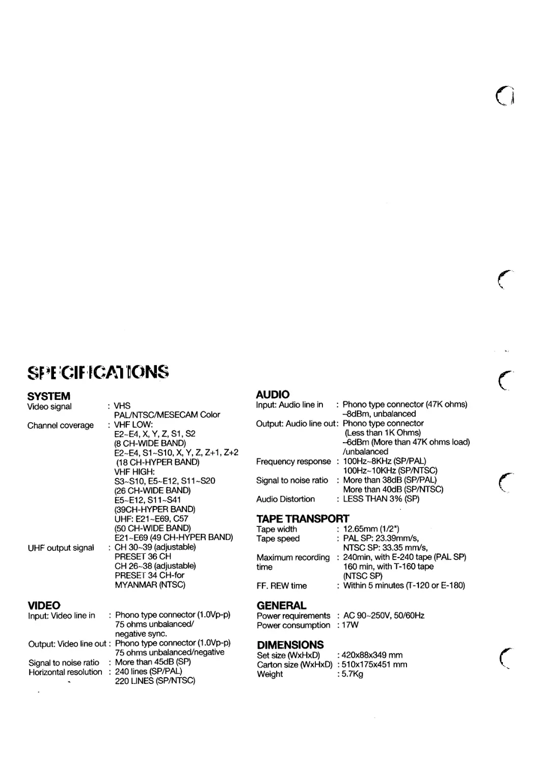
                    SPECIFICATIONS

SYSTEM
Video signal	: VHS  PAL/NTSC/MESECAM Color
Channel coverage	: VHF LOW:  E2-E4, X, Y, Z, S1,S2  (8 CH-WIDE BAND)  E2-E4, S1-S10, X, Y, Z, Z+1, Z+2  (18 CH-HYPER BAND)  VHF HIGH:  S3-S10, E5-E12, S11-S20  (26 CH-WIDE BAND)  E5-E12, S11-S41  (39CH-HYPER BAND)  UHF: E21-E69, C57  (50 CH-WIDE BAND)  E21-E69 (49 CH-HYPER BAND)
UHF output signal	: CH 30-39 (adjustable) PRESET 36 CH  CH 26-38 (adjustable) PRESET 34 CH-for MYANMAR (NTSC)

AUDIO

Input: Audio line in : Phono type connector (47K ohms)

-8dBm, unbalanced

Output: Audio line out: Phono type connector
(Less than 1К Ohms)
-6dBm (More than 47K ohms load)
/unbalanced

Frequency response : 100Hz~8KHz (SP/PAL)
100Hz~10KHz (SP/NTSC)

Signal to noise ratio : More than 38dB (SP/PAL)
More than 40dB (SP/NTSC)

Audio Distortion : LESS THAN 3% (SP)

TAPE TRANSPORT

Tape width	: 12.65mm (1/2")

Tape speed	: PAL SP: 23.39mm/s,

NTSC SP: 33.35 mm/s,

Maximum recording : 240min, with E-240 tape (PAL SP)

time	160 min, with T-160 tape

(NTSC SP)

FF. REW time	: Within 5 minutes (T-120 or E-180)

VIDEO

Input: Video line in : Phono type connector (1 .OVp-p)
75 ohms unbalanced/
negative sync.

Output: Video line out: Phono type connector (1 .OVp-p)
75 ohms unbalanced/negative

Signal to noise ratio : More than 45dB (SP)

Horizontal resolution : 240 lines (SP/PAL)
220 LINES (SP/NTSC)

GENERAL

Power requirements
Power consumption

DIMENSIONS

Set size (WxHxD)
Carton size (WxHxD)
Weight

: AC 90-250V, 50/60Hz
:17W

: 420x88x349 mm

: 510x175x451 mm

: 5.7Kg
• Safety Check after Servicing

Examine the area surrounding the repaired location for damage or deterioration. Observe that screws, parts and wires
have been returned to original positions. Afterwards, perform the following tests and confirm the specified values in order
to verify compliance with safety standards.

1.	Insulation resistance test

Confirm the specified insulation resistance or greater between power cord plug prongs and externally exposed parts of
the set (RF terminals, antenna terminals, video and audio input and output terminals, microphone jacks, earphone
jacks, etc.). See table below.

2.	Dielectric strength test

Confirm specified dielectric strength or greater between power cord plug prongs and exposed accessible parts of the
set (RF terminals, antenna terminals, video and audio input and output terminals, microphone jacks, earphone jacks,
etc.) See table below.

3.	Clearance distance

When replacing primary circuit components, confirm
specified clearance distance (d), (d‘) between soldered
terminals, and between terminals and surrounding
metalic parts. See table below.

Chassis - ►

d

Table 1: Rating for selected areas	Fig. 1

AC Line Voltage	Region	Insulation Resistance	Dielectric Strength	Clearance  Distance (d), (d1)
100V	Japan	>1 MQ/500VDC	1kV AC 1 minute	>3 mm
110to130V	USA& Canada	—	900V AC 1 minute	> 3.2mm
*110to130V 200 to 240 V	Europe Australia	>4Mf2/500VDC	3 kV AC1 minute	> 6 mm (d) > 8 mm (d‘) (a: Power cord)

* Class II model only.

Note: This table is unofficial and for reference only. Be sure to confirm the precise values for your particular country and
locality.

4.	Leakage current test

Confirm specified or lower leakage current between В (earth ground, power cord plug prongs) and externally exposed
accessible parts (RF terminals, antenna terminals, video and audio input and output terminals, microphone jacks,
earphone jacks, etc.)	Г ’

Measuring Method: (Power ON)

Insert load Z between В (earth ground, power cord plug
prongs) and exposed accesible parts. Use and AC
voltmeter to measure across both terminals of load Z.
See figure and following table.

Exposedo-
accessiblB
part

— ppAC Voltmter

Z) (high impedance)

Г Earth Ground
power cord plug prongs

Fig. 2

Table 2: Leakage current ratings for selected areas

AC Line Voltage	Region	LoadZ
100V	Japan	О- V^v-o 1k9
110 to 130 V	USA&
	Canada	^^t5k0
		O- VvV- 0
110to130V	Europe	2k0
200 to 240 V	Australia	О- W«~O

50k0

Leakage Current (i)

i<1m Amts

i <0.5 mA rms

I <0.7 mA peak
[<2m Adc

I < 0.7 m A peak

i < 2 m A de

Earth Ground
(B)to:

Exposed accessible
parts
Exposed accessible
parts
Antenna earth
terminals

Other terminals

Note: This table unofficial and for reference only. Be sure to confirm the precise values for your particular country and
locality.
TABU OF CONTE NTS

	I

SECTION 1. GENERAL..............................................................2	"

SECT ION 2. ELECTRICAL ADJUSTMENTS

2-1. ALIGNMENT AND ELECTRICAL ADJUSTMENT.......................................4

2-2. SERVO-LOGIC CIRCUIT ADJUSTMENT ME I HOD.................................5

2-3. VIDEO CIRCUIT ADJUSTMENT ME I’HOD.......................................6

2-4. PIF CIRCUIT ADJUSTMENT METHOD...........................................8

2-5. AUDIO CIRCUIT ADJUSTMENT METHOD..........................................9

SECTION 3. SPECIAL FEATURE

3-1. VISS (VHS INDEX SEARCH SYSTEM)...........................................10

3-2. FULL LOADING SYSTEM (QUICK START)......................................10

3-3. DIGITAL AUTO TRACKING..................................................10

SEC! ION 4. CIRCUI'I OPERATION

4-1. SERVO SYSTEM.............................................................11

4-2. VIDEO SYSTEM...........................................................16

SECTION 5. TROUBLE SHOOTING FLOW CHART

5-1. TIMER CIRCUIT............................................................18

5-2. POWER CIRCUIT..........................................................20

5-3. SERVO/SYSCON CIRCUIT...................................................22

5-4. PIF CIRCUIT............................................................27

5-5. VIDEO CIRCUIT..........................................................29

5-6. AUDIO CIRCUIT..........................................................35

5-7. IC, TR VOLTAGE........................................................ 37

SECT ION 6. CIRCUIT DIAGRAM

6-1. CONNECTION DIAGRAM.......................................................54

6-2. POWER CIRCUIT..............................................................55 _	.

6-3. TIMER CIRCUIT................................................................56	<

6-4. SERVO LOGIC CIRCUIT....................................................57

6-5. VIDEO INTERFACE CIRCUIT................................................58

6-6. MULTI SYSTEM VIDEO CIRCUIT.............................................59

6-7. PRE-AMP CIRCUIT FOR MULTI-SYSTEM.......................................60

6-8. OSD CIRCUIT............................................................61

6-9. SW PIF CIRCUIT.........................................................62

6-10. IF MODULE CIRCUIT.......................................................63

6-11. AUDIO CIRCUIT...........................................................64

SECT ION 7. COMPONENT’S LOCATION GUIDE ON PCD BOI ГОМ VIE W

7-1. POWERPCS.................................................................65

7-2. TIMER I PCB............................................................66

7-3. TIMER II PCB...........................................................67

7-4. MAIN PCB...............................................................68

7-5. PRE-AMP PCB............................................................69

7-6. PIF PCB................................................................70

7-7. VIDEO PCB..............................................................71

SECTION 8. DISASSEMBLY........................................................72

SECT ION 9. E XPLODED VIEWS AND PART LIST

9-1. PANEL FRONT ASSEMBLY.....................................................73

9-2. SEI ASSEMBLY...........................................................74

9-3. SEI TOTAL ASSEMBLY.....................................................75

SECTION 10. ELECTRICAL PART S LIST

10-1. STANDARD PART NUMBER CODING.............................................77

10-2. ELECTRICAL PART LIST (4286W)..........................................79

Z*-
SECTION 1. GENERAL

(j POWER Button

Turns VCR pcjw«r on and off

 stop/eject Button

In STOP mode this button makes a cassette come out
of compartment. In any other motto exoepl STOP this
button operates STOP function.

Cassette Compartment

When tre cassette я inserted ri ths compartment, the
cassette will automatically De ready far operation.

й REWZREV Button

The REW Button serves a dual purpose. Push to rewind
the tape. Whan, this button is pushed during the
playback motto, the pictwe will move quickly backward
and you can search fcr the desired part of the prograrm

ф PLAY Button

Push to playback Iha recorded tape.

®FFrt3UE Button

The FF Button serves a dual purpose. Push to fast
forward the tape. When :his button e pushed firing the
playback mode, the picture will move quickly forward
and you can search for the desired pari of the program.

ф RECORD/OTR Sutton

Push this button to record. If tha safety lab has been
removed from the cassette, tt will nol be possible to
record, thereby preventing your recordings from
accidentally erased Push to input the recording time.
Each touch to the button will increase the recording
Wne by 30 minutes for up to 4 hcurs.

Ф Channel selector^racking Button

Push to fuAxrt ttto channes you wish to view, Rut these
buttons are used by the tracking control buttons in Play
back Mode.

j? । Remote Sensor

ReMives signals from 1he Remote Control.

-Jp. Multi Function Display

indicates what function a Deng operated now.

(П?. @ VIDEO System Selector Switch®

Selects the system manually depending on the signals
In 1he playback mode and Recording mode.

|Ц: INDICATOR

INDICATOR LED is И up by «ch system.

|R: Receiving TV System Selector Switch

Selects raceivTtg TV signal by thia switch
 RF OUTPUT CHANNEL ADJUSTMENT SCREW
tn video playback mode, you can adjust mere accua-
tefy Wrt RF OUT for cbttHng clean picture.

tii RF OUT Terminal

Connect Ibis terminal to your television antenna ter-
minal, using the accessories provided.

; ANTENNA IN Tormina!

Connect g TV aerial to this terminal.

TEST SIGNAL Switch

In test signal mode, you can check channel accordance
Oi the TV and VCR.

©AVIN J ACK Terrrwnsl

Connect a phere jack cH TV or VCR to this tflrminff

® A'V OUT JACK Terminal

Connect a phone jack of TV Or VCR to this termr,al

POWER CORD

Correct this «rd onto the AC output

& RF OUTPUT Selector Switch

Selects the modulator RF output signal.

In MYANMAR, this output sySi&m will change to "M",
G",

3 RESET
section ?. 111 CTBIGAl ADJUST ME Nl S

2-1. ALIGN MEN! AND El E Cl HICAl. ADJUS1 ME N1

For these adjustments, use the equipments mentioned be-
low and proceed by using the alignment tape and video
signal.

The suitable output waveform of the color-bar signal
generator is shown below.

Instrument and Tools Required

1.	Color TV receiver.

2.	Oscilloscope having 10 MHz or more bandwidth.

3.	Color-bar generator.

4.	Frequency counter.

5.	DVM.

6.	AC Voltmeter

7.	Audio oscillator.

8.	Audio attenuator.

9.	Alignment TAPE.

10.	Recording TAPE.

Signal Level and Input and Output Impedance

Requirement

1.	Video output: Negative sync, 1Vp-p standard composite
video signal, 75Q.

2.	Video output: Same as above.

3.	Audio input: Line -8dBm 47KQ unbalanced.

4.	Audio output: -6dBm less than 1 K£2 unbalanced.

Adjustment Sequence

The VCR should be adjusted in the sequence shown below.

color bar signal waveform

Servo & Logic Alignment

Video	Г Audio

Alignment	I	Alignment
2-2. SERVO-LOGIC CIRCUIT ADJUSTMENT METHOD

1. VIDEO HEAD SWITCHING POSITIrON

Adj. Lccatian	Checking Point	Measuring Etjupn^ent	Moda	Test Tape
R695	PTO1 ®PIN TP39fi	OsbJosoope	Play	OP-1  CokxELur

1) Play back the test tape.

Z) Set the oscilloscope in the crop mode la connect the CH1 to SW pulse {PTD1 thaCHE W ТРЗЭв («Лео Otrt'l .
And then trigger ths scape with the Signal from the CH1.

3| Adjust R595 Jar the positive trigger until 6.5rtO-5H cycles before the vertical SYNC pulse,
Adj. Location	Checking Point	Measuring Equipment	Moda	Test Tape
R395	TP395	Osteoscope		EE	*

1)	Set ths TV/LJNF to LINE mode.

2)	SuppV 1he cokx bar signal to the line input terminal. And set for the slop iEE'I mode.

3)	Corned the oscilloscope to TP3S6 and trigger (he scope wrlh a composite SYNC Signal ай TP313 (COMP. SYNC).

4]	Adjust the oscilloscope in order that rt can display a waveform of approx 2Н.

5)	Adust R395 Io obtain 0.510.02 Vp^p between SYNC TIP and 100% white level.

o.rrto,oevp-p

Marizcwital: HWdw.

Venteal: O.ivAVr

г SYNC HP FREQUENCY

Adj. Location	Checking Point	Measuring Equipment	Mode	Teel Tape
R391	TP391	Freq. Counter	REC	Blank Tape

1.1	Set the unh to REC mode without video signal. (at Line mode)

2)	Connect lh*ftMfjency counter Ip TP391.

3)	Must R391 until the SYNC TIP froquency becomes 3.73 MI-tz+0.03 MHz.
3. PLAYBACK Y-S*CNAL OUTPUT LEVEL

Ad|. Location	Checking Point	Measuring Equipment	Mode	Teat Tepe
R396	TP396	Oscaosoope	PB	0P-1 (Cdor Bar)

1)	Playback № test tape (Саку Bar Signal).

2)	Connect the оесяозсаре to TP392 and trigger the scope with a composite SYNC signal at ТРЗИ
Adjust the scope so that fl can display a waveform of approx. 2H.

31 Adjust R396 to obtajn 2.010 1 Vp-p between the SYNC TIP and 100% white lerrel.

Horiijfiia 1 Qrtsrrtv

Ve^cai  05Wm

£.010.1 Vp-p


2-4. PIF CIRCUIT ADJUSTMENT ME; I HOC>

1. PIF COIL Adjustment

Adj. Location	Measuring Point	Measuring Equipment	Condition of Adj.	Input Signal
L109	H101  6 PIN	Oscilloscope Signal Generator	Separated  IF module PCB	•	FC: 38.0 MHz  •	Modulation Factor: No Modulation  •	Input Level: 80dBpV  (750 Loaded)

1)	Connect 12V DC to Pin No. 7 and GND to Pin No. 8 of H101.

2)	Connect the signal generator output to Pin No. 9 and GND to Pin No. 8 of H101.

3)	Connect the oscilloscope probe to the measuring point and GND.

4.	Adjust PIF coil to obtain minimum DC Voltage.

2. AFT COIL Adjustment

Adj. Location  L110	Measuring Point	Measuring Equipment	Condition of Adj.	Input Signal
	'A'	Signal Generator Oscilloscope	Separated  IF module PCB	•	FC: 38.0 MHz  •	Modulation Factor:  30%, fm=15.625KHz  •	Input Level: 80dB|iV  (750 Loaded)

1) Connect an enclosed circuit to H101 Pin No. 3 by following.

12V

[ 24K |

H101-	I

3PIN	___I

18K

г L т

[_ 10K I	[ 0.47pF/50V |

2)	Connect 12V DC to Pin NO. 7 and GND to Pin No. 8 of H101.

3)	Connect the Signal Generator output to Pin No. 9 and GND to Pin No. 8 of H101.

4)	Connect the oscilloscope prohe to the measuring point and GND.

5)	Adjust AFT coil to obtain 2.3±0.15V DC at the point DC voltage changes suddenly.

3. RF AGC VR Adjustment

Adj. Location	Measuring Point	Measuring Equipment	Condition of Adj.	Input Signal
R191	H101  2 Pin	Signal Generator Oscilloscope	Separated  IF module PCB	•	FC: 38.0 MHz  •	Modulation Factor:  30%, fm=15.625KHz  •	Input Level: 92dB|xV  (750 Loaded)

1)	Connect 12V DC to Pin No. 7 and GND to Pin No. 8 of H101.

2)	Connect the signal generator output to Pin No. 9 and GND to pin NO. 8 of H101.

3)	Connect the oscilloscope probe to the measuring point and GND.

4)	Adjust RF AGC VR to obtain 6.010.2V DC.
2 5. AUDIO CIRCUIT ADJUSTMENT ME I HOD

1. PLAYBACK CIRCUIT ADJUSTMENT METHOD

Adj. Location	Measuring Point	Measuring Equipment	Condition of Adj.	Test Tape
R291	Audio Line Out	Audio Level Meter	Play Mode	DP-1
1)	Connect the audio level meter to the audio output jack.  2)	Playback the test tape.  3)	Adjust R291 until the audio level meter reads -6±1.5 dBm playback output.
2. PLAY BACK OUTPUT FREQUENCY CHARACTERISTIC
Adj. Location	Measuring Point	Measuring Equipment	Condition of Adj.	Test Tape
Checking	Audio Line Out	Audio Level Meter	Play Mode	DP-1  DP-2

1) Playback the Test tape, and confirm that the playback output level at 6 KHz is within -1±3 dB as referenced to the 1
KHz playback output level.

3.	BIAS CURRENT ADJUSTMENT AND OSCILLATION FREQUENCY CHECKING

Adj. Location

R292

Measuring Point

TP201 (+),
TP202 (-)

Measuring Equipment

Frequency Counter
AC Voltmeter

Condition of Adj.

REC. Mode

Test Tape

Blank Tape

1)	Connect the positive lead of the AC Voltmeter to TP201 and negative lead to TP202.

2)	Set the VCR to REC mode without audio signal at line mode.

3)	Confirm the frequency counter display is 70 KHz+10% and adjust R292 AC Voltmeter reads 2.4mVrms.

4.	RECORD-PLAYBACK FREQUENCY RESPONSE

Adj. Location Measuring Point

Checking - Audio Line Out

Measuring Equipment

Audio Level Meter
Audio Signal Generator

Condition of Adj.

REC. Play Mode

Test Tape

Blank Tape

1)	Press the TV/LINE button to select line mode.

2)	Connect the audio signal generator to the audio line input and the audio level meter to the audio line output of Phono
Jack.

3)	Record reference audio signal of the 400 Hz, 8 KHz (SP) at -20 dBm in PAL mode.

4)	Check to insure that 8 KHz playback output level is within -1±3dB as referenced to the 400Hz playback output level.

5)	If the difference between 8 KHz playback output level and 400 Hz is more than +2 dB, increase the bias current more '
than 2.4 mVms, and if the difference is less than -4 dBm reduce the bias current less than 2.4 mVrms.

5. RECORD-PLAYBACK OUTPUT LEVEL

Adj. Location	Measuring Point

Checking	Audio Line Out

Measuring Equipment

Audio Level Meter
Audio Signal Generator

Condition of Adj.

REC. Play Mode

Test Tape

Blank Tape

1)	Press the TV/LINE button to select line mode.

2)	Connect the audio signal generator to the audio line input and audio level meter to the audio line output of Phono Jack.

3)	Record and playback the input of the audio reference signal 1 KHz, -8 dBm.

4)	Confirm that play output level is -6±3 dBm, (SP) ±3 dB (LP).
SE Cl ION 3. SH GIAI H AWRI

3-1. VISS (VMS INDEX SE ARCH SYSTEM)
INDE X MARK REGISTER
AUTO REGISTER

• When recording starts in normal recording and OTR as
well as timer recording, INDEX MARK is automatically
registered on video cassette tape.

REC ► SP
0:00:00
'MARK'

•	For 3 seconds 'MARK' will be displayed on TV screen.

•	'MARK' does not appear in OTR mode.

Please Note:

1.	Index Mark cannot be registered on a cassette without
safety tab.

2.	A program must be recorded for more than 5 minutes at
least to operate VISS.

3.	A cassette tape must be fast forwarded for a few
seconds when recording from the beginning of cassette
tape.

*The beginning of a cassette tape film is made of tran-
sparent tape. Recording and index marking cannot be
done on this part due to absence of magnectic coating.

Please Note:

OSD (on-screcn-display) screen will disappear within a few
seconds in INDEX SEARCH mode and INDEX SKIP mode.
To resume OSD (on-screen-display) screen, press OSD
RECALL key, pressing once more will erase OSD.

INDEX SEARCH (ONLY OPEflAESLE: Wil H REiMOl E CONTROL)

(J) Index Search (Start)

1.	Press MENU key and select No. 4
(FUNCTION) on the remote control.

2.	And select No. 1 (INDEX SEARCH).

• A cassette will be rewound to the
beginning.

REW «4
0:55:1?

INDEX SEARCH

(?) Index Search (Play)

• The INDEX FUNCTION will automa-
tically search (The VCR will play for
the first 6 seconds at every index
marked segement and will search
again. This process will be repeated
at every index marked segement to
the end of a cassette).

• To interrupt while playing for 6
seconds to watch, press play key.

FF ►►
0:55:12
INDEX SE ARCH
P.01

INDEX

• INDEX SKIP function allows you to locate a specific index marked part. Use INDEX +, INDEX - keys to skip and locate.

WATCHING BASKETBALL GAME NOW

Basketball
Game

Soap	Football

Opera	Game

-2	-1	+1	+2	+3

(J) Index Skip

Press INDEX (+) key

twice.

REW««
0:55:00
P.02

(?) Play Back

• VCR will fast forward
and play from the be-
ginning of the football
game.

@ Index Skip

• Press INDEX (-) key

twice.

REW ««
0:55:00
P.-02

@ Play Elack

• VCR will rewind and play
from the beginning of
the news.

3-2. F ULL LOADING SYS1 E M (QUICK S1AR1)

The operation of VCR starts within 0.8-1 second after pressing any key.

This function allows you to operate VCR 3 times faster than other VCR's without quick start function.

3-3. DIGITAL AUTO TRACKING

You can always play back the best picture without manual tracking because this function allows the VCR Head and the
track of tape to accord exactly by automatic sensing of the track signal marked on the video tape.
SE CTION 4. CIRCUIT OPI RATION

4-1. SERVO SYSTEM (DVR-4286W)

1.	General Outline

Servo 1 CHIP (80 pin) IC used in DVR-4286W deals with the functions of exclusive Servo IC and Syscon IC which have
been used up to now, combining their functions, by software.

Because this 1 CHIP IC has not ANALOG AMP inside, every output signal from MOTOR should be input through special
amplification and waveform shaping (sine waveform-square waveform).

*	Salient Features

•	Drum & Capstan Motor soft control.

•	Head sw pulse generation for rotating Heads (Video and Audio heads).

•	QV SYNC signal generation during special operaing (playback) mode.

•	Separation of V-SYNC signal from the C-SYNC signal.

•	Digital auto Tracking soft management.

•	REC CTL Signal generation (Recording mode).

•	INDEX SEARCH Control (VISS).

•	Various speed SLOW mode.

•	Various speed CUE & REV mode.

•	Auto play.

2.	Servo System Organization

In VTR Servo System consists of two control systems: Rotating HEAD DRUM and CAPSTAN MOTOR to make tapes run
at regular speed.

The bolck diagram of VTR SERVO SYSTEM is shown in Fig (1). Now, we will examine the Capstan and Drum controls by
Software Digital SERVO.

This servo control consists of both of the speed control and the phase control and controls them by using ERROR q'ty
corresponding to a mark.

In the speed control, FG signal cycle is the Reference when the motors rotate normally and really motors output the FG
signal. In the phase control, FG signal cycle is generated inside u-COM if being not input from outside.

Phase error is timing difference in the PG signal output from Motors and phase reference signal and it is indicated as
(Table 1) shows the signal used in the phase control.

(Table 1) Phase Servo Signals

		PHASE	REFERENCE
	Recording	Drum PG signal	V-SYNC
DURM	Playback	Drum PG signal	Reference signal generating in the super Timer unit
	Recording	PULSE dividing the CAPSTAN	V-SYNC
CAPSTAN		FG signal
	Playback	PG CTL signal	Reference sygnal generating in the
			super Timer unit

* Note:

FG Signal: Frequency Generator signal. Used in motor speed detection.

PG Signal: Phase Generator signal. Used in motor phase detection.
A.SW&

Q.V.SYNC

SPEED
ERROR

__ RECCTl

I________J

 DETECT PHASE

PHASE — COMP
Л ERROR . , FILTER

___► DETECT

---► PHASE

—, ERROR

PHASE
COMP
FILTER

V1SS ..
, DETECT '

DETECT

-► SPEED
, ERROR

V-SYNC
D.PG

Fig. 1 The block diagram of DRUM & CAPSTAN

J
3. Drum Servo Operation

Drum servo functions to control the DRUM motor mainly and set the drive cycle during SLOW and make, SW PULSE,
Q.V. SYNC, and AFM SW PULSE.

D.FG and D.PG signals output in DRUM MOTOR are used as comparison signal of phase and speed.

The block diagram of DRUM is as follows.

D.FG

D.PG

Error of
Speed control

f

Speed Reference
Phase Reference

I

Error of
Speed control

BIAS Addition
(2.5V)

PWM
OUTPUT

Fig. 2

Phase
compensation

Drum and capstan Controls basically consist of SPEED and PHASE system servo control, by combining each error q'ty of
them.

In the phase control, phase reference signals are made arbitrary pulse of about 25Hz is obtained inside during the play-
back.

In the REC mode, reference signals synchronized V.SYNC.

Calculate the difference of the rising edges of the feed back signal of D.PG and Reference signal made in IC and stabilize
the phase loop by passing the ERROR through the digital filter, the phase compensation fitter. And then output it on the
phase control routine, multiplying by GAIN Kp.

DRUM motor drives by Combining the phase error output in the phase routine and speed error.

Because GAIN doesn't change variously in the DRUM system, special power amplification from outside is not required.

D.PG signal is used as producing the SW PULSE for Video HEAD SW.

The shaping circuit of D.PG signal is shown below.

• 5V

P501

R513*	5R515

3 D.PG

+ R512

C506

: C514

IC601(T)pin

0507 : :: :-R514

Fig. 3
I

Regarding D.PG signal, in Fig (3) goes through C506 and after amplificed by Q501; It is input into pin no. 1 of IC601.

Speed control system controls the speed by comparing the Reference set inside and D.FG signal when Motor rotates.

Method and waveform Shaping circuit for Speed control are as follows.

D.FG signal in Fig (4) goes through C510 and after 1.5Vp-p is input to pin no 6 of OPAMP, it is Schmitte trigger by R521
and R520 and becomes waveform shaping.

/Vaveform shaped D.FG controls the speed by comparting the reference with the difference value to subtract the current
:ycle value from the previous D.FG cycle value.

When the D.FG cycle rotates normally, that is in case it is wider than a target current Drum speed is slow and (+) mark is
selected. (Rotate the DRUM fast)

n case the D.FG cycle is narrower than the target, current speed is fast and (-) mark is selected. (Rotate DRUM slowly)
4. Capstan Servo Operation

Capstan Servo has functions of viss detection, REC CTL PULSE generation and REC CTL DITTY adjustment variously
during VISS, including the function to control the capstan motor.

Capstan speed control has same block in every mode and phase control has different block in each mode of REC and
PB. Capstan control also consists of phase and speed system as DRUM control. Capstan phase control is to maintain the
phase relationships between PB CTL signal and VIDEO SW/P regularly. PB CTL signal production process and phase
control method are as follows.

R505

+5V- W/-

P502

"1 CTL(-)

2 CTL(+)

3 GND

"------ ► P/CTL

R515

CTL signal input via C501 at CTL HEAD is amplified 4000 times by R502 and R504.

And the then it makes PB CTL PULSE of 0.4Vp-p SCHIMITTE with through R509 and it is input to pin no 11 of IC601.

Error is generated as comparing the PB CTL signal input to pin 11 of IC601 to the reference signal for CAPSTAN.

After .the ERROR value is multiplied by appropriate phae LOOP GAIN Kp in each mode and after it passes the phase
compensation filter for stabilization of phase loop, it is added to capstan speed error. Because this value has various gain
in each mode, it drives the Motor by amplifying POWER externally.

Capstan speed control measures the cycle of C.FG which is shaped waveform, outputting from CAPSTAN MOTOR inside
of IC and compares it with reference.

Waveform shaping circuit of C.FG and speed control are as follows.
\-2. VIDEiO SYSTEM

. Y-REC mode

lere, it describes the signal flow for the luminance system on the REC mode.

he recording video signal is inputted to the AGC amplified through Pin 37, and sync signal level is controlled to be

®"*[iMph*[LPF|- {Emphasis} >(5> >©-

Fig. 1 The signal flow on the REC mode

constant.

The chrominance component in the AGC amp, output is filtered out by a LPF and the luminance signal is fed to the YNR
circuit. In the circuit, it is provided a vertical enhancing for the luminance signal.

For the next, high frequency component of the output signal from the YNR circuit is enhanced by the emphasis circuits
(consists of Detail Enhancer, Non-linear Emphasis, and Main Emphasis.), and its output is given from Pin 5.

This signal is fed to the FM modulator through pin 42, and the recording Y-FM signal is obtained from Pin 40.

2. Y-PB mode

The play back Y-FM signal is fed to Pin 39.

Y-Signal^ и-

TDouble lJ FM LT Main Lr.PFLrYNRLr N. L. Lf D. H. I
Limit Г [_Demod [ [peemph p|_LHb | [рОСГ [peemphf [ N. C. |


Fig. 2	The signal flow of the Luminance signal on the PB mode

This signal is passed through the Double Limiter and demodulated to video signal by the Frequency Demodulator.

The Frequency Demodulator output is fed to the YNR circuit block through the Main deemphasis and the LPF.

The circuit including the external CCD (1H delay line) is composed of both functions of the YNR and the drop out
compensation.

The YNR output is fed to the Y/C Mix circuit through the Non-linear de-emphasis, the Double high pass noise canceler
and the Picture control circuit, and then the signal is mixed with the PB chrominance signal and a PB video signal is
obtained from Pin 34 through the Quasi-V/H insertion circuit, the Character insertion circuit and the Video output amplifier.
3. PAL color REC mode

@ ACC Out

г©- и @>-«1 teHcSS.

Video

Killer

REC
Chroma
Out

Fig. 3	The flow chart of the chrominance signal on the REC mode

The flow chart of chrominance signal on the REC mode is shown in Fig. 3.

A recording composite video signal is fed to the AGC circuit from Pin 37, and one of its output signal is passed through a
BPF (fsc: 4.43Mhz) to extract chrominance components from it, then only the chrominance signal is fed to the ACC
amplifier. The gain of ACC amp. is controlled with the DC voltage at Pin 14. The output from ACC amp, is obtained from
Pin 25 which can be used for a PAL/SECAM detection, while it is fed to the main converter through the burst emphasis
(up) circuit.

Also the other output from ACC amp, is fed to the level detector (ACC DET.) through the burst gate amplifier. The output is
smoothed by the external filtering capacitor connected to Pin 14 and the signal is fed back to the ACC amplifier in order to
control the burst level of ACC amp. constant.

Accordingly, the signal level of burst which is passed through the Burst emphasis circuit and the Main converer circuit is
controlled Burst emphasis circuit and the Main converter circuit is controlled constant, and the REC chroma, Signal is
stabilized even if a level of input video signal is fluctuated.

The output from Main converter is fed to the Killer circuit through the LPF.

The Killer detector can give a reliable operation thanks to the application of both systems of the Synchronized detection
(APC killer) and the Peak detection (ACC killer) on the REC mode.

The signal through the killer circuit is obtained from Pin 15 as a REC chroma, output.

4. PAL color PB mode

The down-converted chroma signal on the PB mode (PAL: 627kHz) is inputted at Pin 15 through an external chroma LPF.

PB Chroma
In

NTSC/PAL

B.Uttr

L Killer

lACCL Г Burst L
]_Det I L Gate Г

MESECAM

Y/C
Mix

Fig. 4 The flow chart of the chrominance signal on the PB mode

The input signal at Pin 15 is fed to the Main converter through the ACC amplifier. And the output from the Main converter
is obtained from Pin 25 through the BPF and the Comb amplifier. After filtering out crosstalk components by an external
comb fitter, the signal is inputtd again at Pin 27, and this signal is fed to the Y/C mixer through the 6 dB amplifier, the BPF,
the PB amplifier, the Burst de-emphasis (down) and the Killer circuit.

However, in case of MESECAM mode, the Main converter output through the BPF is fed to the PB amplifier by bypassing
the Comb amplifier and the Comb filter. In addition, the Killer circuit is switched off on the MESECAM mode.
sections. THOUBII SHOO! ING I IOWCl 1АГП

5-1. TIME R ClRCUI1

Digitron does
not operate.

Is +5V supplied
to pin® of IC 701?

Yes
и

Is -28V supplied
to pin® of IC701?

Yes

No

Is +5V supplied
from D510 anode?

Is-28V at
D814 anode?

Yes

No

No

Check
F802 FUSE

Check D814 and
primary power circuit

Check the connector
and pattern.

Is DC 3.5V supplied
to pin (T) and ® of G701 ?

Check the Trans output
and connector.

Yes

Is 5V at pin @
of IC701?

No

> Check IC702 (Reset IC).

Yes

Do pin ® and
@ oscillate?

No

Is +5V applied
to pin @ of IC701 ?

No

Check the
power terminal.

Yes

Check X701
and IC701.

Yes
v

Is Digitron lit when
pressing S101
(Reset key)?

Yes
v

END of Check
в.

Digitron is lit but keys do
not operate.

Is each key pulse applied
to pin @ ~ @ of IC701 ?

Yes

Check the pin serial of
pin (5) ~ (§) of IC701.

No

Check key matrix
circuit.

Broadcast signal is not
received when changing channel.

Is the external ANT connected
to RF IN of VCR and RF OUT to TV?

Check and change the
cable connection state.

Yes

Does the TV CH correspond to	No	Set the TV CH to same
VCR CH		VCR CH.

Yes

Is the output of pin @
of IC701 normal?

No

Check IC701.

Yes

Is pin (9) of No
IC701V? ’ ’

Yes

Is pin @ of
IC601 "L"?

Yes

No

Is ЛПЛ signal applied
to pin @ of IC601 ?

Yes

No

Check video
Circuit.

Check TUNER No
and IF PCB,. ' 4

Check connector
and pattern.

Change IC601.
5-2. POWEiR CIFiCUIT

•	When change the parts which are out of order, first, remove the power plug from the socket and then discharge the
voltage across between both terminals of C807. (Use an external scores of KQ resistance)

•	When check the primary circuit by using the oscilloscopes insulate the oscilloscope surely. (Use the isulating
transformer) and must connect GND into the primary GND), (But there is no connection when check the secondary
circuit.).

•	When change IC801, check FUSE and Cement resistance surely.

•	After completing the service, please chedk if SMPS shield case is adhered and P801 is connected.

A. CHECKING THE PRIMARY CIRCUIT.

No output Voltage

Yes

Prepare the instrument
connecting the insulating Trans.

Yes

Open P801

I Yes

Check F801 FUSE

I Yes

Is voltage applied to D801?

No

Check D801 & L801

Yes

Is voltage applied to the
both terminals of C807?

No

Check R802

Yes

Check voltage of Q801 Gate

Yes

Is voltage output from pin3 of IC801 ~

Check Q801

No

No

Check R803, 805

814 & 806.

Yes

Check Q802,803
D802

Change IC801

Yes

Check the Secondary circuit.
В. CHECKING THE SE CONDARY CIRCUIT.

Open P801

Is D811 Short?

Yes

Change D811,10801 &
Check the primary circuit.

Check each voltage.

J Yes

Check Trans output of
No output stage.

Check the Diode of
No output stage.

Check coil, capacitor of
No output stage.

Check the environmental
terminals of IC8Q1.
a

5-3. SE RVO/SYSGON CIRCUIT

A.

Playback picture
is not good.

Noise appears although
adjusting Tracking.

No

Adjust Tracking.

Yes

Noise shakes up and
down on the screen.

No

Noise appears although
change cassette tape.

Yes Check and re adjust the
DECK transport system.

Yes

Is CTL pulse applied
tp pin @ of IC601?

No

CTL HEAD height is normal
and there is no dust

No Adjust the HEAD height
" ' and remove dust.

Yes

Yes

Check circuit adjacent
to 10501.


The voltage of pin @
of IC601 Is not changed.

No

Check R531 and C520.

Yes

Is the voltage of
Pin® of P502 5V?

Yes

Is C.FG applied
to pin (9) of IC601?

Yes
и

Check IC601.

No

No

Check R517 and R518.

Check IC502.
в.

Playback picture
is not good.

Noise appears on the
screen on the whole.

Check Flow A.

Yes

Are SW pulse and HA SW
applied to Pre Amp circuit?

Yes

Is Enve. waveform supplied
to at pin (4) of PT01?

Yes

Check VIDEO circuit.

No

Is SW pulse supplied
from pin ©of IC601?

Yes

No

Check D.FG input
and connector.

£ Check pattern.

c.

Auto stop during playback.

Is Reel pulse applied to
pin® of IC601?

Yes

Is SW pulse supplied
to pin ©of IC601?

Yes

Check IC601.

V'
Drum МЛ loading stops.
Drum M/l and Capstan M/T rotate
at regular speed (In REC mode)

Is C. Sync applied to
pin@of IC601?

J Yes

Is pin @ of IC601 GND? -

I Yes

No

No

Check Motor.

G.

Emergency mode when plugging.
(Power Cord)

I

Is EVER 5V supplied?

J Yes

Does X601 crystal oscillate?

| Yes

Do S. DATA, CLK and RDY
Signals of IC601 exchange
with TIMER?

| Yes

Is CAM SW DATA Correct?

| Yes

Check IC603.

Yes

Check IC601.

Check C. Sync of
VIDEO IC and Pattern.

Check IC601.

Check power circuit.

Check IC601 and crystal.

Check IC701 when S.RDY Signal
is supplied.

Check IC601 when S.RDY Signal
is not supplied.

Recheck connector
and CAM SW contact.
н.

Cassette is not inserted.

Is Motor 12V supplied?

Yes

Does START Sensor operate
when pushing it after inserting
a casstte tape?

Yes

Is 9.1V at pin (8) of IC602?

Yes

v

Is 5V supplied to pin @ of IC601 ?

Yes

и

Check IC602 and DECK part.

Check IC861 of POWER circuit.

Check START sensor and
LED in DECK part.

Check D601.

Check IC601.
5’4. FiF SIGNAL. SYSTEM (PIF CIRCUI1)

A.

No RF output Picture

Is there a video signal No Refer to the Troubleshooting
in RF102 Modulator?	”	for video EE mode

Yes

Is there a Audio signal _ No Refer to the Troubleshooting
in RF102 Modulator? ........... '	for Audio

Yes

Is the power supply
voltage (+5V) supplied?

Check the power circuit

Yes

Change RF102
в.

When not receiving
broad casting signals

и

Is the voltage supplied to
RF101 tuner voltage terminal?

Check the power circuit

Yes

Is there a RF signal
in RF101 IF out?

No	Is the SERIAL correspondence normal?	_No

	I Yes

Change RF101 TUNER


Check the
Timer circuit

Yes

Is there a video signal at
pin (4) of H101?

Yes

Is there a audio signal at
pin (5) of H101?

No

Is the voltage 12V supplied No
to pin@ of IC101?

Yes

Yes

Check the PIF
MODULE (RF103)

Check the EE circuits

VIDEO/AUDIO circuits

Check the
power circuit
I

5-5. VIDEiO CIRCUI1

A.

EE Mode picture N.G

| Yes

Is Video Signal Supplied to
10131 ©or ©pin?

| Yes

Is +12V supplied to
IC131 © pin?

I Yes

Is Signal OUTPUT
at IC131<g> pin?

Yes

Is Signal Supplied to
IC301 © pin?

Is Signal OUTPUT
at IC301® pin?

Yes

Is Signal Supplied to
QS01 Emitter?

| Yes

Is Signal Supplied
to ICS01 @ pin?
| Yes

Is Signal output
at ICS01 (8) pin?

| Yes L

Is Signal output
at QS03 (8) Emitter?

Yes

LINE OUT

No

No

No

No

No

No

No

No

No

Check R.F Part and Line in jack

Check ON/OFF 12V circuit

Check IC 131® pin
(Turner Mode: L) (Line MOde: H)

| Yes

Change IC 131

| No

Check IC601 (39) pin
and Q136

Check IC131 ® pin or IC301 ® pin.

Check IC301 © pin(5V)
© pin(5V)

|>Yes

Check 10301(5) pin
(EE mode:L) (PB mode:H)

Yes

Change IC301

ChangeQ312

Check ICS01 © pin
(Low)

| Yes

Change QS06
orQSOI

Change QS03

No

No

No

м

Check POWER circuit

Check IC601

Change ICS01
в

PB luminance N.G

Yes

Is signal output at
ICA01 (LA7374) ® pin?

Yes
и

Is signal output at
QA08 emitter?

Yes
и

Is signal output
at PA03 (9) pin?

I Yes

Is signal supplied
to IC301 ® pin?

Yes
и

Is signal output
at IC302 (4) pin?

| Yes

Is signal supplied
to IC301 @ pin?
^Yos

Is signal output
at IC301 @) pin?

| Yes

Return to E.E
mode picture N.G.

No

No

No

No

No

No

Is +5V supplied
to ICA01 ф pin?

I Yes

Is H.SW pulse supplied
to ICA01 (e) pin?

Yes

Check ICA01 (6) pin.
Low level: 0-0.5V
High level: 1-1.5V

Yes

Clean head
or change head

IS PB +5V supplied
to PA03(5) pin?

Yes

Check PA03
(connector)

Is +5V supplied
atlC301 @,@pin

Is +5V supplied
to IC302 (j) pin?

Check Q308, 309

No

No

No

No

Check POWER
circuit (+5V)

Check Servo
circuit (H/SW)

Check

H/SW level

Check PB5V

Check QA06, 07, 08

No

Check IC303
(Regulator IC +5V)

Change IC301

Yes

Is 8.86MHz supplied
at IC302@ pin?

| No

Check the 8.86MHz
oscillation circuit.
с.

v

Is signal supplied
to X405 (2) pin?

|YeS

Is signal supplied
to IC301 @ pin?

| Yes

Is signal supplied
to IC301 @ pm?

J Yes

Return to E.E
mode picture N.G.

Check Q402

Check Q403

Yes

Is 4.43MHz oscillated
at IC301 @@ pin?

| No

Г Check X402

No I-------

и

Confirm the system select
switch of front panel.
PB color N.G

I Yes

Is signal output at
IC A01 (7) pin?

No	Is +5V supplied to	No
	ICA01 ф pin?

jYes

Check power
circuit (+5V)

Is H.SW pulse supplied to ICA01 (6) pin?	No	Check system circuit.

^Yes
Check ICA01 (6) pin.	No	Check H.SW
Low level: 0-0.5V		pulse level
High level: 1-1.5V		•

Yes

Yes

Is signal output at
QA16 emitter?

Yes

No

Clean head
or change head

IS PB +5V supplied
to PA03® pin?

Check PB5V

Yes

CheckQA12, QA16

Is signal supplied
to IC301 ® pin?
lYes

No

Check PA03
connector

15 signal output
to IC301 @ pin?

Yes

Is signal supplied
to X405 ® pin?

^Yes

Is signal supplied
to IC301 @ pin?

Yes

Is signal supplied
to IC301 @ pin?

I Yes

Return to E.E
mode picture N.G.

No

No

No

Yes

Check Q402

CheckQ403

Is +5V supplied
to IC301	@ pin

Check IC303

Change IC301

Yes

Is 4.43MHz oscillated
at IC301 @@ pin?

No

Confirm the system select
switch of front panel.
REC Luminance N.G

| Yes

Check E.E mode

| Yes

Output of IC301 ® pin
is FM modulation signal.

Yes

v

Is FM modulator signal
supplied to PA02 © pin

Yes

Is FM signal supplied
to ICA01 @ pin?

Yes

Is +5V supplied to
IC A01 (J) pin?

^Yes

Is REC ©signal supplied
to ICA01© pin?

J Yes

Is H.SW pulse supplied
to IC A01 © pin?

| Yes

Is signal Output at
IC A01 ® or® pin?

| Yes

Check drum

No

No

No

No

No

No

Check IC301 © pin
(Low level)
| No

Check IC601 ® pin
(EE©)

Check connect wire

► Check QA04

Check power circuit
(+5V)

Check syscon circuit
(REC "H")

Check syscon circuit
(H. SW)

Change ICA01
EL REC chroma N.G

| Yes

Check E.E mode

Yes

Is signal output at IC301 @ pin?		No		Is 3.58MHz oscillated at IC301 © pin?		No		Change X402
				|Yes  Is state of IC301 @) pin "L‘?				i	Yes
					I No
	,Yes			Check system select switch
Is signal supplied to PA02 (2) pin?			No		Check connector wire
	Yes
Is signal supplied to ICA01 © pin?			No	*”	Check CA24, RA22
	Yes			-
Is +5V supplied to IC A01 ф pin?			No		Check power circuit (+5V)
	.Yes
Is REC H signal supplied to IC A01 (7) pin?			No		Check syscon circuit (RECH')
	rYes
Is H.SW pulse supplied to IC A01 (6) pin?			No	Ite.,	Check syscon circuit (H/SW)
I	Yes
Is signal Output at IC A01 ©or© pin?			No		Change ICA01

| Yes

Check drum
F. OSD Picture N.G

Is 5V supplied to ICS01 @ and ® pin?	_№	Check ON/OFF +5V
Yes
Check oscilation of ICS01 © pin	_№	Check XS01 (17.7MHz)
| Yes
Check serial data (ICS (3)(4)(5) pin)	№	Check timer circuit
| Yes
Change ICS01 and check OSC circuit.

G. OSD Character N.G

Is 5V supplied to
ICS01 @ and (?) pin?

Yes

No

Check ON/OFF+5V

Is serial data input into
ICS01 ©©© pin

Yes

Is H-Syno input
into ICS01 ® pin?

Yes

Is V-sync input
into ICS01® pin

Yes

Check timer circuit

No

No

Check ICS01 circuit

' Is 5V supplied to
1CS02 Vcc ((7) pin)

| Yes

Is video signal input
ICS02 @ pin

| Yes

Change ICS02'

No

No

Check video
circuit
5-6. AUDIO CIRCUIT

A.

PB AUDIO N.G

Yes

Is 9V supplied at
IC201 (7) pin

Yes

Is IC201 (ft) pin "H"?

Yes

Is IC201 ® pin

Yes

Is impedance less than
10 Ohm between IC201
(3) pin and GND

Yes

Is Audio signal supplied
atlC201@pin

Yes

Is Audio signal supplied
at IC201 @ pin?

No

No

No

No

No

Is 12V supplied at I No
Q207 collector f
^Yes

Check Q207, D206

D208

Check syscon circuit
(IC601@pin)

Check syscon circuit
(IC601 (62) pin)

Is IC201 @) pin
^Yes

Change IC201

Check R291

Check Q144

Clean A/C head

Check 12V circuit

No

Check syscon circuit
(IC601 ® pin)
в.

REC Audio N.G

Yes

Is Q203 Base "H"?

Yes

Is 12V supplied at
T201® pin?

Yes

и

Is 70KHz supplied at
P2O1 ф pin?

Yes

Is REC, Bias Adjusted
to2.4mV?

No

No

No

No

Yes

Is Audio signal supplied I_No

at IC201 ® pin? Г ‘ ‘

Yes
v

Clean A/C HEAD

Check syscon circuit
(IC601 ® pin)

Is 12V supplied at
Q202 emitter?
| Yes

Check Q202, Q203

Check Q201, R292

Adjust R292

Check 12V circuit

Is Audio signal supplied
at IC201 ® or@ pin?

Yes
и

ChangeIC201

No

No
--->

Check Audio input
circuit

Check syscon circuit
(IC601® ,® pin)
5-7. IC, 1R VOL! AGE

DC voltage of servo-syscon IC (IC601)		REC
PIN NO	PB
1	0.14	0.14
2	4.7	4.7
3	0	0
4	4.7	4.7
5	5	5
6	5	5
7	0.5	0.5
8	N.C (LOW)
9	3.0	3.0
10	3.0	3.0
11	3.0	3.0
12	0.5	0.5
13	2.5	2.5
14	5	5
15	0	0
16	0	2.5
17	2.6	2.6
18	2.6	2.6

REMARK

SERIAL INPUT

SERIAL OUTPUT

SERIAL CLK

C-SYNC INPUT

DRUM, PG INPUT

5V CAPSTAN F.G INPUT

5V DRUM F.G INPUT

5V C.T.L INPUT

^5V C-SYNC INPUT

5V VIDEO HEAD SWITCHING

AUDIO NOMAL (H), Hi Fi(L)

ON SPECIAL PLAY

5V

DRUM МЯ CONTROL PWM

^5V Q.V-SYNC

(ON RECORDING)

5V CAPSTAN МЯ CONTROL PWM
PIN NO	PB	REC	REMARK
19	0	0	G.N.D
20	5	5	EVER 5V
21	3.0	3.0	P.G DELAY ADJUST
22	5	5
23	0	0	G.N.D
25	1.2V	-4.0V	VIDEO AUTO TRACKING ENVE DEI ECTING WAVE INPUT L EVEL
26	5	5
27	2.9	2.9	DRUM HEAD SELECT INPUT
28	2.5	2.5	NTSC/PAL SELECT INPUT
29	5	5	RESET (L)
30	5	5	EVER 5V
31	2.4	2.4	Im И fm Lv CRYSTAL 12MHzTERMINAL
			,, ' CONNECTION
			/ v v V v V-.  А Л Л Л A "1
' 32	1.4	1.4	CRYSTAL 12MHz TERMINAL
			JvVUvU CONNECTION
33	0	0	G.N.D
34	0	0
35	TAPE SPEED SP (L)/LP, SLP (H)
36	2.5	2.5	COLOR ROTARY SWITCHING OUTPUT R (CH 1 :H)/L (CH 2: L)
37	0	5
38	50Hz (L)/60Hz (H)
39	TV MODE (HJ/LINE MODE (L)
40	TV MODE (H)/VCR	MODE (L)
41	0	0	POWER ON/OFF CONTROL PORT POWER ON (L)
42 .	0	0
43	0	0
44	2.5	2.5	J5V

PIN NO	PB	REC	REMARK
45	0	0	CAPSTAN МЯ FORWARD (H)/REV (L)
46	0	0
47	0	0
48	0	0
49	0	0
50	5	5	TYPE START SENSOR INPUT
51	5	5	CST DOWN/CST OUT INPUT (L)
52	0	5	REC SAFI YSW INPUT
53	2.5	2.5	REEL PULSE
54	2.5	2.5	"|5V REEL PULSE
55	5	5	TAPE END SENSOR INPUT
56	0	0
57	TRACK (H) PORT When special expect playback (L) output by using.
58	5	0	TIME Delay in the EE/REC MODE, (L) will output
59	0	5	PLAY KEY IN MODE, PB (L) will output
60	0	5	Delay RECORD EXcutive output
61	5	5
62	0	0	AUDIO MUTE (H) OUTPUT
63	When the tape speed is SP mode, the (L) will be output.
64	When the tape speed is SP mode, the (L) will be output.
65	When the tape speed is SP mode, the (H) will be output.
66	0	0
67	0	0	G.N.D
68	5	5	EVER5V
69	0	0
			“f L Г L .
70	1.9	1.9	I 3.2V	| 2.5V SCHMIT Г TRIGGER LEVEL CONTROL
•			-
PIN NO	PB	REC	REMARK
71	0	0	LOADING М/Г FORWARD (H) OUTPUT
72	0	0	LOADING M/T REVERSE (H) OUTPUT
73	5	5	CAM SW CONTROL
74	0	0	CAM SW CONTROL
75	0	0	CAM SW CONTROL
76	0	0	CAM SW CONTROL
77	5	5	EVER 5V
78	0	0
79	1.1	1.1	SERIAL READY OUTPUT PORT
80	2.5	2.5	Г }5V 5V SERVO REFERENCE
			|	OUTPUT


:501 (MC4558C)		IC502 (MC4558C)			IC603 (KA8306)
NO	PB (SP)		NO	PB(SP)		NO	PB (SP)
1	2.9		1	2.9		1	0
2	3.1		2	3.1		2	0.5
3	3.0		3	3.0		3	0.5
4	0		4	0		4	0
5	3.1		5	3.1		5	0
6	3.1		6	3.1		6	0
7	3.1		7	3.1		7	12
8	5.7		8	5.7		8	6
						9	12
						10	0.5

861 (PQ12RF11)

NO	PB(SP)
1	14
2	12
3	0
4	4.1
DC voltage of PRE-AMP IC (LA7374. ICA01)
PIN NO.	PB-V	REC-V
1	5	0
2	5	0
3	3.8 (1.2)	0
4	0	0
5	0	0
6	0-1.7	0-1.7
7	1.5 (0.2)	4.3
8	0	0
9	3.7 (0.2)	3.7
10	0.8	0.6
11	2.5 (0.2)	5
12	0	1.7
13	0	2.3 (0.5)
14	0	1.9
15	0	1.7 (0.2)
16	0	0
17	0	4(2.5)
18	0	0.1 (0.1)
19	0	0
20	0	4
21	0	4
22	0	0
23	0	0
24	0	0.1
25	0	0
26	0	0
27	0	0
28	0	0.1
29	0	0
30	0	0
( ) voltages are AC peak to peak value.  DC value of video signal is sync, tip voltage.  The value of pulse waveform is DC voltage between low and high level.

i

(

ii
DC voltage of transistors of the PRE-AMP circuit

	PB-V			REC-V
LOC.	E	C	В	E	c	V
QA01	1.5 (1.4)	5	2.2 (1.4)	0	0	0
QA02	0	0	4.8	0	0	0
QA04	1.7	5	2.3	0	0	0
QA06	3.2	1.8	2.5	0	0	0
QA07	0.8	3.6	1.5	0	0	0
QA08	3	5	3.6	0	0	0
QA09	3	0	0	0	0	0
QA11	5	5	0	0	0	0
QA12	1.8	5	2.5	0	0	0
QA13	0	0	2.9	0	0	0
QA14	0	2.9	0.5	0	0	0
QA15	5	5	0.8	0	0	0
QA16	1.8	5	2.5	0	0	0
QA17	0	5	0.5	0	0	0
QA18	2.1	0	1.5	0	0	0
QA20	5	5	0	0	0	0

) voltages are AC peak to peak value.

)C value of video signal is sync, tip voltage.

'he value of pulse waveform is DC voltage between low and high level.
DC voltage of video IC (LA7480, IC301) in PAL mode
PIN NO.	PB-V	REC-V
1	0.1	0
2	2.2 (0.4)	0.6
3	3.3 (0.5)	2.4 (0.5)
4	2.5 (0.6)	2.9 (0.5)
5	4.4	2.7 (1.4)
6	4.4	2.8 (0.5)
7	4.4	4.4
8	2.5 (0.6)	2.4 (0.6)
9	3.3	2.2
10	2.2 (0.4)	2.1
11	0	0
12	2.2 (0.4)	2.1 (0.4)
13	3.0 (0.3)	2.5
14	2.4	1.8
15	2.3	3.1 (0.4)
16	2.4	2.4
17	2.3	2.3
18	3.9 (0.7)	3.9 (0.6)
19	2.5 (0.7)	3.4 (0.6)
20	0	0
21	5.2 (0.3)	5.1 (0.3)
22	2.9 (0.3)	3.1 (0.2)
23	0.4	3.2
24	3.2	3.2
25	2.4 (1.2)	2.4 (1.0)
26	2.0	2.0
27	2.0 (0.3)	2.0
28	5.0	5.1
29	1.9 (0.2)	1.9
30	4.2	4.2
31	3.1 (0.3)	3.6
32	0.2-4.6	0.2-4.6
33	0.1	0.1
34	2.0 (2.0)	2.0 (2.0)
35	5.0	5.1
36	0.2-4.5	0.2-4.5
37	3.4 (1.0)	3.4-1.0
38	1.5	1.5
39	3.3 (0.6)	3.3
40	3.7	3.1 (1.0)
41	1.2	1.1
42	0	2..6

*	( ) voltages are AC peak to peak value.

*	DC value of video signal is sync, tip voltage.

*	The value of pulse waveform is DC voltage between low and high level.
DC voltage of CCD IC (IC302, LC89925) in PAL mode

PIN NO.
1

2

3

4

5

6

7

8

PB-V	REC-V
0.3	0.3
0	0
5.0	0
3.6 (0.5)	0
0	0
2.5 (0.3)	0.4 (0.4)
1.2 (0.8)	0
9.0	0

DC voltage of 5V regulator IC (PQ05RF11, IC303) in PAL mode

PIN NO.	PB-V	REC-V
1	5.7	5.8
2	5.1	5.1
3	0	0
4	5.6	5.6

) voltages are AC peak to peak value.

)C value of video signal is sync, tip voltage.

'he value of pulse waveform is CXI voltage between low and high level.
• DC voltage of transistors of the video circuit in PAL mode

LOG.	E	PB-V				REC-V
		c		В		E		C		V
Q301	3.9 (0.6)	0		3.3 (0.6)		3.0 (0.5)		0		2.4 (0.5)
Q302	4.5 (0.6)	0		3.9 (0.6)		3.7 (0.6)		0		3.1 (0.6)
Q303	0	3.9 (0.6)		0		0.0 (0.4)		3.0 (0.5)		0
Q307	0	0		4.9		0		0.0 (0.8)		0
Q308	1.0 (0.5)	5.0		1.6 (0.5)		0		0		0
Q309	1.3 (0.6)	0		0.7 (0.6)		0.7		0		0
Q310	0	0		5.0		0		2.6		0
Q311	0.4	5.0		5.0		0.5.1		5.1		5.1
Q312	2.6 (1.0)	0		2.0 (1.0)		2.6 (2.0)		0		2.0 (2.0)
П401.	n„		0.		од.		0.		0.		n.
Q402	1.7 (1.2)		5.1		2.4 (1.2)		1.7 (1.0)		5.0		2.4 (1.0)
Q403	1.9 (0.2)		5.1		2.5 (0.2)		1.9		5.0		2.5
Q404	1.9 (0.2)		5.1		0.0 (0.2)		1.9		5.0		0
Q405	1.9 (0.2)		5.1		0.0 (0.2)		1.9		5.0		0
Q406	4.5 (0.6)		0		5.1 (0.3)		4.5 (0.6)		5.0		5.1 (0.2)
Q409	2.6 (3.6)		5.0		3.2 (3.6)		0		0		0
Q410	0		3.2 (3.6)		0		0		0		5.0
Q411	3.2 (0.8)		5.1		3.9 (0.6)		3.3 (0.6)		5.0		3.9 (0.4)
Q412	0		5.0		0.0 (0.2)		0		5.0		0
Q413	0.9		0		0.2		0.7		0		0
Q415	0		5.1		0		0		5.0		0

*	( ) voltages are AC peak to peak value.

*	DC value of video signal is sync, tip voltage.

*	The value of pulse waveform is DC voltage between low and high level.
• DC voltage of OSD IC (168K88E6ML, ICS01)

PIN NO.	PB-V	REC-V
1	3.0 (7.3)	3.0 (7.0)
2	2.5 (4.9)	2.5 (5.0)
3	5.0	5.0
4	0.4-5.0	5.0
5	0.4-5.0	0.5-0.5
6	4.4	4.4
7	5.0	5.0
8	2.6 (2.0)	2.6 (2.0)
9	3.8	3.6
10	2.6 (2.0)	2.6 (2.0)
11	0	0
12	0	0
13	0	0
14	0	0
15	0	0
16	2.3 (3.7)	2.3 (2.7)
17	2.3 (2.7)	2.3 (2.7)
18	0.0-5.0	0.0-5.0
19	5.0	5.0
20	5.0	5.0'

DC voltage of SYNC, separator IC (LVA519S, ICS02) in PAL mode
PIN NO.	PB-V	REC-V
1	2.8 (1.8)	2.8 (1.7)
2	1.4	1.4
3	1.4	1.4
4	1.7 (3.0)	1.7 (3.0)
5	0	0
6	1.2 (1.4)	1.2 (1.4)
7	5.0	5.0
8	0.0-5.0	0.0-5.0
9	5.0	5.0

* (	) voltages are AC peak to peak value.

* DC value of video signal is sync, tip voltage.

* The value of pulse waveform is DC voltage between low and high level.
• DC voltage of transistors of the OSD circuit in PAL mode

	LOG.	• ' E	PB-V		REC-V
			c	В	E	C	V
	QS01	2.6 (2.0)	2.6 (2.0)	1.8 (2.0)	2.6 (2.0)	2.6 (2.0)	1.8 (2.0)
	QS02	1.2 (2.0)	2.6 (2.0)	1.2 (2.0)	0.6 (2.0)	2.6 (2.0)	0.6 (2.0)
	QS03	3.4 (2.0)	0	2.6 (2.0)	3.4 (2.0)	0	2.6 (2.0)
	QS04	0 (0.3)	2.2 (2.8)	0	0 (0.3)	2.2 (2.8)	0
	QS05	2.2 (2.8)	2.2 (0.8)	1.8	2.2 (2.8)	2.2 (2.8)	0
	QA06	0	2.6 (2.0)	0	0	2.6 (2.0)	0

• DC voltage of input select IC (MC14053B, IC131)

__		- - 	— -	—		— --- • - — • -				... _ 		 . - - . - -
PIN NO.	PB-V	REC-V
— . 		. .. - 	   	— -			 ••				—
1	0	0
2	0	0
3	0	0
4	0	0
5	0	0
6	0	0
7	0	0
8	0	0
9	0	0
10	0	0
11	12	12
12	6	6
13	6	6
14	6	6
15	0	0
16	12	12

*	( ) voltages are AC peak to peak value.

*	DC value of video signal is sync, tip voltage.

*	The value of pulse waveform is DC voltage between low and high level.
DC voltage of transistors of switch and PIF circut in PAL /Line mode

	PB-V			REC-V
LOC.	E	C	В	E	C	V
Q130	0	0	0	0	0	0
Q131	0	0	0	0	0	0
Q132	2.6 (2.0)	12	3.3 (2.0)	2.6 (2.0)	12	3.3 (2.0)
Q133	0	0-9	0-0.7	0	-0.12-0.04	0-0.7
Q136	0	12	0	0	12	0
Q137	12	0	12	12	0	12
Q138	12	0	12	12	0	12
Q139	12	12	9	12	12	9
Q140	6.8 (D)	0(G)	6.4 (S)	8.0 (D)	0(G)	7(S)
Q141	0	0	5	0	0	5
Q142	0	12	0	0	12	0
Q143	0	12	0	0	12	0
Q144	0	0(1.3)	0.3	0	0	0

Ю voltage of transistors of the IF module circuit in PAL-B/G mode

LOC.	E	PB-V		REC-V
		c	В	E	C	V
Q101	0	0	0	0	12	0
Q102	0.6	10	1.4	0.6	0.6	1.3
Q103	4	12	0	4	12	4.5

) voltages are AC peak to peak value.

> value of video signal is sync, tip voltage.

le value of pulse waveform is DC voltage between low and high level.
• DC voltage of И Ю (LA7530N, Ю101)
PIN NO.	PB-V	REC-V
1	5.8	5.8
2	4.7 (0.7)	4.7 (0.7)
3	5.8 (4.0)	5.8 (4.0)
4	5.1	5.1
5	5.1	5.1
6	4.5	4.5
7	4.5	4.5
8	0	0
9	1.1	1.1
10	7.5	7.5
11	7.8	7.8
12	3.9	3.9
13	8.5	8.5
14	8.5	8.5
15	4.0	4.0
16	5 (4.0)	5 (4.0)
17	12	12
18	0	0
19	3.1	3.1
20	3.1	3.1

• DC voltage of sound carrier converter Ю (LA7975, IC 103) in PAL-B/G mode

PIN NO.	PB-V	REC-V
1	3.1	3.1
2	12	12
3	0	0
4	12	12
5	11	11

*	( ) voltages are AC peak to peak value.

*	DC value of video signal is sync, tip voltage.

*	The value of pulse wavefonri is DC voltage between low and high level.
PIN NO.	PB-V	REC-V
1	0	0
2	3.5	3.5
3	0	0(50)
4	0	0
5	9.2	9.2
6	3.6	3.6
7	9.3	9.3
8	3.6	3.6 (0.28)
9	0	0
10	3.6	3.6 (0.28)
11	4.2	0.7
12	4.2	4.2 (0.28)
13	3	3.2
14	0	0
15	4.2	4.3
16	4.2	4.2
17	0	0.3
18	4.2	4.3
19	4.2	4.3
20	0	0
21	4.2	4.2
22	4.0	4.2
23	0	0
24	0.1	5.0

>C voltage of transistors of switch and PIF circut in PAL/Line mode
LOC.	E	PB-V c	' в  <	E	REC-V  C	V
Q201	0	0.3	0.3
Q202	12.5	0	12.5	12.5	12.5	12
Q203	0	12.5	0	0	0	5
Q204	0	0	6.6	0	0	6.6
Q205-	0	0	6.7	0	0	6.7
Q206	0	6.6	0.5	0	6.6	0.5
Q207	9.3	13	10	9.3	12.5	10

) voltages are AC peak to peak value.

C value of video signal is sync, tip voltage.

ie value of pulse waveform is DC voltage between low and high level.
	Л’—  • DC voltage of TIMER IC (IC701, PAL MODE)				I £
PIN NO	| PB	REC	| REMARK	P
1	0	5.0	In case of CH switch etc, output terminal of Audio Mute which is supplied to PIF circuit.
2	0	0	KARAOKE DATA for the use of KARAOKE function.	Г-
3	0	0	KARAOKE CLOCK for the use of KARAOKE function.
4	0	0	KARAOKE STROBE for the use of KARAOKE function.
5	0.0-5.0	0.0-5.0	SERIAL-CLOCK terminal in order to communicate syscon and data.
6	0.0-5.0	0.0-5.0	SERIAL-CLOCK terminal.
7	0.0-5.0	0.0-5.0	SERIAL-OUTPUT terminal.
8	0	0.0-5.0	SERIAL-INPUT termnal.
9	0.0-5.0	5.0	Terminal which connects the input of SYNC detector.
10	0.0-5.0	5.0	OSD CLOCK terminal in order to control OSD IC.
11	0	0.0-5.0	OSD DATA terminal in order to control OSD IC.	f
12	0	0
13	0	0
14	0	0
15	0	0
16	-0.2-0.2	0
17	0	-0.2-0.2	Terminal which outputs PWM DATA for the use of sharpness cosntrol.
18	0	0.0-5.0	Terminal which outputs PWM DATA for the use of VT voltage-control of tuner.
19	0	0.0-5.0		in
20	5.0	0	OSD STROBE terminal in order to control OSD IC.
21	0	5.1
22	0	0
23	0	0	Output terminal of AFl defeat in order to control AFl operation of tuner.
24	0.4	0	Output terminal of NTSC (H)/PAL (L) in order to control NTSC and PAL.
25	5.1	0.4	Terminal which inputs the received DATA by the remote control unit.
26	5.1	5.1	Input terminal of the POWER FAIL (L) in order to check whether the POWER FAILURE is occurred.
27	5.1	5.1	In case of initial state, input terminal which supplies the signal of reset.
28	1.7 (2.5)	1.7 (2.0)	Terminal which connects the 32.7KHz X-TAL that becomes the standard CLOCK for the use of the power failure compensation.
29	2.4 (4.8)	2.4 (4.8)	Terminal which connects the 32.7KHz X-TAL that becomes the standard CLOCK for the use of the power failure compensation.
30	2.1 (4.0)	2.4 (4.0)	Terminal which connects the 4.19MHz X-TAL for the use of the system CLOCK in order to operate the timer ц-com.
3.1	2.5 (4.6)	2.5 (4.6)	Terminal which connects the 4.19MHz X-TAL for the use of the system CLOCK in order to operate the timer p-com.
32	0	0	G.N.D
33	0	0
34	0	0
35	0	0		г-
36 *	0	0
SECTION 6. CIRCUIT DIAGRAM

6-1. OVERALL CONNECTION DIAGRAM

POWER (SMPS) PCB

MAIN PCB

DRUM MOTOR ASS’Y

CAPSTAN MOTOR ASS’Y

YC120(LUGV

PBO1

EVER 14V
РОЮ FNL (U

EWR 44V

GND
MOTOR GND '

-2bv

EVER 5.8V
ж
GND

ID
IB
ID

ID

IB
IB
IQ
ID
ID
ID

YC130(LUG)

Y8101

DI
□I
□I
DI
DI
□I
□I
DI
□I
Ш1

РВЫ
EVER 14V

POWER FAL (O

EVER 44V
G N 0
MOTOR GM)

-28V
EVER 5ЛУ

TIMER I PCB

*ai

GND

P708
X58 NTSC (Hl

(H)

К 2

QUU-KikjBWI,

□i

iLI

□1
Q!

□I
□I

□I
□I

□I
□I
□I
□I
XI
XI
lEI
El
XI


MCSFCAM a
SECAM L (I

К 3
*1
К 1
к о
G 3

ЕД —
с 5

POWER FAL

P701

C ND
TWER 5V
-SER-SC

—2BV

S - A

Y1OB51

CKO

P708

S - В
S - CLOCK

IB
IB
ID
ID
IQ

□
□

IB

IQ

IB

ID

ID

IB

Р704
УТ

W (Й)
WM."
М. (н)
BASS ON/OFF

P703
TIMER RESET

M/g
AFT DEFEAT

AFT
GND
OSD DATA
OSD STB
OSD CUt

GND

| P6Q2
Pl c nK

'□I
□I
□I
□I
□I
□I

TIMER 5V

-28V

POWER FAR,
W1

Р6ОЗ

□I
Bl
DI
SI
□I

S - A

S - В
S - CLOCK

s - READY
SYNC (L)

GND

IB

IQ
IB

IB

IB

IB

IQ
IB
IB

IB

IB
IB
ID

QI
□I
DI
SI
□I
DI
□I
□I
DI
XI
El
El

DIP

P131
vr

V» (H)
VH (H)
VL (H)_____

BASS ON/OFF
TIMER RESET

М/ЕГ
AFT DEFEAT

AFT
G ND
OSD DATA
OSD STB
OSD CU( ~

MODULATOR

К—STROBE
К—CLOCK
' K-DATA '
GND
W
AUDIO MUTE

IQ
IB
IB
IB
ID

Bl

□I

□1

DI

Bl
Bl

P132

K—STROBE
K—CLOCK
K-DATA
GND
P—CTL
AUDIO MUTE

TIMER II PCB


QI
DI
□I
□I

XI
El
XI

DIP

К 0
G 3
_SU_

G 4
GND

Hl1 "*
GND
Mg WSLM
4.43 NTSC (H)

MCP (H)
PAL (H)
МНЭТАМ (H)
ЯЕРАМ L (h)
ON/OFF 5V

ID
В
IB
IB
IB
□
IQ
IB

IB

Y10G56

DIP

Р71Д
co

ИС CM/OFF CTL
---МЮ ALC

ID

IQ
IB

ID

Y11456

□
QI
□I
□I
Bl
□I
□I
DI
□I

pSo>

GND

PB - FM
ON/OFF 5V
REC-SECAM

PB 5V
PB SECAM
C. SYNC

O N D_
УЮЕО IN

TO M3M JO

POWER-II

ПР

SERVO/LOGIC

DIP

If MODULE

Y0U018

L ERASE HEAD

OSD

JLMJL

титл

I

or SW/PIF

vceo our
AUDIO OUT

PSO£
H
GND

H101
SF SELECT
RF AGC

ON/OFF 12V
GND
IF

YSX035

YS1227

DP

VIDEO

GND
CTL
ENVE
gw. М1ЛС'
TRK PLY
ON/OFF Ы

IB

IQ

IB

ID

IS

IB

P501
MOTOR 12V
РЛРЕЕР en.

D. PG
D. MOTOR GND
0. FG

ID
IQ
ID
:□
is


CTL REF
CAP РЯУЕ V
c. UMCT
MOTOR 12V~
C, MOTOR GND

GND

ID
ID
ID
IX
IE

:e
it

P5O3
GND	i
ОШ D	C
CAM C	3
CAM В	4
MM A	s
TAPE START	4
TAPE EM)	7
вся PULSE_	•


izrznjoix

ID

IQ
ID

ID

IS

IB

IQ
ID
ID

в
IB
IB

VIDEO

P2O1
AWNOHEAD
AUDIO HEAD

GND

AUDIO
&
KARAOKE

-&SF
FE HEAD
GND

TOI
JUQ.

MODULE =Ц=

PB W

f, ON,

мИГ

IQ
ID
В
IS

DI
Bl
□I
DI
SI
Bl
□I
DI
□I

P3Q6

0 к B'~
ЗЛ8 NTSC (H)
4.43 NTSC (Hl
=w

ME5ECAM (Hl
SECAM t(H)
ON/OFF 5V
SIF SELECT

P30B

GND

ШС OW/OFF CTL
MIC ALC

CAM SW PCB

□I

□I

□I

□I

□I

□I

□I

□I
□I

□I

XI

El

POO1
" G N Ь

CAM D

CAM C
—SETS—

CAM A
TAPE START
TAPE END
REB- PULSE
REC SAFETY
EVER SV

wm H.
FX/tfTR (+)

736Г

iam>KuQ»

DI
□I
DI
QI
□I
DI

W DM V
c, umtt
MOTOR 12V

C. MOTOR ONt
g н p, 1

SENSOR & REEL PULSE PCB

REC SAFETY

TABE START

IQ,
IB

LQ

START SENSOR PCB

ACE HEAD PCB

QI
□I
DI
□I
□I

TO4
~CTL~<
CTL1

AUDIO HEAD
। AUDIO HEAD

GND
A. ERASE HEAD

CONTROL НЕЮ

AUDIO нею

A. ERASE НЕЮ

FE HEAD PCB

FE HEAD
GND

FE HEAD

PRE-AMP PCB

(TO POWER)

DI
□I
Bl
DI
DI
□I
DI
DI
Di
□I

El
£1

Ж

ID
IQ

IB
ID
IS
□
IQ


P3O4 _
GND
REC’’- C
GND

Y - FM
REC - Y
JSSZJHL
LP (H)
C-ROTARY
GND
MOEOJN
M/g

УЮЕР OUT

C. SYNC
PB C - W
PB C - OUT

—gP?
APC ERROR T
l>/sl>.

p-CTl P


PB C - FM |S

REC - C 4

М/1Г	T

NC«	g

(Hit

1

REC - Y
0n/qFF5V
SP (H)
TRICK (H)
S£SSS£-SS£
ENVE. DET, DC
SW, PULSE

C. SYNC
HA SW. PULSE

fa»""

REC (H)

id
IB
IB
ID
ID
IB
IQ
D
ID
ira
IX
?E

a
a

^ждама!

-EfiLffiL
P9 — C

<£МнГ

PB Y -FM

ID
IS
IB

IQ
ID
ID

T11C43

Y11G47

YUTO

Bl
□I
□I
DI
SI
□I
□I
O;

□1
□I
XI
El

PA02

GND

REC - C
GND
REC - Y
ON/OFF 6V~
SP (H)
TRICK (H)
WWUTOH RM4

ENVE, DET. DC

SW. PULSE

C. SYNC

HA. SW. PULSE

| PA03

DI
QI
□I
DI
Bl
□I
□I
□I
□I

REC (H)
OWE. ПЖ RCTH
MESECAM (Hf
M/g

W 5V

PB - c

P8 Y —FM

YC120(LUG)

тая*

LP - L
LP COMMON
- fa

GND
SP-R
3.fiSMMQN

У - L

ID
IQ
ID
IO

IB
ID
IQ

END SENSOR PCB

RED

VIDEO HEAD

SP-R

SP-L
6-2. POWER SUPPLY SCHEMATIC DIAGRAM

R830
5£M(1/2W>
R-CDMP

PA801

T2A/2^0V f

0801-Г
104(250V>

L801 0804
29rH 332(250V)
8

6

5818
471D-14A

D801
S1VBS60 2Я

R805
220K
1/4V

0811
221(110

0808
В102РЦЮ

R802	C807	R803	0809	R804

DhM(2V> 82UF/400V 22OKC1/4W> 474C400V) 330K(2V>

0

0822
B102K

5813
EU01Z

0824
10uF/63V

0802
472 (400V)

C805
472 (400V)

-------f C812

. 5816
EG01C "Г

D812
RU4Z

L802
BEAD

0818 4 +
1000u/25V3 c

C803
472 (400V)

C808
472 (400V)

R814
100(iV)

0

5808
1N4148

D814
EU01Z

J- HOT GND


0814

223 >
< R807
>iooav>

COLD GND

0802
D1330

0803
B1050

0815
183J

0813
102J

R810
1K(1/6W>

R809
18KU/6V)

R813
lOOhM
(1/6W)

D802
UP-18V

R811
0.56(1 V)


D805
1N4148

Q801
K1611

R806
220
,C1W)

D803
RU2YX

C835
2200P

0827
102

D815
RK46

D817
EU01Z,

0834
102

0826
47u/50V

0831
lOOu/lOV

C833	"Г C832

470u/10V	I	0.01ц

L804
22uH

0817
330U/25V

L803
22uH

D8U
UP-18V

R825
0.33(1 w>

1000C10V)

0825
1000G0V)

F802
1A/250V

5809
1N4148

0806
KTA1015Y

P801
EVER 14V
POWER DOVNCO
EVER -*-44V

GND
GND

£
2

3

EVER -28V

EVER 5£V
FL (+>
FL (->
GND

5
Д
7
8
9
10

HOT

KHY B286V-P 3-2 94.4,23

ЛЛЛг

R815
220

D810
MA4051N(H)

R812	5804

5.6K	1N4148

R808
10K
f-Wn-

0816
0.1
R820 I R821

R819	3.9K T б*8*

10K

5808
ИА858

5807
1N4148

R818
220
♦-ЛЛЛг

IC801

3131-P

R817
5£K

3.3U/50V

0805
KTC1815Y

R816
18K

0804
KTA1015Y
6-3. TIMER CIRCUIT

DIODE OPTION

G1

AFT

G701

VCR

9BT-128GK

яг select b

2

S726

02701

R712 >
270 S

$707

IC703

93C56

MX CUM

ms

R7I3
270

R7U
270

$703
PLAY

0702
1N4148

$704
REC

R710
270

$706

CH DOWN

—H—
0703
1N4148

$702
STTP/EJECT

-и—
070!
1N4148

TEST

D704_
1N4140

57И
POWER DNAFF

S725

R709
270

’ЙГ	PJ701

|_ __________MIC_IN

(8287V ONLY)

P71S
OO
MIC IN
NIC OFFCL)
MIC ALC

—s=r
S-CLK

me cd
GND

Б 8

л и й

IASS (NAFF

C701

oo

00

M38174M8.XXXSP

Vu

oo

GND

T SV

DSC 2

-2RV

tan

□SC 1

E SV

KU* I

OJC

IP

POWER F

RB701

DHR38

MASS

C706
&ttu

GB C7 0603040302(3

D709
TRW

□I
□I
□I
□I
□I

□I
□1
□I
□1
Ell
□I

DI
QI
□I
□I
□I

©11»
441

MODEL	D701	D702	D703	D704
4286W	X	X	X	X
8286W	0	X	X	X
8487W	0	X	X	о

"P?04
Vr CPVM>

Yu <H>

---V-
Vl 00

BASS QMFF

Р7Ы

GND
TIMER SV
EVER SV
___-20V
POWER FAIL
П
Г2

"K-STWBE

K-CLOCK

k-UTA

GND

—P-CTL
AUDIO MUTE


D706

1M140

СТОЙ
Uttu

C707

C710

47uA6V 47UHSV

Т7Й

R704 R705R706
1SK ISK 1SK

Й7Й1 X701 CTCtt*
1,C703

язл МПСДС
443 MTSCOO
NCPOD
PALOO
ICSECANOO
SEDW LOO

КЗ

IQ
IQ
ID
10
IO

IO
IO

!□

RZSg.

-2L.

-VA-

C7Q1
Ши

C7W
47u/16V

SYSTEM
SELECT

SV

IC702
MN1280R

GND

IE
IE
IC
IE

Р7И

VM jfTSCOO
4.43 NTSCOO
NCPOO
PALOO

NESECANOO
SECAN LOO
КЗ
Rg
KI
KO
a

G3

GND

raCwUani

ГТгЕЕйЗП

OAiDAO

R714
270

OO

$£G OCCK

Р7Ц
GND
338 NTSCOO
4.43 NTSC<H>
NCPOO
PM.00
«SECMaOO
SECANLOO
ON/tFF SV

ID
ID
ID
ID
ID
ID
ID
ID


S724
TV SYSTEM
SELECTOR

$705
CH UP

$708
REV

M

R7M
100K

R7QS
INK

Я706
INK

R707
ЮПК
6-4. SERVO LOGIC CIRCUIT

* R533 will delete at 2 Head Models.

oh

57
TO OSD

ON/OFF 5V^>

VIDEO OUT ">

7д TO SW/PIF
Г P-CTL ~
G VIDEd~IN~
( SIF SELECT

• И TO SERVO/SYSCCfo
C PB 5V *
( ON/OFF 5V

rC LP/SLP/PB(H) <
°C EVER 5.8V

C COMPARATOR PULSE

—VA----

RIO1 470

TO VIDEO

P301
EE(L)	1
SP(H)	8
REC(H)	3
PB 5V	4
M/M	5
V. ON/OFF CTL	6
GND	7
ON/OFF 5V	8
EVER 5.8V	9

EE(L)
TRICK(H)

(	C.SYNC

( Q.V

“ ( HA.SW.PULSE

C SW.PULSE

(	SP(H)

(	LP(H)

( C-ROTARY
fiCENVE FOR~PATH

C GND	~

(	REC(H)

C ENVE.DET.DC

c—"Й7Й ~

1 (V- ON/OFF CTL

TO VIDEO

-w-

DI06
1N4148

RI08

G.

TO TIMER II

	P306
a	vNU  3.58 NTSC(H)
3	4.43 NTSC(H)
4	NCP(H)
5	PAL(H)
6	MESECAM(H)
7	SECAM .L(H)
8	ON/OFF 5V
9	SIF SELECT

Й TO TIMER II
P308

3

g

3

GND
MIC—IN
MIC ON/OFF CTL

MIC ALC

TO AUDIO
MIC—IN

frlC ON/OFF CT^ —

2

g
Э

5

6

1

8

9

GND
MIC ALC
TO SECAM.L
P307
GND
PB FM
ON/OFF 5V
REC SECAM
PB 5V
PB SECAM
C.SYNC

GND
VIDEO IN

CODE : V18286AA3
CHJ 82B6W-VI 1-9	94.1.31

O*

A

RI06
1OK

P302
	1
Y-f^fe .	g
REC-Y	3
TRICK(H)	4
LP(H)	5
C-ROTARY	6
GND	7
VIDEO IN	8
M/M	9
BGP	10
VIDEO OUT	11
o.v	12
C-SYNC	13
PB C-IN	14
PB C-OUT	15

TO VIDEO j

RI04
10K

RI03
10K

1СЮ1

RI14

P307

This components not used at
4286W and 8286W SERIES.

P303
APC ERROR	1
LP/SLP.PB(H)	g
P-CTL	3
SECAM(H)	4
PB.C-FM	5
REC-C	5
M/M	7
3.58 NTSC(H)	8
4.43 NTSC(H)	9
NCP(H)	10
MESECAM(H)	11
PAL(H)	I2
TO PRE-AMP
P304
GND	1
REC-C	g
GND	3
REC-Y	4
ON/OFF 5V	3
§P(H)	6
TfeidK(M)	7
COMPARATOR PULSE	8
ENVE.DET.DC	9
SW.PULSE	10
C. SYNC	11

HA.SW.PULSE 12

TO PRE-AMP

P305
REC(H)	1
ENVE FOR PATH	g
MESECAM(H)	3
M/M	4
PB 5V	5
PB-C	6
GND	7
SECAM(H)	8
PB. Y-FM	9
CUI

P3O2

0422 0423

r1W

0.0 lu

CLOTu

3 c

nu/ic '

R436

x*o*
8Л67238МЩ

R413
18K

0312
KM812Y

0*20
56P

0*39
24₽

R420
10K

R328
X9K

МЗВ
270

R412
2.7K

0*12
KSR110*

L*15
33u

CU2
27P

R429
680 M

L413
33u

R*19
33K

0*15
1N4148

D412
1N4148

R439
1ЛК

0405
KTC1823Y

040*
KTC1623Y

W
ЗОР

0*02
KTC1823Y

—5AiV
R327
820

1P396
77507

L4O3
15u

C328
0Л>1«|

C4O3
0.1u

0*43
aiu

R442
2ЛК

R433
12K

R326
*70

TP313

I C. SWC1

KMY Qjntnr V 1-8 МЛЛВ

—IF—
0*35 12P

0*30
1000P

—IF—

0*12
470P

-HF-

KZSKDVO

R*22
IK

X402
4.433819

0*2*
0Д47и(М)

1412
56u
WV I
R430 k
270 H

—Ib
0*15

0406.
1H4148

w» Io*1»
1<Ж KC1623Y

C436
20P
R434
270

, . 0405
^114*148

• • 0414

i k 1N4148

0*26
1u/5£N

X 0419
T 0.01 u

R435

1410 ,ЛК
33u

PB O-FW
RCt
мЛГ~

W03
<УС ERROR
LP/SLP Mftfl

P-CH. "

C326

R324

1ЛК IQu/W

vuks

UEEM

DRIVER

x on

S

O.cS2u?M)

L302

>R305
< 4.7K

33u

таг

-VA-

0*11

сзов:
3BP

R415
1ЛС

L4O1
5Ли

D4O3
1N4148

0407
43P

R4O2
IK

C4U
lu/ XN

0302
KTA812Y

0409
KTD1823Y

0406

КТС1623Г

0310
KTR110*

0*10
QJ)1u
HF-

0428 _
0.0Z2u(M)

0331
0.1u

0409
0.01 u
-HF-

0320
1и/БС*

DV/tM Ml

ChM Ml

v/a cup

□
□
□
□
□
□
□i
□ I
□ I
a.
[El
El
El
[El
El

□
□
Q
□ i
□1
□ I
□ I
□I
□I

I Y - FM
| Rec«
I TRICK
ГиП
C - RCraHY

о к D
VIDEO N

M/P "
' 8 0 P

VIDEO OUT*
QV OH

0 - SYNC
PB C - IN
PB C - OUT


R391 | R320
5KB 12K

D305
1N4148

0*19
1N4148

324
0.011

R39S
5KB


0421
47u/tC f

0410
1N4144

R42B
22K i-W^'

J? 0427
T 0.022u(M)

R427
IK

HF-
0429
1000P

IC301

Uk7480

IC303

PQ05RF11


HED*

aw

0*01
KSR110*

iP PC
R5cl

—M-
D420
1N4148

BBK

IR330
18K

0311
KSR20QS

R3M

2QKB

R302
2-2K

R303
1ЛК

ТРЭ95

c 0319

+ 3Ju/ 5W

R3oe
2^K

R301
хек

0301
58P

0302
200P

K531j
2K

R311
8.2K

wv-

0316
10u/3( /

a *

0317
ОДЗиЛ5ОУ

040*
lu/50*


’ *0311

R3i:
sao

R313
IK

0302
1N41U

0314
5P

0313

120RL

0307
KTRI10*

a ^0315
10u/5( /

R31*
2K

3401
0Л1

s<<M)

R401
1ЛК

0402
MM7u

1405
12K

D401
1N4148

R4O6
10K

MUM

0*02
IN4148

P301

ZOE

У ХЮ
"EQ M
PB 5V
fi/fr

RBC 9У
5.6V

1309
lOOu

♦7u/10V

4й*"«п

1r3O5 S2®T «1?

0303
KSR1104

0308
ЮАВ12Г

L303
39u

R317
12K

0318
100P

IC302
LC89925
D303
1N4146

X405
MS-31 PC-22K

1409

R431
1ЛК

X406
MS-32LC-1K

L40* 15u

M37
15K

R440
10K

C432
1000P

RUI
15K

X407
MS-32NC-12

и—*-
0*11

KTC1623Y

R421
2ЛК

0319
sop:

0308
KTC1623Y

130* R316
lOOu IK

R315
1K

0*13
КТЛ812Г

D*0*
1N4148

1u/50V

Mdd

RD

PA

M.C

OUT

CLK

Mm

R416
1ЛС


0403
I TC1623V

0*10

X403

ЗЛ79545 KTR1104

R424
33K

c*ie
68P

0*09
1N4148

R414 10K

R411

0413

□
□
□

□
□
□

□
5

20

12

г
з

P A 0 1
1	LP—L
г	LP—COMMON
3	LP—R
4	GND
5	SP-R
6	SP COMMON
7	SP-L

ICA01

LA7374

(REC/PRE-AMP)

CA01
220u/10V

QA01
KSC1623Y

QA06

KSA812Y

0A07

KSC1623Y

P A 0 2

GND
REC-C

GND
REC-Y
ON/OFF 5V

TRICK(H)
COMPARATOR PULSE
ENVE.DET.DC
SW. PULSE
C.SYNC-

LA14
10u


HA.SW.PULSE -*i

ICA02
MC14013B
(D-F/F)

CA27
3P

RJ05
0

CA45
0.1 и

CA43
0.1 и

GA44
0.1и

JP005 Q*02
0	KSR1104

J. CA46

T 0-1u

PRE (MD

IW7 «*5

SP

«ЛЕ

RAO1
3.9K

RJ09
0

RA11
1K

LA15
100u

RA14 CA10
33K 0.01 и

RA12
6.2K

CA52
56P

RJ10
0

CA07
0.047u

CA03
D.047u

CA08
0.01 и

CA36
0.01 и

RA15 СА11
ЗЗК 0.01 и
-лллН1-
>RA13
> 6.2К

CA05
0.01 и

CA12 CA13
100u/10V 0.01 u

CA04
4.7u/50V

RA10
1.3K
• иАЛЛг

<*55
47u/lOV^ 10*

SV 30

RA02
120K


RA03
12K

RA05
10K

CA06
0.1u(M)

CA26
47u/10V

RA25 LA04‘

IK 33u

RA30
12MC

RA28

390

CA28
0.01 и

JLcA53

0.1 u

R403
0	. 2^K

CA29
27P

LA05
56u

CA30
0.01 u

RA33
560

CA31
0.01 u

-IF

RA35 RA36
560 560

RAM LAOS
1K lOu

RA41
1K

RA29
_52Q.

RA32
2.2K

JP001
0

LA10
680u

RJ01
О

RA39
1.2K

LA07
1B0u

RA37
1.5K

OAO9
KSR2104

QA17
KSR11G4

QA11
KSR2104

CA49
1B0P
----Й

CA32 сАзз
100P 150P

QA18

KTA812Y

RA52
2.7K

RA48
10K

0A20
KSR21O4

LA08
100u

LA12
100u

QAO8
KSC1623T
RA38
680

1.СА34Л
T 27P S 1

DA01
1N4148

4h
CA09
0.01 U

—Wv-----

RA09
100K

DA02
1N4148

Ttr 51K

CA37
470P

RA42 <
10K у RA43
1K

CA39
0.1 u(M)

LA09
470u

QA12
KSC1623Y

СА38
0.01 u

LA11 RA47 CA41
150u 1K 270P

QA13
KSR1102

0A15
KSR2104

RA44
1K

RA45
270

RJ07
0

QA14
SR1104

CA42
0.01 u

—IF

RA49

0A16
KSC1623Y

PAQ3
REC(H)
ENVE FOR PATH
MESECAM(Hj~
М/Я
PB 5V
PB-C

GND
SECAM(H)
PB. Y-FM

1

£
з

5.
T

8

Q

VDD

0

Q

CLK

Q

RES

CLK

D

5

RES

6

D

VSS

SET

RA16LA13
180 33u

RA17
910
-AW

СА19
160Р

НН

LA03
270u

♦

CA14

47u/10V

LA01
33u

Hh
CA17
15P

CA18
68P

CA21
2OP

CA15
0.01 u

CA24
0.01 и

RA22
6.8K
-Wr

В

♦

LA02
82u

CA20
160P

RA51

390

RA50
560

Hh
CAZ3
0.01 и

RA19
33K

RA10
33K

CA25
0.01 и

RA21
1K

QA04
KSC1623Y

♦

D

• INTERNAL SW MODE TABLE OF THE PRE-AMP Ю.

\ SW		HA SW	PB ON TR		PB AMP CTL		HEAD SHORT		REC DRIVE
MODE \			SW1	SW2	SW3	SW4	SW5	SW6	SW7	SW8
REC	SP	L	OFF	ON	ON	ON	ON	OFF	OFF	ON
	EP	H	ON	OFF	ON	ON	OFF	ON	ON	OFF
PB	SP	L	ON	ON	ON	OFF	ON	OFF	OFF	OFF
	EP	H	ON	ON	OFF	ON	OFF	ON	OFF	OFF
	TRICK	ALTER- NATION	ON	ON	OFF	OFF	OFF	OFF	OFF	OFF

INSERT THE JP005 AND DELETE THE ICA02, at 4286W SERIES.

DELETE THE JP005 AND INSERT THE ICA02, at DVR-8286W SERIES.

• САО5, СА27 ARE NOT А CHF COMPONENT

< RJOO MEANS CHIP REStSTORfO OHM)

• JPOOO MEANS WIRE COPPER

L£J 82B8W-F 5-5 МЛ25

*

E

♦

F

1.7
CS21I

200P?

CS22 200P

TTT CS20

200P

TP396
|V. OUT|

QS03
KTA1266Y

ICS01

168K88E6ML

LS03
1OOu

ICS02

LVA519S

RS20
2.2K
WW


RS19
2.2K

RS01

DS02
1N4148
—«----

DS03
1N4148

TO SV/PIF

CS01 LS01
39P<CH> 15u

RS17 200 л ,
RS18 200
-----------------VW--------------

20

DSC 1

VDD 1

DSC 2

VERT

19

ISYNC. SE

18

HOR

CS

SCK

17

DSC IN

HD

VCD

S. IN

DSC OUT

16

TO VIDEO INTERFACE

AC

15

P3

P2

14

VDD 2

6

Pl

13

CV OUT

LECHA

P0

CV IN

10

GND

CS08
15PCCH)

RS10
2.7K

CS14
56P

PHASE
DET

RS14
2.7K

CS10
lOOu/lOV

CS09
47U/10V

CSO4
O.Olu

CS19
560P(CDG>

CS03
0.22u/50V

CS15
0.1u

RS12
L2K(G)

-j- CS23
180P

XS02	XS01 CS07

17.7M	14.3M 15PCCH)

ON/OFF 5V
VIDEO OUT
MESECAM CH>
SECAM (H)

RS13
27K

CSH
15PCCH)

12

DSO1
1N4148

QS02
KSR1OO1

В

CS02

RS08
100K


QSO1
KTA1266Y

RS06
1.5K

QS05
KSR2001

REG

CS18
3300P

<> QSO4
KSR1OO1

RS15
2.2K

-АЛЛ----

АЛЛ/----

RS16
2.2K

QS06
KSR1004

CS24
O.Olu

D

61

♦

RS11 RS21 CS16
2M 560 lu/50V

CS17
0.022uCM>

KHY 8286V-0D 8-1	94.4.25

E

.85
WIDE BAND « VTSS702Z

TUNER

HYPER

BAND । TEKE4-073A

SU

VUED Ж

AUDIO M

VT

KD *5V

BH

AGC

N£

B$T *5V

R136

О

О

AUDIO OUT

О

VIDEO in

О

OUT

<►

Cl 40
0.1u(M)

«70
UK

027
Wu/50V

«65
470

061
10u/50V

C142
0.1 u(M)

«60
UOK

«37
гас

050

Miu

055
OJlu

028
0.01U

044
47u/2SV

049
47u/25V

058
47u/50V

048
lOu/SOV

0137
KSR2002

0139
KSR2002

PJ01

AUDIO IN

«38
KSR2002

AW
«64
75

047
ODlu

057
470U/63V

cur
0.1 и(Ы)

039____

OJu 0134
KTA1266Y

«30 «31 «32
100K WOK WOK

----VA------

Q133 эон
KTC3198Y

035
Wu/50V

—

«35
75

054
41 Miu

«59

CTL1

CTL2

KYH 8286V-PS 4-3

«

WK

«38
WOK

16

VDD

RF102
RF MODULATOR
© MCB8-UIK36A с/ю @ MDLX4-302A(M/G>

RF101
. TUNER
VTSS702Z

053
Miu

R167
IK

045 046
(Ши lOu/SOV

«61
24K

RUS
WK

«62
WK

056
047u/50V

059
0>47u/50V

>—w*—
«43

82K

41----

.043
WOP
033
lOu/SOV

0

0132
KTC3198Y

IC131
MC14053B

S101
TIMER RESET

«41
IK

LS5

Г R138- ™39- R140,	“1 : FOR DVR-8287W ONLY

I—C129, 0130, 0131, QBO—1

TO IF MOT

RF103
SIF SELECT RF AGC	1  2
AFT VIDEO OUT	3 4
AUDIO OUT	5
IF AGC	6
ON/OFF 12V	7
GND	В
IF	9

0141

«42

030
KSR1004

J«33
43K

0131
KTC3198Y

KSWOOl KSOOOl

«43

KS«001

&

«39
LOOK

«40
WOK

«36
KSU004

029 1U/50V

030 1U/50V
031 lu/SOV

О

025
100u/16V
«48
4.7K

------VA------“
«47

4.7K


TO TIMER

«31
VT	1
VUCH)	2
VHCH)	3
VLGO	4
BASS ON/OFF	5
TIMER RESET	6
K/H	7
AFT DEFEAT	В
AFT	9
GND	10
DSD DATA	11
DSD STROBE	12
OSD CLOCK	13

TO SERVD/SYSCONl

EVER 32V

EVER 5V

DN/QFF 12V

TV^CT
__ту/пяе
мЯГ

R157
2.7K

«58
1И

«68
470

«40

K30AGR

026
1W/50V

«34
IK
ЛЛЛ

0144

KSM004

та DSD
VIDED PUT

DATA
CLOCK

ON/OFF 5V

TO TWER

P132

'K-STROBE	1
K-CLDCK	2
K-DATA	3
GND	4
P-CTL	5
AUDIO MUTECD	6

TO VIDEO
INTERFACE

P-CTL

VIDED IN
SIF SELECT

ТП AUDIO
K-STROBE
K-CLDCK

K-DATA
AUDIO IN <LN>
AUDIO IN (TV)
AUDIO IN (K)

AUDIO OUT
AUDIO PUT <N>
AUDIO OUT <B>
AUDIO MUTE
0 К

Q103
KTC3198Y

R122
470

R123
75

AW

L104

6.8u

Z101
SFE6.0MB

C117
15P

C113I
39P

L106 L1Ю
15u	DRF-1334

Z105
TPS5.5MB

Z106.

TPS6.0MB

Z107

IC103

LA7975

C121 _L
75P

R119
120
--------VW
C116 ---

0.01 a

C114

R118R120

390

1K

L109
TRF—1335

R117]

0115

<	>47uh 6V

Cl 12
0.47u/50V

j MIX [

{HPF]

C118
0.01 u

C119

47u/25V	X101

CSB500

2.9

2.9

0

11.7

5.4

3.8

8.2

8.2

3.8

5.9

20

5.6

5.9

7.0

7.4

R112
*5.6K

13

14

19

18

17

16

2

4.6
R110
270^.

LIMITER ।
AMP

I FM DET

C109
10P

R109
470

|MUTE|

| VIDEO DET

IC101

IF AGO I ... I ,
NC -«4VIF AMP

I RF AGO

LA7530N

Z104
CDA6.0MC26

0107

3.01 и

C105 -r
1000P

__C104

T 0.01u

<VW> R107

R113
1.8K

M)

C106

C108

0.068u(M) 0.47u/50V

2.7K R191

M L103,0r'V'

TRF3615

IL C111

<	10u/50V

rrr ТТГ

R124
18K

*if used hyper tuner changed value of resistors same as below.

R101 : 680 OHM
R105 : 2K OHM

R123 : 82 OHM

A

8

C

♦

D

C103
0.01 u
Z103
DSW2201M

R104
62

Q102
KTC3197

L102
1.3u

R103
1K

R105

1.3K

R102
5.6K

C120

Q1O1
KSR1004

C101
0.01u

L105
0.22u

E

F

H101
SIF SELECT
RF AGC
AFT
VIDEO OUT
AUDIO OUT
IF AGC
ON/OFF 12V
GND
IF

LEJ 8286W- Г 4—7 94.4.25

1.2

2_
3

5.
£
7_

_8
9
трап

TP202

АЛЛ-

pan

AUDIO HEAD
AUDIO HEAD
GND
ERASE HEAD
GND

C221

R212

330

0207
KTC3205Y

С219
22U/25V

R204<
,390К

0218
3900Р

С2Ш 0205
&3U/50V	KSR1004

0209 4
30V^ С

ucxv 2C
22u/25V

REC

4W\4

-BdB

-BdB

LINE

R214
1К
АЛЛ-

огое
UZ-9.1BM

R215	0211

4.7К OOluQO

FROM SERVO/SYSCON
U»(H)
A.MUTE
REC(H)

ESQ.)
ON/OFF 12V

SLP(H)
ТУ/ПЙЁГ

ON/OFF 5V

3

5

м/Я

4700РТ

R292

1ООКВ

GND

ргог

IC201

2

BA7790LS

tu ALC

MUTE

R205

И

«ЛЛЛР12К

1Н

94.4.25

LEJ 8286W-A 4-7

R217
4.7К

R222
гас

R210
91К

R20G
ПК

R202
220

R219
15К

L201
100м

0203
KSR1004

R239
5ДК

R237
560

L203
IOrH

D207
1N4148

R213
10К

R211
&2К

Т201
DED-004

0205
6800Р

R228

54

0204
KSR1004

R224
L8K

R225 R226
62К 18К

0206
KSR1004

R220
470

0202
1N4148

R238
24К
A/W

С210
5600РСЮ

0209
1N4148

R235
100К

0205
1N4148

0201
KTC1959Y

С201
0Л47и

R230
еле
-VA
R231
10К

R233
ТОК
АЛЛт

0229
04U/50V

С208
OOluOO

0202
220P/500V

R227 С217
47К 1000Р

R209 0213
47К 22U/25V

С214	С215

8200Р 22U/25V

0204
♦700Р

0223 R221
ггоор ас
—е-----•—

R218
4.7К

0,1м
С207

0222
L015u

<лллЛ
R223

. 18К

0212
04и/

0220

47u <16V

4—и-

D201
1N4148

1
г

_i_
£
3

ГЕ HEAD
GND

*216 4,7u/50V

TO VIDEO
INTERFACE

MIC-IN
MIC ON/OFF CTL

МЮ ON/OFF CTL
GND
A.MUTE

л

егоз,
47U/16V

R229
1К

ПНГ>—
L202
22nH

0202
KTA966Y

TUNER

ТО SW/PIF
К—STROBE “

K-CLOCK
K-DATA

AUDIO IN(IN)
AUDIO IN(TV)
AUDIO IN(K>
AUDIO OUT

AUDIO OUT(N)
AUDIO OUT(B)

AUDIO MUTE

TO KARAOKE
QN/OFF 12V~
ON/OFF 9V
QN/OFF 5V
K-STROBE
K-CLOCK

K-DATA
AUDIO OUT
AUDIO OUT(bT
AUDIO OUT(N)
AUDIO IN(K)

MIC-IN
9-3. SET TOTAL ASSEMBLY
No.	Part Code	Part Name	Qty	Description	Remark
1	97PC157100	CHASSICS MAIN AS	1
2	97PC122202	PANEL FRONT AS	1
3	97P0452800	COVER TOP	1	SECCT=0.8
4	7003400812	SCREW MACHINE	4	BIN 4x8 MFZN BK	3FIX
5	97P0452900	COVER BOTTOM	1	SECC T+0.6
6	7124301211	SCREW TAPPING	7	T2S RND 3x12 MFZN	5 FIX
6Л KNOBi“l
7.8*t?“l 8*1?

STROKEt 0.5±0.3
928 «ПЧЧ зет1.

А: 04~06

В:0.7°19

SEC А-А	SEC В-В'

SEC С-С'	SEC D-D'

No.	Part Code	Part Name	Qty	Description	Remark
1	97P0310700	PANEL FRONT	1	HI-PS (HB)
2	97P3022200	SPRING DOOR	2	SUS 304 CSPT0.2
3	97P0802500	LEG FRONT	2	HI-PS (HB)
4	97P0953905	PLATE FUNCTION	1	PVC T0.5
5	97P1814700	DOOR FRONT	1	HI-PS (HB)
6	97P0953800	PLATE DOOR	1	PVC T0.5
7	97P4706000	FILTER DIGITRON	1	PVC T0.5
8	97P1612400	WINDOW FRONT	1	PMMA
9	97P1502800	BADGE DAEWOO	1	AL
10	97P1332900	KNOB POWER/EJECT	1	ABS
11	97P3033600	SPRING DOOR F/L	1	SWPB
12	97P1813900	DOOR F/L	1	ABS
13	97P1708500	INDICATOR LED	1	PS
14	97P0954000	PLATE EARTH 1	1	SUS 304 CSPT0.15
15	97P1332800	KNOB FUNCTION	1	ABS
16	97P1333000	KNOB REC	1	ABS
SE Cl ION 10.E II GThlGAI PAE flS LIST

10-1. S1ANDARD F'AFll NUMEiEiR CODING

10-1-1. RESISTOR CODING

1. Fixed Resistor Coding

C
D

F
К
N
S

W
X
Y

Type of Resistor

Composition Resistor
Carbon Resistor
Fusible Resistor
Ceramic Resistor
Metal Alm Resistor
Metal-Oxlde Film
Resistor

Wire Wound Resistor
Cement Resistor
Chip Resistor

Type of Resistor

Code
" -A
 -B
-4
-2
01
02

2. Somi-Fixed Resistor Coding

Wattage

1/6W

1/8W

1/4W

1/2W

1W

2W

Distance

Code Distance

A
В
C
D
E
F
G
H
G
H
J
К
X
Z


Material		Shape	Knob		Code
			WITH	1	11
		VERTICAL
CARBON	1		WITHOUT	2	12
FILM			WITH	3	13
		HORIZONTAL
			WITHOUT	4	14
			WITH	1	21
		VERTICAL
METAL  GRAZE	5		without’ with	2  3	22  23
		HORIZONTAL
			WITHOUT	4	24
			WITH	1	51
		VERTICAL
CARBON	5		WITHOUT	2	52
SOLID			 WITH	3	53
		HORIZONTAL
			WITHOUT	4	54
			WITH	1	61
		VERTICAL	—
			WITHOUT	2	62
CERMIEl'	6		WITH	3	63
		HORIZONTAL
			WITHOUT	4	64

2.5 mm

5.0 mm

7.5 mm

10.0 mm

12.5 mm

15.0 mm

17.5 mm

20.0 mm

17.5 mm

20.0 mm

22.5 mm

25.0 mm
Auto Insertion
Auto Insertion

Pin Length

Value

Example

478........0.4712

479.........4.712

470........  4712

471.........47012

472........4.7K12

473.........47K12

Tolerance

Symbol

F
G
J

К
M

N

Value
(Same as Axed Type)

Tolerance
+1%
±2%
±5%
±10%
±20%
±30%

Knob

Type
10-1-2 RESISTOR CODING

1. Normal

Code	Type  Type -	Distance (Sarno As Rxed		Distance		Value (Same as Rxed Resistor)
				Code	Voltage
A	Aluminum	Resistor)		0J	6.3V
В	Barrier Layer :			1A	10V
C	Ceramic	oriajn;		1C	16V
E	Electrolytic,		>r	1D	20V
L	Line Across	Charactenstic		1E	25V
M	Mylar '			1V	35V
s	Styrol			1G	40V
N	Metalized Polyester			1H	50V
Q	Mica			1J	63V
	Oil			2A	100V
T	Tantal			2B	125 V
				2C	160 V
				2D	200V
				2E	250V
				2F	315 V

2. Temperature Compensation

(Same as Fixed
Resistor)

Distance	Characteristic				Voltage
(Same as Fixed Resistor)	Capacitance		Temperature		(Same as Normal)
	Coefficient (ppm/°C)		Coefficient (ppmAC)
	A	+100	F	+15
	В	+30	G	±30
	C	0	H	±60
	H	-30	J	+120
	L	-80	К	+250
	P	-150	L	±500
	R	-220	M	±1000
	S	-330	N	±2500
	T	-470
	U	-750
	V	-1000
	SI	+350-
		-1000

Value

(Same as Fixed Resistor)

Tolerance

(Same as Fixed Resistor)

10-1-3. FUSE CODING

Regulation

Characteristics

T
W
C
P

Type

Fiber
Glass Tube
Lead Type
Glass Tube
Temperalure
Wire
Ceramic
Plastic

A
В
C
D
E
F
G

Size

MF41

MF51

MF60

MFG1

MF01

MF04

MF05

4.6x16

5.2x20

6.3x30

6.3x31.8

10.3x38.1

14.3x50.8

20.5x76.2

Value

(Same as Fixed Resistor)

Voltage

1 AC 125V

2 AC250V

3	125/250V


10-2. ELE CTRICAL PARIS L ISI (4286W)

10-2-1. PCB MAIN AS
LOC.	PARTCODE	PART NAME	PART DESC
B001	97P0708602	BOARD ANT	HI-PS (HB) 8286S
B002	97P2812300	SPACER PCB R	SBR DVR-8088N
B003	7125300812	SCREW TAPPING	T2S FLT 3x8 MFZN BLACK
B004	97P0931930	PLATE ANTENNA BOARD	PVC T=0.5 DVR-4157D(KD)
CI01	CCXF1H103Z	CCERA	50V F 0.01 MF Z (JAPPING)
CI02	CEXE1A470A	C ELECTRO	RS 10V47MF 5x11
CI03	CBXF1H104Z	C CERA SEMI	50V F 0.1 MF Z (TAPPING)
CS01	CXCH1H300J	CCERA	50V CH 30PF J (TAPPING)
CS02	CXCH1H220J	CCERA	50V CH 22PF J (TAPPING)
CS03	CEXE1H228A	C ELECTRO	50V RS 0.22MF(5x11)TP
CS04	CCXF1H103Z	CCERA	50V F 0.01 MF Z (TAPPING)
CS07	CXCH1H150J	CCERA	50V CH 15PF J (TAPPING)
CS08	CXCH1H150J	CCERA	50V CH 15PF J (TAPPING)
CS09	CEXE1A470A	C ELECTRO	RS 10V 47MF 5x11
CS10	CEXE1A101A	C ELECTRO	RS 10V100MF 6.3x11
CS11	CXCH1H150J	CCERA	50V CH 15PF J (TAPPING)
CS14	CXSL1H560J	CCERA	50V SL 56PF J (TAPPING)
CS15	CBXF1H104Z	CCERA SEMI	50V F 0.1 MF Z (TAPPING)
CS16	CEXE1H109A	C ELECTRO	50V RS 1 MF (5x11) TP
CS17	CMXM2A223J	C MYLAR	100V0.022MF J (TAPPING)
CS18	CMXM2A332J	C MYLAR	100V3300PF J (TAPPING)
CS19	CZXC1H451J	C CERA MONOLITHIC	NPO 50V 560PF J
CS20	CXSL1H201J	CCERA	SL 50V 200PF J
CS21	CXSL1H201J	CCERA	SL 50V 200PF J
CS22	CXSL1H201J	CCERA	SL 50V 200PF J
CS23	CXSL1H181J	CCERA	SL 50V 180PF J
CS24	CCXF1H103Z	CCERA	50V F 0.01 MF Z (TAPPING)
C125	CEXE1C101A	C ELECTRO	RS 16V 100MF 8x11.5
C126	CEXE1H109A	C ELECTRO	50V RS 1 MF (5X11) TP
C127	CEXE1H100A	C ELECTRO	50V RS 10MF (5x11) TP
C128	CCXF1H103Z	CCERA	50V F 0.01 MF Z (TAPPING)
C133	CEXE1H100A	C ELECTRO	50V RS 10MF(5x11)TP
C135	CEXE1H100A	C ELECTRO	50V RS 10MF (5x11) TP
C139	CBXF1H104Z	CCERA SEMI	50V F 0.1 MF Z (TAPPING)
C140	CMXM2A104J	C MYLAR	100V 0.1MF J (TAPPING)
C141	CMXM2A104J	C MYLAR	100V 0.1MF J (TAPPING)
C142	CMXM2A104J	CMYLAR	100V 0.1MF J (TAPPING)
C143	CXSL1H101J	CCERA	SL 50V100PFJ
LOC.	PART CODE	PART NAME	| PART DESC
C145	CCXF1H103Z	CCERA	50V F 0.01 MF Z (TAPPING)
C146	CEXE1H100A	0 ELECTRO	50VRS10MF(5x11)TP
C147	CCXF1H103Z	CCERA	50V F 0.01 MF Z (TAPPING)
C148	CEXE1H100A	C ELECTRO	50V RS 10MF(5x11)TP
C149	CEXE1E470A	C ELECTRO	RS 25V 47MF 6.3x11
C150	CCXF1H103Z	CCERA	50V F 0.01 MF Z (TAPPING)
C153	CCXF1H103Z	CCERA	50V F 0.01 MF Z (TAPPING)
C154	CCXF1H103Z	CCERA	50V F 0.01 MF Z (TAPPING)
C155	CCXF1H103Z	CCERA	50V F 0.01 MF Z (TAPPING)
C156	CEXE1H478A	C ELECTRO	50VRS0.47MF(5x11)TP
C157	CEXF1A471A	C ELECTRO	RSS 10V 470MF8x11.5
C158	CEXF1H470V	C ELECTRO	50V RSS47MF (6.3x11) TP
C159	CEXE1H478A	C ELECTRO	50VRS0.47MF(5x11)TP
C161	CEXE1H100A	CELECTRO	50V RS 10MF(5x11)TP
C201	CMXM2A473J	C MYLAR	100V 0.047MF J (TAPPING)
C202	CCXB2H221K	CCERA	500V В 220PF К (TAPPING)
C203	CEXE1C470A	C ELECTRO	RS 16V47MF 6.3x11
C204	CCXB1H472K	CCERA	50V В 4700PF К (TAPPING)
C205	CMXM2A682J	C MYLAR	100V 6800PF J (TAPPIN)
C207	CEXE1H479A	C ELECTRO	50V RS 4.7MF (5x11) TP
C208	CMXM2A103J	C MYLAR	100V 0.01 MF J (TAPPING)
C209	CEXE1H108A	C ELECTRO	50V RS 0.1 MF (5x11) TP
C210	CMXM2A562J	C MYLAR	100V 5600PF J (TAPPING)
C211	CMXM2A103J	C MYLAR	100V 0.01 MF J (TAPPING)
C212	CEXE1H108A	C ELECTRO	50V RS 0.1 MF (5x11) TP
C213	CEXE1E220A	C ELECTRO	RS 25V 22MF 5x11
C214	CMXM2A922J	C MYLAR	100V 8200PF J (TAPPING)
C215	CEXE1E220A	C ELECTRO	RS 25V 22MF 5x11
C216	CEXE1H339A	C ELECTRO	50VRS3.3MF(5x11)TP
C217	CMXM2A102J	C MYLAR	100V1000PF J (TAPPING)
C218	CMXM2A392J	C MYLAR	100V 3900PF J (TAPPING)
C219	CEXE1E220A	C ELECTRO	RS 25V 22MF 5x11
C220	CEXE1C470A	C ELECTRO	RS 16V47MF 6.3x11
C221	CEXE1H479A	C ELECTRO	50VRS4.7MF(5x11)TP
C222	CMXM2A153J	C MYLAR	100V 0.015MF J (TAPPING)
C223	CMXM2A222J	C MYLAR	100V 2200PF J (TAPPING)
C224	CMXM2A472J	C MYLAR	100V 4700PF J (TAPPING)
C228	CEXE1E220A	C ELECTRO	RS 25V 22MF 5x11
C229	CEXE1H108A	C ELECTRO	50V RS 0.1 MF (5x11) TP
C501	CEXE1A470A	C ELECTRO	RS10V47MF5x11
C503.	CEXE1H479A	C ELECTRO	50V RS 4.7MF (5x11) TP
LOC.	PARTCODE	PART NAME	PART DESC
C504	CEXE1A470A	C ELECTRO	RS 10V 47MF 5x11
C505	CCXB1H102K	0 CERA	50V В 1000PF К (TAPPING)
C506	CEXE1H479A	C ELECTRO	50V RS 4.7MF (5x11) TP
C507	CCXF1H103Z	CCERA	50V F 0.01 MF Z (TAPPING)
C509	CEXE1A470A	C ELECTRO	RS 10V47MF5X11
C510	CEXE1H479A	C ELECTRO	50V RS ,7MF(5x11)TP
C514	CCXF1H103Z	CCERA	50V F 0.01 MF Z (TAPPING)
C515	CMXM2A103J	C MYLAR	100V 0.01 MF J (TAPPING)
C516	CMXM2A103J	C MYLAR	100V 0.01 MF J (TAPPIG)
C517	CEXE1H479A	C ELECTRO	50VRS4.7MF(5x11)YP
C519	CCXF1H103Z	CCERA	50V F 0.01 MF Z (TAPPING)
C520	CCXF1H103Z	CCERA	50V F 0.01 MF Z (TAPPING)
C523	CXSL1H101J	CCERA	SL50V100PFJ
C524	CCXF1H103Z	CCERA	50V F 0.01 MF Z (TAPPING)
C527	CCXF1H103Z	CCERA	50V F 0.01 MF Z (TAPPING)
C528	CEXE1E470A	C ELECTRO	RS 25V 47MF 6.3x11
C529	CCXF1H103Z	CCERA	50V F 0.01 MF Z (TAPPING)
C530	CEXE1A470A	C ELECTRO	RS 10V47MF 5x11
C531	CEXE1A470A	C ELECTRO	RS 10V 47MF 5x11
C532	CCXF1H103Z	CCERA	50V F 0.01 MF Z (TAPPING)
C533	CEXE1A470A	C ELECTRO	RS 10V 47MF 5x11
C534	CCXF1H103Z	CCERA	50V F 0.01 MF Z (TAPPING)
C537	CEXE1C470A	C ELECTRO	RS 16V47MF 6.3x11
C538	CCXF1H103Z	CCERA	50V F 0.01 MF Z (TAPPING)
C539	CCXF1H103Z	CCERA	50V F 0.01 MF Z (TAPPING)
C540	CCXF1H103Z	CCERA	50V F 0.01 MF Z (TAPPING)
C541	CCXF1H103Z	CCERA	50V F 0.01 MF Z (TAPPING)
C542	CCXF1H103Z	CCERA	50V F 0.01 MF Z (TAPPING)
C543	CDXA0H104K	C SUPER	5.5V 0.1 F TAPING
C550	CEXE1C470A	C ELECTRO	RS 16V47MF 6.3x11
C601	CXSL1H150J	CCERA	50VSL15PFJ
C602	CXSL1H150J	CCERA	50VSL15PFJ
C604	CEXE1E220A	C ELECTRO	RS 25V 22MF 5x11
0605	CEXF1A471A	C ELECTRO	RSS 10V 470MF8X11.5
0606	CBXF1H104Z	C CERA SEMI	50V F 0.1 MF Z (TAPPING)
0607	CEXE1H100A	C ELECTRO	50V RS 10MF (5x11) TP
0608	CEXE1H100A	C ELFCTRO	50V RS 10MF(5x11)TP
0861	CCXF1H103Z	CCERA	50V F 0.1 MF Z (TAPPING)
0862	CEXE1E470A	C ELECTRO	RS 25V 47MF 6.3x11
C863	CCXF1H103Z	CCERA	50V F 0.01 MF Z (TAPPING)
0864	CEXE1E470A	C ELECTRO	RS 25V 47MF 6.3x11
LOC.	| PART CODE	PART NAME	| PART DESC
C865	CEXE1E470A	C ELECTRO	RS 25 47MF 6.3x11
C866	CEXE1C470A	C ELECTRO	RS 16V47MF 6.3x11
C867	CEXE1H470A	C ELECTRO	RS 50V 47MF 8x11.5
C870	CCXF1H103Z	CCERA	50V F 0.01 MF Z (TAPPING)
C871	CBXF1H104Z	CCERA SEMI	50V F 0.1 MF Z (TAPPING)
C872	CCXF1H103Z	CCERA	50V F 0.01 MF Z (TAPPING)
C873	CEXE1H220A	C ELECTRO	RS 50V 22MF 6.3x11
DI01	DZN4148—	DIODE	1N4148 AUTO52MM
DI03	DZN4148—	DIODE	1N4148 AUTO52MM
DI04	DZN4148—	DIODE	1N4148 AUTO52MM
DI05	DZN4148—	DIODE	1N4148 AUTO52MM
DI06	DZN4148—	DIODE	1N4148 AUTO52MM
DS01	DZN4148—	DIODE	1N4148 AUTO52MM
DS02	DZN4148—	DIODE	1N4148 AUTO52MM
D201	DZN4148—	DIODE	1N4148 АШО52ММ
D202	DZN4148—	DIODE	1N4148 AUTO52MM
D205	DZN4148—	DIODE	1N4148 AUTO52MM
D206	DZN4148—	DIODE	1N4148 AUTO52MM
D207	DZN4148—	DIODE	1N4148 AUTO52MM
D208	DZN4148—	DIODE	1N4148 AUTO52MM
D501	DZN4148—	DIODE	1N4148 AUTO 52MM
D502	DZN4148—	DIODE	1N4148 А1ЛО52ММ
D503	DZN4148—	DIODE	1N4148 AUTO52MM
D504	DZN4148—	DIODE	1N4148 AUTO52MM
D505	DZN4148—	DIODE	1N4148 AUTO52MM
D506	DZZ6R2BM-	DIODE ZENER	UZ6.2BM (AUTO)
D507	DZZ7R5BM-	DIODE ZENER	UZ-7.5BM
D508	DZN4148—	DIODE	1N4148 AUTO 52MM
D510	DZN4148—	DIODE	1N4148 AUTO52MM
D602	DZN4148—	DIODE	1N4148 AUTO52MM
D861	DZN4148—	DIODE	1N4148 AUTO52MM
D862	DZZ7R5BM-	DIODE ZENER	UZ-7.5BM
D863	DZA10R1M-	DIODE ZENER	MA 1051M (5.1V)
D866	DZN4003—	DIODE	1N4003
D867	1KA33V——	IC ZENER	KA33V
D868	DZZP33BM--	DIODE ZENER	UZP-33B 1W
D869	DZZP33BM-	DIODE ZENER	UZP-33B 1W
D870	DZZP18BM—	DIODE ZENER	UZP-18B 1W
ICS01	168K88EML	IC OSD	168K88E6ML
ICS02	1LVA519S—	IC	LVA519S (SYNC. SEPARATOR)
1С13Г	173F14053B	IC CMOS	MC14053B (TRIPLE 2CH MUX)
LOC.	| PART CODE	PART NAME	PART DESC
IC201	1BA7790LS-	IC AUDIO	BA7790LS
IC501	1MC4558C-	IC OPAMP	MC4558C (KA4558)
IC502	1MC4558C—	IC OPAMP	MC4558C (KA4558)
IC601	176K88F5SS	IC MICOM	176K88F5SS
IC603	1DBL2018C-	IC DRIVER	DBL2018-C
IC604	1K1A7042P-	IC SWITCH	KIA7042P
IC861	1PQ12RF11-	IC REGULATOR	PQ12RF11
LS01	5CPX150J-	COIL PEAKING	15UH J RADIAL
LS03	5CPX101J—	COIL PEAKING	PL 100UH J (TAPPING)
L201	5CPX101J—	COIL PEAKING	PL 100UH J (TAPPING)
L202	56Z223J402	COIL PEAKING	PC-6S-223J
L203	5CPX103J—	COIL PEAKING	10MM 5MM J RADIAL
PJ01	97P6307500	JACK PIN	DSPM-8907-04
PT01	97P6291279	CONN WAFER	WIBP-06S-20T
P131	97P885X035	CONN AS	5H18H-13S 750MM
P132	97P8811662	CONN AS	6H-6S 620MM
P201	97P885X031	CONN AS	6H-3S/5S 470MM
P202	97P8851227	CONN AS	2H-2S 270M
P304	97P8811C43	CONN AS	12H-12S 430MM
P305	97P8811947	CONN AS	9H-9S 470MM
P306	97P6269300	CONN WAFER	00-8283-0912-00000
P501	97P6269800	CONN WAFER	00-8283-1412-00000
P503	97P8810C27	CONN AS	12H-12S 270MM
P602	97P8810743	CONN AS	7H-7S 430MM
P603	97P8810651	CONN AS	6H-6S510MM
P861	97P8811A33	CONN AS	10H-10S 330MM
QI01	TZSR2001-	TR	KSR2001 (AUTO)
QI04	TZSR2001—	TR	KSR2001 (AUTO)
QI05	TZSR1004—	TR	KSR1004 (AUTO)
QS01	TZIA1266Y-	TR	KI A1266Y- (AUTO) (1015Y)
QS02	TZSR1001—	TR	KSR1001 (AUTO)
QS03	TZIA1266Y-	TR	KI A1266Y- (AUT O) (1015Y)
QS04	TZSR1001—	TR	KSR1001 (AUTO)
QS05	TZSR2001 —	TR	KSR2001 (AUTO)
QS06	TZSR1004—	TR	KSR1004 (AU10)
Q131	TZIC3198Y-	TR	KTC3198Y-(1815Y) (AUT 0)
Q132	TZIC3198Y-	TR	KTC3198Y-(1815Y) (AU1O)
0133	TZIC3198Y-	TR	KTC3198Y-(1815Y) (AUT O)
Q136	TZSR1004—	TR	KSR1004 (AUTO)
Q137	TZSR2002—	TR	KSR2002 (AUTO)
Q138	TZSR2002—	TR	KSR2002 (AUTO)
LOC.	PART CODE	PART NAME	PART DESC
Q139	TZSR2002—	TR	KSR2002 (AUTO)
Q140	TZIK30AGR-	FEI	КГКЗОА-GR (AUTO)
Q141	TZSR1001—	TR	KSR1001 (AUTO)
Q142	TZSR1001—	TR	KSR1001 (AUTO)
Q143	TZSR1001--	TR	KSR1001 (AUTO)
Q144	TZSR1004—	TR	KSR1004 (AUTO)
Q201	TZ1C3202Y-	TR	KTC3202Y (AUTO) (1959Y)
Q202	TZIA1273Y-	TR	KTA1273Y (966Y)
Q203	TZSR1004—	TR	KSR1004 (AUTO)
Q204	TZSR1004—	TR	KSR1004 (AUTO)
Q205	TZSR1004—	TR	KSR1004 (AUTO)
Q206	TZSR1004—	TR	KSR1004 (AUTO)
Q207	TZIC3205Y-	TR	K1C3205Y (2236Y)
Q501	TZIC3198Y-	TR	KI C3198Y-(1815Y) (AUTO)
0601	TZIA1273Y-	TR	K1A1273Y (966Y)
0602	TZSR1004—	TR	KSR1004 (AUTO)
0603	TZSR2001-	TR	KSR2001 (AUTO)
0605	TZSC3198Y-	TR	KI C3198Y-(1815Y) (AUTO)
0607	TZSR1004—	TR	KSR1004 (AUTO)
Q861	TKSD1273FP	TR	KSD1273FP
Q862	TZSR1001-	TR	KSR1001 (AUTO)
RF101	4859710230	TUNER VARACTOR	VTSS702Z
RF102	97P7207600	MODULATOR RF	MCB8-UZ3619G/K
RI01	RD-AZ471J-	R CARBON FILM	1/6 470 OHM J
RI02	RD-AZ103J-	R CARBON FILM	1/61 OK OHM J
RI03	RD-AZ103J-	R CARBON FILM	1/61 OK OHM J
RI04	RD-AZ103J-	R CARBON FILM	1/61 OK OHM J
RI05	RD-AZ103J-	R CARBON FILM	1/61 OK OHM J
RI06	RD-AZ103J-	R CARBON FILM	1/61 OK OHM J
RI07	RD-AZ102J-	R CARBON FILM	1/61К OHM J
RI15	RD-AZ103J-	R CARBON FILM	1/61 OK OHM J
RS01	RD-AZ101J-	R CARBON FILM	1/6 100 OHM J
RS03	RD-AZ682J-	R CARBON FILM	1/66.8KOHM J
RS06	RD-AZ152J-	R CARBON FILM	1/61.5KOHM J
RS08	RD-AZ104J-	R CARBON FILM	1/6100KOHMJ
RS10	RD-AZ272J-	R CARBON FILM	1/62.7KOHM J
RS11	RD-AZ205J-	R CARBON FILM	1/6 2M OHM J
RS12	RD-AZ123J-	R CARBON FILM	1/612KOHMJ
RS13	RD-AZ273J-	R CARBON FILM	1/627KOHMJ
RS14	RD-AZ272J-	R CARBON FILM	1/62.7KOHM J
RS15'	RD-AZ222J-	R CARBON FILM	1/62.2KOHM J
LOC.	PARTCODE	PART NAME	PART DESC
RS16	RD-AZ222J-	R CARBON FILM	1/6 2.2KOHMJ
RS17	RD-AZ201J-	R CARBON FILM	1/6200 OHM J
RS18	RD-AZ273J-	R CARBON FILM	1/6 27KOHMJ
RS19	RD-AZ222J-	R CARBON FILM	1/62.2KOHMJ
RS20	RD-AZ222J-	R CARBON FILM	1/62.2KOHMJ
RS21	RD-AZ561J-	R CARBON FILM	1/6 560 OHM J
R130	RD-AZ104J-	R CARBON FILM	1/6ЮОКОНМ J
R131	RD-AZ104J-	R CARBON FILM	1/6ЮОКОНМ J
R132	RD-AZ104J-	R CARBON FILM	1/6ЮОКОНМ J
R133	RD-AZ433J-	R CARBON FILM	1/6 43KOHMJ
R134	RD-AZ102J-	R CARBON FILM	1/6 1K OHM J
R135	RD-AZ750J-	R CARBON FILM	1/6 75 OHM J
R136	RD-AZ750J-	R CARBON FILM	1/6 75 OHM J
R137	RD-AZ222J-	R CARBON FILM	1/6 2.2KOHMJ
R141	RD-AZ102J-	R CARBON FILM	1/6 1K OHM J
R142	RD-AZ303J-	R CARBON FILM	1/6 30KOHMJ
R143	RD-AZ822J-	R CARBON FILM	1/6 8.2KOHM J
R144	RD-AZ103J-	R CARBON FILM	1/61 OK OHM J
R145	RD-AZ303J-	R CARBON FILM	1/6 30KOHMJ
R146	RD-AZ103J-	R CARBON FILM	1/61 OK OHM J
R149	RD-AZ103J-	R CARBON FILM	1/6ЮКОНМ J
R150	RD-AZ103J-	R CARBON FILM	1/6ЮКОНМ J
R157	RD-AZ272J-	R CARBON FILM	1/6 2.7KOHM J
R158	RD-AZ105J-	R CARBON FILM	1/6 1M OHM J
R159	RD-AZ222J-	R CARBON FILM	1/6 2.2KOHM J
R160	RD-AZ114J-	R CARBON FILM	1/6 11 OK OHM J
R161	RD-AZ243J-	R CARBON FILM	1/6 24KOHM J
R162	RD-AZ183J-	R CARBON FILM	1/6 18K OHM J
R163	RD-AZ103J-	R CARBON FILM	1/61 OK OHM J
R164	RD-AZ750J-	R CARBON FILM	1/6 75 OHM J
R165	RD-AZ471J-	R CARBON FILM	1/6 470 OHM J
R167	RD-AZ102J-	R CARBON FILM	1/6 1K OHM J
R168	RD-AZ471J-	R CARBON FILM	1/6 470 OHM J
R170	RD-AZ103J-	R CARBON FILM	1/61 OK OHM J
R201	RD-AZ100J-	R CARBON FILM	1/6 10 OHM J
R202	RD-AZ221J-	R CARBON FILM	1/6220 OHM J
R203	RD-AZ113J-	R CARBON FILM	1/611KOHMJ
R204	RD-AZ394J-	R CARBON FILM	1/6 390KOHM J
R205	RD-AZ123J-	R CARBON FILM	1/612KOHMJ
R208	RD-AZ105J-	R CARBON FILM	1/6 1M OHM J
R209	RD-AZ473J-	R CARBON FILM	1/6 47KOHMJ
LOC.	PART CODE	PART NAME	PART DESC
R210	RD-AZ912J-	R CARBON FILM	1/6 9.1KOHMJ
R211	RD-AZ622J-	R CARBON FILM	1/66.2KOHM J
R212	RD-AZ331J-	R CARBON FILM	1/6330 OHM J
R213	RD-AZ103J-	R CARBON FILM	1/61 OK OHM J
R214	RD-AZ102J-	R CARBON FILM	1/61К OHM J
R215	RD-AZ472J-	R CARBON FILM	1/6 4.7KOHM J
R216	RD-AZ472J-	R CARBON FILM	1/6 4.7KOHM J
R217	RD-AZ472J-	R CARBON FILM	1/64.7KOHM J
R218	RD-AZ472J-	R CARBON FILM	1/6 4.7KOHMJ
R219	RD-AZ153J-	R CARBON FILM	1/615KOHMJ
R220	RD-AZ471J-	R CARBON FILM	1/6 470 OHM J
R221	RD-AZ202J-	R CARBON FILM	1/6 2K OHM J
ГИ'И	Rn-AT-lft-ll.	RCARRON FILM	1/618KOHM J