/


Теги: semiconductor devices technical data sheet transistors electrical signals
Год: 2010


Текст
PD-94791B
IRF3205PbF
l
l
l
l
l
l
l
Advanced Process Technology
Ultra Low On-Resistance
Dynamic dv/dt Rating
175°C Operating Temperature
Fast Switching
Fully Avalanche Rated
Lead-Free
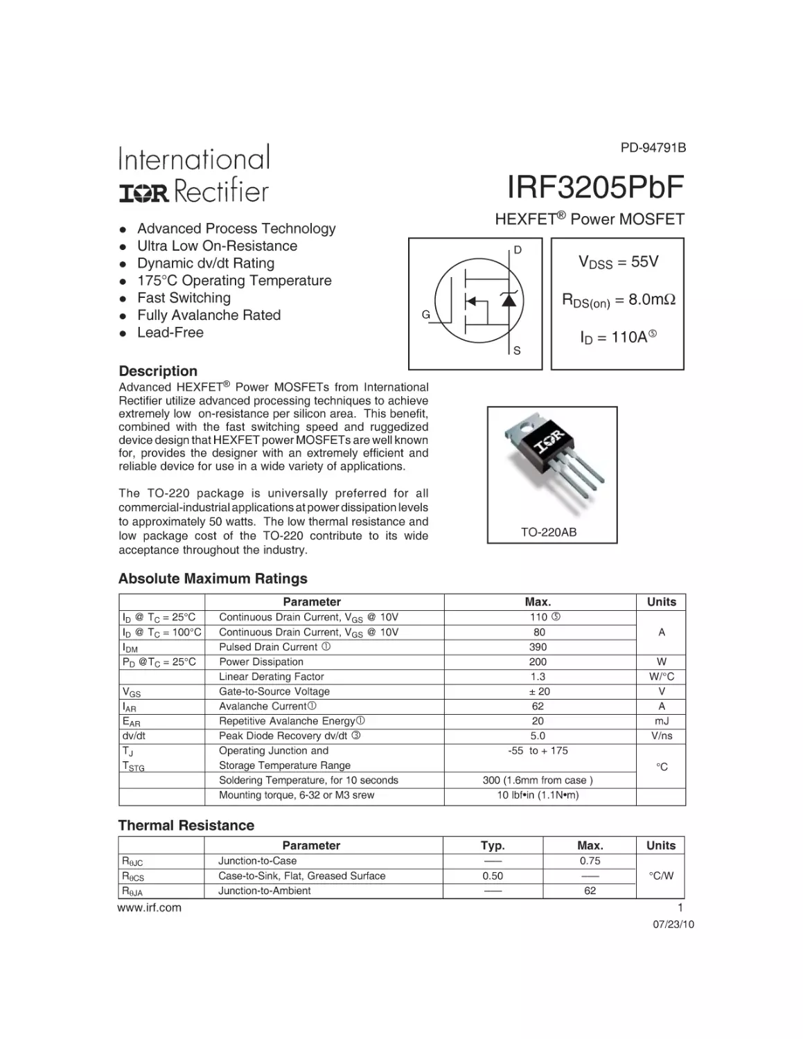
HEXFET® Power MOSFET
D
VDSS = 55V
RDS(on) = 8.0mΩ
G
ID = 110A
S
Description
Advanced HEXFET® Power MOSFETs from International
Rectifier utilize advanced processing techniques to achieve
extremely low on-resistance per silicon area. This benefit,
combined with the fast switching speed and ruggedized
device design that HEXFET power MOSFETs are well known
for, provides the designer with an extremely efficient and
reliable device for use in a wide variety of applications.
The TO-220 package is universally preferred for all
commercial-industrial applications at power dissipation levels
to approximately 50 watts. The low thermal resistance and
low package cost of the TO-220 contribute to its wide
acceptance throughout the industry.
TO-220AB
Absolute Maximum Ratings
Parameter
ID @ TC = 25°C
ID @ TC = 100°C
IDM
PD @TC = 25°C
VGS
IAR
EAR
dv/dt
TJ
TSTG
Continuous Drain Current, VGS @ 10V
Continuous Drain Current, VGS @ 10V
Pulsed Drain Current
Power Dissipation
Linear Derating Factor
Gate-to-Source Voltage
Avalanche Current
Repetitive Avalanche Energy
Peak Diode Recovery dv/dt
Operating Junction and
Storage Temperature Range
Soldering Temperature, for 10 seconds
Mounting torque, 6-32 or M3 srew
Max.
Units
110
80
390
200
1.3
± 20
62
20
5.0
-55 to + 175
A
W
W/°C
V
A
mJ
V/ns
°C
300 (1.6mm from case )
10 lbf•in (1.1N•m)
Thermal Resistance
Parameter
RθJC
RθCS
RθJA
www.irf.com
Junction-to-Case
Case-to-Sink, Flat, Greased Surface
Junction-to-Ambient
Typ.
Max.
Units
–––
0.50
–––
0.75
–––
62
°C/W
1
07/23/10
IRF3205PbF
Electrical Characteristics @ TJ = 25°C (unless otherwise specified)
RDS(on)
VGS(th)
gfs
Parameter
Drain-to-Source Breakdown Voltage
Breakdown Voltage Temp. Coefficient
Static Drain-to-Source On-Resistance
Gate Threshold Voltage
Forward Transconductance
Qg
Qgs
Qgd
td(on)
tr
td(off)
tf
Gate-to-Source Forward Leakage
Gate-to-Source Reverse Leakage
Total Gate Charge
Gate-to-Source Charge
Gate-to-Drain ("Miller") Charge
Turn-On Delay Time
Rise Time
Turn-Off Delay Time
Fall Time
Min.
55
–––
–––
2.0
44
–––
–––
–––
–––
–––
–––
–––
–––
–––
–––
–––
IDSS
Drain-to-Source Leakage Current
LD
Internal Drain Inductance
–––
LS
Internal Source Inductance
–––
Ciss
Coss
Crss
EAS
Input Capacitance
Output Capacitance
Reverse Transfer Capacitance
Single Pulse Avalanche Energy
–––
–––
–––
–––
V(BR)DSS
∆V(BR)DSS/∆TJ
IGSS
Typ.
–––
0.057
–––
–––
–––
–––
–––
–––
–––
–––
–––
–––
14
101
50
65
Max. Units
Conditions
–––
V
VGS = 0V, ID = 250µA
––– V/°C Reference to 25°C, ID = 1mA
8.0
mΩ VGS = 10V, ID = 62A
4.0
V
VDS = VGS, ID = 250µA
–––
S
VDS = 25V, ID = 62A
25
VDS = 55V, VGS = 0V
µA
250
VDS = 44V, VGS = 0V, TJ = 150°C
100
VGS = 20V
nA
-100
VGS = -20V
146
ID = 62A
35
nC
VDS = 44V
54
VGS = 10V, See Fig. 6 and 13
–––
VDD = 28V
–––
ID = 62A
ns
–––
RG = 4.5Ω
–––
VGS = 10V, See Fig. 10
Between lead,
4.5 –––
6mm (0.25in.)
nH
G
from package
7.5 –––
and center of die contact
3247 –––
VGS = 0V
781 –––
VDS = 25V
211 –––
pF
ƒ = 1.0MHz, See Fig. 5
1050 264 mJ IAS = 62A, L = 138µH
D
S
Source-Drain Ratings and Characteristics
IS
ISM
VSD
trr
Qrr
ton
Parameter
Continuous Source Current
(Body Diode)
Pulsed Source Current
(Body Diode)
Diode Forward Voltage
Reverse Recovery Time
Reverse Recovery Charge
Forward Turn-On Time
Min. Typ. Max. Units
Conditions
D
MOSFET symbol
––– ––– 110
showing the
A
G
integral reverse
––– ––– 390
S
p-n junction diode.
––– ––– 1.3
V
TJ = 25°C, IS = 62A, VGS = 0V
––– 69 104
ns
TJ = 25°C, IF = 62A
––– 143 215
nC
di/dt = 100A/µs
Intrinsic turn-on time is negligible (turn-on is dominated by LS+LD)
Notes:
Repetitive rating; pulse width limited by
max. junction temperature. ( See fig. 11 )
Starting TJ = 25°C, L = 138µH
RG = 25Ω, IAS = 62A. (See Figure 12)
ISD ≤ 62A, di/dt ≤ 207A/µs, VDD ≤ V(BR)DSS,
TJ ≤ 175°C
2
Pulse width ≤ 400µs; duty cycle ≤ 2%.
Calculated continuous current based on maximum allowable
junction temperature. Package limitation current is 75A.
This is a typical value at device destruction and represents
operation outside rated limits.
This is a calculated value limited to TJ = 175°C.
www.irf.com
IRF3205PbF
1000
1000
VGS
15V
10V
8.0V
7.0V
6.0V
5.5V
5.0V
BOTTOM 4.5V
I D , Drain-to-Source Current (A)
I D , Drain-to-Source Current (A)
100
100
10
4.5V
1
10
10
20µs PULSE WIDTH
TJ = 175 °C
1
0.1
100
1
10
100
VDS , Drain-to-Source Voltage (V)
VDS , Drain-to-Source Voltage (V)
Fig 1. Typical Output Characteristics
Fig 2. Typical Output Characteristics
RDS(on) , Drain-to-Source On Resistance
(Normalized)
1000
I D , Drain-to-Source Current (A)
4.5V
20µs PULSE WIDTH
TJ = 25 °C
1
0.1
VGS
15V
10V
8.0V
7.0V
6.0V
5.5V
5.0V
BOTTOM 4.5V
TOP
TOP
TJ = 25 ° C
TJ = 175° C
100
10
1
V DS= 25V
20µs PULSE WIDTH
4
6
8
10
VGS , Gate-to-Source Voltage (V)
Fig 3. Typical Transfer Characteristics
www.irf.com
12
2.5
ID = 107A
2.0
1.5
1.0
0.5
0.0
-60 -40 -20 0
VGS = 10V
20 40 60 80 100 120 140 160 180
TJ , Junction Temperature ( ° C)
Fig 4. Normalized On-Resistance
Vs. Temperature
3
IRF3205PbF
VGS = 0V, f = 1 MHZ
Ciss = Cgs + Cgd, Cds SHORTED
Crss = Cgd
5000
C, Capacitance(pF)
Coss = Cds + Cgd
4000
Ciss
3000
2000
Coss
1000
Crss
16
VGS , Gate-to-Source Voltage (V)
6000
0
10
12
10
8
6
4
2
100
0
Fig 5. Typical Capacitance Vs.
Drain-to-Source Voltage
ISD , Reverse Drain Current (A)
40
60
80
100
120
Fig 6. Typical Gate Charge Vs.
Gate-to-Source Voltage
1000
10000
OPERATION IN THIS AREA LIMITED
BY RDS(on)
TJ = 175° C
100
ID , Drain Current (A)
1000
10
10us
100
TJ = 25 ° C
1
V GS = 0 V
0.8
1.4
2.0
VSD ,Source-to-Drain Voltage (V)
Fig 7. Typical Source-Drain Diode
Forward Voltage
4
20
QG , Total Gate Charge (nC)
VDS, Drain-to-Source Voltage (V)
0.1
0.2
V DS= 44V
V DS= 27V
V DS= 11V
14
0
1
ID = 62A
2.6
100us
1ms
10
1
10ms
TC = 25 °C
TJ = 175 °C
Single Pulse
1
10
100
1000
VDS , Drain-to-Source Voltage (V)
Fig 8. Maximum Safe Operating Area
www.irf.com
IRF3205PbF
LIMITED BY PACKAGE
VGS
100
ID , Drain Current (A)
RD
V DS
120
D.U.T.
RG
+
V
DD
-
80
10V
Pulse Width ≤ 1 µs
Duty Factor ≤ 0.1 %
60
Fig 10a. Switching Time Test Circuit
40
VDS
90%
20
0
25
50
75
100
125
150
TC , Case Temperature ( ° C)
175
10%
VGS
td(on)
Fig 9. Maximum Drain Current Vs.
Case Temperature
tr
t d(off)
tf
Fig 10b. Switching Time Waveforms
Thermal Response(Z thJC )
1
D = 0.50
0.20
0.1
0.10
PDM
0.05
0.02
0.01
0.01
0.00001
t1
SINGLE PULSE
(THERMAL RESPONSE)
t2
Notes:
1. Duty factor D = t 1 / t 2
2. Peak TJ = P DM x Z thJC + TC
0.0001
0.001
0.01
0.1
1
t1 , Rectangular Pulse Duration (sec)
Fig 11. Maximum Effective Transient Thermal Impedance, Junction-to-Case
www.irf.com
5
15V
L
VDS
DRIVER
D.U.T
RG
+
- VDD
IAS
20V
0.01Ω
tp
Fig 12a. Unclamped Inductive Test Circuit
V(BR)DSS
tp
A
EAS , Single Pulse Avalanche Energy (mJ)
IRF3205PbF
500
ID
25A
44A
BOTTOM 62A
TOP
400
300
200
100
0
25
50
75
100
125
150
175
Starting T J, Junction Temperature ( ° C)
Fig 12c. Maximum Avalanche Energy
Vs. Drain Current
I AS
Fig 12b. Unclamped Inductive Waveforms
Current Regulator
Same Type as D.U.T.
50KΩ
QG
12V
.2µF
.3µF
10 V
QGS
D.U.T.
QGD
+
V
- DS
VGS
VG
3mA
Charge
Fig 13a. Basic Gate Charge Waveform
6
IG
ID
Current Sampling Resistors
Fig 13b. Gate Charge Test Circuit
www.irf.com
IRF3205PbF
Peak Diode Recovery dv/dt Test Circuit
+
D.U.T
Circuit Layout Considerations
• Low Stray Inductance
• Ground Plane
• Low Leakage Inductance
Current Transformer
+
-
-
+
RG
•
•
•
•
Driver Gate Drive
P.W.
+
dv/dt controlled by RG
Driver same type as D.U.T.
ISD controlled by Duty Factor "D"
D.U.T. - Device Under Test
Period
D=
-
VDD
P.W.
Period
VGS=10V
*
D.U.T. ISD Waveform
Reverse
Recovery
Current
Body Diode Forward
Current
di/dt
D.U.T. VDS Waveform
Diode Recovery
dv/dt
Re-Applied
Voltage
Body Diode
VDD
Forward Drop
Inductor Curent
Ripple ≤ 5%
ISD
* VGS = 5V for Logic Level Devices
Fig 14. For N-Channel HEXFETS
www.irf.com
7
IRF3205PbF
TO-220AB Package Outline
Dimensions are shown in millimeters (inches)
TO-220AB Part Marking Information
EXAMPLE: T HIS IS AN IRF1010
LOT CODE 1789
ASS EMBLED ON WW 19, 2000
IN T HE AS S EMBLY LINE "C"
Note: "P" in assembly line position
indicates "Lead - Free"
INT ERNAT IONAL
RECT IFIER
LOGO
AS SEMBLY
LOT CODE
PART NUMBER
DAT E CODE
YEAR 0 = 2000
WEEK 19
LINE C
TO-220AB package is not recommended for Surface Mount Application
Notes:
1. For an Automotive Qualified version of this part please seehttp://www.irf.com/product-info/auto/
2. For the most current drawing please refer to IR website at http://www.irf.com/package/
Data and specifications subject to change without notice.
This product has been designed and qualified for the Industrial market.
Qualification Standards can be found on IR’s Web site.
IR WORLD HEADQUARTERS: 233 Kansas St., El Segundo, California 90245, USA Tel: (310) 252-7105
TAC Fax: (310) 252-7903
Visit us at www.irf.com for sales contact information.07/2010
8
www.irf.com
IMPORTANT NOTICE
The information given in this document shall in no
event be regarded as a guarantee of conditions or
characteristics (“Beschaffenheitsgarantie”) .
With respect to any examples, hints or any typical
values stated herein and/or any information
regarding the application of the product, Infineon
Technologies hereby disclaims any and all
warranties and liabilities of any kind, including
without limitation warranties of non-infringement
of intellectual property rights of any third party.
In addition, any information given in this document
is subject to customer’s compliance with its
obligations stated in this document and any
applicable legal requirements, norms and
standards concerning customer’s products and any
use of the product of Infineon Technologies in
customer’s applications.
The data contained in this document is exclusively
intended for technically trained staff. It is the
responsibility of customer’s technical departments
to evaluate the suitability of the product for the
intended application and the completeness of the
product information given in this document with
respect to such application.
For further information on the product, technology,
delivery terms and conditions and prices please
contact your nearest Infineon Technologies office
(www.infineon.com).
WARNINGS
Due to technical requirements products may
contain dangerous substances. For information on
the types in question please contact your nearest
Infineon Technologies office.
Except as otherwise explicitly approved by Infineon
Technologies in a written document signed by
authorized
representatives
of
Infineon
Technologies, Infineon Technologies’ products may
not be used in any applications where a failure of
the product or any consequences of the use thereof
can reasonably be expected to result in personal
injury.